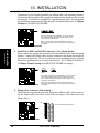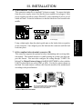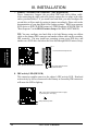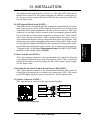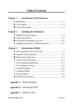
1
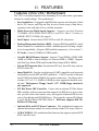
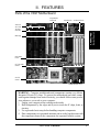
VX97 USER'S MANUAL
User's Notice
No part of this product, including the product and software may be reproduced,
transmitted, transcribed, stored in a retrieval system, or translated into any language
in any form by any means without the express written permission of ASUSTeK
COMPUTER INC. (hereinafter referred to as ASUS) except documentation kept by
the purchaser for backup purposes.
ASUS provides this manual "as is" without warranty of any kind, either express or
implied, including but not limited to the implied warranties or conditions of merchantability or fitness for a particular purpose. In no event shall ASUS be liable for any loss
or profits, loss of business, loss of use or data, interruption of business, or for indirect,
special, incidental, or consequential damages of any kind, even if ASUS has been
advised of the possibility of such damages arising from any defect or error in this
manual or product. ASUS may revise this manual from time to time without notice.
Products mentioned in this manual are mentioned for identification purposes only.
Product names appearing in this manual may or may not be registered trademarks or
copyrights of their respective companies.
The product name and revision number are both printed on the board itself. Manual
revisions are released for each board design represented by the digit before and after
the period of the manual revision number. Manual updates are represented by the
third digit in the manual revision number.
© Copyright 1997 ASUSTeK COMPUTER INC. All rights reserved.
Product Name:
VX97
Manual Revision: 1.01
Release Date:
January 1997
VX97 User’s Manual
1
FCC & DOC COMPLIANCE
Federal Communications Commission Statement
This device complies with FCC Rules Part 15. Operation is subject to the following
two conditions:
•
•
This device may not cause harmful interference, and
This device must accept any interference received, including interference that
may cause undesired operation.
This equipment has been tested and found to comply with the limits for a Class B
digital device, pursuant to Part 15 of the FCC Rules. These limits are designed to
provide reasonable protection against harmful interference in a residential installation. This equipment generates, uses and can radiate radio frequency energy and, if
not installed and used in accordance with manufacturer's instructions, may cause
harmful interference to radio communications. However, there is no guarantee that
interference will not occur in a particular installation. If this equipment does cause
harmful interference to radio or television reception, which can be determined by
turning the equipment off and on, the user is encouraged to try to correct the interference by one or more of the following measures:
•
•
•
•
Re-orient or relocate the receiving antenna.
Increase the separation between the equipment and receiver.
Connect the equipment to an outlet on a circuit different from that to which the
receiver is connected.
Consult the dealer or an experienced radio/TV technician for help.
WARNING: The use of shielded cables for connection of the monitor to the graphics card is required to assure compliance with FCC regulations. Changes or modifications to this unit not expressly approved by the party responsible for compliance
could void the user's authority to operate this equipment.
Canadian Department of Communications Statement
This digital apparatus does not exceed the Class B limits for radio noise emissions
from digital apparatus set out in the Radio Interference Regulations of the Canadian
Department of Communications.
2
VX97 User’s Manual
I. INTRODUCTION
I. INTRODUCTION
(Manual / Checklist)
How this manual is organized
This manual is divided into the following sections:
I.
II.
III.
IV.
V.
Introduction:
Features:
Installation:
BIOS Setup:
DMI Utility:
Manual information and checklist
Information and specifications concerning this product
Instructions on setting up the motherboard.
BIOS software setup information.
BIOS supported Desktop Management Interface
Item Checklist
Please check that your package is complete. If you discover damaged or missing
items, please contact your retailer.
√
The VX97 motherboard
√
2 serial port ribbon cables attached to a mounting bracket
√
1 parallel ribbon cable with mounting bracket
√
1 IDE ribbon cable
√
1 floppy ribbon cable
√
Support drivers and utilities as follows (view FILELIST.TXT for details)
• Flash Memory Writer utility to update the FLASH BIOS
• Desktop Management Interface (DMI) utility
• Bus Master IDE Drivers for various operating systems
• Readme files for descriptions and use of the files
√
This user's manual
Optional PS/2 mouse cable with mounting bracket
Optional infrared module
VX97 User’s Manual
3
II. FEATURES
Features of the VX97 Motherboard
The VX97 is carefully designed for the demanding PC user who wants a great many
features in a small package. This motherboard:
• Easy Installation: Is equipped with BIOS that supports auto detection of hard
drives, PS/2 mouse, and Plug and Play devices to make setup of hard drives,
expansion cards, and other devices virtually automatic.
II. FEATURES
(Features)
4
•
Multi-Processor/Multi-Speed Support: Supports one Intel Pentium
75-200MHz (P55C-MMX, P54C/P54CS), Cyrix P166+ (Rev 2.7 or later), or
AMD-K5 (PR75-133MHz) (See page 8).
•
Intel Chipset: Features Intel's 430VX PCIset with I/O subsystems.
•
Desktop Management Interface (DMI): Supports DMI through BIOS which
allows hardware to communicate within a standard protocol creating a higher
level of compatibility. (Requires DMI-enabled components.) (See section V)
•
L2 Cache: Comes in 256KB or 512KB models.
•
Versatile DRAM Memory Support: Supports 72-pin SIMMs of 4MB, 8MB,
16MB, or 32MB to form a memory size between 8MB to 128MB. Supports
both Fast Page Mode (FPM) and Extended Data Output (EDO) SIMMs.
•
ISA and PCI Expansion Slots: Provides three PCI slots, three ISA slots, and one
PCI/ISA share slot.
•
Super Multi-I/O: Provides two high-speed UART compatible serial ports and
one parallel port with EPP and ECP capabilities. UART2 can also be directed
from COM2 to the Infrared Module for wireless connections. Two floppy drives
of either 5.25" or 3.5" (1.44MB or 2.88MB) are also supported without an external card. The Japanese "Floppy 3 mode" (3.5" 1.2MB) floppy standard is
also supported.
•
PCI Bus Master IDE Controller: Comes with an onboard PCI Bus Master
IDE controller with two connectors that supports four IDE devices in two channels, provides faster data transfer rates, and supports Enhanced IDE devices
such as Tape Backup and CD-ROM drives. This controller supports PIO Modes
3 and 4 and Bus Master IDE DMA Mode 2. BIOS now supports IDE CDROM or SCSI bootup.
•
Optional IrDA and PS/2 Mouse Connector: This motherboard supports an
optional infrared port module for wireless interface and a PS/2 mouse cable set.
•
NCR SCSI BIOS: This motherboard has firmware that supports optional NCR
SCSI controller cards.
VX97 User’s Manual
II. FEATURES
Parts of the VX97 Motherboard
Programmable
Flash ROM
Super Multi-I/O Serial/Parallel Ports
II. FEATURES
(Parts of Board)
3 ISA Slots
3 PCI Slots
1 PCI/ISA
Share Slot
IDE/Floppy
Intel's 430VX
PCIset
(4) 72-pin SIMM
Sockets
CPU ZIF
Socket 7
256KB/ 512KB L2 Cache
WARNING: Computer motheboards and components contain very delicate
Integrated Circuit (IC) chips. To protect the motherboard and other components against damage from static electricity, you should follow some precautions whenever you work on your computer.
1. Unplug your computer when working on the inside.
2. Hold components by the edges and try not to touch the IC chips, leads, or
circuitry.
3. Use a grounded wrist strap before handling computer components.
4. Place components on a grounded antistatic pad or on the bag that came with
the component whenever the components are separated from the system.
VX97 User’s Manual
5
III. INSTALLATION
Map of the VX97 Motherboard
PS/2 Mouse
Universal Serial
Bus (Reserved)
Keyboard
Keyboard BIOS
Serial Ports
Flash ROM for BIOS
ISA Slot 1
COM 2
Parallel Port (Printer)
Board Power Input
P9
P8
SIMM Socket 4 (Bank 1)
SIMM Socket 3 (Bank 1)
SIMM Socket 2 (Bank 0)
SIMM Socket 1 (Bank 0)
Secondary IDE
Primary IDE
Floppy Drives
PCI Slot 1
III. INSTALLATION
(Map of Board)
Intel PIIX3
PCIset
BBLKW
PCI Slot 2
PCI Slot 3
PCI Slot 4
ISA Slot 2
ISA Slot 3
ISA Slot 4
COM 1
Block Program (Dis/En)
Intel 430VX
PCIset
BUS FREQ
FS0
FS1
FS2
CPU ZIF Socket 7
RTC Clear
CR2032
3V Lithium Cell
(RTC RAM
Memory)
CPU Voltage ID
BUS Ratio
VID2
VID1
BF0
VID0
BF1
IDE LED
Infrared Con.
Panel Connections
256/512KB OnBoard L2 Cache
System Memory (SIMM)
Install memory in any or all of the banks in any combination as follows:
Bank
Bank 0
SIMM Sockets 1&2
Bank 1
SIMM Sockets 3&4
Memory Module
4MB, 8MB, 16MB, 32MB
72-pin FPM or EDO SIMM
4MB, 8MB, 16MB, 32MB
72-pin FPM or EDO SIMM
Total System Memory (Max 128MB)
Total Memory
x2
x2
=
IMPORTANT: Banks 0 & 1 must have the same size memory installed in pairs.
Do not use memory modules with more than 24 chips per module. Modules with
more than 24 chips exceed the design specifications of the memory subsystem and
will be unstable. Memory speed setup is required through "Auto Configuration"
in BIOS Chipset Setup of the BIOS SOFTWARE.
6
VX97 User’s Manual
III. INSTALLATION
Jumpers
1. Flash ROM Boot Block Programming (BBLKW)
This sets the operation mode of the boot block area of the Programmable Flash
ROM to allow programming in the Enabled position. This is required only if
prompted by the Flash Memory Writer Utility as shown in BIOS SOFTWARE.
BBLKW
1
2
3
BBLKW
1
2
3
Disabled / Protected
(Default)
Enabled
Boot Block Programming (Disable / Enable)
Operation (Default)
III. INSTALLATION
(Jumpers)
2. Real Time Clock (RTC) RAM
This clears the user-entered information stored in the CMOS RAM of the Real
Time Clock such as hard disk information and passwords. To clear the RTC
data: (1) Turn off the PC, (2) Short this jumper, (3) Power on the PC, (4) Turn
off the PC, (5) Remove this jumper, (6) Power on the PC, (7) Hold down
<Delete> during bootup and enter BIOS setup to re-enter user preferences.
Clear Data
RTC RAM (Operation / Clear Data)
3. Voltage Regulator Output Selection (VID0, VID1, VID2)
Intel P54C Pentium Intel P55C Pentium AMD-K5
MMX (200MHz) (PR75-133MHz)
(75-200MHz)
Cyrix 6x86 166+
Rev2.7 (133MHz)
3 2 1
3 2 1
3 2 1
3 2 1
3 2 1
3 2 1
2.5V
AMD3
2.7V
AMD1
2.8V
P55C
2.9V
AMD2
3.4V
STD
3.5V
VRE
VID2
VID1
VID0
Voltage Regulator Output Selection
VX97 User’s Manual
7
III. INSTALLATION
4. CPU External (BUS) Frequency Selection (FS0, FS1, FS2)
These jumpers tell the clock generator what frequency to send to the CPU. These
allow the selection of the CPU’s External frequency (or BUS Clock). The BUS Clock
times the BUS Ratio equals the CPU's Internal frequency (the advertised CPU speed).
5. CPU to BUS Frequency Ratio (BF0, BF1)
These jumpers set the frequency ratio between the Internal frequency of the CPU
and the External frequency (called the BUS Clock) within the CPU. These must
be set together with the above jumpers CPU External (BUS) Frequency Selection.
FS0
FS1
FS2
FS0
FS1
FS2
FS0
FS1
FS2
FS0
FS1
FS2
1
2
3
1
2
3
1
2
3
1
2
3
50MHz
55MHz
60MHz
66MHz
CPU External Clock (BUS) Frequency Selection
BF0
BF1
BF0
BF1
BF0
BF1
BF0
BF1
III. INSTALLATION
(Jumpers)
Intel
Cyrix
2.5x (5/2)
1.5x (3/2) 2.0x(2/1)
3.0x (3/1) 2.0x(2/1)
1.0x (1/1)
CPU : BUS Frequency Ratio
3.0x (3/1)
4.0x (4/1)
Set the jumpers by the Internal speed of the Intel, AMD, or Cyrix CPU as follows:
CPU Model
Intel Pentium
Intel Pentium
Intel Pentium
Intel Pentium
Intel Pentium
Intel Pentium
Intel Pentium
Intel Pentium
Freq.
200MHz
166MHz
150MHz
133MHz
120MHz
100MHz
90MHz
75MHz
Ratio
3.0x
2.5x
2.5x
2.0x
2.0x
1.5x
1.5x
1.5x
BUS Freq.
66MHz
66MHz
60MHz
66MHz
60MHz
66MHz
60MHz
50MHz
(BUS Freq.)
FS2 FS1 FS0
[2-3] [1-2] [2-3]
[2-3] [1-2] [2-3]
[2-3] [2-3] [1-2]
[2-3] [1-2] [2-3]
[2-3] [2-3] [1-2]
[2-3] [1-2] [2-3]
[2-3] [2-3] [1-2]
[2-3] [2-3] [2-3]
AMD-K5-PR133
AMD-K5-PR120
AMD-K5-PR100
AMD-K5-PR90
AMD-K5-PR75
100MHz
90MHz
100MHz
90MHz
75MHz
1.5x
1.5x
1.5x
1.5x
1.5x
66MHz
60MHz
66MHz
60MHz
50MHz
[2-3]
[2-3]
[2-3]
[2-3]
[2-3]
*Cyrix 166+
133MHz
2.0x
66MHz
[2-3] [1-2] [2-3]
[1-2]
[2-3]
[1-2]
[2-3]
[2-3]
[2-3]
[1-2]
[2-3]
[1-2]
[2-3]
(Freq. Ratio)
BF1 BF0
[2-3] [1-2]
[2-3] [2-3]
[2-3] [2-3]
[1-2] [2-3]
[1-2] [2-3]
[1-2] [1-2]
[1-2] [1-2]
[1-2] [1-2]
[1-2]
[1-2]
[1-2]
[1-2]
[1-2]
[1-2]
[1-2]
[1-2]
[1-2]
[1-2]
[1-2] [2-3]
*NOTE: Only Cyrix Revision 2.7 or later is supported on this motherboard. See previous page for
revision identification. Bootup screen will show 6x86-P166+ -S CPU at 133MHz with the
Cyrix 166+ installed on this motherboard.
Compatible Cyrix CPU Identification
The only Cyrix CPU that is supported on this motherboard is
labeled Cyrix 6x86 P166+ but must be Revision 2.7 and later.
Look on the underside of the CPU for the serial number. The
number should read G8DC6620A or larger.
8
VX97 User’s Manual
III. INSTALLATION
External Connectors
WARNING: Some pins are used for connectors or power sources. These are
clearly separated from jumpers in "Map of the Motherboard". Placing jumper
caps over these will cause damage to your motherboard.
IMPORTANT: Ribbon cables should always be connected with the red stripe on
the Pin 1 side of the connector. The four corners of the connectors are labeled on
the motherboard. Pin 1 is the side closest to the power connector on hard drives
and floppy drives. IDE ribbon cable must be less than 18in. (46cm), with the
second drive connector no more than 6in. (15cm) from the first connector.
III. INSTALLATION
(Connectors)
1. Keyboard Connector (5-pin female)
This connection is for a standard IBM-compatible keyboard. May also be known
as a 101 enhanced keyboard.
Keyboard Connector (5-pin female)
This motherboard accepts an AT Keyboard
Connector Plug as shown here.
Keyboard Connector
2. PS/2 Mouse Connector (6-pin block)
If you are using a PS/2 mouse, you must purchase an optional PS/2 mouse set
which connects to the 6 pin block and mounts to an open slot on your computer's
case. The system will direct IRQ12 to the PS/2 mouse if one is detected. If not
detected, expansion cards can use IRQ12. Use “PS/2 Mouse Control” in BIOS
Features Setup of the BIOS SOFTWARE for settings.
1 234
1: GND
(Motherboard) 2: DATA
3: NC
5 8
4: VCC
2
3
1 4
5: CLK
(Cable Set)
8: NC
5 8
This optional PS/2 mouse cable
and bracket set is necessary to
provide a connector for a PS/2
mouse on a free expansion slot
cover.
PS/2 Mouse Module Connector
VX97 User’s Manual
9
III. INSTALLATION
3. Parallel Printer Connector (26 Pin Block)
Connection for the included parallel port ribbon cable with mounting bracket.
Connect the ribbon cable to this connection and mount the bracket to the case on
an open slot. It will then be available for a parallel printer cable. You can enable
the parallel port and choose the IRQ through "Onboard Parallel Port" in Chipset
Features of the BIOS SOFTWARE.
Pin 1
For this connector to be available, you must connect
the included Parallel (25-Pin female) cable set to a
free expansion slot opening.
TIP: You may also remove the bracket connectors
and mount them directly to the case to save expansion
slot space.
Parallel (Printer) Connector
III. INSTALLATION
(Connectors)
4. Serial Port COM1 and COM2 Connectors (Two 10-pin blocks)
These connectors support the provided serial port ribbon cables with mounting
bracket. Connect the ribbon cables to these connectors and mount the bracket to
the case on an open slot. The two serial ports on the mounting bracket will then
be used for pointing devices or other serial devices. See "Onboard Serial Port"
in Chipset Features Setup of the BIOS SOFTWARE for settings.
COM 1
COM 2
Pin 1
Pin 1
For these connectors to be available, you must connect
the included Serial cable set from COM1 (using the
9-Pin male) & COM2 (using the 25-Pin male) to a free
expansion slot opening.
TIP: You may also remove the bracket connectors
and mount them directly to the case to save expansion
slot space.
Serial Port Connectors
5. Floppy drive connector (34-pin block )
This connector supports the provided floppy drive ribbon cable. After connecting the single end to the board, connect the two plugs on the other end to the
floppy drives.
Pin 1
Connect the Red stripe to Pin 1
Floppy Drive Connector
10
VX97 User’s Manual
III. INSTALLATION
6. Power connector (12-pin block)
This connector connects to a standard 5 Volt power supply. To connect the leads
from the power supply, ensure first that the power supply is not plugged. Most
power supplies provide two plugs (P8 and P9), each containing six wires, two of
which are black. Orient the connectors so that the black wires are located in the
middle.
RED
RED
RED
WHT
BLK
BLK
BLK
BLK
BLU
YLW
RED
ORG
+5V
GND
P9
P8
+5V -12V
Power Connector
-5V
AT Power Connector
on Motherboard
Power Plugs from
Power Supply
III. INSTALLATION
(Connectors)
PG +12V
Using a slight angle, align the plastic guide pins on the lead to their receptacles
on the connector. Once aligned, press the lead onto the connector until the lead
locks into place.
7. IrDA-compliant infrared module connector (IR)
This connector supports the optional wireless transmitting and receiving infrared module. This module mounts to a small opening on system cases that support this feature. You must also configure the setting through "UART2 Use
Infrared" in Chipset Features Setup of the BIOS SOFTWARE to select whether
UART2 is directed for use with COM2 or IrDA. Use the five pins as shown on
the Back View and connect a ribbon cable from the module to the motherboard
according to the pin definitions.
Front View
NC
GND
+5V
Back View
IRRX
IRTX
+5V
NC
IRTX
GND
For the infrared feature to be available,
you must connect an optional Infrared
module to the motherboard.
IRRX
Infrared Module Connector
VX97 User’s Manual
11
III. INSTALLATION
7. Primary / Secondary IDE connectors (Two 40-pin Block)
These connectors support the provided IDE hard disk ribbon cable.
After connecting the single end to the board, connect the two plugs at the other
end to your hard disk(s). If you install two hard disks, you must configure the
second drive to Slave mode by setting its jumper accordingly. Please refer to the
documentation of your hard disk for the jumper settings. BIOS now supports
SCSI device or IDE CD-ROM bootup (see "HDD Sequence SCSI/IDE First" &
"Boot Sequence" in the BIOS Features Setup of the BIOS SOFTWARE).
TIP: You may configure two hard disks to be both Masters using one ribbon
cable on the primary IDE connector and another ribbon cable on the secondary
IDE connector. You may install one operating system on an IDE drive and
another on a SCSI drive and select the boot disk through BIOS Features Setup.
Pin 1
III. INSTALLATION
(Connectors)
Connect the Red stripe to Pin 1
IDE (Hard Drive) Connectors
Secondary IDE Connector
Primary IDE Connector
8. IDE activity LED (IDE LED)
This connector supplies power to the cabinet’s IDE activity LED. Read and
write activity by devices connected to the Primary or Secondary IDE connectors
will cause the LED to light up.
+
TIP: If the case-mounted LED does not light,
try reversing the 2-Pin plug.
IDE (Hard Drive) LED
Hard Drive LED Lead
12
VX97 User’s Manual
III. INSTALLATION
9. Turbo LED Lead (PANEL)
The motherboard's turbo function is always on. The turbo LED connection is
labeled here but the LED will remain constantly lit while the system power is
on. You may wish to connect the Power LED from the system case to this lead.
See the figure below.
III. INSTALLATION
(Connectors)
10. SMI Suspend Switch Lead (PANEL)
This allows the user to manually place the system into a suspend mode or "Green"
mode where system activity will be instantly decreased to save electricity and
expand the life of certain components when the system is not in use. This 2-pin
connector (see the figure below) connects to the case-mounted suspend switch.
If you do not have a switch for the connector, you may use the "Turbo Switch"
since it does not have a function. SMI is activated when it detects a short to
open moment and therefore leaving it shorted will not cause any problems. May
require one or two pushes depending on the position of the switch. Wake-up can
be controlled by settings in the BIOS but the keyboard will always allow wakeup (the SMI lead cannot wake-up the system). If you want to use this connector,
"Suspend Switch" in the Power Management Setup of the BIOS SOFTWARE
should be on the default setting of Enable.
11. Reset Switch Lead (PANEL)
This 2-pin connector connects to the case-mounted reset switch for rebooting
your computer without having to turn off your power switch This is a preferred
method of rebooting in order to prolong the life of the system's power supply.
See the figure below.
12. Keyboard Lock Switch Lead & System Power LED (PANEL)
This 5-pin connector connects to the case-mounted keyboard lock switch for
locking the keyboard and also to connect the system power LED. The system
power LED lights when the system is powered on. See the figure below.
13. Speaker Connector (PANEL)
This 4-pin connector connects to the case-mounted speaker.
Turbo or
Power LED
SMI Lead
Reset SW
GND
+5V
NC
GND
LOCK
GND
GND
+5V
GND
GND
SPKR
+5V
GND
Power LED &
Keyboard Lock
Speaker
Connector
System Panel Connectors
VX97 User’s Manual
13
III. INSTALLATION
Power Connection Procedures
1. After all jumpers and connections are made, close the system case cover.
2. Make sure that all switches are in the off position as marked by
.
3. Connect the power supply cord into the power supply located on the back of
your system case as instructed by your system user's manual.
4. Connect all power cords into a power strip that is equipped by a surge protector.
5. You may then turn on your devices in the following order:
a. Your monitor
b. External SCSI devices (starting with the last device on the chain)
c. Your system power
III. INSTALLATION
(Power Connections)
6. The power LED on the front panel of the system case will light and the monitor
LED as well. The system will then run power-on tests. While the tests are
running, additional messages will appear on the screen. If you do not see anything within 30 seconds from the time you turn on the power, the system may
have failed a power-on test. Recheck your jumper settings and connections or
call your authorized dealer for assistance.
7. During power-on, hold down the <Delete> key to enter BIOS setup. Follow the
next section "BIOS SOFTWARE" for instructions.
14
VX97 User’s Manual
IV. BIOS SOFTWARE
BIOS Setup
If you are installing the motherboard, reconfiguring your system, or you receive a
Run Setup message, you will need to enter new BIOS setup information. This section describes how to configure your system using this utility.
The BIOS ROM of the system stores the Setup utility. When you turn on the computer, the system provides you with the opportunity to run this program. This appears during the Power-On Self Test (POST). Press the <Delete> key to call up the
Setup utility. If you are a little bit late pressing the mentioned key(s), POST will
continue with its test routines, thus preventing you from calling up Setup. If you
still need to call Setup, reset the system by simultaneously pressing the <Ctrl>, <Alt>
and <Delete> keys, or by pushing the Reset button on the system case. You can also
restart by turning the system off and then back on again. But do so only if the first
two methods fail to reboot your computer.
IV. BIOS
(BIOS Setup)
When you invoke Setup, the CMOS SETUP UTILITY main program screen will
appear with the following options:
Load Defaults
The LOAD BIOS DEFAULTS option loads the minimized settings for troubleshooting. Choose LOAD SETUP DEFAULTS in order to load optimized defaults for
regular use, then continue with other custom settings that you would like. Choose
SAVE & EXIT SETUP when you are done.
A section at the bottom of the above screen displays the control keys for this screen.
Take note of these keys and their respective uses. Another section just below the
control keys section displays information on the currently highlighted item in the list.
VX97 User’s Manual
15
V. DESKTOP MANAGEMENT
Desktop Management Interface (DMI)
Introducing the DMI Configuration Utility
This motherboard supports DMI within the BIOS level and provides a DMI Configuration Utility to maintain the Management Information Format Database (MIFD).
DMI is able to auto-detect and record information pertinent to a computer’s system
such as the CPU type, CPU speed, and internal/external frequencies, and memory
size. The onboard BIOS will detect as many system information as possible and
store those collected information in a 4KB block in the motherboard’s Flash EPROM
and allow the DMI to retrieve data from this database. Unlike other BIOS software,
the BIOS on this motherboard uses the same technology implemented for Plug and
Play to allow dynamic real-time updating of DMI information versus creating a new
BIOS image file and requiring the user to update the whole BIOS. This DMI Configuration Utility also allows the system integrator or end user to add additional
information into the MIFD such as serial numbers, housing configurations, and vendor information. Those information not detected by the motherboard BIOS and has
to be manually entered through the DMI Configuration Utility and updated into the
MIFD. This DMI Configuration Utility provides the same reliability as PnP updating and will prevent the refreshing failures associated with updating the entire BIOS.
System Requirements
The DMI Configuration Utility (DMICFG.EXE) must be ran in real mode in order
for the program to run, the base memory must be at least 180K. Memory managers
like HIMEM.SYS (required by windows) must not be installed. You can boot up
from a system diskette without AUTOEXEC.BAT and CONFIG.SYS files, “REM”
HIMEM.SYS in the CONFIG.SYS, or press <F5> during bootup to bypass your
AUTOEXEC.BAT and CONFIG.SYS files.
V. DMI
(DMI Introduction)
16
VX97 User’s Manual