1
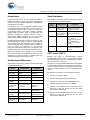
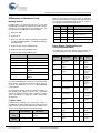
AN76348 Migrating from EZ-USB® FX2LP™ Based Design to EZ-USB FX3 Based Design Author: Rama Sai Krishna V Associated Project: No Associated Part Family: CYUSB3014 Software Version: None Related Application Notes: For a complete list of the application notes, click here. If you have a question, or need help with this application note, contact the author at [email protected] Abstract ® AN76348 tells you how to modify the top-level application to migrate an EZ-USB design based on FX2LP™ to one based on FX3™. This application note highlights the differences between FX3 and FX2LP in architecture, hardware level, and firmware framework using a bulkloop example. Contents Introduction .......................................................................2 Architectural Differences ...................................................2 Serial Interfaces ................................................................2 GPIF versus GPIF II ..........................................................2 Differences in Hardware Level ..........................................3 Booting Options ............................................................3 Crystal / Clock ..............................................................3 Power Supply Configurations and Decoupling Capacitance .................................................................3 Differences in Software Level............................................4 Development Tools ......................................................4 Applications in PC ........................................................4 FX2LP and FX3 Firmware Framework ..............................4 BulkLoop Example on FX2LP ...........................................4 Programmer’s View of FX3 ...............................................5 FX3 Firmware Stack ..........................................................6 Firmware Framework....................................................6 Firmware API Library ....................................................6 Embedded Real Time OS.............................................6 BulkLoop Example on FX3 ................................................6 Tool Chain Initialization ................................................7 Device Initialization.......................................................7 www.cypress.com Application Definition .................................................... 8 Application Code .......................................................... 8 Application Thread ....................................................... 9 Debug Initialization ....................................................... 9 Application Initialization .............................................. 10 Available Collateral ......................................................... 11 Document No. 001-76348 Rev. ** 1 Migrating from EZ-USB® FX2LP™ Based Design to EZ-USB FX3 Based Design Introduction Serial Interfaces Cypress EZ-USB FX3 is the next generation USB 3.0 peripheral controller, which provides highly integrated and flexible features that enable developers to add USB 3.0 functionality to any system. More details on the serial interfaces supported by FX2LP and FX3 are listed in the following table. EZ-USB FX3 has a fully configurable, parallel, general programmable interface called GPIF II, which can connect to an external processor, ASIC, or FPGA. The GPIF II is an enhanced version of the GPIF in FX2LP, Cypress’s flagship USB 2.0 product. GPIF II provides easy and glueless connectivity to popular interfaces, such as asynchronous SRAM, asynchronous and synchronous address data multiplexed interface, and many others. EZ-USB FX2LP based design cannot be used as it is with the EZ-USB FX3 as both of these are totally different devices. But the top level application can be modified to work with EZ-USB FX3. A simple example, bulkloop is used to explain the differences in the firmware frameworks. EZ-USB FX3 has many enhancements over EZ-USB FX2LP; later sections give more details of these. Note This application note is targeted to the customers who already worked with EZ-USB FX2LP device. So, this application note has been written by assuming that you are already familiar with the FX2LP device. Architectural Differences The following table lists the differences between EZ-USB FX3 and EZ-USB FX2LP. Feature EZ-USB FX2LP EZ-USB FX3 Core 8051 ARM926EJ CPU speed 48 MHz 200 MHz RAM 16 KB 512 KB Endpoints 7 32 serial interfaces supported I2C, UART I2C, UART, I2S, SPI Flexible programmable interfaces GPIF, 48 MHz, 8/16 – bit interface GPIF II, 100 MHz, 8/16/32 – bit interface USB USB 2.0 device USB 3.0 device, USB 2.0 OTG Speeds supported High speed, full speed Super speed, high speed, full speed GPIOs Up to 40 Up to 60 JTAG debugger interface Not available Supported. www.cypress.com Serial Interface EZ-USB FX2LP EZ-USB FX3 I2C master only at 100 and 400 kHz master only at 100 kHz, 400 kHz and 1 MHz UART supports only 115.2 K baud and 230.4 K baud range of baud rates from 300 bps to 4608 Kbps I2S not supported I2S Master as transmitter only; sampling frequencies supported by the I2S interface are 32 kHz, 44.1 kHz, and 48 kHz SPI not supported SPI Master; maximum frequency of operation is 33 MHz GPIF versus GPIF II EZ-USB FX3 offers a high-performance general programmable interface, GPIF II. This interface enables functionality similar to but more advanced than FX2LP's GPIF and Slave FIFO interfaces. The GPIF II is a programmable state machine that enables a flexible interface that may function either as a master or slave in industry standard or proprietary interfaces. Both parallel and serial interfaces may be implemented with GPIF II. The features of the GPIF II are summarized as follows: Functions as master or slave Supports 16 configurable control pins when 16 or 8 data bus is used. All control pins can be either input/output or bidirectional. Provides 256 firmware programmable states Supports 8 bit, 16 bit, and 32 bit parallel data bus Enables interface frequencies up to 100 MHz. Supports 14 configurable control pins when 32 bit data bus is used. All control pins can be either input/output or bidirectional. Document No. 001-76348 Rev. ** 2 Migrating from EZ-USB® FX2LP™ Based Design to EZ-USB FX3 Based Design Based on the clocking option that is used, the FSLC[2:0] lines can be tied to power, through a weak pull-up resistor, or to ground. The following table shows the values of FSLC[2:0] for the different clocking options. Differences in Hardware Level Booting Options 2 EZ-USB FX2LP can boot from USB and I C only. But EZ-USB FX3 can load boot images from various sources, selected by the configuration of the PMODE pins. The boot options for EZ-USB FX3 are listed as follows: Boot from USB Boot from GPIF II Async ADMUX mode FSLC[2] FSLC[1] FSLC[0] Crystal/Clock 0 0 0 19.2 MHz crystal 1 0 0 19.2 MHz input clock 1 0 1 26 MHz input clock 1 1 0 38.4 MHz input clock 1 1 1 52 MHz input clock 2 Boot from I C Boot from SPI (SPI devices supported are M25P16 (16 Mbit), M25P80 (8 Mbit), and M25P40 (4 Mbit) or their equivalents Power Supply Configurations and Decoupling Capacitance Boot from GPIF II Sync ADMUX mode The table below shows the different power domains and the voltage settings on each of these domains for FX3. Boot from GPIF II Async SRAM mode PMODE[2:0] Boot From Parameter F00 Sync ADMUX (16-bit) F01 Async ADMUX (16-bit) F11 USB boot F0F F1F Description Min (V) Max (V) VDD Core voltage supply 1.15 1.25 1.2 V typical Async SRAM (16-bit) AVDD Analog voltage supply 1.15 1.25 1.2 V typical I2C, On Failure, USB boot is enabled VIO1 GPIF II I/O power domain 1.7 3.6 1.8, 2.5 and 3.3 V typical VIO2 IO2 power domain 1.7 3.6 1.8, 2.5 and 3.3 V typical VIO3 IO3 power domain 1.7 3.6 1.8, 2.5 and 3.3 V typical VIO4 UART/SPI/I2S power domain 1.7 3.6 1.8, 2.5 and 3.3 V typical VIO5 I2C and JTAG supply domain 1.15 3.6 1.2, 1.8, 2.5 and 3.3 V typical VBATT USB voltage supply 3.2 6 3.7 V typical VBUS USB voltage supply 4.1 6 5 V typical CVDDQ Clock voltage supply 1.7 3.6 1.8, 3.3 V typical U3TXVDDQ USB3.0 1.2 V supply 1.15 1.25 1.2 V typical U3RXVDDQ USB3.0 1.2 V supply 1.15 1.25 1.2 V typical 2 1FF I C only 0F1 SPI, on Failure, USB boot is enabled. 2 If an external EEPROM is used on the I C bus for firmware image booting, 1 kΩ pull-up resistors should be placed on the SCL and SDA lines for up to 1 MHz EEPROM communication. We recommend adding pull-up and pull-down options on the PMODE [2:0] signals and load the combination needed for preferred booting option. Adding the options gives the flexibility to debug the system during early development. Crystal / Clock EZ-USB FX2LP supports only crystal input, where as EZ-USB FX3 supports external clock input along with the crystal support. The following table lists the details of the clock or crystal inputs that these two devices accept. EZ-USB FX2LP EZ-USB FX3 External clock Not supported 19.2, 26, 38.4, and 52 MHz Crystal 24MHz 19.2 MHz www.cypress.com Notes Document No. 001-76348 Rev. ** 3 Migrating from EZ-USB® FX2LP™ Based Design to EZ-USB FX3 Based Design In the case of FX2LP, we need to provide 0.1-μF ceramic capacitors to decouple device power input pins. The specific recommendation for the ceramic capacitor nearest to each EZ-USB FX3 power pin is given in the following table. Cap Value (µF) Number of Caps Pin Name 0.1, 0.01 4 of each VDD 0.1, 2.2 1 of each AVDD 0.1, 22 1 of each U3TXVDDQ 0.1, 22 1 of each U3RXVDDQ 0.1, 0.01 1 of each CVDDQ 0.1, 0.01 1 of each per supply VIO1-5 FX2LP and FX3 Firmware Framework Any of our firmware examples will be frameworks based so that you can start with one of those, or start by copying one of the examples that has been given to you. Differences in the firmware framework are explained below using the bulkloop example. Bulkloop example can be found in the location (Cypress\USB\Examples\FX2LP\Bulkloop) after installing the FX2LP DVK. BulkLoop Example on FX2LP If you look at the FX2LP’s firmware framework you will be noticing the following mentioned files: Differences in Software Level Development Tools The FX2LP firmware frameworks were written using Keil uVision2 IDE. In the case of FX3, a set of development tools is provided with the SDK, which includes the GPIF II Designer and the third party ARM software development tool provides an integrated development environment (Eclipse IDE) with compiler, linker, assembler, and JTAG debugger. You can download the FX3 SDK from the following link: http://www.cypress.com/?id=3521&rtID=119 TD_Init() is called once during the initialization of the frameworks. TD_Poll() is called repeatedly during device operation. The function should contain a state machine that implements the user's peripheral function. bulkloop.c: This source file contains initialization and task dispatch function definitions that are called from fw.c. This is where you will customize the frameworks for your specific device. In this case, for bulkloop transfers. dscr.a51: Assembly file that contains your device's custom descriptors. USBJmpTb.OBJ: Object code that contains the ISR jump table for USB and GPIF interrupts. EZUSB.LIB: The EZ-USB library is an 8051 .LIB file that implements functions that are common to many firmware projects. Typically, there is no reason to modify these functions so they are provided in library form. However, the kit includes the source code for the library in the event that you need to modify a function or if you just want to know how something is done. Details on the GPIF II designer are beyond the scope of this document. Applications in PC CyControl.exe: We have a new Control Center application that comes along with the FX3 SDK. The application can be used to program both FX2LP and FX3. Using this application we can download the code in to RAM or program the EEPROM connected to FX3 device. Streamer.exe: We have a streamer application for FX3, similar to the one we have for FX2LP. Using this application we can measure the throughput numbers for ISO and BULK streams. BulkLoop.exe: Additional to the two applications mentioned previously, we have BulkLoop application for FX3. This application can be used to test the bulkloop example. The application also has options to send different types of data to run this bulkloop test. All these applications can be found in the below mentioned path once you install the FX3 SDK in the default location: C:\Program Files\Cypress\EZUSB FX3 SDK\1.0\application\c_sharp www.cypress.com fw.c: This is the main frameworks source file. It contains main(), the task dispatcher, and the SETUP command handler. For most firmware projects, there is no need to modify this file. There are total four dispatcher functions called in the main(). They are TD_Init(), TD_Poll(), TD_Suspend(), and TD_Resume(). The bulkloop application code is implemented in the TD_Poll() function in bulkloop.c. Bulkloop is a simple application that can be tested with the help of CyConsole/Control Center and FX2LP DVK. You can see EP2 and 4 are configured as OUT EPs, EP6 and 8 are configured as IN EPs after downloading the bulkloop firmware into FX2LP DVK using CyConsole. Now you can test this example by sending some bytes of data into EP2 Document No. 001-76348 Rev. ** 4 Migrating from EZ-USB® FX2LP™ Based Design to EZ-USB FX3 Based Design and you can read the same data back from EP6. Similarly you can send some bytes to EP4 and read it back from EP8. The two other important entities that are external to the FX3 are: Programmer’s View of FX3 The FX3 comes with the easy-to-use EZ-USB tools providing a complete solution for fast application development. Cypress EZ-USB FX3 is a user programmable device and is delivered with a complete software development kit. The FX3 device can be set up to: Configure and manage USB functionality, such as charger detection, USB device/host detection, and endpoint configuration Interface to different master/slave peripherals on the GPIF interface Connect to serial peripherals (UART, SPI, GPIO, I C, 2 I S) Set up, control, and monitor data flows between the peripherals (USB, GPIF, and serial peripherals) 2 www.cypress.com Perform necessary operations, such as data inspection, data modification, header / footer information, addition/deletion USB host/device When the FX3 is connected to a USB host, it functions as a USB device. The FX3 enumerates as a super-speed, high-speed, or full-speed USB peripheral corresponding to the host type. When a USB device is connected, the FX3 plays the role of the corresponding high-speed, full-speed, or low-speed USB host. GPIF II master/slave: GPIF II is a fully configurable interface and can realize any application specific protocol. Any processor, ASIC, DSP, or FPGA can be interfaced to the FX3. FX3 bootloader or firmware configures GPIF II to support the corresponding interface. Document No. 001-76348 Rev. ** 5 Migrating from EZ-USB® FX2LP™ Based Design to EZ-USB FX3 Based Design FX3 Firmware Stack Powerful and flexible applications can be rapidly built using FX3 firmware framework and FX3 API libraries. Firmware Framework The firmware (or application) framework has all the startup and initialization code. The firmware also contains the individual drivers for the USB, GPIF, and serial interface blocks. The framework: Defines the program entry point Performs the stack setup Performs kernel initialization Provides placeholders for application thread startup code Firmware API Library The FX3 API library provides a comprehensive set of APIs to control and communicate with the FX3 hardware. These APIs provide a complete programmatic view of the FX3 hardware. c yf x a p i . a A full-fledged API library is provided in the FX3 SDK. This API is similar to EZUSB.LIB in case of FX2LP. You do not have to manually link this library to your project. The path of this library will be automatically added to your IDE during the SDK installation. cyfxapi.a and the corresponding header files provide all the APIs required for programming the different blocks of the FX3. The APIs provide for the following: Semaphores, Message Queues, Mutexes, and Timers are used for inter-thread communication and task synchronization. The framework gives hooks for the application logic to configure the device behavior and to perform data transfers through it. The application logic itself can be implemented across multiple threads and make use of all of the OS services that are used by the Cypress provided drivers. The ThreadX operating system from Express Logic is used as the embedded RTOS in the FX3 device. All of the functionality supported by the ThreadX OS is made available for use by the application logic. Some constraints on their use are placed to ensure the smooth functioning of all of the drivers. The ThreadX services are not directly exposed by the firmware framework. This is to ensure that the application logic is independent of the OS used and need not be changed to accommodate a future changes in the embedded OS. The OS services are made available through a set of platform specific wrappers that are placed around them. BulkLoop Example on FX3 We can do much complex applications with the help of FX3. But we are taking you through the steps of bulkloop firmware development to understand the FX3 firmware framework easily. Bulkloop example can be found in the location (Cypress\EZ-USB FX3 SDK\1.0\firmware\dma_examples\ cyfxbulklpauto) after installing the FX3 SDK. The bulkloop example consists of the following files: Programming each of the individual blocks of the FX3 device - GPIF, USB, and serial interfaces cyfx_gcc_startup.S: FX3 startup code. Explained in the later sections. Programming the DMA engine and setting up of data flows between these blocks cyfxbulklpauto.h: This file contains the defines used in cyfxbulklpdscr.c The overall framework for application development, including system boot and init, OS entry, and application init cyfxbulklpdscr.c: This file contains the USB descriptors. This file is similar to dscr.a51 in case of FX2LP. Threadx OS calls as required by the application cyfxtx.c: This file defines the porting required for the ThreadX RTOS. This file shall be provided in source form and must be compiled with the application source code cyfxbulklpauto.c: This file contains the main application logic of the bulkloop example. The application is explained in the subsequent sections. Power management features Programming low-level DMA engine Debug capability Embedded Real Time OS The FX3 firmware framework makes use of an Embedded Real-Time Operating System. The drivers for various peripheral blocks in the platform are typically implemented as separate threads and other OS services, such as www.cypress.com The entry point for the FX3 firmware is CyU3PFirmwareEntry() function. The function is defined in the FX3 API library and is not visible to the user. Document No. 001-76348 Rev. ** 6 Migrating from EZ-USB® FX2LP™ Based Design to EZ-USB FX3 Based Design goto handle_fatal_error; } The firmware entry function performs the following actions: Invalidates the caches (which were used by the bootloader) Initialize the memory management unit (MMU) and the caches As part of the device initialization: a. The CPU clock is setup. A NULL is passed as an argument for CyU3PDeviceInit() that selects the default clock configuration. Initializes the SYS, FIQ, IRQ, and SVC modes of stacks b. The VIC is initialized c. The GCTL and the PLLs are configured. The execution is then transferred to the Tool chain initialization (CyU3PToolChainInit()) function. The device initialization functions is part of the FX3 library 2. Tool Chain Initialization The next step in the initialization sequence is the tool chain initialization that is defined by the specific Toolchain used and provides a method to initialize the stacks and the C library. As all the required stack initialization is performed by the firmware entry function, the Toolchain initialization is over ridden, that is, the stacks are not reinitialized. The tool chain initialization function written for the GNU GCC compiler for ARM processors is presented as an example below. You can find this part of code in cyfx_gcc_startup.S. You do not need to modify this file. main In this function, only two actions are performed: The BSS area is cleared The control is transferred to the main(). Device Initialization This is the first user defined function in the initialization sequence. The function main() is the C programming language entry for the FX3 firmware. Three main actions are performed in this function. 1. Device initialization: This is the first step in the main(). status = CyU3PDeviceInit (NULL); if (status != CY_U3P_SUCCESS) { www.cypress.com goto handle_fatal_error; 3. # clear the BSS area __main: mov R0, #0 ldr R1, =_bss_start ldr R2, =_bss_end 1: cmp R1, R2 strlo R0, [R1], #4 blo 1b { } global CyU3PToolChainInit CyU3PToolChainInit: b Device cache configuration: The second step is to configure the device caches. The device has 8 KB data cache and 8 KB instruction cache. In this example, only instruction cache is enabled as the data cache that is useful only when there is a large amount of CPU based memory accesses. When used in simple cases, the CPU can decrease performance due to large number of cache flushes, and then cleans and it also adds complexity to the code. status = CyU3PDeviceCacheControl (CyTrue, CyFalse, CyFalse); I/O matrix configuration: The third step is the configuration of the I/Os that are required. This 2 includes the GPIF and the serial interfaces (SPI, I C, 2 I S, GPIO, and UART). io_cfg.isDQ32Bit = CyFalse; io_cfg.useUart = CyTrue; io_cfg.useI2C = CyFalse; io_cfg.useI2S = CyFalse; io_cfg.useSpi = CyFalse; io_cfg.lppMode = CY_U3P_IO_MATRIX_LPP_UART_ONLY; /* No GPIOs are enabled. */ io_cfg.gpioSimpleEn[0] = 0; io_cfg.gpioSimpleEn[1] = 0; io_cfg.gpioComplexEn[0] = 0; io_cfg.gpioComplexEn[1] = 0; status = CyU3PDeviceConfigureIOMatrix (&io_cfg); if (status != CY_U3P_SUCCESS) { goto handle_fatal_error; } In this bulkloop example: a. 16 bit data bus b. GPIO, I C, I S, and SPI are not used c. UART is used 2 2 The I/O matrix configuration initialized and Document No. 001-76348 Rev. ** data structure is the 7 Migrating from EZ-USB® FX2LP™ Based Design to EZ-USB FX3 Based Design CyU3PDeviceConfigureIOMatrix function (in the library) is invoked. 4. The final step in the main() function is invocation of the OS. The invocation is done by issuing a call to the CyU3PKernelEntry() function. This function is defined in the library and is a non-returning call. This function is a wrapper to the actual ThreadX OS entry call. This function: a. Initializes the OS b. Sets up the OS timer Application Definition The function CyFxApplicationDefine() is called by the FX3 library after the OS is invoked. In this function application specific threads are created. This function is similar to the TD_Poll() in FX2LP firmware, where we write the application logic. In the bulkloop example, only one thread is created in the application define function. This is shown as follows: /* Allocate the memory for the threads */ ptr = CyU3PMemAlloc (CY_FX_BULKLP_THREAD_STACK); Application Code In the bulkloop example, 1 Auto DMA channel is created after setting up the Producer (OUT) and Consumer (IN) endpoint. This DMA channel connects the two sockets of the USB port. Two endpoints 1 IN and 1 OUT are configured as bulk endpoints. The endpoint maxPacketSize is updated based on the speed. CyU3PUSBSpeed_t usbSpeed = CyU3PUsbGetSpeed(); /* First identify the usb speed. Once that is identified, * create a DMA channel and start the transfer on this. */ /* Based on the Bus Speed configure the endpoint packet size */ switch (usbSpeed) { case CY_U3P_FULL_SPEED: size = 64; break; case CY_U3P_HIGH_SPEED: size = 512; break; /* Create the thread for the application */ retThrdCreate = CyU3PThreadCreate (&BulkLpAppThread, /* Bulk loop App Thread structure */ "21:Bulk_loop_AUTO", /* Thread ID and Thread name */ BulkLpAppThread_Entry, /* Bulk loop App Thread Entry function */ 0, /* No input parameter to thread */ ptr, /* Pointer to the allocated thread stack */ CY_FX_BULKLP_THREAD_STACK, /* Bulk loop App Thread stack size */ CY_FX_BULKLP_THREAD_PRIORITY, /* Bulk loop App Thread priority */ CY_FX_BULKLP_THREAD_PRIORITY, /* Bulk loop App Thread priority */ CYU3P_NO_TIME_SLICE, /* No time slice for the application thread */ CYU3P_AUTO_START /* Start the Thread immediately */ ); Note that more threads (as required by the user application) can be created in the application define function. All other FX3 specific programming must be done only in the user threads. www.cypress.com case CY_U3P_SUPER_SPEED: size = 1024; break; default: CyU3PDebugPrint (4, "Error! Invalid USB speed.\n"); CyFxAppErrorHandler (CY_U3P_ERROR_FAILURE); break; } CyU3PMemSet ((uint8_t *)&epCfg, 0, sizeof (epCfg)); epCfg.enable = CyTrue; epCfg.epType = CY_U3P_USB_EP_BULK; epCfg.burstLen = 1; epCfg.streams = 0; epCfg.pcktSize = size; /* Producer endpoint configuration */ apiRetStatus = CyU3PSetEpConfig(CY_FX_EP_PRODUCER, &epCfg); if (apiRetStatus != CY_U3P_SUCCESS) { CyU3PDebugPrint (4, "CyU3PSetEpConfig failed, Error code = %d\n", apiRetStatus); CyFxAppErrorHandler (apiRetStatus); } Document No. 001-76348 Rev. ** 8 Migrating from EZ-USB® FX2LP™ Based Design to EZ-USB FX3 Based Design /* Consumer endpoint configuration */ apiRetStatus = CyU3PSetEpConfig(CY_FX_EP_CONSUMER, &epCfg); if (apiRetStatus != CY_U3P_SUCCESS) { CyU3PDebugPrint (4, "CyU3PSetEpConfig failed, Error code = %d\n", apiRetStatus); CyFxAppErrorHandler (apiRetStatus); } /* Create a DMA Auto Channel between two sockets of the U port. * DMA size is set based on the USB speed. */ dmaCfg.size = size; dmaCfg.count = CY_FX_BULKLP_DMA_BUF_COUNT; dmaCfg.prodSckId = CY_FX_EP_PRODUCER_SOCKET; dmaCfg.consSckId = CY_FX_EP_CONSUMER_SOCKET; dmaCfg.dmaMode = CY_U3P_DMA_MODE_BYTE; dmaCfg.notification = 0; dmaCfg.cb = NULL; /*In case if we are going to use DMA Manual then we need assign a call back function to dmaCfg.cb. (dmaCfg.cb = CyFxBulkLpDmaCallback;) dmaCfg.prodHeader = 0; dmaCfg.prodFooter = 0; dmaCfg.consHeader = 0; dmaCfg.prodAvailCount = 0; apiRetStatus = CyU3PDmaChannelCreate (&glChHandleBulkLp, CY_U3P_DMA_TYPE_AUTO, &dmaCfg); if (apiRetStatus != CY_U3P_SUCCESS) { CyU3PDebugPrint (4, "CyU3PDmaChannelCreate failed, Error code = %d\n", apiRetStatus); CyFxAppErrorHandler(apiRetStatus); } Application Thread The Application entry point for the bulkloop example is the BulkLpAppThread_Entry () function. /* Entry function for the BulkLpAppThread. */ void BulkLpAppThread_Entry (uint32_t input) { /* Initialize the debug module */ CyFxBulkLpApplnDebugInit(); /* Initialize the bulk loop application */ CyFxBulkLpApplnInit(); www.cypress.com for (;;) { CyU3PThreadSleep (1000); } } The main actions performed in this thread are: Initializing the debug mechanism Initializing the main bulkloop application Each of these steps is explained as follows. Debug Initialization The debug module uses the UART to output the debug messages. The UART has to be first configured before the debug mechanism is initialized. This is done by invoking the UART init function. /* Initialize the UART for printing debug messages */ apiRetStatus = CyU3PUartInit(); The next step is to configure the UART. The UART data structure is first filled in and this is passed to the UART SetConfig function. /* Set UART Configuration */ uartConfig.baudRate = CY_U3P_UART_BAUDRATE_115200; uartConfig.stopBit = CY_U3P_UART_ONE_STOP_BIT; uartConfig.parity = CY_U3P_UART_NO_PARITY; uartConfig.txEnable = CyTrue; uartConfig.rxEnable = CyFalse; uartConfig.flowCtrl = CyFalse; uartConfig.isDma = CyTrue; apiRetStatus = CyU3PUartSetConfig (&uartConfig, NULL); The UART transfer size is set next that is configured to be infinite in size. So that the total debug prints are not limited to any size. /* Set the UART transfer */ apiRetStatus = CyU3PUartTxSetBlockXfer (0xFFFFFFFF); Finally the Debug module is initialized. The two main parameters are: The destination for the debug prints, which is the UART socket The verbosity of the debug that is set to level 8, so all debug prints that are below this level (0 to 7) will be printed. /* Initialize the Debug application */ apiRetStatus = CyU3PDebugInit (CY_U3P_LPP_SOCKET_UART_CONS, 8); Document No. 001-76348 Rev. ** 9 Migrating from EZ-USB® FX2LP™ Based Design to EZ-USB FX3 Based Design Application Initialization The application initialization consists of the following steps: USB Initialization The USB stack in the FX3 library is first initialized. The initialization is done by invoking the USB Start function. /* Start the USB functionality */ apiRetStatus = CyU3PUsbStart(); The fast enumeration is the easiest way to setup a USB connection, where all enumeration phase is handled by the library. Only the class / vendor requests need to be handled by the application. In case of FX2LP, this enumeration part is handled in the function SetupCommand(void) in fw.c. The next step is to register for callbacks. In this example, callbacks are registered for USB Setup requests and USB Events. CyU3PUsbRegisterSetupCallback(CyFxBulkLp ApplnUSBSetupCB, CyTrue); /* Setup the callback to handle the USB events. */ CyU3PUsbRegisterEventCallback(CyFxBulkLp ApplnUSBEventCB); The callback functions and the callback handling are described in later sections. The USB descriptors are set and this is done by invoking the USB set descriptor call for each descriptor. /* Set the USB Enumeration descriptors */ /* Device Descriptor */ apiRetStatus = CyU3PUsbSetDesc(CY_U3P_USB_SET_HS_DEVICE _DESCR, NULL, (uint8_t *)CyFxUSB20DeviceDscr); The previous code snippet is for setting the Device Descriptor. The other descriptors set in the example are Device Qualifier, Other Speed, Configuration, BOS (for Super Speed), and String Descriptors. The USB pins are connected. The FX3 USB device is visible to the host only after this action. Hence it is important that all setup is completed before the USB pins are connected. USB Setup Callback Since the fast enumeration model is used, only vendor and class specific requests are received by the application. Standard requests are handled by the firmware library. Since there is no vendor or class specific requests to be handled, the callback just returns CyFalse. /* Callback to handle the USB setup requests. */ CyBool_t CyFxBulkLpApplnUSBSetupCB ( uint32_t setupdat0, /* SETUP Data 0 */ uint32_t setupdat1 /* SETUP Data 1 */ ) { /* Fast enumeration is used. Only class, vendor and unknown requests * are received by this function. These are not handled in this * application. Hence return CyFalse. */ return CyFalse; } U S B E ve n t C a l l b a c k The USB events of interest are: Set Configuration, Reset, and Disconnect. The bulkloop is started on receiving a SETCONF event and is stopped on a USB reset or USB disconnect. /* This is the callback function to handle the USB events. */ void CyFxBulkLpApplnUSBEventCB ( CyU3PUsbEventType_t evtype, /* Event type */ uint16_t evdata /* Event data */ ) { switch (evtype) { case CY_U3P_USB_EVENT_SETCONF: /* Stop the application before restarting. */ if (glIsApplnActive) { CyFxBulkLpApplnStop (); } /* Start the loop back function. */ CyFxBulkLpApplnStart (); break; /* Connect the USB Pins */ /* Enable Super Speed operation */ apiRetStatus = CyU3PConnectState(CyTrue, CyTrue); www.cypress.com Document No. 001-76348 Rev. ** case CY_U3P_USB_EVENT_RESET: case CY_U3P_USB_EVENT_DISCONNECT: /* Stop the loop back function. */ if (glIsApplnActive) { 10 Migrating from EZ-USB® FX2LP™ Based Design to EZ-USB FX3 Based Design CyFxBulkLpApplnStop (); } break; default: break; Available Collateral } } D e ve l o p m e n t K i t ® CYUSB3KIT-001 EZ-USB FX3™ Development Kit DMA Setup The DMA channel transfer is enabled: /* Set DMA Channel transfer size */ apiRetStatus = CyU3PDmaChannelSetXfer (&glChHandleBulkLp, CY_FX_BULKLP_DMA_TX_SIZE); if (apiRetStatus != CY_U3P_SUCCESS) { CyU3PDebugPrint (4, "CyU3PDmaChannelSetXfer Failed, Error code = %d\n", apiRetStatus); CyFxAppErrorHandler(apiRetStatus); } We do not have any CyFxBulkLpDmaCallback function as we are using the Auto commit mode. But if you are going to use the manual channel then we need to commit the buffer in CyFxBulkLpDmaCallback function using the below mentioned code. if (type == CY_U3P_DMA_CB_PROD_EVENT) { /* This is a produce event notification to the CPU. This notification is * received upon reception of every buffer. The buffer will not be sent * out unless it is explicitly committed. The call shall fail if there * is a bus reset / usb disconnect or if there is any application error. */ status = CyU3PDmaChannelCommitBuffer (chHandle, input->buffer_p.count, 0); if (status != CY_U3P_SUCCESS) { CyU3PDebugPrint (4, "CyU3PDmaChannelCommitBuffer failed, Error code = %d\n", status); } } You can download USBBulkLoopAuto.img (.img is the file that you get after the project is built) to FX3 using CyControl and test this bulkloop example using CyControl or BulkLoop.exe. www.cypress.com For more details on the FX3 software development kit, refer to the documents available in the path Cypress\EZUSB FX3 SDK\1.0\doc. (1.0 in this path is version of the SDK, it may change in future). Datasheet CYUSB3014 SDK EZ-USB FX3 Software Development Kit GPIF II Designer GPIF™ II Designer Ap p l i c a t i o n N o t e s AN75705 - Getting Started with FX3 AN65974 - Designing with the EZ-USB® FX3 Slave FIFO Interface AN70707 - EZ-USB FX3 Hardware Guidelines and Schematic Checklist AN70193 - EZ-USB FX3 SPI Boot Option AN73150 - Booting EZ-USB FX3 over High-Speed USB AN68914 - EZ-USB FX3 I2C Boot Option ® AN68829 - Slave FIFO Interface for EZ-USB FX3™: 5-Bit Address Mode ® Design ® ® AN73304 - Booting EZ-USB FX3 over Synchronous ADMux Interfaces ® ® Go to http://www.cypress.com to download the latest version of the product collateral About the Author Name: Rama Sai Krishna V Title: Applications Engineer Sr. Background: Rama Sai Krishna holds an M.Tech in Systems and Control Engg. from IIT Bombay. He is currently working on Cypress USB peripherals. Contact: [email protected] Document No. 001-76348 Rev. ** 11 Migrating from EZ-USB® FX2LP™ Based Design to EZ-USB FX3 Based Design Document History ® Document Title: Migrating from EZ-USB FX2LP™ Based Design to EZ-USB FX3 Based Design – AN76348 Document Number: 001-76348 Revision ** ECN 3565979 www.cypress.com Orig. of Change RSKV Submission Date 03/30/2012 Description of Change New application note Document No. 001-76348 Rev. ** 12 Migrating from EZ-USB® FX2LP™ Based Design to EZ-USB FX3 Based Design Worldwide Sales and Design Support Cypress maintains a worldwide network of offices, solution centers, manufacturer’s representatives, and distributors. To find the office closest to you, visit us at Cypress Locations. PSoC® Solutions Products Automotive cypress.com/go/automotive psoc.cypress.com/solutions Clocks & Buffers cypress.com/go/clocks PSoC 1 | PSoC 3 | PSoC 5 Interface cypress.com/go/interface Lighting & Power Control cypress.com/go/powerpsoc cypress.com/go/plc Memory cypress.com/go/memory Optical Navigation Sensors cypress.com/go/ons PSoC cypress.com/go/psoc Touch Sensing cypress.com/go/touch USB Controllers cypress.com/go/usb Wireless/RF cypress.com/go/wireless Cypress Developer Community Community | Forums | Blogs | Video | Training All other trademarks or registered trademarks referenced herein are the property of their respective owners. Cypress Semiconductor 198 Champion Court San Jose, CA 95134-1709 Phone Fax Website : 408-943-2600 : 408-943-4730 : www.cypress.com © Cypress Semiconductor Corporation, 2012. The information contained herein is subject to change without notice. Cypress Semiconductor Corporation assumes no responsibility for the use of any circuitry other than circuitry embodied in a Cypress product. Nor does it convey or imply any license under patent or other rights. Cypress products are not warranted nor intended to be used for medical, life support, life saving, critical control or safety applications, unless pursuant to an express written agreement with Cypress. Furthermore, Cypress does not authorize its products for use as critical components in life-support systems where a malfunction or failure may reasonably be expected to result in significant injury to the user. The inclusion of Cypress products in life-support systems application implies that the manufacturer assumes all risk of such use and in doing so indemnifies Cypress against all charges. This Source Code (software and/or firmware) is owned by Cypress Semiconductor Corporation (Cypress) and is protected by and subject to worldwide patent protection (United States and foreign), United States copyright laws and international treaty provisions. Cypress hereby grants to licensee a personal, non-exclusive, non-transferable license to copy, use, modify, create derivative works of, and compile the Cypress Source Code and derivative works for the sole purpose of creating custom software and or firmware in support of licensee product to be used only in conjunction with a Cypress integrated circuit as specified in the applicable agreement. Any reproduction, modification, translation, compilation, or representation of this Source Code except as specified above is prohibited without the express written permission of Cypress. Disclaimer: CYPRESS MAKES NO WARRANTY OF ANY KIND, EXPRESS OR IMPLIED, WITH REGARD TO THIS MATERIAL, INCLUDING, BUT NOT LIMITED TO, THE IMPLIED WARRANTIES OF MERCHANTABILITY AND FITNESS FOR A PARTICULAR PURPOSE. Cypress reserves the right to make changes without further notice to the materials described herein. Cypress does not assume any liability arising out of the application or use of any product or circuit described herein. Cypress does not authorize its products for use as critical components in life-support systems where a malfunction or failure may reasonably be expected to result in significant injury to the user. The inclusion of Cypress’ product in a life-support systems application implies that the manufacturer assumes all risk of such use and in doing so indemnifies Cypress against all charges. Use may be limited by and subject to the applicable Cypress software license agreement. www.cypress.com Document No. 001-76348 Rev. ** 13