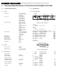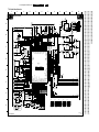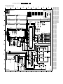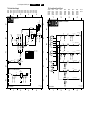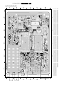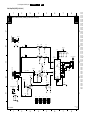
1
Colour Television
Chassis
LC4.1U
AA
E_14520_000.eps
170904
Contents
Page
1. Technical Specifications, Connections,
and Chassis Overview
2
2. Safety Instructions, Warnings, and Notes
4
3. Directions for Use
6
4. Mechanical Instructions
7
5. Service Modes, Error Codes, and Faultfinding 9
6. Block Diagrams, Testpoint Overviews,
and Waveforms
Wiring Diagram
15
Block Diagram Audio & Video
16
Block Diagram Scaler & Supply
17
Testpoint Overview TV & Scaler Board
18-19
Testpoint Overview Front IR / LED Panel
20
I2C Overview
21
Supply Voltage Overview
22
7. Circuit Diagrams and PWB Layouts
Diagram
Tuner & VIF
(Diagram A1) 23
Hercules
(Diagram A2) 24
Hercules Supply
(Diagram A3) 25
Audio Amplifier (2x2W)
(Diagram A4) 26
TV-Supply
(Diagram A5) 27
Scaler
(Diagram A6) 28
Scaler LVDS
(Diagram A7) 29
Scaler IO
(Diagram A8) 30
Supply
(Diagram A9) 31
Rear IO Cinch
(Diagram A10) 31
Side AV Panel
(Diagram D) 34
Top Control Panel
(Diagram E) 36
Audio Amplifier (2x5W) (20 & 23”)(Diagram I)
37
Front IR / LED Panel
(Diagram J)
39
Contents
Page
8. Alignments
9. Circuit Descriptions
Abbreviation List
IC Data Sheets
10 Spare Parts List
11 Revision List
41
45
49
51
54
57
PWB
32-33
32-33
32-33
32-33
32-33
32-33
32-33
32-33
32-33
32-33
35
36
38
39
©
Copyright 2004 Philips Consumer Electronics B.V. Eindhoven, The Netherlands.
All rights reserved. No part of this publication may be reproduced, stored in a
retrieval system or transmitted, in any form or by any means, electronic,
mechanical, photocopying, or otherwise without the prior permission of Philips.
Published by BB 0469 Service PaCE
Printed in the Netherlands
Subject to modification
EN 3122 785 14530
EN 2
1.
Technical Specifications, Connections and Chassis Overview
LC4.1U AA
1. Technical Specifications, Connections and Chassis Overview
1.1
Technical Specifications
1.2
Connections
1.1.1
Vision
1.2.1
Rear Connections
Display type
Screen size:
Resolution (HxV)
Viewing angle
Light output
Tuning system
Colour systems
Video playback
Channel selections
Aerial input
1.1.2
: 14 inch: LCD-VA
: 15 inch: DV-LCD-IPS
: 17-23 inch:
DV-LCD-IPS
: 14 inch (37 cm)
: 15 inch (38 cm)
: 17 inch (45 cm)
: 20 inch (51 cm)
: 23 inch (59 cm)
: 14 inch: 640x480
(VGA)
: 15 inch: 1024x768
(XGA)
: 17 inch: 1280x768
(WXGA)
: 20 inch: 640x480
(VGA)
: 23 inch: 1280x768
(WXGA)
: 14 inch: 170x170 deg.
: 15 inch: 130x100 deg.
: 17-23 inch:
176x176 deg.
: 450 cd/m2
: PLL
: NTSC
: NTSC
: 100 channels
: PLL
: 75 ohm
: Coax
AERIAL
IN
Pr
1
R
Maximum power
1.1.3
: 90-240 V ac
: 50 / 60 Hz
Ambient conditions:
- Temperature range
- Maximum humidity
: +5 to +40 °C
: 90 % R.H.
Power consumption
- Normal operation
- Standby
: from 32 W
: to 110 W
: <2W
10
15
E_14520_064.eps
270904
Aerial - In
- IEC-type
Coax, 75 ohm
D
FM Ant
- IEC-type
Coax, 75 ohm
D
AV1 Cinch: Video CVBS/YPbPr/RGB - In, Audio - In
Wh - Audio L
0.5 VRMS / 10 kohm
Rd - Audio R
0.5 VRMS / 10 kohm
Bu - Video Pb/B 0.7 VPP / 75 ohm
Rd - Video Pr/R 0.7 VPP / 75 ohm
Ye - Video CVBS 1 VPP / 75 ohm
Ge - Video Y/G 0.7 VPP / 75 ohm
Bk - Sync H
0-5V
Bk - Sync V
0-5V
jq
jq
jq
jq
jq
jq
jq
jq
VGA: RGB - In
1
AV stereo
BTSC
14-17 inch: 2x2 W
20-23 inch: 2x5 W
Power supply:
- Mains voltage
- Mains frequency
L
Figure 1-1 Rear connections
6
Miscellaneous
5
11
AUDIO VIDEO
IN
IN
FM
IN
11
:
:
:
:
VGA
Y
6
Sound
Sound systems
Pb
5
10
15
E_06532_002.eps
050404
Figure 1-2 VGA Connector
1
2
3
4
5
6
7
8
9
10
11
12
13
14
15
- Red
- Green
- Blue
- Red - gnd
- Green - gnd
- Blue - gnd
- 5V_DC
- DDC_SDA
- H-sync
- V-sync
- DDC_SCL
0.7 V_pp / 75 ohm
0.7 V_pp / 75 ohm
0.7 V_pp / 75 ohm
Ground
Ground
Ground
Ground
Ground
+5 V_dc
Ground
Ground
DDC data
0-5V
0-5V
DDC clock
j
j
j
H
H
H
H
H
j
H
H
j
j
j
j
Technical Specifications, Connections and Chassis Overview
1.2.2
LC4.1U AA
1.
EN 3
Side Connections
S-VHS - In Hosiden
1 -Y
Ground
2 -C
Ground
3 -Y
1 Vpp/75 ohm
4 -C
0.3 Vpp/75 ohm
HEADPHONE
AUDIO R IN
AUDIO L IN
H
H
j
j
VIDEO IN
S-VIDEO
AUDIO IN (PC/HD)
DATA
E_14520_065.eps
270904
Figure 1-3 Side connections
Mini Jack: Audio - in
4 - Audio - L
0.5 Vrms / 10 kohm
3 - Audio - R
0.5 Vrms / 10 kohm
1.3
Video - In (Cinch)
1 - CVBS
1 Vpp/75 ohm
jq
Audio - In (Cinch)
1 - Audio - R
0.5 Vrms/10 k ohm
2 - Audio - L
0.5 Vrms/10 k ohm
jq
jq
Jack: Headphone- Out
Bk - Headphone 32 - 600 ohm / 10 mW
rt
jq
jq
Chassis Overview
TOP CONTROL PANEL
E
LCD PANEL
TV & SCALER
BOARD
AMPLIFIER
PANEL
J
A
I
FRONT IR / LED
PANEL
SIDE IO PANEL
D
POWER SUPPLY
UNIT
E_14520_052.eps
200904
Figure 1-4 Chassis Overview
EN 4
2.
LC4.1U AA
Safety Instructions, Warnings, and Notes
2. Safety Instructions, Warnings, and Notes
2.1
•
Safety Instructions
Safety regulations require that during a repair:
• Connect the set to the Mains (AC Power) via an isolation
transformer (> 800 VA).
• Replace safety components, indicated by the symbol h,
only by components identical to the original ones. Any
other component substitution (other than original type) may
increase risk of fire or electrical shock hazard.
Safety regulations require that after a repair, the set must be
returned in its original condition. Pay in particular attention to
the following points:
• Route the wire trees correctly and fix them with the
mounted cable clamps.
• Check the insulation of the Mains (AC Power) lead for
external damage.
• Check the strain relief of the Mains (AC Power) cord for
proper function.
• Check the electrical DC resistance between the Mains (AC
Power) plug and the secondary side (only for sets which
have a Mains (AC Power) isolated power supply):
1. Unplug the Mains (AC Power) cord and connect a wire
between the two pins of the Mains (AC Power) plug.
2. Set the Mains (AC Power) switch to the "on" position
(keep the Mains (AC Power) cord unplugged!).
3. Measure the resistance value between the pins of the
Mains (AC Power) plug and the metal shielding of the
tuner or the aerial connection on the set. The reading
should be between 4.5 Mohm and 12 Mohm.
4. Switch "off" the set, and remove the wire between the
two pins of the Mains (AC Power) plug.
• Check the cabinet for defects, to avoid touching of any
inner parts by the customer.
•
•
E_06532_006.eps
240604
Figure 2-1 Dolby PL Symbol
2.3.2
Schematic Notes
•
•
•
•
•
•
2.2
Warnings
•
•
•
•
All ICs and many other semiconductors are susceptible to
electrostatic discharges (ESD w). Careless handling
during repair can reduce life drastically. Make sure that,
during repair, you are connected with the same potential as
the mass of the set by a wristband with resistance. Keep
components and tools also at this same potential.
Available ESD protection equipment:
– Complete kit ESD3 (small tablemat, wristband,
connection box, extension cable and earth cable) 4822
310 10671.
– Wristband tester 4822 344 13999.
Be careful during measurements in the high voltage
section.
Never replace modules or other components while the unit
is switched "on".
When you align the set, use plastic rather than metal tools.
This will prevent any short circuits and the danger of a
circuit becoming unstable.
2.3
Notes
2.3.1
General
•
Measure the voltages and waveforms with regard to the
chassis (= tuner) ground (H), or hot ground (I), depending
on the tested area of circuitry. The voltages and waveforms
shown in the diagrams are indicative. Measure them in the
Service Default Mode (see chapter 5) with a colour bar
signal and stereo sound (L: 3 kHz, R: 1 kHz unless stated
otherwise) and picture carrier at 475.25 MHz for PAL, or
61.25 MHz for NTSC (channel 3).
Where necessary, measure the waveforms and voltages
with (D) and without (E) aerial signal. Measure the
voltages in the power supply section both in normal
operation (G) and in standby (F). These values are
indicated by means of the appropriate symbols.
The semiconductors indicated in the circuit diagram and in
the parts lists, are interchangeable per position with the
semiconductors in the unit, irrespective of the type
indication on these semiconductors.
Manufactured under license from Dolby Laboratories.
“Dolby”, “Pro Logic” and the “double-D symbol”, are
trademarks of Dolby Laboratories.
2.3.3
All resistor values are in ohms and the value multiplier is
often used to indicate the decimal point location (e.g. 2K2
indicates 2.2 kohm).
Resistor values with no multiplier may be indicated with
either an "E" or an "R" (e.g. 220E or 220R indicates 220
ohm).
All capacitor values are given in micro-farads (µ= x10-6),
nano-farads (n= x10-9), or pico-farads (p= x10-12).
Capacitor values may also use the value multiplier as the
decimal point indication (e.g. 2p2 indicates 2.2 pF).
An "asterisk" (*) indicates component usage varies. Refer
to the diversity tables for the correct values.
The correct component values are listed in the Electrical
Replacement Parts List. Therefore, always check this list
when there is any doubt.
Rework on BGA (Ball Grid Array) ICs
General
Although (LF)BGA assembly yields are very high, there may
still be a requirement for component rework. By rework, we
mean the process of removing the component from the PWB
and replacing it with a new component. If an (LF)BGA is
removed from a PWB, the solder balls of the component are
deformed drastically so the removed (LF)BGA has to be
discarded.
Device Removal
As is the case with any component that, it is essential when
removing an (LF)BGA, the board, tracks, solder lands, or
surrounding components are not damaged. To remove an
(LF)BGA, the board must be uniformly heated to a temperature
close to the reflow soldering temperature. A uniform
temperature reduces the chance of warping the PWB.
To do this, we recommend that the board is heated until it is
certain that all the joints are molten. Then carefully pull the
component off the board with a vacuum nozzle. For the
appropriate temperature profiles, see the IC data sheet.
Area Preparation
When the component has been removed, the vacant IC area
must be cleaned before replacing the (LF)BGA.
Removing an IC often leaves varying amounts of solder on the
mounting lands. This excessive solder can be removed with
either a solder sucker or solder wick. The remaining flux can be
removed with a brush and cleaning agent.
After the board is properly cleaned and inspected, apply flux on
the solder lands and on the connection balls of the (LF)BGA.
Safety Instructions, Warnings, and Notes
Note: Do not apply solder paste, as this has shown to result in
problems during re-soldering.
Device Replacement
The last step in the repair process is to solder the new
component on the board. Ideally, the (LF)BGA should be
aligned under a microscope or magnifying glass. If this is not
possible, try to align the (LF)BGA with any board markers.
To reflow the solder, apply a temperature profile according to
the IC data sheet. So as not to damage neighbouring
components, it may be necessary to reduce some
temperatures and times.
More Information
For more information on how to handle BGA devices, visit this
URL: www.atyourservice.ce.philips.com (needs subscription,
not available for all regions) ). After login, select “Magazine”,
then go to “Workshop Information”. Here you will find
Information on how to deal with BGA-ICs.
2.3.4
Lead Free Solder
Some PWBs in this chassis are “lead-free prepared”. This is
indicated on the PWB by the PHILIPS lead-free logo (either by
a service-printing or by a sticker). It does not mean that leadfree solder is actually used!
P
b
Figure 2-2 Lead-free logo
Due to this fact, some rules have to be respected by the
workshop during a repair:
• Use only lead-free soldering tin Philips SAC305 with order
code 0622 149 00106. If lead-free solder paste is required,
please contact the manufacturer of your soldering
equipment.
• Use only adequate solder tools applicable for lead-free
soldering tin.
• Adjust your solder tool so that a temperature around 217 220 deg. C is reached at the solder joint.
• Do not mix lead-free soldering tin with leaded soldering tin;
this will lead to unreliable solder joints!
• Use only original spare parts listed in this manual. These
are lead-free parts!
• On the website www.atyourservice.ce.philips.com (needs
subscription, not available for all regions) you can find
more information on:
– Aspects of lead-free technology.
– BGA (de-)soldering, heating-profiles of BGAs used in
Philips sets, and others.
2.3.5
Practical Service Precautions
•
•
It makes sense to avoid exposure to electrical shock.
While some sources are expected to have a possible
dangerous impact, others of quite high potential are of
limited current and are sometimes held in less regard.
Always respect voltages. While some may not be
dangerous in themselves, they can cause unexpected
reactions - reactions that are best avoided. Before reaching
into a powered TV set, it is best to test the high voltage
insulation. It is easy to do, and is a good service precaution.
LC4.1U AA
2.
EN 5
EN 6
3.
LC4.1U AA
Directions for Use
3. Directions for Use
You can download this information from the following website:
http://www.philips.com/support
Mechanical Instructions
LC4.1U AA
4.
EN 7
4. Mechanical Instructions
4.2
Index of this chapter:
1. Service Position
2. Rear Cover Removal
3. Power Supply Unit Removal
4. TV & Scaler Board Removal
5. Side I/O Panel Removal
6. Top Control Panel Removal
7. Audio Amplifier Panel Removal
8. Exchanging the LCD Panel
9. Re-assembly
Rear Cover Removal
1
Note: Figures below can deviate from the actual situation, due
to different set executions.
Note: To diagnose the set with ComPair it is not needed to
open the set entirely.
To access the ComPair connector, proceed with the following:
1. Manually unlock and remove the cover cap.
2. Remove the tape shielding that covers the ComPair
connector (1).
E_14520_035.eps
160904
Note: Make sure that both the ComPair connector and the
UART connector are shielded off with a piece of insulating tape
after repair for ESD reasons. Place this tape over the holes in
the rear cover of the set.
Figure 4-3 Rear cover removal
1. Make sure all power-, audio-, video- and coax- cables are
unplugged.
2. Remove all Torx screws (1) around the edges of the rear
cover.
3. Remove the rear cover and store it in a safe place.
4.3
1
Power Supply Unit Removal
E_14520_034.eps
160904
Figure 4-1 ComPair connector
4.1
Service Position
4.1.1
Foam Bars
1
E_14520_036.eps
160904
Figure 4-4 Power supply unit
1. Disconnect all cables from the Power supply unit.
2. Remove all mounting screws (1) from the Power supply
unit.
3. Take out the Power supply unit.
E_06532_018.eps
170504
Figure 4-2 Foam bars
The foam bars (order code 3122 785 90580) can be used for
all types and sizes of Flat TVs. By laying the plasma or LCD TV
flat on the (ESD protective) foam bars, a stable situation is
created to perform measurements and alignments. By placing
a mirror under the TV, you can easily monitor the screen.
EN 8
4.4
4.
Mechanical Instructions
LC4.1U AA
4.7
TV & Scaler Board Removal
Audio Amplifier Panel Removal
1
2
1
2
E_14520_037.eps
160904
E_14520_039.eps
160904
Figure 4-5 TV & Scaler board removal
Figure 4-7 Audio amplifier panel removal
1. Disconnect all cables from the TV & Scaler board.
2. Remove the screw from the grounding cable (1).
3. Remove the mounting screw (2) and remove the board.
4.5
1. Disconnect all cables from the audio amplifier panel.
2. Remove all mounting screws from the audio amplifier panel
(1).
3. Unlock the panel by twisting back the clamp at the bottom
(2).
4. Take out the audio amplifier panel.
Side I/O Panel Removal
4.8
Exchanging the LCD Panel
1
2
E_14520_038.eps
160904
1
Figure 4-6 Side I/O panel removal
1. Disconnect all cables from the Side I/O panel.
2. Remove the mounting screw (1).
3. Unlock the panel by twisting back the clamp at the bottom
(2).
4. Take out the Side I/O panel from the bracket.
4.6
E_14520_040.eps
160904
Top Control Panel Removal
Figure 4-8 Exchanging the LCD panel
1.
2.
3.
4.
1. Disconnect the cable from the top control panel.
2. Remove the two mounting screws from the top control
panel.
3. Take out the top control panel.
4.9
Disconnect all cables from the LCD Panel.
Remove all mounting screws (1) from the metal cover.
Lift and take off the metal cover.
Now you can exchange the LCD panel.
Re-Assembly
To re-assemble the whole set, do all processes in reverse
order.
Notes:
Do not forget to replace the ground cable of the TV & Scaler
board, while mounting the screw at the board topside. See
figure “TV & Scaler board removal”.
Service Modes, Error Codes, and Fault Finding
LC4.1U AA
5.
EN 9
5. Service Modes, Error Codes, and Fault Finding
Index of this chapter:
1. Test Points
2. Service Modes
3. Problems and Solving Tips (related to CSM)
4. ComPair
5. Error Codes
6. The Blinking LED Procedure
7. Fault Finding and Repair Tips
5.1
Test Points
This chassis is equipped with test points in the service printing.
In the schematics test points are identified with a rectangle box
around Fxxx or Ixxx. These test points are specifically
mentioned in the service manual as “half moons” with a dot in
the centre.
Perform measurements under the following conditions:
• Television set in Service Default Alignment Mode.
• Video input: Colour bar signal.
• Audio input: 3 kHz left channel, 1 kHz right channel.
5.2
How to enter
To enter SDM, use one of the following methods:
• Press the following key sequence on the remote control
transmitter: “062596” directly followed by the MENU button
(do not allow the display to time out between entries while
keying the sequence).
• Short "Service" jumpers on the TV board during cold start
and apply mains (see Figure "Service jumpers"). Then
press the mains button (remove the short after start-up).
Caution: Entering SDM by shorting "Service" jumpers will
override the +5V-protection. Do this only for a short period.
When doing this, the service-technician must know exactly
what he is doing, as it could damage the television set.
• Or via ComPair.
1
Service Modes
Service Default mode (SDM) and Service Alignment Mode
(SAM) offers several features for the service technician, while
the Customer Service Mode (CSM) is used for communication
between the call centre and the customer.
This chassis also offers the option of using ComPair, a
hardware interface between a computer and the TV chassis. It
offers the abilities of structured troubleshooting, error code
reading, and software version readout for all chassis.
Minimum requirements for ComPair: a Pentium processor, a
Windows OS, and a CD-ROM drive (see also paragraph
"ComPair").
5.2.1
Service Default Mode (SDM)
Purpose
• To create a predefined setting for measurements to be
made.
• To override software protections.
• To start the blinking LED procedure.
• To inspect the error buffer.
• To check the life timer.
Specifications
• Tuning frequency: 61.25 MHz.
• Colour system: NTSC.
• All picture settings at 50% (brightness, colour contrast,
hue).
• Bass, treble and balance at 50 %; volume at 25 %.
• All service-unfriendly modes (if present) are disabled. The
service unfriendly modes are:
– Timer / Sleep timer.
– Child / parental lock.
– Blue mute.
– Hotel / hospital mode.
– Auto shut off (when no “IDENT” video signal is
received for 15 minutes).
– Skipping of non-favourite presets / channels.
– Auto-storage of personal presets.
– Auto user menu time-out.
– Auto Volume Levelling (AVL).
E_14520_041.eps
160904
Figure 5-1 Service jumpers
After entering SDM, the following screen is visible, with SDM in
the upper right corner of the screen to indicate that the
television is in Service Default Alignment Mode.
00022
LC41US1 1.00/S41EV1 1.01
SDM
ERR 0 0 0 0 0
OP 000 057 140 032 120 128 000
E_14520_060.eps
230904
Figure 5-2 SDM menu
How to navigate
Use one of the following methods:
• When you press the MENU button on the remote control,
the set will switch on the normal user menu in the SDM
mode.
• On the TV, press and hold the VOLUME DOWN and press
the CHANNEL DOWN for a few seconds, to switch from
SDM to SAM and reverse.
EN 10
5.
LC4.1U AA
Service Modes, Error Codes, and Fault Finding
•
How to exit
Switch the set to STANDBY by pressing the mains button on
the remote control transmitter or the television set.
If you turn the television set off by removing the mains (i.e.,
unplugging the television) without using the mains button, the
television set will remain in SDM when mains is re-applied, and
the error buffer is not cleared.
5.2.2
Service Alignment Mode (SAM)
Purpose
• To change option settings.
• To display / clear the error code buffer.
• To perform alignments.
Specifications
• Operation hours counter (maximum five digits displayed).
• Software version, Error codes, and Option settings display.
• Error buffer clearing.
• Option settings.
• AKB switching.
• Software alignments (Tuner, White Tone, Geometry &
Audio).
• NVM Editor.
• ComPair Mode switching.
3.
4.
5.
6.
7.
How to enter
To enter SAM, use one of the following methods:
• Press the following key sequence on the remote control
transmitter: “062596" directly followed by the OSD/
STATUS button (do not allow the display to time out
between entries while keying the sequence).
• Or via ComPair.
8.
After entering SAM, the following screen is visible, with SAM in
the upper right corner of the screen to indicate that the
television is in Service Alignment Mode.
12.
13.
00022 LC41US1 1.00/S41EV1 1.01
ERR 0 0 0 0 0
SAM
Clear ?
. ComPair Mode
On
10.
11.
How to navigate
• In SAM, select menu items with the MENU UP/DOWN keys
on the remote control transmitter. The selected item will be
highlighted. When not all menu items fit on the screen, use
the MENU UP/DOWN keys to display the next / previous
menu items.
• With the MENU LEFT/RIGHT keys, it is possible to:
– Activate the selected menu item.
– Change the value of the selected menu item.
– Activate the selected submenu.
• In SAM, when you press the MENU button twice, the set
will switch to the normal user menus (with the SAM mode
still active in the background). To return to the SAM menu
press the MENU or STATUS/EXIT button.
• When you press the MENU key in while in a submenu, you
will return to the previous menu.
OP 000 057 140 032 120 128 000
. Clear
. Options
. Tuner
. White Tone
. Audio
. NVM Editor
. SC NVM Editor
9.
Europe: T= 1 page TXT, F= Full TXT, V= Voice
control.
• LATAM and NAFTA: N= Stereo non-dBx, S=
Stereo dBx.
• Asian Pacific: T= TXT, N= non-TXT, C= NTSC.
• ALL regions: M= mono, D= DVD, Q= Mk2.
– D= the language cluster number.
– X= the main software version number (updated with a
major change that is incompatible with previous
versions).
– Y= the sub software version number (updated with a
minor change that is compatible with previous
versions).
– EEEEEE= the scaler sw cluster
– F= the main sw version no.
– GG= the sub-version no.
SAM. Indication of the Service Alignment Mode.
Error Buffer. Shows all errors detected since the last time
the buffer was erased. Five errors possible.
Option Bytes. Used to set the option bytes. See “Options”
in the Alignments section for a detailed description. Seven
codes are possible.
Clear. Erases the contents of the error buffer. Select the
CLEAR menu item and press the MENU RIGHT key. The
content of the error buffer is cleared.
Options. Used to set the option bits. See “Options” in the
Alignments section for a detailed description.
Tuner. Used to align the tuner. See “Tuner” in the
Alignments section for a detailed description.
White Tone. Used to align the white tone. See “White
Tone” in the Alignments section for a detailed description.
Audio. No audio alignment is necessary for this television
set.
NVM Editor. Can be used to change the NVM data in the
television set. See table “NVM data” further on.
SC NVM Editor. Can be used to edit Scaler NVM.
ComPaIr. Can be used to switch on the television to In
System Programming (ISP) mode, for software uploading
via ComPair.
Caution: When this mode is selected without ComPair
connected, the TV will be blocked. Remove the AC power
to reset the TV.
E_14520_061.eps
230904
Figure 5-3 SAM menu
Menu explanation
1. LLLLL. This represents the run timer. The run timer counts
normal operation hours, but does not count standby hours.
2. AAABCD-X.Y. This is the software identification of the
main microprocessor:
– A= the project name (LC41).
– B= the region: E= Europe, A= Asia Pacific, U= NAFTA,
L= LATAM.
– C= the software diversity:
How to store SAM settings
To store the settings changed in SAM mode, leave the top level
SAM menu by using the POWER button on the remote control
transmitter or the television set.
How to exit
Switch the set to STANDBY by pressing the mains button on
the remote control transmitter or the television set.
If you turn the television set “off” by removing the mains (i.e.,
unplugging the television) without using the mains button, the
television set will remain in SAM when mains is re-applied, and
the error buffer is not cleared.
Service Modes, Error Codes, and Fault Finding
5.2.3
LC4.1U AA
5.
EN 11
Customer Service Mode (CSM)
5.3
Problems and Solving Tips Related to CSM
Purpose
The Customer Service Mode shows error codes and
information on the TV’s operation settings. The call centre can
instruct the customer (by telephone) to enter CSM in order to
identify the status of the set. This helps the call centre to
diagnose problems and failures in the TV set before making a
service call.
The CSM is a read-only mode; therefore, modifications are not
possible in this mode.
5.3.1
Picture Problems
How to enter
To enter CSM, press the following key sequence on the remote
control transmitter: “123654” (do not allow the display to time
out between entries while keying the sequence).
Upon entering the Customer Service Mode, the following
screen will appear:
1 00022
LC41US1 1.00/S41EV1 1.01 CSM
2 CODES 0 0 0 0 0
3 OP 000 057 140 032 120 128 000
4 20PF8846/12
5
6 NOT TUNED
7 PAL
8 STEREO
9 CO 50 CL 50 BR 50
0 AVL Off
E_14520_062.eps
230904
Figure 5-4 CSM menu
Menu explanation
1. Indication of the decimal value of the operation hours
counter, Software identification of the main microprocessor
(see "Service Default or Alignment Mode" for an
explanation), and the service mode (CSM= Customer
Service Mode).
2. Displays the last five errors detected in the error code
buffer.
3. Displays the option bytes.
4. Displays the type number version of the set.
5. Reserved item for P3C call centres (AKBS stands for
Advanced Knowledge Base System).
6. Indicates the television is receiving an "IDENT" signal on
the selected source. If no "IDENT" signal is detected, the
display will read "NOT TUNED"
7. Displays the detected Colour system (e.g. PAL/NTSC).
8. Displays the detected Audio (e.g. stereo/mono).
9. Displays the picture setting information.
10. Displays the sound setting information.
How to exit
To exit CSM, use one of the following methods:
• Press the MENU, STATUS/EXIT, or POWER button on the
remote control transmitter.
• Press the POWER button on the television set.
Note: The problems described below are all related to the TV
settings. The procedures used to change the value (or status)
of the different settings are described.
Picture too dark or too bright
If:
• The picture improves when you press the AUTO PICTURE
button on the remote control transmitter, or
• The picture improves when you enter the Customer
Service Mode,
Then:
1. Press the AUTO PICTURE button on the remote control
transmitter repeatedly (if necessary) to choose
PERSONAL picture mode.
2. Press the MENU button on the remote control transmitter.
This brings up the normal user menu.
3. In the normal user menu, use the MENU UP/DOWN keys
to highlight the PICTURE sub menu.
4. Press the MENU LEFT/RIGHT keys to enter the PICTURE
sub menu.
5. Use the MENU UP/DOWN keys (if necessary) to select
BRIGHTNESS.
6. Press the MENU LEFT/RIGHT keys to increase or
decrease the BRIGHTNESS value.
7. Use the MENU UP/DOWN keys to select PICTURE.
8. Press the MENU LEFT/RIGHT keys to increase or
decrease the PICTURE value.
9. Press the MENU button on the remote control transmitter
twice to exit the user menu.
10. The new PERSONAL preference values are automatically
stored.
White line around picture elements and text
If:
The picture improves after you have pressed the AUTO
PICTURE button on the remote control transmitter,
Then:
1. Press the AUTO PICTURE button on the remote control
transmitter repeatedly (if necessary) to choose
PERSONAL picture mode.
2. Press the MENU button on the remote control transmitter.
This brings up the normal user menu.
3. In the normal user menu, use the MENU UP/DOWN keys
to highlight the PICTURE sub menu.
4. Press the MENU LEFT/RIGHT keys to enter the PICTURE
sub menu.
5. Use the MENU UP/DOWN keys to select SHARPNESS.
6. Press the MENU LEFT key to decrease the SHARPNESS
value.
7. Press the MENU button on the remote control transmitter
twice to exit the user menu.
8. The new PERSONAL preference value is automatically
stored.
Snowy picture
Check CSM line 6. If this line reads “Not Tuned”, check the
following:
• Antenna not connected. Connect the antenna.
• No antenna signal or bad antenna signal. Connect a proper
antenna signal.
• The tuner is faulty (in this case line 2, the Error Buffer line,
will contain error number 10). Check the tuner and replace/
repair the tuner if necessary.
EN 12
5.
LC4.1U AA
Service Modes, Error Codes, and Fault Finding
Black and white picture
If:
• The picture improves after you have pressed the AUTO
PICTURE button on the remote control transmitter,
Then:
1. Press the AUTO PICTURE button on the remote control
transmitter repeatedly (if necessary) to choose
PERSONAL picture mode.
2. Press the MENU button on the remote control transmitter.
This brings up the normal user menu.
3. In the normal user menu, use the MENU UP/DOWN keys
to highlight the PICTURE sub menu.
4. Press the MENU LEFT/RIGHT keys to enter the PICTURE
sub menu.
5. Use the MENU UP/DOWN keys to select COLOUR.
6. Press the MENU RIGHT key to increase the COLOUR
value.
7. Press the MENU button on the remote control transmitter
twice to exit the user menu.
8. The new PERSONAL preference value is automatically
stored.
Menu text not sharp enough
If:
• The picture improves after you have pressed the AUTO
PICTURE button on the remote control transmitter,
Then:
1. Press the AUTO PICTURE button on the remote control
transmitter repeatedly (if necessary) to choose
PERSONAL picture mode.
2. Press the MENU button on the remote control transmitter.
This brings up the normal user menu.
3. In the normal user menu, use the MENU UP/DOWN keys
to highlight the PICTURE sub menu.
4. Press the MENU LEFT/RIGHT keys to enter the PICTURE
sub menu.
5. Use the MENU UP/DOWN keys to select PICTURE.
6. Press the MENU LEFT key to decrease the PICTURE
value.
7. Press the MENU button on the remote control transmitter
twice to exit the user menu.
8. The new PERSONAL preference value is automatically
stored.
5.4
ComPair
5.4.1
Introduction
ComPair (Computer Aided Repair) is a service tool for Philips
Consumer Electronics products. ComPair is a further
development on the European DST (service remote control),
which allows faster and more accurate diagnostics. ComPair
has three big advantages:
• ComPair helps you to quickly get an understanding on how
to repair the chassis in a short time by guiding you
systematically through the repair procedures.
• ComPair allows very detailed diagnostics (on I2C level) and
is therefore capable of accurately indicating problem areas.
You do not have to know anything about I2C commands
yourself because ComPair takes care of this.
• ComPair speeds up the repair time since it can
automatically communicate with the chassis (when the
microprocessor is working) and all repair information is
directly available. When ComPair is installed together with
the SearchMan electronic manual of the defective chassis,
schematics and PWBs are only a mouse click away.
5.4.2
Specifications
ComPair consists of a Windows based faultfinding program
and an interface box between PC and the (defective) product.
The ComPair interface box is connected to the PC via a serial
or RS232 cable.
For this chassis, the ComPair interface box and the TV
communicate via a bi-directional service cable via the service
connector.
The ComPair faultfinding program is able to determine the
problem of the defective television. ComPair can gather
diagnostic information in two ways:
• Automatic (by communication with the television): ComPair
can automatically read out the contents of the entire error
buffer. Diagnosis is done on I2C level. ComPair can access
the I2C bus of the television. ComPair can send and
receive I2C commands to the micro controller of the
television. In this way, it is possible for ComPair to
communicate (read and write) to devices on the I2C busses
of the TV-set.
• Manually (by asking questions to you): Automatic
diagnosis is only possible if the micro controller of the
television is working correctly and only to a certain extends.
When this is not the case, ComPair will guide you through
the faultfinding tree by asking you questions (e.g. Does the
screen give a picture? Click on the correct answer: YES /
NO) and showing you examples (e.g. Measure test-point I7
and click on the correct oscillogram you see on the
oscilloscope). You can answer by clicking on a link (e.g.
text or a waveform picture) that will bring you to the next
step in the faultfinding process.
By a combination of automatic diagnostics and an interactive
question / answer procedure, ComPair will enable you to find
most problems in a fast and effective way.
Beside fault finding, ComPair provides some additional
features like:
• Up- or downloading of pre-sets.
• Managing of pre-set lists.
• Emulation of the Dealer Service Tool (DST).
• If both ComPair and SearchMan (Electronic Service
Manual) are installed, all the schematics and the PWBs of
the set are available by clicking on the appropriate
hyperlink.
Example: Measure the DC-voltage on capacitor C2568
(Schematic/Panel) at the Mono-carrier.
– Click on the “Panel” hyperlink to automatically show
the PWB with a highlighted capacitor C2568.
– Click on the “Schematic” hyperlink to automatically
show the position of the highlighted capacitor.
Service Modes, Error Codes, and Fault Finding
5.4.3
5.5.2
How To Connect
1. First, install the ComPair Browser software (see the Quick
Reference Card for installation instructions).
2. Connect the RS232 interface cable between a free serial
(COM) port of your PC and the PC connector (marked with
“PC”) of the ComPair interface.
3. Connect the mains adapter to the supply connector
(marked with “POWER 9V DC”) of the ComPair interface.
4. Switch the ComPair interface “OFF”.
5. Switch the television set “OFF” with the mains switch.
6. Connect the ComPair interface cable between the
connector on the rear side of the ComPair interface
(marked with “I2C”) and the ComPair connector at the rear
side of the TV.
7. Plug the mains adapter in a mains outlet, and switch the
interface “ON”. The green and red LEDs light up together.
The red LED extinguishes after approx. 1 second while the
green LED remains lit.
8. Start the ComPair program and read the “Introduction”
chapter.
VCR
Power
9V DC
5.5.3
I2C
ComPair order codes:
• ComPair Software: ST4191.
• ComPair Interface Box: 4822 727 21631.
• AC Adapter: T405-ND.
• ComPair Quick Start Guide: ST4190.
Note: If you encounter any problems, contact your local
support desk.
5.5.1
Error Codes
How To Read The Error Buffer
You can read the error buffer in 3 ways:
• On screen via the SAM (if you have a picture).
Examples:
– ERROR: 0 0 0 0 0 : No errors detected
– ERROR: 6 0 0 0 0 : Error code 6 is the last and only
detected error
– ERROR: 9 6 0 0 0 : Error code 6 was detected first and
error code 9 is the last detected (newest) error
• Via the blinking LED procedure (when you have no
picture). See “The Blinking LED Procedure”.
• Via ComPair.
Error Codes
Table 5-1 Error code overview
How To Order
The error code buffer contains all errors detected since the last
time the buffer was erased. The buffer is written from left to
right. When an error occurs that is not yet in the error code
buffer, it is displayed at the left side and all other errors shift one
position to the right.
How To Clear The Error Buffer
In case of non-intermittent faults, write down the errors present
in the error buffer and clear the error buffer before you begin
the repair. This ensures that old error codes are no longer
present.
If possible, check the entire contents of the error buffer. In
some situations, an error code is only the result of another error
and not the actual cause of the problem (for example, a fault in
the protection detection circuitry can also lead to a protection).
Figure 5-5 ComPair Interface connection
5.5
EN 13
Note: If you exit SAM by disconnecting the mains from the
television set, the error buffer is not reset.
E_06532_008.eps
180804
5.4.4
5.
The error code buffer is cleared in the following cases:
• By using the CLEAR command in the SAM menu:
– To enter SAM, press the following key sequence on the
remote control transmitter: “062596” directly followed
by the OSD/STATUS button (do not allow the display
to time out between entries while keying the
sequence).
– Make sure the menu item CLEAR is highlighted. Use
the MENU UP/DOWN buttons, if necessary.
– Press the MENU RIGHT button to clear the error
buffer. The text on the right side of the “CLEAR” line will
change from “CLEAR?” to “CLEARED”
• If the contents of the error buffer have not changed for 50
hours, the error buffer resets automatically.
TO
I2C SERVICE
CONNECTOR
PC
LC4.1U AA
5.6
Error
Device
Error description
0
Not applicable
No Error
Check item Diagram
1
Not applicable
-
-
-
2
Not applicable
-
-
-
3
Not applicable
-
-
4
GM5221
I2C error while communicating 7401
with the Genesis Scaler
7403
and/or Flash-ROM is faulty/
empty
A6
5
Not applicable
+5v protection
7930
A6
6
I2C bus
General I2C error
7011, 3083, A2
3084
7
Not applicable
-
-
8
M24C32
I2C error while communicating 7402
with the Scaler EEPROM
A7
9
M24C16
I2C error while communicating 7099
with the EEPROM
A2
10
Tuner
I2C error while communicating 1302, 3302, A1
with the PLL tuner
3303, 3327
11
Not applicable
-
-
-
12
Not applicable
-
-
-
13
Not applicable
-
-
-
-
-
The Blinking LED Procedure
Using this procedure, you can make the contents of the error
buffer visible via the front LED. This is especially useful when
there is no picture.
When the SDM is entered, the front LED will blink the contents
of the error-buffer:
• The Led blinks with as many pulses as the error code
number, followed by a time period of 1.5 seconds, in which
the Led is off.
• Then this sequence starts is repeated.
Any RC5 command terminates this sequence.
Example of error buffer: 12 9 6 0 0
After entering SDM, the following occurs:
• 1 long blink of 5 seconds to start the sequence,
EN 14
•
•
•
•
•
5.7
5.
LC4.1U AA
Service Modes, Error Codes, and Fault Finding
Fault Finding and Repair Tips
Notes:
• It is assumed that the components are mounted correctly
with correct values and no bad solder joints.
• Before any fault finding actions, check if the correct options
are set.
5.7.1
NVM Editor
In some cases, it can be handy if one directly can change the
NVM contents. This can be done with the “NVM Editor” in SAM
mode.
5.7.2
Tuner and IF
No Picture in RF mode
1. Check whether picture is present in AV. If not, go to Video
processing troubleshooting section.
2. If present, check that the Option settings are correct.
3. Check that all supply voltages are present.
4. Check if I2C lines are working correctly (3.3V).
5. Manually store a known channel and check if there is IF
output at Tuner pin 11.
6. Feed in 105 dBuV at Tuner pin 11 and check whether there
is RGB output from Video Processing IC. If yes, Tuner may
be defected. Change Tuner.
Sound in picture problem for L' system (rolling horizontal
lines)
1. Check whether AGC L' in Sam mode is set to 0.
2. If yes, align the set to correct value.
Required system is not selected correctly
1. Check whether the Service jumper (#4022, 08 05 size) is
present. If yes, remove it.
2. Check whether SEL_IF pin is according to what is
specified.
5.7.3
2. If they are present, check RGB output.
3. If there is no RGB output, the IC TDA120xx can be failed.
12 short blinks followed by a pause of 1.5 seconds,
9 short blinks followed by a pause of 1.5 seconds,
6 short blinks followed by a pause of 1.5 seconds,
1 long blink of 1.5 seconds to finish the sequence,
The sequence starts again at 12 short blinks.
Video Processing
No power
1. Check +12 V and 3V3 at position 1910.
2. If no supply, check the connector 1910.
3. If it is correct, check the power supply board.
Power supply is correct but no green light
1. Check the two connectors 1007 and 1008, if they are
properly inserted.
2. If they are inserted correctly, check if the 3V3 is present.
No picture display
1. Check the RGB signal.
2. If it is present, check pin 3 of IC7006 (NE555).
3. If it has output, the problem is in SCALER part.
4. Otherwise, check H-out on pin 2 of NE555. If the input
signal of pin2 is present, but no output, the IC is failed.
Note:
• If the H-out (pin 67) doesn’t have signal or the level is low,
check the output of NE555 (pin 3) during start up.
• If the H-out (pin 67) has a signal (or has a signal for a very
short time), change IC7006 (NE555).
No TV but PC is present
1. Check if HSYNC and VSYNC are present at PIN 3 of 7007
and 7005.
Comb Filter not working
1. Check the option bit 5 in SAM.
5.7.4
Power Supply
Check fuses
This power supply contains three fuses. One is near the mains
inlet (marked on the board as 1102) and two other are near the
output connectors (marked 1610 and 1660).
1. Check with power supply in off state by means of ohmic
measurement.
2. Fuse 1102 may open in case of severe lightning strikes
and/or failures in the power supply. Despite the fact, that
this fuse is mounted in a fuse holder and the marking text
on the board, it is not meant to be field replaceable.
3. Fuses 1610 and 1660 may open in case a severe overload
of the 12 V outputs. Replacement of the power supply is
needed, but not before the cause of the overload
conditions is resolved.
Standby mode
1. Apply a 12 ohm load resistor of sufficient power rating to all
outputs (+3 V3, +12 VAL, +12 VL and +24 V). Connect the
STBY pin to GND.
2. Over an input voltage range of 90 V_ac to 264 V_ac only
the +3 V3 output shall be up and within regulation (±5%).
The voltage on the POWER DOWN pin shall be < 0.3 V at
an input voltage below 160 V_ac, and 3.3 V ±10% at an
input voltage higher than 240 V_ac.
Normal mode:
1. Apply a 12 ohm load resistor of sufficient power rating to all
outputs (+3 V3, +12 VAL, +12 VL and +24 V). Connect the
STBY pin to the +3 V3 output.
2. Over an input voltage range of 90 V _ac to 264 V_ac all
outputs shall be up and within regulation (±5%). The
voltage on the POWER DOWN pin shall be 3.3 V ±10%
over the entire input voltage range. Additionally, the
voltage on the big capacitor mounted flat on the PCB shall
be 400 V ±10%
Block Diagrams, Testpoint Overviews, and Waveforms
LC4.1U AA
6.
EN 15
6. Block Diagrams, Testpoint Overviews, and Waveforms
Wiring Diagram
E
TOP CONTROL
1308
2P
LCD SCREEN
TTL (LVDS) CONNECTION
Rigth
Speaker
Left
Speaker
INVERTER
I
12P
BACK
LIGHT
CONNECTION
LCD SCREEN
1910
1200
A
SCALER
5P
1704
40P
1703
2P
2P 1008
7011
7401
1401
4P
TUNER
5P
1010
10P
1007
6P
5P
5P
1402
1701
3P
1706
1951
1206
12P
AUDIO AMPLIFIER
(5W)
FOR 2x5W
D
SIDE I/O
4P
1105
6P
5P
POWER
IN
1107
1108
10P
BACK
LIGHT
CONNECTION
LCD SCREEN
FOR 2x2W
3P
1110
1001
1870
FRONT
IR/LED
1111
4P
J
E_14520_001.eps
170904
Block Diagrams, Testpoint Overviews, and Waveforms
LC4.1U AA
6.
EN 16
Block Diagram Audio & Video
7
VIF2
7014
25
8
3
VIF1
Sound
Tr aps
24
CVBS1
RGB Matrix
Blue & Black
Stretch
Gamma Corr.
10
4
SCL
SDA
5
F305
3311
1
F313
cvbs/y
31
RF_AGC
COMPAIR
2
AGC
Detect
6323
4333
7316
4334
2
1330
7
8
3
S IF2
QSS Mixer/
AM Demod.
29
Dig. 2H/4H
Combfilter
Y Delay Adj.
QSS/FM
+5VSW
AM
C-X
SAT
c
S IF1
F315
HERCULES 7011
TDA15001H
NAFTA
TDA15011H AP-NTSC / LATAM
TDA15021H
EU / AP-PAL
7320
SEL_IF
CS1A..D
PA L/NTSC/
SECAM
Decoder &
Baseband
Delay
H/V
Output
sw.
CVBS_SC1_AV1_IN
REAR IO CINCH
Peaking
SCAVEM
U/V Delay
Vint
RGB/YPRPB Insert
YUV Interface
87
SEE
BLOCKDIAGRAM
SCALER
I039
EF
A3
B_SDTV
HISTOGRAM
2014
7015
75
76
70
71
72
HOUT
67
FB/SC
66
7005# 8
VCC
2
THR
TR
4
RES
7
DISC
3
OUT
CTRL
5
2015
2028
6
7006# 8
VCC
2
THR
TR
4
RES
7
H_CS_SDTV
DISC
OUT
3
CTRL
A8
5
2029
2034
6
SANDCASTLE
VDRA
VDRB
23
2040
VSYNC
22
3010
UIN
YIN
74
VIN
80
UOUT
79
VOUT
SC1_B_U_IN
77 78
B/Pb-3
SC1_B_U_IN
7012
# = NE555 TIMER
Vertical & EastWest Geometry
YOUT
CVBS_SC1_AV1_IN
G/Y3
cvbs
64
R/Pr-3
43
Pb
SC1_G_Y_ IN
A8
G_SDTV
F006
52
SC1_G_Y_ IN
BO
TO
I041
EF
F007
Sync Sep
H-OSC
H-Shift
H-Drive
H/V
CVBS/Y-X
+
59
Y
CVBS
86
SCAVEM
on Text
58
AV3_C_IN
SC1_R_V_IN
GO
R_SDTV
7013
+5VSW
YUV IN/OUT
51
SC1_R_V_IN
85
YUV
Uint
55
AV3_CVBS_Y_IN
Pr
RO
cvbs/y
INSSW3
A3
A10
Skin Tone
U/V Tint
Saturation
Chroma
3323
SSIF
RGB Matrix
Blue & Black
Stretch
Gamma Corr.
I044
EF
CVBS/Y- X
INA..D
F314
BRI
Yint
30
1
3
1331
A2
CON
Input
sw.
3005
1328
B_OSD
4331
FM
A2
2
11
TV
A1
4327
Fast Blanking
9
2321
R_OSD
1302 6,7
7011 - IF
F312
F306
G_OSD
+5VSW +VTUN
HERCULES (IF+VIDEO)
3025
A2
TUNER + VIF
C-X
A3
A1
7016
3031
7007# 8
3036
VCC
6
2
THR
TR
4
RES
7
DISC
3
OUT
CTRL
5
2042
2045
+5VSW
V_SDTV
A8
2057
L
R
L_SC1_AV1_IN
L_SC1_AV1_IN
R_SC1_AV1_IN
R_SC1_AV1_IN
2056
5013
2027
Y_NOTCH
A6
SECAM
only
D
SIDE I/O (AV Part)
1108
4
C
4
SVHS
2
3
1
5
Y/CVBS
1010
4
2
A4
AV3_C_IN
AV3_CVBS_Y_IN
2
AV3_LR_IN
7101
6
6
7
7
L
9
9
R
10
10
L
R
2718
AUDOUT SL
PC_AUDIO_LR
CVBS
SVHS
AUDIO IN
AUDIO AMPLIFIER (2X2W)
(14, 15, and 17’’)
2712
AUDOUT SR
D
AUD_SUP
7712
TDA1517ATW
I706
3
15,16
I707
I710
8,9
2736
I711
2737
12,13
18
17
MUTE
MUTE
MODE
AUDOUT SL
AUDOUT SL
HERCULES (AUDIO)
AUDOUT SR
7011 - SOUND
QSS/FM
L/R_SC1_AV1_IN
34,35
AV3_LR_IN
49,50
56,57
PC_AUDIO_LR
SOUND_ENABLE
1
POWER_DOWN
2
2
3
3
I2S Proc
Audio
Control
Vol/Treb/
Bass
Features
DACs
61
AUDOUTLSR
60
AUDOUTLSL
3
&
11
12
EXT_MUTE
13
I
1
62,63
Audio Select
ADC/DAC
1706
1
MUTE
MUTE
OR
1105
4
2
1106
HEADPHONE
3
4
2
5
1
R
4Ω/2W
OR
8Ω/5V
L
7710
A2
AD Conv
Std Stereo
Decoder
&
AUDOUT SR
53,54
OUT_MUTE
OR
AUDIO AMPLIFIER (2x5W) 20 & 23’’
1706
7709
TDA7297D
STANDBY
2
AUDOUT SL
14
3
AUDOUT SR
7
4
SC1_LR_RF_OUT
2
3
7706
74LVCO8AD
A1
1110
1
STANDBY
A2
STANDBY
SSIF(Tuner FM) 33
1701
1
7702
7703
A2
A2
SIDE AV
(LS CONN. PART)
36,37
19
L+
16
L-
MUTE
1107
1
2
2
3
3
12
2
R+
4
4
13
5
R-
5
5
7703-1
5
1704
1
7370
OUT_MUTE
FROM 1,2-1200
INVERTER PANEL
1703
AUD_SUP
7703-2
E_14520_058.eps
270904
Block Diagrams, Testpoint Overviews, and Waveforms
LC4.1U AA
6.
EN 17
Block Diagram Scaler & Supply
A6
PCHD-IO
A7
SCALER (ANA IN)
SCALER (LVDS, TTL OUT)
2
GREEN_Y
3
BLUE_PB
2
VGA_5V
+5VSW
5
15
11
9
1
6460
see
blockdiagram
VIDEO
PC_DET
A7
3470
SDA
13
HS
14
27
G_SDTV
3
B_SDTV
7
RED_PR
25
GREEN_Y
1
BLU_PB
5
HD_FILT ER
21
SD_PCHD_SEL
22
SOG
17
R_PR+
14
G_Y+
11
B_PB+
ANALOG
INPUT
PORT
3497 2466 R_PR3499 2468
23
+
5
6
TRIPLE
ADC
&
PLL
3479 2470 B_PB-
7463
DDC
NVM
TOP CONTROL
A3
A3
HERCULES
(FRONT CONTROL LOOP THROUGH)
1308
CHANNEL +
CHANNELVOLUME+
VOLUMEPOWER
2
2
KEYBOARD
+3V3STBY
1008
+5VSW
KEYBOARD
3062
FRONT IR/LED
8
DVI
INPUT
N.C.
VSYNC
N.C.
1870
1007
1
1
12 FBIN
CLOCK
RECOVERY
PLL
2 PLL_SEL
FBIN
VIDEO
IR
2
2
3
3
7803
LED_SEL
7801
+3V3STBY
6801
GREEN
4
5
5
6
PC_TV_LED
RED
4
LV_E3_TX1+
7403
M29W040B-55k1
KEYBOARD
ER7
18
LV_E4_TX2-
17
LV_E5_TX2+
ER5
14
LV_E8_TX3-
13
LV_E9_TX3+
ER1
16
LV_E6_TXC-
15
LV_E7_TXC+
ER3
38
LV_O0
37
LV_O1
ROM
INTERFACE
ADDRESS
A2
+3V3STBY
6
6
LV_E3_TX1+
8
LV_E4_TX2-
10
LV_E5_TX2+
12
LV_E6_TX3-
18
LV_E7_TX3+
20
LV_E8_TXC-
14
LV_E9_TXC+
16
36
LV_O2
35
LV_O3
34
LV_O4
33
LV_O5
32
LV_O6
31
LV_O7
30
LV_O8
29
LV_O9
43
PD20
44
PD21
45
PD22
46
PD23
1402
EB3
169
PC_TV_LED
1403
14M31818
7804
CLK_SYN
170
1
EB2
17
EB1
19
EB0
21
EG7
24x
EG6
25
27
EG4
29
EG3
31
EG2
FED
33
EB4
FHSYNC
35
EB5
FVSYNC
37
FSSYNC
39
EB6
EB7
PAN_VCC 38,36
SDM PINS
4015
7011
D
u-Processor
SEL_IF
114
KEYBOARD
120
115
IR
111
SOUND_ENABLE
107
PC-TV-LED
97
108
SCL
119
HERCULES 109
IC
SDA
A8
STATU S_1
116
A3
P50_LINE_ITV_IR_SW
123
3,93,96
+1V8_A
+1V8_B
100,117,118,124
EXT_MUTE
99
TV_SC_COM
98
TV_IRQ
STANDBY
122
127 P1.4
HERC_RESET
14 DECDIG
DECDIG
4,5,7,9,88,90,94
+3V3STBY
15,69,82
+5VSW
A1
1112
A3
UART
CONN.
FOR
SERVICE
A1
10
1001
1
1
1
3123
2
2
2
3124
3
3
4
4
3
A5
1910
1
A5
A3
A4
7001,7003
+3V3STBY
F014
+1V8_A
+1V8_B
7070
DECDIG
HERC_RESET
F015
SCL_IO
WC
SYSTEM
SDA
SCL
JTAG_SCL_UART_RX
3430
3431
F903
8
7930
AUD_SUP
A4
A5
3
3
OSC
+3V3STBY
4
2007
7
REF
+3V3STBY
3931
5
5930
11
VCC
6
A9
2
R
4
3441
9
10
11
12
5910
3910
A3
67
PANEL_PWR_CTL
68
LAMP_ON_OFF
81
TV_SC_COM
82
TV_IRQ
83
FBIN
85
PC_DET
88
SD_PCHD_SEL
90
POWER_DOWN
A9
A5
A2
A2
A6
A8
A8
98
BACK_LIGHT_ADJ1
100
BACK_LIGHT_ADJ2
PLL_SEL
A8
A2
A3
A5
A5
A5
A8
7955
F954
3
2
+1V8
6930
2997
+5VSW
F911
+VTUN
6910
7910
A4
6911
7920
STANDBY A2
BACK_LIGHT_ADJ1 A7
+3V3STBY
5932
+12VSW
F907
POWER_DOWN A2
FSHCLK
SUPPLY
1
F906
8
FVSYNC
55
42
F913
5
6
FROM
SUPPLY
PANEL
FHSYNC
49
101
S Q
F905
48
7437
7936
1
FED
3442
3937
A5
47
SDA_IO
EEPROM
(NVM)
4kx8
3936
A3
2006
HERCULES (SUPPLY)
+3V3STBY
JTAG_SDL_UART_TX
7
A3
7402
M24C32
TV-SUPPLY
2
POWER_DOWN
1401
A2
126 6073
128 6076
+3V3STBY
1111
A7
5
6
7099
104 NVM_WP 7
NVM
2k x 8
102
SIDE AV
(UART PART)
2931
HERCULES (CONTROL)
5931
A2
23
EG5
DATA
FLASH
ROM
512kx8
IR
LED_SEL
LV_E2_TX1-
EG0
Y_NOTCH
3802
+3V3STBY
19
4
ER2
7802
1
RC
RECEIVER
LV_E2_TX1-
3
LV_E1_TX0+
A7
7520
MK1575-01
Y_NOTCH
A2
20
EG1
ER0
PLL_SEL
A7
LV_E1_TX0+
ER4
CS_HSYNC
F503
6 9
5
6060
7060
4
15
H_CS_SDTV
A3
21
LV_E0_TX0-
F499
2 3
14 1
10,11
SD_PCHD_SEL
A7
5x
7510
H_CS_SDTV 13
V_SDTV
1
HS
12
VS
2
LV_E0_TX0-
ER6
SCL
7462
8
LVDS
Tx
22
G_Y-
PC_HD_SEL
DCC_VGA_5V
J
R_SDTV
A7
VS
15
E
7461
FROM
A2
VGA_5V
12
1
5920 1
3
+8VSW_TV
2921
LAMP_ON_OFF A7
2
To LCD MONITOR (LVDS)
RED_PR
PAN_VCC
F912
E_14520_033.eps
230904
(MAINLY FOR 20”)
1
1404
F534
7401
GM5221
To LCD MONITOR (TTL)
A8
Block Diagrams, Testpoint Overviews, and Waveforms
LC4.1U AA
6.
EN 18
Testpoint Overview TV & Scaler Board (Top Side)
X1
413
I414
I415
I416
I417
I418
I419
I420
I421
I422
I424
I425
I426
I427
I428
I429
I430
I431
I432
I434
I436
I437
I438
I439
I440
I441
I442
I443
I444
I445
I446
I447
I448
I449
I450
I451
I452
SERVICE TESTPOINT
X1
X1
500mV / div DC
5ms / div
3139 123 5819.3
E_14520_055.eps
230904
A4
B4
A4
B4
A4
B4
A5
B4
A5
B4
B4
A5
B5
A5
B5
A4
B5
A4
B5
B5
B5
A5
B5
A5
B5
A5
B5
A5
B5
A5
B5
A5
B5
A5
B5
A5
B5
Block Diagrams, Testpoint Overviews, and Waveforms
LC4.1U AA
6.
EN 19
Testpoint Overview TV & Scaler Board (Bottom Side)
SERVICE TESTPOINT
F014
F015
F404
F405
F406
F407
F903
F905
F906
F907
F911
F912
F913
F951
F954
=
=
=
=
=
=
=
=
=
=
=
=
=
=
=
1V9 DC
1V9 DC
3V3 DC
1V8 DC
1V8 DC
3V3 DC
0V DC
3V3 DC
14V3 DC
3V3 DC
33V DC
8V1 DC
5V4 DC
12V DC
1V8 DC
E_14520_056.eps
230904
3139 123 5819.3
F006
1V / div DC
20us / div
F007
200mV / div DC
20us / div
F302
1V / div DC
20us / div
F303
1V / div DC
20us / div
F305
F306
F312
F313
F314
F315
200mV / div AC
20us / div
200mV / div AC
20us / div
20mV / div AC
20us / div
20mV / div AC
20us / div
20mV / div AC
20us / div
20mV / div AC
20us / div
F499
1V / div DC
20us / div
F501
1V / div DC
20us / div
F502
1V / div DC
5ms / div
F503
1V / div DC
5ms / div
F525
1V / div DC
20us / div
F002
F003
F004
F005
F006
F007
F008
F009
F010
F013
F014
F015
F017
F018
F020
F021
F022
F023
F026
F029
F030
F031
F032
F033
F034
F050
F051
F099
F175
F176
F177
F178
F301
F302
F303
F305
F306
F307
F308
F309
F310
F311
F312
F313
F314
F315
F401
F402
F403
F404
F405
F406
F407
F408
F409
F410
F411
F412
F413
F414
F415
F416
F417
F455
F456
F457
F471
F472
F473
F474
F475
F476
F477
F479
F480
F481
F482
F483
F487
F488
F489
F490
F491
F492
F493
F494
F495
F496
C4
D6
B4
D3
D3
D3
D3
B4
D3
B4
C5
C6
D5
B4
B4
B4
C4
D6
B3
C3
E4
E4
E4
E4
E4
B4
B4
A4
E2
E3
E3
E3
B4
E4
D4
D5
C5
D5
E5
E5
D6
D5
C5
C5
D4
D4
D1
C2
B1
C1
C2
C2
B2
C1
D3
D3
D3
D3
C1
B1
B1
C1
C2
C2
C2
C3
E2
E2
D1
E1
E1
E1
E1
D1
D1
D2
D2
D2
D2
D2
D1
D1
D1
D1
D1
D1
D2
D2
F497
F498
F499
F501
F502
F503
F520
F521
F525
F526
F527
F528
F529
F530
F531
F532
F533
F534
F535
F536
F701
F702
F707
F708
F709
F710
F902
F903
F904
F905
F906
F907
F908
F909
F910
F911
F912
F913
F951
F952
F954
I001
I002
I003
I004
I005
I006
I008
I009
I010
I011
I012
I013
I014
I015
I016
I017
I018
I019
I020
I021
I022
I023
I024
I025
I026
I027
I028
I029
I030
I031
I032
I033
I034
I035
I036
I037
I038
I039
I040
I041
I042
I043
I044
I045
I046
I047
I048
C2
D2
C1
D2
D2
C1
C2
C2
B1
B1
B2
B2
B2
B2
B2
B2
B1
B2
B2
B2
D6
D6
B5
A5
E6
A4
A4
A4
A4
A4
A6
A4
A5
A5
A5
B6
E4
B5
A2
B1
E2
C6
C4
C6
C3
C6
C6
C3
B4
B4
D4
D3
B3
D3
B4
C4
B5
B5
C5
C4
C4
C5
C5
C5
C5
C4
C3
C4
D4
D4
D4
C3
C3
D3
D3
D3
C3
D3
D3
E3
D3
D3
D3
D3
D3
C3
C3
C3
I049
I050
I051
I052
I053
I054
I055
I056
I057
I058
I059
I060
I061
I062
I063
I064
I065
I066
I067
I068
I069
I070
I071
I072
I073
I082
I091
I093
I094
I095
I096
I097
I098
I099
I175
I176
I177
I178
I179
I180
I181
I182
I183
I184
I185
I301
I302
I303
I304
I306
I307
I308
I309
I310
I311
I312
I313
I371
I401
I402
I403
I404
I405
I406
I407
I408
I409
I410
I411
I412
I433
I435
I462
I463
I464
I465
I466
I467
I470
I471
I472
I473
I474
I475
I476
I477
I478
I479
C3
C3
C3
C3
C3
C3
B3
C4
D3
B3
B4
B3
B3
B4
B4
B4
D4
D3
B4
B4
D3
B4
B4
C5
C5
B5
B3
C5
C4
B4
C5
D3
B4
B4
E3
E3
E2
E3
E3
E2
E2
E2
E2
E3
E3
D5
D5
D5
D5
D4
D4
D5
D4
D5
D4
E5
D5
D4
C2
D2
B1
B1
D2
D2
D2
D2
B3
B2
C2
C2
B3
B2
E1
E1
D1
D1
D2
E2
D1
D1
D2
D1
D1
D1
D1
D1
D1
D1
I039
I041
I044
500mV / div DC
20us / div
500mV / div DC
20us / div
500mV / div DC
20us / div
I480
I481
I482
I483
I484
I485
I486
I487
I492
I493
I494
I496
I510
I511
I512
I513
I514
I515
I516
I517
I518
I519
I520
I701
I705
I706
I707
I708
I709
I710
I711
I714
I715
I716
I717
I718
I719
I720
I721
I722
I901
I902
I904
I905
I906
I907
I908
I909
I910
I911
I912
I913
I951
I952
I953
I954
I955
I956
I957
E1
D1
E1
E1
D1
E1
D2
D2
D1
C1
C1
C1
C1
C1
E2
D1
D1
A2
D2
D2
D2
C1
D1
A5
D6
B5
A5
A5
B5
B5
A4
D6
D6
D6
E6
E6
B5
D6
B5
B4
B6
A6
B6
A6
B6
A6
E4
B6
B6
B6
A6
A4
A1
A1
A1
A1
A1
D2
E1
Block Diagrams, Testpoint Overviews, and Waveforms
LC4.1U AA
6.
EN 20
Testpoint Overview Front IR / LED Panel (Bottom Side)
F801 A1
3139 123 5836.1
F802 A1
F803 A1
F804 A1
Personal Notes:
E_14520_024.eps
150904
E_06532_012.eps
060804
Block Diagrams, Testpoint Overviews, and Waveforms
LC4.1U AA
6.
EN 21
I2C IC Overview
I2C BUS INTERCONNECTION DIAGRAM
A2 HERCULES
A1 TUNER IF
+3V3STBY +3V3STBY
A7 SCALER
(LVDS)
ERR
6
3096
3088
7011
109
SET
PROCESSOR
108
PART OF
VIDEOPROCESSER
(HERCULES)
F303
3083
SDA
SDA
3084
SCL
SCL
+3V3STBY +3V3STBY
F302
3303
+3.3VSTBY
5
3097
104
NVM_WP
7
6
3302
5
3430
78
4
1331
1302
UR1316
TUNER
7099
M24C16
EEPROM
(NVM)
3431
2
ComPair
3414
77
7401
GM5221
SCALER
1
3433
93
SDA_IO
92
SCL_IO
CONNECTION
FOR SERVICE
+3V3STBY
3
ERR
6
ERR
9
ERR
10
ERR
4
3444
A8
D_SUB
VGA CONNECTOR
15
11
5
SCALER-IO
(OPTIONAL)
84
PC_DET
A7
NVM_WPP
5
7
6
7402
M24C32
EEPROM
ERR
8
6460
+5VSW
1687
9 VGA_5V
3469
3470
12
SDA_VGA
3463
15
SCL_VGA
3464
DDC_VGA_5V
3484
3483
1
5
6
7462
M24C02
EEPROM
256x8
D
A6
SCALER
ANA IN
ADDRESS
SIDE AV
(UART PART)
ROM
INTER
FACE
+3V3STBY +3V3STBY
7403
M29W040B
FLASH
ROM
512kx8
DATA
1111
+3V3STBY
1112
3123
1
UART
FOR
SERVICE
3124
2
3
6109
6109
6110
6110
3401
3402
1
+3V3STBY
2
2
JTAG_SDA_UART_TX
3442
3
3
JTAG_SCL_UART_RX
3441
4
4
1
ERR
4
1401
72
71
E_14520_031.eps
240904
Block Diagrams, Testpoint Overviews, and Waveforms
LC4.1U AA
6.
EN 22
Supply Voltage Overview
SUPPLY
PANEL
(INVERTER)
A5
TV SUPPLY
A1
1910
1
1200
AUD_SUP
A5 +5VSW
A5 +VTUN
F905
+3V3STBY
+3V3STBY
5520
+VTUN
A5 +3V3STBY
+3V3STBY
SCALER IO
+3V3STBY
+5VSW
A4
2
3
A8
A5
F903
AUD_SUP
TUNER IF
A5
VDD
+5VSW
+5VSW
6460
+3V3STBY
(FOR ITV ONLY)
4
1001
A8
A7
A6
A4
A3
A2
A1
5
6
7
F906
8
9
10
11
12
+12VSW
+12VSW
A2
STANDBY
A2
15
HERCULES
A5 +3V3STBY
A5 +8VSW_TV
TO 45 - 7011
A5
5931
6930
TO LCD DISPLAY
2
5932
5910
6910
+5VSW
A10
A8
A7
A2
A1
F911
+VTUN
A1
J
A5 +3V3STBY
6911
-/C33
7910
A3
+3V3STBY
HERCULES
(SUPPLY)
3910
7920
L78M08CDT
+5VSW
+1V8_A
127
F913
+5VSW
+1V8_B
HERCULES
7930
MC34063AD
1
A10 REAR IO CINCH
7011
A7
8 SUPPLY 1
IC
+12VSW 5920
1
3936
7936
6
3469
3470
+5VSW
3937
+12VSW 5930
VGA_5V
3374
6005
14
3935
DCC_VGA_5V
9
11
+8VSW_TV
A5 +5VSW
BACK_LIGHT_ADJ1 A7
LAMP_ON_OFF
5
VGA
CONN.
(OPT.)
+3V3STBY
A9
A14
POWER_DOWN
A2
7001
1007
5
FRONT IR/LED
1870
5
+3V3STBY
+1V8_A
F912
+8VSW_TV
3
+8VSW_TV
7004
A2
CONTROL
7003
+3V3STBY
A9
7002
7061
7070
SUPPLY
7955
CONTROL
+1V8
+3V3STBY
5955
7954
S
D
7953
5959
+1V8
A6
A5 +5VSW
+5VSW
*
A4
PANEL_PWR_CTL
A7
+1V8_B
A5
G
A5 AUDIO_SUP
CONTROL
7404
AUDIO AMPLIFIER (2x2W)
5957
*
AUDIO_SUP
A5 +3V3STBY
+3V3STBY
D
A6
SCALER (ANA IN)
1401
+3V3STBY
A5 +3V3STBY
*SEE DIVERSITY LIST
5401
+3V3_AVDD
+3V3_AVDD
5404
+3V3_DVDD
+3V3_DVDD
A9 +1v8
1
5403
A7
+3V3STBY
+5VSW
AUDIO AMPLIFIER (2x5W)
(20” & 23”)
AUD_SUP
2
+1V8_AVDD
+1V8_DVDD
SCALER (LVDS OUT)
+3V3STBY
I
1703
1
+1V8
5402
A5 +5VSW
1111
+3V3STBY
5961
A5 +3V3STBY
1
SIDE AV
+3V3_DVDD
+3V3_AVDD
LVDS 1404
CONN. 1
2
OR
LCD
DISPLAY
PAN_VCC
1402
36
38
TT4
CONN.
OR
42
E_14520_059.eps
230904
Circuit Diagrams and PWB Layouts
LC4.1U AA
7.
EN 23
7. Circuit Diagrams and PWB Layouts
TV & Scaler Board: Tuner & VIF
1302 A2
1328 B9
1329 D9
1330 E9
1331 B1
1332 A1
2302 C3
2303 C3
2307 D4
2308 D4
2309 B6
2311 C5
2313 E5
2314 E5
2317 E6
2318 E6
1
2321 C6
2324 B7
3302 C2
3303 C2
3309 B6
3311 C6
3314 E6
3315 E6
3316 E6
3317 E6
3319 D6
3320 D6
2
3321 C7
3322 C7
3323 C7
3324 C7
3325 C7
3326 D7
3327 C4
4312 E5
3
4318 E7
4327 B8
4328 B8
4329 C8
4331 C8
4333 E8
4334 E8
4336 E8
4
4337 C9
4338 C9
4339 C3
5309 B6
5321 C6
5324 B7
5339 B9
5340 E9
6310 B6
6311 C6
6323 C7
6324 C7
5
7316 E6
7320 D6
7325 D7
F301 B2
F302 C2
F303 C2
F305 A5
F306 A5
6
F307 C3
F308 B5
F309 D2
F310 D2
F311 E6
F312 D10
F313 E10
F314 E10
7
F315 E10
I301 C4
I302 E5
I303 E6
I304 E6
I306 B7
I307 C7
I308 C7
8
I309 C7
I310 D6
I311 D7
I312 C3
I313 C3
S301 C1
S302 C2
9
10
TUNER + VIF
1302
UR1316
UR1336
*
1302
UR1316/A I H-3
*
PRE-FIL
TRACK
FILTER
MIX-OSC
RF
TV
I57
12
0V
3309
14
5324
6u8
2309
330u 6.3V
S302
3322
6311
3302
I312
2321
4339
F302
SCL
RES
I301
100R
F303
SDA
A2
2302
22p
SEL_IF
F310
I308
E
1V / div DC
20us / div
F313
I
ISWI
3324
2K2
* 4329
* 4331
I310
F306
200mV / div AC
20us / div
F314
200mV / div AC
20us / div
F315
20mV / div AC
20us / div
B
O1
O2
**
6324
1SS356
2
3
1
4
5
6
9
10
13
14
15
18
RES
3326
47K
7320
BC847BW
0V
C
I303
2313
0V6
I302
7316
BFS20
1V2
2318
F311
20mV / div AC
20us / div
RES
3315
150K
4312
NC
11
12
16
17
GND
D
*
1329
OFWK3955L
F312
*
*
*
4318
1n0
4333
2
3
4334
1
4
5
6
9
10
13
14
15
18
4336
I304
3317
560R
7
8
O1
O2
F313
1330
*OFWK9656L
3316
820R
3314
100K
I
ISWI
FOR CHINA ONLY
0V5
20mV / div AC
20us / div
*
RES
820n
5339
GND
3320
18K
1n0
20mV / div AC
20us / div
1330
OFWK9656L
OFWK9361L
OFWK9352L
--
NC
I309
3325
22K
7325
BC847BW
2307
47n
2314
100n
1V / div DC
20us / div
F312
-OFWK9355L
--
*
I311
F305
* 1329--
*
IF_TER
+5VSW
F303
3323
2K2
6323
1SS356
3319
27K
F302
3321
2K2
5V4
A2
5321
390n
2303
22p
2308
2u2 50V
F309
6K8
10n
3311
3327
1K0
100R
RF_AGC
I307
10K
I313
A2
2311
100u 16V
+VTUN
3303
A
2324
10n
BAS316
F307
A2
1328
OFWK3953L
OFWK7265L
OFWK3956L
OFWM1967L
1328
OFWK3953L
* 4327
* 4328
I306
F308
S3B-EH
CHINA NAFTA
-Y
Y
---Y
--Y
---Y
-Y
-Y
---
10K
ADC
SDA
SCL
AS
TU|FM
EUROPE
AP
CHINA
NAFTA
6310
1
2
3
AP
Y
-Y
-Y
-Y
----
F305
15
MT
2
NC
1331
S301
COMPAIR
CONNECTOR
FOR SERVICE
10
MT
B
D
FM_IFOUT
5309
12u
3
5V3
4
2V6
5
2V6
8
13
BM04B-SRSS-TBT
0V
PLL
9
VT
7V1
7
VCC
5V3
F301
11
+5VSW
F306
AGC
DET
RF
FM
6
6
NC
5V3
5
1
AGC
1V7
4
3
2
1
IFOUT
IF AMP
+3V3STBY
ITV INTERFACE
1332
C
GAIN
CTRL
PRE-AMP
NC
A
TRACK
FILTER
EU
Y
--Y
Y
Y
-----
*
4327
4328
4329
4331
4333
4334
4336
4337
4338
4339
4337
4338
PAL / SECAM
NTSC / LATAM
2317
1n0
I
ISWI
O1
O2
NC
F314
7
8
RES
5340
11
12
16
17
F315
VIF2
A2
VIF1
A2
SIF2
A2
A2
SIF1
GND
40M4
A2
SSIF
E_14520_007.eps
160904
3139 123 5833.3
1
2
3
4
5
6
7
8
9
10
E
Circuit Diagrams and PWB Layouts
LC4.1U AA
7.
EN 24
TV & Scaler Board: Hercules
1
2
3
4
5
6
7
8
9
10
11
12
HERCULES
+3V3STBY
1001
24M576
8p2
5003
2009
3059
1K0
3007
12K
I020
I021
2011
1u0 10V
220n
I010
2008
470n 10V
2010
2060
6n8
100n
RES
1K0
RES
E
2061
10u 16V
VSYNC 47K
3062
A1
F
A1
A1
0R
VIF1
VIF2
2063
3060
SIF1
150n
39K
SIF2
3057
A1
A1
RF_AGC
A1
SSIF
2359
10n
1u0
A10 SC1_L_RF_OUT
3372
100R 2371
1u0
*EMC
2373
1n0
2375
10u 50V
RESERVE
FOR FNAC
IMPROVEMENT
I066
3092
100R
100R
3091
3V3
AV3_C_IN
0
1
2
1
2
3
4
A2
A2
AV3_L_IN
AV3_R_IN
A2
A2
PC_AUDIO_L
PC_AUDIO_R
4M5
3389
+3V3STBY
I058
I059
I060
3V3
I038
3012
330R
I040
I057
3V3
2V
1V6
3V3
3V3
1V8
1V8
1V9
1V8
2V4
5V4
1V3
1V3
1V3
0V
5V3
0V1
1V7
1V9
1V8
1V3
1V3
5V4
0V
0V4
0V7
2V
100u 16V
2381
I013
100n
I054
I034
I035
I036
10K
1n0
10K
3048
2052
3054
RES
RES
B
2049
10u 16V
7012
BC847BW
1V3
*
I053
I046
I047
I048
I049
I050
I051
I052
I004
I043 1V9
7013
BC847BW
2022
33p
1V3
2032
2031
2030
3035
5010
10u
I039
I041
330R
I045
3020
1V9
7014
BC847BW
I069
330R
2025
33p
2026
33p
I044
1V3
*
*
A8
2046
27p
4011
G_SDTV
10u
2047
27p
4012
R_SDTV
A8
A8
2048
27p
D
+3V3STBY
F029
100n
100n
100n
100R
2035
100u 16V
E
4013
2027
2055
2056
2057
100n
100n
100n
100n
3006
470R
5006
5013
47u
2033
+5VSW
220n
2050
22p
3061
100K
3014
22K
I037
SC1_B_U_IN
A10
SC1_G_Y_IN
A10
SC1_R_V_IN
A10
SC1_FBL_IN
Y_NOTCH
A10
A6
HOUT
SANDCASTLE
A3
A3
4016
FOR SECAM ONLY
5005
2023
2051
220n
10u
16V
F006
G
F007
I039
I041
I044
200mV / div DC
20us / div
500mV / div DC
20us / div
500mV / div DC
20us / div
500mV / div DC
20us / div
H
1V / div DC
20us / div
BAS316
+5VSW
+8VSW_TV
3
4
5
6
F
+5VSW
E_14520_008.eps
160904
2
C
5012
F006
F005
B_SDTV
5011
10u
3139 123 5833.3
1
4010
4V4
I008
I026
I027
3019
330R
2021
33p
5007
I032
I033
5008
220n
2380
A
3052
100R
220n
2V
100n
2041
96
95
94
93
92
91
90
89
88
87
86
85
84
83
82
81
80
79
78
77
76
75
74
73
72
71
70
69
68
67
66
65
2394
I042
330R
3049
2379
220n
2378
220n
F034 12 11
1V9
2020
33p
I056
5372
F008
F010
2044
2V
3V3
3V3
3V3
3V3
3375
I070
I064
I063
I062
INT0/P0.5
6005
I055
F032
F033
+5VSW
F099
4V4
+1V8_A
5370
1
2
3
4
5
6
7
8
9
10
F031
FROM 1108 OF SIDE AV BD
A3
+3V3STBY
IR
4K7
+3V3STBY
TV_IRQ
A5
A5
A3
I061
EXT_MUTE
TV_SC_COM
A5
SCL
ADR
SDA
3084
100R
A1
+3V3STBY
3K3
3088
+3V3STBY
100R SDA
3096
3083
3K3
220n
2076
A2
F030
100n
I030
2013
O
GND
I029
5004
4014
100R
RES
2066
1n0
10R
I
I065
2386
1n0
100n
3374
3058
RES
1009
SFSKA
3074
100K
2395
100n
2396
10u 16V
RES
2065
1n0
AUDIO PROCESSING
5014
4u7
2357
2u2 50V
0V
SC1_CVBS_RF_OUT
A8/A10
3n3
2356
7370-2
PUMH7
I067
100n
100n
100n
100n
100n
100n
100n
100n
100n
100n
10n
100R
100R
2358
2374
100n
3359
*EMC
2372
1n0
2V2
OUT_MUTE
A3
2002
1n0
47p
47p
1V0
7370-1
PUMH7
H
2036
2037
2355
2u2 50V
RES 4023
3009
100K
AV3_L_IN
2384
AV3_R_IN
2385
2053
2054
2382
PC_AUDIO_L
2383
PC_AUDIO_R
CVBS_SC1_AV1_IN
2016
2376
2377
AV3_CVBS_Y_IN
2017
AV3_C_IN
2018
2397
1u0 3390
AUDOUTLSL
AUDOUTLSR
2398
1u0 3391
100R 2370
NAFTA
AP-NSTC / LATAM
EU / AP-PAL
VDDadc(1.8)
VSSadc
VDDA2(3.3V)
VDDA(1.8V)
GNDA
VREFAD
VREFAD_POS
VREFAD_NEG
VDDA1(3.3V)
BO
GO
RO
BLKIN
BCLIN
VP3
GND3
B/Pb-3
G/Y-3
/Pr-3
INSSW3
VOUT(SWO1)
UOUT(INSW-S)
YOUT
YSYNC
IN(G/Y-2/CVBS/Y-X)
UIN(B/Pb-2)
VIN(R/Pr-2/C-X)
VDDcomb
VSScomb
HOUT
FBISO/CSY
SVM
390R
3371
A10 SC1_R_RF_OUT
+3V3STBY
A3
TDA15001H
TDA15011H
TDA15021H
A10 L_SC1_AV1_IN
A10 R_SC1_AV1_IN
3V3
3V3
2V8
2V8
2V8
I068
I071
3064
10K
3V2
0V
2V
HERCULES
7011
SSIF
G
5072
A1
100R
0V
3V3
680R
A3
3053
3010
3011
F002
3008
SCL
2V4
1u0
100R
2007
8p2
2077
3065
F007
2006
2071
100u 16V
+5VSW
2043
100n
(2Kx8)
EEPROM
2019
33p
47p
47p
47p
47p
2005
100n
F022
2V4
330R
2389
2390
2391
2399
DECDIG
WC
AV3_CVBS_Y_IN
100p
I091
5371
A2
A2
A4
A4
A3
A2
A2
A8
220n
VSSP2
VSSC4
VDDC4
VDDA3(3.3V)
VREF_POS_LSL
VREF_NEG_LSL+LSR
VREF_POS_LSR+HPL
VREF_NEG_HPL+HPR
VREF_POS_HPR
XTALIN
XTALOUT
VSSA1
VGUARD/SWIO
DECDIG
VP1
PH2LF
PH1LF
GND1
SECPLL
DECBG
AVL/EWD
VDRB
VDRA
VIFIN1
VIFIN2
VSC
IREF
GNDIF
DVBIN1/SIFIN1
DVBIN2/SIFIN2
AGCOUT
EHTO
+1V8_A
0V 33
2V2 34
2V2 35
3V9 36
3V8 37
I371 2V2 38
2V8 39
F023
40
2V 41
1V9 42
2V0 43
0V 44
8V 45
I031 2V2 46
5V4 47
I011 1V2 48
I012 2V2 49
I014 2V2 50
I016 1V4 51
I028 1V6 52
2V2 53
2V2 54
1V4 55
2V2 56
2V2 57
1V4 58
1V6 59
3V8 60
3V8 61
2068
1
2
3
I019 2V
4
5
6
3V1
7
8
3V1 9
10
1V6
1V5 11
12
13
2V5 14
5V4 15
0V 16
2V3 17
18
I072
2V3 19
I073
2V3 20
0V1 21
I022
0V4 22
I023
0V7 23
1V9 24
VIF1
1V9 25
VIF2
I024
2V5 26
I025
1V9 27
28
SIF1 1V9 29
SIF2 1V9 30
5V 31
0V4 32
3370
680R
3394
75R
F003 0V
AVL/SWO/
SSIF/REFIN
AUDIOIN5L
AUDIOIN5R
AUDOUTSL
AUDOUTSR
DECSDEM
AMOUT/QSSO/AUDEEM
GND2
PLLIF
SIFAGC/DVBAGC
DVBO//IFVO/FMRO
DVBO/FMRO
VCC8V
AGC2SIF
VP2
SVO/IFOUT/CVBS1
AUDIOIN4L
AUDIOIN4R
CVBS4/Y4
C4
AUDIOIN2L
AUDIOIN2R
CVBS2/Y2
AUDIOIN3L
AUDIOIN3R
CVBS3Y3
C2/C3
AUDOUTLSL
AUDOUTLSR
62
AUDOUTHPL
63
AUDOUTHPR
64
CVBSO/PIP
5060
HERC_RESET
220n
0V
A2
A2
2004
I018
D
3093
4K7
2078
3050
128
P1.5/TX 127
P1.4/RX 126
P1.2/INT2 125
VSSC3 124
VDDC3 123
P2.5/PWM4 122
P2.4/PWM3 121
VSSC1/P 120
P3.3/ADC3 119
P3.2/ADC2
118
DECV1V8 117
VDDC1(1.8)
116
P3.1/ADC1 115
P3.0/ADC0 114
P2.3/PWM2 113
P2.2/PWM1 112
P2.1/PWM0 111
P2.0/PMW 110
VDDP(3.3V) 109
P1.7/SDA 108
P1.6/SCL 107
P1.3/T1 106
P0.0/I2SDI1 105
P0.1/12SD01 104
P0.2/I2SD02 103
P0.3/I2SCLK 102
P0.4/I2SWS 101
VSSC2 100
VDDC2 99
P1.1/T0 98
P1.0/INT1 97
2387
100n
1n0
4009
2388
330u
6.3V
100R
3070
5002
+1V8_A
2058
A3
+3V3STBY
3073
15K
5009
1m0
220n
I015
+3V3STBY
3067
4K7
5071
2074
I017 3V3
F013
6073
BAT54 COL
A3,A4 STANDBY
1K0
F020
I009
+3V3STBY
4015
FOR SERVICE SDM
4K7
SEL_IF
10n
220n
3072
6076
BAT54 COL
C
6
Φ
3V3
A2
F021
+1V8_B
POWER_DOWN
A4,A5
F026
3051
100R
2V
3V3
3V3
3078
3079
3075
3077
P50_LINE_ITV_IR_SW
A3
2073
7
1010
4V4
100R
5070
2072
+1V8_B
100R
NVM_WP
5
3094
10R
3016
2K2
4K7
4K7
4K7
3013
3081
I082
0V
0V7
0V
B
3080
1K0 1%
SOUND_ENABLE
+3V3STBY
3082
KEYBOARD
10K
STATUS_1
A3
3087
+3V3STBY
LIGHT_SENSOR
A8
3086
2K2
F004
PC_TV_LED
A3
+3V3STBY
A
A3
7099
M24C16-WMN6
2099
1n0
+3V3STBY
4K7
8
3097
7
8
9
10
11
12
1001 D3
1009 H4
1010 A12
2002 H2
2004 C4
2005 D2
2006 D3
2007 D3
2008 E2
2009 E2
2010 E2
2011 E3
2013 H5
2016 G6
2017 G6
2018 G6
2019 B9
2020 B10
2021 C9
2022 C10
2023 G8
2025 C9
2026 D10
2027 E7
2030 E8
2031 E8
2032 E8
2033 F9
2035 E9
2036 G4
2037 G4
2041 D8
2043 E2
2044 D8
2046 C12
2047 C12
2048 D12
2049 B11
2050 F8
2051 G8
2052 D8
2053 G6
2054 G6
2055 E7
2056 E7
2057 E7
2058 F4
2060 E2
2061 E3
2063 F3
2065 H3
2066 H4
2068 D3
2071 D3
2072 B3
2073 B4
2074 C4
2076 B6
2077 C8
2078 B8
2099 A9
2355 G5
2356 G5
2357 G4
2358 G4
2359 F3
2370 G3
2371 G3
2372 G4
2373 G4
2374 G4
2375 G4
2376 G6
2377 G6
2378 C7
2379 C8
2380 D8
2381 D8
2382 G6
2383 G6
2384 G6
2385 G6
2386 H2
2387 C3
2388 C3
2389 G7
2390 G7
2391 G7
2394 C8
2395 H4
2396 H4
2397 G6
2398 G6
2399 G7
3006 E8
3007 E2
3008 E2
3009 H5
3010 F3
3011 F3
3012 B10
3013 B5
3014 F8
3016 C7
3019 C10
3020 C10
3035 E8
3048 D8
3049 C9
3050 C9
3051 B9
3052 B11
3053 F3
3054 E8
3057 F4
3058 H3
3059 E2
3060 F3
3061 F7
3062 F2
3064 C5
3065 F7
3067 C2
3070 D2
3072 C3
3073 C2
3074 H4
3075 B2
3077 B2
3078 B2
3079 B2
3080 B4
3081 B4
3082 B5
3083 B6
3084 B7
3086 A4
3087 A3
3088 B7
3091 C7
3092 B7
3093 B8
3094 B8
3096 B6
3097 A9
3359 G5
3370 F4
3371 G2
3372 G2
3374 H5
3375 C6
3389 C7
3390 G6
3391 G6
3394 D3
4009 C3
4010 B11
4011 C11
4012 C11
4013 E8
4014 H2
4015 B5
4016 F8
4023 G5
5002 C4
5003 D2
5004 H5
5005 G8
5006 E9
5007 C8
5008 C8
5009 C3
5010 B11
5011 C11
5012 D11
5013 E8
5014 H2
5060 D4
5070 B3
5071 C5
5072 B6
5370 C8
5371 C7
5372 C8
6005 H5
6073 C2
6076 C2
7011 E5
7012 B11
7013 C11
7014 C11
7099 A10
7370-1 G2
7370-2 G3
F002 E2
F003 D4
F004 A3
F005 F7
F006 F7
F007 F8
F008 A12
F010 A12
F013 C2
F020 C3
F021 B3
F022 E1
F023 F5
F026 A9
F029 E9
F030 A12
F031 A12
F032 A12
F033 A12
F034 B12
F099 B10
I004 E7
I008 E7
I009 C3
I010 E2
I011 F5
I012 F6
I013 D7
I014 F6
I015 C5
I016 F6
I017 C4
I018 D3
I019 D4
I020 E3
I021 E3
I022 E4
I023 E4
I024 E4
I025 E4
I026 E7
I027 E7
I028 F6
I029 H5
I030 H5
I031 F5
I032 D8
I033 D8
I034 D8
I035 D8
I036 D8
I037 F11
I038 B9
I039 C11
I040 B10
I041 C11
I042 C9
I043 C10
I044 C11
I045 C9
I046 E7
I047 E7
I048 E7
I049 E7
I050 E7
I051 E7
I052 E7
I053 E7
I054 D7
I055 C8
I056 C8
I057 B11
I058 C6
I059 C7
I060 C7
I061 B7
I062 C6
I063 C6
I064 C6
I065 H3
I066 H4
I067 C6
I068 C5
I069 C10
I070 C6
I071 C5
I072 E4
I073 E4
I082 B5
I091 B7
I371 F5
Circuit Diagrams and PWB Layouts
LC4.1U AA
7.
EN 25
TV & Scaler Board: Hercules Supply
1
2
3
4
5
6
7
8
HERCULES-SUPPLY
I093
2V5
7061
BSH103
TO 1308 OF TOP CNTL BD
+5VSW
+3V3STBY
7070
BSH103
3089
150K
3001
1R0
3002
22K
3003
1R0
A
I006
I005
I003
0V
3004
22K
*EMC
2067
1n0
0V
I099
I001
2V5
1
1
7004
BC847BW
3V3
+1V8_A
F014
7002
BC847BW
2
2V5
F018
KEYBOARD
A2
F009
I098
IR
LED_SEL
A2
A2
PC_TV_LED
LIGHT_SENSOR
P50_LINE_ITV_IR_SW
A2
A2
A2
F017
F050
F051
B
2082
1u0
2012
16V 100u
+1V8_B
3066
4K7
I096
2
1006
1
2
3
4
5
6
7
8
A2
3
2V5
3
ITV INTERFACE
F015
I002
3024
4K7
2024
16V 100u
2001
220n
2083
10u
SANDCASTLE
A2
2003
+5VSW
+3V3STBY
HOUT
A2
3022
1K0
3023
10K
6002
3025
2K7
3036
56K
2014
2V9
100p
I097
2028
10n
7015
BC847B
0V4
3037
68K
7005
NE555D
3V6
5
6
2
4
5V4
COMP
X>U R
U
AU
X
Y
R1
2045
10n
Y< U S
2
1
1
3 0V7
7
0V4
3027
10K
0V
3028
4K7
7007
NE555D
3V6
5
6
5V3 2
4
COMP
U
AU
X
Y
R1
D
X>U R
Y< U S
2
3 0V
7
1
1
1
1
3021
820R
C
16V
8
3005
2K2
0V4
RES
3076
2K2
BAS316
47u
D
7003
3V1 BC807-25
7001
3V1 BC807-25
6060
BZX384-C2V7
DECDIG
8
TO 1870 OF FRONT IR/LED BD
3063
2K2
7060
PDTC114ET
C
2079
22n
I094
I57
1
2
3
4
5
6
A2
BAS316
1008
1007
I095
HERC_RESET
0V
+3V3STBY
1
2
B
6061
+1V8_B
+3V3STBY
A
9
2015
3n3
3055
3V6
5
6
2
4
8
3033
100K
COMP
U
AU
X
Y
R1
X>U R
Y< U S
2
1
1
0V95
7016
BC847B
0V2 3
7
0V6
3031
470R
1
0V2
7006
NE555D
F
2029
3n3
2040
E
3056
4K7
6006
BAS316
220p
RES
3038
3032
1K8
3029
1K0
H_CS_SDTV
F
F014 = 1V9 DC
F015 = 1V9 DC
A8
3030
4K7
RES
4001
A2
3034
220K
RES
4002
3026
820R
2034
10n
A8
1K0
2042
3n3
E
V_SDTV
VSYNC
1
3139 123 5833.3
E_14520_009.eps
170904
2
3
4
5
6
7
8
9
1006 B1
1007 B1
1008 A1
2001 B7
2003 C4
2012 B5
2014 C1
2015 E4
2024 B5
2028 D2
2029 F4
2034 E2
2040 E5
2042 E6
2045 D5
2067 A2
2079 A8
2082 B6
2083 B7
3001 A4
3002 A4
3003 A5
3004 A5
3005 C1
3021 D1
3022 C1
3023 C1
3024 B6
3025 C2
3026 E2
3027 D4
3028 D4
3029 F4
3030 F4
3031 F4
3032 F5
3033 E5
3034 E5
3036 C4
3037 D1
3038 F5
3055 E6
3056 E7
3063 A3
3066 B6
3076 C1
3089 A8
4001 F1
4002 F6
6002 C2
6006 E5
6060 A3
6061 A9
7001 A4
7002 B5
7003 A5
7004 B4
7005 D3
7006 E3
7007 D5
7015 D1
7016 E5
7060 B3
7061 A7
7070 A8
F009 B2
F014 B4
F015 B4
F017 B2
F018 B2
F050 C2
F051 C2
I001 A5
I002 B6
I003 A5
I005 A4
I006 A4
I093 A8
I094 A9
I095 A9
I096 B6
I097 D1
I098 B2
I099 B3
Circuit Diagrams and PWB Layouts
LC4.1U AA
7.
EN 26
TV & Scaler Board: Audio Amplifier (2x2W)
1
2
3
4
5
6
7
8
AUDIO AMPLIFIER (2x2W)
A
FOR 14, 15, 17 INCH
A
AUD_SUP
(10V)
2719
100n
2714
470u 16V
AUDIO AMP 2 X 2W
7712
TDA1517ATW
15
P_GND P_GND
16
VP1 VP2
A2
B
I719
3744
AUDOUTLSL
100R
F707
I706
2718
3
1u0
A2 AUDOUTLSR
3745
F708
100R
2712
1u0
I701
C
11V2
3706
+3V3STBY
3722 10K
8K2
2703
10u 16V
I720
3725
10K
3V3
7702
BC847BW
SVRR
NC
2724
100u 16V
I708
2704
1u0
PGND
SGND 1
2
4
10
11
P_GND
3V3
3V3
I716
3V3
STANDBY
AUDOUTLSL
3V2
0V
A2
AUDOUTLSR
0V
3V3
14
A2
A2
3V3
3
POWER_DOWN
12
13
OUT1
OUT2
I710
2736
470u
16V
I721
I711
2737
470u
16V
I722
1701
1 L TO 1110 OF SIDE AV
2 GND
3R
EMC
2738
1n0
1
2
6
7
14
19
20
B
EMC
2739
1n0
P_GND
C
F710
P_GND
1706
4703
4X AND GATES +3V3STBY
7706-1
74LVC08AD
1
8
9
3V3
I705
F701
HS
21
2705
1u0
I715
7703
BC847BW 11V2
3V2
STANDBY
*
A2
I709
I714
OUT1A
POWER OUT1B
AMPLIFIER
MODE
5
3719
10K
SOUND_ENABLE
17
*EMC
2741
470p
3726
10K
3717
10K
D
IN2-
Φ
OUT2A
OUT2B
I707
AUD_SUP
+3V3STBY
A2
18
*EMC
2742
470p
3727
10K
IN1+
1
2 TO 1706 OF AUD AMP 2X5W
3
4
5
D
MUTE
2
A2,A4,A5
7706-2
74LVC08AD
4
14
7
5706
FOR 20, 23 INCH
6
+3V3STBY
3V3
5
E
7
E
3730
3K3
14
7706-3
74LVC08AD
9
8
0V
F709
OUT_MUTE
A2
10
7
I718
A2
EXT_MUTE
F702
I717
0V7
7710
BC847BW
3V3
13
*
7
F
11
3V3
3732
1K0
14
7706-4
74LVC08AD
12
*
4703
4704
F
RES
RES
4704
E_14520_010.eps
160904
3139 123 5833.3
1
2
3
4
5
6
7
8
1701 B8
1706 D5
2703 C3
2704 C4
2705 C4
2712 B3
2714 A6
2718 B3
2719 A5
2724 C5
2736 B6
2737 B6
2738 B7
2739 B7
2741 C4
2742 B4
3706 C3
3717 C2
3719 C2
3722 C3
3725 C2
3726 C3
3727 B3
3730 E3
3732 F3
3744 B1
3745 B1
4703 D2
4704 F2
5706 D5
7702 C2
7703 C3
7706-1 D2
7706-2 E2
7706-3 E2
7706-4 F2
7710 F3
7712 B5
F701 D1
F702 F1
F707 B1
F708 C1
F709 E3
F710 C6
I701 B2
I705 D3
I706 B4
I707 B4
I708 C4
I709 B5
I710 B6
I711 B6
I714 C3
I715 C3
I716 D3
I717 F3
I718 F2
I719 B2
I720 C2
I721 B7
I722 B7
Circuit Diagrams and PWB Layouts
LC4.1U AA
7.
EN 27
TV & Scaler Board: TV Supply
1
2
3
4
5
6
7
8
9
TV-SUPPLY
A
A
F903
B
TO/FROM 1200 OF POWER SUPPLY UNIT
AUD_SUP
1910
1
2
3
4
5
6
7
8
9
10
11
12
F904
*EMC
2936
1n0
P_GND
F905
(3V3) 3V3
(3V3) 3V3
+3V3STBY
+3V3STBY
I913
(0V) 14V5
(0V) 3V3
(0V3) 3V2
(3V3) 3V3
(0V) 3V3
F906
F907
F908
F909
F910
+12VSW
3936
1K0
POWER_DOWN A2,A3,A4
*EMC *EMC
2938
2939
1n0
1n0
*EMC
2940
1n0
*EMC
2941
1n0
*EMC
2942
1n0
LAMP_ON_OFF
A7
F902 BACK_LIGHT_ADJ2
(0V7) 0V6
A7
I910
0V5
7930
MC34063AD
I901
9V7
8
B
7936
BC636
14V
A7
BACK_LIGHT_ADJ1
*EMC
2937
1n0
14V4
3937
150R
A2
STANDBY
SWC
DCOL
DCOL
1 9V7
SWC
S Q
I904
14V4
C
3935
1R0
5930
+12VSW
3930
1R0
I911
R
7 IS
IS
I902
6
VCC
VCC
14V4
10u
2930
470u 16V
2 SUP_GND
SWE
3
TIMC
0V7
TIMC I905
2931
REFERENCE
470p
3932
1V2
I912
5
2K2
5931
220u
6930
SS14
REGULATOR
CIN_NEG
GND
1K0 1%
4
GND
C
3910
SWE
IPK
OSC
3934
1R0
3931
1R0
SUP_GND
SUP_GND
F913
5932
10u
2935
470u 10V
SUP_GND
D
SUP_GND
I909
3933
+5VSW
5V4
RES
2943
1m0 16V
D
SUP_GND
3K3 1%
2934
2933
470u 16V
4n7
SUP_GND
5910
1m0
F911
33V5
6910
BAV99
F903
F905
F906
F907
F911
F912
F913
E
=
=
=
=
=
=
=
0V DC
3V3 DC
14V3 DC
3V3 DC
33V DC
8V1 DC
5V4 DC
I906
2911
35V 22u
I907
+VTUN
6911
BZX384-C33
5V3
E
7910
BC817-25
0V3
3911
1K0
SUP_GND
SUP_GND
2910
470p
7920
L78M08CDT
5920
I908
14V3 1
+12VSW
F
2920
16V 47u
IN
OUT
COM
3
F912
SUP_GND
7V9
+8VSW_TV
2921
16V 47u
F
2
E_14520_011.eps
160904
3139 123 5833.3
1
2
3
4
5
6
7
8
9
1910 A1
2910 E8
2911 E9
2920 F3
2921 F4
2930 D3
2931 C6
2933 D6
2934 D4
2935 D8
2936 A2
2937 B1
2938 B2
2939 B2
2940 B2
2941 B2
2942 B2
2943 D8
3910 C7
3911 E7
3930 C3
3931 C3
3932 D4
3933 D4
3934 C4
3935 C3
3936 B7
3937 B6
5910 E7
5920 F3
5930 C2
5931 C6
5932 D8
6910 E8
6911 E9
6930 C7
7910 E7
7920 F4
7930 B4
7936 B7
F902 C3
F903 A2
F904 A1
F905 B2
F906 B2
F907 B2
F908 B2
F909 B2
F910 B2
F911 E9
F912 F9
F913 D9
I901 C4
I902 C3
I904 C7
I905 C6
I906 E7
I907 E7
I908 F3
I909 D7
I910 B7
I911 C4
I912 D4
I913 B1
Circuit Diagrams and PWB Layouts
LC4.1U AA
7.
EN 28
TV & Scaler Board: Scaler
1
2
3
4
5
6
7
8
9
10
11
12
SCALER
7401-1
GM5221
VDD1_ADC_1.8
DATA
4
3
2
1
208
207
204
203
ADDR
RMDATA0
RMDATA1
RMDATA2
RMDATA3
RMDATA4
RMDATA5
RMDATA6
RMDATA7
5
6
7
OE
WE
CS
0V
182
A8
SOG
0V
146
A8
A8
R_PR+
R_PR-
0V2
0V
151
152
A8
A8
G_Y+
G_Y-
0V2
0V
147
148
A8
A8
B_PB+
B_PB-
0V2
0V
142
143
ANA-IN
HSYNC
CSYNC
VSYNC
+3V3_DVDD
+1V8_DVDD
SOG
9
41
75
86
96
139
179
0
1
2
3
4
5
6
7
VSYNC
A
B G R ADC
AVDD_3.3
50
73
95
190
205
A8
181
REDp
REDn
7401-6
GM5221
RING VDD
GREENp
GREENn
CORE VDD
SUPPLY
BLUEp
BLUEn
B
AGND
B G R ADC
GND1_ADC
156
ROM INTERFACE
0V2
144
149
153
SDI
SDO
SCLK
RING & CORE GND
8
42
51
74
76
87
94
97
140
180
191
206
B
0
1
2
3
4
5
6
7
8
9
10
11
12
13
14
15
16
17
CS_HSYNC
163
202
201
200
199
198
197
196
195
194
193
192
189
188
187
186
185
184
183
RMADDR0
RMADDR1
RMADDR2
RMADDR3
RMADDR4
RMADDR5
RMADDR6
RMADDR7
RMADDR8
RMADDR9
RMADDR10
RMADDR11
RMADDR12
RMADDR13
RMADDR14
RMADDR15
RMADDR16
RMADDR17
7401-7
GM5221
A8
154
164
A
+3V3_AVDD
141
145
150
+1V8_AVDD
+3V3STBY
+1V8_AVDD
C
F416
+3V3_AVDD
C
+3V3STBY
3423
D
10K
RMADDR9
1
2
I404
1406
F414
3433
3434
10K
10K
RMADDR12
RMADDR13
1
2
F415
F403
1405
132
133
128
129
A
0
512K-1
123
124
0
DQ
+3V3STBY
FOR TESTING
E
3404
3405
24
31
22
10K
10K
113
130
125
120
134
7
13
14
15
17
18
19
20
21
118
119
+3V3_AVDD
RMDATA0
RMDATA1
RMDATA2
RMDATA3
RMDATA4
RMDATA5
RMDATA6
RMDATA7
3403
150R
3416
I401 114
100R
RXCp
RXCn
+3V3_AVDD
F404
2401
47u 6.3V
2403
100n
2407
100n
2408
100n
2409
100n
2410
100n
2411
100n
2412
100n
2413
100n
2414
100n
2415
100n
2416
100n
2417
100n
2418
220p
2419
220p
RX0p
RX0n
D
RX1p
RX1n
+1V8
RX2p
RX2n
CLK_OUT
AGND
REXT
GND_RXPLL
138
F402
+1V8_AVDD
2420
47u 6.3V
F408
F405
2421
100n
2422
100n
2423
100n
2424
100n
2425
100n
2426
220p
2427
220p
E
OE
WE
CE
+3V3STBY
+3V3_AVDD
+1V8
16
3406
10K
5401
IMB
RX0
RX1
RX2
RXC
AVDD-33
DVI
VDD-18
5402
1407
0
1
2
3
4
5
6
7
8
9
10
11
12
13
14
15
16
17
18
IMB
RX0
RX1
RX2
RXC
1
2
I403
12
11
10
9
8
7
6
5
27
26
23
25
4
28
29
3
2
30
1
7401-2
GM5221
136
RMADDR0
RMADDR1
RMADDR2
RMADDR3
RMADDR4
RMADDR5
RMADDR6
RMADDR7
RMADDR8
RMADDR9
RMADDR10
RMADDR11
RMADDR12
RMADDR13
RMADDR14
RMADDR15
RMADDR16
RMADDR17
2445
100n
ROM
512Kx8
[FLASH]
115
127
122
117
131
7403
M29W040B-55K1
126
121
116
137
+3V3STBY
RMADDR1
RMADDR2
RMADDR3
RMADDR5
RMADDR6
RMADDR7
RMADDR8
RX0
RX1
RX2
RXPLL
10K
10K
10K
10K
10K
10K
10K
32
3417
3418
3419
3420
3421
3429
3422
3407-4 DEN
3407-3 DHS
3407-2 DVS
3407-1 DCLK
A6
A6
A6
A6
VCLK
VDATA
2444
5p6
1403
14M31818
ADC_TEST
F401
171
3V3
TCLK
*
3425
3426
3427
3428
+1V8_AVDD
H
CLK-SYN
TCLK
XTAL
168
AGND_RPLL
4
5403
5
6
3
2
1
F406
I408
I407
I406
I405
2429
100n
2430
100n
2431
100n
2432
100n
2433
100n
2434
100n
2435
220p
2436
220p
2404
100n
2405
100n
F
+3V3STBY
*
3425
0R
*
3426
0R
*
*
3427
0R
3428
0R
+3V3_DVDD
F407
X1
7401-3
GM5221
AVDD_RPLL_33
VDD_RPLL_18
+3V3_AVDD
3424-4
10K
2428
47u 6.3V
111
110
109
108
107
106
103
102
GPIO <23:16>
2443
5p6
3424-3
10K
5404
RESERVED
RESERVED
112
+3V3_AVDD +3V3_AVDD
166
4
3
2
1
FBIN
0
1
2
3
4
5
6
7
3424-2
10K
GND_RPLL
14"
-----
15" 17" 20"
--Y
----Y
Y
-Y
Y
X1
Y_NOTCH
23"
-Y
---
F404
F405
F406
F407
=
=
=
=
A2
2437
47u 6.3V
2438
100n
2439
100n
2440
100n
2441
100n
2442
100n
2402
100n
G
2406
100n
3V3 DC
1V8 DC
1V8 DC
3V3 DC
170
2V7
500mV / div DC
5ms / div
H
165
5
6
7
8
58
59
60
61
62
63
65
70
135
155
167
A7,A8
169
G
33R
33R
33R
33R
10
43
44
45
46
47
48
49
55
57
NC
NC
I402
VIDEO
158
159
160
161
162
2V4
A6 PD20
A6 PD21
A6 PD22
A6 PD23
A7FED
A7FHSYNC
A7FVSYNC
A7FSHCLK
NC
XTAL
52
53
54
104
105
157
F
3435
10K
7401-9
GM5221
7401-5
GM5221
7
8
+1V8_DVDD
3424-1
10K
E_14520_012.eps
160904
3139 123 5833.3
1
2
3
4
5
6
7
8
9
10
11
12
1403 G5
1405 E2
1406 D2
1407 D2
2401 D9
2402 G10
2403 D9
2404 G10
2405 G10
2406 G11
2407 D9
2408 D10
2409 D10
2410 D10
2411 D10
2412 D10
2413 D11
2414 D11
2415 D11
2416 D11
2417 D12
2418 D12
2419 D12
2420 E9
2421 E9
2422 E9
2423 E9
2424 E10
2425 E10
2426 E10
2427 E10
2428 F9
2429 F9
2430 F9
2431 F9
2432 F10
2433 F10
2434 F10
2435 F10
2436 F10
2437 G9
2438 G9
2439 G9
2440 G9
2441 G10
2442 G10
2443 G4
2444 G5
2445 C4
3403 E6
3404 E3
3405 E3
3406 E3
3407-1 G2
3407-2 G2
3407-3 G2
3407-4 G2
3416 E6
3417 C2
3418 C2
3419 C2
3420 C2
3421 C2
3422 D2
3423 D2
3424-1 F7
3424-2 F8
3424-3 F8
3424-4 F8
3425 G7
3426 G8
3427 G8
3428 G8
3429 D2
3433 D2
3434 D2
3435 F7
5401 C9
5402 E9
5403 F9
5404 G9
7401-1 A8
7401-2 C8
7401-3 G5
7401-5 F3
7401-6 B10
7401-7 A4
7401-9 F6
7403 C4
F401 G4
F402 D8
F403 E3
F404 D9
F405 E9
F406 F9
F407 G9
F408 E7
F414 D2
F415 E2
F416 C11
I401 E7
I402 F7
I403 D2
I404 D2
I405 F7
I406 F7
I407 F7
I408 F7
Circuit Diagrams and PWB Layouts
LC4.1U AA
7.
EN 29
TV & Scaler Board: Scaler LVDS
4
5
6
7
+3V3_AVDD
2450
+3V3STBY
173
174
175
100n
F409
F417
1401
176
3V3
3V3
3V2
1
TO 1111 OF SIDE AV
2
3
4
3401
10K
3402
10K
A1,A2
A1,A2
SCL 3431
SDA 3430
77
78
100R
100R
F410
79
80
F411
F412
B
JTAG_SCL_UART_RX
JTAG_SDA_UART_TX
3441
100R
71
72
3442
100R
I412 66
I411 64
I410 56
LBADC
RETURN
SCL
SDA
SCL
SDA
SCL
SDA
DI
DO
GPIO
DDC_VGA
SCL
NVRAM
SDA
0
1
PWM
2
3
DDC_DVI
HOST
0
1
2
3
4
5
6
7
8
9
10
11
12
13
14
15
PC_DET
SD_PCHD_SEL
PC_HD_SEL
POWER_DOWN
A2,A3,A5
PLL_SEL
SCL_IO
SDA_IO
A8
0V
F456
3V3
3V3
F457
6
(4Kx8)
EEPROM
SCL
5
ADR
SDA
1
0
2
1
3
2
B
A8
RES
3439
I433
3V3
TDI
TDO
RESET
WC
+3V3STBY+5VSW
I409
A
Φ
7
F455
4440
3440
JTAG
PAN_VCC
3415
I435
0V
47K
3432
47K
4K7
BACK_LIGHT_ADJ1
*
*
*
3440
2449
4440
*
2449
10u
7437
BC847BW
ANALOG
4K7
10u
N
PWM
N
N
Y
177
RES
4409
BACK_LIGHT_ADJ2
PPWR
PBIAS
E
CH0p
CH0n
CH1p
CH1n
CH2p
CH2n
CH3p
CH3n
F
CLKp
CLKn
AVSS
LV_O
LV_E5_TX2+
LV_E4_TX2-
13
14
LV_E9_TX3+
LV_E8_TX3-
15
16
LV_E7_TXC+
LV_E6_TXC-
67 PANEL_PWR_CTL
LAMP_ON_OFF
68
A9
A5
37
38
LV_O1
LV_O0
35
36
LV_O3
LV_O2
33
34
LV_O5
LV_O4
29
30
LV_O9
LV_O8
31
32
LV_O7
LV_O6
5
6
7
8
33R EB4
33R EB5
33R EB6
33R EB7
LV_O3
LV_O2
LV_O1
LV_O0
3412-4
3412-3
3412-2
3412-1
4
3
2
1
5
6
7
8
33R
33R
33R
33R
EB0
EB1
EB2
EB3
LV_O7
LV_O6
LV_O5
LV_O4
3411-4
3411-3
3411-2
3411-1
4
3
2
1
5
6
7
8
33R
33R
33R
33R
EG4
EG5
EG6
EG7
LV_E1_TX0+
LV_E0_TX0LV_O9
LV_O8
3410-4
3410-3
3410-2
3410-1
4
3
2
1
5
6
7
8
33R
33R
33R
33R
LV_E9_TX3+
LV_E8_TX3LV_E7_TXC+
LV_E6_TXC-
3408-4
3408-3
3408-2
3408-1
4
3
2
1
5
6
7
8
33R
33R
33R
33R
ER0
ER1
ER2
ER3
LV_E5_TX2+
LV_E4_TX2LV_E3_TX1+
LV_E2_TX1-
3409-4
3409-3
3409-2
3409-1
4
3
2
1
5
6
7
8
33R
33R
33R
33R
ER4
ER5
ER6
ER7
FED
EB7
EB2
I424
I425
I426
I427
I428
I429
I430
I431
I432
EB1
I434
EB0
ER0
EG7
ER1
EG6
ER2
EG5
ER3
EG4
ER4
EG3
ER5
EG2
ER6
EG1
ER7
EG0
I436
I437
I438
I439
I440
I441
I442
I443
I444
I445
I446
I447
I448
I449
I450
I451
I452
EB6
EG0
EG1
EG2
EG3
EB5
EB4
EB3
18p
18p
2447
2476
* EMC
18p
2458
2459
18p
LV_E9_TX3+
LV_E8_TX3-
F525
F526
LV_E7_TXC+
LV_E6_TXC-
F527
F535
LV_E5_TX2+
LV_E4_TX2-
F528
F529
LV_E3_TX1+
LV_E2_TX1-
F536
F531
LV_E1_TX0+
LV_E0_TX0-
F530
F532
F533
1V2 20 22 21
19
1V3 18
17
1V3 16
15
1V3 14
13
1V3 12
11
1V3 10
9
1V3 8
7
1V3 6
5
1V3 4
1V3 3
2
11V6 1
D
F534
E
PAN_VCC
F
E_14520_013.eps
170904
3139 123 5833.3
1
2
3
4
5
C
1404
1V / div DC
20us / div
28
39
25
AVSS
LV_E LV
17
18
4
3
2
1
18p
18p
CLKp
CLKn
LV_E3_TX1+
LV_E2_TX1-
3413-4
3413-3
3413-2
3413-1
2456
2457
CH3p
CH3n
19
20
PD20
PD21
PD22
PD23
18p
18p
CH2p
CH2n
LV_E1_TX0+
LV_E0_TX0-
2454
2455
D
21
22
18p
18p
CH1p
CH1n
FHSYNC
41
40
39
38
37
36
35
34
33
32
31
30
29
28
27
26
25
24
23
22
21
20
19
18
17
16
15
14
13
12
11
10
9
8
7
6
5
4
3
2
1
* EMC
CH0p
CH0n
FVSYNC
42
2452
2453
7401-4
GM5221
LV_E LV
LV_O
AVDD_3.3
AVDD_3.3
I413
I414
I415
I416
I417
I418
I419
I420
I421
I422
A5
F525
TO LCD MONITOR CONNECTOR (TTL)
(MAINLY FOR 20" PANEL)
27
40
26
FSHCLK
1402
TO LCD MONITOR (LVDS)
RES
2446
47p
+3V3_AVDD
LVDS
A5
11V9
3V3
11
24
A8
A8
A8
HD_FILTER
2448
100n
7402
M24C32-WMN6T
UART
+3V3_DVDD
12
23
A2
A2
A6,A8
3436
2K2
GND
LBADC
C
TV_SC_COM
TV_IRQ
FBIN
81
82
83
84
85
88
89
90
91
92
93
98
99
100
101
69
3444
10K
3443
10K
3414
10K
RESET
IN1
IN2
IN3
2
LBADC
VDD33
3V3
A
+3V3STBY
8
SYSTEM
178
1
3
4
2
1
2
7401-8
GM5221
F413
+3V3STBY
1
FOR DEV ONLY
1409
SKHU
172
SCALER LVDS
8
4
3
2
2
1
1
6
7
8
1401 A1
1402 C5
1404 C8
1409 A3
2446 C5
2447 D6
2448 A8
2449 B7
2450 A3
2452 E6
2453 E6
2454 E6
2455 E6
2456 E7
2457 E7
2458 D6
2459 D6
2476 D7
3401 A2
3402 A2
3408-1 E4
3408-2 E4
3408-3 E4
3408-4 E4
3409-1 F4
3409-2 F4
3409-3 F4
3409-4 F4
3410-1 E4
3410-2 E4
3410-3 E4
3410-4 E4
3411-1 E4
3411-2 E4
3411-3 E4
3411-4 D4
3412-1 D4
3412-2 D4
3412-3 D4
3412-4 D4
3413-1 D4
3413-2 D4
3413-3 D4
3413-4 D4
3414 A6
3415 B6
3430 B3
3431 B3
3432 C7
3436 B6
3439 B7
3440 B7
3441 B3
3442 B3
3443 A7
3444 A7
4409 C7
4440 B7
7401-4 C1
7401-8 A4
7402 A7
7437 C7
F409 A1
F410 B2
F411 B2
F412 B1
F413 A3
F417 A3
F455 A7
F456 B7
F457 B7
F525 D7
F526 D7
F527 D7
F528 D7
F529 D7
F530 E7
F531 D7
F532 E7
F533 E7
F534 E7
F535 D7
F536 D7
I409 B6
I410 B3
I411 B3
I412 B3
I413 C5
I414 C5
I415 C5
I416 C5
I417 C5
I418 D5
I419 D5
I420 D5
I421 D5
I422 D5
I424 D5
I425 D5
I426 D5
I427 D5
I428 D5
I429 D5
I430 D5
I431 D5
I432 E5
I433 B7
I434 E5
I435 B6
I436 E5
I437 E5
I438 E5
I439 E5
I440 E5
I441 E5
I442 E5
I443 E5
I444 E5
I445 E5
I446 F5
I447 F5
I448 F5
I449 F5
I450 F5
I451 F5
I452 F5
Circuit Diagrams and PWB Layouts
LC4.1U AA
7.
EN 30
TV & Scaler Board: Scaler IO
2
3
4
5
6
SCALER IO
I512
2477
220R
F472
I513
3503
2478
220R
A2
B_SDTV
F473
1u0
3504
220R
SD/HD SELECTION
*
*
*
I514
3505
2479
220R
1u0
3506
220R
7461
SM5301BS-G
1461
S462
S461
S460
3473
75R
I483
I484
I485
22R
22R
22R
9
23
0V
22
3V3
26
3472
75R
25
F483
5V3
7462
M24C02-WMN6
2460
100n
7 0V
100R
3463
100R
I486
6
I487
5
Φ
22p
2K2
I464
3
2V5
6
5
(256x8)
WC
EEPROM
5V3
0
1
2
ADR
1
2
3
I465
2451
7
2V4
20
0V3
21
0V3
PC_HD_SEL
A7
F488
PC_DET
A7
3469
+5VSW
6460
KDR721S
3470
10K
VCC
DISABLE
Φ
VCC
2471
47u
6.3V
THROUGH
MUXSEL
2472
100n
2473
100n
2474
100n
2475
100n
4
NC1
I473
GSR1
8
NC2
I470
RINA|YINA
28
NC3
RINB|YINB
GSG1
17
1V6
ROUT|YOUT
GINA|UINA
I471
14
1V6
GOUT|UOUT
GINB|UINB
I472
GSB1
11
1V7
BOUT|VOUT
3496
22R
3497
22R
3498
22R
3499
22R
3480
22R
3479
22R
2483
100n
RFC
GND
3519
RES 0R
2514
7520
MK1575-01
F
I492
I496
3520
33K
2517
10n
I478
2469
10n
2470
10n
I479
F494
F495
F496
R_PR-
A6
G_Y+
A6
G_Y-
A6
B_PB+
A6
B_PB-
A6
HD_FILTER A7
SD_PCHD_SEL A7
3510
I517
14
0V2
1
2
4X1
4X2
3511
220R
I518
1
2
10
15
0V
3
5
9
4
100p
VDD
MDX
G4
2511
220R
100n
100n
7510-2
74LVC14APW
14
14
2
1
0V2
3V1 3
7
I510
4
0V2
7
CS_HSYNC
3512
220R
A6
F499
E
3V3
7510-3
74LVC14APW
14
I520
5
0V
14
6
7
2512
100p
3V3 9
7510-4
74LVC14APW
I511
8
3513
F503
VSYNC
A6
220R
7
3V3
3501
10K
VEE VSS
**
4511
4X INVERTER SCHMITT-TRIGGER
7510-5
74LVC14APW
14
11
7510-6
74LVC14APW
13
10
7
F
14
12
7
E_14520_014.eps
160904
3139 123 5833.3
2
3
4
D
2510
2515
10n
1
C
4510
2520
100n
2519
1n0
2468
10n
4519
2513
10u 16V
10n
F493
A6
A6
F497
RES
5520
I494
2467
I477
F492
SOG
R_PR+
3V3
+3V3STBY
2516
680p
I493
13
12
11
3V3
2518
10n
10n
I476
+3V3STBY
4463
4464
F520
FBIN
NC
FCLK
OE
CLK2
FS2
CLK1
CHPR
0V2
0V
1
REFIN
2
FS0
3
VDDA
4
VDDD
5
FS1
6
GNDA
7
GNDD
8
CHGP
2466
I475
F491
F498
GND_HS
8
A6,A7 FBIN
16
15
14
13
12
11
10
9
10n
3478
RES
16
F521
2465
F490
100K
VFC
7
PLL_SEL
10n
BINB|VINB
VDD
A7
2464
I474
BINA|VINA
7463
74HC4053D
6
4520
E
F502
DDC_VGA_5V
B
I519
V_SDTV
A
7
F489
+3V3STBY
SYNC
2463
SELECTION
H_CS_SDTV F501
A3
A3
A3
F487
7510-1
74LVC14APW
A3
6
A10/ A2
5V4
I516
SCL
5V3
SDA
I463
4
D
3464
H_CS_SDTV
V_SDTV
150R
16
13
10
19
3484
10K
3471 820R
3483
10K
33p
I515
27
2V3
2
1
3468
F480
2462
F482
I466
I467
DDC_VGA_5V
22p
F481
1K0
1K0
2K2
3481
3482
HS
VS
I462
3467
F479
2461
17 16
3474
75R
3477
3476
3475
8
D-SUB
1u0 I480
1u0 I481
1u0 I482
2480
2481
2482
F477 VGA_5V
S464
C
F474 RED_PR
F475 GREEN_Y
F476 BLUE_PB
S463
1
2
3
4
5
6
7
8
9
10
11
12
13
14
15
VGA_5V
+5VSW
4460
4461
4462
18
B
SC1_CVBS_RF_OUT
BM05B-SRSS-TBT
5462
G_SDTV
1V / div DC
5ms / div
1V / div DC
5ms / div
1V / div DC
20us / div
1V / div DC
20us / div
24
A2
1u0
3502
220R
1
2
3
4
5
RES
4518
3507
VGA NON-VGA
-Y
-Y
-Y
-Y
-Y
12
F471
4460
4461
4462
4463
4464
ITV INTERFACE
1462
F503
29
30
A2
9
I57
15
A
8
F502
F501
F499
*
R_SDTV
7
S465
1
5
6
7
8
9
1461 B1
1462 A8
2451 D5
2460 C2
2461 D4
2462 D4
2463 E6
2464 C8
2465 C8
2466 C8
2467 C8
2468 C8
2469 D8
2470 D8
2471 B6
2472 B6
2473 B7
2474 B7
2475 B7
2477 A3
2478 A3
2479 B3
2480 B3
2481 B3
2482 B3
2483 D6
2510 D8
2511 E7
2512 E6
2513 F3
2514 F2
2515 F3
2516 F3
2517 F4
2518 F4
2519 F4
2520 F4
3463 D2
3464 D2
3467 D4
3468 D4
3469 B7
3470 B7
3471 D5
3472 C3
3473 C2
3474 C2
3475 B3
3476 B3
3477 B3
3478 D7
3479 D7
3480 D7
3481 C2
3482 C2
3483 C2
3484 C2
3496 C7
3497 C7
3498 C7
3499 C7
3501 F5
3502 A3
3503 A2
3504 A3
3505 B2
3506 B3
3507 A2
3510 E6
3511 E6
3512 E9
3513 E9
3519 E2
3520 F3
4460 B5
4461 B5
4462 B5
4463 F6
4464 F6
4510 D7
4511 F7
4518 F8
4519 F7
4520 F3
5462 B6
5520 F4
6460 B8
7461 B5
7462 D3
7463 E5
7510-1 D7
7510-2 D8
7510-3 E7
7510-4 E8
7510-5 F7
7510-6 F8
7520 F2
F471 A1
F472 A1
F473 B1
F474 B1
F475 B1
F476 B1
F477 C1
F479 C1
F480 C1
F481 C1
F482 C2
F483 C3
F487 A7
F488 A7
F489 B6
F490 C8
F491 C8
F492 C8
F493 C8
F494 C8
F495 C8
F496 D8
F497 D8
F498 D8
F499 E9
F501 E1
F502 E1
F503 E9
F520 E1
F521 E1
I462 C5
I463 D5
I464 D5
I465 D5
I466 C3
I467 C3
I470 C6
I471 C6
I472 D6
I473 C8
I474 C8
I475 C8
I476 C8
I477 C8
I478 C8
I479 D8
I480 B3
I481 B3
I482 B3
I483 B4
I484 B4
I485 B4
I486 D2
I487 D2
I492 E4
I493 F3
I494 F3
I496 F3
I510 E8
I511 E8
I512 A3
I513 A3
I514 B3
I515 C1
I516 D6
I517 E6
I518 E6
I519 E7
I520 E7
S460 C2
S461 C2
S462 C3
S463 C2
S464 C2
S465 B7
Circuit Diagrams and PWB Layouts
LC4.1U AA
7.
EN 31
TV & Scaler Board: Supply
2995 E1
2996 E2
2997 E3
2998 B1
3955 C2
3958 C2
TV & Scaler Board: Rear IO Cinch
5955 B2
5956 B2
5957 B3
5958 A2
5959 B3
5960 B1
1
5961 B4
7404 D2
7953 B3
7954 C3
7955 D2
F951 B4
2
F952 D1
F954 E3
I951 B3
I952 B3
I953 B2
I954 C2
3
1175-1 B1
1175-2 A1
1176 D1
2175 A4
2176 A3
I955 C2
I956 D1
I957 A4
4
1
A
I957
PAN_VCC_IN
RES
5958
*
5959
1
I951
14V4
5960
RES
I175 A3
I176 C3
I177 B3
I178 A4
I179 C4
2
I180 C2
I181 C3
I182 D2
I183 D3
I184 D2
IN
OUT
3
5961
F951
3
2
S179 C2
S180 D2
4
A
1175-2 4
2962
100n
B
L
5
Pb
6
*EMC
2180
330p
I175
3177
F176
PAN_VCC
A7
11V9
2960
47u 16V
I185 D3
S175 B2
S176 B2
S177 C2
S178 D2
A
RES
5956
5955
3186 D3
F175 B2
F176 A2
F177 C2
F178 C1
A
COM
*
2959
100n
B
2998
1m0 6.3V
3181 C3
3182 C3
3183 D3
3184 D3
3185 D3
7953
L4940D2T12
*
+3V3STBY +12VSW
5
4
3
2
1
3176 B3
3177 A3
3178 A3
3179 C3
3180 C3
REAR IO CINCH
(OPTIONAL)
1951
TO 1951 +5V DC CONVERTER
SUPPLY
+5VSW
2178 C4
2179 C3
2180 A2
2181 C2
3175 B2
22K
S176
2961 C2
2962 B4
2994 E1
2176
330p
3178
47K
L_SC1_AV1_IN
2175
2u2
A2
I178
7
14V4
SS = 4V9
3
I952
7954
SI2301DS-T1
I953
14V4
2
3955
10K
2961
10n
*
5957
B
CVBS
Y
F175
8
3175
75R
9
I177
3176
CVBS_SC1_AV1_IN
A2
100R
S175
1951 A4
2959 B3
2960 B4
B
1
1V3
*
C
1951
2959
5957
5959
7953
3958
1K0
A7
15"
17" 20"
Y
--Y
--
Y
---
-Y
-Y
Y
Y
--
-Y
-Y
Y
23"
F951 = 12V DC
F954 = 1V8 DC
1175-1 1
C
--Y
---
I955
0V
(0V)
0V6
F952
PANEL_PWR_CTL
14"
R
Pr
2
F177
F178
3
*EMC
330p
2181
C
7404
PDTC114ET
S177
I954
I180
CVBS
L
IN
OUT
+1V8
2996
100n
1
2995
100n
A2
I183
SC1_G_Y_IN
A2
SC1_R_V_IN
A2
3184
75R
D
I184
E
E_14520_015.eps
160904
3139 123 5833.3
2
C
SC1_B_U_IN
D
2997
47u 6.3V
3
4
I185
3185
100R
S180
E
1
A2
I179
100R
1176 1
COM
2994
47u 6.3V
I181
3183
2
S178
+3V3STBY
4
F954
2
2179
330p
2u2
3182
75R
I182
R
7955
LD1086D2T18
3
3180
47K
R_SC1_AV1_IN
3
SUPPLY FOR SCALER
I956
22K
2178
100R
S179
D
I176
3181
6
5
D
3179
3186
75R
E_14520_057.eps
220904
3139 123 5819.3
1
2
3
4
Circuit Diagrams and PWB Layouts
LC4.1U AA
7.
EN 32
Layout TV & Scaler Board (Top Side)
3139 123 5819.3
E_14520_053.eps
220904
1001
1006
1007
1008
1009
1010
1175
1176
1302
1331
1332
1401
1402
1403
1404
1405
1406
1407
1409
1461
1462
1701
1706
1910
1951
2002
2003
2005
2006
2007
2011
2012
2014
2015
2016
2017
2018
2024
2028
2029
2034
2035
2036
2037
2042
2045
2049
2051
2058
2060
2061
2063
2065
2066
2067
2071
2073
2076
2077
2083
2308
2309
2311
2355
2356
2357
2358
2359
2370
2371
2372
2373
2374
2375
2376
2377
2380
2381
2382
2383
2384
2385
2386
2387
2388
2391
2396
2397
2398
2399
C2
B3
B3
B4
D3
D6
E4
E4
E2
E3
E3
D4
A5
C6
B5
A6
B6
A6
C6
E6
D6
B3
A4
A3
A5
D3
D4
B2
C2
C2
C2
C1
D4
E4
D4
D4
D4
C2
E4
D4
E4
B4
D3
D3
D4
D4
D4
C4
D3
C2
C2
C2
D3
D4
B3
C2
B3
B3
B4
C2
C1
D3
D3
D4
D3
D3
D3
D3
D3
D3
D3
D3
D3
D3
D4
D4
A4
B4
D4
D4
D3
D4
D3
B2
C2
D4
E4
D4
D4
D4
2401
2419
2420
2428
2437
2443
2444
2446
2449
2450
2451
2460
2461
2463
2464
2465
2466
2467
2468
2469
2470
2471
2474
2483
2510
2511
2512
2513
2703
2704
2705
2714
2719
2724
2736
2737
2738
2739
2911
2920
2921
2930
2933
2935
2936
2942
2943
2959
2960
2962
2994
2995
2996
2997
2998
3009
3010
3011
3013
3022
3023
3025
3026
3027
3028
3029
3030
3036
3037
3038
3053
3055
3056
3057
3058
3062
3063
3065
3074
3080
3081
3082
3088
3091
3092
3096
3327
3359
3371
3372
C4
D5
C4
B4
C4
C6
C6
B4
B4
C6
D6
D5
D5
D5
D6
D6
D6
D6
D6
D5
D6
D6
D6
D6
D6
D6
D6
D6
A2
A2
A2
A4
A3
B2
B2
A3
B2
B2
B1
E3
E3
A1
B1
C1
A3
A3
C1
B6
A6
A5
D5
D5
E5
E5
A6
D3
C2
C2
B3
D4
D4
E4
D4
E4
E4
D4
D4
D4
D4
D4
C2
D4
D4
D3
D3
C2
B3
D4
D4
B3
B3
B3
B4
B4
B4
B3
C1
D3
D3
D3
3389
3390
3391
3394
3407
3408
3409
3410
3411
3412
3413
3424
3425
3426
3427
3428
3467
3471
3479
3480
3496
3497
3498
3499
3501
3510
3511
3512
3513
3910
3937
4002
4009
4014
4015
4023
4460
4461
4462
4463
4464
4510
4511
4518
4519
5009
5014
5072
5402
5403
5706
5910
5930
5931
5932
5957
5959
5961
6002
6060
6930
7005
7006
7007
7011
7060
7370
7401
7403
7461
7462
7463
7510
7712
7920
7936
7953
7955
B4
D4
D4
C2
B4
B5
B5
B5
B5
B5
B4
D5
D5
D5
D5
D5
D5
D6
D6
D5
D6
D6
D6
D6
D5
D6
D6
C6
C6
A2
B1
D4
B2
D3
B3
D3
D6
D6
D6
D5
D5
C6
D6
D6
D6
B2
D3
B3
C4
C4
A4
A2
A1
A1
B1
B6
B6
A5
D4
B3
A2
E4
D4
D4
C3
B3
D3
C5
B6
D6
D5
D5
C6
B2
E3
B1
A6
E5
Circuit Diagrams and PWB Layouts
LC4.1U AA
7.
EN 33
Layout TV & Scaler Board (Bottom Side)
3139 123 5819.3
E_14520_054.eps
220904
1328
1329
1330
2001
2004
2008
2009
2010
2013
2019
2020
2021
2022
2023
2025
2026
2027
2030
2031
2032
2033
2040
2041
2043
2044
2046
2047
2048
2050
2052
2053
2054
2055
2056
2057
2068
2072
2074
2078
2079
2082
2099
2175
2176
2178
2179
2180
2181
2302
2303
2307
2313
2314
2317
2318
2321
2324
2378
2379
2389
2390
2394
2395
2402
2403
2404
2405
2406
2407
2408
2409
2410
2411
2412
2413
2414
2415
2416
2417
2418
2421
2422
2423
2424
2425
2426
2427
2429
2430
2431
C4
C5
D4
C4
C5
C4
C4
C4
D4
D3
D3
D3
D3
D3
D3
D3
C3
C4
C4
C4
C3
D2
C3
C4
C3
D2
D3
D3
D4
C3
C4
C4
C3
C3
C3
C5
B4
B4
B3
B5
C5
B4
E3
E3
E3
E3
E3
E3
E5
D5
D5
D5
D5
D5
D5
C4
D4
B3
B3
D4
D3
C3
D4
C2
C2
C2
C2
C2
D1
C1
C1
C2
C2
C2
C2
C2
C2
C1
C2
C2
C2
C2
C1
C1
C2
C2
C2
C2
C2
C2
2432
2433
2434
2435
2436
2438
2439
2440
2441
2442
2445
2447
2448
2452
2453
2454
2455
2456
2457
2458
2459
2462
2472
2473
2475
2476
2477
2478
2479
2480
2481
2482
2514
2515
2516
2517
2518
2519
2520
2712
2718
2741
2742
2910
2931
2934
2937
2938
2939
2940
2941
2961
3001
3002
3003
3004
3005
3006
3007
3008
3012
3014
3016
3019
3020
3021
3024
3031
3032
3033
3034
3035
3048
3049
3050
3051
3052
3054
3059
3060
3061
3064
3066
3067
3070
3072
3073
3075
3076
3077
C2
C1
C2
C2
C2
C2
C2
C2
C1
C1
B1
B2
C3
B2
B2
B2
B2
B2
B2
B1
B2
D2
E1
D1
D1
B2
E1
D1
D1
E1
E1
E1
C1
C1
C1
D1
D1
D1
D1
A5
B5
A5
B4
B5
A6
A6
A4
A4
A5
A5
A5
A1
C6
C6
C6
C6
D3
C3
C4
C4
D3
D3
B3
D3
D3
D3
C4
D2
D2
D2
D2
C3
C4
D3
D3
D3
D3
C3
C4
C5
D3
C4
C5
B4
B4
B4
B4
B4
D3
B4
3078
3079
3083
3084
3086
3087
3089
3093
3094
3097
3175
3176
3177
3178
3179
3180
3181
3182
3183
3184
3185
3186
3302
3303
3309
3311
3314
3315
3316
3317
3319
3320
3321
3322
3323
3324
3325
3326
3370
3374
3375
3401
3402
3403
3404
3405
3406
3414
3415
3416
3417
3418
3419
3420
3421
3422
3423
3429
3430
3431
3432
3433
3434
3435
3436
3439
3440
3441
3442
3443
3444
3463
3464
3468
3469
3470
3472
3473
3474
3475
3476
3477
3478
3481
3482
3483
3484
3502
3503
3504
B4
B4
B3
B4
B4
B4
B5
B3
B3
B4
E2
E2
E3
E3
E3
E3
E2
E2
E2
E2
E3
E3
E5
D5
D5
E5
D5
D5
D5
D5
D6
D5
D4
D4
D4
D4
D4
D4
D4
D4
B4
D3
D3
C2
B1
B1
B1
C3
B2
C2
B1
B1
B1
B1
B1
B1
B1
B1
C3
C3
B3
B1
B1
D2
B3
B3
B3
C3
C3
C3
C3
D2
D2
D2
D2
D2
E1
E1
E1
E1
E1
E1
C2
D2
D2
D2
D2
E1
E1
D1
3505
3506
3507
3519
3520
3706
3717
3719
3722
3725
3726
3727
3730
3732
3744
3745
3911
3930
3931
3932
3933
3934
3935
3936
3955
3958
4001
4010
4011
4012
4013
4016
4312
4318
4327
4328
4329
4331
4333
4334
4336
4337
4338
4339
4409
4440
4520
4703
4704
5002
5003
5004
5005
5006
5007
5008
5010
5011
5012
5013
5060
5070
5071
5309
5321
5324
5339
5340
5370
5371
5372
5401
5404
5462
5520
5920
5955
5956
5958
5960
6005
6006
6061
6073
6076
6310
6311
6323
6324
6460
D1
D1
E2
C1
D1
D6
D6
D6
D6
D6
A5
B5
D6
E6
B5
A5
B6
A6
A6
A6
A6
A6
A6
B6
A1
A1
D2
D3
D3
D3
C4
D3
D5
D5
C4
C4
C4
C4
D4
D4
D4
C5
C5
E5
B3
B3
D1
D6
D6
C5
C4
D4
D3
C4
C4
B3
D3
D3
D3
C3
C5
B5
B5
D5
D4
D4
C5
D4
B3
B3
B4
C3
C3
D1
D1
E4
A1
A1
B1
A1
D4
D2
B4
B4
B4
E5
E5
C4
D4
D2
6910
6911
7001
7002
7003
7004
7012
7013
7014
7015
7016
7061
7070
7099
7316
7320
7325
7402
7404
7437
7520
7702
7703
7706
7710
7910
7930
7954
S175
S176
S177
S178
S179
S180
S301
S302
S460
S461
S462
S463
S464
S465
A6
B6
C6
C6
C6
C5
D3
D3
D3
D2
D2
C5
B5
B3
D5
D5
D4
C3
A1
B3
C1
D6
D6
D6
E6
A5
A6
A1
E2
E3
E3
E2
E2
E3
E4
E4
E1
E1
E1
E1
E1
E1
Circuit Diagrams and PWB Layouts
LC4.1U AA
7.
EN 34
Side AV Panel
2
3
4
5
6
7
8
SIDE AV
1108
AV3_CVBS_Y_IN
A2
RES
2115
47p
10R
AV3_C_IN
A2
EMC
2102
47p
SVHS AUDIO IN
1
4
3
2
1104
SVHS
1101
G_VID
I104
I106
3
3101
I107
RES
6106
10R
AV3_CVBS_Y_IN
A2
EMC
2101
47p
*
3114
47K
2105
470p
2106
470p
HEADPHONE
I117
I118
2112
3105
75R
120R
3115
120R
3116
F107
F108
10V 220u
EMC
2114
470p
G_AUD_OUT
C
AV3_R_IN
3107
1K0
RES
6107
G_AUD_IN
+3V3STBY
BAV99
A2
G_UART_PC_AUD
2104
470p
JTAG_SCL_UART_TX
JTAG_SCL_UART_RX
3123
3124
1199
TYPE
F105
G_AUD_IN
470p
G_AUD_IN
6110
EMC
2120
470p
G_AUD_OUT
3
4
5
1n0
G_AUD_OUT
EMC
4109
G_AUD_IN
FOR SERVICE
UART
G_VID
EMC
4110
G_UART_PC_AUD
F
G_VID
G_UART_PC_AUD G_AUD_IN
E_14520_025.eps
150904
G_UART_PC_AUD
2
G_AUD_IN
1
2
3
3139 123 5831.1
1
4108
G_UART_PC_AUD
100R
100R
S101
F
EMC
2118
1112
I116
EMC
2119
E
BAV99
6111
S104
3110
47K
1
2
3
4
6
D
2 x 2W 2 x 5W
Y
N
Y
N
Y
N
Y
N
N
Y
N
Y
Y
N
RES
6108
BZX384-C4V7
AV3_L_IN
1111
Screw Mounting Hole
+3V3STBY
S102
4
*
4102
4103
4104
4105
4106
4107
4108
L
FROM 1401 OF TV&SCALER
3109
1K0
I111
R
+
+
-
G_AUD_OUT
2103
470p
BZX384-C4V7
L
3108
47K
G_AUD_OUT
1
2
3
L
GND
R
A2
6112
S103
I110
G_AUD_IN
I716
G_AUD_OUT
(2 X 2W)
G_VID
WHITE
1102-2 3
EMC
2110
1n0
1110
6
E
EMC
2109
1n0
4
3
2
1
* *
6109
G_AUD_IN
R
EMC
2108
1n0
FROM 1701 OF TV&SCALER
RES
6102
RED
1102-3 5
EMC
2107
1n0
3106
75R
BZX384-C4V7
S109
RES
6101
1105
F110
F112
F111
F113
1
2
3
4
5
L+
LGND
R+
R-
I108
2
* * *
FOR ITV
1107
G_VID
0R
BZX384-C4V7
YELLOW
1102-1 1
3122
4103
3127
18K
0R
8 OHMS @ 5W
4 OHMS @ 2W
(2 X 5W)
3121
4106
FROM 1704 OF AUD AMP
2117
4107
3126
18K
4u7
D
B
1106
4105
G_AUD_OUT
CVBS
4
2
7
1
6
3
5
F106
EMC
2113
470p
7101
BC857B
A
G_VID G_AUD_IN
4104
10V 220u
RES
6105
RES
PC_AUDIO_L
PC_AUDIO_R
+3V3STBY
3125
1K0
I114
I115
I102
1K0
3113
47K
2111
*
C
AV3_L_IN
AV3_R_IN
G_UART_PC_AUD
G_VID
I103
I113
A2
F109
G_VID
6103
3112
AV3_C_IN
A2
I101
1K0
A2
4102
6104
75R
S107
RES
2116
47p
7
5
6
3104
2
RES
S108
4
B
F102
S106
1
F101 3111
S105
A
3103
1
2
3
4
5
6
7
8
9
10
I112
FROM 1010 OF TV&SCALER
1
7
8
1101 A1
1102-1 D1
1102-2 E1
1102-3 E1
1104 A4
1105 D8
1106 B8
1107 D4
1108 A8
1110 E4
1111 E4
1112 F7
1199 F1
2101 B3
2102 A3
2103 E3
2104 F3
2105 A7
2106 A7
2107 D7
2108 D7
2109 D7
2110 D7
2111 B5
2112 B5
2113 C7
2114 C7
2115 A2
2116 B2
2117 C2
2118 E8
2119 F1
2120 F1
3101 B3
3103 A3
3104 B1
3105 B2
3106 D3
3107 E2
3108 E3
3109 E2
3110 F3
3111 A6
3112 A6
3113 A6
3114 A7
3115 B6
3116 B6
3121 C5
3122 C5
3123 F5
3124 F5
3125 C2
3126 C2
3127 D2
4102 D8
4103 D8
4104 B5
4105 C5
4106 C8
4107 C8
4108 C8
4109 F8
4110 F8
6101 D2
6102 D2
6103 B2
6104 B1
6105 B2
6106 B2
6107 E6
6108 E7
6109 F6
6110 F6
6111 F7
6112 F7
7101 C1
F101 A5
F102 A5
F105 F5
F106 B8
F107 B8
F108 B8
F109 B5
F110 D7
F111 D7
F112 D7
F113 D7
I101 A7
I102 A6
I103 C1
I104 B1
I106 B2
I107 B1
I108 D2
I110 E2
I111 E2
I112 A8
I113 A8
I114 A8
I115 A8
I116 F3
I117 B6
I118 B6
I716 D8
S101 F6
S102 F6
S103 E1
S104 F1
S105 B5
S106 B5
S107 B1
S108 B2
S109 D1
Circuit Diagrams and PWB Layouts
LC4.1U AA
7.
EN 35
Layout Side AV Panel (Top Side)
1101 A2
1102 A3
1104 A1
1105 A3
1106 A4
1107 A3
1108 A2
1110 A3
1111 A1
1112 A1
2111 A4
2112 A4
E_14520_026.eps
150904
3139 123 5831.1
Layout Side AV Panel (Bottom Side)
2101
2102
2103
2104
2105
A3
A3
A2
A2
A4
2106
2107
2108
2109
2110
A4
A1
A2
A2
A2
3139 123 5831.1
2113
2114
2115
2116
2117
A1
A1
A3
A3
A2
2118
2119
2120
3101
3103
A1
A1
A1
A3
A3
3104
3105
3106
3107
3108
A3
A3
A2
A2
A2
3109
3110
3111
3112
3113
A2
A2
A4
A4
A4
3114
3115
3116
3121
3122
A4
A1
A1
A1
A1
3123
3124
3125
3126
3127
A4
A4
A3
A3
A2
4102
4103
4104
4105
4106
A2
A1
A2
A1
A2
4107
4108
4109
4110
4120
A2
A2
A2
A4
A4
4121
4122
4123
6101
6102
A3
A3
A3
A2
A2
6103
6104
6105
6106
6107
A3
A3
A4
A3
A4
6108
6109
6110
6111
6112
A4
A4
A4
A4
A4
7101 A3
E_14520_027.eps
150904
Circuit Diagrams and PWB Layouts
LC4.1U AA
7.
EN 36
Top Control Panel
Layout Top Control Panel (Top Side)
1
2
3
TOP CONTROL
KEY
0V4
0V9
2V1
1V5
0V
A
1308
F308
F309
BZX384-C4V7
1
2
6306
TO 1008 OF TV+SCALER BD
A
B
VOLTAGE
CH+
CHVOL+
VOLPOWER
KEYBOARD
RES
3317
3318
150R
3319
390R
I304
I305
C
3320
1K8
I306
I307
3323
0R
0R
I308
I309
1310
SKQNAB
1311
SKQNAB
CH+
CH-
VOL+
C
1312
SKQNAB
1313
SKQNAB
VOL-
POWER
E_14520_028.eps
150904
3139 123 5869.1
1
2
3
1309 A6
1310 A5
1311 A3
1312 A2
1313 A4
E_14520_029.eps
150904
3139 123 5869.1
Layout Top Control Panel (Bottom Side)
3317 A6
3139 123 5869.1
3322
1309
SKQNAB
B
3321
820R
1308 B1
1309 C2
1310 C2
1311 C3
1312 C3
1313 C3
3317 B1
3318 B2
3319 B2
3320 B2
3321 B3
3322 C2
3323 C3
6306 B1
F308 B1
F309 B1
I304 B2
I305 B2
I306 B2
I307 B3
I308 C2
I309 C3
1308 A1
3318 A2
3319 A2
3320 A4
3321 A6
3322 A5
3323 A6
6306 A6
E_14520_030.eps
150904
Circuit Diagrams and PWB Layouts
LC4.1U AA
7.
EN 37
Audio Amplifier (2x5W) (20 & 23 inch)
1
2
3
4
5
6
7
8
AUDIO AMPLIFIER (2x5W) (FOR 20 & 23 INCH)
A
FROM1,2-1200
INVERTER PANEL
A
AUD_SUP
1703
I701
I702
1
2
P_GND
4710
B
F702
2712
1u0
3714
R
P_GND
I712
I709
8K2
*EMC
2741
470p
3715
1K8
(10V)
11V2
2713
100n
F703
I718
3726
L
1u0
7709
TDA 7297D 15
*EMC
2742
470p
3727
1K8
6
14
IN1
D
FROM 1706 OF TV+SCALER BD
Φ
1V4
1
2
3
4
5
7703-1 4V5
BC847BS
STANDBY
3748
AUD_SUP
10K
I704
I705
3V2
I713
2703
10u 16V
3749
E
F705
10K
F706
POWER
AMPLIFIER OUT2+
4V5
12
4V5
13
ST_BY
MUTE
NC
5V7
16
5V7
2
5V7
5
5V7
18
17
9
4
3
I707
I708
I710
I711
I714
C
1
2
3
4
5
P_GND
5V7
5V7
D
3744
10K
7703-2
BC847BS
5709
I728
2746
1u0 10V
3751
6K8
3V3
3701
3K3
EMC
2747
OUT1-
19
P_GND
I703
2V8
TO 1107 OF SIDE AV
P_GND
PW GND
SGND
8 20 11 10 1 21
I706
4V5
SCREW MOUNTING HOLE
1710
TYPE
IN2
3747
10K
5710
2715
470u 16V
1704
OUT23706
10K
3750
6K8
2V8
3702
3K3
AUD_SUP
7
3746
10K
AUD_SUP
F704
P_GND P_GND P_GND
OUT1+
AUD_SUP
1706
2714
470u 16V
VCC
1V4
C
2719
100n
I719
2718
8K2
B
AUD_SUP
E
MUTE
470p
EMC
2748
F702
F703
I707
I711
50mV / div AC
2ms / div
50mV / div AC
2ms / div
200mV / div AC
2ms / div
200mV / div AC
2ms / div
470p
P_GND
E_14520_017.eps
240904
3139 123 5883.1
1
2
3
4
5
6
7
8
1703 A1
1704 C8
1706 D1
1710 E1
2703 D5
2712 B4
2713 B6
2714 B7
2715 B8
2718 C4
2719 B7
2741 B5
2742 C5
2746 E5
2747 E1
2748 E1
3701 E3
3702 D4
3706 D5
3714 B4
3715 B4
3726 C4
3727 C4
3744 D5
3746 C5
3747 D3
3748 D4
3749 E2
3750 D5
3751 E5
4710 B1
5709 D7
5710 D1
7703-1 D4
7703-2 E3
7709 C6
F702 B2
F703 C2
F704 D2
F705 E2
F706 E2
I701 B1
I702 B1
I703 D3
I704 D5
I705 D4
I706 D5
I707 C8
I708 C8
I709 B4
I710 C8
I711 C8
I712 B5
I713 D5
I714 C8
I718 C4
I719 C5
I728 D6
Circuit Diagrams and PWB Layouts
LC4.1U AA
7.
EN 38
Audio Amplifier (2x5W) (20 & 23 inch)
1703
1704
1706
2703
2712
2713
2714
2715
2718
2719
2741
2742
2746
2747
2748
3701
3702
3706
3714
3715
3726
3727
3744
3746
3747
3748
3749
3750
3751
4710
4713
4715
4718
4719
5709
5710
7703
7709
3139 123 5883.1
E_14520_018.eps
140904
B3
C2
A3
B3
B3
B1
C2
C3
B3
A1
B3
B3
B3
B3
C3
B3
B3
B3
B3
B3
A3
B3
B3
B3
B3
B3
B3
B3
B3
B3
B1
B3
B3
A3
B2
A3
B3
B2
Circuit Diagrams and PWB Layouts
LC4.1U AA
7.
EN 39
Front IR / LED Panel
1870 B1
2801 C4
2802 C4
3801 B3
3802 A4
3803 C3
3805 D4
3806 D4
4806 E4
1
Layout Front IR / LED Panel (Top Side)
6801-1 B4
6801-2 B3
7801 B3
7802 C3
7803 B4
7804 C4
7805 E4
7806 E4
F801 C1
2
F802 C1
F803 B1
F804 B1
F805 B1
I801 B3
I802 B4
3
I803 B3
I804 C4
I805 B4
1870 A1
I806 B4
I807 D4
I808 E4
6801 A1
7802 A1
7805 A1
4
FRONT IR / LED
+3V3STBY
A
A
3802
330R
7803
BC847B
I802
3801
3K3
1
3
6801-2
SPR-325MVW
GREEN
F803
F804
F805
F802
F801
I806
6801-1
SPR-325MVW
RED
2
1870
1
2
3
4
5
6
B
I803
2
TO 1007 TV-SCALER BD
I801
B
I805
7801
BC857B
IR
LED_SEL
+3V3STBY
PC-TV-LED
+3V3STBY
C
7804
BC847B
C
3803
220R
E_14520_022.eps
150904
3139 123 5836.1
I804
3V5 3
3V5 1
2
7802
VS
2801
10u 6.3V
2802
10u
OUT
Layout Front IR / LED Panel (Bottom Side)
GND
TSOP1836LL3V
D
2801 A1
2802 A1
3801 A1
3802 A1
3803 A1
3805 A1
3806 A1
4806 A1
7801 A1
7803 A1
7804 A1
D
+3V3STBY
3805
100R
3806
330R
I807
7805
BPW34
7806
BPW34
I808
E
4806
E
FOR ITV
E_14520_021.eps
150904
3139 123 5836.1
1
2
3
4
3139 123 5836.1
E_14520_023.eps
150904
Circuit Diagrams and PWB Layouts
LC4.1U AA
7.
EN 40
Personal Notes:
E_06532_013.eps
060804
Alignments
LC4.1U AA
8.
EN 41
8. Alignments
General: The Service Default Mode (SDM) and Service
Alignment Mode (SAM) are described in chapter 5. Menu
navigation is done with the cursor Up, Down, Left or Right keys
of the remote control transmitter.
8.1
8.2
There are no hardware alignments foreseen for the LCD-TV.
8.3
General Alignment Conditions
Software Alignments
With the software alignments of the Service Alignment Mode
(SAM) the geometry, white tone and tuner (IF) can be aligned.
To store the data: Use the RC button Menu to switch to the
main menu and next, switch to ‘Stand-by’ mode.
Perform all electrical adjustments under the following
conditions:
Mains voltage and frequency: 100-240 V / 50/60 Hz.
Allow the set to warm up for approximately 10 minutes.
Test probe: Ri > 10 M ohm; Ci < 2.5 pF.
8.3.1
Hardware Alignments
SAM Menu
00022
LC41US1 1.00/S41GV1 1.01
SAM
SDM
SAM
ERR 0 0 0 0 0
OP 000 057 140 032 120 128 000
00022 LC41US1 1.00/S41GV1 1.01
ERR 0 0 0 0 0
. OP1
. OP2
. OP3
. OP4
. OP5
. OP6
0
57
140
32
120
128
. OP7
0
. Delta Cool Red -3
. Delta Cool Green -1
. Delta Cool Blue 5
SAM
SAM
SAM
OP 000 057 140 032 120 128 000
. Clear
. Options
. Tuner
. White Tone
. Audio
. NVM Editor
. SC NVM Editor
Clear ?
. ComPair Mode
On
. IFPLL
. AGC
. AGCL'
32
30
255
. Normal Red
. Normal Green
. Normal Blue
32
35
41
SAM
1 00022
SAM
LC41US1 1.00/S41GV1 1.01 CSM
2 CODES 0 0 0 0 0
3 OP 000 057 140 032 120 128 000
4 20PF8846/12
5
6 NOT TUNED
. Cool
. Normal
. Delta Warm Red
. Delta Warm Green
2
-3
. Warm
. Delta Warm Blue
-13
7 PAL
8 STEREO
9 CO 50 CL 50 BR 50
0 AVL Off
SAM
. QSS Off
. FMI On
. NICAM Alignment 63
. DBE
Off
SAM
.ADR
.VAL
0x0000
0x0000
.Store
Store ?
0
0
SAM
.ADR
.VAL
0x0000
0x0000
.Store
Store ?
0
0
E_14520_063.eps
230904
Figure 8-1 SAM Menu
EN 42
8.3.2
8.
Alignments
LC4.1U AA
White Tone
•
In the White Tone sub menu the colour values for the colour
temperature values can be changed.
The colour temperature mode (Normal, Delta Cool, Delta
Warm) or the colour (R, G, B) can be selected with the Right/
Left cursor keys. The mode or value can be changed with the
Up/Down cursor keys.
First the values for the Normal colour temperature should be
selected. Range: 0-255, 128 represent the middle of the value
(no offset difference). Then the offset values for the Delta Cool
and Delta Warm mode can be selected. Note that the
alignment values are non-linear. The range is: -50 to +50, 0
represents the middle value, (no offset difference).
•
Input signal strength: >=10 mV rms (80 dBµV) terminal voltage.
Input injection point: Aerial input.
Alignment Method
Initial Set-up
• 12 minutes soaking time before carrying out Colour Temp
alignment.
• Incredible Picture/Contrast+ and Active Control & Light
Sensor must be switched Off for proper tracking.
• Set all colour temperature settings to their initial values, i.e.
Red=185; Green=180; Blue=193.
• The offset values for Cool & Warm should be preloaded
into NVM.
• The alignment is done for Normal only.
Method of alignments
1. Place the colour sensor of the meter at the centre of the
screen with standard orientation (at 0 degree orientation).
2. Set the meter in (T, delta UV, Y) mode.
3. Set Brightness and Colour to nominal (Factory mode,
Brightness 60).
4. Set Colour temp to normal.
5. Set Contrast to make the light output Y on the meter 250 nit
+/-10%.
6. Set Green=128.
7. Adjust Red and Blue to bring delta UV and T to the value
as in the table.
8. Repeat the procedure if necessary to obtain the values as
in the table.
Expected Results
• Measured parameters: Refer to table,
• Specifications: Refer to table,
• Units of measurement: Kelvin.
EUROPE
NORMAL
COOL
WARM
T (K)
∆UV
T (K)
∆UV
T (K)
∆UV
8500
-003
11500
-005
7000
-005
Tolerance +/-10% +/-003 +/-10% +/-003 +/-10% +/-003
8.3.3
Grey Scale Adjustment
SDTV Grey Scale Adjustment
Equipment and setting
• E.g. Fluke 54200 or Philips PM5580.
• 100% “8-step grey scale” pattern.
Alignment Method
• Switch with the RC to TV mode,
• Press the MUTE button on RC,
• Set SMART PICTURE to SOFT mode,
• Activate the auto colour function by pressing keysequence:
"INFO - MUTE - MUTE - MUTE - INFO - MENU - INFO”.
Expected Results
• Visual check if the 8 Grey levels are correct.
Analog PC Grey Scale Adjustment
Equipment and setting
• Quantum Data 802B.
• PC input signal, with 64 levels Grey scale pattern,
1024x768 @ 60Hz (Format= 81:DMT1060, Pattern=
123:Grey 64).
• PC input at D-sub VGA connector.
Alignment Method
• Switch with the RC to PC mode.
• Press the MUTE button on RC.
• Set BRIGHTNESS and CONTRAST to nominal “50”.
• Activate the auto colour function by pressing keysequence:
"INFO - MUTE - MUTE - MUTE - INFO - MENU - INFO”.
Expected Results
• Visual check if the 64 Grey levels are correct.
HD Grey Scale Adjustment
Equipment and setting
• Quantum Data 802B.
• HD input signal, Top half 100% colour bar and bottom half
Grey scale pattern,1920x1080i@60Hz YPbPr (Format=
1080i30, Pattern= HDBar100).
• HD input at D-sub VGA connector.
Table 8-1 Colour temperatures
Colour
temp.
8.3.4
The value can be incremented or decremented by pressing
the right/left Menu-button on the RC.
Switch the set to standby to store the data.
Tuner Adjustment
AGC (RF AGC Take Over Point)
Set pattern generator (e.g. PM5580) with colour bar pattern
and connect to aerial input with RF signal amplitude - 10mV
and set frequency for NTSC to 61.25 MHz.
• Activate the SAM-menu. Go to the sub-menu Tuner, select
the sub-menu option AFC Window and adjust the value to
100kHz.
• Select the AGC sub-menu.
• Connect a DC multi-meter to F306 pin1 of the tuner.
• Adjust the AGC until the voltage at pin 1 of the tuner is 3.3
Volts +0.5 / -1.0.
Alignment Method
• Switch with the RC to HD mode.
• Press the MUTE button on RC.
• Activate the auto colour function by pressing keysequence:
"INFO - MUTE - MUTE - MUTE - INFO - MENU - INFO”.
Expected Results
• Visual check if Colour bar tint and Grey scale is correct.
Alignments
8.3.5
Sound
No adjustments needed for sound.
The default values for the audio alignments are:
• QSS: On
• FMI: Off
• NICAM Alignment: 63
• Lip Sync: Off
• DBE: Off
8.3.6
Options
Options are used to control the presence/absence of certain
features and hardware.
How to change an Option Byte
An Option Byte represents a number of different options.
Changing these bytes directly makes it possible to set all
options very fast. All options are controlled via seven option
bytes. Select the option byte (OP1.. OP7) with the cursor UP/
DOWN keys, and enter the new value.
Leaving the OPTION sub menu saves the changes in the
Option Byte settings. Some changes will only take effect after
the set has been switched “off” and “on” with the AC power
switch (cold start).
LC4.1U AA
8.
EN 43
EN 44
8.
LC4.1U AA
Alignments
Geometry adj. for Large screen sets
Double Tuner for PIP available
Not used
Not used
Virtual Dolby Effect
16:9 sets
Wide Screen Signalling Bit detection
Sub woofer available
VGA input available
Not used
Ultra Bass Boost available
Delta Volume feature available
Not used
Not used
Stereo DBX for NTSC available
Stereo NICAM 2CS available
External Source 1 available
External Source 2 available
External Source 3 (Side AV) available
Component Video In available
Super Video Home System 2 available
Super Video Home System 3 available
LATAM specific simplified Hotel Mode
Not used
Zapping of channels feature available
Surf List available
FM trap available
comb filter available
Auto Picture Impr. feature available
Not used
Light Sensor enabled
2 txt pages on screen available
1= 5 s, 0= 2 s (Europe fixed 1.2 s)
Not used
Not used
3D comb filter available
Not used
Not used
West Europe Set (0 - East Europe Set) by default "on"
For Europe multi standard set
14PF7846
Not used
UI for Magnavox sets (NAFTA)
Naming of channel feature available
Histogr. algorithm available (TDA9178)
Picture Rotation available
Fine Tuning algorithm available
PIP Philips tuner
Tint for NTSC transmission
15PF8946
Philips Tuner available
FM Radio available
Low Noise Amplifier available
Auto Tuning System
Automatic Channel Installation
Activate Plug & Play menu at start-up
After virgin = English + Great Britain
AP-PAL tuning algorithm for China
17PF8946
7 (128)
OP_PHILIPS_TUNER
6 (64)
OP_FM_RADIO
5 (32)
OP_LNA
4 (16)
OP_ATS
3 (8)
OP_ACI
2 (4)
OP_UK_PNP
1 (2)
OP_VIRGIN_MODE
0 (1)
OP_CHINA
OP1 (DEC):
OP1 (HEX):
7 (128)
OP_SC
6 (64)
OP_UI_GREEN
5 (32)
OP_CHANNEL_NAMING
4 (16)
OP_LTI
3 (8)
OP_TILT
2 (4)
OP_FINE_TUNING
1 (2)
OP_PIP_PHILIPS_TUNER
0 (1)
OP_HUE
OP2 (DEC):
OP2 (HEX):
7 (128)
OP_EW_FUNCTION
6 (64)
OP_2TUNER_PIP
5 (32)
OP_PIP_SPLITTER
4 (16)
OP_SPLITTER
3 (8)
OP_VIRTUAL_DOLBY
2 (4)
OP_WIDE_SCREEN
1 (2)
OP_WSSB
0 (1)
OP_ECO_SUBWOOFER
OP3 (DEC):
OP3 (HEX):
7 (128)
OP_PC_MODE
6 (64)
OP_HD
5 (32)
OP_ULTRA_BASS
4 (16)
OP_DELTA_VOLUME
3 (8)
OP_TAIWAN_KOREA
2 (4)
OP_VOLUME_LIMITER
1 (2)
OP_STEREO_DBX
0 (1)
OP_STEREO_NICAM_2CS
OP4 (DEC):
OP4 (HEX):
7 (128)
OP_AV1
6 (64)
OP_AV2
5 (32)
OP_AV3
4 (16)
OP_CVI
3 (8)
OP_SVHS2
2 (4)
OP_SVHS3
1 (2)
OP_HOTEL_MODE
0 (1)
OP_SIMPLY FACTORY
OP5 (DEC):
OP5 (HEX):
7 (128)
OP_PERSONAL_ZAPPING
6 (64)
OP_SMART_SURF
5 (32)
OP_FMTRAP
4 (16)
OP_COMBFILTER
3 (8)
OP_ACTIVE_CONTROL
2 (4)
OP_VIDEO_TEXT
1 (2)
OP_LIGHT_SENSOR
0 (1)
OP_TWIN_TEXT
OP6 (DEC):
OP6 (HEX):
7 (128)
OP_TIME_WIN1
6 (64)
OP_MALAY
5 (32)
OP_THAI
4 (16)
OP_3D_COMBFILTER
3 (8)
OP_DUMMY6
2 (4)
OP_DUMMY7
1 (2)
OP_WEST_EU
0 (1)
OP_MULTI_STANDARD_EUR
OP7 (DEC):
OP7 (HEX):
20PF8946
Description
20PF7846
Bit (DEC) Option
23PF8946
Table 8-2 Option codes (general overview for all displays)
1
1
0
0
0
0
0
0
192
C0
0
0
0
0
0
0
0
1
1
01
1
0
0
0
1
1
0
0
140
8C
1
1
0
0
0
0
0
0
192
C0
1
0
1
1
0
1
0
0
180
B4
0
1
1
1
1
0
0
0
120
78
0
0
0
0
0
0
0
0
0
00
1
1
0
0
0
0
0
0
192
C0
0
0
0
0
0
0
0
1
1
01
1
0
0
0
1
0
0
0
136
88
0
0
0
0
0
0
0
0
0
0
1
0
1
1
0
1
0
0
180
B4
0
1
1
1
1
0
0
0
120
78
0
0
0
0
0
0
0
0
0
00
1
1
0
0
0
0
0
0
192
C0
0
0
0
0
0
0
0
1
1
01
1
0
0
0
1
0
0
0
136
88
0
1
0
0
0
0
0
0
64
40
1
0
1
1
0
1
0
0
180
B4
0
1
1
1
1
0
0
0
120
78
0
0
0
0
0
0
0
0
0
00
1
1
0
0
0
0
0
0
192
C0
0
0
0
0
0
0
0
1
1
01
1
0
0
0
1
1
0
0
140
8C
1
1
0
0
0
0
0
0
192
C0
1
0
1
1
0
1
0
0
180
B4
0
1
1
1
1
0
0
0
120
78
0
0
0
0
0
0
0
0
0
00
1
1
0
0
0
0
0
0
192
C0
0
0
0
0
0
0
0
1
1
01
1
0
0
0
1
0
0
0
136
88
1
1
0
0
0
0
0
0
192
C0
1
0
1
1
0
1
0
0
180
B4
0
1
1
1
1
0
0
0
120
78
0
0
0
0
0
0
0
0
0
00
1
1
0
0
0
0
0
0
192
C0
0
0
0
0
0
0
0
1
1
01
1
0
0
0
1
0
0
0
136
88
0
0
0
0
0
0
0
0
0
0
1
0
1
1
0
1
0
0
180
B4
0
1
1
1
1
0
0
0
120
78
0
0
0
0
0
0
0
0
0
00
Circuit Descriptions, Abbreviation List, and IC Data Sheets
LC4.1U AA
9.
EN 45
9. Circuit Descriptions, Abbreviation List, and IC Data Sheets
•
Index of this chapter
1. Introduction
2. Block Diagram
3. Power Supply
4. Input/Output
5. Tuner and IF
6. Video: TV Part
7. Video: Scaler Part
8. Audio Processing
9. Control
10. LCD Display
11. Abbreviation List
12. IC Data Sheets
9.1
•
The architecture consists of a TV and Scaler panel with I/O,
Side I/O panel, Sound Amplifier Panel, Top Control Panel and
Power Supply panel.
The functions for video/audio processing, microprocessor (P),
and CC/Teletext (TXT) decoder are all combined in one IC
(TDA120xx, item 7011), the so-called third generation Ultimate
One Chip (UOC-III) or “Hercules”. This chip has the following
features:
• Control, small signal, mono/stereo, and extensive Audio/
Video switching in one IC.
• Upgrade with digital sound & video processing.
• Alignment free IF, including SECAM-L/L1 and AM.
• FM sound 4.5/5.5/6.0/6.5, no traps/bandpass filters.
• Full multi-standard color decoder.
• One Xtal reference for all functions (microprocessor, RCP,
TXT/CC, RDS, color decoder, and stereo sound
processor).
Introduction
The LC4.1 LCD TV is a global LCD TV for the year 2004. It is
the successor of the LC13 LCD TV and covers screens sizes
14, 15, 17, 20 and 23 inch (in both 4:3 and 16:9 ratio) with SP2
and ARCH3 styling.
This chassis has the following (new) features:
9.2
Audio: The sound processor is part of the UOC processor
(called “Hercules”). The chassis has a FM Radio with 40
preset channels.
Video: Enhanced video features, video drivers and Active
Control.
Block Diagram
AC Mains Input
Power Supply
Main
Board
Low Pass
Filter
Embedded
Flash
Video Filter
with LSI
(SM5301BSG)
Video Buffer
RGB Output
HERCULES
(VDP+STEREO)
Tuner
TV/FM
FLASH
Memory
PC_HD_SEL
555
trigger
circuits
H/V
Sync
Switch
(74HC4053D)
Schmitt
Triggers
Pin181,182
SD_PCHD_SEL
GM5221
Pin85
(PC_DET)
PC
detect
circuit
VGA_5V
IIC
H/V Sync
AV1
(Scart or
Cinch)
NVM
Jump
Audio
Amplifier(2x2
w)
Compair
(Service)
SOG, R_PR+, R_PR-,
G_Y+, G_Y-, B_PB+,
B_PB- signal producing
circuits
NVM
Speakers
and HP
LVDS/TTL
LCD
Panel
Pin 111
GND( Industrial
mode)
+3V3STBY( normal
operation)
RGB or YPbPr
Compair
(UART)
VGA INPUT
Cinch_to_VGA
Adaptor
(YPbPr)
Audio amplifier(2x5w)
board for 20,23 inch
AUD_SUP AUDIO CONTROL
SINGALS
(Standby, Mute,)
Side AV
Panel
Audio Output CVBS/YC Input
and HP output
PC Audio Input
UART (Optional)
E_14520_046.eps
160904
Figure 9-1 Block Diagram LC4.1
EN 46
9.
LC4.1U AA
Circuit Descriptions, Abbreviation List, and IC Data Sheets
The PLL tuner UR1316 (with FM radio) delivers the IF-signal,
via audio & video SAW-filters, to the Video Signal Processor
and FLASH embedded TEXT/Control/Graphics Micro
Controller TDA120x1 (item 7011, also called Hercules). This IC
has the following functions:
• Analogue Video Processing
• Sound Demodulation
• Audio Interfaces and switching
• Volume and tone control for loudspeakers
• Reflection and delay for loudspeaker channels
• Micro Controller
• Data Capture
• Display
The Hercules has one input for the internal CVBS signal and a
video switch with 3 external CVBS inputs and a CVBS output.
All CVBS inputs can be used as Y-input for Y/C signals.
However, only 2 Y/C sources can be selected because the
circuit has 2 chroma inputs. It is possible to add an additional
CVBS(Y)/C input (CVBS/YX and CX) when the YUV interface
and the RGB/YPRPB input are not needed. One SCARTconnector is used (SCART1). This connector is fully equipped.
The video part delivers the RGB signals to the Scaler IC.
The Genesis GM5221 Scaler IC receives either the SDTV
video input signals from the Hercules or the PC input signal
from an external computer. Switching between the two signals
is done via the SD/HD selection IC (7461).
After the video processing done by the Scaler, the digital data
is sent via a Low Voltage Differential Signalling bus to the LCD
panel. LVDS is used to improve data speed and to reduce EMI
significantly.
There are two I2C lines and two interrupt and communication
lines (TV_IRQ and TV_SC_COM) for the Scaler control. The
Scaler communicates with the Hercules as a slave device. To
avoid buffer overflow at the Scaler side, the TV_SC_COM line
provides the necessary hardware flow control. To allow bidirectional communication, the Scaler can initiate a service
interrupt-request to the Hercules via the TV_IRQ line.
The Hercules, and EEPROM are supplied with 3.3 V, which is
also present during STANDBY.
The EEPROM, or NVM (Non Volatile Memory) is used to store
the settings.
The sound part is built up around the Hercules. The Source
Selection, Decoding and Processing are all done by the
Hercules.
Power supply input are several DC voltages coming from a
supply panel.
9.3
Power Supply
For Service, this supply panel is a black box. When defect (this
can be traced via the fault-finding tips, or by strange
phenomena), a new panel must be ordered (see table below for
ordering codes), and after receipt, the defective panel must be
send for repair.
Table 9-1 Ordering Codes Power Supply
Screen size (inches)
Ordering Code
14
3341 101 20010
15
3341 101 20020
17
3122 137 23040
20
3122 137 23100
23
3122 137 23070
9.4
Input/Output
The I/O is divided over two parts: Rear I/O and Side I/O. The
rear I/O is integrated in the TV & Scaler board.
Table 9-2 I/O Connectivity
Rear I/O
Screen
size
Scart VGA
(inches)
9.5
Side I/O
Y/C
CVBS
+ L/R
HP
PC
Audio
14
X
X
X
X
15
X
X
X
X
X
X
17
X
X
X
X
X
X
20
X
X
X
23
X
X
X
X
X
X
Tuner and IF
A Philips UR13xx Tuner with second input (for FM Radio) is
used in the TV board. The SIF and FM signals are decoded by
the Hercules. Tuning is done via I2C.
9.5.1
Video IF amplifier
The IF-filter is integrated in a SAW (Surface Acoustic Wave)
filter. One for filtering IF-video (1328) and one for IF-audio
(1330). The type of these filters is depending of the standard(s)
that has to be received.
The output of the tuner is controlled via an IF-amplifier with
AGC-control. This is a voltage feedback from pin 31 of the
Hercules to pin 1 of the tuner. The AGC-detector operates on
top sync and top white level. AGC take-over point is adjusted
via the service alignment mode ’Tuner' - 'AGC’. If there is too
much noise in the picture, then it could be that the AGC setting
is wrong. The AGC-setting could also be mis-aligned if the
picture deforms with perfect signal; the IF-amplifier amplifies
too much.
Circuit Descriptions, Abbreviation List, and IC Data Sheets
9.6
LC4.1U AA
9.
EN 47
Video: TV Part (diagrams A1, A2, and A3)
Video IF
Tuner
when using SM5301BS, Low Pass Filter circuit is
not needed. Otherwise, LPF circuit is needed.
Hercules
27
AM
Demodulator
Ro
Go
Bo
Dematrix
CVBS1
Video
Buffer and
Low Pass
Filter
3
Analog Input Port
SM5301BS-G Video
Filter LSI
RGB/
YPbPr,SOG
7
VFC
AV1 In
(YPbPr or
CVBS for AP/
LATAM/USA)
Scaler
25,1,5
LCD
Panel
MUXSEL
Through
21
Video Switching
Matrix
22
23
99
YUV
interface
and
processing
89
PC_HD_SEL
B/Pb-3(Pin 80)
V-SDTV(Pin 23)
to 555 trigger
circuit
G/Y-3(Pin 79)
SCART1 In
(CVBS,RGB,F
BL) only for
Europe
R/Pr-3(Pin 78)
Sync
Separator
CVBS2/Y2(Pin 55)
Side AV
(YC or CVBS)
for all region
Scart1 Out
CVBS for
Europe only
181,182
88
SD_PCHD_SEL
H_CS_SDTV(Pin
67) to 555 trigger
circuit
INSSW3(Pin 77)
CVBS_Y_IN
Schmitt
Trigger
Circuit
74HC4053
VGA D-sub
CVBS3/Y3(Pin 58)
H/V
PC Input
(RGB-HV)
C_IN
C2/C3(Pin 59)
HD Input
RCA-to-VGA
Adaptor(YPbPr)
DVBO/IFVO/
FMRO(Pin 43)
E_14520_047.eps
160904
Figure 9-2 Block diagram video processing
The video processing is completely handled by the Hercules
• IF demodulator.
• Chrominance decoder
• Sync separator.
• Horizontal & vertical drive.
• RGB processing.
• CVBS and SVHS source select.
9.7.2
Analog RGB
The RGB input is fed to pins 142, 143, 147, 148, 151 and 152.
This input consists of either the Hercules RGB output or the
RGB/YpbPr input of the VGA connector. The Scaler can switch
between the two signals via the PC_HD_SEL signal and
selection IC SM5301 (7461).
It has also build in features like:
• CTI.
• Black stretch.
• Blue stretch.
• White stretch.
• Slow start up.
• Dynamic skin tone correction etc.
Further, it also incorporates sound IF traps and filters, and
requires only one crystal for all systems.
9.7
Video: Scaler Part (diagram A6, A7, and A8)
The Genesis gm5221 Scaler is an all-in-one graphics and
video processing IC for LCD monitors and televisions with up
to XGA output resolutions. The Scaler controls the display
processing in an LCD TV, e.g. like the deflection circuit in a
CRT-based TV. It controls all the view modes (e.g. like
"zooming" and "shifting"). Features like PC (VGA) or HD inputs,
are also handled by this part.
9.7.1
Features
The Scaler provides several key IC functions:
• Scaling.
• Auto-configuration/ Auto-Detection.
• Various Input Ports:
– Analog RGB.
– Video Graphics.
• Integrated LVDS Transmitter.
• On-chip Micro-controller
Inputs
PC (VGA) input
The VGA input is processed by the VGA block of the Scaler.
The Scaler supports up to 1080i and UXGA 60Hz formats.
DVI-D input
The DVI-D input is not supported by this chassis.
9.7.3
Output
The Display Output Port provides data and control signals that
permit the Scaler to connect to a variety of display devices
using a TTL or LVDS interface. The output interface has four
channel 6/8-bit LVDS transmitters and is configurable for single
or dual wide LVDS. All display data and timing signals are
synchronous with the DCLK output clock. The integrated LVDS
transmitter is programmable to allow the data and control
signals to be mapped into any sequence depending on the
specified receiver format.
EN 48
9.8
9.
Circuit Descriptions, Abbreviation List, and IC Data Sheets
LC4.1U AA
9.8.2
Audio Processing
Hercules
SIF
SIF Input
Tuner
SSIF(FM)
AUDOUTLSL(Pin 60)
AUDOUTLSR(Pin 61)
Audio Power
Amplifier 2x2w
output
(TDA1517ATW
) for 14, 15, 17
inch
SSIF Input
Cinch 1 In (AV1) for
AP/LATAM/USA or
SCART1 In
for Europe
Audio-IN5L(Pin 34)
Audio-IN5R(Pin 35)
Side AV In for all
region
Audio-IN4L(Pin 49)
Audio-IN4R(Pin 50)
Amplifier 2x5w
output
(TDA7297D) for
20,23 inch
The features available in the Hercules are as follows:
• Treble and Bass Control.
• Surround Sound Effect that includes:
– Incredible Stereo.
– Incredible Mono.
– 3D Sound (not for AV Stereo).
– TruSurround (not for AV Stereo).
– Virtual Dolby Surround, VDS422 (not for AV Stereo).
– Virtual Dolby Surround, VDS423 (not for AV Stereo).
– Dolby Pro-Logic (not for AV Stereo).
• Bass Feature that includes:
– Dynamic Ultra-Bass.
– Dynamic Bass Enhancement.
– BBE (not for AV Stereo).
• Auto-Volume Leveler.
• 5 Band Equalizer.
• Loudness Control.
All the features stated are available for the Full Stereo versions
and limited features for the AV Stereo
2 x 4 ohm
stereo
speaker
or
Headphone
(1) if HP is
used, the
main
speakers
will be
muted.
AUDOUTSL(Pin 36)
AUDOUTSR(Pin 37)
SCART1 Out
only for Europe
PC Audio In
Audio-IN2L(Pin 53)
Audio-IN2R (Pin 54)
Control Signals
E_14520_048.eps
160904
Figure 9-3 Block diagram audio processing
The audio decoding is done entirely via the Hercules. The IF
output from the Tuner is fed directly to either the Video-IF or the
Sound-IF input depending on the type of concept chosen.
There are mainly two types of decoder in the Hercules, an
analogue decoder that decodes only Mono, regardless of any
standards, and a digital decoder (or DEMDEC) that can decode
both Mono as well as Stereo, again regardless of any
standards.
9.8.3
Diversity
The diversity for the Audio decoding can be broken up into two
main concepts:
• The Quasi Split Sound concept used in Europe and some
AP sets.
• The Inter Carrier concept, used in NAFTA and LATAM.
The UOC-III family makes no difference anymore between
QSS- and Intercarrier IF, nearly all types are softwareswitchable between the two SAW-filter constructions.
Simple data settings are required for the set to determine
whether it is using the Inter Carrier or the QSS concept. These
settings are done via the “QSS” and “FMI” bit found in SAM
mode. Due to the diversity involved, the data for the 2 bits are
being placed in the NVM location and it is required to write once
during startup.
On top of that, it can be further broken down into various
systems depending on the region. The systems or region
chosen, will in turn affect the type of sound standard that is/are
allowed to be decoded.
• For the case of Europe, the standard consists of BG/DK/I/
LL’ for a Multi-System set. There are also versions of
Eastern Europe and Western Europe set and the standard
for decoding will be BG/DK and I/DK respectively. FM
Radio is a feature diversity for the Europe sets. The same
version can have either FM Radio or not, independent of
the system (e.g. sets with BG/DK/I/LL’ can have or not
have FM radio).
• For the case of NAFTA and LATAM, there is only one
transmission standard, which is the M standard. The
diversity then will be based on whether it has a dBx noise
reduction or a Non-dBx (no dBx noise reduction).
• For the case of AP, the standard consists of BG/DK/I/M for
a Multi-System set. The diversity here will then depends on
the region. AP China can have a Multi-System and I/DK
version. For India, it might only be BG standard.
Audio Amplifier
The audio amplifier part is very straightforward. There are two
different executions:
• 14, 15, 17 inch: Amplification is done via the integrated
power amplifier TDA1517, and delivers a maximum output
of 2 x 6 W_rms. Normal operating supply is from 6 V to 18
V.
• 20, 23 inch: Amplification is done via the integrated power
amplifier TDA7297, and delivers a maximum output of 2 x
15 W_rms. Normal operating supply is from 6.5 V to 18 V.
Muting is done via the SOUND_ENABLE line connected to pin
13 of the amplifier-IC and coming from the Hercules.
In this chassis, the analogue decoder is used in two cases:
• It is used for AM Sound demodulation in the Europe
SECAM LL’ transmission.
• It is used for all FM demodulation in AV-Stereo sets.
9.8.1
Functionality
9.8.4
Audio: Lip Sync
The LC4.1E is not equipped with Lip Sync. This is not needed.
9.9
Control
9.9.1
Hercules
The System Board has two main micro-controllers on board.
These are:
• On-chip x86 micro-controller (OCM) from Genesis LCD TV/
Monitor Controller.
• On-chip 80C51 micro-controller from Philips
Semiconductor UOCIII (Hercules) series.
Each micro-controller has it own I2C bus which host its own
internal devices.
The Hercules is integrated with the Video and Audio Processor.
For dynamic data storage, such as SMART PICTURE and
SMART SOUND settings, an external NVM IC is being used.
Another feature includes an optional Teletext/Closed Caption
decoder with the possibility of different page storage depending
on the Hercules type number.
The Micro Controller ranges in ROM from 128 kB with no TXTdecoder to 128 kB with a 10 page Teletext or with Closed
Caption.
9.9.2
Block Diagram
The block diagram of the Micro Controller application is shown
below.
Circuit Descriptions, Abbreviation List, and IC Data Sheets
LC4.1U AA
9.
EN 49
9.11 Abbreviation list
IIC BUS1
Tuner
HREC
RST
127
P1.4
Sel IF/
SDM
114
P2.3
Status1
Sound
Amp
NVM
Sound_Enable
NVM_WP
111
P2.0
93
92
NVRAM NVRAM
_SDA
_SCL
Light
Sense
SCL
72
71
SCALER
TV_SC_COM
81 GPIO0
P1.1 99
ADC3 120
97
INT0
102
P0.4
122
P2.4
128
P1.5
126
INT2
SD_PCHD_SEL
PC_HD_SEL
LAMP_ON_OFF
67
(PPWR)
PANEL_PWR_CTL
HD_FILTER
98 BACK_LIGHT_ADJ1
(GPIO11/
PWM0)
90 GPIO7
P50_LINE_ITV_IR_SW
PC_DET
68
(PBIAS)
99
(PWM1)
Keyboard
POWER_DOWN
123
P2.5
194 193 187
85
(GPIO4)
88
(GPIO5)
89
(GPIO6)
77 DDC_SCL_VGA
82 GPIO1
INT1 98
83
GPIO2
78 DDC_SDA_VGA
TV_IRQ
HERCULES
+3V3STBY
NVM_WP
SDA 109
SCL 108
1407
1406
1405
SDA
115
ADC0
GPROBE for Debug
or ComPair(Scaler)
NVM
104
P0.2
116
ADC1
0/6/12
IIC BUS 2
ComPair
ROM_DATA0-7
111 103 106 107 108
GPIO23
5 6 7
ROM_ADD0-17
RC
MUX
+3V3STBY
Standby
TV_IR
EXT_MUTE
HIGH or
LOW
level input
POWER
DOWN
Flash ROM
E_14490_062.eps
160904
Figure 9-4 Micro Controller block diagram
9.9.3
ADC
AFC
AGC
Basic Specification
The Micro Controller operates at the following supply voltages:
• +3.3 V_dc at pins 4, 88, 94, and 109.
• +1.8 V_dc at pins 93, 96, and 117.
• I2C pull up supply: +3.3V_dc.
9.9.4
1080i
1080p
2CS
480i
480p
ACI
Pin Configuration and Functionality
The ports of the Micro Controller can be configured as follows:
• A normal input port.
• An input ADC port.
• An output Open Drain port.
• An output Push-Pull port.
• An output PWM port.
• Input/Output Port
9.10.1 Specifications
Resolution (HxV)
Luminance
Supplier
BOCMA
C-FRONT
CBA
CL
CLUT
ComPair
CSM
CVBS
9.10 LCD Display
Panel model
AM
AP
AR
ASD
AV
B-SC1-IN
B-SC2-IN
B-TXT
B/G
:
:
:
:
:
:
:
:
:
:
:
:
:
:
:
:
T140VN01 (14”)
LC150X02 (15”)
LC171W03 (17”)
LC201V02 (20”)
QD23WL04 (23”)
640x480 pixels (14”)
1024x768 pixels (15”)
1280x768 pixels (17”)
640x480 pixels (20”)
1280x768 (23”)
450 nit (14”)
450 nit (15”)
450 nit (17”)
450 nit (20”)
450 nit (23”)
AU Optronics Corp
(14”)
: LG.Philips LCD (15”,
17”, 20”)
: Quanta Displays Inc
(23”)
CVBS-EXT
CVBS-INT
CVBS-MON
CVBS-TER-OUT
DAC
DBE
DFU
DNR
DRAM
DSP
DST
DTS
DVD
EEPROM
EPG
EPLD
EU
EXT
FBL
FBL-SC1-IN
FBL-SC2-IN
SCART switch control signal on A/V
board. 0 = loop through (AUX to TV), 6
= play 16:9 format, 12 = play 4:3
format
1080 visible lines, interlaced
1080 visible lines, progressive scan
2 Carrier Stereo
480 visible lines, interlaced
480 visible lines, progressive scan
Automatic Channel Installation:
algorithm that installs TV channels
directly from a cable network by
means of a predefined TXT page
Analogue to Digital Converter
Automatic Frequency Control: control
signal used to tune to the correct
frequency
Automatic Gain Control: algorithm that
controls the video input of the feature
box
Amplitude Modulation
Asia Pacific
Aspect Ratio: 4 by 3 or 16 by 9
Automatic Standard Detection
Audio Video
Blue SCART1 in
Blue SCART2 in
Blue teletext
Monochrome TV system. Sound
carrier distance is 5.5 MHz
Bimos one Chip Mid-end Architecture:
video and chroma decoder
Chrominance front input
Circuit Board Assembly (or PWB)
Constant Level: audio output to
connect with an external amplifier
Colour Look Up Table
Computer aided rePair
Customer Service Mode
Composite Video Blanking and
Synchronisation
CVBS signal from external source
(VCR, VCD, etc.)
CVBS signal from Tuner
CVBS monitor signal
CVBS terrestrial out
Digital to Analogue Converter
Dynamic Bass Enhancement: extra
low frequency amplification
Directions For Use: owner's manual
Dynamic Noise Reduction
Dynamic RAM
Digital Signal Processing
Dealer Service Tool: special
(European) remote control designed
for service technicians
Digital Theatre Sound
Digital Video Disc
Electrically Erasable and
Programmable Read Only Memory
Electronic Program Guide: system
used by broadcasters to transmit TV
guide information (= NexTView)
Electronic Programmable Logic
Device
EUrope
EXTernal (source), entering the set by
SCART or by cinches (jacks)
Fast Blanking: DC signal
accompanying RGB signals
Fast blanking signal for SCART1 in
Fast blanking signal for SCART2 in
EN 50
9.
FBL-TXT
FLASH
FM
FMR
FRC
FRONT-C
FRONT-DETECT
FRONT-Y_CVBS
G-SC1-IN
G-SC2-IN
G-TXT
H
HA
HD
HP
I
I2C
I2S
IC
IF
Interlaced
IR
IRQ
Last Status
LATAM
LC04
LCD
LED
LINE-DRIVE
L/L'
LS
LVDS
M/N
MOSFET
MPEG
MSP
MUTE
NC
NICAM
NTSC
NVM
O/C
ON/OFF LED
OSD
P50
LC4.1U AA
Circuit Descriptions, Abbreviation List, and IC Data Sheets
Fast Blanking Teletext
FLASH memory
Field Memory / Frequency Modulation
FM Radio
Frame Rate Converter
Front input chrominance (SVHS)
Front input detection
Front input luminance or CVBS
(SVHS)
Green SCART1 in
Green SCART2 in
Green teletext
H_sync to the module
Horizontal Acquisition: horizontal sync
pulse coming out of the BOCMA
High Definition
HeadPhone
Monochrome TV system. Sound
carrier distance is 6.0 MHz
Integrated IC bus
Integrated IC Sound bus
Integrated Circuit
Intermediate Frequency
Scan mode where two fields are used
to form one frame. Each field contains
half the number of the total amount of
lines. The fields are written in "pairs",
causing line flicker.
Infra Red
Interrupt ReQuest
The settings last chosen by the
customer and read and stored in RAM
or in the NVM. They are called at startup of the set to configure it according
the customers wishes
LATin AMerica
Philips chassis name for LCD TV 2004
project
Liquid Crystal Display
Light Emitting Diode
Line drive signal
Monochrome TV system. Sound
carrier distance is 6.5 MHz. L' is Band
I, L is all bands except for Band I
LoudSpeaker
Low Voltage Differential Signalling,
data transmission system for high
speed and low EMI communication.
Monochrome TV system. Sound
carrier distance is 4.5 MHz
Metal Oxide Semiconductor Field
Effect Transistor
Motion Pictures Experts Group
Multi-standard Sound Processor: ITT
sound decoder
MUTE Line
Not Connected
Near Instantaneous Compounded
Audio Multiplexing. This is a digital
sound system, used mainly in Europe.
National Television Standard
Committee. Colour system used
mainly in North America and Japan.
Colour carrier NTSC M/N = 3.579545
MHz, NTSC 4.43 = 4.433619 MHz
(this is a VCR norm, it is not
transmitted off-air)
Non Volatile Memory: IC containing
TV related data (for example, options)
Open Circuit
On/Off control signal for the LED
On Screen Display
Project 50 communication: protocol
between TV and peripherals
PAL
PC
PCB
PIG
PIP
PLL
Progressive Scan
PWB
RAM
RC
RC5
RGB
RGBHV
ROM
SAM
SIF
SC
SC1-OUT
SC2-B-IN
SC2-C-IN
SC2-OUT
S/C
SCART
SCL
SD
SDA
SDRAM
SECAM
SIF
SMPS
SND
SNDL-SC1-IN
SNDL-SC1-OUT
SNDL-SC2-IN
SNDL-SC2-OUT
SNDR-SC1-IN
SNDR-SC1-OUT
SNDR-SC2-IN
SNDR-SC2-OUT
SNDS-VL-OUT
SNDS-VR-OUT
SOPS
S/PDIF
SRAM
STBY
SVHS
SW
THD
TXT
uP
VA
VL
Phase Alternating Line. Colour system
used mainly in Western Europe
(colour carrier = 4.433619 MHz) and
South America (colour carrier PAL M =
3.575612 MHz and PAL N = 3.582056
MHz)
Personal Computer
Printed Circuit Board (or PWB)
Picture In Graphic
Picture In Picture
Phase Locked Loop. Used, for
example, in FST tuning systems. The
customer can directly provide the
desired frequency
Scan mode where all scan lines are
displayed in one frame at the same
time, creating a double vertical
resolution.
Printed Wiring Board (or PCB)
Random Access Memory
Remote Control transmitter
Remote Control system 5, the signal
from the remote control receiver
Red, Green, and Blue. The primary
colour signals for TV. By mixing levels
of R, G, and B, all colours (Y/C) are
reproduced.
Red, Green, Blue, Horizontal sync,
and Vertical sync
Read Only Memory
Service Alignment Mode
Sound Intermediate Frequency
SandCastle: two-level pulse derived
from sync signals
SCART output of the MSP audio IC
SCART2 Blue in
SCART2 chrominance in
SCART output of the MSP audio IC
Short Circuit
Syndicat des Constructeurs
d'Appareils Radiorecepteurs et
Televisieurs
CLock Signal on I2C bus
Standard Definition
DAta Signal on I2C bus
Synchronous DRAM
SEequence Couleur Avec Memoire.
Colour system used mainly in France
and Eastern Europe. Colour carriers =
4.406250 MHz and 4.250000 MHz
Sound Intermediate Frequency
Switch Mode Power Supply
SouND
Sound left SCART1 in
Sound left SCART1 out
Sound left SCART2 in
Sound left SCART2 out
Sound right SCART1 in
Sound right SCART1 out
Sound right SCART2 out
Sound right SCART2 out
Surround sound left variable level out
Surround sound right variable level out
Self Oscillating Power Supply
Sony Philips Digital InterFace
Static RAM
STandBY
Super Video Home System
SubWoofer / SoftWare
Total Harmonic Distortion
TeleteXT
Microprocessor
Vertical Acquisition
Variable Level out: processed audio
output toward external amplifier
Circuit Descriptions, Abbreviation List, and IC Data Sheets
VCR
VGA
WD
WYSIWYR
LC4.1U AA
9.
EN 51
Video Cassette Recorder
Video Graphics Array
Watch Dog
What You See Is What You Record:
record selection that follows main
picture and sound
Quartz crystal
Component video (Y= Luminance, Pb/
Pr= Colour difference signals)
Luminance (Y) and Chrominance (C)
signal
Luminance-signal
Component video
XTAL
YPbPr
Y/C
Y-OUT
YUV
9.12 IC Data Sheets
This section shows the internal block diagrams and pin layouts
of ICs that are drawn as "black boxes" in the electrical diagrams
(with the exception of "memory" and "logic" ICs).
9.12.1 Diagram A7, Type GM5221 (IC7401)
gm5221 Functional Block Diagram
XTAL
NVRAM
GPIO
DDC2Bi
422 to 444
Conversion
Test
Pattern
Generator
On-chip
RAM / ROM
GPIO
4X
PWM
Back-light
Audio
uv
Y
ACM-II
Chroma
Adjust
ACC
Luma
Shaping
OSD
Controller
Co l o r L o o k -u p -Tab l e
HDCP
BT 656
External
ROM I/F
Di g i t al Co l o r A d j u s t m en t s
UltraReliable
DVI Rx
Serial
Master
Co l o r Sp ac e Co n v er s i o n
Triple
ADC&PLL
Schmitt
Tri gg er
DDC2Bi
In t el l i g en t Im ag e Pr o c es s i n g ™
Zo o m / Sh r i n k Fi l t er
w i t h ed g e en h an c em en t
DVI
X86
Micro-controller
Reset CCT
I m a g e C ap t u r e /
Meas u r em en t
Analog
YUV/RGB
Parallel or Serial
EEPROM
3 X GeneralPurpose ADC
Clock
Generation
Resetn
Keypad Sensing
Temp Senso r
Display
Timing
Control
2X
LVDS
Tx
Histogram
High-light Window
E_14520_049.eps
170904
Figure 9-5 Internal Block Diagram
LVDS
Panel I/F
EN 52
9.
Circuit Descriptions, Abbreviation List, and IC Data Sheets
LC4.1U AA
9.12.2 Diagram A2, Type TDA12029H (IC7011)
Block diagram of the “AV-stereo” TV processor with audio DSP
SSIF
QSSO/AMOUT
SCART/CINCH IN/OUT
REFO
SIFIN/DVBIN
DVBO/IFVO/
FMRO
DVBO/FMRO
SWITCH
QSS SOUND IF
AGC
QSS MIXER
AM DEMODULATOR
LS-OUT
I2S
L
HP-OUT
L
R
AUDIO CONTROL
VOLUME
TREBBLE/BASS
FEATURES
DACs
AUDIO SELECT
SOUND PLL
ADC/DAC
DEEMPHASIS
R
AM
I/Os
RDS
AGCOUT
VIFIN
VISION IF/AGC/AFC
PLL DEMOD.
SOUND TRAP
GROUP DELAY
VIDEO AMP.
IFVO/SVO/
CVBSI
YSYNC
CVBS2/Y2
PAL/SECAM/NTSC
BASE-BAND
µ-PROCESSOR AND TELETEXT DECODER
DECODER
DELAY LINE
DIGITAL SIGNAL PROCESSING FEATURES
YUV IN/OUT
REF
C
CVBS3/Y3
C2/C3
VIDEO SWITCH
VIDEO IDENT.
CVBS4/Y4
C4
VIDEO FILTERS
DIGITAL
2H/4H
COMB FILTER
Y DELAY ADJ.
SCAVEM
ON TEXT
BL R
CON.
PEAKING
SCAN VELOCITY
MODULATION
U/V DELAY
BRI
H/V SYNC SEP.
H-OSC. + PLL
2nd LOOP
H-SHIFT
H-DRIVE
B
CR
RO
GO
BO
BCLIN
WHITE-P. ADJ.
Y
CVBSO/
PIP
G
RGB CONTROL
OSD/TEXT INSERT
CONTR/BRIGHTN
CCC
BLKIN
SVM
H/V
VERTICAL
RGB/YPRPB INSERT
& EAST-WEST
YUV INTERFACE
SKIN TONE
U/V TINT
RGB MATRIX
BLUE STRETCH
BLACK STRETCH
SATURATION
GEOMETRY
GAMMA CONTROL
SAT
Vo Uo Yo Yi Vi Ui
V-DRIVE
EHTO BL
G/Y
R/PR B/PB
EWD
HOUT
B/PB
SWO1 BL
R/PR
G/Y
(CVBSx/Yx) (Cx)
97 EHTO
99 DVBIN2/SIFIN2
98 AGCOUT
IREF
GNDIF
DVBIN1/SIFIN1
VIFIN1
VIFIN2
VSC
105
104
103
102
101
100
DECBG
AVL/EWD
107 VDRB
106 VDRA
PH1LF
GND1
SECPLL
DECDIG
VP1
PH2LF
115
114
113
112
111
110
109
108
119 XTALIN
118 XTALOUT
117 VSSA1
116 VGUARD/SWIO
122 VREF_POS_LSR+HPL
121 VREF_NEG_HPL+HPR
120 VREF_POS_HPR
127 VSSC4
126 VDDC4
125 VDDA3(3.3V)
124 VREF_POS_LSL
123 VREF_NEG_LSL+LSR
128 VSSP2
Pin configuration “stereo” and “AV-stereo” versions with Audio DSP
AVL/SWO/SSIF/
96 REFIN/REFOUT
P1.5/TX 1
P1.4/RX 2
P1.2/INT2 3
VSSC3 4
VDDC3 5
P2.5/PWM4 6
P2.4/PWM3 7
VSSC1/P 8
P0.3/I2SCLK
P0.4/I2SWS
VSSC2
VDDC2
P1.1/T0
P1.O/INT1
INT0/P0.5
74
73
72
71
70
69
68
67
66
65
QFP-128 0.8 mm pitch “face down version”
HOUT 62
FBISO/CSY 63
SVM 64
P0.2/I2SDO2
21
22
23
24
25
26
27
28
29
30
31
32
84 VCC8V
83 AGC2SIF
82 VP2
81 SVO/IFOUT/CVBSI
80 AUDIOIN4L
79 AUDIOIN4R
78 CVBS4/Y4
77 C4
76 AUDIOIN2L/SSIF
75 AUDIOIN2R
R/PR-3 51
INSSW3 52
VOUT(SWO1) 53
UOUT(INSW-2) 54
YOUT 55
YSYNC 56
YIN(G/Y-2/CVBS/Y-X) 57
UIN (B/PB-2) 58
VIN(R/PR-2/C-X) 59
VDDcomb 60
VSScomb 61
P1.7/SDA
P1.6/SCL
P1.3/T1
P0.0/I2SDI1
P0.1/I2SDO1
87 SIFAGC/DVBAGC
86 DVBO//IFVO/FMRO
85 DVBO/FMRO
VP3 47
GND3 48
B/PB-3 49
G/Y-3 50
P2.1/PWM0
P2.0/PMW
VDDP(3.3V)
88 PLLIF
11
12
13
14
15
16
17
18
19
20
VDDA1(3.3V.) 41
BO 42
GO 43
RO 44
BLKIN 45
BCLIN 46
P2.3/PWM2
P2.2/PWM1
89 GND2
9
10
GNDA 37
VREFAD 38
VREFAD_POS 39
VREFAD_NEG 40
P3.2/ADC2
DECV1V8
VDDC1(1.8)
P3.1/ADC1
P3.0/ADC0
92 AUDOUTSR
91 DECSDEM
90 AMOUT/QSSO/AUDEEM
VDDadc(1.8) 33
VSSadc 34
VDDA2(3.3V) 35
VDDA(1.8V) 36
P3.3/ADC3
95 AUDIOIN5L
94 AUDIOIN5R
93 AUDOUTSL
CVBS2/Y2
AUDIOIN3L
AUDIOIN3R
CVBS3/Y3
C2/C3
AUDOUTLSL
AUDOUTLSR
AUDOUTHPL
AUDOUTHPR
CVBSO/PIP
E_14490_063.eps
160804
Figure 9-6 Internal Block Diagram and Pin Configuration
Circuit Descriptions, Abbreviation List, and IC Data Sheets
LC4.1U AA
9.
9.12.3 Diagram A12, Type S9993CT (IC7808)
INT
BLOCK DIAGRAM
RESET#
DSCL
Slave
I2 C
Slave
Registers
---------------Configuration
Logic Block
HDCP
Keys
EEPROM
Mode
Control
MCLKIN
SCK
WS
SD0
DE
control
signals
RX2±
Video
Color
Space
Converter
Up/Down
Sampling
control
signals
HSYNC
VSYNC
ODCK
24
Video
DAC
SETR
30
Q[23:0]
AnGY
AnRPr
AnBPb
SCK
WS
SDO
SPDIF
OGND
MCLKIN
MCLKOUT
32
31
30
29
28
27
26
VCC
Q20
40
VSYNC
HSYNC
Q19
GND
42
41
34
33
Q17
Q18
44
43
Q22
Q23
DE
OVCC
ODCK
OGND
47
46
45
Q21
Q15
Q16
49
48
37
36
35
Q14
50
39
38
PIN CONFIGURATION
Q13
51
25
N/C
Q12
52
24
PLLIN
Q11
53
23
PVCC2
Q10
54
22
PGND2
Q9
55
21
OVCC
OVCC
56
20
RSVDO
OGND
57
19
RSVDO
Q8
58
18
RSVDL
Q7
59
17
VCC
Q6
60
Q5
61
Q4
62
Q3
63
VCC
64
GND
65
OGND
66
OVCC
5
DACGNDR
RESET#
72
4
N/C
RSVDL
73
3
N/C
CSCL
74
2
DACGND
CSDA
75
1
DACVCC
AGND
OGND
DSDA
DSCL
99
100
71
GND
VCC
DACVCCR
INT
96
6
97
98
70
RX2-
AnRPr
Q0
RX2+
AGND
7
94
95
69
AGND
AVCC
COMP
Q1
92
93
8
91
68
RX1RX1+
AVCC
RSET
Q2
89
90
9
AVCC
DACGNDG
67
86
10
87
88
DACVCCG
(Top View)
84
85
AnGY
11
82
83
DACGNDB
12
AVCC
RXC-
13
79
80
81
DACVCCB
100-Pin
TQFP
PGND1
PVCC1
EXT_RES
AnBPb
14
76
GND
15
77
78
16
SiI 9993
RX0+
AGND
RX1±
MCLKOUT
SPDIF
RXC+
AGND
RX0-
RX0±
PanelLink
TMDS TM
Digital
Core
MCLK
Gen
Audio
Data
Decode
Logic
Block
R_EXT
RXC±
CSCL
Aux Data
Logic
Block
HDCP
Decryption
Engine
XOR
Mask
CSDA
OMPC
DSDA
I2C
Figure 9-7 Internal Block Diagram and Pin Configuration
E_14620_149.eps
090804
EN 53
EN 54
10.
LC4.1U AA
Spare Parts List
10. Spare Parts List
Set level
Various
0096
8402
8404
2422 076 00546 Cable FM aerial
3139 131 03981 Cable 41p 150
3139 131 03991 Cable 20p 150
TV & Scaler Board [A]
Various
1001
1007
1008
1010
1175
1328
1331
1401
1402
1403
1404
1461
1701
1706
1910
1951
2422 543 01414
2422 025 08149
2422 025 09405
2422 025 16963
2422 026 05385
2422 549 44377
4822 267 10748
2422 025 09406
2422 025 18024
2422 543 01374
2422 025 18314
2422 025 18477
2422 025 10768
2422 025 16966
2422 025 16705
2422 025 16702
Xtal 24M576
Connector 6p m
Connector 2p m
Connector 10p m
Socket 6p f
45.75MHz
Connector 3p
Connector 4p m
Connector 40p m
Xtal 14.318 Mhz
Connector 20p m v
Socket sub-D 15p f
Connector 3p m
Connector 5p m
Connector 12p m
Connector 5p m
4822 126 13879
4822 124 80151
4822 126 13879
2238 586 59812
4822 126 14487
4822 126 14487
3198 017 44740
3198 017 41050
5322 126 11582
4822 126 13879
4822 124 12095
2238 586 59812
2020 552 94427
2020 552 00002
2238 586 59812
2238 586 59812
5322 126 11583
2222 867 15339
2222 867 15339
2222 867 15339
2222 867 15339
4822 126 13879
4822 124 12095
2222 867 15339
2222 867 15339
2238 586 59812
5322 126 11583
2020 552 00002
2238 586 59812
2238 586 59812
2238 586 59812
4822 126 13879
5322 126 11583
4822 124 12095
4822 126 11785
4822 126 11785
4822 126 13883
4822 126 13879
2020 552 00002
2238 586 59812
4822 126 13879
5322 126 11583
4822 126 11669
4822 126 11669
4822 126 11669
4822 124 23002
4822 124 23002
3198 016 31020
2238 586 59812
2238 586 59812
2238 586 59812
2238 586 59812
2238 586 59812
3198 016 31020
2238 586 59812
220nF +80-20% 16V
47µF 16V
220nF +80-20% 16V
100nF 20% 50V 0603
8.2pF 0.5% 50V 0603
8.2pF 0.5% 50V 0603
470nF 10V 0603
1µF 10V 0603
6.8nF 10% 63V
220nF +80-20% 16V
100µF 20% 16V
100nF 20% 50V 0603
100pF 5% 50V
3.3nF 2% 50V 0805
100nF 20% 50V 0603
100nF 20% 50V 0603
10nF 10% 50V 0603
33pF 5% 50V 0603
33pF 5% 50V 0603
33pF 5% 50V 0603
33pF 5% 50V 0603
220nF +80-20% 16V
100µF 20% 16V
33pF 5% 50V 0603
33pF 5% 50V 0603
100nF 20% 50V 0603
10nF 10% 50V 0603
3.3nF 2% 50V 0805
100nF 20% 50V 0603
100nF 20% 50V 0603
100nF 20% 50V 0603
220nF +80-20% 16V
10nF 10% 50V 0603
100µF 20% 16V
47pF 5% 50V 0603
47pF 5% 50V 0603
220pF 5% 50V
220nF +80-20% 16V
3.3nF 2% 50V 0805
100nF 20% 50V 0603
220nF +80-20% 16V
10nF 10% 50V 0603
27pF 5% 50V 0603
27pF 5% 50V 0603
27pF 5% 50V 0603
10µF 16V
10µF 16V
1nF 25V 0603
100nF 20% 50V 0603
100nF 20% 50V 0603
100nF 20% 50V 0603
100nF 20% 50V 0603
100nF 20% 50V 0603
1nF 25V 0603
100nF 20% 50V 0603
g
2001
2003
2004
2005
2006
2007
2008
2009
2010
2011
2012
2013
2014
2015
2016
2017
2018
2019
2020
2021
2022
2023
2024
2025
2026
2027
2028
2029
2030
2031
2032
2033
2034
2035
2036
2037
2040
2041
2042
2043
2044
2045
2046
2047
2048
2049
2051
2052
2053
2054
2055
2056
2057
2058
2060
2061
2063
2067
2068
2071
2072
2073
2074
2076
2077
2078
2079
2082
2083
2099
2175
2176
2178
2179
2302
2303
2307
2308
2309
2311
2313
2314
2317
2318
2321
2355
2356
2357
2358
2359
2372
2373
2374
2375
2376
2377
2378
2379
2380
2381
2382
2383
2384
2385
2387
2388
2389
2390
2391
2394
2395
2396
2397
2398
2399
2401
2402
2403
2404
2405
2406
2407
2408
2409
2410
2411
2412
2413
2414
2415
2415
2416
2417
2418
2419
2420
2421
2422
2423
2424
2425
2426
2427
2428
4822 124 23002
3198 017 31540
3198 016 31020
4822 126 13879
4822 124 12095
4822 126 13879
5322 126 11583
4822 126 13879
4822 126 13879
3198 017 41050
2020 552 94427
2238 916 15641
3198 017 41050
2020 552 96637
3198 016 31020
4822 126 14491
4822 126 14241
4822 126 14491
4822 126 14241
4822 122 33761
4822 122 33761
3198 017 34730
3198 030 82280
2020 012 93761
3198 030 72290
3198 016 31020
2238 586 59812
3198 016 31020
3198 016 31020
5322 126 11583
3198 030 82280
3198 030 82280
2238 586 59812
5322 126 11579
5322 126 11583
3198 016 31020
3198 016 31020
2238 586 59812
4822 124 12082
2238 586 59812
2238 586 59812
4822 126 13879
4822 126 13879
4822 124 12095
2238 586 59812
2238 586 59812
2238 586 59812
2238 586 59812
2238 586 59812
2238 586 59812
2020 012 93761
4822 126 11785
4822 126 11785
4822 126 11785
2238 586 59812
2238 586 59812
4822 124 23002
3198 017 41050
3198 017 41050
4822 126 11785
4822 124 11131
2238 586 59812
2238 586 59812
2238 586 59812
2238 586 59812
2238 586 59812
2238 586 59812
2238 586 59812
2238 586 59812
2238 586 59812
2238 586 59812
2238 586 59812
2238 586 59812
2238 586 59812
2238 586 59812
4822 122 33752
2238 586 59812
2238 586 59812
4822 126 13883
4822 126 13883
4822 124 11131
2238 586 59812
2238 586 59812
2238 586 59812
2238 586 59812
2238 586 59812
4822 126 13883
4822 126 13883
4822 124 11131
10µF 16V
150nF 10V 0603
1nF 25V 0603
220nF +80-20% 16V
100µF 20% 16V
220nF +80-20% 16V
10nF 10% 50V 0603
220nF +80-20% 16V
220nF +80-20% 16V
1µF 10V 0603
100pF 5% 50V
22nF 10% 25V 0603
1µF 10V 0603
10µF 10% 6.3V 0805
1nF 25V 0603
2.2µF 10V 0805
330pF 0603 50V
2.2µF 10V 0805
330pF 0603 50V
22pF 5% 50V
22pF 5% 50V
47nF 16V 0603
2.2µF 20% 50V
330µF 6.3V
22µF 20% 35V
1nF 25V 0603
100nF 20% 50V 0603
1nF 25V 0603
1nF 25V 0603
10nF 10% 50V 0603
2.2µF 20% 50V
2.2µF 20% 50V
100nF 20% 50V 0603
3.3nF 10% 63V
10nF 10% 50V 0603
1nF 25V 0603
1nF 25V 0603
100nF 20% 50V 0603
10µF 20% 50V
100nF 20% 50V 0603
100nF 20% 50V 0603
220nF +80-20% 16V
220nF +80-20% 16V
100µF 20% 16V
100nF 20% 50V 0603
100nF 20% 50V 0603
100nF 20% 50V 0603
100nF 20% 50V 0603
100nF 20% 50V 0603
100nF 20% 50V 0603
330µF 6.3V
47pF 5% 50V 0603
47pF 5% 50V 0603
47pF 5% 50V 0603
100nF 20% 50V 0603
100nF 20% 50V 0603
10µF 16V
1µF 10V 0603
1µF 10V 0603
47pF 5% 50V 0603
47µF 6.3V
100nF 20% 50V 0603
100nF 20% 50V 0603
100nF 20% 50V 0603
100nF 20% 50V 0603
100nF 20% 50V 0603
100nF 20% 50V 0603
100nF 20% 50V 0603
100nF 20% 50V 0603
100nF 20% 50V 0603
100nF 20% 50V 0603
100nF 20% 50V 0603
100nF 20% 50V 0603
100nF 20% 50V 0603
100nF 20% 50V 0603
15pF 5% 50V
100nF 20% 50V 0603
100nF 20% 50V 0603
220pF 5% 50V
220pF 5% 50V
47µF 6.3V
100nF 20% 50V 0603
100nF 20% 50V 0603
100nF 20% 50V 0603
100nF 20% 50V 0603
100nF 20% 50V 0603
220pF 5% 50V
220pF 5% 50V
47µF 6.3V
2429
2430
2431
2432
2433
2434
2435
2436
2437
2438
2439
2440
2441
2442
2443
2444
2445
2448
2451
2460
2461
2462
2463
2464
2465
2466
2467
2468
2469
2470
2471
2472
2473
2474
2475
2477
2478
2479
2480
2481
2482
2483
2510
2513
2514
2515
2516
2517
2518
2519
2520
2703
2712
2714
2718
2719
2724
2736
2737
2738
2739
2741
2742
2910
2911
2920
2921
2930
2931
2933
2934
2935
2936
2937
2938
2939
2940
2941
2942
2959
2960
2961
2962
2994
2995
2996
2997
2998
2238 586 59812
2238 586 59812
2238 586 59812
2238 586 59812
2238 586 59812
2238 586 59812
4822 126 13883
4822 126 13883
4822 124 11131
2238 586 59812
2238 586 59812
2238 586 59812
2238 586 59812
2238 586 59812
3198 016 35680
3198 016 35680
2238 586 59812
2238 586 59812
2222 867 15339
2238 586 59812
4822 122 33761
4822 122 33761
2238 586 59812
5322 126 11583
5322 126 11583
5322 126 11583
5322 126 11583
5322 126 11583
5322 126 11583
5322 126 11583
4822 124 11131
2238 586 59812
2238 586 59812
2238 586 59812
2238 586 59812
3198 017 41050
3198 017 41050
3198 017 41050
3198 017 41050
3198 017 41050
3198 017 41050
2238 586 59812
2238 586 59812
4822 124 23002
4822 122 33752
5322 126 11583
3198 016 36810
5322 126 11583
5322 126 11583
3198 016 31020
2238 586 59812
4822 124 23002
3198 017 41050
2020 012 93795
3198 017 41050
2238 586 59812
4822 124 12095
4822 124 80791
4822 124 80791
3198 016 31020
3198 016 31020
4822 126 13881
4822 126 13881
4822 126 13881
3198 030 72290
4822 124 80151
4822 124 80151
4822 124 80791
4822 126 13881
4822 124 80791
4822 126 13193
4822 124 80195
5322 126 11578
5322 126 11578
5322 126 11578
5322 126 11578
5322 126 11578
5322 126 11578
5322 126 11578
2238 586 59812
4822 124 80151
5322 126 11583
2238 586 59812
4822 124 11131
2238 586 59812
2238 586 59812
4822 124 11131
4822 124 42027
100nF 20% 50V 0603
100nF 20% 50V 0603
100nF 20% 50V 0603
100nF 20% 50V 0603
100nF 20% 50V 0603
100nF 20% 50V 0603
220pF 5% 50V
220pF 5% 50V
47µF 6.3V
100nF 20% 50V 0603
100nF 20% 50V 0603
100nF 20% 50V 0603
100nF 20% 50V 0603
100nF 20% 50V 0603
5.6pF 0.5pF 50V 0603
5.6pF 0.5pF 50V 0603
100nF 20% 50V 0603
100nF 20% 50V 0603
33pF 5% 50V 0603
100nF 20% 50V 0603
22pF 5% 50V
22pF 5% 50V
100nF 20% 50V 0603
10nF 10% 50V 0603
10nF 10% 50V 0603
10nF 10% 50V 0603
10nF 10% 50V 0603
10nF 10% 50V 0603
10nF 10% 50V 0603
10nF 10% 50V 0603
47µF 6.3V
100nF 20% 50V 0603
100nF 20% 50V 0603
100nF 20% 50V 0603
100nF 20% 50V 0603
1µF 10V 0603
1µF 10V 0603
1µF 10V 0603
1µF 10V 0603
1µF 10V 0603
1µF 10V 0603
100nF 20% 50V 0603
100nF 20% 50V 0603
10µF 16V
15pF 5% 50V
10nF 10% 50V 0603
680pF 25V 0603
10nF 10% 50V 0603
10nF 10% 50V 0603
1nF 25V 0603
100nF 20% 50V 0603
10µF 16V
1µF 10V 0603
470µF 20% 16V
1µF 10V 0603
100nF 20% 50V 0603
100µF 20% 16V
470µF 20% 16V
470µF 20% 16V
1nF 25V 0603
1nF 25V 0603
470pF 5% 50V
470pF 5% 50V
470pF 5% 50V
22µF 20% 35V
47µF 16V
47µF 16V
470µF 20% 16V
470pF 5% 50V
470µF 20% 16V
4.7nF 10% 63V
470µF 20% 10V
1nF 10% 50V 0603
1nF 10% 50V 0603
1nF 10% 50V 0603
1nF 10% 50V 0603
1nF 10% 50V 0603
1nF 10% 50V 0603
1nF 10% 50V 0603
100nF 20% 50V 0603
47µF 16V
10nF 10% 50V 0603
100nF 20% 50V 0603
47µF 6.3V
100nF 20% 50V 0603
100nF 20% 50V 0603
47µF 6.3V
470µF 20% 6,3V
Spare Parts List
f
3001
3002
3003
3004
3005
3007
3008
3009
3010
3012
3013
3016
3019
3020
3022
3023
3024
3025
3026
3027
3028
3029
3030
3031
3032
3032
3033
3034
3036
3037
3048
3049
3050
3051
3052
3054
3055
3056
3057
3059
3060
3061
3062
3063
3065
3066
3070
3072
3073
3074
3075
3077
3078
3079
3080
3081
3082
3083
3084
3086
3087
3088
3089
3091
3092
3093
3094
3096
3097
3175
3176
3177
3178
3179
3180
3181
3182
3183
3184
3185
3186
3302
3303
3309
3311
3314
3315
3316
3317
3327
4822 117 12917
4822 051 30223
4822 117 12917
4822 051 30223
4822 051 30223
4822 051 30472
4822 117 12925
4822 117 13632
4822 051 30102
4822 051 30331
4822 051 30101
4822 051 30101
4822 051 30331
4822 051 30331
4822 051 30102
4822 051 30103
4822 051 30472
2322 704 62702
5322 117 13057
4822 051 30103
4822 051 30472
4822 051 30102
4822 051 30472
4822 051 30471
4822 117 11817
4822 117 12903
4822 117 13632
4822 117 12891
2322 704 65603
4822 051 30683
4822 051 30103
4822 051 30331
4822 051 30331
4822 051 30331
4822 051 30101
4822 051 30103
4822 051 30102
4822 051 30472
4822 051 30681
4822 051 30102
4822 051 30393
4822 117 13632
4822 051 30008
4822 051 30222
4822 051 30008
4822 051 30472
4822 051 30101
4822 051 30102
4822 051 30153
4822 117 13632
4822 051 30472
4822 051 30472
4822 051 30472
4822 051 30222
2322 704 61002
4822 051 30101
4822 051 30472
4822 051 30101
4822 051 30101
4822 051 30222
4822 051 30103
4822 051 30332
4822 051 30154
4822 051 30101
4822 051 30472
4822 051 30472
4822 051 30109
4822 051 30332
4822 051 30472
4822 051 30759
4822 051 30101
4822 051 30223
4822 117 12925
4822 051 30223
4822 117 12925
4822 051 30101
4822 051 30759
4822 051 30101
4822 051 30759
4822 051 30101
4822 051 30759
4822 051 30101
4822 051 30101
4822 051 30103
4822 051 30008
4822 117 13632
4822 051 30154
4822 117 12968
4822 051 30561
4822 051 30102
1Ω 5% 0.062W
22kΩ 5% 0.062W
1Ω 5% 0.062W
22kΩ 5% 0.062W
22kΩ 5% 0.062W
4.7Ω 5% 0.062W
47kΩ 1% 0.063W 0603
100kΩ 1% 0603 0.62W
1kΩ 5% 0.062W
330Ω 5% 0.062W
100Ω 5% 0.062W
100Ω 5% 0.062W
330Ω 5% 0.062W
330Ω 5% 0.062W
1kΩ 5% 0.062W
10kΩ 5% 0.062W
4.7Ω 5% 0.062W
2.7kΩ 1%
820Ω 1% 0.063W 0603
10kΩ 5% 0.062W
4.7Ω 5% 0.062W
1kΩ 5% 0.062W
4.7Ω 5% 0.062W
47Ω 5% 0.062W
1.2kΩ 1% 0.0625W
1.8kΩ 1% 0.063W 0603
100kΩ 1% 0603 0.62W
220kΩ 1%
65kΩ 0603
68kΩ 5% 0.062W
10kΩ 5% 0.062W
330Ω 5% 0.062W
330Ω 5% 0.062W
330Ω 5% 0.062W
100Ω 5% 0.062W
10kΩ 5% 0.062W
1kΩ 5% 0.062W
4.7Ω 5% 0.062W
680Ω 5% 0.062W
1kΩ 5% 0.062W
39kΩ 5% 0.062W
100kΩ 1% 0603 0.62W
Jumper 0603
2.2kΩ 5% 0.062W
Jumper 0603
4.7Ω 5% 0.062W
100Ω 5% 0.062W
1kΩ 5% 0.062W
15kΩ 5% 0.062W
100kΩ 1% 0603 0.62W
4.7Ω 5% 0.062W
4.7Ω 5% 0.062W
4.7Ω 5% 0.062W
2.2kΩ 5% 0.062W
1kΩ 1%
100Ω 5% 0.062W
4.7Ω 5% 0.062W
100Ω 5% 0.062W
100Ω 5% 0.062W
2.2kΩ 5% 0.062W
10kΩ 5% 0.062W
3.3Ω 5% 0.062W
150kΩ 5% 0.062W
100Ω 5% 0.062W
4.7Ω 5% 0.062W
4.7Ω 5% 0.062W
10Ω 5% 0.062W
3.3Ω 5% 0.062W
4.7Ω 5% 0.062W
75Ω 5% 0.062W
100Ω 5% 0.062W
22kΩ 5% 0.062W
47kΩ 1% 0.063W 0603
22kΩ 5% 0.062W
47kΩ 1% 0.063W 0603
100Ω 5% 0.062W
75Ω 5% 0.062W
100Ω 5% 0.062W
75Ω 5% 0.062W
100Ω 5% 0.062W
75Ω 5% 0.062W
100Ω 5% 0.062W
100Ω 5% 0.062W
10kΩ 5% 0.062W
Jumper 0603
100kΩ 1% 0603 0.62W
150kΩ 5% 0.062W
820Ω 5% 0.62W
560Ω 5% 0.062W
1kΩ 5% 0.062W
3359
3370
3374
3375
3389
3390
3391
3394
3401
3402
3403
3404
3405
3406
3407
3408
3409
3410
3411
3412
3413
3414
3416
3417
3418
3419
3420
3421
3422
3423
3424
3425
3426
3427
3428
3428
3430
3431
3433
3434
3435
3441
3442
3443
3444
3463
3464
3467
3468
3469
3470
3471
3472
3473
3474
3475
3476
3477
3478
3479
3480
3481
3482
3483
3484
3496
3497
3498
3499
3501
3502
3503
3504
3505
3506
3507
3510
3511
3512
3513
3519
3519
3520
3706
3717
3719
3722
3725
3726
3727
3730
3732
3744
3745
4822 051 30391
4822 051 30681
5322 117 11726
4822 051 30101
4822 051 30101
4822 051 30101
4822 051 30101
4822 051 30759
4822 051 30103
4822 051 30103
4822 051 30151
4822 051 30103
4822 051 30103
4822 051 30103
3198 031 13390
3198 031 13390
3198 031 13390
3198 031 13390
3198 031 13390
3198 031 13390
3198 031 13390
4822 051 30103
4822 051 30101
4822 051 30103
4822 051 30103
4822 051 30103
4822 051 30103
4822 051 30103
4822 051 30103
4822 051 30103
3198 031 11030
4822 117 12917
4822 117 12917
4822 117 12917
3198 021 31080
4822 117 12917
4822 051 30101
4822 051 30101
4822 051 30103
4822 051 30103
4822 051 30103
4822 051 30101
4822 051 30101
4822 051 30103
4822 051 30103
4822 051 30101
4822 051 30101
4822 051 30222
4822 051 30222
4822 051 30151
4822 051 30103
4822 117 12968
4822 051 30759
4822 051 30759
4822 051 30759
4822 117 12139
4822 117 12139
4822 117 12139
4822 117 13632
4822 117 12139
4822 117 12139
4822 051 30102
4822 051 30102
4822 051 30103
4822 051 30103
4822 117 12139
4822 117 12139
4822 117 12139
4822 117 12139
4822 051 30103
4822 051 30221
4822 051 30221
4822 051 30221
4822 051 30221
4822 051 30221
4822 051 30221
4822 051 30221
4822 051 30221
4822 051 30221
4822 051 30221
2422 549 42896
4822 051 30008
4822 051 30333
4822 051 30103
4822 051 30103
4822 051 30103
5322 117 13056
4822 051 30103
4822 051 30392
4822 051 30392
4822 051 30102
4822 051 30102
5322 117 13056
5322 117 13056
390Ω 5% 0.062W
680Ω 5% 0.062W
10Ω 5%
100Ω 5% 0.062W
100Ω 5% 0.062W
100Ω 5% 0.062W
100Ω 5% 0.062W
75Ω 5% 0.062W
10kΩ 5% 0.062W
10kΩ 5% 0.062W
150Ω 5% 0.062W
10kΩ 5% 0.062W
10kΩ 5% 0.062W
10kΩ 5% 0.062W
33Ω 5% 1206
33Ω 5% 1206
33Ω 5% 1206
33Ω 5% 1206
33Ω 5% 1206
33Ω 5% 1206
33Ω 5% 1206
10kΩ 5% 0.062W
100Ω 5% 0.062W
10kΩ 5% 0.062W
10kΩ 5% 0.062W
10kΩ 5% 0.062W
10kΩ 5% 0.062W
10kΩ 5% 0.062W
10kΩ 5% 0.062W
10kΩ 5% 0.062W
10kΩ 5% 1206
1Ω 5% 0.062W
1Ω 5% 0.062W
1Ω 5% 0.062W
1Ω 5% 0603
1Ω 5% 0.062W
100Ω 5% 0.062W
100Ω 5% 0.062W
10kΩ 5% 0.062W
10kΩ 5% 0.062W
10kΩ 5% 0.062W
100Ω 5% 0.062W
100Ω 5% 0.062W
10kΩ 5% 0.062W
10kΩ 5% 0.062W
100Ω 5% 0.062W
100Ω 5% 0.062W
2.2kΩ 5% 0.062W
2.2kΩ 5% 0.062W
150Ω 5% 0.062W
10kΩ 5% 0.062W
820Ω 5% 0.62W
75Ω 5% 0.062W
75Ω 5% 0.062W
75Ω 5% 0.062W
22Ω 5% 0.062W
22Ω 5% 0.062W
22Ω 5% 0.062W
100kΩ 1% 0603 0.62W
22Ω 5% 0.062W
22Ω 5% 0.062W
1kΩ 5% 0.062W
1kΩ 5% 0.062W
10kΩ 5% 0.062W
10kΩ 5% 0.062W
22Ω 5% 0.062W
22Ω 5% 0.062W
22Ω 5% 0.062W
22Ω 5% 0.062W
10kΩ 5% 0.062W
220Ω 5% 0.062W
220Ω 5% 0.062W
220Ω 5% 0.062W
220Ω 5% 0.062W
220Ω 5% 0.062W
220Ω 5% 0.062W
220Ω 5% 0.062W
220Ω 5% 0.062W
220Ω 5% 0.062W
220Ω 5% 0.062W
Bead 120Ω 100MHz
Jumper 0603
33kΩ 5% 0.062W
10kΩ 5% 0.062W
10kΩ 5% 0.062W
10kΩ 5% 0.062W
8.2kΩ 1% 0.063W 0603
10kΩ 5% 0.062W
3.9Ω 5% 0.063W 0603
3.9Ω 5% 0.063W 0603
1kΩ 5% 0.062W
1kΩ 5% 0.062W
8.2kΩ 1% 0.063W 0603
8.2kΩ 1% 0.063W 0603
LC4.1U AA
3910
3911
3930
3932
3933
3934
3935
3936
3937
3955
3958
4xxx
10.
EN 55
4822 051 30222
4822 051 30102
4822 117 12917
2322 704 61002
2322 704 63302
4822 117 12917
4822 117 12917
4822 051 30102
2306 207 03151
4822 051 30103
4822 051 30102
4822 051 30008
2.2kΩ 5% 0.062W
1kΩ 5% 0.062W
1Ω 5% 0.062W
1kΩ 1%
3.3kΩ 1% 0603
1Ω 5% 0.062W
1Ω 5% 0.062W
1kΩ 5% 0.062W
150Ω 5% 0.5W
10kΩ 5% 0.062W
1kΩ 5% 0.062W
Jumper 0603
2422 549 44197
4822 157 11716
4822 157 11716
4822 157 11716
4822 157 11716
2422 549 44197
2422 549 44197
2422 536 00667
3198 018 51090
3198 018 51090
3198 018 51090
2422 549 44197
4822 157 11716
2422 549 42896
2422 549 42896
3198 018 31290
3198 018 33970
4822 157 11716
4822 157 11716
2422 549 44197
4822 157 11717
4822 157 11717
4822 157 11717
4822 157 11717
4822 157 11717
4822 157 11716
4822 157 11716
2422 536 00667
2422 549 45333
2422 535 94639
2422 536 00689
2422 535 94639
2422 549 45333
2422 549 45333
2422 549 45333
2422 549 45333
2422 549 45333
Bead 220Ω at 100MHz
Bead 30Ω at 100MHz
Bead 30Ω at 100MHz
Bead 30Ω at 100MHz
Bead 30Ω at 100MHz
Bead 220Ω at 100MHz
Bead 220Ω at 100MHz
1000µF 20% 7032
10µH 10% 0603
10µH 10% 0603
10µH 10% 0603
Bead 220Ω at 100MHz
Bead 30Ω at 100MHz
Bead 120Ω 100MHz
Bead 120Ω 100MHz
12µH 10%
0.39µF 10% 0805
Bead 30Ω at 100MHz
Bead 30Ω at 100MHz
Bead 220Ω at 100MHz
Bead 50Ω at 100MHz
Bead 50Ω at 100MHz
Bead 50Ω at 100MHz
Bead 50Ω at 100MHz
Bead 50Ω at 100MHz
Bead 30Ω at 100MHz
Bead 30Ω at 100MHz
1000µF 20% 7032
Bead 120Ω 100MHz
10µH 20%
220µF 20%
10µH 20%
Bead 120Ω 100MHz
Bead 120Ω 100MHz
Bead 120Ω 100MHz
Bead 120Ω 100MHz
Bead 120Ω 100MHz
4822 130 11397
4822 130 11397
4822 130 11397
9322 102 64685
4822 130 11397
4822 130 80622
4822 130 80622
9322 193 16685
5322 130 34337
9340 548 71115
9322 128 70685
BAS316
BAS316
BAS316
UDZ2.7B
BAS316
BAT54
BAT54
KDR721S
BAV99
PDZ33B
SMSS14
3198 010 43130
3198 010 42310
3198 010 43130
3198 010 42310
9322 208 05668
9322 208 05668
9322 208 05668
9352 761 81557
3198 010 42310
3198 010 42310
3198 010 42310
5322 130 60159
5322 130 60159
4822 130 11155
9340 547 13215
9340 547 13215
4822 209 17226
5322 130 42718
9322 210 77671
9322 156 81668
9322 205 12671
4822 130 11155
9322 199 80668
BC807-25
BC847BW
BC807-25
BC847BW
NE555D
NE555D
NE555D
TDA15001H/N1
BC847BW
BC847BW
BC847BW
BC846B
BC846B
PDTC114ET
BSH103
BSH103
M24C08-WMN6
BFS20
GM5221-LF-BC
M24C32-WMN6TNKSA
MX29LV040QC-70G
PDTC114ET
SM5301BS-G
b
5002
5003
5004
5005
5006
5007
5008
5009
5010
5011
5012
5060
5070
5071
5072
5309
5321
5370
5371
5372
5401
5402
5403
5404
5462
5520
5706
5910
5920
5930
5931
5932
5956
5957
5958
5959
5961
d
6002
6005
6006
6060
6061
6073
6076
6460
6910
6911
6930
ce
7001
7002
7003
7004
7005
7006
7007
7011
7012
7013
7014
7015
7016
7060
7061
7070
7099
7316
7401
7402
7403
7404
7461
EN 56
7462
7463
7510
7520
7702
7703
7706
7710
7712
7910
7920
7930
7936
7953
7954
7955
10.
9322 145 26668
4822 209 60792
9352 607 39118
9322 212 97668
3198 010 42310
3198 010 42310
9352 500 20118
3198 010 42310
9352 683 73118
4822 130 42804
9322 163 24668
5322 209 90529
4822 130 41087
9322 199 25668
9322 157 51685
9322 189 19668
LC4.1U AA
M24C02-WMN6
74HC4053D
74LVC14APW
MK1575-01G
BC847BW
BC847BW
74LVC08AD
BC847BW
TDA1517ATW/N1
BC817-25
L78M08CDT
MC34063AD
BC638
L4940D2T12
SI12301DS
LD1086D2T18
Side AV Panel [D]
Various
1101
1102
1104
1105
1106
1107
1108
1110
1111
1112
4822 267 10484
4822 265 10658
2422 026 05513
2422 025 09406
2422 026 05059
4822 267 10637
2422 025 10771
2422 025 10768
2422 025 09406
2422 025 18468
YKF51-5359
Soc 3P
Soc phone 1p
Connector 4p m
Connector Phone
Connector 5p
Connector 10p m
Connector 3p m
Connector 4p m
Connector 3p m
3198 016 31510
4822 126 11785
3198 016 31510
4822 126 11785
4822 126 13881
4822 126 13881
2020 552 94427
2020 552 94427
3198 016 31020
3198 016 31020
3198 016 31020
3198 016 31020
4822 124 12245
4822 124 12245
4822 126 13881
4822 126 13881
2020 552 96305
150pF 10% 50V 0603
47pF 5% 50V 0603
150pF 10% 50V 0603
47pF 5% 50V 0603
470pF 5% 50V
470pF 5% 50V
100pF 5% 50V
100pF 5% 50V
1nF 25V 0603
1nF 25V 0603
1nF 25V 0603
1nF 25V 0603
220µF 20% 10V
220µF 20% 10V
470pF 5% 50V
470pF 5% 50V
4.7µF 20-80% 10V
4822 051 30109
4822 051 30109
4822 051 30759
4822 051 30759
4822 051 30759
4822 051 30223
4822 117 12925
4822 051 30223
4822 117 12925
4822 051 30223
4822 051 30223
4822 117 12925
4822 117 12925
4822 051 30121
4822 051 30121
4822 051 30101
4822 051 30101
4822 051 30102
4822 051 30183
4822 051 30183
4822 051 30008
10Ω 5% 0.062W
10Ω 5% 0.062W
75Ω 5% 0.062W
75Ω 5% 0.062W
75Ω 5% 0.062W
22kΩ 5% 0.062W
47kΩ 1% 0.063W 0603
22kΩ 5% 0.062W
47kΩ 1% 0.063W 0603
22kΩ 5% 0.062W
22kΩ 5% 0.062W
47kΩ 1% 0.063W 0603
47kΩ 1% 0.063W 0603
120Ω 5% 0.062W
120Ω 5% 0.062W
100Ω 5% 0.062W
100Ω 5% 0.062W
1kΩ 5% 0.062W
18kΩ 5% 0.062W
18kΩ 5% 0.062W
Jumper 0603
f
3101
3103
3104
3105
3106
3107
3108
3109
3110
3111
3112
3113
3114
3115
3116
3123
3124
3125
3126
3127
41xx
d
61xx
Top Control Panel [E]
f
Various
3801
3802
3803
1308
1309
1310
1311
1312
1313
4822 265 20682
4822 276 13775
4822 276 13775
4822 276 13775
4822 276 13775
4822 276 13775
S2B-PH-K
Switch 1p 0.1A 12V
Switch 1p 0.1A 12V
Switch 1p 0.1A 12V
Switch 1p 0.1A 12V
Switch 1p 0.1A 12V
3318
3319
3320
3321
3322
3323
4822 051 30151
4822 051 30391
4822 117 12903
4822 117 12968
4822 051 30008
4822 051 30008
150Ω 5% 0.062W
390Ω 5% 0.062W
1.8kΩ 1% 0.063W 0603
820Ω 5% 0.62W
Jumper 0603
Jumper 0603
d
6306
4822 130 11148 UDZ4.7B
Audio Amplifier Panel [I]
Various
2422 025 17117 Connector 2p m
2422 025 16966 Connector 5p m
2422 025 16702 Connector 5p m
g
2703
2712
2713
2714
2715
2718
2719
2741
2742
2746
4822 124 23002
3198 017 41050
2238 586 59812
2020 021 91871
2020 021 91871
3198 017 41050
2238 586 59812
4822 126 13881
4822 126 13881
3198 017 41050
10µF 16V
1µF 10V 0603
100nF 20% 50V 0603
470µF 20% 16V
470µF 20% 16V
1µF 10V 0603
100nF 20% 50V 0603
470pF 5% 50V
470pF 5% 50V
1µF 10V 0603
4822 051 30332
4822 051 30332
4822 051 30103
5322 117 13056
4822 117 12903
5322 117 13056
4822 117 12903
4822 051 30103
4822 051 30103
4822 051 30103
4822 051 30103
4822 051 30103
4822 051 30682
4822 051 30682
3.3Ω 5% 0.062W
3.3Ω 5% 0.062W
10kΩ 5% 0.062W
8.2kΩ 1% 0.063W 0603
1.8kΩ 1% 0.063W 0603
8.2kΩ 1% 0.063W 0603
1.8kΩ 1% 0.063W 0603
10kΩ 5% 0.062W
10kΩ 5% 0.062W
10kΩ 5% 0.062W
10kΩ 5% 0.062W
10kΩ 5% 0.062W
6.8Ω 5% 0.062W
6.8Ω 5% 0.062W
f
3701
3702
3706
3714
3715
3726
3727
3744
3746
3747
3748
3749
3750
3751
b
5709
5710
4822 157 11716 Bead 30Ω at 100MHz
4822 157 11716 Bead 30Ω at 100MHz
ce
7703
7709
9340 425 20115 BC847BS
9322 206 09668 TDA7297D
Front IR / LED Panel [J]
4822 130 11148 UDZ4.7B
Various
ce
7101
1870
4822 130 60373 BC856B
4822 265 31067 Connector 7p m
g
2801
2802
4822 051 30332 3.3Ω 5% 0.062W
4822 051 30331 330Ω 5% 0.062W
4822 051 30221 220Ω 5% 0.062W
d
6801
9322 192 35676 SPR-325MVW
ce
f
1703
1704
1706
g
2101
2101
2102
2102
2103
2104
2105
2106
2107
2108
2109
2110
2111
2112
2113
2114
2117
Spare Parts List
2020 552 96637 10µF 10% 6.3V 0805
2020 552 96637 10µF 10% 6.3V 0805
7801
7802
7803
7804
4822 130 60373
9322 207 16667
5322 130 60159
5322 130 60159
BC856B
TSOP34836LL1B
BC846B
BC846B
Revision List
11. Revision List
Manual xxxx xxx xxxx.0
• First release.
LC4.1U AA
11.
EN 57