1
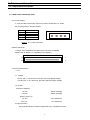
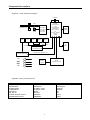
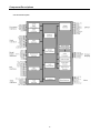
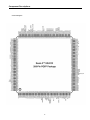
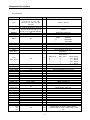
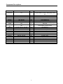
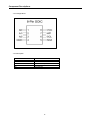
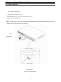
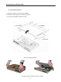
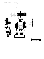
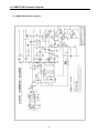
SERVICE
MANUAL
D V C-T 6 3 0 0 N
For version 2
Component descriptions
1. Precautions
2. Reference Information
3. Product Specification
4. Operating Instructions
5. Disassembly and Reassembly
6. Troubleshooting
7. Electrical Part List
8. Block Diagram
9. PCB Diagrams
10. Wiring Diagram
11. Schematic Diagrams
12. Oscillograms
.
1. Precautions
1-1 Safety Precautions
1) Before returning an instrument to the customer,
and then in the OFF position, measure from a
always make a safety check of the entire
known earth ground (metal water pipe, conduit,
instrument, including, but not limited to, the
etc.)
following items:
instrument (antennas, handle brackets, metal
to
cabinets,
all
exposed
metal
screwheads,
parts
metallic
of
the
overlays,
(1) Be sure that no built-in protective devices are
control shafts, etc.), especially and exposed
defective or have been defeated during servicing.
metal parts that offer an electrical return path
(1) Protective shields are provided to protect
to the chassis.
both the technician and the customer. Correctly
Any current measured must not exceed 0.5mA.
replace all missing protective shields, including
Reverse the instrument power cord plug in the
any remove for servicing convenience.
outlet and repeat the test. See Fig. 1-1.
(2) When reinstalling the chassis and/or other
Any measurements not within the limits
assembly in the cabinet, be sure to put back in
specified herein indicate a potential shock
place all protective devices, including, but not
hazard that must be eliminated before returning
limited to, nonmetallic control knobs, insulating
the instrument to the customer.
fish papers, adjustment and compartment
covers/shields, and isolation resistor/capacitor
networks. Do not operate this instrument or
permit it to be operated without all protective
Device
Under
Test
devices correctly installed and functioning.
(Reading
should not
be above
0.5mA)
Test all
exposed Meter
Surfaces
(2) Be sure that there are no cabinet openings
2-Wire Cord
through which adults or children might be able
to insert their fingers and contact a hazardous
Also test with Plug
reserved (Using AC
adapter Plug as
Earth Ground
required)
Fig. 1-1 AC Leakage Test
voltage. Such openings include, but are not
limited to, excessively wide cabinet ventilation
slots, and an improperly fitted and/or incorrectly
secured cabinet back cover.
(4) Insulation
(3) Leakage
Current
Hot
Check-With
Resistance
Test
Cold
Check-(1)
Unplug the power supply cord and connect a
the
jumper wire between the two prongs of the plug.
instrument completely reassembled, plug the
(2) Turn on the power switch of the instrument.
AC line cord directly into a 120V AC outlet. (Do
(3) Measure the resistance with an ohmmeter
not use a isolation transformer during this test.)
between the jumpered AC plug and all exposed
Use a leakage current tester or a metering
metallic cabinet parts on the instrument, such
system that complies with American National
as screwheads, antenna, control shafts, handle
Standards institute (ANSI) C101.1 Leakage
brackets, etc. When an exposed metallic part
Current
for
Laboratories
Appliances
and
(UL)
(40.7).
1270
has a return path to the chassis, the reading
Underwriters
With
should be between 1 and 5.2 megohm. When
the
there is no return path to the chassis, the
instrument’s AC switch first in the ON position
reading must be infinite. If the reading is not
2
Servicing Precautions
(5) within the limits specified, there is the possibility
the AC power cord for damage.
of a shock hazard, and the instrument must be
re-pared and rechecked before it is returned to
5) Components, parts, and/or wiring that appear to
the customer. See Fig. 1-2.
have overheated or that are otherwise damaged
should be replaced with components, parts
and/or wiring that meet original specifications.
Additionally determine the cause of overheating
and/or damage and, if necessary, take corrective
Antenna
Terminal
action to remove and potential safety hazard.
Exposed
Metal Part
6) Product
ohmmeter
Safety
Notice-Some
electrical
and
mechanical parts have special safety-related
ohm
characteristics which are often not evident from
Fig. 1-2 Insulation Resistance Test
evisual inspection, nor can the protection they
give necessarily be obtained by replacing them
2) Read and comply with all caution and safety
with
components
rated
for
higher
voltage,
related notes non or inside the cabinet, or on the
wattage, etc. Parts that have special safety
chassis.
characteristics are identified by shading, an (
or a (
)
) on schematics and parts lists. Use of a
3) Design Alteration Warning-Do not alter of add to
substitute replacement that does not have the
the mechanical or electrical design of this
same safety characteristics as the recommended
instrument. Design alterations and additions,
replacement part might created shock, fire
including but not limited to, circuit modifications
and/or other hazards. Product safety is under
and the addition of items such as auxiliary audio
review continuously and new instructions are
output
issued whenever appropriate.
connections,
might
alter
the
safety
characteristics of this instrument and create a
hazard to the user. Any design alterations or
additions will make you, the service, responsible
for personal injury or property damage resulting
there from.
4) Observe original lead dress. Take extra care to
assure correct lead dress in the following areas:
(1) near sharp edges, (2) near thermally hot
parts (be sure that leads and components do not
touch thermally hot parts), (3) the AC supply, (4)
high voltage, and (5) antenna wiring. Always
inspect in all areas for pinched, out -of-place, or
frayed wiring, Do not change spacing between a
component and the printed-circuit board. Check
3
1-2 Servicing Precautions
CAUTION : Before servicing Instruments covered
(3) The components used in the unit have a
by this service manual and its supplements, read
specified flame resistance and dielectric
and follow the Safety Precautions section of this
strength.
manual.
When replacing components, use components
which have the same ratings. Components I-
Note :
If unforeseen circument create conflict
enti-fied by shading, by (
) or by (
) in the
between the following servicing precautions and
circuit diagram are important for safety or for the
any of the safety precautions, always follow the
characteristics of the unit. Always replace them
safety precautions. Remember: Safety First.
with the exact replacement components.
1-2-1 General Servicing Precautions
(4) An insulation tube or tape is sometimes used
and some components are raised above the
(1) a. Always unplug the instrument’s AC power
printed wiring board for safety. The internal
cord from the AC power source before (1) re-
wiring is sometimes clamped to prevent contact
moving or reinstalling any component, circuit
with heating components. Install such elements
board, module or any other instrument
as they were.
assembly, (2) disconnecting any instrument
electrical plug or other electrical connection,
(5) After servicing, always check that the removed
(3) connecting a test substitute in parallel with
screws, components, and wiring have been
an electrolytic capacitor in the instrument.
installed correctly and that the portion around
b. Do not defeat any plug/socket B+ voltage
the serviced part has not been damaged and so
interlocks with which instruments covered by
on. Further, check the insulation between the
this service manual might be equipped.
blades of the attachment plug and accessible
c. Do not apply AC power to this instrument
conductive parts.
and /or any of its electrical assemblies unless
all solid-state device heat sinks are correctly
1-2-2 Insulation Checking Procedure
installed.
d. Always connect a test instrument’s ground
Disconnect the attachment plug from the AC outlet
lead to the instrument chassis ground before
and turn the power ON. Connect the insulation
connecting the test instrument positive lead.
resistance meter (500V) to the blades of the
Always remove the test instrument ground lead
attachment plug. The insulation resistance between
last.
each blade of the attachment plug and accessible
conductive parts(see note) should be more than 1
Note : Refer to the Safety Precautions section
Megohm.
ground lead last.
Note : Accessible conductive parts include metal
(2) The service precautions are indicated or printed
panels, input terminals, earphone jacks, etc.
on the cabinet, chassis or components. When
servicing, follow the printed or indicated service
precautions and service materials.
4
1-3 ESD Precautions
Electrostatically Sensitive Devices (ESD)
its protective package until immediately before you
are ready to install it. (Most replacement ESD
Some semiconductor (solid state) devices can be
devices are packaged with leads electrically
damaged easily by static electricity.
shorted together by conductive foam, aluminum
Such
components
commonly
are
called
foil or comparable conductive materials).
Electrostatically Sensitive Devices(ESD). Examples
of typical ESD devices are integrated circuits and
(7) Immediately before removing the protective
some field-effect transistors and semiconductor
materials from the leads of a replacement ESD
chip components. The following techniques should
device touch the protective material to the
be used to help reduce the incidence of component
chassis or circuit assembly into which the
damage caused by static electricity.
device will be installed.
(1) Immediately before handling any semiconductor
components
or
CAUTION : Be sure no power is applied to the
semiconductor-equipped
chassis or circuit, and observe all other safety
assembly, drain off any electrostatic charge on
precautions.
your body by touching a known earth ground.
Alternatively, obtain and wear a commercially
(8)
Minimize
bodily
motions
when
handling
replacement
ESD
devices.
available discharging wrist strap device, which
unpackaged
should be removed for potential shock reasons
(Otherwise harmless motion such as the
prior to applying power to the unit under test.
brushing together of your clothes fabric or the
lifting of your foot from a carpeted floor can
(2) After removing an electrical assembly equipped
generate static electricity sufficient to damage
with ESD devices, place the assembly on a
an ESD device).
conductive surface such as aluminum foil, to
prevent electrostatic charge buildup or exposure
of the assembly.
(3) Use only a grounded-tip soldering iron to solder
or unsolder ESD device.
(4) Use only an anti-static solder removal devices.
Some solder removal devices not classified as
“anti-static” can generate electrical charges
sufficient to damage ESD devices.
(5) Do not use freon-propelled chemicals. These
can generate electrical charges sufficient to
damage ESD devices.
(6) Do not remove a replacement ESD device from
5
2. Reference Information
2-1 Component Descriptions
2-1-1 DVD ATAPI LOADER (RL-A700)
* D.C. Power Supply
A 4-pin shrouded, keyed male connector is used to provide the D.C. Power.
The pin assignment is described below.
PIN
1
2
3
4
DC VOLTS
+12V
GND
GND
+5V
Figure-1 D.C. Power Connector
* Interface Connector
A 39-pin male, unshielded, shrouded, keyed connector are applied.
Please refer to Section 7-2-3 regarding its pin definition.
39
1
40
2
Interface Connector
* Electrical Charateristics
1. Power
1-1. Voltage
+5V DC with ±5% tolerance, less than 100mVp-p Ripple Voltage
+12V DC with ±10% tolerance, less than 150mVp-p Ripple Voltage
1-2. Current
Continuous Reading
+5V DC
500mA (Average)
+12V DC
300mA (Average)
Seeking & Spin up
+5V DC
0.8 A (Maximum)
+12V DC
1.5 A (Maximum)
2. Signal Summary
The physical interface consists of single ended TTL compatible receivers.
6
Component Descriptions
3. Connector Pin Definition
Signal
Pin
I/O
CS0
CS1
DA0
DA1
DA2
DASP
DD0
DD1
DD2
DD3
DD4
DD5
DD6
DD7
DD8
DD9
DD10
DD11
DD12
DD13
DD14
DD15
DIOR
DIOW_
DMARK_
DMARQ_
INTRQ
AOCS16
IORDY
PDIAG_
RESET_
CSEL
KEY PIN
GND
37
38
35
33
36
39
17
15
13
11
9
7
5
3
4
6
8
10
12
14
16
18
25
23
29
21
31
32
27
34
1
28
20
2,19,22,24,26,30,40
I
I
I
I
I
I/O
I/O
I/O
I/O
I/O
I/O
I/O
I/O
I/O
I/O
I/O
I/O
I/O
I/O
I/O
I/O
I/O
I
I
I
O
O
O
O
I/O
I
Description
Chip select 0
Chip select 1
Device address bit 0
Device address bit 1
Device address bit 2
Device active or slave (device 1) present
Data bus bit 0
Data bus bit 1
Data bus bit 2
Data bus bit 3
Data bus bit 4
Data bus bit 5
Data bus bit 6
Data bus bit 7
Data bus bit 8
Data bus bit 9
Data bus bit 10
Data bus bit 11
Data bus bit 12
Data bus bit 13
Data bus bit 14
Data bus bit 15
I/O read
I/O write
DMA acknowledge
DMA request
Interrupt request
I/O device 16-bit
II/O ready
Passed diagnostics
Reset
Cable select
Key pin
7
Component Descriptions
*Appendix 1. DSL-710A Block Diagram
33.86MHz
MT1368
(Decoder/Servo)
Disc
MT1366
(RF AMP.)
Disc Motor Unit
Laser
Pickup
Spindle
Motor
Focus
Coil
Track
Coil
Laser Driver
Equalizer
Error Gen.
Sled
Motor
ATAPI
Buffer Manager
Demodulator
Error Correction
PLl
Focus & Tracking
Feeding
Loading
Loading
Motor
I/F
Conn.
Motor Signal
Actuator Signal
DRAM
(4Mbit)
BA5954FP
4Ch Motor Drive
BA6664FM
Spindle Motor Drive
Spindle Motor Signal for CLV
5V
GND
GND
12V
Flash
Memory
(1Mbit)
80C52
System Controller
*Appendix 2. Key-Components List
ITEM
Laser Pickup
Spindle Motor
Feedling Motor
Loading Motor
Decoder IC
RF Amp IC
Actuator & Motor Drive IC
Spindle Motor Drive IC
Model Name
SF-HD6AVS
RSM-2811G
RF-300CA-11440
RF-300CA-11440
M5705
SP3721A
BA5954FP
BA6664FM
8
MAKER
Sanyo Electric
Samhongsa
Mabuchi
Mabushi
Ali
Ali
Rohm
Rohm
Component Descriptions
2-1-2 Fiber Optic Transmitting Module for Digital Audio Equipments (VST5B))
* Recommended Operating Conditions
Item
Supply Voltage
High Level Input Voltage
Low Level Input Voltage
Symbol
Vcc
VIH
VIL
Min.
4.75
2.0
0
9
Typ.
5.0
-
Max.
5.25
Vcc
0.8
Unit
V
V
V
Component Descriptions
2-1-3 NTSC/PAL Digital Video Encoder (AD7170)
10
Component Descriptions
11
Component Descriptions
12
Component Descriptions
TM
2-1-4 DVD Processor Chip (Swan-2
ES4318)
* Features
l
Single-chip DVD video decoder in a 208-pin PQFP package
l
Supports MPEG-1 system and MPEG-2 program streams
l
Programmable multimedia processor architecture
l
Compatible with Audio CD, Video CD, VCD 3.0, and Super Video CD(SVCD)
l
DVD Navigation 1
l
Built-in Content Scrambling System(CSS)
-
Audio
l
Built-in Karaoke key-shift function
l
Dolby
l
Dolby Pro Logic
l
Linear PCM streams for 24 bit / 96KHz
l
Concurrent S/PDIF out and 2-channel audio output
l
Sensaura Dolby Digital Virtual Surround
l
DTS Digital Surround 2-channel downmix stereo output
l
S/PDIF output for encoded AC-3, DTS Digital output or Linear PCM
-
Peripheral
l
Glueless unterface to DVD loaders (ATAPI or A/V bus I/F)
l
Bidirectional I C audio interface
l
Direct servo / loader interface
l
8 general-purpose auxiliary ports
l
Single 27MHz clock input
-
Smart Technology
l
SmartZoom
l
l
TM
Digital 2-channel downmix audio output for Dolby
2
TM
for motion zoom & pan
TM
for NTSC to PAL conversion and vice versa
SmartScale
SmartStream
TM
for video error concealment
13
TM
Component Descriptions
*Functional Description
14
Component Descriptions
* Pinout Diagram
15
Component Descriptions
*Pin Description
Name
Number
1, 9, 18, 27, 35, 44, 51, 59, 68, 75,
83, 92, 99, 104, 111,121, 130,
139, 148, 157, 164, 172, 183,
193, 201
23:19,16:10,7:2,207:204
8,17,26,34,43,52,60,67,76,84,91
,98,103112,120,129,138,147,15
6,163,171,177,184,192,200,208
24
I/O
Definition
I
3.65 V ± 150 mv.
O
Device address output.
I
Ground.
I
O
RSEL
25
I
TDMDR
TDMCLK
TDMFS
TDMTSC#
TWS
SEL_PLL1
28
29
30
31
I
I
I
O
O
I
Reset input, active low.
TDM transmit data
ROM Select
RSEL
Selection
0
16-bit ROM
1
8-bit ROM
TDM receive data.
TDM clock input.
TDM frame synch.
TDM output enable, active low.
Audio transmit frame sync.
Select PLL1.
Audio transmit serial data port.
Select PLL0.
SEL_PLL2
SEL_PLL0
Clock Output
0
0
2.5 x DCLK
0
1
3 x DCLK
1
0
3.5 x DCLK
1
1
4 x DCLK
Select PLL2. See the table for pin number 33.
Audio master clock for audio DAC.
Audio transmit bit clock.
S/PDIF (IEC958)Format Output.
Audio receive serial data.
Audio receive frame synch.
Audio receive bit clock.
Analog PLL Capacitor.
Crystal input.
Crystal output.
DRAM address bus.
Column address strobe, active low.
Output enable, active low.
Clock enable, active low.
DRAM write enable, active low.
Row address strobe, active low.
DRAM data bus.
SDRAM chip select [1:0], active low.
Data input / output mask.
Clock to SDRAM.
Clock Input(27MHz).
8-bit YUV output.
2X pixel clock.
Pixel clock.
VCC
LA[21:0]
VSS
RESET#
TDMDX
TSD
SEL_PLL0
SEL_PLL2
MCLK
TBCK
SDIF_DOBM
RSD
RWS
RBCK
APLLCAP
XIN
XOUT
DMA[11:0]
DCAS#
DOE#
DSCK_EN
DWE#
DRAS[2:0]#
DB[15:0]
DCS[1:0]#
DQM
DSCK
DCLK
YUV[7:0]
PCLK2XSCN
PCLKQSCN
1.
VSY
NC
H#
32
33
36
39
40
41
45
46
47
48
49
50
66:61, 58:53
69
O
I
71
74:72
96:93, 90:85, 82:77
97, 100
101
102
105
115:113, 110:106
116
117
I/O
I/O
O
I
I
I
I
I
O
O
O
O
I
O
O
I/O
O
O
O
I
O
I/O
I/O
118
I/O
70
16
Vertical synch for screen video interface,
programmable for rising or falling edge, active
low.
Component Descriptions
Name
Number
I/O
HSYNCH#
119
I/O
HD[15:0]
HCS1FX#
HCS3FX#
HIOCS16#
HA[2:0]
VPP
HWR#/DCI_
ACK#
HRD#DCI_C
LK
HD[15:0]
HWRQ#
HRDQ#
HIRQ
HRST#
HIORDY
HWR#
AUX[7:0]
LOE#
LCS[3:0]#
LD[15:0]
LWRLL#
LWRHL#
NC
141:140, 137:131, 128:122
152
153
151
158, 155:154
159
O
O
O
I
I/O
I
149
I,I
150
I,I
Host read/DCI Interface Clock.
141:140, 137:131, 128:122
142
143
144
145
146
149
169:165, 162:160
170
176:173
197:194, 191:185, 182:178
198
199
37, 38, 42, 203:202
I/O
O
O
I/O
O
I
O
I/O
O
O
I/O
O
O
Host data bus.
Host write request.
Host read request.
Host interrupt.
Host reset.
Host I/O ready
Host write request.
Auxiliary ports.
Device output enable, active low.
Chip select[3:0], active low.
Device data bus.
Device write enable, active low.
Device write enable, active low.
No Connect pins. Leave open
17
Definition
Horizontal synch for screen video interface,
programmable for rising or falling edge, active
low.
Host data bus
Host select 1.
Host select 3.
Device 16-bit data transfer.
Host address bus.
Peripheral protection voltage.
Host write/DCI Interface Acknowledge Signal,
active low.
Component Descriptions
2-1-5 DIGITAL-TO-ANALOG STEREO AUDIO CONVERTER (CS4391)
* Block Diagram
18
Component Descriptions
19
Component Descriptions
20
Component Descriptions
21
Component Descriptions
2-1-6
8-BIT MTP MICROCONTROLLER (W78LE52)
* Features
Fully static design 8-bit CMOS microcontroller
256 bytes of on-chip scratchpad RAM
8 KB electrically erasable/programmable MTP-ROM
64 KB program memory address space
64 KB data memory address space
Four 8-bit bi-directional ports
Three 16-bit timer/counters
One full duplex serial port(UART)
Watchdog Timer
Eight sources, two-level interrupt capability
EMI reduction mode
Built-in power management
Code protection mechanism
Packages : DIP 40: W78LE52-24
*Pin Configurations
22
Component Descriptions
*Pin Description
SYMBOL
EA#
PSEN#
ALE
RST
XTAL1
XTAL2
VSS
VDD
P0.0 - P0.7
P1.0 - P1.7
P2.0 - P2.7
P3.0 - P3.7
P4.0 - P4.3
DESCRIPTIONS
EXTERNAL ACCESS ENABLE: This pin forces the processor to execute out of
external ROM. It should be kept high to access internal ROM. The ROM address and
data will not be presented on the bus if EA pin is high and the program counter is
within on-chip ROM area.
PROGRAM STORE ENABLE: PSEN enables the external ROM data onto the Port 0
address/ data bus during fetch and MOVC operations. When internal ROM access is
performed, no PSEN strobe signal outputs from this pin.
ADDRESS LATCH ENABLE: ALE is used to enable the address latch that separates
the address from the data on Port 0.
RESET: A high on this pin for two machine cycles while the oscillator is running
resets
the device.
CRYSTAL1: This is the crystal oscillator input. This pin may be driven by an external
clock.
CRYSTAL2: This is the crystal oscillator output. It is the inversion of XTAL1.
GROUND: Ground potential
POWER SUPPLY: Supply voltage for operation.
PORT 0: Port 0 is a bi-directional I/O port which also provides a multiplexed low
order
address/data bus during accesses to external memory. The pins of Port 0 can be
individually configured to open-drain or standard port with internal pull-ups.
PORT 1: Port 1 is a bi-directional I/O port with internal pull-ups. The bits have
alternate
functions which are described below:
T2(P1.0): Timer/Counter 2 external count input
T2EX(P1.1): Timer/Counter 2 Reload/Capture control
PORT 2: Port 2 is a bi-directional I/O port with internal pull-ups. This port also
provides the upper address bits for accesses to external memory.
PORT 3: Port 3 is a bi-directional I/O port with internal pull-ups. All bits have alternate
functions, which are described below:
RXD(P3.0) : Serial Port receiver input
TXD(P3.1) : Serial Port transmitter output
INT0 (P3.2) : External Interrupt 0
INT1(P3.3) : External Interrupt 1
T0(P3.4) : Timer 0 External Input
T1(P3.5) : Timer 1 External Input
WR(P3.6) :External Data Memory Write Strobe
RD(P3.7) : External Data Memory Read Strobe
PORT 4: Another bit-addressable bidirectional I/O port P4. P4.3 and P4.2 are
alternative function pins. It can be used as general I/O port or external interrupt input
sources (INT2 / INT3 ).
23
Component Descriptions
* Block Diagram
*Absolute Maximum Ratings
PARAMETER
DC Power Supply
Input Voltage
Operating
Temperature
Storage Temperature
SYMBOL
VDD-VSS
VIN
MIN.
-0.3
VSS -0.3
MAX.
+7.0
VDD +0.3
UNIT
V
V
TA
0
70
°C
TST
-55
+150
°C
24
Component Descriptions
2-1-7 Serial EEPROM, 2K (256 x 8) (AT24C02)
* Features
• Low-Voltage and Standard-Voltage Operation
– 5.0 (V CC = 4.5V to 5.5V)
– 2.7 (V CC = 2.7V to 5.5V)
– 2.5 (V CC = 2.5V to 5.5V)
– 1.8 (V CC = 1.8V to 5.5V)
• Internally Organized 128 x 8 (1K), 256 x 8 (2K), 512 x 8 (4K),1024 x 8 (8K) or 2048 x 8 (16K)
• 2-Wire Serial Interface
• Schmitt Trigger, Filtered Inputs for Noise Suppression
• Bidirectional Data Transfer Protocol
• 100 kHz (1.8V, 2.5V, 2.7V) and 400 kHz (5V) Compatibility
• Write Protect Pin for Hardware Data Protection
• 8-Byte Page (1K, 2K), 16-Byte Page (4K, 8K, 16K) Write Modes
• Partial Page Writes Are Allowed
• Self-Timed Write Cycle (10 ms max)
• High Reliability
– Endurance: 1 Million Write Cycles
– Data Retention: 100 Years
– ESD Protection: >3000V
• Automotive Grade and Extended Temperature Devices Available
• 8-Pin and 14-Pin JEDEC SOIC, 8-Pin PDIP, 8-Pin MSOP, and 8-Pin TSSOP Packages
25
Component Descriptions
* Pin Configurations
* Pin Description
Pin Name
A0 - A2
SDA
SCL
WP
NC
Function
Address Inputs
Serial Data
Serial Clock Input
Write Protect
No Connect
26
Component Descriptions
2-1-8 512K Bit CMOS 5.0 Volt-only, Uniform Sector Flash Memory (A29040)
27
Component Descriptions
28
Component Descriptions
2-1-9 64MBit SDRAM 1MX 16BitX4Banks Synchronous DRAM LVTTL (K4S641632D)
29
Component Descriptions
30
Component Descriptions
31
3. Product Specifications
n
Playback System
DVD Video
Video CD (1.1, 2.0, 3.0)
SVCD and CVD
CDDA
CD-ROM with MP3 data
n
Television Signal System
NTSC/PAL
n
n
Video Performance
Video Out
1 Vpp / 75 ohm
S-Video Out
Y : 1 Vpp / 75 ohm
C : 0.286 Vpp / 75 ohm
Component Out
0.7 Vpp / 75 ohm
D/A Converter
27MHz / 10bit
Audio Performance
Frequency Response
DVD : fs 48/96KHz, 4Hz ~ 2/44KHz
Video CD : fs 44.1KHz, 4Hz~20KHz
Audio CD : fs 44.1KHz, 4Hz~20KHz
Output Level
Analog : 2Vrms (1 KHz)
Digital : 1.15 Vpp
D/A Converter
96KHz/24bit
S/N Ratio
110 dB
32
Product Specifications
n
n
Connections
Coaxial digital audio out
X1
Optical digital audio out
X1
Audio Analog out for 2-channel
X1
Component Video
X1
Composite Video out
X1
S-Video out
X1
Power Supply
Power Source
Power Consumption
n
AC 100~240V, 50/60Hz
< 20 Watt
Set
Dimensions (W X H X D)
440 X 60 X 270 (mm )
Net Weight
3.2 Kg
Gross Weight
4 Kg
33
4. Operating Instructions
4-1 Basic Connections
Connecting to audio equipment & TV
Connecting to AUDIO SYSTEM
Audio equipment
TV set
Method1: DVD Player + 2CH Streo Amplifer
Method2: DVD Player + TV with Audio Input
Jack(L,R)
Connecting to TV (for VIDEO)
Method1: DVD Player + TV with Video input
Jack
Method2: DVD Player + TV with S-video Jack
Method3: DVD Player + TV with Component
Input Jack
Connecting to a monaural TV set
*The way connected DVD Player and TV for Video
TV set
is the same with the procedure described in above
DVD Play + TV with Audio Input Jack
34
Operating Instructions
Connecting to a decoder with a Dolby Digital or DTS processing
TV set
Coaxial audio cable (optional)
To coaxial digital audio input
Optical audio cable (optional)
To optical digital audio input
Decoder or Amplifier with
Dolby Digital / dts
Center
Front
Front
Subwoofer
Surround
Surround
35
Operating Instructions
4-2 Selecting Video MODE
Press SETUP button and select VIDEO submenu on SETUP screen. After that, select TV type by pressing
DOWN arrow button ( ▼) until desired TV mode is selected. For more information, refer to 7.2 Video on
the Instruction Manual.
4-3 Selecting the desired DVD menu Item
When a DVD disc is loaded, select desired menu item using arrow
button or numeric button, if number for each menu item is displayed,
then press the SELECT button to start play. To select subtitles, the
forth menu item in the figure as shown right, press the RIGHT arrow
button three times and press the SELECT button.
Example:
1. Press the RIGHT arrow button ( ▶ )
2. Press the RIGHT arrow button ( ▶ )
3. Press the RIGHT arrow button ( ▶ )
4. Press the SELECT button
4-4 Selecting the desired MP3 folder
When a MP3 disc is loaded, you may see the menu screen as shown
right. To play a MP3 title, you should select a title under the desired
folder. Use arrow button, select the folder, which you want to play,
by pressing the SELECT button. If you press the SELECT button,
you can see the file lists under the folder. To select DDROST folder
in this case, press the SELECT button.
Example:
1. Press the SELECT button
36
Operating Instructions
4-5 Selecting the desired MP3 title
Use arrow button and select an MP3 title using the SELECT button
then play will start automatically. When you know the title number,
enter the MP3 title number using numeric buttons and press the SELECT button. If you want to play an adjacent MP3 title, press the
NEXT button for next title and the PREV button for previous title
during playing. To select “005 HAVEYOU” MP3 title in this case,
press the DOWN arrow button twice and press the SELECT button.
Example:
1. Press the DOWN arrow button ( ▼)
2. Press the DOWN arrow button ( ▼)
3. Press the SELECT button
4-6 Searching
When you want to view the disc contents in fast forward or fast reverse, you can do that by pressing FF/SF button(
(
) or FR/SR button
). There are total 6 steps for DVD, 4 steps for VCD and 2 steps for
CDDA in fast searching. They are FAST 2X, FAST 4X, FAST 8X,
FAST 16X, FAST 32X and FAST 64X for both direction. To search
at FAST 16X in forward direction, press the FF/SF button 4 times
during play mode.
Example:
1. Press the FF/SF button (
)
2. Press the FF/SF button (
)
3. Press the FF/SF button (
)
4. Press the FF/SF button (
)
4-7 Resume Play
If power is OFF by pressing the POWER button during PLAY or PRESTOP state, play is resumed from the
point where it was stopped. If you switch OFF by disconnecting AC cord, the machine will start playing from
the first track or chapter.
Example:
Press the POWER button during play mode or prestop mode.
37
Operating Instructions
4-8 Slow Viewing
When you want to view the disc contents very slowly in forward or
reverse direction, you can do that by pressing the FF/SF button (
or the FR/SR button (
)
) during pause mode. There are total 3 steps
for DVD and VCD. They are SLOW 1/2X, SLOW 1/4X and SLOW
1/8X for both direction. The slow reverse function is possible only
when a DVD disc is loaded. To view at slow 1/4X in forward direction, press the FF/SF button (
) two times during pause mode.
Example:
1. press the PLAY/PAUSE button (
1. Press the FF/SF button (
2. Press the FF/SF button (
)
)
)
4-9 Selecting Audio Language
This function works only with discs on which multiple audio sound
track languages are recorded. If the loaded disc supports multiple
languages, you can see the AUDIO indicator on fluorescent display.
In the figure shown right, there are total 8 audio languages. To select
the third audio language, press the AUDIO button twice during play.
Example:
1. Press the AUDIO button
2. Press the AUDIO button
4-10 Selecting Subtitle Language
This function works only with discs on which multiple subtitle langauges are recorded. If the loaded disc supports multiple languages,
you can see the SUB-T indicator on fluorescent display. In the figure
shown right, there is only one subtitle language. To turn on the subtitle language, press the SUBTITLE button. If you press it again,
you can turn off the subtitle language.
Example:
1. Press the SUBTITLE button
38
Operating Instructions
4-11 Selecting Angle
Some DVD discs may contain scenes, which have been shot simultaneously from a number of different angles. If the loaded disc supports multiple angles, you can see
indicator on the fluorescent
display and the TV screen. In the figure shown right, there are total
9 angles. To switch to the angle number 2, press the ANGLE button.
Example:
1. Press the ANGLE button
39
5. Disassembly and Reassembly
5-1 Cabinet and PCB
5-1-1 Door Tray Removal
1) Supply Power and open Tray (1).
2) Disassemble the Door Tray (2) in direction off arrow “A”.
3) Close Tray (1) and power off.
Note : If Tray doesn’t open, insert a sharp point into emergency hole, and then push the tap in the hole in
direction of arrow, After then open tray manually
(1) Tray
(2) Door Tray
“A”
¸ Emergency Hole
.
¹ Screw Driver
<Bottom View>
Fig 5-1 Door Tray Removal
40
Disassembly and Reassembly
5-1-2 Top Cabinet Removal
1) Remove 4 Screws (1) on the back Top Cabinet.
2) Remove 2 Screws (2), (3) on the left and right side.
3) Lift up the Top Cabinet in direction of arrow.
(2) 2 Screws
(1) 4 Screws
(3) 2 Screws
Fig 5-2 Top Cabinet Removal
*You have to lift up in direction of arrow, certainly!
41
Disassembly and Reassembly
5-1-3 PCB Cable Removal
1) Disconnect PCN1 (1).
2) Disconnect PCN4 (2).
3) Disconnect LCN1 (3).
4) Disconnect CON2 (4).
5) Disconnect CON1 (5).
6) Disconnect CON6 (6).
(1) PCN1
(3) LCN1
(5) CON1
(2) PCN4
(6) CON6
(4)CON2
Fig 5-3 PCB Cable Removal
42
Disassembly and Reassembly
5-1-4 PCB and Front Ass’y Removal
1) Remove 2 Screws (1) on the back of the Cabinet.
2) Remove 8 Screws (2) and disassemble the Main PCB (3) and SMPS PCB (4).
3) Remove 6 Screws (5) and disassemble the Front Ass’y (6).
(2) 8 Screws
(4) SMPS PCB
(3) Main PCB
(1) 2 Screws
(6) Front Ass’y
(5) 6 Screws
Fig 5-4 PCB and Front Ass’y Removal
43
Disassembly and Reassembly
5-1-5 Loader Removal
1)Remove 4 Screws (1) and disassemble the Loader (2).
(1) 4 Screws
(2) Loader
Fig 5-5 Loader Removal
44
Disassembly and Reassembly
5-1-6 Front PCB Removal
1) Remove 9 Screws (1) and disassemble the Front PCB (2) from the Front Ass’y (3).
(3) Front Ass’y
(2) Front PCB
(1) 9 Screws
Fig 5-6 Front PCB Removal
45
6. Troubleshooting
An Appearance
Requires Confirmation
No power
Insert the AC power plug securely into the power outlet.
No picture
Make sure that the equipment is connected properly.
Make sure that the input setting for the TV is Video (AV).
No sound
Make sure that the equipment is connected properly.
Distorted sound
Make sure that the input settings for the TV and stereo system are
correct.
No fast
reverse
forward
or
fast
Some discs may have sections that prohibit fast forward or fast reverse.
No proper aspect ratio
Select the correct setup for TV aspect ratio that matches your TV set.
No operations can be
performed with the remote
controller
Check the batteries are installed with the correct polarities.
Point the remote control unit at the remote control sensor and operate.
Remove the obstacles between the remote control unit and remote
control sensor.
Set the POWER button to OFF and then back to ON.
Alternatively, turn off the power, disconnect the power plug and then
reconnect it.
No button operation
Audio soundtrack and/or
Subtitle language is not the
one you selected.
If the audio soundtrack and/or subtitle language does not exist on the
disc, the language selected at the initial settings will not be seen.
No Angle change
This function is dependent on software availability. Even if a disc has a
number of angles recorded, these angles may be recorded for specific
scenes only.
46
7. Electrical Part List
7-1.Main board
Location
DVD-2100 USA 향 Rev.MP01
NO
Spec
Pak'
Usa'
No
ASS'Y OPTION
1 AAA, 1.5V, BATTERY
2
ASS'Y MAIN
1 SMPS
2 Hard Disc Cable,
Ass'y
mm, 40Pin
3 DVD Loader, Mechanism Ass'y
1
1
Ass'y
1
1 80C52(80C51), 40PIN DIP, MPU
DIP
1
U601
2 FLASH ROM 512K * 8
DIP
1
U201
PCB ASS'Y, MAIN (T/U)
PCB ASS'Y, MAIN (M/I)
1 POWER CON', 12PIN, 2.54mm
Strat
1
CON1
2 FRONT CON', WAFER,11PIN, 2.54mm strat
1
CON2
3 BOX HEADER, 20*2, 2.54mm
1
CON6
4 S-VHS CON, MINI DIN, SHILD
1
CON4
5 RCA CON', W-Y,R-B, SHILD
PCB-L
1
CON5
6 RCA CON', SHILD, (G-U-R)
PCB-L
1
CON3
7 Headphone CON' 5PIN, 2.54mm
1
CON7
8 Optical Connector for Audio
1
P1
1
X601
1
X201
9 X-TAL, 11.0592MHZ,HC-49/S, 20pF
10 X-TAL, 27MHZ,HC-49/S, 20pF
HC49/S
HC49/S
PCB ASS'Y, MAIN (DIP)
1 40PIN, DIP, MPU SOCKET
DIP
1
U601
2 32PIN, DIP, ROM SOCKET
DIP
1
U201
1 ELEC' CAP', 100uF/16V,M
5mm
5
CE3,CE4,CE5,CE6,CE20
2 ELEC' CAP', 100uF/25V,M
5mm
2
CE1,CE2
3 ELEC' CAP', 10uF/16V,M
5mm
15
4 ELEC' CAP', 10uF/25V,M
5mm
2
CE7,101,102,201,202,303,304,305,306,315,316,317,318,601,
602
CE320,CE321
5 ELEC' CAP', 47uF/16V,M
5mm
2
CE301,CE401
6 ELEC' CAP', 22uF/16V,M
5mm
8
CE505,CE506,CE511,CE512,CE513,CE514,CE515,CE516
1 PCB, 2 LAYER
FR4
1
2 CPU&RISC SINGLE CHIP
PQFP
1
U101
3 Video Encoder, NTSC/PAL
LQFP
1
U401
64M-SDRAM,
4
3.3V,400mil,512K*16*8
5 TTL, HEX INVERTER(FAST)
TSOP(
II)
SOIC
1
U102
1
U208
6 TTL, HEX INVERTER
SOIC
1
U207
7 EEPROM, 2KBIT,SOIC
SOIC
1
U204
8 AUDIO DAC,
SOIC
1
U301
9 DUAL OP-AMP
SOIC
2
U304,U306
PCB ASS'Y, MAIN (RAD)
PCB ASS'Y, MAIN (SMD)
47
Electrical Part List
Location
DVD-2100 USA 향 ev.MP01
NO
Spec
Pak'
Usa'
No
PCB ASS'Y, MAIN (SMD)
10 WOUND INDUCT',15uH,3225
SMD
4
L404,L407,L408,L409
11 CHIP POWER BEAD
12 CHIP FERRITE BEAD
3216
7
L1,L2,L3,L4,L5,L6,L21
2012
21
L8 ~ L20, L22, L23, L25, L26, L201,L202, L301, L402
13 ZENER DIODE, 3.9V,350mW
SOT-23
0
14 ZENER DIODE, 8.2V,350mW
SOT-23
2
15 Switching diode
SOT-23
0
16 Dual Diode, Common cathode
SOT-23
0
17 RLS4148
SOT-23
1
D601
18 GENERAL TR, NPN
SOT-23
13
Q301,Q302,Q303,Q501,502,503,505,506,507,512,513,514,515
19 Switching TR, NPN
SOT-23
2
Q519,Q701
20 Switching TR, PNP
SOT-23
2
Q520,Q702
21 GENERAL TR, PNP
SOT-23
1
Q304
22 CHIP RES', 1/8W,33 ΩJ
3216
1
R7
23 CHIP RES', 1/8W,0 ΩJ
1608
5
R131,R235,R272,R274,R406
24 CHIP RES', 1/8W,10 ΩJ
1608
13
25 CHIP RES', 1/8W,100K ΩJ
1608
14
26 CHIP RES', 1/8W,10K ΩJ
1608
4
R8,R601,R616,R620
27 CHIP RES', 1/8W,1K ΩJ
1608
10
R241,R242,R350,R351,R353,R354,R586,R587,R590,R591
28 CHIP RES', 1/8W,1M ΩJ
1608
3
R234,R261,R277
29 CHIP RES', 1/8W,120 ΩJ
1608
2
R551,R539
30 CHIP RES', 1/8W,1.2K ΩJ
1608
4
R327,R329,R331,R333
31 CHIP RES', 1/8W,22 ΩJ
1608
7
R301,R302,R303,R304,R305,R306,R307
32 CHIP RES', 1/8W,220 ΩJ
1608
3
R262,R270,R603
33 CHIP RES', 1/8W,20K ΩJ
1608
6
R535,R541,R547,R558,R564,R570
34 CHIP RES', 1/8W,33 ΩJ
1608
27
R113,114,115,117,118,204,205,206,207,208,209,210,211,212,213,214,
215,216,217,218,219,228,229,230,232,401,402
35 CHIP RES', 1/8W,3.3K ΩJ
1608
15
R271,R345,R347,R361,R405,R538,R544,R550,R561,R567,R573,R602
,R609,R612,R617
36 CHIP RES', 1/8W,3.9K ΩJ
1608
0
37 CHIP RES', 1/8W,4.7K ΩJ
1608
6
R2,R3,R120,R121,R122,R202
38 CHIP RES', 1/8W,47 ΩJ
1608
8
R220,R221,R222,R223,R224,R225,R226,R227
39 CHIP RES', 1/8W,470 ΩJ
1608
0
40 CHIP RES', 1/8W,47K ΩJ
1608
2
R129,R130
41 CHIP RES', 1/8W,330 ΩJ
1608
2
R127,R128
42 CHIP RES', 1/8W,560 ΩJ
1608
1
R404
43 CHIP RES', 1/8W,5.6K ΩJ
1608
8
R322,R323,R324,R325,R326,R328,R330,R332
44 CHIP RES', 1/8W,620 ΩJ
1608
8
R408,R409,R414,R415,R416,R417,R418,R419
45 CHIP RES', 1/8W,6.2K ΩJ
1608
2
R348,R346
46 CHIP RES', 1/8W,75 ΩJ
1608
7
R545,R562,R574,R584,R585,R588,R589
47 CHIP RES', 1/8W,68 ΩJ
1608
1
R568
48 CHIP RES', 1/8W,91 ΩJ
1608
1
R124
49 CHIP CAP', 25V,3pF,J,COG
1608
4
C412,C421,C424,C427
50 CHIP CAP', 25V,15pF,J,COG
1608
0
D301,D302
R101,R102,R103,R104,R105,R106,R107,R108,R109,R110,R111,R112
,R231
R530,R531,R536,R540,R542,R546,R548,R552,R559,R563,R565,R569
,R571,R575
48
Electrical Part List
DVD-2100 USA 향
Rev.MP01
NO
Spec
Location
Pak' Usa'
No
PCB ASS'Y, MAIN (SMD)
51 CHIP CAP', 25V,22pF,J,COG 1608
1
C228
1608
4
C302,C303,C304,C305
53 CHIP CAP', 25V,27pF,J,COG 1608
13
C124,C125,C129,C413,C414,C422,C423,C425,C426,C428,C429,C602,603
54 CHIP CAP', 25V,33pF,J,COG 1608
2
C227,C229
CHIP
55
25V,330pF,J,COG
1608
0
56 CHIP CAP', 25V,47pF,J,COG 1608
7
C219,C531,C532,C533,C535,C536,C537
1608
2
C540,C541
1608
4
C306,C307,C308,C309
68
C1,C2,C3,C4,C5,C6,C7,C20,C101,C102,C103,C104,C105,C106,C107,C108
,C109,C110,C111,C112,C113,C114,
C115,C116,C117,C118,C120,C121,C123,C128,C201,C202,C203,C204,C205
,C206,C207,C208,C209,C210,C211,C212,
C213,C214,C215,C218,C220,C232,C233,BC301,BC303,BC304,BC305,BC314
,BC315,BC318,BC319,BC320,BC321,
C401,C402,C405,C406,C407,C408,C409,C410,C601
52
CHIP
25V,2700pF,J,COG
CHIP
57
25V,470pF,J,COG
CHIP
58
25V,560pF,J,COG
59
CHIP
25V,0.1uF,Z,Y5V
CAP',
CAP',
CAP',
CAP',
CAP',
1608
Total
49
Electrical Part List
7-2 FRONT BOARD PART LIST
Location
Front Board SB Type
Spec
Pak' Usa'
No
ASS'Y FRONT
PCB ASS'Y, FRONT (T/U)
PCB ASS'Y, FRONT (M/I)
(IR)INFRA RECIEVER
L Type
1
U2
TR
TO-92
1
Q1
VFD DISPLAY
1
U3
WIRE
1
CON2
FRONT SIGNAL WIRE, 11PIN-11PIN(PCB), PCB IN WIRE
1
CON1
TACT S/W, 4PIN,5mm
11
SW1,SW2,SW3,SW4,SW5,SW6,SW8,SW9,SW10,SW11,SW12
FRONT POWER WIRE, 5PIN-5PIN(PCB), PCB IN
5mm
PCB ASS'Y, FRONT (RAD)
LED,RED, 3 PIE, 5mm Formming, High 4.5mm
1
D2
ELEC' CAP', 10uF/16V,M
5mm
3
CE1,CE2,CE4
ELEC' CAP', 10uF/50V,M
5mm
1
CE3
PCB, 1 LAYER
FR1
1
JUMPER
8mm
14
JP1,JP2,JP3,JP6 ~ JP9, JP18 ~ JP24
JUMPER
12mm
10
JP4,JP5,JP10 ~ JP17
DIODE
AXIAL
3
D3,D4,D5
Axial Cap, 50V,0.IUF,Z
AXIAL
7
C1,C3,C4,C5,C6,C7,C8
AXIAL,BEAD, 3560
AXIAL
2
L1,L2
AXI' RES', 1/6W,3.3K ΩJ
AXIAL
2
R1,R9
AXI' RES', 1/6W,56K ΩJ
AXIAL
1
R12
AXI' RES', 1/6W,10K ΩJ
AXIAL
6
R3,R4,R5,R6,R7,R8
AXI' RES', 1/6W,330 ΩJ
AXIAL
AXI' RES', 1/6W,22 ΩJ
AXIAL
1
NR1
PQFP
1
U1
PCB ASS'Y, FRONT (AXI)
PCB ASS'Y, FRONT BOTTUM (SMD)
VFD DRIVER
Total
50
Electrical Part List
7-3 SMPS PART LIST
SMPS
NO
1
2
3
4
5
6
7
8
RESISTOR
RESISTOR
RESISTOR
RESISTOR
RESISTOR
RESISTOR
RESISTOR
Spec
CAR
CAR
CAR
CAR
CAR
CAR
CAR
RESISTOR
Location
CAR
Usa'
1
1
2
1
1
1
5
1
No
9 RESISTOR
CAR
1
R10
10 RESISTOR
CAR
1
R11
11 RESISTOR
CAR
1
R17
12 RESISTOR
CAR
1
R19
13 RESISTOR
CAR
2
R23,R24
R2
R3
R5,R7
R4
R8
R12
R9,13,20,22,30
R18
14 CAPACITOR
ELE
1
C1
15 CAPACITOR
ELE
1
C13
C7,C8
16 CAPACITOR
ELE
2
17 CAPACITOR
ELE
2
C9,C10
18 CAPACITOR
ELE
3
C14,C15,C17
19 CAPACITOR
ELE
4
C16,19,20,25
20 CAPACITOR
CER
2
C5,C106
21 CAPACITOR
MF
2
C101,C102
22 CAPACITOR
CER
1
C11
23 CAPACITOR
CER
1
C4
CER
1
C103
25 DIODE
1
D1
26 DIODE
1
D4
27 DIODE
2
D3,D5
28 DIODE
3
D8,D9,D10
29 DIODE
1
ZD2
30 DIODE
4
D401-4
31 DIODE
2
D11,D71
32 IC
1
U1
33 IC
1
U2
34 IC
1
U3
35 IC
1
U4
36 FET
1
Q1
37 TR
2
Q2,Q3
38 TR
39 TR
40 FET
1
1
1
Q501
Q42
Q5
24 CAPACITOR
51
Electrical Part List
SMPS
NO
Spec
Location
Usa'
No
41 TRANS
1
T1
42 FUSE
1
F1
43 FUSE HOLDER
1
44 CHOKE
1
L4
45 CHOKE
2
L2,L3
46 AXIAL CHOKE
2
L6,L7
47 VARISTOR
1
V1
48 THERMISTOR
1
TH1
49 LINE FILTER
1
LF1
50 HARNESS(12PIN)
1
CN1
51 HARNESS(4PIN)
1
CN2
52 WAFER
1
CN3
53 WAFER
1
P1
54 HEAT SINK
2
55 PCB
1
56 TRANS CUSHION
1
57 BOX (OUT BOX)
1/40
58 JUMPER
5
S2,3,4,9,10
59 JUMPER
2
S5,6
60 SCREW
2
Total
52
8. Block Diagram
MAIN PCB
POWER
LOADER
PCB
(DVS)
VIDEO
D/A
ENCODER
CONVERTE
R
A/V
DECODER
SUB
&
MICOM
MAIN CPU
HEAD PHONE
PCB
KEY
VFD
REMOCON
EYE
FRONT PCB
53
MATRIX
RCU
9. PCB Diagrams
9 - 1 Main PCB (Top)
54
PCB Diagrams
9 - 2 Main PCB (Bottom)
55
PCB Diagrams
9 - 3 Front PCB (Top)
9 - 4 Front PCB (Bottom)
56
PCB Diagrams
9 - 5 SMPS PCB (Top)
9- 6 SMPS PCB (Bottom)
57
10. Wiring Diagram
58
11. Schematic Diagrams
11-1 Main PCB Schematic Diagram
11-1-1 Main PCB Top Schematic diagram
BC847A
Title
DVD-2100U
Size
A3
Document Number
Main Block
Date:
Monday, March 04, 2002 Sheet
1
of
5
BC857A
3(C)
3(C)
1F
3F
Rev
MP01
2(B)
1(E)
2(B)
MEMO
+5VD+5VD
1(E)
+5VA1
L21 PB3216
R2
R3
4.7K
4.7K
DD[0..15]
CON6
100u/16V
L1
L2
PB3216
L3
PB3216
L4
PB3216
L5
PB3216
L6
PB3216
+5VD
DRST#
DD15
DD14
DD13
DD12
DD11
DD10
DD9
DD8
+3.65V +5VALL
1
3
5
7
9
11
13
15
17
19
21
23
25
27
29
31
33
35
37
39
DWR#
DRD#
DIORDY
DIRQ
DA1
DA0
DACS1#
C2
C3
C4
C5
C6
104
104
104
104
104
2
RESET
GND 4
D7
D8 6
D6
D9
8
D5
D10 10
D4
D11 12
D3
D12 14
D2
D13 16
D1
D14 18
D0
D15 20
GND
KEY 22
DRQ
GND 24
IOW
GND 26
IOR
GND 28
IOCHRDY BALE
30
DACK
GND 32
IRQ14
IOCS1634
A1
RESERVED36
A0
A2 38
CS0
CS1 40
ACTIVITY
GND
DD0
DD1
DD2
DD3
DD4
DD5
DD6
DD7
SCART SW
CON3
RCA CONN X3
Y/G
Cb
Y/G L10
FB2012
5
Cb L18
FB2012
2
Cr L19
FB2012
3
DIOCS16#
DA2
DACS3#
Cr
HDR-2X20
BOTTOM
C1
104
FB2012
CON4
S-VHS
6
7
IR
FB2012
HOST_DATA
HOST_CS HOST_DATA
HOST_CLK HOST_CS
HOST_CLK
ASDATA_DVD
LRCK_DVD
MCLK
BCLK_DVD
MD_DACO
ML_DACO
OPEN_SW
MC_DACO
FB2012VFD_STB
FB2012VFD_CLKO
FB2012VFD_DATA
FB2012POWER_LED
FB2012POWER_SW
HP_L
HP_R
POWER_LED
POWER_SW
AMUTE
VRSTB
ARSTB
FB2012OPEN_SW
CVBS
Y
C
R/Cr
G/Y
B/Cb
MAIN_R
MAIN_L
ALO_RCA
C_SVHS L17
ALO_RCA
L23
FB2012
ARO_RCA
L22
FB2012
AGNDV
ARO_RCA
MAIN_R
MAIN_L
CVBS_RCA
L25
CVBS_RCA
FB2012
MAIN_SW
C120
104
MAIN_DEC
R8
10K
DET_SUB
HP_L
L26
FB2012
CON5B
RCA-JACK
4
SPDIF
+5VA
1
2
3
4
5
CON5A
CON5D
CON5C
RCA-JACK RCA-JACK RCA-JACK
2
8
6
R127
330
SPDIF
CON7
HP_CONN
FB2012
MAIN_AV
DET_SUB
CON_ESS(FRONT)
ASDATA_DVD
LRCK_DVD ASDATA_DVD
LRCK_DVD
MCLK
MAIN_R
BCLK_DVD MCLK
BCLK_DVD MAIN_L
CVBS
Y
C
R/Cr
G/Y
B/Cb
7
L8
MRSTB
CVBS
Y
C
R/Cr
G/Y
B/Cb
A/V DECODER
MD_DACO
ML_DACO
MC_DACO
ARSTB
VRSTB
AMUTE
+5VD
C123
104
H/P ONLY
59
R124
91
+5VDC
L20
FB2012
HP_R
3
POWER_CTL
HOST_DATA
HOST_CS
HOST_CLK
IR
CON2
MRSTB
YUV[0..7]
HSYNC
VSYNC
27MHz
I2C_CLK
I2C_DATA
1
POWER_CTL
104 10u/16V
YUV[0..7]
HSYNC
VSYNC
27MHz
I2C_CLK
I2C_DATA
AMUTE
SUBMICOM
MRSTB
C_SVHS
YUV[0..7]
HSYNC
VSYNC
27MHz
I2C_CLK
I2C_DATA
ARSTB
VRSTB
SUB MICOM
MD_DACO
ML_DACO
MC_DACO
17
1
3
VFD_STB
VFD_CLK
VFD_DATA
CE7
1
IR
2
GND_D3
GND_D4
+5V_ALL5 L9
OPEN_SW6
RCU_LED7 L11
VFD_STB8 L12
VFD_CLKO
9 L13
VFD_DATA
10 L14
POWER_LED
11 L15
POWER_SW
5
A/V
33(3216)
C7
2
Y_SVHS
Y_SVHS L16
DACS3#
DIOCS16#
DA[0..2]
DD[0..15]
DRST#
DWR#
DRD#
DIORDY
DIRQ
DACS1#
19
18
DA[0..2]
+5VALL
R7
W Component
AGNDV
CE1
CE2
CE3
CE4
CE5
CE6
100u/25V
100u/25V
100u/16V
100u/16V
100u/16V
100u/16V
4
CONP_ESS1(POWER)
5
104
1&4
CE20
+12VALL-12VALL+5VA
PB3216
CON1
1
+9VALL2
AGND3
-9V_ALL4
AGND
5
+5V_A6
AGND7
+5V_D8
DGND9
+3.65V10
ON/OFF11
DGND12
+5V_ALL
C20
C121
104
R128
330 P1
TOTX178A
3
2 IN
1 VCC
GND
22
21
Schematic Diagrams
11-1-2 Main PCB A/V Decoder Block Schematic diagram
+5VA
PL301
FB2012
+5VAA
+5VA1
L402
FB2012
CE301
47u/16V
+5VVA
BC301
104
HeadPhone PCB Only
+8.2V
R346
C401
6.2K
CE401
47u/16V
BC318
104
104
U302
V+
R345
3.3K
2
-
3
+
8
1
HP_L
R350
10
-8.2V
Q301
BC847A
1K
+5VD
CE305
8
R361
3.3k
10u/16V
+5VAA
1
R301
-
22
3
RST
VA
SDATA
10u/16V
R348
22
4
22
5
LRCK
CMOUT
12
C302
R304
22
6
MCLK
FILT+
11
272
22
R306
22
9
R307
22
10
8
2
+5VD
7
BC305 CE304
104
AOUTA-
SDA
AOUTA+
CS
AOUTB+
VL
AOUTBAMUTEC
M3
BMUTEC
6.2K
BC314
SCLK
SCL
1K
+12A
10u/16V
R303
R305
Q302
BC847A
104
104
R302
ML_DACO
HP_R
R351
BC319
BC303 CE303
16
MCLK
MD_DACO
V-
4
17
AGND
LRCK_DVD
MC_DACO
7
NJM4560
BCLK_DVD
11
+
6
BC304 CE306
104
ARSTB
9
5
3.3K
U301
ASDATA_DVD
R347
R326
5.6K
C306
104
560p
19
CE315
10u/16V
CE316
10u/16V
18
R322
5.6K
R323
5.6K
15
R327
1.2K
R329
1.2K
C303
14
MUTE_SUB
U304
V+
2
-
3
+
5
+
6
-
8
1
MAIN_L
C307
R328
5.6K
272
560p
20
C304
R330
5.6K R331
1.2K
13
272
10u/16V
CE317
10u/16V
CE318
10u/16V
CS4391
R324
5.6K
R325
5.6K
R333
C308
560p
1.2K
-12A
7
VC305
4
MAIN_R
NJM4560
H/P ONLY
R332
5.6K
272
C309
BC315
104
560p
+12ALL
Q303
BC847A
+8.2V
BC321
104
R354
1K
D302
8.2V
C412
3p
CE321
10u/25V
DACA
L404
-12ALL
YUV[0..7]
YUV[0..7]
2
YUV0
YUV1
YUV2
YUV3
YUV4
3
R404
560
C421
27MHz
R406
R353
1K
44
43
42
41
40
39
38
37
36
35
34
U401
+5VVA
C408
104
YUV5
YUV6
YUV7
104
VAA
P5
P6
P7
P8
P9
P10
P11
P12
GND
VAA
DACB
ADV7170/7171
VREF
DAC A
DAC B
VAA
GND
VAA
DAC D
DAC C
COMP
SDATA
SCLOCK
L407
15uH
R414
C422
C423
620(330)
27p
27p
B/Cb
+5VVA
33
32
31
30
29
28
27
26
25
24
23
C405
104
C406
104
104
33
33
R415
620
W Component
C424
C407
R401
R402
3p
DACD
L408
P13
P14
P15
/HSYNC
FIELD/VSYNC
BLANK
ALSB
GND
VAA
GND
/RESET
C410
1
2
3
4
5
6
7
8
9
10
11
SCRESET/RTC
CE320
10u/25V
CLOCK
GND
P4
P3
P2
P1
P0
TTX
D301
8.2V
3p
0
TTXREQ
RSET
27MHz
G/Y
15uH
R416
620
R417
620
C426
27p
12
13
14
15
16
17
18
19
20
21
22
C425
27p
104
+5VVA
R405
3.3K
HSYNC
VSYNC
HSYNC
VSYNC
C427
3p
+5VVA
TP404
C402
1
BC320
104
C414
27p
TP401
TP402
TP403
-8.2V
R409
620
C413
27p
Q304
BC857AL
CVBS
15uH
R408
620
DACC
VRSTB
VRSTB
C409
104
6
I2C_CLK
I2C_DATA
L409
15uH
C428
27p
C429
27p
R418
620
I2C_DATA
R/Cr/C
R419
620
7
Title
<Title>
Size
C
Date:
60
Document Number
<Doc>
Monday, March 04, 2002
Rev
MP01
Sheet
1
of
1
Schematic Diagrams
11-1-3 Main PCB MPEG Decoder Block Schematic diagram
+3.65V
+3.65V
MCLK
10u/16V
R202
4.7K
C101
C102
C103
104
104
104
104
104
104
104
104
104
104
104
R121
4.7K
39LF040
VDD
+3.2V
R204
R205
R206
R207
R208
R209
R210
R211
R212
R213
R214
R215
R216
R217
R218
R219
33
33
33
33
33
33
33
33
33
33
33
33
33
33
33
33
122
123
124
125
126
127
128
131
132
133
134
135
136
137
140
141
HD0/DCI[0]
HD1/DCI[1]
HD2/DCI[2]
HD3/DCI[3]
HD4/DCI[4]
HD5/DCI[5]
HD6/DCI[6]
HD7/DCI[7]
HD8/DCI_FDS
HD9
HD10
HD11
HD12
HD13
HD14
HD15
52
44
51
35
43
34
203
202
27
18
26
917
1
8
201
208
193
200
184
192
172
177
183
171
104
104
C208
VSS
C209
C211
C104
C105
C106
C107
C108
C109
104
104
104
104
104
104
104
104
C110
C122 OPEN
MA11
33
RAS0#
C129 27p
C124 27p
R113
R114
33
33
CAS#
WE#
TP105 33 C125 27p DQMX
DSCK
R118
R101
R102
R103
R104
R105
R106
R107
R108
R109
R110
R111
R112
10
10
10
10
10
10
10
10
10
10
10
10
77
78
79
80
81
82
85
86
87
88
89
90
93
94
95
96
DB0
DB1
DB2
DB3
DB4
DB5
DB6
DB7
DB8
DB9
DB10
DB11
DB12
DB13
DB14
DB15
160
161
162
165
166
167
168
169
I2C_DATA
I2C_CLK
HOST_DATA
23
24
25
26
29
30
31
32
33
34
22
35
DSCK
MA0
MA1
MA2
MA3
MA4
MA5
MA6
MA7
MA8
MA9
MA10
WE#
DQMX
BA1
C112
VDDQ
3
C113
VSSQ
15 LDQM
39 UDQM
VDDQ
36
40 NC
NC
1 VDD
VSSQ
VDDQ
VSSQ
WRLL#
LCS3#
LOE#
CE202
DB7
DB6
DB5
DB4
DB3
DB2
DB1
DB0
DB8
DB9
DB10
DB11
DB12
DB13
DB14
DB15
6 104
3
9
C115
12 104
49
C114
52 104
VDDQ
43
C117
VSSQ
46 104
104 41 VSS
20
BA1
21 BA0
BA1
VDD
27
C118
VSS 28 104
I2C_DATA
I2C_CLK
HOST_DATA
VFD_DATA
VFD_STB
VFD_CLK
HOST_CLK
HOST_CS
HOST_CLK
HOST_CS
+5VD
C220
104
C219
47p
U204
8
7 VCC
6 NC
5 SCL
SDA
AT24C02A
C111
104
2
4
5
7
8
10
11
13
42
44
45
47
48
50
51
53
A0
A1
A2
VSS
1
2
3
4
104
4
C234
104(open)
24
WE 730
CE 32
OE
104
DQ0
DQ1
DQ2
DQ3
DQ4
DQ5
DQ6
DQ7
DQ8
DQ9
DQ10
DQ11
DQ12
DQ13
DQ14
DQ15
104 54 VSS
14
VDD
C116
8
104
A0
A1
A2
A3
A4
A5
A6
A7
A8
A9
A10
A11
38
37 CLK
CKE
19
CS
18 RAS
17
CAS
16 WE
RAS0#
CAS#
48
+3.65V
C207
33
R115
MA0
MA1
MA2
MA3
MA4
MA5
MA6
MA7
MA8
MA9
MA10
MA11
FB2012
50
APLLCAP
C206
R117
49
XIN
XOUT
C205
YUV0
YUV1
YUV2
YUV3
YUV4
YUV5
YUV6
YUV7
MA[0..11]
VSS
VCC
VCC
VCC
VSS
VSS
NC
NC
VCC
VCC
VSS
VCC
VSS
VCC
VSS
VCC
VSS
VCC
VSS
VSS
VSS
VSS
VCC
VSS
VCC
AUX0
AUX1
AUX2
AUX3
AUX4
AUX5
AUX6
AUX7
5
SPDIF
14 U207D
9
8
7
74HCU04
L201
U102
K4S641632D
YUV[0..7]
1K
1K
DD0
DD1
DD2
DD3
DD4
DD5
DD6
DD7
DD8
DD9
DD10
DD11
DD12
DD13
DD14
DD15
14 U207B
3
4
7
74HCU04
XIN
R241
R242
HA0
HA1
HA2
+3.65V
D201
1N5817(open)
VSS
154
155
158
112
LD0
LD1
LD2
LD3
LD4
LD5
LD6
LD7
33
33
33
VCC
VCC
21
22
23
25
26
27
28
29
R228
R229
R230
120
D0
D1
D2
D3
D4
D5
D6
D7
DA0
DA1
DA2
53
54
55
56
57
58
61
62
63
64
65
66
DB0
DB1
DB2
DB3
DB4
DB5
DB6
DB7
DB8
DB9
DB10
DB11
DB12
DB13
DB14
DB15
VSS
U209
SST39VF040(open)
47
47
47
47
47
HRST
HRD/DCI_ACK
HWR/DCI_CLK
HRDQ
HWRQ/DCI_REQ
HIORDY
HIOCS16
HCS1FX
HCS3FX
HIRQ/DCI_ERR
104
111
DD[0..15]
SST39VF040 Use only
DIORDY
DIOCS16#
DACS1#
DACS3#
DIRQ
145
150
149
143
142
146
151
152
153
144
VCC
VSS
DA[0..2]
47
47
47
99
103
DIORDY
DIOCS16#
DACS1#
DACS3#
DIRQ
R221
R224
R223
TP204
TP205
R222
R225
R226
R227
R220
VCC
VSS
Debuging port
DRST#
DRD#
DWR#
92
98
DRST#
DRD#
DWR#
VSS
VSS
LA21
84
91
LD[0..7]
VSS
VCC
ROM EMULATOR(open)
76
83
2
4
100
97
72
73
74
69
71
70
101
102
DMA0
DMA1
DMA2
DMA3
DMA4
DMA5
DMA6
DMA7
DMA8
DMA9
DMA10
DMA11
VCC
VCC
1 RESET CLK/CE1
3
WE ADDR/CE1
ES4318
14 U207A
1
2
7
74HCU04
14 U207C
5
6
7
74HCU04
HSYNC
VSYNC
106
107
108
109
110
113
114
115
DCS0
DCS1
DRAS0
DRAS1
DRAS2
DCAS
DWE
DOE/DSCK_EN
DQM
DSCK
68
75
J201
MRSTB
WRLL#
LD0
LD1
LD2
LD3
LD4
LD5
LD6
LD7
LD8
LD9
LD10
LD11
LD12
LD13
LD14
LD15
VSS
VSS
104
22
24 CE
16
OE
GND
W27E040/080
178
179
180
181
182
185
186
187
188
189
190
191
194
195
196
197
60
67
LD0
LD1
LD2
LD3
LD4
LD5
LD6
LD7
VCC
C218
U101
14 U207F
13
12
7
74HCU04
TP104
116
117
119
118
YUV0
YUV1
YUV2
YUV3
YUV4
YUV5
YUV6
YUV7
59
+5VDD
104
+3.65V
PCLK2XSCN
PCLKQSCN
HSSCN
VSSCN
VCC
TP208
32
BCLK_DVD
LRCK_DVD
ASDATA_DVD
TP101
TP102
TP103
41
42
SPDIF_DOBM
SPDIF_DIBM
164
+5VD
14 U207E
11
10
7
74HCU04
C232
47
46
45
LOE
LA0
LA1
LA2
LA3
LA4
LA5
LA6
LA7
LA8
LA9
LA10
LA11
LA12
LA13
LA14
LA15
LA16
LA17
LA18
LA19
LA20
LA21
104
40
32
33
36
37
38
RBCK
RWS
RSD
VSS
LD0
LD1
LD2
LD3
LD4
LD5
LD6
LD7
204
205
206
207
2
3
4
5
6
7
10
11
12
13
14
15
16
19
20
21
LA20 22
LA21
23
C128
39
MCLK
LWRLL
LWRHL
163
170
TDMTSC
TDMDX/RSEL
TDMDR
TDMFS
TDMCLK
LOE#
LA0
LA1
LA2
LA3
LA4
LA5
LA6
LA7
LA8
LA9
LA10
LA11
LA12
LA13
LA14
LA15
LA16
LA17
LA18
LA19
L202
FB2012
VCC
+5VD
not insert
TBCK
TWS/SEL_PLL1
TSD0/SEL_PLL0
TSD1/SEL_PLL2
TSD2
TSD3
VCC
VPP
13
14
15
17
18
19
20
21
198
199
LCS0
LCS1
LCS2
LCS3
157
159
D0
D1
D2
D3
D4
D5
D6
D7
WRLL#
RESET
VCC
VSS
LCS3#
LOE#
U201
A0
A1
A2
A3
A4
A5
A6
A7
A8
A9
A10
A11
A12
A13
A14
A15
A16
A17
A18
A19
173
174
175
176
VCC
VSS
2
LCS1#
LCS2#
LCS3#
CLK
148
156
LA18
A0
A1
A2
A3
A4
A5
A6
A7
A8
A9
A10
A11
A12
A13
A14
A15
A16
A17
A18
C204
139
147
12
11
10
9
8
7
6
5
27
26
23
25
4
28
29
3
2
30
31
1
open
0
20
19
18
17
16
15
14
13
3
2
31
1
12
4
5
11
10
6
9
C203
VCC
VSS
LA0
LA1
LA2
LA3
LA4
LA5
LA6
LA7
LA8
LA9
LA10
LA11
LA12
LA13
LA14
LA15
LA16
LA17
LA0
LA1
LA2
LA3
LA4
LA5
LA6
LA7
LA8
LA9
LA10
LA11
LA12
LA13
LA14
LA15
LA16
LA17
LA18
C202
VCC
VSS
TP206
TP207
LA[0..21]
open
0
open
C201
130
138
24
10
R275
R274
R276
C215
121
129
105
RST#
MRSTB
8 M --> R272, R274, R276 : Open
8 M --> R273, R275 : 0 ohm
LA19
C214
R123
OPEN
R231
Flash --> R273, R275, R276 : Open
Flash --> R272, R274 : 0 ohm
+5VD
C213
R271
3.3K
XIN
R273
R272
C212
R130
47K
R129
47K
R122
4.7K
31
25
28
30
29
EPROM --> R272, R275, R274 : Open
EPROM --> R273, R276 : 0 ohm
10u/16V
R120
4.7K
+5VD
C126
open
R232
33
TP201
TP202
+3.65V
DIP Type
MCLK
CE101
DB[0..15]
CE201
+5VD
CE102
+5VALL
R277 1M
10u/16V
+5VD
10u/16V
C210
R261
C233
104
1M
R270
220
104
14 U208A
1
2
7
74HC04
14 U208B
3
4
7
74HC04
C229
33p
R131
0
14 U208C
5
6
7
74HC04
1
C231
open
R234 1M
R262
220
C227
33p
X201
27MHz
14
13
7
C228
22p
U208F
74HC04
R235
0
12
27MHz
C235
open
Title
DVD-2000 (USA)
Size
A2
Date:
61
Document Number
Rev
MP01
Main DEC Circuit
Monday, March 04, 2002
Sheet
3
of
5
Schematic Diagrams
11-1-4 Main PCB A/V switch Block Schematic diagram
W Component
+5VVA
+5VVA
+5VVA
R535
20K
R558
20K
R547
20K
Q505
Q501
R/Cr/C CE513
Q503
22u/16V
B/Cb CE514
G / Y CE511
22u/16V
BC847A
BC847A
BC847A
Y_SVHS
Cr
R539
R536
100K
R/Cr/C
R538
3.3K
22u/16V
120
R540
100K
Cb
R551
C531
47p
R548
100K
R550
3.3K
120
R552
100K
R559
100K
C533
47p
R562
75
R561
3.3K
R563
100K
C535
47p
R/Cr/C
G/Y
G/Y
B/Cb
B/Cb
CVBS
CVBS
MAINL
+5VVA
MAIN_L
+5VVA
23
+5VVA
24
MAINR
MAIN_R
R541
20K
20
R570
20K
Q502
G / Y CE516
22u/16V
CVBS
CE512
R544
3.3K
Q506
BC847A
BC847A
C_SVHS
Y/G
R542
100K
R564
20K
22u/16V
BC847A
R545
CE515
22u/16V
R/Cr/C
Q507
75
R546
100K
CVBS_RCA
R574
C532
47p
R571
100K
MAIN_L
CE505
22u/16V
R530
100K
MAIN_R
CE506
22u/16V
R531
100K
R573
3.3K
R584
R568
75
R575
100K
R565
100K
C537
47p
R567
3.3K
68
R569
100K
C536
47p
R585
ALO_RCA
75
R586
1K
Q512
BC847A
R588
75
R587
Q513
BC847A
1K
C540
470p
R589
ARO_RCA
75
R590
1K
Q514
BC847A
75
R591
Q515
BC847A
1K
C541
470p
HWAMUTE
+12VALL
Q520
KRA107S
BC847A
Q519
KRC107S
AMUTE
HWAMUTE
BC857A
KRC107S
KRA107S
3(C)
3(C)
3(C)
3(C)
1F
3F
NH
PH
2(B) 1(E)
2(B) 1(E)
2(B)
1(E)
2(B)
KDS226
1(E)
KDS184
3(CO)
3(K)
C3
B3
2(A1) 1(K2) 2(A2) 1(A1)
K
A
4
of
MEMO
Title
DVD-2000 (USA)
Size
A2
Date:
62
Document Number
Rev
MP01
Scart S/W Circuit
Monday, March 04, 2002
Sheet
5
Schematic Diagrams
11-1-5 Main PCB Submicom Block Schematic diagram
not insert for deburg
+5VALL
CON601
+5VALL
+5VD
TXD
RXD
GND_D
12
1
2
3
4
CE602
10u/16V
14
C601
R620
10K
OPEN
104
R602 R612 R609 R617
U601
MRSTB
+5VALL
HOST_DATA
HOST_CS
VRSTB
ARSTB
CE601
10u/16V
D601
R601
MMBD4148
10K
IR
C602
HOST_DATA
HOST_CS
IR
HOST_CLK
HOST_CLK
27p
R603
220
X601
11.0592MHz
C603
27p
1
2
3
4
5
6
7
8
9
10
11
12
13
14
15
16
17
18
19
20
P1.0/T2
P1.1/T2EX
P1.2
P1.3
P1.4
P1.5
P1.6
P1.7
RST
P3.0/RXD
P3.1/TXD
P3.2/INT0
P3.3/INT1
P3.4/T0
P3.5/T1
P3.6/WR
P3.7/RD
XTAL2
XTAL1
VSS
VCC
P0.0/A0
P0.1/A1
P0.2/A2
P0.3/A3
P0.4/A4
P0.5/A5
P0.6/A6
P0.7/A7
EA/VPP
ALE/PROG
PSEN
P2.7/A15
P2.6/A14
P2.5/A13
P2.4/A12
P2.3/A11
P2.2/A10
P2.1/A9
P2.0/A8
40
39
38
37
36
35
34
33
32
31
30
29
28
27
26
25
24
23
22
21
3.3K
3.3K
3.3K
3.3K
POWER_CTL
POWER_LED
AMUTE
+5VALL
DET_SUB
OPEN_SW
POWER_SW
OPEN_SW
POWER_SW
Q702
KRA107S
ML_DACO
MC_DACO
MD_DACO
MUTE_SUB
R619
open
80c52
R616
10K
Q701
KRC107S
R618
OPEN
16
13
15
Title
Size
A4
Date:
63
DVD-2100U
Document Number
Rev
MP01
Submicom Circuit
Monday, March 04, 2002
Sheet
5
of
5
11-2 Front PCB Schematic Diagram
+5VALL
+5VALL
R8
KEY4
KEY3
SW3
R3
10K
OPEN_SW
KEY2
KEY1
11-2 Front PCB Schematic diagram
SW6
SW4
SW5
D3
STOP
SW7
MENU
SW8
STEP
SW9
1N4148
D4
PAL/NTSC
SW11
SKIP+
SW12
SKIPSW13
1N4148
SEG1
SEG2
10K
DISPLAY
SW10
POWER_SW
D5
SW2
SW1
OPEN/CLOSE
POWER
FR
FF
PLAY/SEL
SEG3
SETUP
1N4148
R4
R5
R6
R7
10K
10K
10K
10K
+5VALL
C1
CE1 +
104
10/16
+5VD
1
IR 2
GND_D 4
+5V_ALL 7
VFD_STB 8
VFD_CLKO
9
VFD_DATA 5
OPEN_SW 11
POWER_SW 3
GND_D 10
POWER_LED 6
RCU_LED
IR
R1
330
13
12
11
10
9
8
7
6
5
4
3
2
1
U4
KEY4
KEY3
KEY2
KEY1
STB
CLK
IC
DIN
DOUT
SW4
SW3
SW2
SW1
VFD_STB
VFD_CLKO
VFD_DATA
OPEN_SW
POWER_SW
+5VD
C6
+
C7
3
SEG1
SEG2
SEG3
SEG4
SEG5
SEG6
SEG7
SEG8
SEG9
SEG10
SEG11
SEG12
CE4
10/16
14
15
16
17
18
19
20
21
22
23
24
25
26
VDD
SEG1/KS1
SEG2/KS2
SEG3/KS3
SEG4/KS4
SEG5/KS5
SEG6/KS6
SEG7/KS7
SEG8/KS8
SEG9/KS9
SEG10/KS10
SEG11/KS11
SEG12/KS12
104
2
IR
1
uPD16311
27
28
29
30
31
32
33
34
35
36
37
38
39
TSOP1838
FLT+
OSC
VSS
LED1
LED2
LED3
LED4
LED5
VDD
GRID1
GRID2
GRID3
GRID4
GRID5
52
51
50
49
48
47
46
45
44
43
42
41
40
POWER_LED
Q1
KRC107M
GRID1
GRID2
GRID3
GRID4
GRID5
-26V
FLTC4
CON2
104
104/50
GRID8
GRID7
GRID6
SEG13
SEG14
SEG15
SEG16
C5
NR1
22(1/4W)
-26V
1
2
3
4
5
SEG1
SEG2
SEG3
SEG4
SEG5
SEG6
SEG7
SEG8
SEG9
SEG10
SEG11
SEG12
SEG13
SEG14
SEG15
SEG16
20
21
22
23
24
25
26
27
28
29
30
31
32
33
34
35
C3
10/50 104/50
GRID8
GRID7
GRID6
GRID5
GRID4
GRID3
GRID2
GRID1
L2
FB
5
6
7
8
9
10
11
12
FLT+
CE3
+
CON_FRPWR
POWER LED(RED)
56K
SEG13/GRID16
SEG14/GRID15
SEG15/GRID14
SEG16/GRID13
SEG17/GRID12
SEG18/GRID11
VDD
VEE
SEG19/GRID10
SEG20/GRID9
GRID8
GRID7
GRID6
U2
FLT-
10/16
U3
38
39
F2
F2
CE2 +
104
8G
7G
6G
5G
4G
3G
2G
1G
C8
F1
F1
1
2
+5VD
P1
P2
P3
P4
P5
P6
P7
P8
P9
P10
P11
P12
P13
P14
P15
P16
FLT+
FLTDGND
-26V
+5VD
D2
R12
104
POWER_LED
+5VALL
OUT
3.3K
+5VD
CON_FRONT
GND
VFD_DATA
KEY4
KEY3
KEY2
KEY1
VFD_STB
VFD_CLKO
CON1
VCC
+5VALL
R9
L1
FB
DVD VFD(HNR-08SM07)
Title
DVD-2000(new VFD)
Size
A3
Document Number
Date:
64
Rev
MP02
Front Board Circuit
Wednesday, September 19, 2001
Sheet
6
of
6
11-3 SMPS PCB Schematic Diagram
11-3 SMPS PCB Schematic diagram
65
12. Oscillograms
1.
27MHz
2. ROM- DATA-BUS
3. RAM-DATA-BUS
4. 12C-CLK
5. 12C-DATA
6. HSYNC
66
Oscillograms
7. VSYNC
8. BCLK-DVD
9. LRCK-DVD
10. TSDO
11. MCLK
12. HOST-DATA
67
Oscillograms
13. HOST-CLK
14. HOST-CS
15. MC-DACO
16. MD-DACO
17. VFD-DATA
18. VFD-STB
68
Oscillograms
19. VFD-CLK
20. COMPOSITE-OUT
21. COXIAL-OUT
22. OPTICAL-OUT
23. S-VIDEO
24. COMPONENT OUT
69
MEMO
70


![catalogue_pdf [1.82] Mo - Enseirb](http://vs1.manualzilla.com/store/data/006360324_1-6d38883db81245c16ae9c413a1d8cfa1-150x150.png)