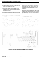
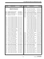
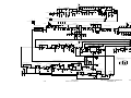
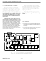
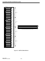
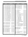
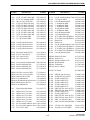
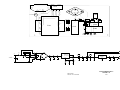
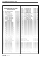
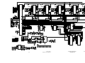
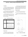
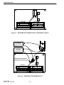
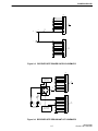
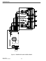
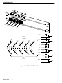
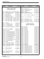
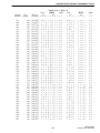
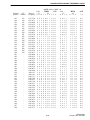
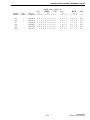
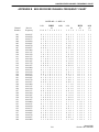
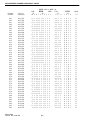
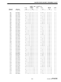
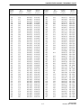
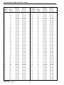
1
MULTI-NET® II VOTER SYSTEM Second Printing March 2000 Part No. 001-3139-502 3-00mwp -1 Printed in U.S.A. February 1996 Part No. 001-3039-505 February 1996 Part No. 001-3039-505 -2 MULTI-NET II VOTER SYSTEM Copyright 1997 by the E.F. Johnson Company The E.F. Johnson Company designs and manufactures two-way radio equipment to serve a wide variety of communications needs. Johnson produces equipment for the mobile telephone and land mobile radio services which include business, industrial, government, public safety, and personal users. LAND MOBILE PRODUCT WARRANTY The manufacturer’s warranty statement for this product is available from your product supplier or from the E.F. Johnson Company, 299 Johnson Avenue, Box 1249, Waseca, MN 56093-0514. Phone (507) 835-6222. WARNING This device complies with Part 15 of the FCC rules. Operation is subject to the condition that this device does not cause harmful interference. In addition, changes or modification to this equipment not expressly approved by E. F. Johnson could void the user’s authority to operate this equipment (FCC rules, 47CFR Part 15.19). DO NOT allow the antenna to come close to or touch, the eyes, face, or any exposed body parts while the radio is transmitting. DO NOT operate the radio near electrical blasting caps or in an explosive atmosphere. DO NOT operate the radio unless all the radio frequency connectors are secure and any open connectors are properly terminated. DO NOT allow children to operate transmitter equipped radio equipment. SAFETY INFORMATION Proper operation of this radio will result in user exposure below the Occupational Safety and Health Act and Federal Communication Commission limits. The information in this document is subject to change without notice. E.F. Johnson Company will not be liable for any misunderstanding due to misinformation or errors found in this document. LTR, LTR-Net, Multi-Net, Viking Head/EFJohnson Logo, Call Guard and SUMMIT are registered trademarks of E.F. Johnson Company All other company and/or product names used in this manual are trademarks and/or registered trademarks of their respective manufacturer. -3 February 1996 Part No. 001-3039-505 February 1996 Part No. 001-3039-505 -4 TABLE OF CONTENTS 1 INTRODUCTION 1.1 1.2 1.4 DESCRIPTION . . . . . . . . . . . . . . . . . . . . . . . . . . . . . . . . . . . . . . . . . . . . . . . . . . . . . . . . . . . . . . . . . . . . . . . . . . . . 1-1 MAIN COMPONENTS . . . . . . . . . . . . . . . . . . . . . . . . . . . . . . . . . . . . . . . . . . . . . . . . . . . . . . . . . . . . . . . . . . . . . . 1-1 RECEIVER DECODER MODULE. . . . . . . . . . . . . . . . . . . . . . . . . . . . . . . . . . . . . . . . . . . . . . . . . . . . . . . . . . . . . . 1-1 RECEIVER MULTIPLEXER MODULE . . . . . . . . . . . . . . . . . . . . . . . . . . . . . . . . . . . . . . . . . . . . . . . . . . . . . . . . . 1-1 CENTRAL DE-MULTIPLEXER MODULE . . . . . . . . . . . . . . . . . . . . . . . . . . . . . . . . . . . . . . . . . . . . . . . . . . . . . . 1-1 CHANNEL RECEIVER VOTER MODULE . . . . . . . . . . . . . . . . . . . . . . . . . . . . . . . . . . . . . . . . . . . . . . . . . . . . . . 1-1 VOTER DIAGNOSTICS MODULE . . . . . . . . . . . . . . . . . . . . . . . . . . . . . . . . . . . . . . . . . . . . . . . . . . . . . . . . . . . . . 1-2 VOTER SHELF . . . . . . . . . . . . . . . . . . . . . . . . . . . . . . . . . . . . . . . . . . . . . . . . . . . . . . . . . . . . . . . . . . . . . . . . . . . . . 1-2 VOTER POWER SUPPLY . . . . . . . . . . . . . . . . . . . . . . . . . . . . . . . . . . . . . . . . . . . . . . . . . . . . . . . . . . . . . . . . . . . . 1-2 COMPONENTS OF A VOTER SYSTEM . . . . . . . . . . . . . . . . . . . . . . . . . . . . . . . . . . . . . . . . . . . . . . . . . . . . . . . . 1-2 VOTER SYSTEM ALIGNMENT . . . . . . . . . . . . . . . . . . . . . . . . . . . . . . . . . . . . . . . . . . . . . . . . . . . . . . . . . . . . . 1-7 PRELIMINARY. . . . . . . . . . . . . . . . . . . . . . . . . . . . . . . . . . . . . . . . . . . . . . . . . . . . . . . . . . . . . . . . . . . . . . . . . . . . . 1-7 8000 SERIES RDM AND RVM ALIGNMENT . . . . . . . . . . . . . . . . . . . . . . . . . . . . . . . . . . . . . . . . . . . . . . . . . . . . 1-8 2000 SERIES RDM AND RVM ALIGNMENT . . . . . . . . . . . . . . . . . . . . . . . . . . . . . . . . . . . . . . . . . . . . . . . . . . . 1-11 VOICE LEVEL TO SWITCH ALIGNMENT. . . . . . . . . . . . . . . . . . . . . . . . . . . . . . . . . . . . . . . . . . . . . . . . . . . . . 1-13 FSK RECEIVE DATA LEVEL FROM SWITCH . . . . . . . . . . . . . . . . . . . . . . . . . . . . . . . . . . . . . . . . . . . . . . . . . 1-14 FSK DATA OVER VOICE PATH . . . . . . . . . . . . . . . . . . . . . . . . . . . . . . . . . . . . . . . . . . . . . . . . . . . . . . . . . . . . . 1-14 VOICE LEVEL FROM SWITCH ALIGNMENT. . . . . . . . . . . . . . . . . . . . . . . . . . . . . . . . . . . . . . . . . . . . . . . . . . 1-15 VOTER ERROR MESSAGES . . . . . . . . . . . . . . . . . . . . . . . . . . . . . . . . . . . . . . . . . . . . . . . . . . . . . . . . . . . . . . . 1-15 2 8000 SERIES RECEIVER DECODER MODULE (RDM) 2.1 2.2 2.3 2.4 2.5 2.6 GENERAL . . . . . . . . . . . . . . . . . . . . . . . . . . . . . . . . . . . . . . . . . . . . . . . . . . . . . . . . . . . . . . . . . . . . . . . . . . . . . . . . INITIAL RECEPTION . . . . . . . . . . . . . . . . . . . . . . . . . . . . . . . . . . . . . . . . . . . . . . . . . . . . . . . . . . . . . . . . . . . . . . RSSI UPDATES . . . . . . . . . . . . . . . . . . . . . . . . . . . . . . . . . . . . . . . . . . . . . . . . . . . . . . . . . . . . . . . . . . . . . . . . . . . . DISCONNECT . . . . . . . . . . . . . . . . . . . . . . . . . . . . . . . . . . . . . . . . . . . . . . . . . . . . . . . . . . . . . . . . . . . . . . . . . . . . . SWITCH SETTINGS. . . . . . . . . . . . . . . . . . . . . . . . . . . . . . . . . . . . . . . . . . . . . . . . . . . . . . . . . . . . . . . . . . . . . . . . 800 MHz RECEIVER DRAWER ALIGNMENT . . . . . . . . . . . . . . . . . . . . . . . . . . . . . . . . . . . . . . . . . . . . . . . . . FIRST OSCILLATOR FREQUENCY ADJUSTMENT . . . . . . . . . . . . . . . . . . . . . . . . . . . . . . . . . . . . . . . . . . . . . . SECOND OSCILLATOR FREQUENCY ADJUSTMENT . . . . . . . . . . . . . . . . . . . . . . . . . . . . . . . . . . . . . . . . . . . MULTIPLIER TUNE UP. . . . . . . . . . . . . . . . . . . . . . . . . . . . . . . . . . . . . . . . . . . . . . . . . . . . . . . . . . . . . . . . . . . . . . FRONT END AND IF ALIGNMENT. . . . . . . . . . . . . . . . . . . . . . . . . . . . . . . . . . . . . . . . . . . . . . . . . . . . . . . . . . . . DIVERSITY AND SQUELCH ADJUSTMENT. . . . . . . . . . . . . . . . . . . . . . . . . . . . . . . . . . . . . . . . . . . . . . . . . . . . 800 MHz RECEIVER PERFORMANCE TESTS . . . . . . . . . . . . . . . . . . . . . . . . . . . . . . . . . . . . . . . . . . . . . . . . SINAD SENSITIVITY . . . . . . . . . . . . . . . . . . . . . . . . . . . . . . . . . . . . . . . . . . . . . . . . . . . . . . . . . . . . . . . . . . . . . . . DIVERSITY AND SQUELCH THRESHOLD LEVEL . . . . . . . . . . . . . . . . . . . . . . . . . . . . . . . . . . . . . . . . . . . . . . RECEIVE DATA LEVEL . . . . . . . . . . . . . . . . . . . . . . . . . . . . . . . . . . . . . . . . . . . . . . . . . . . . . . . . . . . . . . . . . . . . . 900 MHz RECEIVER DRAWER ALIGNMENT . . . . . . . . . . . . . . . . . . . . . . . . . . . . . . . . . . . . . . . . . . . . . . . . . INTRODUCTION . . . . . . . . . . . . . . . . . . . . . . . . . . . . . . . . . . . . . . . . . . . . . . . . . . . . . . . . . . . . . . . . . . . . . . . . . . . TEST EQUIPMENT FREQUENCY STABILITY . . . . . . . . . . . . . . . . . . . . . . . . . . . . . . . . . . . . . . . . . . . . . . . . . . SYNTHESIZER ADJUSTMENT . . . . . . . . . . . . . . . . . . . . . . . . . . . . . . . . . . . . . . . . . . . . . . . . . . . . . . . . . . . . . . . MULTIPLIER TUNE-UP . . . . . . . . . . . . . . . . . . . . . . . . . . . . . . . . . . . . . . . . . . . . . . . . . . . . . . . . . . . . . . . . . . . . . SECOND OSCILLATOR ADJUSTMENT . . . . . . . . . . . . . . . . . . . . . . . . . . . . . . . . . . . . . . . . . . . . . . . . . . . . . . . . FRONT END ALIGNMENT . . . . . . . . . . . . . . . . . . . . . . . . . . . . . . . . . . . . . . . . . . . . . . . . . . . . . . . . . . . . . . . . . . . IF ALIGNMENT . . . . . . . . . . . . . . . . . . . . . . . . . . . . . . . . . . . . . . . . . . . . . . . . . . . . . . . . . . . . . . . . . . . . . . . . . . . . DIVERSITY AND SQUELCH ADJUSTMENT. . . . . . . . . . . . . . . . . . . . . . . . . . . . . . . . . . . . . . . . . . . . . . . . . . . . 900 MHz RECEIVE DATA LEVEL ADJUSTMENT . . . . . . . . . . . . . . . . . . . . . . . . . . . . . . . . . . . . . . . . . . . . . 900 MHz RECEIVER PERFORMANCE TESTS . . . . . . . . . . . . . . . . . . . . . . . . . . . . . . . . . . . . . . . . . . . . . . . . SINAD SENSITIVITY . . . . . . . . . . . . . . . . . . . . . . . . . . . . . . . . . . . . . . . . . . . . . . . . . . . . . . . . . . . . . . . . . . . . . . . DIVERSITY AND SQUELCH THRESHOLD LEVEL . . . . . . . . . . . . . . . . . . . . . . . . . . . . . . . . . . . . . . . . . . . . . . RECEIVE DATA LEVEL . . . . . . . . . . . . . . . . . . . . . . . . . . . . . . . . . . . . . . . . . . . . . . . . . . . . . . . . . . . . . . . . . . . . . 1.3 2.7 2.8 2.9 2.10 1 2-1 2-1 2-1 2-2 2-2 2-2 2-2 2-3 2-3 2-3 2-3 2-3 2-3 2-4 2-4 2-5 2-5 2-5 2-5 2-5 2-5 2-6 2-6 2-6 2-7 2-7 2-7 2-8 2-8 TABLE OF CONTENTS (CONT.) 2.11 RDM ALIGNMENT . . . . . . . . . . . . . . . . . . . . . . . . . . . . . . . . . . . . . . . . . . . . . . . . . . . . . . . . . . . . . . . . . . . . . . . . . 2-8 EQUIPMENT REQUIRED . . . . . . . . . . . . . . . . . . . . . . . . . . . . . . . . . . . . . . . . . . . . . . . . . . . . . . . . . . . . . . . . . . . 2-8 CLOCK ADJUSTMENT . . . . . . . . . . . . . . . . . . . . . . . . . . . . . . . . . . . . . . . . . . . . . . . . . . . . . . . . . . . . . . . . . . . . . 2-8 RECEIVE AUDIO LEVEL . . . . . . . . . . . . . . . . . . . . . . . . . . . . . . . . . . . . . . . . . . . . . . . . . . . . . . . . . . . . . . . . . . . 2-8 RECEIVE DATA DEVIATION. . . . . . . . . . . . . . . . . . . . . . . . . . . . . . . . . . . . . . . . . . . . . . . . . . . . . . . . . . . . . . . . 2-8 FSK LEVEL . . . . . . . . . . . . . . . . . . . . . . . . . . . . . . . . . . . . . . . . . . . . . . . . . . . . . . . . . . . . . . . . . . . . . . . . . . . . . . . 2-9 RSSI LEVEL DETECTOR. . . . . . . . . . . . . . . . . . . . . . . . . . . . . . . . . . . . . . . . . . . . . . . . . . . . . . . . . . . . . . . . . . . . 2-9 RDM OPERATIONAL MODE . . . . . . . . . . . . . . . . . . . . . . . . . . . . . . . . . . . . . . . . . . . . . . . . . . . . . . . . . . . . . . . . 2-9 RDM FINAL ALIGNMENT . . . . . . . . . . . . . . . . . . . . . . . . . . . . . . . . . . . . . . . . . . . . . . . . . . . . . . . . . . . . . . . . . . 2-9 3 2000 SERIES RECEIVER DECODER MODULE (RDM) 3.1 3.2 3.3 3.4 3.5 GENERAL. . . . . . . . . . . . . . . . . . . . . . . . . . . . . . . . . . . . . . . . . . . . . . . . . . . . . . . . . . . . . . . . . . . . . . . . . . . . . . . . . 3-1 INITIAL RECEPTION . . . . . . . . . . . . . . . . . . . . . . . . . . . . . . . . . . . . . . . . . . . . . . . . . . . . . . . . . . . . . . . . . . . . . . 3-1 RSSI UPDATES . . . . . . . . . . . . . . . . . . . . . . . . . . . . . . . . . . . . . . . . . . . . . . . . . . . . . . . . . . . . . . . . . . . . . . . . . . . . 3-2 DISCONNECT . . . . . . . . . . . . . . . . . . . . . . . . . . . . . . . . . . . . . . . . . . . . . . . . . . . . . . . . . . . . . . . . . . . . . . . . . . . . . 3-2 INTRODUCTION. . . . . . . . . . . . . . . . . . . . . . . . . . . . . . . . . . . . . . . . . . . . . . . . . . . . . . . . . . . . . . . . . . . . . . . . . . . 3-2 HOW TO USE THIS SECTION . . . . . . . . . . . . . . . . . . . . . . . . . . . . . . . . . . . . . . . . . . . . . . . . . . . . . . . . . . . . . . . 3-3 GETTING STARTED . . . . . . . . . . . . . . . . . . . . . . . . . . . . . . . . . . . . . . . . . . . . . . . . . . . . . . . . . . . . . . . . . . . . . . . 3-3 COMPUTER DESCRIPTION . . . . . . . . . . . . . . . . . . . . . . . . . . . . . . . . . . . . . . . . . . . . . . . . . . . . . . . . . . . . . . . . . 3-3 EEPROM DATA STORAGE. . . . . . . . . . . . . . . . . . . . . . . . . . . . . . . . . . . . . . . . . . . . . . . . . . . . . . . . . . . . . . . . . . 3-3 MINIMUM FREE MEMORY REQUIRED . . . . . . . . . . . . . . . . . . . . . . . . . . . . . . . . . . . . . . . . . . . . . . . . . . . . . . 3-3 REPEATER PROGRAM SOFTWARE. . . . . . . . . . . . . . . . . . . . . . . . . . . . . . . . . . . . . . . . . . . . . . . . . . . . . . . . . 3-4 INSTALLING THE SOFTWARE . . . . . . . . . . . . . . . . . . . . . . . . . . . . . . . . . . . . . . . . . . . . . . . . . . . . . . . . . . . . . . 3-4 STARTING THE PROGRAM . . . . . . . . . . . . . . . . . . . . . . . . . . . . . . . . . . . . . . . . . . . . . . . . . . . . . . . . . . . . . . . . . 3-4 2000 RDM PROGRAMMER. . . . . . . . . . . . . . . . . . . . . . . . . . . . . . . . . . . . . . . . . . . . . . . . . . . . . . . . . . . . . . . . . . 3-5 ALIGNMENT SOFTWARE . . . . . . . . . . . . . . . . . . . . . . . . . . . . . . . . . . . . . . . . . . . . . . . . . . . . . . . . . . . . . . . . . . 3-5 HELP F1 . . . . . . . . . . . . . . . . . . . . . . . . . . . . . . . . . . . . . . . . . . . . . . . . . . . . . . . . . . . . . . . . . . . . . . . . . . . . . . . . . . 3-5 PULL DOWN MENUS. . . . . . . . . . . . . . . . . . . . . . . . . . . . . . . . . . . . . . . . . . . . . . . . . . . . . . . . . . . . . . . . . . . . . . . 3-5 MENU DISPLAYS. . . . . . . . . . . . . . . . . . . . . . . . . . . . . . . . . . . . . . . . . . . . . . . . . . . . . . . . . . . . . . . . . . . . . . . . . . 3-5 FILE MENU . . . . . . . . . . . . . . . . . . . . . . . . . . . . . . . . . . . . . . . . . . . . . . . . . . . . . . . . . . . . . . . . . . . . . . . . . . . . . . . 3-5 EDIT . . . . . . . . . . . . . . . . . . . . . . . . . . . . . . . . . . . . . . . . . . . . . . . . . . . . . . . . . . . . . . . . . . . . . . . . . . . . . . . . . . . . . 3-7 TRANSFER . . . . . . . . . . . . . . . . . . . . . . . . . . . . . . . . . . . . . . . . . . . . . . . . . . . . . . . . . . . . . . . . . . . . . . . . . . . . . . . 3-9 HARDWARE . . . . . . . . . . . . . . . . . . . . . . . . . . . . . . . . . . . . . . . . . . . . . . . . . . . . . . . . . . . . . . . . . . . . . . . . . . . . . 3-10 TEST . . . . . . . . . . . . . . . . . . . . . . . . . . . . . . . . . . . . . . . . . . . . . . . . . . . . . . . . . . . . . . . . . . . . . . . . . . . . . . . . . . . . 3-12 UTILITIES . . . . . . . . . . . . . . . . . . . . . . . . . . . . . . . . . . . . . . . . . . . . . . . . . . . . . . . . . . . . . . . . . . . . . . . . . . . . . . . 3-12 REPEATER PROGRAMMING. . . . . . . . . . . . . . . . . . . . . . . . . . . . . . . . . . . . . . . . . . . . . . . . . . . . . . . . . . . . . . . 3-13 800 MHz RECEIVER ALIGNMENT. . . . . . . . . . . . . . . . . . . . . . . . . . . . . . . . . . . . . . . . . . . . . . . . . . . . . . . . . . 3-15 PRE-TEST . . . . . . . . . . . . . . . . . . . . . . . . . . . . . . . . . . . . . . . . . . . . . . . . . . . . . . . . . . . . . . . . . . . . . . . . . . . . . . . 3-15 PROGRAM TUNE-UP CHANNEL. . . . . . . . . . . . . . . . . . . . . . . . . . . . . . . . . . . . . . . . . . . . . . . . . . . . . . . . . . . . 3-15 TCXO FREQUENCY ADJUST. . . . . . . . . . . . . . . . . . . . . . . . . . . . . . . . . . . . . . . . . . . . . . . . . . . . . . . . . . . . . . . 3-15 VCO TEST . . . . . . . . . . . . . . . . . . . . . . . . . . . . . . . . . . . . . . . . . . . . . . . . . . . . . . . . . . . . . . . . . . . . . . . . . . . . . . . 3-15 FRONT END ADJUSTMENTS (Rev. 5). . . . . . . . . . . . . . . . . . . . . . . . . . . . . . . . . . . . . . . . . . . . . . . . . . . . . . . . 3-15 FRONT END ADJUSTMENTS (Rev. 6). . . . . . . . . . . . . . . . . . . . . . . . . . . . . . . . . . . . . . . . . . . . . . . . . . . . . . . . 3-16 AUDIO DISTORTION. . . . . . . . . . . . . . . . . . . . . . . . . . . . . . . . . . . . . . . . . . . . . . . . . . . . . . . . . . . . . . . . . . . . . . 3-16 900 MHz RECEIVER ALIGNMENT. . . . . . . . . . . . . . . . . . . . . . . . . . . . . . . . . . . . . . . . . . . . . . . . . . . . . . . . . . 3-18 PRE-TEST . . . . . . . . . . . . . . . . . . . . . . . . . . . . . . . . . . . . . . . . . . . . . . . . . . . . . . . . . . . . . . . . . . . . . . . . . . . . . . . 3-18 VOLTAGE MEASUREMENTS . . . . . . . . . . . . . . . . . . . . . . . . . . . . . . . . . . . . . . . . . . . . . . . . . . . . . . . . . . . . . . 3-19 PROGRAM TUNE-UP CHANNEL. . . . . . . . . . . . . . . . . . . . . . . . . . . . . . . . . . . . . . . . . . . . . . . . . . . . . . . . . . . . 3-19 TCXO FREQUENCY ADJUST. . . . . . . . . . . . . . . . . . . . . . . . . . . . . . . . . . . . . . . . . . . . . . . . . . . . . . . . . . . . . . . 3-19 VCO TEST . . . . . . . . . . . . . . . . . . . . . . . . . . . . . . . . . . . . . . . . . . . . . . . . . . . . . . . . . . . . . . . . . . . . . . . . . . . . . . . 3-19 FRONT-END ADJUSTMENTS . . . . . . . . . . . . . . . . . . . . . . . . . . . . . . . . . . . . . . . . . . . . . . . . . . . . . . . . . . . . . . 3-19 AUDIO DISTORTION. . . . . . . . . . . . . . . . . . . . . . . . . . . . . . . . . . . . . . . . . . . . . . . . . . . . . . . . . . . . . . . . . . . . . . 3-20 3.6 3.7 3.8 3.9 3.10 3.11 3.12 2 TABLE OF CONTENTS (CONT.) 3.13 3.14 FULL RDM - ALL TEST . . . . . . . . . . . . . . . . . . . . . . . . . . . . . . . . . . . . . . . . . . . . . . . . . . . . . . . . . . . . . . . . . . . VOLTAGE MEASUREMENTS . . . . . . . . . . . . . . . . . . . . . . . . . . . . . . . . . . . . . . . . . . . . . . . . . . . . . . . . . . . . . . . RECEIVER FREQUENCY CHECK . . . . . . . . . . . . . . . . . . . . . . . . . . . . . . . . . . . . . . . . . . . . . . . . . . . . . . . . . . . . VOTER INTERFACE . . . . . . . . . . . . . . . . . . . . . . . . . . . . . . . . . . . . . . . . . . . . . . . . . . . . . . . . . . . . . . . . . . . . . . . SCHEMATIC DIAGRAMS AND COMPONENT LAYOUTS. . . . . . . . . . . . . . . . . . . . . . . . . . . . . . . . . . . . . 3 RECEIVER MULTIPLEXER MODULE (RMM) 3.1 3.2 3.3 3.4 3.5 GENERAL . . . . . . . . . . . . . . . . . . . . . . . . . . . . . . . . . . . . . . . . . . . . . . . . . . . . . . . . . . . . . . . . . . . . . . . . . . . . . . . . RECEIVE CALL ORDER OR RSSI DATA . . . . . . . . . . . . . . . . . . . . . . . . . . . . . . . . . . . . . . . . . . . . . . . . . . . . . DATA PACKET . . . . . . . . . . . . . . . . . . . . . . . . . . . . . . . . . . . . . . . . . . . . . . . . . . . . . . . . . . . . . . . . . . . . . . . . . . . . SWITCH SETTINGS. . . . . . . . . . . . . . . . . . . . . . . . . . . . . . . . . . . . . . . . . . . . . . . . . . . . . . . . . . . . . . . . . . . . . . . . ALIGNMENT . . . . . . . . . . . . . . . . . . . . . . . . . . . . . . . . . . . . . . . . . . . . . . . . . . . . . . . . . . . . . . . . . . . . . . . . . . . . . . RMM ANALOG FSK OPERATION . . . . . . . . . . . . . . . . . . . . . . . . . . . . . . . . . . . . . . . . . . . . . . . . . . . . . . . . . . . . RMM FINAL ALIGNMENT. . . . . . . . . . . . . . . . . . . . . . . . . . . . . . . . . . . . . . . . . . . . . . . . . . . . . . . . . . . . . . . . . . . 4 CENTRAL DE-MULTIPLEXER MODULE (CDM) 4.1 4.2 4.3 4.4 4.5 GENERAL . . . . . . . . . . . . . . . . . . . . . . . . . . . . . . . . . . . . . . . . . . . . . . . . . . . . . . . . . . . . . . . . . . . . . . . . . . . . . . . . INPUT DATA . . . . . . . . . . . . . . . . . . . . . . . . . . . . . . . . . . . . . . . . . . . . . . . . . . . . . . . . . . . . . . . . . . . . . . . . . . . . . . OUTPUT DATA . . . . . . . . . . . . . . . . . . . . . . . . . . . . . . . . . . . . . . . . . . . . . . . . . . . . . . . . . . . . . . . . . . . . . . . . . . . . SWITCH SETTINGS. . . . . . . . . . . . . . . . . . . . . . . . . . . . . . . . . . . . . . . . . . . . . . . . . . . . . . . . . . . . . . . . . . . . . . . . ALIGNMENT . . . . . . . . . . . . . . . . . . . . . . . . . . . . . . . . . . . . . . . . . . . . . . . . . . . . . . . . . . . . . . . . . . . . . . . . . . . . . . CDM ANALOG FSK OPERATION . . . . . . . . . . . . . . . . . . . . . . . . . . . . . . . . . . . . . . . . . . . . . . . . . . . . . . . . . . . . . CDM FINAL ALIGNMENT . . . . . . . . . . . . . . . . . . . . . . . . . . . . . . . . . . . . . . . . . . . . . . . . . . . . . . . . . . . . . . . . . . . 5 CHANNEL RECEIVER VOTER MODULE (cRVM) 5.1 5.2 5.3 5.4 5.5 GENERAL . . . . . . . . . . . . . . . . . . . . . . . . . . . . . . . . . . . . . . . . . . . . . . . . . . . . . . . . . . . . . . . . . . . . . . . . . . . . . . . . cRVM TO RVM . . . . . . . . . . . . . . . . . . . . . . . . . . . . . . . . . . . . . . . . . . . . . . . . . . . . . . . . . . . . . . . . . . . . . . . . . . . . RECEIVE ORDERS . . . . . . . . . . . . . . . . . . . . . . . . . . . . . . . . . . . . . . . . . . . . . . . . . . . . . . . . . . . . . . . . . . . . . . . . RSSI . . . . . . . . . . . . . . . . . . . . . . . . . . . . . . . . . . . . . . . . . . . . . . . . . . . . . . . . . . . . . . . . . . . . . . . . . . . . . . . . . . . . . . PRIORITY OF SITES . . . . . . . . . . . . . . . . . . . . . . . . . . . . . . . . . . . . . . . . . . . . . . . . . . . . . . . . . . . . . . . . . . . . . . . PRIORITY PROGRAMMING . . . . . . . . . . . . . . . . . . . . . . . . . . . . . . . . . . . . . . . . . . . . . . . . . . . . . . . . . . . . . . . . . SWITCH SETTINGS. . . . . . . . . . . . . . . . . . . . . . . . . . . . . . . . . . . . . . . . . . . . . . . . . . . . . . . . . . . . . . . . . . . . . . . . LED DEFINITION. . . . . . . . . . . . . . . . . . . . . . . . . . . . . . . . . . . . . . . . . . . . . . . . . . . . . . . . . . . . . . . . . . . . . . . . . . SITE LED DEFINITION . . . . . . . . . . . . . . . . . . . . . . . . . . . . . . . . . . . . . . . . . . . . . . . . . . . . . . . . . . . . . . . . . . . . . . RVM LEDS . . . . . . . . . . . . . . . . . . . . . . . . . . . . . . . . . . . . . . . . . . . . . . . . . . . . . . . . . . . . . . . . . . . . . . . . . . . . . . . . CALL LED . . . . . . . . . . . . . . . . . . . . . . . . . . . . . . . . . . . . . . . . . . . . . . . . . . . . . . . . . . . . . . . . . . . . . . . . . . . . . . . . . AUDIO ALIGNMENT. . . . . . . . . . . . . . . . . . . . . . . . . . . . . . . . . . . . . . . . . . . . . . . . . . . . . . . . . . . . . . . . . . . . . . . RVM REMOVAL . . . . . . . . . . . . . . . . . . . . . . . . . . . . . . . . . . . . . . . . . . . . . . . . . . . . . . . . . . . . . . . . . . . . . . . . . . . RVM AND CHANNEL SELECTION . . . . . . . . . . . . . . . . . . . . . . . . . . . . . . . . . . . . . . . . . . . . . . . . . . . . . . . . . . . CHANNEL 1 AUDIO OUTPUT LEVEL . . . . . . . . . . . . . . . . . . . . . . . . . . . . . . . . . . . . . . . . . . . . . . . . . . . . . . . . . CHANNEL 2 AUDIO OUTPUT LEVEL . . . . . . . . . . . . . . . . . . . . . . . . . . . . . . . . . . . . . . . . . . . . . . . . . . . . . . . . . CHANNEL 3 AUDIO OUTPUT LEVEL . . . . . . . . . . . . . . . . . . . . . . . . . . . . . . . . . . . . . . . . . . . . . . . . . . . . . . . . . CHANNEL 4 AUDIO OUTPUT LEVEL . . . . . . . . . . . . . . . . . . . . . . . . . . . . . . . . . . . . . . . . . . . . . . . . . . . . . . . . . RVM REPLACEMENT . . . . . . . . . . . . . . . . . . . . . . . . . . . . . . . . . . . . . . . . . . . . . . . . . . . . . . . . . . . . . . . . . . . . . INSTALLED SYSTEM ADJUSTMENTS. . . . . . . . . . . . . . . . . . . . . . . . . . . . . . . . . . . . . . . . . . . . . . . . . . . . . . . PRELIMINARY. . . . . . . . . . . . . . . . . . . . . . . . . . . . . . . . . . . . . . . . . . . . . . . . . . . . . . . . . . . . . . . . . . . . . . . . . . . . . ESTABLISH A MULTI-NET CALL . . . . . . . . . . . . . . . . . . . . . . . . . . . . . . . . . . . . . . . . . . . . . . . . . . . . . . . . . . . . RVM LEVEL ADJUSTMENTS . . . . . . . . . . . . . . . . . . . . . . . . . . . . . . . . . . . . . . . . . . . . . . . . . . . . . . . . . . . . . . . . 5.6 5.7 5.8 5.9 5.10 3 3-20 3-20 3-20 3-22 3-49 4-1 4-1 4-1 4-2 4-2 4-2 4-2 5-1 5-1 5-1 5-2 5-2 5-2 5-2 6-1 6-1 6-1 6-2 6-2 6-2 6-2 6-3 6-3 6-3 6-3 6-6 6-6 6-6 6-6 6-6 6-6 6-7 6-7 6-7 6-7 6-7 6-8 TABLE OF CONTENTS (CONT.) 6 VOTER DIAGNOSTIC MODULE (VDM) 6.1 6.2 6.3 DESCRIPTION. . . . . . . . . . . . . . . . . . . . . . . . . . . . . . . . . . . . . . . . . . . . . . . . . . . . . . . . . . . . . . . . . . . . . . . . . . . . . 7-1 VDM SETUP PROCEDURE. . . . . . . . . . . . . . . . . . . . . . . . . . . . . . . . . . . . . . . . . . . . . . . . . . . . . . . . . . . . . . . . . . 7-3 SWITCH SETTINGS . . . . . . . . . . . . . . . . . . . . . . . . . . . . . . . . . . . . . . . . . . . . . . . . . . . . . . . . . . . . . . . . . . . . . . . . 7-3 JUMPER PLACEMENT . . . . . . . . . . . . . . . . . . . . . . . . . . . . . . . . . . . . . . . . . . . . . . . . . . . . . . . . . . . . . . . . . . . . . 7-3 VDM BACKPLANE EXTERNAL CONNECTIONS . . . . . . . . . . . . . . . . . . . . . . . . . . . . . . . . . . . . . . . . . . . . . . . 7-3 ALIGNMENT . . . . . . . . . . . . . . . . . . . . . . . . . . . . . . . . . . . . . . . . . . . . . . . . . . . . . . . . . . . . . . . . . . . . . . . . . . . . . . 7-3 7 BACKPLANE 7.1 7.2 7.3 7.4 DESCRIPTION. . . . . . . . . . . . . . . . . . . . . . . . . . . . . . . . . . . . . . . . . . . . . . . . . . . . . . . . . . . . . . . . . . . . . . . . . . . . . 8-1 VDM BUS LOADING . . . . . . . . . . . . . . . . . . . . . . . . . . . . . . . . . . . . . . . . . . . . . . . . . . . . . . . . . . . . . . . . . . . . . . . 8-1 SWITCH SETTINGS . . . . . . . . . . . . . . . . . . . . . . . . . . . . . . . . . . . . . . . . . . . . . . . . . . . . . . . . . . . . . . . . . . . . . . . . 8-1 POWER CONNECTIONS. . . . . . . . . . . . . . . . . . . . . . . . . . . . . . . . . . . . . . . . . . . . . . . . . . . . . . . . . . . . . . . . . . . . 8-1 8 POWER SUPPLIES 8.1 8.2 8.3 8.4 8.5 8.6 RECEIVER SITE POWER SUPPLY (-490) . . . . . . . . . . . . . . . . . . . . . . . . . . . . . . . . . . . . . . . . . . . . . . . . . . . . . 9-1 RECEIVER SITE REDUNDANT KIT (-495) . . . . . . . . . . . . . . . . . . . . . . . . . . . . . . . . . . . . . . . . . . . . . . . . . . . . 9-1 VOTER SHELF POWER SUPPLY (-555). . . . . . . . . . . . . . . . . . . . . . . . . . . . . . . . . . . . . . . . . . . . . . . . . . . . . . . 9-1 VOTER POWER SUPPLY REDUNDANT PLATE (-553) . . . . . . . . . . . . . . . . . . . . . . . . . . . . . . . . . . . . . . . . . 9-1 POWER CONSUMPTION . . . . . . . . . . . . . . . . . . . . . . . . . . . . . . . . . . . . . . . . . . . . . . . . . . . . . . . . . . . . . . . . . . . 9-1 VOLTAGE ADJUSTMENTS . . . . . . . . . . . . . . . . . . . . . . . . . . . . . . . . . . . . . . . . . . . . . . . . . . . . . . . . . . . . . . . . . 9-2 -555 SUPPLY . . . . . . . . . . . . . . . . . . . . . . . . . . . . . . . . . . . . . . . . . . . . . . . . . . . . . . . . . . . . . . . . . . . . . . . . . . . . . . 9-2 REDUNDANT SUPPLY ADJUSTMENTS . . . . . . . . . . . . . . . . . . . . . . . . . . . . . . . . . . . . . . . . . . . . . . . . . . . . . . 9-2 RECEIVER SITE REDUNDANT KIT INSTALLATION. . . . . . . . . . . . . . . . . . . . . . . . . . . . . . . . . . . . . . . . . . 9-2 VOTER SHELF POWER SUPPLY (-501). . . . . . . . . . . . . . . . . . . . . . . . . . . . . . . . . . . . . . . . . . . . . . . . . . . . . . 9-11 REDUNDANT POWER SUPPLY . . . . . . . . . . . . . . . . . . . . . . . . . . . . . . . . . . . . . . . . . . . . . . . . . . . . . . . . . . . . 9-11 POWER CONSUMPTION . . . . . . . . . . . . . . . . . . . . . . . . . . . . . . . . . . . . . . . . . . . . . . . . . . . . . . . . . . . . . . . . . . 9-11 VOLTAGE ADJUSTMENTS . . . . . . . . . . . . . . . . . . . . . . . . . . . . . . . . . . . . . . . . . . . . . . . . . . . . . . . . . . . . . . . . 9-11 -501 SUPPLY . . . . . . . . . . . . . . . . . . . . . . . . . . . . . . . . . . . . . . . . . . . . . . . . . . . . . . . . . . . . . . . . . . . . . . . . . . . . . 9-11 8.7 8.8 8.9 8.10 8.11 9 RECEIVER REVERT BOARD (RRB) 9.1 9.2 9.3 9.4 9.5 GENERAL. . . . . . . . . . . . . . . . . . . . . . . . . . . . . . . . . . . . . . . . . . . . . . . . . . . . . . . . . . . . . . . . . . . . . . . . . . . . . . . . 10-1 INPUT DATA . . . . . . . . . . . . . . . . . . . . . . . . . . . . . . . . . . . . . . . . . . . . . . . . . . . . . . . . . . . . . . . . . . . . . . . . . . . . . 10-1 INSTALLATION . . . . . . . . . . . . . . . . . . . . . . . . . . . . . . . . . . . . . . . . . . . . . . . . . . . . . . . . . . . . . . . . . . . . . . . . . . 10-1 RVM AUDIO AND RS-232 DATA. . . . . . . . . . . . . . . . . . . . . . . . . . . . . . . . . . . . . . . . . . . . . . . . . . . . . . . . . . . . 10-1 BAUD RATE . . . . . . . . . . . . . . . . . . . . . . . . . . . . . . . . . . . . . . . . . . . . . . . . . . . . . . . . . . . . . . . . . . . . . . . . . . . . . 10-1 SWITCH SETTINGS . . . . . . . . . . . . . . . . . . . . . . . . . . . . . . . . . . . . . . . . . . . . . . . . . . . . . . . . . . . . . . . . . . . . . . . 10-2 ALIGNMENT . . . . . . . . . . . . . . . . . . . . . . . . . . . . . . . . . . . . . . . . . . . . . . . . . . . . . . . . . . . . . . . . . . . . . . . . . . . . . 10-2 A 8000 RECEIVER CHANNEL FREQUENCY CHART B 8900 RECEIVER CHANNEL FREQUENCY CHART C 2008 RECEIVER CHANNEL FREQUENCY CHART D 2009 RECEIVER CHANNEL FREQUENCY CHART E VOTER FAILURE ALARMS 4 TABLE OF CONTENTS (CONT.) LIST OF FIGURES 1-1 1-2 1-3 1-4 1-5 1-6 1-7 1-8 1-9 1-10 1-11 1-12 1-13 1-14 1-15 1-16 1-17 1-18 1-19 1-20 1-21 1-22 1-23 1-24 2-1 2-2 2-3 2-4 2-5 2-6 2-7 2-8 2-9 2-10 2-11 2-12 2-13 2-14 2-15 2-16 2-17 2-18 2-19 3-1 3-2 3-3 3-4 3-5 3-6 3-7 3-8 LOCAL SITE BLOCK DIAGRAM. . . . . . . . . . . . . . . . . . . . . . . . . . . . . . . . . . . . . . . . . . . . . . . . . . . . . . . . . . . . . . . 1-2 REMOTE VOTER SYSTEM. . . . . . . . . . . . . . . . . . . . . . . . . . . . . . . . . . . . . . . . . . . . . . . . . . . . . . . . . . . . . . . . . . . . 1-2 5-CHANNEL LOCAL SITE (with 1 REMOTE SITE) . . . . . . . . . . . . . . . . . . . . . . . . . . . . . . . . . . . . . . . . . . . . . . . . 1-3 5-CHANNEL REMOTE SITE. . . . . . . . . . . . . . . . . . . . . . . . . . . . . . . . . . . . . . . . . . . . . . . . . . . . . . . . . . . . . . . . . . . 1-4 5-CHANNEL LOCAL SITE (with 5 REMOTE SITES) . . . . . . . . . . . . . . . . . . . . . . . . . . . . . . . . . . . . . . . . . . . . . . . 1-5 5-SITE 4-CHANNEL VOTER SYSTEM BLOCK DIAGRAM . . . . . . . . . . . . . . . . . . . . . . . . . . . . . . . . . . . . . . . . . 1-6 MLM S3 SWITCH SETTINGS . . . . . . . . . . . . . . . . . . . . . . . . . . . . . . . . . . . . . . . . . . . . . . . . . . . . . . . . . . . . . . . . . . 1-7 MLM S9 SWITCH . . . . . . . . . . . . . . . . . . . . . . . . . . . . . . . . . . . . . . . . . . . . . . . . . . . . . . . . . . . . . . . . . . . . . . . . . . . . 1-7 MLM S9 TEST MODE . . . . . . . . . . . . . . . . . . . . . . . . . . . . . . . . . . . . . . . . . . . . . . . . . . . . . . . . . . . . . . . . . . . . . . . . 1-7 MLM S2 SWITCH . . . . . . . . . . . . . . . . . . . . . . . . . . . . . . . . . . . . . . . . . . . . . . . . . . . . . . . . . . . . . . . . . . . . . . . . . . . . 1-7 MLM S2 SWITCH SETTING . . . . . . . . . . . . . . . . . . . . . . . . . . . . . . . . . . . . . . . . . . . . . . . . . . . . . . . . . . . . . . . . . . . 1-7 RDM S1 AUDIO GATE ENABLE . . . . . . . . . . . . . . . . . . . . . . . . . . . . . . . . . . . . . . . . . . . . . . . . . . . . . . . . . . . . . . . 1-8 RVM S2 SWITCH . . . . . . . . . . . . . . . . . . . . . . . . . . . . . . . . . . . . . . . . . . . . . . . . . . . . . . . . . . . . . . . . . . . . . . . . . . . . 1-8 U44 LEVEL ADJUST . . . . . . . . . . . . . . . . . . . . . . . . . . . . . . . . . . . . . . . . . . . . . . . . . . . . . . . . . . . . . . . . . . . . . . . . . 1-8 RVM S2 SWITCH . . . . . . . . . . . . . . . . . . . . . . . . . . . . . . . . . . . . . . . . . . . . . . . . . . . . . . . . . . . . . . . . . . . . . . . . . . . 1-11 U44 LEVEL ADJUST . . . . . . . . . . . . . . . . . . . . . . . . . . . . . . . . . . . . . . . . . . . . . . . . . . . . . . . . . . . . . . . . . . . . . . . . 1-11 MLM S2 GATE SETTINGS . . . . . . . . . . . . . . . . . . . . . . . . . . . . . . . . . . . . . . . . . . . . . . . . . . . . . . . . . . . . . . . . . . . 1-13 MLM S2 MODEM/FSK GATES. . . . . . . . . . . . . . . . . . . . . . . . . . . . . . . . . . . . . . . . . . . . . . . . . . . . . . . . . . . . . . . . 1-14 CIM S5 FSK ALIGNMENT TONE. . . . . . . . . . . . . . . . . . . . . . . . . . . . . . . . . . . . . . . . . . . . . . . . . . . . . . . . . . . . . . 1-14 MLM S2 TRANSMIT ENABLE . . . . . . . . . . . . . . . . . . . . . . . . . . . . . . . . . . . . . . . . . . . . . . . . . . . . . . . . . . . . . . . . 1-14 CIM S5 ALIGNMENT TONE . . . . . . . . . . . . . . . . . . . . . . . . . . . . . . . . . . . . . . . . . . . . . . . . . . . . . . . . . . . . . . . . . . 1-15 MLM S2 GATE AND TRANSMIT. . . . . . . . . . . . . . . . . . . . . . . . . . . . . . . . . . . . . . . . . . . . . . . . . . . . . . . . . . . . . . 1-15 MLM ALIGNMENT POINTS DIAGRAM. . . . . . . . . . . . . . . . . . . . . . . . . . . . . . . . . . . . . . . . . . . . . . . . . . . . . . . . 1-16 CIM ALIGNMENT POINTS DIAGRAM. . . . . . . . . . . . . . . . . . . . . . . . . . . . . . . . . . . . . . . . . . . . . . . . . . . . . . . . . 1-17 RDM BLOCK DIAGRAM . . . . . . . . . . . . . . . . . . . . . . . . . . . . . . . . . . . . . . . . . . . . . . . . . . . . . . . . . . . . . . . . . . . . . 2-2 TEST TONE RELATIONSHIP . . . . . . . . . . . . . . . . . . . . . . . . . . . . . . . . . . . . . . . . . . . . . . . . . . . . . . . . . . . . . . . . . . 2-2 800 MHz RECEIVER ALIGNMENT POINTS DIAGRAM. . . . . . . . . . . . . . . . . . . . . . . . . . . . . . . . . . . . . . . . . . . . 2-4 TEST PROBE DIAGRAM. . . . . . . . . . . . . . . . . . . . . . . . . . . . . . . . . . . . . . . . . . . . . . . . . . . . . . . . . . . . . . . . . . . . . . 2-6 900 MHz RECEIVER ALIGNMENT POINTS DIAGRAM. . . . . . . . . . . . . . . . . . . . . . . . . . . . . . . . . . . . . . . . . . . . 2-7 RRB TO RDM INTERCONNECT . . . . . . . . . . . . . . . . . . . . . . . . . . . . . . . . . . . . . . . . . . . . . . . . . . . . . . . . . . . . . . 2-10 RDM DRAWER. . . . . . . . . . . . . . . . . . . . . . . . . . . . . . . . . . . . . . . . . . . . . . . . . . . . . . . . . . . . . . . . . . . . . . . . . . . . . 2-10 RDM ALIGNMENT POINTS DIAGRAM . . . . . . . . . . . . . . . . . . . . . . . . . . . . . . . . . . . . . . . . . . . . . . . . . . . . . . . . 2-11 800 MHz RDM COMPONENT LAYOUT (COMPONENT SIDE VIEW) . . . . . . . . . . . . . . . . . . . . . . . . . . . . . . . 2-29 800 MHz RDM COMPONENT LAYOUT (OPPOSITE COMPONENT SIDE VIEW) . . . . . . . . . . . . . . . . . . . . . 2-30 800 MHz RDM SCHEMATIC DIAGRAM. . . . . . . . . . . . . . . . . . . . . . . . . . . . . . . . . . . . . . . . . . . . . . . . . . . . . . . . 2-31 8000 RECEIVER COMPONENT LAYOUT (TOP VIEW) . . . . . . . . . . . . . . . . . . . . . . . . . . . . . . . . . . . . . . . . . . . 2-32 8000 RECEIVER SCHEMATIC . . . . . . . . . . . . . . . . . . . . . . . . . . . . . . . . . . . . . . . . . . . . . . . . . . . . . . . . . . . . . . . . 2-33 8900 RECEIVER COMPONENT LAYOUT (TOP VIEW) . . . . . . . . . . . . . . . . . . . . . . . . . . . . . . . . . . . . . . . . . . . 2-34 8900 RECEIVER SCHEMATIC . . . . . . . . . . . . . . . . . . . . . . . . . . . . . . . . . . . . . . . . . . . . . . . . . . . . . . . . . . . . . . . . 2-35 8900 SYNTHESIZER BOARD (TOP VIEW). . . . . . . . . . . . . . . . . . . . . . . . . . . . . . . . . . . . . . . . . . . . . . . . . . . . . . 2-36 8900 SYNTHESIZER SCHEMATIC . . . . . . . . . . . . . . . . . . . . . . . . . . . . . . . . . . . . . . . . . . . . . . . . . . . . . . . . . . . . 2-37 8900 LOCAL OSCILLATOR BOARD (TOP VIEW) . . . . . . . . . . . . . . . . . . . . . . . . . . . . . . . . . . . . . . . . . . . . . . . 2-38 8900 LOCAL OSCILLATOR SCHEMATIC . . . . . . . . . . . . . . . . . . . . . . . . . . . . . . . . . . . . . . . . . . . . . . . . . . . . . . 2-39 2000 RDM BLOCK DIAGRAM . . . . . . . . . . . . . . . . . . . . . . . . . . . . . . . . . . . . . . . . . . . . . . . . . . . . . . . . . . . . . . . . . 3-2 PROGRAMMING FLOWCHART . . . . . . . . . . . . . . . . . . . . . . . . . . . . . . . . . . . . . . . . . . . . . . . . . . . . . . . . . . . . . . . 3-4 RDM TEST MENU . . . . . . . . . . . . . . . . . . . . . . . . . . . . . . . . . . . . . . . . . . . . . . . . . . . . . . . . . . . . . . . . . . . . . . . . . . . 3-5 FILE MENU . . . . . . . . . . . . . . . . . . . . . . . . . . . . . . . . . . . . . . . . . . . . . . . . . . . . . . . . . . . . . . . . . . . . . . . . . . . . . . . . . 3-5 LOAD FILE . . . . . . . . . . . . . . . . . . . . . . . . . . . . . . . . . . . . . . . . . . . . . . . . . . . . . . . . . . . . . . . . . . . . . . . . . . . . . . . . . 3-5 SAVE FILE . . . . . . . . . . . . . . . . . . . . . . . . . . . . . . . . . . . . . . . . . . . . . . . . . . . . . . . . . . . . . . . . . . . . . . . . . . . . . . . . . 3-6 EDIT PROGRAMMING FLOWCHART . . . . . . . . . . . . . . . . . . . . . . . . . . . . . . . . . . . . . . . . . . . . . . . . . . . . . . . . . . 3-6 EDIT MENU . . . . . . . . . . . . . . . . . . . . . . . . . . . . . . . . . . . . . . . . . . . . . . . . . . . . . . . . . . . . . . . . . . . . . . . . . . . . . . . . 3-7 5 TABLE OF CONTENTS (CONT.) 3-9 3-10 3-11 3-12 3-13 3-14 3-15 3-16 3-17 3-18 3-19 3-20 3-21 3-22 3-23 3-24 3-25 3-26 3-27 3-28 3-29 3-30 3-31 3-32 3-33 3-34 3-35 3-36 3-37 3-38 3-39 3-40 3-41 3-42 3-43 3-44 3-45 3-46 3-47 3-48 3-49 3-50 3-51 3-52 3-53 3-1 3-2 3-3 3-4 3-5 3-6 4-1 4-2 4-3 RDM REPEATER SETUP PARAMETERS SCREEN . . . . . . . . . . . . . . . . . . . . . . . . . . . . . . . . . . . . . . . . . . . . . . . . 3-7 REPEATER LIST. . . . . . . . . . . . . . . . . . . . . . . . . . . . . . . . . . . . . . . . . . . . . . . . . . . . . . . . . . . . . . . . . . . . . . . . . . . . . 3-9 REPEATER TYPE SELECTION. . . . . . . . . . . . . . . . . . . . . . . . . . . . . . . . . . . . . . . . . . . . . . . . . . . . . . . . . . . . . . . . . 3-9 DELETE REPEATER . . . . . . . . . . . . . . . . . . . . . . . . . . . . . . . . . . . . . . . . . . . . . . . . . . . . . . . . . . . . . . . . . . . . . . . . . 3-9 TRANSFER MENU . . . . . . . . . . . . . . . . . . . . . . . . . . . . . . . . . . . . . . . . . . . . . . . . . . . . . . . . . . . . . . . . . . . . . . . . . . . 3-9 WRITE SETUP PARAMETERS . . . . . . . . . . . . . . . . . . . . . . . . . . . . . . . . . . . . . . . . . . . . . . . . . . . . . . . . . . . . . . . . . 3-9 PROGRAM WRITE SETUP . . . . . . . . . . . . . . . . . . . . . . . . . . . . . . . . . . . . . . . . . . . . . . . . . . . . . . . . . . . . . . . . . . . . 3-9 READ SETUP PARAMETERS . . . . . . . . . . . . . . . . . . . . . . . . . . . . . . . . . . . . . . . . . . . . . . . . . . . . . . . . . . . . . . . . . . 3-9 READING SETUP . . . . . . . . . . . . . . . . . . . . . . . . . . . . . . . . . . . . . . . . . . . . . . . . . . . . . . . . . . . . . . . . . . . . . . . . . . . . 3-9 HARDWARE PROGRAMMING FLOWCHART . . . . . . . . . . . . . . . . . . . . . . . . . . . . . . . . . . . . . . . . . . . . . . . . . . 3-10 HARDWARE MENU. . . . . . . . . . . . . . . . . . . . . . . . . . . . . . . . . . . . . . . . . . . . . . . . . . . . . . . . . . . . . . . . . . . . . . . . . 3-10 RF LINE MONITOR FOR RDM . . . . . . . . . . . . . . . . . . . . . . . . . . . . . . . . . . . . . . . . . . . . . . . . . . . . . . . . . . . . . . . . 3-10 REVISION/VERSION . . . . . . . . . . . . . . . . . . . . . . . . . . . . . . . . . . . . . . . . . . . . . . . . . . . . . . . . . . . . . . . . . . . . . . . . 3-11 TEST PROGRAMMING FLOWCHART . . . . . . . . . . . . . . . . . . . . . . . . . . . . . . . . . . . . . . . . . . . . . . . . . . . . . . . . . 3-11 TEST MENU . . . . . . . . . . . . . . . . . . . . . . . . . . . . . . . . . . . . . . . . . . . . . . . . . . . . . . . . . . . . . . . . . . . . . . . . . . . . . . . 3-12 RDM TO VOTER INTERFACE . . . . . . . . . . . . . . . . . . . . . . . . . . . . . . . . . . . . . . . . . . . . . . . . . . . . . . . . . . . . . . . . 3-12 UTILITIES MENU . . . . . . . . . . . . . . . . . . . . . . . . . . . . . . . . . . . . . . . . . . . . . . . . . . . . . . . . . . . . . . . . . . . . . . . . . . . 3-12 COM PORT SELECTION . . . . . . . . . . . . . . . . . . . . . . . . . . . . . . . . . . . . . . . . . . . . . . . . . . . . . . . . . . . . . . . . . . . . . 3-12 LAPTOP INTERCONNECT CABLE . . . . . . . . . . . . . . . . . . . . . . . . . . . . . . . . . . . . . . . . . . . . . . . . . . . . . . . . . . . . 3-12 COLOR MODE SELECTION . . . . . . . . . . . . . . . . . . . . . . . . . . . . . . . . . . . . . . . . . . . . . . . . . . . . . . . . . . . . . . . . . . 3-13 SETUP PARAMETERS. . . . . . . . . . . . . . . . . . . . . . . . . . . . . . . . . . . . . . . . . . . . . . . . . . . . . . . . . . . . . . . . . . . . . . . 3-14 800 MHz RECEIVER ALIGNMENT POINTS (REVISION 5 OR EARLIER) . . . . . . . . . . . . . . . . . . . . . . . . . . . . 3-17 800 MHz RECEIVER ALIGNMENT POINTS (REVISION 6) . . . . . . . . . . . . . . . . . . . . . . . . . . . . . . . . . . . . . . . . 3-17 900 MHz RECEIVER ALIGNMENT POINTS . . . . . . . . . . . . . . . . . . . . . . . . . . . . . . . . . . . . . . . . . . . . . . . . . . . . . 3-18 AUDIO REVERT BOARD ALIGNMENT POINTS . . . . . . . . . . . . . . . . . . . . . . . . . . . . . . . . . . . . . . . . . . . . . . . . 3-22 RDM ALIGNMENT POINTS (OPP COMP SIDE) . . . . . . . . . . . . . . . . . . . . . . . . . . . . . . . . . . . . . . . . . . . . . . . . . 3-23 RDM ALIGNMENT POINTS (COMP SIDE). . . . . . . . . . . . . . . . . . . . . . . . . . . . . . . . . . . . . . . . . . . . . . . . . . . . . . 3-24 800 MHz RECEIVER TEST SETUP . . . . . . . . . . . . . . . . . . . . . . . . . . . . . . . . . . . . . . . . . . . . . . . . . . . . . . . . . . . . . 3-25 900 MHz RECEIVER TEST SETUP . . . . . . . . . . . . . . . . . . . . . . . . . . . . . . . . . . . . . . . . . . . . . . . . . . . . . . . . . . . . . 3-26 SWITCH BACKPLANE WIREHARNESS. . . . . . . . . . . . . . . . . . . . . . . . . . . . . . . . . . . . . . . . . . . . . . . . . . . . . . . . 3-27 SWITCH PUNCH BLOCK . . . . . . . . . . . . . . . . . . . . . . . . . . . . . . . . . . . . . . . . . . . . . . . . . . . . . . . . . . . . . . . . . . . . 3-28 800/900 MHz TRANSMIT/RECEIVE VCOs . . . . . . . . . . . . . . . . . . . . . . . . . . . . . . . . . . . . . . . . . . . . . . . . . . . . . . 3-50 RDM AUDIO REVERT OPTION . . . . . . . . . . . . . . . . . . . . . . . . . . . . . . . . . . . . . . . . . . . . . . . . . . . . . . . . . . . . . . . 3-51 800 MHz RECEIVER COMPONENT LAYOUT . . . . . . . . . . . . . . . . . . . . . . . . . . . . . . . . . . . . . . . . . . . . . . . . . . . 3-52 800 MHz RECEIVER SCHEMATIC. . . . . . . . . . . . . . . . . . . . . . . . . . . . . . . . . . . . . . . . . . . . . . . . . . . . . . . . . . . . . 3-53 900 MHz RECEIVER COMPONENT LAYOUT . . . . . . . . . . . . . . . . . . . . . . . . . . . . . . . . . . . . . . . . . . . . . . . . . . . 3-54 900 MHz RECEIVER SCHEMATIC. . . . . . . . . . . . . . . . . . . . . . . . . . . . . . . . . . . . . . . . . . . . . . . . . . . . . . . . . . . . . 3-55 RDM INTERFACE BOARD COMPONENT LAYOUT (COMP SIDE VIEW) . . . . . . . . . . . . . . . . . . . . . . . . . . . 3-56 RDM INTERFACE BOARD COMPONENT LAYOUT (OPP COMP SIDE VIEW) . . . . . . . . . . . . . . . . . . . . . . . 3-57 RDM INTERFACE BOARD SCHEMATIC (1 OF 3). . . . . . . . . . . . . . . . . . . . . . . . . . . . . . . . . . . . . . . . . . . . . . . . 3-59 RDM INTERFACE BOARD SCHEMATIC (2 OF 3). . . . . . . . . . . . . . . . . . . . . . . . . . . . . . . . . . . . . . . . . . . . . . . . 3-60 RDM INTERFACE BOARD SCHEMATIC (3 OF 3). . . . . . . . . . . . . . . . . . . . . . . . . . . . . . . . . . . . . . . . . . . . . . . . 3-61 OCXO COMPONENT LAYOUT . . . . . . . . . . . . . . . . . . . . . . . . . . . . . . . . . . . . . . . . . . . . . . . . . . . . . . . . . . . . . . . 3-62 OCXO SCHEMATIC . . . . . . . . . . . . . . . . . . . . . . . . . . . . . . . . . . . . . . . . . . . . . . . . . . . . . . . . . . . . . . . . . . . . . . . . . 3-63 OCXO POWER SUPPLY . . . . . . . . . . . . . . . . . . . . . . . . . . . . . . . . . . . . . . . . . . . . . . . . . . . . . . . . . . . . . . . . . . . . . 3-64 RMM BLOCK DIAGRAM . . . . . . . . . . . . . . . . . . . . . . . . . . . . . . . . . . . . . . . . . . . . . . . . . . . . . . . . . . . . . . . . . . . . . 4-1 RMM PINOUT . . . . . . . . . . . . . . . . . . . . . . . . . . . . . . . . . . . . . . . . . . . . . . . . . . . . . . . . . . . . . . . . . . . . . . . . . . . . . . . 4-2 RMM ALIGNMENT POINTS DIAGRAM . . . . . . . . . . . . . . . . . . . . . . . . . . . . . . . . . . . . . . . . . . . . . . . . . . . . . . . . . 4-3 RMM COMPONENT LAYOUT (COMPONENT SIDE VIEW) . . . . . . . . . . . . . . . . . . . . . . . . . . . . . . . . . . . . . . . . 4-7 RMM COMPONENT LAYOUT (OPPOSITE COMPONENT SIDE VIEW) . . . . . . . . . . . . . . . . . . . . . . . . . . . . . . 4-8 RECEIVER MULTIPLEXER MODULE SCHEMATIC DIAGRAM . . . . . . . . . . . . . . . . . . . . . . . . . . . . . . . . . . . . 4-9 CDM BLOCK DIAGRAM. . . . . . . . . . . . . . . . . . . . . . . . . . . . . . . . . . . . . . . . . . . . . . . . . . . . . . . . . . . . . . . . . . . . . . 5-1 CDM ALIGNMENT POINTS DIAGRAM . . . . . . . . . . . . . . . . . . . . . . . . . . . . . . . . . . . . . . . . . . . . . . . . . . . . . . . . . 5-3 CDM COMPONENT LAYOUT (COMPONENT SIDE VIEW) . . . . . . . . . . . . . . . . . . . . . . . . . . . . . . . . . . . . . . . . 5-7 6 TABLE OF CONTENTS (CONT.) 4-4 4-5 5-1 5-2 5-3 5-4 5-5 5-6 5-7 5-8 5-9 6-1 6-2 6-3 6-4 6-5 6-6 6-7 6-8 7-1 7-2 7-3 7-4 8-1 8-2 8-3 8-4 8-5 8-6 8-7 8-8 8-9 8-10 8-11 8-12 8-13 8-14 8-15 8-16 9-1 9-2 9-3 9-4 9-5 CDM COMPONENT LAYOUT (OPPOSITE COMPONENT SIDE VIEW) . . . . . . . . . . . . . . . . . . . . . . . . . . . . . . 5-8 CENTRAL DE-MULTIPLEXER MODULE SCHEMATIC DIAGRAM . . . . . . . . . . . . . . . . . . . . . . . . . . . . . . . . . 5-9 RVM BLOCK DIAGRAM . . . . . . . . . . . . . . . . . . . . . . . . . . . . . . . . . . . . . . . . . . . . . . . . . . . . . . . . . . . . . . . . . . . . . 6-1 PRIORITY BYTE CONFIGURATION . . . . . . . . . . . . . . . . . . . . . . . . . . . . . . . . . . . . . . . . . . . . . . . . . . . . . . . . . . . .6-2 CHANNEL 100 SWITCH SETTINGS . . . . . . . . . . . . . . . . . . . . . . . . . . . . . . . . . . . . . . . . . . . . . . . . . . . . . . . . . . . . 6-2 RVM ALIGNMENT POINTS . . . . . . . . . . . . . . . . . . . . . . . . . . . . . . . . . . . . . . . . . . . . . . . . . . . . . . . . . . . . . . . . . . . 6-4 cRVM ALIGNMENT POINTS . . . . . . . . . . . . . . . . . . . . . . . . . . . . . . . . . . . . . . . . . . . . . . . . . . . . . . . . . . . . . . . . . . 6-5 RVM COMPONENT LAYOUT (COMPONENT SIDE VIEW) . . . . . . . . . . . . . . . . . . . . . . . . . . . . . . . . . . . . . . . 6-15 RVM COMPONENT LAYOUT (OPPOSITE COMPONENT SIDE VIEW) . . . . . . . . . . . . . . . . . . . . . . . . . . . . . 6-16 RVM SCHEMATIC (1 of 2) . . . . . . . . . . . . . . . . . . . . . . . . . . . . . . . . . . . . . . . . . . . . . . . . . . . . . . . . . . . . . . . . . . . 6-17 RVM SCHEMATIC (2 of 2) . . . . . . . . . . . . . . . . . . . . . . . . . . . . . . . . . . . . . . . . . . . . . . . . . . . . . . . . . . . . . . . . . . . 6-18 VDM BLOCK DIAGRAM . . . . . . . . . . . . . . . . . . . . . . . . . . . . . . . . . . . . . . . . . . . . . . . . . . . . . . . . . . . . . . . . . . . . . 7-1 DATA BUSSES . . . . . . . . . . . . . . . . . . . . . . . . . . . . . . . . . . . . . . . . . . . . . . . . . . . . . . . . . . . . . . . . . . . . . . . . . . . . . . 7-1 VDM BLOCK DIAGRAM . . . . . . . . . . . . . . . . . . . . . . . . . . . . . . . . . . . . . . . . . . . . . . . . . . . . . . . . . . . . . . . . . . . . . 7-2 VDM ALIGNMENT POINTS DIAGRAM . . . . . . . . . . . . . . . . . . . . . . . . . . . . . . . . . . . . . . . . . . . . . . . . . . . . . . . . . 7-4 VDM COMPONENT LAYOUT (COMPONENT SIDE VIEW) . . . . . . . . . . . . . . . . . . . . . . . . . . . . . . . . . . . . . . . . 7-9 VDM COMPONENT LAYOUT (OPPOSITE COMPONENT SIDE VIEW) . . . . . . . . . . . . . . . . . . . . . . . . . . . . . 7-10 VDM SCHEMATIC DIAGRAM (1 OF 2) . . . . . . . . . . . . . . . . . . . . . . . . . . . . . . . . . . . . . . . . . . . . . . . . . . . . . . . . 7-11 VDM SCHEMATIC DIAGRAM (2 OF 2) . . . . . . . . . . . . . . . . . . . . . . . . . . . . . . . . . . . . . . . . . . . . . . . . . . . . . . . . 7-12 BACKPLANE WIRING DIAGRAM . . . . . . . . . . . . . . . . . . . . . . . . . . . . . . . . . . . . . . . . . . . . . . . . . . . . . . . . . . . . . 8-4 VOTER INTERCONNECT SCHEMATIC . . . . . . . . . . . . . . . . . . . . . . . . . . . . . . . . . . . . . . . . . . . . . . . . . . . . . . . . . 8-5 VOTER SHELF BACKPLANE COMPONENT LAYOUT . . . . . . . . . . . . . . . . . . . . . . . . . . . . . . . . . . . . . . . . . . . . 8-6 VOTER SHELF SCHEMATIC DIAGRAM . . . . . . . . . . . . . . . . . . . . . . . . . . . . . . . . . . . . . . . . . . . . . . . . . . . . . . . . 8-7 RECEIVER SITE POWER SUPPLY COMPONENT LAYOUT . . . . . . . . . . . . . . . . . . . . . . . . . . . . . . . . . . . . . . . . 9-6 RECEIVER SITE REDUNDANT KIT . . . . . . . . . . . . . . . . . . . . . . . . . . . . . . . . . . . . . . . . . . . . . . . . . . . . . . . . . . . . 9-6 RECEIVER SITE POWER SUPPLY SCHEMATIC . . . . . . . . . . . . . . . . . . . . . . . . . . . . . . . . . . . . . . . . . . . . . . . . . 9-7 RECEIVER SITE REDUNDANT KIT SCHEMATIC . . . . . . . . . . . . . . . . . . . . . . . . . . . . . . . . . . . . . . . . . . . . . . . . 9-7 POWER SUPPLY AND CONTROL BOARD . . . . . . . . . . . . . . . . . . . . . . . . . . . . . . . . . . . . . . . . . . . . . . . . . . . . . . 9-8 POWER SUPPLY CONTROL BOARD SCHEMATIC . . . . . . . . . . . . . . . . . . . . . . . . . . . . . . . . . . . . . . . . . . . . . . . 9-9 REDUNDANT PLATE . . . . . . . . . . . . . . . . . . . . . . . . . . . . . . . . . . . . . . . . . . . . . . . . . . . . . . . . . . . . . . . . . . . . . . . 9-10 POWER SUPPLY 25-PIN CONNECTOR . . . . . . . . . . . . . . . . . . . . . . . . . . . . . . . . . . . . . . . . . . . . . . . . . . . . . . . . 9-15 POWER SUPPLY 8-PIN CONNECTOR . . . . . . . . . . . . . . . . . . . . . . . . . . . . . . . . . . . . . . . . . . . . . . . . . . . . . . . . . 9-15 POWER SUPPLY 12-PIN CONNECTORS . . . . . . . . . . . . . . . . . . . . . . . . . . . . . . . . . . . . . . . . . . . . . . . . . . . . . . . 9-16 -500 POWER SUPPLY FRONT VIEW . . . . . . . . . . . . . . . . . . . . . . . . . . . . . . . . . . . . . . . . . . . . . . . . . . . . . . . . . . 9-17 -500 POWER SUPPLY REAR VIEW. . . . . . . . . . . . . . . . . . . . . . . . . . . . . . . . . . . . . . . . . . . . . . . . . . . . . . . . . . . . 9-17 -500 POWER SUPPLY INTERCONNECT . . . . . . . . . . . . . . . . . . . . . . . . . . . . . . . . . . . . . . . . . . . . . . . . . . . . . . . 9-18 FUSE PANEL COMPONENT LAYOUT (CONNECTOR SIDE VIEW) . . . . . . . . . . . . . . . . . . . . . . . . . . . . . . . . 9-19 FUSE PANEL COMPONENT LAYOUT (FUSE SIDE VIEW) . . . . . . . . . . . . . . . . . . . . . . . . . . . . . . . . . . . . . . . 9-20 FUSE PANEL SCHEMATIC . . . . . . . . . . . . . . . . . . . . . . . . . . . . . . . . . . . . . . . . . . . . . . . . . . . . . . . . . . . . . . . . . . 9-21 RVM TO MLM LINK WIRING . . . . . . . . . . . . . . . . . . . . . . . . . . . . . . . . . . . . . . . . . . . . . . . . . . . . . . . . . . . . . . . . 10-1 REVERT HARNESS . . . . . . . . . . . . . . . . . . . . . . . . . . . . . . . . . . . . . . . . . . . . . . . . . . . . . . . . . . . . . . . . . . . . . . . . . 10-2 RECEIVER REVERT BOARD (COMP SIDE) . . . . . . . . . . . . . . . . . . . . . . . . . . . . . . . . . . . . . . . . . . . . . . . . . . . . 10-4 RECEIVER REVERT SCHEMATIC . . . . . . . . . . . . . . . . . . . . . . . . . . . . . . . . . . . . . . . . . . . . . . . . . . . . . . . . . . . . 10-5 RRB INSTALLATION . . . . . . . . . . . . . . . . . . . . . . . . . . . . . . . . . . . . . . . . . . . . . . . . . . . . . . . . . . . . . . . . . . . . . . . 10-6 LIST OF TABLES 1-1 2-1 2-2 2-3 3-1 3-2 3-3 ERROR MESSAGES . . . . . . . . . . . . . . . . . . . . . . . . . . . . . . . . . . . . . . . . . . . . . . . . . . . . . . . . . . . . . . . . . . . . . . . . .1-15 RDM RSSI INFORMATION . . . . . . . . . . . . . . . . . . . . . . . . . . . . . . . . . . . . . . . . . . . . . . . . . . . . . . . . . . . . . . . . . . . .2-1 RDM SWITCH SETTINGS . . . . . . . . . . . . . . . . . . . . . . . . . . . . . . . . . . . . . . . . . . . . . . . . . . . . . . . . . . . . . . . . . . . . .2-2 C60 REPLACEMENT VALUES . . . . . . . . . . . . . . . . . . . . . . . . . . . . . . . . . . . . . . . . . . . . . . . . . . . . . . . . . . . . . . . . .2-2 2000 RDM RSSI INFORMATION . . . . . . . . . . . . . . . . . . . . . . . . . . . . . . . . . . . . . . . . . . . . . . . . . . . . . . . . . . . . . . . .3-2 RDM SETUP PARAMETERS . . . . . . . . . . . . . . . . . . . . . . . . . . . . . . . . . . . . . . . . . . . . . . . . . . . . . . . . . . . . . . . . . .3-14 ALARMS . . . . . . . . . . . . . . . . . . . . . . . . . . . . . . . . . . . . . . . . . . . . . . . . . . . . . . . . . . . . . . . . . . . . . . . . . . . . . . . . . .3-22 7 TABLE OF CONTENTS (CONT.) 3-1 3-2 4-1 4-2 5-1 5-2 5-3 5-4 5-5 5-6 6-1 6-2 6-3 7-1 8-1 8-2 8-3 9-1 RMM RSSI INFORMATION . . . . . . . . . . . . . . . . . . . . . . . . . . . . . . . . . . . . . . . . . . . . . . . . . . . . . . . . . . . . . . . . . . . 4-1 RMM SWITCH SETTINGS . . . . . . . . . . . . . . . . . . . . . . . . . . . . . . . . . . . . . . . . . . . . . . . . . . . . . . . . . . . . . . . . . . . . 4-2 CDM RSSI INFORMATION . . . . . . . . . . . . . . . . . . . . . . . . . . . . . . . . . . . . . . . . . . . . . . . . . . . . . . . . . . . . . . . . . . . 5-1 CDM SWITCH SETTINGS . . . . . . . . . . . . . . . . . . . . . . . . . . . . . . . . . . . . . . . . . . . . . . . . . . . . . . . . . . . . . . . . . . . . 5-2 cRVM OPERATION . . . . . . . . . . . . . . . . . . . . . . . . . . . . . . . . . . . . . . . . . . . . . . . . . . . . . . . . . . . . . . . . . . . . . . . . . . 6-3 RVM OPERATION . . . . . . . . . . . . . . . . . . . . . . . . . . . . . . . . . . . . . . . . . . . . . . . . . . . . . . . . . . . . . . . . . . . . . . . . . . . 6-3 RVM ADJUST EE-POTS . . . . . . . . . . . . . . . . . . . . . . . . . . . . . . . . . . . . . . . . . . . . . . . . . . . . . . . . . . . . . . . . . . . . . . 6-3 SITE LEDs . . . . . . . . . . . . . . . . . . . . . . . . . . . . . . . . . . . . . . . . . . . . . . . . . . . . . . . . . . . . . . . . . . . . . . . . . . . . . . . . . . 6-3 RVM LEDs . . . . . . . . . . . . . . . . . . . . . . . . . . . . . . . . . . . . . . . . . . . . . . . . . . . . . . . . . . . . . . . . . . . . . . . . . . . . . . . . . 6-3 CALL LED . . . . . . . . . . . . . . . . . . . . . . . . . . . . . . . . . . . . . . . . . . . . . . . . . . . . . . . . . . . . . . . . . . . . . . . . . . . . . . . . . 6-3 VDM SWITCH SETTINGS . . . . . . . . . . . . . . . . . . . . . . . . . . . . . . . . . . . . . . . . . . . . . . . . . . . . . . . . . . . . . . . . . . . . 7-3 VDM JUMPER PLACEMENT . . . . . . . . . . . . . . . . . . . . . . . . . . . . . . . . . . . . . . . . . . . . . . . . . . . . . . . . . . . . . . . . . . 7-3 BACKPLANE PINOUTS . . . . . . . . . . . . . . . . . . . . . . . . . . . . . . . . . . . . . . . . . . . . . . . . . . . . . . . . . . . . . . . . . . . . . . 7-3 POWER CONNECTIONS . . . . . . . . . . . . . . . . . . . . . . . . . . . . . . . . . . . . . . . . . . . . . . . . . . . . . . . . . . . . . . . . . . . . . 8-1 POWER CONSUMPTION . . . . . . . . . . . . . . . . . . . . . . . . . . . . . . . . . . . . . . . . . . . . . . . . . . . . . . . . . . . . . . . . . . . . . 9-1 POWER SUPPLY CONNECTIONS . . . . . . . . . . . . . . . . . . . . . . . . . . . . . . . . . . . . . . . . . . . . . . . . . . . . . . . . . . . . . 9-2 POWER CONSUMPTION . . . . . . . . . . . . . . . . . . . . . . . . . . . . . . . . . . . . . . . . . . . . . . . . . . . . . . . . . . . . . . . . . . . . 9-11 BAUD SWITCH SETTINGS . . . . . . . . . . . . . . . . . . . . . . . . . . . . . . . . . . . . . . . . . . . . . . . . . . . . . . . . . . . . . . . . . . 10-2 8 INTRODUCTION SECTION 1 INTRODUCTION 1.1 DESCRIPTION Each RMM is capable of handling 10 RDMs, with 3 RMMs required per 30 channel site. With 3 RMMs per site (maximum) and 32 voted receiver sites, the maximum number of RMMs is 3 x 32 = 96 (see Section 4). The Voter System is an additional feature of the Multi-Net System that allows receiver voting. The voter system is used in Wide Area systems that require simultaneous RF coverage over an area not capable of coverage by a single repeater site. The Voter System is also used to assist the RF coverage of a system using portables where a single receiver cannot cover the area, but a single transmitter site is sufficient for outgoing coverage. 1.2.3 CENTRAL DE-MULTIPLEXER MODULE The Central De-Multiplexer Module (CDM), in the Local Site, receives the multiplexed data from the Remote Site RMM or directly from the RDM at the Local Site and de-multiplexes the information to the appropriate line to send to the RVMs (see Section 5). 1.2 MAIN COMPONENTS The Voter System consists of at least one or more of the following modules. See Figures 1-1 and 1-3 for a Local Site and Figures 1-2 and 1-4 for a Remote Site and Figure 1-6 for a 5-channel voter system block diagram. A CDM is connected to each Remote Site RMM, therefore, 96 CDMs are the maximum number for a Voter System. A CDM is not required for the Local Site RDMs, these are hard wired to the RVM. 1.2.1 RECEIVER DECODER MODULE 1.2.4 CHANNEL RECEIVER VOTER MODULE See Section 2 (8000/8900) or Section 3 (2008/2009). The Channel Receiver Voter Module (cRVM), at the Local Site, receives audio directly from the RDMs at both the Local and the Remote Sites. The cRVM receives the RSSI level directly from the Local Site RDMs and through the CDMs for Remote Sites. The cRVM compares the different sites and selects the audio from RDM with the best RSSI value. The cRVM connects the selected audio to the Repeater (see Section 6). The 800 or 900 MHz Receiver Decoder Module (RDM) is the Receiver and Interface board. The RDM decodes the subaudible data and four levels of Received Signal Strength Indication (RSSI) plus the condition of the squelch line, open or closed, from the receiver. In the Remote site information is then passed from the RDM, to the RMM, to the Local Site CDM and then to the RVM. In the Local Site, the RDMs are hard wired to the RVM. Each cRVM can handle the audio from 4-RDMs and the RSSI level information from 1-Local RDM and 3-CDMs (or 4-CDMs). There can be 32 possible Voter Sites; divide this by 4 and 8 is the maximum number of RVMs required (1-cRVM and 7-slave RVMs) per channel. For a 30 channel system with 32 Voter Sites, the maximum number of RVMs required is 240 (30-cRVMs and 210-slave RVMs). The Multi-Net System is capable of handling 30 channels and the Voter System is capable of handling 32 voted receiver sites, the maximum number of RDMs is 960. 1.2.2 RECEIVER MULTIPLEXER MODULE The Receive Multiplexer Module (RMM), in the Remote Site, receives RSSI data from multiple RDMs and multiplexes the information onto a single line to be transmitted to a CDM at the Local Site. As stated above, a cRVM can have 4 audio/data inputs (channels). If a fifth site is added, a slave RVM is added to each cRVM to accommodate the fifth site. 1-1 March 2000 Part No. 001-3139-502 INTRODUCTION 1.2.5 VOTER DIAGNOSTICS MODULE The Voter Diagnostics Module (VDM), in the Switch, is the data communication buffer between the SMM and the Voting System (see Section 7). The type of data exchanges between the Voting System and the VDM pertains to: Memory Read of the voters; Receiver Site Enable/Disable; and Alarm/Control Information. RDM RRB RMM 1.2.6 VOTER SHELF Each Voter Shelf (VSH) contains 13 slots for cRVM, RVM and CDM modules (see Section 8). The maximum total of cRVMs/RVMs is 240, divide this by 13 slots and the total number of VSHs needed for cRVMs/RVMs is 19. The maximum total of CDMs is 96, divide this by 13 slots and the total number of VSHs needed for CDMs is 8. The maximum possible total number of VSHs is 27. IN SWITCH CDM cRVM MLM CIM VOTER SWITCH 1.2.7 VOTER POWER SUPPLY Figure 1-1 LOCAL SITE BLOCK DIAGRAM Each Voter Power Supply (VPS) has the capacity to handle two VSHs (see Section 9). The maximum total of VSHs is 27, divide this by 2 and the total number of VPSs needed is 14. There are two VPSs per power shelf, therefore, 7 power shelves are the maximum number per system. 32 SITES MAX 30/960 RECEIVERS RDM 1.2.8 COMPONENTS OF A VOTER SYSTEM Component Part Number Section 3/96 800 MHz RDM 900 MHz RDM 800 MHz RDM 900 MHz RDM RMM CDM RVM VDM VSH VSH Redundant Plate VSH PS 4-Shelf VSH PS 2-Shelf 023-3039-580 023-3039-590 023-3008-231 023-2009-231 023-3039-530 023-3039-540 023-3039-520 023-3039-570 023-3039-550 250-3039-553 250-3039-554 250-3039-555 2 2 3 3 4 5 6 7 8 9 9 9 RMM 30 BASE STATIONS MAX 3/96 CDM 8/240 cRVM IN SWITCH MLM CIM VOTER SWITCH Figure 1-2 REMOTE VOTER SYSTEM March 2000 Part No. 001-3139-502 1-2 INTRODUCTION OCXO OCXO POWER SUPPLY c R V M c R V M INTERFACE BOARD c R V M c R V M c R V M INTERFACE BOARD C D M INTERFACE BOARD INTERFACE BOARD INTERFACE BOARD RDM RDM RDM RDM RDM RECEIVER RECEIVER RECEIVER RECEIVER RECEIVER POWER SUPPLY Figure 1-3 5-CHANNEL LOCAL SITE (with 1 REMOTE SITE) 1-3 March 2000 Part No. 001-3139-502 INTRODUCTION OCXO OCXO POWER SUPPLY RMM INTERFACE BOARD INTERFACE BOARD INTERFACE BOARD INTERFACE BOARD INTERFACE BOARD RDM RDM RDM RDM RDM RECEIVER RECEIVER RECEIVER RECEIVER RECEIVER POWER SUPPLY Figure 1-4 5-CHANNEL REMOTE SITE March 2000 Part No. 001-3139-502 1-4 INTRODUCTION OCXO OCXO POWER SUPPLY C C C C C D D D D D M M M M M c R V M R V M c R V M R V M c R V M RDM RDM R V M c R V M RDM R V M c R V M RDM R V M RDM POWER SUPPLY Figure 1-5 5-CHANNEL LOCAL SITE (with 5 REMOTE SITES) 1-5 March 2000 Part No. 001-3139-502 March 2000 Part No. 001-3139-502 1-6 RDM 1 RDM 1 RDM 1 RDM 1 RDM 1 RDM 2 RECEIVER SITE 5 RDM 2 RECEIVER SITE 4 RDM 2 RECEIVER SITE 3 RDM 2 RECEIVER SITE 2 RDM 2 RECEIVER SITE 1 RDM 3 RDM 3 RDM 3 RDM 3 RDM 3 RDM 4 RDM 4 RDM 4 RDM 4 RDM 4 Figure 1-6 5-SITE 4-CHANNEL VOTER SYSTEM BLOCK DIAGRAM AUDIO BUS 5 RMM AUDIO BUS 4 RMM AUDIO BUS 3 RMM AUDIO BUS 2 RMM AUDIO BUS RRB 1 RRB 2 RRB 3 RRB 4 5 CDM 4 CDM 3 CDM 2 CDM LOCAL SITE RRB 1-2 RVM Site CDM 5-3 Channel Card CDM 5-4 4 cRVM RDM 5-4 RDM 4-4 RDM 3-4 RDM 2-4 RDM 1-4 CDM 3 - 2 NOTE: Bus Designators CDM 5-4 CDM 4-4 CDM 3-4 CDM 2-4 RRB 1-4 RS-232 AUDIO RRB 1-4 RDM 5-3 CDM 5-3 RDM 3-3 RDM 2-3 RDM 1-3 RS-232 AUDIO RRB 1-3 RDM 5-2 RDM 4-2 RDM 3-2 RDM 2-2 RDM 1-2 RDM 4-3 RVM 3 cRVM RVM 2 cRVM RS-232 AUDIO RRB 1-2 RDM 5-1 RDM 4-1 RDM 3-1 RDM 2-1 RDM 1-1 CDM 4-3 CDM 3-3 CDM 2-3 RRB 1-3 CDM 5-2 CDM 4-2 CDM 3-2 CDM 2-2 RVM 1 cRVM CDM 5-2 CDM 5-1 CDM 4-4 CDM 4-3 CDM 4-2 CDM 4-1 CDM 3-4 CDM 3-3 CDM 3-2 CDM 3-1 CDM 2-4 CDM 2-3 CDM 2-2 CDM 2-1 CDM 5-1 CDM 4-1 CDM 3-1 CDM 2-1 RRB 1-1 RS-232 AUDIO RRB 1-1 MLM OR SUMMIT RPTR CHANNEL 4 MLM OR SUMMIT RPTR CHANNEL 3 MLM OR SUMMIT RPTR CHANNEL 2 MLM OR SUMMIT RPTR CHANNEL 1 INTRODUCTION INTRODUCTION 1.3 VOTER SYSTEM ALIGNMENT 4. Record the settings of S2 in the MLM drawer. 1 _____ 2 _____ 3 _____ 4 _____ 5 _____ 6 _____ 7 _____ 8 _____ Note: See Section 3.11 for 2000 RDM alignment. 1.3.1 PRELIMINARY LS 1 B 2 ON 1. Verify that S3, section 5 in the MLM is set for the proper mode (see Figure 1-23). For a Voter system the switch should be “up” or “On” indicating Voter Mode. For a Non-Voter system, the switch should be “down” or “Off” indicating Non-Voter Mode. 3 4 5 6 MS 8 B 7 S2 LS 1 B 2 ON 3 S3 4 Figure 1-10 MLM S2 SWITCH 5 6 7 VO TE OD RM E= MS 8 B ON 5. Set the MLM drawer S2 switches as shown in Figure 1-11. This enables the repeat gate, logic squelch gate and the transmitter. Figure 1-7 MLM S3 SWITCH SETTINGS 2. Record the settings of S9 in the MLM drawer. 1 ______ 2 ______ 3 ______ 4 ______ ON LS 1 B 2 3 1 4 2 5 3 6 4 7 ON S2 S9 MS B 8 Figure 1-8 MLM S9 SWITCH Figure 1-11 MLM S2 SWITCH SETTING 3. Put S9 into Test Mode by setting the switch as shown in Figure 1-9. Reset switch S8 (see Figure 1-23) which must be pressed after changing the switches to actually enter the selected mode. 1 NOTE: Either of the following two procedures can be used to setup the RDM and RVM alignment. Procedure 1 may not work in some systems due to specific installation issues. Procedure 2 will provide repeatable and consistent results when using properly calibrated test equipment and is the preferred procedure. MSB 2 3 4 LSB ON S9 NOTE: Refer to Simulcast System Alignment manual (Part No. 004-0690-300) for the alignment procedure in a Simulcast System. Figure 1-9 MLM S9 TEST MODE 1-7 March 2000 Part No. 001-3139-502 INTRODUCTION 1.3.2 8000 SERIES RDM AND RVM ALIGNMENT 9. On the RVM connect a Transmission Test Set to the TP associated with the input port being used (see Section 6.8 and Figure 6-4.) Verify that this TP is self-adjusted in approximately 3 minutes to -20 dBm. 1. Connect an RF Signal Generator to Receiver Ant 1, set S1 to “ANT1”. (See Figures 2-3 or 2-5.) Port 1 - TP2 Port 2 - TP3 Port 3 - TP4 Port 4 - TP5 2. Set the signal generator to the receive channel frequency at an output level of 100 µV modulated with a 1 kHz tone at ±1.5 kHz deviation (±750 Hz for 900 MHz). 10.On the RVM connect a Transmission Test Set to P1, pin 21 (on the back of the RVM) and adjust U44 for approximately -17 dBm (see Note below). Record the settings of S2 in the RVM. 1 ___ 2 ___ 3 ___ 4 ___ 3. On the RDM, set S1 sections 1-3 as shown in Figure 1-12 and reset the RDM. This disables the FSK gate and enables the Audio gate. (See Figure 2-8.) 1 LS 1 B 2 ON 2 3 4 ON MS 3 B 4 S2 5 6 7 S1 8 Figure 1-13 RVM S2 SWITCH Figure 1-12 RDM S1 AUDIO GATE ENABLE 1 LSB 2 3 4. On the RDM connect a Transmission Test Set to TP3 and adjust R29 for a meter reading of -20 dBm. If signal level is required to be reduced, do so evenly for the level settings of Steps 4 through 7 (see Figure 2-8.) S2 Figure 1-14 U44 LEVEL ADJUST 5. Connect a Transmission Test Set to TP4 on the RDM and adjust R35 for -12 dBm. NOTE: On the RVM adjust U44 by setting S2, sections 1-3 as shown in Figure 1-18. To decrease the level set S2, section 4 “On” and to increase the level set to “Off”. Press S1 repeatedly until approximately -17 dBm level is reached. Refer to NOTE 2 on next page concerning U44. 6. On the RDM set S1, sections 1=Off, 2-3=On and reset the RDM by pressing S3 momentarily. This enables the FSK gate and disables the Audio gate. 7. Connect a Transmission Test Set to TP4 on the RDM and adjust R46 for -20 dBm. 11. Disable or shut off the Signal Generator RF output. Disconnect the Signal Generator from the RDM. Connect the antenna cable coax to the Antenna 1 input on the RDM (S1 should still be set to "ANT1"). 8. On the RDM set S1, sections 1-3 On and reset the RDM by pressing S3 momentarily. March 2000 Part No. 001-3139-502 4 MSB ON 1-8 INTRODUCTION 2. Adjust a communications service monitor to the RDM receiver frequency (transmit frequency of the portable). Verify that the Low Speed Data Deviation is approximately 1 kHz (800 Hz for 900 MHz systems). NOTE 1: Two procedures are detailed for RDM and RVM alignment. Procedure 1 requires a communications service monitor with signal generator and spectrum analyzer capabilities, a Transmission Test Set, and a Multi-Net portable radio. Procedure 2 requires an RF Signal Source capable of simultaneous internal (frequency range of 10 Hz to 10 kHz) and external modulation, two personnel, a Multi-Net/LTR Signaling Encoder-Decoder (PN 023-3039-360), i.e. MED box, two RF Signal Analyzers capable of measuring deviation of an RF signal, and a Transmission Test Set. NOTE: This assumes that no audio or background noise is being transmitted by the portable. Adjust the portable per the product service manual if the deviation is not correct. 3. Press and hold the "5" key on the portable. Verify on the communications service monitor that the measured deviation of the portable is now approximately 2.5 kHz (1.6 kHz for 900 MHz). Adjust the portable per the product service manual if the deviation is not correct. Release the "5" key on the portable and take down the call. NOTE 2: This audio deviation adjustment procedure should be done first at the Main Receiver Site. The main receiver site is typically the site that is collocated at the transmitter site and would have the Revert option installed. Once the levels are set at the Main Site, NO further adjustment of U44 should be done. (See Procedure 1 Step 9 or Procedure 2 Step 12.) The remaining RVM inputs will self-align using the 1200 Hz pilot tone that is generated from the RDM as a reference. It is critical that the pilot tone level leaving the RDM is set properly since the RVM uses this level to make up for losses through the links. If the RDM-Audio Link-RVM path at the remaining receiver sites is functioning properly, audio deviation tests done from these sites should be within 0.2 to 0.3 kHz of the Main Receiver Site. Deviation levels outside of this range may be caused by improper setup of the RDM or RVM or poor audio response of the remote site links. NOTE: 800 MHz radios - 1 kHz Low Speed Data and 1.5 kHz for the DTMF tone. 900 MHz systems - 800 Hz Low Speed Data and 800 Hz for the DTMF tone. 4. Adjust the communications service monitor to the transmitter site frequency (receive frequency of the portable). 5. Bring up a dispatch call using a Multi-Net portable equipped with a DTMF keypad. 6. Verify that the Low Speed Data deviation from the transmitter site is approximately 1 kHz (800 Hz for 900 MHz). PROCEDURE 1 Necessary equipment: • • • • NOTE: This assumes that no audio or background noise from the portable is being received and then retransmitted. RF Signal Source capable of internal modulation of 1 kHz tone. RF Signal Analyzer capable of measuring deviation of an RF signal. Transmission Test Setup Multi-Net portable equipped with a DTMF keypad. 7. If the Low Speed Data is not at 1 kHz (800 Hz for 900 MHz) of deviation, refer to the repeater service manual for proper adjustment. 8. Press and hold the “5” key on the portable. Verify on the communications service monitor that the measured deviation of the transmit site signal is now approximately 2.5 kHz (1.6 kHz for 900 MHz). Release the “5” key on the portable and take down the call. This test procedure can be used to verify system performance, but is not recommended for system setup. 1. Bring up a dispatch call using a Multi-Net portable equipped with a DTMF keypad. 1-9 March 2000 Part No. 001-3139-502 INTRODUCTION 4. RDM Site - Disable the internal modulation source without changing the deviation setting. Enable the external modulation port. Adjust the MED box to encode the Multi-Net data. Adjust the data out level of the MED box to achieve 1 kHz (800 Hz for 900 MHz) of deviation as measured on the Signal Analyzer. NOTE: 800 MHz systems - 1 kHz Low Speed Data and 1.5 kHz for the DTMF tone. 900 MHz systems - 800 Hz Low Speed Data and 800 Hz for the DTMF tone. 9. On the RVM, if the composite deviation is not 2.5 kHz (1.6 kHz for 900 MHz), adjust U44 (see Step 10) to attain 2.5 kHz (1.6 kHz for 900 MHz). Refer to NOTE 2 on Page 1-9. 5. RDM Site - Enable the internal modulation source with a 1 kHz tone. The composite deviation will now measure 2.5 kHz (1.6 kHz for 900 MHz) on the Signal Analyzer. 10.On the MLM drawer connect a Transmitter Test Set to W6 of J701 and record this meter reading for Voice Level from Switch alignment. (Voice Level is ____________) NOTE: 800 MHz systems - 1 kHz Low Speed Data and 1.5 kHz for the 1 kHz tone. 900 MHz systems - 800 Hz Low Speed Data and 800 Hz for the 1 kHz tone. PROCEDURE 2 Necessary equipment: • • • • 6. RDM Site - Adjust the Signal Source to 100 µV of RF level. Connect the Signal Source to the RDM "ANT1" antenna port (S1 should still be set to "ANT1"). Two personnel will generally be required to perform this setup. Multi-Net/LTR Signaling Encoder-Decoder (PN023-3039-360), i.e. MED box. RF Signal Source capable of simultaneous internal and external modulation. Internal modulation source frequency range of 10 Hz to 10 kHz. RF Signal Analyzer capable of measuring deviation of an RF signal. 7. RDM Site - A dispatch call should now be set up. If not, check the MED box to be sure that the MultiNet data is being encoded and the correct Multi-Net parameters are being sent. 8. Transmitter Site - Record the deviation of the transmitted signal (it should be 2.5 kHz for 800 MHz systems and 1.6 kHz for 900 MHz systems). 1. Transmitter Site - Disconnect the transmit antenna from the repeater and connect to a Signal Analyzer (with the appropriate pads). Adjust the signal analyzer to the transmit frequency and setup for a deviation measurement. 9. RDM Site - Disable the 1 kHz tone on the internal modulation source of the Signal Source (the external port must remain active). The dispatch call should still be complete. 2. RDM Site - Connect the MED box to the Signal Source as described in the MED box operation and service manual. Set the MED box parameters to the desired system (choose a Group ID that is not currently active by other system users). 10.Transmitter Site - At the transmit site record the deviation of the transmitted signal (it should be 1 kHz of Low Speed Data for 800 MHz and 800 Hz of Low Speed Data for 900 MHz systems). If the deviation is not correct, adjust the level to the correct setting as described in the repeater service manual. 3. RDM Site - Connect the Signal Source to the Signal Analyzer (monitor function for a communications service monitor). Adjust the output level of the Signal Source to the required input level of the Signal Analyzer. Enable the internal modulation source and set the modulation frequency to 1 kHz at 1.5 kHz deviation (800 Hz for 900 MHz) and verify with the Signal Analyzer that the deviation is correct. March 2000 Part No. 001-3139-502 11. RDM Site - Enable the 1 kHz tone on the internal modulation source of the Signal Source (the external port must remain active). The dispatch call should still be complete. 1-10 INTRODUCTION 12.Transmitter Site - At the transmit site record the deviation of the transmitted signal (it should be 2.5 kHz for 800 MHz systems and 1.6 kHz for 900 MHz systems). If the deviation is not correct, adjust U44 in the RVM (see Step 10) to attain 2.5 kHz deviation for 800 MHz systems and 1.6 kHz deviation for 900 MHz systems. Refer to NOTE 2 on Page 1-9. 1 LSB 2 3 4 MSB ON S2 Figure 1-16 U44 LEVEL ADJUST 13.Voter Site - On the MLM drawer connect a Transmitter Test Set to W6 of J701 and record this meter reading for Voice Level from Switch alignment. (Voice Level _____________) 3. Disable or shut off the Signal Generator RF output. Disconnect the Signal Generator from the RDM. Connect the antenna cable coax to the Antenna 1 input on the RDM (S1 should still be set to "ANT1"). NOTE: Either of the following two procedures can be used to setup the RDM and RVM alignment. Procedure 1 may not work in some systems due to specific installation issues. Procedure 2 will provide repeatable and consistent results when using properly calibrated test equipment and is the preferred procedure. NOTE 1: Two procedures are detailed for RDM and RVM alignment. Procedure 1 requires a communications service monitor with signal generator and spectrum analyzer capabilities, a Transmission Test Set, and a Multi-Net portable radio. Procedure 2 requires an RF Signal Source capable of simultaneous internal (frequency range of 10 Hz to 10 kHz) and external modulation, two personnel, a Multi-Net/LTR Signaling Encoder-Decoder (PN 023-3039-360), i.e. MED box, two RF Signal Analyzers capable of measuring deviation of an RF signal, and a Transmission Test Set. 1.3.3 2000 SERIES RDM AND RVM ALIGNMENT 1. Refer to Section 3 of this manual for receiver alignment and Section 3.13.3 Voter Interface for RDM Audio and FSK level Adjustment. 2. On the RVM connect a Transmission Test Set to P1, pin 21 (on the back of the RVM) and adjust U44 for approximately -17 dBm. Record the settings of S2 in the RVM. Refer to NOTE 2 on this page. NOTE 2: This audio deviation adjustment procedure should be done first at the Main Receiver Site. The main receiver site is typically the site that is collocated at the transmitter site and would have the Revert option installed. Once the levels are set at the Main Site, NO further adjustment of U44 should be done. (See Procedure 1 Step 9 or Procedure 2 Step 12.) The remaining RVM inputs will self-align using the 1200 Hz pilot tone that is generated from the RDM as a reference. It is critical that the pilot tone level leaving the RDM is set properly since the RVM uses this level to make up for losses through the links. If the RDM-Audio Link-RVM path at the remaining receiver sites is functioning properly, audio deviation tests done from these sites should be within 0.2 to 0.3 kHz of the Main Receiver Site. Deviation levels outside of this range may be caused by improper setup of the RDM or RVM or poor audio response of the remote site links. On the RVM adjust U44, by setting S2, sections 1-3 as shown in Figure 1-16. To decrease the level set S2, section 4 to “On” and to increase the level set to “Off”. Press S1 repeatedly until approximately -17 dBm level is reached. 1 2 3 4 ON S2 Figure 1-15 RVM S2 SWITCH 1-11 March 2000 Part No. 001-3139-502 INTRODUCTION PROCEDURE 1 NOTE: This assumes that no audio or background noise from the portable is being received and then retransmitted. Necessary equipment: • • • • 7. If the Low Speed Data is not at 1 kHz (800 Hz for 900 MHz) of deviation, refer to the repeater service manual for proper adjustment. RF Signal Source capable of internal modulation of 1 kHz tone. RF Signal Analyzer capable of measuring deviation of an RF signal. Transmission Test Setup Multi-Net portable equipped with a DTMF keypad. 8. Press and hold the "5" key on the portable. Verify on the communications service monitor that the measured deviation of the transmit site signal is now approximately 2.5 kHz (1.6 kHz for 900 MHz). Release the "5" key on the portable and take down the call. This test procedure can be used to verify system performance, but is not recommended for system setup. NOTE: 800 MHz systems - 1 kHz Low Speed Data and 1.5 kHz for the DTMF tone. 900 MHz systems - 800 Hz Low Speed Data and 800 Hz for the DTMF tone. 1. Bring up a dispatch call using a Multi-Net portable equipped with a DTMF keypad. 9. If the composite deviation is not 2.5 kHz (1.6 kHz for 900 MHz), adjust U44 on the RVM (see Step 10) to attain 2.5 kHz (1.6 kHz for 900 MHz). Refer to NOTE 2 on page 1-11. 2. Adjust a communications service monitor to the RDM receiver frequency (transmit frequency of the portable). Verify that the Low Speed Data Deviation is approximately 1 kHz (800 Hz for 900 MHz systems). 10.Connect a Transmitter Test Set to W6 of J701 on the MLM drawer and record this meter reading for Voice Level from Switch alignment. (Voice Level is ____________) NOTE: This assumes that no audio or background noise is being transmitted by the portable. Adjust the portable per the product service manual if the deviation is not correct. 3. Press and hold the "5" key on the portable. Verify on the communications service monitor that the measured deviation of the portable is now approximately 2.5 kHz (1.6 kHz for 900 MHz). Adjust the portable per the product service manual if the deviation is not correct. Release the "5" key on the portable and take down the call. PROCEDURE 2 Necessary equipment: • • NOTE: 800 MHz radios - 1 kHz Low Speed Data and 1.5 kHz for the DTMF tone. 900 MHz systems - 800 Hz Low Speed Data and 800 Hz for the DTMF tone. • 4. Adjust the communications service monitor to the transmitter site frequency (receive frequency of the portable). • 5. Bring up a dispatch call using a Multi-Net portable equipped with a DTMF keypad. 1. Transmitter Site - Disconnect the transmit antenna from the repeater and connect to a Signal Analyzer (with the appropriate pads). Adjust the signal analyzer to the transmit frequency and set up for a deviation measurement. 6. Verify that the Low Speed Data deviation from the transmitter site is approximately 1 kHz (800 Hz for 900 MHz). March 2000 Part No. 001-3139-502 Two personnel will generally be required to perform this setup. Multi-Net/LTR Signaling Encoder-Decoder (PN023-3039-360), i.e. MED box. RF Signal Source capable of simultaneous internal and external modulation. Internal modulation source frequency range of 10 Hz to 10 kHz. RF Signal Analyzer capable of measuring deviation of an RF signal. 1-12 INTRODUCTION 10.Transmitter Site - At the transmit site record the deviation of the transmitted signal (it should be 1 kHz of Low Speed Data for 800 MHz and 800 Hz of Low Speed Data for 900 MHz systems). If the deviation is not correct, adjust the level to the correct setting as described in the repeater service manual. 2. RDM Site - Connect the MED box to the Signal Source as described in the MED box operation and service manual. Set the MED box parameters to the desired system (choose a Group ID that is not currently active by other system users). 3. RDM Site - Connect the Signal Source to the Signal Analyzer (monitor function for a communications service monitor). Adjust the output level of the Signal Source to the required input level of the Signal Analyzer. Enable the internal modulation source and set the modulation frequency to 1 kHz at 1.5 kHz deviation (800 Hz for 900 MHz) and verify with the Signal Analyzer that the deviation is correct. 11. RDM Site - Enable the 1 kHz tone on the internal modulation source of the Signal Source (the external port must remain active). The dispatch call should still be complete. 12.Transmitter Site - At the transmit site record the deviation of the transmitted signal (it should be 2.5 kHz for 800 MHz systems and 1.6 kHz for 900 MHz systems). If the deviation is not correct, adjust U44 in the RVM (see Step 10) to attain 2.5 kHz deviation for 800 MHz systems and 1.6 kHz deviation for 900 MHz systems. Refer to NOTE 2 on page 1-11. 4. RDM Site - Disable the internal modulation source without changing the deviation setting. Enable the external modulation port. Adjust the MED box to encode the Multi-Net data. Adjust the data out level of the MED box to achieve 1 kHz (800 Hz for 900 MHz) of deviation as measured on the Signal Analyzer. 13.Voter Site - On the MLM drawer connect a Transmitter Test Set to W6 of J701 and record this meter reading for Voice Level from Switch alignment. (Voice Level _____________) 5. RDM Site - Enable the internal modulation source with a 1 kHz tone. The composite deviation will now measure 2.5 kHz (1.6 kHz for 900 MHz) on the Signal Analyzer. 1.3.4 VOICE LEVEL TO SWITCH ALIGNMENT NOTE: 800 MHz systems - 1 kHz Low Speed Data and 1.5 kHz for the 1 kHz tone. 900 MHz systems - 800 Hz Low Speed Data and 800 Hz for the 1 kHz tone. 1. Set S2 switches in the MLM drawers as shown in Figure 1-17 and reset the MLM. This enables the Receive Audio Gate and Logic Squelch Gate. 6. RDM Site - Adjust the Signal Source to 100 µV of RF level. Connect the Signal Source to the RDM antenna port. ON 7. RDM Site - A dispatch call should now be set up. If not, check the MED box to be sure that the MultiNet data is being encoded and the correct Multi-Net parameters are being sent. LS 1 B 2 3 4 5 6 7 S2 8. Transmitter Site - Record the deviation of the transmitted signal (it should be 2.5 kHz for 800 MHz systems and 1.6 kHz for 900 MHz systems). MS B 8 Figure 1-17 MLM S2 GATE SETTINGS 9. RDM Site - Disable the 1 kHz tone on the internal modulation source of the Signal Source (the external port must remain active). The dispatch call should still be complete. 2. On the MLM drawer connect a Transmission Test Set to TP2 and adjust R202 for a meter reading of -12 dBm. (See Figure 1-23.) 1-13 March 2000 Part No. 001-3139-502 INTRODUCTION 3. On the MLM drawer connect a Transmission Test Set to TP3 and adjust R19 for a meter reading of -12 dBm for LL/DC links or -28 dBm for MW/T1 links. 1 LSB 2 3 1 2 4. On the associated CIM connect a Transmission Test Set to J11 and adjust R41 for a meter reading of -6 dBm. 4 8 S5 1.3.5 FSK RECEIVE DATA LEVEL FROM SWITCH Figure 1-19 CIM S5 FSK ALIGNMENT TONE 2. On the MLM drawer connect a Transmission Test Set to TP6 and adjust R47 for a meter reading of -12 dBm for LL/DC links or -28 dBm for MW//T1 links. 1. In the MLM drawers set S2 switch as shown in Figure 1-18 and reset the MLM. This enables MODEM U9 and the FSK gate. 3. In the MLM drawers set S2 as shown in Figure 1-20 and reset the MLM by pressing S8 momentarily. This enables the transmitter. LS 1 B 2 ON MSB 4 ON 3 4 5 1 2 6 4 7 8 MS B 8 LS 1 B 2 ON 3 S2 4 5 1 2 6 4 7 8 MS B 8 S2 Figure 1-18 MLM S2 MODEM/FSK GATES Figure 1-20 MLM S2 TRANSMIT ENABLE 2. Proceed according to the type of data path that was selected: 4. On the MLM drawer connect a Transmission Test Set to TP1 and adjust R38 for a meter reading of -12 dBm for LL/DC links or -28 dBm for MW/T1 links. Separate RS-232 Data Path Separate 4-Wire FSK Data Path FSK Data Over Voice Path Separate RS-232 Data Path 5. On the associated CIM connect a Transmission Test Set to TP8 and adjust R102 for a meter reading of -12 dBm. This adjusts the Secondary Receive level on the CIM. If an RS-232 link is used, alignment is not required. Reselect the normal operating mode in the MLM drawer. 1.3.6 FSK DATA OVER VOICE PATH Separate 4-Wire FSK Data Path 1. In the CIM set S5 as shown in Figure 1-21 to generate the alignment tone. 1. In the CIM set S5 as shown in Figure 1-19 to generate the FSK alignment tone over the data path. At the Switch, this tone will be at the average voice level of -12 dBm with LL/DC links or -28 dBm with MW/T1 links. (See Figure 1-24.) March 2000 Part No. 001-3139-502 2. Connect a Transmission Test Set to J12 and adjust R44 for a meter reading of -12 dBm for LL/DC links or -28 dBm for MW/T1 links. 1-14 INTRODUCTION 1 LSB 2 4 1 LS 1 B 2 ON 3 MSB ON 3 4 2 5 1 4 2 8 S5 6 7 4 8 MS B 8 S2 Figure 1-21 CIM S5 ALIGNMENT TONE Figure 1-22 MLM S2 GATE AND TRANSMIT 3. In the CIM set S5 as shown in Figure 1-19 to generate a 1200 Hz alignment tone over the voice path. 2. In the CIM set S5 as shown in Figure 1-21 to generate an alignment tone. 4. Connect a Transmission Test Set to J12 and adjust R86 for a level of -20 dBm with LL/DC links or -36 dBm with MW/T1 links. 3. In the CIM connect a transmission Test Set to J12 and adjust R44 for an average voice level of -12 dBm with LL/DC links or -28 dBm with MW/T1 links. 5. On the MLM drawer connect a Transmission Test Set to TP6 and adjust R47 for a meter reading of -12 dBm. 4. On the MLM connect a Transmission Test Set to TP5 and adjust R32 for the level recorded in Section 1.3.2, Step 20. This is for 1.5 kHz of deviation out of the transmitter. 6. In the MLM drawers set S2 as shown in Figure 1-20 and reset the MLM by pressing S8 momentarily. This enables the transmitter. (See Figure 1-23.) Alignment is complete. Reselect the normal operating mode of all the cards involved in the alignment. 7. On the MLM drawer connect a Transmission Test Set to TP3 and adjust R38 for a meter reading of -20 dBm for LL/DC links or -36 dBm for MW/T1 links. 1.4 VOTER ERROR MESSAGES Table 1-1 ERROR MESSAGES 8. On the CIM connect a Transmission Test Set to TP8 and adjust R102 for a meter reading of -12 dBm. This adjusts the Secondary Receive level on the CIM. (See Figure 1-24.) Error Displayed CRVM MSG - Chnl: 1 Failed CDMs: 1.2 CRVMSTAT - Chnl: 2 RVM: 1 Fail 1.3.7 VOICE LEVEL FROM SWITCH ALIGNMENT CRVM Msg - Chnl: 2 Data: 21 Failed RVMs: 6 1. In the MLM drawers set S2 as shown in Figure 1-22 and reset the MLM by pressing S8 momentarily. This enables the Repeat gate, Logic Squelch gate and the Transmitter. CRVM Msg - Chnl: 1 Failed RDMs: 1 1-15 Error Description CRVM for Channel 1 Failed to Receive from CDMs 1 and 2. CRVM for Channel 2 Failed to Communicate with the VDM CRVM for Channel 2 failed to Receive from RVM 6 The Data: 21 (00100001) indicates RVMs 1 and 6 are enabled. CRVM for Channel 1 failed to Receive from RDM 1 March 2000 Part No. 001-3139-502 March 2000 Part No. 001-3139-502 1-16 S8 RESET J701 TP6 S9 1 2 3 4 S5 1 2 3 4 S2 1 2 3 4 5 6 7 8 S1 1 2 3 4 5 6 7 8 R202 TP5 TP1 R38 Figure 1-23 MLM ALIGNMENT POINTS DIAGRAM S3 TP3 1 2 3 4 5 6 7 8 TP2 S4 R19 1 2 3 4 5 6 7 8 R32 R47 INTRODUCTION CR403 CR402 CR404 (YEL) (RED) (GRN) 1-17 3 2 1 J24 6 5 4 3 2 1 MON/ LINE EQU R102 TP9 J15 2 1 2 1 J14 R90 TP8 MAIN OUTPUT (Tx) J2 P33 S3 S4 ON 1 ON S1 32 4 3 2 1 J27 TP3 11 10 9 8 7 6 5 4 3 2 1 J32 TP4 R83 R86 ON S5 3 1 2 J36 4 3 2 1 4 3 2 1 4 3 2 1 ON MON/ MAIN INPUT (Rx) J22 LINE J1 (LINE) 12 12 J21 EQU R44 J13 J12 J11 R41 DS1 CR401 (GRN) S2 TP5 J31 11 10 9 8 7 6 5 4 3 2 1 1 2 3 4 5 6 7 8 64 32 P2 33 1 P1 INTRODUCTION Figure 1-24 CIM ALIGNMENT POINTS DIAGRAM March 2000 Part No. 001-3139-502 INTRODUCTION March 2000 Part No. 001-3139-502 1-18 INTRODUCTION SPECIFICATIONS VOTER SHELF Dimensions 21.4" W x 12.5" D x 8.2" H Environment -30°C to +60°C (-22°F to +142°F) at 20% to 80% humidity (noncondensing) Average Power 26 modules x 6.1W ÷ 0.7 (efficiency) = 227W Average Heat 227W x 3.6 = 817 BTU per hour MODULES CDM and RVM Dimensions 11.5" W x 8" H (8.6" including extractors) Weight 0.95 lbs. Environment -30°C to +60°C (-22°F to +142°F) at 20% to 80% humidity (noncondensing) Average Power and Current +5V DC at 0.8A = 4.0W +12V DC at 0.08A = 0.96W -12V DC at 0.06A = 0.7W -5V DC at 0.07A = 0.35W Total Average Power = 6.1W Total Maximum Power = 8.0W RDM Dimensions 14.5" W x 17.625" D x 3.5" H Average Power and Current +13.8V DC at 0.5A = 6.9W Environment -30°C to +60°C (-22°F to +142°F) at 20% to 80% humidity (noncondensing) RMM Dimensions 14.5" W x 17.625" D x 3.5" H Average Power and Current +13.8V DC at 0.8A = 11W Environment -30°C to +60°C (-22°F to +142°F) at 20% to 80% humidity (noncondensing) 1-19 March 2000 Part No. 001-3139-502 INTRODUCTION March 2000 Part No. 001-3139-502 1-20 8000 SERIES RECEIVER DECODER MODULE (RDM) SECTION 2 8000 SERIES RECEIVER DECODER MODULE (RDM) 2.1 GENERAL 2.3 RSSI UPDATES The Receiver Decoder Module (RDM) is designed for either operation with the 800 MHz or 900 MHz receivers and is located in the receiver drawer. Refer to the Multi-Net 8000 Repeater Service Manual, Part No. 001-8000-377 or Multi-Net 8900 Repeater Service Manual, Part No. 001-8900-379 for detailed information on the circuit description and alignment. The RDM is powered from 13.8V DC. The RDM operates in the temperature range of -30°C to +60°C (-22°F to +140°F) with 10%-90% humidity. The RDM continues to sample the RSSI every 10 milliseconds and averages the RSSI for each “Word”. When this average has been determined, the RDM sends the updated RSSI information to the RMM. The upper 4-bits of the byte are unused or 0. The lower 4-bits of the byte are the RSSI information, see Table 2-1. The updated RSSI information is sent via a secondary RS-232 line (refer to Figure 2-1). The path is the RSSI update path where the RDM connects to a Receiver Multiplexer Module (RMM). This path is a 1200 baud, RS-232 line. The RDM decodes the subaudible data and four levels of Received Signal Strength Indication (RSSI) plus the condition of the squelch line, open or closed, from the receiver. In the Remote Site, information is then passed to the RDM, to the RMM, to the Local Site CDM and then to the RVM. In the Local Site, the RDMs are hard wired to the RVM. The audio line is a direct connect path between the RDM and RVM. This line is also an audio 1200 baud line with FSK blank and burst data on initial decode. The Multi-Net System is capable of handling 30 channels and the Voter System is capable of handling 32 voted receiver sites, the maximum number of RDMs is 960. Table 2-1 RDM RSSI INFORMATION 2.2 INITIAL RECEPTION The RDM RSSI is squelch plus four additional levels to the squelch settings. The opening squelch setting is 6 dB SINAD plus four squelch settings at 10 dB, 15 dB, 20 dB and 25 dB, ± 2 dB. Hex Value DESCRIPTION Strongest RSSI signal level 7 6 5 4 Weakest RSSI signal level a call will be started at 3 Weakest RSSI level before a call will be dropped. The initial RSSI level is determined by averaging the RSSI during the initial decode time. The averaging is done by sampling during the subaudible "WORD" transmitted continuously from the mobile. The "WORD" is 225 milliseconds in length, the RSSI is sampled every 10 milliseconds during this "WORD" period. The initial reception will be sent directly to the Receiver Voter Module (RVM) via a 1200 baud FSK blank and burst signaling on the main audio line. This also indicates what Home, Group ID, Unique ID, priority and status has been received. 2* Time-Out no update received 1 No Data received from RDM (generated by RMM only) 0* * Idle state. 2-1 Turn-off Code received from mobile March 2000 Part No. 001-3139-502 8000 SERIES RECEIVER DECODER MODULE (RDM) 2.4 DISCONNECT Disconnect by the Mobile can occur one of two ways. One way is when the RDM is no longer decoding the subaudible “Word” from the Mobile. The RDM sends a Receive Time-Out byte by the RS-232 to the RMM. The second way is when the RDM decodes the Turn-off Code from the Mobile. The RDM sends a Receive Turn-Off Byte by the RS-232 to the RMM, see Figure 2-1. Figure 2-2 TEST TONE RELATIONSHIP 2.6 800 MHz RECEIVER DRAWER ALIGNMENT Refer to the alignment points and test setup diagram in Figure 2-3 and proceed as follows: (Refer to Appendix A for frequencies.) Figure 2-1 RDM BLOCK DIAGRAM 2.6.1 FIRST OSCILLATOR FREQUENCY ADJUSTMENT 2.5 SWITCH SETTINGS 1. Set the frequency monitor to the first oscillator frequency (Rx Freq + 45 MHz) and monitor the first oscillator signal with a pickup loop. Table 2-2 RDM SWITCH SETTINGS Switch Section S1 S1 1 2 3 4 S1 5 S1 S2 6 1-10 Description 2. Adjust C59 for the correct frequency. Any one section OFF sends the RDM into board test. NOTE: C60 can be changed to one of the values in Table 2-3 to change the adjustment range of C59. Increasing the capacitor value decreases the adjustment range and vice versa. Off - Normal On - Extended RVM operation ON - 9600 Baud for Revert link to Remoted MLM. Table 2-3 C60 REPLACEMENT VALUES OFF - 2400 Baud for Revert link to MLM. ON - Receiver Revert Disable OFF - Receiver Revert Enable FCC channel number 1 (MSB), 10 (LSB). Description 27 pF ±5% 50V NPO ceramic 30 pF ±5% 50V NPO ceramic 33 pF ±5% 50V NPO ceramic 36 pF ±5% 50V NPO ceramic 39 pF ±5% 50V NPO ceramic NOTE: Refer to Appendix A and B for frequencies. March 2000 Part No. 001-3139-502 2-2 Part Number 510-3113-270 510-3113-300 510-3113-330 510-3113-360 510-3113-390 8000 SERIES RECEIVER DECODER MODULE (RDM) 2.6.2 SECOND OSCILLATOR FREQUENCY ADJUSTMENT 5. Tune L6, L7, L8, L9, L10, and L11 for maximum DC voltage at TP1 (reduce the generator output as in the preceding step). 1. Set the frequency monitor to 55.7000 MHz. Monitor the signal by inserting the pickup loop through the opening in the shield over the second oscillator stage. 6. Repeat the adjustments in step d, tuning for maximum DC voltage. Also repeat step e, tuning for best SINAD. Continue until no further improvement is achieved. 2. Adjust L16 for the correct frequency ± 100 Hz. 7. Connect the positive lead of a DC voltmeter to TP2 and the negative lead to TP3 (both voltmeter inputs must be floating). Set the generator output for 100 microvolts and adjust T5 for 0.0 volts DC. (T5 is readjusted in Logic drawer adjustments.) 2.6.3 MULTIPLIER TUNE UP 1. Connect a DC voltmeter to TP4 and adjust L20 and L21 for a maximum meter reading (typically 0.6 V). 2. Connect a DC voltmeter to TP5 and adjust L22 and L23 for a maximum meter reading (typically 0.7 V). 8. Check 12 dB SINAD sensitivity with 1 kHz modulation at ± 3 kHz deviation. It should be 0.35 microvolt or better. If not, repeat the preceding adjustments. 3. Connect a DC voltmeter to TP6 and adjust L24, L25, and L26 for a maximum meter reading. Adjust L27 for a minimum meter reading (typically 0.8-1.0 V). 2.6.5 DIVERSITY AND SQUELCH ADJUSTMENT 1. Preset R87 fully clockwise and set S1 to the antenna jack being used (ANT 1 or ANT 2). Connect an AC voltmeter to the front panel AUDIO TEST jack. 2.6.4 FRONT END AND IF ALIGNMENT 2. With no signal input, note the meter reading to establish a 0 dB reference. 1. Preset L6, L7, L8, L9, and L10 so that the adjusting screws are approximately 1/4 inch above the casting. Preset L11 3/4 inch above casting. 3. Move S1 to the center "DIV" position and increase the unmodulated signal generator output to obtain 67 dB quieting. 2. Set the signal generator to the receive channel frequency and set the modulation for 1 kHz at ± 3 kHz deviation. Connect the generator to Antenna 1 (J2) and set S1 on the receiver board to "ANT 1" if required. Adjust R87 fully clockwise. 4. While listening to the audio from the speaker, (adjust the LOCAL VOL control as required), turn R87 counterclockwise until the audio just squelches. NOTE: S1 may need to be switched again when adjusting audio deviation in Logic alignment. 2.7 800 MHz RECEIVER PERFORMANCE TESTS 3. Connect an AC voltmeter and SINAD meter to the AUDIO TEST jack on the front panel. The audio level at this jack is not adjustable. Connect a DC voltmeter to TP1. Increase the generator output level until SINAD can be measured. 2.7.1 SINAD SENSITIVITY 1. Set the RF signal generator to the channel frequency with an output modulated with 1 kHz at ± 3 kHz deviation. Connect the generator to the appropriate antenna jack on the back panel of the receiver drawer. 4. Adjust L12, L13, L14, T1, T2, T3, and T4 for maximum DC voltage at TP1 (reduce the generator output as required to keep TP1 voltage below 1.7 volts). 2-3 March 2000 Part No. 001-3139-502 8000 SERIES RECEIVER DECODER MODULE (RDM) 3. Switch diversity control switch S1 on the receiver board to the center "DIV" position. Increase the unmodulated generator output so that the audio unsquelches. 2. Connect a SINAD meter to the AUDIO TEST jack on the receiver drawer front panel. 3. Increase the generator output to obtain a SINAD reading of -12 dB. The generator output should be 0.35 microvolt or less. 4. Decrease the generator output and the audio should unsquelch when the meter reading is 6-7 dB below the 0 dB reference. If not, refer to Service Manual (see Section 2.1). 4. If using diversity antennas, connect the generator to the other antenna jack and sensitivity should be the same. 2.7.2 DIVERSITY AND SQUELCH THRESHOLD LEVEL 2.7.3 RECEIVE DATA LEVEL 1. Connect the generator to the receive antenna jack as described in the preceding section. Connect an AC voltmeter to the AUDIO TEST jack. 1. Connect an RF signal generator to the appropriate receive antenna jack. Set the generator for the receive channel frequency with an output level of 100 microvolts, modulated with 100 Hz at ± 1 kHz deviation. 2. With no RF generator output signal, note the reading on the AC voltmeter. This is the 0 dB reference. Adjust the LOCAL AUDIO control so that audio can be heard from the speaker when the audio unsquelches. 2. The data signal at TP8 on the logic board should be 0.56 volt P-P or 0.34 volt RMS. If not, refer to Service Manual (see Section 2.1). Figure 2-3 800 MHz RECEIVER ALIGNMENT POINTS DIAGRAM March 2000 Part No. 001-3139-502 2-4 8000 SERIES RECEIVER DECODER MODULE (RDM) 2.8 900 MHz RECEIVER DRAWER ALIGNMENT 2.8.3 SYNTHESIZER ADJUSTMENT 2.8.1 INTRODUCTION Refer to the alignment points and test setup diagram in Figure 2-5 and proceed as follows: (Refer to Appendix B for frequencies.) This alignment procedure should be performed with the drawer installed in the repeater because a reference signal from the local oscillator drawer is required for proper operation of the receiver drawer. 1. Connect a DC voltmeter to TP201 on the synthesizer board. While depressing S204, adjust L201 for a meter reading of 3.50V. If L201 adjusts properly and out-of-lock LED CR205 is off, proceed to Section 2.8.4. 2.8.2 TEST EQUIPMENT FREQUENCY STABILITY The receiver frequency is locked to the 1.250000 MHz reference frequency from the local oscillator drawer. This frequency is stable to within ±0.1 PPM from -30° to +60° C as required by the FCC. To properly align the IF sections of the receiver, the signal generator must have similar stability. Since most test equipment is not this stable, a separate reference oscillator that is stable to ±0.05 or ±0.01 PPM may be needed to clock the signal generator. 2. If CR205 is on or if L201 does not adjust properly, the multiplier stages which provide feedback to the synthesizer may not be tuned properly. Perform the next step and Section 2.8.4 and then start again with Step 1. Adjustment of the 1.250000 MHz reference frequency probably should not be attempted for the same reason, unless the communications monitor has a stability of ±0.01 PPM or better. If it is certain that one or both oscillators in the local oscillator drawer are off frequency, there is an adjusting screw on the oscillators that is used to change the frequency slightly. Adjustment should only be performed when the ambient temperature is near the calibration reference of 25° C (77° F). 2.8.4 MULTIPLIER TUNE-UP 3. Connect a DC voltmeter to TP4 in the Receiver and adjust L201 on the Synthesizer board for a maximum meter reading. 1. Connect a DC voltmeter to TP4 and adjust L25 for maximum (typically 0.14V). 2. Connect a DC voltmeter to TP5 and adjust L18 and L19 for maximum (typically 1.1V). 3. Connect a DC voltmeter to TP6 and adjust L20, L21 and L22 for maximum. Then adjust L23 for minimum (typically 1.0V). If power is removed from the local oscillator drawer, the oscillators require a restabilization period that is related to the length of time power is removed. No frequency-critical adjustments should be attempted until the oscillator frequency has stabilized. Sample restabilization times are listed below. Do not place a repeater in service until the oscillators have had time to stabilize. Battery backup is recommended on at least the repeater or repeaters containing the local oscillator drawer. 4. Momentarily press S201 on the Synthesizer board and then press and hold S204 until LED CR205 turns off. Check the DC voltage at TP201 and readjust if necessary as described in Section 2.8.3, Step 1. Then repeat steps 1-3 of this Section. 2.8.5 SECOND OSCILLATOR ADJUSTMENT Length of Time Power Restabilization Time Was Removed 24 hours 1 month 3 months 1. Using a pickup loop connected to a communications monitor, monitor the second oscillator signal by inserting the loop through the opening in the shield over the second oscillator stage. 24 hours 48 hours 4 weeks 2. Adjust C55 for 34.3000 MHz. 2-5 March 2000 Part No. 001-3139-502 8000 SERIES RECEIVER DECODER MODULE (RDM) 2.8.6 FRONT END ALIGNMENT 2.8.7 IF ALIGNMENT Front end helicals L6-L11 are adjusted using the peak/dip method. Proceed as follows: NOTE: A signal generator stable to ±0.1 PPM or better is required to properly tune the IF stages. Refer to Section 2.8.2 for more information. 1. Connect a DC voltmeter to TP1. Preset the cores of L12, L13, L14, T1, T2, T3 and T4 near the top of the can. 2. Set the signal generator to the channel frequency, modulated with 1 kHz at ±1.5 kHz deviation. Adjust the output level for a meter reading of approximately 1.5V DC. Figure 2-4 TEST PROBE DIAGRAM 1. Fabricate the probe shown in Figure 2-4 and connect it to an RF voltmeter or spectrum analyzer. 3. Adjust L12, L13, L14, T1, T2, T3 and T4 for maximum DC voltage (keep readjusting the signal generator output to keep the voltage at TP1 below 2.5V DC). Repeat this step. 2. Set the signal generator on the channel frequency and connect it to either antenna jack on the back of the drawer. Set diversity control switch S1 to the antenna being used (ANT 1 or ANT 2). 4. Increase the signal generator output to -60 dBm (220 µV). 3. Insert the probe in the hole adjacent to the L6 helical. Increase the signal generator output (unmodulated) to obtain a reading on the RF voltmeter. (A 250 mV input signal produces about 10 mV at the test probe.) 5. Connect a DC voltmeter across TP2 and TP3 (both voltmeter inputs must be floating). Adjust T5 for 0V across TP2 and TP3. 6. Connect a distortion analyzer to the front panel AUDIO TEST jack. Increase the generator output to -47 dBm (1 mV) and ±2.5 kHz deviation. Adjust T1, T2 and T5 for lowest distortion. 4. Insert a shorting rod (heavy piece of bare wire) into the hole adjacent to the L7 helical and lightly touch the helical coil. 2.8.8 DIVERSITY AND SQUELCH ADJUSTMENT 5. Adjust L6 for a peak on the RF voltmeter. 6. Move the shorting rod to L8 and adjust L7 for a dip on the RF voltmeter (the probe remains in the L6 cavity). 1. Preset R87 fully clockwise and set S1 to the antenna jack being used (ANT 1 or ANT 2). Connect an AC voltmeter to the front panel AUDIO TEST jack. 7. Move the shorting rod to L9 and adjust L8 for a peak on the RF voltmeter. 2. With no RF signal input, note the meter reading to establish a 0 dB reference. 8. Move the shorting rod to L10 and adjust L9 for a dip on the RF voltmeter. 3. Switch S1 to the center "DIV" position and increase the unmodulated signal generator output to obtain 7 dB quieting. 9. Move the shorting rod to L11 and adjust L10 for a peak on the RF voltmeter. 4. While listening to the audio from the speaker (adjust the LOCAL VOL control as required), turn R87 counterclockwise until the audio just squelches. 10.Remove the shorting rod and adjust L11 for a dip on the RF voltmeter. Remove the probe from L6. March 2000 Part No. 001-3139-502 2-6 8000 SERIES RECEIVER DECODER MODULE (RDM) Figure 2-5 900 MHz RECEIVER ALIGNMENT POINTS DIAGRAM 2.9 900 MHz RECEIVE DATA LEVEL ADJUSTMENT 2.10 900 MHz RECEIVER PERFORMANCE TESTS 1. Connect a signal generator to the receiver antenna jack, see Section 2.8.6. Set the generator to the receive channel frequency with an output level of 100 µV, modulated with 150 Hz at ±800 Hz deviation. 2.10.1 SINAD SENSITIVITY 1. Set the RF signal generator to the channel frequency, modulated with 1 kHz at ±1.5 kHz deviation. Connect the generator to the receiver antenna jack. 2. On the Logic Drawer, connect an AC voltmeter or oscilloscope between TP8 and chassis ground. Adjust R81 for 0.56V P-P (±0.05V) or 0.20V RMS (±0.02V) at TP8. 2. Connect a SINAD meter to the AUDIO TEST jack on the front panel of the receiver. 3. Increase the generator output to obtain a SINAD of -12 dB. The generator output should be 0.35 µV or less. 3. Connect a DC voltmeter to TP8 on the Logic Drawer and adjust T5 on the Receiver Drawer for a meter reading of 4.0V DC ±0.2V. 4. If using diversity antennas, connect the generator to the other antenna jack and sensitivity should be the same. 4. Repeat Step 2. 2-7 March 2000 Part No. 001-3139-502 8000 SERIES RECEIVER DECODER MODULE (RDM) 2.10.2 DIVERSITY AND SQUELCH THRESHOLD LEVEL 2.11.2 CLOCK ADJUSTMENT Verify the clock frequency of the microprocessor. 1. Establish the 0 dB reference for quieting as described in Section 2.10.1. Adjust the LOCAL AUD control so that audio can be heard from the speaker when the receiver unsquelches. 1. Measure the frequency at U1, pin 19 with a frequency counter and 10:1 (10M ohm) probe. 2. Frequency should be 11.059 MHz ±500 Hz. 2. Switch diversity control switch S1 on the receiver board to the enter "DIV" position. 3. Adjust C5 if necessary. 2.11.3 RECEIVE AUDIO LEVEL 3. Increase the unmodulated generator output so that the audio unsquelches. Then decrease the generator output and the audio should squelch when approximately 7 dB quieting is reached. If not, refer to Section 2.8.8. 1. Set the IFR signal generator to the receive channel frequency with an output modulation set to 1 kHz at ±1.33 kHz deviation for 900 MHz or ±1.5 kHz deviation for 800 MHz at a level of -70 dBm. 2.10.3 RECEIVE DATA LEVEL 2. Connect the generator to antenna 1 (J6). 1. Connect a signal generator to the appropriate receive antenna jack. Set the generator output for the receive channel frequency with an output level of 100 µV, modulated with 150 Hz at ±800 Hz deviation. 3. Verify that S1 on the receiver board is set to "Ant 1". 4. On the Decoder board set S1, Sections 1/2 "On", 3 "Off" and reset the RDM. 2. The data signal at TP8 on the logic board should be 0.56V P-P or 0.20V RMS. If not, refer to Section 2.9. 5. Using a transmission test set verify that -20 dBm is measured at TP3. 6. Adjust R29 if necessary. 2.11 RDM ALIGNMENT 7. Verify that -12 dBm is measured at TP4. 2.11.1 EQUIPMENT REQUIRED 8. Adjust R35 if necessary. • Frequency counter with 10:1 probe. 2.11.4 RECEIVE DATA DEVIATION • IFR signal generator (or equivalent). • AC Voltmeter 1. Set the IFR signal generator to the receive channel frequency with an output modulation set to 100 Hz at ±800 Hz deviation at a level of 100 µV. • DC Voltmeter 2. Connect the generator to antenna 1 (J6). • Distortion Analyzer 3. On the Decoder board set S1, Sections 1/2 "On", 3 "Off" and reset the RDM. • Oscilloscope • Transmission Test Set 4. Using an AC voltmeter, verify that 0.34V RMS or 0.56V P-P is measured at TP1. • Multi-Net Encoder/Decoder Box 5. Adjust R20 if necessary. March 2000 Part No. 001-3139-502 2-8 8000 SERIES RECEIVER DECODER MODULE (RDM) 6. Using a DC voltmeter, verify that 4V ±.2V is measured at TP1. 9. Adjust the generator until -15 dB is read on the SINAD meter. 7. Adjust T5 on the receiver board if necessary. 10.Connect an Oscilloscope to TP7. 8. If T5 was adjusted, repeat Step 4. 11. Verify TP7 is toggling between a 0 and 1. 2.11.5 FSK LEVEL 12.Adjust R84 if necessary. NOTE: Before this test can be performed, the Receive Audio Level test must be completed. 13.Adjust the generator until -20 dB is read on the SINAD meter. 1. On the Decoder board set S1, Sections 1 "Off", 2/3 "On" and reset the RDM. 14.Connect an oscilloscope to TP5. 15.Verify that it is toggling between a 0 and 1. 2. Using a transmission test set, verify that -20 dBm is measured at TP4. 16.Adjust R96 if necessary. 17.Adjust the generator until -25 dB is read on the SINAD meter. 3. Adjust R46 if necessary. 4. On the Decoder board, set S1, Sections 1-3 to "On" and reset the RDM. 18.Connect an oscilloscope to TP6. 2.11.6 RSSI LEVEL DETECTOR 19.Verify that TP6 is toggling between a 0 and 1. 1. Set the IFR signal generator to the receive channel frequency with an output modulation set to 1 kHz at ±1.5 kHz deviation for 900 MHz or ±3 kHz deviation for 800 MHz at a level of -70 dBm. 20.Adjust R108 if necessary. 2.11.7 RDM OPERATIONAL MODE 1. On the Decoder board set S1, Sections 1-3 "Off" and reset the RDM. 2. Connect the generator to antenna 1 (J6). 2.11.8 RDM FINAL ALIGNMENT 3. Verify that S1 on the receiver board is set to "Ant 1". 1. Set the IFR signal generator to the receive channel frequency with an output modulation set to 1 kHz at ±1.5 kHz deviation at a level of -70 dBm for 800 MHz RDM or 1.3 kHz for 900 MHz RDM. 4. Connect the SINAD meter from the IFR to the Audio Output. 5. Adjust the generator until -10 dB is read on the SINAD meter. 2. Connect the generator to antenna 1 (J6). 6. Connect an Oscilloscope or DC voltmeter to TP8. 3. Verify that S1 on the Receiver board is set to "Ant 1". 7. Verify that TP8 is toggling between 0 and 1. 4. On the RDM, set S1, sections 1/2 "On", 3 "Off" and press the Reset (S3). NOTE: A low, 0, on TP8 is active, indicating SINAD is greater than the measured value. Toggling indicates SINAD is equal to the measured value. 5. Using a transmission test set adjust R29 for -20 dBm at TP3. 8. Adjust R72 if necessary. 2-9 March 2000 Part No. 001-3139-502 8000 SERIES RECEIVER DECODER MODULE (RDM) 6. Using a transmission test set adjust R35 for -12 dBm at TP4. 8. Using a transmission test set adjust R46 for -20 dBm at TP4. 7. On the RDM, set S1, sections 1 "Off", 2/3 "On" and press the Reset (S3). 9. On the RDM, set S1, sections 1-3 "On" and press the Reset (S3). Figure 2-6 RRB TO RDM INTERCONNECT J585 ANTENNA JACKS ANT 2 ANT 1 RDM RECEIVER LEDs AUDIO TEST JACK ON/OFF/VOL Figure 2-7 RDM DRAWER March 2000 Part No. 001-3139-502 2-10 SPEAKER MSB LSB 8000 SERIES RECEIVER DECODER MODULE (RDM) Figure 2-8 RDM ALIGNMENT POINTS DIAGRAM 2-11 March 2000 Part No. 001-3139-502 8000 SERIES RECEIVER DECODER MODULE (RDM) SYMBOL NUMBER PART NUMBER DESCRIPTION SYMBOL NUMBER 800 MHz RECEIVER DECODER MODULE PART NO. 023-3039-580 A 321 A 581 A 583 A 585 A 587 RDM revert harness RDM board assembly 800 MHz receiver Rear connector Drawer C 038 C 039 C 040 C 041 C 042 C 043 C 044 C 045 C 046 C 047 C 048 C 049 C 050 C 051 C 052 C 053 C 054 C 055 C 056 C 057 C 058 C 059 C 060 C 061 C 062 C 063 C 064 C 065 C 066 C 067 C 068 C 069 C 070 C 071 C 072 C 073 C 074 023-3039-321 023-3039-581 023-3039-583 023-3039-585 023-3039-587 RDM BOARD ASSEMBLY PART NO. 023-3039-581 C 001 C 002 C 003 C 004 C 005 C 006 C 007 C 008 C 009 C 010 C 011 C 012 C 013 C 014 C 015 C 016 C 017 C 018 C 019 C 020 C 021 C 022 C 023 C 024 C 025 C 026 C 027 C 028 C 031 C 032 C 033 C 034 C 035 C 036 C 037 470 pF ±5% NPO 1206 chip 470 pF ±5% NPO 1206 chip 20 pF ±5% NPO 1206 chip 20 pF ±5% NPO 1206 chip 5-35 pF vert mono .1 µF X7R ±10% 1210 10 µF 16V SMD TANT 82 pF ±5% NPO 1206 chip 15 µF 20V SMD TANT 15 µF 20V SMD TANT .01 µF X7R ±10% chip .0068 µF X7R ±10% chip .022 µF X7R ±10% chip .047 µF X7R ±10% chip 470 pF ±5% NPO 1206 chip 10 µF 16V SMD TANT 10 µF 16V SMD TANT 1 µF 16V SMD TANT 1 µF 16V SMD TANT 1 µF 16V SMD TANT 1 µF 16V SMD TANT 1 µF 16V SMD TANT 20 pF ±5% NPO 1206 chip 20 pF ±5% NPO 1206 chip .0022 µF X7R ±10% chip .1 µF X7R ±10% 1210 1 µF 16V SMD TANT 1 µF 16V SMD TANT 1 µF 16V SMD TANT 1 µF 16V SMD TANT 10 µF 16V SMD TANT 10 µF 16V SMD TANT .01 µF X7R ±10% chip 1 µF 16V SMD TANT 470 pF ±5% NPO 1206 chip March 2000 Part No. 001-3139-502 510-3602-471 510-3602-471 510-3602-220 510-3602-220 512-1010-005 510-3607-104 510-2625-100 510-3602-820 510-2626-150 510-2626-150 510-3606-103 510-3606-682 510-3606-223 510-3606-473 510-3602-471 510-2625-100 510-2625-100 510-2625-109 510-2625-109 510-2625-109 510-2625-109 510-2625-109 510-3602-200 510-3602-200 510-3606-222 510-3607-104 510-2625-109 510-2625-109 510-2625-109 510-2625-109 510-2625-100 510-2625-100 510-3606-103 510-2625-109 510-3602-471 2-12 DESCRIPTION 470 pF ±5% NPO 1206 chip 10 µF 16V SMD TANT 10 µF 16V SMD TANT .1 µF X7R ±10% 1210 .1 µF X7R ±10% 1210 .0022 µF X7R ±10% chip .01 µF X7R ±10% chip .01 µF X7R ±10% chip .1 µF X7R ±10% 1210 .1 µF X7R ±10% 1210 .0022 µF X7R ±10% chip .01 µF X7R ±10% chip .01 µF X7R ±10% chip .1 µF X7R ±10% 1210 .1 µF X7R ±10% 1210 .0022 µF X7R ±10% chip .01 µF X7R ±10% chip .01 µF X7R ±10% chip .1 µF X7R ±10% 1210 .1 µF X7R ±10% 1210 .0022 µF X7R ±10% chip .01 µF X7R ±10% chip .01 µF X7R ±10% chip 12 pF ±5% NPO 1206 chip .1 µF X7R ±10% 1210 .01 µF X7R ±10% chip .01 µF X7R ±10% chip .01 µF X7R ±10% chip .1 µF X7R ±10% 1210 .1 µF X7R ±10% 1210 .1 µF X7R ±10% 1210 .01 µF X7R ±10% chip .01 µF X7R ±10% chip .01 µF X7R ±10% chip .01 µF X7R ±10% chip .01 µF X7R ±10% chip 10 µF 16V SMD TANT PART NUMBER 510-3602-471 510-2625-100 510-2625-100 510-3607-104 510-3607-104 510-3606-222 510-3606-103 510-3606-103 510-3607-104 510-3607-104 510-3606-222 510-3606-103 510-3606-103 510-3607-104 510-3607-104 510-3606-222 510-3606-103 510-3606-103 510-3607-104 510-3607-104 510-3606-222 510-3606-103 510-3606-103 510-3602-120 510-3607-104 510-3606-103 510-3606-103 510-3606-103 510-3607-104 510-3607-104 510-3607-104 510-3606-103 510-3606-103 510-3606-103 510-3606-103 510-3606-103 510-2625-100 CH001 Covers - top & bottom 017-2197-041 CR001 CR002 CR003 CR004 CR005 CR006 CR008 549-4001-001 549-4001-003 523-1504-012 523-1504-012 523-1504-012 523-1504-012 523-1500-883 Red LED Green LED UHF/VHF band switch SOT UHF/VHF band switch SOT UHF/VHF band switch SOT UHF/VHF band switch SOT 1N4448 SI diode 8000 SERIES RECEIVER DECODER MODULE (RDM) SYMBOL NUMBER DESCRIPTION PART NUMBER CR009 CR010 CR011 CR012 CR013 CR014 CR015 CR016 CR017 CR018 CR019 CR020 CR021 CR022 CR023 1N4448 SI diode 1N4448 SI diode 1N4448 SI diode 1N4448 SI diode 1N4448 SI diode 1N4448 SI diode 1N4448 SI diode 1N4448 SI diode 1N4448 SI diode 1N4448 SI diode 1N4448 SI diode 1N4448 SI diode 1N4448 SI diode 1N4448 SI diode 1N4448 SI diode 523-1500-883 523-1500-883 523-1500-883 523-1500-883 523-1500-883 523-1500-883 523-1500-883 523-1500-883 523-1500-883 523-1500-883 523-1500-883 523-1500-883 523-1500-883 523-1500-883 523-1500-883 EP001 EP002 EP003 EP004 3/32" heat shrink tubing 3/32" heat shrink tubing 3/32" heat shrink tubing 3/32" heat shrink tubing 042-0241-552 042-0241-552 042-0241-552 042-0241-552 SYMBOL NUMBER LS001 Speaker 589-1012-002 MP001 MP002 MP001 MP002 MP003 MP004 MP005 MP006 MP007 017-2197-061 547-0017-060 017-2221-034 017-2221-034 017-2197-111 017-2197-121 017-2197-131 017-2197-141 017-2197-116 Speaker mounting bracket Volume knob Heat sink TO-220 Heat sink TO-220 Shield mixer Shield receiver top Shield receiver bottom Shield cover Shield cover, mixer NP001 M-Net 800 MHz RDM label 559-9001-243 P 001 12-pin locking header P 004 BNC plug crimp RG-188 515-9031-211 515-3006-003 PA001 M-Net Voter RDM software 023-9998-233 PC001 PC Bd rcvr/decoder module 035-3039-580 576-0003-658 F 001 Fuse 2A AGC 534-0003-024 Q 002 SI NPN SOT-23 FH003 Fuse clip 534-1007-001 R 001 R 002 R 003 R 004 R 005 R 006 R 007 R 008 R 009 R 010 R 011 R 012 R 013 R 014 R 015 R 016 R 017 R 018 R 019 R 020 R 021 R 022 R 023 R 024 HW001 Nut 4-40 x .063 NPB HW002 4-40 mach panhead ZPS phil HW003 No 4 shakeproof washer 560-2104-006 575-1604-010 596-1104-008 HW001 HW002 HW003 HW004 HW005 HW006 HW007 HW008 HW009 HW011 HW015 HW016 HW017 HW020 6-32 panhead taptite 1/4" TT 4-40 x .250 panhead phil Lockwshr int 1/4 x .025 NPB Nut hex 1/4-32 x .094 NPB Nut 4-40 x .063 NPB Lockwasher int 4 x .063 NPB 4-40 mach panhead ZPS phil Grill cloth Eyelet 6-32 panhead taptite 1/4 Washer ins 4 x 32 fiber Socket LED panel mount Socket LED panel mount No 4 shakeproof washer 575-0606-008 575-0604-008 596-2114-013 560-9043-012 560-2104-006 596-2104-008 575-1604-016 018-1111-001 031-0511-004 575-0606-008 596-4404-009 550-0006-100 550-0006-100 596-1104-008 J 002 5-pin male connector 515-9031-035 L 001 6.8 µH ±10% RF choke 542-3504-035 2-13 PART NUMBER DESCRIPTION 220 ohm ±5% 1206 SMD 100k ohm ±5% 1206 SMD 100k ohm ±5% 1206 SMD 10k ohm ±5% 1206 SMD 10k ohm ±5% 1206 SMD 43k ohm ±5% 1206 SMD 10k ohm ±5% 1206 SMD 47k ohm ±5% 1206 SMD 10k ohm ±5% 1206 SMD 8.2k ohm ±5% 1206 SMD 10k ohm ±5% 1206 SMD 100k ohm ±5% 1206 SMD 100k ohm ±5% 1206 SMD 47k ohm ±5% 1206 SMD 10k ohm ±5% 1206 SMD 12k ohm ±5% 1206 SMD 56k ohm ±5% 1206 SMD 56k ohm ±5% 1206 SMD 12k ohm ±5% 1206 SMD 50k ohm multi-turn pot 12k ohm ±5% 1206 SMD 10k ohm ±5% 1206 SMD 47k ohm ±5% 1206 SMD 100k ohm ±5% 1206 SMD 569-0115-221 569-0115-104 569-0115-104 569-0115-103 569-0115-103 569-0115-433 569-0115-103 569-0115-473 569-0115-103 569-0115-822 569-0115-103 569-0115-104 569-0115-104 569-0115-473 569-0115-103 569-0115-123 569-0115-563 569-0115-563 569-0115-123 562-0110-503 569-0115-123 569-0115-103 569-0115-473 569-0115-104 March 2000 Part No. 001-3139-502 8000 SERIES RECEIVER DECODER MODULE (RDM) SYMBOL NUMBER R 025 R 026 R 027 R 028 R 029 R 030 R 031 R 032 R 033 R 034 R 035 R 036 R 037 R 038 R 039 R 040 R 041 R 042 R 043 R 044 R 045 R 046 R 047 R 048 R 058 R 059 R 060 R 061 R 062 R 063 R 064 R 065 R 066 R 067 R 068 R 069 R 070 R 071 R 072 R 074 R 075 R 076 R 077 R 078 R 079 R 080 R 081 DESCRIPTION 100k ohm ±5% 1206 SMD 2.2k ohm ±5% 1206 SMD 2.2k ohm ±5% 1206 SMD 10k ohm ±5% 1206 SMD 100k ohm trim pot 1k ohm ±5% 1206 SMD 100k ohm ±5% 1206 SMD 100k ohm ±5% 1206 SMD 10k ohm ±5% 1206 SMD 4.7k ohm ±5% 1206 SMD 100k ohm trim pot 1k ohm ±5% 1206 SMD 10k ohm ±5% 1206 SMD 100k ohm ±5% 1206 SMD 100k ohm ±5% 1206 SMD 100k ohm ±5% 1206 SMD 100k ohm ±5% 1206 SMD 300 ohm ±5% 1206 SMD 300 ohm ±5% 1206 SMD 910 ohm ±5% 1206 SMD 4.3k ohm ±5% 1206 SMD 100k ohm trim pot 33k ohm ±5% 1206 SMD 47k ohm ±5% 1206 SMD 10k ohm ±5% 1206 SMD 10k ohm ±5% 1206 SMD 10k ohm ±5% 1206 SMD 220 ohm ±5% 1206 SMD 2.7k ohm ±5% 1206 SMD 4.7k ohm ±5% 1206 SMD 6.8k ohm ±5% 1206 SMD 12k ohm ±5% 1206 SMD 47k ohm ±5% 1206 SMD 10k ohm ±5% 1206 SMD 47k ohm ±5% 1206 SMD 330k ohm ±5% 1206 SMD 1M ohm ±5% 1206 SMD 10k ohm ±5% 1206 SMD 500k ohm multi-trim pot 2.7k ohm ±5% 1206 SMD 4.7k ohm ±5% 1206 SMD 6.8k ohm ±5% 1206 SMD 12k ohm ±5% 1206 SMD 47k ohm ±5% 1206 SMD 10k ohm ±5% 1206 SMD 47k ohm ±5% 1206 SMD 330k ohm ±5% 1206 SMD March 2000 Part No. 001-3139-502 PART NUMBER SYMBOL NUMBER 569-0115-104 569-0115-222 569-0115-222 569-0115-103 562-0110-104 569-0115-102 569-0115-104 569-0115-104 569-0115-103 569-0115-472 562-0110-104 569-0115-102 569-0115-103 569-0115-104 569-0115-104 569-0115-104 569-0115-104 569-0115-301 569-0115-301 569-0115-911 569-0115-432 562-0110-104 569-0115-333 569-0115-473 569-0115-103 569-0115-103 569-0115-103 569-0115-221 569-0115-272 569-0115-472 569-0115-682 569-0115-123 569-0115-473 569-0115-103 569-0115-473 569-0115-334 569-0115-105 569-0115-103 562-0110-504 569-0115-272 569-0115-472 569-0115-682 569-0115-123 569-0115-473 569-0115-103 569-0115-473 569-0115-334 R 082 R 083 R 084 R 086 R 087 R 088 R 089 R 090 R 091 R 092 R 093 R 094 R 095 R 096 R 098 R 099 R 100 R 101 R 102 R 103 R 104 R 105 R 106 R 107 R 108 R 110 R 111 R 112 R 113 R 114 R 115 R 116 R 117 R 118 R 120 R 121 R 122 R 123 R 124 R 125 R 126 R 127 R 128 R 129 R 130 R 131 R 132 2-14 DESCRIPTION 1M ohm ±5% 1206 SMD 10k ohm ±5% 1206 SMD 500k ohm multi-trim pot 2.7k ohm ±5% 1206 SMD 4.7k ohm ±5% 1206 SMD 6.8k ohm ±5% 1206 SMD 12k ohm ±5% 1206 SMD 47k ohm ±5% 1206 SMD 10k ohm ±5% 1206 SMD 47k ohm ±5% 1206 SMD 330k ohm ±5% 1206 SMD 1M ohm ±5% 1206 SMD 10k ohm ±5% 1206 SMD 500k ohm multi-trim pot 2.7k ohm ±5% 1206 SMD 4.7k ohm ±5% 1206 SMD 6.8k ohm ±5% 1206 SMD 12k ohm ±5% 1206 SMD 47k ohm ±5% 1206 SMD 10k ohm ±5% 1206 SMD 47k ohm ±5% 1206 SMD 330k ohm ±5% 1206 SMD 1M ohm ±5% 1206 SMD 10k ohm ±5% 1206 SMD 500k ohm multi-trim pot 220 ohm ±5% 1206 SMD 100 ohm ±5% 1206 SMD 33k ohm ±5% 1206 SMD 56k ohm ±5% 1206 SMD 1k ohm ±5% 1206 SMD 47 ohm ±5% 1206 SMD 43k ohm ±5% 1206 SMD 43k ohm ±5% 1206 SMD 43k ohm ±5% 1206 SMD 10k ohm ±5% 1206 SMD 10k ohm ±5% 1206 SMD 10k ohm ±5% 1206 SMD 10k ohm ±5% 1206 SMD 10k ohm ±5% 1206 SMD 10k ohm ±5% 1206 SMD 10k ohm ±5% 1206 SMD 10k ohm ±5% 1206 SMD 10k ohm ±5% 1206 SMD 10k ohm ±5% 1206 SMD 10k ohm ±5% 1206 SMD 10k ohm ±5% 1206 SMD 10k ohm ±5% 1206 SMD PART NUMBER 569-0115-105 569-0115-103 562-0110-504 569-0115-272 569-0115-472 569-0115-682 569-0115-123 569-0115-473 569-0115-103 569-0115-473 569-0115-334 569-0115-105 569-0115-103 562-0110-504 569-0115-272 569-0115-472 569-0115-682 569-0115-123 569-0115-473 569-0115-103 569-0115-473 569-0115-334 569-0115-105 569-0115-103 562-0110-504 569-0115-221 569-0115-101 569-0115-333 569-0115-563 569-0115-102 569-0115-470 569-0115-433 569-0115-433 569-0115-433 569-0115-103 569-0115-103 569-0115-103 569-0115-103 569-0115-103 569-0115-103 569-0115-103 569-0115-103 569-0115-103 569-0115-103 569-0115-103 569-0115-103 569-0115-103 8000 SERIES RECEIVER DECODER MODULE (RDM) SYMBOL NUMBER DESCRIPTION PART NUMBER R 133 10k ohm ±5% 1206 SMD R 134 10k ohm ±5% 1206 SMD R 135 10k ohm ±5% 1206 SMD 569-0115-103 569-0115-103 569-0115-103 RT073 RT085 RT097 RT109 569-3001-001 569-3001-001 569-3001-001 569-3001-001 Thermistor Thermistor Thermistor Thermistor S 001 DIP switch 8-pos S 002 DIP switch 10-pos S 003 Momentary SPST 583-5002-008 583-5002-010 583-4005-002 TP001 TP002 TP003 TP004 TP005 TP006 TP007 TP008 Brown tip jack Red tip jack Orange tip jack Yellow tip jack Green tip jack Blue tip jack Violet tip jack Gray tip jack 105-2208-201 105-2202-211 105-2206-201 105-2207-201 105-2204-201 105-2210-201 105-2212-201 105-2213-201 U 001 U 002 U 003 U 004 U 005 U 006 U 007 U 008 U 009 U 010 U 011 U 012 U 013 U 014 U 015 U 016 U 017 U 019 U 021 4k EPROM processor 8751 Hex open drain buffer SOIC µP power reset 5V SO-8 Quad OP-AMP SOIC Quad OP-AMP SOIC Quad OP-AMP SOIC Bilateral switch SW SOIC 40668B bilat SW SOIC FSK modem DIP 7911 4049 Hex inv-buf SOIC RS-232C/V.28 driver/receiver Voltage converter Volt reg TO-92 LM320L-5 +9V volt reg TO-220 Reg 5V TO-220 7805 Quad OP-AMP SOIC Quad OP-AMP SOIC Quad OP-AMP SOIC Quad OP-AMP SOIC 544-5010-499 544-3716-906 544-2012-001 544-2020-008 544-2020-008 544-2020-008 544-3016-066 544-3016-066 544-3988-004 544-3016-049 544-2023-014 544-2019-060 544-2003-054 544-2003-059 544-2003-016 544-2020-008 544-2020-008 544-2020-008 544-2020-008 W 103 W 104 W 105 W 106 RG-188A/U coax cable RG-188A/U coax cable RG-188A/U coax cable RG-188A/U coax cable 597-3002-003 597-3002-003 597-3002-003 597-3002-003 SYMBOL NUMBER PART NUMBER DESCRIPTION X 001 28-pin IC socket X 002 40-pin IC socket 515-5008-018 515-5008-019 Y 001 11.0590 MHz crystal Y 002 2.4576 MHz crystal HC-18U 521-0011-059 521-0002-458 Z 001 EMI suppression filter 532-3003-002 RDM REAR CONNECTOR PART NO. 023-3039-585 C 502 C 503 C 504 C 505 C 506 470 pF ±5% NPO 1206 chip 470 pF ±5% NPO 1206 chip 470 pF ±5% NPO 1206 chip 470 pF ±5% NPO 1206 chip 470 pF ±5% NPO 1206 chip 510-3602-471 510-3602-471 510-3602-471 510-3602-471 510-3602-471 EP001 .138 x .241 ferrite bead 517-2002-002 HW585 Bail lock PC mount 537-9055-007 J 585 515-7141-101 Ribbon receptacle 14-pin str PC585 PCB conn filter 035-1010-110 RDM DRAWER PART NO. 023-3039-587 2-15 HW012 HW013 HW014 HW018 HW019 HW020 HW021 HW022 HW023 8-32 flathead phil BZPS TT Lockwshr int 10 x .032 NPB Nut 10-32 x .375 CPS Screw 8-32 panhead CPS phil Lockwasher int 8 x .020 NPB Self clinching fastener 8-32 mach panhead ZPS phil 8-32 x 0.125 nut CPS 1/2" dia hole plug 575-6208-010 596-2110-012 560-1110-021 575-0608-012 596-1108-011 537-9047-002 575-1608-008 560-1108-011 537-9001-011 MP008 MP009 MP012 MP013 MP014 MP015 MP016 MP017 MP018 1/4 turn fastener bail type Retainer for MP008 Drawer handle Drawer front Drawer middle Drawer rear Drawer right side Drawer left side Drawer slide 537-4001-101 537-4002-001 017-2139-201 014-0783-325 014-0783-330 014-0783-335 014-0783-320 014-0783-315 537-9057-001 March 2000 Part No. 001-3139-502 8000 SERIES RECEIVER DECODER MODULE (RDM) SYMBOL NUMBER PART NUMBER DESCRIPTION MP019 Drawer bracket MP020 Flexible grommet MP050 Plastic wear washer SYMBOL NUMBER 017-2222-210 574-0001-025 574-9019-050 C 042 C 043 C 044 C 045 C 046 C 047 C 048 C 049 C 050 C 051 C 053 C 055 C 056 C 057 C 058 C 059 C 060 C 061 C 062 C 063 C 064 C 065 C 066 C 067 C 068 C 069 C 070 C 071 C 072 C 073 C 074 C 075 C 076 C 077 C 078 C 079 C 080 C 081 C 082 C 083 C 084 C 085 C 086 C 087 C 088 C 089 C 090 RDM 8000 RECEIVER PART NO. 023-3039-583 A 004 A 006 A 007 A 101 A 584 TCXO In cable short Receive In cable long/ref osc Receive In cable short Connector RDM receiver harness 023-3039-588 023-3039-599 023-3039-598 023-4406-503 023-3039-584 C 001 C 002 C 003 C 004 C 005 C 006 C 007 C 008 C 009 C 010 C 011 C 012 C 014 C 015 C 016 C 017 C 018 C 019 C 021 C 024 C 025 C 026 C 027 C 028 C 029 C 030 C 032 C 033 C 034 C 035 C 036 C 037 C 038 C 039 11 pF ±5% 50V NPO submin 3.6 pF ±5% 50V NPO submin 11 pF ±5% 50V NPO submin 3.6 pF ±5% 50V NPO submin 11 pF ±5% 50V NPO submin 11 pF ±5% 50V NPO submin 11 pF ±5% 50V NPO submin 11 pF ±5% 50V NPO submin 11 pF ±5% 50V NPO submin 11 pF ±5% 50V NPO submin 2 pF ±5% 50V NPO submin 11 pF ±5% 50V NPO submin 2200 pF ±20% 50V Y5U disc 11 pF ±5% 50V NPO submin 2200 pF ±20% 50V Y5U disc 11 pF ±5% 50V NPO submin 2.2 pF ±5% 50V NPO disc 2200 pF ±20% 50V Y5U disc 56 pF ±5% NPO 1206 chip 56 pF ±5% NPO 1206 chip 10 pF ±5% 50V N150 disc 12 pF ±5% 50V N150 disc .01 µF ±20% 16V Y5S disc 8.2 pF ±5% 50V N150 disc .01 µF ±20% 16V Y5S disc 20 pF ±5% 50V N150 disc .33 pF ±5% 500V comp 1.8 pF ±5% 50V NPO disc .01 µF ±20% 16V Y5S disc 2200 pF ±20% 50V Y5U disc 47 pF ±5% 50V N150 disc .01 µF ±20% 16V Y5S disc .01 µF ±20% 16V Y5S disc 82 pF ±5% 50V N150 disc 510-3113-110 510-3113-369 510-3113-110 510-3113-369 510-3113-110 510-3113-110 510-3113-110 510-3113-110 510-3113-110 510-3113-110 510-3113-209 510-3113-110 510-3204-222 510-3113-110 510-3204-222 510-3113-110 510-3213-229 510-3204-222 510-3602-560 510-3602-560 510-3216-100 510-3216-120 510-3210-103 510-3216-829 510-3210-103 510-3216-200 510-9502-338 510-3213-189 510-3210-103 510-3204-222 510-3216-470 510-3210-103 510-3210-103 510-3216-820 March 2000 Part No. 001-3139-502 2-16 DESCRIPTION .01 µF ±20% 16V Y5S disc .01 µF ±20% 16V Y5S disc .01 µF ±20% 16V Y5S disc 12 pF ±5% 50V N150 disc .1 µF ±20% 16V Y5S disc .01 µF ±20% 16V Y5S disc 2.7 pF ±5% 50V NPO disc .1 µF ±20% 16V Y5S disc 33 pF ±5% 50V NPO submin 100 pF ±5% 50V NPO submin 1 pF ±5% 500V comp .01 µF ±20% 16V Y5S disc 1 µF ±20% 35V dip prep .01 µF ±20% 16V Y5S disc .01 µF ±20% 16V Y5S disc 1.9-15.7 pF variable vert mt 33 pF ±5% 50V NPO submin 100 pF ±5% 50V NPO submin 300 pF ±5% 50V NPO submin 39 pF ±5% 50V N150 disc .01 µF ±20% 16V Y5S disc .75 pF ±5% 500V comp 1000 pF ±20% 50V Y5U disc 68 pF ±5% 50V N150 disc 68 pF ±5% 50V N150 disc 4.7 pF ±10% NPO axial ceram 1000 pF ±20% 50V Y5U disc 22 pF ±5% 50V N150 disc 22 pF ±5% 50V N150 disc 1000 pF ±20% 50V Y5U disc .01 µF ±20% 16V Y5S disc 100 pF ±5% 50V NPO submin .01 µF ±20% 16V Y5S disc 11 pF ±5% 50V NPO submin .01 µF ±20% 16V Y5S disc 12 pF ±5% 50V N150 disc 470 pF ±20% 1kV Y5F ceram 12 pF ±5% 50V N150 disc 470 pF ±20% 1kV Y5F ceram 39 pF ±5% 50V N750 disc 62 pF ±5% 50V N750 disc 2 pF ±5% 500V comp 11 pF ±5% 50V NPO disc 1000 pF ±20% 50V Y5U disc .01 µF ±20% 16V Y5S disc 100 pF ±20% 50V Y5U disc 10 pF ±5% 50V NPO submin PART NUMBER 510-3210-103 510-3210-103 510-3210-103 510-3216-120 510-3210-104 510-3210-103 510-3213-279 510-3210-104 510-3113-330 510-3113-101 510-9502-109 510-3210-103 510-2245-109 510-3210-103 510-3210-103 187-0109-005 510-3113-330 510-3113-101 510-3113-301 510-3216-390 510-3210-103 510-9502-758 510-3204-102 510-3216-680 510-3216-680 510-3514-479 510-3204-102 510-3216-220 510-3216-220 510-3204-102 510-3210-103 510-3113-101 510-3210-103 510-3113-110 510-3210-103 510-3216-120 510-3260-471 510-3216-120 510-3260-471 510-3220-390 510-3220-620 510-9502-209 510-3213-110 510-3204-102 510-3210-103 510-3202-101 510-3113-100 8000 SERIES RECEIVER DECODER MODULE (RDM) SYMBOL NUMBER C 091 C 092 C 093 C 094 C 095 C 096 C 097 C 098 C 099 C 100 C 101 C 102 C 103 C 104 C 105 C 106 C 107 C 108 C 109 C 110 C 111 C 112 C 113 C 114 C 115 C 116 C 117 C 118 C 119 C 120 C 121 C 122 C 123 C 125 C 126 C 127 C 128 C 129 C 130 C 131 C 132 C 133 C 134 C 135 C 136 C 137 C 138 DESCRIPTION 3 pF ±5% 50V NPO submin 39 pF ±5% 50V NPO submin 10 pF ±5% 50V NPO submin 1000 pF ±20% 50V Y5U disc .68 pF ±5% 50V NPO submin 2 pF ±5% 50V NPO submin 100 pF ±20% 50V Y5U disc 6.8 µF ±20% 35V dip prep 100 µF 10V aluminum 6.8 µF ±20% 35V dip prep 470 µF 16V aluminum .01 µF ±20% 16V Y5S disc .01 µF ±20% 16V Y5S disc .1 µF 10V Y5U ceram disc 1000 pF ±20% 50V Y5U disc .1 µF 10V Y5U ceram disc 1 µF ±20% 35V molded 100 µF ±20% 6V dip prep .1 µF ±10% 250V flatfoil .0033 µF ±5% 63V poly mini 820 pF ±5% 50V NPO submin .047 µF ±5% 63V poly mini .22 µF ±5% 63V poly mini .047 µF ±5% 63V poly mini .033 µF ±5% 63V poly mini .15 µF ±5% 63V poly mini .047 µF ±5% 63V poly mini .047 µF ±5% 63V poly mini .1 µF 10V Y5U ceram disc .01 µF ±10% 250V flatfoil 10 µF 25V aluminum .01 µF ±20% 16V Y5S disc 10 µF 25V radial aluminum 10 µF 25V radial aluminum .0033 µF ±5% 63V poly mini .047 µF ±20% 16V Y5S disc 220 µF 16V aluminum 100 pF ±5% 50V NPO submin 100 pF ±5% 50V NPO submin 100 pF ±5% 50V NPO submin 1000 pF ±5% 50V NPO subm .01 µF ±20% 16V Y5S disc .1 µF 10V Y5U ceram disc 11 pF ±5% 50V NPO submin .01 µF ±10% 250V flatfoil 11 pF ±5% 50V NPO submin .1 µF 10V Y5U ceram disc PART NUMBER SYMBOL NUMBER 510-3113-309 510-3113-390 510-3113-100 510-3204-102 510-3113-688 510-3113-209 510-3202-101 510-2245-689 510-4003-005 510-2245-689 510-4116-471 510-3210-103 510-3210-103 510-3208-104 510-3204-102 510-3208-104 510-2025-109 510-2241-101 510-1203-104 510-1033-332 510-3113-821 510-1033-473 510-1033-224 510-1033-473 510-1033-333 510-1033-154 510-1033-473 510-1033-473 510-3208-104 510-1203-103 510-4006-002 510-3210-103 510-4125-100 510-4125-100 510-1033-332 510-3210-473 510-4006-004 510-3113-101 510-3113-101 510-3113-101 510-3113-102 510-3210-103 510-3208-104 510-3113-110 510-1203-103 510-3113-110 510-3208-104 C 139 C 140 C 141 C 142 C 143 C 144 C 145 C 146 C 147 C 148 C 149 C 150 C 152 C 153 C 154 C 155 C 156 C 157 C 158 C 159 C 160 C 170 C 190 C 191 C 192 C 193 11 pF ±5% 50V NPO submin 11 pF ±5% 50V NPO submin .1 µF 10V Y5U ceram disc .01 µF ±20% 16V Y5S disc .01 µF ±20% 16V Y5S disc .1 µF ±10% 250V flatfoil .1 µF ±10% 250V flatfoil 1 µF ±20% 35V dip prep 1 µF ±20% 35V dip prep .1 µF 10V Y5U ceram disc .01 µF ±20% 16V Y5S disc 470 pF ±5% 50V NPO submin .33 pF ±5% 500V comp .33 pF ±5% 500V comp 100 µF 10V aluminum .33 pF ±5% 500V comp .01 µF ±20% 16V Y5S disc 100 pF ±20% 50V Y5U disc 100 pF ±20% 50V Y5U disc .33 µF ±5% 63V poly mini 1.8 pF ±5% 50V NPO disc .1 µF ±20% 16V Y5S disc 33 pF ±5% 50V N150 disc .01 µF ±20% 16V Y5S disc .1 µF ±20% 25V Z5U axial 1 µF ±10% 35V submin 510-3113-110 510-3113-110 510-3208-104 510-3210-103 510-3210-103 510-1203-104 510-1203-104 510-2245-109 510-2245-109 510-3208-104 510-3210-103 510-3113-471 510-9502-338 510-9502-338 510-4003-005 510-9502-338 510-3210-103 510-3202-101 510-3202-101 510-1033-334 510-3213-189 510-3210-104 510-3216-330 510-3210-103 510-3546-104 510-2575-109 CR001 CR002 CR003 CR004 CR005 CR006 CR008 CR009 CR010 CR011 CR012 CR013 CR014 CR015 CR016 CR017 CR018 CR019 CR020 CR021 Pin diode MPN3404 Pin diode MPN3404 Voltage variable cap diode Si diode 1N4448 Hot carrier diode 1N5711 Hot carrier diode 1N5711 5.1V ±5% 1W zener Si diode 1N4448 Si diode 1N4448 Si diode 1N4448 Si diode 1N4448 Si diode 1N4448 Si diode 1N4448 Si diode 1N4448 Si diode 1N4448 Si diode 1N4448 Si diode 1N4448 Si diode 1N4448 Si diode 1N4448 Si diode 1N448 523-1000-022 523-1000-022 523-0009-081 523-1500-883 523-1500-014 523-1500-014 523-2503-519 523-1500-883 523-1500-883 523-1500-883 523-1500-883 523-1500-883 523-1500-883 523-1500-883 523-1500-883 523-1500-883 523-1500-883 523-1500-883 523-1500-883 523-1500-883 2-17 PART NUMBER DESCRIPTION March 2000 Part No. 001-3139-502 8000 SERIES RECEIVER DECODER MODULE (RDM) SYMBOL NUMBER DESCRIPTION CH602 Top/bottom covers PART NUMBER 017-2197-041 EP001 EP001 EP002 EP003 EP004 EP010 EP011 EP012 4-chnl board shield 017-2089-001 Helical coil form 013-1627-101 Crystal pin insulator 018-1080-008 Insulator washer TO-72 574-5005-009 3/8" coil shield 578-0002-001 1/8" heat shrink tubing 042-0241-553 0.055 ID x 0.015 Teflon tubing 058-0053-515 0.055 ID x 0.015 Teflon tubing 058-0053-515 HW001 HW002 HW003 HW004 HW005 HW009 HW010 HW011 Tension lock nut CPS 560-1810-022 Socket 515-5006-002 4-40 x 0.25 panhd phil taptite 575-0604-008 10-32 hex set screw NPB 575-9059-028 10-32 hex set screw NPB 575-9059-032 10-32 hex set screw NPB 575-9059-024 4-40 panhead slot nylon screw 575-4504-008 Eyelet 031-0511-004 HW001 HW002 HW003 HW004 HW005 HW006 HW007 HW008 HW009 HW011 HW012 HW013 HW014 HW015 6-32 panhead taptite 1/4" 4-40 x 0.375 panhead phil 1/4 x 0.025 int lockwshr NPB 1/4-32 x 0.094 hex nut NPB 4-40 x 0.063 nut NPB 4 x 0.015 int lockwshr NPB 4-40 panhead phil screw NPB Grill cloth Eyelet 8-32 panhead phil screw CPS 8-32 flathd taptite phil BZPS 10 x 0.032 int lockwshr NPB 10-32 x 0.375 nut CPS 4 x 0.032 fiber insul washer 575-0606-008 575-0604-012 596-2114-013 560-9043-012 560-2104-006 596-2104-008 575-2604-016 018-1111-001 031-0511-004 575-0608-012 575-6208-010 596-2110-012 560-1110-012 596-4404-009 J 002 J 003 J 005 BNC panel mount connector BNC panel mount connector 3.6 mm jack enclosed 515-3006-004 515-3006-004 515-2001-011 L 001 L 002 L 003 L 004 L 005 L 006 L 007 L 008 3.5T coil 26 AWG 5.5T coil 26 AWG 3.5T coil 26 AWG 3.5T coil 26 AWG 3.5T coil 26 AWG Helical coil 2.25T helical coil 2.25T helical coil 542-0001-035 542-0001-055 542-0001-035 542-0001-035 542-0001-035 016-2186-201 016-2186-205 016-2186-205 March 2000 Part No. 001-3139-502 SYMBOL NUMBER L 009 L 010 L 011 L 012 L 013 L 014 L 015 L 016 L 019 L 020 L 021 L 022 L 023 L 024 L 025 L 026 L 027 L 028 2-18 DESCRIPTION 2.25T helical coil 2.25T helical coil Coil 0.66-1.2 µH variable inductor 0.66-1.2 µH variable inductor 0.66-1.2 µH variable inductor 20 µH RF choke 0.22-0.37 µH vari inductor vio 1 µH RF choke 0.22-0.37 µH vari inductor vio 0.22-0.37 µH vari inductor vio RF coil Valox space wnd red RF coil Valox space wnd vio Helical coil Helical coil Helical coil Helical coil 4.5T coil 22 AWG PART NUMBER 016-2186-205 016-2186-205 016-2186-202 542-1013-001 542-1013-001 542-1013-001 542-4503-200 542-1006-117 542-4503-109 542-1006-117 542-1006-117 542-1012-112 542-1012-113 016-2186-212 016-2186-211 016-2186-204 016-2186-203 542-0010-045 LS001 2" 8 ohm Mylar speaker 589-1012-007 MP001 Casting MP002 Crystal can 015-0881-501 508-5100-004 MP001 MP002 MP003 MP004 MP005 MP006 MP007 MP008 MP009 MP010 MP011 MP012 MP013 MP014 MP015 MP016 MP017 MP050 017-2197-061 547-0017-060 017-2197-111 017-2197-121 017-2197-131 017-2197-141 017-2197-116 537-4001-101 537-4002-001 574-0001-025 014-0783-021 017-2139-202 014-0783-031 017-2197-031 013-1627-001 017-2197-032 014-0783-041 574-9019-050 Speaker mounting bracket Volume knob Mixer shield Top shield Bottom shield Cover shield Mixer cover shield 1/4 turn bail type fastener Retainer for MP008 Flexible grommet Drawer front Drawer handle Drawer rear panel Drawer left rail Guide pin Drawer right rail Drawer side member Plastic wear washer, black NP001 Receiver label NP002 800 MHz Receiver label 559-3059-003 559-9001-260 PC001 PC board 035-0462-501 8000 SERIES RECEIVER DECODER MODULE (RDM) SYMBOL NUMBER DESCRIPTION PART NUMBER Q 001 Q 002 Q 003 Q 004 Q 005 Q 006 Q 007 Q 008 Q 009 1 GHz low noise J-FET low noise RF TO-92 J-FET low noise RF TO-92 Si NPN FM osc/mul TO-92 Si NPN FM osc/mul TO-92 Si NPN FM osc/mul TO-92 Si PNP UHF high gain Si PNP UHF high gain Si NPN gen purp TO-92 576-0003-052 576-0006-014 576-0006-009 576-0003-002 576-0003-002 576-0003-002 576-0003-037 576-0003-037 576-0003-053 R 001 R 002 R 003 R 004 R 005 R 006 R 007 R 008 R 009 R 010 R 011 R 012 R 013 R 014 R 016 R 017 R 018 R 019 R 020 R 021 R 022 R 023 R 024 R 027 R 028 R 029 R 030 R 031 R 032 R 033 R 034 R 035 R 036 R 037 R 038 R 039 R 040 2.2k ohm ±5% 1/4W CF 2.2k ohm ±5% 1/4W CF 2.2k ohm ±5% 1/4W CF 1.8k ohm ±5% 1/4W CF 3.3k ohm ±5% 1/4W CF 470 ohm ±5% 1/4W CF 10k ohm ±5% 1/4W CF 10 ohm ±5% 1/4W CF 100k ohm ±5% 1/4W CF 100 ohm ±5% 1/4W CF 10k ohm ±5% 1/4W CF 2.7k ohm ±5% 1/4W CF 10k ohm ±5% 1/4W CF 10 ohm ±5% 1/4W CF 6.8k ohm ±5% 1/4W CF 3.9k ohm ±5% 1/4W CF 33k ohm ±5% 1/4W CF 2.2k ohm ±5% 1/4W CF 4.7k ohm ±5% 1/4W CF 33 ohm ±5% 1/4W CF 3.3k ohm ±5% 1/4W CF 330 ohm ±5% 1/4W CF 2.2k ohm ±5% 1/4W CF 10k ohm ±5% 1/4W CF 390 ohm ±5% 1/4W CF 100k ohm ±5% 1/4W CF 47k ohm ±5% 1/4W CF 27k ohm ±5% 1/4W CF 470 ohm ±5% 1/4W CF 47 ohm ±5% 1/4W CF 47k ohm ±5% 1/4W CF 10k ohm ±5% 1/4W CF 470 ohm ±5% 1/4W CF 10k ohm ±5% 1/4W CF 47 ohm ±5% 1/4W CF 47k ohm ±5% 1/4W CF 10k ohm ±5% 1/4W CF 569-0513-222 569-0513-222 569-0513-222 569-0513-182 569-0513-332 569-0513-471 569-0513-103 569-0513-100 569-0513-104 569-0513-101 569-0513-103 569-0513-272 569-0513-103 569-0513-100 569-0513-682 569-0513-392 569-0513-333 569-0513-222 569-0513-472 569-0513-330 569-0513-332 569-0513-331 569-0513-222 569-0513-103 569-0513-391 569-0513-104 569-0513-473 569-0513-273 569-0513-471 569-0513-470 569-0513-473 569-0513-103 569-0513-471 569-0513-103 569-0513-470 569-0513-473 569-0513-103 SYMBOL NUMBER R 041 R 042 R 043 R 044 R 045 R 046 R 047 R 048 R 049 R 050 R 051 R 052 R 053 R 054 R 055 R 057 R 058 R 059 R 060 R 061 R 062 R 063 R 064 R 065 R 066 R 067 R 068 R 069 R 070 R 071 R 072 R 073 R 074 R 075 R 076 R 077 R 077 R 079 R 080 R 081 R 082 R 083 R 084 R 085 R 086 R 087 R 088 2-19 PART NUMBER DESCRIPTION 220 ohm ±5% 1/4W CF 10 ohm ±5% 1/4W CF 47 ohm ±5% 1/4W CF 10k ohm ±5% 1/4W CF 47k ohm ±5% 1/4W CF 10k ohm ±5% 1/4W CF 220 ohm ±5% 1/4W CF 270 ohm ±5% 1/4W CF 47 ohm ±5% 1/4W CF 10k ohm ±5% 1/4W CF 47k ohm ±5% 1/4W CF 220 ohm ±5% 1/4W CF 10k ohm ±5% 1/4W CF 12k ohm ±5% 1/4W CF 10k ohm ±5% 1/4W CF 180 ohm ±10% 1/2W CC 100k ohm ±5% 1/4W CF 1k ohm ±5% 1/4W CF 4.7k ohm ±5% 1/4W CF 4.7k ohm ±5% 1/4W CF 10k ohm ±5% 1/4W CF 100k ohm ±5% 1/4W CF 10k ohm ±5% 1/4W CF 100k ohm ±5% 1/4W CF 10k ohm ±5% 1/4W CF 10k ohm ±5% 1/4W CF 47k ohm ±5% 1/4W CF 47k ohm ±5% 1/4W CF 22k ohm ±5% 1/4W CF 10k ohm ±5% 1/4W CF 100 ohm ±5% 1/4W CF 1M ohm ±5% 1/4W CF 100 ohm ±5% 1/4W CF 1M ohm ±5% 1/4W CF 10k ohm ±5% 1/4W CF 120k ohm ±5% 1/4W CF 100k ohm ±5% 1/4W CF 10k ohm ±5% 1/4W CF 10k ohm ±5% 1/4W CF 10k ohm volume pot 18 ohm ±5% 1/4W CF 39 ohm ±5% 1/4W CF 150k ohm ±5% 1/4W CF 18k ohm ±5% 1/4W CF 5.1k ohm ±5% 1/4W CF 200k ohm trimmer single turn 10k ohm ±5% 1/4W CF 569-0513-221 569-0513-100 569-0513-470 569-0513-103 569-0513-473 569-0513-103 569-0513-221 569-0513-271 569-0513-470 569-0513-103 569-0513-473 569-0513-221 569-0513-103 569-0513-123 569-0513-103 569-1504-181 569-0513-104 569-0513-102 569-0513-472 569-0513-472 569-0513-103 569-0513-104 569-0513-103 569-0513-104 569-0513-103 569-0513-103 569-0513-473 569-0513-473 569-0513-223 569-0513-103 569-0513-101 569-0513-105 569-0513-101 569-0513-105 569-0513-103 569-0513-124 569-0513-104 569-0513-103 569-0513-103 562-0016-005 569-0513-180 569-0513-390 569-0513-154 569-0513-183 569-0513-512 562-0112-204 569-0513-103 March 2000 Part No. 001-3139-502 8000 SERIES RECEIVER DECODER MODULE (RDM) SYMBOL NUMBER R 089 R 090 R 091 R 092 R 093 R 094 R 095 R 096 R 097 R 098 R 099 R 100 R 101 R 102 R 103 R 104 R 105 R 106 R 107 R 108 R 109 R 110 R 111 R 115 R 116 R 117 R 190 R 191 R 192 R 193 R 194 R 195 DESCRIPTION 10k ohm ±5% 1/4W CF 47k ohm ±5% 1/4W CF 47k ohm ±5% 1/4W CF 100k ohm ±5% 1/4W CF 100k ohm ±5% 1/4W CF 68k ohm ±5% 1/4W CF 10k ohm ±5% 1/4W CF 10k ohm ±5% 1/4W CF 4.7k ohm ±5% 1/4W CF 12k ohm ±5% 1/4W CF 10k ohm ±5% 1/4W CF 10k ohm ±5% 1/4W CF 47k ohm ±5% 1/4W CF 47k ohm ±5% 1/4W CF 330k ohm ±5% 1/4W CF 1M ohm ±5% 1/4W CF 100k ohm ±5% 1/4W CF 100k ohm ±5% 1/4W CF 2.2k ohm ±5% 1/4W CF 470k ohm ±5% 1/4W CF 2.2k ohm ±5% 1/4W CF 6.8k ohm ±5% 1/4W CF 22k ohm ±5% 1/4W CF 1k ohm ±5% 1206 SMD 390 ohm ±5% 1206 SMD 51 ohm ±5% 1206 SMD 2.7 ohm ±5% 1/4W CF Zero ohm resistor 10 ohm ±5% 1/4W CF Zero ohm resistor 20k ohm ±5% 1/4W CF 100k ohm ±5% 1/4W CF PART NUMBER 569-0513-103 569-0513-473 569-0513-473 569-0513-104 569-0513-104 569-0513-683 569-0513-103 569-0513-103 569-0513-472 569-0513-123 569-0513-103 569-0513-103 569-0513-473 569-0513-473 569-0513-334 569-0513-105 569-0513-104 569-0513-104 569-0513-222 569-0513-474 569-0513-222 569-0513-682 569-0513-223 569-0115-102 569-0115-391 569-0115-510 569-0513-279 569-0500-001 569-0513-100 569-0500-001 569-0513-203 569-0513-104 RT001 Thermistor 569-3001-001 S 001 583-3001-023 DP3T slide switch T 001 T 002 T 003 T 004 T 005 10 mm 10.7 MHz IF xformer 10 mm 10.7 MHz IF xformer 10 mm 10.7 MHz IF xformer 10 mm 10.7 MHz IF xformer 7.16 MHz ph mod xformer PC 592-5013-012 592-5013-012 592-5013-012 592-5013-012 592-5009-022 TP001 TP002 TP003 TP004 Red tip jack Red tip jack Red tip jack Red tip jack 105-2202-211 105-2202-211 105-2202-211 105-2202-211 March 2000 Part No. 001-3139-502 SYMBOL NUMBER DESCRIPTION PART NUMBER TP005 Red tip jack TP006 Red tip jack 105-2202-211 105-2202-211 U 001 U 002 U 003 U 004 U 005 U 006 U 007 U 008 U 009 U 010 U 011 U 012 Linear amplifier CA3012 FM IF system Dual 4-bit binary counter Phase comp/count 4568B Dual monostable multivibrator Quad op amp 3303 Quad analog switch Quad op amp 3303 Quad op amp 3303 Dual D flip-flop 8-pin audio amp TBA820M 9V regulator ±5% TO-92 544-2002-003 544-2002-007 544-3532-393 544-3014-568 544-3014-528 544-2020-003 544-3014-066 544-2020-003 544-2020-003 544-3014-013 544-2006-003 544-2003-014 W 001 W 002 W 103 W 999 Coaxial cable RG-188A/U Coaxial cable RG-188A/U Rx coax cable assembly Coaxial cable RG-188A/U 597-3002-003 597-3002-003 597-3003-274 597-3002-003 X 001 Crystal socket 126-0110-014 Y 002 Second local oscillator crystal 520-0055-700 Z 001 Z 002 Z 003 Z 004 Z 005 Z 006 45 MHz 4-pole filter 10.7 MHz 4-pole crystal filter 10.7 MHz 4-pole crystal filter 10.7 MHz 4-pole crystal filter 10.7 MHz 2-pole crystal disc 10.7 MHz 4-pole crystal filter 532-0009-001 532-0006-003 532-0006-003 532-0006-003 532-0010-001 532-0006-003 900 MHz RECEIVER DECODER MODULE PART NO. 023-3039-590 A 110 A 201 A 321 A 581 A 585 A 587 A 593 A 599 2-20 Synthesizer shield 900 MHz synthesizer RDM revert harness RDM assembly Rear connector Drawer 900 MHz receiver Receive In cable long/ref osc 023-8900-110 023-8900-201 023-3039-321 023-3039-581 023-3039-585 023-3039-587 023-3039-593 023-3039-599 8000 SERIES RECEIVER DECODER MODULE (RDM) SYMBOL NUMBER PART NUMBER DESCRIPTION SYMBOL NUMBER RDM 8900 RECEIVER PART NO. 023-3039-593 A 002 A 003 A 004 A 005 A 584 Synthesizer RF cable short Synthesizer RF cable long Receive in cable short Receive in cable long/RF osc RDM Receiver harness 023-8900-371 023-8900-372 023-3039-598 023-3039-599 023-3039-584 C 001 C 002 C 003 C 004 C 005 C 006 C 007 C 008 C 009 C 010 C 011 C 012 C 014 C 015 C 017 C 018 C 019 C 021 C 024 C 025 C 026 C 027 C 028 C 029 C 030 C 031 C 033 C 034 C 035 C 036 C 037 C 038 C 039 C 040 C 041 C 042 C 043 C 044 9.1 pF ±5% NPO 50V submin 3.6 pF ±5% NPO 50V submin 9.1 pF ±5% NPO 50V submin 3.6 pF ±5% NPO 50V submin 9.1 pF ±5% NPO 50V submin 9.1 pF ±5% NPO 50V submin 9.1 pF ±5% NPO 50V submin 9.1 pF ±5% NPO 50V submin 9.1 pF ±5% NPO 50V submin 9.1 pF ±5% NPO 50V submin 3.3 pF ±5% NPO 50V submin 9.1 pF ±5% NPO 50V submin .0022 µF ±20% Y5U disc 12 pF ±5% NPO 50V submin 9.1 pF ±5% NPO 50V submin 1.5 pF ±5% 50V NPO disc .0022 µF ±20% Y5U disc 56 pF ±5% NPO 1206 chip 56 pF ±5% NPO 1206 chip 15 pF ±5% 50V NPO disc 7.5 pF ±5% 50V NPO disc .01 µF ±20% 16V Y5U disc 2 pF ±5% 50V NPO disc .01 µF ±20% 16V Y5U disc 20 pF ±5% 50V N150 disc .1 µF ±20% 16V Y5U disc 4.7 pF ±5% 50V NPO disc .01 µF ±20% 16V Y5U disc .0022 µF ±20% Y5U disc 47 pF ±5% 50V N150 disc .01 µF ±20% 16V Y5U disc .1 µF ±20% 16V Y5U disc 82 pF ±5% 50V N150 disc .01 µF ±20% 16V Y5U disc .0022 µF ±20% Y5U disc .01 µF ±20% 16V Y5U disc .01 µF ±20% 16V Y5U disc .01 µF ±20% 16V Y5U disc 510-3113-919 510-3113-369 510-3113-919 510-3113-369 510-3113-919 510-3113-919 510-3113-919 510-3113-919 510-3113-919 510-3113-919 510-3113-339 510-3113-919 510-3204-222 510-3113-120 510-3113-919 510-3213-159 510-3204-222 510-3602-560 510-3602-560 510-3213-150 510-3213-759 510-3210-103 510-3213-209 510-3210-103 510-3216-200 510-3210-104 510-3213-479 510-3210-103 510-3204-222 510-3216-470 510-3210-103 510-3210-104 510-3216-820 510-3210-103 510-3204-222 510-3210-103 510-3210-103 510-3210-103 C 045 C 046 C 047 C 048 C 049 C 050 C 051 C 052 C 053 C 054 C 055 C 056 C 057 C 058 C 059 C 060 C 061 C 062 C 063 C 064 C 065 C 066 C 070 C 071 C 072 C 073 C 077 C 078 C 079 C 080 C 081 C 082 2-21 PART NUMBER DESCRIPTION 12 pF ±5% 50V N150 disc .1 µF ±20% 16V Y5U disc .01 µF ±20% 16V Y5U disc 2.7 pF ±5% 50V NPO disc .01 µF ±20% 16V Y5U disc 91 pF ±5% NPO 50V submin 300 pF ±5% NPO 50V submin 75 pF ±5% NPO 50V submin 4.7 pF ±5% 500V comp 1.5 pF ±5% NPO 50V submin 2 pF ±5% NPO 50V submin 2.7 pF ±5% NPO 50V submin 3.3 pF ±5% NPO 50V submin 3.9 pF ±5% NPO 50V submin 4.7 pF ±5% NPO 50V submin 5.1 pF ±5% NPO 50V submin 5.6 pF ±5% NPO 50V submin 6.2 pF ±5% NPO 50V submin 6.8 pF ±5% NPO 50V submin 7.5 pF ±5% NPO 50V submin 8.2 pF ±5% NPO 50V submin 9.1 pF ±5% NPO 50V submin 10 pF ±5% NPO 50V submin 11 pF ±5% NPO 50V submin 12 pF ±5% NPO 50V submin 3.5-20 pF vertical mon 43 pF ±5% NPO 50V submin .0022 µF ±20% Y5U disc 75 pF ±5% NPO 50V submin 5.6 pF ±5% 500V comp 100 pF ±20% 50V Y5U disc .001 µF ±20% Y5U disc .01 µF ±20% 16V Y5U disc 68 pF ±5% 50V N150 disc 68 pF ±5% 50V N150 disc 4.7 pF ±10% NPO axial cerm .01 µF ±20% 16V Y5U disc .001 µF ±20% Y5U disc 22 pF ±5% 50V N150 disc 22 pF ±5% 50V N150 disc .001 µF ±20% Y5U disc 10 pF ±5% NPO 50V submin .01 µF ±20% 16V Y5U disc 12 pF ±5% 50V N150 disc 470 pF ±20% 1kV Y5F ceram 12 pF ±5% 50V N150 disc 470 pF ±20% 1kV Y5F ceram 510-3216-120 510-3210-104 510-3210-103 510-3213-279 510-3210-103 510-3113-910 510-3113-301 510-3113-750 510-9502-479 510-3113-159 510-3113-209 510-3113-279 510-3113-339 510-3113-399 510-3113-479 510-3113-519 510-3113-569 510-3113-629 510-3113-689 510-3113-759 510-3113-829 510-3113-919 510-3113-100 510-3113-110 510-3113-120 512-1010-002 510-3113-430 510-3204-222 510-3113-750 510-9502-569 510-3202-101 510-3204-102 510-3210-103 510-3216-680 510-3216-680 510-3514-479 510-3210-103 510-3204-102 510-3216-220 510-3216-220 510-3204-102 510-3113-100 510-3210-103 510-3216-120 510-3260-471 510-3216-120 510-3260-471 March 2000 Part No. 001-3139-502 8000 SERIES RECEIVER DECODER MODULE (RDM) SYMBOL NUMBER C 083 C 084 C 085 C 086 C 087 C 088 C 089 C 090 C 091 C 092 C 093 C 094 C 095 C 096 C 097 C 098 C 099 C 100 C 101 C 102 C 103 C 104 C 105 C 109 C 110 C 111 C 111 C 113 C 114 C 115 C 116 C 117 C 118 C 119 C 120 C 121 C 122 C 123 C 124 C 125 C 126 C 127 C 128 C 129 C 130 C 131 C 132 DESCRIPTION 39 pF ±5% 50V N750 disc 62 pF ±5% 50V N750 disc 2 pF ±5% 500V comp 11 pF ±5% 50V NPO disc .001 µF ±20% Y5U disc .01 µF ±20% 16V Y5U disc 100 pF ±20% Y5U disc 10 pF ±5% NPO 50V submin 3 pF ±5% NPO 50V submin 39 pF ±5% NPO 50V submin 10 pF ±5% NPO 50V submin .001 µF ±20% Y5U disc .68 µF ±5% 50V NPO disc 2 pF ±5% 50V NPO disc 100 pF ±20% Y5U disc 6.8 µF ±20% 35V dip prep 100 µF 25V electrolytic radial .33 pF µ% 500V comp 470 µF 16V radial low temp 1 µF ±10% 35V submin .1 µF 10V Y5U ceramic disc 10 µF 35V radial low temp .01 µF ±20% 16V Y5U disc .1 µF ±10% polyester .0033 µF ±5% 63V poly mini 220 pF ±5% NPO 50V submin .047 µF ±5% 63V poly mini .47 µF ±5% 63V poly mini .047 µF ±5% 63V poly mini .033 µF ±5% 63V poly mini .15 µF ±5% 63V poly mini .047 µF ±5% 63V poly mini .047 µF ±5% 63V poly mini .1 µF 10V Y5U ceramic disc .01 µF ±10% polyester 10 µF 25V aluminum .1 µF ±20% 16V Y5U disc 33 pF ±5% 50V N150 disc 10 µF 35V radial low temp 10 µF 35V radial low temp .0033 µF ±5% 63V poly mini .047 µF ±20% 16V Y5U disc 220 µF 16V aluminum 100 pF ±5% NPO 50V submin 100 pF ±5% NPO 50V submin 100 pF ±5% NPO 50V submin 1800 pF ±5% NPO 50V subm March 2000 Part No. 001-3139-502 PART NUMBER SYMBOL NUMBER 510-3220-390 510-3220-620 510-9502-209 510-3213-110 510-3204-102 510-3210-103 510-3202-101 510-3113-100 510-3113-309 510-3113-390 510-3113-100 510-3204-102 510-3113-688 510-3213-209 510-3202-101 510-2245-689 510-4425-101 510-9502-338 510-4216-471 510-2575-109 510-3208-104 510-4235-100 510-3210-103 510-1039-104 510-1033-332 510-3113-221 510-1033-473 510-1033-474 510-1033-473 510-1033-333 510-1033-154 510-1033-473 510-1033-473 510-3208-104 510-1039-103 510-4006-002 510-3210-104 510-3216-330 510-4235-100 510-4235-100 510-1033-332 510-3210-473 510-4006-004 510-3113-101 510-3113-101 510-3113-101 510-3113-182 2-22 DESCRIPTION PART NUMBER C 133 C 134 C 135 C 136 C 137 C 138 C 139 C 140 C 141 C 142 C 143 C 144 C 145 C 146 C 147 C 148 C 149 C 150 C 151 C 154 C 157 C 158 .01 µF ±20% 16V Y5U disc .1 µF 10V Y5U ceramic disc 9.1 pF ±5% NPO 50V submin .01 µF ±10% polyester 10 pF ±5% NPO 50V submin .1 µF 10V Y5U ceramic disc 9.1 pF ±5% NPO 50V submin 9.1 pF ±5% NPO 50V submin .1 µF 10V Y5U ceramic disc .01 µF ±20% 16V Y5U disc .01 µF ±20% 16V Y5U disc .1 µF ±10% polyester .1 µF ±10% polyester 1 µF ±10% 35V submin 1 µF ±10% 35V submin .1 µF 10V Y5U ceramic disc .01 µF ±20% 16V Y5U disc 470 pF ±5% NPO 50V submin .01 µF ±20% 16V Y5U disc 100 µF 25V electrolytic radial 100 pF ±5% NPO 50V submin 100 pF ±5% NPO 50V submin 510-3210-103 510-3208-104 510-3113-919 510-1039-103 510-3113-100 510-3208-104 510-3113-919 510-3113-919 510-3208-104 510-3210-103 510-3210-103 510-1039-104 510-1039-104 510-2575-109 510-2575-109 510-3208-104 510-3210-103 510-3113-471 510-3210-103 510-4425-101 510-3113-101 510-3113-101 CR001 CR002 CR003 CR004 CR005 CR006 CR007 CR008 CR009 CR010 CR011 CR012 CR013 CR014 CR015 Pin diode MPN3404 Pin diode MPN3404 Hot carrier diode 1N5711 Hot carrier diode 1N5711 Si diode 1N4448 Si diode 1N4448 Si diode 1N4448 Si diode 1N4448 Si diode 1N4448 Si diode 1N4448 Si diode 1N4448 Si diode 1N4448 Si diode 1N4448 Si diode 1N4448 Si diode 1N4448 523-1000-022 523-1000-022 523-1500-014 523-1500-014 523-1500-883 523-1500-883 523-1500-883 523-1500-883 523-1500-883 523-1500-883 523-1500-883 523-1500-883 523-1500-883 523-1500-883 523-1500-883 EP002 EP003 EP004 EP005 EP006 EP007 Crystal pin insulator Insulator washer TO-72 3/8" coil shield Crystal pin insulator 2-hole 0.03 Teflon tubing Helical coil form 018-1080-008 574-5005-009 578-0002-001 018-1080-001 058-0053-510 013-1627-101 F 001 2A subminiature fuse 534-0009-020 8000 SERIES RECEIVER DECODER MODULE (RDM) SYMBOL NUMBER DESCRIPTION PART NUMBER HW001 HW002 HW003 HW004 HW004 HW007 HW009 HW010 HW011 Tension lock nut CPS Rubber grommet 0.118 ID 4-40 panhead philips screw 10-32 hex set screw NPB 10-32 hex set screw NPB 10-lead IC spacer 10-32 hex set screw NPB 4-40 panhead slot nylon scr Eyelet 560-1810-022 574-0002-003 575-0604-010 575-9059-028 575-9059-032 574-5002-001 575-9059-024 575-4504-008 031-0511-004 L 001 L 002 L 003 L 004 L 005 L 006 L 007 L 008 L 009 L 010 L 011 L 012 L 013 L 014 L 015 L 016 L 017 L 018 L 019 L 020 L 021 L 022 L 023 L 024 L 025 L 026 L 027 L 028 3.5T coil 26 AWG 5.5T coil 26 AWG 2.5T coil 26 AWG 2.5T coil 26 AWG 2.5T coil 26 AWG Helical coil 2 1/8T helical coil 2 1/8T helical coil 2 1/8T helical coil 2 1/8T helical coil Helical coil 0.66-1.2 µH variable inductor 0.66-1.2 µH variable inductor 0.66-1.2 µH variable inductor 20 µH RF choke 12.5T coil 26 AWG 12.5T coil 26 AWG RF coil red Valox space wnd RF coil vio Valox space wnd Helical coil Helical coil Helical coil Helical coil 1.5T coil 26 AWG 0.22-0.37 µH var ind vio 7.5T coil 26 AWG 10.5T coil 26 AWG 3.6 µH RF choke 542-0001-035 542-0001-055 542-0001-025 542-0001-025 542-0001-025 016-2186-204 016-2186-206 016-2186-206 016-2186-206 016-2186-206 016-2186-204 542-1013-001 542-1013-001 542-1013-001 542-4503-200 542-0001-125 542-0001-125 542-1012-112 542-1012-113 016-2186-212 016-2186-211 016-2186-204 016-2186-203 542-0001-015 542-1006-117 542-0001-075 542-0001-105 542-4503-369 MP001 Casting MP002 Spacer MP003 Helical coil form 015-0881-501 312-0012-083 013-1627-102 PC001 PC board 035-8900-100 Q 001 Q 002 576-0003-052 576-0003-051 1 GHz low noise Si NPN VHF/UHF amp/osc SYMBOL NUMBER 2-23 PART NUMBER DESCRIPTION Q 003 Q 004 Q 005 Q 006 Q 007 Q 008 J-FET low noise RF TO-92 Si NPN VHF/UHF amp/osc Si NPN VHF/UHF amp/osc Si PNP UHF high gain Si PNP UHF high gain Si NPN VHF/UHF amp/osc 576-0006-009 576-0003-051 576-0003-051 576-0003-037 576-0003-037 576-0003-051 R 001 R 002 R 003 R 004 R 005 R 006 R 007 R 008 R 009 R 010 R 011 R 012 R 013 R 014 R 015 R 016 R 017 R 018 R 019 R 020 R 021 R 022 R 023 R 024 R 025 R 026 R 027 R 028 R 029 R 030 R 031 R 032 R 033 R 034 R 035 R 036 R 037 R 038 R 039 R 040 2.2k ohm ±5% 1/4W CF 2.2k ohm ±5% 1/4W CF 2.2k ohm ±5% 1/4W CF 1.8k ohm ±5% 1/4W CF 4.7k ohm ±5% 1/4W CF 430 ohm ±5% 1/4W CF 27k ohm ±5% 1/4W CF 10 ohm ±5% 1/4W CF 100k ohm ±5% 1/4W CF 100 ohm ±5% 1/4W CF 10k ohm ±5% 1/4W CF 2.7k ohm ±5% 1/4W CF 5.6k ohm ±5% 1/4W CF 10 ohm ±5% 1/4W CF 10 ohm ±5% 1/4W CF 6.8k ohm ±5% 1/4W CF 3.9k ohm ±5% 1/4W CF 33k ohm ±5% 1/4W CF 2.2k ohm ±5% 1/4W CF 4.7k ohm ±5% 1/4W CF 33 ohm ±5% 1/4W CF 3.3k ohm ±5% 1/4W CF 330 ohm ±5% 1/4W CF 2.2k ohm ±5% 1/4W CF 390 ohm ±5% 1/4W CF 1k ohm ±5% 1/4W CF 12k ohm ±5% 1/4W CF 12k ohm ±5% 1/4W CF 2.7k ohm ±5% 1/4W CF 10k ohm ±5% 1/4W CF 51 ohm ±5% 1/4W CF 47k ohm ±5% 1/4W CF 10k ohm ±5% 1/4W CF 47k ohm ±5% 1/4W CF 10k ohm ±5% 1/4W CF 470 ohm ±5% 1/4W CF 470 ohm ±5% 1/4W CF 47 ohm ±5% 1/4W CF 47k ohm ±5% 1/4W CF 10k ohm ±5% 1/4W CF 569-0513-222 569-0513-222 569-0513-222 569-0513-182 569-0513-472 569-0513-431 569-0513-273 569-0513-100 569-0513-104 569-0513-101 569-0513-103 569-0513-272 569-0513-562 569-0513-100 569-0513-100 569-0513-682 569-0513-392 569-0513-333 569-0513-222 569-0513-472 569-0513-330 569-0513-332 569-0513-331 569-0513-222 569-0513-391 569-0513-102 569-0513-123 569-0513-123 569-0513-272 569-0513-103 569-0513-510 569-0513-473 569-0513-103 569-0513-473 569-0513-103 569-0513-471 569-0513-471 569-0513-470 569-0513-473 569-0513-103 March 2000 Part No. 001-3139-502 8000 SERIES RECEIVER DECODER MODULE (RDM) SYMBOL NUMBER R 041 R 042 R 043 R 044 R 045 R 046 R 047 R 048 R 049 R 050 R 051 R 052 R 053 R 054 R 055 R 056 R 057 R 058 R 059 R 060 R 061 R 067 R 068 R 069 R 070 R 071 R 072 R 073 R 074 R 075 R 076 R 077 R 078 R 079 R 080 R 082 R 083 R 084 R 085 R 086 R 087 R 088 R 089 R 090 R 091 R 092 R 093 DESCRIPTION 220 ohm ±5% 1/4W CF 10 ohm ±5% 1/4W CF 47 ohm ±5% 1/4W CF 10k ohm ±5% 1/4W CF 47k ohm ±5% 1/4W CF 10k ohm ±5% 1/4W CF 220 ohm ±5% 1/4W CF 270 ohm ±5% 1/4W CF 47 ohm ±5% 1/4W CF 10k ohm ±5% 1/4W CF 47k ohm ±5% 1/4W CF 220 ohm ±5% 1/4W CF 10k ohm ±5% 1/4W CF 12k ohm ±5% 1/4W CF 10k ohm ±5% 1/4W CF 47 ohm ±5% 1/4W CF 10k ohm ±5% 1/4W CF 18 ohm ±5% 1/4W CF 10 ohm ±5% 1/4W CF 2.7 ohm ±5% 1/4W CF 470 ohm ±5% 1/4W CF 10 ohm ±5% 1/4W CF 56k ohm ±5% 1/4W CF 56k ohm ±5% 1/4W CF 20k ohm ±5% 1/4W CF 10k ohm ±5% 1/4W CF 100 ohm ±5% 1/4W CF 1M ohm ±5% 1/4W CF 100 ohm ±5% 1/4W CF 1M ohm ±5% 1/4W CF 10k ohm ±5% 1/4W CF 120k ohm ±5% 1/4W CF 100k ohm ±5% 1/4W CF 10k ohm ±5% 1/4W CF 10k ohm ±5% 1/4W CF 100k ohm ±5% 1/4W CF 39 ohm ±5% 1/4W CF 330k ohm ±5% 1/4W CF 27k ohm ±5% 1/4W CF 2.7k ohm ±5% 1/4W CF 200k ohm trimmer single turn 10k ohm ±5% 1/4W CF 10k ohm ±5% 1/4W CF 47k ohm ±5% 1/4W CF 47k ohm ±5% 1/4W CF 100k ohm ±5% 1/4W CF 100k ohm ±5% 1/4W CF March 2000 Part No. 001-3139-502 PART NUMBER SYMBOL NUMBER 569-0513-221 569-0513-100 569-0513-470 569-0513-103 569-0513-473 569-0513-103 569-0513-221 569-0513-271 569-0513-470 569-0513-103 569-0513-473 569-0513-221 569-0513-103 569-0513-123 569-0513-103 569-0513-470 569-0513-103 569-0513-180 569-0513-100 569-0513-279 569-0513-471 569-0513-100 569-0513-563 569-0513-563 569-0513-203 569-0513-103 569-0513-101 569-0513-105 569-0513-101 569-0513-105 569-0513-103 569-0513-124 569-0513-104 569-0513-103 569-0513-103 569-0513-104 569-0513-390 569-0513-334 569-0513-273 569-0513-272 562-0112-204 569-0513-103 569-0513-103 569-0513-473 569-0513-473 569-0513-104 569-0513-104 R 094 R 095 R 096 R 097 R 098 R 099 R 100 R 101 R 102 R 103 R 104 R 105 R 106 R 107 R 108 R 109 R 110 R 111 2-24 DESCRIPTION 68k ohm ±5% 1/4W CF 10k ohm ±5% 1/4W CF 10k ohm ±5% 1/4W CF 4.7k ohm ±5% 1/4W CF 12k ohm ±5% 1/4W CF 10k ohm ±5% 1/4W CF 10k ohm ±5% 1/4W CF 47k ohm ±5% 1/4W CF 47k ohm ±5% 1/4W CF 330k ohm ±5% 1/4W CF 1M ohm ±5% 1/4W CF 100k ohm ±5% 1/4W CF 100k ohm ±5% 1/4W CF 2.2k ohm ±5% 1/4W CF 470k ohm ±5% 1/4W CF 2.2k ohm ±5% 1/4W CF 6.8k ohm ±5% 1/4W CF 22k ohm ±5% 1/4W CF PART NUMBER 569-0513-683 569-0513-103 569-0513-103 569-0513-472 569-0513-123 569-0513-103 569-0513-103 569-0513-473 569-0513-473 569-0513-334 569-0513-105 569-0513-104 569-0513-104 569-0513-222 569-0513-474 569-0513-222 569-0513-682 569-0513-223 RT001 200 ohm thermistor RT002 Thermistor 569-3001-003 569-3001-001 S 001 DP3T slide switch 583-3001-023 T 001 T 002 T 003 T 004 T 005 10 mm 10.7 MHz IF xformer 10 mm 10.7 MHz IF xformer 10 mm 10.7 MHz IF xformer 10 mm 10.7 MHz IF xformer 7.16 MHz ph mod xformer PC 592-5013-012 592-5013-012 592-5013-012 592-5013-012 592-5009-022 TP001 TP002 TP003 TP004 TP005 TP006 Red tip jack Red tip jack Red tip jack Red tip jack Red tip jack Red tip jack 105-2202-211 105-2202-211 105-2202-211 105-2202-211 105-2202-211 105-2202-211 U 001 U 002 U 003 U 004 U 005 U 006 U 007 U 008 U 009 Linear amplifier CA3012 FM IF system +9V regulator TO-220 Quad op amp 3303 Quad analog switch Quad op amp 3303 Quad op amp 3303 Dual D flip-flop 8-pin audio amp TBA820M 544-2002-003 544-2002-007 544-2003-059 544-2020-003 544-3014-066 544-2020-003 544-2020-003 544-3014-013 544-2006-003 8000 SERIES RECEIVER DECODER MODULE (RDM) SYMBOL NUMBER PART NUMBER DESCRIPTION Y 002 17.15 MHz crystal 521-4017-150 Z 001 Z 002 Z 003 Z 005 45 MHz 4-pole 10 kHz BW 10.7 MHz 4-pole 7.5 kHz BW 10.7 MHz 4-pole 10 kHz BW 10.7 MHz 2-pole 532-0009-004 532-0006-004 532-0006-005 532-0010-001 SYMBOL NUMBER RDM RSSI CABLE PART NO. 023-3039-595 HW001 25-pos round D-sub hood 515-6008-027 J 001 25-pin D-sub receptacle 515-0505-012 MP001 14-pos right angle hood 515-7140-071 P 001 515-7140-051 14-pin ribbon contact plug W 001 3-cond 24 AWG stranded W 002 3-cond 24 AWG stranded 597-4002-060 597-4002-060 8900 SYNTHESIZER PART NO. 023-8900-201 A 201 Ref Osc input cable assembly 023-1010-175 C 200 C 201 C 202 C 203 C 204 C 206 C 207 C 208 C 209 C 210 C 211 C 212 C 213 C 214 C 215 C 216 C 217 C 218 C 219 C 220 C 221 4.7 pF ±5% NPO 50V ceramic 10 pF ±5% NPO 50V ceramic .01 µF ±30% 25V Y5R ceram 47 pF ±5% 50V NPO ceramic 51 pF ±5% 50V NPO ceramic 39 pF ±5% 50V N750 ceramic .01 µF ±30% 25V Y5R ceram 100 µF 10V aluminum electro .01 µF ±30% 25V Y5R ceram 1 µF ±10% 35V tantalum 15 µF ±10% 15V tantalum .01 µF ±30% 25V Y5R ceram 1 µF ±10% 35V tantalum 1 µF ±10% 35V tantalum 1 µF ±10% 35V tantalum 1 µF ±10% 35V tantalum 1 µF ±10% 35V tantalum 47 pF ±5% 50V N750 ceram 47 pF ±5% 50V N750 ceram .001 µF ±10% 50V Y5P cer 33 pF ±5% 50V N750 ceram 510-3113-479 510-3113-100 510-3528-103 510-3113-470 510-3113-510 510-3521-390 510-3528-103 510-4110-101 510-3528-103 510-2575-109 510-2073-150 510-3528-103 510-2575-109 510-2575-109 510-2575-109 510-2575-109 510-2575-109 510-3521-470 510-3521-470 510-3527-102 510-3521-330 2-25 PART NUMBER DESCRIPTION C 222 C 223 C 224 C 225 C 226 C 227 C 228 C 230 C 231 C 232 C 233 C 234 C 235 C 241 47 µF ±20% 20V tantalum 1 µF ±10% 35V tantalum 47 µF ±20% 20V tantalum 1 µF ±10% 35V tantalum 39 pF ±5% 50V N750 ceram .001 µF ±10% 50V Y5P cer 39 pF ±5% 50V N750 ceram .01 µF ±30% 25V Y5R ceram 100 pF ±5% 50V P350 ceram 39 pF ±5% 50V NPO ceramic 39 pF ±5% 50V NPO ceramic 10 pF ±5% 50V NPO ceramic 39 pF ±5% 50V NPO ceramic .01 µF ±30% 25V Y5R ceram 510-2004-470 510-2575-109 510-2004-470 510-2575-109 510-3521-390 510-3527-102 510-3521-390 510-3528-103 510-3512-101 510-3113-390 510-3113-390 510-3113-100 510-3113-390 510-3528-103 CR201 CR202 CR203 CR204 CR205 CR290 Varicap diode 5.1V ±5% 1W zener Si diode 1N4448 Si diode 1N4448 Red LED Varicap diode 523-0009-034 523-2503-519 523-1500-883 523-1500-883 549-4001-002 523-0009-034 EP001 3/8" coil shield EP002 Insulator washer EP201 0.025" square pin 578-0003-002 574-5005-009 515-7101-207 HW201 Socket for Y201 515-5006-055 J 004 J 201 J 202 J 203 J 402 BNC panel mount connector 4-pin right angle connector JCM connector JCM connector BNC panel mount connector 515-3006-004 515-9035-004 142-0701-326 142-0701-326 515-3006-004 L 201 L 203 L 204 L 205 0.27-0.37 µH variable inductor 542-1006-118 3.5T coil 26 AWG 542-0001-035 1.5T coil 26 AWG 542-0001-015 3.5T coil 26 AWG 542-0001-035 MP000 Synthesizer shelf assembly 023-8900-110 P 205 515-5010-001 Shorting socket PC001 PC board 035-8900-200 Q 201 Q 202 576-0006-014 576-0003-053 N-Channel JFET amplifier NPN general purpose March 2000 Part No. 001-3139-502 8000 SERIES RECEIVER DECODER MODULE (RDM) SYMBOL NUMBER DESCRIPTION PART NUMBER Q 203 Q 204 Q 205 NPN 470 MHz amplifier NPN 470 MHz amplifier NPN general purpose 576-0003-027 576-0003-027 576-0003-053 R 200 R 201 R 202 R 203 R 204 R 205 R 206 R 207 R 208 R 209 R 210 R 211 R 212 R 213 R 214 R 215 R 216 R 217 R 221 R 222 R 223 R 224 R 225 R 226 R 227 R 228 R 229 R 230 R 231 R 232 R 233 R 234 R 235 R 236 R 237 R 238 R 239 R 240 R 241 R 242 R 243 R 244 R 245 51 ohm ±5% 1/4W CF 180k ohm ±5% 1/4W CF 390 ohm ±5% 1/4W CF 27 ohm ±5% 1/4W CF 100 ohm ±5% 1/4W CF 10k ohm ±5% 1/4W CF 10k ohm ±5% 1/4W CF 10k ohm ±5% 1/4W CF 10k ohm ±5% 1/4W CF 10k ohm ±5% 1/4W CF 10k ohm ±5% 1/4W CF 10k ohm ±5% 1/4W CF 10k ohm ±5% 1/4W CF 10k ohm ±5% 1/4W CF 10k ohm ±5% 1/4W CF 10k ohm ±5% 1/4W CF 10k ohm ±5% 1/4W CF 10k ohm ±5% 1/4W CF 10k ohm ±5% 1/4W CF 10k ohm ±5% 1/4W CF 47k ohm ±5% 1/4W CF 1M ohm ±5% 1/4W CF 47k ohm ±5% 1/4W CF 330k ohm ±5% 1/4W CF 51k ohm ±5% 1/4W CF 100k ohm ±5% 1/4W CF 100k ohm ±5% 1/4W CF 10k ohm ±5% 1/4W CF 10k ohm ±5% 1/4W CF 22k ohm ±5% 1/4W CF 1.8k ohm ±5% 1/4W CF 10 ohm ±5% 1/4W CF 390 ohm ±5% 1/4W CF 51 ohm ±5% 1/4W CF 270k ohm ±5% 1/4W CF 3.3k ohm ±5% 1/4W CF 3k ohm ±5% 1/4W CF 2.2k ohm ±5% 1/4W CF 10M ohm ±5% 1/4W CF 10M ohm ±5% 1/4W CF 10k ohm ±5% 1/4W CF 22k ohm ±5% 1/4W CF 1k ohm ±5% 1/4W CF 569-0513-510 569-0513-184 569-0513-391 569-0513-270 569-0513-100 569-0513-103 569-0513-103 569-0513-103 569-0513-103 569-0513-103 569-0513-103 569-0513-103 569-0513-103 569-0513-103 569-0513-103 569-0513-103 569-0513-103 569-0513-103 569-0513-103 569-0513-103 569-0513-473 569-0513-105 569-0513-473 569-0513-334 569-0513-513 569-0513-104 569-0513-104 569-0513-103 569-0513-103 569-0513-223 569-0513-182 569-0513-100 569-0513-391 569-0513-510 569-0513-271 569-0513-332 569-0513-302 569-0513-222 569-0513-106 569-0513-106 569-0513-103 569-0513-223 569-0513-102 March 2000 Part No. 001-3139-502 SYMBOL NUMBER PART NUMBER DESCRIPTION R 246 R 247 R 248 R 290 R 291 R 292 100 ohm ±10% 1/2W CC 82k ohm ±5% 1/4W CF 270 ohm ±5% 1/4W CF 100k ohm ±5% 1/4W CF 47k ohm ±5% 1/4W CF 1M ohm ±5% 1/8W SMD 569-1004-101 569-0513-823 569-0513-271 569-0513-104 569-0513-473 569-0115-105 S 201 S 202 S 203 S 204 SPST push button switch 4-position DIP switch 7-position DIP switch SPST push button switch 583-4012-001 583-5002-104 583-5002-107 583-4012-001 TP201 Brown test jack 105-2208-211 U 201 U 202 U 203 U 204 U 205 U 206 U 207 544-3014-051 544-3014-051 544-3014-051 544-3014-051 544-3954-020 544-2018-003 544-3954-012 8-Channel analog multiplexer 8-Channel analog multiplexer 8-Channel analog multiplexer 8-Channel analog multiplexer Frequency synthesizer 8820 Dual JFET op amp TL-082 Divide by 80/81 prescaler 8900 LOCAL OSCILLATOR PART NO. 0238900-300 2-26 A 002 A 003 A 004 A 005 A 006 A 008 A 009 OCXO pigtail wire assembly Drawer slide assembly Local Oscillator harness 14-pin connector assembly RF output cable (to Rx) Coax cable assembly Battery backup assembly 023-8900-350 023-4406-701 023-8900-380 023-4406-503 023-1010-170 023-8900-415 023-8900-320 C 295 C 296 C 297 C 298 C 299 C 300 C 301 C 302 C 303 C 304 C 305 C 306 C 307 C 308 .01 µF ±20% 16V Y5S ceramic510-3210-103 22 µF ±20% 15V tantalum 510-2243-220 150 pF ±10% 50V X7R cer 510-3607-151 150 pF ±10% 50V X7R cer 510-3607-151 220 µF 25V aluminum 510-4125-221 2.2 µF ±20% 35V tantalum 510-2245-229 .001 µF ±5% 63V polyester 510-1033-102 47 µF ±20% 20V tantalum 510-2044-470 .1 µF ±5% 63V polyester 510-1033-104 150 pF ±10% 50V Y5P cer 510-3527-151 .001 µF ±10% 50V Y5P cer 510-3527-102 150 pF ±10% 50V Y5P cer 510-3527-151 .047 µF ±5% 63V polyester 510-1033-473 1 µF 50V alum electrolytic 510-4150-109 8000 SERIES RECEIVER DECODER MODULE (RDM) SYMBOL NUMBER C 315 C 316 DESCRIPTION 3900 pF ±2% 50V NPO cer 3900 pF ±2% 50V NPO cer CH001 Drawer cover, top/bottom CR301 CR302 CR303 CR304 CR305 CR306 CR307 CR361 CR362 Si diode 1N4448 Si diode 1N4448 Red LED Red LED Red LED Red LED Si diode 1N4448 3A Si diode 3A Si diode PART NUMBER SYMBOL NUMBER 510-3545-392 510-3545-392 PART NUMBER DESCRIPTION MP050 Plastic wear washer MP300 Heat sink TO-220 MP300 OCXO bracket 574-9019-050 539-0009-100 017-2222-150 NP300 OCXO drawer label 559-9001-272 P 301 P 302 P 350 Shorting socket Shorting socket Cap with grommet (J350) 515-5010-001 515-5010-001 515-6002-007 PC300 OCXO PC board PC320 Battery back-up PC board 035-8900-310 035-8900-320 Q 300 Q 301 Q 302 Q 303 Q 304 Q 305 Q 306 NPN general purpose NPN general purpose NPN general purpose NPN general purpose NPN general purpose NPN general purpose PNP general purpose 576-0003-053 576-0003-053 576-0003-053 576-0003-053 576-0003-053 576-0003-053 576-0003-057 R 299 R 300 R 301 R 302 R 304 R 305 R 306 R 307 R 308 R 309 R 310 R 311 R 312 R 313 R 314 R 315 R 318 R 319 R 320 R 321 R 322 R 323 R 324 R 325 R 326 R 327 100k ohm ±5% 1/4W CF 27k ohm ±5% 1/4W CF 10k ohm ±5% 1/4W CF 1k ohm ±5% 1/4W CF 200 ohm ±5% 1/4W CF 10k ohm ±5% 1/4W CF 1k ohm ±5% 1/4W CF 200 ohm ±5% 1/4W CF 10k ohm ±5% 1/4W CF 1k ohm ±5% 1/4W CF 200 ohm ±5% 1/4W CF 3.3k ohm ±5% 1/4W CF 10k ohm ±5% 1/4W CF 4.7k ohm ±5% 1/4W CF 10k ohm ±5% 1/4W CF 5.1k ohm ±5% 1/4W CF 270 ohm ±5% 1/4W CF 10k ohm ±5% 1/4W CF 10k ohm ±5% 1/4W CF 1k ohm ±5% 1/4W CF 200 ohm ±5% 1/4W CF 1k ohm ±5% 1/4W CF 270k ohm ±5% 1/4W CF 10k ohm ±5% 1/4W CF 470k ohm ±5% 1/4W CF 39k ohm ±5% 1/4W CF 569-0513-104 569-0513-273 569-0513-103 569-0513-102 569-0513-201 569-0513-103 569-0513-102 569-0513-201 569-0513-103 569-0513-102 569-0513-201 569-0513-332 569-0513-103 569-0513-472 569-0513-103 569-0513-512 569-0513-271 569-0513-103 569-0513-103 569-0513-102 569-0513-201 569-0513-102 569-0513-274 569-0513-103 569-0513-474 569-0513-393 017-2197-041 523-1500-883 523-1500-883 549-4001-002 549-4001-002 549-4001-002 549-4001-002 523-1500-883 523-0017-001 523-0017-001 EP302 Terminal block 586-2004-005 F 300 4A subminiature fuse 534-0009-040 HW003 HW004 HW007 HW008 #4 shoulder washer 1/2" hole plug #10 flat washer #10 U-type nut 596-4504-008 537-9001-011 596-9112-016 560-1810-002 J 301 J 302 J 303 J 304 J 350 3-pin connector 3-pin connector Red test jack Red test jack 8-pin female connector 515-9031-102 515-9031-102 105-2202-201 105-2202-201 515-1005-108 K 300 5V reed relay 567-2002-001 L 300 L 301 L 302 3.6 µH RF choke 15 µH RF choke 3.6 µH RF choke 542-4503-369 542-4503-150 542-4503-369 MP003 MP004 MP008 MP009 MP011 MP012 MP013 MP014 MP015 MP016 MP018 Clip assembly for MP008 Flexible grommet 1/4 turn fastener Retainer for MP008 Drawer front panel Drawer handle Drawer back Drawer left rail Guide pin Drawer right rail Drawer PC board support 537-4003-001 574-0001-025 537-4001-001 537-4002-001 014-0771-073 017-2139-202 014-0783-083 017-2197-031 013-1627-001 017-2197-032 014-0783-045 2-27 March 2000 Part No. 001-3139-502 8000 SERIES RECEIVER DECODER MODULE (RDM) SYMBOL NUMBER DESCRIPTION PART NUMBER R 328 R 332 R 333 R 334 R 339 R 340 R 341 R 342 R 343 R 361 270 ohm ±5% 1/4W CF 51 ohm ±5% 1/4W CF 1k ohm ±5% 1/4W CF 1k ohm ±5% 1/4W CF 10k ohm ±5% 1/4W CF 1k ohm ±5% 1/4W CF 1k ohm ±5% 1/4W CF 10k ohm ±5% 1/4W CF 10k ohm ±5% 1/4W CF 3.3 ohm ±10% 5W WW S 300 SPST momentary (NC) switch 583-0006-010 U 299 U 300 U 302 U 303 U 305 U 306 U 311 U 312 U 313 Adjustable regulator 2931 Retriggerable multi-vibrator Quad 2-input OR gate Retriggerable multi-vibrator Hex D flip-flop Phase lock loop Quad 2-input NAND gate 4-bit binary counter Dual line driver 55121 544-2003-043 544-3764-123 544-3532-032 544-3764-123 544-3532-074 544-3014-046 544-3532-000 544-3532-393 544-2023-022 Y 300 Y 301 5 MHz OCXO 5 MHz OCXO 561-0006-011 561-0006-011 March 2000 Part No. 001-3139-502 569-0513-271 569-0513-510 569-0513-102 569-0513-102 569-0513-103 569-0513-102 569-0513-102 569-0513-103 569-0513-103 569-2006-339 2-28 W13 LOGIC NOISE SQUELCH W14 SQUELCH ENABLE RED CR1 GREEN CR2 W15 NOISE AMP OUTPUT W16 13.8V DC IN 12 W61 W59 J2 W57 W55 W53 1 W51 W62 W17 GROUND W60 W58 W11 W10 W9 W56 W12 W18 RPTR RX AUDIO IN W54 W19 RPTR RX DATA IN W52 W106 S1 J1 1 1 1 L1 28 40 Y2 Y3 1 1 5 U1 U9 16 1 S3 CR10 CR8 CR14 CR12 10 U11 1 WO34 12 WO35 CR11 14 9 15 TP8 W62 C5 Y1 R84 R72 CR9 CR15 CR13 8 21 20 W57 10 S2 RT85 WO7 WO2 RT73 R46 TP7 TP6 W56 R35 R20 CR18 W59 TP3 CR23 R108 CR21 CR16 CR18 CR19 CR16 CR17 R96 TP5 WO1 TP4 TP1 R29 WO24 3 TP2 U13 2 1 WO23 W52 3 WO3 5 WO30 1 2 2 1 F1 1 2 3 U12 1 4 U15 RT109 U14 W51 W506 W502 W63 W508 W504 W505 W58 W55 W60 March 2000 Part No. 001-3139-502 W61 C503 C504 C505 C502 EP1 W54 2-29 W503 W514 C506 RT97 3 Z1 8 WO21 800 MHz RDM COMPONENT LAYOUT (COMPONENT SIDE VIEW) FIGURE 2-9 FOLDOUT R40 R39 + C74 C38 C33 + 1 U8 8 14 C1 + C16 R42 R4 7 7 1 8 14 C4 14 R69 C3 8 1 U2 U10 C45 R5 C R48 1 8 R9 March 2000 Part No. 001-3139-502 R3 C24 C23 7 1 U7 R1 U3 5 R10 C25 R44 4 R11 C7 + C63 C6 R114 C61 R8 C65 C64 R127 R126 Q2 R112 C62 R135 R134 R133 R132 R131 R130 R129 R128 E B R110 R111 R113 R115 C41 R71 R67 R68 R66 14 R70 U16 8 R45 R41 R43 R65 C26 1 R6 R64 R62 R63 C44 C43 7 R81 R116 C46 R83 14 R80 R79 R78 C47 8 R82 U17 C50 C42 R76 R77 R74 R75 C48 C49 C66 1 7 14 R2 U6 8 + C17 7 CR6 R30 R47 +C22 1 +C27 R17 + C40 C2 7 R13 C35 +C36 C15 C37 + C39 R37 R36 C11 R16 R15 C12 + C9 R25 14 +C28 R19 8 +C21 R34 R14 1 U4 1 4 C14 CR4 7 R18 8 R23 R60 U5 CR5 R24 1 C71 CR3 R12 7 C20+ +C19 R28 C8 R38 R31 R32 C13 R21 C72 R22 + C10 R27 R26 R58 C18+ C73 C32 R106 R59 C31 C56 R107 R103 14 R104 C57 C51 R102 R93 8 C60 R105 R98 R100 R99 R101 C68 1 U16 R95 R92 R90 R91 14 R117 7 R94 8 C52 C55 1 U19 C34 + R118 C67 7 C59 C58 R88 R89 R87 R86 C54 C53 8 R61 C70 14 R33 R7 R125 R124 R123 R122 R121 R120 C69 800 MHz RDM COMPONENT LAYOUT (OPPOSITE COMPONENT SIDE VIEW) FIGURE 2-10 2-30 +5V U2D /DTR 1 PI 0 RxA 2 PI 1 FSK 3 PI 2 LTR 8 PI 7 Vcc 40 PO 0 AD0 PO 1 AD1 PO 2 AD2 PO 3 AD3 PO 4 AD4 PO 5 AD5 74C906 9 +4.5V C50 .01 U17A 3403 1 R77 12k RT85 8k C49 .01 2 R75 4.7k U17B 3403 7 CR14 CR15 CR13 C48 2200pF REPEATER Rx AUDIO C19 1 R28 10k 5 R29 100k R84 500k TP3 2 9 10 + U17D 3403 14 R82 1M 13 12 + R83 10k C46 .1 R80 47k R116 43k 7 U10C 4049 C27 1 TP7 R39 100k +4.5V R32 C20 100k 1 1 R34 4.7k C66 .1 U6D 3403 14 13 +4.5V R81 330k U6D 3403 7 6 R37 10k C21 R38 1 100k 6 5 3 12 + 4 5 + R89 12k RT97 8k + 3 R87 4.7k U19B 3403 7 CR18 CR19 R86 2.7k W56 W63 +4.5 V +4.5 V R43 300 U8B 4066 U6C 3403 8 9 C16 10 R42 300 10 + WO62 SWITCH TX AUDIO 1 WO 23 6 U19C 3403 8 C43 2200pF R96 500k R62 2.7k 13 U19D 3403 14 R94 1M 13 C51 .1 R117 43k 12 CR23 CR21 R107 10k 14 3 36 13 4 35 12 5 34 11 6 +5V 10 9 P27 A15 28 13 8 P26 A14 27 14 7 P25 A13 26 15 6 P24 A12 25 16 5 P23 A11 24 17 4 P22 A10 23 18 3 P21 A9 22 19 2 20 1 5 PI 4 R127 10k R128 10k R129 10k R130 10k R131 10k R132 10k R133 10k R134 10k MSB 74C906 7 PI 6 R4 10k R3 100k 31 EA/V DD +5V 13 INT 1 P33 14 TO P34 3 U10A 4049 C42 .1 U16B 3403 7 C44 .01 R63 4.7k 5 + +4.5V TP5 U16A 3403 1 2 R67 10k RT73 8k R65 CR1 C45 12k 0 .01 LSB P20 A8 21 3 + CR8 CR1 1 CR9 R2 100k U2A 4049 1 2 C2 470pF R66 47k 9 U16C 3403 8 10 + R71 10k 2 R68 47k C67 .1 TP8 U16D 3403 14 13 R6 43k 12 + 9 U10D 4049 6 PI 5 +5V 12 INT 0 P32 10 C26 .1 R70 1M C41 .1 R7 10k U2E 4049 11 R69 330k R93 330k 10 + 3 SW Tx 2 +5V R99 4.7k U21B 3403 7 + 5 R98 2.7k 6 R100 6.8k 11 B RTS C58 2200pF +5V R108 500k C69 .01 R102 47k 9 10 + R104 47k 13 12 + C56 .1 U21D 3403 14 R106 1M R118 43k 5 U10B 4049 C6 .001 C68 .1 R9 10k VS 8 C7 10 3 CT 4 +5V U3 7705 8 TC R44 910 C25 .0022 R10 8.2k 1 REF TP6 4 V BB -5V RESET 6 SENSE 7 INPUT RESET 5 4 GND XTAL 2 23 U9 7911 R61 220 P1 J1 2 W9 CR2 GRN 1 Y2 2.458 MHz 2 Vcc R11 10k S3 2 RES IN U17C 3403 8 XTAL 1/ 24 CLK 1 RING WO2 WO1 +5V R33 10k R48 47k TD 10 1 U7A 4066 5 4 C59 .01 2 W57 U11B RS14 232 3 13 3 +4.5V R8 47k PO 6 33 AD6 PO 7 32 AD7 4 PI 3 9 RST/V PD +4.5 V C57 .1 CR20 2 37 12 +4.5V CR22 15 R126 10k U7B 4066 R103 10k 1 38 10 RxD P3 O P36 WR 16 +4.5V RT109 8k S1 16 P37 RD 17 15 U2C R5 10k C1 470pF R64 6.8k R72 500k +4.5V 12 + R95 10k R92 47k R101 12k R125 10k 15 TI P35 6 9 U21A 3403 1 R124 10k +9V 10 + C60 .01 R123 10k RS-232 2 U2F 74C9 06 WO 59 C17 10 R122 10k R135 10k S2 11 U11A WO RS-232 Rx7 R41 100k C53 2200pF R90 47k CR16 CR17 + 5 R88 6.8k C52 .1 R91 10k R40 100k R121 10k U1 8751 +4.5 V C54 .01 2 C22 1 WO 24 SWITCH TX AUDIO 2 +4.5V U19A 3403 1 C5 5-35pF 18 XTAL 2 R120 10k 39 20 Vss TP4 R45 4.3k R46 100k Y1 11.059 MHz R36 1k U8A 4066 R47 33k 19 XTAL 1 C4 20pF R35 100k +4.5V C55 .01 11 TxD P3 I FSK C3 20pF 13 2 3 + +4.5V U17C 3403 8 R31 100k U6A 3403 1 6 +9V R30 1k C15 470pF R78 47k CR12 SW Tx 74C906 R74 2.7k 6 R76 6.8k C47 .1 R79 10k + 5 RxA U2C +4.5V + 3 8 C70 .01 C23 20pF R1 220 C24 20pF 3 W10 4 W11 10 GND RECEIVER FRONT PANEL CR1 RED 6 CAP 1 D GND 22 5 W12 7 CAP 2 MC 3 20 7 W14 SQUECLH ENABLE TO RECEIVER J101, PIN 14 3 RESET MC 2 19 6 W13 LOGIC NOISE SQUELCH TO RECEIVER J101, PIN 5 9 A GND MC 0 17 8 W15 NOISE AMP OUTPUT TO RECEIVER JCT R97/C133 MC 4 21 11 W18 REPEATER RECEIVE AUDIO IN TO RECEIVER J101, PIN 10 12 W19 REPEATER RECEIVE DATA IN TO RECEIVER J101, PIN 1 9 W16 +13.8V DC IN TO RECEIVER J101, PIN 12 12 RTS R105 330k MC 1 18 +5V /DTR DTR 16 +4.5V POWER WO21 NOTES: REPEATER Rx DATA 1. ALL RESISTORS ARE IN OHMS AND CAPACITORS IN MICROFARADS UNLESS OTHERWISE SPECIFIED. W51 2. IC PIN NUMBERS NOT SHOWN: PIN NUMBER +5V +9V -5V -7.5V IC 40 U1 14 U2, U7 8 U3 U4, U5, U6, U16, U17, U19, U21 4 14 U8 2 U9 4 1 U10 U11 16 8 TP1 GND 20 7 3 11 7 9, 22 8 9 1 WO30 LTR R12 100k C8 82pF C11 .01 R13 R14 100k 47k U4D 3403 14 13 C13 .022 C14 .047 R18 56k R17 56k 12 + 9 U4C 3403 8 R19 12k 10 + 2 U4B 3403 7 1 R21 12k +9V C28 1 R22 10k 9 C18 1 8 Vcc 8 C34 10 U12 ICL7660 4 CAP 3 GND V OUT 5 2 3 U14 + C74 10 C38 470pF 1 + C40 10 2 C71 .01 C72 .01 U15 7805 C73 .01 TP2 R24 100k 2 10 + U5A 3403 +9V R26 2.2k 1 R25 100k CR4 3 + SOURCE R58 10k R27 2.2k 6 U5B 3403 R59 10k +9V +4.5V 7 5 + C9 15 R23 47k 2 CAP 1 3 Z1 CR3 C10 15 U6C 3403 C37 470pF SOURCE +5V W52 WO3 CR5 +9V R16 12k U4A 3403 3 + 5 + C12 .0068 R15 10k 6 SOURCE +9V F1 2A C31 1 C32 1 R60 10k R110 C65 220 .01 +9V WO34 SOURCE -7.5V SOURCE -5V CR6 1 + C33 10 C35 .01 U13 3201 2 OUTPUT 5 B 3 3 C36 1 Y3 +9V L1 6.8uH R112 33k C61 12pF R113 56k WO35 Q2 3658 R111 100 SW 2 AF 1 R114 1k C63 .01 R115 47 C64 .01 C62 .1 GND 4 2-31 March 2000 Part No. 001-3139-502 800 MHz RDM SCHEMATIC FIGURE 2-11 FOLDOUT 2 3 + C39 10 COAX TO J4 TO J101 PIN14 C79 R41 C81 R44 R47 C86 C5 R2 Y2 R28 C134 S D G C158 L3 C55 Q2 C10 + C56 L11 L10 L9 L8 L7 L6 COAX TO J3 C8 C151 C125 + + 8 C126 U11 1 7 R82 + C128 DIV S1 + C123 ANT1 ANT2 14 U10 1 CR16 R94 TO J5 AUDIO TEST LOCAL ON/OFF/VOL March 2000 Part No. 001-3139-502 LOCAL SPEAKER 8000 RECEIVER COMPONENT LAYOUT (COMPONENT SIDE VIEW) FIGURE 2-13 2-32 R96 8 R95 14 C138 C139 C140 C141 C135 C101 + CR20 L5 R3 R27 L4 L2 C4 C157 C2 L24 C3 CR6 R1 L25 C1 COAX TO J2 L1 C92 C11 TP5 C87 Q7 CR1 C49 E B S C CR5 R46 CR2 SQ8B E R52 R51 R50 R48 C90 R53 C95 L26 C93 C C85 C84 C80 C77 C12 L27 C72 R36 R45 C78 R39 R40 C70 R35 TP6 C E C9 C74 B C6 R37 Q6 R49 TP4 C17 C73 C91 C62 R32 L28 C14 R4 R42 C15 R7 R34 C63 C64 R30 R59 C61 C102 CR3 L19 R31 C103 R60 R61 C106 R66 R67 Q4 C Q5 B E C7 C51 C66 C65 C76 C142 C B E C68 C B E C88 C89 R8 R10 C53 R92 C16 C25 L23 C67 C97 C19 C17 R11 R12 C29 R14 R93 CR13 CR14 CR15 C107 C105 Z3 R13 C52 Z2 C28 L22 + R43 C137 CR19 C75 Z1 L16 RT100 L21 C154 C83 R56 CR18 R101 L13 L12 C50 R98 CR4 C69 R6 E C96 C Q1 B C24 E R5 C82 R38 CR7 CR17 C144 C145 C26 C34 R83 C146 + L14 Q9 L20 R33 C21 R9 C124 R100 C143 R104 C122 R108 R107 R102 14 R103 + C147 CR12 R90 R89 R109 R110 8 R106 R105 C121 + R78 C118 7 1 7 R99 C130 R88 U9 1 U8 R80 R76 C116 C117 R75 C114 R73 R72 C113 U7 T1 C150 C18 8 C132 R29 CR11 8 D G S R58 C58 C30 C27 14 7 8 C31 Y1 C108 C149 C60 C57 U5 1 C59 14 C156 8 9 Q3 R84 1 14 C133 C46 C129 C148 R62 16 C99 + R97 R91 R86 R77 C120 C131 R18 C42 C49 R20 C45 R55 C119 U6 C115 C33 R22 Z5 L15 C48 R54 R70 C111 R87 R85 14 1 R74 R71 + C98 7 8 C112 C35 C40 U4 16 R63 C39 R79 C159 T2 8 TP1 R68 R69 T3 T4 16 C110 C109 TO J5 GND 9 U1 5 1 R64 1 4 Z6 1 U2 9 C37 C38 C36 8 TP3 T5 C44 C43 Z4 R23 R19 R24 C155 R17 U4 CR8 + C100 R16 C41 C47 R21 TP2 C153 R15 C32 R57 7 1 C104 8 C127 PIN6 R65 CR9 CR10 PIN1 PIN2 PIN10 PIN12 7 C136 +9V C76 .01 R42 10 C75 100pF R43 47 C154 100 + RETRIGGERABLE MONOSTABLE MULTIVIBRATOR R59 1k W103 14 12 MR 3 0 U3 54LS393 2 1 CLK R61 4.7k 2 MR R64 10k PCOUT 13 PCIN U4 4568 Q 9 R65 100k R63 100k +5V + C107 1 R66 10k 2 + C108 100 U5 4528 A DP3 5 10 F DP2 6 4 B DP1 7 5 C 9 C1 C60 33pF R31 27k L19 C57 .01 C58 .001 C59 1.9-15.7pF CR3 C64 .01 C65 C67 .75pF 68pF Q4 3002 R34 47k C68 68pF C149 .01 R49 47 C150 470pF THIRD DOUBLER C89 100pF C81 12pF C86 11pF C77 11pF R52 220 C92 39pF C85 R46 2pF 10k Q8 3066 R45 47k R51 47k C90 10pF C80 470pF C87 .001 CR5 L26 L27 L28 C91 3pF R48 270 L24 L25 C95 .68pF R53 10k TP4 CR4 14 C94 .001 FOURTH DOUBLER R50 10k TP5 R41 220 C93 10pF Q7 3037 C73 .001 R36 470 C88 .01 R47 220 R44 10k R40 10k R35 10k R37 10k R62 10k T2 C69 4.7pF R32 470 C84 62pF C79 12pF L23 Q6 3002 C72 22pF Q5 3002 L21 C62 300pF 3 D C71 22pF L22 C61 100pF SECOND DOUBLER R39 47k C70 .01 FIRST DOUBLER C83 39pF C74 .01 TP6 C97 100pF CR6 C96 2pF C105 .001 T1 15 G 11 Q1/C2 6 C66 .001 Y1 R30 47k CD 13 16 QD CR11 B 11 1 15 CTL QD 8 R29 100k +5V DP4 4 PE R67 10k R38 47 C82 470pF 12 1 16 C19 .0022 R6 470 C21 56pF C24 56pF SECOND MIXER +13.8V R14 10 R117 51 IF AMPLIFIER DISCRIMINATOR +9V C34 .01 FIRST MIXER Q1 3052 C18 2.2pF R5 3.3k HELICAL BANDPASS FILTER C15 11pF C12 C14 11pF .0022 C10 11pF L6 L7 L9 L8 L10 L11 C11 2pF R11 10k 45 MHz CRYSTAL FILTER R7 10k R8 10 R4 1.8k C27 .01 C55 .01 + C25 10pF L12 Q3 6009 C28 8.2pF L13 C30 20pF C152 .33pF C32 .33pF C29 .01 R12 2.7k 3 T2 10 C36 47pF 1 Z2 Z3 R116 390 2 2 C39 82pF 5 1 T3 C153 .33pF 2 4 4 4 Z4 3 T4 1 13 16 15 AGC OUT TUNE OUT NC AUDIO OUT 6 U2 CA3089E 3 3 DC BIAS 4 AC RET C38 .01 C170 .1 12 MUTE OUT R17 3.9k Z6 3 2 11 V+ 1 IF IN 2 C43 .01 DC REF BIAS QUAD IN 9 10 R18 33k C42 .01 C46 .1 C155 .33pF C160 1.8pF R16 6.8k C53 1pF L16 TP1 10.7 MHz CRYSTAL FILTER U1 2203 C37 .01 R27 10k 8 1 R13 10k C17 11pF C56 1 R21 33 C47 .01 R115 1k 10.7 MHz CRYSTAL FILTER C33 1.8pF R9 100k L14 Z1 C16 .0022 R10 100 C26 12pF T1 C35 .0022 GND 4 AFC OUT 7 MUTE IN 5 GND 14 R19 2.2k QUAD OUT 8 TP2 R23 330 R22 3.3k TP3 Q2 6014 C50 33pF Y2 55.7MHz SECOND OSCILLATOR R20 4.7k C44 .01 C45 12pF L15 T5 C48 2.7pF R24 2.2k Z5 C51 100pF R28 390 C49 .01 RX DATA/AUDIO PART OF J101 ASSEMBLY +4.5V 1 (TO LOGIC J701-1) RECEIVE AUDIO PROCESSING R78 100k C121 10 RX AUDIO + HIGH-PASS FITLER >300 Hz C115 .033 LOW-PASS FITLER <3 kHz C118 .047 SQUELCH ENABLE C120 .01 R76 10k R83 39 +13.8V R69 47k C109 .1 R68 47k C113 .22 C111 820pF R70 22k 6 C112 .047 R71 10k U6B 3303 7 C159 .33 5 + C110 +4.5V .0033 C116 .15 R77 120k R74 100 R72 100 U6C 9 U6D 13 C117 .047 3303 8 C114 .047 3303 1 14 LOGIC NOISE SQUELCH C151 .01 U7A 4066 3 1 5 9 J5 +4.5V +4.5V 8 3 IN R79 10k C128 220 5 OUT LOCAL SPEAKER 8 OHM LS1 SOURCE R80 10k LOCAL AUDIO ON/OFF/VOL + +9V DIVIRSITY SWITCH C123 10 +4.5V C127 .047 C192 .1 C1 11pF NOISE AMPLIFIER HIGH-PASS FITLER >30 kHz C129 100pF C131 100pF R87 200k R84 150k U8B 6 3303 7 R85 18k C132 1000pF R88 10k R86 5.1k 2 U8A 3303 1 5 + C133 .01 CR12 CR13 R89 CR15 10k CR14 R97 4.7k R109 2.2k + C147 1 6 R91 47k COMPARATOR S +9V 13 U9D 3303 14 3 + +9V R95 10k NOISE RECTIFIER 12 + 10 + 9 R92 100k R90 47k R93 100k U10A 4013 3303 8 11 C Q 1 3 C C135 11pF R 4 CR16 R94 68k 10 C8 1pF C139 11pF C7 1pF R110 6.8k C106 .1 C156 .01 C104 .1 C105 .001 C119 .1 C141 .1 C138 .1 2-33 C134 .1 C137 11pF +9V +5V GND U3 14 J3 7 U4, U5 16 8 C158 100pF 3303 7 RT100 8k R2 2.2k R98 12k C143 .01 4 11 U7, U10 14 7 L1 C5 11pF NOISE AMPLIFIER U6, U8, U9 L3 C6 11pF NOISE AMPLIFIER OUTPUT March 2000 Part No. 001-3139-502 CR8 5.1V PIN NUMBER IC C3 11pF C157 100pF C144 .1 NOISE SQUELCH CONTROL R99 10k NOISE RECTIFIER CR21 R102 47k SCHMITT TRIGGER CR17 CR18 CR19 CR20 2 - U9A 3303 1 5 + +9V C100 6.8 NOTES: ANTENNA 2 C140 11pF 6 +5V R57 180 +5V +9V U9B R107 2.2k SOURCE R54 12k R1 2.2k C4 3.6pF R3 2.2k R96 10k C98 6.8uF 2. IC CONNECTIONS NOT SHOWN: C9 11pF Q 13 R C101 47 CR2 Q 12 U10B 4013 C136 .01 C142 .01 9 D Q 2 5 D U9C 8 S 12 +13.8V DC + 3 1. ALL CAPACITORS ARE IN MICROFARADS AND ALL RESISTORS ARE IN OHMS UNLESS OTHERWISE SPECIFIED. L5 ONE-SHOT SQUELCH ADJUST C99 100 J2 L4 L2 C130 100pF + 1 + ANTENNA 1 TOGGLE FLIP-FLOP R55 10k U3 78L09 C190 33 C2 3.6pF DIVERSITY ANTENNA CONTROL 2 2 + R190 2.7 CR1 S1 ANTENNA SWITCH ANT 1 ANT 2 +13.8V +9V SOURCE FREQ GAIN COMP 2 1 R82 C126 18 3300pF GND 4 (TO LOGIC J701-5) SOURCE TBA820 6 AUDIO TEST JACK +4.5V R81 10k BOOT STRAP U11 5 C125 10 7 Vcc U7C 4066 13 + R192 10 6 2 3 + R75 1M R73 1M 4 14 (FROM LOGIC J701-14) AUDIO AMPLIFIER AUDIO GATING U7B 4066 U6A 2 3303 12 + 10 + 10 (TO EXCITER J401-1) DE-EMPHASIS + J4 OSCILLATOR PHASE-LOCK 13 CLK C103 .01 C63 39pF L20 CR10 R60 4.7k Q9 3053 TCXO REF FROM EXCITER CR9 DUAL BINARY COUNTER C102 .01 R58 100k R33 47 FIRST OSCILLATOR/TRIPLER C78 .01 3 + R100 10k R101 47k C145 .1 13 - U8D 3303 14 12 + R104 1M TIMING BUFFER R111 R108 22k 470k R105 R106 U8C 100k 100k 3303 10 + 8 + C146 9 1 R103 330k 800 MHz RECEIVER SCHEMATIC FIGURE 2-13 FOLDOUT TO J101 J6 PIN 14 FROM SYNTH BD R41 C78 R49 C80 C84 R45 R44 C85 R47 C70 R40 R39 R34 R35 C79 C81 B E C Q6 CR3 R46 C86 C87 TP5 J2 L20 C92 C1 L21 R31 Q7 (ANT 1) L1 L2 C5 C2 C100 L6 CR2 L5 C3 L3 R3 L7 L8 L9 C7 L10 L11 L4 C158 C6 R2 C10 C4 C91 C90 R1 C97 C94 C93 CB E C77 C E CR1 CR4 B C157 L22 Q5 R48 R52 R51 R50 L23 R36 TP6 R53 C12 R4 R5 C19 B C71 C72 C73 C88 C89 C9 C15 E C14 R7 R42 C17 C34 R14 Q1 R57 C66 L24 C96 C E B L19 +C154 R43 C56 RT1 R28 TP4 R37 C11 RT2 R29 C B C55 E C50 Q2 C61 Q4 C95 R33 R32 R67 C58 C52 L16 R27 Y2 C53 C51 R92 L17 C E L18 C83 C35 L28 C28 R11 C27 R90 R89 CR5 CR6 CR7 CR8 R93 C59 C57 C65 C63 C64 R6 E C C24 CR14 C8 1 J3 C124+ 8 C101 + C151 5 U9 R83 R59 C104 + C122 C124+ 1 R58 C141 + S1 C128 C127 4 R60 R82 +C102 C139 C140 ANT 2 8 14 U8 1 ANT 1 R96 CR9 R94 7 R95 U3 C137 3 C138 2 C135 C145 R8 R10 C126 R101 CR10 CR11 CR12 CR13 C134 L12 R30 7 R110 R98 Z1B C21 C123 C103 C144 T1 Z1A C29 R12 R9 Z2A S D G C30 L26 C150 C25 C18 C54 R13 C33 C38 R16 14 R103 R104 R102 U6 C147 + 1 1 8 + C13 C26 8 U7 7 R109 R80 R107 C146 14 C132 R108 R106 R105 R78 C118 7 + C99 Q8 B C82 R38 R56 L25 C60 L14 Q3 R88 C130 C129 C131 R77 1 C41 C133 C46 R18 R20 C49 C136 Q7 1 CR140 C142 R140 4 U9 CR141 R141 R81 J7 TO SYNTH BD 1 J8 TO SYNTH BD 5 AUDIO TEST JACK 8 J5 LOCAL ON/OFF/VOL PIN 3 C141 PIN 1 C140 C120 R76 8 U5 C116 C142 R97 R91 R84 C121 + C115 R85 C148 R86 14 14 R73 R75 C117 R74 R72 C114 C112 C113 R55 R70 R54 C119 C111 R69 R71 + C98 U4 8 R87 R79 1 R15 L27 L13 T2 C40 R15 C39 W15 R68 7 T3 1 U1 R99 R100 Z5 16 C37 C143 9 T4 TP1 C45 L15 1 U2 C110 C109 C48 T5 Z3B Z3A 8 C42 TP3 C44 C43 R22 R23 R17 R19 R24 C36 R25 C156 Z2B C31 F1 TP2 C149 C62 PIN 5 C105 PIN 12 C47 PIN PIN PIN 1 2 10 2 3 4 SIGNAL ENHANCER BOARD March 2000 Part No. 001-3139-502 900 MHz RECEIVER COMPONENT LAYOUT (COMPONENT SIDE VIEW) FIGURE 2-14 2-34 (ANT 2) +9V R42 10 + R56 47 BUFFER C62 .01uF R61 470 L25 R38 47 C71 22 L18 R32 47k J6 L26 FROM SYNTHESIZER R34 47k C63 68 C60 100 R33 10k C64 68 C65 4.7 L19 C82 470 C83 39 C84 62 C149 .01uF R49 47 C150 470 C89 100 C93 10 C86 11 C81 12pF R50 10k C77 10 C85 R46 2 10k R45 47k R51 47k C80 470 C87 .001uF CR3 TO SYNTHESIZER C95 R53 .68 10k TP4 CR14 L22 L23 L24 C91 3 R48 270 L20 L21 TP6 C66 .01uF C97 100 CR4 C96 2 C100 .33 J7 J8 C92 39 C90 10 TO J202 ON SYNTHESIZER BOARD 4 R52 220 Q7 3037 TP5 R41 220 C94 .001uF FOURTH DOUBLER Q6 3037 C73 .001uF R36 470 C88 .01uF R47 220 THIRD DOUBLER R44 10k C79 12 R40 10k R35 10k R57 10k C61 .001uF R37 470 C78 .01uF Q5 3051 C72 22 Q4 3051 Q8 3051 L27 SECOND DOUBLER R39 47k C70 .001uF FIRST DOUBLER R43 47 C154 100uF R31 51 NC 3 +9V C19 2200 R6 430 NC 2 1 C21 56 C24 56 R14 10 FIRST MIXER C35 2200 C12 C14 9.1 2200 C10 9.1pF SECOND MIXER C27 .01 45 MHz CRYSTAL FILTER C26 7.5 C25 15 C15 12 L13 L7 L9 L8 L10 L11 C11 3.3 T1 C30 20pF DISCRIMINATOR Z1B R4 1.8k C59 5.6 C29 .01 R12 2.7k Z2A Z2B R30 10k L16 IF OUT 5 U1 8 CA3012 GND 2 2 4 R10 100 DOUBLER C53 4.7 R13 5.6k 1 T3 2 2 C31 .1uF 15 T4 V+ 1 IF IN 1 MUTE OUT AGC OUT Z3A 16 13 NC TUNE OUT AUDIO OUT 6 U2 CA3089E R17 3.9k R16 6.8k 3 Z3B 3 4 3 12 11 4 C37 .01uF C57 .022uF R27 12k C39 82pF TP1 4 C44 .01uF C38 .1uF 3 DC BIAS DC REF QUAD AC RET BIAS IN 2 9 10 C43 R20 .01uF 4.7k R18 33k C42 .01uF C46 .1uF 10.7 MHz CRYSTAL FILTER Vcc 1 IF IN 1 C47 .01uF R21 33 R26 1k 10 C36 47 T2 3 C33 4.7 R9 100k L14 C40 .01 10.7 MHz CRYSTAL FILTER Q3 6009 C28 2 L28 Z1A L6 C41 .002uF R11 10k C18 1.5 R7 27k R5 4.7k HELICAL BANDPASS FILTER C17 9.1 L12 +13.8V +9V R8 10 C34 .01 Q1 3052 IF AMPLIFIER R15 10 +9V AFC OUT 7 GND MUTE IN 5 4 GND 14 Y2 C58 75 C52 75 L17 C50 91 R28 12k C45 12pF C56 43 C54 L15 T5 C48 2.7 R24 2.2k Z5 C55 3.5-20 C49 .01uF RT1 C51 300 R29 2.7k R23 330 TP3 17.150MHz Q2 3051 R19 2.2k QUAD OUT TP2 8 R22 3.3k PART OF J101 ASSEMBLY RAW DATA/AUDIO 1 (TO LOGIC) RECEIVE AUDIO PROCESSING R78 100k C121 10uF + +4.5V HIGH-PASS FITLER >300 Hz R69 56k C109 .1uF R68 56k C118 .047uF 6 3303 7 +4.5V C110 .0033uF C112 .047uF R71 10k U4B C113 .47uF 5 + U4C 9 3303 8 C114 .047uF R77 120k U4D 13 C117 .047uF 3303 1 14 4 + U5A 4066 3 2 +4.5V 7 8 R81 10k BOOT STRAP 6 R79 10k U9 TBA820 7 IN GND GAIN 4 R80 10k 2 LOCAL ON/OFF/VOL + +9V + R58 18 OUT 5 FREQ COMP 1 C124 10uF SOURCE C127 .047uF +4.5V NOISE AMPLIFIER HIGH-PASS FITLER >30 kHz C130 100 C129 100 C131 100 R87 200k R84 330k 6 U6B 3303 7 R85 27k 5 + R86 2.7k C132 1800 R88 10k 2 U6A 3303 1 C133 .01uF CR5 C148 .1uF + C147 1uF CR6 CR8 R97 4.7k R109 2.2k C138 .1uF R91 47k 13 U7D 3303 14 3 + CR7 +9V R95 10k R89 10k 12 + R90 100k C142 .01uF C141 .1uF C137 10 6 S 5 D COMPARATOR R93 100k Q 2 9 D Q 1 11 C U8A 4013 U7C 10 + 9 R92 100k C134 .1uF 3303 3 C 8 C135 9.1 8 S R 4 CR9 C136 .01uF .01 R94 68k 10 C3 9.1 C8 9.1 C139 9.1 C7 9.1 R110 6.8k C6 9.1 J3 C158 100 NOISE AMPLIFIER 3303 7 RT2 8k R2 2.2k GND U5, U7, U8 14 7 U4, U6 4 11 L1 C5 9.1 R98 12k C143 .01uF NOISE AMPLIFIER OUTPUT C157 100 C144 .1uF NOISE SQUELCH CONTROL R99 10k CR10 NOISE RECTIFIER R102 47k TIMING BUFFER R108 470k SCHMITT TRIGGER CR11 2 U7A 3303 1 CR12 March 2000 Part No. 001-3139-502 SUPPLY L3 5 2-35 IC ANTENNA 2 C140 9.1 6 + R54 12k +9V U7B R107 2.2k C98 6.8uF PIN NUMBER R1 2.2k C4 3.6 R3 2.2k R96 10k C101 47uF 2. IC CONNECTIONS NOT SHOWN: C9 9.1 Q 13 R 2 CR2 Q 12 U10B 4013 12 +13.8V DC + C99 100uF 1. ALL CAPACITORS ARE IN PICOFARADS AND ALL RESISTORS ARE IN OHMS UNLESS OTHERWISE SPECIFIED. L5 ONE-SHOT NOISE RECTIFIER SQUELCH ADJUST + NOTES: L4 L2 TOGGLE FLIP-FLOP R55 10k J2 ANTENNA 1 +9V F1 2A 1 C123 33 C2 3.6 DIVERSITY ANTENNA CONTROL U3 78S09 3 2 + R60 2.7 CR1 S1 ANTENNA SWITCH ANT 1 ANT 2 (TO LOGIC) +13.8V +9V C103 .1uF C126 3300 5 SOURCE LOCAL SPEAKER 8 OHM C128 LS1 220uF SOURCE C1 9.1 DIVIRSITY SWITCH C125 10uF 14 (FROM LOGIC) LOGIC NOISE SQUELCH C151 .01uF Vcc U5C 4066 9 J5 AUDIO TEST JACK +4.5V C122 .1uF 1 13 5 +4.5V C104 10 6 3 + R75 1M R59 10 +13.8V AUDIO GATING U5B 4066 U4A 2 3303 12 + 10 + R73 1M R83 100 AUDIO AMPLIFIER R74 100 R72 100 SQUELCH ENABLE C120 .01uF R76 10k C116 .15uF C111 220 R70 20k 10 (TO LOGIC) DE-EMPHASIS + C115 .033uF LOW-PASS FITLER <3 kHz RX AUDIO CR13 3 + R100 10k R101 47k C145 .1uF 13 U6D 3303 14 12 + R104 1M R105 100k R106 100k + C146 1uF U6C 10 + 3303 8 9 R103 330k 900 MHz RECEIVER SCHEMATIC FIGURE 2-15 FOLDOUT J4 (RX) J402 (EXCITER) 5 4 1 C220 1 E C233 8 1 C208 + R203 Y201 CR201 R290 R200 CR290 C209 R209 R208 R206 R207 R211 R205 R212 R242 C224 C222 R206 J202 R213 C207 C234 B CR202 R214 4 E C235 + C 16 R240 + 1 R237 C217 Q204 16 3 R238 R239 U203 U204 M2 4 M3 R236 R216 M1 C216 S202 R222 TX RX 1 M0 2 B P205 9 R241 L203 C 1 C202 R226 R232 8 TO RECEIVER OR EXCITER J201 CR204 Q203 9 C203 L201 CR203 C221 16 S J203 R227 L205 20 Q201 R233 C227 A5 7 A6 C211 CR205 D C200 C204 U206 R247 8 C228 C213 U205 1 C E R204 + + + C201 G + R228 + B Q202 1.25 MHz FROM LO DRAWER R234 C230 A4 5 C231 A3 4 TP201 R201 R230 R235 S203 A2 R217 C214 A1 C226 10 11 R225 U201 1 A0 R229 C E Q205 + R231 B 8 R215 8 C223 + C210 9 9 1 R243 S204 U207 C224 C218 U202 C219 R245 16 8 C212 C215 1 R248 R221 R244 R210 C225 R223 R291 C241 S201 RF INPUT FROM 3RD DOUBLER (EXCITER OR RECEIVER) R246 March 2000 Part No. 001-3139-502 900 MHz SYNTHESIZER BOARD COMPONENT LAYOUT (COMPONENT SIDE VIEW) FIGURE 2-16 2-36 SOURCE R246 100 3 +9V DC 1 GND 4 AUDIO IN 2 LOCK DETECT OUT (0 = UNLOCKED) C206 39 CR202 5.1V + C208 100 C209 .01 + C210 1 C212 .01 + C213 1 + C214 1 + C215 1 + C216 1 + C217 1 C226 39 R233 1.8k CR205 OUT-OF-LOCK +9V + C211 15 DATA DEMULTIPLEXERS +5V 13 X0 M2 14 X1 TX (M6) 15 X2 A0 12 X3 R205 10k S202 R206 10k R207 10k R208 10k R209 10k R210 10k R211 10k R212 10k R213 10k R214 10k R215 10k 4 R216 10k R217 10k M3 X 3 A 11 R232 22k D0 1 X4 B 10 B 5 X5 C 9 C R4 2 X6 R8 4 X7 INH 6 INH +5V SYNTHESIZER 3 R222 10k 3 M2 2 M1 M0 14 X1 RX (M7) 15 X2 A1 12 X3 A5 R1 S203 7 A6 6 +5V U202 4051 X 3 A 11 D1 A INH 13 ME A 15 DS0 B 16 DS1 1 X4 B 10 B C 17 DS2 5 X5 C 9 C D0 9 D0 R5 2 X6 R9 4 X7 INH 6 INH A5 D1 10 D1 D2 11 D2 D3 12 D3 OSC 8 OUT PDA 1 +9V LOCK SPEED-UP INTEGRATOR NC R241 10M R292 1M R226 330k R221 10k R227 51k +5V PDB 2 C221 33pF CR204 CR203 U205 NJ8820 R228 100k C222 47 REFERENCE BUFFER 2 R229 100k C224 47 U206A TL082 U206A TL082 1 + 3 + C223 1 R242 10M R231 10k R201 180k + C225 1 CR290 CR201 A4 4 M0 13 X0 TX (M4) 14 X1 3 A2 A A6 1 X4 B 10 B R2 5 X5 R6 2 X6 R10 C 9 INH 6 PE R223 C218 47k 47pF P205 RX RX TX M1 13 X0 RX (M5) 14 X1 +5V (M9) TX 15 X2 A3 X 3 D3 12 X3 A 11 A 1 X4 B 10 B R3 5 X5 C 9 C R7 2 X6 INH 6 INH 4 X7 2-37 U204 4051 Vcc 1 MOD CNTRL U207 8719 3 OUTPUT GND 4 R224 1M R234 10 2,8 C INH +5V FIN 4 +5V 4 X7 C203 47pF Q201 6014 R291 47k R203 27 R202 390 C200 47pF C204 51pF J203 TO RECEIVER OR EXCITER R200 51 OSC IN 7 14 A0 C202 .01 Y201 R244 22k MOD CTRL 18 R225 47k RESET S201 L201 R245 1k 20 CH A 11 C207 .01 C201 10pF +5V C221 33pF D2 12 X3 A1 1 X 3 A2 +5V 2 15 X2 +5V (MB) A3 U203 4051 R290 100k +2.5V 19 RB 5 R204 100 TP201 + 1 LD 13 X0 M3 DRIVER Q202 3053 A R0 A4 +5V U201 4051 + +9V J201 C219 47pF INPUT 7 C228 39pF R247 82k IN 5 L205 R235 390 L205 R238 3.3k 1. ALL RESISTORS ARE IN OHMS AND ALL CAPACITORS IN MICROFARADS UNLESS OTHERWISE SPECIFIED. 2. IC PINS NOT SHOWN: +9V C230 .001 R248 270 C241 .01 J4 (RX) J402 (EXCITER) A201 1.25 MHz INPUT FROM LO DRAWER R243 10k Q203 3027 C233 39 C227 .001 R236 51 R239 3k Q204 3027 NOTES: C231 100pF Q205 3053 R237 270 C234 10pF C235 39pF R240 2.2k L204 J202 RF INPUT FROM THIRD DOUBLER (EXCITER OR RECEIVER) C232 39pF PIN NUMBER IC U201, U202, U203, U204 U205 U206 U207 March 2000 Part No. 001-3139-502 +5V +9V GND 16 7,8 6 5 8 4 2,8 4 900 MHz SYNTHESIZER SCHEMATIC FIGURE 2-17 FOLDOUT ALARM OUTPUT 1 + C302 8 C 1 F C308 R342 R341 R340 PIN 3 B 7 + PIN 4 TO OCXO 1 PIN 5 PIN 1 C C395 + 8 E J304 R339 U305 1 Q300 8 14 U306 R322 R321 Q305 9 16 CR306 B R326 R327 J301 C298 8 C307 R308 E C396 + U303 R318 R315 R324 R314 9 16 TO OCXO 2 PIN 5 PIN 1 B 1 Q304 PIN 3 E R305 OCXO-2 1 C R328 B Q300 R325 CR305 E 7 C306 R301 C 16 PIN 4 8 Q301 R310 R309 1 C305 OCXO-1 C 14 R323 R333 CR303 B U300 1 R304 R302 E R313 R311 R312 CR307 14 9 16 B 7 1 OUTPUT 8 U313 1 E C U302 Q302 9 CR302 Q306 8 14 7 C304 + R306 C 8 C297 CR304 C316 C315 C343 K300 R307 L302 L301 L300 6 CR301 5 C303 + R334 B 5 R300 R299 E 4 U311 3 C301 4 C300 1 3 C332 U299 2 2 U312 F300 C299 TO REPEATER WIRE HARNESS J300-1 J300-2 +13.8V GND J303 J302 R320 S300 OCXO 1 INTERRUPT March 2000 Part No. 001-3139-502 900 MHz LOCAL OSCILLATOR COMPONENT LAYOUT (COMPONENT SIDE VIEW) FIGURE 2-18 2-38 BUFFER +5V OCXO 1 5 MHz J303 RF OUT 1 GND 2 GND 3 +13.8V IN 4 OCXO SELECT R328 270 Y300 R340 1k C297 150pF R339 10k CR301 C295 .01 Q300 3053 INTERRUPT SWITCH BINARY COUNTER 4 U311A 54LS00 1 3 2 U311B 54LS00 4 6 5 10 9 8 1 CLK 49 dB VARIABLE ATTENUATOR BOARD LINE DRIVER +5V U311C 54LS00 15 14 U312 Q1 4 54LS393 L300 S300 U313 R332 51 C315 3900 J305 1.25 MHz RF OUTPUT C316 3900 55121 BUFFER +13.8V SOURCE C305 1000 R311 3.3k +5V OCXO 2 5 MHz L302 A10 11 12 13 2 L301 9 10 CLR +13.8V +5V J304 RF OUT R318 270 1 GND 2 GND 3 +13.8V IN 4 Y301 R341 1k C298 150pF R342 10k CR302 J300 R343 10k + C296 22 Q303 3053 +5V R312 10k +13.8V 6 C U300B 74HC123 10 TRIG C304 150 R313 4.7k 7 3 Q 12 Q302 3053 Q 13 Q 4 B+ OUT BACK PANEL TERMINAL STRIP R301 10k R304 200 OCXO 2 FAIL DETECT RETRIG ONE-SHOT +5V R314 10k NOTE: CONNECT +12V BATTERY TO CACK PANEL TERMINAL STRIP WITH POSITIVE (+) LEAD TO TERMINAL 3 AND NEGATIVE (-) LEAD TO TERMINAL 2. (TERMINAL 2 IS ALREADY CONNECTED TO PC BOARD GROUND.) 15 14 R Q 13 3 CLR J301 Q 4 C303 .1uF P301 C307 .47uF ∆ F DETECT RETRIG ONE-SHOT +5V C308 1 3 Q 13 PCB IN U303B 74HC123 11 CLR Q 12 2∆F 4 R310 200 +5V 7 VCO OUT INH 5 6 C/B C/A PC2 OUT 13 U306 4046 14 PCA IN TRIG 9 2 1 R309 1k CR307 K300 C 10 TRIG BACK PANEL TERMINAL STRIP Q306 3057 Q304 3053 6 R R334 1k ALARM OUT R308 10k PHASE-LOCKED LOOP 7 +5V +5V 1 R325 10k RELAY DRIVER FAIL DETECT LOGIC R333 1k 2 1 R324 270k 3 FEEDTHROUGH CAPACITOR AND FERRITE BEADS ARE PART OF CONNECTOR ASSEMBLY (PN 023-4406-503). 3 TRIG U305A 54LS74 11 CLK 8 Q C302 47uF PIN NUMBER +5V GND 8 16 14 7 8 1,4 R323 1k U303A 74HC123 Q 9 + R302 1k CR303 OCXO 1 FAIL C 2 TRIG 12 D Q301 3053 C306 150 R315 5.1k R361 3.3 C301 .001uF R300 27k 1 1. ALL RESISTORS ARE IN OHMS AND ALL CAPACITORS ARE IN PICOFARADS UNLESS OTHERWISE SPECIFIED. IC U300, U303, U306, U313 U302, U305, U311, U312 U308, U309 +5V + TO F300 PAD (OCXO BOARD) 3 3 2. IC PINS NOT SHOWN: 1 BATTERY B+ IN 2 R306 1k CR304 OUTPUT FAIL C TRIG B+ IN C300 2.2uF R299 100k R307 200 Q 13 OUTPUT FAIL DETECT 14 3 CLR FROM BACK PANEL J300-12 + 2 U300A 74HC123 CR362 C299 220uF U299 OUT 5 LM2931 NOTES: 15 R 2 TRIG CR361 SOURCE +5V + R305 10k +5V REGULATOR 4 IN 12 +5V R 9 TRIG OCXO 1 FAIL DETECT RETRIG ONE-SHOT F300 4A R1 R326 470k C S Q 5 U305B 54LS74 PCP OUT 1 VCO IN R2 11 2 D 12 3 CLK J302 CR305 OCXO 2 FAIL P302 3 ALARM RELAY 2 Q 6 9 1 +5V R320 10k Q305 3053 R327 39k R322 200 R321 1k CR306 ∆F FAIL 2-39 March 2000 Part No. 001-3139-502 900 MHz LOCAL OSCILLATOR SCHEMATIC FIGURE 2-19 FOLDOUT March 2000 Part No. 001-3139-502 2-40 2000 SERIES RECEIVER DECODER MODULE (RDM) SECTION 3 2000 SERIES RECEIVER DECODER MODULE (RDM) 3.1 GENERAL The Multi-Net System is capable of handling 30 channels and the Voter System is capable of handling 32 voted receiver sites, the maximum number of RDMs is 960. The 2000 Series Receiver Decoder Module (RDM) is designed for either operation with the 800 MHz or 900 MHz receivers. Refer to the Summit® QX Repeater Service Manual, Part No. 001-2008-102 or Summit QX Repeater Service Manual, Part No. 001-2009-100 for detailed information on the circuit description. The RDM is powered from 15V DC and operates in the temperature range of -30°C to +60°C (-22°F to +140°F) with 10%-90% non-condensing humidity. 3.2 INITIAL RECEPTION The RDM RSSI is squelch plus four additional levels to the squelch settings. The opening squelch setting is 6 dB SINAD plus four squelch settings at 10 dB, 15 dB, 20 dB and 25 dB, ± 2 dB. The initial RSSI level is determined by averaging the RSSI during the initial decode time. The averaging is done by sampling during the subaudible “Word” transmitted continuously from the mobile. The “Word” is 225 milliseconds in length, the RSSI is sampled every 10 milliseconds during this “Word” period. The initial reception will be sent directly to the Receiver Voter Module (RVM) via a 1200 baud FSK blank and burst signaling on the main audio line. This also indicates what Home, Group ID, Unique ID, Priority and Status has been received. The RDM decodes the subaudible data and four levels of Received Signal Strength Indication (RSSI) plus the condition of the squelch line, open or closed, from the receiver. In the Remote site information is then passed from the RDM, to the RMM, to the Local Site CDM and then to the RVM. In the Local Site, the RDMs are hard wired to the RVM. 3-1 March 2000 Part No. 001-3139-502 2000 SERIES RECEIVER DECODER MODULE (RDM) 3.3 RSSI UPDATES RDM sends a Receive Time-Out byte by the RS-232 to the RMM. The second way is when the RDM decodes the Turn-off Code from the Mobile. The RDM sends a Receive Turn-Off Byte by the RS-232 to the RMM. See Figure 3-1. The RDM continues to sample the RSSI every 10 milliseconds and averages the RSSI for each “WORD”. When this average has been determined, the RDM sends the updated RSSI information to the RMM. The upper 4 bits of the byte are unused or 0. The lower 4 bits of the byte are the RSSI information, see Table 3-1. RECEIVERS The updated RSSI information is sent via a secondary RS-232 line (Refer to Figure 3-1). The path is the RSSI update path where the RDM connects to a Receiver Multiplexer Module (RMM). This path is a 1200 baud, RS-232 line. AUDIO RDM RVM RS-232 The audio line is a direct connect path between the RDM and RVM. This line is also an audio 1200 baud line with FSK blank and burst data on initial decode. RMM Figure 3-1 2000 RDM BLOCK DIAGRAM NOTE: See Appendix C and D for frequency chart. Table 3-1 2000 RDM RSSI INFORMATION 3.5 INTRODUCTION Hex Value DESCRIPTION Strongest RSSI signal level 7 6 5 4 Weakest RSSI signal level a call will be started at 3 Weakest RSSI level before a call will be dropped. The Johnson 2000 Repeater Program on 3.5 inch disk, Part No. 023-9998-297, uses an IBM personal computer to program the EEPROM Memory in the Receiver Decode Module (RDM) Interface Board. To lessen the chance of programming errors and simplify operation, the program uses yes/no questions or toggles through the available responses. 2* Time-Out no update received 1 No Data received from RDM (generated by RMM only) 0* * Idle state. The computer is connected directly from the serial card to the RDM Interface Board. The interconnect cables used are shown in Figure 3-27. The DB-9 to 8-pin modular adapter is connected to the serial port of the computer and an interconnect cable connects the adapter to the Interface Board. Turn-off Code received from mobile 3.4 DISCONNECT NOTE: These connections are for the IBM computer and may differ from an IBM compatible. In which case, consult the manuals for your computer for serial card outputs and connections. Disconnect by the Mobile can occur one of two ways. One way is when the RDM is no longer decoding the subaudible “WORD” from the Mobile. The March 2000 Part No. 001-3139-502 3-2 2000 SERIES RECEIVER DECODER MODULE (RDM) 3.5.1 HOW TO USE THIS SECTION Although the program uses color to highlight certain areas on the screen, a monochrome (black and white) monitor or LCD laptop also provide satisfactory operation. Most video formats such as EGA and VGA are supported. A serial port is required to connect the Repeater to the computer. One or two serial ports are standard with most computers. One port may be used by the mouse. This Section introduces the program and illustrates how to use the features. This Section is organized to easily find programming information with the Table of Contents and Parameter Tables for the responses required for programming. Graphic reproductions of the screens are shown for reference. Adjacent to the screens are tables to provide the parameters, available responses and a brief description of the parameter. It is not the intent of this Section to teach computer operation, but to allow the user to become familiar with the available screens and the responses without having to be at the computer. The cables from the Repeater to the computer are not included. With most computers, the adapter-tocomputer cable is a standard DB-25 M-F cable, PN 023-5800-017, (the male connector plugs into the adapter). If your computer requires a male connector, a male-to-male cable is also available, PN 023-5800016. The cable from the adapter to the Repeater has a DB-9 to 8-pin connector (see Figure 3-27). 3.5.2 GETTING STARTED 3.5.4 EEPROM DATA STORAGE NOTE: Before starting you should already know how to start MS-DOS, format and make backup copies of disks, copy and delete files, and run programs. If you are unfamiliar with any of these actions, refer to the MS-DOS manual for your computer for more information (see Section 3.10.8). The data programmed into the MPC is stored by an EEPROM Memory. Since this type of device is nonvolatile, data is stored indefinitely without the need for a constant power supply. A repeater can be removed from the site or even stored indefinitely without affecting programming. Since EEPROM Memory is also reprogrammable, a new device is not needed if programming is changed. Follow the computer instructions for loading the disk. The MS-DOS Revision 2.0 or later operating system is needed to run the programs. The computer needs to have RS-232C capability, for example, the Serial Card in slot "COM1" or "COM2". 3.5.5 MINIMUM FREE MEMORY REQUIRED NOTE: With Windows 95 and NT, memory management is handled automatically and the following does not apply. 3.5.3 COMPUTER DESCRIPTION Approximately 535K of free conventional memory is required to run this program with help informaiton. If you have at least 640K of memory and not enough is available, there may be other programs that are also being loaded into conventional memory. To check the amount of memory avialable, use the DOS MEM command if available. The programming software is designed to run on an IBM PC or compatible computer that meets the following minimum requirements. • One 3.5" high density disk drive • 640K of memory • MS-DOS version 2.0 or higher • One serial port • Monochrome or color monitor and video card To make more memory available, the DOS MEMMAKER program can be run to automatically optimize your memory configuration. A DOS boot disk may also be used to start the computer without loading non-essential programs into memory. Refer to the documentation included with your computer for more information on how to make more memory available. 3-3 March 2000 Part No. 001-3139-502 2000 SERIES RECEIVER DECODER MODULE (RDM) Creating a Windows Shortcut or Program Icon NOTE: Adequate memory space may not be available even if the computer is equipped iwth several megabytes of memory. This is because most DOS programs run in only the 640K block of conventional memory. If you want to try and run the program from Windows 95, a shortcut icon can be created that can then be double clicked to start the program. To create this shortcut icon, select Start -> Settings -> Taskbar. Then select the Start Menu Programs tab and click the Ass button. Inofrmation is then displayed to guide you through the process. 3.6 REPEATER PROGRAM SOFTWARE 3.6.1 INSTALLING THE SOFTWARE 3.6.2 STARTING THE PROGRAM Make a Backup Copy If your computer is running the Windows operating system, double click the icon for the program. If the program des not run properly, Windows must be exited and the program run from the DOS prompt. When running it from the DOS prompt, make sure the current directory is the one containing the program and then type 2000PGMR to start the program. When you receive the programming software, make a backup copy and store the master in a safe place. To make a copy the distribution disk with Windows 95 Explorer, right click the floppy drive icon and select Copy Disk. With Windows 3.1 file manager, select Copy Disk fromt he Disk menu. With DOS, use the DISKCOPY command. For example, type DISKCOPY A: A: with single floppy drive systems, or DISKCOPY A: B: with dual drive systems. HELP - F1 Load Create a Separate Directory Save FILE You may want to create a separate directory on your hard disk for programming. This can be done using Windows Explorer, File Manager, or DOS. For example, to create from DOS a directory called VOTERPGMR on drive C:, type C: (Enter) to make it the current directory if necessary. Then type MD \VOTERPGMR (Enter). To change to that directory, type CD \VOTERPGMR. Save As DOS Shell Quit ALT X Setup Parameters F4 EDIT Select Repeater Repeater Type Delete Repeater TRANSFER Read Setup Parms F5 Write Setup Parms F6 Copying Files to Hard Drive RX/TX Data The Personality and Tuning programs are not compressed. Therefore, they can be run directly without the need for any type of conversion. The name of the personality program is 2000PGMR.EXE and the associated help file is 2000PGMR.HLP. These files are approximately 480K and 42K in size, respectively. HARDWARE RF Data Revisions Mode Select Receiver TEST Full Rptr/Station/RDM Voter Interface The program can be run fromt he floppy disk, but you will probably want to copy these files to the programming directory of your hard disk. To do this, use Windows Explorer or File Manager or the DOS COPY command. March 2000 Part No. 001-3139-502 Figure 3-2 PROGRAMMING FLOWCHART 3-4 2000 SERIES RECEIVER DECODER MODULE (RDM) 3.7 2000 RDM PROGRAMMER 3.10 PULL DOWN MENUS When the program is loaded into the computer and executed, the menu shows the files available from the directory. The program is used to Create, Edit, Transfer and Receive the repeater and channel parameters described in Section 3.10.8. 3.10.1 MENU DISPLAYS The menus available are listed at the top of the screen. Move the cursor with the arrow keys to highlight the menu name. Press Enter to view the menu and the arrow keys to scroll through the menu. Call up the highlighted selection by pressing Enter. IMPORTANT The commands and displays referred to in this Section are for the IBM PC and may differ from IBM compatible. Refer to the computer’s operating system manual for command explanations. 3.10.2 FILE MENU This menu manipulates new or existing files into directories and saves files to be called up at another time. 3.8 ALIGNMENT SOFTWARE The software for the RDM programs the Interface Board to open and close the audio/data gates necessary for the alignment selected from the Test-Full Repeater menu. Under the menu heading Test are the alignment procedures for the 800 MHz Receiver (see Section 3.11), 900 MHz Receiver (see Section 3.12) and overall Full RDM (see Section 3.13) including the Interface Board (see Figure 3-3). Figure 3-4 FILE MENU Load Refer to Section 3.11 for Alignment Procedures as shown in the program, alignment points diagrams and test setup diagrams. Load reads information from a stored file. The program requests the filename to be loaded into the buffer. The filename from a disk can be entered in the highlighted area. Then move the cursor down with the arrow key and highlight “Ok” and press Enter. To select an existing file, use the arrow keys to move down the menu list and press Enter when the highlighted filename is the file to load. Load File Dir c:\example\file\load File *.qx file1.qx Figure 3-3 RDM TEST MENU ..\ tmp\ 3.9 HELP F1 Help screens are available for most parameters and options in this program. Whenever a parameter or options clarification is needed, press F1 and if a help screen is available it will pop-up on the screen. Press Escape <ESC> to exit the pop-up screen. Ok Cancel Figure 3-5 LOAD FILE 3-5 March 2000 Part No. 001-3139-502 2000 SERIES RECEIVER DECODER MODULE (RDM) Save Print Repeater Configuration This saves the edited version of an existing file loaded in the buffer under the same filename in the directory and deletes the old file. Loads a new file created in the Edit menu into the directory. Select the destination for the configurations. Printer - Prints to printer connected to PC. File - Writes printable test to selected filename. Save As Select which RDM data will be printed. All RDMs - Prints the data for all valid RDMs. Single RDM - Print the data for the entered RDM number. Use Save As to edited version of an existing file loaded in the buffer under a new filename or give a new file created in the Edit menu a filename. NOTE: A list of valid RDMs can be seen under the Edit-Select Repeater menu selection. Save File Dir c:\example\file\load File *.qx test.qx DOS Shell ..\ tmp\ Temporarily suspends the program and returns to DOS. Directories and other DOS commands can be performed. To return to the program from DOS, type EXIT and press Enter. Ok Cancel Quit (ALT X) Quit exits the RDM program and returns to DOS. Be sure all files are saved before exiting the program. Figure 3-6 SAVE FILE Repeater Number Channel Number System Key TELCO Network Type System Priority Type Voter Baud Rate Test Mode ID Revert Operation Signal Strength Boundary Indexes Setup Parameters F4 Select Repeater EDIT Default Repeater Number Repeater Type Repeater Type Delete Repeater Frequency Band Power Level IAC Type Multi-Net LTR Universal Station RDM 800 MHz 800 MHz (-12.5 kHz) 900 MHz 75W 8 I/O IAC Figure 3-7 EDIT PROGRAMMING FLOWCHART March 2000 Part No. 001-3139-502 3-6 2000 SERIES RECEIVER DECODER MODULE (RDM) 3.10.3 EDIT NOTE: The parameters are shown in the lower left of the pop-up screen for reference. Repeater Number Each RDM is programmed with a repeater number from 1-30 for Multi-Net or 1-20 for LTR. Number selection can be arbitrary as long as each RDM is assigned a different number. However, make sure that this number agrees with the Home repeater number programmed in the mobiles assigned to that Home repeater and also with the repeater number assigned in the Channel Interface Module (CIM) in the Switch. Figure 3-8 EDIT MENU This menu is used to create new files and set or change the RDM operating parameters. The filename for the RDMs in this file is shown in the lower left corner of the screen. Channel Number RDM Setup Parameters Each RDM is programmed with a number of the channel that it is operating on (1-399 900 MHz Systems or 1-920 800 MHz Systems). If the operating frequency of a RDM is changed, this channel number must also be changed. This programs the RDM parameters and options of each RDM at a Site. The following paragraphs explain the parameters that are set by this screen (see Figure 3-9) and give a brief description of each. Figure 3-9 RDM REPEATER SETUP PARAMETERS SCREEN 3-7 March 2000 Part No. 001-3139-502 2000 SERIES RECEIVER DECODER MODULE (RDM) System Key The system RDMs and all mobiles are programmed with a unique System Key. The function of the System Key is to ensure that only authorized users can access a Multi-Net system. The RDM System Key is programmed at the factory, and the mobile system key is programmed into the transceiver by the system operator. The System Key is a number which is used by both the RDMs and the mobiles to encode the data stream. Unless both are programmed with the proper key, communication is not possible. The System Key is provided to the system operator by the E.F. Johnson Company. Both Reserved and Next Channel. This is a combination of the Next Channel and Reserved Channel priority schemes. When only one repeater is free, it is reserved for exclusive use by Priority 1 mobiles. When two channels are free, immediate access is given to both Priority 1 and 2 mobiles. Then, if two repeaters remain free for 0.5 second, the stepped access begins. Priority 3 mobiles are given first access, followed by Priority 4 mobiles at the 1-second point, and Priority 5 mobiles at the 1.5-second point. If during this time, only one repeater is again free, stepped access halts and only Priority 1 mobiles have access. However, if a third repeater becomes available, all mobiles have immediate access. Telco Network Type Voter Baud Rate CIM to RDM voter data signaling. This is the selectable data rate for voter data, 2400 or 9600 baud. System Priority Type Test Mode ID Each RDM determines the current system priority on its channel. The current priority is then transmitted to its mobiles with other control information. The system priority received from the Home repeater and the access priority programmed into each mobile determines if a mobile can access the system at that time. The Group ID that is transmitted when the Repeater is in the Test Mode. Mobiles with the same Group ID can communicate with the Repeater in the Test Mode. The Group IDs are from 1-225, 0 = disabled, the default for Test Mode is 253. None. No priority is when all mobiles have equal preference in accessing the system because priority 5 is always transmitted by the repeater. Revert Operation The revert operation is selected if the RDM local site has a revert board. Reserved Channel. The last available channel is reserved for exclusive use by Priority 1 mobiles. Therefore, when only one channel is free, a system priority number of “1” is transmitted by the repeater. Signal Strength Boundary Indexes The signal strength boundary indexes define the boundary points of four contiguous bands in the range of possible signal strength values. Four indexes are entered to divide the 5 bands (the outside limits are fixed). The four values must be in ascending order in the range from 0-255. Default values are: Next Channel. This priority comes on line only when all channels in the system are busy. A timed sequence of access priority is stepped through when a channel does become available. Priority 1 mobiles are given immediate access, and then 0.5 second later, priority 2 mobiles are given access, and so on until 2 seconds later when priority 5 mobiles are given access. A mobile programmed with a priority number equal to or greater than the current priority status can always immediately access the system. If a second channel becomes available during the countdown sequence, all mobiles have immediate access. March 2000 Part No. 001-3139-502 1. Squelched 2. Weakest 3. 4. 5. Strongest 3-8 Lower 0 36 42 48 97 Upper 35 41 47 96 255 2000 SERIES RECEIVER DECODER MODULE (RDM) Select Repeater 3.10.4 TRANSFER Select the repeater number to be programmed or edited from the pop-up menu (see Figure 3-10). Move the cursor with the arrow keys to highlight the repeater number and press Enter. Repeater List Figure 3-13 TRANSFER MENU default Rptr 1 Write Setup Parameters ------------- This command sends the contents of a file to the repeater and programs the EEPROM memory in the Main Processor Card (MPC). ------Rptr 30 Figure 3-10 REPEATER LIST Program Rptr 1 Ok Cancel Repeater Type Selection This screen (see Figure 3-11) selects the repeater type (Multi-Net signaling protocol and features): Frequency Band Power Level IAC Type Figure 3-14 WRITE SETUP PARAMETERS 800 MHz 800 MHz [-12.5 kHz] 900 MHz 75W 4 I/O IAC Programming Setup Parameters Count = 1 Figure 3-15 PROGRAM WRITE SETUP Read Setup Parameters This command reads the contents of the EEPROM memory of a repeater and loads it into a buffer. The contents of the buffer is then displayed to show the programming of the repeater. Read Setup Parms? Ok Figure 3-11 REPEATER TYPE SELECTION Cancel Figure 3-16 READ SETUP PARAMETERS Delete Repeater Reading Setup Parameters Select Rptr To Delete Rptr 1 Attempting access to Repeater Figure 3-17 READING SETUP Figure 3-12 DELETE REPEATER 3-9 March 2000 Part No. 001-3139-502 2000 SERIES RECEIVER DECODER MODULE (RDM) UID Home GID Data Received From Radio Pri Data Transmitted to Radio Stat RX/TX Data RF Data HARDWARE Time RF Line Monitor Receive Synthesizer Revisions Mode Select Normal Receive High Stability Test Wideband Audio Output LO Injection RSSI Figure 3-18 HARDWARE PROGRAMMING FLOWCHART 3.10.5 HARDWARE RF Data The A/D Monitor Screen shows the state of the lines (see Figure 3-20). These lines are being monitored by the A to D converter on the RDM Interface board. The normal values for each line are defined as follows. Synthesizer Lock Lines Wideband Audio Output LO Injection RSSI Figure 3-19 HARDWARE MENU Yes or No approx 200 approx 250 20-150 NOTE: For an 800 MHz RDM, the Receiver High Stability RF Line Monitor will indicate a Yes condition. Receive/Transmit Data Values with no label are the actual A to D reading. This is an information screen used at the RDM site while the computer (laptop) is connected to the Interface Board of the RDM being monitored. This information is contained in the data message exchanged between the RDM and the destination user (mobile or Switch). The message contains data received from the destination and data sent to the mobile by the repeater. The repeater receives the destination’s: Unique ID, Home Repeater Number, Group ID, Priority, Status and Time Stamp. This same information is sent to the destination in the update message from the repeater. The time stamp is included because messages are sent continually and this provides a reference for when a data exchange took place. March 2000 Part No. 001-3139-502 RF Line Monitor for RDM Synthesizer Lock Lines Receive Parameters Receive Synthesizer: Yes Wideband Audio Output: 0 Receive High Stability: Yes LO Injection: 0 RSSI: 0 Figure 3-20 RF LINE MONITOR FOR RDM 3-10 2000 SERIES RECEIVER DECODER MODULE (RDM) Revision/Version Mode Select The Revision/Version is displayed for the repeater modules. The format for all modules is R.V. (revision.version). The MPC information also includes the software release date and the repeater serial number (see example in Figure 3-21). The Mode Select screen places the repeater either in the normal mode or the test mode. In the Normal mode the repeater operates as a normal repeater. In the Test mode the repeater transmits a test word. This test word is the Test Mode ID set up in the Setup Parameters (see Table 3-2). While in the test mode the repeater is “busy”, therefore it is important to place the repeater in Normal mode when the test mode is no longer required. Repeater Version Display Repeater Number: 1 HSDB: 00.020 MAC: 0.00 TIC: 0.00 MPC/TPI/RDM: 1.0 02/15/96 21 Serial Number: 1234567891234567 Figure 3-21 REVISION/VERSION All Receive Tests TCXO Frequency Adjust Audio Distortion Hum & Noise Measurement SINAD Measurement Squelch Adjust Receiver TEST Full Rptr/Station/RDM Voter Interface All Test Data Level Adjust RDM Setup RSSI Adjustment (Factory) Receiver Tests RSSI Adjustment (Field) RDM Operation Miscellaneous Tests All Operational Tests Handshake Test Alarm Test RDM Audio Level Adjustment RDM FSK Level Adjustment Revert Audio Adjustment (Local Site Only) Figure 3-22 TEST PROGRAMMING FLOWCHART 3-11 March 2000 Part No. 001-3139-502 2000 SERIES RECEIVER DECODER MODULE (RDM) 3.10.6 TEST 3.10.7 UTILITIES Figure 3-25 UTILITIES MENU COM Port Figure 3-23 TEST MENU This is the COM port used to send and receive data from the Repeater MPC. An interface cable connects the Repeater to the computer (see Figure 3-27). Receiver This menu selection walks through the alignment of the receiver on the computer screen. Refer to Sections 3.11 and 3.12 for the Receiver alignment in this manual and Figures 3-30, 3-31 and 3-32 for an alignment points diagram and Figures 3-36 and 3-37 for the Receiver Test Setup. Select COM Port Desired ( ) COM 1 ( ) COM 2 Baud rate: 9600 Spacebar to Select Full RDM Figure 3-26 COM PORT SELECTION This menu selection walks through the alignment of the entire repeater. The Receiver and Exciter portions are performance tests and adjustments. The Audio and Data portions are level adjustments for the RDM Interface Board. Refer to Figure 3-35 for an alignment points diagram for the Interface Board. TO RDM RDM To Voter Interface TO LAPTOP Figure 3-27 LAPTOP INTERCONNECT CABLE Figure 3-24 RDM TO VOTER INTERFACE Display Mode This menu selection walks through the alignment of the connection between the Repeater and the associated CIM in the Switch. March 2000 Part No. 001-3139-502 This screen allows the color mode to be selected for color monitors. When using a laptop, monochrome is recommend for better resolution. 3-12 2000 SERIES RECEIVER DECODER MODULE (RDM) 6. The Setup Parameters screen appears (see Figure 3-29). Fill in the parameters for this repeater. A brief description of the parameters is in Table 3-2. Full descriptions are in Section 3.10.3. 7. Select parameters, press F2 to accept. 8. Highlight EDIT, press Enter. Figure 3-28 COLOR MODE SELECTION 9. Highlight FILES, press Enter. Alarm Display 10.Highlight SAVE, press Enter. This screen displays a scrolling list of alarms generated by the repeater. 11. Type in a valid DOS filename. For this example site1.dat is used. User Level 12.The file consists of default and repeater one under the filename of site1.dat. There are two levels to choose from, Novice and Advanced. The Novice uses prompts in the EditParameters screens when Escape or F2 keys are pressed that ask "are you sure" before the task is executed. The Advanced selection performs the task without asking the question. Adding A Repeater To A File The example used for Site 1 will again be used to add repeaters to the filename site1.dat. 1. Highlight EDIT, press Enter. 3.10.8 REPEATER PROGRAMMING 2. Highlight SELECT REPEATER, press Enter. Creating A New File 3. The repeater list shown for this file includes default and repeater one. These contain the same parameters with the exception that when selected for edit the programmed repeater can be overwritten and the data lost. An example will be used to show the programming for a new file created for Site 1. NOTE: At any point in the programming sequence, if F1 is selected, a help screen appears to explain the menu selection highlighted at that point. 4. Highlight DEFAULT, press Enter. Select Repeater To Edit 5. Highlight EDIT, press Enter. A repeater is selected to program. When no file exists with programmed repeaters, the default is selected and edited. 6. Highlight SETUP PARAMETERS, press Enter. 7. Change the Repeater number and other parameters as required for this repeater, press F2. 1. Highlight EDIT, press Enter. 8. Highlight EDIT, press Enter. 2. Highlight SELECT REPEATER, press Enter. 9. Highlight FILES, press Enter. 3. Default is the only repeater in this list, press Enter. 10.Highlight SAVE, press Enter. 4. Highlight EDIT, press Enter. 11. Repeater 2 is added to the Repeater List in file site1.dat. 5. Highlight SETUP PARAMETERS, press Enter. 3-13 March 2000 Part No. 001-3139-502 2000 SERIES RECEIVER DECODER MODULE (RDM) Table 3-2 RDM SETUP PARAMETERS Parameter Repeater Number Channel Number System Key Telco Network Type System Priority Type Voter Baud Rate Test Mode ID Revert Operation Signal Strength Boundary Indexes Response 1-30 Multi-Net 1-920 800 MHz 1-399 900 MHz 0-65535 Description Each repeater is assigned a Home Repeater number from 1-30 for Multi-Net. Each repeater is programmed with a number of the channel that it is operating on. The System Key number ensures only authorized users can access a Multi-Net system. Mobiles are programmed with the same System Key. Voter None Reserved Channel Next Channel Both None - All mobiles have priority 5. Reserved Channel - Last available channel is reserved for Priority 1. Next Channel - Priority 1 is transmitted when all channels are busy. A timed sequence of access priority is stepped through when a channel becomes available. Both - Reserved Channel and Next Channel priority schemes. 1 Channel free reserved for Priority 1. 2 Channels free; timed sequence of access priority begins. 2400, 9600 Select the baud rate to use in the voter system. 0 = disabled Select the Group ID that will be transmitted when the repeater is in the test 1-250, 253 (default) mode. Yes, No Select this operation if RDM local site with revert board. The Signal Strength Boundary Indexes define the boundary points of four contiguous bands in the range of possible signal strength values. Four indexes are entered to divide the 5 bands (the outside limits are fixed). The four values must be in ascending order in the range from 0-255. Default values are: Lower Upper 0. Squelched 0 35 1. Weakest 36 41 2. 42 47 3. 48 96 4. Strongest 97 255 Figure 3-29 SETUP PARAMETERS March 2000 Part No. 001-3139-502 3-14 2000 SERIES RECEIVER DECODER MODULE (RDM) 3.11 800 MHz RECEIVER ALIGNMENT NOTE: The Channel Number, Channel Frequency and Synthesizer Frequency appear at the bottom of the screen. CRITICAL ADJUSTMENT 3.11.3 TCXO FREQUENCY ADJUST The TCXO must be adjusted within 5 minutes of turning the power on to the RDM. Do not under any circumstances try to set frequency later on in any of the tests, as TCXO frequency stability cannot then be guaranteed. 1. Place a pick-up loop (sniffer) or RF probe connected to a frequency counter near L210. 2. Set Y201 (TCXO) for the Injection Frequency ±50 Hz (Inj Freq = chnl freq - 52.95 MHz). Refer to Figure 3-30 or 3-31 for component locations. Refer to Figure 3-36 for equipment needed and setup diagram. 3.11.4 VCO TEST 1. The software programs the synthesizer for 3 MHz above the Receive Channel. 3.11.1 PRE-TEST 2. The voltage on TP2 should be < 7.5V. 1. Preset L201, L203, L204, L206, L223 and L224 tuning screws about 1/4 inch above the top of the casting. 3. Record the voltage on J201, pin 13 __________. 4. The software programs the synthesizer for 3 MHz below the Receive Channel. 2. Preset L202 and L205 tuning screws just barely above the tightening lock nuts. 5. The voltage on TP2 should be > 2V. Apply power to the Receiver by plugging the 20-pin cable from the RF Interface Board into J201 (see Figure 3-30 or 3-31). 6. Record the voltage on J201, pin 13 __________. 7. If the voltages recorded in Steps 3 and 6 are not within ±0.2V, tune L224 as required to balance the voltage readings. Measure the voltages at the following pins. U206, pin 1 - +12V DC ±0.4V U207, pin 1 - +12V DC ±0.4V U208, pin 1 - +6V DC ±0.2V R309/R310 junction - +3.5V DC ±0.1V 8. The software programs the synthesizer for the Receive Channel. 3.11.5 FRONT END ADJUSTMENTS (REV. 5) 3.11.2 PROGRAM TUNE-UP CHANNEL REVISION 5 OR EARLIER BOARDS 1. Using the PC and software, program the Synthesizer for the Receive channel number. 1. Set the signal generator to the Receive Channel at a level sufficient to produce an output voltage on J201, pin 7 (RSSI Output). 2. Tune the VCO helical L220 for +4.5V DC ±0.05V on U209, pin 6 or TP2. 2. Tune L204, L205, L206, L201, L202, L203 and L204 for a peak voltage on J201, pin 7. Decrease the generator output level to maintain a 2-3V reading at J201, pin 7. 3. Alternately tune L223 and L224 in 1/2-turn to 1-turn increments until a voltage is measured on J201, pin 13 or TP5. At that time, tune L223 for a peak, then L224 for a peak. 3. Set the generator for 1000 µV into the receiver with a 1 kHz tone at ±3 kHz deviation (100 µV at the receive antenna with 20 dB pad at the generator). 4. Retune L223 and L224 for a peak at TP5. 3-15 March 2000 Part No. 001-3139-502 2000 SERIES RECEIVER DECODER MODULE (RDM) 4. Tune Z213 for 2V ±0.05V on TP4. 3.11.7 AUDIO DISTORTION 5. Tune R264 for 387 mV RMS, ±5 mV RMS, on TP4. 1. Plug a 16 ohm load at J204 on the RDM. 6. Repeat Steps 4 and 5. 2. Connect a distortion analyzer to the 16 ohm load. 7. Measure the distortion on TP4. 3. Measure the distortion of the receive audio at J204 on the RDM with the local volume control set to 2.8V RMS. 8. Tune L207, L209, L211 and L225 for minimum distortion <5%, (typically <3%). 4. The reading should be < 3% (typically <1%). 9. Repeat Step 8 then Steps 4, 5 and 6. 5. Measure receive sensitivity at J204 on the RDM. 6. The reading should be < 0.35 µV (typ. 0.25 µV). 3.11.6 FRONT END ADJUSTMENTS (REV. 6) 7. The software programs the synthesizer for 3 MHz above the Receive Channel. REVISION 6 BOARDS 8. Receive sensitivity should be less than 0.35 µV (typically less than 0.30 µV). 1. Set the signal generator to the Receive Channel at a level sufficient to produce an output voltage on J201, pin 7 (RSSI Output). 9. The software programs the synthesizer for 3 MHz below the Receive Channel. 2. Tune L204, L205, L206, L201, L202, L203 and L204 for a peak voltage on J201, pin 7. Decrease the generator output level to maintain a 2-3V reading at J201, pin 7. 10.Receive sensitivity should be less than 0.35 µV (typically less than 0.30 µV). 3. Set the generator for 1000 µV into the receiver with a 1 kHz tone at ±3 kHz deviation (100 µV at the receive antenna with 20 dB pad at the generator). 11. The software programs the synthesizer for the Receive Channel. 12.Set the generator to the Receive Channel and adjust the level for 15 dB SINAD. 4. Adjust the Quad Detector Coil Z213 for 2V DC on U202, pin 9. 13.Adjust R261 for 0.8V DC ±0.02V DC at TP3 (RSSI). 5. Adjust R264 for 387 mV RMS on J201, pin 9 (TP4). 14.Repeat Steps 4 and 5. 6. Adjust R282 for 2V DC ±0.05V on J201, pin 9 (TP4). 15.Measure the distortion on TP4. 7. Measure the distortion on TP4. 16.On Revision 5 or earlier boards: Tune L207, L209, L211 and L225 for minimum distortion <5%, (typically <3%). 8. Tune L207, L209, L211, L225, C373 and C375 for minimum distortion <5%, (typically <3%). On Revision 6 boards: Tune L207, L209, L211, L225, C373 and C375 for minimum distortion <5%, (typically <3%). 9. Repeat Step 8 then Steps 4, 5 and 6. 17.Repeat Step 8 then Steps 4, 5 and 6. March 2000 Part No. 001-3139-502 3-16 2000 SERIES RECEIVER DECODER MODULE (RDM) J201 2 1 20 19 TP3 9 13 R261 R264 6V TP6 TP4 U206 U208 12V U207 Y201 U209 R309 3.5V 12V TP2 R310 L220 TP1 Z213 PIN 6 L223 L224 TP5 L225 L211 L210 L206 L204 L205 L203 L202 L201 L207 L209 Figure 3-30 800 MHz RECEIVER ALIGNMENT POINTS (REVISION 5 OR EARLIER) J201 2 1 20 19 TP3 9 13 R261 R264 6V TP6 TP4 U206 U208 12V U207 Y201 R282 U209 R309 3.5V 12V TP2 R310 L224 C375 L220 TP1 Z213 L225 PIN 6 L223 TP5 L211 L210 L206 L205 L204 L203 L202 L201 L207 L209 C373 Figure 3-31 800 MHz RECEIVER ALIGNMENT POINTS (REVISION 6) 3-17 March 2000 Part No. 001-3139-502 2000 SERIES RECEIVER DECODER MODULE (RDM) 3.12 900 MHz RECEIVER ALIGNMENT If power is removed from the local oscillator drawer, the oscillators require a minimum restabilization period of 30 minutes. No frequency-critical adjustments should be attempted until the oscillator frequency has stabilized. The receiver frequencies are locked to the 1.250000 MHz reference frequency from the local oscillator drawer. This frequency is stable to within ±0.1 PPM from -30°C to +60°C as required by the FCC. To properly align the IF sections of the receiver, the signal generator must have similar stability. Since most test equipment is not this stable, a separate reference oscillator that is stable to ±0.05 or ±0.01 PPM may be needed to clock the signal generator and frequency counter. Refer to Figure 3-32 for component locations. Refer to Figure 3-37 for equipment needed and setup diagram. Adjustment of the 1.250000 MHz reference frequency probably should not be attempted for the same reason. Unless the communications monitor has a stability of ±0.01 PPM or better, the repeater frequency may be more correct than that of the monitor. If it is certain that one or both oscillators in the local oscillator drawer are off frequency, there is an adjusting screw on the oscillators that is used to change the frequency slightly. Adjustment should only be performed when the ambient temperature is near the calibration reference of 25°C (77°F). 3.12.1 PRE-TEST 1. Preset L201, L202, L203, L204, L206, L223 and L224 tuning screws about 1/4 inch above the top of the casting. 2. Preset L202 and L205 tuning screws so they are just barely above their tightening lock nuts. J201 4 5 8 4 5 TP6 R264 8 R261 U207 5 1 TP4 8 U206 1 1 TP3 U208 20 19 2 1 4 11 20 R284 U208 Y201 1 6 10 4 L220 1 8 5 Z213 U210 TP1 TP5 L231 L224 L225 L223 L211 L206 L209 L205 L204 L203 L202 L207 L229 Figure 3-32 900 MHz RECEIVER ALIGNMENT POINTS March 2000 Part No. 001-3139-502 3-18 L201 2000 SERIES RECEIVER DECODER MODULE (RDM) 3.12.2 VOLTAGE MEASUREMENTS 3. Record the voltage on J201, pin 13 (TP5) ____. Apply power to the Receiver by plugging the 20pin cable from the RF Interface Board into J201 (see Figure 3-32). 4. The Synthesizer is programmed for 199 channels below the Receive Channel. 5. The voltage on U209, pin 6 (TP2) should be > 2V DC. Measure the voltages at the following pins. U206, pin 1 U207, pin 1 U208, pin 1 U210, pin 1 +12V DC ±0.4V 6. Record the voltage on J201, pin 13 (TP5) ____. +12V DC ±0.4V +6V DC ±0.2V +12V DC ±0.4V 7. If the voltages recorded in Steps 3 and 6 are not within ±0.2V, tune L224 as required to balance the voltage readings. 3.12.3 PROGRAM TUNE-UP CHANNEL 8. The Synthesizer is reprogrammed for the Receive Channel. 1. Using the PC and software, program the Synthesizer for the Receive channel number. 3.12.6 FRONT-END ADJUSTMENTS 2. Tune the VCO helical L220 for +4.5V DC ±0.05V on U209, pin 6 or TP2. 1. Set the signal generator to the Receive Channel at a level sufficient to produce an output voltage on J201, pin 7 (TP3) (RSSI Output). 3. Alternately tune L223 and L224 in 1/2-turn to 1-turn increments until a voltage is measured on J201, pin 13 or TP5. At that time, tune L223 for a peak, then L224 for a peak. 2. Tune L204, L205, L206, L201, L202, L203 and L204 for a peak voltage on J201, pin 7 (TP3). Decrease the generator output level to maintain a 23V reading at J201, pin 7. 4. Retune L223 and L224 for a peak at J201, pin 13. 3. Set the generator to 1000 µV with a 1 kHz tone at ±1.5 kHz deviation (100 µV at the Rx antenna with 20 dB pad on the generator). NOTE: The Channel Number, Channel Frequency and Synthesizer Frequency appear at the bottom of the screen. 3.12.4 TCXO FREQUENCY ADJUST 4. Adjust the Quadrature detector coil (Z213) for 2V DC on U202, pin 9. 1. Tune Y201 (TCXO) for 3.5V DC ±0.05V at TP1 (response time is very slow). 5. Adjust R264 for 387 mV RMS, ±5 mV RMS, on J201, pin 9. 2. Place a pick-up loop (sniffer) or RF probe connected to a frequency counter near L210. 6. Adjust R284 for 2V DC ±0.05V DC on J201, pin 9 (TP4). 3. Verify the Injection Frequency ±90 Hz (Inj Freq = chnl freq - 52.95 MHz). 7. Set generator to the channel frequency (±1.5 kHz deviation at 1 kHz tone) at a level that produces 2V DC on J201, pin 7 (TP3 RSSI). 3.12.5 VCO TEST 8. Tune L207, L209, L211 and L225 (and C373/C375 if installed) for peak voltage on J201, pin 7 (TP3). Decrease the generator output level to maintain 23V DC. Distortion should be <5% (typically < 3%). 1. The Synthesizer is programmed for 199 channels above the Receive Channel. 2. The voltage on U209, pin 6 (TP2) should be < 7.5V DC. 9. Repeat Steps 4, 5 and 6. 3-19 March 2000 Part No. 001-3139-502 2000 SERIES RECEIVER DECODER MODULE (RDM) 3.12.7 AUDIO DISTORTION Apply power to the Receiver by plugging the 20pin cable from the Interface Board into J201 (see Figure 3-32). 1. Plug a 16 ohm resistive load at J204 on the RFIB and connect a distortion analyzer to the load. 3.13.2 RECEIVER FREQUENCY CHECK 2. Measure the distortion of the receive audio at J204 on the MAC with the local volume control set to 2.8V RMS. 1. Check the receiver injection frequency with a "sniffer" pickup loop, or RF probe and a suitable frequency counter placed near L210. 3. The reading should be less than 3% (typically < 1%). 2. TCXO Adjustment 4. Measure receive sensitivity at J204 on the Interface Board. Standard 800 MHz: Adjust Y201 for the Injection frequency (chnl freq-52.95 MHz) ±50 Hz. 5. The reading should be < 0.35 µV (typically < 0.25 µV). 900 MHz and High Stability 800 MHz: Adjust Y201 for 3.5V DC (±0.05V) at TP1 (response time is very slow). 6. The Synthesizer is programmed for 199 channels above the Receive Channel. 7. The receive sensitivity should be < 0.35 µV (typically < 0.3 µV). Receiver Audio Distortion Measurement 1. Adjust the RF generator for 100 µV into the receiver with a 1 kHz tone at ±3 kHz dev (±1.5 kHz for 900 MHz). 8. The Synthesizer is programmed for 199 channels below the Receive Channel. 9. The receive sensitivity should be < 0.35 µV (typically < 0.3 µV). 2. Adjust R207 for 0 dBm (775 mV RMS) at J210. 3.13 FULL RDM - ALL TEST 3. Connect a 16 ohm load and distortion analyzer to J204 of the Interface Board. 1. Select the TEST - FULL RDM - ALL TEST and press Enter. 4. Adjust R262 for 2.8V RMS and measure the distortion. Distortion should be < 3%. NOTE: All audio generators and audio voltmeters are unbalanced unless specifically stated otherwise. 3.13.1 VOLTAGE MEASUREMENTS Receiver Hum and Noise Measurement Disconnect the receiver-to-interface cable (20pin) from J201 of the interface board. 1. Adjust the RF generator for 100 µV into the receiver with a 1 kHz tone at ±3 kHz (1.5 kHz at 900 MHz). Measure the voltages at the following pins. 2. Connect a 16 ohm load and distortion analyzer to J204 of the Interface Board. U221, pin 1 +12V DC ±0.4V U223, pin 2 +9V DC ±0.4V U224, pin 2 +5V DC ±0.2V U204, pin 7 +1.25V DC ±0.06V Junction of L202/C279 -0.5V DC ±0.4V March 2000 Part No. 001-3139-502 3. Adjust R262 for 2.8V RMS. 4. Remove modulation from the RF generator. The measured level must be ≤ -45 dB. 3-20 2000 SERIES RECEIVER DECODER MODULE (RDM) 2. Adjust R261 in the receiver for 0.8V DC (±0.02V DC) at TP3 for 800 MHz Receivers and 0.7V DC for 900 MHz Receivers. Receiver SINAD Measurement 1. Adjust the RF generator for 100 µV into the receiver with a 1 kHz tone at ±3 kHz (1.5 kHz at 900 MHz). Receiver Miscellaneous Tests (Optional) 2. Connect a 16 ohm load and distortion analyzer to J204 of the Interface Board. Several additional tests may be performed on the Receiver as listed below: 3. Adjust R262 for 2.8V RMS. • • • • • • • 4. Re-adjust RF level for 12 dB SINAD. 12 dB SINAD reading should be ≤ 0.35 µV. Receiver Squelch Adjustment 1. Adjust the RF generator for 100 µV into the receiver with a 1 kHz tone at ±3 kHz (1.5 kHz at 900 MHz). Signal Displacement Bandwidth Adjacent Channel Rejection Offset Channel Selectivity Intermodulation Rejection Spurious Rejection Audio Response Audio Sensitivity Perform the Test desired using the appropriate RF Generators, modulation frequencies, levels, RS-232 levels and test probes following the latest TIA document measurement procedures. 2. Connect a 16 ohm load and distortion analyzer to J204 of the Interface Board. 3. Adjust R262 for 2.8V RMS. Handshake Test 4. Set the RF generator output for 5 dB SINAD. 1. Program a Multi-Net, portable or mobile for the following parameters. 5. Adjust R222 on the Interface Board so the Receiver just squelches. Multi-Net Home Repeater - Same as repeater number. System Key - Same as repeater. Status Channel - Same as repeater channel. Home Channel - Same as repeater channel. Encode ID - 1 Decode ID - 1 UID - 1 Site - 1 6. Increase the RF generator output until the Receiver unsquelches. Reading should be ≤ 10 dB SINAD. Receiver Data Level Adjustment 1. Adjust the RF generator for 100 µV into the receiver with a 100 Hz tone at ±1 kHz (0.8 kHz at 900 MHz). 2. The RDM is in Normal Operation mode. 2. Insert voltmeter probes into J202 on the Interface Board and connect to an AC voltmeter. 3. Key the radio several times on the programmed System/Group. Display should indicate “4” every time. (Proper Tx/Rx antenna connections are assumed.) 3. Adjust R235 to achieve 340 mV RMS. Receiver RSSI Adjustment Alarm Test NOTE: Use this procedure only when an audio analyzer is unavailable. 1. The RDM is now in Normal Operation mode. 1. Adjust the RF generator for 0.29 µV into the receiver with a 1 kHz tone at ±3 kHz (1.5 kHz at 900 MHz). 2. Verify the front panel display does not indicate any alarms (see Table 3-3). 3-21 March 2000 Part No. 001-3139-502 2000 SERIES RECEIVER DECODER MODULE (RDM) Leased Line/Direct Connect (default) -12 dBm (194 mV RMS) Table 3-3 ALARMS Display No. 0 1 2 3 4 5 6 7 8 9 A B C D E F Microwave/T1 (optional) -28 dBm (31 mV RMS) Definition Test Mode Not Used Normal Operation Revert Operation Receiving Data Not Used Not Used Receive Synthesizer Out of Lock High Stability Synth Out of Lock Data Processor Failure Not Used Not Used Downloading Code Not Used Erasing Code Failure FSK Level Adjustment 1. Connect a balanced AC voltmeter between J205, pin 2 and J206, pin 2. Connect a 600 ohm termination to the meter terminals or across J101, pins 5/6. 2. Adjust R282 on the Interface Board for the type of line. Leased Line/Direct Connect (default) -12 dBm (194 mV RMS) Microwave/T1 (optional) -28 dBm (31 mV RMS) 3.13.3 VOTER INTERFACE Revert Audio Adjustment (Local Site Only) RDM Audio Level Adjustment 1. Adjust the RF generator for 100 µV into the receiver with a 1 kHz tone at ±3 kHz (1.5 kHz 900 MHz). 1. Adjust the RF generator for 100 µV into the receiver with a 1 kHz tone at ±3 kHz (1.5 kHz 900 MHz). 2. With RVM installed, bring up the channel. 3. Measure and record the level at C704 on the Audio Revert Board _______ (see Figure 3-33). 2. Connect a balanced AC voltmeter between J205, pin 2 and J206, pin 2. Connect a 600 ohm termination to the meter terminals or across J101, pins 5/6. 4. With RVM removed, bring up the channel. 7 8 7 6 6 5 5 4 4 2 2 1 1 3 5. Adjust R702 on the Audio Revert Board for the same level as recorded in Step 3. 3 8 3. Adjust R271 on the Interface Board for the type of line. Figure 3-33 AUDIO REVERT BOARD ALIGNMENT POINTS March 2000 Part No. 001-3139-502 3-22 2000 SERIES RECEIVER DECODER MODULE (RDM) C260 C134 C135 C261 C279 U126 C278 C277 C276 CR209 C274 C128 C270 C107 C267 C272 U128 U221 C108 R295 C127 C273 C275 C264 C263 R123 Figure 3-34 RDM ALIGNMENT POINTS (OPP COMP SIDE) 3-23 March 2000 Part No. 001-3139-502 2000 SERIES RECEIVER DECODER MODULE (RDM) U218 J201 R248 R222 R282 R207 T201 U204 J209 R271 J206 S101 J202 J203 J204 U213 J205 Figure 3-35 RDM ALIGNMENT POINTS (COMP SIDE) March 2000 Part No. 001-3139-502 3-24 2000 SERIES RECEIVER DECODER MODULE (RDM) 1.25 MHz TM OCXO 1 O CXO2 DELTA F R OUTPUT V AC M DC C D M DC BACK UP INTERRUPT R M OCX O 1 INTERRUPT M V OCX O 2 INTERRUPT D M RECEIVER RECEIVER RECEIVER RECEIVER POWER SUPPLY DC VOLTMETER AUDIO DISTORTION ANALYZER HP 334A AC OSCILLOSCOPE VOLTMETER COMMUNICATIONS SERVICE MONITOR FREQUENCY COUNTER 2 1 TP3 J201 20 19 U207 R261R264 TP4 U206 Y201 U209 TP2 TP6 Z213 20 dB INTERFACE BOARD L220 TP1 L224 L225 L223 TP5 L211 L206 L205 L204 L203 L202 L201 L207 L209 Figure 3-36 800 MHz RECEIVER TEST SETUP 3-25 March 2000 Part No. 001-3139-502 2000 SERIES RECEIVER DECODER MODULE (RDM) 1.25 MHz TM O CXO1 OCX O2 DE LTA F R O UTP UT V M AC DC C D M DC B ACKUP INTERRUPT R M OCXO 1 INTERRUPT M V OCXO 2 INTERRUPT D M RECEIVER RECEIVER RECEIVER RECEIVER POWER SUPPLY DC VOLTMETER AUDIO DISTORTION ANALYZER HP 334A OSCILLOSCOPE AC VOLTMETER COMMUNICATIONS SERVICE MONITOR 20 dB FREQUENCY COUNTER INTERFACE BOARD R261 R264 R284 8 5 1 4 U208 4 1 8 U206 1 4 5 20 19 TP4 TP6 8 5 U207 J201 2 1 TP3 Y201 U208 20 L220 8 5 1 4 TP1 Z213 11 6 10 U210 1 TP5 L231 L225 L224L223 L211 L207 L209 L206 L205L204 L203L202L201 L229 Figure 3-37 900 MHz RECEIVER TEST SETUP March 2000 Part No. 001-3139-502 3-26 5 6 TXA- 1 4 MB 3 2 1 TXA+ MA TXS- TXS+ J8 4 3 2 1 RXA- 6 RXA+ 5 EB EA RXS- RXS+ J7 VIO/GRN GRN/VIO VIO/BLU BLU/VIO YEL/BRN BRN/YEL WIRE COLORS ARE SOLID/STRIPE VIO/BRN BRN/VIO VIO/ORN ORN/VIO SLT/YEL YEL/SLT UNIT 4 TXA- TXA+ MB MA TXS- TXS+ 3-27 N/C J8/6 J7/6 23 48 25 50 24 49 J7/5 J8/5 YEL/GRN GRN/YEL YEL/BLU BLU/YEL BLK/BRN BRN/BLK N/C 6 5 4 3 2 1 J6 J8/4 22 47 J8/3 UNIT 3 J7/4 21 46 J7/3 RXA- 6 5 4 3 2 1 J8/2 20 45 J8/1 RXA+ EB EA RXS- RXS+ J5 J7/2 19 44 J7/1 J6/6 18 43 J6/5 YEL/ORN ORN/YEL BLK/SLT SLT/BLK BLK/GRN GRN/BLK J6/4 16 41 J6/3 J5/4 15 40 J5/3 J6/2 14 39 W1 J5/2 13 38 J5/1 12 37 J4/5 J4/6 BLK/ORN ORN/BLK RED/SLT SLT/RED RED/GRN J6/1 6 5 4 3 2 1 GRN/RED J3/6 11 36 J3/5 J4/4 10 35 J4/3 RXA- RXA+ EB EA RXS- RXS+ J3/4 9 34 J4/2 8 33 J4/1 J3/2 7 32 J3/1 BLK/BLU BLU/BLK RED/BRN BRN/RED RED/ORN ORN/RED J3/3 6 5 4 3 2 1 J3 FEMALE CONNECTOR FOR CABLES A, B, C AND D J5/6 17 42 J5/5 TXA- TXA+ MB MA TXS- TXS+ J4 UNIT 2 J2/6 6 31 J2/5 J1/6 5 30 J1/5 4 29 J2/3 6 5 4 3 2 1 J2 J2/4 TXA- TXA+ MB MA TXS- TXS+ J1/4 3 28 J1/3 J2/2 2 27 J2/1 RED/BLU BLU/RED WHT/BRN BRN/WHT WHT/ORN ORN/WHT J1/2 1 26 J1/1 UNIT 1 RXA- RXA+ EB EA RXS- RXS+ 6 5 4 3 2 1 J1 WHT/SLT SLT/WHT WHT/GRN GRN/WHT WHT/BLU BLU/WHT 1 2000 SERIES RECEIVER DECODER MODULE (RDM) Figure 3-38 SWITCH BACKPLANE WIREHARNESS March 2000 Part No. 001-3139-502 2000 SERIES RECEIVER DECODER MODULE (RDM) NOT USED PIN NUMBERS 26 WHT/BLU RXS- 1 BLU/WHT RXS+ 27 WHT/ORN TXS- 2 ORN/WHT TXS+ 28 WHT/GRN EB 3 GRN/WHT EA 29 WHT/BRN MB 4 BRN/WHT MA 30 WHT/SLT RXA- 5 SLT/WHT RXA+ 31 RED/BLU TXA- 6 BLU/RED TXA+ 32 RED/ORN RXS- 7 ORN/RED RXS+ 33 RED/GRN TXS- 8 GRN/RED TXS+ 34 RED/BRN EB 9 BRN/RED EA 35 RED/SLT MB 10 SLT/RED MA 36 BLK/BLU RXA- 11 BLU/BLK RXA+ 37 BLK/ORN TXA- 12 ORN/BLK TXA+ 38 BLK/GRN RXS- 13 GRN/BLK RXS+ 39 BLK/BRN TXS- 14 BRN/BLK TXS+ 40 BLK/SLT EB 15 SLT/BLK EA 41 YEL/BLU MB 16 BLU/YEL MA 42 YEL/ORN RXA- 17 ORN/YEL RXA+ 43 YEL/GRN TXA- 18 GRN/YEL TXA+ 44 YEL/BRN RXS- 19 BRN/YEL RXS+ 45 YEL/SLT TXS- 20 SLT/YEL TXS+ 46 VIO/BLU EB 21 BLU/VIO EA 47 VIO/ORN MB 22 ORN/VIO MA 48 VIO/GRN RXA- 23 GRN/VIO RXA+ 49 VIO/BRN TXA- 24 BRN/VIO TXA+ 50 VIO/SLT 25 SLT/VIO UNIT 1 UNIT 2 25 50 24 49 23 48 22 47 21 46 20 45 19 44 18 43 17 42 16 41 15 40 14 39 13 38 12 37 10 35 9 34 8 33 7 32 6 31 MALE CONNECTOR FOR CABLES TO UNITS 1, 2, 3 AND 4 UNIT 3 UNIT 4 Figure 3-39 SWITCH PUNCH BLOCK March 2000 Part No. 001-3139-502 11 36 3-28 5 30 4 29 3 28 2 27 1 26 2000 SERIES RECEIVER DECODER MODULE (RDM) SPECIFICATIONS VOTER SHELF Dimensions 21.4" W x 12.5" D x 8.2" H Environment -30°C to +60°C (-22°F to +142°F) at 20% to 80% humidity (noncondensing) Average Power 26 modules x 6.1W ÷ 0.7 (efficiency) = 227W Average Heat 227W x 3.6 = 817 BTU per hour MODULES CDM and RVM Dimensions 11.5" W x 8" H (8.6" including extractors) Weight 0.95 lbs. Environment -30°C to +60°C (-22°F to +142°F) at 20% to 80% humidity (noncondensing) Average Power and Current +5V DC at 0.8A = 4.0W +12V DC at 0.08A = 0.96W -12V DC at 0.06A = 0.7W -5V DC at 0.07A = 0.35W Total Average Power = 6.1W Total Maximum Power = 8.0W RDM Dimensions 14.5" W x 17.625" D x 3.5" H Average Power and Current +13.8V DC at 0.5A = 6.9W Environment -30°C to +60°C (-22°F to +142°F) at 20% to 80% humidity (noncondensing) RMM Dimensions 14.5" W x 17.625" D x 3.5" H Average Power and Current +13.8V DC at 0.8A = 11W Environment -30°C to +60°C (-22°F to +142°F) at 20% to 80% humidity (noncondensing) 3-29 March 2000 Part No. 001-3139-502 2000 SERIES RECEIVER DECODER MODULE (RDM) March 2000 Part No. 001-3139-502 3-30 2000 SERIES RECEIVER DECODER MODULE (RDM) SYMBOL NUMBER PART NUMBER DESCRIPTION SYMBOL NUMBER 800 MHz VOTER RDM PART NO. 023-2008-230 A 200 Voting Receiver A/L Intfc Bd A 201 800 MHz Receiver A 202 20-pin ribbon cable 023-2000-700 023-2008-200 023-2000-703 EP200 0.156 OD RF shield gasket 574-3002-036 HW200 4-40 x 0.094 hex nut NPS HW201 10-32 x 0.375 nut CPS HW202 6-32 panhead torx ZPS HW203 6-32 mach panhead ZPS HW204 6-32 mach panhead ZPS HW205 No. 4 shakeproof washer HW206 6 x 0.018 int lockwasher HW207 No. 10 flat washer ZPS HW208 4-40 mach panhead ZPS 560-9005-008 560-1110-012 575-0006-010 575-1606-008 575-1606-016 596-1104-008 596-1106-009 596-1410-016 575-1604-012 MP200 MP201 MP202 MP203 MP204 015-0902-011 015-0902-015 017-2210-152 312-7483-008 312-7483-008 Receiver housing Deck cover Receiver mounting plate 1/4" hex brass M/F spacer 1/4" hex brass M/F spacer MP201 MP202 MP203 MP204 023-2000-700 023-2009-200 023-2000-703 EP200 0.156 OD RF shield gasket 574-3002-036 HW200 4-40 x 0.094 hex nut NPS HW201 10-32 x 0.375 nut CPS HW202 6-32 panhead torx ZPS HW203 6-32 mach panhead ZPS HW204 6-32 mach panhead ZPS HW205 No. 4 shakeproof washer HW206 6 x 0.018 int lockwasher HW207 No. 10 flat washer ZPS HW208 4-40 mach panhead ZPS 560-9005-008 560-1110-012 575-0006-010 575-1606-008 575-1606-016 596-1104-008 596-1106-009 596-1410-016 575-1604-012 J 200 BNC panel mount no flange MP200 Receiver housing Deck cover Receiver mounting plate 1/4" hex brass M/F spacer 1/4" hex brass M/F spacer 015-0902-015 017-2210-152 312-7483-008 312-7483-008 RECEIVE VCO 800 MHz PART NO. 023-2008-800 C 803 C 804 C 805 C 806 C 807 C 808 C 809 C 810 C 811 C 812 C 813 1 pF 150V chip 2.7 pF 150V chip .47 µF 16V tantalum SMD 4.7 µF 10V tantalum SMD 27 pF ±5% NPO 0805 chip 27 pF ±5% NPO 0805 chip 15 µF 20V tantalum SMD 27 pF ±5% NPO 0805 chip 27 pF ±5% NPO 0805 chip 4.7 pF 150V chip 6.8 pF 150V chip CR802 Varactor L 803 L 804 L 805 900 MHz VOTER RDM PART NO. 023-2008-230 A 200 Voting Receiver A/L Intfc Bd A 201 900 MHz Receiver A 202 20-pin ribbon cable PART NUMBER DESCRIPTION 510-3656-109 510-3656-279 510-2625-478 510-2624-479 510-3601-270 510-3601-270 510-2626-150 510-3601-270 510-3601-270 510-3656-479 510-3656-689 523-1504-915 .039 µH inductor SMD .039 µH inductor SMD .039 µH inductor SMD PC800 PC board 542-9001-397 542-9001-397 542-9001-397 035-2008-800 Q 801 Q 802 Si NPN gen purp switch/amp 576-0001-300 NPN UHF low noise SOT-23 576-0003-636 R 801 R 802 R 803 R 804 R 805 R 806 R 807 10 ohm ±5% 0805 chip 3.6k ohm ±5% 0805 chip 10 ohm ±5% 0805 chip 4.7k ohm ±5% 0805 chip 5.1k ohm ±5% 0805 chip 6.2k ohm ±5% 0805 chip 180 ohm ±5% 0805 SMD 569-0105-100 569-0105-362 569-0105-100 569-0105-472 569-0105-512 569-0105-622 569-0115-181 RECEIVER PART NO. 023-2008-200 515-3005-002 A 006 A 201 A 203 800 MHz VCO RF input coax Receiver board top shield 023-2008-800 023-2000-161 023-2000-199 015-0902-011 C 201 6.8 pF ±5% NPO 1206 chip 510-3602-689 3-31 March 2000 Part No. 001-3139-502 2000 SERIES RECEIVER DECODER MODULE (RDM) SYMBOL NUMBER C 202 C 203 C 204 C 205 C 206 C 207 C 208 C 209 C 210 C 211 C 212 C 213 C 214 C 215 C 216 C 217 C 218 C 219 C 220 C 221 C 222 C 231 C 232 C 233 C 234 C 235 C 236 C 237 C 238 C 240 C 251 C 252 C 253 C 254 C 255 C 256 C 257 C 258 C 259 C 260 C 261 C 262 C 263 C 264 C 266 C 267 C 268 DESCRIPTION 6.2 pF ±5% NPO 1206 chip 4.7 µF 16V tantalum SMD 56 pF ±5% NPO 1206 chip 6.8 pF ±5% NPO 1206 chip 56 pF ±5% NPO 1206 chip 6.2 pF ±5% NPO 1206 chip 24 pF ±5% NPO 1206 chip 10 pF ±5% NPO 1206 chip 10 pF ±5% NPO 1206 chip .01 µF ±10% X7R chip .01 µF ±10% X7R chip 4.7 µF 16V tantalum SMD 10 pF ±5% NPO 1206 chip 6.8 pF ±5% NPO 1206 chip 3.9 pF ±5% NPO 1206 chip .1 µF ±10% X7R 1210 .001 µF ±5% NPO 1206 chip .1 µF ±10% X7R 1210 .001 µF ±5% NPO 1206 chip .1 µF ±10% X7R 1210 120 pF ±5% NPO 1206 chip 100 pF ±5% NPO 1206 chip 4.7 µF 16V tantalum SMD .01 µF ±10% X7R chip .01 µF ±10% X7R chip 220 pF ±5% NPO 1206 chip 220 pF ±5% NPO 1206 chip 5.6 pF ±5% NPO 1206 390 pF ±5% NPO 1206 4.7 µF 16V tantalum SMD .01 µF ±10% X7R 1206 chip .001 µF ±5% NPO 1206 chip .01 µF ±10% X7R 1206 chip 100 pF ±5% NPO 1206 chip .1 µF ±10% X7R 1210 .1 µF ±10% X7R 1210 .1 µF ±10% X7R 1210 27 pF ±5% NPO 1206 chip 27 pF ±5% NPO 1206 chip 27 pF ±5% NPO 1206 chip 3.3 pF ±5% NPO 1206 chip 27 pF ±5% NPO 1206 chip 5.6 pF ±5% NPO 1206 chip 27 pF ±5% NPO 1206 chip 4.7 µF 16V tantalum SMD 39 pF ±5% NPO 1206 chip 1.5 pF ±5% NPO 1206 chip March 2000 Part No. 001-3139-502 PART NUMBER SYMBOL NUMBER 510-3602-629 510-2625-479 510-3602-560 510-3602-689 510-3602-560 510-3602-629 510-3602-240 510-3602-100 510-3602-100 510-3606-103 510-3606-103 510-2625-479 510-3602-100 510-3602-689 510-3602-399 510-3607-104 510-3602-102 510-3606-104 510-3602-102 510-3606-104 510-3602-121 510-3602-101 510-2625-479 510-3606-103 510-3606-103 510-3602-221 510-3602-221 510-3602-569 510-3602-391 510-2625-479 510-3606-103 510-3602-102 510-3606-103 510-3602-101 510-3607-104 510-3607-104 510-3607-104 510-3602-270 510-3602-270 510-3602-270 510-3602-339 510-3602-270 510-3602-569 510-3602-270 510-2625-479 510-3602-390 510-3602-159 C 269 C 270 C 272 C 273 C 274 C 275 C 276 C 277 C 278 C 279 C 280 C 281 C 282 C 284 C 285 C 286 C 287 C 288 C 289 C 290 C 291 C 292 C 293 C 294 C 295 C 296 C 297 C 298 C 299 C 300 C 301 C 302 C 303 C 304 C 307 C 308 C 309 C 310 C 311 C 312 C 315 C 316 C 317 C 318 C 319 C 320 C 321 3-32 DESCRIPTION 27 pF ±5% NPO 1206 chip 39 pF ±5% NPO 1206 chip 27 pF ±5% NPO 1206 chip 27 pF ±5% NPO 1206 chip 27 pF ±5% NPO 1206 chip 2.4 pF ±5% NPO 1206 chip 6.8 pF ±5% NPO 1206 chip 4.3 pF ±5% NPO 1206 chip 27 pF ±5% NPO 1206 chip 4.7 µF 16V tantalum SMD 12 pF ±5% NPO 1206 chip 4.7 µF 16V tantalum SMD 27 pF ±5% NPO 1206 chip 1.5 pF ±5% NPO 1206 chip .001 µF ±5% NPO 1206 chip .001 µF ±5% NPO 1206 chip 1.5 µF 25V tantalum SMD 10 pF ±5% NPO 1206 chip 4.7 µF 16V tantalum SMD .001 µF ±5% NPO 1206 chip .001 µF ±5% NPO 1206 chip 1.5 µF 25V tantalum SMD 39 pF ±5% NPO 1206 chip 4.7 µF 16V tantalum SMD .001 µF ±5% NPO 1206 chip .001 µF ±5% NPO 1206 chip 1.5 µF 25V tantalum SMD 4.7 µF 16V tantalum SMD 4.7 µF 16V tantalum SMD .001 µF ±5% NPO 1206 chip 39 pF ±5% NPO 1206 chip 27 pF ±5% NPO 1206 chip .1 µF ±10% X7R 1206 39 pF ±5% NPO 1206 chip 100 pF ±5% NPO 1206 4.7 µF 16V tantalum SMD 1 pF ±5% NPO 1206 chip 27 pF ±5% NPO 1206 chip .001 µF ±5% NPO 1206 chip .001 µF ±5% NPO 1206 chip .001 µF ±5% NPO 1206 chip .01 µF ±10% X7R 1206 .001 µF ±5% NPO 1206 chip .001 µF ±10% X7R 1206 .001 µF ±5% NPO 1206 chip .001 µF ±5% NPO 1206 chip .001 µF ±5% NPO 1206 chip PART NUMBER 510-3602-270 510-3602-390 510-3602-270 510-3602-270 510-3602-270 510-3602-249 510-3602-689 510-3602-439 510-3602-270 510-2625-479 510-3602-120 510-2625-479 510-3602-270 510-3602-159 510-3602-102 510-3602-102 510-2627-159 510-3602-100 510-2625-479 510-3602-102 510-3602-102 510-2627-159 510-3602-390 510-2625-479 510-3602-102 510-3602-102 510-2627-159 510-2625-479 510-2625-479 510-3602-102 510-3602-390 510-3602-270 510-3606-104 510-3602-390 510-3602-101 510-2625-479 510-3602-109 510-3602-270 510-3602-102 510-3602-102 510-3602-102 510-3606-103 510-3602-102 510-3606-102 510-3602-102 510-3602-102 510-3602-102 2000 SERIES RECEIVER DECODER MODULE (RDM) SYMBOL NUMBER DESCRIPTION PART NUMBER C 323 C 325 C 326 C 328 C 330 C 331 C 332 C 333 C 334 C 335 C 336 C 337 C 338 C 356 C 357 C 358 C 359 C 362 C 363 C 364 C 365 C 366 C 367 C 373 C 374 C 375 C 376 .001 µF ±5% NPO 1206 chip 100 pF ±5% NPO 1206 chip 3 pF ±5% NPO 1206 chip 820 pF ±5% NPO 1206 chip 27 pF ±5% NPO 1206 chip 27 pF ±5% NPO 1206 chip 27 pF ±5% NPO 1206 chip 27 pF ±5% NPO 1206 chip 27 pF ±5% NPO 1206 chip 27 pF ±5% NPO 1206 chip 4.7 µF 16V tantalum SMD 56 pF ±5% NPO 1206 chip .01 µF ±10% X7R 1206 2 pF ±5% NPO 1206 chip 1.5 pF ±5% NPO 1206 chip 3.9 pF ±5% NPO 1206 chip 2.4 pF ±5% NPO 1206 chip 4.7 µF 16V tantalum SMD .001 µF ±5% NPO 1206 chip 1.5 µF 25V tantalum SMD 4.7 µF 16V tantalum SMD .001 µF ±5% NPO 1206 chip 27 pF ±5% NPO 1206 chip 1.5-15 pF ceramic SMD 4.7 pF ±5% NPO 1206 chip 1.5-15 pF ceramic SMD 4.7 pF ±5% NPO 1206 chip 510-3602-102 510-3602-101 510-3602-309 510-3602-821 510-3602-270 510-3602-270 510-3602-270 510-3602-270 510-3602-270 510-3602-270 510-2625-479 510-3602-560 510-3606-103 510-3602-209 510-3602-159 510-3602-399 510-3602-249 510-2625-479 510-3602-102 510-2627-159 510-2625-479 510-3602-102 510-3602-270 512-1602-001 510-3602-479 512-1602-001 510-3602-479 CH200 CH201 CH202 CH203 3-cavity helical front end 3-cavity helical front end 2-cavity helical front end 1-cavity helical front end 015-0901-038 015-0901-038 015-0901-028 015-0901-010 CR201 CR002 CR203 CR204 Hot carrier diode SOT-23 Switching diode SOT-23 Switching diode SOT-23 Si 9.1V zener SOT-23 523-1504-016 523-1504-002 523-1504-002 523-2016-919 EP200 EP201 EP202 EP203 EP204 EP205 EP206 Crystal pin cer insulator mini Ferrite bead SMD 1206 Ferrite bead SMD 1206 Ferrite bead SMD 1206 Ferrite bead SMD 1206 Ferrite bead SMD 1206 Ferrite bead SMD 1206 010-0345-280 517-2503-002 517-2503-010 517-2503-001 517-2503-010 517-2503-001 517-2503-002 HW200 10-32 hex set screw NPB SYMBOL NUMBER 575-9059-032 3-33 PART NUMBER DESCRIPTION HW201 HW202 HW203 HW204 HW205 10-32 hex set screw NPB Tension lock nut CPS 6-32 panhead Torx ZPS 4-40 panhead slot nylon Polarizing key box cnt 575-9059-024 560-1810-022 575-0006-008 575-4504-008 515-7109-010 J 201 20-pin right angle header 515-9031-375 L 201 L 202 L 203 L 204 L 205 L 206 L 207 L 209 L 210 L 211 L 212 L 213 L 214 L 215 L 216 L 218 L 219 L 220 L 221 L 222 L 223 L 224 L 225 L 226 L 227 L 228 L 229 Helical coil 2.25T helical coil Helical coil Helical coil 2.25T helical coil Helical coil 0.9 µH variable inductor 7mm 0.9 µH variable inductor 7mm 1.5T coil 22 AWG 0.9 µH variable inductor 7mm 1.5T coil 22 AWG .82 µH inductor SMD .1 µH inductor SMD .1 µH inductor SMD .1 µH inductor SMD .1 µH inductor SMD .018 µH inductor SMD 2 3/8 turn helical coil 3T 22 AWG 0.05 ID SMD air 2T 22 AWG 0.05 ID SMD air Helical coil Helical coil 0.9 µH variable inductor 7mm 3T 22 AWG 0.05 ID SMD air 3T 22 AWG 0.05 ID SMD air 3T 22 AWG 0.05 ID SMD air .82 µH inductor SMD 016-2186-201 016-2186-205 016-2186-201 016-2186-201 016-2186-205 016-2186-201 542-1012-008 542-1012-008 542-0010-015 542-1012-008 542-0010-015 542-9001-828 542-9001-108 542-9001-108 542-9001-108 542-9001-108 542-9001-187 016-2186-254 542-0015-003 542-0015-002 016-2186-201 016-2186-201 542-1012-008 542-0015-003 542-0015-003 542-0015-003 542-9001-828 MP200 MP201 MP203 MP204 Helical coil form Helical coil form Damped washer 0.125 Bottom shield 013-1627-100 013-1627-110 018-1132-152 017-2210-101 PC200 PC board 035-2008-200 Q 201 Q 202 Q 205 Q 208 576-0003-636 576-0003-602 576-0003-658 576-0003-636 NPN UHF low noise SOT-23 Si NPN RF amp SOT-23 Si NPN amp NPN UHF low noise SOT-23 March 2000 Part No. 001-3139-502 2000 SERIES RECEIVER DECODER MODULE (RDM) SYMBOL NUMBER DESCRIPTION PART NUMBER Q 209 Q 210 Q 211 Q 214 Q 215 Q 216 Q 217 Q 218 NPN UHF low noise SOT-23 Si NPN amp SOT-23 Si NPN amp SOT-23 NPN UHF low noise SOT-23 NPN UHF low noise SOT-23 NPN .2-2 GHz SO-8 amp NPN 750 mW UHF/800 MHz Si PNP low noise SOT-23 576-0003-636 576-0003-658 576-0003-658 576-0003-636 576-0003-636 576-0003-604 576-0004-098 576-0003-657 R 201 R 203 R 204 R 208 R 209 R 211 R 212 R 213 R 214 R 215 R 227 R 228 R 229 R 230 R 231 R 232 R 247 R 248 R 249 R 250 R 251 R 252 R 253 R 254 R 255 R 256 R 257 R 258 R 259 R 260 R 261 R 262 R 263 R 264 R 265 R 266 R 267 R 268 10k ohm ±5% 1206 SMD 62 ohm ±5% 1206 SMD 10k ohm ±5% 1206 SMD 1.8k ohm ±5% 1206 SMD 680 ohm ±5% 1206 SMD 51 ohm ±5% 1206 SMD 100k ohm ±5% 1206 SMD 5.1k ohm ±5% 1206 SMD 51k ohm ±5% 1206 SMD 1.8k ohm ±5% 1206 SMD 10k ohm ±5% 1206 SMD 1k ohm ±5% 1206 SMD 10 ohm ±5% 1206 SMD 270 ohm ±5% 1206 SMD 10k ohm ±5% 1206 SMD 10k ohm ±5% 1206 SMD 2.2k ohm ±5% 1206 SMD 2.7k ohm ±5% 1206 SMD 3.3k ohm ±5% 1206 SMD 270 ohm ±5% 1206 SMD 3.3k ohm ±5% 1206 SMD 330k ohm ±5% 1206 SMD 6.8k ohm ±5% 1206 SMD 330k ohm ±5% 1206 SMD 27k ohm ±5% 1206 SMD 20k ohm ±5% 1206 SMD 470 ohm ±5% 1206 SMD 150 ohm ±5% 1206 SMD 10k ohm ±5% 1206 SMD Zero ohm ±10% 1206 SMD 5k ohm single turn trimmer 7.5k ohm ±5% 1206 SMD 120k ohm ±5% 1206 SMD 5k ohm single turn trimmer 1.8k ohm ±5% 1206 SMD 470 ohm ±5% 1206 SMD 294 ohm ±1% 1206 SMD 1k ohm ±1% 1206 SMD 569-0115-103 569-0115-620 569-0115-103 569-0115-182 569-0115-681 569-0115-510 569-0115-104 569-0115-512 569-0115-513 569-0115-182 569-0115-103 569-0115-102 569-0115-100 569-0115-271 569-0115-103 569-0115-103 569-0115-222 569-0115-272 569-0115-332 569-0115-271 569-0115-332 569-0115-334 569-0115-682 569-0115-334 569-0115-273 569-0115-203 569-0115-471 569-0115-151 569-0115-103 569-0115-001 562-0112-502 569-0115-752 569-0115-124 562-0112-502 569-0115-182 569-0115-471 569-0111-246 569-0111-301 March 2000 Part No. 001-3139-502 SYMBOL NUMBER R 269 R 270 R 271 R 272 R 273 R 274 R 275 R 276 R 277 R 278 R 279 R 280 R 282 R 283 R 290 R 291 R 292 R 293 R 294 R 295 R 296 R 297 R 299 R 300 R 301 R 302 R 303 R 304 R 306 R 308 R 309 R 310 R 311 R 312 R 313 R 314 R 315 R 319 R 320 R 322 R 323 3-34 DESCRIPTION 1k ohm ±5% 1206 SMD 1k ohm ±5% 1206 SMD 910 ohm ±5% 1206 SMD 240 ohm ±5% 1206 SMD 100 ohm ±5% 1206 SMD 10 ohm ±5% 1206 SMD 6.8k ohm ±5% 1206 SMD 47k ohm ±5% 1206 SMD 150 ohm ±5% 1206 SMD 1.6k ohm ±5% 1206 SMD 1.6k ohm ±5% 1206 SMD 100k ohm ±5% 1206 SMD 5k ohm single turn trimmer 150 ohm ±5% 1206 SMD 1.5k ohm ±5% 1206 SMD 1.3k ohm ±5% 1206 SMD 75 ohm ±5% 1206 SMD 51 ohm ±5% 1206 SMD 10 ohm ±5% 1206 SMD 470 ohm ±5% 1206 SMD 1.8k ohm ±5% 1206 SMD 100 ohm ±5% 1206 SMD 36 ohm ±5% 1206 SMD 36 ohm ±5% 1206 SMD 220 ohm ±5% 1206 SMD 220 ohm ±5% 1206 SMD 43 ohm ±5% 1206 SMD 240 ohm ±5% 1206 SMD 51 ohm ±5% 1206 SMD 22 ohm ±5% 1206 SMD 12.1k ohm ±1% 1206 SMD 4.99k ohm ±1% 1206 SMD 4.3k ohm ±5% 1206 SMD 100 ohm ±5% 1206 SMD 220 ohm ±5% 1206 SMD 220 ohm ±5% 1206 SMD 270 ohm ±5% 1206 SMD 10k ohm ±5% 1206 SMD 10k ohm ±5% 1206 SMD 560 ohm ±5% 1206 SMD 1k ohm ±5% 1206 SMD PART NUMBER 569-0115-102 569-0115-102 569-0115-911 569-0115-241 569-0115-101 569-0115-100 569-0115-682 569-0115-473 569-0115-151 569-0115-162 569-0115-162 569-0115-104 562-0112-502 569-0115-151 569-0115-152 569-0115-132 569-0115-750 569-0115-510 569-0115-100 569-0115-471 569-0115-182 569-0115-101 569-0115-360 569-0115-360 569-0115-221 569-0115-221 569-0115-430 569-0115-241 569-0115-510 569-0115-220 569-0111-409 569-0111-368 569-0115-432 569-0115-101 569-0115-221 569-0115-221 569-0115-271 569-0115-103 569-0115-103 569-0115-561 569-0115-102 RT202 1k ohm ±5% thermistor chip 569-3013-002 TP001 Red vertical tip jack 0.08 TP003 Red vertical tip jack 0.08 TP004 Red vertical tip jack 0.08 105-2202-211 105-2202-211 105-2202-211 2000 SERIES RECEIVER DECODER MODULE (RDM) SYMBOL NUMBER PART NUMBER DESCRIPTION TP005 Red vertical tip jack 0.08 TP006 Red vertical tip jack 0.08 SYMBOL NUMBER 105-2202-211 105-2202-211 U 201 U 202 U 203 U 204 U 206 U 207 U 208 U 209 U 210 Mixer LRMS-2H 544-0007-013 FM IF MC3371D SO-16 544-2002-031 Dual op amp SOIC MC33178 544-2019-018 Op amp SO-8 MC33172D 544-2019-017 +12V regulator 78L12 SO-8 544-2603-032 +12V regulator 78L12 SO-8 544-2603-032 +5V regulator 78L05 SO-8 544-2603-039 Synthesizer MC145190F SOIC 544-3954-026 +12V regulator 78L12 SO-8 544-2603-032 Y 201 17.5 MHz crystal 1 PPM Z 201 Z 203 Z 205 Z 213 52.95 MHz 4-pole 15 kHz BW 532-0009-009 52.95 MHz 4-pole 15 kHz BW 532-0009-009 450 kHz cer filter 15 kHz BW 532-2006-032 455 kHz var inductor w/cap 542-1012-010 R 801 R 802 R 803 R 804 R 805 R 806 R 807 1 pF ±0.1 pF 150V chip 2.7 pF ±0.1 pF 150V chip .47 µF 16V tantalum SMD 4.7 µF 10V tantalum SMD 27 pF ±5% NPO 0805 chip 27 pF ±5% NPO 0805 chip 15 µF 20V tantalum SMD 27 pF ±5% NPO 0805 chip 27 pF ±5% NPO 0805 chip 3.9 pF 150V chip 5.6 pF 150V chip 518-7117-500 510-3356-109 510-3656-279 510-2625-478 510-2624-479 510-3601-270 510-3601-270 510-2626-150 510-3601-270 510-3601-270 510-3656-399 510-3656-569 CR802 Varactor 105G SOT-23 523-1504-015 L 803 .039 µH inductor SMD L 804 .039 µH inductor SMD L 805 .039 µH inductor SMD 542-9001-397 542-9001-397 542-9001-397 PC800 PC board 035-2008-800 Q 801 Si NPN gen purp switch/amp Q 802 NPN UHF low noise SOT-23 576-0001-300 576-0003-636 10 ohm ±5% 0805 chip 3.6k ohm ±5% 0805 chip 100 ohm ±5% 0805 chip 4.7k ohm ±5% 0805 chip 5.1k ohm ±5% 0805 chip 6.2k ohm ±5% 0805 chip 180 ohm ±5% 1206 SMD 569-0105-100 569-0105-362 569-0105-101 569-0105-472 569-0105-512 569-0105-622 569-0115-181 900 MHz HIGH STABILITY RECEIVER PART NO. 023-2009-200 900 MHz RECEIVE VCO PART NO. 023-2009-800 C 803 C 804 C 805 C 806 C 807 C 808 C 809 C 810 C 811 C 812 C 813 PART NUMBER DESCRIPTION 3-35 A 006 A 201 A 202 A 203 900 MHz VCO assembly RF input coax assembly OCXO coax cable assembly Top shield assembly 023-2009-800 023-2000-161 597-3001-215 023-2000-199 C 201 C 202 C 204 C 205 C 206 C 207 C 208 C 209 C 210 C 211 C 212 C 213 C 214 C 215 C 216 C 217 C 218 C 220 C 222 C 224 C 225 C 226 C 227 C 228 C 229 C 230 C 231 C 232 C 233 C 234 C 235 5.6 pF ±5% NPO 1206 chip 4.3 pF ±5% NPO 1206 chip 33 pF ±5% NPO 1206 chip 10 pF ±5% NPO 1206 chip 27 pF ±5% NPO 1206 chip 3 pF ±5% NPO 1206 chip 33 pF ±5% NPO 1206 chip 8.2 pF ±5% NPO 1206 chip 6.8 pF ±5% NPO 1206 chip .01 µF ±10% X7R chip .01 µF ±10% X7R chip 4.7 µF 16V tantalum SMD 7.5 pF ±5% NPO 1206 chip 5.6 pF ±5% NPO 1206 chip 5.6 pF ±5% NPO 1206 chip .1 µF ±10% X7R chip .001 µF ±5% NPO 1206 chip .001 µF ±5% NPO 1206 chip 120 pF ±5% NPO 1206 chip .01 µF ±10% X7R chip .01 µF ±10% X7R chip .01 µF ±10% X7R chip .01 µF ±10% X7R chip .01 µF ±10% X7R chip .01 µF ±10% X7R chip .01 µF ±10% X7R chip 100 pF ±5% NPO 1206 chip 4.7 µF 16V tantalum SMD .01 µF ±10% X7R chip .01 µF ±10% X7R chip 220 pF ±5% NPO 1206 chip 510-3602-569 510-3602-439 510-3602-330 510-3602-100 510-3602-270 510-3602-309 510-3602-330 510-3602-829 510-3602-689 510-3606-103 510-3606-103 510-2625-479 510-3602-759 510-3602-759 510-3602-759 510-3606-104 510-3602-102 510-3602-102 510-3602-121 510-3606-103 510-3606-103 510-3606-103 510-3606-103 510-3606-103 510-3606-103 510-3606-103 510-3602-101 510-2625-479 510-3606-103 510-3606-103 510-3602-221 March 2000 Part No. 001-3139-502 2000 SERIES RECEIVER DECODER MODULE (RDM) SYMBOL NUMBER C 236 C 237 C 238 C 240 C 244 C 245 C 246 C 247 C 248 C 249 C 250 C 251 C 252 C 253 C 254 C 258 C 259 C 260 C 261 C 262 C 264 C 265 C 266 C 267 C 268 C 269 C 270 C 271 C 272 C 273 C 274 C 275 C 277 C 278 C 279 C 280 C 281 C 282 C 284 C 285 C 286 C 287 C 288 C 289 C 290 C 291 C 292 DESCRIPTION 220 pF ±5% NPO 1206 chip 5.6 pF ±5% NPO 1206 390 pF ±5% NPO 1206 4.7 µF 16V tantalum SMD .01 µF ±10% X7R chip 33 µ f 10V tantalum SMD 1 µF 16V tantalum SMD 56 pF ±5% NPO 1206 chip .001 µF ±5% NPO 1206 chip .01 µF ±10% X7R 1206 chip 100 pF ±5% NPO 1206 chip .01 µF ±10% X7R 1206 chip .001 µF ±5% NPO 1206 chip .01 µF ±10% X7R 1206 chip 100 pF ±5% NPO 1206 chip 27 pF ±5% NPO 1206 chip 27 pF ±5% NPO 1206 chip 27 pF ±5% NPO 1206 chip 3.3 pF ±5% NPO 1206 chip 4.3 pF ±5% NPO 1206 chip 4.3 pF ±5% NPO 1206 chip 27 pF ±5% NPO 1206 chip 4.7 µF 16V tantalum SMD 39 pF ±5% NPO 1206 chip 1.5 pF ±5% NPO 1206 chip 27 pF ±5% NPO 1206 chip 100 pF ±5% NPO 1206 chip 5.6 pF ±5% NPO 1206 chip 18 pF ±5% NPO 1206 chip 27 pF ±5% NPO 1206 chip 27 pF ±5% NPO 1206 chip 3.3 pF ±5% NPO 1206 chip 6.8 pF ±5% NPO 1206 chip 27 pF ±5% NPO 1206 chip 4.7 µF 16V tantalum SMD 5.6 pF ±5% NPO 1206 chip 4.7 µF 16V tantalum SMD 27 pF ±5% NPO 1206 chip 1 pF ±5% NPO 1206 chip .001 µF ±5% NPO 1206 chip .001 µF ±5% NPO 1206 chip 1.5 µF 25V tantalum SMD 6.8 pF ±5% NPO 1206 chip 4.7 µF 16V tantalum SMD .001 µF ±5% NPO 1206 chip .001 µF ±5% NPO 1206 chip 1.5 µF 25V tantalum SMD March 2000 Part No. 001-3139-502 PART NUMBER SYMBOL NUMBER 510-3602-221 510-3602-569 510-3602-391 510-2625-479 510-3606-103 510-2524-330 510-2625-109 510-3602-560 510-3602-102 510-3606-103 510-3602-101 510-3606-103 510-3602-102 510-3606-103 510-3602-101 510-3602-270 510-3602-270 510-3602-270 510-3602-339 510-3602-439 510-3602-439 510-3602-270 510-2625-479 510-3602-390 510-3602-159 510-3602-270 510-3602-101 510-3602-569 510-3602-180 510-3602-270 510-3602-270 510-3602-339 510-3602-689 510-3602-270 510-2625-479 510-3602-569 510-2625-479 510-3602-270 510-3602-109 510-3602-102 510-3602-102 510-2627-159 510-3602-689 510-2625-479 510-3602-102 510-3602-102 510-2627-159 C 293 C 294 C 295 C 296 C 297 C 298 C 299 C 300 C 301 C 302 C 303 C 304 C 305 C 306 C 307 C 308 C 309 C 310 C 311 C 312 C 313 C 314 C 315 C 316 C 317 C 318 C 319 C 320 C 321 C 322 C 323 C 324 C 325 C 326 C 328 C 330 C 331 C 332 C 333 C 334 C 335 C 336 C 337 C 338 C 356 C 360 C 363 3-36 DESCRIPTION .01 µF ±10% X7R 1206 4.7 µF 16V tantalum SMD .001 µF ±5% NPO 1206 chip .001 µF ±5% NPO 1206 chip 1.5 µF 25V tantalum SMD 4.7 µF 16V tantalum SMD 4.7 µF 16V tantalum SMD .001 µF ±5% NPO 1206 chip 39 pF ±5% NPO 1206 chip 27 pF ±5% NPO 1206 chip .1 µF ±10% X7R 1206 27 pF ±5% NPO 1206 chip .01 µF ±10% X7R 1206 18 pF ±5% NPO 1206 100 pF ±5% NPO 1206 4.7 µF 16V tantalum SMD 1 pF ±5% NPO 1206 chip 27 pF ±5% NPO 1206 chip .001 µF ±5% NPO 1206 chip .001 µF ±5% NPO 1206 chip .01 µF ±10% X7R 1206 .01 µF ±10% X7R 1206 .001 µF ±5% NPO 1206 chip .01 µF ±10% X7R 1206 .001 µF ±5% NPO 1206 chip .001 µF ±10% X7R 1206 .001 µF ±5% NPO 1206 chip .001 µF ±5% NPO 1206 chip .001 µF ±5% NPO 1206 chip .001 µF ±5% NPO 1206 chip .001 µF ±5% NPO 1206 chip 100 pF ±5% NPO 1206 100 pF ±5% NPO 1206 3 pF ±5% NPO 1206 chip 820 pF ±5% NPO 1206 chip 27 pF ±5% NPO 1206 chip 27 pF ±5% NPO 1206 chip 27 pF ±5% NPO 1206 chip 27 pF ±5% NPO 1206 chip 27 pF ±5% NPO 1206 chip 27 pF ±5% NPO 1206 chip 4.7 µF 16V tantalum SMD 33 pF ±5% NPO 1206 chip .01 µF ±10% X7R 1206 2 pF ±5% NPO 1206 chip 120 pF ±5% NPO 1206 chip .001 µF ±10% X7R 1206 PART NUMBER 510-3606-103 510-2625-479 510-3602-102 510-3602-102 510-2627-159 510-2625-479 510-2625-479 510-3602-102 510-3602-390 510-3602-270 510-3606-104 510-3602-270 510-3606-103 510-3602-180 510-3602-101 510-2625-479 510-3602-109 510-3602-270 510-3602-102 510-3602-102 510-3606-103 510-3606-103 510-3602-102 510-3606-103 510-3602-102 510-3606-102 510-3602-102 510-3602-102 510-3602-102 510-3602-102 510-3602-102 510-3602-101 510-3602-101 510-3602-309 510-3602-821 510-3602-270 510-3602-270 510-3602-270 510-3602-270 510-3602-270 510-3602-270 510-2625-479 510-3602-330 510-3606-103 510-3602-209 510-3602-121 510-3606-102 2000 SERIES RECEIVER DECODER MODULE (RDM) SYMBOL NUMBER DESCRIPTION PART NUMBER C 364 C 365 C 366 C 367 C 368 C 369 C 370 C 371 C 372 C 373 C 374 C 375 1.5 pF ±5% NPO 1206 chip 4.7 µF 16V tantalum SMD .001 µF ±10% X7R 1206 27 pF ±5% NPO 1206 chip 27 pF ±5% NPO 1206 chip 27 pF ±5% NPO 1206 chip 27 pF ±5% NPO 1206 chip 1.3 pF ±5% NPO 1206 chip 1.3 pF ±5% NPO 1206 chip 3.9 pF ±5% NPO 1206 chip 1.5-5 pF ceramic SMD 1.5-5 pF ceramic SMD 510-3602-159 510-2625-479 510-3606-102 510-3602-270 510-3602-270 510-3602-270 510-3602-270 510-3602-139 510-3602-139 510-3602-399 512-1602-001 512-1602-001 CH200 CH201 CH202 CH203 3-cavity helical front end 3-cavity helical front end 2-cavity helical front end 1-cavity helical front end 015-0901-038 015-0901-038 015-0901-028 015-0901-010 CR201 CR204 CR205 CR206 Hot carrier diode SOT-23 Si 9.1V zener SOT-23 5.6V zener SOT-23 5.6V zener SOT-23 523-1504-016 523-2016-919 623-2016-569 623-2016-569 EP200 EP202 EP204 EP206 Cer crystal pin insulator mini Ferrite bead SMD 1206 Ferrite bead SMD 1206 Ferrite bead SMD 1206 010-0345-280 517-2503-010 517-2503-010 517-2503-002 HW200 HW201 HW202 HW203 HW204 HW205 HW206 10-32 hex set screw NPB 10-32 hex set screw NPB Tension lock nut CPS 6-32 panhead torx 4-40 panhead slot nylon screw Polarizing key box cnt 6-32 panhead torx 575-9059-032 575-9059-024 560-1810-022 575-0006-008 575-4504-008 515-7109-010 575-0006-008 J 201 20-pin right angle header 515-9031-375 L 201 L 202 L 203 L 204 L 205 L 206 L 207 L 209 L 210 Helical coil 2 1/16 turns Helical coil 2 1/16 turns Helical coil 2 1/16 turns Helical coil 2 1/16 turns Helical coil 2 1/16 turns Helical coil 2 1/16 turns 0.9 µH variable inductor 7mm 0.9 µH variable inductor 7mm 2.5T coil 22 AWG 016-2186-208 016-2186-209 016-2186-208 016-2186-208 016-2186-209 016-2186-208 542-1012-008 542-1012-008 542-0010-025 SYMBOL NUMBER 3-37 PART NUMBER DESCRIPTION L 211 L 212 L 213 L 214 L 215 L 216 L 217 L 218 L 219 L 220 L 221 L 222 L 223 L 224 L 225 L 226 L 227 L 228 L 230 0.9 µH variable inductor 7mm 1.5T coil 22 AWG 0.82 µH inductor SMD .1 µH inductor SMD .1 µH inductor SMD .1 µH inductor SMD 10 µH inductor SMD .1 µH inductor SMD .018 µH inductor SMD 2 1/4 turn helical coil 4T 22 AWG 0.05 ID SMD air 2T 22 AWG 0.05 ID SMD air Helical coil Helical coil 0.9 µH variable inductor 7mm 3T 22 AWG 0.05 ID SMD air 3T 22 AWG 0.05 ID SMD air 4T 22 AWG 0.05 ID SMD air 0.82 µH inductor SMD 542-1012-008 542-0010-015 542-9001-828 542-9001-108 542-9001-108 542-9001-108 542-9001-100 542-9001-108 542-9001-187 016-2186-252 542-0015-004 542-0015-002 016-2186-204 016-2186-204 542-1012-008 542-0015-003 542-0015-003 542-0015-004 542-9001-828 MP200 MP201 MP203 MP204 MP206 MP210 Helical coil form Helical core Damped washer 0.125 Bottom shield Ground clip Receive shield 013-1627-102 013-1627-105 018-1132-152 017-2210-101 537-5001-002 017-2210-019 PC201 PC board 035-2009-200 Q 201 Q 202 Q 203 Q 204 Q 205 Q 206 Q 207 Q 208 Q 209 Q 210 Q 211 Q 214 Q 215 Q 216 Q 217 NPN RF amp low noise Si NPN RF amp SOT-23 Si NPN amp SOT-23 Si NPN amp SOT-23 Si NPN amp SOT-23 Si NPN amp SOT-23 Si NPN amp SOT-23 NPN UHF low noise SOT-23 NPN UHF low noise SOT-23 Si NPN amp SOT-23 Si NPN amp SOT-23 NPN UHF low noise SOT-23 NPN UHF low noise SOT-23 NPN .2-2 GHz SO-8 amp NPN 750 mW UHF/800 MHz 576-0003-610 576-0003-602 576-0003-658 576-0003-658 576-0003-658 576-0003-658 576-0003-658 576-0003-636 576-0003-636 576-0003-658 576-0003-658 576-0003-636 576-0003-636 576-0003-604 576-0004-098 R 201 R 202 2.7k ohm ±5% 1206 SMD 200 ohm ±5% 1206 SMD 569-0115-272 569-0115-201 March 2000 Part No. 001-3139-502 2000 SERIES RECEIVER DECODER MODULE (RDM) SYMBOL NUMBER R 203 R 204 R 205 R 206 R 207 R 208 R 209 R 211 R 212 R 213 R 214 R 215 R 217 R 218 R 219 R 220 R 221 R 222 R 223 R 224 R 225 R 226 R 227 R 228 R 229 R 230 R 231 R 232 R 234 R 239 R 240 R 241 R 242 R 243 R 244 R 246 R 248 R 249 R 250 R 251 R 252 R 253 R 254 R 255 R 256 R 257 R 258 DESCRIPTION 200 ohm ±5% 1206 SMD 270 ohm ±5% 1206 SMD 510 ohm ±5% 1206 SMD 10 ohm ±5% 1206 SMD 510 ohm ±5% 1206 SMD 1.8k ohm ±5% 1206 SMD 680 ohm ±5% 1206 SMD 51 ohm ±5% 1206 SMD 100k ohm ±5% 1206 SMD 5.1k ohm ±5% 1206 SMD 51k ohm ±5% 1206 SMD 1.8k ohm ±5% 1206 SMD 3.3k ohm ±5% 1206 SMD 2.7k ohm ±5% 1206 SMD 100 ohm ±5% 1206 SMD 100 ohm ±5% 1206 SMD 180 ohm ±5% 1206 SMD 3.3k ohm ±5% 1206 SMD 2.7k ohm ±5% 1206 SMD 100 ohm ±5% 1206 SMD 100 ohm ±5% 1206 SMD 180 ohm ±5% 1206 SMD 10k ohm ±5% 1206 SMD 1k ohm ±5% 1206 SMD 10 ohm ±5% 1206 SMD 270 ohm ±5% 1206 SMD 10k ohm ±5% 1206 SMD 10k ohm ±5% 1206 SMD 1k ohm ±5% 1206 SMD 51 ohm ±5% 1206 SMD 270 ohm ±5% 1206 SMD 10 ohm ±5% 1206 SMD 2.7k ohm ±5% 1206 SMD 3.3k ohm ±5% 1206 SMD 3.3k ohm ±5% 1206 SMD 1k ohm ±5% 1206 SMD 2.7k ohm ±5% 1206 SMD 3.3k ohm ±5% 1206 SMD 270 ohm ±5% 1206 SMD 3.3k ohm ±5% 1206 SMD 330k ohm ±5% 1206 SMD 6.8k ohm ±5% 1206 SMD 1k ohm ±5% 1206 SMD 27k ohm ±5% 1206 SMD 20k ohm ±5% 1206 SMD 100 ohm ±5% 1206 SMD 100 ohm ±5% 1206 SMD March 2000 Part No. 001-3139-502 PART NUMBER SYMBOL NUMBER 569-0115-201 569-0115-271 569-0115-511 569-0115-100 569-0115-511 569-0115-182 569-0115-681 569-0115-510 569-0115-104 569-0115-512 569-0115-513 569-0115-182 569-0115-332 569-0115-272 569-0115-101 569-0115-101 569-0115-181 569-0115-332 569-0115-272 569-0115-101 569-0115-101 569-0115-181 569-0115-103 569-0115-102 569-0115-100 569-0115-271 569-0115-103 569-0115-103 569-0115-102 569-0115-510 569-0115-271 569-0115-100 569-0115-272 569-0115-332 569-0115-332 569-0115-102 569-0115-272 569-0115-332 569-0115-271 569-0115-332 569-0115-334 569-0115-682 569-0115-102 569-0115-273 569-0115-203 569-0115-101 569-0115-101 R 261 R 262 R 263 R 264 R 265 R 266 R 267 R 268 R 269 R 270 R 271 R 272 R 273 R 274 R 275 R 276 R 277 R 278 R 279 R 280 R 281 R 283 R 284 R 285 R 286 R 287 R 290 R 291 R 292 R 293 R 294 R 295 R 296 R 297 R 298 R 299 R 300 R 301 R 302 R 303 R 304 R 311 R 312 R 313 R 314 R 315 R 316 3-38 DESCRIPTION 5k ohm single turn trimmer 10k ohm ±5% 1206 SMD 240k ohm ±5% 1206 SMD 5k ohm single turn trimmer 1k ohm ±5% 1206 SMD 220 ohm ±5% 1206 SMD 294 ohm ±1% 1206 SMD 1k ohm ±1% 1206 SMD 1k ohm ±5% 1206 SMD 1k ohm ±5% 1206 SMD 910 ohm ±5% 1206 SMD 240 ohm ±5% 1206 SMD 100 ohm ±5% 1206 SMD 10 ohm ±5% 1206 SMD 6.8k ohm ±5% 1206 SMD 47k ohm ±5% 1206 SMD 150 ohm ±5% 1206 SMD 1.6k ohm ±5% 1206 SMD 1.6k ohm ±5% 1206 SMD 100k ohm ±5% 1206 SMD 1k ohm ±5% 1206 SMD 100 ohm ±5% 1206 SMD 5k ohm single turn trimmer 300 ohm ±5% 1206 SMD 18 ohm ±5% 1206 SMD 300 ohm ±5% 1206 SMD 1.5k ohm ±5% 1206 SMD 1.3k ohm ±5% 1206 SMD 75 ohm ±5% 1206 SMD 51 ohm ±5% 1206 SMD 10 ohm ±5% 1206 SMD 390 ohm ±5% 1206 SMD 1k ohm ±5% 1206 SMD 220 ohm ±5% 1206 SMD 100 ohm ±5% 1206 SMD 36 ohm ±5% 1206 SMD 36 ohm ±5% 1206 SMD 220 ohm ±5% 1206 SMD 220 ohm ±5% 1206 SMD 43 ohm ±5% 1206 SMD 240 ohm ±5% 1206 SMD 4.3k ohm ±5% 1206 SMD 10 ohm ±5% 1206 SMD 220 ohm ±5% 1206 SMD 220 ohm ±5% 1206 SMD 270 ohm ±5% 1206 SMD 10k ohm ±5% 1206 SMD PART NUMBER 562-0112-502 569-0115-103 569-0115-244 562-0112-502 569-0115-102 569-0115-221 569-0111-246 569-0111-301 569-0115-102 569-0115-102 569-0115-911 569-0115-241 569-0115-101 569-0115-100 569-0115-682 569-0115-473 569-0115-151 569-0115-162 569-0115-162 569-0115-104 569-0115-102 569-0115-101 562-0112-502 569-0115-301 569-0115-180 569-0115-301 569-0115-152 569-0115-132 569-0115-750 569-0115-510 569-0115-100 569-0115-391 569-0115-102 569-0115-221 569-0115-101 569-0115-360 569-0115-360 569-0115-221 569-0115-221 569-0115-430 569-0115-241 569-0115-432 569-0115-100 569-0115-221 569-0115-221 569-0115-271 569-0115-103 2000 SERIES RECEIVER DECODER MODULE (RDM) SYMBOL NUMBER R 319 R 321 R 322 R 323 R 324 DESCRIPTION 10k ohm ±5% 1206 SMD 510 ohm ±5% 1206 SMD 560 ohm ±5% 1206 SMD Zero ohm ±5% 1206 SMD 10k ohm ±5% 1206 SMD PART NUMBER SYMBOL NUMBER 569-0115-103 569-0115-511 569-0115-561 569-0115-001 569-0115-103 RT101 1k ohm ±5% chip thermistor 569-3013-002 TP001 TP003 TP004 TP005 TP006 Red tip jack, vert. 0.08 Red tip jack, vert. 0.08 Red tip jack, vert. 0.08 Red tip jack, vert. 0.08 Red tip jack, vert. 0.08 105-2002-211 105-2002-211 105-2002-211 105-2002-211 105-2002-211 U 201 U 202 U 203 U 204 U 205 U 206 U 207 U 208 U 209 U 210 U 211 Mixer LRMS-2H 544-0007-013 FM IF MC3371D SO-16 544-2002-031 Dual op amp SO-8 544-2019-004 Op amp SO-8 MC33172D 544-2019-017 Parallel load PLL 544-2024-005 +12V regulator 78L12 SO-8 544-2603-032 +12V regulator 78L12 SO-8 544-2603-032 +5V regulator 78L05 SO-8 544-2603-039 Synthesizer MC145190F SOIC 544-3954-026 +12V regulator SOIC 78L12 544-2603-032 Single op amp LMC7101 544-2016-001 W 201 Cable assembly 597-3003-290 Y 201 17.5 MHz crystal 1 PPM 518-7117-500 Z 201 Z 203 Z 205 Z 213 52.95 MHz 4-pole 8 kHz BW 52.95 MHz 4-pole 8 kHz BW 450 kHz cer filter 9 kHz BW 455 kHz var inductor w/cap 532-0009-011 532-0009-011 532-2006-034 542-1012-010 C 110 C 111 C 113 C 114 C 115 C 116 C 117 C 118 C 119 C 120 C 121 C 122 C 123 C 124 C 125 C 126 C 127 C 128 C 129 C 130 C 131 C 133 C 134 C 135 C 136 C 137 C 201 C 202 C 203 C 204 C 205 C 206 C 207 C 208 C 209 C 210 C 211 C 212 C 213 C 214 C 215 C 216 C 217 C 218 C 219 C 220 C 221 AUDIO/LOGIC INTERCONNECT BOARD PART NO. 023-2000-700 C 101 C 102 C 103 C 104 C 105 C 106 C 107 C 108 C 109 10 pF ±5% NPO 1206 chip 10 pF ±5% NPO 1206 chip 62 pF ±5% NPO 1206 chip 62 pF ±5% NPO 1206 chip .1 µF ±10% X7R 1210 150 pF ±5% NPO 1206 chip 20 pF ±5% NPO 1206 chip 20 pF ±5% NPO 1206 chip 1.5 µF 25V SMD tantalum 510-3602-100 510-3602-100 510-3602-620 510-3602-620 510-3607-104 510-3602-151 510-3602-200 510-3602-200 510-2627-159 3-39 PART NUMBER DESCRIPTION 1 µF 16V SMD tantalum 100 pF ±5% NPO 1206 chip .01 µF ±10% X7R chip .01 µF ±10% X7R chip .01 µF ±10% X7R chip .01 µF ±10% X7R chip .1 µF ±10% X7R chip .1 µF ±10% X7R chip .1 µF ±10% X7R chip .1 µF ±10% X7R chip .01 µF ±10% X7R chip .01 µF ±10% X7R chip .01 µF ±10% X7R chip .01 µF ±10% X7R chip .01 µF ±10% X7R chip .01 µF ±10% X7R chip .01 µF ±10% X7R chip .01 µF ±10% X7R chip 10 µF 16V SMD tantalum 10 µF 16V SMD tantalum 10 µF 16V SMD tantalum .01 µF ±10% X7R chip .01 µF ±10% X7R chip 10 µF 16V SMD tantalum .01 µF ±10% X7R chip 10 µF 16V SMD tantalum .1 µF ±10% X7R chip .0022 µF ±10% X7R chip .001 µF ±2% NPO 1206 820 pF ±2% NPO 1206 .001 µF ±2% NPO 1206 100 pF ±2% NPO 1206 68 pF ±5% NPO 1206 chip .033 µF ±5% X7R 1210 .022 µF ±5% X7R 1210 .033 µF ±5% X7R 1210 .068 µF ±5% X7R 1206 .022 µF ±5% X7R 1210 2200 pF ±2% NPO 1206 4700 pF ±2% NPO 1206 .047 µF ±5% X7R 1206 .1 µF ±5% X7R 1206 .022 µF ±5% X7R 1206 6800 pF ±2% NPO 1210 .068 µF ±5% X7R 1206 .1 µF ±5% X7R 1206 .022 µF ±5% X7R 1206 510-2625-109 510-3602-101 510-3606-103 510-3606-103 510-3606-103 510-3606-103 510-3606-104 510-3606-104 510-3606-104 510-3606-104 510-3606-103 510-3606-103 510-3606-103 510-3606-103 510-3606-103 510-3606-103 510-3606-103 510-3606-103 510-2625-100 510-2625-100 510-2625-100 510-3606-103 510-3606-103 510-2625-100 510-3606-103 510-2625-100 510-3606-104 510-3606-222 510-3616-102 510-3616-821 510-3616-102 510-3616-101 510-3602-680 510-3610-333 510-3610-224 510-3610-333 510-3609-683 510-3610-224 510-3616-222 510-3616-472 510-3609-473 510-3609-104 510-3609-223 510-3617-682 510-3609-683 510-3609-104 510-3609-223 March 2000 Part No. 001-3139-502 2000 SERIES RECEIVER DECODER MODULE (RDM) SYMBOL NUMBER C 222 C 223 C 224 C 225 C 226 C 227 C 228 C 229 C 230 C 231 C 232 C 233 C 234 C 235 C 236 C 237 C 238 C 239 C 240 C 241 C 242 C 243 C 244 C 245 C 246 C 247 C 248 C 249 C 250 C 251 C 252 C 253 C 254 C 255 C 256 C 257 C 258 C 259 C 260 C 261 C 262 C 263 C 264 C 265 C 266 C 267 C 268 DESCRIPTION .022 µF ±5% X7R 1206 .01 µF ±5% X7R 1206 100 pF ±5% NPO 1206 chip 100 pF ±5% NPO 1206 chip 100 pF ±5% NPO 1206 chip .001 µF ±5% NPO 1206 chip 20 pF ±5% NPO 1206 chip .01 µF ±5% X7R 1206 .01 µF ±5% X7R 1206 .1 µF ±5% X7R 1206 .1 µF ±5% X7R 1206 1 µF 16V SMD tantalum .022 µF ±5% X7R 1206 .01 µF ±5% X7R 1206 .047 µF ±5% X7R 1206 .0068 µF ±10% X7R chip 15 µF 20V SMD tantalum 15 µF 20V SMD tantalum .001 µF ±2% NPO 1206 470 µF 16V radial low temp 10 µF 16V SMD tantalum .01 µF ±10% X7R chip .1 µF ±5% X7R 1206 15 µF 20V tantalum SMD .1 µF ±10% X7R chip .1 µF ±10% X7R chip 470 µF 16V radial low temp 470 µF 16V radial low temp 300 pF ±5% NPO 1206 300 pF ±5% NPO 1206 4.7 µF 16V tantalum SMD 4.7 µF 16V tantalum SMD 1 µF 16V tantalum SMD 10 µF 16V tantalum SMD 2200 pF ±5% NPO 1206 10 pF ±5% NPO 1206 10 pF ±5% NPO 1206 .047 µF ±10% X7R chip .01 µF ±10% X7R chip .01 µF ±10% X7R chip 15 µF 20V tantalum SMD .01 µF ±10% X7R chip 15 µF 20V tantalum SMD .01 µF ±10% X7R chip 15 µF 20V tantalum SMD .01 µF ±10% X7R chip .001 µF ±5% NPO 1206 chip March 2000 Part No. 001-3139-502 PART NUMBER SYMBOL NUMBER 510-3609-223 510-3609-103 510-3602-101 510-3602-101 510-3602-101 510-3602-102 510-3602-200 510-3609-103 510-3609-103 510-3609-104 510-3609-104 510-2625-109 510-3609-223 510-3609-103 510-3609-473 510-3606-682 510-2626-150 510-2626-150 510-3616-102 510-4216-471 510-2625-100 510-3606-103 510-3609-104 510-2626-150 510-3606-104 510-3606-104 510-4216-471 510-4216-471 510-3602-301 510-3602-301 510-2625-479 510-2625-479 510-2625-109 510-2625-100 510-3602-222 510-3602-100 510-3602-100 510-3606-473 510-3606-103 510-3606-103 510-2626-150 510-3606-103 510-2626-150 510-3606-103 510-2626-150 510-3606-103 510-3602-102 DESCRIPTION C 269 C 270 C 271 C 272 C 273 C 275 C 276 C 277 C 278 C 279 C 280 C 281 C 282 C 283 C 284 C 285 C 286 C 287 C 288 C 289 C 290 C 291 C 292 C 293 C 295 C 296 C 297 C 298 C 299 C 300 C 301 C 302 C 303 C 304 C 305 1.5 µF 25V tantalum SMD 4.7 µF 16V tantalum SMD .001 µF ±5% NPO 1206 15 µF 20V tantalum SMD 82 pF ±5% NPO 1206 15 µF 20V tantalum SMD .1 µF ±10% X7R chip 47 µF 10V tantalum SMD .1 µF ±10% X7R chip 47 µF 10V tantalum SMD 47 µF 10V tantalum SMD .01 µF ±10% X7R chip .01 µF ±10% X7R chip .01 µF ±10% X7R chip .01 µF ±10% X7R chip .01 µF ±10% X7R chip .01 µF ±10% X7R chip 47 µF 10V tantalum SMD .01 µF ±10% X7R chip .01 µF ±10% X7R chip .01 µF ±10% X7R chip .01 µF ±10% X7R chip .01 µF ±10% X7R chip .01 µF ±10% X7R chip 47 µF 10V tantalum SMD .01 µF ±10% X7R chip .01 µF ±10% X7R chip .01 µF ±10% X7R chip .01 µF ±10% X7R chip .01 µF ±10% X7R chip .1 µF ±5% X7R 1206 .01 µF ±10% X7R chip .01 µF ±10% X7R chip 10 µF 63V axial low temp 10 µF 63V axial low temp 510-2627-159 510-2625-479 510-3602-102 510-2626-150 510-3602-820 510-2626-150 510-3606-104 510-2624-470 510-3606-104 510-2624-470 510-2624-470 510-3606-103 510-3606-103 510-3606-103 510-3606-103 510-3606-103 510-3606-103 510-2624-470 510-3606-103 510-3606-103 510-3606-103 510-3606-103 510-3606-103 510-3606-103 510-2624-470 510-3606-103 510-3606-103 510-3606-103 510-3606-103 510-3606-103 510-3609-104 510-3606-103 510-3606-103 510-4363-100 510-4363-100 CR201 CR202 CR203 CR204 CR205 CR206 CR207 CR208 CR209 Dual switch diode SOT-23 Dual switch diode SOT-23 4.3V zener SOT-23 Switching diode SOT-23 UHF/VHF band sw SOT-23 UHF/VHF band sw SOT-23 UHF/VHF band sw SOT-23 Switching diode SOT-23 3A ultra-fast diode sw 523-1504-023 523-1504-023 523-2016-439 523-1504-002 523-1504-012 523-1504-012 523-1504-012 523-1504-002 523-1507-004 DS101 7-segment display green 0.3" 3-40 PART NUMBER 549-4002-020 2000 SERIES RECEIVER DECODER MODULE (RDM) SYMBOL NUMBER DESCRIPTION PART NUMBER EP101 2-hole crystal pin insulator 018-1080-001 F 201 2A/250V subminiature fuse 534-0017-017 FH201 PC board mount fuse holder 534-1017-001 HW101 HW102 HW103 HW104 HW105 4-40 mach panhead ZPS #4 shakeproof washer 4-40 x 0.094 nut NPB 0.142 dia snap rivet Jack screw 575-1604-010 596-1104-008 560-2104-008 574-9015-050 537-9016-020 J 101 J 102 J 103 J 104 J 105 J 106 J 107 J 108 J 201 J 202 J 203 J 204 J 205 J 206 J 207 J 208 J 209 J 210 J 211 J 212 15-pos D-sub rt angle PC mt 8-con modular jack PC mt 3-pin single inline header 3-pin single inline header 14-pin double row header Dual row receptacle 2-pin single inline header 2-pin single inline header 20-pin straight header Horizontal tip jack Horizontal tip jack 3.6mm enclosed jack 2-pin single inline header 2-pin single inline header 1-pin single inline header 1-pin single inline header 1-pin single inline header 1-pin single inline header 1-pin single inline header 1-pin single inline header 515-0506-102 515-2006-040 515-7100-003 515-7100-003 515-7101-407 515-7110-008 515-7100-002 515-7100-002 515-9031-376 105-2204-105 105-2203-101 515-2001-011 515-7100-002 515-7100-002 515-7100-001 515-7100-001 515-7100-001 515-7100-001 515-7100-001 515-7100-001 L 201 20 µH 1A choke L 202 20 µH 1A choke 542-5010-011 542-5010-011 MP101 Control know 032-0792-010 P 103 P 104 P 105 P 107 P 108 P 205 P 206 515-5010-001 515-5010-001 515-5010-001 515-5010-001 515-5010-001 515-5010-001 515-5010-001 2-post shorting socket 2-post shorting socket 2-post shorting socket 2-post shorting socket 2-post shorting socket 2-post shorting socket 2-post shorting socket PC700 PC board SYMBOL NUMBER 035-2000-700 3-41 PART NUMBER DESCRIPTION Q 101 PNP switching transistor Q 102 Si NPN gen purp sw/amp 576-0115-001 576-0001-300 R 101 R 102 R 103 R 104 R 105 R 106 R 107 R 108 R 109 R 110 R 111 R 112 R 113 R 114 R 115 R 116 R 117 R 118 R 119 R 120 R 121 R 122 R 123 R 124 R 131 R 132 R 201 R 202 R 203 R 204 R 205 R 206 R 207 R 208 R 209 R 210 R 211 R 212 R 213 R 214 R 215 R 216 R 217 R 218 569-0115-001 569-0115-103 569-0115-104 569-0115-472 569-0115-103 569-0115-103 569-0115-472 569-0115-103 569-0115-103 569-0115-103 569-0115-103 569-0115-103 569-0115-103 569-0115-103 569-0115-104 569-0115-106 569-0115-202 569-0115-103 569-0115-103 569-0111-401 569-0111-401 569-0115-103 569-0115-103 569-0115-103 569-0115-103 569-0115-103 569-0111-446 569-0111-472 569-0115-105 569-0111-517 569-0111-482 569-0115-433 562-0110-104 569-0115-394 569-0111-418 569-0111-201 569-0111-604 569-0111-205 569-0111-604 569-0111-205 569-0111-604 569-0111-426 569-0115-473 569-0115-103 Zero ohm ±5% 1206 SMD 10k ohm ±5% 1206 SMD 100k ohm ±5% 1206 SMD 4.7k ohm ±5% 1206 SMD 10k ohm ±5% 1206 SMD 10k ohm ±5% 1206 SMD 4.7k ohm ±5% 1206 SMD 10k ohm ±5% 1206 SMD 10k ohm ±5% 1206 SMD 10k ohm ±5% 1206 SMD 10k ohm ±5% 1206 SMD 10k ohm ±5% 1206 SMD 10k ohm ±5% 1206 SMD 10k ohm ±5% 1206 SMD 100k ohm ±5% 1206 SMD 10M ohm ±5% 1206 SMD 2k ohm ±5% 1206 SMD 10k ohm ±5% 1206 SMD 10k ohm ±5% 1206 SMD 10k ohm ±1% 1206 SMD 10k ohm ±1% 1206 SMD 10k ohm ±5% 1206 SMD 10k ohm ±5% 1206 SMD 10k ohm ±5% 1206 SMD 10k ohm ±5% 1206 SMD 10k ohm ±5% 1206 SMD 29.4k ohm ±1% 1206 SMD 54.9k ohm ±1% 1206 SMD 1M ohm ±5% 1206 SMD 147k ohm ±1% 1206 SMD 69.8k ohm ±1% 1206 SMD 43k ohm ±5% 1206 SMD 100k ohm trim pot 390k ohm ±5% 1206 SMD 15k ohm ±1% 1206 SMD 100 ohm ±1% 1206 SMD 1.07M ohm ±1% 1206 SMD 110 ohm ±1% 1206 SMD 1.07M ohm ±1% 1206 SMD 110 ohm ±1% 1206 SMD 1.07M ohm ±1% 1206 SMD 18.2k ohm ±1% 1206 SMD 47k ohm ±5% 1206 SMD 10k ohm ±5% 1206 SMD March 2000 Part No. 001-3139-502 2000 SERIES RECEIVER DECODER MODULE (RDM) SYMBOL NUMBER R 219 R 220 R 221 R 222 R 223 R 224 R 225 R 226 R 227 R 228 R 229 R 230 R 231 R 232 R 233 R 234 R 235 R 236 R 237 R 238 R 239 R 240 R 241 R 242 R 243 R 244 R 245 R 246 R 247 R 248 R 249 R 250 R 251 R 252 R 253 R 254 R 255 R 256 R 257 R 258 R 259 R 260 R 261 R 262 R 263 R 264 R 265 DESCRIPTION 18k ohm ±5% 1206 SMD 150k ohm ±5% 1206 SMD 5.1k ohm ±5% 1206 SMD 100k ohm trim pot 47k ohm ±5% 1206 SMD 1.5k ohm ±5% 1206 SMD 6.2k ohm ±5% 1206 SMD 12k ohm ±5% 1206 SMD 10k ohm ±5% 1206 SMD 10k ohm ±5% 1206 SMD 47k ohm ±5% 1206 SMD 47k ohm ±5% 1206 SMD 330k ohm ±5% 1206 SMD 1M ohm ±5% 1206 SMD 7.5k ohm ±5% 1206 SMD 100k ohm ±5% 1206 SMD 100k ohm ±5% 1206 SMD 470k ohm ±5% 1206 SMD 10k ohm ±5% 1206 SMD 3.9k ohm ±5% 1206 SMD 1k ohm ±5% 1206 SMD 100k ohm ±5% 1206 SMD 100k ohm ±5% 1206 SMD 47k ohm ±5% 1206 SMD 10k ohm ±5% 1206 SMD 7.5k ohm ±5% 1206 SMD 56k ohm ±5% 1206 SMD 56k ohm ±5% 1206 SMD 51k ohm ±5% 1206 SMD 100k ohm trim pot 270k ohm ±5% 1206 SMD 100k ohm ±5% 1206 SMD 100k ohm ±5% 1206 SMD 47k ohm ±5% 1206 SMD 10k ohm ±5% 1206 SMD 18k ohm ±5% 1206 SMD 5.1k ohm ±5% 1206 SMD 1k ohm ±5% 1206 SMD 10k ohm ±5% 1206 SMD 5.1k ohm ±5% 1206 SMD 1k ohm ±5% 1206 SMD 10k ohm ±5% 1206 SMD 47k ohm ±5% 1206 SMD 10k ohm volume/audio switch 1k ohm ±5% 1206 SMD 39 ohm ±5% 1206 SMD 1 ohm ±1% 1206 SMD March 2000 Part No. 001-3139-502 PART NUMBER SYMBOL NUMBER 569-0115-183 569-0115-154 569-0115-512 562-0110-104 569-0115-473 569-0115-152 569-0115-622 569-0115-123 569-0115-103 569-0115-103 569-0115-473 569-0115-473 569-0115-334 569-0115-105 569-0115-752 569-0115-104 569-0115-104 569-0115-474 569-0115-103 569-0115-392 569-0115-102 569-0115-104 569-0115-104 569-0115-473 569-0115-103 569-0115-752 569-0115-563 569-0115-563 569-0115-513 562-0110-104 569-0115-274 569-0115-104 569-0115-104 569-0115-473 569-0115-103 569-0115-183 569-0115-512 569-0115-102 569-0115-103 569-0115-512 569-0115-102 569-0115-103 569-0115-473 562-0018-044 569-0115-102 569-0115-390 569-0115-109 R 266 R 267 R 268 R 270 R 271 R 272 R 273 R 274 R 275 R 276 R 277 R 278 R 279 R 280 R 281 R 282 R 283 R 284 R 285 R 486 R 487 R 288 R 289 R 290 R 291 R 292 R 293 R 294 R 295 DESCRIPTION 2.2 ohm ±5% 1206 SMD 220 ohm ±5% 1206 SMD 51 ohm ±5% 2512 SMD 10k ohm ±5% 1206 SMD 100k ohm trim pot 2.2k ohm ±5% 1206 SMD 100k ohm ±5% 1206 SMD 100k ohm ±5% 1206 SMD 300 ohm ±5% 1206 SMD 300 ohm ±5% 1206 SMD 10k ohm ±5% 1206 SMD 910 ohm ±5% 1206 SMD 1M ohm ±5% 1206 SMD 100k ohm ±5% 1206 SMD 36k ohm ±5% 1206 SMD 100k ohm trim pot 36k ohm ±5% 1206 SMD 10k ohm ±5% 1206 SMD 43k ohm ±5% 1206 SMD 10k ohm ±5% 1206 SMD 43k ohm ±5% 1206 SMD 10k ohm ±5% 1206 SMD 22k ohm ±5% 1206 SMD 22k ohm ±5% 1206 SMD 22k ohm ±5% 1206 SMD 6.2k ohm ±5% 1206 SMD 1k ohm ±5% 1206 SMD 130k ohm ±5% 1206 SMD 300k ohm ±5% 1206 SMD PART NUMBER 569-0115-229 569-0115-221 569-0175-510 569-0115-103 562-0110-104 569-0115-222 569-0115-104 569-0115-104 569-0115-301 569-0115-301 569-0115-103 569-0115-911 569-0115-105 569-0115-104 569-0115-363 562-0110-104 569-0115-363 569-0115-103 569-0115-433 569-0115-103 569-0115-433 569-0115-103 569-0115-223 569-0115-223 569-0115-223 569-0115-622 569-0115-102 569-0115-134 569-0115-304 RT201 10k ohm ±5% chip thermistor 569-3013-007 3-42 RV201 Varistor 250V V275LAY RV202 Varistor 250V V275LAY RV203 Varistor 250V V275LAY 523-2090-005 523-2090-005 523-2090-005 S 101 SPST momentary switch 583-4005-002 T 201 600 ohm modem transformer 592-1015-008 U 101 U 102 U 103 U 104 U 105 U 106 U 107 544-3014-495 544-2003-085 544-2603-032 023-9998-365 544-5002-016 544-5001-412 544-5002-412 BCD-7 latch MC14495 Micro monitor SO-8 SOIC +12V regulator 78L12 SOIC RDM boot code 16-bit CMOS CPU ROMless 32k x 8 SCRAM SO-28 38V64 32 PLCC 2000 SERIES RECEIVER DECODER MODULE (RDM) SYMBOL NUMBER DESCRIPTION PART NUMBER U 108 U 109 U 110 U 111 U 112 U 113 U 114 U 115 U 116 U 117 U 118 U 119 U 120 U 121 U 122 U 123 U 124 U 125 U 126 U 127 U 128 U 201 U 203 U 204 U 205 U 207 U 208 U 210 U 211 U 212 U 213 U 215 U 216 U 217 U 218 U 219 U 220 U 221 U 222 U 223 U 224 Quad 2-in NAND 74HC00 Driver/Rcvr RS-232C/v.28 Prog comm interface 82C5 7-stage binary counter 4024 Hex inverter 74HC04 SOIC 1 of 16 demux 74HC154 SOIC D-flip-flop 74HC574 SOIC D-flip-flop 74HC574 SOIC D-flip-flop 74HC574 SOIC D-flip-flop 74HC574 SOIC 8-bit A/D converter 1 of 16 demux 74HC154 SOIC Quad 2-in NAND 74HC00 Quad 2-in OR 74HC32 Quad 2-in OR 74HC32 9x64 FIFO 74HC7030 9x64 FIFO 74HC7030 87C52 CMOS Transparent latch 74HC573 MAC LTR software 1 of 8 demux 74HC138 Dual op amp SO-8 Quad op amp SOIC Dual op amp SO-8 Dual op amp SO-8 Quad op amp SOIC Dual op amp SO-8 Quad op amp SOIC Quad analog sw SPST SOIC Quad analog sw SPST SOIC 10W audio pentawatt IC Dual op amp SO-8 Dual op amp SO-8 Quad analog sw SPST SOIC FSK modem 7911 28-DIP Hex non-inverter buffer 4050 8-channel mux/demux +12V regulator 78L12 SOIC -5V DC 175 mA supply +9V regulator TO-220 +5V regulator LM2904T-5 544-3766-000 544-2023-014 544-5001-319 544-3016-024 544-3766-004 544-3766-154 544-3766-574 544-3766-574 544-3766-574 544-3766-574 544-2031-001 544-3766-154 544-3766-000 544-3766-032 544-3766-032 544-3764-703 544-3764-703 544-5011-948 544-3766-573 023-9998-291 544-3766-138 544-2019-004 544-2020-008 544-2019-004 544-2019-018 544-2020-008 544-2019-004 544-2020-008 544-3003-001 544-3003-001 544-2006-013 544-2019-018 544-2019-004 544-3003-001 544-3988-004 544-3016-050 544-3016-051 544-2603-032 544-2003-096 544-2003-059 544-2003-091 X 101 X 104 X 105 X 110 X 125 X 127 X 218 10-post right angle IC socket 32-pin IC socket 84-post PLCC socket 28-pin IC socket 40-pin IC socket 28-pin IC socket 28-pin IC socket 515-5008-250 515-5008-108 515-5020-100 515-5008-018 515-5008-019 515-5008-018 515-5008-018 SYMBOL NUMBER Y 101 Y 102 Y 103 Y 201 PART NUMBER DESCRIPTION 10 MHz crystal HC-18 2.4576 MHz crystal HC-18U 11.059 MHz crystal 2.4576 MHz HC-18U Z 201 EMI suppression filter 521-0010-000 521-0002-458 521-0011-059 521-0002-458 532-3003-002 20-PIN RIBBON CABLE PART NO. 023-2000-703 J 001 J 002 20-post open relief 20-post open relief 515-7130-120 515-7130-120 U 102 Micro monitor SO-8 DIP 544-2003-085 W 001 20-cond ribbon cable 28 AWG 597-7004-005 VOTER TO REPEATER CABLE PART NO 023-2000-196 EP001 EP002 EP003 EP004 Washer Contact female 3/16" heat shrink tubing 1/4" heat shrink tubing 016-2025-001 016-1931-002 042-0241-554 042-0241-555 HW001 E-ring 0.073 groove 537-1001-004 HW002 4-20 panhead phil CPS screw 575-5604-016 MP001 Jack screw 013-1430-001 MP002 Cont housing female w/insert 117-0414-103 MP003 Hood female housing 117-0614-103 W 001 3-cond 24 AWG stranded 597-4002-060 VOTER ENCLOSURE PART NO. 023-2000-207 CH200 Voter enclosure 017-2210-155 HW200 HW201 HW202 HW203 HW204 HW205 574-1004-003 574-3002-115 575-1606-012 575-1610-016 575-8206-016 596-1410-016 0.75 OD x 0.437 high Adhesive lens 6-32 mach panhead ZPS 10-32 mach panhead ZPS 6-32 mach flathead 82 phil #10 Flat washer ZPS MP200 Enclosure mounting ears MP201 Top cover MP202 Front door 3-43 017-2210-085 017-2210-150 032-0758-020 March 2000 Part No. 001-3139-502 2000 SERIES RECEIVER DECODER MODULE (RDM) SYMBOL NUMBER DESCRIPTION PART NUMBER MP203 Front door lens MP204 Lock cam MP204 Card guide 6" 032-0758-025 537-9007-012 574-9015-007 NP200 Nameplate NP201 FCC bar code label NP202 FCC bar code label 559-5861-163 559-0220-003 559-0220-003 SYMBOL NUMBER OCXO DRAWER PART NO. 023-2000-921 (w/1 OCXO) 023-2000-922 (w/2 OCXOs) A 001 Main board OCXO drawer A 002 Power supply board OCXO A 003 8-Way BNC RF splitter C 901 C 902 C 903 C 904 C 905 C 906 C 907 C 908 C 909 C 910 C 911 C 912 C 913 C 914 C 915 C 916 C 917 C 921 C 922 C 923 C 924 C 925 C 926 C 927 C 928 C 929 C 930 C 931 C 932 C 933 C 934 C 935 150 pF ±5% NPO 1206 chip .01 µF ±10% X7R chip .0039 µF ±5% X7R 1206 .0039 µF ±5% X7R 1206 .001 µF ±10% X7R chip 150 pF ±5% NPO 1206 chip 150 pF ±5% NPO 1206 chip .01 µF ±10% X7R chip 22 µF 16V SMD tant SMD 22 µF 16V SMD tant SMD 150 pF ±5% NPO 1206 chip .047 µF ±10% X7R chip .01 µF ±10% X7R chip .01 µF ±10% X7R chip .01 µF ±10% X7R chip .01 µF ±10% X7R chip .1 µF ±10% X7R 1210 chip 2.2 µF 16V tantalum SMD 2.2 µF 16V tantalum SMD 470 pF ±5% NPO 1206 chip 470 pF ±5% NPO 1206 chip .01 µF ±10% X7R chip .01 µF ±10% X7R chip .01 µF ±10% X7R chip .01 µF ±10% X7R chip .01 µF ±10% X7R chip .01 µF ±10% X7R chip .01 µF ±10% X7R chip .01 µF ±10% X7R chip .01 µF ±10% X7R chip .01 µF ±10% X7R chip .01 µF ±10% X7R chip March 2000 Part No. 001-3139-502 023-2000-920 023-2000-930 585-0647-027 510-3602-151 510-3606-103 510-3609-392 510-3609-392 510-3606-102 510-3602-151 510-3602-151 510-3606-103 510-2625-220 510-2625-220 510-3602-151 510-3606-473 510-3606-103 510-3606-103 510-3606-103 510-3606-103 510-3607-104 510-2625-229 510-2625-229 510-3602-471 510-3602-471 510-3606-103 510-3606-103 510-3606-103 510-3606-103 510-3606-103 510-3606-103 510-3606-103 510-3606-103 510-3606-103 510-3606-103 510-3606-103 3-44 DESCRIPTION PART NUMBER C 936 C 937 C 938 C 939 C 940 C 941 C 942 C 943 C 944 C 945 C 946 C 947 C 948 .01 µF ±10% X7R chip .01 µF ±10% X7R chip .01 µF ±10% X7R chip .01 µF ±10% X7R chip .01 µF ±10% X7R chip .01 µF ±10% X7R chip .01 µF ±10% X7R chip .01 µF ±10% X7R chip .01 µF ±10% X7R chip .01 µF ±10% X7R chip .01 µF ±10% X7R chip .01 µF ±10% X7R chip .01 µF ±10% X7R chip 510-3606-103 510-3606-103 510-3606-103 510-3606-103 510-3606-103 510-3606-103 510-3606-103 510-3606-103 510-3606-103 510-3606-103 510-3606-103 510-3606-103 510-3606-103 CR901 CR902 CR903 CR904 CR905 CR906 CR907 CR908 Switching diode SOT-23 Dual switch diode SOT-23 Dual switch diode SOT-23 Dual switch diode SOT-23 Dual switch diode SOT-23 Switching diode SOT-23 200V 1.5A rectifier 1N4818 200V 1A rectifier 1N4003 523-1504-002 523-1504-023 523-1504-023 523-1504-023 523-1504-023 523-1504-002 523-0013-201 523-0501-002 DS901 DS902 DS903 DS904 DS905 DS906 Red/Green LED right angle Red/Green LED right angle Red/Green LED right angle Red/Green LED right angle Red/Green LED right angle Red/Green LED right angle 549-4006-001 549-4006-001 549-4006-001 549-4006-001 549-4006-001 549-4006-001 EP001 8 ft. AC cord 3-18 597-1001-011 F 901 2A 250V subminiature 534-0017-017 FH901 Fuse holder PC bd mount 534-1017-001 HW001 HW002 HW003 HW004 HW005 HW006 HW007 HW008 HW009 HW010 HW011 560-1106-010 575-1610-008 575-1610-016 575-6206-308 596-1106-009 596-1410-016 575-9086-012 018-1007-048 018-1007-049 574-3002-118 574-3002-118 6-32 x 0.094 nut 6-32 machine panhead ZPS 10-32 machine panhead ZPS #6 flathead 82 taptite 6 x 0.018 lockwasher int #10 flat washer ZPS 6-32 flathead 82 philips Power supply board insulator LED lens cover Lens adhesive LED lens cover adhesive 2000 SERIES RECEIVER DECODER MODULE (RDM) SYMBOL NUMBER DESCRIPTION PART NUMBER HW012 5/16" cable clamp HW901 0.025 x 0.037 pin receptacle HW902 Rubber feet 572-0001-004 515-5006-255 574-1008-002 J 901 J 902 J 903 J 904 J 905 J 906 J 907 J 908 J 909 J 910 J 911 J 912 J 920 18-pin block header 3-pin single inline header 3-pin single inline header 3-pin single inline header 3-pin single inline header 3-pin single inline header 3-pin single inline header 3-pin single inline header 3-pin single inline header 3-pin single inline header 3-pin single inline header Rear connector housing 18-terminal block connector 586-2006-010 515-7100-003 515-7100-003 515-7100-003 515-7100-003 515-7100-003 515-7100-003 515-7100-003 515-7100-003 515-7100-003 515-7100-003 515-9031-234 586-2006-005 K 901 K 902 K 903 K 904 K 905 K 906 12V SPDT reed DIP 12V SPDT reed DIP 12V SPDT reed DIP 12V SPDT reed DIP 12V SPDT reed DIP 12V SPDT reed DIP 567-2002-021 567-2002-021 567-2002-021 567-2002-021 567-2002-021 567-2002-021 L 901 L 902 L 903 L 904 L 905 L 906 3.9 µH inductor SMD 10 µH inductor SMD 3.9 µH inductor SMD .39 µH inductor SMD 1.2 µH inductor SMD .39 µH inductor SMD 542-9001-399 542-9001-100 542-9001-399 542-9001-398 542-9001-129 542-9001-398 MP001 MP002 MP003 MP004 MP005 MP006 MP007 Power cord strain relief Front panel Lens Drawer Top cover Mounting ear Foam pad 0.312 thick 016-2187-270 017-2210-125 032-0758-035 017-2210-129 017-2210-127 017-2210-132 574-3001-016 P 902 P 903 P 904 P 905 P 906 P 907 P 908 2-pos shorting socket 2-pos shorting socket 2-pos shorting socket 2-pos shorting socket 2-pos shorting socket 2-pos shorting socket 2-pos shorting socket 515-5010-001 515-5010-001 515-5010-001 515-5010-001 515-5010-001 515-5010-001 515-5010-001 SYMBOL NUMBER 3-45 DESCRIPTION PART NUMBER P 909 P 910 P 911 P 912 P 913 2-pos shorting socket 2-pos shorting socket 2-pos shorting socket 2-pos shorting socket 2-pos shorting socket 515-5010-001 515-5010-001 515-5010-001 515-5010-001 515-5010-001 Q 901 Q 902 Q 903 Q 904 Q 905 Q 906 Q 907 Q 908 Q 909 Q 910 Q 911 Q 912 Q 913 Q 914 Q 915 Q 916 Q 917 Q 918 Q 919 Q 920 Q 921 Q 922 Q 923 Q 924 Q 925 Si NPN SOT-23 Si NPN SOT-23 Si NPN SOT-23 Si NPN SOT-23 Si NPN SOT-23 Si NPN SOT-23 Si NPN SOT-23 Si NPN SOT-23 Si NPN SOT-23 Si NPN SOT-23 Si NPN SOT-23 Si NPN SOT-23 Si NPN SOT-23 Si NPN SOT-23 Si NPN SOT-23 Si PNP SOT-23 Si NPN SOT-23 Si PNP SOT-23 Si NPN SOT-23 Si NPN SOT-23 Si PNP SOT-23 Si NPN SOT-23 Si PNP SOT-23 Si NPN SOT-23 Si NPN SOT-23 576-0003-658 576-0003-658 576-0003-658 576-0003-658 576-0003-658 576-0003-658 576-0003-658 576-0003-658 576-0003-658 576-0003-658 576-0003-658 576-0003-658 576-0003-658 576-0003-658 576-0003-658 576-0003-657 576-0003-658 576-0003-657 576-0003-658 576-0003-658 576-0003-657 576-0003-658 576-0003-657 576-0003-658 576-0003-658 R 901 R 902 R 903 R 904 R 905 R 906 R 907 R 908 R 909 R 910 R 911 R 912 R 913 R 914 R 915 1k ohm ±5% 1206 SMD 10k ohm ±5% 1206 SMD 270 ohm ±5% 1206 SMD 51 ohm ±5% 1206 SMD 430 ohm ±5% 1206 SMD 200 ohm ±5% 1206 SMD 2.4k ohm ±5% 1206 SMD 10k ohm ±5% 1206 SMD 430 ohm ±5% 1206 SMD 200 ohm ±5% 1206 SMD 2.4k ohm ±5% 1206 SMD 10k ohm ±5% 1206 SMD 10k ohm ±5% 1206 SMD 3.3k ohm ±5% 1206 SMD 10k ohm ±5% 1206 SMD 569-0115-102 569-0115-103 569-0115-271 569-0115-510 569-0115-431 569-0115-201 569-0115-242 569-0115-103 569-0115-431 569-0115-201 569-0115-242 569-0115-103 569-0115-103 569-0115-332 569-0115-103 March 2000 Part No. 001-3139-502 2000 SERIES RECEIVER DECODER MODULE (RDM) SYMBOL NUMBER R 916 R 917 R 918 R 919 R 920 R 921 R 922 R 923 R 924 R 925 R 926 R 927 R 928 R 929 R 930 R 931 R 932 R 933 R 934 R 935 R 936 R 937 R 938 R 939 R 940 R 941 R 942 R 943 R 944 R 945 R 946 R 948 R 949 R 950 R 951 R 952 R 953 R 954 R 955 R 956 R 957 R 958 R 959 R 960 R 961 R 962 R 963 DESCRIPTION 4.7k ohm ±5% 1206 SMD 1k ohm ±5% 1206 SMD 10k ohm ±5% 1206 SMD 270 ohm ±5% 1206 SMD 1M ohm ±5% 1206 SMD 30k ohm ±5% 1206 SMD 10k ohm ±5% 1206 SMD 5.1k ohm ±5% 1206 SMD 10k ohm ±5% 1206 SMD 270k ohm ±5% 1206 SMD Zero ohm ±5% 1206 SMD 100 ohm ±5% 1206 SMD 150 ohm ±5% 1206 SMD Zero ohm ±5% 1206 SMD 27k ohm ±5% 1206 SMD Zero ohm ±5% 1206 SMD 100 ohm ±5% 1206 SMD 150 ohm ±5% 1206 SMD Zero ohm ±5% 1206 SMD 27k ohm ±5% 1206 SMD Zero ohm ±5% 1206 SMD 100 ohm ±5% 1206 SMD 150 ohm ±5% 1206 SMD Zero ohm ±5% 1206 SMD 27k ohm ±5% 1206 SMD Zero ohm ±5% 1206 SMD 100 ohm ±5% 1206 SMD 150 ohm ±5% 1206 SMD Zero ohm ±5% 1206 SMD 27k ohm ±5% 1206 SMD 15k ohm ±5% 1206 SMD 30k ohm ±5% 1206 SMD 30k ohm ±5% 1206 SMD 15k ohm ±5% 1206 SMD Zero ohm ±5% 1206 SMD Zero ohm ±5% 1206 SMD 1k ohm ±5% 1206 SMD 150 ohm ±5% 1206 SMD 1.3k ohm ±5% 1206 SMD 1.3k ohm ±5% 1206 SMD 30k ohm ±5% 1206 SMD 15k ohm ±5% 1206 SMD 10k ohm ±5% 1206 SMD 36k ohm ±5% 1206 SMD 30k ohm ±5% 1206 SMD 36k ohm ±5% 1206 SMD Zero ohm ±5% 1206 SMD March 2000 Part No. 001-3139-502 PART NUMBER SYMBOL NUMBER 569-0115-472 569-0115-102 569-0115-103 569-0115-271 569-0115-105 569-0115-303 569-0115-103 569-0115-512 569-0115-103 569-0115-274 569-0115-001 569-0115-101 569-0115-151 569-0115-001 569-0115-273 569-0115-001 569-0115-101 569-0115-151 569-0115-001 569-0115-273 569-0115-001 569-0115-101 569-0115-151 569-0115-001 569-0115-273 569-0115-001 569-0115-101 569-0115-151 569-0115-001 569-0115-273 569-0115-153 569-0115-303 569-0115-303 569-0115-153 569-0115-001 569-0115-001 569-0115-102 569-0115-151 569-0115-132 569-0115-132 569-0115-303 569-0115-153 569-0115-103 569-0115-363 569-0115-303 569-0115-363 569-0115-001 3-46 DESCRIPTION PART NUMBER R 964 R 965 R 966 R 967 R 968 R 969 R 970 R 971 R 972 R 973 R 974 R 975 R 976 R 977 1k ohm ±5% 1206 SMD 150 ohm ±5% 1206 SMD 1.3k ohm ±5% 1206 SMD 1.3k ohm ±5% 1206 SMD 30k ohm ±5% 1206 SMD 15k ohm ±5% 1206 SMD 10k ohm ±5% 1206 SMD 36k ohm ±5% 1206 SMD 30k ohm ±5% 1206 SMD 470k ohm ±5% 1206 SMD 39k ohm ±5% 1206 SMD 51 ohm ±5% 1206 SMD 15k ohm ±5% 1206 SMD 15k ohm ±5% 1206 SMD 569-0115-102 569-0115-151 569-0115-132 569-0115-132 569-0115-303 569-0115-153 569-0115-103 569-0115-363 569-0115-303 569-0115-474 569-0115-393 569-0115-510 569-0115-153 569-0115-153 S 901 S 902 S 903 S 904 S 905 Toggle switch on-none-mom Toggle switch on-none-mom Toggle switch on-none-mom 4-pos recessed DIP switch 4-pos recessed DIP switch 583-0006-010 583-0006-010 583-0006-010 583-5002-104 583-5002-104 U 901 U 902 U 903 U 904 U 905 U 906 U 907 U 908 U 909 U 910 U 911 U 912 U 913 U 914 Quad 2-in NAND 74HC00 Quad 2-in AND 74HC08 Quad 2-in AND 74HC08 Hex inverter SOIC 74HC04 Dual 4-bit bi ripple counter Dual differential line driver Dual monostable multivibrator Opto isolation NPN out Opto isolation NPN out Dual D-flip-flop 74HC74 Dual monostable multivibrator Quad 2-in OR gate 74HC32 Phase locked loop 4046 SOIC Quad 2-in AND 74HC08 544-3766-000 544-3766-008 544-3766-008 544-3766-004 544-3766-393 544-2023-026 544-3766-123 544-2010-001 544-2010-001 544-3766-074 544-3766-123 544-3766-032 544-3016-046 544-3766-008 W 902 Coax BNC panel 14.5" W 903 Coax BNC W 904 Coax BNC panel 14.5" 597-3003-250 597-3003-252 597-3003-250 Y 901 10 MHz OCXO ±0.03 PPM Y 901 10 MHz OCXO ±0.03 PPM 561-0006-012 561-0006-012 2000 SERIES RECEIVER DECODER MODULE (RDM) SYMBOL NUMBER DESCRIPTION PART NUMBER SYMBOL NUMBER OCXO DRAWER POWER SUPPLY PART NO. 023-2000-930 C 101 C 102 C 103 C 104 C 105 C 106 C 107 C 108 C 109 C 110 C 111 C 112 1000 µF 50V axial low temp 6.8 µF 35V SMD tantalum .001 µF ±5% NPO 1206 chip 220 µF 25V aluminum axial 15 µF 20V SMD tantalum 15 µF 20V SMD tantalum .001 µF ±5% NPO 1206 2200 µF 25V aluminum axial 15 µF 20V tantalum SMD .001 µF ±5% NPO 1206 .001 µF ±5% NPO 1206 4.7 µF 16V SMD tantalum 510-4350-102 510-2635-689 510-3602-102 510-4325-221 510-2626-150 510-2633-150 510-3602-102 510-4325-222 510-2633-150 510-3602-102 510-3602-102 510-2625-479 CR101 CR102 CR103 CR104 CR105 200V 1.5A 1N4818 200V 1.5A 1N4818 200V 1.5A 1N4818 200V 1.5A 1N4818 200V 1.5A 1N4818 523-0013-201 523-0013-201 523-0013-201 523-0013-201 523-0013-201 EP101 Therma-film washer TO-3 574-5005-001 F 101 1A 250V subminiature 534-0017-014 FH101 Fuse holder PC board mount 534-1017-001 HW101 4-40 machine panhead ZPS HW102 #4 shakeproof washer HW103 4-40 x 0.094 nut NPB HW104 4-40 x 0.25 panhead taptite HW105 6-32 panhead taptite 5/16 HW106 #4 x 0.046 shoulder washer HW107 Grafoil TO-220 HW108 Grafoil pad HW109 6 x 7/16 flathead philips CPS 575-1604-012 596-1104-008 560-2104-008 575-0604-008 575-0606-010 596-4504-008 018-1007-043 018-1007-044 575-0606-014 J 101 J 102 PC board mt AC power cord 4-cond #22 conn housing 515-0028-008 515-9031-233 MP101 OCXO drawer heat sink MP102 OCXO drwr finned heat sink 017-2210-130 014-0771-126 PC100 Power supply board 035-2000-930 R 101 2.49k ohm ±1% 1206 SMD 569-0111-339 3-47 DESCRIPTION PART NUMBER R 102 220 ohm ±1% 1206 SMD 569-0111-234 S 101 115/230V select switch 583-3008-002 T 101 Low profile PC bd mt xfmr 592-3001-030 U 101 Voltage reg TO-3 LM117 U 102 5V regulator LM2940T-5 544-2003-092 544-2003-091 March 2000 Part No. 001-3139-502 2000 SERIES RECEIVER DECODER MODULE (RDM) March 2000 Part No. 001-3139-502 3-48 3.14 SCHEMATIC DIAGRAMS AND COMPONENT LAYOUTS TRANSISTORS Basing Diagram 1 2 1 1 3 1 1 1 1 3 4 4 5 DIODES 6 6 6 6 6 6 6 6 6 Part Number 576-0001-300 576-0002-603 576-0003-600 576-0003-602 576-0003-604 576-0003-612 576-0003-636 576-0003-657 576-0003-658 576-0004-098 576-0004-820 576-0004-821 576-0006-109 523-1504-002 523-1504-012 523-1504-015 523-1504-016 523-1504-023 523-2016-180 523-2016-479 523-2016-519 523-2016-629 523-2016-919 523-5004-002 Identification 1R 2X R2/R3 3604 2T R25 2A 1A 5A 2A 4E 5H A7 Y7 8E/Z1 8F/Z2 8J/Z4 8P/Z8 BASING DIAGRAMS C C TOP VIEW TOP VIEW INTEGRATED CIRCUITS E B B E TOP VIEW 14 16 6 8 1 40 7 9 1 6 39 39 50 B E B C 1 E E C C E TOP VIEW TOP VIEW 1 8 60 1 B C B TOP VIEW C S G D 7 END VIEW 17 29 80 70 29 17 18 18 45 TOP VIEW TOP VIEW 3 2 40 7 28 28 TOP VIEW B E B A 4 5 NC 6 3-49 March 2000 Part No. 001-3139-502 FOLDOUT +12V GROUND WO 805 WO 807 3 R807 TRANSMIT VCO ONLY. +12V WO 801 MOD IN C813 R814 10k C802 TX C804 2.7pF 2 .4pF C805 .47uF .1uF C806 4.7uF 1uF C812 4.7pF 3 .9pF C813 6 .8pF 5.6pF CR802 105G HYPER R803 10 100 R804 4 .7k 12k R807 180 240 C808 R802 3 .6k 27pF Q801 1300 CAPACITIVE MULTIPLIER C809 + 15 C802 2 1.5pF 2 C807 27pF R801 10 C810 27pF L803 .039uH MOD IN C811 27pF CR801 GROUND 2 R803 3 GROUND RF OUT GROUND C803 R806 C804 RX DESIG WO GROUND 808 C812 Q802 E B C + R814 CR801 WO 803 CR802 R804 CONTROL IN L804 R805 C806 + GROUND C805 WO 804 2 +12V WO RF OUT 806 +12V 1. RESISTORS ARE IN OHMS AND CAPACITORS IN MICROFARADS UNLESS OTHERWISE SPECIFIED. L805 Q801 E B R803 R802 C811 C808 C + C810 R802 C809 R801 C807 NOTES: C803 1pF R805 5.1k OSCILLATOR Q802 TO RESONATOR TAP 3636 WO 802 L804 .039uH C804 3 R806 6 .2k C812 3 CONTROL IN TO RESONATOR TRAP C805 3 + C806 3 C813 3 CR802 3 R804 3 March 2000 Part No. 001-3139-502 L805 .039uH R807 3 VCOs FIGURE 3-40 3-50 3 1 70 70 O W O W 2 70 O W 11 9 16 13 5 5 4 3 2 2 1 1 5 8 P702 8 16 13 K702 8 4 6 4 CR702 1 R709 WO707 1 WO706 R703 C706 + C706 +C701 CONNECTOR 515-7110-008 C705 11 9 R708 R707 C708 R704 C703 3 C702 CR701 WO705 C704+ R706 4 1 Q702 6 4 6 + C709 6 8 Q701 7 U701 7 R705 8 P701 P702 K701 8 R702 R701 WO704 RVM AUDIO 4 R706 100k C701 1 P701 RDM AUDIO 4 R701 10k R702 100k C703 220pF R703 10k + 7 U701 + 2904 R704 82k U701B 1 TO MAIN BOARD ASSEMBLY 023-2000-700 3 +15V 1 2 2 REPEATER AUDIO C704 1 2904 6 C702 .001 +9V -5V 2 4 3 + + 1 CONNECTOR 515-7110-008 P702 R705 47k +15V CR702 K702 5 R709 1k RELAY CONTROL 3 TO MAIN BOARD ASSEMBLY 023-2000-700 Q702 3658 INDIC OUT 9 5 INDIC IN 11 6 RVM RS-232 REPEATER RS-232 12 6 14 7 -5V 16 WO 701 8 WO 703 R708 1k +9V WO 705 CR701 R707 4.7k WO 702 8 10 P701 7 13 RDM RS-232 +15V 15 5 K701 +15V WO 706 C705 .01 WO 707 + C707 10 C706 .01 + C709 10 C708 .01 WO 704 Q701 3658 3-51 March 2000 Part No. 001-3139-502 RDM AUDIO REVERT OPTION FIGURE 3-41 FOLDOUT C347 C334 R277 Q203 C239 R223 R226 C229 Q204 R225 C226 C224 C225 R221 C268 C273 R294 R293 Q214 EP206 R311 C275 C310 Q215 R300 L220 C356 C303 C357 CH203 R291 L222 B E A201 CH200 EP1 L203 C203 + Q218 EP201 C311 C362 + March 2000 Part No. 001-3139-502 L226 C201 C337 L207 MP1 C202 C206 C205 L227 L228 L201 L202 CR202 R201 C208 Q201 L204 C204 L205 R218 R292 C274 R296 E W03 C276 R295 E R321 R299 C326 C259 Q209 Q208 L219 C355 R273 C309 C360 C332 C333 C319 C262 C C261 R290 X272 R297 C302 Q216 C277 R306 C263 C288 C278 R298 R265 E B E C269 EP12 R278 R279 C260 C335 EP203 R220 R219 C256 C257 C330 R272 R270 C307 + C308 R268 C320 EP202 C258 R217 C313 C314 R319 R269 + C299 C300 C252 C366 R250 C251 R248 R251 R275 + C279 R247 4 E C267 5 EP9 C207 L213 Z201 C373 C374 Z202 6 L206 3 U201 TP2 R274 C227 R216 EP4 CH201 L210 2 EP10 C312 L209 1 C211 R209 R276 C255 R267 C264 R257 C284 C209 C270 C359 E EP2 R211 C 10 + C365 E C280 1 U209 R203 CR201 Z203 R254 C285 C214 Q202 C210 R208 C212 C213 + C321 R313 1 L212 4 11 1 R222 C305 C331 R271 20 EP204 EP205 R308 EP3 L229 C293 4 8 C376 L211 5 R252 R253 C317 L225 U204 Z204 C215 C375 L223 EP5 Q210 Q211 8 R283 C364+ C338 C301 R322 C216 C281 + TP5 R323 R255 R214 R212 C218 L224 C282 R258 CH202 16 C363 5 U202 9 C220 C323 R213 C325 L218 U210 R281 C248 C253 R240 C372 TP1 1 8 R304 U208 +C297 R314 C327 L217 Q207 C315 R215 C230 C228 R266 Z205 R242 C244 C306 R245 C247 R246 C246 + C245 + C232 Q206 R244 C250 C239 1 R241 R312 R288 C328 C249 R243 14 C243 C242 C241 C371 L208 C296 R302 R301 R316 C322 15 1 U211 4 C254 R249 C351 C340 R227 Q205 R230 C234 R228 C236 L214 28 R210 C238 Y201 C233 R229 EP6 U205 C231 8 C304 Q217 Z213 L216 C222 C240 C235 5 R224 EP7 C354 C354 C237 L215 C318 R282 RT201 R259 R260 5 RT202 R262 4 8 C290 C290 C221 C290 1 EP8 C367 R263 R256 1 C289 8 CR204 4 R280 U203 1 C291 R264 R261 U203 TP6 R318 R231 R234 C324 C318 C318 5 4 C370 TP4 8 5 C292 + C266 C286 R232 R317 C295 C354 C339 + C298 R303 WO16 + C294 C352 U207 C353 C350 R320 C431 C342 C287 C349 19 WO17 WO19 TP3 C348 WO25 WO21 WO23 WO27 20 1 C345 C344 C346 C343 J201 2 L221 R204 CR203 + C336 800 MHz RECEIVER COMPONENT LAYOUT FIGURE 3-42 3-52 +12V RX R247 2.2k R203 62 + C336 4.7 C337 56pF RF AMP +12V RX CR203 +C203 4.7 Q218 3657 L201 A201 RF IN L202 R204 10k L203 C201 6.8pF L226 L221 C204 56pF L204 C206 56pF C202 6.2pF EP201 L205 + C362 4.7 MIXER C205 6.8pF R201 10k C208 24pF L228 L227 4 U201 RF LRMS-2H IF Q201 3636 CR202 6 TO OCXO R239 51 8 C211 .01 R211 51 Z203 C375 1.5-5pF L211 .9uH Z204 L213 .82uH C376 4.7pF 27 OSC IN R322 560 L225 .9uH PD 4 OUT R210 3.6k C225 C24 .01 .01 +6V 3 Vcc C230 .01 R222 3.3k TO TX W201 OCXO GND 16 U202 MC3371D MIXER IN R226 180 3 + C229 .01 OSC B 15 1 9 AUDIO MIXER OUT 3 Vcc IF IN 4 5 DEC 1 DEC 2 6 7 1 C217 .1 C219 .1 R213 5.1k R280 100k QUAD 8 Z205 1 4 3 2 +12V R215 RX 1.8k 4 +6V 5 F IN R281 1k C306 18pF 1 C371 27pF C329 .01 2 L 217 10uH R242 2.7k C244 .01 +12V GND R243 3.3k C248 .001 Q207 3658 C249 .01 +12V C250 100pF TP1 R240 270 R309 12.1k C256 .1 R232 10k R231 10k 18 RF CLK 18 U209 MC145190 20 C328 820pF C307 100pF C333 27pF +6V R319 R269 10k 1k R276 47k 7 17 SYN CS RX 12 R270 1k 2 SYN LK RX 14 L 218 .1uH R248 2.7k R249 3.3k CLK C252 .001 Q211 3658 C253 .01 C254 100pF 7 Vcc 12 CR201 C236 220pF R230 270 C237 5.6pF C222 120pF L215 .1uH L216 .1uH 3 R254 330k C285 .001 + U204A 33172 1 2 TP5 13 RX INJ TP R252 330k 52.5 MHz C238 390pF R253 6.8k C234 .01 V OUT GND A GND B GND C GND 2 3 6 7 1 + C365 4.7 R251 3.3k C331 27pF R283 100 R293 51 L222 R273 100 C309 1pF L 219 .018uH R275 6.8k C258 27pF C356 2pF C310 27pF C259 27pF 11 +12V C309 3pF 2 TP2 R267 294 PD OUT V PD R268 1k Q209 3636 C260 27pF C261 3.3pF C272 18pF Q215 3636 R277 150 R278 1.6k R292 75 TAP 8 7 GND 5 GND 2 GND 1 RF OUT 4 +12V 3 L210 C288 10pF R266 470 SOURCE RECEIVE C311 .001 C312 .001 C321 .001 C290 .001 1 +C289 4.7 V OUT GND A 2 +15V U206 LM78L12 V IN GND B GND C GND 3 6 7 8 1 +15V + C287 1.5 C286 .001 SOURCE L220 FREQ ADJ MOD A006 L212 +15V VCO 753-772 MHz 6 C263 5.6pF R295 470 R300 36 C335 27pF L224 Q217 4098 +12V RX C358 3.9pF CNTL C280 12pF R265 1.8k C273 27pF R291 1.3k C334 27pF L223 R290 1.5k R299 36 6 Q216 3604 C276 6.8pF C357 1.5pF + C281 4.7 R257 470 C277 4.3pF R296 1.8k C275 2.4pF EP206 + C279 4.7 C274 27pF Q214 3636 R279 1.6k C282 27pF EP205 C278 27pF EP203 R311 4.3k R258 100 R297 100 R294 10 +6V R274 10 F IN 11 EP204 EP202 ENABLE LOCK DET C366 .001 +12V R250 270 C257 .1 GND U210 LM78L12 V IN + C364 1.5 C363 .001 R272 240 RX C332 27pF + C308 4.7 R255 27k +12V 8 F IN 5 R323 1k SOURCE Q208 3636 15 6 C251 .01 10 C255 .1 4 TCXO 1.0 PPM 17.5 MHz Q210 3658 DATA C325 100pF 17 C233 .01 C235 220pF Q205 3658 R228 1k +15V +6V 8 R259 10k R312 10 C330 27pF 19 C284 1.5pF +C232 4.7 L214 .1uH C231 100pF 5 9 RX WBAND V DD REF IN RF DATA 20 RF OUT R227 10k 4.7 GNDA GNDB GNDC +6V R271 910 14 DC IN MOD R310 4.99k 3 +6V 3 Y201 2 R244 3.3k +C266 4.7 C316 .01 R264 5k R262 7.5k R229 TRIPLER 10 CR204 9.1V 3 HIGH STABILITY OPTION C324 100pF +12V R315 270 Q206 3658 TP4 + + C240 R282 5k C323 .001 C221 .1 R241 10 U203B MC3317B 7 6 R256 20k Z213 7 RSSI R263 120k C367 27pF +5V RT202 1k 15 N4 kllk klkl R260 0 C220 .001 R214 51k J201 R261 5k 450 kHz 5 TP3 + 13 METER 17 N6 16 N5 U203A MC3317B 1 2 C218 .001 R212 100k WO 32 Q204 3658 U211 LMC7101 C247 56pF R245 3.9k C228 .01 R223 2.7k + C245 33 21 T/R C227 .01 R221 180 R246 1k + C246 1 C314 .01 3 R218 2.7k C226 .01 FV 28 LOCK DET C324 100pF Q203 3658 WO 15 C370 27pF C241 .1 HS LK RX 19 + C301 39pF C313 .01 R225 100 R217 3.3k V 10 R234 1k R219 100 R220 100 U205 MC145151DW2 C242 .1 R316 10k WO16 C305 .01 WO 14 R C243 .1 9 +6V HS CS RX 16 R209 680 +6V R224 100 RX OCXO R320 10k L209 .9uH C215 6.8pF +6V OCXO INPUT J201 L213 .82 C338 .01 C216 3.9pF C293 39pF LO 1 R321 510 WO3 C374 4.7pF 52.95 MHz 4-POLE CRYSTAL FILTER C214 10pF Q202 3602 C270 39pF Z202 C373 1.5-5pF L207 .9uH IF AMP C210 10pF Z201 3 GND B GND C J202 C267 39pF 2 GND A C207 6.2pF 5 R208 1.8k 52.95 MHz 4-POLE CRYSTAL FILTER C209 10pF + C213 4.7 C212 .01 R313 220 L206 R314 220 R301 220 C296 .001 R302 220 + C297 1.5 +12V +15V U207 LM78L12 V IN +12V C303 .1 C291 .001 C269 27pF + C292 1.5 V OUT GND A GND B GND C GND 2 3 6 7 +6V U208 LM78L05 V IN V OUT GND A GND B GND C GND 2 3 6 7 R303 43 SOURCE C268 1.5pF 8 1 R304 240 + C299 4.7 C300 .001 C317 .001 C318 .001 C322 .001 + C298 4.7 1 + C294 4.7 C295 .001 C315 .001 C319 .001 C320 .001 NOTES: 1. ALL RESISTORS ARE IN OHMS AND ALL CAPACITORS IN MICROFARADS UNLES OTHERWISE SPECIFIED. 2. IC NUMBERS NOT SHOWN IC U203, U204 U211 3 3-53 PIN NUMBER +6V GND 8 4 2 5 REMOVED WHEN HIGH STABILITY OPTION IS USED. March 2000 Part No. 001-3139-502 800 MHz RECEIVER SCHEMATIC FIGURE 3-43 FOLDOUT L209 Z202 Z201 1 C209 6 4 3 L206 L205 C280 L204 U201 C208 CH201 C311 C277 C276 R295 C207 R206 L207 March 2000 Part No. 001-3139-502 C271 C202 C279 C269 R294 EP1 C203 R291 R292 C335 Q209 R300 C273 R293 Q209 EP201 C274 R311 06 A0 Q209 Q208 L219 C355 R273 C309 C333 C332 TP2 C360 C275 L222 L203 C360 C361 R282 C376 C259 R299 C326 C334 R278 R277 C258 R275 R279 R274 C260 C261 C268 C370 R272 C330 C256 C302 C257 C307 R270 C331 C356 C310 R290 C272 C303 C319 C308 R268 C255 C377 R276 C357 C278 R296 EP202 C320 R267 CR206 R297 EP9 Q216 EP10 R298 C365 C358 C266 C294 C295 U207 EP5 WO14 L202 3-54 C305 C368 R220 R217 C225 R221 Q203 C226 C224 R219 C314 R319 R269 C299 C300 R304 U208 C297 R316 C322 R302 R301 R314 C296 C369 C230 C228 R224 R222 Q204 R226 C229 R223 R225 C227 R216 R321 R239 C347 C349 C351 C340 C350 C320 C348 C313 L201 CH200 C337 C336 900 MHz RECEIVER COMPONENT LAYOUT (COMPONENT SIDE VIEW) FIGURE 3-44 A201 L212 EP204 U209 L226 C281 Q211 R271 R204 L223 Q210 C263 TP1 C373 C315 C366 L218 C306 C327 R242 C244 C250 R243 L217 R244 R240 C248 R281 C254 C253 C251 R249 R248 R251 R250 C252 C245 EP6 C249 C243 C242 C241 C304 C349 C349 R210 R245 C246 U210 C247 R246 Q207 R265 EP8 U211 C288 C292 C239 Q206 C325 C206 C265 Q201 L224 Y201 U205 C363 C231 WO15 R241 R312 R288 C328 R205 C205 C284 C316 EP7 R266 U202 C364 C233 R229 L208 R315 CR201 C298 R201 EP2 C235 R303 R207 R254 C285 C291 R257 C282 R258 Q217 R283 R256 C236 R227 Q205 R230 C234 R228 L215 R281 R264 R318 R231 R287 C359 Z205 R285 TP5 CR205 C317 WO16 C204 Q202 R211 C211 R209 C237 R284 C292 R317 R232 C324 R234 L227 L225 TP6 L228 R322 L216 L214 R324 C236 C236 TP4 R252 R253 R262 C289 U204 RT101 C286 C352 R247 R255 C338 C367 R263 RT100 C318 J201 R202 R203 C270 20 19 C372 C213 CR201 C212 Z204 U203 C346 C343 WO27 C344 WO21 C345 WO23 WO25 C353 C341 WO17 C342 TP3 C354 C339 C267 C264 Z203 C240 C262 EP3 C219 C217 C221 C280 R323 C373 L211 L230 C214 C375 L213 EP11 C293 R213 C210 R214 Z213 C215 C216 R212 C218 C301 R215 R313 R208 C220 C323 C290 C312 C321 C287 WO19 U206 2 1 WO32 EP4 WO202 R218 L220 CH203 CH202 L210 C371 L221 MP1 RX +12V R202 200 R203 200 + C336 4.7 C311 .001 C337 56pF RX +12V + C203 4.7 C204 33pF L204 L201 A201 RF IN L202 L203 L205 RF AMP C201 5.6pF L226 L221 C202 4.3pF C371 1.3pF MIXER C205 6.8pF R201 2.7k C208 33pF L228 L227 4 RF C372 1.3pF Q201 3636 5 U201 IF LRMS-2H 2 GND A C207 3pF R204 270 TO OCXO R239 51 8 C241 .1 R320 10k OSC IN V 27 WO 15 C370 27pF U205 MC145151DW2 PD OUT 4 28 LOCK DET HS LK RX 19 C324 100pF R219 100 R220 100 C293 .01 C211 .01 R211 51 C216 5.6pF Z203 L209 C375 1.5-5pF L211 C264 4.3pF R210 3.6k R322 560 L225 R217 3.3k Q203 3658 C226 .01 + C246 1 C225 C24 .01 .01 +6V C227 .01 C228 .01 C230 .01 R222 3.3k C369 27pF Q204 3658 R226 270 U211 TP1 LMC7101 3 + C247 56pF TO TX OCXO 16 W201 U202 MC3371D MIXER IN C229 .01 OSC B GND 1 15 9 AUDIO MIXER OUT 3 Vcc IF IN 4 5 DEC 1 DEC 2 6 7 5 1 Z205 2 3 C217 .1 C219 .1 R280 100k C221 .1 R241 10 5 R215 1.8k 15 N4 C242 .01 2 GND F IN R281 1k C306 18pF 1 C304 27pF L 217 10uH R242 2.7k C244 .01 +12V R243 3.3k C248 .001 +12V R315 270 Q206 3658 Q207 3658 3 DC IN R240 270 +6V C256 .1 R232 10k R231 10k U209 MC145190 20 C333 27pF R319 10k R269 1k R276 47k 7 17 SYN CS RX 12 R270 1k 2 SYN LK RX 14 L 218 .1uH DATA C252 .001 CLK Vcc Q211 3658 12 R230 270 R255 27k C222 120pF L215 .1uH L216 .1uH 3 R254 330k C285 .001 + U204A 33172 1 2 TP5 13 RX INJ TP R252 330k 52.5 MHz C238 390pF R253 6.8k C234 .01 SOURCE +12V C253 .01 C254 100pF V IN + C364 1.5 C363 .001 U210 LM78L12 V OUT GND A GND B GND C GND 2 3 6 7 1 + C365 4.7 R251 3.3k C331 27pF R273 100 C309 1pF F IN 11 L 219 .018uH TEST 2 13 F IN C302 27pF C259 27pF C309 3pF TP2 R267 294 V PD PD OUT R283 100 R311 4.3k R275 6.8k R268 1k R279 1.6k Q209 3636 C258 27pF C356 2pF C310 27pF R293 51 L222 C272 18pF C261 3.3pF R290 1.5k R277 150 TAP 8 7 GND 5 GND 2 GND 1 RF OUT 4 +12V 3 C280 5.6pF R286 18 L212 R287 300 L210 R285 300 C288 6.8pF C263 3.9pF R266 220 SOURCE RECEIVE +12V Q215 3636 R278 1.6k R292 75 1 C273 27pF C323 .001 R300 36 C335 27pF C311 .001 C312 .001 C321 .001 C290 .001 + C289 4.7 V OUT GND A 2 +15V U206 LM78L12 V IN GND B GND C GND 3 6 7 8 1 +15V + C287 1.5 C286 .001 SOURCE L220 FREQ ADJ MOD A006 L224 +15V VCO 753-772 MHz 6 L223 Q217 4098 R295 390 C358 3.9pF CNTL + C281 4.7 R257 100 R265 1k C277 6.8pF Q216 3604 C271 5.6pF C282 27pF CR205 5.6V + C279 4.7 R298 100 R296 1k C275 3.3pF EP206 R291 1.3k C334 27pF C278 27pF C274 27pF Q214 3636 C260 27pF R258 100 R297 220 CR206 5.6V R299 36 6 EP204 R294 10 +6V R274 10 LOCK DET C366 .001 EP202 ENABLE +12V + C308 4.7 C236 220pF R247 1k CR201 C237 5.6pF +12V R250 270 C257 .1 GND 2 5 C233 .01 C235 220pF C251 .01 8 R249 3.3k 11 C255 .1 R248 2.7k R272 240 RX C332 27pF 15 R228 1k TCXO 1.0 PPM 17.5 MHz Q208 3636 10 + C232 4.7 Q205 3658 GNDA GNDB GNDC 4 6 7 Q210 3658 C325 100pF 17 TRIPLER L214 .1uH C231 100pF 5 +15V C206 27pF +6V C328 820pF C307 100pF +6V 8 Y201 RF OUT C284 1pF R312 10 C330 27pF 18 RF CLK 18 2 MOD R227 10k R324 10k V DD REF IN RF DATA 20 R244 3.3k +6V 19 + C266 4.7 C316 .01 C250 100pF 9 RX WBAND R262 10k R229 10 C249 .01 R264 5k 4.7 C323 .001 TP4 + + C240 R284 5k RT101 1k 16 N5 U203B MC3317B 7 6 R256 20k +12V 7 RSSI R263 240k C367 27pF +5V RX Z213 4 17 N6 R271 910 14 R323 0 C220 .001 +6V + C245 33 R213 5.1k QUAD 8 R214 51k J201 R261 5k 450 kHz 1 TP3 + 13 METER 4 3 Vcc U203A MC3317B 1 2 C218 .001 R212 100k WO 32 R223 2.7k R218 2.7k R221 180 R245 3.9k C314 .01 3 R246 1k 21 T/R C265 27pF C338 .01 C301 39pF C215 5.6pF Z204 L230 .82 C313 .01 R225 100 C368 27pF 10 FV C244 .1 R234 1k C305 .01 WO 14 R 9 C243 .1 +6V HS CS RX 16 R209 680 52.95 MHz 4-POLE CRYSTAL FILTER C214 7.5pF +6V R224 100 J201 Q202 3602 C270 10pF +6V OCXO INPUT R316 10k WO16 Z202 L213 .82 C262 4.3pF L207 C321 .001 IF AMP C210 10pF LO 1 R321 510 WO202 Z201 C374 1.5-5pF 6 GND C J202 C267 39pF 3 GND B R208 1.8k 52.95 MHz 4-POLE CRYSTAL FILTER C209 8.2pF + C213 4.7 C212 .01 R313 220 L206 R314 220 R301 220 R302 220 C296 .001 + C297 1.5 +12V +15V U207 LM78L12 V IN +12V C269 27pF C291 .001 + C292 1.5 V OUT GND A GND B GND C GND 2 3 6 7 +6V U208 LM78L05 V IN V OUT GND A GND B GND C GND 2 3 6 7 R303 43 SOURCE C268 1.5pF 8 1 R304 240 + C299 4.7 C300 .001 C315 .001 C319 .001 + C298 4.7 1 + C294 4.7 C295 .001 C317 .001 C318 .001 C322 .001 NOTES: 1. ALL RESISTORS ARE IN OHMS AND ALL CAPACITORS IN MICROFARADS UNLES OTHERWISE SPECIFIED. 3-55 March 2000 Part No. 001-3139-502 900 MHz RECEIVER SCHEMATIC FIGURE 3-45 FOLDOUT 4 U101 3 5 1 8 6 8 5 C251 R274 8 C269 + U122 7 1 14 11 10 L202 5 C305 R294 14 11 33 RV201 U124 U123 J106 U110 1 U118 53 1 C125 20 10 1 8 U109 74 9 16 2 J101 15 28 15 U127 U125 9 J105 75 54 21 WO102 14 1 1 40 15 + 32 11 20 U114 J212 14 1 84 83 10 11 U218 1 2 + C130 1 20 8 RV203 14 1 28 U105 C119 1 J211 C129 + 15 + C137 + C255 28 15 5 WO105 RV202 15 16 15 28 1 WO103 U107 29 30 + WO106 WO107 8 12 32 13 L201 4 R124 R109 20 21 20 8 U222 C268 C271 7 U104 8 1 3 2 14 1 8 1 1 C266 + R116 C123 1 8 5 U103 4 Q101 28 3 2 U112 1 1 R245 R208 R276 14 J104 C262 + 04 1 1 R117 WO 1 24 R104 Q102 C111 U108 14 J103 16 U116 1 2 R110 R288 R289 R290 R291 C234 10 11 9 7 1 4 U208 8 1 20 U220 1 5 R247 R246 C236 16 R240 R241 C283 C235 R242 R243 R222 4 J207 C298 R281 1 8 U113 17 R108 R103 19 20 5 U201 8 R202 4 C203 R203 1 R207 C205 C204 4 U202 1 C209 C210 C208 5 8 U209 1 C237 Y201 U216 5 U220 U115 R283 4 R107 R201 C201 R244 R248 R282 T201 12 C124 13 2 14 1 13 C304 1 1 10 11 U224 1 1 20 1 WO101 14 Z201 2 4 U215 R274 9 R273 C303 C250 16 R274 10 6 7A R272 R271 R275 1 C293 5 J206 J205 J202 Y102 J201 Y101 J208 DS 101 14 C284 C240 R256 R255 WO201 J210 1 U210 8 5 CR205 7 CR207 R251 C202 R204 + C280 C288 R249 8 C239 + WO202 C299 C207 R211 R210 R209 C297 C211 C214 8 7 U203 1 14 R250 J209 5 3 C206 R205 DETAIL C U223 C254+ 1 C238 + DETAIL B R206 R208 R253 R252 + C241 C282 CR208 + 4 2 C249 S101 C216 C215 R212 C219 R213 R215 C220 R214 R293 C301 R262 J102 8 1 4 U213 C213 C212 CR206 + U204 R217 R223 C248 C218 R292 C295 + J203 C217 5 R216 R268 J204 C222 C221 DETAIL A R120 C105 F201 8B J108 J107 DETAIL B 12 C124 14 5 8 5 1 U105 C119 1 2 + C130 32 1 8 Y101 1 1 84 83 11 20 U118 53 1 10 8 1 U109 75 54 + C137 R288 R289 R290 R291 C234 29 30 9 U220 2 U208 74 9 16 R120 C105 + C255 15 J211 C129 + DETAIL C U223 Y102 J212 R117 14 C262 + R116 U218 3 2 14 1 8 U112 14 1 7 7 C125 U224 1 1 3 2 C269 + 8 U222 4 C268 C271 L201 L202 5 C305 R294 + WO106 WO107 8 14 15 16 15 28 1 RV202 WO105 WO103 RV201 U124 U123 04 5 8 R240 R241 4 1 C283 C235 R242 R243 R222 4 1 16 11 33 1 4 1 U202 U209 J207 12 32 13 U107 C298 28 1 U103 R110 U108 R124 19 C203 R203 U201 20 20 21 1 R276 J104 J106 15 40 28 1 21 2 15 28 8 15 RV203 14 1 WO 1 8 R202 4 1 5 8 C205 C204 R207 C209 5 8 1 C210 5 7 U203 C299 C207 R211 R210 R209 C297 C211 C214 8 CR205 C208 1 U216 5 C237 Y201 R281 R274 R275 4 R244 16 U104 R245 R208 R282 T201 1 C266 + 8 C284 C240 R256 R255 R248 + C280 J103 R109 U122 5 C251 R274 R274 U215 14 1 24 R201 C201 C254+ 1 8 R283 J206 J205 4 C293 R273 C303 C250 R272 R271 U210 14 J201 C123 J208 CR207 1 C202 R204 R247 R246 C236 R251 7 R249 8 C239 + WO201 J210 14 C216 C215 R212 C238 + C288 R253 R252 WO202 C282 C206 R205 R206 R208 CR208 5 3 C213 C212 CR206 1 J209 4 2 R215 C220 R214 R250 R293 C301 R292 C219 R213 8 U204 C218 5 C222 C221 R216 4 U213 1 R217 R223 C295 + C217 7 4 8 U113 17 R108 R104 Q102 C111 R107 Q101 13 R103 DETAIL A J101 WO102 March 2000 Part No. 001-3139-502 RDM INTERFACE BOARD COMPONENT LAYOUT (COMPONENT SIDE) FIGURE 3-46 3-56 14 1 C292 C257 C258 16 9 R265 R267 C243 + C245 C244 R266 + C242 R261 8 8 5 U214 1 4 R270 C113 U217 1 R263 9 U212 U211 R264 C290 + C287 16 8 9 C259 R279 1 16 R260 CR201 R227 C230 C246 R229 R257 1 7 C231 R258 R226 C300 C232 R228 R230 RT201 C302 R233 U207 CR202 C226 C247 CR204 8 C291 R220 R280 C106 C229 R278 R121 C101 R224 R234 R232 14 R259 4 8 + C233 R218 U205 1 5 R236 R231 R239 R238 5 R237 U206 8 1 R225 R223 C289 4 R277 C116 C228 C256 C136 C120 1 U121 R111 R115 R112 7 C102 1 R123 8 8 8 5 C103 C104 C263 C264 + C272 + C267 + C274 C276 C272 + R295 C273 CR209 C279 + C277 + DETAIL A U128 C270 + 1 4 C121 C134 C122 + C135 C127 8 14 10 U111 1 16 3-57 March 2000 Part No. 001-3139-502 1 1 8 7 R123 C108 C107 20 C128 11 9 U128 U126 C260 C261 C108 C107 20 C128 C260 C261 11 9 U128 1 14 8 R132 C133 16 U126 8 7 C126 R122 C122 U111 1 12 R131 C131 + C278 10 1 C117 C115 8 14 1 7 U120 U119 + C135 C285 13 C224 C225 C227 24 C134 C127 14 R221 8 1 C118 28 R101 CR203 U219 R219 4 1 C121 1 7 R235 C286 R287 R286 5 U102 R114 R113 1 4 R118 R119 U106 R105 U128 C270 + C109 + 8 R102 C114 5 R106 C110 + C263 C264 + C272 + 8 C103 C104 R285 R284 C267 C272 + C276 + C274 C273 CR209 C277 + C278 C279 + 14 15 R295 DETAIL C DETAIL B DETAIL A RDM INTERFACE BOARD COMPONENT LAYOUT (OPPOSITE COMPONENT SIDE) FIGURE 3-47 FOLDOUT DETAIL B R287 R286 8 13 U120 U119 12 8 DETAIL C R231 CR201 8 1 C292 C257 C258 R280 C256 16 9 R267 C243 R265 C244 + C242 R266 R263 R261 8 8 5 U214 1 4 R270 C113 U217 1 March 2000 Part No. 001-3139-502 1 16 R264 9 U212 U211 9 C259 R279 16 R260 CR202 R227 C230 + C245 R258 R226 C300 C232 R228 R230 RT201 C226 C246 R229 R257 7 C231 C290 C229 R220 C247 + C287 R224 U207 1 R233 C302 4 8 8 C291 1 5 14 R218 5 U205 R234 R232 CR204 U206 R236 + C233 R259 R223 8 1 R225 4 C289 C228 R237 CR203 R235 C286 R239 R238 R118 R119 R278 C106 R221 R121 14 R122 R111 R112 C102 C133 C101 C116 C126 1 U121 R132 R115 14 7 R131 C131 + C136 C120 1 8 C224 C225 C227 C117 1 7 C285 24 C115 14 1 C118 28 R219 4 R101 U219 R277 1 1 7 R114 R113 U102 U106 C110 + 5 R105 R102 C114 8 C109 + R106 R285 R284 14 15 8 RDM INTERFACE BOARD COMPONENT LAYOUT (OPPOSITE COMPONENT SIDE) 3-58 MAIN MICROPROCESSOR DISPLAY DRIVER ALARM DISPLAY EPROM FLASH MEMORY 2 f 2 DS101 A0 3 g 3 A1 U101 48 A 5 DMARQ0 A2 14495L U105 1 e 4 A3 MPD70320L-5 51 B 6 DMAAK0 A4 15 dd 5 A5 52 C 9 7 4 14 9 13 A6 A7 h1 54 D 10 8 TC0 DMARQ1 A8 A9 cc 21 A0 12 A0 DQ0 22 A1 11 A1 DQ1 23 A2 10 A2 U3 DQ2 28F001BX BOARD TEST 59 2 +15V 1 WO 101 4 WO 102 14 WO 103 15 WO 104 12 GROUND 8 FSK AUDIO + 5 FSK AUDIO - 6 EA A12 A13 aa CL 1 A10 A11 3 10 NM1 R10 10k bb 43 CTS0 A14 A0 I/O1 A15 A16 A3 8 A3 16 D4 D0 19 Q1 A4 7 A4 17 D5 D1 18 Q2 A5 6 A5 18 D6 D2 17 Q3 A6 5 A6 19 D7 D3 16 Q4 A7 4 A7 A8 15 D2 7 A3 17 D3 8 A4 I/O5 18 D4 5 A5 I/O6 19 D5 4 A6 I/O7 20 D6 5 A7 I/O8 21 D7 25 A8 D4 15 Q5 A8 29 A9 D5 14 Q6 A9 28 A9 A10 D6 13 Q7 A10 24 A10 A11 D7 12 Q8 A11 27 A11 23 CE A12 3 A12 8 A4 DQ4 26 A5 7 A5 DQ5 27 A6 6 A6 DQ6 28 A7 5 A7 DQ7 29 A8 27 A8 24 30 A9 26 A9 21 31 A10 23 32 A11 25 33 A12 4 34 A13 28 35 A14 29 2 D3 I/O3 A4 3 A2 15 A2 25 A16 A2 9 8 DQ3 A15 D2 D1 A3 +5V A1 13 14 9 3 A1 10 I/O2 A3 37 A0 D1 A1 24 36 A0 11 12 9 23 A10 2 A11 U107 28C64 A13 1 A13 I/O4 A12 26 A12 U8 60L256 OE A14 R/W OE WE 25 CE 31 A14 22 CTS1 D0 D0 6 46 11 13 J101 +15V IN RAM 10 27 20 A15 A16 TO T201 (3) A17 38 PWD EPROM 30 +5V U109D RDM RS-232 5 3 12 47 TXD1 A18 REPEATER RS-232 11 A19 39 40 FLASH 11 41 RXD0 84 WE 24 +12V U122-5 (2) U122-1 (2) CE 31 22 Q101 3612 R131 10k RVM AUDIO 10 REPEATER AUDIO MSTB Vpp OE U109C 6 RVM RS-232 12 1 2 1 9 R105 10k +5V 1 R103 100k O0 +5V INDIC IN 7 67 U123-3 (2) INDIC OUT 13 68 U124-25 (2) PT1 TO AUDIO REVERT OPTION 023-2000-710 J106 REPEATER AUDIO 6 1 RVM AUDIO 8 2 J107 P107 J108 2 REPEATER RS-232 13 1 X1 +9V 79 -5V 3 RELAY CONTROL 5 Q102 45 RXD1 D1 VTH D2 R111 10k D3 9 +15V 49 WO 106 53 +9V 75 WO 107 U120B IC1 D4 IC2 D5 IC3 D6 IC4 D7 6 U12A 81 13 D0 14 D1 15 D2 16 D3 17 D4 18 D5 19 D6 20 D7 6 3 G1 D G2 4 74HC00 3 83 19 2 D1 D1 3 D2 D2 4 D3 O15 Q2 D3 5 D4 D4 6 D5 D5 7 D6 D6 8 D7 Q7 D7 9 D8 Q8 11 CLK OC TDL 3 ST J104 RESET PBRST 2 1 S101 RESET RST GND 5 4 12 U217C-9 (3) DATA TO A-D U217B-8 (3) LOGIC SQ A-D 1 G1 3 DISABLE 7 13 18 MREQ R101 0 74HC574 3 17 8 U102 R/W D0 U114 2 A13 23 A14 22 A15 21 A15 20 A O3 U113 B 74HC154 O0 O1 D O2 O4 17 O5 Q15 O6 G2 19 4 1 U122-2 (2) RX FIFO D0 2 D1 U122-4 (2) TX FIFO D1 3 D2 3 D2 4 D3 Q3 5 D3 5 D4 Q4 6 D4 6 D5 Q5 D5 7 D6 Q6 D6 8 D7 Q7 D7 9 D8 Q1 19 U212D-16 (3) RX MUTE U115 C 1 WATCHDOG TD 2 10 FLIP-FLOP 1 WATCHDOG TIMER RESET 2 13 18 U120A Vcc RST 9 8 O11 C R102 10k U11C 1 20 5 R105 10k -5V 74HC32 A19 1300 74HC154 B O14 D0 4 2 21 X2 RESET U212-2 (3) 1 22 A18 R108 10k +5V WO 105 A17 A 16 R132 10k 16 8 R110 10k +5V 15 6 R107 4.7k C1 10pF RDM RS-232 12 +15V 9 10 P108 RVM RS-232 11 14 U108C U108B 4 5 C2Y1 10pF 10 MHz 9 7 3 64 INDIC IN GROUND 2 1 66 T OUT 78 UNDIC OUT 10 RDM AUDIO R104 4.7k U108A READY 23 U119 R109 10k PT0 A16 2 74HC574 Q2 18 17 16 15 14 U211D-15 (3) NORM RX U211D-16 (3) RX SQ ACTIVE U212B-8 (3) U211A-1 (3) RX OPTION GATE U212D-16 (3) LOCAL AUDIO MUTE U212A-1 (3) RX AUDIO GATE 7 13 U217A-1 (3) FSK TO AUDIO GATE U12B 5 2 6 11 CLK MREQ OC 1 4 INTP0 INTP1 PT2 67 68 69 PT3 PT4 70 71 CLK OUT 72 D0 2 D1 D1 3 D2 RD D2 4 D3 WR D3 5 D4 D4 6 D5 Q4 D5 7 D6 Q5 D6 8 D7 Q1 19 U220-11 (3) RF DATA A U116 74HC574 Q2 Q3 18 17 U220-10 (3) RF DATA B U220-9 (3) RF DATA C J201 DATA BUS (7:0) 21 UART 13 RESET RD 12 14 U109A 10 15 5 RxRDY TxE IC U101 U102, U202, U206, U209, U214 U104, U107 U105 +5V 16 -5V +9V +12V GND 8 8 4 16 42,77 28 14 U109 U110 U113 16 26 24 U114, U115, U116, U117, U118, U126 20 8 20 8 2 WR RD R119 10k 9 D8 11 CLK CS INTR 18 RF CLOCK R118 10k OC 1 1 4 8 U203, U207, U210 U205, U215, U216 U211, U212, U217 11 4 4 13 1 16 11 10 D0 U112B 3 20 4 CLK CLK Q1 R117 2k U111 12 76800 11 38400 J105 J105 Q2 2 1 D3 4 3 D4 6 5 8 7 10 9 12 11 14 13 MC14024 9 19200 9 TxC D5 RxC D6 4 C103 62pF C104 62pF Q4 Q5 2 RESET Q6 Q7 3-59 CLK R R122 10k U118 D0 3 13 4 D1 13 D0 14 4 2 COMPUTER TX CLK IN C106 150pF D3 U217D 11 D4 RSSI SELECT 13 D0 14 D1 15 D2 16 D3 17 D4 18 D5 19 D6 20 D7 RSSI 14 D2 D1 D0 2 D1 15 D2 D1 3 D2 16 D3 D2 4 D3 15 6 VIN+ D5 17 D4 D3 5 D4 Q4 18 D5 D4 6 D5 Q5 16 D6 19 D6 D5 7 D6 Q2 20 D7 D6 8 D7 Q7 13 16 HS CS RX U117 74HC574 Q8 12 16 15 18 12 SYN CS RX INC U/D U220-6 (3) RF MUX2 INH +5V D2 Q3 8 D1 1 R116 10M Y102 2.4575 MHz 7,8 19 3 COMPUTER RX ADC0804 CS U112E 4 U201, U204, U208 8 9 4 12 3 1 GROUND 10 40 28,1 16 14 U109D RxD 14 7 1 19 82C51 32 50,80 U106, U123, U124 U108, U111, U112, U120, U121, U122 TxD U110 PIN NUMBER U220 3 20 RF DATA 15 U109C 18 1. ALL RESISTORS ARE IN OHMS AND CAPACITORS IN MICROFARADS UNLESS OTHERWISE SPECIFIED. 2. IC PIN NUMBERS NOT SHOWN. U219 D7 4 MODEM DCD R115 10k NOTES: U125 U127 U128 J102 2 WR C1 D 16 6 9600 5 4800 4 2400 3 1200 25 D7 March 2000 Part No. 001-3139-502 D7 R120 10k D7 9 C105 .1 R121 10k VREF 9 D8 14 Q6 11 17 OC 1 CLK Q3 RDM INTERFACE BOARD SCHEMATIC (1 OF 3) FIGURE 3-48 FOLDOUT SOURCE +15V +9V 1 +15V 3 U201 1 F201 2A SOURCE SOURCE +15V +12V U221 8 78L12 C260 .01 + C268 .001 C262 15 + C269 1.5 + C270 4.7 + C276 .1 C275 15 + CR209 L201 U224 C113 .01 C114 .01 C115 .01 + C297 .01 C298 .01 C299 .01 C300 .01 -5V V OUT 5 C277 47 + R295 300k 2 C267 .01 C296 .01 C295 47 C278 .1 C279 47 + + C280 47 C281 .01 C282 .01 C283 .01 C284 .01 C285 .01 C286 .01 C302 .01 C303 .01 3 SS LM2940T-5 3 + C264 15 SOURCE L202 R294 130k C272 15 +5V 1 + GND 3 U222 2 VREF C265 .01 1 LX 7 8 V+ MAX735EPA +9V OUT +5V 1 SHDN C271 .001 2,3,6,7 78S09 C263 .01 1 LM78L12ACM C261 .01 2 U223 IN 6 C266 15 C117 .01 C121 .01 C122 .01 C123 .01 C124 .01 C125 .01 C126 .01 C127 .01 C128 .01 C288 .01 C289 .01 C290 .01 C291 .01 C292 .01 C293 .01 C117 .01 C118 .01 C119 .01 C120 .01 + C287 47 + C129 10 + C130 10 + C131 10 U122A 74HC32 U112D 1 3 U113-1 (1) U122B U105-84 (1) U6-15 (1) MSTB 13 12 2 U112A 5 1 6 2 4 V25 DATA BUS (7:0) 15 RX FIFO DE 4 TX FIFO A0 5 A1 6 A2 7 D0 SD D1 Q0 D2 Q1 D3 Q2 26 24 D0 23 D1 22 D2 21 D3 20 D4 19 D5 18 D6 17 D7 S1 U105-67 (1) 3 DIR Q0 Q1 D0 5 D0 Q2 D1 6 D1 Q3 D2 7 D2 D3 8 D3 Q5 D4 9 D4 Q6 D5 10 D5 Q7 D6 11 D6 D7 U123 74HC7030 25 A0 A3 8 23 A1 A4 9 22 A2 A5 10 21 A3 A6 11 20 A4 A7 12 19 A5 18 A6 17 A7 27 3 U122D U112B MR DE U124 74HC7030 11 Q3 D5 Q4 D6 Q5 D7 Q6 MR Q7 DIR DOR D8 74HC04 9 8 12 D4 U112C U122C 13 5 6 SD 26 12 D7 27 Q4 24 9 8 4 10 25 U105-68 (1) 13 SI 15 DOR D8 13 HSDB MICROPROCESSOR 16 P3-6 2 4 A0 39 A1 38 A2 37 A3 36 EPROM 17 P3-7 P1-1 P1-0 1 P1-3 PD0 P1-2 3 PD1 PD2 P2-0 PD3 P2-1 21 A8 22 A9 LOWER ADDRESS LATCH ADDRESS SELECT 14 13 35 A5 34 A6 33 A7 32 PD4 P2-2 PD5 P2-3 PD6 P2-4 PD7 U125 P2-5 TP8052AH8640 P2-6 P2-7 2 D1 Q1 A1 3 D2 Q2 A2 4 D3 Q3 23 A10 A13 1 A 24 A11 A14 2 B 25 A12 A15 3 C A3 5 D4 26 A13 4 G2A A4 6 D5 Q5 27 A14 5 G2B A5 7 D6 Q6 28 A15 A6 8 D7 Q7 A7 9 D8 Q8 U128 74HC138 G1 U126 74HC573 Q4 6 9 U102-5 (1) +5V RST C EN 11 R123 10k 31 11 A1 12 A2 13 A3 15 A4 16 19 D0 A5 17 18 D1 A6 18 17 D2 A7 19 16 D3 D0 5 15 D4 D1 6 14 D5 D2 7 13 D6 D3 8 12 D7 D4 9 D5 10 D6 11 D7 12 IO1 A8 IO2 A9 IO3 A10 IO4 IO5 U127 27C256A A11 A12 IO6 A13 IO7 A14 25 A8 24 A9 21 A10 23 A11 2 A12 26 A13 27 A14 Y1 Y2 A4 A0 A0 EA OC IO8 D0 D1 D2 D3 D4 D5 2 D6 CE 20 D7 OE 22 U207-8 (3) LOGIC SQ 7 U210-14 (3) RX DATA 8 19 C107 20pF P1-6 P1-7 ADDRESS BUS (7:0) XTAL 1 Y103 11.059 MHz 18 XTAL 2 PSEN 29 C108 20pF ALE 30 March 2000 Part No. 001-3139-502 RDM INTERFACE BOARD SCHEMATIC (2 OF 3) FIGURE3-49 3-60 U212C HIGH-PASS FILTER > 300 Hz C212 .022 C217 .022 11 C221 .022 LOW -PASS FILTER < 3 kHz J210 10 TP 9 DE-EMPHASIS NARROW BAND AUDIO ADJ C204 820pF J201 U201A 2 R201 29.4k R202 54.9k 2904 C207 68pF 1 C209 .22 C210 .033 R205 69.8k U201B U203A 2 2904 2904 7 1 5 + R209 15k C208 .033 R203 1M C214 .0047 R210 100 3 + C211 .068 3 + RX WB AUDIO 9 C218 .0068 C222 .022 C215 .047 C219 .068 R212 110 R214 110 C223 .01 R216 18.2k +15V R260 10k WO202 OPTION WO 201 6 R204 147k +5V C213 .0022 R208 390k R207 100k C205 .001 C202 .0022 C201 .1 R206 43k C206 100pF C203 .001 C216 .1 U203B 6 U203D 13 3403 7 5 U211B C220 .1 U203C 9 3403 10 + U204A 2 3403 8 33178 1 14 12 + 3 + + U211C NORMAL RX GATE RECEIVE MUTE GATE 6 11 7 10 + 9 U115-16 (1) RX OPTION 8 U212B U212D LOCAL AUDIO MUTE GATE 7 1 3 2 14 U211A U115-16 (1) U115-19 (1) RX MUTE R215 1.07M 5 C242 10 R263 1k R262 10k LOCAL AUDIO ON/OFF/VOL 16 RECEIVE OPTION GATE R213 1.07M + R261 47k 15 1 + 8 +1.25V R211 1.07M C241 220 6 R217 47k 4 U213 R292 6.2k U115-14 (1) RX AUDIO GATE U204B 6 33178 7 RECEIVE AUDIO GATE C247 .1 LOCAL AUDIO OUTPUT 2 3 J204 EXT SPKR 5 + R293 1k R265 1 C248 470 C244 .1 U212A 1 + R264 39 TDA2003 2 +9V C246 .1 C245 15 C243 .01 C249 470 R268 51 + C301 .1 R267 220 HIGH-PASS FILTER > 30 kHz C225 100pF U115-18 (1) NORMAL RX R266 2.2 R218 10k J106 2 U205A C227 .001 33178 1 R221 5.1k SQ ADJ R222 100k NOISE RECTIFIER 1 14 C232 .1 R227 10k RX SQ ACTIVE GATE R270 10k C252 10 R272 36k R271 100k C228 20pF R225 6.2k U205B 6 C229 .01 R224 1.5k 33178 4 U207A 2 TIMING BUFFER R230 47k 3403 R226 12k RT201 10k C230 .01 CR201 -5V CR202 3403 U207C 7 9 3403 5 + 3 + 8 10 + TP +5V U215A 2 R234 100k R235 100k U207D 12 3403 14 R232 1M R231 330k + R233 1M C233 1 R259 1k 33178 1 3 + U215B 6 R251 47k -5V 5 + 3403 DATA AMPLIFIER 2 U208A R245 56k 2904 1 C234 .022 C236 .047 R246 56k U208B 6 2904 7 R257 10k 7 8 R250 100k -5V U210A 2 C237 .0068 U210C 3403 1 10 + 3 + R243 10k 3403 8 9 -5V C238 15 U210D 12 + C240 .001 13 14 U217A FSK TO AUDIO GATE J211 TP 2 3 R283 36k R282 100k R281 36k C254 1 8 CR206 18 +15V 21 2 2904 1 1 3 17 U125-8 (1) RX DATA +5V + +9V C239 15 R256 1k 6 MC1 R197 910 C155 .0022 U218 U216A R253 10k CR208 CAP 1 TC J212 23 R255 5.1k RV203 A-D LEVEL 19 R158 100k CR207 3403 FSK AUDIO - RV202 A-D LEVEL 2 + 2 J203 CR205 R249 270k R248 100k RV201 C305 10 J202 11 6 R247 51k 3 FSK AUDIO + J206 COMPARATOR 5 + 3 + R244 7.5k 7 2 R276 300 LOGIC SQ A-D + U210B C235 .01 33178 7 C253 10 1 1 RECEIVE DATA FILTER 4 5 + U115-13 (1) DC RESTORATION R242 47k C304 10 T201 600 C251 300pF R273 1k R239 1k U114-12 (1) +5V R238 3.9k 13 + 6 CR204 CR203 4.3V R237 10k 1 U217B J208 R258 2.4k R274 100k + J207 R240 100k J205 + C231 .1 R229 47k R228 10k C250 360pF R236 470k SCHMITT TRIGGER U207B 6 1 5 + R241 100k 2 R275 300 + 3 + R223 47k U211D 16 + R219 18k U115-17 (1) RX SQ ACT NOISE AMPLIFIER + C226 100pF 7 RDM AUDIO 15 R220 150k C224 100pF C257 10pF MC4 RING 7911 CAP 2 RC 7 5 R280 100k BRTS Vcc AGND MC0 DGND MC2 RTS XTAL 1 RESET XTAL 2 DTR 9 22 12 3 C259 .047 Y201 2.4576 MHz R254 18k R279 1M 24 + C258 10pF -5V R277 10k J209 TP J201 RX WBAND 9 RSSI 7 1 13 R284 10k HS LK RX 19 Y4 SYN LK RX 14 2 14 Y1 U219B Z E 3 U105-71 (1) 6 U117-18 (1) 14050 5 15 4 Y2 A0 A1 12 RXINJ 13 Y3 A2 11 U116-19 (1) 10 U116-18 (1) 9 U116-17 (1) R289 22k R285 43k U114-13 (1) 11 HEF405TBTD 14050 R286 10k 9 DATA TO A-D U220 U219A 3 10 U217C Y0 R287 43k R290 22k R291 22k R288 10k 3-61 March 2000 Part No. 001-3139-502 RDM INTERFACE BOARD SCHEMATIC (3 OF 3) FIGURE 3-50 C259 10 16 FOLDOUT DC INPUTS P913 C928 4 3 2 J909 DC ALARM 1 Y901 OCXO 1 R903 C902 U905 1 14 J911 AC ALARM 1 NC 2 3 R956 R955 R958 J910 ENABLE 1 R952 Q915 R951 R948 R946 R977 R972 R971 R968 R970 R969 1 R962 Q921 C938* DC FAIL DISABLE 2 3 R954 R953 R967 R966 R965 R964 DS905 AC FAIL DS906 R963 7 8 C914 R957 Q923 C925 Q924 7 8 U901 14 R919 R961 C915 NO C908 R959 R949 R950 CR906 Q902 R918 R917 C907 R876 R960 Q916 8 Q901 C937 2 3 1 R902 C904 8 C936 NC NO R901 C901 J902 C903 Q917 7 Y902 OCXO 2 C904 Q919 R975 U906 C932 INT EXT CR901 C923 C913 OSC C917 L904 L905 L906 C924 14 1 CR908 WO902 Q920 WO903 +15V P912 Q918 WO904 INPUT BNC 10 MHz FROM W W V 4 5 Q922 REF OUTPUT 2 3 1 Q925 10 MHz REF OUTPUT C916 C926 L902 L903 +5V +15V GND AC/DC SENSE L901 3 7 2 1 OCXO 1 OCXO 2 TEST TEST +15V DC ON/OFF OCXO 2 ALARM - 12 DELTA F ALARM + 13 14 DC ALARM + 15 DC ALARM - 16 AC ALARM + 17 AC ALARM - 18 Q904 14 U914 1 Q912 Q913 9 8 9 7 Q914 1 16 R915 U912 U907 16 1 7 8 U903 14 DELTA F DISABLE 1 2 3 R943 9 6 8 6 7 9 6 8 7 9 8 8 1 14 1 14 1 14 2 13 2 13 2 13 K905 R906 R905 5 S905 1 8 R907 R911 CR902 CR903 CR904 CR905 8 1 R910 R909 R922 C912 R925 R923 C911 DS904 C934 4 5 4 +C922 NO 1 NC 2 3 R940 C947 R937 ENABLE J906 1 R936 R938 DS903 R939 J904 OCXO 1 ALARM R912 NO 5 1 R931 NC 2 3 R935 K906 0CX0 1 R932 R933 R934 C933 6 9 6 9 6 9 7 8 7 8 7 8 March 2000 Part No. 001-3139-502 OCXO 2 DISABLE 2 3 8 U909 R908 R973 C946 C948 U908 +C921 R974 J905 OCXO 2 ALARM Q909 4 Q906 1 K904 DELTA F ALARM - ENABLE R941 Q910 K903 K902 K901 1 11 2 3 Q911 5 S904 7 4 C929 OCXO 2 ALARM + DS901 R942 J908 Q907 10 NC Q908 9 OCXO 1 ALARM - NO 1 13 8 14 2 U910 1 13 7 OCXO 1 ALARM + C943 14 C940 8 8 14 2 8 1 13 9 14 2 14 8 1 U913 RF ALARM OUT - J907 DELTA F ALARM 1 7 C905 1 16 RF ALARM OUT + R928 R929 R944 R924 6 R914 C945 REMOTE + R916 R927 R926 R945 14 5 C906 2 1 R930 REMOTE CONTROL INPUTS 1 REMOTE - R913 C941 C909 + + C910 ALARM RELAYS U911 4 7 OCXO + C931 3 C930 OCXO - C942 1 R920 R921 CR907 8 2 1 GROUND U904 1 C927 7 +15V F901 3 NC 8 C939* J901 RF OUTPUT Q903 NO Q905 1 14 U902 C935 J903 RF OUTPUT ALARM OCXO COMPONENT LAYOUT FIGURE 3-51 3-62 DS902 RF OUTPUT ALARM J901 7 RF ALARM OUT + J902 INPUT BNC 10 MHz FROM WWV WO 902 C901 150pF +5V +5V C902 .01 R903 270 4 5 R901 1k U901B 6 2 R902 10k 1 CR901 3 RF OUT OCXO 1 5 Y901 DC IN 10 MHz C925 .01 CASE GND 1 2 4 5 U901A 74HC00 U901D U904D 12 11 11 10 13 U902B 6 U906A 1 DS7830J 2 5 3 4 9 10 U901C L904 .39uH L905 1.2uH R975 51 C923 470pF C916 .01 L906 .39uH WO 904 10 MHz REF OUTPUT CLOSE UPON ALARM P903 J903 1 C924 470pF +5V 8 1 3 10 U906B 11 9 12 13 U905 CLK QC 5 74HC393 CLR 4 L901 3.9uH L902 10uH C903 .0039 R904 51 C917 .1 L903 3.9uH 1.25 MHz REF OUTPUT TO 8-WAY SPLITTER WO 903 OPEN 3 UPON ALARM Q903 3658 OCXO RF OUTPUT OUTPUT OUTPUT OK ALARM GREEN RED R927 100 Q1 13 R914 3.3k R928 150 R915 10k R929 0 U902C 9 10 Q1 4 15 REXT1 CLR2 11 U907 74HC123 14 CEXT REXT 7 1 2 8 R916 4.7k +5V OCXO 1 ALARM 9 OCXO 1 ALARM + C906 150pF J901 REMOTE + 6 R905 430 R906 200 +15V 1 8 2 7 1 3 6 2 4 5 Q 2 6 CEXT2 6 CLOSE UPON ALARM P904 J904 1 A2 4 U904B U904C 3 4 5 6 R908 10k CR903 R920 1M REMOTE - 5 OCXO + 4 R909 430 +5V R910 200 +15V +5V CR904 S905 1 8 2 7 1 3 6 2 4 6 U909 4N35 5 5 1 2 11 9 10 8 R921 30k + U904D 9 8 FAIL C909 22 STROBE 3 OPEN UPON ALARM Q906 3658 ONLINE GREEN 3 OCXO 1 STANDBY YELLOW 9 10 4 R933 150 U903C 8 FAIL STROBE 1 2 U912A 74HC32 3 R934 0 Q907 3658 +5V OCXO 2 Y902 5 DC IN RF OUT 3 10 MHz C925 CASE GND .01 4 3 CLR1 +5V R919 270 R917 1k C908 .01 Q902 3658 R918 10k CR906 NO 4 NC 3 NC 2 NO +5V R925 270k S902 OCXO 2 TEST CLOSE UPON ALARM P905 J905 1 C912 .047 2 B1 CEXT2 6 10 B2 3 OPEN UPON ALARM Q2 12 A1 +15V C926 .01 J901 CR906 R937 100 1 2 +15V 3 4 5 U912B 74HC32 6 C914 .01 R938 150 R939 0 Q910 3658 +5V DELTA F ALARM 13 DELTA F ALARM + 2 1 3 DISABLE 1 7 14 8 14 DELAT F ALARM - 2 3 COMP IN U914A +5V 74HC08 1 3 2 R948 30k +15V FAIL STROBE + C922 Q916 3657 R946 15k R950 15k R955 1.3k DC ALARM R952 0 Q917 3658 R953 1k C932 .01 4 VCO OUT 6 C1 A A2 12 A1 11 2.2 +5V STANDBY YELLOW R954 150 OK GREEN ALARM RED + C921 2.2 U914D 11 R973 470k R974 39k PCP OUT R956 1.3k CLR 10 R957 30k AC ALARM ALARM RED OK GREEN R960 36k R961 30k R967 1.3k C934 .01 C935 .01 C936 .01 C937 .01 C938 .01 C939 .01 C940 .01 C941 .01 C942 .01 C943 .01 C944 .01 C945 .01 C946 .01 C947 .01 Q913 3658 R968 30k Q923 3657 R970 10k R969 15k 15 DC ALARM + 1 7 14 8 16 DC ALARM - +15V 2-13 K905 6 2 OPEN UPON ALARM AC ALARM Q920 3658 CLOSE UPON ALARM J911 P911 1 17 AC ALARM + 1 7 14 8 18 AC ALARM - +15V K906 Q924 3658 R971 36k R972 30k DC ALARM +5V 3 R976 15k +5V 1. ALL RESISTORS ARE IN OHMS AND ALL CAPACITORS IN MICROFARADS UNLESS OTHERWISE SPECIFIED. C933 .01 Q919 3658 R958 15k NOTES: 2. IC PIN NUMBERS NOT SHOWN: PIN NUMBER IC +5V GND U901, U902, U903, U904 14 7 U905, U910, U912, U914 16 8 U907, U911, U913 6 ENABLE J908 P908 1 3 CLOSE DISABLE UPON ALARM J909 P909 1 Q918 3657 R959 10k R966 1.3k DS906 +5V R928 150 R944 0 U914B 2 +5V R964 1k 4 5 FAIL STROBE +5V 3 DISABLE +5V R965 150 ALARM RED DS901 PRE 12 D U910B Q 8 74HC74 11 CLK Q 9 Q921 3657 Q922 3658 OK GREEN +5V R962 30k R963 0 R927 100 13 DS905 FAIL STROBE DELAT F Q912 3658 13 2 12 13 Q914 3658 +5V R941 0 PC2 OUT 1 K904 3 OPEN UPON ALARM VCO 4 OUT 7 C1 B +15V R945 27k 2 INH 5 ENABLE J910 P910 1 +5V CLOSE UPON ALARM P907 J907 1 SIGN 14 IN U913 4046B R949 30k Q915 3658 +5V +15V C931 .01 FAIL RED DS903 ENABLE J906 P906 1 R951 0 C930 .01 OCXO 2 STANDBY YELLOW ONLINE GREEN U903A 74HC08 FAIL STROBE P913 C929 .01 12 OCXO 2 ALARM - Q911 3658 Q909 3658 +5V 1 AC/DC SENSE FROM 2 POWER SUPPLY 3 023-2000-930 4 8 +5V R936 0 A2 S901 OCXO 1 TEST C913 .01 14 11 OCXO 2 ALARM + K903 CR908 F901 2A 7 +15V R940 27k 2 1 PRE 2 U910A D 74HC74 3 CLK Q 5 S903 DC ON/OFF 1 R924 10k 14 CEXT1 REXT2 7 CLR 4 P912 5 1 Q1 4 15 REXT1 CLR2 11 U907 74HC123 C911 150pF +5V OCXO 2 ALARM Q1 13 R923 5.1k FRONT PANEL SWITCH CONTROLS C925 .01 FAIL RED DS902 OCXO - 3 C907 150pF 10 OCXO 1 ALARM - +5V R931 0 U902A R922 10k 8 K902 R932 100 +5V 14 Q908 3658 2 + C910 22 U904A 74HC04 U903D 1 2 12 11 13 U902C 7 +15V R935 27k R912 10k CR905 R911 2.4k 12 13 U902D 1 Q2 12 A1 5 U908 4N35 5 R907 2.4k 10 B2 +5V CR902 S904 +5V +15V Q904 3658 FAIL STROBE +5V 8 RF ALARM OUT - +5V DS901 B1 3 CLR1 C905 .001 8 Q905 3658 2 R913 10k +5V 14 K901 R936 0 4 7 +15V R930 27k 2 C904 .0039 1 2 3 OPEN UPON ALARM Q925 3658 R977 15k C948 .01 3-63 March 2000 Part No. 001-3139-502 OCXO SCHEMATIC FIGURE 3-52 FOLDOUT J101 230V AC 115V AC S101 2 1 1 3 AC INPUT 4 5 6 3 2 1 3 4 2 AC FUSE F101 3 U102 7 C103 + CR104 CR103 4 + C102 2 1 C110 C111 3 + C105 + C112 C109 + R102 R101 C107 8 + + C106 T101 C104 1 5 + CR102 6 CR101 C101 2 C108 CR105 WO101 WO102 AC SENSE +5V WO103 +15V WO104 GROUND S101 WO101 AC SENSE 115V J101 1 F101 1A 4 6 1 5 2 5 WO103 +15V OUT 3 6 2 4 3 2 7 + 230V AC POWER INPUT 2 3 10 8 C101 1000 + C102 6.8 C103 .001 V IN U101 VOUT A LM117T VOUT B 3 +13.8V ADJ R102 220 1 R101 2.49k + +15V CR105 4 C104 220 + + C106 15 C107 .001 + C108 2200 1 + C109 15 C110 .001 U102 V IN VOUT A LM29940T-5 GND 2 3 WO102 +5V OUT C111 .001 + C105 15 March 2000 Part No. 001-3139-502 OCXO POWER SUPPLY FIGURE 3-53 3-64 C112 4.7 WO104 RECEIVER MULTIPLEXER MODULE (RMM) SECTION 4 RECEIVER MULTIPLEXER MODULE (RMM) 4.1 GENERAL 4.3 DATA PACKET The Receive Multiplexer Module (RMM), in the Remote Site, receives RSSI data from multiple RDMs and multiplexes the information onto a single line to be transmitted to a CDM at the Local Site. The RMM creates a Data Packet to be sent to the Central De-Multiplexer Module (CDM) at the Local Site. The RMM multiplexes the information received from a maximum of 10-RDMs. The RMM is installed in a drawer located at each of the Remote Receiver Sites (see Figure 1-4). The RMM is powered from +12-16V DC (average +13.8V DC) and operates in the temperature range of -30°C to + 60°C (-22°F to +140°F) with 10% to 90% humidity. The RSSI packet consists of 8-bits of information for each of the 10 possible channels. The first 4-bits define the channel and second 4-bits indicate the RSSI level. The RSSI operation communicates at 1200 baud to the CDM via an FSK audio line. Each RMM is capable of handling 10-RDMs, with 3-RMMs required per 30 channel Site. With 3-RMMs per Site (maximum) and 32 voted receiver Sites, the maximum number of RMMs is 3 x 32 = 96. 4.2 RECEIVE CALL ORDER OR RSSI DATA Table 4-1 RMM RSSI INFORMATION The RMM receives the RSSI information from the Receiver Decoder Module (RDM) on the RS-232 input. The RS-232 input is set to 1200 baud (refer to Figure 4-1). Hex Value 7 6 5 4 3 DESCRIPTION Strongest RSSI signal level Weakest RSSI signal level a call will be started at Weakest RSSI level before a call will be dropped. 2* Time-Out no update received 1 No Data received from RDM (generated by RMM only) 0* * Idle state. Turn-off Code received from mobile Figure 4-1 RMM BLOCK DIAGRAM 4-1 March 2000 Part No. 001-3139-502 RECEIVER MULTIPLEXER MODULE (RMM) 4.4 SWITCH SETTINGS Table 4-2 RMM SWITCH SETTINGS Switch Sect. S1 1 2 3 4 1-2 3-4 1 2 3 4 1 2 2 3 4 1 2 3 4 S2 S3 S4 S100 Description Off Not used on RMM Off Off Off On -RMM output (enabled) Off Off Not used on RMM Off Off Off Off - RMM Mux On - 1200 baud FSK (Normal) Off - 9600 baud RS-232 Off Not used on RMM Off Not used on RMM Off-Test, On-Normal Off-Test, On-Normal Off-Test, On-Normal Off-Test, On-Normal 4.5 ALIGNMENT NOTE: If the RMM is set for Digital Operation, alignment is not required. Figure 4-2 RMM PINOUT 4.5.1 RMM ANALOG FSK OPERATION NOTE: RMM output comes out of the Repeater connector on pins 14 and 15. 1. Adjust R27 for -12 dBm at TP100. 4.5.2 RMM FINAL ALIGNMENT 1. Adjust R27 for -12 dBm (±2 dBm) at TP100 for Leased Lines (LL). 2. Adjust R27 for -28 dBm (±2 dBm) at TP100 for T1 links. NOTE: The absolute level for Leased Lines with 0 dBm maximum input would be -12 dBm. The absolute level for T1 Link with -16 dBm maximum input would be -28 dBm. March 2000 Part No. 001-3139-502 4-2 RECEIVER MULTIPLEXER MODULE (RMM) Figure 4-3 RMM ALIGNMENT POINTS DIAGRAM 4-3 March 2000 Part No. 001-3139-502 RECEIVER MULTIPLEXER MODULE (RMM) SYMBOL NUMBER DESCRIPTION PART NUMBER SYMBOL NUMBER RECEIVER MULTIPLEXER MODULE PART NO. 023-3039-530 A 001 Rear connector assembly A 002 Drawer assembly C 001 C 002 C 003 C 004 C 005 C 006 C 007 C 008 C 009 C 010 C 011 C 012 C 013 C 014 C 015 C 016 C 017 C 018 C 019 C 020 C 021 C 022 C 023 C 024 C 025 C 026 C 027 C 028 C 029 C 030 C 031 C 032 C 033 C 034 C 035 C 036 C 037 C 038 C 039 C 040 C 041 .1 µF ±10% X7R 1210 .1 µF ±10% X7R 1210 1 µF 16V SMD tantalum .1 µF ±10% X7R 1210 10 µF 16V SMD tantalum 10 µF 16V SMD tantalum .1 µF X7R ±10% 1210 1 µF 16V SMD TANT .1 µF ±10% X7R 1210 20 pF ±5% NPO 1206 chip 10 pF ±5% NPO 1206 chip 10 pF ±5% NPO 1206 chip 10 pF ±5% NPO 1206 chip 10 pF ±5% NPO 1206 chip 5.1 pF ±5% NPO 1206 chip 10 pF ±5% NPO 1206 chip 5.1 pF ±5% NPO 1206 chip 10 pF ±5% NPO 1206 chip 5.1 pF ±5% NPO 1206 chip 10 pF ±5% NPO 1206 chip 5.1 pF ±5% NPO 1206 chip 10 pF ±5% NPO 1206 chip 5.1 pF ±5% NPO 1206 chip .01 µF ±10% X7R chip .0022 µF ±10% X7R chip .01 µF ±10% X7R chip .01 µF ±10% X7R chip .01 µF ±10% X7R chip 47 µF 25V aluminum radial .1 µF ±10% X7R chip .1 µF ±10% X7R chip .01 µF ±10% X7R chip .01 µF ±10% X7R chip .01 µF ±10% X7R chip .01 µF ±10% X7R chip .1 µF ±10% X7R1210 10 µF 16V SMD TANT 10 µF 16V SMD TANT 10 µF 16V SMD TANT .01 µF ±10% X7R chip .01 µF ±10% X7R chip March 2000 Part No. 001-3139-502 C 042 C 043 C 044 C 048 C 049 C 050 C 051 C 052 C 053 C 054 C 055 C 056 C 057 C 581 C 582 C 583 C 584 C 585 C 586 C 587 C 588 C 589 C 590 C 591 C 592 C 594 C 595 C 603 C 604 023-3039-533 023-3039-535 510-3607-104 510-3607-104 510-2625-109 510-3607-104 510-2625-100 510-2625-100 510-3607-104 510-2625-109 510-3607-104 510-3602-200 510-3602-100 510-3602-100 510-3602-100 510-3602-100 510-3602-519 510-3602-100 510-3602-519 510-3602-100 510-3602-519 510-3602-100 510-3602-519 510-3602-100 510-3602-519 510-3606-103 510-3606-222 510-3606-103 510-3606-103 510-3606-103 510-4225-470 510-3606-104 510-3606-104 510-3606-103 510-3606-103 510-3606-103 510-3606-103 510-3607-104 510-2625-100 510-2625-100 510-2625-100 510-3606-103 510-3606-103 4-4 DESCRIPTION .01 µF ±10% X7R chip 2.2 µF ±10% X7R chip 10 µF 16V SMD TANT 22 µF 16V SMD TANT 22 µF 16V SMD TANT 6.8 µF ±20% 35V DIP 470 pF ±5% NPO 1206 chip .1 µF ±10% X7R chip 24 pF ±5% NPO 1206 chip 220 µF 25V aluminum radial 47 µF 10V SMD TANT .01 µF ±10% X7R chip 24 pF ±5% NPO 1206 chip 470 pF ±5% NPO 1206 chip 470 pF ±5% NPO 1206 chip 470 pF ±5% NPO 1206 chip 470 pF ±5% NPO 1206 chip 470 pF ±5% NPO 1206 chip 470 pF ±5% NPO 1206 chip 470 pF ±5% NPO 1206 chip 470 pF ±5% NPO 1206 chip 470 pF ±5% NPO 1206 chip 470 pF ±5% NPO 1206 chip 470 pF ±5% NPO 1206 chip 470 pF ±5% NPO 1206 chip 470 pF ±5% NPO 1206 chip 470 pF ±5% NPO 1206 chip 470 pF ±5% NPO 1206 chip 470 pF ±5% NPO 1206 chip PART NUMBER 510-3606-103 510-2625-229 510-2625-100 510-2625-220 510-2625-220 510-2245-689 510-3602-471 510-3606-104 510-3602-240 510-4225-221 510-2624-470 510-3606-103 510-3602-240 510-3602-471 510-3602-471 510-3602-471 510-3602-471 510-3602-471 510-3602-471 510-3602-471 510-3602-471 510-3602-471 510-3602-471 510-3602-471 510-3602-471 510-3602-471 510-3602-471 510-3602-471 510-3602-471 CH001 Covers - top & bottom 017-2197-041 CR001 Red LED CR002 Green LED CR004 SI diode 1N4448 549-4001-001 549-4001-003 523-1500-883 EP001 EP002 EP003 EP004 EP005 EP006 EP010 018-1080-001 018-1080-001 018-1080-001 018-1080-001 018-1080-001 018-1080-001 574-5005-060 2-hole crystal pin insulator 2-hole crystal pin insulator 2-hole crystal pin insulator 2-hole crystal pin insulator 2-hole crystal pin insulator 2-hole crystal pin insulator Heat sink insulator TO-220 EP001 .138 x .241 ferrite bead 517-2002-002 EP001 3/32 heat shrink tubing 042-0241-552 RECEIVER MULTIPLEXER MODULE (RMM) SYMBOL NUMBER DESCRIPTION PART NUMBER EP002 3/32 heat shrink tubing EP003 3/32 heat shrink tubing EP004 3/32 heat shrink tubing 042-0241-552 042-0241-552 042-0241-552 F 001 534-0003-024 Fuse 2A AGC FH003 Fuse clip 534-1007-001 HW001 HW002 HW003 HW580 Nut 4-40 x .063 NPB 4-40 mach panhead phil ZPS No 4 shake-proof washer Hdwr kit baillock PC mount 560-2104-006 575-1604-010 596-1104-008 537-9055-007 HW001 HW002 HW011 HW012 HW013 HW014 HW016 HW017 HW018 HW019 HW020 HW021 HW022 HW023 6-32 panhead taptite 1/4 575-0606-008 TT 4-40 x 250 panhead phil 575-0604-008 6-32 panhead taptite 1/4 575-0606-008 8-32 flathead phil BZPS TT 575-6208-010 Lockwasher int 10 x .032 NPB596-2110-012 Nut 10-32 x .375 CPS 560-1110-012 Socket LED panel mount 550-0006-100 Socket LED panel mount 550-0006-100 Screw 8-32 panhead CPS phil 575-0608-012 Lockwasher int 8 X .020 CPS 596-1108-011 No 4 shake-proof washer 596-1104-008 8-32 mach panhead ZPS phil 575-1608-008 8-32 x 0.125 nut CPS 560-1108-011 1/2" dia hole plug 537-9001-011 J 580 Ribbon receptacle 24-pin str 515-7141-102 L 001 L 005 L 006 Toriod 100-200 µH 3-T ferrite choke 3-T ferrite choke 542-8016-001 517-2005-006 517-2005-006 MP001 MP002 MP008 MP009 MP012 MP013 MP014 MP016 MP017 MP018 MP019 MP020 MP050 Heat sink (U 003) Double sided foam tape 1/4 turn fastener bail type Retainer for MP008 Drawer handle Drawer front Drawer middle Drawer right side Drawer left side Drawer slide Drawer bracket Grommet, flexible Plastic wear washer black 017-2221-034 574-3002-013 537-4001-101 537-4002-001 017-2139-201 014-0783-345 014-0783-330 014-0783-320 014-0783-315 537-9057-001 017-2222-210 574-0001-025 574-9019-050 SYMBOL NUMBER NP001 RMM label NP002 Voter ID RMM label 559-9001-242 559-3059-018 PC001 PCB RSSI multiplex module PC500 PCB log rear connector 035-3039-530 035-1010-780 R 001 R 002 R 003 R 004 R 005 R 006 R 007 R 008 R 009 R 010 R 011 R 012 R 013 R 014 R 015 R 016 R 017 R 018 R 019 R 020 R 021 R 022 R 023 R 024 R 025 R 026 R 027 R 028 R 029 R 030 R 031 R 032 R 033 R 034 R 035 R 036 R 037 R 038 R 039 R 040 R 100 4-5 PART NUMBER DESCRIPTION 300 ohm ±5% 1206 SMD 300 ohm ±5% 1206 SMD 47k ohm ±5% 1206 SMD 47k ohm ±5% 1206 SMD 10k ohm ±5% 1206 SMD 10k ohm ±5% 1206 SMD 200k ohm ±5% 1206 SMD 100k ohm ±5% 1206 SMD 200k ohm ±5% 1206 SMD 10k ohm ±5% 1206 SMD 10k ohm ±5% 1206 SMD 620 ohm ±5% 1206 SMD 100k ohm ±5% 1206 SMD 910 ohm ±5% 1206 SMD 10k ohm ±5% 1206 SMD 10k ohm ±5% 1206 SMD 10k ohm ±5% 1206 SMD 10k ohm ±5% 1206 SMD 10k ohm ±5% 1206 SMD 10k ohm ±5% 1206 SMD 2.2k ohm ±5% 1206 SMD 2.2k ohm ±5% 1206 SMD 620 ohm ±5% 1206 SMD 10k ohm ±5% 1206 SMD 10k ohm ±5% 1206 SMD 10k ohm ±5% 1206 SMD 100k ohm trim pot 100k ohm trim pot 1 ohm ±5% 1/4W CF 1 ohm ±5% 1/4W CF 1 ohm ±5% 1/4W CF 1k ohm ±1% 1/8W MF 5.49k ohm ±1% 1/8W MF 10k ohm ±5% 1206 SMD 10k ohm ±5% 1206 SMD 10k ohm ±5% 1206 SMD 10k ohm ±5% 1206 SMD 10k ohm ±5% 1206 SMD 10k ohm ±5% 1206 SMD 10k ohm ±5% 1206 SMD 10k ohm ±5% 1206 SMD 569-0115-301 569-0115-301 569-0115-473 569-0115-473 569-0115-103 569-0115-103 569-0115-204 569-0115-104 569-0115-204 569-0115-103 569-0115-103 569-0115-621 569-0115-104 569-0115-911 569-0115-103 569-0115-103 569-0115-103 569-0115-103 569-0115-103 569-0115-103 569-0115-222 569-0115-222 569-0115-621 569-0115-103 569-0115-103 569-0115-103 562-0110-104 562-0110-104 569-0513-109 569-0513-109 569-0513-109 569-0520-301 569-0520-372 569-0115-103 569-0115-103 569-0115-103 569-0115-103 569-0115-103 569-0115-103 569-0115-103 569-0115-103 March 2000 Part No. 001-3139-502 RECEIVER MULTIPLEXER MODULE (RMM) SYMBOL NUMBER DESCRIPTION PART NUMBER R 101 R 102 R 104 R 105 R 106 R 107 R 108 R 109 10k ohm ±5% 1206 SMD 10k ohm ±5% 1206 SMD 10k ohm ±5% 1206 SMD 10k ohm ±5% 1206 SMD 10k ohm ±5% 1206 SMD 10k ohm ±5% 1206 SMD 300 ohm ±5% 1206 SMD 300 ohm ±5% 1206 SMD 569-0115-103 569-0115-103 569-0115-103 569-0115-103 569-0115-103 569-0115-103 569-0115-301 569-0115-301 S 001 S 002 S 003 S 004 S 005 S 100 DIP switch 4PST DIP switch 4PST DIP switch 4PST DIP switch 4PST Momentary SPST DIP switch 4PST 583-5002-004 583-5002-004 583-5002-004 583-5002-004 583-4005-002 583-5002-004 TP100 Black tip jack TP101 Brown tip jack U 001 U 002 U 003 U 004 U 005 U 006 U 007 U 008 U 009 U 010 U 011 U 012 U 013 U 014 U 015 U 016 U 018 U 019 U 020 U 021 U 022 U 023 U 024 U 025 SYMBOL NUMBER 105-2203-211 105-2208-201 Regulator 5V T0-220 7805 544-2003-016 16-bit CMOS CPU ROMless 544-5002-016 +9V volt regulator TO-220 544-2003-059 Quad OP-AMP SOIC 544-2020-008 RS-232C/V.28 driver/receiver 544-2023-014 RS-232C/V.28 driver/receiver 544-2023-014 RS-232C/V.28 driver/receiver 544-2023-014 RS-232C/V.28 driver/receiver 544-2023-014 FSK modem DIP 7911 544-3988-004 CMOS DUART 88C681J 544-5002-326 CMOS DUART 88C681J 544-5002-326 CMOS DUART 88C681J 544-5002-326 CMOS DUART 88C681J 544-5002-326 CMOS DUART 88C681J 544-5002-326 -5 volt reg TO-92 LM320L 544-2003-054 8k x 8 SRAM 28-DIP 544-5002-116 1 of 16 demux SOIC 74HC154 544-3766-154 Multi-Net RMM/CDM Voter 023-9998-231 µP power reset 5V SO-8 544-2012-001 Hex open drain buffer SOIC 544-3716-906 RS-232C/V.28 driver/receiver 544-2023-014 Quad 2-IN OR 74HC32 544-3766-032 Hex inverter SOIC 74HC04 544-3766-004 DC-DC converter control 544-4006-004 W 005 30 AWG green Kynar 597-7042-634 X 001 515-5020-100 84-pin PLCC socket March 2000 Part No. 001-3139-502 4-6 DESCRIPTION PART NUMBER X 002 X 003 28-pin IC socket 28-pin IC socket 515-5008-018 515-5008-018 Y 001 Y 002 Y 003 Y 004 Y 005 Y 006 Y 007 2.4576 MHz crystal HC-18U 3.686 MHz crystal HC-18 3.686 MHz crystal HC-18 3.686 MHz crystal HC-18 3.686 MHz crystal HC-18 3.686 MHz crystal HC-18 15.000 MHz crystal HC-18 521-0002-458 521-0003-686 521-0003-686 521-0003-686 521-0003-686 521-0003-686 521-0015-000 Z 001 EMI suppression filter 532-3003-002 1 4 5 8 TP100 R28 S2 2 2 U3 1 3 U1 1 Z1 3 2 TP101 40 1 40 1 40 1 40 1 28 R27 1 40 1 3 1 C29 + 1 U10 Y2 U11 U14 Y3 U12 Y5 U13 Y4 Y6 Y1 U9 28 1 28 S5 8 53 1 5 F1 33 54 32 U16 4 U19 U2 U15 14 15 2 3 20 21 20 20 21 20 21 21 84 1 75 S5 16 1 U22 8 9 16 1 S5 8 1 5 4 U7 U8 8 16 1 9 8 9 16 1 S1 8 1 5 4 U6 8 9 1 S4 8 1 5 4 16 Y7 9 WO101 WO102 WO100 U5 8 14 12 74 15 14 15 11 + L6 C50 WO103 L1 8 5 U25 1 C29 + R33 21 L5 WO24 WO13 WO1 WO12 R32 20 R29 R30 R31 1 4 CR4 W1 W2 W3 W4 CR2 OPER CR1: ON - ANALOG MODE (FSK OUT) OFF - DIGITAL MODE (RS-232 OUT) CR1 ANALOG/DIGITAL 4-7 March 2000 Part No. 001-3139-502 RMM COMPONENT LAYOUT (COMPONENT SIDE VIEW) FIGURE 4-4 FOLDOUT +C43 8 C56 C57 + C48 + C49 C28 C52 C53 C12 C13 R34 U21 1 7 C19 C17 C15 C18 C16 C14 C10 C11 R35 R107 R106 R105 R104 R100 C21 C20 R37 R40 R39 C23 C22 C25 R14 R12 C32 8 14 C9 R15 R18 R17 R19 R16 R20 R6 14 C35 5 C7 1 U23 8 1 4 U20 C27 14 7 R38 R36 C44 + R25 R26 R24 C51 U24 8 + C55 1 7 R109 R108 R101 R102 1 R22 R21 U18 + C38 C31 C42 C41 C40 C33 C8+ 13 + C37 R9 R7 14 C26 R5 8 C39 + 24 R8 R23 U20 R2 R1 C6 + C1 C2 1 R10 R11 C5 + 7 C4 R13 C3+ C24 R4 R3 C30 12 C36 March 2000 Part No. 001-3139-502 RMM COMPONENT LAYOUT (OPPOSITE COMPONENT SIDE) FIGURE 4-5 4-8 A1 WO3 W602 22 WO5 W600 20 WO6 W599 19 18 17 W598 WO7 W597 WO8 W593 13 22 A2 23 A3 24 A4 25 A5 26 A6 27 A7 28 A8 29 A9 30 A10 31 A11 32 A12 33 A13 34 A14 35 A15 36 A16 37 A17 A18 R101 10k 1 5 2 6 D0 A1 D1 A2 D2 A3 D3 A4 D4 A5 D5 A6 D6 13 D0 14 D1 A0 1 15 D2 A1 3 16 D3 A2 5 17 D4 A3 6 18 D5 19 D6 R102 10k A19 38 39 40 72 73 A1 A7 D7 A1 20 W604 WO1 W603 WO2 W587 D1 A2 D2 A3 D3 R 2 10 W588 RDM7 8 7 3 3 T 14 11 10 47 A0 1 D1 A1 3 24 D2 A2 5 17 D3 A3 6 23 D4 18 D5 8 4 5 T 12 30 13 31 WO20 R 4 D6 TxD A D7 22 D6 19 D7 W585 C16 10pF A12 WO17 2 C585 470pF RxD A W586 RDM5 6 X2 10 15 1 3 T 14 11 6 2 5 T 12 30 13 31 WO18 4 A3 D3 3 24 D2 A2 5 17 D3 A3 6 23 D4 18 D5 C18 10pF CE D5 TxD B D6 TxD A D7 D1 A2 D2 A3 D3 A1 22 D6 19 D7 D4 SCC2692 EP1 W583 RDM4 3 WO15 2 R 15 10 25 D0 A0 1 16 D1 A1 3 24 D2 A2 5 17 D3 A3 6 23 D4 18 D5 RxD B D5 W584 RDM3 4 7 3 3 T 14 11 8 4 5 T 12 30 13 31 WO16 4 X2 RESET INTRN TxD B D6 TxD A D7 22 D6 19 D7 WO21 W589 8 33 C20 10pF 21 RxD A X2 A3 D3 10 15 A0 1 D1 A1 3 24 D2 A2 5 17 D3 A3 6 23 D4 18 D5 7 3 3 T 14 11 8 4 5 T 12 30 13 31 WO22 W590 R 4 D4 RxD B D5 A1 C14 10pF TxD B D6 TxD A D7 22 D6 19 D7 W581 WO14 35 SEL2 W582 RDM1 2 2 R 15 10 5 1 3 T 14 11 6 2 5 T 12 30 13 31 WO13 X2 RESET 4 R INTRN 34 33 C22 10pF 21 32 RD WR 9 8 CE SEL0 35 9 +5V R34 10k PT6 P1.1/INT P0 RxD1 PT3 60 R40 10k U21B 3 +5V 5 +5V R38 10k U21C 4 U21D 6 9 TxD B D6 TxD A D7 PT2 TxD1 PT1 5 PT4 WO100 W4 5 PT0 P0.1 CR2 WO102 W3 CE RD RESET INTRN R39 10k R37 10k U21A 74HC906 1 2 8 U21E 74HC906 11 10 2 R36 10k 70 69 +5V 68 71 67 3 RESET +5V TxD 0 8 9 4 77 CR1 R108 10k WO101 W2 81 3 44 10 41 26 RESET CAP1 6 R14 910 TD U24C WO103 W1 42 +5V 3 43 46 PO.0 RxD 0 GND R104 10k 6 INPUT RESET S100 1 2 6 CTS1 P2.6 57 3 7 P2.7 58 4 8 X1 Vcc VTH 59 IC IC GND SENSE REF Vs 7 +5V 8 C9 .01 R26 10k 3 + 80 SEL0 3 SEL1 4 SEL2 5 SEL3 6 SEL4 7 19 2 18 CT Y2 A0 Y3 A1 Y4 A2 U18 74HC154 Y5 A3 23 A16 22 A17 21 A18 20 A19 C11 10pF CS1 Y15 DTR 7911 23 MC0 XTAL2 C10 20pF MC1 22 1 5 RTS MC2 TC MC3 RC MC4 RING 17 C25 .0022 7 16 OP5 17 OP0 18 OP1 19 OP2 20 OP3 OP4 21 BRTS 1 S5 RESET C43 2.2 U9 8 Y0 CAP2 XTAL1/CLK Y1 2.46 MHz Y6 CS2 RD R15 10k 11 R18 10k R17 10k R19 10k SOURCE SOURCE 76 +13.8V SUPPRESSOR F1 2A 9 1 Z1 +9V 1 3 C36 .1 49 + C29 47 RD SOURCE 2 U3 C31 .1 3 + C38 10 R21 2.2k WR +4.5V 53 R22 2.2k 75 + C39 10 20 A1 EP1 EP1 11 U5, U6, U7, U8, U22 U9 U10, U11, U12, U13, U14 16 +9 4 1 -8 8 U16, U19 U18 28 24 U21, U23, U24 14 EP1 1200 BAUD WO23 14 W594 WO12 1 R1 300 5 EP1 FSK LINK 15 14 12 R4 47k U4B C5 10 R6 10k 3403 6 9 3403 WO11 2 + 10 +4.5V SOURCE 6 C595 470pF C2 .1 7 4 U4A 2 R23 620 C1 .1 3 C3 1 3403 1 R7 100k 7 R11 10k 1 +13.8V R8 100k 8 +5V TP101 R28 100k R13 100k 10 A1 9 A2 8 A3 7 A4 6 A5 5 A6 4 A7 3 A8 25 A9 24 A10 21 A11 23 A12 2 A13 26 A14 27 A0 20 CS OE 22 A1 A0 10 A1 9 A2 O0 11 D0 A2 8 A3 O1 12 D1 A3 7 A4 O2 13 D2 A4 6 O3 15 D3 A5 5 A6 O4 16 D4 A6 4 A7 O5 17 D5 A7 3 A8 O6 18 D6 A8 25 A9 O7 19 D7 A9 24 A10 21 A11 23 A12 2 8 + 5 W595 A0 A0 WR A1 OE A2 O0 11 D0 A3 O1 12 D1 A4 O2 13 D2 A5 O3 15 D3 A6 O4 16 D4 A7 O5 17 D5 A8 O6 18 D6 A9 O7 19 D7 U4C C4 .1 7 C594 470pF 22 20 2 40 W591 S2 GND 77,42 11 9 C7 .1 R3 47k + +5 50,80 R27 100k R5 10k C591 470pF PIN NUMBERS IC R2 300 WO24 C592 470pF 1. ALL CAPACITORS ARE IN MICROFARADS AND RESISTORS IN OHMS UNLESS OTHERWISE SPECIFIED. U2 U4 W592 TP100 C6 10 + 12 2. IC PIN NUMBERS NOT SHOWN: R20 10k +5V CE NOTES: R16 10k 50 2 IC R24 10k U20 RES IN R100 10k IC 5 RESET TL7705A 1 R35 10k X2 C12 10pF R25 10k 5 P2.5 56 Y2 10 MHz 79 R105 10k CTS0 Vcc C13 10pF R106 10k P2.4 55 EA P1.0 78 24 +5V R107 10k GND R10 10k U4D 13 U1 7805 3 C8 1 3403 2 C30 .1 + C37 10 A5 A10 U19 27L512/256 U16 6264 22 A10 14 3 + +4.5V 12 + R12 620 R9 200k +4.5V A11 A12 A11 A12 A13 A14 +5V 1 8 7 +13.8V R31 1 R30 1 L6 C50 6.8 C49 22 SW EMTR DR COL CT 2 3 U25 CR4 L1 C51 470pF SENSE 33063 R29 1 GND 6 C48 22 SW COL C24 .01 C26 .01 C27 .01 C28 .01 C33 .01 C34 .01 C35 .01 C40 .01 C41 .01 C42 .01 -8V 1 4 U15 2 LM320L R32 1.2k Vcc -COMP SOURCE L5 + C54 220 + C55 47 C56 .01 C57 24pF 3 C32 .01 + C44 10 5 C53 24pF C52 .1 R33 3.6k 4-9 March 2000 Part No. 001-3139-502 D7 WR U24B 4 R109 10k D6 19 X1/CLK U24D 6 D5 22 X2 U6F 7 D4 18 RxD A +5V 1 3 D5 D3 23 9 SEL4 SEL1 6 +5V RxD B D2 17 RD 35 U23B 83 D4 D1 24 C23 5.1pF 34 R/W D3 D0 16 Y6 3.686 MHz X1/CLK A19 PT5 A3 U13 8 SEL3 D2 25 S3A C581 470pF RxD A Y2 3.686 MHz 32 CE A2 SCC2692 EP1 RDM2 1 C15 5.1pF 8 D1 C582 470pF X1/CLK WR D0 A1 MC145406 EP1 33 INTRN 9 A0 U22 U14 RESET RD 35 R 2 C589 470pF RDM9 10 Y5 3.686 MHz 32 CE D2 D0 16 S4B C21 5.1pF WR A2 25 C590 470pF 34 X1/CLK 9 D1 SCC2692 EP1 RDM10 9 EP1 R D0 A1 MC145406 A1 S3B C583 470pF A0 U5 U12 MC145406 RxD A RD 35 D0 A1 U8 D4 RxD B Y4 3.686 MHz 32 8 A0 8 U24A 2 1 A1 C19 5.1pF WR 4 5 A0 D1 C584 470pF X1/CLK U23C 9 10 74HC04 1 2 D0 16 EP1 R 33 21 INTRN 32 MREQ R 5 C17 5.1pF A14 A18 D2 U11 34 RESET Y3 3.686 MHz A13 A17 A2 25 C586 470pF 33 A16 D1 S1A EP1 A11 A15 D0 A1 SCC2692 EP1 RDM6 5 C588 470pF A10 A0 MC145406 A1 D5 TxD B U23A 45 D4 RxD B 74HC32 11 D0 16 U7 U10 15 25 S1B C587 470pF U2 A9 U6E 6 WO19 A8 Rx RS-232 LINK 23 D0 A1 SCC2692 EP1 RDM8 7 D7 Tx 9600 BAUD 24 A0 MC145406 UPD70320 WO10 +5V S4A A0 EP1 WO9 W596 16 21 A1 U6 WO4 W601 21 A0 RMM SCHEMATIC FIGURE 4-6 FOLDOUT 21 March 2000 Part No. 001-3139-502 4-10 CENTRAL DE-MULTIPLEXER MODULE (CDM) SECTION 5 CENTRAL DE-MULTIPLEXER MODULE (CDM) 5.1 GENERAL The CDM can only de-multiplex the Data Packet received from one RMM. The packet contains information for each of the 10 possible output lines. The information for the RSSI has the first 4-bits to define the line number and the second 4-bits to indicate the RSSI level, see Table 5-1. The Central De-Multiplexer Module (CDM), in the Local Site, receives the multiplexed data from the Remote Site RMM or directly from the RDM at the Local Site and de-multiplexes the information to the appropriate line to send to the RVMs. 5.3 OUTPUT DATA A CDM is connected to each Remote Site RMM, therefore, 96 CDMs are the maximum number for a Voter System. A CDM is not required for the Local Site RDMs, these are hard wired to the RVM. The CDM sends the RSSI information to the RVMs via the RS-232 output ports at 1200 baud. The data is routed to the appropriate output port according to the received line number associated with the data. The CDM is installed in a card rack located near the Voter. The CDM is powered by +5V DC, -5V DC, +12V DC and -12V DC. The CDM operates in the -30°C to + 60°C (-22°F to +140°F) temperature range with 10 to 90% humidity. Table 5-1 CDM RSSI INFORMATION Hex Value DESCRIPTION Strongest RSSI signal level 7 6 5 4 Weakest RSSI signal level a call will be started at 3 Weakest RSSI level before a call will be dropped. 2* Receive Time-Out from RDM 1 No Data received from RMM or RDM Turn-off Code from mobile was received 0* * Idle state. 5.2 INPUT DATA The CDM receives the Data Packet from the Remote Site Receiver Multiplexer Module (RMM). The input is 1200 baud RSSI with FSK audio data. Figure 5-1 CDM BLOCK DIAGRAM 5-1 March 2000 Part No. 001-3139-502 CENTRAL DE-MULTIPLEXER MODULE (CDM) 5.4 SWITCH SETTINGS NOTE: CDM input goes in on CDM P1, pins 1 and 2 (right connector). Table 5-2 CDM SWITCH SETTINGS 5.5 ALIGNMENT SWITCH SEC. S1 1 2 3 4 1-2 3-4 1 2 3 4 1 2 2 3 4 1 2 3 4 S2 S3 S4 S100 DESCRIPTION NOTE: If the CDM is set for Digital Operation, alignment is not required. On - CDM output for CH6 On - CDM output for CH5 On - CDM output for CH8 On - CDM output for CH7 Off On - CDM input enabled On - CDM output for CH2 On - CDM output for CH1 On - CDM output for CH4 On - CDM output for CH3 On - CDM Demux On - 1200 Baud FSK (Normal) Off - 9600 Baud RS-232 On - CDM output for CH10 On - CDM output for CH9 Off - Test, On - Normal Off - Test, On - Normal Off - Test, On - Normal Off - Test, On - Normal March 2000 Part No. 001-3139-502 5.5.1 CDM ANALOG FSK OPERATION 1. Inject a 1200 Hz signal at -12 dBm to P1, pin 22. 2. Adjust R28 for -12 dBm at TP101. 5.5.2 CDM FINAL ALIGNMENT 1. The maximum level is being received from the transmission line (RMM link). 2. Adjust R28 for 0 dBm (±2 dBm) at TP101. 5-2 CENTRAL DE-MULTIPLEXER MODULE (CDM) Figure 5-2 CDM ALIGNMENT POINTS DIAGRAM 5-3 March 2000 Part No. 001-3139-502 CENTRAL DE-MULTIPLEXER MODULE (CDM) SYMBOL NUMBER DESCRIPTION PART NUMBER SYMBOL NUMBER CENTRAL DE-MULTIPLEXER MODULE PART NO. 023-3039-540 C 001 C 002 C 003 C 004 C 005 C 006 C 007 C 008 C 009 C 010 C 011 C 012 C 013 C 014 C 015 C 016 C 017 C 018 C 019 C 020 C 021 C 022 C 023 C 024 C 025 C 026 C 027 C 028 C 029 C 030 C 031 C 032 C 033 C 034 C 035 C 036 C 038 C 039 C 040 C 041 C 042 C 043 C 044 C 045 .1 µF X7R ±10% 1210 .1 µF X7R ±10% 1210 1 µF 16V SMD TANT .1 µF X7R ±10% 1210 10 µF 16V SMD TANT 10 µF 16V SMD TANT .1 µF X7R ±10% 1210 1 µF 16V SMD TANT .1 µF X7R ±10% 1210 20 pF ±5% NPO 1206 chip 10 pF ±5% NPO 1206 chip 10 pF ±5% NPO 1205 chip 10 pF ±5% NPO 1206 chip 10 pF ±5% NPO 1206 chip 5.1 pF ±5% NPO 1206 chip 10 pF ±5% NPO 1206 chip 5.1 pF ±5% NPO 1206 chip 10 pF ±5% NPO 1206 chip 5.1 pF ±5% NPO 1206 chip 10 pF ±5% NPO 1206 chip 5.1 pF ±5% NPO 1206 chip 10 pF ±5% NPO 1206 chip 5.1 pF ±5% NPO 1206 chip .01 µF X7R ±10% chip .0022 µF X7R ±10% chip .01 µF X7R ±10% chip .01 µF X7R ±10% chip .01 µF X7R ±10% chip 47 µF 25V aluminum radial .1 µF X7R ±10% chip .1 µF X7R ±10% chip .01 µF X7R ±10% chip .01 µF X7R ±10% chip .01 µF X7R ±10% chip .01 µF X7R ±10% chip .1 µF X7R ±10% 1210 10 µF 16V SMD TANT 10 µF 16V SMD TANT .01 µF X7R ±10% chip .01 µF X7R ±10% chip .01 µF X7R ±10% chip 2.2 µF 16V SMD TANT 47 µF 25V aluminum radial .1 µF X7R ±10% 1210 March 2000 Part No. 001-3139-502 C 046 C 047 C 058 510-3607-104 510-3607-104 510-2625-109 510-3607-104 510-2625-100 510-2625-100 510-3607-104 510-2625-109 510-3607-104 510-3602-200 510-3602-100 510-3602-100 510-3602-100 510-3602-100 510-3602-519 510-3602-100 510-3602-519 510-3602-100 510-3602-519 510-3602-100 510-3602-519 510-3602-100 510-3602-519 510-3606-103 510-3606-222 510-3606-103 510-3606-103 510-3606-103 510-4225-470 510-3606-104 510-3606-104 510-3606-103 510-3606-103 510-3606-103 510-3606-103 510-3607-104 510-2625-100 510-2625-100 510-3606-10 510-3606-103 510-3606-103 510-2625-229 510-4225-470 510-3607-104 DESCRIPTION 47 µF 25V aluminum radial .1 µF X7R ±10% 1210 47 µF 25V aluminum radial 510-4225-470 510-3607-104 510-4225-470 CR001 LED red right angle PCB CR002 LED green right angle 549-4001-035 549-4001-037 EP001 EP002 EP003 EP004 EP005 EP006 EP010 2-hole crystal pin insulator 2-hole crystal pin insulator 2-hole crystal pin insulator 2-hole crystal pin insulator 2-hole crystal pin insulator 2-hole crystal pin insulator Heat sink insul TO-220 SL 018-1080-001 018-1080-001 018-1080-001 018-1080-001 018-1080-001 018-1080-001 574-5005-060 F 001 F 002 F 003 F 004 Fuse 1A hirel pigtail Fuse 1A hirel pigtail Fuse 1A hirel pigtail Fuse 1A hirel pigtail 534-0014-100 534-0014-100 534-0014-100 534-0014-100 HW001 HW002 HW004 HW005 HW006 HW007 Nut 4-40 x .063 NPB 560-2104-006 4-40 mach panhead ZPS phil 575-1604-010 Nut 2-56 NPB 560-2101-006 Lockwasher int NPB 596-2102-006 Screws 2-56 panhead phil NPB 575-2602-014 Card inj/ext nylon W/2P 537-9057-020 J 001 11-pin single row receptacle 515-7110-211 MP002 Double sided foam tape 574-3002-013 P 001 515-7082-101 DIN 64-pin male right angle PC 001 PC board R 001 R 002 R 003 R 004 R 005 R 006 R 007 R 008 R 009 R 010 R 011 R 012 5-4 PART NUMBER 300 ohm ±5% 1206 SMD 300 ohm ±5% 1206 SMD 47k ohm ±5% 1206 SMD 47k ohm ±5% 1206 SMD 10k ohm ±5% 1206 SMD 10k ohm ±5% 1206 SMD 200k ohm ±5% 1206 SMD 100k ohm ±5% 1206 SMD 200k ohm ±5% 1206 SMD 10k ohm ±5% 1206 SMD 10k ohm ±5% 1206 SMD 620 ohm ±5% 1206 SMD 035-3039-540 569-0115-301 569-0115-301 569-0115-473 569-0115-473 569-0115-103 569-0115-103 569-0115-204 569-0115-104 569-0115-204 569-0115-103 569-0115-103 569-0115-621 CENTRAL DE-MULTIPLEXER MODULE (CDM) SYMBOL NUMBER R 013 R 014 R 015 R 016 R 017 R 018 R 019 R 020 R 021 R 022 R 023 R 024 R 025 R 026 R 027 R 028 R 034 R 035 R 036 R 037 R 038 R 039 R 040 R 100 R 101 R 102 R 104 R 105 R 106 R 107 R 108 R 109 S 001 S 002 S 003 S 004 S 005 S 100 DESCRIPTION 100k ohm ±5% 1206 SMD 910 ohm ±5% 1206 SMD 10k ohm ±5% 1206 SMD 10k ohm ±5% 1206 SMD 10k ohm ±5% 1206 SMD 10k ohm ±5% 1206 SMD 10k ohm ±5% 1206 SMD 10k ohm ±5% 1206 SMD 2.2k ohm ±5% 1206 SMD 2.2k ohm ±5% 1206 SMD 620 ohm ±5% 1206 SMD 10k ohm ±5% 1206 SMD 10k ohm ±5% 1206 SMD 10k ohm ±5% 1206 SMD 100k ohm trim pot 100k ohm trim pot 10k ohm ±5% 1206 SMD 10k ohm ±5% 1206 SMD 10k ohm ±5% 1206 SMD 10k ohm ±5% 1206 SMD 10k ohm ±5% 1206 SMD 10k ohm ±5% 1206 SMD 10k ohm ±5% 1206 SMD 10k ohm ±5% 1206 SMD 10k ohm ±5% 1206 SMD 10k ohm ±5% 1206 SMD 10k ohm ±5% 1206 SMD 10k ohm ±5% 1206 SMD 10k ohm ±5% 1206 SMD 10k ohm ±5% 1206 SMD 10k ohm ±5% 1206 SMD 10k ohm ±5% 1206 SMD DIP switch 4PST DIP switch 4PST DIP switch 4PST DIP switch 4PST Momentary SPST DIP switch 4PST PART NUMBER 569-0115-104 569-0115-911 569-0115-103 569-0115-103 569-0115-103 569-0115-103 569-0115-103 569-0115-103 569-0115-222 569-0115-222 569-0115-621 569-0115-103 569-0115-103 569-0115-103 562-0110-104 562-0110-104 569-0115-103 569-0115-103 569-0115-103 569-0115-103 569-0115-103 569-0115-103 569-0115-103 569-0115-103 569-0115-103 569-0115-103 569-0115-103 569-0115-103 569-0115-103 569-0115-103 569-0115-103 569-0115-103 U 006 U 007 U 008 U 009 U 010 U 011 U 012 U 013 U 014 U 016 U 018 U 019 U 020 U 021 U 022 U 023 U 024 583-5002-004 583-5002-004 583-5002-004 583-5002-004 583-4005-002 583-5002-004 TP100 Black tip jack TP101 Brown tip jack 105-2203-211 105-2208-201 U 001 U 002 U 004 U 005 544-2003-059 544-5002-016 544-2020-008 544-2023-014 +9V volt regulator TO-220 16-bit CMOS CPU ROMless Quad OP-AMP SOIC RS-232 C/V.28 driver/receiver SYMBOL NUMBER 5-5 DESCRIPTION PART NUMBER RS-232 C/V.28 driver/receiver 544-2023-014 RS-232 C/V.28 driver/receiver 544-2023-014 RS-232 C/V.28 driver/receiver 544-2023-014 FSK modem DIP 7911 544-3988-004 CMOS DUART 88C681J 544-5002-326 CMOS DUART 88C681J 544-5002-326 CMOS DUART 88C681J 544-5002-326 CMOS DUART 88C681J 544-5002-326 CMOS DUART 88C681J 544-5002-326 8k x 8 SRAM 28-DIP 544-5002-116 1 of 16 demux SOIC 74HC154 544-3766-154 Multi-Net RMM/CDM Voter 023-9998-231 µP power reset 5V SO-8 544-2012-001 Hex open drain buffer SOIC 544-3716-906 RS-232 C/V.28 driver/receiver 544-2023-014 Quad 2-IN OR 74HC32 544-3766-032 Hex inverter SOIC 74HC04 544-3766-004 W 002 30 AWG green Kynar 597-7042-634 X 001 X 002 X 003 84-pos PLCC socket 28-pin IC socket 28-pin IC socket 515-5020-100 515-5008-018 515-5008-018 Y 001 Y 002 Y 003 Y 004 Y 005 Y 006 Y 007 2.4576 MHz crystal HC-18U 3.686 MHz crystal HC-18 3.686 MHz crystal HC-18 3.686 MHz crystal HC-18 3.686 MHz crystal HC-18 3.686 MHz crystal HC-18 15.000 MHz crystal HC-18 521-0002-458 521-0003-686 521-0003-686 521-0003-686 521-0003-686 521-0003-686 521-0015-000 Z 001 Z 002 Z 003 Z 004 EMI suppression filter EMI suppression filter EMI suppression filter EMI suppression filter 532-3003-002 532-3003-002 532-3003-002 532-3003-002 March 2000 Part No. 001-3139-502 CENTRAL DE-MULTIPLEXER MODULE (CDM) March 2000 Part No. 001-3139-502 5-6 N1 F4 F3 Z4 1 3 2 F2 F1 C44 + C58 + S2 1 4 Z2 TP100 R28 5 2 8 U1 1 2 Z1 3 2 TP101 1 C29 + 40 1 40 1 1 40 1 1 40 3 40 28 R27 1 1 3 1 28 1 28 U10 Y2 Y3 U11 U14 8 53 1 33 54 5 33 1 32 Y1 U12 Y4 Y6 U13 U9 Y5 S5 U16 4 U19 U2 14 15 20 20 21 21 20 21 20 21 20 21 12 74 75 84 1 14 15 14 15 11 S5 W101 CR1 ANL/DIG 16 1 16 1 16 1 W100 W102 U22 + C46 8 W103 3 5 1 8 4 9 U7 U8 8 9 8 9 16 1 S1 S5 CR2 OPER 5 1 8 4 5 U6 P1 Y5 1 U5 8 8 16 1 S4 9 4 8 9 1 2 Z3 64 32 5-7 March 2000 Part No. 001-3139-502 CDM COMPONENT LAYOUT (COMPONENT SIDE) FIGURE 5-3 FOLDOUT C47 C2 C1 R1 R5 1 C4 7 + C5 + C39 8 U4 R23 R8 24 14 R3 R4 R7 R9 C26 C33 + C8 + C3 R13 13 C40 U16 C41 1 C42 C31 R22 C38 + R21 12 C30 + C6 R11 R10 R2 C36 C22 C32 C11 R12 C10 R14 C25 R20 R16 R19 R17 R18 R15 C23 C20 C21 C18 C16 C19 C15 R104 R105 R106 R107 C17 C14 C34 R100 C35 C24 R39 R40 R37 R35 7 1 U21 14 7 8 U24 1 C43+ 14 5 U20 1 4 C45 R27 R24 R26 R25 R36 R34 C13 1 C12 8 U23 C28 14 R38 8 8 C9 R6 C7 R102 R101 R108 R109 7 March 2000 Part No. 001-3139-502 CDM COMPONENT LAYOUT (OPP COMPONENT SIDE) FIGURE 5-4 5-8 P1 9 10 11 12 A0 21 A1 22 A2 23 A3 24 A4 25 A5 26 A6 27 A0 D0 A1 D1 A2 D2 A3 D3 A4 D4 A5 D5 A6 D6 13 D0 14 D1 A0 1 15 D2 A1 3 16 D3 A2 5 17 D4 A3 6 18 D5 19 D6 A0 D0 A1 D1 A2 D2 A3 D3 24 U10 MC145406 D4 SCC2692 P1 2 RVM8 57 R D0 A0 1 16 D1 A1 3 24 D2 A2 5 17 D3 A3 6 23 D4 18 D5 28 30 A7 28 A8 29 A9 30 A7 D7 D7 20 A8 U2 A9 15 10 7 3 3 T 14 11 8 4 5 T 12 30 13 31 4 RVM7 59 R D0 A1 D1 A2 D2 A3 D3 25 D0 A0 1 16 D1 A1 3 24 D2 A2 5 17 D3 A3 6 23 D4 RxD B D5 TxD B D6 TxD A D7 2 R 10 15 RxD B D5 S1A 22 D6 5 1 3 T 19 D7 6 2 5 T 4 RVM5 55 RxD A D4 SCC2692 P1 RVM6 31 18 D5 R A0 D0 A1 D1 A2 D2 A3 D3 25 D0 A0 1 16 D1 A1 3 24 D2 A2 5 17 D3 A3 6 23 D4 18 D5 U8 U11 MC145406 S1B 26 A0 U7 U6 18 25 14 11 12 30 13 31 TxD B D6 TxD A D7 2 R 15 10 S3B 22 D6 7 3 3 T 19 D7 8 4 5 T RxD A D4 SCC2692 P1 4 RVM3 29 R D0 A1 D1 A2 D2 A3 D3 25 D0 A0 1 16 D1 A1 3 24 D2 A2 5 17 D3 A3 6 23 D4 14 11 12 30 13 31 RxD B D5 TxD B D6 TxD A D7 U14 MC145406 R 2 10 15 S4B 22 D6 7 3 3 T 19 D7 8 4 5 T R 4 RVM9 63 RxD A D4 SCC2692 P1 RVM10 61 18 D5 A0 D0 A1 D1 A2 D2 A3 D3 25 D0 16 D1 24 D2 17 D3 23 D4 18 D5 22 D6 19 D7 U22 U5 U12 MC145406 RVM4 27 A0 14 11 12 30 13 31 RxD B D5 TxD B D6 TxD A D7 U13 MC145406 SCC2692 P1 2 RVM2 23 R 15 10 14 11 12 30 13 31 S3A 22 D6 5 1 3 T 19 D7 6 2 5 T 4 RVM1 25 RxD A D4 R RxD B D5 TxD B D6 TxD A D7 RxD A UPD70320 32 41 42 43 44 50 54 56 +5V A10 31 A11 32 A12 33 A13 34 A14 35 A15 36 A16 37 A17 38 A18 58 60 R101 10k S4A 62 64 1 5 2 6 R102 10k A19 39 40 72 73 A10 33 A11 C16 10pF A12 6 U23C 9 10 A16 MREQ RS-232 LINK 7 10 47 CE 4 5 2 34 33 C20 10pF 21 X2 33 RESET Y5 3.686 MHz C14 10pF INTRN 32 X1/CLK WR 9 8 CE RESET INTRN 32 X1/CLK 34 33 C22 10pF 21 WR 9 8 CE 32 WR 9 8 CE RD 35 9 8 SEL2 SEL4 SEL1 SEL0 6 9 34 A19 R/W PT5 83 +5V R34 10k PT6 RxD1 35 U23B +5V P1.1/INT P0 Rx PT3 60 R40 10k U21B 3 +5V 5 +5V R38 10k U21C 4 9 CE RD RESET INTRN R37 10k U21A 74HC906 1 2 8 U21E 1 3 WR +5V R39 10k U21D 6 X1/CLK C23 5.1pF RD 35 X2 Y6 3.686 MHz X1/CLK C15 5.1pF RD 35 X2 Y2 3.686 MHz C21 5.1pF RD 35 8 U23A 45 32 SEL3 74HC04 1 2 A18 INTRN 8 U24A A17 RESET C19 5.1pF WR A15 X2 Y4 3.686 MHz X1/CLK 74HC32 11 33 C18 10pF 21 C17 5.1pF A14 U6E 9600 BAUD 34 RESET INTRN 32 A13 Tx 53 X2 Y3 3.686 MHz 74HC906 11 10 2 R36 10k 70 U6F 15 PT2 TxD1 PT1 69 +5V 68 U24D 6 W4 5 PT4 WO100 5 P0.1 PT0 71 67 U24B 4 CR2 W3 3 R109 10k WO102 RESET +5V TxD 0 W1 WO103 8 9 4 77 CR1 W2 R108 10k WO101 42 +5V 3 43 46 PO.0 RxD 0 C13 10pF 41 26 R107 10k GND 24 R105 10k R104 10k 6 INPUT RESET S100 1 P2.5 56 2 6 CTS1 P2.6 57 3 7 P2.7 58 4 8 X1 Vcc VTH R25 10k 5 CTS0 59 RESET 5 R24 10k U20 TL7705A 1 GND SENSE REF Vs 7 +5V 8 C9 .01 R26 10k RES IN R35 10k 3 + 80 SEL0 3 SEL1 4 SEL2 5 SEL3 6 SEL4 7 19 2 18 CT Y2 A0 Y3 A1 Y4 A2 U18 74HC154 Y5 A3 23 A16 22 A17 21 A18 20 A19 C11 10pF IC 3 IC SOURCE 4 IC Z1 22 8 Y0 CS1 Y15 1 5 17 C30 .1 Z3 RING BRTS 1 11 OP3 OP4 21 R15 10k R18 10k R17 10k R19 10k + 20 C44 47 TP100 C6 10 R2 300 R27 100k C7 .1 R6 10k R5 10k C45 .1 + R3 47k C46 47 1 5 SOURCE R4 47k U4B C5 10 R1 300 3403 6 U4C C4 .1 +5V 9 3403 + 10 +4.5V 1 +13.8V U1 3 2 SOURCE SOURCE +12V +9V 6 5 C2 .1 4 U4A 2 1 Z2 1 3 U1 SOURCE 3 78S09 C36 .1 38 2 + C29 47 2 C31 .1 + C38 10 R21 2.2k C1 .1 +4.5V 3 7 R23 620 SOURCE 1 Z4 40 2 R22 2.2k + C3 1 3403 1 R7 100k R10 10k U4D 13 C8 1 3403 +4.5V 12 + + PIN NUMBERS IC U2 U4 U5, U6, U7, U8, U22 U9 C58 47 C24 .01 5-9 C37 10 R12 620 +5V C47 .1 9 A2 8 A3 7 A4 6 A5 5 A6 4 A7 3 A8 25 A9 24 A10 21 A11 23 A12 2 A13 26 A14 27 2. IC PIN NUMBERS NOT SHOWN: 14 3 + +4.5V 3 + 1. ALL CAPACITORS ARE IN MICROFARADS AND RESISTORS IN OHMS UNLESS OTHERWISE SPECIFIED. C39 10 -12V SUPPRESSOR C30 .1 R11 10k R9 200k 7 A1 NOTES: R8 100k 8 2 TP101 R28 100k R13 100k 10 7805 + 5 FSK LINE A0 C26 .01 A0 R20 10k 20 CS OE 22 A1 A0 10 A1 9 A2 O0 11 D0 A2 8 A3 O1 12 D1 A3 7 O2 13 D2 A4 6 O3 15 D3 A5 5 A6 O4 16 D4 A6 4 A7 O5 17 D5 A7 3 A8 O6 18 D6 A8 25 A9 O7 19 D7 A9 24 A10 21 A11 23 A12 2 A4 A5 U19 27L512/256 A0 WR A1 OE A2 O0 11 D0 A3 O1 12 D1 O2 13 D2 A5 O3 15 D3 A6 O4 16 D4 A7 O5 17 D5 A8 O6 18 D6 A9 O7 19 D7 A4 C27 .01 C28 .01 C33 .01 C34 .01 C35 .01 C40 .01 C41 .01 March 2000 Part No. 001-3139-502 +5 50,80 +9 +12 -12 GND 8 77,42 11 9 4 16 1 U10, U11, U12, U13, U14 2 40 22 20 U16, U19 U18 28 24 14 12 U21, U23, U24 14 7 A10 A11 A12 U16 6264 8 7 + 1200 BAUD SUPPRESSOR R16 10k 75 S2 39 MC4 OP2 20 53 3 2 F3 1A RC OP1 19 WR + 1 46 8 MC3 OP0 18 49 -5V SUPPRESSOR 37 TC OP5 17 RD 9 SOURCE F4 1A MC2 16 76 13 6 RTS C25 .0022 7 +5V 37 22 DTR MC0 XTAL2 MC1 S5 RESET C43 2.2 U9 Y6 CS2 CAP2 XTAL1/CLK C10 20pF 3 2 21 R14 910 CE 1 36 45 6 RD 7911 23 +5V SUPPRESSOR F1 1A CAP1 TD Y1 2.46 MHz R100 10k IC 2 14 RESET 50 X2 C12 10pF 1 R106 10k P2.4 55 EA Y7 10 MHz 79 34 10 +5V Vcc 78 F2 1A 3 44 GND P1.0 33 81 U24C 22 A10 A11 A12 A13 A14 C42 .01 CDM SCHEMATIC FIGURE 5-5 FOLDOUT 21 March 2000 Part No. 001-3139-502 5-10 CHANNEL RECEIVER VOTER MODULE (cRVM) SECTION 6 CHANNEL RECEIVER VOTER MODULE (cRVM) 6.1 GENERAL The cRVM or RVMs can connect any one of the 4 possible audio’s it might be receiving to the Receive Audio path. The cRVM then can connect this Receive Audio path to the destination card. The Receive Audio path needs to be connected between the cRVM and RVMs. This path is connected by closing section 4 of the switch located on the backplane between the cards. The Channel Receiver Voter Module (cRVM), at the Local Site, receives audio directly from the RDMs at both the Local and the Remote Sites. The cRVM receives the RSSI level directly from the Local Site RDMs and through the CDMs for Remote Sites. The cRVM compares the different Sites and selects the audio from RDM with the best RSSI value. The cRVM connects the selected audio to the Repeater. Refer to Section 8 for the location of the backplane switches. Each cRVM can handle the audio from 4-RDMs and the RSSI level information from 1-Local RDM and 3-CDMs (or 4-CDMs). There can be 32 possible Voter Sites, divide this by 4 and 8 is the maximum number of RVMs required (1-cRVM and 7-slave RVMs) per channel. For a 30 channel system with 32 Voter Sites, the maximum number of RVMs required is 240 (30-cRVMs and 210-slave RVMs). 6.3 RECEIVE ORDERS The RVM receives the initial Receive Call Orders via a 1200 baud FSK blank and burst signaling on the main audio line (Refer to Figure 6-1). The RVM receives the update RSSI information from the Receiver Decoder Module (RDM) via the RMM and CDM on the RS-232 input. The RVM handles a maximum of 4-RDMs and/or 4-CDMs. As stated above, a cRVM can have 4 audio/data inputs (channels). If a fifth Site is added, a slave RVM is added to each cRVM to accommodate the fifth Site. The initial Receive Call Orders requires an RSSI level of "4" to start a call. After the call has been received, an RSSI level of "3" is required to keep the call. The RVM is powered by +5V DC, -5V DC, +12V DC and -12V DC. The RVM operates in the -30°C to + 60°C (-22°F to +140°F) temperature range with 10% to 90% humidity. The 1200 baud RS-232 input from the CDM contains only the RSSI Level. 6.2 cRVM TO RVM The cRVM and RVMs associated with a channel need to be installed as a group in consecutive slots within the Voter shelf (see Figure 1-5). This group of RVMs are independent from the group of RVMs associated with another channel. The switches located on the backplane need to be properly selected to group cRVMs and RVMs together as required (see Figure 8-3). The cRVM and RVMs communicate to each other via the cRVM to RVM bus at 19.2k baud. This bus needs to be connected between the cards. Connect the bus by closing section 3 of the switch located on the backplane between the cards. The proper loading for this bus is done by closing section 2 of the switch associated with the cRVM. This loading needs to be done only to the cRVM or one of the RVMs. Figure 6-1 RVM BLOCK DIAGRAM 6-1 March 2000 Part No. 001-3139-502 CHANNEL RECEIVER VOTER MODULE (cRVM) 6.4 RSSI 6.5.1 PRIORITY PROGRAMMING The RVM evaluates the RSSI levels from the different receiver Sites and selects the receiver with the best RSSI level. If the RVM is a Slave RVM (sRVM) it creates a Status Message and passes on the RDM with the best RSSI level. This message is sent to the Channel RVM (cRVM). A cRVM is capable of handling up to 7-sRVMs and the cRVM option is switch selectable (see 6-5). The cRVM evaluates the RSSI levels from the different receiver Sites and selects the receiver with the best RSSI level. This level is then evaluated with the RSSI levels received from sRVMs. The cRVM creates and sends a Receive Call Order with the best receiver to the Multi-Net Logic Module (MLM) via a separate 9600 baud or 2400 baud RS-232 line depending on the setting of S5, section 6 (see Table 6-1). The RVM passes the best selected RDM audio to the MLM. To program the priority of the Sites, go into the SMM under Manual Device Control (F2). In the Manual Device Control menu select the Receiver Voter Control (F6). In the Receiver Voter Control menu select RVM Memory Management (F1). Select write mode and go to EEPROM location. Enter location “0” and the hex (0xh) value of the priority byte. The priority byte consists of 8-bits with only the lower four bits being used. See Figure 6-2. When the receiver with the best RSSI level is from a sRVM, the cRVM sends a System Order to this sRVM. The System Order contains the necessary information to connect the audio properly. Figure 6-2 PRIORITY BYTE CONFIGURATION The time to receive the information from the different RDMs, decode the data, vote for the best RDM and pass the information to the MLM is less than 120 milliseconds. 6.6 SWITCH SETTINGS Refer to the RVM board alignment points diagram (Figure 6-4) and cRVM board alignment points diagram (Figure 6-5) for the location of switches and sections. The RVM continues to evaluate the updated RSSI levels received. The cRVM selects a better RDM if there is an RDM that has a better RSSI level than the one selected. NOTE: See Appendix A to D for frequencies and Figure 6-3 for an example of switch settings for 800 MHz Channel 100. S6 S5 6.5 PRIORITY OF SITES 4 ON 8 7 6 5 4 3 2 1 3 2 The RVM can be programmed from the SMM to give a priority to each of the RDMs connected to it. The priority is a two-level priority, normal (0) or low (1), which is written to EEPROM address 0. The upper 4-bits are unused. 1 ON S7 4 3 2 1 ON Assuming a mobile transmits and the call is received by two Sites with the same RSSI value, if one Site has a low priority and the other a normal priority, the RVM chooses the normal priority for the call. March 2000 Part No. 001-3139-502 Figure 6-3 CHANNEL 100 SWITCH SETTINGS 6-2 CHANNEL RECEIVER VOTER MODULE (cRVM) 6.7 LED DEFINITION Table 6-1 cRVM OPERATION Switch Section The 4-pairs of Green and Yellow LEDs represent Sites 1 through 4 (see Table 6-4). The Green LED just below S4 is the power indicator LED. The two Yellow LEDs define whether the RVM is a cRVM or RVM (see Table 6-5). The bottom Green LED is the Call LED (see Table 6-6). Description On - RVM1 enabled Off - RVM1 closed On - RVM2 enabled 2 Off - RVM2 closed On - RVM3 enabled 3 Off - RVM3 closed On - RVM4 enabled 4 Off - RVM4 closed On - RVM5 enabled 5 Off - RVM5 closed On - RVM6 enabled 6 Off - RVM6 closed On - RVM7 enabled 7 Off - RVM7 closed cRVM Address** S5 1-5 Off - 2400 Baud link 6 to Normal MLM On - 9600 baud link to 6 Remote MLM Bit 8* 7 Bit 9* 8 S6 1-4 Bits 0-3* S7 1-4 Bits 4-7* * Bits of Go To FCC Channel Number. ** Only used for VDM recognition. S3 1 6.7.1 SITE LED DEFINITION Table 6-4 SITE LEDs Green LED Off On Blinking Off Off On On Blinking Blinking SECTION S3 1-3 4-7 8 S5 1-5 Definition Site Disabled Link Good Link Open Not Used Link Noisy Active Call Chosen Active Call Not Used CDM Error 6.7.2 RVM LEDS Table 6-5 RVM LEDs Top Yellow LED Off On Off On Table 6-2 RVM OPERATION SWITCH Yellow LED Off Off Off On Blinking On Blinking On Blinking DESCRIPTION RVM Address (1-7) Not used On - RVM Off - cRVM cRVM Address (1-30) Bottom Yellow LED Off Off On On Definition Not Used RVM Only cRVM Only Not Used 6.7.3 CALL LED Table 6-6 CALL LED Table 6-3 RVM ADJUST EE-POTS Switch Section S2 4 S2 S1 S8 1-3 Green LED Off On Description Off- Pulse EE-pots up On- Pulse EE-pots down EE-pot select (CS1-CS6) Press for one pulse to EE-pot Reset 6-3 Definition No Active Call Active Call March 2000 Part No. 001-3139-502 March 2000 Part No. 001-3139-502 6-4 Figure 6-4 RVM ALIGNMENT POINTS CR11 CR12 CALL GRN S1 CR10 YEL ON EEPOT SELECT (CS1 - CS6) DOWN UP PULSE EEPOT AUDIO LEVEL ADJUST S8 RESET YEL 1 2 3 4 S2 CR8 CR9 YEL CR6 CR7 GRN CR5 YEL +5V GRN SITE 4 SITE 3 CR4 GRN CR3 GRN YEL CR2 CR1 YEL GRN 14 8 1 U27 15 28 TP2 TP3 TP5 TP1 BIT 9 BIT 8 cRVM ADDRESS (1-30) TP4 RVM cRVM S3 ON 8 7 6 5 4 3 2 1 OFF - 2400 BAUD LINK TO NORMAL MLM ON - 9600 BAUD LINK TO REMOTE MLM ON RVM ADDRESS (1-7) TP6 J4 1 2 J6 1 2 S6 11 1 J5 BIT 7 BIT 6 BIT 5 BIT 4 4 3 2 1 4 3 2 1 64 32 33 1 S7 GO TO FCC CHANNEL NUMBER BIT 3 BIT 2 BIT 1 BIT 0 ON SITE 2 SITE 1 2 J3 1 2 J2 1 S5 8 7 6 5 4 3 2 1 P1 CHANNEL RECEIVER VOTER MODULE (cRVM) ON 6-5 CR11 CR12 YEL CALL GRN S1 CR10 ON EEPOT SELECT (CS1 - CS6) DOWN UP PULSE EEPOT AUDIO LEVEL ADJUST S8 RESET YEL 1 2 3 4 S2 CR8 CR9 YEL CR6 CR7 GRN CR5 YEL CR4 GRN CR3 GRN YEL CR2 YEL +5V GRN SITE 4 SITE 3 SITE 2 SITE 1 CR1 2 14 8 1 U27 15 28 2 J2 1 TP2 TP3 TP5 TP1 BIT 9 BIT 8 cRVM ADDRESS (1-30) TP4 S3 DISABLED RVM RVM 1 RVM 2 RVM 3 RVM 4 RVM 5 RVM 6 RVM 7 ENABLED ON TP6 J4 1 2 J6 1 2 RVM ADDRESS (1-7) cRVM 8 7 6 5 4 3 2 1 OFF - 2400 BAUD LINK TO NORMAL MLM ON - 9600 BAUD LINK TO REMOTE MLM ON S6 11 1 J5 BIT 7 BIT 6 BIT 5 BIT 4 4 3 2 1 4 3 2 1 64 32 33 1 S7 GO TO FCC CHANNEL NUMBER BIT 3 BIT 2 BIT 1 BIT 0 ON GRN 1 J3 S5 8 7 6 5 4 3 2 1 P1 CHANNEL RECEIVER VOTER MODULE (cRVM) ON Figure 6-5 cRVM ALIGNMENT POINTS March 2000 Part No. 001-3139-502 CHANNEL RECEIVER VOTER MODULE (cRVM) 6.8 AUDIO ALIGNMENT 5. To increase the audio output level set S2, section 4 "Off". NOTE: This is a pre-installation procedure, intended for use in a "bench" alignment of an RVM. It is not intended for alignment of an operational voter system. 6. Adjust the audio output level by pressing S1 repeatedly until -25 dBm is measured. 6.8.1 RVM REMOVAL 6.8.4 CHANNEL 2 AUDIO OUTPUT LEVEL Remove all external connections to the RVM to be aligned (i.e. clips from punch blocks or backplane connectors). Remove the 1200 Hz from P1, pins 25 and 26 and connect 1200 Hz to P1, pins 27 and 28. Remove the jumper from J6 and place it onto just one of the pins. The LEDs CR1 and CR2 will turn off and the RVM will be self-aligning Channel 2 to the on-board reference 1200 Hz tone. The self-alignment will take approximately 10 seconds. 6.8.2 RVM AND CHANNEL SELECTION On the SMM, select the desired RVM to be aligned and enable each of the channels. 1. Remove RVM from the Voter shelf and place it into an Extender Card. When the self-alignment of U41 is complete its associated LEDs CR3 and CR4 will start flashing. 2. Place jumpers on J2, J3, J4 and J6 to enable alignment task (see Figure 6-4). 1. Connect the transmission test set to TP3 and verify that U41 has been aligned to -20 dBm ±2 dBm. 3. Inject 1200 Hz at -20 dB into P1, pins 25/26. 2. Connect the transmission test set to P1, pin 21. 4. Reset RVM. 3. Verify the audio output level measures -25 dBm. 6.8.3 CHANNEL 1 AUDIO OUTPUT LEVEL The RVM will be self-aligning Channel 1 to the on-board reference tone (1200 Hz) generated at FSK chip U29, pin 8. The self-alignment will take approximately 5 minutes. 6.8.5 CHANNEL 3 AUDIO OUTPUT LEVEL 1. Connect the transmission test set to TP2 and verify U40 is -20 dBm ±2 dBm. Remove the 1200 Hz tone from P1, pins 27 and 28. Connect the 1200 Hz tone to P1, pins 29 and 30. Remove the jumper from J2 and place it onto just one of the pins. LEDs CR3 and CR4 will turn off and the RVM will be self-aligning Channel 3 to the on-board reference tone. The self-alignment will take approximately 10 seconds. 2. Connect the transmission test set to P1, pin 21, measured output should be -25 dBm. When the self-alignment of U42 is complete its associated LEDs CR5 and CR6 will start flashing. 3. If adjustment is necessary, note setting and select U44 by setting S2 sections 1/3 Off, 2 On. 1. Connect the transmission test set to TP4 and verify that U42 is -20 dBm ±2 dBm. 4. To decrease the audio output level set S2, section 4 "On". 2. Connect the transmission test set to P1 pin 21, measured output should be -25 dBm. When the self-alignment of U40 is complete its associated LEDs CR1 and CR2 will start flashing. March 2000 Part No. 001-3139-502 6-6 CHANNEL RECEIVER VOTER MODULE (cRVM) 6.8.6 CHANNEL 4 AUDIO OUTPUT LEVEL NOTE: To engage Sites on RVM, on the SMM use Device Number of VDM connected to the shelf of the RVM. Use cRVM number (S5, 1-5) for channel number, RVM number is 0 (zero) if all are cRVMs. Remove the 1200 Hz tone from P1, pins 29 and 30. Connect the 1200 Hz tone to P1, pins 31 and 32. Remove the jumper from J3 and place it onto just one of the pins. LEDs CR5 and CR6 will turn off and the RVM will be self-aligning Channel 4 to the on-board reference tone. The self-alignment will take approximately 10 seconds. 6.10 INSTALLED SYSTEM ADJUSTMENTS 6.10.1 PRELIMINARY This procedure is for a installed System that is properly aligned and the audio levels from the Receiver to the Voter are set: When the self-alignment of U43 is complete, its associated LEDs CR7 and CR8 will start flashing. 1. Connect the transmission test set to TP5 and verify that U43 is -20 dBm ±2 dBm. • 800 MHz Repeaters: -12 dBm at 1.5 kHz audio deviation less data 2. Connect the transmission test set to P1 pin 21, measured output should be -25 dBm. • 900 MHz Repeaters: -12 dBm at 1.33 kHz audio deviation less data NOTE: Personnel performing this alignment should be familiar with the System wiring and Audio I/O connections. • The levels set in this procedure should be set on one input channel for each cRVM output, all of the other inputs self-align to the -20 dBm Pilot Tone. • If more than 4 Sites are used per channel, this alignment must be performed on one input channel for each cRVM and RVM. 2. Remove the jumper from J4 and place it onto just one of the pins. (Removal of jumpers J6, J2-J4 places the RVM into normal operation.) • The level should be set from a "Master" Site or the most accessible Site. 3. The LEDs CR7 and CR8 will turn off. • Verify audio levels from the other Sites are set properly at the input to the cRVM. The output should not vary more than a few tenths of a dB from each associated Site. 6.9 RVM REPLACEMENT The RVM alignment is complete. 1. Remove the RVM from the Extender Board and remove the 1200 Hz from P1, pins 31 and 32. 4. Return S2 to noted setting (Section 6.8.3, Step 3). 5. Set all other switches for the desired mode of operation. 6.10.2 ESTABLISH A MULTI-NET CALL 6. Replace the RVM in the Voter shelf. 1. If the repeater is off, turn it on and wait 1-2 minutes for the cRVM in the Voter to self-align before bringing up a Multi-Net call. 7. Replace all external connections. 8. On the SMM, select the RVM and disable the unused channel. 2. Set an IFR to Transmit a Multi-Net call. a. Connect a SED box to the Ext. Mod SINAD Port of the IFR. NOTE: To check output on pin 21, tear down the call and let RVM adjust for two to three minutes before setting (will not adjust during a call). b. Power the SED box from the repeater IAC. 6-7 March 2000 Part No. 001-3139-502 CHANNEL RECEIVER VOTER MODULE (cRVM) 1. Verify a -12 dBm audio level from the Receiver to the Voter. c. Set Parameters as follows: Display Entry/Encode Data = Encode Data Repeater/Mobile = Mobile Digital/Analog = Analog Normal/Inverted = Normal Encode/Decode = Encode Enter the data as: System Key UID HOME GID GOTO STA PRI R 2. If the measured level is incorrect the cRVM EEPOT must be adjusted (see Figure 6-5). 3. Set S2, sections 1 and 3 OFF, section 2 ON. Set S2, section 4: OFF to increase the output when pressing S1 ON to decrease the output when pressing S1 d. Connect the IFR to the Repeater’s receive port. 4. Press S1 to change the output level as close to -12 dBm as possible. e. Set the frequency to the Receive frequency. f. Position the IFR to generate. 5. Set S2, sections 1-4 OFF when the alignment is completed. g. Check that the Data Level coming from the SED is at 1 kHz deviation. (If the level is low or high, adjust Data Out POT on the SED box.) NOTE: The cRVM should not be measured or adjusted for 2-3 minutes after power up, if the receiver has been turned off, or if levels have been changed on the receiver or circuits. This allows time for the cRVM to selfalign to the Pilot Tone. h. Set the IFR to generate a 1 kHz tone at: 1.5 kHz deviation at 800 MHz 1.33 kHz deviation at 900 MHz 1.2 kHz deviation NPSPAC. 6. Continue with the above steps for ALL channels at the first Site before continuing to other Sites. 6.10.3 RVM LEVEL ADJUSTMENTS NOTE: The cRVM can compensate for some line loss/ gain discrepancies, however excessive line losses must be considered. Leased line circuits may have loss/gain that is not controllable at the Site and must be dealt with by the carrier. The circuits should have been previously measured and tolerances taken into account. March 2000 Part No. 001-3139-502 6-8 CHANNEL RECEIVER VOTER MODULE (cRVM) SYMBOL NUMBER PART NUMBER DESCRIPTION SYMBOL NUMBER RECEIVER VOTER MODULE PART NO. 023-3039-520 C 001 C 002 C 003 C 004 C 005 C 006 C 007 C 008 C 009 C 010 C 011 C 012 C 013 C 014 C 015 C 016 C 017 C 018 C 019 C 020 C 021 C 022 C 023 C 024 C 025 C 026 C 027 C 028 C 029 C 030 C 031 C 032 C 033 C 034 C 035 C 036 C 037 C 038 C 039 C 040 C 041 C 042 C 043 C 044 20 pF ±5% NPO 1206 .1 µF ±10% X7R 1210 .1 µF ±10% X7R 1210 .1 µF ±10% X7R 1210 .0022 µF ±10% X7R chip 20 pF ±5% NPO 1206 10 pF ±5% NPO 1206 20 pF ±5% NPO 1206 .1 µF ±10% X7R 1210 .1 µF X7R ±10% 1210 10 pF ±5% NPO 1206 chip .0022 µF ±10% X7R chip 20 pF ±5% NPO 1206 .1 µF ±10% X7R 1210 .1 µF ±10% X7R 1210 10 pF ±5% NPO 1206 chip .0022 µF ±10% X7R chip .1 µF ±10% X7R 1210 .1 µF ±10% X7R 1210 10 pF ±5% NPO 1206 chip .0022 µF ±10% X7R chip .001 µF X7R ±10% chip 220 pF ±5% NPO 1206 chip .015 µF X7R ±10% chip .1 µF X7R ±10% chip 220 pF ±5% NPO 1206 chip .001 µF X7R ±10% chip .01 µF X7R ±10% chip .01 µF X7R ±10% chip .01 µF X7R ±10% chip .01 µF X7R ±10% chip .01 µF X7R ±10% chip 10 pF ±5% NPO 1206 chip .01 µF X7R ±10% chip 4.7 pF ±5% N470 SMD .01 µF X7R ±10% chip .01 µF X7R ±10% chip .01 µF X7R ±10% chip .01 µF X7R ±10% chip .01 µF X7R ±10% chip .01 µF X7R ±10% chip .01 µF X7R ±10% chip .01 µF X7R ±10% chip .01 µF X7R ±10% chip C 045 C 046 C 047 C 048 C 049 C 050 C 051 C 052 C 053 C 054 C 055 C 056 C 057 C 058 C 059 C 060 C 061 C 062 C 063 C 064 C 065 C 066 C 067 C 068 C 069 C 070 C 071 C 072 C 073 C 074 C 075 C 076 C 077 C 078 C 079 C 080 C 081 C 082 C 083 C 084 C 085 C 086 C 087 C 089 C 090 C 091 C 092 510-3602-200 510-3607-104 510-3607-104 510-3607-104 510-3606-222 510-3602-200 510-3602-100 510-3602-200 510-3607-104 510-3607-104 510-3602-100 510-3606-222 510-3602-200 510-3607-104 510-3607-104 510-3602-100 510-3606-222 510-3607-104 510-3607-104 510-3602-100 510-3606-222 510-3606-102 510-3602-221 510-3606-153 510-3606-104 510-3602-221 510-3606-102 510-3606-103 510-3606-103 510-3606-103 510-3606-103 510-3606-103 510-3602-100 510-3606-103 510-3624-479 510-3606-103 510-3606-103 510-3606-103 510-3606-103 510-3606-103 510-3606-103 510-3606-103 510-3606-103 510-3606-103 6-9 PART NUMBER DESCRIPTION .01 µF X7R ±10% chip .01 µF X7R ±10% chip .01 µF X7R ±10% chip .01 µF X7R ±10% chip .01 µF X7R ±10% chip .01 µF X7R ±10% chip .01 µF X7R ±10% chip .01 µF X7R ±10% chip .01 µF X7R ±10% chip .01 µF X7R ±10% chip .01 µF X7R ±10% chip 10 pF ±5% NPO 1206 chip 150 pF ±5% NPO 1206 chip .01 µF X7R ±10% chip 4.7 pF ±5% N470 SMD .01 µF X7R ±10% chip .01 µF X7R ±10% chip .1 µF X7R ±10% 1210 .01 µF X7R ±10% chip .01 µF X7R ±10% chip .01 µF X7R ±10% chip .1 µF X7R ±10% 1210 22 pF ±5% NPO 1206 chip .1 µF X7R ±10% 1210 22 pF ±5% NPO 1206 chip .01 µF X7R ±10% chip .01 µF X7R ±10% chip .01 µF X7R ±10% chip .01 µF X7R ±10% chip .01 µF X7R ±10% chip .01 µF X7R ±10% chip 10 pF ±5% NPO 1206 chip .01 µF X7R ±10% chip 10 pF ±5% NPO 1206 chip 10 pF ±5% NPO 1206 chip .01 µF X7R ±10% chip 4.7 pF ±5% N470 SMD .1 µF X7R ±10% 1210 .01 µF X7R ±10% chip .01 µF X7R ±10% chip 10 pF ±5% NPO 1206 chip 4.7 pF ±5% N470 SMD .01 µF X7R ±10% chip 2.2 µF 20V SMD TANT 10 µF 16V SMD TANT 10 µF 16V SMD TANT 10 µF 16V SMD TANT 510-3606-103 510-3606-103 510-3606-103 510-3606-103 510-3606-103 510-3606-103 510-3606-103 510-3606-103 510-3606-103 510-3606-103 510-3606-103 510-3602-100 510-3602-151 510-3606-103 510-3624-479 510-3606-103 510-3606-103 510-3607-104 510-3606-103 510-3606-103 510-3606-103 510-3607-104 510-3602-220 510-3607-104 510-3602-220 510-3606-103 510-3606-103 510-3606-103 510-3606-103 510-3606-103 510-3606-103 510-3602-100 510-3606-103 510-3602-100 510-3602-100 510-3606-103 510-3624-479 510-3607-104 510-3606-103 510-3606-103 510-3602-100 510-3624-479 510-3606-103 510-2626-229 510-2625-100 510-2625-100 510-2625-100 March 2000 Part No. 001-3139-502 CHANNEL RECEIVER VOTER MODULE (cRVM) SYMBOL NUMBER DESCRIPTION PART NUMBER SYMBOL NUMBER DESCRIPTION PART NUMBER C 093 C 094 C 095 C 096 C 097 C 098 C 099 C 100 C 101 C 102 C 103 C 104 C 105 C 106 C 107 C 108 C 109 C 110 C 111 C 112 C 113 C 114 C 115 C 116 C 117 C 118 C 119 C 120 C 121 C 122 C 123 C 124 C 125 C 126 2.2 µF 20V SMD TANT 10 µF 16V SMD TANT 2.2 µF 20V SMD TANT 10 µF 16V SMD TANT 2.2 µF 20V SMD TANT 10 µF 16V SMD TANT 10 µF 16V SMD TANT 2.2 µF 20V SMD TANT 2.2 µF 20V SMD TANT 2.2 µF 20V SMD TANT 2.2 µF 20V SMD TANT 2.2 µF 20V SMD TANT 2.2 µF 20V SMD TANT 2.2 µF 20V SMD TANT 2.2 µF 20V SMD TANT 33 µF 10V SMD TANT 10 µF 16V SMD TANT 10 µF 16V SMD TANT 10 µF 16V SMD TANT 10 µF 16V SMD TANT 33 µF 10V SMD TANT 1 µF 16V SMD TANT 2.2 µF 20V SMD TANT 10 µF 16V SMD TANT 2.2 µF 20V SMD TANT 47 µF 25V aluminum radial 47 µF 25V aluminum radial 47 µF 25V aluminum radial 47 µF 25V aluminum radial 47 µF 25V aluminum radial 1 µF 16V SMD TANT 1 µF 16V SMD TANT 2.2 µF 20V SMD TANT 2.2 µF 20V SMD TANT 510-2626-229 510-2625-100 510-2626-229 510-2625-100 510-2626-229 510-2625-100 510-2625-100 510-2626-229 510-2626-229 510-2626-229 510-2626-229 510-2626-229 510-2626-229 510-2626-229 510-2626-229 510-2624-330 510-2625-100 510-2625-100 510-2625-100 510-2625-100 510-2624-330 510-2625-109 510-2626-229 510-2625-100 510-2626-229 510-4225-470 510-4225-470 510-4225-470 510-4225-470 510-4225-470 510-2625-109 510-2625-109 510-2626-229 510-2626-229 CR013 SI Diode 1N4448 523-1500-883 EP001 EP002 EP003 EP004 EP005 EP006 EP007 EP008 EP009 EP010 EP018 Crystal pin insulator Crystal pin insulator Crystal pin insulator Crystal pin insulator Crystal pin insulator Crystal pin insulator Crystal pin insulator Crystal pin insulator Crystal pin insulator Double sided foam tape Heatsink insulator TO-220 018-1080-001 018-1080-001 018-1080-001 018-1080-001 018-1080-001 018-1080-001 018-1080-001 018-1080-001 018-1080-001 574-3002-015 574-5005-060 F 001 F 002 F 003 F 004 1A high reliability pigtail 1A high reliability pigtail 1A high reliability pigtail 2A high reliability pigtail 534-0014-100 534-0014-100 534-0014-100 534-0014-200 HW001 HW002 HW003 HW004 HW005 HW006 HW007 Nut 2-56 x 0.063 560-2102-006 Lockwasher int 2 x 0.013 NPB 596-2102-006 Screw 2-56 panhead phil NPB 575-2602-014 Card injector/extractor nylon 537-9057-020 Nut 4-40 x 0.094 NPB 560-2104-008 4-40 mach panhead phil ZPS 575-1604-008 Lockwasher 4 x 0.015 596-2104-908 J 002 J 003 J 004 J 005 J 006 2-pin single inline header 2-pin single inline header 2-pin single inline header 11-pin single row receptacle 2-pin single inline header 515-7100-002 515-7100-002 515-7100-002 515-7110-211 515-7100-002 K 001 2A DPDT relay, sub min 567-0024-003 CR001 CR002 CR003 CR004 CR005 CR006 CR007 CR008 CR009 CR010 CR011 CR012 Green LED submin Yellow LED submin Green LED submin Yellow LED submin Green LED submin Yellow LED submin Green LED submin Yellow LED submin Green LED submin Yellow LED submin Yellow LED submin Green LED submin 549-4001-122 549-4001-121 549-4001-122 549-4001-121 549-4001-122 549-4001-121 549-4001-122 549-4001-121 549-4001-122 549-4001-121 549-4001-121 549-4001-122 P 001 P 002 P 003 P 004 P 006 DIN 64-pin male right angle Shorting socket Shorting socket Shorting socket Shorting socket 515-7082-101 515-5010-001 515-5010-001 515-5010-001 515-5010-001 March 2000 Part No. 001-3139-502 6-10 PC100 PC board 035-3039-520 Q 001 NPN gen purp 2N3904 576-0003-058 R 001 R 002 300 ohm ±5% 1206 SMD 10k ohm ±5% 1206 SMD 569-0115-301 569-0115-103 CHANNEL RECEIVER VOTER MODULE (cRVM) SYMBOL NUMBER R 003 R 004 R 005 R 006 R 007 R 008 R 009 R 010 R 011 R 012 R 013 R 014 R 015 R 016 R 017 R 018 R 019 R 020 R 021 R 022 R 023 R 024 R 025 R 026 R 027 R 028 R 029 R 030 R 031 R 032 R 033 R 034 R 035 R 036 R 037 R 038 R 039 R 040 R 041 R 042 R 043 R 044 R 045 R 046 R 047 R 048 R 049 DESCRIPTION 100k ohm ±5% 1206 SMD 100k ohm ±5% 1206 SMD 10k ohm ±5% 1206 SMD 620 ohm ±5% 1206 SMD 300 ohm ±5% 1206 SMD 10k ohm ±5% 1206 SMD 10k ohm ±5% 1206 SMD 300 ohm ±5% 1206 SMD 300 ohm ±5% 1206 SMD 300 ohm ±5% 1206 SMD 220k ohm ±5% 1206 SMD 220k ohm ±5% 1206 SMD 10k ohm ±5% 1206 SMD 10k ohm ±5% 1206 SMD 10k ohm ±5% 1206 SMD 910 ohm ±5% 1206 SMD 300 ohm ±5% 1206 SMD 300 ohm ±5% 1206 SMD 910 ohm ±5% 1206 SMD 220k ohm ±5% 1206 SMD 100k ohm ±5% 1206 SMD 100k ohm ±5% 1206 SMD 220k ohm ±5% 1206 SMD 10k ohm ±5% 1206 SMD 620 ohm ±5% 1206 SMD 10k ohm ±5% 1206 SMD 10k ohm ±5% 1206 SMD 300 ohm ±5% 1206 SMD 300 ohm ±5% 1206 SMD 910 ohm ±5% 1206 SMD 220k ohm ±5% 1206 SMD 100k ohm ±5% 1206 SMD 100k ohm ±5% 1206 SMD 220k ohm ±5% 1206 SMD 10k ohm ±5% 1206 SMD 620 ohm ±5% 1206 SMD 10k ohm ±5% 1206 SMD 10k ohm ±5% 1206 SMD 300 ohm ±5% 1206 SMD 910 ohm ±5% 1206 SMD 220k ohm ±5% 1206 SMD 100k ohm ±5% 1206 SMD 100k ohm ±5% 1206 SMD 220k ohm ±5% 1206 SMD 10k ohm ±5% 1206 SMD 620 ohm ±5% 1206 SMD 10k ohm ±5% 1206 SMD PART NUMBER SYMBOL NUMBER 569-0115-104 569-0115-104 569-0115-103 569-0115-621 569-0115-301 569-0115-103 569-0115-103 569-0115-301 569-0115-301 569-0115-301 569-0115-224 569-0115-224 569-0115-103 569-0115-103 569-0115-103 569-0115-911 569-0115-301 569-0115-301 569-0115-911 569-0115-224 569-0115-104 569-0115-104 569-0115-224 569-0115-103 569-0115-621 569-0115-103 569-0115-103 569-0115-301 569-0115-301 569-0115-911 569-0115-224 569-0115-104 569-0115-104 569-0115-224 569-0115-103 569-0115-621 569-0115-103 569-0115-103 569-0115-301 569-0115-911 569-0115-224 569-0115-104 569-0115-104 569-0115-224 569-0115-103 569-0115-621 569-0115-103 R 050 R 051 R 052 R 053 R 054 R 055 R 056 R 057 R 058 R 059 R 060 R 061 R 062 R 063 R 064 R 065 R 066 R 067 R 068 R 069 R 070 R 071 R 072 R 073 R 074 R 075 R 076 R 077 R 078 R 079 R 080 R 081 R 082 R 083 R 084 R 085 R 086 R 087 R 088 R 089 R 090 R 091 R 092 R 093 R 094 R 095 R 096 6-11 DESCRIPTION 10k ohm ±5% 1206 SMD 10k ohm ±5% 1206 SMD 100k ohm ±5% 1206 SMD 47k ohm ±5% 1206 SMD 10k ohm ±5% 1206 SMD 10k ohm ±5% 1206 SMD 10k ohm ±5% 1206 SMD 100k ohm ±5% 1206 SMD 10k ohm ±5% 1206 SMD 10k ohm ±5% 1206 SMD 100k ohm ±5% 1206 SMD 10k ohm ±5% 1206 SMD 10k ohm ±5% 1206 SMD 100k ohm ±5% 1206 SMD 10k ohm ±5% 1206 SMD 100k ohm ±5% 1206 SMD 82k ohm ±5% 1206 SMD 100k ohm ±5% 1206 SMD 4.99k ohm ±1% 1206 SMD 49.9k ohm ±1% 1206 SMD 4.99k ohm ±1% 1206 SMD 4.99k ohm ±1% 1206 SMD 4.99k ohm ±1% 1206 SMD 49.9k ohm ±1% 1206 SMD 100k ohm ±5% 1206 SMD 10k ohm ±5% 1206 SMD 10k ohm ±5% 1206 SMD 10k ohm ±5% 1206 SMD 10k ohm ±5% 1206 SMD 100k ohm ±5% 1206 SMD 100k ohm ±5% 1206 SMD 2k ohm ±5% 1206 SMD 100k ohm ±5% 1206 SMD 5.1k ohm ±5% 1206 SMD 47k ohm ±5% 1206 SMD 100k ohm ±5% 1206 SMD 82k ohm ±5% 1206 SMD 10k ohm ±5% 1206 SMD 10k ohm ±5% 1206 SMD 10k ohm ±5% 1206 SMD 10k ohm ±5% 1206 SMD 100k ohm ±5% 1206 SMD 100k ohm ±5% 1206 SMD 10k ohm ±5% 1206 SMD 10k ohm ±5% 1206 SMD 10k ohm ±5% 1206 SMD 10k ohm ±5% 1206 SMD PART NUMBER 569-0115-103 569-0115-103 569-0115-104 569-0115-473 569-0115-103 569-0115-103 569-0115-103 569-0115-104 569-0115-103 569-0115-103 569-0115-104 569-0115-103 569-0115-103 569-0115-104 569-0115-103 569-0115-104 569-0115-823 569-0115-104 569-0111-368 569-0111-468 569-0111-368 569-0111-368 569-0111-368 569-0111-468 569-0115-104 569-0115-103 569-0115-103 569-0115-103 569-0115-103 569-0115-104 569-0115-104 569-0115-202 569-0115-104 569-0115-512 569-0115-473 569-0115-104 569-0115-823 569-0115-103 569-0115-103 569-0115-103 569-0115-103 569-0115-104 569-0115-104 569-0115-103 569-0115-103 569-0115-103 569-0115-103 March 2000 Part No. 001-3139-502 CHANNEL RECEIVER VOTER MODULE (cRVM) SYMBOL NUMBER R 097 R 098 R 099 R 100 R 101 R 102 R 103 R 104 R 105 R 106 R 107 R 108 R 109 R 110 R 111 R 112 R 113 R 114 R 115 R 116 R 117 R 118 R 119 R 120 R 121 R 122 R 123 R 124 R 125 R 126 R 127 R 128 R 129 R 130 R 131 R 132 R 133 R 134 R 135 R 136 R 137 R 138 R 139 R 140 R 141 R 142 R 143 DESCRIPTION 10k ohm ±5% 1206 SMD 10k ohm ±5% 1206 SMD 10k ohm ±5% 1206 SMD 10k ohm ±5% 1206 SMD 10k ohm ±5% 1206 SMD 10k ohm ±5% 1206 SMD 10k ohm ±5% 1206 SMD 10k ohm ±5% 1206 SMD 10k ohm ±5% 1206 SMD 10k ohm ±5% 1206 SMD 10k ohm ±5% 1206 SMD 10k ohm ±5% 1206 SMD 10k ohm ±5% 1206 SMD 10k ohm ±5% 1206 SMD 10k ohm ±5% 1206 SMD 10k ohm ±5% 1206 SMD 10k ohm ±5% 1206 SMD 10k ohm ±5% 1206 SMD 10k ohm ±5% 1206 SMD 10k ohm ±5% 1206 SMD 10k ohm ±5% 1206 SMD 10k ohm ±5% 1206 SMD 10k ohm ±5% 1206 SMD 10k ohm ±5% 1206 SMD 10k ohm ±5% 1206 SMD 10k ohm ±5% 1206 SMD 10k ohm ±5% 1206 SMD 10k ohm ±5% 1206 SMD 10k ohm ±5% 1206 SMD 10k ohm ±5% 1206 SMD 10k ohm ±5% 1206 SMD 10k ohm ±5% 1206 SMD 10k ohm ±5% 1206 SMD 10k ohm ±5% 1206 SMD 10k ohm ±5% 1206 SMD 10k ohm ±5% 1206 SMD 1k ohm ±5% 1/4W CF 1k ohm ±5% 1/4W CF 1k ohm ±5% 1/4W CF 1k ohm ±5% 1/4W CF 1k ohm ±5% 1/4W CF 1k ohm ±5% 1/4W CF 1k ohm ±5% 1/4W CF 1k ohm ±5% 1/4W CF 1k ohm ±5% 1/4W CF 1k ohm ±5% 1/4W CF 1k ohm ±5% 1/4W CF March 2000 Part No. 001-3139-502 PART NUMBER SYMBOL NUMBER 569-0115-103 569-0115-103 569-0115-103 569-0115-103 569-0115-103 569-0115-103 569-0115-103 569-0115-103 569-0115-103 569-0115-103 569-0115-103 569-0115-103 569-0115-103 569-0115-103 569-0115-103 569-0115-103 569-0115-103 569-0115-103 569-0115-103 569-0115-103 569-0115-103 569-0115-103 569-0115-103 569-0115-103 569-0115-103 569-0115-103 569-0115-103 569-0115-103 569-0115-103 569-0115-103 569-0115-103 569-0115-103 569-0115-103 569-0115-103 569-0115-103 569-0115-103 569-0513-102 569-0513-102 569-0513-102 569-0513-102 569-0513-102 569-0513-102 569-0513-102 569-0513-102 569-0513-102 569-0513-102 569-0513-102 6-12 DESCRIPTION PART NUMBER R 144 R 145 R 146 R 147 R 148 R 149 R 150 R 151 R 152 R 153 R 154 R 155 R 156 R 157 R 158 R 159 R 160 R 161 R 162 R 163 R 164 R 165 R 166 R 167 R 168 R 169 R 170 R 171 R 172 R 173 R 174 R 175 R 176 R 177 10k ohm ±5% 1206 SMD 10k ohm ±5% 1206 SMD 10k ohm ±5% 1206 SMD 10k ohm ±5% 1206 SMD 10k ohm ±5% 1206 SMD 10k ohm ±5% 1206 SMD 10k ohm ±5% 1206 SMD 4.7k ohm ±5% 1206 SMD 10k ohm ±5% 1206 SMD 4.7k ohm ±5% 1206 SMD 10k ohm ±5% 1206 SMD 10k ohm ±5% 1206 SMD 10k ohm ±5% 1206 SMD 10k ohm ±5% 1206 SMD 1k ohm ±5% 1206 SMD 10k ohm ±5% 1206 SMD 10k ohm ±5% 1206 SMD 10k ohm ±5% 1206 SMD 10k ohm ±5% 1206 SMD 10k ohm ±5% 1206 SMD 430 ohm ±5% 1/4W CF 10k ohm ±5% 1206 SMD 10k ohm ±5% 1206 SMD 10k ohm ±5% 1206 SMD 10k ohm ±5% 1206 SMD 10k ohm ±5% 1206 SMD 10k ohm ±5% 1206 SMD 10k ohm ±5% 1206 SMD 10k ohm ±5% 1206 SMD 10k ohm ±5% 1206 SMD 10k ohm ±5% 1206 SMD 10k ohm ±5% 1206 SMD 620 ohm ±5% 1/4W CF 10k ohm ±5% 1206 SMD 569-0115-103 569-0115-103 569-0115-103 569-0115-103 569-0115-103 569-0115-103 569-0115-103 569-0115-472 569-0115-103 569-0115-472 569-0115-103 569-0115-103 569-0115-103 569-0115-103 569-0115-102 569-0115-103 569-0115-103 569-0115-103 569-0115-103 569-0115-103 569-0513-431 569-0115-103 569-0115-103 569-0115-103 569-0115-103 569-0115-103 569-0115-103 569-0115-103 569-0115-103 569-0115-103 569-0115-103 569-0115-103 569-0513-621 569-0115-103 S 001 S 002 S 003 S 005 S 006 S 007 S 008 Momentary SPST Dip switch 4PST Dip switch 8-pos Dip switch 8-pos Dip switch 4PST Dip switch 4PST Momentary SPST 583-4005-002 583-5002-004 583-5002-008 583-5002-008 583-5002-004 583-5002-004 583-4005-002 TP001 TP002 TP003 TP004 Brown tip jack Red tip jack Orange tip jack Yellow tip jack 105-2208-201 105-2202-211 105-2206-201 105-2207-201 CHANNEL RECEIVER VOTER MODULE (cRVM) SYMBOL NUMBER DESCRIPTION PART NUMBER TP005 Green tip jack TP006 Blue tip jack 105-2204-201 105-2210-201 U 001 U 002 U 003 U 004 U 005 U 006 U 007 U 008 U 009 U 010 U 011 U 012 U 013 U 014 U 015 U 018 U 019 U 020 U 021 U 023 U 024 U 025 U 026 U 027 U 028 U 029 U 030 U 031 U 032 U 033 U 034 U 035 U 036 U 037 U 038 U 039 U 040 U 041 U 042 U 043 U 044 U 045 U 046 U 047 544-5002-016 544-5002-116 023-9998-234 544-3766-154 544-2023-014 544-2023-014 544-3766-004 544-5001-401 544-2012-001 544-2023-002 544-2023-003 544-3766-032 544-2020-008 544-3014-158 544-3766-074 544-2003-059 544-3766-008 544-2026-008 544-2031-001 544-5002-326 544-5002-326 544-5002-326 544-2023-002 544-3988-004 544-3988-004 544-3988-004 544-3988-004 544-5002-326 544-3016-066 544-3016-066 544-3016-066 544-3716-906 544-3716-906 544-3716-906 544-3716-906 544-0004-210 544-0004-210 544-0004-210 544-0004-210 544-0004-210 544-0004-210 544-9015-001 544-2020-008 544-2020-008 16-bit CMOS CPU 8kx8 SRAM DIP-28 70NS RVM software 1of16 Demux SOIC HC154 RS232 C/V.28 driver/receiver RS232 C/V.28 driver/receiver HEX inverter SOIC 74HC04 16k EEPROM 2816A µP power reset 5V S0-8 Dual line driver Triple line receiver Quad 2-IN OR 74HC32 Quad OP-AMP SOIC Serial input phase lock loop Dual D flip-flop 74HC74 +9V volt regulator TO-220 Quad 2-in AND SOIC HC08 Low pwr FM IF SO16 SA604 8-bit AC/DC converter CMOS DUART 88C681J CMOS DUART 88C681J CMOS DUART 88C681J Dual line driver FSK MODEM 28-DIP 7911 FSK MODEM 28-DIP 7911 FSK MODEM 28-DIP 7911 FSK MODEM 28-DIP 7911 CMOS DUART 88C681J Bilateral switch SOIC 4066B Bilateral switch SOIC 4066B Bilateral switch SOIC 4066B Hex open drain buffer SO-14 Hex open drain buffer SO-14 Hex open drain buffer SO-14 Hex open drain buffer SO-14 DIG POT x 9C104 100k DP8 DIG POT x 9C104 100k DP8 DIG POT x 9C104 100k DP8 DIG POT x 9C104 100k DP8 DIG POT x 9C104 100k DP8 DIG POT x 9C104 100k DP8 Dual switch cap filter MF-10 Quad OP-AMP SOIC 3403 Quad OP-AMP SOIC 3403 SYMBOL NUMBER U 048 U 049 U 051 6-13 PART NUMBER DESCRIPTION Quad OP-AMP SOIC 3403 544-2020-008 Hex open drain buffer SO-14 544-3716-906 Quad OP-AMP SOIC 544-2020-008 W 002 #30 AWG Kynar green wire 597-7042-634 X 001 X 002 X 003 X 027 X 028 X 029 X 030 84-pos PLCC socket 28-pin IC socket 28-pin IC socket 28-pin IC socket 28-pin IC socket 28-pin IC socket 28-pin IC socket 515-5020-100 515-5008-018 515-5008-018 515-5008-018 515-5008-018 515-5008-018 515-5008-018 Y 001 Y 002 Y 003 Y 004 Y 005 Y 006 Y 007 Y 008 Y 009 Y 010 3.686 MHz crystal HC-18 3.686 MHz crystal HC-18 3.686 MHz crystal HC-18 3.686 MHz crystal HC-18 12 MHz µP crystal 2.4576 MHz HC-18U 2.4576 MHz HC-18U 2.4576 MHz HC-18U 2.4576 MHz HC-18U 15 MHz HC-18U 521-0003-686 521-0003-686 521-0003-686 521-0003-686 521-0012-000 521-0002-458 521-0002-458 521-0002-458 521-0002-458 521-0015-000 Z 001 Z 002 Z 003 Z 004 EMI suppression filter EMI suppression filter EMI suppression filter EMI suppression filter 532-3003-002 532-3003-002 532-3003-002 532-3003-002 March 2000 Part No. 001-3139-502 CHANNEL RECEIVER VOTER MODULE (cRVM) March 2000 Part No. 001-3139-502 6-14 1 40 8 7 6 5 4 3 2 1 1 J3 16 1 40 1 2 J6 J4 1 2 U23 U24 1 2 U31 9 8 Y1 9 8 Y4 Y3 C B E 16 1 U11 U10 2 Q1 40 16 1 ON J2 1 1 S5 40 U25 U26 Y2 1 9 8 S6 4 3 2 1 S3 16 1 ON CR13 8 7 6 5 4 3 2 1 ON 21 20 YEL YEL GRN YEL R133 CR2 R134 + CR3 + + + + YEL 28 1 1 11 28 24 12 75 U21 + C122 + + U8 R140 U1 10 33 1 11 +5V GRN ON 54 32 13 15 14 + R164 15 14 8 1 5 8 4 TP3 CR12 R143 + + 5 U41 S1 J5 1 8 1 4 16 1 TP2 TP1 TP6 5 1 1 28 1 28 1 28 P1 U45 28 10 11 11 U28 U27 Y9 R142 U18 9 8 + C121 Y8 CR11 9 TP4 Y7 GRN 4 R141 + C118 5 Y6 YEL + U5 Z4 8 U40 CR10 Z3 TP5 U42 1 + C120 16 1 U14 U39 S8 16 1 8 1 CR9 53 33 Y5 12 4 YEL Z1 Z2 S2 1 2 3 4 + C119 U2 U3 R139 CR8 4 3 2 1 74 84 R138 CR7 GRN 1 1 R137 CR6 16 1 R136 CR5 9 8 R135 CR4 S7 ON GRN + U6 21 20 21 20 Y10 GRN 21 20 CR1 64 32 U30 U29 K1 14 6-15 15 14 15 14 15 14 March 2000 Part No. 001-3139-502 15 RVM COMPONENT LAYOUT (COMPONENT SIDE) FIGURE 6-6 FOLDOUT 8 7 14 1 14 March 2000 Part No. 001-3139-502 16 U7 1 6-16 R130 R129 R131 R128 1 R72 R73 R71 +C106 U15 U4 24 R150 R149 R148 R152 C63 14 R54 C49 8 R55 R69 C105+ R70 R68 C73 R84 +C107 R74 C20 +C103 R48 C16 +C102 C11 R83 C20 C74 R176 R56 C14 R33 R31 R30 R1 R41 R65 R67 C23 R76 C1 C13 R42 C21 C8 R32 C17 C6 R21 C12 C5 R6 R27 +C101 C80 C7 C62 8 C87 R157 R156 R57 + C116 C26 R85 R170 R171 +C123 C84 C31 R88 C51 C29 C64 R18 R11 R12 C3 R4 R23 R24 C46 +C126 C93 + R177 C82 +C125 C19 1 C45 C35 9 U32 C44 8 C57 R155 7 R80 U34 R144 R145 1 R146 14 + C108 U37 R79 C71 1 + C110 R83 C114 8 7 C33 R169 8 R91 U13 C109 + 7 C68 1 R82 C25 8 R158 C67 14 C75 7 R62 R63 1 7 C24 R81 R59 U38 + C111 1 C78 R90 C65 14 14 R132 7 R61 R60 C72 R58 R162 C117+ 8 8 C47 8 R77 R64 8 R78 R165 7 1 + C112 C76 U49 R89 R159 R59 R95 R93 + C98 14 C86 U36 U51 U33 C85 13 R49 C97 + 8 7 7 C28 1 R94 1 1 R175 12 C30 JUMPER C50 R50 U47 R101 R122 R119 R116 R113 R109 R105 R125 R87 C38 R47 + C96 U12 C60 8 C61 14 C83 8 R92 R166 +C124 7 C115+ + C90 7 C40 C81 R17 C62 R8 R9 + C94 R28 R26 C42 1 C41 C79 C2 R29 C43 14 C27 R86 R7 C91 + R16 8 C54 R102 R126 R123 R117 R114 R110 R120 R106 14 C55 R39 C34 R174 1 R52 C48 R40 R2 U46 R160 C68 C53 R5 7 C58 7 C59 8 C56 U35 R161 14 + C113 7 C52 8 C32 7 R127 R167 8 R15 R3 + C89 5 R111 R118 U9 R147 C39 R124 R168 14 C37 C66 R107 R115 R172 4 R151 R153 14 R99 R121 R45 R44 1 R154 1 R98 R97 C18 R43 R46 R35 R34 C15 R36 8 R103 R163 U48 R96 C36 R112 R100 R104 R108 R173 R37 + C95 7 1 14 14 1 14 U20 1 U19 RVM COMPONENT LAYOUT (OPP COMPONENT SIDE) FIGURE 6-7 C99 + C104+ R66 R10 C4 C77 R19 R20 + C92 C9 C10 R51 R53 C22 R22 R25 R14 R13 +5V P1 A0 1 RS1 OP0 29 A0 21 A0 D0 13 D0 A0 1 RS1 D0 25 D0 A1 3 RS2 OP1 12 A1 22 A1 D1 14 D1 A1 3 RS2 D1 16 D1 A2 5 RS3 OP2 28 A2 23 A2 D2 15 D2 A2 5 RS3 D2 24 D2 A3 6 RS4 OP3 13 A3 24 A3 D3 16 D3 A3 6 RS4 D3 17 D3 30 TxD A OP4 27 A4 25 A4 D4 17 D4 30 TxD A D4 23 D4 D5 18 D5 D6 22 D6 U31 19 88C681 D7 D7 9 A5 10 P1 U5E 5 23 12 U5C P1 3 47 14 D5 18 D5 A6 27 A6 D6 19 D6 11 A7 28 A7 D7 20 D7 12 A8 29 A8 OP7 15 U39-7 (2) 18 A9 30 A9 1 8 2 IP3 TxD B 11 U27-10 (2) 22 A10 31 A10 2 7 39 IP4 RxD B 10 U27-26 (2) U28-25 (2) 24 A11 32 A11 3 6 38 IP5 IP1 4 U27-25 (2) U28-26 (2) 41 A12 33 A12 4 5 37 IP6 OP0 29 U40-7 (2) 42 A13 34 A13 33 X2 OP1 12 U42-7 (2) 43 A14 OP2 28 U41-7 (2) A15 44 A16 37 A16 A17 38 A17 56 A18 39 A18 58 A19 40 A19 7 14 U11A 55122 9 19 U6D 4 55 U7C 5 6 S5 6 R175 10k R174 10k R172 10k 44 OP6 26 U44-7 (2) 1 45 10 RxD B R161 10k 5 4 U7D 74HC04 9 8 2 1 U35E SITE 4 12 13 R106 10k R110 10k 7 10 9 3 13 4 IP6 37 12 5 9 8 D3 D7 25 D0 16 D1 24 D2 17 D3 23 D4 18 D5 2 22 D6 1 19 D7 (BIT 9) J3 RxD1 INTP0 P1 9 8 60 5 PO 1 46 9 20 43 3 U7E 14 15 52 10 47 11 Rx CONTROL U6C 3 14 53 60 R122 10k R119 10k R116 10k R138 1k CR7 (GRN) R139 1k CR8 (YEL) R140 1k R145 10k R144 10k 4 IP1 OP2 28 9 CLK OSC IN 1 10 DATA U14 145158 11 LE OSC 2 OUT 13 F FIN 8 R X2 33 Y2 3.686 MHz 30 TxD A U23 88C681 +5V D0 25 D0 RD D1 16 D1 1 RS1 D2 24 D2 A1 3 RS2 D3 17 D3 A2 5 RS3 D4 23 D4 A3 6 RS4 D5 18 D5 D6 22 D6 D7 19 D7 R147 10k C69 22pF C67 22pF 1 R 2 D WR A0 9 Y5 12MHz +5V C59 4.7pF 31 RxD A 8 R158 1k C56 10pF X1/CLK 32 13 TOUT 64 CTS0 HLDRQ 58 EA HLDAK TxD1 4 PO 0 R113 10k R109 10k R105 10k 57 U38-2 (2) FSK 4 3 CT U38-12 (2) AUDIO LVL 4 U38-8 (2) FSK 3 P17 66 U37-4 (2) NOTCH P24 55 C82 .1 U38-6 (2) AUDIO CNTRL P25 56 DMARQ1 54 R101 10k RESET 1 REF U37-6 (2) 1200 Hz Q 5 U15 3 CLK 74HC74 Q U45-10/-11 (2) 120 kHz 6 S 4 +5V +5V +12V CR13 R153 4.7k R151 4.7k OP3 13 + C125 2.2 K1-1 (2) Q1 3058 +5V R167 10k A16 23 A A17 22 B A18 21 C A19 20 D 9 U38-10 (2) AUDIO LVL 3 +5V 1 U37-2 (2) FSK 2 O3 O4 U4 74HC154 O5 O2 O8 O6 O0 O15 G1 18 R168 10k 4 5 35 CE DMAAK0 51 6 11 72 PT5 DMARQ0 48 5 12 71 PT4 4 13 70 PT3 3 14 69 PT2 2 15 68 PT1 IC1 9 A0 8 A0 1 16 67 PT0 IC2 75 A1 7 A1 D0 IC3 53 A2 6 A2 D1 IC4 49 A3 5 A3 A4 4 A4 A5 3 A5 59 NM1 R163 10k 62 R127 10k INTP2/INTAK PO2 6 A6 20 27 OC 18 CE U8 2816 D2 D3 D4 2 A6 D5 7 2 IP5 38 (BIT 2) 6 3 IP6 37 (BIT 3) 5 4 34 RESET OP 0 29 21 INTRN OP 4 27 35 CE OP 2 28 9 RD D0 25 D0 8 WR D1 16 D1 D2 A1 U25 D2 24 MC2681 3 D3 17 RS2 A2 5 A3 6 A0 WE 1 (BIT 1) A0 10 A0 22 22 OE 20 CE1 WE A0 10 A0 3 WR OE CE 20 5 35 9 D0 A1 9 A1 D0 11 D0 A1 9 A1 10 D1 A2 8 A2 D1 12 D1 A2 8 A2 D0 11 D0 D0 18 11 D2 A3 7 A3 D2 13 D2 A3 7 A3 D1 12 D1 D1 17 13 D3 A4 6 A4 D3 15 D3 A4 6 A4 D2 13 D2 D2 16 14 D4 A5 5 A5 D4 16 D4 A5 5 A5 D3 15 D3 D3 15 15 D5 A6 4 A6 D5 17 D5 A6 4 A6 D4 16 D4 D4 14 16 D6 A7 3 A7 D6 18 D6 A7 3 A7 D5 17 D5 D5 13 17 D7 A8 25 A8 D7 19 D7 A8 25 A8 D6 18 D6 D6 12 A9 24 A9 D7 19 D7 D7 11 A10 21 A10 A11 23 A11 A12 2 A12 A13 26 A13 A14 27 A14 A7 1 A7 D6 NOTES: A8 23 A8 D7 1. ALL RESISTORS ARE IN OHMS AND ALL CAPACITORS IN MICROFARADS UNLESS OTHERWISE SPECIFIED. A9 22 A9 A9 24 A9 2. IC PINS NOT SHOWN: A10 19 A10 A10 21 A10 A11 23 A11 A12 2 A12 GND 42,77 14 12 9 7 4 8 6 8,10 20 U2 6264 1 CE2 26 +5V S6 +5V VTH 76 21 8 IP4 39 R121 10k +5V R159 10k R152 10k (BIT 0) +5V U27-3 (2) U28-3 (2) U29-3 (2) U30-3 (2) U37-8 (2) R150 10k 17 G2 19 61 U37-10 (2) R149 10k 7 U35A 1 2 INTP0 73 PT6 IP3 2 6 RESET 81 74 PT7 S1 R148 10k R173 10k 3 U38-4 (2) AUDIO LVL 2 +5V S8 RESET 5 9 +5V 2 U9 TL7705A SENSE 7 INPUT RESET 6 10 R165 10k 34 RESET RES IN 8 PIN NUMBERS +5V +12V -5V -12V 50,80 U1 28 U2, U3 24 U4, U48 1 8 16 U5, U6 U7, U12, U15, U16, U17, U47, U50 14 8 U9 16 U10, U11, U48 U14 4 U21 20 40 U23, U24, U25, U31 OP1 12 21 INTRN 7 IC 7 IP0 U5E 4 61 U35B 3 4 U36-6 (2) AUDIO LEVEL 65 TC0 52 R125 10k S3 PO3 7 CTS1 +5V 62 R137 1k CR6 (YEL) R146 10k 10 RxD B U29-26 (2) U5D 10 35 R169 10k U35D 8 R136 1k CR5 (GRN) PO 4 8 Tx CONTROL 10 11 12 13 U26B 55121 7 48 PO 5 10 SCK0 U11B 55122 U29-25 (2) RD 9 R135 1k CR4 (YEL) OP0 29 WR R162 10k CR3 (GRN) 36 IP2 R154 10k TxD0 U12C 74HC32D 9 8 10 R134 1k +5V +5V WR RD CEN U12A 74HC32D 3 R133 1k CR2 (YEL) S5 IP5 38 21 INTRN 21 6 CR1 (GRN) PO 6 11 5 6 12 R126 10k +5V 1 2 3 4 U26A 55121 R117 10k 2 PO 7 12 11 R114 10k 14 D1 R160 10k U17D 5 6 SITE 3 U49B 4 3 IP4 39 D6 INTRN U35E 10 11 1 +5V WR RD CE 9 35 8 U12B U36B 4 3 15 D4 7 IP0 SITE 2 16 D2 14 OP5 J6 U36D 8 9 IP3 2 D0 7 IP0 27 OP4 +12V SITE 1 IP2 36 D5 +5V U47A 74HC08D 13 2 3 1 4 IP1 36 IP2 (U39 - U44)-2(2) U/D (U39 - U44)-1 (2) INC R115 10k U36E 10 11 R102 10k RESET 34 11 83 R/W 2 MREQ +5V 64 R120 10k 63 INT POLL U7A 2 1 2 R111 10k +5V +5V U43-7 (2) R107 10k U36F 12 13 32 X1/CLK OP3 13 R103 10k Y5 3. 686 MHz C81 4.7pF J2 R99 10k U24 OP7 15 88C681 33 X2 C79 10pF R98 10k OP6 26 31 RxD A 11 34 RESET 1 14 15 51 Y1 3.686 MHz 2 10 11 12 13 U10B 55121 R100 10k C86 4.7pF +5V 41 RxD0 5 6 1 2 R104 10k 32 X1/CLK 1 2 3 4 13 R106 10k C85 10pF +5V U10A 55121 R112 10k S2 36 A15 54 15 31 RxD A 15 +5V U1 35 A14 UPD70320 50 U7B 3 4 2 57 6 59 R97 10k OP5 14 U5D 26 A5 U5B R96 10k U36A 2 1 U3 27C256A VPP 1 +5V 2 INTR RD V IN +6 CS CLK R 19 U21 DB0 ADC0804 DB1 R155 10k CLK IN 4 U30-25 (2) U30-26 (2) C57 150pF DB2 DB3 U13-14 (2) 1 RS1 U49C 6 5 U49E 10 11 CR10 (YEL) R141 1k CR12 (GRN) R143 1k U49D 9 CR11 (YEL) R142 1k D3 D4 23 D4 RS4 D5 18 D5 D6 22 D6 D7 19 D7 10 RxD B +12V R118 10k +5V R132 10k IP0 7 J3 2 V IN - 7 1 +5V +5V DB4 R123 10k DB5 R157 10k DB6 DB7 8 RS3 4 IP1 R124 10k V REF 9 R156 10k C62 .1 R128 10k IP4 2 R129 10k R130 10k R131 S7 10k (BIT 4) 8 1 IP5 39 (BIT 5) 7 2 IP6 38 (BIT 6) 6 3 IP3 37 (BIT 7) 5 4 S5 (BIT 8) 10 7 +5V C53 .01 C52 .01 C51 .01 C50 .01 C49 .01 C48 .01 C47 .01 6-17 C46 .01 C45 .01 C44 .01 C43 .01 C42 .01 C41 .01 C40 .01 C39 .01 C38 .01 C37 .01 C36 .01 C34 .01 C32 .01 C31 .01 C30 .01 C29 .01 March 2000 Part No. 001-3139-502 C28 .01 RVM SCHEMATIC (1 OF 2) FIGURE 6-8 FOLDOUT +5V -5V C91 10 7 CS U31-15 (1) R2 10k + R7 300 6 VL R9 10k U46B 3403 7 C92 10 + R10 300 R8 10k - 6 U34C 3403 8 C2 .1 12 U31-14 (1) 2 U31-27 (1) U39 U / D EEPOT 5 V W - 9 INC 1 8 TC R176 620 + 10 + 5 +5V 1 +5V 11 R16 10k 8 26 11 16 R11 300 4 9 Q13 (1) 1 C89 2.2 U31-14 (1) 1 INC U31-27 (1) 2 U/D R15 10k CS 7 3 V H 3 + BRTS RESET 18 MC1 TP2 CAP1 3 5 RC +12V U31-10 (1) VW 5 13 - C5 .0022 R18 910 +5V 16 R52 100k C100 2.2 -12V U37D 74C906 8 9 +9V VL 6 C93 2.2 R26 10k + U48B 3403 7 CS 7 2 U/D VW 5 3 V H 5 + R19 300 C9 .1 U41 EEPOT +4.5V U31-12 (1) R28 10k C101 2.2 6 - U47B 3403 7 C94 10 5 + R22 220k R25 220k 5 RC XTAL2 23 17 MC0 CD 1 +5V INPUT 33 +5V 11 12 35 C11 10pF RESET BRTS CAP1 RTS R35 100k 29 U37A 74C906 2 1 U1-54 (1) FSK 2 U48C 3403 8 CS 7 U31-27 (1) 2 U/D VL 6 C95 2.2 R37 10k + 9 - 1 INC 3 V H 10 + R30 300 C14 .1 U42 EEPOT U32C 4066B INPUT +12V 2 - VW 5 C96 10 3 + 5 RC C12 .0022 XTAL2 23 CD 12 8 INPUT 18 MC1 39 -12V BRTS RESET 25 C16 10pF R60 100k U48D 3403 14 C97 2.2 R47 10k 3 V H 12 + R41 300 C18 .1 32 VL 6 VW 5 9 - U47C 3403 8 10 + R43 220k 3 CAP2 7 U38D 74C906 8 9 +5V U38C 5 6 +9V 12 11 U32D 4066B C116 10 + 10 R89 10k U1-64 (1) AUDIO U13A CONTROL 3403 1 8 6 3 U38E 11 10 9 U34C 4066B 19 MC2 XTAL2 23 17 MC0 CD +4.5V CL 12 LSH 9 19 BPB R72 4.99k VA+ 7 18 HPB +9V VD+ 8 C100 33 IFA IN 16 LIMD1 C111 10 11 +C112 10 NOTES: 1. ALL RESISTORS ARE IN OHMS AND ALL CAPACITORS IN MICROFARADS UNLESS OTHERWISE SPECIFIED. C24 .015pF U9-5 (1) 2. IC PINS NOT SHOWN: 5 RSSI OUTPUT C17 .0022 R32 910 C25 .1 R82 100k R63 100k R62 10k U13C 3403 11 R83 5.1k 13 - U13D 3403 14 PIN NUMBERS GND +5V +9V -5V -9V 11 4 9,22,12 4 2 13,14 8 7 4 11 2,13 4 7 14 4 8 U21-6 (1) 12 + 10 + R64 10k IC U13, U51 U27, U28, U29, U30 U45 U34, U35, U36 U20 U39, U40 U41, U42, U43, U44, U46 + C114 1 25 1 C20 10pF C1 20pF U25-4 (1) U1-58 (1) FSK 4 U38A 74C906 2 1 11 12 U34D 4066B 1 13 10 2 U34A 4066B U38F 13 12 +9V U1-57 (1) AUDIO LEVEL 4 +5V R87 10k U36C 74C906 6 5 U1-7 (1) AUDIO LEVEL RESET RTS CAP1 3 + C117 R93 2.2 10k U9-5 (1) 6 CAP2 7 C21 .0022 10 U33D 4066B +9V C795 .01 RING BRTS R88 10k 12 11 U25-10 (1) +5V 21 MC 4 3 V H R42 910 U31-14 (1) U31-27 (1) 1 2 INC U/D CS 7 U44 EEPOT VL 6 VW 5 C74 .01 C73 .01 C72 .01 C71 .01 C70 .01 C66 .01 C65 .01 C64 .01 C63 .01 C61 .01 +4.5V R94 10k 16 R84 47k R73 49.9k R74 100k C107 2.2 R81 2k U23-10 (1) Y9 2.4576 MHz DTR - 2 U33C 4066B + C110 U20 10 SA604D 15 IFAD2 LIMD2 10 +C109 10 U1-55 (1) AUDIO LEVEL 3 14 IFAO XTAL1 24 18 MC1 C26 220pF R79 100k 9 U22-26 (1) R95 10k 13 - U47D 3403 14 C115 2.2 + R90 10k AGND15 R80 100k +9V 5 RC 12 +5V +4.5V R48 620 11 R85 100k R71 4.99k 17 INVB R76 10k 6 S1B 16 SAB 6 TP6 C113 33 +4.5V U30 26 7911FSK RD 46 4 5 U34B 4066B C103 2.2 C98 10 S1A 5 U45 MF10 U33B 4066B +9V 3 MUTE IN 9 13 -5V 3 HPA + C106 2.2 4 1 IFAD1 U1-56 (1) FSK 3 16 20 MC3 R46 220k INPUT R59 10k R61 10k C13 20pF U23-4 (1) U31-13 (1) R49 10k + 13 - U43 EEPOT U15-5 (1) (120 kHz) CLKB11 2 BPA R70 4.99k R75 10k 5 R77 U37B 10k 74HC906 4 3 CLKA10 4 INVA R69 49.9k +9V CAP1 6 RTS TP5 R68 4.99 8 + R1 300 U31-27 (1) 2 U / D + 31 C105 2.2 1 R78 10k U37D 6 5 U1-66 (1) (NOTCH) DTR R45 100k U51A 3403 12 LIM IN 21 MC 4 +5V R44 100k +5V RING 7 CS 7 U1-52 (1) AUDIO LEVEL 2 R21 910 Y8 2.4576 MHz 17 MC0 1 C121 + 47 3 + +5V XTAL1 24 19 MC2 38 R50 10k 2 - R38 620 11 C19 .1 2 U33A 4066B R92 100k +5V C68 .01 12 + R86 82k C27 .001 + 3 R166 10k +4.5V U29 26 7911FSK RD 40 R53 47k +9V 20 MC3 +5V 1 INC U31-14 (1) 9 U38B 3 4 C87 .01 GND 2 +5V R36 220k 6 13 TP1 + C124 1 + C123 1 Z4 OUT 3 U9-5 (1) C102 2.2 30 37 1 R171 10k +4.5V C23 220pF R66 82k U1-65 (1) (1200 Hz) 16 TP4 U47A 3403 1 C104 2.2 U24-10 (1) U31-28 (1) R39 10k R33 220k 5 8 6 + R31 300 U31-14 (1) + R34 100k R56 10k 6 CAP2 7 U13B 3403 7 -12V 1 IN 11 R67 100k 3 3 6 + C15 .1 3 U32B 4066B R65 100k +4.5V C22 .001 +4.5V DTR R40 10k 2 R58 10k C8 20pF U24-4 (1) R170 10k SOURCE 10 F1 1A U1-51 (1) RING 21 MC 4 +5V 36 21 25 18 MC1 34 45 Y7 2.4576 MHz U28 26 7911FSK RD 4 14 XTAL/CLK 24 19 MC2 2 3 U37E 11 10 5 R27 620 20 MC3 28 1 R57 100k 4 + 6 - 1 INC U31-27 (1) +4.5V TP3 1 13 U32A 4066B R91 100k + R20 300 U31-14 (1) + C120 47 + C118 47 C83 .01 GND 2 + R24 100k SOURCE C84 .01 R164 CR9 (GRN) 430 Z3 OUT 3 9 R54 10k R6 620 U1-48 (1) + R23 100k +5V 1 IN 8 R55 10k + C10 .1 U18 OUT 2 78S09 GND 3 SOURCE 7 F4 2A +5V 27 +C119 47 C77 .01 GND 2 +9V +4.5V 12 + R29 10k +9V 1 IN 5 + R14 220k 16 Z1 OUT 3 6 CAP2 7 C90 10 1 IN 6 DTR U46D 3403 14 SOURCE +12V 5 U9-5 (1) C122 + 47 SOURCE 4 F2 1A U31-11 (1) 21 MC 4 U31-29 (1) R17 10k VL 6 U40 EEPOT R13 220k K1 +12V U48A 3403 1 2 - R12 300 C4 .1 13 R3 100k TD 10 RING C80 .01 GND 2 C6 20pF U31-4 (1) + 15 R4 100k 25 CD U27 26 7911FSK RD Z2 OUT 3 3 + 25 6 + C3 .1 P1 XTAL2 23 17 MC0 -5V 1 IN 2 C7 10pF Y6 2.4576 MHz 19 MC2 SOURCE J5 1 F3 1A XTAL/CLK 24 20 MC3 C126 2.2 R177 10k VH 3 RTS + R5 10k +4.5V March 2000 Part No. 001-3139-502 RVM SCHEMATIC FIGURE 6-9 6-18 C60 .01 C58 .01 C55 .01 C54 .01 VOTER DIAGNOSTIC MODULE (VDM) SECTION 7 VOTER DIAGNOSTIC MODULE (VDM) 7.1 DESCRIPTION The VDM communicates with the Voter System at 1200 baud. The VDM polls the Voter System every 2-seconds for data or alarms. The Voter Diagnostics Module (VDM), in the Switch, is the data communication buffer between the SMM and the Voting System. The type of data exchanges between the Voting System and the VDM pertains to: Memory Read of the voters; Receiver Site Enable/Disable; and Alarm/Control Information. The Voter Diagnostic Module is a Basic Board Module (BBM) with voter software installed that communicates to the receiver voter system. The VDM communicates to the System Management Module via the Intra-Terminal Data Bus (IDB) and to the Receiver Voter Module(s) (RVMs) via the Voter Diagnostic Bus (VDB). Voice communication does not take place on this module. The VDM passes messages from the SMM receiver to enable and disable sites. The VDM polls the voter shelf for alarms and passes the information to the SMM. See Appendix E. Figure 7-1 VDM BLOCK DIAGRAM Figure 7-2 DATA BUSSES 7-1 March 2000 Part No. 001-3139-502 VOTER DIAGNOSTIC MODULE (VDM) Figure 7-3 VDM BLOCK DIAGRAM March 2000 Part No. 001-3139-502 7-2 VOTER DIAGNOSTIC MODULE (VDM) Table 7-2 VDM JUMPER PLACEMENT 7.2 VDM SETUP PROCEDURE 7.2.1 SWITCH SETTINGS JU Table 7-1 VDM SWITCH SETTINGS Sec Description S1 1 2 3 4 On = AFSK Data Receive Secondary Line Enabled On = AFSK Data Receive Main Audio Input Enabled On = Voice from main board Enabled On = AFSK Data Receive from PCM Enabled S2 S3 7.2.3 VDM BACKPLANE EXTERNAL CONNECTIONS Refer to Section 7 for pinouts on the shelf backplane and wire harness pinouts. Resets the microprocessor 1 2 3 4 1 2 3 4 1 2 3 4 S4 S5 Description J14 Jumper pin 1 to 2 for high impedance ground path J15 for split 600 ohm inputs and outputs. Leave open J21 if no ground path desired. J22 * Normal setting. Refer to the VDM alignment points diagram for the location of these switches (See Figure 7-4). Sw Pin On = AFSK Secondary Transmit Data + Enabled On = AFSK Secondary Transmit Data - Enabled On = Digital Secondary Transmit Data gnd Enabled On = Digital Secondary Transmit Data signal Enabled Table 7-3 BACKPLANE PINOUTS On = Digital Secondary Receive Data signal Enabled On = Digital Secondary Receive Data ground Enabled On = AFSK Secondary Receive Data + Enabled On = AFSK Secondary Receive Data - Enabled Bit 0 - Alignment Test Switch Bit 1 Bit 2 Bit 3 Backplane P34 to P49 Description pin 25 pin 26 pin 27 pin 28 pin 29 pin 30 pin 31 pin 32 Test Tx Data Test Rx Data Sec Rx + Sec Rx EA lead EB lead Main RxA Tip + Main RxA Ring - pin 57 pin 58 pin 59 pin 60 pin 61 pin 62 pin 63 pin 64 Refer to the VDM alignment points diagram for the location of these switches (See Figure 7-4). Table 7-2 VDM JUMPER PLACEMENT Pin J24 1 to 2 2 to 3* J27 1 to 2 2 to 3* P33 1 to 2* 3 to 4* 5 6 J36 1 only* 1 to 2 2 to 3 pin 1 pin 2 pin 3 pin 4 pin 5 pin 6 pin 7 pin 8 P-Even 7.2.2 JUMPER PLACEMENT JU Wire Harness P-Odd J1,3,5,7 Description Not Used Normal operation Not Used No ALC No personality card attached No personality card attached open open Not used -48V E-lead operation -15V E-lead operation Alarm Alarm Sec Tx + Sec Tx MA lead MB lead Main TxA + Main TxA - pin 1 pin 2 pin 3 pin 4 pin 5 pin 6 pin 7 pin 8 RxS+ RxSEA EB RxA+ RxA- pin 1 pin 2 pin 3 pin 4 pin 5 pin 6 J2,4,6,8 TxS+ TxSMA MB TxA+ TxA- pin 1 pin 2 pin 3 pin 4 pin 5 pin 6 7.3 ALIGNMENT Alignment of the Voter Diagnostic Manual is not required because of the RS-232 connection. 7-3 March 2000 Part No. 001-3139-502 VOTER DIAGNOSTIC MODULE (VDM) Figure 7-4 VDM ALIGNMENT POINTS DIAGRAM March 2000 Part No. 001-3139-502 7-4 VOTER DIAGNOSTIC MODULE (VDM) SYMBOL NUMBER DESCRIPTION PART NUMBER SYMBOL NUMBER VOTER DIAGNOSTIC MODULE PART NO. 023-3039-570 A 001 Basic board module C 001 C 002 C 003 C 004 C 006 C 007 C 009 C 010 C 011 C 012 C 013 C 014 C 015 C 016 C 017 C 018 C 019 C 020 C 021 C 022 C 023 C 024 C 025 C 026 C 027 C 028 C 030 C 031 C 032 C 033 C 034 C 035 C 036 C 037 C 038 C 041 C 045 C 046 C 047 C 048 C 049 C 051 .01 µF ±10% X7R 50V chip .01 µF ±10% X7R 50V chip .01 µF ±10% X7R 50V chip 10 pF ±5% NPO 50V 1206 4.7 pF ±5% N470 chip .01 µF ±10% X7R 50V chip .01 µF ±10% X7R 50V chip 2.2 µF 20V tantalum chip .1 µF ±10% X7R 50V chip .01 µF ±10% X7R 50V chip .01 µF ±10% X7R 50V chip .01 µF ±10% X7R 50V chip 10 pF ±5% NPO 50V 1206 .01 µF ±10% X7R 50V chip 10 pF ±5% NPO 50V 1206 .01 µF ±10% X7R 50V chip .01 µF ±10% X7R 50V chip .01 µF ±10% X7R 50V chip .01 µF ±10% X7R 50V chip .01 µF ±10% X7R 50V chip .01 µF ±10% X7R 50V chip .01 µF ±10% X7R 50V chip .01 µF ±10% X7R 50V chip .01 µF ±10% X7R 50V chip .01 µF ±10% X7R 50V chip .01 µF ±10% X7R 50V chip .01 µF ±10% X7R 50V chip .01 µF ±10% X7R 50V chip .01 µF ±10% X7R 50V chip .01 µF ±10% X7R 50V chip .01 µF ±10% X7R 50V chip .01 µF ±10% X7R 50V chip .01 µF ±10% X7R 50V chip .01 µF ±10% X7R 50V chip .01 µF ±10% X7R 50V chip .01 µF ±10% X7R 50V chip .01 µF ±10% X7R 50V chip .01 µF ±10% X7R 50V chip .01 µF ±10% X7R 50V chip .01 µF ±10% X7R 50V chip .01 µF ±10% X7R 50V chip 2.2 µF 20V tantalum chip C 058 C 059 C 060 C 061 C 062 C 063 C 064 C 065 C 066 C 067 C 068 C 069 C 071 C 072 C 073 C 074 C 075 C 077 C 081 C 082 C 083 C 085 C 086 C 087 C 088 C 089 C 090 C 091 C 092 C 093 C 094 C 095 C 096 C 097 C 098 C 099 C 100 C 101 C 102 C 103 C 110 C 111 C 112 C 113 C 200 C 201 023-3039-030 510-3606-103 510-3606-103 510-3606-103 510-3602-100 510-3624-479 510-3606-103 510-3606-103 510-2626-229 510-3607-104 510-3606-103 510-3606-103 510-3606-103 510-3602-100 510-3606-103 510-3602-100 510-3606-103 510-3606-103 510-3606-103 510-3606-103 510-3606-103 510-3606-103 510-3606-103 510-3606-103 510-3606-103 510-3606-103 510-3606-103 510-3606-103 510-3606-103 510-3606-103 510-3606-103 510-3606-103 510-3606-103 510-3606-103 510-3606-103 510-3606-103 510-3606-103 510-3606-103 510-3606-103 510-3606-103 510-3606-103 510-3606-103 510-2626-229 7-5 PART NUMBER DESCRIPTION 10 pF ±5% NPO 50V 1206 20 pF ±5% NPO 50V 1206 .1 µF ±10% X7R 50V chip 10 µF 16V tantalum chip .1 µF ±10% X7R 50V chip .1 µF ±10% X7R 50V chip .1 µF ±10% X7R 50V chip 10 µF 16V tantalum chip 2.2 µF 20V tantalum chip .1 µF ±10% X7R 50V chip 10 µF 63V axial low temp 10 µF 63V axial low temp 2.2 µF 20V tantalum chip 2.2 µF 20V tantalum chip 2.2 µF 20V tantalum chip 2.2 µF 20V tantalum chip 2.2 µF 20V tantalum chip 2.2 µF 20V tantalum chip .1 µF ±10% X7R 50V chip .1 µF ±10% X7R 50V chip .1 µF ±10% X7R 50V chip .1 µF ±10% X7R 50V chip .1 µF ±10% X7R 50V chip 10 µF 63V axial low temp 10 µF 63V axial low temp .0022 µF ±10% X7R 50V cer 47 µF 25V alum electrolytic 47 µF 25V alum electrolytic .01 µF ±10% X7R 50V chip .01 µF ±10% X7R 50V chip .01 µF ±10% X7R 50V chip 10 µF 16V tantalum chip 10 µF 16V tantalum chip 10 µF 16V tantalum chip .01 µF ±10% X7R 50V chip .01 µF ±10% X7R 50V chip .01 µF ±10% X7R 50V chip 47 µF 25V alum electrolytic 2.2 µF 20V tantalum chip 2.2 µF 20V tantalum chip .01 µF ±10% X7R 50V chip 2.2 µF 20V tantalum chip 2.2 µF 20V tantalum chip 2.2 µF 20V tantalum chip .0039 µF ±5% X7R 1206 .022 µF ±10% X7R chip 510-3602-100 510-3602-200 510-3607-104 510-2625-100 510-3607-104 510-3607-104 510-3607-104 510-2625-100 510-2626-229 510-3607-104 510-4363-100 510-4363-100 510-2626-229 510-2626-229 510-2626-229 510-2626-229 510-2626-229 510-2626-229 510-3607-104 510-3607-104 510-3607-104 510-3607-104 510-3607-104 510-4363-100 510-4363-100 510-3606-222 510-4225-470 510-4225-470 510-3606-103 510-3606-103 510-3606-103 510-2625-100 510-2625-100 510-2625-100 510-3606-103 510-3606-103 510-3606-103 510-4225-470 510-2626-229 510-2626-229 510-3606-103 510-2626-229 510-2626-229 510-2626-229 510-3609-392 510-3609-223 March 2000 Part No. 001-3139-502 VOTER DIAGNOSTIC MODULE (VDM) SYMBOL NUMBER CR003 CR004 CR011 CR401 CR402 CR403 CR404 DESCRIPTION Si diode 1N4448 Si diode 1N4448 6.2V ±5% 1W zener LED green LED red LED yellow LED green PART NUMBER 523-1500-883 523-1500-883 523-2503-629 549-4001-122 549-4001-120 549-4001-121 549-4001-122 DS001 7-segment display green 549-4002-020 EP001 Crystal pin insulator EP002 Crystal pin insulator EP003 Insulator, TO-220 018-1080-001 018-1080-001 018-1132-007 F 001 1A hirel pigtail F 002 .5A hirel pigtail F 003 2A hirel pigtail 534-0014-100 534-0014-050 534-0014-200 HW001 NUT 2-56 X .063 NPB HW002 Lockwasher int 2 x .013 NPB HW003 Screw 2-56 panhead phil NPB HW004 Inject-extract nylon handle HW005 Nut 4-40 x .094 NPB HW006 4-40 mach panhead ZPS phil HW011 Dual phone jack cover HW012 Dual phone jack cover 560-2102-006 596-2102-006 575-2602-014 537-9057-020 560-2104-008 575-1604-008 515-2008-003 515-2008-003 J 001 J 002 J 011 J 012 J 014 J 015 J 021 J 022 J 024 J 027 J 031 J 032 J 036 515-2008-002 515-2008-002 105-2208-101 105-2208-101 515-7100-002 515-7100-002 515-7100-002 515-7100-002 515-7100-003 515-7100-003 515-5012-011 515-7110-211 515-7100-003 Dual phone jack .178 ID Dual phone jack .178 ID Horz tip jack .080 Horz tip jack .080 2-pin single inline header 2-pin single inline header 2-pin single inline header 2-pin single inline header 3-pin single inline header 3-pin single inline header 11-pos receptacle SIP 11-pos single row receptacle 3-pin single inline header K 001 SPDT 12V reed PC mount K 002 SPDT 12V reed PC mount 567-2002-021 567-0024-001 P 001 64-pin DIN male right angle P 002 8-pin single row receptacle P 014 Shorting socket 515-7082-101 515-7110-208 515-5010-001 March 2000 Part No. 001-3139-502 SYMBOL NUMBER 7-6 DESCRIPTION PART NUMBER P 015 P 021 P 022 P 024 P 027 P 033 P 034 P 035 P 036 Shorting socket Shorting socket Shorting socket Shorting socket Shorting socket 8-pin single row receptacle Shorting socket Shorting socket Shorting socket 515-5010-001 515-5010-001 515-5010-001 515-5010-001 515-5010-001 515-9031-476 515-5010-001 515-5010-001 515-5010-001 Q 001 Q 002 Q 006 Q 007 Q 011 Q 012 Q 014 Q 015 Q 016 Q 017 Q 018 Q 019 Q 020 Si NPN SOT-23 Si NPN SOT-23 Si NPN SOT-23 Si NPN SOT-23 Si NPN SOT-23 Si NPN SOT-23 Si NPN SOT-23 Si NPN SOT-23 Si NPN SOT-23 Si NPN SOT-23 Si NPN SOT-23 P-chnl E-MOSFET TO-92 P-chnl E-MOSFET TO-92 576-0003-658 576-0003-658 576-0003-658 576-0003-658 576-0003-658 576-0003-658 576-0003-658 576-0003-658 576-0003-658 576-0003-658 576-0003-658 576-0006-109 576-0006-109 R 001 R 004 R 005 R 006 R 008 R 010 R 011 R 012 R 014 R 019 R 021 R 022 R 023 R 027 R 028 R 029 R 031 R 032 R 033 R 036 R 037 R 038 R 039 10k ohm ±5% 1/8W chip 10k ohm ±5% 1/8W chip 140 ohm ±1% chip 10k ohm ±5% 1/8W chip 10k ohm ±5% 1/8W chip 10k ohm ±5% 1/8W chip 140 ohm ±5% 1/8W chip 10k ohm ±5% 1/8W chip 10k ohm ±5% 1/8W chip 10k ohm ±5% 1/8W chip 10k ohm ±5% 1/8W chip 10k ohm ±5% 1/8W chip 10k ohm ±5% 1/8W chip 10k ohm ±5% 1/8W chip 10k ohm ±5% 1/8W chip 10k ohm ±5% 1/8W chip 10k ohm ±5% 1/8W chip 10k ohm ±5% 1/8W chip 10k ohm ±5% 1/8W chip 100k ohm ±5% 1/8W chip 100k ohm ±5% 1/8W chip 220k ohm ±5% 1/8W chip 220k ohm ±5% 1/8W chip 569-0115-103 569-0115-103 569-0111-215 569-0115-103 569-0115-103 569-0115-103 569-0115-103 569-0115-103 569-0115-103 569-0115-103 569-0115-103 569-0115-103 569-0115-103 569-0115-103 569-0115-103 569-0115-103 569-0115-103 569-0115-103 569-0115-103 569-0115-104 569-0115-104 569-0115-224 569-0115-224 VOTER DIAGNOSTIC MODULE (VDM) SYMBOL NUMBER R 040 R 041 R 042 R 043 R 044 R 045 R 046 R 047 R 048 R 049 R 050 R 051 R 053 R 054 R 057 R 058 R 059 R 060 R 061 R 063 R 064 R 065 R 066 R 067 R 068 R 069 R 070 R 071 R 081 R 082 R 083 R 084 R 085 R 086 R 087 R 088 R 089 R 090 R 091 R 092 R 093 R 094 R 095 R 096 R 097 R 098 R 099 DESCRIPTION 3.3k ohm ±5% 1/8W chip 100k ohm ±5% 1/8W chip 3.3k ohm ±5% 1/8W chip 3.3k ohm ±5% 1/8W chip 100k ohm 20 turn trim pot 10k ohm ±5% 1/8W chip 10k ohm ±5% 1/8W chip 3.3k ohm ±5% 1/8W chip 300 ohm ±5% 1/8W chip 300 ohm ±5% 1/8W chip 620 ohm ±5% 1/8W chip 1k ohm ±5% 1/8W chip 4.7k ohm ±5% 1/8W chip 4.7k ohm ±5% 1/8W chip 100k ohm ±5% 1/8W chip 100k ohm ±5% 1/8W chip 100k ohm ±5% 1/8W chip 100k ohm ±5% 1/8W chip 100k ohm ±5% 1/8W chip 100k ohm ±5% 1/8W chip 100k ohm ±5% 1/8W chip 4.7k ohm ±5% 1/8W chip 10k ohm ±5% 1/8W chip 10k ohm ±5% 1/8W chip 10k ohm ±5% 1/8W chip 10k ohm ±5% 1/8W chip 1.5k ohm ±5% 1/8W chip 1.5k ohm ±5% 1/8W chip 10k ohm ±5% 1/8W chip 10k ohm ±5% 1/8W chip 100k ohm ±5% 1/8W chip 10k ohm ±5% 1/8W chip 10k ohm ±5% 1/8W chip 100k ohm trim pot 1k ohm ±5% 1/8W chip 10k ohm ±5% 1/8W chip 10k ohm ±5% 1/8W chip 100k ohm ±5% 1/8W chip 10k ohm ±5% 1/8W chip 10k ohm ±5% 1/8W chip 10k ohm ±5% 1/8W chip 300 ohm ±5% 1/8W chip 300 ohm ±5% 1/8W chip 22k ohm ±5% 1/8W chip 220k ohm ±5% 1/8W chip 100k ohm ±5% 1/8W chip 220k ohm ±5% 1/8W chip PART NUMBER SYMBOL NUMBER 569-0115-332 569-0115-104 569-0115-332 569-0115-332 562-0108-104 569-0115-103 569-0115-103 569-0115-332 569-0115-301 569-0115-301 569-0115-621 569-0115-102 569-0115-472 569-0115-472 569-0115-104 569-0115-104 569-0115-104 569-0115-104 569-0115-104 569-0115-104 569-0115-104 569-0115-472 569-0115-103 569-0115-103 569-0115-103 569-0115-103 569-0115-152 569-0115-152 569-0115-103 569-0115-103 569-0115-104 569-0115-103 569-0115-103 562=0110-104 569-0115-102 569-0115-103 569-0115-103 569-0115-104 569-0115-103 569-0115-103 569-0115-103 569-0115-301 569-0115-301 569-0115-223 569-0115-224 569-0115-104 569-0115-224 R 100 R 101 R 102 R 103 R 104 R 105 R 106 R 107 R 108 R 109 R 110 R 111 R 112 R 113 R 114 R 115 R 116 R 117 R 118 R 119 R 120 R 121 R 122 R 123 R 124 R 125 R 128 R 129 R 130 R 131 R 133 R 135 R 136 R 137 R 138 R 139 R 140 R 141 R 142 R 143 R 146 R 147 R 148 R 149 R 150 R 151 R 152 7-7 PART NUMBER DESCRIPTION 100k ohm ±5% 1/8W chip 10k ohm ±5% 1/8W chip 100k ohm trim pot 10k ohm ±5% 1/8W chip 100 ohm ±5% 1/8W chip 1k ohm ±5% 1/8W chip 1k ohm ±5% 1/8W chip 10k ohm ±5% 1/8W chip 10k ohm ±5% 1/8W chip 10k ohm ±5% 1/8W chip 1k ohm ±5% 1/8W chip 10k ohm ±5% 1/8W chip 47k ohm ±5% 1/8W chip 47k ohm ±5% 1/8W chip 910 ohm ±5% 1/8W chip 1k ohm ±5% 1/8W chip 47k ohm ±5% 1/8W chip 22k ohm ±5% 1/8W chip 22k ohm ±5% 1/8W chip 22k ohm ±5% 1/8W chip 100k ohm ±5% 1/8W chip 100k ohm ±5% 1/8W chip 10k ohm ±5% 1/8W chip 10k ohm ±5% 1/8W chip 430 ohm ±5% 1/8W chip 2.2k ohm ±5% 1/8W chip 100k ohm ±5% 1/8W chip 100k ohm ±5% 1/8W chip 100k ohm ±5% 1/8W chip Zero ohm ±5% 1/8W chip 3.3k ohm ±5% 1/8W chip 300 ohm ±5% 1/8W chip 300 ohm ±5% 1/8W chip 100k ohm ±5% 1/8W chip 100k ohm ±5% 1/8W chip Zero ohm ±5% 1/8W chip 300 ohm ±5% 1/8W chip 300 ohm ±5% 1/8W chip 100k ohm ±5% 1/8W chip 620 ohm ±5% 1/8W chip 22k ohm ±5% 1/8W chip 22k ohm ±5% 1/8W chip 22k ohm ±5% 1/8W chip 22k ohm ±5% 1/8W chip 10k ohm ±5% 1/8W chip 10k ohm ±5% 1/8W chip 10k ohm ±5% 1/8W chip 569-0115-104 569-0115-103 562-0110-104 569-0115-103 569-0115-101 569-0115-102 569-0115-102 569-0115-103 569-0115-103 569-0115-103 569-0115-102 569-0115-103 569-0115-473 569-0115-473 569-0115-911 569-0115-102 569-0115-473 569-0115-223 569-0115-223 569-0115-223 569-0115-104 569-0115-104 569-0115-103 569-0115-103 569-0115-431 569-0115-222 569-0115-104 569-0115-104 569-0115-104 569-0115-001 569-0115-332 569-0115-301 569-0115-301 569-0115-104 569-0115-104 569-0115-001 569-0115-301 569-0115-301 569-0115-104 569-0115-621 569-0115-223 569-0115-223 569-0115-223 569-0115-223 569-0115-103 569-0115-103 569-0115-103 March 2000 Part No. 001-3139-502 VOTER DIAGNOSTIC MODULE (VDM) SYMBOL NUMBER DESCRIPTION PART NUMBER 10k ohm ±5% 1/8W chip 10k ohm ±5% 1/8W chip 10k ohm ±5% 1/8W chip 10k ohm ±5% 1/8W chip 10k ohm ±5% 1/8W chip 10k ohm ±5% 1/8W chip 10k ohm ±5% 1/8W chip 10M ohm ±5% 1/8W chip 620 ohm ±5% 1/8W chip 100k ohm ±5% 1/8W chip 100k ohm ±5% 1/8W chip 10k ohm ±5% 1/8W chip 10k ohm ±5% 1/8W chip 10k ohm ±5% 1/8W chip 10k ohm ±5% 1/8W chip 569-0115-103 569-0115-103 569-0115-103 569-0115-103 569-0115-103 569-0115-103 569-0115-103 569-0115-106 569-0115-621 569-0115-104 569-0115-104 569-0115-103 569-0115-103 569-0115-103 569-0115-103 RN001 22K ohm 9-res 10-pin SIP RN002 10k ohm 7-res 8-pin SIP 569-6000-009 569-6000-014 S 001 S 002 S 003 S 004 S 005 4-pos DIP switch recessed Momentary SPST 4-pos DIP switch recessed 4-pos DIP switch recessed 4-pos DIP switch recessed 583-5002-104 583-4005-002 583-5002-104 583-5002-104 583-5002-104 TP003 TP004 TP005 TP006 TP008 TP009 Orange tip jack vert .080 Yellow tip jack vert .080 Green tip jack vert .080 Blue tip jack vert .080 Gray tip jack vert .080 White tip jack vert .080 105-2206-201 105-2207-201 105-2204-201 105-2210-102 105-2213-201 105-2201-201 U 001 U 002 U 003 U 006 U 007 U 010 U 011 U 012 U 013 U 015 U 016 U 017 U 018 U 019 U 020 Triple line receiver 55122 Dual line driver 55121 Hex inverter SOIC 74HC04 Dual asynch Rx-Tx 40-DIP 16-bit CMOS CPU ROMless MNET voter cont PROM 8kx8 CMOS static RAM 1 of 16 demux SOIC 74HC154 Transparent latch 74HC573 µP power reset 5V SO-8 FSK modem DIP 7911 Quad 2-in OR 74HC32 BCD-7 latch MC144951 CODEC CMOS 29C14PCM Quad 2-in AND 74HC08 544-2023-003 544-2023-002 544-3766-004 544-5001-326 544-5002-016 023-9998-204 544-5001-109 544-3766-154 544-3766-573 544-2012-001 544-3988-004 544-3766-032 544-3014-495 544-2035-001 544-3766-008 R 153 R 154 R 155 R 156 R 157 R 159 R 160 R 162 R 163 R 164 R 165 R 166 R 167 R 168 R 169 March 2000 Part No. 001-3139-502 SYMBOL NUMBER 7-8 DESCRIPTION PART NUMBER U 021 U 022 U 023 U 025 U 026 U 027 U 028 U 029 U 030 U 031 U 032 U 033 U 034 U 035 U 036 U 041 U 042 U 043 U 046 U 047 U 048 U 049 U 050 U 051 U 052 U 053 U 054 U 055 U 056 U 057 U 058 U 059 Quad 2-in NAND 74HC00 Preset counter SOIC 74HC163 Preset counter SOIC 74HC163 Dual line driver 55121 Triple line receiver 55122 Bilateral switch SOIC 4066B Quad op amp SOIC 3403 Opto isol NPN out 4N35 Bilateral switch SOIC 4066B Bilateral switch SOIC 4066B Quad op amp SOIC 3403 Bilateral switch SOIC 4066B Quad op amp SOIC 3403 RS232C/V.28 driver/receiver Hex inverter SOIC 74HC04 D flip-flop SOIC 74HC574 +9V reg TO-220 78SO9 -5V regulator 320T-5 Hex buffer 74C906 Dual line driver 55121 Quad 2-in OR 74HC32 Quad 2-in OR 74HC32 Transparent latch 74HC573 DTMF xcvr call prog detector Quad 2-in AND 74HC08 Hex inverter SOIC 74HC04 D flip-flop SOIC 74HC574 Preset counter SOIC 74HC163 Preset counter SOIC 74HC163 Bilateral switch SOIC 4066B Quad 2-in OR 74HC32 Triple line receiver 55122 544-3766-000 544-3766-163 544-3766-163 544-2023-002 544-2023-003 544-3016-066 544-2020-008 544-2010-001 544-3016-066 544-3016-066 544-2020-008 544-3016-066 544-2020-008 544-2020-008 544-3766-004 544-3766-674 544-2003-059 544-2003-034 544-3714-906 544-2023-002 544-3766-032 544-3766-032 544-3766-573 544-4005-005 544-3766-008 544-3766-004 544-3766-574 544-3766-163 544-3766-163 544-3016-066 544-3766-032 544-2023-003 X 001 X 002 X 006 X 010 X 016 X 019 84-pos PLCC socket 10-pos right angle IC socket 40-pin IC socket 28-pin IC socket 28-pin IC socket 24-pin IC socket 515-5020-100 515-5008-270 515-5008-019 515-5008-018 515-5008-018 515-5008-017 Y 001 Y 002 Y 003 Y 004 10 MHz crystal HC-18U 2.4576 MHz HC-18U 3.686 MHz crystal HC-18U 3.5795 MHz crystal 521-0010-000 521-0002-458 521-0003-686 521-0003-579 Z 001 Z 002 Z 003 EMI suppression filter EMI suppression filter EMI suppression filter 532-3003-002 532-3003-002 532-3003-002 J31 S2 1110 9 8 7 6 5 4 3 2 1 R70 40 1 28 1 RN1 32 33 12 14 15 U7 1 1 84 Y1 16 U18 DS1 J13 1 Y2 15 U6 11 14 14 Y3 7 20 21 CR11 CR401 CR403 CR402 CR404 8 U11 U46 U10 RN2 R71 28 1 75 53 54 74 Z3 9 8 2 J12 1 J11 + + C69 C68 R44 CR3 CR4 2 1 2 Q19 S5 Q20 D G S 1 2 3 4 D G S 5 K2 6 3 4 R83 TP3 2 1 2 U43 R86 TP4 + 9 J27 + + 2 1 2 1 J14 R90 C88 C87 TP9 J15 3 2 1 4 3 2 1 4 3 2 1 S4 4 3 2 1 P1 U59 Y4 1 S1 1 J38 1 2 3 7-9 + 16 1 March 2000 Part No. 001-3139-502 4 9 8 8 11 12 16 1 16 1 9 8 9 16 16 1 64 32 U26 8 S3 R102 TP8 TN Z1 C101 1 2 F3 3 4 F2 5 6 7 F1 8 16 U25 RN U51 11 10 9 8 J32 7 6 5 4 3 2 1 U1 R S P33 16 U2 J2 T TN 1 + 3 22 1 U47 R RN 2 2 1 1 1 2 3 4 5 6 U29 TN T S 1 J22 J21 R RN S C90 C91 U35 J1 T TN 3 P2 1 3 4 1 2 R RN S 1 2 K1 T 3 Z2 U42 6 5 8 7 33 1 1 3 R41 3 8 5 8 9 8 9 8 9 VDM COMPONENT LAYOUT (COMPONENT SIDE) FIGURE 7-5 FOLDOUT March 2000 Part No. 001-3139-502 7-10 R114 U34 8 1 8 U30 B R124 R123 C41 R156 R66 20 R155 B U41 B B B C E B R112 R40 C18 1 R113 R116 R107 R152 C62 R135 R36 C6 R111 R110 R108 R115 C64 + C65 R136 C63 R39 R37 R38 R45 11 R139 14 R93 8 R103 E R91 C R42 C49 R151 10 R142 B R92 Q12 R98 20 B + C51 C R48 Q11 E R133 C R128 Q1 B R43 E R47 C36 + C10 R150 C4 R97 9 7 R5 8 R122 E U3 R129 + C66 B 1 C85 1 C 8 R100 16 Q2 C28 C67 14 R65 R49 1 R46 8 R53 7 U36 R6 14 R1 1 7 R10 U33 R12 14 C3 1 R64 U21 R11 7 7 8 R54 + C77 U20 1 14 R89 7 4 C34 14 1 U49 R99 8 8 14 R95 C86 U32 1 5 C81 14 C60 C200 1 C30 8 U15 R101 1 1 8 C83 7 14 R69 C11 C45 C24 24 R141 7 1 1 R131 7 9 R85 C20 C17 C12 + C113 R165 R164 R154 R167 8 R130 U56 U57 R137 1 16 C23 8 C33 14 R94 8 R88 9 14 R140 C82 U52 C21 C15 C22 C48 C C35 1 R82 R109 U12 + C112 U31 R166 R27 R33 R21 R19 13 R63 14 8 1 + C72 7 12 R57 14 R4 8 + C71 U53 R84 1 R138 R81 R146 R153 7 C38 14 E R148 R147 U22 B R87 1 C14 16 Q18 R14 R8 C7 U48 + C75 R50 1 C32 7 8 C37 U27 R60 1 R149 R67 R28 C9 14 + C74 8 + C102 14 R59 1 C201 U50 7 R120 1 8 R61 11 R152 C46 R29 R22 R23 R118 R117 R119 C13 11 R51 10 U58 8 R169 10 R58 U55 14 R32 1 9 + C111 16 R68 U54 R121 C163 U17 R170 11 + C73 C31 1 + C103 C110 C27 7 C47 C96 + R96 C19 R143 C16 R159 R125 1 20 R160 + C61 R31 8 R168 R162 + C95 14 C2 C1 C93 C99 + C97 C98 R105 R106 10 C25 C26 R104 1 C89 C58 C59 U13 C94 C92 C100 20 7 Q6 C C E Q7 E Q17 C E 7 U28 8 8 7 Q15 Q16 C E Q14 C E U23 7 VDM COMPONENT LAYOUT (OPP COMPONENT SIDE) FIGURE 7-6 +5V R118 22k P1 R117 22k R119 22k 3 2 1 2 4 1 +5V RN1 22k 11 3 4 5 6 7 8 9 10 LE 9 33 8 34 CARD ADDRESS 7 35 D7 Q0 D6 Q1 U13 D5 Q2 74HC573 MICROPROCESSOR 19 D0 18 D1 8 4 70 17 D2 7 3 69 16 D3 6 2 68 15 D4 5 1 14 D5 13 D6 12 1 S5 PT3 R/W PT2 A0 PT1 A1 PT0 A2 MREQ A3 D0 A4 83 RAM EPROM 21 A0 22 A1 23 A2 A0 10 24 A3 A1 9 25 A4 A2 8 26 A5 A3 7 27 A6 A4 6 28 A7 A5 5 29 A8 A6 4 20 CS1 6 36 5 37 4 38 3 D4 Q3 D3 Q4 D2 Q5 D1 Q6 D0 Q7 67 R146 22k R147 22k R148 22k R149 22k 2 D0 13 D7 D1 14 D8 D2 15 D0 D3 16 D1 D4 17 39 2 40 +5V U7 D1 A5 20 A0 CE A0 O0 A1 O1 A2 O2 A3 O3 A4 O4 A5 O5 10 11 D0 A1 9 12 D1 A2 8 13 D2 A3 7 15 D3 A4 6 16 D4 A5 5 17 D5 A6 4 18 D6 A7 3 19 D7 A8 25 A9 24 A10 21 A11 23 A0 A1 I/O1 A2 I/O2 A3 I/O3 A4 I/O4 A5 I/O5 A6 I/O6 A7 I/O7 A8 I/O8 11 D0 12 D1 13 D2 15 D3 16 D4 17 D5 18 D6 19 D7 70320 PIGGYBACK CONNECTOR J31 1 OC D2 A6 D3 A7 D4 A8 D5 A9 D6 A10 D7 A11 P17/READY A12 ADDRESS DECODER 1 17 Y15 Y0 2 MREQ U49-2/12 (2) U17-9 (2) D2 3 D5 D6 D3 4 D7 D4 5 18 19 20 A9 30 11 CS10 U49-10 (2) 4 CS3 U49-13 (2) 31 A10 A16 23 32 A11 A17 22 33 A12 A18 21 34 A13 A19 20 35 A14 36 A15 U53D 8 D5 6 U48D D6 7 R5 140 12 13 Q1 CS11 U48B A14 R10 10k 11 CS12 5 10 65 P16/SCKO R153 10k +5V 3658 1 2 11 R12 10k Q2 U48A 3 12 6109 R152 10k A16 PCM LOOP U19-7 (2) 6 9 CSB DATA 52 R85 10k +5V 49 11 53 IDB DATA 53 11 15 14 9 10 12 11 11 12 13 12 13 U47A/B 43 10 13 1 10 2 3 2 3 4 4 6 U1B/C 43 3447 +5V 46 15 14 7 1 PT5 A19 PT7 P11/INTP0 Y12 A1 Y13 A2 Y4 A3 Y5 Y9 CS11 A7 3 14 CS12 A8 25 15 CS13 A9 24 A10 21 A11 23 A12 2 A13 26 A14 27 5 U50-1 (2) CS4 6 U17-10 (2) CS5 10 U49-1 (2) CS9 9 5 6 45 1 2 R68 10k 37 A16 38 A17 39 A18 40 A19 Y2 CS1 3 CS2 CS2 19 J24 42 4 3 2 74HC04 1 U58B 6 C17 10pF IC IC RESET S3 5 IC P20/DMARQ0 IC P21/DMAAK0 48 51 5 6 U25-13 (2) TX PSC 6 2 7 3 8 4 R95 300 P23/FMARQ1 CTS0 P24/DMAAK1 CTS1 P25/TCI P26/HLDAK 52 R90 100k R91 10k 54 55 56 57 P12/INTP1 TXDO P13/INTP2 58 61 44 62 47 TXDI CLKOUT/PO7 PO4 PO3 8 7 PO6 TX PCM SLOT ADDRESS U22-4 (2) 12 U34D 9 + 10 11 3 + C10 2.2 +5V R32 10k U22-6 (2) 35 R23 10k 2 37 IP3 CS 36 U29-5 (2) R28 10k IP6 IP2 IP1 IRQ IP5 RS1 IP4 RS2 R 21 U19-8 (2) PCM E-LEAD 12 12 A0 1 A1 3 A2 5 A3 6 3 13 12 34 U6 RS3 RS4 U36F RTS 10 16 C85 .1 8 4 +5V W 2681 D0 DUART RESET D1 FSK MC4 DTR RING BRTS 1 11 32 C6 5.1pF C89 .0022 CAP2 7 +5V TC MC0 D2 R22 10k IP0 D3 X1/CLK D4 Y3 3.69 MHz 33 7 D5 X2 D6 38 39 9 8 25 D0 16 D1 24 D2 17 D3 23 D4 18 D5 22 D6 19 D7 RN2 10k +9V 1 13 18 14 8 13 U22-5 (2) PO5 11 12 13 CT RXDI P10/NMI U58D 12 1 2 U22-3 (2) 17 U34C U35E 5 Vpp +5V U23-6 (2) 21 R92 10k 27 RST C11 .1 RESET C86 .1 WE A14 RESIN REF TX FSK C66 (2) R89 10K OE RST U19-18 (2) PCM M-LEAD 7911 R103 10k A12 A13 3 U16 C88 10 C87 10 2 22 +5V U21-13 (2) TXPCC + TX AUDIO 60 1 22 19 A11 2 SENSE FSK RESET 1 EA SECONDARY AUDIO TX + TX AUDIO 59 R94 300 OE A12 CS2 A10 S2 7 R150 10k 81 TP9 8 A12 A11 RESET R154 10k 2 R137 100k A10 U58A +5V C15 10pF Y1 10 MHz 1 R138 100k A9 A9 5 4 X1 78 VTH P27/HLDRQ 59 3 J14 R139 0 1 2 R109 10k U53A +12V IN 7 A8 EPROM +5V U53B +12V IN 45 O7 A7 A15 1 60 PT6 U36C 41 +12V IN 13 O6 27C256 X2 79 PO2 41 RXDO 3 U2A/B 55121 9 A17 P22/TC0 6 5 7 5 12 55121 6 5 44 75 U53C 9 10 A0 13 U10 A6 FLASH 76 +5V 14 PT4 A18 72 73 CSB IDLE 56 CSB DATA 20 15 Y11 74HC154 18 71 74 IDB IDLE 54 CSB IDLE 20 +5V IN A15 Q20 R1 10k CS13 IDB IDLE 22 IDB DATA 21 U12 Y3 CS1 2 U53E R11 140 4 6 10 A13 6109 3658 D8 9 66 Q19 R46 10k 74HC32 11 D7 8 9 Y1 Y10 + 12 +4.5V MC1 +4.5V CAP1 C4 10pF R104 910 8 D7 OP1 U46B 74C906 12 4 3 2 3 4 5 6 7 8 U31-6 (2) FSR U46A 10 -12V IN XTAL/CLK 24 TD 1 2 U31-5 (2) TX PCM U46F 19 -12V IN 14 J15 -12V IN 46 20 1 -48V IN 5 2 -48V IN 47 R141 300 S4 8 RX AUDIO 27 C83 .1 7 3 6 2 5 1 XTAL2 RC R97 220k 2 R99 220k TP8 S1 3403 1 C82 .1 5 4 6 3 R101 10k R93 10k 31 29 3 + J27-2 (2) U34A 6 J32-11 (2) U57-8 (2) PCM FSK 7 2 8 1 SRXA J27-3 (2) +4.5V R88 10k 5 + R143 620 6 1 Z3 + 3 2 C101 47 1 5 Z1 2 C34 .01 C38 .01 7 SOURCE +12V +9V 1 + C32 .01 C90 47 +12V IN U42 2 78S09 SOURCE + C92 .01 3 4 7-11 C90 47 C92 .01 R105 1k R106 1k +9V 1 3 + 2 R29 10k U30-13 (2) PCM LOOP 9 U31-12 (2) AUDIO R166 10k +5V OP0 TXDB RXDB 11 10 14 15 +5V +5V U33C U35C R110 22k R107 10k R112 47k U35B R116 47k 3658 P1 R108 10k R152 10k CR404 (GREEN) POWER LED Q16 26 RXDB Q14 3658 Q15 2 R111 10k 3658 R113 47k 25 TXDB R114 910 R115 1k R81 10k +5V +5V +4.5V C1 .01 C2 .01 C7 .01 C8 .01 C9 .01 C12 .01 C13 .01 C14 .01 C16 .01 C18 .01 C19 .01 C20 .01 C21 .01 C22 .01 C23 .01 C3 .01 C24 .01 C25 .01 C26 .01 C27 .01 C33 .01 C35 .01 C36 .01 C37 .01 C41 .01 C45 .01 C46 .01 C47 .01 C48 .01 C49 .01 SOURCE -12V Z1 C93 .01 C91 47 SOURCE F1 1A 8 R21 10k -5V SOURCE 3 6 C31 .01 AUDIO CONTROL LINES +5V +12V IN F2 .5 +9V U30-5 (2) RCM 11 +5V CR11 6.2V C100 .01 U31-13 (2) TX DTMF 5 RXDA 11 4 3 R82 10k 5 U33B +5V 8 R19 10k TXDA 12 F3 3A 4 26 3 SOURCE 10 R67 10k 3 10 +5V IN 2 14 9 U33D P2 6 8 NOTES: 1 27 OP7 +5V C51 2.2 3403 7 13 U46D OP6 15 30 +4.5V C30 .01 OP5 Q18 (2) FSK LOOP R100 100k 12 U46E R33 10k 26 13 1. ALL RESISTORS ARE IN OHMS AND CAPACITORS IN MICROFARADS UNLESS OTHERWISE SPECIFIED. 2. IC PIN NUMBERS NOT SHOWN: PIN NUMBER IC +5V -5V +9V GND 8 16 U1, U2, U47 7 U3, U17, U46, U48 14 U6 20 40 50/80 U7 42/77 14 28 U10, U11 24 U12 12 10 20 U13 U15 4 8 4 9/22 2 U16 4 11 U34 8 U35 1 16 9 OP4 +5V C59 20pF 13 U46C RD R98 100k U35D 4 MC3 OP3 23 SECONDARY AUDIO RX U34A C81 .1 RX AUDIO 28 MC2 R140 300 4 C58 10pF Y2 2.46 MHz + R142 100k -48V IN 15 C28 .01 OP2 28 U42 2 78S09 + 3 4 C91 47 + C95 10 C94 .01 C99 .01 C93 .01 March 2000 Part No. 001-3139-502 VDM SCHEMATIC (1 OF 2) FIGURE 7-7 FOLDOUT +5V U7-51 (1) TxPPC U21A 74HC00 6 P1 7 TX PCM PRIMARY 18 11 9 8 12 74HC04 2 1 U20C 10 U25A/B 17 FSX 11 12 55121 16 13 U7-48 (1) Tx PSC 10 +5V 9 U20A 74HC08 TS/D CLK DX U19 VFXI - 3 15 22 U20B 6 2 5 +5V DX GSX 13 11 5 1 4 +5V 12 15 23 11 +5V RC0 14 15 6 3 U20D 4 TP5 29C14 R31 10k U36B 10 9 8 2 3 4 5 U36A R125 2.2k U21C 13 1 TX PCM PRIMARY 20 TX PCM SECONDARY U21D 1 2 3 5 CLK SEL 3 U7-55 (1) Q3 RES P0 1 1 10 10 RES Q1 13 -5V 9 7 PCM LOOP U7-6 (1) +5V 8 PCM E-LEAD U7-62 (1) U1A 4 U27C 3447 3 VTM PCM 23 RX PCM SEC 7 VTM PCM 55 1 18 PCM M-LEAD U7-52 (1) 2 10 PRO - LOOP GSR SIG 4 TX PCM U7-56 (1) SLOT ADDRESS U7-57 (1) D CLK 3 4 U22 P1 EN T 5 3 7 P3 EN P SIGX/ASEL DR CLK R CLK 13 13 CLK X 7 15 P0 P1 12 RC0 P3 CLK 6 U7-54 (1) LOAD 9 2 9 4 5 EN P LOAD 2 5 6 Q2 74HC163 P2 6 U7-58 (1) U23 EN T 74HC163 14 FSR PWR0+ VFXI+ 11 2 C61 10 21 + +5V U59B 15 U27D 3447 14 R96 22k RX PCM PRI 13 8 9 1 2 C60 .01 R69 10k 6 C200 3900pF R850 620 TP3 R84 10k R83 100k U32A 2 1 15 R77 100k R14 10k 4066 1 2 U38C 8 1 2 U32C 9 13 7 9 U38C 7 + 9 R79 1k C107 .0047 C108 10 R144 10k 8 3447 + 10 R80 100k 10 8 ACC PLG 2 ROLLOFF OUT U37 + 4 AGC 1 R75 1M BS IN MAS CLK 49 R4 10k 9 2 2 D0 3 MAS SYNC 16 7 MAS SYNC 48 5 6 D2 4 D3 5 D1 Q5 R6 10k R51 2.2k 5 1 C201 .022 7 Q6 U54 74HC574 3 14 4 13 5 12 6 P0 10 EN T 3 P0 Q2 Q7 7 P1 EN P Q1 10 P2 P3 EN P 7 15 EN T P1 RC0 P2 RC0 U7-61 (1) TI D6 8 D7 9 13 J27 4 1 5 Q3 + U52C RX PCM SLOT ADDRESSING U52B 5 13 12 11 4 9 8 U3B 12 R59 100k U31D R121 100k 11 74HC04 4 3 J3 U3A U7-2 (1) MREQ U12-6 (1) CS5 10 4N35 U46-9 (1) AUDIO +5V 1 2 3 U17C 7 10 U52A 74HC08 CLK BS IN 10 9 8 U52D 4 6 D7 7 C74 2.2 11 16 D6 2 6 5 12 + +4.5V C72 2.2 + Q3 P3 C80 10 U38D 14 +4.5V 2 3 D5 C104 47 + 13 12 U46-5 (1) RCM R63 100k + R158 10k 3 D4 OC U29 15 1 3 +4.5V LOAD RES 15 +5V EXT E-LEAD (EA) 29 6 1 4 D3 D5 1 5 Q4 D2 D4 RES D0 3 D1 CLK LOAD Q0 U38A 2 9 2 +5V CLK 19 Q2 Q1 4 EXT E-LEAD (EB) 30 17 18 +5V R74 10k + 12 C109 10 HF 6270 C79 10 R78 1k 9 + C106 .001 +4.5V +5V 11 +4.5V C105 10 R145 75k TP6 6 + 5 + 10 + +4.5V U46-11 (1) PCM LOOP U59A/B/C MAS CLK 17 6 8 + RX PCM PRI 13 RX PCM PRIMARY 51 3 +4.5V U27D 14 R76 3.3k U30A R57 100k C71 2.2 3403 +5V RX PCM PRIMARY 19 R8 10k +4.5V + RX PCM SECONDARY 6 2 1 + C103 2.2 J36 1 J22 +9V 1 R167 10k 3 3658 +4.5V J32 3 ALARM 58 5 K1 6 CR3 R165 100k +9V 7 Q12 8 9 U57C 8 +5V Q17 -12V U16-8 (1) TX FSK -48V C66 2.2 R122 10k +4.5V 5 P33 R49 300 5 R128 100k PRIMARY TRANSMIT AUDIO R45 10k C67 .1 U28A R151 10k C69 10 U28B 6 3 + 7 +4.5V R87 1k R86 100k R129 100k R49 300 6 5 + FSR R60 U46-3 (1) 100k 6 C75 2.2 + 8 64 + 2 TX DTMF R58 U46-13 (1) 100k 13 1 10 R155 10k 3 R37 100k R36 100k U28D 10 6 C62 .1 R135 300 13 U28C 14 12 C111 2.2 9 8 +4.5V + 10 R38 220k U12-4 (1) CS3 C63 .1 R136 300 3 1 J1 P1 R170 1.5k U7-2 (1) MREQ R39 220k 31 2 4 U12-10 (1) CS9 D IN 7 5 R70 1.5k 2 DTMF RECEIVER 8 +5V 32 +4.5V R163 620 3658 CR401 (GRN) C64 .1 12 U49A R71 1.5k R40 10k R41 100k + + 13 R42 10k 1 C65 10 + 4066 11 9 J11 2 U31A U49D TX 8 9 1 R130 100k PRIMARY AUDIO RX 11 5 1 2 U31C C73 2.2 CR402 (RED) ALRM LED 3 4 J21 9 +4.5V R124 430 2 7 + R54 4.7k R56 10k J2 P1 63 +4.5V S1-7 (1) Q6 4 2 6 3657 +12V R47 10k R44 100k +4.5V 3658 R123 10k C77 2.2 1 +5V R64 4.7k Q11 3 + TP4 7 CR4 C69 10 J12 R61 100k U31B +4.5V 3658 K2 TX PCM R120 U46-1 (1) 100k 5 C102 2.2 R164 100k +4.5V R53 4.7k R65 4.7k C113 2.2 6 +12V +5V ALARM 57 +12V S1-8 (1) PCM FSK +5V C112 2.2 + 4 +12V +4.5V 1 + Q18 EXT M-LEAD (MA) 61 + U6-15 (1) FSK LOOP R131 0 R133 10k R27 10k + EXT M-LEAD (MB) 62 + -15V 2 R43 10k 2 + -48V DE D1 LATCH D2 5 1 7 NOTES: L IN D0 3 4 RX 14 X EN 2 4 2 3 3 2 4 D0 D1 Q0 1. ALL RESISTORS ARE IN OHMS AND CAPACITORS IN MICROFARADS UNLESS OTHERWISE SPECIFIED. Q1 2. IC PINS NOT SHOWN: 8 9 10 6 PIN NUMBER 17 +12V R66 10k Q7 18 3658 19 9 CR403 (YEL) R162 10M 2 D0 Q1 D1 3 D1 Q2 D2 4 D2 D3 5 D3 Q3 D4 6 D4 Q5 D5 7 D5 D6 8 D6 D7 9 D7 19 a 18 b 12 10 13 9 Q4 7 16 LE 74HC574 Q6 Q7 Q8 OC 1 17 14495 7-SEGMENT DRIVER c 14 8 15 5 d 15 5 14 6 13 9 12 10 LE U49C 11 8 9 10 A B C D e 1 4 2 2 f 3 3 g 4 7 h DV X OUT DET D6 X IN D7 1 5 22 6 15 7 20 8 21 9 R168 10k A (a) R159 10k DS1 A (b) +5V (GREEN) U18 U41 D3 D5 Y4 3.58 MHz 10 D0 D4 R160 10k U50 D2 D3 Q3 D4 Q4 D5 Q5 D6 Q6 D7 Q7 LE 11 IC U3, U17, U20, U21, U27, U30, U33, U36, U49, U52, U57 U18, U22, U23, U25, U26 U55, U56, U59 U28, U32, U38 U31 U37 U41, U50, U54 U19 U51 Q2 74HC573 +5V -5V +9V GND 14 7 16 8 4 14 3 20 24 6 1 11 7 6 10 12/20 12 OC 1 U12-5 (1) CS4 A (c) A (d) A (e) A (f) A (g) A (DP) C(5) C(5) 1 6 U7-2 (1) MREQ U12-11 (1) CS10 March 2000 Part No. 001-3139-502 VDM SCHEMATIC (2 OF 2) FIGURE 7-8 7-12 BACKPLANE SECTION 8 BACKPLANE 8.1 DESCRIPTION 8.3 SWITCH SETTINGS The Multi-Net Voter shelf backplane contains slots for RVMs and CDMs. The slot defines the module’s address. The backplane provides for cRVM to RVM Bus loading and distributes: S1 through S13 Section 1 On = cRVM/RVM common audio enabled. Section 2 On = cRVM to RVM bus connection enabled. Section 3 On = Load resistor for cRVM to RVM bus* enabled. Section 4 Not Used. 1. Power. 2. Voter Diagnostics Bus. 3. cRVM to RVM Bus. 4. cRVM and RVM Received Audio. *NOTE: Only one load resistor is switched in when there is an RVM(s) connected to a cRVM. Refer to RVM Section 5. The backplane has active circuitry that distributes the Voter Diagnostics Bus. The Voter shelves can be linked together by connecting a cable from J1 of one shelf to J2 of the next shelf. 8.4 POWER CONNECTIONS Table 8-1 POWER CONNECTIONS 8.2 VDM BUS LOADING The VDM bus needs to be loaded at 75 ohms. A resistor is added to each shelf to provide a 75 ohm load. Therefore, the number of shelves times 75 ohms equals the value of the resistor that must be installed in each shelf at location R14. 8-1 WIRE NO. GAUGE COLOR W100 W101 W102 W103 W104 W105 W106 12 12 18 18 12 12 18 Red Red Blue White Blue Blue Green DESCRIPTION +5V +5V +12V -12V Ground Ground -5V March 2000 Part No. 001-3139-502 BACKPLANE SYMBOL NUMBER PART NUMBER DESCRIPTION SYMBOL NUMBER VOTER SHELF BACKPLANE PART NO. 023-3039-550 A 001 A 002 A 003 A 004 Backplane 19" 13 card rack Voter shelf wiring kit Card rack mounting strip 19" P 026 P 027 P 028 P 029 P 030 P 031 P 032 P 033 P 034 P 035 P 036 P 037 P 038 P 039 P 040 023-3039-551 585-0918-012 023-3039-552 585-3039-013 EP001 Plug contact .093 dia PC 515-9030-013 HW001 HW001 HW002 HW003 4-40 mach panhead ZPS phil Hardware kit baillock PC mt Hardware kit baillock PC mt 0.345 panel fastener 575-1604-012 537-9055-007 537-9055-007 537-0011-030 J 001 4-pos connector receptacle 515-9031-258 DESCRIPTION 12-pin locking header 12-pin locking header 12-pin locking header 12-pin locking header 12-pin locking header 12-pin locking header 12-pin locking header 12-pin locking header 12-pin locking header 12-pin locking header 12-pin locking header 12-pin locking header 12-pin locking header 12-pin locking header 4-pin friction lock header PC001 PCB Multi-Net voter shelf J 001 J 002 14-pin ribbon cont rcpt str PC 515-7141-101 14-pin ribbon cont rcpt str PC 515-7141-101 MP002 Voter card rack number panel 014-0783-099 P 001 P 002 P 003 P 004 P 005 P 006 P 007 P 008 P 009 P 010 P 011 P 012 P 013 P 014 P 015 P 016 P 017 P 018 P 019 P 020 P 021 P 022 P 023 P 024 P 025 515-7082-201 515-7082-201 515-7082-201 515-7082-201 515-7082-201 515-7082-201 515-7082-201 515-7082-201 515-7082-201 515-7082-201 515-7082-201 515-7082-201 515-7082-201 515-9031-211 515-9031-211 515-9031-211 515-9031-211 515-9031-211 515-9031-211 515-9031-211 515-9031-211 515-9031-211 515-9031-211 515-9031-211 515-9031-211 DIN 64-pin female straight DIN 64-pin female straight DIN 64-pin female straight DIN 64-pin female straight DIN 64-pin female straight DIN 64-pin female straight DIN 64-pin female straight DIN 64-pin female straight DIN 64-pin female straight DIN 64-pin female straight DIN 64-pin female straight DIN 64-pin female straight DIN 64-pin female straight 12-pin locking header 12-pin locking header 12-pin locking header 12-pin locking header 12-pin locking header 12-pin locking header 12-pin locking header 12-pin locking header 12-pin locking header 12-pin locking header 12-pin locking header 12-pin locking header March 2000 Part No. 001-3139-502 8-2 PART NUMBER 515-9031-211 515-9031-211 515-9031-211 515-9031-211 515-9031-211 515-9031-211 515-9031-211 515-9031-211 515-9031-211 515-9031-211 515-9031-211 515-9031-211 515-9031-211 515-9031-211 515-9031-203 035-3039-550 R 001 R 002 R 003 R 004 R 005 R 006 R 007 R 008 R 009 R 010 R 011 R 012 R 013 R 014 75 ohm ±5% 1/4W CF 75 ohm ±5% 1/4W CF 75 ohm ±5% 1/4W CF 75 ohm ±5% 1/4W CF 75 ohm ±5% 1/4W CF 75 ohm ±5% 1/4W CF 75 ohm ±5% 1/4W CF 75 ohm ±5% 1/4W CF 75 ohm ±5% 1/4W CF 75 ohm ±5% 1/4W CF 75 ohm ±5% 1/4W CF 75 ohm ±5% 1/4W CF 75 ohm ±5% 1/4W CF 75 ohm ±5% 1/4W CF 569-0513-750 569-0513-750 569-0513-750 569-0513-750 569-0513-750 569-0513-750 569-0513-750 569-0513-750 569-0513-750 569-0513-750 569-0513-750 569-0513-750 569-0513-750 569-0513-750 S 001 S 002 S 003 S 004 S 005 S 006 S 007 S 008 S 009 S 010 S 011 S 012 S 013 DIP switch 4PST DIP switch 4PST DIP switch 4PST DIP switch 4PST DIP switch 4PST DIP switch 4PST DIP switch 4PST DIP switch 4PST DIP switch 4PST DIP switch 4PST DIP switch 4PST DIP switch 4PST DIP switch 4PST 583-5002-004 583-5002-004 583-5002-004 583-5002-004 583-5002-004 583-5002-004 583-5002-004 583-5002-004 583-5002-004 583-5002-004 583-5002-004 583-5002-004 583-5002-004 BACKPLANE SYMBOL NUMBER PART NUMBER DESCRIPTION U 001 U 002 U 003 U 004 Dual line driver 55121 Triple line receiver MC3447 Driver/Receiver RS-232C/V Hex inverter 74HC04 544-2023-002 544-2023-003 544-2023-014 544-3764-004 X 001 X 002 X 003 X 004 16-pin IC socket 16-pin IC socket 16-pin IC socket 14-pin IC socket 515-5008-013 515-5008-013 515-5008-013 515-5008-012 VOTER SHELF WIRING KIT PART NO. 023-3039-552 J 001 Conn RCPT IDC #24 4-pos P 001 8-pin connector housing 515-9031-258 515-9031-262 8-3 March 2000 Part No. 001-3139-502 BACKPLANE RVM P15 P14 J1 J1 N/C TxD1 1 1 53 21 1 1 MLM AUDIO+ N/C GND 2 2 54 22 2 2 MLM AUDIO- N/C RxD1 3 3 55 23 3 3 MLM TX DATA+ N/C GND CDM1+ 4 4 56 24 4 4 MLM TX DATA- 5 1 57 25 5 1 RDM1- CDM1- 6 2 58 26 6 2 RDM1+ CDM2+ RDM2- 7 3 59 27 7 3 CDM2- 8 4 60 28 8 4 RDM2+ CDM3+ 9 5 61 29 9 5 RDM3- CDM3- 10 6 62 30 10 6 RDM3+ 11 7 RDM4- 12 8 RDM4+ P1 CDM4+ 11 7 63 31 CDM4- 12 8 P1 64 32 CDM P15 P14 J1 J1 1 1 53 RMM RXD- 9600 BAUD 2 2 54 RVM5 + RMM RXD+ 9600 BAUD MODEM 21 1 1 RMM RXA+ 1200 BAUD DIRECT 22 2 2 RMM RXA- 1200 BAUD 3 3 55 23 3 3 RVM2 + RVM5 - 4 4 56 24 4 4 RVM2 - RVM8 + 5 1 57 25 5 1 RVM1 + RVM8 - 6 2 RVM1 - 6 2 58 26 RVM7 + 7 3 59 27 7 3 RVM4 + RVM7 - 8 4 60 28 8 4 RVM4 - RVM10 + 9 5 61 29 9 5 RVM3 + RVM10 - 10 6 62 30 10 6 RVM3 - RVM9 + 11 7 63 31 11 7 RVM6 + RVM9 - 12 8 64 32 12 8 RVM6 P1 P1 Figure 8-1 BACKPLANE WIRING DIAGRAM March 2000 Part No. 001-3139-502 8-4 RVM 1 023-3039-520 BACKPLANE 023-3039-550 CR8000/8900 RRB 023-3039-320 SUMMIT J2, PIN 17 AUDIO TO RPTR 1 1 21 cRVM AUDIO + OUT P603, PIN 2 J2, PIN 21 GROUND 2 2 22 cRVM AUDIO - P603, PIN 1 J2, PIN 19 DATA TO RPTR 3 3 23 TX DATA + OUT GROUND 4 4 24 TX DATA - 1 5 25 RDM 1 - 2 6 26 RDM 1 + RDM 1 023-3039-580 P1 P1 P603, PIN 10 3 7 27 RDM 2 - 1 4 8 28 RDM 2 + 2 5 9 29 RDM 3 - TX SEC RS-232 (RMM) WO2 3 6 10 30 RDM 3 + (BOARD TEST) WO 7 4 7 11 31 RDM 4 RDM 4 + P4 J585 P4 AUDIO +13.8V DC (INPUT) WO 21 +13.8V DC (INPUT) 1 +13.8V DC (W51) +9V DC (INPUT) 2 +9V DC (W52) 12 W62 RDM RS-232 7 W57 FSK AUDIO + (RVM) WO 24 5 8 12 32 RDM AUDIO 9 W59 FSK AUDIO - (RVM) WO 23 6 1 1 53 INDICATOR IN 4 7 2 2 54 GROUND 3 8 3 3 55 RELAY CONTROL GROUND GROUND WO 30 MLM AUDIO 11 9 4 4 56 RVM AUDIO 10 10 1 5 57 CDM 1 + MLM RS-232 8 11 2 6 58 CDM 1 - RVM RS-232 6 12 3 7 59 CDM 2 + INDICATOR OUT 5 13 4 8 60 CDM 2 - 14 5 9 61 CDM 3 + 6 10 62 CDM 3 - 7 11 63 CDM 4 + 8 12 64 CDM 4 - W63 W56 DATA GROUND WO 1 RMM 023-3039-530 CDM 1 023-3039-540 BACKPLANE 023-3039-550 P1 J530 RDM #1 2 1 1 21 RXA + 1200 BAUD DIRECT (RMM) RDM #2 1 2 2 22 RXA - 1200 BAUD (RMM) RDM #3 4 3 3 23 RVM 2 + RDM #4 3 4 4 24 RVM 2 - RDM #5 6 1 5 25 RVM 1 + RDM #6 5 2 6 26 RVM 1 - RDM #7 8 3 7 27 RVM 4 + RDM #8 7 4 8 28 RVM 4 - RDM #9 10 5 9 29 RVM 3 + RDM #10 9 6 10 30 RVM 3 - +12V DC 11 7 11 31 RVM 6 + +12V DC 12 8 12 32 RVM 6 - GROUND 13 1 1 53 RXD + 9600 BAUD MODEM (RMM) 2-WIRE FSK (CDM) 14 2 2 54 RXD - 9600 BAUD (RMM) 2-WIRE FSK (CDM) 15 3 3 55 RVM 5 + GROUND 16 4 4 56 RVM 5 - GROUND 17 1 5 57 RVM 8 + GROUND 18 2 6 58 RVM 8 - GROUND 19 3 7 59 RVM 7 + GROUND 20 4 8 60 RVM 7 - GROUND 21 5 9 61 RVM 10 + GROUND 22 6 10 62 RVM 10 - TX RS-232 (CDM) 23 7 11 63 RVM 9 + RX RS-232 24 8 12 64 RVM 9 - 1 1 1 8-5 THE PATH DESIRED MUST BE WIRED AND THEN SWITCH SELECTED. March 2000 Part No. 001-3139-502 VOTER INTERCONNECT SCHEMATIC FIGURE 8-2 FOLDOUT J1 J2 P40 1 2 3 4 GND TxD RxD 9 16 9 16 U2 U1 1 8 16 9 1 8 8 14 U3 U4 1 8 7 1 P13 P12 P11 P10 P9 P8 P7 P6 P5 P4 P3 P2 33 1 33 1 33 1 33 1 33 1 33 1 33 1 33 1 33 1 33 1 33 1 33 1 P1 WO100 WO101 33 1 WO102 WO103 WO104 WO105 WO106 P38 P37 64 32 P36 P35 P33 P32 P31 P29 P28 P27 P25 P24 March 2000 Part No. 001-3139-502 4 3 2 1 P23 64 32 P22 4 3 2 1 5 6 7 8 P21 P19 5 6 7 8 64 32 64 32 64 32 P20 S1 4 3 2 1 5 6 7 8 R1 5 6 7 8 64 32 64 32 P26 4 3 2 1 R2 5 6 7 8 R3 4 3 2 1 5 6 7 8 64 32 64 32 P30 4 3 2 1 5 6 7 8 S2 S3 R4 4 3 2 1 5 6 7 8 64 32 64 32 P34 4 3 2 1 S4 R5 5 6 7 8 S5 R6 4 3 2 1 5 6 7 8 R7 4 3 2 1 R11 64 32 64 32 P39 5 6 7 8 S6 S7 S8 R8 4 3 2 1 R12 5 6 7 8 S9 S10 R9 4 3 2 1 5 6 7 8 R13 4 3 2 1 S11 R10 S12 S13 P18 P17 P16 P15 P14 VOTER SHELF BACKPLANE COMPONENT LAYOUT FIGURE 8-3 8-6 P13 J1 1 P2 P1 33 1 33 2 1 33 1 34 2 34 2 34 2 35 3 35 3 35 3 36 4 36 4 36 4 37 5 37 5 37 5 38 6 38 6 38 6 39 7 39 7 39 7 40 8 40 8 40 8 41 9 41 9 41 9 42 10 42 10 42 10 43 11 43 11 43 11 44 12 44 12 44 12 45 13 45 13 45 13 46 14 46 14 46 14 +5V +5V +5V +5V W100 W101 +5V +5V +5V 2 3 +12V +12V +12V +12V W102 +12V J2 +12V 4 1 3 5 -12V -12V -12V -12V W103 -12V -12V 6 5 7 7 8 W104 8 9 W105 9 10 10 11 11 12 12 -5V 13 -5V 47 S13 14 R13 75 4 4 8 3 7 2 6 1 6 5 15 48 16 49 17 50 18 51 -5V S2 R2 75 4 8 3 7 2 6 1 5 -5V 47 15 S1 R1 75 W106 -5V 4 8 3 7 2 6 1 5 47 15 48 16 49 17 50 18 48 16 49 17 50 18 19 51 19 51 19 52 20 52 20 52 20 53 21 53 21 53 21 54 22 54 22 54 22 55 23 55 23 55 23 56 24 56 24 56 24 57 25 57 25 57 25 58 26 58 26 58 26 59 27 59 27 59 27 60 28 60 28 60 28 61 29 61 29 61 29 62 30 62 30 62 30 63 31 63 31 63 31 64 32 64 32 64 32 -5V 13 14 4 2 2 P38 P39 R14 P17 P16 P15 P14 6 3 +5V 11 U3B P40 2 U4A 74HC04 3 10 74HC04 14 2 1 NOTES: 13 1. ALL RESISTORS ARE IN OHMS UNLESS OTHERWISE SPECIFIED. 12 2 P2 THROUGH P12 P16/P17 THROUGH P36/P37 S2 THROUGH S12 ARE IDENTICAL. 3 THE VDM BUS NEEDS TO BE LOADED AT 75 OHMS. A RESISTOR (R14) IS ADDED TO EACH SHELF TO PROVIDE A 75 OHM LOAD. THEREFORE, THE NUMBER OF SHELVES TIMES 75 OHMS EQUALS THE VALUE OF RESISTOR THAT MUST BE INSTALLED IN EACH SHELF AT LOCATION R14. U1B/C 3447 U3F 74HC04 4 7 +5V 15 U4D 14 74HC04 10 8 9 9 1 2 15 14 9 10 11 12 13 U3A 3 74HC04 2 15 U4B 74HC04 3 4 U1A/B 55121 6 5 7 1 1 2 3 4 8-7 March 2000 Part No. 001-3139-502 VOTER SHELF SCHEMATIC FIGURE 8-4 FOLDOUT March 2000 Part No. 001-3139-502 8-8 POWER SUPPLIES SECTION 9 POWER SUPPLIES 9.1 RECEIVER SITE POWER SUPPLY (-490) 9.5 POWER CONSUMPTION The -490 Receiver Site Power Supply has a 110V AC 50/60 Hz, 5A maximum input and 10 separate 13.8V DC/ground output connections. The voltage, current and power for each supply voltage per card is shown in Table 9-1. Table 9-1 POWER CONSUMPTION 9.2 RECEIVER SITE REDUNDANT KIT (-495) The -495 Receiver Site Redundant Supply Kit allows two power supplies to share the load. Voltage +5V DC -5V DC +12V DC -12V DC 9.3 VOTER SHELF POWER SUPPLY (-555) The -555 Voter Shelf Power Supply has a 115/ 230V AC 50/60 Hz input and 4 continuous duty outputs as follows: Current 0.80A 0.07A 0.08A 0.06A Power 4.00W 0.35W 0.96W 0.72W Total watts for a module is 6.03W. The following formulas are used to find the BTUs per hour. The total wattage of the voter system is found by multiplying the wattage (6.03W) by the number of modules. +5V DC 24A. -5V DC 6A. +12V DC 3A. -12V DC 5A. Watts x Number of Modules = Voter Power The wattage required by the power supply is found by dividing the total wattage of the Voter by the efficiency (0.7) of the power supply. The -555 power supply can handle 2 Voter Shelves. The -555 has: Voter Power ÷ 0.7 = Wattage of the Power Supply 4 separate +5V 2A connections. 2 separate -5V connections. 2 separate +12V connections. 2 separate -12V connections. 6 separate ground connections. The BTUs per hour are found by multiplying a known value (3.6) by the wattage of the power supply. 3.6 x Wattage of the Power Supply = BTU per hour 9.4 VOTER POWER SUPPLY REDUNDANT PLATE (-553) Example: 6.01 x 13 = 78.13W (Voter Power) The voter power supply drawer can be made redundant by the use of the redundant diode plate. The redundant plate allows two power supply drawers to share the load via diodes. One of the power supply drawers may be removed and the remaining drawer will supply the full load. (See Figure 9-7.) 78.13 ÷ 0.7 = 111.6W (Wattage of the Power Supply) 3.6 x 111.6 = 401.76 BTUs per hour 9-1 March 2000 Part No. 001-3139-502 POWER SUPPLIES 5. Remove the AC voltage to the adjusted supply and connect AC voltage to the other power supply. Table 9-2 POWER SUPPLY CONNECTIONS TB1 Term 1 Term 2 Term 3 Wire No. Colo r 6. Connect a voltmeter to U1, pin 76 on an RVM (DO NOT use an extender card). From W1 W1 W1 Blk Wht Grn AC (Hot) AC (Ntrl) AC (Gnd) Line Line Line W1 W2 W6 NC W7 W4 W5 W3 W8 Red Red Blu +5V +5V Gnd F1 F1 Gnd 8. Connect a voltmeter to output of CR3 and verify that the -5V line is -4.8V to -5.2V. (If not, make R68 lower to raise voltage.) Blu Blu Wht Grn Blu Gnd +12V -12V -5V Gnd Gnd F3 F4 F2 Gnd 9.7 RECEIVER SITE REDUNDANT KIT INSTALLATION 7. Adjust the +5V pot for a reading of 5.1V. (If +5.1V cannot be obtained, change R84 to a 5.1k ohm 1/4W resistor.) TB2 Term 1 Term 2 Term 3 Term 4 Term 5 Term 6 Term 7 Term 8 Term 9 1. Remove connector J1 from the -491 board (see Figure 9-1). 9.6 VOLTAGE ADJUSTMENTS 2. Cut connectors off Challenger power supplies. 9.6.1 -555 SUPPLY 3. Install a .250 tab receptacle with heat shrink onto each Challenger power supply wire. See Figure 9-5 for location of components and Table 9-2 for wire connections. 4. On the -491 board, install the Red #12 wire into hole connected to fuse. 1. Connect a voltmeter to U1, pin 76 on an RVM (DO NOT use an extender card). 5. Install .250 tab receptacle and heat shrink to other end of the wire. 2. Adjust the +5V pot on the power supply for a reading of 5.1V. 6. Install the U-shaped connector to ground hole on the -491 board with hardware provided and solder to board. 3. If +5.1V cannot be obtained, change R84 to a 5.6k ohm 1/4W resistor. 9.6.2 REDUNDANT SUPPLY ADJUSTMENTS 7. Install diode onto -490 shelf using hardware provided. See Figure 9-5 for location of components and Table 9-2 for wire connections. 8. Connect the Red wires of the Challenger supplies to the inputs to the diode. 1. Remove the AC voltage to one of the supplies. 9. Connect the Red #12 wire from the -491 board to the output of the diode. 2. Connect a voltmeter to U1, pin 76 on an RVM (DO NOT use an extender card). 10.Connect the ground wires from the Challenger supplies to the U-shaped connector on the -491 board. 3. Adjust the +5V pot for a reading of 5.1V. (If +5.1V cannot be obtained, change R84 to a 5.1k ohm 1/4W resistor.) 11. Two green LEDs are provided for power supply operation indicators. Early shelves do not have holes in the front panel and must be drilled to accommodate these LEDs (see Figure 9-2 for wiring details). 4. Connect a voltmeter to output of CR3 and verify that the -5V line is -4.8V to -5.2V. (If not, make R68 lower to raise voltage.) March 2000 Part No. 001-3139-502 9-2 POWER SUPPLIES SYMBOL NUMBER DESCRIPTION PART NUMBER SYMBOL NUMBER RECEIVER SITE POWER SUPPLY PART NO. 023-3039-490 A 002 Challenger power supply 023-0226-141 HW001 #4 shakeproof washer HW003 4-40 panhead philips ZPS HW004 Self clinching fastener HW005 6-32 panhead philips ZPS HW006 6 x .018 lockwasher NPB 596-1104-008 575-1604-008 537-9047-002 575-1606-009 596-2106-009 F 001 10A 32V fastblow AGC 534-0003-036 HW004 HW005 HW006 HW007 PART NUMBER DESCRIPTION 4-40 pan head ZPS philips No. 4 shakeproof washer No. 4 shakeproof washer 4-40 x .094 NPB nut W 001 #12 red stranded 575-1604-012 596-1104-008 596-1104-008 560-2104-008 597-7021-202 RECEIVER SITE REDUNDANT POWER SUPPLY WITH DIODE KIT PART NO. 023-0226-141 (Factory Installed) 239-0226-141 (Field Installed) 2 SHELF POWER SUPPLY PART NO. 023-3039-555 FH001 Fuse clip 534-1007-001 J 001 J 002 Power connector Latch header right angle 023-4110-001 515-7100-840 A 001 A 002 Voter PS interface board PS 90V AC:out ±5V, ±12V 023-3039-510 585-4001-506 MP001 MP002 MP001 MP002 Power supply shelf Challenger power supply cover Left latching arm Right latching arm 017-2222-217 017-2222-219 515-6010-011 515-6010-012 B 001 CR001 CR002 CR003 CR004 12V 2.36" square x 1" fan Green LED (+5V) Green LED (-5V) Green LED (+12V) Green LED (-12V) 529-2002-016 549-4001-003 549-4001-003 549-4001-003 549-4001-003 EP001 EP002 EP003 EP004 EP005 EP006 EP007 EP008 EP009 6-ring terminal 16-14 wire 1/8" heat shrink tubing 1/8" heat shrink tubing 1/8" heat shrink tubing 1/8" heat shrink tubing .055 teflon tubing .055 teflon tubing .055 teflon tubing .055 teflon tubing 586-0001-010 042-0241-553 042-0241-553 042-0241-553 042-0241-553 058-0053-515 058-0053-515 058-0053-515 058-0053-515 HW001 HW002 HW003 HW004 HW005 HW006 HW007 HW008 HW009 HW010 HW011 HW012 HW013 7/16 inch cable clamp Screw 8-32 panhead CPS phil Panel mount LED socket Lockwasher int 8 x .020 CPS No. 4 shakeproof washer 5/8" cable clamp 4-40 pan head ZPS philips Self clinching fastener Panel mount LED socket 6-32 pan head ZPS philips 6-32 pan head ZPS philips 6 x .018 int lockwasher CPS 6-32 x .094 nut 572-0001-006 575-0608-012 550-0006-100 596-1108-011 596-1104-008 572-0001-009 575-1604-008 537-9047-002 550-0006-100 575-1606-048 575-1606-048 596-1106-009 560-1106-010 P 001 10-pos vertical connector P 002 10-pos vertical connector 515-1502-030 515-1502-030 PC001 PC board 035-3039-490 RECEIVER SITE REDUNDANT DIODE PART NO. 023-3039-495 CR001 Bridge rectifier 200V 25A 523-4004-008 EP001 EP002 EP003 EP004 EP005 EP006 EP007 EP008 EP009 EP010 586-0001-028 586-0001-028 586-0001-028 586-0001-028 586-0001-028 042-0241-555 042-0241-555 042-0241-555 042-0241-555 042-0241-555 1/4" 2 AWG ring terminal 1/4" 2 AWG ring terminal 1/4" 2 AWG ring terminal 1/4" 2 AWG ring terminal 1/4" 2 AWG ring terminal 1/4" heat shrink tubing 1/4" heat shrink tubing 1/4" heat shrink tubing 1/4" heat shrink tubing 1/4" heat shrink tubing HW001 8-32 pan head ZPS philips HW002 8 x .02 lockwasher int. CPS HW003 8-32 x .125 nut CPS 575-1608-032 596-1108-011 560-1108-011 9-3 March 2000 Part No. 001-3139-502 POWER SUPPLIES SYMBOL NUMBER J 002 DESCRIPTION 22 AWG 4 cond connector PART NUMBER SYMBOL NUMBER 515-9031-233 MP002 Card rack panel number MP003 Shelf MP004 Fan finger guard 2.36" 014-0783-099 017-2222-215 578-1000-010 W 001 8 ft. AC cord 3-18 black 597-1001-002 W 011 18 AWG W 012 18 AWG W 013 18 AWG 510-4054-004 EP001 6 ring terminal 16-14 wire 586-0001-010 F 001 F 002 F 003 F 004 534-0003-029 534-0003-029 534-0003-029 534-0003-029 5A 32V fast blow AGC fuse 5A 32V fast blow AGC fuse 5A 32V fast blow AGC fuse 5A 32V fast blow AGC fuse FH001 Fuse clip 534-1007-001 J 001 515-7100-840 Right angle latch header MP001 Left latching arm MP002 Right latching arm 515-6010-011 515-6010-012 PC 001 PC board 035-3039-510 R 001 R 002 R 003 R 004 220 ohm ±5% 1/4W CF 220 ohm ±5% 1/4W CF 560 ohm ±5% 1/4W CF 560 ohm ±5% 1/4W CF 569-0513-221 569-0513-221 569-0513-561 569-0513-561 TB003 10 pos vert plug wire conn. TB004 10 pos vert plug wire conn. 515-1502-030 515-1502-030 W 001 W 002 W 003 W 004 W 005 W 006 W 007 W 008 W 009 W 010 597-7021-202 597-7021-202 597-7031-809 597-7031-809 597-7031-809 597-7021-206 597-7021-206 597-7021-206 597-7031-809 597-7031-809 12 AWG stranded 12 AWG stranded 18 AWG 18 AWG 18 AWG 12 AWG stranded 12 AWG stranded 12 AWG stranded 18 AWG 18 AWG March 2000 Part No. 001-3139-502 PART NUMBER 597-7031-809 597-7031-809 597-7031-809 VOTER REDUNDANT POWER SUPPLY PART NO. 023-3039-553 POWER SUPPLY CONTROL BOARD PART NO. 023-3039-510 C 001 10000 µF 35V radial DESCRIPTION 9-4 CR001 CR002 CR003 CR004 CR005 200V 25A bridge rectifier 200V 25A bridge rectifier 200V 25A bridge rectifier 200V 25A bridge rectifier 200V 25A bridge rectifier 523-4004-008 523-4004-008 523-4004-008 523-4004-008 523-4004-008 EP001 EP002 EP003 EP004 EP005 EP006 EP007 EP008 EP009 EP010 EP011 EP012 EP013 EP014 EP015 EP016 EP017 EP018 EP019 EP020 EP021 1/4” heat shrink tubing 1/4” heat shrink tubing 1/4" heat shrink tubing 1/4" heat shrink tubing 1/4" heat shrink tubing 1/4" heat shrink tubing 1/4" heat shrink tubing 1/4" heat shrink tubing 1/4" heat shrink tubing 1/4" heat shrink tubing 1/4" heat shrink tubing 1/4" heat shrink tubing 1/4" heat shrink tubing 1/4" heat shrink tubing 1/4" heat shrink tubing 1/4" heat shrink tubing 1/4" heat shrink tubing 1/4" heat shrink tubing 1/4" heat shrink tubing 1/4" heat shrink tubing 1/4" heat shrink tubing 042-0241-555 042-0241-555 042-0241-555 042-0241-555 042-0241-555 042-0241-555 042-0241-555 042-0241-555 042-0241-555 042-0241-555 042-0241-555 042-0241-555 042-0241-555 042-0241-555 042-0241-555 042-0241-555 042-0241-555 042-0241-555 042-0241-555 042-0241-555 042-0241-555 HW001 HW002 HW003 HW004 8-32 pan head ZPS philips 1/4"-20 HH flange ZPS screw 8 x .020 int lock washer CPS 7/16" cable clamp 575-1608-032 575-1914-010 596-1108-011 572-0001-006 MP001 Diode heatsink 19" 014-0783-097 W 001 W 002 W 003 W 004 W 005 597-7021-202 597-7021-202 597-7021-206 597-7021-206 597-7031-809 12 AWG stranded red 12 AWG stranded red 12 AWG stranded blue 12 AWG stranded blue 18 AWG prebonded POWER SUPPLIES SYMBOL NUMBER W 006 W 007 W 011 W 012 W 013 W 014 W 015 W 016 W 017 DESCRIPTION 18 AWG prebonded 18 AWG prebonded 12 AWG stranded red 12 AWG stranded red 12 AWG stranded blue 12 AWG stranded blue 18 AWG prebonded 18 AWG prebonded 18 AWG prebonded PART NUMBER 597-7031-809 597-7031-809 597-7021-202 597-7021-202 597-7021-206 597-7021-206 597-7031-809 597-7031-809 597-7031-809 9-5 March 2000 Part No. 001-3139-502 POWER SUPPLIES FH1 J1 F1 GROUND 10 +13.8V 10 1 J2 1 J2 P1 P2 Figure 9-1 RECEIVER SITE POWER SUPPLY COMPONENT LAYOUT SECONDARY CHALLENGER POWER SUPPLY + 470 470 PRIMARY CHALLENGER POWER SUPPLY + - FH1 SCRATCH OFF SOLDER MASK AND SOLDER HERE AFTER MOUNTING WITH HARDWARE F1 GROUND 10 J2 P2 +13.8V 1 TB2 10 J2 TB1 P1 1 Figure 9-2 RECEIVER SITE REDUNDANT KIT March 2000 Part No. 001-3139-502 9-6 POWER SUPPLIES TB1 1 2 3 4 P1 +13.8V 5 6 7 8 F1 10A J1 9 + 10 TB2 - 1 2 3 4 5 P2 GND 6 7 8 9 10 Figure 9-3 RECEIVER SITE POWER SUPPLY SCHEMATIC TB1 1 2 SECONDARY CHALLENGER POWER SUPPLY - 3 4 5 + P1 +13.8V 6 7 F1 10A 8 9 10 TB2 R3 470 R2 470 1 2 3 4 CR3 GRN SEC FRONT PANEL PS INDICATORS CR2 GRN PRIMARY 5 + 6 - P2 GND 7 PRIMARY CHALLENGER POWER SUPPLY 8 9 10 Figure 9-4 RECEIVER SITE REDUNDANT KIT SCHEMATIC 9-7 March 2000 Part No. 001-3139-502 March 2000 Part No. 001-3139-502 AC LINE W1 TB1 1 BLK HOT 2 WHT NTRL 3 GRN GND L2 F1 C7 C8 T1 R67 R70 R84 C73 PIN 4 TOP J1 +5V ADJUST TB2 9 8 7 6 5 4 3 2 1 9-8 W9 RED 1 R1 W1 W8GND BLU W3 -5V GRN W5 -12V WHT W4 +12V BLU W7 GND BLU NC W6 GND BLU W2 +5V RED W1+5V RED F1 CR1 W2 +5V F3 Figure 9-5 POWER SUPPLY AND CONTROL BOARD CR3 +12V BLK BLK 10 W7 W13 W11 LT BLU W6 C1 + W13 TB4 R3 W4 BLK W13 1 CR4 WHT F4 BLK W13 W12 R4 -12V W8 W5 CR2 10 -5V LT GRN W10 R2 TB3 F2 W3 POWER SUPPLIES POWER SUPPLIES TB4 TB2 +5V 1 WO 1 W1 F1 5A 1 +5V 2 +5V 3 -5V 4 +12V 5 -12V RED +5V 2 + C1 10000 WO 2 W2 R1 220 RED WO 9 W9 RED CR1 6 -5V 8 WO 3 W3 F2 5A 7 GRN R2 220 8 WO 10 9 W10 GRN CR2 +12V 6 WO 4 W4 10 F3 5A TB3 LT BLU 10 +5V 9 +5V 8 -5V 7 +12V 6 -12V R3 560 WO 11 W11 LT BLU 4 CR3 F4 5A -12V 7 W5 WO 5 WHT R4 560 W6 BLU WO 6 3 5 W7 BLU WO 7 5 WO 12 W12 WHT 4 CR4 W8 WO 8 WO 13 3 9 BLU W13 BLK NOTES: 2 ALL RESISTORS ARE IN OHMS AND CAPACITORS IN MICROFARADS UNLESS OTHERWISE SPECIFIED. 1 Figure 9-6 POWER SUPPLY CONTROL BOARD SCHEMATIC 9-9 March 2000 Part No. 001-3139-502 POWER SUPPLIES W13 (BLU) SUPPLY B W14 (BLU) SUPPLY A W3 (BLU) W4 (BLU) W1 (RED)+5 W11 (RED) W12 (RED) W15 (GRN) W2 (RED)+5 W16 (BLU) W5 (GRN)-5 W6 (BLU)+12 W7 (WHT)-12 W17 (WHT) +5V A SUPPLY A +5V CR2 +5V CR3 -5V CR4 +12V CR5 -12V +5V A +5V (RED) +5V (RED) CR1 +5V B -5V (GRN) +12V (BLU) -12V (WHT) +5V B W2 W1 W5 W6 W7 -5V A -5V B CR1 CR2 CR3 W12 W11 CR4 W15 CR5 +12V A W17 W16 +12V B +5V (RED) +5V (RED) -5V (GRN) +12V (BLU) -12V (WHT) -12V A -12V B SUPPLY B GND A GND GND B Figure 9-7 REDUNDANT PLATE March 2000 Part No. 001-3139-502 9-10 POWER SUPPLIES 9.8 VOTER SHELF POWER SUPPLY (-501) The wattage required by the power supply is found by dividing the total wattage of the Voter by the efficiency (0.7) of the power supply. The -501 Voter Shelf Power Supply has a 90264V AC 47-63 Hz input and 4 sets of 4 continuous duty outputs as follows: Voter Power ÷ 0.7 = Wattage of the Power Supply +5V DC 15A. -5V DC 2A. +12V DC 2A. -12V DC 2A. The BTUs per hour are found by multiplying a known value (3.6) by the wattage of the power supply. The -501 power supply can handle 4 Voter Shelves. The -501 has: Example: 3.6 x Wattage of the Power Supply = BTU per hour 6.01 x 13 = 78.13W (Voter Power) 4 separate +5V 15A connections. 4 separate -5V connections. 4 separate +12V connections. 4 separate -12V connections. 4 separate +12V Auxiliary connections. 4 ground connections plus ground bar. 9.11 VOLTAGE ADJUSTMENTS 9.9 REDUNDANT POWER SUPPLY 9.11.1 -501 SUPPLY The voter power supply drawer is made redundant by the use of a second power supply. The fuse board allows two power supplies to share the load via diodes. One of the power supplies may be removed and the remaining power supply will supply the full load (see Figure 9-7.) See Figure 9-5 for location of components and Figure 9-8, Figure 9-9 and Figure 9-10 for wire connections. 9.10 POWER CONSUMPTION 1. Connect the 5V Sence wire (Grn/Yel), to the 5V line on the back plane of the appropriate Voter shelf. (In a 2 or 3 shelf system, connect the 5V sense line to the second shelf. In a 4-shelf system connect the 5V sence line to the third shelf.) 78.13 ÷ 0.7 = 111.6W (Wattage of the Power Supply) 3.6 x 111.6 = 401.76 BTUs per hour After all the Voter shelves are connected to the power supply: The voltage, current and power for each supply voltage per card is shown in Table 9-3. Table 9-3 POWER CONSUMPTION Voltage +5V DC -5V DC +12V DC -12V DC Current 0.80A 0.07A 0.08A 0.06A 2. Turn one of the power supplies OFF. 3. On an RVM, connect a voltmeter to U1, pin 76 (DO NOT use an extender card). Power 4.00W 0.35W 0.96W 0.72W 4. Adjust the +5V pot on the back of the power supply for a reading of 5.1V (see Figure 9-12). Total watts for a module is 6.03W. The following formulas are used to find the BTUs per hour. The total wattage of the voter system is found by multiplying the wattage (6.03W) by the number of modules. 5. Check the voltage at 5V jack on the back of the power supply. The reading should be close to 5.1V. Watts x Number of Modules = Voter Power 7. Turn both power supplies ON. 6. Repeat the process for the second power supply. 9-11 March 2000 Part No. 001-3139-502 POWER SUPPLIES SYMBOL NUMBER PART NUMBER DESCRIPTION SYMBOL NUMBER VOTER POWER SUPPLY PART NO. 023-3039-501 A 001 A 002 A 003 A 979 A 980 A 985 A 986 A 991 A 992 A 993 A 994 PS VAC in, 5V/12V/-12V/ -5V 585-4001-607 PS VAC in, 5V/12V/-12V/ -5V 585-4001-607 Power Supply fuse panel 023-3039-502 Power harness #1 023-3039-979 Power harness #2 023-3039-980 Redundant PS harness 023-3039-985 PS auxiliary cable harness 023-3039-986 Power cable assembly - 1 shelf 023-3039-991 Power cable assembly - 2 shelf 023-3039-991 Power cable assembly - 3 shelf 023-3039-993 Power cable assembly - 4 shelf 023-3039-994 EP001 EP002 EP003 EP004 EP005 Ground bar 1/4" heatshrink tubing 1/4" heatshrink tubing 1/4" heatshrink tubing Solder splice wire terminator 537-9001-079 042-0241-555 042-0241-555 042-0241-555 586-0007-086 HW002 HW003 HW004 HW005 HW006 HW007 HW008 HW009 HW010 HW011 HW012 HW013 HW014 HW015 HW016 HW017 HW018 HW019 HW020 10-32 x 0,375 nut CPS 2-56 0.063 nut NPB Strain relief 2-56 mach panhead phil ZPS 6-32 mach panhead phil ZPS 6-32 mach panhead phil ZPS 6-32 mach panhead phil ZPS 10-32 mach panhead phil ZPS 8-32 panhead phil BZPS #10 x 3/4 socket headcap scr #2 lockwasher internal 6 x 0.018 lockwasher int CPS #10 shakeproof washer Washer 5/8" split loom wire guard 5/8" split loom wire guard 5/8" split loom wire guard 6-32 connector mounting scr 4" nylon cable tie 560-1110-012 560-2102-006 574-0001-010 575-1602-020 575-1606-008 575-1606-016 575-1606-020 575-1610-010 575-8608-012 575-0976-024 596-1102-006 596-1106-009 596-1110-012 596-2406-012 537-9057-105 537-9057-105 537-9057-105 515-7141-215 574-9008-004 J 001 J 003 Tip jack, black 0.081 Tip jack, red 0.081 105-0803-001 105-0802-001 MP001 Power cord strain relief MP002 Mounting bracket ear MP003 Front panel March 2000 Part No. 001-3139-502 DESCRIPTION PART NUMBER MP004 MP005 MP006 MP007 MP008 MP009 Enclosure cover Adjustable pot U bracket U-channel divider L-channel Connector inner wall Main enclosure assembly 017-2210-334 017-2210-335 017-2210-336 017-2210-337 017-2210-338 017-2210-339 S 001 Pwr cord conn. & switch panel 515-0028-023 TB001 2-circuit terminal block 586-2006-002 W 001 W 002 W 003 W 004 597-7021-402 597-7021-400 597-7021-400 597-1001-013 #14 stranded wire, red #14 stranded wire, black #14 stranded wire, black AC pwr cord 6’7" 16 AWG VOTER FUSE PANEL PART NO. 023-3039-502 CR001 CR002 CR003 CR004 CR005 CR006 CR007 CR008 CR009 CR010 CR011 CR012 CR013 CR014 CR015 CR016 CR017 CR018 CR019 CR020 CR027 CR028 CR029 CR030 CR031 CR032 CR033 CR034 016-2187-270 017-2210-330 017-2210-332 9-12 Blue LED Blue LED Blue LED Blue LED Amber LED Amber LED Amber LED Amber LED Amber LED Amber LED Amber LED Amber LED Amber LED Amber LED Amber LED Amber LED Amber LED Amber LED Amber LED Amber LED Switching diode SOT-23 Switching diode SOT-23 Switching diode SOT-23 Switching diode SOT-23 Switching diode SOT-23 Switching diode SOT-23 Switching diode SOT-23 Switching diode SOT-23 549-4001-008 549-4001-008 549-4001-008 549-4001-008 549-4001-006 549-4001-006 549-4001-006 549-4001-006 549-4001-006 549-4001-006 549-4001-006 549-4001-006 549-4001-006 549-4001-006 549-4001-006 549-4001-006 549-4001-006 549-4001-006 549-4001-006 549-4001-006 523-1504-002 523-1504-002 523-1504-002 523-1504-002 523-1504-002 523-1504-002 523-1504-002 523-1504-002 POWER SUPPLIES SYMBOL NUMBER DESCRIPTION PART NUMBER CR035 CR036 CR037 CR038 CR043 CR044 CR045 CR046 CR047 CR048 CR049 CR050 Switching diode SOT-23 Switching diode SOT-23 Switching diode SOT-23 Switching diode SOT-23 Switching diode SOT-23 Switching diode SOT-23 Switching diode SOT-23 Switching diode SOT-23 Switching diode SOT-23 Switching diode SOT-23 Switching diode SOT-23 Switching diode SOT-23 523-1504-002 523-1504-002 523-1504-002 523-1504-002 523-1504-002 523-1504-002 523-1504-002 523-1504-002 523-1504-002 523-1504-002 523-1504-002 523-1504-002 EP002 EP003 EP005 EP006 EP008 EP009 EP011 EP012 EP014 EP015 EP017 EP018 EP020 EP021 EP023 EP024 EP025 EP026 EP027 EP028 EP032 EP033 EP034 EP035 EP036 EP037 EP038 EP039 EP040 EP043 EP046 EP049 EP052 EP053 PC mount spade lug 0.25" PC mount spade lug 0.25" PC mount spade lug 0.25" PC mount spade lug 0.25" PC mount spade lug 0.25" PC mount spade lug 0.25" PC mount spade lug 0.25" PC mount spade lug 0.25" PC mount spade lug 0.25" PC mount spade lug 0.25" PC mount spade lug 0.25" PC mount spade lug 0.25" PC mount spade lug 0.25" PC mount spade lug 0.25" PC mount spade lug 0.25" PC mount spade lug 0.25" PC mount spade lug 0.25" PC mount spade lug 0.25" PC mount spade lug 0.25" PC mount spade lug 0.25" PC mount spade lug 0.25" PC mount spade lug 0.25" PC mount spade lug 0.25" PC mount spade lug 0.25" PC mount spade lug 0.25" PC mount spade lug 0.25" PC mount spade lug 0.25" PC mount spade lug 0.25" PC mount spade lug 0.25" PC mount spade lug 0.25" PC mount spade lug 0.25" PC mount spade lug 0.25" PC mount spade lug 0.25" PC mount spade lug 0.25" 586-3502-021 586-3502-021 586-3502-021 586-3502-021 586-3502-021 586-3502-021 586-3502-021 586-3502-021 586-3502-021 586-3502-021 586-3502-021 586-3502-021 586-3502-021 586-3502-021 586-3502-021 586-3502-021 586-3502-021 586-3502-021 586-3502-021 586-3502-021 586-3502-021 586-3502-021 586-3502-021 586-3502-021 586-3502-021 586-3502-021 586-3502-021 586-3502-021 586-3502-021 586-3502-021 586-3502-021 586-3502-021 586-3502-021 586-3502-021 SYMBOL NUMBER 9-13 DESCRIPTION PART NUMBER EP054 EP055 EP040 EP060 EP061 EP062 EP063 EP064 EP065 PC mount spade lug 0.25" PC mount spade lug 0.25" PC mount spade lug 0.25" PC mount spade lug 0.25" PC mount spade lug 0.25" PC mount spade lug 0.25" PC mount spade lug 0.25" PC mount spade lug 0.25" PC mount spade lug 0.25" 586-3502-021 586-3502-021 586-3502-021 586-3502-021 586-3502-021 586-3502-021 586-3502-021 586-3502-021 586-3502-021 F 001 F 002 F 003 F 004 F 005 F 006 F 007 F 008 F 009 F 010 F 011 F 012 F 013 F 014 F 015 F 016 F 017 F 018 F 019 F 020 15A 32V fuse 2A 32V fuse 2A 32V fuse 2A 32V fuse 15A 32V fuse 2A 32V fuse 2A 32V fuse 2A 32V fuse 15A 32V fuse 2A 32V fuse 2A 32V fuse 2A 32V fuse 15A 32V fuse 2A 32V fuse 2A 32V fuse 2A 32V fuse 2A 32V fuse 2A 32V fuse 2A 32V fuse 2A 32V fuse 534-0332-015 534-0332-002 534-0332-002 534-0332-002 534-0332-015 534-0332-002 534-0332-002 534-0332-002 534-0332-015 534-0332-002 534-0332-002 534-0332-002 534-0332-015 534-0332-002 534-0332-002 534-0332-002 534-0332-002 534-0332-002 534-0332-002 534-0332-002 FH001 Fuse clip 534-1007-006 PC001 PC board 035-3039-500 R 001 R 002 R 003 R 004 R 005 R 006 R 007 R 008 R 009 R 010 R 011 R 012 569-0115-151 569-0115-151 569-0115-151 569-0115-151 569-0115-151 569-0115-151 569-0115-151 569-0115-151 569-0115-151 569-0115-151 569-0115-151 569-0115-151 150 ohm ±5% 1206 SMD 150 ohm ±5% 1206 SMD 150 ohm ±5% 1206 SMD 150 ohm ±5% 1206 SMD 150 ohm ±5% 1206 SMD 150 ohm ±5% 1206 SMD 150 ohm ±5% 1206 SMD 150 ohm ±5% 1206 SMD 150 ohm ±5% 1206 SMD 150 ohm ±5% 1206 SMD 150 ohm ±5% 1206 SMD 150 ohm ±5% 1206 SMD March 2000 Part No. 001-3139-502 POWER SUPPLIES SYMBOL NUMBER R 013 R 014 R 015 R 016 R 017 R 018 R 019 R 020 R 021 R 022 R 023 R 024 R 025 R 026 R 027 R 028 R 029 R 030 R 031 R 032 R 035 R 036 R 037 R 038 R 039 R 040 R 041 R 042 R 059 R 060 R 061 R 062 R 063 R 064 R 065 R 066 R 067 R 068 R 069 R 070 R 071 R 072 R 073 R 074 R 077 R 078 R 079 DESCRIPTION 150 ohm ±5% 1206 SMD 150 ohm ±5% 1206 SMD 150 ohm ±5% 1206 SMD 150 ohm ±5% 1206 SMD 150 ohm ±5% 1206 SMD 150 ohm ±5% 1206 SMD 150 ohm ±5% 1206 SMD 150 ohm ±5% 1206 SMD 150 ohm ±5% 1206 SMD 150 ohm ±5% 1206 SMD 150 ohm ±5% 1206 SMD 150 ohm ±5% 1206 SMD 240 ohm ±5% 1206 SMD 240 ohm ±5% 1206 SMD 240 ohm ±5% 1206 SMD 240 ohm ±5% 1206 SMD 240 ohm ±5% 1206 SMD 240 ohm ±5% 1206 SMD 240 ohm ±5% 1206 SMD 240 ohm ±5% 1206 SMD 240 ohm ±5% 1206 SMD 240 ohm ±5% 1206 SMD 240 ohm ±5% 1206 SMD 240 ohm ±5% 1206 SMD 240 ohm ±5% 1206 SMD 240 ohm ±5% 1206 SMD 240 ohm ±5% 1206 SMD 240 ohm ±5% 1206 SMD 240 ohm ±5% 1206 SMD 240 ohm ±5% 1206 SMD 240 ohm ±5% 1206 SMD 240 ohm ±5% 1206 SMD 240 ohm ±5% 1206 SMD 240 ohm ±5% 1206 SMD 240 ohm ±5% 1206 SMD 240 ohm ±5% 1206 SMD 240 ohm ±5% 1206 SMD 240 ohm ±5% 1206 SMD 240 ohm ±5% 1206 SMD 240 ohm ±5% 1206 SMD 240 ohm ±5% 1206 SMD 240 ohm ±5% 1206 SMD 240 ohm ±5% 1206 SMD 240 ohm ±5% 1206 SMD 100 ohm ±5% 1206 SMD 100 ohm ±5% 1206 SMD 100 ohm ±5% 1206 SMD March 2000 Part No. 001-3139-502 PART NUMBER SYMBOL NUMBER 569-0115-151 569-0115-151 569-0115-151 569-0115-151 569-0115-151 569-0115-151 569-0115-151 569-0115-151 569-0115-151 569-0115-151 569-0115-151 569-0115-151 569-0115-241 569-0115-241 569-0115-241 569-0115-241 569-0115-241 569-0115-241 569-0115-241 569-0115-241 569-0115-241 569-0115-241 569-0115-241 569-0115-241 569-0115-241 569-0115-241 569-0115-241 569-0115-241 569-0115-241 569-0115-241 569-0115-241 569-0115-241 569-0115-241 569-0115-241 569-0115-241 569-0115-241 569-0115-241 569-0115-241 569-0115-241 569-0115-241 569-0115-241 569-0115-241 569-0115-241 569-0115-241 569-0115-101 569-0115-101 569-0115-101 9-14 DESCRIPTION PART NUMBER R 080 R 081 R 082 R 083 R 084 R 089 R 091 R 092 R 093 R 094 100 ohm ±5% 1206 SMD 100 ohm ±5% 1206 SMD 100 ohm ±5% 1206 SMD 100 ohm ±5% 1206 SMD 100 ohm ±5% 1206 SMD 10k ohm ±5% 1206 SMD 330 ohm ±5% 1206 SMD 330 ohm ±5% 1206 SMD 330 ohm ±5% 1206 SMD 330 ohm ±5% 1206 SMD 569-0115-101 569-0115-101 569-0115-101 569-0115-101 569-0115-101 569-0115-103 569-0115-331 569-0115-331 569-0115-331 569-0115-331 U 001 U 002 U 003 U 004 U 005 U 006 U 007 U 008 U 009 U 010 U 011 U 012 U 017 U 018 U 019 U 020 U 021 U 022 U 023 U 024 Opto isolator, NPN out 4N35 Opto isolator, NPN out 4N35 Opto isolator, NPN out 4N35 Opto isolator, NPN out 4N35 Opto isolator, NPN out 4N35 Opto isolator, NPN out 4N35 Opto isolator, NPN out 4N35 Opto isolator, NPN out 4N35 Opto isolator, NPN out 4N35 Opto isolator, NPN out 4N35 Opto isolator, NPN out 4N35 Opto isolator, NPN out 4N35 Opto isolator, NPN out 4N35 Opto isolator, NPN out 4N35 Opto isolator, NPN out 4N35 Opto isolator, NPN out 4N35 Opto isolator, NPN out 4N35 Opto isolator, NPN out 4N35 Opto isolator, NPN out 4N35 Opto isolator, NPN out 4N35 544-2010-001 544-2010-001 544-2010-001 544-2010-001 544-2010-001 544-2010-001 544-2010-001 544-2010-001 544-2010-001 544-2010-001 544-2010-001 544-2010-001 544-2010-001 544-2010-001 544-2010-001 544-2010-001 544-2010-001 544-2010-001 544-2010-001 544-2010-001 POWER SUPPLIES PIN COLOR DESCRIPTION TO POWER SUPPLY LOCATION 1 +5V SENSE* RED A A 2 GRN/YEL GROUND EP1 EP1** BACK PANEL 3 GROUND BLK EP1 EP1 BACK PANEL 4 -5V GRN EP53 EP52 FUSE BOARD 5 GROUND BLK EP1 EP1 BACK PANEL 6 -12V WHT EP55 EP54 FUSE BOARD 8 NC DK BLU 9 +5V ORN ADJ POT PIN 1 ADJ POT PIN 1 BACK PANEL 10 RED +5V ADJ POT PIN 2 ADJ POT PIN 2 BACK PANEL 11 BLU +5V ADJ POT PIN 3 ADJ POT PIN 3 BACK PANEL 23 WHT AC NEUTRAL AC IN SOCKET AC IN SOCKET BACK PANEL 24 BLK AC LOAD AC IN SWITCH AC IN SWITCH BACK PANEL 25 GRN AC GROUND AC IN SOCKET AC IN SOCKET BACK PANEL *SHELF #1 OUTPUT / RED TIP JACK **GROUND BAR 5 6 11 24 18 23 3 8 14 15 25 9 10 19 4 1 7 12 13 17 2 16 22 21 20 023-3039-980 WIRE SIDE VIEW POWER HARNESS #2 FROM POWER SUPPLY Figure 9-8 POWER SUPPLY 25-PIN CONNECTOR PIN WIRE COLOR DESCRIPTION TO POWER SUPPLY B A EP1* A BLACK EP1* GROUND EP1 B BLACK EP1 GROUND EP1 C BLACK EP1 GROUND EP8 D RED EP20 +5V EP9 E RED EP21 +5V EP2 F RED EP15 +5V EP1 G BLACK EP1 GROUND EP60 H BLUE EP61 +12V H LOCATION BACK PANEL BACK PANEL BACK PANEL FUSE BOARD FUSE BOARD FUSE BOARD BACK PANEL FUSE BOARD F G D E C B A 023-3039-979 WIRE SIDE VIEW POWER HARNESS #1 FROM POWER SUPPLY Figure 9-9 POWER SUPPLY 8-PIN CONNECTOR 9-15 March 2000 Part No. 001-3139-502 POWER SUPPLIES PIN 1 3 4 6 7 8 10 11 COLOR RED BLK BLU BLK GRN RED WHT RED DESCRIPTION +5V SENSE* GROUND +12V OUT GROUND -5V OUT +5V OUT -12V OUT +5V OUT 1 EP1** EP43 EP1 EP36 EP17 EP32 EP18 TO SHELF 2 3 EP1 EP1 EP40 EP46 EP1 EP1 EP37 EP38 EP23 EP5 EP33 EP34 EP24 EP6 4 EP1 EP49 EP1 EP39 EP11 EP35 EP12 LOCATION BACK PANEL BACK PANEL FUSE BOARD BACK PANEL FUSE BOARD FUSE BOARD FUSE BOARD FUSE BOARD *SHELF #1 ONLY **GROUND BAR 10 7 4 1 11 8 5 2 12 9 6 3 023-3039-985 REDUNDANT PS CABLE IN REAR PANEL (OPPOSITE WIRE SIDE VIEW) PIN COLOR DESCRIPTION 1 GRN/YEL +5V SENSE* 3 BLK GROUND 4 BLU +12V 6 BLK GROUND 7 GRN -5V 8 RED +5V 10 WHT -12V 11 RED +5V *SHELF #1 ONLY 10 7 4 1 11 8 5 2 12 9 6 3 023-3039-991 POWER CABLE ASSEMBLY 1-4 SHELF (WIRE SIDE VIEW) Figure 9-10 POWER SUPPLY 12-PIN CONNECTORS March 2000 Part No. 001-3139-502 9-16 12 VDC EF Johnson OUTPUT 1 OUTPUTS 2 OUTPUTS 4 OUTPUTS 3 AUX. OUTPUTS +5 +12 -5 -12 +5 +12 -5 -12 +5 +12 -5 -12 +5 +12 -5 -12 +12 +12 +12 +12 15 2 2 2 15 2 2 2 15 2 2 2 15 2 2 2 2 2 2 2 OUTPUT 4 A B OUTPUT 2 + - + - SUPPLY A 5V ADJUST 90-264 VAC 47-63 Hz + - OUTPUT 1 SUPPLY B GND B 5V TEST A 90-264 VAC 47-63 Hz -500 POWER SUPPLY REAR VIEW FIGURE 9-12 -500 POWER SUPPLY FRONT VIEW FIGURE 9-11 9-17 OUTPUT 3 + - March 2000 Part No. 001-3139-502 POWER SUPPLY FOLDOUT J3 +5V SENSE J1 EP1 POWER SUPPLY A 585-4001-607 1-SHELF P1 GND A GND B GND C +5V OUT D EP20 +5V IN +5V OUT E EP21 +5V IN +5V OUT F EP15 GND G +12V OUT H P1 J1 1 FUSE BOARD 023-3039-502 +5V SENSE 3 GROUND 4 +12V +12V OUT (1) EP43 6 GROUND +5V IN -5V OUT (1) EP36 7 -5V EP14 +5V IN +5V OUT (1) EP17 8 +5V EP61 +12V IN -12V OUT (1) EP32 10 -12V +5V OUT (1) EP18 11 +5V P1 +5V SENSE 1 GROUND EP65 GND 2 GROUND EP64 GND 3 GROUND EP63 -5V OUT 4 GROUND EP62 +12V OUT (2) EP40 GND 5 -12V OUT 6 EP52 -5V IN EP54 -12V IN 2-SHELF J1 P1 1 3 GROUND 4 +12V NC 8 6 GROUND +5V OUT 9 1 -5V OUT (2) EP37 7 -5V +5V OUT 10 2 +5V OUT (2) EP23 8 +5V +5V OUT 11 3 -12V OUT (2) EP33 10 -12V AC NEUTRAL 23 AC LINE (WHT) +5V OUT (2) EP24 11 +5V AC LOAD 24 AC LINE (BLK) AC GROUND 25 TRIM POT AC LINE (GRN) 3-SHELF MP1 J1 P1 1 POWER SUPPLY B 585-4001-607 P1 +12V OUT (3) EP46 3 GROUND 4 +12V GND A 6 GROUND GND B -5V OUT (3) EP38 7 -5V GND C +5V OUT (3) EP5 8 +5V +5V OUT D EP8 +5V -12V OUT (3) EP34 10 -12V +5V OUT E EP9 +5V +5V OUT (3) EP6 11 +5V +5V OUT F EP2 +5V IN GND G EP3 +5V IN +12V OUT H EP60 +12V IN 4-SHELF J1 P1 1 3 GROUND 4 +12V 6 GROUND 7 -5V EP11 8 +5V -12V OUT (4) EP35 10 -12V +5V OUT (4) EP12 11 +5V +12V AUX (4) EP28 P1 +5V SENSE 1 GND 2 GND 3 -5V OUT 4 GND 5 -12V OUT 6 NC 8 +5V OUT 9 1 +5V OUT 10 2 +5V OUT 11 3 AC NEUTRAL 23 AC LINE (WHT) AC LOAD 24 AC LINE (BLK) AC GROUND 25 AC LINE (GRN) EP53 EP55 -5V IN -12V IN +12V OUT (4) EP49 -5V OUT (4) EP39 +5V OUT (4) TRIM POT +12V GROUND +12V AUX (3) EP27 +12V GROUND MP1 +12V AUX (2) EP26 +12V GROUND +12V AUX (1) EP25 +12V GROUND March 2000 Part No. 001-3139-502 -500 POWER SUPPLY INTERCONNECT FIGURE 9-13 9-18 EP65 EP28 EP27 EP61 EP26 EP25 EP35 EP55 9-19 EP39 EP49 EP11 EP34 EP64 EP38 EP63 EP46 EP62 EP5 EP33 EP37 EP40 EP23 EP12 EP6 EP8 EP2 EP52 EP20 EP9 EP3 EP53 EP21 March 2000 Part No. 001-3139-502 EP32 EP36 EP43 EP17 EP18 EP24 EP54 FUSE PANEL COMPONENT LAYOUT (CONNECTOR SIDE VIEW) FIGURE 9-14 EP60 EP14 EP15 FOLDOUT GROUND +5V IN (B) -12V IN (A) EP21 +5V IN (B) EP53 -5V IN (B) +12V AUX (1) +12V AUX (2) +12V AUX (3) +12V AUX (4) EP25 EP26 EP27 EP28 3 1 3 3 1 EP61 -12V IN (A) +5V IN (B) EP9 March 2000 Part No. 001-3139-502 FUSE PANEL COMPONENT LAYOUT (FUSE SIDE VIEW) FIGURE 9-15 9-20 R1 R2 CR31 CR32 R3 R4 CR33 R5 R6 1 3 F20 1 EP55 U5 R26 R25 3 CR34 R7 R8 CR38 R15 R16 R84 1 F19 3 4 CR5 U6 R28 R27 1 5 4 CR6 U7 F18 3 5 4 CR7 U8 R30 R29 1 CR46 R23 R24 R78 EP8 5 4 CR8 U12 F17 3 5 4 CR12 U20 R32 R31 1 5 4 CR16 F16 3 CR28 R13 R14 CR37 CR45 R83 1 5 4 R42 R41 3 +5V IN (A) EP3 -12V OUT (4) EP35 U24 F15 1 F13 3 5 CR20 U2 R92 1 4 CR2 R66 R65 EP2 5 4 U11 F12 F9 3 R91 1 EP39 EP12 CR11 U19 F11 R77 CR36 R11 R12 F8 3 -5V IN (A) +5V IN (A) +12V IN (A) 1 EP49 EP11 5 4 CR15 U23 R40 R39 EP52 5 4 CR19 U1 -5V OUT (4) +5V OUT (4) 5 4 CR1 U10 R38 R37 F7 3 R61 1 5 4 CR10 U18 R62 3 F6 1 CR44 R82 R17 R18 CR47 R80 EP20 EP34 EP6 5 4 CR14 U21 R67 3 F5 1 EP54 CR30 CR35 R9 R10 3 R36 5 4 CR17 U4 R94 1 F4 R81 R60 R35 3 F3 1 5 4 CR4 U9 R68 EP60 5 4 CR9 U17 R59 F2 R69 R70 R89 F1 R93 3 5 4 CR13 U22 +5V IN (A) EP15 5 4 CR18 1 CR43 R19 R20 5 4 U3 EP14 CR48 R79 CR29 5 CR3 EP24 EP38 +5V OUT (3) +5V OUT (2) EP18 EP46 EP5 +12V OUT (4) CR50 EP33 -12V OUT (3) F14 EP37 -5V OUT (3) R73 EP40 EP23 EP65 +12V OUT (3) R64 R63 EP32 EP64 EP63 R21 R22 EP36 -12V OUT (2) CR49 EP43 -5V OUT (2) F10 EP17 +12V OUT (2) CR27 -12V OUT (1) R71 -5V OUT (1) R72 +12V OUT (1) R74 EP62 +5V OUT (1) 1 +12V IN (A) 3 EP65 2 EP14 +5V IN EP63 EP64 1 2 1 2 EP62 1 2 EP60 1 +12V IN F1 15A 1 +12V IN EP17 1 +12V IN 2 2 EP53 1 F17 2A 1 2 2 1 5 R7 150 R8 150 R9 150 R31 240 4N35 6 4N35 2 2 1 5 R5 150 +5V OUT (2) R94 330 1 1 4N35 IN CR3 BLUE R29 240 6 +5V IN 1 2 2 1 5 2 1 R91 330 1 +5V SENSE 1 2 2 1 5 IN CR18 AMBER CR48 4 F6 2A EP37 1 EP40 1 -5V OUT (2) R17 150 U18 4N35 IN 6 2 R18 150 R67 240 U21 4N35 IN CR14 AMBER 1 CR36 R62 240 +12V 5 +12V OUT (2) 2 R61 240 6 IN CR17 AMBER 2 CR44 R68 240 +12V 5 1 CR47 4 4 R13 150 R27 240 6 4 2 +12V 5 2 4N35 6 5 R22 150 R71 240 U23 4N35 IN CR15 AMBER 2 CR37 R64 240 +12V 1 6 R72 240 +12V 5 IN CR19 AMBER 1 2 CR45 4 CR32 R21 150 R63 240 U19 IN CR11 AMBER IN CR6 AMBER 1 6 R40 240 +12V OUT (3) 2 R83 100 R39 240 1 EP46 1 -5V OUT (3) 2 R14 150 4N35 F10 2A EP38 1 -12V OUT (3) U11 R28 240 +12V 5 F11 2A EP32 1 2 R4 150 4N35 IN CR1 BLUE CR49 4 4 4 F16 2A F20 2A +5V OUT (4) 1 R92 330 CR2 BLUE R15 150 R2 150 R25 240 4N35 IN 6 5 1 2 CR28 4 +12V CR5 AMBER R16 150 4N35 6 5 IN 2 CR31 +12V CR12 AMBER CR38 4 R42 240 R23 100 R65 240 U20 4N35 IN 6 5 1 2 +12V OUT (4) 2 R84 100 R41 240 1 EP49 1 -5V OUT (4) 2 U12 R26 240 F14 2A EP39 1 -12V OUT (4) 2 +12V AUX (4) U5 +12V F15 2A EP32 1 EP28 2 R1 150 +5V OUT (4) 2 6 R38 240 CR10 AMBER 1 +12V AUX (3) U6 +12V U2 EP9 R70 240 +12V 5 2 +12V 5 EP27 EP12 1 R78 100 6 2 2 R3 150 +5V OUT (3) 2 2 4N35 4N35 EP11 1 R69 240 6 2 R82 100 F12 2A F19 2A CR27 F13 15A EP8 F7 2A R37 240 CR33 4 +5V SENSE 4N35 1 CR43 -12V OUT (2) R12 150 IN CR7 AMBER 1 +5V OUT (3) 2 6 R20 150 4 U1 4N35 +12V OUT (1) U22 IN CR13 AMBER 2 EP33 U10 R30 240 +12V 5 EP6 1 R77 100 EP3 R11 150 R6 150 2 2 +12V 5 2 EP5 1 R60 240 4 1 +12V AUX (2) U7 +12V CR30 F3 15A EP2 6 1 CR35 EP26 2 4 +5V IN 4N35 4 F8 2A F18 2A +5V OUT (2) 2 6 R19 150 R59 240 U17 IN CR9 AMBER 2 CR34 R36 240 +12V 1 EP43 1 2 R81 100 5 F2 2A -5V OUT (1) R89 10k U4 1 6 +12V IN EP36 1 2 U9 4N35 4 EP24 R80 100 F3 2A IN 2 1 1 2 -12V OUT (1) R35 240 IN CR8 AMBER 2 +12V -5V IN EP32 1 R10 150 EP23 1 2 EP21 +5V IN +12V IN CR3 BLUE R32 240 5 1 +12V CR29 F5 15A F4 2A 2 U8 R93 330 4 1 1 2 +12V AUX (1) +5V OUT (1) 2 6 -12V IN EP25 1 -5V IN 1 EP55 2 U3 4N35 EP52 -5V IN 2 2 +5V OUT (1) -12V IN 1 EP61 EP18 1 R79 100 EP20 +5V IN -12V IN 2 2 EP15 +5V IN EP54 1 R66 240 +12V CR16 AMBER CR46 R73 240 U24 4N35 IN 4 R24 100 6 5 1 2 +12V CR20 AMBER CR50 4 4 9-21 March 2000 Part No. 001-3139-502 FUSE PANEL SCHEMATIC FIGURE 9-16 R74 240 FOLDOUT IN March 2000 Part No. 001-3139-502 9-22 RECEIVER REVERT BOARD (RRB) SECTION 10 RECEIVER REVERT BOARD (RRB) 10.1 GENERAL Install the RRB into the RDM by plugging the wire harness onto the RRB board. The revert feature is enabled or disabled by RDM S1, section 6. Set S1, section 6 "Off" to enable the revert feature. The Receiver Revert Board (RRB) is designed for either operation with the 800 MHz or 900 MHz receivers. There is only one RRB per channel in the system and it is installed in the Receiver Decoder Module (RDM) at the local site containing the transmitter portion of the voter. The RRB is a plug-in module to an existing wire harness. The RRB operates in the temperature range of -30°C to +60°C (-22°F to +140°F) with 10-90% humidity. 10.3.1 RVM AUDIO AND RS-232 DATA The Audio and RS-232 Data from the RVM to the MLM need to be routed through the RRB located in the RDM via the rear connector J585. The Audio In is wired from the RVM, pin 21 (MLM Audio +) or J1, pin 1 on the backplane, to the RRB via J585, pin 10. The Audio Out is wired from the RRB via J585, pin 9 to the MLM at TB1, pin 4 (see Figure 10-1). The RDM monitors for the presence of RS-232 data from the RVM to the MLM. If the RS-232 data is lost, the RDM causes the RRB to switch, bypassing the RVM and connects the RDM’s receiver directly to the MLM. The RRB connects the receiver’s audio and data directly to the MLM. The RS-232 data could be lost due to an RVM failure, loss of link or power failure at the voter. The RS-232 Data In is wired from the RVM, pin 23 (MLM Tx Data +) or J1, pin 3 on the back- plane, to the RRB via J585, pin 12. The RS-232 Data Out is wired from the RRB via J585, pin 11, to the MLM at TB1, pin 6 (see Figure 10-1). 10.2 INPUT DATA The RVM sends RS-232 Data at 9600 baud for local MLM and at 2400 baud for a remoted MLM. The RDM is not verifying the data but only looking for the presence of data from the RVM. 10.3.2 BAUD RATE Verify the baud rate settings for the link in the RVM, RDM and MLM (see Table 10-1). 10.3 INSTALLATION Use 9600 baud for Direct Link where the RVM, RDM and MLM are all located at the same location (see Table 2-2 and Table 5-2). The Receiver Revert Board (RRB) feature installation requires rewiring the RVM to MLM link and verifying the switch settings of the RDM, RVM and MLM. The RRB is located in the RDM (see Figures 10-5 and 2-8), for ease of explanation the RDM wiring and switch settings are referenced. Use 2400 baud for Remote Link where either the RVM, RDM or MLM is at a different location. Figure 10-1 RVM TO MLM LINK WIRING 10-1 March 2000 Part No. 001-3139-502 RECEIVER REVERT BOARD (RRB) 10.4 SWITCH SETTINGS 10.5 ALIGNMENT Table 10-1 BAUD SWITCH SETTINGS Module Switch-Section RVM S5- sec 6 RDM S1- sec 5 MLM S3- sec 6 Normal Link (9600 baud) ON ON OFF 1. With the RVM installed, bring up the channel. Connect a transmission test set to J1, pin 11 on the RRB and record the audio level from the RVM. __________ Remote Link (2400 baud) OFF OFF ON 2. With the RVM removed, bring up the channel. Connect the transmission test set to J1, pin 11 and adjust R1 for the same audio level from the RVM. Figure 10-2 REVERT HARNESS March 2000 Part No. 001-3139-502 10-2 RECEIVER REVERT BOARD (RRB) SYMBOL NUMBER PART NUMBER DESCRIPTION SYMBOL NUMBER RECEIVER REVERT BOARD (RRB) PART NO. 023-3039-320 C 001 C 002 C 003 C 004 1000 pF ±5% 50V NPO sub 1 µF ±10% 35V submin 220 pF ±5% 50V NPO submin 1 µF ±10% 35V submin 523-1500-883 523-1500-883 K 001 2A DPDT relay submin K 002 2A DPDT relay submin 567-0024-003 567-0024-003 P 001 12-pin locking header 515-9031-211 PC001 PC board RDM revert board 035-3039-320 Q 001 NPN gen purp 2N3904 Q 002 NPN gen purp 2N3904 576-0003-058 576-0003-058 R 001 R 002 R 003 R 004 R 005 R 006 R 007 R 008 R 009 562-0110-503 569-0513-103 569-0513-473 569-0513-823 569-0513-104 569-0513-472 569-0513-103 569-0513-103 569-0513-103 U 001 Quad op amp 3303 W 060 22 AWG prebonded W 061 22 AWG prebonded W 062 22 AWG prebonded PART NUMBER 597-7032-209 597-7032-209 597-7032-209 510-3113-102 510-2575-109 510-3113-221 510-2575-109 CR002 Si diode 1N4448 CR003 Si diode 1N4448 50k ohm multi-turn pot 10k ohm ±5% 1/4W CF 47k ohm ±5% 1/4W CF 82k ohm ±5% 1/4W CF 100k ohm ±5% 1/4W CF 4.7k ohm ±5% 1/4W CF 10k ohm ±5% 1/4W CF 10k ohm ±5% 1/4W CF 10k ohm ±5% 1/4W CF DESCRIPTION 544-2020-003 RDM REVERT HARNESS PART NO. 023-3039-321 J 002 12-pin connector housing 515-9031-241 W 051 W 052 W 053 W 054 W 055 W 056 W 057 W 058 W 059 22 AWG prebonded 22 AWG prebonded 22 AWG prebonded 22 AWG prebonded 22 AWG prebonded 22 AWG prebonded 22 AWG prebonded 22 AWG prebonded 22 AWG prebonded 597-7032-209 597-7032-209 597-7032-209 597-7032-209 597-7032-209 597-7032-209 597-7032-209 597-7032-209 597-7032-209 10-3 March 2000 Part No. 001-3139-502 RECEIVER REVERT BOARD (RRB) Figure 10-3 RECEIVER REVERT BOARD (COMP SIDE) March 2000 Part No. 001-3139-502 10-4 RECEIVER REVERT BOARD (RRB) Figure 10-4 RECEIVER REVERT SCHEMATIC 10-5 March 2000 Part No. 001-3139-502 RECEIVER REVERT BOARD (RRB) Figure 10-5 RRB INSTALLATION March 2000 Part No. 001-3139-502 10-6 8000 RECEIVER CHANNEL FREQUENCY CHART APPENDIX A 8000 RECEIVER CHANNEL FREQUENCY CHART NOTE: ON = 1 Channel Number FCC Number 1 2 3 4 5 6 7 8 9 10 11 12 13 14 15 16 17 18 19 20 21 22 23 24 25 26 27 28 29 30 31 32 33 34 35 36 37 38 39 40 1 2 3 4 5 6 7 8 9 10 11 12 13 14 15 16 17 18 19 20 21 22 23 24 25 26 27 28 29 30 31 32 33 34 35 36 37 38 39 40 OFF = 0 LSB RDM MSB Receive S2 S6 Frequency 10 9 8 7 6 5 4 3 2 0 LSB S7 0 2 3 4 RVM MSB S5 0 2 3 4 7 8 806.0125 806.0375 806.0625 806.0875 806.1125 806.1375 806.1625 806.1875 806.2125 806.2375 806.2625 806.2875 806.3125 806.3375 806.3625 806.3875 806.4125 806.4375 806.4625 806.4875 806.5125 806.5375 806.5625 806.5875 806.6125 806.6375 806.6625 806.6875 806.7125 806.7375 806.7625 806.7875 806.8125 806.8375 806.8625 806.8875 806.9125 806.9375 806.9625 806.9875 0 1 0 1 0 1 0 1 0 1 0 1 0 1 0 1 0 1 0 1 0 1 0 1 0 1 0 1 0 1 0 1 0 1 0 1 0 1 0 1 1 1 1 1 1 1 1 1 1 1 1 1 1 1 1 0 0 0 0 0 0 0 0 0 0 0 0 0 0 0 0 1 1 1 1 1 1 1 1 1 1 1 1 1 1 1 1 1 1 1 1 1 1 1 1 1 1 1 1 1 1 1 1 1 1 1 1 1 1 1 1 1 1 1 1 1 1 1 1 1 0 1 0 1 0 1 0 1 0 1 0 1 0 1 0 1 0 1 0 1 0 1 0 1 0 1 0 1 0 1 0 1 0 1 0 1 0 1 0 1 1 0 0 1 1 0 0 1 1 0 0 1 1 0 0 1 1 0 0 1 1 0 0 1 1 0 0 1 1 0 0 1 1 0 0 1 1 0 0 1 1 1 1 0 0 0 0 1 1 1 1 0 0 0 0 1 1 1 1 0 0 0 0 1 1 1 1 0 0 0 0 1 1 1 1 0 0 0 0 1 1 1 1 1 1 1 1 0 0 0 0 0 0 0 0 1 1 1 1 1 1 1 1 0 0 0 0 0 0 0 0 1 1 1 1 1 1 1 1 0 1 1 1 1 1 1 1 1 1 1 1 1 1 1 1 0 0 0 0 0 0 0 0 0 0 0 0 0 0 0 0 1 1 1 1 1 1 1 1 1 1 1 1 1 1 1 1 1 1 1 1 1 1 1 1 1 1 1 1 1 1 1 1 1 1 1 1 1 1 1 1 0 0 0 0 0 0 0 0 0 A-1 1 1 1 1 1 1 1 1 1 1 1 1 1 1 1 1 1 1 1 1 1 1 1 1 1 1 1 1 1 1 1 1 1 1 1 1 1 1 1 1 1 1 1 1 1 1 1 1 1 1 1 1 1 1 1 1 1 1 1 1 1 1 1 1 1 1 1 1 1 1 1 1 1 1 1 1 1 1 1 1 1 1 1 1 1 1 1 1 1 1 1 1 1 1 1 1 1 1 1 1 1 1 1 1 1 1 1 1 1 1 1 1 1 1 1 1 1 1 1 1 1 1 1 1 1 1 1 1 1 1 1 1 1 1 1 1 1 1 1 1 1 1 1 1 1 1 1 1 1 1 1 1 1 1 1 1 1 1 1 1 1 0 0 1 1 0 0 1 1 0 0 1 1 0 0 1 1 0 0 1 1 0 0 1 1 0 0 1 1 0 0 1 1 0 0 1 1 0 0 1 1 1 1 0 0 0 0 1 1 1 1 0 0 0 0 1 1 1 1 0 0 0 0 1 1 1 1 0 0 0 0 1 1 1 1 0 0 0 0 1 1 1 1 1 1 1 1 0 0 0 0 0 0 0 0 1 1 1 1 1 1 1 1 0 0 0 0 0 0 0 0 1 1 1 1 1 1 1 1 0 1 1 1 1 1 1 1 1 1 1 1 1 1 1 1 1 1 1 1 1 1 1 1 1 1 1 1 1 1 1 1 0 0 0 0 0 0 0 0 0 1 1 1 1 1 1 1 1 1 1 1 1 1 1 1 1 1 1 1 1 1 1 1 1 1 1 1 1 1 1 1 1 1 1 1 1 1 1 1 1 1 1 1 1 1 1 1 1 1 1 1 1 1 1 1 1 1 1 1 1 1 1 1 1 1 1 1 1 1 1 1 1 1 1 1 1 1 1 1 1 1 1 1 1 1 1 1 1 1 1 1 1 1 1 1 1 1 1 1 1 1 1 1 1 1 1 1 1 1 1 1 1 1 1 1 1 1 1 1 1 March 2000 Part No. 001-3139-502 8000 RECEIVER CHANNEL FREQUENCY CHART Channel Number FCC Number 41 42 43 44 45 46 47 48 49 50 51 52 53 54 55 56 57 58 59 60 61 62 63 64 65 66 67 68 69 70 71 72 73 74 75 76 77 78 79 80 81 82 83 84 85 86 41 42 43 44 45 46 47 48 49 50 51 52 53 54 55 56 57 58 59 60 61 62 63 64 65 66 67 68 69 70 71 72 73 74 75 76 77 78 79 80 81 82 83 84 85 86 March 2000 Part No. 001-3139-502 NOTE: ON = 1, OFF = 0 LSB RDM MSB LSB Receive S2 S6 S7 Frequency 10 9 8 7 6 5 4 3 2 1 1 2 3 4 RVM MSB S5 1 2 3 4 7 8 807.0125 807.0375 807.0625 807.0875 807.1125 807.1375 807.1625 807.1875 807.2125 807.2375 807.2625 807.2875 807.3125 807.3375 807.3625 807.3875 807.4125 807.4375 807.4625 807.4875 807.5125 807.5375 807.5625 807.5875 807.6125 807.6375 807.6625 807.6875 807.7125 807.7375 807.7625 807.7875 807.8125 807.8375 807.8625 807.8875 807.9125 807.9375 807.9625 807.9875 808.0125 808.0375 808.0625 808.0875 808.1125 808.1375 1 1 1 1 1 1 1 0 0 0 0 0 0 0 0 0 0 0 0 0 0 0 0 1 1 1 1 1 1 1 1 1 1 1 1 1 1 1 1 0 0 0 0 0 0 0 1 1 1 1 1 1 1 1 1 1 1 1 1 1 1 1 1 1 1 1 1 1 1 1 1 1 1 1 1 1 1 1 1 1 1 1 1 1 1 1 1 1 1 1 1 1 0 1 0 1 0 1 0 1 0 1 0 1 0 1 0 1 0 1 0 1 0 1 0 1 0 1 0 1 0 1 0 1 0 1 0 1 0 1 0 1 0 1 0 1 0 1 1 0 0 1 1 0 0 1 1 0 0 1 1 0 0 1 1 0 0 1 1 0 0 1 1 0 0 1 1 0 0 1 1 0 0 1 1 0 0 1 1 0 0 1 1 0 1 1 1 0 0 0 0 1 1 1 1 0 0 0 0 1 1 1 1 0 0 0 0 1 1 1 1 0 0 0 0 1 1 1 1 0 0 0 0 1 1 1 1 0 0 0 0 0 0 0 0 0 0 1 1 1 1 1 1 1 1 0 0 0 0 0 0 0 0 1 1 1 1 1 1 1 1 0 0 0 0 0 0 0 0 1 1 1 1 1 1 1 1 1 1 1 1 1 1 0 0 0 0 0 0 0 0 0 0 0 0 0 0 0 0 1 1 1 1 1 1 1 1 1 1 1 1 1 1 1 1 0 0 0 0 0 0 0 0 0 0 0 0 0 0 0 0 0 0 0 0 0 0 0 0 0 0 0 0 0 0 1 1 1 1 1 1 1 1 1 1 1 1 1 1 1 1 1 1 1 1 1 1 1 A-2 1 1 1 1 1 1 1 1 1 1 1 1 1 1 1 1 1 1 1 1 1 1 1 0 0 0 0 0 0 0 0 0 0 0 0 0 0 0 0 0 0 0 0 0 0 0 1 1 1 1 1 1 1 1 1 1 1 1 1 1 1 1 1 1 1 1 1 1 1 1 1 1 1 1 1 1 1 1 1 1 1 1 1 1 1 1 1 1 1 1 1 1 1 1 1 1 1 1 1 1 1 1 1 1 1 1 1 1 1 1 1 1 1 1 1 1 1 1 1 1 1 1 1 1 1 1 1 1 1 1 1 1 1 1 1 1 1 1 1 1 1 1 1 1 1 1 1 1 1 1 1 1 1 1 1 1 1 1 1 1 1 1 1 1 1 1 1 1 1 1 1 1 1 1 1 1 1 1 1 1 1 1 1 1 0 1 0 1 0 1 0 1 0 1 0 1 0 1 0 1 0 1 0 1 0 1 0 1 0 1 0 1 0 1 0 1 0 1 0 1 0 1 0 1 0 1 0 1 0 1 1 0 0 1 1 0 0 1 1 0 0 1 1 0 0 1 1 0 0 1 1 0 0 1 1 0 0 1 1 0 0 1 1 0 0 1 1 0 0 1 1 0 0 1 1 0 1 1 1 0 0 0 0 1 1 1 1 0 0 0 0 1 1 1 1 0 0 0 0 1 1 1 1 0 0 0 0 1 1 1 1 0 0 0 0 1 1 1 1 0 0 0 0 0 0 0 0 0 0 1 1 1 1 1 1 1 1 0 0 0 0 0 0 0 0 1 1 1 1 1 1 1 1 0 0 0 0 0 0 0 0 1 1 1 1 1 1 1 0 0 0 0 0 0 0 0 0 0 0 0 0 0 0 0 0 0 0 0 0 0 0 1 1 1 1 1 1 1 1 1 1 1 1 1 1 1 1 1 1 1 1 1 1 1 1 1 1 1 1 1 1 1 1 1 1 1 1 1 1 1 1 1 1 1 1 1 1 0 0 0 0 0 0 0 0 0 0 0 0 0 0 0 0 0 0 0 0 0 0 0 1 1 1 1 1 1 1 1 1 1 1 1 1 1 1 1 1 1 1 1 1 1 1 1 1 1 1 1 1 1 1 1 1 1 1 1 1 1 1 1 1 1 1 1 1 1 1 1 1 1 1 1 1 1 1 1 1 1 1 1 1 1 1 1 1 1 1 1 1 1 1 1 1 1 1 1 1 1 1 1 1 1 1 1 1 1 1 1 1 1 1 1 8000 RECEIVER CHANNEL FREQUENCY CHART Channel Number FCC Number 87 88 89 90 91 92 93 94 95 96 97 98 99 100 101 111 103 104 105 106 107 108 109 110 111 112 113 114 115 116 117 118 119 110 111 112 113 114 115 116 117 118 119 130 131 132 87 88 89 90 91 92 93 94 95 96 97 98 99 100 101 111 103 104 105 106 107 108 109 110 111 112 113 114 115 116 117 118 119 110 111 112 113 114 115 116 117 118 119 130 131 132 NOTE: ON = 1, OFF = 0 LSB RDM MSB LSB Receive S2 S6 S7 Frequency 10 9 8 7 6 5 4 3 2 1 1 2 3 4 RVM MSB S5 1 2 3 4 7 8 808.1625 808.1875 808.2125 808.2375 808.2625 808.2875 808.3125 808.3375 808.3625 808.3875 808.4125 808.4375 808.4625 808.4875 808.5125 808.5375 808.5625 808.5875 808.6125 808.6375 808.6625 808.6875 808.7125 808.7375 808.7625 808.7875 808.8125 808.8375 808.8625 808.8875 808.9125 808.9375 808.9625 808.9875 809.0125 809.0375 809.0625 809.0875 809.1125 809.1375 809.1625 809.1875 809.2125 809.2375 809.2625 809.2875 0 0 0 0 0 0 0 0 0 1 1 1 1 1 1 1 1 1 1 1 1 1 1 1 1 0 0 0 0 0 0 0 0 0 0 0 0 0 0 0 0 1 1 1 1 1 1 1 1 1 1 1 1 1 1 1 1 1 1 1 1 1 1 1 1 1 1 1 1 1 1 1 1 1 1 1 1 1 1 1 1 1 1 1 1 1 1 1 1 1 1 1 0 1 0 1 0 1 0 1 0 1 0 1 0 1 0 1 0 1 0 1 0 1 0 1 0 1 0 1 0 1 0 1 0 1 0 1 0 1 0 1 0 1 0 1 0 1 0 1 1 0 0 1 1 0 0 1 1 0 0 1 1 0 0 1 1 0 0 1 1 0 0 1 1 0 0 1 1 0 0 1 1 0 0 1 1 0 0 1 1 0 0 1 0 1 1 1 1 0 0 0 0 1 1 1 1 0 0 0 0 1 1 1 1 0 0 0 0 1 1 1 1 0 0 0 0 1 1 1 1 0 0 0 0 1 1 1 1 0 1 0 0 0 0 0 0 0 0 1 1 1 1 1 1 1 1 0 0 0 0 0 0 0 0 1 1 1 1 1 1 1 1 0 0 0 0 0 0 0 0 1 1 1 1 1 0 0 0 0 0 0 0 0 0 1 1 1 1 1 1 1 1 1 1 1 1 1 1 1 1 0 0 0 0 0 0 0 0 0 0 0 0 0 0 0 0 1 1 1 1 1 1 1 1 1 1 1 1 1 1 0 0 0 0 0 0 0 0 0 0 0 0 0 0 0 0 0 0 0 0 0 0 0 0 0 0 0 0 0 0 0 0 1 1 1 1 1 A-3 0 0 0 0 0 0 0 0 0 0 0 0 0 0 0 0 0 0 0 0 0 0 0 0 0 0 0 0 0 0 0 0 0 0 0 0 0 0 0 0 0 1 1 1 1 1 1 1 1 1 1 1 1 1 1 1 1 1 1 1 1 1 1 1 1 1 1 1 1 1 1 1 1 1 1 1 1 1 1 1 1 1 1 1 1 1 1 0 0 0 0 0 1 1 1 1 1 1 1 1 1 1 1 1 1 1 1 1 1 1 1 1 1 1 1 1 1 1 1 1 1 1 1 1 1 1 1 1 1 1 1 1 1 1 1 1 1 1 1 1 1 1 1 1 1 1 1 1 1 1 1 1 1 1 1 1 1 1 1 1 1 1 1 1 1 1 1 1 1 1 1 1 1 1 1 1 1 1 1 1 1 1 1 1 0 1 0 1 0 1 0 1 0 1 0 1 0 1 0 1 0 1 0 1 0 1 0 1 0 1 0 1 0 1 0 1 0 1 0 1 0 1 0 1 0 1 0 1 0 1 0 1 1 0 0 1 1 0 0 1 1 0 0 1 1 0 0 1 1 0 0 1 1 0 0 1 1 0 0 1 1 0 0 1 1 0 0 1 1 0 0 1 1 0 0 1 0 1 1 1 1 0 0 0 0 1 1 1 1 0 0 0 0 1 1 1 1 0 0 0 0 1 1 1 1 0 0 0 0 1 1 1 1 0 0 0 0 1 1 1 1 0 1 0 0 0 0 0 0 0 0 1 1 1 1 1 1 1 1 0 0 0 0 0 0 0 0 1 1 1 1 1 1 1 1 0 0 0 0 0 0 0 0 1 1 1 1 1 1 1 1 1 1 1 1 1 1 0 0 0 0 0 0 0 0 0 0 0 0 0 0 0 0 0 0 0 0 0 0 0 0 0 0 0 0 0 0 0 0 1 1 1 1 1 0 0 0 0 0 0 0 0 0 0 0 0 0 0 0 0 0 0 0 0 0 0 0 0 0 0 0 0 0 0 0 0 0 0 0 0 0 0 0 0 0 1 1 1 1 1 1 1 1 1 1 1 1 1 1 1 1 1 1 1 1 1 1 1 1 1 1 1 1 1 1 1 1 1 1 1 1 1 1 1 1 1 1 1 1 1 1 0 0 0 0 0 1 1 1 1 1 1 1 1 1 1 1 1 1 1 1 1 1 1 1 1 1 1 1 1 1 1 1 1 1 1 1 1 1 1 1 1 1 1 1 1 1 1 1 1 1 1 March 2000 Part No. 001-3139-502 8000 RECEIVER CHANNEL FREQUENCY CHART Channel Number FCC Number 133 134 135 136 137 138 139 140 141 142 143 144 145 146 147 148 149 150 151 152 153 154 155 156 157 158 159 160 161 162 163 064 165 166 167 168 169 170 171 172 173 174 175 176 177 178 133 134 135 136 137 138 139 140 141 142 143 144 145 146 147 148 149 150 151 152 153 154 155 156 157 158 159 160 161 162 163 164 165 166 167 168 169 170 171 172 173 174 175 176 177 178 March 2000 Part No. 001-3139-502 NOTE: ON = 1, OFF = 0 LSB RDM MSB LSB Receive S2 S6 S7 Frequency 10 9 8 7 6 5 4 3 2 1 1 2 3 4 809.3125 809.3375 809.3625 809.3875 809.4125 809.4375 809.4625 809.4875 809.5125 809.5375 809.5625 809.5875 809.6125 809.6375 809.6625 809.6875 809.7125 809.7375 809.7625 809.7875 809.8125 809.8375 809.8625 809.8875 809.9125 809.9375 809.9625 809.9875 810.0125 810.0375 810.0625 810.0875 810.1125 810.1375 810.1625 810.1875 810.2125 810.2375 810.2625 810.2875 810.3125 810.3375 810.3625 810.3875 810.4125 810.4375 0 1 0 1 0 1 0 1 0 1 0 1 0 1 0 1 0 1 0 1 0 1 0 1 0 1 0 1 0 1 0 1 0 1 0 1 0 1 0 1 0 1 0 1 0 1 1 0 0 1 1 0 0 1 1 0 0 1 1 0 0 1 1 0 0 1 1 0 0 1 1 0 0 1 1 0 0 1 1 0 0 1 1 0 0 1 1 0 0 1 1 0 0 0 0 1 1 1 1 0 0 0 0 1 1 1 1 0 0 0 0 1 1 1 1 0 0 0 0 1 1 1 1 0 0 0 0 1 1 1 1 0 0 0 0 1 1 1 1 1 1 0 0 0 0 0 0 0 0 1 1 1 1 1 1 1 1 0 0 0 0 0 0 0 0 1 1 1 1 1 1 1 1 0 0 0 0 0 0 0 0 1 1 1 1 1 1 1 1 1 1 1 1 1 1 0 0 0 0 0 0 0 0 0 0 0 0 0 0 0 0 1 1 1 1 1 1 1 1 1 1 1 1 1 1 1 1 0 0 0 1 1 1 1 1 1 1 1 1 1 1 1 1 1 1 1 1 1 1 1 1 1 1 1 1 1 1 0 0 0 0 0 0 0 0 0 0 0 0 0 0 0 0 0 0 0 A-4 1 1 1 1 1 1 1 1 1 1 1 1 1 1 1 1 1 1 1 1 1 1 1 1 1 1 1 1 1 1 1 1 1 1 1 1 1 1 1 1 1 1 1 1 1 1 0 0 0 0 0 0 0 0 0 0 0 0 0 0 0 0 0 0 0 0 0 0 0 0 0 0 0 0 0 0 0 0 0 0 0 0 0 0 0 0 0 0 0 0 0 0 1 1 1 1 1 1 1 1 1 1 1 1 1 1 1 1 1 1 1 1 1 1 1 1 1 1 1 1 1 1 1 1 1 1 1 1 1 1 1 1 1 1 1 1 1 1 1 1 1 1 1 1 1 1 1 1 1 1 1 1 1 1 1 1 1 1 1 1 1 1 1 1 1 1 1 1 1 1 1 1 1 1 1 1 1 1 1 1 1 1 1 1 0 1 0 1 0 1 0 1 0 1 0 1 0 1 0 1 0 1 0 1 0 1 0 1 0 1 0 1 0 1 0 1 0 1 0 1 0 1 0 1 0 1 0 1 0 1 1 0 0 1 1 0 0 1 1 0 0 1 1 0 0 1 1 0 0 1 1 0 0 1 1 0 0 1 1 0 0 1 1 0 0 1 1 0 0 1 1 0 0 1 1 0 0 0 0 1 1 1 1 0 0 0 0 1 1 1 1 0 0 0 0 1 1 1 1 0 0 0 0 1 1 1 1 0 0 0 0 1 1 1 1 0 0 0 0 1 1 1 1 1 1 0 0 0 0 0 0 0 0 1 1 1 1 1 1 1 1 0 0 0 0 0 0 0 0 1 1 1 1 1 1 1 1 0 0 0 0 0 0 0 0 1 1 1 RVM MSB S5 1 2 3 4 7 8 1 1 1 1 1 1 1 1 1 1 1 0 0 0 0 0 0 0 0 0 0 0 0 0 0 0 0 1 1 1 1 1 1 1 1 1 1 1 1 1 1 1 1 0 0 0 1 1 1 1 1 1 1 1 1 1 1 1 1 1 1 1 1 1 1 1 1 1 1 1 1 1 1 0 0 0 0 0 0 0 0 0 0 0 0 0 0 0 0 0 0 0 1 1 1 1 1 1 1 1 1 1 1 1 1 1 1 1 1 1 1 1 1 1 1 1 1 1 1 1 1 1 1 1 1 1 1 1 1 1 1 1 1 1 1 1 1 1 0 0 0 0 0 0 0 0 0 0 0 0 0 0 0 0 0 0 0 0 0 0 0 0 0 0 0 0 0 0 0 0 0 0 0 0 0 0 0 0 0 0 0 0 0 0 1 1 1 1 1 1 1 1 1 1 1 1 1 1 1 1 1 1 1 1 1 1 1 1 1 1 1 1 1 1 1 1 1 1 1 1 1 1 1 1 1 1 1 1 1 1 1 1 1 1 1 1 1 1 1 1 1 1 1 1 1 1 1 1 1 1 1 1 1 1 1 1 1 1 1 1 1 1 1 1 1 1 1 1 1 1 1 1 1 1 1 1 8000 RECEIVER CHANNEL FREQUENCY CHART Channel Number FCC Number 179 180 181 182 183 184 185 186 187 188 189 190 191 192 193 194 195 196 197 198 199 200 201 202 203 204 205 206 207 208 209 210 211 212 213 214 215 216 217 218 219 220 221 222 223 224 179 180 181 182 183 184 185 186 187 188 189 190 191 192 193 194 195 196 197 198 199 200 201 202 203 204 205 206 207 208 209 210 211 212 213 214 215 216 217 218 219 220 221 222 223 224 NOTE: ON = 1, OFF = 0 LSB RDM MSB LSB Receive S2 S6 S7 Frequency 10 9 8 7 6 5 4 3 2 1 1 2 3 4 RVM MSB S5 1 2 3 4 7 8 810.4625 810.4875 810.5125 810.5375 810.5625 810.5875 810.6125 810.6375 810.6625 810.6875 810.7125 810.7375 810.7625 810.7875 810.8125 810.8375 810.8625 810.8875 810.9125 810.9375 810.9625 810.9875 811.0125 811.0375 811.0625 811.0875 811.1215 811.1375 811.1625 811.1875 811.2125 811.2375 811.2625 811.2875 811.3125 811.3375 811.3625 811.3875 811.4125 811.4375 811.4625 811.4875 811.5125 811.5375 811.5625 811.5875 0 0 0 0 0 0 0 0 0 0 0 0 0 1 1 1 1 1 1 1 1 1 1 1 1 1 1 1 1 0 0 0 0 0 0 0 0 0 0 0 0 0 0 0 0 1 1 1 1 1 1 1 1 1 1 1 1 1 1 1 1 1 1 1 1 1 1 1 1 1 1 1 1 1 1 1 1 1 1 1 1 1 1 1 1 1 1 1 1 1 1 1 0 1 0 1 0 1 0 1 0 1 0 1 0 1 0 1 0 1 0 1 0 1 0 1 0 1 0 1 0 1 0 1 0 1 0 1 0 1 0 1 0 1 0 1 0 1 0 1 1 0 0 1 1 0 0 1 1 0 0 1 1 0 0 1 1 0 0 1 1 0 0 1 1 0 0 1 1 0 0 1 1 0 0 1 1 0 0 1 1 0 0 1 1 0 0 0 0 1 1 1 1 0 0 0 0 1 1 1 1 0 0 0 0 1 1 1 1 0 0 0 0 1 1 1 1 0 0 0 0 1 1 1 1 0 0 0 0 1 1 1 1 1 1 0 0 0 0 0 0 0 0 1 1 1 1 1 1 1 1 0 0 0 0 0 0 0 0 1 1 1 1 1 1 1 1 0 0 0 0 0 0 0 0 1 0 0 0 0 0 0 0 0 0 0 0 0 0 1 1 1 1 1 1 1 1 1 1 1 1 1 1 1 1 0 0 0 0 0 0 0 0 0 0 0 0 0 0 0 0 1 0 0 0 0 0 0 0 0 0 0 0 0 0 1 1 1 1 1 1 1 1 1 1 1 1 1 1 1 1 1 1 1 1 1 1 1 1 1 1 1 1 1 1 1 1 0 A-5 1 1 1 1 1 1 1 1 1 1 1 1 1 0 0 0 0 0 0 0 0 0 0 0 0 0 0 0 0 0 0 0 0 0 0 0 0 0 0 0 0 0 0 0 0 0 0 0 0 0 0 0 0 0 0 0 0 0 0 0 0 0 0 0 0 0 0 0 0 0 0 0 0 0 0 0 0 0 0 0 0 0 0 0 0 0 0 0 0 0 0 0 1 1 1 1 1 1 1 1 1 1 1 1 1 1 1 1 1 1 1 1 1 1 1 1 1 1 1 1 1 1 1 1 1 1 1 1 1 1 1 1 1 1 1 1 1 1 1 1 1 1 1 1 1 1 1 1 1 1 1 1 1 1 1 1 1 1 1 1 1 1 1 1 1 1 1 1 1 1 1 1 1 1 1 1 1 1 1 1 1 1 1 1 0 1 0 1 0 1 0 1 0 1 0 1 0 1 0 1 0 1 0 1 0 1 0 1 0 1 0 1 0 1 0 1 0 1 0 1 0 1 0 1 0 1 0 1 0 1 0 1 1 0 0 1 1 0 0 1 1 0 0 1 1 0 0 1 1 0 0 1 1 0 0 1 1 0 0 1 1 0 0 1 1 0 0 1 1 0 0 1 1 0 0 1 1 0 0 0 0 1 1 1 1 0 0 0 0 1 1 1 1 0 0 0 0 1 1 1 1 0 0 0 0 1 1 1 1 0 0 0 0 1 1 1 1 0 0 0 0 1 1 1 1 1 1 0 0 0 0 0 0 0 0 1 1 1 1 1 1 1 1 0 0 0 0 0 0 0 0 1 1 1 1 1 1 1 1 0 0 0 0 0 0 0 0 1 0 0 0 0 0 0 0 0 0 0 0 0 0 1 1 1 1 1 1 1 1 1 1 1 1 1 1 1 1 1 1 1 1 1 1 1 1 1 1 1 1 1 1 1 1 0 1 1 1 1 1 1 1 1 1 1 1 1 1 0 0 0 0 0 0 0 0 0 0 0 0 0 0 0 0 0 0 0 0 0 0 0 0 0 0 0 0 0 0 0 0 0 0 0 0 0 0 0 0 0 0 0 0 0 0 0 0 0 0 0 0 0 0 0 0 0 0 0 0 0 0 0 0 0 0 0 0 0 0 0 0 0 0 0 0 0 0 0 1 1 1 1 1 1 1 1 1 1 1 1 1 1 1 1 1 1 1 1 1 1 1 1 1 1 1 1 1 1 1 1 1 1 1 1 1 1 1 1 1 1 1 1 1 1 March 2000 Part No. 001-3139-502 8000 RECEIVER CHANNEL FREQUENCY CHART Channel Number FCC Number 225 226 227 228 229 230 231 232 233 234 235 236 237 238 239 240 241 242 243 244 245 246 247 248 249 250 251 252 253 254 255 256 257 258 259 260 261 262 263 264 265 266 267 268 269 270 225 226 227 228 229 230 231 232 233 234 235 236 237 238 239 240 241 242 243 244 245 246 247 248 249 250 251 252 253 254 255 256 257 258 259 260 261 262 263 264 265 266 267 268 269 270 March 2000 Part No. 001-3139-502 NOTE: ON = 1, OFF = 0 LSB RDM MSB LSB Receive S2 S6 S7 Frequency 10 9 8 7 6 5 4 3 2 1 1 2 3 4 RVM MSB S5 1 2 3 4 7 8 811.6125 811.6375 811.6625 811.6875 811.7125 811.7375 811.7625 811.7875 811.8125 811.8375 811.8625 811.8875 811.9125 811.9375 811.9625 811.9875 812.0125 812.0375 812.0625 812.0875 812.1215 812.1375 812.1625 812.1875 812.2125 812.2375 812.2625 812.2875 812.3125 812.3375 812.3625 812.3875 812.4125 812.4375 812.4625 812.4875 812.5125 812.5375 812.5625 812.5875 812.6125 812.6375 812.6625 812.6875 812.7125 812.7375 1 1 1 1 1 1 1 1 1 1 1 1 1 1 1 0 0 0 0 0 0 0 0 0 0 0 0 0 0 0 0 1 1 1 1 1 1 1 1 1 1 1 1 1 1 1 1 1 1 1 1 1 1 1 1 1 1 1 1 1 1 1 1 1 1 1 1 1 1 1 1 1 1 1 1 1 1 0 0 0 0 0 0 0 0 0 0 0 0 0 0 0 0 1 0 1 0 1 0 1 0 1 0 1 0 1 0 1 0 1 0 1 0 1 0 1 0 1 0 1 0 1 0 1 0 1 0 1 0 1 0 1 0 1 0 1 0 1 1 0 0 1 1 0 0 1 1 0 0 1 1 0 0 1 1 0 0 1 1 0 0 1 1 0 0 1 1 0 0 1 1 0 0 1 1 0 0 1 1 0 0 1 1 0 1 1 1 0 0 0 0 1 1 1 1 0 0 0 0 1 1 1 1 0 0 0 0 1 1 1 1 0 0 0 0 1 1 1 1 0 0 0 0 1 1 1 1 0 0 0 1 1 1 1 1 1 1 0 0 0 0 0 0 0 0 1 1 1 1 1 1 1 1 0 0 0 0 0 0 0 0 1 1 1 1 1 1 1 1 0 0 0 0 0 0 0 1 1 1 1 1 1 1 1 1 1 1 1 1 1 1 0 0 0 0 0 0 0 0 0 0 0 0 0 0 0 0 1 1 1 1 1 1 1 1 1 1 1 1 1 1 1 0 0 0 0 0 0 0 0 0 0 0 0 0 0 0 0 0 0 0 0 0 0 0 0 0 0 0 0 0 0 0 1 1 1 1 1 1 1 1 1 1 1 1 1 1 1 A-6 0 0 0 0 0 0 0 0 0 0 0 0 0 0 0 0 0 0 0 0 0 0 0 0 0 0 0 0 0 0 0 1 1 1 1 1 1 1 1 1 1 1 1 1 1 1 0 0 0 0 0 0 0 0 0 0 0 0 0 0 0 0 0 0 0 0 0 0 0 0 0 0 0 0 0 0 0 1 1 1 1 1 1 1 1 1 1 1 1 1 1 1 1 1 1 1 1 1 1 1 1 1 1 1 1 1 1 1 1 1 1 1 1 1 1 1 1 1 1 1 1 1 1 0 0 0 0 0 0 0 0 0 0 0 0 0 0 0 1 1 1 1 1 1 1 1 1 1 1 1 1 1 1 1 1 1 1 1 1 1 1 1 1 1 1 1 1 1 1 1 1 1 1 1 1 1 1 1 1 1 1 1 1 1 0 1 0 1 0 1 0 1 0 1 0 1 0 1 0 1 0 1 0 1 0 1 0 1 0 1 0 1 0 1 0 1 0 1 0 1 0 1 0 1 0 1 0 1 0 1 1 0 0 1 1 0 0 1 1 0 0 1 1 0 0 1 1 0 0 1 1 0 0 1 1 0 0 1 1 0 0 1 1 0 0 1 1 0 0 1 1 0 0 1 1 0 1 1 1 0 0 0 0 1 1 1 1 0 0 0 0 1 1 1 1 0 0 0 0 1 1 1 1 0 0 0 0 1 1 1 1 0 0 0 0 1 1 1 1 0 0 0 1 1 1 1 1 1 1 0 0 0 0 0 0 0 0 1 1 1 1 1 1 1 1 0 0 0 0 0 0 0 0 1 1 1 1 1 1 1 1 0 0 0 0 0 0 0 0 0 0 0 0 0 0 0 0 0 0 0 0 0 0 0 0 0 0 0 0 0 0 0 0 0 0 0 0 0 0 1 1 1 1 1 1 1 1 1 1 1 1 1 1 1 0 0 0 0 0 0 0 0 0 0 0 0 0 0 0 0 0 0 0 0 0 0 0 0 0 0 0 0 0 0 0 1 1 1 1 1 1 1 1 1 1 1 1 1 1 1 0 0 0 0 0 0 0 0 0 0 0 0 0 0 0 0 0 0 0 0 0 0 0 0 0 0 0 0 0 0 0 1 1 1 1 1 1 1 1 1 1 1 1 1 1 1 1 1 1 1 1 1 1 1 1 1 1 1 1 1 1 1 1 1 1 1 1 1 1 1 1 1 1 1 1 1 1 1 1 1 1 1 1 1 1 1 1 1 1 1 1 1 8000 RECEIVER CHANNEL FREQUENCY CHART Channel Number FCC Number 271 272 273 274 275 276 277 278 279 280 281 282 283 284 285 286 287 288 289 290 291 292 293 294 295 296 297 298 299 300 301 302 303 304 305 306 307 308 309 311 310 312 313 314 315 316 271 272 273 274 275 276 277 278 279 280 281 282 283 284 285 286 287 288 289 290 291 292 293 294 295 296 297 298 299 300 301 302 303 304 305 306 307 308 309 311 310 312 313 314 315 316 NOTE: ON = 1, OFF = 0 LSB RDM MSB LSB Receive S2 S6 S7 Frequency 10 9 8 7 6 5 4 3 2 1 1 2 3 4 RVM MSB S5 1 2 3 4 7 8 812.7625 812.7875 812.8125 812.8375 812.8625 812.8875 812.9125 812.9375 812.9625 812.9875 813.0125 813.0375 813.0625 813.0875 813.1125 813.1375 813.1625 813.1875 813.2125 813.2375 813.2625 813.2875 813.3125 813.3375 813.3625 813.3875 813.4125 813.4375 813.4625 813.4875 813.5125 813.5375 813.5625 813.5875 813.6125 813.6375 813.6625 813.6875 813.7125 813.7375 813.7625 813.7875 813.8125 813.8375 813.8625 813.8875 1 0 0 0 0 0 0 0 0 0 0 0 0 0 0 0 0 1 1 1 1 1 1 1 1 1 1 1 1 1 1 1 1 0 0 0 0 0 0 0 0 0 0 0 0 0 0 0 0 0 0 0 0 0 0 0 0 0 0 0 0 0 0 0 0 0 0 0 0 0 0 0 0 0 0 0 0 0 0 0 0 0 0 0 0 0 0 0 0 0 0 0 0 1 0 1 0 1 0 1 0 1 0 1 0 1 0 1 0 1 0 1 0 1 0 1 0 1 0 1 0 1 0 1 0 1 0 1 0 1 0 1 0 1 0 1 0 1 0 1 1 0 0 1 1 0 0 1 1 0 0 1 1 0 0 1 1 0 0 1 1 0 0 1 1 0 0 1 1 0 0 1 1 0 0 1 1 0 0 1 1 0 0 1 0 1 1 1 1 0 0 0 0 1 1 1 1 0 0 0 0 1 1 1 1 0 0 0 0 1 1 1 1 0 0 0 0 1 1 1 1 0 0 0 0 1 1 1 1 0 0 1 1 1 1 1 1 1 1 0 0 0 0 0 0 0 0 1 1 1 1 1 1 1 1 0 0 0 0 0 0 0 0 1 1 1 1 1 1 1 1 0 0 0 0 0 1 0 0 0 0 0 0 0 0 0 0 0 0 0 0 0 0 1 1 1 1 1 1 1 1 1 1 1 1 1 1 1 1 0 0 0 0 0 0 0 0 0 0 0 0 0 1 1 1 1 1 1 1 1 1 1 1 1 1 1 1 1 1 0 0 0 0 0 0 0 0 0 0 0 0 0 0 0 0 0 0 0 0 0 0 0 0 0 0 0 0 0 A-7 1 1 1 1 1 1 1 1 1 1 1 1 1 1 1 1 1 1 1 1 1 1 1 1 1 1 1 1 1 1 1 1 1 1 1 1 1 1 1 1 1 1 1 1 1 1 1 1 1 1 1 1 1 1 1 1 1 1 1 1 1 1 1 1 1 1 1 1 1 1 1 1 1 1 1 1 1 1 1 1 1 1 1 1 1 1 1 1 1 1 1 1 0 0 0 0 0 0 0 0 0 0 0 0 0 0 0 0 0 0 0 0 0 0 0 0 0 0 0 0 0 0 0 0 0 0 0 0 0 0 0 0 0 0 0 0 0 0 1 1 1 1 1 1 1 1 1 1 1 1 1 1 1 1 1 1 1 1 1 1 1 1 1 1 1 1 1 1 1 1 1 1 1 1 1 1 1 1 1 1 1 1 1 1 0 1 0 1 0 1 0 1 0 1 0 1 0 1 0 1 0 1 0 1 0 1 0 1 0 1 0 1 0 1 0 1 0 1 0 1 0 1 0 1 0 1 0 1 0 1 0 1 1 0 0 1 1 0 0 1 1 0 0 1 1 0 0 1 1 0 0 1 1 0 0 1 1 0 0 1 1 0 0 1 1 0 0 1 1 0 0 1 1 0 0 1 0 1 1 1 1 0 0 0 0 1 1 1 1 0 0 0 0 1 1 1 1 0 0 0 0 1 1 1 1 0 0 0 0 1 1 1 1 0 0 0 0 1 1 1 1 0 0 1 1 1 1 1 1 1 1 0 0 0 0 0 0 0 0 1 1 1 1 1 1 1 1 0 0 0 0 0 0 0 0 1 1 1 1 1 1 1 1 0 0 0 0 0 1 1 1 1 1 1 1 1 1 1 1 1 1 1 1 1 1 0 0 0 0 0 0 0 0 0 0 0 0 0 0 0 0 0 0 0 0 0 0 0 0 0 0 0 0 0 1 1 1 1 1 1 1 1 1 1 1 1 1 1 1 1 1 1 1 1 1 1 1 1 1 1 1 1 1 1 1 1 1 1 1 1 1 1 1 1 1 1 1 1 1 1 1 1 1 1 1 1 1 1 1 1 1 1 1 1 1 1 1 1 1 1 1 1 1 1 1 1 1 1 1 1 1 1 1 1 1 1 1 1 1 1 1 1 1 1 1 1 1 1 1 1 1 1 1 1 1 1 1 1 1 1 1 1 1 1 1 1 1 1 1 1 1 1 1 1 1 1 1 1 1 1 1 1 1 1 1 1 1 1 1 1 1 1 March 2000 Part No. 001-3139-502 8000 RECEIVER CHANNEL FREQUENCY CHART Channel Number FCC Number 317 318 319 320 321 322 323 324 325 326 327 328 329 330 331 332 333 334 335 336 337 338 339 340 341 342 343 344 345 346 347 348 349 350 351 352 353 354 355 356 357 358 359 360 361 362 317 318 319 320 321 322 323 324 325 326 327 328 329 330 331 332 333 334 335 336 337 338 339 340 341 342 343 344 345 346 347 348 349 350 351 352 353 354 355 356 357 358 359 360 361 362 March 2000 Part No. 001-3139-502 NOTE: ON = 1, OFF = 0 LSB RDM MSB LSB Receive S2 S6 S7 Frequency 10 9 8 7 6 5 4 3 2 1 1 2 3 4 RVM MSB S5 1 2 3 4 7 8 813.9125 813.9375 813.9625 813.9875 814.0125 814.0375 814.0625 814.0875 814.1125 814.1375 814.1625 814.1875 814.2125 814.2375 814.2625 814.2875 814.3125 814.3375 814.3625 814.3875 814.4125 814.4375 814.4625 814.4875 814.5125 814.5375 814.5625 814.5875 814.6125 814.6375 814.6625 814.6875 814.7125 814.7375 814.7625 814.7875 814.8125 814.8375 814.8625 814.8875 814.9125 814.9375 814.9625 814.9875 815.0125 815.0375 0 0 0 1 1 1 1 1 1 1 1 1 1 1 1 1 1 1 1 0 0 0 0 0 0 0 0 0 0 0 0 0 0 0 0 1 1 1 1 1 1 1 1 1 1 1 0 0 0 0 0 0 0 0 0 0 0 0 0 0 0 0 0 0 0 0 0 0 0 0 0 0 0 0 0 0 0 0 0 0 0 0 0 0 0 0 0 0 0 0 0 0 0 1 0 1 0 1 0 1 0 1 0 1 0 1 0 1 0 1 0 1 0 1 0 1 0 1 0 1 0 1 0 1 0 1 0 1 0 1 0 1 0 1 0 1 0 1 1 0 0 1 1 0 0 1 1 0 0 1 1 0 0 1 1 0 0 1 1 0 0 1 1 0 0 1 1 0 0 1 1 0 0 1 1 0 0 1 1 0 0 1 1 0 0 0 0 1 1 1 1 0 0 0 0 1 1 1 1 0 0 0 0 1 1 1 1 0 0 0 0 1 1 1 1 0 0 0 0 1 1 1 1 0 0 0 0 1 1 1 0 0 0 1 1 1 1 1 1 1 1 0 0 0 0 0 0 0 0 1 1 1 1 1 1 1 1 0 0 0 0 0 0 0 0 1 1 1 1 1 1 1 1 0 0 0 0 0 0 1 1 1 1 1 1 1 1 1 1 1 1 1 1 1 1 0 0 0 0 0 0 0 0 0 0 0 0 0 0 0 0 1 1 1 1 1 1 1 1 1 1 1 0 0 0 1 1 1 1 1 1 1 1 1 1 1 1 1 1 1 1 1 1 1 1 1 1 1 1 1 1 1 1 1 1 1 1 0 0 0 0 0 0 0 0 0 0 0 A-8 1 1 1 0 0 0 0 0 0 0 0 0 0 0 0 0 0 0 0 0 0 0 0 0 0 0 0 0 0 0 0 0 0 0 0 0 0 0 0 0 0 0 0 0 0 0 1 1 1 1 1 1 1 1 1 1 1 1 1 1 1 1 1 1 1 1 1 1 1 1 1 1 1 1 1 1 1 1 1 1 1 1 1 1 1 1 1 1 1 1 1 1 0 0 0 0 0 0 0 0 0 0 0 0 0 0 0 0 0 0 0 0 0 0 0 0 0 0 0 0 0 0 0 0 0 0 0 0 0 0 0 0 0 0 0 0 0 0 1 1 1 1 1 1 1 1 1 1 1 1 1 1 1 1 1 1 1 1 1 1 1 1 1 1 1 1 1 1 1 1 1 1 1 1 1 1 1 1 1 1 1 1 1 1 0 1 0 1 0 1 0 1 0 1 0 1 0 1 0 1 0 1 0 1 0 1 0 1 0 1 0 1 0 1 0 1 0 1 0 1 0 1 0 1 0 1 0 1 0 1 1 0 0 1 1 0 0 1 1 0 0 1 1 0 0 1 1 0 0 1 1 0 0 1 1 0 0 1 1 0 0 1 1 0 0 1 1 0 0 1 1 0 0 1 1 0 0 0 0 1 1 1 1 0 0 0 0 1 1 1 1 0 0 0 0 1 1 1 1 0 0 0 0 1 1 1 1 0 0 0 0 1 1 1 1 0 0 0 0 1 1 1 0 0 0 1 1 1 1 1 1 1 1 0 0 0 0 0 0 0 0 1 1 1 1 1 1 1 1 0 0 0 0 0 0 0 0 1 1 1 1 1 1 1 1 0 0 0 0 0 0 1 1 1 1 1 1 1 1 1 1 1 1 1 1 1 1 1 1 1 1 1 1 1 1 1 1 1 1 1 1 1 1 0 0 0 0 0 0 0 0 0 0 0 1 1 1 0 0 0 0 0 0 0 0 0 0 0 0 0 0 0 0 0 0 0 0 0 0 0 0 0 0 0 0 0 0 0 0 0 0 0 0 0 0 0 0 0 0 0 1 1 1 1 1 1 1 1 1 1 1 1 1 1 1 1 1 1 1 1 1 1 1 1 1 1 1 1 1 1 1 1 1 1 1 1 1 1 1 1 1 1 1 1 1 1 1 1 1 1 1 1 1 1 1 1 1 1 1 1 1 1 1 1 1 1 1 1 1 1 1 1 1 1 1 1 1 1 1 1 1 1 1 1 1 1 1 1 1 1 1 1 8000 RECEIVER CHANNEL FREQUENCY CHART Channel Number FCC Number 363 364 365 366 367 368 369 370 371 372 373 374 375 376 377 378 379 380 381 382 383 384 385 386 387 388 389 390 391 392 393 394 395 396 397 398 399 400 401 402 403 404 405 406 407 408 363 364 365 366 367 368 369 370 371 372 373 374 375 376 377 378 379 380 381 382 383 384 385 386 387 388 389 390 391 392 393 394 395 396 397 398 399 400 401 402 403 404 405 406 407 408 NOTE: ON = 1, OFF = 0 LSB RDM MSB LSB Receive S2 S6 S7 Frequency 10 9 8 7 6 5 4 3 2 1 1 2 3 4 RVM MSB S5 1 2 3 4 7 8 815.0625 815.0875 815.1125 815.1375 815.1625 815.1875 815.2125 815.2375 815.2625 815.2875 815.3125 815.3375 815.3625 815.3875 815.4125 815.4375 815.4625 815.4875 815.5125 815.5375 815.5625 815.5875 815.6125 815.6375 815.6625 815.6875 815.7125 815.7375 815.7625 815.7875 815.8125 815.8375 815.8625 815.8875 815.9125 815.9375 815.9625 815.9875 816.0125 816.0375 816.0625 816.0875 816.1125 816.1375 816.1625 816.1875 1 1 1 1 1 0 0 0 0 0 0 0 0 0 0 0 0 0 0 0 0 1 1 1 1 1 1 1 1 1 1 1 1 1 1 1 1 0 0 0 0 0 0 0 0 0 0 0 0 0 0 0 0 0 0 0 0 0 0 0 0 0 0 0 0 0 0 0 0 0 0 0 0 0 0 0 0 0 0 0 0 0 0 0 0 0 0 0 0 0 0 0 0 1 0 1 0 1 0 1 0 1 0 1 0 1 0 1 0 1 0 1 0 1 0 1 0 1 0 1 0 1 0 1 0 1 0 1 0 1 0 1 0 1 0 1 0 1 0 1 1 0 0 1 1 0 0 1 1 0 0 1 1 0 0 1 1 0 0 1 1 0 0 1 1 0 0 1 1 0 0 1 1 0 0 1 1 0 0 1 1 0 0 1 1 0 0 0 0 1 1 1 1 0 0 0 0 1 1 1 1 0 0 0 0 1 1 1 1 0 0 0 0 1 1 1 1 0 0 0 0 1 1 1 1 0 0 0 0 1 0 0 0 0 0 1 1 1 1 1 1 1 1 0 0 0 0 0 0 0 0 1 1 1 1 1 1 1 1 0 0 0 0 0 0 0 0 1 1 1 1 1 1 1 1 0 1 1 1 1 1 0 0 0 0 0 0 0 0 0 0 0 0 0 0 0 0 1 1 1 1 1 1 1 1 1 1 1 1 1 1 1 1 0 0 0 0 0 0 0 0 0 0 0 0 0 0 0 0 0 0 0 0 0 0 0 0 0 0 0 0 0 0 1 1 1 1 1 1 1 1 1 1 1 1 1 1 1 1 1 1 1 1 1 1 1 1 1 A-9 0 0 0 0 0 0 0 0 0 0 0 0 0 0 0 0 0 0 0 0 0 1 1 1 1 1 1 1 1 1 1 1 1 1 1 1 1 1 1 1 1 1 1 1 1 1 1 1 1 1 1 1 1 1 1 1 1 1 1 1 1 1 1 1 1 1 1 0 0 0 0 0 0 0 0 0 0 0 0 0 0 0 0 0 0 0 0 0 0 0 0 0 0 0 0 0 0 0 0 0 0 0 0 0 0 0 0 0 0 0 0 0 0 0 0 0 0 0 0 0 0 0 0 0 0 0 0 0 0 0 0 0 0 0 0 0 0 0 1 1 1 1 1 1 1 1 1 1 1 1 1 1 1 1 1 1 1 1 1 1 1 1 1 1 1 1 1 1 1 1 1 1 1 1 1 1 1 1 1 1 1 1 1 1 0 1 0 1 0 1 0 1 0 1 0 1 0 1 0 1 0 1 0 1 0 1 0 1 0 1 0 1 0 1 0 1 0 1 0 1 0 1 0 1 0 1 0 1 0 1 0 1 1 0 0 1 1 0 0 1 1 0 0 1 1 0 0 1 1 0 0 1 1 0 0 1 1 0 0 1 1 0 0 1 1 0 0 1 1 0 0 1 1 0 0 1 1 0 0 0 0 1 1 1 1 0 0 0 0 1 1 1 1 0 0 0 0 1 1 1 1 0 0 0 0 1 1 1 1 0 0 0 0 1 1 1 1 0 0 0 0 1 0 0 0 0 0 1 1 1 1 1 1 1 1 0 0 0 0 0 0 0 0 1 1 1 1 1 1 1 1 0 0 0 0 0 0 0 0 1 1 1 1 1 1 1 1 0 0 0 0 0 0 0 0 0 0 0 0 0 0 0 0 0 0 0 0 0 0 1 1 1 1 1 1 1 1 1 1 1 1 1 1 1 1 1 1 1 1 1 1 1 1 1 0 0 0 0 0 0 0 0 0 0 0 0 0 0 0 0 0 0 0 0 0 1 1 1 1 1 1 1 1 1 1 1 1 1 1 1 1 1 1 1 1 1 1 1 1 1 1 1 1 1 1 1 1 1 1 1 1 1 1 1 1 1 1 1 1 1 1 0 0 0 0 0 0 0 0 0 0 0 0 0 0 0 0 0 0 0 0 0 0 0 0 0 1 1 1 1 1 1 1 1 1 1 1 1 1 1 1 1 1 1 1 1 1 1 1 1 1 1 1 1 1 1 1 1 1 1 1 1 1 1 1 1 1 1 1 1 1 1 March 2000 Part No. 001-3139-502 8000 RECEIVER CHANNEL FREQUENCY CHART Channel Number FCC Number 409 410 411 412 413 414 415 416 417 418 419 420 421 422 423 424 425 426 427 428 429 430 431 432 433 434 435 436 437 438 439 440 441 442 443 444 445 446 447 448 449 450 451 452 453 454 409 410 411 412 413 414 415 416 417 418 419 420 421 422 423 424 425 426 427 428 429 430 431 432 433 434 435 436 437 438 439 440 441 442 443 444 445 446 447 448 449 450 451 452 453 454 March 2000 Part No. 001-3139-502 NOTE: ON = 1, OFF = 0 LSB RDM MSB LSB Receive S2 S6 S7 Frequency 10 9 8 7 6 5 4 3 2 1 1 2 3 4 RVM MSB S5 1 2 3 4 7 8 816.2125 816.2375 816.2625 816.2875 816.3125 816.3375 816.3625 816.3875 816.4125 816.4375 816.4625 816.4875 816.5125 816.5375 816.5625 816.5875 816.6125 816.6375 816.6625 816.6875 816.7125 816.7375 816.7625 816.7875 816.8125 816.8375 816.8625 816.8875 816.9125 816.9375 816.9625 816.9875 817.0125 817.0375 817.0625 817.0875 817.1125 817.1375 817.1625 817.1875 817.2125 817.2375 817.2625 817.2875 817.3125 817.3375 0 0 0 0 0 0 0 1 1 1 1 1 1 1 1 1 1 1 1 1 1 1 1 0 0 0 0 0 0 0 0 0 0 0 0 0 0 0 0 1 1 1 1 1 1 1 0 0 0 0 0 0 0 0 0 0 0 0 0 0 0 0 0 0 0 0 0 0 0 0 0 0 0 0 0 0 0 0 0 0 0 0 0 0 0 0 0 0 0 0 0 0 0 1 0 1 0 1 0 1 0 1 0 1 0 1 0 1 0 1 0 1 0 1 0 1 0 1 0 1 0 1 0 1 0 1 0 1 0 1 0 1 0 1 0 1 0 1 1 0 0 1 1 0 0 1 1 0 0 1 1 0 0 1 1 0 0 1 1 0 0 1 1 0 0 1 1 0 0 1 1 0 0 1 1 0 0 1 1 0 0 1 1 0 1 1 1 0 0 0 0 1 1 1 1 0 0 0 0 1 1 1 1 0 0 0 0 1 1 1 1 0 0 0 0 1 1 1 1 0 0 0 0 1 1 1 1 0 0 0 0 0 0 0 0 0 0 1 1 1 1 1 1 1 1 0 0 0 0 0 0 0 0 1 1 1 1 1 1 1 1 0 0 0 0 0 0 0 0 1 1 1 1 1 1 1 0 0 0 0 0 0 0 1 1 1 1 1 1 1 1 1 1 1 1 1 1 1 1 0 0 0 0 0 0 0 0 0 0 0 0 0 0 0 0 1 1 1 1 1 1 1 1 1 1 1 1 1 1 0 0 0 0 0 0 0 0 0 0 0 0 0 0 0 0 0 0 0 0 0 0 0 0 0 0 0 0 0 0 0 0 1 1 1 1 1 1 1 1 1 1 1 1 1 1 1 1 1 1 1 1 1 1 1 1 1 1 1 1 1 1 1 1 1 1 1 1 1 1 1 1 1 1 1 1 1 1 0 0 0 0 0 0 0 A-10 0 0 0 0 0 0 0 0 0 0 0 0 0 0 0 0 0 0 0 0 0 0 0 0 0 0 0 0 0 0 0 0 0 0 0 0 0 0 0 0 0 0 0 0 0 0 0 0 0 0 0 0 0 0 0 0 0 0 0 0 0 0 0 0 0 0 0 0 0 0 0 0 0 0 0 0 0 0 0 0 0 0 0 0 0 0 0 0 0 0 0 0 1 1 1 1 1 1 1 1 1 1 1 1 1 1 1 1 1 1 1 1 1 1 1 1 1 1 1 1 1 1 1 1 1 1 1 1 1 1 1 1 1 1 1 1 1 1 0 1 0 1 0 1 0 1 0 1 0 1 0 1 0 1 0 1 0 1 0 1 0 1 0 1 0 1 0 1 0 1 0 1 0 1 0 1 0 1 0 1 0 1 0 1 1 0 0 1 1 0 0 1 1 0 0 1 1 0 0 1 1 0 0 1 1 0 0 1 1 0 0 1 1 0 0 1 1 0 0 1 1 0 0 1 1 0 0 1 1 0 1 1 1 0 0 0 0 1 1 1 1 0 0 0 0 1 1 1 1 0 0 0 0 1 1 1 1 0 0 0 0 1 1 1 1 0 0 0 0 1 1 1 1 0 0 0 0 0 0 0 0 0 0 1 1 1 1 1 1 1 1 0 0 0 0 0 0 0 0 1 1 1 1 1 1 1 1 0 0 0 0 0 0 0 0 1 1 1 1 1 1 1 1 1 1 1 1 1 1 0 0 0 0 0 0 0 0 0 0 0 0 0 0 0 0 0 0 0 0 0 0 0 0 0 0 0 0 0 0 0 0 1 1 1 1 1 1 1 1 1 1 1 1 1 1 1 1 1 1 1 1 1 1 1 1 1 1 1 1 1 1 1 1 1 1 1 1 1 1 1 1 1 1 1 1 1 1 0 0 0 0 0 0 0 0 0 0 0 0 0 0 0 0 0 0 0 0 0 0 0 0 0 0 0 0 0 0 0 0 0 0 0 0 0 0 0 0 0 0 0 0 0 0 0 0 0 0 0 0 0 1 1 1 1 1 1 1 1 1 1 1 1 1 1 1 1 1 1 1 1 1 1 1 1 1 1 1 1 1 1 1 1 1 1 1 1 1 1 1 1 1 1 1 1 1 1 8000 RECEIVER CHANNEL FREQUENCY CHART Channel Number FCC Number 455 456 457 458 459 460 461 462 463 464 465 466 467 468 469 470 471 472 473 474 475 476 477 478 479 480 481 482 483 484 485 486 487 488 489 490 491 492 493 494 495 496 497 498 499 500 455 456 457 458 459 460 461 462 463 464 465 466 467 468 469 470 471 472 473 474 475 476 477 478 479 480 481 482 483 484 485 486 487 488 489 490 491 492 493 494 495 496 497 498 499 500 NOTE: ON = 1, OFF = 0 LSB RDM MSB LSB Receive S2 S6 S7 Frequency 10 9 8 7 6 5 4 3 2 1 1 2 3 4 817.3625 817.3875 817.4125 817.4375 817.4625 817.4875 817.5125 817.5375 817.5625 817.5875 817.6125 817.6375 817.6625 817.6875 817.7125 817.7375 817.7625 817.7875 817.8125 817.8375 817.8625 817.8875 817.9125 817.9375 817.9625 817.9875 818.0125 818.0375 818.0625 818.0875 818.1125 818.1375 818.1625 818.1875 818.2125 818.2375 818.2625 818.2875 818.3125 818.3375 818.3625 818.3875 818.4125 818.4375 818.4625 818.4875 0 1 0 1 0 1 0 1 0 1 0 1 0 1 0 1 0 1 0 1 0 1 0 1 0 1 0 1 0 1 0 1 0 1 0 1 0 1 0 1 0 1 0 1 0 1 0 1 1 0 0 1 1 0 0 1 1 0 0 1 1 0 0 1 1 0 0 1 1 0 0 1 1 0 0 1 1 0 0 1 1 0 0 1 1 0 0 1 1 0 0 1 0 1 1 1 1 0 0 0 0 1 1 1 1 0 0 0 0 1 1 1 1 0 0 0 0 1 1 1 1 0 0 0 0 1 1 1 1 0 0 0 0 1 1 1 1 0 1 0 0 0 0 0 0 0 0 1 1 1 1 1 1 1 1 0 0 0 0 0 0 0 0 1 1 1 1 1 1 1 1 0 0 0 0 0 0 0 0 1 1 1 1 1 1 1 1 1 1 1 1 1 1 0 0 0 0 0 0 0 0 0 0 0 0 0 0 0 0 1 1 1 1 1 1 1 1 1 1 1 1 1 1 1 1 0 0 0 0 0 1 1 1 1 1 1 1 1 1 1 1 1 1 1 1 1 1 1 1 1 1 1 1 1 1 0 0 0 0 0 0 0 0 0 0 0 0 0 0 0 0 0 0 0 0 0 0 0 0 0 0 0 0 0 0 0 0 0 0 0 0 0 0 0 0 0 0 0 0 0 0 0 0 0 0 0 0 0 0 0 0 0 0 0 0 0 0 0 0 0 0 0 A-11 0 0 0 0 0 0 0 0 0 0 0 0 0 0 0 0 0 0 0 0 0 0 0 0 0 0 0 0 0 0 0 0 0 0 0 0 0 0 0 0 0 0 0 0 0 0 0 0 0 0 0 0 0 0 0 0 0 0 0 0 0 0 0 0 0 0 0 0 0 0 0 0 0 0 0 0 0 0 0 0 0 0 0 0 0 0 0 0 0 0 0 0 1 1 1 1 1 1 1 1 1 1 1 1 1 1 1 1 1 1 1 1 1 1 1 1 1 1 1 1 1 1 1 1 1 1 1 1 1 1 1 1 1 1 1 1 1 1 0 1 0 1 0 1 0 1 0 1 0 1 0 1 0 1 0 1 0 1 0 1 0 1 0 1 0 1 0 1 0 1 0 1 0 1 0 1 0 1 0 1 0 1 0 1 0 1 1 0 0 1 1 0 0 1 1 0 0 1 1 0 0 1 1 0 0 1 1 0 0 1 1 0 0 1 1 0 0 1 1 0 0 1 1 0 0 1 1 0 0 1 0 1 1 1 1 0 0 0 0 1 1 1 1 0 0 0 0 1 1 1 1 0 0 0 0 1 1 1 1 0 0 0 0 1 1 1 1 0 0 0 0 1 1 1 1 0 1 0 0 0 0 0 0 0 0 1 1 1 1 1 1 1 1 0 0 0 0 0 0 0 0 1 1 1 1 1 1 1 1 0 0 0 0 0 0 0 0 1 1 1 1 1 RVM MSB S5 1 2 3 4 7 8 1 1 1 1 1 1 1 1 1 0 0 0 0 0 0 0 0 0 0 0 0 0 0 0 0 1 1 1 1 1 1 1 1 1 1 1 1 1 1 1 1 0 0 0 0 0 1 1 1 1 1 1 1 1 1 1 1 1 1 1 1 1 1 1 1 1 1 1 1 1 1 0 0 0 0 0 0 0 0 0 0 0 0 0 0 0 0 0 0 0 0 0 0 0 0 0 0 0 0 0 0 0 0 0 0 0 0 0 0 0 0 0 0 0 0 0 0 0 0 0 0 0 0 0 0 0 0 0 0 0 0 0 0 0 0 0 0 0 0 0 0 0 0 0 0 0 0 0 0 0 0 0 0 0 0 0 0 0 0 0 0 0 0 0 0 0 0 0 0 0 0 0 0 0 0 0 0 0 0 0 0 0 0 0 0 0 0 0 0 0 0 0 0 0 0 0 0 0 0 0 0 0 0 0 0 0 0 0 0 0 0 0 0 0 0 0 0 0 0 0 0 0 0 0 0 0 0 0 0 0 1 1 1 1 1 1 1 1 1 1 1 1 1 1 1 1 1 1 1 1 1 1 1 1 1 1 1 1 1 1 1 1 1 1 1 1 1 1 1 1 1 1 1 1 1 1 March 2000 Part No. 001-3139-502 8000 RECEIVER CHANNEL FREQUENCY CHART Channel Number FCC Number 501 502 503 504 505 506 507 508 509 510 511 512 513 514 515 516 517 518 519 520 521 522 523 524 525 526 527 528 529 530 531 532 533 534 535 536 537 538 539 540 541 542 543 544 545 546 501 502 503 504 505 506 507 508 509 510 511 512 513 514 515 516 517 518 519 520 521 522 523 524 525 526 527 528 529 530 531 532 533 534 535 536 537 538 539 540 541 542 543 544 545 546 March 2000 Part No. 001-3139-502 NOTE: ON = 1, OFF = 0 LSB RDM MSB LSB Receive S2 S6 S7 Frequency 10 9 8 7 6 5 4 3 2 1 1 2 3 4 RVM MSB S5 1 2 3 4 7 8 818.5125 818.5375 818.5625 818.5875 818.6125 818.6375 818.6625 818.6875 818.7125 818.7375 818.7625 818.7875 818.8125 818.8375 818.8625 818.8875 818.9125 818.9375 818.9625 818.9875 819.0125 819.0375 819.0625 819.0875 819.1125 819.1375 819.1625 819.1875 819.2125 819.2375 819.2625 819.2875 819.3125 819.3375 819.3625 819.3875 819.4125 819.4375 819.4625 819.4875 819.5125 819.5375 819.5625 819.5875 819.6125 819.6375 0 0 0 0 0 0 0 0 0 0 0 1 1 1 1 1 1 1 1 1 1 1 1 1 1 1 1 0 0 0 0 0 0 0 0 0 0 0 0 0 0 0 0 1 1 1 0 0 0 0 0 0 0 0 0 0 0 1 1 1 1 1 1 1 1 1 1 1 1 1 1 1 1 1 1 1 1 1 1 1 1 1 1 1 1 1 1 1 1 1 1 1 0 1 0 1 0 1 0 1 0 1 0 1 0 1 0 1 0 1 0 1 0 1 0 1 0 1 0 1 0 1 0 1 0 1 0 1 0 1 0 1 0 1 0 1 0 1 1 0 0 1 1 0 0 1 1 0 0 1 1 0 0 1 1 0 0 1 1 0 0 1 1 0 0 1 1 0 0 1 1 0 0 1 1 0 0 1 1 0 0 1 1 0 0 0 0 1 1 1 1 0 0 0 0 1 1 1 1 0 0 0 0 1 1 1 1 0 0 0 0 1 1 1 1 0 0 0 0 1 1 1 1 0 0 0 0 1 1 1 1 1 1 0 0 0 0 0 0 0 0 1 1 1 1 1 1 1 1 0 0 0 0 0 0 0 0 1 1 1 1 1 1 1 1 0 0 0 0 0 0 0 0 1 1 1 0 0 0 0 0 0 0 0 0 0 0 1 1 1 1 1 1 1 1 1 1 1 1 1 1 1 1 0 0 0 0 0 0 0 0 0 0 0 0 0 0 0 0 1 1 1 0 0 0 0 0 0 0 0 0 0 0 1 1 1 1 1 1 1 1 1 1 1 1 1 1 1 1 1 1 1 1 1 1 1 1 1 1 1 1 1 1 1 1 0 0 0 0 0 0 0 0 0 0 0 0 0 0 1 1 1 1 1 1 1 1 1 1 1 1 1 1 1 1 1 1 1 1 1 1 1 1 1 1 1 1 1 1 1 1 1 1 1 A-12 0 0 0 0 0 0 0 0 0 0 0 1 1 1 1 1 1 1 1 1 1 1 1 1 1 1 1 1 1 1 1 1 1 1 1 1 1 1 1 1 1 1 1 1 1 1 0 0 0 0 0 0 0 0 0 0 0 1 1 1 1 1 1 1 1 1 1 1 1 1 1 1 1 1 1 1 1 1 1 1 1 1 1 1 1 1 1 1 1 1 1 1 1 1 1 1 1 1 1 1 1 1 1 0 0 0 0 0 0 0 0 0 0 0 0 0 0 0 0 0 0 0 0 0 0 0 0 0 0 0 0 0 0 0 0 0 0 0 0 1 0 1 0 1 0 1 0 1 0 1 0 1 0 1 0 1 0 1 0 1 0 1 0 1 0 1 0 1 0 1 0 1 0 1 0 1 0 1 0 1 0 1 0 1 1 0 0 1 1 0 0 1 1 0 0 1 1 0 0 1 1 0 0 1 1 0 0 1 1 0 0 1 1 0 0 1 1 0 0 1 1 0 0 1 1 0 0 1 1 0 0 0 0 1 1 1 1 0 0 0 0 1 1 1 1 0 0 0 0 1 1 1 1 0 0 0 0 1 1 1 1 0 0 0 0 1 1 1 1 0 0 0 0 1 1 1 1 1 1 0 0 0 0 0 0 0 0 1 1 1 1 1 1 1 1 0 0 0 0 0 0 0 0 1 1 1 1 1 1 1 1 0 0 0 0 0 0 0 0 1 1 1 0 0 0 0 0 0 0 0 0 0 0 1 1 1 1 1 1 1 1 1 1 1 1 1 1 1 1 1 1 1 1 1 1 1 1 1 1 1 1 1 1 1 1 0 0 0 0 0 0 0 0 0 0 0 0 0 0 1 1 1 1 1 1 1 1 1 1 1 1 1 1 1 1 1 1 1 1 1 1 1 1 1 1 1 1 1 1 1 1 1 1 1 0 0 0 0 0 0 0 0 0 0 0 1 1 1 1 1 1 1 1 1 1 1 1 1 1 1 1 1 1 1 1 1 1 1 1 1 1 1 1 1 1 1 1 1 1 1 1 1 1 1 1 1 1 1 1 1 1 0 0 0 0 0 0 0 0 0 0 0 0 0 0 0 0 0 0 0 0 0 0 0 0 0 0 0 0 0 0 0 0 0 0 0 8000 RECEIVER CHANNEL FREQUENCY CHART Channel Number 547 548 549 550 551 552 553 554 555 556 557 558 559 560 561 562 563 564 565 566 567 568 569 570 571 572 573 574 575 576 577 578 579 580 581 582 583 584 585 586 587 588 589 590 591 592 FCC Number 547 548 549 550 551 552 553 554 555 556 557 558 559 560 561 562 563 564 565 566 567 568 569 570 571 572 573 574 575 576 577 578 579 580 581 582 583 584 585 586 587 588 589 590 591 592 NOTE: ON = 1, OFF = 0 LSB RDM MSB LSB Receive S2 S6 S7 Frequency 10 9 8 7 6 5 4 3 2 1 1 2 3 4 819.6625 819.6875 819.7125 819.7375 819.7625 819.7875 819.8125 819.8375 819.8625 819.8875 819.9125 819.9375 819.9625 819.9875 820.0125 820.0375 820.0625 820.0875 820.1125 820.1375 820.1625 820.1875 820.2125 820.2375 820.2625 820.2875 820.3125 820.3375 820.3625 820.3875 820.4125 820.4375 820.4625 820.4875 820.5125 820.5375 820.5625 820.5875 820.6125 820.6375 820.6625 820.6875 820.7125 820.7375 820.7625 820.7875 0 1 0 1 0 1 0 1 0 1 0 1 0 1 0 1 0 1 0 1 0 1 0 1 0 1 0 1 0 1 0 1 0 1 0 1 0 1 0 1 0 1 0 1 0 1 0 1 1 0 0 1 1 0 0 1 1 0 0 1 1 0 0 1 1 0 0 1 1 0 0 1 1 0 0 1 1 0 0 1 1 0 0 1 1 0 0 1 1 0 0 1 1 0 0 0 0 1 1 1 1 0 0 0 0 1 1 1 1 0 0 0 0 1 1 1 1 0 0 0 0 1 1 1 1 0 0 0 0 1 1 1 1 0 0 0 0 1 1 1 1 1 1 0 0 0 0 0 0 0 0 1 1 1 1 1 1 1 1 0 0 0 0 0 0 0 0 1 1 1 1 1 1 1 1 0 0 0 0 0 0 0 0 1 1 1 1 1 1 1 1 1 1 1 1 1 1 0 0 0 0 0 0 0 0 0 0 0 0 0 0 0 0 1 1 1 1 1 1 1 1 1 1 1 1 1 1 1 1 0 0 0 0 0 0 0 0 0 0 0 0 0 0 0 0 0 0 0 0 0 0 0 0 0 0 0 0 0 0 1 1 1 1 1 1 1 1 1 1 1 1 1 1 1 1 1 1 1 1 1 1 1 1 1 1 1 1 1 1 1 1 1 1 1 1 1 1 1 1 1 1 1 1 1 1 0 0 0 0 0 0 0 0 0 0 0 0 0 0 0 0 0 A-13 1 1 1 1 1 1 1 1 1 1 1 1 1 1 1 1 1 1 1 1 1 1 1 1 1 1 1 1 1 1 1 1 1 1 1 1 1 1 1 1 1 1 1 1 1 1 1 1 1 1 1 1 1 1 1 1 1 1 1 1 1 1 1 1 1 1 1 1 1 1 1 1 1 1 1 1 1 1 1 1 1 1 1 1 1 1 1 1 1 1 1 1 0 0 0 0 0 0 0 0 0 0 0 0 0 0 0 0 0 0 0 0 0 0 0 0 0 0 0 0 0 0 0 0 0 0 0 0 0 0 0 0 0 0 0 0 0 0 0 1 0 1 0 1 0 1 0 1 0 1 0 1 0 1 0 1 0 1 0 1 0 1 0 1 0 1 0 1 0 1 0 1 0 1 0 1 0 1 0 1 0 1 0 1 0 1 1 0 0 1 1 0 0 1 1 0 0 1 1 0 0 1 1 0 0 1 1 0 0 1 1 0 0 1 1 0 0 1 1 0 0 1 1 0 0 1 1 0 0 1 1 0 0 0 0 1 1 1 1 0 0 0 0 1 1 1 1 0 0 0 0 1 1 1 1 0 0 0 0 1 1 1 1 0 0 0 0 1 1 1 1 0 0 0 0 1 1 1 1 1 1 0 0 0 0 0 0 0 0 1 1 1 1 1 1 1 1 0 0 0 0 0 0 0 0 1 1 1 1 1 1 1 1 0 0 0 0 0 0 0 0 1 RVM MSB S5 1 2 3 4 7 8 1 1 1 1 1 1 1 1 1 1 1 1 1 0 0 0 0 0 0 0 0 0 0 0 0 0 0 0 0 1 1 1 1 1 1 1 1 1 1 1 1 1 1 1 1 0 0 0 0 0 0 0 0 0 0 0 0 0 0 0 0 0 0 0 0 0 0 0 0 0 0 0 0 0 0 1 1 1 1 1 1 1 1 1 1 1 1 1 1 1 1 1 1 1 1 1 1 1 1 1 1 1 1 1 1 1 1 1 1 1 1 1 1 1 1 1 1 1 1 1 1 0 0 0 0 0 0 0 0 0 0 0 0 0 0 0 0 0 1 1 1 1 1 1 1 1 1 1 1 1 1 1 1 1 1 1 1 1 1 1 1 1 1 1 1 1 1 1 1 1 1 1 1 1 1 1 1 1 1 1 1 1 1 1 1 1 1 1 1 1 1 1 1 1 1 1 1 1 1 1 1 1 1 1 1 1 1 1 1 1 1 1 1 1 1 1 1 1 1 1 1 1 1 1 1 1 1 1 1 1 0 0 0 0 0 0 0 0 0 0 0 0 0 0 0 0 0 0 0 0 0 0 0 0 0 0 0 0 0 0 0 0 0 0 0 0 0 0 0 0 0 0 0 0 0 0 March 2000 Part No. 001-3139-502 8000 RECEIVER CHANNEL FREQUENCY CHART Channel Number FCC Number 593 594 595 596 597 598 599 600 601 601 603 604 605 606 607 608 609 610 611 612 613 614 615 616 617 618 619 620 621 622 623 624 625 626 627 628 629 630 631 632 633 634 635 636 637 638 593 594 595 596 597 598 599 600 601 602 603 604 605 606 607 608 609 610 611 612 613 614 615 616 617 618 619 620 621 622 623 624 625 626 627 628 629 630 631 632 633 634 635 636 March 2000 Part No. 001-3139-502 NOTE: ON = 1, OFF = 0 LSB RDM MSB LSB Receive S2 S6 S7 Frequency 10 9 8 7 6 5 4 3 2 1 1 2 3 4 RVM MSB S5 1 2 3 4 7 8 820.8125 820.8375 820.8625 820.8875 820.9125 820.9375 820.9625 820.9875 821.0000 821.0125 821.0250 821.0375 821.0500 821.0625 821.0750 821.0875 821.1000 821.1115 821.1250 821.1375 821.1500 821.1625 821.1750 821.1875 821.2000 821.2125 821.2250 821.2375 821.2510 821.2625 821.2750 821.2875 821.3101 821.3125 821.3250 821.3375 821.3500 821.3625 821.3750 821.3875 821.4000 821.4125 821.4250 821.4375 821.4500 821.4625 0 0 0 0 0 0 0 0 0 0 0 0 0 0 0 1 1 1 1 1 1 1 1 1 1 1 1 1 1 1 1 0 0 0 0 0 0 0 0 0 0 0 0 0 0 0 1 1 1 1 1 1 1 1 1 1 1 1 1 1 1 1 1 1 1 1 1 1 1 1 1 1 1 1 1 1 1 1 1 1 1 1 1 1 1 1 1 1 1 1 1 1 0 1 0 1 0 1 0 1 0 1 0 1 0 1 0 1 0 1 0 1 0 1 0 1 0 1 0 1 0 1 0 1 0 1 0 1 0 1 0 1 0 1 0 1 0 1 1 0 0 1 1 0 0 1 1 0 0 1 1 0 0 1 1 0 0 1 1 0 0 1 1 0 0 1 1 0 0 1 1 0 0 1 1 0 0 1 1 0 0 1 1 0 1 1 1 0 0 0 0 1 1 1 1 0 0 0 0 1 1 1 1 0 0 0 0 1 1 1 1 0 0 0 0 1 1 1 1 0 0 0 0 1 1 1 1 0 0 0 1 1 1 1 1 1 1 0 0 0 0 0 0 0 0 1 1 1 1 1 1 1 1 0 0 0 0 0 0 0 0 1 1 1 1 1 1 1 1 0 0 0 0 0 0 0 0 0 0 0 0 0 0 0 0 0 0 0 0 0 0 1 1 1 1 1 1 1 1 1 1 1 1 1 1 1 1 0 0 0 0 0 0 0 0 0 0 0 0 0 0 0 1 1 1 1 1 1 1 1 1 1 1 1 1 1 1 0 0 0 0 0 0 0 0 0 0 0 0 0 0 0 0 0 0 0 0 0 0 0 0 0 0 0 0 0 0 0 0 0 0 0 0 0 0 0 0 0 0 0 0 0 0 0 0 0 0 0 0 0 0 0 0 0 0 0 0 0 0 0 0 0 0 0 0 0 0 0 0 0 0 0 0 0 A-14 1 1 1 1 1 1 1 1 1 1 1 1 1 1 1 1 1 1 1 1 1 1 1 1 1 1 1 1 1 1 1 1 1 1 1 1 1 1 1 1 1 1 1 1 1 1 1 1 1 1 1 1 1 1 1 1 1 1 1 1 1 1 1 1 1 1 1 1 1 1 1 1 1 1 1 1 1 1 1 1 1 1 1 1 1 1 1 1 1 1 1 1 0 0 0 0 0 0 0 0 0 0 0 0 0 0 0 0 0 0 0 0 0 0 0 0 0 0 0 0 0 0 0 0 0 0 0 0 0 0 0 0 0 0 0 0 0 0 0 1 0 1 0 1 0 1 0 1 0 1 0 1 0 1 0 1 0 1 0 1 0 1 0 1 0 1 0 1 0 1 0 1 0 1 0 1 0 1 0 1 0 1 0 1 1 0 0 1 1 0 0 1 1 0 0 1 1 0 0 1 1 0 0 1 1 0 0 1 1 0 0 1 1 0 0 1 1 0 0 1 1 0 0 1 1 0 0 1 1 0 1 1 1 0 0 0 0 1 1 1 1 0 0 0 0 1 1 1 1 0 0 0 0 1 1 1 1 0 0 0 0 1 1 1 1 0 0 0 0 1 1 1 1 0 0 0 1 1 1 1 1 1 1 0 0 0 0 0 0 0 0 1 1 1 1 1 1 1 1 0 0 0 0 0 0 0 0 1 1 1 1 1 1 1 1 0 0 0 0 0 0 0 1 1 1 1 1 1 1 1 1 1 1 1 1 1 1 0 0 0 0 0 0 0 0 0 0 0 0 0 0 0 0 0 0 0 0 0 0 0 0 0 0 0 0 0 0 0 0 0 0 0 0 0 0 0 0 0 0 0 0 0 0 0 0 0 0 0 0 0 0 0 0 0 0 0 0 0 0 0 0 0 0 0 0 0 0 0 0 0 0 0 0 0 1 1 1 1 1 1 1 1 1 1 1 1 1 1 1 1 1 1 1 1 1 1 1 1 1 1 1 1 1 1 1 1 1 1 1 1 1 1 1 1 1 1 1 1 1 1 0 0 0 0 0 0 0 0 0 0 0 0 0 0 0 0 0 0 0 0 0 0 0 0 0 0 0 0 0 0 0 0 0 0 0 0 0 0 0 0 0 0 0 0 0 0 8000 RECEIVER CHANNEL FREQUENCY CHART Channel Number FCC Number 639 640 641 642 643 644 645 646 647 648 649 650 651 652 653 654 655 656 657 658 659 660 661 662 663 664 665 666 667 668 669 670 671 672 673 674 675 676 677 678 679 680 681 682 683 684 637 638 639 640 641 642 643 644 645 646 647 648 649 650 651 652 653 654 655 656 657 658 659 660 661 662 663 664 665 666 667 668 669 670 671 672 673 674 675 676 677 678 NOTE: ON = 1, OFF = 0 LSB RDM MSB LSB Receive S2 S6 S7 Frequency 10 9 8 7 6 5 4 3 2 1 1 2 3 4 821.4750 821.4875 821.5000 821.5125 821.5250 821.5375 821.5500 821.5625 821.5750 821.5875 821.6000 821.6125 821.6250 821.6375 821.6500 821.6625 821.6750 821.6875 821.7000 821.7125 821.7250 821.7375 821.7500 821.7625 821.7750 821.7875 821.8000 821.8125 821.8250 821.8375 821.8500 821.8625 821.8750 821.8875 821.9000 821.9125 821.9250 821.9375 821.9500 821.9625 821.9750 821.9875 822.0000 822.0125 822.0250 822.0375 0 1 0 1 0 1 0 1 0 1 0 1 0 1 0 1 0 1 0 1 0 1 0 1 0 1 0 1 0 1 0 1 0 1 0 1 0 1 0 1 0 1 0 1 0 1 0 1 1 0 0 1 1 0 0 1 1 0 0 1 1 0 0 1 1 0 0 1 1 0 0 1 1 0 0 1 1 0 0 1 1 0 0 1 1 0 0 1 1 0 0 1 0 1 1 1 1 0 0 0 0 1 1 1 1 0 0 0 0 1 1 1 1 0 0 0 0 1 1 1 1 0 0 0 0 1 1 1 1 0 0 0 0 1 1 1 1 0 0 1 1 1 1 1 1 1 1 0 0 0 0 0 0 0 0 1 1 1 1 1 1 1 1 0 0 0 0 0 0 0 0 1 1 1 1 1 1 1 1 0 0 0 0 0 0 1 1 1 1 1 1 1 1 1 1 1 1 1 1 1 1 0 0 0 0 0 0 0 0 0 0 0 0 0 0 0 0 1 1 1 1 1 1 1 1 1 1 1 1 1 0 1 1 1 1 1 1 1 1 1 1 1 1 1 1 1 1 1 1 1 1 1 1 1 1 1 1 1 1 1 1 1 1 0 0 0 0 0 0 0 0 0 0 0 0 0 0 1 1 1 1 1 1 1 1 1 1 1 1 1 1 1 1 1 1 1 1 1 1 1 1 1 1 1 1 1 1 1 1 1 1 1 1 1 1 1 1 1 1 1 1 1 A-15 1 0 0 0 0 0 0 0 0 0 0 0 0 0 0 0 0 0 0 0 0 0 0 0 0 0 0 0 0 0 0 0 0 0 0 0 0 0 0 0 0 0 0 0 0 0 1 1 1 1 1 1 1 1 1 1 1 1 1 1 1 1 1 1 1 1 1 1 1 1 1 1 1 1 1 1 1 1 1 1 1 1 1 1 1 1 1 1 1 1 1 1 0 0 0 0 0 0 0 0 0 0 0 0 0 0 0 0 0 0 0 0 0 0 0 0 0 0 0 0 0 0 0 0 0 0 0 0 0 0 0 0 0 0 0 0 0 0 0 1 0 1 0 1 0 1 0 1 0 1 0 1 0 1 0 1 0 1 0 1 0 1 0 1 0 1 0 1 0 1 0 1 0 1 0 1 0 1 0 1 0 1 0 1 0 1 1 0 0 1 1 0 0 1 1 0 0 1 1 0 0 1 1 0 0 1 1 0 0 1 1 0 0 1 1 0 0 1 1 0 0 1 1 0 0 1 1 0 0 1 0 1 1 1 1 0 0 0 0 1 1 1 1 0 0 0 0 1 1 1 1 0 0 0 0 1 1 1 1 0 0 0 0 1 1 1 1 0 0 0 0 1 1 1 1 0 0 1 1 1 1 1 1 1 1 0 0 0 0 0 0 0 0 1 1 1 1 1 1 1 1 0 0 0 0 0 0 0 0 1 1 1 1 1 1 1 1 0 0 0 0 0 RVM MSB S5 1 2 3 4 7 8 0 1 1 1 1 1 1 1 1 1 1 1 1 1 1 1 1 0 0 0 0 0 0 0 0 0 0 0 0 0 0 0 0 1 1 1 1 1 1 1 1 1 1 1 1 1 0 1 1 1 1 1 1 1 1 1 1 1 1 1 1 1 1 1 1 1 1 1 1 1 1 1 1 1 1 1 1 1 1 0 0 0 0 0 0 0 0 0 0 0 0 0 0 1 1 1 1 1 1 1 1 1 1 1 1 1 1 1 1 1 1 1 1 1 1 1 1 1 1 1 1 1 1 1 1 1 1 1 1 1 1 1 1 1 1 1 1 1 1 0 0 0 0 0 0 0 0 0 0 0 0 0 0 0 0 0 0 0 0 0 0 0 0 0 0 0 0 0 0 0 0 0 0 0 0 0 0 0 0 0 0 0 0 0 1 1 1 1 1 1 1 1 1 1 1 1 1 1 1 1 1 1 1 1 1 1 1 1 1 1 1 1 1 1 1 1 1 1 1 1 1 1 1 1 1 1 1 1 1 1 0 0 0 0 0 0 0 0 0 0 0 0 0 0 0 0 0 0 0 0 0 0 0 0 0 0 0 0 0 0 0 0 0 0 0 0 0 0 0 0 0 0 0 0 0 0 March 2000 Part No. 001-3139-502 8000 RECEIVER CHANNEL FREQUENCY CHART Channel Number FCC Number 685 686 687 688 689 690 691 692 693 694 695 696 697 698 699 700 701 702 703 704 705 706 707 708 709 711 710 712 713 714 715 716 717 718 719 720 721 722 723 724 725 726 727 728 729 730 679 680 681 682 683 684 685 686 687 688 689 690 691 692 693 694 695 696 697 698 699 700 701 702 703 704 705 706 707 708 709 711 710 712 713 714 715 716 717 718 719 720 721 722 March 2000 Part No. 001-3139-502 NOTE: ON = 1, OFF = 0 LSB RDM MSB LSB Receive S2 S6 S7 Frequency 10 9 8 7 6 5 4 3 2 1 1 2 3 4 RVM MSB S5 1 2 3 4 7 8 822.0500 822.0625 822.0750 822.0875 822.1000 822.1125 822.1250 822.1375 822.1500 822.1625 822.1750 822.1875 822.2000 822.2125 822.2250 822.2375 822.2500 822.2625 822.2750 822.2875 822.3000 822.3125 822.3250 822.3375 822.3500 822.3625 822.3750 822.3875 822.4000 822.4125 822.4250 822.4375 822.4500 822.4625 822.4750 822.4875 822.5000 822.5125 822.5250 822.5375 822.5510 822.5625 822.5750 822.5875 822.6000 822.6125 1 1 1 0 0 0 0 0 0 0 0 0 0 0 0 0 0 0 0 1 1 1 1 1 1 1 1 1 1 1 1 1 1 1 1 0 0 0 0 0 0 0 0 0 0 0 1 1 1 1 1 1 1 1 1 1 1 1 1 1 1 1 1 1 1 1 1 1 1 1 1 1 1 1 1 1 1 1 1 1 1 1 1 1 1 1 1 1 1 1 1 1 0 1 0 1 0 1 0 1 0 1 0 1 0 1 0 1 0 1 0 1 0 1 0 1 0 1 0 1 0 1 0 1 0 1 0 1 0 1 0 1 0 1 0 1 0 1 1 0 0 1 1 0 0 1 1 0 0 1 1 0 0 1 1 0 0 1 1 0 0 1 1 0 0 1 1 0 0 1 1 0 0 1 1 0 0 1 1 0 0 1 1 0 0 0 0 1 1 1 1 0 0 0 0 1 1 1 1 0 0 0 0 1 1 1 1 0 0 0 0 1 1 1 1 0 0 0 0 1 1 1 1 0 0 0 0 1 1 1 0 0 0 1 1 1 1 1 1 1 1 0 0 0 0 0 0 0 0 1 1 1 1 1 1 1 1 0 0 0 0 0 0 0 0 1 1 1 1 1 1 1 1 0 0 0 1 1 1 0 0 0 0 0 0 0 0 0 0 0 0 0 0 0 0 1 1 1 1 1 1 1 1 1 1 1 1 1 1 1 1 0 0 0 0 0 0 0 0 0 0 0 0 0 0 0 0 0 0 0 0 0 0 0 0 0 0 0 0 0 0 1 1 1 1 1 1 1 1 1 1 1 1 1 1 1 1 1 1 1 1 1 1 1 1 1 1 1 1 1 1 1 1 1 1 1 1 1 1 1 1 1 1 1 1 1 1 0 0 0 0 0 0 0 0 0 0 0 0 0 0 0 0 0 0 0 0 0 0 0 0 0 0 0 A-16 0 0 0 0 0 0 0 0 0 0 0 0 0 0 0 0 0 0 0 0 0 0 0 0 0 0 0 0 0 0 0 0 0 0 0 0 0 0 0 0 0 0 0 0 0 0 1 1 1 1 1 1 1 1 1 1 1 1 1 1 1 1 1 1 1 1 1 1 1 1 1 1 1 1 1 1 1 1 1 1 1 1 1 1 1 1 1 1 1 1 1 1 0 0 0 0 0 0 0 0 0 0 0 0 0 0 0 0 0 0 0 0 0 0 0 0 0 0 0 0 0 0 0 0 0 0 0 0 0 0 0 0 0 0 0 0 0 0 0 1 0 1 0 1 0 1 0 1 0 1 0 1 0 1 0 1 0 1 0 1 0 1 0 1 0 1 0 1 0 1 0 1 0 1 0 1 0 1 0 1 0 1 0 1 1 0 0 1 1 0 0 1 1 0 0 1 1 0 0 1 1 0 0 1 1 0 0 1 1 0 0 1 1 0 0 1 1 0 0 1 1 0 0 1 1 0 0 1 1 0 0 0 0 1 1 1 1 0 0 0 0 1 1 1 1 0 0 0 0 1 1 1 1 0 0 0 0 1 1 1 1 0 0 0 0 1 1 1 1 0 0 0 0 1 1 1 0 0 0 1 1 1 1 1 1 1 1 0 0 0 0 0 0 0 0 1 1 1 1 1 1 1 1 0 0 0 0 0 0 0 0 1 1 1 1 1 1 1 1 0 0 0 0 0 0 0 0 0 0 0 0 0 0 0 0 0 0 0 0 0 0 1 1 1 1 1 1 1 1 1 1 1 1 1 1 1 1 1 1 1 1 1 1 1 1 1 1 1 1 1 1 1 1 1 1 1 1 1 1 1 1 1 1 1 1 1 1 0 0 0 0 0 0 0 0 0 0 0 0 0 0 0 0 0 0 0 0 0 0 0 0 0 0 0 0 0 0 0 0 0 0 0 0 0 0 0 0 0 0 0 0 0 0 0 0 0 0 0 0 0 0 0 0 0 0 0 0 0 0 0 0 0 0 0 0 0 0 0 0 0 0 0 0 0 0 0 0 0 0 0 0 0 0 0 0 0 0 0 0 0 0 0 0 0 0 0 0 0 0 0 0 0 0 0 0 0 0 0 0 0 0 0 0 0 0 0 8000 RECEIVER CHANNEL FREQUENCY CHART Channel Number FCC Number 731 732 733 734 735 736 737 738 739 740 741 742 743 744 745 746 747 748 749 750 751 752 753 754 755 756 757 758 759 760 761 762 763 764 765 766 767 768 769 770 771 772 773 774 775 776 723 724 725 726 727 728 729 730 731 732 733 734 735 736 737 738 739 740 741 742 743 744 745 746 747 748 749 750 751 752 753 754 755 756 757 758 759 760 761 762 763 764 765 766 NOTE: ON = 1, OFF = 0 LSB RDM MSB LSB Receive S2 S6 S7 Frequency 10 9 8 7 6 5 4 3 2 1 1 2 3 4 822.6250 822.6375 822.6500 822.6625 822.6750 822.6875 822.7000 822.7125 822.7250 822.7375 822.7500 822.7625 822.7750 822.7875 822.8000 822.8125 822.8250 822.8375 822.8500 822.8625 822.8750 822.8875 822.9000 822.9125 822.9250 822.9375 822.9500 822.9625 822.9750 822.9875 823.0000 823.0125 823.0250 823.0375 823.0500 823.0625 823.0750 823.0875 823.1000 823.1125 823.1250 823.1375 823.1500 823.0625 823.0750 823.0875 0 1 0 1 0 1 0 1 0 1 0 1 0 1 0 1 0 1 0 1 0 1 0 1 0 1 0 1 0 1 0 1 0 1 0 1 0 1 0 1 0 1 0 1 0 1 0 1 1 0 0 1 1 0 0 1 1 0 0 1 1 0 0 1 1 0 0 1 1 0 0 1 1 0 0 1 1 0 0 1 1 0 0 1 1 0 0 1 1 0 0 1 1 0 0 0 0 1 1 1 1 0 0 0 0 1 1 1 1 0 0 0 0 1 1 1 1 0 0 0 0 1 1 1 1 0 0 0 0 1 1 1 1 0 0 0 0 1 0 0 0 0 0 1 1 1 1 1 1 1 1 0 0 0 0 0 0 0 0 1 1 1 1 1 1 1 1 0 0 0 0 0 0 0 0 1 1 1 1 1 1 1 1 0 0 0 0 0 0 1 1 1 1 1 1 1 1 1 1 1 1 1 1 1 1 0 0 0 0 0 0 0 0 0 0 0 0 0 0 0 0 1 1 1 1 1 1 1 1 1 1 1 1 1 1 0 0 0 0 0 0 0 0 0 0 0 0 0 0 0 0 0 0 0 0 0 0 0 0 0 0 0 0 0 0 0 0 1 1 1 1 1 1 1 1 1 0 0 0 0 0 0 0 0 0 0 0 0 0 0 0 0 0 0 0 0 0 0 0 0 0 0 0 0 0 0 0 0 0 0 0 0 0 1 1 1 1 1 1 1 1 1 A-17 0 0 0 0 0 0 0 0 0 0 0 0 0 0 0 0 0 0 0 0 0 0 0 0 0 0 0 0 0 0 0 0 0 0 0 0 0 1 1 1 1 1 1 1 1 1 1 1 1 1 1 1 1 1 1 1 1 1 1 1 1 1 1 1 1 1 1 1 1 1 1 1 1 1 1 1 1 1 1 1 1 1 1 0 0 0 0 0 0 0 0 0 0 0 0 0 0 0 0 0 0 0 0 0 0 0 0 0 0 0 0 0 0 0 0 0 0 0 0 0 0 0 0 0 0 0 0 0 0 0 0 0 0 0 0 0 0 0 0 1 0 1 0 1 0 1 0 1 0 1 0 1 0 1 0 1 0 1 0 1 0 1 0 1 0 1 0 1 0 1 0 1 0 1 0 1 0 1 0 1 0 1 0 1 0 1 1 0 0 1 1 0 0 1 1 0 0 1 1 0 0 1 1 0 0 1 1 0 0 1 1 0 0 1 1 0 0 1 1 0 0 1 1 0 0 1 1 0 0 1 1 0 0 0 0 1 1 1 1 0 0 0 0 1 1 1 1 0 0 0 0 1 1 1 1 0 0 0 0 1 1 1 1 0 0 0 0 1 1 1 1 0 0 0 0 1 0 0 0 0 0 1 1 1 1 1 1 1 1 0 0 0 0 0 0 0 0 1 1 1 1 1 1 1 1 0 0 0 0 0 0 0 0 1 1 1 1 1 1 1 1 0 RVMMSB S5 1 2 3 4 0 0 0 0 0 1 1 1 1 1 1 1 1 1 1 1 1 1 1 1 1 0 0 0 0 0 0 0 0 0 0 0 0 0 0 0 0 1 1 1 1 1 1 1 1 1 1 1 1 1 1 0 0 0 0 0 0 0 0 0 0 0 0 0 0 0 0 0 0 0 0 0 0 0 0 0 0 0 0 0 0 0 0 1 1 1 1 1 1 1 1 1 0 0 0 0 0 0 0 0 0 0 0 0 0 0 0 0 0 0 0 0 0 0 0 0 0 0 0 0 0 0 0 0 0 0 0 0 0 1 1 1 1 1 1 1 1 1 7 8 0 0 0 0 0 0 0 0 0 0 0 0 0 0 0 0 0 0 0 0 0 0 0 0 0 0 0 0 0 0 0 0 0 0 0 0 0 1 1 1 1 1 1 1 1 1 1 1 1 1 1 1 1 1 1 1 1 1 1 1 1 1 1 1 1 1 1 1 1 1 1 1 1 1 1 1 1 1 1 1 1 1 1 0 0 0 0 0 0 0 0 0 0 0 0 0 0 0 0 0 0 0 0 0 0 0 0 0 0 0 0 0 0 0 0 0 0 0 0 0 0 0 0 0 0 0 0 0 0 0 0 0 0 0 0 0 0 0 March 2000 Part No. 001-3139-502 8000 RECEIVER CHANNEL FREQUENCY CHART Channel Number FCC Number Receive Frequency NOTE: ON = 1, OFF = 0 RDM MSB LSB RVM S2 S6 S7 10 9 8 7 6 5 4 3 2 1 1 2 3 4 1 2 3 4 7 8 777 778 779 780 781 782 783 784 785 786 787 788 789 790 791 792 793 794 795 796 797 798 799 800 801 802 803 804 805 816 817 818 819 810 811 812 813 814 815 816 817 818 819 820 821 822 767 768 769 770 771 772 773 774 775 776 777 778 779 780 781 782 783 784 785 786 787 788 789 790 791 792 793 794 795 796 797 798 799 800 801 802 803 804 805 816 817 818 819 810 811 812 823.2100 823.2125 823.2250 823.2375 823.2500 823.2625 823.2750 823.2875 823.3000 823.3125 823.3250 823.3375 823.3500 823.3625 823.3750 823.3875 823.4000 823.4125 823.4250 823.4375 823.4500 823.4625 823.4750 823.4875 823.5000 823.5125 823.5250 823.5375 823.5500 823.5625 823.5750 823.5875 823.6000 823.6125 823.6250 823.6375 823.6500 823.6625 823.6750 823.6875 823.7000 823.7125 823.7250 823.7375 823.7500 823.7625 0 1 0 1 0 1 0 1 0 1 0 1 0 1 0 1 0 1 0 1 0 1 0 1 0 1 0 1 0 1 0 1 0 1 0 1 0 1 0 1 0 1 0 1 0 1 LSB March 2000 Part No. 001-3139-502 1 0 0 1 1 0 0 1 1 0 0 1 1 0 0 1 1 0 0 1 1 0 0 1 1 0 0 1 1 0 0 1 1 0 0 1 1 0 0 1 1 0 0 1 1 0 1 1 1 0 0 0 0 1 1 1 1 0 0 0 0 1 1 1 1 0 0 0 0 1 1 1 1 0 0 0 0 1 1 1 1 0 0 0 0 1 1 1 1 0 0 0 0 0 0 0 0 0 0 1 1 1 1 1 1 1 1 0 0 0 0 0 0 0 0 1 1 1 1 1 1 1 1 0 0 0 0 0 0 0 0 1 1 1 1 1 1 1 1 1 1 1 1 1 1 0 0 0 0 0 0 0 0 0 0 0 0 0 0 0 0 1 1 1 1 1 1 1 1 1 1 1 1 1 1 1 1 0 0 0 0 0 0 0 1 1 1 1 1 1 1 1 1 1 1 1 1 1 1 1 1 1 1 1 1 1 1 0 0 0 0 0 0 0 0 0 0 0 0 0 0 0 0 0 0 0 0 0 0 0 1 1 1 1 1 1 1 1 1 1 1 1 1 1 1 1 1 1 1 1 1 1 1 1 1 1 1 1 1 1 1 1 1 1 1 1 1 1 1 1 1 1 1 1 1 1 A-18 1 1 1 1 1 1 1 1 1 1 1 1 1 1 1 1 1 1 1 1 1 1 1 1 1 1 1 1 1 1 1 1 1 1 1 1 1 1 1 1 1 1 1 1 1 1 0 0 0 0 0 0 0 0 0 0 0 0 0 0 0 0 0 0 0 0 0 0 0 0 0 0 0 0 0 0 0 0 0 0 0 0 0 0 0 0 0 0 0 0 0 0 0 0 0 0 0 0 0 0 0 0 0 0 0 0 0 0 0 0 0 0 0 0 0 0 0 0 0 0 0 0 0 0 0 0 0 0 0 0 0 0 0 0 0 0 0 0 0 1 0 1 0 1 0 1 0 1 0 1 0 1 0 1 0 1 0 1 0 1 0 1 0 1 0 1 0 1 0 1 0 1 0 1 0 1 0 1 0 1 0 1 0 1 1 0 0 1 1 0 0 1 1 0 0 1 1 0 0 1 1 0 0 1 1 0 0 1 1 0 0 1 1 0 0 1 1 0 0 1 1 0 0 1 1 0 0 1 1 0 1 1 1 0 0 0 0 1 1 1 1 0 0 0 0 1 1 1 1 0 0 0 0 1 1 1 1 0 0 0 0 1 1 1 1 0 0 0 0 1 1 1 1 0 0 0 0 0 0 0 0 0 0 1 1 1 1 1 1 1 1 0 0 0 0 0 0 0 0 1 1 1 1 1 1 1 1 0 0 0 0 0 0 0 0 1 1 1 1 1 1 1 1 1 1 1 1 1 1 0 0 0 0 0 0 0 0 0 0 0 0 0 0 0 0 1 1 1 1 1 1 1 1 1 1 1 1 1 1 1 1 0 0 0 0 0 0 0 1 1 1 1 1 1 1 1 1 1 1 1 1 1 1 1 1 1 1 1 1 1 1 0 0 0 0 0 0 0 0 0 0 0 0 0 0 0 0 0 0 0 0 0 0 0 1 1 1 1 1 1 1 1 1 1 1 1 1 1 1 1 1 1 1 1 1 1 1 1 1 1 1 1 1 1 1 1 1 1 1 1 1 1 1 1 1 1 1 1 1 1 MSB S5 1 1 1 1 1 1 1 1 1 1 1 1 1 1 1 1 1 1 1 1 1 1 1 1 1 1 1 1 1 1 1 1 1 1 1 1 1 1 1 1 1 1 1 1 1 1 0 0 0 0 0 0 0 0 0 0 0 0 0 0 0 0 0 0 0 0 0 0 0 0 0 0 0 0 0 0 0 0 0 0 0 0 0 0 0 0 0 0 0 0 0 0 0 0 0 0 0 0 0 0 0 0 0 0 0 0 0 0 0 0 0 0 0 0 0 0 0 0 0 0 0 0 0 0 0 0 0 0 0 0 0 0 0 0 0 0 0 0 8000 RECEIVER CHANNEL FREQUENCY CHART Channel Number FCC Number 823 824 825 826 827 828 829 830 831 832 833 834 835 836 837 838 839 840 841 842 843 844 845 846 847 848 849 850 851 852 853 854 855 856 857 858 859 860 861 862 863 864 865 866 867 868 813 814 815 816 817 818 819 820 821 822 823 824 825 826 827 828 829 830 - NOTE: ON = 1, OFF = 0 LSB RDM MSB LSB Receive S2 S6 S7 Frequency 10 9 8 7 6 5 4 3 2 0 0 2 3 4 823.7750 823.7875 823.8000 823.8125 823.8250 823.8375 823.8500 823.8625 823.8750 823.8875 823.9000 823.9125 823.9250 823.9375 823.9500 823.9625 823.9750 823.9875 824.0000 824.0125 824.0250 824.0375 824.0500 824.0625 824.0750 824.0875 824.1000 824.1125 824.1150 824.1375 824.1500 824.1625 824.1750 824.1875 824.2100 824.2125 824.2250 824.2375 824.2500 824.2625 824.2750 824.2875 824.3000 824.3125 824.3250 824.3375 0 1 0 1 0 1 0 1 0 1 0 1 0 1 0 1 0 1 0 1 0 1 0 1 0 1 0 1 0 1 0 1 0 1 0 1 0 1 0 1 0 1 0 1 0 1 0 1 1 0 0 1 1 0 0 1 1 0 0 1 1 0 0 1 1 0 0 1 1 0 0 1 1 0 0 1 1 0 0 1 1 0 0 1 1 0 0 1 1 0 0 1 0 1 1 1 1 0 0 0 0 1 1 1 1 0 0 0 0 1 1 1 1 0 0 0 0 1 1 1 1 0 0 0 0 1 1 1 1 0 0 0 0 1 1 1 1 0 1 0 0 0 0 0 0 0 0 1 1 1 1 1 1 1 1 0 0 0 0 0 0 0 0 1 1 1 1 1 1 1 1 0 0 0 0 0 0 0 0 1 1 1 1 1 0 0 0 0 0 0 0 0 0 1 1 1 1 1 1 1 1 1 1 1 1 1 1 1 1 0 0 0 0 0 0 0 0 0 0 0 0 0 0 0 0 1 1 1 1 1 0 0 0 0 0 0 0 0 0 1 1 1 1 1 1 1 1 1 1 1 1 1 1 1 1 1 1 1 1 1 1 1 1 1 1 1 1 1 1 1 1 0 0 0 0 0 1 1 1 1 1 1 1 1 1 0 0 0 0 0 0 0 0 0 0 0 0 0 0 0 0 0 0 0 0 0 0 0 0 0 0 0 0 0 0 0 0 0 0 0 0 0 A-19 1 1 1 1 1 1 1 1 1 1 1 1 1 1 1 1 1 1 1 1 1 1 1 1 1 1 1 1 1 1 1 1 1 1 1 1 1 1 1 1 1 1 1 1 1 1 0 0 0 0 0 0 0 0 0 0 0 0 0 0 0 0 0 0 0 0 0 0 0 0 0 0 0 0 0 0 0 0 0 0 0 0 0 0 0 0 0 0 0 0 0 0 0 0 0 0 0 0 0 0 0 0 0 0 0 0 0 0 0 0 0 0 0 0 0 0 0 0 0 0 0 0 0 0 0 0 0 0 0 0 0 0 0 0 0 0 0 0 0 1 0 1 0 1 0 1 0 1 0 1 0 1 0 1 0 1 0 1 0 1 0 1 0 1 0 1 0 1 0 1 0 1 0 1 0 1 0 1 0 1 0 1 0 1 0 1 1 0 0 1 1 0 0 1 1 0 0 1 1 0 0 1 1 0 0 1 1 0 0 1 1 0 0 1 1 0 0 1 1 0 0 1 1 0 0 1 1 0 0 1 0 1 1 1 1 0 0 0 0 1 1 1 1 0 0 0 0 1 1 1 1 0 0 0 0 1 1 1 1 0 0 0 0 1 1 1 1 0 0 0 0 1 1 1 1 0 1 0 0 0 0 0 0 0 0 1 1 1 1 1 1 1 1 0 0 0 0 0 0 0 0 1 1 1 1 1 1 1 1 0 0 0 0 0 0 0 0 1 1 1 1 1 RVM MSB S5 0 2 3 4 7 8 0 0 0 0 0 0 0 0 0 1 1 1 1 1 1 1 1 1 1 1 1 1 1 1 1 0 0 0 0 0 0 0 0 0 0 0 0 0 0 0 0 1 1 1 1 1 0 0 0 0 0 0 0 0 0 1 1 1 1 1 1 1 1 1 1 1 1 1 1 1 1 1 1 1 1 1 1 1 1 1 1 1 1 1 1 1 1 0 0 0 0 0 1 1 1 1 1 1 1 1 1 0 0 0 0 0 0 0 0 0 0 0 0 0 0 0 0 0 0 0 0 0 0 0 0 0 0 0 0 0 0 0 0 0 0 0 0 0 1 1 1 1 1 1 1 1 1 1 1 1 1 1 1 1 1 1 1 1 1 1 1 1 1 1 1 1 1 1 1 1 1 1 1 1 1 1 1 1 1 1 1 1 1 1 0 0 0 0 0 0 0 0 0 0 0 0 0 0 0 0 0 0 0 0 0 0 0 0 0 0 0 0 0 0 0 0 0 0 0 0 0 0 0 0 0 0 0 0 0 0 0 0 0 0 0 0 0 0 0 0 0 0 0 0 0 0 0 0 0 0 0 0 0 0 0 0 0 0 0 0 0 0 0 0 0 0 0 0 0 0 0 0 0 0 0 0 March 2000 Part No. 001-3139-502 8000 RECEIVER CHANNEL FREQUENCY CHART Channel Number FCC Number 869 870 871 872 873 874 875 876 877 878 879 880 881 882 883 884 885 886 887 888 889 890 891 892 893 894 895 896 897 898 899 900 901 902 903 904 905 906 907 908 909 910 911 912 913 914 - March 2000 Part No. 001-3139-502 NOTE: ON = 1, OFF = 0 LSB RDM MSB LSB Receive S2 S6 S7 Frequency 10 9 8 7 6 5 4 3 2 1 1 2 3 4 RVM MSB S5 1 2 3 4 7 8 824.3500 824.3625 824.3750 824.3875 824.4000 824.4125 824.4250 824.4375 824.4500 824.4625 824.4750 824.4875 824.5000 824.5125 824.5250 824.5375 824.5500 824.5625 824.5750 824.5875 824.6000 824.6125 824.6250 824.6375 824.6500 824.6625 824.6750 824.6875 824.7000 824.7125 824.7250 824.7375 824.7500 824.7625 824.7750 824.7875 824.8000 824.8125 824.8250 824.8375 824.8500 824.8625 824.8750 824.8875 824.9000 824.9125 1 1 1 1 1 1 1 1 1 1 1 0 0 0 0 0 0 0 0 0 0 0 0 0 0 0 0 1 1 1 1 1 1 1 1 1 1 1 1 1 1 1 1 0 0 0 0 0 0 0 0 0 0 0 0 0 0 0 0 0 0 0 0 0 0 0 0 0 0 0 0 0 0 0 0 0 0 0 0 0 0 0 0 0 0 0 0 0 0 0 0 0 0 1 0 1 0 1 0 1 0 1 0 1 0 1 0 1 0 1 0 1 0 1 0 1 0 1 0 1 0 1 0 1 0 1 0 1 0 1 0 1 0 1 0 1 0 1 1 0 0 1 1 0 0 1 1 0 0 1 1 0 0 1 1 0 0 1 1 0 0 1 1 0 0 1 1 0 0 1 1 0 0 1 1 0 0 1 1 0 0 1 1 0 0 0 0 1 1 1 1 0 0 0 0 1 1 1 1 0 0 0 0 1 1 1 1 0 0 0 0 1 1 1 1 0 0 0 0 1 1 1 1 0 0 0 0 1 1 1 1 1 1 0 0 0 0 0 0 0 0 1 1 1 1 1 1 1 1 0 0 0 0 0 0 0 0 1 1 1 1 1 1 1 1 0 0 0 0 0 0 0 0 1 1 1 1 1 1 1 1 1 1 1 1 1 1 0 0 0 0 0 0 0 0 0 0 0 0 0 0 0 0 1 1 1 1 1 1 1 1 1 1 1 1 1 1 1 1 0 0 0 0 0 0 0 0 0 0 0 0 0 0 0 0 0 0 0 0 0 0 0 0 0 0 0 0 0 0 1 1 1 1 1 1 1 1 1 1 1 1 1 1 1 1 1 1 1 0 0 0 0 0 0 0 0 0 0 0 0 0 0 0 0 0 0 0 0 0 0 0 0 0 0 0 1 1 1 1 1 1 1 1 1 1 1 1 1 1 1 1 1 1 1 A-20 1 1 1 1 1 1 1 1 1 1 1 1 1 1 1 1 1 1 1 1 1 1 1 1 1 1 1 0 0 0 0 0 0 0 0 0 0 0 0 0 0 0 0 0 0 0 0 0 0 0 0 0 0 0 0 0 0 0 0 0 0 0 0 0 0 0 0 0 0 0 0 0 0 0 0 0 0 0 0 0 0 0 0 0 0 0 0 0 0 0 0 0 0 0 0 0 0 0 0 0 0 0 0 0 0 0 0 0 0 0 0 0 0 0 0 0 0 0 0 0 0 0 0 0 0 0 0 0 0 0 0 0 0 0 0 0 0 0 0 1 0 1 0 1 0 1 0 1 0 1 0 1 0 1 0 1 0 1 0 1 0 1 0 1 0 1 0 1 0 1 0 1 0 1 0 1 0 1 0 1 0 1 0 1 1 0 0 1 1 0 0 1 1 0 0 1 1 0 0 1 1 0 0 1 1 0 0 1 1 0 0 1 1 0 0 1 1 0 0 1 1 0 0 1 1 0 0 1 1 0 0 0 0 1 1 1 1 0 0 0 0 1 1 1 1 0 0 0 0 1 1 1 1 0 0 0 0 1 1 1 1 0 0 0 0 1 1 1 1 0 0 0 0 1 1 1 1 1 1 0 0 0 0 0 0 0 0 1 1 1 1 1 1 1 1 0 0 0 0 0 0 0 0 1 1 1 1 1 1 1 1 0 0 0 0 0 0 0 0 1 1 1 0 0 0 0 0 0 0 0 0 0 0 0 0 0 0 0 0 0 0 0 0 0 0 0 0 0 0 1 1 1 1 1 1 1 1 1 1 1 1 1 1 1 1 1 1 1 0 0 0 0 0 0 0 0 0 0 0 0 0 0 0 0 0 0 0 0 0 0 0 0 0 0 0 1 1 1 1 1 1 1 1 1 1 1 1 1 1 1 1 1 1 1 1 1 1 1 1 1 1 1 1 1 1 1 1 1 1 1 1 1 1 1 1 1 1 1 1 1 1 0 0 0 0 0 0 0 0 0 0 0 0 0 0 0 0 0 0 0 0 0 0 0 0 0 0 0 0 0 0 0 0 0 0 0 0 0 0 0 0 0 0 0 0 0 0 0 0 0 0 0 0 0 0 0 0 0 0 0 0 0 0 0 0 0 8000 RECEIVER CHANNEL FREQUENCY CHART Channel Number FCC Number 915 916 917 918 919 920 - NOTE: ON = 1, OFF = 0 LSB RDM MSB LSB Receive S2 S6 S7 Frequency 10 9 8 7 6 5 4 3 2 1 1 2 3 4 RVM MSB S5 1 2 3 4 7 8 824.9250 824.9375 824.9500 824.9625 824.9750 824.9875 0 0 0 0 0 0 0 0 0 0 0 0 0 1 0 1 0 1 0 1 1 0 0 1 1 0 0 0 0 1 1 1 1 1 1 0 0 0 0 0 0 0 1 1 1 1 1 1 1 1 1 1 1 1 A-21 0 0 0 0 0 0 0 0 0 0 0 0 0 0 0 0 0 0 0 1 0 1 0 1 0 1 1 0 0 1 1 0 0 0 0 1 1 1 1 1 1 0 1 1 1 1 1 1 1 1 1 1 1 1 0 0 0 0 0 0 0 0 0 0 0 0 March 2000 Part No. 001-3139-502 8000 RECEIVER CHANNEL FREQUENCY CHART March 2000 Part No. 001-3139-502 A-22 8900 RECEIVER CHANNEL FREQUENCY CHART APPENDIX B 8900 RECEIVER CHANNEL FREQUENCY CHART NOTE: ON = 1 OFF = 0 RDM LSB Receive Frequency MSB S2 10 9 8 7 6 5 4 3 2 1 LSB Channel Number 001 002 003 004 005 006 007 008 009 010 011 012 013 014 015 016 017 018 019 020 021 022 023 024 025 026 027 028 029 030 031 032 033 034 035 036 037 038 039 040 896.0125 896.0250 896.0375 896.0500 896.0625 896.0750 896.0875 896.1000 896.1125 896.1250 896.1375 896.1500 896.1625 896.1750 896.1875 896.2000 896.2125 896.2250 896.2375 896.2500 896.2625 896.2750 896.2875 896.3000 896.3125 896.3250 896.3375 896.3500 896.3625 896.3750 896.3875 896.4000 896.4125 896.4250 896.4375 896.4500 896.4625 896.4750 896.4875 896.5000 0 1 0 1 0 1 0 1 0 1 0 1 0 1 0 1 0 1 0 1 0 1 0 1 0 1 0 1 0 1 0 1 0 1 0 1 0 1 0 1 0 1 0 1 0 1 0 1 0 1 0 1 0 1 0 1 0 1 0 1 0 1 0 1 0 1 0 1 0 1 0 1 0 1 0 1 0 1 0 1 1 0 0 1 1 0 0 1 1 0 0 1 1 0 0 1 1 0 0 1 1 0 0 1 1 0 0 1 1 0 0 1 1 0 0 1 1 0 0 1 1 1 1 0 0 0 0 1 1 1 1 0 0 0 0 1 1 1 1 0 0 0 0 1 1 1 1 0 0 0 0 1 1 1 1 0 0 0 0 1 1 1 1 1 1 1 1 0 0 0 0 0 0 0 0 1 1 1 1 1 1 1 1 0 0 0 0 0 0 0 0 1 1 1 1 1 1 1 1 0 1 1 1 1 1 1 1 1 1 1 1 1 1 1 1 0 0 0 0 0 0 0 0 0 0 0 0 0 0 0 0 1 1 1 1 1 1 1 1 1 1 1 1 1 1 1 1 1 1 1 1 1 1 1 1 1 1 1 1 1 1 1 1 1 1 1 1 1 1 1 1 0 0 0 0 0 0 0 0 0 B-1 1 1 1 1 1 1 1 1 1 1 1 1 1 1 1 1 1 1 1 1 1 1 1 1 1 1 1 1 1 1 1 1 1 1 1 1 1 1 1 1 1 1 1 1 1 1 1 1 1 1 1 1 1 1 1 1 1 1 1 1 1 1 1 1 1 1 1 1 1 1 1 1 1 1 1 1 1 1 1 1 1 1 1 1 1 1 1 1 1 1 1 1 1 1 1 1 1 1 1 1 1 1 1 1 1 1 1 1 1 1 1 1 1 1 1 1 1 1 1 1 1 1 1 1 1 1 1 1 1 1 1 1 1 1 1 1 1 1 1 1 1 1 1 1 1 1 1 1 1 1 1 1 1 1 1 1 1 1 1 1 RVM S6 1 2 3 4 1 0 0 1 1 0 0 1 1 0 0 1 1 0 0 1 1 0 0 1 1 0 0 1 1 0 0 1 1 0 0 1 1 0 0 1 1 0 0 1 1 1 1 0 0 0 0 1 1 1 1 0 0 0 0 1 1 1 1 0 0 0 0 1 1 1 1 0 0 0 0 1 1 1 1 0 0 0 0 1 1 1 1 1 1 1 1 0 0 0 0 0 0 0 0 1 1 1 1 1 1 1 1 0 0 0 0 0 0 0 0 1 1 1 1 1 1 1 1 0 MSB S5 7 8 S7 1 2 3 4 1 1 1 1 1 1 1 1 1 1 1 1 1 1 1 0 0 0 0 0 0 0 0 0 0 0 0 0 0 0 0 1 1 1 1 1 1 1 1 1 1 1 1 1 1 1 1 1 1 1 1 1 1 1 1 1 1 1 1 1 1 1 1 1 1 1 1 1 1 1 1 0 0 0 0 0 0 0 0 0 1 1 1 1 1 1 1 1 1 1 1 1 1 1 1 1 1 1 1 1 1 1 1 1 1 1 1 1 1 1 1 1 1 1 1 1 1 1 1 1 1 1 1 1 1 1 1 1 1 1 1 1 1 1 1 1 1 1 1 1 1 1 1 1 1 1 1 1 1 1 1 1 1 1 1 1 1 1 1 1 1 1 1 1 1 1 1 1 1 1 1 1 1 1 1 1 1 1 1 1 1 1 1 1 1 1 1 1 1 1 1 1 1 1 1 1 1 1 1 1 1 1 1 1 1 1 1 1 1 1 1 1 1 1 1 1 1 1 1 1 1 1 1 1 1 1 1 1 1 1 1 1 1 1 1 1 1 1 1 1 March 2000 Part No. 001-3139-502 8900 RECEIVER CHANNEL FREQUENCY CHART Channel Number Receive Frequency NOTE: ON = 1, OFF = 0 LSB RDM MSB LSB S2 S6 S7 10 9 8 7 6 5 4 3 2 1 1 2 3 4 041 042 043 044 045 046 047 048 049 050 051 052 053 054 055 056 057 058 059 060 061 062 063 064 065 066 067 068 069 070 071 072 073 074 075 076 077 078 079 080 081 082 083 084 085 086 896.5125 896.5250 896.5375 896.5500 896.5625 896.5750 896.5875 896.6000 896.6125 896.6250 896.6375 896.6500 896.6625 896.6750 896.6875 896.7000 896.7125 896.7250 896.7375 896.7500 896.7625 896.7750 896.7875 896.8000 896.8125 896.8250 896.8375 896.8500 896.8625 896.8750 896.8875 896.9000 896.9125 896.9250 896.9375 896.9500 896.9625 896.9750 896.9875 897.0000 897.0125 897.0250 897.0375 897.0500 897.0625 897.0750 0 1 0 1 0 1 0 1 0 1 0 1 0 1 0 1 0 1 0 1 0 1 0 1 0 1 0 1 0 1 0 1 0 1 0 1 0 1 0 1 0 1 0 1 0 1 March 2000 Part No. 001-3139-502 1 0 0 1 1 0 0 1 1 0 0 1 1 0 0 1 1 0 0 1 1 0 0 1 1 0 0 1 1 0 0 1 1 0 0 1 1 0 0 1 1 0 0 1 1 0 1 1 1 0 0 0 0 1 1 1 1 0 0 0 0 1 1 1 1 0 0 0 0 1 1 1 1 0 0 0 0 1 1 1 1 0 0 0 0 1 1 1 1 0 0 0 0 0 0 0 0 0 0 1 1 1 1 1 1 1 1 0 0 0 0 0 0 0 0 1 1 1 1 1 1 1 1 0 0 0 0 0 0 0 0 1 1 1 1 1 1 1 1 1 1 1 1 1 1 0 0 0 0 0 0 0 0 0 0 0 0 0 0 0 0 1 1 1 1 1 1 1 1 1 1 1 1 1 1 1 1 0 0 0 0 0 0 0 0 0 0 0 0 0 0 0 0 0 0 0 0 0 0 0 0 0 0 0 0 0 0 1 1 1 1 1 1 1 1 1 1 1 1 1 1 1 1 1 1 1 1 1 1 1 B-2 1 1 1 1 1 1 1 1 1 1 1 1 1 1 1 1 1 1 1 1 1 1 1 0 0 0 0 0 0 0 0 0 0 0 0 0 0 0 0 0 0 0 0 0 0 0 1 1 1 1 1 1 1 1 1 1 1 1 1 1 1 1 1 1 1 1 1 1 1 1 1 1 1 1 1 1 1 1 1 1 1 1 1 1 1 1 1 1 1 1 1 1 1 1 1 1 1 1 1 1 1 1 1 1 1 1 1 1 1 1 1 1 1 1 1 1 1 1 1 1 1 1 1 1 1 1 1 1 1 1 1 1 1 1 1 1 1 1 1 1 1 1 1 1 1 1 1 1 1 1 1 1 1 1 1 1 1 1 1 1 1 1 1 1 1 1 1 1 1 1 1 1 1 1 1 1 1 1 1 1 1 1 1 1 0 1 0 1 0 1 0 1 0 1 0 1 0 1 0 1 0 1 0 1 0 1 0 1 0 1 0 1 0 1 0 1 0 1 0 1 0 1 0 1 0 1 0 1 0 1 1 0 0 1 1 0 0 1 1 0 0 1 1 0 0 1 1 0 0 1 1 0 0 1 1 0 0 1 1 0 0 1 1 0 0 1 1 0 0 1 1 0 0 1 1 0 1 1 1 0 0 0 0 1 1 1 1 0 0 0 0 1 1 1 1 0 0 0 0 1 1 1 1 0 0 0 0 1 1 1 1 0 0 0 0 1 1 1 1 0 0 0 0 0 0 0 0 0 0 1 1 1 1 1 1 1 1 0 0 0 0 0 0 0 0 1 1 1 1 1 1 1 1 0 0 0 0 0 0 0 0 1 1 1 1 1 1 1 RVM MSB S5 1 2 3 4 7 8 1 1 1 1 1 1 1 0 0 0 0 0 0 0 0 0 0 0 0 0 0 0 0 1 1 1 1 1 1 1 1 1 1 1 1 1 1 1 1 0 0 0 0 0 0 0 1 1 1 1 1 1 1 1 1 1 1 1 1 1 1 1 1 1 1 1 1 1 1 1 1 1 1 1 1 1 1 1 1 1 1 1 1 1 1 1 1 1 1 1 1 1 0 0 0 0 0 0 0 0 0 0 0 0 0 0 0 0 0 0 0 0 0 0 0 1 1 1 1 1 1 1 1 1 1 1 1 1 1 1 1 1 1 1 1 1 1 1 1 1 1 1 1 1 1 1 1 1 1 1 1 1 1 1 1 1 1 1 1 1 1 0 0 0 0 0 0 0 0 0 0 0 0 0 0 0 0 0 0 0 0 0 0 0 1 1 1 1 1 1 1 1 1 1 1 1 1 1 1 1 1 1 1 1 1 1 1 1 1 1 1 1 1 1 1 1 1 1 1 1 1 1 1 1 1 1 1 1 1 1 1 1 1 1 1 1 1 1 1 1 1 1 1 1 1 1 1 1 1 1 1 1 1 1 1 1 1 1 1 1 1 1 1 1 1 1 1 1 1 1 1 1 1 1 1 1 8900 RECEIVER CHANNEL FREQUENCY CHART Channel Number Receive Frequency NOTE: ON = 1, OFF = 0 LSB RDM MSB LSB S2 S6 S7 10 9 8 7 6 5 4 3 2 1 1 2 3 4 087 088 089 090 091 092 093 094 095 096 097 098 099 100 101 102 103 104 105 106 107 108 109 110 111 112 113 114 115 116 117 118 119 120 121 122 123 124 125 126 127 128 129 130 131 132 897.0875 897.1000 897.1125 897.1250 897.1375 897.1500 897.1625 897.1750 897.1875 897.2000 897.2125 897.2250 897.2375 897.2500 897.2625 897.2750 897.2875 897.3000 897.3125 897.3250 897.3375 897.3500 897.3625 897.3750 897.3875 897.4000 897.4125 897.4250 897.4375 897.4500 897.4625 897.4750 897.4875 897.5000 897.5125 897.5250 897.5375 897.5500 897.5625 897.5750 897.5875 897.6000 897.6125 897.6250 897.6375 897.6500 0 1 0 1 0 1 0 1 0 1 0 1 0 1 0 1 0 1 0 1 0 1 0 1 0 1 0 1 0 1 0 1 0 1 0 1 0 1 0 1 0 1 0 1 0 1 0 1 1 0 0 1 1 0 0 1 1 0 0 1 1 0 0 1 1 0 0 1 1 0 0 1 1 0 0 1 1 0 0 1 1 0 0 1 1 0 0 1 1 0 0 1 0 1 1 1 1 0 0 0 0 1 1 1 1 0 0 0 0 1 1 1 1 0 0 0 0 1 1 1 1 0 0 0 0 1 1 1 1 0 0 0 0 1 1 1 1 0 1 0 0 0 0 0 0 0 0 1 1 1 1 1 1 1 1 0 0 0 0 0 0 0 0 1 1 1 1 1 1 1 1 0 0 0 0 0 0 0 0 1 1 1 1 1 0 0 0 0 0 0 0 0 0 1 1 1 1 1 1 1 1 1 1 1 1 1 1 1 1 0 0 0 0 0 0 0 0 0 0 0 0 0 0 0 0 1 1 1 1 1 1 1 1 1 1 1 1 1 1 0 0 0 0 0 0 0 0 0 0 0 0 0 0 0 0 0 0 0 0 0 0 0 0 0 0 0 0 0 0 0 0 1 1 1 1 1 B-3 0 0 0 0 0 0 0 0 0 0 0 0 0 0 0 0 0 0 0 0 0 0 0 0 0 0 0 0 0 0 0 0 0 0 0 0 0 0 0 0 0 1 1 1 1 1 1 1 1 1 1 1 1 1 1 1 1 1 1 1 1 1 1 1 1 1 1 1 1 1 1 1 1 1 1 1 1 1 1 1 1 1 1 1 1 1 1 0 0 0 0 0 1 1 1 1 1 1 1 1 1 1 1 1 1 1 1 1 1 1 1 1 1 1 1 1 1 1 1 1 1 1 1 1 1 1 1 1 1 1 1 1 1 1 1 1 1 1 1 1 1 1 1 1 1 1 1 1 1 1 1 1 1 1 1 1 1 1 1 1 1 1 1 1 1 1 1 1 1 1 1 1 1 1 1 1 1 1 1 1 1 1 1 1 0 1 0 1 0 1 0 1 0 1 0 1 0 1 0 1 0 1 0 1 0 1 0 1 0 1 0 1 0 1 0 1 0 1 0 1 0 1 0 1 0 1 0 1 0 1 0 1 1 0 0 1 1 0 0 1 1 0 0 1 1 0 0 1 1 0 0 1 1 0 0 1 1 0 0 1 1 0 0 1 1 0 0 1 1 0 0 1 1 0 0 1 0 1 1 1 1 0 0 0 0 1 1 1 1 0 0 0 0 1 1 1 1 0 0 0 0 1 1 1 1 0 0 0 0 1 1 1 1 0 0 0 0 1 1 1 1 0 1 0 0 0 0 0 0 0 0 1 1 1 1 1 1 1 1 0 0 0 0 0 0 0 0 1 1 1 1 1 1 1 1 0 0 0 0 0 0 0 0 1 1 1 1 1 RVM MSB S5 1 2 3 4 7 8 0 0 0 0 0 0 0 0 0 1 1 1 1 1 1 1 1 1 1 1 1 1 1 1 1 0 0 0 0 0 0 0 0 0 0 0 0 0 0 0 0 1 1 1 1 1 1 1 1 1 1 1 1 1 1 1 1 1 1 1 1 1 1 1 1 1 1 1 1 1 1 1 1 1 1 1 1 1 1 1 1 1 1 1 1 1 1 1 1 1 1 1 1 1 1 1 1 1 1 1 1 0 0 0 0 0 0 0 0 0 0 0 0 0 0 0 0 0 0 0 0 0 0 0 0 0 0 0 0 0 0 0 0 1 1 1 1 1 0 0 0 0 0 0 0 0 0 0 0 0 0 0 0 0 0 0 0 0 0 0 0 0 0 0 0 0 0 0 0 0 0 0 0 0 0 0 0 0 0 1 1 1 1 1 1 1 1 1 1 1 1 1 1 1 1 1 1 1 1 1 1 1 1 1 1 1 1 1 1 1 1 1 1 1 1 1 1 1 1 1 1 1 1 1 1 0 0 0 0 0 1 1 1 1 1 1 1 1 1 1 1 1 1 1 1 1 1 1 1 1 1 1 1 1 1 1 1 1 1 1 1 1 1 1 1 1 1 1 1 1 1 1 1 1 1 1 March 2000 Part No. 001-3139-502 8900 RECEIVER CHANNEL FREQUENCY CHART Channel Number Receive Frequency NOTE: ON = 1, OFF = 0 LSB RDM MSB LSB S2 S6 S7 10 9 8 7 6 5 4 3 2 1 1 2 3 4 133 134 135 136 137 138 139 140 141 142 143 144 145 146 147 148 149 150 151 152 153 154 155 156 157 158 159 160 161 162 163 164 165 166 167 168 169 170 171 172 173 174 175 176 177 178 897.6625 897.6750 897.6875 897.7000 897.7125 897.7250 897.7375 897.7500 897.7625 897.7750 897.7875 897.8000 897.8125 897.8250 897.8375 897.8500 897.8625 897.8750 897.8875 897.9000 897.9125 897.9250 897.9375 897.9500 897.9625 897.9750 897.9875 898.0000 898.0125 898.0250 898.0375 898.0500 898.0625 898.0750 898.0875 898.1000 898.1125 898.1250 898.1375 898.1500 898.1625 898.1750 898.1875 898.2000 898.2125 898.2250 0 1 0 1 0 1 0 1 0 1 0 1 0 1 0 1 0 1 0 1 0 1 0 1 0 1 0 1 0 1 0 1 0 1 0 1 0 1 0 1 0 1 0 1 0 1 March 2000 Part No. 001-3139-502 1 0 0 1 1 0 0 1 1 0 0 1 1 0 0 1 1 0 0 1 1 0 0 1 1 0 0 1 1 0 0 1 1 0 0 1 1 0 0 1 1 0 0 1 1 0 0 0 0 1 1 1 1 0 0 0 0 1 1 1 1 0 0 0 0 1 1 1 1 0 0 0 0 1 1 1 1 0 0 0 0 1 1 1 1 0 0 0 0 1 1 1 1 1 1 0 0 0 0 0 0 0 0 1 1 1 1 1 1 1 1 0 0 0 0 0 0 0 0 1 1 1 1 1 1 1 1 0 0 0 0 0 0 0 0 1 1 1 1 1 1 1 1 1 1 1 1 1 1 0 0 0 0 0 0 0 0 0 0 0 0 0 0 0 0 1 1 1 1 1 1 1 1 1 1 1 1 1 1 1 1 0 0 0 1 1 1 1 1 1 1 1 1 1 1 1 1 1 1 1 1 1 1 1 1 1 1 1 1 1 1 0 0 0 0 0 0 0 0 0 0 0 0 0 0 0 0 0 0 0 B-4 1 1 1 1 1 1 1 1 1 1 1 1 1 1 1 1 1 1 1 1 1 1 1 1 1 1 1 1 1 1 1 1 1 1 1 1 1 1 1 1 1 1 1 1 1 1 0 0 0 0 0 0 0 0 0 0 0 0 0 0 0 0 0 0 0 0 0 0 0 0 0 0 0 0 0 0 0 0 0 0 0 0 0 0 0 0 0 0 0 0 0 0 1 1 1 1 1 1 1 1 1 1 1 1 1 1 1 1 1 1 1 1 1 1 1 1 1 1 1 1 1 1 1 1 1 1 1 1 1 1 1 1 1 1 1 1 1 1 1 1 1 1 1 1 1 1 1 1 1 1 1 1 1 1 1 1 1 1 1 1 1 1 1 1 1 1 1 1 1 1 1 1 1 1 1 1 1 1 1 1 1 1 1 1 0 1 0 1 0 1 0 1 0 1 0 1 0 1 0 1 0 1 0 1 0 1 0 1 0 1 0 1 0 1 0 1 0 1 0 1 0 1 0 1 0 1 0 1 0 1 1 0 0 1 1 0 0 1 1 0 0 1 1 0 0 1 1 0 0 1 1 0 0 1 1 0 0 1 1 0 0 1 1 0 0 1 1 0 0 1 1 0 0 1 1 0 0 0 0 1 1 1 1 0 0 0 0 1 1 1 1 0 0 0 0 1 1 1 1 0 0 0 0 1 1 1 1 0 0 0 0 1 1 1 1 0 0 0 0 1 1 1 1 1 1 0 0 0 0 0 0 0 0 1 1 1 1 1 1 1 1 0 0 0 0 0 0 0 0 1 1 1 1 1 1 1 1 0 0 0 0 0 0 0 0 1 1 1 RVM MSB S5 1 2 3 4 7 8 1 1 1 1 1 1 1 1 1 1 1 0 0 0 0 0 0 0 0 0 0 0 0 0 0 0 0 1 1 1 1 1 1 1 1 1 1 1 1 1 1 1 1 0 0 0 1 1 1 1 1 1 1 1 1 1 1 1 1 1 1 1 1 1 1 1 1 1 1 1 1 1 1 1 1 1 1 1 1 1 1 1 1 1 1 1 1 1 1 1 1 1 1 1 1 1 1 1 1 1 1 1 1 1 1 1 1 1 1 1 1 1 1 1 1 1 1 1 1 0 0 0 0 0 0 0 0 0 0 0 0 0 0 0 0 0 0 0 1 1 1 1 1 1 1 1 1 1 1 1 1 1 1 1 1 1 1 1 1 1 1 1 1 1 1 1 1 1 1 1 1 1 1 1 1 1 1 1 1 1 1 1 1 1 0 0 0 0 0 0 0 0 0 0 0 0 0 0 0 0 0 0 0 0 0 0 0 0 0 0 0 0 0 0 0 0 0 0 0 0 0 0 0 0 0 0 0 0 0 0 1 1 1 1 1 1 1 1 1 1 1 1 1 1 1 1 1 1 1 1 1 1 1 1 1 1 1 1 1 1 1 1 1 1 1 1 1 1 1 1 1 1 1 1 1 1 8900 RECEIVER CHANNEL FREQUENCY CHART Channel Number Receive Frequency NOTE: ON = 1, OFF = 0 LSB RDM MSB LSB S2 S6 S7 10 9 8 7 6 5 4 3 2 1 1 2 3 4 179 180 181 182 183 184 185 186 187 188 189 190 191 192 193 194 195 196 197 198 199 200 201 202 203 204 205 206 207 208 209 210 211 212 213 214 215 216 217 218 219 220 221 222 223 224 898.2375 898.2500 898.2625 898.2750 898.2875 898.3000 898.3125 898.3250 898.3375 898.3500 898.3625 898.3750 898.3875 898.4000 898.4125 898.4250 898.4375 898.4500 898.4625 898.4750 898.4875 898.5000 898.5125 898.5250 898.5375 898.5500 898.5625 898.5750 898.5875 898.6000 898.6125 898.6250 898.6375 898.6500 898.6625 898.6750 898.6875 898.7000 898.7125 898.7250 898.7375 898.7500 898.7625 898.7750 898.7875 898.8000 0 1 0 1 0 1 0 1 0 1 0 1 0 1 0 1 0 1 0 1 0 1 0 1 0 1 0 1 0 1 0 1 0 1 0 1 0 1 0 1 0 1 0 1 0 1 0 1 1 0 0 1 1 0 0 1 1 0 0 1 1 0 0 1 1 0 0 1 1 0 0 1 1 0 0 1 1 0 0 1 1 0 0 1 1 0 0 1 1 0 0 1 1 0 0 0 0 1 1 1 1 0 0 0 0 1 1 1 1 0 0 0 0 1 1 1 1 0 0 0 0 1 1 1 1 0 0 0 0 1 1 1 1 0 0 0 0 1 1 1 1 1 1 0 0 0 0 0 0 0 0 1 1 1 1 1 1 1 1 0 0 0 0 0 0 0 0 1 1 1 1 1 1 1 1 0 0 0 0 0 0 0 0 1 0 0 0 0 0 0 0 0 0 0 0 0 0 1 1 1 1 1 1 1 1 1 1 1 1 1 1 1 1 0 0 0 0 0 0 0 0 0 0 0 0 0 0 0 0 1 0 0 0 0 0 0 0 0 0 0 0 0 0 1 1 1 1 1 1 1 1 1 1 1 1 1 1 1 1 1 1 1 1 1 1 1 1 1 1 1 1 1 1 1 1 0 B-5 1 1 1 1 1 1 1 1 1 1 1 1 1 0 0 0 0 0 0 0 0 0 0 0 0 0 0 0 0 0 0 0 0 0 0 0 0 0 0 0 0 0 0 0 0 0 0 0 0 0 0 0 0 0 0 0 0 0 0 0 0 0 0 0 0 0 0 0 0 0 0 0 0 0 0 0 0 0 0 0 0 0 0 0 0 0 0 0 0 0 0 0 1 1 1 1 1 1 1 1 1 1 1 1 1 1 1 1 1 1 1 1 1 1 1 1 1 1 1 1 1 1 1 1 1 1 1 1 1 1 1 1 1 1 1 1 1 1 1 1 1 1 1 1 1 1 1 1 1 1 1 1 1 1 1 1 1 1 1 1 1 1 1 1 1 1 1 1 1 1 1 1 1 1 1 1 1 1 1 1 1 1 1 1 0 1 0 1 0 1 0 1 0 1 0 1 0 1 0 1 0 1 0 1 0 1 0 1 0 1 0 1 0 1 0 1 0 1 0 1 0 1 0 1 0 1 0 1 0 1 0 1 1 0 0 1 1 0 0 1 1 0 0 1 1 0 0 1 1 0 0 1 1 0 0 1 1 0 0 1 1 0 0 1 1 0 0 1 1 0 0 1 1 0 0 1 1 0 0 0 0 1 1 1 1 0 0 0 0 1 1 1 1 0 0 0 0 1 1 1 1 0 0 0 0 1 1 1 1 0 0 0 0 1 1 1 1 0 0 0 0 1 1 1 1 1 1 0 0 0 0 0 0 0 0 1 1 1 1 1 1 1 1 0 0 0 0 0 0 0 0 1 1 1 1 1 1 1 1 0 0 0 0 0 0 0 0 1 RVM MSB S5 1 2 3 4 7 8 0 0 0 0 0 0 0 0 0 0 0 0 0 1 1 1 1 1 1 1 1 1 1 1 1 1 1 1 1 0 0 0 0 0 0 0 0 0 0 0 0 0 0 0 0 1 1 1 1 1 1 1 1 1 1 1 1 1 1 1 1 1 1 1 1 1 1 1 1 1 1 1 1 1 1 1 1 1 1 1 1 1 1 1 1 1 1 1 1 1 1 1 0 0 0 0 0 0 0 0 0 0 0 0 0 1 1 1 1 1 1 1 1 1 1 1 1 1 1 1 1 1 1 1 1 1 1 1 1 1 1 1 1 1 1 1 1 0 1 1 1 1 1 1 1 1 1 1 1 1 1 0 0 0 0 0 0 0 0 0 0 0 0 0 0 0 0 0 0 0 0 0 0 0 0 0 0 0 0 0 0 0 0 0 0 0 0 0 0 0 0 0 0 0 0 0 0 0 0 0 0 0 0 0 0 0 0 0 0 0 0 0 0 0 0 0 0 0 0 0 0 0 0 0 0 0 0 0 0 0 1 1 1 1 1 1 1 1 1 1 1 1 1 1 1 1 1 1 1 1 1 1 1 1 1 1 1 1 1 1 1 1 1 1 1 1 1 1 1 1 1 1 1 1 1 1 March 2000 Part No. 001-3139-502 8900 RECEIVER CHANNEL FREQUENCY CHART Channel Number Receive Frequency NOTE: ON = 1, OFF = 0 LSB RDM MSB LSB S2 S6 S7 10 9 8 7 6 5 4 3 2 1 1 2 3 4 225 226 227 228 229 230 231 232 233 234 235 236 237 238 239 240 241 242 243 244 245 246 247 248 249 250 251 252 253 254 255 256 257 258 259 260 261 262 263 264 265 266 267 268 269 270 898.8125 898.8250 898.8375 898.8500 898.8625 898.8750 898.8875 898.9000 898.9125 898.9250 898.9375 898.9500 898.9625 898.9750 898.9875 899.0000 899.0125 899.0250 899.0375 899.0500 899.0625 899.0750 899.0875 899.1000 899.1125 899.1250 899.1375 899.1500 899.1625 899.1750 899.1875 899.2000 899.2125 899.2250 899.2375 899.2500 899.2625 899.2750 899.2875 899.3000 899.3125 899.3250 899.3375 899.3500 899.3625 899.3750 0 1 0 1 0 1 0 1 0 1 0 1 0 1 0 1 0 1 0 1 0 1 0 1 0 1 0 1 0 1 0 1 0 1 0 1 0 1 0 1 0 1 0 1 0 1 March 2000 Part No. 001-3139-502 1 0 0 1 1 0 0 1 1 0 0 1 1 0 0 1 1 0 0 1 1 0 0 1 1 0 0 1 1 0 0 1 1 0 0 1 1 0 0 1 1 0 0 1 1 0 1 1 1 0 0 0 0 1 1 1 1 0 0 0 0 1 1 1 1 0 0 0 0 1 1 1 1 0 0 0 0 1 1 1 1 0 0 0 0 1 1 1 1 0 0 0 1 1 1 1 1 1 1 0 0 0 0 0 0 0 0 1 1 1 1 1 1 1 1 0 0 0 0 0 0 0 0 1 1 1 1 1 1 1 1 0 0 0 0 0 0 0 1 1 1 1 1 1 1 1 1 1 1 1 1 1 1 0 0 0 0 0 0 0 0 0 0 0 0 0 0 0 0 1 1 1 1 1 1 1 1 1 1 1 1 1 1 1 0 0 0 0 0 0 0 0 0 0 0 0 0 0 0 0 0 0 0 0 0 0 0 0 0 0 0 0 0 0 0 1 1 1 1 1 1 1 1 1 1 1 1 1 1 1 B-6 0 0 0 0 0 0 0 0 0 0 0 0 0 0 0 0 0 0 0 0 0 0 0 0 0 0 0 0 0 0 0 1 1 1 1 1 1 1 1 1 1 1 1 1 1 1 0 0 0 0 0 0 0 0 0 0 0 0 0 0 0 0 0 0 0 0 0 0 0 0 0 0 0 0 0 0 0 1 1 1 1 1 1 1 1 1 1 1 1 1 1 1 1 1 1 1 1 1 1 1 1 1 1 1 1 1 1 1 1 1 1 1 1 1 1 1 1 1 1 1 1 1 1 0 0 0 0 0 0 0 0 0 0 0 0 0 0 0 1 1 1 1 1 1 1 1 1 1 1 1 1 1 1 1 1 1 1 1 1 1 1 1 1 1 1 1 1 1 1 1 1 1 1 1 1 1 1 1 1 1 1 1 1 1 0 1 0 1 0 1 0 1 0 1 0 1 0 1 0 1 0 1 0 1 0 1 0 1 0 1 0 1 0 1 0 1 0 1 0 1 0 1 0 1 0 1 0 1 0 1 1 0 0 1 1 0 0 1 1 0 0 1 1 0 0 1 1 0 0 1 1 0 0 1 1 0 0 1 1 0 0 1 1 0 0 1 1 0 0 1 1 0 0 1 1 0 1 1 1 0 0 0 0 1 1 1 1 0 0 0 0 1 1 1 1 0 0 0 0 1 1 1 1 0 0 0 0 1 1 1 1 0 0 0 0 1 1 1 1 0 0 0 1 1 1 1 1 1 1 0 0 0 0 0 0 0 0 1 1 1 1 1 1 1 1 0 0 0 0 0 0 0 0 1 1 1 1 1 1 1 1 0 0 0 0 0 0 0 RVM MSB S5 1 2 3 4 7 8 1 1 1 1 1 1 1 1 1 1 1 1 1 1 1 0 0 0 0 0 0 0 0 0 0 0 0 0 0 0 0 1 1 1 1 1 1 1 1 1 1 1 1 1 1 1 1 1 1 1 1 1 1 1 1 1 1 1 1 1 1 1 1 1 1 1 1 1 1 1 1 1 1 1 1 1 1 0 0 0 0 0 0 0 0 0 0 0 0 0 0 0 0 0 0 0 0 0 0 0 0 0 0 0 0 0 0 0 0 0 0 0 0 0 0 0 0 0 0 0 0 0 0 1 1 1 1 1 1 1 1 1 1 1 1 1 1 1 0 0 0 0 0 0 0 0 0 0 0 0 0 0 0 0 0 0 0 0 0 0 0 0 0 0 0 0 0 0 0 1 1 1 1 1 1 1 1 1 1 1 1 1 1 1 0 0 0 0 0 0 0 0 0 0 0 0 0 0 0 0 0 0 0 0 0 0 0 0 0 0 0 0 0 0 0 1 1 1 1 1 1 1 1 1 1 1 1 1 1 1 1 1 1 1 1 1 1 1 1 1 1 1 1 1 1 1 1 1 1 1 1 1 1 1 1 1 1 1 1 1 1 1 1 1 1 1 1 1 1 1 1 1 1 1 1 1 8900 RECEIVER CHANNEL FREQUENCY CHART Channel Number Receive Frequency NOTE: ON = 1, OFF = 0 LSB RDM MSB LSB S2 S6 S7 10 9 8 7 6 5 4 3 2 1 1 2 3 4 271 272 273 274 275 276 277 278 279 280 281 282 283 284 285 286 287 288 289 290 291 292 293 294 295 296 297 298 299 300 301 302 303 304 305 306 307 308 309 310 311 312 313 314 315 316 899.3875 899.4000 899.4125 899.4250 899.4375 899.4500 899.4625 899.4750 899.4875 899.5000 899.5125 899.5250 899.5375 899.5500 899.5625 899.5750 899.5875 899.6000 899.6125 899.6250 899.6375 899.6500 899.6625 899.6750 899.6875 899.7000 899.7125 899.7250 899.7375 899.7500 899.7625 899.7750 899.7875 899.8000 899.8125 899.8250 899.8375 899.8500 899.8625 899.8750 899.8875 899.9000 899.9125 899.9250 899.9375 899.9500 0 1 0 1 0 1 0 1 0 1 0 1 0 1 0 1 0 1 0 1 0 1 0 1 0 1 0 1 0 1 0 1 0 1 0 1 0 1 0 1 0 1 0 1 0 1 0 1 1 0 0 1 1 0 0 1 1 0 0 1 1 0 0 1 1 0 0 1 1 0 0 1 1 0 0 1 1 0 0 1 1 0 0 1 1 0 0 1 1 0 0 1 0 1 1 1 1 0 0 0 0 1 1 1 1 0 0 0 0 1 1 1 1 0 0 0 0 1 1 1 1 0 0 0 0 1 1 1 1 0 0 0 0 1 1 1 1 0 0 1 1 1 1 1 1 1 1 0 0 0 0 0 0 0 0 1 1 1 1 1 1 1 1 0 0 0 0 0 0 0 0 1 1 1 1 1 1 1 1 0 0 0 0 0 1 0 0 0 0 0 0 0 0 0 0 0 0 0 0 0 0 1 1 1 1 1 1 1 1 1 1 1 1 1 1 1 1 0 0 0 0 0 0 0 0 0 0 0 0 0 1 1 1 1 1 1 1 1 1 1 1 1 1 1 1 1 1 0 0 0 0 0 0 0 0 0 0 0 0 0 0 0 0 0 0 0 0 0 0 0 0 0 0 0 0 0 B-7 1 1 1 1 1 1 1 1 1 1 1 1 1 1 1 1 1 1 1 1 1 1 1 1 1 1 1 1 1 1 1 1 1 1 1 1 1 1 1 1 1 1 1 1 1 1 1 1 1 1 1 1 1 1 1 1 1 1 1 1 1 1 1 1 1 1 1 1 1 1 1 1 1 1 1 1 1 1 1 1 1 1 1 1 1 1 1 1 1 1 1 1 0 0 0 0 0 0 0 0 0 0 0 0 0 0 0 0 0 0 0 0 0 0 0 0 0 0 0 0 0 0 0 0 0 0 0 0 0 0 0 0 0 0 0 0 0 0 1 1 1 1 1 1 1 1 1 1 1 1 1 1 1 1 1 1 1 1 1 1 1 1 1 1 1 1 1 1 1 1 1 1 1 1 1 1 1 1 1 1 1 1 1 1 0 1 0 1 0 1 0 1 0 1 0 1 0 1 0 1 0 1 0 1 0 1 0 1 0 1 0 1 0 1 0 1 0 1 0 1 0 1 0 1 0 1 0 1 0 1 0 1 1 0 0 1 1 0 0 1 1 0 0 1 1 0 0 1 1 0 0 1 1 0 0 1 1 0 0 1 1 0 0 1 1 0 0 1 1 0 0 1 1 0 0 1 0 1 1 1 1 0 0 0 0 1 1 1 1 0 0 0 0 1 1 1 1 0 0 0 0 1 1 1 1 0 0 0 0 1 1 1 1 0 0 0 0 1 1 1 1 0 0 1 1 1 1 1 1 1 1 0 0 0 0 0 0 0 0 1 1 1 1 1 1 1 1 0 0 0 0 0 0 0 0 1 1 1 1 1 1 1 1 0 0 0 0 0 RVM MSB S5 1 2 3 4 7 8 1 0 0 0 0 0 0 0 0 0 0 0 0 0 0 0 0 1 1 1 1 1 1 1 1 1 1 1 1 1 1 1 1 0 0 0 0 0 0 0 0 0 0 0 0 0 0 0 0 0 0 0 0 0 0 0 0 0 0 0 0 0 0 0 0 0 0 0 0 0 0 0 0 0 0 0 0 0 0 0 0 0 0 0 0 0 0 0 0 0 0 0 1 1 1 1 1 1 1 1 1 1 1 1 1 1 1 1 1 0 0 0 0 0 0 0 0 0 0 0 0 0 0 0 0 0 0 0 0 0 0 0 0 0 0 0 0 0 1 1 1 1 1 1 1 1 1 1 1 1 1 1 1 1 1 1 1 1 1 1 1 1 1 1 1 1 1 1 1 1 1 1 1 1 1 1 1 1 1 1 1 1 1 1 1 1 1 1 1 1 1 1 1 1 1 1 1 1 1 1 1 1 1 1 1 1 1 1 1 1 1 1 1 1 1 1 1 1 1 1 1 1 1 1 1 1 1 1 1 1 1 1 1 1 1 1 1 1 1 1 1 1 1 1 1 1 1 1 1 1 1 1 1 1 1 1 1 1 1 1 1 1 1 1 1 1 1 1 1 1 1 1 1 1 1 1 March 2000 Part No. 001-3139-502 8900 RECEIVER CHANNEL FREQUENCY CHART Channel Number Receive Frequency NOTE: ON = 1, OFF = 0 LSB RDM MSB LSB S2 S6 S7 10 9 8 7 6 5 4 3 2 1 1 2 3 4 317 318 319 320 321 322 323 324 325 326 327 328 329 330 331 332 333 334 335 336 337 338 339 340 341 342 343 344 345 346 347 348 349 350 351 352 353 354 355 356 357 358 359 360 361 362 899.9625 899.9750 899.9875 900.0000 900.0125 900.0250 900.0375 900.0500 900.0625 900.0750 900.0875 900.1000 900.1125 900.1250 900.1375 900.1500 900.1625 900.1750 900.1875 900.2000 900.2125 900.2250 900.2375 900.2500 900.2625 900.2750 900.2875 900.3000 900.3125 900.3250 900.3375 900.3500 900.3625 900.3750 900.3875 900.4000 900.4125 900.4250 900.4375 900.4500 900.4625 900.4750 900.4875 900.5000 900.5125 900.5250 0 1 0 1 0 1 0 1 0 1 0 1 0 1 0 1 0 1 0 1 0 1 0 1 0 1 0 1 0 1 0 1 0 1 0 1 0 1 0 1 0 1 0 1 0 1 March 2000 Part No. 001-3139-502 1 0 0 1 1 0 0 1 1 0 0 1 1 0 0 1 1 0 0 1 1 0 0 1 1 0 0 1 1 0 0 1 1 0 0 1 1 0 0 1 1 0 0 1 1 0 0 0 0 1 1 1 1 0 0 0 0 1 1 1 1 0 0 0 0 1 1 1 1 0 0 0 0 1 1 1 1 0 0 0 0 1 1 1 1 0 0 0 0 1 1 1 0 0 0 1 1 1 1 1 1 1 1 0 0 0 0 0 0 0 0 1 1 1 1 1 1 1 1 0 0 0 0 0 0 0 0 1 1 1 1 1 1 1 1 0 0 0 0 0 0 1 1 1 1 1 1 1 1 1 1 1 1 1 1 1 1 0 0 0 0 0 0 0 0 0 0 0 0 0 0 0 0 1 1 1 1 1 1 1 1 1 1 1 0 0 0 1 1 1 1 1 1 1 1 1 1 1 1 1 1 1 1 1 1 1 1 1 1 1 1 1 1 1 1 1 1 1 1 0 0 0 0 0 0 0 0 0 0 0 B-8 1 1 1 0 0 0 0 0 0 0 0 0 0 0 0 0 0 0 0 0 0 0 0 0 0 0 0 0 0 0 0 0 0 0 0 0 0 0 0 0 0 0 0 0 0 0 1 1 1 1 1 1 1 1 1 1 1 1 1 1 1 1 1 1 1 1 1 1 1 1 1 1 1 1 1 1 1 1 1 1 1 1 1 1 1 1 1 1 1 1 1 1 0 0 0 0 0 0 0 0 0 0 0 0 0 0 0 0 0 0 0 0 0 0 0 0 0 0 0 0 0 0 0 0 0 0 0 0 0 0 0 0 0 0 0 0 0 0 1 1 1 1 1 1 1 1 1 1 1 1 1 1 1 1 1 1 1 1 1 1 1 1 1 1 1 1 1 1 1 1 1 1 1 1 1 1 1 1 1 1 1 1 1 1 0 1 0 1 0 1 0 1 0 1 0 1 0 1 0 1 0 1 0 1 0 1 0 1 0 1 0 1 0 1 0 1 0 1 0 1 0 1 0 1 0 1 0 1 0 1 1 0 0 1 1 0 0 1 1 0 0 1 1 0 0 1 1 0 0 1 1 0 0 1 1 0 0 1 1 0 0 1 1 0 0 1 1 0 0 1 1 0 0 1 1 0 0 0 0 1 1 1 1 0 0 0 0 1 1 1 1 0 0 0 0 1 1 1 1 0 0 0 0 1 1 1 1 0 0 0 0 1 1 1 1 0 0 0 0 1 1 1 0 0 0 1 1 1 1 1 1 1 1 0 0 0 0 0 0 0 0 1 1 1 1 1 1 1 1 0 0 0 0 0 0 0 0 1 1 1 1 1 1 1 1 0 0 0 RVM MSB S5 1 2 3 4 7 8 0 0 0 1 1 1 1 1 1 1 1 1 1 1 1 1 1 1 1 0 0 0 0 0 0 0 0 0 0 0 0 0 0 0 0 1 1 1 1 1 1 1 1 1 1 1 0 0 0 0 0 0 0 0 0 0 0 0 0 0 0 0 0 0 0 0 0 0 0 0 0 0 0 0 0 0 0 0 0 0 0 0 0 0 0 0 0 0 0 0 0 0 0 0 0 1 1 1 1 1 1 1 1 1 1 1 1 1 1 1 1 1 1 1 1 1 1 1 1 1 1 1 1 1 1 1 1 0 0 0 0 0 0 0 0 0 0 0 1 1 1 0 0 0 0 0 0 0 0 0 0 0 0 0 0 0 0 0 0 0 0 0 0 0 0 0 0 0 0 0 0 0 0 0 0 0 0 0 0 0 0 0 0 0 1 1 1 1 1 1 1 1 1 1 1 1 1 1 1 1 1 1 1 1 1 1 1 1 1 1 1 1 1 1 1 1 1 1 1 1 1 1 1 1 1 1 1 1 1 1 1 1 1 1 1 1 1 1 1 1 1 1 1 1 1 1 1 1 1 1 1 1 1 1 1 1 1 1 1 1 1 1 1 1 1 1 1 1 1 1 1 1 1 1 1 1 8900 RECEIVER CHANNEL FREQUENCY CHART Channel Number Receive Frequency NOTE: ON = 1, OFF = 0 LSB RDM MSB LSB S2 S6 S7 10 9 8 7 6 5 4 3 2 1 1 2 3 4 363 364 365 366 367 368 369 370 371 372 373 374 375 376 377 378 379 380 381 382 383 384 385 386 387 388 389 390 391 392 393 394 395 396 397 398 399 900.5375 900.5500 900.5625 900.5750 900.5875 900.6000 900.6125 900.6250 900.6375 900.6500 900.6625 900.6750 900.6875 900.7000 900.7125 900.7250 900.7375 900.7500 900.7625 900.7750 900.7875 900.8000 900.8125 900.8250 900.8375 900.8500 900.8625 900.8750 900.8875 900.9000 900.9125 900.9250 900.9375 900.9500 900.9625 900.9750 900.9875 0 1 0 1 0 1 0 1 0 1 0 1 0 1 0 1 0 1 0 1 0 1 0 1 0 1 0 1 0 1 0 1 0 1 0 1 0 0 1 1 0 0 1 1 0 0 1 1 0 0 1 1 0 0 1 1 0 0 1 1 0 0 1 1 0 0 1 1 0 0 1 1 0 0 1 0 0 0 0 1 1 1 1 0 0 0 0 1 1 1 1 0 0 0 0 1 1 1 1 0 0 0 0 1 1 1 1 0 0 0 0 0 0 0 0 0 1 1 1 1 1 1 1 1 0 0 0 0 0 0 0 0 1 1 1 1 1 1 1 1 0 0 0 0 0 0 0 0 1 1 1 1 1 0 0 0 0 0 0 0 0 0 0 0 0 0 0 0 0 1 1 1 1 1 1 1 1 1 1 1 1 1 1 1 1 0 0 0 0 0 0 0 0 0 0 0 0 0 0 0 0 0 0 0 0 0 1 1 1 1 1 1 1 1 1 1 1 1 1 1 1 1 B-9 0 0 0 0 0 0 0 0 0 0 0 0 0 0 0 0 0 0 0 0 0 1 1 1 1 1 1 1 1 1 1 1 1 1 1 1 1 1 1 1 1 1 1 1 1 1 1 1 1 1 1 1 1 1 1 1 1 1 0 0 0 0 0 0 0 0 0 0 0 0 0 0 0 0 0 0 0 0 0 0 0 0 0 0 0 0 0 0 0 0 0 0 0 0 0 0 0 0 0 0 0 0 0 0 0 0 0 0 0 0 0 1 1 1 1 1 1 1 1 1 1 1 1 1 1 1 1 1 1 1 1 1 1 1 1 1 1 1 1 1 1 1 1 1 1 1 1 1 0 1 0 1 0 1 0 1 0 1 0 1 0 1 0 1 0 1 0 1 0 1 0 1 0 1 0 1 0 1 0 1 0 1 0 1 0 0 1 1 0 0 1 1 0 0 1 1 0 0 1 1 0 0 1 1 0 0 1 1 0 0 1 1 0 0 1 1 0 0 1 1 0 0 1 0 0 0 0 1 1 1 1 0 0 0 0 1 1 1 1 0 0 0 0 1 1 1 1 0 0 0 0 1 1 1 1 0 0 0 0 0 0 0 0 0 1 1 1 1 1 1 1 1 0 0 0 0 0 0 0 0 1 1 1 1 1 1 1 1 0 0 0 0 0 0 0 0 RVM MSB S5 1 2 3 4 7 8 1 1 1 1 1 0 0 0 0 0 0 0 0 0 0 0 0 0 0 0 0 1 1 1 1 1 1 1 1 1 1 1 1 1 1 1 1 0 0 0 0 0 0 0 0 0 0 0 0 0 0 0 0 0 0 0 0 0 0 0 0 0 0 0 0 0 0 0 0 0 0 0 0 0 0 0 0 0 0 0 0 0 0 0 0 0 0 0 0 0 0 0 0 0 0 1 1 1 1 1 1 1 1 1 1 1 1 1 1 1 1 0 0 0 0 0 0 0 0 0 0 0 0 0 0 0 0 0 0 0 0 0 1 1 1 1 1 1 1 1 1 1 1 1 1 1 1 1 1 1 1 1 1 1 1 1 1 1 1 1 1 1 1 1 1 1 1 1 1 0 0 0 0 0 0 0 0 0 0 0 0 0 0 0 0 1 1 1 1 1 1 1 1 1 1 1 1 1 1 1 1 1 1 1 1 1 1 1 1 1 1 1 1 1 1 1 1 1 1 1 1 1 March 2000 Part No. 001-3139-502 8900 RECEIVER CHANNEL FREQUENCY CHART March 2000 Part No. 001-3139-502 B-10 2008 RECEIVER CHANNEL FREQUENCY CHART APPENDIX C 2008 RECEIVER CHANNEL FREQUENCY CHART Program Channel Number FCC Channel Number Repeater Transmit Frequency Repeater Receive Frequency Program Channel Number FCC Channel Number Repeater Transmit Frequency Repeater Receive Frequency 1 2 3 4 5 6 7 8 9 10 11 12 13 14 15 16 17 18 19 20 21 22 23 24 25 26 27 28 29 30 31 32 33 34 35 36 37 38 39 40 41 42 43 44 1 2 3 4 5 6 7 8 9 10 11 12 13 14 15 16 17 18 19 20 21 22 23 24 25 26 27 28 29 30 31 32 33 34 35 36 37 38 39 40 41 42 43 44 851.0125 851.0375 851.0625 851.0875 851.1125 851.1375 851.1625 851.1875 851.2125 851.2375 851.2625 851.2875 851.3125 851.3375 851.3625 851.3875 851.4125 851.4375 851.4625 851.4875 851.5125 851.5375 851.5625 851.5875 851.6125 851.6375 851.6625 851.6875 851.7125 851.7375 851.7625 851.7875 851.8125 851.8375 851.8625 851.8875 851.9125 851.9375 851.9625 851.9875 852.0125 852.0375 852.0625 852.0875 806.0125 806.0375 806.0625 806.0875 806.1125 806.1375 806.1625 806.1875 806.2125 806.2375 806.2625 806.2875 806.3125 806.3375 806.3625 806.3875 806.4125 806.4375 806.4625 806.4875 806.5125 806.5375 806.5625 806.5875 806.6125 806.6375 806.6625 806.6875 806.7125 806.7375 806.7625 806.7875 806.8125 806.8375 806.8625 806.8875 806.9125 806.9375 806.9625 806.9875 807.0125 807.0375 807.0625 807.0875 45 46 47 48 49 50 51 52 53 54 55 56 57 58 59 60 61 62 63 64 65 66 67 68 69 70 71 72 73 74 75 76 77 78 79 80 81 82 83 84 85 86 87 88 45 46 47 48 49 50 51 52 53 54 55 56 57 58 59 60 61 62 63 64 65 66 67 68 69 70 71 72 73 74 75 76 77 78 79 80 81 82 83 84 85 86 87 88 852.1125 852.1375 852.1625 852.1875 852.2125 852.2375 852.2625 852.2875 852.3125 852.3375 852.3625 852.3875 852.4125 852.4375 852.4625 852.4875 852.5125 852.5375 852.5625 852.5875 852.6125 852.6375 852.6625 852.6875 852.7125 852.7375 852.7625 852.7875 852.8125 852.8375 852.8625 852.8875 852.9125 852.9375 852.9625 852.9875 853.0125 853.0375 853.0625 853.0875 853.1125 853.1375 853.1625 853.1875 807.1125 807.1375 807.1625 807.1875 807.2125 807.2375 807.2625 807.2875 807.3125 807.3375 807.3625 807.3875 807.4125 807.4375 807.4625 807.4875 807.5125 807.5375 807.5625 807.5875 807.6125 807.6375 807.6625 807.6875 807.7125 807.7375 807.7625 807.7875 807.8125 807.8375 807.8625 807.8875 807.9125 807.9375 807.9625 807.9875 808.0125 808.0375 808.0625 808.0875 808.1125 808.1375 808.1625 808.1875 C-1 March 2000 Part No. 001-3139-502 2008 RECEIVER CHANNEL FREQUENCY CHART Program Channel Number FCC Channel Number Repeater Transmit Frequency Repeater Receive Frequency 89 90 91 92 93 94 95 96 97 98 99 100 101 102 103 104 105 106 107 108 109 110 111 112 113 114 115 116 117 118 119 120 121 122 123 124 125 126 127 128 129 130 131 132 133 134 89 90 91 92 93 94 95 96 97 98 99 100 101 102 103 104 105 106 107 108 109 110 111 112 113 114 115 116 117 118 119 120 121 122 123 124 125 126 127 128 129 130 131 132 133 134 853.2125 853.2375 853.2625 853.2875 853.3125 853.3375 853.3625 853.3875 853.4125 853.4375 853.4625 853.4875 853.5125 853.5375 853.5625 853.5875 853.6125 853.6375 853.6625 853.6875 853.7125 853.7375 853.7625 853.7875 853.8125 853.8375 853.8625 853.8875 853.9125 853.9375 853.9625 853.9875 854.0125 854.0375 854.0625 854.0875 854.1125 854.1375 854.1625 854.1875 854.2125 854.2375 854.2625 854.2875 854.3125 854.3375 808.2125 808.2375 808.2625 808.2875 808.3125 808.3375 808.3625 808.3875 808.4125 808.4375 808.4625 808.4875 808.5125 808.5375 808.5625 808.5875 808.6125 808.6375 808.6625 808.6875 808.7125 808.7375 808.7625 808.7875 808.8125 808.8375 808.8625 808.8875 808.9125 808.9375 808.9625 808.9875 809.0125 809.0375 809.0625 809.0875 809.1125 809.1375 809.1625 809.1875 809.2125 809.2375 809.2625 809.2875 809.3125 809.3375 March 2000 Part No. 001-3139-502 C-2 Program Channel Number FCC Channel Number Repeater Transmit Frequency 135 136 137 138 139 140 141 142 143 144 145 146 147 148 149 150 151 152 153 154 155 156 157 158 159 160 161 162 163 164 165 166 167 168 169 170 171 172 173 174 175 176 177 135 136 137 138 139 140 141 142 143 144 145 146 147 148 149 150 151 152 153 154 155 156 157 158 159 160 161 162 163 164 165 166 167 168 169 170 171 172 173 174 175 176 177 854.3625 854.3875 854.4125 854.4375 854.4625 854.4875 854.5125 854.5375 854.5625 854.5875 854.6125 854.6375 854.6625 854.6875 854.7125 854.7375 854.7625 854.7875 854.8125 854.8375 854.8625 854.8875 854.9125 854.9375 854.9625 854.9875 855.0125 855.0375 855.0625 855.0875 855.1125 855.1375 855.1625 855.1875 855.2125 855.2375 855.2625 855.2875 855.3125 855.3375 855.3625 855.3875 855.4125 Repeater Receive Frequency 809.3625 809.3875 809.4125 809.4375 809.4625 809.4875 809.5125 809.5375 809.5625 809.5875 809.6125 809.6375 809.6625 809.6875 809.7125 809.7375 809.7625 809.7875 809.8125 809.8375 809.8625 809.8875 809.9125 809.9375 809.9625 809.9875 810.0125 810.0375 810.0625 810.0875 810.1125 810.1375 810.1625 810.1875 810.2125 810.2375 810.2625 810.2875 810.3125 810.3375 810.3625 810.3875 810.4125 2008 RECEIVER CHANNEL FREQUENCY CHART Program Channel Number 178 179 180 181 182 183 184 185 186 187 188 189 190 191 192 193 194 195 196 197 198 199 200 201 202 203 204 205 206 207 208 209 210 211 212 213 214 215 216 217 218 219 220 FCC Channel Number 178 179 180 181 182 183 184 185 186 187 188 189 190 191 192 193 194 195 196 197 198 199 200 201 202 203 204 205 206 207 208 209 210 211 212 213 214 215 216 217 218 219 220 Repeater Transmit Frequency 855.4375 855.4625 855.4875 855.5125 855.5375 855.5625 855.5875 855.6125 855.6375 855.6625 855.6875 855.7125 855.7375 855.7625 855.7875 855.8125 855.8375 855.8625 855.8875 855.9125 855.9375 855.9625 855.9875 856.0125 856.0375 856.0625 856.0875 856.1125 856.1375 856.1625 856.1875 856.2125 856.2375 856.2625 856.2875 856.3125 856.3375 856.3625 856.3875 856.4125 856.4375 856.4625 856.4875 Repeater Receive Frequency Program Channel Number 810.4375 810.4625 810.4875 810.5125 810.5375 810.5625 810.5875 810.6125 810.6375 810.6625 810.6875 810.7125 810.7375 810.7625 810.7875 810.8125 810.8375 810.8625 810.8875 810.9125 810.9375 810.9625 810.9875 811.0125 811.0375 811.0625 811.0875 811.1125 811.1375 811.1625 811.1875 811.2125 811.2375 811.2625 811.2875 811.3125 811.3375 811.3625 811.3875 811.4125 811.4375 811.4625 811.4875 221 222 223 224 225 226 227 228 229 230 231 232 233 234 235 236 237 238 239 240 241 242 243 244 245 246 247 249 250 251 252 253 254 255 256 257 258 259 260 261 262 263 264 C-3 FCC Channel Number 221 222 223 224 225 226 227 228 229 230 231 232 233 234 235 236 237 238 239 240 241 242 243 244 245 246 247 249 250 251 252 253 254 255 256 257 258 259 260 261 262 263 264 Repeater Transmit Frequency 856.5125 856.5375 856.5625 856.5875 856.6125 856.6375 856.6625 856.6875 856.7125 856.7375 856.7625 856.7875 856.8125 856.8375 856.8625 856.8875 856.9125 856.9375 856.9625 856.9875 857.0125 857.0375 857.0625 857.0875 857.1125 857.1375 857.1625 857.2125 857.2375 857.2625 857.2875 857.3125 857.3375 857.3625 857.3875 857.4125 857.4375 857.4625 857.4875 857.5125 857.5375 857.5625 857.5875 Repeater Receive Frequency 811.5125 811.5375 811.5625 811.5875 811.6125 811.6375 811.6625 811.6875 811.7125 811.7375 811.7625 811.7875 811.8125 811.8375 811.8625 811.8875 811.9125 811.9375 811.9625 811.9875 812.0125 812.0375 812.0625 812.0875 812.1125 812.1375 812.1625 812.2125 812.2375 812.2625 812.2875 812.3125 812.3375 812.3625 812.3875 812.4125 812.4375 812.4625 812.4875 812.5125 812.5375 812.5625 812.5875 March 2000 Part No. 001-3139-502 2008 RECEIVER CHANNEL FREQUENCY CHART Program Channel Number 265 266 267 268 269 270 271 272 273 274 275 276 277 278 279 280 281 282 283 284 285 286 287 288 289 290 291 292 293 294 295 296 297 298 299 300 301 302 303 304 305 306 307 FCC Channel Number 265 266 267 268 269 270 271 272 273 274 275 276 277 278 279 280 281 282 283 284 285 286 287 288 289 290 291 292 293 294 295 296 297 298 299 300 301 302 303 304 305 306 307 March 2000 Part No. 001-3139-502 Repeater Transmit Frequency 857.6125 857.6375 857.6625 857.6875 857.7125 857.7375 857.7625 857.7875 857.8125 857.8375 857.8625 857.8875 857.9125 857.9375 857.9625 857.9875 858.0125 858.0375 858.0625 858.0875 858.1125 858.1375 858.1625 858.1875 858.2125 858.2375 858.2625 858.2875 858.3125 858.3375 858.3625 858.3875 858.4125 858.4375 858.4625 858.4875 858.5125 858.5375 858.5625 858.5875 858.6125 858.6375 858.6625 Repeater Receive Frequency 812.6125 812.6375 812.6625 812.6875 812.7125 812.7375 812.7625 812.7875 812.8125 812.8375 812.8625 812.8875 812.9125 812.9375 812.9625 812.9875 813.0125 813.0375 813.0625 813.0875 813.1125 813.1375 813.1625 813.1875 813.2125 813.2375 813.2625 813.2875 813.3125 813.3375 813.3625 813.3875 813.4125 813.4375 813.4625 813.4875 813.5125 813.5375 813.5625 813.5875 813.6125 813.6375 813.6625 C-4 Program Channel Number FCC Channel Number Repeater Transmit Frequency 308 309 310 311 312 313 314 315 316 318 319 320 321 322 323 324 325 326 327 328 329 330 331 332 333 334 335 336 337 338 339 340 341 342 343 344 345 346 347 348 349 350 351 308 309 310 311 312 313 314 315 316 318 319 320 321 322 323 324 325 326 327 328 329 330 331 332 333 334 335 336 337 338 339 340 341 342 343 344 345 346 347 348 349 350 351 858.6875 858.7125 858.7375 858.7625 858.7875 858.8125 858.8375 858.8625 858.8875 858.9375 858.9625 858.9875 859.0125 859.0375 859.0625 859.0875 859.1125 859.1375 859.1625 859.1875 859.2125 859.2375 859.2625 859.2875 859.3125 859.3375 859.3625 859.3875 859.4125 859.4375 859.4625 859.4875 859.5125 859.5375 859.5625 859.5875 859.6125 859.6375 859.6625 859.6875 859.7125 859.7375 859.7625 Repeater Receive Frequency 813.6875 813.7125 813.7375 813.7625 813.7875 813.8125 813.8375 813.8625 813.8875 813.9375 813.9625 813.9875 814.0125 814.0375 814.0625 814.0875 814.1125 814.1375 814.1625 814.1875 814.2125 814.2375 814.2625 814.2875 814.3125 814.3375 814.3625 814.3875 814.4125 814.4375 814.4625 814.4875 814.5125 814.5375 814.5625 814.5875 814.6125 814.6375 814.6625 814.6875 814.7125 814.7375 814.7625 2008 RECEIVER CHANNEL FREQUENCY CHART Program Channel Number 352 353 354 355 356 357 358 359 360 361 362 363 364 365 366 367 368 369 370 371 372 373 374 375 376 377 378 379 380 381 382 383 384 385 386 387 388 389 390 391 392 393 394 395 396 397 FCC Channel Number 352 353 354 355 356 357 358 359 360 361 362 363 364 365 366 367 368 369 370 371 372 373 374 375 376 377 378 379 380 381 382 383 384 385 386 387 388 389 390 391 392 393 394 395 396 397 Repeater Transmit Frequency 859.7875 859.8125 859.8375 859.8625 859.8875 859.9125 859.9375 859.9625 859.9875 860.0125 860.0375 860.0625 860.0875 860.1125 860.1375 860.1625 860.1875 860.2125 860.2375 860.2625 860.2875 860.3125 860.3375 860.3625 860.3875 860.4125 860.4375 860.4625 860.4875 860.5125 860.5375 860.5625 860.5875 860.6125 860.6375 860.6625 860.6875 860.7125 860.7375 860.7625 860.7875 860.8125 860.8375 860.8625 860.8875 860.9125 Repeater Receive Frequency Program Channel Number 814.7875 814.8125 814.8375 814.8625 814.8875 814.9125 814.9375 814.9625 814.9875 815.0125 815.0375 815.0625 815.0875 815.1125 815.1375 815.1625 815.1875 815.2125 815.2375 815.2625 815.2875 815.3125 815.3375 815.3625 815.3875 815.4125 815.4375 815.4625 815.4875 815.5125 815.5375 815.5625 815.5875 815.6125 815.6375 815.6625 815.6875 815.7125 815.7375 815.7625 815.7875 815.8125 815.8375 815.8625 815.8875 815.9125 398 399 400 401 402 403 404 405 406 407 408 409 410 411 412 413 414 415 416 417 418 419 420 421 422 423 424 425 426 427 428 429 430 431 432 433 434 435 436 437 438 439 440 441 442 443 C-5 FCC Channel Number 398 399 400 401 402 403 404 405 406 407 408 409 410 411 412 413 414 415 416 417 418 419 420 421 422 423 424 425 426 427 428 429 430 431 432 433 434 435 436 437 438 439 440 441 442 443 Repeater Transmit Frequency 860.9375 860.9625 860.9875 861.0125 861.0375 861.0625 861.0875 861.1125 861.1375 861.1625 861.1875 861.2125 861.2375 861.2625 861.2875 861.3125 861.3375 861.3625 861.3875 861.4125 861.4375 861.4625 861.4875 861.5125 861.5375 861.5625 861.5875 861.6125 861.6375 861.6625 861.6875 861.7125 861.7375 861.7625 861.7875 861.8125 861.8375 861.8625 861.8875 861.9125 861.9375 861.9625 861.9875 862.0125 862.0375 862.0625 Repeater Receive Frequency 815.9375 815.9625 815.9875 816.0125 816.0375 816.0625 816.0875 816.1125 816.1375 816.1625 816.1875 816.2125 816.2375 816.2625 816.2875 816.3125 816.3375 816.3625 816.3875 816.4125 816.4375 816.4625 816.4875 816.5125 816.5375 816.5625 816.5875 816.6125 816.6375 816.6625 816.6875 816.7125 816.7375 816.7625 816.7875 816.8125 816.8375 816.8625 816.8875 816.9125 816.9375 816.9625 816.9875 817.0125 817.0375 817.0625 March 2000 Part No. 001-3139-502 2008 RECEIVER CHANNEL FREQUENCY CHART Program Channel Number 444 445 446 447 448 449 450 451 452 453 454 455 456 457 458 459 460 461 462 463 464 465 466 467 468 469 470 471 472 473 474 475 476 477 478 479 480 481 482 483 484 485 486 487 488 489 FCC Channel Number 444 445 446 447 448 449 450 451 452 453 454 455 456 457 458 459 460 461 462 463 464 465 466 467 468 469 470 471 472 473 474 475 476 477 478 479 480 481 482 483 484 485 486 487 488 489 March 2000 Part No. 001-3139-502 Repeater Transmit Frequency 862.0875 862.1125 862.1375 862.1625 862.1875 862.2125 862.2375 862.2625 862.2875 862.3125 862.3375 862.3625 862.3875 862.4125 862.4375 862.4625 862.4875 862.5125 862.5375 862.5625 862.5875 862.6125 862.6375 862.6625 862.6875 862.7125 862.7375 862.7625 862.7875 862.8125 862.8375 862.8625 862.8875 862.9125 862.9375 862.9625 862.9875 863.0125 863.0375 863.0625 863.0875 863.1125 863.1375 863.1625 863.1875 863.2125 Repeater Receive Frequency 817.0875 817.1125 817.1375 817.1625 817.1875 817.2125 817.2375 817.2625 817.2875 817.3125 817.3375 817.3625 817.3875 817.4125 817.4375 817.4625 817.4875 817.5125 817.5375 817.5625 817.5875 817.6125 817.6375 817.6625 817.6875 817.7125 817.7375 817.7625 817.7875 817.8125 817.8375 817.8625 817.8875 817.9125 817.9375 817.9625 817.9875 818.0125 818.0375 818.0625 818.0875 818.1125 818.1375 818.1625 818.1875 818.2125 C-6 Program Channel Number FCC Channel Number Repeater Transmit Frequency 490 491 492 493 494 495 496 497 498 499 500 501 502 503 504 505 506 507 508 509 510 511 512 513 514 515 516 517 518 519 520 521 522 523 524 525 526 527 528 529 530 531 532 533 534 535 490 491 492 493 494 495 496 497 498 499 500 501 502 503 504 505 506 507 508 509 510 511 512 513 514 515 516 517 518 519 520 521 522 523 524 525 526 527 528 529 530 531 532 533 534 535 863.2375 863.2625 863.2875 863.3125 863.3375 863.3625 863.3875 863.4125 863.4375 863.4625 863.4875 863.5125 863.5375 863.5625 863.5875 863.6125 863.6375 863.6625 863.6875 863.7125 863.7375 863.7625 863.7875 863.8125 863.8375 863.8625 863.8875 863.9125 863.9375 863.9625 863.9875 864.0125 864.0375 864.0625 864.0875 864.1125 864.1375 864.1625 864.1875 864.2125 864.2375 864.2625 864.2875 864.3125 864.3375 864.3625 Repeater Receive Frequency 818.2375 818.2625 818.2875 818.3125 818.3375 818.3625 818.3875 818.4125 818.4375 818.4625 818.4875 818.5125 818.5375 818.5625 818.5875 818.6125 818.6375 818.6625 818.6875 818.7125 818.7375 818.7625 818.7875 818.8125 818.8375 818.8625 818.8875 818.9125 818.9375 818.9625 818.9875 819.0125 819.0375 819.0625 819.0875 819.1125 819.1375 819.1625 819.1875 819.2125 819.2375 819.2625 819.2875 819.3125 819.3375 819.3625 2008 RECEIVER CHANNEL FREQUENCY CHART Program Channel Number 536 537 538 539 540 541 542 543 544 545 546 547 548 549 550 551 552 553 554 555 556 557 558 559 560 561 562 563 564 565 566 567 568 569 570 571 572 573 574 575 576 577 578 579 580 581 FCC Channel Number 536 537 538 539 540 541 542 543 544 545 546 547 548 549 550 551 552 553 554 555 556 557 558 559 560 561 562 563 564 565 566 567 568 569 570 571 572 573 574 575 576 577 578 579 580 581 Repeater Transmit Frequency 864.3875 864.4125 864.4375 864.4625 864.4875 864.5125 864.5375 864.5625 864.5875 864.6125 864.6375 864.6625 864.6875 864.7125 864.7375 864.7625 864.7875 864.8125 864.8375 864.8625 864.8875 864.9125 864.9375 864.9625 864.9875 865.0125 865.0375 865.0625 865.0875 865.1125 865.1375 865.1625 865.1875 865.2125 865.2375 865.2625 865.2875 865.3125 865.3375 865.3625 865.3875 865.4125 865.4375 865.4625 865.4875 865.5125 Repeater Receive Frequency Program Channel Number 819.3875 819.4125 819.4375 819.4625 819.4875 819.5125 819.5375 819.5625 819.5875 819.6125 819.6375 819.6625 819.6875 819.7125 819.7375 819.7625 819.7875 819.8125 819.8375 819.8625 819.8875 819.9125 819.9375 819.9625 819.9875 820.0125 820.0375 820.0625 820.0875 820.1125 820.1375 820.1625 820.1875 820.2125 820.2375 820.2625 820.2875 820.3125 820.3375 820.3625 820.3875 820.4125 820.4375 820.4625 820.4875 820.5125 582 583 584 585 586 587 588 589 590 591 592 593 594 595 596 597 598 599 600 601 602 603 604 605 606 607 608 609 610 611 612 613 614 615 616 617 618 619 620 621 622 623 624 625 626 627 C-7 FCC Channel Number 582 583 584 585 586 587 588 589 590 591 592 593 594 595 596 597 598 599 600 601 602 603 604 605 606 607 608 609 610 611 612 613 614 615 616 617 618 619 620 621 622 623 624 625 Repeater Transmit Frequency 865.5375 865.5625 865.5875 865.6125 865.6375 865.6625 865.6875 865.7125 865.7375 865.7625 865.7875 865.8125 865.8375 865.8625 865.8875 865.9125 865.9375 865.9625 865.9875 866.0000 866.0125 866.0250 866.0375 866.0500 866.0625 866.0750 866.0875 866.1000 866.1125 866.1250 866.1375 866.1500 866.1625 866.1750 866.1875 866.2000 866.2125 866.2250 866.2375 866.2500 866.2625 866.2750 866.2875 866.3000 866.3125 866.3250 Repeater Receive Frequency 820.5375 820.5625 820.5875 820.6125 820.6375 820.6625 820.6875 820.7125 820.7375 820.7625 820.7875 820.8125 820.8375 820.8625 820.8875 820.9125 820.9375 820.9625 820.9875 821.0000 821.0125 821.0250 821.0375 821.0500 821.0625 821.0750 821.0875 821.1000 821.1125 821.1250 821.1375 821.1500 821.1625 821.1750 821.1875 821.2000 821.2125 821.2250 821.2375 821.2500 821.2625 821.2750 821.2875 821.3000 821.3125 821.3250 March 2000 Part No. 001-3139-502 2008 RECEIVER CHANNEL FREQUENCY CHART Program Channel Number 628 629 630 631 632 633 634 635 636 637 638 639 640 641 642 643 644 645 646 647 648 649 650 651 652 653 654 655 656 657 658 659 660 661 662 663 664 665 666 667 668 669 670 671 672 673 FCC Channel Number 626 627 628 629 630 631 632 633 634 635 636 637 638 639 640 641 642 643 644 645 646 647 648 649 650 651 652 653 654 655 656 657 658 659 660 661 662 663 664 665 666 667 668 669 March 2000 Part No. 001-3139-502 Repeater Transmit Frequency 866.3375 866.3500 866.3625 866.3750 866.3875 866.4000 866.4125 866.4250 866.4375 866.4500 866.4625 866.4750 866.4875 866.5000 866.5125 866.5250 866.5375 866.5500 866.5625 866.5750 866.5875 866.6000 866.6125 866.6250 866.6375 866.6500 866.6625 866.6750 866.6875 866.7000 866.7125 866.7250 866.7375 866.7500 866.7625 866.7750 866.7875 866.8000 866.8125 866.8250 866.8375 866.8500 866.8625 866.8750 866.8875 866.9000 Repeater Receive Frequency 821.3375 821.3500 821.3625 821.3750 821.3875 821.4000 821.4125 821.4250 821.4375 821.4500 821.4625 821.4750 821.4875 821.5000 821.5125 821.5250 821.5375 821.5500 821.5625 821.5750 821.5875 821.6000 821.6125 821.6250 821.6375 821.6500 821.6625 821.6750 821.6875 821.7000 821.7125 821.7250 821.7375 821.7500 821.7625 821.7750 821.7875 821.8000 821.8125 821.8250 821.8375 821.8500 821.8625 821.8750 821.8875 821.9000 C-8 Program Channel Number FCC Channel Number Repeater Transmit Frequency 674 675 676 677 678 679 680 681 682 683 684 685 686 687 688 689 690 691 692 693 694 695 696 697 698 699 700 701 702 703 704 705 706 707 708 709 710 711 712 713 714 715 716 717 718 719 670 671 672 673 674 675 676 677 678 679 680 681 682 683 684 685 686 687 688 689 690 691 692 693 694 695 696 697 698 699 700 701 702 703 704 705 706 707 708 709 710 711 712 713 866.9125 866.9250 866.9375 866.9500 866.9625 866.9750 866.9875 867.0000 867.0125 867.0250 867.0375 867.0500 867.0625 867.0750 867.0875 867.1000 867.1125 867.1250 867.1375 867.1500 867.1625 867.1750 867.1875 867.2000 867.2125 867.2250 867.2375 867.2500 867.2625 867.2750 867.2875 867.3000 867.3125 867.3250 867.3375 867.3500 867.3625 867.3750 867.3875 867.4000 867.4125 867.4250 867.4375 867.4500 867.4625 867.4750 Repeater Receive Frequency 821.9125 821.9250 821.9375 821.9500 821.9625 821.9750 821.9875 822.0000 822.0125 822.0250 822.0375 822.0500 822.0625 822.0750 822.0875 822.1000 822.1125 822.1250 822.1375 822.1500 822.1625 822.1750 822.1875 822.2000 822.2125 822.2250 822.2375 822.2500 822.2625 822.2750 822.2875 822.3000 822.3125 822.3250 822.3375 822.3500 822.3625 822.3750 822.3875 822.4000 822.4125 822.4250 822.4375 822.4500 822.4625 822.4750 2008 RECEIVER CHANNEL FREQUENCY CHART Program Channel Number 720 721 722 723 724 725 726 727 728 729 731 732 733 734 735 736 737 738 739 740 741 742 743 744 745 746 747 748 749 750 751 752 753 754 755 756 757 758 759 760 761 762 763 764 765 766 FCC Channel Number 714 715 716 717 718 719 720 721 723 724 725 726 727 728 729 730 731 732 733 734 735 736 737 738 739 740 741 742 743 744 745 746 747 748 749 750 751 752 753 754 755 756 Repeater Transmit Frequency 867.4875 867.5000 867.5125 867.5250 867.5375 867.5500 867.5625 867.5750 867.5875 867.6000 867.6250 867.6375 867.6500 867.6625 867.6750 867.6875 867.7000 867.7125 867.7250 867.7375 867.7500 867.7625 867.7750 867.7875 867.8000 867.8125 867.8250 867.8375 867.8500 867.8625 867.8750 867.8875 867.9000 867.9125 867.9250 867.9375 867.9500 867.9625 867.9750 867.9875 868.0000 868.0125 868.0250 868.0375 868.0500 868.0625 Repeater Receive Frequency Program Channel Number 822.4875 822.5000 822.5125 822.5250 822.5375 822.5500 822.5625 822.5750 822.5875 822.6000 822.6250 822.6375 822.6500 822.6625 822.6750 822.6875 822.7000 822.7125 822.7250 822.7375 822.7500 822.7625 822.7750 822.7875 822.8000 822.8125 822.8250 822.8375 822.8500 822.8625 822.8750 822.8875 822.9000 822.9125 822.9250 822.9375 822.9500 822.9625 822.9750 822.9875 823.0000 823.0125 823.0250 823.0375 823.0500 823.0625 767 768 769 770 771 772 773 774 775 776 777 778 779 780 781 782 783 784 785 786 787 788 789 790 791 792 793 794 795 796 797 798 799 800 801 802 803 804 805 806 807 808 809 810 811 812 C-9 FCC Channel Number 757 758 759 760 761 762 763 764 765 766 767 768 769 770 771 772 773 774 775 776 777 778 779 780 781 782 783 784 785 786 787 788 789 790 791 792 793 794 795 796 797 798 799 800 801 802 Repeater Transmit Frequency 868.0750 868.0875 868.1000 868.1125 868.1250 868.1375 868.1500 868.1625 868.1750 868.1875 868.2000 868.2125 868.2250 868.2375 868.2500 868.2625 868.2750 868.2875 868.3000 868.3125 868.3250 868.3375 868.3500 868.3625 868.3750 868.3875 868.4000 868.4125 868.4250 868.4375 868.4500 868.4625 868.4750 868.4875 868.5000 868.5125 868.5250 868.5375 868.5500 868.5625 868.5750 868.5875 868.6000 868.6125 868.6250 868.6375 Repeater Receive Frequency 823.0750 823.0875 823.1000 823.1125 823.1250 823.1375 823.1500 823.1625 823.1750 823.1875 823.2000 823.2125 823.2250 823.2375 823.2500 823.2625 823.2750 823.2875 823.3000 823.3125 823.3250 823.3375 823.3500 823.3625 823.3750 823.3875 823.4000 823.4125 823.4250 823.4375 823.4500 823.4625 823.4750 823.4875 823.5000 823.5125 823.5250 823.5375 823.5500 823.5625 823.5750 823.5875 823.6000 823.6125 823.6250 823.6375 March 2000 Part No. 001-3139-502 2008 RECEIVER CHANNEL FREQUENCY CHART Program Channel Number 813 814 815 816 817 818 819 820 821 822 823 824 825 826 827 828 829 830 831 832 833 834 835 836 837 838 839 840 841 842 843 844 845 846 847 848 849 850 851 852 853 854 855 856 857 858 FCC Channel Number 803 804 805 806 807 808 809 810 811 812 813 814 815 816 817 818 819 820 821 822 823 824 825 826 827 828 829 830 - March 2000 Part No. 001-3139-502 Repeater Transmit Frequency 868.6500 868.6625 868.6750 868.6875 868.7000 868.7125 868.7250 868.7375 868.7500 868.7625 868.7750 868.7875 868.8000 868.8125 868.8250 868.8375 868.8500 868.8625 868.8750 868.8875 868.9000 868.9125 868.9250 868.9375 868.9500 868.9625 868.9750 868.9875 869.0000 869.0125 869.0250 869.0375 869.0500 869.0625 869.0750 869.0875 869.1000 869.1125 869.1250 869.1375 869.1500 869.1625 869.1750 869.1875 869.2000 869.2125 Repeater Receive Frequency Program Channel Number 823.6500 823.6625 823.6750 823.6875 823.7000 823.7125 823.7250 823.7375 823.7500 823.7625 823.7750 823.7875 823.8000 823.8125 823.8250 823.8375 823.8500 823.8625 823.8750 823.8875 823.9000 823.9125 823.9250 823.9375 823.9500 823.9625 823.9750 823.9875 824.0000 824.0125 824.0250 824.0375 824.0500 824.0625 824.0750 824.0875 824.1000 824.1125 824.1250 824.1375 824.1500 824.1625 824.1750 824.1875 824.2000 824.2125 859 860 861 862 863 864 865 866 867 868 869 870 871 872 873 874 875 876 877 878 879 880 881 882 883 884 885 886 887 888 889 890 891 892 893 894 895 896 897 898 899 900 901 902 903 904 C-10 FCC Channel Number - Repeater Transmit Frequency 869.2250 869.2375 869.2500 869.2625 869.2750 869.2875 869.3000 869.3125 869.3250 869.3375 869.3500 869.3625 869.3750 869.3875 869.4000 869.4125 869.4250 869.4375 869.4500 869.4625 869.4750 869.4875 869.5000 869.5125 869.5250 869.5375 869.5500 869.5625 869.5750 869.5875 869.6000 869.6125 869.6250 869.6375 869.6500 869.6625 869.6750 869.6875 869.7000 869.7125 869.7250 869.7375 869.7500 869.7625 869.7750 869.7875 Repeater Receive Frequency 824.2250 824.2375 824.2500 824.2625 824.2750 824.2875 824.3000 824.3125 824.3250 824.3375 824.3500 824.3625 824.3750 824.3875 824.4000 824.4125 824.4250 824.4375 824.4500 824.4625 824.4750 824.4875 824.5000 824.5125 824.5250 824.5375 824.5500 824.5625 824.5750 824.5875 824.6000 824.6125 824.6250 824.6375 824.6500 824.6625 824.6750 824.6875 824.7000 824.7125 824.7250 824.7375 824.7500 824.7625 824.7750 824.7875 2008 RECEIVER CHANNEL FREQUENCY CHART Program Channel Number 905 906 907 908 909 910 911 912 913 914 915 916 917 918 919 920 FCC Channel Number - Repeater Transmit Frequency 869.8000 869.8125 869.8250 869.8375 869.8500 869.8625 869.8750 869.8875 869.9000 869.9125 869.9250 869.9375 869.9500 869.9625 869.9750 869.9875 Repeater Receive Frequency 824.8000 824.8125 824.8250 824.8375 824.8500 824.8625 824.8750 824.8875 824.9000 824.9125 824.9250 824.9375 824.9500 824.9625 824.9750 824.9875 C-11 March 2000 Part No. 001-3139-502 2008 RECEIVER CHANNEL FREQUENCY CHART March 2000 Part No. 001-3139-502 C-12 2009 RECEIVER CHANNEL FREQUENCY CHART APPENDIX D 2009 RECEIVER CHANNEL FREQUENCY CHART Program Channel Number 1 2 3 4 5 6 7 8 9 10 11 12 13 14 15 16 17 18 19 20 21 22 23 24 25 26 27 28 29 30 31 32 33 34 35 36 37 38 39 40 41 42 43 44 FCC Channel Number Repeater Transmit Frequency Repeater Receive Frequency Program FCC Channel Channel Number Number 1 2 3 4 5 6 7 8 9 10 11 12 13 14 15 16 17 18 19 20 21 22 23 24 25 26 27 28 29 30 31 32 33 34 35 36 37 38 39 40 41 42 43 44 935.0125 935.0250 935.0375 935.0500 935.0625 935.0750 935.0875 935.1000 935.1125 935.1250 935.1375 935.1500 935.1625 935.1750 935.1875 935.2000 935.2125 935.2250 935.2375 935.2500 935.2625 935.2750 935.2875 935.3000 935.3125 935.3250 935.3375 935.3500 935.3625 935.3750 935.3875 935.4000 935.4125 935.4250 935.4375 935.4500 935.4625 935.4750 935.4875 935.5000 935.5125 935.5250 935.5375 935.5500 896.0125 896.0250 896.0375 896.0500 896.0625 896.0750 896.0875 896.1000 896.1125 896.1250 896.1375 896.1500 896.1625 896.1750 896.1875 896.2000 896.2125 896.2250 896.2375 896.2500 896.2625 896.2750 896.2875 896.3000 896.3125 896.3250 896.3375 896.3500 896.3625 896.3750 896.3875 896.4000 896.4125 896.4250 896.4375 896.4500 896.4625 896.4750 896.4875 896.5000 896.5125 896.5250 896.5375 896.5500 45 46 47 48 49 50 51 52 53 54 55 56 57 58 59 60 61 62 63 64 65 66 67 68 69 70 71 72 73 74 75 76 77 78 79 80 81 82 83 84 85 86 87 88 D-1 45 46 47 48 49 50 51 52 53 54 55 56 57 58 59 60 61 62 63 64 65 66 67 68 69 70 71 72 73 74 75 76 77 78 79 80 81 82 83 84 85 86 87 88 Repeater Transmit Frequency Repeater Receive Frequency 935.5625 935.5750 935.5875 935.6000 935.6125 935.6250 935.6375 935.6500 935.6625 935.6750 935.6875 935.7000 935.7125 935.7250 935.7375 935.7500 935.7625 935.7750 935.7875 935.8000 935.8125 935.8250 935.8375 935.8500 935.8625 935.8750 935.8875 935.9000 935.9125 935.9250 935.9375 935.9500 935.9625 935.9750 935.9875 936.0000 936.0125 936.0250 936.0375 936.0500 936.0625 936.0750 936.0875 936.1000 896.5625 896.5750 896.5875 896.6000 896.6125 896.6250 896.6375 896.6500 896.6625 896.6750 896.6875 896.7000 896.7125 896.7250 896.7375 896.7500 896.7625 896.7750 896.7875 896.8000 896.8125 896.8250 896.8375 896.8500 896.8625 896.8750 896.8875 896.9000 896.9125 896.9250 896.9375 896.9500 896.9625 896.9750 896.9875 897.0000 897.0125 897.0250 897.0375 897.0500 897.0625 897.0750 897.0875 897.1000 March 2000 Part No. 001-3139-502 2009 RECEIVER CHANNEL FREQUENCY CHART Program FCC Channel Channel Number Number 89 90 91 92 93 94 95 96 97 98 99 100 101 102 103 104 105 106 107 108 109 110 111 112 113 114 115 116 117 118 119 120 121 122 123 124 125 126 127 128 129 130 131 132 133 134 135 136 89 90 91 92 93 94 95 96 97 98 99 100 101 102 103 104 105 106 107 108 109 110 111 112 113 114 115 116 117 118 119 120 121 122 123 124 125 126 127 128 129 130 131 132 133 134 135 136 March 2000 Part No. 001-3139-502 Repeater Transmit Frequency Repeater Receive Frequency 936.1125 936.1250 936.1375 936.1500 936.1625 936.1750 936.1875 936.2000 936.2125 936.2250 936.2375 936.2500 936.2625 936.2750 936.2875 936.3000 936.3125 936.3250 936.3375 936.3500 936.3625 936.3750 936.3875 936.4000 936.4125 936.4250 936.4375 936.4500 936.4625 936.4750 936.4875 936.5000 936.5125 936.5250 936.5375 936.5500 936.5625 936.5750 936.5875 936.6000 936.6125 936.6250 936.6375 936.6500 936.6625 936.6750 936.6875 936.7000 897.1125 897.1250 897.1375 897.1500 897.1625 897.1750 897.1875 897.2000 897.2125 897.2250 897.2375 897.2500 897.2625 897.2750 897.2875 897.3000 897.3125 897.3250 897.3375 897.3500 897.3625 897.3750 897.3875 897.4000 897.4125 897.4250 897.4375 897.4500 897.4625 897.4750 897.4875 897.5000 897.5125 897.5250 897.5375 897.5500 897.5625 897.5750 897.5875 897.6000 897.6125 897.6250 897.6375 897.6500 897.6625 897.6750 897.6875 897.7000 Program FCC Channel Channel Number Number 137 138 139 140 141 142 143 144 145 146 147 148 149 150 151 152 153 154 155 156 157 158 159 160 161 162 163 164 165 166 167 168 169 170 171 172 173 174 175 176 177 178 179 180 181 182 183 184 D-2 137 138 139 140 141 142 143 144 145 146 147 148 149 150 151 152 153 154 155 156 157 158 159 160 161 162 163 164 165 166 167 168 169 170 171 172 173 174 175 176 177 178 179 180 181 182 183 184 Repeater Transmit Frequency Repeater Receive Frequency 936.7125 936.7250 936.7375 936.7500 936.7625 936.7750 936.7875 936.8000 936.8125 936.8250 936.8375 936.8500 936.8625 936.8750 936.8875 936.9000 936.9125 936.9250 936.9375 936.9500 936.9625 936.9750 936.9875 937.0000 937.0125 937.0250 937.0375 937.0500 937.0625 937.0750 937.0875 937.1000 937.1125 937.1250 937.1375 937.1500 937.1625 937.1750 937.1875 937.2000 937.2125 937.2250 937.2375 937.2500 937.2625 937.2750 937.2875 937.3000 897.7125 897.7250 897.7375 897.7500 897.7625 897.7750 897.7875 897.8000 897.8125 897.8250 897.8375 897.8500 897.8625 897.8750 897.8875 897.9000 897.9125 897.9250 897.9375 897.9500 897.9625 897.9750 897.9875 898.0000 898.0125 898.0250 898.0375 898.0500 898.0625 898.0750 898.0875 898.1000 898.1125 898.1250 898.1375 898.1500 898.1625 898.1750 898.1875 898.2000 898.2125 898.2250 898.2375 898.2500 898.2625 898.2750 898.2875 898.3000 2009 RECEIVER CHANNEL FREQUENCY CHART Program FCC Channel Channel Number Number 185 186 187 188 189 190 191 192 193 194 195 196 197 198 199 200 201 202 203 204 205 206 207 208 209 210 211 212 213 214 215 216 217 218 219 220 221 222 223 224 225 226 227 228 229 230 231 232 185 186 187 188 189 190 191 192 193 194 195 196 197 198 199 200 201 202 203 204 205 206 207 208 209 210 211 212 213 214 215 216 217 218 219 220 221 222 223 224 225 226 227 228 229 230 231 232 Repeater Transmit Frequency Repeater Receive Frequency 937.3125 937.3250 937.3375 937.3500 937.3625 937.3750 937.3875 937.4000 937.4125 937.4250 937.4375 937.4500 937.4625 937.4750 937.4875 937.5000 937.5125 937.5250 937.5375 937.5500 937.5625 937.5750 937.5875 937.6000 937.6125 937.6250 937.6375 937.6500 937.6625 937.6750 937.6875 937.7000 937.7125 937.7250 937.7375 937.7500 937.7625 937.7750 937.7875 937.8000 937.8125 937.8250 937.8375 937.8500 937.8625 937.8750 937.8875 937.9000 898.3125 898.3250 898.3375 898.3500 898.3625 898.3750 898.3875 898.4000 898.4125 898.4250 898.4375 898.4500 898.4625 898.4750 898.4875 898.5000 898.5125 898.5250 898.5375 898.5500 898.5625 898.5750 898.5875 898.6000 898.6125 898.6250 898.6375 898.6500 898.6625 898.6750 898.6875 898.7000 898.7125 898.7250 898.7375 898.7500 898.7625 898.7750 898.7875 898.8000 898.8125 898.8250 898.8375 898.8500 898.8625 898.8750 898.8875 898.9000 Program FCC Channel Channel Number Number 233 234 235 236 237 238 239 240 241 242 243 244 245 246 247 248 249 250 251 252 253 254 255 256 257 258 259 260 261 262 263 264 265 266 267 268 269 270 271 272 273 274 275 276 277 278 279 280 D-3 233 234 235 236 237 238 239 240 241 242 243 244 245 246 247 248 249 250 251 252 253 254 255 256 257 258 259 260 261 262 263 264 265 266 267 268 269 270 271 272 273 274 275 276 277 278 279 280 Repeater Transmit Frequency Repeater Receive Frequency 937.9125 937.9250 937.9375 937.9500 937.9625 937.9750 937.9875 938.0000 938.0125 938.0250 938.0375 938.0500 938.0625 938.0750 938.0875 938.1000 938.1125 938.1250 938.1375 938.1500 938.1625 938.1750 938.1875 938.2000 938.2125 938.2250 938.2375 938.2500 938.2625 938.2750 938.2875 938.3000 938.3125 938.3250 938.3375 938.3500 938.3625 938.3750 938.3875 938.4000 938.4125 938.4250 938.4375 938.4500 938.4625 938.4750 938.4875 938.5000 898.9125 898.9250 898.9375 898.9500 898.9625 898.9750 898.9875 899.0000 899.0125 899.0250 899.0375 899.0500 899.0625 899.0750 899.0875 899.1000 899.1125 899.1250 899.1375 899.1500 899.1625 899.1750 899.1875 899.2000 899.2125 899.2250 899.2375 899.2500 899.2625 899.2750 899.2875 899.3000 899.3125 899.3250 899.3375 899.3500 899.3625 899.3750 899.3875 899.4000 899.4125 899.4250 899.4375 899.4500 899.4625 899.4750 899.4875 899.5000 March 2000 Part No. 001-3139-502 2009 RECEIVER CHANNEL FREQUENCY CHART Program FCC Channel Channel Number Number 281 282 283 284 285 286 287 288 289 290 291 292 293 294 295 296 297 298 299 300 301 302 303 304 305 306 307 308 309 310 311 312 313 314 315 316 317 318 319 320 321 322 323 324 325 326 327 328 281 282 283 284 285 286 287 288 289 290 291 292 293 294 295 296 297 298 299 300 301 302 303 304 305 306 307 308 309 310 311 312 313 314 315 316 317 318 319 320 321 322 323 324 325 326 327 328 March 2000 Part No. 001-3139-502 Repeater Transmit Frequency Repeater Receive Frequency 938.5125 938.5250 938.5375 938.5500 938.5625 938.5750 938.5875 938.6000 938.6125 938.6250 938.6375 938.6500 938.6625 938.6750 938.6875 938.7000 938.7125 938.7250 938.7375 938.7500 938.7625 938.7750 938.7875 938.8000 938.8125 938.8250 938.8375 938.8500 938.8625 938.8750 938.8875 938.9000 938.9125 938.9250 938.9375 938.9500 938.9625 938.9750 938.9875 939.0000 939.0125 939.0250 939.0375 939.0500 939.0625 939.0750 939.0875 939.1000 899.5125 899.5250 899.5375 899.5500 899.5625 899.5750 899.5875 899.6000 899.6125 899.6250 899.6375 899.6500 899.6625 899.6750 899.6875 899.7000 899.7125 899.7250 899.7375 899.7500 899.7625 899.7750 899.7875 899.8000 899.8125 899.8250 899.8375 899.8500 899.8625 899.8750 899.8875 899.9000 899.9125 899.9250 899.9375 899.9500 899.9625 899.9750 899.9875 900.0000 900.0125 900.0250 900.0375 900.0500 900.0625 900.0750 900.0875 900.1000 Program FCC Channel Channel Number Number 329 330 331 332 333 334 335 336 337 338 339 340 341 342 343 344 345 346 347 348 349 350 351 352 353 354 355 356 357 358 359 360 361 362 363 364 365 366 367 368 369 370 371 372 373 374 375 376 D-4 329 330 331 332 333 334 335 336 337 338 339 340 341 342 343 344 345 346 347 348 349 350 351 352 353 354 355 356 357 358 359 360 361 362 363 364 365 366 367 368 369 370 371 372 373 374 375 376 Repeater Transmit Frequency Repeater Receive Frequency 939.1125 939.1250 939.1375 939.1500 939.1625 939.1750 939.1875 939.2000 939.2125 939.2250 939.2375 939.2500 939.2625 939.2750 939.2875 939.3000 939.3125 939.3250 939.3375 939.3500 939.3625 939.3750 939.3875 939.4000 939.4125 939.4250 939.4375 939.4500 939.4625 939.4750 939.4875 939.5000 939.5125 939.5250 939.5375 939.5500 939.5625 939.5750 939.5875 939.6000 939.6125 939.6250 939.6375 939.6500 939.6625 939.6750 939.6875 939.7000 900.1125 900.1250 900.1375 900.1500 900.1625 900.1750 900.1875 900.2000 900.2125 900.2250 900.2375 900.2500 900.2625 900.2750 900.2875 900.3000 900.3125 900.3250 900.3375 900.3500 900.3625 900.3750 900.3875 900.4000 900.4125 900.4250 900.4375 900.4500 900.4625 900.4750 900.4875 900.5000 900.5125 900.5250 900.5375 900.5500 900.5625 900.5750 900.5875 900.6000 900.6125 900.6250 900.6375 900.6500 900.6625 900.6750 900.6875 900.7000 2009 RECEIVER CHANNEL FREQUENCY CHART Program FCC Channel Channel Number Number 377 378 379 380 381 382 383 384 385 386 387 388 389 390 391 392 393 394 395 396 397 398 399 377 378 379 380 381 382 383 384 385 386 387 388 389 390 391 392 393 394 395 396 397 398 399 Repeater Transmit Frequency Repeater Receive Frequency 939.7125 939.7250 939.7375 939.7500 939.7625 939.7750 939.7875 939.8000 939.8125 939.8250 939.8375 939.8500 939.8625 939.8750 939.8875 939.9000 939.9125 939.9250 939.9375 939.9500 939.9625 939.9750 939.9875 900.7125 900.7250 900.7375 900.7500 900.7625 900.7750 900.7875 900.8000 900.8125 900.8250 900.8375 900.8500 900.8625 900.8750 900.8875 900.9000 900.9125 900.9250 900.9375 900.9500 900.9625 900.9750 900.9875 D-5 March 2000 Part No. 001-3139-502 2009 RECEIVER CHANNEL FREQUENCY CHART March 2000 Part No. 001-3139-502 D-6 VOTER FAILURE ALARMS APPENDIX E VOTER FAILURE ALARMS ALARM DESCRIPTION 1. CRVMSTAT CRVMSTAT CRVMSTAT Chnl: 1 RVM: 0 FailVDM to Voter shelf link failed or whole voter shelf failed. Chnl: 2 RVM: 0 FailVDM to Voter shelf link failed or whole voter shelf failed. Chnl: 3 RVM: 0 FailVDM to Voter shelf link failed or whole voter shelf failed. 2. CRVMSTAT Chnl: 1 RVM: 0 FailCRVM failed. 3. CRVM Msg CRVM Msg Chnl: 1 failed CDMs: 1RDM failed. Chnl: 1 failed RDMs: 1RDM failed. 4. CRVM Msg Chnl: 1 failed RDMs: 1RDM to RVM link failed. 5. CRVM Msg CRVM Msg CRVM Msg Chnl: 1 failed CDMs: 1RMM to CDM link failed or CDM failed or RMM failed. Chnl: 2 failed CDMs: 1RMM to CDM link failed or CDM failed or RMM failed. Chnl: 1 failed CDMs: 1RMM to CDM link failed or CDM failed or RMM failed. 6. CRVM Msg Chnl: 1 failed CDMs: 1RMM to RVM link (wiring) or RS-232 Tx/Rx or UART. E-1 March 2000 Part No. 001-3139-502 VOTER FAILURE ALARMS March 2000 Part No. 001-3139-502 E-2