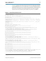
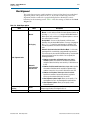
1
Altera Transceiver PHY IP Core User Guide
Altera Transceiver PHY IP Core
User Guide
101 Innovation Drive
San Jose, CA 95134
www.altera.com
UG-01080-1.11
Document last updated for Altera Complete Design Suite version:
Document publication date:
10.1
December 2010
Subscribe
Copyright © 2010 Altera Corporation. All rights reserved. Altera, The Programmable Solutions Company, the stylized Altera logo, and specific device designations
are trademarks and/or service marks of Altera Corporation in the U.S. and other countries. All other words and logos identified as trademarks and/or service marks
are the property of Altera Corporation or their respective owners. Altera products are protected under numerous U.S. and foreign patents and pending applications,
maskwork rights, and copyrights. Altera warrants performance of its semiconductor products to current specifications in accordance with Altera's standard
warranty, but reserves the right to make changes to any products and services at any time without notice. Altera assumes no responsibility or liability arising out of
the application or use of any information, product, or service described herein except as expressly agreed to in writing by Altera. Altera customers are advised to
obtain the latest version of device specifications before relying on any published information and before placing orders for products or services.
Altera Transceiver PHY IP Core User Guide
December 2010 Altera Corporation
Contents
Chapter 1. Introduction
PCS . . . . . . . . . . . . . . . . . . . . . . . . . . . . . . . . . . . . . . . . . . . . . . . . . . . . . . . . . . . . . . . . . . . . . . . . . . . . . . . . . . . . 1–3
PMA . . . . . . . . . . . . . . . . . . . . . . . . . . . . . . . . . . . . . . . . . . . . . . . . . . . . . . . . . . . . . . . . . . . . . . . . . . . . . . . . . . . 1–3
Reset Controller . . . . . . . . . . . . . . . . . . . . . . . . . . . . . . . . . . . . . . . . . . . . . . . . . . . . . . . . . . . . . . . . . . . . . . . . . 1–3
Avalon-MM PHY Management . . . . . . . . . . . . . . . . . . . . . . . . . . . . . . . . . . . . . . . . . . . . . . . . . . . . . . . . . . . 1–8
Serial Loopback . . . . . . . . . . . . . . . . . . . . . . . . . . . . . . . . . . . . . . . . . . . . . . . . . . . . . . . . . . . . . . . . . . . . . . . . . 1–8
Unsupported Features . . . . . . . . . . . . . . . . . . . . . . . . . . . . . . . . . . . . . . . . . . . . . . . . . . . . . . . . . . . . . . . . . . . 1–8
Chapter 2. Getting Started
Installation and Licensing . . . . . . . . . . . . . . . . . . . . . . . . . . . . . . . . . . . . . . . . . . . . . . . . . . . . . . . . . . . . . . . . 2–1
Design Flows . . . . . . . . . . . . . . . . . . . . . . . . . . . . . . . . . . . . . . . . . . . . . . . . . . . . . . . . . . . . . . . . . . . . . . . . . . . 2–1
MegaWizard Plug-In Manager Flow . . . . . . . . . . . . . . . . . . . . . . . . . . . . . . . . . . . . . . . . . . . . . . . . . . . . . . . 2–2
Specifying Parameters . . . . . . . . . . . . . . . . . . . . . . . . . . . . . . . . . . . . . . . . . . . . . . . . . . . . . . . . . . . . . . . . . 2–2
Simulate the IP Core . . . . . . . . . . . . . . . . . . . . . . . . . . . . . . . . . . . . . . . . . . . . . . . . . . . . . . . . . . . . . . . . . . . 2–4
Chapter 3. 10GBASE-R PHY IP Core
Release Information . . . . . . . . . . . . . . . . . . . . . . . . . . . . . . . . . . . . . . . . . . . . . . . . . . . . . . . . . . . . . . . . . . . . . 3–3
Device Family Support . . . . . . . . . . . . . . . . . . . . . . . . . . . . . . . . . . . . . . . . . . . . . . . . . . . . . . . . . . . . . . . . . . . 3–3
Performance and Resource Utilization . . . . . . . . . . . . . . . . . . . . . . . . . . . . . . . . . . . . . . . . . . . . . . . . . . . . . . 3–4
Parameter Settings . . . . . . . . . . . . . . . . . . . . . . . . . . . . . . . . . . . . . . . . . . . . . . . . . . . . . . . . . . . . . . . . . . . . . . . 3–4
Interfaces . . . . . . . . . . . . . . . . . . . . . . . . . . . . . . . . . . . . . . . . . . . . . . . . . . . . . . . . . . . . . . . . . . . . . . . . . . . . . . . 3–5
SDR XGMII TX Interface . . . . . . . . . . . . . . . . . . . . . . . . . . . . . . . . . . . . . . . . . . . . . . . . . . . . . . . . . . . . . . . 3–6
SDR XGMII RX Interface . . . . . . . . . . . . . . . . . . . . . . . . . . . . . . . . . . . . . . . . . . . . . . . . . . . . . . . . . . . . . . . 3–7
Avalon-MM Interface . . . . . . . . . . . . . . . . . . . . . . . . . . . . . . . . . . . . . . . . . . . . . . . . . . . . . . . . . . . . . . . . . . 3–8
Register Descriptions . . . . . . . . . . . . . . . . . . . . . . . . . . . . . . . . . . . . . . . . . . . . . . . . . . . . . . . . . . . . . . . 3–9
Status Interface . . . . . . . . . . . . . . . . . . . . . . . . . . . . . . . . . . . . . . . . . . . . . . . . . . . . . . . . . . . . . . . . . . . . . . 3–11
Clocks, Reset, and Powerdown . . . . . . . . . . . . . . . . . . . . . . . . . . . . . . . . . . . . . . . . . . . . . . . . . . . . . . . . 3–11
Serial Interface . . . . . . . . . . . . . . . . . . . . . . . . . . . . . . . . . . . . . . . . . . . . . . . . . . . . . . . . . . . . . . . . . . . . . . . 3–13
External PMA Control and Reconfig Interface . . . . . . . . . . . . . . . . . . . . . . . . . . . . . . . . . . . . . . . . . . . . 3–13
TimeQuest Timing Constraints . . . . . . . . . . . . . . . . . . . . . . . . . . . . . . . . . . . . . . . . . . . . . . . . . . . . . . . . . . . 3–13
Chapter 4. XAUI PHY IP Core
Release Information . . . . . . . . . . . . . . . . . . . . . . . . . . . . . . . . . . . . . . . . . . . . . . . . . . . . . . . . . . . . . . . . . . . . . 4–1
Device Family Support . . . . . . . . . . . . . . . . . . . . . . . . . . . . . . . . . . . . . . . . . . . . . . . . . . . . . . . . . . . . . . . . . . . 4–2
Performance and Resource Utilization . . . . . . . . . . . . . . . . . . . . . . . . . . . . . . . . . . . . . . . . . . . . . . . . . . . . . . 4–2
Parameter Settings . . . . . . . . . . . . . . . . . . . . . . . . . . . . . . . . . . . . . . . . . . . . . . . . . . . . . . . . . . . . . . . . . . . . . . . 4–3
Configurations . . . . . . . . . . . . . . . . . . . . . . . . . . . . . . . . . . . . . . . . . . . . . . . . . . . . . . . . . . . . . . . . . . . . . . . . . . 4–4
Interfaces . . . . . . . . . . . . . . . . . . . . . . . . . . . . . . . . . . . . . . . . . . . . . . . . . . . . . . . . . . . . . . . . . . . . . . . . . . . . . . . 4–5
SDR XGMII TX Interface . . . . . . . . . . . . . . . . . . . . . . . . . . . . . . . . . . . . . . . . . . . . . . . . . . . . . . . . . . . . . . . 4–6
SDR XGMII RX Interface . . . . . . . . . . . . . . . . . . . . . . . . . . . . . . . . . . . . . . . . . . . . . . . . . . . . . . . . . . . . . . . 4–7
Avalon-MM Interface . . . . . . . . . . . . . . . . . . . . . . . . . . . . . . . . . . . . . . . . . . . . . . . . . . . . . . . . . . . . . . . . . . 4–8
Register Descriptions . . . . . . . . . . . . . . . . . . . . . . . . . . . . . . . . . . . . . . . . . . . . . . . . . . . . . . . . . . . . . . . 4–8
Transceiver Serial Data Interface . . . . . . . . . . . . . . . . . . . . . . . . . . . . . . . . . . . . . . . . . . . . . . . . . . . . . . . 4–12
Dynamic Reconfiguration Interface . . . . . . . . . . . . . . . . . . . . . . . . . . . . . . . . . . . . . . . . . . . . . . . . . . . . . 4–12
Clocks, Reset, and Powerdown . . . . . . . . . . . . . . . . . . . . . . . . . . . . . . . . . . . . . . . . . . . . . . . . . . . . . . . . 4–13
PMA Channel Controller . . . . . . . . . . . . . . . . . . . . . . . . . . . . . . . . . . . . . . . . . . . . . . . . . . . . . . . . . . . . . . 4–14
PMA Control and Status Interface Signals–Soft IP Implementation (Optional) . . . . . . . . . . . . . . . . 4–14
PMA Control and Status Interface Signals–Hard IP Implementation (Optional) . . . . . . . . . . . . . . . 4–15
TimeQuest Timing Constraints . . . . . . . . . . . . . . . . . . . . . . . . . . . . . . . . . . . . . . . . . . . . . . . . . . . . . . . . . . . 4–16
December 2010
Altera Corporation
Altera Transceiver PHY IP Core User Guide
iv
Contents
Chapter 5. Interlaken PHY IP Core
Device Family Support . . . . . . . . . . . . . . . . . . . . . . . . . . . . . . . . . . . . . . . . . . . . . . . . . . . . . . . . . . . . . . . . . . . 5–2
Performance and Resource Utilization . . . . . . . . . . . . . . . . . . . . . . . . . . . . . . . . . . . . . . . . . . . . . . . . . . . . . . 5–2
Parameter Settings . . . . . . . . . . . . . . . . . . . . . . . . . . . . . . . . . . . . . . . . . . . . . . . . . . . . . . . . . . . . . . . . . . . . . . . 5–2
Interface . . . . . . . . . . . . . . . . . . . . . . . . . . . . . . . . . . . . . . . . . . . . . . . . . . . . . . . . . . . . . . . . . . . . . . . . . . . . . . . 5–3
Avalon-ST TX Interface . . . . . . . . . . . . . . . . . . . . . . . . . . . . . . . . . . . . . . . . . . . . . . . . . . . . . . . . . . . . . . . . 5–4
Avalon-ST RX Interface . . . . . . . . . . . . . . . . . . . . . . . . . . . . . . . . . . . . . . . . . . . . . . . . . . . . . . . . . . . . . . . . 5–5
Avalon Memory-Mapped (Avalon-MM) Management Interface . . . . . . . . . . . . . . . . . . . . . . . . . . . . . 5–6
Register Descriptions . . . . . . . . . . . . . . . . . . . . . . . . . . . . . . . . . . . . . . . . . . . . . . . . . . . . . . . . . . . . . . . 5–6
PLL Interface . . . . . . . . . . . . . . . . . . . . . . . . . . . . . . . . . . . . . . . . . . . . . . . . . . . . . . . . . . . . . . . . . . . . . . . . . 5–8
TX and RX Serial Interface . . . . . . . . . . . . . . . . . . . . . . . . . . . . . . . . . . . . . . . . . . . . . . . . . . . . . . . . . . . . . 5–8
Optional Clocks for Deskew . . . . . . . . . . . . . . . . . . . . . . . . . . . . . . . . . . . . . . . . . . . . . . . . . . . . . . . . . . . . 5–9
Simulation Testbench . . . . . . . . . . . . . . . . . . . . . . . . . . . . . . . . . . . . . . . . . . . . . . . . . . . . . . . . . . . . . . . . . . . . 5–9
Chapter 6. PCI Express PHY (PIPE) IP Core
Device Family Support . . . . . . . . . . . . . . . . . . . . . . . . . . . . . . . . . . . . . . . . . . . . . . . . . . . . . . . . . . . . . . . . . . . 6–1
Resource Utilization . . . . . . . . . . . . . . . . . . . . . . . . . . . . . . . . . . . . . . . . . . . . . . . . . . . . . . . . . . . . . . . . . . . . . 6–2
Parameter Settings . . . . . . . . . . . . . . . . . . . . . . . . . . . . . . . . . . . . . . . . . . . . . . . . . . . . . . . . . . . . . . . . . . . . . . . 6–2
Interfaces . . . . . . . . . . . . . . . . . . . . . . . . . . . . . . . . . . . . . . . . . . . . . . . . . . . . . . . . . . . . . . . . . . . . . . . . . . . . . . . 6–3
Avalon-ST TX Input Data from PCI Express PHYMAC . . . . . . . . . . . . . . . . . . . . . . . . . . . . . . . . . . . . . 6–4
Avalon-ST RX Output Data to PCI Express PHYMAC . . . . . . . . . . . . . . . . . . . . . . . . . . . . . . . . . . . . . 6–4
Avalon Memory-Mapped (Avalon-MM) PHY Management Interface . . . . . . . . . . . . . . . . . . . . . . . . 6–4
PHY Management Signals . . . . . . . . . . . . . . . . . . . . . . . . . . . . . . . . . . . . . . . . . . . . . . . . . . . . . . . . . . . . . . 6–6
Register Descriptions . . . . . . . . . . . . . . . . . . . . . . . . . . . . . . . . . . . . . . . . . . . . . . . . . . . . . . . . . . . . . . . 6–6
PIPE Interface . . . . . . . . . . . . . . . . . . . . . . . . . . . . . . . . . . . . . . . . . . . . . . . . . . . . . . . . . . . . . . . . . . . . . . . . 6–9
Transceiver Serial Interface . . . . . . . . . . . . . . . . . . . . . . . . . . . . . . . . . . . . . . . . . . . . . . . . . . . . . . . . . . . . 6–11
Simulation . . . . . . . . . . . . . . . . . . . . . . . . . . . . . . . . . . . . . . . . . . . . . . . . . . . . . . . . . . . . . . . . . . . . . . . . . . . . . 6–12
Chapter 7. Custom PHY IP Core
Device Family Support . . . . . . . . . . . . . . . . . . . . . . . . . . . . . . . . . . . . . . . . . . . . . . . . . . . . . . . . . . . . . . . . . . . 7–1
Performance and Resource Utilization . . . . . . . . . . . . . . . . . . . . . . . . . . . . . . . . . . . . . . . . . . . . . . . . . . . . . . 7–2
Parameter Settings . . . . . . . . . . . . . . . . . . . . . . . . . . . . . . . . . . . . . . . . . . . . . . . . . . . . . . . . . . . . . . . . . . . . . . . 7–2
General Options . . . . . . . . . . . . . . . . . . . . . . . . . . . . . . . . . . . . . . . . . . . . . . . . . . . . . . . . . . . . . . . . . . . . . . 7–2
8B/10B Encoder and Decoder . . . . . . . . . . . . . . . . . . . . . . . . . . . . . . . . . . . . . . . . . . . . . . . . . . . . . . . . . . 7–4
Word Alignment . . . . . . . . . . . . . . . . . . . . . . . . . . . . . . . . . . . . . . . . . . . . . . . . . . . . . . . . . . . . . . . . . . . . . . 7–5
Rate Match FIFO . . . . . . . . . . . . . . . . . . . . . . . . . . . . . . . . . . . . . . . . . . . . . . . . . . . . . . . . . . . . . . . . . . . . . . 7–6
Byte Ordering . . . . . . . . . . . . . . . . . . . . . . . . . . . . . . . . . . . . . . . . . . . . . . . . . . . . . . . . . . . . . . . . . . . . . . . . 7–7
Interfaces . . . . . . . . . . . . . . . . . . . . . . . . . . . . . . . . . . . . . . . . . . . . . . . . . . . . . . . . . . . . . . . . . . . . . . . . . . . . . . . 7–8
Avalon-ST TX Input Data from the MAC . . . . . . . . . . . . . . . . . . . . . . . . . . . . . . . . . . . . . . . . . . . . . . . . . 7–9
Avalon-ST RX Output Data to the MAC . . . . . . . . . . . . . . . . . . . . . . . . . . . . . . . . . . . . . . . . . . . . . . . . . . 7–9
Avalon-MM PHY Management Interface . . . . . . . . . . . . . . . . . . . . . . . . . . . . . . . . . . . . . . . . . . . . . . . . 7–10
PHY Management Signals . . . . . . . . . . . . . . . . . . . . . . . . . . . . . . . . . . . . . . . . . . . . . . . . . . . . . . . . . . . . . 7–11
Register Descriptions . . . . . . . . . . . . . . . . . . . . . . . . . . . . . . . . . . . . . . . . . . . . . . . . . . . . . . . . . . . . . . 7–11
Clock Interface . . . . . . . . . . . . . . . . . . . . . . . . . . . . . . . . . . . . . . . . . . . . . . . . . . . . . . . . . . . . . . . . . . . . . . 7–13
Transceiver Serial Data Interface . . . . . . . . . . . . . . . . . . . . . . . . . . . . . . . . . . . . . . . . . . . . . . . . . . . . . . . 7–14
Optional Status Signals . . . . . . . . . . . . . . . . . . . . . . . . . . . . . . . . . . . . . . . . . . . . . . . . . . . . . . . . . . . . . . . 7–14
Dynamic Partial Reconfiguration I/O Interface . . . . . . . . . . . . . . . . . . . . . . . . . . . . . . . . . . . . . . . . . . 7–15
Chapter 8. Low Latency PHY IP Core
Device Family Support . . . . . . . . . . . . . . . . . . . . . . . . . . . . . . . . . . . . . . . . . . . . . . . . . . . . . . . . . . . . . . . . . . . 8–2
Performance and Resource Utilization . . . . . . . . . . . . . . . . . . . . . . . . . . . . . . . . . . . . . . . . . . . . . . . . . . . . . . 8–2
Parameter Settings . . . . . . . . . . . . . . . . . . . . . . . . . . . . . . . . . . . . . . . . . . . . . . . . . . . . . . . . . . . . . . . . . . . . . . . 8–2
Interfaces . . . . . . . . . . . . . . . . . . . . . . . . . . . . . . . . . . . . . . . . . . . . . . . . . . . . . . . . . . . . . . . . . . . . . . . . . . . . . . . 8–5
Altera Transceiver PHY IP Core User Guide
December 2010 Altera Corporation
Contents
v
Avalon-ST TX and RX Data Interface to the MAC . . . . . . . . . . . . . . . . . . . . . . . . . . . . . . . . . . . . . . . . . 8–6
Avalon-MM PHY Management Interface . . . . . . . . . . . . . . . . . . . . . . . . . . . . . . . . . . . . . . . . . . . . . . . . . 8–7
Register Descriptions . . . . . . . . . . . . . . . . . . . . . . . . . . . . . . . . . . . . . . . . . . . . . . . . . . . . . . . . . . . . . . . 8–7
Serial Data Interface . . . . . . . . . . . . . . . . . . . . . . . . . . . . . . . . . . . . . . . . . . . . . . . . . . . . . . . . . . . . . . . . . . . 8–8
Optional Status Interface . . . . . . . . . . . . . . . . . . . . . . . . . . . . . . . . . . . . . . . . . . . . . . . . . . . . . . . . . . . . . . . 8–8
Chapter 9. Transceiver Reconfiguration Controller
Register Descriptions . . . . . . . . . . . . . . . . . . . . . . . . . . . . . . . . . . . . . . . . . . . . . . . . . . . . . . . . . . . . . . . . . . . . 9–2
Steps to Achieve PMA Controls Reconfiguration . . . . . . . . . . . . . . . . . . . . . . . . . . . . . . . . . . . . . . . . . . . . 9–3
Chapter 10. Migrating from Stratix IV to Stratix V
XAUI PHY . . . . . . . . . . . . . . . . . . . . . . . . . . . . . . . . . . . . . . . . . . . . . . . . . . . . . . . . . . . . . . . . . . . . . . . . . . . . 10–1
Parameter Differences . . . . . . . . . . . . . . . . . . . . . . . . . . . . . . . . . . . . . . . . . . . . . . . . . . . . . . . . . . . . . . . . 10–1
Port Differences . . . . . . . . . . . . . . . . . . . . . . . . . . . . . . . . . . . . . . . . . . . . . . . . . . . . . . . . . . . . . . . . . . . . . . 10–2
PCI Express PHY (PIPE) . . . . . . . . . . . . . . . . . . . . . . . . . . . . . . . . . . . . . . . . . . . . . . . . . . . . . . . . . . . . . . . . . 10–4
Parameter Differences . . . . . . . . . . . . . . . . . . . . . . . . . . . . . . . . . . . . . . . . . . . . . . . . . . . . . . . . . . . . . . . . 10–4
Port Differences . . . . . . . . . . . . . . . . . . . . . . . . . . . . . . . . . . . . . . . . . . . . . . . . . . . . . . . . . . . . . . . . . . . . . . 10–5
Custom PHY . . . . . . . . . . . . . . . . . . . . . . . . . . . . . . . . . . . . . . . . . . . . . . . . . . . . . . . . . . . . . . . . . . . . . . . . . . . 10–8
Parameter Differences . . . . . . . . . . . . . . . . . . . . . . . . . . . . . . . . . . . . . . . . . . . . . . . . . . . . . . . . . . . . . . . . 10–8
Port Differences . . . . . . . . . . . . . . . . . . . . . . . . . . . . . . . . . . . . . . . . . . . . . . . . . . . . . . . . . . . . . . . . . . . . . . 10–9
Additional Information
Revision History . . . . . . . . . . . . . . . . . . . . . . . . . . . . . . . . . . . . . . . . . . . . . . . . . . . . . . . . . . . . . . . . . . . . . Info–1
How to Contact Altera . . . . . . . . . . . . . . . . . . . . . . . . . . . . . . . . . . . . . . . . . . . . . . . . . . . . . . . . . . . . . . . . Info–3
Typographic Conventions . . . . . . . . . . . . . . . . . . . . . . . . . . . . . . . . . . . . . . . . . . . . . . . . . . . . . . . . . . . . . Info–3
December 2010 Altera Corporation
Altera Transceiver PHY IP Core User Guide
vi
Altera Transceiver PHY IP Core User Guide
Contents
December 2010 Altera Corporation
1. Introduction
The Altera® Transceiver PHY IP Core User Guide describes the following
protocol-specific PHYs:
■
10GBASE-R PHY IP Core
■
XAUI PHY IP Core
■
Interlaken PHY IP Core
■
PCI Express PHY (PIPE) IP Core
■
Custom PHY IP Core
■
Low Latency PHY IP Core
The protocol-specific PHYs automatically configure settings for the physical coding
sublayer (PCS) module, leaving a small number of parameters in the physical media
attachment (PMA) module for you to configure. You can use the Custom PHY for
applications that require more flexible settings. The design of all of these PHYs is
modular and uses standard interfaces. All PHYs include an Avalon®
Memory-Mapped (Avalon-MM) interface to access control and status registers and an
Avalon Streaming (Avalon-ST) interface to connect to the MAC for data transfer. The
control and status registers store device-dependent information about the PCS and
PMA modules. You can access this device-dependent information using the
device-independent Avalon-MM interface, reducing overall complexity of your
design and the number of device-dependent signals that you must expose in your
top-level module.
f For more information about the Avalon-MM and Avalon-ST protocols, including
timing diagrams, refer to the Avalon Interface Specifications.
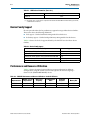
Table 1–1 shows hard and soft implementation support for these IP cores in Stratix® V
devices. Typically, the PCS and PMA are implemented as hard logic, saving FPGA
resources and reducing the complexity of verification. In some cases, the PCS is also
available in soft logic as Table 1–1 indicates.
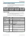
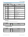
Table 1–1. Stratix V GX Support for Protocol Specific PHY IP Cores
PHY Protocol
December 2010
Soft PCS
Hard PCS
Hard PMA
10GBASE-R
No
Yes
Yes
XAUI
Yes
No
Yes
Interlaken
No
Yes
Yes
PCI Express Gen1 and Gen2
No
Yes
Yes
Custom PHY
No
Yes
Yes
Low latency PHY
No
Yes
Yes
Altera Corporation
Altera Transceiver PHY IP Core User Guide
1–2
Chapter 1: Introduction
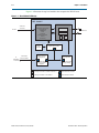
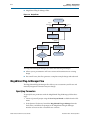
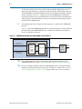
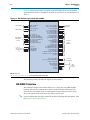
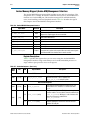
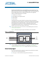
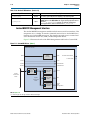
Figure 1–1 illustrates the top level modules that comprise the PHY IP cores.
Figure 1–1. Altera Modular PHY Design
PHY - Stratix V
Avalon-ST
Tx and Rx
To MAC
PCS
PMA
Customized functionality
as required for:
10GBase-R
XAUI
Interlaken
PCI Express PIPE
Custom
Low Latency
Rx Deserializer
Altera Transceiver PHY IP Core User Guide
PLL
S
Avalon-MM PHY
Management
S
CDR
PCS & PMA Control & Status
Register Memory Map
Reset
Controller
Avalon-MM
To
Control & Status
Embedded
Controller
To HSSI Pins
Tx Serializer
Transceiver
Reconfiguration
M
S
Read & Write
Control & Status
Registers
Offset Cancellation
Analog Settings
Hard logic for Stratix V, variable for Stratix IV
M
Avalon-MM master interface
Soft logic for Stratix IV and Stratix V
S
Avalon-MM slave interface
December 2010 Altera Corporation
Chapter 1: Introduction
PCS
1–3
The following sections provide a brief introduction to each of the modules illustrated
in Figure 1–1.
PCS
The PCS implements part of the physical layer specification for networking protocols.
Depending upon the protocol that you choose, the PCS may include many different
functions. Some of the most commonly included functions are: 8B/10B, 64b/66b, or
64b/67b encoding and decoding, rate matching and clock compensation, scrambling
and de-scrambling, word alignment, phase compensation, error monitoring, and
gearbox.
PMA
The PMA receives and transmits differential serial data on the device external pins.
The transmit (TX) channel supports programmable pre-emphasis and programmable
output differential voltage (VOD). It converts parallel input data streams to serial
data.The RX channel supports offset cancellation to correct for process variation and
programmable equalization. It converts serial data to parallel data for processing in
the PCS. The PMA also includes a clock data recovery (CDR) module with separate
CDR logic for each RX channel.
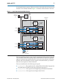
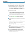
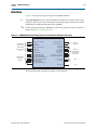
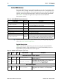
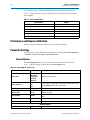
Reset Controller
The reset controller manages signals to reset and power down the PHY channels and
PLLs. The PHY channels operate in two modes: bonded and non-bonded. In bonded
mode, a single Clock Generation Buffer (CGB) divides the output it receives from the
TX PLL to create the parallel clock inputs the TX channel PMA and PCS modules. The
parallel clocks for each channel are carefully tuned to keep the clock skew below 150
ps. Figure 1–2 illustrates bonded mode for Stratix V devices.
December 2010
Altera Corporation
Altera Transceiver PHY IP Core User Guide
1–4
Chapter 1: Introduction
Reset Controller
Figure 1–2. Stratix V Device Bonded Mode Clocking
Channel PLL
Reference
clock input
pin
Tx PLL
High
Low speed
frequency Clock Gen
parallel
clock
clock(s)
Buffer
(CGB)
/n, /m
FPGA-fabric
interface
Transceiver
PMA
PCS
Tx data
Ser
Rx data
CDR
Tx PCS
DeSer
PCS
PMA
Tx data
Rx data
Rx PCS
Tx PCS
Ser
CDR
DeSer
Rx PCS
Data
Clock
Ser = Serializer
DeSer = DeSerializer
Altera Transceiver PHY IP Core User Guide
December 2010 Altera Corporation
Chapter 1: Introduction
Reset Controller
1–5
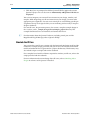
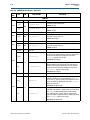
In non-bonded mode, separate CGBs are used for each channel and the skew between
channels is not carefully controlled. Figure 1–3 illustrates mode for Stratix V devices.
Figure 1–3. Stratix V Device Non-Bonded Mode Clocking
High
frequency
clock
Reference
clock input
pin
Tx PLL
FPGA-fabric
interface
Transceiver
Clock Gen
Buffer
(CGB)
/n, /m
PMA
PMA
Low speed
parallel
clock(s)
PCS
PCS
Tx data
Ser
Rx data
CDR
Transceiver
Tx PCS
DeSer
Rx PCS
Clock Gen
Buffer
(CGB)
/n, /m
PMA
PMA
Low speed
parallel
clock(s)
PCS
PCS
Tx data
Ser
Rx data
CDR
Tx PCS
DeSer
Rx PCS
Data
Clock
Ser = Serializer
DeSer = DeSerializer
The reset controller generates a reset sequence appropriate for the protocol. Using the
reset controller section of the memory map, you can choose have the reset sequence
apply to all channels (the default behavior), or mask out some channels so that those
channels will not be affected by the reset sequence. For bonded modes, you should
allow the reset sequence to affect all channels.
The reset controller drives the following reset signals:
December 2010
■
rx_analogreset—This signal resets the analog CDR and deserializer logic present
in the RX channel. (CDR is the first step of the power-up process.)
■
rx_digitalreset—This signal resets all digital logic in the RX PCS and PMA.
■
tx_digitalreset—This signal resets all logic in the TX PCS.
Altera Corporation
Altera Transceiver PHY IP Core User Guide
1–6
Chapter 1: Introduction
Reset Controller
The reset controller also includes a signal to power down the PLLs and transceiver
channels:
■
1
pll_powerdown—This signal powers down a single clock generation circuit.
pll_powerdown is only asserted during a full reset sequence, which is only possible
when the device enters user mode or when you assert and deassert the PHY
management interface reset input.
The Quartus® II software automatically selects the power-down channel feature,
which takes effect when you configure the Stratix IV or Stratix V device. All unused
channels and blocks consume no power, reducing overall power consumption.
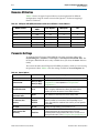
Table 1–2 lists the bonding requirements for the protocol-specific PHYs.
Table 1–2. Bonding Requirements
Protocol
Bonded
Non-Bonded
10GBASE-R
—
v
XAUI
v
—
Interlaken < ×4
—
v
Interlaken > ×4
v
—
PCI Express ×1
—
v
PCI Express ×2, ×4, ×8
v
—
Custom PHY (1)
v
v
Low Latency PHY (1)
v
v
Note to Table 1–2:
(1) You can choose either bonded or non-bonded clocks for the Custom and Low Latency PHY IP cores to meet the
requirements of your design.
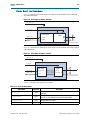
The precise sequence of events that occurs to reset the transceiver PHY depends upon
the configuration chosen. The reset sequence for configurations that only include TX
channels is far simpler because it does not require the RX analog logic to recover the
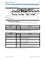
clock from the input data stream or to perform offset cancellation. Figure 1–4
illustrates the critical signals of the reset circuitry for a duplex PHY. As this figure
illustrates, the typical reset sequence includes the following steps:
1. After the PLL locks, tx_ready is asserted.
2. After offset cancellation completes rx_oc_busy is deasserted. (Offset cancellation
corrects for process variations which may result in analog voltages that are offset
from the required ranges.)
Altera Transceiver PHY IP Core User Guide
December 2010 Altera Corporation
Chapter 1: Introduction
Reset Controller
1–7
3. Finally, rx_ready is asserted and phy_mgmt_clk_reset goes low, ending the reset
state.
\
Figure 1–4. Reset Sequence
phy_mgmt_clk
phy_mgmt_clk_reset
pll_islocked
rx_oc_busy
rx_islocked_toref
powerdown_all
tx_ready
rx_ready
Figure 1–5 shows the hardware modules and internal signals that implement reset in
Stratix V devices.
Figure 1–5. Block Diagram of the Reset Sequence Controller
Transceiver PHY
Receiver
PCS
Transmitter
PCS
Transmitter
PMA
Receiver
PMA
Transmitter
PLL
CDR
rx_is_lockedtodata
tx_pll_is_locked
rx_digitalreset
tx_digitalreset
pll_powerdown
rx_analogreset
phy_mgmt_clk_reset
Reset Controller
tx_ready
rx_ready
to / from
user logic
PCS and PMA Control
and Status Register
Memory Map
Avalon-MM
Interface
Avalon - MM
PHY Management
S
M
S
Dynamic
Reconfiguration
S
f For additional timing diagrams illustrating resets for many configurations, refer to
Reset Control and Power Down in volume 4 of the Stratix IV Device Handbook for
Stratix IV devices or Reset Control and Power Down in volume 2 of the Stratix V Device
Handbook for Stratix V devices.
December 2010
Altera Corporation
Altera Transceiver PHY IP Core User Guide
1–8
Chapter 1: Introduction
Avalon-MM PHY Management
Avalon-MM PHY Management
You can use the Avalon-MM PHY Management module to read and write the control
and status registers in the PCS and PMA. This module includes both Avalon-MM
master and slave ports and acts as a bridge. It transfers commands received from an
embedded controller on its slave port to its master port. The Avalon-MM PHY
management master interface connects the Avalon-MM slave ports of PCS and PMA
registers and the Transceiver Reconfiguration module, allowing you to manage these
Avalon-MM slave components through a simple, standard interface. (Refer to
Figure 1–1 on page 1–2.)
Serial Loopback
All of the PHYs, with the exception of PCI Express, support serial loopback mode in
both Stratix IV and Stratix V devices. PCI Express supports reverse parallel loopback
mode as required by the PCI Express Base Specification. Figure 1–6 shows the datapath
for serial loopback. The data from the FPGA fabric passes through the TX channel and
is looped back to the RX channel, bypassing the RX buffer. The received data is
available to the FPGA logic for verification. Using the serial loopback option, you can
check the operation of all enabled PCS and PMA functional blocks in the TX and RX
channels. When serial loopback is enabled, the TX channel sends the data to both the
tx_serial_data output port and the RX channel.
Figure 1–6. Serial Loopback
Transceiver
Tx PMA
Tx PCS
Serializer
tx_dataout
FPGA
Fabric
Serial
loopback
Rx PMA
To FPGA fabric
for verification
Rx PCS
Deserializer
Unsupported Features
The protocol-specific PHYs are not supported in SOPC Builder in the current release.
Altera Transceiver PHY IP Core User Guide
December 2010 Altera Corporation
2. Getting Started
This chapter provides a general overview of the Altera IP core design flow to help you
quickly get started with any Altera IP core. The Altera IP Library is installed as part of
the Quartus II installation process. You can select and parameterize any Altera IP core
from the library. Altera provides an integrated parameter editor that allows you to
customize IP cores to support a wide variety of applications. The parameter editor
guides you through the setting of parameter values and selection of optional ports.
The following sections describe the general design flow and use of Altera IP cores.
Installation and Licensing
The Altera IP Library is distributed with the Quartus II software and downloadable
from the Altera website (www.altera.com).
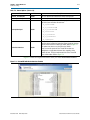
Figure 2–1 shows the directory structure after you install an Altera IP core, where
<path> is the installation directory. The default installation directory on Windows is
C:\altera\<version number>; on Linux it is /opt/altera<version number>.
Figure 2–1. IP core Directory Structure
<path>
Installation directory
ip
Contains the Altera IP Library and third-party IP cores
altera
Contains the Altera IP Library
common
Contains shared components
<IP core name> or uniPHY
Contains the IP core files and documentation
You can evaluate an IP core in simulation and in hardware until you are satisfied with
its functionality and performance. Some IP cores require that you purchase a license
for the IP core when you want to take your design to production. After you purchase
a license for an Altera IP core, you can request a license file from the Altera Licensing
page of the Altera website and install the license on your computer. For additional
information, refer to Altera Software Installation and Licensing.
Design Flows
You can use the following flow(s) to parameterize Altera IP cores:
December 2010
Altera Corporation
Altera Transceiver PHY IP Core User Guide
2–2
Chapter 2: Getting Started
MegaWizard Plug-In Manager Flow
■
MegaWizard Plug-In Manager Flow
Figure 2–2. Design Flows
Select Design Flow
Qsys or
SOPC Builder
Flow
MegaWizard
Flow
Specify Parameters
Specify Parameters
Complete Qsys or
SOPC Builder System
Optional
Perform
Functional Simulation
Does
Simulation Give
Expected Results?
Yes
Add Constraints
and Compile Design
IP Complete
Debug Design
The MegaWizard Plug-In Manager flow offers the following advantages:
■
Allows you to parameterize an IP core variant and instantiate into an existing
design
■
For some IP cores, this flow generates a complete example design and testbench.
MegaWizard Plug-In Manager Flow
The MegaWizard Plug-In Manager flow allows you to customize your IP core and
manually integrate the function into your design.
Specifying Parameters
To specify IP core parameters with the MegaWizard Plug-In Manager, follow these
steps:
1. Create a Quartus II project using the New Project Wizard available from the File
menu.
2. In the Quartus II software, launch the MegaWizard Plug-in Manager from the
Tools menu, and follow the prompts in the MegaWizard Plug-In Manager
interface to create or edit a custom IP core variation.
Altera Transceiver PHY IP Core User Guide
December 2010 Altera Corporation
Chapter 2: Getting Started
MegaWizard Plug-In Manager Flow
2–3
3. To select a specific Altera IP core, click the IP core in the Installed Plug-Ins list in
the MegaWizard Plug-In Manager.
4. Specify the parameters on the Parameter Settings pages. For detailed explanations
of these parameters, refer to the “Parameter Settings” chapter in this document.
1
Some IP cores provide preset parameters for specific applications. If you
wish to use preset parameters, click the arrow to expand the Presets list,
select the desired preset, and then click Apply. To modify preset settings, in
a text editor edit the <installation directory>\ip\altera\uniphy\lib\<IP
core>.qprs file.
5. If the IP core provides a simulation model, specify appropriate options in the
wizard to generate a simulation model.
1
Altera IP supports a variety of simulation models, including
simulation-specific IP functional simulation models and encrypted RTL
models, and plain text RTL models. These are all cycle-accurate models. The
models allow for fast functional simulation of your IP core instance using
industry-standard VHDL or Verilog HDL simulators. For some cores, only
the plain text RTL model is generated, and you can simulate that model.
f For more information about functional simulation models for Altera IP
cores, refer to Simulating Altera Designs in volume 3 of the Quartus II
Handbook.
c
Use the simulation models only for simulation and not for synthesis or any
other purposes. Using these models for synthesis creates a nonfunctional
design.
6. If the parameter editor includes EDA and Summary tabs, follow these steps:
a. Some third-party synthesis tools can use a netlist that contains the structure of
an IP core but no detailed logic to optimize timing and performance of the
design containing it. To use this feature if your synthesis tool and IP core
support it, turn on Generate netlist.
b. On the Summary tab, if available, select the files you want to generate. A gray
checkmark indicates a file that is automatically generated. All other files are
optional.
1
If file selection is supported for your IP core, after you generate the core, a
generation report (<variation name>.html) appears in your project directory.
This file contains information about the generated files.
7. Click the Finish button, the parameter editor generates the top-level HDL code for
your IP core, and a simulation directory which includes files for simulation.
1
December 2010
Altera Corporation
The Finish button may be unavailable until all parameterization errors
listed in the messages window are corrected.
Altera Transceiver PHY IP Core User Guide
2–4
Chapter 2: Getting Started
MegaWizard Plug-In Manager Flow
8. Click Yes if you are prompted to add the Quartus II IP File (.qip) to the current
Quartus II project. You can also turn on Automatically add Quartus II IP Files to
all projects.
You can now integrate your custom IP core instance in your design, simulate, and
compile. While integrating your IP core instance into your design, you must make
appropriate pin assignments. You can create virtual pin to avoid making specific pin
assignments for top-level signals while you are simulating and not ready to map the
design to hardware.
For some IP cores, the generation process also creates a complete example design in
the <variation_name>_example_design_fileset/example_project/ directory. This
example demonstrates how to instantiate and connect the IP core.
1
For information about the Quartus II software, including virtual pins and the
MegaWizard Plug-In Manager, refer to Quartus II Help.
Simulate the IP Core
You can simulate your IP core variation with the functional simulation model and the
testbench or example design generated with your IP core. The functional simulation
model and testbench files are generated in a project subdirectory. This directory may
also include scripts to compile and run the testbench.
For a complete list of models or libraries required to simulate your IP core, refer to the
scripts provided with the testbench.
For more information about simulating Altera IP cores, refer to Simulating Altera
Designs in volume 3 of the Quartus II Handbook.
Altera Transceiver PHY IP Core User Guide
December 2010 Altera Corporation
3. 10GBASE-R PHY IP Core
The Altera 10GBASE-R PHY IP core implements the functionality described in IEEE
802.3 Clause 49. It delivers serialized data to an optical module that drives multi-mode
optical fiber at a line rate of 10.3125 Gbps. In a multi-channel implementation of
10GBASE-R, each channel of the 10GBASE-R PHY IP core operates independently.
You can instantiate multiple channels to achieve higher bandwidths. The PCS is
available in soft logic for Stratix IV GT devices; it connects to a separately instantiated
hard PMA.
Figure 3–1 illustrates a multiple 10 GbE channel IP core in a Stratix IV GT device.
Figure 3–1. Complete 10GBASE-R PHY Design
10GBase-R PHY
ALTGX<n>
SDR XGMII
72 bits @ 156.25 Mbps
To MAC
PCS
10GBASE-R
(64b/66b)
S
Alt_PMA
10GBASE-R
10.3 Gbps
To HSSI Pins
S
10.3125 Gbps serial
ALTGX<0>
SDR XGMII
72 bits @ 156.25 Mbps
To MAC
PCS
10GBASE-R
(64b/66b)
S
Alt_PMA
10GBASE-R
10.3 Gbps
To HSSI Pins
S
10.3125 Gbps serial
To Embedded
Controller
S
Avalon-MM
PHY
Management
Bridge
Low Latency
Controller
M
Avalon-MM
connections
S
Transceiver
Reconfig
S Controller
In this configuration, 10GBASE-R PHY IP core includes a soft PCS and a hard PMA.
The soft PCS connects to an Ethernet MAC running at 156.25 Mbps and transmits data
to a hard 10 Gbps transceiver PMA running at 10.3125 Gbps in a Stratix IV GT device.
December 2010
Altera Corporation
Altera Transceiver PHY IP Core User Guide
3–2
Chapter 3: 10GBASE-R PHY IP Core
To make most effective use of this soft PCS and hard PMA configuration, you can
group up to four channels in a single quad and control their functionality using one
Avalon-MM PHY management bridge, transceiver reconfiguration module, and low
latency controller. As Figure 3–1 illustrates, the Avalon-MM bridge Avalon-MM
master port connects to the Avalon-MM slave port of the transceiver reconfiguration
and low latency controller modules so that you can update analog settings using the
standard Avalon-MM interface.
1
This configuration does not require all four channels in a quad run the 10GBASE-R
protocol.
Figure 3–2 shows the 10GBASE-R PHY IP core available for Stratix V devices. Both the
PCS and PMA of the 10GBASE-R PHY are available as hard IP blocks in Stratix V,
devices saving FPGA resources.
Figure 3–2. 10GBASE-R PHY with Hard PCS with Hard PMA in Stratix V Devices
Stratix V FPGA
10GBASE-R PHY IP Core
SDR XGMII
72 bits @ 156.25 Mbps
Avalon-MM
Control & Status
Hard PCS
10GBASE-R
64b/66b
Scrambler
PRBS
Gearbox
XFI/SFI
Hard PMA
10/3125 Gbps serial
PMD
Copper
or
Optical
Networ
Interfac
f For a 10-Gbps Ethernet solution that includes both the Ethernet MAC and the
10GBASE-R PHY, refer to the 10-Gbps Ethernet MAC MegaCore Function User Guide.
f For more detailed information about the 10GBASE-R transceiver channel datapath,
clocking, and channel placement, refer to the “10GBASE-R” section in the Transceiver
Protocol Configurations in Stratix V Devices chapter of the Stratix V Device Handbook.
Altera Transceiver PHY IP Core User Guide
December 2010 Altera Corporation
Chapter 3: 10GBASE-R PHY IP Core
Release Information
3–3
Release Information
Table 3–1 provides information about this release of the 10GBASE-R PHY IP core.
Table 3–1. 10GBASE-R Release Information
Item
Description
Version
10.1
Release Date
December 2010
Ordering Codes (Note 1)
IP-10GBASERPCS (primary)
IPR-10GBASERPCS (renewal)
Product ID
00D7
Vendor ID
6AF7
Note to Figure 3–1:
(1) No ordering codes or license files are required for Stratix V devices.
Device Family Support
IP cores provide either final or preliminary support for target Altera device families.
These terms have the following definitions:
■
Final support—Verified with final timing models for this device.
■
Preliminary support—Verified with preliminary timing models for this device.
Table 3–2 shows the level of support offered by the 10GBASE-R IP core for Altera
device families.
Table 3–2. Device Family Support
Device Family
Support
Stratix IV GT devices–soft PCS and hard PMA
Final
Stratix V devices–hard PCS and hard PMA
Preliminary
Other device families
No support
f For speed grade information, refer to “Transceiver Performance Specifications” the
DC and Switching Characteristics chapter in volume 3 of the Stratix IV Handbook for
Stratix IV devices or DC and Switching Characteristics for Stratix V Devices in volume 3
of the Stratix V Handbook for Stratix V devices.
December 2010
Altera Corporation
Altera Transceiver PHY IP Core User Guide
3–4
Chapter 3: 10GBASE-R PHY IP Core
Performance and Resource Utilization
Performance and Resource Utilization
Table 3–3 shows the typical expected device resource utilization for a single duplex
channel using the current version of the Quartus II software targeting a Stratix IV GT
device. The numbers of combinational ALUTs, logic registers, and memory bits are
rounded to the nearest 100.
Table 3–3. 10GBASE-R PHY Performance and Resource Utilization—Stratix IV GT Device
Channels
Combinational ALUTs
Logic Registers (Bits)
Memory Bits
1
5200
4100
4700
4
15600
1300
18800
10
38100
32100
47500
Parameter Settings
To configure the 10GBASE-R PHY IP core in the parameter editor, click Installed
Plug-Ins > Interfaces >Ethernet> 10GBASE-R PHY v10.1. The 10GBASE-R PHY IP
core is available for the Stratix IV or Stratix V device family.
This section describes the 10GBASE-R PHY parameters, which you can set using the
parameter editor. Table 3–4 lists the settings available on General Options tab.
Table 3–4. Parameters
Name
Value
Description
General Options
Device family
Stratix IV GT
Stratix V
The target family. Stratix V devices use a hard PCS. Stratix IV devices
use a soft PCS. Both devices use a hard PMA.
Number of channels
1–32
The total number of 10Gbase-R PHY channels.
Mode of operation
Duplex
TX only
RX only
Stratix V devices allow duplex, TX, or RX mode. Stratix IV GX devices
only support duplex mode.
Reference Clock Frequency
322.265625 MHz
644.53125 MHz
Stratix V devices support both frequencies.Stratix IV GX devices only
support 644.53125 MHz.
Additional Options
On/Off
If you turn this option on, the following 2 signals are brought out to
the top level of the IP core to facilitate debugging: hi_ber and
block_lock.
Use external PMA control and
reconfig
On/Off
If you turn this option on, the PMA controller and reconfiguration
block are external, rather than included 10GBASE-R PHY IP core,
allowing you to use the same PMA controller and reconfiguration IP
cores for other protocols in the same transceiver quad. This option is
available in Stratix IV devices.
Starting channel number
0–96
Specifies the starting channel number. Must be 0 or a multiple of 4.
You only need to set this parameter if you are using external PMA
and reconfiguration modules.
Enable additional control and
status pins
f For a description of the Analog options, refer the to “PMA Analog Options” on
page 8–4.
Altera Transceiver PHY IP Core User Guide
December 2010 Altera Corporation
Chapter 3: 10GBASE-R PHY IP Core
Interfaces
3–5
Interfaces
Figure 3–3 illustrates the top-level signals of the 10Base-R PHY.
1
The block diagram shown in the GUI labels the external pins with the interface type
and places the interface name inside the box. The interface type and name are used in
the Hardware Component Description File (_hw.tcl).
f For more information about _hw.tcl files, refer to the Component Interface Tcl Reference
chapter in the SOPC Builder User Guide.
Figure 3–3. 10GBASE-R PHY Pinout Showing Interfaces for Both Internal and External Transceivers
10GBASE-R Top-Level Signals
SDR XGMII Tx
Inputs from MAC
xgmii_tx_dc<n>[71:0]
tx_ready
xgmii_tx_clk
SDR XGMII Rx
Outputs from PCS
to MAC
xgmii_rx_dc<n>[71:0]
rx_ready
xgmii_rx_clk
Avalon-MM PHY
Management
Interface
phy_mgmt_clk
phy_mgmt_clk_reset
phy_mgmt_addr[15:0]
phy_mgmt_writedata[31:0]
phy_mgmt_readdata[31:0]
phy_mgmt_write
phy_mgmt_read
phy_mgmt_waitrequest
rx_serial_data<n>
tx_serial_data<n>
Transceiver
Serial Data
gxb_pdn
pll_locked
pll_pdn
cal_blk_pdn
rx_oc_busy
cal_blk_clk
reconfig_to_gxb[3:0]
reconfig_from_gxb[16:0]
Signals for
External PMA and
Reconfiguration
Stratix IV only
rx_block_lock
rx_hi_ber
Status
pll_ref_clk
Clock
f
The following sections describe the signals in each interface.
December 2010
Altera Corporation
Altera Transceiver PHY IP Core User Guide
3–6
Chapter 3: 10GBASE-R PHY IP Core
Interfaces
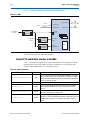
SDR XGMII TX Interface
Table 3–5 describes the signals in the SDR XGMII TX interface. These signals are
driven from the MAC to the PCS. This is an Avalon-ST sink interface.
Table 3–5. SDR XGMII TX Inputs (Note 1)
Signal Name
Direction
Description
Contains 8 lanes of data and control for XGMII. Each lane consists of 8 bits of
data and 1 bit of control.
xgmii_tx_dc<n>[71:0]
Sink
■
Lane 0–[7:0]/[8]
■
Lane 1–[16:9]/[17]
■
Lane 2–[25:18]/[26]
■
Lane 3–[34:27]/[35]
■
lane 4–[43:36]/[44]
■
Lane 5–[52:45]/[53]
■
Lane 6–[61:54]/[62]
■
Lane 7–[70:63]/[71]
Refer to Table 3–6 for the mapping of the xgmii_tx_dc data and control to the
xgmii_sdr_data and xgmii_sdr_ctrl signals.
Output
tx_ready
Input
xgmii_tx_clk
Asserted when the TX channel is ready to transmit data. Because the
readyLatency on this Avalon-ST interface is 0, the MAC may drive
xgmii_tx_dc_valid as soon as tx_ready is asserted.
The XGMII TX clock which runs at 156.25 MHz.
Note to Table 3–5:
(1) <n> is the channel number
f For more information about the Avalon-ST protocol, including timing diagrams, refer
to the Avalon Interface Specifications.
Table 3–6 provides the mapping from the XGMII TX interface to the XGMII SDR
interface.
Table 3–6. Mapping from XGMII TX Bus to XGMII SDR Bus (Part 1 of 2)
Signal Name
XGMII Signal Name
Description
xgmii_tx_dc[7:0]
xgmii_sdr_data[7:0]
Lane 0 data
xgmii_tx_dc[8]
xgmii_sdr_ctrl[0]
Lane 0 control
xgmii_tx_dc[16:9]
xgmii_sdr_data[15:8]
Lane 1 data
xgmii_tx_dc[17]
xgmii_sdr_ctrl[1]
Lane 1 control
xgmii_tx_dc[25:18]
xgmii_sdr_data[23:16]
Lane 2 data
xgmii_tx_dc[26]
xgmii_sdr_ctrl[2]
Lane 2 control
xgmii_tx_dc[34:27]
xgmii_sdr_data[31:24]
Lane 3 data
xgmii_tx_dc[35]
xgmii_sdr_ctrl[3]
Lane 3 control
xgmii_tx_dc[43:36]
xgmii_sdr_data[39:32]
Lane 4 data
xgmii_tx_dc[44]
xgmii_sdr_ctrl[4]
Lane 4 control
xgmii_tx_dc[52:45]
xgmii_sdr_data[47:40]
Lane 5 data
Altera Transceiver PHY IP Core User Guide
December 2010 Altera Corporation
Chapter 3: 10GBASE-R PHY IP Core
Interfaces
3–7
Table 3–6. Mapping from XGMII TX Bus to XGMII SDR Bus (Part 2 of 2)
Signal Name
XGMII Signal Name
Description
xgmii_tx_dc[53]
xgmii_sdr_ctrl[5]
Lane 5 control
xgmii_tx_dc[61:54]
xgmii_sdr_data[55:48]
Lane 6 data
xgmii_tx_dc[62]
xgmii_sdr_ctrl[6]
Lane 6 control
xgmii_tx_dc[70:63]
xgmii_sdr_data[63:56]
Lane 7 data
xgmii_tx_dc[71]
xgmii_sdr_ctrl[7]
Lane 7 control
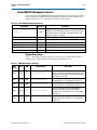
SDR XGMII RX Interface
Table 3–7 describes the signals in the SDR XGMII RX interface. This is an Avalon-ST
source interface. These signals are driven from the PCS to the MAC.
Table 3–7. SDR XGMII RX Inputs
Signal Name
(Note 1)
Direction
Description
Contains 8 lanes of data and control for XGMII. Each lane consists of 8 bits of
data and 1 bit of control.
xgmii_rx_dc<n>[71:0]
Source
■
Lane 0–[7:0]/[8]
■
Lane 1–[16:9]/[17]
■
Lane 2–[25:18]/[26]
■
Lane 3–[34:27]/[35]
■
lane 4–[43:36]/[44]
■
Lane 5–[52:45]/[53]
■
Lane 6–[61:54]/[62]
■
Lane 7–[70:63]/[71]
Refer to Table 3–8 for the mapping of the xgmii_rx_dc data and control to the
xgmii_sdr_data and xgmii_sdr_ctrl signals.
Input
rx_ready
Output
xgmii_rx_clk
Asserted when the RX channel is ready to receive data. Because the
readyLatency on this Avalon-ST interface is 0, the PCS may drive
xgmii_rx_dc_valid as soon as rx_ready is asserted.
This clock is generated by the same reference clock that is used to generate the
transceiver clock. Its frequency is 156.25 MHz. Use this clock for the MAC
interface to minimize the size of the FIFO between the MAC and SDR XGMII RX
interface.
Note to Table 3–7:
(1) <n> is the channel number
Table 3–8 provides the mapping from the XGMII RX interface to the XGMII SDR
interface.
Table 3–8. Mapping from XGMII RX Bus to the XGMII SDR Bus (Part 1 of 2)
Signal Name
XGMII Signal Name
Description
xgmii_rx_dc[7:0]
xgmii_sdr_data[7:0]
Lane 0 data
xgmii_rx_dc[8]
xgmii_sdr_ctrl[0]
Lane 0 control
xgmii_rx_dc[16:9]
xgmii_sdr_data[15:8]
Lane 1 data
December 2010
Altera Corporation
Altera Transceiver PHY IP Core User Guide
3–8
Chapter 3: 10GBASE-R PHY IP Core
Interfaces
Table 3–8. Mapping from XGMII RX Bus to the XGMII SDR Bus (Part 2 of 2)
Signal Name
XGMII Signal Name
Description
xgmii_rx_dc[17]
xgmii_sdr_ctrl[1]
Lane 1 control
xgmii_rx_dc[25:18]
xgmii_sdr_data[23:16]
Lane 2 data
xgmii_rx_dc[26]
xgmii_sdr_ctrl[2]
Lane 2 control
xgmii_rx_dc[34:27]
xgmii_sdr_data[31:24]
Lane 3 data
xgmii_rx_dc[35]
xgmii_sdr_ctrl[3]
Lane 3 control
xgmii_rx_dc[43:36]
xgmii_sdr_data[39:32]
Lane 4 data
xgmii_rx_dc[44]
xgmii_sdr_ctrl[4]
Lane 4 control
xgmii_rx_dc[52:45]
xgmii_sdr_data[47:40]
Lane 5 data
xgmii_rx_dc[53]
xgmii_sdr_ctrl[5]
Lane 5 control
xgmii_rx_dc[61:54]
xgmii_sdr_data[55:48]
Lane 6 data
xgmii_rx_dc[62]
xgmii_sdr_ctrl[6]
Lane 6 control
xgmii_rx_dc[70:63]
xgmii_sdr_data[63:56]
Lane 7 data
xgmii_rx_dc[71]
xgmii_sdr_ctrl[7]
Lane 7 control
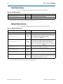
Avalon-MM Interface
The Avalon-MM module provides access to the PCS and PMA registers, the
Transceiver Reconfiguration IP core, and the Low Latency PHY Controller IP core.
PHY management block includes Avalon-MM master and slave interfaces and acts as
a bridge. It transfers commands received on its Avalon-MM slave interface to its
Avalon-MM port.
Table 3–9 describes the signals that comprise the Avalon-MM PHY Management
interface.
Table 3–9. Avalon-MM PHY Management Interface
Signal Name
Direction
Description
phy_mgmt_clk
Input
The clock signal that controls the Avalon-MM PHY management,
calibration, and reconfiguration interfaces. For Stratix IV devices, the
maximum frequency is 50 MHz.
phy_mgmt_clk_reset
Input
Global reset signal that resets the entire 10GBASE-R PHY. A positive
edge on this signal triggers the reset controller.
phy_mgmt_addr[8:0]
Input
9-bit Avalon-MM address. Refer to for the address fields.
phy_mgmt_writedata[31:0]
Input
Input data.
phy_mgmt_readdata[31:0]
Output
Output data.
phy_mgmt_write
Input
Write signal. Asserted high.
phy_mgmt_read
Input
Read signal. Asserted high.
phy_mgmt_waitrequest
Output
When asserted, indicates that the Avalon-MM slave interface is unable
to respond to a read or write request. When asserted, control signals
to the Avalon-MM slave interface must remain constant.
f Refer to the “Typical Slave Read and Write Transfers” and “Master Transfers” sections in
the “Avalon Memory-Mapped Interfaces” chapter of the Avalon Interface Specifications for
timing diagrams.
Altera Transceiver PHY IP Core User Guide
December 2010 Altera Corporation
Chapter 3: 10GBASE-R PHY IP Core
Interfaces
3–9
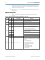
Register Descriptions
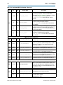
Table 3–10 specifies the registers that you can access over the Avalon-MM PHY
management interface using word addresses and a 32-bit embedded processor. A
single address space provides access to all registers.
Table 3–10. 10GBASE-R Register Descriptions (Part 1 of 3)
Word
Addr
Bit
R/W
Name
Description
PMA Common Control and Status
0x021
[31:0]
RW
0x022
[31:0]
R
cal_blk_powerdown
Writing a 1 to channel <n> powers down the calibration
block for channel <n>
pma_tx_pll_is_locked
Bit[P] indicates that the TX/CMU PLL (P) is locked to the
input reference clock.
Reset Control and Status
0x041
0x042
[31:0]
reset_ch_bitmask
Reset controller channel bitmask for digital resets. The
default value is all 1s. Channel <n> can be reset when
<n> = 1.
W
reset_control (write)
Writing a 1 to bit 0 initiates a TX digital reset using the reset
controller module. The reset affects channels enabled in the
reset_ch_bitmask. Writing a 1 to bit 1 initiates a RX
digital reset of channels enabled in the
reset_ch_bitmask. Both bits 0 and 1 self-clear.
R
reset_status (read)
Reading bit 0 returns the status of the reset controller TX
ready bit. Reading bit 1 returns the status of the reset
controller RX ready bit.
reset_fine_control
You can use the reset_fine_control register to create
your own reset sequence. The reset control module,
illustrated in Figure 1–1 on page 1–2, performs a standard
reset sequence at power on and whenever the
phy_mgmt_clk_reset is asserted. Bits [31:4,0] are
reserved.
reset_tx_digital
Writing a 1 causes the internal TX digital reset signal to be
asserted, resetting all channels enabled in
reset_ch_bitmask. You must write a 0 to clear the
reset condition.
reset_rx_analog
Writing a 1 causes the internal RX digital reset signal to be
asserted, resetting the RX analog logic of all channels
enabled in reset_ch_bitmask. You must write a 0 to
clear the reset condition.
reset_rx_digital
Writing a 1 causes the RX digital reset signal to be
asserted, resetting the RX digital channels enabled in
reset_ch_bitmask. You must write a 0 to clear the
reset condition.
RW
[1:0]
[31:4,0]
[1]
RW
RW
0x044
[2]
[3]
December 2010
RW
RW
Altera Corporation
Altera Transceiver PHY IP Core User Guide
3–10
Chapter 3: 10GBASE-R PHY IP Core
Interfaces
Table 3–10. 10GBASE-R Register Descriptions (Part 2 of 3)
Word
Addr
Bit
R/W
Name
Description
PMA Channel Control and Status
0x061
[31:0]
RW
pma_serial_loopback
Writing a 1 to channel <n> puts channel <n> in serial
loopback mode.
0x063
[31:0]
R
pma_rx_signaldetect
When asserted, the signal level circuit senses if the
specified voltage level exists at the receiver input buffer. Bit
<n> corresponds to channel <n>.
0x064
[31:0]
RW
pma_rx_set_locktodata
When set, programs the RX CDR PLL to lock to the
incoming data. Bit <n> corresponds to channel <n>.
0x065
[31:0]
RW
pma_rx_set_locktoref
When set, programs the RX CDR PLL to lock to the
reference clock. Bit <n> corresponds to channel <n>.
0x066
[31:0]
R
pma_rx_is_lockedtodata
When asserted, indicates that the RX CDR PLL is locked to
the RX data, and that the RX CDR has changed from LTR to
LTD mode. Bit <n> corresponds to channel <n>.
0x067
[31:0]
R
pma_rx_is_lockedtoref
When asserted, indicates that the RX CDR PLL is locked to
the reference clock. Bit <n> corresponds to channel <n>.
10GBASE-R PCS–Stratix IV Devices
0x080 [31:0]
0x081
Provides for indirect addressing of all PCS control and
status registers. Use this register to specify the logical
channel address of the PCS channel you want to access.
RW
INDIRECT_ADDR
[2]
RW
RCLR_ERRBLK_CNT
[3]
RW
RCLR_BER_COUNT
[0]
R
PCS_STATUS
When asserted indicates that the PCS link is up.
HI_BER
When asserted by the BER monitor block, indicates that the
PCS is recording a high BER.
[1]
R
When set to 1, clears the error block count register.
To block: Block synchronizer
When set to 1, clears the bit error rate (BER) register.
To block: BER monitor
From block: BER monitor
[2]
R
BLOCK_LOCK
When asserted by the block synchronizer, indicates that the
PCS is locked to received blocks.
From Block: Block synchronizer
0x082
When asserted, indicates the TX FIFO is full.
[3]
R
TX_FIFO_FULL
[4]
R
RX_FIFO_FULL
[5]
R
RX_SYNC_HEAD_ERROR
When asserted, indicates an RX synchronization error. This
signal is Stratix V devices only.
[6]
R
RX_SCRAMBLER_ERROR
When asserted, indicates an RX scrambler error. This signal
is Stratix V devices only.
Altera Transceiver PHY IP Core User Guide
From block: TX FIFO
When asserted, indicates the RX FIFO is full.
From block: RX FIFO
December 2010 Altera Corporation
Chapter 3: 10GBASE-R PHY IP Core
Interfaces
3–11
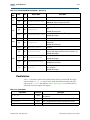
Table 3–10. 10GBASE-R Register Descriptions (Part 3 of 3)
Word
Addr
Bit
[5:0]
R/W
R
Name
Description
Records the bit error rate (BER). Not available for Stratix V
devices.
BER_COUNT
From block: BER monitor
0x083
[7:0]
R
ERROR_BLOCK_COUNT
Records the number of blocks that contain errors. Not
available for Stratix V devices.
From Block: Block synchronizer
Status Interface
Table 3–11 describes signals that provide status information.
Table 3–11. Status Outputs
Signal Name
Direction
Description
block_lock
Output
Asserted to indicate that the block synchronizer has established synchronization.
hi_ber
Output
Asserted by the BER monitor block to indicate a high bit error rate.
Clocks, Reset, and Powerdown
The phy_mgmt_clk_reset signal is the global reset that resets the entire PHY. A
positive edge on this signal triggers a reset.
Refer to the Reset Control and Power Down chapter in volume 2 of the Stratix IV Device
Handbook for additional information about reset sequences in Stratix IV devices.
December 2010
Altera Corporation
Altera Transceiver PHY IP Core User Guide
3–12
Chapter 3: 10GBASE-R PHY IP Core
Interfaces
When connected to the hard PMA, the PCS runs at 257.8125 MHz using the
pma_rx_clock provided by the PMA. You must provide the PMA a input reference
clock running at 644.53725MHz to generate the 257.8125 MHz clock. Figure 3–4
illustrates the clock generation and distribution for Stratix IV devices.
Figure 3–4. Stratix IV GT Clock Generation and Distribution
10GBASE-R Transceiver Channel - Stratix IV GT
TX
64
xgmii_tx_clk
40
TX PCS
(soft IP)
TX PCS
(hard IP)
257.8125
MHz
10.3125
Gbps serial
20
/2
TX PMA
516.625
MHz
TX PLL
pll_ref_clk
644.53125 MHz
5/4
RX
64
xgmii_rx_clk
RX PCS
(soft IP)
RX PCS
(hard IP)
257.8125
MHz
156.25 MHz
10.3125
Gbps serial
20
40
/2
RX PMA
516.625
MHz
GPLL
8/33
Altera Transceiver PHY IP Core User Guide
December 2010 Altera Corporation
Chapter 3: 10GBASE-R PHY IP Core
Interfaces
3–13
Figure 3–5 illustrates the clock generation and distribution for Stratix V devices.
Figure 3–5. Stratix V Clock Generation and Distribution
10GBASE-R Hard IP Transceiver Channel - Stratix V GT
TX
64
xgmii_tx_clk
10.3125
Gbps serial
40
TX PCS
TX PMA
257.8125
MHz
RX
64
xgmii_rx_clk
TX PLL
10.3125
Gbps serial
40
RX PCS
pll_ref_clk
644.53125 MHz
RX PMA
257.8125
MHz
156.25 MHz
GPLL
8/33
1
To ensure proper functioning of the PCS, the maximum PPM difference between the
pll_ref_clk and xgmii_tx_clk clock inputs is 100 PPM. To meet this specification,
you should use xgmii_rx_clk to drive xgmii_tx_clk. The CDR logic recovers
257.8125 MHz clock from the incoming data.
Table 3–13 describes the clock inputs.
Table 3–12. Clock Signals
Signal Name
pll_ref_clk
December 2010
Altera Corporation
Direction
Input
Description
TX PLL reference clock which must be 644.53725 MHz.
Altera Transceiver PHY IP Core User Guide
3–14
Chapter 3: 10GBASE-R PHY IP Core
TimeQuest Timing Constraints
Serial Interface
Table 3–13 describes the input and outputs of the transceiver.
Table 3–13. Transceiver Serial Interface (Note 1)
Signal Name
Direction
rx_serial_data<n>
Input
tx_serial_data<n>
Output
Description
Receiver input data
Transmitter output data
Note to Table 3–13:
(1) <n> is the channel number
External PMA Control and Reconfig Interface
Table 3–14 describes the additional top-level signals 10GBASE-R PHY IP core when
the configuration includes external modules for PMA control and reconfiguration.
You enable this configuration by turning on Use external PMA control and reconfig
available for Stratix IV GT devices. This configuration is illlustrated in Figure 3–1 on
page 3–1.
Table 3–14. External PMA and Reconfiguration Signals
Signal Name
Direction
Input
gxb_pdn
Output
pll_locked
Description
When asserted, powers down the entire GX block. Active high.
When asserted, indicates that the PLL is locked. Active high.
pll_pdn
Input
When asserted, powers down the TX PLL. Active high.
cal_blk_pdn
Input
When asserted, powers down the calibration block. Active high.
rx_oc_busy
Output
Input
Calibration clock. For Stratix IV devices only. It must be in the range
37.5–50 MHz. You can use the same clock for the phy_mgmt_clk and
the cal_blk_clk.
Input
Reconfiguration signals from the transceiver reconfiguration controller
to the PHY device. This signal is only available in Stratix IV devices.
cal_blk_clk
reconfig_to_gxb[3:0]
reconfig_from_gxb[16:0]
When asserted, indicates offset cancellation is in progress. The
transceiver must remain in reset until offset cancellation completes.
Active high.
Output
Reconfiguration RAM. The PHY device drives this RAM data to the
transceiver reconfiguration IP.
TimeQuest Timing Constraints
The timing constraints for Stratix IV GX designs are in alt_10gbaser_phy.sdc. If your
design does not meet timing with these constraints, use LogicLockTM for the
alt_10gbaser_pcs block. You can also apply LogicLock to the alt_10gbaser_pcs and
slightly expand the lock region to meet timing.
h For more information about LogicLock, refer to About LogicLock Regions in Quartus II
Help.
Altera Transceiver PHY IP Core User Guide
December 2010 Altera Corporation
Chapter 3: 10GBASE-R PHY IP Core
TimeQuest Timing Constraints
3–15
Example 3–1 provides the Synopsys Design Constraints File (.sdc) timing constraints
for the 10GBASE-R IP core. To pass timing analysis, you must decouple the clocks in
different time domains. Be sure to verify the each clock domain is correctly buffered in
the top level of your design. You can find the .sdc file in your top-level working
directory. This is the same directory that includes your top-level .v or .vhd file.
Example 3–1. Synopsys Design Constraints for Clocks
#**************************************************************
# Timing Information
#**************************************************************
set_time_format -unit ns -decimal_places 3
#**************************************************************
# Create Clocks
#**************************************************************
create_clock -name {xgmii_tx_clk} -period 6.400 -waveform { 0.000 3.200 } [get_ports
{xgmii_tx_clk}]
create_clock -name {phy_mgmt_clk}
-period 20.00 -waveform { 0.000 10.000 } [get_ports
{phy_mgmt_clk}]
create_clock -name {pll_ref_clk} -period 1.552 -waveform { 0.000 0.776 } [get_ports
{ref_clk}]
#derive_pll_clocks
derive_pll_clocks -create_base_clocks
#derive_clocks -period "1.0"
#**************************************************************
# Create Generated Clocks
#**************************************************************
create_generated_clock -name pll_mac_clk -source [get_pins -compatibility_mode
{*altpll_component|auto_generated|pll1|clk[0]}]
create_generated_clock -name pma_tx_clk -source [get_pins -compatibility_mode
{*siv_alt_pma|pma_direct|auto_generated|transmit_pcs0|clkout}]
**************************************************************
## Set Clock Latency
#**************************************************************
#**************************************************************
# Set Clock Uncertainty
#**************************************************************
#**************************************************************
derive_clock_uncertainty
set_clock_uncertainty -from [get_clocks
{*siv_alt_pma|pma_ch*.pma_direct|receive_pcs*|clkout}] -to pll_ref_clk -setup 0.1
set_clock_uncertainty -from [get_clocks
{*siv_alt_pma|pma_direct|auto_generated|transmit_pcs0|clkout}] -to pll_ref_clk -setup
0.08
set_clock_uncertainty -from [get_clocks
{*siv_alt_pma|pma_ch*.pma_direct|receive_pcs*|clkout}] -to pll_ref_clk -hold 0.1
set_clock_uncertainty -from [get_clocks
{*siv_alt_pma|pma_direct|auto_generated|transmit_pcs0|clkout}] -to pll_ref_clk -hold
0.08
#**************************************************************
# Set Input Delay
#**************************************************************
#**************************************************************
# Set Output Delay
#**************************************************************
#**************************************************************
# Set Clock Groups
#**************************************************************
set_clock_groups -exclusive -group phy_mgmt_clk -group xgmii_tx_clk -group [get_clocks
{*siv_alt_pma|pma_ch*.pma_direct|transmit_pcs*|clkout}] -group [get_clocks
{*siv_alt_pma|pma_ch*.pma_direct|receive_pcs*|clkout}] -group [get_clocks
{*pll_siv_xgmii_clk|altpll_component|auto_generated|pll1|clk[0]}]
December 2010
Altera Corporation
Altera Transceiver PHY IP Core User Guide
3–16
Chapter 3: 10GBASE-R PHY IP Core
TimeQuest Timing Constraints
Synopsys Design Constraints for Clocks (continued)
##**************************************************************
# Set False Path
#**************************************************************
set_false_path -from {*siv_10gbaser_xcvr*clk_reset_ctrl|rx_pma_rstn} -to [get_clocks
{{*siv_alt_pma|pma_ch*.pma_direct|transmit_pcs*|clkout}
{*siv_alt_pma|pma_ch*.pma_direct|receive_pcs*|clkout}
{*pll_siv_xgmii_clk|altpll_component|auto_generated|pll1|clk[0]} phy_mgmt_clk
xgmii_tx_clk}]
set_false_path -from {*siv_10gbaser_xcvr*clk_reset_ctrl|rx_usr_rstn} -to [get_clocks
{{*siv_alt_pma|pma_ch*.pma_direct|transmit_pcs*|clkout}
{*siv_alt_pma|pma_ch*.pma_direct|transmit_pcs*|clkout}
{*pll_siv_xgmii_clk|altpll_component|auto_generated|pll1|clk[0]} phy_mgmt_clk
xgmii_tx_clk}]
set_false_path -from {*siv_10gbaser_xcvr*clk_reset_ctrl|tx_pma_rstn} -to [get_clocks
{{*siv_alt_pma|pma_ch*.pma_direct|receive_pcs*|clkout}
{*siv_alt_pma|pma_ch*.pma_direct|transmit_pcs*|clkout}
{*pll_siv_xgmii_clk|altpll_component|auto_generated|pll1|clk[0]} phy_mgmt_clk
xgmii_tx_clk}]
set_false_path -from {*siv_10gbaser_xcvr*clk_reset_ctrl|tx_usr_rstn} -to [get_clocks
{{*siv_alt_pma|pma_ch*.pma_direct|receive_pcs*|clkout}
{*siv_alt_pma|pma_ch*.pma_direct|transmit_pcs*|clkout}
{*pll_siv_xgmii_clk|altpll_component|auto_generated|pll1|clk[0]} phy_mgmt_clk
xgmii_tx_clk}]
set_false_path -from {*siv_10gbaser_xcvr*rx_analog_rst_lego|rinit} -to [get_clocks
{{*siv_alt_pma|pma_ch*.pma_direct|receive_pcs*|clkout}
{*siv_alt_pma|pma_ch*.pma_direct|transmit_pcs*|clkout}
{*pll_siv_xgmii_clk|altpll_component|auto_generated|pll1|clk[0]} phy_mgmt_clk
xgmii_tx_clk}]
set_false_path -from {*siv_10gbaser_xcvr*rx_digital_rst_lego|rinit} -to [get_clocks
{{*siv_alt_pma|pma_ch*.pma_direct|receive_pcs*|clkout}
{*siv_alt_pma|pma_ch*.pma_direct|transmit_pcs*|clkout}
{*pll_siv_xgmii_clk|altpll_component|auto_generated|pll1|clk[0]} phy_mgmt_clk
xgmii_tx_clk}]
#**************************************************************
# Set Multicycle Paths
#**************************************************************
#**************************************************************
# Set Maximum Delay
#**************************************************************
#**************************************************************
# Set Minimum Delay
#**************************************************************
#**************************************************************
# Set Input Transition
#**************************************************************
1
This .sdc file is only applicable to the 10GBASE-R PHY IP core when compiled in
isolation. You can use it as a reference to help in creating your own .sdc file.
Altera Transceiver PHY IP Core User Guide
December 2010 Altera Corporation
4. XAUI PHY IP Core
The Altera XAUI PHY IP core implements the IEEE 802.3 Clause 48 specification to
extend the operational distance of the XGMII interface and reduce the number of
interface signals. XAUI extends the physical separation possible between the 10 Gbps
Ethernet MAC function implemented in an Altera FPGA and the Ethernet standard
PHY component on a PCB to one meter.
Figure 4–1 illustrates the top-level blocks of the XAUI PHY for Stratix IV GX or
Stratix V devices.
Figure 4–1. XAUI PHY with Hard IP PCS and PMA in Stratix IV GX or Stratix V Devices
Arria II GX, Cyclone IV GX, Stratix IV GX or GT, or Stratix V FPGA
SDR XGMII
72 bits @ 156.25 Mbps
Avalon-MM
Control & Status
XAUI IP Core
4
PCS
8B/10B
Word Aligner
Phase Comp
Hard PMA
4
4 x 3.125 Gbps serial
For Stratix IV GX and GT devices, you can choose a hard XAUI physical coding
sublayer (PCS) and physical media attachment (PMA), or a soft XAUI PCS and PMA
in low latency mode. You can also combine both hard and soft PCS configurations in
the same device, using all six channels in a transceiver bank. In Quartus II version
10.1, the PCS is only available in soft logic for Stratix V devices.
f For more detailed information about the XAUI transceiver channel datapath,
clocking, and channel placement, refer to the “XAUI” section in the Transceiver
Protocol Configurations in Stratix V Devices chapter of the Stratix V Device Handbook.
Release Information
Table 4–1 provides information about this release of the XAUI PHY IP core.
Table 4–1. XAUI Release Information (Part 1 of 2)
Item
Version
Release Date
Ordering Codes (Note 1)
Product ID
December 2010
Altera Corporation
Description
10.1
December 2010
IP-XAUIPCI (primary)–soft PCS
IPR-XAUIPCS (renewal)–soft PCS
00D7
Altera Transceiver PHY IP Core User Guide
4–2
Chapter 4: XAUI PHY IP Core
Device Family Support
Table 4–1. XAUI Release Information (Part 2 of 2)
Item
Description
Vendor ID
6AF7
Note to Table 4–1:
(1) No ordering codes or license files are required for the hard PCS and hard PMA PHY in Arria II GX, Cyclone IV GX,
or Stratix IV GX or GT devices.
Device Family Support
IP cores provide either final or preliminary support for target Altera device families.
These terms have the following definitions:
■
Final support—Verified with final timing models for this device.
■
Preliminary support—Verified with preliminary timing models for this device.
Table 4–2 shows the level of support offered by the XAUI IP core for Altera device
families.
Table 4–2. Device Family Support
Device Family
Support
Arria II GX–hard PCS and hard PMA
Final
Cyclone IV GX–hard PCS and hard PMA
Preliminary
Stratix IV GX and GT devices–soft or hard PCS and hard PMA
Final
Stratix V devices–soft PCS + hard PMA
Preliminary
Other device families
No support
Performance and Resource Utilization
Table 4–3 shows the typical expected device resource utilization for different
configurations using the current version of the Quartus II software targeting a
Stratix IV GX (EP4SG230KF40C2ES) device.
Table 4–3. XAUI PHY Performance and Resource Utilization—Stratix IV GX Device
Number of 3.125
Gbps Channels
Worst-Case
Frequency
Combinational
ALUTs
Dedicated
Registers
Memory Bits
Soft XAUI
4
183.18 MHz
4500
3200
5100
Hard XAUI
4
400 MHz
2000
1300
0
Implementation
Altera Transceiver PHY IP Core User Guide
December 2010 Altera Corporation
Chapter 4: XAUI PHY IP Core
Parameter Settings
4–3
Parameter Settings
To configure the XAUI IP core in the parameter editor, click Installed Plug-Ins >
Interfaces >Ethernet> XAUI PHY v10.1.
This section describes the XAUI PHY IP core parameters, which you can set using the
parameter editor. Table 4–4 lists the settings available on General Options tab.
Table 4–4. General Options
Name
Value
Description
Arria II GX
Cyclone IV GX
Stratix IV
Stratix V
The target device family.
Starting channel number
0–124
The physical starting channel number in the Altera device for channel
0 of this XAUI PHY. In Arria II GX, Cyclone IVGX, and Stratix IV
devices, this starting channel number must be 0 or a multiple of 4.
There are no numbering restrictions for Stratix V devices.
Assignment of the starting channel number is needed for serial
transceiver dynamic reconfiguration.
XAUI interface type
Hard XAUI
Soft XAUI
Specifies whether the interface is implemented in soft or hard logic.
Each interface includes 4 channels.
Number of XAUI interfaces
1
Specifies the number of XAUI interfaces. Only 1 is available in the
current release.
Device family
Table 4–5 describes the settings available on the Additional Options tab.
Table 4–5. Advanced Options—Stratix IV
Name
Value
Soft XAUI PLL type
Include control and status ports
External PMA control and
configuration
Description
CMU PLL
ATX PLL
Allows you to choose a clock multiplier unit (CMU) or auxiliary
transmit (ATX) PLL. The CMU PLL is designed to achieve low TX
channel-to-channel skew. The ATX PLL is designed to improve jitter
performance. This option is only available for the soft PCS.
On/Off
If you turn this option on, the top-level IP core include the status
signals and digital resets shown in Figure 4–3 on page 4–5 and
Figure 4–4 on page 4–6. If you turn this option off, you can access
control and status information using Avalon-MM interface to the
control and status registers. The default setting is off.
On/Off
If you turn this option on, the PMA signals are brought up to the top
level of the XAUI IP core. This option is useful if your design
includes multiple instantiations of the XAUI PHY IP core. To save
FPGA resources, you can instantiate the Low Latency PHY Controller
and Transceiver Reconfiguration Controller IP cores separately in
your design to avoid having these IP cores instantiated in each
instance of the XAUI PHY IP core.
If you turn this option off, the PMA signals remain internal to the
core. The default setting is off. This option is only available for
Arria II GX and Stratix IV GX devices.
Advanced Options—Arria II GX, Cyclone IV GX, a Stratix V Devices
Include control and status ports
December 2010
Altera Corporation
On/Off
If you turn this option on, the top-level IP core includes the TX and
RX status signals shown in Figure 4–3 on page 4–5.
Altera Transceiver PHY IP Core User Guide
4–4
Chapter 4: XAUI PHY IP Core
Configurations
For a description of the PMA analog options, refer to “PMA Analog Options” on
page 8–4.
Configurations
Figure 4–2 illustrates one configuration of the XAUI IP core. As this figure illustrates,
if your variant includes a single instantiation of the XAUI IP core, the transceiver
reconfiguration control logic is included in the XAUI PHY IP core.
Figure 4–2. XAUI PHY Using One Channel Low Latency PHY Controller
Hard XAUI PHY
Transceiver Quad 0
SDR XGMII
72 bits @ 156.25 Mbps
4
Interleave
To MAC
PCS
Alt_PMA
4
S
4 x 3.125 Gbps serial
System
Interconnect
Fabric
S
S
PMA Channel
Controller
S
Low Latency
Controller
Avalon-MM
PHY
M
Mgmt
System
Interconnect
Fabric
S
Transceiver
Reconfiguration
Controller
For more information about transceiver reconfiguration, refer to Chapter 9,
Transceiver Reconfiguration Controller.
Altera Transceiver PHY IP Core User Guide
December 2010 Altera Corporation
Chapter 4: XAUI PHY IP Core
Interfaces
4–5
Interfaces
Figure 4–3 illustrates the top-level signals of the XAUI PHY IP core for the soft IP
implementation which is available for Stratix IV GX and Stratix V devices. Figure 4–4
illustrates the top-level signals of the XAUI PHY IP core for the hard IP
implementation which is available for Stratix IV GX devices. With the exception of the
optional signals available for debugging, the pinout of the two implementations is
nearly identical.
1
The block diagram shown in the GUI labels the external pins with the interface type
and places the interface name inside the box. The interface type and name are used to
define component interfaces in the _hw.tcl.
f For more information about _hw.tcl files refer to refer to the Component Interface Tcl
Reference chapter in the SOPC Builder User Guide.
Figure 4–3. XAUI Top-Level Signals—Soft PCS and Hard PMA
XAUI Top-Level Signals Soft IP Implementation
SDR Tx XGMII
xgmii_tx_dc[71:0]
xgmii_tx_clk
SDR Rx XGMII
xmii_rx_dc[71:0]
xgmii_rx_clk
Avalon-MM PHY
Management
Interface
Clocks
and
Reset
December 2010
Optional
Altera Corporation
phy_mgmt_clk
phy_mgmt_clk_reset
phy_mgmt_address[8:0]
phy_mgmt_writedata[31:0]
phy_mgmt_readdata[31:0]
phy_mgmt_write
phy_mgmt_read
phy_mgmt_waitrequest
pll_ref_clk
rx_digitalreset
tx_digitalreset
xaui_rx_serial_data[3:0]
xaui_tx_serial_data[3:0]
rx_channelaligned
rx_disperr[7:0]
rx_errdetect[7:0]
rx_syncstatus[7:0]
cal_blk_powerdown
gxb_powerdown
pll_powerdown
pll_locked
reconfig_fromgxb[67:0]
reconfig_togxb[3:0]
rx_ready
tx_ready
Transceiver
Serial Data
Rx Status
Optional
Optional
PMA
Channel
Controller
Altera Transceiver PHY IP Core User Guide
4–6
Chapter 4: XAUI PHY IP Core
Interfaces
Figure 4–4 illustrates the top-level signals of the XAUI PHY IP core for the hard IP
implementation which is available for Arria II GX, Cyclone IV GX, and Stratix IV GX
devices.
Figure 4–4. XAUI Top-Level Signals–Hard IP PCS and PMA
XAUI Top-Level Signals Hard IP Implementation
SDR Tx XGMII
xgmii_tx_dc[71:0]
xgmii_tx_clk
SDR Rx XGMII
xmii_rx_dc[71:0]
xgmii_rx_clk
Avalon-MM PHY
Management
Interface
Clock
and
Reset
Optional
Resets
xaui_rx_serial_data[3:0]
xaui_tx_serial_data[3:0]
Transceiver
Serial Data
rx_invpolarity[3:0]
rx_set_locktodata[3:0]
rx_is_lockedtodata[3:0]
rx_set_locktoref[3:0]
rx_is_lockedtoref[3”0]
phy_mgmt_clk
tx_invpolarity[3:0]
phy_mgmt_clk_reset
rx_seriallpbken[3:0]
phy_mgmt_address[8:0]
rx_channelaligned[3:0]
phy_mgmt_writedata[31:0]
pll_locked
phy_mgmt_readdata[31:0]
rx_rmfifoempty[3:0]
phy_mgmt_write
rx_rmfifofull[3:0]
phy_mgmt_read
rx_disperr[7:0]
phy_mgmt_waitrequest
rx_errdetect[7:0]
rx_patterndetect[7:0]
rx_rmfifodatadeleted[7:0]
pll_ref_clk
rx_rmfifodatainserted[7:0]
rx_analogreset
rx_runningdisp[7:0]
rx_digitalreset
rx_syncstatus[7:0]
tx_digitalreset
rx_phase_comp_fifo_error[3:0]
tx_phase_comp_fifo_error[3:0]
rx_rlv[3:0]
Rx and Tx
Status
All Optional
reconfig_togxb[3:0]
Note (1) reconfig_fromgxb[67:0]
Transceiver
Reconfiguration
cal_blk_powerdown
gxb_powerdown
pll_powerdown
pll_locked
rx_ready
tx_ready
Optional
PMA
Channel
Controller
Note to Figure 4–3:
(1) reconfig_fromgxb[67:17] is terminated to ground internally.
The following sections describe the signals in each interface.
SDR XGMII TX Interface
The XAUI PCS interface to the FPGA fabric uses a single data rate (SDR) XGMII
interface. This interface implements a simple version of Avalon-ST protocol. The
interface does not include ready or valid signals; consequently, the sources always
drive data and the sinks must always be ready to receive data.
f For more information about the Avalon-ST protocol, including timing diagrams, refer
to the Avalon Interface Specifications.
Altera Transceiver PHY IP Core User Guide
December 2010 Altera Corporation
Chapter 4: XAUI PHY IP Core
Interfaces
4–7
This interface runs at 156.25 MHz in accordance with XGMII specification; however,
data is only driven on the rising edge of clock. To meet the bandwidth requirements,
the datapath is eight bytes wide with eight control bits, instead of the standard four
bytes of data and four bits of control. The XAUI IP core treats the datapath as two,
32-bit data buses and includes logic to interleave them, starting with the low-order
bytes. Figure 4–5 illustrates the mapping.
Figure 4–5. Interleaved SDR XGMII Data
Original XGMII Data
[63:56]
[55:48]
[47:40]
[39:32]
[31:24]
[23:16]
[15:8]
[7:0]
[15:8]
[39:32]
[7:0]
Interleaved Result
[63:56]
[31:24]
[55:48]
[23:16]
[47:40]
Table 4–6 describes the signals in the SDR TX XGMII interface.
Table 4–6. SDR TX XGMII Interface
Signal Name
Direction
Description
Contains 4 lanes of data and control for XGMII. Each lane consists of
16 bits of data and 2 bits of control.
Source
xgmii_tx_dc[71:0]
Input
xgmii_tx_clk
■
Lane 0–[7:0]/[8], [16:9]/[17]
■
Lane 1–[25:18]/[26], [34:27]/[35]
■
Lane 2–[43:36]/[44], [52:45]/[53]
■
Lane 3–[61:54]/[62],[70:63]/[71]
The XGMII SDR TX clock which runs at 156.25 MHz.
SDR XGMII RX Interface
Table 4–6 describes the signals in the SDR RX XGMII interface.
Table 4–7. SDR XGMII Interface
Signal Name
Direction
Description
Contains 4 lanes of data and control for XGMII. Each lane consists of
16 bits of data and 2 bits of control.
xgmii_rx_dc[71:0]
xgmii_rx_clk
December 2010
Altera Corporation
Sink
Output
■
Lane 0–[7:0]/[8], [16:9]/[17]
■
Lane 1–[25:18]/[26], [34:27]/[35]
■
Lane 2–[43:36]/[44], [52:45]/[53]
■
Lane 3–[61:54]/[62],[70:63]/[71]
The XGMII SDR RX MAC interface clock which runs at 156.25 MHz.
Altera Transceiver PHY IP Core User Guide
4–8
Chapter 4: XAUI PHY IP Core
Interfaces
Avalon-MM Interface
The Avalon-MM PHY management block includes master and slave interfaces. This
component acts as a bridge. It transfers commands received on its Avalon-MM slave
interface to its Avalon-MM port. This interface provides access to the PCS and PMA
registers, the Transceiver Reconfiguration, and the Low Latency PHY Controller IP
cores. Table 4–8 describes the signals that comprise the Avalon-MM PHY
Management interface.
Table 4–8. Avalon-MM PHY Management Interface
Signal Name
Direction
Description
phy_mgmt_clk
Input
Avalon-MM clock input.
phy_mgmt_clk_reset
Input
Global reset signal that resets the entire XAUI PHY. A positive edge
on this signal triggers the reset controller.
phy_mgmt_addr[8:0]
Input
9-bit Avalon-MM address.
phy_mgmt_writedata[31:0]
Input
32-bit input data.
phy_mgmt_readdata[31:0]
Output
32-bit output data.
phy_mgmt_write
Input
Write signal. Asserted high.
phy_mgmt_read
Input
Read signal. Asserted high.
Output
phy_mgmt_waitrequest
When asserted, indicates that the Avalon-MM slave interface is
unable to respond to a read or write request. When asserted, control
signals to the Avalon-MM slave interface must remain constant.
f For more information about the Avalon-MM interface, including timing diagrams,
refer to the Avalon Interface Specifications.
Register Descriptions
Table 4–9 specifies the registers that you can access using the Avalon-MM PHY
management interface using word addresses and a 32-bit embedded processor. A
single address space provides access to all registers.
Table 4–9. XAUI PHY IP Core Registers (Part 1 of 4)
Word
Addr
Bits
R/W
Register Name
Description
PMA Common Control and Status Registers
0x021
[31:0]
RW
0x022
[31:0]
R
cal_blk_powerdown
Writing a 1 to channel <n> powers down the calibration
block for channel <n>.
pma_tx_pll_is_locked
Bit[P] indicates that the TX/CMU PLL (P) is locked to the
input reference clock. There is typically one
pma_tx_pll_is_locked bit per system.
Reset Control Registers
0x041
[31:0]
RW
reset_ch_bitmask
Altera Transceiver PHY IP Core User Guide
Reset controller channel bitmask for digital resets. The
default value is all 1s. Channel <n> can be reset when
<n> = 1.
December 2010 Altera Corporation
Chapter 4: XAUI PHY IP Core
Interfaces
4–9
Table 4–9. XAUI PHY IP Core Registers (Part 2 of 4)
Word
Addr
0x042
Bits
R/W
Register Name
W
reset_control (write)
Writing a 1 to bit 0 initiates a TX digital reset using the reset
controller module. The reset affects channels enabled in the
reset_ch_bitmask. Writing a 1 to bit 1 initiates a RX
digital reset of channels enabled in the
reset_ch_bitmask.
R
reset_status(read)
Reading bit 0 returns the status of the reset controller TX
ready bit. Reading bit 1 returns the status of the reset
controller RX ready bit.
reset_fine_control
You can use the reset_fine_control register to create
your own reset sequence. The reset control module,
illustrated in Figure 1–1 on page 1–2, performs a standard
reset sequence at power on and whenever the
phy_mgmt_clk_reset is asserted. Bits [31:4, 0] are
reserved.
reset_tx_digital
Writing a 1 causes the internal TX digital reset signal to be
asserted, resetting all channels enabled in
reset_ch_bitmask. You must write a 0 to clear the
reset condition.
reset_rx_analog
Writing a 1 causes the internal RX digital reset signal to be
asserted, resetting the RX analog logic of all channels
enabled in reset_ch_bitmask. You must write a 0 to
clear the reset condition.
reset_rx_digital
Writing a 1 causes the RX digital reset signal to be asserted,
resetting the RX digital channels enabled in
reset_ch_bitmask. You must write a 0 to clear the
reset condition.
[1:0]
[31:4,0]
[1]
0x044
[2]
[3]
Description
RW
RW
RW
RW
PMA Control and Status Registers
0x061
[31:0]
RW
phy_serial_loopback
Writing a 1 to channel <n> puts channel <n> in serial
loopback mode.
pma_rx_signaldetect
When channel <n> =1, indicates that receive circuit for
channel <n> senses the specified voltage exists at the RX
input buffer. This option is only operational for the PCI
Express PHY IP core.
0x063
[31:0]
R
0x064
[31:0]
RW
pma_rx_set_locktodata
When set, programs the RX CDR PLL to lock to the
incoming data. Bit <n> corresponds to channel <n>.
0x065
[31:0]
RW
pma_rx_set_locktoref
When set, programs the RX CDR PLL to lock to the
reference clock. Bit <n> corresponds to channel <n>.
0x066
[31:0]
R
pma_rx_is_lockedtodata
When asserted, indicates that the RX CDR PLL is locked to
the RX data, and that the RX CDR has changed from LTR to
LTD mode. Bit <n> corresponds to channel <n>.
00x06
7
[31:0]
R
pma_rx_is_lockedtoref
When asserted, indicates that the RX CDR PLL is locked to
the reference clock. Bit <n> corresponds to channel <n>.
December 2010
Altera Corporation
Altera Transceiver PHY IP Core User Guide
4–10
Chapter 4: XAUI PHY IP Core
Interfaces
Table 4–9. XAUI PHY IP Core Registers (Part 3 of 4)
Word
Addr
Bits
R/W
Register Name
Description
XAUI PCS
[31:2]
0x081
—
[1]
tx_digital reset
RW
[0]
0x082
Reserved
rx_digital reset
[31:4]
—
Reserved
[3:0]
RW
invpolarity[3:0]
—
Resets the TX PCS clock domain.
To block: RX PCS.
Resets the RX PCS clock domain.
To block: TX PCS.
—
Inverts the polarity of corresponding bit on the RX interface.
Bit 0 maps to lane 0 and so on.
To block: Word aligner.
0x083
[31:4]
—
Reserved
[3:0]
RW
invpolarity[3:0]
—
Inverts the polarity of corresponding bit on the TX interface.
Bit 0 maps to lane 0 and so on.
To block: Serializer.
[31:16]
—
[15:8]
Reserved
syncstatus[7:0]
—
Records the synchronization status of the corresponding
bit. The RX sync status regsiter has 2 bits per channel for a
total of 8 bits per XAUI link. Reading the value of the
syncstatus register clears the bits.
From block: Word aligner.
0x084
R
[7:0]
patterndetect[7:0]
When asserted, indicates that the programmed word
alignment pattern has been detected in the current word
boundary. The RX pattern detect signal is 2 bits wide per
channel or 8 bits per XAUI link. Reading the value of the
patterndetect registers clears the bits.
From block: Word aligner.
[31:16]
—
[15:8]
Reserved
disperr[7:0]
—
Indicates that the received 10-bit code or data group has a
disparity error. When set, the corresponding errdetect
bits are also set. There are 2 bits per RX channel for a total
of 8 bits per XAUI link. Reading the value of the errdetect
register clears the bits
From block: 8B/10B decoder.
0x085
R
[7:0]
errdetect[7:0]
When set, indicates that a received 10-bit code group has
an 8B/10B code violation or disparity error. It is used along
with disperr to differentiate between a code violation
error, a disparity error, or both. There are 2 bits per RX
channel for a total of 8 bits per XAUI link. Reading the value
of the errdetect register clears the bits.
From block: 8B/10B decoder.
Altera Transceiver PHY IP Core User Guide
December 2010 Altera Corporation
Chapter 4: XAUI PHY IP Core
Interfaces
4–11
Table 4–9. XAUI PHY IP Core Registers (Part 4 of 4)
Word
Addr
Bits
[31:8]
R/W
—
Register Name
Description
Reserved
—
Indicates a RX phase compensation FIFO overflow or
phase_comp_fifo_error[3: underrun condition on the corresponding lane. Reading the
value of the phase_comp_fifo_error register clears the
0]
bits.
[7:4]
0x086
From block: RX phase compensation FIFO.
R,
sticky
rlv[3:0]
[3:0]
Indicates a run length violation. Asserted if the number of
consecutive 1s or 0s exceeds the number that was set in the
Runlength check option. Bits 0-3 correspond to lanes 0-3,
respectively. Reading the value of the RLV register clears the
bits.
From block: Word aligner.
[31:16]
—
[15:8]
0x087
Reserved
rmfifodatainserted[7:0]
[31:8]
rmfifodatadeleted[7:0]
—
Reserved
rmfifoempty[3:0]
[7:4]
R,
sticky
0x088
[3:0]
When asserted, indicates that the RX rate match block
inserted a ||R|| column. Goes high for one clock cycle per
inserted ||R|| column. Reading the value of the
rmfifodatainserted register clears the bits.
From block: Rate match FIFO.
R,
sticky
[7:0]
—
When asserted, indicates that the rate match block has
deleted an ||R|| column. The flag goes high for one clock
cycle per deleted ||R|| column. There are 2 bits for each
lane. Reading the value of the rmfifodatadeleted
register clears the bits.
From block: Rate match FIFO.
—
When asserted, indicates that the rate match FIFO is empty
(5 words). Bits 0-3 correspond to lanes 0-3, respectively.
Reading the value of the rmfifoempty register clears the
bits.
From block: Rate match FIFO.
rmfifofull[3:0]
When asserted, indicates that rate match FIFO is full (20
words). Bits 0-3 correspond to lanes 0-3, respectively.
Reading the value of the rmfifofull register clears the
bits.
From block: Rate match FIFO.
[31:3]
0x089
[2:0]
—
R,
sticky
Reserved
—
Indicates a TX phase compensation FIFO overflow or
underrun condition on the corresponding lane. Reading the
phase_comp_fifo_error[2: value of the phase_comp_fifo_error register clears the
0]
bits.
From block: TX phase compensation FIFO.
0x08a
December 2010
[0]
RW
Altera Corporation
simulation_flag
Setting this bit to 1 shortens the duration of reset and loss
timer when simulating. Altera recommends that you keep
this bit set during simulation.
Altera Transceiver PHY IP Core User Guide
4–12
Chapter 4: XAUI PHY IP Core
Interfaces
Transceiver Serial Data Interface
Table 4–10 describes the signals in the XAUI transceiver serial data interface. There
are four lanes of serial data for both the TX and RX interfaces. This interface runs at
3.125 GHz. There is no separate clock signal because it is encoded in the data.
Table 4–10. Serial Data Interface
Signal Name
Direction
Description
xaui_rx_serial_data[3:0]
Input
Serial input data.
xaui_tx_serial_data[3:0]
Output
Serial output data.
Dynamic Reconfiguration Interface
As silicon progresses towards smaller process nodes, circuit performance is affected
more by variations due to process, voltage, and temperature. These process variations
result in analog voltages that can be offset from required ranges. Dynamic
reconfiguration compensates for variations due to process, voltage, and temperature.
Table 4–11 describes the signals in the reconfiguration interface. If your XAUI PHY IP
core includes a single transceiver quad, these signals are internal to the core. If your
design uses more than one quad, they are external.
Table 4–11. Dynamic Reconfiguration Interface
Signal Name
reconfig_togxb_data[3:0]
reconfig_fromgxb[67:0]
1
Direction
Description
Input
Reconfiguration signals from the Transceiver Reconfiguration IP
core to the XAUI transceiver.
Output
Reconfiguration signals from the XAUI transceiver to the
Transceiver Reconfiguration IP core. For XAUI variants using a
hard PCS and PMA, reconfig_fromgxb[67:17] are terminated
to ground internally. The soft PCS in Stratix IV GX and GT devices
use 68 bits.
Dynamic reconfiguration is only supported for Stratix IV devices in the current
release.
Altera Transceiver PHY IP Core User Guide
December 2010 Altera Corporation
Chapter 4: XAUI PHY IP Core
Interfaces
4–13
Clocks, Reset, and Powerdown
Figure 4–6 illustrates the clock inputs and outputs for the XAUI IP cores with hard
PCS and PMA blocks.
Figure 4–6. Clock Inputs and Outputs, Hard PCS
phy_mgmt_clk
XAUI Hard IP Core
pll_ref_clk
pll_inclk
Hard PCS
xgmii_tx_clk
rx_cruclk
PMA
4
tx_coreclk
xgmii_rx_clk
4
coreclkout
4 x 3.125 Gbps serial
Figure 4–7 illustrates the clock inputs and outputs for the XAUI IP cores with soft PCS
and PMA blocks.
Figure 4–7. Clock Inputs and Outputs, Soft PCS
phy_mgmt_clk
pll_ref_clk
XAUI Soft IP Core
pll_ref_clk
Soft PCS
xgmii_tx_clk
pma_pll_inclk
xgmii_rx_clk
sysclk
4
PMA
pma_tx_clkout
tx_clkout
pma_rx_clkout rx_recovered_clk
4
4 x 3.125 Gbps serial
Table 4–12 describes the optional reset signals.
Table 4–12. Clock and Reset Signals
Signal Name
Direction
Description
pll_ref_clk
Input
This is a 156.25 MHz reference clock that is used by the TX PLL and
CDR logic.
rx_analogreset
Input
This signal resets the analog CDR and deserializer logic in the RX
channel. It is only available in the hard IP implementation.
rx_digitalreset
Input
PCS RX digital reset signal.
tx_digitalreset
Input
PCS TX digital reset signal.
December 2010
Altera Corporation
Altera Transceiver PHY IP Core User Guide
4–14
Chapter 4: XAUI PHY IP Core
Interfaces
PMA Channel Controller
Table 4–13 describes the signals in this interface.
Table 4–13. Low Latency PHY Controller
Signal Name
Direction
Description
cal_blk_powerdown
Input
Powers down the calibration block. A high-to-low transition on this
signal restarts calibration. Only available in Arria II GX and
Stratix IV GX, and Stratix IV GT devices.
gxb_powerdown
Input
When asserted, powers down the entire transceiver block. Only
available in Arria II GX and Stratix IV GX, and Stratix IV GT devices.
pll_powerdown
Input
Powers down the CMU PLL. Only available in Arria II GX and
Stratix IV GX, and Stratix IV GT devices.
pll_locked
Output
Indicates CMU PLL is locked. Only available in Arria II GX and
Stratix IV GX, and Stratix IV GT devices.
rx_ready
Output
Indicates PMA RX has exited the reset state.
tx_ready
Output
Indicates PMA TX has exited the reset state.
PMA Control and Status Interface Signals–Soft IP Implementation
(Optional)
Table 4–14 lists the optional PMA control and status signals available in the soft IP
implementation. You can also access the state of these signals using the Avalon-MM
PHY Management interface to read the control and status registers which are detailed
in Table 4–9 on page 4–8. However, in some cases, you may need to know the
instantaneous value of a signal to ensure correct functioning of the XAUI PHY. In such
cases, you can include the required signal in the top-level module of your XAUI PHY
IP core.
Table 4–14. Optional Control and Status Signals—Soft IP Implementation, Stratix IV GX and Stratix V Devices
Signal Name
rx_channelaligned
rx_disperr[7:0]
rx_errdetect[7:0]
rx_syncstatus[7:0]
Altera Transceiver PHY IP Core User Guide
Direction
Description
Output
When asserted, indicates that all 4 RX channels are aligned.
Output
Received 10-bit code or data group has a disparity error. It is paired
with rx_errdetect which is also asserted when a disparity error
occurs. The rx_disperr signal is 2 bits wide per channel for a total
of 8 bits per XAUI link.
Output
When asserted, indicates an 8B/10B code group violation. It is
asserted if the received 10-bit code group has a code violation or
disparity error. It is used along with the rx_disperr signal to
differentiate between a code violation error, a disparity error, or
both.The rx_errdetect signal is 2 bits wide per channel for a total
of 8 bits per XAUI link.
Output
Synchronization indication. RX synchronization is indicated on the
rx_syncstatus port of each channel. The rx_syncstatus signal
is 2 bits wide per channel for a total of 8 bits per XAUI link.
December 2010 Altera Corporation
Chapter 4: XAUI PHY IP Core
Interfaces
4–15
PMA Control and Status Interface Signals–Hard IP Implementation
(Optional)
Table 4–15 lists the PMA control and status signals. You can access the state of these
signals using the Avalon-MM PHY Management interface to read the control and
status registers which are detailed in Table 4–9 on page 4–8. However, in some cases,
you may need to know the instantaneous value of a signal to ensure correct
functioning of the XAUI PHY. In such cases, you can include the required signal in the
top-level module of your XAUI PHY IP core.
Table 4–15. Optional Control and Status Signals—Hard IP Implementation, Stratix IV GX Devices (Part 1 of 2)
Signal Name
Direction
Description
rx_invpolarity[3:0]
input
Dynamically reverse the polarity of every bit of the RX data at the
input of the word aligner.
rx_set_locktodata[3:0]
Input
Force the CDR circuitry to lock to the received data.
rx_is_lockedtodata[3:0]
Output
When asserted, indicates the RX channel is locked to input data.
rx_set_locktoref[3:0]
Input
Force the receiver CDR to lock to the phase and frequency of the
input reference clock.
rx_is_lockedtoref[3:0]
Output
tx_invpolarity[3:0]
input
When asserted, indicates the RX channel is locked to input
reference clock.
Dynamically reverse the polarity the data word input to the serializer
in the TX datapath.
Serial loopback enable.
rx_seriallpbken
input
■
1–enables serial loopback
■
0–disables serial loopback
This signal is asynchronous to the receiver. The status of the serial
loopback option is recorded by the PMA channel controller, word
address 0x061.
Output
When asserted indicates that the RX channel is aligned.
pll_locked
Output
In LTR mode, indicates that the receiver CDR has locked to the
phase and frequency of the input reference clock.
rx_rmfifoempty[3:0]
Output
Status flag that indicates the rate match FIFO block is empty (5
words). This signal remains high as long as the FIFO is empty and is
asynchronous to the RX datapath.
Output
Status flag that indicates the rate match FIFO block is full (20
words). This signal remains high as long as the FIFO is full and is
asynchronous to the RX data.
Output
Received 10-bit code or data group has a disparity error. It is paired
with rx_errdetect which is also asserted when a disparity error
occurs. The rx_disperr signal is 2 bits wide per channel for a total
of 8 bits per XAUI link.
Output
Transceiver 8B/10B code group violation or disparity error indicator.
If either signal is asserted, a code group violation or disparity error
was detected on the associated received code group. Use the
rx_disperr signal to determine whether this signal indicates a
code group violation or a disparity error. The rx_errdetect signal
is 2 bits wide per channel for a total of 8 bits per XAUI link.
rx_channelaligned
rx_rmfifofull[3:0]
rx_disperr[7:0]
rx_errdetect[7:0]
December 2010
Altera Corporation
Altera Transceiver PHY IP Core User Guide
4–16
Chapter 4: XAUI PHY IP Core
TimeQuest Timing Constraints
Table 4–15. Optional Control and Status Signals—Hard IP Implementation, Stratix IV GX Devices (Part 2 of 2)
Signal Name
Direction
Description
Output
Indicates that the word alignment pattern programmed has been
detected in the current word boundary. The rx_patterndetect
signal is 2 bits wide per channel for a total of 8 bits per XAUI link.
Output
Status flag that is asserted when the rate match block deletes a ||R||
column. The flag is asserted for one clock cycle per deleted ||R||
column.
Output
Status flag that is asserted when the rate match block inserts a ||R||
column. The flag is asserted for one clock cycle per inserted ||R||
column.
Output
Asserted when the current running disparity of the 8B/10B decoded
byte is negative. Low when the current running disparity of the
8B/10B decoded byte is positive.
Output
Synchronization indication. RX synchronization is indicated on the
rx_syncstatus port of each channel. The rx_syncstatus signal
is 2 bits wide per channel for a total of 8 bits per XAUI link.
rx_phase_comp_fifo_error[3:0]
Output
Indicates a RX phase comp FIFO overflow or underrun condition.
tx_phase_comp_fifo_error[3:0]
Output
Indicates a TX phase compensation FIFO overflow or underrun
condition.
Output
Asserted if the number of continuous 1s and 0s exceeds the number
that was set in the run-length option. The rx_rlv signal is
asynchronous to the RX datapath and is asserted for a minimum of
2 recovered clock cycles.
rx_patterndetect[7:0]
rx_rmfifodatadeleted[7:0]
rx_rmfifodatainserted[7:0]
rx_runningdisp[7:0]
rx_syncstatus[7:0]
rx_rlv[3:0]
TimeQuest Timing Constraints
Example 4–1 provides the .sdc timing constraints for the XAUI clocks. To pass timing
analysis you must decouple the clocks in different time domains.
Example 4–1. Synopsys Design Constraints for Clocks
set_time_format -unit ns -decimal_places 3
derive_pll_clocks
derive_clock_uncertainty
#
# input clocks
create_clock -name {xgmii_tx_clk}-period 6.400 -waveform {0.000 3.2} \
[get_ports {xgmii_tx_clk}]
create_clock -name {phy_mgmt_clk} -period 20.000 -waveform {0.000 10.0} \
[ get_ports {phy_mgmt_clk} ]
create_clock -name {refclk} -period 6.400 -waveform {0.000 3.2} \
[ get_ports {pll_ref_clk} ]
# generated clocks
# xgmii_rx_clk is generated from coreclkout
#****** Use this section for Stratix IV Hard XAUI ******
create_generated_clock -name {xgmii_rx_clk_0} -source [get_pins -compatibility_mode
{*hxaui_0|hxaui_alt4gxb|hxaui_alt4gxb_alt4gxb_dksa_component|central_clk_div0|
coreclkout}]-multiply_by 1 [get_ports {xgmii_rx_clk}]
#****** Use this section for Stratix IV Soft XAUI ******
#create_generated_clock -name {xgmii_rx_clk_0} -source [get_pins -compatibility_mode
{*alt_pma_0|alt_pma_tgx_inst|pma_direct|auto_generated|central_clk_div0|refclkout} ] \
#-multiply_by 1 [get_ports {xgmii_rx_clk}]
Altera Transceiver PHY IP Core User Guide
December 2010 Altera Corporation
Chapter 4: XAUI PHY IP Core
TimeQuest Timing Constraints
4–17
Synopsys Design Constraints for Clocks (continued)
#****** Use this section for Stratix V Soft XAUI ******
#create_generated_clock -name {xgmii_rx_clk_0} -source [get_pins -compatibility_mode
{*alt_pma_0|alt_pma_sv_inst|sv_xcvr_generic_inst|channel_tx[0].duplex_pcs|ch[0].tx_pcs
|clkout} ] -multiply_by 1 [get_ports {xgmii_rx_clk}]
# internal clocks
# There should be no direct (unsynchronized) paths from coreclkout to mgmt_clk
#****** Use this section for Stratix IV Soft XAUI ******
#set_clock_groups -asynchronous -group
{*alt_pma_0|alt_pma_tgx_inst|pma_direct|auto_generated|central_clk_div0|refclkout} group {phy_mgmt_clk}
#set_clock_groups -asynchronous -group
{*alt_pma_0|alt_pma_tgx_inst|pma_direct|auto_generated|receive_pma*|deserclock*} -group
{phy_mgmt_clk}
#set_clock_groups -asynchronous -group {refclk} -group {phy_mgmt_clk}
#****** Use this section for Stratix V Soft XAUI ******
#set_clock_groups -asynchronous -group
{*alt_pma_0|alt_pma_sv_inst|sv_xcvr_generic_inst|channel_rx*.rx_pma*|*} -group
{phy_mgmt_clk}
#set_clock_groups -asynchronous -group
{*alt_pma_0|alt_pma_sv_inst|sv_xcvr_generic_inst|channel_tx*.duplex_pcs|*} -group
{phy_mgmt_clk}
#set_clock_groups -asynchronous -group
{*alt_pma_0|alt_pma_sv_inst|sv_xcvr_generic_inst|channel_tx*.duplex_pcs|ch*.rx_pcs|clo
cktopld*} -group
{*alt_pma_0|alt_pma_sv_inst|sv_xcvr_generic_inst|channel_tx*.duplex_pcs|ch*.tx_pcs|clk
out}
#set_clock_groups -asynchronous -group {refclk} -group {phy_mgmt_clk}
1
December 2010
This .sdc file is only applicable to the XAUI IP core when compiled in isolation. You
can use it as a reference to help in creating your own .sdc file.
Altera Corporation
Altera Transceiver PHY IP Core User Guide
4–18
Altera Transceiver PHY IP Core User Guide
Chapter 4: XAUI PHY IP Core
TimeQuest Timing Constraints
December 2010 Altera Corporation
5. Interlaken PHY IP Core
Interlaken is a high speed serial communication protocol for chip-to-chip packet
transfers. The Altera Interlaken PHY IP core implements Interlaken Protocol
Specification, Rev 1.2. It supports multiple instances, each with 1–24 lanes running at
up to 10.3125 Gbps on Stratix V devices. The key advantage of Interlaken is its low
I/O count compared to earlier protocols such as SPI 4.2. Other key features include
flow control, low overhead framing, and extensive integrity checking. The Interlaken
physical coding sublayer (PCS) transmits and receives Avalon-ST data on its FPGA
fabric interface. It transmits and receives high speed differential serial data using the
PCML I/O standard. Figure 5–1 illustrates the top-level modules of the Interlaken
PHY.
Figure 5–1. Interlaken PHY IP Core
Interlaken PHY IP Core
PCS
PMA
HSSI I/O
Framing:
Avalon-ST
Tx and Rx
FPGA
Fabric
Serializer
Gearbox
Block Synchronization
64b/67b Encoding/Decoding
Scrambing/Descrambling
Lane-Based CRC32
DC Balancing
tx_serial_data
up to
10.3125 Gbps
DeSerializer
and CDR
rx_serial_data
f For more information about the Avalon-ST protocol, including timing diagrams, refer
to the Avalon Interface Specifications.
Interlaken operates on 64-bit data words which are striped round robin across the
lanes to reduce latency. Striping renders the interface independent of exact lane count.
The protocol accepts packets on 256 logical channels. Packets are split into small
bursts which can optionally be interleaved. The burst semantics include integrity
checking and per channel flow control.
The Interlaken PCS supports the following framing functions on a per lane basis:
December 2010
■
Gearbox
■
Block synchronization
■
64b/67b encoding and decoding
■
Scrambling and descrambling
■
Lane-based CRC32
■
DC balancing
Altera Corporation
Altera Transceiver PHY IP Core User Guide
5–2
Chapter 5: Interlaken PHY IP Core
Device Family Support
f For more detailed information about the Interlaken transceiver channel datapath,
clocking, and channel placement, refer to the “Interlaken” section in the Transceiver
Protocol Configurations in Stratix V Devices chapter of the Stratix V Device Handbook.
Device Family Support
IP cores provide either final or preliminary support for target Altera device families.
These terms have the following definitions:
■
Final support—Verified with final timing models for this device.
■
Preliminary support—Verified with preliminary timing models for this device.
Table 5–1 shows the level of support offered by the Interlaken PHY IP core for Altera
device families
Table 5–1. Device Family Support
Device Family
Support
Stratix V devices–hard PCS + hard PMA
Preliminary
Other device families
No support.
Performance and Resource Utilization
Table 5–2 shows the typical expected device resource utilization for different
configurations using the current version of the Quartus II software targeting a
Stratix V (5SGXMB6R2F45C2) device.
633
Table 5–2. Interlaken Performance and Resource Utilization—Stratix V Device
Number of Lanes
Combinational ALUTs
Logic Registers
Memory Bits
1
434
263
0
4
509
346
0
10
633
517
0
15
753
659
0
20
951
916
0
Parameter Settings
To configure the Interlaken IP core in the parameter editor, click Installed Plug-Ins >
Interfaces > Interlaken > Interlaken PHY v10.1. The Interlaken IP core is only
available when you select the Stratix V device family.
This section describes the Interlaken PHY parameters, which you can set using the
parameter editor. Table 5–3 describes the parameters that you can set on the General
tab.
Table 5–3. Parameters
Parameter
Value
Description
General
Device family
Stratix V
Altera Transceiver PHY IP Core User Guide
Specifies the device family.
December 2010 Altera Corporation
Chapter 5: Interlaken PHY IP Core
Interface
5–3
Table 5–3. Parameters
Parameter
Datapath mode
Value
Duplex, RX, TX
Description
Specifies the mode of operation as Duplex, RX, or TX mode.
Specifies the link bandwidth. The following table specifies the
frequency of the reference clock you must provide to achieve
these lane rates and the corresponding PCS frequency.
Lane rate
3125 Mbps
5000 Mbps
6250 Mbps
6375 Mbps
10312.5 Mbps
Number of lanes
1–24
Specifies the number of lanes in a link over which data is striped.
Metaframe length in
words
1–8191
Specifies the number of words in a metaframe. The default value
is 2048.
Rate
3125
5000
6250
6375
10312.5
Ref Clock
156.25
250.0
312.5
318.75
515.625
Optional Ports
Add signals
Create tx_coreclkin
port
Create rx_coreclkin
port
On/Off
When you turn this option on, rx_parallel_data[71:69] are
included in the top-level module. These optional signals report the
status of word and synchronization locks and CRC32 errs. Refer
to Table 5–5 on page 5–5 for more information.
On/Off
When selected tx_coreclkin is available as input port which
drives the write side of TX FIFO, When deselected, an internal state
machine takes control. tx_user_clkout (which is a master
tx_clockout) drives the TX write side of FIFO. tx_user_clkout
is also available as an output port.
On/Off
When selected rx_coreclkin is available as input port which
drives the read side of RX FIFO, When deselected, an internal state
machine takes control. rx_user_clkout (which is a master
rx_clockout) drives the RX read side of FIFO. rx_user_clkout
is also available as an output port.
Interface
Figure 5–2 illustrates the top-level signals of the Interlaken PHY IP core.
1
December 2010
The block diagram shown in the GUI labels the external pins with the interface type
and places the interface name inside the box. The interface type and name are used to
define interfaces in the _hw.tcl.
Altera Corporation
Altera Transceiver PHY IP Core User Guide
5–4
Chapter 5: Interlaken PHY IP Core
Interface
f For more information about _hw.tcl, files refer to the Component Interface Tcl Reference
chapter in Volume 4 of the Quartus II Handbook.
Figure 5–2. Top-Level Interlaken Signals (Note 1)
Interlaken Top-Level Signals
tx_parallel_data<n>[65:0]
tx_ready
tx_datain_bp<n>
tx_clkout<n>
tx_user_clkout
Avalon-ST
TX to/ from
MAC
tx_serial_data<n>
rx_serial_data<n>
tx_coreclkin
rx_coreclkin
High Speed
Serial I/O
For Deskew
(Optional)
rx_parallel_data<n>[71:0]
rx_ready
rx_clkout<n>
rx_fifo_clr<n>
rx_dataout_bp<n>
Avalon-ST
RX from/to
MAC
phy_phy_mgmt_clk
phy_mgmt_clk_reset
phy_mgmt_address[8:0]
phy_mgmt_writedata[31:0]
phy_mgmt_readdata[31:0]
phy_mgmt_write
phy_mgmt_read
phy_mgmt_waitrequest
Avalon-MM PHY
Management
Interface
PLL
pll_ref_clk
Note to Figure 5–2:
(1) <n> = the number of channels in the interface, so that the width of tx_data in 4-channel instantiation is [263:0].
The following sections describe the signals in each interface.
Avalon-ST TX Interface
Table 5–4 lists the signals in the Avalon-ST TX interface.
Table 5–4. Avalon-ST TX Signals
Signal Name
Direction
tx_parallel_data[63:0]
Sink
Avalon-ST data driven from the FPGA fabric.
tx_parallel_data[64]
Sink
Indicates whether tx_parallel_data[63:0] represents command or
data. When 0, tx_parallel_data[63:0]is data. When 1,
tx_parallel_data[63:0] is control.
tx_parallel_data[65]
tx_ready
tx_datain_bp
Altera Transceiver PHY IP Core User Guide
Sink
Description
When asserted, indicates that tx_parallel_data[63:0] is valid.
Source
When asserted, indicates that the TX interface has exited the reset state.
Source
When asserted, indicates that this Avalon-ST sink interface is ready to
receive data. The readyLatency on this Avalon-ST interface is 0 cycles;
consequenty, the application drives tx_parallel_data[63:0]as soon as
tx_ready is asserted. (tx_datain_bp is connected to the ~partialfull
of the TX FIFO, so that when tx_datain_bp is deasserted the TX FIFO is
almost full and back pressures the MAC.)
December 2010 Altera Corporation
Chapter 5: Interlaken PHY IP Core
Interface
5–5
Table 5–4. Avalon-ST TX Signals
Signal Name
Direction
Description
tx_clkout
Output
Output clock from the PCS.
tx_user_clkout
Output
Master channel tx_clkout is available when you do not create the optional
tx_coreclkin.
Avalon-ST RX Interface
Table 5–5 describes the signals in the Avalon-ST RX interface.
Table 5–5. Avalon-ST RX Signals
Signal Name
Direction
Description
rx_parallel_data<n>[63:0]
Source
Avalon-ST data driven from the PCS to the FPGA fabric.
rx_parallel_data<n>[64]
Source
When asserted, indicates that rx_dataout[63:0]is valid.
rx_parallel_data<n>[65]
Source
Indicates whether rx_dataout[63:0] represents command or
data. When 0, rx_dataout[63:0]is data. When 1,
rx_dataout[63:0] is control.
rx_parallel_data<n>[66]
Source
This is a strobe specifying that the current data word is a
synchronization word. It is used for metaframe validation.
rx_parallel_data<n>[67]
Source
When asserted, indicates that the RX FIFO is full.
rx_parallel_data<n>[68]
Source
When asserted, indicates that the RX FIFO can accept new data.
rx_parallel_data<n>[69]
Source
When asserted, indicates that the RX synchronization state machine
has locked to a single synchronization word. The synchronization
state machine must lock to 4, consecutive synchronization words to
exit the synchronization state. This signal is optional.
rx_parallel_data<n>[70]
Source
When asserted, indicates that the RX synchronization state machine
has received 4 consecutive, valid synchronization words. This signal
is optional.
rx_parallel_data<n>[71]
Source
When asserted, indicates a CRC32 error. This signal is optional.
rx_ready
Source
When asserted, indicates that the RX interface has exited the reset
state.
rx_clkout
Output
Output clock from the TX PCS.
rx_fifo_clr<n>
rx_dataout_bp<n>
rx_user_clkout
December 2010
Altera Corporation
Input
When asserted, the RX FIFO is flushed. This signal allows you to
clear the FIFO if synchronization is not achieved.
Sink
When asserted, enables data transmission. This signal functions as a
read enable. The RX interface has a ready latency of 1 cycle so that
rx_dataout<n>[63:0] and rx_ctrlout are valid the cycle after
rx_dataout_bp<n> is asserted.
Output
Master channel rx_clkout is available when you do not create the
optional rx_coreclkin.
Altera Transceiver PHY IP Core User Guide
5–6
Chapter 5: Interlaken PHY IP Core
Interface
Avalon Memory-Mapped (Avalon-MM) Management Interface
The Avalon-MM PHY management block includes master and slave interfaces. This
component acts as a bridge. It transfers commands received on its Avalon-MM slave
interface to its Avalon-MM port. This interface manages PCS and PMA modules,
resets, error handling, and serial loopback controls. Table 5–6 describes the signals
that comprise the Avalon-MM PCS management interface.
Table 5–6. Avalon-MM PCS Management Interface
Signal Name
Direction
Description
phy_mgmt_clk
Input
Avalon-MM clock input.
phy_mgmt_clk_reset
Input
Global reset signal that resets the entire interlaken PHY. A positive
edge on this signal triggers the reset controller.
phy_mgmt_addr[8:0]
Input
9-bit Avalon-MM address.
phy_mgmt_writedata[31:0]
Input
Input data.
phy_mgmt_readdata[31:0]
Output
Output data.
phy_mgmt_write
Input
Write signal.
phy_mgmt_read
Input
Read signal.
Output
phy_mgmt_waitrequest
When asserted, indicates that the Avalon-MM slave interface is unable
to respond to a read or write request. When asserted, control signals
to the Avalon-MM slave interface must remain constant.
Register Descriptions
Table 5–7 specifies the registers that you can access using the Avalon-MM PHY
management interface using word addresses and a 32-bit embedded processor. A
single address space provides access to all registers.
Table 5–7. Interlaken Registers (Part 1 of 3)
Word
Addr
Bits
R/W
Register Name
Description
PMA Common Control and Status Registers
0x022
[31:0]
R
pma_tx_pll_is_locked
Bit[P] indicates that the TX/CMU PLL (P) is locked to the
input reference clock. There is typically one
pma_tx_pll_is_locked bit per system.
Reset Control Registers
0x041
0x042
[31:0]
reset_ch_bitmask
Reset controller channel bitmask for digital resets. The
default value is all 1s. Channel <n> can be reset when
<n> = 1.
W
reset_control (write)
Writing a 1 to bit 0 initiates a TX digital reset using the reset
controller module. The reset affects channels enabled in the
reset_ch_bitmask. Writing a 1 to bit 1 initiates a RX
digital reset of channels enabled in the
reset_ch_bitmask.
R
reset_status(read)
Reading bit 0 returns the status of the reset controller TX
ready bit. Reading bit 1 returns the status of the reset
controller RX ready bit.
RW
[1:0]
Altera Transceiver PHY IP Core User Guide
December 2010 Altera Corporation
Chapter 5: Interlaken PHY IP Core
Interface
5–7
Table 5–7. Interlaken Registers (Part 2 of 3)
Word
Addr
Bits
[31:4,0]
0x044
[1]
[2]
[3]
R/W
RW
RW
RW
RW
Register Name
Description
reset_fine_control
You can use the reset_fine_control register to create
your own reset sequence. The reset control module,
illustrated in Figure 1–1 on page 1–2, performs a standard
reset sequence at power on and whenever the
phy_mgmt_clk_reset is asserted. Bits [31:4, 0] are
reserved.
reset_tx_digital
Writing a 1 causes the internal TX digital reset signal to be
asserted, resetting all channels enabled in
reset_ch_bitmask. You must write a 0 to clear the
reset condition.
reset_rx_analog
Writing a 1 causes the internal RX digital reset signal to be
asserted, resetting the RX analog logic of all channels
enabled in reset_ch_bitmask. You must write a 0 to
clear the reset condition.
reset_rx_digital
Writing a 1 causes the RX digital reset signal to be asserted,
resetting the RX digital channels enabled in
reset_ch_bitmask. You must write a 0 to clear the
reset condition.
PMA Control and Status Registers
0x061
[31:0]
RW
phy_serial_loopback
Writing a 1 to channel <n> puts channel <n> in serial
loopback mode.
0x064
[31:0]
RW
pma_rx_set_locktodata
When set, programs the RX CDR PLL to lock to the
incoming data. Bit <n> corresponds to channel <n>.
0x065
[31:0]
RW
pma_rx_set_locktoref
When set, programs the RX CDR PLL to lock to the
reference clock. Bit <n> corresponds to channel <n>.
0x066
[31:0]
R
pma_rx_is_lockedtodata
When asserted, indicates that the RX CDR PLL is locked to
the RX data, and that the RX CDR has changed from LTR to
LTD mode. Bit <n> corresponds to channel <n>.
00x067
[31:0]
R
pma_rx_is_lockedtoref
When asserted, indicates that the RX CDR PLL is locked to
the reference clock. Bit <n> corresponds to channel <n>.
December 2010
Altera Corporation
Altera Transceiver PHY IP Core User Guide
5–8
Chapter 5: Interlaken PHY IP Core
Interface
Table 5–7. Interlaken Registers (Part 3 of 3)
Word
Addr
Bits
R/W
Register Name
Description
Stratix V Device Registers
[23:0]
—
Reserved
[24]
R
rx_word_lock
[25]
R
—
rx_sync_lock
Asserted when the first alignment pattern is found. The RX
FIFO generates this synchronous signal.
Asserted by the frame synchronizer to indicate that 4 sync
words have been identified so that the RX metaframe is
synchronized.
From block: Frame synchronizer.
[26]
R
rx_framing_err
Asserted by the frame synchronizer to indicate an RX
synchronization error.
From block: Frame synchronizer.
0x081
[27]
R
rx_crc32_err
[28]
R
rx_scrm_err
Asserted by the CRC32 checker to indicate a CRC error in
the corresponding RX lane.
From block: CRC32 checker.
Asserted by the frame synchronizer to indicate an RX
scrambler mismatch.
From block: Frame synchronizer.
[29]
R
rx_sync_word_err
Asserted by the frame synchronizer to indicate that a sync
word is missing.
From block: Frame synchronizer.
[31:30]
—
Reserved
—
PLL Interface
Table 5–9 describes the signals in the PLL interface.
Table 5–8. Serial Interface
Signal Name
Direction
Input
pll_ref_clk
Description
Reference clock for the PHY PLLs. Refer to the Lane rate entry in
Table 5–3 on page 5–2 for required frequencies.
TX and RX Serial Interface
Table 5–9 describes the signals in the chip-to-chip serial interface.
Table 5–9. Serial Interface
Signal Name
Direction
Description
tx_serial_data
Output
Differential high speed serial output data. Using the PCML I/O
standard. Clock is recovered from the data.
rx_serial_data
Input
Differential high speed serial input data. Using the PCML I/O
standard. Clock is recovered from the data.
Altera Transceiver PHY IP Core User Guide
December 2010 Altera Corporation
Chapter 5: Interlaken PHY IP Core
Simulation Testbench
5–9
Optional Clocks for Deskew
Table 5–10 describes the optional clocks that you can create to reduce clock skew.
Table 5–10. Serial Interface
Signal Name
tx_coreclkin
rx_coreclkin
Direction
Description
Input
When enabled tx_coreclkin is available as input port which drives
the write side of TX FIFO. Altera recommends using this clock to
reduce clock skew. When disabled, tx_cllkout drives the write side
the TX FIFO.
Input
When enabled rx_coreclkin is available as input port which drives
the read side of RX FIFO. Altera recommends using this clock to
reduce clock skew. When disabled, rx_cllkout drives the write side
the RX FIFO.
Simulation Testbench
When you generate your Interlaken PHY IP core, the Quartus II software generates
the HDL files that define your parameterized IP core. In addition, the Quartus II
software generates an example Tcl script to compile and simulate your design in
ModelSim. Figure 5–3 illustrates the directory structure for the generated files.
Figure 5–3. Directory Structure for Generated Files
<project_dir>
<design_name>.v or .vhd - the parameterized Interlaken PHY IP core
<design_name>.qip - lists all files used in the Interlaken PHY IP design
<design_name>.bsf - a block symbol file for you Interlaken PHY IP core
<project_dir>/<design_name> - includes PHY IP Verilog and
System Verilog design files for synthesis
<design_name>_sim/alt_interlaken_pcs = includes plain text
Verilog and System Verilog design files for simulation
modelsim_example_script.tcl = example file for compilation and
simulation of the Interlaken PHY IP core
<design_name>_sim/alt_interlaken_pcs/mentor = PHY IP encrypted
Verilog and System Verilog design files for simulation in ModelSim
when using a VHDL-only license
Table 5–11 describes the key files and directories for the parameterized Interlaken
PHY IP core and the simulation environment which are in clear text.
Table 5–11. Generated Files
File Name
Description
<project_dir>
The top-level project directory.
<design_name>.v or .vhd
The top-level design file.
<design_name>.qip
A list of all files necessary for Quartus II compilation.
<design_name>.bsf
A Block Symbol File (.bsf) for your Interlaken PHY.
<project_dir>/<design_name>/
December 2010
Altera Corporation
The directory that stores the HDL files that define the Interlaken PHY IP core.
These files are used for synthesis.
Altera Transceiver PHY IP Core User Guide
5–10
Chapter 5: Interlaken PHY IP Core
Simulation Testbench
Table 5–11. Generated Files
File Name
Description
alt_interlaken_pcs_top.v
The top-level static Verilog HDL file for the Interlaken PHY IP core. It includes
parameterized port widths.
altera_wait_generate.v
Generates waitrequest for alt_interlaken_pcs.
alt_interlaken_pcs_sv.v
The transceiver core and memory-mapped logic for specified number of lanes for
PMA and PLLs.
amm_slave.v
The Avalon-MM slave logic.
alt_reset_ctrl_tgx_cdrauto.sv
The reset controller logic.
<project_dir>/<design_name>_sim/
alt_interlaken_pcs/
The simulation directory.
The example Tcl script to compile and simulate the parameterized Interlaken PHY
IP core. You must edit this script to include the following information:
modelsim_example_script.tcl
■
The simulation language
■
The top-level Interlaken variation name
■
The name of your testbench
These variables are illustrated in Example 5–1
Both the Verilog and VHDL Interlaken PHY IP have been tested extensively with the
following simulators:
■
ModelSim SE
■
Synopsys VCS MX
■
Cadence NCSim
If you select VHDL for Interlaken PHY, only the wrapper generated by the Quartus II
software is in VHDL. All the underlying files are written Verilog or System Verilog. To
enable simulation using a VHDL-only ModelSim license, the underlying Verilog and
System Verilog files for the Interlaken PHY are encrypted so that they can be used
with the top-level VHDL wrapper without purchasing a mixed-language simulator.
f For more information about simulating with ModelSim, refer to the Mentor Graphics
ModelSim Support chapter in volume 3 of the Quartus II Handbook.
Altera Transceiver PHY IP Core User Guide
December 2010 Altera Corporation
Chapter 5: Interlaken PHY IP Core
Simulation Testbench
5–11
Example 5–1. Testbench Variables
#################################################################################
##
## Set your language and top level design name here
##
#################################################################################
# language = verilog (verilog variant of the PHY IP) or vhdl (vhdl variant of the PHY IP)
# defaulted to verilog
set language verilog
#################################################################################
##
## Set your top level design name here
##
#################################################################################
# dut_name = top-level Verilog variant name as generated by Qmegawiz
set dut_name <top level Verilog design name>
# tb_name = top-level testbench name.
# Can be Verilog or VHDL depending on your Modelsim license.
set tb_name <top level Verilog/VHDL testbench name>
December 2010
Altera Corporation
Altera Transceiver PHY IP Core User Guide
5–12
Altera Transceiver PHY IP Core User Guide
Chapter 5: Interlaken PHY IP Core
Simulation Testbench
December 2010 Altera Corporation
6. PCI Express PHY (PIPE) IP Core
The Altera PCI Express PHY (PIPE) IP core implements physical coding sublayer
(PCS) and physical media attachment (PMA) modules as defined by the Intel PHY
Interface for PCI Express (PIPE) Architecture specification. The PCI Express PHY (PIPE)
connects to a PCI Express PHYMAC to create a complete PCI Express design. Altera
supports the Gen1 and Gen2 specifications and ×1, ×2, ×4, or ×8 operation for a total
aggregate bandwidth of 2–32 Gbps.
Figure 6–1 illustrates the top-level blocks of the PCI Express PHY (PIPE) for
Stratix V GX devices.
Figure 6–1. PCI Express PHY (PIPE) with Hard IP PCS and PMA in Stratix V GX Devices
Stratix V FPGA
PCI Express PIPE PHY IP Core
Avalon-ST Tx and Rx
from
PCI Express
MACPHY
Avalon-ST PIPE
Avalon-ST Reconfig
PCS:
PMA:
8B/10B
Elastic Buffer
Rx Detection
Analog Buffers
SERDES
10-bit Interface
HSSI
Differential PCML to ASIC,
ASSP,
FPGA
Avalon-MM Cntrl and Status
f For more detailed information about the PCI Express PHY PIPE transceiver channel
datapath, clocking, and channel placement, refer to the “PCI Express” section in the
Transceiver Protocol Configurations in Stratix V Devices chapter of the Stratix V Device
Handbook.
Device Family Support
IP cores provide either final or preliminary support for target Altera device families.
These terms have the following definitions:
■
Final support—Verified with final timing models for this device.
■
Preliminary support—Verified with preliminary timing models for this device.
Table 6–1 shows the level of support offered by the PCI Express PIPE IP core for
Altera device families
Table 6–1. Device Family Support
Device Family
December 2010
Support
Stratix V devices–hard PCS + hard PMA
Preliminary
Other device families
No support
Altera Corporation
Altera Transceiver PHY IP Core User Guide
6–2
Chapter 6: PCI Express PHY (PIPE) IP Core
Resource Utilization
Resource Utilization
Table 6–2 shows the typical expected device resource utilization for different
configurations using the current version of the Quartus® II software targeting a
Stratix V GX device.
Table 6–2. PCI Express PHY (PIPE) Performance and Resource Utilization—Stratix V Devices
Combinational
ALUTs
Logic Registers
Memory Bits
PLLs
Gen1 ×1
460
285
0
2
Gen1 ×4
530
373
0
5
Gen1 ×8
590
425
0
9
Gen2 ×1
460
295
0
2
Gen2 ×4
530
373
0
5
Gen2 ×8
590
425
0
9
Number of Lanes
Parameter Settings
To configure the PCI Express PHY (PIPE) IP core in the parameter editor, click
Installed Plug-Ins > Interfaces > PCI Express > PCI Express PHY (PIPE) v10.1. The
PCI Express PHY PIPE IP core is only available when you select the Stratix V device
family.
This section describes the PCI Express PHY PIPE parameters, which you can set using
the parameter editor. Table 6–3 lists the settings available on General Options tab.
Table 6–3. General Options
Name
Value
Description
Number of lanes
1, 4, 8
The total number of PCI Express lanes
Protocol version
Gen1 (2.5 Gbps)
Gen2 (5.0 Gbps)
Specifies the protocol version. Gen1 implements PCI Express Base
Specification 1.1. Gen2 implements PCI Express Base
Specification 2.0.
Deserialization factor
8, 16
Specifies the width of the interface between the PHYMAC and PHY
(PIPE). Using the 16-bit interface, reduces the required clock
frequency by half at the expense of extra FPGA resources.
PIPE low latency
synchronous mode
On/Off
When enabled, the rate match FIFO in low latency mode.
PLL reference clock
frequency
100 MHz
125 MHz
The PIPE standard requires a 100 MHz input clock. The 125 MHz
option is provided as a convenience which, depending on your
design, may reduce the number of clock sources you must generate
on your PCB.
Run length
40–160
Specifies the legal number of consecutive 0s or 1s.
True/False
When True, enables the PIPE interface to infer electrical idle instead
of detecting electrical idle using analog circuitry. For more
information about inferring electrical idle, refer to “Section 4.2.3.4
Inferring Electrical Idle” in the PCI Express Base Specification 2.0.
Enable electrical idle
inferencing
Altera Transceiver PHY IP Core User Guide
December 2010 Altera Corporation
Chapter 6: PCI Express PHY (PIPE) IP Core
Interfaces
6–3
Interfaces
Figure 6–2 illustrates the top-level pinout of the PCI Express PHY (PIPE) IP core.
Figure 6–2. PCI Express PHY (PIPE) Top-Level Signals (Note 1)
PCI Express PIPE PHY Top-Level Signals
Avalon-ST Tx
from PCI Express
PHYMAC
pipe_txdata[<n><d>-1:0]
pipetx_datak[<n><d>/8-1:0]
Avalon-ST Rx
to PCI Express
PHYMAC
pipe_rxdata[<n><d>-1:0]
pipe_rxdatak[<n><d>/8-1:0]
pipe_rxvalid[<n>-1:0]
tx_serial_data[<n>-1:0]
rx_serial_data[<n>-1:0]
High Speed
Serial I/O
phy_phy_mgmt_clk
phy_mgmt_clk_reset
phy_mgmt_address[8:0]
phy_mgmt_writedata[31:0]
phy_mgmt_readdata[31:0]
phy_mgmt_write
phy_mgmt_read
phy_mgmt_waitrequest
Avalon-MM PHY
Management
Interface
tx_ready
rx_ready
pll_locked
rx_is_lockedtodata[<n>-1:0]
rx_is_lockedtoref[<n>-1:0]
rx_syncstatus[<d>/<n><s>-1:0]
Status
pll_ref_clk
fixedclk
pipe_pclk
pipe_txdetectrx_loopback[<n>-1:0]
pipe_txelecidle[<n>-1:0]
pipe_txdeemph[<n>-1:0]
pipe_txcompliance[<n>-1:0]
pipe_txmargin[3<n>-1:0]
pipe_rate[1:0]
pipe_powerdown[2<n>-1:0]
pipe_rxpolarity[<n>-1:0]
pipe_rxelecidle[<n>-1:0]
pipe_phystatus[<n>-1:0]
pipe_rxstatus[3<n>-1:0]
rx_eidleinfersel
pipe_txswing[<n>-1:0]
Pipe Interface
Avalon-ST Sink
and Source
Note to Figure 6–2:
(1) <n> is the number of lanes. The PHY (PIPE) supports ×1, ×4, ×8 operation. <d> is the total deserialization factor from the input pin to the PHYMAC
interface. <s> is the symbols size.
1
The block diagram shown in the GUI labels the external pins with the interface type
and places the interface name inside the box. The interface type and name are used in
the _hw.tcl.
f For more information about _hw.tcl files, refer to Component Interface Tcl Reference
chapter in the SOPC Builder User Guide.
The following sections describe the signals in each interface.
December 2010
Altera Corporation
Altera Transceiver PHY IP Core User Guide
6–4
Chapter 6: PCI Express PHY (PIPE) IP Core
Interfaces
Avalon-ST TX Input Data from PCI Express PHYMAC
Table 6–4 describes the signals in the Avalon-ST input interface. These signals are
driven from the PCI Express PHYMAC to the PCS. This is an Avalon sink interface.
f For more information about the Avalon-ST protocol, including timing diagrams, refer
to the Avalon Interface Specifications.
Table 6–4. Avalon-ST TX Inputs
Signal Name
Dir
Description
pipe_txdata[<n><d>-1:0]
Sink
This is TX parallel data driven from the PCI Express PHYMAC. The ready
latency on this interface is 0, so that the PHY must be able to accept data
as soon as the PHY comes out of reset.
pipe_txdatak[<n><d>/8-1:0]
Sink
Data and control indicator for the received data. When 0, indicates that
pipe_txdata is data, when 1, indicates that pipe_txdata is control.
Avalon-ST RX Output Data to PCI Express PHYMAC
Table 6–5 describes the signals in the Avalon-ST output interface. These signals are
driven from the PHY (PIPE) to the PHYMAC. This is an Avalon source interface.
Table 6–5. Avalon-ST RX Inputs
Signal Name
Dir
Description
pipe_rxdata[<n><d>-1:0]
This is RX parallel data driven from the PHY (PIPE). The ready latency on
Source this interface is 0, so that the MAC must be able to accept data as soon
as the PHY comes out of reset.
pipe_rxdatak[<n><d>/8-1:0]
Data and control indicator for the source data. Bit 0 correspond the low
byte of pipe_rxdata. Bit 1 corresponds to the upper byte. When 0,
Source
indicates that pipe_rxdata is data, when 1, indicates that
pipe_rxdata is control.
pipe_rxvalid[<n>-1:0]
Source Asserted when RX data and control are valid.
Avalon Memory-Mapped (Avalon-MM) PHY Management Interface
The Avalon-MM PHY management block includes master and slave interfaces. This
component acts as a bridge. It transfers commands received on its Avalon-MM slave
interface to its Avalon-MM port. This interface provides access to features of the PCS
and PMA that are not part of the standard PIPE interface.
Altera Transceiver PHY IP Core User Guide
December 2010 Altera Corporation
Chapter 6: PCI Express PHY (PIPE) IP Core
Interfaces
6–5
Figure 6–3 illustrates the internal modules of the PCI Express PHY (PIPE) IP core.
Figure 6–3. PCI Express PIPE IP Core (Note 1)
PCI Express PIPE and Avalon-MM Control Interface for Non-PIPE Functionality
PCI Express PIPE
Hard PCS and PMA
Reset
Controller
PIPE reset
Reset
Clocks
Clocks
Tx Data, Datak
Tx Data, Datak
PIPE Control
PIPE Control
S
Avalon-MM
M
PHY
Mgmt
S
Avalon-MM
Control
Non-PIPE
Non-PIPE
Control
S
Avalon-MM
Status
Non-PIPE
Non-PIPE
Status
System
Interconnect
Fabric
System
Interconnect
Fabric
Transceiver
S Reconfiguration
Controller
Clocks
Rx Data, Datak
Valid
PIPE Status
Dynamic
Partial
Reconfiguration
Note to Figure 6–3:
(1) Blocks in gray are soft logic. Blocks in white are hard logic.
December 2010
Altera Corporation
Altera Transceiver PHY IP Core User Guide
6–6
Chapter 6: PCI Express PHY (PIPE) IP Core
Interfaces
PHY Management Signals
Table 6–6 describes the signals that comprise the Avalon-MM PHY Management
interface.
Table 6–6. Avalon-MM PHY Management Interface
Signal Name
Direction
Description
phy_mgmt_clk
Input
Avalon-MM clock input.
phy_mgmt_clk_reset
Input
Global reset signal that resets the entire PHY (PIPE). A positive edge on
this signal triggers the reset controller. Refer to Figure 1–4 on page 1–7
for a timing diagram illustrating the reset sequence for a duplex channel.
phy_mgmt_address[8:0]
Input
9-bit Avalon-MM address.
phy_mgmt_writedata[31:0]
Input
Input data.
phy_mgmt_readdata[31:0]
Output
Output data.
phy_mgmt_write
Input
Write signal.
phy_mgmt_read
Input
Read signal.
Output
phy_mgmt_waitrequest
When asserted, indicates that the Avalon-MM slave interface is unable to
respond to a read or write request. When asserted, control signals to the
Avalon-MM slave interface must remain constant.
Register Descriptions
Table 6–7 describes the registers that you can access over the Avalon-MM PHY
management interface using word addresses and a 32-bit embedded processor. A
single address space provides access to all registers.
Table 6–7. PCI Express PHY (PIPE) IP Core Registers (Part 1 of 4)
Word
Addr
Bits
R/W
Register Name
Description
PMA Common Control and Status Registers
0x022
[31:0]
R
pma_tx_pll_is_locked
Bit[P] indicates that the TX/CMU PLL (P) is locked to the
input reference clock. There is typically one
pma_tx_pll_is_locked bit per system.
Reset Control Registers
0x041
0x042
[31:0]
reset_ch_bitmask
Reset controller channel bitmask for digital resets. The
default value is all 1s. Channel <n> can be reset when
<n> = 1.
W
reset_control (write)
Writing a 1 to bit 0 initiates a TX digital reset using the reset
controller module. The reset affects channels enabled in the
reset_ch_bitmask. Writing a 1 to bit 1 initiates a RX
digital reset of channels enabled in the
reset_ch_bitmask.
R
reset_status(read)
Reading bit 0 returns the status of the reset controller TX
ready bit. Reading bit 1 returns the status of the reset
controller RX ready bit.
RW
[1:0]
Altera Transceiver PHY IP Core User Guide
December 2010 Altera Corporation
Chapter 6: PCI Express PHY (PIPE) IP Core
Interfaces
6–7
Table 6–7. PCI Express PHY (PIPE) IP Core Registers (Part 2 of 4)
Word
Addr
Bits
[31:4,0]
0x044
[1]
[2]
[3]
R/W
RW
RW
RW
RW
Register Name
Description
reset_fine_control
You can use the reset_fine_control register to create
your own reset sequence. The reset control module,
illustrated in Figure 1–1 on page 1–2, performs a standard
reset sequence at power on and whenever the
phy_mgmt_clk_reset is asserted. Bits [31:4, 0] are
reserved.
reset_tx_digital
Writing a 1 causes the internal TX digital reset signal to be
asserted, resetting all channels enabled in
reset_ch_bitmask. You must write a 0 to clear the
reset condition.
reset_rx_analog
Writing a 1 causes the internal RX digital reset signal to be
asserted, resetting the RX analog logic of all channels
enabled in reset_ch_bitmask. You must write a 0 to
clear the reset condition.
reset_rx_digital
Writing a 1 causes the RX digital reset signal to be asserted,
resetting the RX digital channels enabled in
reset_ch_bitmask. You must write a 0 to clear the
reset condition.
PMA Control and Status Registers
0x061
[31:0]
RW
phy_serial_loopback
Writing a 1 to channel <n> puts channel <n> in serial
loopback mode.
pma_rx_signaldetect
When channel <n> =1, indicates that receive circuit for
channel <n> senses the specified voltage exists at the RX
input buffer. This option is only operational for the PCI
Express PHY IP core.
0x063
[31:0]
R
0x064
[31:0]
RW
pma_rx_set_locktodata
When set, programs the RX CDR PLL to lock to the
incoming data. Bit <n> corresponds to channel <n>.
0x065
[31:0]
RW
pma_rx_set_locktoref
When set, programs the RX CDR PLL to lock to the
reference clock. Bit <n> corresponds to channel <n>.
0x066
[31:0]
R
pma_rx_is_lockedtodata
When asserted, indicates that the RX CDR PLL is locked to
the RX data, and that the RX CDR has changed from LTR to
LTD mode. Bit <n> corresponds to channel <n>.
00x067
[31:0]
R
pma_rx_is_lockedtoref
When asserted, indicates that the RX CDR PLL is locked to
the reference clock. Bit <n> corresponds to channel <n>.
PCI Express PCS
0x080
December 2010
[31:0]
RW
Altera Corporation
Lane or group number
Specifies lane or group number for indirect addressing
which is used for all PCS control and status registers. For
variants that stripe data across multiple lanes, this is the
logical group number. For non-bonded applications, this is
the logical lane number.
Altera Transceiver PHY IP Core User Guide
6–8
Chapter 6: PCI Express PHY (PIPE) IP Core
Interfaces
Table 6–7. PCI Express PHY (PIPE) IP Core Registers (Part 3 of 4)
Word
Addr
0x081
Bits
R/W
[31:6]
R
[5:1]
R
Register Name
Description
Reserved
rx_bitslipboundary
selectout
—
Records the number of bits slipped by the RX Word Aligner
to achieve word alignment. Used for very latency sensitive
protocols.
From block: Word aligner.
0x082
0x083
0x084
[0]
R
rx_phase_comp_fifo_error
[31:1]
R
Reserved
When set, indicates an RX phase compensation FIFO error.
From block: RX phase compensation FIFO.
—
When set, indicates a TX phase compensation FIFO error.
[0]
RW
tx_phase_comp_fifo_error
[31:6]
RW
Reserved
[5:1]
RW
Records the number of bits slipped by the TX bit slipper in
tx_bitslipboundary_selec the TX serial output. Used for very latency sensitive
protocols.
t
From block: TX bit-slipper.
[0]
RW
tx_invpolarity
[31:1]
RW
Reserved
[0]
RW
rx_invpolarity
From block: TX phase compensation FIFO.
—
When set, the TX channel inverts the polarity of the TX data.
To block: Serializer.
—
When set, the RX channel inverts the polarity of the received
data. The 8B/10B decoder inverts the decoder input sample
and then decodes the inverted samples.
To block: 8B/10B decoder.
[31:4]
[3]
RW
RW
Reserved
rx_bitslip
—
When set, the word alignment logic operates in bitslip
mode. Every time this register transitions from 0 to 1, the
RX data slips a single bit.
To block: Word aligner.
0x085
[2]
RW
rx_bytereversal_enable
[1]
RW
rx_bitreversal_enable
[0]
RW
rx_enapatternalign
When set enables byte reversal on the RX interface.
To block: Word aligner.
When set enables bit reversal on the RX interface.
To block: Word aligner.
When set, the word alignment logic operates in pattern
detect mode.
To block: Word aligner.
Altera Transceiver PHY IP Core User Guide
December 2010 Altera Corporation
Chapter 6: PCI Express PHY (PIPE) IP Core
Interfaces
6–9
Table 6–7. PCI Express PHY (PIPE) IP Core Registers (Part 4 of 4)
Word
Addr
Bits
R/W
Register Name
[31:20]
R
Reserved
[19:16]
R
rx_rlv
[15:12]
R
rx_patterndetect
Description
—
When set, indicates a run length violation.
From block: Word aligner.
When set, indicates that RX word aligner has achieved
synchronization.
From block: Word aligner.
[11:8]
R
When set, indicates that the received 10-bit code or data
group has a disparity error. When set, the corresponding
errdetect bits are also set.
rx_disperr
From block: 8B/10B decoder.
0x086
[7:4]
R
When set, indicates that the RX interface is synchronized to
the incoming data.
rx_syncstatus
From block: Word aligner.
[3:0]
R
When set, indicates that a received 10-bit code group has
an 8B/10B code violation or disparity error. It is used along
with Rx disparity to differentiate between a code violation
error and a disparity error, or both.
rx_errdetect
In PIPE mode, the PIPE specific output port called
pipe_rxstatus encodes the errors.
From block: 8B/10B decoder.
PIPE Interface
Table 6–8 describes the signals in the PIPE interface.
Table 6–8. PIPE Interface (Part 1 of 2)
Signal Name
Direction
Description
pll_ref_clk
Sink
This is the 100 MHz input reference clock source for the PHY PLL. You can
optionally provide a 125 MHz input reference clock by setting the PLL
reference clock frequency parameter to 125 MHz.
fixedclk
Sink
A 125 MHz clock used for the receiver detect circuitry.
pipe_txdetectrx_loopback
Sink
This signal instructs the PHY to start a receive detection operation. After
power-up asserting this signal starts a loopback operation. Refer to section
6.4 of the Intel PHY Interface for PCI Express (PIPE) Architecture for
a timing diagram.
pipe_txelecidle
Sink
This signal forces the transmit output to electrical idle. Refer to section 7.3
of the Intel PHY Interface for PCI Express (PIPE) Architecture for
timing diagrams.
Transmit de-emphasis selection. In PCI Express Gen2 (5 Gbps) mode it
selects the transmitter de-emphasis:
pipe_txdeemph
December 2010
Altera Corporation
Sink
■
1'b0: -6 dB
■
1'b1: -3.5 dB
Altera Transceiver PHY IP Core User Guide
6–10
Chapter 6: PCI Express PHY (PIPE) IP Core
Interfaces
Table 6–8. PIPE Interface (Part 2 of 2)
Signal Name
Direction
Sink
pipe_txcompliance
Description
When asserted for one cycle, sets the 8B/10B encoder output running
disparity to negative. Used when transmitting the compliance pattern. Refer
to section 6.11 of the Intel PHY Interface for PCI Express (PIPE)
Architecture for more information.
Sink
pipe_txmargin
Transmit VOD margin selection. The PCI Express MegaCore function hard IP
sets the value for this signal based on the value from the Link Control 2
Register. This is 3 bits in the PIPE Specification.
Specifies the link frequency, as follows:
Sink
pipe_rate
■
0 –Gen1 operation, or 2.5 Gbps
■
1–Gen2 operation, or 5.0 Gbps
Figure 6–4 on page 6–11 illustrates the timing of a rate switch from Gen1
to Gen2 and back to Gen1.
This signal requests the PHY to change its power state to the specified
state. The following encodings are defined:
pipe_powerdown<n>[1:0] (1)
Sink
■
2b’00– P0, normal operation
■
2b’01–P0s, low recovery time latency, power saving state
■
2b’10–P1, longer recovery time (64 us maximum latency), lower power
state
■
2b’11–P2, lowest power state. (not supported)
When 1, instructs the PHY layer to invert the polarity on the 8B/10B
receiver decoding block.
pipe_rxpolarity
Sink
pipe_rxelecidle
Source
When asserted, indicates receiver detection of an electrical idle.
pipe_phystatus
Source
This signal is used to communicate completion of several PHY requests.
This signal encodes receive status and error codes for the receive data
stream and receiver detection.The following encodings are defined:
pipe_rxstatus<n>[2:0]
(1)
rx_eidleinfersel[<n>-1:0]
Source
Sink
■
000–receive data OK
■
001–1 SKP added
■
010–1 SKP removed
■
011–Receiver detected
■
100–Both 8B/10B decode error and (optionally) RX disparity error
■
101–Elastic buffer overflow
■
110–Elastic buffer underflow
■
111–Receive disparity error.
When this option is set in the parameter editor, the RX interface infers
electrical idle instead of using analog circuitry to detect a device at the other
end of the link.
Indicates whether the transceiver is using full- or low-swing voltages as
defined by the tx_pipemargin.
pipe_txswing
Source
■
0–Full swing
■
1–Low swing
Note to Table 6–8:
(1) <n> is the number of lanes. The PHY (PIPE) supports ×1, ×4, ×8 operation.
Altera Transceiver PHY IP Core User Guide
December 2010 Altera Corporation
Chapter 6: PCI Express PHY (PIPE) IP Core
Interfaces
6–11
Figure 6–4 illustrates the pipe_pclk switching from Gen1 to Gen2 and back to Gen1.
Figure 6–4. Rate Switch from Gen1 to Gen2
250 MHz (Gen1)
500 MHz (Gen2)
250 MHz (Gen1)
pipe_pclk
pipe_rate
T1
T1
pipe_phystatus[<n>-1:0]
Note to Figure 6–4:
(1) Time T1 is pending characterization.
(2) <n> is the number of lanes.
Transceiver Serial Interface
Table 6–9 describes the differential serial TX and RX connections to FPGA pins.
Table 6–9. Transceiver Differential Serial Interface
Signal Name
Direction
rx_serial_data[<n>-1:0]
Input
tx_serial_data[<n>-1:0]
Output
Description
Receiver differential serial input data, <n> is the number of lanes.
Transmitter differential serial output data <n> is the number of lanes.
Table 6–10 describes the signals the optional status signals.
Table 6–10. Status Signals
(Note 1)
Signal Name
Direction
Signal Name
tx_ready
Output
When asserted, indicates that the TX interface is ready to transmit.
rx_ready
Output
When asserted, indicates that the RX interface is ready to receive.
pll_locked[<p>-1:0]
Output
When asserted, indicates that the PLL is locked to the input reference
clock. This signal is asynchronous.
rx_is_lockedtodata[<n>-1:0]
Output
When asserted, the receiver CDR is in to lock-to-data mode. When
deasserted, the receiver CDR lock mode depends on the
rx_locktorefclk signal level.
rx_is_lockedtoref[<n>-1:0]
Output
Asserted when the receiver CDR is locked to the input reference clock.
This signal is asynchronous.
rx_syncstatus[<d><n>/8-1:0]
Output
Indicates presence or absence of synchronization on the RX interface.
Asserted when word aligner identifies the word alignment pattern or
synchronization code groups in the received data stream.
Note to Table 6–10:
(1) <n> is the number of lanes. <d> is the deserialization factor. <p> is the number of PLLs.
December 2010
Altera Corporation
Altera Transceiver PHY IP Core User Guide
6–12
Chapter 6: PCI Express PHY (PIPE) IP Core
Simulation
Simulation
When you generate your PCIe PIPE IP core, the Quartus II software generates the
HDL files that define your parameterized IP core. In addition, the Quartus II software
generates an example Tcl test script to compile and simulate your design. Figure 6–5
illustrates the directory structure for the generated files.
Figure 6–5. Directory Structure for Generated Files
<project_dir>
<design_name>.v or .vhd - the parameterized PCIe PIPE PHY IP core
<design_name>.qip - lists all files used in the PCIe PIPE PHY IP design
<design_name>.bsf - a block symbol file for you PCIe PIPE PHY IP core
<project_dir>/<design_name> - includes PHY IP Verilog and
System Verilog design files for synthesis
pcie_phy_pipe_assignments.qip = an example of the PLL_TYPE
assignment that assigns the CMU for the TX PLL. To change the
PLL type to LC or ATX, update the PLL_TYPE option to ATX.
<design_name>_sim/altera_pcie_phy = includes plain text
Verilog and System Verilog design files for simulation
modelsim_example_script.tcl = example file for compilation and
simulation of the PCIe PIPE PHY IP core in ModelSim
<design_name>_sim/alt_pcie_phy/mentor = PHY IP encrypted
Verilog and System Verilog design files for simulation in ModelSim
when using a VHDL-only license
If you select VHDL for PCIe PIPE PHY, only the wrapper generated by the Quartus II
software is in VHDL. All the underlying files are written Verilog or System Verilog. To
enable simulation using a VHDL-only ModelSim license, the underlying Verilog and
System Verilog files for the PCIe PIPE PHY are encrypted so that they can be used
with the top-level VHDL wrapper without purchasing a mixed-language simulator.
f For more information about simulating with ModelSim, refer to the Mentor Graphics
ModelSim Support chapter in volume 3 of the Quartus II Handbook.
Altera provides an example Tcl script, modelsim_example_script.tcl, with the PCI
Express PIPE PHY IP core to illustrate how to compile and simulate the core in
ModelSim. You must edit this script to include the following information:
■
The simulation language
■
The top-level PCIe PIPE PHY variation name
■
The name of your testbench
Altera Transceiver PHY IP Core User Guide
December 2010 Altera Corporation
Chapter 6: PCI Express PHY (PIPE) IP Core
Simulation
6–13
Example 6–1 shows the part of the Tcl script that you must edit.
Example 6–1. Simulation Variables
#################################################################################
##
## Set your language and top level design name here
##
#################################################################################
# language = verilog (verilog variant of the PHY IP) or vhdl (vhdl variant of the PHY IP)
# defaulted to verilog
set language verilog
#################################################################################
##
## Set your top level design name here
##
#################################################################################
# dut_name = top-level Verilog variant name as generated by Qmegawiz
set dut_name <top level Verilog design name>
# tb_name = top-level testbench name.
# Can be Verilog or VHDL depending on your Modelsim license.
set tb_name <top level Verilog/VHDL testbench name>
December 2010
Altera Corporation
Altera Transceiver PHY IP Core User Guide
6–14
Altera Transceiver PHY IP Core User Guide
Chapter 6: PCI Express PHY (PIPE) IP Core
Simulation
December 2010 Altera Corporation
7. Custom PHY IP Core
The Altera Custom PHY IP core is a generic PHY that you can customize for use in
Stratix V FPGAs. You can connect your application’s MAC-layer logic to the Custom
PHY to transmit and receive data at rates of 0.600–8.5 Gbps. You can parameterize the
physical coding sublayer (PCS) to include the functions that your application
requires. The following functions are available:
■
8B/10B encode and decode
■
Three different word alignment modes
■
Rate matching
■
Byte ordering
Your MAC layer must use the Avalon-ST to transmit and receive data from the
Custom PHY. The Avalon-ST protocol is a simple protocol designed for driving high
bandwidth, low latency, unidirectional data. To access control and status registers in
the Custom PHY, your design must include an embedded controller with an
Avalon-MM master interface. This is a standard, memory-mapped protocol that is
typically used to read and write registers and memory.
f For more information about the Avalon-ST and Avalon-MM protocols, refer to the
Avalon Interface Specifications.
Figure 7–1 illustrates the top-level signals and modules of the Custom PHY.
Figure 7–1. Custom PHY IP Core
Stratix V FPGA
Custom PHY IP Core
Avalon-ST Tx and Rx
from
Custom
MAC
Avalon-ST Reconfig
Avalon-MM Cntrl and Status
PCS:
8B/10B
Word Aligner
Rate Match FIFO
Byte Ordering
PMA:
Tx Serial Data
Analog Buffers
SERDES
Rx Serial Data
to
ASIC,
ASSP,
FPGA,
or
Backplane
f For more detailed information about the Custom datapath and clocking, refer to the
“Custom Configurations with the Standard PCS” section in the Custom Transceiver
Configuration Datapath in Stratix V Devices chapter of the Stratix V Device Handbook.
Device Family Support
IP cores provide either final or preliminary support for target Altera device families.
These terms have the following definitions:
■
December 2010
Final support—Verified with final timing models for this device.
Altera Corporation
Altera Transceiver PHY IP Core User Guide
7–2
Chapter 7: Custom PHY IP Core
Performance and Resource Utilization
■
Preliminary support—Verified with preliminary timing models for this device.
Table 7–1 shows the level of support offered by the Custom PHY IP core for Altera
device families
Table 7–1. Device Family Support
Device Family
Support
Arria II GX
Preliminary
Arria II GZ
Preliminary
HardCopy IV GX
Preliminary
Stratix IV GX
Preliminary
Stratix V devices–hard PCS and hard PMA
Preliminary
Other device families
No support
Performance and Resource Utilization
Accurate resource utilization numbers are not available at this time.
Parameter Settings
To configure the Custom PHY IP core in the parameter editor, click Installed Plug-Ins
> Interfaces > Transceiver PHY > Custom PHY v10.1.
General Options
The General Options tab allows you to set the basic parameters of your PHY.
Table 7–2 lists the settings available on the General Options tab.
Table 7–2. General Options (Part 1 of 2)
Name
Value
Description
Device family
Arria II GX
Arria II GZ
HardCopy IV
Stratix IV
Stratix V
Specifies the device family.
Mode of operation
Duplex
TX
RX
You can select to transmit data, receive data, or both. Stratix IV only
supports Duplex mode in the current release.
Number of lanes
1–32
The total number of lanes in each direction.
FPGA fabric transceiver
interface width
8,10,16,20,
32,40
Specifies the total serialization factor, from an input or output pin to
the MAC-layer logic.
Enable bonding
On/Off
When enabled, a single clock drives multiple lanes, reducing clock
skew.
Data rate
600–8500 Mbps
Specifies the data rate.
Input clock frequency
60–700 MHz
Specifies the frequency of the PLL input reference clock.
Additional Options
Enable TX Bitslip
Altera Transceiver PHY IP Core User Guide
On/Off
When enabled, the TX bitslip word aligner is operational.
December 2010 Altera Corporation
Chapter 7: Custom PHY IP Core
Parameter Settings
7–3
Table 7–2. General Options (Part 2 of 2)
Name
Value
Description
Create rx_coreclkin port
On/Off
This is an optional clock to drive the coreclk of the RX PCS
Create tx_coreclkin port
On/Off
This is an optional clock to drive the coreclk of the TX PCS
When you turn this option on, the following signals are added to the
top level of your transceiver for each lane:
Create optional port
On/Off
Avalon data interfaces
On/Off
■
rx_syncstatus<n>
■
rx_is_lockedtoref<n>
■
rx_is_locedtodata<n>
■
tx_forceelecidle
■
rx_is_lockedtoref
■
rx_is_lockedtodata
■
rx_signaldetect
When you turn this option on, there is a separate Avalon-ST bus for
each lane which includes the control and status signals for that lane.
Layout and transmission of data is big endian. Refer to Figure 7–2.
This option must be on to use the Transceiver Toolkit.
When you turn this option off, the TX and RX interfaces are
configured as a single data and control bus, regardless of the
number of lanes. The layout and transmission of the TX and RX
buses is little endian. Refer to Figure 7–3.
Figure 7–2 shows the top-level interfaces when you enable Avalon data interfaces.
Figure 7–2. Custom PHY with Avalon Interfaces Enabled
December 2010
Altera Corporation
Altera Transceiver PHY IP Core User Guide
7–4
Chapter 7: Custom PHY IP Core
Parameter Settings
Figure 7–3 shows the top-level interfaces when you disable Avalon data interfaces.
Figure 7–3. Custom PHY with Avalon Interfaces Enabled
8B/10B Encoder and Decoder
The 8B/10B encoder generates 10-bit code groups (control or data word) with proper
disparity from the 8-bit data and 1-bit control identifier. The 8B/10B decoder receives
10-bit data from the rate matcher and decodes it into an 8-bit data + 1-bit control
identifier. Table 7–3 lists the settings available on the 8B/10B tab.
Table 7–3. 8B/10B Options
Name
Value
Description
Enable 8B/10B decoder/encoder
On/Off
Enable this option if your application requires 8B/10B encoding and
decoding. This option on adds the tx_datak<n>, rx_datak<n>,
and rx_runningdisp<n> signals to your transceiver.
Enable manual disparity control
On/Off
When enabled, you can use the tx_forcedisp signal to control the
disparity of the 8B/10B encoder. Turning this option on adds the
tx_forcedisp and tx_dispval signals to your transceiver.
Create optional 8B/10B status
port
On/Off
Enable this option on to include additional 8B/10B the
rx_errdetect and rx_disperr error signals at the top level of the
Custom PHY IP core.
Altera Transceiver PHY IP Core User Guide
December 2010 Altera Corporation
Chapter 7: Custom PHY IP Core
Parameter Settings
7–5
Word Alignment
The word aligner restores word boundaries of received data based on a predefined
alignment pattern. This pattern can be 7, 8, 10, 16, 20, or 32 bits long. The word
alignment module searches for a programmed pattern to identify the correct
boundary for the incoming stream. Table 7–4 lists the settings available on the Word
Aligner tab.
Table 7–4. Word Aligner Options
Name
Value
Description
You can select 1 of the following 3 modes:
■
Manual—In this mode you enable the word alignment function by
asserting rx_enapatternalign using the Avalon-MM interface.
Word aligner starts searching for the alignment pattern as soon as
this control signal is asserted.
■
Bit Slip Mode—You can use bit slip mode to shift the word
boundary using the Avalon-MM interface. For every rising edge of
the rx_bitslip signal, the word boundary is shifted by 1 bit.
Each bit slip removes the earliest received bit from the received
data.
■
Automatic Synchronization State Machine Mode—In this mode,
word alignment is controlled by a programmable state machine.
This mode can only be used with 8B/10B encoding. The data width
at the word aligner can be 10 or 20 bits. You can specify the
following parameters:
Manual
Bit slipping
Word alignment mode
Automatic
synchronization
state machine
■
Number of consecutive valid words before sync state is
reached: Specifies the number of consecutive valid words
needed to reduce the built up error count by 1. Valid values are
0–255.
■
Number of bad data words before loss of sync state: Specifies
the number of bad data words required for alignment state
machine to enter loss of sync state. Valid values are 0–255.
■
Number of valid patterns before sync state is reached:
Specifies the number of consecutive patterns required to
achieve synchronization.Valid values are 0–255.
■
Word alignment pattern length: Allows you to specify a 7- or
10-bit pattern for use in the word alignment state machine.
■
Word alignment pattern: Allows you to specify a word
alignment pattern.
Enable run length violation
checking
On/Off
If you turn this option on, you can specify the run length which is the
maximum legal number of contiguous 0s or 1s.
Run length
40–640
Specifies the threshold for a run-length violation.
December 2010
Altera Corporation
Altera Transceiver PHY IP Core User Guide
7–6
Chapter 7: Custom PHY IP Core
Parameter Settings
Table 7–5 provides more information about the word alignment function.
Table 7–5. Word Aligner Options
Configuration
PMA-PCS
Interface
Width (bits)
8
Word
Alignment
Mode
Word
Alignment
Pattern
Length (bits)
Manual
alignment
16
User-controlled signal starts alignment process.
Alignment occurs once unless signal is re-asserted.
Bit-slip
16
User-controlled signal shifts data 1 bit at a time.
Manual
alignment
Custom
single-width
10
Bit-slip
User-controlled signal starts alignment process.
Alignment occurs once unless signal is re-asserted.
7, 10
Automatic
synchronized
state machine
16
Custom
double-width
20
PCIe PIPE PHY
10
Word Alignment Behavior
User-controlled signal shifts data 1 bit at a time.
Data must be 8B/10B encoded and aligns to selected
word aligner pattern.
Manual
alignment
8, 16, 32
User-controlled signal starts alignment process.
Alignment occurs once unless signal is re-asserted.
Bit-slip
8, 16, 32
User-controlled signal shifts data 1 bit at a time.
Manual
alignment
8, 16, 32
User-controlled signal starts alignment process.
Alignment occurs once unless signal is re-asserted.
Bit-slip
7, 10, 20
User-controlled signal shifts data 1 bit at a time.
Automatic
Synchronized
State Machine
7 and 10 bits
Automatically selected word aligner pattern length
and pattern.
Automatic
synchronized
state machine
10
Automatically selected word aligner pattern length
and pattern.
Rate Match FIFO
The rate match FIFO compensates for small clock frequency differences between the
upstream transmitter and the local receiver clocks by inserting or removing skip
(SKP) symbols or ordered-sets from the inter-packet gap (IPG) or idle streams. It
deletes SKP symbols or ordered-sets when the upstream transmitter reference clock
frequency is greater than the local receiver reference clock frequency. It inserts SKP
symbols or ordered-sets when the local receiver reference clock frequency is greater
than the upstream transmitter reference clock frequency.
Altera Transceiver PHY IP Core User Guide
December 2010 Altera Corporation
Chapter 7: Custom PHY IP Core
Parameter Settings
7–7
If you enable the rate match FIFO, the parameter editor provides options to enter the
rate match insertion and deletion patterns. The lower 10 bits are the control pattern,
and the upper 10 bits are the skip pattern. Table 7–6 lists the settings available on the
Rate Match tab.
Table 7–6. Rate Match FIFO Options (Note 1)
Name
Value
Enable rate match FIFO
Rate match
insertion/deletion +ve
disparity pattern
On/Off
1101000011
1010000011
Rate match
insertion/deletion -ve
disparity pattern
0010111100
0101111100
Description
Turn this option on, to enable the rate match functionality. Turning
this option on adds the rx_rmfifofull, rxrmfifoempty,
rxrmfifodatainserted, and rx_rmfifodatadeleted status
signals to your PHY.
Enter a 10-bit skip pattern (bits 10–19) and a 10-bit control pattern
(bits 0–9). The skip pattern must have neutral disparity.
Enter a 10-bit skip pattern (bits 10–19) and a 10-bit control pattern
(bits 0–9). The skip pattern must have neutral disparity.
Note to Table 7–6:
(1) The rate match FIFO is not supported in Stratix V devices.
Byte Ordering
The byte ordering block is available when the PCS width is doubled at the byte
deserializer. Byte ordering identifies the first byte of a packet by determining whether
the programmed start-of-packet (SOP) pattern is present; it inserts enough pad
characters in the data stream to force the SOP to the lowest order byte lane. Table 7–7
describes the byte order options.
1
You cannot enable Rate Match FIFO when your application requires byte ordering.
Because the rate match function inserts and deletes idle characters, it may shift the
SOP to a different byte lane.
Table 7–7. Byte Order Options
Name
Value
Description
On/Off
Turn this option on if your application uses serialization to create a
datapath that is larger than 1 symbol. This option is only available if
you use the byte deserializer.
Enable byte ordering block
manual control
On/Off
Turn this option on to choose manual control of byte ordering. This
option creates the rx_enabyteord signal. A byte ordering operation
occurs whenever rx_enabyteord is asserted. To perform multiple
byte ordering operations, deassert and reassert rx_enabyteord.
Byte ordering pattern
11111011
Specifies the pattern that identifies the SOP.
Byte ordering pad pattern
00000000
Specifies the pad pattern that is inserted to align the SOP.
Enable byte ordering block
December 2010
Altera Corporation
Altera Transceiver PHY IP Core User Guide
7–8
Chapter 7: Custom PHY IP Core
Interfaces
Table 7–8 lists the Datapath options.
Table 7–8. Datapath Options
Name
Value
Deserializer block width
Deserializer actual width
Description
Specifies the mode of operation for the deserializer which clocks in
serial input data from the RX buffer using the high-speed recovered
clock and deserializes it using the low-speed parallel recovered clock.
Forwards deserialized data to the RX PCS channel. The following 3
modes are supported:
Auto
Single
Double
Auto
Single
Double
■
Auto—Instructs the Quartus II software to determine the
appropriate width
■
Single—supports 8- and 10-bit deserialization factors
■
Double—supports 16- and 20-bit deserialization factors
Specifies the mode selected.
f For a description of the Analog options, refer the to “PMA Analog Options” on
page 8–4.
Interfaces
Figure 7–4 illustrates the top-level signals of the Custom PHY IP core.
Figure 7–4. Custom PHY Top-Level Signals (Note 1)
Custom PHY Top-Level Signals
Avalon-ST Tx
from MAC
Avalon-ST Rx
to MAC
Optional
Optional
tx_parallel_data[<n><d>-1>:0]
tx_clkout<n>
tx_datak[<n><d>-1:0]
tx_forcedisp[<n><d>-1:0]
tx_dispval[<n><d>-1:0]
rx_parallel_data[<n><d>-1:0]
rx_clkout<n>
rx_datak[<n><d>-1:0]
rx_runningdisp[<n><d>-1:0]
rx_enabyteord[<n>-1:0]
phy_mgmt_clk
phy_mgmt_clk_reset
phy_mgmt_address[8:0]
phy_mgmt_writedata[31:0]
phy_mgmt_readdata[31:0]
phy_mgmt_write
phy_mgmt_read
Avalon-MM PHY
Management
Interface
Clocks
Optional
pll_ref_clk
cal_blk_clk
rx_coreclkin<n>
tx_coreclkin<n>
tx_serial_data<n>
rx_serial_data<n>
High Speed
Serial I/O
tx_ready
rx_ready
pll_locked[<p>-1:0]
tx_forceelecidle[<n>-1:0]
tx_bitslipboundaryselect[<n>4:0]
rx_disperr[<n>/<d>-1:0]
rx_errdetect[<n>/<d>-1:0]
rx_synccstatus[<n>/<d>-1:0]
rx_is_lockedtoref[<n>-1:0]
rx_is_lockedtodata[<n>-1:0]
rx_signaldetect[<n>-1:0]
rx_bitslip
rx_bitsilpboundaryselectout[<n>4:0]
Optional
Status
Transceiver
Reconfiguration
Interface
Optional
reconfig_togxb[3:0]
reconfig_fromgxb[16:0]
Note to Figure 7–4:
(1) <n> is the number of lanes. <d> is the deserialization factor. <s> is the symbol size in bits. <p> is the number of PLLs.
Altera Transceiver PHY IP Core User Guide
December 2010 Altera Corporation
Chapter 7: Custom PHY IP Core
Interfaces
1
7–9
The block diagram shown in the GUI labels the external pins with the interface type
and places the interface name inside the box. The interface type and name are used in
the _hw.tcl.
f For more information about _hw.tcl files, refer to Component Interface Tcl Reference
chapter in the SOPC Builder User Guide.
The following sections describe the signals in each interface.
Avalon-ST TX Input Data from the MAC
Table 7–9 describes the signals in the Avalon-ST input interface. These signals are
driven from the MAC to the PCS. This is an Avalon sink interface.
f For more information about the Avalon-ST protocol, including timing diagrams, refer
to the Avalon Interface Specifications.
Table 7–9. Avalon-ST TX Interface
Signal Name
Direction
Description
tx_parallel_data<n>[<d>-1:0]
Sink
This is TX parallel data driven from the MAC. The ready latency on this
interface is 0, so that the PHY must be able to accept data as soon as it
comes out of reset.
Output
tx_clkout
This is the clock for TX parallel data, control, and status signals.
tx_datak<n>
Sink
Data and control indicator for the received data. When 0, indicates that
tx_data is data, when 1, indicates that tx_data is control.
tx_forcedisp
Sink
When asserted, this control signal enables disparity to be forced on the
TX channel. This signal is created if you turn On the Enable manual
disparity control option on the 8B/10B tab.
tx_dispval
Sink
This control signal specifies the disparity of the data. This port is
created if you turn On the Enable disparity control option on the
8B/10B tab.
Avalon-ST RX Output Data to the MAC
Table 7–10 describes the signals in the Avalon-ST output interface. These signals are
driven from the PCS to the MAC. This is an Avalon source interface.
Table 7–10. Avalon-ST RX Interface (Part 1 of 2)
Signal Name
Direction
Description
rx_parallel_data[<n><d>-1:0]
Source
This is RX parallel data driven from the Custom PHY IP core. The ready
latency on this interface is 0, so that the MAC must be able to accept
data as soon as the PHY comes out of reset. Data driven from this
interface is always valid.
rx_clkout
Output
This is the clock for the RX parallel data source interface.
rx_datak<n>
Source
Data and control indicator for the source data. When 0, indicates that
rx_parallel_data is data, when 1, indicates that
rx_parallel_data is control.
December 2010
Altera Corporation
Altera Transceiver PHY IP Core User Guide
7–10
Chapter 7: Custom PHY IP Core
Interfaces
Table 7–10. Avalon-ST RX Interface (Part 2 of 2)
Signal Name
Direction
Source
rx_runningdisp
Input
rx_enabyteord
Description
This status signal indicates the disparity of the incoming data.
This signal is created if you turn On the Enable byte ordering block
control option on the Byte Order tab. A byte ordering operation occurs
whenever rx_enabyteord is asserted. To perform multiple byte
ordering operations, deassert and reassert rx_enabyteord.
Avalon-MM PHY Management Interface
The Avalon-MM PHY management module includes master and slave interfaces. This
component acts as a bridge. It transfers commands received on its Avalon-MM slave
interface to its Avalon-MM master port. This interface provides access to control and
status information for the PCS, PMA, and Reconfiguration blocks.
Figure 7–5 illustrates the role of the PHY Management module in the Custom PHY.
Figure 7–5. Custom PHY IP Core (Note 1)
Custom PHY IP Core
Custom PHY PCS and PMA
Reset
Controller
Reset
Resets
Rx Serial Data & Status
Tx Serial Data
Clocks
Clocks
Tx Data
Tx Parallel Data
Rx Data
Rx Parallel Data
S
Avalon-MM
M
PHY
Mgmt
S
Avalon-MM
Control
Control
S
Avalon-MM
Status
Status
System
Interconnect
Fabric
System
Interconnect
Fabric
Transceiver
S Reconfiguration
Controller
Dynamic
Partial
Reconfiguration
Note to Figure 7–5:
(1) Blocks in gray are soft logic. Blocks in white are hard logic.
Altera Transceiver PHY IP Core User Guide
December 2010 Altera Corporation
Chapter 7: Custom PHY IP Core
Interfaces
7–11
PHY Management Signals
Table 7–11 describes the signals in the PHY Management interface.
Table 7–11. Avalon-MM PHY Management Interface
Signal Name
Direction
Description
Avalon-MM clock input. The frequency range for the
phy_mgmt_clk varies for different devices, as follows:
Input
phy_mgmt_clk
■
Arria II GX, Arria II GZ, HardCopy IV GX, and Stratix IV GX
devices: 37.5–125 MHz
■
Stratix V devices: 50–150 MHz
phy_mgmt_clk_reset
Input
Global reset signal. A positive edge on this signal triggers a reset.
phy_mgmt_address[8:0]
Input
9-bit Avalon-MM address.
phy_mgmt_writedata[31:0]
Input
Input data.
phy_mgmt_readdata[31:0]
Output
Output data.
phy_mgmt_write
Input
Write signal.
phy_mgmt_read
Input
Read signal.
Register Descriptions
Table 7–12 specifies the registers that you can access over the PHY management
interface using word addresses and a 32-bit embedded processor. A single address
space provides access to all registers.
Table 7–12. Low Latency PHY IP Core Registers (Part 1 of 3)
Word
Addr
Bits
R/W
Register Name
Description
PMA Common Control and Status Registers
0x021
[31:0]
RW
0x022
[31:0]
R
cal_blk_powerdown
Writing a 1 to channel <n> powers down the calibration
block for channel <n>.
pma_tx_pll_is_locked
Bit[P] indicates that the TX/CMU PLL (P) is locked to the
input reference clock. There is typically one
pma_tx_pll_is_locked bit per system.
Reset Control Registers
0x041
0x042
[31:0]
reset_ch_bitmask
Reset controller channel bitmask for digital resets. The
default value is all 1s. Channel <n> can be reset when
<n> = 1.
W
reset_control (write)
Writing a 1 to bit 0 initiates a TX digital reset using the reset
controller module. The reset affects channels enabled in the
reset_ch_bitmask. Writing a 1 to bit 1 initiates a RX
digital reset of channels enabled in the
reset_ch_bitmask.
R
reset_status(read)
Reading bit 0 returns the status of the reset controller TX
ready bit. Reading bit 1 returns the status of the reset
controller RX ready bit.
RW
[1:0]
December 2010
Altera Corporation
Altera Transceiver PHY IP Core User Guide
7–12
Chapter 7: Custom PHY IP Core
Interfaces
Table 7–12. Low Latency PHY IP Core Registers (Part 2 of 3)
Word
Addr
Bits
[31:4,0]
0x044
[1]
[2]
[3]
R/W
RW
RW
RW
RW
Register Name
Description
reset_fine_control
You can use the reset_fine_control register to create
your own reset sequence. The reset control module,
illustrated in Figure 1–1 on page 1–2, performs a standard
reset sequence at power on and whenever the
phy_mgmt_clk_reset is asserted. Bits [31:4, 0] are
reserved.
reset_tx_digital
Writing a 1 causes the internal TX digital reset signal to be
asserted, resetting all channels enabled in
reset_ch_bitmask. You must write a 0 to clear the
reset condition.
reset_rx_analog
Writing a 1 causes the internal RX digital reset signal to be
asserted, resetting the RX analog logic of all channels
enabled in reset_ch_bitmask. You must write a 0 to
clear the reset condition.
reset_rx_digital
Writing a 1 causes the RX digital reset signal to be asserted,
resetting the RX digital channels enabled in
reset_ch_bitmask. You must write a 0 to clear the
reset condition.
PMA Control and Status Registers
0x061
[31:0]
RW
phy_serial_loopback
Writing a 1 to channel <n> puts channel <n> in serial
loopback mode.
pma_rx_signaldetect
When channel <n> =1, indicates that receive circuit for
channel <n> senses the specified voltage exists at the RX
input buffer. This option is only operational for the PCI
Express PHY IP core.
0x063
[31:0]
R
0x064
[31:0]
RW
pma_rx_set_locktodata
When set, programs the RX CDR PLL to lock to the
incoming data. Bit <n> corresponds to channel <n>.
0x065
[31:0]
RW
pma_rx_set_locktoref
When set, programs the RX CDR PLL to lock to the
reference clock. Bit <n> corresponds to channel <n>.
0x066
[31:0]
R
pma_rx_is_lockedtodata
When asserted, indicates that the RX CDR PLL is locked to
the RX data, and that the RX CDR has changed from LTR to
LTD mode. Bit <n> corresponds to channel <n>.
00x06
7
[31:0]
R
pma_rx_is_lockedtoref
When asserted, indicates that the RX CDR PLL is locked to
the reference clock. Bit <n> corresponds to channel <n>.
Low Latency PCS
0x080
Lane or group number
Specifies lane or group number for indirect addressing
which is used for all PCS control and status registers. For
variants that stripe data across multiple lanes, this is the
logical group number. For non-bonded applications, this is
the logical lane number.
R
pcs8g_rx_status
Reserved.
[0]
R
rx_phase_comp_fifo_error
[5:1]
R
rx_bitslipboundaryselect
out
[31:0]
RW
[31:6]
0x082
Altera Transceiver PHY IP Core User Guide
When set, indicates an RX phase compensation FIFO error.
From block: RX phase Compensation FIFO
This is an output from the bit slip word aligner which shows
the number of bits slipped.
From block: Word aligner.
December 2010 Altera Corporation
Chapter 7: Custom PHY IP Core
Interfaces
7–13
Table 7–12. Low Latency PHY IP Core Registers (Part 3 of 3)
Word
Addr
Bits
R/W
[31:1]
R
[0]
RW
tx_phase_comp_fifo_error
[31:6]
RW
pcs8g_tx_control
Reserved.
[0]
RW
tx_invpolarity
When set, the TX interface inverts the polarity of the TX
data.
0x082
0x083
Register Name
Description
Reserved.
pcs8g_tx_status
When set, indicates an TX phase compensation FIFO error.
From block: TX phase Compensation FIFO
To block: 8B/10B encoder.
Sets the number of bits that the TX bit slipper needs to slip.
[5:1]
RW
tx_bitslipboundary_select
[31:1]
RW
Reserved.
0x084
[0]
RW
To block: Word aligner.
—
When set, the RX channels inverts the polarity of the
received data.
rx_invpolarity
To block: 8B/10B decoder.
[31:4]
RW
pcs8g_rx_wa_control
Reserved.
[0]
RW
rx_enapatternalign
When set in manual word alignment mode, the word
alignment logic begins operation when this pattern is set.
To block: Word aligner.
0x085
When set, enables bit reversal on the RX interface.
[1]
RW
rx_bitreversal_enable
[2]
RW
rx_bytereversal_enable
[3]
RW
rx_bitslip
To block: Word aligner.
When set, enables byte reversal on the RX interface.
To block: Byte deserializer.
Every time this register transitions from 0 to 1, the RX data
slips a single bit.
To block: Word aligner.
Clock Interface
Table 7–13 describes optional and required clocks for the Custom PHY. The input
reference clock, pll_ref_clk, drives a PLL inside the PHY-layer block, and a PLL
output clock, rx_clkout (described in Table 7–10 on page 7–9) is used for all data,
command, and status inputs and outputs.
Table 7–13. Clock Signals
Signal Name
Direction
Description
pll_ref_clk
Input
Reference clock for the PHY PLLs. Frequency range is
50–700 MHz.
rx_coreclkin
Input
This is an optional clock to drive the coreclk of the RX PCS.
tx_coreclkin
Input
This is an optional clock to drive the coreclk of the TX PCS
Output
pipe_pclk
December 2010
Altera Corporation
Clock for TX and RX parallel data, control, and status.
Altera Transceiver PHY IP Core User Guide
7–14
Chapter 7: Custom PHY IP Core
Interfaces
Transceiver Serial Data Interface
Table 7–14 describes the differential serial data interface and the status signals for the
RX interface.
Table 7–14. Serial Interface and Status Signals
Signal Name
(Note 1)
Direction
rx_serial_data[<n>-1:0]
Input
tx_serial_data[<n>-1:0]
Output
Signal Name
Receiver differential serial input data.
Transmitter differential serial output data.
Note to Table 7–14:
(1) <n> is the number of lanes. <d> is the deserialization factor. <s> is the symbol size in bits. <p> is the number of PLLs.
Optional Status Signals
Table 7–15 describes the optional status signals for the RX interface.
Table 7–15. Serial Interface and Status Signals (Part 1 of 2) (Note 1)
Signal Name
Direction
Signal Name
tx_ready
Output
When asserted, indicates that the TX interface is ready to
transmit.
rx_ready
Output
When asserted, indicates that the RX interface is ready to receive.
pll_locked[<p>-1:0]
Output
When asserted, indicates that the PLL is locked to the input
reference clock.
tx_forceelecidle[<n>-1:0]
Input
When asserted, enables a circuit to detect a downstream receiver.
It is used for the PCI Express protocol.
tx_bitslipboundaryselect
[<n>4:0]
Input
This signal is used for bit slip word alignment mode. It selects the
number of bits that the TX block must slip to achieve a
deterministic latency.
rx_disperr[<d/s><n>-1:0]
Output
When asserted, indicates that the received 10-bit code or data
group has a disparity error.
rx_errdetect[<d/s><n>-1:0]
Output
When asserted, indicates that a received 10-bit code group has
an 8B/10B code violation or disparity error.
rx_syncstatus[<d/s><n>-1:0]
Output
Indicates presence or absence of synchronization on the RX
interface. Asserted when word aligner identifies the word
alignment pattern or synchronization code groups in the received
data stream. This signal is optional.
rx_is_lockedtoref[<n>-1:0]
Output
Asserted when the receiver CDR is locked to the input reference
clock. This signal is asynchronous. This signal is optional.
rx_is_lockedtodata[<n>-1:0]
Output
When asserted, the receiver CDR is in to lock-to-data mode.
When deasserted, the receiver CDR lock mode depends on the
rx_locktorefclk signal level. This signal is optional.
Output
Signal threshold detect indicator required for the PCI Express
protocol. When assertied, it indicates that the signal present at
the receiver input buffer is above the programmed signal
detection threshold value.
Input
Used for manual control of bit silpping. The word aligner slips a
bit of the current word for every rising edge of this signal.
rx_signaldetect[<n>-1:0]
rx_bitslip
Altera Transceiver PHY IP Core User Guide
December 2010 Altera Corporation
Chapter 7: Custom PHY IP Core
Interfaces
7–15
Table 7–15. Serial Interface and Status Signals (Part 2 of 2) (Note 1)
Signal Name
rx_bitslipboundaryselectout
Direction
Output
[<n>-1:0]
Signal Name
This signal is used for bit slip word alignment mode. It reports
the number of bits that the RX block slipped to achieve a
deterministic latency.
Note to Table 7–14:
(1) <n> is the number of lanes. <d> is the deserialization factor. <s> is the symbol size in bits. <p> is the number of PLLs.
Dynamic Partial Reconfiguration I/O Interface
As silicon progresses towards smaller process nodes, circuit performance is affected
more by variations due to process, voltage, and temperature. These process variations
result in analog voltages that can be offset from required ranges. The calibration
performed by the dynamic reconfiguration interface compensates for variations due
to process, voltage and temperature. Table 7–16 describes the signals in the
reconfiguration interface. This interface uses the Avalon-MM PHY Management
interface clock.
Table 7–16. Reconfiguration Interface
Signal Name
reconfig_togxb [3:0]
reconfig_fromgxb [16:0]
December 2010
Altera Corporation
Direction
Sink
Source
Description
Reconfiguration signals from the Transceiver Reconfiguration
Controller.
Reconfiguration signals to the Transceiver Reconfiguration Controller.
Altera Transceiver PHY IP Core User Guide
7–16
Altera Transceiver PHY IP Core User Guide
Chapter 7: Custom PHY IP Core
Interfaces
December 2010 Altera Corporation
8. Low Latency PHY IP Core
The Altera Low Latency IP core receives and transmits differential serial data,
recovering the RX clock from the RX input stream. The PMA connects to a simplified
PCS that whose single function doubles the width of the TX and RX datapaths. An
Avalon-ST interface is used for TX and RX data for the MAC interface. An
Avalon-MM interface provides access to control and status information.
Figure 8–1 illustrates the top-level modules of the Low Latency PHY IP core.
Figure 8–1. Low-Latency PHY IP Core—Stratix IV and Stratix V Devices
Stratix IV or Stratix V FPGA
to
MAC
to
Embedded
Controller
Avalon-ST
Tx serial data
PCS
Phase Comp
Byte Serializer
PMA
Rx serial data
Avalon-MM
Control & Status
Because the Low latency PHY IP core bypasses much of the standard PCS, it
minimizes the PCS latency. Table 8–1 the compares the latency of the standard and
low latency PCS.
Table 8–1. TX Datapath Latency (Note 1)
Block
Normal Latency
Low Latency
TX Channel
TX Phase Compensation FIFO
4–5
3–5
Byte Serializer
1–2
0–2 (2)
RX Channel
Word Aligner
3–7 (3)
1
Byte Serializer
1–2
1
Byte Ordering
1–3
0
RX Phase Compensation FIFO
3–4
2–3
Notes to Table 8–1:
(1) These numbers are preliminary, pending device characterization.
(2) This value depends on whether the block is enabled or disabled.
(3) This value depends on the configuration mode.
f For more detailed information about the Low Latency datapath and clocking, refer to
the “Standard PCS Custom and Low Latency Configurations” section in the Custom
Transceiver Configuration Datapath in Stratix V Devices chapter of the Stratix V Device
Handbook.
f For more information about the Avalon-MM and Avalon-ST protocols, including
timing diagrams, refer to the Avalon Interface Specifications.
December 2010
Altera Corporation
Altera Transceiver PHY IP Core User Guide
8–2
Chapter 8: Low Latency PHY IP Core
Device Family Support
Device Family Support
IP cores provide either final or preliminary support for target Altera device families.
These terms have the following definitions:
■
Final support—Verified with final timing models for this device.
■
Preliminary support—Verified with preliminary timing models for this device.
Table 8–1 shows the level of support offered by the PMA IP core for Altera device
families.
Table 8–1. Device Family Support
Device Family
Support
Stratix V devices
Preliminary
Other device families
No support.
Performance and Resource Utilization
Accurate resource utilization numbers are not available at this time.
Parameter Settings
To configure the Low Latency PHY IP core in the parameter editor, click Installed
Plug-Ins > Interfaces > Transceiver PHY > Low Latency PHY v10.1.
Table 8–2 lists the settings available on General Options tab.
Table 8–2. General Options
Name
Value
Description
Device family
Stratix V
This IP core is only available Stratix V. Arria II GX, Arria II GZ,
HardCopy IV GX, and Stratix IV GX devices are not supported in
this release.
Number of lanes
1-32
Number of channels, default value is 1. For Stratix V devices, the
valid range is 1–24 for the non-bonded mode and 1–5 for the
bonded mode.
Mode of operation
Duplex
RX
TX
Specifies the mode of operation as Duplex, RX, or TX mode.
Phase compensation FIFO mode
None
Embedded
When you select Embedded the PCS includes the phase
compensation FIFO and byte serializer, if required, to double the
data width. Default is None.
Serialization factor
8, 10, 16, 20, 32,
40, 50, 64, 66
This option indicates the parallel data interface width. The
maximum width for Stratix IV devices is 40 bits. The 64- and
66-bit options are not available in the current release.
Data rate
600–12500 Mbps
Specifies the data rate in Mbps. If you choose Bonded mode on
the Additional Options tab, the maximum data rate is 800 Mbps.
Input clock frequency
60–700 MHz
TX PLL input reference frequency in MHz. The allowed range
depends on the device you choose.
Altera Transceiver PHY IP Core User Guide
December 2010 Altera Corporation
Chapter 8: Low Latency PHY IP Core
Parameter Settings
8–3
Table 8–2. General Options
Name
Value
Enable lane bonding
Avalon data interfaces
Description
On/Off
When enabled, the PMA uses bonded clocks.
On/Off
When you turn this option on, there is a separate Avalon-ST bus
for each lane which includes the control and status signals for that
lane. Layout and transmission of data is big endian. When you
turn this option off, the TX and RX interfaces are configured as a
single data and control bus, regardless of the number of lanes.
The layout and transmission of the TX and RX buses is little
endian.
The parameters on the Additional Options tab control clocking and PCS options.
Both bonded (×N) and non-bonded modes are available. In bonded modes, a single
PLL can drive all channels as Figure 1–2 on page 1–4 illustrates.
Table 8–3 describes the options available on the Additional Options tab.
Table 8–3. Additional Options (Part 1 of 2)
Name
Value
Description
On/Off
When you turn this option on, tx_coreclk connects to the write
clock of the TX phase compensation FIFO and you can clock the
parallel TX data generated in the FPGA fabric using this port. This
port allows you to clock the write side of the TX phase
compensation FIFO with a user-provided clock, either the FPGA
fabric clock, the FPGA fabric-TX interface clock, or the input
reference clock. This option must be turned on if the serialization
factor is not 40 in Stratix V devices when10G PCS is used.
Enable rx_coreclkin (Note 1)
On/Off
When you turn this option on, rx_coreclk connects to the read
clock of the RX phase compensation FIFO and you can clock the
parallel RX output data using rx_coreclk. This port allows you to
clock the read side of the RX phase compensation FIFO with a
user-provided clock, either the FPGA fabric clock, the FPGA fabric
RX interface clock, or the input reference clock.
Enable TX bitslip
On/Off
When set, the word aligner operates in bit-slip mode. This option is
available for Stratix V devices using the 10G PCS.
Select 10G PCS
On/Off
This option selects the higher throughput 10G PCS rather than the
standard PCS. This option is available for Stratix V devices.
Deserializer block width
Auto
Single
Double
Specifies the datapath width between the transceiver PCS and
PMA. The deserializer clocks in serial input data from the RX buffer
using the high-speed recovered clock and deserializes it using the
low-speed parallel recovered clock. The Auto mode is available in
the current release so that the Quartus II software determines the
correct setting.
Deserializer actual width
Auto
Single
Double
Indicates the selected deserializer width.
Enable tx_coreclkin
December 2010
Altera Corporation
Altera Transceiver PHY IP Core User Guide
8–4
Chapter 8: Low Latency PHY IP Core
Parameter Settings
Table 8–3. Additional Options (Part 2 of 2)
Name
Value
Description
Parameters for Stratix IV and Derivatives
PLL type
CMU, ATX
Allows you to choose a clock multiplier unit (CMU) or auxiliary
transmit (ATX) PLL. The CMU PLL is designed to achieve low TX
channel-to-channel skew. The ATX PLL is designed to improve
jitter performance. This option is only available for Stratix IV GX
devices.
Starting channel number
0–96
The physical channel number for this transceiver channel.
Note to Table 8–3:
(1) For more information refer to the “FPGA Fabric-Transceiver Interface Clocking” section in the Stratix IV Transceiver Clocking chapter.
Table 8–4 describes the Analog Options tab. Many of the analog options control
pre-emphasis. Programmable pre-emphasis boosts high frequencies in the transmit
data signal, which might be attenuated in the transmission media. Using
pre-emphasis can maximize the data opening at the far-end receiver. By applying
pre-emphasis, the high-frequency components are boosted; that is, pre-emphasized.
There are three pre-emphasis taps—pre-tap, first post-tap, and second post-tap. The
pre-tap sets the pre-emphasis on the data bit before the transition. The first post-tap
and second post-tap set the pre-emphasis on the transition bit and the successive bit,
respectively. The pre-tap and second post-tap also provide inversion control. These
settings are only required for Stratix IV GX and GT. These are automatically calculated
for Stratix V GX devices.
Table 8–4. PMA Analog Options (Part 1 of 2)
Name
Value
Description
TX termination resistance
OCT_85_OHMS
OCT_100_OHMS
Indicates the value of the termination resistor for the transmitter.
OCT_120_OHMS
OCT_150_OHMS
Select the transmitter VOD
control setting
0–7
Sets VOD for the various TX buffers.
Pre-emphasis pre-tap setting
0–7
Sets the amount of pre-emphasis on the TX buffer.
Enable the pre-emphasis pre-tap
polarity inversion
On
Off
Determines whether or not the pre-emphasis control signal for the
pre-tap is inverted. If you turn this option on, the pre-emphasis
control signal is inverted.
Select the TX pre-emphasis first
post-tap setting
0–15
Sets the amount of pre-emphasis for the 1st post-tap.
Specifies the pre-emphasis
second post-tap setting
0–7
Sets the amount of pre-emphasis for the 2nd post-tap.
Enable the pre-emphasis second
post-tap polarity inveresion
On
Off
Determines whether or not the pre-emphasis control signal for the
second post-tap is inverted. If you turn this option on, the
pre-emphasis control signa is inverted.
Select the receiver common
mode voltage
TRISTATE
0.82V
1.1v
Specifes the RX common mode voltage.
Altera Transceiver PHY IP Core User Guide
December 2010 Altera Corporation
Chapter 8: Low Latency PHY IP Core
Interfaces
8–5
Table 8–4. PMA Analog Options (Part 2 of 2)
Name
Value
RX termination resistance
Description
OCT_85_OHMS
OCT_100_OHMS
Indicates the value of the termination resistor for the receiver.
OCT_120_OHMS
OCT_150_OHMS
Sets the equalization DC gain using one of the following settings:
Receiver DC gain
0–4
Receiver static equalizer setting:
■
0–0 dB
■
1–3 dB
■
2–6 dB
■
3–9 dB
■
4–12 dB
This option sets the equalizer control settings. The equalizer uses a
pass band filter. Specifying a low value passes low frequencies.
Specifying a high value passes high frequencies.
0–15
Interfaces
Figure 8–2 illustrates the top-level signals of the Low Latency PHY IP core.
Figure 8–2. Top-Level PMA Signals
Low Latency PHY IP Core Top-Level Signals
Avalon-ST Tx and Rx
to and from MAC
Stratix IV
Only
Avalon-MM PHY
Management
Interface
tx_parallel_data<n>[<d>-1:0]
tx_parallel_clk[<n>-1:0]
rx_parallel_data<n>[<d>-1:0]
tx_ready[<n>-1:0]
rx_ready[<n>-1:0]
phy_mgmt_clk
phy_mgmt_reset
phy_mgmt_address[8:0]
phy_mgmt_writedata[31:0]
phy_mgmt_readdata[31:0]
phy_mgmt_write
phy_mgmt_read
phy_mgmt_waitrequest
tx_serial_data<n>
rx_serial_data<n>
rx_clkout[<n>-1:0]
rx_is_lockedtodata<n>[<n>-1:0]
rx_is_lockedtoref[<n>-1:0]
pll_locked[<n>-1:0]
tx_coreclkin[<n>-1:0]
rx_coreclkin[<n>-1>:0]
tx_bitslip
Serial
Data
Optional
Status
pll_ref_clk
Note to Figure 8–2:
(1) <n> is the number of channels or the number of PLLs. <d> is the deserialization factor.
December 2010
Altera Corporation
Altera Transceiver PHY IP Core User Guide
8–6
Chapter 8: Low Latency PHY IP Core
Interfaces
Figure 8–3 shows the interface connectivity of the PMA IP core.
Figure 8–3. PMA
PMA and Light-Weight PCS
Rx Serial Data
Tx Data
to MAC
to Embedded
Controller
Rx Data
Avalon-MM
PHY
M
Mgmt
S
<n>
Tx Parallel Data
Rx Parallel Data
S
Tx Serial Data
<n>
Channel
Control
TX PLL
Avalon-MM
Control
S
Low Latency
PHY Controller
Transeiver
S Reconfiguration
Controller
Native PMA
Control
CMU
Dynamic
Reconfiguration
The following sections describe each interface.
Avalon-ST TX and RX Data Interface to the MAC
Table 8–5 describes the signals in the Avalon-ST interface. These signals are named
from the point of view of the MAC so that the TX interface is an Avalon-ST sink
interface and the RX interface is an Avalon-ST source.
Table 8–5. Avalon-ST interface
Signal Name
tx_parallel_data<n>[<d-1>:0]
Direction
Description
Sink
This is TX parallel data driven from the MAC FPGA fabric. The ready
latency on this interface is 0, so that the PCS in Low-Latency Bypass
Mode or the MAC in PMA Direct mode must be able to accept data as
soon as it comes out of reset.
tx_clkout[<n>-1:0]
Output
This is the clock for TX parallel data.
tx_ready[<n-1>:0]
Output
When asserted, indicates that the Low Latency IP core is ready to
receive data from the MAC. This signal is only used in Stratix IV
devices.
rx_parallel_data<n><d-1>:0]
Source
This is RX parallel data driven by the Low Latency PHY IP core. Data
driven from this interface is always valid.
Output
This is the ready signal for the RX interface. The ready latency on this
interface is 0, so that the MAC must be able to accept data as soon as
the PMA comes out of reset. This signal is only used in Stratix IV
devices.
rx_ready[<n-1>:0]
Altera Transceiver PHY IP Core User Guide
December 2010 Altera Corporation
Chapter 8: Low Latency PHY IP Core
Interfaces
8–7
Avalon-MM PHY Management Interface
You can use the Avalon-MM PHY Management interface to read and write registers
that control the TX and RX channels, the PMA powerdown and PLL registers, and
loopback modes. Table 8–6 describes the signals in this interface.
Table 8–6. Avalon-MM PHY Management Interface
Signal Name
Direction
Description
phy_mgmt_clk
Input
This clock signal that controls the Avalon-MM PHY management,
calibration, and reconfiguration interfaces. For Stratix IV devices,
the maximum frequency is 50 MHz. For Stratix V devices, the
maximum frequency is 150 MHz.
phy_mgmt_reset
Input
Global reset signal. A positive edge on this signal triggers a reset.
phy_mgmtaddress[8:0]
Input
9-bit Avalon-MM address.
phy_mgmtwritedata[31:0]
Input
Input data.
phy_mgmtreaddata[31:0]
Output
Output data.
phy_mgmtwrite
Input
Write signal.
phy_mgmtread
Input
Read signal.
Register Descriptions
Table 8–7 describes the registers that you can access over the PHY Management
Interface using word addresses and a 32-bit embedded processor.
Table 8–7. PMA Channel Control and Status
Byte
Offset
Bits
R/W
Register Name
Description
pma_rx_signaldetect
When channel <n> =1, indicates that receive circuit for
channel <n> senses the specified voltage exists at the
RX input buffer. This option is only operational for the
PCI Express PHY IP core.
RW
pma_rx_set_locktodata
When set, programs the RX CDR PLL to lock to the
incoming data. Bit <n> corresponds to channel <n>.
RW
pma_rx_set_locktoref
When set, programs the RX CDR PLL to lock to the
reference clock. Bit <n> corresponds to channel <n>.
0x063
[31:0]
R
0x064
[31:0]
0x065
[31:0]
0x066
[31:0]
R
pma_rx_is_lockedtodata
When asserted, indicates that the RX CDR PLL is
locked to the RX data, and that the RX CDR has
changed from LTR to LTD mode. Bit <n> corresponds
to channel <n>.
0x067
[31:0]
R
pma_rx_is_lockedtoref
When asserted, indicates that the RX CDR PLL is
locked to the reference clock. Bit <n> corresponds to
channel <n>.
December 2010
Altera Corporation
Altera Transceiver PHY IP Core User Guide
8–8
Chapter 8: Low Latency PHY IP Core
Interfaces
Serial Data Interface
Table 8–8 describes the signals that comprise the serial data interface.
Table 8–8. Serial Data Interface
Signal Name
Direction
Description
rx_serial_data[<n-1>:0]
Sink
Differential high speed input serial data.
tx_serial_data [<n-1>:0]
Source
Differential high speed output serial data.
Note to Table 8–8:
(1) <n> is the number of modules connecting to the Transceiver Reconfiguration IP core.
Optional Status Interface
Table 8–9 describes the signals that comprise the optional status interface.
Table 8–9. Optional Status Interface
Signal Name
Direction
Description
Output
Low speed clock recovered from the serial data.
Output
When asserted, indicates that the RX CDR is locked to
incoming data. This signal is optional. If latency is not critical,
you can read the value of this signal from the
Rx_is_lockedtodata register.
rx_is_lockedtoref[<n-1>:0]
Output
When asserted, indicates that the RX CDR is locked to the input
reference clock. This signal is optional. When the RX CDR is
locked to data, you can ignore transitions on this signal. If
latency is not critical, you can read the value of this signal from
the Rx_is_lockedtoref register.
pll_locked[<n-1>:0]
Output
When asserted, indicates that the TX PLL is locked to the input
reference clock. This signal is asynchronous.
rx_clkout[<n-1>:0]
rx_is_lockedtodata[<n-1>:0]
tx_coreclkin[<n-1>:0]
Input
This is an optional clock to drive the write side of the TX PCS
FIFO.
rx_coreclkin[<n-1>:0]
Input
This is an optional clock to drive the read side of the RX PCS
FIFO.
tx_bitslip
Output
When set, the data sent to the PMA is slipped. The maximum
number of bits that can be slipped is equal to the value selected
in the serialization factor field - 1 or <d> -1.
Note to Table 8–9:
(1) <n> is the number of modules connecting to the Transceiver Reconfiguration IP core.
Altera Transceiver PHY IP Core User Guide
December 2010 Altera Corporation
9. Transceiver Reconfiguration
Controller
You can use the Altera Transceiver Reconfiguration Controller to dynamically
reconfigure the TX and RX analog settings in Stratix IV GX devices. This modules is
included in the Transceiver Toolkit, the XAUI PHY IP core, and the 10GBASE-R PHY
IP core. Figure 9–1 shows the top-level modules of the Transceiver Reconfiguration
Controller.
f In Stratix IV devices, the PCI Express IP core uses a different reconfiguration IP core.
Refer to the “Transceiver Offset Cancellation” section in the PCI Express Compiler User
Guide for more information.
f For information about dynamic reconfiguration feature in Stratix V devices, refer to
the Dynamic Reconfiguration in Stratix V Devices chapter of the Stratix V Device
Handbook.
Figure 9–1. Transceiver Reconfiguration Controller for Use in a System that Implements Dynamic Reconfiguration
Stratix IV GX
Altera PHYs:
10GBase-R
XAUI
Transceiver Reconfiguration IP Cores
to
Embedded
Controller
S
S
Analog
Control
S
Offset
Cancel- M
lation
Avalon-MM
M
PHY
Mgmt
M
Reconfig
Controller
S
Device Independent Interfaces
reconfig_togxb[3:0]
Dynamic
reconfig_fromgxb[16:0] Reconfiguration
Device Dependent Interface
You can access the dynamic reconfiguration functionality using an embedded
processor to drive the Avalon-MM PHY management interface of the Transceiver
Toolkit, the XAUI PHY IP core or the 10GBASE-R PHY IP core as appropriate. The
Analog Control and Offset Cancellation modules translate device independent
commands received on their Avalon-MM slave interface to the Reconfiguration
Controller module which converts them into device dependent commands on the
dynamic reconfiguration interface.
You can change the following analog PMA settings:
December 2010
■
Pre-emphasis
■
DC gain
■
Differential output voltage (VOD)
Altera Corporation
Altera Transceiver PHY IP Core User Guide
9–2
Chapter 9: Transceiver Reconfiguration Controller
Register Descriptions
1
During power-up, the Stratix IV GX devices perform offset cancellation for the RX
channels to correct for process variations. You cannot reconfigure the PMA analog
settings before this process completes.
f Refer to Figure 1–4 on page 1–7 which illustrates the critical signals for the reset of a
duplex channel.
Register Descriptions
Table 9–1 describes the analog Transceiver Reconfiguration control and status
registers.
Table 9–1. Dynamic Reconfiguration Control and Status Registers (Part 1 of 2)
Offset
0x108
0x109
Bits
R/W
Register Name
[31:10]
—
Reserved
[9:0]
RW
logical_channel_address
[31:10]
—
Reserved
[9:0]
R
physical_channel_address
[31:10]
—
Reserved
Description
—
The logical channel address. Must be specified when
performing dynamic updates.
—
The physical channel address.
—
Error. When asserted, indicates an error. This bit is
asserted if any of the following conditions occur:
[9]
RW
0x10A
status
■
The channel address is invalid.
■
The pre-emphasis value is invalid.
Busy. When asserted, indicates that the a reconfiguration
operation is in progress.
[8]
RW
[7:2]
—
Reserved.
[1]
RW
Read. Writing a 1 to this bit specifies a read operation.
[0]
RW
[31:5]
—
Write. Writing a 1 to this bit specifies a write operation.
Reserved
—
Specifies the offset of the PMA analog setting to be
reconfigured. The following analog settings are available:
0x10B
[4:0]
RW
tx_rx_word_offset
Altera Transceiver PHY IP Core User Guide
■
0–VOD
■
1–Pre-emphasis pre-tap
■
2–Pre-emphasis first post-tap
■
3-Pre-emphasis second post-tap
■
4-15–reserved
■
16–RX equalization DC gain
■
17–RX equalization control
■
13-18–reserved
December 2010 Altera Corporation
Chapter 9: Transceiver Reconfiguration Controller
Steps to Achieve PMA Controls Reconfiguration
9–3
Table 9–1. Dynamic Reconfiguration Control and Status Registers (Part 2 of 2)
Offset
0x10C
Bits
R/W
[15:0]
RW
reconfig_data
[31:16]
—
Reserved
0x110
Register Name
eye_monitor
Description
Reconfiguration data.
—
For complete information about the EyeQ interface and
registers refer to, “EyeQ Interface Register Mapping” in
the Stratix IV Dynamic Reconfiguration chapter in
volume 2 of the Stratix IV Device Handbook.
Steps to Achieve PMA Controls Reconfiguration
You can use the Avalon-MM interface to change settings for the TX and RX channels.
Complete the following steps to reconfigure a setting:
1. Write the channel to be configured to the logical_channel_address.
2. Set the tx_rx_word_offset, indicating which PMA analog control is to be
changed.
3. Write the reconfiguration data to the reconfig_data register.
4. Set the read or write bit to 1.
5. Read the busy bit until it is deasserted, indicating that the operation has
completed.
December 2010
Altera Corporation
Altera Transceiver PHY IP Core User Guide
9–4
Altera Transceiver PHY IP Core User Guide
Chapter 9: Transceiver Reconfiguration Controller
Steps to Achieve PMA Controls Reconfiguration
December 2010 Altera Corporation
10. Migrating from Stratix IV to Stratix V
Previously, Altera provided the ALTGX megafunction as a general purpose
transceiver PHY solution. The current release of the Quartus II software includes
protocol-specific PHY IP cores that simplify the parameterization process.
The design of these protocol-specific transceiver PHYs is modular and uses standard
interfaces. An Avalon-MM interface provides access to control and status registers
that record the status of the PCS and PMA modules. Consequently, you no longer
must include signals in the top level of your transceiver PHY to determine the status
of the serial Rx and Tx interfaces. Using standard interfaces to access this
device-dependent information should ease future migrations to other device families
and reduce the overall design complexity. However, to facilitate debugging, you may
still choose to include some device-dependent signals in the top level of your design
during the initial simulations or even permanently. All protocol-specific PHY IP in
Stratix V devices also include embedded controls for post-reset initialization, and
reconfiguration, which are available through the Avalon-MM interface.
This chapter enumerates the differences between the ALTGX megafunction for use
with Stratix IV GX devices and the protocol-specific transceiver PHYs for use with
Stratix V GX devices in the current release. The following devices are included:
■
XAUI PHY
■
PCI Express PHY (PIPE)
■
Custom PHY
XAUI PHY
This section lists the differences between the parameters and signals for the XAUI
PHY IP core and the ALTGX megafunction when configured in the XAUI functional
mode.
Parameter Differences
Table 10–1 lists the XAUI PHY parameters and the corresponding ALTGX
megafunction parameters.
Table 10–1. Comparison ALTGX Megafunction and XAUI PHY Parameters (Part 1 of 2)
ALTGX Parameter Name (Default Value)
Number of channels
Train receiver clock and data recover (CDR) from
pll_inclk (On)
Tx PLL bandwidth mode (Auto)
XAUI PHY Parameter Name
Comments
In Stratix V devices, this
parameter is locked to 1 (for
4 channels). You cannot
change it in the current
release.
Number of XAUI interfaces
Not available as parameters in
the MegaWizard interface
Use assignment editor to
make these assignment
Rx CDR bandwidth mode (Auto)
December 2010
Altera Corporation
Altera Transceiver PHY IP Core User Guide
10–2
Chapter 10: Migrating from Stratix IV to Stratix V
XAUI PHY
Table 10–1. Comparison ALTGX Megafunction and XAUI PHY Parameters (Part 2 of 2)
ALTGX Parameter Name (Default Value)
XAUI PHY Parameter Name
Comments
Acceptable PPM threshold between receiver CDR VCO
and receiver input reference clock (±1000)
Analog power (Auto)
Loopback option (No loopback)
Enable static equalizer control (Off)
DC gain (0)
Receiver common mode voltage (0.82v)
Use external receiver termination (Off)
Receiver termination resistance (100 ohms)
Not available as parameters in
the MegaWizard interface
Transmitter buffer power (1.5v)
Use assignment editor to
make these assignments
Transmitter common mode voltage (0.65v)
Use external transmitter termination (Off)
Transmitter termination resistance (100 ohms)
VOD setting (4)
Preemphasis 1st post-tap (0)
Preemphasis pre-tap setting (0)
Preemphasis second post-tap setting (0)
Analog controls (Off)
Enable ADCE (Off)
Enable channel and transmitter PLL reconfig (Off)
Starting channel number (0)
—Not available as parameters in
the MegaWizard interface
No longer required
Enable run length violation checking with run length of
(40)
Enable transmitter bit reversal (Off)
Not available as parameters in
the MegaWizard interface
Not available in 10.0
Automatically set to 0. The
Quartus II software handles
lane assignments
Use assignment editor
Word alignment pattern length (10)
Port Differences
Table 10–4 lists the differences between the top-level signals in Stratix IV GX and
Stratix V GX/GS devices.
Table 10–2. Correspondences between XAUI PHY Stratix IV GX and Stratix V Device Signals (Part 1 of 3) (Note 1)
Stratix IV GX Devices
Stratix V Devices
Signal Name
Width
Signal Name
Width
Reference Clocks and Resets
pll_inclk
1
rx_cruclk
[<n> -1:0]
Not available
—
cal_blk_clk
1
Not available
—
reconfig_clk
1
Not available
—
Altera Transceiver PHY IP Core User Guide
1
refclk
December 2010 Altera Corporation
Chapter 10: Migrating from Stratix IV to Stratix V
XAUI PHY
10–3
Table 10–2. Correspondences between XAUI PHY Stratix IV GX and Stratix V Device Signals (Part 2 of 3) (Note 1)
Stratix IV GX Devices
Stratix V Devices
Signal Name
Width
coreclkout
1
rx_coreclk
[<n> – 1:0]
tx_coreclk
[<n> – 1:0]
Signal Name
Width
1
xgmii_rx_clk
Not available
—
xgmii_tx_clk
1
Not available
—
rx_pma_ready
1
Not available
—
tx_pma_ready
1
Data Ports
rx_datain
[<n>-1:0]
xaui_rx_serial
[3:0]
tx_datain
[16<n> -1:0]
xgmii_tx_dc
[63:0]
rx_dataout
[16<n> – 1:0]
xgmii_rx_dc
[63:0]
tx_dataout
[<n> -1:0]
xaui_tx_serial
[3:0]
Optional Tx and Rx Status Ports
gxb_powerdown
[<n>/4 – 1:0]
pll_powerdown
[<n>/4 – 1:0]
rx_analogreset
[<n>/4 – 1:0]
rx_digitalreset
[<n>/4 – 1:0]
rx_digitalreset
1
tx_digitalreset
[<n>/4 – 1:0]
tx_digitalreset
1
pll_locked
[<n>-1:0]
Not available
—
rx_locktorefclk
[<n> -1:0]
Not available
—
rx_locktodata
[<n> -1:0]
Not available
—
rx_pll_locked
[<n>/4 – 1:0]
Not available
—
rx_freqlocked
[<n>/4 – 1:0]
Not available
—
rx_phase_comp_fifo_error
[<n>/4 – 1:0]
Not available
—
tx_phase_comp_fifo_error
[<n>/4 – 1:0]
Not available
—
Not available
—
cal_blk_powerdown
—
Not available, however you can access
them through the Avalon-MM PHY
management interface.
—
—
—
rx_syncstatus
[2<n> – 1:0]
rx_patterndetect
[2<n> – 1:0]
Not available
—
rx_invpolarity
[<n> – 1:0]
Not available
—
rx_ctrldetect
[2<n> – 1:0]
Not available
—
rx_errdetect
[2<n> – 1:0]
rx_errdetect
[<n>*2 – 1:0]
rx_disperr
[2<n> – 1:0]
rx_disperr
[<n>*2 – 1:0]
tx_invpolarity
[<n> – 1:0]
Not available
—
rx_runningdisp
[2<n> – 1:0]
Not available
—
rx_rmfifofull
[2<n> – 1:0]
Not available
—
rx_rmfifoempty
[2<n> – 1:0]
Not available
—
rx_rmfifodatainserted
[2<n> – 1:0]
Not available
—
rx_rmfifodatadeleted
[2<n> – 1:0]
Not available
—
December 2010
Altera Corporation
[<n>*2 – 1:0]
rx_syncstatus
Altera Transceiver PHY IP Core User Guide
10–4
Chapter 10: Migrating from Stratix IV to Stratix V
PCI Express PHY (PIPE)
Table 10–2. Correspondences between XAUI PHY Stratix IV GX and Stratix V Device Signals (Part 3 of 3) (Note 1)
Stratix IV GX Devices
Stratix V Devices
Signal Name
Width
Signal Name
Width
Transceiver Reconfiguration
reconfig_clk
1
Not available
—
reconfig_togxb
[3:0]
Not available
—
reconfig_fromgxb
[16:0]
Not available
—
Avalon MM Management Interface
Not available
phy_mgmt_clk_rst
1
phy_mgmt_clk
1
phy_mgmt_address
[8:0]
phy_mgmt_read
1
phy_mgmt_readdata
[31:0]
phy_mgmt_write
1
phy_mgmt_writedata
[31:0]
Note to Table 10–2:
(1) <n> = the number of lanes. <d> = the total deserialization factor from the pin to the FPGA fabric.
PCI Express PHY (PIPE)
This section lists the differences between the parameters and signals for the PCI
Express PHY (PIPE) IP core and the ALTGX megafunction when configured in the
PCI Express (PIPE) functional mode.
Parameter Differences
Table 10–3 lists the PCI Express PHY (PIPE) parameters and the corresponding
ALTGX megafunction parameters.
Table 10–3. Comparison of ALTGX Megafunction and PCI Express PHY (PIPE) Parameters (Part 1 of 2)
ALTGX Parameter Name (Default Value)
Number of channels
PCI Express PHY (PIPE) Parameter Name
Comments
Number of Lanes
Channel width
Deserialization factor
Subprotocol
Protocol Version
input clock frequency
PLL reference clock frequency
Starting Channel Number
—
Enable low latency sync
pipe_low_latency_syncronous_mode
Enable RLV with run length of
pipe_run_length_violation_checking
Enable electrical idle inference
functionality
Enable electrical idle inferencing
—
Altera Transceiver PHY IP Core User Guide
phy_mgmt_clk_in_mhz
Automatically set to 0.
Quartus II software handles
lane assignments.
Always on
For embedded reset
controller to calculate delays
December 2010 Altera Corporation
Chapter 10: Migrating from Stratix IV to Stratix V
PCI Express PHY (PIPE)
10–5
Table 10–3. Comparison of ALTGX Megafunction and PCI Express PHY (PIPE) Parameters (Part 2 of 2)
ALTGX Parameter Name (Default Value)
PCI Express PHY (PIPE) Parameter Name
Comments
Train receiver CDR from pll_inclk (false)
Tx PLL bandwidth mode (Auto)
Rx CDR bandwidth mode (Auto)
Acceptable PPM threshold (±300)
Analog Power(VCCA_L/R) (Auto)
Reverse loopback option (No loopback)
Enable static equalizer control (false)
DC gain (1)
Rx Vcm (0.82)
Force signal detection (Off)
Signal Detect threshold (4)
Use external receiver termination (Off)
Not available in MegaWizard Interface
Use assignment editor to
make these assignments
Rx term (100)
Transmitter buffer power(VCCH) (1.5)
Tx Vcm (0.65)
Use external transmitter termination (Off)
Tx Rterm (100)
VCO control setting (5)
Pre-emphasis 1st post tap (18)
Pre-tap (0)
2nd post tap (0)
DPRIO - Vod, Pre-em, Eq and EyeQ (Off)
DPRIO - Channel and Tx PLL Reconfig (Off)
Port Differences
Table 10–4 lists the differences between the top-level signals in Stratix IV GX and
Stratix V GX/GS devices. PIPE standard ports remain, but are now prefixed with
pipe_. Clocking options are simplified to match the PIPE 2.0 specification.
Table 10–4. PCIe PHY (PIPE) Correspondence between Stratix IV GX Device and Stratix V Device Signals (Part 1 of 3)
(Note 1)
Stratix IV GX Device Signal Name
Stratix V Device Signal Name
Width
Reference Clocks and Resets
pll_inclk
1
pll_ref_clk
rx_cruclk
Not available
[<n>-1:0]
tx_coreclk
Not available
[<n>-1:0]
rx_coreclk
Not available
[<n>-1:0]
tx_clkout/coreclkout
December 2010
Altera Corporation
pipe_pclk
1
Altera Transceiver PHY IP Core User Guide
10–6
Chapter 10: Migrating from Stratix IV to Stratix V
PCI Express PHY (PIPE)
Table 10–4. PCIe PHY (PIPE) Correspondence between Stratix IV GX Device and Stratix V Device Signals (Part 2 of 3)
(Note 1)
Stratix IV GX Device Signal Name
Stratix V Device Signal Name
Width
1
pll_powerdown
1
rx_analogreset
rx_digitalreset
tx_digitalreset
Refer to the “Avalon-MM PHY Management
Interface” on page 6–6 and “PCI Express PHY
(PIPE) IP Core Registers” on page 6–6
1
1
gxb_powerdown
1
cal_blk_powerdown
1
Not available
tx_ready (reset control status)
1
Not available
rx_ready (reset curl status)
1
PIPE interface Ports
tx_datain
pipe_txdata
[<n><d>-1:0]
tx_ctrlenable
pipe_txdatak
[(<d>/8)*<n>-1:0]
tx_detectrxloop
pipe_txdetectrx_loopback
[<n>-1:0]
tx_forcedispcompliance
pipe_txcompliance
[<n>-1:0]
tx_forceelecidle
pipe_txelecidle
txswing
pipe_txswing
[<n>-1:0]
tx_pipedeemph[0]
pipe_txdeemph
[<n>-1:0]
tx_pipemargin[2:0]
pipe_txmargin
[3<n>-1:0]
rateswitch[0]
pipe_rate[1:0]
[<n>-1:0]
powerdn
pipe_powerdown
[2<n>-1:0]
rx_elecidleinfersel
pipe_eidleinfersel
[3<n>-1:0]
rx_dataout
pipe_rxdata
[<n>-*<d>-1:0]
rx_ctrldetect
pipe_rxdatak
[(<d>/8)*<n>-1:0]
pipedatavalid
pipe_rxvalid
[<n>-1:0]
pipe8b10binvpolarity
pipe_rxpolarity
[<n>-1:0]
pipeelecidle
pipe_rxelecidle
[<n>-1:0]
pipephydonestatus
pipe_phystatus
[<n>-1:0]
pipestatus
pipe_rxstatus
[3<n>-1:0]
[<n>-1:0]
Non-PIPE ports
rx_pll_locked
rx_is_lockedtoref
[<n>--1:0]
rx_freqlocked
rx_is_lockedtodata
[<n>--1:0]
pll_locked
pll_locked
1
rx_syncstatus
rx_syncstatus (also management
interface)
[(<d>/8)*<n>-1:0]
Altera Transceiver PHY IP Core User Guide
December 2010 Altera Corporation
Chapter 10: Migrating from Stratix IV to Stratix V
PCI Express PHY (PIPE)
10–7
Table 10–4. PCIe PHY (PIPE) Correspondence between Stratix IV GX Device and Stratix V Device Signals (Part 3 of 3)
(Note 1)
Stratix IV GX Device Signal Name
Stratix V Device Signal Name
Width
rx_locktodata
[<n>-1:0]
rx_locktorefclk
[<n>-1:0]
tx_invpolarity
[<n>-1:0]
rx_errdetect
[(<d>/8)*<n>-1:0]
rx_disperr
rx_patterndetect
Refer to the “Avalon-MM PHY Management
Interface” on page 6–6
[(<d>/8)*<n>-1:0]
[(<d>/8)*<n>-1:0]
tx_phase_comp_fifo_error
[<n>-1:0]
rx_phase_comp_fifo_error
[<n>-1:0]
rx_signaldetect
[<n>-1:0]
rx_rlv
[<n>-1:0]
rx_datain
rx_serial_data
[<n>-1:0]
tx_dataout
tx_serial_data
[<n>-1:0]
cal_blk_clk
cal_blk_clk
1
fixedclk
fixedclk
1
Reconfiguration
1
reconfig_clk
reconfig_togxb
Refer to the “Avalon-MM PHY Management
Interface” on page 6–6
[3:0]
[16:0]
reconfig_fromgxb
Avalon MM Management Interface
Not available
phy_mgmt_clk_reset
1
phy_mgmt_clk
1
phy_mgmt_address
[8:0]
phy_mgmt_read
1
phy_mgmt_readdata
[31:0]
phy_mgmt_write
1
phy_mgmt_writedata
[31:0]
Note to Table 10–4:
(1) <n> = the number of lanes. <d> = the total deserialization factor from the pin to the FPGA fabric.
December 2010
Altera Corporation
Altera Transceiver PHY IP Core User Guide
10–8
Chapter 10: Migrating from Stratix IV to Stratix V
Custom PHY
Custom PHY
This section lists the differences between the parameters and signals for the Custom
PHY IP core nd the ALTGX megafunction when configured in the Basic functional
mode.
Parameter Differences
Table 10–5 lists the Custom PHY parameters and the corresponding ALTGX
megafunction parameters.
Table 10–5. Comparison of ALTGX Megafunction and Custom PHY Parameters
ALTGX Parameter Name (Default Value)
Custom PHY Parameter Name
General
What is the number of channel?
Number of lanes
Which subprotocol will you be using? (×4, ×8)
Bonded group size in lanes (1–5)
What is the channel width?
Serialization factor
What is the effective data rate?
Data rate
What is the input clock frequency?
Input clock frequency
tx/rx_8b_10b_mode
Enable 8B/10B encoder/decoder
What is the deserializer block width?
Deserializer block width: (1)
Single
Double
Auto
Single
Double
Protocol Settings–Word Aligner
Word Aligner
Use manual word alignment mode
Use manual bitslipping mode
Use the built-in ‘synchronization state machine’
Word alignment mode
Enable run length violation checking with a run length of
Run length
What is the word alignment pattern
Word alignment pattern
What is the word alignment pattern length
Word aligner pattern length
Protocol Settings—Rate match/Byte order
Rate Match
What is the 20-bit rate match pattern1
(usually used for +ve disparity pattern)
Rate match insertion/deletion +ve disparity pattern
What is the 20-bit rate match pattern1
(usually used for -ve disparity pattern)
Rate match insertion/deletion -ve disparity pattern
Protocol Settings—Rate match/Byte order
What is the byte ordering pattern
Byte Order
Byte ordering pattern
Note to Table 10–5:
(1) This parameter is on the Datapath tab.
Altera Transceiver PHY IP Core User Guide
December 2010 Altera Corporation
Chapter 10: Migrating from Stratix IV to Stratix V
Custom PHY
10–9
Port Differences
Table 10–4 lists the differences between the top-level signals in Stratix IV GX and
Stratix V GX/GS devices.
Table 10–6. Custom PHY Correspondences between Stratix IV GX Device and Stratix V Device Signals
ALTGX
Custom PHY
Width
Avalon MM Management Interface
Not available
phy_mgmt_clk_reset
1
phy_mgmt_clk
1
phy_mgmt_address
8
phy_mgmt_read
1
phy_mgmt_readdata
32
phy_mgmt_write
1
phy_mgmt_writedata
32
Clocks
pll_inclk
pll_ref_clk
[<p>-1:0]
Avalon-ST Tx Interface
tx_datain
tx_parallel_data
[<d><n>-1:0]
tx_ctrlenable
tx_datak
[<d><n>-1:0]
rx_ctrldetect
rx_datak
[<d><n>-1:0]
Avalon-ST Rx Interface
rx_dataout
rx_parallel_data
[<d><n>-1:0]
rx_runningdisp
rx_runningdisp
[<d/8><n>-1:0]
rx_enabyteord
rx_enabyteord
[<n>-1:0]
High Speed Serial I/O
rx_datain
rx_serial_data
[<n>-1:0]
tx_dataout
tx_serial_data
[<n>-1:0]
rx_freqlocked
rx_is_lockedtodata
[<n>-1:0]
Note to Table 10–6:
(1) <n> = the number of lanes. <d> = the total deserialization factor from the pin to the FPGA fabric.
December 2010
Altera Corporation
Altera Transceiver PHY IP Core User Guide
10–10
Altera Transceiver PHY IP Core User Guide
Chapter 10: Migrating from Stratix IV to Stratix V
Custom PHY
December 2010 Altera Corporation
Additional Information
This chapter provides additional information about the document and Altera.
Revision History
The table below displays the revision history for the chapters in this user guide.
Date
December
2010
Version
1.11
Changes Made
SPR
■
Corrected frequency range for the phy_mgmt_clk for the Custom PHY IP core in Table 7–11
on page 7–11.
■
Added optional reconfig_fromgxb[67:0] to Figure 4–3 on page 4–5. Provided more
detail on size of reconfig_fromgxb in Table 4–11 on page 4–12
■
Removed table providing ordering codes for the Interlaken PHY IP core. Ordering codes are
not required for Stratix V devices using the hard implementation of the Interlaken PHY.
■
Added note to 10GBASE-R release information table stating that “No ordering codes or
license files are required for Stratix V devices.”
Introduction
December
2010
1.1
■
Revised reset diagram.
■
Added block diagram for reset
■
Removed support for SOPC Builder
Getting Started
December
2010
1.1
■
Removed description of SOPC Builder design flow. SOPC Builder is not supported in this
release.
10GBASE-R PHY Transceiver
December
2010
1.1
■
Added Stratix V support
■
Changed phy_mgmt_address from 16 to 9 bits.
■
Renamed management interface, adding phy_ prefix
■
Renamed block_lock and hi_ber signals rx_block_lock and rx_hi_ber, respectively.
■
Added top-level signals for external PMA and reconfiguration controller in Stratix IV devices.
Refer to Table 3–14 on page 3–13.
■
Removed the mgmt_burstcount signal.
■
Changed register map to show word addresses instead of a byte offset from a base address.
XAUI PHY Transceiver
December
2010
December 2010
1.1
■
Added support for Arria II GX and Cyclone IV GX with hard PCS
■
Renamed management interface, adding phy_ prefix
■
Changed phy_mgmt_address from 16 to 9 bits.
■
Renamed many signals. Refer to “XAUI Top-Level Signals—Soft PCS and Hard PMA” on
page 4–5 and “XAUI Top-Level Signals–Hard IP PCS and PMA” on page 4–6 as appropriate.
■
Changed register map to show word addresses instead of a byte offset from a base address.
■
Removed the rx_ctrldetect and rx_freqlocked signals.
Altera Corporation
Altera Transceiver PHY IP Core User Guide
Info–2
Additional Information
Revision History
Date
Version
Changes Made
SPR
Interlaken PHY Transceiver
December
2010
1.1
■
Added simulation support in ModelSim SE, Synopsys VCS MX, Cadence NCSim
■
Changed number of lanes supported from 4–24 to 1–24.
■
Changed reference clock to be 1/20th rather than 1/10th the lane rate.
■
Renamed management interface, adding phy_ prefix
■
Changed phy_mgmt_address from 16 to 9 bits.
■
Changed many signal names, refer to Figure 5–2 on page 5–4.Changed register map to
show word addresses instead of a byte offset from a base address.
PCI Express PHY (PIPE)
December
2010
1.1
■
Added simulation support in ModelSim SE
■
Added PIPE low latency configuration option
■
Changed phy_mgmt_address from 16 to 9 bits.
■
Changed register map to show word addresses instead of a byte offset from a base address.
■
Added tx_ready, rx_ready, pipe_txswing, and pipe_rxeleciidle signals
■
Added rx_errdetect, rx_disperr, and rx_a1a2sizeout register fields
Custom PHY Transceiver
December
2010
1.1
■
Added support for 8B/10B encoding and decoding in Stratix V devices
■
Added support for rate matching in Stratix V devices.
■
Added support for Arria II GX, Arria II GZ, HardCopy IV GX, and Stratix IV GX devices
■
Renamed management interface, adding phy_ prefix
■
Changed phy_mgmt_address from 8 to 9 bits.
■
Added many optional status ports and renamed some signals. Refer to Figure 7–4 on
page 7–8 and subsequent signal descriptions.
■
Changed register map to show word addresses instead of a byte offset from a base address.
Low Latency PHY IP Core
December
2010
1.1
■
Renamed management interface, adding phy_ prefix
■
Changed phy_mgmt_address from 16 to 9 bits.
■
Changed register map to show word addresses instead of a byte offset from a base address.
■
Removed rx_offset_cancellation_done signal. Internal reset logic determines when
offset cancellation has completed.
■
Removed support for Stratix IV GX devices.
Transceiver Reconfiguration Controller
December
2010
1.1
■
Reconfiguration is now integrated into the XAUI PHY IP core and 10GBASE-R PHY IP core.
■
Revised register map to show word addresses instead of a byte offset from a base address.
Migrating from Stratix IV to Stratix V
December
2010
1.1
■
Changed phy_mgmt_address from 16 to 9 bits.
Altera Transceiver PHY IP Core User Guide
December 2010 Altera Corporation
Additional Information
How to Contact Altera
Date
Info–3
Version
November
2010
1.1
July 2010
1.0
Changes Made
SPR
■
Corrected address offsets in Table 9–1 on page 9–2. These are byte offsets and should be:
0x00, 0x04, 0x08, 0x0C, 0x10, not 0x00, 0x01, 0x02, 0x03, 0x04.
■
Corrected base address for transceiver reconfiguration control and status registers
in Table 9–1 on page 9–2. It should be 0x420, not 0x400.
■
Corrected byte offsets in Table 7–12 on page 7–11 and Table 6–7 on page 6–6. The base
address is 0x200. The offsets are 0x000–0x018.
■
Initial release.
How to Contact Altera
To locate the most up-to-date information about Altera products, refer to the
following table.
Contact (1)
Technical support
Technical training
Product literature
Contact Method
Address
Website
www.altera.com/support
Website
www.altera.com/training
Email
[email protected]
Website
www.altera.com/literature
Non-technical support (General)
Email
[email protected]
(Software Licensing)
Email
[email protected]
Note to Table:
(1) You can also contact your local Altera sales office or sales representative.
Typographic Conventions
The following table shows the typographic conventions this document uses.
Visual Cue
Meaning
Bold Type with Initial Capital
Letters
Indicate command names, dialog box titles, dialog box options, and other GUI
labels. For example, Save As dialog box. For GUI elements, capitalization matches
the GUI.
bold type
Indicates directory names, project names, disk drive names, file names, file name
extensions, software utility names, and GUI labels. For example, \qdesigns
directory, d: drive, and chiptrip.gdf file.
Italic Type with Initial Capital Letters
Indicate document titles. For example, AN 519: Stratix IV Design Guidelines.
Indicates variables. For example, n + 1.
italic type
Variable names are enclosed in angle brackets (< >). For example, <file name> and
<project name>.pof file.
Initial Capital Letters
Indicate keyboard keys and menu names. For example, the Delete key and the
Options menu.
“Subheading Title”
Quotation marks indicate references to sections within a document and titles of
Quartus II Help topics. For example, “Typographic Conventions.”
December 2010
Altera Corporation
Altera Transceiver PHY IP Core User Guide
Info–4
Additional Information
Typographic Conventions
Visual Cue
Meaning
Indicates signal, port, register, bit, block, and primitive names. For example, data1,
tdi, and input. The suffix n denotes an active-low signal. For example, resetn.
Courier type
Indicates command line commands and anything that must be typed exactly as it
appears. For example, c:\qdesigns\tutorial\chiptrip.gdf.
Also indicates sections of an actual file, such as a Report File, references to parts of
files (for example, the AHDL keyword SUBDESIGN), and logic function names (for
example, TRI).
r
An angled arrow instructs you to press the Enter key.
1., 2., 3., and
a., b., c., and so on
Numbered steps indicate a list of items when the sequence of the items is important,
such as the steps listed in a procedure.
■ ■
Bullets indicate a list of items when the sequence of the items is not important.
■
1
The hand points to information that requires special attention.
h
A question mark directs you to a software help system with related information.
f
The feet direct you to another document or website with related information.
c
A caution calls attention to a condition or possible situation that can damage or
destroy the product or your work.
w
A warning calls attention to a condition or possible situation that can cause you
injury.
The envelope links to the Email Subscription Management Center page on the Altera
website, where you can sign up to receive update notifications for Altera documents.
Altera Transceiver PHY IP Core User Guide
December 2010 Altera Corporation