1
SerialLite II MegaCore Function User Guide
SerialLite II MegaCore Function
User Guide
101 Innovation Drive
San Jose, CA 95134
www.altera.com
UG-0705-1.14
Document last updated for Altera Complete Design Suite version:
Document publication date:
13.1
January 2014
Feedback Subscribe
© 2014 Altera Corporation. All rights reserved. ALTERA, ARRIA, CYCLONE, HARDCOPY, MAX, MEGACORE, NIOS, QUARTUS and STRATIX words and logos
are trademarks of Altera Corporation and registered in the U.S. Patent and Trademark Office and in other countries. All other words and logos identified as
trademarks or service marks are the property of their respective holders as described at www.altera.com/common/legal.html. Altera warrants performance of its
semiconductor products to current specifications in accordance with Altera's standard warranty, but reserves the right to make changes to any products and
services at any time without notice. Altera assumes no responsibility or liability arising out of the application or use of any information, product, or service
described herein except as expressly agreed to in writing by Altera. Altera customers are advised to obtain the latest version of device specifications before relying
on any published information and before placing orders for products or services.
January 2014
Altera Corporation
ISO
9001:2008
Registered
SerialLite II MegaCore Function
User Guide
Contents
Chapter 1. About This MegaCore Function
Release Information . . . . . . . . . . . . . . . . . . . . . . . . . . . . . . . . . . . . . . . . . . . . . . . . . . . . . . . . . . . . . . . . . . . . . 1–1
Device Family Support . . . . . . . . . . . . . . . . . . . . . . . . . . . . . . . . . . . . . . . . . . . . . . . . . . . . . . . . . . . . . . . . . . . 1–1
Features . . . . . . . . . . . . . . . . . . . . . . . . . . . . . . . . . . . . . . . . . . . . . . . . . . . . . . . . . . . . . . . . . . . . . . . . . . . . . . . . 1–2
General Description . . . . . . . . . . . . . . . . . . . . . . . . . . . . . . . . . . . . . . . . . . . . . . . . . . . . . . . . . . . . . . . . . . . . . 1–3
Performance and Resource Utilization . . . . . . . . . . . . . . . . . . . . . . . . . . . . . . . . . . . . . . . . . . . . . . . . . . . . . . 1–5
Installation and Licensing . . . . . . . . . . . . . . . . . . . . . . . . . . . . . . . . . . . . . . . . . . . . . . . . . . . . . . . . . . . . . . . . 1–8
OpenCore Plus Evaluation . . . . . . . . . . . . . . . . . . . . . . . . . . . . . . . . . . . . . . . . . . . . . . . . . . . . . . . . . . . . . 1–9
OpenCore Plus Time-Out Behavior . . . . . . . . . . . . . . . . . . . . . . . . . . . . . . . . . . . . . . . . . . . . . . . . . . . . . . 1–9
Chapter 2. Getting Started
Design Flow . . . . . . . . . . . . . . . . . . . . . . . . . . . . . . . . . . . . . . . . . . . . . . . . . . . . . . . . . . . . . . . . . . . . . . . . . . . . 2–1
Create a New Quartus II Project . . . . . . . . . . . . . . . . . . . . . . . . . . . . . . . . . . . . . . . . . . . . . . . . . . . . . . . . . 2–2
Launch the MegaWizard Plug-In Manager . . . . . . . . . . . . . . . . . . . . . . . . . . . . . . . . . . . . . . . . . . . . . . . 2–2
Parameterize . . . . . . . . . . . . . . . . . . . . . . . . . . . . . . . . . . . . . . . . . . . . . . . . . . . . . . . . . . . . . . . . . . . . . . . . . . . . 2–3
Set Up Simulation . . . . . . . . . . . . . . . . . . . . . . . . . . . . . . . . . . . . . . . . . . . . . . . . . . . . . . . . . . . . . . . . . . . . . 2–6
Generate Files . . . . . . . . . . . . . . . . . . . . . . . . . . . . . . . . . . . . . . . . . . . . . . . . . . . . . . . . . . . . . . . . . . . . . . . . 2–6
Simulate the Design . . . . . . . . . . . . . . . . . . . . . . . . . . . . . . . . . . . . . . . . . . . . . . . . . . . . . . . . . . . . . . . . . . . . . 2–7
Instantiate the MegaCore . . . . . . . . . . . . . . . . . . . . . . . . . . . . . . . . . . . . . . . . . . . . . . . . . . . . . . . . . . . . . . . . . 2–7
Specify Constraints . . . . . . . . . . . . . . . . . . . . . . . . . . . . . . . . . . . . . . . . . . . . . . . . . . . . . . . . . . . . . . . . . . . . . . 2–7
Assign Virtual Pins . . . . . . . . . . . . . . . . . . . . . . . . . . . . . . . . . . . . . . . . . . . . . . . . . . . . . . . . . . . . . . . . . . . . 2–7
Fitter Constraints . . . . . . . . . . . . . . . . . . . . . . . . . . . . . . . . . . . . . . . . . . . . . . . . . . . . . . . . . . . . . . . . . . . . . 2–8
Timing Constraints . . . . . . . . . . . . . . . . . . . . . . . . . . . . . . . . . . . . . . . . . . . . . . . . . . . . . . . . . . . . . . . . . . . . 2–8
Compile and Program . . . . . . . . . . . . . . . . . . . . . . . . . . . . . . . . . . . . . . . . . . . . . . . . . . . . . . . . . . . . . . . . . . . 2–8
Chapter 3. Parameter Settings
Link Consistency . . . . . . . . . . . . . . . . . . . . . . . . . . . . . . . . . . . . . . . . . . . . . . . . . . . . . . . . . . . . . . . . . . . . . . . . 3–2
Physical Layer Configuration . . . . . . . . . . . . . . . . . . . . . . . . . . . . . . . . . . . . . . . . . . . . . . . . . . . . . . . . . . . . . 3–2
Data Rate . . . . . . . . . . . . . . . . . . . . . . . . . . . . . . . . . . . . . . . . . . . . . . . . . . . . . . . . . . . . . . . . . . . . . . . . . . . . 3–2
Transfer size . . . . . . . . . . . . . . . . . . . . . . . . . . . . . . . . . . . . . . . . . . . . . . . . . . . . . . . . . . . . . . . . . . . . . . . . . 3–3
Reference Clock Frequency . . . . . . . . . . . . . . . . . . . . . . . . . . . . . . . . . . . . . . . . . . . . . . . . . . . . . . . . . . . . . 3–3
Port Type . . . . . . . . . . . . . . . . . . . . . . . . . . . . . . . . . . . . . . . . . . . . . . . . . . . . . . . . . . . . . . . . . . . . . . . . . . . . 3–4
Self Synchronized Link Up . . . . . . . . . . . . . . . . . . . . . . . . . . . . . . . . . . . . . . . . . . . . . . . . . . . . . . . . . . . . . 3–7
Number of Lanes . . . . . . . . . . . . . . . . . . . . . . . . . . . . . . . . . . . . . . . . . . . . . . . . . . . . . . . . . . . . . . . . . . . . . 3–8
Scramble . . . . . . . . . . . . . . . . . . . . . . . . . . . . . . . . . . . . . . . . . . . . . . . . . . . . . . . . . . . . . . . . . . . . . . . . . . . . . 3–9
De-Scramble . . . . . . . . . . . . . . . . . . . . . . . . . . . . . . . . . . . . . . . . . . . . . . . . . . . . . . . . . . . . . . . . . . . . . . . . . 3–9
Broadcast Mode . . . . . . . . . . . . . . . . . . . . . . . . . . . . . . . . . . . . . . . . . . . . . . . . . . . . . . . . . . . . . . . . . . . . . . 3–9
Clock Compensation . . . . . . . . . . . . . . . . . . . . . . . . . . . . . . . . . . . . . . . . . . . . . . . . . . . . . . . . . . . . . . . . . 3–10
Lane Polarity and Order Reversal . . . . . . . . . . . . . . . . . . . . . . . . . . . . . . . . . . . . . . . . . . . . . . . . . . . . . . 3–10
Lane Polarity . . . . . . . . . . . . . . . . . . . . . . . . . . . . . . . . . . . . . . . . . . . . . . . . . . . . . . . . . . . . . . . . . . . . . . 3–10
Lane Order . . . . . . . . . . . . . . . . . . . . . . . . . . . . . . . . . . . . . . . . . . . . . . . . . . . . . . . . . . . . . . . . . . . . . . . 3–11
Frequency Offset Tolerance . . . . . . . . . . . . . . . . . . . . . . . . . . . . . . . . . . . . . . . . . . . . . . . . . . . . . . . . . 3–11
Link Layer Configuration . . . . . . . . . . . . . . . . . . . . . . . . . . . . . . . . . . . . . . . . . . . . . . . . . . . . . . . . . . . . . . . . 3–11
Data Type:Packets . . . . . . . . . . . . . . . . . . . . . . . . . . . . . . . . . . . . . . . . . . . . . . . . . . . . . . . . . . . . . . . . . . . 3–11
Data Type:Streaming . . . . . . . . . . . . . . . . . . . . . . . . . . . . . . . . . . . . . . . . . . . . . . . . . . . . . . . . . . . . . . . . . 3–11
Regular Data Port . . . . . . . . . . . . . . . . . . . . . . . . . . . . . . . . . . . . . . . . . . . . . . . . . . . . . . . . . . . . . . . . . . . . 3–12
Priority Port . . . . . . . . . . . . . . . . . . . . . . . . . . . . . . . . . . . . . . . . . . . . . . . . . . . . . . . . . . . . . . . . . . . . . . . . . 3–12
Retry-on-error Disabled . . . . . . . . . . . . . . . . . . . . . . . . . . . . . . . . . . . . . . . . . . . . . . . . . . . . . . . . . . . . 3–12
January 2014
Altera Corporation
SerialLite II MegaCore Function
User Guide
iv
Contents
Retry-on-error Enabled . . . . . . . . . . . . . . . . . . . . . . . . . . . . . . . . . . . . . . . . . . . . . . . . . . . . . . . . . . . . . 3–12
Segment Size . . . . . . . . . . . . . . . . . . . . . . . . . . . . . . . . . . . . . . . . . . . . . . . . . . . . . . . . . . . . . . . . . . . . . . 3–12
Retry-on-error . . . . . . . . . . . . . . . . . . . . . . . . . . . . . . . . . . . . . . . . . . . . . . . . . . . . . . . . . . . . . . . . . . . . . . . 3–13
Retry-on-error Responses . . . . . . . . . . . . . . . . . . . . . . . . . . . . . . . . . . . . . . . . . . . . . . . . . . . . . . . . . . . 3–14
Retry-on-error Operation Example . . . . . . . . . . . . . . . . . . . . . . . . . . . . . . . . . . . . . . . . . . . . . . . . . . . 3–15
Flow Control . . . . . . . . . . . . . . . . . . . . . . . . . . . . . . . . . . . . . . . . . . . . . . . . . . . . . . . . . . . . . . . . . . . . . . . . 3–15
Flow Control Operation . . . . . . . . . . . . . . . . . . . . . . . . . . . . . . . . . . . . . . . . . . . . . . . . . . . . . . . . . . . . 3–15
Flow Control Operation Example . . . . . . . . . . . . . . . . . . . . . . . . . . . . . . . . . . . . . . . . . . . . . . . . . . . . 3–17
Selecting the Proper Threshold Value . . . . . . . . . . . . . . . . . . . . . . . . . . . . . . . . . . . . . . . . . . . . . . . . 3–18
Selecting the Proper Pause Duration . . . . . . . . . . . . . . . . . . . . . . . . . . . . . . . . . . . . . . . . . . . . . . . . . 3–19
External Flow Control (When RX FIFO Size is 0) . . . . . . . . . . . . . . . . . . . . . . . . . . . . . . . . . . . . . . . 3–20
Transmit/Receive FIFO Buffers . . . . . . . . . . . . . . . . . . . . . . . . . . . . . . . . . . . . . . . . . . . . . . . . . . . . . . . . 3–20
FIFO Buffer Size . . . . . . . . . . . . . . . . . . . . . . . . . . . . . . . . . . . . . . . . . . . . . . . . . . . . . . . . . . . . . . . . . . . 3–20
FIFO Buffer Structure . . . . . . . . . . . . . . . . . . . . . . . . . . . . . . . . . . . . . . . . . . . . . . . . . . . . . . . . . . . . . . 3–21
Data Integrity Protection: CRC . . . . . . . . . . . . . . . . . . . . . . . . . . . . . . . . . . . . . . . . . . . . . . . . . . . . . . . . . 3–22
16-Bit Versus 32-Bit CRC . . . . . . . . . . . . . . . . . . . . . . . . . . . . . . . . . . . . . . . . . . . . . . . . . . . . . . . . . . . 3–22
Transceiver Configuration . . . . . . . . . . . . . . . . . . . . . . . . . . . . . . . . . . . . . . . . . . . . . . . . . . . . . . . . . . . . . . . 3–23
Voltage Output Differential (VOD) Control Settings . . . . . . . . . . . . . . . . . . . . . . . . . . . . . . . . . . . . . . . 3–23
Pre-Emphasis Control Settings . . . . . . . . . . . . . . . . . . . . . . . . . . . . . . . . . . . . . . . . . . . . . . . . . . . . . . . . . 3–24
Transmitter Buffer Power (VCCH) . . . . . . . . . . . . . . . . . . . . . . . . . . . . . . . . . . . . . . . . . . . . . . . . . . . . . . 3–24
Equalizer Control Settings . . . . . . . . . . . . . . . . . . . . . . . . . . . . . . . . . . . . . . . . . . . . . . . . . . . . . . . . . . . . . 3–25
Bandwidth Mode . . . . . . . . . . . . . . . . . . . . . . . . . . . . . . . . . . . . . . . . . . . . . . . . . . . . . . . . . . . . . . . . . . . . 3–25
Starting Channel number . . . . . . . . . . . . . . . . . . . . . . . . . . . . . . . . . . . . . . . . . . . . . . . . . . . . . . . . . . . . . 3–25
Instantiating a Transceiver Reconfiguration Block . . . . . . . . . . . . . . . . . . . . . . . . . . . . . . . . . . . . . . . . 3–26
ALTGX Support Signals . . . . . . . . . . . . . . . . . . . . . . . . . . . . . . . . . . . . . . . . . . . . . . . . . . . . . . . . . . . . . . 3–26
Error Handling . . . . . . . . . . . . . . . . . . . . . . . . . . . . . . . . . . . . . . . . . . . . . . . . . . . . . . . . . . . . . . . . . . . . . . . . . 3–27
Optimizing the Implementation . . . . . . . . . . . . . . . . . . . . . . . . . . . . . . . . . . . . . . . . . . . . . . . . . . . . . . . . . . 3–28
Improving Performance . . . . . . . . . . . . . . . . . . . . . . . . . . . . . . . . . . . . . . . . . . . . . . . . . . . . . . . . . . . . . . 3–29
Feature Selection . . . . . . . . . . . . . . . . . . . . . . . . . . . . . . . . . . . . . . . . . . . . . . . . . . . . . . . . . . . . . . . . . . 3–29
Running Different Seeds . . . . . . . . . . . . . . . . . . . . . . . . . . . . . . . . . . . . . . . . . . . . . . . . . . . . . . . . . . . . 3–29
Limiting Fanout . . . . . . . . . . . . . . . . . . . . . . . . . . . . . . . . . . . . . . . . . . . . . . . . . . . . . . . . . . . . . . . . . . . 3–29
Floorplanning . . . . . . . . . . . . . . . . . . . . . . . . . . . . . . . . . . . . . . . . . . . . . . . . . . . . . . . . . . . . . . . . . . . . . 3–29
Minimizing Logic Utilization . . . . . . . . . . . . . . . . . . . . . . . . . . . . . . . . . . . . . . . . . . . . . . . . . . . . . . . . . . 3–30
Minimizing Memory Utilization . . . . . . . . . . . . . . . . . . . . . . . . . . . . . . . . . . . . . . . . . . . . . . . . . . . . . . . 3–30
Chapter 4. Functional Description
Interface Overview . . . . . . . . . . . . . . . . . . . . . . . . . . . . . . . . . . . . . . . . . . . . . . . . . . . . . . . . . . . . . . . . . . . . . . 4–1
Atlantic Interface . . . . . . . . . . . . . . . . . . . . . . . . . . . . . . . . . . . . . . . . . . . . . . . . . . . . . . . . . . . . . . . . . . . . . 4–2
High-Speed Serial Interface . . . . . . . . . . . . . . . . . . . . . . . . . . . . . . . . . . . . . . . . . . . . . . . . . . . . . . . . . . . . 4–3
Clocks and Data Rates . . . . . . . . . . . . . . . . . . . . . . . . . . . . . . . . . . . . . . . . . . . . . . . . . . . . . . . . . . . . . . . . . . . 4–4
Aggregate Bandwidth . . . . . . . . . . . . . . . . . . . . . . . . . . . . . . . . . . . . . . . . . . . . . . . . . . . . . . . . . . . . . . . . . 4–4
External Clock Modes . . . . . . . . . . . . . . . . . . . . . . . . . . . . . . . . . . . . . . . . . . . . . . . . . . . . . . . . . . . . . . . . . 4–5
SerialLite II Internal Clocking Configurations . . . . . . . . . . . . . . . . . . . . . . . . . . . . . . . . . . . . . . . . . . . . . 4–5
SerialLite II Deskew Support . . . . . . . . . . . . . . . . . . . . . . . . . . . . . . . . . . . . . . . . . . . . . . . . . . . . . . . . . . . 4–6
SerialLite II Clocking Structure . . . . . . . . . . . . . . . . . . . . . . . . . . . . . . . . . . . . . . . . . . . . . . . . . . . . . . . . . 4–7
Arria V, Cyclone V, and Stratix V Transceiver Clocking . . . . . . . . . . . . . . . . . . . . . . . . . . . . . . . . . 4–13
SerialLite II MegaCore Pin-Out Diagrams . . . . . . . . . . . . . . . . . . . . . . . . . . . . . . . . . . . . . . . . . . . . . . . 4–13
Initialization and Restart . . . . . . . . . . . . . . . . . . . . . . . . . . . . . . . . . . . . . . . . . . . . . . . . . . . . . . . . . . . . . . 4–17
Multiple Core Configuration . . . . . . . . . . . . . . . . . . . . . . . . . . . . . . . . . . . . . . . . . . . . . . . . . . . . . . . . . . . . . 4–18
MegaCore Configuration for Arria V, Cyclone V, and Stratix V Devices . . . . . . . . . . . . . . . . . . . . . . . . 4–19
Design Consideration . . . . . . . . . . . . . . . . . . . . . . . . . . . . . . . . . . . . . . . . . . . . . . . . . . . . . . . . . . . . . . . . . 4–19
Compilation . . . . . . . . . . . . . . . . . . . . . . . . . . . . . . . . . . . . . . . . . . . . . . . . . . . . . . . . . . . . . . . . . . . . . . 4–19
Testbench . . . . . . . . . . . . . . . . . . . . . . . . . . . . . . . . . . . . . . . . . . . . . . . . . . . . . . . . . . . . . . . . . . . . . . . . 4–20
Simulation Support . . . . . . . . . . . . . . . . . . . . . . . . . . . . . . . . . . . . . . . . . . . . . . . . . . . . . . . . . . . . . . . . 4–20
SerialLite II MegaCore Function
User Guide
January 2014 Altera Corporation
Contents
v
Parameter Settings For SerialLite II MegaCore and Custom PHY IP Core . . . . . . . . . . . . . . . . . . . . 4–20
Extra Signals Between SerialLite II MegaCore and Custom PHY IP Core . . . . . . . . . . . . . . . . . . . . . 4–21
Signals . . . . . . . . . . . . . . . . . . . . . . . . . . . . . . . . . . . . . . . . . . . . . . . . . . . . . . . . . . . . . . . . . . . . . . . . . . . . . . . . 4–22
MegaCore Verification . . . . . . . . . . . . . . . . . . . . . . . . . . . . . . . . . . . . . . . . . . . . . . . . . . . . . . . . . . . . . . . . . . 4–32
Chapter 5. Testbench
General Description . . . . . . . . . . . . . . . . . . . . . . . . . . . . . . . . . . . . . . . . . . . . . . . . . . . . . . . . . . . . . . . . . . . . . 5–1
Features . . . . . . . . . . . . . . . . . . . . . . . . . . . . . . . . . . . . . . . . . . . . . . . . . . . . . . . . . . . . . . . . . . . . . . . . . . . . . 5–1
SerialLite II Testbench Files . . . . . . . . . . . . . . . . . . . . . . . . . . . . . . . . . . . . . . . . . . . . . . . . . . . . . . . . . . . . . 5–1
Testbench Specifications . . . . . . . . . . . . . . . . . . . . . . . . . . . . . . . . . . . . . . . . . . . . . . . . . . . . . . . . . . . . . . . . . . 5–2
Simulation Flow . . . . . . . . . . . . . . . . . . . . . . . . . . . . . . . . . . . . . . . . . . . . . . . . . . . . . . . . . . . . . . . . . . . . . . . . . 5–5
Running a Simulation . . . . . . . . . . . . . . . . . . . . . . . . . . . . . . . . . . . . . . . . . . . . . . . . . . . . . . . . . . . . . . . . . 5–6
Simulation Pass and Fail Conditions . . . . . . . . . . . . . . . . . . . . . . . . . . . . . . . . . . . . . . . . . . . . . . . . . . . . . 5–6
Value Change Dump (VCD) File Generation (For the Verilog HDL Testbench) . . . . . . . . . . . . . . . . 5–8
Testbench Time-Out . . . . . . . . . . . . . . . . . . . . . . . . . . . . . . . . . . . . . . . . . . . . . . . . . . . . . . . . . . . . . . . . . . . 5–8
Special Simulation Configuration Settings . . . . . . . . . . . . . . . . . . . . . . . . . . . . . . . . . . . . . . . . . . . . . . . . 5–8
Atlantic Receiver Behavior . . . . . . . . . . . . . . . . . . . . . . . . . . . . . . . . . . . . . . . . . . . . . . . . . . . . . . . . . . . . . 5–9
Testbench Components Description . . . . . . . . . . . . . . . . . . . . . . . . . . . . . . . . . . . . . . . . . . . . . . . . . . . . . . . . 5–9
DUT . . . . . . . . . . . . . . . . . . . . . . . . . . . . . . . . . . . . . . . . . . . . . . . . . . . . . . . . . . . . . . . . . . . . . . . . . . . . . . . . 5–9
SISTER . . . . . . . . . . . . . . . . . . . . . . . . . . . . . . . . . . . . . . . . . . . . . . . . . . . . . . . . . . . . . . . . . . . . . . . . . . . . . . 5–9
AGEN . . . . . . . . . . . . . . . . . . . . . . . . . . . . . . . . . . . . . . . . . . . . . . . . . . . . . . . . . . . . . . . . . . . . . . . . . . . . . . . 5–9
Verilog HDL . . . . . . . . . . . . . . . . . . . . . . . . . . . . . . . . . . . . . . . . . . . . . . . . . . . . . . . . . . . . . . . . . . . . . . . 5–9
VHDL . . . . . . . . . . . . . . . . . . . . . . . . . . . . . . . . . . . . . . . . . . . . . . . . . . . . . . . . . . . . . . . . . . . . . . . . . . . . 5–12
AMON . . . . . . . . . . . . . . . . . . . . . . . . . . . . . . . . . . . . . . . . . . . . . . . . . . . . . . . . . . . . . . . . . . . . . . . . . . . . . 5–12
Verilog HDL . . . . . . . . . . . . . . . . . . . . . . . . . . . . . . . . . . . . . . . . . . . . . . . . . . . . . . . . . . . . . . . . . . . . . . 5–12
VHDL . . . . . . . . . . . . . . . . . . . . . . . . . . . . . . . . . . . . . . . . . . . . . . . . . . . . . . . . . . . . . . . . . . . . . . . . . . . . 5–15
Status Monitors (pin_mon) . . . . . . . . . . . . . . . . . . . . . . . . . . . . . . . . . . . . . . . . . . . . . . . . . . . . . . . . . . . . 5–15
Pin_mon Tasks - Verilog HDL . . . . . . . . . . . . . . . . . . . . . . . . . . . . . . . . . . . . . . . . . . . . . . . . . . . . . . . 5–16
Clock and Reset Generator . . . . . . . . . . . . . . . . . . . . . . . . . . . . . . . . . . . . . . . . . . . . . . . . . . . . . . . . . . . . 5–16
Custom PHY IP Core . . . . . . . . . . . . . . . . . . . . . . . . . . . . . . . . . . . . . . . . . . . . . . . . . . . . . . . . . . . . . . . . . 5–16
Example Testbench – Verilog HDL . . . . . . . . . . . . . . . . . . . . . . . . . . . . . . . . . . . . . . . . . . . . . . . . . . . . . . . 5–16
Additional Information
Document Revision History . . . . . . . . . . . . . . . . . . . . . . . . . . . . . . . . . . . . . . . . . . . . . . . . . . . . . . . . . . . Info–1
How to Contact Altera . . . . . . . . . . . . . . . . . . . . . . . . . . . . . . . . . . . . . . . . . . . . . . . . . . . . . . . . . . . . . . . . Info–1
Typographic Conventions . . . . . . . . . . . . . . . . . . . . . . . . . . . . . . . . . . . . . . . . . . . . . . . . . . . . . . . . . . . . . Info–2
January 2014
Altera Corporation
SerialLite II MegaCore Function
User Guide
1. About This MegaCore Function
SerialLite II MegaCore function is a lightweight protocol suitable for packet and
streaming data in chip-to-chip, board-to-board, and backplane applications. The
SerialLite II protocol offers low gate count and minimum data transfer latency. It
provides reliable, high-speed transfers of packets between devices over serial links.
The protocol defines packet encapsulation at the link layer and data encoding at the
physical layer, and integrates transparently with existing networks without software
support.
Release Information
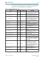
Table 1–1 provides information about this release of the Altera® SerialLite II
MegaCore® function.
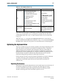
Table 1–1. SerialLite II Release Information
Item
Description
Version
13.1
Release Date
November 2013
Ordering Code
IP-SLITE2
Product ID
00AD
Vendor ID
6AF7
Altera verifies that the current version of the Quartus® II software compiles the
previous version of each MegaCore function. The MegaCore IP Library Release Notes
and Errata report any exceptions to this verification. Altera does not verify
compilation with MegaCore function versions older than one release.
Device Family Support
MegaCore functions provide the following support for Altera device families:
January 2014
■
Preliminary support—Altera verifies the IP core with preliminary timing models for
this device family. The core meets all functional requirements, but might still be
undergoing timing analysis for the device family. It can be used in production
designs with caution.
■
Final support—Altera verifies the IP core with final timing models for this device
family. The core meets all functional and timing requirements for the device family
and can be used in production designs.
Altera Corporation
SerialLite II MegaCore Function
User Guide
1–2
Chapter 1: About This MegaCore Function
Features
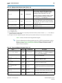
Table 1–2 shows the level of support offered by the SerialLite II MegaCore function to
each Altera device family.
Table 1–2. Device Family Support
Device Family
Arria®
II GX
Support
Final
Arria V
Preliminary
Arria V GZ
Preliminary
Cyclone®
Preliminary
Stratix®
V
IV
Final
Stratix V
Preliminary
Other device families
No support
Features
■
■
Physical layer features
■
622 Mbps to 6.375 Gbps per lane
■
Single or multiple lane support (up to 16 lanes)
■
8-, 16-, or 32-bit data path per lane
■
Symmetric, asymmetric, unidirectional/simplex or broadcast mode
■
Optional payload scrambling
■
Full-duplex or self-synchronizing link state machine (LSM)
■
Channel bonding scalable up to 16 lanes
■
Synchronous or asynchronous operation
■
Automatic clock rate compensation for asynchronous use
■
±100 and ±300 parts per million (ppm)
Link layer features
■
Atlantic™ interface compliant
■
Support for two user packet types: data packet and priority packet
■
Optional packet integrity protection using cyclic redundancy code (CRC-32 or
CRC-16)
■
Optional link management packets
■
Retry-on-error for priority packets
■
Individual port (data/priority) flow control
■
Unrestricted data and priority packet size
■
Support for TimeQuest timing analyzer
■
Polarity reversal
■
Lane order reversal
SerialLite II MegaCore Function
User Guide
January 2014 Altera Corporation
Chapter 1: About This MegaCore Function
General Description
1–3
■
IP functional simulation models for use in Altera-supported VHDL and Verilog
HDL simulators
■
Support for OpenCore® Plus evaluation
General Description
The SerialLite II MegaCore function is a simple, high-speed, low-latency, and
low-resource point-to-point serial data communication link.
The MegaCore function performs up to the following rates:
■
3.75 Gbps in Arria II GX devices
■
5 Gbps in Cyclone V devices
■
6.375 Gbps in Stratix IV, Arria V, and Stratix V devices
The SerialLite II MegaCore function is highly configurable, and provides a wide range
of functionality suited to moving data in many different environments.
The SerialLite II MegaCore function provides a simple and lightweight way to move
data from one point to another reliably at high speeds. It consists of a serial link of up
to 16 bonded lanes, with logic to provide a number of basic and optional link support
functions. The Atlantic interface is the primary access for delivering and receiving
data.
The SerialLite II protocol specifies a link that is simple to build, uses as little logic as
possible, and requires little work for a logic designer to implement. The SerialLite II
MegaCore function uses all of the features available in the SerialLite II protocol. You
can parameterize the MegaCore function using the SerialLite II parameter editor.
A link built using the SerialLite II MegaCore function operates at 622 Mbps to 6.375
Gbps per lane. Link reliability is enhanced by the 8B10B encoding scheme and
optional CRC capabilities. You can achieve further reductions in the bit-error rate by
using the optional retry-on-error feature. Data rate and consumption mismatches can
be accommodated using the optional flow-control feature to ensure that no data is
lost.
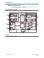
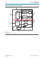
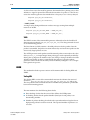
Figure 1–1 shows that the SerialLite II MegaCore function is divided into two main
blocks: a protocol processing portion (data link layer) and a high-speed front end
(physical layer).
Figure 1–1. SerialLite II MegaCore Function High-Level Block Diagram
User
Application
Link Layer
Physical Layer
Logical
Electrical
Logical
Electrical
Physical Layer
Link Layer
User
Application
One or More
Lanes
You can use the SerialLite II MegaCore function in the following applications:
■
January 2014
Chip-to-chip connectivity
Altera Corporation
SerialLite II MegaCore Function
User Guide
1–4
Chapter 1: About This MegaCore Function
General Description
■
Board-to-board connectivity
■
Shelf-to-shelf connectivity
■
Backplane communication
■
Bridging applications
■
Streaming video applications
■
Imaging applications
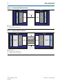
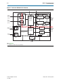
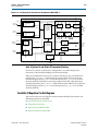
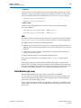
Figure 1–2 and Figure 1–3 show two examples of bridging applications.
Figure 1–2. Typical Application—Bridging Functions
Line Card
Memory
Optical/
Electrical
Converter
ASSP
Stratix IV
FPGA
Stratix IV GX
FPGA
Network
SPI-4.2
Interface
Processor
SPI-4.2
Interface
SerialLite II
Interface
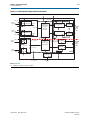
Figure 1–3. Typical Application—Unidirectional Bridging Application
Control Card
Sensor
Sensor
Sensor
Sensor
Stratix IV GX
FPGA
Sensor
Sensor
SerialLite II
Interface
Sensor
Sensor
Sensor
Sensor
Sensor
SerialLite II MegaCore Function
User Guide
January 2014 Altera Corporation
Chapter 1: About This MegaCore Function
Performance and Resource Utilization
1–5
Performance and Resource Utilization
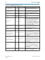
Table 1–3 lists the resources and internal core speeds for a selection of variations using
a 1,024-byte first-in first-out (FIFO) buffer. These results were obtained using the
Quartus II software version 10.1 for the following device: Stratix II GX
(EP2GX90FF1508C3).
Table 1–3. Performance for Stratix II GX (Part 1 of 2)
Parameters
Memory
Combi
Blocks
nLogic
ational Reg.
M4
M512
ALUTs
K
fMAX
(MHz)
Throughp
ut
Mbps (2)
10
267
1250
0
11
285
3125
818
11
11
273
6375
1215
1031
15
11
239
1250
No
1507
1113
15
22
249
3125
No
No
2089
1554
2
48
247
6375
No
No
No
4101
2809
17
87
199
3125
4
No
No
No
6347
4493
1
180
185
6375
Data
1
32
Yes
No
1077
1028
9
12
276
1250
Packet
Data
2
32
Yes
No
1181
1019
1
12
239
3125
1
Packet
Data
4
32
Yes
No
1381
1075
12
12
215
6375
FullDuplex
4
Packet
Data
1
32
Yes
No
1787
1306
16
12
215
1250
FullDuplex
4
Packet
Data
2
32
Yes
No
2387
1446
16
23
192
3125
FullDuplex
4
Packet
Data
4
32
Yes
No
3384
1907
3
49
177
6375
FullDuplex
1
Packet
Priority
2
16
Yes
Yes
1448
1236
1
22
228
3125
FullDuplex
1
Packet
Priority
4
16
Yes
Yes
1675
1284
12
22
225
6375
FullDuplex
4
Packet
Priority
2
16
Yes
Yes
2573
1659
17
41
212
3125
Data
Flow
Numbe
r of
Lanes
CR
C
Flow
Contr
ol
RetryonError
Data/
Type
FullDuplex
1
Packet
Data
1
No
No
No
756
741
9
FullDuplex
1
Packet
Data
2
No
No
No
768
754
FullDuplex
1
Packet
Data
4
No
No
No
863
FullDuplex
4
Packet
Data
1
No
No
No
FullDuplex
4
Packet
Data
2
No
No
FullDuplex
4
Packet
Data
4
No
FullDuplex
16
Packet
Data
2
FullDuplex
16
Packet
Data
FullDuplex
1
Packet
FullDuplex
1
FullDuplex
January 2014
Altera Corporation
Transf
Packet
er Size
Type
(1)
SerialLite II MegaCore Function
User Guide
1–6
Chapter 1: About This MegaCore Function
Performance and Resource Utilization
Table 1–3. Performance for Stratix II GX (Part 2 of 2)
Parameters
Data
Flow
Numbe
r of
Lanes
Data/
Type
Transf
Packet
er Size
Type
(1)
CR
C
Flow
Contr
ol
RetryonError
FullDuplex
4
Packet
Priority
16
Yes
Yes
4
Memory
Combi
Blocks
nLogic
ational Reg.
M4
M512
ALUTs
K
3528
2110
17
41
fMAX
(MHz)
Throughp
ut
Mbps (2)
160
6375
Notes to Table 1–3:
(1) A transfer size of 1 is used for 1,250 Mbps, 2 is used for 3,125 Mbps, and 4 is used for 6,375 Mbps.
(2) Total throughput equals the value in the Throughput column multiplied by the value in the Number of Lanes column.
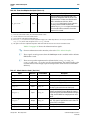
Table 1–4 lists the resources and internal core speeds for a selection of variations using
1,024-byte FIFO buffers. These results were obtained using the Quartus II software
version 10.1 for the following device: Stratix GX (EP1SGX40GF1020C5).
Table 1–4. Performance for Stratix GX (Part 1 of 3)
Memory
Blocks
Parameters
Data
Flow
Number
Packet Transfer
of
Data Type
Type
Size (1)
Lanes
CRC
Flow
Contro
l
Retry
- onError
LEs
M51
M4K
2
fMAX
(MHz)
Throughp
ut
Mbps (2)
FullDuplex
1
Packet
Data
1
No
No
No
1065
9
10
178
1250
FullDuplex
1
Packet
Data
2
No
No
No
1098
0
11
182
3125
FullDuplex
4
Packet
Data
1
No
No
No
1711
15
11
186
1250
FullDuplex
4
Packet
Data
2
No
No
No
2706
23
22
180
3125
FullDuplex
16
Packet
Data
2
No
No
No
8328
50
87
158
3125
FullDuplex
1
Packet
Data
1
32
Yes
No
1687
10
10
172
1250
FullDuplex
1
Packet
Data
2
32
Yes
No
1728
2
11
163
3125
FullDuplex
4
Packet
Data
1
32
Yes
No
2496
17
11
151
1250
FullDuplex
4
Packet
Data
2
32
Yes
No
3848
25
22
127
3125
FullDuplex
1
Packet
Data
and
Priority
2
No
Both
No
2169
2
19
181
3125
FullDuplex
1
Packet
Data
and
Priority
2
32
Both
No
2538
2
19
165
3125
SerialLite II MegaCore Function
User Guide
January 2014 Altera Corporation
Chapter 1: About This MegaCore Function
Performance and Resource Utilization
1–7
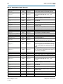
Table 1–4. Performance for Stratix GX (Part 2 of 3)
Memory
Blocks
Parameters
Data
Flow
Number
Packet Transfer
of
Data Type
Type
Size (1)
Lanes
CRC
Flow
Contro
l
Retry
- onError
LEs
M51
M4K
2
fMAX
(MHz)
Throughp
ut
Mbps (2)
FullDuplex
4
Packet
Data
and
Priority
2
No
Both
No
3911
33
38
181
3125
FullDuplex
4
Packet
Data
and
Priority
2
32
Both
No
4797
33
38
125
3125
FullDuplex
1
Packet
Priority
2
No
Yes
No
1350
2
11
188
3125
FullDuplex
4
Packet
Priority
2
No
Yes
No
2993
24
22
173
3125
FullDuplex
8
Packet
Priority
2
No
Yes
No
4787
28
44
167
3125
FullDuplex
1
Packet
Priority
2
16
Yes
Yes
2241
2
21
163
3125
FullDuplex
4
Packet
Priority
2
16
Yes
Yes
4373
26
40
144
3125
FullDuplex
1
Streaming
Data
1
No
No
No
198
0
0
253
1250
FullDuplex
1
Streaming
Data
2
No
No
No
243
0
0
246
3125
FullDuplex
4
Streaming
Data
1
No
No
No
763
4
0
183
1250
FullDuplex
4
Streaming
Data
2
No
No
No
1681
12
0
194
3125
1
Streaming
Data
1
No
No
No
27
0
0
422
1250
1
Streaming
Data
2
No
No
No
35
0
0
422
3125
1
Streaming
Data
1
No
No
No
98
0
0
282
1250
1
Streaming
Data
2
No
No
No
128
0
0
240
3125
4
Packet
Data
1
No
No
No
1392
8
11
177
1250
4
Packet
Data
2
No
No
No
1908
17
17
168
3125
8
Packet
Data
2
No
No
No
2292
13
29
169
3125
Simplex
Tx
Simplex
Tx
Simplex
Rx
Simplex
Rx
Asymm
Tx
Asymm
Tx
Asymm
Tx
January 2014
Altera Corporation
SerialLite II MegaCore Function
User Guide
1–8
Chapter 1: About This MegaCore Function
Installation and Licensing
Table 1–4. Performance for Stratix GX (Part 3 of 3)
Memory
Blocks
Parameters
Data
Flow
Asymm
Number
Packet Transfer
of
Data Type
Type
Size (1)
Lanes
CRC
Flow
Contro
l
Retry
- onError
LEs
M51
M4K
2
fMAX
(MHz)
Throughp
ut
Mbps (2)
4
Packet
Data
1
No
No
No
1604
9
11
195
1250
4
Packet
Data
2
No
No
No
2559
23
16
177
3125
Broadcast Rx
4
Streaming
Data
1
No
No
No
561
0
0
187
1250
Broadcast Rx
4
Streaming
Data
2
No
No
No
729
0
0
200
3125
Broadcast Rx
8
Streaming
Data
2
No
No
No
1359
0
0
181
3125
Rx
Asymm
Rx
Notes to Table 1–4:
(1) A transfer size of 1 is used for 1,250 Mbps and 2 is used for 3,125 Mbps.
(2) Total throughput equals the value in the Throughput column multiplied by the value in the Number of Lanes column.
Installation and Licensing
The SerialLite II MegaCore function is part of the MegaCore IP Library, which is
distributed with the Quartus II software and downloadable from the Altera website,
www.altera.com.
You can use Altera's free OpenCore Plus evaluation feature to evaluate the MegaCore
function in simulation and in hardware before you purchase a license. You need to
purchase a license for the MegaCore function only when you are satisfied with its
functionality and performance, and you want to take your design to production.
After you purchase a license for the SerialLite II MegaCore function, you can request a
license file from the Altera website at www.altera.com/licensing and install it on your
computer. When you request a license file, Altera emails you a license.dat file. If you
do not have internet access, contact your local Altera representative.
SerialLite II MegaCore Function
User Guide
January 2014 Altera Corporation
Chapter 1: About This MegaCore Function
Installation and Licensing
1–9
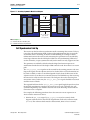
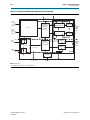
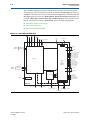
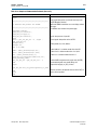
Figure 1–4 shows the directory structure after you install the SerialLite II MegaCore
function, where <path> is the installation directory. The default installation directory
on Windows is c:\altera\<version>; on Linux, it is /opt/altera<version>.
Figure 1–4. SerialLite II MegaCore Function Directory Structure
<path>
Installation directory.
ip
Contains the Altera MegaCore IP Library and third-party IP cores.
altera
Contains the Altera MegaCore IP Library.
common
Contains shared components.
seriallite_ii
Contains the SerialLite II MegaCore function files.
lib
Contains encrypted lower-level design files.
f For details on installation and licensing, refer to Altera Software Installation & Licensing.
OpenCore Plus Evaluation
With Altera's free OpenCore Plus evaluation feature, you can perform the following
actions:
■
Simulate the behavior of a megafunction (Altera MegaCore function or AMPPSM
megafunction) within your system
■
Verify the functionality of your design, as well as evaluate its size and speed
quickly and easily
■
Generate time-limited device programming files for designs that include
megafunctions
■
Program a device and verify your design in hardware
OpenCore Plus Time-Out Behavior
OpenCore Plus hardware evaluation supports the following two operation modes:
■
Untethered—the design runs for a limited time.
■
Tethered—requires a connection between your board and the host computer. If
tethered mode is supported by all megafunctions in a design, the device can
operate for a longer time or indefinitely.
All megafunctions in a device time out simultaneously when the most restrictive
evaluation time is reached. If there is more than one megafunction in a design, a
specific megafunction's time-out behavior may be masked by the time-out behavior of
the other megafunctions.
1
January 2014
For MegaCore functions, the untethered time-out is 1 hour; the tethered time-out
value is indefinite.
Altera Corporation
SerialLite II MegaCore Function
User Guide
1–10
Chapter 1: About This MegaCore Function
Installation and Licensing
Your design stops working after the hardware evaluation time; the SerialLite II
MegaCore function is forced into reset.
f For more information on OpenCore Plus hardware evaluation, refer to AN 320:
OpenCore Plus Evaluation of Megafunctions.
SerialLite II MegaCore Function
User Guide
January 2014 Altera Corporation
2. Getting Started
Design Flow
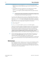
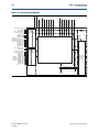
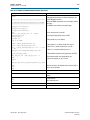
Figure 2–1 outlines the high-level steps required to create a design that includes the
SerialLite II MegaCore function. Each step is explained in detail in the walkthrough
below.
Figure 2–1. SerialLite II MegaCore Design Flow
Specify Parameters
Simulate with Testbench
Instantiate in a Design
Specify Constraints
Compile
Design
Program
Device
This chapter explains how to create a SerialLite II MegaCore function using the
SerialLite II parameter editor in the MegaWizard Plug-In Manager and the Quartus II
software. When you finish generating a custom variation of the SerialLite II MegaCore
function, you can incorporate it into your overall project.
This walkthrough requires the following steps:
1. Create a New Quartus II Project
2. Launch the MegaWizard Plug-In Manager
3. Parameterize
4. Set Up Simulation
5. Generate Files
January 2014
Altera Corporation
SerialLite II MegaCore Function
User Guide
2–2
Chapter 2: Getting Started
Design Flow
Create a New Quartus II Project
You can create a new Quartus II project with the New Project Wizard, which specifies
the working directory for the project, assigns the project name, and designates the
name of the top-level design entity.
To create a new project follow these steps:
1. Choose Programs > Altera > Quartus II <version> (Windows Start menu) to run
the Quartus II software. Alternatively, you can use the Quartus II Web Edition
software.
2. On the File menu, click New Project Wizard.
3. Click Next in the New Project Wizard: Introduction page (the introduction does
not display if you turned it off previously).
4. In the New Project Wizard: Directory, Name, Top-Level Entity page, enter the
following information:
a. Specify the working directory for your project. For example, this walkthrough
uses the c:\altera\projects\slite2_project directory.
b. Specify the name of the project. This walkthrough uses example for the project
name.
1
The Quartus II software automatically specifies a top-level design entity
that has the same name as the project. This walkthrough assumes that the
names are the same.
5. Click Next to display the New Project Wizard: Add Files page.
1
When you specify a directory that does not already exist, a message
prompts you to create a specified directory. Click Yes to create the directory.
6. Click Next to close this page and display the New Project Wizard: Family and
Device Settings page.
7. On the New Project Wizard: Family and Device Settings page, choose the target
device family in the Family list.
8. The remaining pages in the New Project Wizard are optional. Click Finish to
complete the Quartus II project.
Launch the MegaWizard Plug-In Manager
To launch the MegaWizard Plug-In Manager in the Quartus II software, follow these
steps:
1. On the Tools menu, click MegaWizard Plug-In Manager.
1
Refer to Quartus II Help for more information on how to use the
MegaWizard Plug-In Manager.
2. Specify that you want to create a new custom megafunction variation and click
Next.
SerialLite II MegaCore Function
User Guide
January 2014 Altera Corporation
Chapter 2: Getting Started
Parameterize
2–3
3. Under Installed Plug-Ins, expand Interfaces folder and then, click
SerialLite II<version>.
4. Select the output file type for your design; the MegaWizard Plug-In Manager
supports VHDL and Verilog HDL. For this example, select Verilog HDL.
5. The MegaWizard Plug-In Manager shows the project path that you specified in the
New Project Wizard. Append a variation name for the MegaCore function output
files <project path>\<variation name>. For this example, type example as the
variation name.
6. Click Next to display the Parameter Settings page for the SerialLite II MegaCore
function.
Parameterize
This section shows how to parameterize the example SerialLite II MegaCore function
and describes the results of various options. A comprehensive description of all
parameters is contained in Chapter 3, Parameter Settings.
1
The following parameters are ordered as they appear in the SerialLite II parameter
editor. Not all parameters are supported by, or are relevant for, every MegaCore
function variation.
To parameterize your MegaCore function, follow these steps:
1. Click Parameter Settings in the SerialLite II parameter editor. The Physical Layer
page appears.
2. Enter a data rate in megabits per second (Mbps). The SerialLite II MegaCore
function supports data rates of 622 to 6,375 Mbps per lane.
The data rate must be an acceptable range for the Transfer size. SerialLite II
returns a warning or an error message if you specify a data rate that is not within
the range for the specified Transfer size.
3. Choose a Transfer size. The Transfer size determines the number of contiguous
data columns. The Transfer size also determines the serialization/deserialization
(SERDES) factor and internal data path width:
■
A Transfer size of 1 equates to an internal data path of 8 bits (Recommended
for less than 2.5 gigabits per second (Gbps))
■
A Transfer size of 2 equates to an internal data path of 16 bits (Recommended
for less than or equal to 3.125 Gbps)
■
A Transfer size of 4 equates to an internal data path of 32 bits (Typically for
greater than 3.125 Gbps, and only available for Stratix IV devices)
4. Specify the Reference Clock Frequency. This option defines the frequency of the
reference clock for the Arria II GX or Stratix IV internal transceiver. You can select
any frequency supported by the transceiver. This option is not available in Arria V,
Cyclone V, and Stratix V configurations.
5. Select a Port Type. You have three choices: Bidirectional, Transmitter only, and
Receiver only.
January 2014
Altera Corporation
SerialLite II MegaCore Function
User Guide
2–4
Chapter 2: Getting Started
Parameterize
1
If you choose Transmitter only or Receiver only, the self-synchronized
link-up parameter (LSM) is enabled by default.
6. Turn on or off the Self-Synchronized Link-Up option. This parameter allows the
receiver on the far end of the link to synchronize itself to incoming data streams,
rather than on an exchange of status information with the transmitter. Note that
the Self-Synchronized Link-Up feature is only for single lane applications.
7. Under Transmitter Settings, select the number of lanes for the transmitter.
8. Turn on or off the Scramble and Broadcast mode options.
9. Under Receiver Settings, select the number of lanes for the receiver.
Table 2–1 shows the allowable number of lanes depending on the chosen
parameters.
Table 2–1. Number of Transmit Lanes
Self-Synchronized Link-Up
Broadcast
Number of Lanes
v
v
2 – 16
v
—
1
—
v
2 – 16
—
—
1 – 16
10. Turn on or off the De-scramble option.
11. Turn on or off the Enable frequency offset tolerance option. If you turn on this
option, select an offset tolerance of ±100 or ±300 parts per million (ppm).
12. Click Configure Transceiver to display the Configure Transceiver page. Select the
following parameters on the Configure Transceiver page to configure the ALTGX
megafunction.
Refer to “Transceiver Configuration” on page 3–23 for a more detailed description
of the transceiver parameters.
SerialLite II MegaCore Function
User Guide
January 2014 Altera Corporation
Chapter 2: Getting Started
Parameterize
2–5
1
The Configure Transceiver page is disabled when you select Arria V or
Stratix V as the target device family. To add a transceiver, you are required
to instantiate the Custom PHY IP core.
a. For the transmitter, select the Voltage Output Differential (VOD) control
setting value.
b. Under Pre-emphasis, select a value for Specify pre-emphasis control setting.
c. In the Bandwidth mode list, select high or low for the Tx PLL bandwidth.
d. Select a value for the Transmitter Buffer Power (VCCH).
e. Under Receiver Functionality, select a value for Specify equalizer control
setting.
f. In the Bandwidth mode list, select high, medium or low for the Rx PLL
bandwidth.
g. To reconfigure functionality settings, specify a Starting channel number.
h. Click Finish.
13. Click Next to open the Link Layer page.
14. Under Data Type, select Packets or Streaming.
15. If you select Packets, select a packet type: Priority packets and data packets,
Priority packets, or Data packets.
16. If you select a packet type that includes priority packets, follow these substeps;
otherwise, skip to Step 17.
a. Turn on or off the Retry-on-error option.
b. If you turned on Retry-on-error, specify a value for Timeout and Segment
size.
c. Under Buffer Size, specify a value for Transmitter and Receiver.
d. Turn on or off the Enable flow control option.
e. If you turned on Enable flow control, specify the values for the following
settings:
■
Pause quantum time
■
Threshold
■
Refresh period
1
If you selected Priority packets only, skip to Step 18.
17. If you selected a packet type that includes data packets, follow these substeps:
a. Turn on or off the Enable flow control option.
b. If you turned on flow control, specify the values for the following settings:
January 2014
■
Pause quantum time
■
Threshold
■
Refresh period
Altera Corporation
SerialLite II MegaCore Function
User Guide
2–6
Chapter 2: Getting Started
Parameterize
1
For information on setting these parameters, refer to “Flow Control” on
page 3–15.
c. Select the transmitter and receiver buffer sizes (bytes).
18. If your transmitter or receiver requires cyclic redundancy code (CRC) checking,
turn on the Enable CRC option for your chosen packet type and specify a value
for CRC Type.
19. Click Next.
Set Up Simulation
An IP functional simulation model is a cycle-accurate VHDL or Verilog HDL model
produced by the Quartus II software. The model allows for fast functional simulation
of IP using industry-standard VHDL and Verilog HDL simulators.
c You may use these models only for simulation and not for synthesis or any other
purposes. Using these models for synthesis creates a nonfunctional design.
To generate an IP functional simulation model for your MegaCore function, follow
these steps:
1. On the EDA page, under Simulation Libraries, turn on Generate Simulation
Model.
2. Some third-party synthesis tools can use a netlist that contains only the structure
of the MegaCore function, but not detailed logic, to optimize performance of the
design that contains the MegaCore function. If your synthesis tool supports this
feature, turn on Generate netlist.
3. Click Next to display the Summary page.
Generate Files
You can use the check boxes on the Summary page to enable or disable the generation
of specified files. A gray checkmark indicates a file that is automatically generated;
other checkmarks indicate optional files.
To generate your parameterized MegaCore function, follow these steps:
1. Turn on the files you want to generate.
2. To generate the specified files and close the SerialLite II parameter editor, click
Finish. The generation phase can take several minutes to complete.
3. If you generate the MegaCore function instance in a Quartus II project, you are
prompted to add the Quartus II IP File (.qip) to the current Quartus II project.
1
SerialLite II MegaCore Function
User Guide
The .qip file is generated by the SerialLite II parameter editor and contains
information about a generated IP core. In most cases, the .qip file contains
all of the necessary assignments and information required to process the
MegaCore or system in the Quartus II compiler. The SerialLite II parameter
editor generates a single .qip file for each MegaCore function.
January 2014 Altera Corporation
Chapter 2: Getting Started
Simulate the Design
2–7
4. After your review the generation report, <variation name>.html, in your project
directory, click Exit to close the SerialLite II parameter editor.
Simulate the Design
You can simulate your design using the MegaWizard-generated VHDL and
Verilog HDL IP functional simulation models.
f For more information on IP functional simulation models, refer to the Simulating
Altera IP in Third-Party Simulation Tools chapter in volume 3 of the Quartus II Handbook.
Altera also provides a Verilog HDL demonstration testbench that shows you how to
instantiate a model in a design for all configurations. Altera also provides a VHDL
demonstration testbench for a restricted number of configurations. The testbench
stimulates the inputs and checks the outputs of the interfaces of the SerialLite II
MegaCore function, allowing you to evaluate the MegaCore function’s basic
functionality. The testbench is described in detail in Chapter 5, Testbench.
Instantiate the MegaCore
You can now integrate your custom MegaCore function variation into your design
and simulate your complete design using your own custom testbench.
Specify Constraints
This example design applies constraints to create virtual pins and set up timing
analysis.
Assign Virtual Pins
If you are compiling the SerialLite II MegaCore function variation as a standalone
component, you must specify virtual pin assignments. The SerialLite II parameter
editor generates a tool command language (Tcl) script that automates this task. Follow
these steps to run the script:
1. On the Tools menu, click Tcl Scripts to open the Tcl Scripts dialog box.
2. In the project directory, select <variation_name>_constraints.
3. Click Run.
1
January 2014
The script assumes the default names for the virtual pins. If you have connected the
pins to names other than the default names, you must edit this script and change the
virtual pin names when the core is still compiled in stand-alone mode.
Altera Corporation
SerialLite II MegaCore Function
User Guide
2–8
Chapter 2: Getting Started
Compile and Program
Fitter Constraints
The Tcl script also optimizes fitter settings to produce the best performance (fMAX).
Use this script as a guide to set constraints for the SerialLite II MegaCore function
variation in your design. The timing constraints are currently set for the SerialLite II
MegaCore function variation as a standalone component, thus you must update the
script with hierarchy information for your own design. The Tcl script also points to
the generated Synopsys Design Constraints (SDC) timing constraint script if the
TimeQuest timing analyzer is enabled. The Fitter optimizes your design based on the
requirements in the .sdc files in your project.
The script uses the FITTER_EFFORT "STANDARD FIT" Fitter setting.
1
This fitter setting may conflict with your Quartus II software settings.
You can now integrate your MegaCore function variation into your design and
simulate and compile.
Timing Constraints
The SerialLite II MegaCore generates an ASCII file (with the .sdc extension) that
contains design constraints and timing assignments in the industry-standard SDC
format. The constraints in the .sdc file are described using the Tcl tool command
language and follow Tcl syntax rules.
To specify the TimeQuest timing analyzer as the default timing analyzer, on the
Assignments menu, click Timing Analysis Settings. In the Timing Analysis Settings
page, turn on Use TimeQuest Timing Analyzer during compilation.
The TimeQuest timing constraints are currently set for the SerialLite II MegaCore
function variation as a standalone component. You must update the script with
hierarchy information if your own design is not a standalone component.
f Refer to the Quartus II TimeQuest Timing Analyzer chapter in volume 3 of the Quartus II
Handbook for more information on how to use the TimeQuest Timing Analyzer.
Compile and Program
Click Start Compilation on the Processing menu in the Quartus II software to compile
your design. After successfully compiling your design, program the targeted Altera
device with the Programmer (Tools menu) and verify the design in hardware.
SerialLite II MegaCore Function
User Guide
January 2014 Altera Corporation
3. Parameter Settings
Table 3–1 shows the function parameters, which can be set only in the SerialLite II
parameter editor (refer to “Parameterize” on page 2–3). The following sections
describe these parameters.
Table 3–1. Default SerialLite II Variation
Parameter
Default Configuration
Physical Layer
Device family
Depends on the family specified in the
SerialLite II parameter editor
Data rate
3,125 megabits per second (Mbps)
Transfer size
2 Columns
Reference Clock Frequency
156.25 MHz
Port Type
Bidirectional
Self-Synchronized Link-Up
Disabled
Number of lanes (Transmitter and Receiver Settings) 1
Scramble/De-Scramble
Disabled
Broadcast mode
Disabled
Enable frequency offset tolerance
Disabled
Link Layer
Data Type
Packets
Packet type
Data packets
Enable flow control
Disabled
Buffer Size (Transmitter and Receiver)
1,024 bytes
CRC Generation (Transmitter and Receiver)
Disabled
Configure Transceiver
Specify Voltage Output Differential (VOD) control
setting
0
Specify pre-emphasis control setting
0
Bandwidth mode (Transmitter and Receiver)
Low
Transmitter Buffer Power (VCCH)
1.5
Specify equalizer control setting
0
Starting channel number
0
To configure your own variation of the SerialLite II MegaCore function, you must
decide the following issues:
January 2014
■
High-level link configuration
■
Bandwidth required
■
Whether to use CRC checking
Altera Corporation
SerialLite II MegaCore Function
User Guide
3–2
Chapter 3: Parameter Settings
Link Consistency
■
Whether to implement flow control
■
How to size the FIFO buffers
Link Consistency
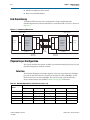
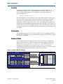
A SerialLite II link consists of two instantiations of logic implementing the
SerialLite II protocol. Each end of the link has a transmitter and a receiver, as shown in
Figure 3–1.
Figure 3–1. Complete SerialLite II Link
Atlantic Interface
Atlantic Interface
Tx
SerialLite II
MegaCore
Function
Variation
System
Logic
Rx
Rx
SerialLite II
MegaCore
Function
Variation
Tx
One or
more lanes
FPGA 1
System
Logic
FPGA 2
High-Speed
Transceivers
High-Speed
Transceivers
Physical Layer Configuration
This section describes the options available to parameterize the physical layer of your
SerialLite II MegaCore function variation.
Data Rate
The SerialLite II MegaCore function supports a data rate range of 622 to 6,375 Mbps
per lane. In Arria II GX devices, the data rate must be less than 3,750 Mbps, and in
Stratix IV devices, less than 6,375 Mbps. The data rate range varies based on the
device and the transfer size (TSIZE) as Table 3–2 on page 3–2 illustrates.
Table 3–2. Data Rate Dependencies on Transfer Size (Part 1 of 2)
Data Rate
Devices
2.5 Gbps
Arria II GX
Arria V
Arria V GZ
Cyclone V
Stratix IV
TSIZE= 1, 2
TSIZE= 1, 2
TSIZE= 1, 2
TSIZE= 2
TSIZE= 1, 2
SerialLite II MegaCore Function
User Guide
3.125 Gbps
TSIZE= 2
3.75 Gbps
TSIZE= 2
TSIZE= 2
(1),
TSIZE= 2
(1),
4
4
TSIZE= 2
(1),
TSIZE= 2
(1),
5 Gbps
6.375 Gbps
Not Supported
Not Supported
4
TSIZE= 4
TSIZE= 4
4
TSIZE= 4
TSIZE= 4
TSIZE= 2
TSIZE= 2
TSIZE= 4
TSIZE= 2
TSIZE= 2
TSIZE= 2
Not Supported
(1),
4
TSIZE= 4
January 2014 Altera Corporation
Chapter 3: Parameter Settings
Physical Layer Configuration
3–3
Table 3–2. Data Rate Dependencies on Transfer Size (Part 2 of 2)
Data Rate
Devices
2.5 Gbps
Stratix V
TSIZE= 1, 2
3.125 Gbps
TSIZE= 2
(1),
4
3.75 Gbps
TSIZE= 2
(1),
4
5 Gbps
TSIZE= 2
(1),
6.375 Gbps
4
TSIZE= 4
Note to Table 3–2:
(1) Symmetric mode (p_RX_NUM_LANES == p_TX_NUM_LANES) only.
The data rates for an individual Arria II GX device are limited to the respective speed
grades, refer to Table 3–3.
Table 3–3. Arria II GX Speed Grade-Data Rate Limits
Device Speed Grade
Minimum Data Rate (Mbps)
Maximum Data Rate (Mbps)
C4
600
3,750
C5
600
3,125
C6
600
3,125
Transfer size
The Transfer size parameter defines many important characteristics of the MegaCore
function variation. Transfer size determines the number of contiguous data columns
and the internal data path width per lane, where:
■
A transfer size of 1 equates to an internal data path of 8 bits (Recommended for
less than 2.5 Gbps)
■
A transfer size of 2 equates to an internal data path of 16 bits (Recommended for
less than or equal to 3.125 Gbps)
■
A transfer size of 4 equates to an internal data path of 32 bits (only available for
Stratix IV FPGA with transfer size greater than 3.125 Gbps, and must be used
when the data rate exceeds 5 Gbps)
A transfer size determines the width of the SERDES block, where:
■
A transfer size of 1 equates to a 10 bit-wide SERDES block
■
A transfer size of 2 equates to a 20 bit-wide SERDES block
■
A transfer size of 4 equates to a 40-bit wide SERDES block
Reference Clock Frequency
The Reference Clock Frequency parameter defines the frequency of the reference
clock for the Arria II GX or Stratix IV internal transceiver. Valid values change with
the data rate but the reference input clock frequency must be within 50 MHz and 622
MHz.
■
The general formula to determine frequency:
Frequency = p×Data Rate/(2×m), where p = 1 or 2, and m = 4, 5, 8, 10, 16, 20, or 25
Condition for frequency to be valid: (50×p) < Frequency < 622
■
January 2014
This parameter is only applicable if you chose Arria II GX or Stratix IV devices.
Altera Corporation
SerialLite II MegaCore Function
User Guide
3–4
Chapter 3: Parameter Settings
Physical Layer Configuration
■
If you select a reference clock frequency that is not equal to the
data rate/(transfer size) * 10, the Clock Compensation option is disabled if the
Receiver only port type option is turned on.
Port Type
The Port Type parameter offers three options: Bidirectional, Transmitter only, and
Receiver only. If you turn on the Bidirectional option, you must specify values for
Transmitter Settings and Receiver Settings. Under Transmitter Settings, you need to
specify the Number of lanes, and select whether or not to enable the Scramble and
Broadcast mode. Under Receiver Settings, you must specify the settings for the
Number of lanes, and select whether or not to enable the De-Scramble option. If you
turn on Transmitter only option, you must specify values for Transmitter Settings
only, and if you turn on Receiver only option, you must specify values for Receiver
Settings only.
The Number of lanes parameter dictates the number of serial links, essentially the
number of external inputs and outputs (I/Os) for the MegaCore function.
If you set the Number of lanes for the transmitter and receiver settings to the same
value, you configure the MegaCore function to operate in symmetric, bidirectional
mode. Refer to Figure 3–2 and Figure 3–3 on page 3–5.
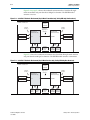
If you set the Port Type to Receiver only or Transmitter only, you configure the
MegaCore function to operate in unidirectional mode, transmitter, or receiver only.
Refer to Figure 3–4 and Figure 3–5 on page 3–6.
If you set the Port Type to Bidirectional, but have the number of lanes set to a value
other than zero, but not equal to the other function’s value, you configure the
MegaCore function to operate in asymmetric mode. Refer to Figure 3–6 and
Figure 3–7 on page 3–7.
Figure 3–2. Symmetric Mode Block Diagram
One or more lanes
(up to N)
FPGA 1
Atlantic
Interface
Light-weight
Linklayer
PHY
Layer
FPGA 2
CDR
SERDES
CDR
SERDES
PHY
Layer
Light-weight
Linklayer
Atlantic
Interface
One or more lanes
(up to N)
Notes to Figure 3–2:
(1) A full line indicates a mandatory lane.
(2) A dashed line indicates an optional lane.
SerialLite II MegaCore Function
User Guide
January 2014 Altera Corporation
Chapter 3: Parameter Settings
Physical Layer Configuration
3–5
Figure 3–3. Streaming Symmetric Mode Block Diagram
One or more lanes
(up to N)
FPGA 1
Atlantic
Interface
PHY
Layer
FPGA 2
CDR
SERDES
CDR
SERDES
PHY
Layer
Atlantic
Interface
One or more lanes
(up to N)
Notes to Figure 3–3:
(1) A full line indicates a mandatory lane.
(2) A dashed line indicates an optional lane.
Figure 3–4. Simplex Mode Block Diagram
FPGA 1
FPGA 2
One lane only
Atlantic
Interface
Light-weight
Linklayer
PHY
Layer
CDR
SERDES
CDR
SERDES
PHY
Layer
Light-weight
Linklayer
Atlantic
Interface
Note to Figure 3–4:
(1) A full line indicates a mandatory lane.
January 2014
Altera Corporation
SerialLite II MegaCore Function
User Guide
3–6
Chapter 3: Parameter Settings
Physical Layer Configuration
Figure 3–5. Streaming Simplex Mode Block Diagram
FPGA 1
FPGA 2
One lane only
Atlantic
Interface
PHY
Layer
CDR
SERDES
CDR
SERDES
PHY
Layer
Atlantic
Interface
Note to Figure 3–5:
(1) A full line indicates a mandatory lane
Figure 3–6. Asymmetric Mode Block Diagram
One or more lanes
(up to N)
FPGA 1
Atlantic
Interface
Light-weight
Linklayer
PHY
Layer
FPGA 2
CDR
SERDES
CDR
SERDES
PHY
Layer
Light-weight
Linklayer
Atlantic
Interface
One or more lanes
(up to M, but
not equal to N)
Notes to Figure 3–6:
(1) A full line indicates a mandatory lane.
(2) A dashed line indicates an optional lane.
SerialLite II MegaCore Function
User Guide
January 2014 Altera Corporation
Chapter 3: Parameter Settings
Physical Layer Configuration
3–7
Figure 3–7. Streaming Asymmetric Mode Block Diagram
One or more lanes
(up to N)
FPGA 1
Atlantic
Interface
PHY
Layer
FPGA 2
CDR
SERDES
CDR
SERDES
PHY
Layer
Atlantic
Interface
One or more lanes
(up to M, but
not equal to N)
Notes to Figure 3–7:
(1) A full line indicates a mandatory lane.
(2) A dashed line indicates an optional lane.
Self Synchronized Link Up
The receiver on the far end must synchronize itself to incoming data streams. To do so,
it uses the self-synchronizing LSM, a light-weight implementation that is especially
useful when data is streaming. As there is no handshaking or exchange of status
information between the receiver and transmitter, this parameter uses considerably
fewer logic elements than the full-duplex LSM. The self-synchronizing LSM can be
used in all modes, except asymmetric mode, but this mode can only support one lane.
This parameter is enabled by default when the MegaCore function operates in
unidirectional mode because the duplex LSM cannot be used when there is no return
path.
The ctrl_tc_force_train signal must be asserted for the training patterns to be sent.
Negate the signal once the adjacent receiver has locked, if this status information can
be made available, or after a user-defined period of time when the link status of the
adjacent receiver is not known or cannot be known. The LSM links up after receiving
64 consecutive valid, error-free characters. The link goes down after receiving four
consecutive errors; at this time, the ctrl_tc_force_train signal should be reasserted
until the receiver relocks.
The required hold time for the ctrl_tc_force_train signal largely depends on when
the ALTGX megafunction completes the power-on reset cycle. Therefore, the selfsynchronizing link-up state machine does not look at the incoming stream until the
transceiver reset is complete.
For example, the following procedure shows the transceiver reset sequence in an
Arria or Stratix transceiver device:
1. Wait for the pll_locked signal (stat_tc_pll_locked) to be asserted, which
happens when the PLL in the ALTGX megafunction locks to the reference clock
(trefclk). The reference clock must be characterized; 10 ms or less is normal.
January 2014
Altera Corporation
SerialLite II MegaCore Function
User Guide
3–8
Chapter 3: Parameter Settings
Physical Layer Configuration
2. Wait for the rx_freqlocked signal (stat_rr_freqlock) to be asserted, which
happens when the ALTGX megafunction locks onto the serial stream; 5 ms or less
is normal.
3. The Rx digital reset needs to complete; this reset normally takes one million
internal tx_coreclock cycles after rx_freqlocked is asserted. The
stat_tc_rst_done signal is asserted to indicate that the reset sequence has been
completed.
1
The normal time values are much shorter in simulation (For example, using
the IP Functional Simulation Model), but not in gate-level simulation. Gatelevel simulation uses the hardware equivalent times.
As you have full visibility of the above signals (via the SignalTap® II logic analyzer
and the port list), you should characterize the timing of these signals to set up the size
of your ctrl_tc_force_train counter. The MegaCore function also has a reset done
status signal (stat_tc_rst_done) that can be useful for measurements. The following
MegaCore function status output signals correspond to each step above:
■
stat_tc_pll_locked
■
stat_rr_freqlock
■
stat_tc_rst_done (to see when rx_digitalreset has been negated).
After the reset controller completes, the MegaCore function waits for the transceiver
byte aligner to detect and align the control (k28.5) character in the training sequence.
Once the transceiver detects this character, the count starts at every k28.5 that is
received (basically, counting every training sequence). Once 64 error-free training
sequences have been received, the MegaCore function reports linkup. Any errors (for
example, disparity or 8B/10B errors) that are received reset the count, and the
MegaCore function continues to wait until 64 error-free training patterns are received.
1
The self-synchronizing LSM also locks onto the clock compensation sequence. As
turning on the Clock Compensation option allows the receiver to automatically
relock if the link goes down, the transmitter is not required to assert
ctrl_tc_force_train to retrain the link (which may be impossible in a unidirectional
link because the transmitter does not necessarily detect that the receiver has lost the
link).
Number of Lanes
Because each lane operates at the bit rate, you can increase the bandwidth by adding
lanes. Adding lanes—up to a maximum of 16—is a simple way to scale the link
during system design. If adding a lane provides more bandwidth than needed, you
can reduce the system clock rate, thereby mitigating possible high-speed design issues
and making it easier to meet performance.
SerialLite II MegaCore Function
User Guide
January 2014 Altera Corporation
Chapter 3: Parameter Settings
Physical Layer Configuration
3–9
Scramble
Scrambling the data eliminates repeating characters, which affect the EMI
substantially at high data rates. A linear feedback shift register (LSFR) is used as a
pseudo-random number generator to scramble the data, using the following
polynomial equation:
G(x) = X16 + X5 + X4 + X3 + 1
The transmitted bits are XORed with the output of the LFSR in the data stream. At the
receiver, the data stream is again XORed with an identical scrambler to recover the
original bits. To synchronize the transmitter to the receiver, the COM character
initializes the LFSR with the initial seed of 0×FFFF XORed with the lane number (LN).
Scrambling is recommended for data rates greater than 3,125 Mbps, and is optional
for lower data rates (622 to 3,125 Mbps inclusive). This parameter applies only to the
transmitter, and allows for scrambling (like CRC) to be enabled in one direction only,
as required.
De-Scramble
This parameter applies only to the receiver, and allows for descrambling (like CRC) to
be enabled in one direction only, as required. Descrambling is required if the incoming
data stream is scrambled.
Broadcast Mode
If you enable the broadcast mode parameter for the transmitter, you configure the
MegaCore function to use a single shared transmitter and multiple receivers in the
master device, as shown in Figure 3–8 and Figure 3–9. The number of receivers is
determined by the number of lanes chosen for the slave receiver. The master
transmitter uses its output lanes to broadcast identical messages to all slave receivers,
and each slave responds individually by sharing the master's lanes.
Figure 3–8. Broadcast Mode Block Diagram
Master FPGA
Slave FPGA N
Broadcastmessage
TX Tsvr 1
Shared TX
Link
Shared TX
PHY
TX Tsvr 2
TX Tsvr N
Broadcastmessage
Broadcastmessage
CDR
SERDES
Atlantic
Interface
RX Link 1
RX PHY 1
RX Tsvr 1
RX Link 2
RX PHY 2
RX Tsvr 2
RX Link N
RX PHY N
RX Tsvr N
PHY
Layer
Light-weight
Linklayer
Atlantic
Interface
N-return
lanes
January 2014
Altera Corporation
SerialLite II MegaCore Function
User Guide
3–10
Chapter 3: Parameter Settings
Physical Layer Configuration
Figure 3–9. Streaming Broadcast Mode Block Diagram
Master FPGA
Slave FPGA N
Broadcastmessage
TX Tsvr 1
Shared TX
PHY
TX Tsvr 2
TX Tsvr N
Broadcastmessage
Broadcastmessage
CDR
SERDES
Atlantic
Interface
RX PHY 1
RX Tsvr 1
RX PHY 2
RX Tsvr 2
RX PHY N
RX Tsvr N
PHY
Layer
Atlantic
Interface
N-return
lanes
Clock Compensation
The clock compensation value determines when the clock compensation sequence is
inserted into, or deleted from, the high-speed serial data stream to compensate for
ppm frequency differences between different clock crystals when the Clock
Compensation option is enabled.
The frequency offset removal (foffre) block includes a FIFO buffer overflow status
output signal: err_rr_foffre_oflw. If this signal toggles, you may need to adjust the
ppm setting.
1
The Clock Compensation option is disabled if the value chosen for the Reference
Clock Frequency option does not equal data rate/ (transfer size* 10), and the
Receiver Only port type option is turned on.
Lane Polarity and Order Reversal
The SerialLite II protocol optionally allows the link to recover from some connection
problems. Lane polarity and lane order are reversed automatically.
Lane Polarity
Each lane consists of a differential pair of signals. It is possible for the positive and
negative sides of this pair to be reversed because of a layout error or because it
simplifies layout. The SerialLite II logic can compensate for such a reversed lane on
the receive side. This reversal occurs during link initialization and remains in place for
as long as the link is active.
For training sequence one, the TID field normally read as /T1/ (D10.2) is read as
/!T1/ (D21.5) when the lane polarity is inverted. Likewise for training sequence two,
the TID field normally read as /T2/ (D5.2) is read as /!T2/ (D26.5) when the lane
polarity is inverted. In these training sequences, the /COM/ character is followed by
seven valid data characters. The last character of the sequence is used to determine
the parity. If any of the parity identifiers in any lane is either /!T1/ (D21.5) or /!T2/
(D26.5), the receiver for that lane inverts the polarity.
SerialLite II MegaCore Function
User Guide
January 2014 Altera Corporation
Chapter 3: Parameter Settings
Link Layer Configuration
3–11
Lane Order
It is possible that the order of lanes may be incorrect due to layout errors. It may also
be reversed, with the most significant lane of one end of the link connected to the least
significant lane of the other end, due to layout constraints. The SerialLite II logic
always detects a lane order mismatch, and compensates for the reversed lane order on
the receive side. This reversal occurs during link initialization and remains in place for
as long as the link is active.
The SerialLite II logic only corrects reversed lane order. If the lane order is scrambled,
the receiving end cannot unscramble it. The following example shows a possible fourlane system, where Serial Lite II can reverse the four-lane system:
Example 3–1. SerialLite II Lane Reversal
Lane
Lane
Lane
Lane
0
1
2
3
->
->
->
->
Lane
Lane
Lane
Lane
3
2
1
0
Frequency Offset Tolerance
The Enable frequency offset tolerance parameter sets the value for the frequency
offset tolerance (clock compensation). This parameter also determines whether the
system is configured for synchronous or asynchronous clocking operation. If you
enable this parameter, the values available are ±100 ppm and ±300 ppm.
Link Layer Configuration
This section describes the options available to parameterize the link layer of the
SerialLite II MegaCore function variation.
Data Type:Packets
Packet mode for packet-based protocols. The data port expects data to arrive in
packets, marked by asserting start of packet (SOP) at the beginning and end of packet
(EOP) at the end of the packet. The receiver passes these packets to the user logic via
the Atlantic interface, with the packet boundaries marked by SOP and EOP.
Data Type:Streaming
The regular data port allows data to be formatted as a stream or in packets. Streaming
data has no beginning or end. It acts like an infinite-length packet and represents an
unending sequence of data bytes. The only Atlantic signals present are txrdp_ena,
txrdp_dav, and txrdp_dat (valid and data) in the transmitter, and rxrdp_ena and
rxrdp_dat for a receiver instantiation. There is no backpressure for the receiver
function; consequently, the user logic must accept the data when rxrdp_ena is high.
There is only backpressure in the transmitter function if clock compensation is
enabled (txrdp_dav is negated when the clock compensation sequence is inserted).
Once system link up is complete, your logic should provide data continuously. The
SerialLite II MegaCore function does not encapsulate streaming data. Streaming
mode does not include link-layer functions.
January 2014
Altera Corporation
SerialLite II MegaCore Function
User Guide
3–12
Chapter 3: Parameter Settings
Link Layer Configuration
If this parameter is enabled, all link layer basic parameters, including data and
priority ports, and buffering are disabled (grayed out).
Regular Data Port
A cut-through data flow is implemented for data packets. Packet data is transmitted
as soon as enough data is received to fill a column, without waiting for the entire
packet to be delivered to the transmitter. This approach provides the lowest latency.
There is no packet size limitation.
Priority Port
The data flow for priority packets depends upon whether Retry-on-error is enabled.
Retry-on-error Disabled
A cut-through data flow is implemented for priority packets. Priority packet data is
transmitted as soon as enough data is received to fill a column, without waiting for
the entire packet to be delivered to the transmitter. This approach provides the lowest
latency. There is no packet size limitation. As the name implies, priority packets have
precedence over data packets. The SerialLite II MegaCore function inserts high
priority packets within a data packet that is already in transmission (nesting packets).
Retry-on-error Enabled
A store-and-forward data flow is implemented for priority packet segments. Priority
packets are broken into SEGMENT_SIZE bytes that are buffered and sent across the link.
The transmission of data does not start until a segment or an end of packet has been
delivered to the transmitter. Therefore, priority packets less than or equal to
SEGMENT_SIZE bytes are buffered before transmission. This buffering is required to
support the Retry-on-error option, which is only allowed for priority packets. As the
name implies, priority packets have precedence over data packets. The SerialLite II
MegaCore function inserts high priority packets within a data packet that is already in
transmission (nesting packets). There is also no maximum packet size limitation.
If a packet is larger than a SEGMENT_SIZE, a full segment must be queued before it can
be transmitted. This queueing may result in mid-packet backpressure on the priority
port Atlantic interface. Segment interleaving, priority segments destined for different
ports, is fully supported, as long as the address change occurs on a segment boundary.
Segment Size
Segment size is only applicable when the Retry-on-error parameter is turned on.
Priority packets are broken into segments of SEGMENT_SIZE bytes and sent across the
link. Priority packets less than or equal to SEGMENT_SIZE bytes and without an end
marker are buffered before transmission.
The SEGMENT_SIZE parameter settings range from 8 to 2,048 bytes in 2n increments,
and the default value is 256 bytes.
SerialLite II MegaCore Function
User Guide
January 2014 Altera Corporation
Chapter 3: Parameter Settings
Link Layer Configuration
3–13
Retry-on-error
The SerialLite II MegaCore function allows you to improve the bit error rate of your
data by using the Retry-on-error parameter. This parameter is only available on the
priority data port. The parameter provides for segments with errors to be
retransmitted, so that only good segments are delivered to the Atlantic receive
interface.
When the Retry-on-error parameter is turned on, all segments sent by the transmitter
are acknowledged. There are two types of acknowledgement:
■
ACK: The received segment is good and error-free.
■
NACK: The received segment contains an error. If you turn on the Retry-on-error
parameter, the transmitter retransmits all segments starting from the segment with
errors. (If you turn off the Retry-on-error parameter, the receiver raises a data
error.)
The segment buffers in the transmitting logic hold segments until they have been
acknowledged. Once a segment has been acknowledged by ACK, it is released from the
buffer so that the buffer can be used for another segment. If a segment is
acknowledged by NACK, that segment and all segments sent after that segment are
retransmitted.
Up to seven segments waiting for acknowledgment can be held at once. If more
segments arrive while all eight buffers are occupied, the priority data port stalls until
an acknowledgment is received, freeing up a buffer for the next segment.
The retry-on-error operation proceeds as follows:
1. When the receiver receives a good segment, the segment is delivered to the
Atlantic interface and an ACK acknowledgment is sent back to the transmitter.
2. Any data errors cause the segment to be acknowledged as errored (NACK). Once
that happens, the receiver ignores all incoming data until it receives the
retransmitted segment.
3. All segments are numbered internally with a segment ID. The receiver knows
which segment it expects next, so if the next expected segment has been corrupted
or lost, the next received segment has the wrong segment number and the receiver
requests a retransmission of the sequence starting with the segment ID it was
expecting.
4. The oldest outstanding segment to be acknowledged has an associated timer, set
by the Timeout value on the Link Layer page in the SerialLite II parameter editor.
If an acknowledgment (ACK or NACK) is lost or corrupted in transit, the timer expires
causing the affected segment and all subsequent segments to be retransmitted.
5. The transmitter knows which segment it expects to be acknowledged next. If the
next acknowledgment is not for the expected segment, the transmitter infers that
the expected acknowledgment was lost and retransmits the segment in question
and all subsequent segments. Only segments that have the correct segment ID are
buffered. The timer starts when the segment is identified as the next segment to be
acknowledged.
January 2014
Altera Corporation
SerialLite II MegaCore Function
User Guide
3–14
Chapter 3: Parameter Settings
Link Layer Configuration
6. If the timer expires three times in succession, a link error is declared and the link is
restarted. You can control the Timeout limit in the SerialLite II parameter editor,
and it is good practice not to set the time-out to be too long so the system does not
have to wait too long for such situations to resolve. However, do not set the
Timeout to be too short because then the system always times out and the link
never remains up. The time-out value is based primarily on the round trip latency
(that is, from the time a packet is sent to when the ACK is returned to that
transmitter). The exact value of the round trip latency is undetermined, pending
device characterization, but a value of 1,024 columns is recommended.
Implementation of the retry-on-error mechanism is optional for the priority port. If
the Retry-on-error parameter is turned off, no segment acknowledgments are
generated or expected, and all segments are transmitted without any
acknowledgements from the receiver.
Table 3–4 shows the retry-on-error options for the priority data port.
Table 3–4. Retry-on-error Options (Priority Data Port Only)
Option
Description
Turned on
Logic is created to acknowledge segments and retransmit segments when errors
occur. Eight transmit segment buffers are created. Available only if the priority
data port is enabled.
Turned off
Logic is not created to acknowledge segments. Available only if the priority data
port is enabled. This is the default setting.
Retry-on-error Responses
Table 3–5 summarizes the response to various transmission errors.
Table 3–5. Retry-on-error Responses
Error
Response
Invalid 8b/10b codes groups
Far end transmitter issues NACK
Running disparity errors
Far end transmitter issues NACK
Unsupported valid code groups
Far end transmitter issues NACK
CRC errored segments with {EGP} sequence
Far end transmitter issues NACK
Out of order segment
Far end transmitter issues NACK
Out of order acknowledgment
Near end transmitter starts re-send
SerialLite II MegaCore Function
User Guide
January 2014 Altera Corporation
Chapter 3: Parameter Settings
Link Layer Configuration
3–15
Retry-on-error Operation Example
Figure 3–10 shows an example of the retry-on-error operation.
Figure 3–10. Retry-On-Error Example
Device A
1
Device B
Seg_A; Seg_B; Seg_C
g_U
; Se
g_T
e
S
_S;
Seg
K _B
ACK _A; NAC
5
6
2
3
4
ACK _S;
ACK _T;
ACK_U
Res end
Seg _B; S
e g_C
ACK _C
ACK _B;
7
Notes to Figure 3–10:
(1) Device A transmits Seg_A, Seg_B, and Seg_C to Device B.
(2) At the same time, Device B transmits Seg_S, Seg_T, and Seg_U to Device A.
(3) Device B properly receives Seg_A, but detects an error with Seg_B.
(4) Device B returns positive acknowledge for Seg_A, but requests retransmission of Seg_B. Device B discards all
subsequently received segments until Seg_B is received again.
(5) Device A acknowledges the proper reception of Seg_S; Seg_T; and Seg_U.
(6) Device A resends all segments starting from Seg_B.
(7) Finally, Device B acknowledges the proper reception of Seg_B and Seg_C.
Flow Control
The SerialLite II MegaCore function provides the Enable flow control parameter as
an optional means of exerting backpressure on a data source when data consumption
is too slow. Use this parameter to ensure that the receive FIFO buffers do not overflow.
1
Flow control is only needed when the system logic on the receiving end of the link is
reading the data slower than the system logic on the transmitting end of the link is
sending data.
The flow control feature in the SerialLite II Megacore function operates by having the
receiving end of the link issue a PAUSE instruction to the transmitting end of the link
when threshold of the receiver’s FIFO buffer is breached. The instruction causes the
transmitter to cease transmission for specified pause duration. Once the pause
duration has expired, the transmission resumes.
Flow Control Operation
When flow control is used, the FIFO buffer is structured as two sections, threshold
and headroom.
January 2014
Altera Corporation
SerialLite II MegaCore Function
User Guide
3–16
Chapter 3: Parameter Settings
Link Layer Configuration
Figure 3–11 shows the FIFO buffer structure with flow control enabled.
Figure 3–11. FIFO Buffer Structure (Flow Control Enabled)
Headroom
Primary Flow
Control Threshold
(ctrl_rr_rdp_fcthresh/
ctrl_rr_hpp_fcthresh)
Threshold
Total depth
of the FIFO
FIFO Width
The threshold value determines if a Flow Control PAUSE is requested. You control the
size of this threshold by setting the flow control threshold per port using the
SerialLite II parameter editor to fall within the total depth of the FIFO. The value for
the flow control threshold signals (ctrl_rr_rdp_fcthresh and
ctrl_rr_hpp_fcthresh) must be within the total FIFO depth. The value must also
ensure required headroom to compensate for the delays for the flow control request to
take effect, and for the remaining data already in the system to be stored in the FIFO.
Refer to section “Selecting the Proper Threshold Value” on page 3–18 for further
analysis.
The total depth of the FIFO (in bytes) is derived by the SerialLite II parameter editor
using the following formula :
Total Depth = FIFO SIZE /(TSIZE * RX_NUMBER_LANES)
In this example, set the FIFO SIZE on the Parameter Settings tab, Link Layer page by
selecting a value in the Receiver field of the Buffer Size section.
TSIZE and the RX_NUMBER_LANES are set on the Physical Layer page. Under Data
Settings, select the TSIZE by selecting a number in the Transfer size option. To set
RX_NUMBER_LANES, specify a value for the Number of lanes option in the Receiver
Settings section.
If in this example you select a high-priority FIFO SIZE of 1,024B, and a TSIZE of 2 in a
four-lane SerialLite II configuration, you compute the Total Depth as follows:
Total Depth =1024/2*4 =128
Based on the above result, for this example, you must set the Threshold value in the
SerialLite II parameter editor to be less than 128 elements. Set the Threshold value in
the appropriate packet settings section on the Link Layer page.
SerialLite II MegaCore Function
User Guide
January 2014 Altera Corporation
Chapter 3: Parameter Settings
Link Layer Configuration
3–17
When flow control is enabled, the SerialLite II MegaCore logic monitors the triggering
receive FIFO buffer and, when a threshold is reached, issues a pause instruction. It
takes some time for the pause instruction to be issued, traverse the connection, and for
transmission to be stopped. It takes more time for all the data that has already been
transmitted to be stored in the receive FIFO buffer. Therefore, there must be a certain
amount of space left in the receive FIFO buffer above the threshold to hold the data
that arrives during this delay. This headroom has contributions from the core latency
and the wire latency. Refer to section “Flow Control Operation Example” on
page 3–17” for more details.
If the far receive FIFO buffer is still in breach of the threshold when the flow control
refresh period timer expires, the far receiver automatically renews the pause to extend
the flow control period. This renewal occurs until the fill level of far receive FIFO is no
longer greater than the threshold. When the renewed flow control packet reaches the
near transmitter before the current pause expires, the pause time is refreshed.
■
This refresh time must be set so that the renewed flow control packets are received
by the near transmitter before the current pause time completes. Set the value of
Refresh period to be smaller than Pause quantum time in the Priority Packet
Settings or Data Packet Settings section on the Link Layer page.
■
If the refresh period is small, more flow control packets are sent on the link,
possibly degrading the performance of an alternate active port. This is a trade off
for the link bandwidth performance.
To overcome head-of-line blocking, every port has its own flow control that suspends
the flow of data to either the priority port or the regular data port, depending on the
FIFO buffer status. For example, if the near transmitter receives a flow control pause
request for the priority port, the data on the regular port is transmitted (as long as the
regular port is not also being requested to pause).
January 2014
Altera Corporation
SerialLite II MegaCore Function
User Guide
3–18
Chapter 3: Parameter Settings
Link Layer Configuration
Flow Control Operation Example
Figure 3–12 on page 3–17 shows an example of a flow control operation.
Figure 3–12. Typical Flow Diagram of FC Operation
Near End
Far End
Data transmitted by
Near Transmitter
Time
Read Ongoing
FIFO read rate < Data transmit rate
FIFO fills
1
2
Threshold hits;
Pause generated and transmitted
by Far Transmitter
3
Wire delay
4
Pause received by Near Receiver;
Pause starts,
Near Transmitter stops sending data
Pause count expires,
Near Transmitter resumes sending data
5
6
7
Notes to Figure 3–12:
(1) Near transmitter starts sending data to far receiver when the link is up. The FIFO inside the far receiver reads the data.
When the user logic on the receiving end of the link is reading the data out of the FIFO slower than the rate at which
the data is being written into the FIFO, the FIFO starts to fill.
(2) The far receiver FIFO fill level breaches the flow control threshold value.
(3) The far transmitter generates and sends the flow control packet with a FC_TIME pause request amount. There is some
internal transmit latency (tlate_fc_transmit) for the flow control packet to hit the serial link.
(4) The flow control packet reaches the near receiver after some wire delay period (t_wd).
(5) There is some latency for the flow control packet to come from the serial link until the near receiver completes
processing the packet (tlate_fc_receive).
(6) The near transmitter stops sending data to the far receiver either as soon as the flow control packet is received, or
after the current active segment has been sent (for Priority packet with Retry-on Error enabled) for the specified
pause duration. This latency accounts for the amount of additional data that has been already transmitted before the
PAUSE request was received (tlate_stop_data).
(7) After the pause quantum time specified by the users expires, the pause stops and the near transmitter continues
sending the data (assuming that no other pause requests have been received).
Selecting the Proper Threshold Value
Table 3–6 on page 3–18 defines the specification value for flow control internal latency,
as mentioned in the previous example. Use this information to determine the
minimum FIFO threshold size avoiding starvation during the flow control.
SerialLite II MegaCore Function
User Guide
January 2014 Altera Corporation
Chapter 3: Parameter Settings
Link Layer Configuration
3–19
To calculate latency numbers in terms of time units, multiply the latency values in
Table 3–6 by the tx_coreclock clock period.
Table 3–6. SerialLite II Flow Control Internal Latency
Internal Latency
Description
Latency Value (cycles)
Latency that occurs during RX FIFO breach up to the
point where the associated flow control link
management packet is sent out on the link. This
includes the time for the core to generate the link
management packet and the time through the
transceiver.
24
t_wd
Wire delay
(1)
tlate_fc_receive
Latency that occurs in the duration when the flow
control link management packet reaches the
transceiver pins until the the core processes the
request.
23 + deskew cycles
tlate_fc_transmit
(2)
Overall system core latency (indicates the amount of Regular data: 41
data that may still be in the system when the PAUSE Priority data: 41 + seg_TX
begins). This data must still be stored in the RX FIFO. seg_RX (3)
tlate_stop_data
(3)
+
Notes to Table 3–6:
(1) t_wd specifies the wire delay between the devices. This value depends on the data rate and trace lengths in the application.
(2) deskew cycles = 0 for single lane configuration;
deskew cycles = worst case lane to lane skew in the transceiver, refer to “SerialLite II Deskew Support” on page 4–6
(3) seg_TX and seg_RX are taken into account only for priority packets with retry-on-error feature. If a priority packet with retry-on-error feature
is in transfer, flow control begins immediately after the current segment of the priority packet has been sent.
seg_TX = [segment size/(TSIZE* TX_NUMBER_LANES)]
seg_RX = [segment size/(TSIZE* RX_NUMBER_LANES)]
The Segment size value is specified by users in the Parameters Settings tab on the Link Layer page.
The Threshold parameter must be set to a value such that the FIFO does not
completely empty during a flow control operation (this can cause inefficiencies in the
system), and leave enough room in the FIFO to ensure any remaining data in the
system can be safely stored in the FIFO without the FIFO overflowing.
The proper threshold value can be derived by subtracting the depth of the FIFO from
the total latency.
Total Latency = [tlate_fc_transmit + t_wd + tlate_fc_receive +
tlate_stop_data] cycles
1
The ratio between one element and one cycle is equal to one. When you write one
element to the FIFO, it takes one clock cycle. Therefore one cycle is one element.
Therefore, the Threshold value should be set based on the following formula:
Threshold value = Total Depth of FIFO (elements) - Total Latency (clock cycles)]
January 2014
Altera Corporation
SerialLite II MegaCore Function
User Guide
3–20
Chapter 3: Parameter Settings
Link Layer Configuration
Selecting the Proper Pause Duration
Activation of flow control causes a pause in transmission. You can specify the
duration of this pause in terms of columns. You can specify a pause duration from to 8
to 2,040 columns. In elements, this value is 8/TSIZE to 2,040/TSIZE elements. Set the
pause duration based on the rate that your system logic consumes the data received. If
a pause is too long, then overall system bandwidth is reduced. If a pause is too short,
it may have to be renewed, which could result in an overall pause that is too long. Part
of determining the pause duration is the read rate of the RX FIFO.
As an example, assume a theoretical pause needs to be 100 elements long. As a
designer, you would not likely know that at design time, so you must estimate a
reasonable value. The effect of a TSIZE-2, 120-element pause (240 columns on the
GUI) causes more delay than needed. However, an 80-element delay (160 columns on
the GUI) results in the pause being renewed after 80 elements, for a total 160 elements
of delay, even longer than the 120-element pause.
Selecting the Proper Refresh Value
The flow control refresh period determines the number of columns before a flow
control packet can be retransmitted (for example if a flow control link management
packet is lost or corrupted). This refresh period must be less than the pause quantum
time. The packet is retransmitted if the FIFO buffer is still breached.
The stat_tc_rdp_thresh_breach, stat_tc_hpp_thresh_breach,
stat_fc_hpp_retransmit and stat_tc_fc_hpp_retransmit status signals indicate
whether the refresh period is set appropriately. If stat_tc_rdp_thresh_breach or
stat_tc_hpp_thresh_breach (which indicates that the RX FIFO is still breached) is
still asserted after the FC refresh period (based on the value set), the far transmitter
generates another flow control packet (based on the value set at the Pause Quantum
Time option) and sends it out, causing the stat_fc_hpp_retransmit or
stat_tc_fc_hpp_retransmit to be asserted.
External Flow Control (When RX FIFO Size is 0)
The SerialLite II MegaCore function supports an external flow control when the RX
FIFO size is zero. The rxrdp_dav and rxhpp_dav input signals are provided to activate
flow control to pause the data transmission when the corresponding regular port or
priority data port is selected.
Drive rxrdp_dav low when the fill level of your external FIFO has been breached; this
action triggers the flow control pause request. When this signal is high, no flow
control requests is generated.
Transmit/Receive FIFO Buffers
The transmit FIFO buffers are used by the transmitting end of the SerialLite II link to
store data to be transmitted across the high-speed serial link. The receive FIFO buffers
are used by the receiving end of the SerialLite II link to store data for presentation to
the Atlantic interface and eventual consumption by the system logic.
The SerialLite II MegaCore function automatically sets the width of the receive FIFO
buffers at TSIZE bytes per lane. You specify the buffer size in the SerialLite II
parameter editor.
SerialLite II MegaCore Function
User Guide
January 2014 Altera Corporation
Chapter 3: Parameter Settings
Link Layer Configuration
3–21
FIFO Buffer Size
The size of the FIFO buffers is based on the factors listed in Table 3–7 on page 3–20.
Table 3–7. Factors Affecting Receive FIFO Buffer Size
Factor
Description
Flow control
If flow control is enabled, the FIFO buffer size should change to
account for the thresholds that must be set.
Pause duration
When optimizing against starvation during flow control, the pause
duration affects the FIFO buffer size.
Number of packets (and
packet sizes)
If you want to use a store-and-forward FIFO (using the eop_dav
and a high threshold), the FIFO must be big enough to hold a full
packet at minimum.
Wire delay and bit rate
The wire propagation delay and the bit rate change the wire latency,
which must be accommodated if flow control is used.
FIFO Buffer Structure
Figure 3–13 shows the Atlantic FIFO buffer structure.
Figure 3–13. Atlantic FIFO Buffer Structure
Headroom
FTL/FTH
Threshold
Total
depth
Width set automatically
The FIFO buffer threshold low (FTL), ctl_rxrdp_ftl/ctl_rxhpp_ftl, value for
receiver variations controls when the rxrdp_dav/rxhpp_dav signals are asserted for
the read side of the FIFO buffer, respectively. If the fill level of the buffer is higher than
the FTL value, the rxrdp_dav/rxhpp_dav signal is asserted indicating that there is a
burst of data available.
1
January 2014
There is no requirement to wait for the rxrdp_dav/rxhpp_dav signal to be asserted;
you can read from the buffer at any time by asserting the rxrdp_ena/rxhpp_ena signal
at all times and qualifying the data with the rxrdp_val/rxhpp_val signal. The FIFO
buffer has built-in underflow protection, such that an underflow condition does not
exit.
Altera Corporation
SerialLite II MegaCore Function
User Guide
3–22
Chapter 3: Parameter Settings
Link Layer Configuration
The receiver Atlantic FIFO buffers include an end-of-packet based data available
feature which can be turned on by asserting the ctl_rxrdp_eopdav/ctl_rxhpp_eopdav
signals. The end-of-packet feature determines whether the dav remains high: if the
signal is asserted, and there is an end-of- packet beneath the FTL threshed, the dav
signal remains high until the end-of-packet is read out of the FIFO buffer. Otherwise,
if the signal is not asserted, the dav signal only remains high when the fill level of the
buffer is higher than the FTL value.
ctl_rxhpp_fth and ctl_rxrdp_fth are the threshold levels for the high priority and
regular data ports on the receiver Atlantic FIFO buffers. When the data fill level is
higher than the threshold level set by ctl_rxhpp_fth or ctl_rxrdp_fth, or dav = 1, it
means that there a large amount of data ready to be fetched at the FIFO buffer. You
must set these threshold levels based on your design requirements, and ensure that
the FIFO buffer does not underflow. You may also set the threshold levels to segment
size of a priority packet; or to the lowest level so that you can fetch data as soon as it is
stored in the FIFO buffer.
You can set ctl_rxhpp_ftl to 1 element unit so that it fetches the data from the RX
FIFO buffer as soon as there is data available. If you want to store some data before
fetching it, you can raise the threshold level.
The FIFO buffer threshold high (ctl_txrdp_fth/ctl_txhpp_fth) value for transmitter
variations controls when the txrdp_dav/txhpp_dav signals are asserted and
deasserted for the write side of the FIFO buffer, respectively. The txrdp_dav signal
indicates when there is room available to write new data into the FIFO buffer, and is
asserted when the fill level of the FIFO is less than the FTH setting, and deasserted
when the fill level of the FIFO is greater than the FTH.
For example, if FTH is five, and the fill level is four, the txrdp_dav/txhpp_dav signal is
high, indicating that the user can write data into the FIFO. If the fill level for this
example is six, the txrdp_dav/txhpp_dav signal is low, indicating that the user should
stop writing data into the FIFO.
ctl_txhpp_fth and ctl_txrdp_fth are the threshold levels for the high priority and
regular data ports on the transmitter Atlantic FIFO buffers. When the data fill level at
the FIFO buffer is lower than the threshold level set by ctl_txhpp_fth or
ctl_txrdp_fth, or dav = 1, it means that there are plenty of spaces available for data to
write into the buffer. You must set these threshold levels high so that the user logic
knows whenever the FIFO buffer has available spaces for data buffering and to ensure
that overflow does not occur. However, these threshold settings should not exceed the
FIFO depth.
For example, if the transmitter buffer size is 4,096 bytes, and the transmitter FIFO
depth is 2,048 element units, you should set the level of ctl_txhpp_fth to 250 element
units.
TSIZE = 2, and one FIFO element = 2 bytes
Maximum TX FIFO level (TX 8 lane) = 2,048/8 = 256 element units
1
You can set any value below 256 element units for ctl_txhpp_fth; Altera
recommends a level of 250 element units or 8'hFA.
SerialLite II MegaCore Function
User Guide
January 2014 Altera Corporation
Chapter 3: Parameter Settings
Link Layer Configuration
3–23
The threshold levels on both the transmitter and receiver Atlantic FIFO buffers differ
according to implementation. They may depend on the data traffic, the FIFO depth,
and the clock frequencies for read and write. Based on your design, you can gauge the
usual fill level of the FIFO buffers and determine the appropriate threshold levels.
Data Integrity Protection: CRC
If you need error protection, you may add CRC checking to your packet. The CRC is
automatically generated in transmission and is automatically checked on reception.
On the data port, a CRC check failure results in the packet being marked as bad using
the rxrdp_err/rxhpp_err signal on the Atlantic interface. You decide independently
for each port whether CRC usage is enabled.
16-Bit Versus 32-Bit CRC
The SerialLite II MegaCore function supports both 16-bit and 32-bit CRC algorithms.
You decide which CRC algorithm to use independently for each port. The 16-bit
algorithm generates a two-byte result, and uses the following polynomial equation:
G(x) = X16 + X12 + X5 + 1
The 32-bit algorithm generates a four-byte result, and uses the following polynomial
equation:
G(x) = X32 + X26 + X23 + X22 + X16 + X12 + X11 + X10 + X8 + X7 + X5 + X4 + X2 + X + 1
The 16-bit version provides excellent protection for packets smaller than about 1
KBytes. For larger packets, CRC-32 can be considered, but it requires significantly
more logic, especially in implementations requiring many lanes. At 16 lanes, CRC-32
logic may constitute as much as half of the logic of the entire SerialLite II instantiation.
Therefore, CRC-32 should only be used when absolutely necessary.
Table 3–8 and Table 3–9 show the different CRC options.
Table 3–8. CRC Options
Option
Description
Enabled
CRC logic is created. CRC usage is specified independently for each port.
Disabled
CRC logic is not created. CRC usage is specified independently for each
port. This is the default CRC setting.
Table 3–9. CRC Type Options
Option
January 2014
Description
16-bit
Generates a two-byte CRC. Adequate for packets of around 1 KBytes or
smaller. This is the default algorithm once CRC usage has been enabled.
32-bit
Generates a 4-byte CRC. Should only be used for packets larger than about
1 KBytes or when extreme protection is required, because it is
resource-intensive.
Altera Corporation
SerialLite II MegaCore Function
User Guide
3–24
Chapter 3: Parameter Settings
Transceiver Configuration
Transceiver Configuration
This section describes the optional, configurable Altera ALTGX gigabit transceiver
megafunctions. The transceiver megafunction offers several configuration options
that can be set based on board-level conditions, design constraints, or other
application-specific requirements, to ensure the proper operation of the serial link.
1
If you select Arria V or Stratix V as the target device family, you are required to
instantiate the Custom PHY IP core as the hard transceiver. For more information
about this configuration, refer to “MegaCore Configuration for Arria V, Cyclone V,
and Stratix V Devices” on page 4–19.
f For more information on Altera gigabit transceiver (ALTGX)megafunction, refer to
the Arria II GX Transceiver Architecture section in volume 2 of the Arria II GX Device
Handbook, and the Stratix IV Transceiver Architecture section in volume 2 of the
Stratix IV Device Handbook.
Voltage Output Differential (VOD) Control Settings
The Stratix IV transceivers allow you to set the VOD to handle different length,
backplane, and receiver requirements. A range from 200 to 1,200 mV is supported for
Stratix IV devices. Arria II GX devices have a fixed value, which cannot be changed.
The range is decoded using the GUI integer value and the on-chip transmitter
programmable termination values.
Table 3–10 shows how the VOD value you chose in the SerialLite II parameter editor
corresponds to the mV value. The VOD value is 0 by default.
Table 3–10. VOD Control Settings
VOD Value (Per Lane)
100 Ohms (mV) Stratix IV
0
200
1
400
2
600
3
700
4
800
5
900
6
1,000
7
1,200
This parameter is disabled when the number of lanes in the transmit direction is equal
to zero.
Pre-Emphasis Control Settings
The programmable Pre-emphasis setting boosts the high frequencies in the transmit
data signal, which may be attenuated by the transmission medium. The Pre-emphasis
setting maximizes the data eye opening at the far-end receiver, which is particularly
useful in lossy transmission mediums. Specify pre-emphasis control setting
parameter is set to 0 by default.
SerialLite II MegaCore Function
User Guide
January 2014 Altera Corporation
Chapter 3: Parameter Settings
Transceiver Configuration
3–25
This parameter is disabled when the number of lanes in the transmit direction is equal
to zero.
For Stratix IV devices, the pre-emphasis control values supported are 0,1,2,3,4, and 5.
For 0, Pre-emphasis option is turned off. For 1, the pre-emphasis is the maximum
negative value. For 2, pre-emphasis is the medium negative value. The value 3 is a
special value in which only the first post-tap is set (set to the maximum), while the
other taps are off. A value of 4 yields a medium positive value, while 5 sets the preemphasis values to the maximum positive supported values. For Arria II GX devices,
the Pre-emphasis setting cannot be changed.
Transmitter Buffer Power (VCCH)
This setting is for information only and is used to calculate the VOD from the buffer
power supply and the transmitter termination to derive the proper VOD range.
The selections available are 1.5 V for Arria II GX devices.
For Stratix IV devices, the Quartus II software automatically selects 1.4 V or 1.5 V. If
you want to set your preferred VCCH value to the transmit and receive pins, perform
the following steps:
1. In the Quartus II window, on the Assignments menu, click Assignment Editor.
2. In the <<new>> row, in the To column, double-click and type rxin to set value for
the receive pin.
3. Double-click in the Assignments Name column, and click I/O Standard (Accepts
wildcards/groups). The entry is set to I/O Standard.
4. Double-click in the Value column and click 1.4-V PCML or 1.5-V PCML.
5. In the new <<new>> row, repeat steps 2 to 4 to set the value for the transmit pin
(txout).
Equalizer Control Settings
The transceiver offers an equalization circuit in each receiver channel to increase noise
margins and help reduce the effects of high frequency losses. The programmable
Equalizer compensates for inter-symbol interference (ISI) and high frequency losses
that distort the signal and reduce the noise margin of the transmission medium by
equalizing the frequency response.
For Stratix IV devices, the equalization control values supported are 0, 1, 2, 3, and 4.
These values correspond to lowest/off (0), between medium and lowest (1), medium
(2), between medium and high (3), and high (4). For Arria II GX devices, the
equalization cannot be changed.
Bandwidth Mode
The transmitter and receiver PLLs in the ALTGX megafunction offer programmable
bandwidth settings. The PLL bandwidth is the measure of its ability to track the input
clock and jitter, determined by the -3 dB frequency of the PLL’s closed-loop gain.
The transmitter offers two settings: high or low. The receiver offers three settings:
high, medium, or low.
January 2014
Altera Corporation
SerialLite II MegaCore Function
User Guide
3–26
Chapter 3: Parameter Settings
Transceiver Configuration
■
The high bandwidth setting provides a faster lock time and tracks more jitter on
the input clock source which passes it through the PLL to help reject noise from the
voltage control oscillator (VCO) and power supplies.
■
The low bandwidth setting filters out more high frequency input clock jitter, but
increases lock time. The PLL is set to the low setting by default.
■
The medium setting balances the lock time and noise rejection/jitter filtering
between the high and low settings.
If the number of lanes in the transmit or receive direction is equal to zero, the
bandwidth mode for that direction is disabled. This parameter is also disabled for
Arria II GX devices.
Starting Channel number
The range for the dynamic reconfiguration starting channel number setting is 0 to 380
for Stratix IV GX devices. These ranges are in multiples of four because the dynamic
reconfiguration interface is per transceiver block. The range 0 to 380 is the logical
channel address, based purely on the number of possible transceiver instances. This
parameter is not applicable for Arria II GX devices.
Instantiating a Transceiver Reconfiguration Block
When you use an Arria II GX, Arria V, Cyclone V, Stratix IV, or a Stratix V device, you
can instantiate a transceiver reconfiguration block that dynamically changes the
following physical media attachment (PMA) settings:
1
■
Pre-emphasis
■
Equalization
■
VOD
■
Offset cancelation
For analog settings, there are no restrictions on using dynamic reconfiguration.
When you use a transceiver-based device, the ALTGX interface allows you to modify
the parameter interface with a reconfiguration block. The altgx_reconfig block is not
instantiated, but the MegaWizard-generated wrapper provides the ports that interface
to the altgx_reconfig block. If you choose to use an altgx_reconfig block, you must
instantiate the altgx_reconfig block and connect the associated signals to the
corresponding SerialLite II MegaCore function top-level signals (tie the
reconfig_fromgxb, reconfig_clk, and reconfig_togxb ports to the altgx_reconfig
block).
1
You must instantiate the transceiver reconfiguration block on an Arria II GX or a
Stratix IV device, because these device transceivers require offset cancelation. Your
Arria II GX or Stratix IV design can compile without the dynamic reconfiguration
block but it cannot function correctly in hardware.
f For more information about the following topics, refer to the respective documents:
SerialLite II MegaCore Function
User Guide
January 2014 Altera Corporation
Chapter 3: Parameter Settings
Transceiver Configuration
3–27
■
Dynamic reconfiguration and offset cancellation for Arria II GX devices, refer to
the AN 558: Implementing Dynamic Reconfiguration in Arria II GX.
■
Dynamic reconfiguration and offset cancellation for Stratix IV devices, refer to the
Stratix IV Dynamic Reconfiguration chapter in the Stratix IV Device Handbook.
■
Dynamic reconfiguration and using the Altera Reconfiguration Controller for
Arria V, Cyclone V, and Stratix V devices, refer to the Altera Transceiver PHY IP Core
User Guide.
ALTGX Support Signals
This section describes the ALTGX support signals, which are only present on variants
that use the Arria II GX and Stratix IV integrated PHY. They are connected directly to
the ALTGX instance. In many cases these signals must be shared with ALTGX
instances that are implemented in the same device. The following signals exist:
■
cal_blk_clk
■
reconfig_clk
■
reconfig_togxb
■
reconfig_fromgxb
■
gxb_powerdown
Table 3–11 describes these ALTGX support signals.
Table 3–11. ALTGX Support Signals
Signal
cal_blk_clk
reconfig_clk
reconfig_togxb
I/O
Description
I
The cal_blk_clk input signal is connected to the ALTGX calibration block clock
(cal_blk_clk) input. All instances of ALTGX in the same device must have their
cal_blk_clk inputs connected to the same signal because there is only one
calibration block per device. This input should be connected to a clock operating as
recommended by the Arria II GX Device Handbook or the Stratix IV Device Handbook.
I
The reconfig_clk input signal is the ALTGX dynamic reconfiguration clock. This
signal must be connected as described in the Arria II GX Device Handbook or the
Stratix IV Device Handbook if the ALTGX dynamic reconfiguration block is used.
Otherwise, this signal must be set to 1'b0.
I
The reconfig_togxb [N:0] input signal is driven from an external dynamic
reconfiguration block. The signal supports the selection of multiple transceiver
channels for dynamic reconfiguration. This signal must be connected as described in
the Arria II GX Device Handbook or the Stratix IV Device Handbook if the external
dynamic reconfiguration block is used. Otherwise, you must set this signal to
4'b0010 for Arria II GX and Stratix IV devices.
N value is 3 for Arria II GX and Stratix IV devices.
January 2014
Altera Corporation
SerialLite II MegaCore Function
User Guide
3–28
Chapter 3: Parameter Settings
Error Handling
Table 3–11. ALTGX Support Signals
I/O
Signal
Description
The reconfig_fromgxb output signal is driven to an external dynamic
reconfiguration block. The width of this bus depends on the number of lanes (it may
require multiple transceiver QUAD blocks), and the device family (for Arria II GX and
Stratix IV, the bus is wider due to offset cancelation support).
O
reconfig_fromgxb
This signal identifies the transceiver channel whose settings are being transmitted to
the dynamic reconfiguration. This signal must be connected as described in the
Arria II GX Device Handbook or the Stratix IV Device Handbook if the external dynamic
reconfiguration block is used. Otherwise, leave this signal unconnected.
For Arria II GX and Stratix IV, you must use the dynamic reconfiguration block because
they require offset cancelation.
gxb_powerdown resets and powers down all circuits in the transceiver block. This
signal does not affect the refclk buffers and reference clock lines.
I
gxb_powerdown
All the gxb_powerdown input signals of cores placed in the same quad should be tied
together. The gxb_powerdown signal should be tied low or should remain asserted for
at least 2 ms whenever it is asserted.
Error Handling
The SerialLite II MegaCore function does error checking and has an interface to view
local errors. The errors are categorized, and the effect of an error depends on the type
of error that occurs.
The SerialLite II MegaCore function has three error types:
■
Data error
■
Link error
■
Catastrophic error
The causes and results of these errors are summarized in Table 3–12.
Table 3–12. Error Summary (Part 1 of 2)
Error Type
Catastrophic
Link
SerialLite II MegaCore Function
User Guide
Cause
■
LSM cannot reverse polarity
■
LSM cannot reorder lanes
■
Eight consecutive {|TS1|} sequences
received in all lanes simultaneously
■
Loss of character alignment
■
Loss of lane alignment
■
Loss of characters from
underflow/overflow
■
Data error threshold exceeded
■
Retry-on-error timer expired three
times
Action
SerialLite II enters
nonrecoverable state
Trigger link initialization
January 2014 Altera Corporation
Chapter 3: Parameter Settings
Optimizing the Implementation
3–29
Table 3–12. Error Summary (Part 2 of 2)
Error Type
Data
Packets Marked
Bad
Cause
■
Invalid 8b/10b codes groups
■
Running disparity errors
■
Unsupported valid code groups
■
Link protocol violation
■
LMP with BIP error
■
CRC error
■
Unexpected channel number
■
Out of order packet
■
Out of order acknowledgment (if retryon-error enabled)
{EBP} marked packet
Action
Two possibilities:
■
If Retry-on-error is enabled
and the packet is a priority
packet, request
retransmission.
■
Otherwise, mark the packet as
bad and forward it to the user
link layer.
Received packet is marked as bad
via the rxrdp_err or rxhpp_err
signals, and forwarded to the
user link layer.
Error signals, such as txrdp_err and txhpp_err, are asserted by user logic. When
txrdp_err is asserted with txrdp_eop, the packet is marked with the end of bad
packet (EBP) marker. The txrdp_err signal is ignored when it is not asserted with
txrdp_eop.
When the txhpp_err is asserted and the Retry-on-error feature is turned off, the
packet is marked with the EBP marker. When the txhpp_err is asserted and the Retryon-error feature is turned on, the packet is not transmitted and is silently dropped.
Optimizing the Implementation
There are a number of steps you can take to optimize your design, depending on your
goals. The features selected in your SerialLite II configuration have a substantial
impact on both resource utilization and performance. Because of the number of
different combinations of options that are available, it is difficult to generalize the
performance or resource requirements of a design. In addition, the performance of a
SerialLite II link in isolation is different from the performance of the same link
instantiated alongside large amounts of other logic in the device.
For the most part, the steps you take to improve performance or resource utilization
are similar to the steps you would take for any other design. The following
suggestions are intended to provide ideas, but should not be considered an
exhaustive list.
Improving Performance
Performance is the factor that depends most on what other logic exists in the device. If
the SerialLite II MegaCore function is competing with other logic for routing
resources, inefficient routing could compromise speed. The following sections
describe some things that can be considered if speed is an issue.
January 2014
Altera Corporation
SerialLite II MegaCore Function
User Guide
3–30
Chapter 3: Parameter Settings
Optimizing the Implementation
Feature Selection
The following features impact speed more significantly. Your system may require
some of these, but if any are optional or can be reconsidered, this may help your
performance. Before making any changes, verify that the feature you want to change
is in the critical speed path.
■
Lane count—running more lanes more slowly reduces the operating frequency
required (but uses more logic resources).
■
CRC—the CRC generation and checking logic degrades performance and latency.
In particular, if you are using CRC-32, evaluate carefully whether the extra
protection over CRC-16 is really worthwhile, because CRC-16 has less impact on
speed.
■
Receive FIFO buffer size—large FIFO buffers increase fanout and may require
longer routing to extend further inside the device.
Running Different Seeds
If your first attempt at hitting performance is close to the required frequency, try
running different placement seeds. This technique often yields a better result. For
information on seed specification and improving speed, you can refer to the
Command-Line Scripting and the Design Space Explorer chapters in volume 2 of the
Quartus II Handbook respectively.
Limiting Fanout
Depending on the number of lanes and the size of memories you choose, fanout can
impact performance. Limiting the fanout during synthesis causes replication of highfanout signals, improving speed. If high-fanout signals are the critical path, limiting
the fanout allowed can help. Refer to volume 1 of the Quartus II Handbook for more
information on limiting fanout.
Floorplanning
The SerialLite II MegaCore function does not come with any placement constraints.
The critical paths depend on where the Fitter places SerialLite II logic in the device, as
well as the other logic in the device. You can use standard floorplanning techniques to
improve performance. Refer to volume 2 of the Quartus II Handbook for more
information on floorplanning.
Minimizing Logic Utilization
The amount of logic required for a SerialLite II link depends heavily on the features
you choose.
The following features have a significant impact on logic usage:
■
Lane count—running fewer lanes at higher bit rates, if possible, uses less logic (but
places more of a burden on meeting performance).
■
CRC—significant savings can be made by eliminating CRC, or in particular,
moving from CRC-32 to CRC-16 in high-lane-count designs. If you are using CRC32, evaluate carefully whether the extra protection over CRC-16 is really
worthwhile, because CRC-16 uses far fewer resources.
SerialLite II MegaCore Function
User Guide
January 2014 Altera Corporation
Chapter 3: Parameter Settings
Optimizing the Implementation
3–31
■
Flow control—this feature requires logic to monitor the FIFO buffer levels and to
generate and act upon PAUSE instructions.
■
Streaming mode—use this mode if packet encapsulation is not required. The
link-layer portion of the SerialLite II MegaCore function contains a significant
amount of logic, which is reduced to zero in streaming mode.
Minimizing Memory Utilization
The amount of memory required for a SerialLite II link depends heavily on the
features you choose. To obtain a measure of the memory required for your
configuration, you must synthesize the design.
The following features have a significant impact on memory usage:
January 2014
■
Lane count—this establishes the bus widths internally, and most memories used
scale almost directly with the number of lanes selected. Running fewer lanes at
higher bit rates, if possible, uses less memory (but places more of a burden on
meeting performance).
■
Receive FIFO buffer size—you can minimize memory usage by not adding
significant amounts of margin to the minimum specified sizes.
■
Use streaming mode if packet encapsulation is not required. The link-layer portion
of the SerialLite II MegaCore function contains a significant amount of logic,
which is reduced to zero in streaming mode.
Altera Corporation
SerialLite II MegaCore Function
User Guide
4. Functional Description
The SerialLite II MegaCore function consists of parameterized logic and a
parameterized testbench. The following sections detail the various possible
configurations and things you should consider when deciding how to configure the
link. Figure 4–1 shows a block diagram of the SerialLite II MegaCore function.
f Refer to Chapter 5, Testbench for more information on the test bench.
Figure 4–1. SerialLite II MegaCore Function Block Diagram
SerialLite II MegaCore Function
PHY Layer (PCS)
SerialLite II
Interface
Link Layer
n-bit
SERDES
Atlantic
Interface
Receiver
Data
Flow
n-bit
SERDES
Word Aligner
Training Detection
& Generator
Link State Machine
SerialLite II
Interface
n-bit
Atlantic
Interface
SERDES
Transmitter
Data
Flow
n-bit
SERDES
As shown in Figure 4–1, the SerialLite II MegaCore function is divided into two main
blocks: a protocol processing portion (data link layer) and a high-speed front end
(physical layer). The protocol processing portion features Atlantic FIFO buffers for
data storage or clock domain crossing, as well as data encapsulation and extraction
logic. The high-speed front end contains a link state machine (LSM) and
serializer/deserializer (SERDES) blocks. The SERDES blocks contain optional highspeed serial clock and data recovery (CDR) logic implemented with high-speed serial
transceivers.
Interface Overview
The SerialLite II MegaCore function has two interfaces, the Atlantic interface and a
high-speed serial interface.
January 2014
Altera Corporation
SerialLite II MegaCore Function
User Guide
4–2
Chapter 4: Functional Description
Interface Overview
Atlantic Interface
The Atlantic interface provides a standard mechanism for delivering data to, and
accepting data from, the SerialLite II MegaCore function. It is a full-duplex,
synchronous point-to-point connection interface that supports a variety of data
widths.
The width of the Atlantic interface is determined by the number of lanes and the
transfer size.
The SerialLite II MegaCore function allows you to create one or two data ports: one
for regular data and one for priority data. Each of these ports has a full Atlantic
interface. Also, in the transmit direction of each type of port, an Atlantic dual clock
domain FIFO buffer is implemented. The receiver dual clock domain Atlantic FIFO
buffer is optional.
The SerialLite II MegaCore function is an Atlantic interface slave when the Atlantic
FIFO buffer is implemented (when the function is not in streaming mode, and the
buffer size is not zero). Otherwise, the SerialLite II MegaCore function is an Atlantic
interface master. This user guide refers to the logic that drives data into the
SerialLite II MegaCore function or receives data from the SerialLite II MegaCore
function as the system logic.
Figure 4–2 shows how the data packets are transmitted and received through the
Atlantic interface.
Figure 4–2. Transmitting and Receiving SerialLite II Data Packets
clk
Transmitter
txrdp_sop
txrdp_eop
txrdp_dat
txrdp_adr
01
02
03
b1
txrdp_dav
txrdp_ena
Receiver
rxrdp_sop
rxrdp_eop
b1
rxrdp_adr
rxrdp_dat
01
02
03
rxrdp_dav
SerialLite II MegaCore Function
User Guide
January 2014 Altera Corporation
Chapter 4: Functional Description
Interface Overview
4–3
On the transmitter side, the user input data packets are sent to the Atlantic interface
once the txrdp_ena signal is asserted (txrdp_ena pin is level triggered). The data
packets go through several internal processes in the SerialLite II data link layer and
physical layer, including all packet framing, CRC, and 8B/10B generation, and bit
serializing. These internal processes produce some core latency of approximately 21
clock cycles to finally send the packets to the High Speed Serial Interface (HSSI) link.
The latency calculation is based on the tx_coreclock frequency and is counted from
the first data presented at the Atlantic interface on the transmitter side to the first data
that appeared at the HSSI.
On the receiver side, the data packets are transmitted through the HSSI link and go
through another SerialLite II MegaCore function. In the other SerialLite II MegaCore
function, the same reverse processes are done in the SerialLite II data link layer and
physical layer to strip off the framing and return the raw data back in the Atlantic
interface. The data are presented at the Atlantic interface after approximately 25 clock
cycles of latency. The latency is counted from the first data that appeared at the HSSI
to the first data that reaches the Atlantic interface on the receiver side.
The Atlantic interface signals are described in Table 4–7 on page 4–25.
1
However, these latencies are based on the simulations and parameters set in the
testbench. The latencies vary depending on different designs and implementations,
and the fill levels of the Atlantic FIFO buffer in designs where the fill levels are used.
f For more information on this interface, refer to the FS 13: Atlantic Interface.
High-Speed Serial Interface
The high-speed serial interface always appears at the external device pins. The highspeed interface consists of the differential signals that carry the high-speed data
between the two ends of a link, as shown in Figure 4–3.
Figure 4–3. High-Speed Serial Interface Connections
SerialLite II
MegaCore
txout
rxin
SerialLite II
MegaCore
Function
Function
(Near)
(Remote)
rxin
txout
High-Speed Serial Interface
The high-speed serial interface signals are detailed in Table 4–5 on page 4–22.
January 2014
Altera Corporation
SerialLite II MegaCore Function
User Guide
4–4
Chapter 4: Functional Description
Clocks and Data Rates
Clocks and Data Rates
A SerialLite II link has two distinct clock rates: the core clock rate and the bit rate. The
core clock rate is the rate of the clock the internal logic is running at. This clock
controls the FPGA logic and is a derived clock from the phase-locked loops (PLLs).
The transmitter and receiver both have their own core clocks, tx_coreclock and
rrefclk respectively.
To determine the clock frequency for tx_coreclock and rrefclk, use the following
formula:
Core clock frequency = Data Rate (Mbps)/(TSIZE×10)
For example, if the data rate is 3,125 Mbps, and the TSIZE is 2, then:
Core clock frequency = 3,125/(2×10) = 156.25 MHz
Aggregate Bandwidth
The bit rate specifies the rate of data transmission on a single lane. In a multilane
configuration, the total available bandwidth is the single-lane bit rate multiplied by
the number of lanes.
For example, calculate the bandwidth for a variation using 8B/10B encoding and an
internal data path of 8 bits (transfer size is equal to 1), and the number of lanes is
equal to 4.
In this mode, the input data bus into the processor portion is 36 bits wide (32 bits of
raw data and 8 bits of control information). With the additional bits per byte (due to
8B/10B encoding) for control information, the data bus size being transmitted from
the byte alignment logic into the protocol-processing portion of the MegaCore
function is equal to the number of lanes × 10 (due to 8B/10B encoding). Thus for 4
lanes, the data bus size is equal to 40 bits (4×10 =40).
For example, a 32-byte packet. Count the number of 32-bit wide rows that are
transmitted into the protocol-processing portion. The result is 8 rows (32 bytes/4
bytes) of solid data, plus one additional row for the start-of-packet marker row and
the end-of-packet marker row (no CRC) which equals 9 rows of 40 bits.
For a 32-byte packet, given a link rate of 800 Mbps × 4 = 3.2 Gbps, the transfer is equal
to the following:
■
data bits: 256
■
bits sent: 360
■
256/360 × 3.2 = 2.276 Gbps
For 64-byte packets, the transfer is the following:
■
data bits: 512
■
bits sent: 680
■
512/680 × 3.2 = 2.409 Gbps
For 128-byte packets, the transfer is the following:
■
data bits: 1,024
■
bits sent: 1,320
SerialLite II MegaCore Function
User Guide
January 2014 Altera Corporation
Chapter 4: Functional Description
Clocks and Data Rates
■
4–5
1,024/1,320 × 3.2 = 2.482 Gbps
External Clock Modes
You can configure the SerialLite II MegaCore function to use one of two clock modes:
synchronous or asynchronous.
A synchronous configuration is typically used for a link where both ends are on the
same board or on two boards driven by the same system clock (refer to Figure 4–4).
Figure 4–4. Synchronous Mode
Ref
Clk
CDR
FPGA 1
Lanes
FPGA 2
An asynchronous configuration is typically used when the two ends of the link are on
different boards, each having its own independent clock source (refer to Figure 4–5).
Figure 4–5. Asynchronous Mode
Ref
Clk1
Ref
Clk2
CDR
FPGA 1
Lanes
FPGA 2
SerialLite II Internal Clocking Configurations
This section contains diagrams illustrating internal clocking configurations.
For Arria V, Cyclone V, and Stratix V configurations, you must identify the PLL
reference clock frequency of the Custom PHY IP core and set the value accordingly in
the .sdc file of the SerialLite II MegaCore function for design integration between both
cores.
January 2014
Altera Corporation
SerialLite II MegaCore Function
User Guide
4–6
Chapter 4: Functional Description
Clocks and Data Rates
When you generate a custom MegaCore function, a Tcl script, named
<variation name>_constraints.tcl, is generated that contains the PPM clock group
settings in Example 4–1. These constraints are automatically written to your project
directory when you run the generated Tcl script. If you do not use the generated Tcl
script, you must specify the PPM clock group assignments manually. You can type the
assignments in Example 4–1 directly into the Tcl console window.
Example 4–1.
If (RX_NUM_LANES > 1 and Stratix II GX)
{
set_instance_assignment -name GXB_0PPM_CLOCK_GROUP_DRIVER 1 -to\
*rx_clkout_wire[0]
set_instance_assignment -name GXB_0PPM_CLOCK_GROUP 1 -to\ *xcvr2_inst|alt2gxb:\
|alt2gxb_component|channel_rec[*].receive
}
If (TX_NUM_LANES > 1 and Stratix II GX)
{
set_instance_assignment -name GXB_0PPM_CLOCK_GROUP_DRIVER 0 -to\
*tx_clkout_int_wire[0]
set_instance_assignment -name GXB_0PPM_CLOCK_GROUP 0 -to\
*xcvr2_inst|alt2gxb:alt2gxb_component|channel_tx[*].transmit
}
SerialLite II Deskew Support
The Table 4–1 defines the parameters for the maximum receiver lane–to–lane deskew
tolerance for the SerialLite II MegaCore as specified at the FPGA pins. You can use
this information to ensure trace length differences do not exceed the timing budget.
The values include worst case lane–to–lane skew in the transceivers. To calculate in
terms of time units, multiply the value in Table 4–1 by the tx_coreclock clock period.
Table 4–1. SerialLite II Deskew Tolerance
SerialLite II MegaCore Function
User Guide
Transfer Size
Max Deskew (Cycles)
1
14
2
6
4
2
January 2014 Altera Corporation
Chapter 4: Functional Description
Clocks and Data Rates
4–7
SerialLite II Clocking Structure
Figure 4–6 through Figure 4–12 show the MegaCore function clock structures, which
vary based on the configuration parameters.
Figure 4–6. Full-Featured Clock Structure
rcvd_clk_out[n-1:0] (1)
rrefclk
ATLFIFO
Atlantic
Regular
tx_coreclk
Freq Off
Removal
RX Core
Freq Off
Removal
Atlantic
Priority
slite2_top
rcvd_clk0
rrefclk
rxrdp_clk
Word Aligner (&
Training Pattern
Detection),
[Link State
Machine]
Byte
deserializer
PComp_FIFO_0
#n SLITE2
High
Speed
Links
PComp_FIFO_n-1
ATLFIFO
rxhpp_clk
n-bit
n-bit
Byte
deserializer
rrefclk
tx_coreclk
rcvd_clkn-1
RREFCLK
txrdp_clk
Atlantic
Regular
tx_coreclk
ATLFIFO
tx_coreclk
Training
Generator [Link
State Machine]
n-bit
Byte
serializer
n-bit
Byte
serializer
TX Core
tx_coreclk
Atlantic
Priority
#m SLITE2
High
Speed
Links
ATLFIFO
TXPLL
txhpp_clk
XCVR
Reset Sync
tx_coreclk
mreset_n
trefclk
Note to Figure 4–6:
(1) Individual recovered clocks (one per channel).
January 2014
Altera Corporation
SerialLite II MegaCore Function
User Guide
4–8
Chapter 4: Functional Description
Clocks and Data Rates
Figure 4–7. No Receiver FIFO Buffers Clock Structure
rcvd_clk_out[n-1:0] (1)
slite2_top
rcvd_clk0
tx_coreclock rrefclk
Atlantic
Regular
(tx_coreclock
domain)
Freq Off
Removal
RX Core
Atlantic
Priority
(tx_coreclock
domain)
Freq Off
Removal
tx_coreclock
Word Aligner (&
Training Pattern
Detection),
[Link State
Machine]
n-bit
Byte
deserializer
PComp_FIFO_0
#n SLITE2
High
Speed
Links
PComp_FIFO_n-1
n-bit
Byte
deserializer
rrefclk
rcvd_clkn-1
RREFCLK
txrdp_clk
Atlantic
Regular
ATLFIFO
tx_coreclock
tx_coreclock
Training
Generator [Link
State Machine]
n-bit
Byte
serializer
n-bit
Byte
serializer
TX Core
tx_coreclock
Atlantic
Priority
#m SLITE2
High
Speed
Links
ATLFIFO
TXPLL
txhpp_clk
XCVR
Reset Sync
tx_coreclock
mreset_n
trefclk
Note to Figure 4–7:
(1) Individual recovered clocks (one per channel).
SerialLite II MegaCore Function
User Guide
January 2014 Altera Corporation
Chapter 4: Functional Description
Clocks and Data Rates
4–9
Figure 4–8. Full-Featured No Frequency Offset Clock Structure
rcvd_clk_out[n-1:0] (1)
rrefclk
slite2_top
Atlantic
Regular
Atlantic FIFO Buffer
rrefclk
RX Core
Atlantic
Priority
rcvd_clk0
rrefclk
rxrdp_clk
Atlantic FIFO Buffer
Word Aligner (&
Training Pattern
Detection),
[Link State
Machine]
n-bit
Byte
Deserializer
PComp_FIFO_0
#n SLITE2
High
Speed
Links
PComp_FIFO_n-1
rrefclk
n-bit
rxhpp_clk
Byte
Deserializer
rcvd_clkn-1
RREFCLK
txrdp_clk
Atlantic
Regular
Atlantic
FIFO
Buffer
tx_coreclock
tx_coreclock
Training
Generator [Link
State Machine]
n-bit
Byte
Serializer
n-bit
Byte
Serializer
TX Core
tx_coreclock
Atlantic
Priority
txhpp_clk
Atlantic
FIFO
Buffer
TXPLL
#m SLITE2
High
Speed
Links
XCVR
Reset Sync
tx_coreclock
mreset_n
trefclk
Note to Figure 4–8:
(1) Individual recovered clock (one per channel).
January 2014
Altera Corporation
SerialLite II MegaCore Function
User Guide
4–10
Chapter 4: Functional Description
Clocks and Data Rates
Figure 4–9. No Receiver FIFO Buffers No Frequency Offset Clock Structure
rcvd_clk_out[n-1:0] (1)
slite2_top
rcvd_clk0
rrefclk
Atlantic
Regular
(rrefclk
domain)
Word Aligner (&
Training Pattern
Detection),
[Link State
Machine]
RX Core
Atlantic
Priority
(rrefclk
domain)
n-bit
Byte
deserializer
PComp_FIFO_0*
#n SLITE2
High
Speed
Links
PComp_FIFO_n-1
n-bit
Byte
deserializer
rcvd_clkn-1
RREFCLK
txrdp_clk
Atlantic
Regular
ATLFIFO
tx_coreclock
tx_coreclock
Training
Generator [Link
State Machine]
n-bit
Byte
serializer
n-bit
Byte
serializer
TX Core
tx_coreclock
Atlantic
Priority
#m SLITE2
High
Speed
Links
ATLFIFO
TXPLL
txhpp_clk
XCVR
Reset Sync
tx_coreclock
mreset_n
trefclk
Note to Figure 4–9:
(1) Individual recovered clocks (one per channel).
SerialLite II MegaCore Function
User Guide
January 2014 Altera Corporation
Chapter 4: Functional Description
Clocks and Data Rates
4–11
Figure 4–10. Streaming Full-Featured Clock Structure
rcvd_clk_out[n-1:0] (1)
slite2_top
rcvd_clk0
rrefclk
Atlantic
Regular
(tx_coreclock
domain)
Freq Off
Removal
Word Aligner (&
Training Pattern
Detection),
[Link State
Machine]
n-bit
Byte
deserializer
PComp_FIFO_0
#n SLITE2
High
Speed
Links
tx_coreclock
PComp_FIFO_n-1
n-bit
Byte
deserializer
rcvd_clkn-1
RREFCLK
tx_coreclock
Training
Generator [Link
State Machine]
Atlantic
Regular
(tx_coreclock
domain)
n-bit
Byte
serializer
n-bit
Byte
serializer
TXPLL
#m SLITE2
High
Speed
Links
XCVR
Reset Sync
tx_coreclock
mreset_n
trefclk
Note to Figure 4–10:
(1) Individual recovered clocks (one per channel).
January 2014
Altera Corporation
SerialLite II MegaCore Function
User Guide
4–12
Chapter 4: Functional Description
Clocks and Data Rates
Figure 4–11. Streaming No Frequency Offset Clock Structure
rrefclk
slite2_top
rcvd_clk_out[n-1:0] (1)
rcvd_clk0
Word Aligner (&
Training Pattern
Detection),
[Link State
Machine]
Atlantic
Regular
(rrefclk
domain)
n-bit
Byte
Deserializer
PComp_FIFO_0
#n SLITE2
High
Speed
Links
Byte
Deserializer
PComp_FIFO_n-1
n-bit
rcvd_clkn-1
RREFCLK
tx_coreclock
Atlantic
Regular
(tx_coreclock
domain)
Training
Generator [Link
State Machine]
n-bit
Byte
Serializer
n-bit
Byte
Serializer
TXPLL
#m SLITE2
High
Speed
Links
XCVR
Reset Sync
tx_coreclock
mreset_n
trefclk
Note to Figure 4–11:
(1) Individual recovered clocks (one per channel).
SerialLite II MegaCore Function
User Guide
January 2014 Altera Corporation
Chapter 4: Functional Description
Clocks and Data Rates
4–13
Figure 4–12. Full Featured Clock Structure for 5G Symmetrical With TSIZE = 2
rcvd_clk_out[n-1:0]
slite2_top
tx_coreclock
rxrdp_clk
tx_coreclk
ATLFIFO
Atlantic
Regular
tx_coreclock
RX Core
Word Aligner (&
Training Pattern
Detection),
[Link State
Machine]
n-bit
rxhpp_clk
Byte
deserializer
RM_
FIFO_0
#n SLITE2
High
Speed
Links
Atlantic
Priority
ATLFIFO
PComp_
FIFO_0
n-bit
PComp_
FIFO_n-1
RM_
FIFO_n-1
Byte
deserializer
tx_coreclock
rcvd_clkn-1
txrdp_clk
Atlantic
Regular
ATLFIFO
tx_coreclock
Training
Generator [Link
State Machine]
n-bit
Byte
serializer
n-bit
Byte
serializer
TX Core
tx_coreclock
Atlantic
Priority
#m SLITE2
High
Speed
Links
ATLFIFO
TXPLL
txhpp_clk
XCVR
Reset Sync
tx_coreclock
mreset_n
trefclk
Arria V, Cyclone V, and Stratix V Transceiver Clocking
For Arria V, Cyclone V, and Stratix V configurations, you must integrate the
transceiver to the SerialLite II MegaCore function manually.
When you configure the transceiver to work in more than 1 lane per SerialLite II
instance, the tx_clkout(0) signal from the TX channel (PHY IP) must drive the
SerialLite II input clock (tx_coreclk) and the input port (tx_coreclkin) of all TX
channels (PHY IP). Similarly, if your design requires more than 1 RX channel per
SerialLite II instance, the rx_clkout(0) from the RX channel (PHY IP) must drive the
SerialLite II input clock (rx_coreclk) and the input port (rx_coreclkin) of all RX
channels (PHY IP).
SerialLite II MegaCore Pin-Out Diagrams
This section shows pin-out diagrams for the SerialLite II MegaCore function. The
following diagrams are included:
January 2014
■
Arria II GX/Stratix IV PHY Layer
■
Transmitter Link Layer
■
Receiver Layer With No FIFO
■
Receiver Link Layer With FIFO
Altera Corporation
SerialLite II MegaCore Function
User Guide
4–14
Chapter 4: Functional Description
Clocks and Data Rates
Your SerialLite II MegaCore function design always contains a PHY layer, based on
the device you select. The link layer portions is present if the Data Type option is set
to Packets. The inclusion of receiver and transmitter components is determined by the
Port Type option that you select (Bidirectional, Transmitter only, Receiver only). For
example, if Data Type is Packets; Port Type is Bidirectional; the receiver FIFO is set to
0 bytes; and the device family is Stratix II GX, refer to the following diagrams:
■
Arria II GX/Stratix IV PHY Layer
■
Transmitter Link Layer
■
Receiver Layer With No FIFO
Figure 4–13. Arria II GX/Stratix IV PHY Layer
stat_rr_link
err_rr_foffre_oflw
stat_tc_foffre_empty
stat_rr_dskw_done_bc
err_rr_dskfifo_oflw
err_rr_pol_rev_required
Atlantic
Interface
rrefclk
rcvd_clk_out
ctrl_rr_enadscram
rx_clkout[0]
RXPLL
rxin[0]
rxrdp_ena
rxrdp_dat
rxin[n]
ctrl_tc_serial_lpbena
err_rr_pcfifo_uflw
err_rr_pcfifo_oflw
err_tc_pcfifo_oflw
err_tc_pcfifo_uflw
slite2_phy
xcvr2
OR
xcvr2_tx/
xcvr2_rx
Atlantic
Interface
txrdp_ena
txrdp_dav
txrdp_dat
err_rr_8berrdet
err_rr_disp
err_rr_rlv
stat_rr_sigdet
stat_rr_rxlocked
stat_rr_freqlock
stat_rr_pattdet
stat_rr_gxsync
txout[0]
txout[n]
reset_logic_gx
cal_blk_clk
reconfig_clk
reconfig_togxb
reconfig_fromgxb
gxb_powerdown
reset_syncer
mreset_n
TXPLL
slite2_top
ctrl_tc_enascram
tx_coreclock
ctrl_tc_force_train
stat_tc_rst_done
trefclk
stat_tc_pll_locked
tx_coreclock
SerialLite II MegaCore Function
User Guide
January 2014 Altera Corporation
Chapter 4: Functional Description
Clocks and Data Rates
4–15
Figure 4–14. Receiver Layer With No FIFO
high speed front
end (Phy)
rrefclk
rxrdp_dav
rxrdp_ena
rxrdp_val
rxrdp_sop
rxrdp_eop
rxrdp_err
rxrdp_mty
rxrdp_dat
rxrdp_adr
rxhpp_dav
rxhpp_ena
Atlantic
rxhpp_val
Interface rxhpp_sop
(Priority
rxhpp_eop
Packets ) rxhpp_err
rxhpp_mty
rxhpp_dat
rxhpp_adr
Phy Layer
Blocks (Ex
xcvr,
slite2_phy)
rx2tx_retimer_fifo
to TX core
Note to Figure 4–14:
err_rr_rx2txfifo_oflw
slite2_ll
RX Core
Atlantic
Interface
(Reg Data
Packets )
;;
;;
;;
;;
;;
stat_rr_roe_nack
stat_rr_roe_ack
stat_rr_fc_value
stat_rr_fc_hpp_valid
stat_rr_fc_rdp_valid
err_rr_addr_mismatch
err_rr_missing_start_dcw
err_rr_crc
err_rr_invalid_lmprx
err_rr_bip8
stat_rr_ebprx
stat_tc_foffre_empty
err_rr_foffre_oflw
slite2_top
tx_coreclock
(1) Signals are present if flow control is enabled. Drive the signal high to indicate that a flow control Link Management Packet is requested.
January 2014
Altera Corporation
SerialLite II MegaCore Function
User Guide
4–16
Chapter 4: Functional Description
Clocks and Data Rates
Figure 4–15. Receiver Link Layer With FIFO
err_rr_rx2txfifo_oflw
stat_rr_roe_nack
stat_rr_roe_ack
stat_rr_fc_value
stat_rr_fc_hpp_valid
stat_rr_fc_rdp_valid
slite2_top
err_rr_addr_mismatch
err_rr_missing_start_dcw
err_rr_crc
err_rr_invalid_lmprx
err_rr_bip8
stat_rr_ebprx
err_rr_foffre_oflw
rxrdp_clk
rxrdp_ena
rxrdp_dav
stat_tc_foffre_empty
Atlantic
Interface
(Reg Data
Packets )
Regular Data
Port Atlantic
FIFO
(rxrdp_atltop)
err_tc/rr_rxhpp_oflw
err_tc/rr_rxrdp_oflw
stat_rxrdp_empty
ctl_rxrdp_ftl
ctrl_rr_rdp_fcthresh
ctl_rxrdp_eopdav
slite2_ll
high speed front
end (Phy)
RX Core
rrefclk
rxrdp_val
rxrdp_sop
rxrdp_eop
rxrdp_err
rxrdp_mty
rxrdp_dat
rxrdp_adr
stat_rxhpp_empty
ctl_rxhpp_ftl
ctrl_rr_hpp_fcthresh
ctl_rxhpp_eopdav
rxhpp_clk
rxhpp_ena
rxhpp_dav
Atlantic
rxhpp_val
Interface rxhpp_sop
(Priority
rxhpp_eop
Packets ) rxhpp_err
rxhpp_mty
rxhpp_dat
rxhpp_adr
High Priority
Port Atlantic
FIFO
(rxhpp_atltop)
Phy Layer
Blocks (Ex
xcvr,
slite2_phy)
rx2tx_retimer_fifo
tx_coreclock
To TX Core
SerialLite II MegaCore Function
User Guide
January 2014 Altera Corporation
Chapter 4: Functional Description
Clocks and Data Rates
4–17
Figure 4–16. Transmitter Link Layer
slite2_top
ctl_txrdp_fth
err_txrdp_oflw
txrdp_clk
txrdp_ena
txrdp_dav
txrdp_sop
txrdp_eop
txrdp_err
txrdp_mty
txrdp_dat
txrdp_adr
Atlantic
Interface
(Reg Data
Packets )
ctl_txhpp_fth
err_txhpp_oflw
rx2tx_retimer_fifo
TX Core
Phy Layer
Blocks
(Ex xcvr,
slite2_phy)
High Priority
Port Atlantic
FIFO
(txhpp_atltop)
tx_coreclock
stat_tc_hpp_thresh_breach
stat_tc_rdp_thresh_breach
stat_tc_fc_hpp_retransmit
stat_tc_fc_rdp_retransmit
err_tc_lm_fifo_oflw
err_tc_is_drop
stat_tc_roe_timeout
ctrl_tc_hpp_fctime
err_tc_roe_rsnd_gt4
Atlantic
Interface
(Priority
Packets )
slite2_ll
ctrl_tc_rdp_fctime
txhpp_clk
txhpp_ena
txhpp_dav
txhpp_sop
txhpp_eop
txhpp_err
txhpp_mty
txhpp_dat
txhpp_adr
Regular Data
Port Atlantic
FIFO
(txrdp_atltop
)
high speed
front end (Phy)
Initialization and Restart
Before the SerialLite II link can operate, the MegaCore function must properly reset
the GX transceiver. The SerialLite II MegaCore function must then be initialized and
trained. The SerialLite II training sequence can generally bring the link up in a few
hundred microseconds; the actual amount of time required varies according to PLL
lock times, the number of lanes, the per-lane deskew, and other variation-specific
factors. The reset of the GX transceiver is controlled by the mreset_n and
gxb_powerdown signals. The minimum pulse width is determined by characterization.
Currently, a 2 ms pulse width is sufficient for the gxb_powerdown input, and three
cycles for the mreset_n signal. For simulation, a reset duration of several clock cycles
(for example, 10) is sufficient.
A link only restarts on its own if a link error occurs during normal operation. A
hardware reset using the mreset_n signal also brings down the link when the reset is
asserted low and reestablishes the link when the reset is released. When one end of
the link is brought down by either of these means, it brings the other end down by
sending training sequences to the other end of the link. The other end of the link
restarts after it sees eight successive training sequences.
January 2014
Altera Corporation
SerialLite II MegaCore Function
User Guide
4–18
Chapter 4: Functional Description
Multiple Core Configuration
Figure 4–17 shows what happens when the SerialLite II MegaCore function is
initialized.
Figure 4–17. Initialization
mreset_n
stat_tc_pll_locked
stat_rr_freqlock
stat_tc_rst_done
stat_rr_link
When the reset_n input signal is asserted, the transceiver and the MegaCore function
start to reset and initialize the MegaCore function. When the corresponding signals,
stat_tc_pll_locked, stat_rr_freqlock, and the stat_tc_rst_done signal go high, a
set of training sequence are transmitted across the link to align the characters and
lanes. When everything is synchronized, the link is established and ready to be used,
stat_rr_link = 1.
Multiple Core Configuration
When you instantiate multiple SerialLite II MegaCore functions, you must apply the
following additional guidelines to create a working design.
■
If you use the Tcl constraints to make assignments for the MegaCore functions,
you must edit the Tcl script associated with each generated SerialLite II MegaCore
function to update the hierarchal paths to each clock node and signal inside the
TCL scripts. You can use the generated scripts as a guide. You must also make
these changes to the generated Synopsys Design Constraints File (.sdc) if you
intend to use the TimeQuest Timing Analyzer.
Note that the Tcl scripts assume a top-level name for several clocks, such as:
trefclk, rxrdp_clk, rxhpp_clk, txrdp_clk, and txhpp_clk. You must edit Set
Clock Names in the scripts if the clock name connected to these inputs does not
match. If the multiple cores are connected to the same clocks at the top-level file,
you must make sure Set Clock Names and clock settings are only available in
one script. You must always set to run this script first in the projects. You must edit
the Tcl script and the .sdc file if you plan to use the TimeQuest timing analyzer.
■
For Arria II GX and Stratix IV designs, you must ensure that the cal_blk_clk
input to each SerialLite II MegaCore function is driven by the same calibration
clock source. In addition, ensure that the SerialLite II MegaCore function and other
MegaCore variants in the system that use the ALTGX megafunction have the same
clock source connected to their respective cal_blk_clk ports.
■
In Arria II GX and Stratix IV designs that include multiple SerialLite II cores in a
single transceiver block, the same signal must drive gxb_powerdown to each of the
SerialLite II MegaCore variants.
SerialLite II MegaCore Function
User Guide
January 2014 Altera Corporation
Chapter 4: Functional Description
MegaCore Configuration for Arria V, Cyclone V, and Stratix V Devices
4–19
MegaCore Configuration for Arria V, Cyclone V, and Stratix V Devices
The supported features for the SerialLite II MegaCore function in Arria V, Cyclone V,
and Stratix V devices are the same with the Stratix IV GX devices except for the hard
transceiver features. Since there is no hard transceiver in this configuration, you need
to instantiate the Custom PHY IP core and integrate both cores in your design. You
can find the Custom PHY IP core in the following directory in the MegaWizard
Plug-In Manager: Installed Plug-Ins > Interfaces > Transceiver PHY > Custom PHY
<version>.
Table 4–2 lists the Custom PHY IP core blocks and the respective data rate that the
SerialLite II MegaCore function utilizes for this configuration.
Table 4–2. Custom PHY IP Core Blocks and Data Rate Used by SerialLite II MegaCore Function
FPGA Fabric
Transceiver
Interface
Width
Blocks Enabled
Data Rate (Mbps)
for Arria V GZ/
Arria V GX/
Stratix V
Data Rate (Mbps)
for Cyclone V
Word alignment mode: Manual (1) /Automatic synchronization state
machine (2)
32
(TSIZE = 4)
Word alignment pattern: 10'h17c
3,126 to 6,375
3,126 to 5,000
1,000 to 5,000
1,000 to 3,750
622 to 2,500
622 to 1,875
8B/10B encoder/decoder
Word alignment mode: Automatic synchronization state machine
16
(TSIZE = 2)
Word alignment pattern: 10'h17c
8B/10B encoder/decoder
Word alignment mode: Automatic synchronization state machine
8
(TSIZE = 1)
Word alignment pattern: 10'h17c
8B/10B encoder/decoder
Notes to Table 4–2:
(1) Assert the rx_enapatternalign register in Custom PHY through the Avalon-MM interface to trigger another
alignment when synchronization is lost.
(2) Applicable only for Arria V GZ and Stratix V devices.
f For more information about the Custom PHY IP core, refer to the Altera Transceiver
PHY IP Core User Guide.
Design Consideration
When you instantiate the SerialLite II MegaCore function and Custom PHY IP core,
you must apply the following considerations to create a working design.
Compilation
If you use Tcl constraints to make assignments for the SerialLite II MegaCore function,
you must perform the following actions:
January 2014
■
Identify the Custom PHY IP core clock node
■
Set the Custom PHY IP core reference clock frequency accordingly in the .sdc file
for design integration between the SerialLite II MegaCore function and Custom
PHY IP core
Altera Corporation
SerialLite II MegaCore Function
User Guide
4–20
Chapter 4: Functional Description
MegaCore Configuration for Arria V, Cyclone V, and Stratix V Devices
Testbench
For the SISTER MegaCore function instance, you are required to edit the SerialLite II
MegaCore function dynamically generated testbench to include the Custom PHY IP
core instantiation. The testbench verifies whether the integration of both cores is
functionally correct in the simulation.
f The SISTER MegaCore function is a SerialLite II MegaCore function with parameters
derived from the DUT parameters. For more information about the testbench, refer to
“Testbench Specifications” on page 5–2.
Simulation Support
The Quartus II software generates the simgen netlist, which contains only the
SerialLite II MegaCore function soft logic. The hard transceiver instantiation logic is
not included. You are required to add the Custom PHY IP core simulation files into
the command line Tcl file (<top level design name>_run_modelsim.tcl) to enable the
simulation to work in the Modelsim simulator.
f For more information about the compilation and simulation flow, refer to the design
example for SerialLite II implementation in Arria V and Stratix V devices.
Parameter Settings For SerialLite II MegaCore and Custom PHY IP Core
The parameters associated with the transceiver configuration (Configure Transceiver
page) in the SerialLite II MegaCore function are disabled since there is no hard
transceiver in this configuration. Other parameters for the SerialLite II MegaCore
function remains the same and are enabled. Refer to “Parameter Settings” on page 3–1
for a more detailed description of the parameters.
The SerialLite II MegaCore function requires specific features to be enabled on the
Custom PHY IP core to support this configuration. Table 4–3 list the options that you
can set using the Custom PHY IP core parameter editor in the MegaWizard Plug-In
Manager. Note that the required ports are essential for the Custom PHY IP core
instantiation.
Table 4–3. Custom PHY IP Core Settings (Part 1 of 2)
Option
Description
Setting
pll_locked output port
Provides Tx PLL locking status in the Custom PHY IP core.
Optional
tx_ready output port
Indicates that the Custom PHY IP core is ready to transmit data.
Required
rx_ready output port
Indicates that the Custom PHY IP core is ready to receive data.
Required
Enable TX Bitslip
Provides control for bitslip functionality.
Off
Provides transceiver clock output to the rx_coreclk signal in the
SerialLite II MegaCore.
Create rx_coreclkin port
SerialLite II MegaCore Function
User Guide
For Arria V, Cyclone V, and Stratix V designs with more than 1
channel, connect transceiver PHY rx_clkout(0) to
rx_coreclkin (N-1:0).
Required
January 2014 Altera Corporation
Chapter 4: Functional Description
MegaCore Configuration for Arria V, Cyclone V, and Stratix V Devices
4–21
Table 4–3. Custom PHY IP Core Settings (Part 2 of 2)
Option
Description
Setting
Provides transceiver clock output to the tx_coreclk signal in the
SerialLite II MegaCore.
Create tx_coreclkin port
For Arria V, Cyclone V, and Stratix V designs with more than 1
channel, connect transceiver PHY tx_clkout(0) to
tx_coreclkin (N-1:0).
Create rx_recovered_clk port
Provides a recovered clock output for the transceiver.
Required
Off
Provide the following ports:
Create optional ports
■
tx_forceelecidle
■
rx_is_lockedtoref
■
rx_is_lockedtodata
■
rx_signaldetect
Optional
Avalon data interfaces
Enables support for Avalon-Streaming (ST) interface.
Optional
Enable embedded reset controller
Enables the controller to reset the transceiver.
Required
Provide the following word aligner status ports for the transceiver:
Create optional word aligner status
ports
■
rx_syncstatus
■
rx_patterndetect
Optional
Enable run length violation checking
Enables run length violation check to the err_rr_rlv signal in the
SerialLite II MegaCore.
Required
Enable rate match FIFO
Enables support for rate match FIFO.
Optional
Create optional rate match FIFO
status ports
Enable the status ports for rate match FIFO.
Optional
Provide the following ports:
■
Enable 8B/10B encoder/decoder
■
Enable manual disparity control
rx_runningdisp—provides running disparity status to the
err_rr_disp signal in the SerialLite II core.
Required
rx_datak—indicates whether the rx_parallel_data output port
contains data or control symbol.
Enables manual disparity control for the 8B/10B encoder/decoder.
Off
Provide the following status ports for the 8B/10B encoder/decoder
operation:
Create optional 8B/10B status ports
■
rx_errdetect
■
rx_disperr
Optional
Enable byte ordering block
Enables byte ordering pattern configuration.
Off
Enable byte ordering block manual
control
Provides manual control for the byte ordering block.
Off
Allow PLL/CDR reconfiguration
Enables support for dynamic reconfiguration of Tx PLL and Rx CDR.
Off
f For more information about the Custom PHY IP core ports, refer to the Altera
Transceiver PHY IP Core User Guide.
Extra Signals Between SerialLite II MegaCore and Custom PHY IP Core
The SerialLite II MegaCore function includes new signals to interface with the
Custom PHY IP core for data communication.
January 2014
Altera Corporation
SerialLite II MegaCore Function
User Guide
4–22
Chapter 4: Functional Description
Signals
Table 4–4 lists the new interface signals.
Table 4–4. New Interface Signals
Signal Name
Direction
Width
Description
rx_parallel_data_out
Input
(Datapath width) x (Number of
receiver channels)
Data input from the hard receiver.
rx_coreclk
Input
1
Clock input from the hard receiver.
tx_parallel_data_in
Output
(Datapath width) x (Number of
transmitter channels)
Data output for the hard transmitter.
tx_ctrlenable
Output
(Number of control bits) x
(Number of transmitter
channels)
Control signal to indicate the control word in
tx_parallel_data_in signal.
1
Clock input from the hard transmitter.
Output
(Number of control bits) x
(Number of receiver channels)
Control signal to indicate that control word is
detected in the hard transceiver.
stat_rr_pattdet
Input
(Number of control bits) x
(Number of receiver channels)
Pattern detect output for the hard transceiver.
err_rr_disp
Input
(Number of control bits) x
(Number of receiver channels)
Disparity error output for the hard transceiver.
Number of receiver channels
Polarity inversion input for the hard transceiver.
Input
tx_coreclk
rx_ctrldetect
Output
flip_polarity
Some transceiver signals are removed due to the exclusion of hard transceiver in this
configuration. Refer to the next section for a more detailed description of the signals.
Signals
Table 4–5 through Table 4–10 show the SerialLite II MegaCore function signals.
1
The signals required for a given configuration, as well as the appropriate bus widths,
are created automatically by the SerialLite II parameter editor based upon the
parameter values you select.
Table 4–5 shows the high-speed serial interface signals.
Table 4–5. High-Speed Serial Interface Signals (Part 1 of 2)
Signal
rxin[n-1]
(1), (4)
txout[m-1]
rrefclk
(3)
trefclk
(4)
(2), (4)
tx_coreclock
SerialLite II MegaCore Function
User Guide
Direction
Clock Domain
Description
Output
—
SerialLite II differential receive data bus. Bus carries
packets, cells, or in-band control words.
Output
—
SerialLite II differential transmit data bus. Bus carries
packets, cells, or in-band control words.
Output
rrefclk
Receive core output PLL-derived clock.
Input
trefclk
Reference clock used to drive the transmitter PLL. The
PLL is used to generate the transmit core clock
(tx_coreclock).
Output
tx_coreclock
Transmitter core output clock. In Arria II GX and
Stratix IV designs, the TX PLL output clock and the
primary clock are used for the TX logic.
January 2014 Altera Corporation
Chapter 4: Functional Description
Signals
4–23
Table 4–5. High-Speed Serial Interface Signals (Part 2 of 2)
Signal
Direction
Input
mreset_n
Clock Domain
Asynchronous
Description
Master reset pin, active low. Asserting this signal
causes the entire SerialLite II MegaCore function,
including the Atlantic FIFO buffers, to be reset.
For Arria V, Cyclone V, and Stratix V designs, hold this
signal asserted until the Custom PHY asserts the
tx_ready and rx_ready output ports.
ctrl_tc_force_train
Input
tx_coreclock
Force training patterns to be sent. Negate once the
receiver has locked. Only used in self-synchronizing
mode. Otherwise, this signal is currently reserved (tie
this signal to 1'b0).
stat_tc_pll_locked
Output
tx_coreclock
PLL locked signal. Indicates that the ALTGX PLL has
locked to the trefclk.
Output
rrefclk
stat_rr_link
(3)
Link Status. When high, the link is enabled.
Notes to Table 4–5:
(1) n = RX number of lanes
(2) m = TX Number of lanes
(3) In broadcast mode, these signals will have the corresponding receiver function number post-fixed. For example, err_rr_crc0 is the CRC error
signal from SerialLite II receiver block 0.
(4) This signal is removed in configurations targeted for Arria V, Cyclone V, and Stratix V devices due to the exclusion of hard transceivers.
Table 4–6 shows the transceiver megafunction signals.
f For more information on Altera gigabit transceiver (ALTGX)megafunction, refer to
the Arria II GX Transceiver Architecture section in volume 2 of the Arria II GX Device
Handbook, and the Stratix IV Transceiver Architecture section in volume 2 of the
Stratix IV Device Handbook.
Table 4–6. Transceiver Megafunction Signals (Part 1 of 3)
Signal
(1), (2)
Direction
ctrl_tc_serial_lpbena
rcvd_clk_out
tx_coreclock
Description
Serial Loopback (TXOUT internally connected to
RXIN). Tie signal to 1'b0 to NOT use loopback, tie
to 1'b1 to Use Serial Loopback.
Per lane recovered clock.
(5)
[srx-1:0]
err_rr_disp
[srx-1:0]
err_rr_pcfifo_uflw
err_rr_pcfifo_oflw
Output
rrefclk
8B/10B error detection signal.
Output
rrefclk
Disparity error detection signal
Output
rrefclk
Interface/phase compensation FIFO buffer
underflow signal (Arria II GX and Stratix IV devices
only).
Output
rrefclk
Interface/phase compensation FIFO buffer overflow
signal (Arria II GX and Stratix IV devices only).
Output
rrefclk
Run length violation status signal.
(5)
[rxnl-1:0]
(5)
[rxnl-1:0]
err_rr_rlv
[rxnl-1:0]
January 2014
Input
Output
[rxnl-1:0]
err_rr_8berrdet
(5)
Clock Domain
Altera Corporation
SerialLite II MegaCore Function
User Guide
4–24
Chapter 4: Functional Description
Signals
Table 4–6. Transceiver Megafunction Signals (Part 2 of 3)
Signal
(1), (2)
err_tc_pcfifo_uflw
[txnl-1:0]
err_tc_pcfifo_oflw
[txnl-1:0]
stat_rr_sigdet
[rxnl-1:0]
stat_rr_gxsync
Direction
Clock Domain
Output
tx_coreclock
Interface/phase compensation FIFO buffer
underflow signal (Arria II GX and Stratix IV devices
only).
Output
tx_coreclock
Interface/phase compensation FIFO buffer overflow
signal (Arria II GX and Stratix IV devices only).
Output
rrefclk
This signal is for debugging purposes only and can
be ignored.
Output
rrefclk
Gives the status of the pattern detector and word
aligner.
Output
rrefclk
Receiver PLL locked signal. Indicates whether or
not the receiver PLL is phase locked to the CRU
reference clock. When the PLL locks to data, which
happens some time after the transceiver’s
rx_freqlocked signal is asserted high, this signal
has little meaning because it only indicates lock to
the reference clock. This signal is active high for
Arria II GX and Stratix IV devices.
Output
rrefclk
Frequency locked signal from the CRU. Indicates
whether the transceiver block receiver channel is
locked to the data mode in the rxin port.
Output
rrefclk
Pattern detection signal
(5)
[srx-1:0]
stat_rr_rxlocked
(5)
[rxnl-1:0]
stat_rr_freqlock
[rxnl-1:0]
stat_rr_pattdet
[srx-1:0]
Description
ALTGX Reconfig from the GXB Bus.
reconfig_fromgxb
(3), (5)
Arria II GX or Stratix IV GX:
[recon_quad*17-1:0]
Output
reconfig_clk
(4)
This signal is connected to the reconfig_fromgxb
port on the altgx_reconfig module. If you use
Arria II GX or Stratix IV device, you must connect
this output to the altgx_reconfig module for
offset cancelation.
ALTGX Reconfig to the GXB Bus.
reconfig_togxb
(5)
Input
reconfig_clk
Arria II GX or Stratix IV GX:
[3:0]
This signal is connected to the reconfig_togxb
port on the altgx_reconfig module. If you use
Arria II GX or Stratix IV device, you must connect
this output to the altgx_reconfig module for
offset cancelation.
ALTGX Reconfig Clock to the GXB.
reconfig_clk
cal_blk_clk
(5)
SerialLite II MegaCore Function
User Guide
Input
—
Input
—
This signal is connected to the reconfig_clk port
on the altgx_reconfig module. If you use
Arria II GX or Stratix IV device, you must connect
this output to the altgx_reconfig module for
offset cancelation.
Calibration clock for the termination resistor
calibration block. The frequency range of
cal_blk_clk is 10 to 125 MHz.
January 2014 Altera Corporation
Chapter 4: Functional Description
Signals
4–25
Table 4–6. Transceiver Megafunction Signals (Part 3 of 3)
Signal
gxb_powerdown
(1), (2)
Direction
Clock Domain
Input
(5)
—
Description
Transceiver block reset and power down. This
signal resets and powers down all circuits in the
transceiver block. This does not affect the refclk
buffers and reference clock lines. All the
gxb_powerdown input signals of cores placed in
the same transceiver block should be tied
together.The gxb_powerdown signal should be tied
low or should remain asserted for at least 2ms
whenever it is asserted.
Notes to Table 4–6:
(1) rxnl is the receive number of lanes; txnl is the transmit number of lanes.
(2) srx is the transfer size × the receive number of lanes.
(3) recon_quad is the total number of Quads being used.
(4) If the altgx_reconfig block is not used, the signal will not toggle (set to a fixed value) and thus is not on any clock domain. If the
altgx_reconfig block is used, this signal is on the reconfig_clk domain.
(5) This signal is removed in configurations targeted for Arria V and Stratix V devices due to the exclusion of hard transceivers.
Table 4–7 on page 4–25 shows the Atlantic interface signals.
f For more information on this interface, refer to the FS13: Atlantic Interface.
1
These signals are only present when the Link Layer mode is enabled and the Atlantic
FIFO buffer is used.
1
There are no specific requirements for Atlantic clocks (rxrdp_clk, rxhpp_clk,
txrdp_clk and txhpp_clk) as they are all system dependent. The Atlantic clocks at the
read side must be fast enough to prevent backpressure which decreases bandwidth
efficiency.
Table 4–7. Atlantic Interface Signals (Part 1 of 3)
Signal
rxrdp_clk
(1)
txrdp_clk
rxhpp_clk
(1)
txhpp_clk
rxrdp_ena
(1)
Direction
Clock Domain
Description
Input
—
Atlantic receive regular data port clock.
Input
—
Atlantic transmit regular data port clock.
Input
—
Atlantic receive high priority port clock.
Input
—
Atlantic transmit high priority port clock.
Input
rxrdp_clk
Enable signal on the Atlantic interface. Indicates that
the data is to be read on the next clock cycle.
rxrdp_dav
(1)
Input
rxrdp_clk
Input (No FIFO buffer) determines whether flow
control is required on this port. When this signal is
low, the fill level has been breached. When this signal
is high, the FIFO buffer has enough space for more
words.
rxrdp_dav
(1)
Output
rxrdp_clk
Output (With FIFO buffer) represents the buffer’s fill
level. This signal is high when the level is above FTL
or if an EOP is in the buffer.
rxrdp_val
(1)
Output
rxrdp_clk
The output data is valid.
rxrdp_sop
(1)
Output
rxrdp_clk
Start of packet indicator on the Atlantic interface.
January 2014
Altera Corporation
SerialLite II MegaCore Function
User Guide
4–26
Chapter 4: Functional Description
Signals
Table 4–7. Atlantic Interface Signals (Part 2 of 3)
Signal
Direction
Clock Domain
Description
rxrdp_eop
(1)
Output
rxrdp_clk
End of packet indicator on the Atlantic interface.
rxrdp_err
(1)
Output
rxrdp_clk
Error indicator on the Atlantic Interface. This signal is
not necessarily held high until rxrdp_eop is
asserted.
rxrdp_mty[m-1:0]
(1), (2)
Output
rxrdp_clk
Number of empty bytes in the data word.
rxrdp_dat[d-1:0]
(1), (3)
Output
rxrdp_clk
User data bits.
Output
rxrdp_clk
User-defined packet ID. Only valid with rxrdp_sop.
txrdp_ena
Input
txrdp_clk
Enable signal on the Atlantic interface. Indicates that
the data is valid.
txrdp_dav
Output
txrdp_clk
Indicates that the input FIFO buffer is not full.
txrdp_sop
Input
txrdp_clk
Start of packet indicator on the Atlantic interface.
txrdp_eop
Input
txrdp_clk
End of packet indicator on the Atlantic interface.
Input
txrdp_clk
Error indicator on the Atlantic interface.
Input
txrdp_clk
Number of empty bytes in the data word.
Input
txrdp_clk
User data bits.
Input
txrdp_clk
User-defined packet ID.
Input
rxhpp_clk
Enable signal on the Atlantic interface. Indicates that
the data is to be read on the next clock cycle.
rxrdp_adr[7:0]
(1)
txrdp_err
txrdp_mty[tm-1:0]
txrdp_dat[td-1:0]
(4)
(5)
txrdp_adr[7:0]
rxhpp_ena
(1)
rxhpp_dav
(1)
Input
rxhpp_clk
Input (No FIFO buffer) determines whether flow
control is required on this port.When this signal is
low, the fill level has been breached. When this signal
is high, the FIFO buffer has enough space for more
words.
rxhpp_dav
(1)
Output
rxhpp_clk
Output (With FIFO buffer) represents the buffer’s fill
level. This signal is high when the level is above FTL
or if an EOP is in the buffer.
rxhpp_val
(1)
Output
rxhpp_clk
The output data is valid.
rxhpp_sop
(1)
Output
rxhpp_clk
Start of packet indicator on the Atlantic interface.
rxhpp_eop
(1)
Output
rxhpp_clk
End of packet indicator on the Atlantic interface.
rxhpp_err
(1)
Output
rxhpp_clk
Error indicator on the Atlantic Interface. This signal is
not necessarily held high until rxhpp_eop is
asserted.
rxhpp_mty[m-1:0]
(1), (2)
Output
rxhpp_clk
Number of empty bytes in the data word.
rxhpp_dat[d-1:0]
(1), (3)
Output
rxhpp_clk
User data bits.
Output
rxhpp_clk
User-defined packet ID. Only valid with rxhpp_sop.
txhpp_ena
Input
txhpp_clk
Enable signal on the Atlantic interface. Indicates that
the data is valid.
txhpp_dav
Output
txhpp_clk
Indicates that the input FIFO buffer is not full.
txhpp_sop
Input
txhpp_clk
Start of packet indicator on the Atlantic interface.
txhpp_eop
Input
txhpp_clk
End of packet indicator on the Atlantic interface.
rxhpp_adr[3:0]
(1)
SerialLite II MegaCore Function
User Guide
January 2014 Altera Corporation
Chapter 4: Functional Description
Signals
4–27
Table 4–7. Atlantic Interface Signals (Part 3 of 3)
Signal
Direction
txhpp_err
txhpp_mty[tm-1:0]
txhpp_dat[td-1:0]
(4)
(5)
txhpp_adr[3:0]
Clock Domain
Description
Input
txhpp_clk
Error indicator on the Atlantic interface.
Input
txhpp_clk
Number of empty bytes in the data word.
Input
txhpp_clk
User data bits.
Input
txhpp_clk
User-defined packet ID.
Notes to Table 4–7:
(1) In broadcast mode, these signals will have the corresponding receiver function number post-fixed. For example, err_rr_crc0 is the CRC error
signal from SerialLite II receiver block 0.
(2) m is the empty value, which is log2 (data width).
(3) d is the data width, which is 8 × transfer size × the RX number of lanes.
(4) tm is the empty value, which is log2 (data width).
(5) td is the data width, which is 8 × transfer size × the TX number of lanes.
Table 4–8 shows the Atlantic interface signals for streaming mode.
Table 4–8. Atlantic Interface Signals for Streaming Mode
Signal
Direction
rxrdp_dat [d-1:0]
Output
(1), (2)
Clock Domain
rrefclk
Description
Received user data bits.
Enable signal on the Atlantic interface.
rxrdp_ena
(1)
Output
txrdp_dat [td-1:0]
(3)
txrdp_ena
rrefclk
Indicates that the data is valid on the current clock
cycle.
Input
tx_coreclock
User data bits to be transmitted.
Input
tx_coreclock
Output
txrdp_dav
tx_coreclock
Enable signal on the Atlantic interface.
Indicates that the data is valid.
Indicates that the core is requesting the user data to
stop while the core inserts the clock compensation
sequence.
If Clock Compensation is not enabled, this signal will
always be high while the link is up.
Notes to Table 4–8:
(1) In broadcast mode, these signals will have the corresponding receiver function number post-fixed. For example, err_rr_crc0 is the CRC error
signal from SerialLite II receiver block 0.
(2) n is = FIFO SIZE / (TSIZE * RX Number of Lanes).
(3) tn is = FIFO SIZE / (TSIZE * TX Number of Lanes).
Table 4–9 shows the protocol processor’s error, status, and control signals.
Table 4–9. Protocol Processor’s Error, Status and Control Signals (Part 1 of 2)
Signal
Direction
Clock Domain
Description
err_rr_rxrdp_oflw
Output
rrefclk
Indicates that the Atlantic FIFO buffer has overflowed
and data has been lost when Clock Compensation is
disabled (regular data port).
err_rr_rxhpp_oflw
Output
rrefclk
Indicates that the Atlantic FIFO buffer has overflowed
and data has been lost when Clock Compensation is
disabled (priority data port).
January 2014
Altera Corporation
SerialLite II MegaCore Function
User Guide
4–28
Chapter 4: Functional Description
Signals
Table 4–9. Protocol Processor’s Error, Status and Control Signals (Part 2 of 2)
Signal
Direction
Clock Domain
Description
err_tc_rxrdp_oflw
Output
tx_coreclock
Indicates that the Atlantic FIFO buffer has overflowed
and data has been lost when Clock compensation is
enabled (regular data port).
err_tc_rxhpp_oflw
Output
tx_coreclock
Indicates that the Atlantic FIFO buffer has overflowed
and data has been lost when the Clock
Compensation is enabled (priority data port).
err_txrdp_oflw
Output
txrdp_clk
Indicates that the Atlantic FIFO buffer has overflowed
and data has been lost (regular data port).
Output
txhpp_clk
Indicates that the high-priority Atlantic FIFO buffer
has overflowed and data has been lost. If the Retryon-error parameter is turned on, this signal remains
high until the FIFO buffer has been emptied by the
SerialLite II MegaCore function.
err_txhpp_oflw
stat_rxrdp_empty
(1)
Output
rxdrp_clk
Indicates that the internal Atlantic FIFO buffer is
empty, and the read request is ignored.
stat_rxhpp_empty
(1)
Output
rxhpp_clk
Indicates that the internal Atlantic FIFO buffer is
empty, and the read request is ignored.
rxhpp_clk
Receive high priority port FIFO threshold low (dav
control). Determines when to inform the user logic
that data is available via the rxhpp_dav signal. This
threshold applies to all buffers. Units are in elements.
Only change at reset.
rxrdp_clk
Receive regular data port FIFO threshold low (dav
control). Determines when to inform the user logic
that space is available via the rxrdp_dav signal. This
threshold applies to all buffers. Units are in elements.
Only change at reset.
rxhpp_clk
Receive high priority port FIFO buffer end-of-packet
(EOP)-based dav control. Assert to turn on dav when
there is an end of packet below the FTL threshold.
Value applies to all Atlantic buffers. Only change at
reset.
Input
rxrdp_clk
Receive regular data port FIFO buffer EOP-based dav
control. Assert to turn on dav when there is an end of
packet below the FTL threshold. Value applies to all
Atlantic buffers. Only change at reset.
Input
txhpp_clk
Transmit high priority port FIFO buffer threshold high
dav control.
Input
txrdp_clk
Transmit regular data port FIFO buffer threshold high
dav control.
ctl_rxhpp_ftl
[n-1:0]
Input
(2)
ctl_rxrdp_ftl
[n-1:0]
Input
(2)
ctl_rxhpp_eopdav
(1)
ctl_rxrdp_eopdav
(1)
ctl_txhpp_fth
[tn-1:0]
(3)
ctl_txrdp_fth
[tn-1:0]
(3)
Input
Notes to Table 4–9:
(1) In broadcast mode, these signals will have the corresponding receiver function number post-fixed. For example, err_rr_crc0 is the CRC error
signal from SerialLite II receiver block 0.
(2) n is = FIFO SIZE / (TSIZE * RX Number of Lanes).
(3) tn is = FIFO SIZE / (TSIZE * TX Number of Lanes).
SerialLite II MegaCore Function
User Guide
January 2014 Altera Corporation
Chapter 4: Functional Description
Signals
4–29
Table 4–10 shows the troubleshooting signals. These signals do not necessarily need to
be connected to external logic. In general, they are for diagnostic purposes. Some
signals in Table 4–10 are only available in certain configurations.
Table 4–10. Troubleshooting Signals (Part 1 of 2)
Signal
Direction
stat_tc_rst_done
err_rr_foffre_oflw
(1)
stat_tc_foffre_empty
stat_rr_ebprx
err_rr_bip8
err_rr_crc
(1)
(1)
(1)
(1)
err_rr_fcrx_bne
(1)
err_rr_roerx_bne
(1)
err_rr_invalid_lmprx
(1)
err_rr_missing_start_dcw
err_addr_mismatch
(1)
(1)
Clock Domain
Description
Output
tx_coreclock
Reset controller logic Done signal. When
high, the reset controller has completed the
ALTGXB reset sequence successfully.
Output
rrefclk
Indicates that frequency offset tolerance FIFO
buffer has overflowed. The link restarts.
Output
tx_coreclock
Indicates that frequency offset tolerance FIFO
buffer has underflowed. The link does not go
down. IDLE characters are inserted. This
does not have a negative impact on the core,
and is simply for diagnostic purposes.
Output
rrefclk
Indicates that an end of bad packet character
was received.
Output
rrefclk
Indicates that a BIP-8 error was detected in
the received link management packet.
Output
rrefclk
Indicates that a CRC error was detected in the
received segment/packet.
Output
rrefclk
Indicates that a flow control link management
packet was received, but flow control is not
enabled.
Output
rrefclk
Indicates that a retry-on-error link
management packet was received, but Retryon-error parameter is not enabled.
Output
rrefclk
Indicates that an invalid link management
packet was received.
Output
rrefclk
Indicates that data byte(s) received, but a
start of data control word (DCW) is missing.
rrefclk
Indicates that the start and end address fields
do not match. Segments are marked with an
error. Possible packets are destined for an
invalid address.
Output
May indicate catastrophic error. Polarity on
the input ALTGXB lines is reversed; the
MegaCore function cannot operate.
err_rr_pol_rev_required
err_rr_dskfifo_oflw
(1)
stat_rr_dskw_done_bc
January 2014
(1)
Altera Corporation
(1)
Output
rrefclk
Output
rrefclk
Indicates that deskew FIFO buffer has
overflowed. Link restarts.
Output
rrefclk
Indicates that a bad column was received
after successful deskew completion. Link is
restarted.
If you see the signal for the first time, you
should manually reset the core. If the signal
triggers again after you reset, then it
confirms a catastrophic error.
SerialLite II MegaCore Function
User Guide
4–30
Chapter 4: Functional Description
Signals
Table 4–10. Troubleshooting Signals (Part 2 of 2)
Signal
Direction
Clock Domain
Description
stat_tc_rdp_thresh_breach
(1)
Output
tx_coreclock
Indicates that the receiver regular data port
FIFO buffer is breached, transmit flow control
link management packet.
stat_tc_hpp_thresh_breach
(1)
Output
tx_coreclock
Indicates that the receiver priority data port
FIFO buffer is breached, transmit flow control
link management packet.
Output
tx_coreclock
Indicates that the transmitter has transmitted
a segment four times without receiving an
ACK for that segment. The link is restarted.
tx_coreclock
Retry-on-error only: Indicates that the
transmitter MegaCore function has timed out
waiting for ACK for a packet. The MegaCore
function sends that packet again.
tx_coreclock
Indicates that the receiver FIFO buffer is still
breached, and the refresh timer has reached
maximum. Retransmitting flow control link
management packet (regular data port).
err_tc_roe_rsnd_gt4
stat_tc_roe_timeout
stat_tc_fc_rdp_retransmit
Output
Output
stat_tc_fc_hpp_retransmit
Output
tx_coreclock
Indicates that the receiver FIFO buffer is still
breached, and the refresh timer has reached
maximum. Retransmitting flow control link
management packet (priority data port).
err_tc_is_drop
Output
tx_coreclock
Indicates that irregular segment received
(segment size boundary violation).
err_tc_lm_fifo_oflw
Output
tx_coreclock
Indicates that the link management FIFO
buffer has overflowed. Link management
packets are lost.
err_rr_rx2txfifo_oflw
Output
rrefclk
Indicates that the receiver to transmitter link
management status information FIFO buffer
has overflowed.
stat_rr_fc_rdp_valid
Output
rrefclk
Indicates that a flow control link management
packet was received (regular data port).
stat_rr_fc_hpp_valid
Output
rrefclk
Indicates that a flow control link management
packet was received (priority data port).
stat_rr_fc_value[7:0]
Output
rrefclk
Indicates that the RAW FC_TIME value is
embedded in the valid flow control link
management packet. Decode with the
stat_rr_fc_rdp_valid and
stat_rr_fc_hpp_valid signals.
stat_rr_roe_ack
Output
rrefclk
Indicates that a retry-on-error link
management packet of type ACK was
received.
stat_rr_roe_nack
Output
rrefclk
Indicates that a retry-on-error link
management packet of type NACK was
received.
Note to Table 4–10:
(1) In broadcast mode, these signals will have the corresponding receiver function number post-fixed. For example, err_rr_crc0 is the CRC error
signal from SerialLite II receiver block 0.
SerialLite II MegaCore Function
User Guide
January 2014 Altera Corporation
Chapter 4: Functional Description
MegaCore Verification
4–31
MegaCore Verification
The SerialLite II MegaCore function has been rigorously tested and verified in
hardware for different platforms and environments. Each environment has individual
test suites, that are designed to cover the following categories:
■
Link initialization
■
Packet format
■
Packet priority
■
Flow control
■
Endurance
■
Throughput
These test suites contain several testbenches, that are grouped and focused on testing
specific features of the SerialLite II MegaCore function. These individual testbenches
set unique parameters for each specific feature test.
January 2014
Altera Corporation
SerialLite II MegaCore Function
User Guide
4–32
SerialLite II MegaCore Function
User Guide
Chapter 4: Functional Description
MegaCore Verification
January 2014 Altera Corporation
5. Testbench
General Description
This chapter describes the features and applications of the SerialLite II testbench to
help you successfully design and verify your design implementation.
This demonstration testbench is available in Verilog HDL for all configurations and in
VHDL for restricted configurations. The testbench shows you how to instantiate a
model in a design, it stimulates the inputs and checks the outputs of the interfaces of
the SerialLite II MegaCore function, demonstrating basic functionality.
The demonstration testbench is generic and can be used with any Verilog HDL or
VHDL simulator. The scripts allow you to run the testbench in the standard edition
(SE) or the Altera edition (AE) of the ModelSim® software.
Figure 5–1 on page 5–3 shows the block diagram of the SerialLite II testbench. The
shaded blocks are provided with the SerialLite II testbench.
1
For Arria V and Stratix V configurations, you are required to edit the dynamically
generated testbench to include the Custom PHY IP core instantiation. For more
information about this configuration, refer to “MegaCore Configuration for Arria V,
Cyclone V, and Stratix V Devices” on page 4–19.
Features
The SerialLite II testbench includes the following features:
■
Easy to use simulation environment for any standard Verilog HDL or VHDL
simulator. For VHDL configurations where the VHDL demonstration testbench is
not generated, a mixed language simulator is required to simulate the Verilog
HDL testbench with the VHDL IP Functional Simulation models.
■
Open source Verilog HDL or VHDL testbench files.
■
Flexible SerialLite II functional model to verify your application that uses any
SerialLite II MegaCore function.
■
Simulates all basic SerialLite II transactions.
SerialLite II Testbench Files
The Verilog HDL demonstration testbench and associated scripts are generated when
you create a MegaCore function variation in the MegaWizard Plug-In Manager, as
described in “Generate Files” on page 2–6.
The VHDL demonstration testbench and the scripts to run it are generated when you
create a MegaCore function variation that meets the following criteria:
January 2014
■
The language is VHDL.
■
Broadcast mode is disabled.
■
The data type is packets (streaming mode is disabled).
Altera Corporation
SerialLite II MegaCore Function
User Guide
5–2
Chapter 5: Testbench
Testbench Specifications
■
Data packets are selected. (Priority packets are disabled.)
■
The number of Rx lanes and Tx lanes is the same.
■
The Rx buffer size is not equal to zero.
The SerialLite II testbench comprises the following files:
1
■
Verilog HDL or VHDL top-level testbench file: <variation_name>_tb.v or
<variation_name>_tb.vhd
■
Verilog HDL or VHDL IP functional simulation model of the device under test
(DUT): <variation_name>.vo or .vho
■
Verilog HDL or VHDL IP functional simulation model of the SISTER MegaCore
function used as a bus functional model for testing the DUT:
<variation_name>_sister_slite2_top.vo or .vho
All utilities are included in the testbench file: <variation_name>_tb.v or
<variation_name>_tb.vhd.
Testbench Specifications
This section describes the modules used by the SerialLite II testbench. Refer to
Figure 5–1 on page 5–3 for a block diagram of the SerialLite II testbench. The
SerialLite II testbench has the following modules:
■
Atlantic™ generators
■
Device under test (DUT)
■
Sister device
■
Atlantic monitors
■
Clock and reset generator
■
Pin monitors
If your application requires a feature that is not supported by the SerialLite II
testbench, you can modify the source code to add the feature. You can also modify the
existing behavior to fit your application needs.
The testbench environment (tb) shown in Figure 5–1 on page 5–3 generates traffic
through the Atlantic generators (agen_dat_dut, agen_pri_dut) and sends it through
the SerialLite II MegaCore function— the device under test (DUT). The SerialLite II
interface of the DUT is connected to the SerialLite II interface of a second SerialLite II
MegaCore function—the SISTER. Data flows through the SISTER MegaCore function
and is received and checked on the Atlantic interface of the SISTER MegaCore
function (amon_dat_sis, amon_pri_sis). A similar data path exists in the opposite
direction, where the SISTER's Atlantic generators (agen_dat_sis, agen_pri_sis) send
data through the SerialLite II SISTER MegaCore function to the DUT, and data is
received on the DUT's Atlantic interface (amon_dat_dut, amon_pri_dut).
Because there is no Atlantic to Atlantic verification, the received data’s integrity is
ensured in the following ways:
■
SerialLite II MegaCore Function
User Guide
Each Atlantic generator generates a certain number of packets or streaming bytes
which the corresponding Atlantic monitor receives.
January 2014 Altera Corporation
Chapter 5: Testbench
Testbench Specifications
5–3
■
The generated data follows a pseudo-random sequence (Verilog HDL) or
incrementing data sequence (VHDL) that is checked by the Atlantic monitors.
■
Each packet has an incrementing identifier (first byte in the packet) that is checked
by the Atlantic monitor.
The SISTER MegaCore function is a SerialLite II MegaCore function with parameters
derived from the DUT parameters. If the DUT is symmetrical (receiver's parameters
matching transmitter's parameters), the SISTER's parameters match the DUT
parameters. If the DUT is asymmetrical, the SISTER's parameters are different than
the DUT's parameters, so that the DUT's transmitter parameters match the SISTER's
receiver parameters and vice-versa. For a broadcast DUT, there are multiple SISTER
instantiations. Pin monitor utilities monitor the SerialLite II status and error pins of
the DUT and SISTER(s).
1
The Custom PHY IP core is only applicable in configurations targeted for Arria V and
Stratix V devices.
Figure 5–1. SerialLite II Testbench Environment (Non-Broadcast)
SerialLite II Testbench
Clock and
Reset
Generator
Atlantic
Interface
AGEN_DAT_DUT
AGEN_PRI_DUT
Atlantic
Interface
SerialLite II
High-Speed
Interface
sl2_top
(IP Functional
Simulation Model)
sl2_top_sister
(IP Functional
Simulation Model)
DUT
SISTER
AMON_DAT_SIS
AMON_PRI_SIS
AMON_DAT_DUT
AGEN_DAT_SIS
AMON_PRI_DUT
AGEN_PRI_SIS
Status
Status
Monitor 1 Monitor X
(DUT)
(DUT)
Custom
PHY IP
Core
Status
Status
Monitor 1 Monitor X
(SISTER) (SISTER)
Notes to Figure 5–1:
(1) The DUT and the SISTER MegaCore functions may have different parameters; depending on the DUT parameters, and some components may be
missing.
(2) _DAT = Regular Data Port; _PRI = High Priority Port; _DUT = Refers to DUT side; _SIS = Refers to SISTER side.
Depending on the SerialLite II link variation you choose (for example, using the
single, broadcast, or asymmetric mode) the SerialLite II testbench environment may
change, but the basic functionality is unchanged: data is sent or received on the
Atlantic interface of the SerialLite II DUT IP model and received or sent on the
Atlantic interface of the SerialLite II SISTER IP model.
January 2014
Altera Corporation
SerialLite II MegaCore Function
User Guide
5–4
Chapter 5: Testbench
Testbench Specifications
Figure 5–2 on page 5–4 shows the testbench environment for a SerialLite II single
mode–transmitter only, non-broadcast MegaCore function. The SISTER model
contains a receiver.
Figure 5–2. SerialLite II Testbench Environment (Single Mode–Transmitter Only, Verilog HDL Only, Non-Broadcast)
SerialLite II Testbench
Clock and
Reset
Generator
Atlantic
Interface
sl2_top
(IP Functional
Simulation Model)
SerialLite II
High-Speed
Interface
Atlantic
Interface
sl2_top_sister
(IP Functional
Simulation Model)
AGEN_DAT_DUT
AGEN_PRI_DUT
AMON_DAT_SIS
DUT
Status
Status
Monitor 1 Monitor X
(DUT)
(DUT)
SISTER
Custom
PHY IP
Core
AMON_PRI_SIS
Status
Status
Monitor 1 Monitor X
(SISTER) (SISTER)
Figure 5–3 shows the testbench environment for a SerialLite II single mode–receiver
only, non-broadcast MegaCore function. The SISTER model contains a transmitter.
Figure 5–3. SerialLite II Testbench Environment (Single Mode–Receiver Only, Verilog HDL Only, Non-Broadcast)
SerialLite II Testbench
Clock and
Reset
Generator
Atlantic
Interface
sl2_top
(IP Functional
Simulation Model)
SerialLite II
High-Speed
Interface
Atlantic
Interface
sl2_top_sister
(IP Functional
Simulation Model)
AMON_DAT_DUT
AMON_PRI_DUT
AGEN_DAT_SIS
DUT
Status
Status
Monitor 1 Monitor X
(DUT)
(DUT)
SerialLite II MegaCore Function
User Guide
SISTER
Custom
PHY IP
Core
AGEN_PRI_SIS
Status
Status
Monitor 1 Monitor X
(SISTER) (SISTER)
January 2014 Altera Corporation
Chapter 5: Testbench
Simulation Flow
5–5
Figure 5–4 on page 5–5 shows the testbench environment for a SerialLite II standard
broadcast mode MegaCore function with multiple SISTER instances that have one
receive and transmit port.
Figure 5–4. SerialLite II Testbench Environment, Verilog HDL Only (Standard Broadcast Mode)
SerialLite II Testbench
Clock and
Reset
Generator
Atlantic
Interface
sl2_top
(IP Functional
Simulation Model)
AGEN_DAT_DUT
Atlantic
Interface
SerialLite II
High-Speed
Interface
AGEN_PRI_DUT
sl2_top_sister
(IP Functional
Simulation Model)
AMON_DAT_SIS0
SISTER0
AGEN_DAT_SIS0
AMON_PRI_SIS0
AGEN_PRI_SIS0
DUT
Status
Status
Monitor 1 Monitor X
(SISTER (SISTER
0)
0)
AMON_DAT_DUT0
AMON_DAT_DUTN-1
sl2_top_sister
(IP Functional
Simulation Model)
AMON_PRI_DUT0
SISTERN-1
AMON_PRI_DUTN-1
AMON_DAT_SISN-1
AMON_PRI_SISN-1
AGEN_DAT_SISN-1
AGEN_PRI_SISN-1
Status
Status
Monitor 1 Monitor X
(DUT)
(DUT)
Custom
PHY IP
Core
Status
Status
Monitor 1 Monitor X
(SISTER (SISTER
N-1)
N-1)
Simulation Flow
This section describes the basic steps to use the SerialLite II testbench. The SerialLite II
testbench performs the following tests, if applicable:
■
The testbench waits for the main reset sequence to end.
■
The testbench waits for both SerialLite II links to come up (DUT and SISTER).
■
If the regular data port is enabled, the testbench begins to send data from the data
port Atlantic generators (DUT and SISTER side). The data Atlantic monitors check
that the first data matches the first data sent from the generators and so on, until
all the data is sent.
■
In Verilog HDL only, if the priority data port is enabled, the testbench begins to
send data from the priority port Atlantic generators. The priority Atlantic
monitors checks that the first priority data matches the first priority data sent from
the generator and so on, until all the data is sent.
Once all monitors receive the last packet, the testbench finishes.
You can use the SerialLite II testbench as a template for creating your own testbench
or modify it to increase the testing coverage.
January 2014
Altera Corporation
SerialLite II MegaCore Function
User Guide
5–6
Chapter 5: Testbench
Simulation Flow
Running a Simulation
Altera provides a ModelSim simulation script that allows you to run a simulation
based on the simulation configuration you have chosen. To run the simulation while
in the ModelSim Tcl environment, first ensure that you have set the Quartus II project
directory to be the working directory.
1. Run ModelSim (vsim) to bring up the user interface.
2. Execute the simulation run, by typing the appropriate command:
do <variation name>_run_modelsim.tcl (Verilog HDL)
or
do <variation_name>_run_modelsim_vhdl.tcl (VHDL)
The testbench creates the run_modelsim.log file as an output file.
1
If you select Arria V or Stratix V as the target device family, you are required to add a
list of the Custom PHY IP core simulation files into the command line Tcl file. For
more information about the simulation support, refer to “MegaCore Configuration for
Arria V, Cyclone V, and Stratix V Devices” on page 4–19.
Simulation Pass and Fail Conditions
The meaning of pass or fail can vary based on intent, so this section clarifies what it
means when a simulation run ends and failure is reported.
The execution of a simulation run consists of the following components:
■
Create data to be transported through the link
■
Verify that the data arrived with or without errors
■
Verify that the various protocols were honored in the delivery of the data
■
Confirm that the state of the link is consistent
The testbench concludes by checking that all of the packets have been received. In
addition, it checks that the Atlantic packet receivers (amon modules) have not detected
any errors in the received packets.
If no errors are detected, and all packets are received, the testbench issues a message
stating that the simulation was successful.
If errors were detected, a message states that the testbench has failed. If not all packets
have been detected, the testbench eventually times out (time limit set by
WATCHTIME), which causes an error and the testbench to fail.
In summary, the testbench checks the following:
■
Were all expected stimulus generated?
■
Did all expected packets arrive and was the data error-free?
■
If errors occurred on the data, did the SerialLite II logic detect the errors?
■
Were there any protocol errors?
■
Is there any evidence of the simulation running too long out of control?
SerialLite II MegaCore Function
User Guide
January 2014 Altera Corporation
Chapter 5: Testbench
Simulation Flow
5–7
If any of those checks detect a problem, the simulation is reported as failing. In a
correctly operating testbench, the only reason for failing is the detection of
deliberately inserted errors. There is a distinction between a simulation run failing
and a test failing. If you insert errors and the errors are detected, the simulation fails.
However, the test was successful because the errors were detected. For this reason,
simulation failure is not by itself an indication of a problem. Example 5–1 shows the
ModelSim log for a successful run.
Example 5–1. run_modelsim.log (Part 1 of 2)
********************************************************************************
#CORE DUT : Comming out of RESET
# Note : CMU PLL is reset
# Time: 0 ns Instance: tb.slite2_top_sis.nlOiO1O.m_cdr.m_rxpll
# Note : CMU PLL is reset
# Time: 0 ns Instance: tb.slite2_top_dut.n1il1i.m_cdr.m_rxpll
# 0 ns VERIFY 0 of 1: example_tb
# ******************************************************************************
# CORE DUT : In RESET
# ******************************************************************************
# ******************************************************************************
# CORE SIS : In RESET
# ******************************************************************************
# Note : CMU PLL is reset
# Time: 2 ns Instance: tb.slite2_top_dut.n1il1O
# Note : CMU PLL is reset
# Time: 2 ns Instance: tb.slite2_top_sis.nlOiO0l
# ******************************************************************************
# CORE DUT : Comming out of RESET
# ******************************************************************************
# ******************************************************************************
# CORE SIS : Comming out of RESET
# ******************************************************************************
# Reset DONE = 1
# **************************
# ******* Link is up. ******
# **************************
# Linked Up, Utils ON
# AGEN_DAT_DUT
4: sent packet id=0 addr=0x14 size=268 err=1, time: 7276 ns
# AGEN_DAT_SIS 11: sent packet id=0 addr=0x9b size=282 err=0, time: 7428 ns
# AGEN_DAT_DUT
6: sent packet id=0 addr=0xe6 size=293 err=1, time: 7434 ns
# AGEN_DAT_DUT
7: sent packet id=0 addr=0xf7 size=379 err=1, time: 8176 ns
# AGEN_DAT_DUT
2: sent packet id=0 addr=0x62 size=373 err=1, time: 8244 ns
# AGEN_DAT_DUT 13: sent packet id=0 addr=0xdd size=446 err=0, time: 8402 ns
# AMON_DAT_SIS: Received ALL
5 packets, time: 13290 ns
# AGEN_DAT_SIS
5: sent packet id=0 addr=0xd5 size=645 err=1, time: 15328 ns
# AGEN_DAT_SIS 15: sent packet id=0 addr=0x0f size=678 err=0, time: 16059 ns
# AGEN_DAT_SIS
8: sent packet id=0 addr=0x98 size=848 err=0, time: 18330 ns
# AGEN_DAT_SIS
4: sent packet id=0 addr=0xa4 size=916 err=1, time: 18686 ns
January 2014
Altera Corporation
SerialLite II MegaCore Function
User Guide
5–8
Chapter 5: Testbench
Simulation Flow
Example 5–1. run_modelsim.log (Part 2 of 2)
#
#
#
#
#
#
#
#
#
#
#
#
#
#
#
#
#
#
#
20000 ns : tb progressing..
AMON_DAT_DUT
5: received packet id=0 addr=0xd5 err=1, time: 21964
AMON_DAT_DUT 15: received packet id=0 addr=0x0f err=0, time: 22726
AMON_DAT_DUT
8: received packet id=0 addr=0x98 err=0, time: 25070
AMON_DAT_DUT
4: received packet id=0 addr=0xa4 err=1, time: 25263
AMON_DAT_DUT: Received ALL
5 packets, time: 25263 ns
25263 ns RUNNING TESTCASE_END #1: example_tb
***************************************************************
$$$ End of testbench example_tb at : 25263 ns
$$$ AUTHOR: unknown
$$$ DATE: `DATE
RUNNING ACTUAL_TC =
1 RUNNING EXPECTED_TC =
1
RUNNING ACTUAL_ERR =
0,
$$$ Exit status for testbench example_tb : TESTBENCH_PASSED
***************************************************************
** Note: Data structure takes 74588614 bytes of memory
Process time 495.56 seconds
$finish
: example_tb.v(1070)
Time: 25263352 ps Iteration: 0 Instance: /tb
ns
ns
ns
ns
Value Change Dump (VCD) File Generation (For the Verilog HDL Testbench)
The simulation allows .vcd file generation if WAVEFORM is tick defined. All signals
are included in the dump file (dumpfile.vcd).
Example 5–2.
# add the following tick define to the testbench to
# create a VCD
`define WAVEFORM
# add the following to the simulator command line to
# create a VCD dump file.
+define+WAVEFORM
Testbench Time-Out
The testbench uses a maximum simulation time to guard against infinite loops or
stuck simulations. The default value of 500,000,000 picoseconds is sufficient for most
simulation runs. However, if more time is needed for a particularly long run, you can
increase the WATCHTIME value. For example, change the already defined
WATCHTIME inside the testbench main section to `define WATCHTIME 100,000,000
for Verilog HDL or for VHDL edit the <variation_name>_tb.vhd to change the constant
WATCHTIME: time: = 100000000 ns;
In Verilog HDL, an alternative to increasing the WATCHTIME is to reset the watch timer
from time to time (for example, after each test case or even after each packet is sent) by
adding the following line, as needed, to the testbench main section:
reset_watchdog_timer;
Every time the reset_watchdog_timer task is called, the testbench time-out resets
with another WATCHTIME time.
Special Simulation Configuration Settings
The SerialLite II MegaCore function contains few settings that have a reduced value in
simulation:
SerialLite II MegaCore Function
User Guide
January 2014 Altera Corporation
Chapter 5: Testbench
Testbench Components Description
5–9
■
The internal counter that controls the duration of the digital resets to the ALTGX
megafunction counts up to 20 in simulation. This count overrides the default value
of 20,000.
■
The clock compensation value determines when the clock compensation sequence
is inserted into the high-speed serial stream (if Clock Compensation is enabled).
In simulation, to minimize the time it takes for the sequence to occur, the value is
always 100 cycles, independent of the actual clock compensation time value —100
or 300 parts per million (ppm).
Atlantic Receiver Behavior
The receiver (Rx) Atlantic interface signals, other than rxhpp/rxrdp_val, can be x
when the rxhpp/rxrdp_val is zero. Therefore, if the user logic uses the receive Atlantic
interface when rxhpp/rxrdp_val is zero, the receiver MegaCore function can transmit
x’s when data is not valid. This invalid data should not be used during simulation.
To ensure valid data transmission, the receive Atlantic interface should only be
sampled when the rxhpp/rxrdp_val is 1.
Testbench Components Description
This section describes the testbench components.
DUT
The Verilog HDL or VHDL IP functional simulation model of the device under test
(DUT).
SISTER
A Verilog HDL or VHDL IP functional simulation model used to test the DUT. When
the DUT is asymmetric (for example, the number of receiving lanes is different than
the number of transmitting lanes), is configured in single mode (receiver or
transmitter only), or is configured in broadcast mode, the SISTER parameters may not
match the DUT parameters, or multiple SISTER MegaCore functions may need to be
instantiated.
AGEN
This testbench includes separate versions of the AGEN module for Verilog HDL and
VHDL.
Verilog HDL
This Verilog HDL version of the AGEN module generates Atlantic data for the
SerialLite II demonstration testbench (agen_dat_dut, agen_pri_dut, agen_dat_sis,
agen_pri_sis, and so on). The data pattern is based on an LFSR to create a predictable
but non-incrementing (pseudo-random) pattern.
This module features few tasks, the main one being the send_packet task that
transmits packets into the SerialLite II MegaCore function. It also supports the
streaming mode if the data port is configured as such.
January 2014
Altera Corporation
SerialLite II MegaCore Function
User Guide
5–10
Chapter 5: Testbench
Testbench Components Description
The first byte of each generated packet is a sequential identifier (id) that seeds the
LFSR. Every time the send_packet task is called, the agen id is incremented by one.
The module operates in one of two modes: data port or priority port. When in priority
port mode, the Atlantic dav signal is ignored for all but the first transfer of a packet.
There can be multiple agen instantiations (for data and priority port, DUT and
SISTER), depending on the DUT’s chosen parameters.
AGEN Tasks
This sections defines the AGEN tasks.
– send_packet(addr,size[31:0],err)
send_packet is the main AGEN task. It causes a packet of a specified size and
destined for a particular address to be transmitted. The err bit may also be assigned a
value. The data is based on a LFSR.
Figure 5–1 describes the send_packet task fields.
Table 5–1. send_packet Task Field Description
Field Location
in Task
Field
1
addr
2
size
3
err
Valid Values
0 to 0xFF (data)
0 to 0xF (priority)
Description
Set to 0.
0 to 0xFFFF_FFFF (bytes)
The size field sets the size, in bytes, of the current packet
being sent by this task.
1'b0 or 1'b1
The err field determines whether an Atlantic error is
asserted at the end of a packet when eop is asserted. You
can optionally set it to 1'b1 to set the error flag for that
packet.
– ipg(min[31:0],max[31:0])
If the gap task is called, successive packets are separated by a a random number of
idle cycles.
Table 5–2. gap Task Field Description
Field Location
in Task
1
2
Field
Valid Values
min
0 to 0xFFFF_FFFF
(cycles)
max
0 to 0xFFFF_FFFF
(cycles)
Description
The min field sets the minimum value, in Atlantic clock
cycles, for a random gap between two packets.
The max field sets the maximum value, in Atlantic clock
cycles, for a random gap between two packets.
A max field greater than or equal to the min field is required.
When max==min, no gap occurs.
– gap(prob[31:0],min[31:0],max[31:0])
SerialLite II MegaCore Function
User Guide
January 2014 Altera Corporation
Chapter 5: Testbench
Testbench Components Description
5–11
If the iptg task is called, idle cycles are inserted between write operations. The
probability of idles between write cycles decreases with larger values of prob.
Table 5–3. iptg Task Field Description
Field Location
in Task
Field
Valid Values
Description
The prob field sets the probability of a transaction gap. The
probability decreases with a larger value of prob.
1
prob
0 to 0xFFFF_FFFF
(integer)
2
min
0 to 0xFFFF_FFFF
(cycles)
The min field sets the minimum value, in Atlantic clock
cycles, for a random gap between AGEN write transactions.
max
0 to 0xFFFF_FFFF
(cycles)
The max field sets the maximum value, in Atlantic clock
cycles, for a random gap between AGEN write transactions.
A max field greater than or equal to the min field is required.
When max==min, no gap occurs.
3
Before each transaction, a random number between 0 and
prob is generated and compared to prob/2. If they match,
a random gap is inserted; if not, no gap is inserted.
– verbose(bit_value)
The verbose task enables or disables the display of AGEN verbose messages.
Table 5–4. verbose Task Field Description
Field Location
in Task
1
Field
bit_value
Valid Values
1'b0 or 1'b1
Description
Setting bit_value to 1, enables the display of verbose
messages.
Setting bit_value to 0, disables the display of verbose
messages (default).
– corrupt_sop
The corrupt_sop task corrupts the start of packet (SOP) of the next packet. When
called, it waits for the SOP and corrupts it (makes SOP==0). All the subsequent
packets are not corrupted.
– corrupt_eop
The corrupt_eop task corrupts the end of packet (EOP) of the next packet. When
called, it waits for the EOP and corrupts it (makes EOP==0). All the subsequent
packets are not corrupted.
AGEN Parameters
The MegaWizard Plug-In Manager sets these parameters based on the selected
configuration, and the parameters are fixed for a given SerialLite II configuration.
1
These parameters are documented for reference purposes only. Do not modify them.
– PRIORITY
January 2014
Altera Corporation
SerialLite II MegaCore Function
User Guide
5–12
Chapter 5: Testbench
Testbench Components Description
A value of one causes the model to generate data intended for a priority port, so that
Atlantic dav signal is ignored for all but the first transfer of a packet. A value of zero
causes the model to generate data intended for a data port, so dav is always obeyed.
defparam agen_dat_dut.PRIORITY=0;
defparam agen_pri_dut.PRIORITY=1;
– PORT_NAME
A string used to distinguish between verbose messages coming from multiple
instances of AGEN.
defparam agen_dat_dut.PORT_NAME = "AGEN_DAT_DUT";
defparam agen_pri_sis.PORT_NAME = "AGEN_PRI_SIS";
VHDL
The VHDL version of the AGEN module generates Atlantic data for the SerialLite II
demonstration testbench (agen_dat_dut, agen_dat_sis). The data generated is based
on an incrementing pattern.
The first element (at SOP) contains a decoded packet size for the packet. Once the
packet is transmitted, the packet size count increases by one for the next packet so that
successively larger packets are sent.
The AGEN generator sends packets until the internal packet count reaches the value
of the packets_to_end input integer. Inner packet gaps can be optionally enabled by
driving the ipg input to the module with a one. Doing so changes the behavior of the
Atlantic write enable so that it is controlled by the output of a pseudo random
generator. Verbose mode for the utility can be enabled by setting the verbose integer
in the generic map to one.
AMON
This testbench includes separate versions of the AMON module for Verilog HDL and
VHDL.
Verilog HDL
This Verilog HDL version of the AMON module monitors the Atlantic data received
(instances: amon_dat_dut, amon_pri_dut, amon_dat_sis, amon_pri_sis, and so on).
The data pattern received must be based on a LFSR that has produced a predictable
but non-incrementing pattern.
The AMON monitor does the following basic checks:
■
Data checking: checks that the received data follows the LFSR pattern
■
id checking: checks that the packet identifier (first byte of each packet) is an
incrementing number.
■
Number of packets checking: checks that the expected number of regular data or
high priority packets have been received. The expected number of packets is set
via tasks.
SerialLite II MegaCore Function
User Guide
January 2014 Altera Corporation
Chapter 5: Testbench
Testbench Components Description
■
5–13
Start or end of packet checking: checks Atlantic packets for missing SOP and EOP
signals
The module operates in one of two modes: data port or priority port. When in priority
port mode, the dav signal is ignored for all but the first transfer of a packet.
There can be multiple AMON instantiations (for data and priority port, DUT and
SISTER), depending on the DUT’s chosen parameters.
AMON Tasks
– data_checking(bit_value)
This task enables or disables the data checking.
Table 5–5. data_checking Task Field Description
Field Location
in Task
1
Field
bit_value
Valid Values
1'b0 or 1'b1
Description
Setting bit_value to 1, enables the data checking (default).
Setting bit_value to 0, disables the data checking.
– id_checking(bit_value)
This task enables or disables the packet id checking.
Table 5–6. id_checking Task Field Description
Field Location
in Task
1
Field
bit_value
Valid Values
1'b0 or 1'b1
Description
Setting bit_value to 1, enables the packet id checking
(default).
Setting bit_value to 0, disables the packet id checking.
– wait_all_packets(number[31:0])
This task waits until all packets (when in packet mode) or streaming bytes (when in
streaming mode) are received.
Table 5–7. wait_all_packets Task Field Description
Field
Location in
Task
1
Field
number
Valid Values
0 to 0xFFFF_FFFF
Description
If in packet mode, this field sets the expected number of packets
to be received. The task waits until all number of packets are
received.
If in streaming mode, this field sets the expected number of
streaming bytes to be received. The task waits until all number of
streaming bytes are received.
– mp_checking(bit_value)
January 2014
Altera Corporation
SerialLite II MegaCore Function
User Guide
5–14
Chapter 5: Testbench
Testbench Components Description
This task enables or disables the missing SOP and EOP checking.
Table 5–8. mp_checking Task Field Description
Field
Location in
Task
1
Field
bit_value
Valid Values
1'b0 or 1'b1
Description
Setting bit_value to 1, enables the missing SOP or EOP checking
(default).
Setting bit_value to 0, disables the missing SOP or EOP checking.
– gap(prob[31:0],min[31:0],max[31:0])
If this task is called, amon read operations may have some gaps between them. The
probability of gaps between read cycles decreases with larger values of prob.
Table 5–9. read_transaction_gap Task Field Description
Field
Location in
Task
Field
Valid Values
Description
The prob field sets the probability for a read transaction gap to
happen. Probability decreases with a larger value of prob.
1
prob
0 to 0xFFFF_FFFF
(integer)
Before each read transaction a random number between 0 and
prob is generated and compared to prob/2. If they match, a
random gap is inserted in the read operation (ena goes low); if
not, no gap is inserted.
2
min
0 to 0xFFFF_FFFF
(cycles)
The min field sets the minimum value, in Atlantic clock cycles, for
a random gap between AMON read transactions.
max
0 to 0xFFFF_FFFF
(cycles)
3
The max field sets the maximum value, in Atlantic clock cycles,
for a random gap between AMON read transactions.
A max field greater than or equal to the min field is required.
When max==min, no gap occurs.
– verbose (bit_value)
This task enables or disables the display of verbose messages.
Table 5–10. verbose Task Field Description
Field
Location in
Task
Field
Valid Values
Description
Setting bit_value to 1, enables the display of verbose messages.
1
bit_value
1'b0 or 1'b1
Setting bit_value to 0, disables the display of verbose messages
(default).
AMON Parameters
The MegaWizard Plug-In Manager sets these parameters based on the selected
configuration, and the parameters are fixed for a given SerialLite II configuration.
1
These parameters are documented for reference purposes only. Do not modify them.
SerialLite II MegaCore Function
User Guide
January 2014 Altera Corporation
Chapter 5: Testbench
Testbench Components Description
5–15
– PRIORITY
A value of one causes the model to receive data intended for a priority port, so that
Atlantic dav signal is ignored for all but the first transfer of a packet. A value of zero
causes the model to receive data intended for a data port, so dav is always obeyed.
defparam amon_dat_dut.PRIORITY=0;
defparam amon_pri_dut.PRIORITY=1;
– PORT_NAME
A string used to distinguish between verbose messages coming from multiple
instances of AMON.
defparam amon_dat_dut.PORT_NAME = "AMON_DAT_DUT";
defparam amon_pri_sis.PORT_NAME = "AMON_PRI_SIS";
VHDL
The VHDL version of the AMON module monitors the Atlantic data received (instances:
amon_dat_dut, amon_dat_sis). The data received is based on a incrementing pattern.
The AMON monitor performs the following functions:
■
Validates transmission of individual packets by extracting the intended packet size
from the SOP and checking it against the actual value of the packet size counter in
the EOP.
■
Counts the total number of packets (provided as an output) to ensure that the all
packets sent are also received.
■
Checks Atlantic packets for missing SOP and EOP signals.
If any errors are detected by the AMON monitor, the error_detect output signal is
asserted.
Inner packet read gaps can optionally be enabled by driving the ipg input to the
module with a one. Doing so changes the behavior of the Atlantic read enable so that
it is instead controlled by the output of a pseudo random generator. Verbose mode for
the utility is enabled by setting the verbose integer in the generic map to one.
Status Monitors (pin_mon)
The simulation includes status pin monitors for the DUT and SISTERs
(pin_mon_<pin_name>). When enabled (by default), the status monitor compares the
received data against the expected data. If the expected value is different from the
current value, the monitor flags an error.
Set the en input pin high to enable a pin monitor, low to disable a pin monitor, or for
Verilog HDL only use the tasks. The Verilog HDL pin monitor expected value can be
set by a task.
January 2014
Altera Corporation
SerialLite II MegaCore Function
User Guide
5–16
Chapter 5: Testbench
Example Testbench – Verilog HDL
Pin_mon Tasks - Verilog HDL
Table 5–11 shows the function of the pin_mon tasks.
Table 5–11. pin_mon Tasks
Task
Function
on
This task enables monitoring (the en input pin must also be set high to enable
monitoring).
off
This task disables monitoring (regardless of the value of the en input pin).
verbose_on
This task enables the display of verbose messages.
verbose_off
This task disables the display of verbose messages.
set_expect (bit_value)
This task sets the expected pin value.
Clock and Reset Generator
The DUT and the SISTER use a common clock, with the frequency set by the
MegaWizard Plug-In Manager.
There is one master reset signal (reset_n) that resets all the logic in the demonstration
testbench (DUT, SISTER(s), AGENs, AMONs and status monitors).
1
Ensure reset_n to the MegaCore function starts high at Time=0, and then goes low for
proper reset of the simulation model. Some simulators do not detect the transition if
reset_n is asserted low at T=0.
To allow for easy modification, the reset section of the testbench is marked by
start–end comment tags:
SERIALLITE2_TB_RESET_START
SERIALLITE2_TB_RESET_END
1
The clock and reset utilities are included in the testbench top-level file.
Custom PHY IP Core
The DUT and the SISTER use an external transceiver for Arria V and Stratix V
configurations. You are required to separately instantiate the Custom PHY IP core
using the MegaWizard Plug-In Manager.
Example Testbench – Verilog HDL
To allow for easy modification of the demonstration testbench, its main section is
marked by start–end tags:
//SERIALLITE2_TB_MAIN_START
//SERIALLITE2_TB_MAIN_END
Because there is no Atlantic to Atlantic score-boarding, the demonstration testbench
focuses on passing error-free data rather than errored data. Any error condition that
involves dropped or errored packets, must be handled in the testbench by setting
proper expectations.
SerialLite II MegaCore Function
User Guide
January 2014 Altera Corporation
Chapter 5: Testbench
Example Testbench – Verilog HDL
5–17
Table 5–12 shows and explains a demonstration testbench main section example,
allowing you to easily modify the testbench. You can change the packet size, port
address, number of packets, and so on, or force certain behavior.
1
This example testbench may not match your testbench exactly.
Table 5–12. Example of a Demonstration Testbench (Part 1 of 5)
Main Section
//SERIALLITE2_TB_MAIN_START
Comments
Start of the testbench main section; the only section
intended to be modified.
integer pkt_cnt_dat_dut;
integer pkt_cnt_pri_dut;
integer pkt_cnt_dat_sis;
Declare packet counters.
integer pkt_cnt_pri_sis;
//-------------------------------------------------------//Define the number of packets / streaming bytes
to be sent
//-------------------------------------------------------Defines the number of packets (5) or streaming bytes
integer packets_to_send; initial packets_to_send (1,500) to be sent.
= 5;
integer streaming_bytes; initial streaming_bytes
= 1500;
//-------------------------------------------------------initial begin
#1;
exp_tc_cnt = 1;
Main initial block.
Sets expectation for the number of test cases (checks);
this number must match the number of tc_start/tc_end
pairs in the testbench, otherwise the testbench is declared
INCOMPLETE.
err_limit = 0;
Sets expectation for the number of errors.
tc_start(`TBID);
Testcase start.
wait (reset_n == 1);
Waiting for the reset to complete; the reset is asserted in a
separate initial block.
// initialize packet counters
pkt_cnt_dat_dut = packets_to_send;
Sets the number of packets to be sent to the regular data
port of the DUT MegaCore function.
pkt_cnt_pri_dut = packets_to_send;
Sets the number of packets to be sent to the high priority
port of the DUT MegaCore function.
pkt_cnt_dat_sis = packets_to_send;
Sets the number of packets to be sent to the regular data
port of the SISTER MegaCore function.
pkt_cnt_pri_sis = packets_to_send;
Sets the number of packets to be sent to the high priority
port of the SISTER MegaCore function.
wait (linked_up == 1);
Wait for DUT and SISTER to go into link-up.
January 2014
Altera Corporation
SerialLite II MegaCore Function
User Guide
5–18
Chapter 5: Testbench
Example Testbench – Verilog HDL
Table 5–12. Example of a Demonstration Testbench (Part 2 of 5)
Main Section
Comments
fork
Launch multiple send packet loops in parallel.
begin
//////////////////////////////////////////////
// Generate RDP packets for DUT
//////////////////////////////////////////////
@(posedge trefclk);
agen_dat_dut.verbose(1);
agen_dat_dut.ipg(0,5);
amon_dat_sis.verbose(1);
fork
while (pkt_cnt_dat_dut > 0) begin : send_loop_dat_dut
integer size;
integer err;
reg [7:0] addr;
Send regular data packets (on Atlantic interface) to the
DUT.
addr = $dist_uniform(seed,0,255);
size = $dist_uniform(seed,1,1024);
err = $dist_uniform(seed,0,1);
agen_dat_dut.send_packet(addr,size,err);
reset_watchdog_timer;
pkt_cnt_dat_dut = pkt_cnt_dat_dut - 1;
end
begin
fork
amon_dat_sis.wait_all_packets(packets_to_send);
join
end
join
end
AGEN and AMON instantiations are set to display verbose
messages.
Set AGEN to insert random inner packet gaps.
Launch two processes in parallel:
- Send regular data packets to the DUT.
Define packet size, error, address.
Packet address is a random number from 0 to 255.
Packet size is a random number from 1 to 1,024.
Packet err is a random number from 0 to 1.
Call the AGEN send packet task (regular data, DUT).
Reset watchdog with every packet being sent.
Repeat this loop pkt_cnt_dat_dut times.
- Wait for the other side (Atlantic interface of the SISTER)
to receive all these packets.
SerialLite II MegaCore Function
User Guide
January 2014 Altera Corporation
Chapter 5: Testbench
Example Testbench – Verilog HDL
5–19
Table 5–12. Example of a Demonstration Testbench (Part 3 of 5)
Main Section
Comments
begin
/////////////////////////////////////////////
/
// Generate RDP packets for SISTER
/////////////////////////////////////////////
/
@(posedge trefclk);
agen_dat_sis.verbose(1);
agen_dat_sis.ipg(0,5);
amon_dat_dut.verbose(1);
fork
while ( pkt_cnt_dat_sis > 0 ) begin :
send_loop_dat_sis
integer size;
integer err;
reg [7:0] addr;
Send regular data packets (on Atlantic interface) to the
SISTER MegaCore function.
AGEN and AMON instantiations are set to display verbose
messages.
Set AGEN to insert random inner packet gaps.
Launch two processes in parallel:
- Send regular data packets to the SISTER.
Define packet size, error, address.
Packet address is a random number from 0 to 255.
addr = $dist_uniform(seed,0,255);
size = $dist_uniform(seed,1,1024);
err = $dist_uniform(seed,0,1);
agen_dat_sis.send_packet(addr,size,err);
reset_watchdog_timer;
pkt_cnt_dat_sis = pkt_cnt_dat_sis - 1;
end
begin
amon_dat_dut.wait_all_packets(packets_to_send
);
end
join
end
January 2014
Altera Corporation
Packet size is a random number from 1 to 1,024.
Packet err is a random number from 0 to 1.
Call the AGEN send packet task (regular data, SISTER).
Reset watchdog with every packet being sent.
Repeat this loop pkt_cnt_dat_sis times.
- Wait for the other side (Atlantic interface of the DUT) to
receive all these packets.
SerialLite II MegaCore Function
User Guide
5–20
Chapter 5: Testbench
Example Testbench – Verilog HDL
Table 5–12. Example of a Demonstration Testbench (Part 4 of 5)
Main Section
begin
//////////////////////////////////////////////
// Generate HPP priority packets for DUT
//////////////////////////////////////////////
agen_pri_dut.verbose(1);
agen_pri_dut.ipg(0,5);
amon_pri_sis.verbose(1);
fork
while ( pkt_cnt_pri_dut > 0 ) begin : send_loop_pri_dut
integer size;
integer err;
reg [3:0] addr;
addr = $dist_uniform(seed,0,15);
size = $dist_uniform(seed,1,780);
err = ( $dist_uniform(seed,0,8) == 4 ) ? 1'b1 : 1'b0;
agen_pri_dut.send_packet(addr,size,err);
Comments
Send high priority packets (on Atlantic interface) to the
DUT MegaCore function.
AGEN and AMON instantiations are set to display verbose
messages.
Set AGEN to insert random inner packet gaps.
Launch two processes in parallel:
- Send high priority packets to the DUT.
Define packet size, error, address.
Packet address is a random number from 0 to 15.
Packet size is a random number from 1 to 780.
reset_watchdog_timer;
pkt_cnt_pri_dut = pkt_cnt_pri_dut - 1;
end
begin
fork
amon_pri_sis.wait_all_packets(packets_to_send);
join
end
join
end
Packet err is a random number from 0 to 1.
Call the AGEN send packet task (high priority, DUT)
Reset watchdog with every packet being sent.
Repeat this loop pkt_cnt_pri_dut times.
- Wait for the other side (Atlantic interface of the SISTER)
to receive all these packets.
SerialLite II MegaCore Function
User Guide
January 2014 Altera Corporation
Chapter 5: Testbench
Example Testbench – Verilog HDL
5–21
Table 5–12. Example of a Demonstration Testbench (Part 5 of 5)
Main Section
Comments
begin
/////////////////////////////////////////////
/
// Generate HPP priority packets for SISTER
/////////////////////////////////////////////
/
agen_pri_sis.verbose(1);
agen_pri_sis.ipg(0,5);
amon_pri_dut.verbose(1);
fork
while ( pkt_cnt_pri_sis > 0 ) begin :
send_loop_pri_sis
integer size;
integer err;
reg [3:0] addr;
addr = $dist_uniform(seed,0,15);
size = $dist_uniform(seed,1,780);
err = ( $dist_uniform(seed,0,8) == 4 ) ? 1'b1
: 1'b0;
agen_pri_sis.send_packet(addr,size,err);
reset_watchdog_timer;
pkt_cnt_pri_sis = pkt_cnt_pri_sis - 1;
end
begin
amon_pri_dut.wait_all_packets(packets_to_send
);
end
join
end
Send high priority packets (on Atlantic interface) to the
SISTER MegaCore function.
AGEN and AMON instantiations are set to display verbose
messages.
Set AGEN to insert random inner packet gaps.
Launch two processes in parallel:
- Send high priority packets to the SISTER.
Define packet size, error, address.
Packet address is a random number from 0 to 15.
Packet size is a random number from 1 to 780.
Packet err is a random number from 0 to 1.
Call the AGEN send packet task (high priority, SISTER).
Reset watchdog with every packet being sent.
Repeat this loop pkt_cnt_pri_sis times.
- Wait for the other side (Atlantic interface of the DUT) to
receive all these packets.
All loops must finish (receive all packets) before
join
exiting.
tc_end(`TBID);
exit;
end
End of test case.
endmodule
End of testbench main section.
Main initial block end.
//SERIALLITE2_TB_MAIN_END
January 2014
Altera Corporation
SerialLite II MegaCore Function
User Guide
Additional Information
This chapter provides additional information about the document and Altera.
Document Revision History
The following table lists the revision history for this document.
Date
Version
January 2014
13.1
Changes
■
Removed information about Arria GX, HardCopy IV, Stratix GX, and Stratix II GX devices.
Altera no longer supports these devices.
■
Added Cyclone V device support.
■
Updated data rate information in Table 3–2 and Table 4–2.
■
Added Arria V and Stratix V device support.
■
Added information about MegaCore configuration for Arria V and Stratix V devices.
■
Updated Arria II GX and Stratix IV device support information.
■
Added information about FIFO threshold settings.
July 2012
12.0
February 2011
10.1
July 2010
10.0
November 2009
9.1
March 2009
9.0
Added Arria II GX device support.
November 2008
8.1
Added requirement to configure a dynamic reconfiguration block with Stratix IV transceivers,
to enable offset equalization.
May 2008
8.0
October 2007
Updated Stratix IV device support information.
7.2.0
■
Added HardCopy IV GX device support.
■
Added timing diagrams in Initialization and Restart, and Atlantic Interface sections.
■
Added additional ALT2GXB parameters - VCCH, Reference Input Clk Frequency and
Reconfiguration Channel Number.
■
Added Stratix IV device support.
■
Added gxb_powerdown signal to ease merging of multiple SerialLite II cores into the same
transceiver block.
■
Added VHDL testbench for some configurations.
■
Moved the ALT2GXB megafunction instantiation into a separate file to ease postgeneration changes.
How to Contact Altera
To locate the most up-to-date information about Altera products, refer to the
following table.
Contact (1)
Technical support
Technical training
Product literature
January 2014
Altera Corporation
Contact Method
Address
Website
www.altera.com/support
Website
www.altera.com/training
Email
Website
[email protected]
www.altera.com/literature
SerialLite II MegaCore Function
User Guide
Info–2
Additional Information
Typographic Conventions
Contact (1)
Contact Method
Nontechnical support (general)
Email
[email protected]
(software licensing)
Email
[email protected]
Address
Note to Table:
(1) You can also contact your local Altera sales office or sales representative.
Typographic Conventions
The following table shows the typographic conventions this document uses.
Visual Cue
Meaning
Bold Type with Initial Capital
Letters
Indicate command names, dialog box titles, dialog box options, and other GUI
labels. For example, Save As dialog box. For GUI elements, capitalization matches
the GUI.
bold type
Indicates directory names, project names, disk drive names, file names, file name
extensions, software utility names, and GUI labels. For example, \qdesigns
directory, D: drive, and chiptrip.gdf file.
Italic Type with Initial Capital Letters
Indicate document titles. For example, Stratix IV Design Guidelines.
Indicates variables. For example, n + 1.
italic type
Variable names are enclosed in angle brackets (< >). For example, <file name> and
<project name>.pof file.
Initial Capital Letters
Indicate keyboard keys and menu names. For example, the Delete key and the
Options menu.
“Subheading Title”
Quotation marks indicate references to sections in a document and titles of
Quartus II Help topics. For example, “Typographic Conventions.”
Indicates signal, port, register, bit, block, and primitive names. For example, data1,
tdi, and input. The suffix n denotes an active-low signal. For example, resetn.
Courier type
Indicates command line commands and anything that must be typed exactly as it
appears. For example, c:\qdesigns\tutorial\chiptrip.gdf.
Also indicates sections of an actual file, such as a Report File, references to parts of
files (for example, the AHDL keyword SUBDESIGN), and logic function names (for
example, TRI).
r
An angled arrow instructs you to press the Enter key.
1., 2., 3., and
a., b., c., and so on
Numbered steps indicate a list of items when the sequence of the items is important,
such as the steps listed in a procedure.
■ ■
Bullets indicate a list of items when the sequence of the items is not important.
■
1
The hand points to information that requires special attention.
h
The question mark directs you to a software help system with related information.
f
The feet direct you to another document or website with related information.
m
The multimedia icon directs you to a related multimedia presentation.
c
A caution calls attention to a condition or possible situation that can damage or
destroy the product or your work.
w
A warning calls attention to a condition or possible situation that can cause you
injury.
SerialLite II MegaCore Function
User Guide
January 2014 Altera Corporation
Additional Information
Typographic Conventions
Visual Cue
Info–3
Meaning
The envelope links to the Email Subscription Management Center page of the Altera
website, where you can sign up to receive update notifications for Altera documents.
The feedback icon allows you to submit feedback to Altera about the document.
Methods for collecting feedback vary as appropriate for each document.
January 2014
Altera Corporation
SerialLite II MegaCore Function
User Guide