1
MITSUBISHI ELECTRIC
MELSEC STlite Series
Modular Input/Output System
Quick Start Guide
Art. no.:
12062012
Version A
MITSUBISHI ELECTRIC
INDUSTRIAL AUTOMATION
About this Manual
The texts, illustrations, diagrams, and examples contained in this manual
are intended exclusively as support material for the explanation, handling and
operation of the components of the MELSEC STlite Series.
If you have any questions concerning the programming and operation of the equipment
described in this manual, please contact your relevant
sales office or department (refer to back of cover).
Current information and answers to frequently asked questions are also
available through the Internet (www.mitsubishi-automation.com)
MITSUBISHI ELECTRIC EUROPE B.V. reserves the right to change the
specifications of its products and/or the contents of this manual at any time
without prior notice.
©2012
MITSUBISHI ELECTRIC EUROPE B.V.
Quick Start Guide
MELSEC STlite Series
Article no.:
A
Version
06/2012
pdp–dk
Changes/Additions/Corrections
First edition
Safety Information
Safety Information
General Safety Information
For use by qualified staff only
This manual is only intended for use by properly trained and qualified electrical technicians who are
fully acquainted with the relevant automation technology safety standards. All work with the hardware described, including system design, installation, configuration, maintenance, service and testing of the equipment, may only be performed by trained electrical technicians with approved qualifications who are fully acquainted with all the applicable automation technology safety standards
and regulations. Any operations or modifications to the hardware and/or software of our products not
specifically described in this manual may only be performed by authorised Mitsubishi Electric staff.
Proper use of the products
The devices of the MELSEC STlite series are only intended for the specific applications explicitly
described in this manual. All parameters and settings specified in this manual must be observed. The
products described have all been designed, manufactured, tested and documented in strict compliance with the relevant safety standards. Unqualified modification of the hardware or software or failure to observe the warnings on the products and in this manual may result in serious personal injury
and/or damage to property. Only peripherals and expansion equipment specifically recommended
and approved by Mitsubishi Electric may be used with the devices of the MELSEC STlite series.
All and any other uses or application of the products shall be deemed to be improper.
Relevant safety regulations
All safety and accident prevention regulations relevant to your specific application must be observed
in the system design, installation, configuration, maintenance, servicing and testing of these products.
The regulations listed below are particularly important in this regard. This list does not claim to be complete, however; you are responsible for being familiar with and conforming to the regulations applicable to you in your location.
● VDE Standards
– VDE 0100
Regulations for the erection of power installations with rated voltages below 1000 V
– VDE 0105
Operation of power installations
– VDE 0113
Electrical installations with electronic equipment
– VDE 0160
Electronic equipment for use in power installations
– VDE 0550/0551
Regulations for transformers
– VDE 0700
Safety of electrical appliances for household use and similar applications
– VDE 0860
Safety regulations for mains-powered electronic appliances and their accessories for household use and similar applications
● Fire safety regulations
● Accident prevention regulations
– Electrical systems and equipment
Quick Start Guide for the MELSEC STlite Series
I
Safety Information
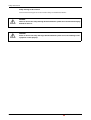
Safety warnings in this manual
In this manual warnings that are relevant for safety are identified as follows:
II
m
DANGER:
b
CAUTION:
Failure to observe the safety warnings identified with this symbol can result in health and injury
hazards for the user.
Failure to observe the safety warnings identified with this symbol can result in damage to the
equipment or other property.
MITSUBISHI ELECTRIC
Safety Information
General Safety Information and Precautions
The following safety precautions are intended as a general guideline for using PLC systems together
with other equipment. These precautions must always be observed in the design, installation and
operation of all control systems.
m
DANGER:
● Observe all safety and accident prevention regulations applicable to your specific application. Always disconnect all power supplies before performing installation and wiring work
or opening any of the assemblies, components and devices.
● Assemblies, components and devices must always be installed in a shockproof housing fitted
with a proper cover and fuses or circuit breakers.
● Devices with a permanent connection to the mains power supply must be integrated in the
building installations with an all-pole disconnection switch and a suitable fuse.
● Check power cables and lines connected to the equipment regularly for breaks and insulation
damage. If cable damage is found immediately disconnect the equipment and the cables
from the power supply and replace the defective cabling.
● Before using the equipment for the first time check that the power supply rating matches that
of the local mains power.
● Take appropriate steps to ensure that cable damage or core breaks in the signal lines cannot
cause undefined states in the equipment.
● You are responsible for taking the necessary precautions to ensure that programs interrupted by brownouts and power failures can be restarted properly and safely. In particular,
you must ensure that dangerous conditions cannot occur under any circumstances, even for
brief periods. EMERGENCY OFF must be switched forcibly, if necessary.
● EMERGENCY OFF facilities conforming to EN 60204/IEC 204 and VDE 0113 must remain fully
operative at all times and in all PLC operating modes. The EMERGENCY OFF facility reset
function must be designed so that it cannot ever cause an uncontrolled or undefined restart.
● You must implement both hardware and software safety precautions to prevent the possibility of undefined control system states caused by signal line cable or core breaks.
● When using modules always ensure that all electrical and mechanical specifications and
requirements are observed exactly.
Quick Start Guide for the MELSEC STlite Series
III
Symbols used in the manual
Use of instructions
Instructions concerning important information are marked separately and are displayed as follows:
NOTE
Text of instruction
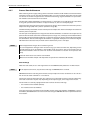
Use of numbering in the figures
Numbering within the figures is displayed by white numbers within black circles and is explained in
a table following it using the same number, e.g.:
Use of handling instructions
Handling instructions are steps that must be carried out in their exact sequence during startup, operation, maintenance and similar operations.
They are numbered consecutively (black numbers in white circles):
Text.
Text.
Text.
Use of footnotes in tables
Instructions in tables are explained in footnotes underneath the tables (in superscript). There is a footnote character at the appropriate position in the table (in superscript).
If there are several footnotes for one table then these are numbered consecutively underneath the
table (black numbers in white circle, in superscript):
IV
Text
Text
Text
MITSUBISHI ELECTRIC
Table of Contents
Contents
Safety Information
Symbols used in the manual
1
Introduction
1.1
System Configuration . . . . . . . . . . . . . . . . . . . . . . . . . . . . . . . . . . . . . . . . . . . . . . . . . . . . . . . . . . . . . . . . . .1-1
1.1.1
Components of the STlite Series. . . . . . . . . . . . . . . . . . . . . . . . . . . . . . . . . . . . . . . . . . . . . . . .1-2
1.1.2
Identification of the Modules. . . . . . . . . . . . . . . . . . . . . . . . . . . . . . . . . . . . . . . . . . . . . . . . . . .1-3
2
Profibus DP
2.1
Overview. . . . . . . . . . . . . . . . . . . . . . . . . . . . . . . . . . . . . . . . . . . . . . . . . . . . . . . . . . . . . . . . . . . . . . . . . . . . . . .2-1
2.2
Head Station STL-PB1 (Profibus DP) . . . . . . . . . . . . . . . . . . . . . . . . . . . . . . . . . . . . . . . . . . . . . . . . . . . . .2-3
2.3
2.2.1
View . . . . . . . . . . . . . . . . . . . . . . . . . . . . . . . . . . . . . . . . . . . . . . . . . . . . . . . . . . . . . . . . . . . . . . . . . .2-4
2.2.2
Device Supply . . . . . . . . . . . . . . . . . . . . . . . . . . . . . . . . . . . . . . . . . . . . . . . . . . . . . . . . . . . . . . . . .2-4
2.2.3
Display Elements . . . . . . . . . . . . . . . . . . . . . . . . . . . . . . . . . . . . . . . . . . . . . . . . . . . . . . . . . . . . . .2-5
2.2.4
Setting the Station Address . . . . . . . . . . . . . . . . . . . . . . . . . . . . . . . . . . . . . . . . . . . . . . . . . . . .2-6
2.2.5
Pin Configuration of the Profibus DP Interface . . . . . . . . . . . . . . . . . . . . . . . . . . . . . . . . . .2-6
2.2.6
Wiring. . . . . . . . . . . . . . . . . . . . . . . . . . . . . . . . . . . . . . . . . . . . . . . . . . . . . . . . . . . . . . . . . . . . . . . . .2-7
2.2.7
Local Process Image . . . . . . . . . . . . . . . . . . . . . . . . . . . . . . . . . . . . . . . . . . . . . . . . . . . . . . . . . . .2-9
2.2.8
Configuration . . . . . . . . . . . . . . . . . . . . . . . . . . . . . . . . . . . . . . . . . . . . . . . . . . . . . . . . . . . . . . . 2-16
Configuration Example for MELSEC System Q. . . . . . . . . . . . . . . . . . . . . . . . . . . . . . . . . . . . . . . . . . 2-17
2.3.1
Settings for the Slave Station. . . . . . . . . . . . . . . . . . . . . . . . . . . . . . . . . . . . . . . . . . . . . . . . . 2-17
2.3.2
Configuring the Profibus DP . . . . . . . . . . . . . . . . . . . . . . . . . . . . . . . . . . . . . . . . . . . . . . . . . 2-17
2.3.3
Saving devices. . . . . . . . . . . . . . . . . . . . . . . . . . . . . . . . . . . . . . . . . . . . . . . . . . . . . . . . . . . . . . . 2-21
Quick Start Guide for the MELSEC STlite Series
V
Table of Contents
3
CC-Link
3.1
Overview . . . . . . . . . . . . . . . . . . . . . . . . . . . . . . . . . . . . . . . . . . . . . . . . . . . . . . . . . . . . . . . . . . . . . . . . . . . . . . 3-1
3.2
Head Station STL-BT1 (CC-Link) . . . . . . . . . . . . . . . . . . . . . . . . . . . . . . . . . . . . . . . . . . . . . . . . . . . . . . . . . 3-2
3.3
View . . . . . . . . . . . . . . . . . . . . . . . . . . . . . . . . . . . . . . . . . . . . . . . . . . . . . . . . . . . . . . . . . . . . . . . . . . 3-3
3.2.2
Device Supply. . . . . . . . . . . . . . . . . . . . . . . . . . . . . . . . . . . . . . . . . . . . . . . . . . . . . . . . . . . . . . . . . 3-3
3.2.3
Display Elements . . . . . . . . . . . . . . . . . . . . . . . . . . . . . . . . . . . . . . . . . . . . . . . . . . . . . . . . . . . . . . 3-4
3.2.4
Setting the Station Address . . . . . . . . . . . . . . . . . . . . . . . . . . . . . . . . . . . . . . . . . . . . . . . . . . . . 3-5
3.2.5
Setting the Transmission Speed and Address Mode . . . . . . . . . . . . . . . . . . . . . . . . . . . . 3-6
3.2.6
Pin Configuration of the CC-Link Interface. . . . . . . . . . . . . . . . . . . . . . . . . . . . . . . . . . . . . . 3-7
3.2.7
Wiring . . . . . . . . . . . . . . . . . . . . . . . . . . . . . . . . . . . . . . . . . . . . . . . . . . . . . . . . . . . . . . . . . . . . . . . . 3-7
3.2.8
Local Process Image . . . . . . . . . . . . . . . . . . . . . . . . . . . . . . . . . . . . . . . . . . . . . . . . . . . . . . . . . . 3-10
Configuration Example for MELSEC System Q . . . . . . . . . . . . . . . . . . . . . . . . . . . . . . . . . . . . . . . . . . 3-18
3.3.1
Settings for the Master Station . . . . . . . . . . . . . . . . . . . . . . . . . . . . . . . . . . . . . . . . . . . . . . . . 3-18
3.3.2
Settings for the Slave Station . . . . . . . . . . . . . . . . . . . . . . . . . . . . . . . . . . . . . . . . . . . . . . . . . 3-19
3.3.3
Configuring the CC-Link Network . . . . . . . . . . . . . . . . . . . . . . . . . . . . . . . . . . . . . . . . . . . . . 3-19
3.3.4
Sequence Program for Initialization of the CC-Link Head Station . . . . . . . . . . . . . . . 3-21
3.3.5
Monitoring the Data Transfer . . . . . . . . . . . . . . . . . . . . . . . . . . . . . . . . . . . . . . . . . . . . . . . . . 3-22
4
Ethernet
4.1
Overview . . . . . . . . . . . . . . . . . . . . . . . . . . . . . . . . . . . . . . . . . . . . . . . . . . . . . . . . . . . . . . . . . . . . . . . . . . . . . . 4-1
4.2
Head Station STL-ETH1 (Ethernet). . . . . . . . . . . . . . . . . . . . . . . . . . . . . . . . . . . . . . . . . . . . . . . . . . . . . . . 4-1
4.3
VI
3.2.1
4.2.1
View . . . . . . . . . . . . . . . . . . . . . . . . . . . . . . . . . . . . . . . . . . . . . . . . . . . . . . . . . . . . . . . . . . . . . . . . . . 4-2
4.2.2
Device Supply. . . . . . . . . . . . . . . . . . . . . . . . . . . . . . . . . . . . . . . . . . . . . . . . . . . . . . . . . . . . . . . . . 4-3
4.2.3
Display Elements . . . . . . . . . . . . . . . . . . . . . . . . . . . . . . . . . . . . . . . . . . . . . . . . . . . . . . . . . . . . . . 4-4
4.2.4
Address Selection Switch . . . . . . . . . . . . . . . . . . . . . . . . . . . . . . . . . . . . . . . . . . . . . . . . . . . . . . 4-5
4.2.5
Hardware Address (MAC ID) . . . . . . . . . . . . . . . . . . . . . . . . . . . . . . . . . . . . . . . . . . . . . . . . . . . 4-6
4.2.6
Fieldbus Connection . . . . . . . . . . . . . . . . . . . . . . . . . . . . . . . . . . . . . . . . . . . . . . . . . . . . . . . . . . 4-6
4.2.7
Process Data Architecture . . . . . . . . . . . . . . . . . . . . . . . . . . . . . . . . . . . . . . . . . . . . . . . . . . . . . 4-7
Configuration Example for MELSEC System Q . . . . . . . . . . . . . . . . . . . . . . . . . . . . . . . . . . . . . . . . . . 4-15
4.3.1
Settings for the Master Station . . . . . . . . . . . . . . . . . . . . . . . . . . . . . . . . . . . . . . . . . . . . . . . . 4-15
4.3.2
Monitoring the Data Transfer . . . . . . . . . . . . . . . . . . . . . . . . . . . . . . . . . . . . . . . . . . . . . . . . . 4-17
4.3.3
The Web-Based Management System (WBM). . . . . . . . . . . . . . . . . . . . . . . . . . . . . . . . . . 4-18
MITSUBISHI ELECTRIC
Table of Contents
A
Appendix
A.1
Process Images. . . . . . . . . . . . . . . . . . . . . . . . . . . . . . . . . . . . . . . . . . . . . . . . . . . . . . . . . . . . . . . . . . . . . . . . . A-1
A.1.1
Digital Input Modules . . . . . . . . . . . . . . . . . . . . . . . . . . . . . . . . . . . . . . . . . . . . . . . . . . . . . . . . . A-1
A.1.2
Digital Output Modules. . . . . . . . . . . . . . . . . . . . . . . . . . . . . . . . . . . . . . . . . . . . . . . . . . . . . . . . A-1
A.1.3
Relay Output Module . . . . . . . . . . . . . . . . . . . . . . . . . . . . . . . . . . . . . . . . . . . . . . . . . . . . . . . . . . A-1
A.1.4
Analog Input Modules . . . . . . . . . . . . . . . . . . . . . . . . . . . . . . . . . . . . . . . . . . . . . . . . . . . . . . . . . A-2
A.1.5
Analog Output Modules . . . . . . . . . . . . . . . . . . . . . . . . . . . . . . . . . . . . . . . . . . . . . . . . . . . . . . . A-8
A.1.6
Encoder module STL-ENC (ID number 51205116) . . . . . . . . . . . . . . . . . . . . . . . . . . . . . .A-12
A.1.7
Counter module STL-C100 (ID number 51244881) . . . . . . . . . . . . . . . . . . . . . . . . . . . . .A-17
A.1.8
SSI Transmitter Interface STL-SSI (ID number 51205057) . . . . . . . . . . . . . . . . . . . . . . .A-18
Index
Quick Start Guide for the MELSEC STlite Series
VII
Table of Contents
VIII
MITSUBISHI ELECTRIC
System Configuration
1
Introduction
Introduction
This Quick Start Guide explains the basic procedures for the first-time use of the modules of the
MELSEC STlite series.
For additional information and a detailed mounting and wiring description of the MELSEC STlite
series, please refer to the installation manual.
1.1
System Configuration
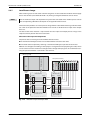
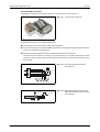
STlite is a modular, field bus independent I/O system. It is comprised of a head station and up to 64
connected modules for any type of signal. Together, these make up the field bus node. An end module
completes the node.
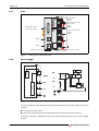
Head station
Fig. 1-1:
Digital or analog I/O modules, special function modules,
power supply modules
End module
Field bus node
Head stations are available for different field bus systems, such as Profibus DP, Ethernet TCP/IP or
CC-Link.
The head station contains the field bus interface, electronics and a power supply terminal. The field
bus interface connects the node to the relevant field bus. The electronics process the data of the I/O
modules or special function modules and make it available for the field bus communication. The 24 V
system supply and the 24 V field supply are fed in via the integrated power supply terminal.
Modules for diverse digital and analog I/O functions as well as special functions can be connected to
the head station. Populating the nodes with STlite modules is based on the requirements of the application. The communication between the head station and the bus modules is carried out via an internal bus.
STlite has a clear port level with LEDs for status indication, insertable markers and pullout group identification plate bracket. The 3-wire technology supplemented by a ground wire connection allows for
direct sensor/actuator wiring.
"ST" means "Slice Type terminal", and refers to the narrow width of the modules (only 12 mm!).
Quick Start Guide for the MELSEC STlite Series
1-1
Introduction
1.1.1
System Configuration
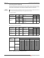
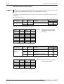
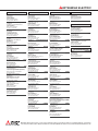
Components of the STlite Series
Type of module
Head stations
Name
ID number
Description
Profibus DP
STL-PB1
51247152
Head station for the connection to
Profibus DP
CC-Link
STL-BT1
51247154
Head station for the connection to
CC-Link
Ethernet
STL-ETH1
51247153
Head station for the connection to
Ethernet TCP/IP
STL-PS
51205036
STL-BPS
51244880
STL-DI8-V1
51205052
STL-DI8-V2
51205053
STL-DO4
51205045
4 transistor outputs, 24 V DC, 0.5 A,
source type
STL-DO8
51205043
8 transistor outputs, 24 V DC, 0.5 A,
source type
STL-RO2
51205044
2 relay outputs 230 V AC / 30V DC,
500 VA/60 W
STL-AD2-V
51205046
2 inputs 0 to 10 V
STL-AD4-V1
51205049
4 inputs 0 to 10 V
STL-AD4-V2
51205050
4 inputs –10 to 10 V
STL-AD2-I
51205047
2 inputs 4 to 20 mA
STL-AD4-I
51205051
4 inputs 4 to 20 mA
51205048
2 inputs for Pt100 resistance thermometers
Power supply modules
Digital input modules
Digital output modules
Voltage
Analog input
modules
Current
Temperature
Voltage
Analog output
modules
Current
with bus
power supply
response time
8 inputs for source type 0.2 ms
sensors, 24 V DC
response time
3.0 ms
STL-DA2-V
51205042
2 outputs 0 to 10 V
STL-DA4-V1
51205038
4 outputs 0 to 10 V
STL-DA4-V2
51205039
4 outputs –10 to 10 V
STL-DA2-I
51205041
2 outputs 4 to 20 mA
STL-DA4-I
51205040
4 outputs 4 to 20 mA
Colorless
passive
Colorless
Yellow
Red
Green
Blue
Encoder module
STL-ENC
51205116
Input module for incremental encoder
with RS422 interface
Counter module
STL-C100
51244881
Forward/reverse counter, 24 V DC,
max. frequency 100 kHz
Interface module
STL-SSI
51205057
Input module for SSI encoder
Bus end module
STL-ET
51205037
End module for the termination of the
internal bus
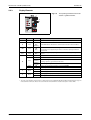
Tab. 1-1:
NOTES
STL-TI2
Power supply modules
24 V DC
Color code
Colorless
Head stations and modules of the STlite series
For the specifications of all available STlite modules please refer to the installation manual of the
STlite series.
For the process images of the modules, please refer to the appendix of this manual.
1-2
MITSUBISHI ELECTRIC
System Configuration
1.1.2
Introduction
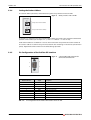
Identification of the Modules
Please note that the name of the module is not printed on the module. However, there are several
methods to identify a module.
Color coded group identification plate bracket
The pullout group marker carriers of the module offer an rough distinguishing mark.
Group identification plate brackets
Fig. 1-2:
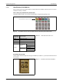
The module type can easily be recognised by the color of the group marker carrier.
Tab. 1-2:
Color of group
identification
plate brackets
Type of module
Yellow
Digital input module
Red
Digital output module
Green
Analog input module
Blue
Analog output module
Color code of the STlite series
Encoder module
Special function
module
Counter module
Interface module
Colorless
Head station
System module
Power supply module
Bus end module
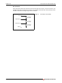
ID number of the module
The ID number, which is unique for each type of module (see table 1-1), is printed on the front side of
the modules.
Fig. 1-3:
Quick Start Guide for the MELSEC STlite Series
ID number at the front of a module
1-3
Introduction
System Configuration
Type label of the modules
A brief description is printed on the side of each module.
Fig. 1-4:
1-4
Example for a type label
MITSUBISHI ELECTRIC
Overview
Profibus DP
2
Profibus DP
2.1
Overview
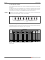
Profibus is one of the most widely used automation networks in Europe. It provides a wide possible
range of compatible devices while delivering fast and robust communication.
Profibus offers users the option to mix devices from different companies. It is an open network ranging from simple I/O stations through to complex PLCs. The network allows extremely fast data
exchange with a wide variety of slave devices.
Profibus DP (Decentralized Peripherals) is used to operate sensors and actuators via a centralized controller in production (factory) automation applications.
As this is an open network, Mitsubishi Profibus units can also be connected to master and slave
devices from other manufacturers.
1
Master
Slaves
1
7
ABCD
4
MNOP
1
YZ!?
-
8
EFGH
5
QRST
9
LIST
IJKL
ACK
RUN
6
STOP
UVWX
MAIN
PREV
2
C1-C4
0
°%#
3
<>()
_'
64
32
16
8
4
2
1
+/*=
ON
OFF
Fig. 2-1:
41 51
61 71
81 91
101 111
121 131
141 151
161 11
21
161 11
21 11
21 31
81 91
141 151
61 71
121 131
41 51
101 111
31
122 132
142 152
162 12
22
42 52
102 112
22 32
82 92
22 12
62 72
162 12
82 92
142 152
62 72
122 132
42 52
102 112
22 32
143 153
163 13
23
63 73
123 133
43 53
103 113
23 33
83 93
23 13
14
24
15
25
16
26
12
22 12
22 12
103 113
123 133
143 153
163 13
23 33
83 93
23 13
63 73
23 13
43 53
13
124 134
144 154
164 14
24
104 114
24 34
84 94
24 14
64 74
24 14
44 54
14
Typical Profibus configuration
Structure
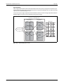
A Profibus DP system consists of a master and up to 124 slaves.
● Master: A Profibus DP Master exchanges the data with the slaves via Profibus DP and controls the
bus. It transfers the data between a supervisory control (e. g. a PLC) and the decentralized
peripheral equipment. The master cyclically reads the input data from the slaves and cyclically
writes the output data to the slaves
● Slave: Profibus DP slaves are the link to the field side. They edit the input data of the peripheral
equipment for the communication with the master and output the master data to the peripheral
equipment.
All field devices are typically connected in a line structure with up to 32 nodes (master and slaves) in
one segment. The beginning and end of each segment must be terminated with a resistor. These
resistors are usually implemented as optionally activatable in the devices or plugs. If there are more
than 32 nodes or the network span is being extended, repeaters must be used to link the networks.
Quick Start Guide for the MELSEC STlite Series
2-1
Profibus DP
Overview
Transmission speeds from 9.6 kbit/s to 12 Mbit/s can be used. The maximum cable length of a bus segment is limited from 100 to 1200 m, depending on the bit rate used. With up to 3 repeaters allowed,
the maximum distance between two stations is 400 to 4800 m.
Cable types
To help reduce costs Profibus DP uses RS 485 technology with shielded 2-wire cabling.
2-2
MITSUBISHI ELECTRIC
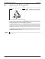
Head Station STL-PB1 (Profibus DP)
2.2
Profibus DP
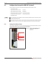
Head Station STL-PB1 (Profibus DP)
The head station STL-PB1 serves as Profibus DP slave. It displays the peripheral data of all connected
STlite modules on Profibus DP.
Fig. 2-2:
Head station STL-PB1 for Profibus DP
(with connected digital input
module)
In the initialization phase the head station determines the physical structure of the node and creates
a process image from this with all inputs and outputs. I/O modules with a bit width smaller than 8 can
be combined to form one byte in order to optimize the address space.
In addition the possibility exists to deactivate projected I/O modules. In this manner the physical
structure of the node can be individually designed with regard to the peripheral signals, without
undertaking any changes to an already existing control application. This is done by correspondingly
parametering the modules with the aid of the planning environment (for instance, GX Configurator-DP).
The diagnostics concept is based on an identification and channel based diagnostics in accordance
with EN 50170-2 (Profibus). Thus it is not necessary to program modules for the evaluation of manufacturer specific diagnostics information.
NOTE
For the specifications of the head station STL-PB1 please refer to the installation manual of the
STlite series.
Quick Start Guide for the MELSEC STlite Series
2-3
Profibus DP
2.2.1
Head Station STL-PB1 (Profibus DP)
View
PROFIBUS
RUN
BF
DIA
BUS
Profibus DP interface
(9 pin D-Sub, female)
I/O
ADDRESS
x1
24V 0V
C
D
+ +
Supply via power jumper
contacts
24 V DC
23
78
B
— —
901
Address
Status of power
supply
– System
– Power jumper contacts
Data contacts
Supply
24 V DC
0V
01 02
A
456
0V
x10
78
Address
23
9 01
456
Configuration interface
Fig. 2-3:
2.2.2
Power jumper contacts
Head station STL-PB1 (Profibus DP)
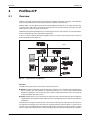
Device Supply
Fieldbus
interface
Modules
24 V
1
24 V
5
24 V /0 V
10 nF
5V
Electronics
5V
0V
2
6
24 V
Electronics
24 V
Fieldbus
interface
3
7
0V
0V
4
10 nF
8
STL-PB1
Fig. 2-4:
Block diagram for the head station STL-PB1 (Profibus DP)
The device supply is intended both for the system and the field units. Two external supply voltages are
required:
● 24 V DC for the head station
● 24 V DC for the connected STlite modules (forwarded via the power jumper contacts)
The fieldbus interface is supplied with electrically isolated voltage from the internal system supply
module.
2-4
MITSUBISHI ELECTRIC
Head Station STL-PB1 (Profibus DP)
2.2.3
Profibus DP
Display Elements
Fig. 2-5:
The operating condition of the head
station is signaled via LEDs.
A
B
LED
Color
RUN
Green
ON
BF
Red
ON
OFF
Blinking
The BF-LED indicates whether the communication functions via the Profibus.*
DIA
Red
ON
OFF
The DIA-LED indicates an external diagnostics.*
The signaling is not supported by all devices or must be explicitly enabled for
each channel.
BUS
Red
Blinking
OFF
The BUS-LED signals a projecting fault with the Profibus DP projecting of the
station.*
Green
IO
A
B
Tab. 2-1:
*
Red
Status
Description
The head station is correctly initialized.*
ON
Data cycle on the internal bus
ON
Hardware error of the head station
Blinking
앫 When starting: internal bus is initialized
앫 During operation: general internal bus fault
Blinking
cyclically
Fault message during internal bus reset and internal fault
Amber
ON
Access to the head station firmware in the Flash-EEPROM
—
OFF
No data cycle on the internal bus
ON
System supply is ok.
OFF
System supply failed.
Green
Green
ON
Field supply (power jumper contacts) is ok.
OFF
Field supply failed.
Description of the LEDs of the STL-PB1
The state of the Profibus communication is displayed by the four LEDs RUN, BF, DIA and BUS. Detailed fault messages are
indicated with a blink code. Please refer to the manual of the STL-PB1 for a detailed description of these LEDs.
Quick Start Guide for the MELSEC STlite Series
2-5
Profibus DP
2.2.4
Head Station STL-PB1 (Profibus DP)
Setting the Station Address
The station address (decimal) is determined using two rotary switches on the STL-PB1.
Fig. 2-6:
Rotary switches of the STL-PB1
ADDRESS
x1
Unit position of the address
23
78
901
456
x10
Tens position of the address
23
78
901
456
The switch “x1 “ determines the units position of the address, the switch “x10 “ determines the decimal
positions of the address (for example “x1“: 2, “x10 “: 4 -> address = 2 + 10 x 4 = 42).
Valid station addresses are between 1 and 99. The head station also permits the station address 0.
The station address is taken over by the head station after switching on the device (initialization
phase). Adjustments of the switch have no effect during operation.
2.2.5
Pin Configuration of the Profibus DP Interface
Fig. 2-7:
9
6
2-6
5
1
Pin of the
D-SUB connector
Signal
1
—
Not used
2
—
Not used
3
RXD/TXD-P
4
RTS
5
GND
6
VP
Tab. 2-2:
9-pin D-SUB female connector for
connection to Profibus DP
7
—
8
RXD/TXD-N
9
—
Description
Receive/transmit data (+)
Ready to send
Supply ground (earth)
Voltage supply
Not used
Receive/transmit data (–)
Not used
Pin configuration of the Profibus DP interface of the STL-PB1
MITSUBISHI ELECTRIC
Head Station STL-PB1 (Profibus DP)
2.2.6
Profibus DP
Wiring
Since RS 485 transmission technology is used, all devices are connected in a line structure. To connect
the STL-PB1 to a Profibus DP network, use only the Profibus connector and shielded twisted pair Profibus cable complying with EN50170. Cable type A is strongly recommended.
Parameter
Specification
Wave resistance
Tab. 2-3: Specifications for cable type A
135 to 165
Capacitance per unit
30 pF/m
Loop resistance
110 /km
Core diameter
0.64 mm
Core cross section
0.34 mm2
The maximum line length for a bus segment depends on the transmission speed.
b
Transmission speed
Max. bus segment
length
9.6 / 19.2 / 45.45 / 93.75 kbit/s
1200 m
187.5 kbit/s
1000 m
500 kbit/s
400 m
1.5 Mbit/s
200 m
3 / 6 / 12 Mbit/s
100 m
Tab. 2-4: Max. bus segment length
CAUTION:
When the Profibus cable is laid, do not lay it close to main circuits or power lines.
They should be installed 100 mm (3.9 inch) or more from each other. Not doing so could result
in noise that would cause malfunctioning.
When connecting the nodes, ensure that the data cables are not mixed up. To achieve high interference resistance of the system against electromagnetic radiation, a shielded data cable (type A is
shielded) should definitely be used. The shielding is to be connected to the protective ground on
both sides ensuring good conductivity via large area shield clamps. Equipotential bonding of all connected field devices is also recommended.
Stubs must absolutely be avoided with transmission rates greater than or equal to 1.5 MBit/s.
Fig. 2-8:
Connection of the Profibus cable
From Profibus node
Profibus node
(e. g. STL-PB1)
3
RXD/TXD-P
8
RXD/TXD-N
To Profibus node
Quick Start Guide for the MELSEC STlite Series
2-7
Profibus DP
Head Station STL-PB1 (Profibus DP)
Bus Terminator
Each end of the Profibus DP network must be terminated with resistors. Since the STL-PB1 is not
equipped with built-in terminating resistors, use a Profibus connector with a bus terminator if the
STL-PB1 is situated at the beginning or end of a network.
Fig. 2-9:
Termination of the Profibus
VP (6)
390 2%
min 1/4 W
RXD/TXD-P (3)
220 2%
min 1/4 W
RXD/TXD-N (8)
390 2%
min 1/4 W
GND (5)
2-8
MITSUBISHI ELECTRIC
Head Station STL-PB1 (Profibus DP)
2.2.7
Profibus DP
Local Process Image
After switching on, the head station STL-PB1 recognizes all connected STlite modules which supply
data or wait for data (data width/bit width > 0). Analog and digital I/O modules can be mixed.
NOTE
For the number of input and output bits or bytes of the connected STlite modules please refer to
the corresponding I/O module description in the appendix of this manual.
The head station produces an internal process image from the data width and the type of STlite module as well as the position of the STlite modules in the node. It is divided into an input and an output
data area.
The data of the STlite modules is separated for the local input and output process image in the
sequence of their position after the head station.
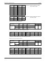
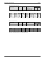
Allocation of the Input and Output Data
The process data is exchanged via the Profibus with the master.
● A maximum of 244 bytes of data is transmitted from the master to the node.
● The head station responds by returning a maximum of 244 bytes input data to the master.
Modules are configured according to their physical arrangement when projecting the node, which
can be taken over from a hardware catalogue of the configuration programs. The information covering the possible modules is contained in the GSD files.
Master (e.g. PLC)
Master
addresses
Inputs
STL-PB1
CPU
Profibus module
Slave (STlite modules)
Allocation list
Inputs
Allocation list
Inputs
Inputs
Inputs
Outputs
Outputs
Profibus
Outputs
Outputs
Outputs
Profibus
Byte orientated allocation
generated on a PC
Bit and byte orientated allocation generated automatically
by the STL-PB1
Fig. 2-10: Allocation of input and output data
Quick Start Guide for the MELSEC STlite Series
2-9
Profibus DP
Head Station STL-PB1 (Profibus DP)
Process Data Structure for Profibus DP
With some I/O modules, the structure of the process data is fieldbus specific. Depending on how the
head station is parameterized, the status bytes (S), control bytes (C) and data bytes (D0...Dn) of the
byte or word orientated modules are transmitted via Profibus in Motorola or Intel format.
NOTE
For the meaning of input and output bits or bytes of the connected STlite modules please refer to
the corresponding I/O module description in the appendix of this manual.
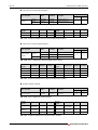
● Digital I/O modules
Process Image [Bit]
Type of module
Digital input modules
Digital output
modules
Tab. 2-5:
Name
ID number
STL-DI8-V1
51205052
STL-DI8-V2
51205053
Description
8 inputs for source type sensors, 24 V DC
Input
Output
8
0
8
0
0
4
STL-DO4
51205045
4 transistor outputs, 24 V DC, 0.5 A,
source type
STL-DO8
51205043
8 transistor outputs, 24 V DC, 0.5 A,
source type
0
8
STL-RO2
51205044
2 relay outputs 230 V AC / 30V DC,
500 VA/60 W
0
2
Profibus DP process data of digital input and output modules
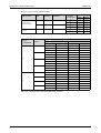
● Two-channel analog input modules
Type of module
Name
ID number
Register
communication
Description
Analog input module
(voltage)
STL-AD2-V
51205046
2 inputs 0 to 10 V
Analog input module
(current)
STL-AD2-I
51205047
2 inputs 4 to 20 mA
Analog input module
(temperature)
STL-TI2
51205048
2 inputs for Pt100
resistance
thermometers
Tab. 2-6:
Process Image [Byte]
Input
Output
Yes
6
6
No
4
0
Yes
6
6
No
4
0
Yes
6
6
No
4
0
Profibus DP process data of two-channel analog input modules
Data type
Register
communication
Channel
1
Yes
2
1
No
2
Tab. 2-7:
2 - 10
MOTOROLA
INTEL
Input
Output
Input
Output
S0
C0
S0
C0
D1
D1
D0
D0
D0
D0
D1
D1
S1
C1
S1
C1
D3
D3
D2
D2
D2
D2
D3
D3
D1
—
D0
—
D0
—
D1
—
D3
—
D2
—
D2
—
D3
—
Mapping for two-channel analog input modules
MITSUBISHI ELECTRIC
Head Station STL-PB1 (Profibus DP)
Profibus DP
● Four-channel analog input modules
Type of module
Name
ID number
Register
communication
Description
STL-AD4-V1
51205049
4 inputs 0 to 10 V
STL-AD4-V2
51205050
4 inputs –10 to 10 V
STL-AD4-I
51205051
4 inputs 4 to 20 mA
Analog input modules
(voltage)
Analog input module
(current)
Tab. 2-8:
Process Image [Byte]
Input
Output
Yes
12
12
No
8
0
Yes
12
12
No
8
0
Yes
12
12
No
8
0
Profibus DP process data of four-channel analog input modules
Data type
Register
communication
Channel
1
2
Yes
3
4
1
2
No
3
4
Tab. 2-9:
MOTOROLA
INTEL
Input
Output
Input
Output
S0
C0
S0
C0
D1
D1
D0
D0
D0
D0
D1
D1
S1
C1
S1
C1
D3
D3
D2
D2
D2
D2
D3
D3
S2
C2
S2
C2
D5
D5
D4
D4
D4
D4
D5
D5
S3
C3
S3
C3
D7
D7
D6
D6
D6
D6
D7
D7
D1
—
D0
—
D0
—
D1
—
D3
—
D2
—
D2
—
D3
—
D5
—
D4
—
D4
—
D5
—
D7
—
D6
—
D6
—
D7
—
Mapping for four-channel analog input modules
Quick Start Guide for the MELSEC STlite Series
2 - 11
Profibus DP
Head Station STL-PB1 (Profibus DP)
● Two-channel analog output modules
Type of module
Name
ID number
Register
communication
Description
Analog output module
STL-DA2-V
(voltage)
51205042
2 outputs 0 to 10 V
Analog output module
STL-DA2-I
(current)
51205041
2 outputs 4 to 20 mA
Process Image [Byte]
Input
Output
Yes
6
6
No
0
4
Yes
6
6
No
0
4
Tab. 2-10: Profibus DP process data of two-channel analog output modules
Data type
Register
communication
Channel
1
Yes
2
1
No
2
MOTOROLA
INTEL
Input
Output
Input
Output
S0
C0
S0
C0
D1
D1
D0
D0
D0
D0
D1
D1
S1
C1
S1
C1
D3
D3
D2
D2
D2
D2
D3
D3
—
D1
—
D0
—
D0
—
D1
—
D3
—
D2
—
D2
—
D3
Tab. 2-11: Mapping for two-channel analog output modules
2 - 12
MITSUBISHI ELECTRIC
Head Station STL-PB1 (Profibus DP)
Profibus DP
● Four-channel analog output modules
Type of module
Name
ID number
Register
communication
Description
STL-DA4-V1
51205038
4 outputs 0 to 10 V
STL-DA4-V2
51205039
4 outputs –10 to 10 V
51205040
4 outputs 4 to 20 mA
Analog output
modules (voltage)
Analog output module
STL-DA4-I
(current)
Process Image [Byte]
Input
Output
Yes
12
12
No
0
8
Yes
12
12
No
0
8
Yes
12
12
No
0
8
Tab. 2-12: Profibus DP process data of four-channel analog output modules
Data type
Register
communication
Channel
1
2
Yes
3
4
1
2
No
3
4
MOTOROLA
INTEL
Input
Output
Input
Output
S0
C0
S0
C0
D1
D1
D0
D0
D0
D0
D1
D1
S1
C1
S1
C1
D3
D3
D2
D2
D2
D2
D3
D3
S2
C2
S2
C2
D5
D5
D4
D4
D4
D4
D5
D5
S3
C3
S3
C3
D7
D7
D6
D6
D6
D6
D7
D7
—
D1
—
D0
—
D0
—
D1
—
D3
—
D2
—
D2
—
D3
—
D5
—
D4
—
D4
—
D5
—
D7
—
D6
—
D6
—
D7
Tab. 2-13: Mapping for four-channel analog output modules
Quick Start Guide for the MELSEC STlite Series
2 - 13
Profibus DP
Head Station STL-PB1 (Profibus DP)
● Encoder module STL-ENC
Type of module
Name
Encoder module
STL-ENC
ID number
Register
communication
Description
Input module for
incremental encoder
51205116
Process Image [Byte]
Input
Output
Yes
6
6
No (not possible)
—
—
Tab. 2-14: Profibus DP process data of the encoder module
Data type
Register
communication
Yes
Channel
1
MOTOROLA
INTEL
Input
Output
Input
Output
S0
C0
S0
C0
D1
D1
D0
D0
D0
D0
D1
D1
S1
C1
S1
C1
D3
D3
D2
D2
D2
D2
D3
D3
Tab. 2-15: Mapping for encoder module STL-ENC
● Counter module STL-C100
Type of module
Name
Counter module
STL-C100
ID number
Register
communication
Description
Forward/reverse
counter, max. frequency 100 kHz
51244881
Process Image [Byte]
Input
Output
Yes
6
6
No (not possible)
—
—
Tab. 2-16: Profibus DP process data of the counter module
Data type
Register
communication
Yes
Channel
1
MOTOROLA
INTEL
Input
Output
Input
Output
S
C
S
C
—
—
—
—
D3
D3
D0
D0
D2
D2
D1
D1
D1
D1
D2
D2
D0
D0
D3
D3
Tab. 2-17: Mapping for counter module STL-C100
2 - 14
MITSUBISHI ELECTRIC
Head Station STL-PB1 (Profibus DP)
Profibus DP
● SSI interface module
Type of module
Name
Interface module
STL-SSI
ID number
51205057
Register
communication
Description
Input module for SSI
encoder
Process Image [Byte]
Input
Output
Yes
6
6
No
4
0
Tab. 2-18: Profibus DP process data of the interface module STL-SSI
Data type
Register
communication
Yes
(Alternative
format, factory
setting)
Yes
(Standard format)
No
Channel
1
1
1
MOTOROLA
INTEL
Input
Output
Input
Output
S0
C0
S0
C0
D1
D1
D0
D0
D0
D0
D1
D1
—
—
—
—
D3
D3
D2
D2
D2
D2
D3
D3
S0
C0
S0
C0
—
—
—
—
D3
D3
D0
D0
D2
D2
D1
D1
D1
D1
D2
D2
D0
D0
D3
D3
D3
—
D0
—
D2
—
D1
—
D1
—
D2
—
D0
—
D3
—
Tab. 2-19: Mapping for interface module STL-SSI
Quick Start Guide for the MELSEC STlite Series
2 - 15
Profibus DP
2.2.8
Head Station STL-PB1 (Profibus DP)
Configuration
Configuration of the I/O Modules
The configuration of the node is performed in accordance with the physical requirements of the head
station and I/O modules.
The head station or the process data channel is to be configured on the first slot. The other slots are
configured in accordance with the physical requirements of the I/O modules. Here only I/O modules
with process data are relevant. The supply modules, bus internal system supply module and the bus
end module are to be ignored for the configuration because they do not provide any process data.
One or two modules are entered in the hardware catalogue for each I/O module.
The module appear as "name/ID number/type/specifications", for example:
STL-DO4/51205045/4DO/24V/0.5 A.
In the hardware catalogue of GX Configurator-DP you will find the entries *STL-DO4 and *STL-RO2.
When using these denominations the head station adds the binary information of the current module
in a byte which was previously opened with a STL-D04 respectively a STL-RO2. The use of "*" is only
permitted when the number of outputs is less than or equal to the remaining bits in the previously
opened byte. The binary I/O modules combined in a byte can be arranged at separate locations, i.e.
binary I/O modules with a different signal type or also byte orientated I/O modules can be connected
between.
In order to be able to individually arrange the scope of connected periphery units independent of the
control program, it is possible to parameterize I/O modules in the configuration table as "not
plugged". In this manner process data still present is filtered for the individual module and not transferred on the Profibus DP to and read by the periphery units.
GSD Files
Under Profibus DP the features of the modules are defined by the manufacturers in the form of a GSD
file (General Station Description).
Structure, content and coding of this unit main data are standardized and made available to the user
allowing to project optional DP slaves using the project units of various manufacturers.
The GSD file is read by the configuration software and the corresponding settings are transmitted. For
the necessary inputs and handling steps please refer to user manual of the FX Configurator DP or GX
Configurator DP.
The GSD files for the STlite series can be downloaded from the following web-site:
– http://www.mitsubishi-automation.com
Menu "MyMitsubishi" 씮 (Login) 씮 "Downloads" 씮 "GSD files"
2 - 16
MITSUBISHI ELECTRIC
Configuration Example for MELSEC System Q
2.3
Profibus DP
Configuration Example for MELSEC System Q
For this example, a Profibus DP slave consisting of the following STlite modules is used:
– Head station STL-PB1
– Digital input module STL-DI8-V1
(8 inputs)
– Digital output module STL-DO4
(4 outputs)
– Analog output module STL-DA4-V1 (4 channels, 0 to 10 V)
– Analog input module STL-AD2-V
(2 channels, 0 to 10 V)
– End module STL-ET
NOTES
For the specifications of the modules and the installation procedures please refer to the installation manual of the STlite series.
STlite modules with power contacts (male contacts) cannot be linked to modules with fewer
power contacts. In this case install a power supply module between the two relevant modules.
2.3.1
Settings for the Slave Station
For this example, the station address of the STL-PB1 is set to "1" (switch x1 = 1, switch x10 = 0, please
refer to section 2.2.4).
2.3.2
Configuring the Profibus DP
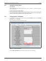
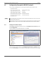
Start the Profibus configuration tool GX Configurator-DP. In the Project menu, click on New. Select
the MELSEC System Q and the corresponding Profibus DP master module.
Don‘t modify the default settings at the next screens. Leave also the device addresses unchanged
("D1000" for input data and "D2000" for output data).
Select Consistency for the data transfer and Data transfer only as shown in the following figure.
Fig. 2-11: Settings for input and output data
Quick Start Guide for the MELSEC STlite Series
2 - 17
Profibus DP
Configuration Example for MELSEC System Q
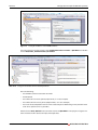
Next, add the GSD files for the MELSEC STlite series to your project (Import Task -> Add GSD files).
Configure a slave station with the STL-PB1 and the STlite I/O modules in the order listed above. Again,
leave all default settings unchanged.
Fig. 2-12: Slave configuration
After wiring the Profibus DP network, downloading the configuration to the PLC and starting the
Profibus DP communication (set Y0 of the master module QJ71PB92V to "1"), you can monitor the
data transfer in the Device Monitor of GX Works2.
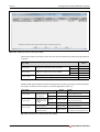
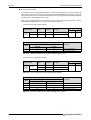
Slot 1: STL-DI8-V1
Slot 4: STL-AD2-V (Channel 1)
Slot 4: STL-AD2-V (Channel 2)
Not used
Slot 2: STL-DO4
Slot 3: STL-DA4-V1 (Channel 1)
Slot 3: STL-DA4-V1 (Channel 2)
Slot 3: STL-DA4-V1 (Channel 3)
Slot 3: STL-DA4-V1 (Channel 4)
Not used
Fig. 2-13: Allocation of the input and output data for this example
As can be seen in the above picture, the input respectively output data of one analog module channel
is spread across two data registers. This is very unfavourable for the programming. The reason for this
is the single byte occupied by each of the digital I/O modules.
2 - 18
MITSUBISHI ELECTRIC
Configuration Example for MELSEC System Q
Profibus DP
Optimising the configuration
The input and output data of the analog modules can be shifted by adding one additional digital
module for each data direction.
But you don‘t have to buy two modules just to simplify the programming – these two modules are
only virtual!
Insert a digital input module with 8 inputs on slot 2 and another digital output module on slot 4.
New module
New module
Fig. 2-14: New configuration with two dummy modules
When a module is added to the configuration, the module parameters can be set. Select "... not
plugged" for both modules.
Fig. 2-15: The new digital input module on slot 2 is "physically not plugged".
Fig. 2-16: The additional digital output module on slot 4 is also "not plugged".
Quick Start Guide for the MELSEC STlite Series
2 - 19
Profibus DP
Configuration Example for MELSEC System Q
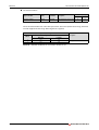
Slot 1: STL-DI8-V1
Slot 2: STL-DI8-V2 (Dummy)
Slot 6: STL-AD2-V (Channel 1)
Slot 6: STL-AD2-V (Channel 2)
Slot 3: STL-DO4
Slot 4: STL-DO4 (Dummy)
Slot 5: STL-DA4-V1 (Channel 1)
Slot 5: STL-DA4-V1 (Channel 2)
Slot 5: STL-DA4-V1 (Channel 3)
Slot 5: STL-DA4-V1 (Channel 4)
Not used
Fig. 2-17: Optimised allocation of the input and output data
For the process images of the individual STlite modules please refer to the appendix, section A.1. For
example, reading a value of 16384 (4000H) from D1001 means that a voltage of 5.00 V is applied to
channel 1 of the STL-AD2-V or, if you want to output 10 V on channel 1 of the STL-DA4-V1, write 32760
(7FF8H) to D2001.
Rearrangement of the Modules
Another option for this example to allocate 16 bit input and output data to a single data register is to
mount first the analog modules and afterwards the digital modules.
Analog modules
Digital modules
Fig. 2-18: Configuration with analog modules mounted first
The device monitor for this configuration is shown on the next page.
2 - 20
MITSUBISHI ELECTRIC
Configuration Example for MELSEC System Q
Profibus DP
Slot 2: STL-AD2-V (Channel 1)
Slot 2: STL-AD2-V (Channel 2)
Slot 3: STL-DI8-V1
Not used
Slot 1: STL-DA4-V1 (Channel 1)
Slot 1: STL-DA4-V1 (Channel 2)
Slot 1: STL-DA4-V1 (Channel 3)
Slot 1: STL-DA4-V1 (Channel 4)
Slot 4: STL-DO4
Not used
Fig. 2-19: Device monitor for the configuration with the analog modules mounted first
2.3.3
Saving devices
A digital output module with less than eight outputs (STL-DO4 or STL-RO2) will occupy a whole byte
although only two or four bits are used. (See allocation for the digital output module STL-DO4 in the
above figure.)
When, for example, another STL-DO4 is used in the configuration, this module can be entered as
*STL-DO4. The four bits belonging to this module will be entered in the same byte as the data for the
previous STL-DO4. Since the byte is now complete, any other STL-DO4 has to be entered as STL-DO4.
This STL-DO4 occupies the bits 3 to 0 of byte n.
This STL-DO4 occupies the bits 7 to 4 of byte n.
This STL-DO4 occupies the bits 3 to 0 of byte n+1.
Fig. 2-20: The amount of used devices is reduced when the denomination "*" is used.
Quick Start Guide for the MELSEC STlite Series
2 - 21
Profibus DP
2 - 22
Configuration Example for MELSEC System Q
MITSUBISHI ELECTRIC
Overview
CC-Link
3
CC-Link
3.1
Overview
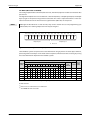
The open fieldbus and control network CC-Link (Control & Communication Link) provides fast data
communications with different devices. As with all manufacturer specific networks, CC-Link is quickly
implemented and is guaranteed to work. CC-Link is also an open network and therefore allows many
third-party products now appearing on the market with CC-Link connectivity.
1
Master
Slave stations
Fig. 3-1:
Typical CC-Link configuration
Structure
A CC-Link system consists of a master and up to 64 slave stations.
● Master: The master has the control information (parameters) and controls the entire network.
One Master station is required in each network. The station number is fixed to 0.
● Slave: The CC-Link slaves are the link to the field side. They edit the input data of the peripheral
equipment for the communication with the master and output the master data to the peripheral
equipment.
● Station: A station is a device that is connected via the CC-Link. Station numbers from 1 to 64 can
be assigned.
● Remote device station: A station that can use bit data and word data (Example: Digital and
analog I/O modules).
● Remote I/O station: A station that can only use bit data (Example: Digital I/O modules)
Transmission speeds from 156 kbit/s to 10 Mbit/s can be used. The maximum transmission distance
is limited from 100 to 1200 m, depending on the bit rate used.
Cable types
The data communications requires standardized shielded twisted-pair cable with 3 wires.
Quick Start Guide for the MELSEC STlite Series
3-1
CC-Link
3.2
Head Station STL-BT1 (CC-Link)
Head Station STL-BT1 (CC-Link)
The head station STL-BT1 is used in a remote station or a remote I/O station on CC-Link. It displays the
peripheral data of all connected STlite modules to the CC-Link.
Fig. 3-2:
Head station STL-BT1 for CC-Link
(with connected digital input
module)
The head station determines the physical structure of the node and automatically creates a local process image from this with all inputs and outputs. This could involve a mixed arrangement of analog
(word by word data exchange) and digital (byte by byte data exchange) modules.
The data of the analog modules are mapped into the process image according to the order of their
position downstream of the head station.
The bits of the digital modules are compiled to form bytes and also mapped into the process image
attached to the data of the analog modules. Should the number of digital I/Os exceed 8 bits, the head
station automatically starts another byte.
The process image is subdivided into an input and output data area. The process data can be read in
via CC-Link and further processed in a control system. The process output data is sent via CC-Link.
The STL-BT1 can occupy up to four stations.
NOTE
3-2
For the specifications of the head station STL-BT1 please refer to the installation manual of the
STlite series.
MITSUBISHI ELECTRIC
Head Station STL-BT1 (CC-Link)
3.2.1
CC-Link
View
CC-Link
L RUN
L ERR
SD
RD
CC-Link interface
(9 pin D-Sub, female)
I/O
78
456
78
456
78
23
456
Address
901
A
B
24V 0V
C
D
+ +
Supply via power jumper
contacts
24 V DC
— —
0V
901
23
Address
901
23
Transmission speed and
Address mode
Status of power
supply
– System
– Power jumper contacts
Data contacts
Supply
24 V DC
0V
01 02
PE PE
x1
x10
Power jumper contacts
Configuration interface
Fig. 3-3:
3.2.2
Head station STL-BT1 (CC-Link)
Device Supply
Fieldbus
interface
Modules
24 V
1
24 V
5
24 V /0 V
10 nF
5V
Electronics
5V
0V
2
6
24 V
Electronics
24 V
3
Fieldbus
interface
7
0V
0V
4
10 nF
8
STL-BT1
Fig. 3-4:
Block diagram for the head station STL-BT1 (CC-Link)
The device supply is intended both for the system and the field units. Two external supply voltages are
required:
● 24 V DC for the head station
● 24 V DC for the connected STlite modules (forwarded via the power jumper contacts)
The fieldbus interface is supplied with electrically isolated voltage from the internal system supply
module.
Quick Start Guide for the MELSEC STlite Series
3-3
CC-Link
3.2.3
Head Station STL-BT1 (CC-Link)
Display Elements
Fig. 3-5:
The operating condition of the head
station is signalled via LEDs.
A
C
LED
Color
Status
L.RUN
Green
ON
Data link is being executed.*
L.ERR
Red
ON
Communication error (host).*
SD
Green
ON
Data is being transmitted.*
RD
Green
ON
Data is being received.*
ON
Node operation*
Green
IO
Red
A
B
Tab. 3-1:
*
3-4
Green
Green
Flickering
Blinking
Blinking
ON
Description
Switch type setting was changed while power was ON.*
Waiting for initial data*
앫 Start up
앫 Faults occurring*
System supply is ok.
OFF
System supply failed.
ON
Field supply (power jumper contacts) is ok.
OFF
Field supply failed.
Description of the LEDs of the STL-BT1
The state of the CC-Link communication is displayed by the four LEDs L.RUN, L.ERR, SD and RD. Detailed fault messages
are indicated with a blink code of the IO LED. Please refer to the manual of the STL-BT1 for a detailed description of these
LEDs.
MITSUBISHI ELECTRIC
Head Station STL-BT1 (CC-Link)
3.2.4
CC-Link
Setting the Station Address
The station address (decimal) is determined using two rotary switches on the STL-BT1.
Fig. 3-6:
Rotary switches of the STL-BT1
Unit position of the address
Tens position of the address
The switch “x1“ determines the units position of the address, the switch “x10“ determines the decimal
positions of the address (for example “x1“: 2, “x10“: 3 -> address = 2 + 10 x 3 = 32).
A valid CC-Link station address can be set within the range from 1 to 64.
The setting is only read during the power up sequence. Changing the switch position during operation does not change the configuration of the head station. Turn off and on the power supply for the
head station to accept the changing.
Rules for CC-Link station numbers:
● Set station number in sequence .
● The station numbers can be set regardless of the order in which stations are connected.
● Do not duplicate station numbers.
● Specify unoccupied station numbers as reserved stations.
Quick Start Guide for the MELSEC STlite Series
3-5
CC-Link
3.2.5
Head Station STL-BT1 (CC-Link)
Setting the Transmission Speed and Address Mode
The STL-BT1 supports five different transmission speeds and two address modes (fixed address mode
and auto address mode).
In auto address mode the head station determines the number of addresses (numbers of occupied
stations) according to the connected STlite modules (one to four addresses per head station).
In fixed address mode the head station sets the number of occupied stations to four irrespective to
the connected STlite modules.
NOTE
Number of units and number of stations:
The number of units is the number of devices that are physically connected to a single CC-Link.
The number of stations is the total number of occupied stations among all slave stations that are
connected via the CC-Link. One unit can occupy up to four station numbers.
Fig. 3-7:
Transmission speed and address
mode selector switch of the STL-BT1
Position of the selector switch
Transmission speed
Fixed address mode
(STL-BT1 occupies 4 stations)
Auto address mode
(STL-BT1 occupies 1 to 4 stations)
156 kbit/s
0
5
625 kbit/s
1
6
2.5 Mbit/s
2
7
5 Mbit/s
3
8
10 Mbit/s
4
9
Tab. 3-2:
3-6
Selection of transmission speed and address mode
MITSUBISHI ELECTRIC
Head Station STL-BT1 (CC-Link)
3.2.6
CC-Link
Pin Configuration of the CC-Link Interface
9-pin D-SUB female connector for
connection to CC-Link
Tab. 3-3:
Pin configuration of the CC-Link
interface of the STL-BT1
5
9
6
3.2.7
Fig. 3-8:
1
Pin of the
D-SUB connector
Signal
1
—
2
—
3
DA
Data A
4
DG
Data ground
5
—
6
—
7
—
8
DB
Data B
9
—
Not used
Housing
SLD
Description
Not used
Not used
Shield
Wiring
Maximum overall cable distance
Master station
Remote station
Remote station
Remote station
Remote station
Station to station cable
length
Maximum overall cable distance
Fig. 3-9:
Definition of cable length
Transmission speed
Maximum overall cable distance
1200 m
625 kbit/s
900 m
2.5 Mbit/s
Tab. 3-4:
Station to station cable length
156 kbit/s
20 cm
400 m
5 Mbit/s
160 m
10 Mbit/s
100 m
The maximum overall cable distance depends on the transmission speed
Quick Start Guide for the MELSEC STlite Series
3-7
CC-Link
Head Station STL-BT1 (CC-Link)
CC-Link Dedicated Cable
Use the CC-Link dedicated cable for the CC-Link system. If a cable other than the CC-Link dedicated
cable is used, the performance of the CC-Link system cannot be guaranteed.
If you have any questions regarding the CC-Link dedicated cable or CC-Link in general, visit the
CC-Link Partner Association homepage http://www.cclink.org/.
NOTE
For details, refer to the CC-Link cable wiring manual issued by CC-Link Partner Association
Connection to CC-Link
– The master module can be situated anywhere in the network.
– Star connection is not allowed.
– Make a daisy chain without drops.
– Each end of a CC-Link network must be terminated with a resistor.
– Use the fieldbus connector STL-CClink con for connection to the D-SUB connector of the head
station STL-BT1 (see next page).
Master
Slave
Slave
DA
DA
DA
DB
DB
DB
DG
DG
DG
110
Terminal
resistor
110
SLD
CC-Link dedicated cable
FG
SLD
CC-Link dedicated cable
FG
Terminal
resistor
SLD
FG
Fig. 3-10: Wiring of a CC-Link network
NOTE
b
3-8
Connect the shielded wire of the CC-Link dedicated cable to “SLD“ of each device, and ground
both ends of the shielded wire.
CAUTION:
When the CC-Link cable is laid, do not lay it close to main circuits or power lines.
They should be installed 100 mm (3.9 inch) or more from each other. Not doing so could result
in noise that would cause malfunctioning.
MITSUBISHI ELECTRIC
Head Station STL-BT1 (CC-Link)
CC-Link
CC-Link Fieldbus Connector
The fieldbus connector STL-CClink con connects a CC-Link device to a CC-Link line.
Fig. 3-11: Connector STL-CClink con
The fieldbus connector has the following features:
● Two horizontal cable entries (One input and one output).
● Fast and maintenance-free CAGE CLAMP쏐 connection, can be held in the open position with the
help of an actuation slide mechanism.
● Externally operable switch to activate or deactivate the terminating resistor.
For the first and last station on the bus, the switch must be set to “ON“ (terminating resistor
activated). Set the switch to “OFF“ for the intermediate stations on the bus (terminating resistor
deactivated).
Fig. 3-12: Internal wiring of the connector
STL-CClink con
DA
DB
DG
DA
DB
DG
36 mm
5–6 mm
Fig. 3-13: Required preparation of the CC-Link
cable for connection to the connector
STL-CClink con
10 mm
Quick Start Guide for the MELSEC STlite Series
3-9
CC-Link
3.2.8
Head Station STL-BT1 (CC-Link)
Local Process Image
After switching on, the head station STL-BT1 recognizes all connected STlite modules which supply
data or wait for data (data width/bit width > 0). Analog and digital I/O modules can be mixed.
The head station produces an internal process image from the data width and the type of STlite module as well as the position of the STlite modules in the node. It is divided into an input and an output
data area.
The data of the digital STlite modules are bit orientated, i.e. the data exchange is made bit for bit. The
analog and special function STlite modules are all byte orientated modules, i.e. modules where the
data exchange is made byte for byte.
NOTE
For the number of input and output bits or bytes of the connected STlite modules please refer to
the corresponding I/O module description in the appendix of this manual.
The data of the STlite I/O modules are separated for the local input and output process image in the
sequence of their position after the head station in the individual process image.
In the respective I/O area, first of all analog modules are mapped, then all digital modules, even if the
order of the connected analog and digital modules does not comply with this order. The bits of the
digital modules are grouped, each of these groups having a data width of 1 byte. Should the number
of digital I/Os exceed 8 bits, the head station automatically starts another byte.
NOTE
A process image restructuring may result if a node is changed or extended. In this case the process
data addresses also change in comparison with earlier ones. In the event of adding a module, take
the process data of all previous modules into account.
Address Area per Station
The areas shown in the following table are allocated for the remote I/O (RX/RY: bit devices) and remote
registers (RWw/RWr: word devices) by the master station, depending on the number of occupied stations.
NOTE
Sixteen points of the remote I/O are reserved for the system.
Number of occupied stations
Type of data
Remote input: RX Remote output: RY Remote registers
Total
3 - 10
2
3
4
64 points
96 points
128 points
User area
16 points
48 points
80 points
112 points
Total
32 points
64 points
96 points
128 points
User area
16 points
48 points
80 points
112 points
4 points
8 points
12 points
16 points
4 points
8 points
12 points
16 points
RWr
RWw
Tab. 3-5:
1
32 points
The size of the address area depends on the number of occupied stations
RX: Inputs from digital input modules
RY: Outputs to digital output modules
RWr: Input data from analog modules or special function modules (e. g. counter)
RWw: Output data to analog modules or special function modules
MITSUBISHI ELECTRIC
Head Station STL-BT1 (CC-Link)
CC-Link
The position of the remote I/O system area is shown in the following table.
Number of occupied stations
RX / RY
1
00 to 0F
User area
10 to 1F
System area
2
User area
System area
30 to 3F
50 to 5F
Cannot be used
Cannot be used
60 to 6F
User area
System area
Cannot be used
70 to 7F
Tab. 3-6:
4
User area
20 to 2F
40 to 4F
3
System area
User areas and system areas
Quick Start Guide for the MELSEC STlite Series
3 - 11
CC-Link
Head Station STL-BT1 (CC-Link)
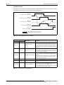
Initial Data Transfer
After power-on or hardware reset, the head station STL-BT1 requests its initial data (i.e. the system bits
for fault behaviour) from the master station as described below.
RX(n+1)8
Initial data processing request
RY(n+1)8
Initial data processing complete
RX(n+1)9
Initial data setting complete
RY(n+1)9
Initial data setting request
RX(n+1)B
Remote station READY
Executed by the sequence program
Executed by the head station STL-BT1
Fig. 3-14: Timing diagram of the system flags
Remote device
Input
Output
RX(n+1)8
RY(n+1)8
RY(n+1)9
RX(n+1)B
Tab. 3-7:
3 - 12
Description
Initial data processing
request
After the power is turned on or after the hardware reset, the
initial data processing request flag is turned on by the head
station STL-BT1 in order to request the initial data setting.
It is turned off when the initial data processing is complete
(When the initial data processing complete flag RY(n+1)8 is
turned on).
After the power is turned on or after the hardware reset, the
Initial data processing com- initial data processing complete processing is executed by
the initial data processing request, and this flag is turned on
plete
after the processing is completed.
When there is an initial data setting request (i.e. RY(n+1)9 is
turned on), this flag is turned on by the initial data setting
completion.
Initial data setting complete
When the initial data setting request flag is turned off after
the initial data setting completion, the initial data setting
complete flag is also turned off.
RX(n+1)9
RX(n+1)A
Signal name
Initial data setting request
This flag is turned on to set or modify the initial data.
Error status
This flag is turned on when an error occurs in the head station
STL-BT1.
Remote station READY
This is turned on when the initial data setting is complete and
the head station STL-BT1 is in the READY status, after the
power is turned on or after the hardware reset.
It is turned off during the test mode. (This is used to interlock
the read and write from the master module.)
Remote devices for initialization
MITSUBISHI ELECTRIC
Head Station STL-BT1 (CC-Link)
CC-Link
Data Exchange
After mapping the I/O-data of the STlite I/O modules to the local process image the head station cyclically transfers the digital input data from the process image to the Remote I/O area and the analog
input data to the Remote Register area.
In the same way the digital output data from the Remote I/O area and the analog output data from the
Remote Register area to the are transferred to the process image.
Head station STL-BT1 (CC-Link)
CC-Link address area
Remote I/O
Inputs
Outputs
Memory area for
input data
Word 0
I/O modules
Analog
Input
modules
Digital
Word 255
CC-Link master
CC-Link address area
Remote registers
In
Out
Memory area for
output data
Word 0
Analog
Output
modules
Digital
Word 255
Fig. 3-15: Data exchange for CC-Link
Quick Start Guide for the MELSEC STlite Series
3 - 13
CC-Link
Head Station STL-BT1 (CC-Link)
Allocation of the Input and Output Data
NOTE
For the meaning of input and output bits or bytes of the connected STlite modules please refer to
the corresponding I/O module description in the appendix of this manual.
The index k in the following tables points to the next free Remote input/output or Remote register
(read/write).
● Digital I/O modules
Process Image [Bit]
Type of module
Digital input modules
Tab. 3-8:
Name
ID number
STL-DI8-V1
51205052
STL-DI8-V2
51205053
Description
8 inputs for source type sensors, 24 V DC
Input
Output
8
0
8
0
Process data of digital input modules
Remote
input
Signal name
RXn(k)
X0
RXn(k+1)
X1
RXn(k+2)
X2
RXn(k+3)
X3
RXn(k+4)
X4
RXn(k+5)
X5
RXn(k+6)
X6
RXn(k+7)
X7
Remote
output
Signal name
Tab. 3-9:
Allocation of data for the digital
input modules STL-DI8-V1 and
STL-DI8-V2
Process Image [Bit]
Type of module
Digital output
modules
Name
ID number
Description
Input
Output
STL-DO4
51205045
4 transistor outputs, 24 V DC, 0.5 A,
source type
0
4
STL-DO8
51205043
8 transistor outputs, 24 V DC, 0.5 A,
source type
0
8
STL-RO2
51205044
2 relay outputs 230 V AC / 30V DC,
500 VA/60 W
0
2
Tab. 3-10: Process data of digital output modules
Remote
input
3 - 14
Signal name
Remote
output
Signal name
RYn(k)
Y0
RYn(k+1)
Y1
RYn(k+2)
Y2
RYn(k+3)
Y3
Tab. 3-11: Allocation of data for the digital
output module STL-DO4
MITSUBISHI ELECTRIC
Head Station STL-BT1 (CC-Link)
Remote
input
Remote
input
CC-Link
Signal name
Signal name
Remote
output
Signal name
RYn(k)
Y0
RYn(k+1)
Y1
RYn(k+2)
Y2
RYn(k+3)
Y3
RYn(k+4)
Y4
RYn(k+5)
Y5
RYn(k+6)
Y6
RYn(k+7)
Y7
Remote
output
Signal name
RYn(k)
Y0
RYn(k+1)
Y1
Tab. 3-12: Allocation of data for the digital
output module STL-DO8
Tab. 3-13: Allocation of data for the relay output module STL-RO2
● Two-channel analog input modules
Process Image [Byte]
Type of module
Analog input
modules
Name
ID number
Description
Voltage
STL-AD2-V
51205046
2 inputs 0 to 10 V
Current
STL-AD2-I
51205047
2 inputs 4 to 20 mA
51205048
2 inputs for Pt100 resistance
thermometers
Temperature
STL-TI2
Input
Output
4
0
Tab. 3-14: Process data of two-channel analog input modules
Remote
register
Signal name
High byte
Low byte
RWrn(k)
AI Channel 1
D1
D0
RWrn(k+1)
AI Channel 2
D3
D2
Remote
register
Signal name
High byte
Low byte
Tab. 3-15: Allocation of data for two-channel analog input modules
● Four-channel analog input modules
Process Image [Byte]
Type of module
Analog input
modules
Voltage
Current
Name
ID number
Description
STL-AD4-V1
51205049
4 inputs 0 to 10 V
STL-AD4-V2
51205050
4 inputs –10 to 10 V
STL-AD4-I
51205051
4 inputs 4 to 20 mA
Input
Output
8
0
Tab. 3-16: Process data of four-channel analog input modules
Remote
register
Signal name
High byte
Low byte
RWrn(k)
AI Channel 1
D1
D0
RWrn(k+1)
AI Channel 2
D3
D2
RWrn(k+2)
AI Channel 3
D5
D4
RWrn(k+3)
AI Channel 4
D7
D6
Remote
register
Signal name
High byte
Low byte
Tab. 3-17: Allocation of data for four-channel analog input modules
Quick Start Guide for the MELSEC STlite Series
3 - 15
CC-Link
Head Station STL-BT1 (CC-Link)
● Two-channel analog output modules
Process Image [Byte]
Type of module
Analog output
modules
Name
ID number
Description
Voltage
STL-DA2-V
51205042
2 outputs 0 to 10 V
Current
STL-DA2-I
51205041
2 outputs 4 to 20 mA
Input
Output
0
4
Tab. 3-18: Process data of two-channel analog output modules
Remote
register
Signal name
High byte
Low byte
Remote
register
Signal name
High byte
Low byte
RWwn(k)
AO Channel 1
D1
D0
RWwn(k+1)
AO Channel 2
D3
D2
Tab. 3-19: Allocation of data for two-channel analog output modules
● Four-channel analog output modules
Process Image [Byte]
Type of module
Analog output
modules
Name
Voltage
Current
ID number
Description
STL-DA4-V1
51205038
4 outputs 0 to 10 V
STL-DA4-V2
51205039
4 outputs –10 to 10 V
STL-DA4-I
51205040
4 outputs 4 to 20 mA
Input
Output
0
8
Tab. 3-20: Process data of four-channel analog output modules
Remote
register
Signal name
High byte
Low byte
Remote
register
Signal name
High byte
Low byte
RWwn(k)
AO Channel 1
D1
D0
RWwn(k+1)
AO Channel 2
D3
D2
RWwn(k+2)
AO Channel 3
D5
D4
RWwn(k+3)
AO Channel 4
D7
D6
Tab. 3-21: Allocation of data for four-channel analog output modules
● Encoder module STL-ENC
Process Image [Byte]
Type of module
Name
Encoder module
STL-ENC
ID number
51205116
Description
Input module for incremental encoder
Input
Output
6
6
Tab. 3-22: Process data of the encoder module
Remote
register
Signal name
High byte
Low byte
Remote
register
Signal name
High byte
Low byte
RWrn(k)
Process data/
Status byte
D0
S0
RWwn(k)
Set value/
Control byte
D0
C0
RWrn(k+1)
Status byte/
Process data
S1
D1
RWwn(k+1)
Control byte/
Set value
C1
D1
RWrn(k+2)
Process data
D3
D2
RWwn(k+2)
Set value
D3
D2
Tab. 3-23: Allocation of data for the encoder module STL-ENC
3 - 16
MITSUBISHI ELECTRIC
Head Station STL-BT1 (CC-Link)
CC-Link
● Counter module STL-C100
Process Image [Byte]
Type of module
Name
Counter module
STL-C100
ID number
Description
Input
Output
6
6
Forward/reverse counter,
max. frequency 100 kHz
51244881
Tab. 3-24: Process data of the counter module
Remote
register
Signal name
RWrn(k)
High byte
Low byte
Remote
register
Signal name
RWwn(k)
High byte
Low byte
Status byte
0
S
Control byte
0
C
RWrn(k+1)
Counter value
D1
D0
RWwn(k+1)
Set value
D1
D0
RWrn(k+2)
Counter value
D3
D2
RWwn(k+2)
Set value
D3
D2
Tab. 3-25: Allocation of data for the counter module STL-C100
● SSI interface module
Process Image [Byte]
Type of module
Name
Interface module
STL-SSI
ID number
Description
51205057
Input module for SSI encoder
Input
Output
4
0
Tab. 3-26: Process data of the interface module STL-SSI
Remote
register
Signal name
High byte
Low byte
RWrn(k)
Process data
D1
D0
RWrn(k+1)
Process data
D3
D2
Remote
register
Signal name
High byte
Low byte
Tab. 3-27: Allocation of data for the interface module STL-SSI
Quick Start Guide for the MELSEC STlite Series
3 - 17
CC-Link
3.3
Configuration Example for MELSEC System Q
Configuration Example for MELSEC System Q
For this example, a CC-Link slave consisting of the following STlite modules is used:
– Head station STL-BT1
– Digital input module STL-DI8-V1
(8 inputs)
– Digital output module STL-DO4
(4 outputs)
– Analog output module STL-DA4-V1 (4 channels, 0 to 10 V)
– Analog input module STL-AD2-V
(2 channels, 0 to 10 V)
– End module STL-ET
NOTE
For the specifications of the modules and the installation procedures please refer to the installation manual of the STlite series.
STlite modules with power contacts (male contacts) cannot be linked to bus modules with fewer
power contacts. In this case install a power supply module between the two relevant modules.
3.3.1
Settings for the Master Station
In this example, a QJ61BT11N is used as master station for the CC-Link. The station number is set to "0"
and the mode switch to "4" for a transmission speed of 10 Mbit/s.
Fig. 3-16: Station number and transmission
speed selector switches of the
QJ61BT11N
Station number: 0
x10 = 0
x1 = 0
Transmission
speed: 10 Mbit/s
MODE = 4
3 - 18
MITSUBISHI ELECTRIC
Configuration Example for MELSEC System Q
3.3.2
CC-Link
Settings for the Slave Station
Station Address
For this example, the station address of the STL-BT1 is set to "1" (switch x1 = 1, switch x10 = 0, please
refer to section 3.2.4).
Transmission Speed and Address Mode
The transmission speed and address mode selector switch of the STL-BT1 is set to "9". This will result
in a transmission speed of 10 Mbit/s and auto address mode (see section 3.2.5). The auto address
mode is needed since the slave station is later set to occupy 1 station.
3.3.3
Configuring the CC-Link Network
Start GX Works2. In the project navigator window, open the Parameter, double click on Network
parameter and then on CC-Link.
Enter the following parameters for the master station.
Fig. 3-17: CC-Link master parameter
Click on Station Information. This will open the screen shown on the next page.
Quick Start Guide for the MELSEC STlite Series
3 - 19
CC-Link
Configuration Example for MELSEC System Q
Abb. 3-18: Parameter for the CC-Link slave station
Set the STlite modules to occupy 1 station. This will result in the following number of occupied devices
in the PLC.
Number of
devices
Type of data
Remote input
RX (Inputs from digital input module STL-DI8-V1)
Remote output
RY (Outputs to digital output module STL-DO4)
Remote register
Total
32 points
User area
16 points
Total
32 points
User area
16 points
RWr (Input data from analog input module STL-AD2-V)
4 points
RWw (Output data to analog out module STL-DA4-V1)
4 points
Tab. 3-28: Number of remote devices for the CC-Link slave station
Combined with the head addresses for the remote devices entered in the master parameter, the process image is as follows (refer to section 3.2.8 and the appendix, section A.1):
Type of data
Remote inputs
Remote output
Devices
Remark
RX (Inputs from
digital input module STL-DI8-V1)
User area
X1000 to X100F
X1000 to X1007: X0 to X7 of STL-DI8-V1
X1008 to X100F: Not used
System area
X1010 to X101F
—
RY (Outputs to digital output module
STL-DO4)
User area
Y1000 to Y100F
Y1000 to Y1003: Y0 to Y3 of STL-DO4
X1004 to X100F: Not used
System area
Y1010 to Y101F
—
RWr (Input data from analog input
module STL-AD2-V)
D1000 to D1003
D1000: Channel 1, D1001: Channel 2
D1002, D1003: Not used
RWw (Output data to analog out
module STL-DA4-V1
D2000 to D2003
D2000: Channel 1, D2001: Channel 2
D2002: Channel 3, D2003: Channel 4
Remote register
Tab. 3-29: Remote devices of the CC-Link slave station
3 - 20
MITSUBISHI ELECTRIC
Configuration Example for MELSEC System Q
3.3.4
CC-Link
Sequence Program for Initialization of the CC-Link Head Station
The program required for initialization of the head station STL-BT1 (refer to Fig. 3-14) is shown in the
following illustrations.
Abb. 3-19: Global Label settings
Abb. 3-20: Program for initialization of the STL-BT1
Quick Start Guide for the MELSEC STlite Series
3 - 21
CC-Link
3.3.5
Configuration Example for MELSEC System Q
Monitoring the Data Transfer
After wiring the CC-Link network, downloading the program and the parameters to the PLC and starting the CC-Link communication by running the sequence program shown on the previous page, you
can monitor the data transfer in the Device Monitor of GX Works2.
Remote inputs
Inputs from STL-DI8-V1
System area
Abb. 3-21: Remote inputs (The input "Remote station ready" (X101B) is ON.)
Remote outputs
Outputs to STL-DO4
System area
Abb. 3-22: Remote outputs for this example
3 - 22
MITSUBISHI ELECTRIC
Configuration Example for MELSEC System Q
CC-Link
Remote register RWr
Input data from STL-AD2-V, channel 1
Input data from STL-AD2-V, channel 2
Abb. 3-23: Remote registers RWr
For the process images of the individual STlite modules please refer to the appendix, section A.1. For
example, reading a value of 16384 (4000H) from D1000 means that a voltage of 5.00 V is applied to
channel 1 of the STL-AD2-V.
Remote register RWw
Output data to STL-DA4-V1, channel 1
Output data to STL-DA4-V1, channel 2
Output data to STL-DA4-V1, channel 3
Output data to STL-DA4-V1, channel 4
Abb. 3-24: Remote registers RWw
If you want to output 10 V on channel 1 of the STL-DA4-V1, write 32760 (7FF8H) to D2000.
Quick Start Guide for the MELSEC STlite Series
3 - 23
CC-Link
3 - 24
Configuration Example for MELSEC System Q
MITSUBISHI ELECTRIC
Overview
Ethernet
4
Ethernet
4.1
Overview
Ethernet is unrivalled for the widest possible set of connectable technologies. While being well established in the office and IT environments, its adoption into automation environments is both rapid and
broad ranging.
Ethernet is a platform for a very wide range of data communications protocols. The combination of
Ethernet and the extremely widespread TCP/IP protocol enables high-speed data communications
between process supervision and the PLC.
There is also a growing demand for Ethernet to be used as a peer-to-peer network.
4.2
Head Station STL-ETH1 (Ethernet)
The head station STL-ETH1 connects the MELSEC STlite modules to the Ethernet fieldbus system. The
STL-ETH1 can be used for widespread solutions in the field of factory automation.
Fig. 4-1:
Head station STL-ETH1 for Ethernet
(with connected digital input
module)
Equipped with two RJ-45 ports, which both work as 2-channel switches, the head station enables easy
and cost-effective cabling such as linear bus topology for which no additional external switches or
hubs are required.
With the DIP switch the last byte of the IP address, as well as the assignment of the IP address (DHCP,
BootP, firm setting) can be given.
In the head station, all input signals from the sensors are combined. After connection, the head station
determines which I/O modules are on the node and creates a local process image from these. Analog
and special function module data is sent via words and/or bytes; digital data is grouped bit-by-bit.
The local process image is divided into two data zones containing the data received and the data to
be sent.
The data of the analog modules is mapped first into the process image. The modules are mapped in
the order of their physical position after the head station.
The bits of the digital modules are combined into words and then mapped after the analog ones in the
process image. If the number of digital I/Os is greater than 16 bits, the head station automatically
begins a new word.
All sensor input signals are grouped in the head station (slave) and transferred to the higher-order
controller (master) via the fieldbus. Process data linking is performed in the higher-order controller.
The higher-order controller puts out the resulting data to the actuators via the bus and the node.
The fieldbus connection consists of two ports (RJ-45). An Ethernet switch integrated in the head station operates in the store and forward mode.
Quick Start Guide for the MELSEC STlite Series
4-1
Ethernet
Head Station STL-ETH1 (Ethernet)
Both ports support:
● 10BASE-T / 100BASE-TX
● Full / Half duplex
● Autonegotiation
● Auto-MDI(X)
In order to send process data via Ethernet, the head station supports a series of network protocols.
The MODBUS/TCP(UDP) protocol and the Ethernet/IP protocol are implemented for exchanging
process data. The two communication protocols can be used optional or together.
For the management and diagnosis of the system, the HTTP, SNTP and SNMP protocols are available.
For the data transfer via Ethernet the FTP is available.
For the automatic assignment of the IP address in the network, alternatively DHCP or BootP can be
used.
An internal server is available for Web-based applications.
HTML pages stored in the head station allow access to information about the configuration, the status
and the I/O data of the fieldbus node via Web browsers.
Using the implemented file system, it is also possible to store individual HTML pages.
4.2.1
For the specifications of the head station STL-ETH1 please refer to the installation manual of the
STlite series.
View
Marking area
8
Address
1
Supply
24 V DC
0V
Fieldbus connection
RJ-45
Fieldbus connection
RJ-45
Fig. 4-2:
4-2
ON
ON
1 2 3 4 5 6 7 8
NOTE
0: WBM
255: DHCP
ETHERNET
LINK 1
ACT
LINK 2
ACT
MS
NS
I/O
Status indication
– Fieldbus
– Fieldbus node
Data contacts
24V
X3
0V
X1
X2
Configuration and
programming interface
(with cover open)
Head station STL-ETH1 (Ethernet)
MITSUBISHI ELECTRIC
Head Station STL-ETH1 (Ethernet)
4.2.2
Ethernet
Device Supply
24 V
24 V
0V
10 nF
DC
Modules
DC
Electronics
Fieldbus
interface
Electronics
Fieldbus interface
0V
10 nF
STL-ETH1
Fig. 4-3:
Block diagram for the head station STL-ETH1 (Ethernet)
The device supply generates the necessary voltage to power the electronics of the device and the
internal electronics of the connected I/O modules.
The fieldbus interface is galvanically separated from the electrical potential of the device via the
transducer.
Quick Start Guide for the MELSEC STlite Series
4-3
Ethernet
4.2.3
Head Station STL-ETH1 (Ethernet)
Display Elements
Fig. 4-4:
ETHERNET
The operating condition of the head
station is signalled via LEDs.
LINK 1
ACT
LINK 2
ACT
MS
NS
I/O
The health of the Ethernet fieldbus is signalled through the top LED group (LINK ACT 1, LINK ACT 2, MS,
and NS).
The two-colored LEDs "MS" (module status) and "NS" (network status) are solely used by the Ethernet/
IP protocol. These two LEDs conform to the Ethernet/IP specifications.
Group
LED
Color
Status
LINK ACT 1
Green
Flashing
ON
LINK ACT 2
Green
Green
Fieldbus
status
MS
I/O
The fieldbus node is not connected to the physical network.
ON
The fieldbus node is connected to the physical network via port 2.
Flashing
*
4-4
The fieldbus node sends and receives Ethernet telegrams via port 2.
OFF
The fieldbus node is not connected to the physical network.
ON
Normal operation
Flashing
The system is not yet configured.
ON
Red/green
Flashing
—
OFF
No system supply voltage
ON
At least one connection (MODBUS/TCP or Ethernet/IP) is established (also connection to the Message router applies).
ON
Red
Flashing
The system indicates a not remediable error.
Self test
No connection (MODBUS/TCP or Ethernet/IP).
The system indicates a double IP address in the network.
At least one connection (MODBUS/TCP or Ethernet/IP) announced a
Time-out, where the controller functions as target.
Red/green
Flashing
—
OFF
No IP address is assigned to the system.
Green
ON
The fieldbus node is operating correctly.
Orange
Flashing
Red
—
Tab. 4-1:
The fieldbus node sends and receives Ethernet telegrams via port 1.
OFF
Flashing
Node status
The fieldbus node is connected to the physical network via port 1.
Red
Green
NS
Description
Self test
The internal data bus is initialized, 1-2 seconds of rapid flashing
indicate start-up.
ON
Controller hardware defect
Flashing
General internal bus error*
Cyclical
flashing
Up to three successive blinking sequences indicate internal data
bus errors. There are short intervals between the sequences.
OFF
No data cycle on the internal bus. (The head station/controller supply is off.)
Description of the LEDs of the STL-ETH1
The blinking of the I/O LED indicates an error message comprised of an error code and error argument. Please refer to the
manual of the STL-ETH1 for a detailed description of the blink codes.
MITSUBISHI ELECTRIC
Head Station STL-ETH1 (Ethernet)
4.2.4
Ethernet
Address Selection Switch
ON
1 2 3 4 5 6 7 8
Fig. 4-5:
Address selection switch of the
STL-ETH1
There are two ways to allocate the IP Address to the fieldbus node:
● Manually assignment of the IP address using of the address selection switch
● Automatic assignment of addresses via a DHCP server on the network.
NOTE
The assignment of the IP addresses via DHCP and the changing of the static base address is not
covered in this Quick start manual. For a detailed description please refer to the user’s manual for
the STL-ETH1.
The address selection switch is used to set the host ID (last digit of the IP address). The coding of the
host ID is bit by bit and begins with address selection switch 1 for bit 0 (LSB) and ends with address
selection switch 8 for bit 7 (MSB).
The base address used depends on the IP address currently saved in the head station. With the original
factory settings, the IP address is configured to the value 0.0.0.0. by default. In this case, the static base
address 192.168.1.X is used.
Use the address selection switch to set the host ID, i.e., the last byte ("X") of the IP address saved in the
head station with values between 1 and 254 binary coded.
Fig. 4-6:
MSB (Bit 7)
8
7
6
5
4
3
2
LSB (Bit 0)
1
ON
0
0
1
1
0
0
1
0
Example for an address selection
switch setting for the host ID 50
(binary code: 00110010). This results
in the IP address 192.168.1.50
OFF
Restart the head station after adjusting the address selection switch to apply the configuration
changes.
NOTES
Use the address selection switch to set the last byte ("X") of the IP address to a value between 1
and 254. The DIP switch is then enabled and the IP address is composed of the base address stored
in the head station and the host ID set on the DIP switch. The IP address setting via the Web-based
Management System is disabled.
If you use the address selection switch to set the value 0 or 255, the address selection switch is disabled and the setting configured in the head station is used.
– With the value 0, the settings of the Web based Management System apply.
– If you set the value 255, the configuration via DHCP is activated.
Quick Start Guide for the MELSEC STlite Series
4-5
Ethernet
4.2.5
Head Station STL-ETH1 (Ethernet)
Hardware Address (MAC ID)
Each ETHERNET head station STL-ETH1 has a unique and internationally unambiguous physical
address, referred to as the MAC-ID (Media Access Control Identity). This is located on the rear of the
controller and on a self-adhesive tearoff label on the side of the controller.
The MAC ID has a set length of 6 bytes (48 bits) (hexadecimal). The first three bytes identify the manufacturer. The second 3 bytes indicate the consecutive serial number for the hardware. (e.g.
00:30:DE:nn:nn:nn)
Write down the head station’s MAC address before mounting the head station.
4.2.6
Fieldbus Connection
The connection to the fieldbus is made via two RJ-45 plugs, which are connected to the fieldbus controller via an integrated switch.
The integrated switch works in store-and-forward operation and for each port, supports the transmission speeds 10/100 Mbit/s as well as the transmission modes full and half-duplex and autonegotiation. The wiring of these plugs corresponds to the specifications for 100BaseTX, which prescribes
a category 5 twisted pair cable as the connecting cable. Cable types S-UTP (Screened Unshielded Twisted Pair) and STP (Shielded Twisted Pair) with a maximum segment length of 100 m (approximately
328 feet) can be used. The RJ-45 socket is physically lower, allowing the head station to fit in an 80 mm
high enclosure once connected.
Fig. 4-7:
1
8
b
4-6
RJ45 type modular jack
Pin of the
RJ45 plug
Signal
1
TD+
Transmit-Data (+)
2
TD–
Transmit-Data (–)
3
RD+
Receive-Data (+)
4
—
5
—
6
RD–
7
—
8
—
Description
Tab. 4-2:
Pin configuration of the fieldbus
interface of the STL-ETH1
Not used
Receive-Data (–)
Not used
CAUTION:
Not for use in telecommunication circuits!
Only use devices equipped with Ethernet or RJ-45 connectors in LANs. Never connect these
devices with telecommunication networks.
MITSUBISHI ELECTRIC
Head Station STL-ETH1 (Ethernet)
4.2.7
Ethernet
Process Data Architecture
After switching on the supply voltage, the head station identifies all I/O modules connected with the
node that send or receive data (data width/bit width > 0). In the maximum total extension the node
can consist of a mixed arrangement of a maximum of 64 analog, digital I/O modules or special function modules connected on the head station.
The data of the digital I/O modules are bit-oriented; i.e., digital data are sent bit by bit. The data of the
analog and special function modules are byte-oriented; i.e., data are sent byte by byte.
The head station stores the process data in the process images. The head station works with a process
output data image (PIO) and a process input data image (PII).
The PIO is filled by the fieldbus master with the process output data. The PII is filled by the head station
with the process input data.
Into the input and output process image the data of the I/O modules are stored in the sequence of its
position after the head station in the individual process image. First, all the byte-oriented I/O modules
(analog I/O and special function modules) are stored in the process image, then the bit-oriented digital I/O modules. The bits of the digital I/O modules are grouped into bytes. If the amount of digital
I/O information exceeds 8 bits, the head station automatically starts a new byte.
NOTES
Avoid equipment damages due to addressing errors!
To avoid equipment damages within the field range, you must consider that, depending on the
specific position of an I/O module in the fieldbus node, the process data of all previous byte or
bit-oriented modules must be taken into account to determine its location in the process data
map.
Consider the Process Data size for each module!
Observe the number of input and output bits or bytes for the individual I/O modules.
Data Exchange
With the head station, data is exchanged either via the MODBUS/TCP protocol or via Ethernet/IP.
NOTE
In this Quick start manual, only the data exchange via MODBUS/TCP is covered.
MODBUS/TCP works according to the master/slave principle. The master controller can be a PC or a
PLC. The head station STL-ETH1 is a slave device.
The master requests communication. This request can be directed to certain nodes by addressing.
The nodes receive the request and, depending on the request type, send a reply to the master.
The STL-ETH1 is essentially equipped with two interfaces for data exchange:
– the interface to the fieldbus (Master)
– the interface to the I/O modules.
Data exchange takes place between the fieldbus master and the I/O modules. If MODBUS is used as
the fieldbus, the MODBUS master accesses the date using the MODBUS functions implemented in the
head station.
Quick Start Guide for the MELSEC STlite Series
4-7
Ethernet
Head Station STL-ETH1 (Ethernet)
Head station STL-ETH1 (Ethernet)
Memory area for
input data
I/O modules
Word 0
Input
modules
Fieldbus master
Word 255
Memory area for
output data
Word 0
Output
modules
I
O
Word 255
Fig. 4-8:
Memory areas and data exchange
The input module data can be read by the CPU and by the fieldbus side. Likewise, data can be written
to the output modules from the CPU and the fieldbus side.
In addition, all output data is mirrored in the STL-ETH1 to a memory area with the address offset 0200H
and 1000H. This allows output values to be read back in by adding 0200H or 1000H to the MODBUS
address.
Addressing
Module inputs and outputs in a head station are addressed internally as soon as they are started. The
order in which the connected modules are addressed depends on the type of module that is connected (input module, output module). The process image is formed from these addresses. The physical arrangement of the I/O modules in the fieldbus node is arbitrary.
Addressing first references complex modules (modules that occupy several bytes) in accordance with
their physical order downstream of the head station; i.e., they occupy addresses starting from word 0.
Following these is the data for the remaining modules, compiled in bytes (modules that occupy less
than one byte). In this process, byte by byte is filled with this data in the physical order. As soon a complete byte is occupied by the bit oriented modules, the process begins automatically with the next
byte.
NOTES
Hardware changes can result in changes of the process image!
If the hardware configuration is changed and/or expanded; this may result in a new process image
structure. In this case, the process data addresses also change. If adding modules, the process data
of all previous modules has to be taken into account.
Observe process data quantity!
For the number of input and output bits or bytes of the individual IO modules please refer to the
corresponding I/O module description in the appendix of this manual.
4-8
MITSUBISHI ELECTRIC
Head Station STL-ETH1 (Ethernet)
Ethernet
Data Exchange between MODBUS/TCP Master and I/O Modules
Data exchange between the MODBUS/TCP Master and the I/O modules is conducted using the MODBUS functions implemented in the controller by means of bit-by-bit or word-by-word reading and
writing routines.
There are 4 different types of process data in the controller:
– Input words
– Output words
– Input bits
– Output bits
Access by word to the digital I/O modules is carried out in accordance with the following table:
Digital Inputs/Outputs
16. 15. 14. 13. 12. 11. 10.
9.
8.
7.
6.
5.
4.
3.
2.
1.
Process data word
Bit
15
Bit
8
Bit
7
Bit
6
Bit
5
Bit
4
Bit
3
Bit
2
Bit
1
Bit
0
Bit
14
Bit
13
Byte
Tab. 4-3:
Bit
12
Bit
11
Bit
10
Bit
9
High byte D1
Low byte D0
Allocation of digital inputs and outputs to process data words
Output can be read back in by adding an offset of 0200H to the MODBUS address.
NOTE
Data > 256 words can be read back by using the cumulative offset!
All output data greater than 256 words and, therefore located in the memory range 6000H to
62FCH, can be read back by adding an offset of 1000H to the MODBUS address.
MODBUS master
Word 0
6000H
0000H
PII
00FFH
62FCH
0000H
(0200H)
00FFH
(02FFH)
Inputs
PIO
6000H
(7000H)
Programmable Fieldbus
Controller
62FCH
(72FCH)
Outputs
I/O modules
PII: Process Input Image
PII: Process Output Image
Fig. 4-9:
Data exchange between MODBUS Master and I/O modules
Register functions start at address 1000H. These functions can be addressed in a similar manner with
the MODBUS function codes that are implemented (read/write).
The specific register address is then specified instead of the address for a module channel.
Quick Start Guide for the MELSEC STlite Series
4-9
Ethernet
Head Station STL-ETH1 (Ethernet)
Allocation of the Input and Output Data
NOTE
For the meaning of input and output bits or bytes of the connected STlite modules please refer to
the corresponding I/O module description in the appendix of this manual.
● Digital input modules
Digital input modules supply one bit of data per input to specify the signal state for the corresponding input. These bits are mapped into the Input Process Image.
When analog input modules are also present in the node, the digital data is always appended
after the analog data in the Input Process Image, grouped into bytes.
Process Image [Bit]
Type of module
Digital input
modules
Tab. 4-4:
Name
ID number
Description
Input
Output
STL-DI8-V1
51205052
8 inputs for source type sensors, 24 V DC
8
0
STL-DI8-V2
51205053
8 inputs for source type sensors, 24 V DC
8
0
Process data of digital input modules
Input Process Image
Bit 7
Bit 6
Bit 5
Bit 4
Bit 3
Bit 2
Bit 1
Bit 0
Input X7
Input X6
Input X5
Input X4
Input X3
Input X2
Input X1
Input X0
Tab. 4-5:
Input process image of digital input modules with 8 inputs
● Digital output modules
Digital output modules use one bit of data per output. These bits are mapped into the Output
Process Image.
When analog output modules are also present in the node, the digital image data is always
appended after the analog data in the Output Process Image, grouped into bytes.
Process Image [Bit]
Type of module
Digital output
modules
Tab. 4-6:
Name
ID number
Description
Input
Output
STL-DO4
51205045
4 transistor outputs, 24 V DC, 0.5 A,
source type
0
4
STL-DO8
51205043
8 transistor outputs, 24 V DC, 0.5 A,
source type
0
8
STL-RO2
51205044
2 relay outputs 230 V AC / 30V DC,
500 VA/60 W
0
2
Process data of digital output modules
Output Process Image
Bit 7
Tab. 4-7:
Bit 6
Bit 5
Bit 4
Bit 3
Bit 2
Bit 1
Bit 0
Output Y3
Output Y2
Output Y1
Output Y0
Allocation of data for the digital output module STL-DO4
Output Process Image
Bit 7
Bit 6
Bit 5
Bit 4
Bit 3
Bit 2
Bit 1
Bit 0
Output Y7
Output Y6
Output Y5
Output Y4
Output Y3
Output Y2
Output Y1
Output Y0
Tab. 4-8:
4 - 10
Allocation of data for the digital output module STL-DO8
MITSUBISHI ELECTRIC
Head Station STL-ETH1 (Ethernet)
Ethernet
Output Process Image
Bit 7
Tab. 4-9:
Bit 6
Bit 5
Bit 4
Bit 3
Bit 2
Bit 1
Bit 0
Output Y1
Output Y0
Allocation of data for the relay output module STL-RO2
● Analog input modules
The hardware of an analog input module has 16 bits of measured analog data per channel and
8 bits of control/status. However, the head station/controller with MODBUS/TCP does not have
access to the 8 control/status bits. The 16 bits of analog data per channel are grouped as words
and mapped in Intel format in the Input Process Image.
When digital input modules are also present in the node, the analog input data is always mapped
into the Input Process Image in front of the digital data.
– Two-channel analog input modules
Process Image [Byte]
Type of module
Name
Voltage
Analog
Current
input
modules
Temperature
ID number
Description
STL-AD2-V
51205046
STL-AD2-I
51205047
2 inputs 4 to 20 mA
51205048
2 inputs for Pt100 resistance
thermometers
STL-TI2
Input
Output
4
0
2 inputs 0 to 10 V
Tab. 4-10: Process data of two-channel analog input modules
Input Process Image
Byte Destination
Description
Offset
High Byte
Low Byte
0
D1
D0
Analog input Channel 1
1
D3
D2
Analog input Channel 2
Tab. 4-11: Allocation of data for two-channel analog input modules
– Four-channel analog input modules
Process Image [Byte]
Type of module
Name
Analog
Voltage
input
modules
Current
ID number
Description
STL-AD4-V1
51205049
4 inputs 0 to 10 V
STL-AD4-V2
51205050
4 inputs –10 to 10 V
STL-AD4-I
51205051
4 inputs 4 to 20 mA
Input
Output
8
0
Tab. 4-12: Process data of four-channel analog input modules
Input Process Image
Byte Destination
Description
Offset
High Byte
Low Byte
0
D1
D0
Analog input Channel 1
1
D3
D2
Analog input Channel 2
2
D5
D4
Analog input Channel 3
3
D7
D6
Analog input Channel 4
Tab. 4-13: Allocation of data for four-channel analog input modules
Quick Start Guide for the MELSEC STlite Series
4 - 11
Ethernet
Head Station STL-ETH1 (Ethernet)
● Analog output modules
The hardware of an analog output module has 16 bits of analog data per channel and 8 bits of
control/status. However, the head station/controller with MODBUS/TCP does not have access to
the 8 control/status bits. The 16 bits of analog data per channel are grouped as words and mapped
in Intel format in the Output Process Image.
When digital output modules are also present in the node, the analog output data is always
mapped into the Output Process Image in front of the digital data.
– Two-channel analog output modules
Process Image [Byte]
Type of module
Voltage
Analog
output
modules Current
Name
ID number
Description
STL-DA2-V
51205042
2 outputs 0 to 10 V
STL-DA2-I
51205041
2 outputs 4 to 20 mA
Input
Output
0
4
Tab. 4-14: Process data of two-channel analog output modules
Output Process Image
Byte Destination
Description
Offset
High Byte
Low Byte
0
D1
D0
Analog output Channel 1
1
D3
D2
Analog output Channel 2
Tab. 4-15: Allocation of data for two-channel analog output modules
– Four-channel analog output modules
Process Image [Byte]
Type of module
Analog
Voltage
output
modules
Current
Name
ID number
Description
STL-DA4-V1
51205038
4 outputs 0 to 10 V
STL-DA4-V2
51205039
4 outputs –10 to 10 V
STL-DA4-I
51205040
4 outputs 4 to 20 mA
Input
Output
0
8
Tab. 4-16: Process data of four-channel analog output modules
Output Process Image
Byte Destination
Description
Offset
High Byte
Low Byte
0
D1
D0
Analog output Channel 1
1
D3
D2
Analog output Channel 2
2
D5
D4
Analog output Channel 3
3
D7
D6
Analog output Channel 4
Tab. 4-17: Allocation of data for four-channel analog output modules
4 - 12
MITSUBISHI ELECTRIC
Head Station STL-ETH1 (Ethernet)
Ethernet
● Encoder module STL-ENC
Process Image [Byte]
Type of module
Name
Encoder module
STL-ENC
ID number
Description
Input module for incremental encoder
51205116
Input
Output
6
6
Tab. 4-18: Process data of the encoder module
The Incremental Encoder Interface Module has a total of 6 bytes of user data in both the Input
and Output Process Image (4 bytes of encoder data and 2 bytes of control/status). The following
table illustrates the Input and Output Process Image, which have 4 words mapped into each
image. Word alignment is applied.
Input and Output Process Image
Byte Destination
Description
Offset
High Byte
Low Byte
0
—
C0/S0
1
D2
D1
2
—
C1/S1
3
D3
D2
Control/Status byte of Channel 1
Data value of Channel 1
Control/Status byte of Channel 2
Data value of Channel 2
Tab. 4-19: Allocation of data for the encoder module STL-ENC
● Counter module STL-C100
Process Image [Byte]
Type of module
Name
Counter module
STL-C100
ID number
Description
51244881
Forward/reverse counter,
max. frequency 100 kHz
Input
Output
5
5
Tab. 4-20: Process data of the counter module
The above counter module has a total of 5 bytes of user data in both the Input and Output Process
Image (4 bytes of counter data and 1 byte of control/status). The counter value is supplied as 32
bits. The following tables illustrate the Input and Output Process Image, which has a total of 3
words mapped into each image. Word alignment is applied.
Input Process Image
Byte Destination
Description
Offset
High Byte
Low Byte
0
—
S
1
D1
D0
2
D3
D2
Status byte
Counter value
Tab. 4-21: Input Process Image of the counter module
Output Process Image
Byte Destination
Description
Offset
High Byte
Low Byte
0
—
C
1
D1
D0
2
D3
D2
Control byte
Counter setting value
Tab. 4-22: Output Process Image of the counter module
Quick Start Guide for the MELSEC STlite Series
4 - 13
Ethernet
Head Station STL-ETH1 (Ethernet)
● SSI interface module
Process Image [Byte]
Type of module
Interface module
Name
STL-SSI
ID number
51205057
Description
Input module for SSI encoder
Input
Output
4
0
Tab. 4-23: Process data of the interface module STL-SSI
The SSI Interface module has a total of 4 bytes of user data in the Input Process Image, which has
2 words mapped into the image. Word alignment is applied.
Input Process Image
Byte Destination
Description
Offset
High Byte
Low Byte
0
D1
D0
1
D3
D2
Data bytes
Tab. 4-24: Allocation of data for the SSI interface module STL-SSI
4 - 14
MITSUBISHI ELECTRIC
Configuration Example for MELSEC System Q
4.3
Ethernet
Configuration Example for MELSEC System Q
For this example, a MODBUS/TCP slave consisting of the following STlite modules is used:
– Head station STL-BT1
– Power supply module STL-BPS
(with bus power supply)
– Digital input module STL-DI8-V1
(8 inputs)
– Digital output module STL-DO4
(4 outputs)
– Analog output module STL-DA4-V1 (4 channels, 0 to 10 V)
– Analog input module STL-AD2-V
(2 channels, 0 to 10 V)
– End module STL-ET
NOTE
For the specifications of the modules and the installation procedures please refer to the installation manual of the STlite series.
STlite modules with power contacts (male contacts) cannot be linked to bus modules with fewer
power contacts. In this case install a power supply module between the two relevant modules.
4.3.1
Settings for the Master Station
Start GX Works2. In the project navigator window, select Intelligent Function module. Right click
and select New module.
Select the MODBUS Interface Module QJ71MT91 and click OK.
Fig. 4-10: In this example, the QJ71MT91 is mounted to slot 0.
Then, in the project navigator window, select Intelligent Function module -> QJ71MT91 and double click on Switch Setting. Enter the IP Address of the QJ71MT91 (see illustration on the next page).
Quick Start Guide for the MELSEC STlite Series
4 - 15
Ethernet
Configuration Example for MELSEC System Q
Fig. 4-11: Setting the IP address of the MODBUS master.
Still in the project navigator window, select Intelligent Function module -> QJ71MT91 and double
click on Automatic_Communication_Parameter.
Abb. 4-12: Setting the automatic communication parameter
Enter the following:
– the IP-Address of the head station STL-ETH1
– the Module ID
– the number of read access points (input words; "3" in this example)
– the number of write access points (output words; "5" in this example)
– the values for the Repetition Interval Timer and the Response Monitoring Timer (set both values
to "0" for an update as fast as possible)
Double click on Auto_Refresh in the selection tree for the QJ71MT91 in the project navigator window and enter the PLC devices for input and output data.
4 - 16
MITSUBISHI ELECTRIC
Configuration Example for MELSEC System Q
Ethernet
In this example, 3 data registers from D1000 onward are reserved for input data from the MODBUS/
TCP node and 5 registers, starting with D2000, serve as output buffer holding data for the STL-ETH1.
Abb. 4-13: Auto refresh settings for the QJ71MT91
4.3.2
Monitoring the Data Transfer
Set the host ID of the STL-ETH1 with the address selection switch (refer to section 4.2.4) according to
the automatic communication parameter settings.
After connecting the Ethernet interface of the QJ71MT91 with the head station’s fieldbus interface,
downloading the parameters to the PLC and powering ON the system, you can monitor the data
transfer in the Device Monitor of GX Works2.
Input data
Input data from STL-AD2-V, channel 1
Input data from STL-AD2-V, channel 2
Inputs from STL-DI8-V1
Abb. 4-14: Input data from the MODBUS/TCP node
Please note that the data from the digital input module is appended after the data from the analog
input module.
For the process images of the individual STlite modules please refer to the appendix, section A.1. For
example, reading a value of 16384 (4000H) from D1000 means that a voltage of 5.00 V is applied to
channel 1 of the STL-AD2-V.
Quick Start Guide for the MELSEC STlite Series
4 - 17
Ethernet
Configuration Example for MELSEC System Q
Output data
Output data to STL-DA4-V1, channel 1
Output data to STL-DA4-V1, channel 2
Output data to STL-DA4-V1, channel 3
Output data to STL-DA4-V1, channel 4
Outputs to STL-DO4
Abb. 4-15: Output data to the MODBUS/TCP node
Please note that the data for the digital output module is appended after the data for the analog output module.
If you want to output 10 V on channel 1 of the STL-DA4-V1, write 32760 (7FF8H) to D2000.
4.3.3
The Web-Based Management System (WBM)
An internal file system and an integrated Web server can be used for configuration and administration
of the system. Together, they are referred to as the Web-Based Management System (WBM).
The HTML pages saved internally provide you with information about the configuration and status of
the fieldbus node. In addition, you can also change the configuration of the device here.
You can also save HTML pages created yourself via the implemented file system.
NOTE
Always restart after making changes to the configuration!
The system must always be restarted for the changed configuration settings to take effect.
To open the WBM, launch a Web browser (e.g., Microsoft Internet Explorer or Mozilla Firefox).
Enter the IP address of the fieldbus coupler/controller in the address bar (192.168.1.1 by default
or as previously configured).
Click Enter to confirm. The start page of WBM loads.
Select the link to the desired HTML page in the left navigation bar. A query dialog appears.
Enter your user name and password in the query dialog
(default: user = "admin", password = "user" or user = "guest", password = "guest").
The corresponding HTML page is loaded.
Make the desired settings.
Press SUBMIT to confirm your changes or press UNDO to discard the changes.
Restart the system to apply the settings.
4 - 18
MITSUBISHI ELECTRIC
Configuration Example for MELSEC System Q
Ethernet
Fig. 4-16: Information screen of the Web-Based Management System
Fig. 4-17: Screen "TCP/IP" of the Web-Based Management System
Quick Start Guide for the MELSEC STlite Series
4 - 19
Ethernet
4 - 20
Configuration Example for MELSEC System Q
MITSUBISHI ELECTRIC
Process Images
Appendix
A
Appendix
A.1
Process Images
A.1.1
Digital Input Modules
STL-DI8-V1 (ID number 51205052) and STL-DI8-V2 (ID number 51205053)
b7
b6
b5
b4
b3
b2
b1
b0
X7
X6
X5
X4
X3
X2
X1
X0
Fig. A-1:
The signal status of the digital input modules is
reflected in one byte.
0: Input is OFF
1: Input is ON
A.1.2
Digital Output Modules
STL-DO4 (ID number 51205045)
b3
b2
b1
b0
Y3
Y2
Y1
Y0
Fig. A-2:
Process image of the digital output module
STL-DO4
0: Output is OFF
1: Output is ON
STL-DO8 (ID number 51205043)
b7
b6
b5
b4
b3
b2
b1
b0
Y7
Y6
Y5
Y4
Y3
Y2
Y1
Y0
Fig. A-3:
Process image of the digital output module
STL-DO8
0: Output is OFF
1: Output is ON
A.1.3
Relay Output Module
STL-RO2 (ID number 51205044)
b1
b0
Y1
Y0
Fig. A-4:
The process image of the relay output module
STL-RO2 occupies two bits
0: Output is OFF
1: Output is ON
Quick Start Guide for the MELSEC STlite Series
A-1
Appendix
A.1.4
Process Images
Analog Input Modules
STL-AD2-V (ID number 51205046)
The two-channel analog input module STL-AD2-V (for voltages from 0 to 10 V) transmits a 16-bit
measured value and 8 status bits per channel. Accessing the status byte depends on the fieldbus system being used.
The digitalized measured value is transmitted in a data word (16 bits) as input byte 0 (low) and input
byte 1 (high) into the process image of the head station/controller.
This value is represented with a 12 bit resolution on bit b3 to b14. The least significant bit b0 is set (1)
when the range of measurement is overranged.
b15 b14 b13 b12 b11
X
0/1
0/1
0/1
0/1
b10
b9
b8
b7
b6
b5
b4
b3
b2
b1
b0
0/1
0/1
0/1
0/1
0/1
0/1
0/1
0/1
X
X
OV
Input byte 1
Input byte 0
X: Not used
OV: Measuring range overflow
Fig. A-5:
NOTE
Process image of the analog input module STL-AD2-V
The representation of the process data of some I/O modules in the process image depends on the
fieldbus head station used.
Please take this information as well as the particular design of the respective control/status bytes
included in the description concerning the process image of the corresponding head station.
Numerical value
Input
[V]
Binary
15
14
13
12
11
X
10
9
8
7
6
5
4
3
Measured value
2
1
0
X
X
OV
Hexadecimal Decimal
Status
byte
(Hex.)
<0.00
0
0
0
0
0
0
0
0
0
0
0
0
0
0
0
0
0000H
0
00H
0.00
0
0
0
0
0
0
0
0
0
0
0
0
0
0
0
0
0000H
0
00H
1.25
0
0
0
1
0
0
0
0
0
0
0
0
0
0
0
0
1000H
4096
00H
2.50
0
0
1
0
0
0
0
0
0
0
0
0
0
0
0
0
2000H
8192
00H
3.75
0
0
1
1
0
0
0
0
0
0
0
0
0
0
0
0
3000H
12288
00H
5.00
0
1
0
0
0
0
0
0
0
0
0
0
0
0
0
0
4000H
16384
00H
6.25
0
1
0
1
0
0
0
0
0
0
0
0
0
0
0
0
5000H
20480
00H
7.50
0
1
1
0
0
0
0
0
0
0
0
0
0
0
0
0
6000H
24576
00H
8.75
0
1
1
1
1
0
0
0
0
0
0
0
0
0
0
0
7000H
28672
00H
10.00
0
1
1
1
1
1
1
1
1
1
1
1
1
0
0
0
7FF8H
32760
00H
>10.00
0
1
1
1
1
1
1
1
1
1
1
1
1
0
0
1
7FF9H
32761
42H
Tab. A-1:
Input values and corresponding process values for the STL-AD2-V
X: Not used; OV: Measuring range overflow
A-2
MITSUBISHI ELECTRIC
Process Images
Appendix
STL-AD4-V1 (ID number 51205049)
The four-channel analog input module STL-AD4-V1 (for voltages from 0 to 10 V) transmits a 16-bit
measured value and 8 status bits per channel. Accessing the status byte depends on the fieldbus system being used.
The digitalized measured value is transmitted in a data word (16 bits) as input byte 0 (low) and input
byte 1 (high) into the process image of the head station/controller.
This value is represented with a 12 bit resolution on bit b3 to b14. Both bits b0 and b1 are set in case
of measurement range overflow or underflow.
b15 b14 b13 b12 b11
X
0/1
0/1
0/1
0/1
b10
b9
b8
b7
b6
b5
b4
b3
b2
b1
b0
0/1
0/1
0/1
0/1
0/1
0/1
0/1
0/1
X
UV
OV
UV
OV
Input byte 1
Input byte 0
X: Not used
UV: Measuring range underflow
OV: Measuring range overflow
Fig. A-6:
NOTE
Process image of the analog input module STL-AD4-V1
The representation of the process data of some I/O modules in the process image depends on the
fieldbus head station used.
Please take this information as well as the particular design of the respective control/status bytes
included in the description concerning the process image of the corresponding head station.
Numerical value
Input
[V]
Binary
15
14
13
12
11
X
10
9
8
7
6
5
4
3
Measured value
2
1
0
Hexadecimal Decimal
Status
byte
(Hex.)
X
UV/OV
<0
0
0
0
0
0
0
0
0
0
0
0
0
0
0
1
1
0003H
3
41H*
0
0
0
0
0
0
0
0
0
0
0
0
0
0
0
0
0
0000H
0
00H
1
0
0
0
1
1
1
0
0
1
1
0
0
0
X
0
0
0CCCH
3276
00H
2
0
0
0
1
1
0
0
1
1
0
0
1
1
0
0
0
1998H
6552
00H
3
0
0
1
0
0
1
1
0
0
1
1
0
0
X
0
0
2664H
9828
00H
4
0
0
1
1
0
0
1
1
0
0
1
1
0
0
0
0
3330H
13104
00H
5
0
1
0
0
0
0
0
0
0
0
0
0
0
0
0
0
4000H
16384
00H
6
0
1
0
0
1
1
0
0
1
1
0
0
1
X
0
0
4CCCH
19660
00H
7
0
1
0
1
1
0
0
1
1
0
0
1
1
0
0
0
5998H
22936
00H
8
0
1
1
0
0
1
1
0
0
1
1
0
0
0
0
0
6660H
26208
00H
00H
9
0
1
1
1
0
0
1
1
0
0
1
1
0
0
0
0
7330H
29488
10.00
0
1
1
1
1
1
1
1
1
1
1
1
1
X
0
0
7FFCH
32764
00H
>10.00
0
1
1
1
1
1
1
1
1
1
1
1
1
X
1
1
7FFFH
32767
42H*
Tab. A-2:
Input values and corresponding process values for the STL-AD4-V1
X: Not used; UV: Measuring range underflow, OV: Measuring range overflow
*
In this cases the ERROR-LED of the corresponding channel is lit.
Quick Start Guide for the MELSEC STlite Series
A-3
Appendix
Process Images
STL-AD4-V2 (ID number 51205050)
The four-channel analog input module STL-AD4-V2 (for voltages from -10 V to 10 V) transmits a 16-bit
measured value and 8 status bits per channel. Accessing the status byte depends on the fieldbus system being used.
The digitalized measured value is transmitted in a data word (16 bits) as input byte 0 (low) and input
byte 1 (high) into the process image of the head station/controller.
This value is represented with a 12 bit resolution on bit b3 to b14. Bit b15 is set when the measured
value is negative. Both bits b0 and b1 are set in case of measurement range overflow or underflow.
b15 b14 b13 b12 b11
b10
b9
b8
b7
b6
b5
b4
b3
b2
b1
b0
Sign
0/1
0/1
0/1
0/1
0/1
0/1
0/1
0/1
X
UV
OV
UV
OV
0/1
0/1
0/1
0/1
Input byte 1
Input byte 0
X: Not used
UV: Measuring range underflow
OV: Measuring range overflow
Fig. A-7:
NOTE
Process image of the analog input module STL-AD4-V2
The representation of the process data of some I/O modules in the process image depends on the
fieldbus head station used.
Please take this information as well as the particular design of the respective control/status bytes
included in the description concerning the process image of the corresponding head station.
Numerical value
Input
[V]
Binary
15
14
13
12
11
10
9
8
7
6
5
4
3
Measured value
2
1
X
UV/OV
0
HexaDecimal
decimal
Status
byte
(Hex.)
<-10
1
0
0
0
0
0
0
0
0
0
0
0
0
0
1
1
8003H
-32765
41H*
-10
1
0
0
0
0
0
0
0
0
0
0
0
0
0
0
0
8000H
-32768
00H
-8
1
0
0
1
1
0
0
1
1
0
0
1
1
0
0
0
9998H
-26214
00H
-6
1
0
1
1
0
0
1
1
0
0
1
1
0
X
0
0
B334H
-19660
00H
-4
1
1
0
0
1
1
0
0
1
1
0
0
1
X
0
0
CCCCH
-13107
00H
-2
1
1
1
0
0
1
1
0
0
1
1
0
0
X
0
0
E664H
-6552
00H
0
0
0
0
0
0
0
0
0
0
0
0
0
0
0
0
0
0000H
0
00H
2
0
0
0
1
1
0
0
1
1
0
0
1
1
0
0
0
1998H
6552
00H
4
0
0
1
1
0
0
1
1
0
0
1
1
0
0
0
0
3330H
13104
00H
6
0
1
0
0
1
1
0
0
1
1
0
0
1
X
0
0
4CCCH
19660
00H
8
0
1
1
0
0
1
1
0
0
1
1
0
0
0
0
0
6660H
26208
00H
10
0
1
1
1
1
1
1
1
1
1
1
1
1
X
0
0
7FFCH
32764
00H
>10
0
1
1
1
1
1
1
1
1
1
1
1
1
X
1
1
7FFFH
32767
42H*
Tab. A-3:
Input values and corresponding process values for the STL-AD4-V2
X: Not used; UV: Measuring range underflow, OV: Measuring range overflow
*
A-4
In this cases the ERROR-LED of the corresponding channel is lit.
MITSUBISHI ELECTRIC
Process Images
Appendix
STL-AD2-I (ID number 51205047)
The two-channel analog input module STL-AD2-I (for currents from 4 to 20 mA) transmits a 16-bit
measured value and 8 status bits per channel. Accessing the status byte depends on the fieldbus system being used.
The digitalized measured value is transmitted in a data word (16 bits) as input byte 0 (low) and input
byte 1 (high) into the process image of the head station/controller.
This value is represented with a 12 bit resolution on bit b3 to b14. The least significant bit b0 is set (1)
when the range of measurement is overranged. Both bits b0 and b1 are set in case of measurement
range underflow or broken wire.
b15 b14 b13 b12 b11
X
0/1
0/1
0/1
0/1
b10
b9
b8
b7
b6
b5
b4
b3
b2
b1
b0
0/1
0/1
0/1
0/1
0/1
0/1
0/1
0/1
X
UV
UV
OV
Input byte 1
Input byte 0
X: Not used
UV: Measuring range underflow
OV: Measuring range overflow
Fig. A-8:
NOTE
Process image of the analog input module STL-AD2-I
The representation of the process data of some I/O modules in the process image depends on the
fieldbus head station used.
Please take this information as well as the particular design of the respective control/status bytes
included in the description concerning the process image of the corresponding head station.
Numerical value
Input
[mA]
Binary
15
14
13
12
11
X
10
9
8
7
6
5
4
3
Measured value
<0
2
X
1
0
Hexadecimal Decimal
Status
byte
(Hex.)
UV OV
Not possible (Reverse voltage protection)
2 to 3.9
0
0
0
0
0
0
0
0
0
0
0
0
0
0
1
1
0003H
3
41H*
<4
0
0
0
0
0
0
0
0
0
0
0
0
0
0
0
0
0000H
0
00H
4
0
0
0
0
0
0
0
0
0
0
0
0
0
0
0
0
0000H
0
00H
6
0
0
0
1
0
0
0
0
0
0
0
0
0
0
0
0
1000H
4096
00H
8
0
0
1
0
0
0
0
0
0
0
0
0
0
0
0
0
2000H
8192
00H
10
0
0
1
1
0
0
0
0
0
0
0
0
0
0
0
0
3000H
12288
00H
12
0
1
0
0
0
0
0
0
0
0
0
0
0
0
0
0
4000H
16384
00H
14
0
1
0
1
0
0
0
0
0
0
0
0
0
0
0
0
5000H
20480
00H
16
0
1
1
0
0
0
0
0
0
0
0
0
0
0
0
0
6000H
24576
00H
18
0
1
1
1
0
0
0
0
0
0
0
0
0
0
0
0
7000H
28672
00H
20
0
1
1
1
1
1
1
1
1
1
1
1
1
0
0
0
7FF8H
32760
00H
>20
0
1
1
1
1
1
1
1
1
1
1
1
1
0
0
1
7FF9H
32761
42H
20.1 to
22
0
1
1
1
1
1
1
1
1
1
1
1
1
0
0
1
7FF9H
32761
42H*
Tab. A-4:
Input values and corresponding process values for the STL-AD2-I
X: Not used; UV: Measuring range underflow, OV: Measuring range overflow
*
In this cases the ERROR-LED of the corresponding channel is lit.
Quick Start Guide for the MELSEC STlite Series
A-5
Appendix
Process Images
STL-AD4-I (ID number 51205051)
The four-channel analog input module STL-AD4-I (for currents from 4 to 20 mA) transmits a 16-bit
measured value and 8 status bits per channel. Accessing the status byte depends on the fieldbus system being used.
The digitalized measured value is transmitted in a data word (16 bits) as input byte 0 (low) and input
byte 1 (high) into the process image of the head station/controller.
This value is represented with a 12 bit resolution on bit b3 to b14. Both bits b0 and b1 are set in case
of measurement range underflow, overflow or broken wire.
b15 b14 b13 b12 b11
X
0/1
0/1
0/1
0/1
b10
b9
b8
b7
b6
b5
b4
b3
b2
b1
b0
0/1
0/1
0/1
0/1
0/1
0/1
0/1
0/1
X
UV
OV
UV
OV
Input byte 1
Input byte 0
X: Not used
UV: Measuring range underflow
OV: Measuring range overflow
Fig. A-9:
NOTE
Process image of the analog input module STL-AD4-I
The representation of the process data of some I/O modules in the process image depends on the
fieldbus head station used.
Please take this information as well as the particular design of the respective control/status bytes
included in the description concerning the process image of the corresponding head station.
Numerical value
Input
[mA]
Binary
15
14
13
12
11
10
9
8
7
6
5
4
3
Measured value
2
1
X
UV/OV
0
HexaDecimal
decimal
Status
byte
(Hex.)
<4.0
0
0
0
0
0
0
0
0
0
0
0
0
0
0
1
1
0003H
3
41H*
4.0
0
0
0
0
0
0
0
0
0
0
0
0
0
0
0
0
0000H
0
00H
5.6
0
0
0
0
1
1
0
0
1
1
0
0
1
X
0
0
0CCCH
3276
00H
7.2
0
0
0
1
1
0
0
1
1
0
0
1
1
0
0
0
1998H
6552
00H
8.8
0
0
1
0
0
1
1
0
0
1
1
0
0
X
0
0
2664H
9828
00H
10.4
0
0
1
1
0
0
1
1
0
0
1
1
0
0
0
0
3330H
13104
00H
12.0
0
1
0
0
0
0
0
0
0
0
0
0
0
0
0
0
4000H
16384
00H
13.6
0
1
0
0
1
1
0
0
1
1
0
0
1
X
0
0
4CCCH
19660
00H
15.2
0
1
0
1
1
0
0
1
1
0
0
1
1
0
0
0
5998H
22936
00H
16.8
0
1
1
0
0
1
1
0
0
1
1
0
0
0
0
0
6660H
26208
00H
18.4
0
1
1
1
0
0
1
1
0
0
1
1
0
0
0
0
7330H
29488
00H
20
0
1
1
1
1
1
1
1
1
1
1
1
1
0
0
0
7FF8H
32760
00H
>20
0
1
1
1
1
1
1
1
1
1
1
1
1
0
1
1
7FFBH
32761
42H*
Tab. A-5:
Input values and corresponding process values for the STL-AD4-I
X: Not used; UV: Measuring range underflow, OV: Measuring range overflow
*
A-6
In this cases the ERROR-LED of the corresponding channel is lit.
MITSUBISHI ELECTRIC
Process Images
Appendix
STL-TI2 (ID number 51205048)
The two-channel analog input module STL-TI2 for temperature acquisition transmits 16-bit measured
values per channel as well as 8 optional status bits to the head station. Accessing the status byte
depends on the fieldbus system being used.
To evaluate the platinum resistance sensors the measured values of the resistance are converted and
sent as temperature values. All temperature values are represented in a standard numeric format.
The possible numerical range matches the defined temperature range of the Pt100 sensors from
-200 °C to +850 °C. The temperature values of the sensors are represented with a resolution of 1 digit
per 0.1 °C within a word (16 bits). Thus, 0.0 °C corresponds to the numeric value 0000H and 100.0 °C to
03E8H (decimal 1000). Temperature values below 0 °C are represented in two’s complement binary
form.
b15 b14 b13 b12 b11
b10
b9
b8
b7
b6
b5
b4
b3
b2
b1
b0
0/1
0/1
0/1
0/1
0/1
0/1
0/1
0/1
0/1
0/1
0/1
0/1
0/1
0/1
0/1
0/1
Input byte 1
Input byte 0
Fig. A-10: Process image of analog module STL-TI2 for temperature acquisition
NOTE
The representation of the process data of some I/O modules in the process image depends on the
fieldbus head station used.
Please take this information as well as the particular design of the respective control/status bytes
included in the description concerning the process image of the corresponding head station.
Numerical value
Binary
Temperature
[C]
Resistance
[ ]
15
14
13
12
11
10
<-200.0
10.00
1
0
0
0
0
0
0
0
0
-200.0
18.49
1
1
1
1
1
0
0
0
-100.0
60.25
1
1
1
1
1
1
0
0
0.0
100.00
0
0
0
0
0
0
0
100.0
138.50
0
0
0
0
0
0
200.0
175.84
0
0
0
0
0
500.0
280.90
0
0
0
1
0
750.0
360.47
0
0
0
1
800.0
375.51
0
0
0
850.0
390.26
0
0
>850.0
>390.26
0
0
0
0
9
8
7
6
5
4
3
2
1
0
0
0
0
0
0
0
1
0
0
1
1
0
0
0
0
0
0
1
1
0
0
0
0
0
0
0
0
0
1
1
0
1
1
1
1
1
1
1
1
1
0
1
0
1
1
1
0
0
0
1
1
0
1
0
1
0
1
1
1
1
1
0
1
1
0
0
0
0
1
0
1
0
0
0
0
1
0
1
0
0
0
0
1
0
Hexadecimal Decimal
Status
byte
(Hex.)
Measured value
Broken wire against RL
Tab. A-6:
-32767
41H*
0
F830H
-2000
00H
0
FC18H
-1000
00H
0
0
0000H
0
00H
0
0
0
03E8H
1000
00H
0
0
0
0
07D0H
2000
00H
1
0
0
0
1388H
5000
00H
0
1
1
0
0
1D4CH
7500
00H
0
0
0
0
0
0
1F40H
8000
00H
0
1
1
0
1
0
0
0
1
1
0
1
0
0
2134H
8500
42H*
0
1
1
0
1
0
0
00H
42H*
Input values and corresponding process values for the STL-TI2
*
NOTE
8001H
In this cases the red ERROR-LED of the corresponding channel is lit.
The measured value can exceed the range from decimal –2000 to 8500 until the limitation applies.
Quick Start Guide for the MELSEC STlite Series
A-7
Appendix
A.1.5
Process Images
Analog Output Modules
STL-DA2-V (ID number 51205042) and STL-DA4-V1 (ID number 51205038)
The analog output modules STL-DA2-V (two channels, 0 to 10 V) and STL-DA4-V1 (four channels, 0 to
10 V) require 16-bit data and 8 status bits per channel.
The digitalized output value is transmitted in a data word (16 bits) as output byte 0 (low) and output
byte 1 (high) via the process image of the head station. This value is represented with a 12 bit resolution on the bits b3 to b14. The three least significant bits (b0 to b2) are not parsed.
b15 b14 b13 b12 b11
X
0/1
0/1
0/1
0/1
b10
b9
b8
b7
b6
b5
b4
b3
b2
b1
b0
0/1
0/1
0/1
0/1
0/1
0/1
0/1
0/1
X
X
X
Output byte 1
Output byte 0
X: Not used
Fig. A-11: Process image of the analog output modules STL-DA2-V and STL-DA4-V1
Some fieldbus systems can process status information by means of a status byte. As the returned status byte of this output module is always zero, it will not be parsed.
Numerical value
Output
[V]
Binary
15
14
13
12
11
10
X
9
8
7
6
5
4
3
Output value
2
1
0
X
X
X
Hexadecimal Decimal
Status
byte
(Hex.)
0.00
0
0
0
0
0
0
0
0
0
0
0
0
0
0
0
0
0000H
0
00H
1.25
0
0
0
1
0
0
0
0
0
0
0
0
0
0
0
0
1000H
4096
00H
2.50
0
0
1
0
0
0
0
0
0
0
0
0
0
0
0
0
2000H
8192
00H
3.75
0
0
1
1
0
0
0
0
0
0
0
0
0
0
0
0
3000H
12288
00H
5.00
0
1
0
0
0
0
0
0
0
0
0
0
0
0
0
0
4000H
16384
00H
6.25
0
1
0
1
0
0
0
0
0
0
0
0
0
0
0
0
5000H
20480
00H
7.50
0
1
1
0
0
0
0
0
0
0
0
0
0
0
0
0
6000H
24576
00H
8.75
0
1
1
1
1
0
0
0
0
0
0
0
0
0
0
0
7000H
28672
00H
10.00
0
1
1
1
1
1
1
1
1
1
1
1
1
0
0
0
7FF8H
32760
00H
Tab. A-7:
Process values and corresponding output values for the STL-DA2-V and STL-DA4-V1
X: Not relevant
A-8
MITSUBISHI ELECTRIC
Process Images
Appendix
STL-DA4-V2 (ID number 51205039)
The analog output module STL-DA4-V2 (four channels, -10 to 10 V) requires 16-bit data and 8 status
bits per channel.
The digitalized output value is transmitted in a data word (16 bits) as output byte 0 (low) and output
byte 1 (high) via the process image of the head station. This value is represented with a 12 bit resolution on the bits b3 to b14. Bit b15 serves as sign bit. The three least significant bits (b0 to b2) are not
parsed.
Negative voltages are output when the output value is specified in two’s complement binary form.
NOTE
Although the bits b0 to b2 are not relevant, they can be used for the ease of programming (see
table below). The resulting output error will only be marginal.
b15 b14 b13 b12 b11
b10
b9
b8
b7
b6
b5
b4
b3
b2
b1
b0
Sign
0/1
0/1
0/1
0/1
0/1
0/1
0/1
0/1
X
X
X
0/1
0/1
0/1
0/1
Output byte 1
Output byte 0
X: Not used
Fig. A-12: Process image of the analog output module STL-DA4-V2
Some fieldbus systems can process status information by means of a status byte. As the returned status byte of this output module is always zero, it will not be parsed.
Numerical value
Binary
Output
[V]
15
14
13
12
11
-10
1
0
0
0
0
0
0
-8
1
0
0
1
1
0
-6
1
0
1
1
0
0
-4
1
1
0
0
1
-2
1
1
1
0
0
0
0
0
2
0
0
0
4
0
0
6
0
8
10
10
9
8
7
6
5
4
3
0
0
0
0
0
0
0
1
1
0
0
1
1
1
0
0
1
1
1
0
0
1
1
0
0
1
1
0
0
1
0
0
0
0
0
0
1
1
0
0
1
1
1
1
0
0
1
1
1
0
0
1
1
0
0
1
1
0
0
1
0
1
1
1
1
1
Status
byte
(Hex.)
1
0
X
X
X
0
0
1
8001H
-32767
00H
1
0
1
0
999AH
-26214
00H
0
1
0
0
B334H
-19660
00H
0
1
1
0
1
CCCDH
-13107
00H
1
0
0
1
1
1
E667H
-6552
00H
0
0
0
0
0
0
0
0000H
0
00H
0
0
1
1
0
0
1
1999H
6553
00H
0
0
1
1
0
0
1
1
3333H
13107
00H
0
1
1
0
0
1
1
0
0
4CCCH
19660
00H
1
0
0
1
1
0
0
1
1
0
6666H
26214
00H
1
1
1
1
1
1
1
1
0
0
7FFCH
32767
00H
Output value
Tab. A-8:
HexaDecimal
decimal
2
Process values and corresponding output values for the STL-DA4-V2
X: Not relevant
Quick Start Guide for the MELSEC STlite Series
A-9
Appendix
Process Images
STL-DA2-I (ID number 51205041)
The analog output module STL-DA2-I (two channels, 4 to 20 mA) requires 16-bit data and 8 status bits
per channel.
The digitalized output value is transmitted in a data word (16 bits) as output byte 0 (low) and output
byte 1 (high) via the process image of the head station. This value is represented with a 12 bit resolution on the bits b3 to b14. The three least significant bits (b0 to b2) are not parsed.
NOTE
Although the bits b0 to b2 are not relevant, they can be used for the ease of programming (see
table below). The resulting output error will only be marginal.
b15 b14 b13 b12 b11
X
0/1
0/1
0/1
0/1
b10
b9
b8
b7
b6
b5
b4
b3
b2
b1
b0
0/1
0/1
0/1
0/1
0/1
0/1
0/1
0/1
X
X
X
Output byte 1
Output byte 0
X: Not used
Fig. A-13: Process image of the analog output module STL-DA2-I
Some fieldbus systems can process status information by means of a status byte. As the returned status byte of this output module is always zero, it will not be parsed.
Numerical value
Output
[mA]
Binary
15
14
13
12
11
10
X
9
8
7
6
5
4
3
Output value
2
1
0
X
X
X
Hexadecimal Decimal
Status
byte
(Hex.)
4
0
0
0
0
0
0
0
0
0
0
0
0
0
0
0
0
0000H
0
00H
6
0
0
0
1
0
0
0
0
0
0
0
0
0
0
0
0
1000H
4096
00H
8
0
0
1
0
0
0
0
0
0
0
0
0
0
0
0
0
2000H
8192
00H
10
0
0
1
1
0
0
0
0
0
0
0
0
0
0
0
0
3000H
12288
00H
12
0
1
0
0
0
0
0
0
0
0
0
0
0
0
0
0
4000H
16384
00H
14
0
1
0
1
0
0
0
0
0
0
0
0
0
0
0
0
5000H
20480
00H
16
0
1
1
0
0
0
0
0
0
0
0
0
0
0
0
0
6000H
24576
00H
18
0
1
1
1
0
0
0
0
0
0
0
0
0
0
0
0
7000H
28672
00H
20
0
1
1
1
1
1
1
1
1
1
1
1
1
1
1
1
7FFFH
32767
00H
Tab. A-9:
Process values and corresponding output values for the STL-DA2-I
X: Not relevant
A - 10
MITSUBISHI ELECTRIC
Process Images
Appendix
STL-DA4-I (ID number 51205040)
The analog output module STL-DA4-I (four channels, 4 to 20 mA) requires 16-bit data and 8 status bits
per channel.
The digitalized output value is transmitted in a data word (16 bits) as output byte 0 (low) and output
byte 1 (high) via the process image of the head station. This value is represented with a 12 bit resolution on the bits b3 to b14. The three least significant bits (b0 to b2) are not parsed.
NOTE
Although the bits b0 to b2 are not relevant, they can be used for the ease of programming (see
table below). The resulting output error will only be marginal.
b15 b14 b13 b12 b11
X
0/1
0/1
0/1
0/1
b10
b9
b8
b7
b6
b5
b4
b3
b2
b1
b0
0/1
0/1
0/1
0/1
0/1
0/1
0/1
0/1
X
X
X
Output byte 1
Output byte 0
X: Not used
Fig. A-14: Process image of the analog output module STL-DA4-I
Some fieldbus systems can process the status information using by means of a status byte. However,
processing of the status byte via the head station is optional, which means that accessing or parsing
the status information depends on the fieldbus system.
Numerical value
Output
[mA]
Binary
15
14
13
12
11
10
X
9
8
7
6
5
4
3
Output value
2
1
0
X
X
X
HexaDecimal
decimal
Status
byte
(Hex.)
4
0
0
0
0
0
0
0
0
0
0
0
0
0
0
0
0
0000H
0
00H
8
0
0
0
1
1
1
1
1
1
1
1
1
1
1
1
1
1FFFH
8191
00H
12
0
0
1
1
1
1
1
1
1
1
1
1
1
1
1
1
3FFFH
16383
00H
16
0
1
0
1
1
1
1
1
1
1
1
1
1
1
1
1
5FFFH
24575
00H
20
0
1
1
1
1
1
1
1
1
1
1
1
1
1
1
1
7FFFH
32767
Error Undefined
00H
40H Tab. A-10: Process values and corresponding output values for the STL-DA4-I
X: Not relevant
Broken wire or inadmissible load combination
The ERROR-LED will also be ON.
Quick Start Guide for the MELSEC STlite Series
A - 11
Appendix
A.1.6
Process Images
Encoder module STL-ENC (ID number 51205116)
Using the encoder module STL-ENC, a 6 byte input and output process image can be transferred to the
head station via two logical channels.
The set values are stored in four output bytes (D0 to D3) and the process data are stored in four input
bytes (D0 to D3). Two control bytes (C0, C1) and two status bytes (S0, S1) are used to select process
data and set values as well as to control the data flow.
Input data
Output data
S0
Status byte S0
C0
Control byte C0
D0
Process data, byte 0 (LSB)
D0
Set value, byte 0 (LSB)
D1
Process data, byte 1
D1
Set value, byte 1
S1
Status byte S1
C1
Control byte C1
D2
Process data, byte 2
D2
Set value, byte 2
D3
Process data, byte 3 (MSB)
D3
Set value, byte 3 (MSB)
Tab. A-11: Input and output bytes of the STL-ENC
NOTE
The representation of the process data of some I/O modules in the process image depends on the
fieldbus head station used.
Please take this information as well as the particular design of the respective control/status bytes
included in the description concerning the process image of the corresponding head station.
The process data is determined by the bits 0 and 1 in the control byte C1:
● Counter value
● Latch value
● Velocity
● Set value
The setting is mirrored in status byte S1 in bit 0 and bit 1.
MapPZD (Control Byte C1 / Status Byte S1, bits 0 and 1)
A - 12
Bit 1
Bit 0
0
0
Counter value
0
1
Latch value
1
0
Velocity (increments per milliseconds)
1
1
Set value
Tab. A-12: Meaning of the bits 1 and 0 in C1/S1
Coding of the process data
MITSUBISHI ELECTRIC
Process Images
Appendix
Status byte S0
b7
b6
b5
b4
b3
b2
b1
b0
0
X
0/1
0/1
0/1
0/1
0/1
0/1
Status byte S0
LATC_VAL
LAT_EXT_VAL
CNT_SET_ACK
UNDERFLOW
OVERFLOW
AckSet LoadExt
Reserved
Reserved
Fig. A-15: Status byte S0 of the STL-ENC
Bit
0
Name
Description
LATC_VAL
Acknowledge bit for EN_LATC (control byte C0, bit 0)
앫 Latch Mode:
This bit is set with a positive edge at input C. It is reset when EN_LATC is reset.
앫 Preload Mode:
This bit is set with a positive edge at C. It is reset when EN_LATC is reset.
1
LAT_EXT_VAL
Acknowledge bit for EN_LAT_EXT (control byte C0, bit 1).
앫 Latch Mode:
This bit is set with a positive edge at the input Latch. It is reset when EN_LAT_EXT is
reset.
앫 Preload Mode:
This bit is set with a positive edge at the input Latch. It is reset when EN_LAT_EXT is
reset.
2
3
CNT_SET_ACK
UNDERFLOW
Acknowledge bit for CNT_SET (control byte C0, bit 2).
Reset if CNT_SET = 0
This bit is set (1) with a counter underflow of 00000000H to FFFFFFFFH.
This bit is reset (0)
– if counter < AAAAAAAAH
– with the positive edge of ResetUnderflow (control byte C0, bit 3)
– if OVERFLOW = 1
4
OVERFLOW
This bit is set (1) with a counter overflow of FFFFFFFFH to 00000000H.
This bit is reset (0)
– if counter > 55555555H
– with the positive edge of ResetOverflow (control byte C0, bit 4)
– if UNDERFLOW = 1
5
AckSet LoadExt
Acknowledge bit for SetLoadExt.
Reset if SetLoadExt = 0 (control byte C0, bit 5)
Tab. A-13: Description of the status byte S0 of the STL-ENC
Quick Start Guide for the MELSEC STlite Series
A - 13
Appendix
Process Images
Status byte S1
Status byte S1
b7
b6
b5
b4
b3
b2
b1
b0
0
0
0/1
0/1
0/1
0/1
0/1
0/1
MapPZD
MapPZD
StaN1
StaN2
N1
N2
Reserved
Reserved
Fig. A-16: Status byte S1 of the STL-ENC
Bit
0
1
Name
MapPZD
Description
앫 Software version XXXX03XX: reserved / not used (0)
앫 Software version XXXX03XX: coding of process data (2 Bits), refer to table A-12
앫 Software version XXXX03XX: reserved / not used (0)
2
StaN1
앫 Software version XXXX03XX: state of cam output 1
0 = cam output 1 reset
1 = cam output 1 set
앫 Software version XXXX03XX: reserved / not used (0)
앫 Software version XXXX03XX: state of cam output 2
3
StaN2
4
N1
Cam window 1st bit
This bit is set, if:
bottom comparative value N1 counter reading top comparative value N1
5
N2
Cam window 2nd bit
This bit is set, if:
bottom comparative value N2 counter reading top comparative value N2
0 = cam output 2 reset
1 = cam output 2 set
Tab. A-14: Description of the status byte S1 of the STL-ENC
A - 14
MITSUBISHI ELECTRIC
Process Images
Appendix
Control byte C0
Control byte C0
b7
b6
b5
b4
b3
b2
b1
b0
0
0/1
0/1
0/1
0/1
0/1
0/1
0/1
EN_LATC
EN_LAT_EXT
CNT_SET
Reset Underflow
Reset Overflow
SetLoad Ext
OpMode
Reserved
Fig. A-17: Control byte C0 of the STL-ENC
Bit
Name
Description
The encoder zero mark is released.
앫 Capture Mode:
With a positive edge at input C the counter reading is transferred to the latch register.
0
EN_LATC
앫 Preload Mode:
With a positive edge at input C the counter reading is transferred to the latch register.
The counter is loaded with the set value.
The confirmation is de-selected for the negative edge of EN_LATC.
EN_LATC is dominant against EN_LAT_EXT.
The external latch input is released.
앫 Capture Mode:
With a positive edge at the input LATCH, the counter reading is transferred to the
latch register.
1
EN_LAT_EXT
앫 Preload Mode:
With a positive edge at the input LATCH, the counter reading is transferred to the
Latch register. The counter is loaded with the set value.
2
CNT_SET
With a positive edge of this bit the counter is initialized on the set value.
3
Reset Underflow
With a positive edge of this bit the status bit UNDERFLOW (status byte 0, bit 3) is reset.
4
Reset Overflow
With a positive edge of this bit the status bit OVERFLOW (status byte 0, bit 4) is reset.
5
SetLoad Ext
With a positive edge of this bit, the set value to which the counter is to be set in the case
of an external event, will be transferred to the process data.
6
OpMode
0 = Capture Mode (The counter is latched by a trigger signal.)
1 = Preload Mode (The counter is latched by a trigger signal. Subsequently, the counter
is loaded with the set value.)
The confirmation is de-selected for the negative edge of EN_LAT_EXT.
Tab. A-15: Description of the control byte C0 of the STL-ENC
Quick Start Guide for the MELSEC STlite Series
A - 15
Appendix
Process Images
Control byte C1
Control byte C1
b7
b6
b5
b4
b3
b2
b1
b0
0
0/1
0/1
0/1
0/1
0/1
0/1
0/1
MapPZD
MapPZD
DisCam1
DisCam2
SetCam1
SetCam2
EnableRef
Reserved
Fig. A-18: Control byte C1 of the STL-ENC
Bit
0
1
Name
Description
MapPZD
Coding of process data (2 Bits), please refer to table A-12
앫 Software version XXXX03XX: reserved / not used (0)
2
DisCam1
앫 Software version XXXX03XX: disable cam output 1
0 = cam output 1 enabled
1 = cam output 1 disabled
앫 Software version XXXX03XX: reserved / not used (0)
3
4
5
DisCam2
SetCam1
SetCam2
앫 Software version XXXX03XX: disable cam output 2
0 = cam output 2 enabled
1 = cam output 2 disabled
앫 With a positive edge, the set value is taken over as the bottom comparative value for
output 1 (N1).
앫 With a negative edge, the set value is taken over as the top comparative value for
output 1 (N1).
앫 With a positive edge, the set value is taken over as the bottom comparative value for
output 2 (N2).
앫 With a negative edge, the set value is taken over as the top comparative value for
output 2 (N2).
Input REF released.
– The controls set Bit EnableRef.
6
EnableRef
– The controls must release EN_LATC (control byte C0, bit 0) or EN_LAT_EXT (control
byte C0, bit 1) with a positive edge.
– A positive edge is created at input REF.
– Subsequently, the next positive edge at input C or input Latch leads to a Capture or
Preload event
Tab. A-16: Description of the control byte C1 of the STL-ENC
A - 16
MITSUBISHI ELECTRIC
Process Images
A.1.7
Appendix
Counter module STL-C100 (ID number 51244881)
Using the counter module STL-C100, a 5 byte input and output process image can be transferred to
the head station via two logical channels.
The transfer of the setting counter value in binary format is made via 4 output bytes (D0 to D3) and the
transfer of the counter reading in binary format is made via 4 input bytes (D0 to D3). The control byte
C0 serves for setting the counter and the outputs. The status byte S0 shows the status of the counter
and the inputs and outputs.
Input data
Output data
S0
Status byte S0
C0
Control byte C0
D0
Counter value, byte 0 (LSB)
D0
Set value, byte 0 (LSB)
D1
Counter value, byte 1
D1
Set value, byte 1
D2
Counter value, byte 2
D2
Set value, byte 2
D3
Counter value, byte 3 (MSB)
D3
Set value, byte 3 (MSB)
Tab. A-17: Input and output bytes of the STL-C100
NOTE
The representation of the process data of some I/O modules in the process image depends on the
fieldbus head station used.
Please take this information as well as the particular design of the respective control/status bytes
included in the description concerning the process image of the corresponding head station.
Status byte S0
Status byte S0
b7
b6
b5
b4
b3
b2
b1
b0
X
X
0/1
0/1
0/1
0/1
0/1
0/1
Actual signal at input CLOCK
Actual signal at input U/D
Actual signal at output Y1
Actual signal at output Y2
Counter is locked*
Counter is set*
This value is not evaluated.
This value is not evaluated.
Fig. A-19: Status byte S0 of the STL-C100
*
For a description of bits 4 and 5 of the status byte, please refer to the description of the bits 4 and 5 of the control byte on
the next page.
Quick Start Guide for the MELSEC STlite Series
A - 17
Appendix
Process Images
Control byte C0
Control byte C0
b7
b6
b5
b4
b3
b2
b1
b0
0
0
0/1
0/1
0/1
0/1
0
0
This bit must be set to zero.
This bit must be set to zero.
Set output Y1
Set output Y2
Lock Counter
Set Counter
This bit must be set to zero.
This bit must be set to zero.
Fig. A-20: Control byte C0 of the STL-C100
Bit
Name
Description
2
Set output Y1
This bit sets the additional output Y1 of the counter module.
0: Output OFF
1: Output ON
3
Set output Y2
This bit sets the additional output Y2 of the counter module.
0: Output OFF
1: Output ON
4
Lock Counter
When this bit is set, the count process is suppressed.
Bit 4 in the status byte S0 indicates the suppression of the counter.
5
Set Counter
When this bit is set, the counter is loaded with the 32 bit value of the output bytes 0 to 3.
As long as the bit is set, the counter is stopped and the loaded value is latched.
The successful loading of the counter is indicated by bit 5 of the status byte S0.
Tab. A-18: Description of the control byte C0 of the STL-C100
A.1.8
SSI Transmitter Interface STL-SSI (ID number 51205057)
Using the SSI Transmitter Interface STL-SSI, a 5 byte input and output process image can be transferred to the head station via one logical channel.
The data received by the transmitter are stored in 3 input bytes (D0 to D2). Neither the input byte (D3)
and the four output bytes (D0 to D3) nor the control byte (C0) and status byte (S0) are used.
Input data
Output data
S0
Status byte S0 (Not used)
C0
D0
Process data, byte 0 (LSB)
D0
D1
Process data, byte 1
D1
D2
Process data, byte 2 (MSB)
D2
D3
Set to 0. (Not used)
D3
Control byte C0 (Not used)
Set to 0. (Not used)
Tab. A-19: Input and output bytes of the STL-SSI
A - 18
MITSUBISHI ELECTRIC
Index
Index
Symbols
S
*STL-DO4
Description . . . . . . . . . . . . . . . . . . . . . . . . . . . . . . . . . 2-16
Example . . . . . . . . . . . . . . . . . . . . . . . . . . . . . . . . . . . . 2-21
*STL-RO2 . . . . . . . . . . . . . . . . . . . . . . . . . . . . . . . . . . . . . . . . 2-16
STL-AD2-I
CC-Link mapping . . . . . . . . . . . . . . . . . . . . . . . . . . . . 3-15
MODBUS/TCP mapping . . . . . . . . . . . . . . . . . . . . . 4-11
Process image . . . . . . . . . . . . . . . . . . . . . . . . . . . . . . . A-5
Profibus DP mapping . . . . . . . . . . . . . . . . . . . . . . . . 2-10
STL-AD2-V
CC-Link mapping . . . . . . . . . . . . . . . . . . . . . . . . . . . . 3-15
MODBUS/TCP mapping . . . . . . . . . . . . . . . . . . . . . 4-11
Process image . . . . . . . . . . . . . . . . . . . . . . . . . . . . . . . A-2
Profibus DP mapping . . . . . . . . . . . . . . . . . . . . . . . . 2-10
STL-AD4-I
CC-Link mapping . . . . . . . . . . . . . . . . . . . . . . . . . . . . 3-15
MODBUS/TCP mapping . . . . . . . . . . . . . . . . . . . . . 4-11
Process image . . . . . . . . . . . . . . . . . . . . . . . . . . . . . . . A-6
Profibus DP mapping . . . . . . . . . . . . . . . . . . . . . . . . 2-11
STL-AD4-V1
CC-Link mapping . . . . . . . . . . . . . . . . . . . . . . . . . . . . 3-15
MODBUS/TCP mapping . . . . . . . . . . . . . . . . . . . . . 4-11
Process image . . . . . . . . . . . . . . . . . . . . . . . . . . . . . . . A-3
Profibus DP mapping . . . . . . . . . . . . . . . . . . . . . . . . 2-11
STL-AD4-V2
CC-Link mapping . . . . . . . . . . . . . . . . . . . . . . . . . . . . 3-15
MODBUS/TCP mapping . . . . . . . . . . . . . . . . . . . . . 4-11
Process image . . . . . . . . . . . . . . . . . . . . . . . . . . . . . . . A-4
Profibus DP mapping . . . . . . . . . . . . . . . . . . . . . . . . 2-11
STL-BT1
Initialization . . . . . . . . . . . . . . . . . . . . . . . . . . . . . . . . 3-12
STL-C100
CC-Link mapping . . . . . . . . . . . . . . . . . . . . . . . . . . . . 3-17
MODBUS/TCP mapping . . . . . . . . . . . . . . . . . . . . . 4-13
Process image . . . . . . . . . . . . . . . . . . . . . . . . . . . . . . A-17
Profibus DP mapping . . . . . . . . . . . . . . . . . . . . . . . . 2-14
STL-CClink con
CC-Link connector . . . . . . . . . . . . . . . . . . . . . . . . . . . 3-9
STL-DA2-I
CC-Link mapping . . . . . . . . . . . . . . . . . . . . . . . . . . . . 3-16
MODBUS/TCP mapping . . . . . . . . . . . . . . . . . . . . . 4-12
Process image . . . . . . . . . . . . . . . . . . . . . . . . . . . . . . A-10
Profibus DP mapping . . . . . . . . . . . . . . . . . . . . . . . . 2-12
STL-DA2-V
CC-Link mapping . . . . . . . . . . . . . . . . . . . . . . . . . . . . 3-16
MODBUS/TCP mapping . . . . . . . . . . . . . . . . . . . . . 4-12
Process image . . . . . . . . . . . . . . . . . . . . . . . . . . . . . . . A-8
Profibus DP mapping . . . . . . . . . . . . . . . . . . . . . . . . 2-12
C
CC-Link
Connection to STL-BT1 . . . . . . . . . . . . . . . . . . . . . . . 3-7
Connector STL-CClink con . . . . . . . . . . . . . . . . . . . . 3-9
Maximum overall cable distance . . . . . . . . . . . . . . 3-7
Number of stations . . . . . . . . . . . . . . . . . . . . . . . . . . . 3-6
CC-Link Terminator . . . . . . . . . . . . . . . . . . . . . . . . . . . . . . . 3-8
Color code . . . . . . . . . . . . . . . . . . . . . . . . . . . . . . . . . . . . . . . 1-3
E
Ethernet
Connection to STL-ETH1 . . . . . . . . . . . . . . . . . . . . . . 4-6
G
GSD files
Import to project . . . . . . . . . . . . . . . . . . . . . . . . . . . . 2-18
Overview . . . . . . . . . . . . . . . . . . . . . . . . . . . . . . . . . . . . 2-16
GX Configurator-DP . . . . . . . . . . . . . . . . . . . . . . . . . . . . . . 2-17
H
Host ID . . . . . . . . . . . . . . . . . . . . . . . . . . . . . . . . . . . . . . . . . . . 4-5
I
ID number . . . . . . . . . . . . . . . . . . . . . . . . . . . . . . . . . . . . . . . . 1-3
M
MAC-ID . . . . . . . . . . . . . . . . . . . . . . . . . . . . . . . . . . . . . . . . . . . 4-6
P
Profibus
Bus terminator . . . . . . . . . . . . . . . . . . . . . . . . . . . . . . . 2-8
Cable specifications . . . . . . . . . . . . . . . . . . . . . . . . . . 2-7
GSD files . . . . . . . . . . . . . . . . . . . . . . . . . . . . . . . . . . . . 2-16
Maximum line length . . . . . . . . . . . . . . . . . . . . . . . . . 2-7
Quick Start Guide for the MELSEC STlite Series
I
Index
STL-DA4-I
CC-Link mapping . . . . . . . . . . . . . . . . . . . . . . . . . . . . 3-16
MODBUS/TCP mapping . . . . . . . . . . . . . . . . . . . . . . 4-12
Process image . . . . . . . . . . . . . . . . . . . . . . . . . . . . . . .A-11
Profibus DP mapping . . . . . . . . . . . . . . . . . . . . . . . . 2-13
STL-DA4-V1
CC-Link mapping . . . . . . . . . . . . . . . . . . . . . . . . . . . . 3-16
MODBUS/TCP mapping . . . . . . . . . . . . . . . . . . . . . . 4-12
Process image . . . . . . . . . . . . . . . . . . . . . . . . . . . . . . . . A-8
Profibus DP mapping . . . . . . . . . . . . . . . . . . . . . . . . 2-13
STL-DA4-V2
CC-Link mapping . . . . . . . . . . . . . . . . . . . . . . . . . . . . 3-16
MODBUS/TCP mapping . . . . . . . . . . . . . . . . . . . . . . 4-12
Process image . . . . . . . . . . . . . . . . . . . . . . . . . . . . . . . . A-9
Profibus DP mapping . . . . . . . . . . . . . . . . . . . . . . . . 2-13
STL-DI8-V1
CC-Link mapping . . . . . . . . . . . . . . . . . . . . . . . . . . . . 3-14
MODBUS/TCP mapping . . . . . . . . . . . . . . . . . . . . . . 4-10
Process image . . . . . . . . . . . . . . . . . . . . . . . . . . . . . . . . A-1
Profibus DP mapping . . . . . . . . . . . . . . . . . . . . . . . . 2-10
STL-DI8-V2
CC-Link mapping . . . . . . . . . . . . . . . . . . . . . . . . . . . . 3-14
MODBUS/TCP mapping . . . . . . . . . . . . . . . . . . . . . . 4-10
Process image . . . . . . . . . . . . . . . . . . . . . . . . . . . . . . . . A-1
Profibus DP mapping . . . . . . . . . . . . . . . . . . . . . . . . 2-10
STL-DO4
CC-Link mapping . . . . . . . . . . . . . . . . . . . . . . . . . . . . 3-14
MODBUS/TCP mapping . . . . . . . . . . . . . . . . . . . . . . 4-10
Process image . . . . . . . . . . . . . . . . . . . . . . . . . . . . . . . . A-1
Profibus DP mapping . . . . . . . . . . . . . . . . . . . . . . . . 2-10
STL-DO8
CC-Link mapping . . . . . . . . . . . . . . . . . . . . . . . . . . . . 3-14
MODBUS/TCP mapping . . . . . . . . . . . . . . . . . . . . . . 4-10
Process image . . . . . . . . . . . . . . . . . . . . . . . . . . . . . . . . A-1
Profibus DP mapping . . . . . . . . . . . . . . . . . . . . . . . . 2-10
II
STL-ENC
CC-Link mapping . . . . . . . . . . . . . . . . . . . . . . . . . . . . 3-16
MODBUS/TCP mapping . . . . . . . . . . . . . . . . . . . . . 4-13
Process image . . . . . . . . . . . . . . . . . . . . . . . . . . . . . . . A-12
Profibus DP mapping . . . . . . . . . . . . . . . . . . . . . . . . 2-14
STL-RO2
CC-Link mapping . . . . . . . . . . . . . . . . . . . . . . . . . . . . 3-14
MODBUS/TCP mapping . . . . . . . . . . . . . . . . . . . . . 4-10
Process image . . . . . . . . . . . . . . . . . . . . . . . . . . . . . . . . A-1
Profibus DP mapping . . . . . . . . . . . . . . . . . . . . . . . . 2-10
STL-SSI
CC-Link mapping . . . . . . . . . . . . . . . . . . . . . . . . . . . . 3-17
MODBUS/TCP mapping . . . . . . . . . . . . . . . . . . . . . 4-14
Process image . . . . . . . . . . . . . . . . . . . . . . . . . . . . . . . A-18
Profibus DP mapping . . . . . . . . . . . . . . . . . . . . . . . . 2-15
STL-TI2
CC-Link mapping . . . . . . . . . . . . . . . . . . . . . . . . . . . . 3-15
MODBUS/TCP mapping . . . . . . . . . . . . . . . . . . . . . 4-11
Process image . . . . . . . . . . . . . . . . . . . . . . . . . . . . . . . . A-7
Profibus DP mapping . . . . . . . . . . . . . . . . . . . . . . . . 2-10
MITSUBISHI ELECTRIC
HEADQUARTERS
EUROPEAN REPRESENTATIVES
EUROPEAN REPRESENTATIVES
MITSUBISHI ELECTRIC EUROPE B.V.
EUROPE
German Branch
Gothaer Straße 8
D-40880 Ratingen
Phone: +49 (0)2102 / 486-0
Fax: +49 (0)2102 / 486-1120
MITSUBISHIELECTRICEUROPEB.V.-org.sl. CZECH REP.
Czech Branch
Avenir Business Park, Radlická 714/113a
CZ-158 00 Praha 5
Phone: +420 - 251 551 470
Fax: +420 - 251-551-471
MITSUBISHI ELECTRIC EUROPE B.V.
FRANCE
French Branch
25, Boulevard des Bouvets
F-92741 Nanterre Cedex
Phone: +33 (0)1 / 55 68 55 68
Fax: +33 (0)1 / 55 68 57 57
MITSUBISHI ELECTRIC EUROPE B.V.
IRELAND
Irish Branch
Westgate Business Park, Ballymount
IRL-Dublin 24
Phone: +353 (0)1 4198800
Fax: +353 (0)1 4198890
MITSUBISHI ELECTRIC EUROPE B.V.
ITALY
Italian Branch
Viale Colleoni 7
I-20041 Agrate Brianza (MB)
Phone: +39 039 / 60 53 1
Fax: +39 039 / 60 53 312
MITSUBISHI ELECTRIC EUROPE B.V.
POLAND
Poland Branch
Krakowska 50
PL-32-083 Balice
Phone: +48 (0)12 / 630 47 00
Fax: +48 (0)12 / 630 47 01
MITSUBISHI ELECTRIC EUROPE B.V.
RUSSIA
52, bld. 3 Kosmodamianskaya nab 8 floor
RU-115054 Мoscow
Phone: +7 495 721-2070
Fax: +7 495 721-2071
MITSUBISHI ELECTRIC EUROPE B.V.
SPAIN
Spanish Branch
Carretera de Rubí 76-80
E-08190 Sant Cugat del Vallés (Barcelona)
Phone: 902 131121 // +34 935653131
Fax: +34 935891579
MITSUBISHI ELECTRIC EUROPE B.V.
UK
UK Branch
Travellers Lane
UK-Hatfield, Herts. AL10 8XB
Phone: +44 (0)1707 / 27 61 00
Fax: +44 (0)1707 / 27 86 95
MITSUBISHI ELECTRIC CORPORATION
JAPAN
Office Tower “Z” 14 F
8-12,1 chome, Harumi Chuo-Ku
Tokyo 104-6212
Phone: +81 3 622 160 60
Fax: +81 3 622 160 75
MITSUBISHI ELECTRIC AUTOMATION, Inc.
USA
500 Corporate Woods Parkway
Vernon Hills, IL 60061
Phone: +1 847 478 21 00
Fax: +1 847 478 22 53
GEVA
AUSTRIA
Wiener Straße 89
AT-2500 Baden
Phone: +43 (0)2252 / 85 55 20
Fax: +43 (0)2252 / 488 60
TECHNIKON
BELARUS
Oktyabrskaya 19, Off. 705
BY-220030 Minsk
Phone: +375 (0)17 / 210 46 26
Fax: +375 (0)17 / 210 46 26
ESCO DRIVES & AUTOMATION
BELGIUM
Culliganlaan 3
BE-1831 Diegem
Phone: +32 (0)2 / 717 64 30
Fax: +32 (0)2 / 717 64 31
Koning & Hartman b.v.
BELGIUM
Woluwelaan 31
BE-1800 Vilvoorde
Phone: +32 (0)2 / 257 02 40
Fax: +32 (0)2 / 257 02 49
INEA RBT d.o.o.
BOSNIA AND HERZEGOVINA
Aleja Lipa 56
BA-71000 Sarajevo
Phone: +387 (0)33 / 921 164
Fax: +387 (0)33/ 524 539
AKHNATON
BULGARIA
4, Andrei Ljapchev Blvd., PO Box 21
BG-1756 Sofia
Phone: +359 (0)2 / 817 6000
Fax: +359 (0)2 / 97 44 06 1
INEA RBT d.o.o.
CROATIA
Losinjska 4 a
HR-10000 Zagreb
Phone: +385 (0)1 / 36 940 - 01/ -02/ -03
Fax: +385 (0)1 / 36 940 - 03
AutoCont C.S. s.r.o.
CZECH REPUBLIC
Technologická 374/6
CZ-708 00 Ostrava-Pustkovec
Phone: +420 595 691 150
Fax: +420 595 691 199
Beijer Electronics A/S
DENMARK
Lykkegårdsvej 17
DK-4000 Roskilde
Phone: +45 (0)46/ 75 76 66
Fax: +45 (0)46 / 75 56 26
Beijer Electronics Eesti OÜ
ESTONIA
Pärnu mnt.160i
EE-11317 Tallinn
Phone: +372 (0)6 / 51 81 40
Fax: +372 (0)6 / 51 81 49
Beijer Electronics OY
FINLAND
Peltoie 37
FIN-28400 Ulvila
Phone: +358 (0)207 / 463 540
Fax: +358 (0)207 / 463 541
UTECO
GREECE
5, Mavrogenous Str.
GR-18542 Piraeus
Phone: +30 211 / 1206 900
Fax: +30 211 / 1206 999
MELTRADE Kft.
HUNGARY
Fertő utca 14.
HU-1107 Budapest
Phone: +36 (0)1 / 431-9726
Fax: +36 (0)1 / 431-9727
Beijer Electronics SIA
LATVIA
Ritausmas iela 23
LV-1058 Riga
Phone: +371 (0)784 / 2280
Fax: +371 (0)784 / 2281
Beijer Electronics UAB
LITHUANIA
Savanoriu Pr. 187
LT-02300 Vilnius
Phone: +370 (0)5 / 232 3101
Fax: +370 (0)5 / 232 2980
ALFATRADE Ltd.
MALTA
99, Paola Hill
Malta- Paola PLA 1702
Phone: +356 (0)21 / 697 816
Fax: +356 (0)21 / 697 817
INTEHSIS srl
MOLDOVA
bld. Traian 23/1
MD-2060 Kishinev
Phone: +373 (0)22 / 66 4242
Fax: +373 (0)22 / 66 4280
HIFLEX AUTOM.TECHNIEK B.V.
NETHERLANDS
Wolweverstraat 22
NL-2984 CD Ridderkerk
Phone: +31 (0)180 – 46 60 04
Fax: +31 (0)180 – 44 23 55
Koning & Hartman b.v.
NETHERLANDS
Haarlerbergweg 21-23
NL-1101 CH Amsterdam
Phone: +31 (0)20 / 587 76 00
Fax: +31 (0)20 / 587 76 05
Beijer Electronics AS
NORWAY
Postboks 487
NO-3002 Drammen
Phone: +47 (0)32 / 24 30 00
Fax: +47 (0)32 / 84 85 77
Fonseca S.A.
PORTUGAL
R. João Francisco do Casal 87/89
PT - 3801-997 Aveiro, Esgueira
Phone: +351 (0)234 / 303 900
Fax: +351 (0)234 / 303 910
Sirius Trading & Services srl
ROMANIA
Aleea Lacul Morii Nr. 3
RO-060841 Bucuresti, Sector 6
Phone: +40 (0)21 / 430 40 06
Fax: +40 (0)21 / 430 40 02
INEA RBT d.o.o.
SERBIA
Izletnicka 10
SER-113000 Smederevo
Phone: +381 (0)26 / 615 401
Fax: +381 (0)26 / 615 401
SIMAP s.r.o.
SLOVAKIA
Jána Derku 1671
SK-911 01 Trencín
Phone: +421 (0)32 743 04 72
Fax: +421 (0)32 743 75 20
PROCONT, spol. s r.o. Prešov
SLOVAKIA
Kúpelná 1/A
SK-080 01 Prešov
Phone: +421 (0)51 7580 611
Fax: +421 (0)51 7580 650
INEA RBT d.o.o.
SLOVENIA
Stegne 11
SI-1000 Ljubljana
Phone: +386 (0)1 / 513 8116
Fax: +386 (0)1 / 513 8170
Beijer Electronics AB
SWEDEN
Box 426
SE-20124 Malmö
Phone: +46 (0)40 / 35 86 00
Fax: +46 (0)40 / 93 23 01
Omni Ray AG
SWITZERLAND
Im Schörli 5
CH-8600 Dübendorf
Phone: +41 (0)44 / 802 28 80
Fax: +41 (0)44 / 802 28 28
GTS
TURKEY
Bayraktar Bulvari Nutuk Sok. No:5
TR-34775 Yukarı Dudullu-Ümraniye-İSTANBUL
Phone: +90 (0)216 526 39 90
Fax: +90 (0)216 526 3995
CSC Automation Ltd.
UKRAINE
4-B, M. Raskovoyi St.
UA-02660 Kiev
Phone: +380 (0)44 / 494 33 55
Fax: +380 (0)44 / 494-33-66
Systemgroup
UKRAINE
2 M. Krivonosa St.
UA-03680 Kiev
Phone: +380 (0)44 / 490 92 29
Fax: +380 (0)44 / 248 88 68
EURASIAN REPRESENTATIVES
TOO Kazpromavtomatika
Ul. Zhambyla 28
KAZ-100017 Karaganda
Phone: +7 7212 / 50 10 00
Fax: +7 7212 / 50 11 50
KAZAKHSTAN
MIDDLE EAST REPRESENTATIVES
ILAN & GAVISH Ltd.
ISRAEL
24 Shenkar St., Kiryat Arie
IL-49001 Petah-Tiqva
Phone: +972 (0)3 / 922 18 24
Fax: +972 (0)3 / 924 0761
GIRIT CELADON LTD
ISRAEL
12 H'aomanut Street
IL-42505 Netanya
Phone: +972 (0)9 / 863 39 80
Fax: +972 (0)9 / 885 24 30
CEG INTERNATIONAL
LEBANON
Cebaco Center/Block A Autostrade DORA
Lebanon - Beirut
Phone: +961 (0)1 / 240 430
Fax: +961 (0)1 / 240 438
AFRICAN REPRESENTATIVE
CBI Ltd.
Private Bag 2016
ZA-1600 Isando
Phone: + 27 (0)11 / 977 0770
Fax: + 27 (0)11 / 977 0761
SOUTH AFRICA
Mitsubishi Electric Europe B.V. /// FA - European Business Group /// Gothaer Straße 8 /// D-40880 Ratingen /// Germany
Tel.: +49(0)2102-4860 /// Fax: +49(0)2102-4861120 /// [email protected] /// www.mitsubishi-automation.com