1
(without price)
Handheld Personal Computer
PA-2500U(PX-675)
FEB. 1998
PA-2500U
R
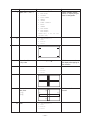
CONTENTS
HARDWARE SPECIFICATIONS -------------------------------------------------------------- 1
General Specifications ------------------------------------------------------------------- 1
Electrical Specifications----------------------------------------------------------------- 2
ACCESSORIES ------------------------------------------------------------------------------------ 3
OPTIONS --------------------------------------------------------------------------------------------- 3
SYSTEM CONFIGURATION -------------------------------------------------------------------- 4
GENERAL GUIDE --------------------------------------------------------------------------------- 5
ADJUSTING DISPLAY CONTRAST --------------------------------------------------------- 6
DESKTOP COMPUTER SYSTEM CONFIGURATION ---------------------------------- 7
SETTING UP ---------------------------------------------------------------------------------------- 7
REPLACING BATTERIES ----------------------------------------------------------------------- 9
To replace the main batteries---------------------------------------------------------- 9
To replace the backup battery------------------------------------------------------- 10
RESET ---------------------------------------------------------------------------------------------- 11
To reset the CASSIOPEIA ------------------------------------------------------------- 11
FULL RESET -------------------------------------------------------------------------------------- 12
To perform a full reset ----------------------------------------------------------------- 12
CONNECTING TO A DESKTOP COMPUTER ------------------------------------------- 13
To connect to a desktop computer ------------------------------------------------ 13
REPLACING THE PC CARD ----------------------------------------------------------------- 14
To replace the PC card----------------------------------------------------------------- 14
REPLACING THE COMPACTFLASH CARD -------------------------------------------- 15
To replace the CompactFlash card ------------------------------------------------ 15
CONNECTING TO EXTERNAL EQUIPMENT ------------------------------------------- 16
To connect external equipment ----------------------------------------------------- 16
MEMORY BACKUP / RESTORE ------------------------------------------------------------ 17
Backup -------------------------------------------------------------------------------------- 17
Restore -------------------------------------------------------------------------------------- 19
BLOCK DIAGRAM ------------------------------------------------------------------------------ 21
DEVICE FEATURES ---------------------------------------------------------------------------- 22
LSI/IC DATA -------------------------------------------------------------------------------------- 24
SH-7093 (CPU / IC1) --------------------------------------------------------------------- 24
MB87A915 (Gate Array/IC3) ---------------------------------------------------------- 27
MC34119 (IC9)----------------------------------------------------------------------------- 32
MAX3241CAI (IC5) ----------------------------------------------------------------------- 32
UPD42S16160LG5 ----------------------------------------------------------------------- 33
RN5VD18CA (IC113) -------------------------------------------------------------------- 33
XC61A Series (IC100 ~ IC103,IC107,IC109,IC110,IC112) -------------------- 33
MAX608 (IC105,IC106) ------------------------------------------------------------------ 34
EMI FILTER ARRAY --------------------------------------------------------------------- 34
UPD23C32000LGY ----------------------------------------------------------------------- 34
POWER SUPPLY CIRCUIT ------------------------------------------------------------------Primary Circuit---------------------------------------------------------------------------5 V Circuit ---------------------------------------------------------------------------------3 V Circuit ---------------------------------------------------------------------------------PCMCIA Circuit --------------------------------------------------------------------------LCD power Circuit ----------------------------------------------------------------------Voltage Line ------------------------------------------------------------------------------DETECTOR CIRCUIT --------------------------------------------------------------------------DIAGNOSTIC PROGRAM --------------------------------------------------------------------Introduction-------------------------------------------------------------------------------OPERATION CHECK --------------------------------------------------------------------------IrDA Communication Test -----------------------------------------------------------Current Consumption and Voltage Detectors Check -----------------------Voltage Detectors Check -------------------------------------------------------------DISASSEMBLY • ASSEMBLY --------------------------------------------------------------1.Module -----------------------------------------------------------------------------------2.Upper case ass’y ---------------------------------------------------------------------3.Removal of touch panel and LCD unit ----------------------------------------4.Precautions when installing LCD unit-----------------------------------------5.Installation of shaft piece----------------------------------------------------------6.How to pass FPC through the upper case -----------------------------------7.Precautions when assembling---------------------------------------------------EXPLOED VIEW --------------------------------------------------------------------------------PARTS LIST --------------------------------------------------------------------------------------WIRING DIAGRAM -----------------------------------------------------------------------------PCB VIEW ----------------------------------------------------------------------------------------SCHEMATIC DIAGRAMS --------------------------------------------------------------------Z340-1 PCB 1/3 (MAIN) ----------------------------------------------------------------Z340-1 PCB 2/3 (POWER SUPPLY) -----------------------------------------------Z340-1 PCB 3/3 (DP I/F BLOCK)----------------------------------------------------Z370-ROM PCB (ROM) ----------------------------------------------------------------Z340-DPMI PCB (MIC) -----------------------------------------------------------------Z340-LED PCB (LED) ------------------------------------------------------------------KEY MATRIX-------------------------------------------------------------------------------
* Windows is a registered trademark of Microsoft Corporation in the U.S.A. and other countries.
* i486DX and Pentium are registered trademarks of Intel Corporation.
35
35
36
37
38
39
40
41
42
42
43
48
50
52
54
54
55
57
60
61
62
63
65
66
68
69
70
70
71
72
73
74
75
76
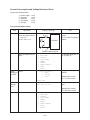
HARDWARE SPECIFICATIONS
General Specifications
Model:
PA-2500U
Display:
640 × 240 dots/0.24 dot pitch, FSTN LCD, 4 grayscale monochrome
CPU:
Memory
RAM:
ROM:
SH3
8M bytes
8M bytes
Speaker:
Sound
Interfaces:
RS-232C: 115.2K BPS
Data communication jack
PC card slot
CompactFlash card slot
Infrared port (IrDA compatible protocol)
Communication distance: 10 to 70 cm
Maximum Speed: 115.2K BPS
Power Supply:
Main
Two AA-size alkaline batteries LR6 (AM3);rechargeable battery pack(A-B10LT);
AC adaptor (AD-C50200)
Back-up
One CR2032 lithium battery
Power Consumption: 3.0 W
Battery Life:
Main
Two AA-size alkaline batteries: 25 hours (in Word, continuous cycle of oneminute input and 10-minutes input standby), 10 hours (input of 90 characters
per minutes in Word)
Rechargeable battery pack: 15 hours (in Word, continuous cycle of one-minute
input and 10-minutes input standby), 10 hours (input of 90 characters per minutes in Word)
* Main Battery life is shortened considerably by use of a modem card or any
other high power consumption PC card.
Back-up
5 year (when main battery is replaced immediately after appearance of low
battery message)
1 month (when unit is left without a main battery)
Operating Temperature:
0 °C to 40 °C (32 °F to 104 °F)
Dimensions (excluding projections):
Folded:
Weight:
24.5H × 185W × 94D mm (1"H × 7-1/4"W × 3-11/16"D)
430 g (15.2 oz) including batteries
—1—
Electrical Specifications
Current Consumption (V-in: 2.6 V ± 0.1 V, LCD Contrast VR: MID.):
Main Battery: Diagnostics Program with alkaline batteries
80 MHz:
650 mA or under
Sleep:
50 mA or under
Standby:
1.4 mA or under
Back-up Battery:
OFF:
450 µA
Voltage Detectors:
VDET1:
2.0 V ± 1% V or under (Low battery message detector for alkaline batteries)
VDET2:
1.6 V ± 1% V or under (Foced power off detector for alkaline batteries)
VDET1R: 3.3 V ± 2% V or under (Low battery message detector for rechargeable battery)
VDET2R: 3.0 V ± 2% V or under (Foced power off detector for rechargeable battery)
VDETS:
2.7 V ± 1% V or under (Low battery message detector for back-up battery)
IrDA:
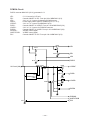
No.
Length (L)
Angle (A)
1
L = 80 cm
A = ±15 degree
2
L = 10 cm
A = 0 degree
PA-2500U
A
PA-2500U
L
—2—
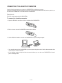
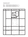
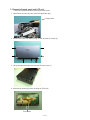
ACCESSORIES
• Stylus
• Dummy Card
The stylus is inserted into the CASSIOPEIA.
• CD-ROM
• RS-232C Cable
The dummy card is inserted in the CASSIOPEIA.
• Manuals (Hardware Manual, User’s Guide)
• Rechargeable Battery Pack
• AC Adapter
*The actual configuration of the AC adapter may differ from that shown in the above illustration.
OPTIONS
• Cradle PA-2010 IFS
Data Communication Cable SB-62
This cable is used to connect a digital camera or other external
equipment to the PA-2500U.
Note: Optional materials are sold separately.
—3—
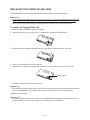
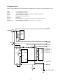
SYSTEM CONFIGURATION
Note that CASSIOPEIA will not operate under AC adapter power alone if its main batteries are not loaded.
AC adapter
CASIO Digital Camera
Data communication
cable (SB-62)
Infrared port
CASSIOPEIA
Desktop Computer
Printer
CompactFlash Card
PC Card
CD-ROM
RS-232C Cable
Printer
Converter
Desktop Computer
Important
If you have a notebook PC with IrDA capabilities or a built-in modem, its COM port may not be set up for
use as a standard serial interface. In such a case, you must change the COM port settings so it can be
used as a standard serial interface. You should also check which COM ports are enabled on a desktop PC
before starting to install Windows CE Services.
See the documentation that comes with your PC for details.
Connection to a desktop computer is quick and easy using the optional cradle.
—4—
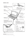
GENERAL GUIDE
• Touch screen
Displays text data and operational indicators, as well as icons that can be operated
using the stylus.
• Infrared port
For infrared communication
• Data communication jack
For connection of a digital camera or
other external equipment.
• Speaker
Outputs alarm tones and
other sounds.
• Microphone
For voice and other
sound recording.
• Keyboard
• Card eject button
(PC card)
Press to eject the card
from the card slot.
• Card slot
(CompactFlash card)
• Card slot (PC card)
• Fn (Function) key
Pressing this key and then a number key
launches Calendar, Contacts, Tasks,
Pocket Word, Pocket Excel, Pocket Power
Point or Inbox.
• Backlight button
Press to turn the backlight on and off.
The backlight also turns off automatically
if you do not perform any key or stylus
operation within a certain amount of
time.
Light
RESET
To remove: Pull on the part of the stylus
that protrudes from the unit.
To replace: Taking care to orient the stylus
correctly, press it until it clicks into
place.
• Stylus
For performing operations on the touch screen.
Important
Take care to avoid damaging or losing the stylus.
—5—
• Reset button
See page 11.
• Power button
Press to turn power on and off.
• Battery holder
Holds main batteries
(AA-size alkaline).
• Battery holder release
Slide to release the battery holder to remove
it, or to secure the battery holder in place.
• Backup battery compartment
Holds the backup battery (CR2032).
• Card cover (CompactFlash card)
• Indicator clear button
Clears a warning indicator
(red) and alarm operation.
Pressing this button also
turns on power. Power can
be turned off only by pressing the power button.
• Indicator (red)
Flashes to indicate the preset
alarm time has been reached, or
to indicate an operational condition
of the application being used.
• Charge indicator (green)
Indicates that charging is in
progress.
• AC adapter jack
For connection of the
AC adapter.
• RS-232C/Cradle connector
For connection of an RS-232C
cable or cradle.
ADJUSTING DISPLAY CONTRAST
Adjust display contrast whenever the figures on the display become dim and difficult to see. To adjust
display contrast, hold down [Alt] and press [<] (to make the display lighter) or [>] (to make the display
darker).
—6—
DESKTOP COMPUTER SYSTEM CONFIGURATION
The computer configuration described below is required to support the installer and the software applications contained on the Microsoft CD-ROM supplied with the CASSIOPEIA.
• Microsoft Windows NT Workstation 4.0 or Windows 95 (U.S. version)
• Desktop computer with a 486/33DX or higher processor (Pentium P90 recommended)
• 12 MB of memory for Windows NT Workstation 4.0
8 MB of memory (12 MB recommended) for Windows 95
• Hard disk drive with 10 to 50 MB of available hard disk space (actual requirements will vary based on
selection of features and user’s current system configuration)
• Available 9 or 25 pin communications port (adapter required for 25 pin communication port)
• One CD-ROM drive
• VGA or higher-resolution graphics card (Super VGA 256-color recommended)
• Keyboard
• Microsoft Mouse or compatible pointing device
Options for either Windows NT Workstation 4.0 or Windows 95:
• Audio card/speakers for sound
• Microsoft Office 97 or Microsoft Office 95
• Serial or built-in infrared adapter for synchronization
• Modem for remote synchronization
• Ethernet LAN connection for remote synchronization
Important
• If you have a notebook PC with IrDA capabilities or a built-in modem, its COM port may not be set up for
use as a standard serial interface. In such a case, you must change the COM port settings so it can be
used as a standard serial interface. You should also check which COM ports are enabled on a desktop
PC before starting to install Windows CE Services. See the documentation that comes with your PC for
details.
Note: Some of the applications contained on the CASSIOPEIA Bonus Software Applications
CD-ROM may require a system configuration different from that described above. See the
applicable files (ReadMe.txt and other files) that are also provided on the CD-ROM.
SETTING UP
Use the following procedure to set up the CASSIOPEIA before using it for the first time.
1. Load the main batteries.
• Load two AA-size alkaline batteries into the battery holder and then attach the holder to the CASSIOPEIA (page 9).
2. Load the backup battery (page 10)
3. Wait for about five seconds, and then press the power switch to turn on power.
• Turning on power causes the CASSIOPEIA display to change in the sequence shown below.
Start up
screen
Set up
screens
4. Set up the CASSIOPEIA .
• Perform the procedures in accordance with the guidance messages that appear on the screen.
—7—
Important
• Should the display lock up or go blank at this time, first perform the full reset (page 12). If this does not
correct the problem, remove the main batteries from the CASSIOPEIA and then remove the back-up
battery. Wait for about five minutes, and then perform this procedure again, starting from step 1. Be
sure that the positive (+) and negative (–) poles of the batteries are facing correctly when you reload
them into the CASSIOPEIA.
• If the message “A problem with memory contents has been found, and memory must be initialized...”
appears, perform the full reset operation described on page 12.
• If the images on the display appear dim, use the procedure on page 6 to adjust the contrast.
• Further information on the above procedures can be found in the H/PC Companion manual in
the section describing system set up.
—8—
REPLACING BATTERIES
The CASSIOPEIA has a dual power supply that consists of main batteries and a backup battery. Be sure to
load the main batteries and a back-up battery before using the CASSIOPEIA for the first time after purchasing it. Also, replace batteries as soon as possible after they start to get weak.
Important!
• Never remove both the main batteries and the backup battery from the CASSIOPEIA at the same time.
If you do, data stored in memory can be corrupted or lost entirely.
• Whenever the main batteries and the backup battery both require replacement, be sure to replace the
main batteries first, before replacing the backup battery.
• Use two AA-size alkaline batteries or the optional rechargeable battery pack for the main power supply,
and a CR2032 lithium battery for the back-up power supply. Never use any other types of battery with
the CASSIOPEIA.
• Be sure to watch out for signs of low battery power. Replace main batteries as soon as possible after the
message shown below appears on the display.
“Your main batteries are running very low on power. Please change the batteries at your next opportunity.”
Replace the backup battery as soon as possible after the message shown below appears.
“Your backup battery is very low or missing. Data loss may result from failure to replace the battery very
soon.”
Failure to replace batteries when they are low can result in corruption or loss of data stored in memory.
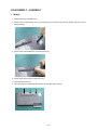
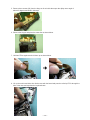
To replace the main batteries
1. Make sure the CASSIOPEIA is turned off.
• If the CASSIOPEIA is on, press the power switch to turn it off.
2. Close the CASSIOPEIA and turn it over.
3. While holding the battery holder release in the “FREE” position, slide the battery holder from the CASSIOPEIA.
• While holding the battery holder release in position, grasp the center of the battery holder and carefully
pull it from the CASSIOPEIA.
4. Remove the old batteries from the battery holder and load two new ones.
• When loading new batteries, make sure that their positive (+) and negative (–) ends are facing correctly.
—9—
5. Reattach the battery holder to the CASSIOPEIA.
• The battery holder will emit a click and the battery holder release will automatically lock when the battery
holder is securely in place.
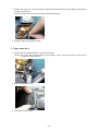
To replace the backup battery
1. Make sure the CASSIOPEIA is turned off.
• If the CASSIOPEIA is on, press the power switch to turn it off.
2. Close the CASSIOPEIA and turn it over.
3. While pressing the release A with the stylus, slide the backup battery cover from the CASSIOPEIA.
4. Remove the old battery.
5. After wiping the surface of a new battery with a soft, dry cloth, load it into the CASSIOPEIA with its
positive (+) side facing up (so you can see it).
6. Slide the backup battery cover back on to the CASSIOPEIA until it snaps securely into place.
Important!
Failure to observe any of the following battery precautions can cause batteries to leak, creating the danger
of property damage, iniury and fire due to explosion.
• When loading batteries,make sure their positive (+) and negative (–) poles are facing correctly.
• Never mix new batteries with old ones.
• Never mix batteries of different types.
• Use only the batteries that are specifically recommended for the CASSIOPEIA.
— 10 —
RESET
You should reset the CASSIOPEIA whenever it stops working or whenever some other operational problem
has caused it to malfunction.
To reset the CASSIOPEIA
1. Press the RESET button with the stylus.
• This automatically turns off CASSIOPEIA power.
2. Press the power switch to turn on power and start the reset process.
• What happens next depends on memory status.
Case A: Memory Contents Not Corrupted
In this case, the display changes in the sequence shown below.
Start up
screen
Nomal
Desktop
Normal operation is restored after the desktop appears, with all memory contents and settings unchanged.
Case B: Memory Contents Corrupted
In this case, the message “A problem with memory contents has been found, and memory must be initialized...” appears on the screen. Use the stylus to touch the screen to change in the sequence shown below.
Start up
screen
Set up
screens
Set up the CASSIOPEIA as described on page 7 of this manual. The desktop appears after set up is
complete.
When memory is seriously corrupted, the above procedure deletes all data stored in memory. When
memory contents are not deleted*, save any data you need onto a computer disk or other medium
and then perform the full reset procedure on page 12.
*Data may be corrupted, so edit data after checking it.
— 11 —
FULL RESET
Perform the full reset when you want to clear all memory contents and settings because memory contents
are corrupted, because you have forgotten the security code, or for any other reason.
Important
The following procedure deletes all data in memory. Be sure to save any important data contents you may
need later to a computer disk or other medium. Always keep separate back-up copies of important data.
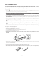
To perform a full reset
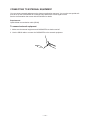
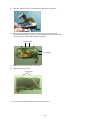
1. While holding down the [Ctrl] key and the [Alt] key, press the RESET button.
RESET button
[Ctrl] key
[Alt] key
2. The message “All memory contents will be deleted! Touch the screen to continue...” appears on the
display.
• If you don’t want to perform a full reset, press the RESET button.
This performs the normal reset, which does not clear memory contents.
\
3. To continue with the full reset procedure and clear all memory contents, touch the screen with the stylus.
• The display changes in the sequence shown below.
Start up
screen
Set up
screens
• Set up the CASSIOPEIA as described on page 7 of this manual.
— 12 —
CONNECTING TO A DESKTOP COMPUTER
Use the following procedure to connect the CASSIOPEIA to a desktop computer.
Note that exchanging data with a desktop computer requires Microsoft Windows CE Services, which is on
the Microsoft CD-ROM that is included with the CASSIOPEIA.
Requirements
RS-232C cable (supplied with CASSIOPEIA)
To connect to a desktop computer
1. Open the RS-232C connector cover on the side of the CASSIOPEIA.
2. Slide the cover into the CASSIOPEIA case as shown below.
3. Use the RS-232C cable to connect the CASSIOPEIA to your desktop computer.
• You can also connect the CASSIOPEIA to your computer using the cradle. See the documentation that
comes with the cradle for details.
• If your desktop computer supports infrared communications, you can also use CASSIOPEIA’s infrared
port to exchange data.
— 13 —
REPLACING THE PC CARD
The CASSIOPEIA comes equipped with a PC card slot that supports memory, modem and other PC cards*.
* Use only PC cards that are compatible with the CASSIOPEIA.
Important
• Be sure to keep the dummy card that comes with the CASSIOPEIA inserted in the card slot whenever
you are not using a PC card.
• Be sure to save any unsaved input or edited data before replacing the PC card.
• Never remove the PC card from the CASSIOPEIA while a PC card operation is in progress. Doing so
can corrupt CASSIOPEIA memory and PC card memory.
To replace the PC card
1. Extend the card eject button.
2. Press the card eject button to partially eject the card, and then pull the card out of the slot.
3. Insert a new PC card into the slot.
•
Push the card into the slot as far as it will go.
Important
• Take care to orient the card correctly. The top of the card should be facing in the same direction as the
top of the CASSIOPEIA. The card will stop part way into the slot if it is not oriented correctly.
• If the card stops part way into the slot, do not try to force it. Doing so can damage the card or the
CASSIOPEIA. Remove the card, make sure it is oriented correctly, and then try inserting it again.
4. Return the card eject button back to its folded position.
Important
• See the documentation that comes with the PC card and the H/PC Companion manual for information
on PC card operations.
— 14 —
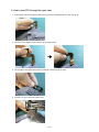
REPLACING THE COMPACTFLASH CARD
The CASSIOPEIA comes equipped with a card slot that supports CompactFlash cards.
Important
• If the card stops part way into the slot, do not try to force it. Doing so can damage the card or the
CASSIOPEIA. Remove the card, make sure it is oriented correctly, and then try inserting it again.
• Be sure to save any unsaved input or edited data before replacing the CompactFlash card.
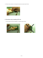
To replace the CompactFlash card
1. Make sure that CASSIOPEIA power is turned off.
2. While pressing down on the card cover 1, slide the cover from the CASSIOPEIA 2.
1
2
3. Press the card eject button to partially eject the card, and then pull the card out of the slot.
4. Insert a new CompactFlash card into the slot.
• Double-check to make sure that the card is oriented correctly before you insert it into the slot.
Back of card
• Push the card into the slot as far as it will go.
Important
• Take care to orient the card correctly. The top of the card should be facing in the same direction as the
top of the CASSIOPEIA. The card will stop part way into the slot if it is not oriented correctly.
5. Replace the card cover.
Important
• In order to protect data stored in memory, the CASSIOPEIA automatically turns off whenever you remove the card cover. Also, power will not turn on while the cover is removed.
— 15 —
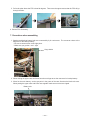
CONNECTING TO EXTERNAL EQUIPMENT
You can connect external equipment to the data communication connector. You can also use special software to set up the CASSIOPEIA to exchange image data with a CASIO digital camera.
See the documentation that comes with the software for details.
Requirements
Optional data communication cable (SB-62)
To connect external equipment
1. Make sure the external equipment and CASSIOPEIA are both turned off.
2. Use the SB-62 cable to connect the CASSIOPEIA to the external equipment.
— 16 —
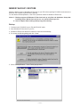
MEMORY BACKUP / RESTORE
Make the backup copy by Windows CE Services to your PC before repairing PA-2500U, and restore the
data from PC to user’s PA-2500U after repairing.
For the details of Backup/Restore, refer to the operation manual of Windows CE Services.
Notes: 1* Backup program of Windows CE Services back up only files and databases. Setup data
including Owner, World Clock and so on, can not be backed up to PC.
2* Use AC adaptor when making backup copy and restoring.
Backup
1. Connect user’s PA-2500U to your PC with RS-232C cable.
2. Start Windows CE Services on your PC.
3. Windows CE Services detects PA-2500U is connected automatically.
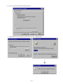
4. PC shows the following dialog and click “Guest”.
5. Select “Backup/Restore...” from “Tools” pop up menu.
— 17 —
6. Click “Full: back up all data” and “Back Up Now”.
7. Confirm the file name of bakup copy and then click “OK”. Backup starts.
— 18 —
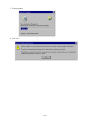
Restore
Execute Restore after repairing.
1. Turn on the user’s PA-2500U and then Welcome wizard appears.
2. Execute touch panel calibration and then skip other setups after calibration.
3. Connect repaired PA-2500U to your PC with RS-232C cable.
4. Start Windows CE Services on your PC.
5. Click “Restore” and confirm the file name backed up. Then click “OK”.
6. Click “Restore”.
— 19 —
7. Restoring starts.
8. Click “OK”.
— 20 —
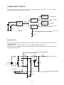
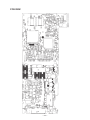
BLOCK DIAGRAM
10 M 32.768 K
PLL X4
80 MHz
CPU
SH-7093 (IC1)
RAM 8 Mbyte
HM51W16165
(RAM5~RAM8)
CompactFlash
Card
ROM 8Mbyte
Memory Slot
(U301~U305)
PCMCIA
Audio Amp.
MC34119
(IC9)
Card
3.68M
SP
LCD unit
Mini Jack
LCD
IrDA
IrDA Transceiver
Gate Array
CIM-10S
(IC4)
RS232C
Connector RS232C Transceiver
MAX3241
(IC5)
MB87A915 (IC3)
EL
EL Driver
HV803
(IC801)
Touch Panel
Indicator (Red) LED
+3.3 V +5 V LCD Power
Keyboard
Charge Indicator (Green) LED
Power Supply
ACL
Voltage Detector
Circuit
Recharger
AAX2
Alkaline
or
Li-ion
CR2032
— 21 —
MIC
DEVICE FEATURES
Device
Features
CPU
SH-7093 (IC1)
Hitachi 32 bit RISC CPU.
Sleep/Standby Power Mode.
TLB supports 1K/4K bytes page,128 entries.
8K bytes Cash.
Interrupt Controller.
User Break Controller.
Bus State Controller.
Watch Dog Timer.
CASIO proprietary RTC.
2K bytes Mask ROM.
ON Controller.
1 ch Serial I/F.
1 ch Serial I/F with 16 bytes FIFO.
1 channel Reload Timer.
2 channel Free Run Timer.
System RAM
HM51W16165 (RAM5~RAM8)
8M bytes DRAM (16M bit DRAM 4K refresh)
ROM
Memory Slot
8M bytes Mask ROM (32 bit Mask ROM)
Z370-ROM PCB
Connects to memory board with ROM.
This connects a development board as well.
System LSI
MB87A915 (IC3)
LCD Controller.
System Controller.
DRAM Access Controller.
Interrupt Controller.
Key Controller.
Audio Controller.
DMA Controller.
Dead Man’s Switch.
Touch Panel Controller.
Infra Red Controller.
RS232C I/F Controller.
IrDA I/F Controller.
3-pin I/F Controller.
LED Controller.
PCMCIA Controller.
CompactFlash Controller.
LCD
4 gray levels
480 × 240, landscape
0.24 mm/pitch
2 × 120 ch common driver.
3 × 160 ch segment driver with SRAM and disply control logic.
LCD Driver
Touch Panel
Resistive input device at the screen pixel resolution.
Just fitting to LCD panel.
Controller in System LSI.
— 22 —
Device
Touch Panel A/D
Features
10 bit analog to digital converter in System LSI.
Audio D/A
10 bit digital to analog converter in System LSI.
8/11.025/22.05 kHz sampling.
Audio A/D
10 bit analog to digital converter in System LSI.
8/11.025/22.05 kHz sampling.
Speaker
PCMCIA
20 mm dynamic type.
One slot for PCMCIA Type I/II card.
Compliance with PCMCIA ver.2.1.
IrDA / RS232C
(alternative)
Serial I/F with 16 byte FIFO in CPU.
115.2 kbaud.
IrDA 0 - 1 m.
9-pin RS232C ±12 V I/F.
3-pin Serial Port
Dead Man’s Switch
CASIO proprietary serial interface to Casio’s digital cameras and electric organizerand so on.
Up to 38.4 kbaud.
0 to +5 V I/F.
‘Manual Reset’ occurs each 15 seconds when the CPU does’t reset the counter.
Notification LED
LED Controller in System LSI.
Notification Button
LCD Contrast
Independent switch.
LCD Contrast is able to be handled by the software using electric volume and
LCD panel driver function.
Keyboard
56 keys and independent ‘Ctrl’,‘Alt’,‘Right Shift’,‘Caps Shift’,‘Alt-Graph’,‘Fn
(means Function: CASIO original)’and “Windows”.
‘ON’ key is an independent key.
ACL
Automatic hard reset for first time. “Power ON Reset” occurs in case of ACL.
Reset Mechanism
‘Manual Reset’ occurs when user pushes ‘Reset Switch’.
‘Power ON Reset’ occurs when user push ‘Reset Switch’ with pressing ‘Notification Switch’.
Battery Cover Detector Detects both open and closed.
Battery Detector
Detects Alkaline or NiMH.
Voltage Detector
Battery
5 levels with Alkaline / NiMH and 1 level with backup battery.
Alkaline AA × 2.
NiMH.
AC adapter.
Power Supply
3.3 V for most hardware logic.
5 V for PCMCIA and 3-pin serial interface.
24 V for LCD panel driver.
— 23 —
LSI/IC DATA
SH-7093 (CPU / IC1)
No.
1
2
3
4
5
6
7
8
9
10
11
12
13
14
15
16
17
18
19
20
21
22
23
24
25
26
27
28
29
30
31
32
33
34
35
36
37
38
39
40
41
42
43
44
45
46
47
48
49
50
51
52
53
54
55
56
57
Pin Name
D27
D26
D25
D24
D23/Port 7
Vss
Vcc
D22/Port 6
D21/Port 5
D20/Port 4
D19/Port 3
D18/Port 2
D17/Port 1
D16/Port 0
D15
D14
Vss
Vcc
Vss
Vcc
D13
D12
D11
D10
D9
D8
D7
D6
D5
Vss
Vcc
D4
D3
D2
D1
D0
A0
A1
A2
A3
Vss
Vcc
A4
A5
A6
A7
A8
A9
Vss
Vcc
A10
A11
A12
Vss
Vcc
A13
A14
Io/Out
I/O
I/O
I/O
I/O
I/O
I/O
I/O
I/O
I/O
I/O
I/O
I/O
I/O
I/O
I/O
I/O
I/O
I/O
I/O
I/O
I/O
I/O
I/O
I/O
I/O
I/O
I/O
I/O
O
O
O
O
O
O
O
O
O
O
O
O
O
O
O
Function
Data bus
Data bus
Data bus
Data bus
Data bus
GND
+3.3V source
Data bus
Data bus
Data bus
Data bus
Data bus
Data bus
Data bus
Data bus
Data bus
GND
+3.3V source
GND
+3.3V source
Data bus
Data bus
Data bus
Data bus
Data bus
Data bus
Data bus
Data bus
Data bus
GND
+3.3V source
Data bus
Data bus
Data bus
Data bus
Data bus
Address bus
Address bus
Address bus
Address bus
GND
+3.3V source
Address bus
Address bus
Address bus
Address bus
Address bus
Address bus
GND
+3.3V source
Address bus
Address bus
Address bus
GND
+3.3V source
Address bus
Address bus
— 24 —
To/From
No.
58
59
60
61
62
63
64
65
66
67
68
69
70
71
72
73
74
75
76
77
78
79
80
81
82
83
84
85
86
87
88
89
90
91
92
93
94
95
96
97
98
99
100
101
102
103
104
105
106
107
108
109
110
111
112
113
114
115
116
117
118
Pin Name
A15
Vss
Vcc
A16
A17
A18
A19
A20
A21
A22
Vss
Vcc
A23
A24
A25
Vss (PLL)
CAP1
Vcc (PLL)
Vss
ONENB
Vcc
EXTAL
XTAL
TESTMDB
Vss
Vcc
MD2 / RXD0
MD1 / TXD0
MD0 / SCK0
BREQB
RESETB
NMI
IRL3B
RXD1
TXD1
SCK1
CTS1
RTS1
BACKB
IOIS16B
STATUS0
ONSTATUSB
Vss
CKIO
Vcc
MD4 / CE2BB
MD3 / CE2AB
ONB
RD / WRB
RDB
CS6B / CE1BB
CS5B / CE1AB
CS4B
CS3B
CS2B
CS1B
CS0B
Vss
Vcc
WE3B / ICIOWRB
WE2B / ICIORDB
Io/Out
Function
O
Address bus
GND
+3.3V source
O
Address bus
O
Address bus
O
Address bus
O
Address bus
O
Address bus
O
Address bus
O
Address bus
GND
+3.3V source
O
Address bus
O
Address bus
O
Address bus
GND for PLL
O
Capacitor connecting terminal for PLL
+3.3V source for PLL
GND
I
ON Circuit enable signal
+3.3V source
I
Oscillator in (10MHz)
O
Oscillator out (10MHz)
I
Test mode control
GND
+3.3V source
I
Data input of serial port 0
I/O
Data output of serial port 0
I/O
Not used
I
Bus request
I
Reset signal from BGA288
I
Non-maskable Interrupt request
I
Interrupt request
I
Data input of serial port 1
O
Data output of serial port 1
I/O
Clock of serial port 1
I
Serial port 1 transmission permission
O
Serial port 1 transmission request
O
Bus access permission
I
Write protect input
O
STATUS0 signal to BGA288
O
V3ROM (+3.3V) ON/OFF control. H=ON
GND
I/O
System clock I/O
+3.3V source
I/O
PCMCIA CE2B signal
I/O
PCMCIA CE2A signal
I
On circuit start request
O
Read/Write signal
O
Read pulse
O
Chip select-6 sigmal
O
Chip select-5 sigmal
O
Chip select-4 sigmal
O
Not used
O
Chip select-2 sigmal
O
Chip select-1 sigmal
O
Chip select-0 sigmal
GND
+3.3V source
O
D31-D24 select signal / IO Write
O
D23-D16 select signal / IO Read
— 25 —
To/From
BGA288
X2
X2
GND
BGA288
BGA288
BGA288
BGA288
BGA288
BGA288
IC5(RS232C),BGA288
IC5(RS232C),BGA288
BGA288
IC5(RS232C)
IC5(RS232C)
BGA288
BGA288
BGA288
BGA288,Power supply unit
BGA288
BGA288
BGA288
BGA288
BGA288,RAM,ROM
BGA288,ROM,LCD unit
BGA288
BGA288
BGA288,ROM Board
BGA288
ROM Board
ROM Board
BGA288
BGA288,ROM Board
No.
119
120
121
122
123
124
125
126
127
128
129
130
131
132
133
134
135
136
137
138
139
140
141
142
143
144
Pin Name
CASHHB / CAS2HB
CASHLB / CAS2LB
Vss
Vcc
WE1B
WE0B
CASLHB
CASLLB / OEB
Vss
Vcc
RASB / CEB
MD5 / RAS2B
HSTBYB
WAITB
Vss
RTCCLK
Vcc(RTC)
XTAL2
EXTAL2
Vss(RTC)
Vcc
D31
D30
D29
D28
Vss
Io/Out
Function
O
D31-D24 / D15-D8 select signal
O
D23-D16 / D7-D0 select signal
GND
+3.3V source
O
D15-D8 select signal
O
D7-D0 select signal
O
D15-D8 select signal
O
D7-D0 select / memory select signal
GND
+3.3V source
O
CE signal for RAM,ROM
Not used
I
Not used
I
Hardware wait request
GND
O
RTC clock output
+3.3V source(for internal RTC)
O
Oscillator terminal(for internal RTC)
I
Oscillator terminal(for internal RTC)
GND(for internal RTC)
+3.3V source
I/O
Data bus
I/O
Data bus
I/O
Data bus
I/O
Data bus
GND
— 26 —
To/From
BGA288,ROM Board
BGA288,ROM Board
BGA288
BGA288,LCD uint,ROM Board
BGA288,ROM Board
BGA288,ROM Board
BGA288,RAM,ROM Board
+3.3V source
BGA288
BGA288
C6
C6
MB87A915 (Gate Array/IC3)
No.
1
2
3
4
5
6
7
8
9
10
11
12
13
14
15
16
17
18
19
20
21
22
23
24
25
26
27
28
29
30
31
32
33
34
35
36
37
38
39
40
41
42
43
44
45
46
47
48
49
50
51
52
53
54
55
56
57
58
59
Pin Name
CFCE1B
IOPORT0
IOPORT1
VSS
V5D3
VS1
V5D4
V5D11
CD1B
V5D5
VDD1
V5CE2B
V5D12
V5D6
V5D13
V5CE1B
V5A10
V5OEB
V5A11
VSS
VDD1
VSS
V5IORDB
V5A9
V5IOWRB
V5A8
V5A17
V5A13
V5A18
V5A14
VDD1
V5A19
V5WEB
V5A20
V5A21
V5A16
VSS
V5A22
V5A15
VDD1
V5A23
V5A12
V5A24
V5A7
VDD1
VSS
V5A25
V5A6
V5A5
V5RESET
V5A4
V5A3
V5A2
V5REGB
VDD1
V5D7
V5D14
V5A1
V5D15
Volt
3v
3v
3v
5V
5V
5V
5V
5V
5V
5V
5V
5V
5V
5V
5V
5V
5V
5V
5V
5V
5V
5V
5V
5V
5V
5V
5V
5V
5V
5V
5V
5V
5V
5V
5V
5V
5V
5V
5V
5V
5V
5V
5V
5V
5V
5V
5V
5V
5V
5V
5V
5V
Io/Out
Function
O
CE signal for CompactFlash card
I/O
Not used
I/O
I/O Port 1
GND
I/O
Data bus
Voltage detect for PCMCIA
I/O
Data bus
I/O
Data bus
I
PCMCIA CARD detect
I/O
Data bus
+5V source
O
CE2 signal for PCMCIA CARD
I/O
Data bus
I/O
Data bus
I/O
Data bus
O
CE1 signal for PCMCIA CARD
O
Address bus
O
OE signal for PCMCIA CARD
O
Address bus
GND
+5V source
GND
O
IORD signal for PCMCIA CARD
O
Address bus
O
IOWR signal for PCMCIA CARD
O
Address bus
O
Address bus
O
Address bus
O
Address bus
O
Address bus
+5V source
O
Address bus
O
WE signal for PCMCIA CARD
O
Address bus
O
Address bus
O
Address bus
GND
O
Address bus
O
Address bus
+5V source
O
Address bus
O
Address bus
O
Address bus
O
Address bus
+5V source
GND
O
Address bus
O
Address bus
O
Address bus
O
Reset signal for PCMCIA CARD
O
Address bus
O
Address bus
O
Address bus
O
Attribute memory select
+5V source
I/O
Data bus
I/O
Data bus
O
Address bus
I/O
Data bus
— 27 —
To/From
CompactFlash card
LCD unit
PCMCIA CARD
PCMCIA CARD
PCMCIA CARD
PCMCIA CARD
PCMCIA CARD
PCMCIA CARD
PCMCIA CARD
PCMCIA CARD
PCMCIA CARD
PCMCIA CARD
PCMCIA CARD
PCMCIA CARD
PCMCIA CARD
PCMCIA CARD
PCMCIA CARD
PCMCIA CARD
PCMCIA CARD
PCMCIA CARD
PCMCIA CARD
PCMCIA CARD
PCMCIA CARD
PCMCIA CARD
PCMCIA CARD
PCMCIA CARD
PCMCIA CARD
PCMCIA CARD
PCMCIA CARD
PCMCIA CARD
PCMCIA CARD
PCMCIA CARD
PCMCIA CARD
PCMCIA CARD
PCMCIA CARD
PCMCIA CARD
PCMCIA CARD
PCMCIA CARD
PCMCIA CARD
PCMCIA CARD
PCMCIA CARD
PCMCIA CARD
PCMCIA CARD
PCMCIA CARD
PCMCIA CARD
PCMCIA CARD
PCMCIA CARD
No.
60
61
62
63
64
65
66
67
68
69
70
71
72
73
74
75
76
77
78
79
80
81
82
83
84
85
86
87
88
89
90
91
92
93
94
95
96
97
98
99
100
101
102
103
104
105
106
107
108
109
110
111
112
113
114
115
116
117
118
119
120
Pin Name
V5D0
V5A0
VDD1
V5D8
V5D1
V5D9
V5BSYB
VSS
VSS
V5WAITB
V5D2
V5INPACKB
V5D10
V5BVD2
LEDONB
PIRB
V5BVD1
V5IOIS16B
IRTXD
CD2B
IRRXD
VDD2
VSS
DISPOFFB
DISPCSB
DISPRSTB
DISPWTB
IOPORT2
PSW0
PSW1
PSW2
PSW3
PSW4
FLSHRSTB
PMUTE
PRECB
FUNKEYIN7
FUNKEYIN6
FUNKEYIN5
FUNKEYIN4
FUNKEYIN3
FUNKEYIN2
FUNKEYIN1
NC
AVCC3
AUDIN
AUDVRL
AUDOUT
AUDVRH
AVCC2
AGND2
AGND1
AVCC1
TCPIN2
VDETADIN
TCPVRL
TCPVRH
TCPIN1
NC
FUNKEYIN0
KBOUT8
Volt
5V
5V
5V
5V
5V
5V
5V
5V
5V
5V
5V
5V
3V
3V
5V
5V
3V
3V
3V
3V
3V
3V
3V
3V
3V
3V
3V
3V
3V
3V
3V
3V
3V
3V
3V
3V
3V
3V
3V
3V
Analog
Analog
Analog
Analog
Analog
Analog
Analog
Analog
Analog
Analog
Analog
Analog
Analog
Analog
3V
3V
Io/Out
Function
I/O
Data bus
O
Address bus
+5V source
I/O
Data bus
I/O
Data bus
I/O
Data bus
I
Busy/Ready signal for PCMCIA CARD
GND
GND
I
Wait signal for PCMCIA CARD
I/O
Data bus
I
Input response
I/O
Data bus
I
Voltage detect for PCMCIA
O
LED signal
O
Voltage V5IRDA(3V) control
I
Battery Detector
I
Write protect
O
Infrared output
I
Card detect
I
Infrared input
+3V source
GND
O
LCD off signal
O
CE signal for LCD driver
O
Reset signal for LCD driner
I
Wait signal from LCD driver
I/O
Not used
O
Touch panel control
O
Touch panel control
O
Touch panel control
O
Touch panel control
O
Touch panel control
O
Reset signal for Flash
O
Audio mute signal
O
Power supply control for recording circuit
I
Function input
I
Function input
I
Function input
I
Function input
I
Function input
I
Function input
I
Function input
Not used
I
+3V source for D/A converter of audio
I
Audio signal input for record
I
Reference voltage for A/D,D/A converters
O
Audio signal output for play
I
Reference voltage for A/D,D/A converters
I
+3V source for Touch panel
I
Ground for Touch panel
I
Analog ground
I
+3V source for D/A converter of audio
I
Analog signal input from Touch panel
I
Power detecting signal
I
Reference voltage for A/D converter of TP
I
Reference voltage for A/D converter of TP
I
Analog signal input from Touch panel
Not used
I
Function input
O
Key common signal
— 28 —
To/From
PCMCIA CARD
PCMCIA CARD
PCMCIA CARD
PCMCIA CARD
PCMCIA CARD
PCMCIA CARD
PCMCIA CARD
PCMCIA CARD
PCMCIA CARD
PCMCIA CARD
PCMCIA CARD,SP
LCD unit
Q123(Power)
PCMCIA CARD
PCMCIA CARD
IrDA
PCMCIA CARD
IrDA
LCD unit
LCD unit
LCD unit
LCD unit
Touch panel
Touch panel
Touch panel
Touch panel
Touch panel
ROM board
Audio amp
LCD unit
Keyboard
Keyboard
Keyboard
Keyboard
Keyboard
Keyboard
Keyboard
+3V source
LCD unit
Audio amp
+3V source
GND
GND
+3V source
Touch panel
Power supply
Touch panel
Keyboard
Keyboard
No.
121
122
123
124
125
126
127
128
129
130
131
132
133
134
135
136
137
138
139
140
141
142
143
144
145
146
147
148
149
150
151
152
153
154
155
156
157
158
159
160
161
162
163
164
165
166
167
168
169
170
171
172
173
174
175
176
177
178
179
180
181
Pin Name
KBOUT7
KBOUT6
KBOUT5
KBOUT4
KBOUT3
KBOUT2
KBOUT1
KBOUT0
KBDIN0
KBDIN1
KBDIN2
KBDIN3
KBDIN4
KBDIN5
KBDIN6
VSS
KBDIN7
XCKIN
XCKOUT
VDD2
ONSWB
PENPUTB
LEDOFFB
DOCKB
CHGDTCT
ACLB
BCVRB
BATDTCT
ACDTCTB
VDETS
VDTC5B
VDTC3B
VDET3B
VDET2R
VDET2
VDET1RB
VDET1B
PSEL5
PLCD
PEL
PDMMYS
PDMMYM
PCRD2
PCRD
P5DCHG
P5V
P25ON
EVOLDAT
EVOLDIR
EVOLCS
EVOLCLK
CAS1HUB
CAS1HLB
CAS1LUB
CAS1LLB
CAS0HUB
CAS0HLB
CAS0LUB
VSS
VDD2
CAS0LLB
Volt
3V
3V
3V
3V
3V
3V
3V
3V
3V
3V
3V
3V
3V
3V
3V
Io/Out
O
O
O
O
O
O
O
O
I
I
I
I
I
I
I
3V
Analog
Analog
3V
3V
3V
3V
3V
3V
3V
3V
3V
3V
3V
3V
3V
3V
3V
3V
3V
3V
3V
3V
3V
3V
3V
3V
3V
3V
3V
3V
3V
3V
3V
3V
3V
3V
3V
3V
3V
3V
3V
I
I
I/O
3V
3V
I
I
I
I
I
I
I
I
I
I
I
I
I
I
I
I
I
O
O
O
O
O
O
O
O
O
O
O
O
O
O
O
O
O
O
O
O
O
O
Function
Key common signal
Key common signal
Key common signal
Key common signal
Key common signal
Key common signal
Key common signal
Key common signal
Key input signal
Key input signal
Key input signal
Key input signal
Key input signal
Key input signal
Key input signal
GND
Key input signal
Oscillator input(3.68MHz)
Oscillator output(3.68MHz)
+3V source
ON switch signal
Pen down status signal
LED cancel signal
Cradle detector
To/From
Keyboard
Keyboard
Keyboard
Keyboard
Keyboard
Keyboard
Keyboard
Keyboard
Keyboard
Keyboard
Keyboard
Keyboard
Keyboard
Keyboard
Keyboard
Keyboard
X1
X1
Keyboard
Touch panel
LCD unit (SW)
RS232C
Power supply
ACL signal at battery loaded.
IC113(Power supply)
Battery cover detecting port
SW100
Alkaline/NiMH detecting port
SW101
AC adaptor detect port
Q105 (Power supply)
Backup battery detecting signal
Q119 (Power supply)
Alkaline battery detecting signal
IC109 (Power supply)
Alkaline battery detecting signal
IC110 (Power supply)
Alkaline battery detecting signal
IC107 (Power supply)
NiMH detecting signal(Off)
Q100 (Power supply)
Alkaline battery detecting signal(Off)
Q103 (Power supply)
NiMH detecting signal(Low Battery)
IC101 (Power supply)
Alkaline battery detecting signal(Low Battery)
IC100 (Power supply)
Power supply select signal for PCMCIA (3/5V)
Q113 (Power supply)
LCD Voltage control signal
Q201 (I/F Block)
EL Voltage control signal
Q116 (Power supply)
For backup battery detector
IC115 (Power supply)
V3 system control signal
Q112 (Power supply)
VGA288 Voltage control signal
Q118 (Power supply)
PCMCIA Voltage control signal
Q117 (Power supply)
V5 Voltage control signal
Q115 (Power supply)
V5 Voltage control signal
Q107,Q111 (Power supply)
LCD(+25V) Voltage control signal
IC201
Electronic volume (DAT)
IC202 (EVOL)
Electronic volume (DIR)
IC202 (EVOL)
Electronic volume (CS)
IC202 (EVOL)
Electronic volume (CLK)
IC202 (EVOL)
CAS signal for DRAM
DRAM
CAS signal for DRAM
DRAM
CAS signal for DRAM
DRAM
CAS signal for DRAM
DRAM
CAS signal for DRAM
DRAM
CAS signal for DRAM
DRAM
CAS signal for DRAM
DRAM
GND
+3V source
CAS signal for DRAM
DRAM
— 29 —
No.
182
183
184
185
186
187
188
189
190
191
192
193
194
195
196
197
198
199
200
201
202
203
204
205
206
207
208
209
210
211
212
213
214
215
216
217
218
219
220
221
222
223
224
225
226
227
228
229
230
231
232
233
234
235
236
237
238
239
240
241
242
Pin Name
LOCK
MEMCLB
A25
A24
A23
A22
A21
A20
A19
A18
A17
A16
A15
A14
A13
A12
A11
A10
A9
A8
A7
VSS
A6
A5
A4
VDD2
A3
A2
A1
A0
D0
D1
D2
D3
D4
D5
VDD2
VSS
D6
D7
D8
D9
D10
D11
D12
D13
D14
D15
MCLOCK
ONENB
RXD0
TXD0
BREQB
RESETB
VSS
IRQB
RXDSH
TXDSH
SCK
BACKB
IOIS16B
Volt
3V
3V
3V
3V
3V
3V
3V
3V
3V
3V
3V
3V
3V
3V
3V
3V
3V
3V
3V
3V
3V
Io/Out
I
I
I
I
I/O
I/O
I/O
I/O
I
I
I
I
I
I
I
I
I/O
I/O
I/O
I/O
I/O
3V
3V
3V
3V
3V
3V
3V
3V
3V
3V
3V
3V
3V
3V
3V
I/O
I/O
I/O
I/O
I/O
I
I
I/O
I/O
I/O
I/O
I/O
I/O
3V
3V
3V
3V
3V
3V
3V
3V
3V
3V
3V
3V
3V
3V
3V
3V
I/O
I/O
I/O
I/O
I/O
I/O
I/O
I/O
I/O
I/O
I
O
O
I
O
O
3V
3V
3V
3V
3V
3V
O
I/O
I
O
I
O
Function
Not used
Not used
Address bus
Address bus
Address bus
Address bus
Address bus
Address bus
Address bus
Address bus
Address bus
Address bus
Address bus
Address bus
Address bus
Address bus
Address bus
Address bus
Address bus
Address bus
Address bus
GND
Address bus
Address bus
Address bus
+3V source
Address bus
Address bus
Address bus
Address bus
Data bus
Data bus
Data bus
Data bus
Data bus
Data bus
+3V source
GND
Data bus
Data bus
Data bus
Data bus
Data bus
Data bus
Data bus
Data bus
Data bus
Data bus
CKIO signal from CPU
ON Circuit enable signal
Data output of serial port 0
Data input of serial port 0
REQ signal to CPU
RESET signal to CPU
GND
IRQ signal to CPU
Data output of signal port 1
Data input of serial port 1
Clock of serial port 1
Bus access permission from CPU
Write protect signal to CPU
— 30 —
To/From
IC1
IC1
IC1
IC1
IC1
IC1
IC1
IC5(RS232C),BGA288
BGA288
IC1
IC1
IC1
N o . Pin Name
243
STATUS0
244 ONSTATUSB
245
CE2B
246
CE2A
247
VDD2
248
ONB
249
RDWRB
250
RDB
251
CS6B
252
CS4B
253
CS2B
254
CS5B
255
ICIOWRB
256
ICIORDB
257
CASHHB
258
CASHLB
259
WRHB
260
WRLB
261
CASLHB
262
CASLLB
263
RASB
264
HSTBY
265
WAITB
266 CKRTC256
267
CFCVRB
268
CFWEB
269
CFWAITB
270
CFVS1
271
CFRESET
272
CFREGB
273
CFRDY
274
CFOEB
275
CFCD2
276
CFCD1
277
VSS
278
CFCE2B
279
TEST3
280
TEST2
281
TEST1
282
DTYPE64
283 SIFSHUTB
284
SIFENB
285
MDTR
286
MDCD
287
TXDB
288
RXDB
Volt
3V
3V
3V
3V
3V
3V
3V
3V
3V
3V
3V
3V
3V
3V
3V
3V
3V
3V
3V
3V
3V
3V
3V
3V
3V
3V
3V
3V
3V
3V
3V
3V
3V
3V
Io/Out
I
I
I
I
3V
3V
3V
3V
3V
3V
3V
3V
3V
3V
3V
O
I
I
I
I
O
O
O
I
O
I
O
I/O
I
I
I
I
I
I
I
I
I
I
I
I
I
I/O
O
O
I
I
O
I
I
O
O
I
O
I
I
Function
STATUS0 signal from CPU
ONSTATUS signal from CPU
CE2B signal from CPU
CE2A signal from CPU
+3V source
ON circuit start signal to CPU
Read/Write signal from CPU
Read pulse signal from CPU
Chip select-6 signal from CPU (PCMCIA)
Chip select-4 signal from CPU (HOTARU)
Chip select-2 signal from CPU (LCD Driver)
Chip select-5 signal from CPU
IOWR signal from CPU
IORD signal from CPU
CASHH signal from CPU
CASHL signal from CPU
WE1 signal from CPU
WE0 signal from CPU
CASLH signal from CPU
CASLL signal from CPU
RAS/CE signal from CPU
HSTBY signal to CPU
WAIT signal to CPU
RTC clock signal from CPU
Compact Flash lock switch
WE signal for CompactFlash card
Wait signal for CompactFlash card
Voltage detect for CompactFlash card
Reset signal for CompactFlash card
REG signal for CompactFlash card
RDY/BSY signal for CompactFlash card
OE signal for CompactFlash card
CompactFlash card detector
CompactFlash card detector
GND
CE2 signal for CompactFlash card
Not used
Not used
Not used
Not used
RXD1 signal for CPU
9-pin RXD1 control
RS232C control signal
RS232C control signal
3-pin TXD signal
3-pin RXD signal
— 31 —
To/From
IC1
IC1
IC1
IC1
IC1
IC1
IC1
IC1
IC1
IC1
IC1
IC1
IC1
IC1
IC1
IC1
IC1
IC1
IC1
IC1
IC1
IC1
IC1
SW1
CompactFlash card
CompactFlash card
CompactFlash card
CompactFlash card
CompactFlash card
CompactFlash card
CompactFlash card
CompactFlash card
CompactFlash card
CompactFlash card
GND
GND
GND
IC5 (RS232C)
IC5 (RS232C)
IC5 (RS232C)
IC5 (RS232C)
3pin JACK
3pin JACK
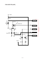
MC34119 (IC9)
CD
FC2
FC1
Vin
1
2
3
4
8
7
6
5
VO2
Gnd
VCC
VO1
(Top View)
MAX3241CAI (IC5)
VCC=3 V
to 5.5 V
28 C1+
C2+ 1
+
MAX3241
26 VCC
R1IN 4
25 GND
R2IN 5
24 C1-
R3IN 6
23 EN
R4IN 7
22 SHON
R5IN 8
21 R1OUTB
T1OUT 9
20 R2OUTB
T2OUT 10
19 R1OUT
T3OUT 11
18 R2OUT
T3IN 12
17 R3OUT
T2IN 13
16 R4OUT
T1IN 14
15 R5OUT
28
24
27 V+
C2– 2
V– 3
C1
+ 0.1 µf
C2
+
1
26
VCC
V+ 27
C1+
C1–
MAX3241
C2+
V–
C4
+
14 T1IN
T1OUT 9
13 T2IN
T2OUT 10
12 T3IN
T3OUT 11
RS-232
OUTPUTS
21 R1OUTB
20 R2OUTB
R1IN 4
19 R1OUT
5k
R2IN 5
18 R2OUT
(Top View)
C3
3
2 C2–
LOGIC
INPUTS
+
LOGIC
OUTPUTS
5k
R3IN 6
17 R3OUT
5k
R4IN 7
16 R4OUT
5k
R5IN 8
15 R5OUT
5k
23 EN
22
GND
25
— 32 —
SHDN
RS-232
INPUTS
UPD42S16160LG5B
A0 to A11
I/O 1 to I/O 16
RAS
UCAS
LCAS
WE
OE
VCC
GND
NC
: Address Inputs
: Data Inputs/Outputs
: Row Address Strobe
: Column Address Strobe (upper)
: Column Address Strobe (lower)
: Write enable
: Output enable
: Power Supply
: Ground
: No Connection
RN5VD18CA (IC113)
5
1
OUT
VDD
GND
NC
CD
4
2
3
: Output (H=Detected)
: Voltage source
: Ground
: No connection
: Connect to capacitor for delay
XC61A Series (IC100 ~ IC103,IC107,IC109,IC110,IC112)
VIN
VOUT
1
VOUT
2
VIN
Vref
3
VSS
VSS
— 33 —
MAX608 (IC105,IC106)
DIP/SO
EXT 1
8
CS
OUT 2
7
GND
FB 3
6
AGND
SHDN 4
5
REF
(Top View)
EMI FILTER ARRAY
UPD23C32000LGY
— 34 —
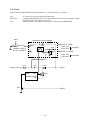
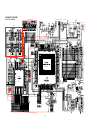
POWER SUPPLY CIRCUIT
The power supply circuit consists of 5 blocks which are Primary circuit, 5 V circuit, 3 V circuit , PCMCIA
power circuit and LCD power circuit as follows;
PCMCIA
power circuit
PCMCIA
5V circuit
5 V system
Fuse
LCD
power circuit
Primary
circuit
Alkaline
LCD
3 V system
3V circuit
Li-ion
AC Adapter
To Detector (VSUB)
Lithium
Primary Circuit
The voltages from both batteries, alkaline and Li-ion, apply to V5 and V3 circuits through the fuse when the
batteries is loaded.
CHGDTCTB is for Li-ion detect. When Li-ion is full charged CHGDTCTB becomes L.
ACDTCTB is for AC adapter detector. It detects whether AC adapter is used or not. When AC adapter is
used ACDTCTB becomes L.
CHGDTCTB (to MB87A915)
F100
D101
F101
To 3V and V5 circuits.
Q127
D100
Alkaline
(1.6 ~ 3.4 V)
D102
Li-ion
(3.0 ~ 3.6 V)
AC Adapter
L100
ACDTCTB (to MB87A915)
C105
— 35 —
5 V Circuit
DC/DC converter MAX608ESA (IC105) generates +5.11 V and it makes up 5 V system.
VIO :
BATDTCT:
P5V :
+5 V source for 3-pin jack and LCD power block.
It distinguishes alkaline and Li-ion to change the load according to the battery. When
alkaline is used, it is H. When Li-ion, it is L.
Controls ON/OFF of DC-DC converter (IC105). From pin 166 of MB87A915.
V3SYS
SW3
Changeover circuit for loading
Q104
BATDTCT
✽ BATDTCT = OPEN
IC104
D104
Alkaline = OPEN
Li-ion = CLOSE
Q106
Q104 ON
IC104 OFF
✽ BATDTCT = CLOSE
Q104 OFF
IC104 ON
L101
F101
L102
D105
VI0
Primary Circuit
SHDN
EXT
Q109
MAX608 (IC105)
CS
Q107
P5V
— 36 —
Load: Min.
Load: Max.
3 V Circuit
DC/DC converter MAX608ESA (IC106) generates +3.77 V and it makes up 3 V system.
V3MAIN :
V3SYS :
V3RAM :
V3ROM :
ONSTATUSB :
V3IRDA :
PIRB :
VSUB :
V3AUD :
PDMMYM :
The reference voltage for the detector.
+3.4 V source for IC1,IC3,IC5.
+3.4 V source for DRAM (RAM5 ~ RAM8).
+3.4 V source for ROM (U301,U302).
Controls ON/OFF of V3ROM. From pin 99 of CPU.
+3.4 V source for IrDA Transceiver CIM-10S (IC4).
Controls ON/OFF of V3IRDA. From pin 75 of MB87A915 (IC3).
+2.7 V source for detecting memory backup battery.
+3.4 V source for MB87A195 (IC3).
Controls ON/OFF of the load at detecting voltage.
V3MAIN
Primary Circuit
D103
L103
Q110
V3SYS
V3AUD
V3RAM
Q108
Q122
VIN
EXT
VOUT
IC108
3.4 V Regulator
Q123
SHDN
EXT
Q112
V+
V3ROM (To ROM)
ONSTATUSB
OFF: H
ON: L
V3IRDA
(To IrDA)
PIRB
(Normally H)
MAX608 (IC106)
CS
DC-DC converter
VSUB
CR2032
PDMMYM
(Normally L)
— 37 —
PCMCIA Circuit
DC/DC converter MAX1651 (IC111) generates 3.4 V
VEL :
PEL :
VPC :
PSEL5 :
VCRDIF :
PCRD :
VCARD :
PCRD2 :
P5DCHG :
ONSTATUSB :
P5V :
5.11 V source for LCD unit.
Controls ON/OFF of VEL. From pin 160 of MB87A915 (IC3).
3.4 V or 5.11 V source for detecting PCMCIA power.
Power supply select signal for PCMCIA (H=5 V, L=3 V).
3.4 V or 5.11 V source for MB87A915 (IC3).
Controls ON/OFF of VCRDIF, From pin 164 of MB87A915 (IC3).
3.4 V or 5.11 V source for PCMCIA connector.
Controls ON/OFF of VCARD. From pin 163 of MB87A915 (IC3).
VCRDIF control signal.
VCRDIF control signal.
Controls ON/OFF of VPC. From pin 166 of MB87A915 (IC3).
Q125
VEL
Q114
Q116
PEL
VPC
PSEL5
Q113
R140 Q124
5V Circuit (VIO)
Q126
VCRDIF
L104
V+
CS
Q117
PCRD
MAX1651(IC111)
Q120
EXT
Q128
VCARD
Q115
D109
Q118
PCRD2
P5DCHG
ONSTATUSB
P5V
Q111
— 38 —
LCD power Circuit
DC/DC converter RN5VH3 (IC201) generates LCD power and it makes up LCD power system for LCD.
VDD :
VAMP :
PLCD :
VLCD+:
VTH :
EVOL 0-3 :
P25ON :
VLCD- :
ONSTATUSB :
+3.7 V source for LCD unit.
+7.0 V source for LCD unit.
Controls ON/OFF of VAMP. From pin 159 of MB87A915 (IC3).
+15.5 V source for LCD unit.
LCD power source for LCD unit.
LCD status.
Controls ON/OFF of LCD power. From pin 167 of MB87A915 (IC3).
-10.0 V source for LCD unit.
Controls ON/OFF of LCD power. From pin 99 of CPU (IC1).
VDD
V3MAIN
Q200
VDD
+
SCI7660
(IC200)
CAP+
+
V0
VAMP
Q201
PLCD
VLCD+
L219
D200
TC74HC4066 (IC202)
1IO
1OI
2IO
VDD
RV5 VH3
(IC201)
Q202
EXT1
2OI
3IO
EXT2
3OI
4IO
1C
2C
3C
4C
VTH
EVOL 0
EVOL 1
EVOL 2
EVOL 3
4OI
FB1
CSW
Q203
P25ON
D203
VLCD-
Q204
Q205
— 39 —
ONSTATUSB
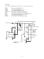
Voltage Line
IC1
SH-7093
CPU
IC3
BGA288
GATE ARRAY
U301/U302
32M-MASK
ROM
CN5
3P Jack
Connector
PCMCIA
Connector
RS-232C
RAM5~8
ECSTOJY106R
D-RAM
IC5
MAX3241
RS232C
V3AUD
V3RAM
V3SYS
V3ROM
V3IRDA
VCRDIF
VIO
VCARD
VLCD+
VLCD–
VDD
VEL
VTH
Connector
CF
— 40 —
Connector
LCD unit
IC9
MC34119
AudioIC
IC4
CIM-10S
IRIC
DETECTOR CIRCUIT
The detector circuit consistes of 7 blocks as follows;
1 : VDETECTOR1 (Alkaline and Li-ion)
2 : VDETECTOR2 (Alkaline and Li-ion)
3 : Backup battery detector
4 : AC Adaptor detector
5 : Full charge detector
6 : 3V detector (AC adaptor is not used)
7 : PCMCIA voltage detector
VDETECTOR 1
VBAT
Alkaline Detector
IC100(2.0V±5%)
VDET1B
(L=Low battery message)
Li-ion Detector
IC101(3.3V±2%)
VDET1RB
(L=Low battery message)
VDETECTOR 2
Alkaline Detector
IC102(1.6V±1%)
VDET2
(H=Forced power off)
Li-ion Detector
IC103(3.0V±2%)
VDET2R
(H=Forced power off)
BACKUP BATTERY DETECTOR
VSUB
VDETS
(H=Low battery message)
IC112(2.7V±1%)
AC ADAPTER DETECTOR
ACDTCB
(L=Adapter used)
Q105
CN101
FULL CHARGE DETECTOR
CHGDTCTB
(L=Full charge)
Q101
Li-ion(CN105)
3V DETECTOR (AC ADAPTOR NO USED)
V3MAIN
VDET3B
(L=Low 3V voltage message)
IC107(3.4V±1%)
PCMCIA VOLTAGE DETECTOR
VPC
5 Voltage
IC109(4.5V±2%)
VDTC5B
(L=Low PCMCIA voltage message)
3 Voltage
IC110(2.1V±2%)
VDTC3B
(L=Low PCMCIA voltage message)
— 41 —
DIAGNOSTIC PROGRAM
Introduction
The following steps must be followed before diagnostics.
START
Remove Main
and Backup
batteries
Load main
batteries
❋Make sure that Battery Holder Release
switch is on “NORMAL OPERATION” side.
Press ON
NO
Display appear?
YES
NO
Display appear?
YES
Display appear?
YES
Press RESET
button and then
ON
Replace
batteries with
new ones
NO
Repair needed
— 42 —
To Diagnostic
OPERATION CHECK
Preparation
1:
2:
3:
4:
PA-2500U
Alkaline batteries
Jigs of RS-JIG-232C and RS-JIG-3PIN
RAM Card XC-110
5 : AC-adapter
6 : Charger
7 : Rechargeable battery pack
8 : Diagnostic program (Diag 340.EXE)
Notes: • Be sure to keep separate back-up copies of all important data in PA-2500U, because the
DISGNOSTICS make data corrupt.
• Diag 340 EXE. (Program is included in CD-ROM(Service Information Disc) with Service Manual
PA-2500U)
• When using alkaline batteries use new ones.
• After all inspections are done perform Full Reset.
(After performing Full Reset make sure Diag 340. EXE is not in the computer.)
Step
Operation
Display
1
Turn power on. Operate
full Reset (refer to P12).
Picture of sky with sun and
clouds. Wait for about 10 seconds.
HP/C Setup Wizard Introduction
2
Enter
Touch Screen Calibration
3
Enter
Touch five crosses as
they appear.
Enter
Next
Touch five crosses as they appear
World Clock (Calender, Clock)
7
Next
Next
Next
8
Next
Differences from Microsoft Windows
9
Next
Finished!
Done
Connect PA-2500U and a PC
then copy Diag 340.exe onto
the desk top of PA-2500U.
Disconnect PA-2500U
and the PC
Double click Diag icon
Windows CE Menu Display
4
5
6
10
11
12
13
Note
World Clock (World Map)
Owner Properties
Synchronizing with your Desktop Computer
Copy Diag 340EXE to PA-2500U
from CD.
Make sure the diagnostic
program is copied.
** Main Menu **
0 AUTO MODE
1 DISPLAY
2 TOUCH PANEL
3 MEMORY
4 SERIAL
5 POWER CONTROL
6 AUDIO
7 OTHERS
8 AUTO MENU1
9 AUTO MENU2
– AUTO MENU3
CPROG Rev, 0.83 for ZX34x(APO OFF)
Make sure that the diagnostic program starts.
Notes: • If the diagnostic program is not stored in the RAM, you need to load the program otherwise
the tests 11, 12 cannot be done.
• Take CF card out after turning the power off.
• When new Diag program comes out, the Rev. value will vary.
• To make the task bar disappear, touch the task bar with the stylus or press control + ESC.
— 43 —
Step
Operation
Display
Note
1
Boot inspection program.
** Main Menu **
0 AUTO MODE
1 DISPLAY
2 TOUCH PANEL
3 MEMORY
4 SERIAL
5 POWER CONTROL
6 AUDIO
7 OTHERS
8 AUTO MENU1
9 AUTO MENU2
– AUTO MENU3
CPROG Rev, 0.83 for ZX34x(APO OFF)
To continue the inspection
you must make the task
bar disappear. When
there is a task bar on the
bottom of the display
press Ctrl + Esc to make
it disappear.
2
1
Checker pattern
3
Space
Reverse checker pattern
4
Space
Frame. The most outside
dots.
5
Space
All dots
6
Space
No display
— 44 —
Step
Operation
Display
Note
Check variable resistor.
Check if display brightness is changeable.
7
Space, Alt + <, Alt + >
** Main Menu **
0 AUTO MODE
1 DISPLAY
2 TOUCH PANEL
3 MEMORY
4 SERIAL
5 POWER CONTROL
6 AUDIO
7 OTHERS
8 AUTO MENU1
9 AUTO MENU2
– AUTO MENU3
CPROG Rev, 0.83 for ZX34x(APO OFF)
8
2
**
1
2
3
9
2
10
Tap on four of the crosses
in any order
11 Enter
Touch Panel **
Case
Points
Cross
Touch Panel
**
1
2
3
NG if crosses remain on
the display after tapping all
four crosses.
OK
Touch Panel **
Case
Points
Cross
12 3
13
Trace on the center of the
black lines.
1➝2
3➝4
3
1
2
4
14
Enter
**
1
2
3
Touch Panel **
Case
Points
Cross
— 45 —
OK when the lines are reversed.
Step
Operation
Display
15
Note
Inspection of Auto-hide
function.
Touch four points 1➝4
as shown in the left. NG if
3 no sound is heard.
1
2
4
16
Enter, 3
17
1
18
Enter
** Memory **
1 ROM CHECK SUM
2 ROM BUS CHECK
19
Enter, 6
** Audio **
1 0.5KHz
2
1 KHz
3
2 KHz
4 Record
20
3
AUDIO 2KHz
21
Enter, 4
R Key
P Key
Enter
22
Press R then speak “test
test”, S
Push ”S” Key to Stop Recording
Start recording. Stop recording.
23
P, S
Push ”S” Key to Stop playing
Start replay. Check your
voice “test test”. Quit replay.
24
Enter, Enter, 7
25
1
** Memory **
1 ROM CHECK SUM
2 ROM BUS CHECK
ROM1=059a
ROM2=059a
ROM3=***
**
1
2
3
4
5
6
8
Make sure that the unit
emits a sound.
:Start Recording
:Play Recorded Sound
Exit
Others **
Switch
PCMCIA(implement)
PCMCIA(RAM card)
Compact Flash(CDs)
Keyboard SERIAL1
Keyboard SERIAL2
Compact Flash
VDET1
VDET2
VDET1R
VDET2R
VDET3
VDETS
Recharge
VDETC3
VDETC5
AC Adapter
Cover
FC Cover
— 46 —
OFF
OFF
ON
ON
OFF
OFF
OFF
OFF
ON
NOT USED
CLOSED
CLOSED
Red LED flashes.
Step
Operation
26
27
Display
VDETS
Remove backup battery
Note
OFF
VDETS
ON
29 Press battery notification
SW.
Recharge
ON
Release battery notification SW.
Recharge
Make sure backup battery
is installed.
28 Put backup battery back in
30
31 Plug in AC adapter.
OFF
AC Adapter
USED
32 Install lithium battery
Green LED lights.
33 Rmove battery cover.
Replace the battery with
alkaline battery. Put the
cover back on.
Make sure green LED
goes out. Put battery
cover back on after checking.
34 Plug out AC adapter
AC Adapter
35 Slide the battery cover
lock switch to FREE
COVER
36
Slide the battery cover
lock switch to LOCK
COVER
37
Remove CF cover
FC COVER
38
Put CF cover back on
FC COVER
39
Press Indicator clear button
40
Enter, 6
** Keyboard Serial **
41
Light, On, Esc, 1, 2, 3, 4,
5, 6, 7, 8, 9, 0, –, BS, ~, q,
w, e, r, t, u, i, o, p, +, |,
Enter, Tab,a, s, d, f, g, h, j,
k, l, ;, ’, Enter, Shift, z, x, c,
v, b, n, m, <, >, ?, , Caps,
Ctrl, Windows, Fn, Alt,
Space, {, }, , ,
** Keyboard Serial **
NOT USED
OPEN
CLOSED
OPEN
CLOSED
Red LED goes out.
KEY
42 Enter, Enter
43
Reset
OK
** Main Menu **
0 AUTO MODE
1 DISPLAY
2 TOUCH PANEL
3 MEMORY
4 SERIAL
5 POWER CONTROL
6 AUDIO
7 OTHERS
8 AUTO MENU1
9 AUTO MENU2
– AUTO MENU3
CPROG Rev, 0.83 for ZX34x(APO OFF)
(Power off)
— 47 —
Press Windows key. Wait
for two seconds, then
press Fn key.
IrDA Communication Test
Prepare 2 units and place them as follows;
PA-2500U
PA-2500U
±15 deg.
PA-2500U
PA-2500U
10 cm
80 cm
UNIT-1
Step
Operation
IrDA
Display
**
0
1
2
3
4
5
6
7
4
UNIT-2
Operation
**
0
1
2
3
4
5
6
7
Main Menu **
AUTO MODE
DISPLAY
TOUCH PANEL
MEMORY
SERIAL
POWER CONTROL
AUDIO
Others
** Serial **
<RS232C Check>
1 Loop Back
2 Send/Receive
<IrDA Check>
3 Interactive
4 Send/Receive
<3 PIN Check>
5 Loop Back
4
<Infrared SEND/RECEIVE>
1 Send data (MAX Baudrate)
2 Receive data(MAX Baudrate)
3 Send data (MIN Baudrate)
4 Receive data(MIN Baudrate)
1
<Infrared SEND/RECEIVE>
1 Send data (MAX Baudrate)
2 Receive data(MAX Baudrate)
3 Send data (MIN Baudrate)
4 Receive data(MIN Baudrate)
4
Note
Display
Main Menu **
AUTO MODE
DISPLAY
TOUCH PANEL
MEMORY
SERIAL
POWER CONTROL
AUDIO
Others
** Serial **
<RS232C Check>
1 Loop Back
2 Send/Receive
<IrDA Check>
3 Interactive
4 Send/Receive
<3 PIN Check>
5 Loop Back
4
<Infrared SEND/RECEIVE>
1 Send data (MAX Baudrate)
2 Receive data(MAX Baudrate)
3 Send data (MIN Baudrate)
4 Receive data(MIN Baudrate)
<Infrared SEND/RECEIVE>
1 Send data (MAX Baudrate)
2 Receive data(MAX Baudrate)
3 Send data (MIN Baudrate)
4 Receive data(MIN Baudrate)
<SEND MODE>
<Infrared SEND/RECEIVE>
1 Send data (MAX Baudrate)
2 Receive data(MAX Baudrate)
3 Send data (MIN Baudrate)
4 Receive data(MIN Baudrate)
2
<SEND MODE>
<Infrared SEND/RECEIVE>
1 Send data (MAX Baudrate)
2 Receive data(MAX Baudrate)
3 Send data (MIN Baudrate)
4 Receive data(MIN Baudrate)
<RECEIVE MODE>
HHHHHHHHHHHHHHHHH
HHHHHHHHHHHHHHHHH
HHHHHHHH.........
— 48 —
"H" indication
continuing without error message for more
than 1 second
(ERROR message is indicated
in transmission
beginning and
transmission
closing, it is normal.)
UNIT-2
UNIT-1
Step
Operation
Display
ENTER
<Infrared SEND/RECEIVE>
1 Send data (MAX Baudrate)
2 Receive data(MAX Baudrate)
3 Send data (MIN Baudrate)
4 Receive data(MIN Baudrate)
<Infrared SEND/RECEIVE>
1 Send data (MAX Baudrate)
2 Receive data(MAX Baudrate)
3 Send data (MIN Baudrate)
4 Receive data(MIN Baudrate)
Operation
HHHHHHHHHHHHHHHHH
HHHHHHH
ENTER
1
<Infrared SEND/RECEIVE>
1 Send data (MAX Baudrate)
2 Receive data(MAX Baudrate)
3 Send data (MIN Baudrate)
4 Receive data(MIN Baudrate)
Note
Display
Make sure H
display stops
<Infrared SEND/RECEIVE>
1 Send data (MAX Baudrate)
2 Receive data(MAX Baudrate)
3 Send data (MIN Baudrate)
4 Receive data(MIN Baudrate)
<Infrared SEND/RECEIVE>
1 Send data (MAX Baudrate)
2 Receive data(MAX Baudrate)
3 Send data (MIN Baudrate)
4 Receive data(MIN Baudrate)
<SEND MODE>
2
<Infrared SEND/RECEIVE>
1 Send data (MAX Baudrate)
2 Receive data(MAX Baudrate)
3 Send data (MIN Baudrate)
4 Receive data(MIN Baudrate)
<Infrared SEND/RECEIVE>
1 Send data (MAX Baudrate)
2 Receive data(MAX Baudrate)
3 Send data (MIN Baudrate)
4 Receive data(MIN Baudrate)
<RECEIVE MODE>
<SEND MODE>
HHHHHHHHHHHHHHHHH
HHHHHHHHHHHHHHHHH
HHHHHHHH.........
HHHHHHHHHHHHHHHHH
HHHHHHH
ENTER
ENTER,
ENTER
ENTER
**
0
1
2
3
4
5
6
7
Main Menu **
AUTO MODE
DISPLAY
TOUCH PANEL
MEMORY
SERIAL
POWER CONTROL
AUDIO
Others
ENTER,
ENTER
— 49 —
(ERROR message is indicated
in transmission
beginning and
transmission
closing, it is normal.)
Make sure H
<Infrared SEND/RECEIVE>
1 Send data (MAX Baudrate) display stops
2 Receive data(MAX Baudrate)
3 Send data (MIN Baudrate)
4 Receive data(MIN Baudrate)
<Infrared SEND/RECEIVE>
1 Send data (MAX Baudrate)
2 Receive data(MAX Baudrate)
3 Send data (MIN Baudrate)
4 Receive data(MIN Baudrate)
<Infrared SEND/RECEIVE>
1 Send data (MAX Baudrate)
2 Receive data(MAX Baudrate)
3 Send data (MIN Baudrate)
4 Receive data(MIN Baudrate)
"H" indication
continuing without error message for more
than 1 second
**
0
1
2
3
4
5
6
7
Main Menu **
AUTO MODE
DISPLAY
TOUCH PANEL
MEMORY
SERIAL
POWER CONTROL
AUDIO
Others
Change the
communication
distance or
angle, and repeat the IrDA
communication
check.
End of IrDA
check
Current Consumption and Voltage Detectors Check
Prepare the following items;
1 : Power supply
2 : Ammeter
3 : Voltmeter
4 : AC adapter
5 : Charger
1 unit
1 unit
1 unit
1 unit
1 unit
Current Consumption Check
Step
Operation
Display (Wiring)
1: Maximum of contrast dial.
2: Set the range of Ammeter to 1 A.
3: Vb = 2.6 ± 0.1 V
Setting
Ib
A
-
V
PA-2500U
Vb
Note
Connect the items as
shown.
Do not load the backup
battery.
+
Alkaline battery terminal
2
Main
Battery at
SLEEP
Boot the diagnostic program
**
0
1
2
3
4
5
6
7
Main Menu **
AUTO MODE
DISPLAY
TOUCH PANEL
MEMORY
SERIAL
POWER CONTROL
AUDIO
Others
To boot the diagnostic, refer to page 43.
ON, 3
** Power Control **
1 40MHz
2 standby
3 sleep
Current consumption at
SLEEP.
Measure the current.
Ib = 50 mA or under.
Sleep mode
Main
Battery
ON
5
Currently CPU clock is 180MHz
Push on key to exit
Current consumption at
ON.
Measure the current.
Ib = 650 mA or under.
5
ON
**
0
1
2
3
4
5
6
7
Main Menu **
AUTO MODE
DISPLAY
TOUCH PANEL
MEMORY
SERIAL
POWER CONTROL
AUDIO
Others
— 50 —
Step
Main
Battery
at OFF
Operation
Display (Wiring)
Note
(Power off)
Current consumption at
OFF.
ON
Measure the current.
Ib = 1.4 mA or under
Backup
battery
1 : Turn the power off.
2 : Supply the voltage to
backup battery terminals as right figure .
3 : Remove main batteries.
4 : Measure the current.
Vs = 3.0 ± 0.1 V
Backup battery terminal
Is
A
V
Connect the items as
shown.
PA-2500U
Vs
+
(No display)
Current consumption of
backup battery.
Measure the current.
Is = 450 µA or under.
— 51 —
Voltage Detectors Check
Check the following detectors;
VDET1:
VDET2:
VDET1R:
VDET2R:
VDETS:
Low battery message detector for alkaline batteries.(2.0 V ± 1 %)
Foced power off detector for alkaline batteries.(1.6V ± 1 %)
Low battery message detector for rechargeable battery.(3.3 V ± 2 %)
Foced power off detector for rechargeable battery.(3.0 V ± 2 %)
Low battery message detector for back-up battery.(2.7 V ± 1 %)
Step
Operation
Setting
Vb = 2.6 ± 0.02 V
Display (Wiring)
Alkaline battery terminal
Note
Connect the items as
shown.
V
VDET1
PA-2500U
Vb
+
AC adapter
Charger
ENTER, 7, 1
VDET1
OFF
VDET2
OFF
VDET1R
OFF
VDET2R
(indefinite)
VDET3
OFF
VDETS
ON
Recharge
OFF
CHKPRG
OFF
AC Adapter
USED
Cover
CLOSED
CardLock
CLOSED
Cradle
NOT STAY
Put power supply voltage
down by degrees.
VDET1
VDET2
ON
OFF
Measure the voltage that
VDET1 becomes ON.
VDET1 = 2.0 V ± 5 %
VDET2
Put power supply voltage
down by degrees.
VDET1
VDET2
ON
ON
Measure the voltage that
VDET2 becomes ON.
VDET2 = 1.6 V ± 1 %
— 52 —
Step
Setting
Operation
Change to connect power
supply to the terminals for
rechargeable battery.
Display (Wiring)
Rechargeable battery terminal
Note
Connect the items as
shown.
-
Vr = 2.6 V
V
VDET1R
Put power supply voltage
down by degrees.
PA-2500U
Vr
+
AC adapter
Charger
VDET1R
VDET2R
ON
OFF
Measure the voltage that
VDET1R becomes ON.
VDET1R= 3.3 V ± 2 %
VDET2R
Put power supply voltage
down by degrees.
VDET1R
VDET2R
Measure the voltage that
VDET2R becomes ON.
ON
ON
VDET2R= 3.0V ± 2 %
VDETS
Change to connect
power supply to the terminals for backup battery.
Backup battery terminal
-
Vs = 3.0 V
V
PA-2500U
+
Vs
Put power supply voltage
down by degrees.
Connect the items as
shown.
VDETS
ON
Measure the voltage that
VDETS becomes ON.
VDETS = 2.7 V ± 1 %
— 53 —
DISASSEMBLY • ASSEMBLY
1. Module
1. Remove dummy card and stylus.
2. Remove the backup battery cover by pressing a point with the stylus shown below, then remove the
backup battery.
3. Remove the main batteries by releasing the lever.
4. Remove the flash memory card cover (23).
5. Unscrew six screws (5).
6. Open the case by unhooking three places by pressing from outside.
— 54 —
7. Remove the connecter in the main battery campartment leading from the backup battery compartment
by pulling it straight up.
Caution:Pulling the wire may cause the pins and hooks to break.
8. Separate upper case and lower case.
2. Upper case ass’y
1. Remove four connectors placed on the main board (38).
Caution: Do not pull the wire that leads from the speaker. Use a minus screw driver to remove the
connector as shown below.
2. Remove ROM board (10).
3. Unscrew ten screws (30).
— 55 —
4. Unscrew two screws (30) to remove the terminal holders. Remove both battery terminal.
Terminal holder
5. Remove the terminal wire, then remove the main board.
6. When you replace K-film (35), stick K-spacer (34) on the “ON” key on new K-film.
* This is to prevent from accidentaly turning the computer off.
K-spacer
— 56 —
3. Removal of touch panel and LCD unit
* Removal is possible without removing the main board.
1. Unscrew two screws (25), then remove hinge holder (24).
Hinge holder
2. Set the lower case with diplay facing up and unscrew six screws (2).
3. Lift up the side with hinges and remove DP lower case (1).
4. Unscrew two screws (56) from the hinge on FPC side.
Two screws
— 57 —
5. Remove three screws (56) from the hinge on tilt unit side then open the diplay at an angle of
about 45 degrees and slide it sideways.
6. Remove the hinges and place the cases flat as shown below.
7. Hold two FPCs togother and roll them up as shown below.
8. Lift up the main board side, then tilt the case with the board and pass the rolled up FPCs through the
hole of the case and separate the keyboard case.
— 58 —
9.
Slide the shaft piece (55) to the direction of the arrow to remove it.
10. Remove seven screws (56) and screw (49) , then remove LCD unit.
Caution:When doing so do not touch the TAB shown by the arrows below.
(To prevent open circuits which cause no display)
Do not touch
Do not touch
11. Remove the connector of the touch panel.
12. Unscrew two screws (56).
Two screws
13. Lift up the touch panel and slide it upwards to remove it.
— 59 —
14. Remove the connector on microphone board, then remove the LCD unit.
4. Precautions when installing LCD unit.
1. Do not touch the TAB of the display. (To prevent open circuits)
— 60 —
5. Installation of shaft piece
1. Roll up the FPC of the display around on a precision screwdriver.
2. Pass FPC through an opening on the bottom of shaft piece (55).
3. Pass FPC through inside of shaft piece then through an opening on the top of shaft piece.
4. Pull the FPC to adjust its position relative to shaft piece.
— 61 —
6. How to pass FPC through the upper case
1. Place upper case with keyboard side facing up above the display which is also facing up.
2. Hold two FPCs togother and roll them up as shown below.
3. Let the upper case stand and pass the rolled up FPCs through the hole.
4. Pull the FPC from inside the upper case.
— 62 —
5. Pull to the point where the FPC is bent 90 degrees. Then move the upper case so that the FPC will go
through the hole.
6. Pull the FPC all the way.
7. Precautions when assembling
1. Speaker and backup battery both are connected by 2-pin connectors. The connector closer to the
hinge are for the backup battery.
* Be sure to connect them to the right place.
* Make sure you get the + and – right.
Hinge holder
2. When closing the upper case and lower case do not forget to set the connector for backup battery.
3. Wires for the main battery, set the gray wire in the gutter of the case first then the black wire next.
When putting the upper case and lower case together make sure no wires are nipped.
Battery wire
— 63 —
4. Before putting the upper case and lower case together do not forget to set the filter (16) next to the
three pin connector.
5. Before putting the upper case and lower case together do not forget to set the hinge holder (24).
— 64 —
EXPLODED VIEW
2
2
1
2
37
56
24
55
56
25
57
3
51
2
a
58 59
c
56
f
46
32
b
25
47
39
49
56
61
e
f
29
d
60
31
30
26
45
27
a
48
28
36
30
27
35
34
38
53
b
50
12
30
41
42
17
30
52
19
10
44
11
30
54
21
14
40
4
13
7
23
8
16
43
17
20
5
5
9
5
15
6
22
— 65 —
PARTS LIST
Item
Code No.
Parts Name
Specifications
Q
R
1
2
3
4
5
6
7
8
9
10
11
12
COMPONENT
6670 1912 CASE/LOWER (DISPLAY)
6562 1170 SCREW
6566 0220 COVER/LED
6670 1908 CASE ASS'Y/BATTERY (MAIN)
6339 1750 SCREW
6566 1420 PLATE/RATING
6562 1140 COVER/CONNECTOR
6562 1730 PEN ASS'Y
6670 2075 CARD ASS'Y/DUMMY
6670 1909 PCB ASS'Y/ROM
6566 0270 LABEL/BATTERY (BACK-UP)
6390 0432 CAP
C341910*1
C442157-1
C341823-1
C140597*2
A33953-33
C442658-1
C341538-1
C341657*1
C241046*2
C140601*2
C341668-2
A310765B-1
1
6
1
1
5
1
1
1
1
1
1
1
C
X
X
B
X
X
B
A
X
B
X
B
13
14
15
16
17
18
19
20
21
22
23
KEY LOWER CASE ASSY
6418 4250 SPRING
6562 1260 LEVER/BATTERY
6562 1270 HOLDER/PEN
6562 1280 FILTER
6562 1390 SCREW
6562 2580 SPACER
6670 1650 PCB ASS'Y/BATTERY (BATTERY)
6562 1740 CASE/LOWER (KEYBOARD)
6562 1670 COVER/BATTERY (BACK-UP)
6562 1660 COVER/ROM
6562 1650 COVER/CF CARD
C441562-1
C241000-1
C241001-1
C341539-1
C341659-1
C442378-1
C341683*1
C140544-1
C341535-1
C341536-1
C341537-1
1
1
1
1
3
1
1
1
1
1
1
C
C
X
B
X
X
C
C
B
X
B
1
4
1
4
1
1
12
1
1
1
1
1
1
1
1
1
1
1
1
1
1
1
1
1
1
1
X
X
C
X
X
X
X
X
X
X
C
C
C
C
A
B
X
X
X
C
C
C
C
C
C
X
KEY UPPER CASE UNIT
24
6562 1310 HOLDER/HINGE
25
6339 1750 SCREW
26
3335 6652 UNIT/TILT
27
6339 1750 SCREW
28
6562 1370 HOLDER/TERMINAL (LEFT)
29
6562 1380 HOLDER/TERMINAL (RIGHT)
30
6562 1390 SCREW
31
6562 1400 BLACKET/SPEAKER
32
6562 1410 NET/SPEAKER
33
6562 1890 SPRING/EARTH
34
6562 2550 SPACER/KEY
35
6566 0250 FILM/KEYBOARD
36
6566 0260 KEYBOARD
37
6566 0390 CASE/UPPER (KEYBOARD)
38
6670 1915 PCB ASS'Y/CPU
39
6670 1654 SPEAKER ASS'Y
40
6562 1470 SHIELD/PC CARD
41
6562 1480 SHIELD/CF CARD
42
6562 1490 BLIND
43
6562 1510 FRAME/CONNECTOR
44
6562 1520 FRAME/CONNECTOR
45
6670 1658 TERMINAL ASS'Y/CHGOUT (CN104)
46
6670 1659 TERMINAL ASS'Y/DETFULL (CN105)
47
6670 1660 TERMINAL ASS'Y/POSITIVE POLE (CN103)
48
6670 1661 TERMINAL ASS'Y/NEGATIVE POLE (CN106)
49
6511 4660 SCREW
Notes: Q – Quantity used per unit
R – Rank
— 66 —
C341542-1
A33953-33
ST145A0001
A33953-33
C341540-1
C341541-1
C341659-1
C442147-1
C442148-1
C442306-1
C442419-1
C140548-2
C140549-2
C140547-2
C140598*3
C341682*1
C241002-1
C341559-1
C442158-1
305027000952000
55021-0001
C341715*1
C341716*1
C341717*1
C341718*1
A310044-25
R – A: Essential
B: Stock recommended
C: Others
D: No stock recommend
Item
Code No.
50
51
52
53
54
55
56
57
58
59
60
61
DP UPPER
6670 1921
6670 1919
6562 1440
6566 0180
6566 0200
6566 0210
6339 1750
3335 6654
6670 1920
6566 0240
6670 1918
6562 1170
X1
X2
X3
CN7
CN2
CN101
CN6
CN4
CN8,CN200
CN9,CN100
CN5
SW1,SW101
SW100
F100,F101
IC4
IC105,IC106
IC111
IC9
RAM5,RAM6
RAM7,RAM8
Parts Name
Q
R
C341909*1
C241138*1
C442144-1
C140651-1
C341825-1
C341824-1
A33953-33
MD554TN00-E2
C442406*2
C442524-1
C341912*1
C442157-1
1
1
2
1
1
1
8
1
1
1
1
1
A
C
C
C
X
X
X
A
B
C
B
X
Z370-1 UNIT
2254 0540 OSCILLATOR/CERAMIC
2254 0539 OSCILLATOR/CERAMIC
2590 2740 OSCILLATOR/CRYSTAL
2254 0558 CONNECTOR
2254 0533 CONNECTOR
2254 0553 CONNECTOR
2254 0554 CONNECTOR
3013 2586 CONNECTOR
2254 0537 CONNECTOR
7930 0471 CONNECTOR
3501 8197 JACK
2254 0557 SWITCH
2254 0532 SWITCH
3632 0714 FUSE/CHIP
2254 0527 IRDA MODULE
2105 6223 CONVERTER /DC-DC
2775 3312 CONVERTER/DC-DC
2116 0225 IC/AMP
2012 5794 LSI/RAM
2012 5795 LSI/RAM
CSTCC3.68MG-TC
CSTCC10.0MG-TC
C-004R-12P15-20
WR-80P-VF50-1-E13
145027068140833
HEC3650-012010
53927-5018
3560-16SR1(11)
IL-FPR-30S-VF-E
24 8005 002 000867
HSJ1169-019010
ESE11MH2T
ESE22MH2
F0805B3R00FW
CIM-10S
MAX608ESA-T
MAX1651CSA-T
MC34119DTBEL
HM51W16165LTBV-7
HM51W16165LTBE-7
1
1
1
1
1
1
1
1
2
2
1
2
1
2
1
2
1
1
2
2
C
C
B
C
C
B
C
B
B
B
C
B
B
B
B
C
C
C
C
C
ACCESSORY
3301 0451 AC ADAPTOR
3335 6594 CABLE/RS232C
3335 6657 SOFTWARE/CD-ROM (MS)
AD-C50200U-CS0
TPX1375-010100
CDZ340AA01A
1 X
1 X
1 X
JIG
1909 2389 RS232C test connector
1909 2388 RAM card
1909 2391 3-pin test cable
RS-JIG-232C
XC-110
RS-JIG-3PIN
CASE UNIT
TOUCH PANEL ASS'Y
PCB ASS'Y/MIC
RUBBER/STOPPER
CASE/UPPER (DISPLAY)
BUTTON/NOTIFICATION (LED)
SHAFT PIECE
SCREW
UNIT/LCD
MIC ASS'Y
HOLDER/MIC
PCB ASS'Y/LED
SCREW
Notes: Q – Quantity used per unit
R – Rank
Specifications
R – A: Essential
B: Stock recommended
C: Others
D: No stock recommend
— 67 —
CN1
LCD Unit
MD554TN00-E2
Touch panel:
EMU601A2C114
SP
20D2
24800500200867
Speaker connector
DATA 0-7
ADD 0-16
IC3(HB87A915)
DATA 0-15
CN2
IL-FPR-30S-VF
LCD connector
PC-CARD
ADD 0-25
10MHZ
10MHZ
DATA 0-15
ADD 0-10
ZX-340
C140694
ADD 0-25
DATA 0-31
Li-ion
32.768KHZ
IC1(SH-7093)
ADP connector
HEC3650-012010
KEY connector
IL-FPR-30S-VF
CN101
CN8
ADD 0-25
10MHZ
PLL
80MHZ
ROM BOARD connector
WR-80P-VF50-1
CN7
CN100
RS232C connector CF connector
53927-5018
3560-16SR
ADD 0-25
CompactFlash card
CN4
RAM5 ~ RAM8
(HM51W16165)
CN6
DATA 0-31
DATA 0-31
LR03
HSJ1169-019101
3pin jack
MAIN BLOCK
PCB-Z370-1
CN5
QV
CN9
3.68MHZ
115.2kbps
38.4kbps
CN200
046240030001800
MIC, LCD connector
CIM-10S
IRDA I/F
IC4
CN201
PC-CARD connector
145027068140833
CN4
CN5
PCB-Z340-LED
086212006
MIC
WM-64KY506
PCB-Z340-DPMI Touch panel connector
086212014
IL-402-4S-E1000
WIRING DIAGRAM
115.2kbps
Backup board connector
248005002000867
ROM BOARD
ROM BOARD
PCB-Z370-ROM
AC adapter
PCB-Z370-BATT
Battery
AD-C50200G
Sub
PCB
ZX-340
KEY MATRIX
C442652
— 68 —
Backup battery
CR2032
PCB VIEW
— 69 —
SCHEMATIC DIAGRAMS
To KEY MATRIX
To SP To Z340-1 PCB 3/3
IrDA I/F
To Z340-1 PCB 3/3
(DP I/F BLOCK )
Z340-1 PCB 1/3 (MAIN)
To Z340-1 PCB 2/3
DRAM
3.68 MHz for Oscillator (RS232C,IrDA)
PCMCIA
10.0 MHz for Oscillator (Main Clock)
To Z340-1 PCB 3/3
CN2
To Z340-1 PCB 3/3
Gate Array
CPU
CN5
3-pin Jack
RS232C
32.768 KHz for Clock
CN4
To Z340-1 PCB 3/3 (DP I/F BLOCK)
— 70 —
>
>
>
>
>
>
Z340-1 PCB 2/3 (POWER SUPPLY)
>
Li-ion
>
Alkaline
3.4V DC/DC
Alkaline Detector
>
5.11V DC/DC
2.0V
1.6V
3.4V
3V Detector
>
Li-ion Detector
4.5V
>
>
PCMCIA Detector
3.3V
>
>
>
2.7V
ACL
3.0V
>
>
Primary Circuit
>
>
3.4V Regulator
Backup Battery Detector
>
3.77V DC/DC
2.7V
>
>
>
>
>
>
— 71 —
Z340-1 PCB 3/3 (DP I/F BLOCK)
To LCD unit
To LCD unit
To Z340-DPMI PCB (MIC)
CN200
CN201
LCD Power Circuit
<
<
<
<
+15.5 V
<
<
–10.0 V
<
CN7
From Z370-ROM PCB (ROM)
CN6
CompactFlash Card
— 72 —
Z370-ROM PCB (ROM)
To Z340-1 PCB 1/3 (MAIN)
CN7
— 73 —
Z340-DPMI PCB (MIC)
To Z340-LED PCB (LED)
CN5
From Z340-1 PCB 1/3 (MAIN)
CN4
To LCD unit
CN1
— 74 —
Z340-LED PCB (LED)
V3SYS
1M
R5
SW1
EVQPSC02K
1
V3SYS
1
CN5
LEDOFFB
Q1
DTA114YKAT146
3
2
LEDONB
R1
680
3
R2
680
4
D2
SML-210LT
V3SYS
D4
SML-210LT
5
D3
SML-210LT
D1
SML-210LT
R3
91
— 75 —
R4
91
CHGDTCTB
GND
V3SYS
To DPMI PCB
2
KEY MATRIX
Key matrix for American English
KeyOutput0
Key
Imput0
Key
Imput1
Key
Imput2
Key
Imput3
Key
Imput4
Key
Imput5
Key
Imput6
Esc
Tab
1
2
3
4
5
Key
Imput7
~
`
KeyOutput1
6
7
8
9
0
—
–
Resv.
ELON
KeyOutput2
Q
W
E
R
T
Y
U
I
KeyOutput3
A
S
D
F
G
H
O
P
KeyOutput4
Z
X
C
V
B
N
J
K
KeyOutput5
M
<
,
L
Resv.
:
;
+
=
KeyOutput6
Delete
BackSpace
?
/
|
\
Resv.
PgUp
G
Enter
Resv.
Resv.
KeyOutput7
Resv.
Space
{
[
}
]
Home
F
PgDn
H
End
E
Resv.
Key
Imput8
Key
Imput9
Key
Imput10
Key
Imput11
Key
Imput12
Key
Imput13
Key
Imput14
Key
Imput15
Ctrl
Alt
Shift
(R)
Shift
(L)
Windows
Resv.
Fn
Resv.
>
.
Function-key matrix
KeyOutput8
— 76 —
CASIO TECHNO CO.,LTD.
Overseas Service Division
8-11-10, Nishi-Shinjuku
Shinjuku-ku, Tokyo 160-0023, Japan