1
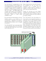
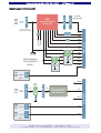
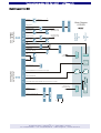
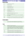
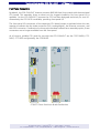
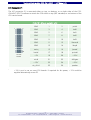
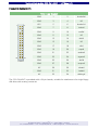
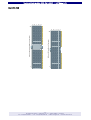
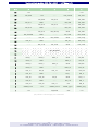
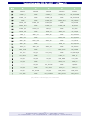
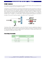
Technical Information
CC0-CHILLOUT • LPC Super-I/O Board
Document No. 3254 • Edition 5
2004-05
Technical Information CC0-CHILLOUT • LPC Super-I/O
Contents
About this Manual . . . . . . . . . . . . . . . . . . . . . . . . . . . . . . . . . . . . . . . . . . . . . . . . . . . . . . .
Edition History . . . . . . . . . . . . . . . . . . . . . . . . . . . . . . . . . . . . . . . . . . . . . . . . . . . . .
Related Documents . . . . . . . . . . . . . . . . . . . . . . . . . . . . . . . . . . . . . . . . . . . . . . . . .
Nomenclature . . . . . . . . . . . . . . . . . . . . . . . . . . . . . . . . . . . . . . . . . . . . . . . . . . . . .
Trade Marks . . . . . . . . . . . . . . . . . . . . . . . . . . . . . . . . . . . . . . . . . . . . . . . . . . . . . .
Legal Disclaimer - Liability Exclusion . . . . . . . . . . . . . . . . . . . . . . . . . . . . . . . . . . . . .
3
3
4
4
4
4
CC0-CHILLOUT Features . . . . . . . . . . . . . . . . . . . . . . . . . . . . . . . . . . . . . . . . . . . . . . . . . . . 5
Short Description . . . . . . . . . . . . . . . . . . . . . . . . . . . . . . . . . . . . . . . . . . . . . . . . . . . 6
Block Diagram CC0-CHILLOUT . . . . . . . . . . . . . . . . . . . . . . . . . . . . . . . . . . . . . . . . . 8
Block Diagram CCZ-RIO . . . . . . . . . . . . . . . . . . . . . . . . . . . . . . . . . . . . . . . . . . . . . . 9
Top View Component Assembly . . . . . . . . . . . . . . . . . . . . . . . . . . . . . . . . . . . . . . 10
On-Board Connectors . . . . . . . . . . . . . . . . . . . . . . . . . . . . . . . . . . . . . . . . . . . . . . 11
Front Panel Connectors . . . . . . . . . . . . . . . . . . . . . . . . . . . . . . . . . . . . . . . . . . . . . 11
Jumpers . . . . . . . . . . . . . . . . . . . . . . . . . . . . . . . . . . . . . . . . . . . . . . . . . . . . . . . . 11
Installing and Replacing Components . . . . . . . . . . . . . . . . . . . . . . . . . . . . . . . . . . . . . . . .
Before You Begin . . . . . . . . . . . . . . . . . . . . . . . . . . . . . . . . . . . . . . . . . . . . . . . . . .
Warnings . . . . . . . . . . . . . . . . . . . . . . . . . . . . . . . . . . . . . . . . . . . . . . . . . .
Caution . . . . . . . . . . . . . . . . . . . . . . . . . . . . . . . . . . . . . . . . . . . . . . . . . . .
Installing the Board . . . . . . . . . . . . . . . . . . . . . . . . . . . . . . . . . . . . . . . . . . . . . . . .
Removing the Board . . . . . . . . . . . . . . . . . . . . . . . . . . . . . . . . . . . . . . . . . . . . . . .
EMC Recommendations . . . . . . . . . . . . . . . . . . . . . . . . . . . . . . . . . . . . . . . . . . . . .
12
12
12
12
13
14
15
Technical Reference - Connectors . . . . . . . . . . . . . . . . . . . . . . . . . . . . . . . . . . . . . . . . . . .
Caution . . . . . . . . . . . . . . . . . . . . . . . . . . . . . . . . . . . . . . . . . . . . . . . . . . . . . . . . .
Please Note . . . . . . . . . . . . . . . . . . . . . . . . . . . . . . . . . . . . . . . . . . . . . . . . . . . . . .
Front Panel Connectors . . . . . . . . . . . . . . . . . . . . . . . . . . . . . . . . . . . . . . . . . . . . .
LPC Connector P1 . . . . . . . . . . . . . . . . . . . . . . . . . . . . . . . . . . . . . . . . . . . . . . . . .
IDE/ATA Connector P2 . . . . . . . . . . . . . . . . . . . . . . . . . . . . . . . . . . . . . . . . . . . . . .
IDE/ATA Connector P3 . . . . . . . . . . . . . . . . . . . . . . . . . . . . . . . . . . . . . . . . . . . . . .
Floppy Disk Connector P4 . . . . . . . . . . . . . . . . . . . . . . . . . . . . . . . . . . . . . . . . . . .
Power Connector P5 . . . . . . . . . . . . . . . . . . . . . . . . . . . . . . . . . . . . . . . . . . . . . . .
Micro Floppy Disc Connector P12 . . . . . . . . . . . . . . . . . . . . . . . . . . . . . . . . . . . . .
Fan Heatsink Header P6..P9 . . . . . . . . . . . . . . . . . . . . . . . . . . . . . . . . . . . . . . . . . .
MIDI/Gameport Header P10 . . . . . . . . . . . . . . . . . . . . . . . . . . . . . . . . . . . . . . . . .
MIDI Header P11 . . . . . . . . . . . . . . . . . . . . . . . . . . . . . . . . . . . . . . . . . . . . . . . . . .
Rear I/O J1/J2 . . . . . . . . . . . . . . . . . . . . . . . . . . . . . . . . . . . . . . . . . . . . . . . . . . . .
16
16
16
17
18
19
20
21
22
23
24
24
24
25
RS-232E Transceivers . . . . . . . . . . . . . . . . . . . . . . . . . . . . . . . . . . . . . . . . . . . . . . . . . . . . 28
Power Supply Requirements . . . . . . . . . . . . . . . . . . . . . . . . . . . . . . . . . . . . . . . . . . . . . . . 28
Schematics . . . . . . . . . . . . . . . . . . . . . . . . . . . . . . . . . . . . . . . . . . . . . . . . . . . . . . . . . . . . 29
-2EKF Elektronik GmbH • Philipp-Reis-Str. 4 • 59065 HAMM • Germany
Tel. +49 (0)2381/6890-0 • Fax. +49 (0)2381/6890-90 • E-Mail [email protected] • Internet www.ekf.de
Technical Information CC0-CHILLOUT • LPC Super-I/O
About this Manual
This manual is a short form description of the technical aspects of the CC0-CHILLOUT, required
for installation and system integration. It is intended for the very advanced user only.
Edition History
EKF
Document
Ed.
Text # 3254
cc0_tie.wpd
Contents/Changes
Author
Date
1
Technical Information CC0-CHILLOUT
English
Preliminary edition, to be completed later on
jj
6. Nov 03
2
Added table P11 (opt. MIDI header)
jj
24. Nov 03
3
Changed elements in table J1 (rear I/O
connector), regarding rows 7...3 (DVI
connector handover)
jj
18
December
2003
4
Added MTBF
jj
23 April
2004
5
Added block diagram CCZ-RIO
jj
7 May 2004
-3EKF Elektronik GmbH • Philipp-Reis-Str. 4 • 59065 HAMM • Germany
Tel. +49 (0)2381/6890-0 • Fax. +49 (0)2381/6890-90 • E-Mail [email protected] • Internet www.ekf.de
Technical Information CC0-CHILLOUT • LPC Super-I/O
Related Documents
For a description of the CPU card, which acts as a LPC controller and carrier board with respect
to the CC0-CHILLOUT, please refer to the correspondent CPU user guide, available by download
at http://www.ekf.de/c/ccpu/ccpu.html.
Nomenclature
Signal names used herein with an attached '#' designate active low lines.
Trade Marks
Some terms used herein are property of their respective owners, e.g.
Pentium, Celeron: ® Intel
CompactPCI : ® PICMG
Windows 98, Windows NT, Windows 2000, Windows XP: ® Microsoft
EKF does not claim this list to be complete.
Legal Disclaimer - Liability Exclusion
This manual has been edited as carefully as possible. We apologize for any potential mistake.
Information provided herein is designated exclusively to the proficient user (system integrator,
engineer). EKF can accept no responsibility for any damage caused by the use of this manual.
-4EKF Elektronik GmbH • Philipp-Reis-Str. 4 • 59065 HAMM • Germany
Tel. +49 (0)2381/6890-0 • Fax. +49 (0)2381/6890-90 • E-Mail [email protected] • Internet www.ekf.de
Technical Information CC0-CHILLOUT • LPC Super-I/O
CC0-CHILLOUT Features
Feature Summary
Form Factor
Single size Eurocard (160x100mm2), front panel width 4HP (20.3mm)
LPC Super-I/O
Chip
LPC47B27x, parallel port, 2 serial ports, floppy drive controller port,
keyboard controller & mouse port, infrared port, MIDI/gameport, fan
control ports, GPIOs, serial IRQs
Front Panel
Connectors
No front panel connectors are provided on the CC0-CHILLOUT, use the
CC6-ACID instead if front panel I/O is required
On-Board
Connectors 1
LPC Interface, IDE/ATA 40-pin header 2.54mm, IDE/ATA 44-pin header
2.00mm, floppy disk header 34-pin 2.54mm, floppy disk 26-pos. ZIF
socket, floppy disk power, 2 x fan heatsink header (pulse width
modulation), 2 x fan heatsink header (tacho generator), MIDI/gameport
header
Rear I/O
Connectors
J1: IDE, PS/2 KB/MS, RJ45 Ethernet 2, Video analog/digital 2
J2: Serial1/COM1, Serial2/COM2, LPT, floppy disk, USB 2, GPIO, IRDA
On-Board
Functions
Speaker, IDE activity, optional LEDs: GPIO21, GPIO22, GPIO43, GPIO60,
GPIO61, 3.3V, 5V, 12V
Hard Disk
Option
Hard disk drive 2.5-inch optional on-board
MTBF
0.185 * 106h
1
Not all of these connectors may be present on your actual CC0-CHILLOUT board.
Assembly of these connectors is highly custom specific. Discuss your needs with EKF
before ordering.
2
Available as an option only, which requires also the CPU carrier board to be assembled
custom specific, for passing the related signals to the CC0-CHILLOUT by board-to-board
stackers.
Subject to changes
-5EKF Elektronik GmbH • Philipp-Reis-Str. 4 • 59065 HAMM • Germany
Tel. +49 (0)2381/6890-0 • Fax. +49 (0)2381/6890-90 • E-Mail [email protected] • Internet www.ekf.de
Technical Information CC0-CHILLOUT • LPC Super-I/O
Short Description
Available as a companion board to the CC2TANGO, CC5-RAVE, CC7-JAZZ and the CC8BLUES CPU cards, the CC0-CHILLOUT is
provided with common legacy I/O ports.
Interconnection between the CC0 I/O
module and the CPU carrier board is
achieved by the LPC (Low Pin Count)
interface.
As an option, the CC0-CHILLOUT is available
with a rugged on-board 2.5-inch hard disk
drive.
The CC0-CHILLOUT has been designed for
rear I/O and therefore requires a non-bussed
single-slot P1/P2 backplane in addition to the
CompactPCI bus. However, if front panel I/O
is preferred, the CC6-ACID should be used
instead.
Typically, the CC0-CHILLOUT shares an 8HP
front panel together with the associated CPU
carrier board. Therefore the chosen CPU
board and the CC0 should be ordered as an
integral unit.
-6EKF Elektronik GmbH • Philipp-Reis-Str. 4 • 59065 HAMM • Germany
Tel. +49 (0)2381/6890-0 • Fax. +49 (0)2381/6890-90 • E-Mail [email protected] • Internet www.ekf.de
Technical Information CC0-CHILLOUT • LPC Super-I/O
The CC0-CHILLOUT communicates to the
host CPU by means of the LPC interface. This
is a multiplexed ISA bus, enabling the superI/O controller chip to emulate the legacy I/O
interfaces. Among these are parallel and
serial ports, the PS/2 interfaces, and last not
least the classic 1.4/2.8MB floppy disk
controller. As an option, the CC0-CHILLOUT
provides MIDI and gameport attachment,
and control outputs for fans with either
tachometer output or pulse width
modulation input.
Most of the functions of the CC0-CHILLOUT
are available for rear I/O across the
connectors J1/P1. A suitable rear I/O
transition module would be required in
addition in order to gain access to the I/O
ports from the systems back panel.
By connecting the boards together, the hosts
ATA/IDE interface is also available on the
CC0-CHILLOUT. Optionally, the board is
equipped with a robust 2.5-inch hard disk
drive, particularly suited for use in a rugged
environment.
The CC0-CHILLOUT must be inserted on a
slot outside of the CompactPCI backplane. A
single slot rear I/O P1/P2 backplane should
be present in the system rack at the CC0
reserved slot. Most EKF systems have the
CPCI busprint justified to the left margin of
the 19-inch rack, with the system slot (CPU
slot) orientated to the right end of the
backplane. Following next to the right side,
the CC0-CHILLOUT should be placed in
between the remaining free mounting space.
Several I/O functions are also directly
available by on-board headers on the CC0,
mainly the IDE and FD interfaces. Most of
the on-board connectors are only stuffed as
an option, however.
The CC0-CHILLOUT can be mounted either
on the left (bottom) side of the CPU board,
or right (top) side. Specify your actual needs
when ordering the unit.
Single-Slot Rear I/O Backplane
CPCI System Slot
P2
P2
P2
P2
P2
P1
P1
P1
P1
P1
P2
P2
J2
J1
© EKF
LPC
-7EKF Elektronik GmbH • Philipp-Reis-Str. 4 • 59065 HAMM • Germany
Tel. +49 (0)2381/6890-0 • Fax. +49 (0)2381/6890-90 • E-Mail [email protected] • Internet www.ekf.de
Technical Information CC0-CHILLOUT • LPC Super-I/O
LPC
(Low Pin Count)
Super I/O
LPCT (Top Mounting)
LPCB (Bottom Mounting)
P10
FDD P12
CC2
CC5
CC7
CC8
FDD P4/5
LPC P1
Block Diagram CC0-CHILLOUT
34
26
external
Floppy-Disk
FD
FAN
P6-P9
IRDA
KB/MS
Game
GPIO
LPT
J1
Spkr
ADM
811
COM1
RS-232E
SD
Block Diagram
CC0-CHILLOUT
SD
J-SER1
Option
© EKF
SER1
Option
ADM
811
Rear I/O J2
MIDI
P11
TTL
COM2
RS-232E
SER2
TTL
USB1
J-SER2
USB1
CC2
CC5
CC7
Option
40
IDE1
EN
44
IDE2
Optional On-Board
Ultra ATA 2.5-"
Hard Disk Drive
IDE
Game
Super I/O
CC2
CC5
CC7
RJ45
RJ45
CC2
CC5
CC7
DVI-I
J-IDE2
DVI
Option
-8EKF Elektronik GmbH • Philipp-Reis-Str. 4 • 59065 HAMM • Germany
Tel. +49 (0)2381/6890-0 • Fax. +49 (0)2381/6890-90 • E-Mail [email protected] • Internet www.ekf.de
Rear I/O J1
CC2
CC5
CC7
Super I/O
Primary IDE P3
Primary IDE P2
KB/MS
Bus
Switch
Technical Information CC0-CHILLOUT • LPC Super-I/O
Block Diagram CCZ-RIO
J1
RS-232-1 (COM1)
Rear Panel COM2
Optional Flat Cable
Rear Panel COM1
Optional Flat Cable
Serial-1 (TTL)
4HP
Rear Panel
I/O
Serial-2 (TTL)
Option 8HP
Rear Panel
I/O
J2 Rear I/O
Rear I/O Connector
CC0-CHILLOUT
CCA-LAMBADA
RS-232-2 (COM2)
Block Diagram
CCZ-RIO
COM2
Floppy Disk I/F
Floppy ZIF 26
GPIO (J1)
Floppy 34
GPIO (J2)
USB
USB
Speaker
Parallel Printer
Fan Control, IRDA I/O
MIDI
RS-232-2 (J2)
Optional Flat Cable
Game
ETH
Ethernet (available with CC0-CHILLOUT as an option)
MS
KB
MS
VGA
PS/2 Keyboard/Mouse
DVI-I Digital & Analog Video (available with CC0-CHILLOUT as an option)
RS-232-1 (J2)
Optional Flat Cable
GPIO (J1)
GPIO Connector
COM1
J1 Rear I/O
Rear I/O Connector
CC0-CHILLOUT
CCA-LAMBADA
Reset, Key Lock
IDE/ATA I/F (Secondary IDE)
PWR
+5V
-9EKF Elektronik GmbH • Philipp-Reis-Str. 4 • 59065 HAMM • Germany
Tel. +49 (0)2381/6890-0 • Fax. +49 (0)2381/6890-90 • E-Mail [email protected] • Internet www.ekf.de
Technical Information CC0-CHILLOUT • LPC Super-I/O
LED1
P2
P5
FUSE4
P12
1
P11
1
LED5
1
ST1
FUSE2
P1 LPCT
J1
Rear I/O
Hard Disk Drive
2.5-Inch
Option
P3
1
ST2
DVI
SIO
LED2
© EKF
FUSE1
LED3
P10
RJ45
LED4
J2
LED6
Rear I/O
J_IDE2
J_SER2
J_SER1
FUSE5
P9
1
USB
P4
P8
P7
P6
FUSE3
Top View Component Assembly
CC0-CHILLOUT
- 10 EKF Elektronik GmbH • Philipp-Reis-Str. 4 • 59065 HAMM • Germany
Tel. +49 (0)2381/6890-0 • Fax. +49 (0)2381/6890-90 • E-Mail [email protected] • Internet www.ekf.de
Technical Information CC0-CHILLOUT • LPC Super-I/O
On-Board Connectors
P1
LPC Low Pin Count interface
P2
IDE 40-pin header
P3
IDE 44-pin header
P4
Floppy disk header 34-pin
P5
Floppy disk power (opt.)
P6..P9
Fan heatsink headers (opt.)
P10
MIDI/gameport header (opt.)
P11
Midi header (opt.)
P12
Floppy disk header 26-pos. ZIF
J1
Rear I/O metric connector 5 x 25 brown key
J2
Rear I/O metric connector 5 x 22
DVI
Re-routing of host CPU front panel video connector analog/digital
(opt. stacker)
RJ45
Re-routing of host CPU front panel Ethernet connector (opt. stacker)
USB
Re-routing of host CPU USB front panel connector (opt. stacker)
Front Panel Connectors
No front panel connectors available with the CC0-CHILLOUT
Make use of the CC6-ACID instead if front panel I/O is required
Jumpers
J-IDE2
Enables IDE bus switches when set
Please note: In order to make use of the header P3 (IDE interface for
2.5-inch hard disk) or rear I/O IDE across J1, either connected to an
on-board HDD or an external drive, the jumper J-IDE must be set.
However, if neither P3 nor J1 is in use, J-IDE must be removed in
order to avoid reflections on the IDE bus caused by tapped signal
traces.
J-SER1
Enables the optional RS-232 transceiver (COM1) when set
If removed, the transceiver is in a high-impedance shutdown mode
J-SER2
Enables the optional RS-232 transceiver (COM2) when set
If removed, the transceiver is in a high-impedance shutdown mode
- 11 EKF Elektronik GmbH • Philipp-Reis-Str. 4 • 59065 HAMM • Germany
Tel. +49 (0)2381/6890-0 • Fax. +49 (0)2381/6890-90 • E-Mail [email protected] • Internet www.ekf.de
Technical Information CC0-CHILLOUT • LPC Super-I/O
Installing and Replacing Components
Before You Begin
Warnings
The procedures in this chapter assume familiarity with the general terminology associated with
industrial electronics and with safety practices and regulatory compliance required for using and
modifying electronic equipment.
Disconnect the system from its power
source and from any telecommunication
lin ks, n e tw o r ks or modem s b e f o r e
performing any of the procedures
described in this chapter. Failure to
disconnect power, or telecommunication
links before you open the system or
perform any procedures can result in
personal injury or equipment damage.
Some parts of the system can continue to operate even though the power switch is in its off
state.
Caution
Electrostatic discharge (ESD) can damage components. Perform the procedures described in this
chapter only at an ESD workstation. If
such a station is not available, you can
provide some ESD protection by wearing
an antistatic wrist strap and attaching it
to a metal part of the system chassis or
board front panel. Store the board only
in its original ESD protected packaging.
Retain the original packaging (antistatic
bag and antistatic box) in case of returning the board to EKF for rapair.
- 12 EKF Elektronik GmbH • Philipp-Reis-Str. 4 • 59065 HAMM • Germany
Tel. +49 (0)2381/6890-0 • Fax. +49 (0)2381/6890-90 • E-Mail [email protected] • Internet www.ekf.de
Technical Information CC0-CHILLOUT • LPC Super-I/O
Installing the Board
Warning
This procedure should be done only by qualified technical personnel. Disconnect the system
from its power source before doing the procedures described here. Failure to disconnect power,
or telecommunication links before you open the system or perform any procedures can result in
personal injury or equipment damage.
Typically you will perform the following steps:
C
Switch off the system, remove the AC power cord
C
Attach your antistatic wrist strap to a metallic part of the system
C
Remove the board packaging, be sure to touch the board only at the front panel
C
Identify the related CompactPCI slot (peripheral slot for I/O boards, system slot for CPU
boards, with the system slot typically most right or most left to the backplane)
C
Insert card carefully (be sure not to damage components mounted on the bottom side of
the board by scratching neighboured front panels)
C
A card with onboard connectors requires attachment of associated cabling now
C
Lock the ejector lever, fix screws at the front panel (top/bottom)
C
Retain original packaging in case of return
- 13 EKF Elektronik GmbH • Philipp-Reis-Str. 4 • 59065 HAMM • Germany
Tel. +49 (0)2381/6890-0 • Fax. +49 (0)2381/6890-90 • E-Mail [email protected] • Internet www.ekf.de
Technical Information CC0-CHILLOUT • LPC Super-I/O
Removing the Board
Warning
This procedure should be done only by qualified technical personnel. Disconnect the system
from its power source before doing the procedures described here. Failure to disconnect power,
or telecommunication links before you open the system or perform any procedures can result in
personal injury or equipment damage.
Typically you will perform the following steps:
C
Switch off the system, remove the AC power cord
C
Attach your antistatic wrist strap to a metallic part of the system
C
Identify the board, be sure to touch the board only at the front panel
C
unfasten both front panel screws (top/bottom), unlock the ejector lever
C
Remove any onboard cabling assembly
C
Activate the ejector lever
C
Remove the card carefully (be sure not to damage components mounted on the bottom
side of the board by scratching neighboured front panels)
C
Store board in the original packaging, do not touch any components, hold the board at
the front panel only
Warning
Do not expose the card to fire. Battery cells and other components could
explode and cause personal injury.
- 14 EKF Elektronik GmbH • Philipp-Reis-Str. 4 • 59065 HAMM • Germany
Tel. +49 (0)2381/6890-0 • Fax. +49 (0)2381/6890-90 • E-Mail [email protected] • Internet www.ekf.de
Technical Information CC0-CHILLOUT • LPC Super-I/O
EMC Recommendations
In order to comply with the CE regulations for EMC, it is mandatory to observe the following
rules:
C
The chassis or rack including other boards in use must comply entirely with CE
C
Close all board slots not in use with a blind front panel
C
Front panels must be fastened by built-in screws
C
Cover any unused front panel mounted connector with a shielding cap
C
External communications cable assemblies must be shielded (shield connected only at
one end of the cable)
C
Use ferrite beads for cabling wherever appropriate
C
Some connectors may require additional isolating parts (e.g. 10Base-2 BNC T-connector)
Reccomended Accessories
Blind CPCI Front
Panels
EKF Elektronik
Widths currently available (1HP=5.08mm):
with handle 4HP/8HP
without handle 2HP/4HP/8HP/10HP/12HP
Ferrit Bead Filters
ARP Datacom,
63115 Dietzenbach
Ordering No.
102 820 (cable diameter 6.5mm)
102 821 (cable diameter 10.0mm)
102 822 (cable diameter 13.0mm)
Isolating Elements
ARP Datacom,
63115 Dietzenbach
Ordering No. 182 068
(Cheapernet T-connector)
Metal Shielding
Caps
Conec-Polytronic,
59557 Lippstadt
Ordering No.
CDFA 09 165 X 13129 X (DB9)
CDSFA 15 165 X 12979 X (DB15)
CDSFA 25 165 X 12989 X (DB25)
- 15 EKF Elektronik GmbH • Philipp-Reis-Str. 4 • 59065 HAMM • Germany
Tel. +49 (0)2381/6890-0 • Fax. +49 (0)2381/6890-90 • E-Mail [email protected] • Internet www.ekf.de
Technical Information CC0-CHILLOUT • LPC Super-I/O
Technical Reference - Connectors
Caution
Some of the connectors provide operating voltage (e.g. 5V and 12V) to devices inside the
system chassis, such as fans and internal peripherals. Not all of these connectors are overcurrent
protected. Do not use these connectors for powering devices external to the computer chassis.
A fault in the load presented by the external devices could cause damage to the board, the
interconnecting cable and the external devices themselves.
Please Note
The CC0-CHILLOUT transition module may be equipped with several on-board connectors for
system internal usage. Not all of these connectors may be present on a particular board. Be sure
to specify your individual needs when ordering the CC0 board. Characteristic features and the
pin assignments of each connector are described on the following pages (connector designation
in alphabetical order).
- 16 EKF Elektronik GmbH • Philipp-Reis-Str. 4 • 59065 HAMM • Germany
Tel. +49 (0)2381/6890-0 • Fax. +49 (0)2381/6890-90 • E-Mail [email protected] • Internet www.ekf.de
Technical Information CC0-CHILLOUT • LPC Super-I/O
Front Panel Connectors
By default, the CC0-CHILLOUT shares a common 8HP (40.6mm) front panel with the associated
CPU board. This assembly forms a robust unit for rugged conditions. No front panel I/O is
available for the CC0-CHILLOUT, because the CC0 has been designed exclusively for rear I/O.
Alternatively the CC6-ACID is available, providing front panel I/O.
The front panel I/O connectors of the respective CPU board remain unviolated unless the user
requires to redirect also the video connector (DVI-I analog/digital), the Ethernet connector, and
the USB1 connector. If redirection for these ports has been ordered as an assembly option, these
connectors are no longer available from the front panel.
As of current, suitable CPU cards for use with the CC0-CHILLOUT are the CC2-TANGO, CC5RAVE, CC7-JAZZ and (partially) the CC8-BLUES.
CC0CHILLOUT
CC2TANGO
CC0CHILLOUT
CC2TANGO
U
S
B
GP
GP
PWR/RES
IDE
PWR/RES
IDE
E
T
H
D
V
I
CC0/CC2 Front Panel w/o & with Redirection
- 17 EKF Elektronik GmbH • Philipp-Reis-Str. 4 • 59065 HAMM • Germany
Tel. +49 (0)2381/6890-0 • Fax. +49 (0)2381/6890-90 • E-Mail [email protected] • Internet www.ekf.de
Technical Information CC0-CHILLOUT • LPC Super-I/O
LPC Connector P1
The LPC connector P1 is mounted either on top, on bottom, or on both sides of the CC0CHILLOUT PCB. This allows to attach the CC0 either on top (EKF standard) or on bottom of the
CPU carrier board.
P1 (LPT) 1.27mm Socket 2 x 13
1
2
26
1.27mm
Socket
1
GND
1
2
pciclk
GND
3
4
lad0
GND
5
6
lad1
GND
7
8
lad2
GND
9
10
lad3
GND
11
12
lframe#
GND
13
14
ldrq#
serirq
15
16
lpme#
lsmi#
17
18
pcirst#
+5V
19
20
+3.3V
rcin#
21
22
a20gate
+12V 1
23
24
+3.3V
sio_clk14
25
26
speaker
+12V is not in use on most CPU boards. If required for fan power, +12V could be
supplied alternatively across P5.
- 18 EKF Elektronik GmbH • Philipp-Reis-Str. 4 • 59065 HAMM • Germany
Tel. +49 (0)2381/6890-0 • Fax. +49 (0)2381/6890-90 • E-Mail [email protected] • Internet www.ekf.de
Technical Information CC0-CHILLOUT • LPC Super-I/O
IDE/ATA Connector P2
P2 (2.54mm Dual Row Pin Header)
1
2
Key
39
40
2.54mm
reset#
1
2
GND
d07
3
4
d08
d06
5
6
d09
d05
7
8
d10
d04
9
10
d11
d03
11
12
d12
d02
13
14
d13
d01
15
16
d14
d00
17
18
d15
GND
19
20
KEY
dmarq
21
22
GND
iow#
23
24
GND
ior#
25
26
GND
iordy
27
28
dmack#
29
30
intrq
31
32
a1
33
34
cblid#
a0
35
36
a2
cs1#
37
38
cs3#
act#
39
40
GND
GND
40
IDE1
EN
44
IDE2
Optional On-Board
Ultra ATA 2.5-"
Hard Disk Drive
IDE2
J-IDE2
- 19 EKF Elektronik GmbH • Philipp-Reis-Str. 4 • 59065 HAMM • Germany
Tel. +49 (0)2381/6890-0 • Fax. +49 (0)2381/6890-90 • E-Mail [email protected] • Internet www.ekf.de
Rear I/O J1
Bus
Switch
Primary IDE P3
CC2
CC5
CC7
Primary IDE P2
P2 is provided for attachment of classic IDE devices (e.g. 3.5-" hard disk drive, DVD-ROM). Usage
of the IDE connector P2 requires the IDE bus switches disabled (jumper J-IDE2 removed). No
stubs are allowed on an IDE cable assembly, i.e. use either P2 (J-IDE2 removed), or P3 (J-IDE2
set), or rear I/O IDE (J-IDE2 set).
Technical Information CC0-CHILLOUT • LPC Super-I/O
IDE/ATA Connector P3
P3 (2.00mm Header)
1
43
2
44
2.00mm
reset#
1
2
GND
d07
3
4
d08
d06
5
6
d09
d05
7
8
d10
d04
9
10
d11
d03
11
12
d12
d02
13
14
d13
d01
15
16
d14
d00
17
18
d15
GND
19
20
KEY
dmarq
21
22
GND
iow#
23
24
GND
ior#
25
26
GND
iordy
27
28
NC
dmack#
29
30
GND
intrq
31
32
NC
a1
33
34
cblid#
a0
35
36
a2
cs1#
37
38
cs3#
act#
39
40
GND
drvpwr
41
42
drvpwr
GND
43
44
NC
P3 is provided for a 2.5-" on-board hard disk drive. Either usage of the IDE connector P3, or rear
I/O IDE across connector J1 require the IDE bus switches enabled (jumper J-IDE2 set). No stubs
are allowed on a IDE cable assembly, i.e. exclusively use either P2 (J-IDE2 removed), or P3 (J-IDE2
set), or rear I/O IDE (J-IDE2 set).
- 20 EKF Elektronik GmbH • Philipp-Reis-Str. 4 • 59065 HAMM • Germany
Tel. +49 (0)2381/6890-0 • Fax. +49 (0)2381/6890-90 • E-Mail [email protected] • Internet www.ekf.de
Technical Information CC0-CHILLOUT • LPC Super-I/O
Floppy Disk Connector P4
P4 (2.54mm Header)
1
2
33
34
2.54mm
GND
1
2
drvden0#
GND
3
4
NC
KEY
5
6
drvden1#
GND
7
8
index#
GND
9
10
mtr0#
GND
11
12
NC
GND
13
14
ds0#
GND
15
16
NC
GND
17
18
dir#
GND
19
20
step#
GND
21
22
wdata#
GND
23
24
wgate#
GND
25
26
trk0#
GND
27
28
wrtprt#
NC
29
30
rdata#
GND
31
32
hdsel#
NC
33
34
dskchg#
The CC0-CHILLOUT is provided with a 34-pin header, suitable for attachment of a single floppy
disk drive with mating connector.
- 21 EKF Elektronik GmbH • Philipp-Reis-Str. 4 • 59065 HAMM • Germany
Tel. +49 (0)2381/6890-0 • Fax. +49 (0)2381/6890-90 • E-Mail [email protected] • Internet www.ekf.de
Technical Information CC0-CHILLOUT • LPC Super-I/O
Power Connector P5
P5
1
AMP 171826-4
1
+5V/1.25A
2
GND
3
GND
4
+12V/1.25A
The initial purpose of the optional connector P5 was to deliver +5V power to an attached
floppy disk drive wired to P4. A suitable cable assembly matching the AMP 171826-4 would be
required. Alternatively, P5 can be used to pass +5V and +12V redundantly (in addition to the
LPC connector P1) to the CC0-CHILLOUT, which can improve the power distribution when an
on-board hard disk drive is in use (especially if a pair of drives is connected to P3). The current
across P5 is limited by resettable fuses.
- 22 EKF Elektronik GmbH • Philipp-Reis-Str. 4 • 59065 HAMM • Germany
Tel. +49 (0)2381/6890-0 • Fax. +49 (0)2381/6890-90 • E-Mail [email protected] • Internet www.ekf.de
Technical Information CC0-CHILLOUT • LPC Super-I/O
Micro Floppy Disc Connector P12
P12 (1mm ZIF Receptacle)
1
26
1mm pitch
FFC/FPC receptacle
vertical ZIF 26-position
1
+5V
2
index#
3
+5V
4
ds0#
5
+5V
6
dskchg#
7
NC
8
NC
9
drvden0#
10
mtr0#
11
NC
12
dir#
13
modsel
14
step#
15
GND
16
wdata#
17
GND
18
wgate#
19
GND
20
trk0#
21
NC
22
wrtprt#
23
GND
24
rdata#
25
GND
26
hdsel#
In addition to P4, the CC0-CHILLOUT is also provided with a 26-position FFC/FPC ZIF socket,
suitable for attachment of a single floppy disk drive with mating connector (typically low profile
drives, e.g. TEAC FD05HF5630, Y-E Data YD-702J-6637, Citizen X1DE-00R, Mitsumi D353F3,
Samsung SFD-321S, NEC FD1238H).
You may chose either the P4 connector or P12, but not both simultaneously.
- 23 EKF Elektronik GmbH • Philipp-Reis-Str. 4 • 59065 HAMM • Germany
Tel. +49 (0)2381/6890-0 • Fax. +49 (0)2381/6890-90 • E-Mail [email protected] • Internet www.ekf.de
Technical Information CC0-CHILLOUT • LPC Super-I/O
Fan Heatsink Header P6..P9
P6 - P9 (2.54mm Pin Row)
1
GND
2
+12V
3
Control
2.54mm
1
GND
2
+12V
3
Tachometer (P6/P7)
Pulse Width Modulation (P8/P9)
MIDI/Gameport Header P10
P10 (2.54mm Header)
1
2
15
16
2.54mm
5V
1
2
5V
joy1but1
3
4
joy2but1
joy1x
5
6
joy2x
GND
7
8
midi_out
GND
9
10
joy2y
joy1y
11
12
joy2but2
joy1but2
13
14
midi_in
GND
15
16
NC
MIDI Header P11
P11 (2.54mm Pin Row)
1
Midi-In
2
GND
3
Midi-Out
2.54mm
1
MIDI-IN
2
GND
3
MIDI-OUT
- 24 EKF Elektronik GmbH • Philipp-Reis-Str. 4 • 59065 HAMM • Germany
Tel. +49 (0)2381/6890-0 • Fax. +49 (0)2381/6890-90 • E-Mail [email protected] • Internet www.ekf.de
Technical Information CC0-CHILLOUT • LPC Super-I/O
Rear I/O J1/J2
a b c d e f
25
a b c d e f
J2 Rear I/O 2mm Metric Connector
J1 Rear I/O 2mm Hard Metric Connector
22
1
1
- 25 EKF Elektronik GmbH • Philipp-Reis-Str. 4 • 59065 HAMM • Germany
Tel. +49 (0)2381/6890-0 • Fax. +49 (0)2381/6890-90 • E-Mail [email protected] • Internet www.ekf.de
Technical Information CC0-CHILLOUT • LPC Super-I/O
#J1
A
B
25
+5V
24
IDE_d08
+5V
23
+3.3V
22
C
D
E
+3.3V
+5V
VI/O
IDE_reset#
IDE_d07
IDE_d09
IDE_d10
+5V
IDE_d06
IDE_d11
GND
+3.3V
IDE_d04
IDE_d05
21
+3.3V
IDE_d12
IDE_d13
M66EN (GND)
IDE_d03
20
IDE_d14
GND
VI/O
IDE_d01
IDE_d02
19
+3.3V
IDE_d15
IDE_dmarq
GND
IDE_d00
18
IDE_dmack#
GND
+3.3V
IDE_ior#
IDE_iow#
17
+3.3V
IDE_a1
IDE_cblid#
GND
IDE_iordy
16
IDE_a2
GND
VI/O
IDE_a0
IDE_intrq
15
+3.3V
IDE_cs1#
IDE_act#
GND
IDE_cs0#
14
13
KEY (BROWN)
12
11
RJ45_1
RJ45_2
RJ45_3
GND
KB_dat
10
RJ45_4
GND
+3.3V
RJ45_5
KB_clk
9
RJ45_6
RJ45_7
RJ45_8
GND
MS_dat
8
RJ45_9
GND
VI/O
RJ45_10
MS_clk
7
DVI_17
DVI_9
DVI_10
GND
+5V_km
6
DVI_18
GND
+3.3V
DVI_1
DVI_2
5
DVI_24
DVI_23
DVI_6
GND
DVI_14
4
DVI_C2
GND
VI/O
DVI_16
DVI_7
3
DVI_C4
DVI_C3
DVI_C1
+5V
DVI_8
2
GAME_but11
+5V
GAME_but12
GAME_joy1x
GAME_joy1y
1
+5V
-12V
keylock#
+12V
+5V
pin positions coloured gray: not connected
- 26 EKF Elektronik GmbH • Philipp-Reis-Str. 4 • 59065 HAMM • Germany
Tel. +49 (0)2381/6890-0 • Fax. +49 (0)2381/6890-90 • E-Mail [email protected] • Internet www.ekf.de
Technical Information CC0-CHILLOUT • LPC Super-I/O
#J2
A
B
C
D
E
22
GPIO21
GPIO22
GPIO43
GPIO60
GPIO61
21
COM1_ri
GND
COM2_ri
COM2_cts
FD_drvden0#
20
COM1_cts
GND
COM2_rxd
GND
FD_drvden1#
19
GND
GND
COM2_dsr
COM2_dcd
FD_index#
18
COM1_rxd
COM1_dsr
COM2_dtr
GND
FD_mtr0#
17
COM1_dcd
GND
COM2_rts
COM2_txd
FD_ds0#
16
COM1_dtr
COM1_rts
SER2_ri
GND
FD_dir#
15
COM1_txd
GND
SER2_cts
SER2_rxd
FD_step#
14
SER1_ri
SER1_cts
SER2_dsr
GND
FD_wdata#
13
SER1_rxd
GND
V(I/O)
SER2_dcd
FD_wgate#
12
SER1_dsr
SER1_dcd
SER2_dtr
GND
FD_trk0#
11
SER1_dtr
GND
V(I/O)
SER2_rts
FD_wrtprt#
10
SER1_rts
SER1_txd
SER2_txd
GND
FD_rdata#
9
SER1_shdn
GND
V(I/O)
SER2_shdn
FD_hdsel#
8
LPT_slct
LPT_pe
LPT_busy
GND
FD_dskchg#
7
LPT_ack#
GND
V(I/O)
USB1_d+
USB1_d-
6
LPT_d7
LPT_d6
LPT_d5
USB_GND
+5V_usb1
5
LPT_d4
GND
V(I/O)
MIDI_out
MIDI_in
4
V(I/O)
LPT_d3
LPT_slctin#
GND
speaker
3
LPT_d2
GND
LPT_init#
IRDA_tx
IRDA_rx
2
LPT_d1
LPT_error#
LPT_d0
FAN_tach2
FAN_tach1
1
LPT_alf#
GND
LPT_strobe#
FAN_pwm2
FAN_pwm1
pin positions coloured gray: not connected
- 27 EKF Elektronik GmbH • Philipp-Reis-Str. 4 • 59065 HAMM • Germany
Tel. +49 (0)2381/6890-0 • Fax. +49 (0)2381/6890-90 • E-Mail [email protected] • Internet www.ekf.de
Technical Information CC0-CHILLOUT • LPC Super-I/O
RS-232E Transceivers
The Super-I/O chip provides two asynchronous serial ports (TTL level), which are passed via the
J2 rear I/O connector to a rear I/O transition module.
Furthermore, the CC0-CHILLOUT is optionally provided with two serial transceivers according to
RS-232E. As with the TTL level serial port signals, also the RS-232 transmission lines are wired to
the J2 rear I/O connector for usage on a transition module (back panel COM port connectors).
Each transceiver can be individually disabled by the jumpers J-SER1 and J-SER2, if either the
particular RS-232 interface is not at all required (with a power saving effect), or if a different
interface type is required, e.g. EIA/TIA-485 or optically isolated RS-232 (physical transceivers
located on the rear I/O transition module, attached to the TTL level signals).
Conclusion: Each on-board transceiver on the CC0-CHILLOUT must be enabled by setting its
associated jumper J-SERx in order to use the COMx rear panel connector(s). If however the serial
TTL lines are needed for a special interface solution, the particular on-board transceiver(s) must
be disabled by removing its jumper J-SERx.
Power Supply Requirements
Operating
Voltage
max. Current
+5V / ±0.25V
TBD
+3.3V / ±0.1V
TBD
+12V / ±0.5V
TBD
- 28 EKF Elektronik GmbH • Philipp-Reis-Str. 4 • 59065 HAMM • Germany
Tel. +49 (0)2381/6890-0 • Fax. +49 (0)2381/6890-90 • E-Mail [email protected] • Internet www.ekf.de
Technical Information CC0-CHILLOUT • LPC Super-I/O
Schematics
Complete circuit diagrams for this product are available for customers on request. Signing of a
non-disclosure agreement would be needed. Please contact [email protected] for details.
EKF reserves the right to refuse distribution of confidential information material for any reason
that EKF may consider substantial.
- 29 EKF Elektronik GmbH • Philipp-Reis-Str. 4 • 59065 HAMM • Germany
Tel. +49 (0)2381/6890-0 • Fax. +49 (0)2381/6890-90 • E-Mail [email protected] • Internet www.ekf.de
Technical Information CC0-CHILLOUT • LPC Super-I/O
EKF Elektronik GmbH
Philipp-Reis-Str. 4
59065 HAMM
Germany
Fax. +49 (0)2381/6890-90
Tel. +49 (0)2381/6890-0
Internet www.ekf.de
E-Mail [email protected]