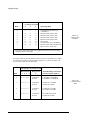
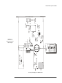
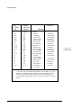
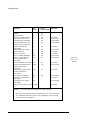
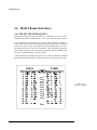
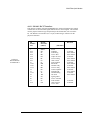
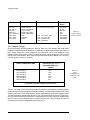
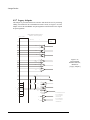
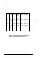
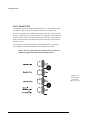
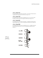
1
Modems
Model 2240
Fiber Optic Modem
Users Manual
Canoga Perkins
Caution!
This product may contain a laser diode emitter operating at a wavelength of 1300 nm - 1600 nm. Use
of optical instruments (for example: collimating optics) with this product may increase eye hazard.
Use of controls or adjustments or performing procedures other than those specified herein may result
in hazardous radiation exposure.
Under normal conditions, the radiation levels emitted by this product are under the Class 1 limits in 21
CFR Chapter 1, Subchapter J.
ATTENTION!
Cet équipement peut avoir une diode laser émettant à des longueurs d'onde allant de 1300nm à
1600nm. L’utilisation d’instruments optiques (par exemple : un collimateur optique) avec cet
équipement peut s’avèrer dangereuse pour les yeux. Procéder à des contrôles, des ajustements ou toute
procédure autre que celles décrites ci-après peut provoquer une exposition dangereuse à des radiations.
Sous des conditions normales, le niveau des radiations émises par cet équipement est en dessous des
limites prescrites dans CFR21, chapitre 1, sous chapitre J.
Notice!
This device contains static sensitive components. It should be handled only with proper Electrostatic Discharge (ESD) grounding procedures.
NOTE!
Cet équipement contient des composants sensibles aux décharges électro-statiques. Il doit
absolument être manipulé en respectant les règles de mise à la terre afin de prévenir de telles
décharges.
2
2240 Fiber Optic Modem
Notice!
Canoga Perkins has prepared this manual for use by customers and Canoga Perkins personnel as a guide for the proper installation, operation and/or maintenance of Canoga Perkins
equipment. The drawings, specifications and information contained in this document are the
property of Canoga Perkins and any unauthorized use or disclosure of such drawings,
specifications and information is prohibited.
Canoga Perkins reserves the right to change or update the contents of this manual and to
change the specifications of its products at any time without prior notification. Every effort has
been made to keep the information in this document current and accurate as of the date of
publication or revision. However, no guarantee is given or implied that the document is error
free or that it is accurate with regard to any specification.
CANOGA PERKINS CORPORATION
An Inductotherm Company
20600 Prairie Street
Chatsworth, CA 91311-6008
Business Phone: (818) 718-6300
(Monday through Friday 7 a.m. - 5 p.m. Pacific Time)
FAX: (818) 718-6312 (24 hrs.)
Web Site: www.canoga.com
Email: [email protected]
Copyright © 1991, 1992, 1993, 1994, 1996, 1997, 1998, 2000, 2001
Canoga Perkins Corporation
All Rights Reserved
Model 2240
Fiber Optic Modem
Model Number 2240 - UM
Users Manual
Part Number 6911100
Rev. K 06/2001
To reference Technical Advisories and Product Release Notes, go to Canoga Perkins’
website: http://www.canoga.com/cservice.htm
3
Canoga Perkins
Model 2240 Fiber Optic Modem
4
2240 Fiber Optic Modem
Table of Contents
1. Description .................................................... 11
1.1 2240 Modem ................................................................ 11
1.1.1 Functions, LEDs and Switches ............................................. 12
1.2
1.3
1.4
1.5
2201 Rack Chassis ...................................................... 13
2202 Modem Shelf ...................................................... 13
2200R Series Redundant Card .................................. 14
Modem Operation ...................................................... 14
1.5.1
1.5.2
1.5.3
1.5.4
1.5.5
1.5.6
1.5.7
General .................................................................................. 14
System Test and Diagnostics ................................................ 16
Transmit Section ................................................................... 16
Receive Section ..................................................................... 17
Expanded Interface Control Channels .................................. 17
Expanded Interface Auxiliary Channels ............................... 17
Fiber Optics ........................................................................... 18
1.6 Loss Budget ................................................................. 18
1.7 Initial Unit Testing ..................................................... 18
2. Installation and Setup .................................. 19
2.1 Installation .................................................................. 19
2.1.1
2.1.2
2.1.3
2.1.4
2.1.5
2.1.6
Unpacking the Unit ............................................................... 19
Standalone Modem Installation ............................................ 19
Rack-Mount Modem Installation .......................................... 20
Fiber Cable and Connectors .................................................. 20
2202 Modem Shelf Installation ............................................. 21
Custom Oscillator Installation .............................................. 21
2.2 Setup ............................................................................ 22
2.2.1 HI / LO Optic Power Switch ................................................. 22
2.2.2 Internal Control Switches ...................................................... 24
2.2.2.1 Carrier Detect (CD) Signal Options ................................... 24
2.2.2.2 Internal Clock Option Switches ......................................... 25
2.2.2.2.1 TBL / NORM Switch ...................................................... 25
2.2.2.2.2 CLK / EXT Switch .......................................................... 25
2.2.3 Signal Ground Strap .............................................................. 26
2.2.4 SCT Normal / Invert Jumper ................................................. 26
2.2.5 EXTRA CLOCK Jumper ...................................................... 27
5
Canoga Perkins
3. Mode and Rate Selection ............................ 29
3.1 Operating Mode / Data Rate Selection ..................... 29
3.2 External Clock Modes ................................................ 31
3.2.1 Sampled External Clock Mode - Mode 0 ............................... 31
3.2.2 Locked External Clock Mode - Mode 7 ................................. 32
3.3 Internal Clock Modes - Modes 1, 2, 3, 4 ................... 32
3.3.1 Standard Internal Clock Rates (Groups 1, 2 and 3) ............... 33
3.3.2 Custom Internal Clock Rates (Group 4) ................................ 33
3.4 Slave Clock Mode - Mode 5 ....................................... 35
3.4.1 Loopback Clock for Slave Mode ........................................... 35
3.5 Asynchronous Mode - Mode 6 ................................... 35
3.6 Consideration of Propagation Delays ....................... 37
3.7 Internal Clock Option Switches ................................. 38
3.7.1 TBL / NORM Switch ............................................................. 38
3.7.2 CLK / EXT Switch ................................................................ 38
4. Data Interfaces .............................................. 41
4.1 Data Interfaces Overview .......................................... 41
4.2 RS-423 / 232D Model 432 ........................................... 42
4.2.1
4.2.2
4.2.3
4.2.4
4.2.5
RTS_BIAS Jumper ............................................................... 44
DCD Jumper ......................................................................... 44
CTS_GATE Jumper .............................................................. 44
DSR Jumper .......................................................................... 45
CH_GND Jumper .................................................................. 45
4.3 RS-449 / 422 Model 422.............................................. 45
4.3.1
4.3.2
4.3.3
4.3.4
4.3.5
4.3.6
RS_BIAS Jumper .................................................................. 48
RR Jumper............................................................................. 48
CS_GATE Jumper ................................................................ 48
DM Jumper ........................................................................... 49
CH_GND Jumper .................................................................. 49
UNBAL_REF Jumper ........................................................... 49
4.4 RS-530 Interface Model 430 ...................................... 50
4.4.1 RTS_BIAS Jumper ............................................................... 52
4.4.2 DCD Jumper ......................................................................... 52
6
2240 Fiber Optic Modem
4.4.3 DSR Jumper .......................................................................... 52
4.4.4 CHASSIS_GND Jumper ....................................................... 52
4.4.5 SCT Switch ........................................................................... 54
4.4.6 CTS_GATE Jumper .............................................................. 54
4.4.7 CTS_OUT Jumper ................................................................ 54
4.4.8 CTS (A) Jumper .................................................................... 54
4.4.8.1 KG_SWING Jumper .......................................................... 54
4.4.8.2 KG_OUT Jumper ............................................................... 54
4.5 CCITT V.35 (ISO 2593-1993) Model 436 ................. 55
4.5.1
4.5.2
4.5.3
4.5.4
4.5.5
RTS_BIAS Jumper ............................................................... 58
DCD Jumper ......................................................................... 58
CTS_GATE Jumper .............................................................. 58
DSR Jumper .......................................................................... 59
CH_GND Jumper .................................................................. 59
4.6 Multi-Channel Interfaces........................................... 60
4.6.1 RS-449 / RS-423 Model MC1 .............................................. 60
4.6.1.1 RS-449 / DC-37 Interface .................................................. 61
4.6.1.1.1 RS_BIAS Jumper ............................................................ 63
4.6.1.1.2 RR Jumper ....................................................................... 63
4.6.1.1.3 CS_GATE Jumper .......................................................... 63
4.6.1.1.4 CH_GND Jumper ............................................................ 64
4.6.1.1.5 UNBAL_REF Jumper ..................................................... 64
4.6.1.2 RS-423 / DB-25 Interface .................................................. 64
4.6.2 V.35 / RS-423 Model MC2 .................................................. 66
4.6.2.1 CCITT V.35 / MRC 34 Interface ....................................... 67
4.6.2.1.1 RTS_BIAS Jumper ......................................................... 69
4.6.2.1.2 DCD Jumper ................................................................... 70
4.6.2.1.3 CTS_GATE Jumper ........................................................ 70
4.6.2.1.4 CH_GND Jumper ............................................................ 70
4.6.2.2 RS-423 / DB-25 Interface .................................................. 71
4.7 T1 / E1 Interfaces ....................................................... 71
4.7.1 Transparent Bipolar - Models 4BX ....................................... 71
4.8 TTL / BNC Interface Model -BN .............................. 75
4.9 Programmable Buffered Interface / Model P53 ...... 76
4.9.1 Jumper Settings ..................................................................... 80
7
Canoga Perkins
4.9.2
4.9.3
4.9.4
4.9.5
4.9.6
4.9.7
Generic Interface ................................................................... 81
External Station ..................................................................... 82
Internal ................................................................................. 83
External ................................................................................. 84
DTE Adapter ......................................................................... 85
Legacy Adapter ..................................................................... 86
4.10 High-Speed RS-422 / Mil-Std 188-114C .....................
Interfaces .......................................................................... 87
4.10.1
4.10.2
4.10.3
4.10.4
4.10.5
4.10.6
Model TW ........................................................................... 87
Model TW8 ......................................................................... 90
Model T22 ........................................................................... 91
Model T88 ........................................................................... 91
Model D22 .......................................................................... 91
Model D88 .......................................................................... 91
4.11 Interface Reconfiguration ........................................ 93
4.12 Standalone Reconfiguration .................................... 94
5. Troubleshooting ............................................ 95
5.1 Diagnostic Procedures ................................................ 95
5.2 Local and Remote Loopback ..................................... 95
5.2.1 Loopback Tests ...................................................................... 95
5.2.2 Remote Loopback Test .......................................................... 96
6. Diagnostic Procedures.................................. 97
6.1 2240 / 2201 Diagnostic Procedures ............................ 97
6.1.1 Required Equipment ............................................................. 97
6.2 Loopback Test Diagnostic Procedure ....................... 98
6.3 Fiber Optic Diagnostic Procedure .......................... 100
7. Specifications .............................................. 101
7.1
7.2
7.3
7.4
7.5
Optical Interface ....................................................... 101
System Electrical ...................................................... 102
Indicators and Controls ........................................... 103
Physical / Environmental:........................................ 103
2240 Fiber Optic Modem Configurations .............. 104
APPENDIX A Limited Warranty .................. 105
8
2240 Fiber Optic Modem
List of Figures
1-1
1-2
1-3
1-4
Model 2240 Modem ..........................................................................................
Model 2201 Rack Chassis .................................................................................
Model 2202 Modem Shelf .................................................................................
2240 Functional Block Diagram ......................................................................
11
13
14
15
2-1
2-2
2-3
2-4
2-5
2240 Standalone Rear Panel Layout ...............................................................
Location of Oscillators .....................................................................................
Eight-Position Internal Options DIP Switch ..................................................
Factory Setting for CD / DCD or CD / SYNC Switches ................................
Extra Clock Pins in Tail Circuit Application at Clock Source End ............
20
21
23
24
28
3-1
3-2
3-3
3-4
4-1
4-2
4-3
4-4
4-5
4-6
4-7
4-8
29
36
36
39
41
74
74
75
78
79
81
4-9
4-10
4-11
4-12
4-13
4-14
4-15
4-16
4-17
4-18
2240 Front Panel Mode / Rate Switches .........................................................
Typical Tail Circuit Implementation ..............................................................
RS-449 / 422 Null Cable Diagram for 2240 ....................................................
Location of Internal Switches and Jumpers ...................................................
Interchangeable Interfaces ...............................................................................
Transparent Bipolar Interface Connectors ....................................................
Example of Link Between Bipolar and Clocked Interface ............................
BNC Connectors ...............................................................................................
Available Strapping Options for Programmable Buffered Interface ..........
Board Layout for Programmable Buffered Interface ...................................
Programmable Buffered Interface, Model P53, Basic DCE RS-530............
External Station Programmable Buffered Interface, Model P53,
DCE RS-530 ..................................................................................................
Programmable Buffered Interface, Model P53, External Station ...............
Internal Programmable Buffered Interface, Model P53, DCE RS-530 .......
Internal Programmable Buffered Interface, Model P53 ..............................
External Programmable Buffered Interface, Model P53, DCE RS-530 ......
External Programmable Buffered Interface, Model P53 ..............................
Programmable Buffered Interface, Model P53 [DTE] ..................................
Programmable Buffered Interface, Model P53 [Legacy Adapter] ..............
Four TwinAx Connectors (BJ-77, 3-Lug) .......................................................
Five TwinAx Connectors (BJ-77, 3-Lug) ........................................................
Interface Card Installation ..............................................................................
5-1
5-2
Local Loopback from User-End of Fiber Link .............................................. 95
Remote Loopback from User-End of Fiber Link ........................................... 96
82
82
83
83
84
84
85
86
90
91
93
9
Canoga Perkins
List of Tables
1-A Control Leads Available................................................................ 12
2-A Link Loss Range ............................................................................ 22
3-A
3-B
3-C
3-D
3-E
Mode Switch Positions ................................................................... 30
Locked External Rates .................................................................. 30
Standard Internal Clock Rates ..................................................... 31
Group 4 Internal Clock Rate Divide Ratio .................................. 33
Standard Oscillator and Divide Factors ...................................... 34
4-A
4-B
4-C
4-D
4-E
4-F
4-G
4-H
4-I
4-J
4-K
4-L
4-M
4-N
4-O
4-P
4-Q
4-R
4-S
4-T
4-U
4-V
RS-232D Pinouts ............................................................................ 43
RS-449 Pinouts ............................................................................... 46
RS-530 Signals and Pin Assignments ........................................... 51
Settings For the CTS (A) Jumper................................................. 54
CCITT V.35 Pinouts ...................................................................... 56
Pinout Differences (-435 vs. -436) ................................................. 57
RS-366A Adapters ......................................................................... 60
RS-449 Pinouts for Model MC1 ................................................... 61
RS-423 Pinouts for Model MC1 ................................................... 65
RS-366A Adapters ......................................................................... 66
CCITT V.35 Pinouts for MC2 ...................................................... 68
Pinout Differences (MC2/435 vs. MC2/436) ................................ 69
Configuration Switch Settings ...................................................... 72
Transparent Bipolar Line Interfaces ........................................... 73
BNC Supported Signals ................................................................. 76
Delay Times for Programmable Buffered Interfaces ................. 79
Jumper Settings and Descriptions ................................................ 80
Strap Configurations for RLSD (CD) Output ............................ 80
TwinAx Supported Signals ........................................................... 87
Model Characteristics ................................................................... 88
Jumper Strap Options ................................................................... 89
Models D22 and D88 Connector Pin Assignments ..................... 92
6-A Link Loss Range .......................................................................... 100
7-A Launch Power and Rx Sensitivity .............................................. 102
10
2240 Fiber Optic Modem
1. Description
1.1 2240 Modem
The 2240 is a full-featured modem for full-duplex operation over fiber optic cable.
The 2240 is available in Standalone and Rack-Mount models.
Figure 1-1.
Model 2240
Modem
The 2240 modem operates at speeds from DC (0 bps) to 1.500 Mbps in asynchronous
mode, 0 bps to 2.050 Mbps in synchronous mode (depending on the Rate and Mode
selection refer to Section 3), including the common rates of 1.536 Mbps, 1.544 Mbps,
and 2.048 Mbps. Refer to Section 2, "Installation," for further details.
The 2240s are intended to operate with one of a wide variety of electrical interfaces, as
listed below.
RS-423 / 232
RS-449
RS-449 / RS-423 (MC1)
RS-530
Twinax 422
Twinaxial Mil-Std 188-114C
CCITT V.35
Transparent T1 / E1
CCITT V.35 / RS-423 (MC2)
Programmable RS-422
TTL / BNC
DC-37 Mil-Std 188-114
Various configurations of the 2240 provide local and end-to-end modem controls
including those listed in Table 1-A.
11
Canoga Perkins
Various configurations of the 2240 provide local and end-to-end modem controls
including those listed in Table 1-A.
Data / Clock
Controls
Send Data
Receive Data
Send Timing
Receive Timing
Terminal Timing
Request to Send
Clear To Send
Data Set Ready
Data Carrier Detect
Local Test
Remote Test
Sec. Request to Send
Sec. Data Carrier Detect
Data Terminal Ready
Ring Indicator
1.1.1 Functions, LEDs and Switches
The 2240 Modem incorporates a Loopback Control switch, labeled "Loop," located
on the front panel. Use of this switch is outlined in Sections 5 and 6.
Indicator lights are provided for Power On, Receive and Transmit Data activity,
Local and Remote sync, and Loop On. All of these indicators are located on the
front panel of the modem in both standalone and rackmount versions.
An 8-position DIP switch on the front panel is for the control of operating modes
and internal clock rates. Use of this switch is outlined in Section 3.
The electrical interface connection and fiber optic connections are made at the rear
panel of the modem.
The HI / LO optical power switch (refer to Section 2.2.1) is also located at the rear
panel of the modem.
12
Table 1-A.
Control Leads
Available
2240 Fiber Optic Modem
1.2 2201 Rack Chassis
The 2201 Rack Chassis (see Figure 1-2) is designed to accommodate up to ten 2200
series modems, except for the MC1 and MC2 interfaces. For the Model 2240 Modem
with MC1 and MC2 interfaces, only five modems may be installed in the Rack Chassis.
The 2201 Rack Chassis offers a variety of features including local audible / visible and
remote power failure alarms, optional redundant power supply. Rack-mount modems
are hot-swappable.
Figure 1-2.
Model 2201
Rack Chassis
1.3 2202 Modem Shelf
The Model 2202 Modem Shelf (see Figure 1-3) is designed to accommodate either
one or two standalone 2200 series modems. Hardware is provided for securing the
modems side by side in the shelf. The 2202 is designed to fit easily into a 19-inch
equipment rack, either flush mount or recess mount.
13
Canoga Perkins
Figure 1-3.
Model 2202
Modem Shelf
1.4 2200R Series Redundant Card
This card allows a single electrical interface to be shared between two modems
installed in a 2201 Rack Chassis. This model can be operated in three modes:
Remote control, Manual control and Automatic. In the Remote control mode, two
contact closure inputs (which are also RS-232 level compatible) are provided to
permit forcing the modem to receive on either the primary or secondary link.
Transmission occurs only over the selected link.
Two 2240s can operate as a single redundant pair when operating in a 2201 Rack
Chassis. The 2200R board is the redundancy controller and signal switch. The
combination of these three boards (two rack-mount modem cards and a 2200R card)
occupy three slots to provide a redundant fiber optic path. Special interface boards,
Redundant Paddle Boards (4PB) are substituted for the normal I/O boards in the two
modems. Refer to the 2201 Rack Chassis / 2200R Redundant Modem Card User
Manual.
1.5 Modem Operation
1.5.1 General
The 2240 Modem can use an external clock, provide the master clock, or one end
can be slaved to the other for either of these cases. The electrical connection
between the data equipment and the 2240 Modem differs from model to model
depending on which interface is employed (modem is usually DCE). The electronic
conversion from voltage level to optical signal level is similar in all applications. For
a description of the available interfaces, refer to Section 4. Figure 1-4 provides a
functional block diagram of a the 2240 Modem.
14
2240 Fiber Optic Modem
Figure 1-4.
2240 Functional
Block Diagram
15
Canoga Perkins
The modem functions as a 10-channel multiplexer. The following discussion
assumes an 8.19 MHz composite. Lower composite speeds result in proportionally
lower submultiples. Clock and data are carried on a 4.096 Mbps and 2.048 Mbps
channel, respectively. Each of the three control leads and five Auxiliary lines are
carried on a 64 kbps channel. The remaining 1.536 kbps bandwidth splits into 1.024
Mbps for multiplexer synchronization, 256 kbps for low-speed channel synchronization and 256 kbps for supervisory channels. Each 64 kbps channel can be used to
carry an async data signal if the user's equipment can tolerate the 16 microseconds of
pulse distortion due to sampling.
The composite speed of the 2240 Modem varies between 4.1 and 8.2 Mbps, depending on the selected mode of operation. A detailed description of mode selection is to
be found in Section 3. A brief description follows.
The modem has two basic external clock operating modes: "Sampled" and "External
Locked." In the Sampled mode, the composite speed is fixed at 8.192 MHz and
clock, data and control / auxiliary channels are sampled at 4.096, 2.048 and .064
MHz, respectively. This mode is recommended for low data speed applications (less
than 128 kbps).
For the "External Locked" modes, the composite speed is a multiple of an external
clock. For T1 and E1, the multiple is four and the resulting composite rates are 6.176
and 8.192 MHz, respectively. Also, for the "External Locked" modes, the sampling
frequency for the control and auxiliary channels is 1/128th of the composite rate.
Therefore, this sampling rate can vary from 32 to 64 kHz, resulting in sampling jitter
of 32 to 16 µsec, respectively.
1.5.2 System Test and Diagnostics
Both Local and Remote test modes can be invoked via a front panel switch. These
are useful for diagnosing system problems. Refer to Sections 5 and 6 for more
details on these test modes. Two front panel LEDs, Loc and Rem Sync, also help to
isolate system problems by indicating whether the local and remote composites are
synchronized.
1.5.3 Transmit Section
Each interface signal input to the modem is converted to logic level for use by the
modem circuit. The logic level signal is then multiplexed and encoded into a biphase data stream, which in turn is converted to an optical signal for transmission
over the fiber optic cable.
16
2240 Fiber Optic Modem
The heart of the 2240 transmitter is a ten-channel multiplexer. This multiplexer takes
the clock, data and control lead inputs from the interface, multiplexes them, then adds
framing and supervisory information. This composite data is then converted into a
Manchester-coded signal which drives the modulator of the optical transmitter.
The function of the multiplexer is highly dependent on the operating mode of the modem
(refer to Section 3). Supervisory information is related to frame synchronization and
loopback status.
1.5.4 Receive Section
An optical receiver circuit converts the incoming signal to a biphase logic signal. It is
then de-multiplexed into all necessary interface signals.
The receiver first extracts the clock and data information from the Manchester-coded
optical signal. After frame-bit lock is established, the de-multiplexer separates out the
clock, data and control lead signals, as well as the supervisory information. The supervisory states are mainly routed to control status indicators, while the remaining signals are
routed to the interface circuits. The operation of the receiver is somewhat dependent on
the 2240 operating mode, but much less dependent than the transmitter.
1.5.5 Expanded Interface Control Channels
The 400 series of 2200 Series Fiber Optic Modem Interfaces can support additional
Control Leads up to a maximum of four. There are three channels dedicated to use for
Control. Refer to descriptions of these interfaces in Section 4, "Data Interfaces." The
fourth is the Aux Channel 1 input and output which is available on the expanded
interface connector.
1.5.6 Expanded Interface Auxiliary Channels
The 2240 has five Auxiliary Channels. One of these channels is available on the
expanded interface connector and the other four on the Auxiliary Interface Connector
(see Figure 3-4). The MC1 and MC2 interfaces make use of all eight control and
auxiliary channels (refer to Section 4).
17
Canoga Perkins
1.5.7 Fiber Optics
Each interface signal input to the modem is converted to logic level for use by the
modem circuit. The logic level signal is then multiplexed and encoded into a
biphase data stream, which in turn is converted to optical signal level for transmission over the fiber optic cable.
1.6 Loss Budget
The maximum possible transmission distance is dependent on the overall power
loss over the fiber optic link. This is called the link loss. The modem’s loss
budget is determined by comparing the launch power at the modem with receiver
sensitivity at the other end of the link. The difference is the loss budget.
For reliable operation over a long term, i.e., several years, the link loss should be
at least 3 dB less than the modem’s loss budget. This allows for minor increases
in link loss through terminations and any slight deterioration in optical power
output.
The connectors are clearly marked as to their function, either Transmit (Tx) or
Receive (Rx), on the back panel of the 2240 standalone units, and on the rear of
the 2201 Rack Chassis.
The 2240 modem can be used with most popular sizes of multimode and single
mode optic cable; including 50/125, 62.5/125 and 8-10/125.
NOTE: When using 85/125 or 100/140 micron fiber optic cable, an
in-line attenuator may need to be installed between the 2240 and the
Receive (Rx) fiber optic cable for proper modem operation.
1.7 Initial Unit Testing
The Remote and Local Sync indicators on the front panel constantly indicate link
integrity. The Local Sync indicator blinks off momentarily if an error has been
detected. The Loopback Test feature may be used to verify that the fiber optic
modem link and electrical interface are installed correctly.
18
2240 Fiber Optic Modem
2. Installation and Setup
2.1 Installation
Installation for the 2240 Fiber Optic Modem includes unpacking the unit, and
considerations for installing the standalone and rackmount models.
2.1.1 Unpacking the Unit
Each 2240 Modem is shipped factory tested, and packed in protective cartons.
Unpack the unit and retain the shipping carton and protective packing for reuse in
the event a need arises for returning it to the factory.
To assure proper operation of the modem, please inspect it and its shipping carton
carefully for damage. If damage is sustained to the unit, file a liability claim
immediately with the freight carrier.
2.1.2 Standalone Modem Installation
Installing the standalone version of the 2240 Modem is relatively straightforward.
It should be located conveniently to the operator and the electrical and optical
cables. Fiber optics cables should be isolated from foot traffic to prevent possible
damage.
The standalone power supply, which is attached to the unit, is a wall-type transformer or in-line for 115/230 VAC. It should be plugged into a standard AC wall
outlet that incorporates a ground line.
NOTE: The in-line transformer has a slide switch on the bottom
which is used to select the AC line voltage being used. This switch
must be set correctly.
WARNING:
AN INCORRECT SETTING MAY DAMAGE THE MODEM AND/
OR THE TRANSFORMER.
19
Canoga Perkins
2.1.3 Rack-Mount Modem Installation
The 2201 Rack Chassis is designed for installation in a standard 19-inch wide
equipment rack. Tabs are provided on each side of the unit, and are predrilled for
standard spacing. Refer to the 2201 Rack Chassis User Manual for more information
on installing a 2201.
When installing a modem or panel, the Nylatch retainer should be in an outward, or
released condition. Slide the modem card into the rack until it engages fully with the
PC board edge connector, then push the Nylatch retainers in.
For each modem installed, compatible communications cables and appropriate fiber
optic cables, terminated with the appropriate type connectors, will be required.
2.1.4 Fiber Cable and Connectors
The Transmit (Tx) from the local modem should be connected to the Receive (Rx) at
the remote modem and the Receive (Rx) from the local modem should be connected
to the Transmit (Tx) at the remote modem.
The connectors are clearly marked as to their function, either Transmit (Tx) or
Receive (Rx) on the back panel of the 2240 standalone units. Figure 2-1 is shown
with the V.35 Interface.
Figure 2-1.
2240 Standalone
Rear Panel Layout
20
2240 Fiber Optic Modem
2.1.5 2202 Modem Shelf Installation
The 2202 Modem Shelf is mounted in an equipment rack. Two 2200 Series standalone
modems may be installed in the 2202, side-by-side on the shelf. Refer to the 2202
Modem Shelf User Manual for more information about installation.
2.1.6 Custom Oscillator Installation
The third oscillator on the main 2240 board can be installed or changed to allow the use
of Group 4 Internal Clock Rates.
Once the board is accessed, notice the four-pin socket located near the two standard
oscillators (see Figure 2-2). Ensure that the oscillator pins are straight and that the
modem is not powered up. Insert the oscillator in the same orientation as the two
standard oscillators, then reinstall the modem.
STANDARD
OSCILLATORS
Figure 2-2.
Location of
Oscillators
ALM-
CUSTOM
OSCILLATOR
SOCKET
ALM+
RLY
ON
OFF
NC
NO
ON
OFF
1
21
Canoga Perkins
2.2 Setup
The setting up of the 2240 Modem includes the two-section HI / LO optic power
switch, internal control switches and the signal ground strap. The setup, as described
in the following sections, provides the initial configurations for operation of the unit.
2.2.1 HI / LO Optic Power Switch
All versions, except for ELED and LP Lasers models, incorporate an optic power level
dual DIP switch for varying the transmit power of the fiber optic LED or Laser (see
Figure 2-1). Both sections of the switch must be set the same. The switch for the 2240
standalone is located on the rear panel of its enclosure. (The switch for the 2240 Rack
Chassis is located at the rear of the PC card, adjacent to the transmit optical connector.)
The optical power switch provides two settings for optical transmission level. The
appropriate switch setting depends on the loss of the fiber optic link. Each optical
model has a different transition point in terms of loss. Refer to Table 2-A for the link
loss ranges for each optical model.
For example, if the 850nm model is used and the link loss is 5 dB, use the LO setting
on that line.
Link Loss Range
Model
HI Power
LO Power
Table 2-A.
Link Loss Range
850nm Standard
1310nm HP Laser
1550nm HP Laser
1310nm LP Laser
>6 dB to Max
>6 dB to Max
>6 dB to Max
–
<6 dB
<6 dB
<6 dB
–
NOTE: The 1310nm LP Laser does not have a HI / LO power switch.
22
2240 Fiber Optic Modem
2.2.2 Internal Control Switches
An 8-position DIP switch located on the modem board provides access for internal
control options (see Figure 2-3). Switch positions 1 through 6 provide the following options:
•
•
Carrier Detect (CD) Signal Options (1 and 2)
Clocking Options (7 and 8)
External Clock Mode, switch position 7, and the Divide Ratio Table Select, switch
position 8, are described in Section 2.2.2.2.
NOTE: The nomenclature used for this switch is "off" equals "open."
Factory switch settings are shown in Figure 2-3.
Figure 2-3.
Eight-Position
Internal Options
DIP Switch
23
Canoga Perkins
2.2.2.1 Carrier Detect (CD) Signal Options
There are two switches on the internal switch block which control the response of
the CD signal on the Standard Data Interfaces. These switches operate as a pair
and only one switch should be set to ON at any time.
Factory Setting =
CD / DCD set to OFF
CD / SYNC set to ON
The CD signal may be used as an output for an end-to-end Control Channel by
setting the CD / DCD switch to ON and the CD / SYNC switch to OFF. This
setting is only used with Standard Data Interfaces which do not support the
expanded interface connector.
The factory setting causes the standard data connector CD signal to track the state
of the modem’s optical receive synchronizer. CD will assert when the modem is
in local sync. This also means that CD will track the state of the front panel Local
Sync LED.
On expanded data interfaces, the standard data connector CD signal in the CD =
local sync mode (factory setting) can be used to gate CTS (or its equivalent signal)
OFF when the modem’s receiver is out of sync. See Figure 2-4 for an illustration
of this factory setting.
Refer to the sections on the RS-449, RS-530, V.35, MC1 and MC2 interfaces for
more information about the CD-CTS gating function.
J2 = Standard data
connector
Rx Fiber
Optical
Receiver
Front Panel LED
24
RTS from far end CD/DCD
(DCD = RTS from
far end)
or CD/SYNC
Local Sync
selector switches
CD
J3 = Expanded data
connector
To
Interfaces
Figure 2-4.
Factory Setting
for CD / DCD or
CD / SYNC
Switches
2240 Fiber Optic Modem
2.2.2.2 Internal Clock Option Switches
There are two switches on the Internal switch block which affect the operation of
the Clock circuits:
•
•
TBL / NORM
CLK / EXT
2.2.2.2.1 TBL / NORM Switch
The TBL / NORM switch controls the Data Rate Table as indicated in Table 3-D.
It is configured as ON when shipped from the factory. If it is switched to OFF,
the alternate Divide Ratios become active.
Factory Setting = ON
2.2.2.2.2 CLK / EXT Switch
The CLK / EXT switch controls which clock is used for synchronous input. If it is
switched to ON, any mode which sources Send Timing (Internal or Slave) will use
a turned-around clock coming in on Terminal Timing from the user's equipment.
This compensates for round-trip delays in the sourced clock which could otherwise shift the clock-data phasing of the transmit signal and cause errors. This
setting can only be used where leads for both are available, and if the user's
equipment can turn the Send Timing back around onto the Terminal Timing leads,
either internally or at the other end of the cable.
NOTE: The ON setting of the CLK / EXT switch is required for
operating redundant modems using either internal or slave clocking.
Factory Setting = OFF
25
Canoga Perkins
2.2.3 Signal Ground Strap
The jumper selects whether chassis ground is connected directly to signal ground
(CHASSIS position) or signal ground is separated from chassis ground (FLOAT
position).
NOTE: Float can be overridden by chassis ground jumpers on
interface cards or by a jumper in the 2201 Rack Chassis.
When installed in the 2201 Rack Chassis, any modem main board,
interface, or rack chassis jumper being set to SHORT will override
the FLOAT and 100_OHM positions on all of the other modems.
CONSIDER THIS JUMPER CAREFULLY.
Factory Setting = FLOAT
2.2.4 SCT Normal / Invert Jumper
This jumper allows the SCT output from the 2240 to be normal phase or inverted
phase. The purpose of this jumper is to allow compensation for round trip transmit
clock / transmit data phase delays in situations where the customer equipment can not
return SCT as SCTE (refer to Sections 3.6 and 3.7 for discussions of transmit clock /
data phasing and SCTE use).
In the NORM position the 2240 samples TXD at the clock edge corresponding to the
appropriate standards, i.e., the 2240 samples TXD at the SCT A lead FALLING
edge.
In the INV (invert) position the 2240 samples TXD at the clock edge opposite of the
appropriate standards, i.e., the 2240 samples TXD at the SCT A lead RISING edge.
Factory Setting = NORM
26
2240 Fiber Optic Modem
2.2.5 EXTRA CLOCK Jumper
This two-pin jumper (W26, labeled XTCLK), in conjunction with the enhanced
interfaces (- 422, - 436 and - 430), allows the 2240 to accept BOTH customer clocks
for tail circuit applications. Refer to the RS-449, V.35 and RS-530 interface
sections for more information on the enhanced interfaces. This jumper causes the
2240 to shift data out (RXD) from the 2240 in sync with either the 2240's SCR
(present operation) or the extra clock pins on enhanced interfaces. In the case of the
RS-530 interface there are no unused pins, so a switch on the RS-530 interface is
used to select the direction of the SCT leads (refer to RS-530 interface section). In a
typical application (see Figure 2-5) these extra clock pins would be cabled to the
customer's T1 CSU / DSU's SCT (ST) pins (keep in mind that the 2240s are acting
as a tail circuit). This feature is also necessary if older "gapped clock" CSU / DSUs
are used.
With the jumper OFF, the 2240 shifts data out (RXD) in sync with its SCR signal.
With the jumper ON, the 2240 shifts data out (RXD) in sync with the extra clock
signal.
Factory Setting = OFF
Figure 2-5 illustrates the use of extra clock pins in a tail circuit application at the
clock source end.
27
Canoga Perkins
Enhanced 2240 with Extra Clock
Customer's T1
CSU/DSU
PLL
RT
TT
TX
OPTICS
FIFO CONTROL
WR
DI
R
FIFO
RD
SD
ST
X
FIFO CONTROL
RD
W
SD
RD
DO
DI
FIBER
DO
OPTICAL
RX
RT
NOTE 1: X equals the extra clock input pins on the enhanced interfaces.
"Extra clock" jumper would have to be ON at this 2240.
NOTE 2: Control lead crossovers are not shown for clarity.
NOTE 3: The 2240 in the diagram would be operating in Mode 7, with rate set to
match CSU / DSU speed. The 2240 at far end would be operating in
slave mode.
28
Figure 2-5.
Extra Clock Pins
in Tail Circuit
Application at
Clock Source End
2240 Fiber Optic Modem
3. Mode and Rate Selection
3.1 Operating Mode / Data Rate Selection
The 2240 has eight clock operating modes: seven modes for synchronous data
transmission and one asynchronous mode. Each synchronous mode is characterized by one of three transmit clock types: External Clock (clocked from customer's
equipment), Internal Clock (modem generates Tx clock and RX clock) and Slave
Clock (transmit clock same as received from far-end modem).
The operating mode is selected by setting three of the eight paddle-style switches
(positions 5, 6 and 7) on the front panel (see Figure 3-1). Table 3-A lists the modes
and the switch positions. The switch positions are numbered from left to right (1 to 8).
NOTE: Front panel DIP switch Position 8 is now functional. It acts as
an optical receiver frequency range select. OPEN selects the new low
range and CLOSED selects the original (or normal) operating range.
This switch should be in the CLOSED position except when the far
end modem is operating in Locked External Mode (Mode 7) and the
far end modem's external clock frequency falls into the LOW range
(refer to Table 3-B).
1
2
3
4
5
6
7
8
OPEN
Figure 3-1.
2240 Front Panel
Mode / Rate Switches
CLOSED
RATE SWITCHES
MODE
RANGE
SELECT
(RATE 0 / MODE 7 / ORIGINAL RANGE SHOWN)
29
Canoga Perkins
Mode
DIP Switches
(C) Closed (O) Open
5
6
7
0
C
C
C
1
2
3
4
5
6
7
O
C
O
C
O
C
O
C
O
O
C
C
O
O
C
C
C
O
O
O
O
Operating Mode
Sampled External Clock up to
1.544 Mbps *
Internal Clock Group 1 Rate
Internal Clock Group 2 Rate
Internal Clock Group 3 Rate
Internal Clock Group 4 Rate
Slave Clock
Asynchronous up to 1.500 Mbps *
External Clock with Variable Lock
Ratios (refer to Table 3-B)
Table 3-A.
Mode Switch
Positions
* Frequency Limit assumes that user's equipment can tolerate 250 ns of pulse
distortion on the clock signal.
For many modes, the specific data rate must be selected. The data rate is selected
by setting four switches on the front panel (positions 1-4). Refer to Tables 3-B
and 3-C for the data rate switch settings.
DIP Switches (C) Closed (O) Open
Rate
0
30
Rate Switches
1 2 3 4
C C C C
Range Select
8
Allowable Range of External
Clock Frequency (Mode 7)
C (Normal)
O (Low)
1.490 MHz to 2.060 MHz
1.026 MHz to 1.480 MHz
1
O C C C
C (Normal)
O (Low)
750 kHz to 1.025 MHz
513 kHz to 749 kHz
2
C O C C
C (Normal)
O (Low)
375 kHz to 512.5 kHz
256.3 kHz to 374 kHz
3
O O C C
C (Normal)
O (Low)
187.5 kHz to 256.2 Hz
128 kHz to 187 kHz
Table 3-B.
Locked External
Rates
2240 Fiber Optic Modem
DIP Switches
(C) Closed
(O) Open
Rate
Table 3-C.
Standard Internal
Clock Rates
0
1
2
3
4
5
6
7
8
9
Data Rates
Normal and Alternate Table Switch
(TBL / NORM) set to NORM
Rate Switches
1 2 3 4
Group 1
Group 2*
Group 3*
C
O
C
O
C
O
C
O
C
O
2.048M
1.024M
512K
256K
115.2K**
57.6K**
28.8K**
14.4K**
128K
64K
1.536M
768K
384K
192K
448K
224K
112K
56K
96K
48K
1.544M
19.2K
9.6K
4.8K
153.6K
76.8K
38.4K
19.2K
2.4K
1.2K
C
C
O
O
C
C
O
O
C
C
C
C
C
C
O
O
O
O
C
C
C
C
C
C
C
C
C
C
O
O
* These Data Rates, except 1.544M, have up to 125 ns of jitter
** These Data Rates actually run 0.7% higher than noted and have up to 125 ns
jitter.
3.2 External Clock Modes
The external clock modes are used when it is necessary to have the DTE provide the
transmit clock or when the 2240 is used as a tail circuit connecting to a DCE. In these
modes, the DTE or DCE sends this clock to the modem on the Terminal Timing (TT)
or equivalent signal leads. For an example of a typical complete tail circuit, refer to
Section 3.4. There are two different types of External Clock Modes in the 2240:
Sampled and Locked.
NOTE: Interfaces which extract the clock from a composite signal, such
as T1 or E1, require the use of the Locked External Clock Mode.
3.2.1 Sampled External Clock Mode - Mode 0
In this mode, the 2240 transmits an 8.192 Mbps optical composite signal which is
derived from an internal oscillator. One half of the composite bandwidth is used to
send the clock signal which is sampled at 4.096 MHz. One fourth of the composite
bandwidth is used to send the data signal which is sampled at 2.048 MHz. This
sampling results in 244 nanoseconds of pulse distortion on the clock received at the
other modem. The distortion is a result of the sampling process. The maximum data
rate is limited to 1.544 Mbps where the distortion is 37% of the clock period.
31
Canoga Perkins
NOTE: The pulse distortion is 37% of the bit period at a data rate of
1.544 Mbps. When using this operating mode, it is important to con
sider the effect of this large distortion on the connected equipment.
Sampled External Clock Mode does not use the Rate Switches.
3.2.2 Locked External Clock Mode - Mode 7
When the customer-supplied clock is within certain ranges, this mode allows transmission of clock and data signals with minimal jitter. In the Locked mode, the entire
transmitter section of the 2240 is locked to the clock provided by the DTE. The Locked
mode is always used for T1 (1.544 Mbps), E1 (2.048 Mbps), any synchronous data
transmission between 1.490 Mbps and 2.060 Mbps and possibly at lower speeds if the
customer's equipment cannot tolerate the pulse jitter of the sampled external clock
mode.
NOTE: Since the customer's equipment supplies the transmit clock in
Mode 7, the 2240 turns off its ST or equivalent signal leads.
NOTE: The use of front panel DIP switch position 8 to select the LOW
frequency ranges shown in Table 3-B is an enhancement feature added to
the 2240 after mid-summer 1996. Earlier versions of the 2240 do not
have this enhancement.
Set the Rate switches to the appropriate setting for your data rate. Refer to Table 3-B
for the rate switch settings and the range of data rates which use the Locked External
Clock Mode. If the desired data rate falls below 128 kHz, the Sampled External Clock
Mode must be used.
3.3 Internal Clock Modes - Modes 1, 2, 3, 4
The internal clock modes are used to provide the Transmit Clock for the DTE. In
these modes, the modem sends the clock to the DTE on the Send Timing (ST), or
equivalent, signal leads. Each of the four modes provides a separate group of
clock frequencies. Each of the four modes provides a separate group of clock
frequencies. The first three groups of clock rates are synthesized from standard
frequency references and are shown in Table 3-C. The fourth group allows for a
custom set of frequencies to be provided if an additional oscillator is specified for
the modem prior to purchase. Oscillators can be changed in the field, if necessary.
32
2240 Fiber Optic Modem
DIP Switches
(C) Closed (O) Open
Rate
Table 3-D.
Group 4 Internal
Clock Rate Divide
Ratio
0
1
2
3
4
5
6
7
8
9
Rate Switches
1
2 3
4
Group 4 Divide Ratios
Normal and Alternate Table
NORM (ON) * TBL (OFF)
C
O
C
O
C
O
C
O
C
O
4
8
16
32
48
96
192
384
64
128
C
C
O
O
C
C
O
O
C
C
C
C
C
C
O
O
O
O
C
C
C
C
C
C
C
C
C
C
O
O
16
32
64
128
768
1536
3072
6144
256
512
* Factory setting
In Group 4, the Rate Switches select the divider ratio for this oscillator. Refer to
Table 3-D and Section 3.3.2 for more details.
3.3.1 Standard Internal Clock Rates (Groups 1, 2 and 3)
If the data rate appears in Table 3-C, select the corresponding internal clock group with
the mode switches (refer to Table 3-A). Then set the Rate Switches to complete the rate
selection process.
3.3.2 Custom Internal Clock Rates (Group 4)
The Group 4 Internal Clock Mode can be used if an oscillator has been specified or
installed in the custom oscillator socket (refer to Section 2.1.6). The available
oscillators and their respective clock frequencies are given in Table 3-E. If the rate
appears in table, choose the appropriate oscillator option for the modem.
Obtaining the desired divide ratio may require changing the position of the TBL /
NORM DIP switch as shown in Table 3-D. The location of the TBL / NORM switch
is shown in Figures 2-3 and 3-4.
33
Canoga Perkins
Table 3-E.
Standard Oscillator
and Divide Factors
34
2240 Fiber Optic Modem
3.4 Slave Clock Mode - Mode 5
The Slave Clock Mode is used to provide a clock to the DTE which is identical to the
clock received from the other modem. In this mode, the clock signal received from the
other end of the link is sent to the DTE on both Receive Timing (RT) and Send Timing
(ST) or equivalent signal leads. This mode is typically used in tail circuits where the
user’s DCE normally provides both the transmit and receive clocks to the DTE.
Since modems operating in Slave Mode get the transmit clock from the optical input,
the clock to the DTE is only present when a valid optical signal is present (see Figure
3-2). See Figure 3-3 for a diagram of the null cable for the DCE-DCE crossover cable.
3.4.1 Loopback Clock for Slave Mode
Select a rate from the Group 1 Internal Clock Rates and set the Rate Switches accordingly. Whenever a loopback is active, that clock will be sent to the DTE on the Send
Timing (ST) and Receive Timing (RT), or equivalent, signal leads.
NOTE: If the local loopback modem is operating in Mode 5 (slave clock
mode), the remote device will receive garbled data because of the overall
timing configuration. The local loopback will function correctly.
3.5 Asynchronous Mode - Mode 6
The Asynchronous Mode should be used when a data signal is present without a
separate clock signal. The only exception to this is when the signal is bipolar T1 or E1.
For those signals, the 2240 interface extracts a clock from the signal.
This mode samples the data signal at 4.096 MHz which results in a pulse distortion of
244 ns. The effect of this distortion on the connected equipment must be carefully
assessed.
For a 37% distortion limit, the maximum data rate is 1.544 Mbps for all forms of NRZ
coding. For the various forms of Manchester or Biphase coding, the limit is 768 kbps.
If the distortion limit is 25%, these limits are reduced to 1.024 Mbps and 512 kbps,
respectively.
The Rate Switches do not have any function in asynchronous mode.
35
Canoga Perkins
Figure 3-2.
Typical Tail Circuit
Implementation
Figure 3-3.
RS-449 / 422
Null Cable
Diagram
for 2240
NOTE: If the customer's DCE does not support TT (or equivalent)
lead, a buffered interface may be needed to realign the data or the
extra clock function may be used (refer to Section 4.9). Canoga
Perkins offers a wide selection of buffered interfaces.
36
2240 Fiber Optic Modem
3.6 Consideration of Propagation Delays
Whenever the modem is sending a transmit clock to the DTE, it is important to
understand the effect of the time required for that clock to propagate from the
modem to the DTE.
Clock-to-Data phasing is particularly important in any synchronous data link. The
modem expects the data to be valid (unchanging) at the point in time when the
clock is transitioning to "clock" the data.
When the modem is the source of the transmit clock, there is a finite time delay
before that clock arrives at the DTE to clock its transmitter. There is another time
delay before the data from the DTE arrives back at the modem.
Since the modem uses its own clock signal to align the data, there is a potential for
these delays to make the data invalid at the point of re-alignment. This problem
only occurs at high data rates and if the cable to the DTE is very long or has high
capacitance.
In such cases it is desirable to use a clock signal sourced from the DTE, because it
will experience the same time delays as the data signal. To get an aligned clock
signal, loop the clock from the ST to TT leads at the DTE end of the cable (if the
DTE does not do this by default).
NOTE: The 2240 can be made to use the TT signal for realigning the
data by turning ON the CLK / EXT switch on the main board. This
switch is position 7 of the internal options switches, as illustrated in
Figures 2-3 and 3-4. It is set to the OFF position when shipped from
the factory.
37
Canoga Perkins
3.7 Internal Clock Option Switches
There are two switches on the Internal switch block which affect the operation of
the Clock circuits: TBL / NORM and CLK / EXT (see Figures 2-3 and 3-4 for
the locations of these switches).
3.7.1 TBL / NORM Switch
The TBL / NORM switch controls the Data Rate Table as indicated in Table 3-D.
It is configured as ON when shipped from the factory. If it is switched to OFF, the
alternate Divide Ratios become active.
Factory Setting = ON
3.7.2 CLK / EXT Switch
The CLK / EXT switch controls which clock is used for synchronous input. If it is
switched to ON, any mode which sources Send Timing (Internal or Slave) will use
a turned-around clock coming in on Terminal Timing from the user's equipment.
This compensates for round-trip delays in the sourced clock which could otherwise shift the clock-data phasing of the transmit signal and cause errors. This
setting can only be used where leads for both are available, and if the user's
equipment can turn the Send Timing back around onto the Terminal Timing leads,
either internally or at the other end of the cable.
NOTE: The ON setting of the CLK / EXT switch is required for
operating redundant modems using either internal or slave clocking.
NOTE: On standalone models, these switches can only be accessed
after the top cover has been removed. The cover is fastened by
screws on the sides of the case. If the modem is mounted in a 2202
Modem Shelf, it must first be removed from the shelf. Be sure to
disconnect power before removing the cover.
Factory Setting = OFF
38
TX O P T
NO RM
F LO A T
H I/LO W
O P TIC S
P O W E R SW ITC H E S
C H A SSIS
TB L/N O R M
C LK /E X T
A LM /IN V
ON
O FF
O FF
ON
O FF
A LM /LO C
A LM /R E M
ON
O FF
A LM /C H A N
O FF
FA C TO R Y
SET
C D /S Y N C
O FF O N
IN TE R N A L O P TIO N
S W ITC H E S
C D /D C D
R TS
NC
NO
R LY
A LM A LM +
R E S. FO R
F U TU R E
U SE
R E LA Y
O P TIO N
JUM PER
IN TE R N A L
O P TIO N
S W ITC H E S
E X PA N D E D IN TE R FA C E
C O N N E C TO R
A U X IN TE R FA C E
C O N N E C TO R
STA N D A R D
IN TE R FA C E
C O N N E C TO R
O S C ILLATO R
3 LO C A TIO N
IN V
S C T C LO C K
PH A SE
NO RM
C O N TA C T
PO W ER
JU M P E R S
E X TR A C LO C K
ON
OFF
Figure 3-4.
Location of
Internal Switches
and Jumpers
ON
OFF
SIG N A L G R O U N D J U M P E R
2240 Fiber Optic Modem
Factory Settings are Illustrated
39
Canoga Perkins
This page is intentionally left blank.
40
2240 Fiber Optic Modem
4. Data Interfaces
4.1 Data Interfaces Overview
A variety of interfaces are available for the 2240 Modem (see following listing).
RS-423 / 232
RS-449
RS-449 / RS-423 (MC1)
RS-530
TwinAx 422
Twinaxial Mil-Std 188-114C
CCITT V.35
Transparent T1 / E1
CCITT V.35 / RS-423 (MC2)
Programmable RS-530
TTL / BNC
DC-37 Mil-Std 188-114
Each conforms to existing standards. Refer to Section 7, "Specifications," for
applicable standards/physical connector types. Refer to Section 7.5, "2240 Fiber
Optic Modem Configurations," for a list of available interface options.
In general, all interface modules are configured as Data Communications
Equipment (DCE). All devices supports a variety of control leads and auxiliary
channels. The 2240 provides these signals as end-to-end paths. See each
respective section for a general description of interface features. Figure 4-1
shows the interchangeability of interfaces.
Figure 4-1.
Interchangeable
Interfaces
41
Canoga Perkins
4.2 RS-423 / 232D Model 432
NOTE: The maximum data rate for this interface, 153.6 kbps, is
limited by the interface driver slew rate.
This interface is electrically compatible with EIA RS-423A. It will also operate
with RS-232D systems when adhering to the more limiting RS-232D specifications (20 kbps and 2500 pF cable capacitance). EIA standard RS-423A does not
reference physical connector types or pinouts.
This interface uses the physical connector type and pinouts specified in RS-232D
(refer to Table 4-A). The RS-423/232D interface uses a 25-pin female D-type
connector for the physical connection.
The TD, RD, SCT, SCR and SCTE pins carry the primary clock and data signals.
The remaining pins are either ground references or control signals.
Transmit Data (TD) and Receive Data (RD) are the data input and output signals
for the modem. Serial Clock Transmit (SCT) is the modem’s transmit clock
output used for the Internal and Slave modes. Serial Clock Receive (SCR) is
always the clock signal for the Receive Data. Serial Clock Transmit External
(SCTE) is the clock signal input used in External Clock Mode.
None of the control leads interact with the data transmission. The control leads
are provided in order to comply with a variety of DTE interface requirements.
Most of the control leads are actually end-to-end signal channels which can be
used for any purpose as long as it conforms to the electrical interface standards of
RS-232D or RS-423A. One example of this would be asynchronous data transmission at rates up to 19.2 kbps (30% jitter due to sampling at 64 kHz).
The RTS, CTS and DCD pins function together to provide the most common
handshake functions. An input to RTS (see description of RTS-Bias jumper) is
transmitted to the DCD output at the other end of the link (see description of DCD
jumper). CTS follows RTS locally but it is delayed by approximately 1 msec
when RTS turns ON (see description of CTS-Gate jumper).
There are four other end-to-end control lead pairs. They are listed below with the
input signal listed first:
STD to SRD
DTR to RI
42
SRTS to SDCD
DSRS to SCTS
2240 Fiber Optic Modem
Pin
Number
Table 4-A.
RS-232D
Pinouts
1
2
3
4
5
6
7
8
12
13
14
15
16
17
18
19
20
21
22
23
24
25
RS-232D
Pin Name
(abbrev)
Direction
Full Name
PG
TD
RD
RTS
CTS
DSR
SG
DCD
SDCD
SCTS
STD
SCT
SRD
SCR
LL
SRTS
DTR
RL
RI
DSRS
SCTE
TM
Protective Ground
Transmit Data
Receive Data
Request to Send
Clear to Send
DCE Ready
Signal Ground
Receive Line Sig. Det.
Secondary Line Sig. Det.
Secondary CTS
Secondary TD
Transmit Clock
Secondary RD
Receive Clock
Local Loopback
Secondary RTS
DTE Ready
Remote Loopback
Ring Indicator
Data Signal Rate Selector
Transmit Clock External
Test Mode
to modem
from modem
to modem
from modem
from modem
from modem
from modem
from modem
to modem
from modem
from modem
from modem
to modem
to modem
to modem
to modem
from modem
to modem
to modem
from modem
Data Set Ready (DSR) and Test Mode (TM) are local status leads and follow the functions
described in RS-232D. DSR typically indicates that the modem is ready to handle transmit
data. During loopbacks, the behavior of this signal is dependent on the position of the DSR
jumper (see description of DSR jumper). TM indicates that a loopback is active on one or
both modems.
Local Loopback (LL) and Remote Loopback (RL) are loopback control leads and perform
the same functions as the 2240 front panel LOOP switch LOC and REM positions. LL and
RL are interface signal inputs which can be used to activate the LOC or REM loop functions.
43
Canoga Perkins
4.2.1 RTS_BIAS Jumper
The RTS_BIAS jumper controls the state that RTS floats to when there is no signal
driving the RTS pin. The OFF position forces this signal to the OFF (negated) state
when the interface cable is disconnected. The ON position forces it to the ON
(asserted) state.
Factory Setting = OFF
4.2.2 DCD Jumper
The DCD Jumper determines the source of the DCD output. In the CTRL position,
the DCE output functions as the output for the RTS input at the far end. In the CD
jumper position and with local RTS ON, CTS will turn ON either when the modem's
fiber optic receiver is in sync (main PCBA internal switch S1 CD / DCD = OFF and
CD / SYNC = ON) or the state of the RTS signal at the far end (main PCBA internal
switch S1 CD / DCD = ON and CD / SYNC = OFF). Refer to Section 2.2.2.1 for
more information on the internal switch S1 CD / DCD and CD / SYNC positions.
Factory Setting = CTRL
4.2.3 CTS_GATE Jumper
The CTS_GATE jumper controls the state of CTS when the local RTS is ON. When
the jumper is in the ON position, CTS follows RTS only. The CD position allows
the 2240’s standard data interface signal CD to gate CTS. In the CD jumper position
and with local RTS ON, CTS will turn ON either when the modem's fiber optic
receiver is in sync (main PCBA internal switch S1 CD / DCD = OFF and CD /
SYNC = ON) or the RTS signal at the far end is ON (main PCBA internal switch S1
CD / DCD = ON and CD / SYNC = OFF). Refer to Section 2.2.2.1 for more
information on the internal switch S1 CD / DCD and CD / SYNC positions.
Factory Setting = ON
44
2240 Fiber Optic Modem
4.2.4 DSR Jumper
The DSR jumper controls the behavior of the DSR signal. The EIA position
causes the DSR to turn OFF in certain test conditions when the transmit data is
blocked and has no end-to-end or loopback path. This condition exists when the
far-end 2240 modem has a local loopback active. The TEST position causes DSR
to turn OFF (negate) whenever any loopback is active at one or both modems.
Factory Setting = EIA
4.2.5 CH_GND Jumper
The jumper selects whether chassis ground is connected directly to signal ground
(SHORT position) or through a 100 Ohm resistor (100_OHM position).
NOTE: In the standalone model, the 100_OHM position will only
put a 100 Ohm resistor between the two grounds if the 2240's main
board SIGNAL GND jumper is set to the FLOAT position.
When installed in the 2201 Rack Chassis, any modem main board,
interface, or rack chassis jumper being set to SHORT will override
the FLOAT and 100_OHM positions on all of the other modems.
CONSIDER THIS JUMPER CAREFULLY.
Factory Setting = 100_OHM
4.3 RS-449 / 422 Model 422
This interface complies with EIA Standard RS-449. Electrical characteristics
comply with RS-422 for clock and data signals and RS-423 for control signals.
The RS-449 / 422 interface applies the physical connector type and pinouts
specified in RS-449 (refer to Table 4-B). The interface uses a 37-pin, female Dtype connector for the physical connection.
45
Canoga Perkins
Pin
Number
A/B
RS-449
PIN Name
(abbrev)
1
4/22
5/23
6/24
7/25
8/26
9/27
10
11/29
12/30
13/31
14
15
17/35
18
19
20
33
34
37
2/36*
SHLD
SD
ST
RD
RS
RT
CS
LL
DM
TR
RR
RL
IC
TT
TM
SG
RC
SQ
NS
SC
N/A
Direction
(full name)
shield
send data
send timing
receive data
request to send
receive timing
clear to send
local loopback
data mode
terminal ready
receiver ready
remote loopback
incoming call
terminal timing
test mode
signal ground
receive common
signal quality
new signal
send common
extra clock for
receive data
to modem
from modem
from modem
to modem
from modem
from modem
to modem
from modem
to modem
from modem
to modem
from modem
to modem
from modem
- (tied to SG)
from modem
to modem
to modem
to modem
* The extra clock is an enhancement added to -422 interfaces. Any -422
interface card outfitted with this capability can be identified via the lack
of the W16 / W15 BAL_CTRL jumper. The W16 / W15 jumper was
never described in the manual, so do not try to find a reference to it in the
manual.
46
Table 4-B.
RS-449 Pinouts
2240 Fiber Optic Modem
The SD, RD, ST, RT and TT pins carry the primary data and clock signals
(conforming to the RS-449 and RS-422 standards). In addition, an extra clock
signal input (conforming to RS-422) is provided to make the 2240/-422 combination more "DTE-like" in tail circuit applications at the clock source end (refer to
Section 2.2.6). The remainder of the pins are either ground references or control
signals. Send Data (SD) and Receive Data (RD) are the data input and output
signals for the modem, respectively.
Send Timing (ST) is the modem’s transmit clock reference output that is used for
the internal and slave clock modes. Receive Timing (RT) is the clock signal for
the receive data unless the 2240’s main PCBA W26 (XTCLK) jumper is ON, in
which case the Extra Clock input signal is used to shift receive data out from the
2240 (refer to Section 2.2.6). Terminal Timing (TT) is the transmit clock signal
used in either of the External clock modes or when the main board internal CLK /
EXT switch is set to EXT (refer to Section 3.7).
The control signal outputs are unbalanced drivers (conforming to the RS-423
Standard). The B-leads of any differential control signal outputs are tied to signal
ground to comply with RS-422.
None of the control leads interact with the data transmission. They are provided
in order to comply with a variety of DTE interface requirements. Most of the
control leads are actually end-to-end signal channels which can be used for any
purpose as long as it conforms to the RS-449 interface standards.
Three end-to-end control leads are provided as part of this interface. An input to
RS (Request to Send) is transmitted to the RR (Receiver Ready) output at the
other end of the link (see description of RS-Bias jumper and RR jumper). CS
(Clear to Send) follows RS locally but is delayed approximately 1 millisecond
when RS turns ON (see description of CS-Gate jumper). The other two end-toend control lead pairs are listed below with the input signal listed first:
TR to IC
NS to SQ
DM and TM are local status leads and follow the functions described in RS-449.
Data Mode (DM) typically indicates that the modem is ready to handle transmit
data. During loopbacks, the behavior of this signal is dependent on the position of
the DM jumper (see description of DM jumper).
47
Canoga Perkins
Local Loopback (LL) and Remote Loopback (RL) are loopback control leads and
perform the same functions as the 2240 front panel LOOP switch LOC and REM
positions. LL and RL are interface signal inputs which can be used to activate the
LOC or REM loop functions. These signals can control the loopback functions
only if the front panel switch is in the center OFF position.
4.3.1 RS_BIAS Jumper
The RS_BIAS jumper controls the state that RS floats to when there is no signal
driving the RS pin. The OFF position forces this signal to the OFF (negated) state
when the interface cable is disconnected. The ON position forces it to ON
(asserted).
Factory Setting = OFF
4.3.2 RR Jumper
The RR Jumper determines the source of the RR output. In the CTRL position,
the RR output functions as the output for the RS input at the far end. In the CD
jumper position, the RR output will turn ON either when the modem’s fiber optic
receiver is in sync (main PCBA internal switch S1 CD / DCD = OFF and CD /
SYNC = ON) or the far end RTS is ON (main PCBA internal switch S1 CD /
DCD = ON and CD / SYNC = OFF). Refer to Section 2.2.2.1 for more information on the internal switch S1 CD / DCD and CD / SYNC positions.
Factory setting = CTRL
4.3.3 CS_GATE Jumper
The CS_GATE jumper controls the state of CS when the local RS is ON. When
the jumper is in the ON position, CTS follows RS only. The CD position allows
the 2240's standard data interface signal CD to gate CS. In the CD jumper
position and with local RS ON, CS will turn ON either when the modem's fiber
optic receiver is in sync (main PCBA internal switch S1 CD / DCD = OFF and CD
/ SYNC = ON) or the RTS signal at the far end is ON (main PCBA internal switch
S1 CD / DCD = ON and CD / SYNC = OFF). Refer to Section 2.2.2.1 for more
information on the internal switch S1 CD / DCD and CD / SYNC positions.
Factory Setting = ON
48
2240 Fiber Optic Modem
4.3.4 DM Jumper
The DM jumper controls the behavior of the DM signal. The EIA position turns
DM OFF when the far-end 2240 modem has a local loopback active. The TEST
position causes DM to turn OFF whenever any loopback is active at one or both
modems.
Factory Setting = EIA
4.3.5 CH_GND Jumper
The jumper selects whether chassis ground is connected directly to signal ground
(SHORT position) or through a 100 Ohm resistor (100_OHM position).
NOTE: In the standalone model, the 100_OHM position will only
put a 100 Ohm resistor between the two grounds if the 2240's main
board SIGNAL GND jumper is set to the FLOAT position.
When installed in the 2201 Rack Chassis, any modem main board,
interface or rack chassis jumper being set to SHORT will override
the FLOAT and 100_OHM positions on all of the other modems.
CONSIDER THIS JUMPER CAREFULLY.
Factory Setting = 100_OHM
4.3.6 UNBAL_REF Jumper
RS-449 specifies that unbalanced inputs to a DCE are to be referenced to the SC
(Send Common) pin. This pin on the DCE is tied to the signal ground of the DTE
through the interface cable. If this ground connection is present, and you prefer to
use it, move the UNBAL_REF jumpers to SC.
Factory Setting = GND
49
Canoga Perkins
4.4 RS-530 Interface Model 430
NOTE: The -430 interface supersedes the previous -R30 interface for
2240 applications. The -430 interface is a superset of the -R30. If exact
compatibility with the older -R30 is desired, the DCD jumper can be
moved from the factory strapped CTRL setting (end-to-end RTS-DCD
control lead pair always enabled) to CD (DCD function selected by
main board CD / DCD and CD / SYNC switches).
This interface conforms to EIA RS-530. The interface uses RS-422 (balanced)
electrical signals for all interface circuits (data, clock and control), except for the
loopback and test mode pins which use RS-423 (unbalanced bipolar) electrical
signals. Jumper options are detailed in the following sections. The DB-25 pin
assignments and signals supported are detailed in Table 4-C.
The interface connector is a female DB-25 with a separate 3.5 mm stereo phone jack
that can be used as an alarm contact input. Refer to Section 2.2.3 for more information on configuring the alarm contact input.
The TD, RD, SCT, SCR and SCTE pins carry the primary data and clock signals
(conforming to the RS-449 and RS-422 standards). In addition, the SCT leads can
be reversed via a switch to provide an extra clock signal input (conforming to RS422) to make the 2240 / -430 combination more DTE-like in tail circuit applications
at the clock source (refer to Section 2.2.6). The remainder of the pins are either
ground references or control signals. Transmit Data (TD) and Receive Data (RD) are
the data input and output signals to the modem, respectively.
Serial Clock Transmit (SCT) is the modem’s transmit clock reference output that is
used for the internal and slave clock modes. Serial Clock Receive (SCR) is the clock
signal for the receive data unless the 2240's main PCBA W26 (XTCLK) jumper is
ON, in which case the Extra Clock input signal is used to shift receive data out from
the 2240 (refer to Section 2.2.6). Serial Clock Transmit External (SCTE) is the
transmit clock signal used in either of the External Clock modes or when the main
board internal CLK/EXT switch is set to EXT (refer to Section 3.7).
50
2240 Fiber Optic Modem
Table 4-C.
RS-530 Signals and
Pin Assignments
Pin
#
A/B
Signal Name
Direction
FG
TD
RD
RTS
CTS
DSR
SG
DCD
SCR
SCT
SCTE
DTR
LL
RL
TM
01
02/14
03/16
04/19
05/13
06/22
07
08/10
17/09
15/12 *
24/11
20/23
18 **
21 **
25
Frame Ground
Transmit Data
Receive Data
Request to Send
Clear to Send
Data Set Ready
Signal Ground
Data Carrier Detect
Receive Clock
Transmit Clock
External Tx Clock
Data Terminal Ready
Local Loopback
Remote Loopback
Test Mode
to modem
from modem
to modem
from modem
from modem
from modem
from modem
to/from modem
to modem
to modem
to modem
to modem
from modem
*
**
Becomes extra clock input if SCT switch is set to IN position.
These signals are single ended and activate a modem’s system test.
All other signals are balanced.
Two end-to-end control leads are provided as part of this interface. An input to
RTS (Request To Send) is transmitted to the DCD (Data Carrier Detect) output at
the other end of the link (refer to Sections 4.4.1, "RTS-Bias Jumper," and 4.4.2,
"DCD Jumper"). The factory setting (refer to Section 4.4.7, "CTS_OUT Jumper")
configures CTS as a local control. In this mode, CTS (Clear To Send) follows
RTS locally but is delayed approximately 1 millisecond when RTS turns ON (refer
to Section 4.4.6, "C,TS_GATE Jumper"). Changing the CTS_OUT jumper
enables the second DTR to CTS control channel. In addition, the CTS (A) jumper
allows configuring the CTS(A) output lead for cryptography applications (refer to
Section 4.4.8, "CTS (A) Jumper").
51
Canoga Perkins
4.4.1 RTS_BIAS Jumper
The RTS_BIAS jumper controls the state that RTS floats to when there is no signal
driving the RTS pin. The OFF position forces this signal to the OFF (negated) state
when the interface cable is disconnected. The ON position forces it to ON (asserted).
Factory Setting = OFF
4.4.2 DCD Jumper
The DCD jumper determines the source of the DCD output. In the CTRL position,
the DCD output functions as the output for the RTS input at the far end. In the CD
jumper position, the DCD output will turn ON either when the modem’s fiber optic
receiver is in sync (main board internal switch S1 CD / DCD = OFF and CD / SYNC
= ON) or when the far end RTS is ON (main board switch S1 CD / DCD = ON and
CD / SYNC = OFF). Refer to Section 2.2.1 for more information on the internal
switch S1 CD / DCD and CD / SYNC positions.
Factory Setting = CTRL
4.4.3 DSR Jumper
The DSR jumper controls the behavior of the DSR signal. The EIA position turns
DSR OFF when the far end 2240 has a local loopback active. The TEST position
causes DSR to turn OFF whenever any loopback is active at one or both of the
modems.
Factory Setting = TEST
4.4.4 CHASSIS_GND Jumper
The jumper selects whether chassis ground is connected directly to signal ground
(SHORT position) or through a 100 Ohm resistor (100_OHM position).
NOTE: In the standalone model, the 100_OHM position only puts a
100 Ohm resistor between the two grounds if the 2240's main board
SIGNAL GND jumper is set to the FLOAT position.
When installed in the 2201 Rack Chassis, any modem main board,
interface or rack chassis jumper being set to SHORT will override the
FLOAT and 100_OHM positions on all of the other modems.
CONSIDER THIS JUMPER CAREFULLY.
Factory Setting = 100_OHM
52
2240 Fiber Optic Modem
4.4.5 SCT Switch
This slide switch selects whether the SCT leads are outputs (OUT position) or
inputs (IN position). The OUT position makes the 2240 "pure-DCE" and RD data
is shifted out in sync with the 2240-supplied SCR clock. The IN position makes
the SCT leads inputs and the 2240 will shift RD out in sync with the customersupplied clock on the SCT leads if the main board XTCLK (W26) jumper is ON.
Refer to Section 2.2.6 on the use of the XTCLK jumper.
Factory Setting = OUT
4.4.6 CTS_GATE Jumper
NOTE: This jumper is functional only when the CTS_OUT jumper is
in the CTS position.
Then, the CTS_GATE jumper controls the state of CTS when the local RTS is
ON. When the jumper is in the ON position, CTS follows RTS only. The CD
position allows the 2240’s standard data interface signal CD to gate CTS. In the
CD jumper position and with local RTS ON, CTS will turn ON either when the
modem’s fiber optic receiver is in sync (main PCBA internal switch S1 CD / DCD
= OFF and CD / SYNC = ON) or the RTS signal at the far end is ON (main PCBA
internal switch S1 CD / DCD = ON and CD / SYNC = OFF). Refer to Section
2.2.2.1 for more information on the internal switch S1 CD / DCD and CD / SYNC
positions.
Factory Setting = ON
4.4.7 CTS_OUT Jumper
This jumper selects the source of the CTS output signal. In the CTS position, CTS
provides the local CTS function (refer to Section 4.4.6, "CTS_GATE Jumper") In
the RI position, the CTS tracks the state of the DTR input at the far end 2240.
Factory Setting = CTS
53
Canoga Perkins
4.4.8 CTS (A) Jumper
This jumper selects the electrical characteristic of the CTS (A) lead. In the
NORM position, the CTS (A) is a normal RS-422 balanced driver, as per RS-530.
The KG position is intended for interfacing to cryptography equipment. If you are
not interested in KG applications, leave this jumper in the factory NORM position
and skip the following KG jumper settings for the -430 interface.
In the KG position, CTS (A) follows the DTR input at the far end and the output is
driven by an unbalanced driver whose output voltage swing is controlled by the
KG_SWING jumper and whose sense is controlled by the KG_OUT jumper.
Factory Setting = NORM
4.4.8.1 KG_SWING Jumper
This jumper selects the output swing for the CTS (A) lead when the CTS (A)
jumper is in the KG position. Refer to Table 4-D.
4.4.8.2 KG_OUT Jumper
This jumper can invert the sense of the CTS (A) when the CTS (A) jumper is in
the KG position. Refer to Table 4-D.
54
CTS (A)
KG_OUT
KG_SWING
CTS (A) lead
when DTR is
asserted at
far end 2240
CTS (A) lead
when DTR is
negated at
far end 2240
KG
NORM
+6V_GND
+6V
GND
KG
NORM
+6V_-6V
+6V
-6V
KG
NORM
-6V_GND
GND
-6V
KG
INV
+6V_GND
GND
+6V
KG
INV
+6V_-6V
-6V
+6V
KG
INV
-6V_GND
-6V
GND
Table 4-D.
Settings For the
CTS (A) Jumper
2240 Fiber Optic Modem
4.5 CCITT V.35 (ISO 2593-1993) Model 436
This interface complies with CCITT Standard V.35 and ISO 2593-1993. Electrical
characteristics comply with V.35 for clock and data signals and RS-232 levels for
control signals.
This interface uses the physical connector type and pinouts specified in ISO 2593-1993
(refer to Table 4-E). The V.35 interface uses a 34 pin female Winchester connector for
the physical connection.
Note that the table lists the function name shown in ISO 2593 and an aka where
applicable. The rest of this section refers to the ISO 2593 function name and aka
interchangeably. For example, the aka Serial Clock Transmit (SCT) is the same as
ISO 2593 Transmitter Signal Element Timing.
The TXD, RXD, SCT, SCR and SCTE pins carry the primary data and clock signals
(conforming to the V.35 standard). In addition, an extra clock signal input is provided
to make the 2240 / -436 combination more "DTE-like" in tail circuit applications at the
clock source end (refer to Section 2.2.6). The remainder of the pins are either ground
references or control signals. Transmit Data (TXD) and Receive Data (RXD) are the
data input and output signals for the modem, respectively.
Serial clock Transmit (SCT) is the modem’s transmit clock reference output that is
used for the internal and slave clock modes. Serial Clock Receive (SCR) is the clock
signal for the receive data unless the 2240's main PCBA W26 (XTCLK) jumper is ON,
in which case the Extra Clock input signal is used to shift receive data out from the
2240 (refer to Section 2.2.6). Serial Clock Transmit External (SCTE) is the transmit
clock signal used in either of the External clock modes or when the main board’s
internal CLK / EXT switch is set to EXT (refer to Section 3.7).
55
Canoga Perkins
Function
Pin
(A/B)
CCITT
Direction
Circuit Number
Shield
Signal Ground
Request to Send (aka RTS)
Clear to Send (aka CTS)
Data Set Ready (aka DSR)
Data Channel Receive Line
Signal Detector (aka DCD)
Data Terminal Ready
(aka DTR)
Calling Indicator (aka RI)
Local Loopback
Remote Loopback
Received Data (aka RXD)
Receiver Signal Element
Timing, DCE Source
(aka SCR)
Transmitted Data (aka TXD)
Transmitter Signal Element
Timing, DCE Source
(aka SCT)
Transmitter Signal Element
Timing, DTE Source
(aka SCTE)
Test Indicator (aka TM)
Secondary Transmit Data
(aka STD)
Secondary Receive Data
(aka SRD)
Extra Clock for Receive Data
A
B
C
D
E
F
101
102
105
106
107
109
to modem
from modem
from modem
from modem
H
108
to modem
J
L
N
R/T
V/X
125
141
140
104
115
from modem
to modem
to modem
from modem
from modem
P/S
Y/AA
103
114
to modem
from modem
U/W
113
to modem
NN
K*
142
-
from modem
to modem
M*
-
from modem
FF/DD*
-
to modem
NOTE 1: The 2240 connects the Shield pin to chassis ground.
* These pins carry signals which are not defined by V.35 or ISO 2593-1993.
If a straight-through cable is used, verify compatibility of this pin usage
with the customer's equipment.
56
Table 4-E.
CCITT V.35
Pinouts
2240 Fiber Optic Modem
NOTE: The previous V.35 interface, Model -435, did not conform to
the ISO 2593 pinout and was the predecessor to the -436 interface.
The signals listed in Table 4-F have different pinouts on the -435
versus the -436. The -435 also did not support the Extra Clock for
the receive data signal. This pinout difference table is only included
as a reference.
Table 4-F.
Pinout Differences
(-435 vs. -436)
Function
Pin
(A/B)
Test Indicator
Secondary Receive Data
Local Loopback
Remote Loopback
CC
L
EE
DD
CCITT
Direction
Circuit Number
142
119
141
140
from modem
from modem
to modem
to modem
None of the control leads interact with the data transmission. They are provided in
order to comply with a variety of DTE interface requirements. Most of the control
leads are actually end-to-end signal channels which can be used for any purpose as
long as it conforms to the V.35 interface standards.
The RTS, CTS and DCD pins function together to provide the most common
handshake functions. An input to RTS (see description of RTS-Bias jumper) is
transmitted to the DCD output at the other end of the link (see description of DCD
jumper). CTS follows RTS locally but it is delayed by approximately 1 msec when
RTS turns on (see description of CTS-Gate jumper). There are two other end-toend control lead pairs. They are listed below with the input signal listed first:
DTR to RI
STD to SRD
Data Set Ready (DSR) typically indicates that the modem is ready to handle
transmit data. During loopbacks, the behavior of this signal is dependent on the
position of the DSR jumper (see description of DSR jumper). Test Mode (TM) is
turned ON (asserted) ONLY when a loopback is active on either one or both
modems.
57
Canoga Perkins
Local Loopback (LL) and Remote Loopback (RL) are loopback control leads and
perform the same functions as the 2240 front panel LOOP switch, LOC and REM
positions. LL and RL are interface signal inputs which can be used to activate the
LOC or REM loop functions. These signals can control the loopback functions
only if the front panel switch is in the center or OFF position.
4.5.1 RTS_BIAS Jumper
The RTS_BIAS jumper controls the state that RTS floats to when there is no signal
driving the RTS pin. The OFF position forces this signal to the OFF (negated) state
when the interface cable is disconnected. The ON position forces it to ON (asserted).
Factory Setting= OFF
4.5.2 DCD Jumper
The DCD jumper determines the source of the DCD output. In the CTRL position, the DCD output functions as the output for the RTS input at the far end. In
the CD jumper position and with local RTS ON, CTS will turn ON either when the
modem’s fiber optic receiver is in sync (main PCBA internal switch S1 CD /
DCD = OFF and CD / SYNC = ON) or the state of the RTS signal at the far end
(main PCBA internal switch S1 CD / DCD = ON and CD / SYNC = OFF). Refer
to Section 2.2.2.1 for more information on the internal switch S1 CD / DCD and
CD / SYNC positions.
Factory Setting = CTRL
4.5.3 CTS_GATE Jumper
The CTS_GATE jumper controls the state of CTS when the local RTS is ON.
When the jumper is in the ON position, CTS follows RTS only. The CD position
allows the 2240’s standard data interface signal CD to gate CTS. In the CD
jumper position and with local RTS ON, CTS will turn ON either when the
modem’s fiber optic receiver is in sync (main PCBA internal switch S1 CD /
DCD = OFF and CD / SYNC = ON) or the RTS signal at the far end is ON (main
PCBA internal switch S1 CD / DCD = ON and CD / SYNC = OFF). Refer to
Section 2.2.2.1 for more information on the internal switch S1 CD / DCD and CD
/ SYNC positions.
Factory Setting = ON
58
2240 Fiber Optic Modem
4.5.4 DSR Jumper
The DSR jumper controls the behavior of the DSR signal. The CCITT turns DSR
OFF when the far-end 2240 modem has a local loopback active. The TEST
position causes DSR to turn OFF (negate) whenever any loopback is active at one
or both modems.
Factory Setting = CCITT
4.5.5 CH_GND Jumper
The jumper selects whether chassis ground is connected directly to signal ground
(SHORT position) or through a 100 Ohm resistor (100_OHM position).
NOTE: In the standalone model, the 100_OHM position will only
put a 100 Ohm resistor between the two grounds if the 2240's main
board SIGNAL GND jumper is set to the FLOAT position.
When installed in the 2201 Rack Chassis, any modem main board,
interface or rack chassis jumper being set to SHORT will override
the FLOAT and 100_OHM positions on all of the other modems.
CONSIDER THIS JUMPER CAREFULLY.
Factory Setting = 100_OHM
59
Canoga Perkins
4.6 Multi-Channel Interfaces
4.6.1 RS-449 / RS-423 Model MC1
This interface includes two physical connectors. The RS-449 / 422 uses a 37-pin,
female D-Type connector and the RS-423 uses a 25-pin, female D-Type connector.
A typical application for this interface is to transport data and dialer information
from a video location to the network equipment over fiber optic cable. The RS-449
interface can carry the Video Codec data with the control lead used for call set up.
The RS-423 interface can carry either serial RS-232 data or parallel RS-366A data
for the dialing equipment, when used with the appropriate RS-366A adapter (2240366-ACE or 2240-366-DTE) or equivalent cables.
Table 4-G delineates the adapter wiring necessary to utilize the RS-423 for both the
DTE (Data Terminal Equipment) and ACE (Automatic Calling Equipment) ends.
Table 4-G.
RS-366A Adapters
60
2240 Fiber Optic Modem
4.6.1.1 RS-449 / DC-37 Interface
This interface complies with EIA Standard RS-449. Electrical characteristics comply
with RS-422 for clock and data signals and RS-423 for control signals. The interface
uses the physical connector type and pinouts specified in RS-449 (refer to Table 4H). The RS-449 / 422 interface uses a 37-pin, female D-Type connector for the
physical connection.
Table 4-H.
RS-449 Pinouts
for Model MC1
Pin
Number
A/B
RS-449
Pin Name
(abbrev)
1
4/22
5/23
6/24
7/25
8/26
9/27
10
11/29
12/30
13/31
14
15
17/35
18
19
20
37
2/36
SHLD
SD
ST
RD
RS
RT
CS
LL
DM
TR
RR
RL
IC
TT
TM
SG
RC
SC
N/A
Direction
(full name)
shield
send data
send timing
receive data
request to send
receive timing
clear to send
local loopback
data mode
terminal ready
receiver ready
remote loopback
incoming call
terminal timing
test mode
signal ground
receive common
send common
extra clock for
receive data
to modem
from modem
from modem
to modem
from modem
from modem
to modem
from modem
to modem
from modem
to modem
from modem
to modem
from modem
to modem
to modem
61
Canoga Perkins
The SD, RD, ST, RT and TT pins carry the primary data and clock signals
(conforming to the RS-449 and RS-422 standards). In addition, an extra clock
signal input (conforming to RS-422) is provided to make the 2240 / -422 combination more "DTE-like" in tail circuit applications at the clock source end (refer to
Section 2.2.6). The remainder of the pins are either ground references or control
signals. Send Data (SD) and Receive Data (RD) are the data input and output
signals for the modem, respectively.
Send Timing (ST) is the modem’s transmit clock reference output that is used for
the internal and slave clock modes. Receive Timing (RT) is the clock signal for
the receive data unless the 2240's main PCBA W26 (XTCLK) jumper is ON, in
which case the Extra Clock input signal is used to shift receive data out from the
2240 (refer to Section 2.2.6). Terminal Timing (TT) is the transmit clock signal
used in either of the External clock modes or when the main board internal CLK /
EXT switch is set to EXT (refer to Section 3.7).
NOTE: The extra clock signal is an enhancement added to -422
interfaces. The -422 interfaces with this capability can be identified
by their lack of the W16 / W15 BAL_CTRL jumper. The W16 / W15
jumper was never described in the manual, so do not try to find a
reference to it in the manual.
Two end-to-end control leads are provided as part of this interface. An input to
RS (Request to Send) is transmitted to the RR (Receiver Ready) output at the
other end of the link (see description of RS-Bias jumper and RR jumper). CS
(Clear to Send) follows RS locally but is delayed approximately 1 millisecond
when RS turns ON (see description of CS-Gate jumper). The other end-to-end
control lead pair is listed below with the input signal listed first :
TR to IC
This path, in conjunction with crossover cables at the DCE-DCE end, can be used
to implement incoming call handshaking (see Figure 3-2).
Local Loopback (LL) and Remote Loopback (RL) are loopback control leads and
perform the same functions as the 2240 front panel LOOP switch LOC and REM
positions. LL and RL are interface signal inputs which can be used to activate the
LOC or REM loop functions. These signals can control the loopback functions
only if the front panel switch is in the center or OFF position.
62
2240 Fiber Optic Modem
4.6.1.1.1 RS_BIAS Jumper
The RS_BIAS jumper controls the state that RS floats to when there is no signal driving the RS pin. The OFF position forces this signal to the OFF (negated) state when the
interface cable is disconnected. The ON position forces it to ON (asserted).
Factory Setting = OFF
4.6.1.1.2 RR Jumper
The RR jumper determines the source of the RR output. In the CTRL position, the
RR output functions as the output for the RS input at the far end. In the CD jumper
position, the RR output will turn ON either when the modem's fiber optic receiver is
in sync (main PCBA internal switch S1 CD / DCD = OFF and CD / SYNC = ON) or
when the far end RTS is ON (main PCBA internal switch S1 CD / DCD = ON and
CD / SYNC = OFF). Refer to Section 2.2.2.1 for more information on the internal
switch S1 CD / DCD and CD / SYNC positions.
Factory setting = CTRL
4.6.1.1.3 CS_GATE Jumper
The CS_GATE jumper controls the state of CS when the local RS is ON. When the
jumper is in the ON position, CTS follows RS only. The CD position allows the
2240's standard data interface signal CD to gate CS. In the CD jumper position and
with local RS ON, CS will turn ON either when the modem's fiber optic receiver is
in sync (main board internal switch S1 CD / DCD = OFF and CD / SYNC = ON) or
the RTS signal at the far end is ON (main board internal switch S1 CD / DCD = ON
and CD / SYNC = OFF). Refer to Section 2.2.2.1 for more information on the
internal switch S1 CD / DCD and CD / SYNC positions.
Factory setting = ON
63
Canoga Perkins
4.6.1.1.4 CH_GND Jumper
The jumper selects whether chassis ground is connected directly to signal ground (SHORT
position) or through a 100 Ohm resistor (100_OHM position).
NOTE: In the standalone model, the 100_OHM position will only put a 100 Ohm
resistor between the two grounds if the 2240's main board SIGNAL GND jumper is set
to the FLOAT position.
When installed in the 2201 Rack Chassis, any modem main board, interface or rack
chassis jumper being set to SHORT will override the FLOAT and 100_OHM positions
on all of the other modems. CONSIDER THIS JUMPER CAREFULLY.
Factory Setting = 100_OHM
4.6.1.1.5 UNBAL_REF Jumper
RS-449 specifies that unbalanced inputs to a DCE are to be referenced to the SC (Send Common) pin. This pin on the DCE is tied to the signal ground of the DTE through the interface
cable. If this ground connection is present, and you prefer to use it, move the UNBAL_REF
jumpers to SC.
Factory Setting = GND
4.6.1.2 RS-423 / DB-25 Interface
NOTE: The maximum data rate for this interface is 9.6 kbps.
This interface is electrically compatible with EIA RS-423A. It will also operate with asynchronous RS-232D systems.
This interface uses the physical connector type and pinouts specified in RS-232D (refer to
Table 4-I). The RS-423/232D interface uses a 25-pin, female D-type connector for the
physical connection.
64
2240 Fiber Optic Modem
There are six end-to-end control lead pairs. They are listed with the input signal
listed first.
TD to RD
STD to SRD
DTR to RI
SRTS to SDCD
DSRS to SCTS
RTS to DCD
Pin
Number
Table 4-I.
RS-423 Pinouts
for Model MC1
1
2
3
4
5
6
7
8
12
13
14
16
19
20
22
23
25
RS-232
Pin Name
(abbrev)
Direction
(full name)
PG
TD
RD
RTS
CTS
DSR
SG
DCD
SDCD
SCTS
STD
SRD
SRTS
DTR
RI
DSRS
TM
Protective Ground
Transmit Data
Receive Data
Request to Send
Clear to Send
DCE Ready
Signal Ground
Receive Line Sig. Det.
Secondary Line Sig. Det.
Secondary CTS
Secondary TD
Secondary RD
Secondary RTS
DTE Ready
Ring Indicator
Data Signal Rate Selector
Test Mode
to modem
from modem
to modem
from modem
from modem
from modem
from modem
from modem
to modem
from modem
to modem
to modem
from modem
to modem
from modem
65
Canoga Perkins
4.6.2 V.35 / RS-423 Model MC2
This interface includes two physical connectors. The CCITT V.35 uses a 34-pin,
female Winchester connector and the RS-423 uses a 25-pin, female D-Type connector.
A typical application for this interface is to transport data and dialer information from
a video location to the network equipment over fiber optic cable. The V.35 interface
can carry the video Codec data with the control lead used for call set up. The RS-423
interface can carry either serial RS-232 data or parallel RS-366A data for the dialing
equipment when used with the appropriate RS-366A adapter (2240-366-ACE or 2240366-DTE) or equivalent cabling.
Table 4-J delineates the adapter wiring necessary to utilize the RS-423 for both the
DTE (Data Terminal Equipment) and ACE (Automatic Calling Equipment) ends.
Table 4-J.
RS-366A
Adapters
66
2240 Fiber Optic Modem
4.6.2.1 CCITT V.35 / MRC 34 Interface
This interface complies with CCITT Standard V.35 and ISO 2593-1993. Electrical characteristics comply with V.35 for clock and data signals and RS-232 levels
for control signals.
This interface uses the physical connector type and pinouts specified in ISO 25931993 (refer to Table 4-K). The V.35 interface uses a 34-pin female Winchester
connector for the physical connection.
Note that the table lists the function name shown in ISO 2593 and an aka where
applicable. The rest of this section refers to the ISO 2593 function name and aka
interchangeably. For example, the aka Serial Clock Transmit (SCT) is the same
as ISO 2593 Transmitter Signal Element Timing.
The TXD, RXD, SCT, SCR and SCTE pins carry the primary data and clock
signals (conforming to the V.35 standard). In addition, an extra clock signal input
is provided to make the 2240 / -MC2 combination more "DTE-like" in tail circuit
applications at the clock source end (refer to Section 2.2.6). The remainder of the
pins are either ground references or control signals. Transmit Data (TXD) and
Receive Data (RXD) are the data input and output signals for the modem, respectively.
Serial clock Transmit (SCT) is the modem’s transmit clock reference output that is
used for the internal and slave clock modes. Serial Clock Receive (SCR) is the
clock signal for the receive data unless the 2240's main PCBA W26 (XTCLK)
jumper is ON, in which case the Extra Clock input signal is used to shift receive
data out from the 2240 (refer to Section 2.2.6). Serial Clock Transmit External
(SCTE) is the transmit clock signal used in either of the External clock modes or
when the main board's internal CLK / EXT switch is set to EXT (refer to Section
3.7).
Two end-to-end control leads are provided as part of this interface. An input to
RTS is transmitted to the DCD output at the other end of the link (see description
of RTS-Bias jumper and DCD jumper). CTS (Clear to Send) follows RTS locally
but is delayed approximately 1 millisecond when RTS turns ON (see description
of CTS-Gate jumper). The other end-to-end control lead pair is listed below with
the input signal listed first:
DTR to RI
This path, in conjunction with crossover cables at the DTR end, can be used to
implement incoming call handshaking.
67
Canoga Perkins
Function
Pin
(A/B)
CCITT
Direction
Circuit Number
Shield
Signal Ground
Request to Send (aka RTS)
Clear to Send (aka CTS)
Data Set Ready
Data Channel Receive Line
Signal Detector (aka DCD)
Data Terminal Ready
(aka DTR)
Calling Indicator (aka RI)
Local Loopback
Remote Loopback
Received Data (aka RXD)
Receiver Signal Element
Timing, DCE Source
(aka SCR)
Transmitted Data (aka TXD)
Transmitter Signal Element
Timing, DCE Source
(aka SCT)
Transmitter Signal Element
Timing, DTE Source
(aka SCTE)
Test Indicator (aka TM)
Extra Clock for Receive Data
A
B
C
D
E
F
101
102
105
106
107
109
to modem
from modem
from modem
from modem
H
108
to modem
J
L
N
R/T
V/X
125
141
140
104
115
from modem
to modem
to modem
from modem
from modem
P/S
Y/AA
103
114
to modem
from modem
U/W
113
to modem
NN
FF/DD *
142
-
from modem
to modem
* These pins carry signals which are not defined by V.35 or ISO 2593-1993.
If a straight-through cable is used, verify compatibility of this pin usage with
the customer's equipment.
NOTE 1: The 2240 connects the Shield pin to chassis ground.
NOTE 2: The extra clock signal is an enhancement added to -MC2 interfaces.
MC2 interfaces with this capability can be identified by the addition of a
heatsink on the voltage regulator, VR1.
68
Table 4-K.
CCITT V.35
Pinouts for MC2
2240 Fiber Optic Modem
The previous V.35 interface Model MC2 / 435, did not conform to the ISO 2593
pinout and was the predecessor to the MC2 / 436 interface. The MC2 / 436 went
into production during mid-summer 1996. The signals listed in Table 4-L have
different pinouts on the MC2 / 435 versus the MC2 / 436. The MC2 / 435 also did
not support the Extra Clock for the receive data signal. This pinout difference
table is only included as a reference. MC2 / 436 interfaces can be identified by
the addition of a heatsink on the voltage regulator, VR1.
Table 4-L.
Pinout
Differences
(MC2 / 435 vs.
MC2 / 436)
Function
Pin
(A/B)
Test Mode
Local Loopback
Remote Loopback
CC
EE
DD
CCITT
Direction
Circuit Number
142
141
140
from modem
to modem
to modem
4.6.2.1.1 RTS_BIAS Jumper
The RTS_BIAS jumper controls the state that RTS floats to when there is no signal
driving the RTS pin. The OFF position forces this signal to the OFF (negated) state
when the interface cable is disconnected. The ON position forces it to ON (asserted).
Factory Setting = OFF
69
Canoga Perkins
4.6.2.1.2 DCD Jumper
The DCD jumper determines the source of the DCD output. In the CTRL position, the DCD output functions as the output for the RTS input at the far end. In
the CD jumper position and with local RTS ON, CTS will turn ON either when the
modem’s fiber optic receiver is in sync (main PCBA internal switch S1 CD /
DCD = OFF and CD / SYNC = ON) or the state of the RTS signal at the far end
(main PCBA internal switch S1 CD / DCD = ON and CD / SYNC = OFF). Refer
to Section 2.2.2.1 for more information on the internal switch S1 CD / DCD and
CD / SYNC positions.
Factory setting = CTRL
4.6.2.1.3 CTS_GATE Jumper
The CTS_GATE jumper controls the state of CTS when the local RTS is ON.
When the jumper is in the ON position, CTS follows RTS only. The CD position
allows the 2240's standard data interface signal CD to gate CTS. In the CD
jumper position and with local RTS ON, CTS will turn ON either when the
modem’s fiber optic receiver is in sync (main PCBA internal switch S1 CD /
DCD = OFF and CD / SYNC = ON) or the RTS signal at the far end is ON (main
PCBA internal switch S1 CD / DCD = ON and CD / SYNC = OFF). Refer to
Section 2.2.2.1 for more information on the internal switch S1 CD / DCD and CD
/ SYNC positions.
Factory setting = ON
4.6.2.1.4 CH_GND Jumper
The jumper selects whether chassis ground is connected directly to signal ground
(SHORT position) or through a 100 Ohm resistor (100_OHM position).
NOTE: In the standalone model, the 100_OHM position will only put a 100
Ohm resistor between the two grounds if the 2240's main board SIGNAL GND
jumper is set to the FLOAT position.
When installed in the 2201 Rack Chassis, any modem main board, interface or
rack chassis jumper being set to SHORT will override the FLOAT and
100_OHM positions on all of the other modems.
CONSIDER THIS JUMPER CAREFULLY.
Factory Setting = 100_OHM
70
2240 Fiber Optic Modem
4.6.2.2 RS-423 / DB-25 Interface
NOTE: The maximum data rate for this interface is 9.6 Kbps.
This interface is electrically compatible with EIA RS-423A. It will also operate
with asynchronous RS-232D systems.
This interface uses the physical connector type and pinouts specified in RS-232D
(refer to Table 4-I). The RS-423 / 232D interface uses a 25-pin, female D-type
connector for the physical connection. These signal channels operate independently from the main data channel of the V.35 interface. A worst case sampling
jitter of 21 microseconds will be experienced on these channels.
There are six end-to-end control lead pairs. They are listed below with the input
signal listed first:
TD to RD
STD to SRD
DTR to RI
SRTS to SDCD
DSRS to SCTS
RTS to DCD
4.7 T1 / E1 Interfaces
4.7.1 Transparent Bipolar - Models 4BX
NOTE: This interface replaces the 4T (1-3) and 4E (1-3) models.
It is completely compatible with these previous interface models.
The 4Bx interfaces are compatible with any bipolar, line-coded T1 or E1 data
(1.544 or 2.048 Mbps). All types of codes, including AMI, B8ZS, B7S or HDB3,
will be accurately transmitted/received. Five DIP switches are used in configuring
particular applications (refer to Table 4-M). Switch positions 1 and 2 select T1 or
E1. Positions 3 through 5 select line build out values for T1 usage.
71
Canoga Perkins
There are three different types of interface connectors, and each is identified by
the number at the end of the interface code of the order number (refer to Table 4N). The connectors are female DA-15 (4B1); four-position terminal block (4B2);
or two female BNCs (4B3). Figure 4-2 shows how the input and output pairs are
wired to these connectors.
Table 4-M.
Configuration
Switch Settings
72
2240 Fiber Optic Modem
Table 4-N.
Transparent
Bipolar Line
Interfaces
Model #
Interface
Connector
Type
4B1
4B2
4B3
DA-15
Terminal Block
BNC (75 ohm)
Speed
1.544 Mhz T1 or 2.048 Mhz E1
1.544 Mhz T1 or 2.048 Mhz E1
1.544 Mhz T1 or 2.048 Mhz E1
These interfaces are fully transparent to line codes such as B8ZS or HDB3.
Three DIP switches (3, 4 and 5) are provided for selecting various line build
out settings as indicated in Table 4-M. Standard factory settings are T1 at
0-133 feet for all three models. Two DIP switches (1 and 2) are provided to
select CCITT speed (2.048 Mhz) or T1 speed (1.544 Mhz).
This interface performs jitter attenuation of the transmit line input signal. It is also
designed to propagate an all "1's" AMI stream if the end-to-end line is interrupted at
any point.
When using any of the Transparent Bipolar Interfaces, the 2240 modem rate and
mode front panel DIP switches should be set as follows: 1-4 = closed, 5-7 = open
(Rate 0, Mode 7). In addition, the first two positions of the internal DIP switch S1
must be:
CD / DCD = OFF and CD / SYNC = ON. Refer to Section 2.2.2.1.
If the interface signal is lost, Loss of Signal (LOS), the all "1's" Alarm Indication
Signal (AIS) is sent to the other end.
Factory Setting = Both jumpers are OFF
These interfaces allow full inter-operation with any of the synchronous data interfaces when the customer's T1/E1 is AMI-coded (see Figure 4-3). This interface will
not inter-operate with synchronous data interfaces if the T1 / E1 is B8ZS or HDB3.
Two jumper straps are provided for setting the line termination impedance to either
100 ohm for T1 or 120 ohm for E1 applications. These straps are located near the
middle of the interface board and are provided only for the 4B1 and 4B2 versions.
For the 4B3 version (BNC connectors) the termination impedance is fixed at 75
ohms.
73
Canoga Perkins
Figure 4-2.
Transparent Bipolar
Interface Connectors
2240
(mode 7)
Tx
T1
4B1
Rx
2240
(mode 5
Slave)
Data
Clk Tx
V.35
Data
Clk Rx
74
436
Figure 4-3.
Example of Link
Between Bipolar
and Clocked
Interface
2240 Fiber Optic Modem
4.8 TTL / BNC Interface Model -BN
This model uses BNC (bayonet) connectors for the physical interface. The electrical
signal characteristics are unbalanced TTL levels, with only the clock and data
circuits supported. Four BNC connectors are supplied for connection to a DTE
device.
High speeds and long distances (clock and data only) can be achieved using this
interface.
This interface version has a switchable dual purpose port for the Send Timing (SCT)
and Terminal Timing (SCTE) clock signals. A two-position slide switch (S1) on the
interface card controls the port direction.
When the switch is set towards the BNC connectors, the port is configured as an input
(for the SCTE clock). Sliding the switch away from the BNC connectors configures
the port as an output (for the SCT clock). (See Figure 4-4 for connectors and refer to
Table 4-O for signals supported.)
NOTE: When setting up the clock select, the proper main circuit board
clock mode must be set correctly, i.e., external for the SCTE clock input,
slave or internal for the SCT clock output.
Figure 4-4.
BNC Connectors
75
Canoga Perkins
Signal
TxD
RxD
SCR
SCT
SCTE
Full Name
Transmit Data
Receive Data
Serial Clock Receive
Serial Clock Transmit
External Clock Transmit
Direction
To Modem
From Modem
From Modem
From Modem
To Modem
4.9 Programmable Buffered Interface / Model P53
The Model P53 Interface Module complies with EIA Standard RS-530 while all
clock, data and control signals follow the RS-422 standard. The basic configuration of the P53 interface is a DCE device (w/Fem DB-25) and two connector
adapters are provided with the interface: the DCE / DTE adapter which converts
the interface to the DTE form (w/Male DB-25) and the "Legacy" adapter which
converts the interface to the original Model P2 interface.
This interface implements a set of circuits (resources) which can be interconnected
in various ways to satisfy a host of differing applications. These resources are:
•
•
•
a 16-bit FIFO (first-in, first-out) buffer
an inverter
a switchable delay line
The FIFO can be utilized to buffer either the received or the transmitted data (not
both). The Delay Line, in conjunction with a four-position DIP switch, provides an
option for fine tuning the relationship between clock and data timing. Table 4-P
defines the delay lines versus switch settings for the Model P53 Interface.
76
Table 4-O.
BNC Supported
Signals
2240 Fiber Optic Modem
A wire wrap header (J3) provides the means to interconnect these resources
together with the standard modem transmit and receive circuits to perform the
intended function. Figure 4-5 illustrates how the resources are tied into the J3
header. Specific applications are satisfied by wire wrap connections between
appropriate pins.
Four pre-wrapped headers are provided with the interface. These implement
the most common applications. See Figures 4-7, 4-9,4-11 and 4-13. Numerous other configurations are possible by different wired versions of the header,
P3. The four versions included are identified by part number labels affixed to
the underside of the header. The version included in the socket as shipped is
P/N 610030-001 (see Figure 4-13).
The P53 can be used to interface with encryption devices on the BLACK side
where modems act as the network and supply clocking in a synchronous
configuration, or to the RED (clear) side of a data encryption (KG) equipment.
In the RED side application, the interface acts as the "tail-circuit adapter"
device. This configuration allows the modem to accept two synchronous
clocks (typically, DCE devices only accept one): one for transmit (external
clock) and one for receive (FIFO input clock).
Another common application is with systems that communicate over geosynchronous satellites. In this application, the FIFO is used to make up for clock
drift (Doppler shift) caused by the satellite's elliptical orbit around the earth.
77
Canoga Perkins
KG Swing
Jumpers
FIFO
Data Out
Data In
Shift Out
Shift I
Modem
Alarm
W19
8
n
W20
RLSD
10
5
3
12
4
3
19
9
16
RxD
From
Rx Data
6
Fiber
17
13
9
SCR
Inverter
1
15
2
14
SCT
20
Wire Wrap Header J3
12
16
FIFO
23
Clock
24
17
SCTE
11
11
Figure 4-5.
Available Strapping
Options for
Programmable
Buffered Interface
IN
Delay
OUT
Line
10
Internal
15
Clock From
Modem
J1(DB - 25)
2
18
xD
TxD
7
To
Fiber
7
1
Tx Data
SG
8
FG
5
CTS
13
From Modem
6
DSR
22
RTS
19
4
To Modem
18
LL
To Modem
RL
78
Tx Clock
14
21
2240 Fiber Optic Modem
SW1 Position
(O)pen (C)losed
1 2 3 4
C
O
C
O
C
O
C
O
C
O
C
O
C
O
C
O
Table 4-P.
Delay Times for
Programmable
Buffered Interface
C
C
O
O
C
C
O
O
C
C
O
O
C
C
O
O
C
C
C
C
O
O
O
O
C
C
C
C
O
O
O
O
C*
C
C
C
C
C
C
C
O
O
O
O
O
O
O
O
Delay Time
P53
*
20 ns
30 ns
40 ns
50 ns
60 ns
70 ns
80 ns
90 ns
100 ns
110 ns
120 ns
130 ns
140 ns
150 ns
160 ns
170 ns
* * Default setting as shipped
Sw1
Dl1
DSR
W15
W16
Test
GND
RSTBIAS
Figure 4-6.
Board Layout
for Programmable
Buffered Interface
W18
W17
W19
OFF
ON
KG
W20
NORM
J3
W6
W5
INVERT
SHORT
W2
W10
W1
W14
100 ohm
W13
KG OUT
W12
W11
CHASSIS GND
-6V
W8
W9
+/-6V
+6V
NORM
W7
79
Canoga Perkins
Jumper
Description
W1 / W2
W5, W6, W7
W8 / W9
W10 / W11
W12 / W13 / W14
W15 / W16
W17 / W18
W19 / W20
Chassis Ground
RCVR Terminations
Legacy Config.
RLSD Output Swing
RLSD Output Swing
DSR
RTS Bias
RLSD
Notes
Factory
Setting
W1 - 100 ohms / W2 - Short
W1 Default
All Out
Both Out
W11
W13
W16 Default
W18 Default
W20 Default
W15 - Test / W16 - GND
W17 - On / W18 - Off
W19 - Single Ended /
W20 - Differential
Table 4-Q.
Jumper Settings
and Descriptions
4.9.1 Jumper Settings
All jumper settings and descriptions are listed in Table 4-Q. This interface has strap option
jumpers to configure the RLSD Output at J1-8 (DB-25) to support the KG-194 Resync functionality. Jumper straps W10 / W11 (adjacent to U11) and W12 / W13 / W14 (adjacent to U8)
implement this function (refer to Table 4-Q and Figure 4-6). Jumper straps W10 / W11 control
the ON / OFF level and W12 / W13 / W14 configure the RLSD Output to Bipolar (+6 V and -6 V)
or single-ended (+6 and 0 or -6 and 0).
STRAP CONFIGURATIONS
W11 and W14
W11 and W12
W11 and W13
W10 and W14
W10 and W12
W10 and W13
CD OUTPUT (AT J1-8 * * )
VOLTAGE LEVEL ±1 V
ON/OFF
+6/-6
+6/0
0/-6
-6/+6
0/+6
-6/0
* * J1-6 when using the "Legacy" (P2) Converter
The W1 / W2 strap connects chassis ground to signal ground (W2 position), connects chassis
ground through 100 ohms to signal ground (W1 position), or isolates chassis ground from signal
ground (jumper out). The W5, W6 and W7 jumpers, when installed, ground the midpoints of the
100 ohm termination resistances of the FIFO CLK, SCTE and TxD line receivers. These jumpers may provide improved performance in cases where the RS-422 inputs are bipolar rather
than the more common unipolar types. The W8, W9 and W15 / W16 jumpers are used for
converting to the Legacy configuration (see Figure 4-15).
80
Table 4-R.
Strap
Configurations
for RLSD (CD)
Output
2240 Fiber Optic Modem
4.9.2 Generic Interface
Figure 4-7 illustrates basic DCE configurations, which bypass all the "feature"
circuits provided by the P53 Interface.
PROGRAMMABLE BUIFFERED INTERFACE
MODEL P53, GENERIC DCE RS-530
P/N 6100030-006
KG Swing
Jumpers
FIFO
Data Out
Data In
Shift Out
Shift I
Modem
Alarm
W19
8
n
W20
RLSD
10
5
3
12
4
3
19
9
16
RxD
From
Rx Data
6
Fiber
17
Figure 4-7.
Programmable
Buffered Interface,
Model P53, Basic
DCE RS-530
13
9
SCR
Inverter
1
15
2
14
SCT
12
11
20
FIFO
IN
Delay
16
OUT
Line
23
Clock
10
24
17
SCTE
Internal
15
Clock From
11
Modem
J1(DB - 25)
2
18
xD
TxD
7
Tx Clock
14
To
Fiber
7
Tx Data
SG
8
P/N 6100030-006
1
FG
5
CTS
Wire Wrap
13
Net List
6
From Modem
6-13
7-17
DSR
22
4
RTS
8-18
9-19
To Modem
14-15
19
18
LL
To Modem
RL
21
81
Canoga Perkins
4.9.3 External Station
The External Station is used when an external station clock is providing timing (see
Figures 4-8 and 4-9). When connecting KG or KIV encryptors together on the
Black side, using an external timing device you should install the external station
clock strapped header in the J3 position. In this application, the modems are acting
as the network, although the timing input is from an outside source. The modem in
which the timing source is connected should be set for external and the other modem
set for slave. This header is provided with the interface.
Typical External Station Clock Application
Station
Clock
KG/KIV
KG/KIV
CANOGA
PERKINS
CANOGA
MM or SM
PERKINS
RED
BLK
Loop
Off
Data
Optics
Pwr
Off
2270
Clock
Fiber Optics
Fiber
Rate mode
Rem/Loc
On
Rx
TX
RX
Tx
Loop
Optics
Pwr
2270
Clock
Fiber
Rate mode
Modem
Rem/Loc
On
TX
RX
KG Swing
Jumpers
FIFO
Data In
Shift Out
Shift I
Modem
Alarm
W19
8
Rx
Tx
BLK
RED
Modem
Figure 4-8.
External Station
Programmable
Buffered Interface,
Model P53,
DCE RS-530
P/N 6100030-004
Data Out
Data
n
W20
RLSD
10
5
3
12
4
3
19
9
16
RxD
From
Rx Data
6
Fiber
17
13
9
SCR
Inverter
1
15
2
14
SCT
12
11
20
Delay
OUT
Line
23
Clock
Figure 4-9.
Programmable
Buffered Interface,
Model P53,
External Station
IN
16
FIFO
10
24
17
SCTE
Internal
15
Clock From
11
Modem
J1(DB - 25)
2
18
xD
TxD
7
Tx Clock
14
Tx Data
SG
8
P/N 6100030-004
1
FG
Wire Wrap
5
Net List
CTS
13
3-6
4-9
6
From Modem
5-7, 14 & 17
8-18
DSR
22
4
RTS
12-19
To Modem
19
18
LL
To Modem
RL
82
To
Fiber
7
21
2240 Fiber Optic Modem
4.9.4 Internal
The internal function is used when network equipment is set for Eternal Timing (see
Figures 4-10 and 4-11). When connecting KG or KIV encryptors together on the Black
side, you should install the internal strapped header in the J3 position. In this application, the modems are acting as the network timing source. In most cases, both modems
should be set for internal master clock. The rate switches should be set to the appropriate speed for the circuit. This header is provided with the interface.
Typical Internal Clock Application
KG/KIV
KG/KIV
CANOGA
PERKINS
RED
BLK
Off
Loop
Data
Optics
Pwr
Off
2270
Clock
Fiber
Rate mode
Rem/Loc
On
RX
Figure 4-10.
Internal
Programmable
Buffered Interface,
Model P53,
DCE RS-530
CANOGA
PERKINS
MM or SM
Fiber Optics
Loop
Data
Optics
Pwr
2270
Clock
Fiber
Rem/Loc
Rate mode
Modem
Tx
Rx
TX
On
RX
Tx
Rx
TX
BLK
RED
Modem
P/N 6100030-005
KG Swing
Jumpers
FIFO
Data Out
Data In
Shift Out
Shift I
Modem
Alarm
W19
8
n
W20
RLSD
10
5
3
12
4
3
19
9
16
RxD
From
Rx Data
6
Fiber
17
13
9
SCR
Inverter
1
15
2
14
SCT
Figure 4-11.
Internal
Programmable
Buffered Interface,
Model P53
12
11
20
IN
Delay
16
FIFO
OUT
Line
23
Clock
10
24
17
SCTE
Internal
15
Clock From
11
Modem
J1(DB - 25)
2
18
xD
TxD
7
Tx Clock
14
To
Fiber
7
Tx Data
SG
8
P/N 6100030-005
1
FG
Wire Wrap
Net List
5
CTS
6-13
7-17
13
8-18
6
From Modem
9-19
10-14
DSR
22
RTS
19
4
11-15
To Modem
18
LL
To Modem
RL
21
83
Canoga Perkins
4.9.5 External
The External function is used when network equipment is set for Network or Internal Timing (see Figures 4-12 and 4-13). When connecting KG or KIV encryptors
on the Red side to a DTE device, you should install the external strapped header in
the J3 position. In this application, the modems are acting as an extension of the Red
side cable in a true tail circuit. The modem at the Red end is set for external clock
and the modem at the DTE end is set for slave clock. This header is provided with
the interface.
KG/KIV
CANOGA
PERKINS
BLK
RED
Off
Loop
Fiber Optics
Fiber
Rem/Loc
On
RX
Rx
TX
Loop
Off
2270
Clock
Rate mode
CANOGA
PERKINS
MM or SM
Data
Optics
Pwr
Tx
2270
Rem/Loc
On
RX
KG Swing
Jumpers
FIFO
Shift Out
Shift I
TX
Rx
Tx
Modem
Figure 4-12.
External
Programmable Buffered Interface, Model
P53, DCE RS-530
P/N 6100030-001
Data In
DTE
Fiber
Rate mode
Modem
Data Out
Data
Optics
Pwr
Clock
Modem
Alarm
W19
8
n
W20
RLSD
10
5
3
12
4
3
19
9
16
RxD
From
Rx Data
6
Fiber
17
13
9
SCR
Inverter
1
15
2
14
SCT
12
11
20
OUT
Line
23
Clock
Figure 4-13.
External
Programmable
Buffered Interface,
Model P53
IN
Delay
16
FIFO
10
24
17
SCTE
Internal
15
Clock From
11
Modem
J1(DB - 25)
2
18
xD
TxD
7
14
To
Fiber
7
Tx Data
SG
8
P/N 6100030-001
1
FG
Wire Wrap
5
CTS
Net List
3-6
13
4-9
5-16
6
DSR
From Modem
7-17
8-18
22
12-19
4
RTS
To Modem
19
18
LL
To Modem
RL
84
Tx Clock
21
2240 Fiber Optic Modem
4.9.6 DTE Adapter
This adapter is supplied with the P53 interface and should be used when connecting to
a DCE device. This allows the use of a straight-through RS-530 cable. Figure 4-14
illustrates the DCE to DTE pin assignments. The gender of this adapter on the user
side is male.
PROGRAMMABLE BUFFERED INTERFACE
MODEL P53, DCE RS-530 [DTE]
DTE ADAPTER
4
8
MODEM
RLSD
19
ALARM
10
2
3
RxD
14
16
24
17
SCR
11
9
15
NC
SCT
12
NC
15
Figure 4-14.
Programmable
Buffered Interface,
Model P53 [DTE]
20
FIFO
12
23
CLOCK
24
17
SCTE
9
11
2
3
TxD
16
14
SG
7
7
1
FG
1
5
NC
CTS
13
6
DSR
22
4
RTS
19
LL
RL
NC = NOT CONNECTED
85
Canoga Perkins
4.9.7 Legacy Adapter
This adapter is provided with the P53 interface and should be used if preexisting
cabling was installed for use with Model P2 interface cards (see Figure 4-15). This
adapter converts the standard RS-530 pin assignment on the P53 back to the original
P2 pin assignments.
PROGRAMMABLE BUFFERED INTERFACE
MODEL P53, DCE RS-530 [LEGACY]
LEGACY ADAPTER
6
RLSD (RS-423)
8
MODEM
ALARM
20
3
RxD
21
16
9
17
SCR
10
9
12
15
SCT
13
12
17
Figure 4-15.
Programmable
Buffered Interface,
Model P53
[Legacy Adapter]
20
FIFO
18
23
CLOCK
24
3
SCTE
11
4
2
14
TxD
14
15
SG
7
7
1
1
FG
5
2
W8
W9
CTS
5
13
6
8
DSR
11
22
4
16
RTS
19
W15/W16 MUST BE SET TO W15
22
W8-IN CONNECTS PINS
25
2,5,8,11,16,22 AND 25 TO
LL
SIGNAL GROUND
W9-IN CONNECTS PINS
RL
2,5,8,11,16,22 AND 25 TO
CHASSIS GROUND
86
2240 Fiber Optic Modem
4.10 High-Speed RS-422 / Mil-Std 188114C
Interfaces
There are three High-Speed RS-422 interface models (TW, T22 and D22) and three
High-Speed Mil-Std 188-114C interface models (TW8, T88 and D88) available.
All can operate up to 20 Mbps (2240 limited to 2.048 Mbps). All support only
clock and data signals as shown in Table 4-R. Both the RS-422A and Mil-Std 188114C are balanced differential electrical signals.
Signal
Table 4-S.
TwinAx
Supported
Signals
TxD
RxD
SCR
SCT
SCTE
Full Name
Transmit Data
Receive Data
Serial Clock Receive
Serial Clock Transmit
External Clock Transmit
Direction
To Modem
From Modem
From Modem
From Modem
To Modem
The RS-422A operates between +1 and +4 volts whereas the Mil-Std 188-114C
swings between +/-3 volts. The termination impedances vary slightly as illustrated
in Table 4-T. The two interface types will communicate with each other but
center tap ground jumpers E2 and E3 must be removed from a Mil-Std 188-114C
interface (refer to Table 4-U).
The basic differences between the models is the type of physical connectors used
for the interface. Table 4-T lists the six interface models with the corresponding
source and termination impedances and physical connectors. Table 4-U shows the
jumper options available and the factory default settings for the jumpers.
4.10.1 Model TW
The signaling used on this interface is RS-422A. Four TwinAx connectors (BJ77, 3-lug) are used for the physical connection (see Figure 4-16).
A switch is provided to select whether the fourth TwinAx (SCT / SCTE) is to be
used as an output (SCT) or as an input (SCTE). By setting the switch to the SCT
position, the port becomes an output providing the clock to the connected device.
When set for SCTE, the port becomes an input and will accept a clock from the
connected device.
87
Canoga Perkins
Model
Electrical
Interface
Type
Physical
Interface
Type
Physical
Interface
Figure /
Table
Driver
Impedance
Termination
Impedance
TW
RS-422A
4 TwinAx
Figure 4-16
<100 Ohms
100 Ohms ±10%
TW8
Mil-Std
118-114C
4 TwinAx
Figure 4-16
<100 Ohms
78 Ohms ±10%
T22
RS-422A
5 TwinAx
Figure 4-17
<100 Ohms
100 Ohms ±10%
T88
Mil-Std
188-114C
5 TwinAx
Figure 4-17
<100 Ohms
78 Ohms ±10%
D22
RS-422A
DC-37
Table 4-V
<100 Ohms
100 Ohms ±10%
D88
Mil-Std
188-114C
DC-37
Table 4-V
<100 Ohms
124 Ohms ±10%
SCT should be selected if the modem is set for Internal or Slave Clock mode.
SCTE should be selected if the modem is set for External Clock mode.
NOTE: The SCT output cannot be returned on the SCTE leads to
eliminate propagation delay problems with this interface.
88
Table 4-T.
Model
Characteristics
2240 Fiber Optic Modem
Table 4-U.
Jumper Strap
Options
JUMPER
ID
DESCRIPTION
TW
FACTORY CONFIGURATION
TW8 T22
T88 D22
D88
W3 / W4*
W3 = VCO disabled
W4 = VCO enabled
W4
W4
W4
W4
W4
W4
W5 / W6** W6 = Normal SCT
W5 = Inverted SCT
W6
W6
W6
W6
W6
W6
W5 / W6
W7
W7
W7
W7
W7
W7
W10
W10
W10
W10
W7 = Shield connected to
chassis ground
W8 = Shield connected to
signal ground
W9 / W10 W9 = Chassis ground
connected to signal ground
W10 = Not connected
W10 W10
E2
TxD RCV termination
resistor
N/A
IN
N/A
IN
N/A
IN
E3
SCTE RCV termination
resistor center tap to shield
ground
N/A
IN
N/A
IN
N/A
IN
* W3 / W4 jumper option may not exist on some older versions. It is only required
when performing Local loopbacks. The W4 position corrects the duty cycle of
External Clock above 9 Mbps.
** The W5 / W6 jumper option serves the same function as the SCT Normal / Invert
Jumper on the main 2240 board. Either one may be used to invert SCT.
Refer to Section 2.2.5 for details.
89
Canoga Perkins
4.10.2 Model TW8
The signaling used on this interface is Mil-Std 188-114C. Four TwinAx connectors (BJ-77, 3-lug) are used for the physical connection (see Figure 4-16).
A switch is provided to select whether the fourth TwinAx (SCT / SCTE) is to be
used as an output (SCT) or as an input (SCTE). By setting the switch to the SCT
position, the port becomes an output providing the clock to the connected device.
When set for SCTE, the port becomes an input and will accept a clock from the
connected device.
SCT should be selected if the modem is set for Internal or Slave Clock mode.
SCTE should be selected if the modem is set for External Clock mode.
NOTE: The SCT output cannot be returned on the SCTE leads to
eliminate propagation delay problems with this interface.
Figure 4-16.
Four TwinAx
Connectors
(BJ-77, 3-Lug)
90
2240 Fiber Optic Modem
4.10.3 Model T22
The signaling used on this interface is RS-422A. Five TwinAx connectors (BJ-77,
3-lug) are used for the physical connection (see Figure 4-17).
4.10.4 Model T88
The signaling used on this interface is Mil-Std 188-114C. Five TwinAx connectors (BJ-77, 3-lug) are used for the physical connection (see Figure 4-17).
4.10.5 Model D22
The signaling used on this interface is RS-422A. A standard 37-position, D-type
female connector (DC-37) is used as the physical connection (refer to Table 4-V).
4.10.6 Model D88
The signaling used on this interface is Mil-Std 188-114C. A standard 37-position,
D-type female connector (DC-37) is used as the physical connection (refer to
Table 4-V).
Figure 4-17.
Five TwinAx
Connectors
(BJ-77, 3-Lug)
91
Canoga Perkins
*
Table 4-V.
Models D22 and
D88 Connector
Pin Assignments
92
2240 Fiber Optic Modem
4.11 Interface Reconfiguration
Figure 4-18 illustrates how the interface circuit board fits into the larger main
modem board opening.
A header-type connector is provided to connect the two circuit boards together.
The interface board may be removed by loosening the two retaining screws and
nuts, then pulling the board outward from its connector.
Once a replacement board is in position, the two flanged lock nuts and screws are
secured with built-in flat washers above and below the board junctures.
It may be desirable to select a new data rate at this time using the front panel
switches as outlined in Chapter 3 of this manual.
Retaining Screw
Figure 4-18.
Interface Card
Installation
Retaining Screw
93
Canoga Perkins
4.12 Standalone Reconfiguration
To access the circuit board on a standalone unit, the enclosure cover must first be
removed by loosening the six screws on the sides of the unit. Next, unplug the
power supply connector from the PC board, and remove the two screws holding
the rear panel in place.
The entire circuit board may now be removed by loosening the eight mounting
screws. The interface board may now be changed as outlined in Section 4.11,
"Interface Reconfiguration."
The rear panel supplied with the new interface must also be exchanged with the
original rear panel. The unit may then be assembled in the reverse order of the
disassembly.
94
2240 Fiber Optic Modem
5. Troubleshooting
5.1 Diagnostic Procedures
The following procedures are intended for use in the event of a system failure, not
during the initial installation of a 2240 optical link. For initial installation checkout,
refer to Section 1.7 of this manual. Also, refer to Section 6 for detailed diagnostics.
5.2 Local and Remote Loopback
5.2.1 Loopback Tests
All 2240s have built-in Local and Remote Loopback. These tests can be used to
verify the basic operation of a 2240 system.
The test modes can be activated by setting the Loopback switch on the front panel or
by turning on the Local Loopback or Remote Loopback control leads in the electrical
interface (supported interfaces only). See Section 4 for more information.
Whenever either modem has a Loopback selected, the Loop On indicators on both
modems will be on and the DSR signal on the interface may be negated (check
strapping of interface). Figure 5-1 shows a local loopback configuration.
TX
Figure 5-1.
Local Loopback
from User-End
of Fiber Link
USER
TERMINAL
RX
LOOP
OFF
SYNC
LOOP
LED
ON
LOOP
LOCAL
LOOP
LED
ON
LOCAL
LOOP
FIBER OPTIC LINK
SYNC
RX
HOST
TERMINAL
TX
95
Canoga Perkins
NOTE: Interface control of the loopback tests is only supported on the
following modular interfaces: RS-423 / RS-232C, RS-449, RS-530 and
V.35.
When activated, the Local Loopback test will cause all data transmission from the near
end (local) user device to be looped back toward the receive of that same device. The
data from the remote user device will not loop back (it will continue receiving data
from the local device), but the Loop On indicator at the far end turns on.
The loopback point is set at the electrical interface of the local modem (see Figure 5-1).
NOTE: If the local loopback modem is operating in Mode 5 (slave clock
mode), the remote device will receive garbled data because of the overall
timing configuration. The local loopback will function correctly.
5.2.2 Remote Loopback Test
When activated, the Remote Loopback test will cause all data transmission from the
near end (local) user device to be looped back after the optical sections of the remote
device.
The data from the remote user device also loops back locally at the electrical interface.
See Figure 5-2.
TX
USER
TERMINAL
RX
96
LOOP
OFF
SYNC
LOOP
ON
LOOP
REMOTE
REMOTE
LOOP
FIBER OPTIC LINK
LOOP
ON
SYNC
RX
HOST
TERMINAL
TX
Figure 5-2.
Remote Loopback
from User-End
of Fiber Link
2240 Fiber Optic Modem
6. Diagnostic Procedures
6.1 2240 / 2201 Diagnostic Procedures
The following diagnostic procedures should be followed to test the 2240 system,
troubleshoot a defective link or detect a defective fiber optic cable, connector,
modem or power supply.
NOTE: Refer to the 2201 Rack Chassis / 2200R Redundant Modem
Card User Manual for diagnostic procedures for the 2201 Rack
Chassis and power supplies.
6.1.1 Required Equipment
1) Multimeter - for AC voltage, resistance and continuity tests
2) Fiber Optic Power Meter - should be calibrated atthe correct optical wave
length with the appropriate optical connectors
3) A short (one meter or less) fiber optic jumper cable consistent with the
modem optics under test, terminated with the appropriate connectors
4) A Bit Error Rate Tester (BERT) with the appropriate electrical interface and
cable
Step
Symptom
Possible Cause(s)
Action
1
No power indicator
on front panel(s)
No AC power
Check AC
power
source
2
No power indicator
on front panel(s)
Defective modem
Replace
Modem
NOTE: Once any power system problems have been corrected,
continue the system checkout after the Loopback Diagnostic
Procedure.
97
Canoga Perkins
6.2 Loopback Test Diagnostic Procedure
Step
Symptom
Possible Cause(s)
1
No Sync Indication.
2
Verify the optical cable loss. Remove the Tx fiber from the modem. Use
the optical power meter and fiber optic jumper cable to determine the
optical launch power for this modem. Reconnect the Tx fiber to the
modem. Remove the Rx fiber from the modem and determine the optical
receive power into this modem. Reconnect the Rx fiber to the modem.
Repeat the above step for the modem at the other end and record both
optical power levels.
Defective fiber optic
modem(s), cable(s)
or connectors. If the
modems are configured for a tail circuit
(one is externally
locked and the other
is slave), verify that the
externally locked 2240
has a clock on its TT
(or equivalent) leads
that matches its rate
switch.
Action
Continue to the
to the next step.
Perform the following optical loss calculation:
Near-end Receiver level minus far-end Transmit level = Near-end link
loss figure.
Far-end Receiver level minus near-end Transmit level = Far-end link loss
figure.
If the optical cable loss figure exceeds the optical link loss budget
specified for the modem, set the optical launch power for the modem(s)
to the high power setting and repeat the power measurements (refer to the
"Specifications" section for appropriate loss budget figures). If the actual
cable loss still exceeds the loss budget for the modem, go to Step 3. If
the cable loss is within the specified loss budget for the modem, go to
Step 5.
98
2240 Fiber Optic Modem
Step
Symptom
Possible Cause(s)
Action
3
Cable loss exceeds
modem loss budget.
Defective
F/O cable
Repair or
replace defective
cable
4
Cable loss exceeds
modem loss budget.
Defective Fiber
Optic Connectors
Repolish or
replace defective
connector
5
Set the Remote Loopback switch on the near-end modem. Set up BERT
tester for the proper clocking, data rate and format as used with the
circuit. Use the existing interface cables if possible. Connect the BERT
tester in place of the near-end user device. Run the BERT test and go to
the next step.
6
Loopback test passes
but modems will not
pass data.
Modem not
configured
properly
Verify / correct
switch and strap
settings on modem
and devices
7
Loopback test passes
but modems will not
pass data.
Interface cables
damaged or miswired.
Repair damaged or
miswired cables
8
Optically loopback
each modem and repeat
BERT test as detailed in
Step 5 of this procedure.
Defective modem or
electrical interface
Replace defective
modem
Defective modem or
electrical interface
Replace defective
modem
Modem fails BERT
test when optically
looped back to itself.
9
Set the Local Loopback switch on the
near-end modem.
Modem fails BERT
when looped locally
99
Canoga Perkins
6.3 Fiber Optic Diagnostic Procedure
If the Loopback Test is successful, and the modems still do not function, check the
fiber optic parameters as outlined below. There also may be a data rate incompatibility. If this check out of the electrical and optical links provides no indication as
to the problem, contact Canoga Perkins Installation and Repair Department for assistance.
NOTE: Each range limit has a +1dB margin at the transition point.
The following are some additional checkpoints to consider:
Fiber optics.
• Are you using a fiber optic link of less than the High Power Loss
Budget? (refer to Table 6-A)
Set the optical power switch to LO.
• Are you using a fiber optic link of more than the Low Power Loss
Budget?(refer to Table 6-A)
Set the optical power switch to HI.
• Are the fiber optic cables marked correctly?
Connect Tx cable to Tx connector, Rx to the Rx connector.
If Local and Remote Sync indicators do not come on, try swapping cables
at one end of link.
• Is the data rate set correctly?
• Are you using the correct clock mode (internal/external) for
synchronous transmission or are you using asynchronous
transmission?
•
Link Loss Range
Model
850 nm Standard
1310 nm HP Laser
1550 nm HP Laser
1310 nm LP Laser
HI Power
>6 dB to Max
>6 dB to Max
>6 dB to Max
–
LO Power
<6 dB
<6 dB
<6 dB
–
NOTE: The 1310 nm LP Laser does not have a HI/LO power switch.
100
Table 6-A.
Link Loss Range
2240 Fiber Optic Modem
7. Specifications
7.1 Optical Interface
Composite Error Rate:
1 in 1010 or better
Fiber Optic Cable Compatibility:
50 and 62.5 micron Multimode
or 8 to 10 micron Single Mode fiber
Transmitter:
LED (850nm)
Laser diode (1310nm or 1550nm)
HI / LO Optical Power Switch:
Reduces transmit power
to accommodate a zero loss link
Wavelength:
850, 1310 or 1550 nanometers
Fiber Optic Connector:
ST or FC type
Fiber Optic Receiver:
850nm standard
PIN diode
1310nm Laser
PIN (InGaAs)
1550nm Laser
PIN (InGaAs)
Transmission Code
Biphase multiplexed
Typical Fiber Optic Link Loss Budget:
850nm LED
15 dB with 62.5/125 mm fiber
1310nm LP Laser
13 dB with 8 or 10/125 sm fiber or
62.5/125 mm fiber
1310nm HP Laser
25 dB with 8 or 10/125 sm fiber or
62.5/125 mm fiber
1550nm HP Laser
25 dB with 8 or 10/125 sm fiber or
62.5/125 mm fiber
101
Canoga Perkins
TYPICAL LAUNCH POWER AND Rx SENSITIVITY
LAUNCH POWER (dBm)
OPTIC TYPE
HI
LO
Rx SENS. (dBm)
850 LED
-15±2
-20±4
-32
1310 LP LASER
-15±2
-15±2
-32
1310 / 1550 HP LASER
-5±1
-14±2
-32
7.2 System Electrical
Interface Connector:
102
Interface
Connector Type
RS-232C / 423 / 530
Programmable RS-530 (P53)
RS-422 (422)
CCITT V.35 (V.36)
TTL / BNC
RS-422, Mil-Std 188-114C
female DB-25
female DB-25
female DC-37
female 34-pin Winchester
four female BNC coaxial
four or five female Twinaxial connectors, BJ-77 (3-lug)
Transparent T1 / E1
female DA-15, two female BNCs or Terminal strip
Interfaces Supported:
RS-232D / RS-423
RS-449
CCITT V.35
TTL / BNC
Programmable RS-422 (P)
TwinAx 422
TwinAx MIL-STD-188-114C
DC-37 MIL-STD-188-114
Transparent T1 / E1
CCITT V.35 / RS-423 (MC2), RS-449 / 423 (MC1)
RS-530
Table 7-A.
Launch Power and
Rx Sensitivity
2240 Fiber Optic Modem
Power Requirement:
Standalone
115 VAC +10% @ 0.22 Amps
115/230 VAC + 10% switchable
@ 0.11 Amps ,47 to 63 Hz
-48VDC; 0.5 Amps (max)
Rack Mount PC Card
18 VAC +10% @ 1.1 Amps per board
50 to 64 Hz
7.3 Indicators and Controls
Indicators (6):
Tx/Rx Data Activity; Local / Remote Sync;
Loopback Active; Power On;
Power Alarms (2201 Rack Only)
Controls (10):
Local / Remote Loopback Slide Switch;
Operating Mode DIP Switch; Data Rate DIP
Switch; Hi / Low Optic Power DIP Switch
7.4 Physical / Environmental:
Dimensions:
2240-S Standalone
PC Card
Unit Weights [shipping]:
2240-S Standalone
PC Card
Operating Environment:
Temperature
Humidity
12.8" L x 8.5" W x 2.5" H
12.5" L x 7.8" W x 1.06" H
3.63 lbs
0.9 lbs
0 to 50 0C
0 to 95% (non-condensing)
103
Canoga Perkins
7.5 2240 Fiber Optic Modem Configurations
2240-S-XXX-XX-XX-X
2240-R-XXX-XX-XX-0
S = STANDALONE
R = RACKMOUNT
POWER OPTIONS
0N/A
1115V-AC WALL PLUG
2115/230V IN-LINE
348VDC (Call Canoga Perkins for additional DC options)
CRYSTAL OPTIONS
00 NO CRYSTAL
The 2240 Fiber Optic Modem provides most standard clock rates
with built in oscillators. If a non-standard internal clock rate is
required, refer to Section 3.3, or call Canoga Perkins and ask for
Applications Support.
FIBER OPTIONS MULTIMODE (STANDARD)
01 850nm LED ST
11 1310nm LASER ST
13 1310nm LASER FC
16 1310nm LP LASER ST
17 1310nm LP LASER FC
SINGLE MODE (STANDARD)
11 1310nm LASER ST
13 1310nm LASER FC
16 1310nm LP LASER ST
17 1310nm LP LASER FC
21 1550nm HP LASER ST
23 1550nm HP LASER FC
*
*
**
INTERFACE
432
422
430
435
436
4B1
4B2
4B3
-BN
-TW
TW8
T22
T88
D88
MC1
MC2
P53
4PB
000
OPTIONS
EIA 423 / EIA 232 / DB-25 w/ Control
EIA 422 / DC-37 w/ Control
EIA 530 / DB-25
V.35 / MRC-34 w/ Control (Special Situations Only)
V.35 / MRC-34 w/ Control
1.544 / 2.048 T1 / E1 DA-15
1.544 / 2.048 T1 / E1 / TERM STRIP
1.544 / 2.048 T1 / E1 / BNC
TTL / BNC
422 / TWIN AX
MIL 118-114A / TWIN AX
422 / 5 Conn TWIN AX
MIL 188-114A / 5 Conn TWIN AX
MIL 188-114A / DC-37
Multi-channel; (1) EIA 449 (DC-37), EIA 423 (DB-25)
Multi-channel; (1) V.35 (MRC-34), EIA 423 (DB-25)
Programmable 8 Bit Buffered Interface, EIA 530 / DB-25
REDUNDANT PADDLE BOARD
NO INTERFACE
* Includes Adapter, EIA 423 to EIA 366 ACE, Male to Female, DB-25
and Adapter, EIA 423 to EIA 366 DTE, Male to Female, DB-25.
* * Consult Factory Before Ordering to Confirm Configuration.
Note: RS prefix designations have been changed to EIA.
The EIA 232 and RS-232 are the same Part Number.
104
2240 Fiber Optic Modem
Appendix A
Limited Warranty
A.1
Products
Canoga Perkins warrants that, at the time of sale, its products will be free from defects in
material and workmanship, and if properly installed and used will substantially conform to
Canoga Perkins' published specifications. Subject to the conditions and limitations set forth
below, Canoga Perkins will, at its opinion, either repair or replace any part of its product(s)
that prove defective by use of improper worksmanship or materials. This warranty does not
cover any damage to products that have been subjected to lightning damage or other Acts of
Nature, misuse, neglect, accident, damage, improper installation or maintenance, or alteration
or repair by anyone other thanCanoga Perkins or its authorized representative. Customer must
notify Canoga Perkins promptly in writing of any claim based on warranty. Canoga Perkins is
not liable for, and does not cover under warranty, any costs associated with service and/or the
installation of its products of for any inspection, packig or labor costs in connection
withreturn of goods. In the event Canoga Perkins breaches its obligation of warranty, customer sole and exclusive remedy is limited to replacement, repair, or credit of the purchase
price, at Canoga Perkins' option.
A.2
Duration of Warranty
Three-year Warranty: This product is covered by this warranty for a period of three (3) years
from the date of shipment.
A.3
Limitations
Canoga Perkins may at its sole discretion modify its Limited Warranty at any time and from
time to time.
Other than those expressly stated herein, THERE ARE NO OTHER WARRANTIES OF
ANY KIND, EXPRESSED OR IMPLIED, AND SPECIFICALLY EXCLUDED BUT NOT
BY WAY OF LIMITATION, ARE THE IMPLIED WARRANTIES FOR FITNESS FOR A
PARTICULAR PURPOSE AND MERCHANTABILITY. IT IS UNDERSTOOD AND
AGREED CANOGA PERKINS' LIABILITY WHETHER IN CONTRACT, IN TORT,
UNDER ANY WARRANTY, IN NEGLIGENCE OR OTHERWISE SHALL NOT EXCEED
THE AMOUNT OF THE PURCHASE PRICE PAID BY THE PURCHASER AND UNDER
NO CIRCUMSTANCES SHALL CANOGA PERKINS BE LIABLE FOR SPECIAL,
INDIRECT, INCIDENTAL OR CONSEQUENTIAL DAMAGES. THE PRICE STATED
FOR THE EQUIPMENT IS A CONSIDERATION IN LIMITING CANOGA PERKINS'
LIABILITY. NO ACTION, REGARDLESS OF FORM, ARISING OUT OF THE TRANSACTIONS OF THIS AGREEMENT MAY BE BROUGHT BY PURCHASER MORE
THAN ONE YEAR AFTER THE CAUSE OF THE ACTION HAS ACCRUED. CANOGA
105
Canoga Perkins
PERKINS' MAXIMUM LIABILITY SHALL NOT EXCEED AND CUSTOMER'S REMEDY IS LIMITED TO EITHER (i) REPAIR OR REPLACEMENT OF THE DEFECTIVE
PART OF PRODUCT, OR AT CANOGA PERKINS' OPTION (ii) RETURN OF THE
PRODUCT AND REFUND OF THE PURCHASE PRICE, AND SUCH REMEDY SHALL
BE CUSTOMER'S ENTIRE AND EXCLUSIVE REMEDY.
A.4
Customer Service Department Repair Warranty
Repairs performed by the Canoga Perkins Customer Service Department will be free from
defects in material and workmanship for a period of ninety (90) DAYS from the date the
repaired product is shipped, or until the expiration of the original factory warranty, whichever
is longer.
Shipping charges to Canoga Perkins will be at customer's expense. Units will be returned to
the customer FOB origin. Repaired units will be returned to the customer by standard ground
shipment unless otherwise specified, with any additional costs for customer specified expedited delivery at the customer’s expense.
A.5
Return Policy
Customer must obtain an RMA (Return Material Authorization) number from the Canoga
Perkins Customer Service Department (818) 718-6300 prior to returning a product for
service or repair.
If the product's warranty has expired, customer must provide the Canoga Perkins Customer
Service Representative with a Purchase Order to authorize the repair.
Whenever possible, products should be returned in the original shipping carton or
packaging with a description of the failure and results of any diagnostic testing
included.
106