1
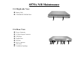
SERVICE MANUAL FOR
8575A
8 5 7 5 A
BY: Sissel Diao
TESTING
TESTING TECHNOLOGY
TECHNOLOGY DEPARTMENT
DEPARTMENT // TSSC
TSSC
Aug . 2002
8575A N/B Maintenance
Contents
1. Hardware Engineering Specification …………………………………………………………………
4
1.1 Introduction …………………………………………………………………………………………………………. 4
1.2 System Hardware Parts ……………………………………………………………………………………………. 6
1.3 Other Functions …………………………………………………………………………………………………….. 42
1.4 Peripheral Components …………………………………………………………………………………………….. 47
1.5 Power Management ………………………………………………………………………………………………… 50
1.6 Appendix 1: SiS961 GPIO Definitions …………………………………………………………………………….. 52
1.7 Appendix 2: H8 Pins Definitions …………………………………………………………………………………… 53
2. System View and Disassembly ………………………………………………………………………...
59
2.1 System View …………………………………………………………………………………………………………. 59
2.2 System Disassembly ………………………………………………………………………………………………… 62
3. Definition & Location of Connectors / Switches ……………………………………………………..
81
3.1 Mother Board ……………………………………………………………………………………………………….. 81
3.2 DC Power Board ……………………………………………………………………………………………………. 84
3.3 ESB Board …………………………………………………………………………………………………………... 85
3.4 Touch-pad …………………………………………………………………………………………………………… 86
3.5 Daughter Board …………………………………………………………………………………………………….. 86
1
8575A N/B Maintenance
Contents
4. Definition & Location of Major Component …………………………………………………………
87
4.1 Mother Board ……………………………………………………………………………………………………….. 87
5. Pin Description of Major Component ………………………………………………………………...
89
5.1 Intel Pentium 4 Processor mPGA478 Socket ……………………………………………………………………... 89
5.2 SiS650 IGUI Host / Memory Controller …………………………………………………………………………... 95
5.3 SiS691 MuTIOL Media I/O Controller …………………………………………………………………………… 100
5.4 SiS301LV / Chrontel CH7019 TV/LVDS Encoder ……………………………………………………………….. 106
5.5 PCI1410GGU PCMCIA Controller ……………………………………………………………………………….. 109
5.6 uPD72872 IEEE1394 Controller …………………………………………………………………………………… 114
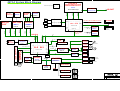
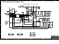
6. System Block Diagram …………………………………………………………………………………
116
7. Maintenance Diagnostics ………………………………………………………………………………
117
7.1 Introduction …………………………………………………………………………………………………………. 117
7.2 Error Codes …………………………………………………………………………………………………………. 118
7.3 Maintenance Diagnostics …………………………………………………………………………………………… 120
8. Trouble Shooting ……………………………………………………………………………………….
121
8.1 No Power …………………………………………………………………………………………………………….. 122
2
8575A N/B Maintenance
Contents
8.2 No Display ……………………………………………………………………………………………………………
8.3 VGA Controller Failure LCD No Display …………………………………………………………………………
8.4 External Monitor No Display ………………………………………………………………………………………
8.5 Memory Test Error …………………………………………………………………………………………………
8.6 Keyboard (K/B) Touch-Pad (T/P) Test Error …………………………………………………………………….
8.7 Hard Disk Drive Test Error ………………………………………………………………………………………..
8.8 CD-ROM Driver Test Error ………………………………………………………………………………………..
8.9 USB Test Error ………………………………………………………………………………………………………
8.10 PIO Port Test Error ……………………………………………………………………………………………….
8.11 Audio Failure ………………………………………………………………………………………………………
8.12 LAN Test Error ……………………………………………………………………………………………………
8.13 PC Card Socket Failure ……………………………………………………………………………………………
8.14 IEEE 1394 Failure …………………………………………………………………………………………………
129
133
135
137
139
141
143
145
148
150
153
155
157
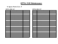
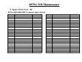
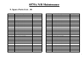
9. Spare Parts List ………………………………………………………………………………………..
159
10. System Exploded Views ………………………………………………………………………………
182
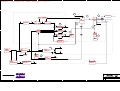
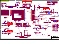
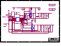
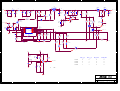
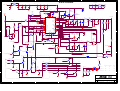
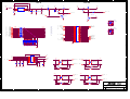
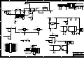
11. Circuit Diagram ………………………………………………………………………………………
184
12. Reference Material ……………………………………………………………………………………
217
3
8575A N/B Maintenance
1. Hardware Engineering Specification
1.1 Introduction
The 8575A motherboard would support the Intel® Pentium® 4 processor with FC-PGA2 packaged, using
478-Pin micro PGA (mPGA478) socket, which will supports different speeds up to Willamette P4 1.7GHz
(Throttling)/Northwood above 2.0GHz (Throttling).
This system is based on PCI architecture, which have standard hardware peripheral interface. The power
management complies with Advanced Configuration and Power Interface (ACPI) 1.0. It also provides easy
configuration through CMOS setup, which is built in system BIOS software and can be pop-up by pressing
F2 at system start up or warm reset. System also provides icon LEDs to display system status, such as power
indicator, HDD/CDROM, NUM LOCK, CAP LOCK, SCROLL LOCK, SUSPEND MODE and Battery
charging status. It also equipped 2 USB ports.
The memory subsystem supports 0MB on board memory, two JEDEC-standard 200-pin, small-outline, dual
in-line memory module (SODIMM), support PC2100 & PC2700.
SiS650 IGUI Host Memory Controller integrates a high performance host interface for Intel Pentium 4
processor, a high performance 2D/3D Graphic Engine, a high performance memory controller, an AGP 4X
interface, and SiS MuTIOL® Technology connecting w/ SiS961 MuTIOL® Media I/O.
4
8575A N/B Maintenance
The SiS961 MuTIOL® Media I/O integrates the Audio Controller with AC 97 Interface, the Ethernet MAC,
the Dual Universal Serial Bus Host Controllers, the IDE Master/Slave controllers, and the MuTIOL® Connect
to PCI bridge. The PCI to LPC bridge, I/O Advanced Programmable Interrupt Controller, legacy system I/O,
I/O Advanced Programmable Interrupt Controller and legacy power management functionalities are also
integrated. The SiS961 also incorporates an universal interface supporting the asynchronous inputs/outputs of
the X86 compatible microprocessors like P4.
The SiS301LV is a Display device which has two data operation paths. Channel B path is selected when
SiS301LV performs TV or LCD only display function. There’s scaling hardware in this path. In LCD display
mode, this hardware can make lower VGA resolution display to fit up to 1280x1024 LCD panel. In TV display
mode, this scaler can provide overscan and underscan option for TV. At TV and LCD simultaneous display
mode, TV data stream run through Channel B and LCD data stream run through Channel A.
To provide for the increasing number of multimedia applications, the AC97 CODEC ALC201 is integrated
onto the motherboard.
A full set of software drivers and utilities are available to allow advanced operating systems such as Windows
Me and Windows 2000 to take full advantage of the hardware capabilities such as bus mastering IDE, Windows
95-ready Plug & Play, Advanced Power Management (APM) and Advance configuration and power interface
(ACPI).
Following chapters will have more detail description for each individual sub-systems and functions.
5
8575A N/B Maintenance
1.2 System Hardware Parts
CPU
Core logic
VGA Control
System BIOS
Memory
Video Memory
Clock Generator
DDR Clock Buffer
Embedded controller
PCMCIA
Audio System
Super I/O
Modem
PHY of LAN
IEEE1394
Mobile Intel® Pentium® 4 Processor – M Built on 0.13-micron process Available speeds
1.80GHz, 1.70GHz, 1.60GHz, 1.50GHz, 1.40GHz
Intel® Pentium® 4 processor; Willamette/Northwood with mFCPGA2 Package, mPGA 478
Socket
Support up to Willamette P4 1.7GHz (Throttling) / Northwood above 2.0 GHz(Throttling)
FSB 400MHz /PC 2100/1600
SiS 650+SiS961: Host & Memory & AGP Controller integrates a high performance host
interface for Intel Pentium 4 processor, a high performance memory controller, a AGP
interface, and SiS MuTIOL® Technology connecting w/ SiS961 MuTIOL® Media IO.
SiS301LV
256KB Flash EPROM
Inside -Includes System BIOS, VGA BIOS, and plug & Play capability, ACPI
0MB on board memory
-Two JEDEC-standard 200-pin, small-outline, dual in-line memory module (SODIMM)
-Support PC2100 & PC2700
8/16/32/64 UMA
ICS 952001
ICS 93722
Hitachi H8 3437S
Card Bus Controller: TI PCI1410
One type II slot/ Card Bus support/ No ZV port support
Power Switch : TI TPS2211
AC97 CODEC: Advance Logic, Inc, ALC201
Power Amplifier: TI TPA0202
NS PC87393
56Kbps (V.90, worldwide) MDC Modem
ICS1893Y-10 10/100 base T PHY
IEEE1394 OHCI Controller : NEC uPD72872
6
8575A N/B Maintenance
1.2.1 CPU_Intel Pentium 4 Processor
Built on 0.13-micron process technology and Intel® NetBurst™ micro-architecture, the Mobile Intel®
Pentium® 4 Processor - M represents a new generation of mobile computing. It provides superior capabilities
for graphics-intensive multimedia applications, and processor-intensive background computing tasks such as
compression, encryption, and virus scanning. Enhanced Intel® SpeedStep® technology helps to optimize
application performance and power consumption, and Deeper Sleep Alert State, a dynamic power management
mode, adjusts voltage during brief periods of inactivity - even between keystrokes - for longer battery life.
Innovative Micro FCPGA packaging technology enables the processor to fit into small form factors, such as
thin-and-light notebooks.
The Intel® Pentium® 4 processor, Intel’s most advanced, most powerful processor, is based on the new Intel®
NetBurst™ micro-architecture. The Pentium 4 processor is designed to deliver performance across applications
and usages where end users can truly appreciate and experience the performance. These applications include
Internet audio and streaming video, image processing, video content creation, speech, 3D, CAD, games, multimedia, and multi-tasking user environments. The Intel Pentium 4 processor delivers this world-class
performance for consumer enthusiast and business professional desktop users as well as for entry-level
workstation users.
Highlights of the Pentium 4 Processor :
Available at speeds ranging from 1.50 to 2 GHz
Featuring the new Intel NetBurst micro-architecture
7
8575A N/B Maintenance
Supported by the SiS650 chipset
Fully compatible with existing Intel Architecture-based software
Internet Streaming SIMD Extensions 2
Intel® MMX™ media enhancement technology
Memory cache ability up to 4 GB of addressable memory space and
system memory scalability up to 64GB of physical memory
Support for uni-processor designs
Based upon Intel’s 0.18 micron manufacturing process
Intel Pentium 4 Processor Product Feature Highlights
The Intel NetBurst micro-architecture delivers a number of new and innovative features including Hyper
Pipelined Technology, 400 MHz System Bus, Execution Trace Cache, and Rapid Execution Engine as well as
a number of enhanced features Advanced Transfer Cache, Advanced Dynamic Execution, Enhanced Floatingpoint and Multi-media Unit, and Streaming SIMD Extensions 2. Many of these new innovations and advances
were made possible with improvements in processor technology, process technology, and circuit design that
could not previously be implemented in high-volume, manufacturable solutions. The features and resulting
benefits of the new micro-architecture are defined below.
8
8575A N/B Maintenance
Hyper Pipelined Technology:
The hyper-pipelined technology of the NetBurst micro-architecture doubles the pipeline depth compared to
the P6 micro-architecture used on today’s Pentium III processors. One of the key pipelines, the branch
prediction/ recovery pipeline, is implemented in 20 stages in the NetBurst micro-architecture, compared to
10 stages in the P6 micro-architecture. This technology significantly increases the performance, frequency,
and scalability of the processor.
400 MHZ System Bus:
The Pentium4 processor supports Intel’s highest performance desktop system bus by delivering 3.2 GB
of data per second into and out of the processor. This is accomplished through a physical signaling scheme
of quad pumping the data transfers over a 100-MHz clocked system bus and a buffering scheme allowing
for sustained 400-MHz data transfers. This compares to 1.06 GB/s delivered on the Pentium III processor’s
133-MHz system bus.
Level 1 Execution Trace Cache:
In addition to the 8KB data cache, the Pentium 4 processor includes an Execution Trace Cache that stores
up to 12K decoded micro-ops in the order of program execution. This increases performance by removing
the decoder from the main execution loop and makes more efficient usage of the cache storage space since
instructions that are branched around are not stored. The result is a means to deliver a high volume of
instructions to the processor’s execution units and a reduction in the overall time required to recover from
branches that have been mis-predicted.
9
8575A N/B Maintenance
Rapid Execution Engine:
Two Arithmetic Logic Units (ALUs) on the Pentium 4 processor are clocked at twice the core processor
frequency. This allows basic integer instructions such as Add, Subtract, Logical AND, Logical OR, etc. to
execute in half a clock cycle. For example, the Rapid Execution Engine on a 1.50 GHz Pentium 4 processor
runs at 3 GHz.
256KB, Level 2 Advanced Transfer Cache:
The Level 2 Advanced Transfer Cache (ATC) is 256KB in size and delivers a much higher data throughput
channel between the Level 2 cache and the processor core. The Advanced Transfer Cache consists of a 256bit (32-byte) interface that transfers data on each core clock. As a result, the Pentium 4 processor 1.50 GHz
can deliver a data transfer rate of 48 GB/s. This compares to a transfer rate of 16 GB/s on the Pentium III
processor at 1 GHz. Features of the ATC include:
Non-Blocking, full speed, on-die Level 2 cache
8-way set associativity
256-bit data bus to the level 2 cache
Data clocked into and out of the cache every clock cycle
Advanced Dynamic Execution:
The Advanced Dynamic Execution engine is a very deep, out-of-order speculative execution engine that
keeps the execution units executing instructions. The Pentium 4 processor can also view 126 instructions
in flight and handle up to 48 loads and 24 stores in the pipeline. It also includes an enhanced branch
prediction algorithm that has the net effect of reducing the number of branch mis-predictions by about
33% over the P6 generation processor’s branch prediction capability. It does this by implementing a 4KB
branch target buffer that stores more detail on the history of past branches, as well as by implementing a
more advanced branch prediction algorithm.
10
8575A N/B Maintenance
Enhanced Floating-Point and Multimedia Unit:
The Pentium 4 processor expands the floating-point registers to a full 128-bit and adds an additional register
for data movement which improves performance on both floating-point and multimedia applications.
Internet Streaming SIMD Extensions 2 (SSE2):
With the introduction of SSE2, the NetBurst micro-architecture now extends the SIMD capabilities that
MMX technology and SSE technology delivered by adding 144 new instructions. These instructions include
128-bit SIMD integer arithmetic and 128-bit SIMD double-precision floating-point operations. These new
instructions reduce the overall number of instructions required to execute a particular program task and as a
result can contribute to an overall performance increase. They accelerate a broad range of applications,
including video, speech, and image, photo processing, encryption, financial, engineering and scientific
applications.
Features Used for Test and Performance / Thermal Monitoring:
Built-in Self Test (BIST) provides single stuck-at fault coverage of the micro-code and large logic
arrays, as well as testing of the instruction cache, data cache, Translation Lookaside Buffers (TLBs),
and ROMs.
IEEE 1149.1 Standard Test Access Port and Boundary Scan mechanism enables testing
of the Pentium 4 processor and system connections through a standard interface.
Internal performance counters can be used for performance monitoring and event counting.
Includes a new Thermal Monitor feature that allows motherboards to be cost effectively designed to
expected application power usages rather than theoretical maximums.
11
8575A N/B Maintenance
1.2.2 System Frequency
1.2.2.1 System frequency synthesizer_ICS952001
Programmable Timing Control Hub™ for P4™ processor
General Description :
The ICS952001 is a two chip clock solution for desktop designs using SIS 645/650 style chipsets. When
used with a zero delay buffer such as the ICS9179-06 for PC133 or the ICS93705 for DDR applications it
provides all the necessary clocks signals for such a system.
The ICS952001 is part of a whole new line of ICS clock generators and buffers called TCH™ (Timing
Control Hub). ICS is the first to introduce a whole product line which offers full programmability and
flexibility on a single clock device. Employing the use of a serially programmable I2C interface, this device
can adjust the output clocks by configuring the frequency setting, the output divider ratios, selecting the ideal
spread percentage, the output skew, the output strength, and enabling/disabling each individual output clock.
TCH also incorporates ICS's Watchdog Timer technology and a reset feature to provide a safe setting under
unstable system conditions. M/N control can configure output frequency with resolution up to 0.1MHz
increment.
12
8575A N/B Maintenance
Recommended Application:
SiS645/650 style chipsets
Output features:
2 - Pairs of differential CPUCLKs @ 3.3V
1 - SDRAM @ 3.3V
8 - PCI @3.3V
2 - AGP @ 3.3V
2 - ZCLKs @ 3.3V
1 - 48MHz, @3.3V fixed
1 - 24/48MHz, @3.3V selectable by I2 C
3 - REF @3.3V, 14.318MHz
Key Specifications:
PCI - PCI output skew: < 500ps
CPU - SDRAM output skew: < 1ns
AGP - AGP output skew: <150ps
13
8575A N/B Maintenance
Features/Benefits:
Programmable output frequency, divider ratios, output rise/fall time, output skew.
Programmable spread percentage for EMI control.
Watchdog timer technology to reset system if system malfunctions
Programmable watch dog safe frequency.
Support I2 C Index read/write and block read/write operations
For PC133 SDRAM system use the ICS9179-06 as the memory buffer.
For DDR SDRAM system use the ICS93705 as the memory buffer.
Uses external 14.318MHz crystal.
14
8575A N/B Maintenance
1.2.2.2 DDR buffer frequency synthesizer_ICS93722
Low Cost DDR Phase Lock Loop Zero Delay Buffer
Recommended Application:
SiS645/650 style chipsets
Product description/features:
Low skew, low jitter PLL clock driver
I2 C for functional and output control
Feedback pins for input to output synchronization
Spread Spectrum tolerant inputs
3.3V tolerant CLK_INT input
Switching Characteristics
PEAK - PEAK jitter (66MHz): <120ps
PEAK - PEAK jitter (>100MHz): <75ps
CYCLE - CYCLE jitter (66MHz): <120ps
CYCLE - CYCLE jitter (>100MHz): <65ps
OUTPUT - OUTPUT skew: <100ps
Output Rise and Fall Time: 650ps - 950ps
DUTY CYCLE: 49.5% - 50.5%
15
8575A N/B Maintenance
1.2.3 Core Logic_SiS650 + SiS961
1.2.3.1 SiS650 IGUI Host/Memory Controller
SiS650 IGUI Host Memory Controller integrates a high performance host interface for Intel Pentium 4
processor, a high performance 2D/3D Graphic Engine, a high performance memory controller, an AGP 4X
interface, and SiS MuTIOL® Technology connecting w/ SiS961 MuTIOL® Media IO.
SiS650 Host Interface features the AGTL & AGTL+ compliant bus driver technology with integrated ondie termination to support Intel Pentium 4 processors. SiS650 provides a 12-level In-Order-Queue to support
maximum outstanding transactions up to 12. It integrated a high performance 2D/3D Graphic Engine, Video
Accelerator and Advanced Hardware Acceleration MPEGI/MPEGII Video Decoder for the Intel Pentium 4
series based PC systems. It also integrates a high performance 2.1GB/s DDR266 Memory controller to sustain
the bandwidth demand from the integrated GUI or external AGP master, host processor, as well as the multi
I/O masters. In addition to integrated GUI, SiS650 also can support external AGP slot with AGP 1X/2X/4X
capability and Fast Write Transactions. A high bandwidth and mature SiS MuTIOL® technology is
incorporated to connect SiS650 and SiS961 MuTIOL® Media I/O together. SiS MuTIOL® technology is
developed into three layers, the Multi-threaded I/O Link Layer delivering 1.2GB bandwidth to connect
embedded DMA Master devices and external PCI masters to interface to Multi-threaded I/O Link layer, the
Multi-threaded I/O Link Encoder/Decoder in SiS961 to transfer data w/ 533 MB/s bandwidth from/to Multithreaded I/O Link layer to/from SiS650, and the Multi-threaded I/O Link Encoder/Decoder in SiS650 to
transfer data w/ 533 MB/s from/to Multi-threaded I/O Link layer to/from SiS961.
16
8575A N/B Maintenance
An Unified Memory Controller supporting PC133 or DDR266 DRAM is incorporated, delivering a high
performance data transfer to/from memory subsystem from/to the Host processor, the integrated graphic engine
or external AGP master, or the I/O bus masters. The memory controller also supports the Suspend to RAM
function by retaining the CKE# pins asserted in ACPI S3 state in which only AUX source deliver power. The
SiS650 adopts the Shared Memory Architecture, eliminating the need and thus the cost of the frame buffer
memory by organizing the frame buffer in the system memory. The frame buffer size can be allocated from
8MB to 64MB.
The Integrated GUI features a high performance 3D accelerator with 2 Pixel / 4 Texture, and a 128 bit 2D
accelerator with 1T pipeline BITBLT engine. It also features a Video Accelerator and advanced hardware
acceleration logic to deliver high quality DVD playback. A Dual 12 bit DDR digital video link interfaced to
SiS 301B Video Bridge packaged in 100-pin PQFP is incorporated to expand the SiS650 functionality to
support the secondary display, in addition to the default primary CRT display. The SiS301B Video Bridge
integrates an NTSL/PAL video encoder with Macro Vision Ver. 7.1.L1 option for TV display, a TMDS
transmitter with Bi-linear scaling capability for TFT LCD panel support, and an analog RGB port to support a
secondary CRT. The primary CRT display and the extended secondary display (TV, TFT LCD Panel, 2'nd
CRT) features the Dual View Capability in the sense that both can generate the display in independent
resolutions, color depths, and frame rates.
17
8575A N/B Maintenance
Two separate buses, Host-t-GUI in the width of 64 bit, and GUI-t-Memory Controller in the width of 128
bit are devised to ensure concurrency of Host-t-GUI streaming, and GUI-t-MC streaming. In PC133, or
DDR266 memory subsystem, the 128 bit GUI-t-MC bus will attain the AGP4X or AGP 8X equivalent texture
transfer rate, respectively. The Memory Controller mainly comprises the Memory Arbiter, the M-data/MCommand Queues, and the Memory Interface. The Memory Arbiter arbitrates a plenty of memory access
requests from the GUI or AGP controller, Host Controller, and I/O bus masters based on a default optimized
priority list with the capability of dynamically prioritizing the I/O bus master requests in a bid to offering
privileged service to 1) the isochronous downstream transfer to guarantee the min. latency & timely delivery,
or 2) the PCI master upstream transfer to curb the latency within the maximum tolerant period of 10us. Prior to
the memory access requests pushed into the M-data queue, any command compliant to the paging mechanism
is generated and pushed into the M-CMD queue. The M-data/M-CMD Queues further orders and forwards
these queuing requests to the Memory Interface in an effort to utilizing the memory bandwidth to its utmost by
scheduling the command requests in the background when the data requests streamlines in the foreground.
18
8575A N/B Maintenance
1.2.3.2 SiS961 MuTIOL® Media I/O overview
The SiS961 MuTIOL® Media I/O integrates the Audio Controller with AC 97 Interface, the Ethernet
MAC, the Dual Universal Serial Bus Host Controllers, the IDE Master/Slave controllers, and the MuTIOL®
Connect to PCI bridge. The PCI to LPC bridge, I/O Advanced Programmable Interrupt Controller, legacy
system I/O, I/O Advanced Programmable Interrupt Controller and legacy power management functionalities
are also integrated. The SiS961 also incorporates an universal interface supporting the asynchronous
inputs/outputs of the X86 compatible microprocessors like PIII, K7 and P4.
The Integrated Audio Controller features a 6 channels of AC 97 v2.2 compliance audio to present 5.1channel Dolby digital material or to generate stereo audio with simultaneous V.90 HSP modem operation.
Besides, 4 separate SDATAIN pins are provided to support multiple audio Codecs + one modem Codec
maximally, effectuating the realization of 5.1 channel Dolby digital material in theater quality sound. Both
traditional consumer digital audio channel as well as the AC 97 v2.2 compliant consumer digital audio slot are
supported. VRA mode is also associated with both the AC 97 audio link and the traditional consumer digital
audio channel.
The integrated Fast Ethernet MAC features an IEEE 802.3 and IEEE 802.3x compliant MAC supporting
full duplex 10 Base-T, 100 Base-T Ethernet, or 1Mb/s & 10Mb/s Home networking. 5 wake-up Frames,
Magic Packet and link status change wake-up functions in G1/G2 states are supported. Besides, the integrated
MAC provides a scheme to store the MAC address without the need of an external EEPROM. The 25 MHz
oscillating circuit is integrated so as only an external low cost 25 MHz crystal is needed for the clocking
system.
19
8575A N/B Maintenance
The integrated Universal Serial Bus Host Controllers features Dual Independent OHCI Compliant Host
controllers with six USB ports delivering 2 x 12 Mb/s bandwidth and rich connectivity. Besides, each port can
be optionally configured as the wake-up source. Legacy USB devices as well as over current detection are also
implemented. The integrated IDE Master/Slave controllers features Dual Independent IDE channels supporting
PIO mode 0,1,2,3,4, and Ultra DMA 33/66/100. It provides two separate data paths for the dual IDE channels
that sustain the high data transfer rate in the multitasking environment. The MuTIOL® Connect to PCI bridge
supporting 6 PCI master is compliant to PCI 2.2 specification. The SiS961 also incorporates the legacy system
I/O like: two 8237A compatible DMA controllers, three 8254 compatible programmable 16-bit counters,
hardwired keyboard controller and PS2 mouse interface, Real Time clock with 256B CMOS SRAM and two
8259A compatible Interrupt controllers. Besides, the I/O APIC managing up to 24 interrupts with both Serial
and FSB interrupt delivery modes is supported.
The integrated power management module incorporates the ACPI 1.0b compliance functions, the APM 1.2
compliance functions, and the PCI bus power management interface spec. v1.1. Numerous power-up events
and power down events are also supported. 21 general purposed I/O pins are provided to give an easy to use
logic for specific application. In addition, the SiS961 supports Intel Speed Step technology and Deeper Sleep
power state for Intel Mobile processor. For AMD processor, the SiS961 use the CPUSTP# signal to reduce
processor voltage during C3 and S1 state.
20
8575A N/B Maintenance
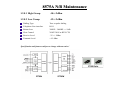
1.2.4 SiS301LV TV Encoder / LVDS Transmitter
General Description
SiS301LV, which is an accompany chip of SiS VGA chip, integrates :
A NTSC/PAL video encoder with Macrovision Ver.7.1.L1 option for TV display.
A LVDS transmitter with bi-linear scaling capability for TFT LCD panel display.
All the above functions can support dual-display features. It means that the second display device driven by
SiS301LV can display independent resolutions, color depths and frame rates different from the traditional CRT
monitor driven by primary VGA chip. SiS301LV receives digital video signals and control signals from the
primary VGA chip then transforms them into composite, S-Video or component video output for TV display,
LVDS signals for LCD display. The output display combination can be one of the three :
(1) Primary CRT+SiS301LV TV
(2) Primary CRT+SiS301LV LCD
(3) SiS301LV TV + SiS301LV LCD.
V ide o
D e co de r
The package type of SiS301LV is 128-pin LQFP.
Fra m e
B u ffe r
F ea ture
C on n ector
CRT
M o n itor
P rim a ry
VG A
(S iS 65 0/
S iS 33 0 )
1st cha nne l
2 nd c hannel
S iS 30 1 LV
N TS C /P A L
TV
LC D
M on ito r
21
8575A N/B Maintenance
1.2.4.1 TV-Out :
Supports PAL and NTSC Systems.
Supports Composite, S-Video, and Component RGB( SCART) Output Signals
Supports Macrovision Copy Protection Process Rev. 7.1.L1
Support Progressive TV 525P YPbPr Output Signals.
Support Macrovision Conpy Protection Waveforms for 525p Progressive Scan Output
Supports TV/Primary VGA Independent Display Resolution and Frame Rate at Enhanced Mode
Provides Adaptive 6-Line Anti-Flicker Filtering.
Provides Hardware Interpolation for Programmable Under-Scan/Over-Scan Adjustment.
Provides Programmable Display Position Adjustment.
Provides Programmable Notch Filter for Cross Color Elimination.
Provides Chrominance Filter for Cross Luminance Elimination.
Provides Color Saturation Adjustment for Vivid TV Output.
Provides Gamma Correction Independent of That of Primary VGA.
Auto-Sense of TV Connection
22
8575A N/B Maintenance
1.2.4.2 LVDS
Supports LVDS Transmitter Function.
Single LVDS supports pixel rate up to 110M pixel/sec.
Compatible with TIA/EIA-644 LVDS standard.
Provides Bi-linear Scaling to Scale VGA Low Resolution Mode up for LCD Display – up to 1280x1024
Supports LCD/Primary VGA Independent Display Resolution and Frame Rate at Enhanced Mode.
Support 2D dither for 18-bit panels.
Provides Programmable Display Centering.
Compliant with VESA DDC2B
Compliant with VESA Plug & Display, Hot Plugging Function.
Provides Correction Independent of That of Primary VGA
23
8575A N/B Maintenance
1.2.5 PC Card Interface Controller: TI PCI1410
The TI PCI1410 is a high-performance PCI-to-PC Card controller that supports a single PC Card socket
compliant with the 1997 PC Card Standard. The PCI1410 provides features that make it the best choice for
bridging between PCI and PC Cards in both notebook and desktop computers. The 1997 PC Card Standard
retains the 16-bit PC Card specification defined in PCI Local Bus Specification and defines the new 32-bit PC
Card, CardBus, capable of full 32-bit data transfers at 33 MHz. The PCI1410 supports both 16-bit and
CardBus PC Cards, powered at 5 V or 3.3 V, as required. .
The PCI1410 is compliant with the PCI Local Bus Specification, and its PCI interface can act as either a PCI
master device or a PCI slave device. The PCI bus mastering is initiated during 16-bit PC Card DMA transfers
or CardBus PC Card bridging transactions. The PCI1410 is also compliant with the latest PCI Bus Power
Management Interface Specification and PCI Bus Power Management Interface Specification for PCI to
CardBus Bridges.
All card signals are internally buffered to allow hot insertion and removal without external buffering. The
PCI1410 is register compatible with the IntelE 82365SL-DF and 82365SL ExCA controllers. The PCI1410
internal data path logic allows the host to access 8-, 16-, and 32-bit cards using full 32-bit PCI cycles for
maximum performance. Independent buffering and a pipeline architecture provide an unsurpassed
performance level with sustained bursting. The PCI1410 can also be programmed to accept fast posted writes
to improve system-bus utilization.
24
8575A N/B Maintenance
Multiple system-interrupt signaling options are provided, including: parallel PCI, parallel ISA, serialized ISA,
and serialized PCI. Furthermore, general-purpose inputs and outputs are provided for the board designer to
implement sideband functions. Many other features designed into the PCI1410, such as socket activity lightemitting diode (LED) outputs, are discussed in detail throughout the design specification.
An advanced complementary metal-oxide semiconductor (CMOS) process achieves low system power
consumption while operating at PCI clock rates up to 33 MHz. Several low-power modes enable the host
power management system to further reduce power consumption.
Features
Ability to wake from D3hot and D3cold
Fully compatible with the Intel 430TX (Mobile Triton II) chipset
A 144-terminal low-profile QFP (PGE), 144-terminal MicroStar BGAE ball grid array (GGU) package, or
209-terminal MicroStar BGAE (GHK) package
3.3-V core logic with universal PCI interfaces compatible with 3.3-V and 5-V PCI signaling environments
Mix-and-match 5-V/3.3-V 16-bit PC Cards and 3.3-V CardBus Cards
Single PC Card or CardBus slot with hot insertion and removal
Burst transfers to maximize data throughput on the PCI bus and the CardBus bus
Parallel PCI interrupts, parallel ISA IRQ and parallel PCI interrupts, serial ISA IRQ with parallel PCI
interrupts, and serial ISA IRQ and PCI interrupts
25
8575A N/B Maintenance
1.2.5.1 Single-Slot PC Card Power Interface Switch: TPS2211A
The TPS2211A PC Card power-interface switch provides an integrated power-management solution for a
single PC Card. All of the discrete power MOSFETs, a logic section, current limiting, and thermal protection
for PC Card control are combined on a single integrated circuit, using the Texas Instruments LinBiCMOSTM
process. The circuit allows the distribution of 3.3-V, 5-V, and/or 12-V card power, and is compatible with
many PCMCIA controllers. The current-limiting feature eliminates the need for fuses, which reduces
component count and improves reliability. Current-limit reporting can help the user isolate a system fault to
the PC Card.
The TPS2211A features a 3.3-V low-voltage mode that allows for 3.3-V switching without the need for 5 V.
Bias power can be derived from either the 3.3-V or 5-V inputs. This facilitates low-power system designs
such as sleep mode and pager mode where only 3.3 V is available.
End equipment for the TPS2211A includes notebook computers, desktop computers, personal digital assistants
(PDAs), digital cameras, and bar-code scanners.
26
8575A N/B Maintenance
Features
Fully Integrated VCC and Vpp Switching for Single-Slot PC CardTM Interface
Low rDS(on) (70-m 5-V VCC Switch and 3.3-V VCC Switch)
Compatible With Industry-Standard Controllers
3.3-V Low-Voltage Mode
Meets PC Card Standards
12-V Supply Can Be Disabled Except During 12-V Flash Programming
Short-Circuit and Thermal Protection
Space-Saving 16-Pin SSOP (DB)
Compatible With 3.3-V, 5-V, and 12-V PC Cards
Break-Before-Make Switching
PC Card is a trademark of PCMCIA (Personal Computer Memory Card International Association)
LinBiCMO is a trademark of Texas Instruments
27
8575A N/B Maintenance
1.2.6 IEEE1394 : NEC µPD72872 OHCI-Link Layer Controller
The µPD72872 is NEC’s 1-chip solution of an OHCI-LINK layer controller and a two port, physical layer
implementation compliant to P1394a specification draft 2.0. It supports the connection with transmission
speeds up to 400Mbps. The two-port shrink version of the µPD72870 chip with PCI/CardBus Interface offers a
compact and low-cost solution for implementing applications in PC, PC-Cards as µPD72872 supports the 1394
Open Host Controller Interface 1.0
Features
Link Layer compliant with 1394 Open Host Controller Interface specification release 1.0 Physical layer
compliant with definition in P1394a draft 2.0 (Data Rate 100/200/400 Mbps)
Selectable active port number (1, 2 ports)
Modular 32-bit host interface compliant with PCI specification release 2.1
Supports PCI Bus Power Management Interface specification release 1.1
Modular 32-bit host interface compliant with CardBus specification
Cycle Master and Isochronous Resource Manager support
32-bit CRC generation and checking for receive/transmit packets
Supports 4 isochronous transmit DMAs and 4 isochronous receive DMAs
2-wire Serial EEPROM™ interface supported
28
8575A N/B Maintenance
Separate power supply Link and PHY
Programmable latency timer from serial EEPROM™ in CardBus mode (CARD_ON = 1)
Temperature range: 0 to 70°C
Operating voltage: 3.3 V ± 10%, single power supply
1.2.7 AC’97 Audio System: Advance Logic, Inc, ALC201
SiS961 is an AC’97 2.1 compliant controller that communicates with companion Codecs SiS a digital serial
link called the AC-link.
The ALC201 is an AC97 2.2 compatible stereo audio codec designed for PC multimedia systems.The
ALC201 provides the way for PC98 and PC99-compliant desktop, portable and entertainment PCs, where
high-quality audio is required. The ALC201 AC’97 CODEC provides a complete high quality audio solution.
Features
Single chip audio CODEC with high S/N ratio (>90 dB)
18-bit ADC and DAC resolution
Compliant with AC’97 2.2 specification
Meet performance requirements for audio on PC2001 systems
29
8575A N/B Maintenance
18-bit stereo full-duplex CODEC with independent and variable sampling rate
4 analog line-level stereo input with 5-bit volume control: LINE_IN, CD, VIDEO, AUX
2 analog line-level mono input: PC_BEEP, PHONE_IN
Mono output with 5-bit volume control
Stereo output with 5-bit volume control
2 MIC inputs: Software selectable
Power management
3D Stereo Enhancement
Headphone output with 50mW/20ohm driving capability (ALC201)
Line output with 50mW/20ohm driving capability (ALC201A)
Headphone jack-detect function to mute LINE output
Multiple CODEC extension
MC’97 chained in allowed for multi-channel application
External Amplifier power down capability
Support S/PDIF out is fully compliant with AC’97 specification rev2.2
DC offset cancellation
Power support: Digital: 3.3V Analog: 5V
Standard 48-Pin LQFP Package
30
8575A N/B Maintenance
1.2.8 MDC: PCTel Modem Daughter Card PCT2303W
The PCT2303W chipset is designed to meet the demand of this emerging worldwide AMR/MDC market. The
combination of PC-TEL’s well proven PCT2303W chipset and the HSP56TM MR software modem driver
allows systems manufactures to implement modem functions in PCs at a lower bill of materials (BOM) while
maintaining higher system performance.
PC-TEL has streamlined the traditional modem into the Host Signal Processing (HSP) solution. Operating
with the Pentium class processors, HSP becomes part of the host computer’s system software. It requires less
power to operate and less physical space than standard modem solutions. PC-TEL’s HSP modem is an easily
integrated, cost-effective communications solution that is flexible enough to carry you into the future.
The PCT2303W chip set is an integrated direct access arrangement (DAA) and Codec that provides a
programmable line interface to meet international telephone line requirements. The PCT2303W chip set is
available in two 16-pin small outline packages (AC’97 interface on PCT303A and phone-line interface on
PCT303W). The chip set eliminates the need for an AFE, an isolation transformer, relays, opto-isolators, and
2-to 4-wire hybrid. The PCT2303W chip set dramatically reduces the number of discrete components and cost
required to achieve compliance with international regulatory requirements. The PCT2303W complies with
AC’97 Interface specification Rev. 2.1.
31
8575A N/B Maintenance
The chip set is fully programmable to meet worldwide telephone line interface requirements including those
described by CTR21, NET4, JATE, FCC, and various country-specific PTT specifications. The programmable
parameters of the PCT2303W chip set include AC termination, DC termination, ringer impedance, and ringer
threshold. The PCT2303W chip set has been designed to meet stringent worldwide requirements for out-ofband energy, billing-tone immunity, lightning surges, and safety requirements.
Operating System Compatibility
Windows 98 /NT4.0 /Win 2K /Win XP
Compatibility
ITU-T V.90
56000, 54667, 53333,52000, 50667, 49333, 48000,
46667, 45333, 42667, 41333, 40000, 38667, 37333,
36000, 34667, 33333, 32000, 30667, 29333, 28000bps
K56Flex
56000, 54000, 52000, 50000, 48000, 46000, 44000,
42000, 40000, 38000, 36000, 32000bps
ITU-T V.34Annex
33600,31200 bps
ITU-T V.34
28800 bps
ITU-T V.32bis
14400 bps
ITU-T V.32
9600,4800 bps
ITU-T V.22bis
2400 bps
ITU-T V.22
1200 bps
ITU-T V.21
300 bps
ITU-T V.23
1200/75 bps
32
8575A N/B Maintenance
ITU-T V.17
14400,12000,9600,7200 bps
ITU-T V.29
9600,7200 bps
ITU-T V.27ter
4800,2400 bps
Bell 212A
1200 bps
Bell 103
300 bps
Modulation
56000bps(V90&K56Flex)
PCM
33600 bps (V.34Annex)
TCM
28800 bps (V.34)
TCM
14400 bps (V.32bis)
TCM
12000 bps (V.32bis)
TCM
9600 bps (V.32bis)
TCM
7200 bps (V.32bis)
QAM
9600 bps (V.32)
TCM, QAM
4800 bps (V.32)
QAM
14400 bps (V.17)
TCM
12000 bps (V.17)
TCM
9600 bps (V.29)
QAM
7200 bps (V.29)
QAM
4800 bps (V.27ter)
DPSK
33
8575A N/B Maintenance
2400 bps (V.27ter)
DPS
2400 bps (V.22bis)
QAM
1200/75bps (V.23)
FSK
1200bps(V.22/Bell 212A)
DPSK
300bps(V.21/Bell 103)
FSK
Data Compression
V.42bis, MNP5
Error Correction
V.42 LAPM, MNP 2-4
DTE interface
DTMF Tone Frequency
Low Group Frequency (Hz)
High Group
Frequency
(Hz)
1209
1336
1477
1633
697
1
2
3
A
770
4
5
6
B
852
7
8
9
C
941
*
0
#
D
DTMF signal level
34
8575A N/B Maintenance
1.2.8.1 High Group
-10+/-2dBm
1.2.8.2 Low Group
-12+/-2dBm
Dialing Type
Tone or pulse dialing
Telephone Line interface
RJ-11
Return Loss
300HZ - 3400HZ >= 10db
Flow Control
XOFF/XON or RTS/CTS
Receive Level
-35 +/- 2dBm
Transmit Level
>-15 dBm
Specification and features subject to change without notice!
35
8575A N/B Maintenance
1.2.9 Keyboard System: H8 (3437S) Universal Keyboard Controller
CPU
Two-way general register configuration
Eight 16-bit registers or sixteen 8-bit registers
High-speed operation
Maximum clock rate: 16Mhz at 5V
Available in temperature range: 0°C~70°C
Memory
Include 60KB ROM and 2KB RAM
16-bit free-running timer
One 16-bit free-running counter
Two output-compare lines
Four input capture lines
8-bit timer (2 channels)
Each channel has one 8-bit up counter, two time constant registers
PWM timer (2 channels)
Resolution: 1/250
Duty cycle can be set from 0 to 100%
I2C bus interface (one channel)
Include single master mode and slave mode
Host interface (HIF)
8-bit host interface port
Three hosts interrupt requests (HIRQ1, 11,12)
Regular and fast A20 gate output
Keyboard controller
Controls a matrix-scan keyboard by providing a keyboard
scan function with wake-up Interrupts and sense ports
A/D converter
10-bit resolution
8 channels: single or scan mode (selectable)
36
8575A N/B Maintenance
D/A converter
8-bit resolution
2 channels
Interrupts
Nine external interrupt lines: NMI#, IRQ0 to 7#
26 on-chip interrupt sources
Power-down modes
Sleep mode
Software standby mode
Hardware standby mode
A single chip microcomputer
On-chip flash memory
Maximum 64kbyte-address space
Support three PS/2 port for external keyboard, mouse and internal track pad.
Support SMI, SCI trigger input:
Cover switch
Battery charging control
Smart Battery monitoring
Control D/D system on/off
Fan control and LED indicator serial interface
100pin TQFP
37
8575A N/B Maintenance
1.2.10 System Flash Memory (BIOS)
2 M bit Flash memory
Flashed by 5V only
User can upgrade the system BIOS in the future just running flash program
1.2.11 Memory System
64MB, 128MB, 256MB, 512MB (x64) 200-Pin DDR SDRAM SODIMMs
JEDEC-standard 200-pin, small-outline, dual in-line memory module (SODIMM)
Utilizes 200 Mb/s and 266 Mb/s DDR SDRAM components
128MB (16 Meg x 64, [H] and [HD]); 256MB (32 Meg x 64 [HD]); 512MB (64 Meg x 64 [HD])
VDD= VDDQ= +2.5V ±0.2V
VDDSPD = +2.2V to +5.5V
2.5V I/O (SSTL_2 compatible)
Commands entered on each positive CK edge
DQS edge-aligned with data for READs; center-aligned with data for WRITEs
Internal, pipelined double data rate (DDR) architecture; two data accesses per clock cycle
Bi-directional data strobe (DQS) transmitted/received with data—i.e.,source-synchronous data capture
Differential clock inputs (CK and CK# - can be multiple clocks, CK0/CK0#, CK1/CK1#, etc.)
Four internal device banks for concurrent operation
38
8575A N/B Maintenance
Selectable burst lengths: 2, 4 or 8
Auto precharge option
KBC and PS2 mouse can be individually disabled
Auto Refresh and Self Refresh Modes
15.6µs (MT4VDDT864H, MT8VDDT1664HD), 7.8125µs (MT4VDDT1664H, MT8VDDT3264HD,
MT8VDDT6464HD) maximum average periodic refresh interval
Serial Presence Detect (SPD) with EEPROM
Serial Presence Detect (SPD) with EEPROM
Fast data transfer rates PC2100 or PC1600
Selectable READ CAS latency for maximum compatibility
Gold-plated edge contacts
1.2.12 PHY: 3.3-V 10Base-T/100Base-TX Integrated PHYceiver The ICS1893
General Description
The ICS1893 is a low-power, physical-layer device (PHY) that supports the ISO/IEC 10Base-T and 100BaseTXCarrier-Sense Multiple Access/Collision Detection (CSMA/CD) Ethernet standards. The ICS1893
architecture is based on the ICS1892. The ICS1893 supports managed or unmanaged node, repeater, and switch
applications.
39
8575A N/B Maintenance
The ICS1893 incorporates digital signal processing (DSP) in its Physical Medium Dependent (PMD) sublayer.
As a result, it can transmit and receive data on unshielded twisted-pair (UTP) category 5 cables with attenuation
in excess of 24 dB at 100 MHz. With this ICS-patented technology, the ICS1893 can virtually eliminate errors
from killer packets.
The ICS1893 provides a Serial Management Interface for exchanging command and status information with a
Station Management (STA) entity.
The ICS1893 Media Dependent Interface (MDI) can be configured to provide either half- or full-duplex
operation at data rates of 10 MHz or 100 MHz. The MDI configuration can be established manually (with input
pins or control register settings) or automatically (using the Auto-Negotiation features). When the ICS1893
Auto-Negotiation sublayer is enabled, it exchanges technology capability data with its remote link partner and
automatically selects the highest-performance operating mode they have in common.
Features
Supports category 5 cables with attenuation in excess of 24 dB at 100 MHz across a temperature range
from -5 to +85 C
DSP-based baseline wander correction to virtually eliminate killer packets across temperature range
from -5 to +85 C
Low-power, 0.35-micron CMOS (typically 400 mW)
Single 3.3-V power supply
40
8575A N/B Maintenance
Single-chip, fully integrated PHY provides PCS, PMA, PMD and AUTONEG sublayers of IEEE standard
10Base-T and 100Base-TX IEEE 802.3 compliant
Fully integrated, DSP-based PMD includes:
Adaptive equalization and baseline wander correction
Transmit wave shaping and stream cipher scrambler
MLT-3 encoder and NRZ/NRZI encoder
Highly configurable design supports:
Node, repeater, and switch applications
Managed and unmanaged applications
10M or 100M half- and full-duplex modes
Parallel detection
Auto-negotiation, with Next Page capabilities
MAC/Repeater Interface can be configured as:
10M or 100M Media Independent Interface
100M Symbol Interface (bypasses the PCS)
10M 7-wire Serial Interface
Small Footprint 64-pin Thin Quad Flat Pack (TQFP)
41
8575A N/B Maintenance
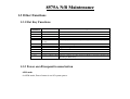
1.3 Other Functions
1.3.1 Hot Key Functions
Keys
Combination
Fn + F1
Fn + F2
Fn + F3
Fn + F4
Fn + F5
Fn + F6
Fn + F7
Fn + F8
Fn + F9
Fn + F10
Fn + F11
Fn + F12
Feature
Reserve
Reserve
Volume Down
Volume Up
LCD/external CRT
switching
Brightness down
Brightness up
Brightness MAX
Pause
Break
Panel Off/On
Suspend to DRAM / HDD
Meaning
Rotate display mode in LCD only, CRT only, and simultaneously display.
Decreases the LCD brightness
Increases the LCD brightness
Toggle Max Brightness
Toggle Panel on/off
Force the computer into either Suspend to HDD or Suspend to DRAM mode
depending on BIOS Setup.
1.3.2 Power on/off/suspend/resume button
APM mode
At APM mode, Power button is on/off system power.
42
8575A N/B Maintenance
APM mode
At ACPI mode. Windows power management control panel set power button behavior.
You could set “standby”, “power off” or “hibernate”(must enable hibernate function in power Management) to
power button function.
Continue pushing power button over 4 seconds will force system off at ACPI mode.
1.3.3 Cover Switch
System automatically provides power saving by monitoring Cover Switch. It will save battery power and
prolong the usage time when user closes the notebook cover.
At ACPI mode there are four functions to be chosen at windows power management control panel.
1.
None
2.
Standby
3.
Off
4.
Hibernate (must enable hibernate function in power management)
1.3.4 Reset Switch
There is a reset switch at bottom side of notebook. It will reset embedded controller H8 and turn off system
totally. When system hands up and Power button has no function, this switch is the only way to turn off
system without remove power source.
43
8575A N/B Maintenance
1.3.5 LED Indicators
System has eight status LED indicators to display system activity, which include three at front side and five
above keyboard.
1) Three LED indicators at front side:
From left to right that indicates: AC Power, Battery Power and Battery Status
AC Power: This LED lights green when AC is powering the notebook, and flash (on 1 second, off 1
second) when Suspend to DRAM is active using AC power. The LED is off when the notebook is off or
powered by batteries.
Battery Power: This LED lights green when the notebook is being powered by Battery, and flash (on 1
second, off 1 second) when Suspend to DRAM is active using Battery power. The LED is off when the
notebook is off or powered by batteries, or when Suspend to Disk.
Battery Status: During normal operation, this LED stays off as long as the battery is charged. When the
battery charge drops to 10% of capacity, the LED lights red, flashes per 1 second and beeps per 2 second.
When AC is connected, this indicator glows green if the battery pack is fully charged or orange (amber) if
the battery is being charged.
2) Five LED indicators above keyboard:
From left to right that indicates LAN, CD-ROM/HARD DISK DRIVE, NUM LOCK, CAPS LOCK and
SCROLL LOCK.
44
8575A N/B Maintenance
1.3.6 Battery Status
Battery Warning
System also provides Battery capacity monitoring and gives user a warning so that users have chance to save
his data before battery dead. Also, this function protects system from mal-function while battery capacity is
low.
Battery Warning: Capacity below 10%, Battery Capacity LED flashes per second, system beeps per 2 seconds.
System will suspend to HDD after 2 Minutes to protect users data.
Battery Low State
After Battery Warning State, and battery capacity is below 4%, system will generate beep for twice per second.
Battery Dead State
When the battery voltage level reaches 7.4 volts, system will shut down automatically in order to extend the
battery packs' life.
1.3.7 Fan power on/off management
FAN is controlled by H8 embedded controller-using AD2201 to sense CPU temperature and PWM control fan
speed. Fan speed is depended on CPU temperature. Higher CPU temperature faster Fan Speed.
45
8575A N/B Maintenance
1.3.8 CMOS Battery
CR2032 3V 220mAh lithium battery
When AC in or system main battery inside, CMOS battery will consume no power.
AC or main battery not exists, CMOS battery life at less (220mAh/5.8uA) 4 years.
Battery was put in battery holder, can be replaced.
1.3.9 I/O Port
One Power Supply Jack.
One External CRT Connector For CRT Display
Supports two USB port for all USB devices.
One MODEM RJ-11 phone jack for PSTN line
One RJ-45 for LAN.
Headphone Out Jack.
Microphone Input Jack.
Line in Jack
One Card Bus Sockets for one type II PC card extension
1.3.10 Battery current limit and learning
Implanted H/W current limit and battery learning circuit to enhance protection of battery.
46
8575A N/B Maintenance
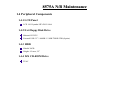
1.4 Peripheral Components
1.4.1 LCD Panel
LCD 14.1 Hyundai HT14X12-100A
1.4.2 Ext.Floppy Disk Drive
Mitsumi D353GU
External USB 3.5” 1.44MB /1.2 MB/720KB FDD (Option)
1.4.3 HDD
Hitachi 30GB
Height: 9.5 mm, 2.5”
1.4.4 24X CD-ROM Drive
TEAC
47
8575A N/B Maintenance
1.4.5 8W/4R CD-RW
KEM
Height: 12.7 mm IDE I/F
1.4.6 Keyboard
Windows 98 Keyboard, 1 color, multi languages support JP, US and Europe Keyboard with “ Volume UP ”
and “ Volume Down ” word.
1.4.7 Track Pad Synaptics
Accurate positioning
Low fatigue pointing action
Low profile
No moving part, high reliability
Low power consumption
Environmentally sealed
Compact size.
Software configurable
Low weight
Operating temperature: 0 to 60 degree C
48
8575A N/B Maintenance
Operating humidity: 5%-95% relative humidity, non condensing
Storage temperature: -40 to +65 degree C
ESD: 15KV applied to front surface SEE ESD Testing specification PN 520-000270-01
Power supply voltage: 5.0Voltage ± 10%
Power supply current: 4.0mA max operating
1.4.8 Fan
HY45J05-001
1.4.9 Memory
DDR-RAM/ATP//128M/256M
DDR-RAM/Apacer//128M/256M
DDR-RAM/Unidorsa//128M/256M
1.4.10 Modem MDC
Askey
49
8575A N/B Maintenance
1.5 System Management
The 8575A system has built in several power saving modes to prolong the battery usage for mobile purpose.
User can enable and configure different degrees of power management modes via ROM CMOS setup
(booting by pressing F2 key). Following are the descriptions of the power management modes supported.
1.5.1 System Management Mode
Full on mode
In this mode, each device is running with the maximal speed. CPU clock is up to its maximum.
Doze Mode
In this mode, CPU will be toggling between on & stop grant mode either. The technology is clock throttling.
This can save battery power without loosing much computing capability. The CPU power consumption and
temperature is lower in this mode.
Standby mode
For more power saving, it turns of the peripheral components. In this mode, the following is the status of each
device:
CPU: Stop grant
LCD: backlight off
HDD: spin down
50
8575A N/B Maintenance
Suspend to DRAM
The most chipset of the system is entering power down mode for more power saving. In this mode, the
following is the status of each device:
Suspend to DRAM:
CPU: off
Twister K: Partial off
VGA: Suspend
PCMCIA: Suspend
Audio: off
SDRAM: self refresh
Suspend to HDD:
All devices are stopped clock and power-down
System status is saved in HDD
All system status will be restored when powered on again
1.5.2 Other Power Management Functions
HDD & Video access
System has the ability to monitor video and hard disk activity. User can enable monitoring function for video
and/or hard disk individually. When there is no video and/or hard disk activity, system will enter next PMU
state depending on the application. When the VGA activity monitoring is enabled, the performance of the
system will have some impact.
51
8575A N/B Maintenance
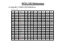
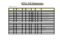
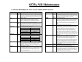
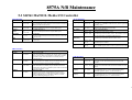
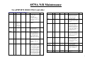
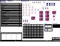
1.6 Appendix 1: SiS961 GPIO Definitions
SB_SiS961 GPIO
Signal
Name
MUX
Function
GPIO0
Buffer
Type
Power
Plane
MB_ID0
I/O
Main
Mitac Definition
During
Tolerant PCISRT#
After
PCISRT#
S1
S3
S4/S5
Driven Defined Driven Defined Driven Defined
Off
Off
GPIO1
LDRQ1#
CD_IN#
I/O
Main
Driven Defined Driven Defined Driven Defined
Off
Off
GPIO2
THERM#
SB_THRM#
I/O
Main
Driven Defined Driven Defined Driven Defined
Off
Off
GPIO3
EXTSMI#
EXTSMI#
I/O
Main
Driven Defined Driven Defined Driven Defined
Off
Off
GPIO4
CLKRUN#
CLKRUN#
I/O
Main
Driven Defined Driven Defined Driven Defined
Off
Off
GPIO5
PREQ5#
LCD_ID0
I/O
Main
Driven Defined Driven Defined Driven Defined
Off
Off
GPIO6
PGNT5#
LCD_ID1
I/O
Main
Driven Defined Driven Defined Driven Defined
Off
Off
LCD_ID2
I/O
AUX
Driven Defined Driven Defined Driven Defined Driven Defined Driven Defined
GPIO7
GPIO8
RING#
WAKEUP#
I/O
AUX
High-Z
High-Z
High-Z
High-Z
High-Z
GPIO9
AC_SDIN2
SCI#
I/O
AUX
High-Z
High-Z
High-Z
High-Z
High-Z
GPIO10 AC_SDIN3
CRT_IN#
I/O
AUX
High-Z
High-Z
High-Z
High-Z
High-Z
GPIO11
SPK_OFF
I/O
AUX
Driven Defined Driven Defined Driven Defined Driven Defined Driven Defined
GPIO12 CPUSTP#
I/O
AUX
Driven Defined Driven Defined Driven Defined Driven Defined Driven Defined
GPIO13 DPRSLPVR
CPU_STP#
MPCIACT#
/DPRSLPVR
I/O
AUX
Driven Defined Driven Defined Driven Defined Driven Defined Driven Defined
GPIO14
CD_PWRON#
I/O
AUX
Driven Defined Driven Defined Driven Defined Driven Defined Driven Defined
GPIO15 VR_HILO#
VR_HILO#
I/O
AUX
Driven Defined Driven Defined Driven Defined Driven Defined Driven Defined
GPIO16 LO_HI#
LO_HI#
OD
AUX
Driven Defined Driven Defined Driven Defined Driven Defined Driven Defined
GPIO17 VGATEM#
VGATEM#
I/O
AUX
Driven Defined Driven Defined Driven Defined Driven Defined Driven Defined
GPIO18 PMCLK
CD_RST
O
AUX
Driven Defined Driven Defined Driven Defined Driven Defined Driven Defined
GPIO19 SMBCLK
SMBCLK
O
AUX
High-Z
High-Z
High-Z
High-Z
High-Z
GPIO20 SMBDATA
SMBDATA
O
AUX
High-Z
High-Z
High-Z
High-Z
High-Z
52
8575A N/B Maintenance
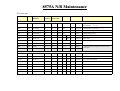
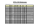
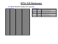
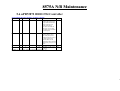
1.7 Appendix 2: H8 Pins Definitions
The shadowed block is the selected function
Name
Pin
H8 Pin
Definitions
During
RESET
After
RESET/OFF
ON
STANDBY
Function
MD0
6
H8_MODE0
I↑
I
H
I
H
I
H
I
H
I
H
H
H mode3 single chip mode
MD1
5
H8_MODE1
I↑
I
H
STBY#
8
STBY#
I↑
I
H
I
H
I
H
H8 Hardware Standby input pull high
NMI#
7
POWER BTN#
I↑
I
H
I
HL
H
I
H
Power button
RESET#
1
RESET#
I
I
LH
I
H
I
H
H8 chip reset
XTAL
2
Crystal
I
I
I
I
EXTAL
3
Crystal
I
I
I
I
RESET OUT#
100
RESET OUT
O
O
O
O
Crystal input
Port A COMOS input level (input high min=3.5V, input low max=1.0V)
PA0
48
LID#
I↑
I
H
I
I
H
PA1
47
H8 ADEN#
I↑
I
H/L
I
I
H/L
AC adaptor in detect
PA2
31
RI#
I↑
I
H
I
I
H
Ring detect
PA3
30
BATT DEAD#
I↑
I
H
I
I
H
Battery low detect
PA4
21
H8 SUSC
I↑
I
H
I
I
L
System resume from S4 soft off through RTC
Alarm
PA5
20
H8 SUSC#
I↑
I
L
I
I
H
System to S4 soft off
PA6
11
BAT_CLK
I↑
I
L
I
I
H
PA7
10
H8_SUSB
I↑
I
H
I
I
H
L
Invert from SUSA# to wake up H8 when system
resumed by MDC modem and internal LAN.
Inform system power management status
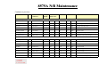
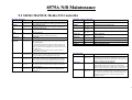
53
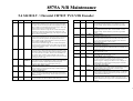
8575A N/B Maintenance
PCI reset gate
Name
Pin
H8 Pin
Definitions
During
RESET
After
RESET/OFF
ON
STANDBY
Function
Port B TTL input voltage (input high min=2V, input low max=0.8V)
PB0
91
H8 SB PWRBTN#
T
O
L
IHL
O
Keep H
Power button trigger VIA8231 on/off Duplicate
Power BTN#
5→3V
PB1
10
H8 WAKE#
T
O
H
O
O
Keep H
Wake up SB at ACPI mode
PB2
81
Force Discharge
T
O
O
Keep H
Power button trigger VIA8231 on 5→3V
PB3
80
CHARGING1
T
O
LLH
O
O
Keep
Battery charge control
PB4
69
VDD5 SW
T↓
O
L
O
H
O
Keep H
H8 VDD5 power source switch
PB5
68
H8 RCIN#
T
O
O
LH
O
Keep H
Reset CPU
PB6
58
CHARGING2
T
O
O
O
Keep
Battery charge control
PB7
57
SMbus SW
T
O
O
O
Keep
PB6
58
VADJ1
T
O
O
O
Keep
PB7
57
VADJ2
T
O
O
O
Keep
5→3V
Lithium ion battery charging CV mode voltage
level adjust
Port 1 TTL input voltage (input high min=2V, input low max=0.8V)
P10/A0
79
KB OUT0
L
O
L
O
LH
O
Keep L
Key matrix scan output 0
P11/A1
78
KB OUT1
L
O
L
O
LH
O
Keep L
Key matrix scan output 1
P12/A2
77
KB OUT2
L
O
L
O
LH
O
Keep L
Key matrix scan output 2
P13/A3
76
KB OUT3
L
O
L
O
LH
O
Keep L
Key matrix scan output 3
P14/A4
75
KB OUT4
L
O
L
O
LH
O
Keep L
Key matrix scan output 4
P15/A5
74
KB OUT5
L
O
L
O
LH
O
Keep L
Key matrix scan output 5
P16/A6
73
KB OUT6
L
O
L
O
LH
O
Keep L
Key matrix scan output 6
P17/A7
72
KB OUT7
L
O
L
O
LH
O
Keep L
Key matrix scan output 7
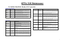
54
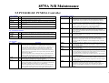
8575A N/B Maintenance
Continue to previous
Name
Pin
H8 Pin
Definitions
During
RESET
After
RESET/OFF
ON
STANDBY
Function
Port 2 TTL input voltage (input high min=2V, input low max=0.8V)
P20/A8
67
KB OUT8
L
O
L
O
LH
O
Keep L
Key matrix scan output 8
P21/A9
66
KB OUT9
L
O
L
O
LH
O
Keep L
Key matrix scan output 9
P22/A10
65
KB OUT10
L
O
L
O
LH
O
Keep L
Key matrix scan output 10
P23/A11
64
KB OUT11
L
O
0
O
LH
O
Keep L
Key matrix scan output 11
P24/A12
63
KB OUT12
L
O
0
O
LH
O
Keep L
Key matrix scan output 12
P25/A13
62
KB OUT13
L
O
0
O
LH
O
Keep L
Key matrix scan output 13
P26/A14
61
KB OUT14
L
O
0
O
LH
O
Keep L
Key matrix scan output 14
P27/A15
60
KB OUT15
L
O
0
O
LH
O
Keep L
Key matrix scan output 15
Port 3 TTL input voltage (input high min=2V, input low max=0.8V)
P30/HDB0/D0
82
ISA SD0
T
I/O
I/O
I/O
Keep
ISA DATA bit 0
P31/HDB1/D1
83
ISA SD1
T
I/O
I/O
I/O
Keep
ISA DATA bit 1
P32/HDB2/D2
84
ISA SD2
T
I/O
I/O
I/O
Keep
ISA DATA bit 2
P33/HDB3/D3
85
ISA SD3
T
I/O
I/O
I/O
Keep
ISA DATA bit 3
P34/HDB4/D4
86
ISA SD4
T
I/O
I/O
I/O
Keep
ISA DATA bit 4
P35/HDB5/D5
87
ISA SD5
T
I/O
I/O
I/O
Keep
ISA DATA bit 5
P36/HDB6/D6
88
ISA SD6
T
I/O
I/O
I/O
Keep
ISA DATA bit 6
P37/HDB7/D7
89
ISA SD7
T
I/O
I/O
I/O
Keep
ISA DATA bit 7
55
8575A N/B Maintenance
Continue to previous
Name
Pin
H8 Pin
Definitions
During
RESET
After
RESET/OFF
ON
STANDBY
Function
Port 4 TTL input voltage (input high min=2V, input low max=0.8V)
P40/TMCI0
49
H8 PWR ON
T↓
O
L
O
LH
O
Keep
System power on, need pull down to
define initial state during reset
P41/TMO0
50
H8 THRM#
T
O
L
O
H
O
Keep H
Thermal throttling control to
Southbridge
P42/TMRI0
51
SCI#/
FAN SPD SW
T
O
H
O
Keep
SCI output and Fan Speed Tachometer
Switch
P43/TMCI1/HIRQ1
52
H8 SCI/
FAN SPEED
T
O
O
O
Keep
Need invert to SCI# sending to SB
5→3V/ Fan speed tachometer
P44/TMCO1/HIRQ1
53
ISA IRQ1
T
O
0
O
O
Keep
Keyboard IRQ1
P45/TMRI1/HIRQ1
54
ISA IRQ12
T
O
0
O
O
Keep
PS2 mouse IRQ12
P46/PWM0
55
Beep sound
T
O
O
O
Keep
Hot key and battery dead beep sound
P46/PWM0
55
FAN ON#0
T
O
1
O
O
Keep
Fan power PWM control
P47/PWM1
56
FAN ON#1
T
O
1
O
O
Keep
Fan power PWM control
Port 5 TTL input voltage (input high min=2V, input low max=0.8V)
P50/TXD0
14
LED DATA
T
O
O
O
Keep
LED indicator shift data
P51/RXD0
13
H8 SMI#
T
O
O
O
Keep
External SMI#
P52/SCK0
12
LED CLK
T
O
O
O
Keep
LED indicator shift clock
5→3V
56
8575A N/B Maintenance
Continue to previous
Name
Pin
H8 Pin
Definitions
During
RESET
After
RESET/OFF
ON
STANDBY
Function
Port 6 Schmitt trigger input voltage (min=1.0V max=3.5V)
P60/KEYIN0/FTCI
26
KEY IN0
T↑
I
I
I
Keep
Key matrix input 0 need pull high
P61/KEYIN1/FTOA
27
KEY IN1
T↑
I
I
I
Keep H
Key matrix input 1 need pull high
P62/KEYIN2/FTIA
28
KEY IN2
T↑
I
I
I
Keep
Key matrix input 2 need pull high
P63/KEYIN3/FTIB
29
KEY IN3
T↑
I
I
I
Keep
Key matrix input 3 need pull high
P64/KEYIN4/FTIC
32
KEY IN4
T↑
I
I
I
Keep
Key matrix input 4 need pull high
P65/KEYIN5/FTID
33
KEY IN5
T↑
I
I
I
Keep
Key matrix input 5 need pull high
P66/KEYIN6/IRQ6
34
KEY IN6
T↑
I
I
I
Keep
Key matrix input 6 need pull high
P67/KEYIN7/IRQ7
35
KEY IN7
T↑
I
I
I
Keep
Key matrix input 7 need pull high
Port 7 TTL input voltage (input high min=2V, input low max=0.8V)
P70/AN0
38
BAT VOLT1
T
I
I
I
T
Battery voltage measure
P71/AN1
39
BAT VOLT2
T
I
I
I
T
Battery voltage measure
P71/AN1
39
I_LIMIT
T
I
I
I
T
P72/AN2
40
3V/PWR ok
T
I
I
I
T
P73/AN3
41
2.5V
T
I
I
I
T
P73/AN3
41
LI/NIMH#
T
I
I
I
Keep
To differential 3S3P lithium ion
battery and 9S NiMH battery
P74/AN4
42
BAT TEMP1
T
I
I
I
T
Battery thermister temperature
P75/AN5
43
BAT TEMP2
T
I
I
I
T
Battery thermister temperature
P75/AN5
43
VCC CORE
T
I
I
I
T
P76/AN6/DA0
44
Charge-I_CTR
T
O
O
O
T
Charging current adjust
P77/AN7/DA1
45
BL ADJ
T
O
O
O
T
Backlight inverter brightness adjust
Monitor system on/off state
57
8575A N/B Maintenance
Continue to previous
Name
Pin
H8 Pin
Definitions
During
RESET
After
RESET/OFF
ON
STANDBY
Function
Port 8 TTL input voltage (input high min=2V, input low max=0.8V)
P80/HA0
93
ISA SA2
T
I
I
I
Keep
P81/GA20
94
X(H8 A20GATE)
T
O
O
O
Keep H
CPU A20gate
P82/CS1
95
H8 KBCS#
T
I
I
I
Keep
IO port 60/64 chip select
P83/IOR
96
ISA IOR#
T
I
I
I
Keep
ISA I/O read#
P84/IRQ2/TXD1
97
ISA IOW#
T
I
I
I
Keep
ISA I/O write
P85/IRQ4/RXD1
98
H8 MCCS#
T
I
I
I
Keep
IO port 62/66 chip select
P86/IRQ5/SCK1
99
BAT CLK
T↑
I/O
I/O
I/O
Keep
SM BUS clock need pull high
5→3V
Port 9 TTL input voltage (input high min=2V, input low max=0.8V)
P90/IRQ2/ESC2
25
K/M CLK
T↑
I/O
I/O
I/O
Keep
need pull high
P91/IRQ1/EIOW
24
M CLK
T↑
I/O
I/O
I/O
Keep
need pull high
P92/IRQ0
23
H8/T CLK
T↑
I/O
I/O
I/O
Keep
need pull high
P93/RD
22
K/M DATA
T↑
I/O
I/O
I/O
Keep
need pull high
P94/WR
19
M DATA
T↑
I/O
I/O
I/O
Keep
need pull high
P95/AS
18
H8/T DATA
T↑
I/O
I/O
I/O
Keep
need pull high
P96/0
17
ENABKL
T↑
I
I
I
T
Read H8 send A20gate status
P97/WAIT/SDA
16
BAT DATA
T↑
I/O
I/O
I/O
Keep
SM BUS clock need pull high
5→3V
↑ Pull High
↓ Pull Low
5→3V Level shift
58
8575A N/B Maintenance
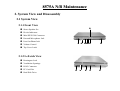
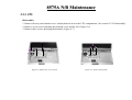
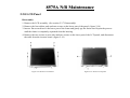
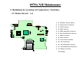
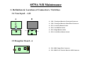
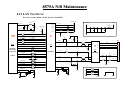
2. System View and Disassembly
2.1 System View
2.1.1 Front View
Stereo Speaker Set
Device Indicators
Mini IEEE1394 Connector
External Microphone Jack
Line Out Phone Jack
Volume Control
Top Cover Latch
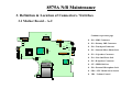
2.1.2 Left-side View
Kensington Lock
Ventilation Openings
RJ-45 Connector
PC Card Slot
Hard Disk Drive
59
8575A N/B Maintenance
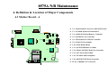
2.1.3 Right-side View
Battery Pack
CD-ROM/DVD-ROM Drive
2.1.4 Rear View
Power Connector
S-Video Output Connector
USB Ports
Parallel Port
D/D Fan
RJ-11 Connector
VGA Port
Ventilation Openings
60
8575A N/B Maintenance
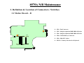
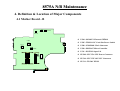
2.1.5 Top-open View
LCD Screen
Microphone
Keyboard
Touch Pad
Power Button
Easy Start Buttons
Battery Charge Indicator
Battery Power Indicator
AC Power Indicator
61
8575A N/B Maintenance
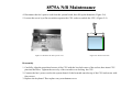
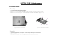
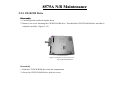
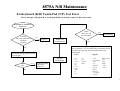
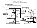
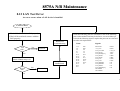
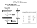
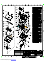
2.2 System Disassembly
The section discusses at length each major component for disassembly/reassembly and show corresponding
illustrations. Use the chart below to determine the disassembly sequence for removing components from the
notebook.
NOTE: Before you start to install/replace these modules, disconnect all peripheral devices and make sure the
notebook is not turned on or connected to AC power.
2.2.1 Battery Pack
2.2.2 Keyboard
Modular Components
2.2.3 CPU
2.2.4 HDD Module
2.2.5 CD-ROM Drive
2.2.6 SO-DIMM
2.2.7 LCD Assembly
NOTEBOOK
LCD Assembly Components
2.2.8 LCD Panel
2.2.9 Inverter Board
2.2.10 System Board
Base Unit Components
2.2.11 Touch-pad
2.2.12 Modem Card
62
8575A N/B Maintenance
2.2.1 Battery Pack
Disassembly
1. Carefully put the notebook upside down.
2. Slide the release lever to the “unlock” ( ) position (), then sliding and holding the release lever
outwards while pull the battery pack out of the compartment (). (Figure 2-1)
Figure 2-1 Remove the battery pack
Reassembly
1. Push the battery pack into the compartment. The battery pack should be correctly connected when you
hear a clicking sound.
2. Slide the release lever to the “lock” ( ) position.
63
8575A N/B Maintenance
2.2.2 Keyboard
Disassembly
1. Open the top cover.
2. Insert a small rod, such as a straightened paper clip, into the eject hole near the power connector of the
notebook. (Figure 2-2)
3. Push the rod firmly and slide the easy start buttons cover to the left (). Then lift the easy start buttons cover up
from the left side (). (Figure 2-3)
Figure 2-2 Insert a rod easy to remove
Figure 2-3 Remove easy start
buttons cover
64
8575A N/B Maintenance
3. Remove three screws fastening keyboard on the base unit cover. (Figure 2-4)
4. Slightly lift up the keyboard and disconnect the cable from the system board to detach the keyboard.
(Figure 2-5)
Figure 2-4 Remove three screws
Figure 2-5 Remove keyboard
Reassembly
1. Reconnect the keyboard cable and fit the keyboard back into place with three screws.
2. Replace the easy start buttons cover.
65
8575A N/B Maintenance
2.2.3 CPU
Disassembly
1. Remove the easy start buttons cover and keyboard to access the CPU compartment. (See section 2.2.2 Disassembly)
2. Remove seven screws fastening the heatsink cover and the rail. (Figure 2-6)
3. Remove three screws fastening the heatsink. (Figure 2-7)
Figure 2-6 Remove the cover and rail
Figure 2-7 Remove the heatsink
66
8575A N/B Maintenance
4. Disconnect the fan’s power cord from the system board, then lift up the heatsink. (Figure 2-8)
5. Loosen the screw by a flat screwdriver,upraise the CPU socket to unlock the CPU. (Figure 2-9)
Figure 2-8 Remove the fan’s power cord
Figure 2-9 Remove the CPU
Reassembly
1. Carefully, align the arrowhead corner of the CPU with the beveled corner of the socket, then insert CPU
pins into the holes. Tighten the screw by a flat screwdriver to locking the CPU.
2. Connect the fan’s power cord to the system board, fit the heatsink onto the top of the CPU and secure with
four screws.
3. Replace the keyboard .Then replace easy start buttons cover.
67
8575A N/B Maintenance
2.2.4 HDD Module
Disassembly
1. Carefully put the notebook upside down.
2. Remove one screw and slide the HDD module out of the compartment. (Figure 2-10)
3. Remove six screws to separate the hard disk drive from the metal shield. (Figure 2-11)
Figure 2-10 Remove HDD module
Figure 2-11 Disassemble the hard disk
Reassembly
1. To install the hard disk drive, place it in the bracket and secure with six screws.
2. Slide the HDD module into the compartment and secure with one screw.
68
8575A N/B Maintenance
2.2.5 CD-ROM Drive
Disassembly
1. Carefully put the notebook upside down.
2. Remove one screw fastening the CD/DVD-ROM drive. Then hold the CD/DVD-ROM drive and slide it
outwards carefully. (Figure 2-12)
Figure 2-12 Remove one screw to loose
the CD/DVD-ROM drive
Reassembly
1. Push the CD/DVD-ROM drive into the compartment.
2. Secure the CD/DVD-ROM drive with one screw.
69
8575A N/B Maintenance
2.2.6 SO-DIMM
Disassembly
1. Carefully put the notebook upside down.
2. Remove seven screws to access the SO-DIMM socket. (Figure 2-13)
3. Full the retaining clips outwards () and remove the SO-DIMM (). (Figure 2-14)
Figure 2-13 Remove the SO-DIMM cover
Figure 2-14 Remove the SO-DIMM
Reassembly
1. To install the SO-DIMM, match the SO-DIMM’s notched part with the socket’s projected part and firmly
insert the OS-DIMM into the socket at 20-degree angle. Then push down until the retaining clips lock the
SO-DIMM into cover.
2. Replace the SO-DIMM cover.
3. Replace seven screws to fasten the SO-DIMM socket cover.
70
8575A N/B Maintenance
2.2.7 LCD
Disassembly
1.Carefully put the notebook upside down and remove seven screws to access the SO-DIMM socket.
2.Remove the tape from the antenna on the Mini-PCI socket.(Figure 2-15)
Figure 2-15 Remove the tape from
the antenna
Figure 2-16 Remove the LCD hinge cover
and button board
3. Open the top cover. Remove easy start buttons cover, keyboard, and heatsink . (See section 2.2.2 and 2.2.3 Disassembly)
4. Pull out the antenna from the CPU compartment.
5. Remove the two hinge covers and remove two screws fastening the easy start button board.(Figure 2-16)
71
8575A N/B Maintenance
6. Disconnect the LCD cables from the system board, and remove four screws of the hinges. Now you can
separate the LCD assembly from the base unit. (Figure 2-17)
Figure 2-17 Remove cables and screws
to separate LCD
Reassembly
1. Attach the LCD assembly to the base unit and secure with four screws on the hinges.
2. Replace the antenna to the SO-DIMM socket.
3. Reconnect the LCD cable connectors to the system board.
4. Fit the easy start button board and secure with tow screws.
5. Replace two hinge cover, the heatsink, keyboard and easy start buttons cover.
72
8575A N/B Maintenance
2.2.8 LCD Panel
Disassembly
1. Remove the LCD assembly. (See section 2.2.7 Disassembly)
2. Remove the four rubber pads and two screws on the lower part of the panel. (figure 2-18)
3. Insert a flat screwdriver to the lower part of the frame and gently pry the frame out. Repeat the process
until the frame is completely separated from the housing.
4. Remove the two screws on two sides and two screws on the lower part of the LCD panel, and disconnect
the cable from the inverter board. (figure 2-19)
Figure 2-18 Remove LCD frame
Figure 2-19 Remove LCD panel
73
8575A N/B Maintenance
Reassembly
1. Fit the LCD panel back into place and secure with four screws, and reconnect the cable to the inverter board.
2. Fit the LCD frame back into the housing and replace the four screws and four rubber pads.
3. Replace the LCD assembly. (See section 2.2.7 Reassembly)
74
8575A N/B Maintenance
2.2.9 Inverter Board
Disassembly
1. Remove the LCD assembly and detach the LCD panel. (see instructions in previous two sections)
2. To remove the inverter board on the bottom side of the LCD assembly, disconnect the cable and remove
one screw. (figure 2-20)
Figure 2-20 Remove the inverter board
Reassembly
1. Fit the inverter board back into place and secure with one screw.
2. Reconnect the cable.
3. Replace the LCD frame. (See section 2.2.8 Reassembly)
4. Replace the LCD assembly. (See section 2.2.7 Reassembly)
75
8575A N/B Maintenance
2.2.10 System Board
Disassembly
1. Remove the battery pack, keyboard, CPU, HDD module, CD/DVD-ROM drive and LCD assembly.
(See section 2.2.1 to 2.2.5 and 2.2.7 Disassembly)
2. Remove sixteen screws on the bottom of the notebook. (Figure 2-21)
3. Remove nine screws fastening the base unit cover. (figure 2-22)
Figure 2-21 Remove the bottom
Figure 2-22 Remove nine screws
76
8575A N/B Maintenance
4. Lift up the base unit cover and disconnect the touch pad cord. (Figure 2-23)
5. Remove the four screws fastening the base unit. (Figure 2-24)
Figure 2-23 Remove the base unit cover
Figure 2-24 Remove the metal shield
77
8575A N/B Maintenance
6. Remove three screws fastening the connectors shield and disconnect the cables. (Figure 2-25)
7. Carefully put the notebook upside down.
8. Remove seven screws and four hex nuts fastening the system board and disconnect one cable . Now
you can remove the system board. (Figure 2-26)
Figure 2-25 Remove the screws and
disconnect the cable
Figure 2-26 Remove the system board
Reassembly
1. Replace seven screws and four hex nuts fasten the system board.
2. Reconnect one cable of system board fan and one cable of little battery to system board.
3. Replace three screws fasten the the connectors shield .
4. Reconnect two cables of speakers and one cable to system board.
5. Reconnect the touch pad cord.
6. Replace the base unit cover and secure with nine screws
7. Carefully put the notebook upside down. Then replace the bottom frame and secure with sixteen screws.
8. Replace the battery pack, LED panel, keyboard, CPU, HDD module, CD/DVD-ROM drive and LCD assembly.
78
8575A N/B Maintenance
2.2.11 Touch-pad
Disassembly
1. Remove the base unit cover. (See steps 1-6 in section 2.2.10 Disassembly.)
2. Remove the eight screws to lift up the touch pad holder and touch pad panel. (Figure 2-27)
Figure 2-27 Remove the touch-pad
Reassembly
1. Replace the touch-pad holder and touch-pad panel, and secure with eight screws.
2. Assemble the base unit cover. (See section 2.2.10 Reassembly)
79
8575A N/B Maintenance
2.2.12 Modem Card
Disassembly
1. Remove the battery pack, keyboard, CPU, HDD module, CD/DVD-ROM drive, and LCD assembly. (See
section 2.2.1 to 2.2.5 and 2.2.7 Disassembly)
2. Disassemble the notebook to access the system board. (See section 2.2.10 Disassembly)
3. Remove the two screws fastening the modem card,and then disconnect the cable from system board. (Figure 2-28)
Figure 2-28 Remove the Modem card
Reassembly
1. Reconnect the cable to the modem card and secure the modem card with two screws.
2. Assemble the notebook. (See section 2.2.10 Reassembly)
80
8575A N/B Maintenance
3. Definition & Location of Connectors / Switches
3.1 Mother Board – A-1
J1 : Modem Connector (RJ11)
J12
J7
J2 : External VGA Connector
J4
J14
J6
J5
J18
J1
J25
VR1
J21
J20
J24
J28
J13
J2
J27
SW6
J5 : MDC Jump Wire Connector
J6 : Easy Start Buttons Connector
J8 : Fan Connector
J11
J23
J9 : LAN Connector (RJ45)
J11 : PC Card Socket
J12 : Secondary IDE Connector
J9
J509
J8
J4 : D/D Connector
J7 : MISC Connector
J19
J3
J3 : LCD Connector
J13 : Internal Keyboard Connector
J14 : Battery Connector
To next page
81
8575A N/B Maintenance
3. Definition & Location of Connectors / Switches
3.1 Mother Board – A-2
J12
J7
Continue to previous page
J4
J14
J6
J5
J18
J1
J25
VR1
J21
J20
J24
J13
J2
J8
J19 : Primary IDE Connector
J20 : Touch-pad Connector
J28
J21 : Internal Micro Phone Jack
J27
J23 : L Speaker Connector
J19
J3
J18 : MDC Connector
J24 : Line Out Phone Jack
SW6
J11
J25 : R Speaker Connector
J23
J27 : IEEE1394 Port
J28 : External Microphone Jack
SW6 : CPU Model Select Switch
J9
VR1 : Volume Control
82
8575A N/B Maintenance
3. Definition & Location of Connectors / Switches
3.1 Mother Board – B
J503 : Fan Connector
J503
J506 : 200-pin expansion DDR SDRAM Socket
J508
ON
J505 : 200-pin expansion DDR SDRAM Socket
J509
2
1
SW503
J508 : CMOS Battery Connector
?
J509 : Mini PCI Socket
SW503 : Country Selection for Keyboard
J506
J505
U6 U5 U3
83
8575A N/B Maintenance
3. Definition & Location of Connectors / Switches
3.2 DC Power Board - A
J1 : TV Out Jack
J2 : Power Jack (AC adapter)
SW1
J3
J1
PJ2
J5
J6
PJ1
J7
J4
J8
J3 : Parallel Port Connector
J2
J4 : USB Port Connector
J5 : USB Port Connector
J6 : Inverter Board Connector
J7 : USB Port Connector
J8 : USB Port Connector
PJ1 : D/D Connector
PJ2 : MISC Connector
SW1 : Cover Switch
84
8575A N/B Maintenance
3. Definition & Location of Connectors / Switches
3.3 ESB Board – A,B
A
SW1
SW2
SW3
SW4
SW5
SW6
J501 : Easy Start Button Connector
SW1 : Programmable Easy Start Button Switch
SW2 : Programmable Easy Start Button Switch
SW3 : Programmable Easy Start Button Switch
B
J501
SW4 : Programmable Easy Start Button Switch
SW5 : Programmable Easy Start Button Switch
SW6 : Programmable Easy Start Button Power Switch
85
8575A N/B Maintenance
3. Definition & Location of Connectors / Switches
3.4 Touch-pad – A,B
A
B
J501 : Touch-pad Board to Touch-pad Connector
J502 : Touch-pad Board to Main Board Connector
SW1 : Scroll Up Button Switch
SW2 : Left Button Switch
SW3 : Right Button Switch
J501
SW2
SW1
J502
SW3
SW4 : Scroll Down Button Switch
SW4
3.5 Daughter Board -A
JP1 : MDC Jump Wire Connector
JP1
JP3
JP3 : MDC/LAN Transfer Board to M/B Connector
86
8575A N/B Maintenance
4. Definition & Location of Major Components
4.1 Mother Board - A
U1 : Intel Pentium 4 Processor mPGA478 Socket
U3 : LF-H80P Isolation Transformers
U4 : SiS650 IGUI Host/Memory Controller
U11
PU10
U16
U5 : ISC1893Y LAN Controller
U15
U6 : PCI1410GGU PCMCIA Controller
U10
U9 : ICS93722 Clock Buffer
U4
U10 : Flash ROM (BIOS)
U1
U11 : SN74CBTD3384 Level Shift
U14
U14 : SiS961 MuTIOL Media I/O Controller
U15 : ALC201 Audio CODEC
U3 U5
U6
J509
U18
U9
U16 : TPA0202 Audio Amplifier
U18 : uPD72872 IEEE1394 Controller
PU10 : CM8500 1.25V Generator
87
8575A N/B Maintenance
4. Definition & Location of Major Components
4.1 Mother Board - B
PU508
PU510
PU511
U504 : SiS301LV/Chrontel CH7019
U509
U505 : TPS2211 PC Card Slot Power Switch
U511
U508 : ICS952001 Clock Generator
U508
U509 : H8/F3437 Micro Controller
U511 : PC87393 Super I/O
?
U505
U504
PU508 : LTC3716 CPU Power Generator
PU510 : LTC3707 1.8V/2.5V Generator
PU511 : TL594C PWM
U6 U5 U3
88
8575A N/B Maintenance
5. Pin Descriptions of Major Components
5.1 Intel Pentium 4 Processor mPGA478 Socket
Type
Description
A[35:3]#
Name
Input/
Output
A20M#
Input
A[35:3]# (Address) define a 2 36 -byte physical memory address space.
In sub-phase 1 of the address phase, these pins transmit the address of a
transaction. In sub-phase 2, these pins transmit transaction type
information. These signals
must connect the appropriate pins of all agents on the Pentium 4
processor in the 478-pin package system bus. A[35:3]# are protected by
parity signals AP[1:0]#. A[35:3]# are source synchronous signals and
are latched into the receiving buffers by ADSTB[1:0]#. On the
active-to-inactive transition of RESET#, the processor samples a subset
of the A[35:3]# pins to determine power-on configuration.
If A20M# (Address-20 Mask) is asserted, the processor masks physical
address bit 20 (A20#) before looking up a line in any internal cache and
before driving a read/write transaction on the bus. Asserting A20M#
emulates the 8086 processor's address wrap-around at the 1-Mbyte
boundary. Assertion of A20M# is only supported in real mode.
A20M# is an asynchronous signal. However, to ensure recognition of
this signal following an Input/Output write instruction, it must be valid
along with the TRDY# assertion of the corresponding Input/Output
Write bus transaction.
ADS# (Address Strobe) is asserted to indicate the validity of the
transaction address on the A[35:3]# and REQ[4:0]# pins. All bus agents
observe the ADS# activation to begin parity checking, protocol
checking, address decode, internal snoop, or deferred reply ID match
operations associated with the new transaction.
Address strobes are used to latch A[35:3]# and REQ[4:0]# on their
rising and falling edges. Strobes are associated with signals as shown
below.
ADS#
ADSTB[1:0]#
Input/
Output
Input/
Output
Signals
Associated Strobe
REQ[4:0]#, A[16:3]#
A[35:17]#
ADSTB0#
ADSTB1#
Name
AP[1:0]#
BCLK[1:0]
Type
Description
Input/
Output
AP[1:0]# (Address Parity) are driven by the request initiator along
with ADS#,A[35:3]#, and the transaction type on the REQ[4:0]#. A
correct parity signal is high if an even number of covered signals
are low and low if an odd number of covered signals are low. This
allows parity to be high when all the covered signals are high.
AP[1:0]# should connect the appropriate pins of all Pentium 4
processor in the 478-pin package system bus agents. The following
table defines
Input
BINIT#
Input/
Output
BNR#
Input/
Output
Request Signals
subphase 1
subphase 2
A[35:24]#
A[23:3]#
REQ[4:0]#
AP0#
AP1#
AP1#
AP1#
AP0#
AP0#
The differential pair BCLK (Bus Clock) determines the system bus
frequency. All processor system bus agents must receive these
signals to drive their outputs and latch their inputs.
All external timing parameters are specified with respect to the
rising edge of BCLK0 crossing V CROSS .
BINIT# (Bus Initialization) may be observed and driven by all
processor system bus agents and if used, must connect the
appropriate pins of all such agents. If the BINIT# driver is enabled
during power-on configuration, BINIT# is asserted
to signal any bus condition that prevents reliable future operation.
If BINIT# observation is enabled during power-on configuration,
and BINIT# is sampled asserted, symmetric agents reset their bus
LOCK# activity and bus request arbitration state machines. The bus
agents do not reset their IOQ and transaction tracking state
machines upon observation of BINIT# activation. Once the BINIT#
assertion has been observed, the bus agents will re-arbitrate for the
system bus and attempt completion of their bus queue and IOQ
entries.
If BINIT# observation is disabled during power-on configuration, a
central agent may handle an assertion of BINIT# as appropriate to
the error handling architecture of the system.
BNR# (Block Next Request) is used to assert a bus stall by any bus
agent who is unable to accept new bus transactions. During a bus
stall, the current bus owner cannot issue any new transactions.
89
8575A N/B Maintenance
5.1 Intel Pentium 4 Processor mPGA478 Socket
Name
BPM[5:0]#
BPRI#
BR0#
BSEL[1:0]
COMP[1:0]
Type
Input/
Output
Description
BPM[5:0]# (Breakpoint Monitor) are breakpoint and performance
monitor signals. They are outputs from the processor which indicate the
status of breakpoints and programmable counters used for monitoring
processor performance. BPM[5:0]# should connect the appropriate pins
of all Pentium 4 processor in the 478-pin package system bus agents.
BPM4# provides PRDY# (Probe Ready) functionality for the TAP port.
PRDY# is a processor output used by debug tools to determine
processor debug readiness.
BPM5# provides PREQ# (Probe Request) functionality for the TAP
port. PREQ# is used by debug tools to request debug operation of the
processor. Please refer to the Intel® Pentium® 4 Processor in the
478-pin Package and Intel® 850 Chipset Platform Design Guide for
more detailed information.
These signals do not have on-die termination. Refer to the Intel®
Pentium® 4 Processor in the 478-pin Package and Intel® 850
Chipset Platform Design Guide for termination requirements.
Input BPRI# (Bus Priority Request) is used to arbitrate for ownership of the
processor system bus. It must connect the appropriate pins of all
processor system bus agents. Observing BPRI# active (as asserted by
the priority agent) causes all other agents to stop issuing new requests,
unless such requests are part of an ongoing locked operation. The
priority agent keeps BPRI# asserted until all of its
requests are completed, then releases the bus by deasserting BPRI#.
Input/ BR0# drives the BREQ0# signal in the system and is used by the
Output processor to request the bus. During power-on configuration this pin is
sampled to determine the agent ID = 0.
This signal does not have on-die termination and must be
terminated.
Output The BCLK[1:0] frequency select signals BSEL[1:0] are used to select
the processor input clock frequency. The required frequency is
determined by the processor, chipset and clock synthesizer. All agents
must operate at the same frequency. The Pentium 4 processor in the
478-pin package operates currently at a 400 MHz system bus frequency
(100 MHz BCLK[1:0] frequency).
Analog COMP[1:0] must be terminated on the system board using precision
resistors. Refer to the Intel® Pentium® 4 Processor in the 478-pin
Package and Intel® 850 Chipset Platform Design Guide for details on
implementation.
Name
D[63:0]#
Type
Description
Input/
Output
D[63:0]# (Data) are the data signals. These signals provide a 64-bit
data path between the processor system bus agents, and must
connect the appropriate pins on all such agents. The data driver
asserts DRDY# to indicate a valid data transfer.
D[63:0]# are quad-pumped signals and will thus be driven four
times in a common clock period. D[63:0]# are latched off the falling
edge of both DSTBP[3:0]# and DSTBN[3:0]#. Each group of 16
data signals correspond to a pair of one DSTBP# and one DSTBN#.
The following table shows the grouping of data signals to data
strobes and DBI#.
Quad-Pumped Signal Groups
Data Group
D[15:0]#
D[31:16]#
D[47:32]#
D[63:48]#
DBI[3:0]#
DBR#
Input/
Output
Output
DSTBN#/
DSTBP#
0
1
2
3
DBI#
0
1
2
3
Furthermore, the DBI# pins determine the polarity of the data
signals. Each group of 16 data signals corresponds to one DBI#
signal. When the DBI# signal is active, the corresponding data
group is inverted and therefore sampled active high.
DBI[3:0]# are source synchronous and indicate the polarity of the
D[63:0]# signals. The DBI[3:0]# signals are activated when the data
on the data bus is inverted. The bus agent will invert the data bus
signals if more than half the bits, within the covered group, would
change level in the next cycle.
DBI[3:0] Assignment To Data Bus
Bus Signal
Data Bus Signals
DBI3#
DBI2#
DBI1#
DBI0#
D[63:48]#
D[47:32]#
D[31:16]#
D[15:0]#
DBR# is used only in processor systems where no debug port is
implemented on the system board. DBR# is used by a debug port
interposer so that an in-target probe can drive system reset. If a
debug port is implemented in the system, DBR# is a no connect in
the system. DBR# is not a processor signal.
90
8575A N/B Maintenance
5.1 Intel Pentium 4 Processor mPGA478 Socket
Name
DBSY#
DEFER#
DP[3:0]#
DSTBN[3:0]#
DSTBP[3:0]#
FERR#
GTLREF
Type
Description
Input/ DBSY# (Data Bus Busy) is asserted by the agent responsible for
Output driving data on the processor system bus to indicate that the data
bus is in use. The data bus isreleased after DBSY# is deasserted.
This signal must connect the appropriate pins on all processor
system bus agents.
DEFER# is asserted by an agent to indicate that a transaction
Input
cannot be guaranteed in-order completion. Assertion of
DEFER# is normally the responsibility of the addressed
memory or Input/Output agent. This signal must connect the
appropriate pins of all processor system bus agents.
Input/ DP[3:0]# (Data parity) provide parity protection for the
Output D[63:0]# signals. They are driven by the agent responsible for
driving D[63:0]#, and must connect the appropriate pins of all
Pentium 4 processor in the 478-pin package system bus gents.
Input/ Data strobe used to latch in D[63:0]#.
Output
Signals
Associated Strobe
D[15:0]#, DBI0#
DSTBN0#
D[31:16]#, DBI1#
DSTBN1#
D[47:32]#, DBI2#
DSTBN2#
D[63:48]#, DBI3#
DSTBN3#
Input/ Data strobe used to latch in D[63:0]#.
Output
Signals
Associated Strobe
D[15:0]#, DBI0#
DSTBP0#
D[31:16]#, DBI1#
DSTBP1#
D[47:32]#, DBI2#
DSTBP2#
D[63:48]#, DBI3#
DSTBP3#
Output FERR# (Floating-point Error) is asserted when the processor
detects an unmasked floating-point error. FERR# is similar to
the ERROR# signal on the Intel 387 coprocessor, and is
included for compatibility with systems using MSDOS*-type
floating-point error reporting.
Input GTLREF determines the signal reference level for AGTL+ input
pins. GTLREF should be set at 2/3 VCC. GTLREF is used by the
AGTL+ receivers to determine if a signal is a logical 0 or
logical 1. Refer to the Intel® Pentium® 4 Processor in the
478-pin Package and Intel® 850 Chipset Platform Design
Guide for more information.
Name
HIT#
HITM#
IERR#
IGNNE#
INIT#
ITPCLKOUT[1:0]
ITP_CLK[1:0]
Type
Description
Input/ HIT# (Snoop Hit) and HITM# (Hit Modified) convey
Output transaction snoop operation results. Any system bus agent may
assert both HIT# and HITM# together to indicate that it requires
Input/ a snoop stall, which can be continued by reasserting
Output HIT# and HITM# together.
Output IERR# (Internal Error) is asserted by a processor as the result of
an internal error. Assertion of IERR# is usually accompanied by
a SHUTDOWN transaction on the processor system bus. This
transaction may optionally be converted to an external error
signal (e.g., NMI) by system core logic. The processor will keep
IERR# asserted until the assertion of RESET#, BINIT#, or
INIT#.
This signals does not have on-die termination.
Input IGNNE# (Ignore Numeric Error) is asserted to force the
processor to ignore a numeric error and continue to execute
noncontrol floating-point instructions. If IGNNE# is deasserted,
the processor generates an exception on a noncontrol
floating-point instruction if a previous floating-point instruction
caused an error.IGNNE# has no effect when the NE bit in
control register 0 (CR0) is set. IGNNE# is an asynchronous
signal. However, to ensure recognition of this signal following
an Input/Output write instruction, it must be valid along with the
TRDY# assertion of the corresponding Input/Output Write bus
transaction.
Input INIT# (Initialization), when asserted, resets integer registers
inside the processor without affecting its internal caches or
floating-point registers. The processor then begins execution at
the power-on Reset vector configured during power-on
configuration. The processor continues to handle snoop requests
during INIT# assertion. INIT# is an asynchronous signal and
must connect the appropriate pins of all processor system bus
agents. If INIT# is sampled active on the active to inactive
transition of RESET#, then the processor executes its Built-in
Self-Test (BIST).
Output The ITPCLKOUT[1:0] pins do not provide any output for the
Pentium® 4 processor in the 478-pin package.
Input ITP_CLK[1:0] are copies of BCLK that are used only in
processor systems where no debug port is implemented on the
system board. ITP_CLK[1:0] are used as BCLK[1:0] references
for a debug port implemented on an interposer. If a debug port
is implemented in the system, ITP_CLK[1:0] are no connects in
the system. These are not processor signals.
91
8575A N/B Maintenance
5.1 Intel Pentium 4 Processor mPGA478 Socket
Name
LINT[1:0]
LOCK#
MCERR#
PROCHOT#
Type
Description
LINT[1:0] (Local APIC Interrupt) must connect the appropriate
Input
pins of all APIC Bus agents. When the APIC is disabled, the
LINT0 signal becomes INTR, a maskable interrupt request
signal, and LINT1 becomes NMI, a nonmaskable interrupt.
INTR and NMI are backward compatible with the signals of
those names on the Pentium processor. Both signals are
asynchronous.
Both of these signals must be software configured via BIOS
programming of the APIC register space to be used either as
NMI/INTR or LINT[1:0]. Because the APIC is enabled by
default after Reset, operation of these pins as LINT[1:0] is the
default configuration.
Input/ LOCK# indicates to the system that a transaction must occur
Output atomically. This signal must connect the appropriate pins of all
processor system bus agents. For a locked sequence of
transactions, LOCK# is asserted from the beginning of the
first transaction to the end of the last transaction.
When the priority agent asserts BPRI# to arbitrate for ownership
of the processor system bus, it will wait until it observes
LOCK# deasserted. This enables symmetric agents to retain
ownership of the processor system bus throughout the bus
locked operation and ensure the atomicity of lock.
Input/ MCERR# (Machine Check Error) is asserted to indicate an
Output unrecoverable error without a bus protocol violation. It may be
driven by all processor system bus agents.
MCERR# assertion conditions are configurable at a system
level. Assertion options are defined by the following options:
Enabled or disabled.
Asserted, if configured, for internal errors along with IERR#.
Asserted, if configured, by the request initiator of a bus
transaction after it observes an error.
Asserted by any bus agent when it observes an error in a bus
transaction.
For more details regarding machine check architecture, please
refer to the IA-32 Software Developer’s Manual, Volume 3:
System Programming Guide.
Output PROCHOT# will go active when the processor temperature
monitoring sensor detects that the processor has reached its
maximum safe operating temperature.
This indicates that the processor Thermal Control Circuit has
been activated, if enabled. .
Name
PWRGOOD
RESET#
RS[2:0]#
RSP#
Type
Description
Input
PWRGOOD (Power Good) is a processor input. The processor
requires this signal to be a clean indication that the clocks and
power supplies are stable and within their specifications.
‘Clean’ implies that the signal will remain low (capable of
sinking leakage current), without glitches, from the time that the
power supplies are turned on until they come within
specification. The signal must then transition monotonically to a
high state. PWRGOOD can be driven inactive at any time, but
clocks and power must again be stable before a subsequent
rising edge of PWRGOOD. The PWRGOOD signal must be
supplied to the processor; it is used to protect internal circuits
against voltage sequencing issues. It should be driven high
throughout boundary scan operation.
Input
Asserting the RESET# signal resets the processor to a known
state and invalidates its internal caches without writing back any
of their contents. For a power-on Reset, RESET# must stay
active for at least one millisecond after VCC and BCLK have
reached their proper specifications. On observing active
RESET#, all system bus agents will deassert their outputs within
two clocks. RESET# must not be kept asserted for more than 10
ms while PWRGOOD is asserted.
A number of bus signals are sampled at the active-to-inactive
transition of RESET# for power-on configuration.
This signal does not have on-die termination and must be
terminated on the system board.
Input
RS[2:0]# (Response Status) are driven by the response agent
(the agent responsible for completion of the current transaction),
and must connect the appropriate pins of all processor system
bus agents.
Input
RSP# (Response Parity) is driven by the response agent (the
agent responsible for completion of the current transaction)
during assertion of RS[2:0]#, the signals for which RSP#
provides parity protection. It must connect to the appropriate
pins of all processor system bus agents.
A correct parity signal is high if an even number of covered
signals are low and low if an odd number of covered signals are
low. While RS[2:0]# = 000, RSP# is also high, since this
indicates it is not being driven by any agent guaranteeing
correct parity.
92
8575A N/B Maintenance
5.1 Intel Pentium 4 Processor mPGA478 Socket
Name
REQ[4:0]#
SKTOCC#
SLP#
SMI#
STPCLK#
TCK
Type
Description
Input/ REQ[4:0]# (Request Command) must connect the appropriate
Output pins of all processor system bus agents. They are asserted by the
current bus owner to define the currently active transaction type.
These signals are source synchronous to ADSTB0#. Refer to the
AP[1:0]# signal description for a details on parity checking of
these signals.
Output SKTOCC# (Socket Occupied) will be pulled to ground by the
processor. System board designers may use this pin to determine
if the processor is present.
Input
SLP# (Sleep), when asserted in Stop-Grant state, causes the
processor to enter the Sleep state. During Sleep state, the
processor stops providing internal clock signals to all units,
leaving only the Phase-Locked Loop (PLL) still operating.
Processors in this state will not recognize snoops or interrupts.
The processor will recognize only assertion of the RESET#
signal, deassertion of SLP#, and removal of the BCLK input
while in Sleep state. If SLP# is deasserted, the processor exits
Sleep state and returns to Stop-Grant state, restarting its internal
clock signals to the bus and processor core units. If the BCLK
input is stopped while in the Sleep state the processor will exit
the Sleep state and transition to the Deep Sleep state.
Input
SMI# (System Management Interrupt) is asserted
asynchronously by system logic. On accepting a System
Management Interrupt, the processor saves the current state and
enter System Management Mode (SMM). An SMI
Acknowledge transaction is issued, and the processor begins
program execution from the SMM handler.
If SMI# is asserted during the deassertion of RESET# the
processor will tristate its outputs.
Input
STPCLK# (Stop Clock), when asserted, causes the processor to
enter a low power Stop-Grant state. The processor issues a
Stop-Grant Acknowledge transaction, and stops providing
internal clock signals to all processor core units except the
system bus and APIC units. The processor continues to snoop
bus transactions and service interrupts while in Stop-Grant state.
When STPCLK# is deasserted, the processor restarts its internal
clock to all units and resumes execution. The assertion of
STPCLK# has no effect on the bus clock; STPCLK# is an
asynchronous input.
Input
TCK (Test Clock) provides the clock input for the processor
Test Bus (also knownas the Test Access Port).
Name
TESTHI[12:8]
TESTHI[5:0]
THERMDA
Type
Description
Input
TDI (Test Data In) transfers serial test data into the processor.
TDI provides the serial input needed for JTAG specification
support.
Output TDO (Test Data Out) transfers serial test data out of the
processor. TDO provides the serial output needed for JTAG
specification support.
Input
TESTHI[12:8] and TESTHI[5:0] must be connected to a VCC
power source through a resistor for proper processor operation.
Other Thermal Diode Anode.
THERMDC
Other
THERMTRIP#
Output Assertion of THERMTRIP# (Thermal Trip) indicates the
processor junction temperature has reached a level beyond
which permanent silicon damage may occur. Measurement of
the temperature is accomplished through an internal thermal
sensor which is configured to trip at approximately 135°C.Upon
assertion of THERMTRIP#, the processor will shut off its
internal clocks (thus halting program execution) in an attempt to
reduce the processor junction temperature. To protect the
processor, its core voltage (VCC) must be removed following
the assertion of THERMTRIP#. Once activated, THERMTRIP#
remains latched until RESET# is asserted. While the assertion of
the RESET# signal will de-assert THERMTRIP# , if the
processor’s junction
temperature remains at or above the trip level, THERMTRIP#
will again be asserted after RESET# is de-asserted.
Input
TMS (Test Mode Select) is a JTAG specification support signal
used by debug tools.
Input
TRDY# (Target Ready) is asserted by the target to indicate that
it is ready to receive a write or implicit writeback data transfer.
TRDY# must connect the appropriate pins of all system bus
agents.
Input
TRST# (Test Reset) resets the Test Access Port (TAP) logic.
TRST# must be driven low during power on Reset. This can be
done with a 680 . pull-down resistor.
Input
VCCA provides isolated power for the internal processor core
PLLs. Refer to the Intel® Pentium® 4 Processor in the 478-pin
Package and Intel® 850 Chipset Platform Design Guide for
complete implementation details.
TDI
TDO
TMS
TRDY#
TRST#
VCCA
Thermal Diode Cathode.
93
8575A N/B Maintenance
5.1 Intel Pentium 4 Processor mPGA478 Socket
Name
VCCIOPLL
VCCSENSE
VCCVID
VID[4:0]
VSSA
VSSSENSE
TMS
TRDY#
TRST#
VCCA
Type
Description
Input
VCCIOPLL provides isolated power for internal processor system
bus PLLs. Follow he guidelines for VCCA, and refer to the Intel®
Pentium® 4 Processor in the 478-pin Package and Intel® 850
Chipset Platform Design Guide for complete implementation
details.
Output VCCSENSE is an isolated low impedance connection to processor
core power(VCC). It can be used to sense or measure power near
the silicon with little noise.
Input
There is no imput voltage requirement for VCCVID for designs
intended tosupport only the Pentium 4 processor in the 478-pin
package. Refer to the Intel® Pentium® 4 Processor in the
478-pin Package and Intel® 850 Chipset Platform Design
Guide for more information.
Output VID[4:0] (Voltage ID) pins can be used to support automatic
selection of power supply voltages (Vcc). These pins are not
signals, but are either an open circuit or a short circuit to VSS
on the processor. The combination of opens and shorts
defines the voltage required by the processor. The VID pins are
needed to cleanly support processor voltage specification
variations. The power supply must supply the voltage that is
requested by these pins, or disable itself.
Input
VSSA is the isolated ground for internal PLLs.
Output VSSSENSE is an isolated low impedance connection to processor
core VSS. It can be used to sense or measure ground near the
silicon with little noise
Input
TMS (Test Mode Select) is a JTAG specification support signal
used by debug tools.
Input
TRDY# (Target Ready) is asserted by the target to indicate that
it is ready to receive a write or implicit writeback data transfer.
TRDY# must connect the appropriate pins of all system bus
agents.
Input
TRST# (Test Reset) resets the Test Access Port (TAP) logic.
TRST# must be driven low during power on Reset. This can be
done with a 680 . pull-down resistor.
Input
VCCA provides isolated power for the internal processor core
PLLs. Refer to the Intel® Pentium® 4 Processor in the 478-pin
Package and Intel® 850 Chipset Platform Design Guide for
complete implementation details.
94
8575A N/B Maintenance
5.2 SiS650 IGUI Host/Memory Controller
Host BUS Interface
Name
CPUCLK
CPUCLK#
CPURST#
CPUPWRGD#
ADS#
Pin Attr
I
0.71V – M
O
1.2~1.85V – M
O
1.2~1.85V
–M
I/O
1.2~1.85V – M
HADSTB[1:0]#
1.2~1.85V – M
HREQ[4:0]#
I/O
1.2~1.85V – M
HA[31:3]#
I/O
1.2~1.85V – M
O
1.2~1.85V – M
BREQ0#
BPRI#
O
1.2~1.85V – M
BNR#
I/O
1.2~1.85V – M
HLOCK#
I
1.2~1.85V – M
HIT#
I/O
1.2~1.85V – M
I/O
1.2~1.85V – M
HITM#
DEFER#
O
1.2~1.85V – M
Signal Description
Host differential clock input.
Host Bus Reset:
CPURST# is used to keep all the bus agents in
the same initial state before valid cycles issued.
CPUPWRGD# is used to inform CPU that main power is
stable
Address Strobe :
Address Strobe is driven by CPU or SiS650 to indicate the
start of a CPU bus cycle.
Source synchronous address strobe used to latch
HREQ[4:0]# & HA[31:3]# at both falling and rising edge.
HREQ[4:0]# & HA[16:3]# are latched by
HASTB0#
HA[31:17] are latched by HASTB1#
Request Command:
HREQ[4:0]# are used to define each transaction type during
the clock when ADS# is asserted and the clock after ADS# is
asserted.
Host Address Bus
Symmetric Agent Bus Request:
BREQ0# is driven by the symmetric agent to request for the
bus.
Priority Agent Bus Request:
BPRI# is driven by the priority agent that wants to request the
bus.
BPRI# has higher priority than BREQ0# to access a bus.
Block Next Request:
This signal can be driven asserted by any bus agent to block
further requests being pipelined.
Host Lock :
CPU asserts HLOCK# to indicate the current bus cycle is
locked.
Keeping a Non-Modified Cache Line
Name
RS[2:0]#
HTRDY#
DRDY#
DBSY#
HD[63:0]#
DBI[3:0]#
HDSTBP[3:0]#
HDSTBN[3:0]#
Hits a Modified Cache Line:
Hit Modified indicates the snoop cycle hits a modified line in
the L1/L2 cache of CPU.
Defer Transaction Completion:
r defer response to host bus.
HNCOMP
Pin Attr
Signal Description
O
Response Status:
1.2~1.85V – M RS[2:0]# are driven by the response agent to indicate the transaction
response type. The following shows the response type.
RS[2:0]
Response
000
Idle State
001
Retry
010
Defer
011
Reserved
100
Reserved
101
No data
110
Implicit Write-back
111
Normal Data
O
Target Ready:
1.2~1.85V – M During write cycles, response agent will drive TRDY# to indicate it
is ready to accept data.
I/O
Data Ready:
1.2~1.85V – M DRDY# is driven by the bus owner whenever the data is valid on
the bus.
I/O
Data Bus Busy:
1.2~1.85V – M Whenever the data is not valid on the bus with DRDY# is deserted,
DBSY# deasserted to hold the bus.
I/O
Data Bus Busy:
1.2~1.85V – M Whenever the data is not valid on the bus with DRDY# is deserted,
DBSY# deasserted to hold the bus.
I/O
Dynamic Bus Inversion: An active DBI# will invert
1.2~1.85V – M it’s corresponding data group signals.
DBI0# is referenced by HD[15:0],
DBI1# is referenced by HD[31:16]
DBI2# is referenced by HD[47:32]
DBI3# is referenced by HD[63:48]
I/O
Source synchronous data strobe used to latch data at falling edge
1.2~1.85V – M HD[15:0], DBI0# are latched by HDSTBP0#
HD[31:16], DBI1# are latched by HDSTBP1#
HD[47:32], DBI2# are latched by HDSTBP2#
HD[63:48], DBI3# are latched by HDSTBP3#
I/O
Source synchronous data strobe used to latch data at falling edge
1.2~1.85V– M HD[15:0], DBI0# are latched by HDSTBN0#
HD[31:16], DBI1# are latched by HDSTBN1#
HD[47:32], DBI2# are latched by HDSTBN2#
HD[63:48], DBI3# are latched by HDSTBN3#
I
GTL N-MOS Compensation Input
M
95
8575A N/B Maintenance
5.2 SiS650 IGUI Host/Memory Controller
Host BUS Interface Continue
Name
Pin Attr
I
M
I
HVREF[4:0]
HNCOMPVREF M
HPCOMP
SiS MuTIOL Interface
Signal Description
Name
GTL P-MOS Compensation Input
ZCLK
AGTL+ I/O reference voltage
ZUREQ/ZD
REQ
ZSTB[1:0]
ZSTB[1:0]#
ZAD[15:0]
DRAM Controller
Name
Pin Attr
I
3.3V - M
I
SDRCLKI
2.5V/3.3V - M
FWDSDCLKO O
2.5V/3.3V – M
O
MA[14:0]
2.5V/3.3V - M
O
SRAS#
2.5V/3.3V - M
O
SCAS#
2.5V/3.3V - M
O
SWE#
2.5V/3.3V - M
O
CS[5:0]#
2.5V/3.3V - M
CSB[5:0]#
O
DQM[7:0]#
2.5V/3.3V - M
I/O
DQS[7:0]
2.5V/3.3V - M
I/O
MD[63:0]
2.5V/3.3V - M
O (open-drain)
CKE[5:0]
2.5V/3.3V –
AUX
O (open-drain)
S3AUXSW#
2.5V/3.3V (CKE6)
AUX
DDRVREF[A:B] I
M
SDCLK
Signal Description
ZVREF
SDRAM Clock Input
ZCMP_N
SDRAM Read Clock Input
ZCMP_P
SDRAM Forward Clock Output
AGPCLK
System Memory Address Bus
AFRAME#
SDRAM Row Address Strobe
SDRAM Column Address Strobe
AIRDY#
ATRDY#
SDRAM Write Enable
ASTOP#
SDRAM Chip Select
CSB[5:0] multiplexed with DQS[5:0]
SDRAM Input/Output Data Mask
DDR Data Strobe
ADEVSEL#
ASERR#
AREQ#
System Memory Data Bus
AGNT#
SDRAM Clock Enable
AAD[31:0]
Pin Attr
I
3.3V - M
I/O
1.8V - M
I/O
1.8V - M
I/O
1.8V - M
I/O
1.8V - M
I
M
I
M
I
M
I
3.3V – M
I/O
1.5V/3.3V - M
I/O
1.5V/3.3V - M
I/O
1.5V/3.3V - M
I/O
1.5V/3.3V - M
I/O
1.5V/3.3V - M
I
1.5V/3.3V - M
I
1.5V/3.3V - M
O
1.5V/3.3V - M
I/O
1.5V/3.3V - M
Signal Description
SiS MuTIOL Connect
SiS MuTIOL Connect Control pins
SiS MuTIOL Connect Strobe
Strobe Compliment
I/O
1.8V - M
SiS MuTIOL Connect Reference Voltage
N-MOS Compensation Input
P-MOS Compensation Input
AGP Clock
AGP Frame#
AGP Initiator Ready
AGP Target Ready
AGP Stop#
AGP Device Select
AGP System Error
AGP Bus Request
AGP Bus Grant
AGP Address/Data Bus
Aux power switch for ACPI-S3 state, low active.
DDR I/O Reference Voltage
96
8575A N/B Maintenance
5.2 SiS650 IGUI Host/Memory Controller
VB Interface
SiS MuTIOL Interface Continue
Name
Pin Attr
I/O
1.5V/3.3V - M
I/O
APAR
1.5V/3.3V - M
O
ST[2:0]
1.5V/3.3V - M
I
PIPE#
1.5V/3.3V - M
I/O
SBA[7:0]
1.5V/3.3V - M
I
RBF#
1.5V/3.3V - M
I
WBF#
1.5V/3.3V - M
AD_STB[1:0] I/O
1.5V/3.3V - M
AD_STB[1:0]# I/O
1.5V/3.3V - M
I
SB_STB
1.5V/3.3V - M
I
SB_STB#
1.5V/3.3V - M
AC/BE[3:0]
Signal Description
Name
AGP Command/Byte Enable
VBCLK
AGP Parity
VBHCLK
AGP Status Bus
VBCAD
AGP Pipeline Request
VBCTL[1:0]
Side Band Address
VGPIO[3:2]
Read Buffer Full
VBHSYNC
Write Buffer Full
VBVSYNC
AD Bus Strobe
VBDE
AD Bus Strobe Compliment
VBGCLK
Side Band Strobe
Side Band Strobe Compliment
VBD[11:0]
VAHSYNC
VAVSYNC
VADE
VAGCLK
Stereo Glasses Interface
Name
CSYNC
RSYNC
LSYNC
Pin Attr
O
3.3V - M
O
3.3V - M
O
3.3V - M
Pin Attr
I
1.8V/3.3V - M
O
1.8V/3.3V – M
I/O
1.8V/3.3V – M
O
1.8V/3.3V - M
I/O
3.3V - M
I/O
1.8V/3.3V - M
I/O
1.8V/3.3V - M
I/O
1.8V/3.3V - M
I/O
1.8V/3.3V - M
Signal Description
I/O
1.8V/3.3V - M
I/O
1.8V/3.3V - M
I/O
1.8V/3.3V - M
I/O
1.8V/3.3V - M
I/O
1.8V/3.3V - M
Stereo Clock
VAGCLK#
I/O
1.8V/3.3V - M
VAD[11:0]
I/O
1.8V/3.3V - M
Stereo Right
Stereo Left
Signal Description
Channel B/A Clock Input
VBCLK multiplexed with SBA0
VB Programming Interface Clock
VBHCLK multiplexed with RBF#
VB Programming Interface Data
VBCAD multiplexed with AREQ#
VB Data Control
VBCTL[1:0] multiplexed with AAD[29:28]
VB GPIO pins
VGPIO[3:2] multiplexed with PIPE#/WBF#
Channel B H-Sync
VBHSYNC multiplexed with AAD30
Channel B V-Sync
VBVSYNC multiplexed with AAD31
Channel B Data Valid
VBDE multiplexed with AAD27
Channel B Clock Output.
This clock is used to trigger dual edge data transfer.
Perfect duty cycle is required.
VBGCLK multiplexed with AD_STB1
Channel B Data
VBD[11:0] multiplexed with AAD
Channel A H-Sync
VAHSYNC multiplexed with AAD18
Channel A V-Sync
VAVSYNC multiplexed with AAD17
Channel A Data Valid
VADE multiplexed with AAD16
Channel A Clock Output.
This clock is used to trigger dual edge data transfer.
Perfect duty cycle is required.
VAGCLK multiplexed with AD_STB0
Channel A Differential Clock Output. (To support
Chrontel).
VAGCLK# multiplexed with AD_STB0#
Channel A Data
VAD[11:0] multiplexed with AAD
97
8575A N/B Maintenance
5.2 SiS650 IGUI Host/Memory Controller
VGA Interface
Name
VOSCI
HSYNC
VSYNC
INTA#
VGPIO[1:0]
VCOMP
VRSET
VVBWN
ROUT
GOUT
BOUT
Pin Attr
I
3.3V - M
O
3.3V - M
O
3.3V - M
O
3.3V - M
I/O
3.3V - M
AI
Analog - M
AI
Analog - M
AI
Analog - M
AO
Analog - M
AO
Analog - M
AO
Analog - M
Signal Description
14.318 Reference Clock Input
Horizontal Sync
Vertical Sync
Internal VGA Interrupt Pin
Internal VGA GPIO pins
GROUND
Analog
DACAVDD1
1.8V
MAIN
Analog
DACAVDD2
1.8V
MAIN
Analog
DACAVSS1
0V
GROUND
Analog
DACAVSS2
0V
GROUND
Digital
MAIN
Digital
GROUND
Analog
Reference Resistor
DDRAVDD
3.3V
MAIN
Analog
DDRAVSS
0V
GROUND
Analog
Voltage Reference
ECLKAVDD
3.3
MAIN
Analog
Red Signal Output
ECLKAVSS
0V
GROUND
Analog
Green Signal Output
IVDD
1.8V
MAIN
Digital
OVDD
3.3V
MAIN
Digital
PVDD
3.3V
MAIN
Digital
PVDDM
3.3V
AUX
Digital
PVDDP
1.8V
MAIN
Digital
PVDDZ
1.8V
MAIN
Digital
SDAVDD
3.3V
MAIN
Analog
SDAVSS
0V
GROUND
Analog
VDDM
2.5/3.3V
MAIN(AUX)
Digital
VDDQ
1.5/1.8/3.3V
MAIN
Digitalv
VDDZ
1.8V
MAIN
Digital
VDDMCMP
1.8V
MAIN
Analog
VTT
1.2~1.85V
MAIN
Digital
Z1XAVDD
3.3V
MAIN
Analog
Z1XAVSS
0V
GROUND
Analog
Z4XAVDD
3.3V
MAIN
Analog
Z4XAVSS
0V
GROUND
Analog
Blue Signal Output
Power Plane
Type Attribute
Analog
A1XAVSS
0V
GROUND
Analog
A4XAVDD
3.3V
MAIN
Analog
A4XAVSS
0V
GROUND
Analog
GROUND
Analog
AUX
Digital
AUX3.3
3.3V
AUX
Digital
C1XAVDD
3.3V
MAIN
Analog
0V
0V
0V
MAIN
C1XAVSS
C4XAVSS
3.3V
3.3V
1.8V
Type Attribute
Analog
DCLKAVSS
A1XAVDD
AUX1.8
Power Plane
MAIN
DCLKAVDD
Tolerance
AGPVSSREF 0V
Tolerance
3.3V
Compensation Pin
Power and Ground Signals
Name
Name
C4XAVDD
GROUND
Analog
98
8575A N/B Maintenance
5.2 SiS650 IGUI Host/Memory Controller
Test Mode/Hardware Trap/Power Management
Name
DLLEN#
DRAM_SEL
TRAP[1:0]
ENTEST
TESTMOD
E[2:0]
AUXOK
PCIRST#
PWROK
Pin Attr
I/O
3.3V/5V - M
I
3.3V/5V - AUX
I
3.3V/5V - M
I
3.3V/5V - M
I
3.3V/5V - M
I
3.3V - AUXI
I
3.3V - AUXI
I
3.3V - AUXI
Signal Description
Hardware Trap pin (refer to section 5)
Hardware Trap pin (refer to section 5)
Hardware Trap pins (refer to section 5)
Test Mode enable pin
Test Mode select pin
Nand Tree Test: 100
Auxiliary Power OK :
This signal is supplied from the power source of resume well. It
is also used to reset the logic in resume power well. If there is
no auxiliary power source on the system, this pin should be tied
together with PWROK.
PCI Bus Reset :
PCIRST# is supplied from SiS MuTIOL Media IO SiS961.
Main Power OK :
A high-level input to this signal indicates the power being
supplied to the system is in stable operating state. During the
period of PWROK being low, CPURST and PCIRST# will all
be asserted until after PWROK goes high for 24 ms.
99
8575A N/B Maintenance
5.3 SiS961 MuTIOL Media I/O Controller
Host Bus Interface
Name
FERR#
IGNNE#
NMI
INTR
APICD[1:0]
CPUSLP#/
CPUSTP#
STPCLK#
Pin Attr
I
1.1V/2.65V -M
OD
1.1V/2.65V -M
OD
1.1V/2.65V -M
OD
1.1V/2.65V -M
I/OD
1.1V/2.65V -M
OD
1.1V/2.65V -M
OD
1.1V/2.65V -M
INIT#
OD
1.1V/2.65V -M
APICCK
I
2.5V - M
A20M#
OD
1.1V/2.65V- M
MuTIOL Connect Interface
Signal Description
Floating Point Error:
CPU will assert this signal upon a floating point error occurring.
Ignore Numeric Error:
IGNNE# is asserted to inform CPU to ignore a numeric error.
Non-Maskable Interrupt:
A rising edge on NMI will trigger a non-maskable interrupt to
CPU.
Interrupt Request:
High-level voltage of this signal conveys to CPU that there is
outstanding interrupt(s) needed to be serviced.
APIC Data:
These two signals are used to send and receive APIC data.
CPU Sleep:
The CPUSLP# can be used to force CPU enter the Sleep state.
CPU Clock STOP:
For Intel Mobile processor, this signal can be used to stop the
clock to the processor. If the processor is in Quick Start state
and the processor clock is stopped, the processor will enter the
Deep Sleep state.
For AMD processor, this signal can be to reduce processor
voltage during C3/S1 state.
Stop Clock:
STPCLK# will be asserted to inhibit or throttle CPU activities
upon a pre-defined power management event occurs
Initialization:
INIT is used to re-start the CPU without flushing its internal
caches and registers. In Pentium III platform it is active high.
This signal requires an external pull-up resistor tied to 3.3V.
APIC Clock:
This signal is used to determine when valid data is being sent
over the APCI bus.
Address 20 Mask:
When A20M# is asserted, the CPU A20 signal will be
forced to “0”
Name
Pin Attr
Signal Description
Megaband I/O Connect Clock
ZVRE
I
3.3V - M
I/O
1.8V - M
I/O
1.8V - M
I/O
1.8V - M
I/O
1.8V - M
I/O
1.8V - M
I -M
ZCMP_N
I -M
N-MOS Compensation Input
ZCMP_P
I -M
P-MOS Compensation input
ZCLK
ZUREQ
ZDREQ
ZSTB[1:0]
ZSTB[1:0]#
ZAD[15:0]
Megaband I/O Conect Controll pins
Megaband I/O Conect Controll pins
Megaband I/O Connect Strobe
Strobe Compliment
Address/Data pins
Megaband I/O Connect I/O reference voltage
PCI Interface
Name
Pin Attr
PCICLK
I
3.3V/5V -M
C/BE[3:0]#
I/O
3.3V/5V -M
PLOCK#
I/O
3.3V/5V -M
Signal Description
PCI Clock:
The PCICLK input provides the fundamental timing and the
internal operating frequency for the SiS961. It runs at the same
frequency and skew of the PCI local bus.
PCI Bus Command and Byte Enables:
PCI Bus Command and Byte Enables define the PCI command
during the address phase of a PCI cycle, and the PCI byte
enables during the data phases. C/BE[3:0]# are outputs when the
SiS961 is a PCI bus master and inputs when it is a PCI slave.
PCI Lock:
When PLOCK# is sampled asserted at the beginning of a PCI
cycle, SiS961 considers itself being locked and remains in the
locked state until PLOCK# is sampled and negated at the
following PCI cycle.
100
8575A N/B Maintenance
5.3 SiS961 MuTIOL Media I/O Controller
PCI Interface Continue
Name
Pin Attr
AD[31:0]
I/O
3.3V/5V -M
PAR
I/O
3.3V/5V -M
FRAME#
IRDY#
I/O
3.3V/5V -M
I/O
3.3V/5V -M
TRDY#
I/O
3.3V/5V -M
STOP#
I/O
3.3V/5V -M
Signal Description
PCI Address /Data Bus:
In address phase:
1.When the SiS961 is a PCI bus master, AD[31:0] are output
signals.
2.When the SiS961 is a PCI target, AD[31:0] are input signals.
In data phase:
1.When the SiS961 is a target of a memory read/write cycle,
AD[31:0] are floating.
2.When the SiS961 is a target of a configuration or an I/O cycle,
AD[31:0] are output signals in a read cycle, and input signals in
a write cycle.
Parity:
SiS961 drives out Even Parity covering AD[31:0] and
C/BE[3:0]#. It does not check the input parity signal.
Frame#:
FRAME# is an output when the SiS961 is a PCI bus master.
The SiS961 drives FRAME# to indicate the beginning and
duration of an access. When the SiS961 is a PCI slave device,
FRAME# is an input signal.
Initiator Ready:
IRDY# is an output when the SiS961 is a PCI bus master. The
assertion of IRDY# indicates the current PCI bus master's
ability to complete the current data phase of the transaction. For
a read cycle, IRDY# indicates that the PCI bus master is
prepared to accept the read data on the following rising edge of
the PCI clock. For a write cycle, IRDY# indicates that the bus
master has driven valid data on the PCI bus. When the SiS961 is
a PCI slave, IRDY# is an input pin.
Target Ready:
TRDY# is an output when the SiS961 is a PCI slave. The
assertion of TRDY# indicates the target agent's ability to
complete the current data phase of the transaction. For a read
cycle, TRDY# indicates that the target has driven valid data
onto the PCI bus. For a write cycle, TRDY# indicates that the
target is prepared to accept data from the PCI bus. When the
SiS961 is a PCI master, it is an input pin.
Stop#:
STOP# indicates that the bus master must start terminating its
current PCI bus cycle at the next clock edge and release control
of the PCI bus. STOP# is used for disconnection, retry, and
target-abortion sequences on the PCI bus.
Name
Pin Attr
DEVSEL#
I/O
3.3V/5V -M
PREQ[4:0]#
I
3.3V/5V -M
O
3.3V –M
I
I/O
3.3V/5V- M
O
I/O
3.3V- M
I
3.3V/5V –M
PGNT[4:0]#
PREQ5# /
GPIO5
PGNT5# /
GPIO6
INT[A:D]#
PCIRST#
O
3.3V –M
SERR#
I
3.3V/5V –M
Signal Description
Device Select:
As a PCI target, SiS961 asserts DEVSEL# by doing positive or
subtractive decoding. SiS961 positively asserts DEVSEL# when
the DRAM address is being accessed by a PCI master, PCI
configuration registers or embedded controllers’ registers are
being addressed, or the BIOS memory space is being accessed.
The low 16K I/O space and low 16M memory space are
responded subtractively. The DEVESEL# is an input pin when
SiS961 is acting as a PCI master. It is asserted by the addressed
agent to claim the current transaction.
PCI Bus Request:
PCI Bus Master Request Signals
PCI Bus Grant:
PCI Bus Master Grant Signals
PCI Bus Request:
PCI Bus Master Request Signal
PCI Bus Grant:
PCI Bus Master Grant Signal
PCI interrupt A,B,C,D:
The PCI interrupts will be connected to the inputs of the internal
Interrupt controller through the rerouting logic associated with
each PCI interrupt.
PCI Bus Reset:
PCIRST# will be asserted during the period when PWROK is
low, and will be kept on asserting until about 24ms after
PWROK goes high.
System Error:
When sampled active low, a non-maskable interrupt (NMI) can
be generated to CPU if enabled.
101
8575A N/B Maintenance
5.3 SiS961 MuTIOL Media I/O Controller
IED Interface
Name
IDA[15:0]
IDB[15:0]
IDECSA[1:0]#
IDECSB[1:0]#
IIOR[A:B]#
IIOW[A:B]#
ICHRDY[A:B]
IDREQ[A:B]
IDACK[A:B]#
IIRQ[A:B]
IDSAA[2:0]
IDSAB[2:0]
CBLID[A:B]
Power Management Interface
Pin Attr
I/O
3.3V/5V -M
I/O
3.3V/5V -M
O
3.3V -M
O
3.3V -M
O
3.3V -M
O
3.3V -M
I
3.3V/5V -M
I
3.3V/5V -M
O
3.3V -M
I
3.3V/5V -M
O
3.3V -M
O
3.3V -M
I
3.3V/5V -M
Signal Description
Primary Channel Data Bus
SPK
ENTEST
OSCI
Pin Attr
O
3.3V -M
I
3.3V/5V -M
I
3.3V -M
Pin Attr
OD
<=5V -AUX
EXTSMI# /
GPIO3
I
I/O
3.3V/5V -M
PME#
I
3.3V/5V -AUX
PSON#
OD
<=5V -AUX
AUXOK
I
3.3V -AUX
PWRBTN#
I
3.3V/5V -AUX
RING /
GPIO8
I
I/O
3.3V/5V -AUX
ACPILED :
ACPILED can be used to control the blinking of an LED at the
frequency of 1Hz to indicate the system is at power saving
mode.
External SMI#:
EXTSMI# can be used to generate wakeup event, sleep event, or
SCI/SMI# event to the ACPI compatible power management
unit.
PME# :
When the system is in power-down mode, an active low event
on PME# will cause the PSON# to go low and hence turn on the
power supply. When the system is in suspend mode, an active
PME# event will cause the system wakeup and generate an
SCI/SMI#.
ATX Power ON/OFF control:
PSON# is used to control the on/off state of the ATX power
supply. When the ATX power supply is in the OFF state, an
activated power-on event will force the power supply to ON
state.
Auxiliary Power OK:
This signal is supplied from the AUX power source. It is also
used to reset the logic in AUX power well. If there is no
auxiliary power source on the system, this pin should be tied
together with PWROK.
Power Button:
This signal is from the power button switch and will be
monitored by the ACPI-compatible power management unit to
switch the system between working and sleeping states.
Ring Indication:
An active RING pulse and lasting for more than 4ms will cause
a wakeup event for system to wake from S1~S5.
BCLK_STP#
GPIO12
O
I/O
3.3V/5V -AUX
O
O
3.3V/5V -AUX
Stop CPU clock:
Output to the external clock generator for it to turn off the CPU
clock during C3/Sx.
Deeper Sleep:
DPRSLP# can be used to lower the Intel processor voltage
during C3/S1 state.
Secondary Channel Data Bus
Primary Channel CS[1:0]
Secondary Channel CS[1:0]
Primary/Secondary Channel IOR# Signals
Primary/Secondary Channel IOW# Signals
Primary/Secondary Channel ICHRDY# Signals
Primary/Secondary Channel DMA Request Signals
Primary/Secondary Channel DMACK# Signals
Primary/Secondary Channel Interrupt Signals
Primary Channel Address [2:0]
Secondary Channel Address [2:0]
Primary/Secondary Ultra-66 Cable ID
Legacy I/O and Miscellaneous Signals
Signal Name
Name
ACPILED
Signal Description
Speaker output:
The SPK is connected to the system speaker.
SiS961 Test Mode Enable Pin
SiS961 Test Mode Enable Pin
DPRSLPVR
GPIO13
Signal Description
102
8575A N/B Maintenance
5.3 SiS961 MuTIOL Media I/O Controller
Keyboard Control Interface
Name
KBDAT /
GPIO15
KBCLK /
GPIO16
PMDAT /
GPIO17
PMCLK /
GPIO18
Pin Attr
I/OD
O/OD
3.3V/5V -AUX
I/OD
O/OD
3.3V/5V -AUX
I/OD
O/OD
3.3V/5V -AUX
I/OD
O/OD
3.3V/5V -AUX
Signal Description
Keyboard Dada:
When the internal keyboard controller is enabled, this pin is
used as the keyboard data signal.
Keyboard Clock:
When the internal keyboard controller is enabled, this pin is
used as the keyboard clock signal.
PS2 Mouse Data:
When the internal keyboard and PS2 mouse controllers are
enabled, this pin is used as PS2 mouse data signal.
PS2 Mouse Clock:
When the internal keyboard and PS2 mouse controllers are
enabled, this pin is used as the PS2 mouse clock signal.
MAC Interface
Name
RXER
MIICLK25M
MDC
Pin Attr
I
3.3V/5V -AUX
I
3.3V/5V -AUX
O
3.3V -AUX
TXD[0:3]
I
3.3V/5V -AUX
TXEN
O
3.3V -AUX
RXD[0:3]
I
3.3V/5V -AUX
Name
O
3.3V -AUX
MDIO
I/O
3.3V/5V -AUX
RXDV
I
3.3V/5V -AUX
COL
I
3.3V/5V -AUX
CRS
I
3.3V/5V -AUX
RXCLK
I
3.3V/5V -AUX
TXCLK
I
3.3V/5V -AUX
Signal Description
RX Packet Error
This event is signaled after the last received descriptor in a
failed packet reception that has been updated with valid status.
PHY 25MHz Clock Input:
This pin provides the 25MHz clock signal input to the built-in
oscillator.
Management Data Clock:
Clock signal with a maximum rate of 2.5MHz used to transfer
management data for the external physical unit on the
MIIMDIO pin.
Receive Data:
This is a group of 4 data signals aligned on nibble boundaries
which are driven synchronous to the RXCLK by the external
physical unit.
Transmit Data:
This is a group of 4 data signals which are driven synchronous
to the TXCLK for transmission to the external physical unit.
Receive Data:
This is a group of 4 data signals aligned on nibble boundaries
which are driven synchronous to the RXCLK by the external
physical unit.
Pin Attr
TXEN
Signal Description
Transmit Enable:
When set to a 1, and the transmit state machine is idle, then the
transmit state machine becomes active. This bit will read back
as a 1 whenever the transmit state machine is active. After initial
power-up, software must insure that the transmitter has
completely reset before setting this bit
Management Data I/O:
Bi-direction signal used to transfer management information for
the external physical unit. Requires external pull-up resistor.
Receive Data Valid.
This indicates that the external physical unit is presenting
recovered and decoded nibbles on the RXD[3:0] and that
RXCLK is synchronous to the recovered data. This signal will
encompass the frame, starting with the Start-Of-Frame delimiter
and excluding the End-Of-Frame delimiter.
Collision Detect:
This signal is asserted high asynchronous by the external
physical unit upon detection of a collision on the medium. It’ll
remain asserted as long as the collision condition persists.
Carrier Sense:
This signal is asserted high asynchronously by the physical unit
upon detection of a non-idle medium.
Receive Clock
A continuous clock that is recovered from the incoming data.
During 100Mb/s operation RXCLK is 25MHz and during
10Mb/s this is 2.5MHz.
Transmit Clock
A continuous clock that is sourced by the physical unit. During
100Mb/s operation RXCLK is 25MHz and during 10Mb/s this
is 2.5MHz.
103
8575A N/B Maintenance
5.3 SiS961 MuTIOL Media I/O Controller
LPC Interface
AC’97 Interface
Name
Pin Attr
LAD[3:0]
I/O
3.3V/5V-M
LDRQ#
I
3.3V/5V-M
I
I/O
3.3V/5V-M
O
3.3V -M
LDRQ1# /
GPIO1
LFRAME#
SIRQ
I/O
3.3V/5V -M
Signal Description
Name
LPC Address/Data Bus:
LPC controller drives these four pins to transmit LPC command,
address, and data to LPC device.
LPC DMA Request 0:
This pin is used by LPC device to request DMA cycle.
LPC DMA Request 1:
This pin is used by LPC device to request DMA cycle.
AC_BIT_CLK
I
3.3V/5V -M
AC_RESET#
O
3.3V -AUX
I
3.3V/5V -AUX
I
3.3V/5V -AUX
AC_SDIN0
AC_SDIN1
LPC Frame:
This pin is used to notify LPC device that a start or a abort LPC
cycle will occur.
I/O
3.3V/5V -M
AC_SDIN[3:2]/
GPIO[10:9]
AC_SDOUT
AC_SYNC
Pin Attr
I
I/O
3.3V/5V -AUX
O
3.3V -M
O
3.3V -M
Signal Description
AC’97 Bit Clock:
This signal is a 12.288MHz serial data clock, which is generated
by primary Codec.
AC’97 Reset:
Hardware reset signal for external Codecs.
AC’97 Serial Data Input :
Serial data input from primary Codec.
AC’97 Serial Data Input:
Serial data input from secondary Codec. When Modem Codec is
used, this pin dedicate to Modem Serial data input.
AC’97 Serial Data Input:
Serial data input from third and forth Audio Codec.
AC’97 Serial Data Output:
Serial data output to Codecs.
AC’97 Synchronization:
This is a 48KHz signal, which is used to synchronize the Codecs
TRC Interface
Name
BATOK
Pin Attr
I
3.3V -RTC
OSC32KHI
I
3.3V-RTC
OSC32KHO
O
<3.3V -RTC
PWROK
I
3.3V-RTC
Signal Description
Battery Power OK:
When the internal RTC is enabled, this signal is used to indicate
that the power of RTC well is stable. It is also used to reset the
logic in RTC well. If the internal RTC is disabled, this pin
should be tied low.
RTC 32.768 KHz Input:
When internal RTC is enabled, this pin provides the 32.768
KHz clock signal from external crystal or oscillator.
RTC 32.768 KHz Output:
When internal RTC is enabled, this pin should be connected
with the other end of the 32.768 KHz crystal or left unconnected
if an external oscillator is used.
Main Power OK:
A high-level input to this signal indicates the power being
supplied to the system is in stable operating state. During the
period of PWROK being low, PCIRST# will all be asserted
until after PWROK goes high for 12 ms.
USB Interface
Name
USBCLK48M
OC[0:5]#
UV[2:0]+,
UV[2:0]UV[5:3]+,
UV[5:3]-
Pin Attr
Signal Description
I
3.3V/5V -M
USB 48 MHz clock input:
This signal provides the fundamental clock for the USB
Controller.
I/O
USB Port 0-5 Overcurrent Detection:
3.3V/5V - AUX OC[0:5]# are used to detect the overcurrent condition of USB
Ports 0-5.
I/O
USB Port [2:0] Differential:
3.3V - AUX
These differential pairs are used to transmit Data/Address
/Command signals for ports 0-2. (USB controller 1)
I/O
USB Port [5:3] Differential:
3.3V - AUX
These differential pairs are used to transmit Data/Address/
Command signals for ports 3-5. (USB controller 2)
104
8575A N/B Maintenance
5.3 SiS961 MuTIOL Media I/O Controller
Power and Ground Signals
Name
General Purpose I/O
Tolerance
Power Plane
Type Attribute
VSS
0V
GROUND
Digital
VSSZ
0V
GROUND
Digital
IVDD
1.8V
MAIN
Digital
PVDDZ
1.8V
MAIN
Digital
VDDZ
1.8V
MAIN
Digital
VDDZCMP
1.8V
MAIN
Analog
VSSZCMP
0V
GROUND
Analog
ZVSSREF
0V
GROUND
Analog
PVDD
3.3V
MAIN
Digital
OVDD
3.3V
MAIN
Digital
VTT
1.1V-2.65V
MAIN
Digital
IVDD_AUX
1.8V
AUX
Digital
PVDD_AUX
3.3V
AUX
Digital
OVDD_AUX
3.3V
AUX
Digital
MIIAVDD
3.3V
AUX
Analog
MIIAVSS
0V
GROUND
Analog
USBVDD
3.3V
AUX
Analog
USBVSS
0V
GROUND
Analog
RTCVDD
3.3V
RTC
Analog
RTCVSS
0V
GROUND
Analog
Z1XAVDD
3.3V
MAIN
Analog
Z1XAVSS
0V
GROUND
Analog
Z4XAVDD
3.3V
MAIN
Analog
Z4XAVSS
0V
GROUND
Analog
IDEAVDD
1.8V
MAIN
Analog
IDEAVSS
0V
GROUND
Analog
Signal Name
GPIO[6:0]
GPIO14,[12:7]
GPIO13
GPIO[18:15]
GPIO[20:19]
Pin Attr
I/O
3.3V/5V -M
I/O
3.3V/5V -AUX
O
3.3V/5V - AUX
O
3.3V/5V - AUX
I/O
3.3V/5V - AUX
Signal Description
GPIO:
Can be a general purpose input or output.
GPIO :
Can be a general purpose input or output.
GPO:
Can be a general purpose output.
GPO:
Can be a general purpose output.
GPIO:
Can be a general purpose input or output.
105
8575A N/B Maintenance
5.4 SiS301LV / Chrontel CH7019 TV/LVDS Encoder
Pin #
66,101
65,102
63,104
Type
In/Out
In/Out
In
Symbol
H1,H2
V1,V2
DE1,DE2
62,105
Out
FLD/STL1
FLD/STL2
107
In/Out
SPD
108
In
SPC
106
In
AS
Description
Horizontal Sync Input / Output
When the SYO control bit is low, these pins accept a horizontal
sync inputs for use with the input data. The amplitude will be 0 to
VDDV. VREF1 is the threshold level for these inputs. These pins
must be used as inputs in RGB Bypass mode.
When the SYO control bit is high, the TV encoder will output a
horizontal sync pulse 64 pixels wide to one of these pins. The
output is driven from the DVDD supply. This output is valid only
when TV-Out is in operation.
Vertical Sync Input / Output
When the SYO control bit is low, these pins accept a vertical sync
inputs for use with the input data. The amplitude will be 0 to
VDDV. VREF1 signal is the threshold level. These pins must be
used as inputs in RGB Bypass mode.
When the SYO control bit is high, the TV encoder will output a
vertical sync pulse one line wide to one of these pins. The output
is driven from the DVDD supply. This output is valid only when
TV-Out is in operation.
Data Enable
These pins accept a data enable signal which is high when active
video data is input to the device, and remains low during all other
times. The levels are 0 to VDDV. VREF1 is the threshold level.
One of these inputs is used by the LVDS links. The TV-Out
function uses H and V sync signals and values in the SAV register
as reference to active video.
TV Field / Flat Panel Stall Signal
These outputs can be programmed to be either a TV Field output
from the TV encoder or a Stall output from the flat panel
Up-scaler. These outputs are tri-stated upon power up.
Serial Port Data Input / Output
This pin functions as the bi-directional data pin of the serial port,
and uses VREF2 / 2 as the threshold voltage. VREF2 divide by 2
function is generated on-chip.
Serial Port Clock Input
This pin functions as the clock input of the serial port and uses
VREF2 / 2 as the threshold voltage. VREF2 divide by 2 function is
generated on-chip.
Address Select (Internal Pull-up)
This pin determines the device address of the serial port.
Pin #
Type
Symbol
112
In/Out
SDD
113
In/Out
SDC
114,116
In/Out
DD1, DD2
111
In
VREF2
115,117
In/Out
DC1,DC2
123-126
56,57
In/Out
GPIO[5:0]
127
Out
ENAVDD
128
Out
ENABLK
121
In
HPD
122
Out
HPINT*
36
In
VSWING
58
In
RESET*
Description
Low-Voltage DDC Serial Data
Low-voltage serial data for DDC. It uses VREF2 / 2 as the
threshold voltage. VREF2 divide by 2 function is generated
on-chip.
Low-Voltage DDC Serial Clock
Low-voltage serial clock for DDC. It uses VREF2 / 2 as the
threshold voltage. VREF2 divide by 2 function is generated
on-chip.
DDC Serial Data
Serial data for DDC. (0V to 5V) .
Reference Voltage 2
Used to generate the threshold level for SDD, SDC, SPD and
SPC port. This pin should be tied externally to the maximum
voltage seen by the ports. (1.5V to 3.3V).
DDC Serial Clock
Clock for DDC. (0V to 5V)
General Purpose Input / Output [5:0]
These pins provide general purpose I/O and are controlled via
the serial port. (3.3V).
Panel Power Enable
Enable panel VDD. (3.3V)
Back Light Enable
Enable Back-Light of LCD Panel. (3.3V)
Hot Plug Detect (Internal Pull-down)
This input pin determines whether a CRT monitor is connected
to the VGA connector. When terminated, the monitor is
required to apply a voltage greater than 2.4 volts. Changes on
the status of this pin will be relayed to the graphics controller
via the HPINT* pin pulling low.
Hot Plug Interrupt Output
This pin provides an open drain output, which pulls low when a
termination change has been detected on the HPD input.
LVDS Voltage Swing Control
This pin sets the swing level of the LVDS outputs. A 2.4K Ohm
resistor should be connected between this pin and LGND ( pin
35) using short and wide traces.
Reset * Input (Internal Pull-up)
When this pin is low, the device is held in the power on reset
condition. When this pin is high, reset is controlled through the
serial port.
106
8575A N/B Maintenance
5.4 SiS301LV / Chrontel CH7019 TV/LVDS Encoder
2
Pin #
Type
Symbol
Analog LPLLCAP
5,24
Out
LL2C,LL1C
6,25
Out
LL2C*,LL1C* Negative LVDS differential Clock2 & Clock1
8,11,14,17
Out
LDC[7:4]
9,12,15,18
21,27,30,33
22,28,31,34
38
Out
Out
Out
Analog
LDC[7:4]*
LDC[3:0]
LDC[3:0]*
ISET
40,42,44,46 Out
41,43,45,47 Out
120
Out
110
In
119
Out
109
In
49
Out
50
Out
Description
LVDS PLL Capacitor
This pins allows coupling of any signal to the on-chip loop
filter capacitor.
Positive LVDS differential Clock2 & Clock1
52
Pin #
Type
Symbol
In
XI/FIN
53
Out
XO
59
Out
P-OUT
61
In
VREF1
Positive LVDS differential data[7:4]
Negative LVDS differential data[7:4]
Positive LVDS differential data[3:0]
Negative LVDS differential data [3:0]
Current Set Resistor Input
This pin sets the DAC current. A 140-ohm resistor should be
connected between this pin and DAC_GND (pin 39) using
short and wide traces.
DACB[3:0]
DAC Output B
Video Digital-to-Analog outputs.
DACA[3:0]
DAC Output A
Video Digital-to-Analog outputs.
VOUT
V-Sync Output
This pin is the output of a voltage translating digital buffer and
is driven from V5V.
VIN
V-Sync Input
This pin is the input of a voltage translating digital buffer.
Input threshold can be programmed by serial port to equal to
VREF2/2 or to DVDD/2. The amplitude will be 0 to VDDV.
VREF1 is the threshold level for these inputs.
HOUT
H-Sync Output
This pin is the output of a voltage translating digital buffer and
is driven from V5V.
HIN
H-Sync Input
This pin is the input of a voltage translating digital buffer.
Input threshold can be programmed by serial port to equal to
VREF2/2 or to DVDD/2.
C/HSYNC
Composite / Horizontal Sync
Provides composite sync in TV modes and horizontal sync in
bypass RGB mode. This pin is driven by the DVDD supply.
BCO/VSYNC Buffered Clock Outputs / Vertical Sync
This output pin provides buffered crystal oscillator clock
output or VSYNC output in bypass RGB mode. This pin is
driven by the DVDD supply.
68-73,77-82 In
D1[11:0]
76,74
In
XCLK1
XCLK1*
85-90,94-99 In
D2[11:0]
93,91
XCLK
XCLK2*
In
Description
Crystal Input / External Reference Input
A parallel resonant 14.31818MHz crystal (+ 20 ppm) should
be attached between this pin and XO. However, an external
CMOS compatible clock can drive the XI/FIN input.
Crystal Output
A parallel resonance 14.31818MHz crystal (+ 20 ppm)
should be attached between this pin and XI / FIN. However,
if an external CMOS clock is attached to XI/FIN, XO should
be left open.
Pixel Clock Output
This pin provides a pixel clock signal to the VGA controller
which can be used as a reference frequency. The output is
selectable between 1X and 2X of the pixel clock frequency.
The output driver is driven from the VDDV supply (pin 60).
This output has a programmable tri-state. The capacitive
loading on this pin should be kept to a minimum.
Reference Voltage Input 1
The VREF1 pin inputs a reference voltage of VDDV / 2.
The signal is derived externally through a resistor divider
and decoupling capacitor, and will be used as a reference
level for data, sync and clock inputs.
Data1[11] through Data1[0] Inputs
These pins accept the 12 data inputs from a digital video
port of a graphics controller. The levels are 0 to VDDV.
VREF1 is the threshold level.
External Clock Inputs
These inputs form a differential clock signal input to the
device for use with the H1, V1 and D1[11:0] data. If
differential clocks are not available, the XCLK1* input
should be connected to VREF1. The clock polarity can be
selected by the MCP1 control bit.
Data2[11] through Data2[0] Inputs
These pins accept the 12 data inputs from a digital video
port of a graphics controller. The levels are 0 to DVDDV.
VREF1 is the threshold level.
External Clock Inputs
These inputs form a differential clock signal input to the
device for use with the H2, V2 and D2[11:0] data. If
differential clocks are not available, the XCLK2* input
should be connected to VREF1. The clock
polarity can be selected by the MCP2 control bit.
107
8575A N/B Maintenance
5.4 SiS301LV / Chrontel CH7019 TV/LVDS Encoder
118
Pin #
Type
Power
Symbol
V5V
Description
5V supply for H/VOUT (5V)
64,83,84,103
Power
DVDD
Digital Supply Voltage (3.3V)
67,75,92,100
Power
DGND
Digital Ground
60
Power
VDDV
I/O Supply Voltage (1.1V to 3.3V)
55
54
51
37
39,48
7,13,19,20,26,32
4,10,16,23,29,35
1
3
Power
Power
Power
Power
Power
Power
Power
Power
Power
TVPLL_VDD
TVPLL_VCC
TVPLL_GND
DAC_VDD
DAC_GND
LVDD
LGND
LPLL_VDD
LPLL_GND
TV PLL Supply Voltage (3.3V)
TV PLL Supply Voltage (3.3V)
TV PLL Ground
DAC Supply Voltage (3.3V)
DAC Ground
LVDS Supply Voltage (3.3V)
LVDS Ground
LVDS PLL Supply Voltage (3.3V)
LVDS PLL Ground
108
8575A N/B Maintenance
5.5 PCI1410GGU PCMCIA Controller
Power Supply
Name
PCI Interface Control
I/O
Description
GND
Device ground terminals
VCC
Power supply terminal for core logic (3.3V)
VCCCB
Clamp voltage for PC Card interface. Matches card signaling environment,
5 V or 3.3 V.
Clamp voltage for interrupt subsystem interface and miscellaneous I/O, 5 V
or 3.3 V
Clamp voltage for PCI signaling, 5 V or 3.3 V
VCCI
VCCP
I/O
Description
DEVSEL#
Name
I/O
FRAME#
I/O
PCI device select. The PCI1410 asserts DEVSEL# to claim a PCI cycle as
the target device. As a PCI initiator on the bus, the PCI1410 monitors
DEVSEL# until a target responds. If no target responds before timeout
occurs, then the PCI1410 terminates the cycle with an initiator abort.
PCI cycle frame. FRAME# is driven by the initiator of a bus cycle.
FRAME# is asserted to indicate that a bus transaction is beginning, and data
transfers continue while this signal is asserted. When FRAME# is
deasserted, the PCI bus transaction is in the final data phase.
PCI bus grant. GNT# is driven by the PCI bus arbiter to grant the PCI1410
access to the PCI bus after the current data transaction has completed.
GNT# may or may not follow a PCI bus request, depending on the PCI bus
parking algorithm.
Initialization device select. IDSEL selects the PCI1410 during configuration
space accesses. IDSEL can be connected to one of the upper 24 PCI address
lines on the PCI bus.
PCI initiator ready. IRDY# indicates the PCI bus initiator’s ability to
complete the current data phase of the transaction. A data phase is
completed on a rising edge of PCLK where both IRDY# and TRDY# are
asserted. Until IRDY# and TRDY# are both sampled asserted, wait states
are inserted.
PCI parity error indicator. PERR# is driven by a PCI device to indicate that
calculated parity does not match PAR when PERR# is enabled through bit 6
of the command register.
PCI bus request. REQ# is asserted by the PCI1410 to request access to the
PCI bus as an initiator.
PCI system error. SERR# is an output that is pulsed from the PCI1410 when
enabled through bit 8 of the command register indicating a system error has
occurred. The PCI1410 need not be the target of the PCI cycle to assert this
signal. When SERR# is enabled in the command register,
this signal also pulses, indicating that an address parity error has occurred
on a CardBus interface.
PCI cycle stop signal. STOP# is driven by a PCI target to request the
initiator to stop the current PCI bus transaction. STOP# is used for target
disconnects and is commonly asserted by target devices that do not support
burst data transfers.
PCI target ready. TRDY# indicates the primary bus target’s ability to
complete the current data phase of the transaction. A data phase is
completed on a rising edge of PCLK when both IRDY# and TRDY# are
asserted. Until both IRDY# and TRDY# are asserted, wait states are
inserted.
GNT#
I
IDSEL
I
IRDY#
I/O
PERR#
I/O
REQ#
O
SERR#
O
STOP#
I/O
TRDY#
I/O
PC Card Power Switch
Name
VCCD0
VCCD1
VPPD0
VPPD1
I/O
O
O
Description
Logic controls to the TPS2211 PC Card power interface switch to control
AVCC.
Logic controls to the TPS2211 PC Card power interface switch to control
AVPP.
PCI System
Name
GRST#
I/O
Description
I
Global reset. When the global reset is asserted, the GRST# signal causes the
PCI1410 to place all output buffers in a high-impedance state and reset all
internal registers. When GRST# is asserted, the device is completely in its
default state. For systems that require wake-up from D3, GRST# will
normally be asserted only during initial boot. PRST# should be used
following initial boot so that PME context is retained when transitioning
from D3 to D0. For systems that do not require wake-up from D3, GRST#
should be tied to PRST#.
When the SUSPEND# mode is enabled, the device is protected from the
GRST#, and the internal registers are preserved. All outputs are placed in a
high-impedance state, but the contents of the registers are preserved.
PCI bus clock. PCLK provides timing for all transactions on the PCI bus.
All PCI signals are sampled at the rising edge of PCLK.
PCI reset. When the PCI bus reset is asserted, PRST# causes the PCI1410 to
place all output buffers in a high-impedance state and reset internal
registers. When PRST# is asserted, the device is completely nonfunctional.
After PRST is deasserted, the PCI1410 is in a default state.
When the SUSPEND# mode is enabled, the device is protected from the
PRST#, and the internal registers are preserved. All outputs are placed in a
high-impedance state, but the contents of the registers are preserved.
PCLK
I
PRST#
I
109
8575A N/B Maintenance
5.5 PCI1410GGU PCMCIA Controller
Multifunction and Miscellaneous Pins
Name
PCI Address and Data
I/O
Description
MFUNC0
I/O
MFUNC1
I/O
Multifunction terminal 0. MFUNC0 can be configured as parallel PCI
interrupt INTA#, GPI0, GPO0, socket activity LED output, ZV switching
outputs, CardBus audio PWM, GPE#, or a parallel IRQ.
Multifunction terminal 1. MFUNC1 can be configured as GPI1, GPO1,
socket activity LED output, ZV switching outputs, CardBus audio PWM,
GPE#, or a parallel IRQ.
Serial data (SDA). When VPPD0 and VPPD1 are high after a PCI reset, the
MFUNC1 terminal provides the SDA signaling for the serial bus interface.
The two-pin serial interface loads the subsystem identification and other
register defaults from an EEPROM after a PCI reset.
Multifunction terminal 2. MFUNC2 can be configured as PC/PCI DMA
request, GPI2, GPO2, socket activity LED output, ZV switching outputs,
CardBus audio PWM, GPE#, RI_OUT#, or a parallel IRQ.
Multifunction terminal 3. MFUNC3 can be configured as a parallel IRQ or
the serialized interrupt signal IRQSER.
Multifunction terminal 4. MFUNC4 can be configured as PCI LOCK#,
GPI3, GPO3, socket activity LED output, ZV switching outputs, CardBus
audio PWM, GPE#, RI_OUT#, or a parallel IRQ.
Serial clock (SCL). When VPPD0 and VPPD1 are high after a PCI reset,
the MFUNC4 terminal provides the SCL signaling for the serial bus
interface. The two-pin serial interface loads the subsystem identification and
other register defaults from an EEPROM after a PCI reset.
Multifunction terminal 5. MFUNC5 can be configured as PC/PCI DMA
grant, GPI4, GPO4, socket activity LED output, ZV switching outputs,
CardBus audio PWM, GPE#, or a parallel IRQ.
Multifunction terminal 6. MFUNC6 can be configured as a PCI CLKRUN#
or a parallel IRQ.
Ring indicate out and power management event output. Terminal provides
an output for ring-indicate or PME# signals.
Speaker output. SPKROUT is the output to the host system that can carry
SPKR# or CAUDIO through the PCI1410 from the PC Card interface.
SPKROUT is driven as the exclusive-OR combination of card
SPKR#//CAUDIO inputs.
Suspend. SUSPEND# protects the internal registers from clearing when the
GRST# or PRST# signal is asserted.
MFUNC2
I/O
MFUNC3
I/O
MFUNC4
I/O
MFUNC5
I/O
MFUNC6
I/O
RI_OUT#/PME#
O
SPKROUT
O
SUSPEND#
I
I/O
Description
AD[31:0]
Name
I/O
C/BE#[3:0]
I/O
PAR
I/O
PCI address/data bus. These signals make up the multiplexed PCI address
and data bus on the primary interface. During the address phase of a
primary bus PCI cycle, AD31–AD0 contain a 32-bit address or other
destination information. During the data phase, AD31–AD0 contain data.
PCI bus commands and byte enables. These signals are multiplexed on the
same PCI terminals. During the address phase of a primary bus PCI cycle,
C/BE#3–C/BE#0 define the bus command. During the data phase, this 4-bit
bus is used as byte enables. The byte enables determine which byte paths of
the full 32-bit data bus carry meaningful data. C/BE#0 applies to byte 0
(AD7–AD0), C/BE#1 applies to byte 1 (AD15–AD8), C/BE2 applies to
byte 2 (AD23–AD16), and C/BE#3 applies to byte 3 (AD31–AD24).
PCI bus parity. In all PCI bus read and write cycles, the PCI1410 calculates
even parity across the AD31–AD0 and C/BE#3–C/BE#0 buses. As an
initiator during PCI cycles, the PCI1410 outputs this parity indicator with a
one-PCLK delay. As a target during PCI cycles, the calculated parity is
compared to the initiator’s parity indicator. A compare error results in the
assertion of a parity error (PERR#).
16-Bit PC Card Address and Data (Slots A and B)
Name
I/O
ADDR[25:0]
O
DATA[15:0]
I/O
Description
PC Card address. 16-bit PC Card address lines. ADDR25 is the most
significant bit.
PC Card data. 16-bit PC Card data lines. DATA15 is the most significant
bit.
110
8575A N/B Maintenance
5.5 PCI1410GGU PCMCIA Controller
16-Bit PC Card Interface Control (Slots A and B)
Name
I/O
Description
BVD1
(STSCHG#/RI#)
I
Battery voltage detect 1. BVD1 is generated by 16-bit memory PC Cards
that include batteries. BVD1 is used with BVD2 as an indication of the
condition of the batteries on a memory PC Card. Both BVD1 and BVD2 are
high when the battery is good. When BVD2 is low and BVD1 is high, the
battery is weak and should be replaced. When BVD1 is low, the battery is
no longer serviceable and the data in the memory PC Card is lost.
Status change. STSCHG# is used to alert the system to a change in the
READY, write protect, or battery voltage dead condition of a 16-bit I/O PC
Card.
Ring indicate. RI is used by 16-bit modem cards to indicate a ring detection.
Battery voltage detect 2. BVD2 is generated by 16-bit memory PC Cards
that include batteries. BVD2 is used with BVD1 as an indication of the
condition of the batteries on a memory PC Card. Both BVD1 and BVD2 are
high when the battery is good. When BVD2 is low and BVD1 is high, the
battery is weak and should be replaced. When BVD1 is low, the battery is
no longer serviceable and the data in the memory PC Card is lost.
Speaker. SPKR# is an optional binary audio signal available only when the
card and socket have been configured for the 16-bit I/O interface. The audio
signals from cards A and B are combined by the PCI1410 and are output on
SPKROUT. DMA request. BVD2 can be used as the DMA request signal
during DMA operations to a 16-bit PC Card that supports DMA. The PC
Card asserts BVD2 to indicate a request for a DMA operation.
Card detect 1 and Card detect 2. CD1# and CD2# are internally connected
to ground on the PC Card. When a PC Card is inserted into a socket, CD1#
and CD2# are pulled low.
Card enable 1 and card enable 2. CE1# and CE2# enable even- and
odd-numbered address bytes. CE1# enables even-numbered address bytes,
and CE2# enables odd-numbered address bytes.
Input acknowledge. INPACK# is asserted by the PC Card when it can
respond to an I/O read cycle at the current address.
DMA request. INPACK# can be used as the DMA request signal during
DMA operations from a 16-bit PC Card that supports DMA. If it is used as
a strobe, then the PC Card asserts this signal to indicate a request for a
DMA operation.
I/O read. IORD# is asserted by the PCI1410 to enable 16-bit I/O PC Card
data output during host I/O read cycles.
DMA write. IORD# is used as the DMA write strobe during DMA
operations from a 16-bit PC Card that supports DMA. The PCI1410 asserts
IORD# during DMA transfers from the PC Card to host memory.
I/O write. IOWR# is driven low by the PCI1410 to strobe write data into
16-bit I/O PC Cards during host I/O write cycles.
DMA read. IOWR# is used as the DMA write strobe during DMA
operations from a 16-bit PC Card that supports DMA. The PCI1410 asserts
IOWR# during transfers from host memory to the PC Card.
BVD2
(SPKR#)
I
CD1#
CD2#
I
CE1#
CE2#
O
INPACK#
I
IORD#
O
IOWR#
O
Name
OE#
READY
(IREQ#)
REG#
RESET
WAIT#
WE#
WP
(IOIS16#)
VS1#
VS2#
I/O
Description
O Output enable. OE# is driven low by the PCI1410 to enable 16-bit memory PC
Card data output during host memory read cycles.
DMA terminal count. OE# is used as terminal count (TC) during DMA
operations to a 16-bit PC Card that supports DMA. The PCI1410 asserts OE# to
indicate TC for a DMA write operation.
I
Ready. The ready function is provided by READY when the 16-bit PC Card and
the host socket are configured for the memory-only interface. READY is driven
low by the 16-bit memory PC Cards to indicate that the memory card circuits are
busy processing a previous write command. READY is driven high when the
16-bit memory PC Card is ready to accept a new data transfer command.
Interrupt request. IREQ# is asserted by a 16-bit I/O PC Card to indicate to the
host that a device on the 16-bit I /O PC Card requires service by the host
software. IREQ# is high (deasserted) when no interrupt is requested.
O Attribute memory select. REG# remains high for all common memory accesses.
When REG# is asserted, access is limited to attribute memory (OE# or WE#
active) and to the I/O space (IORD# or IOWR# active). Attribute memory is a
separately accessed section of card memory and is generally used to record card
capacity and other configuration and attribute information.
DMA acknowledge. REG# is used as a DMA acknowledge (DACK#) during
DMA operations to a 16-bit PC Card that supports DMA. The PCI1410 asserts
REG to indicate a DMA operation. REG# is used in conjunction with the DMA
read (IOWR#) or DMA write (IORD#) strobes to transfer data.
O PC Card reset. RESET forces a hard reset to a 16-bit PC Card.
I
Bus cycle wait. WAIT# is driven by a 16-bit PC Card to extend the completion of
the memory or I/O cycle in progress.
O Write enable. WE# is used to strobe memory write data into 16-bit memory PC
Cards. WE# is also used for memory PC Cards that employ programmable
memory technologies.
DMA terminal count. WE# is used as TC# during DMA operations to a 16-bit PC
Card that supports DMA. The PCI1410 asserts WE# to indicate TC# for a DMA
read operation.
I
Write protect. WP applies to 16-bit memory PC Cards. WP reflects the status of
the write-protect switch on 16-bit memory PC Cards. For 16-bit I/O cards, WP is
used for the 16-bit port (IOIS16#) function.
I/O is 16 bits. IOIS16# applies to 16-bit I/O PC Cards. IOIS16# is asserted by the
16-bit PC Card when the address on the bus corresponds to an address to which
the 16-bit PC Card responds, and the I/O port that is addressed is capable of
16-bit accesses.
DMA request. WP can be used as the DMA request signal during DMA
operations to a 16-bit PC Card that supports DMA. If used, then the PC Card
asserts WP to indicate a request for a DMA operation.
I/O Voltage sense 1 and voltage sense 2. VS1# and VS2#, when used in conjunction
with each other, determine the operating voltage of the PC Card.
111
8575A N/B Maintenance
5.5 PCI1410GGU PCMCIA Controller
CardBus PC Card Interface System (Slots A and B)
Name
CCLK
CCLKRUN#
CRST#
I/O
Description
O
CardBus clock. CCLK provides synchronous timing for all transactions on
the CardBus interface. All signals except CRST#, CCLKRUN#, CINT#,
CSTSCHG, CAUDIO, CCD2#, CCD1#, CVS2, and CVS1 are sampled on
the rising edge of CCLK, and all timing parameters are defined with the
rising edge of this signal. CCLK operates at the PCI bus clock frequency,
but it can be stopped in the low state or slowed down for power savings.
CardBus clock run. CCLKRUN# is used by a CardBus PC Card to request
an increase in the CCLK frequency, and by the PCI1410 to indicate that the
CCLK frequency is going to be decreased.
CardBus reset. CRST# brings CardBus PC Card-specific registers,
sequencers, and signals to a known state. When CRST# is asserted, all
CardBus PC Card signals are placed in a high-impedance state, and the
PCI1410 drives these signals to a valid logic level. Assertion can be
asynchronous to CCLK, but deassertion must be synchronous to CCLK.
I/O
O
CardBus PC Card Address and Data (Slots A and B)
Name
I/O
Description
CAD[31:0]
I/O
CardBus address and data. These signals make up the multiplexed CardBus
address and data bus on the CardBus interface. During the address phase of
a CardBus cycle, CAD31–CAD0 contain a 32-bit address. During the data
phase of a CardBus cycle, CAD31–CAD0 contain data. CAD31 is the most
significant bit.
CardBus bus commands and byte enables. CC/BE#3–CC/BE#0 are
multiplexed on the same CardBus terminals. During the address phase of a
CardBus cycle, CC/BE#3–CC/BE#0 define the bus command. During the
data phase, this 4-bit bus is used as byte enables. The byte enables
determine which byte paths of the full 32-bit data bus carry meaningful
data. CC/BE#0 applies to byte 0 (CAD7–CAD0), CC/BE#1 applies to byte
1 (CAD15–CAD8), CC/BE#2 applies to byte 2 (CAD23–CAD8), and
CC/BE#3 applies to byte 3 (CAD31–CAD24).
CardBus parity. In all CardBus read and write cycles, the PCI1410
calculates even parity across the CAD and CC/BE# buses. As an initiator
during CardBus cycles, the PCI1410 outputs CPAR with a one-CCLK
delay. As a target during CardBus cycles, the calculated parity is compared
to the initiator’s parity indicator; a compare error results in a parity error
assertion.
CC/BE#[3:0]
CPAR
I/O
I/O
CardBua PC Card Interface Control (Slots A and B)
Name
CAUDIO
CBLOCK#
I/O
Description
I
CardBus audio. CAUDIO is a digital input signal from a PC Card to the
system speaker. The PCI1410 supports the binary audio mode and outputs a
binary signal from the card to SPKROUT.
CardBus lock. CBLOCK# is used to gain exclusive access to a target.
I/O
CCD1#
CCD2#
I
CE1#
CE2#
O
CDEVSEL#
I/O
CFRAME#
I/O
CGNT#
O
CINT#
I
CIRDY#
I/O
CardBus detect 1 and CardBus detect 2. CCD1# and CCD2# are used in
conjunction with CVS1 and CVS2 to identify card insertion and interrogate
cards to determine the operating voltage and card type.
Card enable 1 and card enable 2. CE1# and CE2# enable even- and
odd-numbered address bytes. CE1# enables even-numbered address bytes,
and CE2# enables odd-numbered address bytes.
CardBus device select. The PCI1410 asserts CDEVSEL# to claim a
CardBus cycle as the target device. As a CardBus initiator on the bus, the
PCI1410 monitors CDEVSEL# until a target responds. If no target responds
before timeout occurs, then the PCI1410 terminates the cycle with an
initiator abort.
CardBus cycle frame. CFRAME# is driven by the initiator of a CardBus bus
cycle. CFRAME# is asserted to indicate that a bus transaction is beginning,
and data transfers continue while this signal is asserted. When CFRAME# is
deasserted, the CardBus bus transaction is in the final data phase.
CardBus bus grant. CGNT# is driven by the PCI1410 to grant a CardBus
PC Card access to the CardBus bus after the current data transaction has
been completed.
CardBus interrupt. CINT# is asserted low by a CardBus PC Card to request
interrupt servicing from the host.
CardBus initiator ready. CIRDY# indicates the CardBus initiator’s ability to
complete the current data phase of the transaction. A data phase is
completed on a rising edge of CCLK when both CIRDY# and CTRDY# are
asserted. Until CIRDY# and CTRDY# are both sampled asserted, wait
states are inserted.
112
8575A N/B Maintenance
5.5 PCI1410GGU PCMCIA Controller
CardBua PC Card Interface Control (Slots A and B) Continue
I/O
Description
CPERR#
Name
I/O
CREQ#
I
CSERR#
I
CSTOP#
I/O
CardBus parity error. CPERR# reports parity errors during CardBus
transactions, except during special cycles. It is driven low by a target two
clocks following that data when a parity error is detected.
CardBus request. CREQ# indicates to the arbiter that the CardBus PC Card
desires use of the CardBus bus as an initiator.
CardBus system error. CSERR# reports address parity errors and other
system errors that could lead to catastrophic results. CSERR# is driven by
the card synchronous to CCLK, but deasserted by a weak pullup, and may
take several CCLK periods. The PCI1410 can report CSERR# to the system
by assertion of SERR# on the PCI interface.
CardBus stop. CSTOP# is driven by a CardBus target to request the initiator
to stop the current CardBus transaction. CSTOP# is used for target
disconnects, and is commonly asserted by target devices that do not support
burst data transfers.
CardBus status change. CSTSCHG alerts the system to a change in the
card’s status, and is used as a wake-up mechanism.
CardBus target ready. CTRDY# indicates the CardBus target’s ability to
complete the current data phase of the transaction. A data phase is
completed on a rising edge of CCLK, when both CIRDY# and CTRDY#
are asserted; until this time, wait states are inserted.
CardBus voltage sense 1 and CardBus voltage sense 2. CVS1 and CVS2 are
used in conjunction with CCD1# and CCD2# to identify card insertion and
interrogate cards to determine the operating voltage and card type.
CSTSCHG
I
CTRDY#
I/O
CVS1
CVS2
I/O
113
8575A N/B Maintenance
5.6 uPD72872 IEEE1394 Controller
PCI/Cardbus Interface Signals: (52 pins)
Name
PAR
I/O
PIN NO.
IOL
Volts(V)
I/O
44
PCI/Cardbus
5/3.3
I/O 9, 10, 12, 13, PCI/Cardbus
15-18, 23, 24,
26-29, 32, 33,
47-50, 52, 53,
55, 56, 58,59,
62, 63, 65-68
CBE0-CBE3 I 21, 34, 45, 57
AD0-AD31
FRAME
I/O
35
PCI/Cardbus
5/3.3
Function
Block*
Parity is even parity across Link
AD0-AD31 and
CBE0-CBE3.
It is an input when
AD0-AD31 is an input; it is
an output when AD0-AD31
is an output.
PCI Multiplexed Address
and Data
I/O
PIN NO.
IOL
Volts(V)
REQ
Name
O
8
PCI/Cardbus
5/3.3
Bus_master Request
indicates to the bus arbiter
that this device wants to
become a bus master.
GNT
I
7
-
5/3.3
Link
Bus_master Grant
indicates to this device that
access to the bus has been
granted.
IDSEL
I
22
-
5/3.3
Initialization Device Select Link
is used as chip select for
configuration read/write
transaction during the phase
of device initialization. If
Cardbus mode (CARD_ON
= 1), this pin should be
pulled up to VDD.
DEVSEL
I/O
39
PCI/Cardbus
5/3.3
Device Select when actively Link
driven, indicates that the
driving device has decoded
its address as the target of
the current access.
STOP
I/O
40
PCI/Cardbus
5/3.3
PCI Stop when actively
driven, indicates that the
target is requesting the
current bus master to stop
the transaction.
PME
O
3
PCI/Cardbus
5/3.3
CLKRUN
I/O
2
PCI/Cardbus
5/3.3
PME Output for power
Link
management enable.
PCICLK Running as input, Link
to determine the status of
PCLK; as output, to request
starting or speeding up
clock.
INTA
O
4
PCI/Cardbus
5/3.3
Link
5/3.3
Link
Command/Byte Enables
are multiplexed Bus
Commands & Byte enables.
5/3.3
Link
Frame is asserted by the
initiator to indicate the
cycle beginning and is kept
asserted during the burst
cycle. If Cardbus mode
(CARD_ON = 1), this pin
should be pulled up to VDD.
TRDY
I/O
37
PCI/Cardbus
5/3.3
Target Ready indicates that Link
the current data phase of the
transaction is ready to be
completed.
IRDY
I/O
36
PCI/Cardbus
5/3.3
Initiator Ready indicates Link
that the current bus master is
ready to complete the
current data phase. During a
write, its assertion indicates
that the initiator is driving
valid data onto the data bus.
During a read, its assertion
indicates that the initiator is
ready to accept data from the
currently-addressed target.
Function
Block*
Link
Link
Interrupt the PCI interrupt Link
request A.
114
8575A N/B Maintenance
5.6 uPD72872 IEEE1394 Controller
PCI/Cardbus Interface Signals: (52 pins) Continue
I/O
PIN NO.
IOL
Volts(V)
PERR
Name
I/O
41
PCI/Cardbus
5/3.3
Parity Error is used for
Link
reporting data parity errors
during all PCI transactions,
except a Special Cycle.
It is an output when
AD0-AD31 and PAR are
both inputs. It is an input
when AD0-AD31 and PAR
are both outputs.
Function
Block*
SERR
O
42
PCI/Cardbus
5/3.3
PRST
I
5
-
5/3.3
System Error is used for
Link
reporting address parity
errors, data parity errors
during the Special Cycle, or
any other system error
where the effect can be
catastrophic. When reporting
address parity errors, it is an
output.
Reset PCI reset
Link
I
6
-
5/3.3
PCI Clock 33 MHz system Link
bus clock.
Remark *: If the Link pin is pulled up, it should be connected to L_VDD.
PCLK
115
8575A N/B Maintenance
6. System Block Diagram
U1
Pentium 4 Processor-M
Willamette/Northwood
Micro-FCPGA2 478 pin
LCD PANEL
J509
TV S-VIDEO
U504
TV-Encoder
SiS301LV/
CH7019
MINI PCI
Socket
CRT
U2
Thermal Sensor
ADM1032
U4
IGUI Host/Memory
Controller
SiS650
PCI BUS
200 pin DDR SO-DIMM Socket * 2
Hyperzip Data Bus
External Microphone
USB
U6
Internal Microphone
HDD
PCMCIA
Controller
PCI 1410
U14
CDROM
MuTIOL Media I/O
Cover Switch
U505
Power
Switch
PCMCIA/
CARDBUS
Socket
RJ-45 Jack
AC Link
U15
U16
Amplifier
Audio Codec
SPDIF JACK
Controller
U5
LAN PHY
J18
M.D.C
SiS961
IR Module
U511
ISA BUS
U509
Power Button
Micro
Super I/O
Print Port
RJ-11 Jack
FAN
LPC
U18
IEEE 1394
Controller
uPD72872
Internal Speaker
Controller
PC87393
U10
Flash ROM
H8/F3437
Touch Pad
Keyboard
116
8575A N/B Maintenance
7. Maintenance Diagnostics
7.1 Introduction
Each time the computer is turned on, the system bios runs a series of internal checks on the hardware.
This power-on self test (post) allows the computer to detect problems as early as the power-on stage. Error
messages of post can alert you to the problems of your computer.
If an error is detected during these tests, you will see an error message displayed on the screen. If the
error occurs before the display is initialized,then the screen cannot display the error message. Error codes or
system beeps are used to identify a post error that occurs when the screen is not available.
The value for the diagnostic port (378H) is written at the beginning of the test. Therefore, if the test
failed, the user can determine where the problem occurred by reading the last value written to port 378H by
the 378H port debug board plug at PIO PORT.
117
8575A N/B Maintenance
7.2 Error Codes
Following is a list of error codes in sequent display on the PIO debug board.
Code
POST Routine Description
Code
POST Routine Description
10h
Some type of lone reset
20h
Test keyboard
11h
Turn off FAST A20 for POST
21h
Test keyboard controller
12h
Signal power on reset
22h
Check if CMOS RAM valid
13h
Initialize the chipset
23h
Test battery fail & CMOS X-SUM
14h
Search for ISA Bus VGA adapter
24h
Test the DMA controller
15h
Reset counter / Timer 1
25h
Initialize 8237A controller
16h
User register config through CMOS
26h
Initialize int vectors
17h
Sizememory
27h
RAM quick sizing
18h
Dispatch to RAM test
28h
Protected mode entered safely
19h
Check sum the ROM
29h
RAM test completed
1Ah
Reset PIC’s
2Ah
Protected mode exit successful
1Bh
Initialize video adapter(s)
2Bh
Setup shadow
1Ch
Initialize video (6845Regs)
2Ch
Going to initialize video
1Dh
Initialize color adapter
2Dh
Search for monochrome adapter
1Eh
Initialize monochrome adapter
2Eh
Search for color adapter
1Fh
Test 8237A page registers
2Fh
Signon messages displayed
118
8575A N/B Maintenance
7.2 Error Codes
Following is a list of error codes in sequent display on the PIO debug board.
Code
POST Routine Description
Code
POST Routine Description
30h
Special init of keyboard ctlr
40h
Configure the COMM and LPT ports
31h
Test if keyboard Present
41h
Initialize the floppies
32h
Test keyboard Interrupt
42h
Initialize the hard disk
33h
Test keyboard command byte
43h
Initialize option ROMs
34h
Test, blank and count all RAM
44h
OEM’s init of power management
35h
Protected mode entered safely(2)
45h
Update NUMLOCK status
36h
RAM test complete
46h
Test for coprocessor installed
37h
Protected mode exit successful
47h
OEM functions before boot
38h
Update output port
48h
Dispatch to operate system boot
39h
Setup cache controller
49h
Jump into bootstrap code
3Ah
Test if 18.2Hz periodic working
50h
ACPI init
3Bh
Test for RTC ticking
51h
PM init & Geyserville
3Ch
Initialize the hardware vectors
52h
USB HC init
3Dh
Search and init the mouse
3Eh
Update NUMLOCK status
3Fh
Special init of COMM and LPT ports
119
8575A N/B Maintenance
7.3 Maintenance Diagnostics
7.3.1 Diagnostic Tools :
LED
*
8
PIO CONNECTOR
*
1
OR
P/N:411904800001
Description: PWA; PWA-378Port Debug BD
Note: Order it from MIC/TSSC
7.3.2 Circuit:
PIO
Connector
LED
25
13
14
1
PIN1 : STROBE
PIN 13 : SLCT
PIN10: ACK#
PIN 16 : INT#
PIN11: BUSY
PIN 17 : SELIN#
PIN12: PTERR
PIN 14 : AUTOFD#
PIN{9:2}: PD{7:0}
120
8575A N/B Maintenance
8. Trouble Shooting
8.1 No Power
8.2 No Display
8.3 VGA Controller Failure LCD No Display
8.4 External Monitor No Display
8.5 Memory Test Error
8.6 Keyboard (K/B) Touch-Pad (T/P) Test Error
8.7 Hard Driver Test Error
8.8 CD-ROM Driver Test Error
8.9 PIO Port Test Error
8.10 USB Port Test Error
8.11 Audio Failure
8.12 LAN Test Error
8.13 PC Card Socket Failure
8.14 IEEE 1394 Failure
121
8575A N/B Maintenance
8.1 No Power
When the power button is pressed, nothing happens, no fan activity is heard and power indicator is not light up.
No power
Is the
notebook connected
to power (either AC adaptor
or battery)?
No
Connect AC adaptor
or battery.
Check following parts and signals:
Parts:
Try another known good
battery or AC adapter.
Power
OK?
Board-level
Troubleshooting
Replace the faulty
AC adaptor or
Battery.
Yes
No
Is the
M/B and charger
BD connected
properly?
Battery
Yes
Connect AC adaptor
or battery.
AC
J2
PF501
PL508
PL501
JS501
PU502
PD502
PD514
PD505
PD506
PD504
Parts:
Power
OK?
Try another known
good charger BD.
Yes
No
ADINP
ALWAYS
+DVMAIN
+VDD5S
Check following parts and signals:
No
Replace the faulty
Charger BD.
Where from
power source problem
(first use AC to
power it)?
Signals:
Replace
Motherboard
J14
PF502
PL504
PL505
PR564
PU513
Signals:
PU512
PR551
PQ509
PQ508
RP553
PR552
BATT
VMAIN
-ADEN
BAT_V
BAT_T
122
8575A N/B Maintenance
8.1 No Power
When the power button is pressed, nothing happens, no fan activity is heard and power indicator is not light up.
P15
L32
P25
BATT
MIIAVDD
Main Voltage Map
U512
P16
Charge
P16
U523
USBVDD
PU513
Discharge
P27
P2
NOTE:
+1.8V
PD3,PL5,PQ1,PL6,PU9
PU10
J7
P3
P6
P29
: Page 1- 3 of D/D board
circuit diagram.
P23
1.25V
: Page 6 - 29 of M/B board
circuit diagram.
P29
L543
PJ2
P1
+PHYVDD
: Through by part PF501.
PF501
P29
L544
PF501
PL501
PL508
JS501
POWER IN
J2
PD514
PD505
PD506
JO502
PU502
P2
PL504
PL505
ADINP
+DVMAIN
P2
P2
P1
PU2
PU3
PU4
+DVMAIN1
P1
+3V_P
PU4
PU5
PU6
PL3
PD503
+PHYAVDD
JO506
JO507
P1
PD504
JO1
JO2
P1
PU503
+3V
P1
PU501
+5V_P
+5V
JS6
JS7
P3
U505
USB5VCC5
PJ2
PU4
PU5
PU6
PL3
PU507
J7
F504
U506
Q509
P27
H8_AVREF1
JO503
JO504
P27
Q8
+5VA
Q511
+5V
P27
+5VAS
U17
P15
+3VA
P1
JO505
+12V_P
PQ1
+12V
P1
P27
PJ1/J4
+D/VMAIN
Q14
P1
P20
P17
+5VS_CD
USB0VCC5
ALWAYS
P17
+5VS_HDD
P2
U3
JS2
JS3
P27
JS4
JS5
P2
U1
P2
To next page
+5VS
Discharge
P2
P2
+3VS
P18
VCCA
U505
5V_AMP
P18
VCCP
JS505
L554
P2
P20
AVDDAD
+12VS
PL7
PU510
PU7
PU507
VMAIN
P24
JO501
JO502
+1.8V_P
PU8
PU509
P15
P24
+2.5V_P
VCC_RTC
PL501
PL502
PU505
PU506
PU501
PU502
PU508
PU1~PU6
P24
+1.8VS
JO503
JO504
To next page
P24
+2.5V_DDR
To next page
P26
+VCC_CORE
123
8575A N/B Maintenance
8.1 No Power
When the power button is pressed, nothing happens, no fan activity is heard and power indicator is not light up.
Main Voltage Map
P2
L23
+3VS
P24
P11
From last page
L14
P6
L519
CPUAVDD
L15
P6
L10
PHYAVDD
L507
P6
P6
P6
P7
L509
P7
DDRAVDD
L505
P7
P7
L508
P7
P7
Z4XAVDD
P9
L17
P9
+DAV_VDD
P9
L513
P10
LCDVCC
L520
P11
VDDA
DDRVREFB
P11
L22
P11
CBVDDA
P11
L24
P11
CBVDD
P11
P12
R95
+DDRVREF
P11
VDDREF
L517
P11
P24
VDDSD
+1.8VS
P14
R557
L26
P14
From last page
L518
P19
P7
L514
DACAVDD1,2
P14
L524
SVDDZCMP
+3V_LAN
Q529
20
P7
VDDZCMP
SZ4XAVDD
L8
P7
ZVREF
SZ1XAVDD
+LPLL_VDD
Q503
F503
L504
P7
R616
VDDPCI
L16
P7
L512
Z1XAVDD
L12
L20
+LVDD3
ECLKAVDD
L515
P9
P9
From last page
P11
VDDAGP
+LVDD2
DCLKAVDD
L506
L21
+LVDD0/1
SDAVDD
L516
P9
L510
DDRVREFA
VDDCPU
+TVPLL_VDD
AGPVREF
L13
L18
+TVPLL_VCC
L9
+2.5V_DDR
VDDZ
P9
L7
AGPAVDD2
R62
L19
+VDDV
AGPAVDD1
L511
P9
+DVDD
P7
R613
VDDA48
L38
P14
IDEAVDD
+3VS_SPD
R109
P14
SZVREF
124
8575A N/B Maintenance
8.1 No Power
When the power button is pressed, nothing happens, no fan activity is heard and power indicator is not light up.
PD504
ALWAYS
PD503
PL508
120Z/100M
PL501
120Z/100M
PF501
J2
JO502
ADINP
POWER IN
PC501
0.1µ
G
S
PC502
0.1µ
PD501
RLZ24D
PD514
8
7
6
5
3
2
1
JS501
D
D/D Board
PD505
+DVMAIN
PU502
SI4835DY
PD506
PC518
0.1µ
PR507
470K
PC523
1000P
PR516
4.7K
PR508
100K
PQ501
2N7002
Step1 : Connect Adaptor to ( D/D BD ) J2 & O/P “ALWAYS”.
LEARNING
P22
U509
Step2 : “ALWAYS” --> U506 Generate +5VA.
PR509
1M
Step3 : H8 O/P “LEARNING” for Charger Circuitry.
PR3
10
3
+VDD5S
Step4 : For MOSFET “PU502” G=0,D<-->S.
81
45
PC4
0.1µ
Step5 : O/P “ADINP”& “+DVMAIN”.
4,5
VCC
PU1
RS+/-
P2
OUT
P2
P27
PJ2
J7
R674
2.2K
I_LIMT
6
Micro
Controller
H8/F3437
39
47
1
PC5
1µ
MAX4173FEUT-T
R724
100K
8
7
3
R618
10K
F/B
P27
5VTAP
OUT
SENSE
SHUTDN
1
Q509
SI2301DS
D
+5VA
Q511
SI2301DS
S
S
+5V
+5VA
D
2
2
D508
RLZ5.6B
D516
UDZ5.6B
C698
10µ
4
C699
4.7µ
R621
100K
G
6
IN
H8_AVREF1
G
F504
-H8_RESET
U506
LP2951-02BM
ALWAYS
SW502
-SW_+5VA
GND
R718
1K
R725
10K
SW_+5VA
Q510
DTC144WK
4
3
To H8
From H8
RESET
VCC
P22
MN
U515
C799
0.01µ
Mother Board
125
8575A N/B Maintenance
8.1 No Power – Battery Charge
When the power button is pressed, nothing happens, no fan activity is heard and power indicator is not light up.
Mother Board
PQ1
SI4835DY
PL5
120Z/100M
PU9B
SI4925DY
3
2
1
ADINP
PL6
33UH
8
7
6
5
5
6
PC14
10µ
PC567
0.01µ
PR4
4.7K
PC15
100µ
PR14
4.7K
PR3
100K
1.25V
PQ3
MMBT2222A
3
+
PC581
0.1µ
PR7
20K
PR558
14K
PR16
33k
PU514A
LMV393M
PQ4
2N7002
PR10
13.7k
PR8
976K
6
D
BAT_TYPE
NIMH_CELL
0
0
0
12.40V
0
1
0
0
12.50V
1
0
0
0
12.60V
1
1
0
0
D/VADJ2
D/VADJ1
3
1
From H8
5
VADJ_1_P
0
PR5
1M
PQ2B
NDC7002N
PQ2A
NDC7002N
2
PR544
47K
VADJ_2_P
12.30V
LI_OVP
4
PQ506
DTC144WK
PD511
RLZ20C
LI_OVP
1
PR9
487K
CHARGING
To next page
PR15
100K
2N+
From H8
BATT
2
_
4
2
PD7
BAS32L
PL501
4
PR562
100K
PR560
130K
PD4
EC31QS04
8
7
1
8
PC13
0.01µ
PC39
1000P
4
PC38
1000P
PU9A
SI4925DY
3
+5VAS
G
S
D
PD3
EC31QS04
From H8
PR6
1M
PQ507
2N7002
G
S
8,11
PR545
1M
PC569
0.1µ
12
13
5
6
14
PR540
10K
OUTPUTCTRL
CT
C1,C2
2IN+
PU511
1IN-
PWM
RT
FEEDBACK
TL594C
REF
DTC
16
2IN+
PR547
249K
+5VAS
3
4
PC575
0.01µ
VMAIN
From H8
PR543
6.19K
2IN-
PR542
10K
CHARGE_I_CTR
2
+5VAS
PR546
2.49K
PC580
0.1µ
PR561
4.7K
PR559
100K
PR556
681K
8
PC568
1000P
VCC
P25
1.25V
PC575
0.01µ
6
PR541
100K
PC570
0.1µ
5
PC566
1µ
JS1
BATT_DEAD
+
7
_
To H8
4
PC573
150P
PQ510
SCK431LCSK-5
C898
0.1µ
PR557
100K
PU514A
LMV393M
126
8575A N/B Maintenance
8.1 No Power – Battery Discharge
When the power button is pressed, nothing happens, no fan activity is heard and power indicator is not light up.
Mother Board
PU513
SI4835DY
8
7
6
5
PC578
0.01µ
VMAIN
G
PU512
SI4835DY
S
8
7
6
5
3
2
1
PR553
100K
G
S
D
PC579
1000P
3
2
1
D
BATT1
BATT
PR564
301K
PR552
33K
P23
H8_AVREF1
PQ508
2N7002
J14
PR551
226K
PL505
120Z/100M
PF502
+5VA
-ADEN
PL504
120Z/100M
C709
0.1µ
ADINP
1,2
PQ509
DTC144WK
C708
0.1µ
C728
0.1µ
C731
0.1µ
+5VA
36,37
3
4,9,59
-ADEN
+5VAS
BAT_V
R672
2.2K
P22
D511
BAV70LT1
BAT_VOLT
1
PC584
1000P
2
Battery Connector
PC583
0.01µ
38
PR11
4.99K
BAT_TEMP
BAT_T
3
PC19
0.1µ
PR12
20K
PR563
100K
PC582
0.1µ
R671
22
47
42
C707
68P
C737
0.1µ
3
C736
0.1µ
R655
1M
C710
68P
U509
Micro
Controller
H8/F3437
2
X503
16MHZ
127
8575A N/B Maintenance
8.1 No Power – Select CPU Model
When the power button is pressed, nothing happens, no fan activity is heard and power indicator is not light up.
Core_In
PGOOD
BOOST1
35
P26
PC534
1000P
VID0_P
SW1
17
BG1
From U1 CPU
34
31
PU508
18-21
G
TG2
PR511
2.2K
PR513
10K
PR581
20K
BOOST2
24
JO511
SW2
11
VOS-
BG2
27
DT/MOBO#
VCC_SENSE
From U1 CPU
G
S
PR20
187K
PU5
PD516
FDD6672A EC31QS04
G
S
PQ9
2N7002
PR504
.005
PU516
FDD6676
PU4
FDD6676
G
PL2
1.2UH
PR2
10
PU6
FDD6676
25
PQ513
2N7002
PQ514
2N7002
PD501
EC31QS04
PC517
0.1µ
G
26
INTVCC_3
PU502
FDD6676
G
PC538
0.1µ
JO34
S
PD505
EC10QS04
16,10
PC541
470P
PR502
.005
S
LTC3716
4,15
D
1
D
RUN/SS
PL1
1.2UH
CPU_CORE
Generator
8
PC525
0.22µ
PD515
EC31QS04
G
S
PR522
22K
PU3
FDD6672A
G
D
PC536
1000P
D
PU2
FDD6676
S
VID[1:4]
PU1
FDD6676
D
INTVCC_3
+VCC_CORE
PC529
0.1µ
PD503
EC31QS04
S
PR518
43.2K
PU515
FDD6676
G
33
From page 7 in M/B circuit
PR519
18.2K
G
PC516
0.1µ
D
TG1
PU501
FDD6676
S
VIN
D
PD504
EC10QS04
D
36
INTVCC_3
D
23
PR572
0
H_PWRGD
29
S
INTVCC
PR514
5.1
PL501
120Z/100M
S
PL502
120Z/100M
D
VMAIN
DT/MOBO#
VSS_SENSE
From U1 CPU
VID1
+5VA
PQ7
2N7002
PQ519
2N7002
From U14 SiS961
PR23
750K
PQ518
2N7002
+5VA
PR32
0
PD6
BAS32L
PR602
1M
PR21
20K
JO36
VID3
PR29
26.7K
PR590
0
DPRSLPVR
VID2
PR22
26.7K
JO35
PQ10
2N7002
MOBO/DT#
PQ520
2N7002
PR602
1M
PR27
100K
PQ8
2N7002
PQ6
2N7002
CPU Model Select table
SW6
DT/MOBO#
X
W/N#
PR35
1M
PR26
2M
PR34
2M
1
2
3
4
8
7
6
5
MOBO/DT#
DT/MOBO#
W/N#
Mobile
ON
OFF
OFF
Northwood
OFF
ON
OFF
Willamette
OFF
ON
ON
X
128
8575A N/B Maintenance
8.2 No Display
There is no display on both LCD and VGA monitor after power on although the LCD and monitor is known-good.
No Display
Monitor
or LCD module
OK?
No
Replace monitor
or LCD.
Board-level
Troubleshooting
Yes
Make sure that CPU module,
DIMM memory are installed
Properly.
Display
OK?
Yes
Correct it.
No
Replace
Motherboard
System
BIOS writes
error code to port
378H?
Yes
Refer to port 378H
error code description
section to find out
which part is causing
the problem.
No
1.Try another known good CPU
module, DIMM module and BIOS.
2.Remove all of I/O device (FDD,
HDD, CD-ROM…….) from
motherboard except LCD or monitor.
Display
OK?
No
Yes
Check system clock and reset
circuit.
1. Replace faulty part.
2. Connect the I/O device to the
M/B one at a time to find out
which part is causing the problem.
To be continued
Clock and reset checking
129
8575A N/B Maintenance
8.2 No Display
****** System Clock Check ******
+3VS
+VCC_CORE
+3VS
R664
10K
33
R673
10K
R678
10K
40
R644
33
HCLK_CPU
39
R648
33
HCLK_CPU#
R645
49.9
R626
4.7K
PD#/VTT_PWRGD
Q516
MMBT3904L
9
R641
22
ZCLK0
31
R661
22
AGP_CLK
R632
22
SDRAMCLK
R630
33
REFCLK0
44
R635
33
HCLK_SIS650
43
R639
33
HCLK_SIS650#
47
2
P11
+3VS
L520
300Z/100M
36
C719
0.1µ
C718
1000P
FS0
R636
49.9
+3VS
37
R875
10K
U508
120Z/100M
L19
120Z/100M
VDDZ
L20
120Z/100M
VDDPCI
L23
120Z/100M
VDDA48
28
L21
120Z/100M
VDDAGP
29
L18
120Z/100M
VDDCPU
42
L16
120Z/100M
VDDSD
48
15
FS4
7
4
FS2
1
Clock
Generator
ICS952001
10
26
14
FS3
27
C702
10P
2
3
4
FWDSDCLKO
D520
R83
33
R633
33
REFCLK1
R625
33
REFCLK3
R646
22
ZCLK1
R667
33
USBCLK_SB
R668
33
CLK_SBPCI
R670
22
CLK_SIO
R656
33
CLK_LPC33
14.318MHZ_TV
R565
0
MOD_XOUT
6
U14
MuTIOL
Media I/O
Controller
SiS961
20
8
P21 U511
Super I/O
PC87393
P9
To U504
SiS301LV/Chrontel CH7019
17
R660
33
CLK_CARDPCI
To U6
PCMCIA Controller
P18
23
R756
33
CLK_MINIPCI
To J509
MINI PCI Socket
P28
21
R755
33
CLK_1394PCI
To U18
IEEE1394 Controller
P29
X502
14.318MHz
1
C701
10P
IGUI
Host/Memory
Controller
SiS650
P14 P15 P16
3
L17
11
U4
CPU_STP#
FS1
VDDREF
13,19
R640
49.9
P6 P7
To next page
R624
4.7K
45
+3VS
CPU
Pentium 4
R649
49.9
+3VS
Q517
MMBT3904L
C715
0.1µ
P4 U1
130
8575A N/B Maintenance
8.2 No Display
****** System Clock Check ******
P12 J505
FWDSDCLKO
8
CLK_INT
2
R90
0
CLK_DDR0
1
R91
0
CLK_DDR0#
4
R89
0
CLK_DDR1
5
R88
0
CLK_DDR1#
13
R94
0
CLK_DDR2
14
R93
0
CLK_DDR2#
17
R98
0
CLK_DDR3
16
R97
0
CLK8_DDR3#
24
R100
0
CLK_DDR4
25
R101
0
CLK_DDR4#
26
R102
0
CLK_DDR5
27
R102
0
CLK_DDR5#
From previous page
+2.5V_DDR
L22
300Z/100M
CBVDDA
C111
0.1µ
10
VDDA
C101
1000P
P11
+2.5V_DDR
L24
600Z/100M
C99
10µ
CBVDD
C112
0.1µ
C150
0.1µ
3,12,23
FBINT
VDD[0:2]
C110
0.1µ
FB_OUTT
20
BF_OUT
19
R99
22
C196
10P
U9
Bit 2
FS4
Bit 7
FS3
Bit 6
FS2
Bit 4
FS1
Bit 5
FS0
CPU
(MHz)
SDRAM
(MHz)
ZCLK
(MHz)
AGP
(MHz)
0
0
0
0
0
0
0
0
0
0
0
0
0
0
0
0
0
0
0
0
0
0
0
0
1
1
1
1
1
1
1
1
0
0
0
0
1
1
1
1
0
0
0
0
1
1
1
1
0
0
1
1
0
0
1
1
0
0
1
1
0
0
1
1
0
1
0
1
0
1
0
1
0
1
0
1
0
1
0
1
66.7
100.00
100.00
100.00
100.00
100.00
100.00
100.00
100.00
100.00
100.00
80.00
80.00
95.00
95.00
66.67
66.67
100.00
200.00
133.33
150.00
125.00
160.00
133.33
200.00
166.67
166.67
133.33
133.33
95.00
126.67
66.67
66.67
66.67
66.67
66.67
60.00
62.50
66.67
80.00
66.67
62.50
71.43
66.67
66.67
63.33
63.33
50.00
66.67
66.67
66.67
66.67
60.00
62.50
66.67
66.67
66.67
62.50
83.33
66.67
66.67
63.33
63.33
50.00
Clock
Buffer
P12 J506
ICS93722
131
8575A N/B Maintenance
8.2 No Display
****** Power Good & Reset Circuit Check ******
+5VS
+5VS
R894
0
U2
MAX809
+3VS
3
VCC
1,3
PWROK
2
RESET#
IN
EN
R517
10K
PG
P5
OUT
C514
0.1µ
P7
C223
0.1µ
U502
MIC5248
CPU_CORE_EN
4
VCCPVID
5
P4
C513
1µ
R145
100K
+3V
+VCC_CORE
D513
RLS4148
U1
PWROK
P6 P7
P24 P26
CPU_CORE_EN
AUXOK
R706
100K
D15
RLS4148
PU510
R12
301
R705
1K
IGUI
Host/Memory
Controller
SiS650
C782
22µ
H_PWRGD
PU508
D14
RLS4148
H8_PWROK
8575A
Power
Module
U4
68
CPU
R512
51
Pentium 4
CPURST#
CPUPWRGD
-PCIRST
+5VS
J19
R214
10K
IDE_RST#
P17
R682
1K
PWR_ON
H8_PWRON
C732
10P
R215
10K
P22
49
AUXOK
R679
20K
PWROK
R1
P14 P15
-PCIRST
R1
Q18
DTC144TKA
Q19
DTC144TKA
P17
+5VA
R718
1K
R725
10K
3
C799
0.01µ
VCC
MN
P22
RESET
1
-H8_RESET
U515
R665
10K
SIS_PWRBTN#
1
91
R724
100K
SIS_PWRBTN
Q515
DTC144WK
J12
Secondary EIDE Connector
U14
+3V
Micro
Controller
H8/F3437
4
Primary EIDE
Connector
5
U509
SW502
1
MuTIOL
Media I/O
Controller
SiS961
P9
-PCIRST
To I/O devices
AC97_RST#
P18
P21
P28
P29
U504
U6
U511
J509
U18
SiS301LV
PCMCIA
LPC
MINI PCI IEEE 1394
Chrotel/CH7019 Controller Super I/O
Socket
Controller
P19
P20
J18
MDC
U15
Audio Codec
132
8575A N/B Maintenance
8.3 VGA Controller Failure LCD No Display
There is no display or picture abnormal on LCD although power-on-self-test is passed.
VGA Controller Failure
LCD No Display
1. Confirm LCD panel or monitor is good
and check the cable are connected
properly.
2. Try another known good monitor or
LCD module.
Check if
U504, J3 are cold
solder?
Board-level
Troubleshooting
Yes
Re-soldering.
No
Display
OK?
Yes
Replace faulty
LCD or monitor.
One of the following parts on the mother-board may be
defective, use an oscilloscope to check the following signal or
replace the parts one at a time and test after each replacement.
No
Remove all the I/O device & cable from
motherboard except LCD panel or extended
monitor.
Display
OK?
No
Yes
Connect the I/O device & cable
to the M/B one at a time to find
out which part is causing the
problem.
Replace
Motherboard
Parts:
U4
U504
U509
J3
J7
PJ2
J6
Q503
F503
L504
Q2
Signals:
R828
R829
R830
L514
L512
L513
L515
SW1
R511
+3VS
LCDVCC
ENAVDD
PID[0:2]
TXCLK+
TXCLKTX2CLK+
TX2CLKTXOUT[0:2]+
TXOUT[0:2]-
TX2OUT[0:2]+
TX2OUT[0:2]BLADJ
KH8_ENABKL
-LID
133
8575A N/B Maintenance
8.3 VGA Controller Failure LCD No Display
There is no display or picture abnormal on LCD although power-on-self-test is passed.
Q503
NDS9410
+3VS
8
7
6
5
LCDVCC
1,2
S
D
+12VS
C506
0.1µ
J3
L504
120Z/100M
F503
mircoSMDC110
3
2
1
G
C510
0.1µ
R505
470K
C509
1000P
C3
0.1µ
+3VS
C2
1000P
P10
RP1
1K*4
32,34,36
Q2
DTC144TKA
C506
0.1µ
R1
P9
U504
ENABKL
DISPLAY
LCD_ID2 LCD_ID1 LCD_ID0
UNIQAC
0
0
1
HYUNDAI
0
1
0
HANNSTAR
0
1
1
CMO
1
0
0
P7
U4
128
TXCLK-
10
5
TX2CLK+
6
TX2CLK-
33,30,27
TXOUT [0:2]+
20,26,25
34,31,28
TXOUT [0:2]-
22,28,27
17,14,11
TX2OUT [0:2]+
13,14,19
18,15,12
TX2OUT [0:2]-
15,16,21
7
9
LCD_ID0
31
PID1
R829
0
LCD_ID1
33
PID2
R830
0
LCD_ID2
35
RP40
10K*4
+5VA
DC Power Board
X 8
7
6
5
R74
100
P27
R642
10K
Micro
Controller
H8/F3437
45
BLADJ
17
H8_ENABKL
48
+5V
J7 PJ2 P2
+5VS
BLADJ
8
ENABKL
-LID
7
49
C714
2.2µ
Signal
HI
LOW
-LID
Normal
Suspend
ENPBLT1
-LID
R511
1K
C522
2.2µ
J6
L514
2,3
L512
11
L513
4
L515
1
SW1
C512
0.1µ
C513
0.1µ
P2
Inverter
U509
LCD
1 X
0
3
R828
2
PID0
SiS650
P22
SiS301LV/
Chrontel
CH7019
4
IGUI
Host/Memory
Controller
127
8
25
LCD Connector
ENAVDD
24
TXCLK+
5,6
Inverter Board
Cover Switch
134
8575A N/B Maintenance
8.4 External Monitor No Display
There is no display or picture abnormal on CRT monitor, but it is OK for LCD.
External Monitor No Display
1. Confirm monitor is good and check
the cable are connected properly.
2. Try another known good monitor.
Check if
U4, J2
are cold solder?
Board-level
Troubleshooting
Yes
Re-soldering.
No
Display
OK?
Yes
Replace faulty monitor.
One of the following parts on the mother-board may be
defective, use an oscilloscope to check the following signal or
replace the parts one at a time and test after each replacement.
No
Remove all the I/O device & cable from
motherboard except monitor.
Display
OK?
No
Yes
Connect the I/O device & cable
to the M/B one at a time to find
out which part is causing the
problem.
Replace
Motherboard
Signals:
Parts:
U4
U14
U508
J2
R1
R566
R546
R547
R548
Q505
Q502
Q501
Q506
FA501
L503
L502
L501
CRT_IN#
REFCLK0
CRT_DDDA
CRT_HSYNC
CRT_VSYNC
CRT_DDCK
CRT_RED
CRT_GREEN
CRT_BLUE
135
8575A N/B Maintenance
8.4 External Monitor No Display
There is no display or picture abnormal on CRT monitor, but it is OK for LCD.
+3VS
+3VS
+3VS
REFCLK0
P15
P11
5
To U14 SiS961
From U508 Clock Gen.
R552
2.2K
R566
100
R546
33
R548
100
CRT_DDDA
S
G
CRT_HSYNC
S
G
CRT_VSYNC
S
G
CRT_DDCK
S
C1
1000P
FA501
120OHM/100MHZ
G
P10
D
12
Q505
2N7002
13
D
Q502
2N7002
14
D
Q501
2N7002
15
D
Q506
2N7002
U4
CRT_GREEN
L502
120Z/100M
2
CRT_BLUE
L501
120Z/100M
3
2
X
8
7
6
JL1
5
7
CP502
22P*4
8
6,7,8,10
1
3
4
2
1
3
CP501
22P*4
X
X
5
L514
120Z/100M
4
RP502
75*4
+1.8VS
5
C593
0.1µ
6
VCOMP
SiS650
8
C600
0.1µ
7
VVBWN
2
1
1X
120Z/100M
3
L503
4
IGUI
Host/Memory
Controller
CRT_RED
External VGA Connector
R547
33
R558
2.2K
6
P7
J2
R2
1K
R1
1K
CRT_IN#
JL501
DACAVDD1,2
C583
0.1µ
DACAVSS1,2
VRSET
C584
1µ
C561
10µ
JL509
R545
130
136
8575A N/B Maintenance
8.5 Memory Test Error
Extend DDR SDRAM is failure or system hangs up.
Memory Test Error
1.If your system installed with expansion
SO-DIMM module then check them for
proper installation.
2.Make sure that your SO-DIMM sockets
are OK.
3.Then try another known good SO-DIMM
modules.
Test
OK?
Yes
Board-level
Troubleshooting
Replace the faulty
DDR SDRAM module.
No
If your system host bus clock running at
266MHZ then make sure that SO-DIMM
module meet require of PC 266.
Test
Ok?
Yes
Replace
Motherboard
Replace the faulty
DDR SDRAM module.
One of the following components or signals on the motherboard
may be defective ,Use an oscilloscope to check the signals or
replace the parts one at A time and test after each replacement.
Signals:
Parts:
U4
U508
U9
J505
J506
RP8~RP12
RP13~RP15
RP16~RP20
R632
R614
R658
R662
R98
R100
R102
R97
R101
R103
R90
R91
R98
R88
R94
R93
+2.5V_DDR
+DDRVREF
CKE[0:3]
DDR_DQM[0:7]
DDR_MD[0:63]
DDR_BA [0,1]
DDR_CS[0:3]#
DDR_MA[0:12]
DDR_DQS[0:7]
DDR_RAS#
DDR_CAS#
DDR_WE#
SDRAMCLK
FWDSDCLK
SMBDATA
SMBCLK
CLK_DDR[0:5]
CLK_DDR[0:5]#
No
137
8575A N/B Maintenance
8.5 Memory Test Error
Extend DDR SDRAM is failure or system hangs up.
+3VS
+1.25V
L516
120Z/100M
DDRAVDD
C623
0.01µ
DDRAVSS
C624
0.1µ
JL507
J505
C632
10µ
+2.5V_DDR
RP21~RP33
33*8
SMBDATA
SMBCLK
RP7
470
CKE [0:3]
P7
CKE 0,1
DDR_DQM [0:7]
DQM [0:7]
DDR_MD [0:63]
MD [0:63]
DDR_BA [0,1], DDR_CS [0:3]#
BA [0,1], CS [0:3]#
DDR_MA [0:12], DDR_DQS [0:7]
MA [0:12], DQS [0:7]
DDR_RAS#, DDR_CAS#, DDR_WE#
RAS#, CAS#, WE#
CS [0,1]#
C689
0.01µ
P15
R613
150
R836
4.7K
From U14 SiS961
DDRVREFA
R90,R89,R94
R91,R88,R93
0
+3VS
10*8
0*8
10*8
CLK_DDR [0:2] , CLK_DDR [0:2]#
R837
4.7K
J506
SMBDATA
C688
0.01µ
R612
150
+2.5V_DDR
SMBCLK
P12
SiS650
C692
0.01µ
R616
150
DDRVREFB
47
SDRAMCLK
R615
150
P11 U508
R658
33
35
+2.5V_DDR
CS [2,3]#
R599
4.7K
Clock Gen.
ICS952001
34
P11
7
R662
33
+3VS
R632
22
CKE 2,3
U9
22
FWDSDCLKO
8
R614
22
Clock Buffer
ICS93722
2,1,4,5,13,14,17,16,24~27
CLK_DDR [0:5] , CLK_DDR [0:5]#
R98,R100,R102
R97,R101,R103
0
DDR SODIMM
C693
0.01µ
DRAM_SEL
DDR SODIMM
RP8~RP12
RP13~RP15
RP16~RP20
+2.5V_DDR
+2.5V_DDR
+DDRREF
U4
IGUI
Host/Memory
Controller
P12
+DDRVREF
R95
1K
R556
1K
CLK_DDR [3:5] , CLK_DDR [3:5]#
138
8575A N/B Maintenance
8.6 Keyboard (K/B) Touch-Pad (T/P) Test Error
Error message of keyboard or touch-pad failure is shown or any key does not work.
Keyboard or Touch-Pad
Test Error
Check
U509, J13, J20
for cold solder?
Is K/B or
T/P cable connected to
notebook
properly?
No
Correct it.
Board-level
Troubleshooting
Try another known good Keyboard
or Touch-pad.
No
No
Parts
Replace
Motherboard
Yes
Re-soldering
One of the following parts or signals on the motherboard
may be defective, use an oscilloscope to check the signals
or replace the parts one at a time and test after each
replacement.
Yes
Test
Ok?
Yes
Replace the faulty
Keyboard or
Touch-Pad
U511
U11
U509
J13
J20
L521
R146
R690
F1
L29
Signals
L33
L31
SW503
RP48
+5VA
H8_AVREF1
+3VS
+5V
-ROMCS
-MCCS
KI[0:7]
KO[0:15]
T_CLK_H8
T_DATA
KBD_US/JP#
SA2
IRQ1
IRQ12
-IOR
-IOW
139
8575A N/B Maintenance
8.6 Keyboard (K/B) Touch-Pad (T/P) Test Error
Error message of keyboard or touch-pad failure is shown or any key does not work.
+5VA
H8_AVREF1
L521
120Z/100M
+3VS
C709
0.1µ
C731
0.1µ
C708
0.1µ
9,59,4
C728
0.1µ
37,36
VCC1,2,B
AVCC
AVREF
R737
100K
J13
SW503
19
KBD_US/JP#
X
1
4
2
3
R744
10K
P21
KI [0:7]
17~24
KO [0:15]
1~16
P22
P22
+5VA
+3VS
Internal Keyboard Connector
U11
72
LPC
Super I/O
73
-ROMCS
-MCCS
R146
0
R690
0
R138
10K
8
14
Level Shift
R245
4.7K
U511
9
-H8_KBCS
U509
R125
10K
95
15 -H8_MCCS
J20
F1
0.25A
Micro
Controller
+5V
98
H8/F3437
PC87393
93
SA2
93
T_CLK_H8
87
IRQ1
53
23
T_DATA
86
IRQ12
54
18
RP48
0
T_CLK
KO 0,1
5,6
KI 0,5
7,8
L29
120Z/100M
1
L33
120Z/100M
2
L31
120Z/100M
P21
3
4
83
-IOR
82
-IOW
96
-IOW_H8
82
C222
47P
C221
0.1µ
Touch-pad
RP48
0
C228
47P
140
8575A N/B Maintenance
8.7 Hard Drive Test Error
Either an error message is shown, or the drive motor spins non-stop, while reading data from or writing
data to hard disk.
Hard Driver Test
Error
Board-level
Troubleshooting
1. Check if BIOS setup is OK?.
2. Try another working drive and cable.
Re-boot
OK?
Yes
Replace the faulty parts.
Parts:
No
Check the system driver for proper
installation.
Re - Test
OK?
One of the following parts or signals on the motherboard may
be defective, use an oscilloscope to check the signals or replace
the parts one at a time and test after each replacement.
Yes
Replace
Motherboard
End
U14
J12
R215
Q19
Q18
R214
JS6
JS7
R202
RP42
RP45
R781
Signals:
R212
R213
R211
R205
R210
+5VS
+5VS_HDD
-PCIRST
IDE_PIORDY
IDE_PDD[0:15]
IDE_PDA[0:2]
IDE_PDCS3#
IDE_PDCS1#
IDE_PDIOR#
IDE_PDIOW#
IDE_PDDACK#
IDE_PDDREQ
IDE_IRQ14
No
141
8575A N/B Maintenance
8.7 Hard Drive Test Error
Either an error message is shown, or the drive motor spins non-stop, while reading data from or writing
data to hard disk.
+5VS
+5VS
+5VS_HDD
JS4
J19
R214
10K
JS5
41, 42
R215
10K
C261
0.1µ
R1
-PCIRST
R1
IDE_RST#
Q19
DTC144TKA
P17
+5VS
10
PIORDY
D19
PG1102W
39
27
RP42, PR45
10*8
IDE_PDD[0:15]
IDE_PDA[0:2], IDE_PDCS3#
PDD[0:15]
RP528
33*4
PDA[0:2], PDCS3#
2~18
33,35,36,38
IDE_PDCS1#
R781
33
PDCS1#
37
IDE_PDIOR#
R212
10
PDIOR#
25
IDE_PDIOW#
R213
22
PDIOW#
23
IDE_PDDACK#
R211
22
PDDACK#
29
IDE_PDDREQ
R205
82
PDDREQ
21
IDE_IRQ14
R210
82
IRQ14
31
Primary EDIE Connector
R202
U14
SiS961
R200
470
R144
4.7K
P14
MuTIOL
Media I/O
Controller
C258
0.1µ
1
+5VS
IDE_PIORDY
C273
4.7µ
Q18
DTC144TKA
142
8575A N/B Maintenance
8.8 CD-ROM Drive Test Error
An error message is shown when reading data from CD-ROM drive.
CD-ROM Driver
Test Error
Board-level
Troubleshooting
1. Try another known good compact disk.
2. Check install for correctly.
Test
OK?
Yes
Parts:
Replace the faulty parts.
No
Replace
Motherboard
Check the CD-ROM driver for proper
installation.
Re - Test
OK?
Yes
End
One of the following parts or signals on the motherboard may
be defective, use an oscilloscope to check the signals or replace
the parts one at a time and test after each replacement.
U14
J12
R215
Q19
Q18
R214
JS6
JS7
R204
RP41
RP44
RP43
Signals:
R208
R176
R203
R170
R207
R777
+5VS
+5VS_CD
-PCIRST
IDE_SIORDY
IDE_SDD[0:15]
IDE_SDA[0:2]
IDE_SDCS3#
IDE_SDCS1#
IDE_SDIOR#
IDE_SDIOW#
IDE_SDDACK#
IDE_SDDREQ
IDE_IRQ15
No
143
8575A N/B Maintenance
8.8 CD-ROM Drive Test Error
An error message is shown when reading data from CD-ROM drive.
+5VS
+5VS
+5VS_CD
JS6
J12
R214
10K
JS7
38~42
R215
10K
C648
4.7µ
R1
-PCIRST
R1
IDE_RST#
Q19
DTC144TKA
P17
+5VS
10
SIORDY
D18
PG1102W
37
27
RP41, PR44
10*8
IDE_SDD[0:15]
IDE_SDA[0:2], IDE_SDCS3#
SDD[0:15]
RP43
33*4
SDA[0:2], SDCS3#
7~21
31,33,34.36
IDE_SDCS1#
R208
33
SDCS1#
35
IDE_SDIOR#
R176
10
SDIOR#
24
IDE_SDIOW#
R203
22
SDIOW#
25
IDE_SDDACK#
R170
22
SDDACK#
28
IDE_SDDREQ
R207
82
SDDREQ
22
IDE_IRQ15
R777
82
IRQ15
29
Secondary EDIE Connector
R204
U14
SiS961
R743
470
R73
4.7K
P14
MuTIOL
Media I/O
Controller
C643
0.1µ
5
+5VS
IDE_SIORDY
C74
0.1µ
Q18
DTC144TKA
144
8575A N/B Maintenance
8.9 USB Test Error
An error occurs when a USB I/O device is installed.
USB Test Error
Check if the USB device is installed
properly. (Including charge board.)
Board-level
Troubleshooting
Test
OK?
Yes
Correct it
Check the following parts for cold solder or one of the following
parts on the mother-board may be defective, use an oscilloscope
to check the following signal or replace the parts one at a time
and test after each replacement.
Parts:
No
M/B
Replace another known good charge
board or good USB device.
Replace
Motherboard
Re-test
OK?
Yes
Correct it
U14
J7
R147
R148
R75
R518
R142
R143
R161
R163
Signals:
D/D
PJ2
JU3
J5
J7
D504
L524
L509
L516
L518
U1
J8
J4
D3
L520
L522
L504
L508
+3V
-USBOC3_5
USBCLK_SB
USBP5+
-USBOC0_1
USBP5-
USBP0+
USB5VCC5
USBP0-
USBP3+
USB0VCC5
USBP3-
USBP1+
USBP1-
No
145
8575A N/B Maintenance
8.9 USB Test Error - 1
An error occurs when a USB I/O device is installed.
DC Power Board
USBCLK_SB
From U508 clock generator
+3V
+3V
L523
120Z/100M
P27
USBVDD
USB0VCC5
J7 PJ2 P2
-USBOC1
R516
10K
P16
C744
0.1µ
C745
1µ
2
-USBOC0_1
C743
10µ
R506
33K
3
J5
C534
1000P
50
OC3,5#
U14
R147
22
USBP0_N
MuTIOL
Media I/O
Controller
USBP0+
48
USBP0_P
R888
0
USBP0C86
100P
C87
22P
USBP1_P
R886
0
R75
22
R889
0
USBP1+
USBP1-
C122
100P
C121
22P
R158
22
USBP0USBP_0+
USBP_0-
R148
22
USBP1_N
SiS961
USBP0+
R518
47K
1
P2
L509
600Z/100M
USB_OC0_1#
USB_OC3_5#
C506
0.1µ
-USBOC0
1
USBVSS
OC0,1#
L524
120Z/100M
D504
BAW56
32
3
1
2
4
3
2
R505
15K
R504
15K
4
34
GND
+5V
USB0VCC5
USBP_1+
USBP_1-
3
VIN0
P2
VOUT1
VIN1
U3
VOUT0
26
4
28
R887
0
C8
1µ
GND_USB
5
L516
120Z/100M
1
C10
1µ
R3
33K
C517
0.1µ
-USBOC1
R142
22
USBP3_P
USBP3_N
USBP3+
R893
0
USBP3-
J7
USBP_3+
C9
1000P
C84
22P
R143
22
R161
22
USBP5_P
USBP5_N
R892
0
USBP5C126
100P
C125
22P
R163
22
USBP1+
3
USBP1USBP_5+
USBP_5-
1
3
P2
L518
600Z/100M
R891
0
USBP5+
1
14
USBP_316
C83
100P
R5
47K
R508
15K
1
2
4
3
2
R509
15K
4
JO512
GND
R890
0
GND_USB
146
8575A N/B Maintenance
8.9 USB Test Error - 2
An error occurs when a USB I/O device is installed.
DC Power Board
USBCLK_SB
From U508 clock generator
+3V
+3V
L523
120Z/100M
P27
USBVDD
J7 PJ2 P2
-USBOC3
R10
10K
P16
C744
0.1µ
C745
1µ
2
-USBOC3_5
C743
10µ
R7
33K
3
J8
C11
1000P
50
OC3,5#
U14
USBP5+
48
R147
22
USBP0_P
USBP0+
R888
0
USBP0-
1
P3
USBP5-
3
1
2
4
3
2
USBP_0+
R514
15K
R513
15K
32
USBP0_N
R8
47K
L522
600Z/100M
USB_OC0_1#
USB_OC3_5#
C525
0.1µ
-USBOC5
1
USBVSS
OC0,1#
L520
120Z/100M
USB5VC5
D3
BAW56
USBP_0-
4
34
MuTIOL
Media I/O
Controller
C86
100P
C87
22P
USBP1_P
R148
22
R886
0
R75
22
R889
0
USBP1+
GND
+5V
USB5VCC5
3
USBP_1+
VIN0
P3
VOUT1
VIN1
U1
VOUT0
26
USBP1_N
USBP1-
USBP_1-
4
28
C122
100P
SiS961
C121
22P
R158
22
R887
0
C3
1µ
GND_USB
5
L504
120Z/100M
1
C509
1µ
R2
33K
C504
0.1µ
-USBOC3
R142
22
USBP3_P
USBP3_N
USBP3+
R893
0
USBP3-
J4
USBP_3+
14
USBP_3-
16
C1
1000P
R4
47K
1
P3
L508
600Z/100M
USBP3+
C83
100P
C84
22P
R143
22
R161
22
USBP5_P
USBP5_N
USBP5+
R892
0
USBP5C126
100P
C125
22P
R163
22
3
R891
0
USBP3USBP_5+
1
USBP_5-
3
R503
15K
1
2
4
3
2
R502
15K
4
JO501
GND
R890
0
GND_USB
147
8575A N/B Maintenance
8.10 PIO Port Test Error
When a print command is issued, printer prints nothing or garbage.
PIO Port Test Error
1. Check if PIO device is installed
properly. (J504)
2. Check CMOS LPT port setting properly.
Test
OK?
Yes
Board-level
Troubleshooting
Parts:
Correct it
No
Try another known good
PIO device.
Yes
Replace the
faulty parts.
No
Re - Test
OK?
Yes
End
One of the following parts or signals on the motherboard may
be defective, use an oscilloscope to check the signals or replace
the parts one at a time and test after each replacement.
Replace
Motherboard
Signals:
M/B
D/D
U511
J7
RP501
RP503
RP504
RP505
R501
CP503
CP504
CP505
CP506
C504
PJ2
U501
U502
J3
RP1
RP2
R1
RP3
RP4
D1
+5VS
P_LPD0
P_LPD1
P_LPD2
P_LPD3
P_LPD4
P_LPD5
P_LPD6
P_LPD7
-P_STB
-P_AFD
-P_ERR
-P_INIT
-P_SLIN
-P_ACK
P_BUSY
P_PE
P_SLCT
No
148
8575A N/B Maintenance
8.10 PIO Port Test Error
When a print command is issued, printer prints nothing or garbage.
+5VS
P3
PJ2 P2
Mother Board
P27
J7
RP1
0*4
-PP_STB
11
14
STB#
1
-P_AFD
7
2
-PP_AFD
10
15
AFD#
14
6
3
P_LPD0
9
16
LPD0
2
-P_ERR
5
4
-PP_ERR
8
17
ERR#
15
8
1
PP_LPD1
7
18
LPD1
3
7
2
-PP_INIT
6
19
INIT#
16
P_LPD2
6
3
PP_LPD2
5
20
LPD2
4
-P_SLIN
5
4
-PP_SLIN
4
21
SLIN#
17
PP_LPD3
3
22
LPD3
5
2
1
23
24
P_LPD1
-P_INIT
P_LPD [4:7]
RP503
0*4
19
DP_LPD [4:7]
39
17
U511
P_SLCT, -P_STB
-P_INIT, -P_SLIN
0*4
P_LPD3
RP504
0*4
DP_SLCT, -DP_STB
-P_AFD, -P_ERR
LPC
Super I/O
RP2
37
R1
0
-DP_AFD, -DP_ERR
RP505
0*4
P3
-DP_INIT, -DP_SLIN
-P_ACK, P_BUSY
-DP_ACK, DP_BUSY
0*4
PC87393
R501
0
P_PE
35
DP_PE
P_LPD4
CP503
22P*4
C504
22P
CP505
22P*4
CP506
22P*4
14
LPD4
6
7
8
7
2
10
15
LPD5
6
3
PP_LPD6
9
16
LPD6
P_LPD7
5
4
PP_LPD7
8
17
LPD7
9
-P_ACK
8
1
-PP_ACK
7
18
ACK#
10
P_BUSY
7
2
PP_BUSY
6
19
BUSY
11
5
20
4
21
3
22
X
23
24
P_LPD6
29
36
8
P_PE
6
3
PP_PE
P_SLCT
5
4
PP_SLCT
32
27
11
PP_LPD5
34
CP504
22P*4
13
PP_LPD4
31
+3VS
GND_IO2
12
1
P_LPD5
33
VDD[0:3]
U502
PAC128401Q
RP3
18-27
RP4
0*4
X
2
1
GND_IO2
PE
SLCT
P3
Parallel Port Connector
P_LPD0
41
P21
J3
1
21
DP_LPD [0:3]
13
8
43
P_LPD [0:3]
D501
BAS32L
12
-P_STB
25
23
RP501
0*4
U501
PAC128401Q
12
13
GND_IO2
149
8575A N/B Maintenance
8.11 Audio Failure
No sound from speaker after audio driver is installed.
Audio Failure
1. Check if speaker cables are connected
properly.
2. Make sure all the drivers are installed
properly.
Test
OK?
Board-level
Troubleshooting
Check the following parts for cold solder or one of the following parts on the
motherboard may be defective,use an oscilloscope to check the following signal
or replace parts one at a time and test after each replacement.
1.If no sound cause
of line out, check
the following
parts & signals:
Yes
Correct it.
2. If no sound cause
of MIC, check
the following
parts & signals:
3. If no sound cause
of CD-ROM, check
the following
parts & signals:
No
1.Try another known good speaker,
CD-ROM.
2. Exchange another known good
charger board.
Re-test
OK?
Replace
Motherboard
Yes
Correct it.
Parts:
Signals:
Parts:
Signals:
Parts:
Signals:
U14
U15
U16
VR1
L529
L28
L530
Q528
Q529
J24
AOUT_R
AOUT_L
+3VS
5V_AMP
+3VS_SPD
SPK_OFF
SPDIFOUT
U14
U15
J21
J28
C272
L531
L532
+5VS
AVDDAD
MIC1
U14
U15
J12
R187
R185
R186
CDROM_LEFT
CDROM_RIGHT
CDROM_COMM
No
150
8575A N/B Maintenance
8.11 Audio Failure
No sound from speaker after audio driver is installed.
AVDDAD
AUDIO IN
L553
120Z/100M
1,9
+3VS
C88
10µ
L532
600Z/100M
R728
2.7K
J21
R727
2.2K
MIC_VREF
1
DVDD1,2
C116
0.1µ
C801
1µ
C118
47P
R739
2.7K
C788
2.2µ
AGND
+5VS
AGND
25,38
C784
10µ
C117
0.1µ
AGND
AVDD1,2
C120
0.1µ
AGND
21
AGND
5
L531
600Z/100M
C272
1µ
J28
3
MIC_3
MIC_2
MIC
4
2
1
AGND
MIC2
C798
220P
C264
0.1µ
L535
600Z/100M
AGND
AGND
External
MIC
CAGND
8
AC97_SDOUT
5
20
AC97_SYNC
R764
22
10
AC97_RST#
U15
18
11
AC97_BITCLK
R699
22
6
Audio Codec
SPK_OFF#
AGND
R154
22
AC97_SDIN
MuTIOL
Media I/O
Controller
MIC1
P20
22
U14
AGND
AVDDAD
L554
120Z/100M
JS505
P15
Internal
MIC
2
To next page
19
C271
1µ
R187
6.8K
C269
1µ
R185
6.8K
C270
1µ
R193
100K
R191
100K
R192
100K
2
CDROM_LEFT
1
CDROM_COMM
3
P17
R186
6.8K
ALC201
C227
10P
CDROM_RIGHT
J12
CDROM
CONN
R141
0
2
AGND
SiS961
R150
1M
X3
24.576MHZ
SB_SPKR
AVDDAD
3
C246
10P
C771
0.1µ
5
R703
10K
R697
470K
1
U6
PCI1410GU
-CARDSPK
R700
10K
4
2
3
P18
C777
0.1µ
U513
R698
20K
LINE/IN/L
23
LINE/IN/R
24
48
12
PC_BEEP
AGND
C274
0.1µ
R173
0
C260
0.1µ
R165
0
AGND
SPDIFOUT
36
AOUT_R
35
AOUT_L
To next page
AGND
L34
120Z/100M
L35
120Z/100M
L40
120Z/100M
L545
120Z/100M
L546
120Z/100M
L547
120Z/100M
AGND
151
8575A N/B Maintenance
8.11 Audio Failure
No sound from speaker after audio driver is installed.
AUDIO OUT
C803
2.2µ
R731
10K
C804
2.2µ
-DEVICE_DECT
-DECT_HP/OPT
0
0
HP
0
1
OPT
1
0
No this condition
1
1
No device
R719
20K
R732
10K
R720
10K
VR1_5
5V_AMP
L39
600Z/100M
21
20
22
SPKROUT+
1
15
SPKROUT-
2
RLINE IN
RHP IN
L43
600Z/100M
AOUT_R
5
C286
4.7µ
4
P20
C201
0.1µ
5V_AMP
7
MUTE IN
6
From last page
1
3
SPKLOUT+
10
SPKLOUT-
3
R159
47K
C287
4.7µ
R168
100K
-DEVICE_DECT
R1
L44
600Z/100M
16
Q523
DTC144TKA
L27
120Z/100M
C284
0.1µ
From last page
R721
20K
C806
2.2µ
R734
10K
R722
10K
R713
10K
-DECT_HP/OPT
5V_AMP
C289
100µ
R710
22
5
L529
R714
22
LVDD/RVDD
3
4
2
1
2
1
R194
1K
L536
120Z/100M
CAGND
4
3
C791
100P
R174
1K
C789
100P
L534
600Z/100M
L28
600Z/100M
LHP IN
LLINE IN
J24
-DEVICE_DECT
LINE OUT
SPDIFOUT
AGND
7
8
9
From last page
+3VS_SPD
VR1_2
-DECT_HP/OPT
R1
Q528
DTC144TKA
J23
R762
4.7K
C280
100µ
4
R733
10K
SPK_OFF
HP/LINE#
C247
0.1µ
5
C805
2.2µ
L
R1
SE/BTL#
TPA0202
7,18
C245
100µ
Q10
DTC144TKA
5V_AMP
14
5V_AMP
JS3
AMP_MUTE
2
Amplifier
+5V
R96
4.7K
R
1
L45
600Z/100M
U16
2
AOUT_L
VR1
10K
+3VS_SPD
Q529
DTA144WK
Internal
Speaker
CONN
AMP_MUTE
11
+3VS
J25
2
IC
1
3
L552
120Z/100M
LED
Drive
4
L530
152
8575A N/B Maintenance
8.12 LAN Test Error
An error occurs when a LAN device is installed.
LAN Test Error
1.Check if the driver is installed properly.
2.Check if the notebook connect with the
LAN properly.
Board-level
Troubleshooting
Test
OK?
Yes
Correct it.
No
Check if BIOS setup is ok.
Replace
Motherboard
Re-test
OK?
Yes
Correct it.
Check the following parts for cold solder or one of the following
parts on the mother-board may be defective, use an oscilloscope
to check the following signal or replace the parts one at a time and
test after each replacement.
Parts:
U14
U5
U3
J9
L5
R171
R177
R166
R167
R172
R178
R72
R69
R67
Signals:
RP6
RP5
X4
L6
L8
R32
L4
R31
R538
R35
R537
X1
MIIAVDD
+3V_LAN
LAN_DATAIO
LAN_DCLK
LAN_MTXD[0:3]
LAN_MTXE
LAN_MTXC
LAN_COL
LAN_CRS
LAN_MRXDV
LAN_MRXER
LAN_MRXC
LAN_MRXD[0:3]
OSC25MHI
OSC25MHO
RXIN+
RXINLAN_CT
TXD+
TXDPJRX+
PJRXPJTX+
PJTXPJ8
PJ7
PJ5
PJ4
No
153
8575A N/B Maintenance
8.12 LAN Test Error
An error occurs when a LAN device is installed.
+3V
+3V_LAN
L5
120Z/100M
MIIAVDD
VDD[0:6]
C232
0.01µ
C230
0.1µ
JL522
MIIAVSS
C754
10µ
+3V_LAN
VDD_IO0
VDD_IO1
P0AC
R64
1.5K
P15 P16
U14
SiS961
33
LAN_DATAIO
30
R177
33
LAN_DCLK
31
R166
33
LAN_MTXD0
45
R167
33
LAN_MTXD1
46
R172
33
LAN_MTXD2
47
R178
33
LAN_MTXD3
37
R609
51
R66
0
R61
10K
R49
22K
55
R595
10K
18
+3V
L8
120Z/100M
0
C57
1µ
C44
0.1µ
C45
0.1µ
C48
0.1µ
C62
0.1µ
C59
0.1µ
C64
0.1µ
C54
0.1µ
P19
43
LAN_MTXC
R72
22
44
LAN_COL
R69
22
49
R67
R41
56
14
R46
56
22
RP6
22*4
U5
8
LAN_MRXER
2
7
39
LAN_MRXC
3
6
38
4
5
1
13
RXIN-
3
4
3
LAN_CT
1
8
2
7
34
LAN_MRXD2
3
6
33
LAN_MRXD3
4
5
32
OSC25MHO
TXC
5
L4
TXD+
C305
10P
TXD-
X4
25MHZ
C306
10P
3
R30
61.9
15
PJRX-
3
10
PJTX+
8
9
PJTX-
7
7
1
4
8
11
1
3
2
4
X1
25MHZ
C68
27P
R538
75
R31
75
PJ7
1,2
PJ4
4,5
TD+
TDC
RXC
14
R35
75
R537
75
P19
TDC577
1000P
R27
61.9
L5
120Z/100M
52
C65
27P
1
6
35
53
3
2
4
TX+
PJRX+
LF-H80P
C37
100P
6
LAN_MRXD1
P19
TX-
6
RP5
22*4
RXRD-
16
U3
36
LAN_MRXD0
RX+
RDC
R32
0
2
OSC25MHI
2
RD+
C310
0.1µ
ISC1893Y
1
1
2
3
50
LAN_MRXDV
J9
L6
RXIN+
48
LAN_MTXE
LAN_CRS
C41
10P
RJ45 LAN Connector
MuTIOL
Media I/O
Controller
RESETN
R171
+3V_LAN
7,8,15,16,25,54,63
GND_45
C311
0.1µ
R260
0
R261
0
R262
0
R263
0
LAN_GND
JS502
LAN_GND
GND_45
154
8575A N/B Maintenance
8.13 PC Card Socket Failure
An error occurs when a PC card device is installed.
PC Card Socket Failure
1. Check if the PC CARD device is
installed properly.
2. Confirm PC card driver is installed ok.
Test
OK?
Yes
Board-level
Troubleshooting
Replace
Motherboard
Try another known good PC card device.
Re-test
OK?
No
Parts:
Signals
U14
U508
U513
U505
J11
R249
R785
Q20
R789
R793
R219
R220
R218
PCI_AD[0:31]
Correct it
No
Yes
Check the following parts for cold solder or one of the following
parts on the mother-board may be defective, use an oscilloscope
to check the following signal or replace the parts one at a time and
test after each replacement.
Change the faulty
part then end.
PCI_C/BE# [0:3]
PCI_REQ0#
PCI_FRAME#
PCI_IRDY#
PCI_TRDY#
PCI_DEVSEL#
PCI_STOP#
PCI_INTC#
-PCIRST#
PCI_SERR#
CARD_PME#
SERIRQ
-CARD_RI
CLK_CARDPCI
-VCCEN0
-VCCEN1
-VPPEN0
-VPPEN1
+3VS
VCCA
VPPA
PCI_GNT0#
PCI_PAR
PCI_PERR#
155
8575A N/B Maintenance
8.13 PC Card Socket Failure
An error occurs when a PC card device is installed.
R249
10K
+5VS
+3VS
+3VS
SUSPEND#
+12VS
R785
0
AUX_VCC
PCI_VCC[0:3]
CORE_VCC[0:5]
VCCA
-VCCEN0
1
-VCCEN1
2
VPPEN0
15
VPPEN1
14
SKT_VCC0,1
C203
0.1µ
+3VS
R223
10K
5,6
VCCA VPPA
U505
TPS2211
11~13
17,51
10
18,52
C684
0.1µ
C662
0.1µ
C650
0.1µ
PCMCIA
CAD9
R219
0
Controller
CAD12
R220
0
R218
0
-CCBE[0:3]
PCI_AD[0:31]
R789
100
IDSEL
U14
PCI_C/BE#[0:3]
SiS961
PCI1410
-CFRAME, -CIRDY, -CTRDY
-CDEVSEL, -CSTOP, CPAR
-CPERR, -CBLOCK, CVS1,2
PCI_DEVSEL, PCI_FRAME#, PCI_IRDY#
-CSERR, -CREQ, -CINT
PCI_TRDY#, PCI_STOP#, PCI_PAR, PCI_PERR#
CAUDIO, CSTSCHG, -CCD1,2
PCI_SERR#, PCI_REQ0#, CARD_PME#, SERIRQ
R2_D2, R2_D14, R2_A18
-PCIRST, PCI_GNT0#
-CGNT
PCI_INTB#
Card Bus Socket
From U508 Clock Generator
MuTIOL
Media I/O
Controller
P18
CAD[0:31]
CLK_CARDPCI
PCI_AD20
C661
0.1µ
U513
Q20
DTC144WK
P14 P15
J11
9
P18
C217
0.1µ
-CARD_RI
To H8
3,4
R793
0
CCLK
156
8575A N/B Maintenance
8.14 IEEE 1394 Failure
An error occurs when a IEEE 1394 device is installed.
IEEE1394 Fail
1. Check if the 1394 device is installed
properly.
2. Confirm 1394 driver is installed ok.
Board-level
Troubleshooting
Test
OK?
Yes
Correct it.
No
Check if BIOS setup is ok.
Replace
Motherboard
Re-test
OK?
No
Yes
Correct it.
Check the following parts for cold solder or one of the following
parts on the mother-board may be defective, use an oscilloscope
to check the following signal or replace the parts one at a time and
test after each replacement.
Parts:
Signals
U14
U508
U18
U7
J27
L543
L544
R231
R224
R198
R197
R196
R195
R225
X6
PCI_AD[0:31]
PCI_C/BE# [0:3]
PCI_REQ1#
PCI_FRAME#
PCI_IRDY#
PCI_TRDY#
PCI_DEVSEL#
PCI_STOP#
PCI_INTC#
-PCIRST#
PCI_GNT1#
PCI_PAR
PCI_PERR#
PCI_SERR#
1394_PME#
CLK_1394PCI
SDATA
SCLK
TPA+
TPATPB+
TPBTPBIAS1
+3VS
+PHYVDD
+PHYAVDD
157
8575A N/B Maintenance
8.14 IEEE 1394 Failure
An error occurs when a IEEE 1394 device is installed.
+3VS
+3VS
+PHYVDD
R86
2.7K
L543
C857
4.7µ
C231
0.1µ
C859
0.1µ
C233
0.1µ
R87
2.7K
R236
0
116
SDATA
5
117
SCLK
6
P29
+3VS
7
+PHYAVDD
NM24C02N
8
87
R242
0
L544
U18
C861
4.7µ
U7
C235
0.1µ
C863
0.1µ
C239
0.1µ
C241
0.1µ
88
C252
0.1µ
1
IEEE 1394
CLK_1394PCI
R225
6
C299
22P
1M
C93
0.1µ
3
2
4
C300
22P
X6
24.576MHZ
Controller
J27
From U508 Clock Gen.
uPD72872
TPA+
R198
0
4
P14 P15
PCI_AD22
R231
100
100
TPA-
R197
0
3
IDSEL
U14
99
TPB+
R196
0
2
98
TPB-
R195
0
1
PCI_C/BE#[0:3]
MuTIOL
Media I/O
Controller
PCI_DEVSEL, PCI_FRAME#, PCI_IRDY#
R241
56
PCI_TRDY#, PCI_STOP#, PCI_PAR, PCI_PERR#
96
R243
56
R238
56
R240
56
JS506
P29
1394 Socket
101
PCI_AD[0:31]
GND1,2
TPBIAS1
PCI_SERR#, PCI_REQ1#, 1394_PME#,
SiS961
C303
0.01µ
-PCIRST, PCI_GNT1#
PCI_INTC#
C304
0.01µ
C302
270P
R239
5.1K
1394_GND
R224
0
158
8575A N/B Maintenance
9. Spare Parts List - 1
8575A ID3 14”
Part Number
Description
8575A ID3 14”
Location(S)
Part Number
Description
541667170052
AK;19-UN,BOX,8575A
344670500042
DUMMY CARD;PCMCIA,TETRA
346600000186
AL-FOIL/CONDUCTIVE ADHESIVE;T=0.
523499999054
DVD COMBO ASSY OPTION;8575,ID3
343671600014
AL-FOIL;HST-PANEL_15"-XGA,8175
523467172012
DVD COMBO ASSY;MATSUSHITA,ID3,85
441999900065
BATT ASSY OPTION;LI-ION,2000mAH
523467120038
DVD-COMBO DRIVE;UJDA720,8170
442671700003
BATT ASSY;11.1V/6AH,LI,ID3,MSL,8
227671600001
END CAP;14.1",8175
441503900201
BATT ASSY;LI,9CELLS/6AH,8575ID3
227671600008
END CAP;BATTERY,AK BOX,8175
541350390201
BATT KIT;8575ID3/11.1V,6AH,LI
227671600009
END CAP;FDD,AK BOX,8175
344671720019
BEZEL;BATTERY,ID3,8575
345671600018
GASKET;HEATSINK,K/B_PLATE,8175
221671640001
BOX;AK,8175
344670500024
GRAIN;PLASTIC,ABS+PC,BLACK,TETRA
344600000544
BOX;PVC,0.5*218*240MM,T/P BUTTON
451671720071
HDD ME KIT;ID3,8575
342671600007
BRACKET;LCD,14",8175
340671600020
HINGE;L,14",8175
342671600005
BRACKET;LCD,R,14",8175
340671600018
HINGE;R,14",8175
221600020123
CARTON;330*535*373MM,HOUSING CAS
340671720011
HOUSING ASSY;CDROM,ID3,8575
221671220002
CARTON;NON-BRAND,MSL,8170
340671720007
HOUSING ASSY;ID3,8575
451671720091
CD-ROM ME KIT;TEAC,ID3,8575
340671720003
HOUSING ASSY;LCD,14",ID3,8575
331810006014
CON;MODULAR JACK,FM,6P4C,R/A,UK
451671750001
HOUSING KIT;ID3,8575A
346600000059
CONDUCTIVE TAPE;15MM,UCTP,PRC
344671720018
HOUSING;BATTERY,ID3,8575
340671720008
COVER ASSY;DIMM,ID3,8575
346671720002
INSULATOR;REAR,SCREW,ID3,8575
340671720001
COVER ASSY;ID3,8575
451671720032
LABEL KIT;N-B,8575 ID3
340671720004
COVER ASSY;KB,ID3,8575
242671720002
LABEL;AGENCY-GLOBAL,ID3,8575
340671720010
COVER ASSY;LCD,14",ID3,8575
242671720001
LABEL;BATT 11.1V/6AH,LI,MSL,ID3,
344671720017
COVER;BATTERY,ID3,8575
242669900009
LABEL;BLANK,60*80MM,7170
344671720002
COVER;DUMMY,ID3,8575
441671720031
LCD ASSY;UNIPAC,XGA,14.1",ID3,85
344671720013
COVER;HDD,ID3,8575
451671720052
LCD ME KIT;UNIPAC,XGA,14.1",ID3,
344671720023
COVER;HINGE,ID3,8575
413000020289
LCD;UB141X01,TFT,14.1",XGA,UNIPA
Location(S)
159
8575A N/B Maintenance
9. Spare Parts List - 2
8575A ID3 15”
8575A ID3 14”
Part Number
Description
Location(S)
Part Number
Description
416267175001
LT PF;UNIPAC,XGA,14.1",ID3,8575A
541667170052
AK;19-UN,BOX,8575A
526267175010
LTXNX;8575A/T4XX/XXK/3XX1/L9D3C/
346600000364
AL-FOIL/CONDUCTIVE ADHESIVE;T=0.
561567175001
MANUAL KIT;EN,8575A,N-B
346671600021
AL-FOIL;CONDUCTIVE,LCD-SAM_XGA,8
561567175013
MANUAL;USER'S,EN,8575A,N-B
441999900065
BATT ASSY OPTION;LI-ION,2000mAH
416267175901
NB PF OPTION;XGA,14.1",ID3,8575A
442671700003
BATT ASSY;11.1V/6AH,LI,ID3,MSL,8
461503900201
PACKING KIT;8575ID3,BATT,LI
441503900201
BATT ASSY;LI,9CELLS/6AH,8575ID3
461671600002
PACKING KIT;N-B,14.1",8175
541350390201
BATT KIT;8575ID3/11.1V,6AH,LI
221671650014
PARTITION;AK BOX,8175
344671720019
BEZEL;BATTERY,ID3,8575
221671650004
PARTITION;FDD,AK BOX,8175
221671640001
BOX;AK,8175
222668820001
PE BAG;ANTI-STATIC,170x270MM,ORC
344600000544
BOX;PVC,0.5*218*240MM,T/P BUTTON
411503900203
PWA;PWA-8575ID3/BATT GAUGE BD,LI
342671600006
BRACKET;LCD,L,15",8175
411503900201
PWA;PWA-8575ID3/BATT PROTECTION
342671600004
BRACKET;LCD,R,15",8175
411503900202
PWA;PWA-8575ID3/BATT PROTECTION
221600020123
CARTON;330*535*373MM,HOUSING CAS
345671720005
RUBBER;BTM SCREW,ESD,ID3,8575
221671220001
CARTON;MITAC,MSL,8170
565180626001
S/W;CD*1,DVD,WIN-DVD,INTERVIDEO
451671720091
CD-ROM ME KIT;TEAC,ID3,8575
565167000013
S/W;CD-ROM,B'S RECORDER GOLD2.0
346600000177
CONDUCTIVE TAPE;UCTP,W=30MM,PRC
370102610401
SPC-SCREW;M2.6L4,K-HD,t0.8,NIB/N
340671720008
COVER ASSY;DIMM,ID3,8575
370102610405
SPC-SCREW;M2.6L4,NIW,K-HD,t=0.8,
340671720001
COVER ASSY;ID3,8575
370102610805
SPC-SCREW;M2.6L8,K-HD,NIW/NLK
340671720004
COVER ASSY;KB,ID3,8575
370102010302
SPC-SCREW;M2L3,NIW,K-HD,736
340671720009
COVER ASSY;LCD,15",ID3,8575
421671600006
WIRE ASSY;LCD,UNIPAC,14",XGA,817
344671720017
COVER;BATTERY,ID3,8575
344671720002
COVER;DUMMY,ID3,8575
344671720013
COVER;HDD,ID3,8575
344671720023
COVER;HINGE,ID3,8575
344670500042
DUMMY CARD;PCMCIA,TETRA
P/N:526267175010
Location(S)
160
8575A N/B Maintenance
9. Spare Parts List - 3
8575A ID3 15”
Part Number
Description
8575A ID3 15”
Location(S)
Part Number
Description
523499999054
DVD COMBO ASSY OPTION;8575,ID3
413000020265
LCD;LT150X3-124,TFT,15",LVDS,XGA
523467172012
DVD COMBO ASSY;MATSUSHITA,ID3,85
416267175902
LT PF OPTION;XGA,15",ID3,8575A
523467120038
DVD-COMBO DRIVE;UJDA720,8170
416267175003
LT PF;SAMSUNG,XGA,15.1",ID3,8575
227671600002
END CAP;15.1",8175
526267175011
LTXMX;8575A/T5XX/XXK/3RU1/L9B2C/
227671600008
END CAP;BATTERY,AK BOX,8175
561567175001
MANUAL KIT;EN,8575A,N-B
227671600009
END CAP;FDD,AK BOX,8175
561567175013
MANUAL;USER'S,EN,8575A,N-B
345671600018
GASKET;HEATSINK,K/B_PLATE,8175
242670000005
NAMEPLATE;LOGO,MITAC,7521
344670500024
GRAIN;PLASTIC,ABS+PC,BLACK,TETRA
461503900201
PACKING KIT;8575ID3,BATT,LI
451671720071
HDD ME KIT;ID3,8575
461671600009
PACKING KIT;MITAC,15",8175
340671600019
HINGE;L,15",8175
221671650014
PARTITION;AK BOX,8175
340671600017
HINGE;R,15",8175
221671650004
PARTITION;FDD,AK BOX,8175
340671720011
HOUSING ASSY;CDROM,ID3,8575
222668820001
PE BAG;ANTI-STATIC,170x270MM,ORC
340671720007
HOUSING ASSY;ID3,8575
411503900203
PWA;PWA-8575ID3/BATT GAUGE BD,LI
340671720002
HOUSING ASSY;LCD,15",ID3,8575
411503900201
PWA;PWA-8575ID3/BATT PROTECTION
451671750001
HOUSING KIT;ID3,8575A
411503900202
PWA;PWA-8575ID3/BATT PROTECTION
344671720018
HOUSING;BATTERY,ID3,8575
345671720005
RUBBER;BTM SCREW,ESD,ID3,8575
346671720002
INSULATOR;REAR,SCREW,ID3,8575
565180626001
S/W;CD*1,DVD,WIN-DVD,INTERVIDEO
531099990213
KBD OPTION;87,RU,8575
565167000013
S/W;CD-ROM,B'S RECORDER GOLD2.0
531020237355
KBD;87,RU,K000918J1,8175
370102610405
SPC-SCREW;M2.6L4,NIW,K-HD,t=0.8,
451671720031
LABEL KIT;MITAC,8575 ID3
370102610805
SPC-SCREW;M2.6L8,K-HD,NIW/NLK
242671720002
LABEL;AGENCY-GLOBAL,ID3,8575
370102010302
SPC-SCREW;M2L3,NIW,K-HD,736
242671720001
LABEL;BATT 11.1V/6AH,LI,MSL,ID3,
225600000029
TAPE;ACETUM ADHESIVE,W=20mm,BLK,
242669900009
LABEL;BLANK,60*80MM,7170
421671600002
WIRE ASSY;LCD,SAM,15",XGA,8175
441671720034
LCD ASSY;SAMSUNG,XGA,15.1",ID3,8
451671720053
LCD ME KIT;SAMSUNG,XGA,15.1",ID3
Location(S)
P/N:526267175011
161
8575A N/B Maintenance
9. Spare Parts List - 4
8575A ID4 14”
Part Number
Description
8575A ID4 14”
Location(S)
Part Number
Description
541667170038
AK;05-EU,BAG,8575A
451671600051
HDD ME KIT;8175
441999900062
BATT ASSY OPTION;LI,9-CELL,8575
340671600020
HINGE;L,14",8175
442671700002
BATT ASSY;11.1V/6AH,LI,MSL,8575
340671600018
HINGE;R,14",8175
441503900001
BATT ASSY;Li,9CELLS/6AH,8575
340671700002
HOUSING ASSY;8575
541350390001
BATT KIT;8575/11.1V,6AH,Li
340671600039
HOUSING ASSY;CDROM,8175
344671600020
BEZEL;BATTERY,8175
340671730002
HOUSING ASSY;LCD,14",ID4,8575
342671600007
BRACKET;LCD,14",8175
451671760001
HOUSING KIT;ID4,8575A
342671600005
BRACKET;LCD,R,14",8175
344671600019
HOUSING;BATTERY,8175
220671600002
CARRY BAG;N-B,8175
346671700021
INSULATOR;REAR,SCREW,8575
221671720004
CARTON;NEOBOOK,8575
531099990215
KBD OPTION;87,SP,8575
431671760001
CASE KIT;ID4,8575A
531020237362
KBD;87,SP,K000918J1,8175
451671600031
CD ROM ME KIT;8175
340671700015
KEYBOARD COVER;ASSY-B,8575
346600000059
CONDUCTIVE TAPE;15MM,UCTP,PRC
451671700032
LABEL KIT;N-B,8575
340671700001
COVER ASSY;8575
242671700001
LABEL;AGENCY-GLOBAL,8575
340671600012
COVER ASSY;DIMM,8175
242671700002
LABEL;BATT 11.1V/6AH,LI,PANASONI
340671600029
COVER ASSY;HDD,8175
441671730003
LCD ASSY;UNIPAC,XGA,14.1〃,ID4,8
340671600022
COVER ASSY;LCD,14",8175
451671730003
LCD ME KIT;UNIPAC,XGA,14.1〃,ID4
344671600018
COVER;BATTERY,8175
413000020289
LCD;UB141X01,TFT,14.1",XGA,UNIPA
344671600010
COVER;DUMMY,8175
416267176001
LT PF;UNIPAC,XGA,14.1",ID4,8575A
344671600016
COVER;HDD,8175
526267176006
LTXNX;8575A/T4XX/XXX/3SP9/L9S4D/
344671600011
COVER;HINGE,8175
561567175003
MANUAL KIT;EU,8575A,N-B
344671600043
DUMMY CARD;PCMCIA,8175
561567175013
MANUAL;USER'S,EN,8575A,N-B
227671600001
END CAP;14.1",8175
561567175015
MANUAL;USER'S,EU,8575A,N-B
227669900007
END CAP;IN BAG,7170
242671730004
NAMEPLATE;NEOBOOK,8575
345671600018
GASKET;HEATSINK,K/B_PLATE,8175
416267176901
NB PF OPTION;XGA,14.1",ID4,8575A
Location(S)
162
8575A N/B Maintenance
9. Spare Parts List - 5
8575A ID4 14”
Part Number
Description
8575A ID4 15”
Location(S)
Part Number
Description
461503900001
PACKING KIT;8575,BATT,Li
541667170038
AK;05-EU,BAG,8575A
461671700003
PACKING KIT;CALSA CARTON,N-B,14"
346600000364
AL-FOIL/CONDUCTIVE ADHESIVE;T=0.
221671250002
PARTITION;CARRY BAG,8170
346671600021
AL-FOIL;CONDUCTIVE,LCD-SAM_XGA,8
221671250001
PARTITION;IN BAG,8170
441999900062
BATT ASSY OPTION;LI,9-CELL,8575
222668820004
PE BUBBLE BAG;190X190MM,ANTI-STA
442671700002
BATT ASSY;11.1V/6AH,LI,MSL,8575
411503900003
PWA;PWA-8575/BATT GAUGE BD,LI
441503900001
BATT ASSY;Li,9CELLS/6AH,8575
411503900001
PWA;PWA-8575/BATT PROTECTION BD,
541350390001
BATT KIT;8575/11.1V,6AH,Li
411503900002
PWA;PWA-8575/BATT PROTECTION BD,
344671600020
BEZEL;BATTERY,8175
345671700034
RUBBER;BTM SCREW,ESD,8575
342671600006
BRACKET;LCD,L,15",8175
370102610401
SPC-SCREW;M2.6L4,K-HD,t0.8,NIB/N
342671600004
BRACKET;LCD,R,15",8175
370102610401
SPC-SCREW;M2.6L4,K-HD,t0.8,NIB/N
220671600002
CARRY BAG;N-B,8175
370102610801
SPC-SCREW;M2.6L8,NIB,K-HD,t=1.1,
221671720004
CARTON;NEOBOOK,8575
421671600006
WIRE ASSY;LCD,UNIPAC,14",XGA,817
431671760001
CASE KIT;ID4,8575A
451671600031
CD ROM ME KIT;8175
346600000177
CONDUCTIVE TAPE;UCTP,W=30MM,PRC
340671700001
COVER ASSY;8575
P/N:526267176006
340671600012
COVER ASSY;DIMM,8175
340671600029
COVER ASSY;HDD,8175
340671600021
COVER ASSY;LCD,15",8175
344671600018
COVER;BATTERY,8175
344671600010
COVER;DUMMY,8175
344671600016
COVER;HDD,8175
344671600011
COVER;HINGE,8175
344671600043
DUMMY CARD;PCMCIA,8175
227671600002
END CAP;15.1",8175
Location(S)
163
8575A N/B Maintenance
9. Spare Parts List - 6
8575A ID4 15”
Part Number
Description
8575A ID4 15”
Location(S)
Part Number
Description
227669900007
END CAP;IN BAG,7170
561567175015
MANUAL;USER'S,EU,8575A,N-B
345671600018
GASKET;HEATSINK,K/B_PLATE,8175
242671730004
NAMEPLATE;NEOBOOK,8575
451671600051
HDD ME KIT;8175
461503900001
PACKING KIT;8575,BATT,Li
340671600019
HINGE;L,15",8175
461671700002
PACKING KIT;CALSA CARTON,N-B,15"
340671600017
HINGE;R,15",8175
221671250002
PARTITION;CARRY BAG,8170
340671700002
HOUSING ASSY;8575
221671250001
PARTITION;IN BAG,8170
340671600039
HOUSING ASSY;CDROM,8175
222668820004
PE BUBBLE BAG;190X190MM,ANTI-STA
340671730001
HOUSING ASSY;LCD,15",ID4,8575
411503900003
PWA;PWA-8575/BATT GAUGE BD,LI
451671760001
HOUSING KIT;ID4,8575A
411503900001
PWA;PWA-8575/BATT PROTECTION BD,
344671600019
HOUSING;BATTERY,8175
411503900002
PWA;PWA-8575/BATT PROTECTION BD,
346671700021
INSULATOR;REAR,SCREW,8575
345671700034
RUBBER;BTM SCREW,ESD,8575
531099990215
KBD OPTION;87,SP,8575
370102610401
SPC-SCREW;M2.6L4,K-HD,t0.8,NIB/N
531020237362
KBD;87,SP,K000918J1,8175
370102610801
SPC-SCREW;M2.6L8,NIB,K-HD,t=1.1,
340671700015
KEYBOARD COVER;ASSY-B,8575
225600000029
TAPE;ACETUM ADHESIVE,W=20mm,BLK,
451671700032
LABEL KIT;N-B,8575
421671600002
WIRE ASSY;LCD,SAM,15",XGA,8175
242671700001
LABEL;AGENCY-GLOBAL,8575
242671700002
LABEL;BATT 11.1V/6AH,LI,PANASONI
441671730001
LCD ASSY;SAMSUNG,XGA,15〃,ID4,85
451671730001
LCD ME KIT;SAMSUNG,XGA,15〃,ID4,
413000020265
LCD;LT150X3-124,TFT,15",LVDS,XGA
416267176902
LT PF OPTION;XGA,15",ID4,8575A
416267176003
LT PF;SAMSUNG,XGA,15.1",ID4,8575
526267176007
LTXNX;8575A/T5XX/XXX/3SP9/L9S4D/
561567175003
MANUAL KIT;EU,8575A,N-B
561567175013
MANUAL;USER'S,EN,8575A,N-B
Location(S)
P/N:526267176007
164
8575A N/B Maintenance
9. Spare Parts List - 7
8575A ID5 14”
8575A ID5 14”
Part Number
Description
Location(S)
Part Number
Description
541667170040
AK;07-GR,BOX,8575A
344671600043
DUMMY CARD;PCMCIA,8175
346600000186
AL-FOIL/CONDUCTIVE ADHESIVE;T=0.
227671600001
END CAP;14.1",8175
343671600014
AL-FOIL;HST-PANEL_15"-XGA,8175
227671600008
END CAP;BATTERY,AK BOX,8175
441999900062
BATT ASSY OPTION;LI,9-CELL,8575
227671600009
END CAP;FDD,AK BOX,8175
442671700002
BATT ASSY;11.1V/6AH,LI,MSL,8575
451671600051
HDD ME KIT;8175
441503900001
BATT ASSY;Li,9CELLS/6AH,8575
340671600020
HINGE;L,14",8175
541350390001
BATT KIT;8575/11.1V,6AH,Li
340671600018
HINGE;R,14",8175
344671600020
BEZEL;BATTERY,8175
340671700002
HOUSING ASSY;8575
221671640001
BOX;AK,8175
340671600039
HOUSING ASSY;CDROM,8175
342671600007
BRACKET;LCD,14",8175
340671740002
HOUSING ASSY;LCD,14",ID5,8575
342671600005
BRACKET;LCD,R,14",8175
451671770001
HOUSING KIT;ID5,8575A
221671220002
CARTON;NON-BRAND,MSL,8170
344671600019
HOUSING;BATTERY,8175
431671770001
CASE KIT;ID5,8575A
346671700021
INSULATOR;REAR,SCREW,8575
451671600031
CD ROM ME KIT;8175
531099990211
KBD OPTION;87,GR,8575
331810006010
CON;MODULAR JACK,FM,6P4C,R/A,GR
531020237349
KBD;87,GR,K000918J1,8175
346600000059
CONDUCTIVE TAPE;15MM,UCTP,PRC
451671700032
LABEL KIT;N-B,8575
340671600012
COVER ASSY;DIMM,8175
242671700001
LABEL;AGENCY-GLOBAL,8575
340671600029
COVER ASSY;HDD,8175
242671700002
LABEL;BATT 11.1V/6AH,LI,PANASONI
340671740006
COVER ASSY;ID5,8575
242669900009
LABEL;BLANK,60*80MM,7170
340671740005
COVER ASSY;KB,ID5,8575
441671740003
LCD ASSY;UNIPAC,XGA,14.1",ID5,85
340671740004
COVER ASSY;LCD,14",ID5,8575
451671740003
LCD ME KIT;UNIPAC,XGA,14.1",ID5,
344671600018
COVER;BATTERY,8175
413000020289
LCD;UB141X01,TFT,14.1",XGA,UNIPA
344671740107
COVER;DUMMY,ID5,8575
416267177901
LT PF OPTION;XGA,14.1",ID5,8575A
344671600016
COVER;HDD,8175
416267177001
LT PF;UNIPAC,XGA,14.1",ID5,8575A
344671740106
COVER;HINGE,ID5,8575
526267177015
LTXNX;8575A/T4XX/XXX/3GR4/L9D3E/
Location(S)
165
8575A N/B Maintenance
9. Spare Parts List - 8
8575A ID5 15”
8575A ID5 14”
Part Number
Description
Location(S)
Part Number
Description
561567175005
MANUAL KIT;GR,8575A,N-B
541667170040
AK;07-GR,BOX,8575A
561567175017
MANUAL;USER'S,GR,8575A,N-B
346600000364
AL-FOIL/CONDUCTIVE ADHESIVE;T=0.
461503900001
PACKING KIT;8575,BATT,Li
346671600021
AL-FOIL;CONDUCTIVE,LCD-SAM_XGA,8
461671600002
PACKING KIT;N-B,14.1",8175
441999900062
BATT ASSY OPTION;LI,9-CELL,8575
221671650014
PARTITION;AK BOX,8175
442671700002
BATT ASSY;11.1V/6AH,LI,MSL,8575
221671650004
PARTITION;FDD,AK BOX,8175
441503900001
BATT ASSY;Li,9CELLS/6AH,8575
222668820001
PE BAG;ANTI-STATIC,170x270MM,ORC
541350390001
BATT KIT;8575/11.1V,6AH,Li
411503900003
PWA;PWA-8575/BATT GAUGE BD,LI
344671600020
BEZEL;BATTERY,8175
411503900001
PWA;PWA-8575/BATT PROTECTION BD,
221671640001
BOX;AK,8175
411503900002
PWA;PWA-8575/BATT PROTECTION BD,
342671600006
BRACKET;LCD,L,15",8175
345671700034
RUBBER;BTM SCREW,ESD,8575
342671600004
BRACKET;LCD,R,15",8175
370102610401
SPC-SCREW;M2.6L4,K-HD,t0.8,NIB/N
221671220002
CARTON;NON-BRAND,MSL,8170
370102610401
SPC-SCREW;M2.6L4,K-HD,t0.8,NIB/N
431671770001
CASE KIT;ID5,8575A
370102610801
SPC-SCREW;M2.6L8,NIB,K-HD,t=1.1,
451671600031
CD ROM ME KIT;8175
421671600006
WIRE ASSY;LCD,UNIPAC,14",XGA,817
331810006010
CON;MODULAR JACK,FM,6P4C,R/A,GR
346600000177
CONDUCTIVE TAPE;UCTP,W=30MM,PRC
P/N:526267177015
340671600012
COVER ASSY;DIMM,8175
340671600029
COVER ASSY;HDD,8175
340671740006
COVER ASSY;ID5,8575
340671740005
COVER ASSY;KB,ID5,8575
340671740003
COVER ASSY;LCD,15",ID5,8575
344671600018
COVER;BATTERY,8175
344671740107
COVER;DUMMY,ID5,8575
344671600016
COVER;HDD,8175
344671740106
COVER;HINGE,ID5,8575
Location(S)
166
8575A N/B Maintenance
9. Spare Parts List - 9
8575A ID5 15”
8575A ID5 15”
Part Number
Description
Location(S)
Part Number
Description
344671600043
DUMMY CARD;PCMCIA,8175
561567175005
MANUAL KIT;GR,8575A,N-B
227671600002
END CAP;15.1",8175
561567175017
MANUAL;USER'S,GR,8575A,N-B
227671600008
END CAP;BATTERY,AK BOX,8175
461503900001
PACKING KIT;8575,BATT,Li
227671600009
END CAP;FDD,AK BOX,8175
461671600010
PACKING KIT;N-B,15",8175
451671600051
HDD ME KIT;8175
221671650014
PARTITION;AK BOX,8175
340671600019
HINGE;L,15",8175
221671650004
PARTITION;FDD,AK BOX,8175
340671600017
HINGE;R,15",8175
222668820001
PE BAG;ANTI-STATIC,170x270MM,ORC
340671700002
HOUSING ASSY;8575
411503900003
PWA;PWA-8575/BATT GAUGE BD,LI
340671600039
HOUSING ASSY;CDROM,8175
411503900001
PWA;PWA-8575/BATT PROTECTION BD,
340671740001
HOUSING ASSY;LCD 15",ID5,8575
411503900002
PWA;PWA-8575/BATT PROTECTION BD,
451671770001
HOUSING KIT;ID5,8575A
345671700034
RUBBER;BTM SCREW,ESD,8575
344671600019
HOUSING;BATTERY,8175
370102610401
SPC-SCREW;M2.6L4,K-HD,t0.8,NIB/N
346671700021
INSULATOR;REAR,SCREW,8575
370102610801
SPC-SCREW;M2.6L8,NIB,K-HD,t=1.1,
531099990211
KBD OPTION;87,GR,8575
225600000029
TAPE;ACETUM ADHESIVE,W=20mm,BLK,
531020237349
KBD;87,GR,K000918J1,8175
421671600002
WIRE ASSY;LCD,SAM,15",XGA,8175
451671700032
LABEL KIT;N-B,8575
242671700001
LABEL;AGENCY-GLOBAL,8575
242671700002
LABEL;BATT 11.1V/6AH,LI,PANASONI
242669900009
LABEL;BLANK,60*80MM,7170
441671740001
LCD ASSY;SAMSUNG,XGA,15.1",ID5,8
451671740001
LCD ME KIT;SAMSUNG,XGA,15.1",ID5
413000020265
LCD;LT150X3-124,TFT,15",LVDS,XGA
416267177902
LT PF OPTION;XGA,15",ID5,8575A
416267177003
LT PF;SAMSUNG,XGA,15.1",ID5,8575
526267177014
LTXNX;8575A/T5XX/XXX/3GR4/L9D3E/
Location(S)
P/N:526267177014
167
8575A N/B Maintenance
9. Spare Parts List - 10
8575A-ID3/ID4/ID5 Common Spare Parts
Part Number
Description
Location(S)
Part Number
Description
Location(S)
441999900205
AC ADPT ASSY OPTION;8575
272075104701
CAP;.1U ,50V,+80-20%,0603,Y5V,S
C106,C107,C108,C110,C111
442671200004
AC ADPT ASSY;19V/4.74A,DELTA,817
272075104701
CAP;.1U ,50V,+80-20%,0603,Y5V,S
C504,C506,C512,C513,C517
361400003030
ADHESIVE;ABS+PC PACK,G485,CEMIDA
272075104703
CAP;.1U ,50V,+80-20%,0603,Y5V,S
361400003005
ADHESIVE;HEAT,TRANSFER,HTA-48(W)
272075104703
CAP;.1U ,50V,+80-20%,0603,Y5V,S
541667170065
AK;EN,8575A,UTILITY ONLY
272072104402
CAP;.1U ,CR,16V,10%,0603,X7R,SM
346600000531
AL-FOIL/ADHESIVE;T=0.1,W=220,PRC
272003104701
CAP;.1U ,CR,25V ,+80-20%,0805,Y
C803,C805,PC22,PC23,PC25
346671700016
AL-FOIL;HDD,M/B,8575
272005104404
CAP;.1U,CR,50V,10%,0805,SMT
PC529,PC538,PC545,PC557
338536010006
BATTERY;LI,3.6V/2.0AH,18650,PANA
272072334701
CAP;.33U ,CR,16V ,+80-20%,0603,Y
242670800113
BFM-WORLD MARK;WINXP,7521N
272072474701
CAP;.47U ,16V,+80-20%,0603,Y5V,S
340671600010
BRACKET ASSY;T/P,8175
272072474701
CAP;.47U ,16V,+80-20%,0603,Y5V,S
340671600028
BRACKET ASSY;T/P,INSULATOR,8175
272002474401
CAP;.47U ,CR,16V ,10%,0805,X7R,S
342671600003
BRACKET;HDD,8175
272075102701
CAP;1000P,50V ,+/-20%,0603,X7R,S
421015560001
CABLE ASSY;PHONE LINE,6P2C,W/Z C
627207510241
CAP;1000P,50V ,10%,0603,X7R,SMT
272072153401
CAP;.015U ,CR,16V,10%,0603,X7R,S
272030102405
CAP;1000P,CR,3KV,10%,1808,X7R,TU
C501,C502,C577
272075103403
CAP;.01U ,50V,10%,0603,X7R,SMT
272075102403
CAP;1000P,CR,50V,10%,0603,X7R,SM
C1,C11,C534,C9,PC13,PC23
272075103702
CAP;.01U ,50V,+80-20%,0603,Y5V,S
C212,C213,C232,C26,C265,C
272075102403
CAP;1000P,CR,50V,10%,0603,X7R,SM
PC28,PC29,PC521,PC527,PC
272075103401
CAP;.01U ,CR,50V ,10%,0603,X7R,S
PC16,PC20,PC27,PC541
272075101701
CAP;100P ,50V ,+ -10%,0603,NPO,S
PC22
272075103401
CAP;.01U ,CR,50V ,10%,0603,X7R,S
PC525,PC551
272075101401
CAP;100P ,50V ,10%,0603,COG,SMT
C1,C37,C579,C789,C791
272005103401
CAP;.01U ,CR,50V,10%,0805,X7R
PC501,PC583
272075101401
CAP;100P ,50V ,10%,0603,COG,SMT
C4,C7
272005103401
CAP;.01U ,CR,50V,10%,0805,X7R
PC519
272075100701
CAP;10P ,50V ,+-10%,0603,NPO,SM
C196,C291,C41,C43,C732
272073223401
CAP;.022U,CR,25V ,10%,0603,X7R,S
PC10
272075100302
CAP;10P ,CR,50V ,5%,0603,NPO,SM
C701,C702
272072473401
CAP;.047U,16V ,10%,0603,X7R,SMT
272021106501
CAP;10U ,10V ,20%,1210,X7R,SMT
C100,C132,C133
272072104702
CAP;.1U ,16V,+80-20%,0603,Y5V,S
272021106501
CAP;10U ,10V ,20%,1210,X7R,SMT
PC31
272073104703
CAP;.1U ,25V,+80-20%,0603,X7R,S
272011106701
CAP;10U ,10V,+80-20%,1206,Y5V,S
C10,C12,C14,C15,C16,C18,C
272073104701
CAP;.1U ,25V,+80-20%,0603,Y5V,S
272012106701
CAP;10U ,16V ,+80-20%,1206,Y5U,
C531,PC21
C152,C154,C172,C192
C143,C144,C145,C146,C147
PC4,PC502
PC542,PC572
C101,C130,C151,C153,C155
168
8575A N/B Maintenance
9. Spare Parts List - 11
Location(S)
Part Number
272012106701
Part Number
CAP;10U ,16V ,+80-20%,1206,Y5U,
Description
C698,PC24,PC27,PC533,PC5
272075220701
CAP;22P ,50V ,+ -10%,0603,NPO,S
Description
Location(S)
272022106701
CAP;10U ,16V,+80-20%,1210,Y5V,S
PC1,PC2
272075220701
CAP;22P ,50V ,+ -10%,0603,NPO,S
272023106501
CAP;10U ,25V ,20%,1210,Y5U,SMT
PC546,PC577
272075220301
CAP;22P ,50V ,5% ,0603,COG,SMT
C610,C651
272073151301
CAP;150P ,CR,25V,5% ,0603,NPO,SM
PC573
272021226701
CAP;22U ,10V,+80-20%,1210,Y5V,S
C109,C11,C21,C22,C255,C51
272073151301
CAP;150P ,CR,25V,5% ,0603,NPO,SM
PC9
272075271401
CAP;270P ,50V,+-10%,0603,X7R,SMT
C2,C5
272431157507
CAP;150U ,TPC,6.3V,20%,H1.9,7343
C17,C9,PC524,PC531,PC547
272075271401
CAP;270P ,50V,+-10%,0603,X7R,SMT
C302,C38,C81
272431157507
CAP;150U ,TPC,6.3V,20%,H1.9,7343
PC12,PC29,PC30
272075270302
CAP;27P ,50V ,5%,0603,COG,SMT
C65,C68
272071105701
CAP;1U ,CR,10V ,80-20%,0603,Y5
C10,C3,C509,C8
272075209001
CAP;2P ,CR,50V ,+-0.25PF,0603,
272071105701
CAP;1U ,CR,10V ,80-20%,0603,Y5
C136,C137,C138,C139,C140
272073330701
CAP;33P ,25V ,+/-10%,0603,NPO,S
C12,C13
272001105402
CAP;1U ,CR,10V,10%,0805,X5R,SM
PC5
272001475701
CAP;4.7U ,CR,10V ,+80-20%,0805,Y
C756,C857,C861
272001105402
CAP;1U ,CR,10V,10%,0805,X5R,SM
PC532
272002475701
CAP;4.7U ,CR,16V ,+80-20%,0805,Y
C286,C287
272002105403
CAP;1U ,CR,16V,10%,0805,X7R,SM
272012475701
CAP;4.7U ,CR,16V ,+80-20%,1206,Y
C273,C648,C699
272003105701
CAP;1U ,CR,25V ,+80%-20%,0805,
PC550
272012475502
CAP;4.7U ,CR,16V,20%,1206,Y5U,SM
272003105701
CAP;1U ,CR,25V ,+80%-20%,0805,
PC580
272013475701
CAP;4.7U ,CR,25V ,+80-20%,1206,Y
272002105701
CAP;1U ,CR,16V ,-20+80%,0805,Y5
C521,C546,PC566
272075471401
CAP;470P ,50V,10%,0603,X7R,SMT
PC19
272001225401
CAP;2.2U ,CR,10V ,10%,0805,X7R,S
272075471401
CAP;470P ,50V,10%,0603,X7R,SMT
PC541,PC556,PC563
272002225701
CAP;2.2U ,CR,16V ,+80-20%,0805,Y
C283,C788,C804,C806
272072471301
CAP;470P ,CR,16V ,5% ,0603,NPO,P
272012225702
CAP;2.2U ,CR,16V ,+80-20%,1206,Y
C522
272075470701
CAP;47P ,50V ,+ -10%,0603,NPO,S
C118,C121,C122,C125,C126
272012225702
CAP;2.2U ,CR,16V ,+80-20%,1206,Y
C714
272431476502
CAP;47U ,6.3V,20%,SP-CON,7343,S
PC11
272075200302
CAP;20P ,CR,50V ,5% ,0603,NPO,S
C290
272431476502
CAP;47U ,6.3V,20%,SP-CON,7343,S
272075222701
CAP;2200P,50V ,+/-20%,0603,X7R,S
C23,PC548,PC562
272075681401
CAP;680P ,50V ,10%,0603,X7R,SMT
272075221302
CAP;220P ,50V ,5% ,0603,NPO,SMT
C519,C520,C549,C550,C798
272030680402
CAP;68P ,3KV,10%,1808,NPO,SMT,P
272075221302
CAP;220P ,50V ,5% ,0603,NPO,SMT
PC18,PC28
272075680302
CAP;68P ,50V ,5% ,0603,NPO,SMT
272431225501
CAP;220U ,TT,4V,20%,7243,OS-CON,
PC20
221669950008
CARD BOARD;FRAME,PALLET,7170
272431227001
CAP;220U, 2.5V,TPE, 7343,18MR
PC591,PC592,PC6,PC8
221669950006
CARD BOARD;TOP,PALLET,7170
C299,C300,C504
PC596
C707,C710
169
8575A N/B Maintenance
9. Spare Parts List - 12
Part Number
Description
Location(S)
Part Number
Description
Location(S)
221671620001
CARTION;BATTERY,20IN1
291000020204
CON;HDR,MA,2P*1,3.5MM,R/A,SMT,SM
431671750001
CASE KIT;ID3,8575A
331040050010
CON;HDR,MA,50P,0.8MM,R/A,H1.1
335152000044
CFM-BAT;FUSE THERMAL 98'C
291000011030
CON;HDR,MA,5P*2,1.27MM,ST,H17,85
J6
313000020360
CHOKE COIL;1.25uH,+30-0%,4.5Ts,D
PL1,PL2
291000020303
CON;HDR,SHROUD,MA,3P,1.25MM,R/A,
J503
273000111002
CHOKE COIL;120OHM/100MHZ,20%,321
L1,L4,L529,L530,L6
291000256823
CON;IC CARD PART;68P,0.635,H5,SM
J11
273000111002
CHOKE COIL;120OHM/100MHZ,20%,321
L508,L509,L518,L522
331000004018
CON;IEEE1394,MA,4P,.8MM,R/A,LINK
J27
331000008038
CON;BAT,8P,2.5MM,SUYIN
J14
331870004017
CON;MINI DIN,4P,R/A,W/GROND,C108
J1
291000001001
CON;BATTERY,10P,FM,2MM,R/A,SMT
291000810205
CON;PHONE JACK,2P,H=8.4,R/A,SMT
J1
331000007015
CON;BATTERY,FM,7P,R/A,8175,PRC
291000810808
CON;PHONE JACK,8P,H=12.59,R/A,RJ
J9
331720015006
CON;D,FM,15P,2.29,R/A,3ROW
J2
331840010005
CON;POF MINI JACK,10P,W/SPDIF,2F
J24
331720025005
CON;D,FM,25P,2.775,R/A
J3
331910002006
CON;POWER JACK,2P,20VDC,5A,DIP
J2
291000153006
CON;FPC/FFC,15P*2,.8MM,BD/BD,ST,
J18
331840005013
CON;STEREO JACK,5P,R/A,28MF60-07
J28
291000142404
CON;FPC/FFC,24P,1MM,H8.2,ST,ACES
J13
331000004029
CON;USB,MA,R/A,4P*1,2551A-04G5T-
J4,J5,J7,J8
291000150804
CON;FPC/FFC,8P,1MM,R/A,2CONTAC,E
J501
291000410201
CON;WFR,MA,2P,1.25,ST,SMT/MB
J21,J23,J25,J5
291000144004
CON;HDR,20P*2,1.0MM,H=4.6,ST,SMT
J3
291000410301
CON;WFR,MA,3P,1.25,ST,SMT/MB
J8
331040020004
CON;HDR,FM,10P*2,2.54MM,R/A,H8,4
J4
291000410401
CON;WFR,MA,4P,1.25MM,ST,SMT
J502
331030044013
CON;HDR,FM,22*2,2MM,ST,C16805
291000410801
CON;WFR,MA,8P*1,1.25MM,ST,SMT
J20
331040050013
CON;HDR,FM,25P*2,1.27X1.27MM,D/R
J7
346600000040
CONDUCTIVE TAPE;10MM,UCTP,PRC
291000011024
CON;HDR,FM,5P*2,1.27MM,ST,H4.5,S
J501
346600000060
CONDUCTIVE TAPE;25MM,UCTP,PRC
331040020005
CON;HDR,MA,10P*2,2.54MM,R/A,H8.4
PJ1
346600000039
CONDUCTIVE TAPE;5MM,UCTP/8269H,P
291000021101
CON;HDR,MA,11P*1,1.25,R/A,DF13-1
225600000290
CONDUCTIVE TAPE;U-TEK/UCTP,W=10M
291000011209
CON;HDR,MA,12P*1,1.25,ST,SMT
J6
225600000292
CONDUCTIVE TAPE;U-TEK/UCTP,W=20M
291000024409
CON;HDR,MA,22P*2,2MM,R/A,SMT,ALL
J19
342503400302
CONTACT PLATE;W5L135T0.13,8170LI
331040050012
CON;HDR,MA,25P*2,1.27X1.27MM,D/R
PJ2
342503400005
CONTACT PLATE;W5L24T0.13,7170LI,
291000020202
CON;HDR,MA,2P*1,1.25,R/A,SMT,HIR
J508
342503400004
CONTACT PLATE;W5L45T0.13,7170LI,
J12
170
8575A N/B Maintenance
9. Spare Parts List - 13
Part Number
Description
Location(S)
Part Number
Description
Location(S)
342503400006
CONTACT PLATE;W5L45T0.13,7170LI,
288103104001
DIODE;EC31QS04-TE12L,40V,3A,SMT
PD505,PD506,PD514
342503400303
CONTACT PLATE;W5L75T0.13,8170LI,
288104148001
DIODE;RLS4148,200MA,500MW,MELF,S
D11,D14,D15,D16,D17,D513
342503400301
CONTACT PLATE;W5L92T0.15,8170LI,
288100020001
DIODE;RLZ20C,ZENER,19.23V,5%,SMT
PD511
342503400002
CONTACT PLATE;W5L9T0.13,7170LI,P
288100024002
DIODE;RLZ24D,ZENER,23.63V,5%,SMT
PD501
342503400003
CONTACT PLATE;W7L7T0.13,7170LI,P
288100056001
DIODE;RLZ5.6B,ZENER,5.6V,5%,LL34
D10,D5,D508
313000150093
CORE;LAN CORE,230OHM/100MHZ,LF-1
288100056005
DIODE;UDZ5.6B,ZENER,5.6V,UMD2,SM
D516
272625220401
CP;22P*4 ,8P,50V ,10%,1206,NPO,S
288100018003
DIODE;UDZS18B,ZENER,18V,SOD-323,
346600000142
DIALAMY;T=0.1,W=113,WHITE,PRC
272602107501
EC;100U,16V,M,6.3*5.5,-55+85'C,S
C245,C280,C289
331660020004
DIMM SOCKET;DDR SODIMM 200P, CA0
J505
312271006358
EC;100U,25V,RA,M,D6.3*7,SGX,SANY
PC15,PC17,PC18
331660020005
DIMM SOCKET;DDR SODIMM 200P, CA0
J506
312271006358
EC;100U,25V,RA,M,D6.3*7,SGX,SANY
PC25
288100032013
DIODE;BAS32L,VRRM75V,MELF,SOD-80
D501,PD2,PD3,PD515,PD51
312271005357
EC;10U,25V,20%,RA,6.3*6.8,+105
PC11,PC12,PC14
288100032013
DIODE;BAS32L,VRRM75V,MELF,SOD-80
PD506,PD507,PD510,PD517
312271005357
EC;10U,25V,20%,RA,6.3*6.8,+105
PC2,PC3
288100054001
DIODE;BAT54,30V,200mA,SOT-23
D509,D510
312273361501
EC;330U ,6.3V ,RA,M,6.3*7,+105C
PC1,PC6
288100701002
DIODE;BAV70LT1,70V,225MW,SOT-23
D511
312304705351
EC;47U,25V,20%,D10X10.5,105'C,SY
PC31,PC32,PC33
288100099001
DIODE;BAV99,70V,450MA,SOT-23
D1,D3,D4,D6
312374705351
EC;47U,25V,20%,D10X10.5,85,SYO
288100099001
DIODE;BAV99,70V,450MA,SOT-23
PD5,PD8
312278206152
EC;820U ,4V,+-20%,10X10.5,FPCAP
PC3,PC5,PC7,PC9
288100099001
DIODE;BAV99,70V,450MA,SOT-23
481672400002
F/W ASSY;KBD CTRL,SCORPIO
U509
288100056003
DIODE;BAW56,70V,215mA,SOT-23
D3,D504
481671750001
F/W ASSY;SYS/VGA BIOS,8575A
U10
288100056003
DIODE;BAW56,70V,215mA,SOT-23
D514
481672400001
F/W ASSY;SYS/VGA BIOS,SCORPIO
U10
288100084002
DIODE;BZX84C5V6,5.2~6V,350mA,SOT
340671200020
FAN ASSY;8170
288101004024
DIODE;EC10QS04,RECT,40V,1A,CHIP,
PD1,PD2
273000610019
FERRITE ARRAY;130OHM/100MHZ,3216
FA501
288101004024
DIODE;EC10QS04,RECT,40V,1A,CHIP,
PD1,PD4
273000610019
FERRITE ARRAY;130OHM/100MHZ,3216
FA501
CP501,CP502,CP503,CP504,
288100112003
DIODE;EC11FS2-TE12L,SCHOTTKY,200
PD503,PD504,PD511
273000150013
FERRITE CHIP;120OHM/100MHZ,2012,
L27,L504,L523,L554,PL5,PL
288100112003
DIODE;EC11FS2-TE12L,SCHOTTKY,200
PD504,PD505
273000150013
FERRITE CHIP;120OHM/100MHZ,2012,
L504,L512,L514,L516,L520,L
288103104001
DIODE;EC31QS04-TE12L,40V,3A,SMT
PD3,PD4,PD501,PD502,PD5
273000130039
FERRITE CHIP;130OHM/100MHZ,1608,
L1,L4,L513,L515
171
8575A N/B Maintenance
9. Spare Parts List - 14
Part Number
Description
273000130039
FERRITE CHIP;130OHM/100MHZ,1608,
273000150001
FERRITE CHIP;220OHM/100MHZ,2012,
Location(S)
Part Number
L16,L17,L18,L19,L20,L21,L2
345671700030
GASKET;PHONE JACK,ESD,8575
Description
345671700004
GASKET;USB,8575
273000150036
FERRITE CHIP;32OHM/100MHZ,2012,S
L34,L35,L40,L545,L546,L547
230000010004
GLUE;9001B,BLACK,PRC
273000130038
FERRITE CHIP;600OHM/100MHZ,1608,
L28,L39,L43,L44,L45,L531,L
230000010003
GULE;9001A,BLACK,PRC
422665400002
FFC ASSY;TOUCH PAD,CASE KIT,VENU
340671700006
HEATSINK ASSY;N/B,8575
341671200010
FINGER;EMI GROUND SMD FINGER,H=4
E501,E502
340671750001
HEATSINK ASSY;P4,CPU,ID3,8575A
341671200010
FINGER;EMI GROUND SMD FINGER,H=4
E511,E518,E519
344600000425
HOUSING;HIROSE/DF13-4S-1.25C,PRC
Location(S)
342671700001
FINGER;EMI GROUNDING SMD FINGER
E1,E10,E2,E4,E5,E7,E8,E9
344600000842
HOUSING;HRS/DF13-11S-1.25C,PRC
342672400007
FINGER;EMI GROUNDING SMD FINGER
E501,E502,E503,E507,E520
344600000843
HOUSING;HRS/DF13-12S-1.25C,PRC
288003600001
FIR;HSDL3600#007,FRONT VIEW,10P,
U2
344600000889
HOUSING;HRS/DF13-8S-1.25C,PRC
295000010105
FUSE;1A,NORMAL,1206,SMT
F1,F501,F503,F504
344600000577
HOUSING;JAE/F1-S20S,PRC
295000010057
FUSE;228R,139C',5A/250V,SMT,PRC
344600000863
HOUSING;JST//SHDR-40V-S-B,PRC
295000010116
FUSE;FAST, 10A, 86VDC, 6125,SMT
PF501
344600000824
IC CARD CON PART;68P,IC11SA-BD-P
295000010116
FUSE;FAST, 10A, 86VDC, 6125,SMT
PF502
291000614793
IC SOCKET;UPGA479M,479P,MOLEX
U1
295000010029
FUSE;FAST,.75A,63V,1206,THIN FIL
PF501
282574373004
IC;74AHC373,OCT D-TRAN,TSSOP,20P
U8
295000010114
FUSE;FAST,1.75A,63VDC,1206,SMT,P
282574186002
IC;74AHCT1G86,SINGLE,XOR,SOT23,S
U513
335152000062
FUSE;LR4-730,POLY SWITCH,PRC
282074338402
IC;74CBTD3384,10 BIT BUS SW,TSOP
U11
345671700009
GASKET;BRACKET T/P,8575
282574164002
IC;74VHC164,SIPO REGISTER,TSSOP,
U517
345671700033
GASKET;BTM SHD,ESD,8575
284501032001
IC;ADM1032,TEMPERATURE MTR,SO8
U2
345671700032
GASKET;HEATSINK,ESD,8575
284500202003
IC;ALC202,AUDIO CODEC,TQFP,48P
U15
345671700029
GASKET;HOUSING,ESD,8575
286308800006
IC;AME8800AEEV,VOL REG.,SOT23-5,
U17
345671700011
GASKET;KB PLATE-1,8575
286308801002
IC;AME8801MEEV,VOL REG.,SOT23-5,
U512
345671700031
GASKET;LAN,ESD,8575
286002040001
IC;BQ2040,GAS GAUGE,SO,16P,SMT
345671600016
GASKET;LCD-HINGE,8175
284508500002
IC;CM8500,3A BUS TERMINATOR,PTSS
PU10
345671700019
GASKET;MIC,8575
283400000003
IC;EEPROM,NM24C02N,2K,SO,8P
U7
172
8575A N/B Maintenance
9. Spare Parts List - 15
Part Number
Description
Location(S)
Part Number
Description
Location(S)
283400000003
IC;EEPROM,NM24C02N,2K,SO,8P
286300431014
IC;SC431LCSK-.5,.5%,ADJ REG,SOT2
PQ510
283450083001
IC;FLASH,256K*8-70,PLCC32,ST39SF
284500301004
IC;SIS301LV,TV ENCODER/LVDS,128P
U504
283450083001
IC;FLASH,256K*8-70,PLCC32,ST39SF
284500650002
IC;SIS650,N.B.,BGA702
U4
284583437003
IC;H8/F3437S,KBD CTRL,TQFP,100P,
284500961003
IC;SIS961 HM-I/O,S.B.,BGA371
U14
284583437003
IC;H8/F3437S,KBD CTRL,TQFP,100P,
286300594001
IC;TL594C,PWM CONTROL,SO,16P
PU511
286317812001
IC;HA178L12UA,VOLT REGULATOR,SC-
PU507
286100202001
IC;TPA0202,AUDIO AMP,2W,TSSOP,24
U16
284501893001
IC;ICS-1893,LAN-PHY,TQFP,64P,SMT
U5
286302211001
IC;TPS2211,POWER DISTRI SW,SSOP1
U505
284593722001
IC;ICS93722,DDR ZERO DELAY CLOCK
U9
284572872001
IC;UPD72872;IEEE1394;PQFP120,2PO
U18
284595200101
IC;ICS952001,TIMING CTL HUB FOR
U508
273000990012
INDUCTOR;10UH,CDRH127,SUMIDA,SMT
PL2
286300811002
IC;IMP811,RESET CIRCUIT,4.38,SOT
U515
273000990012
INDUCTOR;10UH,CDRH127,SUMIDA,SMT
PL4
286100393004
IC;LMV393,DUAL COMPARTOR,SSOP,8P
PU514
273000990031
INDUCTOR;10UH,CDRH127B,SUMIDA,SM
PL3
286302951015
IC;LP2951ACM,VOLTAGE REGULATOR,S
U506
273000990054
INDUCTOR;10UH,D124C,+/-20%,TOKO,
PL3
U509
286303707001
IC;LTC3707,PWM SWITCH REG,SOOP,2
PU4
273000990115
INDUCTOR;3.3uH,3A,CSS054D,SMT
PL8
286303707001
IC;LTC3707,PWM SWITCH REG,SOOP,2
PU510
273000990021
INDUCTOR;33uH,CDRH124,SUMIDA,SMT
PL6
286303716001
IC;LTC3716,PWM,QSOP,36P
PU508
273000150106
INDUCTOR;4.7UH,10%,2012,30mA,SMT
L2,L3
286104173001
IC;MAX4173F,I-SENSE AMP,SOT23,6P
PU1
346671200036
INSULATOR,MDC,8170
286300809002
IC;MAX809S,RESET CIRCUIT,2.9V,SO
U12
346600000464
INSULATOR/2ADHESIVE;FIBER/W204,T
286305258001
IC;MIC 5258-1.2BM5,LV12,LDO REG,
U502
346600000481
INSULATOR/2ADHESIVE;FIBER/W204,T
286301414001
IC;MM1414,PROTECTION,TSOP-20A,PR
346600000517
INSULATOR/2ADHESIVE;FIBER/W204,T
286300965001
IC;OZ965R,CCFL CTRL,TSSOP16,O2
346600000414
INSULATOR/ADHESIVE;FIBER/W204,T=
284501284001
IC;PAC1284-01Q,TERMIN. NETWK,QSO
U501,U502
346600000463
INSULATOR/ADHESIVE;FIBER/W204,T=
284587393002
IC;PC87393F,TQFP,100P
U511
346600000515
INSULATOR/ADHESIVE;FIBER/W204,T=
284501410008
IC;PCI1410AGGU,BGA144P
U6
346503100005
INSULATOR;5,BATTERY ASSY,7521Li
286309701001
IC;RT9701,POWER DISTRI SW,SOT23-
U1,U3
346671700001
INSULATOR;AL-FOIL,M/B BOTTOM,857
286381250001
IC;S-81250,DECECTOR,SOT-89,PRC
346503400504
INSULATOR;BATT ASSY,L125,8175
173
8575A N/B Maintenance
9. Spare Parts List - 16
Part Number
Description
Location(S)
Part Number
Description
346503400502
INSULATOR;BATT ASSY,L22R9.2,8175
242668300017
LABEL;4*3MM,HI-TE
346503200006
INSULATOR;BATT ASSY,ONE ROUND,GR
242668300017
LABEL;4*3MM,HI-TE
346503400503
INSULATOR;BATT ASSY,W7L13,8175
624200010140
LABEL;5*20,BLANK,COMMON
346671700006
INSULATOR;CD-ROM,M-B,8575
242600000157
LABEL;BAR CODE & S/N,13.5*75,COM
346503400301
INSULATOR;FOR 3 CELLS,DOUBLE-FA,
242600000364
LABEL;BLANK,6*6MM,HI-TEMP
346503400501
INSULATOR;FOR 4 CELL,DOUBLE-FACE
242600000452
LABEL;BLANK,7MM*7MM,PRC
346503200002
INSULATOR;FOR 4 CELLS,GRAMPUS
242600000452
LABEL;BLANK,7MM*7MM,PRC
346669900004
INSULATOR;INVERTER,7170
242664800013
LABEL;CAUTION,INVERT BD,PITCHING
346671700023
INSULATOR;M/B,ESD,8575
242600000315
LABEL;RED ARROW HEAD,PRC
346671750002
INSULATOR;MINIPCI,ID3,8575A
242600000195
LABEL;SOFTWARE,INSYDE BIOS-M
346503400203
INSULATOR;ONE ROUND,STINGRAY
294011200069
LED;GREEN,19-21VGC/TR8,LED_CL190
346503900001
INSULATOR;PCB ASSY,W15L52,8575
294011200001
LED;GRN,H1.5,0805,PG1102W,SMT
346671600015
INSULATOR;PCMCIA,8175
294011200070
LED;RED/GREEN,19-22SRVGC/TR8,LED
346671700022
INSULATOR;PHONE JACK,8575
421671600051
MICROPHONE ASSY;8175
346671600009
INSULATOR;T/P,BRACKET,8175
291000001203
MINIPCI SOCKET;124P,0.8MM,H=6,SM
346600000403
INSULATOR;TWO DIALAMY,T=0.1,W=60
346600000446
MYLAR/3M-467;T=0.1,W=46,BLACK,PR
346503400303
INSULATOR;W13MML52MM,8170Li,PRC
346600000465
MYLAR/ADHESVIE;MYLAR/W204,T=0.1,
242600000145
LABEL;10*10,BLANK,COMMON
346600000074
MYLAR;T=0.1,W=110,BLACK,PRC
242600000145
LABEL;10*10,BLANK,COMMON
346600000226
MYLAR;T=0.1,W=113,BLACK,PRC
242600000145
LABEL;10*10,BLANK,COMMON
346600000574
MYLAR;T=0.1,W=220,BLACK,PRC
242600000457
LABEL;20*7MM,COMMON,PRC
346600000321
MYLAR;T=0.2,W=72.4,BLACK,PRC
242662300009
LABEL;25*10MM,3020F
375102030010
NUT-HEX;M2,2,NIW
242662300009
LABEL;25*10MM,3020F
375120262008
NUT-HEX;M2.6,NCG
242662300009
LABEL;25*10MM,3020F
227671600003
PAD;LCD/KB,ANIT-STATIC,8175
242600000434
LABEL;25*6MM,COMMON
224670830002
PALLET;1250*1080*130,7521N
Location(S)
D18,D19,D20,D21,D22,D23
J509
174
8575A N/B Maintenance
9. Spare Parts List - 17
Part Number
Description
Location(S)
Part Number
Description
Location(S)
221671650009
PARTITION;BATTERY,8575N
411671750010
PWA;PWA-8575A,MOTHER R00 BD
221671250005
PARTITION;HDD CASE,8170
411671750012
PWA;PWA-8575A,MOTHER R00 BD,SMT
221671250003
PARTITION;PALLET,8170
411671750011
PWA;PWA-8575A,MOTHER R00 BD,T/U
221671650010
PARTITION;TOP/BTM,8575N
411503400201
PWA;PWA-STINGRAY/INVERTER BD
412155600047
PCB ASSY;MDM,56K,UNIV,F-PACK,WO/
411503400202
PWA;PWA-STINGRAY/INVERTER BD,SMT
316671200005
PCB;PWA-8170/ESB BD
332810000034
PWR CORD;250V/2.5A,2P,BLK,EU,175
316503400501
PCB;PWA-8175/BATT GAUGE BD
271046037103
RES;.003,1.5W,1%,2512,SMT
PR501,PR503
R01
316503400502
PCB;PWA-8175/BATT PROTECTION BD
271046057102
RES;.005,1.5W,1%,2512,SMT
PR502,PR504
316671700002
PCB;PWA-8575/DD BD
R0B
271045087101
RES;.008 ,1W ,1% ,2512,SMT
PR16
316671700003
PCB;PWA-8575/TOUCHPAD BD
R00
271045107101
RES;.01 ,1W ,1% ,2512,SMT
PR4,PR506
316671750001
PCB;PWA-8575A/MOTHER BD
R01
271045107101
RES;.01 ,1W ,1% ,2512,SMT
PR525
316503400101
PCB;PWA-STINGRAY/INVERTER BD
271045157101
RES;.015 ,1W ,1% ,2512,SMT
PR515
222600020049
PE BAG;50*70MM,W/SEAL,COMMON
271586026101
RES;.02 ,2W,1%,2512,SMT
PR13
222600020310
PE BAG;70X100MM,W/SEAL,COMMON
271046257101
RES;.025 ,2W ,1% ,2512,SMT,PRC
222667220003
PE BAG;L560XW345,CERES
271002000301
RES;0
,1/10W,5% ,0805,SMT
L2
222670000001
PE BUBBLE BAG;BATTERY,7521
271002000301
RES;0
,1/10W,5% ,0805,SMT
L513
222503220001
PE BUBBLE BAG;BATTERY,GRAMPUS
271071000002
RES;0
,1/16W,5% ,0603,SMT
C305,C723,L538,PR32,PR52
222671620001
PE BUBBLE BAG;CD-ROM HOUSING,817
271071000002
RES;0
,1/16W,5% ,0603,SMT
PR17,PR522,PR523,R1,R511
230000000003
PEN;OIL,BLUE,PRC
271071152101
RES;1.5K ,1/16W,1% ,0603,SMT
273000150033
PHASEOUT;FERRITE CHIP,120OHM/100
271071152101
RES;1.5K ,1/16W,1% ,0603,SMT
343671600006
PLATE;KB,8175
271071152302
RES;1.5K ,1/16W,5% ,0603,SMT
R64
411671200007
PWA;PWA-8170,ESB BD
271071100302
RES;10 ,1/16W,5% ,0603,SMT
PR1,PR2,PR521,R100,R101,
411671700007
PWA;PWA-8575,D/D BD R0A,SMT
271071100302
RES;10 ,1/16W,5% ,0603,SMT
PR3
411671700006
PWA;PWA-8575,D/D BD R0A,T/U
271071100302
RES;10 ,1/16W,5% ,0603,SMT
411671700009
PWA;PWA-8575,T/P BD
271071102211
RES;10.2K,1/16W,1% ,0603,SMT
L12,L13,L14,L15,L22,L24,L2
R579
175
8575A N/B Maintenance
9. Spare Parts List - 18
Location(S)
Part Number
271071101101
Part Number
RES;100 ,1/16W,1% ,0603,SMT
Description
R522,R536
271071131101
RES;130 ,1/16W,1% ,0603,SMT
R545
271071101301
RES;100 ,1/16W,5% ,0603,SMT
R231,R548,R566,R74,R789,R
271071134701
RES;130K ,1/16W,0.1% ,0603,SMT
PR560
271071101301
RES;100 ,1/16W,5% ,0603,SMT
271071134101
RES;130K ,1/16W,1% ,0603,SMT
PR575
271071101301
RES;100 ,1/16W,5% ,0603,SMT
271071147011
RES;147 ,1/16W,1% ,0603,SMT
R549
271071104101
RES;100K ,1/16W,1% ,0603,SMT
271071151101
RES;150 ,1/16W,1% ,0603,SMT
R109,R116,R21,R508,R553,R
271071104101
RES;100K ,1/16W,1% ,0603,SMT
271071151302
RES;150 ,1/16W,5% ,0603,SMT
R503
271071104101
RES;100K ,1/16W,1% ,0603,SMT
271071154101
RES;150K ,1/16W,1% ,0603,SMT
271071104101
RES;100K ,1/16W,1% ,0603,SMT
271071153101
RES;15K ,1/16W,1% ,0603,SMT
PR13,PR14
271071104302
RES;100K ,1/16W,5% ,0603,SMT
PR15,PR27,PR28,PR3,PR538
271071153101
RES;15K ,1/16W,1% ,0603,SMT
PR528,PR532,R720,R722
271071104302
RES;100K ,1/16W,5% ,0603,SMT
PR508,PR518
271071153101
RES;15K ,1/16W,1% ,0603,SMT
271071104302
RES;100K ,1/16W,5% ,0603,SMT
271071153301
RES;15K ,1/16W,5% ,0603,SMT
R107,R114,R269,R270
271071104302
RES;100K ,1/16W,5% ,0603,SMT
271071153301
RES;15K ,1/16W,5% ,0603,SMT
R502,R503,R504,R505,R508
271071103101
RES;10K ,1/16W,1% ,0603,SMT
PR12,PR19
271071164301
RES;160K ,1/16W,5% ,0603,SMT
271071103101
RES;10K ,1/16W,1% ,0603,SMT
PR507,PR513,PR527,PR540,
271071182214
RES;18.2K,1/16W,1%,0603,SMT
PR519
271071103101
RES;10K ,1/16W,1% ,0603,SMT
271071187311
RES;187K ,1/16W,1% ,0603,SMT
PR20
271071103302
RES;10K ,1/16W,5% ,0603,SMT
PR574,R125,R138,R149,R15
271071102102
RES;1K ,1/16W,1% ,0603,SMT
PR19,R556,R95
271071103302
RES;10K ,1/16W,5% ,0603,SMT
R10,R516
271071102102
RES;1K ,1/16W,1% ,0603,SMT
271071103302
RES;10K ,1/16W,5% ,0603,SMT
271071102302
RES;1K ,1/16W,5% ,0603,SMT
PR517
271071106301
RES;10M ,1/16W,5% ,0603,SMT
R189
271071102302
RES;1K ,1/16W,5% ,0603,SMT
PR537,R1,R174,R194,R43,R5
271071111101
RES;110 ,1/16W,1% ,0603,SMT
R20
271071105101
RES;1M ,1/16W,1% ,0603,SMT
PR550
271071113101
RES;11K ,1/16W,1% ,0603,SMT
PR530
271071105101
RES;1M ,1/16W,1% ,0603,SMT
271071113101
RES;11K ,1/16W,1% ,0603,SMT
PR8
271071105301
RES;1M ,1/16W,5% ,0603,SMT
271071121211
RES;12.1K,1/16W,1% ,0603,SMT
R578,R731,R732,R733,R734
271071105301
RES;1M ,1/16W,5% ,0603,SMT
PR509,PR521,PR6,PR7,R528
271071127211
RES;12.7K,1/16W,1%,0603,SMT
PR508
271071222102
RES;2.2K ,1/16W,1% ,0603,SMT
PR511
271071137271
RES;13.7K,1/16W,.1%,0603,SMT
PR10,PR558
271071222302
RES;2.2K ,1/16W,5% ,0603,SMT
R552,R558,R672,R674
PR557,PR563
Description
Location(S)
PR5,PR539,PR545,PR6,PR60
176
8575A N/B Maintenance
9. Spare Parts List - 19
Part Number
Description
271071225301
RES;2.2M,1/16W,5% ,0603,SMT
271071249111
RES;2.49K,1/16W,1% ,0603,SMT
271012278101
271071272101
Location(S)
Part Number
Description
Location(S)
271071205301
RES;2M ,1/16W,5% ,0603,SMT
PR26,PR34,PR35
PR546
271071301301
RES;300 ,1/16W,5% ,0603,SMT
R267
RES;2.7 ,1/8W,1% ,1206,SMT
R14
271071301011
RES;301 ,1/16W,1% ,0603,SMT
R12,R62
RES;2.7K ,1/16W,1% ,0603,SMT
PR531
271071301311
RES;301K ,1/16W,1% ,0603,SMT
PR564
271071272101
RES;2.7K ,1/16W,1% ,0603,SMT
PR9
271071324211
RES;32.4K,1/16W,1% ,0603,SMT
PR5
271071272301
RES;2.7K ,1/16W,5% ,0603,SMT
R86,R87
271071330302
RES;33 ,1/16W,5% ,0603,SMT
R16,R166,R167,R171,R172,R
271071200101
RES;20 ,1/16W,1% ,0603,SMT
R544
271071330302
RES;33 ,1/16W,5% ,0603,SMT
R9
271072201101
RES;200 ,1/10W,1% ,0603,SMT
R57
271071333301
RES;33K ,1/16W,5% ,0603,SMT
PR16,PR552,R697
271071201301
RES;200 ,1/16W,5% ,0603,SMT
R246,R524,R63,R748,R749,R
271071333301
RES;33K ,1/16W,5% ,0603,SMT
R2,R3,R506,R7
271071201301
RES;200 ,1/16W,5% ,0603,SMT
271071390302
RES;39 ,1/16W,5% ,0603,SMT
R532
271071204101
RES;200K ,1/16W,1% ,0603,SMT
PR18
271072302301
RES;3K ,1/10W,5% ,0603,SMT
R739
271071203701
RES;20K ,1/16W,.1%,0603,SMT
PR7
271002472301
RES;4.7K ,1/10W,5% ,0805,SMT
PR516
271071203101
RES;20K ,1/16W,1% ,0603,SMT
PR12,PR21,PR581
271071472302
RES;4.7K ,1/16W,5% ,0603,SMT
PR14,PR4,PR561,R120,R144
271071203101
RES;20K ,1/16W,1% ,0603,SMT
271071499111
RES;4.99K,1/16W,1% ,0603,SMT
PR11
271071203302
RES;20K ,1/16W,5% ,0603,SMT
R679,R719,R721
271071412311
RES;412K ,1/16W,1% ,0603,SMT
PR22
271071215211
RES;21.5K,1/16W,1% ,0603,SMT
PR526
271071432211
RES;43.2K,1/16W,1% ,0603,SMT
PR518
271071221302
RES;22 ,1/16W,5% ,0603,SMT
R117,R118,R119,R129,R130
271071471101
RES;470 ,1/16W,1% ,0603,SMT
271071226311
RES;226K ,1/16W,1% ,0603,SMT
PR551
271071471302
RES;470 ,1/16W,5% ,0603,SMT
R137,R156,R157,R200,R201
271071223302
RES;22K ,1/16W,5% ,0603,SMT
PR522,R49
271071474301
RES;470K ,1/16W,5% ,0603,SMT
PR507,PR510
271071244301
RES;240K ,1/16W,5% ,0603,SMT
271071474301
RES;470K ,1/16W,5% ,0603,SMT
R505,R683,R7
271071249311
RES;249K ,1/16W,1% ,0603,SMT
PR547
271071475011
RES;475 ,1/16W,1% ,0603,SMT
R85
271071267211
RES;26.7K,1/16W,1% ,0603,SMT
PR29
271071473301
RES;47K ,1/16W,5% ,0603,SMT
PR544,R134,R159
271071270301
RES;27 ,1/16W,5% ,0603,SMT
R509
271071473301
RES;47K ,1/16W,5% ,0603,SMT
R4,R5,R518,R8
271071202301
RES;2K ,1/16W,5% ,0603,SMT
PR573,R577,R727,R728,R83
271071487211
RES;48.7K,1/16W,1% ,0603,SMT
271071205101
RES;2M ,1/16W,1% ,0603,SMT
271071487311
RES;487K ,1/16W,1% ,0603,SMT
PR9
177
8575A N/B Maintenance
9. Spare Parts List - 20
Location(S)
Part Number
271071499811
Part Number
RES;49.9 ,1/16W,1% ,0603,SMT
Description
R533,R535,R636,R640,R645
271071822301
RES;8.2K ,1/16W,5% ,0603,SMT
Description
R190
Location(S)
271071518301
RES;5.1 ,1/16W,5% ,0603,SMT
PR17,PR514
271071866111
RES;8.66K,1/16W,1% ,0603,SMT
PR549
271071512101
RES;5.1K ,1/16W,1% ,0603,SMT
R239
271071820301
RES;82 ,1/16W,5% ,0603,SMT
R205,R207,R210,R777
271002515302
RES;5.1M ,1/8W ,5% ,0805,SMT,PRC
271071887211
RES;88.7K,1/16W,1% ,0603,SMT
271071562301
RES;5.6K ,1/16W,5% ,0603,SMT
R131,R140
271071909101
RES;9.09K,1/16W,1% ,0603,SMT
271071510301
RES;51 ,1/16W,5% ,0603,SMT
R512,R513,R514,R515,R516
271071909011
RES;909 ,1/16W,1% ,0603,SMT
271071511812
RES;51.1,1/16W,1% 0603,SMT
R14,R521
271071976311
RES;976K ,1/16W,1% ,0603,SMT
PR8
271071513301
RES;51K ,1/16W,5% ,0603,SMT
R184
271611000301
RP;0*4 ,8P ,1/16W,5% ,0612,SMT
RP1,RP2,RP3,RP4
271071536211
RES;53.6K,1/16W,1% ,0603,SMT
PR18
271611000301
RP;0*4 ,8P ,1/16W,5% ,0612,SMT
RP48,RP501,RP503,RP504,R
271071560101
RES;56 ,1/16W,1% ,0603,SMT
R276,R41,R46,R605,R676
271571000301
RP;0*8 ,16P ,1/16W,5% ,1606,SM
RP13,RP14,RP15
271071560301
RES;56 ,1/16W,5% ,0603,SMT
R238,R240,R241,R243,R587
271611100301
RP;10*4 ,8P ,1/16W,5% ,0612,SMT
FA502,FA503,FA504,FA505,F
271071561101
RES;560 ,1/16W,1% ,0603,SMT
271571100301
RP;10*8 ,16P ,1/16W,5% ,1606,SM
RP10,RP11,RP12,RP16,RP17
271071576311
RES;576K ,1/16W,1% ,0603,SMT
PR556
271611103301
RP;10K*4 ,8P ,1/16W,5% ,0612,SMT
RP3,RP4,RP40,RP518,RP529
271071604111
RES;6.04K,1/16W,1% ,0603,SMT
R550
271611102301
RP;1K*4 ,8P ,1/16W,5% ,0612,SMT
RP1
271071619111
RES;6.19K,1/16W,1% ,0603,SMT
PR543
271621102302
RP;1K*8 ,10P,1/32W,5% ,1206,SMT
RP2,RP507
271071682301
RES;6.8K ,1/16W,5% ,0603,SMT
R185,R186,R187
271611220301
RP;22*4 ,8P ,1/16W,5% ,0612,SMT
RP5,RP512,RP6
271071604811
RES;60.4 ,1/16W,1% ,0603,SMT
R50
271611330301
RP;33*4 ,8P ,1/16W,5% ,0612,SMT
RP43,RP528
271071619811
RES;61.9 ,1/16W,1% ,0603,SMT
R27,R30
271571330301
RP;33*8 ,16P ,1/16W,5% ,1606,SM
RP21,RP22,RP23,RP24,RP25
271071620102
RES;62,1/16W,1% 0603,SMT
R10,R11,R528
271611472301
RP;4.7K*4,8P ,1/16W,5% ,0612,SMT
RP36,RP46,RP47,RP511,RP5
271071681101
RES;680 ,1/16W,1% ,0603,SMT
R534
271621472303
RP;4.7K*8,10P,1/16W,5% ,1206,SMT
RP514,RP519
271071683101
RES;68K ,1/16W,1% ,0603,SMT
271621471301
RP;470*4,8P,1/16W,5%,1206,SMT
RP7
271071698311
RES;698K ,1/16W,1% ,0603,SMT
271621473301
RP;47K*8 ,10P,1/16W,5% ,1206,SMT
RP513,RP517
271071750101
RES;75 ,1/16W,1% ,0603,SMT
R25,R562
271611750301
RP;75*4 ,8P ,1/16W,5% ,0612,SMT
RP5
271071750302
RES;75 ,1/16W,5% ,0603,SMT
R31,R35,R525,R537,R538,R5
271611750301
RP;75*4 ,8P ,1/16W,5% ,0612,SMT
RP502
271071754301
RES;750K ,1/16W,5% ,0603,SMT
PR23
271621822302
RP;8.2K*8,10P,1/32W,5% ,1206,SMT
RP37,RP38,RP39
R228
178
8575A N/B Maintenance
9. Spare Parts List - 21
Part Number
Description
Location(S)
Part Number
Description
Location(S)
345671600002
RUBBER PAD;LCD,LOWER,8175
370102010407
SPC-SCREW;M2L4,K-HD,NIB/NLK
345671600001
RUBBER PAD;LCD,UPPER,8175
370102010401
SPC-SCREW;M2L4,NIB,FLT(+),NL,731
345503400001
RUBBER;2MM,ROUND,STINGRAY
370102010606
SPC-SCREW;M2L6,K-HD(t0.2),NIB/NL
565167170001
S/W;CD ROM,SYSTEM DRIVER,8575
370103010405
SPC-SCREW;M3L4,NIW,K-HD,T0.3
340671200013
SCREW ASSY;CPU,8170
370103010604
SPC-SCREW;M3L6,NIB,K-HD,t0.8,NYL
340671200014
SCREW ASSY;IC,82845,8170
340671700003
SPEAKER ASSY,L,8575
371102011502
SCREW;M2L15,FLT(+),NIW/NLK
340671700008
SPEAKER ASSY;R,8575
340671750002
SHIELDING ASSY;TOP,ID3,8575A
226600030149
SPONGE/2ADHESIVE;CR-RUBBER/G9000
341671700001
SHIELDING;AUDIO,8575
226600030058
SPONGE;CR,T=1.5MM,W=8MM,PRC
333050000119
SHRINK TUBE;600V,105'C,D0.8*6MM,
377244010002
STANDOFF;#4-40DP3.5H5L5.5,NIW
333050000120
SHRINK TUBE;600V,105'C,D0.8*9MM,
341668300008
STANDOFF;MDC MODEM,NLK,HOPE
333050000107
SHRINK TUBE;UL,600V,105'C,ID2.5*
297120101007
SW;DIP,SPST,4P,24VDC,.025A,SMT
333050000117
SHRINK TUBE;UL,600V,105'C,ID2.5*
297120100008
SW;DIP;SPST,8P,24VDC,25MA,SMT,FH
SW6
333050000116
SHRINK TUBE;UL,600V,105'C,ID3.5*
297040105012
SW;PUSH BUTTOM,4P,SP,12V/50MA,H2
SW1,SW2,SW3,SW4,SW5,SW
333050000098
SHRINK TUBE;ULCSA,125'C,D0.7MM,B
297040105012
SW;PUSH BUTTOM,4P,SP,12V/50MA,H2
SW502
561860000022
SINGLE PAGE;GN,NOTE FOR BATTERY&
297040105010
SW;PUSH BUTTOM,5P,SPST,12V/50MA,
SW1,SW2,SW3,SW4
361400003021
SOLDER CREAM;NOCLEAN,P4020870980
297030102001
SW;TOGGLE,SPST,5V/0.2mA,H10.7MM,
SW1
370102610302
SPC-SCREW;M2.6L3,NIB,K-HD,NYLOK
225600000309
TAPE;3M-467/DOUBLE RELEASE PAPER
370102610603
SPC-SCREW;M2.6L6,K-HD,NIB/NLK
225600000032
TAPE;ACETURM ADHESTIVE,W=4mm,BLK
370102610603
SPC-SCREW;M2.6L6,K-HD,NIB/NLK
225600000032
TAPE;ACETURM ADHESTIVE,W=4mm,BLK
370102030301
SPC-SCREW;M2L3,K-HD,1,NIB/NLK
225600000034
TAPE;ACETURN ADHESI,W=10mm,PRC
370102030301
SPC-SCREW;M2L3,K-HD,1,NIB/NLK
225600000061
TAPE;ADHENSIVE,DOUBLE-FACE,W20,U
370102030301
SPC-SCREW;M2L3,K-HD,1,NIB/NLK
225600000310
TAPE;ADHENSIVE,DOUBLE-FACE,W8,UL
370102010309
SPC-SCREW;M2L3.0,NIW/NLK,HD07
622200000008
TAPE;CARTON,2.5"W,30M/RL,PRC
370102010407
SPC-SCREW;M2L4,K-HD,NIB/NLK
225671700006
TAPE;CONDUCTIVE,20X20,PLATE,KB
SW503
179
8575A N/B Maintenance
9. Spare Parts List - 22
Part Number
Description
Location(S)
Part Number
Description
Location(S)
225671700009
TAPE;CONDUCTIVE,BTM SHD,ESD,8575
288200144002
TRANS;DTA144WK,PNP,SMT
PQ506,Q529
225671700008
TAPE;CONDUCTIVE,KB COVER,ESD,857
288200114001
TRANS;DTC114TKA,10K,N-MOSFET,SOT
Q13
225671700007
TAPE;CONDUCTIVE,KB,ESD,8575
288200144003
TRANS;DTC144TKA,N-MOSFET,SOT-23
Q10,Q11,Q17,Q18,Q19,Q2,Q
225600000375
TAPE;CONDUCTIVE/DOUBLE RELEASE P
288200144001
TRANS;DTC144WK,NPN,SOT-23,SMT
PQ509,Q20,Q5,Q510,Q9
225600000004
TAPE;DOUBLE SIDE,12MM*15M
288206612003
TRANS;FDD6612A,30V,30A,.028hm,N-
PU501,PU502,PU515,PU516
225600000237
TAPE;G9000,W=110,PRC
288206676004
TRANS;FDD6676,30V,78A,.0085hm,N-
PU1,PU2,PU3,PU4,PU5,PU6
225600000312
TAPE;G9000,W=113,PRC
288202222001
TRANS;MMBT2222AL,NPN,TO236AB
PQ3
225600000344
TAPE;G9000,W=220,PRC
288203904010
TRANS;MMBT3904L,NPN,Tr35NS,TO236
PQ511,Q12,Q15,Q516,Q517,
225600000268
TAPE;G9000,W=72,PRC
288203906002
TRANS;MMBT3906L,40V,200mA,SOT23,
225600000054
TAPE;INSULATING,POLYESTER FILM,1
288203906018
TRANS;MMBT3906L,PNP,Tr35NS,TO236
Q14
225600000027
TAPE;INSULATOR,W10T0.06,UL-510
288207002001
TRANS;NDC7002N,N-MOSFET,SSOT-6
PQ2
225600000143
TAPE;SONY G9000,W=10,T=0.15,PRC
288202301001
TRANS;SI2301DS,P-MOSFET,SOT-23
PQ1
225600000177
TAPE;T=0.05MM,W=7MM,KAPTON/ADHES
288202301001
TRANS;SI2301DS,P-MOSFET,SOT-23
Q1,Q509,Q511,Q6,Q8
333334000046
TERMINAL;HRS/DF13-2630SCF,PRC
288202302001
TRANS;SI2302DS,N-MOSFET,SOT-23
Q534
333334000046
TERMINAL;HRS/DF13-2630SCF,PRC
288204416001
TRANS;Si4416DY,N-MOSFET,.028OHM,
PU2,PU5
333334000084
TERMINAL;JAE/FI-C3-A1-15000,PRC
288204416001
TRANS;Si4416DY,N-MOSFET,.028OHM,
PU507,PU509
333334000099
TERMINAL;JST/SSH-003T-P0.2,PRC
288204425002
TRANS;SI4425DY,PMOS,8.5A/30V,0.0
PU502
346671750001
THERMAL PAD;MOS,ID3,8575A
288204425002
TRANS;SI4425DY,PMOS,8.5A/30V,0.0
PU512,PU513
345671700003
THERMAL PAD;SIS301,8575
288204425002
TRANS;SI4425DY,PMOS,8.5A/30V,0.0
310111103013
THERMISTOR;10K,1%,RA,DISK,103AT-
288204532001
TRANS;SI4532DY,N&P-MOSFET,SO8,PR
442164900010
TOUCH PAD MODULE;TM41PD-350
288204788001
TRANS;SI4788CY,P-MOS,5A1.8~5.5V,
PU504,PU505
288227002006
TRANS;2N7002LT1,N-CHANNEL FET,ES
PQ10,PQ4,PQ504,PQ505,PQ
288204810001
TRANS;SI4810DY,N-MOS,.0155OHM,SO
PU3,PU6
288227002001
TRANS;2N7002LT1,N-CHANNEL FET,SO
PQ2,PQ501,PQ502,PQ503
288204810001
TRANS;SI4810DY,N-MOS,.0155OHM,SO
PU7,PU8
288227002001
TRANS;2N7002LT1,N-CHANNEL FET,SO
Q3,Q4,Q501,Q502,Q505,Q50
288204835001
TRANS;SI4835DY,PMOS,6A/30V,.035,
PQ1
628820014401
TRANS;DTA144EKA,PNP,100MA,50V,SO
288204925001
TRANS;SI4925DY,P-MOSFET,SO-8
PU9
180
8575A N/B Maintenance
9. Spare Parts List - 23
Location(S)
Part Number
288209410001
Part Number
TRANS;SI9410DY,N-MOSFET,.04OHM,S
Description
Q503
332110030057
WIRE;#30,UL1571,OD0.6mm,ORANGE,P
273001050039
TRANSFORMER;10/100 BASE,LF-H80P,
U3
332110030060
WIRE;#30,UL1571,OD0.6mm,ORANGE/B
271911103906
VR;10K,20%,0.05W,RN101GAC10KPGJ-
VR1
332110030053
WIRE;#30,UL1571,OD0.6mm,PURPLE,P
421671700002
WIRE ASSY;ANTENNA,8575
332110030056
WIRE;#30,UL1571,OD0.6mm,RED,PRC
421668300005
WIRE ASSY;BIOS,BATTERY,HOPE
332110030051
WIRE;#30,UL1571,OD0.6mm,WHITE,PR
421671600010
WIRE ASSY;INVERT,8175
332110030054
WIRE;#30,UL1571,OD0.6mm,YELLOW,P
421671700004
WIRE ASSY;MDC,EMI,8575
332110032036
WIRE;#32,1571,BLACK/RED/#28,DRAI
421671700001
WIRE ASSY;TOUCHPAD,8575
332110032014
WIRE;#32,UL1571,BLK,PRC
332110020057
WIRE;#20,UL1007,122MM,RED,PRC
332110032006
WIRE;#32,UL1571,BLK/WHT,PRC
332110020028
WIRE;#20,UL1007,50MM,RED,PRC
332110032005
WIRE;#32,UL1571,BROWN/WHT,PRC
332110020050
WIRE;#20,UL1007,55MM,BLK,PRC
332110032002
WIRE;#32,UL1571,GRAY,PRC
332110020020
WIRE;#20,UL1007,BLK,PRC
332110032003
WIRE;#32,UL1571,ORANGE/BLK,PRC
332110020019
WIRE;#20,UL1007,RED,PRC
332110032004
WIRE;#32,UL1571,RED/WHT,PRC
332110020019
WIRE;#20,UL1007,RED,PRC
332110032001
WIRE;#32,UL1571,WHT,PRC
332110026096
WIRE;#26,UL1007,165MM,WHITE,PRC
273001050062
XSFORMER;CI8.5,SIT16260,16/2600T
332110026097
WIRE;#26,UL1007,55MM,BLACK,PRC
274011431408
XTAL;14.318M,50PPM,32PF,7*5,4P,S
X502
332110026099
WIRE;#26,UL1007,93MM,YELLOW,PRC
274011431422
XTAL;14.318MHZ,16PF,20PPM,8*4.25
X501
332110026008
WIRE;#26,UL1007,BLACK,PRC
274011600408
XTAL;16MHZ,16PF,50PPM,8*4.5,2P
X503
332110026016
WIRE;#26,UL1007,WHITE,PRC
274012457405
XTAL;24.576M,50PPM,16PF,7*5,4P,S
X6
332110026013
WIRE;#26,UL1007,YELLOW,PRC
274012500401
XTAL;25MHZ,30PPM,18PF,4P,SMT
X1,X4
332110030058
WIRE;#30,UL1571,OD0.6mm,BLACK,PR
274013276103
XTAL;32.768KHZ,20PPM,12.5PF,CM20
X5
332110030052
WIRE;#30,UL1571,OD0.6mm,BLUE,PRC
332110030059
WIRE;#30,UL1571,OD0.6mm,BROWN,PR
332110030055
WIRE;#30,UL1571,OD0.6mm,GREEN,PR
332110030050
WIRE;#30,UL1571,OD0.6mm,GREY,PRC
J508
Description
Location(S)
181
PDF created with FinePrint pdfFactory trial version http://www.fineprint.com
PDF created with FinePrint pdfFactory trial version http://www.fineprint.com
A
B
DESIGN
CHECK
ISSUED
MTG13
ID3.0/OD6.0
1
FD502
FIDUCIAL-MARK
FD501
FIDUCIAL-MARK
1
1
1
1
1
E522
TOUCHPAD_METAL10
1
E521
TOUCHPAD_METAL10
1
E520
TOUCHPAD_METAL10
1
1
E519
TOUCHPAD_METAL10
MTG32
ID3.0/OD4.0
1
1
1
E518
TOUCHPAD_METAL10
1
E511
TOUCHPAD_METAL10
MTG12
ID3.0/OD4.0
2
4
5
6
12
11
10
4
5
6
12
11
10
3
2
1
4
5
6
7
8
9
13
12
11
10
3
7
+1.8VS
4
5
6
+3V
+3VS
1
EC502
0.1U/NA
0603
50V
2
1
2
EC501
0.1U/NA
0603
50V
SIGNAL
MTG20
ID4.9/OD7.6
1
7
8
9
EC2
0.1U/NA
0603
50V
+3VS
IDSEL
POWER STATES
STATE
MTG22
ID2.8/OD7.6
12
11
10
AGND
7
8
9
+3V
12
11
10
6
5
MTG21
ID2.8/OD7.6
3
2
1
7
8
9
4
5
6
MTG16
ID2.8/OD6
8
7
8
9
7
8
9
13
12
11
10
3
2
1
3
2
1
4
5
6
1
MTG15
ID2.8/OD6.0
MTG14
ID2.8/OD7.6
12
11
10
4
MTG17
ID2.8/OD6.0
+5VS
MTG5
ID2.8/OD7.6
3
2
1
4
5
6
2
4
5
6
1
1
12
11
10
7
8
9
7
8
9
E9
E10
TOUCHPAD_METAL10 TOUCHPAD_METAL10
3
2
1
E8
TOUCHPAD_METAL10
MTG4
ID2.8/OD6.5
3
2
1
MTG3
ID2.8/OD7.6
3
2
1
E7
TOUCHPAD_METAL10
1
E5
TOUCHPAD_METAL10
1
E4
TOUCHPAD_METAL10
1
1
1
E1
E2
TOUCHPAD_METAL10 TOUCHPAD_METAL10
VOTAGE
FULL ON
STR
STD
MEC-OFF
-SUSB
-
HIGH
LOW
LOW
LOW
-SUSC
-
HIGH
HIGH
LOW
LOW
+19V
O
O
O
O
BATTERY
+12V
O
O
O
O
+VCC_RTC
+3.3V
O
O
O
O
+VCC_CORE
+1.75V
O
O
X
X
+1.8VS
+1.8V
O
X
X
X
+1.8V
+1.8V
O
O
X
X
+2.5V
O
O
X
X
+3VS
+3.3V
O
X
X
X
+3V
+3.3V
O
O
X
X
+3VA
+3.3V
O
O
O
0
+5VS
+5V
O
X
X
X
+5V
+5V
O
O
X
X
+5VA
+5V
O
O
0
0
+12VS
+12V
O
X
X
X
+12V
+12V
O
O
X
X
REMARK
IDSEL
AD20
AD22
PCIINT
PCIINT
INTA#
INTB#
INTC#
BUS MASTER
CHIP
TI1410
1394 (UPD72872)
REQ/GNT
-REQ0/-GNT0
-REQ1/-GNT1
CHIP
TI1410
1394 (UPD72872)
CHIP
SIS 650
PCMCIA (TI1410)
1394 (UPD72872)
1
Title
Size
C
Date:
A
FD4
FIDUCIAL-MARK
E507
TOUCHPAD_METAL10
MTG6
ID3.0/OD4.0
1
FD503
FIDUCIAL-MARK
FD3
FIDUCIAL-MARK
1
1
1
E503
TOUCHPAD_METAL10
1
E502
TOUCHPAD_METAL10
1
FD2
FIDUCIAL-MARK
1
FD1
FIDUCIAL-MARK
1
1
1
MTG11
ID3.0/OD6.0
1
1
1
E501
TOUCHPAD_METAL10
+2.5V_DDR
DRAW
MTG10
ID3.0/OD6.0
FD504
FIDUCIAL-MARK
ADP
1
MTG9
ID3.2/OD6.0
TP514
TP507
TP505
TOUCHPAD_METAL8 TOUCHPAD_METAL8 TOUCHPAD_METAL8
1
1
2
3
4
5
6
7
8
9
10
11
12
13
14
15
16
17
18
19
20
21
22
23
24
25
26
27
28
29
30
1
Page
COVER SHEET & SCREW HOLE
System Block Diagram
Power Block Diagram
P4-CPU (1/2)
P4-CPU (2/2)
SIS650(1/3)
SIS650(2/3)
SIS650(3/3)
TV/LVDS ENCODER(SiS301LV)
LCD/VGA INTERFACE & LEDs
MAIN CLOCK & CLOCK BUFFER
DDR SODIMMs
DDR TERMINATION
SIS961(1/3)
SIS961(2/3)
SIS961(3/3)
IDE INETRFACE
PCI 1410 / PU2211
LAN PHY (ICS 1893) & MDC
AUDIO CODEC & AUDIO AMP
SUPER I/O, T/P & BUTTON
MICROCONTROLLER (H8)
BATTERY CONNECT AND +1.25V
2.5v_DDR / +1.8VS
CHARGER
CPU CORE
D/D CONNECTOR
MINI PCI SLOT
NEC UPD72872 IEEE1394
Revision
2
Title
2
MTG8
ID3.2/OD6.0
1
Contexts
MTG7
ID3.2/OD6.0
1
Revision 01
1
MODEL : 8575 A
B
8575A COVER SHEET & SCREW HOLE
Document
Number
Rev
01
BD 311671750001 & TU 411671750012
Monday, June 17, 2002
Sheet
1
of
30
A
B
8575 A System Block Diagram
Pentium 4
Pentiun 4 Processor-M
Willamette/Northwood
Speed Step!
D/D Power Components
VID
C.P.U.
ADM 1032
IEEE 1394
SSOP 16
TV
PCI 1410
NEC
UPD72872
PCMCIA
CONTROLLER
PQFP120
uBGA 144
Pannel
HOST
SIS301LV
TV
2
Sis 650
DDR SDRAM PC2100/PC1600
Memory Bus / 266MHz
SDRAM
702-Balls BGA
CRT
Clock
Generator
Local
LAN
Control
HUB[0..11]
4
LPC
PC87393
IR Module
HP-3600
Super I/O
PRINTER
PORT
AC Link
AC'97
5
Realtek ALC201
Audio Codec
PQFP 48
Mic-in
Connector
Internal
Microphone
TPA 0202
Amplifier
Internal
Speaker
SPDIF
JACK
FWH
M.D.C.
ISA BUS
RJ-11
Connect
(30 pin)
FWH
82802
H8-3437S
Touch PAD
PQFP 100
HDD
Internal
Keyboard
Keyboard
Micro Controller
TQFP 100PIN
CD-ROM
DVD-ROM
CD-RW
Combo
ICS93722
External
Microphone
1
5
LPC
Secondary EIDE
(CDROM/DVD)
Primary EIDE (HDD)
371-Balls BGA
USB
Cover Switch
USB
IDE
Ultra DMA 33/66/100
DUAL USB
HyperZip
PCI
SiS 961
Ultra DMA 33/66/100
1
Control
MII
ICS1893
DDR Clock
Generator
13
PCI BUS
DDRAM Slot * 2
(200Pins
SO-DIMM)
ICS952001
Hyper Zip
HyperZip
Data Bus 266MHz
512MB/sec
AD[0..31]
LAN PHY
10/100 M
RJ-45
Connector
AD[0..31]
Control
AD[0..31]
Control
AD[0..31]
Control
Memory
SO-DIMM
200 Pin DDR SO-DIMM Socket*2
AGP
128-pin LQFP
LVDS
H8-3437
Thermal Recorder
Control
Power Switch
Control
D[0..15]
2
MINI PCI
SLOT
TPS211
IC CARD
Socket
NM24C02N
-HD[0..63]
EEPROM
A[0..25]
MINI 1394
CONNECTOR
-HA3..31]
Micro-FCPGA 479 pin
1
Touch Pad
Power Button
Flash ROM
512KB
PLCC 32
16MHz
FAN1 For CPU
FAN2 For D/D
Fan 1
Fan 2
Title
Size
Date:
A
B
8575A SYSTEM BLOCK DIAGRAM
Document
Number
Rev
01
BD 311671700001 & TU 411671700011
Monday, June 17, 2002
Sheet
2
of
30
5
4
3
2
1
POWER DIAGRAM OF THE PROJECT 8575
D
D
1
DTC 144WK
ALWAYS
H8_AVREF1
LP2951
3
2
SW_+5VA
H8_PWRON
SI
2301DS
+5V
3
2
+5VS
H8
F3437
-SUSB
LEVEL SHIFT
S3AUXSW#
SIS_PWRBTN
+5VA
SI
2301DS
-POWERBTN
-SUSC
PSON#
SIS
961
SIS_PWRBTN#
PSON
BATOK
AUXOK
H8_PWROK
SI4788
5
PSON
+12V
MAX
1632
C
+12VS
C
SI2301
4
PSON
+3V
SIS
650
+3VS
MAX
809
SI4788
PWR_ON
PWROK
PSON
6
CPUPWRGD
AUXOK
circuit
CPU
AUXOK
+1.8VS
+3VS
VMAIN
B
PWR
JACK
SI
4835DY
LEARNING
MAX
4173FEUT
+5VAS
PWR_ON
+5VS
LTC
1628CG
B
+2.5V_DDR
-SUSC
2N7002
+VCC_RTC
circuit
MIC
5248
+VCC_CORE
4
CPU_CORE_EN
LTC
1709EG
H_PWRGD
+VCC_RTC
+VCC_RTC
RTC BAT
BATOK
circuit
BATOK
A
A
電子訊號線
視線輔助線
Title
8575A POWER BLOCK DIAGRAM
Size
Date:
5
4
3
2
Document
Number
Rev
01
BD 311671700001 & TU 411671700011
Monday, June 17, 2002
Sheet
1
3
of
30
3
TP501
G4
H_LOCK#
MCERR#
V6
RESET#
RS#2
RS#1
RS#0
RSP#
TRDY#
AB25
F4
G5
F1
AB2
J6
H_INIT#
DBI#0
DBI#1
DBI#2
DBI#3
E21
G25
P26
V21
DBI#0
DBI#1
DBI#2
DBI#3
DSTBN#0
DSTBN#1
DSTBN#2
DSTBN#3
E22
K22
R22
W22
DSTBN#0
DSTBN#1
DSTBN#2
DSTBN#3
15
H_LOCK# 6
CPURST#
H_RS#2
H_RS#1
H_RS#0
6
CPURST# 6
H_RS#[0..2]
H_RS#[0..2] 6
H_TRDY# 6
H_TRDY#
WMT478/NWD_14
BGA_PGA479_SKT
6
C
DBI#[0..3]
DBI#[0..3]
DSTBN#[0..3]
DSTBN#[0..3]
DSTBP#0
DSTBP#1
DSTBP#2
DSTBP#3
R524
200
0603
PLACE THESE INSIDE SOCKET CAVITY
26
VSS_SENSE
1 R248
2
10 0603
DSTBP#[0..3] 6
22
R10
62
0603
1
2
3
4
0*4
-THRMTRIP
VID4
-THRMTRIP
-H_PROCHOT
H_INIT#
26
0
VID[0..4]
VID[0..4]
1
R507
R275
470
0603D
AF2
AF3
AF4
AD20
A5
AE23
AD22
A4
VCC
RSVD
VCCVID
VCCA
VCCSENSE
VCCIOPLL
VSSA
VSSSENSE
AE21
A22
A7
B3
C4
A2
RSVD
RSVD
RSVD
THRMDA
THRMDC
THRMTRIP#
AD3
AF25
AD2
AF24
RSVD
RSVD
RSVD
RSVD
H_GTLREF2_3
TESTHI5
TESTHI4
TESTHI3
TESTHI2
TESTHI7
TESTHI6
SKTOCC#
AC23
AC24
AC20
AC21
AB22
AA20
AF26
TESTHI5
TESTHI4
TESTHI3
TESTHI2
TESTHI7
TESTHI6
TESTHI1
PWRGOOD
PROCHOT#
SLP#
AA2
AB23
C3
AB26
TESTHI1
CPUPWRGD
-H_PROCHOT
SLP#
D4
C1
D5
F7
E6
ITP_TCK
ITP_TDI
ITP_TDO
ITP_TMS
-ITP_TRST
TCK
TDI
TDO
TMS
TRST#
R60 2
0 0603
CPU_DPSLP# 15
CPU_GTLREF
SKTOCC#
GND
CPUPWRGD 6
H_SLP#
15
2
2
2
2
R277
Q12
MMBT3904L
-H_BPM4_PRDY
-H_BMP1_ITP
PLACE CLOSE TO J515
GND
-H_BMP0_ITP
R516
51
0603
R515
51
0603
R514
51
0603
R513
51
0603
R509
27
0603
1%
2
1206
R532
39
0603
DBR#
ITP_TMS
-H_BMP0_ITP
-H_BMP1_ITP
-H_BPM4_PRDY
-H_BPM5_PREQ
ITP_TCK
H_FERR#
2
470
0603D
R503
150
0603
1
TESTHI0
TESTHI1
TESTHI2
TESTHI3
B 1
E
-H_BPM5_PREQ
2
2
C
Q7
MMBT3904L
R527
51
0603
1
1
R530
51
0603
R512 R504
51
150/NA
0603
0603
ITP_TDO
CPURST#
R276
56
1%
0603D
C
R526
51
0603
2
2
2
R506
R525
1.5K/NA 75
0603
0603
1%
+VCC_CORE
B
E
R529
51
0603
1
1
1
1
R508
150
0603
RP2
1K*8
AA6
F6
AA21
F20
D
1
+VCC_CORE
R267
300
0603D
+VCC_CORE
10
9
8
7
6
CPU_THERMDA
CPU_THERMDC
-THRMTRIP
GTLREF3
GTLREF2
GTLREF1
GTLREF0
VID4
VID3
VID2
VID1
VID0
-H_BMP1_ITP
-H_BMP0_ITP
+3VS
15 H_961_FERR#
1
2
3
4
5
VCCIO_PLL
PLL_VSSA
TESTHI0
DBR#
H_DPSLP#
VID0_R
VID1_R
VID2_R
VID3_R
1206
VID4_R
2
0603
+VCC_CORE
TESTHI4
TESTHI5
TESTHI6
TESTHI7
AE1
AE2
AE3
AE4
AE5
PLL_VCCA
AD24
AE25
AD25
8
7
6
5
DESIGN GUIDE PAGE 236
DESCRIPTION(NO extra pull-up
resistors required)
REQUEST NEW PART NUMBER FOR 51.1 Ohm, 1%
1 R247
2
10 0603
TESTHI0
DBR#
TESTHI12
G_LO/HI# 15
C
VID0
VID1
VID2
VID3
1
R11
62
0603
LINT0
LINT1
SMI#
STPCLK#
1
H_COMP1
VCC_SENSE
DSTBP#0
DSTBP#1
DSTBP#2
DSTBP#3
1
H_COMP0
2
0603
26
-H_BPM5_PREQ
-H_BPM4_PRDY
RP506
2
2
0603
2
R521
1
51.1
1%
1
2
R14
1
VCCPVID
AB4
AA5
Y6
AC4
AB5
AC6
WMT478/NWD_14
BGA_PGA479_SKT
+VCC_CORE
1
D1
E5
B5
Y4
+VCC_CORE
5
BPM#5
BPM#4
BPM#3
BPM#2
BPM#1
BPM#0
WMT478/NWD_14
BGA_PGA479_SKT
PRECISION FSB COMPENSATION RESISTORS
51.1
1%
H_INTR
H_NMI
H_SMI#
H_STPCLK#
VID4_R
VID3_R
VID2_R
VID1_R
VID0_R
DSTBP#[0..3]
F21
J23
P23
W23
H_INTR
H_NMI
H_SMI#
H_STPCLK#
A20M#
FERR#
IGNNE#
1
W5
LOCK#
1
15
15
15
15
C6
B6
B2
1
INIT#
1 R520
2
1K 0603
H_INIT#
6
H_DBSY# 6
H_DEFER# 6
H_DRDY# 6
H_HIT#
6
H_HITM# 6
TP520
15
H_A20M#
H_FERR#
H_IGNNE#
TP1
TP2
1
1
H_COMP0
H_COMP1
2
AC3
6
H_BPRI#
R748
R749
R750
R751
R752
R753
R754
R63
R246
AD6
AD5
A6
L24
P1
1
IERR#
H_BR#0
0603
0603
0603
0603
0603
0603
0603
0603
0603
H_A20M#
H_FERR#
H_IGNNE#
BSEL0
BSEL1
TESTHI11
COMP0
COMP1
BCLK0
BCLK1
ITP_CLK0
ITP_CLK1
2
H_DBSY#
H_DEFER#
H_DRDY#
H_HIT#
H_HITM#
2
2
2
2
2
2
2
2
2
15
U1C
AF22
AF23
AC26
AD26
ITP_CLK0
ITP_CLK1
2
H_BPRI#
H5
E2
H2
F3
E3
1
1
1
1
1
1
1
1
1
HCLK_CPU
HCLK_CPU#
HCLK_CPU
HCLK_CPU#
1
D2
200
200
200
200
200
200
200
200
200
11
11
1
BPRI#
DBSY#
DEFER#
DRDY#
HIT#
HITM#
+VCC_CORE
H_A20M#
H_STPCLK#
H_SLP#
H_SMI#
H_IGNNE#
H_NMI
H_INTR
G_LO/HI#
H_DPSLP#
HD#32
HD#33
HD#34
HD#35
HD#36
HD#37
HD#38
HD#39
HD#40
HD#41
HD#42
HD#43
HD#44
HD#45
HD#46
HD#47
HD#48
HD#49
HD#50
HD#51
HD#52
HD#53
HD#54
HD#55
HD#56
HD#57
HD#58
HD#59
HD#60
HD#61
HD#62
HD#63
M23
N22
P21
M24
N23
M26
N26
N25
R21
P24
R25
R24
T26
T25
T22
T23
U26
U24
U23
V25
U21
V22
V24
W26
Y26
W25
Y23
Y24
Y21
AA25
AA22
AA24
2
TESTHI8
TESTHI9
TESTHI10
H_BR#0
6
D#32
D#33
D#34
D#35
D#36
D#37
D#38
D#39
D#40
D#41
D#42
D#43
D#44
D#45
D#46
D#47
D#48
D#49
D#50
D#51
D#52
D#53
D#54
D#55
D#56
D#57
D#58
D#59
D#60
D#61
D#62
D#63
2
U6
W4
Y3
H6
D#31
D#30
D#29
D#28
D#27
D#26
D#25
D#24
D#23
D#22
D#21
D#20
D#19
D#18
D#17
D#16
D#15
D#14
D#13
D#12
D#11
D#10
D#9
D#8
D#7
D#6
D#5
D#4
D#3
D#2
D#1
D#0
1
TESTHI8
TESTHI9
TESTHI10
BR#0
H_BNR#
H25
K23
J24
L22
M21
H24
G26
L21
D26
F26
E25
F24
F23
G23
E24
H22
D25
J21
D23
C26
H21
G22
B25
C24
C23
B24
D22
C21
A25
A23
B22
B21
1
L25
K26
K25
J26
H_BNR#
HD#31
HD#30
HD#29
HD#28
HD#27
HD#26
HD#25
HD#24
HD#23
HD#22
HD#21
HD#20
HD#19
HD#18
HD#17
HD#16
HD#15
HD#14
HD#13
HD#12
HD#11
HD#10
HD#9
HD#8
HD#7
HD#6
HD#5
HD#4
HD#3
HD#2
HD#1
HD#0
6
2
DP#3
DP#2
DP#1
DP#0
H_ADS#
1
H_REQ#[0..4]
H_REQ#[0..4]
G1
AC1
V5
AA3
G2
2
H_ADSTB#1
H_ADSTB#0
H_ADS#
ADS#
AP#0
AP#1
BINIT#
BNR#
2
6
U1B
A#3
A#4
A#5
A#6
A#7
A#8
A#9
A#10
A#11
A#12
A#13
A#14
A#15
A#16
A#17
A#18
A#19
A#20
A#21
A#22
A#23
A#24
A#25
A#26
A#27
A#28
A#29
A#30
A#31
ADSTB#1
ADSTB#0
REQ#4
REQ#3
REQ#2
REQ#1
REQ#0
A#35
A#34
A#33
A#32
1
TP502
1 6
6
1
K2
K4
L6
K1
L3
M6
L2
M3
M4
N1
M1
N2
N4
N5
T1
R2
P3
P4
R3
T2
U1
P6
U3
T4
V2
R6
W1
T5
U4
R5
L5
H3
J3
J4
K5
J1
AB1
Y1
W2
V3
2
HA#3
HA#4
HA#5
HA#6
HA#7
HA#8
HA#9
HA#10
HA#11
HA#12
HA#13
HA#14
HA#15
HA#16
HA#17
HA#18
HA#19
HA#20
HA#21
HA#22
HA#23
HA#24
HA#25
HA#26
HA#27
HA#28
HA#29
HA#30
HA#31
H_ADSTB#1
H_ADSTB#0
H_REQ#4
H_REQ#3
H_REQ#2
H_REQ#1
H_REQ#0
TP504
HD#[0..63]
HD#[0..63]
U1A
D
TP512
6
1
TP503
1
HA#[3..31]
HA#[3..31]
1
6
2
1
4
1
5
ITP_TDI
GND
RP507
1
2
3
4
5
10
9
8
7
6
B
-ITP_TRST
R534
680
0603
1206
4
3
2
1
Close to CPU socket
RP3
10K*4
1206
One 220PF for each GTL REF Pin
1.5" MAX.
R13
51/NA
0603
R523
51
0603
1
R12
301
0603
2
2
2
1
C549
220P
0603
5%
2
1
2
1
C546
1U
0805
5%
2
2
R536
100
0603
1%
A
U2
+3VS
62
0603
1%
2
3
D+
D-
SCLK
SDATA
8
7
SCL_THRM 22
SDA_THRM 22
1
5
VDD
GND
ALERT
THEPM
6
4
-THERM_ERR 22
ADM1032
SO8
C24
0.1U
0603
50V
H_FERR#
7343
C21
2
1
20%
16V 33U
PLL_VCCA
CPUPWRGD
H_BR#0
1
CPU_GTLREF
5
6
7
8
1
0603D
2
1
PLACE AT CPU END
+
49.9
1%
2
0603
2
2
0/NA
0603
R535
1
L3
4.7UH
2012
R528
C23
2200P
1
L2
4.7UH
2012
1
C520
1
1
C519
220P
0603
5%
1
1
1
220P
0603
5%
2
1
2
C521
1U
0805
5%
CPU_THERMDC
2
2
1
1
R522
100
0603
1%
R531
+VCC_CORE
+VCC_CORE
PLACE AT CPU END
H_GTLREF2_3
2
0603
2
+VCC_CORE
R533
1
2
49.9
1%
CPU_THERMDA
2
+VCC_CORE
VID4
+3VS
PLACE CLOSE TO CPU SOCKET
2
1K*8
TESTHI8
TESTHI9
TESTHI10
1
ITP_CLK0
ITP_CLK1
B
7343 C22
2
1
20%
16V 33U
+
VCCIO_PLL
GND
CPURST#
PLL_VSSA
C550
220P
0603
5%
0
0
0
0
0
0
0
0
0
0
0
0
0
0
0
0
1
1
1
1
1
1
1
1
1
1
1
1
1
1
1
1
VID3
VID2
VID1
VID0
VOLT.
0
0
0
0
0
0
0
0
1
1
1
1
1
1
1
1
0
0
0
0
0
0
0
0
1
1
1
1
1
1
1
1
0
0
0
0
1
1
1
1
0
0
0
0
1
1
1
1
0
0
0
0
1
1
1
1
0
0
0
0
1
1
1
1
0
0
1
1
0
0
1
1
0
0
1
1
0
0
1
1
0
0
1
1
0
0
1
1
0
0
1
1
0
0
1
1
0
1
0
1
0
1
0
1
0
1
0
1
0
1
0
1
0
1
0
1
0
1
0
1
0
1
0
1
0
1
0
1
1.75
1.70
1.65
1.60
1.55
1.50
1.45
1.40
1.35
1.30
1.25
1.200
1.15
1.100
1.050
1.000
0.975
0.950
0.925
0.9
0.875
0.85
0.825
0.8
0.775
0.75
0.725
0.7
0.675
0.65
0.625
0.6
A
CPU SIGNAL TERMINATION
CP1812_7243 SHAPE
GTL Reference CKT
PLL SUPPLY FILTER
Title
8575A PENTIUM4 (1/2)
Size
Date:
5
4
3
2
Document
Number
Rev
01
BD 311671700001 & TU 411671700011
Monday, June 17, 2002
1
Sheet
4
of
30
5
4
3
+VCC_CORE
2
1
Place these caps at
CPU solder side
+VCC_CORE
+
C17
150U
7343
10V
2
1
1
2
C9
150U
7343
10V
1
2
C532
0.1U
0603
50V
C548
0.1U
0603
50V
1
C545
10U
1206
10V
2
C19
10U
1206
10V
1
+VCC_CORE
2
1
C16
10U
1206
10V
1
C552
0.1U
0603
50V
2
1
2
1
2
C530
0.1U
0603
50V
C8
10U
1206
10V
C512
10U
1206
10V
1
2
1
1
2
C539
10U
1206
10V
2
C518
10U
1206
10V
1
1
2
C542
10U
1206
10V
2
C523
10U
1206
10V
1
2
1
C553
10U
1206
10V
2
2
C525
10U
1206
10V
2
2
C551
10U
1206
10V
C5
10U
1206
10V
1
C
C516
10U
1206
10V
+5VS
+5VS
C536
0.1U
0603
50V
2
2
1
C554
10U
1206
10V
1
1
C557
10U
1206
10V
2
1
C543
10U
1206
10V
2
1
C544
10U
1206
10V
2
1
2
1
2
C529
10U
1206
10V
1
C540
0.1U
0603
50V
2
1
C13
0.1U
0603
50V
2
1
2
C538
0.1U
0603
50V
1
1
C556
10U
1206
10V
2
1
C535
10U
1206
10V
2
1
C537
10U
1206
10V
2
1
2
1
1
1
C547
0.1U
0603
50V
2
1
C531
0.1U
0603
50V
2
1
2
1
C526
10U
1206
10V
2
1
2
1
C533
10U
1206
10V
2
1
2
1
2
C528
10U
1206
10V
C555 +
22U
1210
10V
Place these caps at
CPU south side
+VCC_CORE
2
1
2
C11
22U
1210
10V
C18
10U
1206
10V
Place these caps at
CPU north side
C541
10U
1206
10V
C511
22U
1210
10V
+VCC_CORE
1
C15
10U
1206
10V
2
1
C14
10U
1206
10V
2
1
C12
10U
1206
10V
2
1
C515
10U
1206
10V
2
2
1
2
C6
22U
1210
10V
1
D
C517
10U
1206
10V
2
1
C20
10U
1206
10V
2
1
C10
10U
1206
10V
2
1
2
1
2
1
2
C524
10U
1206
10V
C534
10U
1206
10V
C7
10U
1206
10V
1
+5VS
R517
10K
0603
0603/0805
CO-LAYOUT
2
R894
0
0603
U502
2
C514
0.1U
0603
50V
IN
EN
GND
PG
4
OUT
5
CPU_CORE_EN 26
VCCPVID
1
C601
0.1U/NA
0603
50V
2
1
1
2
1
3
2
MIC5248
SOT25
VCCPVID 4
C513
1U
0603
2
WMT478/NWD_14
BGA_PGA479_SKT
AE7
AE24
AE22
AE19
AD14
AD12
AD10
AD8
AD4
AD1
AD23
AD21
AE17
AE15
AE13
AE11
AE9
AE26
AB20
AC17
AC15
AC13
AC11
AC9
AC7
AC5
AC2
AC25
AC22
AC19
AD18
AD16
AA4
AA1
AA23
AA19
AB18
AB16
AB14
AB12
AB10
AB8
AB6
AB3
AB24
AB21
V4
V1
V23
W6
W3
W24
W21
Y5
Y2
Y25
Y22
AA17
AA15
AA11
AA9
AA26
AA7
C527
10U
1206
10V
1
VSS
VSS
VSS
VSS
VSS
VSS
VSS
VSS
VSS
VSS
VSS
VSS
VSS
VSS
VSS
VSS
VSS
VSS
VSS
VSS
VSS
VSS
VSS
VSS
VSS
VSS
VSS
VSS
VSS
VSS
VSS
VSS
VSS
VSS
VSS
VSS
VSS
VSS
VSS
VSS
VSS
VSS
VSS
VSS
VSS
VSS
VSS
VSS
VSS
VSS
VSS
VSS
VSS
VSS
VSS
VSS
VSS
VSS
VSS
VSS
VSS
VSS
VSS
VSS
VSS
VSS
VSS
VSS
VSS
VSS
VSS
VSS
VSS
VSS
VSS
VSS
VSS
VSS
VSS
VSS
VSS
VSS
VSS
VSS
VSS
VSS
AF8 VSS
AF6 VSS
AF1 VSS
AF20 VSS
A17 VSS
A15 VSS
A13 VSS
A11 VSS
A9 VSS
A26 VSS
AA13VSS
B14 VSS
M25
M22
E11
E9
E26
E7
E4
E1
E23
E19
F18
F16
F14
F12
F10
F8
F5
F2
F25
F22
G6
G3
G24
VCC
VCC
VCC
VCC
VCC
VCC
VCC
VCC
VCC
VCC
VCC
VCC
VCC
VCC
VCC
VCC
VCC
VCC
VCC
VCC
VCC
VCC
VCC
VCC
VCC
VCC
VCC
VCC
VCC
VCC
VCC
VCC
VCC
VCC
VCC
VCC
VCC
VCC
VCC
VCC
VCC
VCC
VCC
VCC
VCC
VCC
VCC
VCC
VCC
VCC
VCC
VCC
VCC
VCC
VCC
VCC
VCC
VCC
VCC
VCC
VCC
VCC
VCC
VCC
VCC
VCC
VCC
VCC
VCC
VCC
VCC
VCC
VCC
VCC
VCC
VCC
VCC
VCC
VCC
VCC
VCC
VCC
VCC
VCC
VSS
VSS
VSS
VSS
VSS
VSS
VSS
VSS
VSS
VSS
VSS
VSS
VSS
VSS
VSS
VSS
VSS
VSS
VSS
VSS
VSS
VSS
VSS
VSS
VSS
VSS
VSS
VSS
VSS
VSS
VSS
VSS
VSS
VSS
VSS
VSS
VSS
VSS
VSS
VSS
C5 VSS
C2 VSS
C25 VSS
C22 VSS
C19 VSS
D18 VSS
D16 VSS
D14 VSS
D12 VSS
D10 VSS
D8 VSS
D6 VSS
D3 VSS
D24 VSS
D21 VSS
D20 VSS
E17 VSS
E15 VSS
E13 VSS
A3 VSS
A24 VSS
A21 VSS
A19 VSS
B18 VSS
B16 VSS
B12 VSS
B10 VSS
B26 VSS
B8 VSS
B4 VSS
B23 VSS
B20 VSS
C17 VSS
C15 VSS
C13 VSS
C11 VSS
C9 VSS
C7 VSS
AF18 VSS
AF16 VSS
AF14 VSS
AF12 VSS
AF10 VSS
C
N6
N3
N24
N21
P5
P2
P25
P22
R26
R4
R1
R23
T6
T3
T24
T21
U5
U2
U25
U22
V26
G21
H26
H4
H1
H23
J5
J2
J25
J22
K6
K3
K24
K21
L26
L4
L1
L23
M5
M2
A8
A10
A12
A14
A16
A18
A20
B7
B9
B11
B13
B15
B17
B19
C8
C10
C12
C14
C16
C18
C20
D7
D9
D11
D13
D15
D17
D19
E8
E10
E12
E14
E16
E18
E20
F9
F11
F13
F15
F17
F19
AA8
AA10
AA12
AA14
AA16
AA18
AB7
AB9
AB11
AB13
AB15
AB17
AB19
AC8
AC10
AC12
AC14
AC16
AC18
AD7
AD9
AD11
AD13
AD15
AD17
AD19
AE6
AE8
AE10
AE12
AE14
AE16
AE18
AE20
AF5
AF7
AF9
AF11
AF13
AF15
AF17
AF19
AF21
+VCC_CORE
U1D
D
B
B
A
A
Title
8575A PENTIUM4 (2/2)
Size
Date:
5
4
3
2
Document
Number
Rev
01
BD 311671700001 & TU 411671700011
Monday, June 17, 2002
1
Sheet
5
of
30
2
3
SIS650(1/3)
4
5
1206
8
7
6
5
FC_VBD11
FC_VBD10
FC_VBD9
FC_VBD8
VBD7
VBD6
VBD5
VBD4
FA504 10*4
1
2
3
4
1206
8
7
6
5
FC_VBD7
FC_VBD6
FC_VBD5
FC_VBD4
VBD3
VBD2
VBD1
VBD0
FA506 10*4
1
2
3
4
1206
8
7
6
5
FC_VBD3
FC_VBD2
FC_VBD1
FC_VBD0
FC_VBD[0..11]
5
6
7
8
4
3
2
1
VAD11
VAD10
VAD9
VAD8
1206
8
7
6
5
FC_VAD11
FC_VAD10
FC_VAD9
FC_VAD8
VAD7
VAD6
VAD5
VAD4
FA505 10*4
1
2
3
4
1206
8
7
6
5
FC_VAD7
FC_VAD6
FC_VAD5
FC_VAD4
VAD3
VAD2
VAD1
VAD0
FA507 10*4
1
2
3
4
1206
8
7
6
5
FC_VAD3
FC_VAD2
FC_VAD1
FC_VAD0
CP509
22P*4/NA
1206
4
3
2
1
1
JP_NET20
CP508
22P*4/NA
1206
R36
2 22
1
VAHSYNC
VAHSYNC 9
9
FA503 10*4
1
2
3
4
CP510
22P*4/NA
1206
FC_VAD[0..11]
9
R37
AVSYNC
2 22
1
VAVSYNC
VAVSYNC 9
A
CP511
22P*4/NA
1206
CP512
22P*4/NA
1206
BHSYNC
R29
1
2 22
VBHSYNC
BVSYNC
R24
1
2 22
VBVSYNC
VBHSYNC 9
5
6
7
8
CP507
22P*4/NA
1206
5
6
7
8
CPUAVSS
C82
10U
1206
10V
2
2
1
1
2
C76
0.01U
0603
2
120Z/100M
2012
C78
0.1U
0603
50V
JL500
1
2
4
3
2
1
+3VS
1
8
4
3
2
1
FA502 10*4
1
2
3
4
4
3
2
1
CPUAVDD
7
AHSYNC
VBD11
VBD10
VBD9
VBD8
A
L14
6
4
3
2
1
1
1
GND
2
GND
+VCC_CORE
R57
200
0603
1%
C56
0.1U
0603
50V
2
2
1
1
AGPVREF
R544
1
20
2
1%
HNCOMP
0603D
AD24
AA24
ADSTB1#
ADSTB0#
HA#31
HA#30
HA#29
HA#28
HA#27
HA#26
HA#25
HA#24
HA#23
HA#22
HA#21
HA#20
HA#19
HA#18
HA#17
HA#16
HA#15
HA#14
HA#13
HA#12
HA#11
HA#10
HA#9
HA#8
HA#7
HA#6
HA#5
HA#4
HA#3
AF26
AE25
AH28
AD26
AG29
AE26
AF28
AC24
AG28
AE29
AD28
AC25
AD27
AE28
AF27
AB24
AB26
AC28
AC26
AC29
AA26
AB28
AB27
AA25
AA29
AA28
Y26
Y24
Y28
HA31#
HA30#
HA29#
HA28#
HA27#
HA26#
HA25#
HA24#
HA23#
HA22#
HA21#
HA20#
HA19#
HA18#
HA17#
HA16#
HA15#
HA14#
HA13#
HA12#
HA11#
HA10#
HA9#
HA8#
HA7#
HA6#
HA5#
HA4#
HA3#
GND
1
110
1%
HVREF
HPCOMP
HNCOMP
HNCVREF
VBD7
VBD6
VBD5
VBD4
VBD3
VBD2
VBD1
VBD0
VAD6
VAD5
VAD4
VAD7
VAD8
VAD9
VAD10
VAD11
VADE
AVSYNC
AHSYNC
VBD11
VBD10
VBD8
VBD9
VAD1
VAD0
VAD2
VAD3
VBDE
VBCTL0
VBCTL1
BHSYNC
BVSYNC
BCLK
U21
T21
P21
N21
J17
B20
B19
A19
A7
F9
B7
M6
M5
M4
L3
L6
L4
K6
L2
K3
J3
K4
J2
J6
J4
J1
H6
F4
F1
G6
E3
F5
E2
E4
E1
D3
D4
C2
F7
C3
E6
B2
D5
D6
A3
D7
C5
A5
C6
D8
C7
5
6
7
8
SBA7
SBA6
SBA5
SBA4
SBA3
SBA2
SBA1
SBA0
PHYAVSS
PHYAVDD
SB_STB
SB_STB#
HPCOMP
BHCLK
R22 1
R108 1
R110 1
BCAD
AD_STB0/VAGCLK
AD_STB0#/VAGCLK#
K1
L1
AD_STB1/VBGCLK
AD_STB1#/VBGCLK#
C1
D1
BGCLK
BGCLK#
B10
AGP_CLK
AGPRCOMP
M1
AGPRCOMP
AGPAVDD1
AGPVSS1
B9
A9
AGPAVDD1
AGPAVSS1
AGPVDD2
AGPVSS2
B8
A8
AGPAVDD2
AGPAVSS2
AGPVERF
AGPVSSREF
M3
M2
AGP_CLK 11
+3VS
1
HD#[0..63]
9
VBCAD
9
R33
1
2 22
BGCLK#
R34
1
2 22/NA VBGCLK#
VBGCLK
VBGCLK
9
VBGCLK# 9
AGPVREF
DSTBN3#
DSTBN2#
DSTBN1#
DSTBN0#
F20
F23
K24
P24
GND
DSTBN#3
DSTBN#2
DSTBN#1
DSTBN#0
DSTBP3#
DSTBP2#
DSTBP1#
DSTBP0#
F21
F24
L24
N25
DSTBP#3
DSTBP#2
DSTBP#1
DSTBP#0
DSTBN#[0..3]
AGPRCOMP 1
60.4
DSTBP#[0..3]
+3VS
R50
DSTBN#[0..3] 4
2
1%
0603D
60 OHM 1%
DSTBP#[0..3] 4
+3VS
L507
AGPAVDD1
SIS650
BGA540_77_85
1
C34
0.01U
0603
2
120Z/100M
2012
C29
0.1U
0603
50V
JL503
1
2
C559
10U
1206
10V
JP_NET20
DBI#[0..3]
HD#[0..63]
AGCLK
R42
1
2 22
VAGCLK
1
C563
10U
1206
10V
2
JP_NET20
VAGCLK
AGCLK#
9
C43
10P
0603
10%
R45
1
2 22/NA
VAGCLK#
C50
10P/NA
0603
10%
VAGCLK# 9
VADE
VBDE
VBCTL0
VBCTL1
GND
GND
GND
DBI#[0..3]
4
VADE
VBDE
9
9
VBCTL0
VBCTL1
9
9
Title
Size
C
GND
Date:
1
B
D
1
1
2
1
2
C33
0.01U
0603
4
2
120Z/100M
2012
C28
0.1U
0603
50V
JL504
1
2
2
AGPAVDD2
D
VBHCLK
BGCLK
AGPAVSS1
L511
9
C
0603D
112 OHM 1%
AGPAVSS2
VBCAD
B5
A4
VBCLK
9
VBHCLK
2 0
2 0/NA
2 0/NA
D10
B3
C4
AGCLK
AGCLK#
AGPCLK
HD#63
HD#62
HD#61
HD#60
HD#59
HD#58
HD#57
HD#56
HD#55
HD#54
HD#53
HD#52
HD#51
HD#50
HD#49
HD#48
HD#47
HD#46
HD#45
HD#44
HD#43
HD#42
HD#41
HD#40
HD#39
HD#38
HD#37
HD#36
HD#35
HD#34
HD#33
HD#32
HD#31
HD#30
HD#29
HD#28
HD#27
HD#26
HD#25
HD#24
HD#23
HD#22
HD#21
HD#20
HD#19
HD#18
HD#17
HD#16
HD#15
HD#14
HD#13
HD#12
HD#11
HD#10
HD#9
HD#8
HD#7
HD#6
HD#5
HD#4
HD#3
HD#2
HD#1
HD#0
GND
2
E8
F8
D9
AGP8XDET
ADBIH
ADBIL
B21
F19
A21
E19
D22
D20
B22
C22
B23
A23
D21
F22
D24
D23
C24
B24
E25
E23
D25
A25
C26
B26
B27
D26
B28
E26
F28
G25
F27
F26
G24
H24
G29
J26
G26
J25
H26
G28
H28
J24
K28
J29
K27
J28
M24
L26
K26
L25
L28
M26
P26
L29
N24
N26
M27
N28
P27
N29
R24
R28
M28
P28
R26
R29
R20
ST0
ST1
ST2
AD0/VBD7
AD1/VBD6
AD2/VBD5
AD3/VBD4
AD4/VBD3
AD5/VBD2
AD6/VBD1
AD7/VBD0
AD8/VAD6
AD9VAD5
AD10/VAD4
AD11/VAD7
AD12/VAD8
AD13/VAD9
AD14/VAD10
AD15/VAD11
AD16/VADE
AD17/VAVSYN
AD18/VAHSYNC
AD19/VBD11
AD20/VBD10
AD21/VBD8
AD22/VBD9
AD23/VAD1
AD24/VAD0
AD25/VAD2
AD26/VAD3
AD27/VBDE
AD28/VBCTL0
AD29/VBCTL1
AD30/VBHSYNC
AD31/VBVSYNC
H_ADSTB#1
H_ADSTB#0
HPCOMP
HNCOMP
HCOMPVREF
HREQ4#
HREQ3#
HREQ2#
HREQ1#
HREQ0#
HVREF0
HVREF1
HVREF2
HVREF3
HVREF4
W28
W29
W24
W25
Y27
H3
VBCAD
VBCLK
2
22
1
1
2
R62
301
0603
1%
H_REQ#4
H_REQ#3
H_REQ#2
H_REQ#1
H_REQ#0
APAR
RBF#/VBHCLK
WBF#/VGPIO2
PIPE#/VGPIO3
2 0
1
DBI#3
DBI#2
DBI#1
DBI#0
1
+3VS
C27
0.01U
0603
2
R25
75
0603D
1%
ADS#
HITM#
HIT#
DRDY#
DBSY#
BNR#
1
2
HNCVREF
V28
T28
U28
W26
V24
V27
2
1
H_ADSTB#1
H_ADSTB#0
2
HA#[3..31]
1
C
4
C26
0.01U
0603
VBVSYNC 9
2
4
HA#[3..31]4
1
R21
150
0603D
1%
RS2#
RS1#
RS0#
H_ADS#
H_HITM#
H_HIT#
H_DRDY#
H_DBSY#
H_BNR#
R19
1
+VCC_CORE
T24
T26
U29
C9
A6
G2
G1
G3
G4
H5
H1
1
2
GND
H_REQ#[0..4]
H_ADS#
H_HITM#
H_HIT#
H_DRDY#
H_DBSY#
H_BNR#
H_RS#2
H_RS#1
H_RS#0
AREQ#/VBCAD
AGNT#
AFRAME#
AIRDY#
ATRDY#
ADEVSEL#
ASERR#
ASTOP#
R23
1
2
1
1
2
4
4
4
4
4
4
4
H_REQ#[0..4]
HLOCK#
DEFER#
HTRDY#
CPURST#
CPUPWRGD
BPRI#
BREQ0#
F6
F3
H4
K5
2
H_RS#[0..2]
Place this
cap under
650 solder
side
C597
0.1U
0603
50V
U24
U26
V26
C20
D19
T27
U25
BCLK
AC/BE3#
AC/BE2#
AC/BE1#
AC/BE0#
DBI3#
DBI2#
DBI1#
DBI0#
4
1
C628
0.01U
0603
2
R563
150
0603D
1%
GND
E21
A27
H27
R25
2
2
HVREF
H_LOCK#
H_DEFER#
H_TRDY#
CPURST#
CPUPWRGD
H_BPRI#
H_BR#0
HD63#
HD62#
HD61#
HD60#
HD59#
HD58#
HD57#
HD56#
HD55#
HD54#
HD53#
HD52#
HD51#
HD50#
HD49#
HD48#
HD47#
HD46#
HD45#
HD44#
HD43#
HD42#
HD41#
HD40#
HD39#
HD38#
HD37#
HD36#
HD35#
HD34#
HD33#
HD32#
HD31#
HD30#
HD29#
HD28#
HD27#
HD26#
HD25#
HD24#
HD23#
HD22#
HD21#
HD20#
HD19#
HD18#
HD17#
HD16#
HD15#
HD14#
HD13#
HD12#
HD11#
HD10#
HD9#
HD8#
HD7#
HD6#
HD5#
HD4#
HD3#
HD2#
HD1#
HD0#
1
1
4
4
4
4
4
4
4
H_RS#[0..2]
C638
0.01U
0603
CPUCLK
CPUCLK#
H_LOCK#
H_DEFER#
H_TRDY#
CPURST#
CPUPWRGD
H_BPRI#
H_BR#0
CPUAVSS
CPUAVDD
U4A
AJ26
AH26
11 HCLK_SIS650
11 HCLK_SIS650#
AH27
AJ27
GND
+VCC_CORE
R562
75
0603D
1%
GND
AH25
AJ25
JP_NET20
B
GND
PHYAVSS
PHYAVDD
PHYAVSS
GND
C80
10U
1206
10V
2
2
2
C77
0.01U
0603
GND
2
120Z/100M
2012
C79
0.1U
0603
50V
JL502
1
2
1
1
1
CPUAVSS
CPUAVDD
PHYAVDD
5
6
7
8
5
6
7
8
GND
+3VS
L15
2
3
4
5
6
7
8575A SIS650 (1/3)
Document
Number
Rev
01
BD 311671700001 & TU 411671700011
Monday, June 17, 2002
Sheet
of
6
8
30
1
2
3
4
5
6
7
8
SIS650(2/3)
U4B
DDR_DQS6
DDR_DQM7
DDR_DQS7
VDDZCMP
ZCMP_N
ZCMP_P
VSSZCMP
Z1XAVDD
Z1XAVSS
470*4
1206
Z4XAVDD
Z4XAVSS
S3AUXSW# 15,22
2 22
AD11
SDRCLKI
AE11
SDAVDD
Y1
SDAVDD
SDAVSS
Y2
SDAVSS
DDRAVDD
AA1
DDRAVDD
0.1U
C667 1
DDRAVSS
AA2
DDRAVSS
0.1U
DRAM_SEL
AJ19
AH2
W3
FWDSDCLKO 11
1
10P/NA
0603
DDR_DQM0
DDR_DQM1
DDR_DQM2
DDR_DQM3
DDR_DQM4
DDR_DQM5
DDR_DQM6
DDR_DQM7
C654 1
1
C35
0.01U
0603
120Z/100M
2012
C30
0.1U
0603
50V
JL505
1
2
26
H_PWRGD
K
C562
10U
1206
10V
1
2
U12
MAX809
PWROK
2
VCC
1
0603D
DACAVDD1
DACAVSS1
DACAVDD2
DACAVSS2
C13
C14
DACAVDD2
DACAVSS2
DCLKAVDD
DCLKAVSS
B15
A15
DCLKAVDD
DCLKAVSS
ECLKAVDD
ECLKAVSS
B14
A14
ECLKAVDD
ECLKAVSS
SIS650
BGA540_77_85
DLLEN#
DRAM_SEL
TRAP0
TRAP1
CSYNC
RSYNC
LSYNC
1
1
2
1
2
VSSZCMP
GND
C583
0.1U
0603D
50V
120Z/100M
2012
C584
1U
0603
1
JL509
2
Z4XAVSS
0
1(DDR)
0
650 Debug Mode Disable/Enable (0/1)
embedded pull-low
(30〜50K Ohm)
Yes
Yes
Yes
C
0
0
1
0
PANEL ID0
Video Bridge Disable/Enable (0/1)
PANEL ID1
PANEL ID2
Z1XAVSS
JP_NET20
5
4.7K/NA
4.7K
4.7K/NA
4.7K
1%
0603D
PID0
R828 1 0
0603D_DFS
2 0603
LCD_ID0
PID1
R829 1 0
2 0603D_DFS
LCD_ID1
PID2
R830 1 0
2 0603D_DFS
LCD_ID2
Title
GND
6
2
2
2
2
LCD_ID0
10
LCD_ID1
10
LCD_ID2
10
C599
10U
1206
10V
JP_NET20
GND
1
1
1
1
2
120Z/100M
2012
C607
0.1U
0603
50V
JL513
1
2
1
C606
0.01U
0603
1
1
2
C63
10U
1206
10V
R570
R599
R571
R18
+3VS
2
Z1XAVDD
1
C67
0.01U
0603
GND
4
Default
Disable PLL
DDR
R545
130
C580
10U
1206
10V
JP_NET20
2
C630
10U
1206
10V
JP_NET20
3
1
Enable PLL
SDR
2
Size
C
Date:
2
0
DLLEN#
DRAM_SEL
TRAP0
RSYNC
L515
2
120Z/100M
2012
C66
0.1U
0603
50V
JL512
1
2
1
1
2
1
C641
0.01U
0603
GND
1
B
+1.8VS
L514
1
+3VS
2
2 56
1
1
R5961
Z4XAVDD
2
120Z/100M
2012
C637
0.1U
0603
50V
JL511
1
2
2
ZCMP_P
1
2
1
B12
C12
50V
DACAVDD2
L12
1
2 56
R615
150
0603D
1%
DACAVDD1
DACAVSS1
VRSET
2
0.1U
GND
2
R5871
1
ZCMP_N
2
C693
0.01U
0603D
VCOMP
VRSET
VVBWN
+3VS
DACAVDD1
C223
0.1U
0603
50V
+1.8VS
2
VDDZCMP
DDRVREFB
C71
10U
1206
10V
E14
D14
F14
50V
DACAVSS2
L518
2
JP_NET20
1
120Z/100M
C692012
0.1U
0603
50V
JL510
1
2
2
1
2
1
2
SDAVSS
C70
0.01U
0603
VCOMP
VRSET
VVBWN
PCI_INTA# 9,14,17
2
0.1U
DACAVSS1
R616
150
0603D
1%
C692
0.01U
0603D
PID1
RSYNC
PID2
NB Hardwre Trap Table
1
2
E12
A11
F12
C593
VCOMP
3
1
1
2
1
0603D
SOT23N
RESET#
GND
2
1
B11
C600
GND
2
L13
SDAVDD
INTA#
GND
VVBWN
R145
100K
0603
1
+3VS
CRT_DDCK 10
CRT_DDDA 10
C561
10U
1206
10V
GND
1
D
2 100
2 100
CSYNC
RSYNC
LSYNC
JP_NET20
A
C589
0.1U
0603D
50V
120Z/100M
2012
C31
0.1U
0603
50V
JL506
1
2
GND
+2.5V_DDR
GND
R548 1
R566 1
2
JP_NET20
GND
PWROK
C36
0.01U
0603
DCLKAVSS
GND
JP_NET20
D13
D12
+3VS
1
2
GND
DLLEN#
L505
DCLKAVDD
2
C632
10U
1206
10V
R553
150
0603D
1%
CRT_HSYNC 10
CRT_VSYNC 10
VGPIO0
VGPIO1
CRT_RED 10
CRT_GREEN 10
CRT_BLUE 10
GND
2
A
RLS4148
2
R612
150
0603D
1%
2
1
K
1
1
1
C688
0.01U
0603D
2
DDRAVSS
120Z/100M
2012
C624
0.1U
0603
50V
JL507
1
2
H8_PWROK
15
2 33
2 33
R554
4.7K
0603D
0603
+3VS
ZVREF
2
2
1
2
1
2
C623
0.01U
0603
22
1
1
2
1
2
C689
0.01U
0603D
C595
0.1U
0603D
50V
R546 1
R547 1
AUXOK
D15
+3VS
L516
1
0603
2 50V
RLS4148
DDRVREFA
DDRAVDD
PWROK
2 50V
PID0
TRAP0
1
1
1
TP6
TP508
TP7
+3VS
L506
+1.8VS
R557
150
0603D
1%
HSYNC
VSYNC
F13
E13
GND
DDRVREFA
DDRVREFB
DRAM_SEL
ECLKAVSS
R613
150
0603D
1%
Z4XAVDD
Z4XAVSS
9,14,17,18,21,28,29 -PCIRST
15
PWROK
15
AUXOK
GND
GND
ECLKAVDD
+2.5V_DDR
V2
V1
A12
B13
A13
2
D14
12 DDR_DQM[0..7]
Z1XAVDD
Z1XAVSS
C691
FWDSDCLKO
FWDSDCLKO
DDRVREFA
DDRVREFB
W1
W2
ROUT
GOUT
BOUT
REFCLK0 11
1
12
12
12
12
E11 DLLEN#
F10 ENTEST
ZVREF
V5
U4
U2
V6
8
7
6
5
C15
2
CKE0
CKE1
CKE2
CKE3
1
2
3
4
A10 TESTMODE2
F11 TESTMODE1
C11 TESTMODE0
CKE3
CKE2
CKE0
CKE1
SIS650
BGA540_77_85
C
U3
VDDZCMP
ZCMP_N
ZCMP_P
VSSZCMP
RP7
TP513
TP511
SDRAMCLK 11
R614 1
ZVREF
+2.5V_DDR
D11 TRAP1
E10 TRAP0
12
12
12
12
VOSCI
1
DDR_DQM6
DDR_MD56
DDR_MD57
DDR_MD58
DDR_MD59
DDR_MD60
DDR_MD61
DDR_MD62
DDR_MD63
AA3
ZAD0
ZAD1
ZAD2
ZAD3
ZAD4
ZAD5
ZAD6
ZAD7
ZAD8
ZAD9
ZAD10
ZAD11
ZAD12
ZAD13
ZAD14
ZAD15
ZAD0
ZAD1
ZAD2
ZAD3
ZAD4
ZAD5
ZAD6
ZAD7
ZAD8
ZAD9
ZAD10
ZAD11
ZAD12
ZAD13
ZAD14
ZAD15
2
DDR_MD48
DDR_MD49
DDR_MD50
DDR_MD51
DDR_MD52
DDR_MD53
DDR_MD54
DDR_MD55
DDR_CS0#
DDR_CS1#
DDR_CS2#
DDR_CS3#
SDCLK
T4
R3
T5
T6
R2
R6
R1
R4
P4
N3
P5
P6
N1
N6
N2
N4
ZAD[0..15]
1
DDR_DQM5
DDR_DQS5
AE7
AF7
AH6
AJ5
AF8
AD7
TP510
TP509
ZSTB1
ZSTB1#
2
DDR_DQS4
CS0#
CS1#
CS2#
CS3#
CS4#
CS5#
1
1
S3AUXSW#
ZSTB0
ZSTB0#
P1
P3
1
DDR_MD40
DDR_MD41
DDR_MD42
DDR_MD43
DDR_MD44
DDR_MD45
DDR_MD46
DDR_MD47
DDR_RAS# 12
DDR_CAS# 12
DDR_WE# 12
AB2
AA4
AB1
Y6
AA5
Y5
Y4
T3
T1
ZSTB1
ZSTB1#
ZAD[0..15]
2
DDR_DQM4
AH8
AJ7
AH7
CKE0
CKE1
CKE2
CKE3
CKE4
CKE5
S3AUXSW#
ZSTB0
ZSTB0#
14
14
14
Y3 PCIRST#
W4 PWROK
W6 AUXOK
B
DDR_DQS3
14
14
1
DDR_MD32
DDR_MD33
DDR_MD34
DDR_MD35
DDR_MD36
DDR_MD37
DDR_MD38
DDR_MD39
SRAS#
SCAS#
SWE#
1
1
ZUREQ
ZDREQ
2
DDR_DQM3
ZUREQ
ZDREQ
1
DDR_DQS2
ZCLK
14
14
2
DDR_DQM2
DDR_MD24
DDR_MD25
DDR_MD26
DDR_MD27
DDR_MD28
DDR_MD29
DDR_MD30
DDR_MD31
DDR_MA11
DDR_MA12
V3
U6
U1
MA11 --> BANK SELECT 0
MA12 --> BANK SELECT 1
MA13 --> MEM_MA11
MA14 --> MEM_MA12
DDR_BA0 12
DDR_BA1 12
A
ZCLK0
11
1
DDR_MD16
DDR_MD17
DDR_MD18
DDR_MD19
DDR_MD20
DDR_MD21
DDR_MD22
DDR_MD23
12
2
DDR_DQM1
DDR_DQS1
DDR_MA[0..12]
DDR_MA0
DDR_MA1
DDR_MA2
DDR_MA3
DDR_MA4
DDR_MA5
DDR_MA6
DDR_MA7
DDR_MA8
DDR_MA9
DDR_MA10
AH11
AF12
AH12
AG12
AD12
AH15
AF15
AH16
AE15
AD15
AF11
AG8
AJ11
AG16
AF16
1
DDR_MD8
DDR_MD9
DDR_MD10
DDR_MD11
DDR_MD12
DDR_MD13
DDR_MD14
DDR_MD15
U4C
MA0
MA1
MA2
MA3
MA4
MA5
MA6
MA7
MA8
MA9
MA10
MA11
MA12
MA13
MA14
2
DDR_DQM0
DDR_DQS0
1
12 DDR_DQS[0..7]
MD0/SMD63
MD1/SMD30
MD2/SMD29
MD3/SMD59
MD4/SMD31
MD5/SMD62
MD6/SMD60
MD7/SMD28
DQM0/SMD61
DQS0/CSB0#
MD8/SMD27
MD9/SMD58
MD10/SMD55
MD11/SMD23
MD12/SMD26
MD13/SMD57
MD14/SMD56
MD15/SMD24
DQM1/SMD25
DQS1/CSB1#
MD16/SMD22
MD17/SMD53
MD18/SMD20
MD19SMD19
MD20/SMD54
MD21/SMD21
MD22/SMD51
MD23/SMD50
DQM2/SMD52
DQS2/CSB2#
MD24/SMD18
MD25/SMD17
MD26/SDQM7
MD27/SDQM6
MD28/SMD49
MD29/SMD48
MD30/SDQM3
MD31/SDQM2
DQM3/SMD16
DQS3/CSB3#
MD32/SDQM5
MD33/SDQM4
MD34/SMD47
MD35/SMD45
MD36/SDQM1
MD37/SDQM0
MD38/SMD46
MD39/SMD14
DQM4/SMD15
DQS4/CSB4#
MD40/SMD13
MD41/SMD43
MD42/SMD42
MD43/SMD10
MD44/SMD44
MD45/SMD12
MD46/SMD41
MD47/SMD9
DQM5/SMD11
DQS5/CSB5#
MD48/SMD40
MD49/SMD8
MD50/SMD37
MD51/SMD36
MD52/SMD39
MD53/SMD7
MD54/SMD6
MD55/SMD5
DQM6//SMD38
DQS6/CSB6#
MD56/SMD35
MD57/SMD34
MD58/SMD1
MD59/SMD0
MD60/SMD4
MD61/SMD3
MD62/SMD33
MD63/SMD32
DQM7/SMD2
DQS7/CSB7#
2
A
AJ23
AG22
AH21
AJ21
AD23
AE23
AF22
AF21
AD22
AH22
AD21
AG20
AE19
AF19
AE21
AD20
AD19
AH19
AF20
AH20
AF18
AG18
AH17
AD16
AD18
AD17
AF17
AJ17
AE17
AH18
AD14
AG14
AJ13
AE13
AJ15
AF14
AD13
AF13
AH13
AH14
AD10
AH10
AE9
AD8
AG10
AF10
AH9
AF9
AD9
AJ9
AH5
AG4
AE5
AH3
AG6
AF6
AF5
AF4
AH4
AJ3
AE4
AD6
AE2
AC5
AG2
AG1
AF3
AC6
AD4
AF2
AB6
AD3
AA6
AB3
AC4
AE1
AD2
AC1
AB4
AC2
1
DDR_MD0
DDR_MD1
DDR_MD2
DDR_MD3
DDR_MD4
DDR_MD5
DDR_MD6
DDR_MD7
2
12 DDR_MD[0..63]
7
8575A SIS650 (2/3)
Document
Number
Rev
01
BD 311671700001 & TU 411671700011
Monday, June 17, 2002
Sheet
of
7
8
30
D
1
2
3
4
5
6
7
8
SIS650(3/3)
+1.8VS
+3VS
+3V
+VCC_CORE
A
A
+3VS
+3V
+1.8V
C635
+3VS
C
C558 1
2 10U
C611 1
2 1U 0603
C612 1
2 0.1U
C619 1
2 0.1U
FOR AUX3.3 &
PVDDM
GND
FOR OVDD &
PVDD
+VCC_CORE
+1.8VS
C565 1
2 10U
C605 1
2 1U 0603
C629 1
2 0.1U
C631 1
2 10U
C603 1
2 10U
C633 1
2 1U 0603
C585 1
2 0.1U
C647 1
2 1U 0603
C665 1
2 10U
C644 1
2 1U 0603
C586 1
2 0.1U
C608 1
2 0.1U
C634 1
2 0.1U
C590 1
2 10U
C616 1
2 1U 0603
C596 1
2 0.1U
C677 1
2 0.1U
C617 1
2 0.1U
GND
GND
GND
GND
B
GND
FOR VTT
+2.5V_DDR
+3VS
C620 1
2 0.1U
C594 1
2 0.1U
C587 1
2 0.1U
C598 1
2 0.1U
C609 1
2 0.1U
GND
C680
10U
1206
10V
C674
10U
1206
10V
C666
10U
1206
10V
1
PVDDM_0
PVDDM_1
PVDDM_2
PVDDM_3
PVDDM_4
J14
J15
K15
K10
K12
K14
M10
P11
PVDDZ
OVDD_0
OVDD_1
OVDD_2
PVDD_0
PVDD_1
PVDD_2
PVDD_3
L12
L14
L15
L16
L18
M11
M19
N11
P19
R11
T19
U11
V19
W11
W13
W15
W17
IVDD_0
IVDD_1
IVDD_2
IVDD_3
IVDD_4
IVDD_5
IVDD_6
IVDD_7
IVDD_8
IVDD_9
IVDD_10
IVDD_11
IVDD_12
IVDD_13
IVDD_14
IVDD_15
IVDD_16
W10
Y11
Y13
Y15
Y17
SIS650
BGA540_77_85
1U 0603
C659
10U
1206
10V
2
VDDZ_0
VDDZ_1
VDDZ_2
VDDZ_3
VDDZ_4
VDDZ_5
VDDZ_6
VDDZ_7
VDDZ_8
VDDZ_9
VDDZ_10
2 0.1U
1
N5
R5
U5
W5
P9
P10
R9
R10
T9
T10
T11
A20
A22
A24
A26
C19
C21
C23
C25
C27
E20
E22
E24
F25
H25
K25
M25
P25
T25
V25
Y25
AB25
AD25
E27
G27
J27
L27
N27
R27
U27
W27
AA27
AC27
AE27
D29
F29
H29
K29
M29
P29
T29
V29
Y29
AB29
AD29
AF29
AE24
AG25
B4
B6
C8
C10
D2
F2
H2
K2
P2
T2
V4
AD1
AF1
AC3
AE3
AG3
AG5
AG7
AG9
AG11
AG13
AG15
AG17
AG19
AG21
AG23
AJ4
AJ6
AJ8
AJ10
AJ12
AJ14
AJ16
AJ18
AJ20
AJ22
AJ24
AG27
1
2
VDDQ_0
VDDQ_1
VDDQ_2
VDDQ_3
VDDQ_4
VDDQ_5
VDDQ_6
VDDQ_7
VDDQ_8
VDDQ_9
VDDQ_10
VDDQ_11
VDDQ_12
VDDQ_13
VDDQ_14
VDDQ_15
VDDQ_16
VDDQ_17
VSS_0
VSS_1
VSS_2
VSS_3
VSS_4
VSS_5
VSS_6
VSS_7
VSS_8
VSS_9
VSS_10
VSS_11
VSS_12
VSS_13
VSS_14
VSS_15
VSS_16
VSS_17
VSS_18
VSS_19
VSS_20
VSS_21
VSS_22
VSS_23
VSS_24
VSS_25
VSS_26
VSS_27
VSS_28
VSS_29
VSS_30
VSS_31
VSS_32
VSS_33
VSS_34
VSS_35
VSS_36
VSS_37
VSS_38
VSS_39
VSS_40
VSS_41
VSS_42
VSS_43
VSS_44
VSS_45
VSS_46
VSS_47
VSS_48
VSS_49
VSS_50
VSS_51
VSS_52
VSS_53
VSS_54
VSS_55
VSS_56
VSS_57
VSS_58
VSS_59
VSS_60
VSS_61
VSS_62
VSS_63
VSS_64
VSS_65
VSS_66
VSS_67
VSS_68
VSS_69
VSS_70
VSS_71
VSS_72
VSS_73
VSS_74
VSS_75
VSS_76
VSS_77
VSS_78
VSS_79
VSS_80
VSS_81
VSS_82
VSS_83
VSS_84
C653
FOR
AUX1.8
1
E5
E7
E9
G5
J5
L5
H8
H9
J8
J9
J10
J13
K9
K11
K13
L10
N9
N10
U10
U9
2
GND
2
VDDM_0
VDDM_1
VDDM_2
VDDM_3
VDDM_4
VDDM_5
VDDM_6
VDDM_7
VDDM_8
VDDM_9
VDDM_10
VDDM_11
VDDM_12
VDDM_13
VDDM_14
VDDM_15
VDDM_16
VDDM_17
VDDM_18
VDDM_19
VDDM_20
VDDM_21
VDDM_22
VDDM_23
VDDM_24
VDDM_25
VDDM_26
VDDM_27
VDDM_28
VDDM_29
VDDM_30
VDDM_31
VDDM_32
L17
L19
N19
R19
U19
W19
+1.8VS
AB5
AD5
AE6
AE8
AE10
AE12
AE14
AE16
AE18
AE20
AE22
V10
V11
W18
Y9
Y10
Y12
Y14
Y16
Y18
Y19
AA8
AA9
AA10
AA13
AA14
AA15
AA16
AA17
AB8
AB9
AB13
AB17
AUX1.8
AUX3.3
1
GND
1
+2.5V_DDR
+3V
2
B
VTT_0
VTT_1
VTT_2
VTT_3
VTT_4
VTT_5
VTT_6
VTT_7
VTT_8
VTT_9
VTT_10
VTT_11
VTT_12
VTT_13
VTT_14
VTT_15
VTT_16
VTT_17
VTT_18
VTT_19
VTT_20
M12 VSS_85
M13 VSS_86
M14 VSS_87
M15 VSS_88
M16 VSS_89
M17 VSS_90
M18 VSS_91
N12 VSS_92
N13 VSS_93
N14 VSS_94
N15 VSS_95
N16 VSS_96
N17 VSS_97
N18 VSS_98
P12 VSS_99
P13 VSS_100
P14 VSS_101
P15 VSS_102
P16 VSS_103
P17 VSS_104
P18 VSS_105
R12 VSS_106
R13 VSS_107
R14 VSS_108
R15 VSS_109
R16 VSS_110
R17 VSS_111
R18 VSS_112
T12 VSS_113
T13 VSS_114
T14 VSS_115
T15 VSS_116
T16 VSS_117
T17 VSS_118
T18 VSS_119
U12 VSS_120
U13 VSS_121
U14 VSS_122
U15 VSS_123
U16 VSS_124
U17 VSS_125
U18 VSS_126
V12 VSS_127
V13 VSS_128
V14 VSS_129
V15 VSS_130
V16 VSS_131
V17 VSS_132
V18 VSS_133
B25 VSS_134
C28 VSS_135
C29 VSS_136
D27 VSS_137
D28 VSS_138
E28 VSS_139
E29 VSS_140
AF23 VSS_141
AF24 VSS_142
AF25 VSS_143
AG24VSS_144
AG26VSS_145
AH23VSS_146
AH24VSS_147
A16
A17
A18
B16
B17
B18
C16
C17
C18
D15
D16
D17
D18
E15
E16
E17
E18
F15
F16
F17
F18
VTT_21
VTT_22
VTT_23
VTT_24
VTT_25
VTT_26
VTT_27
VTT_28
VTT_29
VTT_30
VTT_31
VTT_32
VTT_33
VTT_34
VTT_35
VTT_36
VTT_37
VTT_38
VTT_39
VTT_40
VTT_41
VTT_42
VTT_43
VTT_44
VTT_45
VTT_46
VTT_47
VTT_48
VTT_49
U4D
PVDDP_0
PVDDP_1
PVDDP_2
PVDDP_3
PVDDP_4
PVDDP_5
+VCC_CORE
H21
H22
J16
J20
J21
J22
K16
K17
K18
K19
K20
K21
L20
M20
N20
P20
R20
R21
T20
U20
V20
W20
Y20
Y21
AA20
AA21
AA22
AB21
AB22
+1.8V
2 0.1U
1
C658
GND
GND
C673 1
2 1U 0603
C669 1
2 1U 0603
C672 1
2 1U 0603
C668 1
2 1U 0603
C671 1
2 0.1U
C682 1
2 0.1U
C670 1
2 0.1U
C681 1
2 0.1U
GND
FOR VDDM
FOR VDDQ
+1.8VS
+VCC_CORE
+1.8VS
+2.5V_DDR
C591 1
2 0.1U
C645 1
2 0.1U
C685 1
2 0.1U
C604 1
2 0.1U
C621 1
2 0.1U
C690 1
2 0.1U
C626 1
2 0.1U
C622 1
2 0.1U
C686 1
2 0.1U
C655 1
2 0.1U
C639 1
2 0.1U
GND
C
+3V
C646 1
2 0.1U
C649 1
2 0.1U
C636 1
2 1U 0603
C657 1
2 0.1U
GND
GND
+3VS
GND
FOR VTT
GND
GND
FOR
VDDM
C618 1
2 0.1U
C613 1
2 0.1U
GND
GND
+1.8VS
D
D
GND
Title
Size
C
Date:
1
2
3
4
5
6
7
8575A SIS650 (3/3)
Document
Number
Rev
01
BD 311671700001 & TU 411671700011
Monday, June 17, 2002
Sheet
of
8
8
30
5
4
3
CLOSE TO CH7017
11 14.318MHZ_TV
1
1 357K/NA 2 0603
R47
1 357K/NA 2 0603
R78
1 10K/NA 2 0603
R77
1 357K/NA 2 0603
1
2
14.318MHZ
C610
22P
0603
5%
2
R592 1 357K/NA 2 0603
C651
22P
0603
5%
R831 1 0
R59
6
6
1
2
75 ohm
02
R51
NA
4.7K ohm
03
R55
NA
0 ohm
04
R59
0 ohm
05
R60
0 ohm
10K ohm
06
R63
NA
10K ohm
07
R76
0 ohm
08
R79
0 ohm
NA
09
R248
0 ohm
NA
10
R541
NA
11
R542
0 ohm
12
R549
147 ohm
13
R550
6.04K ohm
14
R586
0 ohm
2
15
R588
NA
120Z/100M
2012
JL534
1
2
JP_NET20
16
R589
0 ohm
17
R597
0 ohm
18
R598
NA
19
R600
0 ohm
NA
20
R602
0 ohm
NA
21
R603
0 ohm
22
R834
NA
23
R835
24
C32
NA
2
25
C72
NA
0.1u
120Z/100M
2012
JL540
1
2
JP_NET20
26
C307
0.1u
NA
DGND
R594 1
2 0
0603
27
C887
0.1u
28
C888
1u
NA
29
R604
NA
0 ohm
30
R601
0 ohm
NA
31
R111
NA
10K ohm
0
0603
2
R123
1
2
10K/NA
0603
C75
0.1U
50V
0603
1
1
2
1
2
1
2
1
2
+LVDD2
1
C569
10U
1206
25V
LGND1
TX2OUT2- 10
TX2OUT2+ 10
TX2CLKTX2CLK+
C570
1U
0603
2
TX2OUT1- 10
TX2OUT1+ 10
C578
0.1U
0603
50V
1
1
1
TX2OUT0- 10
TX2OUT0+ 10
L510
+LVDD0/1
10
10
L513
LGND2
C582
1U
0603
1
1
C571
10U
1206
25V
2 0
120Z/100M
2012
TP521
100 R74
1 0603
2
JL537
2
JP_NET20
2
C560
0.1U
0603
50V
PCI_INTA# 7,14,17
R104
4.7K/NA
0603
ENABKL
ENAVDD
22,27
10
2 0
0603
-PCIRST
7,14,17,18,21,28,29
2.4K ohm
1
C55
27P/NA
0603
5%
10K ohm
NA
NA
0 ohm
NA
75 ohm
2K ohm
NA
0.1u
NA
R588 1
2 10K/NA
0603
R589 1
2 0
0603
+3VS
R45
NA
22 ohm
33
R23
22 ohm
NA
34
R19
0 ohm
NA
35
R22
0 ohm
NA
R108
NA
0 ohm
37
R110
NA
0 ohm
38
R34
NA
22 ohm
R81
4.7K/NA
0603
DD2
R105
1 0/NA
2
0603
R106
1
2 33/NA
0603
GPIOC
C614
0.1U
0603
50V
VGA
C73
10U
1206
25V
YUV TV
SCART
DC2
R82
1 0/NA
2
0603
R84
1
2 33/NA
0603
GPIOD
Normal
TV
GPIOA
0
0
1
1
GPIOB
0
1
0
1
A
+3VS
R115 1
GPIOA
R122 1
R111 1
GPIOB
R112 1
4
B
C32
0.1U/NA
0603
50V
0603
C51
27P/NA
0603
5%
C
10K ohm
32
36
+5VS
LPLLGND
ENABKL
ENAVDD
NA
140 ohm
1
1
2 50V
0603
2 0
0603
+3VS
2
1
0 ohm
PAGE 06
JL541
1
2
JP_NET20
+5VS
R586 1
2
120Z/100M
2012
C566
10U
1206
25V
+LPLL_VDD
C579
100P
0603
10%
+3VS
1
C576
1U
0603
1
C575
0.1U
0603
50V
+3VS
L509
1
TX2CLKTX2CLK+
+LVDD0/1
2 0/NA
0603
+LPLL_VDD
2
TX2OUT2TX2OUT2+
R541 1
2
TX2OUT1TX2OUT1+
C307 1
0.1U
R79 1
1
1
2
1
1
2
2
LGND
NA
2
R51
4.7K/NA
0603
2
2
2
1
VBCAD
VBHCLK
1
1
1
1
R52
4.7K
0603
A
R113
2
120Z/100M
2012
C72
0.1U/NA
0603
50V
C568
10U
1206
25V
+LVDD3
10
10
2 0
0603
TX2OUT0TX2OUT0+
1
1
2
L25
2
+3VS
2
1
+VREF2
+3VS
TXCLKTXCLK+
R542 1
GPIO3
GPIO2
R2781
0/NA 2
R76 10603
AS
C574
1U
0603
1
HPD
C573
0.1U
0603
50V
TXOUT2- 10
TXOUT2+ 10
TXCLKTXCLK+
14x20
LQFP
VADE
VADE
1
2
2
103
104
105
106
107
108
109
110
111
112
113
114
115
116
117
118
119
120
121
122
123
124
125
126
127
128
C640
0.1U
0603
2
1
1
2
C42
0.1U
0603
0603
TXOUT1- 10
TXOUT1+ 10
TXOUT2TXOUT2+
+3VS
1
C888
2
2.2U/NA
0805C
NA
2
6
C664
10U
1206
25V
GPIOA
GPIOB
GPIOC
GPIOD
DD2
DC2
JP_NET20
2
120Z/100M
2012
JL538
2
1
1
2
1
1U
TXOUT0- 10
TXOUT0+ 10
TXOUT1TXOUT1+
1
2
3
2
+DVDD
L519
1
2
0603
2
+3VS
TXOUT0TXOUT0+
DVDD0
DE2
FLD/STL2
AS
SPD
SPC
HIN
VIN
VREF2
SDD
SDC
DD1
DC1
DD2
DC2
V5V
HOUT
VOUT
HPD
HPINT*
GPIO[0]
GPIO[1]
GPIO[2]
GPIO[3]
ENAVDD
ENABKL
FC_VAD[0..11]
FC_VAD[0..11]
6
VAHSYNC
6
VAVSYNC
2K
1
FC_VAD6
FC_VAD7
FC_VAD8
FC_VAD9
FC_VAD10
FC_VAD11
R835
1
NC1
L508
2
VAGCLK#
VAGCLK
B
SiS301LV/
Chrontel CH7019
1
2
6.04K
2.4K CH7019
38
37
36
35
34
33
32
31
30
29
28
27
26
25
24
23
22
21
20
19
18
17
16
15
14
13
12
11
10
9
8
7
6
5
4
3
2
1
GND0
VIN
VOUT
C564
JP_NET20
DAC_GND
1
2 0
0603
1
ISET
DAC_VDD
VSWING
LGND5
LDC0*
LDC0
LVDD5
LDC1*
LDC1
LGND4
LDC2*
LDC2
LVDD4
LL1C*
LL1C
LGND3
LDC3*
LDC3
LVDD3
LVDD2
LDC4*
LDC4
LGND2
LDC5*
LDC5
LVDD1
LDC6*
LDC6
LGND1
LDC7*
LDC7
LVDD0
LL2C*
LL2C
LGND0
LPLL_GND
LPLLCAP
LPLL_VDD
+5VS
NC0
2
2
R40
+DVDD
5
120Z/100M
2012
JL533
1
2
C567
10U
1206
25V
2
DGND
U503
0805
AME8800AEEV/NA
SOT25
1
C572
1U
0603
1
2
FC_VAD0
FC_VAD1
FC_VAD2
FC_VAD3
FC_VAD4
FC_VAD5
C581
0.1U
0603
50V
2
2 0/NA
0603
1
C40
0.1U
0603
2
+3VS
R550
1
1
1
2
C39
0.1U
0603
FC_VBD6
FC_VBD7
FC_VBD8
FC_VBD9
FC_VBD10
FC_VBD11
140 CH7019
R549
1
2
147
2
R8
5
NA
L512
1
2 0
0603
1
CLOSE TO CH7017
VBCAD
VBHCLK
R40
4
+DAC_VDD
U504
CH7017
PQFP128A_0.5MM
2
FC_VBD0
FC_VBD1
FC_VBD2
FC_VBD3
FC_VBD4
FC_VBD5
V1
H1
DGND3
D1[0]
D1[1]
D1[2]
D1[3]
D1[4]
D1[5]
XCLK1*
DGND2
XCLK1
D1[6]
D1[7]
D1[8]
D1[9]
D1[10]
D1[11]
DVDD3
DVDD2
D2[0]
D2[1]
D2[2]
D2[3]
D2[4]
D2[5]
XCLK2*
DGND1
XCLK2
D2[6]
D2[7]
D2[8]
D2[9]
D2[10]
D2[11]
DGND0
H2
V2
R540 1
0/NA
R543
75
0603
C887
0.1U
0603
50V
+DAC_VDD
2
R9
65
66
67
68
69
70
71
72
73
74
75
76
77
78
79
80
81
82
83
84
85
86
87
88
89
90
91
92
93
94
95
96
97
98
99
100
101
102
VBGCLK#
VBGCLK
+DVDD
6
6
1
2 0/NA
0603
2 0
0603
FC_VBD[0..11]
+DVDD
MOD_XOUT
2
0
R604 1
R597 1
VBCTL0
FC_VBD[0..11]
C652
10U
1206
25V
1
0603
10K CH7019
VBVSYNC
VBHSYNC
6
6
R834
75/NA
0603
CH7019
01
TV_CRMA 27
R518
2
(Fin/10)*20.83 KHz
TVPLL_GND
2 C739
0.1U/NA
0603
1
10K/NA
0603
(Fin/10)*20.83 KHz
20 MHz to 35 MHz
SiS301LV
TP518
64
63
62
61
60
59
58
57
56
55
54
53
52
51
50
49
48
47
46
45
44
43
42
41
40
39
2
1
20 MHz to 35 MHz
2
C627
1U
0603
DVDD1
DE1
FLD/STL1
VREF1
VDDV
P-OUT
RESET*
GPIO[5]
GPIO[4]
TVPLL_VDD
TVPLL_VCC
XO
XI / FIN
TVPLL_GND
BCO/VSYNC
C/HSYNC
DAC_GND0
DACA[3]
DACB[3]
DACA[2[
DACB[2]
DACA[1]
DACB[1]
DACA[0]
DACB[0]
DAC_GND1
1
1
2
2
6
6
6
6
8
7
6
5
1
C615
10U
1206
25V
1
1
1
C697
0.1U
0603
+VREF1
R559
(Fin/10)*20.83 KHz
75*4/NA 1206
TVPLL_GND
C738
0.1U
0603
50V
(Fin/10)*20.83 KHz
10 MHz to 20 MHz
FS0 and SR0 HAVE
INTERNAL
PULL_UP 100K
Ohm
GND
RP508
1
2
3
4
+VDDV
C740
10U
1206
25V
120Z/100M
2012
1
C727
10U
1206
25V
JP_NET20
1
2
2 0603
Modulation Rate
10 MHz to 20 MHz
TV_LUMA 27
2
2 JL539
1
L540
6
+DAC_VDD
R511
75/NA
0603
Input Frequency
D
R833
1M/NA
0603
P2010/NA
SO8
GND
R510 1 0
2 0
0603
8
7
6
5
VDD
SR0
MODOUT
SSON
+TVPLL_VDD
1
2
120Z/100M
2012
2
120Z/100M
2012
6
6
R603 1
VBCTL1
2
1
2
1
2
1
C625
0.1U
0603
50V
L528
1
C
2 0
0603
XIN
XOUT
FS0
VSS
L542
120Z/100M
2012
+3VS
GND
+TVPLL_VCC
2
C602
0.1U
0603
50V
2 0
0603
R600 1
CLOSE TO CH7017
L541
1
2 0/NA
1
VBCLK
2
+3VS
1
VBDE
VBDE
2
6
1
2
3
4
R832
1M/NA
0603
2
R55
MOD_XOUT
+DVDD
1
-PCIRST
7,14,17,18,21,28,29 -PCIRST
2 0603
U522
AS
GPIO2
GPIO3
GPIO4
GPIO5
D
Spread Range Selection
1
R48
1 10K/NA 2 0603
1
FS0 SR0 Spreading Range
1
0 +/- 1.50%
1
1 +/- 2.50%
0 +/- 1.25%
0
0
1 +/- 2.00%
2
1 10K/NA 2 0603
R53
X501
1
R54
MOD_XOUT
2
0/NA
0603
2
R124 1 357K/NA 2 0603
1
R133 1 10K/NA 2 0603
R593 1 10K/NA 2 0603
SiS301LV/CH7019
R565
+DVDD
2
3
2 10K/NA
0603
2 4.7K/NA
0603
2 4.7K/NA
0603
2 4.7K/NA
0603
+3VS
+3VS
GPIOC
0
0
1
GPIOD
0
1
0
Normal
TV
YUV TV
Normal
PAL
525I
PAL-M
PAL-N
525P
750P
1
1
Normal
NTSC
1080I
Title
Size
C
Date:
2
8575A TV/LVDS ENCODER (SiS301LV)
Document
Number
Rev
01
BD 311671700001 & TU 411671700011
Monday, June 17, 2002
Sheet
1
9
of
30
5
4
LCD & CRT INTERFACE
1
D20
D21
K
A PG1102W
K
A PG1102W
K
A PG1102W
2
1
+3V
4
U516C
5
6
R1
2
3
U516B
3
-BATT_LED
3
14
2
Q526
15,24,27
R1
2
PSON
Q527
DTC144TKA/NA
R156
470
0603
7
GND
2
GND
C802
4.7U/NA
0805C_1206
16V
74AHC14_V/NA
TSSOP14
1
74AHC14_V/NA
TSSOP14
1
7
74AHC14_V/NA
TSSOP14
BATT_POWER#
GND
R740
1
2
+5VS
220K/NA
0603
1
+3V
+3V
2
R1
Q21
DTC144TKA
LCD_ID0
LCD_ID1
LCD_ID2
4
3
2
1
LCD_ID0
LCD_ID1
LCD_ID2
RP40
10K*4
1206
C510
10U
1206
10V
8
7
6
5
CLOSE TO NDS 9410
+12VS
1
1
Close to LCD Connector
TXOUT1+ 9
TXOUT1- 9
C
+3VS
8
7
6
5
C507
0.1U
0603
50V
Q2
R1
2
R505
C506
0.1U
0603
50V
1
C509
1000P
0603
SO8
2
C3
0.1U
0603
50V
TXOUT0+ 9
TXOUT0- 9
TXOUT1+
TXOUT11 RP1
2
3
4
3
2
1
C508
10U_NA
1206
10V
470K
0603
2
DTC144TKA
1
TXOUT2+
TXOUT2-
Q503NDS9410
F503mircoSMDC110
1
2
TXOUT2+
TXOUT2-
TXOUT0+
TXOUT0-
1
9
9
TX2OUT2+
TX2OUT2-
C2
1000P
0603
TX2OUT1+ 9
TX2OUT1- 9
2
TX2OUT2+
TX2OUT2-
TX2OUT1+
TX2OUT1-
1
9
9
TX2OUT0+
TX2OUT0-
9
9
2
TX2OUT0+
TX2OUT0-
TXCLK+
TXCLK-
2
G
9
9
TXCLK+
TXCLK-
14" 330mA,15"800mA
120Z/100M 2012
L504 1
2
LCDVCC
2
4
6
8
10
12
14
16
18
20
22
24
26
28
30
32
34
36
38
40
D
TX2CLK+
TX2CLK-
TX2CLK+
TX2CLK-
LCD
J3
1
3
5
7
9
11
13
15
17
19
21
23
25
27
29
31
33
35
37
39
S
9
9
+3VS
ENAVDD
ENAVDD
9
1K*4
1206
GND1
GND2
5
6
7
8
MA/20PX2/ST
ACES
87216-4000
Layout Note:
+5VS
S/W/W/S=12/6/6/12 mils
as short as possible
㆕組各自平行走線等長
LCD_ID0
1
0
1
0
U501
+5VS
1
8
2
7
3
6
4
5
B
1
LCD_ID1
0
1
1
0
MPCI_PD
MPCI_PD
GND
LCD CONNECTOR
LCD_ID2
0
0
0
1
A
3
15,28
BATT_POWER#
LCDVCC
DISPLAY
UNIQAC
HYUNDAI
HANNSTAR
CMO
K
1
C809
0.1U
0603
50V
1
2
74VHC164
TSSOP14
7
7
7
2
1
14
D23
PG1102W
Q17
DTC144TKA
2
VCC
R869
10K
0603
R1
2
2
GND
ACPILED
4
CLR
27
27
ACPILED
3
7
-BATT_R
-BATT_G
15
1
9
-AC_POWER 27
2
-H8_RESET
22 -H8_RESET
-AC_POWER
BATT_POWER#
-BATT_R
-BATT_G
1
CLK
-SCROLL
-NUM
-CAP
2
8
3
4
5
6
10
11
12
13
3
LED_CLK
QA
QB
QC
QD
QE
QF
QG
QH
1
A
B
R264
470
0603
-BATT_LED 27
R199
10K
0603
2
1
2
1
22 LED_CLK
LED_DATA
74VHC164
22 LED_DATA
-BATT_LED
1
+5VA
U517
D
1
DTC144TKA/NA
1M/NA
0603
1
1
2
D22
R157
470
0603
2
R201
470
0603
22 -SCROLL
22 -NUM
22 -CAP
U516A
R723
1
+5VS
C807
1U
0603
7
1
C808
1U
0603
1
2
C810
1U
0603
14
(NA D10,D8,D9,D11,D15,R586
,R211,R212,R213,R96,
For LCD 15")
14
+3V
+3V
D15
SCROLL
2
D14
CAP
2
D13
NUM
1
HDD
2
D15
CDROM
1
D16
C
F502
mircoSMDC110/NA
+5VS
2
+5VS
1
2 L502130Z/100M
1608
CRT_BLUE
1
2 L501130Z/100M
1608
S
Q506
S
2N7002
CP501
22P*4
1206
1
CP502
22P*4
1206
1
2
A
R2
100K
0603
SHORT-SMT3
JL501
2
D
1
R1
2
5
6
7
8
2N7002
JL1
SHORT-SMT3
GND_CRT15
GND_CRT15
1
GND_CRT15
1
GND_CRT15
2
GND_CRT15
J2
VGA
SUYIN
7535S-15G2T-05
17
+3VS
C503
10U_NA
1206
10V
5
6
7
8
CRT_DDCK
RP502
75*4
1206
5
6
7
8
CRT_DDCK
D
5
6
7
8
7
1
9
2
10
3
11
4
12
5
13
6
14
7
15
8
1
CRT_VSYNC
4
3
2
1
G
D
S
CRT_VSYNC
16
GND_CRT15
FA501
130OHM/100MHZ
Close to VGA Connector
CP1
22P*4/NA
1206
D
S
7
2N7002
D
2N7002
4
3
2
1
S
Q501
D2
3
BAV99_NA
5
6
7
8
2
Q502
CRT_HSYNC
4
3
2
1
Q505
D
4
3
2
1
G
CRT_DDDA
CRT_HSYNC
S
D
S
7
7
CRT_DDDA
DDC2B
SSOP8
1
External VGA
Connector
CRT_GREEN
2
EC11FS2/NA
D501
K
1608
4
3
2
1
CRT_BLUE
2 L503130Z/100M
G
CRT_GREEN
7
1
2
7
CRT_RED
2
CRT_RED
DDC2B 1Amp
(40mil-60mil)
Close to VGA Connector
G
W/S=16/12/12/12/16 mils
7
R552
2.2K
0603
A
1
1
PACDN006/NA
R558
2.2K
0603
D
S
A
2
LED INDICATOR
D
B
3
C1
100P
0603
10%
2
1K
0603
CRT_IN#
15
GND_CRT15
Title
GND_CRT15
5
4
3
Size
2
Date:
8575A LCD/VGA INTERFACE
Document
Number
Rev
01
BD 311671700001 & TU 411671700011
Monday, June 17, 2002
1
Sheet
10
of
30
1
2
3
4
VDDREF
L23
+3VS
L19
U508
VDDREF
VDDZ
VDDPCI
1
C113
0.1U
0603
50V
CPU_STP#
15
K
D520
CPU_STP#
A
RLS4148/NA
+3VS
1
GND
+3VS
R875
10K
0603
+3VS
L21
R673
10K
0603
+3VS
GND
2
1
2
PD#*/VTT_PWRGD
C90
0.1U
0603
50V
2 475 1%
0603
1
38
IREF
C715 120Z/100M
0.1U 2012
0603
50V
36
1
2
C719
0.1U
0603
50V
C718
1000P
0603
37
2
1
1
L16
VDDSD
R644
R648
1
1
2 33
2 33
HCLK_CPU
HCLK_CPU#
CPUCLKT_1
CPUCLKC_1
44
43
R635
R639
1
1
2 33
2 33
HCLK_SIS650
HCLK_SIS650#
SDRAM
47
R632
1
2 22
SDRAMCLK
31
30
R661
1
2 22
AGP_CLK
ZCLK0
ZCLK1
9
10
R641
R646
1
1
2 22
2 22
ZCLK0
ZCLK1
14
15
16
17
20
21
22
23
FS3 R668
FS4 R656
1
1
2 33
2 33
CLK_SBPCI
CLK_LPC33
R660
1
2 33
CLK_CARDPCI
R755
1
2 33
CLK_1394PCI
R756
1
2 33
R630
R633
R638
R625
R667
R670
R83
1
1
1
1
1
1
1
2
2
2
2
2
2
2
R658
R662
1
1
2 33
2 33
ICS952001
SSOP48
GND
FS0
FS1
FS2
2
3
4
**FS0/REF0
**FS1/REF1
**FS2/REF2
48MHZ
24_48MHZ/MULTISEL*
27
26
SCLK
SDATA
35
34
VDDA
GNDA
HCLK_CPU 4
HCLK_CPU# 4
AGPCLK0
AGPCLK1
L520
GND
E
+3VS
2
R85
2
Q517
MMBT3904L
B
33
GND
1
2
C
B
40
39
C
Q516
MMBT3904L
B
E
2
GND
130Z/100M
1608
GNDREF
GNDZ
GNDPCI0
GNDPCI1
GND48
GNDAGP
GNDCPU
GNDSD
CPUCLKT_0
CPUCLKC_0
**FS3/PCICLK_F0
**FS4/PCICLK_F1
PCICLK0
PCICLK1
PCICLK2
PCICLK3
PCICLK4
PCICLK5
2
+VCC_CORE
R678
10K
0603
1
5
8
18
24
25
32
41
46
R664
10K
0603
1
C107
0.1U
0603
50V
1
1
2
130Z/100M
1608
*PCI_STOP#
CPU_STOP#*
1
VDDAGP
2
12
45
GND
2
+3VS
1
VDDREF
VDDZ
VDDPCI0
VDDPCI1
VDDA48
VDDAGP
VDDCPU
VDDSD
2
GND
C96
0.1U
0603
50V
A
1
11
13
19
28
29
42
48
HCLK_SIS650 6
HCLK_SIS650# 6
SDRAMCLK 7
X502
3
2
4
14.318MHZ
+3VS
L18
1
C95
0.1U
0603
50V
2
GND
C
2
1
1
VDDCPU
2
130Z/100M
1608
C109
22U
1210
10V
C701
10P
0603
5%
2 0603
SMBDATA
R837 1 4.7K
2 0603
CLK_MINIPCI
GND
USE WIRE JUMPING WHEN DEBUG PORT IS INSTALLED
18
28
REFCLK0 7
REFCLK1 15
14.318MHZ_AUDIO 20
REFCLK3 15
USBCLK_SB 16
CLK_SIO 21
14.318MHZ_TV 9
SMBCLK 12,15
SMBDATA 12,15
C702
10P
0603
5%
Layout note: Place crystal within
500 mils of CLK Gen.
GND
C94
0.1U
0603
50V
49.9/NA
1% 0603D
2
CLK_1394PCI 29
SMBCLK
SMBDATA
R836 1 4.7K
R623
CLK_CARDPCI
REFCLK0
REFCLK1
14.318MHZ_AUDIO
REFCLK3
USBCLK_SB
CLK_SIO
14.318MHZ_TV
SMBCLK
GND
7
14
HCLK_CPU
HCLK_CPU#
HCLK_SIS650
HCLK_SIS650#
R645
R649
R636
R640
1
1
1
1
2
2
2
2
49.9
49.9
49.9
49.9
1%
1%
1%
1%
0603D
0603D
0603D
0603D
SDRAMCLK
C705 1
2 10P/NA
0603D
ZCLK0
C711 1
2 10P/NA
0603D
ZCLK1
C713 1
2 10P/NA
0603D
CLK_SBPCI
C724 1
2 10P/NA
0603D
CLK_LPC33
C717 1
2 10P/NA
0603D
AGP_CLK
C721 1
2 10P/NA
0603D
CLK_CARDPCI
C720 1
2 10P/NA
0603D
REFCLK3
C703 1
2 10P/NA
0603D
14.318MHZ_AUDIO
C92
1
2 10P/NA
0603D
REFCLK0
C704 1
2 10P/NA
0603D
REFCLK1
C706 1
2 10P/NA
0603D
USBCLK_SB
C722 1
2 10P/NA
0603D
CLK_SIO
C725 1
2 10P/NA
0603D
14.318MHZ_TV
C89
1
2 10P/NA
0603D
CLK_1394PCI
C812 1
2 10P/NA
0603D
CLK_MINIPCI
C813 1
2 10P/NA
0603D
GND
1
1
C97
22U
1210
10V
2
C108
0.1U
0603
50V
2
+3VS
2
1
C98
0.1U
0603
50V
2
2
130Z/100M
1608
C85
22U
1210
10V
2
VDDPCI
2
1
1
1
L20
2
1
+3VS
1
1
49.9/NA
1% 0603D
2
2 33/NA
2 33/NA
1
1
CLK_SBPCI 14
CLK_LPC33 21
+3VS
GND
R628
R629
R622
1
1
ZCLK0
ZCLK1
CLK_MINIPCI
33
33
33
33
22
22
33
CLOSE
TO
U525
AGP_CLK 6
X2
1
2
VDDA48
VDDAGP
VDDCPU
VDDSD
R268
10K
0603
VDDZ
2
130Z/100M
1608
130Z/100M
C114 1608
0.1U
0603
50V
2
1
2
+3VS
VDDA48
2
1
1
1
8
+3VS
GND
A
7
7
2
C91
0.1U
0603
50V
X1
1
2
130Z/100M
1608
6
L17
6
CLOCK GEN/BUFFER
+3VS
1
5
B
C
GND
GND
U9
SMBCLK
SMBDATA
66.67
0
0
0
0
1
100.00
100.00
66.67
66.67
0
0
0
1
0
100.00
200.00
66.67
66.67
0
0
0
1
1
100.00
133.33
66.67
66.67
0
0
1
0
0
100.00
150.00
60.00
60.00
0
0
1
0
1
100.00
125.00
62.50
62.50
0
0
0
0
1
1
1
0
1
1
0
0
1
0
100.00
100.00
100.00
160.00
133.33
200.00
66.67
80.00
66.67
7
CBVDD
CBVDDA
+3VS
R626
R624
R637
R669
R650
66.67
66.67
66.67
1
0
0
1
100.00
166.67
62.50
62.50
0
1
0
1
0
100.00
166.67
71.43
83.33
0
1
0
1
1
80.00
133.33
66.67
66.67
0
1
1
0
0
80.00
133.33
66.67
66.67
0
1
1
0
1
95.00
95.00
63.33
63.33
0
1
1
1
0
95.00
126.67
63.33
63.33
0
1
1
1
1
66.67
66.67
50.00
50.00
1
1
1
1
1
2
2
2
2
2
4.7K
4.7K
4.7K
4.7K
4.7K
FS0
FS1
FS2
FS3
FS4
GND
3
12
23
10
VDD0
VDD1
VDD2
VDDA
6
11
15
28
GND0
GND1
GND2
GND3
21
18
9
N/C0
N/C1
N/C2
CLK_DDR0
CLK_DDR0#
CLKT1
CLKC1
4
5
R89
R88
1
1
2
2
0
0
CLK_DDR1
CLK_DDR1#
CLKT2
CLKC2
13
14
R94
R93
1
1
2
2
0
0
CLK_DDR2
CLK_DDR2#
CLKT3
CLKC3
17
16
R98
R97
1
1
2
2
0
0
CLK_DDR3
CLK_DDR3#
CLKT4
CLKC4
24
25
R100 1
R101 1
2
2
0
0
CLK_DDR4
CLK_DDR4#
CLKT5
CLKC5
26
27
R102 1
R103 1
2
2
0
0
CLK_DDR5
CLK_DDR5#
CLK_DDR0 12
CLK_DDR0# 12
CLK_DDR1 12
CLK_DDR1# 12
CLK_DDR2 12
CLK_DDR2# 12
CLK_DDR3 12
CLK_DDR3# 12
CLK_DDR4 12
CLK_DDR4# 12
CLK_DDR5 12
CLK_DDR5# 12
ICS93722
SSOP28A
GND
BF_OUT
C196 1
2 10P
0603D
CLK_DDR0
C104 1
2 10P/NA
0603D
CLK_DDR0#
C105 1
2 10P/NA
0603D
CLK_DDR1
C103 1
2 10P/NA
0603D
CLK_DDR1#
C102 1
2 10P/NA
0603D
CLK_DDR2
C135 1
2 10P/NA
0603D
CLK_DDR2#
C134 1
2 10P/NA
0603D
CLK_DDR3
C195 1
2 10P/NA
0603D
CLK_DDR3#
C194 1
2 10P/NA
0603D
CLK_DDR4
C197 1
2 10P/NA
0603D
CLK_DDR4#
C198 1
2 10P/NA
0603D
CLK_DDR5
C199 1
2 10P/NA
0603D
CLK_DDR5#
C200 1
2 10P/NA
0603D
D
GND
+2.5V_DDR
+2.5V_DDR
L22
1
120Z/100M
2012
C111
0.1U
0603
50V
L24
1
CBVDDA
2
2
0
FWDSDCLKO
FBINT
CLK_INT
C101
1000P
0603
C99
10U
1206
10V
CBVDD
2
120Z/100M
2012
C112
0.1U
0603
50V
C150
0.1U
0603
50V
1
66.67
0
0
2
66.67
2
2
1
66.67
2 22
1
1
2
0
1
R90
R91
1
0
R99
2
1
2
0
20
8
BF_OUT
19
CLKT0
CLKC0
FB_OUTT
1
0
SCLK
SDATA
2
AGP
(MHz)
1
ZCLK
(MHz)
0
0
D
SDRAM
(MHz)
BF_OUT
FWDSDCLKO
2
V
FS4 FS3 FS2 FS1 FS0
CPU
(MHz)
1
Bit 2 Bit 7 Bit 6 Bit 4 Bit 5
7
22
C110
0.1U
0603
50V
Title
GND
GND
Size
C
Date:
1
2
3
4
5
6
7
8575A MAIN CLOCK & CLOCK BUFFER
Document
Number
Rev
01
BD 311671700001 & TU 411671700011
Monday, June 17, 2002
Sheet
of
11
8
30
A
DDR_CS3#
DDR_CS2#
DDR_CS0#
DDR_CS1#
0*8
1
2
3
4
5
6
7
8
DDR_CS3#
DDR_CS2#
DDR_CS0#
DDR_CS1#
16
15
14
13
12
11
10
9
RPX8
WE#
CAS#
CS3#
CS2#
CS0#
CS1#
WE#
CAS#
13
13
CS3#
CS2#
CS0#
CS1#
13
13
13
13
D
DDR SODIMM
+2.5V_DDR
+2.5V_DDR
PLACE CLOSE TO J507
3
2
7
7
7
7
7
7
7
7
7
7
7
7
7
7
7
7
7
7
7
7
7
7
7
7
7
7
7
7
7
7
7
7
7
7
7
7
7
7
7
7
7
7
7
7
7
7
7
7
7
7
7
7
7
7
7
7
7
7
7
7
7
7
7
7
DDR_MD4
DDR_MD5
DDR_DQM0
DDR_MD0
DDR_MD1
DDR_DQS0
DDR_MD6
DDR_MD7
DDR_MD2
DDR_MD3
DDR_MD8
DDR_MD13
DDR_MD12
DDR_MD9
DDR_DQS1
DDR_DQM1
DDR_MD18
DDR_MD23
DDR_DQM2
DDR_MD22
DDR_MD21
DDR_MD19
DDR_MD24
DDR_MD29
DDR_MD30
DDR_MD27
DDR_MD28
DDR_MD25
DDR_DQS3
DDR_MD31
DDR_DQM3
DDR_MD26
DDR_MD39
DDR_MD38
DDR_MD45
DDR_MD44
DDR_MD40
DDR_DQM5
DDR_MD46
DDR_MD42
DDR_MD41
DDR_DQS5
DDR_MD43
DDR_MD47
DDR_MD49
DDR_MD55
DDR_MD48
DDR_MD54
DDR_MD52
DDR_DQM6
DDR_MD53
DDR_DQS6
DDR_MD50
DDR_MD51
DDR_MD57
DDR_MD61
DDR_MD62
DDR_MD60
DDR_DQM7
DDR_DQS7
DDR_MD63
DDR_MD59
DDR_MD56
DDR_MD58
RP20
RP19
RP17
RP16
RP11
RP10
RP9
RP8
0*8
1
2
3
4
5
6
7
8
1
2
3
4
5
6
7
8
1
2
3
4
5
6
7
8
1
2
3
4
5
6
7
8
1
2
3
4
5
6
7
8
1
2
3
4
5
6
7
8
1
2
3
4
5
6
7
8
1
2
3
4
5
6
7
8
10*8
10*8
10*8
10*8
10*8
10*8
10*8
10*8
16
15
14
13
12
11
10
9
16
15
14
13
12
11
10
9
16
15
14
13
12
11
10
9
16
15
14
13
12
11
10
9
16
15
14
13
12
11
10
9
16
15
14
13
12
11
10
9
16
15
14
13
12
11
10
9
16
15
14
13
12
11
10
9
RPX8
RPX8
RPX8
RPX8
RPX8
RPX8
RPX8
RPX8
RPX8
RPX8
MA5
MA12
MA8
MA9
MA1
MA4
BA0
RAS#
MA3
MA2
MA10
MA0
BA1
MA11
MA7
MA6
MD4
MD5
DQM0
MD0
MD1
DQS0
MD6
MD7
MD2
MD3
MD8
MD13
MD12
MD9
DQS1
DQM1
MD18
MD23
DQM2
MD22
MD21
MD19
MD24
MD29
MD30
MD27
MD28
MD25
DQS3
MD31
DQM3
MD26
MD39
MD38
MD45
MD44
MD40
DQM5
MD46
MD42
MD41
DQS5
MD43
MD47
MD49
MD55
MD48
MD54
MD52
DQM6
MD53
DQS6
MD50
MD51
MD57
MD61
MD62
MD60
DQM7
DQS7
MD63
MD59
MD56
MD58
7
7
7
7
7
7
7
7
7
7
7
7
7
7
7
7
13
13
13
13
13
13
13
13
13
13
13
13
13
13
13
13
13
13
13
13
13
13
13
13
13
13
13
13
13
13
13
13
13
13
13
13
13
13
13
13
13
13
13
13
13
13
13
13
13
13
13
13
13
13
13
13
13
13
13
13
13
13
13
13
13
13
13
13
13
13
13
13
13
13
13
13
13
13
13
13
+DDRVREF
C106
0.1U
0603
50V
GND
MD0
MD1
C130
1000P
0603
DQS0
MD2
GND
MD3
MD8
MD9
DQS1
7
7
7
7
11
11
11
11
11
11
11
11
11
11
11
11
CKE0
CKE1
CKE2
CKE3
CKE0
CKE1
CKE2
CKE3
MD10
MD11
CLK_DDR0
CLK_DDR0#
MD16
MD17
CLK_DDR0
CLK_DDR0#
CLK_DDR1
CLK_DDR1#
CLK_DDR2
CLK_DDR2#
CLK_DDR3
CLK_DDR3#
CLK_DDR4
CLK_DDR4#
CLK_DDR5
CLK_DDR5#
CLK_DDR0
CLK_DDR0#
CLK_DDR1
CLK_DDR1#
CLK_DDR2
CLK_DDR2#
CLK_DDR3
CLK_DDR3#
CLK_DDR4
CLK_DDR4#
CLK_DDR5
CLK_DDR5#
DQS2
MD18
MD19
MD24
MD25
DQS3
MD26
MD27
CLK_DDR2
CLK_DDR2#
CKE1
MA12
MA9
MA7
MA5
MA3
MA1
DDR_MD32
DDR_MD37
DDR_DQS4
DDR_DQM4
DDR_MD36
DDR_MD33
DDR_MD34
DDR_MD35
DDR_MD14
DDR_MD10
DDR_MD11
DDR_MD15
DDR_MD16
DDR_MD20
DDR_DQS2
DDR_MD17
DDR_MD32
DDR_MD37
DDR_DQS4
DDR_DQM4
DDR_MD36
DDR_MD33
DDR_MD34
DDR_MD35
RP12
1
2
3
4
5
6
7
8
10*8
DDR_MD14
DDR_MD10
DDR_MD11
DDR_MD15
DDR_MD16
DDR_MD20
DDR_DQS2
DDR_MD17
RP18
1
2
3
4
5
6
7
8
10*8
RPX8
16
15
14
13
12
11
10
9
MD32
MD37
DQS4
DQM4
MD36
MD33
MD34
MD35
RPX8
16
15
14
13
12
11
10
9
MD14
MD10
MD11
MD15
MD16
MD20
DQS2
MD17
MD32
MD37
DQS4
DQM4
MD36
MD33
MD34
MD35
MD14
MD10
MD11
MD15
MD16
MD20
DQS2
MD17
MA10
BA0
WE#
CS0#
13
13
13
13
13
13
13
13
MD32
MD33
DQS4
MD34
MD35
MD40
13
13
13
13
13
13
13
13
MD41
DQS5
MD42
MD43
MD48
MD49
DQS6
MD50
MD51
MD56
+2.5V_DDR
MD57
DQS7
+DDRVREF
1
MD58
MD59
R95
1K
0603
1%
+DDRVREF
J505
SMBDATA
SMBCLK
11,15 SMBDATA
11,15
SMBCLK
1
3
5
7
9
11
13
15
17
19
21
23
25
27
29
31
33
35
37
39
2
4
6
8
10
12
14
16
18
20
22
24
26
28
30
32
34
36
38
40
41
43
45
47
49
51
53
55
57
59
61
63
65
67
69
71
73
75
77
79
81
83
85
87
89
91
93
95
97
99
101
103
105
107
109
111
113
115
117
119
121
123
125
127
129
131
133
135
137
139
141
143
145
147
149
151
153
155
157
159
161
163
165
167
169
171
173
175
177
179
181
183
185
187
189
191
193
195
197
199
42
44
46
48
50
52
54
56
58
60
62
64
66
68
70
72
74
76
78
80
82
84
86
88
90
92
94
96
98
100
102
104
106
108
110
112
114
116
118
120
122
124
126
128
130
132
134
136
138
140
142
144
146
148
150
152
154
156
158
160
162
164
166
168
170
172
174
176
178
180
182
184
186
188
190
192
194
196
198
200
1
16
15
14
13
12
11
10
9
16
15
14
13
12
11
10
9
MD4
MD5
DQM0
MD6
2
RP15
0*8
1
2
3
4
5
6
7
8
1
2
3
4
5
6
7
8
1
RP14
DDR_MA5
DDR_MA12
DDR_MA8
DDR_MA9
DDR_MA1
DDR_MA4
DDR_BA0
DDR_RAS#
DDR_MA3
DDR_MA2
DDR_MA10
DDR_MA0
DDR_BA1
DDR_MA11
DDR_MA7
DDR_MA6
PLACE CLOSE TO J508
2
DDR_MA5
DDR_MA12
DDR_MA8
DDR_MA9
DDR_MA1
DDR_MA4
DDR_BA0
DDR_RAS#
DDR_MA3
DDR_MA2
DDR_MA10
DDR_MA0
DDR_BA1
DDR_MA11
DDR_MA7
DDR_MA6
1
7
7
7
7
7
7
7
7
7
7
7
7
7
7
7
7
MA5
MA12
MA8
MA9
MA1
MA4
BA0
RAS#
MA3
MA2
MA10
MA0
BA1
MA11
MA7
MA6
2
4
E
J506
1
7
7
7
7
RP13
DDR_WE#
DDR_CAS#
DDR_WE#
DDR_CAS#
C
C148
0.1U
0603
50V
MD0
MD1
C588
1000P
0603
DQS0
MD2
2
7
7
B
GND
GND
MD7
MD12
MD3
MD8
MD13
DQM1
MD9
DQS1
MD14
MD15
MD10
MD11
CLK_DDR3
CLK_DDR3#
MD20
MD21
MD16
MD17
DQM2
MD22
DQS2
MD18
MD23
MD28
MD19
MD24
MD29
DQM3
MD25
DQS3
MD30
MD31
MD26
MD27
CLK_DDR5
CLK_DDR5#
CKE0
CKE3
MA11
MA8
MA12
MA9
MA6
MA4
MA2
MA0
MA7
MA5
MA3
MA1
BA1
RAS#
CAS#
CS1#
MA10
BA0
WE#
CS2#
MD36
MD37
MD32
MD33
DQM4
MD38
DQS4
MD34
MD39
MD44
MD35
MD40
MD45
DQM5
MD41
DQS5
MD46
MD47
MD42
MD43
CLK_DDR1#
CLK_DDR1
MD52
MD53
MD48
MD49
DQM6
MD54
DQS6
MD50
MD55
MD60
MD51
MD56
MD61
DQM7
MD57
DQS7
MD62
MD63
MD58
MD59
SMBDATA
SMBCLK
11,15 SMBDATA
11,15
SMBCLK
1
2
0.6MM/200P/H5.2
AMP1376408-1
1
3
5
7
9
11
13
15
17
19
21
23
25
27
29
31
33
35
37
39
2
4
6
8
10
12
14
16
18
20
22
24
26
28
30
32
34
36
38
40
41
43
45
47
49
51
53
55
57
59
61
63
65
67
69
71
73
75
77
79
81
83
85
87
89
91
93
95
97
99
101
103
105
107
109
111
113
115
117
119
121
123
125
127
129
131
133
135
137
139
141
143
145
147
149
151
153
155
157
159
161
163
165
167
169
171
173
175
177
179
181
183
185
187
189
191
193
195
197
199
42
44
46
48
50
52
54
56
58
60
62
64
66
68
70
72
74
76
78
80
82
84
86
88
90
92
94
96
98
100
102
104
106
108
110
112
114
116
118
120
122
124
126
128
130
132
134
136
138
140
142
144
146
148
150
152
154
156
158
160
162
164
166
168
170
172
174
176
178
180
182
184
186
188
190
192
194
196
198
200
4
MD4
MD5
DQM0
MD6
MD7
MD12
MD13
DQM1
MD14
MD15
MD20
MD21
DQM2
MD22
MD23
MD28
MD29
DQM3
MD30
MD31
3
CKE2
MA11
MA8
MA6
MA4
MA2
MA0
BA1
RAS#
CAS#
CS3#
MD36
MD37
DQM4
MD38
MD39
MD44
MD45
DQM5
2
MD46
MD47
CLK_DDR4#
CLK_DDR4
MD52
MD53
DQM6
MD54
MD55
MD60
MD61
DQM7
MD62
MD63
0.6MM/200P/H5.2
AMP1376409-1
2
R556
1K
0603
1%
GND
+2.5V_DDR
GND
GND
1
1
PLACE CLOSE TO J508
+2.5V_DDR
GND
GND
0603D
0603D
1
C142
1U
2
C140
1U
1
0603D
2
C144
0.1U
1
0603D
2
C145
0.1U
1
0603D
2
C146
0.1U
1
0603D
2
C147
0.1U
1
0603D
2
C143
0.1U
1
C100
10U
1210
10V
2
1
2
C133
10U
1210
10V
1
0603D
1
2
0603D
2
1
C141
1U
C136
1U
2
0603D
1
C137
1U
2
0603D
1
C138
1U
2
1
C132
10U
1210
10V
+2.5V_DDR
2
2
1
PLACE CLOSE TO J507
C139
1U
0603D
Title
Size
C
Date:
A
B
C
D
8575A DDR SO-DIMMs
Document
Number
Rev
01
BD 311671700001 & TU 411671700011
Monday, June 17, 2002
Sheet
E
12
of
30
5
4
3
2
1
+1.25V
RPX8
+1.25V
1
C158
0.1U
0603
16V
C160
1000P
0603
RPX8
C180
0.1U
0603
16V
C163
1000P
0603
D
+1.25V
1
GND
C164
1000P
0603
1
C159
0.1U
0603
16V
2
C168
0.1U
0603
16V
1
C161
0.1U
0603
16V
2
GND
1
GND
C165
0.1U
0603
16V
2
GND
C171
0.1U
0603
16V
1
RPX8
1
C188
0.1U
0603
16V
2
1
2
1
2
1
1
2
2
33*8
C156
0.1U
0603
16V
GND
C167
0.1U
0603
16V
C166
0.1U
0603
16V
MD[0..63]
MA12
MA9
MA7
MA5
MA8
MA11
MA3
MA1
RP30
RP28
33*8
RPX8
1
1
C151
1000P
0603
2
1
1
C155
1000P
0603
2
2
C153
1000P
0603
GND
2
RPX8
C170
1000P
0603
C193
1000P
0603
2
1
1
C187
1000P
0603
2
1
1
2
2
2
1
1
2
1
33*8
C169
0.1U
0603
16V
2
RPX8
GND
C
C152
0.015U
0603
2
1
+1.25V
33*8
RPX8
1
C177
1000P
0603
+1.25V
2
1
GND
C174
0.1U
0603
16V
33*8
1
1
C192
0.015U
0603
C172
0.015U
0603
GND
GND
C183
0.1U
0603
16V
C154
0.015U
0603
2
RPX8
C182
1000P
0603
2
33*8
C179
0.1U
0603
16V
2
RPX8
2
33*8
1
1
GND
1
RP21
C190
1000P
0603
C186
1000P
0603
B
2
RP22
33*8
2
RP23
C173
1000P
0603
GND
1
RP24
+1.25V
C178
1000P
0603
GND
2
RP29
C181
0.1U
0603
16V
RPX8
RPX8
GND
THESE DECOUPLING CAPACITOR SHOULD BE PLACE WITHIN 150 Mils OF +1.25V THERMINATION R-PACKs
33*8
RPX8
C189
0.1U
0603
16V
1
12
12
12
12
12
12
12
12
RP31
33*8
C191
1000P
0603
2
B
RP32
+1.25V
1
C
RP33
2
MD5
MD4
MD0
DQM0
DQS0
MD1
MD7
MD6
MD3
MD2
MD12
MD8
MD9
MD13
DQM1
DQS1
MD10
MD14
MD15
MD11
MD16
MD17
DQS2
MD20
MD25
MD29
DQS3
DQM3
MD31
MD30
MD26
MD27
MD39
MD38
MD45
MD44
MD40
DQM5
MD41
MD46
MD42
DQS5
MD47
MD43
MD49
MD48
MD53
MD52
MD54
DQM6
DQS6
MD55
MD51
MD50
MD56
MD60
MD57
MD61
DQM7
DQS7
MD63
MD62
MD59
MD58
MD18
MD21
MD22
DQM2
MD19
MD23
MD24
MD28
MA12
MA9
MA7
MA5
MA8
MA11
MA3
MA1
1
MD[0..63]
2
12
1
1
2
3
4
5
6
7
8
1
2
3
4
5
6
7
8
1
2
3
4
5
6
7
8
1
2
3
4
5
6
7
8
1
2
3
4
5
6
7
8
1
2
3
4
5
6
7
8
1
2
3
4
5
6
7
8
1
2
3
4
5
6
7
8
1
2
3
4
5
6
7
8
1
2
3
4
5
6
7
8
C162
0.1U
0603
16V
C176
0.1U
0603
16V
2
16
15
14
13
12
11
10
9
16
15
14
13
12
11
10
9
16
15
14
13
12
11
10
9
16
15
14
13
12
11
10
9
16
15
14
13
12
11
10
9
16
15
14
13
12
11
10
9
16
15
14
13
12
11
10
9
16
15
14
13
12
11
10
9
16
15
14
13
12
11
10
9
16
15
14
13
12
11
10
9
1
RPX8
1
RP27
1 33*8
2
3
4
5
6
7
8
1 33*8
2
3
4
5
6
7
8
2
MA10
MA6
MA2
MA4
BA0
MA0
RAS#
BA1
16
15
14
13
12
11
10
9
16
15
14
13
12
11
10
9
C175
0.1U
0603
16V
2
MA10
MA6
MA2
MA4
BA0
MA0
RAS#
BA1
RP26
CS0#
CS1#
CS2#
CS3#
2
12
12
12
12
12
12
12
12
WE#
CAS#
1
CS0#
CS1#
CS2#
CS3#
2
WE#
CAS#
12
12
12
12
1
12
12
2
D
2
1
C184
0.1U
0603
16V
GND
2
1 33*8
2
3
4
5
6
7
8
16
15
14
13
12
11
10
9
2
RP25
1
MD32
MD36
MD33
MD37
DQS4
DQM4
MD34
MD35
MD32
MD36
MD33
MD37
DQS4
DQM4
MD34
MD35
2
12
12
12
12
12
12
12
12
12 DQM[0..7]
DQM[0..7]
A
12 DQS[0..7]
DQS[0..7]
1
C157
0.1U
0603
16V
C185
1000P
0603
2
2
1
GND
GND
DQM0
DQM1
DQM2
DQM3
DQM4
DQM5
DQM6
DQM7
DQS0
DQS1
DQS2
DQS3
DQS4
DQS5
DQS6
DQS7
A
Title
Size
C
Date:
5
4
3
2
8575A DDR TERMINATION
Document
Number
Rev
01
BD 311671700001 & TU 411671700011
Monday, June 17, 2002
Sheet
1
13
of
30
2
1
1
PCI_AD[0..31]
2
18,28,29 PCI_AD[0..31]
D
PCI_AD31
PCI_AD30
PCI_AD29
PCI_AD28
PCI_AD27
PCI_AD26
PCI_AD25
PCI_AD24
PCI_AD23
PCI_AD22
PCI_AD21
PCI_AD20
PCI_AD19
PCI_AD18
PCI_AD17
PCI_AD16
PCI_AD15
PCI_AD14
PCI_AD13
PCI_AD12
PCI_AD11
PCI_AD10
PCI_AD9
PCI_AD8
PCI_AD7
PCI_AD6
PCI_AD5
PCI_AD4
PCI_AD3
PCI_AD2
PCI_AD1
PCI_AD0
IDEAVSS
17
PCI_GNT4#
17
PCI_GNT3#
17,28 PCI_GNT2#
17,29 PCI_GNT1#
17,18 PCI_GNT0#
18,28,29 PCI_C/BE#[0..3]
7,9,17
17,18
17,28,29
17,28
PCI_INTA#
PCI_INTB#
PCI_INTC#
PCI_INTD#
17,18,28,29 PCI_FRAME#
17,18,28,29 PCI_IRDY#
17,18,28,29 PCI_TRDY#
17,18,28,29 PCI_STOP#
C
17,18,28,29 PCI_SERR#
17,18,28,29 PCI_PAR
17,18,28,29 PCI_DEVSEL#
17
PCI_LOCK#
11
CLK_SBPCI
7,9,17,18,21,28,29 -PCIRST
+1.8VS
RP516
ZSTB0
ZSTB1
ZSTB0#
ZSTB1#
1
2
3
4
8
7
6
5
GND
4.7K*4/NA
1206
11
ZCLK1
7
7
ZSTB0
ZSTB0#
7
7
ZSTB1
ZSTB1#
7
7
ZUREQ
ZDREQ
Place near to 961 chip
C257
10U
1206
10V
D
J5
J4
H2
H1
J3
K4
J2
J1
K5
K2
L3
K1
L1
L4
L5
L2
N5
P2
P3
P4
R2
R3
R1
T1
P5
T2
U1
U2
T3
R5
U3
V1
PCI_REQ4#
PCI_REQ3#
PCI_REQ2#
PCI_REQ1#
PCI_REQ0#
F1
F2
E1
H5
F3
PREQ4#
PREQ3#
PREQ2#
PREQ1#
PREQ0#
PCI_GNT4#
PCI_GNT3#
PCI_GNT2#
PCI_GNT1#
PCI_GNT0#
H3
G1
G2
G3
H4
PGNT4#
PGNT3#
PGNT2#
PGNT1#
PGNT0#
PCI_C/BE#3
PCI_C/BE#2
PCI_C/BE#1
PCI_C/BE#0
K3
M4
P1
R4
C/BE3#
C/BE2#
C/BE1#
C/BE0#
PCI_INTA#
PCI_INTB#
PCI_INTC#
PCI_INTD#
E3
F4
E2
G4
INTA#
INTB#
INTC#
INTD#
PCI_FRAME#
PCI_IRDY#
PCI_TRDY#
PCI_STOP#
M3
M1
M2
N4
FRAME#
IRDY#
TRDY#
STOP#
PCI_SERR#
PCI_PAR
PCI_DEVSEL#
PCI_LOCK#
M5
N3
N1
N2
SERR#
PAR
DEVSEL#
PLOCK#
CLK_SBPCI
-PCIRST
Y2
C3
PCICLK
PCIRST#
ZCLK1
V20
ZCLK
ZSTB0
ZSTB0#
N19
N20
ZSTB0
ZSTB0#
ZSTB1
ZSTB1#
K20
K19
ZSTB1
ZSTB1#
ZUREQ
ZDREQ
N16
N17
ZUREQ
ZDREQ
SVDDZCMP
SZCMP_N
R19
N18
VDDZCMP
ZCMP_N
SZCMP_P
SVSSZCMP
R18
P18
ZCMP_P
VSSZCMP
SZ1XAVDD
SZ1XAVSS
U20
U19
Z1XAVDD
Z1XAVSS
SZ4XAVDD
SZ4XAVSS
T20
T19
Z4XAVDD
Z4XAVSS
SZVREF
SZVSSREF
R20
P20
ZVREF
ZVSSREF
IDEAVDD
IDEAVSS
IDEAVDD
IDEAVSS
Y3
Y4
ICHRDYA
IDREQA
IIRQA
CBLIDA
W10
V10
Y11
U12
IDE_PIORDY
IDE_PDDREQ
IDE_IRQ14
IIORA#
IIOWA#
IDACKA#
V11
Y9
Y10
IDE_PDIOR#
IDE_PDIOW#
IDE_PDDACK#
T11
U11
W11
IDE_PDA2
IDE_PDA1
IDE_PDA0
IDECSA1#
IDECSA0#
T12
V12
IDE_PDCS3#
IDE_PDCS1#
ICHRDYB
IDREQB
IIRQB
CBLIDB
W17
Y17
T16
U17
IDE_SIORDY
IDE_SDDREQ
IDE_IRQ15
IIORB#
IIOWB#
IDACKB#
T14
W16
V16
IDE_SDIOR#
IDE_SDIOW#
IDE_SDDACK#
Y18
T15
IDE_SDA2
IDE_SDA1
IDSAB0
IDECSB1#
IDECSB0#
V17
U16
W18
IDE_SDCS3#
IDE_SDCS1#
IDA0
IDA1
IDA2
IDA3
IDA4
IDA5
IDA6
IDA7
IDA8
IDA9
IDA10
IDA11
IDA12
IDA13
IDA14
IDA15
U10
V9
W8
T9
Y7
V7
Y6
Y5
W6
U8
W7
V8
U9
Y8
T10
W9
IDE_PDD0
IDE_PDD1
IDE_PDD2
IDE_PDD3
IDE_PDD4
IDE_PDD5
IDE_PDD6
IDE_PDD7
IDE_PDD8
IDE_PDD9
IDE_PDD10
IDE_PDD11
IDE_PDD12
IDE_PDD13
IDE_PDD14
IDE_PDD15
IDB0
IDB1
IDB2
IDB3
IDB4
IDB5
IDB6
IDB7
IDB8
IDB9
IDB10
IDB11
IDB12
IDB13
IDB14
IDB15
Y16
V15
U14
W14
V13
T13
Y13
Y12
W12
W13
U13
Y14
V14
W15
Y15
U15
IDE_SDD0
IDE_SDD1
IDE_SDD2
IDE_SDD3
IDE_SDD4
IDE_SDD5
IDE_SDD6
IDE_SDD7
IDE_SDD8
IDE_SDD9
IDE_SDD10
IDE_SDD11
IDE_SDD12
IDE_SDD13
IDE_SDD14
IDE_SDD15
IDSAA2
IDSAA1
IDSAA0
IDSAB2
IDSAB1
M18
M19
M17
M16
M20
L16
L20
L18
K18
J20
K17
K16
H20
J18
H19
H18
B
120Z/100M
2012
C266
0.1U
0603
50V
JL514
1
2
GND
AD31
AD30
AD29
AD28
AD27
AD26
AD25
AD24
AD23
AD22
AD21
AD20
AD19
AD18
AD17
AD16
AD15
AD14
AD13
AD12
AD11
AD10
AD9
AD8
AD7
AD6
AD5
AD4
AD3
AD2
AD1
AD0
PCI_REQ4#
PCI_REQ3#
PCI_REQ2#
PCI_REQ1#
PCI_REQ0#
C265
0.01U
0603
2
JP_NET20
ZAD0
ZAD1
ZAD2
ZAD3
ZAD4
ZAD5
ZAD6
ZAD7
ZAD8
ZAD9
ZAD10
ZAD11
ZAD12
ZAD13
ZAD14
ZAD15
U14A
17
17
17,28
17,29
17,18
+1.8VS
L38
IDEAVDD
1
SIS961(1/3)
1
2
3
1
4
2
5
1
IDE_PIORDY 17
IDE_PDDREQ 17
IDE_IRQ14 17
TP517
IDE_PDIOR# 17
IDE_PDIOW# 17
IDE_PDDACK# 17
IDE_PDA2 17
IDE_PDA1 17
IDE_PDA0 17
IDE_PDCS3# 17
IDE_PDCS1# 17
1
IDE_SIORDY 17
IDE_SDDREQ 17
IDE_IRQ15 17
TP516
IDE_SDIOR# 17
IDE_SDIOW# 17
IDE_SDDACK# 17
C
IDE_SDA2 17
IDE_SDA1 17
IDE_SDA0 17
IDE_SDCS3# 17
IDE_SDCS1# 17
IDE_PDD[0..15]
IDE_PDD[0..15]
17
B
IDE_SDD[0..15]
IDE_SDD[0..15]
17
ZAD0
ZAD1
ZAD2
ZAD3
ZAD4
ZAD5
ZAD6
ZAD7
ZAD8
ZAD9
ZAD10
ZAD11
ZAD12
ZAD13
ZAD14
ZAD15
SIS961
BGA335_36
7
ZAD[0..15]
ZAD[0..15]
+1.8VS
SZVREF
SVSSZCMP
1
SZ4XAVSS
JP_NET20
C208
0.1U
0603D
50V
JL520
2
SZ1XAVSS
JP_NET20
GND
C207
0.1U
0603
50V
1
2
120Z/100M
2012
2
C213
0.01U
0603
1
1
1
C206
0.1U
0603
50V
1
+3VS
L517
SZ1XAVDD
2
120Z/100M
2012
2
1
C212
0.01U
0603
2
1
C312
10U
1206
10V
JL519
2
1
2
C642
0.1U
0603
50V
1
C592
0.01U
0603
2
2 0603
+3VS
L26
SZ4XAVDD
2
120Z/100M
2012
1
C700
10U
1206
10V
JL521
2
A
JP_NET20
GND
GND
2
2
R116
150
0603D
1
1
A
1
2 0603
56
1%
2
56
1%
1
SZCMP_N R605 1
SZCMP_P R676 1
2
C202
0.1U
0603D
50V
2
2
R109
150
0603D
1
1
1
2
+1.8VS
L524
SVDDZCMP
1
GND
JL531
2
SZVSSREF
JP_NET20
Title
Size
C
Date:
5
4
3
2
8575A SIS961 (1/3)
Document
Number
Rev
01
BD 311671700001 & TU 411671700011
Monday, June 17, 2002
Sheet
1
14
of
30
2
2
2
2
2
2
7
0603
0603
PWROK
0603
0603
0603
C786
0.1U
0603
50V
R181 2
100K
R702 2
100K
B
AC97_SDIN
1
0603D
MDC_SDIN
1
0603D
20
19
SMBDATA
SMBCLK
AC97_SDIN
MDC_SDIN
R746 1
AC97_SYNC
1
2
1
NC1
C283
AME8800AEEV
SOT25
16,20
AC97_BITCLK
C119
10P/NA
0603
1
C288
4.7U/NA
0805
+80-20%
4
1
2
3
REFCLK1
SB_SPKR
22 SIS_PWRBTN#
-PME
GND
Close to 961 chip
+5VA
GND0
VIN
VOUT
11
2 0
0603D
1
10
ACPILED
26
DPRSLPVR
28
MPCIACT#
VR_HI/LO#
2.2U
0805C
2
1
2
1
2
C281
1U
0603D
NC0
19,20 AC97_RST#
19,20 AC97_BITCLK
Need no close to 961 chip
R701
U17
5
0603
C811
10P/NA
0603
10%
GND
+3VA
2 22
2
19,20 AC97_SYNC
close to 961
GND
GND
LAN_MRXDV
MIIRXER
C8
LAN_MRXER
RTC_X1
C2
OSC32KHI
MIIRXD0
D8
LAN_MRXD0
RTC_X2
D2
OSC32KHO
MIIRXD1
A5
LAN_MRXD1
BATOK
MIIRXD2
B5
LAN_MRXD2
D3
D1
BATOK
PWROK
MIIRXD3
A4
LAN_MRXD3
C1
RTCVDD
MIICOL
B7
LAN_COL
MIICRS
E9
LAN_CRS
MIIMDC
C5
R177 1
33
2
0603
LAN_DCLK
MIIMDIO
E7
R171 1
33
2
0603
LAN_DATAIO
MIIAVDD
MIIAVSS
B9
B8
MIIAVDD
MIIAVSS
RTCVSS
SMBDATA
SMBCLK
B2
A1
GPIO20
GPIO19
AC97_SDIN
MDC_SDIN
A2
D5
AC_SDIN0
AC_SDIN1
W2
T5
AC_SDOUT
AC_SYNC
AC97_RST#
AC97_BITCLK
D6
Y1
AC_RESET#
AC_BIT_CLK
GPIO0
V2
REFCLK1
ENTEST
SB_SPKR
W3
G5
V3
OSCI
ENTEST
SPK
GPIO1
T8
GPIO2
T4
SIS_PWRBTN#
-PME
PSON#
A14
B14
D14
PWRBTN#
PME#
PSON#
GPIO3
T6
GPIO4
W1
LCD_ID3
AUXOK
A3
A15
AUXOK
ACPILED
GPIO5
U5
MB_ID0
GPIO6
U4
MB_ID1
LAN_MRXDV 19
LAN_MRXD1 19
LAN_MRXD2 19
LAN_MRXD3 19
R188 1
2 0/NA
0603
CD_RST
-EXTSMI
2
22/NA
0603D
3
OUT
VDD
4
2
GND
E/D
1
C240
47P/NA
0603
25MHZ/NA
OSC_TXC30CO
GND
+3VS
2 0603D_DFS
E5
GPIO14
GPIO8
C14
-WAKE_UP 22
GPIO15
GPIO9
E6
-SCI
22
GPIO16
GPIO10
B3
CRT_IN#
10
GPIO17
GPIO11
F5
GPIO12
D4
1
LCD_ID3
SPK_OFF 20
C232
0.01U
0603
R256
10K
0603
MIIAVSS
1
2
JP_NET20
+3VS
CPU_DPSLP# 4
+3VS
R685
10K/NA
0603
R1
2
R282
10K
0603
Q13
DTC114TKA
4.7K
2
0603D
D514
PSON#
LPC_AD1
7,22
GND
2
S3AUXSW#
S3AUXSW#
29
1
1
1394_PME#
1
R717
10K
0603
R627
10K
0603
-SUSC
22,24
R551
1M/NA
0603
1
CARD_PME#
2
JP_NET10
H8_SUSC
10,24,27
H8_SUSC
3
22
DF13-2P-1.25H
R1
Q513
DTC144TKA
PSON
-SUSC
2
R620
D
2 0
0603D_DFS
1
-PME
JL547
R1
Q524
DTC144TKA
GND
2
PSON#
28
1
MPCI_PME#
2
JP_NET10
1
1
GND
PSON
GND
R619
4.7K
0603D
JL546
18
2
0603
+3V
2
JP_NET10
3
2 1K
2
GND1
GND2
3
4
R693 1
Q522
DTC144TKA
2
JL545
+5V
1
2
R1
1
+5V
GND
1
2
2
BAW56
J508
D
3
2
GND
R708
10K
0603
-SUSC
0603D
1
GND
R707
10K
0603
LPC_DRQ#
2
PLACE CLOSE TO 961
GND
1
R716
10K
0603
GND
1
1
2
GND
2
+5V
32
R715
1
+3V
1
E
GND
4.7K
+3V
2
GND
R729
1
1
1
4.7K*4
1206
C277
10U
1206
10V
R863
10K
0603
2
1
2
1
C282
0.01U
0603
2
1
BATOK
2
0603
2
2
C279
1U
0603
R686
10K
0603
LPC_AD3
LPC_AD0
SERIRQ
LPC_AD2
8
7
6
5
2
A
1
1
2
1
2
R180
0
0603
Q15
MMBT3904L
B
1
10K
C255
22U
1210
10V
C
1
R183
10K
0603
1
2
3
4
2
1
C256
1U
0603
MB_ID1
RP36
R175
2
2
R162
10K
0603
MB_ID0
+3VS
RLS4148
RLS4148
C
CPU_STP#
2
R862
10K/NA
0603
2
Need no close to 961 chip
K
B
1
D16
R184
51K
0603
C754
10U
1206
10V
GND
+3VS
GND
A
130Z/100M
1608
C230
0.1U
0603
50V
JL522
1
2
GND
CPU_STP# 11
C780
0.1U
0603
16V
GND
K
2
GPIO11
+3VA
D17
+3V
L32
MIIAVDD
R253
10K/NA
0603
2 0603 A16
C
Q14
MMBT3906L
E
C
B
C234
0.01U/NA
0603D
GND
22
2 0603 E13
GPIO18
R840 1 0
SIS961
BGA335_36
+VCC_RTC
1
GND
-SB_THRM 22
2 0603
MPCI_PD
OSC1
17
R257 1 100K
2 0603 B15
GPIO11
LAN_DATAIO 19
SPDIFOUT 20
CD_RST
R255 1 0
R279 1 0
R153
LAN_DCLK 19
C4
2 0603 D13
+3V
LAN_CRS 19
GPIO7
R259 1 0
Need very close to 961
LAN_COL 19
GPIO13
VR_GATE
GND
LAN_MRXD0 19
B1
26
GND
LAN_MRXER 19
2 0603
G_LO/HI#
1
LAN_MRXC 19
R254 1 0
4
C306
10P/NA
0603
10%
2
LAN_MRXC
C7
R258 1 0
10,28
1
A7
MIIRXDV
2
MIIRXCLK
GND
25MHZ
C305
0
0603
10%
LAN_MTXD3 19
LFRAME#
LDRQ#
SIRQ
E4
1
LAN_MTXD2 19
LAN_MTXD3
W4
U7
V6
+VCC_RTC
3
2
4
LAN_MTXD1 19
LAN_MTXD2
A
X4
LAN_MTXD0 19
LAN_MTXD1
LPC_FRAME#
LPC_DRQ#
SERIRQ
AC97_SDOUT
16,19,20 AC97_SDOUT
MIITXD3
B4
2
10M/NA
0603
LAN_MTXD0
LAD0
LAD1
LAD2
LAD3
GND
11,12
11,12
C6
2
0603
2
0603
2
0603
2
0603
V5
T7
U6
W5
GND
1 10K/NA 2 0603
MIITXD2
R166 1
33
R167 1
33
R172 1
33
R178 1
33
R244
1
2
R850
CPU_STP#
10K
10K
10K/NA
10K
10K/NA
10K/NA
1
1
1
1
1
1
1
MIITXD1
D7
LPC_AD0
LPC_AD1
LPC_AD2
LPC_AD3
PWROK
2
R851
R852
R853
R252
R265
R266
-WAKE_UP
-SCI
S3AUXSW#
MPCIACT#
VR_GATE
VR_HI/LO#
E8
OSC25MHO
OSC25MHO
LAN_MTXE 19
1
+3V
MIITXD0
16
LAN_MTXC 19
2
2 0603
2 0603
LAN_MTXE
1
1 10K
1 10K
B6
1
21 LPC_FRAME#
21
LPC_DRQ#
18,21
SERIRQ
+3VS
R250
R251
LPC_AD0
LPC_AD1
LPC_AD2
LPC_AD3
LAN_MTXC
MIITXEN
2
21
21
21
21
OSC25MHI
A6
1
GND
APICCK
APICD0
APTCD1
A8
MIITXCLK
3
GND
GND
-SB_THRM
-EXTSMI
Y19
V18
W19
MIICLK25M
1
REFCLK3
REFCLK3
INIT#
A20M#
SMI#
INTR
NMI
IGNNE#
FERR#
STPCLK#
CPUSLP#
2
11
2
2
C782
22U
1210
10V
T18
P16
R17
R16
Y20
U18
T17
W20
V19
1
1
R706
100K
0603
GND
H_INIT#
H_A20M#
H_SMI#
H_INTR
H_NMI
H_IGNNE#
H_FERR#
H_STPCLK#
SLP#
2
0603
0603
1
20P
2
2
1K
RTC_X2
H_INIT#
H_A20M#
H_SMI#
H_INTR
H_NMI
H_IGNNE#
H_961_FERR#
H_STPCLK#
H_SLP#
1
AUXOK
OSC25MHI
2
AUXOK
2
4
1
4
4
4
7 4
4
4
4
4
4
R705
1
Need very close to 961
U14B
RLS4148
R189
10M
0603D
8
1
X5
32.768KHZ
CM200
C290
A
1
1
10P
0603
A
K
RTC_X1
2
7
2
D513
1
6
SIS961(2/3)
+3V
C291
5
1
4
1
3
1
2
1
1
Title
Size
C
Date:
1
2
3
4
5
6
7
8575A SIS961 (2/3)
Document
Number
Rev
01
BD 311671700001 & TU 411671700011
Monday, June 17, 2002
Sheet
of
15
8
30
27
C83
47P
0603
27
USB_OC0_1#
G20
J16
H17
G17
H16
G16
OC0#
OC1#
OC2#
OC3#
OC4#
OC5#
D16
F17
USBVDD0
USBVDD1
B17
E19
USBVSS0
USBVSS1
USB_OC2#
USB_OC3_5#
USB_OC4#
USB_OC5#
USB_OC3_5#
2
2
C84
47P
0603
USB_OC0_1#
USBVDD
USBVSS
IVDD_AUX0
IVDD_AUX1
F12
F9
+1.8V
OVDD0
OVDD1
OVDD2
OVDD3
OVDD4
OVDD5
OVDD6
OVDD7
H6
K6
M6
P6
R11
R13
R7
R9
+3VS
OVDD_AUX0
OVDD_AUX1
OVDD_AUX2
OVDD_AUX3
OVDD_AUX4
F10
F11
F14
F15
F7
PVDD0
PVDD1
PVDD2
PVDD3
J6
N6
R12
R8
+3VS
PVDD_AUX0
PVDD_AUX1
F13
F8
+3V
PVDDZ
K15
+1.8VS
VDDZ0
VDDZ1
VDDZ2
VDDZ3
VDDZ4
VDDZ5
VDDZ6
G15
J15
J17
L15
L17
N15
P17
+1.8VS
VTT0
VTT1
P15
R15
+VCC_CORE
NC10
NC11
NC12
NC13
NC14
NC15
NC16
NC17
NC18
NC19
NC20
NC21
NC22
NC23
NC24
NC25
NC26
NC27
NC28
NC29
NC30
NC31
NC32
NC33
NC34
NC35
NC36
NC37
NC38
NC39
A19
C16
E17
C19
D20
F20
A20
C17
D17
C20
E20
F19
F16
B16
C15
A18
A17
B20
B19
B11
D11
A11
E10
D9
B10
A10
A9
C9
C10
D10
GND
CLOSE TO 961
R75
27
1
USBP1+
USBP1_P
2
22
0603D
R158
1
USBP5+
C121
47P
0603
C122
47P
0603
GND
GND
CLOSE TO 961
R161
27
1
0603D
1
22
B
USBP1_N
2
2
1
USBP1-
2
27
USBP4_P
2
22
0603D
R163
USBP4_N
1
2
0603D
1
22
C125
47P
0603
C126
47P
0603
2
1
USBP5-
2
27
GND
GND
GND
CTL1
D0
D1
D2
D5
D3
SCLK_1394
D4
D6
D7
GND
RP521
1
2
3
4
5
10
9
8
7
6
4.7K*8/NA 1206
J13
J19
K12
K13
L12
L13
L19
M12
M13
P19
VSSZ0
VSSZ1
VSSZ2
VSSZ3
VSSZ4
VSSZ5
VSSZ6
VSSZ7
VSSZ8
VSSZ9
C11
A12
B12
C12
A13
D12
E11
E12
B13
C13
NC0
NC1
NC2
NC3
NC4
NC5
NC6
NC7
NC8
NC9
C750
1
C764 1
2 0.1U
C751
1
C760 1
2 0.1U
R269 1
R270 1
2 0.1U
0603D
2 0.1U
0603D
2 0.1U
0603D
A
USBP5_P
USBP5_N
2 15K
2 15K
R114 1
R107 1
+3V
+3V
C787 1
USBP2_P
USBP2_N
2 15K
2 15K
1U
2 10U
C779 1
2 0603
C753 1
2 0.1U
GND
+3V
GND
+3V
L523
USBVDD
1
C744
0.1U
0603
50V
2
120Z/100M
2012
C745
1U
0603
C743
10U
1206
10V
USBVSS
R757
1
USBREF
2
432/NA
0603
1%
USBVSS
B
SHOULD BE 433 1%
OSC12MHI
OSC12MHO
R160
1
LREQ
IVDD_AUX
USBVDD
LINKON
GPIO22_EEDI
GPIO21_EESK
LPS
IVDD_AUX
USBVDD
GPIO24_EECS
GPIO23_EEDO
USBVSS
USBREF
OSC12MHI
USBPVSS
USBPVDD
OSC12MHO
USBREFAVDD
USBVSS
2
10M/NA
0603
X2
3
2
4
C816 1
0.1U/NA
2 0603
50V
C817 1
1U/NA
2 0603
1
12MHZ/NA
C123
20P/NA
0603
5%
L538
C124
20P/NA
0603
5%
1
2
0
0603
USBVSS
GND
GND
GND
CTL0
OSC25MHO
OSC25MHO 15
C
PLACE UNDER 961 SOLDER SIDE
+3V
R164
SIS961
BGA335_36
GND
RP522
1
2
3
4
5
2 0.1U
GND
USBREFAVDD
10
9 LREQ
8 LPS
7
6
1
C127
0.01U/NA
0603
2
CTL0
CTL1
SCLK_1394
LINKON
D4
D5
D6
D7
VSS0
VSS1
VSS2
VSS3
VSS4
VSS5
VSS6
VSS7
VSS8
VSS9
VSS10
VSS11
VSS12
VSS13
VSS14
VSS15
VSS16
VSS17
VSS18
VSS19
VSS20
VSS21
VSS22
VSS23
VSS24
VSS25
VSS26
VSS27
VSS28
C767 1
2 0603
GND
1
D0
D1
D2
D3
C
H10
H11
H12
H13
H8
H9
J10
J11
J12
J8
J9
K10
K11
K8
K9
L10
L11
L8
L9
M10
M11
M8
M9
N10
N11
N12
N13
N8
N9
1
1
0603D
1
22
+1.8VS
C748 1
2
USBP3_N
2
G6
H15
L6
M15
R10
R14
R6
C749
1
1
USBP3-
1
27
UV0+
UV0UV1+
UV1UV2+
UV2UV3+
UV3UV4+
UV4UV5+
UV5-
2 0.1U
2
R143
IVDD0
IVDD1
IVDD2
IVDD3
IVDD4
IVDD5
IVDD6
USBCLK48M
B18
C18
E14
D15
E16
E15
D18
D19
E18
F18
G18
G19
C757 1
2
0603D
V4
USBP0_P
USBP0_N
USBP1_P
USBP1_N
USBP2_P
USBP2_N
USBP3_P
USBP3_N
USBP4_P
USBP4_N
USBP5_P
USBP5_N
1U
2 0603
0/NA
0603
+1.8VS
2
1
USBP3_P
2
22
USBCLK_SB
USBCLK_SB
+1.8VS
C766 1
C128
0.1U/NA
0603
50V
C824
10U/NA
1206
10V
2
11
1
GND
2
1
USBP3+
GND
8
1U
U14C
CLOSE TO 961
R142
27
C86
47P
0603
2
A
C87
47P
0603
1
1
0603D
2
22
+3VS
USBP0_N
2
1
1
USBP0-
7
1
0603D
R148
27
6
SIS961(3/3)
USBP0_P
2
22
5
2
1
USBP0+
4
CLOSE TO 961
R147
27
3
2
2
1
1
4.7K*8/NA 1206
JL542
2
1
C763
1
C772
1
C775
1
C778
1
C752
1
2 0.1U
0603D
2 0.1U
0603D
2 0.1U
0603D
2 0.1U
0603D
2 0.1U
0603D
JP_NET20
+1.8V
C768
1
C758
1
2 0.1U
0603D
2 0.1U
0603D
GND
+3V
GND
1
C761
0.01U
0603
2
1
2
2
1
AME8801MEEV
SOT25
C769
1U
0603
10V
1
C756
4.7U
0805
+80-20%
JL543
2
JP_NET20
120Z/100M/NA
2012
C828
0.1U/NA
0603
50V
JL544
1
2
C829
0.01U/NA
0603
USBPVSS
JP_NET20
GND
GND
C762
1
2 0.1U
0603D
C746
1
C747
1
2 0.1U
0603D
2 0.1U
0603D
2
+3VS
1
C827
10U/NA
1206
10V
1
C826
0.1U/NA
0603
50V
1
1
C825
0.01U/NA
0603
+3V
L539
USBPVDD
2
2
4
1
5
BYP
2
OUT
1
VIN
GND
EN
2
1
2
3
0/NA
0603
1
1
2
+1.8V
R764
IVDD_AUX
2
+1.8V
U512
2
+3V
C313
10U/NA
1206
10V
+VCC_CORE
C773
1
C774
1
C776
1
2 0.1U
0603D
2 0.1U
0603D
2 0.1U
0603D
GND
GND
GND
GND
+3V
+3V
D
1
D
0
1
R179 1
2 10K/NA
SB_SPKR
SB_SPKR (LPC addr mapping)
disable
enable
0
R555 1
2 10K/NA
USB_OC2#
AC97_SDOUT (PCICLK PLL)
enable
disable
0
R608 1
2 10K/NA
USB_OC5#
USB_OC2# (SB debug mode)
enable
disable
1
USB_OC5# (Trap mode)
PCI AD
ROM
1
Default
R169
4.7K/NA
0603
AC97_SDOUT 15,19,20
SB_SPKR 15,20
+3V
RP518
1
2
3
4
8
7
6
5
10K*4
GND
USB_OC2#
USB_OC5#
+3V
U13
GPIO24_EECS
GPIO21_EESK
GPIO22_EEDI
GPIO23_EEDO
1
2
3
4
1206
CS
SK
DI
DO
VCC
NC1
NC0
GND
8
7
6
5
1
AC97_SDOUT
NM93C46/NA
SO8
C129
1U/NA
0603
Title
2
2 10K/NA
2
R182 1
GND
Size
C
8575A SIS961 (3/3)
Document
Number
2
3
4
5
6
7
Rev
01
BD 311671700001 & TU 411671700011
Date: Monday, June 17, 2002
1
Sheet
of
16
8
30
A
1
14 IDE_PDD[0..15]
14 IDE_SDD[0..15]
terminating resistors should be place close to South Bridge
IDE_PDD[0..15]
RP41
IDE_SDD0
IDE_SDD1
IDE_SDD2
IDE_SDD3
IDE_SDD4
IDE_SDD5
IDE_SDD6
IDE_SDD7
RP42
IDE_PDD0
IDE_PDD1
IDE_PDD2
IDE_PDD3
IDE_PDD4
IDE_PDD5
IDE_PDD6
IDE_PDD7
1
2
3
4
5
6
7
8
16
15
14
13
12
11
10
9
PDD0
PDD1
PDD2
PDD3
PDD4
PDD5
PDD6
PDD7
SDD0
SDD1
SDD2
SDD3
SDD4
SDD5
SDD6
SDD7
16
15
14
13
12
11
10
9
14
14
2
16
15
14
13
12
11
10
9
GND
RP44
IDE_SDD8
IDE_SDD9
IDE_SDD10
IDE_SDD11
IDE_SDD12
IDE_SDD13
IDE_SDD14
IDE_SDD15
GND
1 RP45
2
3
4
5
6
7
8
IDE_SIORDY
IDE_PIORDY
R202 1 10
2
0603
PIORDY
IDE_SIORDY
R204 1 10
2
0603
SIORDY
IDE_SDDACK# R170 1 22
IDE_SDIOR#
R176 1 10
IDE_SDIOW#
R203 1 22
14 IDE_SDDACK#
14 IDE_SDIOR#
14 IDE_SDIOW#
IDE_PDDREQ
R205 1
82
2
PDDREQ
IDE_SDDREQ
R207 1
82
2
SDDREQ
14
14
14
14
14
IDE_SDA0
IDE_SDA1
IDE_SDA2
IDE_SDCS3#
IDE_SDCS1#
IDE_SDA0
IDE_SDA1
IDE_SDA2
IDE_SDCS3#
IDE_SDCS1#
SDDACK#
SDIOR#
SDIOW#
2 0603
2 0603
2 0603
RP43
33*4
1 RPSOA_8C 8
2
7
3
6
4
5
R208 1 33
2 0603
SDA0
SDA1
SDA2
SDCS3#
SDCS1#
2
R209
10K
0603
10*8
RPX8
IDE_PDD8
IDE_PDD9
IDE_PDD10
IDE_PDD11
IDE_PDD12
IDE_PDD13
IDE_PDD14
IDE_PDD15
IDE_PIORDY
R206 14 IDE_PDDREQ
10K/NA
0603 14 IDE_SDDREQ
10*8
RPX8
1
ID2.2/OD3.8
1
2
3
4
5
6
7
8
1
IDE INTERFACE
MTG23
B
IDE_SDD[0..15]
PDD8
PDD9
PDD10
PDD11
PDD12
PDD13
PDD14
PDD15
1
2
3
4
5
6
7
8
SDD8
SDD9
SDD10
SDD11
SDD12
SDD13
SDD14
SDD15
16
15
14
13
12
11
10
9
14
IDE_IRQ14
14
IDE_IRQ15
IDE_IRQ14
R210
1
82
2
IRQ14
IDE_IRQ15
R777
1
82
2
IRQ15
10*8
RPX8
10*8 RPX8
GND
IDE_PDDACK# R211 1 22
IDE_PDIOR#
R212 1 10
IDE_PDIOW#
R213 1 22
14 IDE_PDDACK#
14 IDE_PDIOR#
14 IDE_PDIOW#
14
14
14
14
IDE_PDA0
IDE_PDA1
IDE_PDA2
IDE_PDCS3#
14
IDE_PDCS1#
IDE_PDA0
IDE_PDA1
IDE_PDA2
IDE_PDCS3#
IDE_PDCS1#
2 0603
2 0603
2 0603
PDDACK#
PDIOR#
PDIOW#
RP528
33*4
1 RPSOA_8C 8
2
7
3
6
4
5
R781 1 33
PDA0
PDA1
PDA2
PDCS3#
PDCS1#
2 0603
+5VS
1
2
R144
4.7K
0603
J19
1
+5VS
2
R131
5.6K
0603
21
21
21
21
SA16
SA17
SA18
SA19
21,22
21,22
IRQ1
IRQ12
21
-MEMR
4.7K*4
IRQ1
IRQ12
1
2
3
4
5
1
3
2
R743
4.7K*4
+5VS
1
2
470
0603
4.7K*4
A
K
D18 PG1102W
10
9
8
7
6
-P_INIT
-P_INIT
21,27
22 -CDACTP
GND1
GND2
1
3
5
7
9
11
13
15
17
19
21
23
25
27
29
31
33
35
37
39
41
43
45
47
49
2
4
6
8
10
12
14
16
18
20
22
24
26
28
30
32
34
36
38
40
42
44
46
48
50
2
4
6
8
10
12
14
16
18
20
22
24
26
28
30
32
34
36
38
40
42
44
46
48
50
1
SDD8
SDD9
SDD10
SDD11
SDD12
SDD13
SDD14
SDD15
SDDREQ
SDIOR#
SDDACK#
SDA2
+5VS_CD
Close to IDE Connector
D13
R140
5.6K
0603
GND1
GND2
FM/25PX2-R/A
C12441-X50XX
10
9
8
7
6
1
+5VS_CD
EC10QS04/NA
-CDACTP
C643
0.1U
0603
50V
1
-MCCS
-IOR
-IOW
-P_STB
C648
4.7U
1206
16V
JS6 SHORT-SMT3
2
JS7
1
-MCCS
-IOR
-IOW
-P_STB
C74
0.1U
0603
50V
+5VS
SDCS3#
4.7K*8
1206
RP519
4.7K*8
CABLE_SEL
R44
470/NA
0603
RP514
1
2
3
4
5
-MEMR
SDIOW#
SIORDY
IRQ15
SDA1
SDA0
SDCS1#
1
3
5
7
9
11
13
15
17
19
21
23
25
27
29
31
33
35
37
39
41
43
45
47
49
1
8
7
6
5
8
7
6
5
IDE_RST#
2
1
2
3
4
1
2
3
4
GND
SDD7
SDD6
SDD5
SDD4
SDD3
SDD2
SDD1
SDD0
1
4.7K*4
CDROM_COMM 20
CDROM_LEFT 20
CDROM_RIGHT 20
To Audio Codec
J12
2
8
7
6
5
8
7
6
5
R68
10K
0603
1
1
2
3
4
1
2
3
4
R73
4.7K
0603
4.7K*4
W/S=16/12/12/16 mils
CDROM_COMM
CDROM_LEFT
CDROM_RIGHT
2 0603
1
ISA BUS
0
2
4.7K*4
R141 1
K
8
7
6
5
8
7
6
5
1
+5VS GND
1
2
3
4
1
2
3
4
SA16
SA17
SA18
SA19
Q19
DTC144TKA
A
RP47
1206
R1
CLKRUN# 18,21,28,29
1
RP534
1206
2
-PCIRST
2
CLKRUN#
2
2
SA12
SA13
SA14
SA15
SA8
SA9
SA10
SA11
RP46
1206
7,9,14,18,21,28,29
C258
0.1U
0603
50V
GND
2
RP532
1206
C273
4.7U
1206
16V
Q18
DTC144TKA
PLACE CLOSE TO CDROM CONNECTOR
1
SA12
SA13
SA14
SA15
SA8
SA9
SA10
SA11
SA0
SA1
SA2
SA3
SA4
SA5
SA6
SA7
C261
0.1U
0603
50V
PCI_REQ3# 14
PCI_REQ4# 14
PCI_INTD# 14,28
PCI_REQ0# 14,18
2
21
21
21
21
21
21
21
21
SA0
SA1
SA2
SA3
SA4
SA5
SA6
SA7
R1
2
Close to IDE Connector
1206
SD[0..7]
RP531
1206
2
SHORT-SMT3
1206
PCI_REQ3#
PCI_REQ4#
PCI_INTD#
PCI_REQ0#
10K
0603
3
1
PCI_IRDY# 14,18,28,29
PCI_SERR# 14,18,28,29
PCI_PERR# 18,28,29
PCI_TRDY# 14,18,28,29
+3VS
RP530
1206
R215
10K
0603
+5VS_HDD
JS5
PCI_IRDY#
PCI_SERR#
PCI_PERR#
PCI_TRDY#
10
9
8
7
6
SD4
SD5
SD6
SD7
SD0
SD1
SD2
SD3
JS4 SHORT-SMT3
2
2
1
1
1206
10
9
8
7
6
8.2K*8
RP37
EC10QS04/NA
-HDDACTP
22 -HDDACTP
1
1
2
3
4
5
PCI_GNT0# 14,18
PCI_GNT1# 14,29
PCI_GNT2# 14,28
PCI_GNT3# 14
1
2
PCI_INTA#
PCI_INTC#
PCI_REQ2#
PCI_INTB#
GND
R214
D512
1
1
2
3
4
5
PCI_GNT0#
PCI_GNT1#
PCI_GNT2#
PCI_GNT3#
2
+5VS
2
10
9
8
7
6
8.2K*8
RP39
PCI_LOCK#
PCI_DEVSEL#
PCI_STOP#
PCI_FRAME#
1
K
+5VS
RP38
1
2
3
4
5
Q508
DTC144WK/NA
2
CD_RST
K
8.2K
0603
21
21
21,22
21
21
21
21
21
15
R730 10K/NA 0603
A
D19 PG1102W
1
1
IDE_RST#
A
PCI_REQ1#
PCI_GNT4#
PCI_PAR
+3VS
R190
SD[0..7]
R711
100K/NA
0603
PDA2
PDCS3#
PDCS1#
1
+3VS
8.2K*8
21,22
2
470
0603
Secondary EIDE
Connector
7,9,14 PCI_INTA#
14,28,29 PCI_INTC#
14,28 PCI_REQ2#
14,18 PCI_INTB#
1
+3VS
1
14
PCI_LOCK#
14,18,28,29 PCI_DEVSEL#
14,18,28,29 PCI_STOP#
14,18,28,29 PCI_FRAME#
+5VS
R137
MA/22PX2/ST
C16822-X44XX
2
14,29 PCI_REQ1#
14
PCI_GNT4#
14,18,28,29 PCI_PAR
PDD8
PDD9
PDD10
PDD11
PDD12
PDD13
PDD14
PDD15
470
0603
1
PCI BUS
2
4
6
8
10
12
14
16
18
20
22
24
26
28
30
32
34
36
38
40
42
44
2
4
6
8
10
12
14
16
18
20
22
24
26
28
30
32
34
36
38
40
42
44
2
R200
1
3
5
7
9
11
13
15
17
19
21
23
25
27
29
31
33
35
37
39
41
43
1
PDDREQ
PDIOW#
PDIOR#
PIORDY
PDDACK#
IRQ14
PDA1
PDA0
1
3
5
7
9
11
13
15
17
19
21
23
25
27
29
31
33
35
37
39
41
43
2
PDD7
PDD6
PDD5
PDD4
PDD3
PDD2
PDD1
PDD0
3
IDE_RST#
2
2
R151
10K
0603
Primary EIDE
Connector
1
2
21,22
21,22
21,22
21,27
2
Title
SHORT-SMT3
Size
C
Date:
1206
A
B
8575A IDE INTERFACE & PULL-UPs
Document
Number
Rev
01
BD 311671700001 & TU 411671700011
Monday, June 17, 2002
Sheet
17
of
30
5
4
2
-CARDSPK
CLKRUN#
17,21,28,29 CLKRUN#
15,21
B
14,17 PCI_INTB#
SERIRQ
SERIRQ
R793 1 0
2
+3VS
RI_OUT#/PME#
SUSPEND#
SPKR_OUT#
MF6
MF5
MF4
MF3
MF2
MF1
MF0
1
B7
A11
E11
H13
-CCBE3
-CCBE2
-CCBE1
-CCBE0
2
CC/BE3#
CC/BE2#
CC/BE1#
CC/BE0#
1
2
1
2
1
2
R219
CAD9
2
0603
R220
CAD12
C205
10P/NA
0603
10%
1
GND
1 0
R221
10K
0603
VCCA
VCCA
3
-CARD_RI
1
Q20
DTC144WK
CAD14
-CCBE1
CPAR
-CPERR
-CGNT
-CINT
C661
0.1U
0603
50V
C678
10P/NA
0603
10%
R222
-CCLKRUN
PCI1410GGU
BGA144_0.8MM
2
1 0
2
0603
CCLK
-CIRDY
-CCBE2
CAD18
CAD20
CAD21
CAD22
CAD23
CAD24
CAD25
CAD26
CAD27
CAD29
R2_D2
GND1
GND2
C215
10P/NA
0603
10%
1
-CCD1
CAD2
CAD4
CAD6
R2_D14
CAD8
CAD10
CVS1
CAD13
CAD15
CAD16
R2_A18
-CBLOCK
-CSTOP
-CDEVSEL
2
C38
270P
0603
10%
VPPA
-CTRDY
-CFRAME
CAD17
CAD19
CVS2
-CRST
-CSERR
-CREQ
-CCBE3
CAUDIO
CSTSCHG
CAD28
CAD30
CAD31
-CCD2
B
GND3
GND4
C81
270P
0603
10%
0.635/H5/68P
CL640
HIROSE
GND
C217
2
22
CAD11
2
R134
47K
0603
1
2
R223
10K
0603
1 0
0603
C211
10P/NA
0603
VPPA
10%
1
2
N13
M13
N12
M12
L9
D3
H2
L4
M8
K11
F12
C10
B6
0603
L8
L11
M9
M11
N11
L10
N10
K9
N9
K8
C204
10P/NA
0603
10%
35
36
37
38
39
40
41
42
43
44
45
46
47
48
49
50
51
52
53
54
55
56
57
58
59
60
61
62
63
64
65
66
67
68
1
CARD_PME#
R218
1
2
3
4
5
6
7
8
9
10
11
12
13
14
15
16
17
18
19
20
21
22
23
24
25
26
27
28
29
30
31
32
33
34
2
-CARDSPK
CCLK
2
2
CARD_PME#
1 0
1
15
20
J11
2
0603
C650
0.1U
0603
50V
CAD0
CAD1
CAD3
CAD5
CAD7
-CCBE0
1
2
C
1
R249 1
10K
IDSEL
PCI_CLK
DEVSEL#
FRAME#
IRDY#
TRDY#
STOP#
PAR
PERR#
SERR#
REQ#
GNT#
RST#
Card Bus Socket
2
11 CLK_CARDPCI
14,17,28,29 PCI_DEVSEL#
14,17,28,29 PCI_FRAME#
14,17,28,29 PCI_IRDY#
14,17,28,29 PCI_TRDY#
14,17,28,29 PCI_STOP#
14,17,28,29 PCI_PAR
17,28,29 PCI_PERR#
14,17,28,29 PCI_SERR#
14,17 PCI_REQ0#
14,17 PCI_GNT0#
7,9,14,17,21,28,29 -PCIRST
F3
M10
H11
D12
C8
B4
2
CLK_CARDPCI
PCI_DEVSEL#
PCI_FRAME#
PCI_IRDY#
PCI_TRDY#
PCI_STOP#
PCI_PAR
PCI_PERR#
PCI_SERR#
PCI_REQ0#
PCI_GNT0#
-PCIRST
F4
H1
L1
J4
K1
K3
L2
M2
L3
M1
A1
B1
G4
0603
-CFRAME
-CIRDY
-CTRDY
-CDEVSEL
-CSTOP
CPAR
-CPERR
-CSERR
-CREQ
-CGNT
-CINT
-CBLOCK
-CCLKRUN
-CRST
R2_D2
R2_D14
R2_A18
CVS1
CVS2
-CCD1
-CCD2
CAUDIO
CSTSCHG
+3V
+3V
CARD_VCC
CARD_VCC
CARD_VCC
CARD_VCC
+3V
+3V
CARD_VCC
CARD_VCC
CARD_VCC
CARD_VCC
CARD_VCC
CARD_VCC
CARD_VCC
CARD_VCC
VCCA
1
2
B12
B11
A12
A13
B13
C12
D13
C13
A5
B8
C11
D6
D11
D5
B9
A2
J13
E10
C6
D9
L12
A4
B5
C5
VOLT
PCI1410 HAVE INTEGRATED ALL PULL UP RES ABOVE
2
R789 1 100
PCI_AD20
CCLK
CFRAME#
CIRDY#
CTRDY#
CDEVSEL#
CSTOP#
CPAR
CPERR#
CSERR#
CREQ#
CGNT#
CINT#
CBLOCK#
CCLKRUN#
CRST#
R2_D2
R2_D14
R2_A18
CVS1
CVS2
CCD1#
CCD2#
CAUDIO
CSTSCHG
CAD31
CAD30
CAD29
CAD28
CAD27
CAD26
CAD25
CAD24
CAD23
CAD22
CAD21
CAD20
CAD19
CAD18
CAD17
CAD16
CAD15
CAD14
CAD13
CAD12
CAD11
CAD10
CAD9
CAD8
CAD7
CAD6
CAD5
CAD4
CAD3
CAD2
CAD1
CAD0
GND
1
C/BE3#
C/BE2#
C/BE1#
C/BE0#
B2
C3
B3
A3
C4
A6
D7
C7
A8
D8
A9
C9
A10
B10
D10
E12
F10
E13
F13
F11
G10
G11
G12
H12
H10
J11
J12
K13
J10
K10
K12
L13
C839
0.1U
0603
50V
GND
2
E1
J3
N1
N5
CAD31
CAD30
CAD29
CAD28
CAD27
CAD26
CAD25
CAD24
CAD23
CAD22
CAD21
CAD20
CAD19
CAD18
CAD17
CAD16
CAD15
CAD14
CAD13
CAD12
CAD11
CAD10
CAD9
CAD8
CAD7
CAD6
CAD5
CAD4
CAD3
CAD2
CAD1
CAD0
C838
0.1U
0603
50V
PC CARD PULL UP
CCD#1
CCD#2
CBLOCK#
CSTOP#
CDEVSEL#
CTRDY#
CVS1
CVS2
CRST#
CSERR#
CPERR#
CINT#
CIRDY#
CREQ#
CSTSCHG#
CAUDIO
1
PCI_C/BE#3
PCI_C/BE#2
PCI_C/BE#1
PCI_C/BE#0
SIGNAL
C149
0.1U
0603
50V
2
14,28,29
14,28,29
14,28,29
14,28,29
AUX_VCC
PCI_C/BE#3
PCI_C/BE#2
PCI_C/BE#1
PCI_C/BE#0
C
VCCD0#/VCC5#/SDAT
VCCD1#/VCC3#/SCLK
VPPD0/VPP_PGM/SLAT
VPPD1/VPP_VCC
AD31
AD30
AD29
AD28
AD27
AD26
AD25
AD24
AD23
AD22
AD21
AD20
AD19
AD18
AD17
AD16
AD15
AD14
AD13
AD12
AD11
AD10
AD9
AD8
AD7
AD6
AD5
AD4
AD3
AD2
AD1
AD0
CORE_VCC0
CORE_VCC1
CORE_VCC2
CORE_VCC3
CORE_VCC4
CORE_VCC5
G1
K2
N4
L6
C2
C1
D4
D2
D1
E4
E3
E2
F2
F1
G2
G3
H3
H4
J1
J2
N2
M3
N3
K4
M4
K5
L5
M5
K6
M6
N6
M7
N7
L7
K7
N8
PCI_VCC0
PCI_VCC1
PCI_VCC2
PCI_VCC3
PCI_AD31
PCI_AD30
PCI_AD29
PCI_AD28
PCI_AD27
PCI_AD26
PCI_AD25
PCI_AD24
PCI_AD23
PCI_AD22
PCI_AD21
PCI_AD20
PCI_AD19
PCI_AD18
PCI_AD17
PCI_AD16
PCI_AD15
PCI_AD14
PCI_AD13
PCI_AD12
PCI_AD11
PCI_AD10
PCI_AD9
PCI_AD8
PCI_AD7
PCI_AD6
PCI_AD5
PCI_AD4
PCI_AD3
PCI_AD2
PCI_AD1
PCI_AD0
C203
0.1U
0603
50V
G13
A7
GND0
GND1
GND2
GND3
GND4
GND5
GND6
GND7
14,28,29 PCI_AD[0..31]
U6
SKT_VCC0
SKT_VCC1
C837
0.1U
0603
50V
1
C836
0.1U
0603
50V
VCCA
2
0603
PCI_AD[0..31]
C131
0.1U
0603
50V
2
1
R217 1 0/NA
C833
0.1U
0603
50V
1
D
C832
0.1U
0603
50V
2
0603
2
+3VS
+3VS
-VCCEN0
-VCCEN1
VPPEN0
VPPEN1
2
1
R216 1 0
-PCIRST
2
7,9,14,17,21,28,29
1
2
REQ0#/GNT0#
R785
0
0603
2
R784
0/NA
0603
FOR TI 1410
2
PCI_INTB#
1
1
+3VS
1
+3V
AD20
+3VS
1
PCMCIA CONTROLLER & CARDBUS SCOKET
PCI1410
D
3
1
2
0.1U
50V
0603
U505
16
15
14
13
12
11
10
9
VCCA
+3VS
VPPEN0
VPPEN1
VPPA
+12VS
SSOP16
TPS2211
1
C684
0.1U
0603
50V
2
1
C679
4.7U/NA
1206
16V
2
C662
0.1U
0603
50V
1
C676
0.1U
0603
50V
2
2
C675
0.1U
0603
50V
1
A
1
C683
0.1U
0603
50V
SHDN
VDDP0
VDDP1
AVCCA
AVCCB
AVCCC
AVPP
12V
2
1
C687
0.1U
0603
50V
2
1
1
C695
0.1U
0603
50V
2
A
C696
0.1U
0603
50V
2
2
1
Close to TPS2211
VCCD0
VCCD1
3.3VA
3.3VB
5VA
5VB
GND
OC
1
+5VS
1
2
3
4
5
6
7
8
2
-VCCEN0
-VCCEN1
+3VS
C694
4.7U/NA
1206
16V
Close to TPS2211
Title
8575A PCI1410 & 1394 PHY
Size
Date:
5
4
3
2
Document
Number
Rev
01
BD 311671700001 & TU 411671700011
Sheet
Monday, June 17, 2002
1
18
of
30
5
4
3
2
1
+3V_LAN
1
+3V_LAN
+3V_LAN
0603D
2
R66
1
0603D
2
0
R61
10K
0603D
1
R609 0
1
2
C44
0.1U
0603D
50V
A
1
C45
0.1U
0603D
50V
2
C48
0.1U
0603D
50V
1
LAN LED FOR DEBUG CONVENIENCE
D507
R595
CL-190G/NA
PHY Address = 00001
R49
LAN_GND
RP4
10K*4
RPSOA_8C
2
+3V
TP_RXN
TP_RXP
14
13
RXINRXIN+
TP_TXN
TP_TXP
6
5
TXDTXD+
TP_CT
3
LAN_CT
2 22
2 22
31
30
49
50
MDC
MDIO
COL
CRS
18
RESETN
52
53
REF_OUT
REF_IN
HW/SW
100TCSR
10TCSR
23
10
9
NOD/REP
LOCK
ANSEL
DPXSEL
1
27
26
24
NC
MII/SI
20
19
1
R58
1K
0603D
R577
2K
0603D
C47
0.1U/NA
0603D
50V
VSS0
VSS1
VSS2
VSS3
VSS4
VSS5
VSS6
VSS7
VSS8
VSS9
VSS10
VSS11
2
C65
27P
0603D
5%
1
1
LAN_GND LAN_GND
R260
1
R841
1K
0603D
2
2
1
1
2
R56
1K
0603D
1
25MHZ
TXC7X5
274012500401
C68
27P
0603D
5%
C46
0.1U/NA
0603D
50V
R579
1.5K
1%
0603D
1.51K
LAN_GND
R43
1K
0603D
C
LAN_GND LAN_GND
LAN_GND
2
X1
3
2
4
1
4
11
12
17
22
28
29
40
56
57
58
61
C
LAN_GND
R578
12.1k
1%
0603D
1
1
1
C57
1U
0603
1
2
3
4
1
R69
R67
R65
1M/NA
0603D
21
8
7
6
5
2
TXEN
TXER
TXCLK
0603D
0603D
LSTA
10/100SEL
44
42
43
2
1
TXD0
TXD1
TXD2
TXD3
2 1K 0603D
2 22 0603D
2
0603
RXTRI
45
46
47
48
1
1
2
22K
41
R71
R72
+3V_LAN
1
RXDV
RXER
RXCLK
55
60
59
62
64
2
LAN_DCLK
LAN_DATAIO
LAN_COL
LAN_CRS
36
39
38
P0AC
P2LI
P1CL
P3TD
P4RD
1
2
R64
15
LAN_MTXE
1.5K
0603D LAN_GND
15
LAN_MTXC
15
15
15
15
7
8
15
16
25
54
63
37
51
LAN_MTXD0
LAN_MTXD1
LAN_MTXD2
LAN_MTXD3
RXD0
RXD1
RXD2
RXD3
2
1
15
15
15
15
35
34
33
32
1
LAN_GND
8
7
6
5
22*4 1206
8
7
6
5
2 1K 0603D
2
LAN_MRXDV
LAN_MRXER
LAN_MRXC
D
1
15
15
15
1
2
3
4
RP6
1
2
3
4
R70 1
1206
2
+3V_LAN
LAN_MRXD0
LAN_MRXD1
LAN_MRXD2
LAN_MRXD3
22*4
VDD0
VDD1
VDD2
VDD3
VDD4
VDD5
VDD6
VDD_IO0
VDD_IO1
RP5
K
284501893001
ISC1893Y-10
PQFP64_0.5MM
U5
D
15
15
15
15
10K
0603D
2
LAN_GND
1
C62
0.1U
0603D
50V
2
1
1
C59
0.1U
0603D
50V
2
C64
0.1U
0603D
50V
2
2
1
120Z/100M
2012
1
2
2
L8
1
2
+3V
LAN_GND
2
GND
0
0603
GND
GND
LAN_GND
LAN_GND
+3V_LAN
R261
1
U20
2
0
0603
GND
LAN_GND
PJTX-
1
8
PJTX+
2
7
PJ7
3
6
PJRX-
4
5
PJRX+
RJ45
R262
2
NC2
NC3
12
13
LF-H80P
SOX16
2 0603
1
C209
10P/NA
0603
2
AC97_BITCLK 15,20
MTG24
ID2.8/OD5.0
1
1
MDC_GND2
SHORT-SMT3
JO509
1
2
2
SHORT-SMT3
MTG25
ID2.8/OD5.0
AUDIO CODEC ON DAUGHTER BOARD
JO508
MDC_GND1
JO55
J5
1
2
L1
S501
Protector/NA
50UH
1808A
C501
1000P
1808B
3KV
10%
A
F501
2
0805
1
RJ11
J1
GND1
GND2
CHOKE_WLT04020201
1
R4
1
0/NA
GND_HOLE
1
2
2
ST/MA-2
HIROSE
DF13-2P-1.25V
JO56
0805
GND_45
2
C502
1000P
1808B
3KV
10%
GND_HOLE
1
2
GND1
GND2
1.016MM/H8.6
OCTEKCONN
PJS-OXSXT
Title
8575A LAN PHY (ICS1893) & MDC
Size
Custom
MINISMDC110
Date:
4
AC97_SYNC 15,20
MDC_SDIN 15
AC97_BITCLK
1
R3
1
0/NA
SHORT-SMT4
GND_45
5
AC97_SYNC
MDC_SDIN
MDC SCREW HOLE
LOW
AUDIO CODEC ON MOTHER BD
2
1
C577
1000P
1808
3KV
10%
2
2
R537 R538
75
75
0603 0603
2
R31
75
0603
1
R35
75
0603
2
2
2 0603
2 0603
22
PJ7
LAN_GND
JS502
1
HIGH
PIN 16
PJ4
1
1
C310
0.1U
0603
50V
22
22
R117 1
2
NC0
NC1
MDC HARDWARE STRAP
1
4
5
R119 1
R118 1
1
PJTX+
PJTX-
1
16
14
15
2
RX+
RXC
RX-
2
RD+
RDC
RD-
1
1
3
2
PJRX+
PJRX-
2
10
11
9
MODEM_SPK 20
C210
1U
0603
CLOSE TO MDC
FM/0.8MM/H2.4
AMP C-179373
1
TX+
TXC
TX-
1
TD+
TDC
TD-
5
7
6
8
B
MODEM_SPK
2
R120 4.7K
1
2
0603
1
1
1
C730
1U
0603
Modem Dougther
Board
2
2
CLOSE TO MDC
1
0603
AC97_SDOUT
AC97_RST#
+5V
R121
0603
0_NA 2
1
2
4
6
8
10
12
14
16
18
20
22
24
26
28
30
2
2 0
GND_45
2
1
JO6
3
R32
L4
CHOKE_PLP3216S_1
PLP3216S
C311
0.1U
0603
50V
LAN_GND
LAN_CT
4
3
3
1
2
A
0603
0603
2
2
LAN_GND
2
0603
0603
2
2
2
1
2
2
C37
100P
0603
10%
L5
130Z/100M
1608
JO5
L6
1 0/NA
1
0/NA
1 0/NA
1
0/NA
1
1
R27
61.9
0603
1%
2
R30
61.9
0603
1%
JO4
1
2
R28
R26
1
1
3
5
7
9
11
13
15
17
19
21
23
25
27
29
U3
R38
R39
RXIN+
RXIN-
TXD+
TXD-
JO3
+3V
J18
MONO_OUT
20 MONO_OUT
8PX1/1.016MM
CONN_PJS-AST_8
15,16,20 AC97_SDOUT
15,20 AC97_RST#
R41
56
0603
1%
4
S/W/W/S=12/6/6/12 mils
as short as possible
GND1
GND2
GND3
GND4
CHOKE_PLP3216S_1
PLP3216S
1
R46
56
0603
1%
JO2
2
2
LAN_GND
C41
10P
0603
10%
1
1
2
㆓組各自平行走線等長
㆓組㆗間須絕緣, EX: GND SHIELDING
GND1
GND2
GND3
GND4
1
2
2
JO1
C54
0.1U
0603
50V
SHOULD BE 4.7PF
Layout Note:
1
2
3
4
5
6
7
8
+3V
1
LAN_GND
1
CLOSE TO
ICS1839
0
0603
GND
1
2
2
1
SSOP8
PACDN006/NA
2
B
GND_45
PJ4
PJRX+
PJTXPJTX+
2
R263
1
2
3
4
5
6
7
8
PJ7
PJRX-
1
PJ4
LAN_GND
1
0
0603
GND
J9
1
2
2
1
3
2
Document
Number
Rev
01
BD 311671700001 & TU 411671700011
Monday, June 17, 2002
1
Sheet
19
of
30
5
4
3
1
1
JS505
SHORT-SMT4
C796
+12VS
IN0
IN1
ERR
SD
C784
10U
1206
10V
R738 1
330K/NA
2
0603
D
JP
Close to ADP3301
ADP3301AR-5/NA
SO8
2
C797
1U/NA
0603
AGND
2
1
1
C117
0.1U
0603
50V
2
2
C120
0.1U
0603
50V
2
1
1
C116
0.1U
0603
50V
2
1
C88
0.1U
0603
50V
OUT0
OUT1
NR
GND
1
1
2
1
2
2
C759
10U_NA
1206
10V
Close to Codec
R165
0
0603
JP501
8
7
6
5
2
U514
1
2
3
4
2
0.01U/NA
0603
Close to Codec
C765
10P/NA
0603
R173
0
0603
2
2
1
AVDDAD
2
1
AC97_BITCLK
1
1
L554
120Z/100M
2012
L553
130Z/100M
1608
1
1
+3VS
D
R704
R187 1
2 6.8K
5%
CDROM_RIGHT
18
C269 1
2
1U 10V
0603
R185 1
2 6.8K
5%
CDROM_LEFT
CD/GND
19
C270 1
2
1U 10V
0603
R186 1
2 6.8K
5%
CDROM_COMM
VIDEO/L
16
C267 1
2 0.1U/NA
50V
0603
VIDEO/R
17
C268 1
2 0.1U/NA
50V
0603
CD/L
14
C263 1
2 0.1U/NA
50V
0603
15
C278 1
2 0.1U/NA
50V
0603
FLT3D
LINE/OUT/L
35
33
FLTI
LINE/OUT/R
36
34
FLTO
PHONE
13
C262 1
2
1U 10V
0603
MONO_OUT
37
C225 1
2
1U 10V
0603
ALT_LINE_OUT_L
39
C224 1
2 0.1U
50V
0603
ALT_LINE_OUT_R
41
C219 1
2 0.1U
50V
0603
AFLT1
29
C250 1
2 1000P 50V
0603
AFLT2
30
C251 1
2 1000P 50V
0603
REFFLT
27
VREFOUT
28
2 C243
32
0603
10V 1U
1
2 C238
1
2 C236
1
0603
R271
0
0603
2
R136
0
0603
CS4299
X
C254
0.1U
0603
50V
AGND
AGND
AGND
2
36Z/100M
2012
1
1
36Z/100M
2012
L35
AGND
1
2
AGND
AGND
+5V
1
1
R728
R1
Q528
DTC144TKA
1
2 -DECT_HP/OPT
SPK_OFF
-DEVICE_DECT
5V_AMP
TPA0202_GND
AGND
2 1
2.2U
0805
10K
+80-20% 0603
2
1
1
R734
470P/NA
2
AMP_MUTE
1 R722
2
10K
0603
C795
1
2 10%
0603
C201
0.1U
0603
50V
SPK_OFF
HI
LOW
Normal
2
2
2
AGND
AGND
R168
2
+3VS_SPD
2 1608
L534
1
1608
2
600Z/100M/NA
L530
1
1608
4
2
L537
L529
5
4
2
3
1
7
8
9
2
600Z/100M/NA
6
11
Drive
IC
LED
2F1138-TJ1
FOXCONN
5V_AMP
CHOKE_PLP3216S_1
PLP3216S
L526
1
Q523
R1
2
600Z/100M/NA
1608
L527
1
1608
2
600Z/100M/NA
L552
130Z/100M
1608
2 -DEVICE_DECT
DTC144TKA
A
CHOKE_PLP3216S_1
PLP3216S
Title
8575A AUDIO CODEC & AUDIO AMP
Size
Document
Custom
Number
AGND
5
1
600Z/100M
L525
L533
AGND
2
0
Ohms?
1
600Z/100M
-DECT_HP/OPT
1 4.7K
2
R726
0603
SPDIFOUT 1
2
1608 600Z/100M
L28
1
CAGND
CAGND
1
1
1
AVDDAD
1608
2
600Z/100M
1608
2
600Z/100M
1608
J24
AGND
0603
2
R159
47K
0603
1
Shut Down
2
C245
+ 100U
16V
EW6.3
RA/D3.6/5P
HCH
IDJ-B27-F6T
External Micro Phone Jack
4
AGND
L536
3
B
L535
AGND
3
AGND
100K
0603
Signal
C284
0.1U
0603
50V
0603
2
2
600Z/100M 1608
0603D
C798
220P
0603
10%
1
Line Out Phone Jack
1
+
C247
0.1U
0603
50V
2
25
26
27
28
29
C280 100U 6.3V
1
2
Very Close to TPA0202 Pin 18/7
2
G1
G2
G3
G4
G5
L
J25
R710 22
LINE_OUT_5
HIROSE
1
ST/MA-2
R714 22
DF13-2P-1.25V
LINE_OUT_2
J23
1
HIROSE
R194
R174
ST/MA-2
DF13-2P-1.25V
C791
100P 1K
1K
C789
100P
EW6.3
0603
0603 0603 0603
1
2
17
23
R
1
2
1
NC0
NC1
NC2
1
2
2
1
12
13
24
2
L39
2
L43
2
L44
2
L45
2
2
18
7
GND0
GND1
GND2
GND3
TSSOP24_TPA0102
R739
2.7K
0603
1
L531
5
4
3
2
1
4
G6
G7
G8
G9
G10
MIC_3
MIC_2
AGND
3
SHUTDOWN
RVDD
LVDD
1608 1
600Z/100M
1608 1
600Z/100M
1608 1
600Z/100M
1608 1
600Z/100M
1
0603
VR1_2
C806
1
+
30
31
32
33
34
C788
2.2U
0805
+80-20%
2
470P/NA
AGND
8
2
0603
C794
1
2 10%
SE/BTL#
HP/LINE#
MUTE IN
MUTE OUT
L OUT+
L OUT-
SPKLOUT+
SPKLOUT-
1
20K
14
16
11
9
SPKROUT+
SPKROUT-
3
10
2
1
AGND
22
15
-DEVICE_DECT
3
R721
2
2
2
R733
2 1
2.2U
0805
10K
+80-20% 0603
AGND
C285
1U
0603
L BYPASS
R BYPASS
J28
2
1
C805
C248
1U
0603
LLINE IN
LHP IN
R OUT+
R OUT-
1
1
AGND
JO33 JO32
1
6
19
0603
1
470P/NA
RLINE IN
RHP IN
2
C793
1
2 10%
2
Amplifier
1
2.2K
0603
C801
1U
0603
R713
10K
0603
Internal Speaker Connector
1
1
1
2 1
2.2U
0805
10K
+80-20% 0603
2
1
R732
4
5
2
5
21
20
2
1
U16
0603
1 R720
2
10K
0603
C804
C289 100U 6.3V EW6.3
1
2
L27
120Z/100M
2012
2
470P/NA
VR1
10K
7
6
3
2
0603
C792
1
2 10%
VR1_5
4
20K
1
AOUT_R/L Cap x2 - SIZE0805
0805 4.7U +80-20%
AOUT_R 2
1
C286
AOUT_L 2
1
C287
0805 4.7U
+80-20%
1
2
R719
2
1
SHORT-SMT4
R731
2 1
2.2U
0805
10K
+80-20% 0603
AGND
BAV99/NA
AVDDAD
2
C803
1
2
D522
R727
2 MIC_VREF
2.7K
0603
JS3
1
D521
BAV99/NA
AVDDAD
2
DTC144TKA
15
36Z/100M
2012
AGND
Q10
R1
2
L532
600Z/100M
1608
0603D
2
2
36Z/100M
2012
L547
1
AMP_MUTE
L40
3
1
1
AGND
1
R745
10K/NA
0603
3
L546
R96
4.7K
0603
2
36Z/100M
2012
Q529
DTA144WK
1
AGND
+3VS
3
1
AVDDAD
+3VS_SPD
5V_AMP
2
0603
1
2
36Z/100M
2012
AGND
MIC_VREF
2
0/NA
B
AGND AGND
AGND
R155
L34
1
SPARKGAP_6
SPDIFOUT 15
X
1000P
1
L545
C253
10U
1206
10V
JO57
3
X
C249
0.1U
0603
50V
HIROSE
ST/MA-2
DF13-2P-1.25V
1
Cap p33/34
0.01U
AGND
AGND
C220
1000P/NA
0603
2
1U
Very Close to Codec
1
Cap pin33:
C118
47P
0603
3
2
Cap pin32: 0.1U
J21
1
2
20mil
ALC201
PQFP48_0.5MM
SPDIFOUT
INTERNAL MICROPHONE
1
ALC200
D25
BAV99/NA
AGND
1
CHIP
Cap pin31: 0.1U
2
R700
10K
0603
0.1U
0603
50V
2
3
1
R698
10K
0603
C
MONO_OUT 19
1
1
2
2
33K 0603
AHCT1G86DBV
SOT25
4
7
4
2
2
50V
C777
1 R697
1
-CARDSPK
-CARDSPK
1
0.1U_NA
1
5
U513
0.1U
50V
0603
1
18
0603
C244
0603
NC1
NC2
NC3
ID0#
ID1#
EAPD
S/PDIF_OUT
AVDDAD
MONO_OUT
2
2
2
50V
AGND
2
1
1
0.1U_NA
AVSS1
AVSS2
2
10K
AGND
2
1
40
43
44
45
46
47
48
C237
C771
AGND
1
AVDDAD
R703
AGND AGND
AOUT_R
2
0603 50V
1000P_NA
AOUT_L
MIC
1
2
10V 1U
1
0603
BPCFG
CDROM_COMM 17
R192
100K
0603
3
31
R191
100K
0603
1
2 C242
R193
100K
0603
2
1
26
42
SB_SPKR
SB_SPKR
2
15,16
10V 1U
CDROM_LEFT 17
2
AUX/L
AUX/R
0603
DVSS1
DVSS2
1
1
C246
10P/NA
0603
2
C227
10P/NA
0603
2
24.576MHZ/NA
CDROM_RIGHT 17
1
PC_BEEP
AGND
2
XTL/OUT
MIC
0603
1
XTL/IN
2
CD/R
2
0603
X3
1
1
0603
1U 10V
1
25
38
50V
2
MIC2
20
2
12
2 0.1U
C271 1
22
1
1M/NA
C264 1
MIC2
1U 10V
2
3
0603
MIC1
MODEM_SPK 19
C790
0.1U_NA
0603
50V
2
0603
2
50V
2
21
1
1 R150
2 0.1U
C272 1
24
MIC1
1
0
0603
2
C260 1
LINE/IN/R
RESET#
SDATA/OUT
SDATA/IN
SYNC
BIT/CLK
2
2
0603
MODEM_SPK
2
10K/NA 0603
2
CLOSE TO CODEC
50V
1
2
0603
R709
1K
0603
2 0.1U
23
2
1
11
5
8
10
6
1
C274 1
LINE/IN/L
1
15,19 AC97_BITCLK
22
1
R699
AVDD1
AVDD2
1
9
AC97_BITCLK
R139
11 14.318MHZ_AUDIO
2
0603
AGND
U15
L.CH
22
1
R154
AC97_SYNC
15,19 AC97_SYNC
AGND
R.CH
AC97_SDIN
AC97_SDIN
DVDD1
DVDD2
AC97_SDOUT
15,16,19 AC97_SDOUT
15
AGND
AC97_RST#
15,19 AC97_RST#
C
A
2
+5VS
2
AUDIO CODE & AMPLIFIER
2
Date:
Rev
01
BD 311671700001 & TU 411671700011
Monday, June 17, 2002
1
Sheet
20
of
30
A
B
TOUCH_PAD
J502
F1
1
+5V
2
TP_VCC
DATA
CLK
1.1A
130Z/100M 1608
2
C228 C221
47P 0.1U
0603 0603
50V
1
2
3
4
5
6
7
8
1
1
2
C222
47P
0603
1
T_DATA
T_CLK
1
1608
1608
2
22
22
2 130Z/100M
2 130Z/100M
J501
J20
HIROSE
MA/8P/ST
DF13B-8P-1.25V
2
L29
T_DATA L31 1
T_CLK L33 1
KO0
KO1
KI0
KI5
HIROSE
ST/MA-4/NA
DF13-4P-1.25V
1
2
3
4
GND2
GND1
D3
8
7
6
5
4
3
2
1
22
22
22
22
TP_GND
1
2
5
SCRL_UP
SCRL_DOWN
3
4
RIGHT
D4
2
3
SW2
1
2
5
TP_GND
3
4
LEFT
D1
1
2
5
12
11
10
9
8
7
6
5
27
26
23
25
4
28
29
3
2
30
22
24
SA0
SA1
SA2
SA3
SA4
SA5
SA6
SA7
SA8
SA9
SA10
SA11
SA12
SA13
SA14
SA15
SA16
SA17
WE#
31
-MEMW
R128
2 0603
1
VPP
32
VCC
16
VSS
Flash
ROM
0/NA 1
SA18
Close to EEPROM
1
C218
0.1U
0603
50V
C216
0.1U
0603
50V
2
2
1
+5VS
MTG1
ID2.2/OD5.5
2
D6
2
3
SW4
MTG2
ID2.2/OD5.5
1
2
5
3
4
1
BAV99/NA
SCRL
DOWN
12V/50MA/NA
STS-042-A
TP_GND
BAV99/NA
SCRL
UP
12V/50MA/NA
STS-042-A
17,22
1
2 0603
1
A0
A1
A2
A3
A4
A5
A6
A7
A8
A9
A10
A11
A12
A13
A14
A15
A16
A17
CE#
OE#
O0
O1
O2
O3
O4
O5
O6
O7
1
3
4
TP_GND
TP_GND
TP_GND
MTG19
ID2.2/OD5.5
-ROMCS
-MEMR
-MEMR
-ROMCS
22
MTG18
ID2.2/OD5.5
17
1
0
+5VS
13
14
15
17
18
19
20
21
SA[0..17]
1
SD0
SD1
SD2
SD3
SD4
SD5
SD6
SD7
R132
SA[0..17]
U10
1
SD[0..7]
17,22 SD[0..7]
2
3
SW1
Flash ROM
1
BAV99/NA
12V/50MA/NA
STS-042-A
2
1
BAV99/NA
12V/50MA/NA
STS-042-A
ACES
HDR/MA-8/NA
88206-0800
2
3
SW3
RIGHT
LEFT
TP_GND
28F020-PLCC
8575 T/P BRD
TP_GND
STRAP OPTION
X
0
1
NORMAL MODE , XRDY DISABLE
0
1
0
LATCH MODE ,XA12-19, XRDY ENABLE
1
1
0
LATCH MODE , GPIO 10-17 , XRDY ENABLE
0
1
1
LATCH MODE , XA12-19, XRDY DISABLE
1
1
1
LATCH MODE , GPIO 10-17 ,XRDY DISABLE
CLKIN
21
22
23
24
25
26
27
28
29
30
31
32
33
34
DSKCHG#
HDSEL#
RDATA#
WP#
TRK0#
WGATE#
WDATA#
SETP#
DIR#
DR0#
MTR0#
INDEX#
DENSEL
DRATE0/IRSL2
95
94
93
92
91
90
87
86
85
84
83
82
81
80
79
78
77
76
75
74
XA0/GPIO20
XA1/GPIO21
XA2/GPIO22
XA3/GPIO23
XA4/GPIO24/XSTB0#
XA5/XSTB1#/XCNF2
XA6/GPIO26/PRIQA/XSTB2#
XA7/GPIO27/PIRQB
XA8/GPIO30/PIRQC
XA9/GPIO31/MTR1#/PIRQD
XA10/GPIO32/XIORD#/MDRX
XA11/GPIO33/XIOWR#/MDTX
XA12/GPIO10/JOYABTN1/RI2#
XA13/GPIO11/JOYBBTN1/DTR2#_BOUT2
XA14/GPIO12/JOYAY/CTS2#
XA15/GPIO13/JOYBY/SOUT2
XA16/GPIO14/JOYBX/RTS2#
XA17/GPIO15/JOYAX/SIN2
XA18/GPIO16/JOYBBTN0/DSR2#
XA19/DCD2#/JOYABTN0/GPIO17
1
2
GND
17
17
17,22
17
SA0
SA1
SA2
SA3
17,22
17,22
IRQ1
IRQ12
TP515
22 FAN_SPD0/1#
17,22
-IOR
17,22
-IOW
17
SA12
17
SA13
17
SA14
17
SA15
17
SA16
17
SA17
17
SA18
17
SA19
1
SA0
SA1
SA2
SA3
-XSTB
XCNF2
IRQ1
IRQ12
-IOR
-IOW
SA12
SA13
SA14
SA15
SA16
SA17
SA18
SA19
PC87393
1
PNF/XRDY
SLCT/WGATE#
PE/WDATA#
BUSY_WAIT#/MTR1#
ACK#/DR1#
SLIN#_ASTRB#/STEP#
INIT#/DIR#
ERR#/HDSEL#
AFD#_DSTRB#/DENSEL
STB#_WRITE#
35
36
37
40
41
47
49
51
53
54
PIO/-PNF
P_SLCT
P_PE
P_BUSY
-P_ACK
-P_SLIN
-P_INIT
-P_ERR
-P_AFD
-P_STB
DCD1#
DSR1#
SIN1
RTS1#/TEST
SOUT1/XCNF0
CTS1#
DTR1#_BOUT1/BADDR
RI1#
55
56
57
58
59
60
61
62
P_LPD[0..7] 27
+3VS
R681
10K
0603
P_SLCT
P_PE
P_BUSY
-P_ACK
-P_SLIN
-P_INIT
-P_ERR
-P_AFD
-P_STB
27
27
27
27
27
17,27
27
27
17,27
IRTX
IRRX1
IRRX2_IRSL0
IRSL1
IRSL3/PWUREQ#
XD0/GPIO00/JOYABTN1
XD1/GPIO01/JOYBBTN1
XD2/GPIO02/JOYAY
XD3/GPIO03/JOYBY
XD4/GPIO04/JOYBX
XD5/GPIO05/JOYAX
XD6/GPIO06/JOYBBTN0
XD7/GPIO07/JOYABTN0
XWR#/XCNF1
XRD#/GPIO34/WDO#
XIOWR#/XCS1#/MTR1#/DRATE0
XIORD#/GPIO37/IRSL2/DR1#
XCS0#/DR1#/XDRY/GPIO25
70
69
68
67
66
-COM1DCD
-COM1DSR
COM1RXD
-COM1RTS
COM1TXD
-COM1CTS
-COM1DTR
-COM1RI
IRTX
IRRX
FIRSEL
XCNF0
COM1TXD
SD0
SD1
SD2
SD3
SD4
SD5
SD6
SD7
4
5
73
71
72
-MEMW
-MEMR
-MCCS
+3VS
+3VS
R152
10K/NA
0603
R677
10K
0603
1
J507
IRTX
IRRX
FIRSEL
SD[0..7]
17,22
U8
SD0
SD1
SD2
SD3
SD4
SD5
SD6
SD7
-ROMCS
-MEMR
-MCCS
17
17,22
-ROMCS
22
3
4
7
8
13
14
17
18
1
11
-XSTB
2
D0
D1
D2
D3
D4
D5
D6
D7
OC
G
Q0
Q1
Q2
Q3
Q4
Q5
Q6
Q7
2
5
6
9
12
15
16
19
VCC
GND
20
10
74AHC373_V
R92
10K
0603
R245 1 4.7K
0603
-COM1DCD
-COM1DSR
COM1RXD
-COM1RTS
COM1TXD
-COM1CTS
-COM1DTR
-COM1RI
XCNF1
27
27
27
SD0[0..7]
3
2
1
100
99
98
97
96
+3VS
R149
10K
0603
-MEMW
VSS0
VSS1
VSS2
VSS3
GND
P_LPD0
P_LPD1
P_LPD2
P_LPD3
P_LPD4
P_LPD5
P_LPD6
P_LPD7
1
20
52
50
48
46
45
44
43
42
2
CLK_SIO
HDS402
SW_HDS402
1
R744
10K
0603
LCLK
LRESET#
LFRAME#
LDRQ#
LPCPD#
CLKRUN#/GPIO36
SERIRQ
SMI#/GPIO35
2
1
CLK_SIO
8
9
12
11
7
6
10
19
P_LPD[0..7]
PD0/INDEX#
PD1/TRK0#
PD2/WP#
PD3/RDATA#
PD4/DSKCHG#
PD5/MSEN0
PD6/DRATE0
PD7/MSEN1
+3VS
TSSOP20
282574373004
SA4
SA5
SA6
SA7
SA8
SA9
SA10
SA11
+3VS
SA4
SA5
SA6
SA7
SA8
SA9
SA10
SA11
17
17
17
17
17
17
17
17
1
2
3
4
5
6
7
8
9
10
11
12
1
2
3
4
5
6
7
8
9
10
11
12
FPC/FFC-12P/1MM/NA
+3VS
1
4
3
11
CLK_LPC33
-PCIRST
LPC_FRAME#
LPC_DRQ#
-LPCPD
CLKRUN#
SERIRQ
KBD_US/JP#
2
SW503
LAD0
LAD1
LAD2
LAD3
C115
0.1U
2
1
R737
100K
0603
15
16
17
18
1
17,18,28,29 CLKRUN#
15,18
SERIRQ
+3VS
LPC_AD0
LPC_AD1
LPC_AD2
LPC_AD3
2
11 CLK_LPC33
7,9,14,17,18,28,29 -PCIRST
15 LPC_FRAME#
15
LPC_DRQ#
50V
0603DA
1
2
R675
10K
0603
C741
0.1U
2
LPC_AD[0..3]
50V
0603DA
1
LPC_AD[0..3]
C729
0.1U
50V
0603DA
2
15
+3VS
50V
0603DA
1
2FH
C726
0.1U
2
4FH
2EH
VDD0
VDD1
VDD2
VDD3
4EH
OPEN
1
MOUNTED
U511
50V
0603DA
14
39
63
88
DATA REGISTER
INDEX REGISTER
13
38
64
89
R303
C735
0.1U
2
BASE ADDRESS SELECT
1
+3VS
2
NO BIOS
1
FUNCTIONALITY
0
2
XCNF0
0
1
XCNF1
X
2
XCNF2
284587393002
Title
PQFP100_0.5MM
A
B
8575A SUPER I/O, T/P & BUTTON
Size
Document Number
BD 311671700001 & TU 411671700011
Date:
Monday, June 17, 2002
Sheet
Rev
01
21
of
30
A
B
H8 Mode Select Table
MODE3
Single-Chip mode
-ROMCS
-SB_THRM
17,21
R15
R16
1
2
1
1
33
0603D
2 0
0603
2 0
2 0
R127
C25
1000P
0603D
27
1
-SW_+5VA
2
0
0603
1B1
1B2
1B3
1B4
1B5
2
5
6
9
10
14
17
18
21
22
2A1
2A2
2A3
2A4
2A5
2B1
2B2
2B3
2B4
2B5
15
16
19
20
23
1
13
1OE#
2OE#
VCC
GND
24
12
R125
10K
0603
-H8_SMI
R129
R130
2 22
2 22
1
1
JS2
+5VS
1
23
23
4
4
-THRMTRIP
-THERM_ERR
Close to 74CBTD3384DBQ
2
33
Signal
HI
-DC/DC_FAN
FAN Off
+5VS
-FAN0
3
0603
LOW
FAN On
1
2
1
1
1
15
-WAKE_UP
2
1 0*4/NA 1206 8
2
7
3
6
4
5
-IOW_D
-H8_MCCS_D
T_CLK_D
-IOW
17,21
T_CLK
21
External Pull Up/Down
+5VA
+5VA
RP517
-ADEN
H8_MODE0
H8_MODE1
1
2
3
4
5
R1
2
SIS_PWRBTN
10
9
8
7
6
-BATT_DEAD
-POWERBTN
10
9
8
7
6
KI4
KI5
KI6
KI7
47K*8
1206
RP513
KI0
KI1
KI2
KI3
1
2
3
4
5
U515
C799
0.01U
0603
3
MN
4
VCC
RESET
2
GND
1
47K*8
-H8_RESET
IMP811
SOT143
R724
100K
0603
GND
BAT_CLK
R666 1
BAT_DATA
R653 1
1206
2 10K
0603
2 10K
0603
1
RP511
T_CLK
T_DATA
GND
5
OS
+5VAS
4
V+
1
-H8_RESET
LM26/NA
C734
1U/NA SOT25
0603
1
2
3
DTC144TKA
2
+5V
+3V
GND
7,15
8
7
6
5
+5V
GND
R652
10K
0603
1
Q519
R1
1
2
3
4
4.7K*4
1206
HYST
GND
VTEMP
R634
10K
0603
S3AUXSW#
S3AUXSW#
1
H8_SUSB
Q514
-SUSB
3
Q512
DTC144TKA
2
R1
DTC144TKA
-SUSB
Title
FAN_SPD
Size
Date:
A
-IOW
-H8_MCCS
T_CLK
DTC144TKA
Q515
DTC144TKA
2
3
FAN0_SPD
1206 8
7
6
5
SIS_PWRBTN#
A
1
2
1
D
S
Q3
2N7002
-H8_WAKE_UP
1
R665
10K
0603
R725
10K
0603
ESD0805A/NA
NA WHILE ASSEMBLY
+5VA
1 0*4
2
3
4
RP49
3
Q11
1
G
S
D
S
D
RP48
R1
R747
10K
0603
-WAKE_UP
R1
D
Q4
2N7002
-H8_MCCS_D
PORT90
T_CLK_D
-IOW_H8
-H8_MCCS_H8
T_CLK_H8
+3V
+5VA
1K
0603
D515
12V/50MA
TC010-PSs11CET-B(T)
SW_STS-042A
SCI#/FAN_SPD
DTC144TKA
1
C716
0.1U
0603
50V
15 SIS_PWRBTN#
1
3
4
MPU-101-80/NA
H8_MODE1
2
4
6
8
10
U510
SCI#/FAN_SWITCH
S
1
3
5
7
9
1
2
MA/.1/GOLD/NA
GND
FAN1_SPD
BATT_DEAD 25
C
3
R718
3
4
2
3
Q518
R1
PORT91
J26
15
R680
10K
0603
Q5
DTC144WK
2
21 FAN_SPD0/1#
H8_MODE0
-H8_RESET
-IOW_D
+3V
+3VS
+5V
C505
1000P
0603D
2 BATT_DEAD
GND
3
FAN0_SPD
2
33
0603D
-CARD_RI 18
+3V
BAT54
G
1
2
R643
1K
0603
SW501
-PWRSW
2
+5V
-SCI
R502
2
10K
0603
1
1
2
R6
+5VS
Q504
DTC144TKA
-THRMTRIP
E
-THERM_ERR
1
1
C712
0.1U
50V
0603
DTC144TKA
R519
0
0603
C710
68P
0603
5%
SW502
2
DF13-3P-1.25H
Q520
R1
10K
0603
+VCC_CORE
1
2
5
1
R17
100K
0603
-POWERBTN
25
25
25
+5VA
-H8_RESET 10
D510
2
C723 1 0
0603
R654
Reset
Switch
OPEN-SMT3
GND
R5
1
CHARGING
D/VADJ1
D/VADJ2
0*4
1206
H8_SUSC 15
-SUSC
15,24
+5VA
2
C214
0.1U
0603
50V
2
R7
470K
0603
1
RLZ5.6B
MLL34B
1
2
3
D
1
2
3
K
FAN
J503
Q1
NDS352P
G
CHARGING
D/VADJ1
D/VADJ2
23,27
JO31
1
S
D5
2
1
A
2
1
-ADEN
Q533
DTC144TKA
Close to NDS352P
C4
0.1U
0603
50V
SW_+5VA 27
H8_PWROK 7
8
7
6
5
2
SHORT-SMT3
1
+5VS
BAT_C
BAT_D
AGND
SECOND POWER SWITCH
1
2
3
4
LEARNING 27
16MHZ
C707 TXC8X4.5
68P
0603
5%
-H8_MCCS
BAT_CLK
BAT_DATA
Cover Switch
RP515
0603
X503
2
-H8_KBCS
-H8_THRM
SN74CBTD3384
QSOP24A
R126
0/NA
0603
GND
Small Fan Control
0603
R691 1
R135 1
SCL_THRM
SDA_THRM
2
10K
0603
2 0
1 R690
-MCCS
-MCCS
4
4
FAN1_SPD
2
1 R146
-ROMCS
-SB_THRM
1A1
1A2
1A3
1A4
1A5
3
4
MPU-101-80/NA
-LID
-LID
R1
+5VS
U11
3
4
7
8
11
21
SW5
1
2
1K/NA
0603
1
21
15
R138
10K
0603
GND
-EXTSMI
C714
2.2U
16V
1206
2
2
-EXTSMI
1
4
3
FAN On
FAN Off
15
T_DATA
2
1M
VCC
1
1
LOW
+5VA
GND
3
1
2
GND
0603
+5VA
10P
0603
5%
1
K
33
HI
-FAN
C732
-FAN1
1
1
NA WHILE ASSEMBLY
R659
MN
IMP811/NA
SOT143
27
R655
PQFP100_0.5MM
H8/F3437
2
2
PWR_ON 24,27
1
1
1
R684
1
2
S
Signal
R683
470K
0603
2
1K
0603
1
FAN
HIROSE
ST/MA-3
DF13-3P-1.25V
RLZ5.6B
MLL34B
1
2
3
Q6
NDS352P
G
D
1
2
A
D10
J8
1
R679
20K
0603
PWR_ON
1
H8_PWRON
Close to NDS352P
C733
0.1U
0603
50V
2
R682
+5VS
RESET
2
CPU Fan Control
BAT54
2
3
LED_CLK
3
1
LED_DATA
10
1
2
0
0603
U507
D509
ENABKL
ENABKL
1
10
17,21 9,27
1
2
21
21
21
21
-IOR
R642
10K
0603
R663
H8_ENABKL
3
1
KI5
KI0
KO1
KO0
17,21 IRQ1
17,21 IRQ12
+5VA
BAT54/NA
2
KI5
KI0
KO1
KO0
H8_PWRON
-H8_THRM
SCI#/FAN_SWITCH
SCI#/FAN_SPD
IRQ1
IRQ12
-FAN0
-FAN1
LED_DATA
-H8_SMI
LED_CLK
KI0
KI1
KI2
KI3
KI4
KI5
KI6
KI7
SD[0..7]
SD[0..7]
LOW
Suspend
2
17,21
FPC/FFC/1MM/24P
85203-24-02
ACES
1
2
1 JO7
HI
Normal
3
2
23
23
1
1 JO9
D12
R647
10K/NA
0603
2
2
SD0
SD1
SD2
SD3
SD4
SD5
SD6
SD7
BAT_V
BAT_T
+5VS
1
1 JO11
2 0603
Come From Battery
2
1 JO13
2
R610 1 0/NA
2
27
CHARGE_I_CTR 25
BLADJ
27
SA2
17,21
1
1 JO8
2
I_LIMIT
2
2
1 JO15
Micro
Controller
38
39
40
41
42
43
44 CHARGE_I_CTR
BLADJ
45
SA2
93
94
-H8_KBCS
95
-IOR
96
-IOW_H8
97
-H8_MCCS_H8
98
BAT_CLK
99
PORT90
25
PORT91
24
T_CLK_H8
23
22
19
T_DATA
18
H8_ENABKL
17
BAT_DATA
16
H8_MODE0
6
H8_MODE1
5
SIS_PWRBTN
91
-H8_WAKE_UP
90
LEARNING
81
CHARGING_RP
80
SW_+5VA
69
H8_PWROK
68
D/VADJ_1_RP
58
D/VADJ_2_RP
57
-LID
48
-ADEN
47
31
-BATT_DEAD
30
H8_SUSC
21
-SUSC
20
BAT_CLK
11
H8_SUSB
10
-H8_STBY
8
-POWERBTN
7
-H8_RESET
1
2
3
100
1
2
1 JO10
2
-CDACTP
BAT_V
BAT_T
2
1 JO12
1 JO17
2 0603
2 0603
B
1 JO14
2
2
1 2.2K
1 22
1
2
1 JO19
P70/AN0
P71/AN1
P72/AN2
P73/AN3
P74/AN4
P75/AN5
P76/AN6/DA0
P77/AN7/DA1
P80/HA0
P81/GA20
P82/CS1
P83/IOR
P84/IRQ2/TXD1/I
P85/IRQ4/RXD1/C
P86/IRQ5/SCK1/S
P90/IRQ2/ESC2
P91/IRQ1/EIOW
P92/IRQ0
P93/RD
P94/WR
P95/AS
P96/0
P97/WAIT/SDA
MD0
MD1
PB0/XDB0
PB1/XDB1
PB2/XDB2
PB3/XDB3
PB4/XDB4
PB5/XDB5
PB6/XDB6
PB7/XDB7
PA0/KEYIN8
PA1/KEYIN9
PA2/KEYIN10
PA3/KEYIN11
PA4/KEYIN12
PA5/KEYIN13
PA6/KEYIN14
PA7/KEYIN15
/STBY/FVPP
/NMI
/RES
XTAL
EXTAL
/RESO
2
1 JO16
2
-CDACTP
-LID
2
1 JO18
2
1 JO21
P10/A0
P11/A1
P12/A2
P13/A3
P14/A4
P15/A5
P16/A6
P17/A7
P20/A8
P21/A9
P22/A10
P23/A11
P24/A12
P25/A13
P26/A14
P27/A15
P30/HDB0/D0
P31/HDB1/D1
P32/HDB2/D2
P33/HDB3/D3
P34/HDB4/D4
P35/HDB5/D5
P36/HDB6/D6
P37/HDB7/D7
P40/TMCI0
P41/TMO0
P42/TMRI0
P43/TMCI1/HIRQ1
P44/TMO1/HIRQ1
P45/TMRI1/HIRQ1
P46/PW0
P47/PW1
P50/TXD0
P51/RXD0
P52/SCK0
P60/KEYIN0/FTCI
P61/KEYIN1/FTOA
P62/KEYIN2/FTIA
P63/KEYIN3/FTIB
P64/KEYIN4/FTIC
P65/KEYIN5/FTID
P66/KEYIN6/IRQ6
P67/KEYIN7/IRQ7
1
2
1 JO23
2
79
78
77
76
75
74
73
72
67
66
65
64
63
62
61
60
82
83
84
85
86
87
88
89
49
50
51
52
53
54
55
56
14
13
12
26
27
28
29
32
33
34
35
R674
2 0603
2
1 JO20
1 JO25
2
-SCROLL
-NUM
-CAP
-HDDACTP
-CDACTP_KI4
1206
8
7
6
5
C737
0.1U
0603
50V
2
2
2
1
2
3
4
5
6
7
8
9
10
11
12
13
14
15
16
17
18
19
20
21
22
23
24
1
1 JO22
1 JO27
2
1 JO24
2
1 JO29
2
17
Signal
1
2
2
R672
R671
GND_H8
2.2K
1
K
U509
KO0
KO1
KO2
KO3
KO4
KO5
KO6
KO7
KO8
KO9
KO10
KO11
KO12
KO13
KO14
KO15
C736
0.1U
0603
50V
5
6
7
8
JP_BEAD_DFS
0603B_DFS
2
1 JO26
1
RP512
22*4
1206
2
70
71
92
15
46
36
1
2
1 JO28
2
-SCROLL
-NUM
-CAP
-HDDACTP
0*4/NA
Quick Switch Button: Stuff RP589, R1359
LED: Stuff RP590, R1360
BAT_VOLT
BAT_TEMP
4
3
2
1
L522
Level
Shift
2
Internal Keyboard
Connector
2
10
10
10
17
-HDDACTP_KO1
-CAP_KI3
-NUM_KI2
-SCROLL_KI1
2 0603
RP509
1
2
3
4
BAV70LT1
GND_H8
1
GND_H8
2
R611 1 0
3
2
D502
J13
1 JO30
+2.5V_DDR
+VCC_CORE
SPEED
S100-0000-101
HDR/SHR/MA/5PX2
KO0
KO1
KO2
KO3
KO4
KO5
KO6
KO7
KO8
KO9
KO10
KO11
KO12
KO13
KO14
KO15
KI0
KI1
KI2
KI3
KI4
KI5
KI6
KI7
D511
C728
0.1U
0603
50V
BAV99/NA
3
KI4
1206
8
7
6
5
2
1
120Z/100M/NA
1608
C731
0.1U
0603
50V
2
1
2
1
2
C708
0.1U
0603
50V
VSS1
VSS2
VSS3
VSS4
AVSS
AVREF
+5VS
+3V
1
2 -SCROLL_KI1
4 -NUM_KI2
6 -CAP_KI3
8 -CDACTP_KI4
10
1
3
5
7
9
C709
0.1U
0603
50V
1
D9
+5VA
Close to H8-3437F
2
9
59
37
4
3
D505
J6
H8_AVREF1
L521
1
0*4
2
1
VCC1
VCC2
AVCC
VCCB
-HDDACTP_KO1
KO0
-PWRSW
2
3
EASY START BTN
BAV99/NA
1
1
Close to H8-3437F
BAV99/NA
D504
2
Expended mode with On-Chip ROM enable
+5VA
1
D8
3
1
MODE2
2
3
BAV99/NA
2
0
2
D503
C522
1U_NA
0603
1
2
1
BAV99/NA
Expended mode with On-Chip ROM disable
RP510
1
2
3
4
2
1
D7
3
MODE1
1
3
BAV99/NA
2
1
2
1
2
+5VA
0
KO1
KI3
KI2
KI1
1
BAV99/NA
DEFAULT SHORT
Description
1
MD0 MD1 MODE
+5VA
2
MICROCONTROLLER (H8)
B
8575A MICROCONTROLLER (H8)
Document
Number
Rev
01
BD 311671700001 & TU 411671700011
Monday, June 17, 2002
Sheet
22
of
30
E
D
1.25V CM8500
CONNECTOR
C
B
A
& BATTERY
4
4
PL8
+1.25V
1
2
1
1
2
3
4
5
6
7
8
PC28
1000P
0603
10%
1
2
R539
1K
0603
VCC1
PVDD1
VL1
PGND1
AGND1
SD
VIN/2
AGND2
VCC2
PVDD2
VL2
PGND2
AGND4
VFB
VCCQ
AGND3
GND
16
15
14
13
12
11
10
9
17
2
+3VS
1
K
PC27
10U
1206
10V
2
PD9
RLZ3.6B/NA
MLL34B
PC590
1000P
0603
10%
GND
GND
+2.5V_DDR
CM8500
TSSOP16_GND
PC29
1000P
0603
10%
PC23
0.1U
0805
25V
+80-20%
2
1
PC24
10U
1206
10V
2
1
PR19
1K
0603
1%
1
A
2
PC26
0.1U
0805
25V
+80-20% 1
1
2
PU10
2
1
GND
2
1
PC22
0.1U
0805
25V
+80-20%
1
2
PC25
0.1U
0805
25V
+80-20%
1
2
1
DDR_IN
PR18
200K
0603
1 1%
PL506
DDR_IN
2
120Z/100M
2012
2
PC21
0.1U
0603
50V
PR17
5.1
0603
2
3.3UH
PC20
+ 220U
7243
4V
2
2
1
1
1
PC30
0.01U
50V
10%
0603D
GND
2
GND
3
3
GND
VMAIN
1
PC36
1000P
0603
10%
2
PC585
1000P
0603
10%
2
1
2
PU513
SI4835DY
SO8
PC587
1000P
0603
10%
4
3
D
2
5
6
7
8
GND
5
6
7
8
G
PR552
33K
0603
D
22,27
G
-ADEN
D
1
2
4
PU512
SI4835DY
SO8
1
2
3
1
2
3
1
S
PR548
100K/NA
0603
S
1
PR553
100K
0603
1
2
+5VA
PQ509
1
ADINP
2
2
D
S
G
DTC144WK
SOT23AN_1
PQ508
2N7002
SOT23_FET
GND
1
PR551
226K
0603B
1%
S
25,27
2
Battary connector
PL505
BEAD_120Z/100M_6A
0805D
BATT
2
PF502
TR/SFT-10A
FUSE_2917
2
+5VAS
0805D
2
1
2
3
BAT_C
1
R/A-7P/2.5MM
SUYIN
250005MR07G100ZU
PC583
0.01U
0805
2
BAV99
1
GND
PD8
GND
1
2
GND
22
PC584
1000P
0603
1
1
PD5
PR12
22
20K
0603D
1%
2
PC19
0.1U
0603D
GND
2
BATTGND
BAT_T
1
1
1
2
22
PC582
0.1U
0603D
+5VA
PR11
4.99K
0603D
1%
GND
PR563
100K
0603D
1%
PC578
0.01U
50V
10%
0603D
2
BAT_V
1
2
PC588
0.01U/NA
50V
10%
0603D
1
2
2
1
PC579
1000P
0603
J14
1
2
3
4
5
6
7
2
PR564
301K
0603D
1%
22
1
PL504
BEAD_120Z/100M_6A
1
25
1
2
BATT1
BATT
1
25
1
GND
2
2
3
BAT_D
1
BAV99
GND
Title
Size
C
Date:
E
D
C
B
8575A Bat con, DDR 1.25V
Document
Number
Rev
01
BD 311671700001 & TU 411671700011
Monday, June 17, 2002
Sheet
A
23
of
30
E
D
C
B
A
+1.8V_P
+1.8VS
JO45
1
2
SHORT-SMT4
JO46
1
4
2
4
SHORT-SMT4
PL7
+2.5V_P
1
5
6
7
8
PC528
1000P
0603
25V
10%
2
1
PC10
0.1U
0603
50V
2
+ PC11
10U
25V
1
1
1
+ PC12
10U
25V
2
PC37
1000P
0603
25V
10%
2
1
2
D/VMAIN_P1
2
120Z/100M
2012
2
1
VMAIN
+5VA
GND
PR538
100K
0603
1
2
3
BAS32L
D
G
2
PC562
0.022U
0603
25V
10%
PU509
SI4416DY
SO8
2
1
1
2
1
2
1
1
2
1
PC549
1000P
0603
25V
10%
4
GND
S
2
0
0603
2
2
1
PD507 GND
5
6
7
8
PC554
10U
1206
16V
PC557
0.1U
0603
50V
PL4
SW2.5
PR525
2 2.5V_2
1
10UH
+2.5V_P
2
.01
2512
1%
PR526
21.5K
0603
1%
5
6
7
8
INTVCC1
1
2
PC564
0.1U
0603
50V
1
1
PC547
+ 150U
7343
6.3V
2
1
PC552
+ 150U
7343
6.3V
2
2
PC560
+ 150U
7343
6.3V
A
1
2
3
EC10QS04
1
1
PD2
S
2
2
PU8
SI4810DY
SO8
K
4
2
D
G
BG2.5
PC558
470P/NA
50V
0603
1
1
PC522
1000P/NA
0603
1
A
3
PR507
10K
0603
1%
GND
PC550
0.1U
0603
50V
PR529
15,22
BAS32L
FB1.8V
2
K
1
K
A
1
2
3
1
2
INTVCC1
TG2.5
-SUSC
PC521
1000P
0603
BST1.8
GND
PD510
PC35
0.1U
0603
50V
SENSE3-
2
LTC3707
QSOP28
SENSE3+
PC531
+ 150U
7343
6.3V
A
2
2
PC561
1000P
25V
0603
10%
PD1
EC10QS04/NA
S
PD506
BAS32L
2
PC556
470P
50V
0603
2
K
1
4
PC524
+ 150U
7343
6.3V
PR508
12.7K
0603
1%
2
5
6
7
8
1
2
G
BG1.8
PC553
0.1U
0603
50V PR570
0/NA
0603
GND
28
1
27
26
25
24
23
22
21
20
19
18
17
16
15
PGOOD
TG1
SW1
BOOST1
VIN
BG1
EXTVCC
INTVCC
PGND
BG2
BOOST2
SW2
TG2
RUN/SS2
PR524
0
0603
2
PU7
SI4810DY
SO8
D
SENSE4+
PC543
10U
1206
16V
PC555
1000P/NA
0603
2
SENSE4-
PR527
10K
0603
1%
1
1
0/NA
0603
PC545
0.1U
0603
50V
+1.8V_P
2
PR515
0.015
2512
1%
2
2
0603
2
RUN/SS1
SENSE1+
SENSE1VOSENSE1
FREQSET
STBYMD
FCB
ITH1
SGND
3.3VOUT
ITH2
VOSENSE2
SENSE2SENSE2+
1.8V_2 1
1
PR523
1
2
50V
1
1
2
3
4
5
6
7
8
9
10
11
12
13
14
2
1
2
3
1
1
470P
10,15,27
A
1
PC563
2
PSON
PU510
SENSE3+
SENSE3FB1.8V
1
FCB
2
PC544
1000P
25V
0603
10%
FCB
2
2
0/NA
0603
+5V
0603
1
1
K
2
1
1
1
1
10UH
D124C
2
1%
50V
2
PL3
SW1.8
1
2
1
+3VS
R878
Q538
DTC144TKA
1
PR528 15K 0603
PC559 33P_NA
0603
2
GND
S
2
10K
2
PR531
1
1
1
GND
PC551
0.01U 0603
PC565 33P_NA
50V
0603
PR532 15K 0603 1%
JO503
SHORT-SMT4
2
2
2.7K
3
PC548
0.022U
25V
0603
10%
1
2
2
INTVCC1
SHORT-SMT4
4
R877
0603
S
PQ505
2N7002
SOT23_FET
S
1 PR539
1M
PR530
0603
11K
0603 1%
1
2
3
1K
0603
D
2
D
S
G
+5V
2
D PQ504
S 2N7002
SOT23_FET
D
PWR_ON
2
PR537
1
R1
1
TG1.8
G
22,27
G
1
1
PU507
SI4416DY
SO8
D
GND
+2.5V_DDR
JO504
PC546
10U
1210
25V
20%
JS503
1
2
SHORT-SMT1
GND
FB2.5V
1
1
Title
Size
C
Date:
E
D
C
B
8575A +1.8V,+2.5V_DDR
Document
Number
Rev
01
BD 311671700001 & TU 411671700011
Monday, June 17, 2002
Sheet
A
24
of
30
3
PQ4
D
2N7002 S
SOT23_FET
G LI_OVP
2
PQ2A
NDC7002N
D/VADJ_1
22
D/VADJ2
22
6
2
GND
D/VADJ1
D/VADJ_2
2
PR549
8.66K
0603
1%
PR5
1M
0603
2
PR550
1M
0603
1%
2
PR6
1M
0603
1
PR540
10K
0603B
1%
1
1
5
C
PR543
6.19K
0603
1%
2
PR547
249K
0603
1%
2.49K
0603
1%
PR546
GND
2
PC572
0.1U
25V
0603
20%
0.1U
50V
0603B
2
PR13
0.02
2512
1%
2
1
1
BATTGND
JO507
OPEN-SMT2
2
2
2
REF
1
1
2
1
PC570
1
2
K
A
2
1
D
PR9
487K
0603
1%
2
1
GND
1
PR8
976K
0603
1%
1
PC568
1000P
0603B
10%,X7R
0603
PR542
10K
0603B
1%
2
4
1
1
2
1
1
1
2
PR10
13.7K
0603
0.1%
GND
3
1
PR541
100K
0603B
PC566
1U
0805
16V
2
PC575
0.01U
50V
10%
1
2
RLZ20C
MLL34B
S
PR558
13.7K
0603
0.1%
LI_OVP
1
PU514A
LMV393M
SSOP8
PQ2B
NDC7002N
1
PC574
0.1U_NA
0603B
50V
PD511
2
-
2
TL594C
SO16
23
PR16
33K
0603
1
1
2
2
GND
8
7
6
5
4
3
2
1
2
1
2IN+
E1
C1
E2
GND
C2
RT
VCC
CT
OUTPUTCTRL
DTC
REF
FEEDBACK
2IN1IN2IN+
1IN+
1
C
2
2IN+
GND
PC571
0.01U_NA
0603
50V
10%
1
1
9
10
11
12
13
14
15
16
PC569
0.1U
0603B
50V
2
2
PR545
1M
0603
+
GND
100K
0603
3
D
S
PU511
2
2
1
1
D
S
G
2
PC573
150P
0603
PQ507
2N7002
SOT23_FET
BATT
100K
0603B
4
1
PR544
47K
0603
1
8
PC581
0.1U
0603
50V
2
CHARGING
1
A
BAS32L
MLL34B
8
7
1
1
K
PR7
20K
0603
0.1%
2
1
PQ506
DTA144WK
SOT23AN_1
22
PD7
2
3
4
1
1A-1206
FUSE_1206
PR562
2
1
1.25V
PC16
0.1U_NA
0603
50V
2
PF501
+5VAS
1
GND
3
PR15
2
GND
PC576
0.1U
0603
50V
1
2
GND
PQ3
MMBT2222A
E
GND
+ PC18
100U
25V
2
2
B
PR560
130K
0603
.1%
A
PR3
100K
0603D
PU9A
SI4925DY
SO8
L6
D
+
PC577PC17
10U 100U
1210 25V
25V
2
PD4
EC31QS04
DC2010
1
PR14
4.7K
0603
C
PR4
4.7K
0603
2
K
4
1
PC15
100U
25V
2
2
1
+
PC567
0.01U
0603
50V
10%
2
33UH
IND_CDR127_1
1
1
1
2
1
2
1
PC39
1000P
0603
10%
2
1
2
PC38
1000P
0603
10%
+ PC14
10U
25V
5
6
L5
2
2
BEAD_120Z/100M
0805D
PC13
0.01U
10%
50V
0603
1
K
EC31QS04
DC2010
PU9B
SI4925DY
SO8
PL6
L4 1
2
A
ADINP
8
7
6
5
G
D
L3
S
3,27
L2 1
D
L1
1
SO8
SI4835DY
3
2
1
PL5
1
PQ1
PD3
2
2
4
2
5
OPEN-SMT2
1
JO506
JS1
1
1
2
SHORT-SMT3
CHARGE_I_CTR 22
VMAIN
B
B
1
1
PR556
576K
0603
PR559
100K
0603
VADJ_2_P
+
6
-
7
BATT_DEAD 22
PU514B
LMV393M
SSOP8
2
1
1
3
4
1
5
2
8
1.25V
PR557
100K
0603
1%
C898
0.1U
0603
50V
LI
2
GND
VADJ_1_P
BAT_TYPE
NIMH_CELL
2
GND
2
PQ510 SOT23N
SCK431LCSK-.5
PC580
1U
0805
25V
2
2
PR561
4.7K
0603
1
1
+5VAS
12.30V
0
0
0
0
12.40V
0
1
0
0
12.50V
1
0
0
0
12.60V
1
1
0
0
9.68V
A
A
GND
Title
Size
C
Date:
5
4
3
2
8575A Charger
Document
Number
Rev
01
BD 311671700001 & TU 411671700011
Monday, June 17, 2002
Sheet
1
25
of
30
5
4
3
EAIN
PLLFLTR
PLLIN
VBIAS
23
7
AMPMD
FCB
SENSE2+
SENSE2-
14
13
VOS+
VOS-
12
11
2
1
PC533
PD505
10U
1206 EC10QS04
10V
PU502
FDD6672A
SOT252B_FET
1
2
1
2
1
G
PC537
1
2
PC517
0.1U
0603
50V
PR1
10
0603
1000P
25V
0603
10%
GND
G
PL2
CORE_2
1
PR503
0.003
2512
1%
DH2_CORE_2
2
1
PR2
10
0603
2
2
1
2
K
D
D
PR504
1
PD502
EC31QS04-TE12L
G
.005
2512
1%
4
VCC_SENSE
A
A
S
G
1.25UH
0.8X3
30%
PD516
EC31QS04-TE12L
2
S
G
PR20
187K
0603
1%
D
S
G
PU5
FDD6672A
SOT252B_FET
S
1
DL2_CORE
D
PQ9
2N7002
PU4
FDD6672A
SOT252B_FET
S
PU6
FDD6672A
SOT252B_FET
D
GND
1
2
B
GND
FB-
G
S
PQ516
2N7002
SOT23_FET
DT/MOBO#
For
Mobile
JO35
SHORT-SMT2
S
1
1
1
PR593
10K/NA
0603
S
2
0_NA
0603
PR29
26.7K
0603
1%
FB-
PR25
1
PR27
1
PR30
1
PR31
1
PR33
1
VID0
0_NA
2
0603
100K
2
0603
VID2
0_NA
2
0603
VID3
0_NA
2
0603
2
0603
VID4
0_NA
VID0_P
VID1
PR28
100K
0603
SW6
K
GND
1
2
3
4
8
7
6
5
MOBO/DT#
1
FHDS-04
PR34
2M
0603
DT/MOBO#
W/N#
Mobile
ON
OFF
Northwood
OFF
ON
OFF
OFF
Willamette
OFF
ON
ON
A
2
D
S
G
1
1
D
D
S
G
PR26
2M
0603
2
W/N#
PR35
2M
0603
2
D
S
DT/MOBO#G
PQ5
2N7002/NA
S
DT/MOBO#
PQ6
2N7002
D
PQ8
2N7002
PR601
1M
0603
FB-
W/N#
D
S
G
DT/MOBO#
S
PD10
BAS32L/NA
MLL34B
A
PD6
BAS32L
MLL34B
D
S
MOBO/DT#
S
A
PR602
1M
0603
A
K
0
0603
PQ519
D 2N7002
S
1
G
1
2
2
1
DPRSLPVR
PQ520
2N7002
2
PR32
15
S
D
GND
D
2
2
+5VA
D
S
G
1
S
1
MOBO/DT#
2
D PQ518
S 2N7002
G
1
PR24
2
D
PR590
2
PQ7
2N7002
D
PR23
750K
0603
1%
2
20K 1%
0603
SHORT-SMT2
4
1
VID0
2
R909 0_NA 0603
1
2
0
0603
PR21
1
PR22
412K
0603
1%
D
D
S
2
1
PQ10
2N7002
S
VSS_SENSE 4
GND
+5VS
2
2
2
S2-
JO36
+5VA
1
1
1
1
2
A
PU516
FDD6672A
SOT252B_FET
S
K
2
S
D
S2+
1
G
GND
1
PC538
0.1U
0603
50V
SHORT-SMT2
D
G
1
2
D
D
S
PC506
0.1U
0603
50V
GND
D PQ515
S 2N7002
SOT23_FET
G
S1-
2
1
DT/MOBO#
B
+ PC5
820U
4V
GND
D
S
G
PR585
100K
0603
+ PC3
820U
4V
C
D
S
RUN/SS
PC504
10U
1206
10V
GND
JO511
SHORT-SMT2
JO34
PQ514
2N7002
PC503
10U
1206
10V
S1+
GND
SHORT-SMT1
+5VA
PR501
0.003
2512
1%
FB+
JS501
2
K
K
PD515
EC31QS04-TE12L
1 0/NA
0603
VR_GATE
5 CPU_CORE_EN
PD501
EC31QS04-TE12L
PU3
FDD6672A
SOT252B_FET
LTC3716
SSOP36A
PR581
2 20K 1%
0603
SGND1
2
.005
1% 2512
1
2
1
VDIFFIUT
5
6
22
1000P
25V
0603
10%
1
2
10
TG2
BOOST2
SW2
BG2
DH2_CORE_1
2
PU2
FDD6676
SOT252B_FET
2
1.25UH
0.8X3
30%
1
ATTENOUT
ATTENIN
24
26
25
27
PU1
FDD6676
SOT252B_FET
A
PC527
G
2
15
16
G
S
G
+VCC_CORE
PR502
1
D
2
3
PL1
CORE_1
DL1_CORE
S
SENSE1+
SENSE1-
PC529
0.1U
0603
50V
DH1_CORE_1
D
35
33
34
31
S
S
1
PU508
TG1
BOOST1
SW1
BG1
1
GND
PQ513
2N7002
D
2
D
PU515
FDD6676
SOT252B_FET
G
DH1_CORE_2
2
30
29
32
GND
PR582
S
1
D
D
G
D
VID0
VID1
VID2
VID3
VID4
2
15
1
2
1
K
1
2
1
2
5.1
0603
PC526
0.1U
0603
50V
S
PGOOD
17
18
19
20
21
GND
K
2
36
PC516
0.1U
0603
D
1
GND
PC592
+ 220U
7343
2.5V
S
1
2
PR580
0_NA
0603
PC542
0.1U
0603
PC591
+ 220U
7343
2.5V
GND
D
1
PR579
0_NA
0603
PD504
EC10QS04
A
2
ITH
4
470P
0603
10%
PR521
2
10
0603 MOBO/DT#
1
2
2
C
1
1%
+3V
PR577
0_NA
0603
PC596
680P
0603
10%
2
0603
PC595
2
0.01U
0603
1
E
D
S
10K
2 INTVCC_3
8
GND
9
1
PQ511
MMBT3904L
B
D
S
PR513
1
2
1%
1
1
A
PR576
0
0603
C
PQ512
2N7002
G
2.2K
0603
2
1
BAS32L
MLL34B
2
PR575
130K
0603
1%
PR511
INTVCC_3
PD517
2
PR574
10K
0603
PC541
K
1
PR573
2K
0603
1
1
INTVCC_3
2
RUN/SS
VID0_P
VID1
VID2
VID3
VID4
VID0_P
VID1
VID2
VID3
VID4
1
+3V
4
4
4
4
4
RUN/SS
2
1
0
0603
2 22K
0603
1
PGND
PR572
2
1
RUN/SS
28
CORE_PG
0 0603
PC532
1U
0805
10V
1000P
0603 10%
2
PC525
1
2 0.022U 0603
25V
10%
PC536
PR522
1
2 1000P 10% 1
0603 25V
1
2
EXTVCC
INTVCC
VIN
PC534
1
2
2
1
PR571
1
SGND
H_PWRGD
+5V
PU501
FDD6676
SOT252B_FET
A
1
PR514
PR518
43.2K
0603
1%
PC8
+ 220U
7343
2.5V
2
INTVCC_3
GND
PR519
18.2K
0603
1%
PC6
+ 220U
7343
2.5V
2
GND
2
GND
D
+ PC9
820U
4V
2
+ PC7
820U
4V
+ PC34
10U/NA
25V
2
1
1
+ PC33
47U
25V
2
+ PC32
47U
25V
2
+ PC31
47U
25V
2
PC512
0.1U
0603
50V
1
1
1
PC513
0.1U
0603
50V
2
1
1
PC530
0.1U
0603
50V
2
2
2
PC505
0.1U
0603
50V
2
PL501
120Z/100M
2012
PC507
1000P
0603
+VCC_CORE
core_in
1
2
2
2
1
1
1
1
1
1
VMAIN
2
CPU CORE
PL502
120Z/100M
2012
GND
GND
GND
GND
Title
Size
C
Date:
5
4
3
2
8575A CPU CORE
Document
Number
Rev
01
BD 311671700001 & TU 411671700011
Monday, June 17, 2002
Sheet
1
26
of
30
A
B
C
D
+5VA
E
+5VAS
Q8
Q509
ALWAYS
+5VA
+5VAS
R621
100K
0603
R80
100K
0603
SI2301DS
G
D11
A
2
K
-ADEN
1
22,23
RLS4148
-SW_+5VA 22
GND
22
Q510
DTC144WK
2
SW_+5VA
Q9
DTC144WK
3
GND
SI2301DS
GND
3
GND
GND
D
2
C699
4.7U
1206
16V
A
2
SI2301DSG
C698
10U
1206
16V
2
A
UDZ5.6B
SOD323
+5V
G
D516
RLZ5.6B
MLL34B
2
1
G
K
D508
GND
D
1
S
1
S
1
D
S
D
S
G
1
Q511
G
6
1
5
4
LP2951-02BM
SO8
R618
10K
0603
1
5VTAP
OUT
ERRGND
D
S
3216FF-1
IN
SENSE
F/B
SHUTDN
D
S
8
2
7
3
+5VA
H8_AVREF1
U506
2
K
F504
1
+3V
1
2
GND
MTG26
ID2.8/OD7.6
3
2
1
1
GND
J7
2
DP_LPD0
DP_LPD1
DP_LPD2
DP_LPD3
DP_LPD4
DP_LPD5
DP_LPD6
DP_LPD7
DP_SLCT
-DP_STB
-DP_AFD
-DP_ERR
-DP_INIT
-DP_SLIN
-DP_ACK
DP_BUSY
DP_PE
1
2
3
4
1
2
3
4
1
2
3
4
1
2
3
4
2
0
RP501
0*4
1206
16
16
USB_OC0_1#
USB_OC3_5#
21
FIRSEL
21
21
RP503
0*4
1206
IRRX
IRTX
RP504
0*4
1206
USBP_1USBP_1+
RP505
0*4
1206
9
9
TV_CRMA
TV_LUMA
USBP_3USBP_3+
4
3
2
1
4
3
2
1
4
3
2
1
4
3
2
1
22
5
6
7
8
5
6
7
8
5
6
7
8
5
6
7
8
2
1
10,15,24
CP503
22P*4
1206
CP504
22P*4
1206
CP505
22P*4
1206
CP506
22P*4
1206
50
48
46
44
42
40
38
36
34
32
30
28
26
24
22
20
18
16
14
12
10
8
6
4
2
DP_BUSY
FIRSEL
DP_PE
IRRX
IRTX
-DP_ACK
USBP_0USBP_0+
+5VA
+5VAS
BLADJ
+12VS
PSON
BLADJ
PSON
C504
22P
0603
5%
50
48
46
44
42
40
38
36
34
32
30
28
26
24
22
20
18
16
14
12
10
8
6
4
2
49
47
45
43
41
39
37
35
33
31
29
27
25
23
21
19
17
15
13
11
9
7
5
3
1
49
47
45
43
41
39
37
35
33
31
29
27
25
23
21
19
17
15
13
11
9
7
5
3
1
-LID
22
I_LIMIT
22
LEARNING 22
LEARNING
DP_LPD0
DP_LPD1
DP_LPD2
DP_LPD3
DP_LPD4
DP_LPD5
DP_LPD6
DP_LPD7
DP_SLCT
-DP_STB
-DP_AFD
-DP_ERR
-DP_INIT
-DP_SLIN
-AC_POWER
-BATT_LED
-BATT_G
-BATT_R
ENPBLT
PWR_ON
USBP_5USBP_5+
GND
MTG27
ID2.8/OD7.6
3
2
1
P_LPD0
P_LPD1
P_LPD2
P_LPD3
P_LPD4
P_LPD5
P_LPD6
P_LPD7
P_SLCT
-P_STB
-P_AFD
-P_ERR
-P_INIT
-P_SLIN
-P_ACK
P_BUSY
P_PE
8
7
6
5
8
7
6
5
8
7
6
5
8
7
6
5
R501 1
4
5
6
12
11
10
7
8
9
21
21
21
21
21
21
21
21
21
17,21
21
21
17,21
21
21
21
21
P_LPD0
P_LPD1
P_LPD2
P_LPD3
P_LPD4
P_LPD5
P_LPD6
P_LPD7
P_SLCT
-P_STB
-P_AFD
-P_ERR
-P_INIT
-P_SLIN
-P_ACK
P_BUSY
P_PE 0603
12
11
10
7
8
9
4
5
6
2
GND
-AC_POWER 10
-BATT_LED 10
-BATT_G 10
-BATT_R 10
ENABKL 9,22
PWR_ON 22,24
FM/22PX2/1.27
B06P-0110-441
SPEED
GND
J4
USBP_11
2
1
USBP1-
CHOKE_PLP3216S_1
PLP3216S/NA
CHOKE_PLP3216S_1
PLP3216S/NA
L555
USBP_0+
USBP0+ 1616
L556
USBP_1+
USBP1+
2
PC501
0.01U
0805
4
PC502
0.1U
0603
USBP0- 1616
3
HDR/10PX2/H8.4
PH/PS-D-RA-44-X-X
CEN
USBP_0-
4
PC4
0.1U
0603
3
VMAIN
2
1
PC2
10U
1210
16V
ALWAYS
DVMAIN1
2
1
PC1
10U
1210
16V
2
2
1
ADINP
+5VS
2
+3V
23,25
2
4
6
8
10
12
14
16
18
20
3
+3VS
1
+5V
1
1
3
5
7
9
11
13
15
17
19
3
0603
GND
GND
GND
GND
R886 0
2
R888 2
GND
R887 2 0
1
0603
0
R889
1
USBP_5-
3
4
3
L557
USBP_5+
USBP5+
R890 2
0
R892
0
2
1
1 0603
0603
0603
USBP3-
16
USBP3+
16
CHOKE_PLP3216S_1
PLP3216S/NA
16
4
CHOKE_PLP3216S_1
PLP3216S/NA
4
1 0603
1
USBP_32
16
1
2
USBP5-
0
2
1
GND
R891
R893
2
2
0
0
4
L558
USBP_3+
1 0603
1 0603
Title
Size
C
Date:
A
B
C
D
8575A TO D/D Connector & H8 power
Document
Number
Rev
01
BD 311671700001 & TU 411671700011
Monday, June 17, 2002
Sheet
E
27
of
30
5
4
3
2
1
MINI-PCI
MINI-PCI
AD21
PCI_INTD#
REQ2#/GNT2#
D
D
+3VS
AD[0..31]
14,18,29 PCI_AD[0..31]
J509
2 0603
11 CLK_MINIPCI
14,17 PCI_REQ2#
AD31
AD29
AD27
AD25
14,18,29 PCI_C/BE#3
PCI_C/BE#3
AD23
AD21
AD19
14,18,29 PCI_C/BE#2
14,17,18,29 PCI_IRDY#
17,18,21,29 CLKRUN#
14,17,18,29 PCI_SERR#
17,18,29 PCI_PERR#
14,18,29 PCI_C/BE#1
AD17
PCI_C/BE#2
PCI_IRDY#
CLKRUN#
PCI_SERR#
PCI_PERR#
PCI_C/BE#1
AD14
AD12
AD10
AD8
AD7
AD5
AD3
C851
0.1U
0603
50V
1
AD1+5VS
2
1
C850
0.1U
0603
50V
2
1
C849
10U
1206
10V
2
2
B
1
+3VS
C852
0.1U
0603
50V
GND
1
C855
0.1U
0603
50V
2
1
C854
0.1U
0603
50V
2
1
2
1
2
C853
0.1U
0603
50V
GND1
GND2
C856
0.1U
0603
50V
+5VS
2 0603
0
-PCIRST
PCI_INTD# 14,17
7,9,14,17,18,21,29
C
PCI_GNT2# 14,17
MPCI_PME#
MPCI_PME# 15
AD30
AD28
AD26
AD24
R802
1
PCI_AD21
2
100
0603
AD22
AD20
PCI_PAR
AD18
AD16
PCI_PAR
PCI_FRAME#
PCI_TRDY#
PCI_STOP#
14,17,18,29
PCI_FRAME# 14,17,18,29
PCI_TRDY# 14,17,18,29
PCI_STOP# 14,17,18,29
PCI_DEVSEL#
PCI_DEVSEL# 14,17,18,29
AD15
AD13
AD11
AD9
PCI_C/BE#0
PCI_C/BE#0 14,18,29
AD6
AD4
AD2
AD0
R885
1
2
MPCI_PD1
+3VS
0
0603
+3VS
R803
10K
0603
B
Q534
S
D
SI2302DS
MPCIACT#
MPCIACT# 15
+3V
JS511
GND1
GND2
1
2
GND
2
SHORT-SMT4
124P/0.8MM/H6
SPEED
B27-101-0038
GND
R800 1
MINIPCI_INTD#
D
S
+3VS
2
4
6
8
10
12
14
16
18
20
22
24
26
28
30
32
34
36
38
40
42
44
46
48
50
52
54
56
58
60
62
64
66
68
70
72
74
76
78
80
82
84
86
88
90
92
94
96
98
100
102
104
106
108
110
112
114
116
118
120
122
124
1
C
RING
TX+
TXPJ4
PJ5
LED2_YELP
LED2_YELN
RESERVED4
5V[1]
INTA#
RESERVED5
3.3VAUX[0]
RST#
3.3V[4]
GNT#
GROUND9
PME#
RESERVED6
AD[30]
3.3V[5]
AD[28]
AD[26]
AD[24]
IDSEL
GROUND10
AD[22]
AD[20]
PAR
AD[18]
AD[16]
GROUND11
FRAME#
TRDY#
STOP#
3.3V[6]
DEVSEL#
GROUND12
AD[15]
AD[13]
AD[11]
GROUND13
AD[9]
C/BE[0]#
3.3V[7]
AD[6]
AD[4]
AD[2]
AD[0]
RESERVED_WIP4[0]
RESERVED_WIP4[1]
GROUND14
M66EN
AC_SDATA_OUT
AC_CODEC_ID0#
AC_RESET#
RESERVED7
GROUND15
SYS_AUDIO_IN
SYS_AUDIO_IN_GND
AUDIO_GND2
MPCIACT#
3.3VAUX[1]
G
MPCI_PD1
MINIPCI_INTC#
TIP
RX+
RXPJ7
PJ8
LED1_GRNP
LED1_GRNN
CHSGND
INTB#
3.3V[0]
RESERVED0
GROUND0
CLK
GROUND1
REQ#
3.3V[1]
AD[31]
AD[29]
GROUND2
AD[27]
AD[25]
RESERVED1
C/BE[3]#
AD[23]
GROUND3
AD[21]
AD[19]
GROUND4
AD[17]
C/BE[2]#
IRDY#
3.3V[2]
CLKRUN#
SERR#
GROUND5
PERR#
C/BE[1]#
AD[14]
GROUND6
AD[12]
AD[10]
GROUND7
AD[8]
AD[7]
3.3V[3]
AD[5]
RESERVED2
AD[3]
5V[0]
AD[1]
GROUND8
AC_SYNC
AC_SDATA_IN
AC_BIT_CLK
AC_CODEC_ID1#
MOD_AUDIO_MON
AUDIO_GND0
SYS_AUDIO_OUT
SYS_AUDIO_OUT_GND
AUDIO_GND1
RESERVED3
VCC5VA
1
0/NA
2 0603
1
3
5
7
9
11
13
15
17
19
21
23
25
27
29
31
33
35
37
39
41
43
45
47
49
51
53
55
57
59
61
63
65
67
69
71
73
75
77
79
81
83
85
87
89
91
93
95
97
99
101
103
105
107
109
111
113
115
117
119
121
123
2
R801 1
14,17,29 PCI_INTC#
3
2
DTC144TKA/NA
Q536
1
R874 1
0
MPCI_PD
R873
10K/NA
0603
R1
10,15
1
2
+3VS
GND
C846
0.1U
0603
50V
PIN24, 124 ARE AUX_POWER
GND
A
A
Title
Size
C
Date:
5
4
3
2
8575A Mini PCI
Document
Number
Rev
01
BD 311671700001 & TU 411671700011
Monday, June 17, 2002
Sheet
1
28
of
30
GND
C
14,17,28 PCI_INTC#
R224
1 0
0603
XI
XO
2
17,18,21,28 CLKRUN#
15
1394_PME#
9
10
12
13
15
16
17
18
23
24
26
27
28
29
32
33
47
48
49
50
52
53
55
56
58
59
62
63
65
66
67
68
AD31
AD30
AD29
AD28
AD27
AD26
AD25
AD24
AD23
AD22
AD21
AD20
AD19
AD18
AD17
AD16
AD15
AD14
AD13
AD12
AD11
AD10
AD9
AD8
AD7
AD6
AD5
AD4
AD3
AD2
AD1
AD0
CLKRUN#
1394_PME#
2
3
4
8
35
36
37
39
40
41
42
44
CLKRUN
PME
INTA
REQ
FRAME
IRDY
TRDY
DEVSEL
STOP
PERR
SERR
PAR
14,17 PCI_REQ1#
14,17,18,28 PCI_FRAME#
14,17,18,28 PCI_IRDY#
14,17,18,28 PCI_TRDY#
14,17,18,28 PCI_DEVSEL#
14,17,18,28 PCI_STOP#
17,18,28 PCI_PERR#
14,17,18,28 PCI_SERR#
14,17,18,28 PCI_PAR
PC2
PC1
PC0
TPB1N
TPB1P
TPA1N
TPA1P
TPBIAS1
TPBIAS0
XO
R228 9.09K 1%
1
2
0603
XO
91
92
RI0
RI1
GND
14,18,28 PCI_AD22
1
C301
0.1U
0603
50V
TPB0N
TPB0P
TPA0N
TPA0P
GROM_SDA
GROM_SCL
116
117
+3VS
8
7
6
5
+PHYVDD
R233 1 10K
0603
2
R234 1 10K
0603
2
1
CARDON
PCI_C/BE#3
PCI_C/BE#2
PCI_C/BE#1
PCI_C/BE#0
10K*4
RPSOA_8C
PRST
PCLK
GNT
IDSEL
PORTDIS
P_RESETB
CPS
TP519
GND
2 0603D
LVDD0
LVDD1
LVDD2
LVDD3
LVDD4
LVDD5
LVDD6
1
14
25
31
43
51
64
2 1U/NA 0603
C297 1
2 1U/NA 0603
C298 1
2 1U/NA 0603
PCI_VDD0
PCI_VDD1
19
60
P_DVDD2
P_DVDD3
P_DVDD4
73
79
112
P_AVDD5
P_AVDD6
P_AVDD7
P_AVDD8
P_AVDD9
P_AVDD10
82
86
90
95
110
111
DGND0
DGND1
DGND2
DGND3
DGND4
DGND5
DGND6
DGND7
DGND8
DGND9
DGND10
11
20
30
38
46
54
61
69
80
113
120
GND
85
115
114
77
76
ICN
ICL4
ICL3
ICL2
ICL1
119
118
CARD_ON
GROM_EN
75
74
ICH2
ICH1
21
34
45
57
CBE3
CBE2
CBE1
CBE0
AGND0
AGND1
AGND2
AGND3
AGND4
AGND5
AGND6
AGND7
+PHYVDD
R227
R229
R811
R813
0603 1 R272
0603 1 R273
0
0/NA
0/NA
0
2
2
2
2
0603
0603
0603
0603
+PHYVDD
R811
R813
0
NA
R230
NA
0
R882
0
NA
R883
0
NA
R884
0
NA
1
2
1
2
1
2
1
1
2
2 0
2 0
ALWAYS
83
84
89
94
106
107
108
109 0
GND
1
2
B
CPS
100K
0603
GND
1 R274
R226
390K/NA
0603
R230
2 0603
GND
R195 1
2
0
0603
CHOKE_PLP3216S_1
PLP3216S/NA
TPBTPB+
TPATPA+
WC-
7
VCC
8
56
R240
1
R241
1
2
0603D
2
0603D
1
0.01U
2
0603D
56
1
1U
R242
0
0603
C304
1
1
1
1
1
8
GND1
GND2
0603
2
0603D
R243
1
2
L42
0603D
2
TPA+
R198 1
0
TPA-
2
1394_GND
0603
Size
C
Date:
3
2
SHORT-SMT4
D24
ESD41A/NA
RPSOA_8_1
Title
4
A
JS506
1
PLP3216S/NA
CHOKE_PLP3216S_1
R197 1
2
0
0603
GND1
GND2
IEEE1394/4P
LINKTEK
AVR20-4XXX0X
56
TPBIAS1
GND
2
6
JO505 JO501 JO502 JO510
R196 1
0
4
C303
C93
0.1U
0603
50V
2
L41
0603D
4
2
2
A2
1
2
3
1
R238
2
SCLK
0603D
0603
2
SDATA
6
2 1%
10%
1
2
3
4
7
5.1K
56
270P
5
5
SCLK
C302
2
J27
1
2
3
4
2
1
TPBTPB+
TPATPA+
1
SDA
A1
5
2
1
2
1
2
1
2
0
NA
+PHYAVDD
1
U7
A0
2
1
NA
NA
R811
3
R87
2.7K
0603
1
2
0
R229
+PHYAVDD
1
R86
2.7K
0603
2
2
R237
2.7K/NA
0603
2
2
R236
0
0603
1
1
1
1
2
1
1
1
1
R227
+3VS
R239
GND
1
C
+3VS
TPB-
NM24C02N
SO8
C252
0.1U
50V
0603D
uPD72873/74
3
+3VS
R235
0/NA
0603
C241
0.1U
50V
0603D
GND
uPD72872
TPB+
4
2 1U/NA 0603
C876 1
R804
0
0603
SDATA
SCLK
UPD72872
PQFP120_0.4MM
+5VS
C239
0.1U
50V
0603D
14,18,28 PCI_C/BE#[0..3]
GND
A
C875 1
2
1 RP529
2
3
4
PORTDIS
CPS
2
R232 1 10K
B
5
6
7
22
78
81
93
C863
0.1U
50V
0603D
GND
3
NOTE
7,9,14,17,18,21,28 -PCIRST
11 CLK_1394PCI
14,17 PCI_GNT1#
R231 1 100
2
0603
C235
0.1U
50V
0603D
1
RI0 & RI1 connect an external resistor
of 9.1K 0.5% to limit the LSI's current.
C300
22P
0603D
2
24.576MHZ
PORTDIS
PC1
PC0
CARDON
88
TPBIAS1
96
97
1
1
1
2
1
P/N:274012457405
PC2
XI
C861
4.7U
0805
+80-20%
TPBTPB+
TPATPA+
98
99
100
101
0603D
3
2
4
GND
87
C233
0.1U
50V
0603D
GND
4
1M
X6
C299
22P
0603D
XI
2
PC2
PC1
PC0
72
71
70
102
103
104
105
R225
1
C859
0.1U
50V
0603D
D
PCI_AD31
PCI_AD30
PCI_AD29
PCI_AD28
PCI_AD27
PCI_AD26
PCI_AD25
PCI_AD24
PCI_AD23
PCI_AD22
PCI_AD21
PCI_AD20
PCI_AD19
PCI_AD18
PCI_AD17
PCI_AD16
PCI_AD15
PCI_AD14
PCI_AD13
PCI_AD12
PCI_AD11
PCI_AD10
PCI_AD9
PCI_AD8
PCI_AD7
PCI_AD6
PCI_AD5
PCI_AD4
PCI_AD3
PCI_AD2
PCI_AD1
PCI_AD0
2
C296
0.1U
50V
0603D
C231
0.1U
50V
0603D
1
1
C295
0.1U
50V
0603D
2
1
C294
0.1U
50V
0603D
2
1
C293
0.1U
50V
0603D
2
1
C292
0.1U
50V
0603D
2
1
C276
0.1U
50V
0603D
2
1
2
1
C275
0.1U
50V
0603D
2
2
1
+3VS
+PHYAVDD
+3V L544
1
2
130Z/100M
0603D
2
14,18,28 PCI_AD[0..31]
C857
4.7U
0805
+80-20%
U18
PCI_AD[0..31]
1
+PHYVDD
+3V L543
1
2
130Z/100M
0603D
2
AD22
INTC#
REQ1#/GNT1#
C259
0.1U
50V
0603D
2
IEEE1394-uPD72872
NEC UPD72872
D
3
2
4
1
5
2
8575A IEEE 1394
Document
Number
Rev
01
BD 311671700001 & TU 411671700011
Monday, June 17, 2002
Sheet
1
29
of
30
5
4
3
2
1
8575 A MB R01
D
D
R00
R0A
PVT
First Generation
Page-15 R280,R281,D26 --->DEL
Page-15 R257 (VR HI/LO#)/100K--->Pull-down
Page-22 R909 to +5VA/NA Reserve for Pull-up
R01
MP
C
C
B
B
A
A
Title
Size
C
Date:
5
4
3
2
8575A M/B Revision
Document
Number
Rev
01
BD 311671700001 & TU 411671700011
Monday, June 17, 2002
Sheet
1
30
of
30
41
?6
<
*$
7
/+2
,19
87
1+
,1
+ 7
1+
;
<
.4
5$!
,11
7
:1
1+
S
,
87
1+
/1+2
8
1
;
:
18<
;
,:
6$
,
87
1+
,
+ 17
8+
,
76$
+
,
6$
9
<
;
,9
+ 17
8+
!
,=
S
G
!41
7
*:!
:
D
*$+,,
<
1
:
4
73
5$!
1+2 1+2
6$
,
87
1+
;
,
1+
;
G
!31
+2
5$!
1
:
71
*!
:
D
2$
,
6$
71
3:47
:9$
!1
1
,11
7
+
5$!
5$!
.1
,1
87
1+
;
!
.4
5$!
-,.
,
7
+
4,
=:
1+
;
1
:
<
*$+,,
,
87
1+
;
,
<
;
,9
;
-.
;
,: ,9
6$
$
/
1
8<
;
,1
87
1+
!
,=
,
+ 17
8+
$
0
-,.
5!
5
.
+*$
.5
>+,,
*$+,,
5$!
.5
.
5
7$6
S
,
+ 76$
8+
7$6
$
/
$
0
+
$
-
=
.!
-,.
*3
5$!
8+7
*3
+
$
$
0
$
/
!
.4
6$
!4
/+2
81
1
;
7
*:!
:
D
G
;
1+
,:
87
1+
4
73
!,
<
1< , 2$
:
1
9
:
1
,
87
, 2$
1+
1< ;
7
1
:
9
8<
6$
,
1+
; $
/
$
0
-.
9
.
, 87 /1+
5$!
:
<
;
*$+,,
+2
2$
1
S
=1
$
2-
D
S
5
5$!
!
2$
7
*!
:
D
G
!3
=1
$
2-
,1:
72$
1+
;
5
,1
87
1+
5$!
D
S
,
1+
;
+ ,
7
1+
+ ,
7
1+
1
:
1:
<
1
<
!
/1+
/!+*$
411
?6
/!+*$
30
5$!
-.1
/+
/+2
/1+
/1+2
/!6+*$
1
$0
$0
1
$0
$0
/!+*$
11
/+
1
/+2
$0
$0
1
$0
!'
!"#
$#%
&
(
)
!1
,-
<
1
9
1
9
/1+
/+
/+
5$!
/!+*$
5$!
5$!
5$!
/!6+*$
41
?6
,1
87
1+
/:0;
41
?6
,19
87
:1
5$!
5$!
,1
5$!
5$!
1:
<
,1
72$
+
,1
87
1+
5$!
?6
<
,:
7
5$!
*$*!,6$
41
-
/1+
19
>-
70
=1
$
D
S
4
$*$5 5
4
$*$5
,
87
1+
/+!!1
1
0
/
7
+,,
5$!
5$!
!
7
5$!
07.,
*24**
7
+*$
+7
5$!
7.+,,1
1
+7
90,.4
1
=
-
*$*!,6$
/+
:
1
/+
S
/1+
D
,
7
$
=
$
07.,2
5$!
5$!
5$!
19
1<
,1
6$
5$!
5$!
5$!
7.6>
7*$
110510
,1
6$
1
30
1
<
D
S
1:
1<
,1
87
1+
!1
07.,
07.,
5
,19
87
1+
!
/+
<
?6
,
2,17
419
?66$
7.0
7.0
1
9
41:
G
:
1
/1+
G
71
:
S
!
G
71
:
D
5
D
S
/+
/+
41
?66$
7./
7./
*!
+*$
1
<
,9
,1
7
:1
+
5$!
3!6>63:89
30!000>0>
,
$
,1
87
1+
+ ,
7
+
,1:
87
1+
<
!1
,=0
4
1 !,
8<
:1
:
:
1
1
<
6$
6$
+ ,
7
+
<
,=0
4
!,
<
!1
4?!
44.
71 *:1!
!11
4
!+*$
1
86$
1
;
$0
,1
87
1+
,1
87
1+
G
41
?6
6-0
-7
29
1: 1 19
!*$
D
1
S
,<0
-1
30
1
!,0.
41:
?6
4
?6
/1+
!*$
!1
,=0
4
!,
<
:
:
!1
,-
<
4
.1
7.+,,1
1
<
41
1:
<
,1
,1
87
1+
5$!
5$!
5$!
41 -1
.
!
!
.
!
:1,
.
!
!
1
:
9
:
1
363?
/1+
41
.
!
:1,
,1
87
1+
5$!
5$!
1
:
9
419
?6
,
2,17
7.0
1
1<
5$!
5$!
41
?66$
7.0
11
1<
,11
6$
6>6
!
00
0,2
0.24
!
0.25
0.2
41 5$!
5$!
5$!
.4!
411 41
?66$
7./
,1
87
1+
$.4
/1+
7./
,1
872$
1+
1
7.6>
7*$
110510
6>68
!
50:0
5$!
*24**
4
$*$5
24! 24! 24! 24! 24! 24!1 24! 24! 24,
02. 02-!
02
02*$*
024*$ 0,2
0.24
!
0.25
0.2
$.4
2$ 7.10 7.1/ $
04*!
*24**
4
$*$5
24!
24!
24!
24!
24!
24!1
24!
24!
24,
02.
02-!
02
02*$*
024*$
0,2
0.24
!
0.25
0.2
$.4
2$
7.10
7.1/
7.0
7./
/1+
/1+
.4!
/+
9
1
9
1
9
1
9
1
9
1
7.0
7./
9
1
9
1
9
1
9
1
9
1
7.0
7./
1
:
:
:
:
:
7.0
7./
+2,
+247
1
:
:
:
:
:
07.,21
2.7
-*
4
2
*>
*>
02,<
7.0
7./
07.,2
07.,21
2.7
-*
4
2
*>
*>
02,<
7.0
7./
?6
,1
72$
+
700!.
07.,
<
,1
87
+
1
04*!
,1
6$
!'
!,
!"#
$#%
&
(
)
Place two fuses on same location,
only use one fuse.
!
GND_TV
7
+*$
GND
+7
1
!1
7.1+,,1
<
A
:
1
24!
24!1
24!
24!
02,<
2.7
2
24,
02,<
2.7
2
24,
:
1
A
02,<
2.7
2
24,
4!
,<@
.7
1
9
4,
:
:
9
1
,:=
=
1
30
1
1
:
9
:
9
1
07.,21
07.,21
!
07.,
07.,1
.1
7.1+,,1
<
07.,1
<
41
*
1015
7*$
:
<
,
?6
,1
72$
+
4!
71
24!
24!1
24!
24!
,1
6$
,11
87
1+
5$!
5$!
5$!
4!
4!1
24!
24!1
24!
24!
/+
.@
-!@
4!
@
4!
*$*@
4!
4*$@
4!
,:=
=
,1
6$
5$!
5$!
5$!
7.6>
7*$
110510
1
1<
5$!
5$!
5$!
1
9
1
1<
:
24!
:
24!
02*$*
24!
024*$
9
41:
?6
,
2,17
41
?66$
7.0
7.0
24!
1
:
1
,19
7
24!
24!
02*$*
24!
024*$
24!
02*$*
24!
024*$
A
71
02.
02-!
24!
02
41
?66$
7./
*$*!,6$
90,.4
1
-1
.4
<
,
+7
+*$
7./
:
1
1
1A
GND
02.
02-!
24!
02
,
;
/1+
02.
02-!
24!
02
,1
87
1+
07.,
,
;
GND_TV
,1
72$
+
1+
2.
!2!-
A
?6
<
,
7
+247 +2, 411
*$*!,6$
5$!
,
;
+247
+2,
4
?6
:
,
41
-1
/1+
,1
;
1+
1
:
,:01
*$*0!*$6
4
?6
:
5$!
5$!
5$!
5$!
TV OUT
,
.+996$
.+996$
GND_TV
!
/+
41
5$!
5$!
5$!
7.6>
7*$
110510
41
?66$
7.1/
7.1/
:
?6
,
2,17
,1
6$
1
1<
1
1<
41
?66$
7.10
7.10
/+
,1
6$
4
7
*>
*>
-*
4 1
,1
87
:1
5
*!8:6!8
5
*!8:6!8
5
*!8:6!8
1
:
9
-!
-*!7,*40<
-!
-*!7,*40<
1
-!
-*!7,*40<
-!
-*!7,*40<
:
9
-*2-!7
1
?6
*
!2$!
*
!2,3!
>!
>!
!6!
+,,
!
5$!
-!7
30
1
:
6$
*>
*>
-*
4
:
9
4
,1
7
+
41
19
:1
,1
87
+
30
-!1
-*!7,*40<
-!1
-*!7,*40<
-!1
-*!7,*40<
-!1
-*!7,*40<
!'
!,
!"#
$#%
&
(
)
Reference Material
Intel Pentium 4 Processor mPGA478 Socket
Intel, INC
SiS650 IGUI Host / Memory Controller
SiS, INC
SiS691 MuTIOL Media I/O Controller
SiS, INC
SiS301LV / Chrontel CH7019 TV/LVDS Encoder
SiS, INC
PCI1410GGU PCMCIA Controller
TI, INC
uPD72872 IEEE1394 Controller
NEC, INC
8575A Hardware Engineering Specification
Technology Corp./MiTAC
SERVICE
SERVICE MANUAL
MANUAL FOR
FOR 8575A
8575A
Sponsoring Editor : Jesse Jan
Author : Sissel Diao
Assistant Editor : Janne Liu
Publisher : MiTAC International Corp.
Address : 1, R&D Road 2, Hsinchu Science-Based Industrial, Hsinchu, Taiwan, R.O.C.
Tel : 886-3-5779250
Fax : 886-3-5781245
First Edition : Aug. 2002
E-mail : Willy.Chen @ mic.com.tw
Web : http: //www.mitac.com
http: //www.mitacservice.com