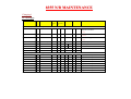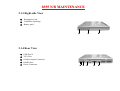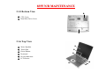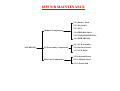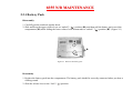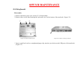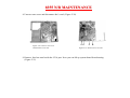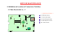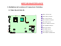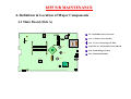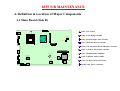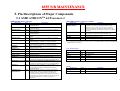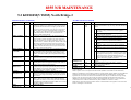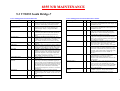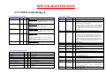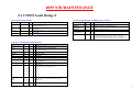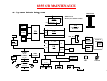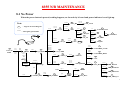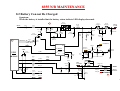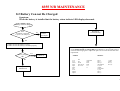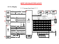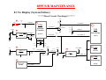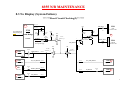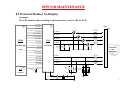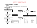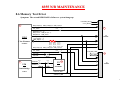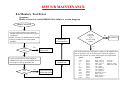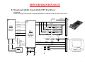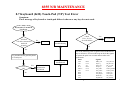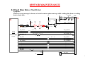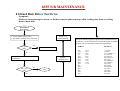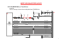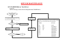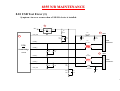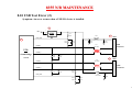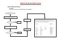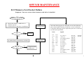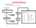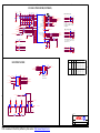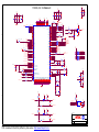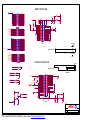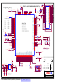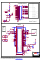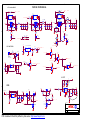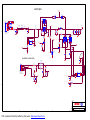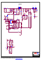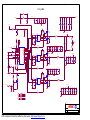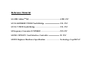
1
SERVICE MANUAL FOR
8355
BY: Rain Li
Repair Technology Research Department /EDVD
Nov.2003
8355 N/B MAINTENANCE
Contents
1. Hardware Engineering Specification …………………………………………………………………
4
1.1 Introduction …………………………………………………………………………………………………………. 4
1.2 System Hardware Part………………………………………………………………………………………………. 6
1.3 Other Functions ……………………………………………………………………………………………………… 47
1.4 Peripheral Components……………………………………………………………………………………………… 52
1.5 Power Management………………………………………………………………………………………………….. 53
1.6 Appendix 1 : VT8235 GPIO Definition……………………………………………………………………………... 56
1.7 Appendix 2 : H8 Pins Definition ……………………………………………………………………………………. 58
1.8 Appendix 3 : 8355 Product Specification …………………………………………………………………………… 63
2. System View and Disassembly ………………………………………………………………………...
66
2.1 System View ………………………………………………………………………………………………………… 66
2.2 System Disassembly ………………………………………………………………………………………………… 69
3. Definition & Location of Connectors / Switches ……………………………………………………..
95
3.1 Mother Board ……………………………………………………………………………………………………….. 95
4. Definition & Location of Major Components ………………………………………………………..
98
4.1 Mother Board ……………………………………………………………………………………………………….. 98
5. Pin Description of Major Component …….………………………………………………………….
100
5.1 AMD AthlonTM 64 Processor ………………………………………………………………………………………. 100
5.2 K8T800M (VT8385) North Bridge ………………………………………………………………………………… 102
1
8355 N/B MAINTENANCE
Contents
5.3 VT8235 South Bridge ………………………………………………………………………………………………. 106
6. System Block Diagram ………………………………………………………………………………..
115
7. Maintenance Diagnostics ………………………………………………………………………………
116
7.1 Introduction ………………………………………………………………………………………………………… 116
7.2 Error Codes ………………………………………………………………………………………………………… 117
7.3 Debug Tool ………………………………………………………………………………………………………….. 119
8. Trouble Shooting ………………………………………………………………………………………
121
8.1 No Power ……………………………………………………………………………………………………………. 122
8.2 Battery Can not Be Changed ……………………………………………………………………………………… 126
8.3 No Display …………………………………………………………………………………………………………… 128
8.4 AGP Controller Failure LCD No Display ………………………………………………………………………… 132
8.5 External Monitor No Display ……………………………………………………………………………………… 132
8.6 Memory Test Error ………………………………………………………………………………………………… 136
8.7 Keyboard (K/B) Touch-Pad (T/P) Test Error …………………………………………………………………….. 138
8.8 Hard Driver Test Error …………………………………………………………………………………………….. 140
8.9 CD-ROM Driver Test Error………………………………………………………………………………………… 142
8.10 USB Port Test Error ……………………………………………………………………………………………….. 144
8.11 PC Card Socket Failure …………………………………………………………………………………………… 147
8.12 Memory-Card Socket Failure …………………………………………………………………………………….. 149
8.13 IEEE1394 Test Error………………………………………………………………………………………………. 151
8.14 LAN Test Error…………………………………………………………………………………………………….. 153
2
8355 N/B MAINTENANCE
Contents
8.13 Audio Failure ………….…………………………………………………………………………………………… 155
9. Spare Parts List ………………………………………………………………………………………..
158
10. System Exploded Views ………………………………………………………………………………
172
11. Circuit Diagram ………………………………………………………………………………………
174
12. Reference Material …………………………………………………………………………………...
207
3
8355 N/B MAINTENANCE
1. Hardware Engineering Specification
1.1 Introduction
The 8355 motherboard would support the AMD ClawHammer K8 processor with uPGA Package,
2700+/3000+/3300+/3600+/3900+/4200+, FSB 800MHz
This system is based on PCI architecture, which have standard hardware peripheral interface. The power management
complies with Advanced Configuration and Power Interface (ACPI) 2.0. It also provides easy configuration through
CMOS setup, which is built in system BIOS software and can be pop-up by pressing F2 at system start up or warm
reset. System also provides ico LEDs to display system status, such as AC Power, Battery Power, Battery status, CDROM, HDD, NUM LOCK, CAP LOCK, SCROLL LOCK, WIRELESS LAN status. It also equipped 4 USB2.0 ports.
The memory subsystem supports 0MB on board; Expandable up to 1024MB Expandable with combination of optional
128/256/512 MB memory 200-pin DDR 266/333/400 Memory Module x2, PC-2100/2700/3200 specification
The K8T800 North Bridge plus VT8235 South Bridge chipset is a high performance, cost-effective and energy
efficient solution for the implementation of desktop personal computer systems with 8 / 16-bit 800 / 600 / 400 / 200
MHz HyperTransport. CPU host interface based on AMD K8 / ClawHammer. processors.
The VT8235 “V-Link Client Controller” is a highly integrated PCI /LPC controller. Its internal bus structure is based
on a 66 MHz PCI bus that provides 2x bandwidth compared to previous generation PCI bridge chips. The VT8235
also provides a 533 MB/sec bandwidth Host / Client V-Link interface with V-Link-PCI and V-Link-LPC controllers.
It supports six PCI slots of arbitration and decoding for all integrated functions and LPC bus.
4
8355 N/B MAINTENANCE
The RADEON MOBILITY 9600 provides the fastest and most advanced 2D, 3D, and multimedia graphics
performance for the latest applications in full 32-bit color. Its architecture introduces the latest achievements in the
graphics industry, which enable the use of the progressive new features in upcoming applications, but without
compromising performance. ATI’s exclusive support of DirectX® 9.0 features, highly optimized OpenGL® support,
and flexible memory configurations allow implementations targeted at both gaming enthusiast and workstation
platforms.
To provide for the increasing number of multimedia applications, the AC97 CODEC CMI9738-S is integrated onto
the motherboard
A full set of software drivers and utilities are available to allow advanced operating systems such as Windows XP and
Windows 2000 to take full advantage of the hardware capabilities such as bus mastering IDE, Windows 95-ready Plug
& Play, Advanced Power Management (APM) and Advance configuration and power interface (ACPI).
Following chapters will have more detail description for each individual sub-systems and functions.
5
8355 N/B MAINTENANCE
1.2 System Hardware Part
CPU
Core logic
VGA Control
System BIOS
Memory
AMD ClawHammer K8 processor with uPGA Package
2700+/3000+/3300+/3600+/3900+/4200+
FSB 800MHz
VIA K8T800 + VT8235
ATI M10P with 64MB External VRAM (Reserve for 128MB VRAM)
Insyde 256 KB Flash EPROM (Include System BIOS and VGA BIOS)
ACPI 2.0; DMI 2.3.1 compliant
Plug & Play capability
0MB on board; Expandable up to 1024MB
Expandable with combination of optional 128/256/512 MB memory
200-pin DDR 266/333/400 DRAM Memory Module x2,
PC-2100/2700/3200 specification
ICS 950403
Clock
Generator
IEEE1394
VT6307L
Audio System AC97 CODEC: C-MEDIA ELECTRONICS INC., CMI9738-S
Power Amplifier: Anpec APA2020
Super I/O
PC87397
Modem
56Kbps(V.90, worldwide) MDC Modem
PHY of LAN VT6103 10/100 base -T PHY
PCMCIA
ENE710
CARD
ENE710
READER
6
8355 N/B MAINTENANCE
1.2.1 CPU_ ClawHammer PROCESSOR
The ClawHammer processor family is designed to support performance desktop and workstation applications. It
provides a high-performance HyperTransport. link to I/O, as well as a single 64-bit high-performance DDR
memory controller.
Compatible with Existing 32-bit Code Base
Including support for SSE, SSE2, MMXTM, 3DNow!TM, technology and all legacy x86 instructions
Runs existing operating systems and drivers
Local APIC on-chip
AMD x86-64 Technology
AMD.s 64-bit x86 instruction set extensions
64-bit integer registers, 48-bit virtual addresses, 40-bit physical addresses
Eight new 64-bit integer registers (16 total)
Eight new 128-bit SSE/SSE2 registers (16 total)
Integrated Memory Controller
Low-latency, high-bandwidth
72-bit DDR at 200, 266, 333, and 400 MHz (64-bits + 8-bits ECC)
7
8355 N/B MAINTENANCE
HyperTransport. Technology to I/O Devices
Two 8-bit links each support 1600 mega-transfers (MT) per second or 1.6 Gbytes/s in each direction
Can be configured as single 16-bit link supporting 1600 MT/s or 3.2 Gbytes/s in each direction
64-Kbyte 2-way Associative ECC-Protected L1 Data Cache
Two 64-bit operations per cycle, 3-cycle latency
64-Kbyte 2-way Associative Parity-Protected L1 Instruction Cache
With advanced branch prediction
16-way Associative ECC-Protected L2 Cache
Exclusive cache architecture.storage in addition to L1 caches
256 KB, 512 KB, and 1 MB options
Machine Check Architecture
Includes hardware scrubbing of major ECC-protected arrays
Power Management
Multiple low-power states
System Management Mode (SMM)
8
8355 N/B MAINTENANCE
ACPI 2.0 compliant, including support for processor performance states
Power Supplies
VDD (core): 1.50-V at 52 Amps (max)
VDDIO: 2.5-V at 3.0 Amps (max) for DDR I/O
VLDT: 1.2-V at 0.5 Amps for HyperTransport
VTT: 1.25-V at 0.5 Amps required for 2.5-V I/Os
Target CPU Core Power: 78.00 Watts
Target Maximum Thermal Power: 89 Watts
Electrical Interfaces
HyperTransport. Technology: LVDS-like differential, unidirectional
DDR: SSTL per JEDEC DDR specification
Clock, reset, and test signals also use DDR-like electrical specifications
Packaging
754-pin lidded micro PGA
1.27-mm pin pitch
29x29 row pin array
40mm x 40mm organic substrate, Organic C4 die attach
9
8355 N/B MAINTENANCE
1.2.2 System frequency
1.2.2.1 System frequency synthesizer_ICS950402
Programmable Timing Control Hub™ AMD-K8™ processor
General Description
The ICS950403 is a main system clock solution for desktop designs using the AMD K8 CPU. It provides all
necessary clock signals for Clawhammer and Sledgehammer systems.
The ICS950403 is part of a whole new line of ICS clock generators and buffers called TCH™ (Timing Control
Hub). This part incorporates ICS's newest clock technology which offers more robust features and functionality.
Employing the use of a serially programmable I2C interface, this device can adjust the output clocks by configuring
the frequency setting, the output divider ratios, selecting the ideal spread percentage, the output skew, the output
strength, and enabling/disabling each individual output clock. M/N control can configure output
frequency with
resolution up to 0.1MHz increment.
Recommended Application:
AMD K8 System Clock with AMD or VIA Chipset
Output Features:
2 - Differential pair push-pull K8 CPU clocks
9 - PCICLK (Including 1 free running) @3.3V
3 - Selectable PCICLK/HTTCLK @3.3V
1 - HTTCLK @3.3V
10
8355 N/B MAINTENANCE
1 - 48MHz, @3.3V fixed.
1 - 24/48MHz @ 3.3V
3 - REF @3.3V, 14.318MHz.
Features:
Programmable output frequency.
Programmable output divider ratios.
Programmable output rise/fall time.
Programmable output skew..
Programmable spread percentage for EMI control.
Watchdog timer technology to reset system if system malfunctions.
Programmable watch dog safe frequency.
Support I2C Index read/write and block read/write operations.
Uses external 14.318MHz crystal.
Supports Hyper Transport Technology (HTTCLK).
11
8355 N/B MAINTENANCE
1.2.3 VIA K8T800+VT8235
1.2.3.1 K8T800
The K8T800 is a high performance, cost-effective and energy efficient solution for the implementation of desktop
personal computer systems with 8 / 16-bit 800 / 600 / 400 / 200 MHz HyperTransport. CPU host interface based on
AMD K8 / ClawHammer. processors.
Defines Highly Integrated Solutions for Performance PC Desktop Designs
High performance North Bridge with HyperTransport. interface to AMD. K8 CPU plus AGP 8x external bus to
external Graphics Controller plus high-speed V-Link interface to chipset South Bridge
Combines with VIA K8T400M V-Link South Bridge for integrated LAN, Audio, ATA133 IDE, and 6 USB 2.0
ports
578 Ball Grid Array package with 35 x 35 mm body size, 1.27mm ball pitch, and heat spreader
2.5V core, 0.22 u process
High Performance K8 CPU Interface
Chipset support for AMD. K8 / ClawHammer. processor
Processor interface via HyperTransport. bus
Separate transmit and receive buses for no lost bus turnaround cycles
All transmit and receive signals use 2 pin low-voltage-swing differential signalling for high-reliability and high
speed
12
8355 N/B MAINTENANCE
8 or 16-bit control / address / data transfer both directions
800 / 600 / 400 / 200 MHz Double Data Rate operation both directions
Default 8-bit / 200 MHz operation on startup for high reliability with speedup to dual 16-bit, 800 MHz operation (3.2
GB/sec total bandwidth) under software control (transmit and receive may be different widths and / or speeds)
Full Featured Accelerated Graphics Port (AGP) 8x Controller
Supports 533 MHz 8x, 266 MHz 4x, and 133 MHz 2x transfer modes for AD and SBA signaling
AGP v3.0 compliant with 8x transfer mode
Pseudo-synchronous with the host CPU bus with optimal skew control
Supports SideBand Addressing (SBA) mode (non-multiplexed address / data)
AGP pipelined split-transaction long-burst transfers up to 1GB/sec
Eight level read request queue
Four level posted-write request queue
Thirty-two level (quadwords) read data FIFO (256 bytes)
Sixteen level (quadwords) write data FIFO (128 bytes)
Intelligent request reordering for maximum AGP bus utilization
Supports Flush/Fence commands
Graphics Address Relocation Table (GART)
One level TLB structure
Sixteen entry fully associative page table
13
8355 N/B MAINTENANCE
LRU replacement scheme
Independent GART lookup control for host / AGP / PCI master accesses
Windows 95 OSR-2 VXD and integrated Windows 98 / 2000 / XP miniport driver support
High Bandwidth 533 MB / Sec 8-bit V-Link Host Controller South Bridge Interface
Supports 66 MHz V-Link Host interface with total bandwidth of 533 MB/sec
Operates in 2x, 4x, and 8x modes
Full duplex commands with separate command / strobe
Request / Data split transaction
Configurable outstanding transaction queue for Host to V-Link Client accesses
Supports Defer / Defer-Reply transactions
Transaction assurance for V-Link Host to Client access eliminates V-Link Host-Client Retry cycles
Intelligent V-Link transaction protocol to eliminate data wait-state / throttle transfer latency
All V-Link transactions for both Host and Client have a consistent view of transaction data depth and buffer size to
avoid data overflow
Highly efficient V-Link arbitration with minimum overhead
All V-Link transactions have predictable cycle length with known command / data duration
14
8355 N/B MAINTENANCE
1.2.3.2 VT8235
The VT8235 South Bridge is a high integration, high performance, power-efficient, and high compatibility device
that supports Intel and non-Intel based processor to V-Link bus bridge functionality to make a complete Microsoft
PC2001-compliant PCI/LPC system. The VT8235 includes standard intelligent peripheral controllers:
a) IEEE 802.3 compliant 10 / 100 Mbps PCI bus master Ethernet MAC with standard MII interface to external
PHYceiver.
b) Master mode enhanced IDE controller with dual channel DMA engine and interlaced dual channel commands.
Dedicated FIFO coupled with scatter and gather master mode operation allows high performance transfers between
PCI and IDE devices. In addition to standard PIO and DMA mode operation, the VT8235 also supports the
UltraDMA-133, 100, 66, and 33 standards to allow reliable data transfer at rates up to 133 MB/sec. The IDE
controller is SFF-8038i v1.0 and Microsoft Windows-family compliant.
c) Universal Serial Bus controller that is USB v2.0 / 1.1 and Universal HCI v2.0 / 1.1 compliant. The VT8235
includes three root hubs with six function ports with integrated physical layer transceivers. The USB controller
allows hot plug and play and isochronous peripherals to be inserted into the system with universal driver support.
The controller also implements legacy keyboard and mouse support so that legacy software can run transparently in
a non-USB-aware operating system environment.
d) Keyboard controller with PS2 mouse support.
e) Real Time Clock with 256 byte extended CMOS. In addition to the standard ISA RTC functionality, the
integrated RTC also includes the date alarm, century field, and other enhancements for compatibility with the ACPI
standard.
15
8355 N/B MAINTENANCE
f) Notebook-class power management functionality compliant with ACPI and legacy APM requirements. Multiple
sleep states (power-on suspend, suspend-to-DRAM, and suspend-to-Disk) are supported with hardware automatic
wake-up. Additional functionality includes event monitoring, CPU clock throttling and stop (Intel processor
protocol), PCI bus clock stop control, modular power, clock and leakage control, hardware-based and softwarebased event handling, general purpose I/O, chip select and external SMI.
g) Full System Management Bus (SMBus) interface.
h) Integrated bus-mastering dual full-duplex direct-sound AC97-link-compatible sound system.
i) Plug and Play controller that allows complete steerability of all PCI interrupts and internal interrupts / DMA
channels to any interrupt channel. One additional steerable interrupt channel is provided to allow plug and play and
reconfigurability of onboard peripherals for Windows family compliance. The VT8235 also enhances the
functionality of the standard ISA peripherals. The integrated interrupt controller supports both edge and level
triggered interrupts channel by channel. The integrated DMA controller supports type F DMA in addition to
standard ISA DMA modes. Compliant with the PCI-2.2 specification, the VT8235 supports delayed transactions
and remote power management so that slower ISA peripherals do not block the traffic of the PCI bus. Special
circuitry is built in to allow concurrent operation without causing dead lock even in a PCI-to-PCI bridge
environment. The chip also includes eight levels (doublewords) of line buffers from the PCI bus to the ISA bus to
further enhance overall system performance.
16
8355 N/B MAINTENANCE
1.2.4 RADEON MOBILITY 9600
General Description
The RADEON MOBILITY 9600 provides the fastest and most advanced 2D, 3D, and multimedia graphics
performance for the latest applications in full 32-bit color. Its architecture introduces the latest achievements in the
graphics industry, which enable the use of the progressive new features in upcoming applications, but without
compromising performance. ATI’s exclusive support of DirectX® 9.0 features, highly optimized OpenGL® support,
and flexible memory configurations allow implementations targeted at both gaming enthusiast and workstation
platforms.
SMARTSHADER™ — Advanced Shader Technology
Provides complete hardware-accelerated support for the new DirectX® 9.0 programmable shader model,
enabling more complex and realistic texture and lighting effects than ever before.
Significant improvement over first-generation shaders introduced in DirectX® 9.0, with a much more powerful
and intuitive instruction set.
Offers full support for this feature in OpenGL® applications.
SMOOTHVISION™ — Flexible Anti-Aliasing and Anisotropic Filtering
The most flexible and efficient anti-aliasing implementation available to date.
Eliminates “jaggies” on the edges of objects, shimmering pixels on distant surfaces, and other visual artifacts for
smoother-looking images.
Offers full support for this feature in OpenGL® applications.
17
8355 N/B MAINTENANCE
SMOOTHVISION™ — Flexible Anti-Aliasing and Anisotropic Filtering
The most flexible and efficient anti-aliasing implementation available to date.
Eliminates “jaggies” on the edges of objects, shimmering pixels on distant surfaces, and other visual artifacts
for smoother-looking images.
Unique adaptive process can independently select the anti-aliasing pattern for each pixel within a 4x4 region,
rather than relying on a fixed pattern for the whole image.
Better visual quality with minimal performance degradation.
Supports DirectX® 9.0 multisampling and related effects, including motion blur and depth-of-field.
High Performance Memory Support
Incorporates support for DDR SDRAM/SGRAM at up to 350 MHz.
Features ATI’s second generation HYPER Z™III technology that conserves memory bandwidth for improved
performance in demanding applications.
Boosts effective memory bandwidth by over 20%.
Dual Display Support
Leading-edge technology, fully optimized with HYDRA VISION™, flexibly supports multiple combinations of
traditional CRT monitors, flat panel displays and TV.
Features Dual Channel DVI support.
32-bit PCI bus (Rev 2.2), 3.3 V with bus mastering support.
18
8355 N/B MAINTENANCE
Comprehensive AGP support including 1.5 Volt (AGP 4X) and 0.8 Volt (AGP8X) mode operation, sideband
addressing, AGP texturing (direct memory execution), and support for AGP reads and writes, including fast write
capability.
Single channel 128/64-bit memory interface using SGRAM or SDRAM to build 8/16/32/64 MB configurations.
Operating frequency is 67MHz minimum to 350MHz maximum, SDR or DDR.
16-bit Zoom Video port.
Support for ROM or Flash RAM parallel or serial video BIOS.
Two independent CRT controllers to support two asynchronous simultaneous display paths.
Integrated DAC for CRT with stereoscopic display support.
Integrated second DAC for the second CRT (TV) support.
Integrated LVDS interface: single and dual pixel per clock, up to 85MHz per channel.
LCD panel detection.
Integrated TMDS transmitter running up to 165MHz (when matched with coherently clocked receiver; otherwise,
135MHz) for support up to 1600x1200 at 60Hz. Fully compliant with DVI and DFP connection standards.
Radiometric expansion.
Ideal for Windows 2000 and Windows XP
RADEON MOBILITY 9600 provides comprehensive support for all new Windows 2000 and Windows XP
display-oriented features, including acceleration of new GDI extensions like Alpha BLTs, Transparent BLTs,
and Gradient Fills, as well as exclusive, patent-pending hardware alpha cursor support.
19
8355 N/B MAINTENANCE
1.2.4.1 General and Interfacing Features
32-bit PCI bus (Rev 2.2), 3.3 V with bus mastering support.
Comprehensive AGP support including 1.5 Volt (AGP 4X) and 0.8 Volt (AGP8X) mode operation, sideband
addressing, AGP texturing (direct memory execution), and support for AGP reads and writes, including fast
write capability.
Single channel 128/64-bit memory interface using SGRAM or SDRAM to build 8/16/32/64 MB configurations.
Operating frequency is 67MHz minimum to 350MHz maximum, SDR or DDR.
16-bit Zoom Video port.
Support for ROM or Flash RAM parallel or serial video BIOS.
Two independent CRT controllers to support two asynchronous simultaneous display paths.
Integrated DAC for CRT with stereoscopic display support.
Integrated second DAC for the second CRT (TV) support.
Integrated LVDS interface: single and dual pixel per clock, up to 85MHz per channel.
LCD panel detection.
Integrated TMDS transmitter running up to 165MHz (when matched with coherently clocked receiver;
otherwise, 135MHz) for support up to 1600x1200 at 60Hz. Fully compliant with DVI and DFP connection
standards. Ratiometric expansion.
Support for external TMDS transmitter via 24-bit digital output to drive most popular TMDS transmitters up to
165MHz frequency.
Internal and external Spread Spectrum support.
Integrated enhanced TV encoder with 10-bit DAC (shared between second CRT DAC and TV).
20
8355 N/B MAINTENANCE
Independent DDC lines for DAC and TMDS connections. Also full AppleSense support on DAC connection.
Static and dynamic Power Management support (APM as well as ACPI) with full VESA DPMS and Energy
Star compliance.
PCI bus power management 1.1 and AGP Busy and Stop signals Rev 1.61 and Solano 2-M.
Full POWERPLAYTM and POWER ON DEMAND support.
Comprehensive testability including full internal scan, memory BIST, I/O XOR tree and Iddq. Ideal accelerator
for Windows 2000 and Windows XP - includes patent pending hardware support for the Windows 2000 and
Windows XP alpha cursor, as well as acceleration of new GDI extensions such as Alpha BLTs, Transparent
BLTs, and Gradient Fills.
Fully compliant with PC 2001 requirements.
Fully compliant with Mobile PCI rev 1.0.
Full ACPI 1.0b, OnNow, and IAPC (Instantly Available PC) power management, including PCI power
management registers.
Bi-endian support for compliance on a variety of processor platforms.
Unique enhanced TCA (Triple-Cache Architecture) incorporates texture, pixel and vertex caches to maximize
effective memory bandwidth.
CCE high-speed pull architecture software interface optimized for Pentium III/4 and Athlon systems:
• Bus mastering of 2D&3D display lists.
• Direct walk of Direct3D/OpenGL vertex list.
• Ultra-thin driver layer.
• Maximizes concurrency between RADEON MOBILITY 9000 and host.
Triple 10-bit palette DAC supports pixel rates to 400MHz.
21
8355 N/B MAINTENANCE
DDC1 and DDC2ci for plug and play monitors.
Hydravision for dual monitor support.
Hardware I2C.
Integrated hardware diagnostic tests performed automatically upon initialization.
High quality components through at-speed testing, built-in Scan, Iddq, CRC, chip diagnostics, and XOR tree.
Single chip solution in 0.15 micron, 1.2V-1.5V CMOS technology in 696 BGA and 648 BGA package.
Flexible memory support:
• SGRAM or SDRAM.
• SDR or DDR.
• DDR support for both system memory SDRAM and graphics SGRAM devices.
• 128-bit or 64-bit interface.
• 8MB to 64MB.
Comprehensive HDKs, SDKs and utilities augmented by full engineering support.
Complete local language support (contact ATI for current list).
Dual RGB CRT output with DDC.
Integrated enhanced TV encoder based on Rage Theater support at 1024x768.
HDCP 1.0 support on integrated TMDS transmitter.
Digital interface with external TMDS Tx with dedicated DDC, configurable as a 24 bit SDR bus or a 12 bit DDR bus.
Independent h/w icon & h/w cursor on both display paths (simultaneous h/w cursor & icon).
IEEE 1149.1 Scan path interface.
VIP 2.0 with multi channel DMA transfer. Support for Rage Theater via VIP.
22
8355 N/B MAINTENANCE
1.2.5 AC’97 AUDIO SYSTEM: C-MEDIA ELECTRONICS INC., CMI9738-S
The CMI9738-S is an 18-bit, full duplex AC'97 2.2 compatible stereo audio CODEC designed for PC multimedia
systems,including host/soft audio and AMR/CNR based designs. The CMI9738-S incorporates proprietary converter
technology to achieve a high SNR, greater than 90 dB. The CMI9738-S AC'97 CODEC supports multiple CODEC
extensions with independent variable sampling rates and built-in 3D effects. The CMI9738-S CODEC provides two
pairs of stereo outputs with independent volume controls, a mono output, and multiple stereo and mono inputs, along
with flexible mixing, gain and mute functions to provide a complete integrated audio solution for PCs.
Features
Single chip audio CODEC with high S/N ratio (>90dB)
Compliant with AC’97 2.2 & WHQL specifications
Support of S/PDIF out is compliant with AC’97 rev2.2 specifications
Meets performance requirements for audio on PC2001 systems
Meets Microsoft PC99 & WLP 2.0 audio requirements
18-bit Stereo full-duplex CODEC with independent and variable sampling rate
18-bit ADC and 20-bit DAC resolution
Four analog line-level stereo inputs with 5-bit volume control: LINE_IN, CD, VIDEO, AUX
High quality differential CD input
Two analog line-level mono input: PC_BEEP,PHONE_IN
Supports double sampling rate (96KHz) of DVD audio playback
Two software selectable MIC inputs
23
8355 N/B MAINTENANCE
+30dB boost preamplifier for MIC input
Stereo output with 6-bit volume control
Mono output with 5-bit volume control
Headphone output with 50mW/8. Driving capability
Line output with 50mW/8. driving capability
Headphone jack-detect function to mute LINE/MONO/HP output, and to control S/PDIF output
3D Stereo Enhancement
Multiple CODEC extension capability
External Amplifier Power Down (EAPD) capability
High performance converter technology
Power management and enhanced power saving features
2 GPIO pins
No external crystal/clock required
14.318MHz 24.576MHz PLL saves crystal
DC Voltage volume control
Auxiliary power (VAUX ) to support Power Off CD function
Power support: Digital: 3.3V; Analog: 3.3V/5V
Standard 48-Pin LQFP Package
24
8355 N/B MAINTENANCE
1.2.6 MDC: PCTel MODEM DAUGHTER CARD PCT2303W
The PCT2303W chipset is designed to meet the demand of this emerging worldwide AMR/MDC market. The
combination of PC-TEL’s well proven PCT2303W chipset and the HSP56TM MR software modem driver allows
systems manufactures to implement modem functions in PCs at a lower bill of materials (BOM) while maintaining
higher system performance.
PC-TEL has streamlined the traditional modem into the Host Signal Processing (HSP) solution. Operating with the
Pentium class processors, HSP becomes part of the host computer’s system software. It requires less power to operate
and less physical space than standard modem solutions. PC-TEL’s HSP modem is an easily integrated, cost-effective
communications solution that is flexible enough to carry you into the future.
The PCT2303W chip set is an integrated direct access arrangement (DAA) and Codec that provides a programmable
line interface to meet international telephone line requirements. The PCT2303W chip set is available in two 16-pin
small outline packages (AC’97 interface on PCT303A and phone-line interface on PCT303W). The chip set eliminates
the need for an AFE, an isolation transformer, relays, opto-isolators, and 2-to 4-wire hybrid. The PCT2303W chip set
dramatically reduces the number of discrete components and cost required to achieve compliance with international
regulatory requirements. The PCT2303W complies with AC’97 Interface specification Rev. 2.1.
The chip set is fully programmable to meet worldwide telephone line interface requirements including those described
by CTR21, NET4, JATE, FCC, and various country-specific PTT specifications. The programmable parameters of the
PCT2303W chip set include AC termination, DC termination, ringer impedance, and ringer threshold. The
PCT2303W chip set has been designed to meet stringent worldwide requirements for out-of-band energy, billing-tone
immunity, lightning surges, and safety requirements.
25
8355 N/B MAINTENANCE
Operating System Compatibility
Windows 98 / NT4.0 /Win 2K /Win XP
Compatibility
ITU-T V.90
56000,54667,53333,52000,50667,49333,48000,46667,45333,
42667,41333,40000,38667,37333,36000,34667,33333,32000,
30667,29333, 28000bps
K56Flex
56000,54000,52000,50000,48000,46000,44000,42000,40000,
38000,36000, 32000bps.
ITU-T V.34Annex
33600,31200 bps.
ITU-T V.34
28800 bps
ITU-T V.32bis
14400 bps
ITU-T V.32
9600,4800 bps
ITU-T V.22bis
2400 bps
ITU-T V.22
1200 bps
ITU-T V.21
300 bps
ITU-T V.23
1200/75 bps
ITU-T V.17
14400,12000,9600,7200 bps
ITU-T V.29
9600,7200 bps
ITU-T V.27ter
4800,2400 bps
26
8355 N/B MAINTENANCE
Bell 212A
1200 bps
Bell 103
300 bps
Modulation
56000bps(V90&K56Flex)
PCM
33600 bps (V.34Annex)
TCM
28800 bps (V.34)
TCM
14400 bps (V.32bis)
TCM
12000 bps (V.32bis)
TCM
9600 bps (V.32bis)
TCM
7200 bps (V.32bis)
QAM
9600 bps (V.32)
TCM, QAM
4800 bps (V.32)
QAM
14400 bps (V.17)
TCM
12000 bps (V.17)
TCM
9600 bps (V.29)
QAM
7200 bps (V.29)
QAM
4800 bps (V.27ter)
DPSK
2400 bps (V.27ter)
DPSK
2400 bps (V.22bis)
QAM
27
8355 N/B MAINTENANCE
1200/75bps (V.23)
FSK
1200bps(V.22/Bell 212A)
DPSK
300bps(V.21/Bell 103)
FSK
Data Compression
V.42bis, MNP5
Error Correction
V.42 LAPM, MNP 2-4
DTE interface
DTMF Tone Frequency
Low Group Frequency (Hz)
High Group
Frequency
(Hz)
1209
1336
1477
1633
697
1
2
3
A
770
4
5
6
B
852
7
8
9
C
941
*
0
#
D
DTMF signal level
28
8355 N/B MAINTENANCE
2.6.1.1
High group
-10+/-2dBm
2.6.1.2
Low group
-12+/-2dBm
Dialing Type
Tone or pulse dialing
Telephone Line interface
RJ-11
Return Loss
300HZ - 3400HZ >= 10db
Flow Control
XOFF/XON or RTS/CTS
Receive Level
-35 +/- 2dBm
29
8355 N/B MAINTENANCE
Transmit Level
>-15 dBm
Specification and features subject to change without notice!
2.6 MDC: PCTel MODEM DAUGHTER CARD PCT2303W
30
8355 N/B MAINTENANCE
1.2.7 VT6307L PCI 1394a Integrated Host Controller
1.2.7.1 Overview
The VT6307L IEEE 1394 OHCI Host Controller provides high performance serial connectivity. It implements the
Link and Phy layers for IEEE 1394-1995 High Performance Serial Bus a specification release 1.0 and 1394a P2000. It
is compliant with 1394 Open HCI 1.0 and 1.1 with DMA engine support for high performance data transfer via a 32bit bus master PCI host bus interface.
The VT6307L supports 100, 200 and 400 Mbit/sec transmission via an integrated 2-port PHY. The VT6307L services
two types of data packets: asynchronous and isochronous (real time). The 1394 link core performs arbitration
requesting, packet generation and checking, and bus cycle master operations. It also has root node capability and
performs retry operations.
The VT6307L is ready to provide industry-standard IEEE 1394 peripheral connections for desktop and mobile PC
platforms. Support for the VT6306 is built into Microsoft Windows 98, Windows ME, and Windows 2000.
1.2.7.2 Integrated 400 Mbit 2-Port PHY
Supports provisions of IEEE 1394-1995 Standard for High Performance Serial Bus and the P1394a P2000.
Fully interoperable with IEEE Std 1394-1995 devices
Provides two 1394a fully compliant cable ports at 100 / 200 / 400 Mbit per second
Host notification of PHY LinkOn events
Full 1394a P2000 Support includes:
31
8355 N/B MAINTENANCE
• Arbitrated short reset
• Enhanced priority arbitration
• Connection debounce
• Multispeed packet concatenation
• Ack accelerated arbitration
• Fly-by concatenation
• Per port disable, suspend, resume, through register write and remote command packet
• Remote access packet
• Boundary node short reset
• No PHY_ID wrap past 63
Logic performs bus initialization and arbitration functions
Encode and decode functions included for data-strobe bit-level encoding
Incoming data resynchronized to local clock.
24.576 MHz crystal oscillator and PLL provide TX/RX data at 100/200/400 Mbps and Link-Layer Controller
clock at 49.152 MHz.
Cable power presence monitoring.
Programmable node power class information for system power management
Fully Compliant 1394a P2000 PHY register map
Separate TPBIAS for each port
Cable ports monitor line conditions for active connection to remote node
Automatic power down inactive circuit and logic for low power application
Self power up reset and pinless PLL to reduce passive component counts on system
32
8355 N/B MAINTENANCE
Automatic configuration to single-port, two-port, and three-port applications; unused ports power down
automatically
Dedicated power supply pins separate from link core
2KV ESD protection
1.2.8 EMBEDDED CONTROLLER-H8
I. OVERVIEW
H8/300 CPU, a high-speed processor with an architecture featuring powerful bit-manipulation instructions, ideally
suited for real time control applications.
1.2.8.1 Main Features
CPU
Two-way generate register configuration
• Eight 16-bit registers, or
• Sixteen 8-bit registers
High-speed operation Maximum clock rate (ø clock): 16 MHz at 5 V, 12 MHz at 4 V or 10 MHz at 3V
• 8- or 16-bit register-register add/subtract: 125 ns (16 MHz), 167 ns (12 MHz), 200 ns (10 MHz)
• 8 x 8-bit multiply: 875 ns (16MHz), 1167 ns (12 MHz), 1400 ns (10 MHz)
• 16 ÷8-bit divide: 875 ns (16MHz), 1167 ns (12 MHz), 1400 ns (10 MHz)
Streamlined, concise instruction set
33
8355 N/B MAINTENANCE
• Instruction length: 2 or 4 bytes
• Register-register arithmetic and logic operations
• MOV instruction for data transfer between registers and memory
Instruction set features
• Multiply instruction (8 bits x 8 bits)
• Divide instruction (16 bits ÷8 bits)
• Bit-accumulator instructions
• Register-indirect specification of bit positions
Memory
1. 60-kbytes ROM with 2-kbytes RAM
Timer
One 16-bit free running timer
Two 8-bit timers
Two PWM timers (duty cycle 0-100%, resolution: 1/250)
One Watchdog timer
Interface
Two Serial Communication Interfaces
34
8355 N/B MAINTENANCE
One I2C bus interface
Host Interface
• 8-bit host interface port
• Three host interrupt requests (HIRQ1, HIRQ11, HIRQ12)
• Regular and fast A20 gate output
• Two register sets, each with two data registers and a status register
A/D converter –
10-bit resolutions
8 channels – single or scan mode (selectable)
Start of A/D conversion can be externally triggered
Sample-and-hold function
D/A converter –
8-bit resolutions
2 channels
I/O ports –
74 input/output lines (16 of which can drive LEDs)
8 input-only lines
35
8355 N/B MAINTENANCE
Interrupts –
9 external interrupt lines: NMI, IRQ0, to IRQ7
26 on-chip interrupt sources
Wait control –
Three selectable wait modes
Operating modes –
Expanded mode with on-chip ROM disabled (mode 1)
Expanded mode with on-chip ROM enabled (mode 2)
Single-chip mode (mode 3)
Power-down modes –
Sleep mode
Software Standby mode
Hardware Standby mode
Other features –
On-chip oscillator
36
8355 N/B MAINTENANCE
1.2.8.2 Features
Operating voltage: 2.4V~5.5V
32/34 bidirectional I/O lines
One 8-bit programmable timer counter with overflow
interrupts
Crystal or RC oscillator
Watchdog Timer
3K_16 program EPROM
160_8 data RAM
One external interrupt pin (shared with PC2)
HALT function and wake-up feature reduce power
consumption
Six-level subroutine nesting
Bit manipulation instructions
16-bit table read instructions
63 powerful instructions
All instructions in 1 or 2 machine cycles
20/28-pin SOP, 40-pin DIP, 48-pin SSOP package
37
8355 N/B MAINTENANCE
1.2.9 System Flash Memory (BIOS)
2 M bit Flash memory
Flashed by 5V only
User can upgrade the system BIOS in the future just running flash program.
1.2.10 Memory System
64MB, 128MB, 256MB, 512MB (x64) 200-Pin DDR SDRAM SODIMMs
JEDEC-standard 200-pin, small-outline, dual in-line memory module (SODIMM)
Utilizes 200 Mb/s and 266 Mb/s DDR SDRAM components
64MB (8 Meg x 64 [H]); 128MB (16 Meg x 64, [H] and [HD]); 256MB (32 Meg x 64 [HD]);
64 [HD])
512MB (64 Meg x
VDD= VDDQ= +2.5V ±0.2V
VDDSPD = +2.2V to +5.5V
2.5V I/O (SSTL_2 compatible)
Commands entered on each positive CK edge
DQS edge-aligned with data for READs; center-aligned with data for WRITEs
Internal, pipelined double data rate (DDR) architecture; two data accesses per clock cycle
Bidirectional data strobe (DQS) transmitted/received with data—i.e.,source-synchronous data capture
Differential clock inputs (CK and CK# - can be multiple clocks, CK0/CK0#, CK1/CK1#, etc.)
38
8355 N/B MAINTENANCE
Four internal device banks for concurrent operation
Selectable burst lengths: 2, 4, or 8
Auto precharge option
Auto Refresh and Self Refresh Modes
15.6µs (MT4VDDT864H, MT8VDDT1664HD), 7.8125µs (MT4VDDT1664H, MT8VDDT3264HD,
MT8VDDT6464HD) maximum average periodic refresh interval
Serial Presence Detect (SPD) with EEPROM
Fast data transfer rates PC2100 or PC1600
Selectable READ CAS latency for maximum compatibility
Gold-plated edge contacts
1.2.11 VT6103 FAST ETHERNET 10/100 1-PORT PHY/TRANSCEIVER
OVERVIEW
The VT6103 is a Physical Layer device for Ethernet 10Base-T and 100Base-TX using category 5 Unshielded, Type 1
Shielded, and Fiber Optic cables. This VLSI device is designed for easy implementation of 10 / 100 Mb/s Fast
Etherent LANs. It interfaces to a MAC through an MII interface ensuring interoperability between products from
different vendors.
PRODUCT FEATURES
Single Chip 100Base-TX / 10Base-T Physical Layer Solution
39
8355 N/B MAINTENANCE
Dual Speed – 100 / 10 Mbps
Half and Full Duplex
MII Interface to Ethernet Controller
MII Interface to Configuration & Status
Optional Repeater Interface
Auto Negotiation: 10 / 100, Full / Half Duplex
Meet All Applicable IEEE 802.3, 10Base-T and 100Base-Tx Standards
On Chip Wave Shaping – No External Filters Required
Adaptive Equalizer
Baseline Wander Correction
LED Outputs
• Link Status
• Duplex status
• Speed Status
• Collision
48 Pin SSOP Package
1.2.12 Cardbus/MediaReader Controller
Features
3.3V operation with 5V tolerant
40
8355 N/B MAINTENANCE
208-pin LQFP / 209-ball LFBGA package for CB710
PCI Interface
Compliant with PCI Local Bus Specification, Revision 2.2
PCI Bus Power Management Interface Specification, Revision 1.1
PCI Mobile Design Guide, Version 1.1
Advanced Configuration and Power Interface Specification, Revision 1.0
CardBus Interface
Compliant with PC Card Standard 8.0
Support Standardized Zoomed Video Register Model
Support CardBay PC card interface
Smart Card Interface
Compliant with PC/SC Specification 1.0
Support ISO7816 T=0 and T=1 asynchronous communication protocols
Two power enable pins to support 5V and 3V smart cards
Support programmable card clock frequencies
Programmable F and D parameters to support different data rates
One traffic LED pin.
41
8355 N/B MAINTENANCE
Secure Digital Interface
Compliant with SD Memory Card Specification Version 1.0
Support 4 parallel data lines
Has an optional reference clock source to control the operating clock frequency
Up to 10MByte/sec Read/Write rate when the optional reference clock source
Contains 16 Bytes of data buffer to regulate the data flow between PCI interface
interface
Support Write Protect Switch
Support Card Detect either by DAT3 or by dedicated Card Detect Switch
One Traffic LED pin
One power enable pin.
Memory Stick Interface
Compliant with Memory Stick Standard Format Specification Version 1.3
Has an optional reference clock source to control the operating clock frequency of Memory Stick
Up to 2.5MByte/sec Read/Write rate when the optional reference clock source is used
Contains 16 Bytes of data buffer to regulate the data flow between PCI interface and the Memory
42
8355 N/B MAINTENANCE
Stick interface
One Traffic LED pin
One power enable pin
SmartMedia Interface
Compliant with SmartMedia Standard 2000.
Compliant with SmartMedia Interface Library (SMIL) version 1.0
Two power enable pins to support 5V and 3V SmartMedia cards
Support hardware ECC (1-bit correction and 2-bits detection) generation
One traffic LED pin
Interrupt configuration
Supports parallel PCI interrupts
Supports parallel IRQ and parallel PCI interrupts
Supports serialized IRQ and parallel PCI interrupts
Supports serialized IRQ and PCI interrupts
Power Management Control Logic
Supports CLKRUN# protocol
43
8355 N/B MAINTENANCE
Supports SUSPEND#
Supports PCI PME# from D3, D2, D1 and D0
Supports PCI PME# from D3Cold
Supports D3STATE#
Supports Zoomed Video port.
Power Switch Interface
Supports parallel 4-wire power switch interface
Misc Control Logic
Supports socket activity LED
Supports 12 GPIOs and GPE#
Supports SPKROUT, CAUDIO and RIOUT#
Supports PCI LOCK
44
8355 N/B MAINTENANCE
1.2.13 SuperI/O-PC87393
General Description
National Semiconductor’s PC87393 of LPC SuperI/O devices is targeted for a wide range of portable applications.
PC99 and ACPI compliant, the PC87393 features an X-Bus Extension for read and write operations over the X-Bus, a
full IEEE 1284 Parallel Port with a Parallel Port Multiplexer (PPM) for external Floppy Disk Drive (FDD) support, a
Musical Instrument Digital Interface (MIDI) port, and a
Game port. Like all National LPC SuperI/O devices, the PC87393 offers a single-chip solution to the most commonly
used PC I/O peripherals.
The PC87393 also incorporates: a Floppy Disk Controller (FDC), two enhanced Serial Ports (UARTs), one with Fast
Infrared (FIR, IrDA 1.1 compliant), General-Purpose Input/Output (GPIO) support for a total of 32 ports, Interrupt
Serializer for Parallel IRQs and an enhanced WATCHDOGTM timer.
Outstanding Features
X-Bus Extension for read and write operations
LPC bus interface, based on Intel’s LPC Interface Specification Rev. 1.01, February 1999 (supports CLKRUN
and LPCPD signals) and Intel FWH transactions
PC99 and ACPI compliant
Serial IRQ support (15 options)
Interrupt Serializer (four Parallel IRQs to Serial IRQ)
45
8355 N/B MAINTENANCE
PPM for external FDD signal support
MIDI interface compatible with MPU-401 UART mode
Game port inputs for up to two joysticks
Protection features, including GPIO lock and pin configuration lock
32 GPIO ports (16 standard, 16 with Assert IRQ/SMI)
5V tolerant and back-drive protected pins (except LPC bus pins)
100-pin TQFP Package
46
8355 N/B MAINTENANCE
1.3 Other Functions
1.3.1 Hot Key Function
Keys
combination
Feature
Meaning
Fn + F1
Reserve
Fn + F2
Reserve
Fn + F3
Reserve
Fn + F4
Reserve
Fn + F5
Display switch
LCD->CRT->LCD&CRT, TV-out will be not TV present.
TV->CRT->TV&CRT, TV-out is connected.
Fn + F6
Brightness down
Adjust LCD panel backlight darkness.
Fn + F7
Brightness up
Adjust LCD panel backlight lightness.
Fn + F8
MAX brightness toggle
Toggle LCD brightness maximum or user setting
Fn + F9
Reserved
Fn + F10
Battery Low Warning
Beep toggle
Toggle to enable/mute the “Battery Low Warning” Beep sound
Fn + F11
LCD panel toggle on/off
Toggle LCD panel on or off.
Fn + F12
System sleep
System sleep button function.
47
8355 N/B MAINTENANCE
1.3.2 Power ON/OFF/Suspend/Resume Button
APM mode
At APM mode, Power button is on/off system power.
ACPI mode
At ACPI mode. Power button behavior was set by windows power management control panel.
You could set “standby” , “power off” or “hibernate”(must enable hibernate function in power management) to power
button function. Continue pushing power button over 4 seconds will force system off at ACPI mode.
1.3.3 Cover Switch
System automatically provides power saving by monitoring Cover Switch. It will save battery power and prolong the
usage time when user closes the notebook cover.
At ACPI mode there are four functions to be chosen at windows power management control panel.
1. None
2. Standby
3. Off
4. Hibernate (must enable hibernate function in power management)
48
8355 N/B MAINTENANCE
1.3.4 LED Indicators
System has eight status LED indicators at front side which to display system activity. From left to right that indicate,
AC POWER, BATTERY POWER, BATTERY STATUS, WIRELESS LAN, CD-ROM, HARD DISK, NUM
LOCK, CAPS LOCK and SCROLL LOCK.
AC POWER: This LED lights green when AC is powering the notebook, and flash (on 1 second, off 1 second) when
Suspend to DRAM is active using AC power. The LED is off when the notebook is off or powered by batteries.
BATTERY POWER: This LED lights green when the notebook is being powered by Battery, and flash (on 1 second,
off 1 second) when Suspend to DRAM is active using Battery power. The LED is off when the notebook is off or
powered by batteries, or when Suspend to Disk.
BATTERY STATUS: During normal operation, this LED stays off as long as the battery is charged. When the
battery charge drops to 10% of capacity, the LED lights red, flashes per 1 second and beeps per 2 second. When AC
is connected, this indicator glows green if the battery pack is fully charged or orange (amber) if the battery is being
charged.
1.3.5 Fan power on/off management
FAN is controlled by H8 embedded controller-using AD2201 to sense CPU temperature and PWM control fan speed.
Fan speed is depended on CPU temperature. Higher CPU temperature faster Fan Speed.
49
8355 N/B MAINTENANCE
1.3.6 CMOS Battery
CR2032 3V 220mAh lithium battery
When AC in or system main battery inside, CMOS battery will consume no power.
AC or main battery not exists, CMOS battery life at less (220mAh/5.8uA) 4 years.
Battery was put in battery holder, can be replaced.
1.3.7 I/O Port
Bi-directional Parallel Port (EPP/ECP) x 1
USB port (2.0, backward compatible with USB1.1) x 4
RJ-11 port x 1
RJ-45 port x 1
IR port x 1, complies with IrDA 1.1
DC input x 1
VGA monitor port x1
Audio-out x 1 (S/P DIF)
Mic-in x 1
Hardware Volume Control
S Video TV-Out x 1 (NTSC/PAL)
50
8355 N/B MAINTENANCE
IEEE1394a x 1
1.3.8 Mini PCI (type III B)Battery current limit and learning
Implanted H/W current limit and battery learning circuit to enhance protection of battery.
51
8355 N/B MAINTENANCE
1.4 Peripheral Components
-
12.7mm Height
24X CD ROM Drive
8X DVD ROM Drive
24X10X8X24 Combo or above
Super Combo DVD-RW module
2.5" 9.5 mm height: 20/30/40/60 GB; Support Ultra DMA 66/100/133
Changeable for Distributor
-
Support External FDD w/z USB I/F; 3.5 Format for 720KB/1.2MB/1.44MB
14.1” XGA TFT Display; Resolution: 1024x768
15” XGA/ SXGA+ TFT Display; Resolution: 1024X768 /1400x1050
19mm key pitch/ 3.0mm key stroke/ 307mm length
Windows Logo Key x 1; Application Key x 1
Bi-directional Parallel Port (EPP/ECP) x 1
USB port (2.0, backward compatible with USB1.1) x 4
RJ-11 port x 1
RJ-45 port x 1
IR port x 1, complies with IrDA 1.1
DC input x 1
VGA monitor port x1
Audio-out x 1 (S/P DIF)
Mic-in x 1
Hardware Volume Control
S Video TV-Out x 1 (NTSC/PAL)
IEEE1394a x 1
Mini PCI (type III B)
Built-in 56Kbps V.90 modem
Built-in 10/100 M based-T LAN
One Mini PCI slot and one antenna reserved for wireless LAN(Type III B)
Battery
-
12 cell (2200mAH/3.7V) Li-ion standard
AC adapter
-
ROM Drive
HDD
FDD
Display
Keyboard
I/O Port
Communication
Universal AC adapter 150W ; Input: 100-240V, 50/60Hz AC (support power on charge)
52
8355 N/B MAINTENANCE
1.5 Power Management
The 8355 system has built in several power saving modes to prolong the battery usage for mobile purpose. User can
enable and configure different degrees of power management modes via ROM CMOS setup (booting by pressing F2
key). Following are the descriptions of the power management modes supported.
1.5.1 System Management Mode
Full on mode
In this mode, each device is running with the maximal speed. CPU clock is up to its maximum.
Doze Mode
In this mode, CPU will be toggling between on & stop grant mode either. The technology is clock throttling. This
can save battery power without loosing much computing capability.
The CPU power consumption and temperature is lower in this mode.
Standby mode
The most chipset of the system is entering power down mode for more power saving. In this mode, the following is
the status of each device:
CPU: Stop grant
LCD: backlight off
53
8355 N/B MAINTENANCE
HDD: spin down
Suspend to DRAM
The most chipset of the system is entering power down mode for more power saving. In this mode, the following is
the status of each device:
Suspend to DRAM
CPU: off
VT8235: Partial off
VGA: Suspend
PCMCIA: Suspend
Audio: off
SDRAM: self refresh
Suspend to HDD
All devices are stopped clock and power-down
System status is saved in HDD
All system status will be restored when powered on again
54
8355 N/B MAINTENANCE
1.5.2 Other Power Management Functions
HDD & Video Access
System has the ability to monitor video and hard disk activity. User can enable monitoring function for video
and/or hard disk individually. When there is no video and/or hard disk activity, system will enter next PMU state
depending on the application. When the VGA activity monitoring is enabled, the performance of the system will
have some impact.
55
8355 N/B MAINTENANCE
1.6 Appendix 1: VT 8235 GPIO Definition
Signal MUX
Name Function
Mitac
Definition
Buffer Power Default
Type Plane Value
GPI0
RESERVE
I
RTC
Hi-Z
TTL
GPI1
RESERVE
I
AUX Hi-Z
TTL
GPI2 EXTSMI# EXTSMI#
I
AUX Defined
TTL
GPI3 RING#
WAKE_UP#
I
AUX Defined
TTL
GPI4 LID#
RESERVE
I
AUX Defined
TTL
GPI5 BATLOW# SCI#
I
AUX Defined
TTL
GPI6 AGPBZ#
RESERVE
I
MAIN Defined
TTL
GPI7 REG5#
RESERVE
INTRUDE
GPI16 R#
RESERVE
I
MAIN Hi-Z
TTL
GPI17 CPUMISS RESERVE
THRM# /
GPI18 AOLGPI THRM#
GPI19 IORDY
I
RTC
Type
Defined
TTL
I
MAIN Defined
TTL
I
MAIN Defined
TTL
RESERVE
I
MAIN Defined
TTL
GPO0
RESERVE
O
AUX H
TTL
GPO1 SUSA#
SUSA#
O
AUX Defined
TTL
GPO2 SUSB#
SUSB#
O
AUX Defined
TTL
GPO3 SUSST1# SB_SUSST#
O
AUX Defined
TTL
GPO4 SUSCLK
RESERVE
O
AUX Defined
TTL
GPO5 CPUSTP# RESERVE
O
MAIN Defined
TTL
GPO6 PCISTP#
PCISTOP#
O
MAIN Defined
TTL
GPO7 GNT5#
RESERVE
O
MAIN Defined
TTL
56
8355 N/B MAINTENANCE
Continued to the previous table
PCREQA /
GPIO8 VGATE
MB_ID0
I/O
MAIN Hi-Z
TTL
GPIO9 PCREQB
MB_ID1
I/O
MAIN Hi-Z
TTL
GPIO10
KBD_CS0
I/O
MAIN Hi-Z
TTL
GPIO11
KBD_CS1
I/O
MAIN Hi-Z
TTL
RESERVE
I/O
MAIN Hi-Z
TTL
RESERVE
I/O
MAIN Hi-Z
TTL
CRT_IN
I/O
MAIN Hi-Z
TTL
I/O
MAIN Hi-Z
TTL
I/O
MAIN Hi-Z
OD
I/O
MAIN Hi-Z
OD
GPIO22 GHI#
FAN3_SPDCTR I/O
MAIN Hi-Z
OD
GPIO23 DPSLP#
LDTSTOP#
I/O
MAIN Hi-Z
OD
GPIO24 GPIOA
SPKR_MUTE#
I/O
MAIN Hi-Z
OD/TTL
GPIO25 GPIOC
FAN2_SPDCTR I/O
MAIN Hi-Z
OD/TTL
GPIO26 SMBDT2
RESERVE
I/O
AUX
Hi-Z
OD
GPIO27 SMBCK2
RESERVE
I/O
AUX
Hi-Z
OD
GPIO28 VIDSEL
RESERVE
I/O
MAIN Hi-Z
OD
GPIO29 VRDSLP
RESERVE
I/O
MAIN Hi-Z
OD
GPIO30 GPIOD
FAN1_SPDCTR I/O
MAIN Hi-Z
OD/TTL
GPIO31 GPIOE
MINIPCI_PD
MAIN Hi-Z
OD/TTL
INTE# /
GPIO12 PCGNTA
INTF# /
GPIO13 PCGNTB
GPIO14 INTG#
GPIO15 INTH#
MPCIACT#
ACSDIN2 /
GPIO20 PCS0#
RESERVE
ACSDIN3 /
PCS1# /
GPIO21 SLPBTN# RESERVE
I/O
57
8355 N/B MAINTENANCE
1.7 Appendix 2: H8 Pins Definition
Hitachi H8 3437S to VT8235 pin function definitions for Insyde code
the shadowed block is the selected function
Name
Pin
H8 Pin Definitions
During
RESE
T
After
RESET/O
FF
ON
MD0
STANDBY
Function
6
H8_MODE0
I↑
I
H
I
H
I
H
H
MD1
5
H8_MODE1
I↑
I
H
I
H
I
H
H mode3 single chip mode
STBY#
8
H8_STBY#
I↑
I
H
I
H
I
H
H8 Hardware Standby input pull high
NMI#
7
PWRBTN#
I↑
I
H
I
HLH
I
H
Power button
RESET#
1
H8_RESET#
I
I
LH
I
H
I
H
H8 chip reset
XTAL
2
EXTAL
3
Crystal
I
I
I
I
Crystal
I
I
I
I
RESET OUT#
100
RESERVE
O
O
O
O
Crystal input
Port A CMOS input level (input high min=3.5v, input low max=1.0v)
PA0
48
LID#
T↑
I
H
I
I
H
PA1
47
ADEN#
T↑
I
H/L
I
I
H/L
AC adaptor in detect
PA2
31
CARD_RI#
T↑
I
H
I
I
H
Ring detect
PA3
30
BATT DEAD#
T↑
I
H
I
I
H
Battery low low detect
PA4
21
H8 SUSC
T↑
I
H
I
I
L
System resume from S4 soft off through
RTC Alarm
PA5
20
H8 SUSC#
T↑
I
L
I
I
H
System to S4 soft off
PA6
11
BAT_CLK
T↑
I
L
I
I
H
PA7
10
H8_SUSB
T↑
I
H
I
I
H
L
Invert from SUSA# to wake up H8 when
system resumed by MDC modem and
internal LAN.
Inform system power management status
58
8355 N/B MAINTENANCE
Charging 1
PCI reset gate
Name
Pin
H8 Pin Definitions
During
RESE
T
After
RESET/O
FF
ON
STANDBY
Function
Port B TTL input voltage (input high min=2v, input low max=0.8v)
PB0
91
SB_PWRBTN#
T
O
L
LHL
O
Keep H
Power button trigger via8231 on /off
Duplicate Power BTN#
5→3V
PB1
90
H8_WAKE UP#
T
O
H
O
O
Keep H
Wake up SB at ACPI mode
5→3V?
PB2
81
LEARNING
T
O
O
Keep H
Power button trigger via8231 on
5→3V
PB3
80
CHARGING_RP
T
O
O
Keep
Battery charge control
PB4
69
VDD5 SW
T↓
O
LLH
O
H
O
Keep H
H8 vdd5 power source switch
PB5
68
H8_PWROK
T
O
L
O
LH
O
Keep H
PB6
58
RESERVE
T
O
O
O
Keep
PB7
57
RESERVE
T
O
O
O
Keep
O
Port 1 TTL input voltage (input high min=2v, input low max=0.8v)
P10/A0
79
KB OUT0
L
O
L
O
LH
O
Keep L
Key matrix scan output 0
P11/A1
78
KB OUT1
L
O
L
O
LH
O
Keep L
Key matrix scan output 1
P12/A2
77
KB OUT2
L
O
L
O
LH
O
Keep L
Key matrix scan output 2
P13/A3
76
KB OUT3
L
O
L
O
LH
O
Keep L
Key matrix scan output 3
P14/A4
75
KB OUT4
L
O
L
O
LH
O
Keep L
Key matrix scan output 4
P15/A5
74
KB OUT5
L
O
L
O
LH
O
Keep L
Key matrix scan output 5
P16/A6
73
KB OUT6
T
O
L
O
LH
O
Keep L
Key matrix scan output 6
P17/A7
72
KB OUT7
T
O
L
O
LH
O
Keep L
Key matrix scan output 7
59
8355 N/B MAINTENANCE
Continued to the previous table
Port 2 TTL input voltage (input high min=2v, input low max=0.8v)
P20/A8
67
KB OUT8
L
O
L
O
LH
O
Keep L
Key matrix scan output 8
P21/A9
66
KB OUT9
L
O
L
O
LH
O
Keep L
Key matrix scan output 9
P22/A10
65
KB OUT10
L
O
L
O
LH
O
Keep L
Key matrix scan output 10
P23/A11
64
KB OUT11
L
O
0
O
LH
O
Keep L
Key matrix scan output 11
P24/A12
63
KB OUT12
L
O
0
O
LH
O
Keep L
Key matrix scan output 12
P25/A13
62
KB OUT13
L
O
0
O
LH
O
Keep L
Key matrix scan output 13
P26/A14
61
KB OUT14
L
O
0
O
LH
O
Keep L
Key matrix scan output 14
P27/A15
60
KB OUT15
L
O
0
O
LH
O
Keep L
Key matrix scan output 15
Port 3 TTL input voltage (input high min=2v, input low max=0.8v)
P30/HDB0/D0
82
ISA SD0
T
I/O
I/O
I/O
Keep
ISA DATA bit 0
P31/HDB1/D1
83
ISA SD1
T
I/O
I/O
I/O
Keep
ISA DATA bit 1
P32/HDB2/D2
84
ISA SD2
T
I/O
I/O
I/O
Keep
ISA DATA bit 2
P33/HDB3/D3
85
ISA SD3
T
I/O
I/O
I/O
Keep
ISA DATA bit 3
P34/HDB4/D4
86
ISA SD4
T
I/O
I/O
I/O
Keep
ISA DATA bit 4
P35/HDB5/D5
87
ISA SD5
T
I/O
I/O
I/O
Keep
ISA DATA bit 5
P36/HDB6/D6
88
ISA SD6
T
I/O
I/O
I/O
Keep
ISA DATA bit 6
P37/HDB7/D7
89
ISA SD7
T
I/O
I/O
I/O
Keep
ISA DATA bit 7
Port 4 TTL input voltage (input high min=2v, input low max=0.8v)
P40/TMCI0
49
H8 PWRON
T↓
O
L
O
LH
O
Keep
System power on, need pull down to define
initial state during reset
P41/TMO0
50
H8 THRM#
T
O
L
O
H
O
Keep H
Thermal throttling control to Southbridge
P42/TMRI0
51
SCI#/
FAN SPD SW
T
O
H
O
Keep
SCI output and Fan Speed Tachometer
Switch
P43/TMCI1/HIRQ1
52
SCI#/
FAN SPEED
T
O/I
O
O
Keep
Need invert to SCI# sending to SB
5→3V/ Fan speed tachometer
P44/TMCO1/HIRQ1
53
ISA IRQ1
T
O
0
O
O
Keep
Keyboard IRQ1
P45/TMRI1/HIRQ1
54
ISA IRQ12
T
O
0
O
O
Keep
PS2 mouse IRQ12
P46/PWM0
55
FAN ON#0
T
O
1
O
O
Keep
Fan power PWM control
P47/PWM1
56
FAN ON#1
T
O
1
O
O
Keep
Fan power PWM control
60
8355 N/B MAINTENANCE
Continued to the previous table
Port 5 TTL input voltage (input high min=2v, input low max=0.8v)
P50/TXD0
14
LED DATA
T
O
O
O
Keep
LED indicator shift data
P51/RXD0
13
H8 SMI#
T
O
O
O
Keep
External SMI# 5→3V
P52/SCK0
12
LED CLK
T
O
O
O
Keep
LED indicator shift clock
Port 6 Schmitt trigger input voltage (min=1.0v max=3.5v)
P60/KEYIN0/FTCI
26
KEY IN0
T↑
I
I
I
Keep
Key matrix input 0 need pull high
P61/KEYIN1/FTOA
27
KEY IN1
T↑
I
I
I
Keep
Key matrix input 1 need pull high
P62/KEYIN2/FTIA
28
KEY IN2
T↑
I
I
I
Keep
Key matrix input 2 need pull high
P63/KEYIN3/FTIB
29
KEY IN3
T↑
I
I
I
Keep
Key matrix input 3 need pull high
P64/KEYIN4/FTIC
32
KEY IN4
T↑
I
I
I
Keep
Key matrix input 4 need pull high
P65/KEYIN5/FTID
33
KEY IN5
T↑
I
I
I
Keep
Key matrix input 5 need pull high
P66/KEYIN6/IRQ6
34
KEY IN6
T↑
I
I
I
Keep
Key matrix input 6 need pull high
P67/KEYIN7/IRQ7
35
KEY IN7
T↑
I
I
I
Keep
Key matrix input 7 need pull high
Battery voltage measure
Port 7 TTL input voltage (input high min=2v, input low max=0.8v)
P70/AN0
38
BAT VOLT1
T
I
I
I
T
P71/AN1
39
I_LIMIT
T
I
I
I
T
P72/AN2
40
H8_I_DISCHG
T
I
I
I
T
P73/AN3
41
H8_I_CHG
T
I
I
I
T
P74/AN4
42
BAT TEMP1
T
I
I
I
T
P75/AN5
43
VCC CORE
T
I
I
I
T
Monitor system on/off state
Battery thermister temperature
P76/AN6/DA0
44
H8_I_CTR
T
O
O
O
T
Charging current adjust
P77/AN7/DA1
45
BL ADJ
T
O
O
O
T
Backlight inverter brightness adjust
Port 8 TTL input voltage (input high min=2v, input low max=0.8v)
P80/HA0
93
ISA SA2
T
I
I
I
Keep
P81/GA20
94
RESERVE
T
O
O
O
Keep
P82/CS1
95
H8 KBCS#
T
I
I
I
Keep
IO port 60/64 chip select
P83/IOR
96
ISA IOR#
T
I
I
I
Keep
ISA I/O read#
P84/IRQ2/TXD1
97
ISA IOW#
T
I
I
I
Keep
ISA I/O write
P85/IRQ4/RXD1
98
H8 MCCS#
T
I
I
I
Keep
IO port 62/66 chip select
P86/IRQ5/SCK1
99
BAT CLK
T↑
I/O
I/O
I/O
Keep
SM BUS clock need pull high
5→3V
61
8355 N/B MAINTENANCE
Continued to the previous table
Port 9 TTL input voltage (input high min=2v, input low max=0.8v)
P90/IRQ2/ESC2
25
PORT90
T↑
I/O
I/O
I/O
Keep
P91/IRQ1/EIOW
24
PORT91
T↑
I/O
I/O
I/O
Keep
P92/IRQ0
23
H8/T CLK
T↑
I/O
I/O
I/O
Keep
P93/RD
22
RSMRST
T↑
I/O
I/O
I/O
Keep
P94/WR
19
RESERVE
T↑
I/O
I/O
I/O
Keep
P95/AS
18
T DATA
T↑
I/O
I/O
I/O
Keep
need pull high
P96/0
17
H8_ENABKL
T↑
I
I
I
T
Read H8 send A20gate status
P97/WAIT/SDA
16
BAT DATA
T↑
I/O
I/O
I/O
Keep
SM BUS clock need pull high
5→3V
need pull high
need pull high
↑ Pull High
↓ Pull Low
5→3V Level shift
62
8355 N/B MAINTENANCE
1.8 Appendix 3: 8355 product spec.
CPU
-
AMD ClawHammer K8 processor with uPGA Package
2700+/3000+/3300+/3600+/3900+/4200+
FSB 800MHz
Core Logic
-
VIA K8T800 + VT8235
L2 Cache
-
512KB OD
Insyde 256 KB Flash EPROM (Include System BIOS and VGA BIOS)
ACPI 2.0; DMI 2.3.1 compliant
Plug & Play capability
0MB on board; Expandable up to 1024MB
Expandable with combination of optional 128/256/512 MB memory
200-pin DDR 266/333/400 DRAM Memory Module x2, PC-2100/2700/3200 specification
12.7mm Height
24X CD ROM Drive
8X DVD ROM Drive
24X10X8X24 Combo or above
Super Combo DVD-RW module
2.5" 9.5 mm height: 20/30/40/60 GB; Support Ultra DMA 66/100/133
Changeable for Distributor
-
Support External FDD w/z USB I/F; 3.5 Format for 720KB/1.2MB/1.44MB
14.1” XGA TFT Display; Resolution: 1024x768
15” XGA/ SXGA+ TFT Display; Resolution: 1024X768 /1400x1050
-
ATI M10P with 64MB External VRAM (Reserve for 128MB VRAM)
19mm key pitch/ 3.0mm key stroke/ 307mm length
Windows Logo Key x 1; Application Key x 1
Button
-
1x Wireless RF switch button with LED
Pointing Device
-
Glide pad with 2x buttons and 4 direction scroll button
PCMCIA
-
TypeII X1 Without ZV -Cardbus Support
4 in 1 Card reader
-
Card Reader SD/SM/MMC
System BIOS
Memory
ROM Drive
HDD
FDD
Display
Video Controller
Keyboard
63
8355 N/B MAINTENANCE
Continued to the previous table
Indictor
Audio System
I/O Port
Communication
-
3 LEDs for Power/Battery status (on display housing )
1 LED for Radio wave status Power LED (with switch button)
5 LEDs for HDD Access, ODD Access , Num lock, Cap lock and Scroll Lock .
1 LED for Card reader status
Sound Blaster Pro compatible
AC97 V2.1 Codec
Built-in Mono Microphone
2X Speaker (w/z sound chamber)
Bi-directional Parallel Port (EPP/ECP) x 1
USB port (2.0, backward compatible with USB1.1) x 4
RJ-11 port x 1
RJ-45 port x 1
IR port x 1, complies with IrDA 1.1
DC input x 1
VGA monitor port x1
Audio-out x 1 (S/P DIF)
Mic-in x 1
Hardware Volume Control
S Video TV-Out x 1 (NTSC/PAL)
IEEE1394a x 1
Mini PCI (type III B)
Built-in 56Kbps V.90 modem
Built-in 10/100 M based-T LAN
One Mini PCI slot and one antenna reserved for wireless LAN(Type III B)
AC adapter
-
Universal AC adapter 150W (3 pins); Input: 100-240V, 50/60Hz AC (support power on charge)
Battery
-
12 cell (2200mAH/3.7V) Li-ion standard
Dimensions
-
Weight
-
3.6kg
Accessories
-
Power Cord, AC Adapter, RJ-11 Phone Cable, Manual, System Driver CD-Title
Manual Printings
-
EN, GR, CH, Pan-EU
332x285x37.1~41.1(max)
64
8355 N/B MAINTENANCE
Continued to the previous table
Agency
-
FCC, CE, UL, TUV, CB, BSMI
Architecture
-
Support PC2001 Specification, Designed for Windows XP(driver ready for 98,ME, and 2000)
Options
-
128/256/512MB DDR SDRAM, AC Adapter w/o Power Cord, Notebook Carry Bag
65
8355 N/B MAINTENANCE
2. System View and Disassembly
2.1 System View
2.1.1 Front View
1
2
3
4
5
6
7
8
Hold Switch
Volume Control
Audio Output
Microphone Input
1394 port
Card Reader Slot
IR Module
Top Cover Latch
2.1.2 Left-side View
1
2
3
4
5
PCMCIA Card Socket
CD/DVD-ROM Drive
RJ-11 Connector
RJ-45 Connector
USB Port*2
66
8355 N/B MAINTENANCE
2.1.3 Right-side View
1
2
3
Kensington Lock
Ventilation Openings
Battery pack
2.1.4 Rear View
1
2
3
4
5
USB Port*2
VGA Port
S-Video Output Connector
Parallel Port
Power Connector
67
8355 N/B MAINTENANCE
2.1.5 Bottom View
1
2
CPU Cover
Hard Disk Drive Cover
2.1.6 Top View
1
2
3
4
5
6
Stereo Speaker
Touch Pad
Power Button
Keyboard
Device Indicators
LCD Screen
68
8355 N/B MAINTENANCE
2.2 System Disassembly
The section discusses at length each major component for disassembly/reassembly and show corresponding
illustrations. Use the chart below to determine the disassembly sequence for removing components from the
notebook.
NOTE: 1. Before you start to install/replace these modules, disconnect all peripheral devices and make sure
the notebook is not turned on or connected to AC power.
2. During disassembly, 1) Label each cable as you disconnect it, noting its position and routing;
2) Keep all the screws.
69
8355 N/B MAINTENANCE
2.2.1 Battery Pack
2.2.2 Keyboard
Modular Components
2.2.3 CPU
2.2.4 HDD Disk Drive
2.2.5 CD/DVD-ROM Drive
2.2.6 DDR SDRAM
2.2.7 LCD Assembly
NOTEBOOK
LCD Assembly Components
2.2.8 Inverter Board
2.2.9 LCD Panel
2.2.10 System Board
Base Unit Components
2.2.11 Modem Card
2.2.12 Touch Pad
70
8355 N/B MAINTENANCE
2.2.1 Battery Pack
Disassembly
1. Carefully put the notebook upside down.
2. Slide and keep the upper release lever on “unlock” (
) position (), and then pull the battery pack out of the
compartment () while sliding the lower release lever downwards to “unlock” ( ) position (). (Figure 2-1)
Figure 2-1 Remove the battery pack
Reassembly
1. Replace the battery pack into the compartment. The battery pack should be correctly connected when you hear a
clicking sound.
2. Slide the release lever to the “lock” ( ) position.
71
8355 N/B MAINTENANCE
2.2.2 Keyboard
Disassembly
1. Remove the battery pack. (See section 2.2.1 Disassembly)
2. Remove three screws that fastening the keyboard cover on the bottom of the notebook. (Figure 2-2)
Figure 2-2 Remove three screws
Figure 2-3 Insert a rod easy to remove
3. Insert a small rod, such as a straightened paper clip, into the eject hole near the USB ports of the notebook.
(Figure 2-3)
72
8355 N/B MAINTENANCE
4. Open the top cover. Slide out the keyboard cover. (Figure 2-4)
5. Remove two screws fastening the keyboard. (Figure 2-5)
Figure 2-4 Slide out the keyboard cover
Figure 2-4 Remove two screws
73
8355 N/B MAINTENANCE
5. Disconnect the cable from system board. (Figure 2-6)
Figure 2-6 Disconnect the cable
Reassembly
1. Reconnect the keyboard cable.
2. Replace the keyboard and secure with two screws.
3. Replace the keyboard cover and secure with three screws.
4. Replace the battery pack. (See section 2.2.1 Reassembly)
74
8355 N/B MAINTENANCE
2.2.3 CPU
Disassembly
1. Carefully put the notebook upside down.
2. Remove the battery pack. (See section 2.2.1 Disassembly)
3. Remove four screws that fasten the heatsink compartment covers. (Figure 2-7)
Figure 2-7 Remove four screws
Figure 2-8 Remove the heatsink
compartment cover
4. Remove four spring screws fastening the heatsink. (Figure 2-8)
75
8355 N/B MAINTENANCE
5. Disconnect the fan’s power cord to detach the heatsink from the CPU compartment. (Figure 2-9)
6. To remove the existing CPU, lift the socket arm up to the vertical position. (Figure 2-10)
Figure 2-9 Disconnect the fan’s cord
Figure 2-10 Remove the CPU
Reassembly
1. Carefully, align the arrowhead corner of the CPU with the beveled corner of the socket, then insert CPU pins into
the holes. Place the lever back to the horizontal position and push the lever to the left .
2. Connect the fan’s power cord to the system board, fit the heatsink onto the top of the CPU and secure with four
spring screws.
3. Replace the heatsink compartment cover and secure with four screws.
4. Replace the battery pack. (See section 2.2.1 Reassembly)
76
8355 N/B MAINTENANCE
2.2.4 HDD Module
Disassembly
1. Carefully put the notebook upside down.
2. Remove the battery pack. (See section 2.2.1 Disassembly)
3. Remove one screw fastening the HDD compartment cover. Then sliding it outward. (Figure 2-11)
Figure 2-11 Remove HDD compartment
cover
Figure 2-12 Remove three screws that
secure the top shielding
4. Remove three screws that secure the top shielding of the hard disk drive. (Figure 2-12)
77
8355 N/B MAINTENANCE
5. Unscrew two screws to slide out the hard disk drive from the compartment. (Figure 2-13)
Figure 2-13 slide out the hard disk drive
Figure 2-14 Free the hard disk
6. To free the hard disk drive, remove two screws that secure the holding. (Figure 2-14)
Reassembly
1. Fit the hard disk drive into the holding and secure with two screws.
2. Replace the hard disk drive into compartment and secure with two screws.
3. Fit the top shielding and secure with three screws.
4. Replace the HDD’s cover and secure with one screw.
5. Then replace battery pack. (See section 2.2.1 Reassembly)
78
8355 N/B MAINTENANCE
2.2.5 CD/DVD-ROM Drive
Disassembly
1. Carefully put the notebook upside down. Remove the battery pack. (Refer to section 2.2.1 Disassembly)
2. Remove three screws fastening the CD/DVD-ROM drive. (Figure 2-15)
3. Insert a small rod, such as a straightened paper clip, into CD/DVD-ROM drive’s manual eject hole () and push
firmly to release the tray. Then gently pull out the CD/DVD-ROM drive by holding the tray that pops out().
(Figure 2-15)
Figure 2-15 Remove the CD/DVD
-ROM drive
Reassembly
1. Push the CD/DVD-ROM drive into the compartment and secure with three screws.
2. Replace the battery pack. (Refer to section 2.2.1 reassembly)
79
8355 N/B MAINTENANCE
2.2.6 SO-DIMM
Disassembly
1. Carefully put the notebook upside down. And remove the battery pack and the keyboard. (See sections 2.2.1and
2.2.2 disassembly)
2. Pull the retaining clips outwards () and remove the SO-DIMM (). (Figure 2-16)
Figure 2-16 Remove the SO-DIMM
Reassembly
1. To install the DDR, match the DDR's notched part with the socket's projected part and firmly insert the
SO-DIMM into the socket at 20-degree angle. Then push down until the retaining clips lock the DDR into
position.
2. Replace the battery pack and the keyboard. (See sections 2.2.1 and 2.2.2 reassembly)
80
8355 N/B MAINTENANCE
2.2.7 LCD Assembly
Disassembly
1. Carefully put the notebook upside down. And remove the battery pack and the keyboard. (See sections 2.2.1and
2.2.2 disassembly)
2. Remove two screws on the rear side of notebook. (Figure 2-17)
3. Open the top cover. Rip the insulating tape off to free the antenna. (Figure 2-18)
Figure 2-17 Remove two screws
Figure 2-18 Free the antenna
81
8355 N/B MAINTENANCE
6. Then remove the two hinge covers. (Figure 2-19)
7. Remove two screws of the hinges and disconnect the two LCD wires from the system board. (Figure 2-20)
Figure 2-19 Remove the hinge cover
Figure 2-20 Disconnect the two LCD wires
82
8355 N/B MAINTENANCE
8. Carefully put the notebook upside down,remove two screws of the hinges,Now you can separate the LCD assembly
from the base unit. (Figure 2-21)
Figure 2-21 Remove the LCD assembly
Reassembly
1. Attach the LCD assembly to the base unit and secure with four screws of the hinges.
2. Reconnect the LCD wires to the system board..
3. Fit two hinge covers and secure with two screws.
4. Replace the battery pack and the keyboard. (See section 2.2.1 and 2.2.2 reassembly) .
83
8355 N/B MAINTENANCE
2.2.8 Inverter Board
Disassembly
1. Carefully put the notebook upside down. And remove the battery pack and the keyboard. (See sections 2.2.1and
2.2.2 disassembly)
2. Remove the LCD Assembly. (See section 2.2.7 Disassembly)
3. Remove the four rubber pads and four screws. (figure 2-22)
4. Insert a flat screwdriver to the lower part of the top cover and gently pry the frame out. Repeat the process until the
cover is completely separated from the housing.
5. Disconnect one wire from inverter board and remove two screws fastening the inverter board. (Figure 2-23)
Figure 2-22 Unscrew four screws
Figure 2-23 Disconnect one cable
84
8355 N/B MAINTENANCE
Reassembly
1. Fit the inverter board back into place and secure with two screws, and reconnect the wire to the inverter board. .
2. Fit the LCD top cover back into the housing and secure with four screws and four rubber pads
3. Replace the LCD Assembly. (See section 2.2.7 Reassembly)
4. Replace the battery pack and the keyboard. (See section 2.2.1 and 2.2.2 reassembly) .
85
8355 N/B MAINTENANCE
2.2.9 LCD Panel
Disassembly
1. Carefully put the notebook upside down.
2. Remove the battery pack. (See section 2.2.1 Disassembly)
3. Remove the LCD Assembly. (See section 2.2.7 Disassembly)
4. Disconnect one wire from inverter board and remove two screws fastening the inverter board. (Figure 2-22)
5. Remove eight screws. And then lift up LCD panel. (Figure 2-24)
6. To free the LCD panel, remove eight screws. (Figure 2-25)
Figure 2-24 Separate the LCD panel
Figure 2-25 Unscrew eight screws
86
8355 N/B MAINTENANCE
Reassembly
1. Attach the LCD panel holding to panel and secure with eight screws.
2. Fit the LCD panel into place and secure with eight screws.
3. Replace the inverter board. (See section 2.2.8 Reassembly)
4. Replace the LCD assembly. (See section 2.2.7 Reassembly)
5. Replace the battery pack. (See section 2.2.1 Reassembly)
87
8355 N/B MAINTENANCE
2.2.10 System Board
Disassembly
1. Carefully put the notebook upside down.
2. Remove the battery pack. (See section 2.2.1 Disassembly)
3. Remove the keyboard, CPU, hard disk drive, CD/DVD-ROM drive, DDR-SDRAM and LCD Assembly. (See the
previous sections Disassembly)
4. Remove nine screws on the bottom of notebook. (Figure 2-26)
5. Turnover the notebook. Remove two screws. And disconnect three wires. (Figure 2-27)
Figure 2-26 Unscrew nine screws
Figure 2-27 Remove two screws
88
8355 N/B MAINTENANCE
6. Disconnect the touch pad’s cable. Then lift up the system top cover. (Figure 2-28)
Figure 2-28 Remove the top cover
Figure 2-29 Remove the modem card
7. To remove the modem card, remove two screws and disconnect the wire. (Figure 2-29)
89
8355 N/B MAINTENANCE
8. Unscrew one screw and disconnect fan’s cord. (Figure 2-30)
Figure 2-30 Unscrew one screw
and disconnect one cord
Figure 2-31 Remove four hex nuts
9. Remove four hex nuts beside the VGA port. Now you can lift up system board from housing.
(Figure 2-31)
90
8355 N/B MAINTENANCE
Reassembly
1. Fit the system board back into housing and secure with one screw and four hex nuts.
2. Reconnect the fan’s cord.
3. Reconnect the modem card’s wire. Fit the modem card and secure with two screws.
4. Fit the top cover. Reconnect the touch pad’s cable to system board.
5. Reconnect the speaker’s cords to system board.
6. Fasten the top cover by two screws.
7. Put up the notebook upside down. Reconnect the other speaker’s cord.
8. Fasten the housing by nine screws.
9. Reassemble the notebook. (See the previous sections Reassembly)
91
8355 N/B MAINTENANCE
2.2.11 Modem Card
Disassembly
1. Carefully put the notebook upside down.
2. Remove the battery pack. (See section 2.2.1 Disassembly)
3. Remove the keyboard, CPU, hard disk drive, CD/DVD-ROM drive, DDR-SDRAM and LCD Assembly. (See the
previous sections Disassembly)
4. Remove the system top cover. (See the steps1 to 6 of section 2.2.10 Disassembly)
5. Remove two screws fastening the modem card. disconnect cord from system board. (Figure 2-32)
Figure 2-32 Remove the modem card
Reassembly
1. Reconnect the cord. Then fit the modem card and secure with two screws.
2. Reassemble the notebook. (See the previous sections Reassembly)
92
8355 N/B MAINTENANCE
2.2.12 Touch Pad
Disassembly
1. Carefully put the notebook upside down.
2. Remove the battery pack. (See section 2.2.1 Disassembly)
3. Remove the keyboard, CPU, hard disk drive, CD/DVD-ROM drive, DDR-SDRAM and LCD Assembly. (See the
previous sections Disassembly)
4. Remove the system top cover. (See the steps1 to 6 of section 2.2.10 Disassembly)
5. Remove two screws fastening the touch pad bracket. Then remove it. (Figure 2-33)
6. Remove the click holder and touch pad panel. (Figure 2-33)
Figure 2-33 Free the touch pad
93
8355 N/B MAINTENANCE
Reassembly
1. Fit the touch pad panel and click holder
2. Then fit the touch pad bracket and secure with two screws.
3. Reassemble the notebook. (See the previous sections Reassembly)
94
8355 N/B MAINTENANCE
3. Definition & Location of Connectors / Switches
3.1 Main Board (Side A) – 1
J2,J3 : LCD Connector
J14
J4 : Right Internal Speaker Connector
J11
J2
J5 : Left Internal Speaker Connector
J9
J4
J13
J7
J6-7 : DDR SO-DIMM Module Socket
J8 : Internal Keyboard Connector
J9 : Mini PCI Socket
J6
J10 : Touch-pad Connector
J8
J11 : MDC Connector
J13 : Card Reader Connector
J10
J3
J5
J14 : RTC Battery Connector
J15
J15 : LED Indicator Board Connector
------ To next page ------
95
8355 N/B MAINTENANCE
3. Definition & Location of Connectors/ Switches
3.1 Main Board (Side A) – 2
------ Continued to previous page -----J16 : IEEE1394 Connector
J19
J17 : External Audio Output
J18 : External Microphone Input
J19 : MDC Jump Wire Connector
J16
VR1 : Volume Controller
J18
J17
VR1
96
8355 N/B MAINTENANCE
3. Definition & Location of Connectors/ Switches
3.1 Main Board (Side B)
PJ501 : AC Power Jack
J528
PJ501
PJ502
PJ502 : Battery Connector
J501 : S-Video Connector
J529
J502 : Parallel Port Connector
J502
J503 : CRT Connector
J530
J521-524 : USB Ports Connector
J532
J501
J527 : RJ45/RJ11 Connector
J528 : FAN Connector
J529 : HDD Connector
J503
J521
J522
J530 : CDROM Connector
J524
J523
J527
J532 : PCMCIA Card Bus Socket
97
8355 N/B MAINTENANCE
4. Definition & Location of Major Components
4.1 Main Board (Side A)
U12
U23
U9 : ICS950403 Clock Generator
U12 : VT6103 LAN Controller
U16 : VGA Control Chip ATI M10
U30
U18,U29,U30 : On Board External VRAM
U20 : South Bridge VT8235
U16
U29
U23 : Flash ROM (BIOS)
U9
U18
U20
98
8355 N/B MAINTENANCE
4. Definition & Location of Major Components
4.1 Main Board (Side B)
U503 : CPU Socket
U518
U503
U506
U506 : North Bridge VT8385
U509 : PC87393 Super I/O Controller
U517
U511 : H8/F3437 Micro Controller
U514 : ENE CP710 PCMCIA &Reader Controller
U516 : VT6307L IEEE1394 Controller
U517 :TPA0202 Audio Amplifier
U523
PU502
U514
U511
U509
U516
U518 : CMI9738 Audio CODEC
U523 : On Board External VRAM
PU502 :CPU Power Controller
99
8355 N/B MAINTENANCE
5. Pin Descriptions of Major Components
5.1 AMD ATHLONTM 64 Processor-1
DDR SDRAM Memory Interface
Signal Name
Type
DDR SDRAM Memory Interface Continue
Description
MEMDATA[63:0]
O-IOD Differential DDR SDRAM clock to the top of DIMM 0 for
unbuffered DIMMs.1
O-IOD Differential DDR SDRAM clock to the top of DIMM 0 for
unbuffered DIMMs.1
O-IOD Differential DDR SDRAM clock to the bottom of DIMM 0 for
unbuffered DIMMs.1
O-IOD Differential DDR SDRAM clock to the bottom of DIMM 0 for
unbuffered DIMMs.1
O-IOD Differential DDR SDRAM clock to DIMM 3 for registered
DIMMs.1
O-IOD Differential DDR SDRAM clock to DIMM 3 for registered
DIMMs. 1
O-IOD Differential DDR SDRAM clock to the middle of DIMM 1 for
unbuffered DIMMs, or DIMM 1 for registered DIMMs.1
O-IOD Differential DDR SDRAM clock to the middle of DIMM 1 for
unbuffered DIMMs, or DIMM 1 for registered DIMMs.1
O-IOS Clock Enables to DIMMs. Used to gate clocks for power
management functionality.1
B-IOS DRAM Data Strobes synchronous with MEMDATA and
MEMCHECK during DRAM read and writes.1
B-IOS DRAM Interface Data Bus
MEMCHECK[7:0]
B-IOS
DRAM Interface ECC Check Bits
MEMCS_L[7:0]
O-IOS
DRAM Chip Selects1
MEMRASA_L
MEMRASB_L
O-IOS
MEMCASA_L
MEMCASB_L
O-IOS
MEMWEA_L
MEMWEB_L
O-IOS
DRAM Row Address Select. MEMRASA_L and
MEMRASB_L are functionally identical. Two copies are
provided to accommodate the loading of unbuffered DIMMs.1
DRAM Column Address Select. MEMCASA_L and
MEMCASB_L are functionally identical. Two copies are
provided to accommodate the loading of unbuffered DIMMs.1
DRAM Write Enable. MEMWEA_L and MEMWEB_L are
functionally identical.
Two copies are provided to accommodate the loading of
unbuffered DIMMs.1
DRAM Column/Row Address. Two copies are provided to
accommodate the loading of unbuffered DIMMs. During
precharges, activates, reads, and writes, the two copies
are inverted from each other (except A[10] which is used for
auto-precharge) to minimize switching noise. The signals are
inverted only when the bus is used to carry address
information.1
MEMCLK_H/L[7]
MEMCLK_H/L[6]
MEMCLK_H/L[5]
MEMCLK_H/L[4]
MEMCLK_H/L[3]
MEMCLK_H/L[2]
MEMCLK_H/L[1]
MEMCLK_H/L[0]
MEMCKEA
MEMCKEB
MEMDQS[17:0]
MEMADDA[13:0]
MEMADDB[13:0]
O-IOS
Signal Name
Type
MEMBANKA[1:0]
MEMBANKB[1:0]
O-IOS
MEMRESET_L
O-IOS
MEMVREF
VREF
DRAM Bank Address. Two copies are provided to
accommodate the loading of unbuffered DIMMs. During
precharges, activates, reads, and writes the two copies are
inverted from each other to minimize switching noise. The
signals are inverted only when the bus is used to carry address
information.1
DRAM Reset pin for Suspend-to-RAM power management
mode. This pin is required for registered DIMMs only.
DRAM Interface Voltage Reference1
Description
MEMZP
A
Compensation Resistor tied to VSS1
MEMZN
A
Compensation Resistor tied to 2.5 V1
Notes:
1. For connection details and proper resistor values, see the AMD Athlon™ 64 Processor Motherboard
Design Guide, order# 24665.
JTAG Pin Descriptions
Signal Name
Type
Description
TCK
I-IOS
JTAG Clock
TMS
I-IOS
JTAG Mode Select
TRST_L
I-IOS
JTAG Reset
TDI
I-IOS
JTAG Data Input
TDO
O-IOS
JTAG Data Output
Clock
Signal Name
Type
Description
CLKIN_H/L
I-IOD
200-MHz PLL Reference Clock
FBCLKOUT_H/L
O-IOD Core Clock PLL 200-MHz Feedback Clock
100
8355 N/B MAINTENANCE
5.1 AMD ATHLONTM 64 Processor-2
Miscellaneous
HyperTransport™ Technology
Signal Name
Type
Signal Name
Description
Type
Description
L0_CLKIN_H/L[1:0]
I-HT
Link 0 Clock Input
RESET_L
I-IOS
System Reset
L0_CTLIN_H/L[1:0]
I-HT
Link 0 Control Input2
PWROK
I-IOS
L0_CADIN_H/L[15:0]
I-HT
Link 0 Command/Address/Data Input
L0_CLKOUT_H/L[1:0]
O-HT
Link 0 Clock Outputs
VID[4:0]
O-IOS
Indicates that voltages and clocks have reached specified
operation
Voltage ID to the regulator
L0_CTLOUT_H/L[1:0]
O-HT
Link 0 Control Output
THERMDA
A
Anode (+) of the thermal diode
THERMDC
A
Cathode (–) of the thermal diode
THERMTRIP_L
COREFB_H/L
O-IO-O Thermal Sensor Trip output, asserted at nominal temperature of
D
125oC.
A
Differential feedback for VDD Power Supply
VDDIOFB_H/L
A
CORE_SENSE
A
VDD voltage monitor pin
VDDA
S
Filtered PLL Supply Voltage
VTT_SENSE
A
VTT voltage monitor pin
VDDIO_SENS
A
VDDIO voltage monitor pin
VDD
S
Core power supply
VDDIO
S
DDR SDRAM I/O ring power supply
VDDLDT_A
VDDLDT_B
VTT_A
VTT_B
VS
S
S
HyperTransport™ I/O ring power supply for side A and side B
of the package
VTT regulator voltage for side A and side B of the die
S
Ground
L0_CADOUT_H/L[15:0] O-HT
LDTSTOP_L
L0_REF1
L0_REF0
I-IOS
A
A
Link 0 Command/Address/Data Outputs
HyperTransport™ Technology Stop Control Input. Used for
power management and for changing HyperTransport link width
and frequency
Compensation Resistor to VLDT1
1
Compensation Resistor to VSS
Notes:
1.These pins are used in an alternating fashion to compensate RTT by internal comparison to 3/4
VLDT and 1/4 VLDT and compensate RON by comparison to each other around 1/2 VLDT. For
proper resistor value, see the AMD Athlon™ 64 Processor Motherboard Design Guide, order
# 24665.
2.The unused L0_CTLIN_H/L[1] pins must be properly terminated such that the true pin is pulled
High and the complement is pulled Low. Refer to the AMD Athlon™ 64 Processor Motherboard
Design Guide, order# 24665, for details.
Differential feedback for VDDIO Power Supply
Debug
Signal Name
Type
Description
DBREQ_L
I-IOS
Debug Request
DBRDY
O-IOS
Debug Request
101
8355 N/B MAINTENANCE
5.2 K8T800M(VT8385) North Bridge-1
“Hyper Transport” transmit Interface
“Hyper Transport” Receive Interface
RCAD15/RCAD15# G24,G23
I
TCAD15/TCAD15# E20,D21
O Transmit Differential Control/Address/Data Pair 15
RCAD14/RCAD14# J22,H22
I
Receive Differential Control/Address/Data Pair 14
TCAD14/TCAD14# D19,C19
O Transmit Differential Control/Address/Data Pair 14
RCAD13/RCAD13# J24,J23
I
Receive Differential Control/Address/Data Pair 13
TCAD13/TCAD13# E18,E19
O Transmit Differential Control/Address/Data Pair 13
Receive Differential Control/Address/Data Pair 12
O Transmit Differential Control/Address/Data Pair 12
RCAD12/RCAD12# L22,K22
RCAD11/RCAD11# N22,M22
I
TCAD12/TCAD12# D17,C17
I
Receive Differential Control/Address/Data Pair 11
TCAD11/TCAD11# D15,C15
O Transmit Differential Control/Address/Data Pair 11
RCAD10/RCAD10# N24,N23
I
Receive Differential Control/Address/Data Pair 10
TCAD10/TCAD10# E14,E15
Signal Name
Type
I/O
Description
Receive Differential Control/Address/Data Pair 15
O Transmit Differential Control/Address/Data Pair 10
RCAD9/RCAD9#
R22,P22
I
Receive Differential Control/Address/Data Pair 9
TCAD9/TCAD9#
D13,C13
O Transmit Differential Control/Address/Data Pair 9
RCAD8/RCAD8#
R24,R23
I
Receive Differential Control/Address/Data Pair 8
TCAD8/TCAD8#
E12,E13
O Transmit Differential Control/Address/Data Pair 8
RCAD7/RCAD7#
H26,G26
I
Receive Differential Control/Address/Data Pair 7
TCAD7/TCAD7#
B20,C20
O Transmit Differential Control/Address/Data Pair 7
RCAD6/RCAD6#
H24,H25
I
Receive Differential Control/Address/Data Pair 6
TCAD6/TCAD6#
A19,A20
O Transmit Differential Control/Address/Data Pair 6
RCAD5/RCAD5#
K26,J26
I
Receive Differential Control/Address/Data Pair 5
TCAD6/TCAD5#
B18,C18
O Transmit Differential Control/Address/Data Pair 5
RCAD4/RCAD4#
K24MJ25
I
Receive Differential Control/Address/Data Pair 4
TCAD6/TCAD4#
A17,A18
O Transmit Differential Control/Address/Data Pair 4
RCAD3/RCAD3#
M24,M25
I
Receive Differential Control/Address/Data Pair 3
TCAD6/TCAD3#
A15,A16
O Transmit Differential Control/Address/Data Pair 3
RCAD2/RCAD2#
P26,N26
I
Receive Differential Control/Address/Data Pair 2
TCAD6/TCAD2#
B14,C14
O Transmit Differential Control/Address/Data Pair 2
RCAD1/RCAD1#
P24,P25
I
Receive Differential Control/Address/Data Pair 1
TCAD6/TCAD1#
A13,A14
O Transmit Differential Control/Address/Data Pair 1
RCAD0/RCAD0#
T26,R26
I
Receive Differential Control/Address/Data Pair 0
TCAD6/TCAD0#
B12,C12
O Transmit Differential Control/Address/Data Pair 0
RCLK0/RCLK0#
M26,L26
I
Receive Differential Control Clock Pair0.Clock for RCAD0-7
O Transmit Differential Clock Pair 0. Clock for TCAD 0-7
RCLK1/RCLK1#
L24,L23
I
RCTL/RCTL#
F24,F25
Receive Differential Control Clock Pair1.Clock for
RCAD8-15
Receive Differential Control
TCLK0/TCLK0#
B16,C16
TCLK0/TCLK1#
E16,E17
O Transmit Differential Clock Pair 1. Clock for TCAD 8-15
TCTL/TCTL#
A21,A22
O Transmit Differential Control
102
8355 N/B MAINTENANCE
5.2 K8T800M(VT8385) North Bridge-2
“Hyper Transport” Control
B11
HTRST#
O
A12
HTSTP#
I
AGP Bus Interface
Hyper Transport Reset.Connect to RESET# pin of K8
CPU.2.5V swing.Active when the RESET# input is active
Hyper Transport Stop. Connect to South Bridge DPSLP# pin
Signal Name
Type
I/O
GD[31:0]
(See pin
list
IO
GBE[3:0]
(GBE[3:0#] for 4x
mode
AC7
AD11
AF11
AD11
GPAR
AC16
IO
GDBIH /GPIPE#
GDBIL
AC5
AC4
IO
IO
V-Link Interface
Signal Name
VAD7,
VAD6
VAD5
VAD4
VAD3
VAD2
VAD1,
VAD0
Type
AF25
AD24
AF20
AE19
AE24
AF24
AD21
AD20
I/O
IO
IO
IO
IO
IO
IO
IO
IO
Description
Address/Data Bus.Also used to pass strap information from the south
bridge to the north bridge (the physical strap is not on the north bridge
VAD pin of the south bridge with the information passed over to the
north bridge at reset time)
Connection
Register
SB Pin
VAD7-Test Mode
L=Disable,
n/a
SDCS3#
H=Enable
VAD6-ROMSIP
L=Disable,
Rx51[7]
SDA2
H=Enable
VAD5-Loop Test Mode
L=Disable,
n/a
SDA1
H=Enable
VAD4-reserved
n/a
n/a
SAD0
VAD3-Fast Command
L=Disable,
Rx53[7]
SA19
H=Enable
VAD2-HT Bus Width
L=8 bits,
n/a
SA18
H=16 bits
VAD1-HT Bus Frequency Msb LL=200MHz
RxCC[9]
SA17
LH=400MHz
VAD0-HT Bus Frequency Lsb LL=600MHz
RxCC[8] SA16
LH=800MHz
Parity
VPAR
AF19
IO
VBE#
AE21
IO Byte Enable
UPCMD
AF26
I
Command from Client(South Bridge) to Host(North Bridge)
UPSTB
AE23
I
Strobe from Client to Host
UPSTB#
AF23
I
Complement Strobe form Client to Host
DNCMD
AD23
O Command from Host(North Bridge) to Client(South Bridge)
DNSTB
AF22
O Strobe from Host to Client
DNSTB#
AD22
O Complement Strobe form Host to Client
GDS0F (GDS0 for AE15
4x)
GDS0S (GDS0# for AF15
4x)
GDS1F (GDS1 for
4x)
GDS1S GDS1# for
4x)
AE7
IO
IO
AF7
GFRM (GFRM# for AC9
4x)
IO
Description
Address / Data Bus. Address is deiven with GDS assertion for
AGP-style transfers and with GFRM# assertion for PCI-stle
trafers.
Command /byte Enable (interpreted as C/BE# for AGP 2x/4x
And (C# /BE# for PCI ) driven by the master (graphics
controller) when requests are being enqueued using GPIPE#
2x/4x only as GPIPE# isn’t used in 8x mode). These pin
provide valide byte information during AGP write transaction
And are driven by master. Thfe target (this chip) drives these
line to “0000” during the return of AGP read data. For PCI
cycles, commands are driven on gollowing clocks
AGP Parity A single parity bit is provided over GD[31:0]
and GBE[3:0]..
Dynamic Bus inversion High /Low. AGP 8x transfer mode
only. Driven by the source to indicate whether the
corresponding data bit group should be inverted). Used to
limit thenamber of simultaneously switching outputs to 8 for
each 16-pin group.
Pipelined Request. Not used by AGP 8x. Asserted by the
master external graphics the master enqueues one request is to
be enqueued by the target (North bridge ) The master
enqueues one request each rising edge of GCLK while
GPIPE# is asserted. When GPIPE# is deasserted no new
requests are enqueued across the AD bus
Note: See RxAE[1] for GPIPE# GDBIH pin function selection
Bus Strobe 0. Source synchronous strobes for GD[15:0] (the
agent that is providing the data drives these signals) GDS0
provides timing for 2x data transfer mode: GDS0 and GDS0#
Provide timing for 4x mode. For 8x transfer mode, GDS0 is
interpreted as GDS0F (“First strobe) and GDS0# as
GDS0S(“second” strobe )
Bus Strobe 1. Source synchronous strobes for GD[31:16] (i.
e , the agent that is providing the data drives these signals ).
GDS1 provides timing for 2x data transfer mode: GDS1 and
GDS1F (“first” strobe) and GDS1# as GDSIS (“second”
strobe)
Frame. Assertion indicates the address phase of a PCI/ transfer
. Negation indicates that one more date transfer is desired by
the cycle initiator interpreted as active high for AGP 8x.
103
8355 N/B MAINTENANCE
5.2 K8T800M(VT8385) North Bridge-3
AGP Bus Interface(continued)
AGP Bus Interface (Continued)
Signal Name
Type
I/O
AC10
IO
GTRDY (GTRDY# AC14
for 4x)
IO
GDSEL (GDSEL#
for 4x mode)
AC11
IO
GSTOP
(GSTOP# for 4x)
AC12
IO
AGP8XDT#
Y2
I
GRBF
(GRBF# for 4x)
AD6
I
SBA[7:0]#
(SBA[7:0] for 4x)
(see pin
list)
I
GIRDY (GIRDY#
for 4x)
SBSF (SBS for 4x), AF1
SBSS (SBS# for 4x)
I
AC1
I
GWBF
(GWBF# for 4x)
Description
Initiator Ready. (interpreted as active low for PCI/ AGP2x/4x
And high for AGP 8x). For AGP write cycles, the assertion of
this pin indicates that the master is ready to provide all write
data for the current transaction. Once this pin is assertion the
master is ready to transfer a subsequent block of read data.
The master is never allowed to insert a wait state during the
Initial block transfers. For PCI cycles asserted when the
initiator is ready for data transfer.
Target Ready. (interpreted as active low for PCI/AGP2x/4x
and high for AGP 8x). For AGP cycles, indicates that the
target is ready to provide read data for the entire transaction
(when the transaction can complete within four clocks). Or is
ready to transfer a ( initial or subsequent ). Block of data when
The transfer requires more than four clock to complete. The
target is allowed to insert wait states after each block transfer
for both read write transaction. For PCI cycles asserted when
The target is ready for data transfer
Device Select (PCI transaction only). This signal is driven by
the north bridge when a PCI initiator is attempting to access
Main memory. It is an input when the chip is acting as PCI
Initiator. Not used for AGP cycles. Interpreted as active high
for AGP 8x.
Stop (PCI transactions only). Asserted by the target to
request the master to stop the current transaction. Interpreted
as active high for AGP 8x.
AGP 8x transfer mode Detect. Low indicates that the
extemal graphics card can support 8x transfer mode. Value is
visible in AGP3.0 Status register Rx84[3].
Read buffer full. Indicates if the master (graphics controller)
is ready to accept previously requested low priority read data.
When GRBF# is asserted, the north bridge will not return low
priority read data to the graphics controller.
Side Band Address. Provides an additional bus to pass
address and command information from the master (graphics
controller) to the target (north bridge). These pins are ignored
until enabled.
Sideband Strobe. Driven by the master to provide timing for
SBA[7:]. SBS is used for AGP 2x while SBS and SBS# are
used together for AGP 4x. For 8x mode, the strobe mechanism
works differently with SBS interpreted as SBSF (First” strobe)
and SBS# as SBSS (“Second” strobe).
Write buffer Full.
Signal Name
ST[2:0]
Type
AB1
AA1
AA2
I/O
O
Description
Status (AGP only). Provides information from the arbiter to a
master to indicate what it may do. Only valid while GGNT# is
asserted.
000 Indicates that previously requested low priority read or
flush data is being returned to the master (graphics
controller).
001 Indicates that previously requested low priority read is
being returned to the master.
010 Indicates that the master is to provide low priority write
data for a previously enqueued write command.
011 Indicates that the master is to provide high priority write
data for a previously enqueued write command.
100 Reserved. (arbiter must not issue. May be defined in
future).
101 Reserved. (arbiter must not issue. May be defined in
future).
110 Reserved. (arbiter must not issue. May be defined in
future).
111 Indicates that the master (graphics controller) has been
given permission to start a bus transaction. Then master
may enqueue AGP requests by asserting PIPE# or start
a PCI transaction by asserting GFRM#.ST[2:0] are
always outputs from the target (north bridge logic) and
inputs to the master (graphics controller).
Request. Master (graphics controller) request for use of the
AGP bus.
Grant. Permission is given to the master (graphics
controller) to use the AGP bus.
AGP System Error.
Y1
I
GREQ
(GREQ# for 4x)
AA3
O
GGNT
(GGNT# for 4x)
AC15
IO
GSERR
(GSERR# for 4x)
Note: Separate system interrupt are not provided for AGP. The AGP connector provides interrupts via
PCI bus INIA-B#.
Note: A separate reset is not required for the AGP bus (RESET# resets both PCI and AGP buses).
Note: Two mechanisms are provided by AGP bus to qnqueu master request: GPIPE# (to send addresses
multiplexed on the AD lines) and the SBA port (to send addresses unmultiplexed). AAGP master
implement one or the other or select one at initialization time (they are not allowed to change during
runtime). Only one of the two will be used; the signals associated with the other will not be used.
GRBF# has an the internal pullup to maintain it in the deasserted state incase it is not implemented
on the master device. AGP 8x mode allows only SBA (GPIPE# isn’t used in 8x mode).
Note: AGP 8x signal levels are 0V and0.8V AGP 8x mode maintains most signals at a low level when
inactive resulting in no current flow.
104
8355 N/B MAINTENANCE
5.2 K8T800M(VT8385) North Bridge-4
Clock, Reset, Power Control and Test
Signal Name
Type
I/O
Description
GCLK
A11
I
AGP Clock. 66 MHz clock for AGP logic.
RESET#
AD25
I
PWROK
AE26
I
SUSST
AD26
I
TESTIN
AC26
I
DEBUG
AC17
Reset. Input from the south Bridge chip. 3.3V tolerant input.
When asserted, this signal resets the chip and sets all register
bits to the default value. The rising edge of this signal is used to
sample all power-up strap options. In addition, HTRST# is
driven active to reset the K8 CPU.
Power Ok. Driven by South Bridge PWROK output from the
power supply PWRGOOD input to PULL-up to disable.
Suspend Status. For implementation of the Suspend-to-DRAM
feature. Connect to an external pull-up to disable.
Test In. This pin is used for terssting and must be left
unconnected or tied high (4.7KΩ to 2.5V) on all board designs.
Debug.
NC
(see pin
list)
No Connect. Reserved for graphics functions in pin-compatible
“K8M800” chipset north bridge.
105
8355 N/B MAINTENANCE
5.3 VT8235 South Bridge-1
V-Link Interface
Advanced Programmable Interrupt Controller (APIC)Interface
Signal Name
Pin #
VAD[15:0]
K22,J22,G24,H22,
G22,G23,F23,D25,
K26,K24,E24,E26,
J25,J26,F26,F25
I/O
IO
VBE[1:0]#
L26,F24
IO
VCLK
L24
I
Signal Description
Address /Data Bus. Bits 0-7 are implemented and bits
8-15 are reserved for future use. VAD[6:0]are used to
send strap information o he chipset north bridge. A
power up VAD[6:4]reflect he state of straps on pins
SDA[2:0] and VAD[3:0]reflect the state of straps on pins
SA[19:16].The specific interpretation of these straps is
north bridge chip design dependent.
Parity. If the VPAR function is implemented in a
compatible manner on the north bridge, this pin should
be connected to the north bridge VPAR pin (P4X333,
P4X400, P4X800,KT400).If VPAR is not implemented
in the north bridge chip or is incompatible with he 8235
(4x V-Link north bridges) connect this pin to an 8.2K
pull up to 2.5V (Pro266,Pro266T,KT266, KT266A,
KT333, P4X266, PN266,KN266,KM266, P4M266,
P4N266).See app note AN222 for details.
Byte Enables.VBE0#is used with VAD[7-0]and VBE1#
is used with VAD[15-8](VBE1#and VAD[15-8]are
reserved for future use).
V-Link Clock.
VPAR
IO
UPCMD
K25
O
Command from Client-to-Host.
DNCMD
J24
I
Command from Host-to-Client.
UPSTB
H24
O
Strobe from Client-to-Host.
Strap /SA17
AE11
I
UPSTB#
H26
O
Complement Strobe from Client-to-Host.
Strap /SA16
AF11
I
DNSTB
G25
I
Strobe from Host-to-Client.
DNSTB#
G26
I
Complement Strobe from Host-to-Client.
Strap /SOE#
AD12
I
Voltage Reference.
Strap /SPKR
AE9
I
Strap
AF12
/ROMCS#/KBCS#
D26
VLVREF
J23
I
VLCOMP
K23
I
V-Link Compensation.
VCCVK
(see pin list)
P
V-Link VK Power.
Signal Name
APICD1
Pin #
V23
I/O
Signal Description
O
Internal APIC Data 1.Function 0 Rx58[6]=1
APICD0
T22
O
Internal APIC Data 0.Function 0 Rx58[6]=1
APICCLK
U23
I
APIC Clock.
Signal Name
Strap /SDCS3#
Pin #
AD23
I
Strap /SDA2
AF23
I
Strap /SDA1
AC22
I
Strap /SDA0
AE23
I
Strap /SA19
AC11
I
Strap /SA18
AD11
I
Straps
I/O
I
Signal Description
Strap. State reflected on VAD[7]at powerup. No internal
function.
Strap. State reflected on VAD[6]at powerup. No internal
function.
Strap. State reflected on VAD[5]at powerup. No internal
function.
Strap. State reflected on VAD[4]at powerup. No internal
function.
Strap. State reflected on VAD[3]at powerup. No internal
function.
Strap. State reflected on VAD[2]at powerup. No internal
function.
Strap. State reflected on VAD[1]at powerup. No internal
function.
Strap. State reflected on VAD[0]at powerup. No internal
function.
Strap. Strap low o enable (high o disable)auto reboot.
Strap. Strap low o enable (high o disable)CPU frequency s
rapping
Strap. Strap high to enable LPCBIOSROM
106
8355 N/B MAINTENANCE
5.3 VT8235 South Bridge-2
CPU Speed Control Interface
CPU Interface
Signal Name Pin #
VGATE
C8
/GPIO8
/PCREQA
VIDSEL
P25
/GPIO28
Signal Name Pin #
A20M#
T25
VRDSLP
/GPIO29
I/O
I
OD
P24
OD
GHI#/GPIO2 R24
2
OD
DPSLP#/GPI P26
O23
CPUMISS
Y1
/GPI17
OD
Signal Description
Voltage Gate. Signal from he CPU voltage regulator. High indicates
he voltage regulator output is stable. This pin performs he VGATE
function if Device 17 Function 0 Rx53[7]=0,E5[4]=1 and E4[3]=0.
Voltage Regulator ID Select. Connected o he CPU voltage regulator.
Low selects the voltage ID from the CPU; high selects a different
fixed voltage ID (the lower voltage used for CPU deep sleep mode).
This pin performs the VIDSEL function if Function 0 RxE5[3]=0.
Voltage Regulator Deep Sleep. Connected to the CPU voltage
regulator. High selects the proper voltage for deep sleep mode. This
pin performs he VRDPSLP function if Function 0 RxE5[3]=0.
CPU Speed Select. Connected o he CPU voltage regulator, used to
select high speed (L) or low speed (H).This pin performs the GHI#
function if Function 0 RxE5[3]=0.
CPU Deep Sleep.
CPU Missing. Used to detect the physical presence of the CPU chip in
its socket. High indicates no CPU present. Connect to the CPUMISS
pin of he CPU socket. The state of this pin may be read in the SMBus
2 registers. This pin may be used as CPUMISS and GPI17 at the same
time.
AGPBZ#/GPI A8
I
AGP Busy. Low indicates that an AGP master cycle is in progress
6
(CPU speed transitions will be postponed if his input is asserted
low).Connected to the AGP Bus AGPBZ# pin.
Summary of Internal Pull-Up /Pull-Down Resistor Implementation Internal Pullups are present on pins
KBCK,KBDT,MSCK,MSDT,SERIRQ,LAD [3:0 ]Internal Pulldowns are present on pins SA [19-16 ]
and all LAN pins
FERR#
U26
IGNNE#
T26
INIT#
R25
INTR
T23
NMI
R23
SLP#
U25
I/O
Signal Description
OD A20 Mask. Connect to A20 mask input of he CPU to control address
bi -20 generation. Logical combination of the A20GATE input (from
internal or external keyboard controller) and Port 92 bit -1 (Fast_A20).
I
Numerical Coprocessor Error. This signal is tied o he coprocessor
error signal on the CPU. Internally generates interrupt 13 if active.
Output voltage swing is programmable tot 1.5V or 2.5V by Device 17
Function 0 Rx67[2].
OD Ignore Numeric Error. This pin is connected to the CPU “ignore
error”pin.
OD Initialization. The VT8235 asserts INIT# if it detects a shut-down
special cycle on he PCI bus or if a soft reset is initiated by he register
OD CPU Interrupt. INTR is driven by he VT8235 to signal he CPU hat an
interrupt request is pending and needs service.
OD Non-Maskable Interrupt. NMI is used o force a non-maskable
interrupt to the CPU. The VT8235 generates an NMI when PCI bus
SERR# is asserted.
OD Sleep. Used to put the CPU to sleep.
SMI#
T24
OD
I
System Management Interrupt. SMI# is asserted by he VT8235 o he
CPU in response to different Power-Management events.
STPCLK#
R26
OD Stop Clock. STPCLK# is asserted by he VT8235 to the CPU to
throttle the processor clock.
Note: Connect each of the above signals to 150 .pullup resistors to VCC_CMOS (see Design Guide).
Serial EEPROM Interface
Signal Name
Pin #
EECS#
A13
Low Pin Count (LPC)Interface
Signal Name
Pin #
LFRM#
AE7
I/O PU
IO
LPC Frame.
LREQ#
IO
LAD[3-0]
AD7
Signal Description
LPC DMA /Bus Master Request.
AF7,AD8,AE8, IO PU LPC Address /Data.
AF8
Note: Connect the LPC interface LPCRST#(LPC Reset)signal to PCIRST#
I/O PU
Signal Description
O
Serial EEPROM Chip Select.
EECK
C14
O
Serial EEPROM Clock.
EEDO
A14
O
Serial EEPROM Data Output.
EEDI
B14
I
Serial EEPROM Data Input.
These pins are disabled if the SDCS1#pin is strapped low to enable serial EEPROM connection via the
MII interface.
107
8355 N/B MAINTENANCE
5.3 VT8235 South Bridge-3
PCI Bus Interface
PCI Bus Interface Continue
Signal Name Pin #
AD[31:0]
see pin
list)
I/O
IO
Signal Name
REQ5#/GPI7,
REQ4#,
REQ3#,
REQ2#,
REQ1#,
REQ0#
GNT5#/GPO
7,
GNT4#,
GNT3#,
GNT2#,
GNT1#,
GNT0#
PCIRST#
Pin #
N4
L4
H4
D4
C5
D6
P4
M4
J4
E4
D5
E6
I/O
I
Signal Description
PCI Request. These signals connect to the VT8235 from each PCI slot
(or each PCI master)o request he PCI bus. To use pin N4 as REQ5#,
Function 0 RxE4 must be set to 1 otherwise his pin will function as
General Purpose Input 7.
O
PCI Grant. These signals are driven by he VT8235 to grant PCI access
to a specific PCI master. To use pin P4 as GNT5#,Function 0 RxE4
must be set to 1 otherwise this pin will function as General Purpose
Output 7.
IO
Signal Description
Address /Data Bus. Multiplexed address and data. The address is
driven with FRAME# assertion and data is driven or received in
following cycles.
Command /Byte Enable. The command is driven with FRAME#
assertion. Byte enables corresponding to supplied or requested data
are driven on following clocks.
Device Select. The VT8235 asserts his signal o claim PCI transactions
through positive or subtractive decoding. As an input, DEVSEL#
indicates the response to a VT8235-initiated transaction and is also
sampled when decoding whether to subtractively decode the cycle.
Frame. Assertion indicates the address phase of a PCI transfer.
Negation indicates that one more data transfer is desired by the cycle
initiator.
Initiator Ready. Asserted when the initiator is ready for data transfer.
CBE[3:0]#
L1,A4,
D1,F4
IO
DEVSEL#
B3
IO
FRAME#
B4
IO
IRDY#
C4
TRDY#
A3
R2
O
PCI Reset. This signal is used o reset devices attached to the PCI bus.
IO
Target Ready. Asserted when the target is ready for data transfer.
PCICLK
R22
I
C3
IO
PCKRUN#
AF5
IO
C1
I
Stop. Asserted by the target to request the master to stop the current
transaction.
System Error. SERR# can be pulsed active by any PCI device that
detects a system error condition. Upon sampling SERR# active, the
VT8235 can be programmed o generate an NMI to the CPU.
Parity. A single parity bi is provided over AD[31:0]and C/BE[3:0]#.
PCI Clock. This signal provides timing for all transactions on the PCI
Bus.
PCI Bus Clock Run. This signal indicates whether he PCI clock is or
will be stopped high) or running (low).The VT8235 drives his signal
low when he PCI clock is running default on reset)and releases it
when it stops the PCI clock. External devices may assert this signal
low o request hat he PCI clock be restarted or prevent it from
stopping. Connect his pin o ground using a 100 .resistor if he function
is not used. Refer to the“PCI Mobile Design Guide”and he VIA
“VT8633 Apollo Pro266 Design Guide”for more details.
STOP#
SERR#
PAR
D3
IO
INTA#
INTB#
INTC#
INTD#
INTE#
/GPIO12
/PCGNTA,
INTF#
/GPIO13
/PCGNTB,
INTG#
/GPIO14,
INTH#
/GPIO15
P1,
P2,
P3,
R1
A7,
B8,
D8,
C7
I
PCI Interrupt Request .The INTA# through INTD# pins are typically
connected to the PCI bus INTA#-INTD# pins per the able below.
INTE-H# are enabled by setting Device 17,Function 0 Rx5B[1]=1.
BIOS settings must match the physical connection method.
PCI Slot 1
PCI Slot 2
PCI Slot 3
PCI Slot 4
PCI Slot 5
PCI Slot 6
INTA#
INTA#
INTB#
INTC#
INTD#
INTE#
INTF#
INTB#
INTB#
INTC#
INTD#
INTE#
INTF#
INTG#
INTC#
INTC#
INTD#
INTE#
INTF#
INTG#
INTH#
INTD#
INTD#
INTE#
INTF#
INTG#
INTH#
INTA#
PC /PCI DMA
Signal Name
Pin # I/O
PCREQA/GPIO8/VGA C8
I
TE
PCREQB /GPIO9
B7
I
PU
Signal Description
PC /PCI Request A. Device 17 Function 0 Rx53[7]=1
PC /PCI Request B. Device 17 Function 0 Rx53[7]=1
PCGNTA /GPIO12
A7
O
PC /PCI Grant A. Device 17 Function 0 Rx53[7]=1
PCGNTB /GPIO13
B8
O
PC /PCI Grant B. Device 17 Function 0 Rx53[7]=1
108
8355 N/B MAINTENANCE
5.3 VT8235 South Bridge-4
LAN Controller -Media Independent Interface (MII)
Universal Serial Bus 2.0 Interface
Signal Name
Pin #
MCOL
C13
I/O PU
Signal Description
I
PD MII Collision Detect. From he external PHY.
Signal Name
Pin #
USBP0+
A21
MCRS
I
USBP0 –
USBP1+
B21
IO
E21
IO
USBP1 –
USBP2+
D21
IO
A19
IO
USBP2 –
USBP3+
B19
IO
E19
IO
USBP3 –
USBP4+
D19
IO
A17
IO
USBP4 –
USBP5+
B17
IO
E17
IO
USBP5 –
USBCLK
D17
IO
D23
I
USB 2.0 Port 5 Data –
USB 2.0 Clock.48MHz clock input for he USB interface
USBOC0#
A15
I
USB 2.0 Port 0 Over Current Detect. Port 0isdisablediflow.
USBOC1#
B15
I
USB 2.0 Port 1 Over Current Detect. Port1isdisablediflow.
USBOC2#
C15
I
USB 2.0 Port 2 Over Current Detect. Port2isdisablediflow.
USBOC3#
E15
I
USB 2.0 Port 3 Over Current Detect. Port 3isdisablediflow.
USBOC4#
D14
I
USB 2.0 Port 4 Over Current Detect. Port 4isdisablediflow.
USBOC5#
E14
I
USB 2.0 Port 5 Over Current Detect. Port 5isdisablediflow.
USBVCC
(see pin list)
Power USB 2.0 Port Differential Output Interface Logic Voltage.3.3V
USBGND
(see pin list)
Power USB 2.0 Port Differential Output Interface Logic Ground.
VSUSUSB
D15
VCCUPLL
A23,D22
Power USB 2.0 Suspend Power.2.5V ±5%.
Power USB 2.0 PLL Analog Voltage.2.5V ±5%.
GNDUPLL
B23,E22
Power USB 2.0 PLL Analog Ground.
MDCK
B13
C9
O
MDIO
B9
IO
MRXCLK
B10
I
MRXD[3-0]
MRXDV
A9,D9,D10,E1 I
0
C10
I
MRXERR
A10
MTXCLK
MTXD[3-0]
MTXENA
MIIVCC
MIIVCC25
RAMVCC
RAMGND
PD MII Carrier Sense. Asserted by the external PHY when the
media is active.
PD MII Management Data Clock. Sent to the external PHY as
a timing reference for MDIO
PD MII Management Data I/O. Read from he MDI bit or
written to the MDO bit.
PD MII Receive Clock.2.5 or 25 MHz clock recovered by the
PHY.
PD MII Receive Data. Parallel receive data lines driven by the
external PHY synchronous with MRXCLK.
PD MII Receive Data Valid.
I
PD MII Receive Error. Asserted by the PHY when it detects a
data decoding error.
A12
I
PD MII Transmit Clock. Always active 2.5 or 25 MHz clock
supplied by the PHY.
C11,B11,A11, O
PD MII Transmit Data. Parallel transmit data lines
C12
synchronized to MTXCLK.
B12
O
PD MII Transmit Enable. Signals that transmit is active from
the MII port to the PHY.
D11,D12,E11, Pow
MII Interface Power.3.3V ±5%.
E12
er
D13,E13
Pow
MII Suspend Power.2.5V ±5%.
er
E7
Pow
Power For Internal LAN RAM.2.5V ±5%.
er
E8
Pow
Ground For Internal LAN RAM.
er
I/O
Signal Description
IO
USB 2.0 Port 0 Data +
USB 2.0 Port 0 Data –
USB 2.0 Port 1 Data +
USB 2.0 Port 1 Data –
USB 2.0 Port 2 Data +
USB 2.0 Port 2 Data –
USB 2.0 Port 3 Data +
USB 2.0 Port 3 Data –
USB 2.0 Port 4 Data +
USB 2.0 Port 4 Data –
USB 2.0 Port 5 Data +
General Purpose I/O
Signal Name
GPIOA /GPI24/GPO24
Pin # I/O
Signal Description
AE5 IO
General Purpose I/O A /24. RxE6[0]=1
GPIOC /GPI25/GPO25
AE6
IO
General Purpose I/O C /25.
GPIOD /GPI30/GPO30
AD6
IO
General Purpose I/O D /30.
GPIOE /GPI31/GPO31
AC6
IO
General Purpose I/O E /31.
The output type of he above pins may be selected as either OD or TTL (see Device 17 Function 0 RxE7)
Programmable Chip Selects
Signal Name
PCS0#/GPIO20 /ACSDIN2
Pin # I/O
Signal Description
U2
O
Programmable Chip Select 0.RxE4[6]=1,E5[1]=1
PCS1#/GPIO21/ACSDIN3
/SLPBTN#
V1
O
Programmable Chip Select 1.RxE4[6]=1,E5[2]=1
109
8355 N/B MAINTENANCE
5.3 VT8235 South Bridge-5
UltraDMA-133 /100 /66 /33 Enhanced IDE Interface
UltraDMA-133 /100 /66 /33 Enhanced IDE Interface Continue
Signal Name Pin #
I/O
Signal Description
Signal Name Pin #
I/O
PDRDY /
Y26
PDDMARDY
/
PDSTROBE
I
PDDRQ
Y22
I
Primary Device DMA Request.Primary channel DMA request
SDDRQ
AE15
I
Secondary Device DMA Request.Secondary channel DMA request
PDDACK#
W26
O
SDDACK#
AD22
O
SDRDY /
AD15
SDDMARDY
/
SDSTROBE
I
EIDE Mode:
Primary I/O Channel Ready.Device read indicator
UltraDMA Mode:Primary Device DMA Ready .Output flow control.
The device may assert DDMARDY o pause output
transfers Primary Device Strobe .Input data strobe
(both edges).The device may s op DSTROBE to
pause input data transfers
EIDE Mode:
Secondary I/O Channel Ready. Device ready
indicator
UltraDMA Mode: Secondary Device DMA Ready .Output flow
control. The device may assert DDMARDY to
pause output transfers Secondary Device
Strobe .Input data strobe (both edges).The
device may stop DSTROBE o pause input data
transfers
EIDE Mode:
Primary Device I/O Read. Device read strobe
UltraDMA Mode:
Primary Host DMA Ready .Primary channel
input flow control .The host may assert
HDMARDY o pause input transfers Primary
Host Strobe .Output data strobe (both
edges).The host may stop HSTROBE o pause
output data transfers
EIDE Mode:
Secondary Device I/O Read. Device read strobe
UltraDMA Mode: Secondary Host DMA Ready .Input flow control.
The host may assert HDMARDY to pause input
transfers Host Strobe B .Output strobe (both
edges).The host may stop HSTROBE to pause
output data transfers
EIDE Mode:
Primary Device I/O Write. Device wri te
strobe
UltraDMA Mode:
Primary Stop.Stop transfer: Asserted by the
host prior to initiation an UltraDMA burst;
negated by the host before data is transferred an
UltraDMA burst. Assertion of STOP by he host
during or after transfer in UltraDMA mode
signals the nation of the burst
EIDE Mode:
Secondary Device I/O Write.Device writ strobe
UltraDMA Mode:
Secondary Stop .Stop transfer Asserted by the
host prior to initiation of an UltraDMA
burst;negated by the host before data is
transferted in an ULtraDMA burst Assert of
Stop by the host during or after data transfer in
ULtraDMA mode signals the termination of the
burst
IRQ14
AE24
I
Primary Device DMA Acknowledge.Primary channel DMA
acknowledge
Secondary Device DMA Acknowledge.Secondary channel DMA
acknowledge
Primary Channel Interrupt Request.
IRQ15
AF24
I
PDCS1#
V24
PDCS3#
W24
PDIOR#/
Y24
PHDMARDY
/
PHSTROBE
O
SDIOR#/
AF22
SHDMARDY
/
SHSTROBE
O
PDIOW#/
PSTOP
O
SDIOW#/
SSTOP
Y25
AC21
SDCS1#/srap AC23
SDCS3#/s rap AD23
PDA[2-0]
SDA[2-0]/s
rap
V26,V2
5,Y23
AF23,A
C22,AE
23
PDD[15-0]
(see pin
list)
SDD[15-0]/S (see pin
A[15-0]
list)
PDCOMP
W23
SDCOMP
AC15
Signal Description
Secondary Channel Interrupt Request.
Primary Master Chip Select.This signal corresponds toCS1FX#on the
primary IDM connector
Primary Slave Chip Select.This signal corresponds to CS3FX# on the
primary IDE connector.
Secondary Master Chip Select.This signal corresponds o CS17X# on
he secondary IDE connector.S rap low (resistor o ground) to enable
serial EEPROM interface via he MII bus (this disables the EExx
pins).This pin has an internal pullup to default to serial EEPROM
interface via the EEPROM interface via the Eexx pine
Secondary Slave Chip Select. This signal corresponds toCS37X#on
the secondary IDE connector. Strap information is communicated to
the north bridge via VAD[7].
Primary Disk Address. PDA[2:0]are used o indicate which by e in
either the ATA command block or control block is being accessed.
Secondary Disk Address. SDA[2:0]are used o indicate which
byte in either the ATA command block or control block is being
accessed. Strap information is communicated to the north bridge via
VAD[6:4].
Primary Disk Data.
Secondary Disk Data.
Primary Disk Compensation.
Secondary Disk Compensation.
Serial IRQ
Signal Name
Pin #
SERIRQ
AE10
I/O
I
Signal Description
Serial IRQ. This pin has an internal pull-up resistor.
110
8355 N/B MAINTENANCE
5.3 VT8235 South Bridge-6
General Purpose Inputs
General Purpose Inputs Continue
Signal Name
GPI0 (VBAT)
Pin # I/O
Signal Description
AE3 I
General Purpose Input 0.Status on PMIO Rx20[0]
GPI1 (VSUS33)
AC3
I
GPI2 /EXTSMI#(VSUS33)
AA1
I
General Purpose Input 2.Status on PMIO Rx20[4]
GPI3 /RING#(VSUS33)
Y2
I
General Purpose Input 3.Status on PMIO Rx20[8]
GPI4 /LID#(VSUS33)
AC1
I
General Purpose Input 4.Status on PMIO Rx20[11]
GPI5 /BATLOW#(VSUS33)
W4
I
General Purpose Input 5.Status on PMIO Rx20[12]
GPI6 /AGPBZ#
A8
I
General Purpose Input 6.Status on PMIO Rx20[5]
GPI7 /REQ5#
N4
I
General Purpose Input 7.RxE4[2]=0
GPI8
/GPO8
/PDREQA C8
/VGATE
GPI9 /GPO9 /PDREQB
B7
I
I
General Purpose Input8. RxE4[3]=0, E5[4]=0,
53[7]=0
General Purpose Input 9. RxE4[3]=0,53[7]=0
GPI10 /GPO10
D7
I
General Purpose Input 10.RxE4[3]=0
GPI11 /GPO11
General Purpose Input 1.Status on PMIO Rx20[1]
Signal Name
Pin # I/O
Signal Description
GPI27
/GPO27
/SMBCK2 AE1 I
General Purpose Input 27.Rx95[2]=1,95[3]=0
(VSUS33)
GPI28 /GPO28 /VIDSEL
P25 I
General Purpose Input 28.RxE5[3]=1,PMIO
4C[28]=1
GPI29 /GPO29/VRDSLP
P24 I
General Purpose Input 29.RxE5[3]=1,PMIO
4C[29]=1
GPI30 /GPO30 /GPIOD
AD6 I
General Purpose Input 30.RxE6[6]=0
GPI31 /GPO31/GPIOE
AC6
I
Note:Defaul pin function is underlined in he signal name column above.
Note:Input pin s a us for he above GPI pins 31-0 is also available on PMIO Rx4B-48 [31-0 ]
Note:See also Power Management I/O register Rx50 for input pin change status for GPI16-19 and 24-27
Note:See also Power Management I/O register Rx52 for SCI/SMI select for GPI16-19 and 24-27
Note:See also Power Management I/O register Rx4C.General purpose input pins 20-31 are shared with
OD (open drain)general purpose output functions,so to use one of these pins as an input pin,a one must
be written to the corresponding bit of PMIO Rx4C.
A6
I
General Purpose Input 11.RxE4[3]=0
GPI12
/GPO12 A7
/INTE#/PDGNTA
GPI13
/GPO13 B8
/INTF#/PDGNTB
GPI14 /GPO14 /INTG#
D8
I
I
General Purpose Input 12. RxE4[4]=0,5B[1]=0,
53[7]=0
General Purpose Input 13. RxE4[4]=0,5B[1]=0,
53[7]=0
General Purpose Input 14.RxE4[4]=0,5B[1]=0
GPI15 /GPO15/INTH#
C7
I
General Purpose Input 15.RxE4[4]=0,5B[1]=0
Resets,Clocks,and Power Status
GPI16 /INTRUDER#(VBAT)
AD3
I
General Purpose Input 16.Status on PMIO Rx20[6]
GPI17 /CPUMISS
Y1
I
General Purpose Input 17.Status on PMIO Rx20[5]
Signal Name
Pin #
PWRGD
AF4
GPI18 /THRM#/AOLGPI
Y4
I
General Purpose Input 18.Rx8C[3]=0
GPI19 /IORDY
AD10 I
General Purpose Input 19.RxE5[0]=1
PWROK#
AE2
O
PCIRST#
R2
O
OSC
AC12
I
RTCX1
AD4
I
RTCX2
AF3
O
I
GPI20
U2
/GPO20/ACSDIN2/PCS0#
GPI21
V1
/GPO21/ACSDIN3/PCS1#/SLP
BTN#
GPI22 /GPO22 /GHI#
R24
I
GPI23 /GPO23 /DPSLP#
P26
I
GPI24 /GPO24/GPIOA
AE5
I
General Purpose Input 22.RxE5[3]=1,PMIO
4C[22]=1
General Purpose Input 23.RxE5[3]=1,PMIO
4C[23]=1
General Purpose Input 24.RxE6[0]=0
GPI25 /GPO25/GPIOC
AE6
I
General Purpose Input 25.RxE6[1]=0
/GPO26/SMBDT2 AD1
I
General Purpose Input 26.Rx95[2]=1,95[3]=0
GPI26
(VSUS33)
I
I
General Purpose Input 20.RxE4[6]=1,E5[1]=0,
PMIO 4C[20]=1
General Purpose Input 21.RxE4[6]=1,E5[2]=0
PMIO 4C[21]=1
General Purpose Input 31.RxE6[7]=0
I/O
I
Signal Description
Power Good. Connected o he Power Good signal on he Power
Supply. Internal logic powered by VBAT.
Power OK. Internal logic powered by VSUS33.
TEST
AF9
I
PCI Reset. Active low reset signal for he PCI bus. The VT8235
will assert his pin during power-up or from he control register.
Oscillator.14.31818 MHz clock signal used by he in ernal
Timer.
RTC Crystal Input :32.768 KHz crystal or oscilla or input.
This input is used for the internal RTC and power-well power
management logic and is powered by VBAT.
RTC Crystal Output :32.768 KHz crystal output. Internal
logic powered by VBAT.
Test.
TPO
U24
O
Test Pin Output. Output pin for est mode.
NC
W22,AD17
-
No Connect. Reserved for future use,do not connect.
111
8355 N/B MAINTENANCE
5.3 VT8235 South Bridge-7
Power Management and Event Detection
Power Management and Event Detection Continue
Signal Name
PWRBTN#
Signal Name
CPUSTP#/GPO5
SLPBTN#/GPIO21
/ACSDIN3 /PCS1#
RSMRST#
EXTSMI#/GPI2
PME#
SMBALRT#
LID#/GPI4
INTRUDER#/GPI16
THRM#/GPI18
/AOLGPI
RING#/GPI3
BATLOW#/GPI5
Pin # I/O
Signal Description
AD2 I
Power Button.Used by the Power Management
subsystem to monitor an external system on/off but
on or switch. Internal logic powered by VSUS33.
V1
I
Sleep Button. Used by he Power Management
subsystem to monitor an external sleep but on or
switch.RxE4[6]=1,80[6]=1,E5[2]=0 and PMIO
Rx4C[21]=1
AD5 I
Resume Reset. Resets he internal logic connected o
he VSUS33 power plane and also resets portions of
he internal RTC logic. Internal logic powered by
VBAT.
AA1 IOD External System Management Interrupt. When
enabled o allow it ,a falling edge on this input causes
an SMI# to be generated o he CPU o enter SMI
mode.(10K PU to VSUS33 if not used)(3.3V only)
W3
I
Power Management Event.(10K PU o VSUS33 if
not used)
AB2 I
SMB Alert .When programmed to allow it (SMB I/O
Rx8[3]=1),assertion generates an IRQ, SMI,or power
management event.(10K PU o VSUS33 if not used)
AC1 I
Notebook Computer Display Lid Open /Closed
Monitor. Used by he Power Management subsystem
to monitor he opening and closing of the display lid
of notebook computers. Can be used o detect either
low-to-high or high-to-low transitions o generate an
SMI#.(10K PU o VSUS33 if not used)
AD3 I
Intrusion Indicator. The value of his bi may be read at
PMIO Rx20[6]
Y4
I
Thermal Alarm Monitor.Rx8C[3]=1.Rising or
falling edges (selectable by PMIO Rx2C[6])may be
detected to status at used a PMIO Rx20[10].Setting of
this status bit may then be used to generate an SCI or
SMI. THRM# may also be used to enable duty cycle
control of stop-clock (STPCLK#)o automatically
limit maximum temperature (see Device 17 Function
0 Rx8C[7-3]).
Y2
I
Ring Indicator. May be connected to external
modem circuitry to allow he system to be re-activated
by a received phone call.(10K PU to VSUS33 if not
used)
W4
I
Battery Low Indicator. (10K PU to VSUS33 if not
used)(3.3V only)
PCISTP#/GPO6
SUSA#/GPO1
SUSB#/GPO2
SUSC#
SUSST1#/GPO3
SUSCLK
CPUMISS /GPI17
AOLGPI /GPI18
/THRM#
Pin # I/O
Signal Description
AC7 O
CPU Clock Stop (RxE4[0]=0).Signals the system
clock generator to disable the CPU clock outputs. Not
connected if not used.
AF6 O
PCI Clock Stop (RxE4[1]=0).Signals the system
clock generator o disable he PCI clock outputs. Not
connected if not used.
AA2 O
Suspend Plane A Control (Rx94[2]=0).Asserted
during power management POS, STR, and STD
suspend states. Used to control the primary power
plane.(10K PU to VSUS33 if not used)
AF2 O
Suspend Plane B Control (Rx94[3]=0).Asserted
during power management STR and STD suspend
states. Used o control he secondary power plane.(10K
PU o VSUS33 if not used)
AF1 O
Suspend Plane C Control. Asserted during power
management STD suspend state. Used to control he
tertiary power plane. Also connected to ATX
power-on circuitry. (10K PU o VSUS33 if not used)
Y3
O
Suspend Status 1 (Rx94[4]=0).Typically connected
to the North Bridge to provide information on host
clock status. Asserted when the system may stop the
host clock, such as Stop Clock or during POS, STR,
or STD suspend statues. Connect 10K PU to
VSUS33.
AB1 O
Suspend Clock.32.768 KHz output clock for use by
the North Bridge (e.g.,VT8633 or VT8366)for
DRAM refresh purposes. Stopped during
Suspend-to-Disk and Soft-Off modes. Connect 10K
PU to VSUS33.
Y1
I
CPU Missing. Used to detect the physical presence
of the CPU chip in its socket. High indicates no CPU
present. Connect to he CPUMISS pin of the CPU
socket.The state of his pin may be read in the SMBus
2 registers.This pin may be used as CPUMISS and
GPI17 a the same time.
R2
I
Alert On LAN. The state of this pin may be read in
the SMBus 2 registers. This pin may be used as
AOLGPI, GPI18andTHRM#alla the same time.
112
8355 N/B MAINTENANCE
5.3 VT8235 South Bridge-8
Internal Keyboard Controller
Power and Ground
Signal Name
MSCK /IRQ1
Signal Name
Pin #
I/O
Signal Description
VCC33
(see pin list)v P
I/O Power.3.3V ±5%
VCC
(see pin list) P
Core Power.2.5V ±5%.This supply is turned on only when he
mechanical switch on the power supply is turned on and he
PWRON signal is conditioned high .
Note: The VT8235L core voltage is 2.5V so board designs that
are intended t all w use of either VT8235 or VT8235L should
take this difference into account and allow the core voltage to
be selected as either 2.5V (for the VT8235)or 3.3V (for the
VT8235L).
GND
(see pin list) P
Ground. Connect o primary motherboard ground plane.
Pin # I/O PU
Signal Description
W2
IO/I PU MultiFunction Pin (Internal mouse controller enabled by
Rx51[1]) Rx51[1]=1 Mouse Clock. From internal mouse
controller. Rx51[1]=0 Interrupt Request 1 .Interrupt
input 1.
MSDT /IRQ12
W1
IO/I PU MultiFunction Pin (Internal mouse controller enabled by
Rx51[1]) Rx51[1]=1 Mouse Data. From internal mouse
controller. Rx51[1]=0 Interrupt Request 12. Interrupt
input 12.
KBCK /KA20G
V3
IO /I PU MultiFunction Pin (Internal keyboard controller enabled
by Rx51[0]) Rx51[0]=1 Keyboard Clock. From internal
keyboard controller Rx51[0]=0 Gate A20.Input from
external keyboard controller.
KBDT /KBRC
V2
IO/I PU MultiFunction Pin (Internal keyboard controller enabled
by
Rx51[0])
Rx51[0]=1 Keyboard Data. From internal keyboard
controller.
Rx51[0]=0 Keyboard Reset. From external keyboard
controller (KBC)for CPURST# generation
KBCS#/ROMCS#/srap AF12 O/O
Keyboard Chip Select (Rx51[0]=0).To external
keyboard controller chip. Strap high o enable LPC ROM:
Note: KBCK,KBDT,MSCK,and MSDT are powered by the VSUS33 suspend voltage plane.
AC97 Audio /Modem Interface
Signal Name
Pin # I/O
Signal Description
ACRST#
R3
AC97 Reset.
O
ACBTCK
T3
I
AC97 Bit Clock.
ACSYNC
T1
O
AC97 Sync.
ACSDO
U1
O
AC97 Serial Data Out.
VSUS33
AA4,AB4,
AC4,AC5
P
VSUS25
T4,U4
P
VSUSUSB
D15
P
VBAT
AE4
P
VLVREF
J23
P
VCCVK
(see pin list)
P
MIIVCC
D11,D12,
E11,E12
P
MIIVCC25
D13,E13
P
RAMVCC
E7
P
ACSDIN0 (VSUS33)
T2
I
AC97 Serial Data In 0.
RAMGND
E8
P
ACSDIN1 (VSUS33)
U3
I
AC97 Serial Data In 1.
USBVCC
(see pin list)
P
ACSDIN2 /GPIO20 /PCS0#
U2
I
USBGND
(see pin list)
P
AC97 Serial Data In2.RxE4[6]=0,E5[1]=0,PMIO
Rx4C[20]=1
ACSDIN3/GPIO21
V1
I
AC97 Serial Data In 3.RxE4[6]=0,E5[2]=0,PMIO
/PCS1#/SLPBTN#
Rx4C[21]=1
The supply voltage for ACSDIN0-1 is VSUS33 so these inputs can support wake-up on modem ring
Suspend Power.3.3V ±5%.Always available unless the
mechanical switch of the power supply is turned off. If the
“soft-off”state is not implemented, then this pin can be
Connected to VCC33.Signals powered by or referenced o this
plane are:PWRGD, RSMRST#,PWRBTN#,SMBCK1/2,
SMBDT1/2,GPO0,SUSA#/GPO1,SUSB#/ GPO2,SUSC#,
SUSST1#/GPO3,SUSCLK /GPO4,GPI1,GPI2/EXTSMI#,GPI3
/RING#,GPI4 /LID,GPI5 /BATLOW#,GPI6 /PME#,
SMBALRT#
Suspend Power.2.5V ±5%.
USB Suspend Power.2.5V ±5%.
RTC Battery. Battery input for internal RTC
(RTCX1,RTCX2)
V-Link Voltage Reference.0.9V ±5%.0.34 xVCC25to0.38
xVCC25.
V-Link Compensation Circuit Voltage.2.5V ±5%
LAN MII Power.3.3V ±5%.Power for LAN Media
Independent Interface (interface to external PHY).Connect o
VCC33 through a ferrite bead.
LAN MII Suspend Power.2.5V ±5%.
LAN RAM Power.2.5V ±5%.Power for LAN internal RAM.
Connect to VCC through a ferrite bead.
LAN RAM Ground. Connect o GND through a ferrite bead.
USB 2.0 Differential Output Power.3.3V ±5%.Power for
USB differential outputs (USBP0+,P0 –,P1+,P1 –,P2+,
P2 –, P3+, P3 –,P4+,P4 –,P5+,P5 –).Connect o VSUS33
through a ferrite bead.
USB 2.0 Differential Output Ground. Connect to GND
through a ferrite bead.
113
8355 N/B MAINTENANCE
5.3 VT8235 South Bridge-9
Power and Ground Continue
System Management Bus (SMB)Interface (I 2 CBus)
Signal Name
Pin #
VCCUPLL
A23,D22
Signal Name
SMBCK1
Pin #
AB3
I/O
Signal Description
IO
SMB /I2 C Channel 1 Clock.
SMBCK2
/GPI27/GPO27
SMBDT1
AE1
IO
SMB /I2 C Channel 2 Clock.Rx95[2]=0
AC2
IO
SMB /I2C Channel 1 Data.
AD1
IO
SMB /I3C Channel 2 Data.Rx95[2]=0
AB2
I
SMB Alert.(enabled by System Management Bus I/O space
Rx08[1]When the chip is enabled to allow it, assertion
generates an IRQ SMI interrupt or a power management resume
event. Connect o a ohm pull up to VSUS33 if not used.
GNDU B23,E22
PLL
PLLVCC
P22
PLLGND
P23
I/O
Signal Description
P
USB 2.0 PLL Analog Voltage.2.5V ±5%.Connect to VCC
through a ferrite bead.
P
USB 2.0 PLL Analog Ground. Connect to GND through a
ferrite bead.
P
PLL Analog Power.2.5V ±5%.Connect to VCC through a
ferrite bead.
P
PLL Analog Ground. Connect o GND through a ferrite bead.
SMBDT2
/GPI26/GPO26
SMBALRT#
ISA Subset /Parallel BIOS ROM Interface
Signal Name
Pin #
ROMCS#/KBCS#/ AF12
strap
SPKR /srap
AE9
I/O
O
O
PU Signal Description
ROM Chip Select (Rx51[0]=1).Chip Select o the BIOS
ROM. Strap high to enable LPCROM.
Speaker. Strap low to enable (high o disable)CPU
frequency strapping.
Memory Read.
MEMR#
AE12
O
MEMW#
AF10
O
Memory Write.
IOR#
AC10
O
I/O Read.
IOW#
AD9
O
I/O Write.
IORDY /GPI19
AD10
I
SOE#/s rap
AD12
O
I/O Ready. Used to insert wait states in I/O or memory
cycles. RxE5[0]=0
XD Bus Tranceiver Output Enable. Strap low to enable
auto reboot.
XD Bus. For input of BIOS ROM data or data from to
her on-board I/O or memory devices.
XD[7-0]
AD13,AE IO
13,
AF13,AD
14,
AE14,AF
14,
AC13,AC
14
SA[19-16]/GPO[19 AC11,AD O
-16]
11,
AE11,AF
/sraps
11
SA[15-0]/SDD[15- (see pin O
0]
lis )
PD System Address 19-16.Strap states are passed to North
Bridge via VAD[3-0].Functions as SA[19-16]if
RxE4[5]=0.
System Address 15-0.
114
8355 N/B MAINTENANCE
6. System Block Diagram
DDR
DDR DIMM
U503
AMD - K8
HyperTransport
DDR SDRAM
Memory Bus 200/266/333MHz
U9
TV
CLOCK GEN
ICS950403
HyperTransport
PANNEL
U16
U506
AGP
ATI/M10
VT8385
RJ45
V - LINK
MINI_PCI
CRT
U516
IEEE 1394
U12
V - LINK
LAN PHY
LAN
PCI
VT6103
AC’97
U514
U20
VT8235
PCMCIA
VIA VT6307
USB2.0
SD/MMC
/SM/MS
CARDBUS
USB*4
CB710
U518
AC97
CODEC
Mic.
LPC
MDC
MODEM
FWH
KBC
IDE
Touch Pad
ALC202
U509
U517
PWR AMP
RJ11
CD-ROM
PC87393
APA2020
FIR
Headphone/SPDIF
HDD
SUPER I/O
P/IO
U23
U511
SYS BIOS
H8
INT.
Keyboard
115
8355 N/B MAINTENANCE
7. Maintenance Diagnostics
7.1 Introduction
Each time the computer is turned on, the system bios runs a series of internal checks on the hardware. This poweron self test (post) allows the computer to detect problems as early as the power-on stage. Error messages of post
can alert you to the problems of your computer.
If an error is detected during these tests, you will see an error message displayed on the screen. If the error occurs
before the display is initialized,then the screen cannot display the error message. Error codes or system beeps are
used to identify a post error that occurs when the screen is not available.
The value for the diagnostic port (378H) is written at the beginning of the test. Therefore, if the test failed, the user
can determine where the problem occurred by reading the last value written to port 378H by the 378H port debug
board plug at Mini PCI Slot or by the PIO debug board plug at PIO port.
116
8355 N/B MAINTENANCE
7.2 Error Codes
Following is a list of error codes in sequent display on the PIO debug board.
Code
POST Routine Description
Code
POST Routine Description
10h
Some type of lone reset
20h
Test keyboard
11h
Turn off FAST A20 for POST
21h
Test keyboard controller
12h
Signal power on reset
22h
Check if CMOS RAM valid
13h
Initialize the chipset
23h
Test battery fail & CMOS X-SUM
14h
Search for ISA Bus VGA adapter
24h
Test the DMA controller
15h
Reset counter / Timer 1
25h
Initialize 8237A controller
16h
User register config through CMOS
26h
Initialize int vectors
17h
Size memory
27h
RAM quick sizing
18h
Dispatch to RAM test
28h
Protected mode entered safely
19h
Check sum the ROM
29h
RAM test completed
1Ah
Reset PIC’s
2Ah
Protected mode exit successful
1Bh
Initialize video adapter(s)
2Bh
Setup shadow
1Ch
Initialize video (6845Regs)
2Ch
Going to initialize video
1Dh
Initialize color adapter
2Dh
Search for monochrome adapter
1Eh
Initialize monochrome adapter
2Eh
Search for color adapter
1Fh
Test 8237A page registers
2Fh
Sign on messages displayed
117
8355 N/B MAINTENANCE
7.2 Error Codes
Following is a list of error codes in sequent display on the PIO debug board.
Code
POST Routine Description
Code
POST Routine Description
30h
Special init of keyboard ctlr
40h
Configure the COMM and LPT ports
31h
Test if keyboard Present
41h
Initialize the floppies
32h
Test keyboard Interrupt
42h
Initialize the hard disk
33h
Test keyboard command byte
43h
Initialize option ROMs
34h
Test, blank and count all RAM
44h
OEM’s init of power management
35h
Protected mode entered safely(2)
45h
Update NUMLOCK status
36h
RAM test complete
46h
Test for coprocessor installed
37h
Protected mode exit successful
47h
OEM functions before boot
38h
Update output port
48h
Dispatch to operate system boot
39h
Setup cache controller
49h
Jump into bootstrap code
3Ah
Test if 18.2Hz periodic working
50h
ACPI init
3Bh
Test for RTC ticking
51h
PM init & Geyserville CPU init
3Ch
Initialize the hardware vectors
52h
USB HC init
3Dh
Search and init the mouse
3Eh
Update NUMLOCK status
3Fh
Special init of COMM and LPT ports
118
8355 N/B MAINTENANCE
7.3 Debug Tool
7.3.1 Diagnostic Tool for Mini PCI Slot :
P/N:411906900001
Description: PWA; PWA-MPDOG/MINI PCI DOGKILLER CARD
Note: Order it from MIC/TSSC
119
8355 N/B MAINTENANCE
7.3.2 Diagnostic Tool for PIO Port :
P/N:411904800001
Description: PWA; PWA-378Port Debug BD
Note: Order it from MIC/TSSC
120
8355 N/B MAINTENANCE
8. Trouble Shooting
8.1 No Power
8.9 CD-ROM Driver Test Error
8.2 Battery Can not Be Charged
8.10 USB Port Test Error
8.3 No Display
8.11 PC Card Socket Test Error
8.4 AGP Controller Failure LCD No Display
8.12 Memory-Card Socket Failure
8.5 External Monitor No Display
8.13 IEEE1394 Test Error
8.6 Memory Test Error
8.14 LAN Test Error
8.7 Keyboard and Touch Pad Test Error
8.15 Audio Failure
8.8 Hard Disk Drive Test Error
121
8355 N/B MAINTENANCE
8.1 No Power
When the power button is pressed, nothing happens, no fan activity is heard and power indicator is not light up.
PU506
Note:
: Page 24 on circuit diagram.
P24
PU19
PU16
PU18
P28
+5VS_P
JL520
JL521
: Through by part PU502.
PU502
PL512
PL513
P29
+1.5V_M9
P25
P26
U27
+5VS
P21
+AGP_5V
P30
Power In
PJ501
PL1
PL2
PL3
PF1
PQ2
PQ3
P31
ADINP
PD1
P30
D_VMAIN
+3VS_P
PGDN
R525
R612
P27
+1.25VS_P
JL522
P25
+1.25VTT
U504
Battery
PU504
PQ10,PQ11
PU7
PU4
PU5
Discharge
P31
P15
+5V_HDD
P15
+5V_CD
P2
P27
+2.5VS_P
JL515
JL516
JL517
P25
+2.5VS_DIMM
U526
P2
+1.25VSREF_MEM
P26
+2.5V
P29
+2.5V_M10
L516
+5VS
P30
+VMAIN_2951
F503
U508
P26
H8_AVREF1
Q517
Q32
Q31
P26
VDD5
U519
P26
VDD5S
P26
VCC_RTC
P8
VDD_DAC2.5
L512
PD3
P3
+2.5VDDA
+1.25VSREF_CLAW
VCC_CORE
PU6
L54
VA
R136
R615
P32
Charge
PD5
+5V_TP
P25
+3VS
P20
U515
R53
R57
PU502
PU505
PU507
PU508
PL10
PU11
PQ12
PU9
PU10
JL518
JL519
P28
+2.5VDDA_RUN
R619
R627
P22
L517
P3
U7
+5V
L534
PU15
PU17
P25
VGA_1.2/1.0
L521
L520
L549
P8
VDD_PNLIO2.5
P8
VDD_MCLK2.5
P8
VDD_MEM_IO
122
8355 N/B MAINTENANCE
8.1 No Power
When the power button is pressed, nothing happens, no fan activity is heard and power indicator is not light up.
Note:
: Page 12 on circuit diagram.
P12
U529
P26
PU8
+3V
PGUP +3VS
U8
L528
U4
L75
L71
L60
P27
L62
+1.2VLDTA
P5
VSUSNB
P12
+3VS_USB
P12
+2.5VS
P18
+PHYVDD
P18
+PHYAVDD
P19
+3VS_LAN
U15
PU503
P26
L514
+1.5VAGP
P25
+1.8V_P
JL523
P8
AGP_VDDQ
PU503
: Through by part PU503.
P8
VDD_CORE1.5
P23
+1.8V
L24
L545
L515
L513
P8
ADD_1.8
P8
VDDDI_1.8
P8
VDD_PLL1.8
P8
VDD_CORE1.8
L4
L518
L61
L63
P8
A2VDDQ_1.8
P8
VDD_PNLIO1.8
P8
VDD_PNLPLL1.8
P8
VDD_MEMPLL1.8
123
8355 N/B MAINTENANCE
8.1 No Power:
When the power button is pressed, nothing happens ,power indicator does not light up.
PD5
BAV70LT1
PQ3
SI4835DY
D
S
G
D
PC1
1000P
G
4
G
S
PQ1
2N7002
LEARNING
To H8
PR2
1M
5
PR565 0
3
PR566 0
4
PR65
PR547
20K
0
1
Battery In
+VMAIN_2951
F503
FUSE_1206
H8_AVREF1
8
2
Q32
SI2301DS
6
U508
7
VDD5
Q517
SI2301DS
1
VDD5S
PL9
BAT_D To H8
PL8
2
3
5
PL7
PC551
0.1U
PR534
301K
PC63
0.01U
D_VMAIN
PR533
100K
BAT_V
To H8
PC543
0.1U
6
PU504
MAX4377
D22
UDZ5.6B
C322
10U
R220
100K
C314
4.7U
VDD5_SW#
To H8
VDD5_SW
From H8
PR41
4.7K
PC79
1U
5
6
Q513
DTC144WK
1
PR42
100K
PR43
787K
1
7
PR538
10
PR539
10
PC567
1U
8
1.25V
2
8
I_DISCHG
From H8
3
P26
VDD5
PC553
0.1U
BAT_C To H8
PF502
TR/SFT-10A
PR30 PR29
.04
.04
PC64
1000P
+5VS
LP2951-02BM
D24
RLZ5.6B
BAT_T
To H8 PC65
0.01P
PJ502
RS- 5
BATT
From P29
S
PR546
4.99
DTC144WK
D
D
1
D
PC501
1U
PQ5
G
D
G
VDD5
2
S
RS+ 4
3
G
8
7
6
5
OUT
3
2
1
6
PQ10
SI4835DY
8
7
6
5
VCC
PQ4
2N7002
8
7
6
5
S
PR501
10
PR1
100K
3
PR10
33K
ADEN#
To H8
PR4
226K
PQ2
SI4835DY
3
2
1
PU501
MAX4173
I_LIMIT
To H8
4
PR3
470K
PQ11
SI4835DY
PR9
100K
4
PC10 PC20
0.1U 0.1U
PD4
RLZ24D
PR6
4.7K
4
PR7
.02
PL3
S
Power In
PF1
PR5
4.7K
PD1
3
2
1
PL2
PJ501
8
7
6
5
3
2
1
D/VMAIN
ADINP
To P29
P30
PL1
PD3
BAV70LT1
+VMAIN_2951
PQ15
SCK431
PC76
0.1U
PR44
100K
PU10B
LMV393M
7
PC29
1U
I_CHG
From H8
BATT_DEAD
From H8
4
P31
124
8355 N/B MAINTENANCE
8.1 No Power:
When the power button is pressed, nothing happens ,power indicator does not light up.
No power
Check following parts and signals:
Is the
Notebook connected
to power (Either AC adaptor
or battery)?
No
Connect
AC adaptor
or battery
PARTS:
Where
From Power Source
Problem(First use
AC to power it)
Yes
Board-level
Troubleshooting
Try another known good battery
or AC adapter.
Power
OK?
No
Replace
Motherboard
Yes
Replace the faulty
AC adaptor , or
Battery.
AC
PJ501
PF1
PL1
PL2
PL3
PC10
PC20
PD4
PU501
PR501
PC501
PQ1-5
PQ10
PQ11
PR1-7
PD1
PD3
PD5
PR9
PR10
SIGNAL:
PU504
H8
PR29
PR30
PC64
PC65
PR538
PR539
PC29
PC567
F503
U508
D22
D24
Q32
Q513
Q517
R220
C314
C322
ADINP
D/VMAIN
VDD5S
ADEN#
LEARNING
+VMAIN_2951
VDD5_SW
VDD5_SW#
I_DISCHG
I_CHG
Check following parts and signals:
PARTS:
Battery
PJ502
PF502
PC551
PL7-9
PC63
PR534
PR533
PC543
H8
PR565
PR566
PU504
PU10
PR41-44
PQ15
PC79
PC76
PR546
PR547
PC553
PR65
SIGNAL:
D/VMAIN
BAT_V
BAT_T
BAT_C
BAT_D
BATT_DEAD
125
8355 N/B MAINTENANCE
8.2 Battery Can not Be Charged
Symptom:
When the battery is installed but the battery status indicate LED display abnormal.
PQ12
SI4835DY
P31
PL10
3
2
1
S
PR35
4.7K
PF3
1A
PR37
4.7K
C
B
PR33
23.2K
2IN+
PQ13
PR31
100K
E
PD15
EC31QS04
PR39
130K
PR36
10K
PR32
787K
80 CHARGING_RP
D
G
S
PQ509
2N7002
R630
0
41
8, 11
12
VDD5
U511
3
I_CHG
D23
BAV70LT1
C1&C2
VCC
1 1IN+
2IN+
2
TL594C
2
1
R184
0
44
1
42
11
16
RP10
22*4 8
R200
2.2K
38
C331
0.1U
I_CTR
C327
0.1U
3
2
PR551
23.2K
RP10
22*4
BAT_C
PR544
100K
PD14
RLZ20C
PR543
33K
RT 6
CT
PR545
47K
1.25V
+
PU10A
-
5
PC84
1000P
PC77
0.1U
PR48
10K
PR40
22.1K
D
LI_OVP
G
PQ508
2N7002
S
PR45
+
1M
PC80
150P
PL9 120Z/100M
PR546
4.99K
BAT_V
7
Reference
Section 8.1
BAT_T
BAT_D
3
VDD5S
VDD5
RP10
22*4 6
BATT
To P28
5
6
CHARGING
16
PU11
1IN-
H8/F3437
PU9B
SI4925DY
PD16
BAS32L
3
P23
1
2
2
R667
0
PU9A
SI4925DY
7
4
1
PQ14
DTA144WK
8
D
PD13
PL508
33UH
8
7
6
5
G
ADINP
PC553
0.1U
RS2+
To PU504
PR547
20K
PL8 120Z/100M
PL7 120Z/100M
PR534
301K
PC543
0.1U
PR533
100K
PF502/10A
1
BAT_C
PC63
0.01U
BAT_D
PR65 0
5
PJ502
PR566 0
3
PR565 0
4
Battery
Connector
P30
126
8355 N/B MAINTENANCE
8.2 Battery Can not Be Charged
Symptom:
When the battery is installed but the battery status indicate LED display abnormal.
Battery can not Charge
Is the
Notebook connected
to power (AC adaptor)?
No
Board-level
Troubleshooting
Connect
AC adaptor.
Yes
1. Make sure that the battery is good.
2. Make sure that the battery is installed properly.
Check the following parts for cold solder or one of the following parts
on the mother-board and charge BD may be defective, use an oscilloscope to
check the following signal or replace the parts one at a time and test after each
replacement.
Yes
Battery charge
OK?
No
Replace
Motherboard
Correct it.
PARTS
U511
PU11
PJ502
PQ12
PQ13
PQ14
PU9
PU10
PQ508
PQ509
SIGNAL
D23
PF3
PF502
PD13-PD16
PL7-PL10
Charge BD
D501
R670
R662
U13
J3
BATT
BAT_C
BAT_D
CHARGING
LI_OVP
ADINP
LEARNING
I_CTR
BAT_T
BAT_V
I_CHG
VDD5
BAT_C
BAT_D
127
8355 N/B MAINTENANCE
8.3 No Display
******System Clock Check******
P2
C191
3900P
R88
15
CPUCK-
R531
169 C189
3900P
R86
15
U503
AMD-K8
P5
CPUCK+
R92
GCLK_NB
U16
66M_AGP
7
R93
22
FS1 48
R91
22
8
+3V
P12~14
U20
SB
VT8235
R537
0
26
SMB_CLK1
R536
0
R535
0
25
USB_CLK
R78
22
SB_VCLK
R94
22
6
PCI_SB_CLK R73
22
23
14M_SB_IOSC
P20
U518
AC’97 CODEC
PCI_1394CLK
22
R77
22
CLK_LPC33
28
R72
33
LPC_SUPIO
17
R82
22
MINI_PCI_CLK
R868
CODEC_XIN
R97
22 FS0
1
10K
3
R96
0
C212
6.8P
FS2
0
0
0
0
1
1
1
1
0
0
0
0
1
1
1
1
FS1
0
0
1
1
0
0
1
1
0
0
1
1
0
0
1
1
FS0
0
1
0
1
0
1
0
1
0
1
0
1
0
1
0
1
CPU(Mhz)
100.90
133.90
168.00
202.00
100.20
133.50
166.70
200.40
150.00
180.00
210.00
240.00
270.00
233.33
266.67
300.00
Super I/O
8
20
P17
J9
R183
HTT(Mhz)
67.27
66.95
67.20
67.33
66.80
66.75
67.68
66.80
60.00
60.00
70.00
60.00
67.50
66.67
66.67
75.00
+3.3VCLK
2,9,16,19,29,35,38,43,46
32
RLS4148
R785
0
FS3
0
0
0
0
0
0
0
0
1
1
1
1
1
1
1
1
U509 P22
93
22
Clock
Generator
22 FS2 45
D2
SUSA#
+3V
R90
180
R87
FS3 31
0
VT6307
22
R722
4.7K
0
R646
CB710
13 PCI_CARD_CLK R89
ICS950403
SMB_DATA1 R284
14M_SB_APICCLK
U9
+3V
R279
4.7K
U516 P18
36
22
ATI M10
U514 P16
C180
0.1U
C187
0.1U
C197
0.1U
C181
0.1U
C201
0.1U
C193
0.1U
C561
0.1U
C186
0.1U
C210
0.1U
C183
0.1U
C560
10U
PCI(Mhz)
33.63
33.48
33.60
33.67
33.40
33.38
33.34
33.40
33.00
33.00
35.00
30.00
33.75
33.33
37.50
37.50
0
25
MINI-PCI Slot
VT8385
P7
P6
14
U506
NB
37
DEFAULT
+3V
L510
120Z/100M
C553
10U
4
X1
14.318MHz
C182
6.8P
128
8355 N/B MAINTENANCE
8.3 No Display (System Failure)
******Reset Circuit Checking(1)******
+3VS
R522
1K
PWRBTN#
7
R168
10K
P23
U511
C511
0.1U
91
MN
U507 RESET
IMP811 GND
1
C750
0.01U
68
1
VCC
C870
0.1U
H8_PWROK
2
X501
16MHz
2
P3
GND
MAIN_PWROK
2
+5VS
U11B
74AHCT08_V
8
R692
100K
1
VT8235
C679
18P
+5VS
U513 RESET#
MAX809
ALL_PWROK_5V
1M
P26
3
South Bridge
2
R642
R233
0
U20
RSMRST#
R266
0
H8/F3437
3
+3V
R721
10K
C742
1U
R811
100K
C678
18P
P12~14
+3VS
Q15
DTC144WK
1
U11A
74AHCT08_V
4
5
+2.5VS_DIMM
P26
8
1,2
3
A,B
GND
U13
NC7S08
VCC
Y
2
1 ALL_PWROK_2.5V
P5
P27
U503
AMD-K8
14
3
VCC
2 H8_RESET# 1
SB_PWRBTN#
1
14
R808
10K
P23
4
2
Embeded
Controller
7
VDD5
3
SB_PWRBTN
7
P23
SW2
U506
North Bridge
PG_1.2V
8355_1.2V
Module
VT8385
PG_VCC_CORE
129
8355 N/B MAINTENANCE
8.3 No Display (System Failure)
******Reset Circuit Checking(2)******
P12
P12-14
RTC_X1
+5V
HDD_RST#
RTC_X2
U20
ALL_PWROK_2.5V
From previous page
South Bridge
VT8235
C735
10P
X5
32.768KHZ
3
2
14
U510c
74AHC14_V
3
2
6
5
0
7
ALL_PWROK_5V
From previous page
P16 U514
166
CB710
IEEE1394
P17
J9
JL508
PCI_1394_RESET#
92
26
R633
0
JL509
AG28
R727
22
AGP_RESET#
CDROM_RST# 5
R617
22
U510B
74AHC14_V
14
4
14
3
9
J530
CDROM
CONNECTOR
JL512
+3V
U510D
74AHC14_V
8
7
JL513
LPC_SPIO_RESET#
JL514
NB_RESET#
MINIPCI_RESET# JL510
PCI Slot
P7 U16
1
1
7
R720
0
175
P18 U516
CARD_RESET#
Q534
DTC144TKA
P15
Q533
DTC144TKA
IDE_RESET#
+3V
R822
22
R826
10K
R827
10K
+3V
R282
4.7K
J529
HDD
CONNECTOR
R611
22
+3V
D27
BAW56
PCIRST#
R276
C729
10P
1
R789
22
9
AD25
U509 P22
Super I/O
U506 P5
VT8385
JL511
ATI M10
130
8355 N/B MAINTENANCE
8.3 No Display (System Failure)
No Display
NO
LCD module
OK?
Board-level
Troubleshooting
Replace
LCD.
Yes
Make sure that CPU module,
DIMM memory are installed
Properly.
Display
OK?
No
Replace
Motherboard
Yes
System Clock
Parts:
No
Yes
Reset Signal
Correct it.
1.Try another known good CPU
module, DIMM module and BIOS.
2.Remove all of I/O device (HDD,
CD-ROM…….) from
motherboard except LCD
Display
OK?
One of the following parts on the mother-board may be
defective, use an oscilloscope to check the following signal or
replace the parts one at a time and test after each replacement.
1. Replace faulty part.
2. Connect the I/O device to the
M/B one at a time to find out
which part is causing the problem.
U9
C191
C189
R531
R92
R94
R284
R536
R78
R91
R73
R646
R90
D2
R96
R97
R785
X1
C182
C212
R72
R77
R87
R89
R82
R183
L510
Signals:
+3V
CPUCK+
CPUCKGCLK_NB
66M_AGP
SMB_DATA1
SMB_CLK1
USB_CLK
SB_VCLK
PCI_SB_CLK
14M_SB_IOSC
CODEC_XIN
PCI_CARD_CLK
PCI_1394CLK
CLK_LPC33
MINI_PCI_CLK
14M_SB_APICCLK
Parts:
SW2
U11
U13
U507
U510
U511
U513
X5
X501
Q15
Q533
Q534
R611
R617
R633
R727
R789
Signals:
PWRBTN#
H8_RESET#
SB_PWRBTN#
RSMRST#
ALL_PWROK_5V
ALL_PWROK_2.5V
MAIN_PWROK
PG_1.2V
PG_VCC_CORE
PCIRST#
CARD_RESET#
PCI_1394_RESET#
MINIPCI_RESET#
AGP_RESET#
HDD_RST#
CDROM_RST#
LPC_SPIO_RESET#
131
8355 N/B MAINTENANCE
8.4 AGP Controller Failure LCD No Display
Symptom:
There is no display on LCD although power-on-self-test is passed.
J2 P11
PANEL_ID[0:3]
AGP_AD[0:31]
P7
AGP_SBA[0:7]
AGP_CBE[0:3]
TXCLK+
11
TXCLK-
13
TX2CLK+
10
TX2CLK-
AGP_ST[0:2]
AGP_ADSTB[0:1]
12
TXOUT[0:3]+
17,23,29,35
TXOUT[0:3]-
19,25,31,37
TX2OUT[0:3]+
16,22,28,34
TX2OUT[0:3]-
AGP_ADSTB[0:1]#
18,24,30,36
AGP_RESET#
U16
AGP_REQ#
ENAVDD
R586
0
AGP_GNT#
North Bridge
ATI M10
AGP_PAR
Q501
2N7002
AGP_STOP#
VT8385
R504
10K
+3V
4
LCD
C39
1U
1
2
3
U506
L46
120Z/100M +PANEL_VDD 1,2,3
F501
FUSE_1206
R503
1M
Q503
SI4835DY
C505
0.22U
5
6
7
8
PP55
5,6,7,8
AGP_DEVSEL#
+3V
+3V
+5V
AGP_TRDY#
AGP_IRDY#
AGP_FRAME#
ENABKL
ICS950403
R91
22
C211
22P
ENABL_VGA
3
J3
P24
1
DTC144TKA
AGP_RBF#
P6
1
L39
120Z
Q518
AGP_WBF#
U9
R817
10K
2
R190
10K
R595
0
P23
66M_AGP
U511
H8
X1
X2
R403
0
H8_ENABKL
D503
RLS4148
45
C687
0.1U
BLADJ
R338
1K
L42
120Z
4
To
Inverter
Board
C291
22P
R404
0
R139
1M
57
X3
27MHz
C290
22P
132
8355 N/B MAINTENANCE
8.4 AGP Controller Failure LCD No Display
Symptom:
There is no display on LCD although power-on-self-test is passed.
AGP Controller Failure
1. Confirm LCD panel or monitor is good
and check the cable are connected
properly.
2. Try another known good monitor or
LCD module.
Check if
MB:U506,U16, J2, J3,
Charge BD: J2,J3
are cold colder?
Board-level
Troubleshooting
Yes
Re-soldering.
No
Display
OK?
Yes
Replace faulty
LCD or monitor.
One of the following parts on the mother-board may be
defective, use an oscilloscope to check the following signal or
replace the parts one at a time and test after each replacement.
No
Remove all the I/O device & cable from
motherboard except LCD panel or extended
monitor.
Display
OK?
No
Yes
Connect the I/O device & cable
to the M/B one at a time to find
out which part is causing the
problem.
Replace
Motherboard
Parts:
U506
U511
U9
U16
J2
J3
R94
C211
R137
R141
R139
Signals:
X3
F501
Q518
Q503
Q501
R503
R504
L46
L39
L42
D503
TXCLK+
TXCLKTX2CLK+
TX2CLKTXOUT[0:3]+
TXOUT[0:3]TX2OUT[0:3]+
TX2OUT[0:3]PANEL_ID[0:3]
ENABL_VGA
+PANEL_VDD
BLADJ
ENAVDD
133
8355 N/B MAINTENANCE
8.5 External Monitor No Display
Symptom:
The CRT monitor shows nothing or abnormal color, but it is OK for LCD.
AGP_AD[0:31]
PP55
P7
AGP_SBA[0:7]
J503
Q1
FDV301N
AGP_CBE[0:3]
L31
120Z/100M
CRT_HSYNC
AGP_ST[0:2]
AGP_ADSTB[0:1]
Q2
FDV301N
CRT_VSYNC
AGP_ADSTB[0:1]#
AGP_RESET#
U506
L32
120Z/100M
Q3
FDV301N
CRT_DDCK
U16
AGP_REQ#
P11
L33
120Z/100M
Q502
FDV301N
CRT_DDDA
L30
120Z/100M
AGP_GNT#
North Bridge
ATI M10
AGP_PAR
R505
4.7K
+3V
R508
4.7K
+5V
ANALOG
CRT
DISPLAY
AGP_STOP#
VT8385
AGP_DEVSEL#
AGP_TRDY#
AGP_IRDY#
AGP_FRAME#
CRT_RED
L34
120Z/100M
CRT_GREEN
L35
120Z/100M
CRT_BLUE
L36
120Z/100M
R403
0
R139
1M
X3
27MHz
C290
22P
3
2
1
8
C291
22P
R404
0
7
X2
4
X1
6
4
RP516
75*4
5
C211
22P
66M_AGP
6
22
5
ICS950403
R91
7
P6
8
U9
3
1
AGP_RBF#
2
AGP_WBF#
CP502
22P*4
134
8355 N/B MAINTENANCE
8.5 External Monitor No Display
Symptom:
The CRT monitor shows nothing or abnormal color, but it is OK for LCD.
AGP Controller Failure
1. Confirm monitor is good and check
the cable are connected properly.
2. Try another known good monitor.
Check if
U505, J504
are cold solder?
Board-level
Troubleshooting
Yes
Re-soldering.
No
Display
OK?
Yes
Replace faulty monitor.
One of the following parts on the mother-board may be
defective, use an oscilloscope to check the following signal or
replace the parts one at a time and test after each replacement.
No
Remove all the I/O device & cable from
motherboard except monitor.
Display
OK?
No
Yes
Connect the I/O device & cable
to the M/B one at a time to find
out which part is causing the
problem.
Replace
Motherboard
Parts:
Signals:
M/B
U506
J503
U9
U16
R94
C211
R505
R508
Q502
Q1
Q2
Q3
RP516
CP502
X3
R139
R141
L30-L36
CRT-DDCK
CRT_DDDA
CRT_VSYNC
CRT_HSYNC
CRT_RED
CRT_GREEN
CRT_BLUE
135
8355 N/B MAINTENANCE
8.6 Memory Test Error
Symptom: The extend DDR RAM is failure or system hangs up.
+1.25VSREF_MEM
+2.5VS_DIMM
P2
DDR_CLK[0,5,7] DDR_CLK[0,5,7]# DDR_CS[0:1]#
CPU_CKEA
R540
P4
10
MEMADD_A[ 0 . . 13 ]
DDR_CASA# DDR_BA A[ 0 , 1 ]
DDR_RASA# DDR_WEA#
U503
Claw Hammer
J6
DIMM0
CPU_MD [ 0 : 63 ]
CPU_DQM [ 0 . . 7 ]
DDR_ DQS [ 0 . . 7 ]
RP503
RP509
RP518
RP525
AMD-K8
RP505
RP511
RP520
RP526
RP507
RP514
RP522
RP530 10*8
DDR_CLK[1,4,6] DDR_CLK[1,4,6]# DDR_CS[2:3]#
CPU_CKEB
R538
CPUCLK+
R88
10
CPUCLK-
R86
10
R536
0
R535
0
25
R284
SMBDATA1 0
R537
0
26
SMBCLK1
U20
+1.25VSREF_MEM
+2.5VS_DIMM
36
P13
10
P4
37
U9
P6
J7
DIMM1
ICS950403
South Bridge
VT8235
SMBCLK_DDR
SMBDATA_DDR
136
8355 N/B MAINTENANCE
8.6 Memory Test Error
Symptom:
Either on board or extend DDR RAM is failure or system hangs up.
Memory Test Error
1.If your system installed with expansion
DIMM module then check them for proper
installation.
2.Make sure that your DIMM sockets are OK.
3.Then try another known good DIMM
modules.
Test
OK?
Yes
Board-level
Troubleshooting
Replace the faulty
DDR module.
If your system host bus clock running at
800MHZ then make sure that DIMM module
meet require of PC-2100/2700/3200.
No
Yes
Yes
Re-soldering
No
One of the following components or signals on the motherboard
may be defective ,Use an oscilloscope to check the signals or
replace the parts one at A time and test after each replacement.
No
Test
Ok?
Check
U503,U20
J6,J7
For any cold
solder?
Replace the faulty
DDR RAM module.
Signals:
Parts:
Replace
Motherboard
U503
U20
U9
J6
J7
R538
R88
R86
R536
R535
R537
R284
RP503
RP505
RP507
RP509
RP511
RP514
RP518
RP520
RP522
RP525
RP526
RP530
DDR_CLK[0:1]
DDR_CLK[4:7]
DDR_CS[0:3]#
CPU_CKEA
CPU_CKEB
CPU_MD[0:63]
CPU_DQM[0:7]
CPU_DQS[0:7]
MEMADD_A[0:13]
DDR_CASA#
DDR_BAA[0:1]
DDR_RASA#
CPUCLK+
CPUCLKSMBCLK_DDR
SMBDATA_DDR
137
8355 N/B MAINTENANCE
8.7 Keyboard (K/B) Touch-Pad (T/P) Test Error
Symptom:
Error message of keyboard or touch-pad failure is shown or any key does not work.
J8
From U20
South Bridge
P22
SA2
93
ISA_IOR#
96
ISA_IOW#
Super I/O
ISA_IRQ1
KI4
U511
54
Key Board
Controller
R288
22
SW5
SCRL_UP
R289
22
R305
22
SW8
SCRL_DN
R306
22
R297
22
SW6
SCRL_LEFT
R298
22
R333
22
SW9
SCRL_RIGHT
R334
22
F504
0.5A/POLYSW
H8/F3437
R209
10K
H8_KBCS# 95
R821
10K
R829
0
23
H8_T_CLK
18
T_DATA
H8_MCCS# 98
9
8
ROMCS#
14
SW_LEFT
15
U19
74CBTD
3384 P23
KO0
3
R642
1M
1
C678
18P
J10
L523
L522
SW4
SMT1-03
L517
600Z/100M
C759
0.1U
C679
18P
SW7
SMT1-03
P22
12 , 11
10 , 9
7,8
5,6
16MHz
2
R640
0
2
SW_RIGHT
X501
+5V_TP
1,2
+5VS
72
ISA_MCCS#
KO [0:15]
53
VDD5
R216
0
KI3
P22
SD [0:7]
73
KI5
97
PC87393
ISA_IRQ12
P23
25
KI [0:7]
P23
KI6
U509
KBD_CS0
SW4
SW7
Touch-Pad Module
138
8355 N/B MAINTENANCE
8.7 Keyboard (K/B) Touch-Pad (T/P) Test Error
Symptom:
Error message of keyboard or touch-pad failure is shown or any key does not work.
Keyboard or Touch-Pad
Test Error
Is K/B or
T/P cable connected to
notebook
properly?
No
Correct it.
Board-level
Troubleshooting
Replace
Motherboard
No
Re-soldering
One of the following parts or signals on the motherboard
may be defective, use an oscilloscope to check the signals
or replace the parts one at a time and test after each
replacement.
Try another known good Keyboard
or Touch-pad.
Yes
Yes
No
Yes
Test
Ok?
Check
U511, J8, J10
for cold Solder?
Replace the faulty
Keyboard or
Touch-Pad
Signals
Parts
U509
U511
U19
J8 ~9
SW4~9
L517
R205
R209
L522
L523
R640
C759
X4
R642
C678
C679
KBD_CS0
KI [0:7]
KO [0:15]
SD [0:7]
ISA_IOR#
ISA_IOW#
ISA_IRQ1
ISA_IRQ12
ROMCS#
H8_KBCS#
ISA_MCCS#
H8_MCCS#
H8_T_CLK
T_DATA
SCRL_RIGHT
SCRL_LEFT
SCRL_UP
SCRL_DN
SW_LEFT
SW_RIGHT
139
8355 N/B MAINTENANCE
8.8 Hard Disk Driver Test Error
Symptom:
Either an error message is shown, or the drive motor spins non-stop, while reading data from or writing
+5V_HDD
+5V
data to hard-disk.
J529
+5V
P13
+3V
+3V
+3V
D27
BAW56
PCIRST#
R276
R282
4.7K
2
14
14
6
U510C
7
74AHC14_V
ALL_PWROK_5V
R627
0
R611
22
3
5
0
0
C309
1U
R826
10K
R827
10K
R619
9
8
7
JL512
Q534
DTC144WK
U510D
74AHC14_V
C664
1U
HDD_RST#
C668
10U
P15
1
Q533
DTC144WK
3
2
41,42
1
1
U20
South Bridge
VT8235
IDE_PDCS1#
3
6
IDE_PDCS3#
4
5
RP30
22*4
RP29 RP28 RP5 RP535 22*4
HD_PDD[ 0 , 15 ]
IDE_D_PDCS1#
37
IDE_D_PDCS3#
38
IDE_D_PDD[ 0 , 15 ]
IDE_PDA2
1
8
IDE_PDDACK#
2
IDE_PDDREQ
3
IDE_PDIOW#
RP27
22*4
IDE_D_PDA2
36
7
IDE_D_PDDACK#
29
6
IDE_D_PDDREQ
21
4
5
IDE_D_PDIOW#
23
IDE_IRQ14
1
8
IDE_D_IRQ14
31
IDE_PDA0
2
7
IDE_D_PDA0
35
IDE_PDIOR#
3
6
IDE_D_PDIOR#
25
IDE_PDA1
4
5
IDE_D_PDA1
33
HD_PRDY
R165
RP540
22*4
27
22
R166
4.7K
J15
7
HD_LED#
39
+5V
140
8355 N/B MAINTENANCE
8.8 Hard Disk Driver Test Error
Symptom:
Either an error message is shown, or the drive motor spins non-stop, while reading data from or writing
data to hard-disk.
Hard Driver
Test Error
Board-level
Troubleshooting
1. Check if BIOS setup is OK?.
2. Try another working drive and cable.
Re-boot
OK?
Yes
PARTS:
Replace the faulty parts.
No
Check the system driver for proper
installation.
Re - Test
OK?
No
Replace
Motherboard
Yes
End
One of the following parts or signals on the motherboard may
be defective, use an oscilloscope to check the signals or replace
the parts one at a time and test after each replacement.
U20
U510
J529
J15
RP27
RP540
R165
R166
RP29
RP28
RP5
RP535
RP30
D27
R282
Q533
SIGNALS:
Q534
R611
R282
R617
R627
R827
R826
C664
C668
JL512
+5V_HDD
PCIRST#
ALL_PWROK_5V
IDE_PDCS1#
IDE_PDCS3#
HD_PDD[0:15]
IDE_PDA2
IDE_PDDACK#
IDE_PDIOW#
IDE_IRQ14
IDE_PDA0
IDE_PDIOR#
IDE_PDA1
HD_PRDY
HDD_RST#
HD_LED#
141
8355 N/B MAINTENANCE
8.9 CD-ROM Driver Test Error
Symptom:
An error message is shown when reading data from CD-ROM drive.
+5V_CD
+5V
+5V
P13
+3VS
+3VS
+3VS
D27
BAW56
PCIRST#
R276
R282
4.7K
2
14
14
6
U510C
7
74AHC14_V
ALL_PWROK_5V
R615
0
R617
22
3
5
0
0
C669
1U
R826
10K
R827
10K
R610
9
8
7
JL512
Q534
DTC144WK
U510D
74AHC14_V
C659
1U
CDROM_RST#
P15
5
Q533
DTC144WK
3
2
C654
10U
J530
1
1
U20
South Bridge
VT8235
CDROM_IRQ15
1
8
CDROM_SDIOR#
2
7
RP13
22*4
RP534 RP537 RP544 RP543 22*4
CDROM_SDD[ 0 , 15 ]
IDE_D_IRQ15
29
IDE_D_SDIOR#
24
IDE_D_SDD[ 0 , 15 ]
CDROM_SDA0
1
8
CDROM_SDA2
2
CDROM_SDCS1#
3
CDROM_SDCS3#
RP11
22*4
IDE_D_SDA0
33
7
IDE_D_SDA2
34
6
IDE_D_SDCS1#
35
4
5
IDE_D_SDCS3#
36
CDROM_SDA1
1
8
IDE_D_SDA1
31
CDROM_SDIOW#
2
7
IDE_D_SDIOW#
25
CDROM_SDDACK#
3
6
IDE_D_SDDACK#
28
CDROM_SDDREQ
4
5
IDE_D_SDDREQ
22
CDROM_SDRDY
R626
RP554
22*4
27
22
R618
4.7K
J15
9
CDROM_LED#
37
+5V
142
8355 N/B MAINTENANCE
8.9 CD-ROM Driver Test Error
Symptom:
An error message is shown when reading data from CD-ROM drive.
CD-ROM Driver
Test Error
Board-level
Troubleshooting
1. Try another known good compact disk.
2. Check install for correctly.
Re-boot
OK?
Yes
PARTS:
Replace the faulty parts.
No
Check the CD-ROM driver for proper
installation.
Re - Test
OK?
No
Replace
Motherboard
Yes
End
One of the following parts or signals on the motherboard may
be defective, use an oscilloscope to check the signals or replace
the parts one at a time and test after each replacement.
U20
D27
R276
R282
JL512
U510
Q533
Q534
R827
R826
R610
R615
C654
C659
SIGNALS:
R617
R626
RP13
RP11
RP554
R618
J530
J15
+5V_CD
PCIRST#
ALL_PWROK_5V
CDROM_SDCS1#
CDROM_SDCS3#
CDROM_SDD[0:15]
CDROM_SDA2
CDROM_SDDACK#
CDROM_SDIOW#
CDROM_IRQ15
CDROM_SDA0
CDROM_SDIOR#
CDROM_SDA1
CDROM_SDRDY
CDROM_RST#
CDROM_LED#
143
8355 N/B MAINTENANCE
8.10 USB Test Error (1)
Symptom: An error occurs when a USB I/O device is installed.
P24
+5VS
3
4
VIN0
VIN1
VOUT0 1
U3
VOUT1
5
R8
470K
USB_OC0#
P12
R11
560K
1
C502
150U
C48
0.01U
C868
1000P
L28
90Z/100M
USBP0_P
U20
South Bridge
P24 J522
L501
120Z/100M
1
4
2
3
USBP0_N
2
R356
15K
VT8235
USB
Connector
3
R357
15K
P24
L25
90Z/100M
USBP1_P
J521
3
1
4
2
3
USBP1_N
2
R360
15K
R361
15K
R3
470K
1
L1
120Z/100M
USB_OC1#
R544
560K
USB
Connector
C1
1000P
C33
0.01U
144
8355 N/B MAINTENANCE
8.10 USB Test Error (2)
Symptom: An error occurs when a USB I/O device is installed.
P24
+5VS
3
4
VIN0
VOUT0 1
VIN1
VOUT1
U501
5
R10
470K
USB_OC2#
P12
R12
560K
1
C506
150U
C50
0.01U
C508
1000P
L44
90Z/100M
USBP2_P
U20
South Bridge
P24 J524
L504
120Z/100M
1
4
2
3
USBP2_N
2
R358
15K
VT8235
USB
Connector
3
R359
15K
P24
L38
90Z/100M
USBP3_P
J523
3
1
4
2
3
USBP3_N
2
R362
15K
R363
15K
R510
470K
1
L503
120Z/100M
USB_OC3#
R509
560K
USB
Connector
C45
1000P
C504
0.01U
145
8355 N/B MAINTENANCE
8.10 USB Test Error
Symptom:
An error occurs when a USB I/O device is installed.
USB Test Error
Check if the USB device is installed
properly. (Including charge board.)
Board-level
Troubleshooting
Test
OK?
Yes
Correct it
Replace another known good USB
device.
Replace
Motherboard
No
Signals:
Parts:
No
Re-test
OK?
Check the following parts for cold solder or one of the following
parts on the MB and Charge BD may be defective, use an
oscilloscope to check the following signal or replace the parts
one at a time and test after each replacement.
Yes
Correct it
U20
U3
U501
J521-524
R8
R10-12
C48
C50
L501
L503
L504
L1
L25
L28
L14
L38
R360-363
R356-359
C502
C868
C506
C508
R3
R544
C33
C1
C45
R510
R509
C504
+5VS
USB_OC[0:3]#
USBP0_P
USBP0_N
USBP1_P
USBP1_N
USBP2_P
USBP2_N
USBP3_P
USBP3_N
146
8355 N/B MAINTENANCE
8.11 PC-Card Socket Failure
Symptom : An error occurs when a PC card device is installed.
+3VS
P16
P12-14
P16
PCI_AD [0:31]
C/BE# [0:3]
+3VS
U20
South Bridge
VT8235
1
152
VCC3_EN#
2
147
VPPD0
15
148
VPPD1
14
U514
R702
0
154
PCIINTC#
R713
0
157
PCI_CLKRUN#
169
Card Bus
Controller
168
CB710
161
SUSB#
R365
From Page 6
To Page 18
R701
0
R822
22
R720
0
0
156
PCI_CARD_CLK
180
CARDSPK#
149
IRQSER
146
PRST#
166
POWER_ON_RESET# 175
5,6
13,12,11
+CARD_VCC
10
+VPPOUT
U22
TPS2211A
J532
17,51
P16
52
PCI_DEVSEL#,PCI_PERR#,PCI_SERR#,PCI_PAR
PCIINTB#
3,4
CAD [0:31]
PCI_FRAME#,PCI_IRDY#,PCI_TRDY#,PCI_STOP#
PCICARDBUS_GNT0#
CARD_RST#
From Page 10
VCC5_EN#
1,7,31,64,86,120
143,164,178,,187,201
PCICARDBUS_REQ0#
To Page 12
151
+5V
CAD9
R303
0
8
CAD12
R295
0
10
CCBE# [0:3]
61
CREQ#
60
51
CFRAME#
54
50
CIRDY#
20
49
CTRDY#
53
47
CDEVSEL#
50
45
CSTOP#
49
58
CRST#
58
41
CPAR
13
43
CPERR#
14
70
CSERR#
59
46
CGNT#
15
69
CINT#
16
73
CCLKRUN#
R21
0
PC-CARD
SLOT
33
147
8355 N/B MAINTENANCE
8.11 PC-Card Socket Failure
Symptom : An error occurs when a PC card device is installed.
PC Card Test Error
1. Check if the PC CARD device is
installed properly.
2. Confirm PC card driver is installed ok.
Test
OK?
Yes
Board-level
Troubleshooting
Replace
Motherboard
Try another known good PC card device.
Re-test
OK?
No
Parts:
Signals
U20
U514
U22
J532
R702
R713
R365
R701
R822
R720
R303
R295
R21
PCI_AD[0:31]
CAD[0:31]
C/BE# [0:3]
CCBE# [0:3]
PCICARDBUS_REQ0#
CREQ#
PCI_FRAME#
CFRAME#
PCI_IRDY#
CIRDY#
PCI_TRDY#
CTRDY#
PCI_DEVSEL#
CDEVSEL#
PCI_STOP#
CSTOP#
PCIINTB#
CGNT#
PCIRST#
CRST#
PCICARDBUS_GNT0#
CSERR#
PCI_SERR#
CPAR#
PCI_CLKRUN#
CPERR#
Correct it
No
Yes
Check the following parts for cold solder or one of the following
parts on the mother-board may be defective, use an oscilloscope
to check the following signal or replace the parts one at a time and
test after each replacement.
Change the faulty
part then end.
VCC5-EN#
VCC3-EN#
VPPD0
VPPD1
+CARD-VCC
+VPPOUT
148
8355 N/B MAINTENANCE
8.12 Memory-Card Socket Failure
Symptom : An error occurs when a memory card device is installed.
+SMVDD +SDVDD +MSVDD
+3V
Q20
SI2301DS
C347
0.1U
R40
10K
R28
100K
P16
JL505 SM_PWR3EN# 138
JL506 SD_PWREN#
94
JL507 MS_PWREN#
89
P12-14
90
MS_LED#
140
SM_LED#
95
SD_LED#
MAIN_PWROK
From P26
R354
SD_CMD
7
93
SD_CD#
2
92
SD_WP#
3
100
SD_CLK
R706
10
+SDVDD
C354
1U
SM CARD
118
SM_CD#
11
132
SM_R/B#
23
128 SM_LVD
20
130
SM_WP#
21
131
SM_WE#
133
SM_ALE
22
24
134
SM_RE#
25
135
SM_CLE
26
27
R702
0
154
PCIINTC#
R713
0
157
Card Bus
Controller
PCICARDBUS_REQ0#
169
CB710
PCICARDBUS_GNT0#
168
PCI_CLKRUN#
161
136 SM_CE#
156
139
SM_WPD#
28
84
MS_BS
31
32
0
PCI_CARD_CLK
From Page 6
To Page 18
CARD_RST#
From Page 10
U514
10
PCIINTB#
R365
R701
0
R822
22
R720
0
180
CARDSPK#
149
85
MS_SDIO
IRQSER
146
87
MS_INS#
88
MS_SCLK
PRST#
166
POWER_ON_RESET# 175
P17
6
SM_SD[0,7]
PCI_DEVSEL#,PCI_PERR#,PCI_SERR#,PCI_PAR
SUSB#
To Page 12
J13
102
1,7,31,64,86,120
143,164,178,,187,201
PCI_FRAME#,PCI_IRDY#,PCI_TRDY#,PCI_STOP#
Q30
DTC144TKA
SD CARD
C727
10P
+3VS
3
2
0
C/BE# [0:3]
VT8235
+3V
SD_DATA[0,3]
PCI_AD [0:31]
South Bridge
R542
330
+3V
R118
1K
U20
D1
CL-190G
Memory card
connector
34
R56
10
36
C38
10P
30
+MSVDD
C353
1U
MS CARD
149
8355 N/B MAINTENANCE
8.12 Memory-Card Socket Failure
Symptom : An error occurs when a memory card device is installed.
Memory Card Test Error
1. Check if the memory CARD device is
installed properly.
2. Confirm memory card driver is installed ok.
Yes
Test
OK?
Board-level
Troubleshooting
Parts:
Correct it
No
Try another known good memory card device.
Re-test
OK?
No
Yes
Change the faulty
part then end.
Check the following parts for cold solder or one of the following
parts on the mother-board may be defective, use an oscilloscope
to check the following signal or replace the parts one at a time and
test after each replacement.
Replace
Motherboard
U20
U514
J13
Q20
C347
R28
R118
R40
JL505
JL506
JL507
R702
R713
R365
Signals
R701
R822
R720
R706
C727
C354
R56
C38
C353
PCI_AD[0:31]
C/BE# [0:3]
PCICARDBUS_REQ0#
PCI_FRAME#
PCI_IRDY#
PCI_TRDY#
PCI_DEVSEL#
PCI_STOP#
PCIINTB#
PCIRST#
PCICARDBUS_GNT0#
PCI_SERR#
PCI_CLKRUN#
SD_CD#
SD_ WP#
SM_CD#
SM_IVD
SM_WP#
SM_WE#
SM_R/B#
SM_ALE
SM_RE#
SM_CLE
SM_CE#
SM_WPD#
MS_BS
MS_SDIO
MS_INS#
MS_SCLK
+MSVDD
+SDVDD
150
8355 N/B MAINTENANCE
8.13 IEEE1394 Test Error
Symptom: An error occurs when IEEE1394 device is installed.
+3V
P18
R302
10K
31
L71
120Z/100M
+PHYAVDD
+3VS
P12
C374
2.2U
R307
10K
R290
0
32
65,75,89,
62,76,90
R299
510
C372
0.1U
C367
0.1U
5 SDA
6 SCLK
7 WC
8 VCC
U28
A0
1
2
A1
3
A2
4
GND
NM24C02N
D_VMAIN
R714
100 108
PCI_AD22
PCI_AD[0,31]
+3V
R777
11K
63
PCI_C/BE[0,3]#
U20
South Bridge
PCI_FRAME#,PCI_IRDY#,PCI_TRDY#,PCI_STOP#
PCI_DEVSEL#,PCI_PERR#,PCI_SERR#,PCI_PAR
8,20,33,35,102
113,114,125
VT8235
+3V
PCI1394_GNT#3
PCI1394_REQ#3
From page 6
+3VS
R758
4.99K
C785
270P
R751
54.9
R747
54.9
R759
54.9
R755
54.9
IEEE1394
74
TPB1AS0
VT6307
72
TPA0N
73
TPA0P
4
70
TPB0N
1
71
TPB0P
93
L86
90Z/100M
39,49
XI
XO
92
60
61
J16
3
2
L87
90Z/100M
C385
2.2U
PCI_1394_RESET#
C781
0.01U
P18
96
+PHYVDD
L75
120Z/100M
PCI_1394_RESET##
From Page 12
U516
95
PCI_1394CLK
C778
0.33U
R778
1K
1394
Connector
24.576
MHZ
C802
10P
X6
C808
10P
151
8355 N/B MAINTENANCE
8.13 IEEE1394 Test Error
Symptom: An error occurs when IEEE1394 device is installed.
1394 Test Error
1.Check if the driver is installed properly
2.Check if the device connect with the
1394IEEE properly
Board-level
Troubleshooting
Test
OK?
Yes
Correct it.
No
Change another good device
Replace
Motherboard or I/O Board
Re-test
OK?
Yes
Change the faulty
part then end.
Check the following parts for cold solder or one of the following
parts on the mother-board and I/O board may be defective, use
an oscilloscope to check the following signal or replace the parts
one at a time and test after each replacement.
Parts:
U20
U516
U28
J16
L71
C374
C372
R714
L75
C385
R302
R307
R290
R299
C367
R777
R778
Signals
L86
L87
R751
R747
R759
R755
C778
C781
R758
C785
TPA0P
TPA0N
TPB0P
TPB0N
TPB1AS0
PCI_AD[0,31]
PCI_C/BE#[0,3]
GROM_SDA
GROM_SCL
PCI_FRAME#
PCI_DEVSEL#
PCI_TRDY#
PCI_IRDY#
PCI1394_REQ#3
PCI1394_GNT#3
PCI_1394CLK
PCI_1394_RESET#
PCI_STOP#
PCI_PERR#
PCI_SERR#
PCI_PAR
+3V
D_VMAIN
+PHYAVDD
+PHYVDD
NO
152
8355 N/B MAINTENANCE
8.14 LAN Test Error
Symptom: An error occurs when LAN device is installed.
+3VS_LAN
RP527
22*4
LAN_MRXD0_2
6
LAN_MRXD1
LAN_MRXD1 _2
5
LAN_MRXD2
LAN_MRXD2 _2
4
LAN_MRXD3
LAN_MRXD3 _2
3
LAN_MTXD3
20
LAN_MRXD0
P14
LAN_MTXD3
R686
33
LAN_MTXD0
LAN_MTXD0
17
LAN_MTXD1
18
LAN_MTXD2
LAN_MTXD2
19
LAN_MTXEN
LAN_MTXEN
16
RP19
33*4
LAN_MTXD1
U20
South Bridge
LAN_MRXDV
22
LAN_MRXDV _2
9
R552
22
LAN_MRXER _2
11
R559
22
LAN_MRXC _2
10
22
22
LAN_MRXD3 _2
16
LAN_MTXC
R561
R553
LAN_MTXC _2
15
LAN_DCLK
R691
33
LAN_DCLK
2
LAN_DADAIO
R230
33
LAN_DADAIO _2
1
21
22
LAN_MRXER
LAN_MRXC
LAN_MRXD3
R557
VT8235
LAN_COL
R554
22
LAN_COL _2
LAN_CRS
R555
22
LAN_CRS _2
L541
120Z/100M
P19
C860
10P
41 LAN_TX+
R109
100K
U12
32 LAN_RX-
3
LANPHY
R47
51.1
VT6103
U502
LF-H41S
R48
51.1
11 R34
0 PJTX+ 1
9 R35
0 PJTX- 2
16 R27
0 PJRX+3
14 R30
0 PJRX- 6
10
PJ4
15
PJ7
J527
4,5
7,8
LAN
Connector
RXC
CMT
C120
0.1U
R528
0
LAN_OSCIN_2
R49
75
R45
75
R38
75
C112
1000P
R783
0
LAN_OSCOUT_2
R46
75
R51
0
LANPHY_RESET# 48
3
Q11
DTC144WK
3
Q12
DTC144WK
8
33 LAN_RX+
45
2
2
C226
1U
R104
4.7K
R112
4.7K
7
L49
90Z/100M 6
L51
90Z/100M 1
46
+3VS
R784
51.1
40 LAN_TX-
+3VS
+3VS
R801
51.1
C830
10P
C199
27P
X2
25MHz
C198
27P
1
1
153
8355 N/B MAINTENANCE
8.14 LAN Test Error
Symptom: An error occurs when LAN device is installed.
LAN Test Error
1.Check if the driver is installed properly
2.Check if the connect with the
LAN properly
Board-level
Troubleshooting
Test
OK?
Yes
Correct it.
No
Check if BIOS setup is ok.
Re-test
OK?
NO
Replace
Motherboard or
I/O board
Yes
Correct it.
Check the following parts for cold solder or one of the following
parts on the mother-board may be defective, use an oscilloscope
to check the following signal or replace the parts one at a time and
test after each replacement.
Parts:
U20
U12
U502
J527
RP527
RP19
R686
R557
R552
R559
R561
R553
R691
R230
R554
R555
Q11
Q12
Signals
X2
L541
L49
L51
R34
R35
R27
R30
R49
R45
R38
R46
C112
R51
R783
C120
LAN_MRXD0
LAN_MRXD1
LAN_MRXD2
LAN_MRXD3
LAN_MRXDV
LAN_MRXER
LAN_MRXC
LAN_MTXD0
LAN_MTXD1
LAN_MTXD2
LAN_MTXD3
LAN_MTXE
LAN_MTXC
LAN_DCLK
LAN_TX+
LAN_TXLAN_RX+
LAN_RXPJTX+
PJTXPJRX+
PJRXPJ4
PJ7
LAN_COL
LAN_CRS
LAN_DATAIO
LANPHYI_RESET#
154
8355 N/B MAINTENANCE
8.15 Audio Failure
Symptom:
No sound from speaker after audio driver is installed.
+3V
Input Of Audio Subsystem
L533
120Z/100M
C817
4.7U
C825
0.1U
C793
0.1U
AC97_SDOUT
U20
South
Bridge
AC97_SDIN0
AC97_BITCLK
R264 22
9
25,38
C782
0.1U
C821
0.1U
C747
10U
R309
4.7K
2
4
C758
0.01U
L525 600Z/100M
R768 22
L527
C376
2.2U
5
U518
6
21
MIC1
C762
1U
PC_BEEP
12
C394
0.1U
P20
MIC_INT
L526
L85
120Z/100M
ALC202
J530
C771
R739
10K
1U
4
CB710
U32
R327
33K
20 CDROM_R
C773
R326
10K
1U
R738
33K
19 CDROM_GND
R325
10K
P20
3
C877
100P
18 CDROM_L
2
7
MIC_EXT
600Z/100M
C786
0.1U
1
149 CARDSPK#
P20
6
R308
2.2K
R834
27K
AC’97
CODEC
SB_SPKR
U514
2
J18
10
R708 22
3
600Z/100M
MIC1
+
-
Extend MIC
VA
P16
1
8
VT8235
R321
10K
1
3
11
R263 22
AC97_SYNC
5
P20
R707 22
AC97_RST#
+5V
U515
1
P13
JO501
VA
C772
R741
33K
R773
10K
R740
10K
CDROM
Connector
CDROM_LEFT 1
CDROM_RIGHT 2
P15
CD_COMM 3
0.22U
R732
0
155
8355 N/B MAINTENANCE
8.15 Audio Failure
Symptom:
No sound from speaker after audio driver is installed.
Output Of Audio Subsystem
P13
R765
15K
R764
20K
R735
15K
J4
R734
20K
R Internal
Speaker
P20
AC97_RST#
U518
AC97_SDOUT
AC97_SDIN0
U20
South
Bridge
AC97_SYINC
C823
36 10U
C392
AOUT_R
5
AC’97
CODEC
ALC202
AC97_BITCLK
AOUT_L
2.2U
4
7
6
3
VR1
1
C806
0.1U
R770
12.1K
4.7U
R730
12.1K
C810
SPDIFOUT
+AMP_5V
VT8235
R781
0
+3V
SPKR_MUTE#
J5
1
0.1U
R729
12.1K
4
3
3
C783
1U
LOUT+
10
LOUT-
C383
100U
C804
0.1U
L509
AMPLIFIER
TPA0202
C757
0.1U
2
Q27
DTC144TKA
DECT_HP#/OPT
2
1
DEVICE_DECT#
1
L508
2
C370
100U
+AMP_5V C365
100U
J17
R748
15K
SE/BTL#
HP/LINE#
Head Phone
16
14
3
L537 5
DEVICE
_DECT#
2
C797
0.1U
Q529
DTC144TKA
1
GNT_Code
L82
4
R311
22
L76
2
R314
22
L81
3
L536 1
GNT_Code
3
1
Q26
DTC144TKA
3
7
18
R749
10K
R752
4.7K
L Internal
Speaker
5
Q528
DTA144WK
2
R859
0
C749
2
21
+5VS
+AMP_5V
ROUT-
20
L534
120Z/100M
L78
600Z/100M
15
1
L506
U517
2
C816
35 10U
R771
12.1K
L505
ROUT+
22
P21
R312
1K
R313
1K
DECT_HP#/OPT
L80
600Z/100M
8
7
9
Drive
IC
LED
L78
600Z/100M
156
8355 N/B MAINTENANCE
8.15 Audio Failure
Symptom:
No sound from speaker after audio driver is installed.
Audio Drive Failure
1. Check if speaker cables are connected
properly.
2. Make sure all the drivers are installed
properly.
Test
OK?
Board-level
Troubleshooting
Yes
Correct it.
1.If no sound cause
of line out, check
the following
parts & signals:
1.Try another known good speaker,
CD-ROM.
2. Exchange another known good
charger board.
Re-test
OK?
Check the following parts for cold solder or one of the following parts on the
motherboard may be defective,use an oscilloscope to check the following signal
or replace parts one at a time and test after each replacement.
Replace
Motherboard
Yes
Correct it.
Parts:
U20
U518
U517
J4
J5
L505
L506
L508
L509
C83
C816
VR1
C392
C806
R771
R770
C810
C749
R730
R729
R765
R764
2. If no sound cause
of MIC, check
the following
parts & signals:
3. If no sound cause
of CD-ROM, check
the following
parts & signals:
Signals:
Parts:
Signals:
Parts:
Signals:
AOUT_R
AOUT_L
ROUT+
ROUTLOUT+
LOUTAC97_RST#
U518
C762
L526
L85
L25
L527
J18
MIC1
MIC1
MIC_INT
MIC_EXT
U20
U518
C771
C773
C772
R738
R741
R739
R773
R740
J530
CDROM_L
CDROM_R
CDROM_GND
CDROM_LEFT
CDROM_RIGHT
CD_COMM
157
8355 N/B MAINTENANCE
9. Spare Part List-1
Part Number Description
Location(S)
Part Number Description
Location(S)
422675400021
AC ADPT ASSY;19V,7.9A,SPI,150W,S
272073223401
CAP;.022U,CR,25V ,10%,0603,X7R,S
C257
361400003030
ADHESIVE;ABS+PC PACK,G485,CEMIDA
272072473402
CAP;.047U,16V ,10%,0603,X7R,SMT
C160,C867
361400003005
ADHESIVE;HEAT,TRANSFER,HT A-48(W)
272075473401
CAP;.047U,50V,10%,0603,X7R,SMT
C244,C991
541667540019
AK;19-UN,BOX,8355
272105104701
CAP;.1U ,16V,+80-20%,0402,SMT
C313,C318,C320,C321,C323,C327
541667540031
AK;8355,UT ILIT Y ONLY
272075104701
CAP;.1U ,50V,+80-20%,0603,Y5V,S
C110,C111,C115,C117,C120,C125
340675400034
AL PLATE ASSY;CHOCK,M/B,8355
272075104703
CAP;.1U ,50V,+80-20%,0603,Y5V,S
C10,C11,C12,C18,C21,C6,C8
441999900085
BATT ASSY OPT ION;LI-ION,MTC,8355
272102104401
CAP;.1U ,CR,10V,10%,0402,X5R,SM
C277,C312,C941,C943,C947,C951
442675400003
BATT ASSY;14.8V/6.6AH,LI,W/O GAU
272072104402
CAP;.1U ,CR,16V,10%,0603,X7R,SM
C1,C4,C16,C13
442675400005
BATT ASSY;14.8V/6.6AH,LI,W/O GAU
272072104402
CAP;.1U ,CR,16V,10%,0603,X7R,SM
C297,C619,C683,C690,C789,PC54
441675400002
BATT ASSY;8355 SANYO,WO_GAUGE
272005104404
CAP;.1U,CR,50V,10%,0805,SMT
PC106,PC107,PC43,PC505,PC52,P
338536010052
BATT ERY;LI,3.7V/2.2AH,18650,SANY
272072224701
CAP;.22U ,16V ,+80-20%,0603,Y5V,
C157,C219,C304,C407,C505,C588
242670800113
BFM-WORLD MARK;WINXP,7521N
272072224402
CAP;.22U ,16V ,10%,0603,X7R,SMT
C108,C118,C121,C139,C208,C209
343675400001
BOSS;ST ANDOFF,MB,8355
272072334701
CAP;.33U ,CR,16V ,+80-20%,0603,Y
C166,C778
221677040001
BOX,AK,LYNX
272030102401
CAP;1000P,2KV,10%,1808,X7R,SMT
C112
340675400011
BRACKET ASSY;T OUCH-PAD,8355
272075102701
CAP;1000P,50V ,+/-20%,0603,X7R,S
342675400013
BRACKET ;IO,8355
272075102701
CAP;1000P,50V ,+/-20%,0603,X7R,S
342675400006
BRACKET ;LCD 15",SPWG,L,8355
272030102405
CAP;1000P,CR,3KV,10%,1808,X7R,TU
C3,C4
342675400005
BRACKET ;LCD 15",SPWG,R,8355
272075102403
CAP;1000P,CR,50V,10%,0603,X7R,SM
C156,C203,C220,C230,C515,C54,P
342675400012
BRACKET ;ROM,8355
272075101701
CAP;100P ,50V ,+ -10%,0603,NPO,S
C2,C206,C24,C25,C27,C34,C35,C6
421673400005
CABLE ASSY;T V-OUT ,8640S
272075101401
CAP;100P ,50V ,10%,0603,COG,SMT
C379,C615,C877,PC116,PC117
272075103501
CAP;.01U ,50V ,20%,0603,X7R,SMT
272075101302
CAP;100P ,CR,50V,5%,0603,NPO,SMT
C11
272105103702
CAP;.01U ,50V,+80-20%,0402,SMT
C750,C952,C956,C960,C964,C969
272010101301
CAP;100P,2KV,5%,1206,NPO,SMT,onl
272075103702
CAP;.01U ,50V,+80-20%,0603,Y5V,S
C103,C145,C146,C171,C225,C228
272010101302
CAP;100P,2KV,5%,1206,NPO,SMT,onl
272075103401
CAP;.01U ,CR,50V ,10%,0603,X7R,S
PC112,PC114,PC506,PC533,PC54
272431107507
CAP;100U,6.3V,TPC,7343,POSCAP,H=
272073223401
CAP;.022U,CR,25V ,10%,0603,X7R,S
C7,C8
272075100701
CAP;10P ,50V ,+-10%,0603,NPO,SM
MT G501,MT G502,MTG503
C1,C130,C133,C140,C153,C256,C2
C15
C154,C155,C336,C38,C727,C729,C
158
8355 N/B MAINTENANCE
9. Spare Part List-2
Part Number Description
Location(S)
Part Number Description
Location(S)
272021106501
CAP;10U ,10V ,20%,1210,X7R,SMT
PC32,PC42,PC563
272075222701
CAP;2200P,50V ,+/-20%,0603,X7R,S
C1,C2,C3,C4
272011106701
CAP;10U ,10V,+80-20%,1206,Y5V,S
C279,C303,C307,C308,C322,C324
272075221302
CAP;220P ,50V ,5% ,0603,NPO,SMT
C10,C11,C12,C13,C14,C15,C16,C1
272011106407
CAP;10U,10V,+/-10%,1206,X5R,SMT,
PC102,PC48,PC50,PC528
272431227504
CAP;220U ,4V ,20%,7343,POSCAP,SM
PC54,PC55,PC56,PC57
272001106703
CAP;10U,10V,+80-20%,0805,Y5V,SMT
272431227402
CAP;220U,2V,-35/+10%,H1.9,S,SP-C
272001106705
CAP;10U,10V,+80-20%,0805,Y5V,SMT
C654,C668,C680,C685,C686,C688
272431227527
CAP;220U,4V,+/-20%,H2.8,PT,NCC
272023106502
CAP;10U,25V,M,1210,T2.5MM,X5R,SM
PC11,PC12,PC22,PC23,PC26,PC2
272431227527
CAP;220U,4V,+/-20%,H2.8,PT,NCC
PC62
272023106002
CAP;10U,25V,M,1210,T2.8MM,X5R,SM
272431227526
CAP;220U,PC-CON,2V,+/-20%,10mOHM
PC13,PC16,PC17,PC18,PC25,PC2
272011106404
CAP;10U,6.3V,10%,1206,X7R,SMT
C102,C107,C169,C253,C254,C302
272075220301
CAP;22P ,50V ,5% ,0603,COG,SMT
C163,C177,C184,C190,C192,C202
272431157507
CAP;150U ,TPC,6.3V,20%,H1.9,7343
C502,C506,PC91
272075271401
CAP;270P ,50V,+-10%,0603,X7R,SMT
C785
272431157507
CAP;150U ,TPC,6.3V,20%,H1.9,7343
272075270302
CAP;27P ,50V ,5%,0603,COG,SMT
C198,C199
272431157512
CAP;150U,6.3V,+/-20%,H2.8,PT,NCC
272073332401
CAP;3300P,CR,25V ,10%,0603,X7R,S
C175
272431157512
CAP;150U,6.3V,+/-20%,H2.8,PT,NCC
272075331301
CAP;330P ,CR,50V,5% ,0603,NPO,SM
C12
272431157509
CAP;150U,KOCAP,6.3V,20%,7343,SMT
C161,C172,C235,C282,C361,C371
272075330302
CAP;33P ,50V,5% ,0603,NPO,SMT
C30,C31,C32
272075180304
CAP;18P ,50V ,5% ,0603,NPO,SMT
C182,C212,C678,C679
272073392401
CAP;3900P,50V,10%,0603,X7R,SMT
C189,C191
272001105403
CAP;1U ,10%,10V ,0805,X7R,SMT
C742,PC104
272075390301
CAP;39P ,50V ,5% ,0603,NPO,SMT
C150
272071105701
CAP;1U ,CR,10V ,80-20%,0603,Y5
C9
272011475401
CAP;4.7U ,10%,10V ,1206,X7R,SMT
C164,C314
272071105701
CAP;1U ,CR,10V ,80-20%,0603,Y5
C147,C162,C194,C224,C226,C231
272001475701
CAP;4.7U ,CR,10V ,+80-20%,0805,Y
C104,C105,C134,C144,C159,C168
272001105402
CAP;1U ,CR,10V,10%,0805,X5R,SM
C6
272012475701
CAP;4.7U ,CR,16V ,+80-20%,1206,Y
C14
272012105702
CAP;1U ,CR,16V ,+80-20%,1206,Y
C298,PC542,PC61
272075472701
CAP;4700P,50V ,+ -20%,0603,X7R,S
C880,PC523
272072105702
CAP;1U ,CR,16V,+80-20%,0603,Y5
C5,C9
272075471401
CAP;470P ,50V,10%,0603,X7R,SMT
C337,C915,C919,C937
272013105501
CAP;1U ,CR,25V ,+80-20%,1206,Y
PC79
272075470701
CAP;47P ,50V ,+ -10%,0603,NPO,S
C375,C798
272002105701
CAP;1U ,CR,16V ,-20+80%,0805,Y5
C239,C258,C309,C39,C659,C664,C
272431476502
CAP;47U ,6.3V,20%,SP-CAP,7343,S
C2
272001225401
CAP;2.2U ,CR,10V ,10%,0805,X7R,S
C5
272431476504
CAP;47U,6.3V,20%,AO-CAP,7343,SMT
272002225701
CAP;2.2U ,CR,16V ,+80-20%,0805,Y
C343,C374,C376,C385,C392,C677
272431476503
CAP;47U,6.3V,20%,PC-CON,7343,SMT
272075222701
CAP;2200P,50V ,+/-20%,0603,X7R,S
C510,PC119
272075561701
CAP;560P ,CR,50V ,20%,0603,X7R,S
C7
159
8355 N/B MAINTENANCE
9. Spare Part List-3
Part Number Description
272075560301
CAP;56P ,50V,5%,0603,NPO,SMT
272030050301
CAP;5P,3KV,5%,1808,NPO,SMT,only
272030050302
CAP;5P,3KV,5%,1808,NPO,SMT,only
272075060301
Location(S)
PC522
Part Number Description
Location(S)
331000007015
CON;BATTERY,FM,7P,R/A,8175,PRC
331720015006
CON;D,FM,15P,2.29,R/A,3ROW
J503
C17
331720025005
CON;D,FM,25P,2.775,R/A
J502
CAP;6.8P,50V,+-0.5PF ,0603,NPO,S
C100,C101,C106,C109,C113,C114
291000025027
CON;FM,0.8MM,25P*2,R/A,SMT,Allt
J530
272075680302
CAP;68P ,50V ,5% ,0603,NPO,SMT
C151
291000151201
CON;FPC/FFC,12P,0.5MM,R/A,SMT
J10,J525
221675450007
CARD BOARD;W/AK BOX,FRAME,PALLET
291000152604
CON;FPC/FFC,26P,1MM,R/A,ELCO,SMT
J8
221675450008
CARD BOARD;W/AK BOX,T/B,PALLET,8
291000144004
CON;HDR,20P*2,1.0MM,H=4.6,ST,SMT
J2
221600020252
CARTON;BATTERY,CAIMAN,PWR
291000141002
CON;HDR,5P*2,1.0MM,H=4.6,ST,SMT,
J501
221675420004
CARTON;W/AK BOX,N-B,8355
291000141002
CON;HDR,5P*2,1.0MM,H=4.6,ST,SMT,
J15
431675400001
CASE KIT;8355 ID1
291000023002
CON;HDR,FM,15P*2,0.8MM.H4.4,R/A,
J11
335152000044
CFM-BAT;FUSE THERMAL 98'C
291000014409
CON;HDR,FM,22P*2,2.0MM,SMT,SPEED
J529
313000020360
CHOKE COIL;1.25uH,+30-0%,4.5Ts,D
PL503,PL504,PL505
291000021104
CON;HDR,MA,11P*1,1.25,R/A,3811Y-
J1
273000500092
CHOKE COIL;2.2UH ,20%,16A,3.5MM
PL5,PL509
291000021101
CON;HDR,MA,11P*1,1.25,R/A,DF13-1
273000500084
CHOKE COIL;400UH(REF),D.2*1,10.5
L507
291000021103
CON;HDR,MA,11P,1.25MM,R/A,SMT,DF
273000150313
CHOKE COIL;90OHM/100MHZ,20%,2012
L25,L28,L38,L44,L49,L51,L86,L8
291000011201
CON;HDR,MA,12P*1,1.25MM,ST,SMT
J3
273000150314
CHOKE COIL;90OHM/100MHZ,20%,2012
291000010201
CON;HDR,MA,2P*1,1.25MM,ST,SMT
J14,J19,J4,J5
361200001018
CLEANNER;YC-336,LIQUID,STENCIL/P
291000000203
CON;HDR,MA,2P*1,3.5MM,R/A,SMT,SM
J2
523467540907
COMBO ASSY OPTION;8355
291000020204
CON;HDR,MA,2P*1,3.5MM,R/A,SMT,SM
523467540007
COMBO ASSY;KME,UJDA750,8355
291000010301
CON;HDR,MA,3P*1,1.25MM,ST,SMT
J1,J528
523467540011
COMBO ASSY;Liteon,LSC-24082K,835
331000004009
CON;IEEE1394,MA,4P*1,0.8MM,R/A
J16
523467540006
COMBO ASSY;QSI,SBW-242,8355
291000253701
CON;MEMORY CARD,37P,SD,SM,SSFDC,
J13
523467540008
COMBO ASSY;TEAC,DW-224E-93,8355
331000007018
CON;MINI DIN,7P,R/A,W/GROUND,ALL
J501
340672300026
COMBO BEZEL ASSY;QSI,SBW-081,MAN
291000616801
CON;PCMCIA CARD,68P,TAI-SOL,WEAS
J532
331000008038
CON;BAT,8P,2.5MM,SUYIN
PJ502
291000811007
CON;PHONE JACK,10P,R/A,RJ45,RJ11
J527
331000004036
CON;BATTERY,0402A120,4P,R/A,8500
PJ501
331840010008
CON;STEREO JACK,10P,W/SPDIF,R/A,
J17
160
8355 N/B MAINTENANCE
9. Spare Part List-4
Part Number Description
Location(S)
Part Number Description
Location(S)
331840005013
CON;STEREO JACK,5P,R/A,28MF60-07
J18
291000612004
DIMM SOCKET;DDR,200P,0.6MM,H4,SM
331000004029
CON;USB,MA,R/A,4P*1,2551A-04G5T-
J521,J522,J523,J524
288100340008
DIODE;B340LA,40V,3A,SMA,DIODES,S
346675400029
CONDUCTIVE TAPE;DC IN,MB,8355
288100032013
DIODE;BAS32L,VRRM75V,MELF,SOD-80
PD12,PD16,PD22,PD23,PD505,PD
346675400028
CONDUCTIVE TAPE;KB,8355
288100054002
DIODE;BAT54C,SCHOTTKY DIODE,SOT2
D28
345678300011
CONDUCTIVE TAPE;T/P BRAKCET,UP,8
288100701002
DIODE;BAV70LT1,70V,225MW,SOT-23
D23,PD3,PD5
225675400001
CONDUCTIVE TAPE;TOP ASSY,DDR,RIG
288100099001
DIODE;BAV99,70V,450MA,SOT-23
D1
225675400001
CONDUCTIVE TAPE;TOP ASSY,DDR,RIG
288100099001
DIODE;BAV99,70V,450MA,SOT-23
D3,D5,D6
345678300012
CONDUCTIVE TAPE;TP BRAKCET,LEFT,
288100056003
DIODE;BAW56,70V,215mA,SOT-23
D27
345678300013
CONDUCTIVE TAPE;TP BRAKCET,RIGHT
288105224002
DIODE;BZT52C2V4,ZENER,2.2-2.6V,0
345678300013
CONDUCTIVE TAPE;TP BRAKCET,RIGHT
288105233002
DIODE;BZT52C3V3,ZENER,3.1-3.5V,0
342668200003
CONTACT PLATE;2,W4L20T0.15
288105243001
DIODE;BZT52C4V3,ZENER,4.0-4.6V,0
342504300005
CONTACT PLATE;W5L102T0.13,8500
288105524002
DIODE;BZV55-C2V4,ZENER,5%,SOD-80
PD502,PD504,PD8
342503400004
CONTACT PLATE;W5L45T0.13,7170LI,
288105533001
DIODE;BZV55-C3V3,ZENER,5%,SOD-80
PD503
342503400006
CONTACT PLATE;W5L45T0.13,7170LI,
288105543001
DIODE;BZV55-C4V3,ZENER,5%,SOD-80
PD20
340675400014
COVER ASSY;CPU,8355
288103104001
DIODE;EC31QS04-TE12L,40V,3A,SMT
PD13,PD15,PD18,PD19,PD2,PD5
340675400007
COVER ASSY;LCD 15",8355
288100050001
DIODE;RB050L-40,40V,3A,SMT
340675400010
COVER ASSY;SPEAKER,K/B,8355
288104148001
DIODE;RLS4148,200MA,500MW,MELF,S
D14,D2,D25,D4,D503,D511,D7
340675400008
COVER ASSY;TOP,8355
288100020001
DIODE;RLZ20C,ZENER,19.23V,5%,SMT
PD14
344675400021
COVER;BATTERY,8355
288100024002
DIODE;RLZ24D,ZENER,23.63V,5%,SMT
PD4
344675400024
COVER;HDD,8355
288100056001
DIODE;RLZ5.6B,ZENER,5.6V,5%,LL34
D24,PD21
344675400016
COVER;HINGE,8355
288101040006
DIODE;SBM1040,10A,SCHOTTKY,POWER
PD1
272625220401
CP;22P*4 ,8P,50V ,10%,1206,NPO,S
288100073002
DIODE;SFPJ-73,DC2010,30V,3A,SMT
291000612005
DIMM SOCKET;DDR 200P,0.6MM,H4,SM
288100056005
DIODE;UDZ5.6B,ZENER,5.6V,UMD2,SM
D22
291000612014
DIMM SOCKET;DDR REVERSE,200P,0.6
J7
288100056005
DIODE;UDZ5.6B,ZENER,5.6V,UMD2,SM
D3,D4,ZD3
291000612013
DIMM SOCKET;DDR STANDARD,200P,0.
J6
288100018003
DIODE;UDZS18B,ZENER,18V,SOD-323,
ZD1,ZD2
CP1,CP2,CP502
161
8355 N/B MAINTENANCE
9. Spare Part List-5
Part Number Description
Location(S)
Part Number Description
Location(S)
344672300025
DUMMY CARD;PCMCIA,MANGUSTA
295000010048
FUSE;0.5A/15V,POLY SWITCH,SMD
F504
523408610080
DVD COMBO DRIVE;8X24X10X24X,SBW-
295000010111
FUSE;1.5A,NORMAL,1206,SMT
PF2
272602107501
EC;100U,16V,M,6.3*5.5,-55+85'C,S
C365,C370,C383
295000010105
FUSE;1A,NORMAL,1206,SMT
PF3
312271006358
EC;100U,25V,RA,M,D6.3*7,SGX,SANY
PC554
295000010057
FUSE;228R,139C',5A/250V,SMT,PRC
312271005357
EC;10U,25V,20%,RA,6.3*6.8,+105 ℃
PC558,PC559
295000010106
FUSE;2A,NORMAL,1206,SMT
312272263511
EC;22U,25V,20%,RA,8*10.5,105 ℃,O
PC508,PC509,PC515,PC516
295000010116
FUSE;FAST, 10A, 86VDC, 6125,SMT
PF1,PF502
312276206161
EC;620U,6.3V,+50% -10%,RA,10*10.
PC561
295000010029
FUSE;FAST,.75A,63V,1206,THIN FIL
F503
312278206151
EC;820U ,4V,+-20%,100*10.5,SP.OS
PC560
295000010140
FUSE;FAST,2A,63VDC,1206,SMT,0433
312278206151
EC;820U ,4V,+-20%,100*10.5,SP.OS
295000010134
FUSE;FAST,2A,63VDC,1206,SMT,PRC
F1
312278206155
EC;820U,4V,+-20%,D10X12.5,4PS820
295000100006
FUSE;FAST,2A/63V,R433002,1206,SM
F501
227675400004
END CAP;W/AK BOX,8355
335152000062
FUSE;LR4-730,POLY SWITCH,PRC
227675400003
EPE PAD;K/B,8355
295000010077
FUSE;NANO,10A/32V,R451,SMT
481675400002
F/W ASSY;KBD CTRL,8355
U511
295000010009
FUSE;NORMAL,5A/32VDC,3216,SMT
481675400001
F/W ASSY;SYS/VGA BIOS,8355
U23
345675400040
GASKET;1394,SLD,MB,8355
340675400029
FAN ASSY;IO,8355
345678300001
GASKET;CARDREADER,MB,8555
340678300018
FAN ASSY;IO,YS,8555
345675400035
GASKET;DOWN,TOP SHIELDING,8355
273000610013
FERRITE ARRAY;120OHM100MHZ,3216,
FA501
345675400030
GASKET;KB,8355
273000150307
FERRITE BEAD;120 OHM/100MHZ,3A,0
L1,L24,L27,L3,L4,L501,L503,L50
345675400011
GASKET;M/B ASSY,1394,8355
273000150013
FERRITE CHIP;120OHM/100MHZ,2012,
L26,L41,L46,L47,L520,L535,L547
345675400012
GASKET;M/B ASSY,MIC-IN,8355
273000130039
FERRITE CHIP;130OHM/100MHZ,1608,
L10,L11,L12,L13,L14,L15,L16,L1
345675400039
GASKET;MIC,SLD,MB,8355
273000130038
FERRITE CHIP;600OHM/100MHZ,1608,
L505,L506,L508,L509,L525,L526
345675400038
GASKET;PCMCIA,8355
422675400001
FFC ASSY;TOUCH-PAD,8355
345675400037
GASKET;ROM,MB,BIG,8355
288001001001
FIR,GP2W1001YP,GDE VIEW,10P,SMT,
345675400036
GASKET;ROM,MB,SMALL,8355
245600010016
FLOW CARD;SPS,GRAY
345678300005
GASKET;S-TERMINAL ,MB,8555
295000010028
FUSE;0.14A/60V,POLY SWITCH,PTC,S
345678300010
GASKET;TUNER,MB,8555
PC510,PC519,PC524,PC527
U33
F502
PF4,PF501
162
8355 N/B MAINTENANCE
9. Spare Part List-6
Part Number Description
Location(S)
Part Number Description
Location(S)
451675400111
HDD ME KIT;8355
284508807001
IC;AME8807AEHA,600mA,CMOS LDO,AM
U15
340675400025
HEATSINK ASSY;CPU,AMD K8 DTM,MPT
286308824002
IC;AME8824,0.3A,LDO REG.,SOT26
PU503,PU8
340675400024
HEATSINK ASSY;CPU,AMD K8 DTM,UNP
286302020001
IC;APA2020ARI,AUDIO AMP,2W,TSSOP
U517
343675400003
HEATSINK;NORTH BRIDGE,MPT,8355
284500010003
IC;ATI MOBILITY M10-P,AGP,BGA 70
U16
340675400006
HINGE;L,15",8355
286300710001
IC;CB710,PCI/CARDBUS,LQFP,208P,S
U514
284509738002
IC;CMI9738-S,AC97 CODEC,LQFP,48P
U518
286302211002
IC;CP2211,POWER DISTRI SW,SSOP16
U22
U21
340675400005
HINGE;R,15",8355
344674300038
HOLDER;PCMCIA,TAI-SOL,P2P2601-22
340675400015
HOUSING ASSY;HOUSING,8355
283466570001
IC;EEPROM,9346,64*16 BITS,SO8,SM
340675400003
HOUSING ASSY;LCD 15",8355
283467540001
IC;EEPROM,M24C02-WMN6T,2K,SO8,SM
451675400051
HOUSING KIT;8355 ID1
283467540002
IC;EEPROM,M93C46-WMN6T,64*16 BIT
344675400022
HOUSING;BATTERY,8355
283400000003
IC;EEPROM,NM24C02N,2K,SO,8P
U28
291000617542
IC SOCKET;AMD K8 BGA-PGA754-SKT,
283400000003
IC;EEPROM,NM24C02N,2K,SO,8P
U5
291000617544
IC SOCKET;AMD K8 BGA-PGA754-SKT,
U503
283767540002
IC;EM6A9320BI-3.6M,DDR SDRAM,4MX
286304377001
IC; MAX4377F,I-SENSEAMP ,MSOP8,S
PU504
283410310001
IC;FLASH,256K*8,PLCC32, W49F002
282574008005
IC;74AHC08,QUAD 2-I/P AND,TSSOP,
U10
283480404001
IC;FLASH,256K*8-70,PLCC32,A29002
282574014004
IC;74AHC14,HEX INVERTER,TSSOP,14
U510
283450083001
IC;FLASH,256K*8-70,PLCC32,ST39SF
282574373004
IC;74AHC373,OCT D-TRAN,TSSOP,20P
U512
286369438001
IC;G692L438T,RESET CIRCUIT,4.38V
282674008001
IC;74AHCT08,2I/P AND GATE,TSSOP,
U11
286300690001
IC;GMT690B,RESET CIRCUIT,2.93V,S
282574186002
IC;74AHCT1G86,SINGLE,XOR,SOT23,S
U32
284583437003
IC;H8/F3437S,KBD CTRL,TQFP,100P,
282074338402
IC;74CBTD3384,10 BIT BUS SW,TSOP
U19
283767630002
IC;HY8250128323,DDR SDRAM,4MX32,
282574164002
IC;74VHC164,SIPO REGISTER,TSSOP,
U24
284595040301
IC;ICS950403,TIMING CTL HUB FOR
286308800001
IC;AME8800,0.3A,1.5%,LDO,SOT89
U4
286300811002
IC;IMP811,RESET CIRCUIT,4.38,SOT
U507
286308800006
IC;AME8800AEEV,VOL REG.,SOT23-5,
U519
286306207001
IC;ISL6207CB,PWM DRIVER,SO8,SMT
PU505,PU507,PU508
286308800016
IC;AME8800DEET,300mA,LDO REGULAT
U8
286306559002
IC;ISL6559,MULTI-PHASE PWM CTL,S
PU502
286308801011
IC;AME8801DEEV,VOL REG.,SOT25,5P
U7
283767540001
IC;K4D263238E,DDR SDRAM,4MX32,BG
U18,U29,U30,U523
J532
U9
163
8355 N/B MAINTENANCE
9. Spare Part List-7
Part Number Description
Location(S)
Part Number Description
284500086001
IC;LM86,TEMPERATURE MTR,SO8
U5
273000990163
INDUCTOR;6.2UH,20%,A916CY-6R2M,S
286100393004
IC;LMV393,DUAL COMPARTOR,SSOP,8P
PU10
345675400025
INSULATOR;1394,SLD,MB,8355
286302951015
IC;LP2951ACM,VOLTAGE REGULATOR,S
U508
346675400016
INSULATOR;AL-FOIL ,M/B,8355
286303728001
IC;LTC3728L,PWM CTRL,LTC,5X5QFN,
346678300026
INSULATOR;ASSY,6CELL,SINGLE FACE
286303728002
IC;LTC3728LX,PWM CTRL,LTC,5X5 QF
PU19
346503100301
INSULATOR;BATT ASSY,6CELLS,7521C
286104173001
IC;MAX4173F,I-SENSE AMP,SOT23,6P
PU501
346502800004
INSULATOR;BATT ASSY,BATT+,BATT-,
286300809002
IC;MAX809S,RESET CIRCUIT,2.9V,SO
U513
346503400502
INSULATOR;BATT ASSY,L22R9.2,8175
286301414001
IC;MM1414,PROTECTION,TSOP-20A,PR
U1
346503200202
INSULATOR;BATT ASSY,ONE ROUND,BL
281300708001
IC;NC7SZ08,SINGLE AND GATE,SOT23
U13
346503200101
INSULATOR;BATT ASSY,POLY,W30L64,
286300965001
IC;OZ965R,CCFL CTRL,TSSOP16,O2
U1
346674500002
INSULATOR;BATT ASSY,W7L11 (FOR G
284587393002
IC;PC87393F,TQFP,100P
U509
346674500001
INSULATOR;BATTERY ASSY (FOR GP3)
286309167001
IC;RT9167-47CB,200MA LDO REGULAT
U515
346668300024
INSULATOR;DIMM P/N MB TOP,HOPE
286309202001
IC;RT9202CS,PWM CONTROLLER,SOP-8
PU506
346673100023
INSULATOR;FOR 4 CELLS ,8060
286309701001
IC;RT9701,POWER DISTRI SW,SOT23-
U3,U501
346673800021
INSULATOR;FOR 4 CELLS,DOUBLE FA
286300812002
IC;S-812C,DECECTOR,SOT-89,PRC
U2
346669900004
INSULATOR;INVERTER,7170
286301486001
IC;SC1486,PWM CTRL,SC,TSSOP-28
PU7
346675400023
INSULATOR;M/B,MDC,8355
286300431011
IC;SC431CSK-.5,.5%,ADJ REG,SOT23
PQ15
346675400017
INSULATOR;MINI PCI,8355
286300594001
IC;TL594C,PWM CONTROL,SO,16P
PU11
346675400018
INSULATOR;ROM ,8355
284508800001
IC;VIA K8T800,N.B.,BGA578,SMT
U506
531067540913
KBD OPTION;DM,8355
284506103002
IC;VT6103,LAN-PHY,SSOP,48P,SMT
U12
531017240124
KBD;88,DA,3000170024,ZIPPY,8355
284506307001
IC;VT6307L,PCI-1394,2PORT,LQFP,1
U516
531020237629
KBD;88,DM,K011718B1,8355
284508235006
IC;VT8235,SOUTH BRIDGE,BGA,487P,
U20
451675400002
LABEL KIT;N-B,8355
273000990021
INDUCTOR;33uH,CDRH124,SUMIDA,SMT
PL508
242600000145
LABEL;10*10,BLANK,COMMON
273000990129
INDUCTOR;4.7UH,20%,D124C,H4.5,TO
PL510
242600000145
LABEL;10*10,BLANK,COMMON
273000990123
INDUCTOR;4.7UH,20%,D128C,H7.8,TO
PL511
242662300009
LABEL;25*10MM,3020F
Location(S)
PL6
164
8355 N/B MAINTENANCE
9. Spare Part List-8
Part Number Description
Location(S)
Part Number Description
Location(S)
242600000385
LABEL;27*10,LAN ID BAR CODE
294011200016
LED;GREEN,H0.8,0603,CL-190G,SMT
D1,D10,D3,D5,D7
242600000378
LABEL;27*7MM,HI-TEMP 260'C
294011200043
LED;RE/GR,H0.8,L1.9,W1.6,19-22SR
LED5,LED6
242668300028
LABEL;32*7MM,POLYESTER FILM,HOPE
416267540903
LT PF OPTION;15",SXGA+,8355 ID1
624200010140
LABEL;5*20,BLANK,COMMON
416267540010
LT PF;15",SXAG+,AU,8355 ID1
624200010140
LABEL;5*20,BLANK,COMMON
526267540015
LTXNX;8355/S5XX/XXM/3DM1/L3D3A/X
242600000232
LABEL;6*6MM,GAL,BLANK,COMMON
561567540025
MANUAL;QSG,EN,8355
242675400001
LABEL;AGENCY-GLOBAL,8355
339115000051
MICROPHONE;-56+-3dB,2KOHM,3V,FCE
242600000088
LABEL;BAR CODE,125*65,COMMON
291000611245
MINIPCI SOCKET;124P,0.8MM,H=4,S
242600000157
LABEL;BAR CODE,125*65,COMMON
291000611247
MINIPCI SOCKET;124P,0.8MM,H=4.0,
242669900009
LABEL;BLANK,60*80MM,7170
344675400015
NAME-PLATE;SPEAKER COVER,8355
242600000452
LABEL;BLANK,7MM*7MM,PRC
451675400072
ODD ME KIT;8355
242600000452
LABEL;BLANK,7MM*7MM,PRC
461675400002
PACKING KIT;8355, SANYO,WO_GAUGE
242600000452
LABEL;BLANK,7MM*7MM,PRC
461675400006
PACKING KIT;N-B,8355
242664800013
LABEL;CAUTION,INVERT BD,PITCHING
224673130001
PALLET;COMPLEX,1300x1100x126,806
242669600005
LABEL;LOT NUMBER,RACE
221600050218
PARTITION;BATTERY,MARLIN,CAIMAN,
242600000001
LABEL;PAL,20*5MM,COMMON
221675350014
PARTITION;HDD ME KIT,8080
242600000315
LABEL;RED ARROW HEAD,PRC
221600050219
PARTITION;TOP/BTM,BATTERY,MARLIN
242600000195
LABEL;SOFTWARE,INSYDE BIOS-M
221675450009
PARTITION;W/AK BOX,PALLET,8355
441675400036
LCD ASSY;15",SXAG+,AU,8355 ID1
412672300001
PCB ASSY;FAX MODEM 56K,MDC56S-I,
451675400036
LCD ME KIT;15",SXAG+,AU,8355 ID1
316675400003
PCB;PWA-8355/BATT PROTECTION BD
413000021005
LCD;AU-B150PG01,TFT,15",SXGA+
316675400002
PCB;PWA-8355/LED TRANS BD
294011200155
LED;BLUE,H0.8,SF0603-B70140-30,S
D8
316675400001
PCB;PWA-8355/MOTHER BD
R01
294011200069
LED;GREEN,19-21VGC/TR8,LED_CL190
LED1,LED2,LED3,LED4
316600000041
PCB;PWA-INVERTER BD (DA1-05A01-A
R0A
294011200034
LED;GREEN,H.8,0603,19-21VGC/TR,S
222600020049
PE BAG;50*70MM,W/SEAL,COMMON
294011200160
LED;GREEN,H=0.8,0603,SF0603-G651
222670820003
PE BAG;L560*W345,7521N
D1
MIC1
J9
R00
165
8355 N/B MAINTENANCE
9. Spare Part List-9
Part Number Description
Location(S)
Part Number Description
Location(S)
222668820003
PE BUBBLE BAG;160X270MM,ANTI-STA
271071101101
RES;100 ,1/16W,1% ,0603,SMT
PR19,R525,R53,R57,R612,R777
222503220001
PE BUBBLE BAG;BATTERY,GRAMPUS
271071101301
RES;100 ,1/16W,5% ,0603,SMT
PR25,R106,R58,R636,R714
230000000003
PEN;OIL,BLUE,PRC
271071101301
RES;100 ,1/16W,5% ,0603,SMT
R3,R41,R42
411675400008
PWA,PWA-8355 BOARD, SANYO,WO_GAU
271071104101
RES;100K ,1/16W,1% ,0603,SMT
R16,R13
411675400009
PWA﹔PWA-8355BATT PROTECTION,WO_
271071104101
RES;100K ,1/16W,1% ,0603,SMT
PR533
411675400004
PWA;PWA-8355,LED BD
271061104501
RES;100K ,1/16W,5% ,0402,SMT
R220,R811
411675400001
PWA;PWA-8355,MOTHER BD
271071104302
RES;100K ,1/16W,5% ,0603,SMT
PR1,PR16,PR26,PR27,PR31,PR42
411675400003
PWA;PWA-8355,MOTHER BD,SMT
271071104302
RES;100K ,1/16W,5% ,0603,SMT
R10,R4
411675400002
PWA;PWA-8355,MOTHER BD,T/U
271071105311
RES;105K ,1/16W,1% ,0603,SMT
PR59
411672900001
PWA;PWA-INVERTER BD DA1-05A01
271071107311
RES;107K ,1/16W,1% ,0603,SMT
PR504
332810000199
PWR CORD;250V/10~16A,3P,BLK,EU
271071103701
RES;10K ,1/16W,.1%,0603,SMT
PR36
297212000003
RELAY;REED,200V,.5A,NORMAL OPEN,
SW1
271071103101
RES;10K ,1/16W,1% ,0603,SMT
R8,R18,R19
271045057101
RES;.005 ,1W,1% ,2512,SMT
PR554
271071103101
RES;10K ,1/16W,1% ,0603,SMT
PR17,PR23,PR38,PR526,PR529,P
271046057102
RES;.005,1.5W,1%,2512,SMT
271061103501
RES;10K ,1/16W,5% ,0402,SMT
R100,R122,R128,R130,R168,R171
271045107101
RES;.01 ,1W ,1% ,2512,SMT
PR553,PR7
271071103302
RES;10K ,1/16W,5% ,0603,SMT
PR505,R138,R152,R173,R185,R18
271045207101
RES;.02 ,1W ,1% ,2512,SMT
PR29,PR30
271071103302
RES;10K ,1/16W,5% ,0603,SMT
R43,R44
271002000301
RES;0 ,1/10W,5% ,0805,SMT
L65,L88,PR567,R192,R285,R304,R
271071121211
RES;12.1K,1/16W,1% ,0603,SMT
PR563,R729,R730,R770,R771
271061000002
RES;0 ,1/16W,0402,SMT
R163,R164,R170,R183,R215,R216
271071121301
RES;120 ,1/16W,5% ,0603,SMT
R22,R23,R346,R347,R54,R59
271071000002
RES;0 ,1/16W,5% ,0603,SMT
R2
271071124101
RES;120K ,1/16W,1% ,0603,SMT
R4
271071000002
RES;0 ,1/16W,5% ,0603,SMT
C28,PR11,PR13,PR14,PR18,PR28
271071134701
RES;130K ,1/16W,0.1% ,0603,SMT
PR39
271072102111
RES;1.02K,1/10W,1% ,0603,SMT
R665
271071150301
RES;15 ,1/16W,5% ,0603,SMT
R9
271071152101
RES;1.5K ,1/16W,1% ,0603,SMT
R25,R26
271071151103
RES;15 ,1/16W,1% ,0603,SMT
R86,R88
271071152302
RES;1.5K ,1/16W,5% ,0603,SMT
R556
271071154101
RES;150K ,1/16W,1% ,0603,SMT
R1
271002100301
RES;10 ,1/10W,5% ,0805,SMT
PR549,PR550,PR569,R367
271071153101
RES;15K ,1/16W,1% ,0603,SMT
PR48
271071100302
RES;10 ,1/16W,5% ,0603,SMT
PR501,PR519,PR520,PR535,PR53
271071153301
RES;15K ,1/16W,5% ,0603,SMT
R356,R357,R358,R359,R360,R361
166
8355 N/B MAINTENANCE
9. Spare Part List-10
Part Number Description
Location(S)
Part Number Description
Location(S)
271071169011
RES;169 ,1/16W,1% ,0603,SMT
R531
271061240302
RES;24,1/16W,5%,0402,SMT
R201,R203,R205,R206,R212,R213
271071174311
RES;174K ,1/16W,1% ,0603,SMT
PR44
271071202102
RES;2K ,1/16W,1% ,0603,SMT
PR557
271061102105
RES;1K ,1/16W,1% ,0402,SMT
R154,R156,R198,R199,R214,R217
271071202301
RES;2K ,1/16W,5% ,0603,SMT
R762
271071102102
RES;1K ,1/16W,1% ,0603,SMT
R14
271071205101
RES;2M ,1/16W,1% ,0603,SMT
R11
271071102102
RES;1K ,1/16W,1% ,0603,SMT
PR511,PR56,R135,R137,R194,R19
271071348111
RES;3.48K,1/16W,1% ,0603,SMT
PR506
271071102302
RES;1K ,1/16W,5% ,0603,SMT
R2
271071301311
RES;301K ,1/16W,1% ,0603,SMT
PR534
271071102302
RES;1K ,1/16W,5% ,0603,SMT
R118,R187,R292,R312,R313,R338
271071303101
RES;30K ,1/16W,1% ,0603,SMT
R3
271071102302
RES;1K ,1/16W,5% ,0603,SMT
R11,R14,R5,R9
271071324011
RES;324 ,1/16W,1% ,0603,SMT
R779
271071105301
RES;1M ,1/16W,5% ,0603,SMT
PR2,PR45,R116,R139,R503,R642,
271071330302
RES;33 ,1/16W,5% ,0603,SMT
R230,R602,R603,R675,R681,R686
271071105301
RES;1M ,1/16W,5% ,0603,SMT
R12
271071331301
RES;330 ,1/16W,5% ,0603,SMT
R542,R652,R670
271071221111
RES;2.21K,1/16W,1% ,0603,SMT
R563,R712
271071332311
RES;332K ,1/16W,1% ,0603,SMT
PR62,PR63
RES;33K ,1/16W,5% ,0603,SMT
PR10,PR543,R327,R738,R741
271071222302
RES;2.2K ,1/16W,5% ,0603,SMT
R200,R308
271071333301
271071225301
RES;2.2M,1/16W,5% ,0603,SMT
R1,R2
271071348812
RES;34.8 ,1/16W,1%,0603,SMT
R24,R521
271071249111
RES;2.49K,1/16W,1% ,0603,SMT
R390
271071361101
RES;360 ,1/16W,1% ,0603,SMT
R599,R648,R661,R678
271071274111
RES;2.74K,1/16W,1% ,0603,SMT
PR508,PR509,PR510
271002383011
RES;383 ,1/10W,1% ,0805,SMT
R666,R674
271071272301
RES;2.7K ,1/16W,5% ,0603,SMT
R207,R223,R225,R226,R527,R662
271071394101
RES;390K ,1/16W,1% ,0603,SMT
R8
271071203101
RES;20K ,1/16W,1% ,0603,SMT
R30,R17
271071302101
RES;3K ,1/16W,1% ,0603,SMT
R147,R658
271071203101
RES;20K ,1/16W,1% ,0603,SMT
PR525,PR547,PR57,PR60
271071402111
RES;4.02K,1/16W,1% ,0603,SMT
PR52,PR53
271071203302
RES;20K ,1/16W,5% ,0603,SMT
R127,R148,R210,R572,R734,R764
271001435301
RES;4.3M,1/10W,5%,0805,SMT
R10
271061220501
RES;22 ,1/16W,5% ,0402,SMT
R208
271071478301
RES;4.7 ,1/16W,5% ,0603,SMT
PR49
271071221302
RES;22 ,1/16W,5% ,0603,SMT
R142,R165,R218,R263,R264,R288
271013478301
RES;4.7 ,1/4W,5% ,1206,SMT
R324,R329
271071221211
RES;22.1K,1/16W,1% ,0603,SMT
PR40
271002472301
RES;4.7K ,1/10W,5% ,0805,SMT
PR5,PR6
271071224301
RES;220K ,1/16W,5% ,0603,SMT
R115,R933
271061472501
RES;4.7K ,1/16W,5% ,0402,SMT
R161,R162
271071226311
RES;226K ,1/16W,1% ,0603,SMT
PR4
271071472302
RES;4.7K ,1/16W,5% ,0603,SMT
PR35,PR37,PR41,R104,R112,R113
271071232271
RES;23.2K,1/16W,.1%,0603,SMT
PR33,PR551
271071499111
RES;4.99K,1/16W,1% ,0603,SMT
PR507,PR542,PR546,R758
167
8355 N/B MAINTENANCE
9. Spare Part List-11
Part Number Description
Location(S)
Part Number Description
Location(S)
271071402811
RES;40.2 ,1/16W,1% ,0603,SMT
R794
271071634111
RES;6.34K,1/16W,1% ,0603,SMT
R310
271071433301
RES;43K ,1/16W,5% ,0603,SMT
R246,R247,R249,R250,R252,R254
271071649111
RES;6.49K,1/16W,1% ,0603,SMT
R549
271071442812
RES;44.2,1/16W,1% ,0603,SMT
R52,R55
271071604811
RES;60.4 ,1/16W,1% ,0603,SMT
R562,R567
271071470301
RES;47 ,1/16W,5% ,0603,SMT
R134,R373,R374,R375,R376
271071634211
RES;63.4K,1/16W,1% ,0603,SMT
PR58
271071471101
RES;470 ,1/16W,1% ,0603,SMT
R21,R23,R27
271071680301
RES;68 ,1/16W,5% ,0603,SMT
R545,R546
271071471302
RES;470 ,1/16W,5% ,0603,SMT
R3,R4,R5,R6,R7
271071681101
RES;680 ,1/16W,1% ,0603,SMT
R18,R19,R515,R516,R517,R518,R5
271071471302
RES;470 ,1/16W,5% ,0603,SMT
PR503,R158,R294,R787,R835
271071713102
RES;715 ,1/16W,1% ,0603,SMT
R124
271071471302
RES;470 ,1/16W,5% ,0603,SMT
R40,R6
271071750302
RES;75 ,1/16W,5% ,0603,SMT
R1,R38,R45,R46,R49,R5,R6
271072474101
RES;470K ,1/10W,1% ,0603,SMT
R7
271071751101
RES;750 ,1/16W,1% ,0603,SMT
R15
271061474501
RES;470K ,1/16W,5% ,0402,SMT
R13,R211,R687
271071750311
RES;750K,1/16W,1% ,0603,SMT
PR20,PR521
271071474301
RES;470K ,1/16W,5% ,0603,SMT
PR22,PR3,PR523,PR571,PR572,P
271071787311
RES;787K ,1/16W,1% ,0603,SMT
PR32,PR43
271071473101
RES;47K ,1/16W,1% ,0603,SMT
PR545
271071822301
RES;8.2K ,1/16W,5% ,0603,SMT
R101,R153,R157,R169,R174,R196
271071499811
RES;49.9 ,1/16W,1% ,0603,SMT
R107,R108,R37,R41
271071866111
RES;8.66K,1/16W,1% ,0603,SMT
PR21
271071499011
RES;499 ,1/16W,1% ,0603,SMT
R123
271071806812
RES;80.6 ,1/16W,1% ,0603,SMT
R67
271071512101
RES;5.1K ,1/16W,1% ,0603,SMT
R663
271071806211
RES;80.6K,1/16W,1% ,0603,SMT
PR524
271071562301
RES;5.6K ,1/16W,5% ,0603,SMT
R167,R753
271071825211
RES;82.5K,1/16W,1% ,0603,SMT
R12,R6,R7
271071562301
RES;5.6K ,1/16W,5% ,0603,SMT
R45
271071821301
RES;820 ,1/16W,5% ,0603,SMT
R533,R534
271071511812
RES;51.1,1/16W,1% 0603,SMT
R47,R48,R784,R801
271611471303
RP; 470*4 ,8P ,1/16W,5% ,0612,S
RP7,RP8
271071511301
RES;510 ,1/16W,5% ,0603,SMT
R299
271571680302
RP; 68*8 ,16P,1/16W,5% ,1606,SM
RP504,RP508,RP510,RP513,RP51
271071536211
RES;53.6K,1/16W,1% ,0603,SMT
R5
271611000301
RP;0*4 ,8P ,1/16W,5% ,0612,SMT
RP1,RP38,RP40,RP42,RP44,RP46
271071549811
RES;54.9 ,1/16W,1% ,0603,SMT
R747,R751,R755,R759
271611100301
RP;10*4 ,8P ,1/16W,5% ,0612,SMT
RP505,RP511,RP520,RP528
271071560301
RES;56 ,1/16W,5% ,0603,SMT
R180,R181,R871,R872,R877,R878
271571100301
RP;10*8 ,16P ,1/16W,5% ,1606,SM
RP503,RP507,RP509,RP514,RP51
271071561101
RES;560 ,1/16W,1% ,0603,SMT
R22,R24,R28
271611103301
RP;10K*4 ,8P ,1/16W,5% ,0612,SMT
RP22,RP3
271071564301
RES;560K ,1/16W,5% ,0603,SMT
R11,R12,R509,R544
271621103302
RP;10K*8 ,10P,1/32W,5% ,1206,SMT
RP12,RP16,RP24,RP4,RP546,RP5
271071619111
RES;6.19K,1/16W,1% ,0603,SMT
PR51
271611153301
RP;15K*4 ,8P ,1/16W,5% ,0612,SMT
RP17
168
8355 N/B MAINTENANCE
9. Spare Part List-12
Part Number Description
Location(S)
Part Number Description
Location(S)
271611220301
RP;22*4 ,8P ,1/16W,5% ,0612,SMT
RP10,RP11,RP13,RP27,RP28,RP2
361200003047
SOLDER PASTE;NO CLEAN,RMA,CK3000
271611240302
RP;24*4 ,8P ,1/16W,5% ,0612,SMT
RP15,RP25,RP26,RP31,RP32,RP3
600100010009
SOLDER WIRE;63/37,0.8,CM,N/C,PRC
271611330301
RP;33*4 ,8P ,1/16W,5% ,0612,SMT
RP19
600100010005
SOLDER WIRE;63/37,0.8,NA,N/C,PRC
271611472301
RP;4.7K*4,8P ,1/16W,5% ,0612,SMT
RP23,RP523
370102611902
SPC-SCREW;M2.6L19,K-HEAD,NIW
271621472302
RP;4.7K*8,10P,1/32W,5% ,1206,SMT
RP18,RP20,RP21,RP515,RP536,R
370102610302
SPC-SCREW;M2.6L3,NIB,K-HD,NYLOK
271611470301
RP;47*4 ,8P ,1/16W,5% ,0612,SMT
RP14
370102630601
SPC-SCREW;M2.6L6,HDt0.5,NIWNLK
271571470301
RP;47*8 ,16P ,1/16W,5% ,1606,SM
RP6,RP9
370102630601
SPC-SCREW;M2.6L6,HDt0.5,NIWNLK
271611680301
RP;68*4 ,8P ,1/16W,5% ,0612,SMT
RP506,RP512,RP521,RP529
370102010205
SPC-SCREW;M2L2(t0.3),N/W/WLK
271611750301
RP;75*4 ,8P ,1/16W,5% ,0612,SMT
RP516
370102010205
SPC-SCREW;M2L2(t0.3),N/W/WLK
345675400023
RUBBER;DOWN LCD,8355
370102010256
SPC-SCREW;M2L2.5,K-HD(t0.5) NLK,
345675930001
RUBBER;LCD,UPPER,8677T
370102010303
SPC-SCREW;M2L3,NIW,K-HD(+),NYLOK
565167540001
S/W;CD ROM,SYSTEM DRIVER,8355
370102010405
SPC-SCREW;M2L4,NIW,K-HD(+),NYLOK
565180626001
S/W;CD*1,DVD,WIN-DVD,INTERVIDEO
370102010405
SPC-SCREW;M2L4,NIW,K-HD(+),NYLOK
565167000013
S/W;CD-ROM,B'S RECORDER GOLD2.0
370102010606
SPC-SCREW;M2L6,K-HD(t0.2),NIB/NL
340675400038
SCREW ASSY;CPU,8355
370103010405
SPC-SCREW;M3L4,NIW,K-HD,T0.3
371101630301
SCREW;M1.6L3,K-HEAD(+),NIB/NLK
370103010604
SPC-SCREW;M3L6,NIB,K-HD,t0.8,NYL
371101630301
SCREW;M1.6L3,K-HEAD(+),NIB/NLK
340678300005
SPEAKER ASSY; L,20*16,2W,MEI-SHA
371102011502
SCREW;M2L15,FLT(+),NIW/NLK
340678300006
SPEAKER ASSY; R,20*16,2W,MEI-SHA
340675400030
SHIELDING ASSY;HDD UP,8355
340678300017
SPEAKER ASSY;L,20*16,2W,FENG-CHI
342675400017
SHIELDING;HDD TOP,8355
340678300016
SPEAKER ASSY;R,20*16,2W,FENG-CHI
333020000002
SHRINK TUBE;600V,105'C,D0.8*11.5
226600030332
SPONGE;320*290*10,CAIMAN,PWR
333050000107
SHRINK TUBE;UL,600V,105'C,ID2.5*
345668900016
SPONGE;BIOS BATT,M722
361400003021
SOLDER CREAM;NOCLEAN,P4020870980
377102010361
S-STANDOFF;M2.0DP3.0H3.6L1.1,NIW
MTG18
361400003021
SOLDER CREAM;NOCLEAN,P4020870980
377102610047
S-STANDOFF;M2.6DP3.5H5L1.1,NW
MTG12,MTG17
361400003037
SOLDER CREAM;SH-6309,SHENMAO,63/
377244010002
STANDOFF;#4-40DP3.5H5L5.5,NIW
169
8355 N/B MAINTENANCE
9. Spare Part List-13
Part Number Description
Location(S)
Part Number Description
Location(S)
297120101007
SW;DIP,SPST,4P,24VDC,.025A,SMT
SW3
288206690003
TRANS;FDS6690S,N-MOS,.022OHM,SO8
297040105010
SW;PUSH BUTTOM,5P,SPST,12V/50MA,
SW2
288206982003
TRANS;FDS6982S,N-MOSFET,DUAL,SO8
297040200001
SW;PUSH BUTTON,DPDT,4P,12V/50MA
SW10
288207764001
TRANS;FDS7764A,N-MOS,.0075OHM,SO
297040102002
SW;PUSH BUTTON,SPST,15V/20MA,H3.
SW4,SW5,SW6,SW7,SW8,SW9
288200301001
TRANS;FDV301N,N-CHANNEL,SOT23
Q1,Q2,Q3,Q502
225600000061
TAPE;ADHENSIVE,DOUBLE-FACE,W20,U
288200503001
TRANS;IPB05N03L,80A,30V,7.2mOHM,
PQ6,PQ7,PQ8
225600000310
TAPE;ADHENSIVE,DOUBLE-FACE,W8,UL
288201403002
TRANS;IPD14N03L,30A,30V,20mOHM,T
PQ19,PQ20,PQ21
225600000054
TAPE;INSULATING,POLYESTER FILM,1
288202222001
TRANS;MMBT2222AL,NPN,TO236AB
PQ13
345675400007
THERMAL PAD;NORTH BRIDGE,MPT,835
288203906018
TRANS;MMBT3906L,PNP,Tr35NS,TO236
Q1
310111103011
THERMISTOR;10K,1%,RA,DISK,103AT-
288204350001
TRANS;PBSS4350Z,50V,5A,SOT223
PQ9
441675400051
TOUCH PAD MODULE;Synaptics,TM41P
288202301001
TRANS;SI2301DS,P-MOSFET,SOT-23
Q20,Q31,Q32,Q4,Q517,Q6
288227002006
TRANS;2N7002LT1,N-CHANNEL FET,ES
PQ1,PQ16,PQ17,PQ18,PQ22,PQ2
288104362001
TRANS;SI4362DY,N-HOSFET,S08
PU14,PU18,PU5
288227002001
TRANS;2N7002LT1,N-CHANNEL FET,SO
Q13,Q18,Q29,Q30,Q35,Q501,Q50
288204532001
TRANS;SI4532DY,N&P-MOSFET,SO8,PR
U2
288200301004
TRANS;3LN01S,N-MOSFET,SMCP
Q2
288204788001
TRANS;SI4788CY,P-MOS,5A1.8~5.5V,
U27,U529
288204900001
TRANS;AO4900,DUAL N-MOSFET WITH
PU6
288204800001
TRANS;SI4800DY,N-MOS,.0185OHM,SO
PU13,PU15,PU16,PU4,U504,U526
288204532002
TRANS;AP4532M,P&N-MOSFET,SO8
288204810001
TRANS;SI4810DY,N-MOS,.0155OHM,SO
288200144010
TRANS;DDTA144WCA,PNP,SOT-23,SMT
288204832001
TRANS;SI4832DY,N-MOSFET,.028OHM,
288200144011
TRANS;DDTC144TCA,NPN,SOT-23,SMT
288204835001
TRANS;SI4835DY,PMOS,6A/30V,.035,
PQ10,PQ11,PQ12,PQ2,PQ3,Q503
288200144009
TRANS;DDTC144WCA,NPN,SOT-23,SMT
288204925001
TRANS;SI4925DY,P-MOSFET,SO-8
PU9
628820014401
TRANS;DTA144EKA,PNP,100MA,50V,SO
Q3,Q4
288208107001
TRANS;TPC8107,13A/30V,P-MOSFET,S
Q10,Q11,Q12,Q7,Q8,Q9
288200144002
TRANS;DTA144WK,PNP,SMT
PQ14,Q528
373101712351
T-SCREW;B,M1.7,L2.35,K-HD,2,NIB
288200144003
TRANS;DTC144TKA,N-MOSFET,SOT-23
Q11,Q12,Q16,Q26,Q27,Q33,Q34,Q
271911103906
VR;10K,20%,0.05W,RN101GAC10KPHJ-
288200144001
TRANS;DTC144WK,NPN,SOT-23,SMT
PQ5,Q15,Q17,Q19,Q23,Q24,Q25,Q
421675400011
WIRE ASSY;ANTENNA,HSD,LCD,8355
288206676003
TRANS;FDB6676,30V/84A,.0075OHM,N
421675400008
WIRE ASSY;ANTENNA,H-T,LCD,8355
288206035005
TRANS;FDD6035AL,46A,30V,16mOHM,T
421675400012
WIRE ASSY;BIOS,BATTERY,8355
288206676005
TRANS;FDS6676S,14.5A,30V,9mOHM,S
421675400001
WIRE ASSY;INVERTER,8355
PU17
VR1
170
8355 N/B MAINTENANCE
9. Spare Part List-14
Part Number Description
Location(S)
421675400004
WIRE ASSY;LCD,AU-B150PG01,8355
421675400009
WIRE ASSY;LED BD,TOP,8355
421675400010
WIRE ASSY;MDC,8355
332110020021
WIRE;#20,UL1007,31MM,BLANK,PRC
332110020042
WIRE;#20,UL1007,70MM,RED,PRC
332110026115
WIRE;#26,UL1007,45MM,BLACK,PRC
332100000017
WIRE;#28,UL1061,100MM,YELLOW,PR
332110028109
WIRE;#28,UL1061,40MM,BLUE,PRC
332110028098
WIRE;#28,UL1061,55MM,RED,PRC
273001050080
XFMR;CI8.5,16T/2600T,220mH,SMT,o
273001050081
XFMR;CI8.5,16T/2600T,220mH,SMT,o
273001050028
XSFORMER;10/100 BASE,LF-H41S,SMT
U502
274011431414
XTAL;14.318MHZ,32PF,50PPM,8*4.5,
X1
274011600408
XTAL;16MHZ,16PF,50PPM,8*4.5,2P
X501
274012457406
XTAL;24.576MHZ,16PF,50PPM,8*4.5,
X6
274012500415
XTAL;25MHZ,20PF,30PPM,8.0*4.5,SM
X2
274012700406
XTAL;27MHZ,20PF,20PPM,8.0*4.5,SM
X3
274013276103
XTAL;32.768KHZ,20PPM,12.5PF,CM20
X5
T1
P/N:526267540015
171
5
4
3
2
1
REVISION
MODEL : 8355
D
PROJECT CODE
PRODUCT CODE
G039
6754
CHIP
INTERRUPT
VGA
ATI M9-CSP64
PCIINTA#
REQ/GNT
PCMCIA
ENE710
PCIINTB#
REQ0#/GNT0#
CARDREADER
ENE710
PCIINTC#
MINIPCI
WIRELESS LAN B/D
IEEE1394
VT6107L
IDSEL
R00
2002/11/6
R0A
2002/12/23
Revision 01
PCB P/N
ASSY P/N
FUNCTION
TAPEOUT DAY
316675400001
411675400001
X1
14.318Mhz
CLOCK GENERATOR
X3
27Mhz
VGA- ATI M9-CSP64
AD20
X5
32.768KhZ
RTC
REQ0#/GNT0#
AD20
X6
24.576Mhz
IEEE 1394- VT6107L
PCIINTC#
REQ2#/GNT2#
AD21
X2
25MhZ
LAN PHY
PCIINTD#
REQ3#/GNT3#
AD22
X7
24.576Mhz
AUDIO CODEC
X4
16Mhz
H8
Contexts
13
12
11
10
7
8
9
LAN_GND
GND
R0D
2003/05/07
12
11
10
8
3
2
1
1
GND_USB
MTG11
MTG/ID4.4/OD7.0
MTG173NRD276_4C8
2
7
3
6
7
8
9
4
GND
GND
5
R01
12
11
10
1
MTG18
ID2.1/OD5.0
5
4
3
2
1
5
4
3
2
1
6
7
8
9
10
6
7
8
9
10
GND
For CPU
1
GND
GND
GND
PAGE 2 Delete R15,R17,R62,R63,R511,R512,R514
Add U34(LM99)
PAGE 6 For ICS950403 Add R868,D2,Delete R83,R867
PAGE 7 Add R779,R777,R749,R870,R130,R122,U524,C665
Delete RP532,R595,Q506,R813,R719,R718,R791
PAGE 8 Add R571,R584,C361,L549,R575
Delete R570,R566,R576
PAGE 9,10 For M10P request
PAGE 20 Add R308,R309,R834,C788,C880,R733,R739,R741,R738
Delete C775, C776, C774, C761, C770, C820,C819,C812
PAGE 23 Change C678,C679 Add R370,R369,R368
Delete R717,R796,R797,R798,R799,R300,Q531,Q532,Q28
C826,C876,C827,C828,C829,D519,L539
PAGE 26 For +2.5V
Add U504,L26,C244,R116,R115,Q18 Delete U505,R111
For +1.5V
Add U15,L27,C301,R390,R391,C381,C384
PAGE 2 For M10P add MTG18
AMD request change R24,R521 from 44.2 to 34.8
PAGE 3 Remove RP1,RP2,SW501
PAGE 5 Add pull up for AGP4x(reserve)
PAGE 7 For ATI modify U524,Add SW3 for MEM_ID
change R794 to 40 ohm,Add RP655
Reserve SUSST# ,STPAGP# from M10 to SB
DEL TP510,TP511
Add spread spectrum IC
Add pull up for AGP4x(reserve)
PAGE 8 Change VDD_MCLK2.5 that follow the VDDR1
PAGE 9 Change VGA resistor pack to 1206
PAGE 14 For K8T800 connect LDTSTOP# to SLP#
Connect AGPBZ# to M10
PAGE 15 Change J530 shape to CONN_C12437_50B
PAGE 17 Change R542 from +3V to +5V
PAGE 18 For EMI Add L86,L87,Del R323,R328,R331,R335
For ESD mount R322
PAGE 19 For EMI Add L49,L51, Del R31,R32,R42,R43
PAGE 20 Change R733,R739,R738,R741
For CD_ROM noise add R732
For ESD change SW4~9 to 297040100015(w/ GND)
PAGE 21 For EMI change C798,C378,C379 to CAGND
PAGE 22 Change J10 power ,GND pin and add Fuse on TP
PAGE 23 Add R950,R951,R952,R953
PAGE 25 Del JL524,JL525,JL526,JL527
PAGE 27 Change PF2 from 1A to 1.5A
PAGE 29 Add L547,L548
PAGE 32 PR502 pull up VDD5
R353
0
0603
GND
MTG12
MTG/ID2.1/OD5.0 GND
MTG17
MTG/ID2.1/OD5.0
FD4
FD2
FIDUCIAL-MARKFIDUCIAL-MARK
A
FD3
FIDUCIAL-MARK
<Core Design>
FD501
FIDUCIAL-MARK
FD504
FD503
FIDUCIAL-MARKFIDUCIAL-MARK
1
DRAWN DESIGN CHECK ISSUES
1
GND
FD1
FIDUCIAL-MARK
FD502
FIDUCIAL-MARK
Title
Size
C
1
1
1
1
8355 M/D B/D
Date:
5
4
B
For PCB layout only
1
1
MTG16
ID3.2/OD8.0
1
MTG13
MTG14
MTG15
ID3.2/OD8.0/IN4.5
ID3.2/OD8.0/IN4.5
ID3.2/OD8.0
1
2003/05/02
7
8
9
4
5
6
GND
MTG503
ID3.3/OD7.0
R0C
3
2
1
MTG502
ID3.3/OD7.0
7
8
9
GND
2 CHANGE R15,R17,R62,R63,R511,R512,R514 to 680 OHM
8 FOR M9_1.8V ADD C896,C897,C898,C899
10 CHANGE R721 to 10K,C742 to 1U
17 DEL D15,D16,ADD R862
20 FOR FIR ADD R864,C901,C902,C395;CHANGE R324,R329
FOR TP DEL D19
PAGE 21 FOR CPU ADD RT500,R865,R866
PAGE 24 FOR CHIPSET APNOTE CHANGE U10 TO U520
GND
3
2
1
3
2
1
13
12
11
10
4
5
6
7
8
9
12
11
10
C
PAGE
PAGE
PAGE
PAGE
PAGE
R0B
7
8
9
7
8
9
7
8
9
13
12
11
10
4
5
6
CAGND
MTG8
ID3.0/OD7.0
MTG118-RD276-30X12
MTG118_RD30X12
MTG501
ID3.3/OD7.0
D
3
2
1
13
12
11
10
4
5
6
GND
4
5
6
MTG6
ID3.0/OD7.0
MTG118-RD276-30X12
MTG118_RD30X12
3
2
1
MTG5
ID3.0/OD7.0
MTG118-RD276-30X12
MTG118_RD30X12
3
2
1
13
12
11
10
4
5
6
13
12
11
10
4
5
6
7
8
9
GND
MTG4
ID3.0/OD7.0
MTG118-RD276-30X12
MTG118_RD30X12
4
5
6
3
2
1
13
12
11
10
4
5
6
7
8
9
4
5
6
MTG3
ID3.0/OD7.0
MTG118-RD276-30X12
MTG118_RD30X12
3
2
1
MTG2
ID3.0/OD7.0
MTG118-RD276-30X12
MTG118_RD30X12
3
2
1
MTG1
ID3.0/OD7.0
MTG118-RD276-30X12
MTG118_RD30X12
1
A
1
2
3
4
5
6
7
8
9
10
11
12
13
14
15
16
17
18
19
20
21
22
23
24
25
26
27
28
29
30
31
32
DESIGN FOR EVT
PAGE2 CHANGE R520,R518 TO 680OHM
DEL C148,C151,C168,C155,R64,L53
FOR DDR_CLK ADD R346,R347 DEL R529,R40,R36,R39
FOR HDT CHANGE R66,R71,R19,R517,R519,R18,R516
CHANGE R17,R15,R53,R62,R514,R511,R512 TO 470OHM
PAGE3 CHANHE U4 AND VID CIRCUIT
CHANGE L54 TO 0OHM,DEL R69
DISABLE VDDA RESERVE CIRCUIT
PAGE4 CHANGE RP515,RP516,RP517 TO 47OHM
ADD C865,C94,C869,C108,C874,DEL C519
FOR DDR_CLK DEL R541,R542,R543,R544
PAGE5 FOR VGA ADD R802 TO +2.5V
FOR COST DOWN ADD U8,C194,C168
DEL Q14,R144,R150,C293,C292,R149,R143
PAGE6 FOR CLK_GEN STRAP ADD R345,R825,R260
FOR EMI ADD C177,C192,C190,C184,C154,C155,C163
PAGE7 FOR AGP_VREF ADD R161,R160,C303,C660 DEL R616
FOR SW_1.5V/1.25V ADD U6A
PAGE8 ADD L542,L540(RESERVE)
DISABLE L514,C600,C280,C592
PAGE9 FOR CRT LEAKAGE DEL R507,R7
FOR EMI ADD RP4,CP502 DEL R501,R502
PAGE10 ADD U4,C147,C879,C841(RESERVE)
DEL L529,L526,RP14,RP15
PAGE11 ADD C148,C151,C883,R852,R854
PAGE12 ADD R186,Q29,R364,U10B
FOR V_LINK CHANGE R658 TO 3K,R672 TO 1K,R648
FOR SMB ADD R537,R535 DEL Q523,Q22,R725,R273
PAGE13 FOR IDE_RESET ADD Q534,Q533,R827,R826
PAGE14 ADD R365
PAGE15 FOR INDICATOR ADD Q30,Q507,R828
DELR260,R711,D516,D517
PAGE17 FOR EMI ADD L541,R529
PAGE18 FOR CMI9738 ADD R834,C880 DEL R732
FOR EMI DEL L84,C824 ADD C391
CHANGE R733,R739 TO 10K, R741,R738 TO 33K
PAGE19 FOR DEPOP CIRCUIT ADD U17,R367,D520,C890
CHANGE VR1
PAGE20 INVERSEJ10
PAGE21 FOR FAN SOFT-START ADD C876,C115,C135
ADD R348,R381,Q31,R355,Q535
PAGE22 ADD R356,R357,R358,R359,R360,R361,R362,R363
SHORT U501,U3 PIN1,2
PAGE24 CHANGE R111,R294,R318 TO 470OHM
ADD U13,R791,C889,C84,R350
2
B
COVER SHEET & SCREW HOLE
ClawHammer_HT&DDR(1/2)
ClawHammer_Power plane(2/2)
DIMM-SLOT & Termination
K8T800(VT8385)
CLOCK GENERATOR AND LED INDICATOR
ATI_M10-P(1/4)
ATI_M10-P(2/4)
ATI_M10-P(3/4)
ATI_M10-P(4/4)
CRT/LCD/TV CONNECTOR
VT8235 (1/3) PCI&USB
VT8235 (2/3) IDE&AC97
VT8235 (3/3) VLINK&LAN
HDD/CDROM CONNECTOR
PCMCIA(ENE710)
CARD READER & MINI PCI
IEEE1394(VT6307L)
LAN PHY(VT6103)
AUDIO CODEC(CMI9738)
AMPLIFILER
SUPER IO(PC87393),TOUCH PAD AND SCROLLER BUTTON
EMBEDED CONTROLLER- H8
USB CONN, BACKLIGHT CONECTOR AND COVER SWITCH
PULL HIGH AND SYSTEM BIOS
POWER PERIPHERIAL
+2.5VS&+1.25VS&1.8V&1.2V
+3VS_P & +5VS_P
M10 +1.2V&+1.0V
ADINP_D/D
CHARGE
VCC_VCORE
1
C
For M/B and machine
Page
Title
HISTORY
3
PDF created with FinePrint pdfFactory trial version http://www.fineprint.com
2
Document
Number
Rev
R01
PCB316675400001/ASSY411675400001
Friday, September 19, 2003
1
Sheet
1
of
32
5
32
COREFB_H
32
COREFB_L
1
4
3
1
1
2
1
ClawHammer-HT&DDR(1/2)
0/NA 2 R513
CORE_SENSE
0603D_DFS
0/NA 2 R16
REFB_H
0603D_DFS
0/NA 2 R20
REFB_L
0603D_DFS
1
CPU_MD[0..63]
5 L0_CADIN_L[0..15]
L0_CADIN_H[0..15]
L0_CADIN_L[0..15]
C
5 L0_CADOUT_H[0..15]
5 L0_CADOUT_L[0..15]
L0_CADOUT_H[0..15]
L0_CADOUT_L[0..15]
B
L0_CADIN_H0
L0_CADIN_H1
L0_CADIN_H2
L0_CADIN_H3
L0_CADIN_H4
L0_CADIN_H5
L0_CADIN_H6
L0_CADIN_H7
L0_CADIN_H8
L0_CADIN_H9
L0_CADIN_H10
L0_CADIN_H11
L0_CADIN_H12
L0_CADIN_H13
L0_CADIN_H14
L0_CADIN_H15
AD27
AD29
AB27
AB29
Y29
V27
V29
T27
AD25
AC27
AB25
AA27
W27
V25
U27
T25
L0_CADIN_L0
L0_CADIN_L1
L0_CADIN_L2
L0_CADIN_L3
L0_CADIN_L4
L0_CADIN_L5
L0_CADIN_L6
L0_CADIN_L7
L0_CADIN_L8
L0_CADIN_L9
L0_CADIN_L10
L0_CADIN_L11
L0_CADIN_L12
L0_CADIN_L13
L0_CADIN_L14
L0_CADIN_L15
AD28
AC29
AB28
AA29
W29
V28
U29
T28
AC25
AC26
AA25
AA26
W26
U25
U26
R25
L0_CADOUT_H15
L0_CADOUT_H14
L0_CADOUT_H13
L0_CADOUT_H12
L0_CADOUT_H11
L0_CADOUT_H10
L0_CADOUT_H9
L0_CADOUT_H8
L0_CADOUT_H7
L0_CADOUT_H6
L0_CADOUT_H5
L0_CADOUT_H4
L0_CADOUT_H3
L0_CADOUT_H2
L0_CADOUT_H1
L0_CADOUT_H0
N26
L25
L26
J25
G25
G26
E25
E26
N29
M28
L29
K28
H28
G29
F28
E29
L0_CADOUT_L15
L0_CADOUT_L14
L0_CADOUT_L13
L0_CADOUT_L12
L0_CADOUT_L11
L0_CADOUT_L10
L0_CADOUT_L9
L0_CADOUT_L8
L0_CADOUT_L7
L0_CADOUT_L6
L0_CADOUT_L5
L0_CADOUT_L4
L0_CADOUT_L3
L0_CADOUT_L2
L0_CADOUT_L1
L0_CADOUT_L0
N27
M25
L27
K25
H25
G27
F25
E27
P29
M27
M29
K27
H27
H29
F27
F29
L0_CADIN_H[0]
L0_CADIN_H[1]
L0_CADIN_H[2]
L0_CADIN_H[3]
L0_CADIN_H[4]
L0_CADIN_H[5]
L0_CADIN_H[6]
L0_CADIN_H[7]
L0_CADIN_H[8]
L0_CADIN_H[9]
L0_CADIN_H[10]
L0_CADIN_H[11]
L0_CADIN_H[12]
L0_CADIN_H[13]
L0_CADIN_H[14]
L0_CADIN_H[15]
L0_REF0
L0_REF1
LDTSTOP_L
NC_A19
NC_A25
NC_AA2
NC_AA3
NC_AE21
NC_AE22
NC_AE23
NC_AE24
NC_AE9
NC_AF18
NC_AF21
NC_AF22
NC_AF23
NC_AF24
NC_AG17
NC_AG18
NC_AG2
NC_AG4
NC_AG6
NC_AG7
NC_AG9
NC_AH1
NC_AH18
NC_AH23
NC_AJ18
NC_AJ23
NC_B13
NC_B18
NC_B19
NC_B7
NC_C1
NC_C12
NC_C15
NC_C18
NC_C19
NC_C20
NC_C21
NC_C22
NC_C23
NC_C24
NC_C3
NC_C6
NC_C9
NC_D12
NC_D18
NC_D20
NC_D22
NC_D3
NC_E13
NC_E14
NC_F3
NC_J3
NC_K1
NC_R2
NC_R3
L0_CADIN_L[0]
L0_CADIN_L[1]
L0_CADIN_L[2]
L0_CADIN_L[3]
L0_CADIN_L[4]
L0_CADIN_L[5]
L0_CADIN_L[6]
L0_CADIN_L[7]
L0_CADIN_L[8]
L0_CADIN_L[9]
L0_CADIN_L[10]
L0_CADIN_L[11]
L0_CADIN_L[12]
L0_CADIN_L[13]
L0_CADIN_L[14]
L0_CADIN_L[15]
L0_CADOUT_H[15]
L0_CADOUT_H[14]
L0_CADOUT_H[13]
L0_CADOUT_H[12]
L0_CADOUT_H[11]
L0_CADOUT_H[10]
L0_CADOUT_H[9]
L0_CADOUT_H[8]
L0_CADOUT_H[7]
L0_CADOUT_H[6]
L0_CADOUT_H[5]
L0_CADOUT_H[4]
L0_CADOUT_H[3]
L0_CADOUT_H[2]
L0_CADOUT_H[1]
L0_CADOUT_H[0]
L0_CADOUT_L[15]
L0_CADOUT_L[14]
L0_CADOUT_L[13]
L0_CADOUT_L[12]
L0_CADOUT_L[11]
L0_CADOUT_L[10]
L0_CADOUT_L[9]
L0_CADOUT_L[8]
L0_CADOUT_L[7]
L0_CADOUT_L[6]
L0_CADOUT_L[5]
L0_CADOUT_L[4]
L0_CADOUT_L[3]
L0_CADOUT_L[2]
L0_CADOUT_L[1]
L0_CADOUT_L[0]
RESET_L
PWROK
TRST_L
TMS
THERMTRIP_L
THERMDC
THERMDA
TDO
TDI
TCK
Y27
Y25
Y28
W25
J29
J26
K29
J27
T29
R27
R29
R26
P28
N25
P27
P25
L0_CLKIN_H0
L0_CLKIN_H1
L0_CLKIN_L0
L0_CLKIN_L1
L0_CLKOUT_H0
L0_CLKOUT_H1
L0_CLKOUT_L0
L0_CLKOUT_L1
L0_CTLIN_H0
L0_CTLIN_H1
L0_CTLIN_L0
L0_CTLIN_L1
L0_CTLOUT_H0
L0_CTLOUT_H1
L0_CTLOUT_L0
L0_CTLOUT_L1
AE26
AF27
AJ27
L0_REF0
L0_REF1
LDTSTOP#
A19
A25
AA2
AA3
AE21
AE22
AE23
AE24
AE9
AF18
AF21
AF22
AF23
AF24
AG17
AG18
AG2
AG4
AG6
AG7
AG9
AH1
AH18
AH23
AJ18
AJ23
B13
B18
B19
B7
C1
C12
C15
C18
C19
C20
C21
C22
C23
C24
C3
C6
C9
D12
D18
D20
D22
D3
E13
E14
F3
J3
K1
R2
R3
BRN#
AF20
AE18
B21
E20
A20
A27
A26
A22
A21
E17
CPU_RESET#
L0_CTLIN_L0
5
L0_CTLOUT_H0 5
1
TP21
L0_CTLOUT_L0 5
1
TP22
LDTSTOP#
1
TP20
TP23
TP24
TP32
TP33
TP41
TP34
TP40
TP37
TP39
TP19
TP43
TP46
TP13
5,14
TP54
1
TP42
4
4
1
BP1
BP3
BP2
BPSCLKBP0
BPSCLK+
4
4
DDR_CLK0
4
DDR_CLK1
TP11
TP27
TP26
TP504
TP506
TP29
TP31
TP503
TP505
SCANSHENA
C12-RESERVE
MEMADDA14 1
1
SINCHN
SCANSHENB
TP16
TP30
TP3
TP1
4
4
D12-RESERVE
MEMADDB14 1
SCANEN
SCANCLK1
DDR_CLK0#
DDR_CLK1#
TP17
TP28
DDR_CLK4
DDR_CLK5
DDR_CLK6
DDR_CLK7
4
4
4
4
H3
K3
J5
L5
DDR_CLK4#
DDR_CLK5#
DDR_CLK6#
DDR_CLK7#
TP7
U2
U1
P1
N2
V1
U3
N1
N3
CPU_CKEA
CPU_CKEB
DDR_CLK0
DDR_CLK1
DDR_CLK2
DDR_CLK3
DDR_CLK4
DDR_CLK5
DDR_CLK6
DDR_CLK7
AE8
AE7
P3
R5
K5
V3
AF10
AF8
E12
D10
1
D8
C8
E8
E7
D6
E6
C4
E5
DDR_CS6#
TP6
TP5
4
4
4
4
CPU_RESET# 3,12
ALL_PWROK_2.5V 3,5,13,26
TP47
DDR_CS3#
DDR_CS2#
DDR_CS1#
DDR_CS0#
DDR_CS3#
DDR_CS2#
DDR_CS1#
DDR_CS0#
4
TRST#
TMS
CPU_THERMTRIP#
CPU_THERMDC
CPU_THERMDA
TDO
TDI
TCK
DDR_RASA#
1 DDR_RASB#
MEMRESET_L
DDR_RASA#
TP14
1
+1.25VSREF_CLAW
4
DDR_WEA#
CPU_THERMTRIP# 23
DDR_WEA#
1 DDR_WEB#
MEMZN
MEMZP
TP12
TP2
TP502
D4
F5
DDR_CLK0#
P4
DDR_CLK1#
P5
DDR_CLK2#
K4
DDR_CLK3#
V4
DDR_CLK4# AE10
DDR_CLK5# AG8
DDR_CLK6#
E11
DDR_CLK7#
C10
1
1
TP4
E13-RESERVE
MEMADDA15 1
1
E14-RESERVE
MEMADDB15
CPU_CKEA
CPU_CKEB
4
4
4
4
M3
T4
U5
W5
Y4
AB3
AA5
AD4
AC5
AD5
M4
AF4
AF6
E9
1
1
1
1
1
1
1
1
1
1
SCANCLK2
1
1
1
1
1
1
1
1
1
1
1
1
1
1
DDR_CASA#
1 DDR_CASB#
DDR_CASA#
4
4
N5
T3
T5
V5
Y3
AB4
Y5
AD3
AB5
AE5
M5
AF3
AE6
E10
1
1
TP15
TP18
TP508
1
DDR_BAA0
DDR_BAA1
TP45
TP44
1
H5
H4
AG10
AG12
G5
F4
D14
C14
1
1
MEMADDA[0]
MEMADDA[1]
MEMADDA[2]
MEMADDA[3]
MEMADDA[4]
MEMADDA[5]
MEMADDA[6]
MEMADDA[7]
MEMADDA[8]
MEMADDA[9]
MEMADDA[10]
MEMADDA[11]
MEMADDA[12]
MEMADDA[13]
MEMDATA[0]
MEMDATA[1]
MEMDATA[2]
MEMDATA[3]
MEMDATA[4]
MEMDATA[5]
MEMDATA[6]
MEMDATA[7]
MEMDATA[8]
MEMDATA[9]
MEMDATA[10]
MEMDATA[11]
MEMDATA[12]
MEMDATA[13]
MEMDATA[14]
MEMDATA[15]
MEMDATA[16]
MEMDATA[17]
MEMDATA[18]
MEMDATA[19]
MEMDATA[20]
MEMDATA[21]
MEMDATA[22]
MEMDATA[23]
MEMDATA[24]
MEMDATA[25]
MEMDATA[26]
MEMDATA[27]
MEMDATA[28]
MEMDATA[29]
MEMDATA[30]
MEMDATA[31]
MEMDATA[32]
MEMDATA[33]
MEMDATA[34]
MEMDATA[35]
MEMDATA[36]
MEMDATA[37]
MEMDATA[38]
MEMDATA[39]
MEMDATA[40]
MEMDATA[41]
MEMDATA[42]
MEMDATA[43]
MEMDATA[44]
MEMDATA[45]
MEMDATA[46]
MEMDATA[47]
MEMDATA[48]
MEMDATA[49]
MEMDATA[50]
MEMDATA[51]
MEMDATA[52]
MEMDATA[53]
MEMDATA[54]
MEMDATA[55]
MEMDATA[56]
MEMDATA[57]
MEMDATA[58]
MEMDATA[59]
MEMDATA[60]
MEMDATA[61]
MEMDATA[62]
MEMDATA[63]
MEMADDB[0]
MEMADDB[1]
MEMADDB[2]
MEMADDB[3]
MEMADDB[4]
MEMADDB[5]
MEMADDB[6]
MEMADDB[7]
MEMADDB[8]
MEMADDB[9]
MEMADDB[10]
MEMADDB[11]
MEMADDB[12]
MEMADDB[13]
MEMBANKA[0]
MEMBANKA[1]
MEMBANKB[0]
MEMBANKB[1]
MEMCASA_L
MEMCASB_L
MEMCHECK[0]
MEMCHECK[1]
MEMCHECK[2]
MEMCHECK[3]
MEMCHECK[4]
MEMCHECK[5]
MEMCHECK[6]
MEMCHECK[7]
MEMCKEA
MEMCKEB
MEMCLK_H[0]
MEMCLK_H[1]
MEMCLK_H[2]
MEMCLK_H[3]
MEMCLK_H[4]
MEMCLK_H[5]
MEMCLK_H[6]
MEMCLK_H[7]
MEMCLK_L[0]
MEMCLK_L[1]
MEMCLK_L[2]
MEMCLK_L[3]
MEMCLK_L[4]
MEMCLK_L[5]
MEMCLK_L[6]
MEMCLK_L[7]
MEMDQS[0]
MEMDQS[1]
MEMDQS[2]
MEMDQS[3]
MEMDQS[4]
MEMDQS[5]
MEMDQS[6]
MEMDQS[7]
MEMDQS[8]
MEMDQS[9]
MEMDQS[10]
MEMDQS[11]
MEMDQS[12]
MEMDQS[13]
MEMDQS[14]
MEMDQS[15]
MEMDQS[16]
MEMDQS[17]
MEMCS_L[7]
MEMCS_L[6]
MEMCS_L[5]
MEMCS_L[4]
MEMCS_L[3]
MEMCS_L[2]
MEMCS_L[1]
MEMCS_L[0]
MEMRASA_L
MEMRASB_L
MEMRESET_L
MEMVEF1
MEMWEA_L
MEMWEB_L
MEMZN
MEMZP
1
2
3
1
5
2
C510
2200P
0603D
CPU_THERMDC
2
2
C515
1000P
0603
10%
+2.5V
1
1
1
R63
680/NA
0603
1%
2
2
2
1
R15
680/NA
0603
1%
1
R514
680/NA
0603
1%
R511
680/NA
0603
1%
2
1
GND
2
GND
+2.5VS_DIMM
1
GND
C156
1000P
0603
10%
2
1
0.1U
16V
0603
10%
C149
2
1
C150
39P
0603
50V
5%
2
1
C166
0.33U
0603
16V
2
1
C160
0.047U
0603
2
C146
0.01U
0603
R62
680/NA
0603
1%
DBREQ#
DBRDY
TCK
TMS
TDI
TRST#
TDO
+1.25VSREF_CLAW
1
R57
100
0603
1%
GND
R17
680/NA
0603
1%
2
1
GND
C145
0.01U
0603
2
1
D+
D-
SCLK
SDATA
VDD
GND
ALERT
THEPM
8
7
R534
GND
CPUCK+
CPUCK-
10%
2 3900P
0603
CPUCLK+
6
CPUCLK-
6
須用 NPO
C
C189 1
10%
2 3900P
0603
width:20/5/5/5/20
R8不能離開 CPU超過 0.5inch
CPU_DQS0
CPU_DQS1
CPU_DQS2
CPU_DQS3
CPU_DQS4
CPU_DQS5
CPU_DQS6
CPU_DQS7
4
4
4
4
4
4
4
4
CPU_DQM0
CPU_DQM1
CPU_DQM2
CPU_DQM3
CPU_DQM4
CPU_DQM5
CPU_DQM6
CPU_DQM7
4
4
4
4
4
4
4
4
T_ERR#
+1.2VLDTA
L0_CTLIN_H1
L0_CTLIN_L1
49.9
1%
2 R37
49.9
1%
2 R41
1
1
B
+2.5V
9,23
9,23
SINCHN
BRN#
680 1 0603
680 1 0603
4
2 R520
2 R518
THERM_ERR# 23
+2.5V
+2.5V
R512
680/NA
0603
1%
12
11
10
9
8
7
6
5
4
3
2
1
12
11
10
9
8
7
6
5
4
3
2
1
VDD
D+
DT_CRIT_A
SMBCLK
SMBDATA
ALERT
GND
LDTSTOP#
8
7
6
5
CPU_RESET#
GND
Processor Debug USE
A
BP1
BP0
SCANEN
SCANSHENA
SCANSHENB
SCANCLK1
SCANCLK2
680
680
680
680
680
680
680
1
1
1
1
1
1
1
2
2
2
2
2
2
2
R66
R71
R19
R517
R519
R18
R516
0603
0603
0603
0603
0603
0603
0603
<Core Design>
GND
J525
GND
3
PDF created with FinePrint pdfFactory trial version http://www.fineprint.com
2 R515
0603
1
2 R65
0603
680/NA
1
2 R76
0603
680
Title
CONN_ELCO6239_12
291000151201
FPC/FFC-12P/0.5MM
6239-012-001-800
8355 M/D B/D
Size
C
Date:
5
C191 1
R531
169
0603
1%
THRM_CLK
THRM_DATA
6
4
LM99
MSOP8
2
1000P
R53
100
0603
1%
2 C153
0603
2 C140
0603
1
1
2
1000P
2 820
0603
2 820
0603
680
1
2
3
4
T_ERR#
HDT USE
+2.5VS_DIMM
2
resistor must
no more than
1000mil from
processor and
5mils trace and
10mil spacing
1
CPU_THERMTRIP# 1
1
0.1U
16V
0603
10%
C741
2
1
1
2
C867
0.047U
0603
2
A
+2.5VS_DIMM
R533
1
BPSCLK-
DDR_CLK0#
DDR_CLK1#
DDR_CLK4#
DDR_CLK5#
DDR_CLK6#
DDR_CLK7#
10K*4
1206
CPU_THERMDA
GND
1
44.2
120
120
120
120
120
120
U34
2
1
2
2
2
2
2
2
MAX6657/NA
SO8
1
L0_REF0
0603
0603
0603
0603
0603
0603
1
1
1
1
1
1
BPSCLK+
+3V
R612
100
0603
1%
1%
2 R55
0603
1%
2 R52
0603
R346
R347
R54
R59
R23
R22
GND
GND
44.2
DDR_CLK0
DDR_CLK1
DDR_CLK4
DDR_CLK5
DDR_CLK6
DDR_CLK7
GND
+3V
+1.2VLDTA
1
D
+3V
+1.25VSREF_MEM
GND
L0_REF1
CPU_DQS0
CPU_DQS1
CPU_DQS2
CPU_DQS3
CPU_DQS4
CPU_DQS5
CPU_DQS6
CPU_DQS7
CPU_DQS8 1 TP25
CPU_DQM0
CPU_DQM1
CPU_DQM2
CPU_DQM3
CPU_DQM4
CPU_DQM5
CPU_DQM6
CPU_DQM7
CPU_DQM81
2 0.22U
Place these
capacitors close to
processor pins
1
34.8
MEMZP 1
AJ13
AJ8
AJ2
AB1
J1
D1
A8
A14
T1
AH13
AH7
AG1
AA1
H1
C2
A7
A13
R1
2 4.7U
1
MEMZN 1
4
U5
R525
100
0603
1%
+2.5VS_DIMM
1%
2 R24
0603
1%
2 R521
0603
CPU_MD0
CPU_MD1
CPU_MD2
CPU_MD3
CPU_MD4
CPU_MD5
CPU_MD6
CPU_MD7
CPU_MD8
CPU_MD9
CPU_MD10
CPU_MD11
CPU_MD12
CPU_MD13
CPU_MD14
CPU_MD15
CPU_MD16
CPU_MD17
CPU_MD18
CPU_MD19
CPU_MD20
CPU_MD21
CPU_MD22
CPU_MD23
CPU_MD24
CPU_MD25
CPU_MD26
CPU_MD27
CPU_MD28
CPU_MD29
CPU_MD30
CPU_MD31
CPU_MD32
CPU_MD33
CPU_MD34
CPU_MD35
CPU_MD36
CPU_MD37
CPU_MD38
CPU_MD39
CPU_MD40
CPU_MD41
CPU_MD42
CPU_MD43
CPU_MD44
CPU_MD45
CPU_MD46
CPU_MD47
CPU_MD48
CPU_MD49
CPU_MD50
CPU_MD51
CPU_MD52
CPU_MD53
CPU_MD54
CPU_MD55
CPU_MD56
CPU_MD57
CPU_MD58
CPU_MD59
CPU_MD60
CPU_MD61
CPU_MD62
CPU_MD63
RP3
C159 1
0805
C157 1
0603D
+2.5VS_DIMM
34.8
AJ16
AJ14
AJ12
AG11
AJ15
AH15
AJ11
AH11
AJ10
AJ9
AH5
AG5
AH9
AJ7
AJ6
AJ5
AJ3
AH3
AF1
AE2
AJ4
AG3
AE3
AE1
AD1
AC2
Y1
W2
AC3
AC1
W3
W1
M1
L2
J2
G3
L1
L3
G1
G2
F1
E3
B3
A3
E1
E2
A4
C5
B5
A5
A9
C11
A6
C7
B9
A10
A11
C13
A15
A17
B11
A12
B15
A16
TP507
CLAWHAMMER
BGA754_SKT
+1.25VSREF_CLAW
CLAWHAMMER
BGA754_SKT
291000617542
BGA754_SKT
CPU_MD[0..63]
U503B
MEMADD_A0
MEMADD_A1
MEMADD_A2
MEMADD_A3
MEMADD_A4
MEMADD_A5
MEMADD_A6
MEMADD_A7
MEMADD_A8
MEMADD_A9
MEMADD_A10
MEMADD_A11
MEMADD_A12
MEMADD_A13
L0_CLKIN_H0 5
L0_CLKIN_H1 5
L0_CLKIN_L0 5
L0_CLKIN_L1 5
L0_CLKOUT_H0 5
L0_CLKOUT_H1 5
L0_CLKOUT_L0 5
L0_CLKOUT_L1 5
L0_CTLIN_H0 5
1
5 L0_CADIN_H[0..15]
L0_CLKIN_H[0]
L0_CLKIN_H[1]
L0_CLKIN_L[0]
L0_CLKIN_L[1]
L0_CLKOUT_H[0]
L0_CLKOUT_H[1]
L0_CLKOUT_L[0]
L0_CLKOUT_L[1]
L0_CTLIN_H[0]
L0_CTLIN_H[1]
L0_CTLIN_L[0]
L0_CTLIN_L[1]
L0_CTLOUT_H[0]
L0_CTLOUT_H[1]
L0_CTLOUT_L[0]
L0_CTLOUT_L[1]
8
7
6
5
R67 2
0603
width:20/8/5/8/20
CLKIN_H
CLKIN_L
CORE_SENSE
COREFB_H
COREFB_L
DBRDY
DBREQ_L
FBCLKOUT_H
FBCLKOUT_L
KEY0
KEY1
1
2
3
4
D
AJ21
AH21
B23
A23
A24
AH17
AE19
AH19
AJ19
AJ28
A28
MEMADD_A[0..13]
4 MEMADD_A[0..13]
U503A
CPUCK+
CPUCKCORE_SENSE
REFB_H
REFB_L
DBRDY
DBREQ#
1 80.6
1%
2
TP501
2
Document
Number
Rev
R01
PCB31675400001/ASSY411675400001
Friday, September 19, 2003
1
Sheet
2
of
32
5
4
3
2
1
ClawHammer-Power plane(2/2)
U503D
1
1
2 1000P
1
2 1000P
1
2 1000P
1
VCC_CORE
GND
1
1
1
1
1
1
1
1
1
1
C75
1
C89
1
2 0.22U/NA
0603D
2 0.22U/NA
0603D
X7R
C118
0603
C68
0603
C121
0603
C139
0603
C71
0603
C80
0603
2 0.22U/NA
0603D
2 0.22U/NA
0603D
+1.25VTT
GND
C56
2 0.22U/NA
0603D
2 0.22U/NA
0603D
1
C170 1
+2.5VS_DIMM
BOT
2 0.22U 16V
10%,X7R
2 0.22U 16V
10%,X7R
2 0.22U 16V
10%,X7R
2 0.22U 16V
10%,X7R
2 0.22U 16V
10%,X7R
2 0.22U 16V
10%,X7R
1
1
1
1
1
1
C144
0805
C832
0805
C60
0805
C596
0805
C891
0805
C87
0805
1
2 4.7U
1
2 4.7U
1
2 4.7U
C
C566 1
10V
C570 1
10V
Place thease decoupling
capacitors on solder
layer of processor
VCC_CORE
2 150U
7343 LESR
2 150U
7343 LESR
C134
0805
C96
0805
C104
0805
C63
0805
C105
0805
C81
0805
C85
0805
GND
+2.5VS_DIMM
C161 1
10V
C55 1
10V
2 150U
7343 LESR
2 150U
7343 LESR
1
2 4.7U
1
2 4.7U
1
2 4.7U
1
2 4.7U
1
2 4.7U
1
2 4.7U
1
2 4.7U
GND
Place these capacitors near socket
BYP
4
AME8801DEEV
SOT25
C162
1U
0603
+ C83
C548
1U
0603
C171
0.01U
0603
150U
10V
7343
LESR
2
R69
10K/NA
0603
1
C167
0.1U
50V
0603
B
+2.5VDDA_RUN
5
+3V
+2.5VDDA_RUN
Q504
用 SI2304DS
2N7002/NA
D
S
+2.5VDDA
L54
1
0/NA
2 R79
0805
2 R80
1
0603
R81
G
10K/NA
0603
D
S
C174
39P/NA
0603
50V
5%
AE13
1
0/NA 2 R526
0603D_DFS
VTT_SENSE
27
R85
1
2
Q9
2N7002/NA
GND
1
Q8
SCK431LCSK-.5/NA
SOT23N
C552
1000P/NA
0603
R74
100/NA
0603
C178
1000P/NA
0603
Q10
2N7002/NA
D
S
G
2
1
C547
0.01U/NA
0603
GND
1K/NA
1
G
S
0.22U
0603D
C176
R70
1K/NA
0603
GND
4.7U
0805
GND
GND
2
1
1
C304
R532
1K/NA
0603
GND
R84
C188
10K/NA 1000P/NA
0603
0603
C175
3300P
0603
25V
10%
1
+1.25VTT
C179
39P/NA
0603
50V
5%
1
+5VS
120Z/100M
2
2012
2
GND
A18
B17
C16
C17
D17
AF16
AG15
AG16
AH16
AJ17
2
GND
1
OUT
2
VIN
GND
EN
1
1
2
3
2
26,27
2
1
PG_1.25VS
0
1
0603D
A
2
GND
2
<Core Design>
14
+2.5V_M10
GND
U10A
1
3
2
150U
10V
7343
LESR
1
2
2 4.7U
U7
Near CPU in 2,5,13,26 ALL_PWROK_2.5V
VLDT pour
2
2
74AHC08_V
TSSOP14
Q7
R1
R113
4.7K
0603
5 NB_LDTRST#
1
R339 1 0/NA
DTC144TKA/NA
Title
8355 M/D B/D
3
CPU_RESET#
2,12
Size
C
2 0603
GND
Date:
4
2 4.7U
1
GND
+2.5VS_DIMM
GND
+5V
GND
5
2 4.7U
1
GND
17,23,26 MAIN_PWROK
+ C98
1
GND
+
1
1
+
1
1
C97
+
1
C78
+
1
GND
7
1
+1.2VLDTA
Place backside of
CPU socket
Place thease capacitors in uPGA
socket cavity
+2.5VS_DIMM
2 0.1U
0603
2 0.1U
0603
2 0.1U
0603
2 0.1U
0603
2 0.1U
0603
2 0.1U
0603
2 0.1U
0603
2 0.1U
0603
2 0.1U
0603
2 0.1U
0603
2 0.1U
0603
2 0.1U
0603
2 0.1U
0603
2 0.1U
0603
2 0.1U
0603
1
+2.5V
VID0
VID1
VID2
VID3
VID4
D
GND
+2.5VS_DIMM
C117
50V
C67
50V
C57
50V
C91
50V
C99
50V
C82
50V
C76
50V
C128
50V
C58
50V
C93
50V
C73
50V
C126
50V
C142
50V
C125
50V
C141
50V
A
VID0
VID1
VID2
VID3
VID4
2 10U
1206
2 10U
1206
GND
10/NA
0603
32
32
32
32
32
C526 1
6.3V
C107 1
6.3V
1
VTT_SENSE
GND
CLAWHAMMER
BGA754_SKT
GND
1
1
1
VTT_A0
VTT_A1
VTT_A2
VTT_A3
VTT_A4
VTT_B0
VTT_B1
VTT_B2
VTT_B3
VTT_B4
1
1
12
Place HT
bypass caps
on topside
near
unconnected
Clawhammer
HT link
1
1
2 0.22U 16V
10%,X7R
2 0.22U 16V
10%,X7R
2 0.22U 16V
10%,X7R
2 0.22U 16V
10%,X7R
2 0.22U 16V
10%,X7R
2 0.22U 16V
10%,X7R
2 10U
1206
2 10U
1206
2 10U
1206
2 10U
1206
2
GND
C164
4.7U
1206
16V
1
1
1
+1.2VLDTA
1
1
C518 1
0603
C517 1
0603
C520 1
0603
C523 1
0603
C521 1
0603
C524 1
0603
C53 1
6.3V
C61 1
6.3V
C169 1
6.3V
C302 1
6.3V
2
+1.2VLDTB
1
1
VCC_CORE
D
S
VLDT0_A0
VLDT0_A1
VLDT0_A2
VLDT0_A3
VLDT0_A4
VLDT0_A5
VLDT0_A6
VLDT0_B0
VLDT0_B1
VLDT0_B2
VLDT0_B3
VLDT0_B4
VLDT0_B5
VLDT0_B6
1
1
2
VDDIO_SENSE 27
1
2 6.8P
5%
2 6.8P
5%
2 6.8P
5%
2 6.8P
5%
2 6.8P
5%
2 6.8P
5%
2 6.8P
5%
2 6.8P
5%
2 6.8P
5%
2 1000P
1
2
0/NA 2 R506
1
1
C123
0603
C113
0603
C135
0603
C122
0603
C131
0603
C119
0603
C79
0603
C72
0603
C100
0603
C133
0603
C130
0603
C74
0603
C409
0603
1
1
0603D_DFS
B27
B29
C26
C28
D25
D27
D29
AF25
AE28
AF29
AG26
AG28
AH27
AH29
1
1
2
TP35
TP38
1
1
1
2 6.8P
5%
2 6.8P
5%
2 6.8P
5%
2 6.8P
5%
2 6.8P
5%
2 6.8P
5%
2 6.8P
5%
2 6.8P
5%
2 6.8P
5%
2 6.8P
5%
2 6.8P
5%
1
D
Near NB within
1 inch*4
1
C127
0603
C92
0603
C95
0603
C137
0603
C101
0603
C124
0603
C90
0603
C116
0603
C132
0603
C114
0603
C86
0603
1
GND
1
2
1 0.22U
060310%,X7R
1 0.22U
060310%,X7R
1 0.22U
060310%,X7R
1 0.22U
060310%,X7R
1 0.22U
060310%,X7R
2 6.8P
5%
2 6.8P
5%
2 6.8P
5%
2 6.8P
5%
2 6.8P
5%
2 6.8P
5%
1
GND
1
C65 2
16V
C62 2
16V
C59 2
16V
C70 2
16V
C66 2
16V
C88
0603
C138
0603
C106
0603
C152
0603
C158
0603
C109
0603
2
+1.2VLDTA
VCC_CORE
1
Near CPU within
in VLDT pour*4GND
AE12
AF12
AE11
1 0.22U
060310%,X7R
1 0.22U
060310%,X7R
1 0.22U
060310%,X7R
X7R
VCC_CORE
1
CLAWHAMMER
BGA754_SKT
C209 2
16V
C208 2
16V
C214 2
16V
VCC_CORE
2
0603
+1.2VLDTA
X7R
EMI
VCC_CORE
3
0
+2.5VS_DIMM
U6
U8
U10
U20
U22
U24
V2
V7
V9
V21
V23
W6
W8
W10
W20
W22
W24
W28
Y2
Y7
Y9
Y11
Y13
Y15
Y17
Y19
Y21
Y23
Y26
AA6
AA8
AA10
AA12
AA14
AA16
AA18
AA20
AA22
AA24
AB2
AB7
AB9
AB11
AB13
AB15
AB17
AB19
AB21
AB23
AC6
AC8
AC10
AC12
AC14
AC16
AC18
AC20
AC22
AC24
AC28
AD2
AD7
AD9
AD11
AD13
AD15
AD17
AD19
AD21
AD23
AD26
AE14
AE16
AE20
AE29
AF2
AF17
AF19
AF26
AF28
AG20
AG21
AG22
AG23
AG24
AG25
AG27
AG29
AH2
AH4
AH6
AH8
AH10
AH12
AH14
AH20
AH22
AH26
AH28
AJ20
AJ22
AJ24
AJ26
S
R61
VID[0]
VID[1]
VID[2]
VID[3]
VID[4]
+2.5VDDA
D5
D7
D9
D11
D13
D15
E4
F6
F8
F10
F12
F14
F16
G4
G7
G9
H6
H8
J4
J7
K6
L4
M6
N4
P6
R4
T6
U4
V6
W4
Y6
AA4
AA7
AB6
AB8
AC4
AC7
AC9
AD6
AD8
AD10
AD12
AD14
AD16
AE4
AF11
AF13
AF5
AF7
AF9
VSS_116
VSS_117
VSS_118
VSS_119
VSS_120
VSS_121
VSS_122
VSS_123
VSS_124
VSS_125
VSS_126
VSS_127
VSS_128
VSS_129
VSS_130
VSS_131
VSS_132
VSS_133
VSS_134
VSS_135
VSS_136
VSS_137
VSS_138
VSS_139
VSS_140
VSS_141
VSS_142
VSS_143
VSS_144
VSS_145
VSS_146
VSS_147
VSS_148
VSS_149
VSS_150
VSS_151
VSS_152
VSS_153
VSS_154
VSS_155
VSS_156
VSS_157
VSS_158
VSS_159
VSS_160
VSS_161
VSS_162
VSS_163
VSS_164
VSS_165
VSS_166
VSS_167
VSS_168
VSS_169
VSS_170
VSS_171
VSS_172
VSS_173
VSS_174
VSS_175
VSS_176
VSS_177
VSS_178
VSS_179
VSS_180
VSS_181
VSS_182
VSS_183
VSS_184
VSS_185
VSS_186
VSS_187
VSS_188
VSS_189
VSS_190
VSS_191
VSS_192
VSS_193
VSS_194
VSS_195
VSS_196
VSS_197
VSS_198
VSS_199
VSS_200
VSS_201
VSS_202
VSS_203
VSS_204
VSS_205
VSS_206
VSS_207
VSS_208
VSS_209
VSS_210
VSS_211
VSS_212
VSS_213
VSS_214
VSS_215
VSS_216
VSS_217
VSS_218
1
RP502
1206 8 AE15
1 0*4
2
7 AF15
3
6 AG14
4
5 AF14
1
2
AG13
VDDIO_SENSE
AH25
AJ25
VSS_0
VSS_1
VSS_2
VSS_3
VSS_4
VSS_5
VSS_6
VSS_7
VSS_8
VSS_9
VSS_10
VSS_11
VSS_12
VSS_13
VSS_14
VSS_15
VSS_16
VSS_17
VSS_18
VSS_19
VSS_20
VSS_21
VSS_22
VSS_23
VSS_24
VSS_25
VSS_26
VSS_27
VSS_28
VSS_29
VSS_30
VSS_31
VSS_32
VSS_33
VSS_34
VSS_35
VSS_36
VSS_37
VSS_38
VSS_39
VSS_40
VSS_41
VSS_42
VSS_43
VSS_44
VSS_45
VSS_46
VSS_47
VSS_48
VSS_49
VSS_50
VSS_51
VSS_52
VSS_53
VSS_54
VSS_55
VSS_56
VSS_57
VSS_58
VSS_59
VSS_60
VSS_61
VSS_62
VSS_63
VSS_64
VSS_65
VSS_66
VSS_67
VSS_68
VSS_69
VSS_70
VSS_71
VSS_72
VSS_73
VSS_74
VSS_75
VSS_76
VSS_77
VSS_78
VSS_79
VSS_80
VSS_81
VSS_82
VSS_83
VSS_84
VSS_85
VSS_86
VSS_87
VSS_88
VSS_89
VSS_90
VSS_91
VSS_92
VSS_93
VSS_94
VSS_95
VSS_96
VSS_97
VSS_98
VSS_99
VSS_100
VSS_101
VSS_102
VSS_103
VSS_104
VSS_105
VSS_106
VSS_107
VSS_108
VSS_109
VSS_110
VSS_111
VSS_112
VSS_113
VSS_114
VSS_115
D 2
VID0
VID1
VID2
VID3
VID4
VDDIOFB_H
VDDIOFB_L
VCC_CORE
1
B
VDDA1
VDDA2
VDDIO_0
VDDIO_1
VDDIO_2
VDDIO_3
VDDIO_4
VDDIO_5
VDDIO_6
VDDIO_7
VDDIO_8
VDDIO_9
VDDIO_10
VDDIO_11
VDDIO_12
VDDIO_13
VDDIO_14
VDDIO_15
VDDIO_16
VDDIO_17
VDDIO_18
VDDIO_19
VDDIO_20
VDDIO_21
VDDIO_22
VDDIO_23
VDDIO_24
VDDIO_25
VDDIO_26
VDDIO_27
VDDIO_28
VDDIO_29
VDDIO_30
VDDIO_31
VDDIO_32
VDDIO_33
VDDIO_34
VDDIO_35
VDDIO_36
VDDIO_37
VDDIO_38
VDDIO_39
VDDIO_40
VDDIO_41
VDDIO_42
VDDIO_43
VDDIO_44
VDDIO_45
VDDIO_46
VDDIO_47
VDDIO_48
VDDIO_49
AA13
AA15
AA17
AA19
AA21
AA23
AA28
AB10
AB12
AB14
AB16
AB18
AB20
AB22
AB24
AB26
AC11
AC13
AC15
AC17
AC19
AC21
AC23
AD18
AD20
AD22
AD24
AE17
AE25
AE27
AG19
AH24
2
C
VDD_101
VDD_102
VDD_103
VDD_104
VDD_105
VDD_106
VDD_107
VDD_108
VDD_109
VDD_110
VDD_111
VDD_112
VDD_113
VDD_114
VDD_115
VDD_116
VDD_117
VDD_118
VDD_119
VDD_120
VDD_121
VDD_122
VDD_123
VDD_124
VDD_125
VDD_126
VDD_127
VDD_128
VDD_129
VDD_130
VDD_131
VDD_132
1
D
VDD_0
VDD_1
VDD_2
VDD_3
VDD_4
VDD_5
VDD_6
VDD_7
VDD_8
VDD_9
VDD_10
VDD_11
VDD_12
VDD_13
VDD_14
VDD_15
VDD_16
VDD_17
VDD_18
VDD_19
VDD_20
VDD_21
VDD_22
VDD_23
VDD_24
VDD_25
VDD_26
VDD_27
VDD_28
VDD_29
VDD_30
VDD_31
VDD_32
VDD_33
VDD_34
VDD_35
VDD_36
VDD_37
VDD_38
VDD_39
VDD_40
VDD_41
VDD_42
VDD_43
VDD_44
VDD_45
VDD_46
VDD_47
VDD_48
VDD_49
VDD_50
VDD_51
VDD_52
VDD_53
VDD_54
VDD_55
VDD_56
VDD_57
VDD_58
VDD_59
VDD_60
VDD_61
VDD_62
VDD_63
VDD_64
VDD_65
VDD_66
VDD_67
VDD_68
VDD_69
VDD_70
VDD_71
VDD_72
VDD_73
VDD_74
VDD_75
VDD_76
VDD_77
VDD_78
VDD_79
VDD_80
VDD_81
VDD_82
VDD_83
VDD_84
VDD_85
VDD_86
VDD_87
VDD_88
VDD_89
VDD_90
VDD_91
VDD_92
VDD_93
VDD_94
VDD_95
VDD_96
VDD_97
VDD_98
VDD_99
VDD_100
2
B20
B24
D24
E19
E21
E23
E28
F18
F20
F22
F24
F26
G11
G13
G15
G17
G19
G21
G23
H10
H12
H14
H16
H18
H20
H22
H24
J9
J11
J13
J15
J17
J19
J21
J23
J28
K8
K10
K12
K14
K16
K18
K20
K22
K24
K26
L7
L9
L21
L23
M8
M10
M20
M22
M24
N7
N9
N21
N23
N28
P8
P10
P20
P22
P24
P26
R7
R9
R21
R23
T8
T10
T20
T22
T24
U7
U9
U21
U23
U28
V8
V10
V20
V22
V24
V26
W7
W9
W21
W23
Y8
Y10
Y12
Y14
Y16
Y18
Y20
Y22
Y24
AA9
AA11
VCC_CORE
B2
B4
B6
B8
B10
B12
B14
B16
B22
B25
B26
B28
C25
C27
C29
D2
D16
D19
D21
D23
D26
D28
E15
E16
E18
E22
E24
F2
F7
F9
F11
F13
F15
F17
F19
F21
F23
G6
G8
G10
G12
G14
G16
G18
G20
G22
G24
G28
H2
H7
H9
H11
H13
H15
H17
H19
H21
H23
H26
J6
J8
J10
J12
J14
J16
J18
J20
J22
J24
K2
K7
K9
K11
K13
K15
K17
K19
K21
K23
L6
L8
L10
L20
L22
L24
L28
M2
M7
M9
M21
M23
M26
N6
N8
N10
N20
N22
N24
P2
P7
P9
P21
P23
R6
R8
R10
R20
R22
R24
R28
T2
T7
T9
T21
T23
T26
2
U503C
3
PDF created with FinePrint pdfFactory trial version http://www.fineprint.com
2
Document
Number
Rev
R01
PCB316675400001/ASSY411675400001
Friday, September 19, 2003
1
Sheet
3
of
32
5
4
3
2
1
DIMM-SLOT & Termination
X7R
+1.25VTT
+1.25VSREF_MEM
+2.5VS_DIMM
+2.5VS_DIMM
+1.25VSREF_MEM
DQS0
MD2
D
MD3
MD8
MD9
DQS1
MD10
MD11
2
2
DDR_CLK5
DDR_CLK5#
MD16
MD17
DQS2
MD18
MD19
MD24
MD25
DQS3
MD26
MD27
C
2
2
DDR_CLK0
DDR_CLK0#
DDR_CKEA
MEMADD_A12
MEMADD_A9
MEMADD_A7
MEMADD_A5
MEMADD_A3
MEMADD_A1
MEMADD_A10
DDR_BAA0
DDR_WEA#
DDR_CS0#
MEMADD_A13
MD32
MD33
DQS4
MD34
MD35
MD40
MD41
DQS5
MD42
MD43
B
MD48
MD49
DQS6
MD50
MD51
MD56
MD57
DQS7
MD58
MD59
SMBDATA_DDR
SMBCLK_DDR
DIMM0
41
43
45
47
49
51
53
55
57
59
61
63
65
67
69
71
73
75
77
79
81
83
85
87
89
91
93
95
97
99
101
103
105
107
109
111
113
115
117
119
121
123
125
127
129
131
133
135
137
139
141
143
145
147
149
151
153
155
157
159
161
163
165
167
169
171
173
175
177
179
181
183
185
187
189
191
193
195
197
199
MD4
MD5
MD0
MD1
DQS0
MD2
DQM0
MD6
MD3
MD8
MD7
MD12
MD9
DQS1
MD13
DQM1
MD10
MD11
MD14
MD15
2
2
42
44
46
48
50
52
54
56
58
60
62
64
66
68
70
72
74
76
78
80
82
84
86
88
90
92
94
96
98
100
102
104
106
108
110
112
114
116
118
120
122
124
126
128
130
132
134
136
138
140
142
144
146
148
150
152
154
156
158
160
162
164
166
168
170
172
174
176
178
180
182
184
186
188
190
192
194
196
198
200
DDR_CLK4
DDR_CLK4#
MD20
MD21
MD16
MD17
41
43
45
DQS2
47
MD18
49
51
MD19
53
MD24
55
57
MD25
59
DQS3
61
63
MD26
65
MD27
67
69
71
73
75
77
79
81
83
85
87
89
91
93
DDR_CKEB
95
97
MEMADD_A12 99
MEMADD_A9 101
103
MEMADD_A7 105
MEMADD_A5 107
MEMADD_A3 109
MEMADD_A1 111
113
MEMADD_A10 115
DDR_BAA0
117
DDR_WEA#
119
DDR_CS2#
121
MEMADD_A13 123
125
MD32
127
MD33
129
131
DQS4 133
MD34
135
137
MD35
139
MD40
141
143
MD41
145
DQS5 147
149
MD42
151
MD43
153
155
157
159
161
MD48
163
MD49
165
167
DQS6 169
MD50
171
173
MD51
175
MD56
177
179
MD57
181
DQS7 183
185
MD58
187
MD59
189
191
SMBDATA_DDR 193
SMBCLK_DDR
195
197
199
DQM2
MD22
MD23
MD28
MD29
DQM3
MD30
MD31
2
2
DDR_CLK1
DDR_CLK1#
DDR_CKEA
MEMADD_A11
MEMADD_A8
MEMADD_A6
MEMADD_A4
MEMADD_A2
MEMADD_A0
DDR_BAA1
DDR_RASA#
DDR_CASA#
DDR_CS1#
MD36
MD37
DQM4
MD38
MD39
MD44
MD45
DQM5
MD46
MD47
DDR_CLK7#
DDR_CLK7
1
3
5
7
9
11
13
15
17
19
21
23
25
27
29
31
33
35
37
39
2
2
MD52
MD53
DQM6
MD54
MD55
MD60
MD61
DQM7
MD62
MD63
14 SMBDATA_DDR
14 SMBCLK_DDR
DIMM1
2
4
6
8
10
12
14
16
18
20
22
24
26
28
30
32
34
36
38
40
42
44
46
48
50
52
54
56
58
60
62
64
66
68
70
72
74
76
78
80
82
84
86
88
90
92
94
96
98
100
102
104
106
108
110
112
114
116
118
120
122
124
126
128
130
132
134
136
138
140
142
144
146
148
150
152
154
156
158
160
162
164
166
168
170
172
174
176
178
180
182
184
186
188
190
192
194
196
198
200
MD4
MD5
DQM0
MD6
2
2
CPU_DQS7
CPU_DQM7
MD7
MD12
MD13
DQM1
MD14
MD15
2
2
CPU_DQS6
CPU_DQM6
MD20
MD21
DQM2
MD22
MD23
MD28
2
CPU_DQM5
2
CPU_DQS5
MD29
DQM3
MD30
MD31
2
CPU_DQM4
2
CPU_DQS4
2
2
DDR_CKEB
CPU_DQM3
CPU_DQS3
MEMADD_A11
MEMADD_A8
MEMADD_A6
MEMADD_A4
MEMADD_A2
MEMADD_A0
2
DDR_BAA1
DDR_RASA#
DDR_CASA#
DDR_CS3#
2
CPU_DQM2
CPU_DQS2
MD36
MD37
DQM4
MD38
MD39
MD44
2
CPU_DQM1
2
CPU_DQS1
MD45
DQM5
MD46
MD47
2
2
DDR_CLK6#
DDR_CLK6
CPU_DQM0
CPU_DQS0
2
2
MD52
MD53
CPU_MD[0..63]
CPU_MD59
CPU_MD63
CPU_MD62
CPU_MD58
CPU_DQS7
CPU_DQM7
CPU_MD57
CPU_MD61
CPU_MD60
CPU_MD56
CPU_MD55
CPU_MD51
CPU_MD50
CPU_MD54
CPU_DQS6
CPU_DQM6
CPU_MD53
CPU_MD52
CPU_MD49
CPU_MD48
2
RP503
10*8
RPX8
8
7
6
5
16
15
14
13
12
11
10
9
CPU_MD47
CPU_MD43
CPU_MD46
CPU_DQM5
CPU_MD42
CPU_DQS5
CPU_MD45
CPU_MD44
CPU_MD41
CPU_MD40
CPU_MD39
CPU_MD38
CPU_DQM4
CPU_MD35
CPU_MD34
CPU_DQS4
CPU_MD37
CPU_MD36
CPU_MD33
CPU_MD32
16
15
14
13
12
11
10
9
8
7
6
5
16
15
14
13
12
11
10
9
1
2
3
4
5
6
7
8
1
2
3
4
1
2
3
4
5
6
7
8
RP509
10*8
RPX8
CPU_MD31
CPU_MD27
CPU_MD30
CPU_MD26
CPU_DQM3
CPU_DQS3
CPU_MD29
CPU_MD25
CPU_MD28
CPU_MD24
CPU_MD23
CPU_MD19
CPU_MD18
CPU_MD22
CPU_DQM2
CPU_MD21
CPU_DQS2
CPU_MD17
CPU_MD16
CPU_MD20
16
15
14
13
12
11
10
9
8
7
6
5
16
15
14
13
12
11
10
9
1
2
3
4
5
6
7
8
1
2
3
4
1
2
3
4
5
6
7
8
RP518
10*8
RPX8
CPU_MD11
CPU_MD10
CPU_MD15
CPU_MD14
CPU_DQM1
CPU_MD13
CPU_DQS1
CPU_MD12
CPU_MD9
CPU_MD8
CPU_MD3
CPU_MD7
CPU_MD6
CPU_MD2
CPU_DQM0
CPU_DQS0
CPU_MD1
CPU_MD5
CPU_MD4
CPU_MD0
16
15
14
13
12
11
10
9
8
7
6
5
16
15
14
13
12
11
10
9
1
2
3
4
5
6
7
8
1
2
3
4
1
2
3
4
5
6
7
8
RP525
10*8
RPX8
8
7
6
5
4
3
2
1
RP505
10*4
1206
RP507
10*8
RPX8
RP511
10*4
1206
RP514
10*8
RPX8
RP520
10*4
1206
RP522
10*8
RPX8
RP528
10*4
1206
RP530
10*8
RPX8
MD59
MD63
MD62
MD58
DQS7
DQM7
MD57
MD61
MD60
MD56
MD55
MD51
MD50
MD54
DQS6
DQM6
MD53
MD52
MD49
MD48
MD59
MD63
MD62
MD58
DQS7
DQM7
MD57
MD61
MD60
MD56
MD55
MD51
MD50
MD54
DQS6
DQM6
MD53
MD52
MD49
MD48
16
15
14
13
12
11
10
9
4
3
2
1
16
15
14
13
12
11
10
9
1
2
3
4
5
6
7
8
5
6
7
8
1
2
3
4
5
6
7
8
RP504
68*8
RPX8
MD47
MD43
MD46
DQM5
MD42
DQS5
MD45
MD44
MD41
MD40
MD39
MD38
DQM4
MD35
MD34
DQS4
MD37
MD36
MD33
MD32
MD47
MD43
MD46
DQM5
MD42
DQS5
MD45
MD44
MD41
MD40
MD39
MD38
DQM4
MD35
MD34
DQS4
MD37
MD36
MD33
MD32
16
15
14
13
12
11
10
9
4
3
2
1
16
15
14
13
12
11
10
9
1
2
3
4
5
6
7
8
5
6
7
8
1
2
3
4
5
6
7
8
RP510
68*8
RPX8
MD31
MD27
MD30
MD26
DQM3
DQS3
MD29
MD25
MD28
MD24
MD23
MD19
MD18
MD22
DQM2
MD21
DQS2
MD17
MD16
MD20
MD31
MD27
MD30
MD26
DQM3
DQS3
MD29
MD25
MD28
MD24
MD23
MD19
MD18
MD22
DQM2
MD21
DQS2
MD17
MD16
MD20
16
15
14
13
12
11
10
9
4
3
2
1
16
15
14
13
12
11
10
9
1
2
3
4
5
6
7
8
5
6
7
8
1
2
3
4
5
6
7
8
RP519
68*8
RPX8
MD11
MD10
MD15
MD14
DQM1
MD13
DQS1
MD12
MD9
MD8
MD3
MD7
MD6
MD2
DQM0
DQS0
MD1
MD5
MD4
MD0
MD11
MD10
MD15
MD14
DQM1
MD13
DQS1
MD12
MD9
MD8
MD3
MD7
MD6
MD2
DQM0
DQS0
MD1
MD5
MD4
MD0
16
15
14
13
12
11
10
9
4
3
2
1
16
15
14
13
12
11
10
9
1
2
3
4
5
6
7
8
5
6
7
8
1
2
3
4
5
6
7
8
RP526
68*8
RPX8
RP506
68*4
1206
RP508
68*8
RPX8
RP512
68*4
1206
GND
2 R540
0603
1
2 CPU_CKEA
MD61
DQM7
MD62
MD63
1
2 CPU_CKEB
C519
2
4V
C204 1
2.5V
2 4.7U/NA
+
+1.25VTT
2 680U/NA
7343
C203 1
0603
C64 1
BOT
C205 1
2.5V
GND
+1.25VTT
Place on 10uF
capacitor on each
end of the VTT
island
C582 1
6.3V
C102 1
6.3V
GND
GND
5
+2.5VS_DIMM
2 1000P
10%
2 100P
0603
2 1000P
10%
2 100P
0603
2 680U/NA
7343
2 10U
1206
2 10U
1206
2 4.7U
2 0.22U
Locae close to DIMMs
X7R
C54 1
0603
C206 1
GND
1
1
1
1
1
1
1
1
1
1
1
1
1
C529
0603
C534
0603
C538
0603
C544
0603
C554
0603
C558
0603
C571
0603
C578
0603
C748
0603
C853
0603
C851
0603
C744
0603
C840
0603
C839
0603
C849
0603
C848
0603
2 0.1U
16V
2 0.1U
16V
2 0.1U
16V
2 0.1U
16V
2 0.1U
16V
2 0.1U
16V
2 0.1U
16V
2 0.1U
16V
2 0.1U/NA
16V
2 0.1U/NA
16V
2 0.1U/NA
16V
2 0.1U/NA
16V
2 0.1U/NA
16V
2 0.1U/NA
16V
2 0.1U/NA
16V
2 0.1U/NA
16V
1
1
1
1
1
1
1
1
1
1
1
1
1
1
1
1
D
GND
+2.5VS_DIMM
+1.25VTT
C528
0603
C530
0603
C533
0603
C535
0603
C537
0603
C539
0603
C542
0603
C545
0603
C551
0603
C555
0603
C557
0603
C562
0603
C568
0603
C572
0603
C575
0603
C580
0603
C584
0603
C586
0603
C844
0603
RP521
68*4
1206
RP524
68*8
RPX8
RP529
68*4
1206
RP531
68*8
RPX8
1
1
1
1
1
1
1
1
1
1
1
1
1
1
1
1
1
1
1
2 0.1U
16V
2 0.1U
16V
2 0.1U
16V
2 0.1U
16V
2 0.1U
16V
2 0.1U
16V
2 0.1U
16V
2 0.1U
16V
2 0.1U
16V
2 0.1U
16V
2 0.1U
16V
2 0.1U
16V
2 0.1U
16V
2 0.1U
16V
2 0.1U
16V
2 0.1U
16V
2 0.1U
16V
2 0.1U
16V
2 0.1U/NA
16V
+2.5VS_DIMM
C834
0603
C573
0603
C540
0603
C559
0603
C833
0603
C843
0603
C855
0603
C780
0603
C854
0603
C583
0603
C852
0603
C850
0603
C569
0603
C543
0603
C532
0603
2 0.1U/NA
16V
2 0.1U
16V
2 0.1U
16V
2 0.1U
16V
2 0.1U/NA
16V
2 0.1U/NA
16V
2 0.1U/NA
16V
2 0.1U/NA
16V
2 0.1U/NA
16V
2 0.1U
16V
2 0.1U/NA
16V
2 0.1U/NA
16V
2 0.1U
16V
2 0.1U
16V
2 0.1U
16V
1
1
1
1
1
1
1
1
1
1
1
1
1
1
1
C
Place alternating caps to GND and +2.5VDIMM in a
single line along VTT island.
DDR_CKEA
DDR_CKEA 1
68
2 R546
0603
2 R538 DDR_CKEB
0603
DDR_CKEB 1
68
2 R545
0603
+1.25VTT
MEMADD_A[0..13]
Bypass capacitor
+1.25VTT
220U/NA 7243
+
+
+
C468
1
0805
2 150U
7343LESR
2 150U
7343LESR
C587 1
0805
C588 1
0603D
+2.5VS_DIMM
1
+
A
C172 1
10V
C69 1
10V
1
+1.25VTT
B
C207
16V
C196
16V
C249
16V
C185
16V
C218
16V
1
1
1
1
1
2 0.1U
0603
2 0.1U
0603
2 0.1U
0603
2 0.1U
0603
2 0.1U
0603
C143
16V
C165
16V
C227
16V
C173
16V
C129
16V
C240
16V
1
1
1
1
1
1
2 0.1U
0603
2 0.1U
0603
2 0.1U
0603
2 0.1U
0603
2 0.1U
0603
2 0.1U
0603
GND
2
DDR_CS3#
2
2
2
2
2
2
2
DDR_CS1#
DDR_CS2#
DDR_CASA#
DDR_WEA#
DDR_CS0#
DDR_RASA#
DDR_BAA0
2
DDR_BAA1
MEMADD_A[0..13] 2
DDR_CS3#
MEMADD_A13
DDR_CS1#
DDR_CS2#
DDR_CASA#
DDR_WEA#
DDR_CS0#
DDR_RASA#
DDR_BAA0
MEMADD_A10
DDR_BAA1
MEMADD_A0
MEMADD_A1
MEMADD_A2
MEMADD_A3
MEMADD_A4
MEMADD_A6
MEMADD_A5
MEMADD_A8
MEMADD_A7
MEMADD_A9
MEMADD_A11
MEMADD_A12
1
2
3
4
5
6
7
8
R373
R374
R375
R376
1
2
3
4
5
6
7
8
1
2
3
4
1
1
1
1
47
47
47
47
+2.5VS_DIMM
+1.25VTT
Place between the processor and
nearest SO-DIMM, and Net length
to the processor should be
500-1000mil
+1.25VSREF_MEM
+2.5VS_DIMM
+1.25VTT
1
10
R530
8.2K
0603
X7R
+1.25VTT
1
10
+2.5VS_DIMM
MD55
MD60
OS-CON OR X7R
Locate close to CPU socket
1
+1.25VTT
DQM6
MD54
0.6MM/200P/H4
QUASAR
CA0123-200N01
291000612014
DIMM_AMP1376409
GND
2 0.1U
16V
2 0.1U
16V
2 0.1U
16V
2 0.1U
16V
2 0.1U
16V
2 0.1U
16V
2 0.1U
16V
2 0.1U
16V
2 0.1U
16V
2 0.1U
16V
2 0.1U
16V
2 0.1U/NA
16V
2 0.1U/NA
16V
2 0.1U/NA
16V
2 0.1U/NA
16V
2 0.1U/NA
16V
2 0.1U/NA
16V
2 0.1U/NA
16V
1
RP513
68*8
RPX8
+1.25VTT
0.6MM/200P/H4
QUASAR
CA0122-200N01
291000612013
DIMM_AMP1376408
C525
0603
C531
0603
C536
0603
C541
0603
C550
0603
C556
0603
C567
0603
C574
0603
C579
0603
C581
0603
C585
0603
C837
0603
C847
0603
C836
0603
C835
0603
C846
0603
C842
0603
C845
0603
+1.25VTT
9
10
11
12
13
14
15
16
1
2
3
4
1
2
3
4
5
6
7
8
1
MD0
MD1
CPU_MD[0..63]
J7
2
4
6
8
10
12
14
16
18
20
22
24
26
28
30
32
34
36
38
40
2
J6
1
3
5
7
9
11
13
15
17
19
21
23
25
27
29
31
33
35
37
39
Net lengths tothe SO-DIMM should
be 200-500mils
RP6
16
47*8
15
RPX8
14
13
12
11
10
9
2 0603
2 0603
2 0603
2 0603
RP9
16
47*8
15
RPX8
14
13
12
11
10
9
8 RP14
7 47*4
6 1206
5
C857 1
0805
C407 1
0603D
C546 1
0805
C861 1
0603D
C464 1
0805
C838 1
0603D
C862 1
0805
C856 1
0805
C865 1
0.22U
C94 1
0.22U
2
16V
2
16V
X7R
0603
X7R
0603
C869 1
0.22U
2 X7R
16V 0603
C108 1
0.22U
C874 1
0.22U
2
16V
2
16V
2 4.7U
2 0.22U
2 4.7U
2 0.22U
2 4.7U
2 0.22U
2 4.7U
X7R
0603
X7R
0603
2 4.7U
Place a cap every 1
inch on VTT trace
between Clawhammer and
DDR
GND
A
<Core Design>
Title
8355 M/D B/D
Add 100PF and 1000PF
VTT fill near
Clawhammer and near
DIMMs(Both sides)
4
GND
GND
Size
C
Date:
3
PDF created with FinePrint pdfFactory trial version http://www.fineprint.com
2
Document
Number
Rev
R01
PCB316675400001/ASSY411675400001
Friday, September 19, 2003
1
Sheet
4
of
32
5
4
3
2
1
BOT side
R802 1 10K
AD6
AC1
AGP_SBA0
AGP_SBA1
AGP_SBA2
AGP_SBA3
AGP_SBA4
AGP_SBA5
AGP_SBA6
AGP_SBA7
AGP_SBA[0..7]
AF1
AE1
7,25 AGP_SBSTBF
7,25 AGP_SBSTBS
Y1
AA3
AC15
AGP_REQ#
AGP_GNT#
VAD[0..7]
VAD0
VAD1
VAD2
VAD3
VAD4
VAD5
VAD6
VAD7
B
14
14
VPAR
VBE#
14
14
14
UPCMD
UPSTB
UPSTB#
AF19
AE21
AF26
AE23
AF23
AD23
AF22
AD22
DNCMD
DNSTB
DNSTB#
LVREF
AC6
AC13
AGP_VREF
TCLK0
TCLK0#
TCLK1
TCLK1#
TCTL
TCTL#
VAD0/STRAP
VAD1/STRAP
VAD2/STRAP
VAD3/STRAP
VAD4/STRAP
VAD5/STRAP
VAD6/STRAP
VAD7/STRAP
B16
C16
E16
E17
A21
A22
L0_CLKIN_H0
L0_CLKIN_L0
L0_CLKIN_H1
L0_CLKIN_L1
L0_CTLIN_H0
L0_CTLIN_L0
L0_CLKIN_H0
L0_CLKIN_L0
L0_CLKIN_H1
L0_CLKIN_L1
L0_CTLIN_H0
L0_CTLIN_L0
R789 1 22
GCLK
RESET#
PWROK
SUSST#
VPAR
VBE#
TESTIN
DEBUG
UPCMD
UPSTB
UPSTB#
DNCMD
DNSTB
DNSTB#
RPCOMP
RNCOMP
RTCOMP
VLVREF
VLPCOMP
AGPVREF_0
AGPVREF_1
AGPNCOMP
AGPPCOMP
2 0603
R597 1
AC26
AC17
2 0
PWROK_NB
SB_SUSST#
2
4.7K
D25
D26
C26
RPCOMP
RNCOMP
RTCOMP
AD19
LCOMPP
+1.5VAGP
R567 60.4
1
W1
V1
1
1%
2
0603
2
0603
1%
GND
1
49.9
C297
0.1U
0603
50V
RNCOMP
1
RTCOMP
R106 1
NC0
NC1
NC2
NC3
NC4
NC5
NC6
NC7
AVDD1
AGND1
+1.5VAGP
U1
T1
GND
AC25
VSUSNB
A1
A2
A3
A4
A5
A6
A7
B1
GND
+2.5VS_DIMM
1%
2 R107
+3VS
2 0603
1
1
2 0.01U
1
2 0.1U
50V
GND
C221
0805
C565
0603
C256
0603
C269
0603
C255
0603
C233
0603
C563
0603
C267
0603
C250
0603
C239
0805
C242
0603
C258
0805
GND
B2
B3
B4
B5
B6
B7
C1
C2
C3
C4
C5
C6
C7
D1
D2
D3
D4
D5
D7
E1
E2
E3
E4
E7
F1
F2
F3
F4
F5
F6
G2
G3
G4
G5
H3
H4
H5
J1
J4
J5
K1
K2
K3
K5
L1
L2
L3
L4
L5
M1
M2
M3
1
2 4.7U
1
2 1000P
1
2 1000P
1
2 0.1U
50V
2 0.1U
50V
2 0.1U
50V
2 0.1U
50V
2 0.1U
50V
2 0.1U
50V
2 1U
16V
2 0.1U
50V
2 1U
16V
1
1
1
1
1
1
1
1
2
GND
GND
AGP_VREF
2
C294 1
0603
10K
DEBUG
360 1%
R138 1
C295 1
50V
2 0603
VOUT
C168
2 1U
0603
2 0.1U
0603
3
C194
AME8800DEET
SOT23N
1U
0603
2 0.01U
1
2 0.01U
1
2 0.01U
1
2 0.01U
1
2 0.01U
1
2 0.01U
1
2 0.01U
1
2 0.01U
D
C564
0603
C268
0603
C238
0603
C232
0603
C217
0603
C229
0603
C225
0603
C237
0603
C261
0603
C228
0603
C234
0603
2 0.1U
50V
2 0.01U
1
1
2 0.1U
50V
2 0.01U
1
1
1
2 0.1U
50V
2 0.01U
1
2 0.01U
1
1
2 0.1U
50V
2 0.01U
1
2 0.01U
1
2 0.1U
50V
1
C
+1.2VLDTA
C223 1
0603
C222 1
0603
2 0.1U
50V
2 0.1U
50V
Around NB
GND
+1.2VLDTA
C219 1
0603D
C257 1
0603
2 0.22U
2 0.022U
25V
10%
GND
+3V
B
AVDD1
L57
1
2
600Z/100M
1608
L58
1
2
600Z/100M
C230
1000P
0603
10%
C231
1U
0603
1608
GND
AGND1
+3V
VT8385
BGA451_99_28
AVDD2
L55
1
2
1608
2
C220
1000P
0603
10%
C224
1U
0603
1608
GND
Q14
SCK431LCSK-.5/NA
SOT23N
R144
100/NA
0603
1%
1
1
2
2 R143
0603
C293
0.1U/NA
50V
0603
C292
1U/NA
0603
GND
A
<Core Design>
R150
100/NA
0603
1%
2
2 R599
0603
4.7U
0805
+80-20%
VIN
2 1U
1
AGND2
120/NA
1
U8
2
150U
10V
7343
用 100U
LESR
2 1U
1
2
+ C282
C272
1U
0603
10K/NA
R145 1
+3VS
1
1
1
C590
1U
0603
GND
VSUSNB
2 1U
1
GND
VSUSNB=2.5V for K8T400M
R76=102,R79=100
2 R149
0603
1
1
1
1%
2 R108
2
2
1
2
1
RPCOMP
C619
0.1U
0603
50V
2 1U
1
GND
600Z/100M
VSUSNB
2 1U
1
+1.2VLDTA
L56
120Z/100M/NA
2012
1
GND
+1.2VLDTA
2
+1.5VAGP
+2.5V
GND
GND
GND
Title
Decoupling capacitors
GND
8355 M/D B/D
GND
Size
C
Date:
5
1
2 0.1U
50V
2 0.01U
1
600Z/100M
GND
100
49.9
1
VCCSUS
AGND2
E25
E26
1
120/NA
R598
1K
0603
1%
The voltage level
is:0.625V
VCCQQ
GNDQQ
AVDD2
C22
C21
C283
0603
C286
0603
C287
0603
C262
0603
C271
0603
C270
0603
C264
0603
C245
0603
C284
0603
C263
0603
C251
0603
C589
0603
C285
0603
2 0.1U
50V
2 0.01U
1
1
1
2
R147
3K
0603
1%
LVREF
VCCATX
GNDATX
VCCARX
GNDARX
1
L89
2 1U
0603
+1.2VLDTA
VCC_0
VCC_1
VCC_2
VCC_3
VCC_4
VCC_5
VCC_6
VCC_7
VCC_8
VCC_9
VCC_10
VCC_11
VCC_12
VCC_13
VCC_14
VCC_15
VCC_16
VCC_17
VCC_18
VCC_19
VCC_20
VCC_21
VCC_22
VCC_23
VCC_24
VCC_25
VCC_26
VCC_27
VCC_28
VCC_29
VCC_30
VCC_31
VCC_32
VCC_33
VCC_34
VCC_35
VCC_36
VCC_37
VCC_38
VCC_39
VCC_40
VCC_41
VCC_42
VCC_43
NC8
NC9
NC10
NC11
NC12
NC13
NC14
NC15
NC16
NC17
NC18
NC19
NC20
NC21
NC22
NC23
NC24
NC25
NC26
NC27
NC28
NC29
NC30
NC31
NC32
NC33
NC34
NC35
NC36
NC37
NC38
NC39
NC40
NC41
NC42
NC43
NC44
NC45
NC46
NC47
NC48
NC49
NC50
NC51
NC52
NC53
NC54
NC55
NC56
NC57
NC58
NC59
R25
T10
T11
T12
T13
T14
T15
T16
T17
U10
U11
U12
U13
U14
U15
U16
U17
V5
W5
W21
W22
W23
W24
W25
W26
AB2
AB3
AB4
AB5
AB6
AB9
AB10
AB15
AB16
AC8
AC22
AC23
AC24
AE2
AE5
AE8
AE11
AE14
AE17
AE20
AE22
AE25
VT8385
BGA451_99_28
+3V
C597 1
2
+2.5V
R562 60.4
+2.5V
LCOMPP
6
12
ALL_PWROK_2.5V 2,3,13,26
13
7,13
R1401
0603
DEBUG
VT8385
BGA451_99_28
A
NB_RESET#
A11
AD25
AE26
AD26
2
2
2
2
2
2
GCLK_NB
F9
H8
H9
H10
H11
H12
H15
H16
J8
K19
L19
M19
P8
R8
R19
T19
U19
V18
V19
W10
W11
W12
W13
W14
W19
Y20
Y21
Y22
Y23
Y24
Y25
Y26
AA21
AA22
AA23
AA24
AA25
AA26
AB21
AB22
AB23
AB24
AB25
AB26
1
AGP_VREF
GREQ#
GGNT#
GSERR#
2
GND_100
GND_101
GND_102
GND_103
GND_104
GND_105
GND_106
GND_107
GND_108
GND_109
GND_110
GND_111
GND_112
GND_113
GND_114
GND_115
GND_116
GND_117
GND_118
GND_119
GND_120
GND_121
GND_122
GND_123
GND_124
GND_125
GND_126
GND_127
GND_128
GND_129
GND_130
GND_131
GND_132
GND_133
GND_134
GND_135
GND_136
GND_137
GND_138
GND_139
GND_140
GND_141
GND_142
GND_143
GND_144
GND_145
GND_146
2
7
AF21
ST0
ST1
ST2
L0_CADIN_L[0..15]
1
14
14
14
AD20
AD21
AF24
AE24
AE19
AF20
AD24
AF25
SBS
SBS#
L0_CADIN_L[0..15]
VCCVL_0
VCCVL_1
VCCVL_2
VCCVL_3
VCCVL_4
VCCVL_5
VCCVL_6
VCCVL_7
VCCVL_8
VCCVL_9
VCCVL_10
VCCVL_11
VCCVL_12
VCCVL_13
VCCVL_14
VCCVL_15
2
VAD[0..7]
SBA0
SBA1
SBA2
SBA3
SBA4
SBA5
SBA6
SBA7
V14
V15
V16
V17
W15
W16
W17
W18
AB17
AB18
AB19
AB20
AC18
AC19
AC20
AC21
A9
A10
A24
A25
A26
B9
B10
B23
B24
B25
B26
C9
C10
C11
C23
C24
C25
D9
D10
D11
D22
D23
D24
E9
E10
E11
E21
E22
E23
E24
F10
F11
F15
F16
F19
F20
F21
F22
F23
G21
G22
H21
J10
J11
J12
J13
J14
J15
J16
J17
K18
K21
L18
L21
M18
N18
N21
P18
P21
R18
T18
T21
T22
T23
T24
T25
U18
U21
U22
U23
U24
U25
U26
V21
V22
V23
V24
V25
V26
3
7,25
7,25
14
AA2
AA1
AB1
AGP_ST0
AGP_ST1
AGP_ST2
GRBF#
GWBF#
2
1
7
7
7
AC2
AC3
AD1
AD2
AF2
AD3
AE3
AF3
GSTOP#
AGP8XDT#
+2.5V
L0_CADIN_H[0..15]
VCCHT_0
VCCHT_1
VCCHT_2
VCCHT_3
VCCHT_4
VCCHT_5
VCCHT_6
VCCHT_7
VCCHT_8
VCCHT_9
VCCHT_10
VCCHT_11
VCCHT_12
VCCHT_13
VCCHT_14
VCCHT_15
VCCHT_16
VCCHT_17
VCCHT_18
VCCHT_19
VCCHT_20
VCCHT_21
VCCHT_22
VCCHT_23
VCCHT_24
VCCHT_25
VCCHT_26
VCCHT_27
VCCHT_28
VCCHT_29
VCCHT_30
VCCHT_31
VCCHT_32
VCCHT_33
VCCHT_34
VCCHT_35
VCCHT_36
VCCHT_37
VCCHT_38
VCCHT_39
VCCHT_40
VCCHT_41
VCCHT_42
VCCHT_43
VCCHT_44
VCCHT_45
VCCHT_46
VCCHT_47
VCCHT_48
VCCHT_49
VCCHT_50
VCCHT_51
VCCHT_52
VCCHT_53
VCCHT_54
VCCHT_55
VCCHT_56
VCCHT_57
VCCHT_58
VCCHT_59
VCCHT_60
VCCHT_61
VCCHT_62
VCCHT_63
VCCHT_64
VCCHT_65
VCCHT_66
VCCHT_67
VCCHT_68
VCCHT_69
VCCHT_70
VCCHT_71
VCCHT_72
VCCHT_73
VCCHT_74
VCCHT_75
VCCHT_76
VCCHT_77
VCCHT_78
2
7 AGP_SBA[0..7]
2 0603
AGP_RBF#
AGP_WBF#
L0_CADIN_H0
L0_CADIN_H1
L0_CADIN_H2
L0_CADIN_H3
L0_CADIN_H4
L0_CADIN_H5
L0_CADIN_H6
L0_CADIN_H7
L0_CADIN_H8
L0_CADIN_H9
L0_CADIN_H10
L0_CADIN_H11
L0_CADIN_H12
L0_CADIN_H13
L0_CADIN_H14
L0_CADIN_H15
L0_CADIN_L0
L0_CADIN_L1
L0_CADIN_L2
L0_CADIN_L3
L0_CADIN_L4
L0_CADIN_L5
L0_CADIN_L6
L0_CADIN_L7
L0_CADIN_L8
L0_CADIN_L9
L0_CADIN_L10
L0_CADIN_L11
L0_CADIN_L12
L0_CADIN_L13
L0_CADIN_L14
L0_CADIN_L15
VCCAGP_0
VCCAGP_1
VCCAGP_2
VCCAGP_3
VCCAGP_4
VCCAGP_5
VCCAGP_6
VCCAGP_7
VCCAGP_8
VCCAGP_9
VCCAGP_10
VCCAGP_11
VCCAGP_12
VCCAGP_13
VCCAGP_14
VCCAGP_15
VCCAGP_16
VCCAGP_17
VCCAGP_18
VCCAGP_19
VCCAGP_20
VCCAGP_21
VCCAGP_22
VCCAGP_23
VCCAGP_24
VCCAGP_25
VCCAGP_26
VCCAGP_27
VCCAGP_28
VCCAGP_29
VCCAGP_30
VCCAGP_31
VCCAGP_32
VCCAGP_33
VCCAGP_34
VCCAGP_35
VCCAGP_36
VCCAGP_37
GND
7,25
7,25
GND
AC12
Y2
7,25 AGP_STOP#
L0_CLKOUT_H0 2
L0_CLKOUT_L0 2
L0_CLKOUT_H1 2
L0_CLKOUT_L1 2
L0_CTLOUT_H0 2
L0_CTLOUT_L0 2
L0_CADIN_H[0..15]
1
R977 1 10K/NA 2 0402
L0_CADOUT_L[0..15] 2
2
+2.5V
GFRM#
GIRDY#
GTRDY#
GDSEL#
B12
A13
B14
A15
A17
B18
A19
B20
E12
D13
E14
D15
D17
E18
D19
E20
C12
A14
C14
A16
A18
C18
A20
C20
E13
C13
E15
C15
C17
E19
C19
D21
L0_CLKOUT_H0
L0_CLKOUT_L0
L0_CLKOUT_H1
L0_CLKOUT_L1
L0_CTLOUT_H0
L0_CTLOUT_L0
M8
N8
T2
T3
T4
T5
T8
T9
U2
U3
U4
U5
U8
U9
V2
V3
V4
V8
V9
V10
V11
V12
V13
W2
W3
W4
W9
Y3
Y4
Y5
AA4
AA5
AB7
AB8
AB11
AB12
AB13
AB14
GND_0
GND_1
GND_2
GND_3
GND_4
GND_5
GND_6
GND_7
GND_8
GND_9
GND_10
GND_11
GND_12
GND_13
GND_14
GND_15
GND_16
GND_17
GND_18
GND_19
GND_20
GND_21
GND_22
GND_23
GND_24
GND_25
GND_26
GND_27
GND_28
GND_29
GND_30
GND_31
GND_32
GND_33
GND_34
GND_35
GND_36
GND_37
GND_38
GND_39
GND_40
GND_41
GND_42
GND_43
GND_44
GND_45
GND_46
GND_47
GND_48
GND_49
GND_50
GND_51
GND_52
GND_53
GND_54
GND_55
GND_56
GND_57
GND_58
GND_59
GND_60
GND_61
GND_62
GND_63
GND_64
GND_65
GND_66
GND_67
GND_68
GND_69
GND_70
GND_71
GND_72
GND_73
GND_74
GND_75
GND_76
GND_77
GND_78
GND_79
GND_80
GND_81
GND_82
GND_83
GND_84
GND_85
GND_86
GND_87
GND_88
GND_89
GND_90
GND_91
GND_92
GND_93
GND_94
GND_95
GND_96
GND_97
GND_98
GND_99
1
7,25 AGP_FRAME#
7,25 AGP_IRDY#
7,25 AGP_TRDY#
7,25 AGP_DEVSEL#
TCAD0
TCAD1
TCAD2
TCAD3
TCAD4
TCAD5
TCAD6
TCAD7
TCAD8
TCAD9
TCAD10
TCAD11
TCAD12
TCAD13
TCAD14
TCAD15
TCAD0#
TCAD1#
TCAD2#
TCAD3#
TCAD4#
TCAD5#
TCAD6#
TCAD7#
TCAD8#
TCAD9#
TCAD10#
TCAD11#
TCAD12#
TCAD13#
TCAD14#
TCAD15#
A8
A23
B8
B13
B15
B17
B19
B21
B22
C8
D6
D8
D12
D14
D16
D18
D20
E5
E6
E8
F7
F8
F12
F13
F14
F17
F18
F26
G1
G25
H1
H2
H23
J2
J3
J18
J21
J25
K4
K10
K11
K12
K13
K14
K15
K16
K17
K23
L10
L11
L12
L13
L14
L15
L16
L17
L25
M10
M11
M12
M13
M14
M15
M16
M17
M21
M23
N10
N11
N12
N13
N14
N15
N16
N17
N25
P5
P10
P11
P12
P13
P14
P15
P16
P17
P23
R1
R2
R3
R4
R5
R10
R11
R12
R13
R14
R15
R16
R17
R21
2 0.1U
50V
2 0.01U
1
2
AC9
AC10
AC14
AC11
GDS0
GDS0#
GDS1
GDS1#
L0_CADOUT_L[0..15]
2
C
GPAR
M26
L26
L24
L23
F24
F25
U506C
+1.2VLDTA
U506B
+1.5VAGP
C266
0603
C265
0603
C281
0603
C236
0603
C289
0603
C241
0603
C260
0603
C243
0603
1
AE15
AF15
AE7
AF7
GDBIH/GPIPE#
GDBIL
L0_CADOUT_H1
L0_CADOUT_H2
L0_CADOUT_H3
L0_CADOUT_H4
L0_CADOUT_H5
L0_CADOUT_H6
L0_CADOUT_H7
L0_CADOUT_H8
L0_CADOUT_H9
L0_CADOUT_H10
L0_CADOUT_H11
L0_CADOUT_H12
L0_CADOUT_H13
L0_CADOUT_H14
L0_CADOUT_H15
L0_CADOUT_L0
L0_CADOUT_L1
L0_CADOUT_L2
L0_CADOUT_L3
L0_CADOUT_L4
L0_CADOUT_L5
L0_CADOUT_L6
L0_CADOUT_L7
L0_CADOUT_L8
L0_CADOUT_L9
L0_CADOUT_L10
L0_CADOUT_L11
L0_CADOUT_L12
L0_CADOUT_L13
L0_CADOUT_L14
L0_CADOUT_L15
NB_LDTRST# 3
LDTSTOP#
2,14
L0_CADOUT_H[0..15]
+1.5VAGP
L0_CADOUT_H[0..15] 2
L0_CADOUT_H0
2
AC16
AGP_PAR
RCLK0
RCLK0#
RCLK1
RCLK1#
RCTL
RCTL#
2
1
7,25
7,25 AGP_ADSTB0
7,25 AGP_ADSTB0#
7,25 AGP_ADSTB1
7,25 AGP_ADSTB1#
GBE0#
GBE1#
GBE2#
GBE3#
T26
P24
P26
M24
K24
K26
H24
H26
R24
R22
N24
N22
L22
J24
J22
G24
R26
P25
N26
M25
K25
J26
H25
G26
R23
P22
N23
M22
K22
J23
H22
G23
+2.5V
K8T400M- VT8385
0603D
1
LDTSTOP#
1
AC5
AC4
9 M10_DBI_HI
9 M10_DBI_LO
RCAD0
RCAD1
RCAD2
RCAD3
RCAD4
RCAD5
RCAD6
RCAD7
RCAD8
RCAD9
RCAD10
RCAD11
RCAD12
RCAD13
RCAD14
RCAD15
RCAD0#
RCAD1#
RCAD2#
RCAD3#
RCAD4#
RCAD5#
RCAD6#
RCAD7#
RCAD8#
RCAD9#
RCAD10#
RCAD11#
RCAD12#
RCAD13#
RCAD14#
RCAD15#
0
B11
A12
2
AGP_CBE#0 AD15
AGP_CBE#1 AF11
AGP_CBE#2 AD11
AGP_CBE#3 AC7
HTRST#
HTSTP#
1
AGP_CBE#[0..3]
7 AGP_CBE#[0..3]
R75
GD0
GD1
GD2
GD3
GD4
GD5
GD6
GD7
GD8
GD9
GD10
GD11
GD12
GD13
GD14
GD15
GD16
GD17
GD18
GD19
GD20
GD21
GD22
GD23
GD24
GD25
GD26
GD27
GD28
GD29
GD30
GD31
2
D
AF18
AD18
AE18
AF17
AD17
AD16
AE16
AF16
AF14
AD14
AD13
AE13
AF13
AD12
AF12
AE12
AD10
AE10
AF10
AD9
AF9
AF8
AE9
AD8
AF6
AD7
AE6
AD5
AF5
AF4
AE4
AD4
NC60
NC61
NC62
NC63
NC64
NC65
NC66
NC67
NC68
NC69
NC70
AGP_AD0
AGP_AD1
AGP_AD2
AGP_AD3
AGP_AD4
AGP_AD5
AGP_AD6
AGP_AD7
AGP_AD8
AGP_AD9
AGP_AD10
AGP_AD11
AGP_AD12
AGP_AD13
AGP_AD14
AGP_AD15
AGP_AD16
AGP_AD17
AGP_AD18
AGP_AD19
AGP_AD20
AGP_AD21
AGP_AD22
AGP_AD23
AGP_AD24
AGP_AD25
AGP_AD26
AGP_AD27
AGP_AD28
AGP_AD29
AGP_AD30
AGP_AD31
M4
M5
N1
N2
N3
N4
N5
P1
P2
P3
P4
U506A
AGP_AD[0..31]
7 AGP_AD[0..31]
4
3
PDF created with FinePrint pdfFactory trial version http://www.fineprint.com
2
Document
Number
Rev
R01
PCB316675400001/ASSY411675400001
Friday, September 19, 2003
Sheet
1
5
of
32
5
4
3
2
1
CLOCK GENERATOR(ICS950403)
+3.3VCLK
U9
0/NA 1 0603
GND
LPC_SUPIO
14 14M_SB_IOSC
R72
1 0603
2 33
R78
R90
R93
R97
1 0603
1 0603
1 0603
1 0603
2 22
2 22
2 22
2 22
1
2
9
16
19
35
38
2
C195
0.1U
0603
32
43
2
C561
0.1U
0603
50V
A
29
1
R868
0603
10K
D2
K
9,13,25 SUSA#
12
USB_CLK
14 14M_SB_APICCLK
2
46
C180
0.1U
0603
50V +3V
1
2
2
C186
0.1U
0603
50V
RLS4148
22
C187
0.1U
0603
50V
1
2
C210
0.1U
0603
50V
2
2
GND
C197
0.1U
0603
50V
1
1
C183
0.1U
0603
50V
1
1
1
C181
0.1U
0603
50V
2
1
2
C201
0.1U
0603
50V
2
1
1
2
1
2
D
C560
10U
1206
10V
28
FS3
FS2
FS1
FS0
31
45
48
1
0
R96 1
0603
20 AUDIO_14.318MHZ
5
10
15
20
27
30
33
34
39
42
47
2
R260 1
10K
2 0603
GND
R539 1
10K/NA2 0603
FS3
GND
+3V
10K/NA2 0603
FS2
1
10K/NA2 0603
FS1
VDDCPU_0
VDDCPU_1
VDD
VDDA
PCICLK0
PCICLK1
****PCICLK2
****PCICLK3
PCICLK4
PCICLK5
~*(PCICLK6)PCI_STOP#
PCICLK9/HTTCLK2
~PCICLK10/HTTCLK3
PCICLK11
24_48MHZ/SEL24_48#*~
AVDD48
48MHZ/FS3**
REF2/FS2*
REF1/FS1*
*FS0/REF0
GND0
GND1
GND2
GND3
GND4
GND5
GND6
GND7
GND8
GND9
GND10
SDATA
SCLK
*(PCICLK47/HTTCLK0)MODEA
*PCICLK48/HTTCLK1/MODEB
~*PCICLK_F/MODEC
RESET#
X1
須用 1%
40
41
36
37
2 15
2 15
R86
R88
13
14
17
18
21
22
24
0603 1
0603 1
0603 1
2 22
2 22
2 22
R89
R87
R82
0603 1
0603 1 0/NA
2 22 R77
2 R83
8
11
12
0603 1
2 22
26
25
10K/NA2 0603
2
2
PCI_CARD_CLK
PCI_1394CLK
MINI_PCI_CLK
CLK_LPC33
PCISTOP#
PCI_CARD_CLK 16
PCI_1394CLK 18
MINI_PCI_CLK 17
22
13,25
66M_AGP
22P
2
GCLK_NB
22P
2
SB_VCLK
22P/NA2
1~8
5~12
D
5~12
AGP Clock Signal
2 22
2 22
2 22
R94
R92
R73
SB_VCLK
GCLK_NB
PCI_SB_CLK
SB_VCLK
GCLK_NB
PCI_SB_CLK
14
5
12
PCI_SB_CLK
22P
2
PCI_CARD_CLK
22P
2
PCI_1394CLK
MINI_PCI_CLK
44
3
1 C211
0603 5%
1 C202
0603 5%
1 C200
0603 5%
1. 6 : 24
2. Series resistors less than 1
3. GCLK_NB & SB_VCLK is 4 longer
than 66M_AGP
7
R345 1
10K
2 0603
R825 1
10K
2 0603
22P
22P
2
2
1 C177
0603
1 C192
0603
1 C190
0603
1 C184
0603
4~15
5%
1~12
5%
1~12
5%
1~12
5%
GND
1. 6 : 24
2. Series resistors less than 1
3. PCI_SB_CLK is 3 more than the
longest PCI clock
X1
X2
66M_AGP
GND
14
14
0603 1
0603 1
0603 1
6
7
23
CPUCLKCPUCLK+
R91 66M_AGP
SMBDATA
SMBCLK
4
1
2
14.318MHZ
274011431414
C182
6.8P
0603
5%
GND
R102 1
AGP Clock Signal
0603 1
0603 1
2
1
R98
VDDPCI_0
VDDPCI_1
VDDPCI_2
CPUCLK8C0
CPUCLK8T0
CPUCLK8C1
CPUCLK8T1
ICS950403
SSOP48
GND
R99
VDDREF_0
VDDREF_1
1
R867 2
2
120Z/100M
2012
C553
10U
1206
10V
C212
6.8P
0603
5%
2
L510
1
1
+3V
GND
USB_CLK
10P
2
LPC_SUPIO
10P
2
CLK_LPC33
22P
2
GND
FS0
C
1 C154
0603 5%
1 C155
0603 5%
1 C163
0603 5%
C
GND
LED INDICIATOR
SCROLL#
NUM#
CAP#
HD_LED#
CDROM_LED#
15
HD_LED#
15 CDROM_LED#
R704
J15
1
3
5
7
9
2
4
6
8
10
2
1
LID#
+5V
23,24
120Z/100M
2012
GND1
GND2
VDD5
GND
U24
23
LED_CLK
23
H8_RESET#
LED_CLK
8
H8_RESET#
9
7
A
B
CLK
CLR
GND
QA
QB
QC
QD
QE
QF
QG
QH
VCC
SCROLL#
NUM#
CAP#
3
4
5
6
10
11
12
13
FS1
FS0
0
0
0
0
1
1
1
1
0
0
0
0
1
1
1
1
0
0
1
1
0
0
1
1
0
0
1
1
0
0
1
1
0
1
0
1
0
1
0
1
0
1
0
1
0
1
0
1
CPU
Mhz
100.90
133.90
168.00
202.00
100.20
133.50
166.70
200.40
150.00
180.00
210.00
240.00
270.00
233.33
266.67
300.00
HTT
Mhz
67.27
66.95
67.20
67.33
66.80
66.75
67.68
66.80
60.00
60.00
70.00
60.00
67.50
66.67
66.67
75.00
PCI
Mhz
33.63
33.48
33.60
33.67
33.40
33.38
33.34
33.40
33.00
33.00
35.00
30.00
33.75
33.33
33.33
37.50
DEFAULT
LED INDICATO R
AC_POWER#
BATT_PWR#
BATT_R#
BATT_G#
AC_POWER#
24
BATT_R#
BATT_G#
24
24
B
14
C77
0.1U
0603
50V
74VHC164
TSSOP14
GND
D
GND
1
B
1
2
FS2
0
0
0
0
0
0
0
0
1
1
1
1
1
1
1
1
2
LED_DATA
LED_DATA
74VHC164
23
MA/5PX2/ST
ACES
87216-1000
GND
291000141002
CONN_ACES87216_10
FS3
R728
SLP_LED#
1 0
2 0603D
D Q527
S
2N7002
G
S
13
+3VS
+3VS
+3VS
6
9
D
U25E
8
11
10
D Q525
D
S 2N7002/NA S
G
74AHC14_V/NA
TSSOP14
7
7
7
74AHC14_V/NA
TSSOP14
Q526
2N7002
G
SUSB#
24
13,16,23,26,29
S
U25D
S
5
D
14
14
14
BATT_LED#
U25C
74AHC14_V/NA
TSSOP14
A
A
BATT_PWR#
1
GND
1
2
R278 1M/NA 0603
2
GND
C364
4.7U/NA GND
1206
10%
2
<Core Design>
1
R281 180K/NA 0603
Title
8355 M/D B/D
Size
C
Date:
5
4
3
PDF created with FinePrint pdfFactory trial version http://www.fineprint.com
2
Document
Number
Rev
R01
PCB316675400001/ASSY411675400001
Friday, September 19, 2003
1
Sheet
6
of
32
5
4
3
2
1
ATI M10-P(1/4)
AGP_VDDQ
AGP2.0(4X).75V
1.02K
1.02K
AGP3.0(8X).35V
324
100
M10_GPIO0
AGPTEST
2
45/NA
0603
GND
5
5
5
FOR M9
AGP_ST0
AGP_ST1
AGP_ST2
AGP_ST0
AGP_ST1
AGP_ST2
AB28
M29
V26
5,25 AGP_SBSTBS
5,25 AGP_ADSTB0#
5,25 AGP_ADSTB1#
B
AGP_VDDQ
5
C665 2
AGP_VREF
AGPTEST
R978 1 10K/NA 2 0402
AGP_VREF
1 R600
2
10K
0603
1 0.1U
50V 0603
1
0603
GND
715 ohm is recommanded for R2SET.
GND
11
11
11
AF29
AD27
AE28
M26
M27
AC25
R124
2
715
5%
TV_CRMA
TV_LUMA
TV_COMP
AK21
AJ23
AJ22
AK22
AJ24
AK24
TV_CRMA
TV_LUMA
TV_COMP
TV_CRMA
TV_LUMA
TV_COMP
AG23
AG24
+3V
0/NA 2 0402
R402 1
0/NA 2 0402
X1
R403 1
0
2 0402
AH28
X2
R404 1
0
2 0402
AJ29
1
R401 1
C609
0.01U
0603
C612
0.1U
0603
50V
1 R139
2
1M 0603
1
1
2
2
2
10V
2
1
1
2
A
C299
0.1U
0603
50V
GND
5,13 SB_SUSST#
AK25
AJ25
22P
0603
5%
1K
R955 1
0/NA 2 0402
1
0603
AH27
AG26
2
27MHZ
TXC8X4.5
C290
R581 2
1
2
C291
2
1
AGP_VDDQ
C273
0.01U
0603
GND
X3
1
C303
10U
1
SB_STBS
AD_STBS0
AD_STBS1
AGPREF
AGPTEST
AGP8X_DET#
R2SET
C_R
Y_G
COMP_B
H2SYNC
V2SYNC
DIGON
BLON
TX0M
TX0P
TX1M
TX1P
TX2M
TX2P
TXCM
TXCP
DDC2CLK
DDC2DATA
HPD1
DDC3CLK
DDC3DATA
SSIN
SSOUT
R
G
B
HSYNC
VSYNC
RSET
GND
C274
1000P
0603
TP49
ST0
ST1
ST2
XTALIN
TEST_MCLK
TEST_YCLK
XTALOUT
DDC1DATA
DDC1CLK
14
7
GND
R563
2.21K
0603
1%
TXOUT0TXOUT0+
TXOUT1TXOUT1+
TXOUT2TXOUT2+
TXOUT3TXOUT3+
TXCLKTXCLK+
TX2OUT0TX2OUT0+
TX2OUT1TX2OUT1+
TX2OUT2TX2OUT2+
TX2OUT3TX2OUT3+
TX2CLKTX2CLK+
1
2
For MEM_ID
+3V
+3V
2 0402
ZV12
0
ENAVDD
ENABKL
R813
1
10K/NA
2
1%
11
11
11
11
11
ZV13
64M
0
Reserve
0603
K4D263238E-GL36
Infineon
HYB25D128323CL3.6
EtroTech
EM6A9320B1-3.6M
Hynix
1
0
0
1
Reserve 64M
1
1
Reserve 128M
EtroTech
H230904RAT309A
B
U524
M10_GPIO14
DIGON
+3V
2
1
2
3
0402
5%
A
B
GND
VCC
Y
5
4
ENAVDD
11
NC7S08/NA
SOT25
+3V
For EMI
FOR M10 A12 only
+3V
L550
120Z/100M/NA
2012
GND
R959
8.2K/NA
0402
5%
+3V
GND
CRT_DDDA
CRT_DDCK
10K
Samsung
64M
Reserve 64M
CONNECT BLON WITH DTC144WK and pullup +5V for M9
CONNECT BLON WITH 0 R for M10
C994
1U/NA
0603
R963
0/NA
0402
5%
GND
2
2 0402
2 0402
+3V
11
24
GND
B6
E8
1
R156 1 1K
R154 1 1K
4
3
BLON FOR M10
BLON# FOR M9
2 R582
100K
CRT_RED
CRT_GREEN
CRT_BLUE
CRT_HSYNC
CRT_VSYNC
+3V
SW3
1
2
HDS402
SW_HDS402
ZV11
LVDS CH2
+3V
GND
1
0603
AF25
AF24
1 10K/NA 2 0402
2 0402
0402
R596 1 10K
2 ZV11
R949 1 10K
2 ZV12
0402
LVDS CH1
Q506
R123 1
0603 499
R399
R957 1 1K/NA
DTC144WK/NA
AK27
AJ27
AJ26
AG25
AH25
1 10K/NA 2 0402
R956 1 1K/NA
GND
2
AF12
R120
GND
R712
2.21K
0603
1%
11
11
11
11
11
11
11
11
11
11
11
11
11
11
11
11
11
11
11
11
R591
47K/NA
0603
+3V
MOBILITY-M10-P
BGA644_64_1MM
2
0402
2
10K
0402
+3V
0603
AF26
1
1
1
1
2
2
10K
0402
ZV13
11
11
X1
X2
R716
AUXWIN
10K
0402
2
DIGON 1 R586 0 2 0603
BLON 1 R595 0 2
ENABKL
AH26
10K
GND
R572
20K
0603D
22P
0603
5%
1
AE12
AG12
TESTEN
SUS_STAT#
+3V
TP512
TP513
TXOUT0TXOUT0+
TXOUT1TXOUT1+
TXOUT2TXOUT2+
TXOUT3TXOUT3+
TXCLKTXCLK+
TX2OUT0TX2OUT0+
TX2OUT1TX2OUT1+
TX2OUT2TX2OUT2+
TX2OUT3TX2OUT3+
TX2CLKTX2CLK+
AE13
AE14
R604 R128 R100 R564
C
AK16
AH16
AH17
AJ16
AH18
AJ17
AK19
AH19
AK18
AJ18
AG16
AF16
AG17
AF17
AF18
AE18
AH20
AG20
AF19
AG19
AJ13
AH14
AJ14
AH15
AJ15
AK15
AH13
AK13
C595
0.01U/NA
0402
+80-20%
50V
I2C_DAT
I2C_CLK
RP1
0*4
1206
8
7
6
5
C49
0.01U/NA
0402
+80-20%
50V
GND
AJ10 1
AK102
AJ11 3
AH114
1 R966
2
620/NA
C996 0603
0.1U/NA
0402
10%5%
16V
C995
0.1U/NA
0402
10%
16V
U530
1
2
3
4
+3V
GND
1
10V
1
C598
10U
2
2
2
C611
1000P
0603
2
1
1
REF_OUT
SBA0
SBA1
SBA2
SBA3
SBA4
SBA5
SBA6
SBA7
C278
0.01U/NA
0402
+80-20%
50V
11
11
11
11
1
R791
1
AD28
AD29
AC28
AC29
AA28
AA29
Y28
Y29
PANEL_ID0
PANEL_ID1
PANEL_ID2
PANEL_ID3
2
AGP_SBA0
AGP_SBA1
AGP_SBA2
AGP_SBA3
AGP_SBA4
AGP_SBA5
AGP_SBA6
AGP_SBA7
AH6
AJ6
AK6
AH7
AK7
AJ7
AH8
C549
AJ8
0.01U/NA
0402
AH9
+80-20%
AJ9
50V
AK9
ZV11
AH10
ZV12
AE6
ZV13
AG6
AF6
AE7
TP515
AF7
1
AE8
33
AG8 R602 1
2 0603
33
AF8 R603 1
2 0603
10K 2 0402
AE9 R870 1
AF9
AG10
1
AF10
1
XIN/CLKIN
VDD
XOUT
REF
PD#
MODOUT
LF
VSS
P2779A/NA
C997
270P/NA SO8
0402
+/-10%
50V
GND
GND
GND
R965 1 150/NA 2 0603
R968 1 0/NA
2 0402
8
7
6
5
REF_OUT
OSC_SPREAD
1
AGP_SBA[0..7]
STP_AGP#
AGP_BUSY#
RBF#
AD_STBF0
AD_STBF1
SB_STBF
TXOUT_L0N
TXOUT_L0P
TXOUT_L1N
TXOUT_L1P
TXOUT_L2N
TXOUT_L2P
TXOUT_L3N
TXOUT_L3P
TXCLK_LN
TXCLK_LP
TXOUT_U0N
TXOUT_U0P
TXOUT_U1N
TXOUT_U1P
TXOUT_U2N
TXOUT_U2P
TXOUT_U3N
TXOUT_U3P
TXCLK_UN
TXCLK_UP
GND
GND
R967
180/NA
0603
1%
GND
A
2
AH30
AH29
AE29
M28
V25
AB29
1206
1
2 0603
2 0603
WBF#
M10_GPIO11
M10_GPIO12
M10_GPIO9
M10_GPIO8
GND
1
AGPTEST
AC26
10
9
8
7
6
2
2
0603
2 0603
0
2 R592
D
RP4
1
2
3
4
5
OSC_SPREAD
2
0402
AF5
1
R794 1 40.2
1%
R620 1
0
0603 1
STPAGP#
AGPBUSY#
R148 1
20K
R127 1
20K
ZV_LCDCNTL0
ZV_LCDCNTL1
ZV_LCDCNTL2
ZV_LCDCNTL3
2 0402
2 0402
R133 1 10K/NA 2 0402
2
40R
22
PCICLK
RST#
REQ#
GNT#
PAR
STOP#
DEVSEL#
TRDY#
IRDY#
FRAME#
INTA#
M10_GPIO13
M10_GPIO10
M10_GPIO6
M10_GPIO7
10K*8
1
M10
AGP_VDDQ
1
AG30
2 R727 AG28
0603
AF28
AD26
M25
N26
V29
V28
W29
W28
AE26
R583 1 10K
R577 1 10K
R132 1 10K/NA 2 0402
2
49.9R
0603
2 R95
M10_GPIO3
SW_1.5V/1.25V 29
1
M9+
2
33/NA
0
2
2
R794
1
0603 1
R126 1 10K/NA 2 0402
74AHC14_V
TSSOP14
1
6
66M_AGP
12 AGP_RESET#
5,25 AGP_REQ#
5,25 AGP_GNT#
5,25 AGP_PAR
5,25 AGP_STOP#
5,25 AGP_DEVSEL#
5,25 AGP_TRDY#
5,25 AGP_IRDY#
5,25 AGP_FRAME#
12,25 PCI_INTA#
5,25 AGP_WBF#
12
STPAGP#
14
AGPBUSY#
+3V
+3V
5,25 AGP_RBF#
5,25 AGP_ADSTB0
5,25 AGP_ADSTB1
5,25 AGP_SBSTBF
5 AGP_SBA[0..7]
1
2
GND
R146
M10_GPIO4
M10_GPIO5
2 0402
R125 1 10K/NA 2 0402
1
C296 22P/NA
2
1
C/BE#0
C/BE#1
C/BE#2
C/BE#3
M10_GPIO2
2
5% 0603
N29
U28
P26
U26
R122 1 10K
U510A
1
FOR M10
AGP_CBE#0
AGP_CBE#1
AGP_CBE#2
AGP_CBE#3
ZV_LCDDATA0
ZV_LCDDATA1
ZV_LCDDATA2
ZV_LCDDATA3
ZV_LCDDATA4
ZV_LCDDATA5
ZV_LCDDATA6
ZV_LCDDATA7
ZV_LCDDATA8
ZV_LCDDATA9
ZV_LCDDATA10
ZV_LCDDATA11
ZV_LCDDATA12
ZV_LCDDATA13
ZV_LCDDATA14
ZV_LCDDATA15
ZV_LCDDATA16
ZV_LCDDATA17
ZV_LCDDATA18
ZV_LCDDATA19
ZV_LCDDATA20
ZV_LCDDATA21
ZV_LCDDATA22
ZV_LCDDATA23
1 0/NA
R405
+3V
2
AGP_CBE#[0..3]
5 AGP_CBE#[0..3]
AGP MODE
Bus configuration straps
1.5V, AGP4X, ID=16
GND
1
AGP_VREF
100K/NA
0603
C
2 0402
R121 1 10K/NA 2 0402
2
2
ROMCS#
AJ5
AH5
AJ4
AK4
AH4
AF4
AJ3
AK3
AH3
AJ2
AH2
AH1
AG3
AG1
AG2
AF3
AF2
3
R616
1
GPIO0
GPIO1
GPIO2
GPIO3
GPIO4
GPIO5
GPIO6
GPIO7
GPIO8
GPIO9
GPIO10
GPIO11
GPIO12
GPIO13
GPIO14
GPIO15
GPIO16
1
1
VDD_CORE1.8
AD0
AD1
AD2
AD3
AD4
AD5
AD6
AD7
AD8
AD9
AD10
AD11
AD12
AD13
AD14
AD15
AD16
AD17
AD18
AD19
AD20
AD21
AD22
AD23
AD24
AD25
AD26
AD27
AD28
AD29
AD30
AD31
1
2
GND
H29
H28
J29
J28
K29
K28
L29
L28
N28
P29
P28
R29
R28
T29
T28
U29
N25
R26
P25
R27
R25
T25
T26
U25
V27
W26
W25
Y26
Y25
AA26
AA25
AA27
M10_GPIO0
M10_GPIO1
M10_GPIO2
M10_GPIO3
M10_GPIO4
M10_GPIO5
M10_GPIO6
M10_GPIO7
M10_GPIO8
M10_GPIO9
M10_GPIO10
M10_GPIO11
M10_GPIO12
M10_GPIO13
M10_GPIO14
2
AGP_AD0
AGP_AD1
AGP_AD2
AGP_AD3
AGP_AD4
AGP_AD5
AGP_AD6
AGP_AD7
AGP_AD8
AGP_AD9
AGP_AD10
AGP_AD11
AGP_AD12
AGP_AD13
AGP_AD14
AGP_AD15
AGP_AD16
AGP_AD17
AGP_AD18
AGP_AD19
AGP_AD20
AGP_AD21
AGP_AD22
AGP_AD23
AGP_AD24
AGP_AD25
AGP_AD26
AGP_AD27
AGP_AD28
AGP_AD29
AGP_AD30
AGP_AD31
C660
10U
1206
16V
2
1
1
2
C603
0.01U
0603
50V
10%
M10_GPIO1
U16A
2
AGP_AD[0..31]
5 AGP_AD[0..31]
AGP_VREF
R777
100
0603
1%
R130 1 10K
R129 1 10K/NA 2 0402
2
D
R777
1
R779
324
0603
1%
R779
2
1
+3V
AGP MODE
GND
<Core Design>
+3V
GND
Title
8355 M/D B/D
Size
C
Date:
5
4
3
PDF created with FinePrint pdfFactory trial version http://www.fineprint.com
2
Document
Number
Rev
R01
PCB316675400001/ASSY411675400001
Friday, September 19, 2003
1
Sheet
7
of
32
5
4
3
2
1
ATI M10-P(2/4)
VGA_1.2/1.0
A2VDDQ_1.8
AVDD_1.8
AG21
AH21
AF22
AH24
VDDR4_0
VDDR4_1
VDDR4_2
VDDR4_3
VDDR4_4
A2VDD_0
A2VDD_1
A2VDDQ
C661
10U
10V
120Z/100M
2
2012
0
0805
1
2
1
2
1
2
1
2
1
2
1
VDD_DAC2.5
C602
10U
1
L516
1
10V
C608
0.1U
0603
50V
L512
1
C724
1000P
0603
120Z/100M
2
2012
VDD_PNLIO2.5
GND
AC10
AC9
AD10
AD9
AG7
C606
0.1U
0603
50V
C604
10U
10V
1
R590
1
+2.5V_M10
GND
C859
10U
10V
C310
0.1U
0603
50V
GND
+3V
AC19
AC21
AC22
AC8
AD19
AD21
AD22
AD7
1
1
10V
C311
0.1U
0603
50V
2
C308
10U
2
C620
0.1U
50V
0603
2
2
1
2
2012
1
1
1
C626
0.01U
0603
C906
0.1U
0603
50V
VDD_MEMPLL1.8
GND
C655
1000P
0603
C905
0.1U
0603
50V
120Z/100M
2
2
2
VDDDI_1.8
2012
VDD_MEM_IO
2
1
10V
C332
0.01U
0603
120Z/100M
2
C713
0.1U
0603
50V
L63
1
C641
0.1U
50V
0603
2
2
C904
10U
2
L545
1
C328
0.1U
0603
50V
1
10V
1
1
C646
0.01U
0603
1
2
1
2
2
1
2
1
2
1
1
C644
10U
2
2
C651
0.1U
0603
50V
GND
C614
1000P
0603
10V
1
1
2
C652
0.01U
0603
1
2
1
2
AVDD_1.8
2012
2
1
1
2
1
2
2
1
1
2
1
2
C325
10U
C148
0.1U
0603
50V
120Z/100M
2
VDD_MEM_IO
C631
1000P
0603
1
1
2
2
1
2
1
2
2
2
1
1
1
1
1
2
1
2
1
2
1
2
1
2
L24
1
10V
C84
0.1U
0603
50V
C593
0.1U
0603
50V
C594
0.1U
0603
50V
VSS_0
VSS_1
VSS_2
VSS_3
VSS_4
VSS_5
VSS_6
VSS_7
VSS_8
VSS_9
VSS_10
VSS_11
VSS_12
VSS_13
VSS_14
VSS_15
VSS_16
VSS_17
VSS_18
VSS_19
VSS_20
VSS_21
VSS_22
VSS_23
VSS_24
VSS_25
VSS_26
VSS_27
VSS_28
VSS_29
VSS_30
VSS_31
VSS_32
VSS_33
VSS_34
VSS_35
VSS_36
VSS_37
VSS_38
VSS_39
VSS_40
VSS_41
VSS_42
VSS_43
VSS_44
VSS_45
VSS_46
VSS_47
VSS_48
VSS_49
VSS_50
VSS_51
VSS_52
VSS_53
VSS_54
VSS_55
VSS_56
VSS_57
VSS_58
VSS_59
VSS_60
VSS_61
VSS_62
VSS_63
VSS_64
VSS_65
VSS_66
VSS_67
VSS_68
VSS_69
VSS_70
VSS_71
VSS_72
VSS_73
VSS_74
VSS_75
VSS_76
VSS_77
VSS_78
VSS_79
VSS_80
VSS_81
VSS_82
VSS_83
VSS_84
VSS_85
VSS_86
VSS_87
VSS_88
VSS_89
VSS_90
VSS_91
VSS_92
VSS_93
VSS_94
VSS_95
VSS_96
VSS_97
VSS_98
VSS_99
VSS_100
VSS_101
VSS_102
VSS_103
VSS_104
VSS_105
VSS_106
VSS_107
VSS_108
VSS_109
VSS_110
VSS_111
VSS_112
VSS_113
VSS_114
VSS_115
VSS_116
VSS_117
VSS_118
VSS1DI
VSS2DI
VSSRH0
VSSRH1
TXVSSR_0
TXVSSR_1
TXVSSR_2
LVSSR_0
LVSSR_1
LVSSR_2
LVSSR_3
LPVSS
MPVSS
PVSS
TPVSS
VSS_123
A2VSSN_0
A2VSSN_1
A2VSSQ
AVSSN
AVSSQ
N15
N16
N23
N24
N27
P15
P16
P4
R12
R13
R14
R15
R16
R17
R18
R23
R24
R30
R7
R8
T1
T13
T14
T15
T16
T17
T18
T19
T27
U15
U16
U4
U8
V15
V16
V30
W15
W23
W24
W27
W7
W8
Y4
C
AE23
AE21
F19
M6
AG13
AG14
AH12
AE16
AE19
AF15
AF20
AJ19
A6
AJ28
AJ12
B
U23
AH22
AJ21
AF23
AH23
AD24
MOBILITY-M10-P
BGA644_64_1MM
VDD_MEM_IO
GND
AVDD
L521
1
120Z/100M
2
2012
VDD_MCLK2.5
2
MOBILITY-M10-P
BGA644_64_1MM
+2.5V_M10
L520
1
L549
1
C662
10U
10V
GND
1
VDD_DAC2.5
C51
10U
C637
0.1U
0603
50V
2
VDD_MEMPLL1.8
VDD_PLL1.8
VDD_PNLPLL1.8
LPVDD
MPVDD
PVDD
TPVDD
10V
C276
0.1U
0603
50V
A2VDDQ_1.8
2012
C645
0.1U
0603
50V
GND
C275
0.1U
0603
50V
2
1 R576
2
0/NA 0805
VDDR3_0
VDDR3_1
VDDR3_2
VDDR3_3
VDDR3_4
VDDR3_5
VDDR3_6
VDDR3_7
LVDDR_25_0
LVDDR_25_1
C300
0.01U
0603
C617
0.1U
0603
50V
120Z/100M
2
1
VDD_PNLPLL1.8
AJ20
A7
AK28
AK12
LVDDR_18_0
LVDDR_18_1
C658
1000P
0603
C616
0.1U
0603
50V
VDD_PNLPLL1.8
2
AE17
AE20
2
0
0805
R584
2
0
0805
1 R566
2
0/NA 0805
C279
10U
1
AE15
AF21
1
10V
2
1
C610
10U
VDD_PNLIO1.8
2
R571
VDD_PNLIO2.5
TXVDDR_0
TXVDDR_1
L4
1
GND
U16E
A10
A16
A2
A22
A29
AA30
AB1
AB23
AB24
AB27
AB7
AB8
AC12
AC14
AC16
AC18
AC4
AD12
AD16
AD18
AD25
AD30
AE27
AG11
AG15
AG18
AG22
AG27
AG5
AG9
AJ1
AJ30
AK2
AK29
C1
C28
C3
C30
D12
D15
D18
D21
D24
D27
D4
D6
D9
F27
G12
G16
G18
G21
G24
G9
H12
H14
H16
H18
H21
H23
H27
H4
H8
H9
K1
K23
K24
K27
K30
K7
K8
L4
M16
M30
M7
M8
C527
0.1U
0603
50V
120Z/100M
2
2012
1
AF13
AF14
VDD1DI
VDD2DI
10V
C516
0.1U
0603
50V
120Z/100M
2
C663
10U
10V
2
VDD_PNLIO1.8
VDDRH0
VDDRH1
C601
10U
C672
0.1U
0603
50V
VDD_PLL1.8
1
CONNECT LVDDR_25 TO 1.8V FOR M9
, TO 2.5V FOR M10
AE24
AE22
10V
C715
0.1U
0603
50V
120Z/100M
2
2
B
F18
N6
VDDDI_1.8
C639
0.1U
0603
50V
2
VDD_MCLK2.5
VDDR1_53
VDDR1_54
VDDR1_55
VDDR1_56
VSS_119
VSS_120
VSS_121
VSS_122
C627
0.01U
0603
2
GND
D13
D19
N4
T4
AB4
D10
D25
E4
L515
1
L61
1
1
C636
0.1U
50V VDD_MEM_IO
0603
VDDCI_0
VDDCI_1
VDDCI_2
VDDCI_3
C628
0.1U
0603
50V
2
1
C640
0.01U
0603
2
1
2
1
2
1
2
C622
10U
1210
10V
C623
1000P
0603
M15
R19
T12
W16
VDDC15_0
VDDC15_1
VDDC15_2
VDDC15_3
VDDC15_4
VDDC15_5
VDDC15_6
VDDC15_7
C656
1000P
0603
2
0/NA 2
2
120Z/100M
2012
VDD_CORE1.8
C674
10U
VDD_MEM_IO
1
R570 1
0805
L519
AC11
AC20
H11
H20
L23
P8
Y23
Y8
120Z/100M
2
2012
2012
2
VDD_CORE1.8
2
C621
1000P
0603
L518
1
1
0
C288
0.01U
0603
GND
2
R575 1
0805
1
VDD_CORE1.5
C638
0.1U
0603
50V
L513
1
2012
1
VDD_CORE
1.8V for M9 , 1.5V for M10
VGA_1.2/1.0
10V
2
GND
C613
10U
1
C
10V
2
C899
0.1U
50V
0603D
C599
10U
1
1
C898
0.1U
50V
0603D
2
1
C897
0.1U
50V
0603D
2
2
C896
0.1U
50V
0603D
2
1
GND
1
VDD_CORE
AA23
AA24
AB30
AC23
AC27
AE30
AF27
J30
M23
M24
N30
P23
P27
T23
T24
T30
U27
V23
V24
W30
Y27
A15
A21
A28
A3
A9
AA1
AA4
AA7
AA8
AD4
B1
B30
D11
D14
D17
D20
D23
D26
D5
D8
E27
F4
G10
G13
G15
G19
G22
G27
G7
H10
H13
H15
H17
H19
H22
J1
J23
J24
J4
J7
J8
L27
L8
M4
N7
N8
R1
R4
T7
T8
V4
V7
V8
2
C650
1000P
0603
VDDP_0
VDDP_1
VDDP_2
VDDP_3
VDDP_4
VDDP_5
VDDP_6
VDDP_7
VDDP_8
VDDP_9
VDDP_10
VDDP_11
VDDP_12
VDDP_13
VDDP_14
VDDP_15
VDDP_16
VDDP_17
VDDP_18
VDDP_19
VDDP_20
VDDR1_0
VDDR1_1
VDDR1_2
VDDR1_3
VDDR1_4
VDDR1_5
VDDR1_6
VDDR1_7
VDDR1_8
VDDR1_9
VDDR1_10
VDDR1_11
VDDR1_12
VDDR1_13
VDDR1_14
VDDR1_15
VDDR1_16
VDDR1_17
VDDR1_18
VDDR1_19
VDDR1_20
VDDR1_21
VDDR1_22
VDDR1_23
VDDR1_24
VDDR1_25
VDDR1_26
VDDR1_27
VDDR1_28
VDDR1_29
VDDR1_30
VDDR1_31
VDDR1_32
VDDR1_33
VDDR1_34
VDDR1_35
VDDR1_36
VDDR1_37
VDDR1_38
VDDR1_39
VDDR1_40
VDDR1_41
VDDR1_42
VDDR1_43
VDDR1_44
VDDR1_45
VDDR1_46
VDDR1_47
VDDR1_48
VDDR1_49
VDDR1_50
VDDR1_51
VDDR1_52
2
2
2
C629
0.01U
0603
VDDC_0
VDDC_1
VDDC_2
VDDC_3
VDDC_4
VDDC_5
VDDC_6
VDDC_7
VDDC_8
VDDC_9
VDDC_10
VDDC_11
VDDC_12
VDDC_13
VDDC_14
VDDC_15
VDDC_16
VDDC_17
VDDC_18
VDDC_19
VDDC_20
VDDC_21
VDDC_22
VDDC_23
VDDC_24
VDDC_25
VDDC_26
VDDC_27
VDDC_28
VDDC_29
VDDC_30
VDDC_31
VDDC_32
VDDC_33
VDDC_34
VDDC_35
VDDC_36
VDDC_37
VDDC_38
VDDC_39
VDDC_40
1
1
1
1
2
C648
0.1U
0603
50V
2
C635
0.1U
0603
50V
C643
0.01U
0603
1
2
C618
1000P
0603
1
10V
C657
0.01U
0603
2
2
C607
10U
1
C624
0.1U
0603
50V
2
10V
1
C605
10U
2
2
1
2
1
C361
+ 150U
7343
2.5V
1
1
U16D
AC13
AC15
AC17
AD13
AD15
M12
M13
M14
M17
M18
M19
N12
N13
N14
N17
N18
N19
P12
P13
P14
P17
P18
P19
U12
U13
U14
U17
U18
U19
V12
V13
V14
V17
V18
V19
W12
W13
W14
W17
W18
W19
D
+1.8V
AGP_VDDQ
1
D
C647
0.1U
0603
50V
VDD_MEM_IO
120Z/100M
2
2012
120Z/100M
2
2012
GND
+1.5VAGP
A
A
<Core Design>
120Z/100M
2
2
VDD_CORE1.5
C600
10U
1210
10V
C591
0.1U
0603
50V
1
2012
2
L514
1
1
120Z/100M/NA
2
2012
AGP_VDDQ
2
L540
1
120Z/100M
2
2012
1
L62
1
+1.8V
C592
0.1U
0603
50V
Title
8355 M/D B/D
Size
C
GND
Date:
5
4
3
PDF created with FinePrint pdfFactory trial version http://www.fineprint.com
2
Document
Number
Rev
R01
PCB316675400001/ASSY411675400001
Friday, September 19, 2003
1
Sheet
8
of
32
5
4
D
C
MEMA_MD0
MEMA_MD1
MEMA_MD2
MEMA_MD3
MEMA_MD4
MEMA_MD5
MEMA_MD6
MEMA_MD7
MEMA_MD8
MEMA_MD9
MEMA_MD10
MEMA_MD11
MEMA_MD12
MEMA_MD13
MEMA_MD14
MEMA_MD15
MEMA_MD16
MEMA_MD17
MEMA_MD18
MEMA_MD19
MEMA_MD20
MEMA_MD21
MEMA_MD22
MEMA_MD23
MEMA_MD24
MEMA_MD25
MEMA_MD26
MEMA_MD27
MEMA_MD28
MEMA_MD29
MEMA_MD30
MEMA_MD31
MEMA_MD32
MEMA_MD33
MEMA_MD34
MEMA_MD35
MEMA_MD36
MEMA_MD37
MEMA_MD38
MEMA_MD39
MEMA_MD40
MEMA_MD41
MEMA_MD42
MEMA_MD43
MEMA_MD44
MEMA_MD45
MEMA_MD46
MEMA_MD47
MEMA_MD48
MEMA_MD49
MEMA_MD50
MEMA_MD51
MEMA_MD52
MEMA_MD53
MEMA_MD54
MEMA_MD55
MEMA_MD56
MEMA_MD57
MEMA_MD58
MEMA_MD59
MEMA_MD60
MEMA_MD61
MEMA_MD62
MEMA_MD63
L25
L26
K25
K26
J26
H25
H26
G26
G30
D29
D28
E28
E29
G29
G28
F28
G25
F26
E26
F25
E24
F23
E23
D22
B29
C29
C25
C27
B28
B25
C26
B26
F17
E17
D16
F16
E15
F14
E14
F13
C17
B18
B17
B15
C13
B14
C14
C16
A13
A12
C12
B12
C10
C9
B9
B10
E13
E12
E10
F12
F11
E9
F9
F8
DQA0
DQA1
DQA2
DQA3
DQA4
DQA5
DQA6
DQA7
DQA8
DQA9
DQA10
DQA11
DQA12
DQA13
DQA14
DQA15
DQA16
DQA17
DQA18
DQA19
DQA20
DQA21
DQA22
DQA23
DQA24
DQA25
DQA26
DQA27
DQA28
DQA29
DQA30
DQA31
DQA32
DQA33
DQA34
DQA35
DQA36
DQA37
DQA38
DQA39
DQA40
DQA41
DQA42
DQA43
DQA44
DQA45
DQA46
DQA47
DQA48
DQA49
DQA50
DQA51
DQA52
DQA53
DQA54
DQA55
DQA56
DQA57
DQA58
DQA59
DQA60
DQA61
DQA62
DQA63
MAA0
MAA1
MAA2
MAA3
MAA4
MAA5
MAA6
MAA7
MAA8
MAA9
MAA10
MAA11
MAA12
MAA13
MAA14
DQMA#0
DQMA#1
DQMA#2
DQMA#3
DQMA#4
DQMA#5
DQMA#6
DQMA#7
QSA0
QSA1
QSA2
QSA3
QSA4
QSA5
QSA6
QSA7
RASA#
CASA#
WEA#
CSA0#
CSA1#
CKEA
CLKA0
CLKA0#
CLKA1
CLKA1#
DIMA_0
DIMA_1
PLLTEST
RSTB_MSK
VREFG
DVOVMODE
DMINUS
DPLUS
DBI_LO
DBI_HI
3
2
ATI M10-P(3/4)
U16B
E22
B22
B23
B24
C23
C22
F22
F21
C21
A24
C24
A25
E21
B20
C19
MEMA_MA0
MEMA_MA1
MEMA_MA2
MEMA_MA3
MEMA_MA4
MEMA_MA5
MEMA_MA6
MEMA_MA7
MEMA_MA8
MEMA_MA9
MEMA_MA10
MEMA_MA11
MEMA_MA12
MEMA_MA13
J25
F29
E25
A27
F15
C15
C11
E11
MEMA_DQM#0
MEMA_DQM#1
MEMA_DQM#2
MEMA_DQM#3
MEMA_DQM#4
MEMA_DQM#5
MEMA_DQM#6
MEMA_DQM#7
J27
F30
F24
B27
E16
B16
B11
F10
MEMA_QSA0
MEMA_QSA1
MEMA_QSA2
MEMA_QSA3
MEMA_QSA4
MEMA_QSA5
MEMA_QSA6
MEMA_QSA7
VMDA[0..63]
MEMA_MD0
MEMA_MD1
MEMA_MD2
MEMA_MD3
MEMA_MD4
MEMA_MD5
MEMA_MD6
MEMA_MD7
MEMA_MD8
MEMA_MD9
MEMA_MD10
MEMA_MD11
MEMA_MD12
MEMA_MD13
MEMA_MD14
MEMA_MD15
MEMA_MD16
MEMA_MD17
MEMA_MD18
MEMA_MD19
MEMA_MD20
MEMA_MD21
MEMA_MD22
MEMA_MD23
MEMA_MD24
MEMA_MD25
MEMA_MD26
MEMA_MD27
MEMA_MD28
MEMA_MD29
MEMA_MD30
MEMA_MD31
MEMA_MD32
MEMA_MD33
MEMA_MD34
MEMA_MD35
MEMA_MD36
MEMA_MD37
MEMA_MD38
MEMA_MD39
MEMA_MD40
MEMA_MD41
MEMA_MD42
MEMA_MD43
MEMA_MD44
MEMA_MD45
MEMA_MD46
MEMA_MD47
MEMA_MD48
MEMA_MD49
MEMA_MD50
MEMA_MD51
MEMA_MD52
MEMA_MD53
MEMA_MD54
MEMA_MD55
MEMA_MD56
MEMA_MD57
MEMA_MD58
MEMA_MD59
MEMA_MD60
MEMA_MD61
MEMA_MD62
MEMA_MD63
A19 MEMA_RAS#
E18 MEMA_CAS#
E19 MEMA_WE#
E20 MEMA_CS0#
F20 MEMA_CS1#
R871
56
1
0603
B19 MEMA_CKE
C915
1
2 470P 10%
0603
R8721
56
2
0603
2
GND
B21 MEMA_CLK0
C20 MEMA_CLK0#
R1761
R1771
2 10
2 10
0603
0603
VCLKA0
VCLKA#0
C18 MEMA_CLK1
A18 MEMA_CLK1#
R1781
R1791
2 10
2 10
0603
0603
VCLKA1
VCLKA#1
DIMA_0
DIMA_1
D30
B13
R8771
AE25
R110 1
0
R8781
56
2
C919
0603
1
2 470P 10%
0603
2
2 0603
10
10
VCLKA1
VCLKA#1
10
10
GND
CONNECT VREFG TO VOLTAGE DIVIDER FOR M10
, TO VGA_1.2/1.0 FOR M9
GND
1 R605
2
1% 0603
1K
1 R705
2
1% 0603
1K
1 R711
2
AG4
R585
AE10
AE11
AF11
DD+
AB26
AB25
R775 1 0/NA
2 0603
1
R746 1 0/NA
2 0603
R568 1
R561 1
0
2
0603
GND
0/NA
MOBILITY-M10-P
BGA644_64_1MM
VCLKA0
VCLKA#0
TP516
1
AG29
56
0603
0603
+3V
GND
1
2
3
4
1
2
3
4
1
2
3
4
1
2
3
4
1
2
3
4
1
2
3
4
1
2
3
4
1
2
3
4
1
2
3
4
1
2
3
4
1
2
3
4
1
2
3
4
1
2
3
4
1
2
3
4
1
2
3
4
1
2
3
4
RP15
24*4
1206
RP25
24*4
1206
RP26
24*4
1206
RP31
24*4
1206
RP32
24*4
1206
RP33
24*4
1206
RP34
24*4
1206
RP35
24*4
1206
RP36
24*4
1206
RP37
24*4
1206
RP39
24*4
1206
RP41
24*4
1206
RP43
24*4
1206
RP45
24*4
1206
RP47
24*4
1206
RP48
24*4
1206
8
7
6
5
8
7
6
5
8
7
6
5
8
7
6
5
8
7
6
5
8
7
6
5
8
7
6
5
8
7
6
5
8
7
6
5
8
7
6
5
8
7
6
5
8
7
6
5
8
7
6
5
8
7
6
5
8
7
6
5
8
7
6
5
D
VDQMA#[0..7]
0
0
0603
0603
2
2
M10_DBI_LO
M10_DBI_HI
RASB#
CASB#
WEB#
CSB0#
CSB1#
CKEB
CLKB0
CLKB0#
CLKB1
CLKB1#
DIMB_0
DIMB_1
MVREFD
MVREFS
MEMVMODE0
MEMVMODE1
R5
MEMB_CS0#
R6
MEMB_CS1#
R3
MEMB_CKE
MEMTEST
1
ALERT
GND1
GND2
SDATA
NC1
NC2
NC3
SCLK
STBY
ADM1021A
1
2
1
2
5
9
13
R935
10K
0402
5%
10
6
R938
0/NA 2
1
0402 5%
11
2
D+
D-
GND
2
12
THRM_DATA
14
15
QSOP16B
M10_ALERT#
R940
0
0402
5%
2,23
THRM_CLK
2,23
R939
0/NA 2
1
SUSA#
0402 5%
R941
0
0402
5%
23
6,13,25
R942
10K
0402
5%
+3V
GND
R1801
56
0603
2
C337
1
2 470P 10%
0603
R1811
56
2
0603
GND
N1
N2
R1821
R1881
2 10
2 10
0603
0603
VCLKB0
VCLKB#0
T2
T3
R1901
R1931
2 10
2 10
0603
0603
VCLKB1
VCLKB#1
DIMB_0
DIMB_1
E3
AA3
B7
B8
R8851
R60
1
0
56
0603
R795 1 4.7K
2 0603
R803 1 4.7K/NA 2 0603
C8
R800
4.7K
0603
R134
47
0603
2
2
R886
56
1
2
C937
0603
1
2 470P 10%
0603
2
0603
C6
C7
GND
5
7
8
D-
VDD
ADD0
ADD1
1
MEMB_WE#
C993
2200P
0603D
TEST
TEST1
+3V
2
MEMB_CAS#
T6
3
4
1
MEMB_RAS#
T5
C992
0.1U
0402
+80-20%
50V
2
R2
D+
1
MEMB_QSA0
MEMB_QSA1
MEMB_QSA2
MEMB_QSA3
MEMB_QSA4
MEMB_QSA5
MEMB_QSA6
MEMB_QSA7
R609
4.7K/NA
0603
1
1
1
1
1
1
1
1
24
24
24
24
24
24
24
24
5%
5%
5%
5%
5%
5%
5%
5%
2
2
2
2
2
2
2
2
0402
0402
0402
0402
0402
0402
0402
0402
VDQMA#0
VDQMA#1
VDQMA#2
VDQMA#3
VDQMA#4
VDQMA#5
VDQMA#6
VDQMA#7
MEMA_QSA0
MEMA_QSA1
MEMA_QSA2
MEMA_QSA3
MEMA_QSA4
MEMA_QSA5
MEMA_QSA6
MEMA_QSA7
R318
R337
R340
R343
R344
R377
R378
R379
1
1
1
1
1
1
1
1
24
24
24
24
24
24
24
24
5%
5%
5%
5%
5%
5%
5%
5%
2
2
2
2
2
2
2
2
0402
0402
0402
0402
0402
0402
0402
0402
VQSA0
VQSA1
VQSA2
VQSA3
VQSA4
VQSA5
VQSA6
VQSA7
MEMA_MA0
MEMA_MA1
MEMA_MA2
MEMA_MA3
MEMA_MA4
MEMA_MA5
MEMA_MA6
MEMA_MA7
MEMA_MA8
MEMA_MA9
MEMA_MA10
MEMA_MA11
MEMA_MA12
MEMA_MA13
MEMA_CS0#
1
2
3
4
1
2
3
4
1
2
3
4
1
2
3
4
RP38
0*4
1206
MEMA_RAS#
MEMA_CAS#
MEMA_WE#
1
2
3
4
RP46
0*4
1206
DIMA_0
DIMA_1
MEMA_CS1#
VMDB[0..63]
2
F6
B3
K6
G1
V5
W1
AC5
AD1
R201
R203
R205
R206
R212
R213
R239
R301
MEMA_CKE
5
5
U527
1
16
10/10/10
MEMB_DQM#0
MEMB_DQM#1
MEMB_DQM#2
MEMB_DQM#3
MEMB_DQM#4
MEMB_DQM#5
MEMB_DQM#6
MEMB_DQM#7
VDD_CORE1.8
1
QSB0
QSB1
QSB2
QSB3
QSB4
QSB5
QSB6
QSB7
E6
B2
J5
G3
W6
W2
AC6
AD2
MEMA_DQM#0
MEMA_DQM#1
MEMA_DQM#2
MEMA_DQM#3
MEMA_DQM#4
MEMA_DQM#5
MEMA_DQM#6
MEMA_DQM#7
VQSA[0..7]
VDQMA#[0..7]
10
VQSA[0..7]
10
VMA[0..13]
VGA_1.2/1.0
+3V
2
DQMB#0
DQMB#1
DQMB#2
DQMB#3
DQMB#4
DQMB#5
DQMB#6
DQMB#7
10
RP40
0*4
1206
RP42
0*4
1206
RP44
0*4
1206
R389 1
R943 1
R33 1
R131 1
0
8
7
6
5
8
7
6
5
8
7
6
5
8
7
6
5
VMA0
VMA1
VMA2
VMA3
VMA4
VMA5
VMA6
VMA7
VMA8
VMA9
VMA10
VMA11
VMA12
VMA13
VCSA#0
8
7
6
5
VRASA#
VCASA#
VWEA#
10
C
VCKEA
2
0402 5%
0/NA 2 0402
0/NA 2 0402
0/NA 2 0402
VMA[0..13]
VCSA#0
10
VRASA#
VCASA#
VWEA#
10
10
10
VCKEA
VDIMA_0
VDIMA_1
VCSA#1
10
VDIMA_0
VDIMA_1
VCSA#1
10
10
10
AGP_VDDQ
MEMB_MA0
MEMB_MA1
MEMB_MA2
MEMB_MA3
MEMB_MA4
MEMB_MA5
MEMB_MA6
MEMB_MA7
MEMB_MA8
MEMB_MA9
MEMB_MA10
MEMB_MA11
MEMB_MA12
MEMB_MA13
N5
M1
M3
L3
L2
M2
M5
P6
N3
K2
K3
J2
P5
P3
P2
2
MOBILITY-M10-P
BGA644_64_1MM
MAB0
MAB1
MAB2
MAB3
MAB4
MAB5
MAB6
MAB7
MAB8
MAB9
MAB10
MAB11
MAB12
MAB13
MAB14
1
A
DQB0
DQB1
DQB2
DQB3
DQB4
DQB5
DQB6
DQB7
DQB8
DQB9
DQB10
DQB11
DQB12
DQB13
DQB14
DQB15
DQB16
DQB17
DQB18
DQB19
DQB20
DQB21
DQB22
DQB23
DQB24
DQB25
DQB26
DQB27
DQB28
DQB29
DQB30
DQB31
DQB32
DQB33
DQB34
DQB35
DQB36
DQB37
DQB38
DQB39
DQB40
DQB41
DQB42
DQB43
DQB44
DQB45
DQB46
DQB47
DQB48
DQB49
DQB50
DQB51
DQB52
DQB53
DQB54
DQB55
DQB56
DQB57
DQB58
DQB59
DQB60
DQB61
DQB62
DQB63
1
B
D7
F7
E7
G6
G5
F5
E5
C4
B5
C5
A4
B4
C2
D3
D1
D2
G4
H6
H5
J6
K5
K4
L6
L5
G2
F3
H2
E2
F2
J3
F1
H3
U6
U5
U3
V6
W5
W4
Y6
Y5
U2
V2
V1
V3
W3
Y2
Y3
AA2
AA6
AA5
AB6
AB5
AD6
AD5
AE5
AE4
AB2
AB3
AC2
AC3
AD3
AE1
AE2
AE3
VMDA[0..63]
VMDA0
VMDA1
VMDA2
VMDA3
VMDA4
VMDA5
VMDA6
VMDA7
VMDA8
VMDA9
VMDA10
VMDA11
VMDA12
VMDA13
VMDA14
VMDA15
VMDA16
VMDA17
VMDA18
VMDA19
VMDA20
VMDA21
VMDA22
VMDA23
VMDA24
VMDA25
VMDA26
VMDA27
VMDA28
VMDA29
VMDA30
VMDA31
VMDA32
VMDA33
VMDA34
VMDA35
VMDA36
VMDA37
VMDA38
VMDA39
VMDA40
VMDA41
VMDA42
VMDA43
VMDA44
VMDA45
VMDA46
VMDA47
VMDA48
VMDA49
VMDA50
VMDA51
VMDA52
VMDA53
VMDA54
VMDA55
VMDA56
VMDA57
VMDA58
VMDA59
VMDA60
VMDA61
VMDA62
VMDA63
U16C
MEMB_MD0
MEMB_MD1
MEMB_MD2
MEMB_MD3
MEMB_MD4
MEMB_MD5
MEMB_MD6
MEMB_MD7
MEMB_MD8
MEMB_MD9
MEMB_MD10
MEMB_MD11
MEMB_MD12
MEMB_MD13
MEMB_MD14
MEMB_MD15
MEMB_MD16
MEMB_MD17
MEMB_MD18
MEMB_MD19
MEMB_MD20
MEMB_MD21
MEMB_MD22
MEMB_MD23
MEMB_MD24
MEMB_MD25
MEMB_MD26
MEMB_MD27
MEMB_MD28
MEMB_MD29
MEMB_MD30
MEMB_MD31
MEMB_MD32
MEMB_MD33
MEMB_MD34
MEMB_MD35
MEMB_MD36
MEMB_MD37
MEMB_MD38
MEMB_MD39
MEMB_MD40
MEMB_MD41
MEMB_MD42
MEMB_MD43
MEMB_MD44
MEMB_MD45
MEMB_MD46
MEMB_MD47
MEMB_MD48
MEMB_MD49
MEMB_MD50
MEMB_MD51
MEMB_MD52
MEMB_MD53
MEMB_MD54
MEMB_MD55
MEMB_MD56
MEMB_MD57
MEMB_MD58
MEMB_MD59
MEMB_MD60
MEMB_MD61
MEMB_MD62
MEMB_MD63
1
FOR 2.5V VDDR1
MEMVMODE=1.8V
MEMVMODE1=GND
FOR 1.8V VDDR1(ELPIDA)
MEMVMODE=GND
MEMVMODE1=1.8V
1 R194
2
1K
0603 1%
1 R195
2
1K
0603 1%
C346 1
2
0.1U 50V 0603
C352
10V
1
2
10U
1206
GND
VCLKB0
VCLKB#0
10
10
VCLKB1
VCLKB#1
10
10
VDD_MEM_IO
1 R135
2
1K
0603 1%
VDD_MEM_IO
1 R137
2
1K
0603 1%
C306 1
2
GND
GND
0.1U 50V 0603
C307
10V
1
2
10U
1206
MEMB_MD0
MEMB_MD1
MEMB_MD2
MEMB_MD3
MEMB_MD4
MEMB_MD5
MEMB_MD6
MEMB_MD7
MEMB_MD8
MEMB_MD9
MEMB_MD10
MEMB_MD11
MEMB_MD12
MEMB_MD13
MEMB_MD14
MEMB_MD15
MEMB_MD16
MEMB_MD17
MEMB_MD18
MEMB_MD19
MEMB_MD20
MEMB_MD21
MEMB_MD22
MEMB_MD23
MEMB_MD24
MEMB_MD25
MEMB_MD26
MEMB_MD27
MEMB_MD28
MEMB_MD29
MEMB_MD30
MEMB_MD31
MEMB_MD32
MEMB_MD33
MEMB_MD34
MEMB_MD35
MEMB_MD36
MEMB_MD37
MEMB_MD38
MEMB_MD39
MEMB_MD40
MEMB_MD41
MEMB_MD42
MEMB_MD43
MEMB_MD44
MEMB_MD45
MEMB_MD46
MEMB_MD47
MEMB_MD48
MEMB_MD49
MEMB_MD50
MEMB_MD51
MEMB_MD52
MEMB_MD53
MEMB_MD54
MEMB_MD55
MEMB_MD56
MEMB_MD57
MEMB_MD58
MEMB_MD59
MEMB_MD60
MEMB_MD61
MEMB_MD62
MEMB_MD63
1
2
3
4
1
2
3
4
1
2
3
4
1
2
3
4
1
2
3
4
1
2
3
4
1
2
3
4
1
2
3
4
1
2
3
4
1
2
3
4
1
2
3
4
1
2
3
4
1
2
3
4
1
2
3
4
1
2
3
4
1
2
3
4
RP49
24*4
1206
RP50
24*4
1206
RP51
24*4
1206
RP52
24*4
1206
RP53
24*4
1206
RP54
24*4
1206
RP55
24*4
1206
RP56
24*4
1206
RP632
24*4
1206
RP636
24*4
1206
RP640
24*4
1206
RP644
24*4
1206
RP646
24*4
1206
RP650
24*4
1206
RP652
24*4
1206
RP654
24*4
1206
8
7
6
5
8
7
6
5
8
7
6
5
8
7
6
5
8
7
6
5
8
7
6
5
8
7
6
5
8
7
6
5
8
7
6
5
8
7
6
5
8
7
6
5
8
7
6
5
8
7
6
5
8
7
6
5
8
7
6
5
8
7
6
5
VMDB0
VMDB1
VMDB2
VMDB3
VMDB4
VMDB5
VMDB6
VMDB7
VMDB8
VMDB9
VMDB10
VMDB11
VMDB12
VMDB13
VMDB14
VMDB15
VMDB16
VMDB17
VMDB18
VMDB19
VMDB20
VMDB21
VMDB22
VMDB23
VMDB24
VMDB25
VMDB26
VMDB27
VMDB28
VMDB29
VMDB30
VMDB31
VMDB32
VMDB33
VMDB34
VMDB35
VMDB36
VMDB37
VMDB38
VMDB39
VMDB40
VMDB41
VMDB42
VMDB43
VMDB44
VMDB45
VMDB46
VMDB47
VMDB48
VMDB49
VMDB50
VMDB51
VMDB52
VMDB53
VMDB54
VMDB55
VMDB56
VMDB57
VMDB58
VMDB59
VMDB60
VMDB61
VMDB62
VMDB63
VMDB[0..63]
10
VDQMB#[0..7]
MEMB_DQM#0
MEMB_DQM#1
MEMB_DQM#2
MEMB_DQM#3
MEMB_DQM#4
MEMB_DQM#5
MEMB_DQM#6
MEMB_DQM#7
R380
R381
R382
R383
R917
R918
R919
R920
1
1
1
1
1
1
1
1
24
24
24
24
24
24
24
24
5%
5%
5%
5%
5%
5%
5%
5%
2
2
2
2
2
2
2
2
0402
0402
0402
0402
0402
0402
0402
0402
VDQMB#0
VDQMB#1
VDQMB#2
VDQMB#3
VDQMB#4
VDQMB#5
VDQMB#6
VDQMB#7
MEMB_QSA0
MEMB_QSA1
MEMB_QSA2
MEMB_QSA3
MEMB_QSA4
MEMB_QSA5
MEMB_QSA6
MEMB_QSA7
R384
R385
R386
R387
R925
R926
R927
R928
1
1
1
1
1
1
1
1
24
24
24
24
24
24
24
24
5%
5%
5%
5%
5%
5%
5%
5%
2
2
2
2
2
2
2
2
0402
0402
0402
0402
0402
0402
0402
0402
VQSB0
VQSB1
VQSB2
VQSB3
VQSB4
VQSB5
VQSB6
VQSB7
1
2
3
4
1
2
3
4
1
2
3
4
1
2
3
4
RP57
0*4
1206
MEMB_RAS#
MEMB_CAS#
MEMB_WE#
MEMB_CKE
1
2
3
4
RP58
0*4
1206
DIMB_0
DIMB_1
MEMB_CS1#
VMB0
VMB1
VMB2
VMB3
VMB4
VMB5
VMB6
VMB7
VMB8
VMB9
VMB10
VMB11
VMB12
VMB13
VCSB#0
8
7
6
5
VRASB#
VCASB#
VWEB#
VCKEB
0/NA 2 0402
0/NA 2 0402
0/NA 2 0402
VDIMB_0
VDIMB_1
VCSB#1
RP634
0*4
1206
RP638
0*4
1206
RP642
0*4
1206
R393 1
R394 1
R948 1
VQSB[0..7]
10
VMB[0..13]
10
VCSB#0
10
VRASB#
VCASB#
VWEB#
VCKEB
10
10
10
10
VDIMB_0
VDIMB_1
VCSB#1
10
10
10
A
<Core Design>
Title
8355 M/D B/D
Size
C
GND
Date:
4
8
7
6
5
8
7
6
5
8
7
6
5
8
7
6
5
10
B
VQSB[0..7]
VMB[0..13]
MEMB_MA0
MEMB_MA1
MEMB_MA2
MEMB_MA3
MEMB_MA4
MEMB_MA5
MEMB_MA6
MEMB_MA7
MEMB_MA8
MEMB_MA9
MEMB_MA10
MEMB_MA11
MEMB_MA12
MEMB_MA13
MEMB_CS0#
VDQMB#[0..7]
3
PDF created with FinePrint pdfFactory trial version http://www.fineprint.com
2
Document
Number
Rev
R01
PCB316675400001/ASSY411675400001
Friday, September 19, 2003
1
Sheet
9
of
32
5
4
3
2
1
ATI M10-P(4/4)
D
D
GND
GND
HY5DU2832222F
BGA144F_08MM_1
GND
GND
HY5DU2832222F
BGA144F_08MM_1
GND
GND
C975
10U
10V
C976
1U
0603
C977
0.1U
0402
10%
16V
C978
0.1U
0402
10%
16V
C979
0.01U
0402
+80-20%
50V
GND
HY5DU2832222F
BGA144F_08MM_1
GND
VDDQ_0
VDDQ_1
VDDQ_2
VDDQ_3
VDDQ_4
VDDQ_5
VDDQ_6
VDDQ_7
VDDQ_8
VDDQ_9
VDDQ_10
VDDQ_11
VDDQ_12
VDDQ_13
VDDQ_14
VDDQ_15
C962
1U
0603
C963
0.1U
0402
10%
16V
C964
0.01U
0402
+80-20%
50V
VDD_MEM_IO
GND
B2
B4
B6
B7
B9
B11
D2
D11
E3
E10
F3
F10
H3
H10
J3
J10
C980
10U
10V
C981
1U
0603
C982
0.1U
0402
10%
16V
1
VDD_MEM_IO
C961
10U
10V
1
C960
0.01U
0402
+80-20%
50V
C6
C7
D3
D10
K3
K6
K7
K10
2
C959
0.1U
0402
10%
16V
B
+2.5V_M10
VDD_0
VDD_1
VDD_2
VDD_3
VDD_4
VDD_5
VDD_6
VDD_7
1
C958
1U
0603
VSS_0
VSS_1
VSS_2
VSS_3
VSS_4
VSS_5
VSS_6
VSS_7
VSS_8
VSS_9
VSSQ_0
VSSQ_1
VSSQ_2
VSSQ_3
VSSQ_4
VSSQ_5
VSSQ_6
VSSQ_7
VSSQ_8
VSSQ_9
VSSQ_10
VSSQ_11
VSSQ_12
VSSQ_13
VSSQ_14
VSSQ_15
VSSQ_16
VSSQ_17
VSSQ_18
VSSQ_19
C983
0.1U
0402
10%
16V
C984
0.01U
0402
+80-20%
50V
2
B2
B4
B6
B7
B9
B11
D2
D11
E3
E10
F3
F10
H3
H10
J3
J10
C957
10U
10V
D6
D7
D9
J5
J6
J7
J8
K4
K9
D4
C8
C9
C10
D5
D8
E4
E9
F4
F9
G4
G9
H4
H9
J4
J9
A3
C3
C4
C5
A10
K8
L9
1
VDDQ_0
VDDQ_1
VDDQ_2
VDDQ_3
VDDQ_4
VDDQ_5
VDDQ_6
VDDQ_7
VDDQ_8
VDDQ_9
VDDQ_10
VDDQ_11
VDDQ_12
VDDQ_13
VDDQ_14
VDDQ_15
C6
C7
D3
D10
K3
K6
K7
K10
A12/RFU1
BA2/RFU2
2
+2.5V_M10
VDD_0
VDD_1
VDD_2
VDD_3
VDD_4
VDD_5
VDD_6
VDD_7
VSS/TH1
VSS/TH2
VSS/TH3
VSS/TH4
VSS/TH5
VSS/TH6
VSS/TH7
VSS/TH8
VSS/TH9
VSS/TH10
VSS/TH11
VSS/TH12
VSS/TH13
VSS/TH14
VSS/TH15
VSS/TH16
VMDB56
VMDB57
VMDB58
VMDB59
VMDB60
VMDB61
VMDB62
VMDB63
VQSB7
1
G7
G8
H5
H6
H7
H8
G5
G6
E5
E6
E7
E8
F5
F6
F7
F8
D12
C12
C11
B12
A9
A8
B8
A7
A12
C
2
VCSB#1
VMDB48
VMDB49
VMDB50
VMDB51
VMDB52
VMDB53
VMDB54
VMDB55
VQSB6
1
1
1
2
2
VCSB#1
GND
K8
L9
DQ24
DQ25
DQ26
DQ27
DQ28
DQ29
DQ30
DQ31
DQS3
E2
E1
F2
F1
H2
H1
J1
J2
G1
2
1
2
1
2
9
VDIMB_1
VREF
MCL
NC1
NC2
NC3
NC4
NC5
NC6
NC7
NC8
NC9
VMDB40
VMDB41
VMDB42
VMDB43
VMDB44
VMDB45
VMDB46
VMDB47
VQSB5
2
C974
0.01U
0402
+80-20%
50V
9
M12
L12
M2
B3
B10
G3
G10
K11
K12
L2
L3
J12
J11
H12
H11
F12
F11
E12
E11
G12
1
C973
0.1U
0402
10%
16V
GND
DQ16
DQ17
DQ18
DQ19
DQ20
DQ21
DQ22
DQ23
DQS2
VMDB32
VMDB33
VMDB34
VMDB35
VMDB36
VMDB37
VMDB38
VMDB39
VQSB4
2
C972
0.1U
0402
10%
16V
C948
10U
10V
DQ8
DQ9
DQ10
DQ11
DQ12
DQ13
DQ14
DQ15
DQS1
A6
B5
A5
A4
B1
C2
C1
D1
A1
1
C971
1U
0603
C947
0.1U
0402
10%
16V
DQ0
DQ1
DQ2
DQ3
DQ4
DQ5
DQ6
DQ7
DQS0
2
GND
C970
10U
10V
R896
1K
0402
1%
A0
A1
A2
A3
A4
A5
A6
A7
A8/AP
BA0
BA1
A9
A10
A11
DQM0
DQM1
DQM2
DQM3
RAS
CAS
WE
CS
CK
CK#
CKE
1
VDD_MEM_IO
VSS_0
VSS_1
VSS_2
VSS_3
VSS_4
VSS_5
VSS_6
VSS_7
VSS_8
VSS_9
VSSQ_0
VSSQ_1
VSSQ_2
VSSQ_3
VSSQ_4
VSSQ_5
VSSQ_6
VSSQ_7
VSSQ_8
VSSQ_9
VSSQ_10
VSSQ_11
VSSQ_12
VSSQ_13
VSSQ_14
VSSQ_15
VSSQ_16
VSSQ_17
VSSQ_18
VSSQ_19
VRASB#
VCASB#
VWEB#
VCSB#0
VCLKB1
VCLKB#1
VCKEB
U523
M4
M5
L5
M6
M7
L8
M8
M9
M10
M3
L4
L7
K5
L6
A2
G11
G2
A11
L1
K1
K2
M1
L10
L11
M11
2
C956
0.01U
0402
+80-20%
50V
R892
1K
0402
1%
1
D6
D7
D9
J5
J6
J7
J8
K4
K9
D4
C8
C9
C10
D5
D8
E4
E9
F4
F9
G4
G9
H4
H9
J4
J9
A3
C3
C4
C5
A10
1
C955
0.1U
0402
10%
16V
2
1
C954
1U
0603
VMDB24
VMDB25
VMDB26
VMDB27
VMDB28
VMDB29
VMDB30
VMDB31
VQSB3
9
9
9
9
9
9
9
VMB0
VMB1
VMB2
VMB3
VMB4
VMB5
VMB6
VMB7
VMB8
VMB12
VMB13
VMB9
VMB10
VMB11
VDQMB#4
VDQMB#5
VDQMB#6
VDQMB#7
VRASB#
VCASB#
VWEB#
VCSB#0
VCLKB1
VCLKB#1
VCKEB
1
B2
B4
B6
B7
B9
B11
D2
D11
E3
E10
F3
F10
H3
H10
J3
J10
C953
10U
10V
A12/RFU1
BA2/RFU2
D12
C12
C11
B12
A9
A8
B8
A7
A12
VDD_MEM_IO
2
VDDQ_0
VDDQ_1
VDDQ_2
VDDQ_3
VDDQ_4
VDDQ_5
VDDQ_6
VDDQ_7
VDDQ_8
VDDQ_9
VDDQ_10
VDDQ_11
VDDQ_12
VDDQ_13
VDDQ_14
VDDQ_15
C6
C7
D3
D10
K3
K6
K7
K10
1
+2.5V_M10
VDD_0
VDD_1
VDD_2
VDD_3
VDD_4
VDD_5
VDD_6
VDD_7
VSS/TH1
VSS/TH2
VSS/TH3
VSS/TH4
VSS/TH5
VSS/TH6
VSS/TH7
VSS/TH8
VSS/TH9
VSS/TH10
VSS/TH11
VSS/TH12
VSS/TH13
VSS/TH14
VSS/TH15
VSS/TH16
VMDB16
VMDB17
VMDB18
VMDB19
VMDB20
VMDB21
VMDB22
VMDB23
VQSB2
2
G7
G8
H5
H6
H7
H8
G5
G6
E5
E6
E7
E8
F5
F6
F7
F8
E2
E1
F2
F1
H2
H1
J1
J2
G1
1
VCSB#1
DQ24
DQ25
DQ26
DQ27
DQ28
DQ29
DQ30
DQ31
DQS3
VMDB8
VMDB9
VMDB10
VMDB11
VMDB12
VMDB13
VMDB14
VMDB15
VQSB1
2
VCSB#1
GND
K8
L9
VREF
MCL
NC1
NC2
NC3
NC4
NC5
NC6
NC7
NC8
NC9
J12
J11
H12
H11
F12
F11
E12
E11
G12
1
1
2
1
2
9
VDIMB_0
DQ16
DQ17
DQ18
DQ19
DQ20
DQ21
DQ22
DQ23
DQS2
VMDB0
VMDB1
VMDB2
VMDB3
VMDB4
VMDB5
VMDB6
VMDB7
VQSB0
2
1
2
1
2
9
M12
L12
M2
B3
B10
G3
G10
K11
K12
L2
L3
DQ8
DQ9
DQ10
DQ11
DQ12
DQ13
DQ14
DQ15
DQS1
A6
B5
A5
A4
B1
C2
C1
D1
A1
1
C969
0.01U
0402
+80-20%
50V
GND
DQ0
DQ1
DQ2
DQ3
DQ4
DQ5
DQ6
DQ7
DQS0
2
C968
0.1U
0402
10%
16V
C946
10U
10V
A0
A1
A2
A3
A4
A5
A6
A7
A8/AP
BA0
BA1
A9
A10
A11
DQM0
DQM1
DQM2
DQM3
RAS
CAS
WE
CS
CK
CK#
CKE
1
C967
0.1U
0402
10%
16V
C277
0.1U
0402
10%
16V
U30
M4
M5
L5
M6
M7
L8
M8
M9
M10
M3
L4
L7
K5
L6
A2
G11
G2
A11
L1
K1
K2
M1
L10
L11
M11
2
Y5V
C966
1U
0603
VMB0
VMB1
VMB2
VMB3
VMB4
VMB5
VMB6
VMB7
VMB8
VMB12
VMB13
VMB9
VMB10
VMB11
VDQMB#0
VDQMB#1
VDQMB#2
VDQMB#3
VRASB#
VCASB#
VWEB#
VCSB#0
VCLKB0
VCLKB#0
VCKEB
1
GND
C965
10U
0805
6.3V
VSS_0
VSS_1
VSS_2
VSS_3
VSS_4
VSS_5
VSS_6
VSS_7
VSS_8
VSS_9
VSSQ_0
VSSQ_1
VSSQ_2
VSSQ_3
VSSQ_4
VSSQ_5
VSSQ_6
VSSQ_7
VSSQ_8
VSSQ_9
VSSQ_10
VSSQ_11
VSSQ_12
VSSQ_13
VSSQ_14
VSSQ_15
VSSQ_16
VSSQ_17
VSSQ_18
VSSQ_19
VRASB#
VCASB#
VWEB#
VCSB#0
VCLKB0
VCLKB#0
VCKEB
2
VDD_MEM_IO
D6
D7
D9
J5
J6
J7
J8
K4
K9
D4
C8
C9
C10
D5
D8
E4
E9
F4
F9
G4
G9
H4
H9
J4
J9
A3
C3
C4
C5
A10
9
1
C952
0.01U
0402
+80-20%
50V
R199
1K
0402
1%
2
Y5V
C951
0.1U
0402
10%
16V
R198
1K
0402
1%
2
C950
1U
0603
VMDA56
VMDA57
VMDA58
VMDA59
VMDA60
VMDA61
VMDA62
VMDA63
VQSA7
9
VMB[0..13]
9
9
9
9
9
9
9
1
B2
B4
B6
B7
B9
B11
D2
D11
E3
E10
F3
F10
H3
H10
J3
J10
C949
10U
0805
6.3V
D12
C12
C11
B12
A9
A8
B8
A7
A12
VDD_MEM_IO
2
VDDQ_0
VDDQ_1
VDDQ_2
VDDQ_3
VDDQ_4
VDDQ_5
VDDQ_6
VDDQ_7
VDDQ_8
VDDQ_9
VDDQ_10
VDDQ_11
VDDQ_12
VDDQ_13
VDDQ_14
VDDQ_15
C6
C7
D3
D10
K3
K6
K7
K10
A12/RFU1
BA2/RFU2
VMDA48
VMDA49
VMDA50
VMDA51
VMDA52
VMDA53
VMDA54
VMDA55
VQSA6
1
+2.5V_M10
VDD_0
VDD_1
VDD_2
VDD_3
VDD_4
VDD_5
VDD_6
VDD_7
VSS/TH1
VSS/TH2
VSS/TH3
VSS/TH4
VSS/TH5
VSS/TH6
VSS/TH7
VSS/TH8
VSS/TH9
VSS/TH10
VSS/TH11
VSS/TH12
VSS/TH13
VSS/TH14
VSS/TH15
VSS/TH16
DQ24
DQ25
DQ26
DQ27
DQ28
DQ29
DQ30
DQ31
DQS3
E2
E1
F2
F1
H2
H1
J1
J2
G1
2
G7
G8
H5
H6
H7
H8
G5
G6
E5
E6
E7
E8
F5
F6
F7
F8
VREF
MCL
NC1
NC2
NC3
NC4
NC5
NC6
NC7
NC8
NC9
VMDA40
VMDA41
VMDA42
VMDA43
VMDA44
VMDA45
VMDA46
VMDA47
VQSA5
1
VCSA#1
DQ16
DQ17
DQ18
DQ19
DQ20
DQ21
DQ22
DQ23
DQS2
J12
J11
H12
H11
F12
F11
E12
E11
G12
2
9
GND
K8
L9
DQ8
DQ9
DQ10
DQ11
DQ12
DQ13
DQ14
DQ15
DQS1
2
1
1
2
2
VDIMA_1
DQ0
DQ1
DQ2
DQ3
DQ4
DQ5
DQ6
DQ7
DQS0
VMDA32
VMDA33
VMDA34
VMDA35
VMDA36
VMDA37
VMDA38
VMDA39
VQSA4
1
1
2
1
9
A0
A1
A2
A3
A4
A5
A6
A7
A8/AP
BA0
BA1
A9
A10
A11
DQM0
DQM1
DQM2
DQM3
RAS
CAS
WE
CS
CK
CK#
CKE
A6
B5
A5
A4
B1
C2
C1
D1
A1
2
VSS_0
VSS_1
VSS_2
VSS_3
VSS_4
VSS_5
VSS_6
VSS_7
VSS_8
VSS_9
VSSQ_0
VSSQ_1
VSSQ_2
VSSQ_3
VSSQ_4
VSSQ_5
VSSQ_6
VSSQ_7
VSSQ_8
VSSQ_9
VSSQ_10
VSSQ_11
VSSQ_12
VSSQ_13
VSSQ_14
VSSQ_15
VSSQ_16
VSSQ_17
VSSQ_18
VSSQ_19
C944
10U
10V
U29
M4
M5
L5
M6
M7
L8
M8
M9
M10
M3
L4
L7
K5
L6
A2
G11
G2
A11
L1
K1
K2
M1
L10
L11
M11
M12
L12
M2
B3
GND
B10
G3
G10
K11
K12
L2
VCSA#1
L3
1
D6
D7
D9
J5
J6
J7
J8
K4
K9
D4
C8
C9
C10
D5
D8
E4
E9
F4
F9
G4
G9
H4
H9
J4
J9
A3
C3
C4
C5
A10
A12/RFU1
BA2/RFU2
C943
0.1U
0402
10%
16V
2
B
VSS/TH1
VSS/TH2
VSS/TH3
VSS/TH4
VSS/TH5
VSS/TH6
VSS/TH7
VSS/TH8
VSS/TH9
VSS/TH10
VSS/TH11
VSS/TH12
VSS/TH13
VSS/TH14
VSS/TH15
VSS/TH16
R894
1K
0402
1%
1
G7
G8
H5
H6
H7
H8
G5
G6
E5
E6
E7
E8
F5
F6
F7
F8
VRASA#
VCASA#
VWEA#
VCSA#0
VCLKA1
VCLKA#1
VCKEA
2
VCSA#1
R890
1K
0402
1%
VMA0
VMA1
VMA2
VMA3
VMA4
VMA5
VMA6
VMA7
VMA8
VMA12
VMA13
VMA9
VMA10
VMA11
VDQMA#4
VDQMA#5
VDQMA#6
VDQMA#7
VRASA#
VCASA#
VWEA#
VCSA#0
VCLKA1
VCLKA#1
VCKEA
1
VCSA#1
GND
VMDA24
VMDA25
VMDA26
VMDA27
VMDA28
VMDA29
VMDA30
VMDA31
VQSA3
9
9
9
9
9
9
9
2
9
VDIMA_0
D12
C12
C11
B12
A9
A8
B8
A7
A12
VDD_MEM_IO
1
9
DQ24
DQ25
DQ26
DQ27
DQ28
DQ29
DQ30
DQ31
DQS3
VMDA16
VMDA17
VMDA18
VMDA19
VMDA20
VMDA21
VMDA22
VMDA23
VQSA2
2
Y5V
GND
E2
E1
F2
F1
H2
H1
J1
J2
G1
2
C942
10U
0805
6.3V
VREF
MCL
NC1
NC2
NC3
NC4
NC5
NC6
NC7
NC8
NC9
VMDA8
VMDA9
VMDA10
VMDA11
VMDA12
VMDA13
VMDA14
VMDA15
VQSA1
1
1
2
2
C941
0.1U
0402
10%
16V
M12
L12
M2
B3
B10
G3
G10
K11
K12
L2
L3
DQ16
DQ17
DQ18
DQ19
DQ20
DQ21
DQ22
DQ23
DQS2
J12
J11
H12
H11
F12
F11
E12
E11
G12
2
2
R893
1K
0402
1%
1
1
2
R889
1K
0402
1%
VRASA#
VCASA#
VWEA#
VCSA#0
VCLKA0
VCLKA#0
VCKEA
DQ8
DQ9
DQ10
DQ11
DQ12
DQ13
DQ14
DQ15
DQS1
1
1
9
9
9
9
9
9
9
DQ0
DQ1
DQ2
DQ3
DQ4
DQ5
DQ6
DQ7
DQS0
VMDA0
VMDA1
VMDA2
VMDA3
VMDA4
VMDA5
VMDA6
VMDA7
VQSA0
2
VDD_MEM_IO
A0
A1
A2
A3
A4
A5
A6
A7
A8/AP
BA0
BA1
A9
A10
A11
DQM0
DQM1
DQM2
DQM3
RAS
CAS
WE
CS
CK
CK#
CKE
A6
B5
A5
A4
B1
C2
C1
D1
A1
1
C
U18
M4
M5
L5
M6
M7
L8
M8
M9
M10
M3
L4
L7
K5
L6
A2
G11
G2
A11
L1
K1
K2
M1
L10
L11
M11
2
VMA0
VMA1
VMA2
VMA3
VMA4
VMA5
VMA6
VMA7
VMA8
VMA12
VMA13
VMA9
VMA10
VMA11
VDQMA#0
VDQMA#1
VDQMA#2
VDQMA#3
VRASA#
VCASA#
VWEA#
VCSA#0
VCLKA0
VCLKA#0
VCKEA
9
VQSB[0..7]
1
VMB[0..13]
9
VDQMB#[0..7]
2
9
VMDB[0..63]
1
VMA[0..13]
VQSB[0..7]
2
VDQMB#[0..7]
9
1
VMDB[0..63]
9
VQSA[0..7]
2
9
VDQMA#[0..7]
1
VMA[0..13]
VMDA[0..63]
2
VQSA[0..7]
1
VDQMA#[0..7]
2
VMDA[0..63]
GND
HY5DU2832222F
BGA144F_08MM_1
A
A
<Core Design>
Title
8355 M/D B/D
Size
Document
Custom
Number
Date:
5
4
3
PDF created with FinePrint pdfFactory trial version http://www.fineprint.com
2
Rev
R01
PCB316675400001/ASSY411675400001
Friday, September 19, 2003
1
Sheet
10
of
32
5
4
D501
2
A
改成 273000150013
L502
K
2
RLS4148/NA
120Z/100M/NA
2012
1
C29
1000P/NA
0603
R501 100K/NA
0603
1
2
Pin#
+3V
R502 1K/NA
0603
1
2
2
2
2
CRTGND
2
CRTGND
1
D
CRT_IN
C28
0
0603
12
Proximity to CRT port
Proximity to Chipset
1
1
1
J503
1
2
JO508 JO507 JO502 JO506
CRTGND
16
Standard VGA
1
2
3
4
5
6
7
8
9
10
11
12
13
14
15
2
1.1A/6V/NA
MICROSMD110
2
CRT_CONNECTOR
1
1
F1
1
+5V
3
Red video
Green video
Blue video
Monitor ID bit 2
Test (ground)
Red video return
Green video return
Blue video return
No connection (mechanical key)
Sync. return
Monitor ID bit 0
Monitor ID bit 1
Horizontal sync.
Vertical sync.
Monitor ID bit 3
D
120Z/100M
1
9
2
10
3
11
4
12
5
13
6
14
7
15
8
L34
1
L35
1
L36
1
2
1608
2
1608
2
1608
CRT_RED
7
CRT_GREEN
7
CRT_BLUE
7
120Z/100M
CP501
22P*4
1206
1
2
3
4
CP502
RP501
RP75*4/NA
RPSOA_8
+5V
5
6
7
8
17
8
7
6
5
5
6
7
8
5
6
7
8
22P*4/NA
1206
RP516
RP75*4
RPSOA_8
22P*4
1206
8
7
6
5
CP2
1
2
3
4
4
3
2
1
4
3
2
1
4
3
2
1
120Z/100M
CRTGND
1
1
1
1
U2
VGA
SUYIN
7535S-15G2T-05
CONN_SYN7535S_15GT
331720015006
GND
GND
GND
GND
4
Q1
FDV301N
SOT23_FET
288200301001
JO503 JO504 JO505 JO501
CRTGND
2
2
2
2
2 1608
1
D
3
2
1
GND
A
OE
VCC
NC7SZ126M5X/NA
SOT25
S
D
S
Q2
FDV301N
SOT23_FET
120Z/100M
L31
Y
5
CRT_HSYNC
7
C
C
L33
1
L30
1
2 1608
D
120Z/100M
2 1608
4
D
5
6
7
8
CRT_DDDA
R508
R505
4.7K
4.7K
7
5
Y
GND
A
OE
VCC
3
2
1
NC7SZ126M5X/NA
SOT25
7
GND
+3V
1
GND
1
CRTGND
S
G
2
R507 R7
6.8K/NA6.8K/NA
0603 0603
1%
1%
+5V
CRT_DDCK
2
+5V
D
S
22P*4
1206
1
1
CP1
SHORT-SMT3
JP_SMT3_DFS
S
2
4
3
2
1
SHORT-SMT3
JP_SMT3_DFS
JS1
2
D
D
S
Q502
FDV301N
SOT23_FET
2
G
JS3
7
U1
G
120Z/100M
1
CRT_VSYNC
Q3
FDV301N
SOT23_FET
2 1608
CRTGND
1
S
2
1
G
L32
D
S
120Z/100M
CRTGND
LCD CONNECTOR
R503
1
3
2
33P
50V
0603D
TV_COMP
2 120Z/100M
1
1
C32
1
2
33P
50V
0603D
L23
L22
JO2
1
1
R5
75
0603D
C35
100P
0603
GND
GND
R6
75
0603D
2
BAV99
C34
100P
0603
2
33P
50V
0603D
1
2
2
1
2
JO520 JO3
1
1
2
3
1
2
4
C505
0.22U
0603D
X7R
5
6
7
8
10K
0603
L46
1
2
2
+3V
TV_LUMA
TV_CRMA
7
7
7
7
PANEL_ID0
PANEL_ID3
TXCLK+
TXCLKTXOUT3+
TXOUT3-
7
7
TXOUT2+
TXOUT2-
7
7
TXOUT1+
TXOUT1-
7
7
TXOUT0+
TXOUT0-
1
3
5
7
9
11
13
15
17
19
21
23
25
27
29
31
33
35
37
39
2
4
6
8
10
12
14
16
18
20
22
24
26
28
30
32
34
36
38
40
+PANEL_VDD
2
GND1
GND2
TV_GND
PANEL_ID1
PANEL_ID2
120Z/100M
0805C
7
7
TX2CLK+
TX2CLK-
7
7
TX2OUT3+
TX2OUT3-
7
7
TX2OUT2+
TX2OUT2-
7
7
TX2OUT1+
TX2OUT1-
7
7
TX2OUT0+
TX2OUT0-
7
7
A
<Core Design>
MA/20PX2/ST
ACES
87216-4000
291000144004
CONN_ACES87216_40
TV_GND
TV_GND
GND
Title
GND
8355 M/D B/D
Size
C
Date:
5
B
J2
+PANEL_VDD
2
2
1
BAV99
2
+3V
L88 TV_GND
0
0805
D
Q501
2N7002
SOT23_FET
7
7
TV_LUMA
TV_CRMA
D5
100P
0603
AU
QDI
AU
7
7
2 120Z/100M
2 120Z/100M
1
1
1
3
1
1
1
3
D6
1
1
1
C24
2
2
2
100P 100P
0603 0603
1
C31
MINI-DIN/7P
C10828-107XX
331000007018
CONN_C10828_7A
GND
GND
1608
GND1
GND2
GND3
C25
R504
S
HYUNDAI
HANNSTAR
7
R1
75
0603D
C27
100P
0603
2
1608
C2
+3V
Q503
SI4835DY
SO8
ENAVDD
G
1
L2
1
2
3
4
5
6
7
2
A
1
2
J501
GND1
GND2
GND3
2
2A->???
FUSE_1206
2
C30
1608
1
2
3
4
5
6
7
7
C39
1U
0805C
TV CONNECTOR
1
1M
0603
CHI MEI
QDI
AU
1
X
N141X6-L01 XGA
QDI141X1LH12 XGA
B141XN04-2 XGA
X
X
X
X
HT15X31-100 XGA
HSD150DX11-BXGA
X
X
B150PG01
SXGA+
QDI15XL06
XGA
B150XG02
XGA
X
2
0
1
0
1
0
1
0
1
0
1
0
1
0
1
0
1
F501
2
VENDOR
1
2
1
CHIP
BAV99
0
0
1
1
0
0
1
1
0
0
1
1
0
0
1
1
PANEL
G
TV CONNECTOR
D3
0
0
0
0
1
1
1
1
0
0
0
0
1
1
1
1
LCDID0
D
+3V
LCDID1
D
S
0
0
0
0
0
0
0
0
1
1
1
1
1
1
1
1
B
TV_GND
LCDID2
S
LCDID3
4
3
PDF created with FinePrint pdfFactory trial version http://www.fineprint.com
2
Document
Number
Rev
R01
PCB316675400001/ASSY411675400001
Friday, September 19, 2003
1
Sheet
11
of
32
5
4
3
2
VT8235 (1/3)- PCI & USB
1
+2.5VS
+3VS
U4
3
VIN
+3VS_USB
1
1
2
C879
AME8800DEFT
SOT89N
4.7U
0805
+80-20%
1
+3V
1U
0603
2
1
C147
+2.5VS
2
GND
VOUT
L530
16,25 PCICARDBUS_GNT#0
25 PCISLOT_GNT#1
17,25 MINIPCI_GNT#2
18,25 PCI1394_GNT#3
25 PCI_GNT#4
25 PCI_GNT#5
6
PCI_SB_CLK
PCI_SB_CLK
R22
PCIRST#
R2
1
1
2
24
24
24
24
24
24
24
24
USBP4+
USBP4USBP5+
USBP5-
8
7
6
5
USBP0_P
USBP0_N
USBP1_P
USBP1_N
USBP2_P
USBP2_N
USBP3_P
USBP3_N
RP17
USB_OC0#
USB_OC1#
USB_OC2#
USB_OC3#
24
24
24
24
+3V
R680 1
R677 1
2 10K 0603
2 10K 0603
GND
USBCLK
USB REXT
INTA#
INTB#
INTC#
INTD#
USB_CLK
D23
C23 R663 1
USB_CLK
KBCK/KA20G
KBDT/KBRC
MSCK/IRQ1
MSDT/IRQ12
REQ0#
REQ1#
REQ2#
REQ3#
REQ4#
REQ5#
6
2 5.1K 1% 0603
R665 2
1 1.02K 0603
1%
+3V
A20G
KBRC#
IPBTDFR/GPI14/GPO14
IPBRDFR/GPI10/GPO10
IPBTDCK/GPI15/GPO15
IPBRDCK/GPI11/GPO11
IPBOUT0/GPI12/GPO12
IPBOUT1/GPI13/GPO13
IPBIN0/GPI8/GPO8
IPBIN1/GPI9/GPO9
GNT0#
GNT1#
GNT2#
GNT3#
GNT4#
GNT5#
PCICLK
PCIRST#
C
15K*4
1206
A15
B15
C15
E15
D14
E14
1
2
3
4
USBOC0#
USBOC1#
USBOC2#
USBOC3#
USBOC4#
USBOC5#
FRAME#
DEVSEL#
IRDY#
TRDY#
STOP#
SERR#
PAR
PERR#
A1
A2
B1
B2
E9
E16
E23
E25
G5
H23
H25
K4
L11
AC9
AC8
B
2
D24
A24
A25
A26
B24
B25
B26
C24
C25
C26
CBE0#
CBE1#
CBE2#
CBE3#
USBP0_P
USBP0_N
USBP1_P
USBP1_N
USBP2_P
USBP2_N
USBP3_P
USBP3_N
USBP4+
USBP4USBP5+
USBP5-
A21
B21
E21
D21
A19
B19
E19
D19
A17
B17
E17
D17
GND
V3
V2
W2
W1
23
23
RP22
10K*4
1206
1
2
3
4
+3VS
GND
8
7
6
5
C708
1U
0603
CRT_IN
KBD_CS0
MPCIACT#
KBD_CS1
GPI12
D8
D7
C7
A6
A7
B8
C8
B7
CRT_IN
KBD_CS0
MPCIACT#
KBD_CS1
GPI12
GPIO13
MB_ID0
MB_ID1
MB_ID0
MB_ID1
GPIO8~11 for input
GPIO12~15 for output
R400
0/NA 2
STPAGP#
0402
1
C691
0.1U
0603D
50V
1
E6
D5
E4
J4
M4
P4
Y5V
2
0
30MIL
USBP0+
USBP0USBP1+
USBP1USBP2+
USBP2USBP3+
USBP3USBP4+
USBP4USBP5+
USBP5-
C686
10U
0805
6.3V
C714
0.1U
0603D
50V
2
PCICARDBUS_GNT#0
PCISLOT_GNT#1
MINIPCI_GNT#2
PCI1394_GNT#3
PCI_GNT#4
PCI_GNT#5
C329
0.1U
0603
50V L65
1
2012
1
D6
C5
D4
H4
L4
N4
C330
10U
1206
10V
+2.5VS_GND
1
PCICARDBUS_REQ#0
PCISLOT_REQ#1
MINIPCI_REQ#2
PCI1394_REQ#3
PCI_REQ#4
PCI_REQ#5
B23
E22
2
16,25 PCICARDBUS_REQ#0
25 PCISLOT_REQ#1
17,25 MINIPCI_REQ#2
18,25 PCI1394_REQ#3
25 PCI_REQ#4
25 PCI_REQ#5
2
P1
P2
P3
R1
PLLGNDA
PLLGNDA
D22
A23
2
2012
120Z/100M
1
PCI_INTA#
PCI_INTB#
PCI_INTC#
PCI_INTD#
PLLVDDA
PLLVDDA
1
2
PCI_INTA#
PCI_INTB#
PCI_INTC#
PCI_INTD#
+2.5V
L69
+2.5VS_USB
1
7,25
16,25
16,17,18,25
17,25
GND
D15
2
B4
B3
C4
A3
C3
C1
D3
C2
C696
0.1U
0603D
50V
1
PCI_FRAME#
PCI_DEVSEL#
PCI_IRDY#
PCI_TRDY#
PCI_STOP#
PCI_SERR#
PCI_PAR
PCI_PERR#
USBSUS25
30MIL
T4
U4
2
PCI_C/BE#[0..3]
16,17,18 PCI_C/BE#[0..3]
16,17,18,25 PCI_FRAME#
16,17,18,25 PCI_DEVSEL#
16,17,18,25 PCI_IRDY#
16,17,18,25 PCI_TRDY#
16,17,18,25 PCI_STOP#
16,17,25 PCI_SERR#
16,17,18 PCI_PAR
16,17,18,25 PCI_PERR#
VSUS25
VSUS25
2
F4
D1
A4
L1
U20A
D
GND
120Z/100M
2012
USBVDD
USBVDD
USBVDD
USBVDD
USBVDD
USBVDD
USBVDD
USBVDD
USBVDD
USBVDD
PCI_C/BE#0
PCI_C/BE#1
PCI_C/BE#2
PCI_C/BE#3
C
AD0
AD1
AD2
AD3
AD4
AD5
AD6
AD7
AD8
AD9
AD10
AD11
AD12
AD13
AD14
AD15
AD16
AD17
AD18
AD19
AD20
AD21
AD22
AD23
AD24
AD25
AD26
AD27
AD28
AD29
AD30
AD31
USBGND
USBGND
USBGND
USBGND
USBGND
USBGND
USBGND
USBGND
USBGND
USBGND
USBGND
USBGND
USBGND
USBGND
USBGND
USBGND
USBGND
USBGND
USBGND
USBGND
USBGND
USBGND
USBGND
USBGND
H3
J2
H2
J1
G3
H1
G2
G1
G4
F2
F1
E1
F3
E2
E3
D2
B5
A5
C6
B6
K1
J3
K2
K3
L2
L3
M2
M1
M3
N1
N3
N2
A16
A18
A20
A22
B16
B18
B20
B22
C16
C17
C18
C19
C20
C21
C22
D16
D18
D20
E18
E20
F18
F19
F21
F20
PCI_AD0
PCI_AD1
PCI_AD2
PCI_AD3
PCI_AD4
PCI_AD5
PCI_AD6
PCI_AD7
PCI_AD8
PCI_AD9
PCI_AD10
PCI_AD11
PCI_AD12
PCI_AD13
PCI_AD14
PCI_AD15
PCI_AD16
PCI_AD17
PCI_AD18
PCI_AD19
PCI_AD20
PCI_AD21
PCI_AD22
PCI_AD23
PCI_AD24
PCI_AD25
PCI_AD26
PCI_AD27
PCI_AD28
PCI_AD29
PCI_AD30
PCI_AD31
VCC33
VCC33
VCC33
VCC33
VCC33
VCC33
VCC33
VCC33
VCC33
VCC33
VCC33
VCC33
VCC33
VCC33
VCC33
VCC33
VCC33
VCC33
VCC33
VCC33
VCC33
VCC33
VCC33
VCC33
VCC33
VCC33
VCC33
VCC33
PCI_AD[0..31]
GND
GND
GND
GND
GND
GND
GND
GND
GND
GND
GND
GND
GND
GND
GND
16,17,18 PCI_AD[0..31]
E5
F5
F7
F8
F12
F13
F16
F17
L5
M5
P5
P21
R5
R21
W5
Y5
Y21
AA21
AB6
AB7
AB10
AB11
AB14
AB15
AB20
AB21
AC18
AC19
D
C694
10U
0805
6.3V
Y5V
11
23,25
17
25
25
25
25
25
GND
7
B
VT8235_7
+3V
14
GND
U510B
+2.5VS
3
4
+3V
C703
0.1U
0603D
50V
1
+3VS
1
4.7K
0603D
D27
7
AGP_RESET#
7
A1
GND
A2
Y1
VCC
Y2
1
23,26 ALL_PWROK_5V
6
5
4
2
R276 0 0603D
14
14
5
6
9
BAW56
SOT23N
74AHC14_V
74AHC14_V
TSSOP14
TSSOP14
GND
1 JL512 2
JP_NET10
1 JL513 2
JP_NET10
1 JL514 2
JP_NET10
IDE_RESET#
15
LPC_SPIO_RESET# 22
NB_RESET#
5
GND
GND
2
2
8
1
NC7WZ07/NA
SC70_6_EIAJ
1
R841 1
2
A
C701
0.1U
0603D
50V
R372
150K/NA
0603
1
K
Y5V
R721
10K
0603
D26
RLS4148/NA
1
C688
10U
0805
6.3V
2
2
C695
0.1U
0603D
50V
1
+3VS_USB
30MIL
2
1
1
L528
120Z/100M
0805C
1
1
2
3
U510D
7
2
U17
+3VS
2
MINIPCI_RESET# 17
GND
U510C
3
GND
A
PCI_1394_RESET# 18
2
7
PCIRST#
2
R371
10K/NA
0603
30MIL
CARD_RESET# 16
R282
Y5V
+3VS
74AHC14_V
TSSOP14
+3V
1
C706
10U
0805
6.3V
2
2
1
+3V
1 JL508 2
JP_NET10
1 JL509 2
JP_NET10
1 JL510 2
JP_NET10
1 JL511 2
JP_NET10
C742
1U
0805
16V
0
2
RSMRST#
CPU_RESET#
13,23
0603
Q505
1K/NA
2 R565
1
2
1
0603
2,3
A
3
R1
DTC144TKA/NA
<Core Design>
GND
GND
GND
GND
Title
8355 M/D B/D
Size
C
Date:
5
4
3
PDF created with FinePrint pdfFactory trial version http://www.fineprint.com
2
Document
Number
Rev
R01
PCB316675400001/ASSY411675400001
Friday, September 19, 2003
1
Sheet
12
of
32
5
4
3
2
1
SA[17:16]==>LDT Frequency
R678
2
AD17
AC15
SDDRQ
SDDACK#
SDIOR#/SHDMARDY/SHSTROBE
SDIOW#/SSTOP
SDRDY/SDDMARDY/SDSTROBE
SDCS1#
SDCS3#
SDA0
SDA1
SDA2
IRQ15
SVREF
SCOMPP
0603
SA16/GPO16
SA17/GPO17
SA18/GPO18
SA19/GPO19
XD0
XD1
XD2
XD3
XD4
XD5
XD6
XD7
1
GPI1
GPI1
25
AE3
AE5
AE6
AD6
AC6
GPI0
GPIOA
GPIOC
GPIOD
MINIPCI_PD
AF5
AC7
AF6
PCI_CLKRUN#
CPUSTP#
PCISTOP#
AE12
AF10
AF12
AD12
AC10
AD9
AF9
AD10
1
1
SOE#
IOR#
IOW#
TESTSB
IOCHRDY
AF11
AE11
AD11
AC11
STRAP_SA16
STRAP_SA17
STRAP_SA18
STRAP_SA19
AC14
AC13
AF14
AE14
AD14
AF13
AE13
AD13
XD0
XD1
XD2
XD3
XD4
XD5
XD6
XD7
2
0
R8551
0/NA 2 0603
PME#
25
PCI_CLKRUN# 16,17,22,25
CPUSTP#
25
PCISTOP#
6,25
2.7K 2 0603D
SOE#
IOR#
IOW#
25
25
25
IOCHRDY
25
+3V
1
+3V
+3V
+3VS
R688
2.7K/NA
0603D
R684
2.7K/NA
0603D
1
R710
4.7K
0603D
STRAP_SA19
STRAP_SA18
SLP_LED#
6
R689
R679
GND
ROMCS# ==> LPC
Interface Select
GND
SDA1 ==>
Extermal loop test mode
0 - Disable LPC
1 - Ensable LPC (Default)
SDA2 ==> ROMSIP Select
0 - Disable (Default)
1 - Ensable
0 - Disable (Default)
1 - Ensable
+3V
+3V
R669
2.7K/NA
25
25
25
25
25
25
25
25
R207
2.7K
0603D
CDROM_SDA1
CDROM_SDA2
R527
R204
2.7K/NA
0603
2.7K
0603
VT8235_7
C
2.7K
0603
1
2.7K
0603
0603D
XD0
XD1
XD2
XD3
XD4
XD5
XD6
XD7
2
2
0 - Disable (Default)
1 - Ensable
2
2 0603
R235 1 4.7K
2 0603
VCC_RTC
SPKR_MUTE# 21,25
FAN2_SPDCTR 23,25
FAN1_SPDCTR 23,25
MINIPCI_PD
17,25
TP57
TP58
R2231
1
1
1
2
1
R8541
GND
SA[18]==>Fast command
0 - 8-Bit (Default)
1 - 16-Bit
2
6,9,25
6,16,23,26,29
23,27
25
14
14
0/NA 2 0603
23,25
1
SUSA#
SUSB#
SUSC#
SMBALRT#
SMBCLK1
SMBDATA1
5,7
R8531
SA[18]==>LDT Width
SCI#
2
25
2 0603
1
SUSCLK
PME#
0
2
AC3
AA3
2
1
1
1
25
2
GPI4
R226
2.7K
0603
GND
R8521
2
SMBALRT#
SMBCLK1
SMBDATA1
R225
2.7K
0603
AC97_SYNC
19,20
AC97_SDOUT 19,20
AC97_RST#
19,20
SCI#
D
STRAP_SA17
GND
8235_PWROK 25
SB_SUSST#
SUSA#
AA2
AF2
AF1
AB2
AB3
AC2
2
1
GND
PWROK_NB
5
+3VS
ALL_PWROK_2.5V 2,3,5,26
SB_PWRBTN# 23
RSMRST#
12,23
R277
WAKE_UP#
23,25
10K
EXTSMI#
23,25
0603D
WAKE_UP#
EXTSMI#
SCI#
GPI4
PME#
SUSST#
SUSCLK
STRAP_SA16
2
MEMR#
MEMW#
ROMCS#/KBCS#
SOE#
IOR#/GPI22/GPO22
IOW#/GPI23/GPO23
TEST
IORDY#/GPI19
R261 0/NA 0603D
1
2
R1141
0
2 0603D
AE2
AF4
AD2
AD5
Y2
AA1
W3
AC1
W4
Y3
AB1
AC97_SYNC
AC97_SDOUT
AC97_RST#
AC97_BITCLK 19,20
AC97_SDIN0
20
AC97_SDIN1
19
R666
383
0805
1%
1
PCLKRUN#
CPUSTP#/GPO5
PCISTP#/GPO6
0603
0603
0603
R674
383
0805
1%
2
SVREF
SCOMPP
1%
1
360
AE15
AD22
AF22
AC21
AD15
AC23
AD23
AE23
AC22
AF23
AF24
GPI0
GPIOA/GPI24/GPO24
GPIOC/GPI25/GPO25
GPIOD/GPI30/GPO30
GPIOE/GPI31/GPO31
SA0/SDD0
SA1/SDD1
SA2/SDD2
SA3/SDD3
SA4/SDD4
SA5/SDD5
SA6/SDD6
SA7/SDD7
SA8/SDD8
SA9/SDD9
SA10/SDD10
SA11/SDD11
SA12/SDD12
SA13/SDD13
SA14/SDD14
SA15/SDD15
22
22
22
R228
2.7K/NA
0603D
1
CDROM_SDDREQ
CDROM_SDDACK#
CDROM_SDIOR#
CDROM_SDIOW#
CDROM_SDRDY
CDROM_SDCS1#
CDROM_SDCS3#
CDROM_SDA0
CDROM_SDA1
CDROM_SDA2
CDROM_IRQ15
15 CDROM_SDDREQ
15 CDROM_SDDACK#
15 CDROM_SDIOR#
15 CDROM_SDIOW#
15 CDROM_SDRDY
15 CDROM_SDCS1#
15 CDROM_SDCS3#
15 CDROM_SDA0
15 CDROM_SDA1
15 CDROM_SDA2
15 CDROM_IRQ15
GPI1
GPO0
PCOMPP
1
1
1
AC97_BITCLK
AC97_SDIN0
AC97_SDIN1
0603D
2
CDROM_SDD[0..15]
AF15
AD16
AF16
AF17
AE17
AD18
AF18
AE18
AF19
AD19
AD20
AF20
AE20
AD21
AF21
AE21
PVREF
2
2
2
0
R227
2.7K/NA
PVREF
1
0603
CDROM_SDD0
CDROM_SDD1
CDROM_SDD2
CDROM_SDD3
CDROM_SDD4
CDROM_SDD5
CDROM_SDD6
CDROM_SDD7
CDROM_SDD8
CDROM_SDD9
CDROM_SDD10
CDROM_SDD11
CDROM_SDD12
CDROM_SDD13
CDROM_SDD14
CDROM_SDD15
SUSA#/GPO1
SUSB#/GPO2
SUSC#
SMBALRT#/GPI7
SMBCK1
SMBDT1
SDIN2
SDIN3
R263
R264
R707
2
15MIL
0603D
CLOSE TO
CHIP
1
W23
PDDREQ
PDDACK#
PDIOR#/PHDMARDY/PHSTROBE
PDIOW#/PSTOP
PDRDY/PDDMARDY/PDSTROBE
PDCS1#
PDCS3#
PDA0
PDA1
PDA2
IRQ14
1
SVREF
200MHz (Default)
400MHz
600MHz
800MHz
+3V
2
15 CDROM_SDD[0..15]
W22
PCOMPP
PWROK#
PWRGD
PWRBTN#
RSMRST#
RING#/GPI3
EXTSMI#/GPI2
PME#/GPI6
LID#/GPI4
BATLOW#/GPI5
SUSST1#/GPO3
SUSCLK/GPO4
R708
C883
10P
0603
10%
-
+3V
R671
1K
0603
1
360
GND
C
PVREF
1%
1
ACBITCLK
ACSDIN0
ACSDIN1
ACSDIN2/GPI20/GPO20
ACSDIN3/GPI21/GPO20
ACSYNC
ACSDO
ACRST#
U20B
T3
T2
U3
U2
V1
T1
U1
R3
15MIL
C151
68P
0603
5%
2
2
R661
PDD0
PDD1
PDD2
PDD3
PDD4
PDD5
PDD6
PDD7
PDD8
PDD9
PDD10
PDD11
PDD12
PDD13
PDD14
PDD15
VDD
VDD
VDD
VDD
VDD
VDD
VDD
VDD
VDD
VDD
VDD
VDD
VDD
VDD
VDD
VDD
VDD
VDD
VDD
AA4
AB4
AC4
AC5
Y22
W26
Y24
Y25
Y26
V24
W24
Y23
V25
V26
AE24
15 HD_PDDREQ
15 HD_PDDACK#
15 HD_PDIOR#
15 HD_PDIOW#
15
HD_PRDY
15 HD_PDCS1#
15 HD_PDCS3#
15
HD_PDA0
15
HD_PDA1
15
HD_PDA2
15
HD_IRQ14
2
AA24
AA25
AB24
AC26
AC24
AD25
AE26
AF25
AF26
AD24
AD26
AC25
AB23
AB26
AA26
AA22
L12
GND
L13
GND
L14
GND
L15
GND
L16
GND
L23
GND
L25
GND
M11
GND
M12
GND
M13
GND
M14
GND
M15
GND
M16
GND
N5
GND
N11
GND
N12
GND
N13
GND
N14
GND
N15
GND
N16
GND
P11
GND
F6
GND
F11
GND
AB25
GND
AB22
GND
HD_PDD0
HD_PDD1
HD_PDD2
HD_PDD3
HD_PDD4
HD_PDD5
HD_PDD6
HD_PDD7
HD_PDD8
HD_PDD9
HD_PDD10
HD_PDD11
HD_PDD12
HD_PDD13
HD_PDD14
HD_PDD15
VSUS33
VSUS33
VSUS33
VSUS33
HD_PDD[0..15]
15 HD_PDD[0..15]
F14
F10
F9
F15
H5
J5
J21
K5
K21
T5
T21
U5
U21
U22
V5
AB8
AB9
AB16
AB17
D
2
C103
0.01U
0603
GND
2
1
+2.5V
1
R673
1K
0603
+3VS
00
01
10
11
+3V
2
VT8235 (2/3)- IDE & AC97
+3V
GND
B
1
1
C731
10U
0805
6.3V
Y5V
2
C698
10U
0805
6.3V
2
1
C720
0.1U
0603D
50V
2
1
0 - BIOS Porting - ACR
1 - Exteral EEPROM
(On-board)(Default)
C734
0.1U
0603D
50V
Y5V
1
2
3
4
8
7
6
5
R662
R656
2.7K
0603
2.7K/NA
0603D
CDROM_SDCS3#
CDROM_SDCS1#
2
C719
0.1U
0603D
50V
2
1
C712
0.1U
0603D
50V
2
1
2
1
C324
10U
1206
10V
C689
0.1U
0603D
50V
R650
R664
2.7K/NA
0603D
2.7K
0603D
1
1
GND
GND
GND
A
+3VS
GND
GND
<Core Design>
G
R709
25 PME#
1
2
0
0603D
D
S
Q521
1 JL502 2
JP_NET10
1 JL503 2
JP_NET10
1 JL504 2
JP_NET10
CARD_PME#
16
1394_PME#
18
MINIPCI_PME# 17
Title
8355 M/D B/D
2N7002
SOT23_FET
Size
C
Date:
5
2
TESTSB
SDIN2
SDIN3
1
RP23
4.7K*4
1206
1
+2.5V
2
GND
+3VS
C733
0.1U
0603D
50V
0 - Disable (Default)
1 - Ensable
+3V
+3V
GND
2
C8
B7
D7
A6
A7
B8
D8
C7
U2
V1
R24
P26
AE5
AE6
AD1
AE1
P25
P24
AD6
AC6
2
MB_ID0
MB_ID1
KBD_CS0
KBD_CS1
RESERVE
RESERVE
CRT_IN
MPCIACT#
RESERVE
RESERVE
FAN3_SPDCTR
LDTSTOP#
SPKR_MUTE#
FAN2_SPDCTR
RESERVE
RESERVE
RESERVE
RESERVE
FAN1_SPDCTR
MINIPCI_PD
C722
0.1U
0603D
50V
1
+3V
+3V
+3V
+3V
+3V
+3V
+3V
+3V
+3V
+3V
+3V
+3V
+3V
+3V
+3VS
+3VS
+3V
+3V
+3V
+3V
+3VS
2
GPIO8
GPIO9
GPIO10
GPIO11
GPIO12
GPIO13
GPIO14
GPIO15
GPIO20
GPIO21
GPIO22
GPIO23
GPIO24
GPIO25
GPIO26
GPIO27
GPIO28
GPIO29
GPIO30
GPIO31
1
AA3
AA2
AF2
Y3
AB1
AC7
AF6
P4
AF11
AE11
AD11
AC11
C692
1U
0603
2
RESERVE
SUSA#
SUSB#
SB_SUSST#
RESERVE
RESERVE
PCISTOP#
RESERVE
SEE STRAP TABLE
SEE STRAP TABLE
SEE STRAP TABLE
SEE STRAP TABLE
1
+3VS
+3VS
+3VS
+3VS
+3VS
+3V
+3V
+3V
B
GND
SDCS3# ==> Test Mode
SDCS1# ==> EEPEOM Select Select
C721
0.1U
0603D
50V
2
GPO0
GPO1
GPO2
GPO3
GPO4
GPO5
GPO6
GPO7
GPO16
GPO17
GPO18
GPO19
+3V
1
PINOUT
AE3
AC3
AA1
Y2
AC1
W4
A8
N4
AD3
Y1
Y4
AD10
2
RESERVE
RESERVE
EXTSMI#
WAKE_UP#
RESERVE
SCI#
RESERVE
RESERVE
RESERVE
RESERVE
THRM#
RESERVE
1
VCC_RTC
+3VS
+3VS
+3VS
+3VS
+3VS
+3V
+3V
VCC_RTC
+3V
+3V
+3V
2
GPI0
GPI1
GPI2
GPI3
GPI4
GPI5
GPI6
GPI7
GPI16
GPI17
GPI18
GPI19
D
S
A
GND
GND
4
3
PDF created with FinePrint pdfFactory trial version http://www.fineprint.com
2
Document
Number
Rev
R01
PCB316675400001/ASSY411675400001
Friday, September 19, 2003
1
Sheet
13
of
32
4
3
2
1
+3VS
VT8235 (3/3)- VLINK&LAN
1
+3V
1
5
1
2
2
1
2
2
C710
0.1U
0603D
50V
C718
0.1U
0603D
50V
2
1
1
C737
10U
0805
6.3V
2
1
1
C693
10U
0805
6.3V
2
1
2
1
2
D
C732
0.1U
0603D
50V
C684
0.1U
0603D
50V
C711
0.1U
0603D
50V
2
C705
10U
0805
6.3V
+2.5V
Y5V
C723
0.1U
0603D
50V
Y5V
C702
0.1U
0603D
50V
+2.5VS
+2.5V
GND
+3VS
D
Y5V
D26
K25
J24
H24
H26
G25
G26
SB_VLREF
J23
SB_VLCOMP
K23
360 1%
C
GND
2 R648
0603
1
6
L24
SB_VCLK
22,25
22,25
22,25
22,25
AF8
AE8
AD8
AF7
LPC_AD0
LPC_AD1
LPC_AD2
LPC_AD3
LPC_LDRQ#
22,25 LPC_LDRQ#
AD7
AE7
22,25 LPC_FRAME#
MTXENA
MTXD0
MTXD1
MTXD2
MTXD3
MTXCLK
VPAR
UPCMD
DNCMD
UPSTB
UPSTB#
DNSTB
DNSTB#
MRXERR
MRXCLK
MRXDV
MRXD0
MRXD1
MRXD2
MRXD3
VLREF
VCOMPP
VCLK
LAD0
LAD1
LAD2
LAD3
MDCK
MDIO
EECS#
EEDO
EEDI
EECK
LREQ
LFRAME#
1
33
2
19
LAN_MRXER
LAN_MRXC
LAN_MRXDV
LAN_MRXD0
LAN_MRXD1
LAN_MRXD2
LAN_MRXD3
19
19
19
19
19
19
19
33
33
2
2
R646 1
0
U24
T22
V23
U23
WSC/APICREQ#
APICD0/APICCS/GPI28/GPO28
APICD1/APICACK/GPI29/GPO29
APICCLK
1
JL2
1
14
7
1
2
3
4
RP7
470*4
1206
8
7
6
5
SB_CPU_NMI#
SB_CPU_SMI#
SB_CPU_STPCLK#
C730
10U
0805
6.3V
Y5V
2
GND
+2.5V
1
2
L524
C682
0.1U
0603
50V
120Z/100M
2012
JL3
Y5V
SB_PLLGND
RTCX1
RTCX2
1
AD4
AF3
2
+2.5V
C680
10U
0805
6.3V
Y5V
JP_NET20
APICLK
2 0603D
C685
10U
0805
6.3V
SB_CPU_A20M#
SB_CPU_IGNNE#
SB_CPU_INIT#
SB_CPU_INTR#
2
1
P23
8
7
6
5
SB_VLREF
R243
VT8235_7
R658
3K
0603
1%
C690
0.1U
0603
16V
GND
1
0603D
2
10M/NA
B
R672
1K
0603
1%
C683
0.1U
0603
16V
2
2
6 14M_SB_APICCLK
1 10K/NA 2 0603
WSCGPI28
GPI29
RP8
470*4
1206
1
B
R653
1K 0603D
330 0603
330 0603
19
19
1
2
3
4
1
+3V
2
2
2
R14
GND
R15
GND
R16
GND
T11
GND
T12
GND
T13
GND
T14
GND
T15
GND
T16
GND
V4
GND
V21
GND
V22
GND
W21
GND
W25
GND
AA5
GND
AA23
GND
AB5
GND
AB12
GND
AB13
GND
AB18
GND
AB19
GND
AE25
GND
AE22
GND
AE19
GND
AE16
GND
AC20
GND
AC17
GND
AC16
GND
P12
GND
P13
GND
P14
GND
P15
GND
P16
GND
R4
GND
R13
GND
R11
GND
R12
GND
+3V
+3V
1
1
1
19
19
19
19
19
+2.5V
120Z/100M
2012
C728
0.1U
0603
50V
SB_PLLVCC
P22
2
PLLGND
R660
R652
R670
2
2
PLLVCC
GND
1
GND
LAN_DCLK
LAN_DATAIO
Y5V
RAM_GND
D Q29
S
2N7002
GND
JP_NET20
AOLGPI/GPI18/THRM#
CPUMISS/GPI17
INTRUDER#/GPI16
2,5
C
L531
2
0603
Y4
Y1
AD3
RAMGND
LDTSTOP#
74AHC08_V
TSSOP14
+3V
1
C726
10U
0805
6.3V
E7
E8
0603
0603
0603
1
THRM#
GPI17
GPI16
2
23,25
THRM#
25
GPI17
R685
1M
1
2
SMBCLK2
SMBDATA2
SMBCLK2
SMBDATA2
SPKR
OSC
VBAT
SMBCK2/GPI27/GPO27
SMBDT2/GPI26/GPO26
6
2
GND
LAN_MTXEN
LAN_MTXD0
LAN_MTXD1
LAN_MTXD2
LAN_MTXD3
RTC_X1
1
25
25
RAMVCC
10K
LAN_EECS#
LAN_EEDO
LAN_EEDI
LAN_EECK
1
VCC_RTC
AE9
AC12
AE4
AE1
AD1
SERIRQ
4
R364
1
2 G
0
0603
SUSB
0603
LAN_MTXC
1
1
2
RP19
33*4
1206
5
6
7
8
RTC_X2
SB_SPKR
14M_SB_IOSC
20,25 SB_SPKR
6 14M_SB_IOSC
C341
1U
0603
AE10
U10B
2
D
R686
1
19
19
+2.5VS_RAM
PCI_SERIRQ
16,22,25 PCI_SERIRQ
2 0603
23
4
3
2
1
R691
R230
R229
SB_CPU_SLP# 1 0
0603
R222
A10
B10
C10
E10
D10
D9
A9
A13
A14
B14
C14
2 0603D
R186 1 4.7K
LAN_CRS
LAN_COL
C9
B9
R197
1 0/NA
0603
DPRSLP#
5
R187 1 1K
B13
C13
B12
C12
A11
B11
C11
A12
+2.5V
GND
S
D11
D12
E11
E12
D13
E13
VBE0#
VBE1#
SB_CPU_A20M#
CPU_SB_FERR#
SB_CPU_IGNNE#
SB_CPU_INIT#
SB_CPU_INTR#
SB_CPU_NMI#
SB_CPU_SLP#
SB_CPU_SMI#
SB_CPU_STPCLK#
+3V
0603
0603
0603
0603
0603
1
1
10K
10K
10K
10K/NA
10K
2
2
2
2
2
2
TP55
VPAR
UPCMD
DNCMD
UPSTB
UPSTB#
DNSTB
DNSTB#
1
1
1
1
1
2
VBE#
5
5
5
5
5
5
5
MCRS
MCOL
T25
U26
T26
R25
T23
R23
U25
T24
R26
AGPBUSY#
7
FAN3_SPDCTR 23
R659
R185
R651
R231
R189
1
5
0603
A20M#
FERR#
IGNNE#
INIT#
INTR
NMI
SLP#/GPO7
SMI#
STPCLK#
GHI#
VIDSEL
VRDSLP
AGPBZ#
DPRSLP#
2
R196 8.2K
1
2
F24
L26
VD0
VD1
VD2
VD3
VD4
VD5
VD6
VD7
VD8
VD9
VD10
VD11
VD12
VD13
VD14
VD15
U20C
R24
GHI#/GPIO22
P25
VIDSEL
P24
VRDSLP
A8
AGPBZ#
P26
DPSLP#/GPIO23
1
+2.5V
F25
F26
J26
J25
E26
E24
K24
K26
D25
F23
G23
G22
H22
G24
J22
K22
2
VAD[0..7]
VAD0
VAD1
VAD2
VAD3
VAD4
VAD5
VAD6
VAD7
MIIVCC
MIIVCC
MIIVCC
MIIVCC
5
VAD[0..7]
MIISUS25
MIISUS25
GND
VCCVK
VCCVK
VCCVK
VCCVK
VCCVK
VCCVK
VCCVK
VCCVK
VCCVK
VCCVK
VCCVK
VCCVK
VCCVK
VCCVK
VCCVK
VCCVK
VCCVK
F22
G21
H21
L21
L22
M21
M22
M23
M24
M25
M26
N21
N22
N23
N24
N25
N26
GND
1 R392
2
0
0402
1
X5
GND
4
32.768KHZ
CM200
+3V
1
2
+3V
GND
G
R722
4.7K
S
0603D
R690
4.7K/NA
0603
2
0603D
C729
10P
0603
5%
2
2N7002/NA
Q523
6
LAN_EECS#
LAN_EECK
LAN_EEDI
LAN_EEDO
R537
0
0603D
0
0603D
2
1
R284 1
+3V
U21
2
SMBDATA
2
D
SMBDATA1
D
S
13
1
2
3
4
CS
SK
DI
DO
VCC
NC1
NC0
GND
8
7
6
5
1
R725
10K/NA
C735
10P
0603
5%
C348
1U
0603
2
1
+5V
1
1
+3VS
1
2
GND
NM93C46
SO8
SMBDATA_DDR 4
+3VS
GND
1
+5V
+3V
A
A
1
R273
10K/NA
G
R279
4.7K
S
0603D
<Core Design>
2
0603D
Q22
SMBCLK
2N7002/NA
6
2
2
D
SMBCLK1
D
S
13
R535
0
0603D
0
2
0603D
1
R536 1
Title
8355 M/D B/D
SMBCLK_DDR 4
Size
C
Date:
5
4
3
PDF created with FinePrint pdfFactory trial version http://www.fineprint.com
2
Document
Number
Rev
R01
PCB316675400001/ASSY411675400001
Friday, September 19, 2003
1
Sheet
14
of
32
5
4
3
2
1
HDD CONNECTOR
HD_PDD[0..15]
IDE_D_PDD0
IDE_D_PDD1
IDE_D_PDD2
IDE_D_PDD3
IDE_D_PDD4
IDE_D_PDD5
IDE_D_PDD6
IDE_D_PDD7
IDE_D_PDD8
IDE_D_PDD9
IDE_D_PDD10
IDE_D_PDD11
IDE_D_PDD12
IDE_D_PDD13
IDE_D_PDD14
IDE_D_PDD15
RP535
22*4
1206
C
13 CDROM_SDD[0..15]
CDROM_SDD[0..15]
1
2
3
4
1
2
3
4
1
2
3
4
IDE_PDCS1#
IDE_PDCS3#
IDE_PDA2
IDE_PDDACK#
IDE_PDDREQ
IDE_PDIOW#
IDE_IRQ14
IDE_PDA0
IDE_PDIOR#
IDE_PDA1
CDROM_SDD0
CDROM_SDD1
CDROM_SDD2
CDROM_SDD3
CDROM_SDD4
CDROM_SDD5
CDROM_SDD6
CDROM_SDD7
CDROM_SDD8
CDROM_SDD9
CDROM_SDD10
CDROM_SDD11
CDROM_SDD12
CDROM_SDD13
CDROM_SDD14
CDROM_SDD15
13 CDROM_SDA0
13 CDROM_SDA2
13 CDROM_SDCS1#
13 CDROM_SDCS3#
13 CDROM_SDA1
13 CDROM_SDIOW#
13 CDROM_SDDACK#
13 CDROM_SDDREQ
13 CDROM_IRQ15
13 CDROM_SDIOR#
RP30
22*4
1206
8
7
6
5
8
7
6
5
8
7
6
5
HD_LED#
GND4
GND3
GND2
GND1
+5V
13
HD_PRDY
1
2
3
4
1
2
3
4
1
2
3
4
1
2
3
4
CDROM_SDA0
CDROM_SDA2
CDROM_SDCS1#
CDROM_SDCS3#
CDROM_SDA1
CDROM_SDIOW#
CDROM_SDDACK#
CDROM_SDDREQ
CDROM_IRQ15
CDROM_SDIOR#
RP540
22*4
1206
8
7
6
5
8
7
6
5
8
7
6
5
8
7
6
5
1
2
3
4
1
2
3
4
1
2
3
4
R165
1
2
IDE_D_PDIOR#
IDE_D_PDIOW#
IDE_D_PDDREQ
22
0603
IDE_D_PDD0
IDE_D_PDD1
IDE_D_PDD2
IDE_D_PDD3
IDE_D_PDD4
IDE_D_PDD5
IDE_D_PDD6
IDE_D_PDD7
HDD_RST#
GND
IDE_D_SDD0
IDE_D_SDD1
IDE_D_SDD2
IDE_D_SDD3
IDE_D_SDD4
IDE_D_SDD5
IDE_D_SDD6
IDE_D_SDD7
IDE_D_SDD8
IDE_D_SDD9
IDE_D_SDD10
IDE_D_SDD11
IDE_D_SDD12
IDE_D_SDD13
IDE_D_SDD14
IDE_D_SDD15
RP534
22*4
1206
RP537
22*4
1206
RP544
22*4
1206
RP543
22*4
1206
8
7
6
5
8
7
6
5
8
7
6
5
IDE_D_PDCS1#
IDE_D_PDA0
IDE_D_PDA1
IDE_D_IRQ14
IDE_D_PDDACK#
R166
4.7K
0603
RP11
22*4
1206
RP554
22*4
1206
RP13
22*4
1206
D
R627
1
J529
43
41
39
37
35
33
31
29
27
25
23
21
19
17
15
13
11
9
7
5
3
1
GND4
GND3
GND2
GND1
43
41
39
37
35
33
31
29
27
25
23
21
19
17
15
13
11
9
7
5
3
1
C668
10U
0805
6.3V
Y5V
44
42
40
38
36
34
32
30
28
26
24
22
20
18
16
14
12
10
8
6
4
2
44
42
40
38
36
34
32
30
28
26
24
22
20
18
16
14
12
10
8
6
4
2
GND
2
C664
1U
0805
16V
0/NA0805_DFS
1
6
IDE_D_PDCS1#
IDE_D_PDCS3#
IDE_D_PDA2
IDE_D_PDDACK#
IDE_D_PDDREQ
IDE_D_PDIOW#
IDE_D_IRQ14
IDE_D_PDA0
IDE_D_PDIOR#
IDE_D_PDA1
RP27
22*4
1206
0/NA0805_DFS
+5V_HDD
GND
HD_LED#
1
13 HD_PDCS1#
13 HD_PDCS3#
13
HD_PDA2
13 HD_PDDACK#
13 HD_PDDREQ
13 HD_PDIOW#
13
HD_IRQ14
13
HD_PDA0
13 HD_PDIOR#
13
HD_PDA1
2
2
RP5
22*4
1206
1
RP28
22*4
1206
+5V
R619
1
2
RP29
22*4
1206
8
7
6
5
8
7
6
5
8
7
6
5
8
7
6
5
2
D
1
2
3
4
1
2
3
4
1
2
3
4
1
2
3
4
1
HD_PDD0
HD_PDD1
HD_PDD2
HD_PDD3
HD_PDD4
HD_PDD5
HD_PDD6
HD_PDD7
HD_PDD8
HD_PDD9
HD_PDD10
HD_PDD11
HD_PDD12
HD_PDD13
HD_PDD14
HD_PDD15
2
13 HD_PDD[0..15]
GND
C309
1U
0805
16V
GND
IDE_D_PDCS3#
IDE_D_PDA2
+5V
R159 10K/NA
0603
1
2
IDE_PIOCS16#
1
R158
2
470
0603
GND
IDE_D_PDD15
IDE_D_PDD14
IDE_D_PDD13
IDE_D_PDD12
IDE_D_PDD11
IDE_D_PDD10
IDE_D_PDD9
IDE_D_PDD8
FM/22PX2/2MM
SPEED
H05-103-0116
291000014409
CONN_H05103_44
GND
RESET#
new shape
FRONT OF PIN
IDE_D_SDA0
IDE_D_SDA2
IDE_D_SDCS1#
IDE_D_SDCS3#
IDE_D_SDA1
IDE_D_SDIOW#
IDE_D_SDDACK#
IDE_D_SDDREQ
IDE_D_IRQ15
IDE_D_SDIOR#
GND
CDROM CONNECTOR
IDE_D_IRQ14
R792 1 4.7K
2 0603
IDE_D_IRQ15
R793 1 4.7K
2 0603
1 LOUT
+3V
FRONT OF PIN
50
RESERVE
5.6K
2 0603
20 CDROM_LEFT
2
20 CDROM_COM M
+5V
R160
10K/NA
0603
R25
1 10K
2 0603
R809
1 10K
2 0603
R141
4.7K
0603
1
IDE_D_PDD7
IDE_D_SDD7
2
GND
CDROM_LEFT
CDROM_COM M
CDROM_RST#
IDE_D_SDD7
IDE_D_SDD6
IDE_D_SDD5
IDE_D_SDD4
IDE_D_SDD3
IDE_D_SDD2
IDE_D_SDD1
IDE_D_SDD0
GND
13 CDROM_SDRDY
GND
1
IDE_D_SDIOW#
1
R142 22 0603
2
IDE_D_IRQ15
IDE_D_SDA1
IDE_D_SDA0
IDE_D_SDCS1#
CDROM_LED#
6 CDROM_LED#
+5V
R606
1
1
1
R826
10K
0603
2
2
R611 22
1
2
R827
10K
0603
R1
R617
22
1
0603
2
HDD_RST#
0603
2
CDROM_RST#
3
Q533
1DTC144TKA
GND
SIDE_PU
2
470/NA
0603
1
3
5
7
9
11
13
15
17
19
21
23
25
27
29
31
33
35
37
39
41
43
45
47
49
GND1
GND2
R1
2
4
6
8
10
12
14
16
18
20
22
24
26
28
30
32
34
36
38
40
42
44
46
48
50
GND1
GND2
FM/25PX2-R/A
C12437-X50XX
291000025027
CONN_C12437_50B
GND
CDROM_RIGHT
CDROM_RIGHT 20
IDE_D_SDD8
IDE_D_SDD9
IDE_D_SDD10
IDE_D_SDD11
IDE_D_SDD12
IDE_D_SDD13
IDE_D_SDD14
IDE_D_SDD15
IDE_D_SDDREQ
IDE_D_SDIOR#
GND
IDE_D_SDDACK#
IDE_D_SDA2
IDE_D_SDCS3#
+5V
R136
GND
1
0/NA0805_DFS
R615
1
new shape
3
Q534
1DTC144TKA
C659
1U
0805
16V
C654
10U
0805
6.3V
2
0/NA0805_DFS
C669
1U
0603
A
Y5V
GND
GND
2
+5V_CD
2
IDE_RESET# 2
2
4
6
8
10
12
14
16
18
20
22
24
26
28
30
32
34
36
38
40
42
44
46
48
50
1
3
5
7
9
11
13
15
17
19
21
23
25
27
29
31
33
35
37
39
41
43
45
47
49
A
IDE_RESET#
B
J530
5.6K
12
ROUT
1
R753 1
2
2
CDROM_SDDREQ
2 0603
1
R167 1
2
IDE_PDDREQ
1
B
C
43
19
3 1 ECA
. . . . . . . . . . . . . . . . . . . . . .K . .
. . . . . . . . . . . .K . . . . . . . . .K . .
44
4 2 F DB
20
GND
GND
<Core Design>
GND
Title
8355 M/D B/D
Size
C
Date:
5
4
3
PDF created with FinePrint pdfFactory trial version http://www.fineprint.com
2
Document
Number
Rev
R01
PCB316675400001/ASSY411675400001
Friday, September 19, 2003
1
Sheet
15
of
32
5
4
3
2
1
1
+CARD_VCC
2 0603
R822 1
12 CARD_RESET#
PCI_AD20
1
R58
0603
12,25 PCICARDBUS_GNT#0
12,25 PCICARDBUS_REQ#0
2
2 22 0603
PCICARDBUS_GNT#0
PCICARDBUS_REQ#0
12,17,18,25 PCI_FRAME#
12,17,18,25 PCI_IRDY#
12,17,18,25 PCI_TRDY#
12,17,18,25 PCI_DEVSEL#
12,17,18,25 PCI_STOP#
12,17,18,25 PCI_PERR#
12,17,25 PCI_SERR#
12,17,18 PCI_PAR
100
PCI_C/BE#0
PCI_C/BE#1
PCI_C/BE#2
PCI_C/BE#3
12,17,18 PCI_C/BE#[0..3]
146
R701
B
PCI_SERIRQ
14,22,25 PCI_SERIRQ
1
2
MS_PWREN#
MS_SCLK
MS_CLKIN
MS_BS
MS_LED#
MS_INS#
MS_SDIO
1
1
SC_PWR5EN#
SC_PWR3EN#
1
2
148
150
147
VPPD0
VPPD1
VPPD2
13
22
44
75
97
111
129
153
167
181
194
207
GND0
GND1
GND2
GND3
GND4
GND5
GND6
GND7
GND8
GND9
GND10
GND11
VCCA
PCLK
SPKROUT
RI_OUT#PME#
SUSPEND#
PRST#
GNT#
REQ#
IDSEL
FRAME#
IRDY#
TRDY#
DEVSEL#
STOP#
PERR#
SERR#
PAR
C/BE0#
C/BE1#
C/BE2#
C/BE3#
17
17
17
17
17
17
17
17
R700 1 10K
G1
G2
G3
G4
G5
G6
G7
G8
2
SM_PWR3EN#
SM_WPD#
SM_WP#
SM_CE#
SM_RE#
SM_LED#
SM_CD#
SM_R/B#
SM_W E#
SM_ALE
SM_LVD
SM_CLE
SM_D0
SM_D1
SM_D2
SM_D3
SM_D4
SM_D5
SM_D6
SM_D7
1 10K
1
10K
GND
17
17
17
17
GND
17
17
17
17
17
17
17
17
17
17
17
17
17
17
17
17
IRQSER
IRQSER
17
19
18
21
20
24
23
26
27
29
30
32
34
33
36
35
37
53
54
55
57
59
60
62
65
66
67
76
77
78
79
81
C
CAD11
GND
CAD10
CCBE0#
2
R237 1
10K 0603
2
2
R697 1
10K 0603
R238 1
10K 0603
+3V
CRST#
R64
43K/NA
0603
MS_PWREN#
MS_CLK1
89
88
91
84
90
87
85
MS_PWREN#
17
R39
1
MS_BS
MS_LED#
MS_INS#
MS_SDIO
MS_BS
MS_LED#
MS_INS#
MS_SDIO
C26
4.7U/NA
1206
16V
GND
GND
R234
CCLKRUN#
2
+CARD_VCC
B
R706
SD_CLK1 1
SD_CLK
2
10
0603D
SD_CLK
17
MS_SCLK
17
C727
10P
10%
0603D
GND
CB710
PQFP208B
1
C38
10P
10%
0603D
GND
33 34
......
......
......
67 68
32BITS
16BITS
1
1
C766
0.1U
0603
50V
2
2
C717
0.1U
0603
50V
1
C801
0.1U
0603
50V
2
1
C800
0.1U
0603
50V
2
2
C716
0.1U
0603
50V
1
C40
0.1U
0603
50V
1
C743
0.1U
0603
50V
2
1
0
0603
CCLKRUN#
2
O NEXT TIME REMOVE
1
R21
CAD9
0603
2
GND
1234
......
+3V
C349
1U
0603
GND
FRONT OF ON BOARD CONNECTOR
35 36
CAD12
0603
2
C343
2.2U
0805
ENE CP2211:286302211002
0603D
1
1
R303 0
+VPPOUT
SSOP16
MS_SCLK
2
10
R766
33
0603
C47
0.1U
0603
50V
1
34
35
68
GND
GND
GND
GND
2
36
33
67
CAD0
CCD1#
CCLKRUN#
CCD2#
DATA3
CD1#
WP
CD2#
A
<Core Design>
GND
demo have add it
,but GP2 and
E-note have not
Title
8355 M/D B/D
Size
C
Date:
5
1
10K
0603
2
1
2
+CARD_VCC
2
1
2
1
2
GND
GND
C5
4.7U/NA
1206
16V
VPPD0
VPPD1
286302211002
GND
GND
SHDN
VDDP0
VDDP1
AVCCA
AVCCB
AVCCC
AVPP
12V
R737
43K/NA
0603
0603
145
144
142
141
116
83
82
1
TPS2211A
C37
0.1U
0603
50V
2
R295 0
1
1
2
C6
0.1U
0603
50V
VCCD0
VCCD1
3.3VA
3.3VB
5VA
5VB
GND
OC
16
15
14
13
12
11
10
9
2
1
2
1
A
2
R245
10K
0603
R744
43K/NA
0603
0
CCLK
2
U22
1
2
3
4
5
6
7
8
R745
43K/NA
0603
2
17
17
17
17
2
CSTSCHG
CAUDIO
CSERR#
CINT#
CIRDY#
CPERR#
CREQ#
CRST#
CFRAME#
1
CCD1#
CCD2#
CVS1
CVS2
CCBE0#
CCBE1#
CCBE2#
CCBE3#
R2_A18
R2_D2
R2_D14
CBLOCK#
CSTOP#
CDEVSEL#
CTRDY#
CPAR
CGNT#
CAD13
CAD14
CAD15
CAD16
CAD17
CAD18
CAD19
CAD20
CAD21
CAD22
CAD23
CAD24
CAD25
CAD26
CAD27
CAD28
CAD29
CAD30
CAD31
CAD10
CAD11
CAD0
CAD1
CAD2
CAD3
CAD4
CAD5
CAD6
CAD7
CAD8
1
R232
10K
0603
VCC5_EN#
VCC3_EN#
GND1
GND2
0603D
+3V
+3V
CTRDY#
CFRAME#
CAD17
CAD19
CVS2
CRST#
CSERR#
CREQ#
CCBE3#
CAUDIO
CSTSCHG
CAD28
CAD30
CAD31
CCD2#
GND
2 R696
2 R695
MS_CLK1 1
+5V
GND1
GND2
D
0.6/H7.5/68P
TAI-SOL
P2P2601-220
344674300038
ICRD_P2P2601_68R
R56
+3V
G1
G2
G3
G4
G5
G6
G7
G8
CCD1#
CAD2
CAD4
CAD6
R2_D14
CAD8
CAD10
CVS1
CAD13
CAD15
CAD16
R2_A18
CBLOCK#
CSTOP#
CDEVSEL#
+CARD_VCC
GPIO5
GPIO6
GPIO7
GPIO8
GPIO9
GPIO10
GPIO11
D3/CAD0
D4/CAD1
D11/CAD2
D5/CAD3
D12/CAD4
D6/CAD5
D13/CAD6
D7/CAD7
D15/CAD8
A10/CAD9
CE2#/CAD10
OE#/CAD11
A11/CAD12
IORD#/CAD13
A9/CAD14
IOWR#/CAD15
A17/CAD16
A24/CAD17
A7/CAD18
A25/CAD19
A6/CAD20
A5/CAD21
A4/CAD22
A3/CAD23
A2/CAD24
A1/CAD25
A0/CAD26
D0/CAD27
D8/CAD28
D1/CAD29
D9/CAD30
D10/CAD31
0
180
149
163
156
166
168
169
182
193
195
196
197
198
199
200
202
5
203
192
162
108
113
112
106
105
107
114
115
117
110
109
SD_CMD
SD_WP#
SD_CD#
SD_LED#
SD_DATA0
SD_DATA1
SD_DATA2
SD_DATA3
1
6,13,23,26,29 SUSB#
0
PCI_CARD_CLK
CARDSPK#
6 PCI_CARD_CLK
20
CARDSPK#
13 CARD_PME#
VCC_SC
SC_PWR5EN#
SC_PWR3EN#
SC_CLK
SC_IO
SC_RST#
SC_CD#
SC_LED#
SC_OC#
SC_C8
SC_C4
GND
2
35
36
37
38
39
40
41
42
43
44
45
46
47
48
49
50
51
52
53
54
55
56
57
58
59
60
61
62
63
64
65
66
67
68
2
R365 1
R236 2 0603
4.7K/NA
PCIINTC-CARDREADER
17
0603
0
1
1
PCIINTB-PCMCIA
SM_PWR5EN#
SM_PWR3EN#
SM_WPD#
SM_WP#
SM_CE#
SM_RE#
SM_LED#
SM_CD#
SM_R/B#
SM_W E#
SM_ALE
SM_LVD
SM_CLE
SM_D0
SM_D1
SM_D2
SM_D3
SM_D4
SM_D5
SM_D6
SM_D7
1
CIRDY#
CCBE2#
CAD18
CAD20
CAD21
CAD22
CAD23
CAD24
CAD25
CAD26
CAD27
CAD29
R2_D2
CCLKRUN#
2
13,17,22,25 PCI_CLKRUN#
IDESL: AD20
137
138
139
130
136
134
140
118
132
131
133
128
135
127
125
123
121
119
122
124
126
R36
1
0.1U/NA
+3V
SM_PWR5EN#
SM_PWR3EN#
SM_WPD#
SM_WP#
SM_CE#
SM_RE#
SM_LED#
SM_CD#
SM_R/B#
SM_WE#
SM_ALE
SM_LVD
SM_CLE
SM_D0
SM_D1
SM_D2
SM_D3
SM_D4
SM_D5
SM_D6
SM_D7
REQ0#/ GNT0#
SD_PWREN#
SD_CLKIN
SD_CLK1
SD_CMD
SD_WP#
SD_CD#
SD_LED#
SD_DAT0
SD_DAT1
SD_DAT2
SD_DAT3
C355
10P/NA
0603
1
2
Q522
DTC144W/NA
ENE CP710
SD_PWREN#
101
94
96
100
102
92
93
95
99
98
104
103
2
10
0603
2
CARD_RI#
VCC_SD
SD_PWREN#
SD_CLKIN
SD_CLK
SD_CMD
SD_WP
SD_CD#
SD_LED#
SD_DAT0
SD_DAT1
SD_DAT2
SD_DAT3
CD1#/CCD1#
CD2#/CCD2#
VS1#/CVS1
VS2#/CVS2
CE1#/CCBE0#
A8/CCBE1#
A12/CCBE2#
REG#/CCBE3#
A18/RSVD (R_A18)
D2/RSVD (R_D2)
D14/RSVD (R_D14)
A19/CBLOCK#
A20/CSTOP#
A21/CDEVSEL#
A22/CTRDY#
A13/CPAR
WE#/CGNT#
WP/CCLKRUN#
BVD1/CSTSCHG
BVD2/CAUDIO
WAIT#/CSERR#
READY/CINT#
A15/CIRDY#
A14/CPERR#
INPACK/CREQ#
RESET/CRST#
A23/CFRAME#
A16/CCLK
23
R702 1
0
2 0603
12,25 PCI_INTB#
R713 1
0
2 0603
12,17,18,25 PCI_INTC#
C736
PCI_SERIRQ
1
RI#
1
1
2
0603
50V
3
1
GND[2]
CCD1#
CAD2
CAD4
CAD6
RFU[1]
CAD8
CAD10
CVS1
CAD13
CAD15
CAD16
RFU[2]
CBLOCK#
CSTOP#
CDEVSEL#
VCC1
VPP2
CTRDY#
CFRAME#
CAD17
CAD19
CVS2
CRST#
CSERR#
CREQ#
CCBE3#
CAUDIO
CSTSCHG
CAD28
CAD30
CAD31
CCD2#
GND[3]
2
+3VS
GPIO5~11:OUTPUT LOW
R272
CCLK
GND[0]
CAD0
CAD1
CAD3
CAD5
CAD7
CCBE0#
CAD9
CAD11
CAD12
CAD14
CCBE1#
CPAR
CPERR#
CGNT#
CINT#
VCC0
VPP1
CCLK
CIRDY#
CCBE2#
CAD18
CAD20
CAD21
CAD22
CAD23
CAD24
CAD25
CAD26
CAD27
CAD29
RFU[0]
CCLKRUN#
GND[1]
1
+3V
+3V
CARD_VCC
CARD_VCC
CARD_VCC
CARD_VCC
CARD_VCC
CARD_VCC
+3V
+3V
CARD_VCC
CARD_VCC
CARD_VCC
CARD_VCC
CARD_VCC
CARD_VCC
AD0
AD1
AD2
AD3
AD4
AD5
AD6
AD7
AD8
AD9
AD10
AD11
AD12
AD13
AD14
AD15
AD16
AD17
AD18
AD19
AD20
AD21
AD22
AD23
AD24
AD25
AD26
AD27
AD28
AD29
AD30
AD31
MFUNC0
MFUNC1
MFUNC2
MFUNC3
MFUNC4
MFUNC5
MFUNC6
VCCD0#
VCCD1#
C357
0.1U
0603
50V
J532
1
2
3
4
5
6
7
8
9
10
11
12
13
14
15
16
17
18
19
20
21
22
23
24
25
26
27
28
29
30
31
32
33
34
CAD0
CAD1
CAD3
CAD5
CAD7
CCBE0#
CAD9
CAD11
CAD12
CAD14
CCBE1#
CPAR
CPERR#
CGNT#
CINT#
2
PC Card Pull-up
15
14
12
11
10
9
8
6
4
3
2
172
208
206
205
204
191
190
189
188
186
185
184
183
179
165
177
176
174
173
171
170
154
155
157
2 R715 0/NA
158
0603D 159
160
PCI_CLKRUN# 161
VCC5_EN#
151
VCC3_EN#
152
C356
0.1U
0603
50V
GND
+SDVDD
16
74
68
56
28
39
52
63
40
80
25
42
45
47
49
41
46
73
72
71
70
69
50
43
61
58
51
48
MF0: INTB
MF1: INTC
MF2:OUTPUT/NC
MF3:OUTPUT/NC
MF4:OUTPUT/NC
MF5:CARD_ACT
MF6:CLKRUN#
38
1
7
31
64
86
120
143
164
178
187
201
VCC1
VCC2
VCC3
VCC4
VCC5
VCC6
VCC7
VCC8
VCC9
VCC10
VCC11
175
G_RST
PCI_AD0
PCI_AD1
PCI_AD2
PCI_AD3
PCI_AD4
PCI_AD5
PCI_AD6
PCI_AD7
PCI_AD8
PCI_AD9
PCI_AD10
PCI_AD11
PCI_AD12
PCI_AD13
PCI_AD14
PCI_AD15
PCI_AD16
PCI_AD17
PCI_AD18
PCI_AD19
PCI_AD20
PCI_AD21
PCI_AD22
PCI_AD23
PCI_AD24
PCI_AD25
PCI_AD26
PCI_AD27
PCI_AD28
PCI_AD29
PCI_AD30
PCI_AD31
PCI_INTB#
CB710 Build-in Pull-up Resistors
CCD#1
CCD#2
CBLOCK#
CSTOP#
CRST#
CSERR#
CDEVSEL#
CTRDY#
CVS1
CVS2
CPERR#
CINT#
CIRDY#
CREQ#
CSTSCHG#
CAUDIO
GND
U514
PCI_AD[0..31]
12,17,18 PCI_AD[0..31]
Signal
GND
Demo have
them,but E-note
schematic have
not
2
VPPD1
VPPD0
0
0603
D
C
C342
1U
GND
2
2 POWER_ON_RESET#
1
+VPPOUT
1
2
+3V
R720
CARD_RESET#
+SDVDD
C892
0.1U
0603
50V
C359
0.1U
0603
50V
GND
2
1
No support ring wake up
2
PCMCIA AND CARDREADER (ENE710)
+CARD_VCC
4
3
PDF created with FinePrint pdfFactory trial version http://www.fineprint.com
2
Document
Number
Rev
R01
PCB316675400001/ASSY411675400001
Friday, September 19, 2003
1
Sheet
16
of
32
5
4
3
2
1
+5V
1
CARD READER CONNECTOR
R542
330
0603
C354
+SDVDD
1U
J13
D1
D K
CL-190G
LED_CL190
D Q30
S 2N7002
G
S
3,23,26 MAIN_PWROK
R354
16
16
16
SD_LED#
SM_LED#
MS_LED#
SD_LED#
SM_LED#
MS_LED#
1
0
2
0603
+SDVDD
Q20
SI2301DS
+SMVDD
D
R28
100K
0603
G
G
1
1
S
D
S
+3V
+MSVDD
SD_PWREN#
16
MS_PWREN#
SM_CD#
SM_SD4
SM_SD3
SM_SD5
SM_SD2
SM_SD6
SM_SD1
SM_SD7
SM_SD0
SM_LVD
SM_WP#
SM_W E#
SM_R/B#
SM_ALE
SM_RE#
SM_CLE
SM_CE#
SM_WPD#
MS_BS
MS_SDIO
MS_BS
MS_SDIO
1
1
16
SM_CD#
SM_D4
SM_D3
SM_D5
SM_D2
SM_D6
SM_D1
SM_D7
SM_D0
SM_LVD
SM_WP#
SM_W E#
SM_R/B#
SM_ALE
SM_RE#
SM_CLE
SM_CE#
SM_WPD#
16
16
16
R118
1K
0603
16
MS_INS#
MS_INS#
MS_SCLK
MS_SCLK
C353
1U
2
2
R40
10K
0603
1 JL505 2
JP_NET10
1 JL506 2
JP_NET10
1 JL507 2
JP_NET10
2
16 SM_PWR3EN#
16
16
16
16
16
16
16
16
16
16
16
16
16
16
16
16
16
16
+MSVDD
2
2
+3V
C347
0.1U
0603
50V
SD_CD#
SD_WP#
SD_DATA1
SD_DATA0
SD_CLK
SD_CMD
SD_DATA3
SD_DATA2
GND[0]
SW-CD1
SW-WP1
DAT1
DAT0
CLK
CMD
DTA3
DAT2
VCC[0]
CD
D4
D3
D5
D2
D6
D1
D7
D0
LVD
WP-IN
WE
BSY
ALE
RE
CLE
CE
SW-WP2
SW-CD2
VCC[1]
BS
SDIO
RESERVED1
INS
RESERVED2
SCLK
GND[1]
pin32: data
GND
1
1
1
1
1
1
2
2
2
2
2
2
43K
43K
43K
8.2K
8.2K
8.2K
0603
0603
0603
0603
0603
0603
SDCD#
SD_WP#
MS_INS#
SM_CD#
SM_WPD#
SM_R/B#
R250
R249
R248
1
1
1
2
2
2
43K
0603
43K
0603
43K/NA 0603
SD_DATA3
SD_CMD
SD_CLK
R247
R246
R543
1
1
1
2
2
2
43K
43K
43K
0603
0603
0603
SD_DATA0
SD_DATA1
SD_DATA2
R256
R257
R259
1
1
1
2
2
2
43K
43K
43K
0603
0603
0603
MS_BS
MS_SDIO
MS_SCLK
R252
1
2
43K
0603
SM_LVD
R271
R283
R258
R251
R255
R253
pin36: clock
pin31: state
When SD card insert
pin2:SD card detect
pin10:SD card power
+SDVDD
pin4,5,8,9:SD card data
D
pin6 :SD card clock
pin7 :SD card command
When SM card insert
pin11:SM card detect
pin12,13,14,15,16,17,18,19:SM card data
pin20:SM card low voltage detect
pin21,22:SM card write protect , enable
pin23:SM card ready/busy
pin25:SM card read enable
GND
2
GND
37P/H6.75/SMT
TAI-SOL
P5S1E920
291000253701
CONN_P5S1E920_37
pin24:SM card address lanch enable
+SMVDD
C351
1
D
GND
16
16
16
16
16
16
16
16
1
2
3
4
5
6
7
8
9
10
11
12
13
14
15
16
17
18
19
20
21
22
23
24
25
26
27
28
29
30
31
32
33
34
35
36
37
SDCD#
SD_WP#
SD_DATA1
SD_DATA0
SD_CLK
SD_CMD
SD_DATA3
SD_DATA2
pin34 : insertion detect
pin30 : power
+3V
1
A2
2
When MS card insert
pin26:SM card command lanch enable
1
R698
R699
R254
0.1U/NA
50V
0603
1
1
1
43K
43K
43K
2
2
2
0603
0603
0603
pin27:SM card enable
SM_W E#
SM_RE#
SM_CE#
pin28:SM card write protect seal detect
demo have,but
E-note have
not
Only support 3.3V memory card
GND
C
C
+3V
MINI-PCI
MINI-PCI
PCI_AD[0..31]
12,16,18 PCI_AD[0..31]
J9
1
2
R151 0603D
R183 12,16,18,25 PCI_INTC#
0
1
2
0402
5%
C319
10P/NA
0402
+/-10%
50V
GND
1 0/NA
0603D
2
MINIPCI_INTD#
1
6 MINI_PCI_CLK
R291
1
12,25 MINIPCI_REQ#2
0
2
R287
MINI_REQ2#
PCI_AD31
PCI_AD29
PCI_AD27
PCI_AD25
1
C676
0.1U
0603D
2
0603D
12,16,18 PCI_C/BE#3
PCI_CBE#3
PCI_AD23
2
C675
0.1U
0603D
2
2
C670
0.1U
0603D
2
C677
2.2U
0805C
B
1
1
1
+3V
PCI_AD21
PCI_AD19
1
2
C350
0.1U
0603D
2
C752
0.1U
0603D
2
2
GND
1
1
1
+3V
C362
0.1U
0603D
GND
C340
0.1U
0603D
12,16,18 PCI_C/BE#2
12,16,18,25 PCI_IRDY#
13,16,22,25 PCI_CLKRUN#
12,16,25 PCI_SERR#
12,16,18,25 PCI_PERR#
12,16,18 PCI_C/BE#1
PCI_AD17
PCI_CBE#2
PCI_IRDY#
PCI_CLKRUN#
PCI_SERR#
PCI_PERR#
PCI_CBE#1
PCI_AD14
PCI_AD12
PCI_AD10
PCI_AD8
PCI_AD7
PCI_AD5
PCI_AD3
+5V
PCI_AD1
A
R631
1
470/NA
2
0603D
R632 1 0
K
CL-190G/NA
LED_CL190
2 0603D
R633 1 0
R634 1 0/NA
2 0603D
2 0603D
R635 1 0
2 0603D
A
D510
PCI_INTD#
TP517
TOUCHPAD_10
12,25
MINIPCI_RESET# 12
MINI_GNT2#
MINIPCI_GPORESET#
MINIPCI_GNT#2 12,25
MINIPCI_PME#
MINIPCI_PME# 13
PCI_AD30
PCI_AD28
PCI_AD26
PCI_AD24
R636
B
100
1
PCI_AD21
2
0603D
PCI_AD22
PCI_AD20
PCI_PAR
PCI_AD18
PCI_AD16
PCI_FRAME#
PCI_TRDY#
PCI_STOP#
PCI_DEVSEL#
PCI_PAR
12,16,18
PCI_FRAME#
PCI_TRDY#
PCI_STOP#
12,16,18,25
12,16,18,25
12,16,18,25
+5V
R787
470
0603
PCI_DEVSEL# 12,16,18,25
PCI_AD15
PCI_AD13
PCI_AD11
CL-190G
LED_CL190
PCI_C/BE#0
+3V
12,16,18
10K/NA 0603
1
2
R621
PCI_AD6
PCI_AD4
PCI_AD2
PCI_AD0
1 R26
0/NA
WIRELESS_PD
2
0603
R622
1
0603D
Q25
MINIPCI_PD
2
2
DTC144WK
0/NA
+3V
MINIPCI_PD
13,25
+3V
R614
10K
0603
R623 1
2 0
R8281 10K
2
0603
G Q507
GND
2 0
+3VS
2 0/NA
+3V
0603D
GND1
GND2
R625 1
0603D
A
S
0603D
R624 1
D
MPCIACT#
MPCIACT#
12
2N7002
<Core Design>
1
124P/0.8MM/H4.0
QUASAR
CA0129-124N01
291000611247
CONN_QTC52016_124
2
C671
0.1U
GND
PIN24, 124 ARE AUX_POWER
50V
0603D
Title
8355 M/D B/D
GND
Size
C
GND
Date:
5
4
D8
BLUE LED
PCI_AD9
PCI_CBE#0
D
S
GND1
GND2
+5V
1
MINIPCI_PD
2
4
6
8
10
12
14
16
18
20
22
24
26
28
30
32
34
36
38
40
42
44
46
48
50
52
54
56
58
60
62
64
66
68
70
72
74
76
78
80
82
84
86
88
90
92
94
96
98
100
102
104
106
108
110
112
114
116
118
120
122
124
1
0
RING
TX+
TXPJ4
PJ5
LED2_YELP
LED2_YELN
RESERVED4
5V[1]
INTA#
RESERVED5
3.3VAUX[0]
RST#
3.3V[4]
GNT#
GROUND9
PME#
RESERVED6
AD[30]
3.3V[5]
AD[28]
AD[26]
AD[24]
IDSEL
GROUND10
AD[22]
AD[20]
PAR
AD[18]
AD[16]
GROUND11
FRAME#
TRDY#
STOP#
3.3V[6]
DEVSEL#
GROUND12
AD[15]
AD[13]
AD[11]
GROUND13
AD[9]
C/BE[0]#
3.3V[7]
AD[6]
AD[4]
AD[2]
AD[0]
RESERVED_WIP4[0]
RESERVED_WIP4[1]
GROUND14
M66EN
AC_SDATA_OUT
AC_CODEC_ID0#
AC_RESET#
RESERVED7
GROUND15
SYS_AUDIO_IN
SYS_AUDIO_IN_GND
AUDIO_GND2
MPCIACT#
3.3VAUX[1]
2A
0603
TIP
RX+
RXPJ7
PJ8
LED1_GRNP
LED1_GRNN
CHSGND
INTB#
3.3V[0]
RESERVED0
GROUND0
CLK
GROUND1
REQ#
3.3V[1]
AD[31]
AD[29]
GROUND2
AD[27]
AD[25]
RESERVED1
C/BE[3]#
AD[23]
GROUND3
AD[21]
AD[19]
GROUND4
AD[17]
C/BE[2]#
IRDY#
3.3V[2]
CLKRUN#
SERR#
GROUND5
PERR#
C/BE[1]#
AD[14]
GROUND6
AD[12]
AD[10]
GROUND7
AD[8]
AD[7]
3.3V[3]
AD[5]
RESERVED2
AD[3]
5V[0]
AD[1]
GROUND8
AC_SYNC
AC_SDATA_IN
AC_BIT_CLK
AC_CODEC_ID1#
MOD_AUDIO_MON
AUDIO_GND0
SYS_AUDIO_OUT
SYS_AUDIO_OUT_GND
AUDIO_GND1
RESERVED3
VCC5VA
K
10K
1
3
5
7
9
11
13
15
17
19
21
23
25
27
29
31
33
35
37
39
41
43
45
47
49
51
53
55
57
59
61
63
65
67
69
71
73
75
77
79
81
83
85
87
89
91
93
95
97
99
101
103
105
107
109
111
113
115
117
119
121
123
3
1
1
2
1
R152
+3V
2
AD21
PCI_INTD#
REQ2#/GNT2#
3
PDF created with FinePrint pdfFactory trial version http://www.fineprint.com
2
Document
Number
Rev
R01
PCB316675400001/ASSY411675400001
Friday, September 19, 2003
1
Sheet
17
of
32
5
4
3
2
1
IEEE139- VT6307L
ALL Capacator must close to power pin
+PHYVDD
+3V
1394
+PHYAVDD
+PHYVDD
L75
R307
10K
0603D
1
33
39
49
PME#
MODE0
MODE1
PHYD0
PHYD1
PHYD5
NC0
NC1
NC2
NC3
NC4
2
2
1
2
10K/NA
0603D
C374
2.2U
+80-20%
0805C
2
GND
pin52: 1 bus manager, 0 no bus manager
default high
pin46: 1 enable 2-wire i2c eeprom , 0 4-wire i2c eeprom
pin48: 1eeprom fast mode , 0 disable
pin47: 1 card bus mode , 0 disable
default low
default low
default low
C372
0.1U
50V
0603D
AGND
C
38
40
56
57
XI
TPBIAS0
74
81
88
XO
R767
1
1K
0603D
C802
10P
0603D
1
C375
C808
10P
0603D
24.576MHZ
TXC8X4.5
274012457406
2
47P
0603D
2
1M/NA 0603D
X6
1
2
1
1
R310
6.34K
0603D
1%
TP524
TP523
1
1
GROM_SDA
GROM_SCL
2
29
30
31
32
R778
1
XI
XO
60
61
2
2
63
66
GND
1394_PME#
37
1394_PME#
GND
13
43
42
GND
GND
44
45
51
87
86
85
84
67
R774
10K/NA
0603D
R763
10K/NA
0603D
1
R304
1
2
0
R285 0
VT6307L
PQFP128A_0.5MM
0805C
2
0805C
B
AGND
GND
GND
GND
internal pull down
GND
00 normal
01 phy test
10 link test
11 watch mode
2
2
2
2
120Z/100M
0805C
0603D
80
79
78
77
AGND
A0
SDA
A1
SCLK
A2
WC-
GND
VCC
GROM_SDA
5
GND
GROM_SCL
6
TPB0P
R780
90Z/100M
CHOKE_ACM2012
7
1
TPB0N
8
R299
510
C367
0.1U
50V
0603D
270P
1
2
R758
2
C781
0603D
0.01U
1
2
54.9
10%
0603D
R755 1
1%
2
4.99K
1%
1
R759 1
0603D
54.9 1%
2
R747 1
0603D
54.9 1%
2
2
0 0805
2
C785
0603D
2
2
1
NM24C02N
SO8
L87
1
1
4
0603D
10K/NA
TPA0N
TPA0P
TPB0P
TPB0N
72
73
71
70
R302
10K
0603D
U28
3
2K
1
1
1
1
R773
L71
+PHYAVDD
2
R762
R761
47
0603D
1
46
48
GND
2
10K/NA
2
2
EECS/EEAUTO#
EEDO
EEDI/SDA
EECK/SCL/EEFAST
1
1
VCCRAM
VCCSUS[0]
VCCSUS[1]
XI
XO
+PHYAVDD
+3VS
R772
52
1
62
76
90
VCCATX0
VCCATX1
VCCATX2
XCPS
XRES
CBE0#
CBE1#
CBE2#
CBE3#
2
BEAD_120Z/100M/NA
0805C
GND
mode1 0
1
1
1
2
R296
2.7K/NA
0603D
65
75
89
XTPBIAS0
XTPBIAS1
NC5
1
9
16
26
25
36
94
103
111
115
121
2
1
R290
0
0603D
VCCARX0
VCCARX1
VCCARX2
PHYLPS/PHYCMC
PHYCLK
PHYLREQ/JMPTSO
PHYLON/JMPTSI
C789
0.1U
X7R
50V
0603D
B
L72
54
55
53
2
+3V
XTPA1P
XTPA1M
XTPB1P
XTPB1M
1
+3V
1
2
R760
10K/NA
0603D
1
6 PCI_1394CLK
12 PCI_1394_RESET#
12,16,17 PCI_PAR
12,16,17,25 PCI_PERR#
12,16,17,25 PCI_STOP#
XTPA0M
XTPA0P
XTPB0P
XTPB0M
VT6307L
FRAME#
DEVSEL#
TRDY#
IRDY#
PGNT#
PREQ#
IDSEL
INTA#
PCICLK
PCIRST#
PAR
PERR#
STOP#
PHYRST#
GND
GND
2
0
PHYD3/JMPCARDEN
GNDATX0
GNDATX1
GNDATX2
GNDRAM
GNDSUS[0]
GNDSUS[1]
R726 1
PHYD6/JMPCMC
PHYD2/JMP12CEEEN
PHYD4/JMPI2CFAST
GNDARX0
GNDARX1
GNDARX2
0603D
123
127
126
124
95
96
108
2 0603
91
PCI_1394CLK
93
PCI_1394_RESET# 92
PCI_PAR
3
PCI_PERR#
2
PCI_STOP#
128
58
PHYCTL0/JMPPC0
PHYCTL1/JMPPC1
PHYD7/JMPPC2
59
69
83
34
41
50
2
PCI_FRAME#
PCI_DEVSEL#
PCI_TRDY#
PCI_IRDY#
PCI1394_GNT#3
PCI1394_REQ#3
D
+3V
64
68
82
R714
PCI_AD22
1
PCI_INTC#
12,16,17,25 PCI_INTC#
12,16,17,25 PCI_FRAME#
12,16,17,25 PCI_DEVSEL#
12,16,17,25 PCI_TRDY#
12,16,17,25 PCI_IRDY#
12,25 PCI1394_GNT#3
10012,25 PCI1394_REQ#3
VCC0
VCC1
VCC2
VCC3
VCC4
VCC5
VCC6
VCC7
15
4
122
107
PCI_C/BE#[0..3]
2
1
AD0
AD1
AD2
AD3
AD4
AD5
AD6
AD7
AD8
AD9
AD10
AD11
AD12
AD13
AD14
AD15
AD16
AD17
AD18
AD19
AD20
AD21
AD22
AD23
AD24
AD25
AD26
AD27
AD28
AD29
AD30
AD31
GND0
GND1
GND2
GND3
GND4
GND5
GND6
GND7
GND8
GND9
GND10
PCI_C/BE#0
PCI_C/BE#1
PCI_C/BE#2
PCI_C/BE#3
C
12,16,17 PCI_C/BE#[0..3]
8
20
24
35
102
113
114
125
U516
L74
1
+3V
+PHYVDD
28
27
23
22
21
19
18
17
14
13
12
11
10
7
6
5
120
119
118
117
116
112
110
109
106
105
104
101
100
99
98
97
1
+3V
+PHYAVDD
PCI_AD0
PCI_AD1
PCI_AD2
PCI_AD3
PCI_AD4
PCI_AD5
PCI_AD6
PCI_AD7
PCI_AD8
PCI_AD9
PCI_AD10
PCI_AD11
PCI_AD12
PCI_AD13
PCI_AD14
PCI_AD15
PCI_AD16
PCI_AD17
PCI_AD18
PCI_AD19
PCI_AD20
PCI_AD21
PCI_AD22
PCI_AD23
PCI_AD24
PCI_AD25
PCI_AD26
PCI_AD27
PCI_AD28
PCI_AD29
PCI_AD30
PCI_AD31
C385
2.2U
+80-20%
0805C
+3V
AGND
+3V
12,16,17 PCI_AD[0..31]
120Z/100M
0805C
C791
0.1U
50V
0603D
BEAD_120Z/100M/NA
0805C
GND
PCI_AD[0..31]
C790
0.1U
50V
0603D
2
2
2
0.1U
50V
0603D
2
1
C809
0.1U
50V
0603D
C787
2
1
1
C373
0.1U
50V
0603D
2
1
C377
0.1U
50V
0603D
2
1
C753
0.1U
50V
0603D
2
1
C751
0.1U
50V
0603D
2
1
C763
0.1U
50V
0603D
2
1
C739
0.1U
50V
0603D
2
1
C764
0.1U
50V
0603D
2
1
C745
0.1U
50V
0603D
2
1
C738
0.1U
50V
0603D
2
1
2
1
2
C740
0.1U
50V
0603D
GND
1
+3VS
1
REQ3
GNT3
INTC
D
+3V
4
3
GND
1394_GND
TPB0P
J16
GND
0603D
TPB0N
R335
R331
R328
R323
TPA0P
C778
1
0.33U
2
R751 1
0603D
16V
0603D
54.9 1%
2
1
1
1
1
0/NA
0/NA
0/NA
0/NA
2
2
2
2
0603
0603
0603
0603
1
2
3
4
5
6
TPA0N
0603D
TPA0P
L86
1
GND
TPBIAS0
TPA0N
2
GND0
GND1
4PX1/0.8MM-MA
MOLEX
54030-0411
331000004009
CONN_MLX54030_4
<Core Design>
A
The length TPA0P and TPA0N
must be the same.Also,TPB0P
and TPB0N must be the
same.Both pair need to be as
close the same length as
possible.
1
2
3
4
4
3
A
90Z/100M
CHOKE_ACM2012
Title
8355 M/D B/D
Size
C
Date:
5
4
3
PDF created with FinePrint pdfFactory trial version http://www.fineprint.com
2
Document
Number
Rev
R01
PCB316675400001/ASSY411675400001
Friday, September 19, 2003
1
Sheet
18
of
32
5
4
3
2
1
LAN PHY- VT6103
14
14
LAN_MRXC
LAN_MRXD3
LAN_MRXD2
LAN_MRXD1
LAN_MRXD0
5
6
7
8
R557
R552
LAN_MRXDV
LAN_MRXER
4
3
2
1
1
1
2
2
22
22
LAN_MRXDV_2
LAN_MRXER_2
0603D
0603D
37
34
R549
R550
VDD0
VDD1
VCC
VCCOSC
VCCRX
VCCTX
VCCPLL
2
1
1
90Z/100M
CHOKE_ACM2012
R103
30
48
1 6.49K
1 4.7K
R547
LANPHY_RESET#
2 0603 1%
2 0603D
2
1
1
GND
10K/NA
0603
7
24
13
47
31
42
38
+3VS_LAN
1
+3VS_LAN
R529 0603
2
0
SSOP48
2
GND
2
25MHZ
TXC8X4.5
274012500415
R783
C198
27P
0603D
1
GND
3
R1
GNDPLL
GND
J527
8
7
6
5
4
3
2
1
PJ4
PJRX+
PJTXPJTX+
MODEM0
MODEM1
R105 0603
2
0/NA
JO9
MODEM_GND
1
JO4
A2
A3
1
GND1
GND2
RJ45/RJ11
AMP 440366-2
B
CONN_AMP440366_1
291000811007
A
1
JO6
1
PJ7
PJ8
RXPJ4
PJ5
RX+
TXTX+
2
JO5
GND1
GND2
D9
A
A
2
JO7
2
2
K
K
D10
JO8
A
ESD0805A/NA
ESD0805A/NA
ESD0805A/NA
ESD0805A/NA
D11
1
D12
B
K
K
2
A2
A3
1
2
GND
GND
2
1
GND
GNDPLL
PJ7
PJRX-
1
LAN_GND
GND
1
GND
2
0
0805
0
0805
DTC144TKA
C226
1U
0603
R51
1
C577
0.1U
0603D
50V
R1
2
2
0
0805
GND
DTC144TKA
3
C112
1000P
2KV
10%
1808
2
120Z/100M
0805C
C576
0.1U
0603D
50V
L48
PLP3216S/NA
C
L511
1
3
75
R46
0603D
X2
C199
27P
0603D
2
4
PJ7
to transformer
CLOSE TO PIN
+3VS_LAN
+3VS
1
2
1M/NA 0603D
1
R117 0603
1
2
0
C522
0.01Uclose
0603
PJRX-
2
1
2
2
LAN_OSCOUT_2
2
1
1
PD#
RESET#
GND0
GND1
GND2
GNDOSC
GNDRX
GNDTX
GNDTXC
GNDPLL
R548
1
2
LAN_OSCIN_2
LAN_OSCOUT_2
75
75
R45
R38
0603D 0603D
R49
75
0603D
3
PJRX+
LANPHY_RESET#
Q11
2
Q12
4.7K*4 RPSOA_8C
LAN_OSCIN_2
45
VT6103
R104
4.7K
0603
R112
4.7K
0603
R109
100K
0603D
46
1
+3VS
XO
REXT
SD/FXEN
BYPOSC/RXDV
ISO/RXER
8
12
23
44
35
43
39
36
+3VS
XI
RXC
PHYAD1/RXD3
PHYAD2/RXD2
PHYAD3/RXD1
PHYAD4/RXD0
9
11
C
+3VS
SYMB/COL
RPTR/CRS
2
PJ4
LF-H41S
SOX16
SOX16
4
2
10
3
4
5
6
L51
1
2
21
22
LAN_MRXC_2
LAN_MRXD3_2
LAN_MRXD2_2
LAN_MRXD1_2
LAN_MRXD0_2
1
2
3
4
PJTX-
1
LAN_COL_2
LAN_CRS_2
0603D
RP527
22*4
RPSOA_8C
8
7
6
5
PJTX+
2
0603
2
0603
2
0603
2
0603
12
13
1
0603D
0603D
22
NC2
NC3
16
15
14
2
22
22
2
NC0
NC1
0
1 R35
0
1 R27
0
1 R30
0
1
2
2
1
4
5
RX+
RXC
RX-
1
1
1
1
R559
0.1U 50V 0603
LAN_RX-
RD+
RDC
RD-
11
10
9
2
R554
R555
TEST#
SPEED
DUPLX
ANEG
GND
1
2
3
TX+
CMT
TX-
1
0603D
26
27
28
29
R319
10K
0603
R43
1
0
LAN_RX+
LAN_RXRP523
LED0
LED1/SPD100
LED2/DUPLEX
LED3/NWAYEN
A
A
2
TXC
TXD0
TXD1
TXD2
TXD3
TXEN
TXER
33
32
R48 1
1
R42
TD+
TDC
TD-
2
14
14
14
14
14
1
RX+
RX-
2
51.1 2 1%
0603
51.1 2 1%
0603
6
7
8
2
LAN_COL
LAN_CRS
R560
15
17
18
19
20
16
14
R528 1
0
0603D
1
14
14
GND
0603D
2
1
LAN_MTXC
LAN_MTXD0
LAN_MTXD1
LAN_MTXD2
LAN_MTXD3
LAN_MTXEN
22
2
LAN_TX+
LAN_TX-
2
14
14
14
14
14
14
LAN_MTXC_2
LAN_MTXD0
LAN_MTXD1
LAN_MTXD2
LAN_MTXD3
LAN_MTXEN
LAN_MTXER
1
41
40
R47 1
C120
K
TP48
R553
TX+
TX-
K
MDIO
MDC
INT#/PHYAD0
LAN_RX+
D15
1 R31
2
0/NA 0603
1 R32
2
0/NA 0603
0603
1 0/NA
2
1%
0603
1 0/NA
2
1%
R34
1
1
2
25
LAN_TX-
PG1102W/NA
PG1102W/NA
2
LAN_DATAIO
LAN_DCLK
1
LAN_DATAIO
LAN_DCLK
D16
1
14
14
+3VS
U12
0603D
D
U502
2
2
+3VS_LAN
GND
1
3
0603D
LAN_TX+
GND
see spec p18
2
1.5K
R556
0603D
2
4
C860
10P
2
INTERNAL PULL LOW
2
Capacator must close to power pin
R801
51.1
0603
1%
1
3
1
1
1
R784
51.1
0603
1%
C830
10P
PLP3216S/NA
L50
4
2
+3VS_LAN
R551
4.7K/NA
0603D
L49
1
C247
0.1U
0603
50V
LAN_MRXDV_2
(BYPOSC)
90Z/100M
CHOKE_ACM2012
2
1
C248
0.1U
0603
50V
2
1
2
1
C246
0.1U
0603
50V
2
1
C215
0.1U
0603
50V
2
C216
0.1U
0603
50V
2
2
C213
0.1U
0603
50V
1
1
D
1
2
2
R558
4.7K/NA
0603D
+3VS_LAN
1
1
L60
120Z/100M
0805C
1
C831
0.01U
0603
L541
120Z/100M
0805C
1
+3VS_LAN
+3VS
2
+3VS_LAN
2
GND
+3VS_LAN
R50
LAN_GND
1
LAN_GND
2
0
0805
RJ-45/RJ11
GND
MDC JUMP WIRE CONNECTOR
1
+3V
AC-Link
D
C
C333
1U
FM/0.8MM/H4.4
AMP 3-1376035-0
2
0/NA
C3
1
0805
1
2
2
1
2
0603D
5
1
L507
2
400UH
GND
R219
1
1
2
2
22
0603D
AC97_SYNC
AC97_SDIN1
0
0603D
AC97_BITCLK
AC97_SYNC
AC97_SDIN1
13,20
13
1.25MM/HDR/MA-2
MOLEX
53398-0290
291000010201
CONN_MLX53398_2
AC97_BITCLK 13,20
R4
120Z/100M
0805C
1
R523
1
2
2
MODEM_GND
MODEM0
MODEM1
R541
560-2010/NA
0805
F502
1
2
0/NA
GND
1
J19
3
R218
2 1000P
10% 2KV
1808
C863
1U
1
C866
0.1U
0603D
50V
2
2
1
A
AC97_SDOUT
AC97_RST#
1
2
+3V
13,20 AC97_SDOUT
13,20 AC97_RST#
M
2
4
6
8
10
12
14
16
18
20
22
24
26
28
30
2
J12
1
JP_SMT4_DFS
SHORT-SMT4
2
R569
R524
120Z/100M
0805C
1
C4
1
2 1000P
10% 2KV
1808
MINISMDC110
POLYSW_MINISMDC110
295000010028
0805
A
MODEM_GND
<Core Design>
1
+3VS
1
3
5
7
9
11
13
15
17
19
21
23
25
27
29
+5V
R14
4.7K
0603D
J11
0603D
C338
10P/NA
0603D
2
GND
Title
GND
GND
8355 M/D B/D
Size
C
Date:
5
4
3
PDF created with FinePrint pdfFactory trial version http://www.fineprint.com
2
Document
Number
Rev
R01
PCB316675400001/ASSY411675400001
Friday, September 19, 2003
1
Sheet
19
of
32
5
4
3
2
1
AUDIO CODEC(CMI9738)
JO514
D
1
D
2
MIC5205BM
OPEN-SMT4
CMI9738
U515
8.2K
5
IN
GND
EN
OUT
1
1
4
R731
180K/NA
0603
1%
C747
10U
0805
6.3V
2.2K
GND_Codec
4.7U
C805
22P/NA
0603
5%
2
CODEC_XOUT
C786 0.1U 50V
1
2
0603
3
R776
1M/NA
MIC1
MIC2
CD/R
2
GND
C813 1
C811
22P/NA
0603
5%
C815 1
C818 1
GND_Codec
1
R782
0
0603
5
GND_Codec
U32
33
34
BPCFG
AUX/R
FLT3D
LINE/OUT/L
FLTI
LINE/OUT/R
FLTO
PHONE
MONO_OUT
NC1
NC2
NC3
ID0#
ID1#
EAPD
S/PDIF_OUT
ALT_LINE_OUT_L
ALT_LINE_OUT_R
AFLT1
AFLT2
2
0.1U
50V
0603
32
DVSS1
DVSS2
2
0603
2
31
40
43
44
45
46
47
48
VA
1
GND_Codec
GND
1
2
Enable external 14.318MHZ
clock source
1
2
R325
10K
0603
R326
10K
0603
1
3
1
33K 0603
AHCT1G86DBV
SOT25
REFFLT
VREFOUT
C775 1
24
C776 1
GND
GND_Codec
GND_Codec
21 SPDIFOUT
C762 1
22
C774 1
20
C773 1
2 0.22U 0603
16V
18
C771 1
2 0.22U 0603
16V
C772 1
2 0.22U 0603
16
C761 1
2 0.1U/NA 0603
50V
17
C770 1
2 0.1U/NA 0603
50V
14
C760 1
2 0.1U
0603
50V
15
C769 1
2 0.1U
0603
50V
2
D6*5.2H->???
MIC_WM64PC
339115000051
C824
2200P/NA
2
1
GND_Codec
C878
0.1U/NA
0603
16V
16V
2
0
2
R834
0603D
L526
GND_Codec
2.7K 2
1
GND_Codec
CDROM_R
CDROM_L
2
0603
2 0.1U/NA 0603
50V
2 0.1U/NA 0603
50V
39
C820 1
2 0.1U/NA 0603
50V
41
C819 1
2 0.1U/NA 0603
50V
29
C803 1
2 1000P 0603
30
C390 1
2 1000P 0603
D518
K
ESD0805A/NA
GND_Codec
AOUT_R
C822 1
2
SPARKGAP_6
A
AOUT_L
C768 1
JO43
1
GND_Codec
GND_Codec
37
JACK-5P-R/A-W9.1
ST-28M-F60
331840005013
CONN_JACK_ST28MF60
CAGND
L85
600Z/100M
1608
C877
100P
0603
10%
CDROM_GND
GND_Codec
C
6 J18
7
5
4
3
MIC_INT
MIC_EXT
1
600Z/100M
1608
C880
4700P
36
13
0603D
CAGND
AOUT_L
21
AOUT_R
21
CAGND
B
GND_Codec
27
28
1
GND_Codec
R929
C388
0.1U
50V
0603
2
MIC_VREF
R317
0/NA
0603
GND_Codec
VA
1
2
4.7K/NA
0603
C794
0.1U
50V
0603
C788
2.2U
0805
GND_Codec
R733
2
CDROM_R
0
0603
L527
+
-
1
0603
35
CMI9738-S
PQFP48_0.5MM
284509738002
R781
1
1
21
19
1
2
GND_Codec
R742 1
2 1U/NA
0603
0603
R743 1
2 1U/NA
0603
0603
2 1U
0603
2 0.1U/NA 0603 50V
C900
0.1U/NA
50V
0603
2
GND_Codec
C335
47P/NA
0603
10%
GND
MIC1
2 600Z/100M 1608
2 600Z/100M 1608
1
1
1
23
2
GND_Codec
2.2K
C382
0.1U/NA
0603
16V
GND_Codec GND_Codec
2
1 R327
2
CARDSPK#
4
7
4
16
PC_BEEP
26
42
SB_SPKR
GND
C394
B
VIDEO/L
AVSS1
AVSS2
1
1
2
C814
22P/NA
0603
5%
Use Crystal
10K
CD/GND
XTL/OUT
AUX/L
24.576MHZ/NA
TXC8X4.5
GND
R321
1
CD/L
XTL/IN
VIDEO/R
2 1U/NA
0603
2 1U/NA
0603
2 1U/NA
0603
2 0.1U/NA
0603
16V
6.8K
2
RESET#
SDATA/OUT
SDATA/IN
SYNC
BIT/CLK
2
C812 1
1
1
LINE/IN/L
LINE/IN/R
X7
1
14,25
12
2.2K
2
1
1
0
0603
C376
2.2U
0805
+80-20%
2
2
0603
1
2
CODEC_XIN
2
2.2K
0
R785
1
6 AUDIO_14.318MHZ
4.7K
0603
2
11
5
8
10
6
R308
JO513
SPARKGAP_6
D513
A
K
1
2 0603
C821
0.1U
50V
0603
1
2 0603
22
NA
2
2
22
R769 1
1
2
R768 1
0.01U
GND
1
AC97_RST#
AC97_SDOUT
AC97_SDIND0
AC97_SYNC
AC97_BITCLK
MIC_VREF
2
2
GND
13,19 AC97_RST#
13,19 AC97_SDOUT
13 AC97_SDIN0
13,19 AC97_SYNC
13,19 AC97_BITCLK
25
38
DVDD1
DVDD2
C
470P
L525
R308
2
GND_CodecGND_Codec
U518
AVDD1
AVDD2
1
C793
0.1U
50V
0603
1
9
2
C825
0.1U
50V
0603
2
1
1
2
C817
4.7U
0805
+80-20%
2
1
1
C782
0.1U
50V
0603
NA
C758
ESD0805A/NA
GND_Codec
R309
AVDD
+3V
NA
NA
1
L533
120Z/100M
2012
4700P
NA
470K
2
NA
180K
R736
C758
0.01U
0603
1
C880
2.7K
2
0
2
R834
RT9167
R736
470K/NA
0603
R731
GND_Codec
OR
1
2.2U
1
C788
+5VS(JO18)
1
RT9167-47CB
SOT25
2
Y5V
1
2
3
2
4.7K
2
R309
ADJ
1
2.2K
RT9167
+5V
2
ALC202
R308
VA
1
CHECK ALC202A, THERE ARE SOME PIN DIFFERENT.
2
CDROM_RIGHT 15
2
CDROM_LEFT 15
10K
0603
R739
CDROM_L
0/NA
2
1
CDROM_GND
2
2
120Z/100M
1
R322
2
0
0805
R732
0
0603
A
GND
R740
1
2
CDROM_COM M 15
0
0603
A
NEAR THE GAP BETWEEN ANALOG AND DIGITAL
2
GND_Codec
10K
0603
R741
33K
0603
1%
2
R738
33K
0603
1%
L532
1
1
1
1
R286
1
GND_Codec
<Core Design>
Title
8355 M/D B/D
Size
C
Date:
5
4
3
PDF created with FinePrint pdfFactory trial version http://www.fineprint.com
2
Document
Number
Rev
R01
PCB316675400001/ASSY411675400001
Friday, September 19, 2003
1
Sheet
20
of
32
5
4
3
2
1
AUDIO AMPLIFIER - TPA0202
1
C392
VR1_5
1
R771
2
1
AOUT_R/L Cap x2 - SIZE0805
1
2.2U
D
20
AOUT_L
VR1
2
C816 10U
6.3V
5
6.3V 0805
C823 10U Y5V
1
2
4
1
15K
0603D
1
10K
7
6
3
1
1
R770
C806
2
1
0.1U
0603D
0805
5P/NA
0603D
2
12.1k
0603
1%
Y5V
D
C795
2
1
2
AOUT_R
2
12.1k
0603
1%
+80-20%
0805C
20
C796
2
5P/NA
0603D
R765
2
2
R764
20K
0603D
GND_Codec
1
R729
5P/NA
0603D
2
1
2
20K
0603D
2
1
+5VS
L534
2
2012
2
1
120Z/100M
12.1k
0603
1%
+80-20%
0805C
+AMP_5V
5P/NA
0603D
R735
2
1
2.2U
15K
0603D
600Z/100M
L509 1
1
L508 600Z/100M
+5V
L543
2012
2
120Z/100M/NA
1
2 1608
2
1608
C512
100P/NA
0603
GND_Codec
R840
1
2
AMP_MUTE
2
GND_Codec
+
+
25
26
27
28
29
C365
100U
16V
CPWX6.6
+
C370
100U
16V
CPWX6.6
DEVICE_DECT#
0603D
0603D
1
R313
1K
R314
22
R311
22
0603D
0603D
2
2
R312
1K
2
2
B
DECT_HP#/OPT
0
HP in
0
1
OPT in
1
0
no this condition
1
on device
VA
L81
BEAD_600Z/100M
1
GND_Codec
BEAD_600Z/100M
0603D
2
1
2
+3V
0603D
3 Q26
R1
1
GND
2
1
C783
1U
0603D
Q528
DTA144WK
SOT23AN_SC70_1
2
2 0603
20
L5291
2 0603D
BEAD_600Z/100M
SPDIFOUT
2
J17
5
4
2
3
1
8
7
9
Drive
IC
LED
GP1FD310TP
SHARP
331840010008
CONN_GP1FD310TP
2
1 0
1
R366
CAGND
3
1
10K
0603D
2
AMP_MUTE
DEVICE_DECT#
GND_Codec
1
R749
1
DTC144TKA
CAGND
0603D
BEAD_600Z/100M
L5371
2 0603D
L82 1
2 0603D
BEAD_600Z/100M
BEAD_600Z/100M
DECT_HP#/OPT L5361
2 0603D
BEAD_600Z/100M
L80 1
2 0603D
C615
100P
0603
10%
+3V
2
R752
4.7K
3
R1
C379
100P
0603
10%
R757
10K
0603D
2
1
2
+AMP_5V
R756
4.7K
2
0603D
0603D
Q529
L76
GND_Codec
R748
15K
1
+AMP_5V
B
1
1
1
2
REMARK
0
2
GND_Codec
1
GND_Codec
50V
0603D
GND_Codec
DEVICE_DECT#
GND
1
APA2020ARI
TSSOP24_TPA0102
C779
0.1U
C
C383
100U
16V
CPWX6.6
1
0/NA
0402
5%
1.25MM/HDR/MA-2
MOLEX
53398-0290
291000010201
CONN_MLX53398_2
C507
100P/NA
0603
1
C804
0.1U
0603D
2
2
17
23
1
C757
0.1U
0603D
1
12
13
24
2
1
G1
G2
G3
G4
G5
C509
100P/NA
0603
1.25MM/HDR/MA-2
MOLEX
53398-0290
291000010201
CONN_MLX53398_2
18
7
SHUTDOWN
G6
G7
G8
G9
G10
C513
100P/NA
0603
1
23 AUDIO_MUTE
30
31
32
33
34
NC0
NC1
NC2
1
2
1
8
SE/BTL#
HP/LINE#
MUTE IN
MUTE OUT
GND0
GND1
GND2
GND3
2
2
GND_Codec
AUDIO_MUTE
RVDD
LVDD
L BYPASS
R BYPASS
J4
2 1608
2
1608
GND
3
10
1
GND_Codec
14
16
11
9
C797
0.1U
0603D
L OUT+
L OUT-
22
15
2
2
1
C807
1U
0603D
2
C756
1U
0603D
LLINE IN
LHP IN
1
1
6
19
R OUT+
R OUT-
2
4
5
RLINE IN
RHP IN
2
U517
21
20
600Z/100M
L505 1
1
L506 600Z/100M
1
2
1
C
J5
1
1
C755
2
1
VR1_2
R730
2
1
C810
2
R734
1
12.1k
0603
1%
2
1
0.1U
0603D
C754
2
1
C749
1
2
GND
1
DTC144TKA
Q27
SPKR_MUTE#
R859
1 0
2 0603
C798
3
R1
2 DECT_HP#/OPT
2
13,25 SPKR_MUTE#
1
DTC144TKA
4
3
1
2
47P
0603D
L79
PLP3216S/NA
CHOKE_PLP3216S
CAGND
A
A
GND
L78
BEAD_600Z/100M
1
2 0603D
DEVICE_DECT#
<Core Design>
Title
8355 M/D B/D
Size
C
Date:
5
4
3
PDF created with FinePrint pdfFactory trial version http://www.fineprint.com
2
Document
Number
Rev
R01
PCB316675400001/ASSY411675400001
Friday, September 19, 2003
1
Sheet
21
of
32
3
2
1
LPC SUPER IO- PC87393
+3V
23,25
23,25
95
94
93
92
91
90
87
86
85
84
83
82
81
80
79
78
77
76
75
74
1
IRTX
IRRX1
IRRX2_IRSL0
IRSL1
IRSL3/PWUREQ#
XA0/GPIO20
XA1/GPIO21
XA2/GPIO22
XA3/GPIO23
XA4/GPIO24/XSTB0#
XA5/XSTB1#/XCNF2
XA6/GPIO26/PRIQA/XSTB2#
XA7/GPIO27/PIRQB
XA8/GPIO30/PIRQC
XA9/GPIO31/MTR1#/PIRQD
XA10/GPIO32/XIORD#/MDRX
XA11/GPIO33/XIOWR#/MDTX
XA12/GPIO10/JOYABTN1/RI2#
XA13/GPIO11/JOYBBTN1/DTR2#_BOUT2
XA14/GPIO12/JOYAY/CTS2#
XA15/GPIO13/JOYBY/SOUT2
XA16/GPIO14/JOYBX/RTS2#
XA17/GPIO15/JOYAX/SIN2
XA18/GPIO16/JOYBBTN0/DSR2#
XA19/DCD2#/JOYABTN0/GPIO17
XD0/GPIO00/JOYABTN1
XD1/GPIO01/JOYBBTN1
XD2/GPIO02/JOYAY
XD3/GPIO03/JOYBY
XD4/GPIO04/JOYBX
XD5/GPIO05/JOYAX
XD6/GPIO06/JOYBBTN0
XD7/GPIO07/JOYABTN0
XWR#/XCNF1
XRD#/GPIO34/WDO#
XIOWR#/XCS1#/MTR1#/DRATE0
XIORD#/GPIO37/IRSL2/DR1#
XCS0#/DR1#/XDRY/GPIO25
1
C20
1
C7
1
C19
1
C15
1
C13
1
C11
1
70
69
68
67
66
2 C8
1
2 C10
1
2 C16
1
2 C21
1
2 C17
1
2 C14
1
2 C12
R807
10K
0603
VCC3_IR GND_FIR
2
R329 4.7
1
2
GND
IRRX
IRTX
C326
0.1U/NA
0603D
2
SHORT-SMT4
C345
6.8U/NA
0603D
MEMW#
MEMR#
ISA_MCCS#
GND_FIR
IR Mode Select
PIO
1
2
3
4
5
XCNF0
COM1TXD
R804
10K/NA
0603
10
9
8
7
6
R788 1 10K
0603
D/ERR#
D/SLIN#
D/INIT#
D/AFD#
26
J519
1
J517
1
J515
1
J513
1
2
+3V
1206
RP542
PD0
PD1
PD2
PD3
+3V
1
2
3
4
5
R786
10K
0603
10
9
8
7
6
4.7K*8
PD4
PD5
PD6
PD7
2
2
2
2
1206
R805 1 4.7K
D/STB#
2 0603D
MEMW#
SD[0..7]
23,25
U512
SD0
SD1
SD2
SD3
SD4
SD5
SD6
SD7
ROMCS#
D
RP536
D/SLCT
D/PE
D/BUSY
D/ACK#
+3V
R812
10K
0603
SD[0..7]
4
5
73
71
72
AVCC
AGND
F_SEL
MD0
MD1
DVCC
DGND
RXD
TXD
LEDA
GND
GP2W1001YP
288001001001
IR_GP2W1001YP
GND
MEMW#
MEMR#
ISA_MCCS#
25
25
23,25
ROMCS#
23,25
3
4
7
8
13
14
17
18
1
11
XSTB#
D0
D1
D2
D3
D4
D5
D6
D7
Q0
Q1
Q2
Q3
Q4
Q5
Q6
Q7
OC
G
VCC
GND
2
5
6
9
12
15
16
19
SA4
SA5
SA6
SA7
SA8
SA9
SA10
SA11
SA4
SA5
SA6
SA7
SA8
SA9
SA10
SA11
20
10
25
25
25
25
25
25
25
25
PIO_GND
J520
1
J518
1
J516
1
J514
1
J512
1
J511
1
J510
1
J509
1
J508
1
J507
1
J506
1
J505
1
J504
1
SPARKGAP_6
SPARKGAP_6
SPARKGAP_6
SPARKGAP_6
+3V
PIO_D/STB#
PIO_D/AFD#
PIO_PD0
PIO_D/ERR#
PIO_PD1
PIO_D/INT#
PIO_PD2
PIO_D/SLIN#
PIO_PD3
2
2
2
2
2
2
PIO_PD4
2
PIO_PD5
2
PIO_PD6
2
PIO_PD7
2
PIO_D/ACK#
2
PIO_D/BUSY
2
PIO_D/PE
2
PIO_D/SLCT
SPARKGAP_6 SPARKGAP_6
SPARKGAP_6 SPARKGAP_6
SPARKGAP_6 SPARKGAP_6
SPARKGAP_6 SPARKGAP_6
SPARKGAP_6 SPARKGAP_6
SPARKGAP_6 SPARKGAP_6
SPARKGAP_6
R703 74AHC373_V
10K
0603 TSSOP20
C841
0.1U
1
14
2
15
3
16
4
17
5
18
6
19
7
20
8
21
9
22
10
23
11
24
12
25
13
J502
C
PIO
7536S-25G2T
SUYIN
27
331720025005
CONN_SYN7536S_25GT PIO_GND
PIO_GND
SIO
J531
50V
0603D
COM1RTS#
COM1TXD
COM1DTR#
COM1CTS#
COM1RXD
COM1DCD#
COM1DSR#
COM1RI#
2
282574373004
GND
GND
R3511
0
2 0805
R3521
0
2 0805
GND
PQFP100_0.5MM
FIRSEL0
FIRSEL1
R367 10 0603
1
2
VCC3_IR
RLS4148
IRTX
IRRX
FIRSEL0
FIRSEL1
SD0
SD1
SD2
SD3
SD4
SD5
SD6
SD7
1
2
3
4
5
6
7
8
9
10
11
D511
+3V
COM1DCD#
COM1DSR#
COM1RXD
COM1RTS#
COM1TXD
COM1CTS#
COM1DTR#
COM1RI#
3
2
1
100
99
98
97
96
U33
R320
0/NA 2
JL501
1
FIR
SHORT-SMT4
1
R324 4.7
1
2
GND
K
PIO_PNF#
D/SLCT
D/PE
D/BUSY
D/ACK#
D/SLIN#
D/INIT#
D/ERR#
D/AFD#
D/STB#
284587393002
FAN_SPD3# R833 1 10K/NA 2 0603
0603
5%
0603
5%
0603
5%
0603
5%
0603
5%
0603
5%
0603
5%
0603
5%
GND_FIR
4.7K*8
55
56
57
58
59
60
61
62
2 C22
1
2
2
C9
1
C315
1U 1
0603D
2
PIO_GND
13
38
64
89
PC87393
1
C395 4.7U 0805
1
2
A
1
2
DCD1#
DSR1#
SIN1
RTS1#/TEST
SOUT1/XCNF0
CTS1#
DTR1#_BOUT1/BADDR
RI1#
JL1
+5V
1
DSKCHG#
HDSEL#
RDATA#
WP#
TRK0#
WGATE#
WDATA#
SETP#
DIR#
DR0#
MTR0#
INDEX#
DENSEL
DRATE0/IRSL2
C23
2 220P
220P
2 220P
220P
2 220P
220P
2 220P
220P
2 220P
220P
2 220P
220P
2 220P
220P
2 220P
220P
2 220P
+3V
VSS0
VSS1
VSS2
VSS3
25
25
25
25
25
25
25
25
23,25
23,25
SA12
SA13
SA14
SA15
SA16
SA17
SA18
SA19
SA0
SA1
SA2
SA2
SA3
XSTB#
XCNF2
TP514
1
ISA_IRQ1
ISA_IRQ1
ISA_IRQ12
ISA_IRQ12
FAN_SPD3#
FAN_SPD0/1#
ISA_IOR#
ISA_IOR#
ISA_IOW#
ISA_IOW#
SA12
SA13
SA14
SA15
SA16
SA17
SA18
SA19
CLKIN
VCC3_IR
1
25 SA0
25 SA1
23,25
25 SA3
PNF/XRDY
SLCT/WGATE#
PE/WDATA#
BUSY_WAIT#/MTR1#
ACK#/DR1#
SLIN#_ASTRB#/STEP#
INIT#/DIR#
ERR#/HDSEL#
AFD#_DSTRB#/DENSEL
STB#_WRITE#
35
36
37
40
41
47
49
51
53
54
PD0
PD1
PD2
PD3
PD4
PD5
PD6
PD7
1
2
C
LCLK
LRESET#
LFRAME#
LDRQ#
LPCPD#
CLKRUN#/GPIO36
SERIRQ
SMI#/GPIO35
52
50
48
46
45
44
43
42
C18
2
21
22
23
24
25
26
27
28
29
30
31
32
33
34
PD0/INDEX#
PD1/TRK0#
PD2/WP#
PD3/RDATA#
PD4/DSKCHG#
PD5/MSEN0
PD6/DRATE0
PD7/MSEN1
0603
5%
0603
5%
0603
5%
0603
5%
0603
5%
0603
5%
0603
5%
0603
5%
0603
5%
1
20
LAD0
LAD1
LAD2
LAD3
1
LPC_SUPIO
6 LPC_SUPIO
50V
0603D
PIO_D/INT#
PIO_D/AFD#
PIO_D/STB#
PIO_D/PE
PIO_D/BUSY
PIO_D/ACK#
PIO_D/ERR#
PIO_D/SLIN#
PIO_D/SLCT
PIO_PD0
PIO_PD1
PIO_PD2
PIO_PD3
PIO_PD4
PIO_PD5
PIO_PD6
PIO_PD7
2
14,16,25 PCI_SERIRQ
2 0603D
PCI_SERIRQ
50V
0603D
2
0
8
9
12
11
7
6
10
19
50V
0603D
1
CLK_LPC33
LPC_SPIO_RESET#
LPC_FRAME#
LPC_LDRQ#
50V
0603D
1608
1608
1608
1608
1608
1608
1608
1608
1608
1608
1608
1608
1608
1608
1608
1608
1608
120Z/100M
120Z/100M
120Z/100M
120Z/100M
120Z/100M
120Z/100M
120Z/100M
120Z/100M
120Z/100M
120Z/100M
120Z/100M
120Z/100M
120Z/100M
120Z/100M
120Z/100M
120Z/100M
120Z/100M
2
2
2
2
2
2
2
2
2
2
2
2
2
2
2
2
2
1
15
16
17
18
C882
0.1U
1
1
1
1
1
1
1
1
1
1
1
1
1
1
1
1
1
2
6 CLK_LPC33
12 LPC_SPIO_RESET#
14,25 LPC_FRAME#
14,25 LPC_LDRQ#
PCI_CLKRUN# R819 1
13,16,17,25 PCI_CLKRUN#
LPC_AD0
LPC_AD1
LPC_AD2
LPC_AD3
LPC_AD0
LPC_AD1
LPC_AD2
LPC_AD3
C881
0.1U
GND
VDD0
VDD1
VDD2
VDD3
U509
2
14,25
14,25
14,25
14,25
C871
0.1U
14
39
63
88
D
C746
0.1U
2
2
1
R655
10K
0603
1
1
+3V
L16
L20
L21
L6
L7
L8
L18
L14
L5
L19
L17
L15
L13
L12
L11
L10
L9
C317 1U 0603D +3V
1
2
1
1
D/INIT#
D/AFD#
D/STB#
D/PE
D/BUSY
D/ACK#
D/ERR#
D/SLIN#
D/SLCT
PD0
PD1
PD2
PD3
PD4
PD5
PD6
PD7
FIR Module
1
4
2
5
+3V
12
11
10
9
8
7
6
5
4
3
2
1
+3V
FAN_SPD0/1# R832 1 10K/NA 2 0603
PIO_GND
GND
GND
HDR/MA-12/NA
ACES
87151-1207/NA
CONN_ACES87151_12
B
SCROLL BUTTON AND WIRELESS ENABLE BUTTON
R288 1
2 0/NA
22
DOWN
J10
1
120Z/100M
L523 1
23 T_CLK
F504
1608
2
L522 1
23 T_DATA
0.5A/POLYSW
2
12
11
10
9
8
7
6
5
4
3
2
1
1608
120Z/100M
2
SW4
1
2
5
L517
3
4
15V/20MA STS-031
1
2
5
C759
3
4
JO42
R411
0/NA
0603
JO10
R412
0/NA
0603
12
11
10
9
8
7
6
5
4
3
2
1
GND
KI4
23 KI4
R407
R305 1
2 0/NA
22
1 0603
2 0603
GND
LEFT
23 KI5
GND
KI5
R409
R297 1
2 0/NA
22
23 KI6
R410
KI6
R333 1
2 0/NA
22
1 0603
2 0603
GND
FPC/FFC-12P/0.5MM
6239-012-001-800
R289 1
15V/20MA STS-031
SW8
R306 1
1
3
2
4
5
1 0603
2 0603
GND
RIGHTGND
1
2
5
297040100015
SW5
3
4
1
2
5
22
2 0603
KO0
KO0
15V/20MA STS-031
SW6
R298 1
3
4
22
2 0603
KO0
22
2 0603
KO0
0/NA
0603
GND
15V/20MA STS-031
SW9
R334 1
1
3
2
4
5
FUNCTIONALITY
0
NO BIOS
X
0
1
NORMAL MODE , XRDYDISABLE
0
1
0
LATCH MODE ,XA12-19, XRDY ENABLE
1
1
0
LATCH MODE , GPIO 10-17 , XRDY ENABLE
0
1
1
LATCH MODE , XA12-19, XRDY DISABLE
1
1
1
LATCH MODE , GPIO 10-17 ,XRDY DISABLE
BASE ADDRESS SELECT
R724
INDEX REGISTER DATA REGISTER
MOUNTED
4EH
4FH
OPEN
2EH
2FH
R413
22
2 0603
0/NA
0603
KO0
A
15V/20MA STS-031
GND
<Core Design>
1
WIRELESS LAN
GND
GND
XCNF0
0
GND
2
1
1
2
SW_RIGHT
XCNF1
X
23 KI2
GND
KI2
R414
0/NA
0603
SW10
R330 1
22
2 0603
1
3
2
4
R332 1
22
2 0603
KO0
2
GND
23
R408
15V/20MA STS-031
2
0.1U
50V
0603
1
A
1
SW7
1
2
GND
2
SW_LEFT
2
120Z/100M
2012
2 0603
GND
+5V_TP
1
1 0603
1
R406
2
KI3
23 KI3
+5VS
GND
XCNF2
1
UP
STRAP OPTION
2
Touch PAD Connector
GND
12V/50MA/H1.7
Title
8355 M/D B/D
TC016-PS11B-A
297040200001
SW_TC016-PS11B
Size
C
Date:
5
B
4
3
PDF created with FinePrint pdfFactory trial version http://www.fineprint.com
2
Document
Number
Rev
R01
PCB316675400001/ASSY411675400001
Friday, September 19, 2003
1
Sheet
22
of
32
5
4
3
2
1
J8
KBD_CS0
GND
12,25
GND
H8_AVREF1
L66
1
C318
0.1U
0402
+80-20%
50V
C321
0.1U
0402
+80-20%
50V
Close to H8-3437F
2
120Z/100M/NA
C313
0.1U
0402
+80-20%
50V
1608
26
+5VS +5V
C858
C323
0.1U
0.1U
R395
R396
0402
0402
+80-20% +80-20% 0/NA
0
50V
50V
0603
0603
VDD5_SW#
2
Q542
2
3
THERM_ERR# 2
MN
4
RESET
GND
1
1
2
1
50V
0603D
S
1
1
2
0
0
0
2 0402
2 0402
2 0402
2
5%
5%H8_MCCS#_H8
5% T_CLK
0
0
0
C
ISA_IOW#
22,25
T_CLK
22
IOW_D#
5%
5% H8_MCCS_D#
T_CLK_D
5%
2 0402
2 0402
2 0402
H8_ENABKL
LID#
ADEN#
CHARGING
CHARGING
31
H8_MODE0
H8_MODE1
H8_MCCS_D#
H8_RESET#
IOW_D#
PORT91
PORT90
T_CLK_D
ALL_PWROK_5V 12,26
24
6,24
26,30
0
0
2 0603
2 0603
0
2 0603
CARD_RI#
1 R816
2
CARD_RI#
0
0402
5%
SUSC
H8_SUSC#
Q5
3
SUSB
R1
2
SUSB
14
1
16
BATT_DEAD
TP509
TP52
TP8
TP51
TP522
TP519
TP520
TP518
1
1
1
1
1
1
1
1
31
DTC144TKA
GND
D508
K
A
ESD0805A/NA
R522
C679
18P
0603
50V
1
2
1
3
1K
0603D
C511
0.1U
0603
50V
B
SW2
2
4
5
External Pull Up/Down
VDD5
TC010-PSS11CET
297040105010
SW_TC010-PS11CET
T-MEC(台灣美琪) GND
GND
VDD5
RP12
H8_MCCS#
H8_MODE0
H8_MODE1
1
2
3
4
5
10K*8
RP546
G Q35
FAN_SPEED2
2
2
2
1
1
1
2
1
2
2
1
R1
3
2
70
71
92
15
46
36
2
26
FAN1_SPDCTR 13,25
C829
0.1U/NA
30
30,31
30
31
KI0
KI1
KI2
KI3
10
9
8
7
6
CARD_RI#
BATT_DEAD#
PWRBTN#
H8_STBY#
10
9
8
7
6
KI4
KI5
KI6
KI7
1206
1
2
3
4
5
G
D
D
S
FAN_SPEED1
H8_SUSC#
2N7002
10K*8
DTC144TKA
1
3
Q18
2N7002
FAN_SPD
1206
SUSC#
BAT_CLK
Q535
BAT_DATA
R820 1 10K
0402
R202 1 10K
0402
2
5%
2
5%
+5VS
HIGH
LOW
R224
10K
1
+5VS
FAN_SPD0/1#
R280
10K
0603D
CHOOSE FAN1_SPD
CHOOSE FAN0_ SPD
R274
10K
0603D
SCI#
+5VS
Q23
DTC144WK
SOT23AN_1
SUSC# 2
SUSB
2 0402
2 0402
2 0603
5%
5%
3 Q33
R1
1
A
R175
10K
0402
5%
K
SUSC#
R162 1 4.7K
R161 1 4.7K
R355 1 4.7K
D25
RLS4148
3
13,27
T_CLK
T_DATA
H8_SUSC#
13,25
3
FAN_SPEED2
2
1
R654 1
R170 1
R163 1
GND
3
1
2
<Core Design>
SCI#/FAN_SPD
Q24
2
DTC144WK
SOT23AN_1
GND
SCI#/FAN_SWITCH
DTC144TKA
3 Q34
R1
1
DTC144TKA
1
SUSB#
1
2
6,13,16,26,29 SUSB#
50V
0603D
1
C339
0.1U/NA
2
L3
120Z/100M
0805C
GND
2
1
2
1
VDD5_SW
R667 1
0
2
0402 5%
R266 1
0
2
0402 5%
+3VS
GND
1.25MM/HDR/MA-3
MOLEX
53398-0390
291000010301
CONN_MLX53398_3
30
SUSC
Q19
SOT23AN_1
DTC144WK
I_LIMIT
I_CHG
I_DISCHG
I_CTR
30
30
30
30
ON BOARD FLASH CIRCUIT
R657 1
R164 1
R641 1
2N7002/NA
0603D
R9
10K
0603D
LEARNING
GND
GND
50V
0603D
22*4
1206
0
2 0603
0
2 0603
0
2 0603
0
2 0603
BAT_V
BAT_T
BAT_C
BAT_D
GND
16MHZ
C678 TXC8X4.5
18P
0603
50V
2
1
1
2
2
0/NA
13,25 FAN2_SPDCTR
+5V
+3V
C41
0.1U
2
0603
1
2
S
D
A
A
1
D
2
1
1
D
S
K
G
+FAN_P2
C707
1000P/NA
0402
+/-20%
50V
2
L539
120Z/100M/NA
0805C
GND
2
RP10
Come From Battery
BAT_V
BAT_T
BAT_C
BAT_D
D FAN_SPD
2 S
D
S
2
1
R687
470K
0402
5%R681
33
1
2 FAN_ON2#
0603
C136
0.1U
0603
16V
10%
50V
0603D
1
C320
0.1U
0402
+80-20%
50V
DTC144TKA
H8_WAKE_UP#
1
G Q28
R300
FAN_SPEED3
Q532
SOT23AN_1
DTC144WK/NA
R200 2.2K 0603
1
2
1
8
2
7
3
6
4
5
14 FAN3_SPDCTR
0603D
R799
10K/NA
0603D
GND
+5V
GND
R798
10K/NA
3
3
Q524
1
DTC144TKA/NA
R1
2
0603
X501
2
GND
GND
C828
0.1U/NA
1
2
3
1.25MM/HDR/MA-3/NA
MOLEX
53398-0390
291000010301
CONN_MLX53398_3
Q4
SI2301DS
G
+5V
+3V
J534
GND
C827
1000P/NA
0603D
R192
2
GND
BAT_VOLT
BAT_TEMP
BAT_CLK
BAT_DATA
C327
0.1U
0402
+80-20%
50V
2
1M
R797
33/NA 2 FAN_ON1#
0603
1
2
1
GND
50V
0603D
AUDIO_MUTE 21
T_DATA
22
D
S
Q519
DTC144WK
SOT23AN_1
C876
0.1U/NA
0603
16V
10%
1
2
C331
0.1U
0402
+80-20%
50V
PWRBTN#
1
D
+5V
0
1
Q16
R642
1
1
3
1
C316
0.1U/NA
+FAN_P3
A
2
3
D519
RLS4148/NA
MLL34B
2
L52
120Z/100M
0805C
K
2
FAN_SPEED1
Q531
SI2301DS/NA
G
2
GND
0603D
R44
10K
0603D
S
R173
10K
1
GND
22,25
ISA_IOR#
BATT_DEAD#
H8_SUSC R269 1
R262 1
BAT_CLK
H8_SUSB R723 1
H8_STBY#
PWRBTN#
H8_RESET#
PQFP100_0.5MM
H8/F3437
R796
470K/NA
0603D
1
1
2
+5V
C826
0.1U/NA
0603
50V
0805
GND
H8_I_LIMIT R2
1
BLADJ
24
H8_I_CHG
H8AGND
R630 1
H8_I_DISCHG R119 1
C687
H8_I_CTR
+3VS
R184 1
0.1U
0402
22,25
+80-20%
50V R724
H8_ISA_IOW#
R348
GND
4.7K/NA
H8_MCCS#
0
0603
H8_T_CLK
0402
5%
RSMRST#
12,13
SA2
BAT_DATA
H8_MODE0
H8_MODE1
SB_PWRBTN
H8_WAKE_UP#
LEARNING
CHARGING_RP
VDD5_SW
H8_PWROK
H8_KBRC#
H8_ENABKL
LID#
ADEN#
1
1
1
2
C704
1000P/NA
0402
+/-20%
50V
2
50V
0603D
1
C43
0.1U
0603
50V
KI2
KI3
KI4
KI5
KI6
FAN_ON1#
2
+3V
GND
1
2
3
LED_CLK
2
1
2
C111
0.1U
1
1
2
1
2
3
J1
LED_DATA
6
+5V
2
S
D
C115
0.1U
0603
16V
10%
A
J528
D7
RLS4148
MLL34B
6
22
22
22
22
22
R13
470K
0402
5%R675
33
G
1
2
SI2301DS
0603
Q6
D
S
+FAN_P1
1.25MM/HDR/MA-3
MOLEX
53398-0390
291000010301
CONN_MLX53398_3
GND
G
K
GND
1
1
2
C110
0.1U
0603
50V
GND
D14
RLS4148
MLL34B
22,25 ISA_IRQ1
22,25 ISA_IRQ12
H8_I_CTR
BLADJ
SA2
H8_A20G
H8_KBCS#
ISA_IOR#
H8_ISA_IOW#
H8_MCCS#
BAT_CLK
PORT90
PORT91
H8_T_CLK
RSMRST
AUDIO_MUTE
T_DATA
A
R398
0
0805
2
R397
0/NA
0805
IMP811
SOT143
C750
0.01U
0402
+80-20%
50V
24
12
R209
10K
0402
5%
+3VS
1
1
1
2
GND
+5V
6
2
+5VS
H8_RESET#
R811
100K
0402
5%
1
VCC
H8_RESET#
2
H8_MCCS#_H8
H8_A20G
BAT_CLK
BAT_DATA
H8_KBRC#
SN74CBTD3384
QSOP24A
2
THERM_ERR#
VCC
GND
13,25 WAKE_UP#
R1
1
DTC144WK
U507
H8_I_LIMIT
H8_I_DISCHG
H8_I_CHG
1
3
38
39
40
41
42
43
44
45
93
94
95
96
97
98
99
25
24
23
22
19
18
17
16
6
5
91
90
81
80
69
68
58
57
48
47
31
30
21
20
11
10
8
7
1
2
3
100
2
R808
10K
0402
5%
2 SB_PWRBTN
D
S
Q15
DTC144WK
SOT23AN_1
1
3
1
SB_PWRBTN# 13
B
SD[0..7]
22,25 SD[0..7]
1OE#
2OE#
15
16
19
20
23
1
MAIN_PWROK 3,17,26
G
2
VDD5
CPU_THERMTRIP# 2
P70/AN0
P71/AN1
P72/AN2
P73/AN3
P74/AN4
P75/AN5
P76/AN6/DA0
P77/AN7/DA1
P80/HA0
P81/GA20
P82/CS1
P83/IOR
P84/IRQ2/TXD1/I
P85/IRQ4/RXD1/C
P86/IRQ5/SCK1/S
P90/IRQ2/ESC2
P91/IRQ1/EIOW
P92/IRQ0
P93/RD
P94/WR
P95/AS
P96/0
P97/WAIT/SDA
MD0
MD1
PB0/XDB0
PB1/XDB1
PB2/XDB2
PB3/XDB3
PB4/XDB4
PB5/XDB5
PB6/XDB6
PB7/XDB7
PA0/KEYIN8
PA1/KEYIN9
PA2/KEYIN10
PA3/KEYIN11
PA4/KEYIN12
PA5/KEYIN13
PA6/KEYIN14
PA7/KEYIN15
/STBY/FVPP
/NMI
/RES
XTAL
EXTAL
/RESO
2
R168
10K
0402
5%
C
2
1
1
DTC144WK
P10/A0
P11/A1
P12/A2
P13/A3
P14/A4
P15/A5
P16/A6
P17/A7
P20/A8
P21/A9
P22/A10
P23/A11
P24/A12
P25/A13
P26/A14
P27/A15
P30/HDB0/D0
P31/HDB1/D1
P32/HDB2/D2
P33/HDB3/D3
P34/HDB4/D4
P35/HDB5/D5
P36/HDB6/D6
P37/HDB7/D7
P40/TMCI0
P41/TMO0
P42/TMRI0
P43/TMCI1/HIRQ1
P44/TMO1/HIRQ1
P45/TMRI1/HIRQ1
P46/PW0
P47/PW1
P50/TXD0
P51/RXD0
P52/SCK0
P60/KEYIN0/FTCI
P61/KEYIN1/FTOA
P62/KEYIN2/FTIA
P63/KEYIN3/FTIB
P64/KEYIN4/FTIC
P65/KEYIN5/FTID
P66/KEYIN6/IRQ6
P67/KEYIN7/IRQ7
2
MAIN_PWROK 3,17,26
Q520
3
KO0
KO1
KO2
KO3
KO4
KO5
KO6
KO7
KO8
KO9
KO10
KO11
KO12
KO13
KO14
KO15
79
78
77
76
75
74
73
72
67
66
65
64
63
62
61
60
SD0
82
SD1
83
SD2
84
SD3
85
SD4
86
SD5
87
SD6
88
SD7
89
H8_PWRON
49
H8_THRM#
50
SCI#/FAN_SWITCH 51
SCI#/FAN_SPD
52
ISA_IRQ1
53
ISA_IRQ12
54
FAN_ON2#
55
FAN_ON1#
56
LED_DATA
14
H8_SMI#
13
LED_CLK
12
KI0
26
KI1
27
KI2
28
KI3
29
KI4
32
KI5
33
KI6
34
KI7
35
KO0
1
22
2
20K
0603
VDD5
R370 1%
24
0402
D23
5%
BAV70LT1
2
TEMP_PROTECT#
2
1
13
2B1
2B2
2B3
2B4
2B5
H8_KBCS#
H8_THRM#
GND
1
1
0
0603
1
2
1
DTC144WK
Single-Chip mode
+3VS
1
R842
3
D
S
Expended mode with On-Chip ROM enable
R208
22/NA
0402
5%
VSS1
VSS2
VSS3
VSS4
AVSS
AVREF
MODE2
2
Expended mode with On-Chip ROM disable
1
0
JP_BEAD_DFS
GND
0603D_DFS U511
9
VCC1
VCC2
AVCC
VCCB
Q541
MODE1
VCC_CORE
9
59
37
4
2
Description
0
1
MODE3
H8AGND
M10_ALERT#
2
4.99K
0603
1%
5%
2A1
2A2
2A3
2A4
2A5
H8_SMI#
GND
R369
1
14
17
18
21
22
2
5
6
9
10
0/NA
0402
5%
THERM
1
ensure low status when vdd5 below 1V
L68
1
2
MAIN_PWROK 3,17,26
H8 Mode Select Table
H8AGND
2
GND
2
FPC/FFC/1MM/26P
6200-267-032-800
ELCO
GND
5%
2 0/NA
0 5% 2 0402
0 5% 2 0402
2 0
R191
2
R368
1
2 0402
RT501
1
GND
MD0 MD1 MODE
1 R215
0
2 0402
1
1
1
1
1B1
1B2
1B3
1B4
1B5
1
VDD5
Close to H8-3437F
C336
10P
0603
10%
0
R830
R823
R818
R831
1A1
1A2
1A3
1A4
1A5
2
R210
20K
0603
3
4
7
8
11
1
25
2
1
PWR_ON
A
0
2 0402 5%
TEMP_PROTECT#
2
1
JO23
1
2
PWR_ON
VDD5
R821
10K
0402
5%
U19
1
JO25
1
2
0402
2
RLS4148/NA
K
R829 1
R717 1
0/NA 2
0603
MCCS# R216 1
2
1
2 0603
1
1
JO27
1
2
R214 1K
1
1%
1
JO29
1
2
H8_PWRON
ROMCS#
22,25 ISA_MCCS#
12
A20G
2,9
THRM_CLK
2,9 THRM_DATA
12
KBRC#
1
JO28
22,25
THRM#
14,25
STR worked at cpu power off and others do not.
EXTSMI#
EXTSMI#
1
JO511
2
JO24
1
0
1
2
2
JO26
JO512
1
2
2
1
1
JO515
2
1
JO516
1
2
2
JO16
1
2
13,25
2
JO15
1
R29
D17
1
JO17
1
JO18
1
2
2
JO20
1
2
2
1
2
JO19
JO510
VDD5
EMBEDED CONTROLLER- H8/F3437
1
JO509
2
1
1
2
2
1
JO518
2
JO517
2
JO521
1
2
1
2
2
JO519
KO0
KO1
KO2
KO3
KO4
KO5
KO6
KO7
KO8
KO9
KO10
KO11
KO12
KO13
KO14
KO15
KI7
KI6
KI5
KI4
KI3
KI2
KI1
KI0
1
2
3
4
5
6
7
8
9
10
11
12
13
14
15
16
17
18
19
20
21
22
23
24
25
26
1
2
1
2
JO522
1
D
2
2
KO0
KO1
KO2
KO3
KO4
KO5
KO6
KO7
KO8
KO9
KO10
KO11
KO12
KO13
KO14
KO15
KI7
KI6
KI5
KI4
KI3
KI2
KI1
KI0
Title
2
8355 M/D B/D
FAN_SPD
Size
C
GND
Date:
5
4
3
PDF created with FinePrint pdfFactory trial version http://www.fineprint.com
2
Document
Number
Rev
R01
PCB316675400001/ASSY411675400001
Friday, September 19, 2003
1
Sheet
23
of
32
5
4
3
2
USB CONNECTOR
+5VS
+5VS
1
1
R10
470K
0603D
2
C868
1000P
0603
GND
C50
0.01U
0603
GND_USB
D
2
2
C508
1000P
0603
2
2
2
R12
560K
0603
L504
1
2
120Z/100M
2012
C506
+ 150U
7343
6.3V
2
GND_USB
USB_OC5#
USB_OC2#
1
GND
C48
0.01U
0603
1
R11
560K
0603
12
2
GND
D
1
1
C503
1U/NA
0603
1
USB_OC2#
USB_OC0#
1
12
2
GND
2
2
R8
470K
0603D
2
120Z/100M
2012
C502
+ 150U
7343
6.3V
2
1
1
1
1
1
L501
C305
1U/NA
0603
1
GND
GND
J524
J522
GND
4
3
2
1
R358
15K
0603
1%
RT9701-CBL
SOT25
GND
3
GND1
GND2
GND3
90Z/100M
CHOKE_ACM2012
1
5
1
GND
2
R359
15K
0603
1%
J523
GND3
GND2
GND1
GND3
GND2
GND1
GND
4
3
2
1
GND
4
3
2
1
1
2
3
4
GND1
GND2
GND3
USB/4PX1
SUYIN
2551A-04G5T-A
331000004029
CONN_SYN2551A_4
USB/4PX1
SUYIN
2551A-04G5T-A
331000004029
CONN_SYN2551A_4
4
USB/4PX1
SUYIN
2551A-04G5T-A
331000004029
CONN_SYN2551A_4
3
90Z/100M
CHOKE_ACM2012
R361
15K
0603
1%
USBP3_P
USBP3_N
4
2
R362
15K
0603
1%
2
3
90Z/100M
CHOKE_ACM2012
R363
15K
0603
1%
2
1
L38
1
12
12
JS2
2
2
R360
15K
0603
1%
VOUT1
USBP2_P
USBP2_N
1
1
1
2
4
3
2
1
VIN1
12
12
1
2
USBP1_P
USBP1_N
C893
1U/NA
0603
VOUT0
1
L25
1
12
12
4
GND1
GND2
GND3
USB/4PX1
SUYIN
2551A-04G5T-A
331000004029
CONN_SYN2551A_4
GND3
GND2
GND1
VIN0
1
2
3
4
4
2
GND3
GND2
GND1
GND
GND
GND1
GND2
GND3
3
2
J521
U501
+5VS
L44
1
2
R357
15K
0603
1%
2
3
1
2
3
4
1
1
R356
15K
0603
1%
1
2
3
4
90Z/100M
CHOKE_ACM2012
5
RT9701-CBL
SOT25
2
2
2
4
2
VOUT1
1
VIN1
1
USBP0_P
USBP0_N
2
4
C46
1U/NA
0603
VOUT0
12
12
1
VIN0
GND
3
L28
1
U3
+5VS
C
C
1
R510
470K
0603D
USB_OC3#
1
2
SHORT-SMT4
C45
1000P
0603
GND
GND_USB
GND
GND_USB
2
USB_OC3#
R509
560K
0603
2
C504
0.01U
0603
2
2
1
1
1
12
C33
0.01U
0603
2
R544
560K
0603
120Z/100M
2012
C44
+ 150U/NA
7343
6.3V
2
GND_USB
GND_USB
JS501
2
2
2
GND
GND
L503
1
1
GND
SHORT-SMT4
C1
1000P
0603
2
USB_OC1#
120Z/100M
2012
C501
+ 150U/NA
7343
6.3V
2
USB_OC1#
1
12
2
1
1
1
1
R3
470K
0603D
SHORT-SMT4
JS502
1
2
L1
1
GND
GND
GND
BACKLITE CONNECTOR
2 120Z/100M
1
2
3
4
L47
120OHM/100MHZ
120Z/100M
2012
1
2
2
GND
GND
VCC
3
+5VS
4
IMP811/NA
SOT143
R171
10K
0402
5%
J3
GND
OPTION FOR WITHOUT
HT82K68E
MOLEX
53398-1290
6,23 LID#
R647
1.25MM/HDR/MA-12
2
VDD5S
FA501
8
7
6
5
ENABKL_VGA
MN
RESET
1
1
0/NA 2 0402
5%
2
AC_POWER#
BATT_LED#
BATT_G#
BATT_R#
2
1
2
1
2
2 120Z/100M
1608
2
C725
0.1U/NA
0402
10%
16V
1
1
K
RLS4148
2
1
A
1
6
6
6
6
L41
2 L42
1
2
3
4
5
6
7
8
9
10
11
12
2012
R338 1 1K
0603
3
U14
1
+5V
BLADJ
1
DTC144TKA
2 120Z/100M
1
ENABKL
TO INVERTER
1608
23
7
GND
23
+5V
R810
470K/NA
0402
5%
D503
2
L39
R1
ENABKL_VGA
C42
0.1U
0603
50V
1
R817
10K
0402
5%
Q518
C36
1U
50V
0603
H8_ENABKL
+5V
1
+5V
1
B
+3V
2
B
C52
0.1U
0603
50V
C312
0.1U
0402
10%
16V
291000011201
CONN_MLX53398_12
GND
A
A
GND
<Core Design>
Title
8355 M/D B/D
Size
C
Date:
5
4
3
PDF created with FinePrint pdfFactory trial version http://www.fineprint.com
2
Document
Number
Rev
R01
PCB 316672210001/ASSY 411672210001
Friday, September 19, 2003
1
Sheet
24
of
32
5
4
3
2
1
PULL HIGH AND BIOS
PCI PULL HIGH
SB GPIO PULL HIGH
SYSTEM BIOS
U23
+3V
4.7K*8
PCICARDBUS_GNT#0
PCISLOT_GNT#1
MINIPCI_GNT#2
PCI1394_GNT#3
PCICARDBUS_GNT#0 12,16
PCISLOT_GNT#1 12
MINIPCI_GNT#2 12,17
PCI1394_GNT#3 12,18
1206
RP21
13,21 SPKR_MUTE#
13,23 FAN2_SPDCTR
13,23 FAN1_SPDCTR
1
2
3
4
5
GPIO24
GPIO25
GPIO30
PCI_STOP#
PCI_SERR#
PCI_PERR#
PCICARDBUS_REQ#0
PCI_STOP#
PCI_SERR#
PCI_PERR#
PCICARDBUS_REQ#0
1
2
3
4
5
10
9
8
7
6
MINIPCI_PD
CPUSTP#
PCISTOP#
IOR#
13,17
13
6,13
13
+5V
PCI_FRAME#
PCI_DEVSEL#
PCI_IRDY#
PCI_TRDY#
PCI_FRAME#
PCI_DEVSEL#
PCI_IRDY#
PCI_TRDY#
12,16,17,18
12,16,17,18
12,16,17,18
12,16,17,18
13 IOW#
13 SOE#
14,20 SB_SPKR
13 IOCHRDY
GPIO23
1
2
3
4
5
SOE#
SB_SPKR
GPI19
1206
10
9
8
7
6
4.7K*8
R244
1
PCI_SERIRQ
GPIO10
GPIO11
R336 1 10K
1206
PCI_SERIRQ
GPIO13
KBD_CS0
KBD_CS1
2 0603
1
50V
0603D
GND
32
R242
12
PCI_REQ#5
PCI_INTC#
PCI_INTD#
PCI_CLKRUN#
PCI_REQ#5
PCI_INTC#
PCI_INTD#
1
2
3
4
5
10
9
8
7
6
4.7K*8
PCISLOT_REQ#1
MINIPCI_REQ#2
PCI1394_REQ#3
PCI_REQ#4
PCISLOT_REQ#1 12
MINIPCI_REQ#2 12,17
PCI1394_REQ#3 12,18
PCI_REQ#4
12
1206
13
13,23
13,23
13
8235_PWROK
WAKE_UP#
EXTSMI#
PME#
1
2
3
4
5
GPI3
GPI2
GPI4
10
9
8
7
6
10K*8
13 SMBALRT#
13 GPI1
2
SA18
0603D
Reserve for 4M ROM
RP24
GPI6
GPI4
GPO4
GPO1
SCI#
GPI4
SUSCLK
SUSA#
13,23
13
13
6,9,13
SMBCLK2
SMBDATA2
THRM#
GPI17
14
14
14,23
14
VCC
C767
0.1U
0/NA
+3VS
RP551
12
12,16,17,18
12,17
13,16,17,22
VPP
+5V
14,16,22
12
12,23
12
GPI12
2
0603D
C193 0
0.1U/NA
2
4.7K*8
GPIO31
GPO5
GPO6
GPIO22
4.7K*8
1206
RP549
RP553
12,16,17,18
12,16,17
12,16,17,18
12,16
10
9
8
7
6
O0
O1
O2
O3
O4
O5
O6
O7
1
10
9
8
7
6
13
14
15
17
18
19
20
21
1
1
2
3
4
5
1
PCI_GNT#4
PCI_GNT#5
PCI_INTA#
PCI_INTB#
PCI_GNT#4
PCI_GNT#5
PCI_INTA#
PCI_INTB#
2
D
12
12
7,12
12,16
SD0
SD1
SD2
SD3
SD4
SD5
SD6
SD7
+3V
RP550
50V 16
0603D
VSS
A0
A1
A2
A3
A4
A5
A6
A7
A8
A9
A10
A11
A12
A13
A14
A15
A16
A17
CE#
OE#
WE#
12
11
10
9
8
7
6
5
27
26
23
25
4
28
29
3
2
30
22
24
SA0
SA1
SA2
SA3
SA4
SA5
SA6
SA7
SA8
SA9
SA10
SA11
SA12
SA13
SA14
SA15
SA16
SA17
ROMCS#
MEMR#
31
MEMW#
D
MEMW#
22
32P/PLCC/SMT
PLCC32
GND
1206
RP552
SMBALRT#
GPI1
1
2
3
4
5
SB X-BUS PULL HIGH
+3V
JL6
10
9
8
7
6
10K*8
SMBCLK2
SMBDATA2
GPI18
GPI17
CPU_CORE_EN
26 CPU_CORE_EN
2 JP_NET10
1
CPU_CORE_EN_P 32
JL10
1206
23
2 JP_NET10
1
PWR_ON
PWR_ON_P
28
C
C
RP16
13
13
13
13
XD0
XD1
XD2
XD3
XD0
XD1
XD2
XD3
1
2
3
4
5
10
9
8
7
6
10K*8
XD4
XD5
XD6
XD7
XD4
XD5
XD6
XD7
JL18
13
13
13
13
2 JP_NET10
1
26,27 PG_VCC_CORE
+2.5VS_DIMM
+3V
4.7K*8
SD0
SD1
SD2
SD3
SD0
SD1
SD2
SD3
R693
10K/NA
0603
22,23
22,23
22,23
22,23
1
1
1
GPIO9
SHORT-SMT4
JL524
2
SHORT-SMT4
JL517
2
MB_ID1
12 MB_ID1
1
GPIO8
SHORT-SMT4
SHORT-SMT4
JL525
2
R241
10K
0603
1
SHORT-SMT4
JL526
2
2
10
9
8
7
6
MB_ID0
1206
+5VS
22
22
22,23
22
SA0
SA1
SA2
SA3
SA0
SA1
SA2
SA3
RP18
10
9
8
7
6
4.7K*8
22
22
22
22
SA12
SA13
SA14
SA15
SA12
SA13
SA14
SA15
GND
1
2
3
4
5
SA4
SA5
SA6
SA7
SA4
SA5
SA6
SA7
22
22
22
22
SA8
SA9
SA10
SA11
22
22
22
22
4.7K*8
SA16
SA17
SA18
SA19
SA16
SA17
SA18
SA19
10
9
8
7
6
4.7K*8
22,23
22,23
22,23
22,23
ISA_MCCS#
ROMCS#
ISA_IOR#
ISA_IOW#
ISA_MCCS#
ROMCS#
ISA_IOR#
ISA_IOW#
ISA_IRQ1
ISA_IRQ12
MEMR#
5,7 AGP_DEVSEL#
5,7 AGP_STOP#
5,7
AGP_RBF#
5,7
AGP_WBF#
5,7 AGP_PAR
5,7 AGP_FRAME#
5,7 AGP_IRDY#
5,7 AGP_TRDY#
ISA_IRQ1
ISA_IRQ12
MEMR#
22,23
22,23
22
5,7 AGP_ADSTB1
5,7 AGP_ADSTB1#
5,7 AGP_SBSTBF
5,7 AGP_SBSTBS
5,7 AGP_REQ#
5,7 AGP_GNT#
5,7 AGP_ADSTB0
5,7 AGP_ADSTB0#
RP547
10
9
8
7
6
4.7K*8
LPC_AD0
LPC_AD1
LPC_AD2
LPC_AD3
LPC_AD0
LPC_AD1
LPC_AD2
LPC_AD3
1
R101
1
R153
1
R157
1
R790
1
R169
1
R174
1
R221
1
R265
2
20603
20603
20603
20603
20603
20603
20603
0603
8.2K
8.2K
8.2K
8.2K
8.2K
8.2K
8.2K
8.2K
2
14,22
14,22
14,22
14,22
1
R315
1
R316
1
R836
1
R837
1
R341
1
R342
1
R838
1
R839
2
20603
20603
20603
20603
20603
20603
20603
0603
8.2K
8.2K
8.2K
8.2K
8.2K
8.2K
8.2K
8.2K
VGA_1.2/1.0
+1.5V_M9
PL512
+1.5VAGP
SHORT-SMT4
1
120Z/100M
2
2012
PL513
1
+1.8V
+1.8V_P
2
120Z/100M
2012
JL523
1
1206
1
2
3
4
5
SHORT-SMT4
+1.25VS_P
JL522
SHORT-SMT4
JL528
1
2
1206
1
2
3
4
5
+1.25VTT
1
RP548
22
22
22
22
B
SHORT-SMT4
JL527
2
AGP PULL HIGH
SA8
SA9
SA10
SA11
SHORT-SMT4
JL521
2
1
RP20
10
9
8
7
6
2
1
1206
1
2
3
4
5
1
SHORT-SMT4
GND
+5VS_P
JL520
1
B
2
SHORT-SMT4
JL519
1
2
1
2
2
1
2
3
4
5
JL518
1
2
SHORT-SMT4
JL516
2
R240
10K/NA
0603
2
SD4
SD5
SD6
SD7
12 MB_ID0
RP515
+3VS_P
+2.5VS_P
1
1
1
R694
10K
0603
+3V
22,23
22,23
22,23
22,23
+3VS
+3V
JL515
ISA AND LPC PULL HIGH
SD4
SD5
SD6
SD7
PG_VCC_CORE_P 32
1206
2
SHORT-SMT4
JL529
2
+1.5VAGP
1
SHORT-SMT4
1206
R814 1 4.7K
2 0603D
LPC_FRAME#
R815 1 4.7K
2 0603D
LPC_LDRQ#
A
LPC_FRAME#
14,22
LPC_LDRQ#
14,22
A
<Core Design>
Title
8355 M/D B/D
5
4
3
PDF created with FinePrint pdfFactory trial version http://www.fineprint.com
2
Size
C
Document Number
PCB316675400001/ASSY411675400001
Date:
Friday, September 19, 2003
Sheet
1
Rev
R01
25
of
32
5
4
3
2
1
POWER PERPHERIAL
AUX switch to MAIN
R111 2 470/NA 1 0603
2 R267 OD5
0603
0.047U
0603
1M
1
1
2
C259
0.1U
0603
25V
+80-20%
GND
D_VMAIN
D_VMAIN
2N7002/NA
OD5
G
Q36
DTA144WK/NA
SOT23AN_SC70_1
1
Q21
R115
220K
0603
2
D 2
GND
Q37
2N7002/NA
D
S
22K/NA
0603
D Q13
S
2N7002
G
2
G
SUSB#
6,13,16,23,29
S
+3VS
1
3
S
C253
10U
1206
10V
GND
2
0603
R388
GND
C254
10U
1206
10V
GND
1 R116
0/NA
1
6,13,16,23,29 SUSB#
150U
10V
7343
LESR
2
2
2
D
C244
1
C252
22U/NA
1210
10V
+ C235
G
C360
0.1U
0603
25V
+80-20%
2
C363
10U
1206
10V
2
120Z/100M
2012
4
1
1
2
1
1
2
C366
10U
1206
10V
1
1
D
S
3
2
1
GND
D2
2 R268 OD3
0603
S
D2
0/NA
OD3
G
C369
22U/NA
1210
10V
R270
1K/NA
0603
Q530
1
150U
10V
7343
LESR
GND
1
1
100K/NA
0603
R754
1K/NA
0603
+ C371
2
4
2
GND
2N7002/NA
C358
0.1U/NA
0603
25V
+80-20%
R275
1
1
C784
0.1U
0603
25V
+80-20%
120Z/100M
2012
+2.5V
2
120Z/100M
2012
L59
8
7
6
5
+2.5VS_DIMM
2
D
1
SI4800DY
SO8
+5V
L73
1
2
1
C873
10U
1206
10V
2
2
C875
10U
1206
10V
2
2
150U
10V
7343
LESR
1
1
1
1
1
C799
22U/NA
1210
10V
+ C777
2
4
+5VS
GND
D
S
1
8
7
6
5
SO8
G
100K/NA
0603
120Z/100M
2012
3
2
1
D
G
2
2
S
D
S
C765
0.1U/NA
0603
25V
+80-20%
R750
1
1
5
6
7
8
L26
U504
AO4403/NA
L535
8
7
6
5
2
+3VS
2012
120Z/100M
2
L70
U26
+3V
AO4403/NA
SO8
DRAIN3
DRAIN1
DRAIN2
GND
1
GND
U528
SOURCE3
SOURCE2
SOURCE1
VIN
U505
GND
GND
3
2
1
4
3
2
1
5
6
7
8
DRAIN3
DRAIN1
DRAIN2
GND
2
2
0603
SOURCE3
SOURCE2
SOURCE1
VIN
U27
1
1 R294
470
6,13,16,23,29 SUSB#
4
3
2
1
2
5
6
7
8
1
DRAIN3
DRAIN1
DRAIN2
GND
1
D
SOURCE3
SOURCE2
SOURCE1
VIN
U529
6,13,16,23,29
SO8
SI4788CY/NA
SO8
SI4788CY
2
4
3
2
1
SUSB#
6,13,16,23,29
D
SUSB#
S
1 0603
SO8
SI4788CY
S
R835 2 470
+3V
C
GND
6,13,16,23,29 SUSB#
U513 SOT23N MAX809S 400660
RTC BATTERY
C
R233
3
RESET#
2
2
1
MAIN_PWROK
+5VS
MAIN_PWROK 3,17,23
C344
0
0603
2
R692
GND
0.1U/NA
50V
0603
U11A
27
1
PG_1.2V
2
GND
U11B
4
0603D
6
+5VS
GND
GND
R349 10K
1
2
14
+2.5V_M10
JP501
U519
7
+5VS
U11D
PWR_ON_M9
PWR_ON_M9
+2.5VS_DIMM
GND
27,29
U13
14
13
3,27
7
9
PG_1.25VS
8
MAIN_PWROK
C895
0.1U
0603
50V
1
2
3
U11C
74AHCT08_V
TSSOP14
1
GND
A
B
GND
CPU_CORE_EN 25
10
5
4
VCC
Y
ALL_PWROK_2.5V 2,3,5,13
NC7S08
SOT25
74AHCT08_V
TSSOP14
7
C792
10U
1206
10V
2
2.2U
+80-20%
0805C
2
2
1
AME8800AEEV
SOT25
C894
0603
2
SHORT-SMT4
JP_SMT4_DFS
4
1
NC1
1
74AHCT08_V
TSSOP14
12
11
NC0
5
ALL_PWROK_5V 12,23
5
25,27 PG_VCC_CORE
VDD5
GND0
VIN
VOUT
74AHCT08_V
TSSOP14
14
GND
7
1
C368
1U
GND
1
2
3
+5VS
3
MAIN_PWROK
GND
3
2
BAT54C
SOT23N
100K
0603
2
D28
1
1
0.1U
50V
0603
2
VCC_RTC
2
14
1
1
GND
1
VCC
C870
2
R293
J14
0
1
1 0603D
R292
2
1
2
1K
0603
1.25MM/HDR/MA-2
MOLEX
53398-0290
291000010201
CONN_MLX53398_2
GND
B
B
GND
GND
GND
+1.5V
+3V
L27
1
2
1
C301
GND
0.1U
50V
0603
GND
U15
0603D
23
3
VDD5_SW#
2
23
VDD5_SW
VDD5_SW
2
C381
10U
6.3V
1206
C384
0.1U
50V
0603
D4
A
K
RLS4148
MLL34B
ADEN#
GND
1
GND
R172
10K
0402
5%
GND
R391
10K
0603
1%
23,30
A
+3VS
Q17
<Core Design>
2
GND
DTC144WK
SOT23AN_1
2
DTC144WK
SOT23AN_1
1
GND
C386
100P/NA
0603
10%
2
VDD5_SW#
GND
1
R217
1K
0402
1%
3
H8AGND
SI2301DS
SOT23_FET
2
R220
100K
0402
5%
R390
2.49K
0603
1%
1
5
AME8807AEHA
SO8
2
ADJ
1
1
8
1
GND0
GND1
GND2
GND3
IN
2
3
6
7
2
1
OUT
VDD5
1
2
1
G
C314
4.7U
1206
2
2
1
K
G
C322 SI2301DS
10U SOT23_FET
10V
1206
Q513
GND
C334
1U
+1.5VAGP
EN
2
G
D
Q31
SI2301DS
SOT23_FET
4
R350
100K
0603
2
S
1
A
D22
UDZ5.6B
SOD323
A
1
S
2
D24
RLZ5.6B
MLL34B
LP2951-02BM
SO8
R806
10K/NA
0402
5%
A
D
S
D
K
5VTAP
OUT
ERRGND
G
2
1
R211
470K
0402
5%
2
Q517
G
FUSE_1206
0.75A
IN
SENSE
F/B
SHUTDN
6
1
5
4
D
S
8
2
7
3
1 R155
100K
0603
D
1
+5VS
Q32
U508
2
G
H8_AVREF1
F503
1
D
S
+VMAIN_2951
PWR_ON_M9
VDD5S
S
1
VDD5
VDD5
2
VDD5
C298
1U
1206
16V
2
2
1
120Z/100M
2012
1
Title
GND
8355 M/D B/D
GND
Size
C
Date:
5
4
3
PDF created with FinePrint pdfFactory trial version http://www.fineprint.com
2
Document
Number
Rev
R01
PCB316675400001/ASSY411675400001
Friday, September 19, 2003
1
Sheet
26
of
32
5
4
3
2
1
+2.5VS&+1.25VS&+1.8V&+1.2V
D_VMAIN
DVMAIN_D1
PL506
PF501
1
2
1
DVMAIN_D1
2
1
PC39
10U/NA
1210
25V
20%
2
1
PC533
0.01U
50V
10%
0603D
2
1
PC532
10U
1210
25V
20%
2
PC531
10U
1210
25V
20%
2
2
D
1
1
PC40
1000P
0603
25V
10%
2
PC530
1000P/NA
0603
1
120Z/100M
2012
2
1
TR/3216FF-3A
PC38
10U
1210
25V
20%
D
GND
8
7
6
5
GND
PU4
SI4800DY
SO8
4
PC48
K
1
2
2
3
2
1
PQ506
2N7002
SOT23_FET
GND
0.1U
50V
0603
BZT52C2V4
SOD123
GND
GND
PR527
1
+1.2V
B
PD504
A
FDS6982S
SO8
K
1
1
PR560
0
0603
S
PC62
+ 220U
7243
4V
PC539
2
PR528
0
0603
D
S
G
PC566
0.1U
0603
50V
2
0/NA
2
S
0603
2
1
6.2UH
TPRH6D38
PU6B 20%
G
1.25DL1
D PQ507
S 2N7002
SOT23_FET
G
2
1
PC53
4.7U
0805
+80-20%
D
PR532
100K
0603
D
SUSC#
2
1
GND
+1.25VS_P
1
1
PR531
13,23
PC51
0.1U
0603
50V
D
PR519
10
0603
1
FDS6982S
SO8
2
VDDIO_SENSE 3
+5VS_P
S
PL6
2
1
GND
0.1U
50V
0603
C
+5VS_P
S
2
2
GND
G
2
1
PC534
0.1U
0603
50V
2
PC47
GND
4
PR520
10
0603
2
0
0603D
0.1U
0805
10%
2
10K
0603
1%
0.1U
50V
0603
PU6A
D
750K
0603
1%
7
8
1
2
1
1
VDD5
1
1
PR18
1
2
2
PR23
1.25V_DDR_1
PR19
100
0603
1%
1
0/NA
0603D
1
GND
1
PC49
2
PC52
1
1.25DH1
1
470K
0603
PR5303,26 PG_1.25VS
0
0603
+5VS_P
PR521
+2.5VS_P
2
GND
GND
PR24
2
FBK1
1
PC45
0.1U
0603
50V
2
+5VS_P
PR22
AGND2.5V
AGND1
PGOOD1
FBK1
VCCA1
VOUT1
TON1
EN/PSV1
BST2
DH2
LX2
ILIM2
VDDP2
DL2
PGND2
SC1486
TSSOP28
PR523
470K
0603
PC535
0.1U
0603
50V
1
PGND1
DL1
VDDP1
ILIM1
LX1
DH1
BST1
REFIN
TON2
REFOUT
VCCA2
FBK2
PGOOD2
AGND2
28
27
26
25
24
23
22
21
20
19
18
17
16
15
5
6
2
3
2
1
K
RB050L-40
A
2
2
PC43
0.1U
0805
10%
PD501
PC538
1000P
0603
10%,X7R
2
2
1
REFIN
2
PR21
10K
0603
1%
0
0603
2
2
PR529
10K
0603
1%
1
S
1
REFIN
K
1
1
2
8
7
6
5
G
PR526
10K
0603
1%
+5VS_P
PD12
BAS32L
2AGND2.5V
1
GND
PU7
1
2
3
4
5
6
7
8
9
10
11
12
13
14
2.5DL1
PU5
IRF7822
SO8
4
D
1
2
1
1
2
2
1
PR522
1
PC537
220P
0
0603
0603
10%
1
1
2
2
PC55
+ 220U
7243
4V
2
PC56
+ 220U
7243
4V
C
PC44
PC46
4.7U
0.1U
0805
0603
+80-20% 50V
10UH/NA
PC536FBK1
0.1U
0603
50V
PR525
PC50
20K
10U
0603
1206
1%
16V
2
1
1
2
PC54
+ 220U
7243
4V
2
PC57
+ 220U
7243
4V
BZT52C3V3
SOD123
A
1
1
PD503
2.5V_DDR_1
2
1
PR524
80.6K
0603
1%
K
1
1
GND
PR559
PD9
BAS32L
1
+5VS_P
PL4
+2.5VS_P
2
10U
16V
1206
A
3
2
1
2.2UH
IHLP-5050CE
15%
2
S
2
1
PR20
750K
0603
1%
A
2.5DH1
2
2
G
PL5
1
+5VS_P
1
D
2
VTT_SENSE
3
B
0
0603
+3V
PF2
+1.8V
1
PC542
1U
1206
16V
PU8
GND
0.1U
50V
0603
2
GND
PD502
PC548
10U
6.3V
1206
0.1U
50V
0603
BZT52C2V4
SOD123
A
PC546
2
PC547
100P/NA
0603
10%
2
1
PR542
4.99K
0603
1%
1
1
PC574
0.1U
50V
0603
1
5
K
0 0805
1
ADJ
AME8824
SOT26
1
2
PR568
0/NA
0603
6
1
PR567
VOUT
GND
GND
1
GND
2
PG_1.2V
1
1
26
PR17
10K
0603
1%
PR536
10K
0603
1%
A
2
2
PR562
100K
0603
2
A
2
2
GND
100K
0603
EN
VIN
PG
GND
3
1
4
1
2
100K
0603
PR28
0
0603
PQ514
3 PBSS4350Z/NA
SOT223
PU503
2
PR561
0.1U
50V
0603
GND
4
2
+1.8V_P
PR537
1
26,29 PWR_ON_M9
2
EN
VIN
PG
1
ADJ
1
2
GND
VOUT
3
1
4
2
5
PC60
2
PR25
100
0603
1
1
6
GND
1
PC41
10U/NA
1210
25V
2
120Z/100M
PC544 2012
AME8824
SOT26
1
1
0.1U
50V
0603
PC42
10U
1210
25V
2
2
BZT52C2V4
SOD123
PC37
2
1
K
GND
PD8
A
GND
2
GND
1
0.1U
50V
0603
2
PQ9
PBSS4350Z
SOT223
4
2
+3V
PL507
PC59
2
3
PC61
1U
1206
16V
1
1
2
+1.2VLDTA
1
2
2
1
3216FF-1
<Core Design>
PR27
GND
1
PR26
100K
0603
Title
8355 M/D B/D
2
100K
0603 PC540
0.1U
0603
50V
1
2
1
25,26 PG_VCC_CORE
2
GND
Size
C
Document
Number
Date:
Friday, September 19, 2003
GND
5
4
3
PDF created with FinePrint pdfFactory trial version http://www.fineprint.com
2
Rev
R01
PCB316675400001/ASSY411675400001
Sheet
1
27
of
32
5
4
3
2
1
+3VS / +5VS
D_VMAIN
PF4
GND
PC97
10U
1210
25V
20%
D
PC98
10U
1210
25V
20%
2
2
2
1
PC101
1000P
0603
25V
10%
1
1
+ PC558
10U
25V
20%
PC96
0.1U
0603
50V
2
1
PC99
0.1U
0603
50V
2
2
2
D_VMAIN_P2
2
PL11
120Z/100M
2012
PC95
0.1U
0603
50V
1
1
1
2
1
1
TR/3216FF-3A
D
GND
GND
5
6
7
8
GND
PU16
SI4800DY
SO8
D
G
4
S
A
1
2
3
2
K
1
1
2
1
A
K
VOSENSE1
2
2
2
K
2
C
2
1
1
1
2
1
2
1000P/NA
0603
20%
D_VMAIN_P2
5
6
7
8
SI4800DY
SO8
1
+ PC559
10U
25V
20%
PU15
D
20K
0603
1%
1
1
GND
PC107
0.1U
0805
10%
PC100
1000P
0603
25V
10%
GND
S
1
2
3
PL510
1
+3VS_P
PR553
GND
2
1
2
PC563
10U
1210
10V
K
1
+ PC560
820U
4V
2
PC103
0.1U
0603
50V
2
.01
2512
1%
1
1
4.7UH
D124C
20%
1
PU17
SI4810DY
SO8
D
G
2
PC118
1000P
0603
20%
PD20
BZT52C4V3
SOD123
A
S
PC111
1000P
0603
20%
S
2
1
S
D
S
G
1
PQ512
2N7002
PQ17
2N7002
2
0
0603
PR57
20K
0603
1%
PC112
0.01U
0603
50V
10%
GND
1
S
2
2
D
S
G
2
D 2
PR61
B
PC108
1000P/NA
0603
20%
VOSENSE2
PR558
100K
0603
GND
GND
1
GND
PR58
63.4K
0603
1%
GND
2
VDD5
1
S
1
PQ513
2N7002
PC565
0.1U
0603
50V
25 PWR_ON_P
RLZ5.6B
MLL34B
PR60
G
1
2
PC102
10U
1206
16V
1
2
3
PQ18
2N7002
PD21
2
D
D
S
PC105
0.1U
0603
50V
GND
4
G
D
S
G
0805
10V
4
1
2
0
0603
BAS32L
PC109
PC30
0.1U/NA
0603
50V
D
1
PR59
105K
0603
1%
GND
LTC3728LX
HVQFN32_1
VOSENSE2
PR63
332K
0603
1%
PC32
10U
1210
10V
2
1
D 2
PR555
25 PWR_ON_P
PD23
GND
2
2
PC117
100P
0603
210% 1
1
B
PC104
1U
PC115
1500P
25V
0603
10%
1
+ PC561
620U
6.3V
20%
5
6
7
8
PR62
332K
0603
+5VS_P
GND
2
1
PR64
100K
0603
BAS32L
24
23
22
21
20
19
18
17
2
2
PC116
100P
0603
10%
2
1
PC110
1000P
25V
0603
10%
RB050L-40
PD22
BOOST1
VIN
BG1
EXTVCC
INTVCC
PGND
BG2
BOOST2
9
10
11
12
13
14
15
16
GND
1
PD19
4
A
VOSENSE1
PLLFLTR
PLLIN
FCB
ITH1
SGND
3.3VOUT
ITH2
VOSENSE2
NC0
SENSE2SENSE2+
RUN/SS2
TG2
SW2
NC1
2K
0603
1
2
3
4
5
6
7
8
A
C
.005
2512
1%
2
1
S
1
VOSENSE1
2
VDD5
2
37
36
35
34
33
32
31
30
29
28
27
26
25
2
PR557
1
PU19
K
1
1
PR556
10K
0603
1%
G
2
4.7UH
D124C
20%
PU18
FDS7764A
SO8
D
PC106
0.1U
0805
10%
1
2
5
6
7
8
2
PC114
0.01U
50V
0603
10%
SGND5
SGND4
SGND3
SGND2
SGND1
NC3
SENSE1SENSE1+
NC2
RUN/SS1
PGOOD
TG1
SW1
1
+5VS_P
PR554
2
1
1
2
3
PL511
1
PC113
0.1U
0603
50V
GND
GND
A
A
<Core Design>
Title
8355 M/D B/D
Size
C
Date:
5
4
3
PDF created with FinePrint pdfFactory trial version http://www.fineprint.com
2
Document
Number
Rev
R01
PCB316675400001/ASSY411675400001
Friday, September 19, 2003
1
Sheet
28
of
32
5
4
3
2
1
FOR M10 +1.2V&+1.0V
D
D
2
2
5
6
7
8
GND
1
1
PC557
+ 220U
7343
2V
PC556
+ 220U
7343
2V
2
PC94
0.1U
0603
16V
2
2
2.7U
DS126C2
20%
PD18
4
1
2
RB050L-40
A
S
1
2
3
2
PU14
IRF7822
SO8
D
G
K
1
2
1
2
S
PC552
470P/NA
0603
10%
PC24
0.1U
0603
50V
GND
GND
1
PR53
4.02K
0603
1%
2
FOR M10,
PR53=3.16K/4.02K
D
2
PR52
4.02K
0603
1%
1
2
D
S
G
FOR M10,
PR52=1.78K/4.02K
PQ16
2N7002
S
7 SW_1.5V/1.25V
C
PC120 220P
1
2
0603
10%
1
GND
2
PR56
1K
0603
1%
1
GND
C
4
+1.5V_M9
PL509
1
5
6
7
8
1
D
2
2
PR11
0
0603
G
LGATE
GND
S
0.1U
0805
10%
8
RT9202
SO8
PC550
8200P/NA
0603
10%
D
2
PHASE
GND
2
2
UGATE
FB
1
S
1
PQ22
2N7002
3
G
4
PC564
K
2
1
PR541
10K/NA
0603
1
PC92
0.1U
0603
16V
1
26,27 PWR_ON_M9
D
S
OCSET
6
PQ23
2N7002
GND
BOOT
PC91
+ 150U
7343
6.3V
PU13
SI4800DY
SO8
D
BAS32L
VCC
7
D
S
PD505
PU506
5
PR16
100K
0603
G
A
2
PC555
1U
0603
1
2
3
1
1
1
PR563
8.2K
0603
PC119
2200P/NA
0603
10%
2
VDD5
1
1
+5VS_P
1
PR50
0
0603
2
PC82
0.1U
0603
50V
GND
GND
FOR M10 +2.5V(Backup)
B
B
R931 2 470/NA 1 0603
SUSB#
6,13,16,23,26
SO8
SI4788CY/NA
SOURCE3
SOURCE2
SOURCE1
VIN
U525
DRAIN3
DRAIN1
DRAIN2
GND
5
6
7
8
L547
GND
2
2
0.047U
0603
C987
22U/NA
1210
10V
1
1
C988
10U
1206
10V
C989
10U
1206
10V
2
150U
10V
7343
LESR
2
G
+
1
1
L548
1
2
120Z/100M
2012
C380
S
D
3
2
1
4
C991
1
+2.5V_M10
2
120Z/100M
2012
2
8
7
6
5
+2.5VS_DIMM
1
SI4800DY
SO8
1
U526
2
4
3
2
1
C990
0.1U
0603
25V
+80-20%
GND
1 R932
1M
GND
2
DVMAIN_D1
0603
DVMAIN_D1
1
1
R933
220K
0603
A
2
2
3
D Q540
S
2N7002
22K/NA
0603
D
S
2N7002/NA
G
<Core Design>
SUSB#
6,13,16,23,26
S
G
D
D 2
1
A
Q539
R934
+3VS
Q538
DTA144WK/NA
SOT23AN_SC70_1
S
GND
6,13,16,23,26 SUSB#
GND
Title
8355 M/D B/D
Size
C
Date:
5
4
3
PDF created with FinePrint pdfFactory trial version http://www.fineprint.com
2
Document
Number
Rev
R01
PCB316675400001/ASSY411675400001
Friday, September 19, 2003
1
Sheet
29
of
32
5
4
3
2
ADINP_D/D
1
+VMAIN_2951
PD3
PD5
1
2
3
2
2
2
D
8
7
6
5
D
G
4
A
3
2
1
1
PC506
0.01U
0603
50V
10%
PC513
0.1U
0603
50V
2
1
PC93
1000P
0603
2
PC503
1000P
0603
PR9
2
PR4
226K
0603
GND
PQ11
SI4835DY
SO8
23,26
1
PR10
33K
0603
S
PQ1
2N7002
5
6
7
8
G
LEARNING
1
23
D
S
BATT
2
PR2
1M
0603
PR29
1 2512
1%
.04
1
D
2
GND
D PQ4
S 2N7002
SOT23_FET
G
C
31
2
2
S
2
1
1
GND
GND
PC65
0.01U
50V
10%
0603D
2
PQ5
DTC144WK
SOT23AN_1
2
GND
1
2
3
PC501
1U
0603
PC64
1000P
0603
25V
10%
PR30
.04
2512
1%
VDD5
GND
1
BATTERY CONNECTOR
2
GND
2
PL9
120Z/100M
2012
1
PC549
0.1U
0603
50V
GND
PF502
2
1
PR534
301K
0603
1%
1
PL7
120Z/100M
2012
GND
PC63
0.01U
0603
50V
10%
BAT_V
PR533
100K
0603
1%
2
2
2
PR546
4.99K
0603
1%
GND
1
B
PU504
1
2
3
4
PC543
0.1U
0603
50V
23
1
I_CHG
2
PR547
20K
0603
1%
PC553
0.1U
0603
50V
GND
OUT1
RS1RS1+
GND
2
PC567PR538
1U 10
0603 0603
VCC
OUT2
RS2RS2+
8
7
6
5
MAX4377F
MSOP8
GND
2
1
1
23,31
1
BAT_T
23
1
1
PC551
0.1U
0603
50V
PL8
120Z/100M
2012
2
VDD5
R/A-7P/2.5MM
SUYIN
250005MR07G100ZU
331000008038
CONN_SYN250005MR_7
2
1
23
23
TR/SFT-10A
FUSE_2917
2
BAT_C
BAT_D
B2
2
1
1
1
B1
PR5650 0603
PR5660
0603
1
2
PR65
1 0 0603 2
1
2
2
PJ502
1
2
3
4
5
6
7
5
6
7
8
2
ADEN#
D
1
2
1
PU501
MAX4173FEUT-T
SOT26
PC507
0.1U
0603
50V
2
I_LIMIT
GND1
GND0
2
1
1
23
3
G
PR501
10
0603
OUT
VCC
D
6
C
RS+
RS-
D
4
5
GND
4
G
2
4
PQ10
SI4835DY
SO8
1
2
3
100K
0603
GND
1
2
3
1
1
PR1
100K
0603
B
1
PR6
4.7K
0805
2
2
GND
PR5
4.7K
0805
1
SBM1040
PC1
1000P
0603
25V
10%
2
PR3
470K
0603
2
PD4
RLZ24D GND
MLL34B
GND
1
PC20
0.1U
0603
50V
2
PC10
0.1U
0603
50V
D_VMAIN
PD1
1
1
2
1
1
1
31
2
A3
2
ADINP
3
2
1
ADP1
G
2
PQ2
SI4835DY
SO8
PR7
.02
2512
1%
A2
1
2
1
TR/SFT-10A
FUSE_2917
PWR-4P
2MJ-0402A120
CONN_JACK_2MJ0402
331000004036
PL3
120Z/100M
2012
2
2
1
K
1
1
1
1
PF1
2
1
1
PL1
120Z/100M
2012
PL2
120Z/100M
2012
4
JO40
S
JO1
S
4
3
2
1
8
7
6
5
GND
JO39
S
4
3
2
1
GND5
GND4
GND3
GND2
GND1
D
S
GND5
GND4
GND3
GND2
GND1
1
BAV70LT1
BAV70LT1
3
2
1
PJ501
3
2
PQ3
SI4835DY
SO8
D
2
GND
PR539
1
I_DISCHG
2
1
23
GND
2
PC29
1U 10
0603 0603
GND
A
A
<Core Design>
Title
8355 M/D B/D
Size
Document
Custom
Number
5
4
3
PDF created with FinePrint pdfFactory trial version http://www.fineprint.com
2
Rev
R01
PCB316675400001/ASSY41167540
0001
Date: Friday, September 19, 2003
1
Sheet
30
of
32
5
4
3
2
1
CHARGER
PQ12
SI4435DY
SO8
L5
2
33UH
IND_CDR127_1
1
K
4
2
2
A
1
1
D
PR34
976K/NA
0603
1%
PR545
2
PQ508 D
S
2N7002
SOT23_FET
G LI_OVP
2
1
CHARGING
23
S
2
2
PC80
150P
0603
25V
5%
1
1
2
1
1
PR45
1M
0603
PR32
787K
0603
1%
47K
0603
2
2
PR36
10K
0603
0.1%
GND
1
PR54
100K
0603
2
PC88
1U
0805
16V
PR48
15K
0603
1%
PC84
1000P
0603
10%
PR552
0/NA
0603
2
2
1
2
1
1
2
PC89
0.1U
25V
0603
20%
0.1U
50V
0603
PR51
6.19K
0603
1%
PR551
23.2K
0603
0.1%
GND
2
1
17.5V
PU10A
LMV393M
SSOP8
C
2
1
2
PC74
REF
LI_OVP
2
PR49
4.7
0603
0.01U
50V
0603
10%
PR38
10K
0603
1%
PR40
22.1K
0603
0.1%
PC77
0.1U
0603
50V
LI_OVP=17.3V
1
GND
1
2
1
2
PC78
2
-
23,30
TL594C
SO16
1
+
2
1
I_CHG
3
1
2IN+
8
7
6
5
4
3
2
1
E1
C1
E2
GND
C2
RT
VCC
CT
OUTPUTCTRL
DTC
REF
FEEDBACK
2IN1IN2IN+
1IN+
GND
33K
0603
GND
2
9
10
11
12
13
14
15
16
PC75
0.1U
0603
50V
PC83
0.01U_NA
0603
50V
10%
1
GND
PU11
RLZ20C
MLL34B
PR543
4
1
1
3
SOT23_FET
PQ509
2N7002
2
C
PC85
0.1U
16V
060310%
1
2
1
D
D
S
G
S
CHARGING
100K
0603B
GND
8
1.25V
GND
1
2
23
PC72
0.1U/NA
0603
50V
2
A
BAS32L
MLL34B
2
PR548
10K/NA
0603
VDD5S
2
1A-1206
FUSE_1206
PQ14
DTA144WK
30
PD14
2
A
2
K
1
VDD5
PD16
2
PR544
PR33
23.2K
0603
0.1%
2IN+
PR39
130K
0603
0.1%
PQ13
MMBT2222A
PF3
1
BATT
2
2
PD15
EC31QS04
1
PC68
10U
1210
25V
1
PC71
0.1U
0603
50V
E
GND
5
6
3
1
2
2
DC2010
PR31
100K
0603D
C
B
L6
1
K
PR37
4.7K
0603
1
4
PR35
4.7K
0603
1
PC73
0.01U
0603
50V
10%
1
D
+ PC554
100U
25V
1
1
1
PC70
10U
1210
25V
2
1
2
PC69
22U_NA
1812
25V
20%
2
PC67
0.01U
0603
50V
10%
1
1
2
2
1
EC31QS04
DC2010
PC66
1000P
0603
L4 1
2
L3
2
BEAD_120Z/100M
0805C
1
1
8
7
2
L2
K
PU9B
SI4925DY
SO8
PL508
G
D
PU9A
SI4925DY
SO8
8
7
6
5
2
L1 A
D
ADINP
S
30
3
2
1
PL10
1
PD13
PR55
1
2
63.4K/NA
0603
1%
23
I_CTR
I_CTR=2V,2A
1V,1A
B
D_VMAIN
2
1
PC79
1U
1206
25V
PR43
787K
0603
1%
PR42
100K
0603
2
2
2
1
PR41
4.7K
0603
1
1
VDD5S
B
8
GND
1.25V
5
PQ15
SCK431LCSK-.5
SOT23N
+
BATT_DEAD=11V
BATT_DEAD
23
LMV393M
SSOP8
1
1
3
1
PU10B
7
4
2
6
A
PR44
174K
0603
1%
PC76
0.1U
0603
50V
A
2
2
GND
<Core Design>
GND
Title
8355 M/D B/D
Size
C
Date:
5
4
3
PDF created with FinePrint pdfFactory trial version http://www.fineprint.com
2
Document
Number
Rev
R01
PCB316675400001/ASSY411675400001
Friday, September 19, 2003
1
Sheet
31
of
32
5
4
3
2
1
VCC_CORE
PL502
1
2
BEAD_120Z/100M
0805D
PL501
2
ISL6207
PC568 SO8
0.1U
50V
0603
GND
2
D2
7
1
1
1
2
2
1
2
1
1
2
2
2
1
2
PC36
0.1U
50V
0603
1
1
PC7
82U/NA
7343
2.5V
PC33
1000P
0603
10%
1
+ PC502
22U/NA
25V
20%
PC3
10U
1210
25V
2
1
PC12
10U
1210
25V
2
1
PC19
1000P
0603
PC4
10U
1210
25V
B
3
2
1
VCC
UGATE
PWM
PHASE
GND
LGATE
D
S
GND
PL505
P4_3
1
2
1
K
1.25UH
0.8X3
30%
8
5
PQ8
FDB6676
G
S
1
ISL6207
PC577 SO8
0.1U
50V
0603
A
PC545
1U
0805
16V
2
1
4
PQ503
2N7002
BOOT
PQ21
FDD6612A
SOT252B_FET
G
2
VCC_CORE
PD7
EC31QS04
DC2010
3
VID4
3
VID3
3
VID2
3
VID1
3
VID0
0
1
0
1
0
1
0
1
PC28
220U
7343
2.5V
PC16
+ 220U
7343
2.5V
20%
PC17
+ 220U
7343
2.5V
20%
1
PC18
+ 220U
7343
2.5V
20%
1
1
1
+
2
PC514
82U
7343
2.5V
2
+
2
PC517
82U/NA
7343
2.5V
1
1
+
2
PC25
220U
7343
2.5V
2
P_VID4
2
2 PR514
0603
2 PR515
0603
2 PR516
0603
2 PR517
0603
2 PR518
0603
2
+
2
0
1
2
1
1
GND
1
GND
GND
PR510
A
+
GND
2
1
2
1
2
PC58
0.1U
0603
50V
D
10
0603
EN
PR569
10
0805
2
PU508
2
S
PQ502
2N7002
PC518
0.1U
0603
50V
GND
PC6
82U/NA
7343
2.5V
1
PR540
1
S
G
2
0.1U
0805
10%
1
1
2
D
D
S
+
D/VMAIN_P3
PC576
6
G
PC5
82U
7343
2.5V
2
1
100K
0603
D
S
+
PD506
EC31QS04
DC2010
PR564
PR502
100K
0603
1
1
1
2
2
1
2
2
1.25UH
0.8X3
30%
GND
PR509
1
2
2
PC578
1U
0805
16V
PQ7
FDB6676
G
ENBALE
VDD5
2
1
1
5
GND
2
1
D/VMAIN_P3
1K
0603
1%
PR503
470
0603
1
8
2
1
D
P4_2
1
+5VS_P
25 CPU_CORE_EN_P
VCC_CORE
PL504
2
LGATE
GND
1
PHASE
GND
IN-
2
PR15
0/NA
0603
1
UGATE
PWM
1
2
1
15
20
33P/NA
0603
25V
VCC
PC11
10U
1210
25V
2
RGND
OVP
4
2
C
2
3
2
COREFB_L
PR14
0
0603
1
10
0603
2
2K
0603
PR511
1
1
2
IN-
BOOT
PC27
10U
1210
25V
COREFB_H
1
IN+
14
EN
2
1
2
7
330P/NA 0/NA
0603
0603
10%
B
S
1
13
ISL6559
PR506 SOL28
3.48K
0603
PR504
107K
0603
1%
2
2
6
1
1
1
12
PC22
10U
1210
25V
+ PC521
22U/NA
25V
20%
PC512
1000P
0603
10%
GND
PQ20
FDD6612A
SOT252B_FET
G
PU507
PC529
OFS
GND_0
GND_1
GND_2
2
PR535
PC15
1000P
0603
2
VSEN
23
19
18
24
PR13
0
0603
A
FB
PR550
10
0805
0.1U
0805
10%
PC35
0.1U
0603
50V
S
VDIFF
2
D
EN
PC575
1
PC516
+ PC509 +
+ PC520
22U
22U
22U/NA
25V
25V
25V
20%
20%
20%
PC511
0.1U
50V
0603
S
ISEN1
ISEN2
ISEN3
ISEN4
2
1
10
FS/DIS
IOUT
COMP
D/VMAIN_P3
2K
0603
22
21
17
25
2
28
PWM1
PWM2
PWM3
PWM4
1
ENBALE
4.99K
0603
1%
VID0
VID1
VID2
VID3
VID4
IN+
2
PR12
0/NA
0603
PD2
EC31QS04
DC2010
16
2
2
VCC
1
7
6
5
4
3
27
11
9
PR507
PR512
PQ6
FDB6676
G
PR508
1
PGOOD
2
P_VID0
P_VID1
P_VID2
P_VID3
P_VID4
2
2 1
5
K
2
26
8
PC525
1
2
LGATE
CLOSE TO CPU
2
1.25UH
0.8X3
30%
8
ISL6207
PC562 SO8
0.1U
50V
0603
PU502
1
VCC_CORE
1
S
PC504
1U
0805
16V
2
2
PHASE
GND
GND
PG_VCC_CORE_P
1
UGATE
PWM
GND
4700P
0603
PC31
1000P
0603
10%
GND
PL503
1
1
1
1
2
VCC
2
GND
C
50V
BOOT
1
3
4
1
EN
D
10
0603
C864
1U
0805
5%
PQ19
FDD6612A
SOT252B_FET
G
K
7
+5VS_P
PC523
2
PC21
0.1U
50V
0603
A
GND
1
+ PC510
820U
4V
20%
ELC03_1
D
1
2
6
33P
2 0603
PR549
10
0805
PU505
2
1
PR505
10K
0603
2
0.1U
0805
10%
2
2
PC526
0.1U
50V
0603
GND
PC522
1
+ PC519
+ PC527
820U
820U
4V
4V
20%
20%
ELC03_1 ELC03_1
1
1
1
PC528
10U
1206
16V
PR570
25 PG_VCC_CORE_P
+ PC524
820U
4V
20%
ELC03_1
PC505
PR513
0
0603
2
1
2
GND
2
GND
2
GND
+5VS_P
2
1
PC34
0.1U
0603
50V
1
1
PC14
1000P
0603
2
PC23
10U
1210
25V
2
1
1
PC26
10U
1210
25V
2
1
2
PC2
1000P
0603
+ PC508
22U
25V
20%
2
1
1
1
D
+ PC515
22U
25V
20%
2
2
1
VCC_CORE
D/VMAIN_P3
2
BEAD_120Z/100M
PC541 0805D
0.01U
0603
2
1
D_VMAIN
D
PC13
+ 220U
7343
2.5V
20%
2K
0603
P_VID3
P_VID2
GND
P_VID1
P_VID0
A
<Core Design>
Title
8355 M/D B/D
Size
C
Date:
5
4
3
PDF created with FinePrint pdfFactory trial version http://www.fineprint.com
2
Document
Number
Rev
R01
PCB316675400001/ASSY411675400001
Friday, September 19, 2003
1
Sheet
32
of
32
Reference Material
AMD AthlonTM 64
AMD. INC
VIA K8T800M VT8385 North Bridge
VIA. INC
VIA VT8235 South Bridge
VIA. INC
Frequency Generator ICS950403
ICS. INC
ENE CB710 PC Card Interface Controller
TI. INC
8355 Engineer Hardware Specification
Technology.Corp/MiTAC
SERVICE MANUAL FOR 8355
Sponsoring Editor : Jesse Jan
Author : Rain Li
Assistant Editor : Janne Liu
Publisher : MiTAC International Corp.
Address : 1, R&D Road 2, Hsinchu Science-Based Industrial, Hsinchu, Taiwan, R.O.C.
Tel : 886-3-5779250
Fax : 886-3-5781245
Second Edition : Nov. 2003
E-mail : Willy .Chen @ mic.com.tw
Web : http: //www.mitac.com
http: //www.mitacservice.com