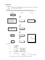
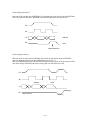
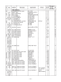
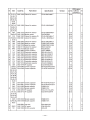
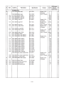
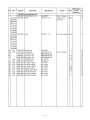
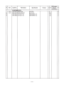
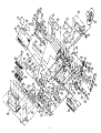
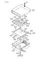
1
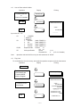
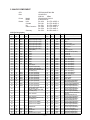
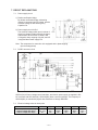
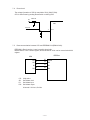
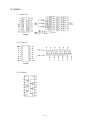
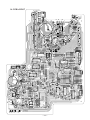
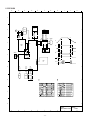
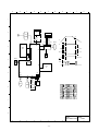
SERVICE MANUAL
(without price)
ELECTRONIC CASH REGISTER
CE-3700
CE-3750
DEC, 1994
INDEX
(EX-278)
(EX-279)
CONTENTS
Page
1. SPECIFICATION .......................................................................................... 1
2. OPTION SPECIFICATIONS ......................................................................... 3
3. INSTALLATION ........................................................................................... 3
4. INITIALIZE.................................................................................................... 4
5. MAJOR COMPONENT ................................................................................ 6
6. BLOCK DIAGRAM ....................................................................................... 7
7. CIRCUIT EXPLANATIONS .......................................................................... 8
8. DISASSEMBLY / ASSEMBLY METHOD .................................................. 12
9. DIAGNOSTIC OPERATION ....................................................................... 13
10. PROGRAMMING THE CE-3700 SERIES CASH REGISTERS ................. 17
11. OPERATION .............................................................................................. 19
12. ERROR CODES ......................................................................................... 20
13. IC DATA ..................................................................................................... 21
14. PCB LAYOUT ............................................................................................ 22
15. CIRCUIT DIAGRAM ................................................................................... 23
16. PARTS LIST ............................................................................................... 33
Product introduction
This machine CE-3700(EX-278) is a succession machine for CE-3400(EX-253).
The simultaneous boot model is EX-279.
EX-278: The drawer not separation type.
EX-279: The drawer separation type.
The Rom/Ram is the internal organs.
1. SPECIFICATION
1-1.
1-2.
1-3.
1-4.
Product
Operating temperature:
Operation air moisture:
Storage temperature:
Storage air moisture:
Bombardment strength:
Package status
Storage temperature:
Storage air moisture:
Vibration strength:
Bombardment strength:
0 °C
~
40 °C
10 %
~
90 %
-25 °C ~
65 °C
10 %
~
95 %
To add bombardment from 10 high cm by single support, and there
isn’t the problem.
-25 °C ~
65 °C
10 %
~
95 %
1.5 G
To add bombardment from 60 high cm by single support, and there
isn’t the problem.
Accessory specifications
Roll paper:
Stamp logotype:
Ink for supplement:
Ink roll:
Dust cover:
P-4575 (EX-P-4574), 45 X 12 X 30 D
CSP-2030ASA-2
Super Ink KC
IR-92 (EX-INK-IR-92-OP)
Only 1 part neighborhood
Printer
CR-812A-009-14-001A:
CR-812A-009-15-001A:
Europe
USA, Canada, UK, Europe
Printing type:
ring select mode
Output sheet number:
2
Chart specifications
Paper width:
44.5 ± 0.5 mm
Maximum paper diameter:
Ø 83 mm
Maximum paper thickness:
0.06 ~ 0.085 mm
Materials:
Regular paper
Inking:
Ink roll
Validation
Print specifications:
Yes
Sensor:
No
Paper cut:
Manual
Stamp
Color:
Purple
Seal side dimension:
30 mm (W) X 20 mm (H)
—1—
1-5.
The durability specifications
Switch
Key board switch:
Control lock:
Operation key
Feed switch
Receipt on/off switch
Reset switch
Drawer:
5,000,000 times
20,000 times
100,000 times
5,000,000 times
10,000 times
100,000 times
1,000,000 times
Printer
MCBF:
Ink roll
Stamp
Ink:
mechanism:
1-6.
50,000 times
500,000 times
Electric specifications
Power consumption
Area
In action
Max.
In holding
Min.
Power off
1-7.
2,000,000 line
400,000 line
120 V
0.40 A
0.09 A
0.08 A
220 V
0.20 A
0.05 A
0.04 A
230V
0.20 A
0.05 A
0.04 A
Memory Protection
Protection battery:
Vanadium Lithium secondary battery
Model: VL3032/IF2
Guard period:
90 days (25 °C) In perfection charge status
Galvanic cell life expectancy:
5 years
Recharge time:
48 hours in secondary battery
CAUTION
Danger of explosion if battery is incorrectly replaced.
Replace only with the same or equivalent type
recommended by the manufacturer.
Dispose of used batteries according
to the manufacture’s instructions.
1-8.
1-9.
Clock, date facility
Clock precision:
Less than ±30 seconds (25 °C)
Automatic calendar:
Until 2099
Electric power supply for an emergency (B-6)
Operating hour:
3 hours
Driving condition
Processing time per customer one person:
60 sec./ person
Purchase item number:
10 item / person
1 item registration amount of money number of digits: 4 digits / item
The handling number of people for 1 hour:
30 person /hour
Recharge time:
8 hours
—2—
240V
0.20 A
0.05 A
0.04 A
2. OPTION SPECIFICATIONS
2-1.
Ink roll:
IR-92
2-2.
Waterproofing cover:
WT-70
2-3.
Roll paper:
P-4575 (45×12×75D)
2-4.
Electric power supply for an emergency: B-6
The parts for adding B-6 are not equipped. They should be ordered separately from service department.
The following parts are necessary to add B-6.
No.
Q1
ZD1
D6,D7
C5
R2,R3,R5
R1
Code No.
2200 3577
2310 8879
2301 0011
2804 5476
2600 7313
2600 5612
6221 4218
Parts Name
Transistor
Zener diode
Diode
Electrolytic capacitor
Carbon film resistor
Carbon film resistor
Connector sub assembly
2-5.
Keyboard Conversion Kit:
CVK-S2/-L2/-LLL2/-FS2
2-6.
Ink for supplement
Super ink K
Specification
2SA1015(GR,O,Y)
RD18EB1
1S2471
50RE47
R-25-10K-J
R-25-2K-J
E311294-1(#22)
3. INSTALLATION
Connection is done of earth-line of drawer and main frame like lower chart.
—3—
Q'ty
1
1
2
1
3
1
1
4. INITIALIZE
By Initialize code
Init. A:
The format is done of EEPROM, and, without it is read, and Init. Code is written in.
Init. B:
The data is read from EEPROM.
4-1. MAC
To hang initial start-up of CPU and peripheral device, and All Clear makes memory.
When there is Data backed up by EEPROM, by Initialize code, to develop it on Memory top.
Operation
Display
Printing
Power off
To continued pushing
J-feed button, and
To set the MODE
switch to Program.
To release from the
Header printing
0000000000
J-feed button.
D1D2D3D4D5
D1 ~ D5
XXXX: Rom Control No.
-- XXXX -D1D2D3D4D5
---------------
#-2
P1
0
Input value D1 ~ D5
D1
D2
D3,D4
D5
0:
YYMMDD
1: MMDDYY
2: DDMMYY
1:
General
2:
US
3:
General
5:
Canada
Department No.
(Add2, DDMMYY)
(Add2, MMDDYY)
(Add3, DDMMYY)
(Add2, MMDDYY)
General
15
US 30
Clerk specification
Switch:
Password No.:
1,2,4
0
(U.S.A. & Canada)
Note: Operation code with Init.B is set up as with settlement in “00000”
—4—
4-2.
Auto or Reset switch initialize
Operation
To push Reset SW.
or
Power on In Low batt.
Display
Printing
0000000000
D1D2D3D4D5
D1 ~ D5
XXXX: Rom Control No.
-- XXXX --
#-2
0
P1
---------------
Input value D1 ~ D5
D1
0:
YYMMDD
1: MMDDYY
2: DDMMYY
1:
General
2:
US
3:
General
5:
Canada
Department No.
D2
(Add2, DDMMYY)
(Add2, MMDDYY)
(Add3, DDMMYY)
(Add2, MMDDYY)
General
15
US 30
Clerk specification
Switch:
Password No.:
D3,D4
D5
Note:
4-3.
D1D2D3D4D5
1,2,4
0
(U.S.A. & Canada)
Operation code with Init.B is set up as with settlement in “00000”.
Flag clear
To do Initialization of work memory, and make the operation sequence with the latest status.
Operation
Display
Printing
Power off
To continued pushing
R-feed button, and
To set the MODE
switch to Program.
Header printing
XXXX: Rom Control No.
To release from the
J-feed button.
#-2
FFFFFFFFF
0
P1
—5—
-- XXXX -D1D2D3D4D5
P1P2P3P4P5P6P7P8
X1X2X3X4
M1M2-D1D2-Y1Y2
--------------Password for P1~P8
Password for X1~X4:
X2/Z2
M1M2D1D2Y1Y2
5. MAJOR COMPONENT
CPU
Ram
Printer
Drawer
Model
MCBF
USA
Canada
UK
Other Countries
Germany
UPD78044AGF080-3B9
LC36256PLL
256K bit
SRam
CR812A-009-15-001A
2,000,000 lines
DL-2416
D-15TC-A55SP-1*
DL-2351
D-15TC-A54SP-1*
DL-2751
D-15TC-A84SP-1*
DL-2350
D-15TC-A54P-1*
DL-2750
D-15TC-A84P-1*
DL-2752
D-15BC-A84S-1*
CPU Pin Description
Pin
No.
1
2
3
4
5
6
7
8
9
10
11
12
13
14
15
16
17
18
19
Port
No.
94
93
92
91
90
81
80
Name
FIP6
FIP5
FIP4
FIP3
FIP2
FIP1
FIP0
In/
Out
O
O
O
O
O
O
O
27
26
25
24
23
22
21
20
SCK0
SO1
SI0
BUSY
STB
SCK1
SO1
SI1
I/O
I/O
I/O
I/O
I/O
I/O
I/O
I/O
Description
Pin
No.
41
42
43
44
45
46
47
48
49
50
51
52
53
54
55
56
57
58
59
Port
No.
32
31
30
3
2
1
0
Name
127
126
125
124
123
122
121
FIP33
FIP32
FIP31
FIP30
FIP29
FIP28
FIP27
O
O
O
O
O
O
O
60
61
62
63
64
65
66
120
117
116
115
114
113
112
FIP26
FIP25
FIP24
FIP23
FIP22
FIP21
FIP20
O
O
O
O
O
O
O
20
21
22
23
24
25
26
17
16
15
14
13
12
ANI7
ANI6
ANI5
ANI4
ANI3
ANI2
I
I
I
I
I
I
Display Digit Signal (Dg7)
Display Digit Signal (Dg6)
Display Digit Signal (Dg5)
Display Digit Signal (Dg4)
Display Digit Signal (Dg3)
Display Digit Signal (Dg2)
Display Digit Signal (Dg1)
Power (VDD)
Data 7
Data 6
Data 5
Data 4
Data 3
Data 2
Data 1
Data 0
Reset Signal
CE(Ram Chip Enable)
R/W(Ram Write Enable)
Analog electric potential of AD
converter (Gnd)
Key Input Signal (KI7)
Key Input Signal (KI6)
Key Input Signal (KI5)
Key Input Signal (KI4)
Key Input Signal (KI3)
Key Input Signal (KI2)
27
11
ANI1
I
Key Input Signal (KI1)
67
111
FIP19
O
28
10
ANI0
I
68
110
FIP18
O
69
107
FIP17
O
30
Key Input Signal (KI0)
Analog electric power supply of
AD converter (Vcc)
Reference voltage input of AD
converter (Gnd)
70
106
FIP16
O
31
Clock Terminal
71
32
72
105
FIP15
O
33
Clock Terminal
Analog electric potential of AD
converter(Gnd)
73
104
FIP14
O
34
System Clock 4.19MHz
74
103
FIP13
O
35
System Clock 4.19MHz
75
102
FIP12
O
EEPROM CE
Buzzer
Decoder CE
DW1&2
Journal Common Signal
76
77
78
79
80
101
100
97
96
95
FIP11
FIP10
FIP9
FIP8
FIP7
O
O
O
O
O
74
73
O
O
29
36
37
38
39
40
37
36
35
34
33
BUZ
PCL
TI2
TI1
O
O
O
O
O
—6—
TO2
TO1
TO0
INTP3
INTP2
INTP1
INTP0
In/
Out
O
O
O
I
I
I
I
70
71
72
O
O
O
Description
Receipt Common Signal
Auto cutter
Stamp
Drawer sensor
Key scan timing plus
Power Down
Printer
Gnd for Vpp (IC)
Address decoder (A12/D0)
A13/Decod1
A14/Decod1
Power (VDD)
Printer Head (HD8)
Printer Head (HD7)
Printer Head (HD6)
Printer Head (HD5)
Printer Head (HD4)
Printer Head (HD3)
Printer Head (HD2)
Printer Head (HD1)
Printer Head (HD10)
Printer Head (HD9)
Printer J-feed
Printer R-feed
Printer Motor
Key Common Signal (KC9)
Display Digit Signal / Key
Common Signal (SGdb/KC8)
Display Digit Signal / Key
Common Signal (SGtr/KC7)
Display Digit Signal / Key
Common Signal (SGg/KC6)
Display Digit Signal / Key
Common Signal (SGf/KC5)
Pull Down electric potential for
Fip (VN)
Display Digit Signal / Key
Common Signal (SGe/KC4)
Display Digit Signal / Key
Common Signal (SGd/KC3)
Display Digit Signal / Key
Common Signal (SGc/KC2)
Display Digit Signal / Key
Common Signal (SGb/KC1)
Display Digit Signal / Key
Common Signal (SGa/KC0)
Key Scan Timing Plus
Display Digit Signal (Dg10)
Display Digit Signal (Dg9)
Display Digit Signal (Dg8)
6. BLOCK DIAGRAM
Standard
CPU
Option
Printer
(CR812A)
Main Display
(10 columns)
Pop-uo Display
(10 columns)
RAM
(32K byte)
EEPROM
(512 byte)
Key board
Drawer
Multi Drawer
Compulsory Drawer
(USA, Canada,Germany, UK)
Buzzer
Power Supply
Back-up battery
(Vanadium Lithium)
Battery operation
(B-6)
—7—
7. CIRCUIT EXPLANATIONS
7-1.
Power supply circuit
1) Diodes rectification bridge
By diodes rectification bridge, alternating
voltage is converted into DC voltage, and the
electrical voltage is done filtering of by
Capacitor C4.
2) Power supply circuit for B-6
The electrical voltage which puts in resistor 3
when line voltage includes anomaly changes,
and transistor Q1 becomes on status, and
CS signal is done outgoing of by this, and VP
is supplied than Power supply B-6.
Note: The component for connection isn’t equipped with in plant shipping.
(service arrangement)
7-2.
DC/DC converter circuit
2SD721(Q2) is Power voltage control transistor, and electric power supply is supplied in DCDC converter with 2SC3303(Q3). 2SC3303(Q3) does a work as oscillator. The frequency of
2SC3303(Q3) is controlled by signal done feed back of through RD27EB1.
7-3.
Electrical voltage value in check point
Rated output electrical voltage
Output voltage drift range
Output voltage drift range
Vc
Min: 23 V
Max: 42 V
AC
Vp
20 V
2V
DC
—8—
Vcc/Vdd
5V
0.3 V
DC
Vns
32 V
10%
DC
Vs
27 V
10%
DC
Vf
4.75 V
7%
AC
7-4.
Reset circuit
The voltage fluctuation of VDD is controlled of IC10 (S-80727AN).
CPU is done Reset by pushing Reset Switch or drifting VDD.
Vdd
S-80727AN
2
3
1
CPU
Reset SW
17
7-5.
Reset
Data communication between CPU and EEPROM IC11(BR93LC46A).
EEPROM is Rom that write / erase is possible electrically.
BR93LC46A is a non- volatile register, and serial data of 16 bit can be memorized with 64
register.
EEPRom
CPU
CS
SK
DI
DO
CS:
SK:
DI:
DO:
1
36
2
14
3
15
4
16
Chip select
Serial data clock
Serial data input
Serial data output
64 words X 16 bits 1,024 bits
—9—
EEPCS
AD2
AD1
AD0
[ Data reading procedure ]
When the CPU read the data of EEPROM, CPU send the CS signal and SK signal to EEPROM.
Then CPU send the address to EEPROM, and then EEPROM return the data to CPU.
CS
SK
Address
DI
DO
Data
Output data here
[ Data writing procedure ]
When the CPU save the data to EEPROM, CPU sends the CS and SK signal to EEPROM.
And CPU send the address and data to EEPROM from pin No. 15.
When the EEPROM writes the data, EEPROM outputs the busy signal form DO terminal to CPU.
After finish writing, EEPROM outputs the ready signal from DO terminal to CPU.
Status
CS
SK
Address
Data
DI
READY(H)
DO
High Impedance
BUSY(L)
— 10 —
7-6.
Time chart
1) RAM writing timing
16.4 us
A0
WE
A1
CE
A2
D0
A3
D1
A4
D2
A5
D3
A6
D4
A7
D5
B2
A0
13.6us
3.95us
1.4us
15.0us
B3
B4
A1
B5
A2
B6
A3
B7
A4
B0
A6
B1
A7
2) RAM reading timing
A0
WE
A1
CE
A2
D0
A3
D1
A4
D2
A5
D3
A6
D4
A7
D5
B2
A0
18.3us
B3
B4
A1
B5
A2
B6
A3
B7
A4
B0
A6
B1
A7
3) EEP-ROM Writing and reading timing
29us
A0
CS
A1
SK
A2
DI
A3
DO
— 11 —
7.45us
8. DISASSEMBLY / ASSEMBLY METHOD
1)
2)
3)
4)
Remove the Printer cover.
Upper case can remove it from by 4 places screws of printer four corners.
(Lower chart 1 reference)
It comes off while sliding of Upper case backward by raising it.
Key board can remove it from by 4 places screws. (Lower chart 2 reference)
— 12 —
9. DIAGNOSTIC OPERATION
9-1.
Start-up method
By the next operation, EX-278 enters Test mode.
1)
2)
3)
4)
5)
Mode switch off.
To continued pushing J-feed button.
To set the Mode switch to Program.
To release from the J-feed button.
To input 9 9 9 9 9 0 0 0 0 0 #2
Printing out
00-00-00
00:00
0000
<Feed>
X:
“Version No.” or “- - • • • • - -”
-- x x x x -----------------
The cancellation of test mode do INIT.
9-2.
Description
1) Key code representation: expect Value number, Clear and Feed button.
2) Various switches status display
3) Testing for Display, Print, DRW, RAM:
Value number 1 column + #2
4) Testing for E2PROM:
Value number 1 column + #2
9-3.
Key code representation
RF
072
071
070
069
068
JF
067
066
065
064
063
062
061
060
059
058
057
C
056
7
4
1
0
055
054
8
5
2
011
053
052
9
6
3
012
051
050
049
048
047
046
045
044
043
042
041
040
039
038
037
036
035
034
033
032
031
030
029
028
027
026
025
024
023
022
021
020
019
014
075
074
013: #1 key
014: #2 key
— 13 —
018
017
016
015
073
013
9-4.
Various switch status display
0: Fixed
For Taiwan
1: Journal mark sensor
0: Except it
For Taiwan
1: Receipt mark sensor
0: Except it
1: Fixed
Non taxable pad For Japan
0: Taxable
(pat short)
1: Non-taxable (pat open)
Drawer sensor
0: Open
1: Close
Journal near end
1: Near end
0: Out of sense
Receipt off switch
0: Receipt on
1: Receipt off
Key clerk
0: Non
1~9, A~F:Clerk code (Hexadecimal representation)
Push clerk
0: Non
1: Clerk 1
2: Clerk 2
3: Clerk 3
4: Clerk 4
Mode representation
1: PGM
2: RF
3: REG1
4: REG2
5: X
6: Z
7: X2Z2
8: Off
0: Disconnected
— 14 —
9-5.
Print, Display, Drawer and Ram testing to do a various test by value number key. The following
code print by all means then.
1#
3#
4#
5#
96 #
8#
9#
1)
1
#2
Display:
1 #2: All testing
3 #2: E2PRom r/w testing
4 #2: E2PRom reading testing
5 #2: Ram reading testing
96 #2:E2PRom Initialization
8 #2: Printing testing
9 #2: Clock testing
All lighting, Ram, R/W, setting the time and date, drawer
opening, printing, receipt(Japan) stamp and receipt issue.
All lighting
Ram: R/W
normal end:
Abnormal end:
To be continued
To do the following printing then breaking
-------2
Receipt printing
Beeping one shot buzzer on
Setting date and time:
Date: Dec. 31st 1994
Time: 23:59
Drawer open:
Drawer No.1 and No.2 are opened.
Test printing:
To do the following print
The first line does print in receipt, journal independence.
The second line does print at receipt, journal same time.
01234567FS@
01234567FS@
Receipt stamp: (only japan)
Receipt issue:
Testing display: To do indication as follows till key or a state changes
1234567890
— 15 —
2)
3
#2
This does R/W test of testing area of E 2PRom during single word,
and, at the time of normal, does normal termination print.
Abnormal end:
To do the following printing then breaking
-------8
Receipt printing
Beeping one shot buzzer on
3)
4
#2
This does read only test of testing area of EEPRom during single word.
This test is continued till off mode or electric power supply enters it.
Abnormal end:
To do the following printing then breaking
-------8
Receipt printing
Beeping one shot buzzer on
4)
5
#2
Read only test .
Outside Ram(0000H~7FFFH) read in testing
The address comparing data which comes under it
= (A0-A7) + (A8-A14)
This test is continued till off mode or electric power supply enters it.
Abnormal end:
To do the following printing then breaking
-------2
Receipt printing
Beeping one shot buzzer on
5)
6)
9
6
8
#2
#2
Blanking (OFFH writing) of data in EEPRom entirely.
Time of day, a date are turned into zero entirely.
All time ring print testing
-------2
Receipt printing
7)
9
#2
Time of day representation testing
Time of day indication is done till clear Key
23 -59
12
— 16 —
10. PROGRAMMING THE CE-3700 SERIES CASH REGISTERS
The Casio CE-3700 series is capable of a versatile range of features and function that give it the
capability to readily adapt to almost any retail environment. The cash register is programmed at the
factory with the most standard operating features and functions. Your local business requirements,
however, may call for other functions of a totally different keyboard layout.
This section explains the different functions available, as well as the procedures that you can use to
tailor the cash register to specific needs. Programming is simplified through the use of worksheets for
each function, and step-by-step flow charts that walk you through each procedure.
10-1. Setting the proper MODE for programming
• Program Modes and feature
Mode
Program 4
Program 3
Program 1
Purpose
Assignment of 89 functions to programmable keys to create the
desired keyboard layout
Definition of machine features and key functions that enhance
printing, totalizing, reporting and overall operation
Programming of time, date and unit prices, amounts, rates, etc.
for enhanced security and automatic registration
Mode indicator
P4
P3
P1
You should perform the procedure shown blow as the first step of programming. Notice that the
flowchart ends with an arrow on the bottom. This indicates that you should continue to the next
programming procedure for the mode you specify.
• Procedure
Program
Program mode
Set the Mode switch to Program
Enter a number to specify the program mode (1 ~ 4)
Sub
Total
Press the Sub total key.
The display should show the letter “P” followed by the
program number you specified (i.e. P3 = Program mode 3).
#1*
Key
Press the # 1 key.
Program mode
Sub
Total
Enter 4-digit password.
Skip this step when the password is not programmed.
Press the Sub total key.
CA/Amt
Tend
key on standard keyboard.
Note: Program mode 1 is automatically set when the Mode switch is set to Program from
another setting.
• Recommended programming sequence
Generally, you should perform programming in the following sequence. Note that we recommend you
check what is programmed for each mode before proceeding to the programming operation.
— 17 —
1 Use Program 4 to read the assignment of functions to programmable keys and then make
changes.
2 Use Program 3 to read the definition of machine features and key functions and then make
changes.
3 Use Program 1 to read programming of time, date and unit price, amounts, rates, etc. and then
make changes.
10-2. Using the worksheets
The worksheets included in this manual for Program 3 and Program 1 help to make your
programming simple and accurate. We recommend that you fill out the pertinent worksheet before
attempting actual programming.
1) Carefully read each definition and specify a selection.
Each definition is following by a Specification column which contains numeric values(Usually to
indicate a simple YES or NO answer). Determine the correct value according to your need and
enter it in the Selection column to the right.
2) Total each set of selections to calculate each program code digit.
Three selections(a,b,c) make up a set. Add up each set of selections and fill in the totals in the
Program code column for data items D8 through D1.
3) Program the feature or function.
Be sure that you have filled in all of the selections and program code digits for the entire worksheet,
and follow the procedure noted for the feature or function you are programming.
4) Check the printed program receipt against the worksheet.
Perform program read operation in each program mode to print setting which you have
programmed, to check then against the worksheet. We recommend that you do so and keep a copy
on record to help out should it become necessary for you to change the program.
10-3. Clearing a machine lock up
If you make a mistake in operation, the cash register may lock up to avoid damage to programs and
preset data. Should this happen, you can use the following procedure to clear the lock-up without
losing any memory data.
• Procedure
Off
Set the Mode switch off.
Press receipt
feed key
RECEIPT
FEED
While holding down the
to X1.
Key, set the mode switch
Off
Press receipt
feed key
Sub
Total
RECEIPT
FEED
Release the
key.
You should see “FFFFFFFFFF” on the display. If 10 of F’s are
not shown on the display or if another character is shown,
immediately set the mode switch to OFF and start from the
beginning of this procedure. IF you don’t see “ FFFFFFFFFF”
on the display, do not press the Sub total key.
Finalize the procedure.
— 18 —
11. OPERATION
Operation of your cash register is designed to be simple enough to master without any special technical knowledge. Anytime you make a mistake in operation, an error tone sounds and further operation
becomes impossible to protect your valuable data. Whenever this happens, you can resume normal
operation after pressing the “C” key.
Printing of the symbol “—” can be programmed when the “C” key is operated in the REG1, REG2, and
RF modes. The number of the “C” key operations can also be programmed for printing on the general
control Read/Reset reports.
As you become familiar with the key layout of the cash register, you may find that your keyboard
entries are getting ahead of the receipt and journal printer. But you never need to worry that the cash
register will miss anything. A built-in key input buffer memory holds entries for up to eight keys to let
the cash register catch up when you slow down or stop.
Another thing you don’t need to worry about is power outages. Your register features built-in rechargeable lithium batteries that return such information as program data, registration records, data, item, and
consecutive number.
These and other features and functions of the CE-3700 series electronic cash register make it a
welcome addition to any retail environment.
• Performing daily cash register operations
The actual operations that you perform with your cash register will depend in the nature of your own
business. The following outline shows the most common operations in the order they are usually
performed.
1
2
3
4
5
6
7
8
9
10
11
Operation
Confirm that enough receipt and journal paper are present, and
load new paper rolls if necessary.
Read daily totals to confirm that the RESET operation was
performed for the previous day's totals.
Preset unit prices for department keys, PLUs and function keys if
necessary.
Set the MODE switch to REG and identify a clerk using a clerk
secret number.
Check the date and time set on the cash register.
Register transaction.
Normal sales
Received on account and paid out
Returns
Perform READ and RESET operation as required, after counting
the money in the cash drawer and registering the amount.
Read daily sales totals.
Read periodic sales totals
Reset daily sales totals
Reset periodic sales totals
Remove the printed journal, reports from the cash register.
Set the MODE switch to OFF and remove the key.
Empty the cash drawer and leave it open.
Carry the journal, reports and cash to the office.
— 19 —
Mode switch
OFF
X1
Program
REG1/REG2
REG1/REG2
REG1/REG2
REG1/REG2
REG1/REG2/RF
X1
X2/Z2
Z1
X2/Z2
REG1/REG2
OFF
OFF
OFF
12. ERROR CODES
Error codes appear on the display whenever you make a mistake during operation. The following table
shows the actual error codes, their meanings, and the actions to take to correct the situation.
Error Code
E 01
Meaning
Position of MODE switch changed before
finalizing the current operation.
E 41
Setting of the receipt ON/OFF button
Changed before finalizing of the registration
under another setting
Prohibited clerk/cashier number(7 ~ 15)
is entered during cashier interrupt registration.
Initialization or unit lock clear operation
in progress.
Registration without entering the clerk
secret number.
Operation attempted without entering the
password in the PRG 1, 3, 4, 6 or X2/Z2.
Registration attempted while the drawer
of the ECR is open.
The drawer is left open longer than the
program time (Drawer Open Alarm)
Two consecutive transactions attempted
in the refund mode.
Transaction cancel buffer is full.
Finalizing of a transaction attempted
without confirmation of the subtotal.
Finalizing of a transaction attempted
without confirmation of the Food stamp
subtotal. *
Finalize operation attempted without
entering the amount tendered.
Change amount exceeds press limit. *
READ/RESET operation attempted
without declare of money in drawer. *
Validation is not performed.
E 94
Printer error
E 02
E 03
E 04
E 08
E 09
E 11
E 16
E 27
E 31
E 32
E 33
E 35
E 38
Remark:
Action
Return the MODE switch to its original
setting and finalize the operation before
changing the position of the MODE switch.
Return the receipt ON/OFF switch to its
original setting and finalize the transaction
changing the setting.
Enter correct number (1 ~ 6).
Complete operation
Enter the clerk secret number.
Enter the password.
Close the drawer before attempting to
perform registration.
Shut the drawer to stop the alarm. When
the optional compulsory drawer is used.
Switch to another mode and then back
to the RF mode for the next transaction.
Finalize the transaction.
Press the "SUB TOTAL" key.
Press the "FS/ST" key.
Enter the amount tendered.
Re-input amount tendered.
Perform money declaration.
Perform validation operation.
Turn the power off, and remove jammed
roll paper from the printer.
Denoted * which these error only occur when certain function are
programmed as compulsory prohibited.
— 20 —
13. IC DATA
1) TC74HC138
2) TC74HC174
3) TC74HC367
— 21 —
14. PCB LAYOUT
B-1 125V 2.5A
F1
1
1
2
1
CA1
CN3
BL BK
BR
GND CS VP
R1
R5
C2
C6
C5
R57
R58
B-22
B-23
BR93LC66A
CN6
C14
C13
32
R18
R19
R20
R21
R22
R23
R24
R25
18
B-8
D21
D22
D23
D24
D25
D26
CN5
B
B-15
B-10
CN7
1
2
CN13
1
1
CA7
D39
D40
D41
D42
C-18
C49
C-19
C-20
C-21
5
CN14
B-32
B-31
C48
IC14
74HC174
C-17
B-30
IC13
74HC174
B-29
F-24
F-25
IC15
74HC138
D-18
C35
F-23
C36
CA6
RA2
C47
C32
D-17
B-27
B-28
B-25
F-18
F-19
F-20
F-21
F-22
RA3
H-2
C31
D-9
D-10
D-11
F-6
F-7
F-8
F-9
F-10
F-11
F-12
F-13
F-14
F-3
F-4
F-5
C-14
B-20
— 22 —
Q15
C-8
R39
E-4
H-1
B-19
IC11
E
Q14
B-21
R59
R60
R61
LC36256PLL-10/12/15
E
IC12
B
D38
R63
C40
R56
1
CN12
DW2
C39
B-26
R51
R52
C-43
R54
C34
E-6
C-15
D29
D30
D31
F-15
F-16
F-17
C33
C45
H-3
E-7
C38
X2
C44
C46
R55
C19
X1
F-26
R64
F-27
C37
J-14
D-14
D-15
D-16
R62
C-42
BR
R
C-12
IC9
BA10393
C-11
R46
D-12
C30
D43
D-6
µPD78044
AGF
R53
D-13
1
B-13
B-14
R48
R49
R50
C29
C27
C28
B-18
C41
D36
C25
C24
D35
ZD5
R40
B-16
2
BK
1
CN11
R
B Q13 E
R47
D-7
R42
E
Q12
R43
R44
R45
3
C-13
R38
F-1
B-17
R41
C-10
1
CN10
3
BR
E-5
IC6
F-2
C22
B
C23
E
Q11 E
Q10
B
R36
3
DW1
BK
BA12003
D-5
C-5
B-11
R31
C17
C-6
R32
IC8 74HC367
C-4
GND
C18
E-3
R35
IC5
IC10
S-80727AN
D37
D28
R27
R28
R29
D-3
D-4
Q9 E
RA1
74HC367
R30
B-24
R33
Q7
E
D34
B
F2
3
IC7
B-12
R34
C26
1
B
CA5
R26
E
Q6
C16
2
R37
D-8
1
Q5
J-2
B
IC4 BA12003
B
3
A
L-1
J-3
D27
B
C-9
CN4
C
D20
A
E D19
C
B-9
E
VDD
R13
D15
C9
Q4
VCC
C-3
BZ1
VN
B-7
R10 VS
R11
R12
3
J-1
D-2
CN8
ZD3
D-1
D16
D17
C-2
D18
R8
R9
C11 µPC24M05
1 IC1
C10
DCSI
C12
ZD4
R7
CA4
IC2
BA12003
C15
B-5
E
B
D14
IC3
BA12003
D32
D33
C20
CN9
B Q8 E B
R16
R17
C-1
C-16
C3
WARNING - FOR CONTINUED
PROTECTION AGAINST
FIRE HAZARD.
D13
REPLACE ONLY WITH
THE SAME TYPE AND
RATING OF FUSE.
CA3
CN1
31
Q3
B-4
K-1
1
R14
R15
ZD2
B-6
1
B
FG
VP
R6
4
C7
R4
D8
Q2
D4
D5
B-2
CA2
R2
R3
E-1
E-2
C8
ZD1
E
Q1
B
B-3
D9
D10
D11
D12
D6
D7
E
D2
D3
C1
C4
1
D1
2 CN2
15. CIRCUIT DIAGRAM
A
B
C
D
E
F
G
H
I
J
K
1
1
B-6
2
POWER
2
E278-E2-2
TRANSFORMER
OPTION
3PIN
FFC
VOLTAGE
SELECTOR
FFC
10PIN
12PIN
15V
MODE-KEY
2PIN
VP
3
31PIN
PRINTER
CR812A
PC
32PIN
VCC
PC
PC
E278-E6
RECEIPT
ON/OFF
RESET SW
min 1.5S
15mS
E241
-E3-2
4
3
E278-E2-1
FFC
PUSH CLERK
40mS
PWD
4
2PIN
NEAR END SENSER
OPTION
2PIN
RST
E278-1
18PIN
E278-E4
FPC
3PIN
3PIN
3PIN
BATTERY
DRAWER
DRAWER
5
6
300mS
CPU-CLK
5
6
OPTION
RECEIPT JOURNAL
FEED FEED
C
X
DATE
TIME
OPEN
RECEIPT VALID
7
PRICE CPN VAT
RC PD
RECEIPT JOURNAL
CLK#
FEED FEED
5 10 15
CR 1 CR 2
RECEIPT VALID
CHK
TEND
NS #
7
8
9
4
9 14
CH
%–
4
5
6
3
8 13
SUB TOTAL
1
2
3
2
7 12
0 00
•
1
6 11
—
RF
PLU
ERR.CORR
CANCEL
CA
AMT
TEND
C
X / FOR
DATE
TIME
OPEN
RC
PD
T/S1 T/S2
6
12
18
24
30
5
11
17
23
29 CR 1 CR 2
CHK
TEND
NS #
7
8
9
4
10
16
22
28
%–
PRICE
4
5
6
3
9
15
21
27 TOTAL MD/ST
— PLU
1
2
3
2
8
14
20
26
0 00
•
1
7
13
19
25
RF
ERR.CORR
CANCEL
CH
SUB
7
CA
AMT
TEND
8
8
A
B
C
D
E
F
— 23 —
G
H
Board No.
Drawing No.
BLOCK DIAGRAM for CE-3700
E240032
I
J
K
A
B
C
D
E
F
G
H
I
J
K
1
1
B-6
2
2
E278-E2-2
POWER
OPTION
TRANSFORMER
15V
3PIN
FFC
FFC
10PIN
VP
12PIN
MODE-KEY
VCC
2PIN
3
FFC
PRINTER
CR812A
3
E278-E2-1
PC
31PIN
min 1.5S
15mS
32PIN
PC
40mS
PWD
E241
-E3-2
RECEIPT
ON/OFF
RESET SW
4
RST
4
2PIN
NEAR END SENSER
300mS
CPU-CLK
OPTION
2PIN
E278-1
18PIN
E278-E4
FPC
5
3PIN
5
5PIN
3PIN
3PIN
KEY CLERK
BATTERY
DRAWER
DRAWER
RECEIPT JOURNAL
FEED FEED
6
C
X
DATE
TIME
OPEN
RECEIPT VALID
OPTION
PRICE CPN VAT
RC PD
5 10 15
CR 1 CR 2
CHK
TEND
NS #
7
8
9
4
9 14
CH
%–
4
5
6
3
8 13
SUB TOTAL
1
2
3
2
7 12
0 00
•
1
6 11
—
RF
PLU
ERR.CORR
CANCEL
6
CA
AMT
TEND
7
7
8
8
A
B
C
D
E
F
— 24 —
G
H
Board No.
Drawing No.
BLOCK DIAGRAM for CE-3750
E240046
I
J
K
D
E
F
G
H
I
KI2
KI1
KI3
KI4
KC1
KC2
KC3
KC4
KI0
KI5
KC5
KC6
KC0
KC7
KI6
KC8
KC9
KI7
6
2
4
VP
1
16
IC3
11
IC2
10
IC2
12
IC2
14
IC2
16
IC3
13
R34
C22
10K G9
C101
1SR35-100
RCOM
RHD1
RHD2
RHD3
RHD4
RHD5
RHD6
RHD7
RHD8
RHD9
RHD10
ACUT
TP
Q11
C21
TO BLOCK DIAGRAM (2/3) PRINTER
6
IC3
12 7
IC2
11 5
IC2
13 3
IC2
15 1
IC3
10 4
5
C15
C101
R50 R49 16K
10K
IC5
R46
R56
8.2K
10K
GNDP
R57
6
BK
BR
R
7
BK
BR
R
1
2
3
Q14
1.8K
2SD1853
GND
D36
1SR35-100
4.7K
R36
GND
5
C101
IC8
74HC367
IC8
GND GND
4
IL-G-3P
CN11
DW1PAD
PWD
16V100µ
STAMP
JFEED
RFEED
JCOM
JHD1
JHD2
JHD3
JHD4
JHD5
JHD6
JHD7
JHD8
JHD9
JHD10
MOTOR
R38 10K
STAMP GND
ACUT
RCOM
C30
C101
TF104
D13
C3 C101
VCC
R48 10K
R47100K
IC9
BA10393
+5
7
–6
C29
C102
1K
R29
+
1K
KI0
KI1
KI2
KI3
KI4
KI5
KI6
KI7
10K
R27
SF
SG
SDP
SH
KI0
KI1
KI2
KI3
KI4
KI5
KI6
KI7
1
IC5
11
IC3
15
IC4
10
IC4
12
IC4
14
IC4
16
GNDP
IL-G-3P
CN12 DW2 PAD
GND
2
D38
DECD2
DECD1
DECD0
4
56K
GND
VCC
P53
TF103
GND GND
8
7
6
5
4
3
2
1
10KX3
PKM22EPP-2002
RSTAP
GND
Y6
KCOM 9
Y7
Y5
PCOM 10
G1
Y4
MCOM 11
G28
Y3
LE2
12
G2A
Y2
LE1
13
C
Y1
14
Y0
B
VCC
15
VCC IC15A
16
C36
X2
6
3
GNDP
R35
2SB926
4.7K
VP
GND
C23
2SA1015
VP
12 15
D32
C20
R37
15
C101
C101
1SR35-100 GNDP
14
10K 2SB926
10
UL-TSCR-0.8A
2SA1015
VP
Q8
F2
Q13
1
13
1SR35-100
Q10
R55
2
3
1.8K
VCC
VP
2SD1853
GND
56K
VP
C101
74HC138
3
2
BA12003
2SD2015
IC5
13 6
IC5
12 2
IC3
14 7
IC4
11 5
IC4
13 3
IC4
15 1
IC3
16
5
VP
2
1S2471
Q5
4.7K
GND
VCC
R62
BZ1
C24 3
C27
7
R59
R60
R61
3.7K
EEPCE
IC5
OTP ONLY
RA3 RGLD8X563J
CA7 CNB8X101K
GND R26 1.8K
GND
GND
Q4
D27
Q6
2SC945
2SD2015
R28
C101
JCOM
C40
C39
C38
VP
14
50V1µ
15EB3
R13 56K
C101
C8
ZD5
R42
C26
KC5
KC6
KC7
KC8
KC9
D12
D11
D10
D9
KC0
KC1
KC2
KC3
KC4
SA
SB
SC
SD
SE
DG8
DG9
DG10
80
79
78
77
76
75
74
73
72
71
70
69
68
67
66
65
P95
P96
P97
P100
P101
P102
P103
P104
P105
VLOAD
P106
P107
P110
P111
P112
P113
C18
C34
1
VP
RFEED
64
JFEED
63
HD9
62
HD10
61
HD1
60
HD2
59
HD3
58
HD4
57
HD5
56
HD6
55
HD7
54
HD8
53
52
51DECD0
50DECD1
49DECD2
48
47TP
46
45
DWS
44
43
42
41
C101X3
GND
C101
R64
56K
C43
CA6
CNB8X101K
R40
BUZZ
VDD
56K
56K
56K VN
GND
56K
56K
R30
D28
56KGND
C31
C101
+
R51
10K
C44
C101
C101
GND
GND
µPD78044
R43
R41
100K
KI3 25
KI2 26
KI1 27
KI0 28
29
30
31
32
33
34
35
36
37
38
39
40
R52
C45 10K
C101
VDD
VDD
LC36256PLL-10/12/15
C42
TF103
DECD2 1 A14 VCC 28
27
DECD0 2 A12
WE
A7 3 A7
A13 26 DECD1
A6 4 A6 IC12 A8 25 A8
5 A5
A9 24 A9
VDD
6 A4
A11 23 A11
GND
7 A3
OE 22
A2 8 A2
A10 21 A10
A1 9 A1
CE 20
A010 A0
I/O7 19 AD7
AD011 I/O0
I/O6 18 AD6
AD112 I/O1
I/O5 17 AD5
AD213 I/O2
I/O4 16 AD4
GND
14 VSS I/O3 15 AD3
IC6
56K
VDD
GND
X1
CST4.19MGW DECCE
5
R63
9
C46
C101
5
R54
9
D30MCOM
330K
4
Q12
2SC945
4
P114
P115
P116
P117
P120
P121
P122
P123
P124
P125
P126
P127
VDD
P70
P71
P72
IC(VPP)
P00
P01
P02
P03
P30
P31
P32
C33 C120
10
P94
P93
P92
P91
P90
P81
P80
VDD
P27
P26
P25
P24
P23
P22
P21
P20
RESET
P74
P73
AVSS
P17
P16
P15
P14
C32 C-002RX
4
1
2
3
4
5
6
7
8
AD7 9
AD6 10
AD5 11
AD4 12
AD3 13
AD2 14
AD1 15
AD0 16
17
CE 18
19
20
KI721
KI622
KI523
KI424
C46
10
D22
D23
D24
D25
D26
D43
CA5 CNB8X221K
7
C101
3
AD0
AD1
AD2
AD3
AD4
AD5
AD6
AD7
BR93LC46A
8
7
6
5
7
R17
R16
R15
R14
VN
DG6
DG5
DG4
DG3
DG2
DG1
DG0
D35
GND
P13
P12
P11
P10
AVDD
AVREF
XT1
XT2
VSS
X1
X2
P37
P36
P35
P34
P33
C37
C101
C48
IC11
VCC
NC
NC
GND
3
TF103
1
CS
2
SK
3
DI
4
DO
VCC
GND
C41
AD2
AD1
AD0
C47
74HC174
16
CLR VCC
2 A5
Q6
Q1
3 AD5
D6
D1
14 AD4
D5
D2
15 A4
Q5
Q2
4 AD3
D4
D3
5 A3
Q4
Q3
9
GND CLK
GND
6
GND
IC13
TF103
2
VDD
GND
C35
6
VDD
IC14 74HC174
1
16
CLR VCC 2
A6 10
A11
Q6
Q1
3 AD5
AD0 11
D6
D1
14 AD4
AD1 6
D5
D2
15 A10
A7 7
Q5
Q2
4 AD3
AD2 13
D4
D3
5 A9
A8 12
Q4
8 Q3
9
GND CLK
6
2
GND
VCC
56K
D31KCOM
D29PCOM
C102
4
1
A0 10
AD0 11
AD1 6
A1 7
AD2 13
A2 12
8
1 2
R45
56K
RA2 RGLD8X563J
GND
C49
TF103
100 X8
CD0
CD1
CD2
CD3
CD4
CD5
CD6
CD7
S-80727AN
IC10
2
3 1
VCC
7
IC8 74HC367
IC8
IC8
IC8
IC7
IC7
IC7
IC7
C16
R32
GNDP
GND 100
5
VF2TFC103
VP
CD7
KCOM
RA1 RGLD8X222J
R58 DTA143ZS
1.8K
2SD1853
KCOM
IC7
14 15
13
12
11
GND IC7 74HC367 VDD
R44
C12
VCC
Q7
D1 CD7
PCOM
VDD
CN13 B28-EH
R25
R24
R23
R22
R21
R20
R19
R18
Q15
R31
56K
R39
56K
TAIWAN
CN8
VCC
1SR35-100
D39 003
D40 002
D41 001
D42 000
KCOM
5
4
3
2
1
VCC
RESET
CN10
IL-G-2P
D34 VP
VP
NEDS
CN3
B28-EH
3
PCOM
CD7
CD6
CD5
CD4
CD3
CD2
CD1
CD0
VF1
SD
SE
SG
SF
SH
DG9
DG8
DG7
DG6
DG5
DG4
DG3
DG2
DG1
DG0
SCOM
SA
SB
SC
SDP
VF2
R33 CRH100-1
KEY CLERK
CN14
IL-G-5P
2
VF1
RSTAMP
RYOUSYUU
CN9
B38-XH
MCOM D21
32 31 23 24 25 26 27 28 29 30 2 9 8 5 6 3 13 14 15 16 17 18 19 20 21 22 7 12 11 10 4 1
K
CN7
IMSA-9604S-18C
18 17 16 15 14 13 12 11 10 9 8 7 6 5 4 3 2 1
CN6 IMSA-9604S-32C
1
J
D33
C
IC5
B
1SR35-100
A
8
8
Board No.
MAIN PCB E278-1 (1/3)
A
B
C
D
E
F
— 25 —
G
H
I
Board No.
E240033
J
K
A
B
C
D
E
F
G
H
I
J
K
1
1
VP CA4
1 CNB3X101K
HBLB31-S2J
CN1
STAMP 1
JFEED 2
RFEED 3
JCOM 4
JHD1 5
JHD2 6
JHD3 7
JHD4 8
JHD5 9
JHD6 10
JHD7 11
JHD8 12
JHD9 13
JHD10 14
15
MOTOR16
RCOM 17
RHD1 18
RHD2 19
RHD3 20
RHD4 21
RHD5 22
RHD6 23
RHD7 24
RHD8 25
RHD9 26
RHD10 27
ACUT 28
29
TP
30
31
4
C28
TFC103
TFC103
C19
TFC103
VP
8
VP
BA12003*3
BA12003
IC2
IC3
IC4
IC5
GND COM
D8
1SR35-100A
9
GNDP
8
GND COM
9
TFC103
4
GNDP
VP
8
6
TFC332 100
5
D16
VFS2
1SS83
VNS
10
C10
4
D14
ZD4
VS
I
1S2471
RD27EB1
PB100A
GND
4.7K
C14
7 D17 1SS83
G
O
IC1
µPC24M05
6
D19
SB007-03SPA
R9
CRB25T29EFX2610
R7
5
33K
C9
2
16V22µ
R8
5.1K
R6
C6
Q3
VFS1
9
GND
RD68EB 2SC3303
2K
RD18EB1
R1
ZD1
CS
VP
BATTERY VL3032/1F2
1 DCS-278 3
R50-1.8K
10K
3
1
2
3
C25
ZD3
Q1
5
4
3
2
1
GND
R4
D4
1SR35-100A
F1
C17
2SD721
WITH HEAT SINK
OSH-3040-SP
2SA1015
10K
50V10000µ
D5
1SR35-100A
D6 1S2471
R2
2
J-Y7541
GND
R3
10K
C5 50V47µ
6
KEY CLERK
GND
Q2
R5
B2P3-VH
GND
8
GND
D3
1SR35-100A C4
1
2
D7 1S2471
C1 TFC103
CN2
IC7
IC8
IC9
VC
5
8
RESET SW JPM1030-0101
1
2
R10
D2
1SR35-100A
VP
16
D1NL20
C11
C2
VCC
VCC
50V100µ
R11
4
BA10393
35V2200µ
3
VP
74HC367*2
25V220µ
D18
TO BLOCK DIAGRAM (1/3) PRINTER
2 3 4 6 7 2 3 4 5 6 7 8 9 2 3 4 5 6 7 8 9 2 3 4
2
VCC
VP
50V10µ
C13
CA3
1 CNB8X101K
C7
VP
ZD2 RD22EB2
CA2
1 CNB8X101K
C101
1
VP
CA1
CNB5X101K
TFC103
VP
VDD
SB007-03SPA
D20
1
2
3
R12
CRB25T29EFX1320
(BR) (BK) (BL)
7
VCC
1
2
3
CN4
5267-03A
CN5
5267-03A
7
GNDP
8
8
A
B
C
D
E
F
— 26 —
G
H
Board No.
MAIN PCB E278-1 (2/3)
I
Drawing No.
E240034
J
K
A
B
C
D
E
F
G
H
I
J
K
1
1
2
3
4
5
6
7
IC1
IC2
IC3
IC4
IC5
IC6
IC7
IC8
IC9
IC10
IC11
IC12
IC13
IC14
IC15
UPC24M05HF
BA12003
BA12003
BA12003
BA12003
UPD78P044GF-080
TC74HC367AP
TC74HC367AP
BA10393
S-80727AN-Z
BR93LC66A
LC36256PLL10/12/15
TC74HC174AP
TC74HC174AP
TC74HC138AP
C1
C2
C3
C4
C5
C6
C7
C8
C9
C10
C11
C12
C13
C14
C15
C16
C17
C18
C19
C20
C21
C22
C23
C24
C25
C26
C27
C28
C29
C30
C31
C32
C33
C34
C35
C36
C37
C38
C39
C40
C41
C42
C43
C44
C45
C46
C47
C48
C49
ECQ-B1H103KFW
ECQ-B1H103KFW
RT-HE40TKYB101K-T
LP5-50V103MS45
RE3-50V470M-T2
RT-HE40TKYB101K-T
RE3-35V222M-T2
RT-HE40TKYB101K-T
ECQ-B1H332JFW
RE3-25V221M-T2
RE2-16V220M-T2
ECQ-B1H103KFW
RE3-50V101M-T2
RE2-50V100M-T2
RT-HE40TKYB101K-T
RT-HE40TKYB101K-T
ECQ-B1H103KFW
ECQ-V1H-104-JZW
ECQ-B1H103KFW
RT-HE40TKYB101K-T
RT-HE40TKYB101K-T
RT-HE40TKYB101K-T
RT-HE40TKYB101K-T
RT-HE40TKYB101K-T
ECQ-B1H103KFW
RE2-50V1R0M-T2
RT-HE40TKYB101K-T
ECQ-B1H103KFW
RT-HE50TKYB102K-T
RT-HE40TKYB101K-T
RT-HE40TKYB101K-T
RT-HE40TKCH150J-T
RT-HE40TKCH120J-T
RE3-16V101M-T2
ECQ-B1H103KFW
ECQ-B1H103KFW
RT-HE50TKYB102K-T
RT-HE40TKYB101K-T
RT-HE40TKYB101K-T
RT-HE40TKYB101K-T
ECQ-B1H103KFW
ECQ-B1H103KFW
RT-HE40TKYB101K-T
RT-HE40TKYB101K-T
RT-HE40TKYB101K-T
RT-HE40TKYB101K-T
RT-HE40TKYB101K-T
RT-HE40TKYB101K-T
ECQ-B1H103KFW
R1
R2
R3
R4
R5
R6
R7
R8
R9
R10
R11
CR-25-2KOHM-J-T
CR-25-10KOHM-J-T
CR-25-10KOHM-J-T
R50XT-08J182
CR-25-10KOHM-J-T
CR-25-5.1KOHM-J-T
CR-25-100OHM-J-T
CR-25-4.7KOHM-J-T
CRB25T29EFX3300
CR-25-33KOHM-J-T
R12
R13
R14
R15
R16
R17
R18
R19
R20
R21
R22
R23
R24
R25
R26
R27
R28
R29
R30
R31
R32
R33
R34
R35
R36
R37
R38
R39
R40
R41
R42
R43
R44
R45
R46
R47
R48
R49
R50
R51
R52
R53
R54
R55
R56
R57
R58
R59
R60
R61
R62
R63
R64
CRB25T29EFX1500
CR-25-56KOHM-J-T
CR-25-56KOHM-J-T
CR-25-56KOHM-J-T
CR-25-56KOHM-J-T
CR-25-56KOHM-J-T
CR-25-100OHM-J-T
CR-25-100OHM-J-T
CR-25-100OHM-J-T
CR-25-100OHM-J-T
CR-25-100OHM-J-T
CR-25-100OHM-J-T
CR-25-100OHM-J-T
CR-25-100OHM-J-T
CR-25-1.8KOHM-J-T
CR-25-10KOHM-J-T
CR-25-4.7KOHM-J-T
CR-25-1KOHM-J-T
CR-25-56KOHM-J-T
CR-25-56KOHM-J-T
CR-25-56KOHM-J-T
CRH100-FC10-J-1R0
CR-25-10KOHM-J-T
CR-25-4.7KOHM-J-T
CR-25-4.7KOHM-J-T
CR-25-10KOHM-J-T
CR-25-10KOHM-J-T
CR-25-56KOHM-J-T
CR-25-4.7KOHM-J-T
CR-25-100KOHM-J-T
CR-25-1KOHM-J-T
CR-25-56KOHM-J-T
CR-25-100OHM-J-T
CR-25-56KOHM-J-T
CR-25-8.2KOHM-J-T
CR-25-100KOHM-J-T
CR-25-10KOHM-J-T
CR-25-16KOHM-J-T
CR-25-10KOHM-J-T
CR-25-10KOHM-J-T
CR-25-10KOHM-J-T
CR-25-56KOHM-J-T
CR-25-330KOHM-J-T
CR-25-1.8KOHM-J-T
CR-25-10KOHM-J-T
CR-25-1.8KOHM-J-T
CR-25-1.8KOHM-J-T
CR-25-10KOHM-J-T
CR-25-10KOHM-J-T
CR-25-10KOHM-J-T
CR-25-56KOHM-J-T
CR-25-56KOHM-J-T
CR-25-56KOHM-J-T
D1
D2
D3
D4
D5
D6
D7
D8
D9
D10
D11
D12
D13
D14
D15
D16
D17
D18
D19
D20
D21
D22
D23
1S2471 T-77-T
1SR35-100A-T-32-T
1SR35-100A-T-32-T
1SR35-100A-T-32-T
1SR35-100A-T-32-T
1S2471 T-77-T
1S2471 T-77-T
1SR35-100A-T-32-T
1S2471 T-77-T
1S2471 T-77-T
1S2471 T-77-T
1S2471 T-77-T
1SR35-100A-T-32-T
1S2471 T-77-T
RB100A-T32-T
1SS83TD
1SS83TD
D1NL20-4070
SB007-03SPA
SB007-03SPA
1S2471 T-77-T
1S2471 T-77-T
1S2471 T-77-T
D24
D25
D26
D27
D28
D29
D30
D31
D32
D33
D34
D35
D36
D37
D38
D39
D40
D41
D42
D43
1S2471 T-77-T
1S2471 T-77-T
1S2471 T-77-T
1S2471 T-77-T
1S2471 T-77-T
1S2471 T-77-T
1S2471 T-77-T
1S2471 T-77-T
1SR35-100A-T-32-T
1SR35-100A-T-32-T
1SR35-100A-T-32-T
1S2471 T-77-T
1SR35-100A-T-32-T
1SR35-100A-T-32-T
1S2471 T-77-T
1S2471 T-77-T
1S2471 T-77-T
1S2471 T-77-T
1S2471 T-77-T
1S2471 T-77-T
ZD1
ZD2
ZD3
ZD4
ZD5
RD18EB1-T1
RD22EB1-T1
RD68EB-T1
RD27EB1-T1
RD15EB3-T1
Q1
Q2
Q3
Q4
Q5
Q6
Q7
Q8
Q9
Q10
Q11
Q12
Q13
Q14
Q15
2SA1015GR.O.Y)TPE2
2SD721
2SC3303-Y
2SD2015
2SD2015
2SC945(K.P.Q.R)-T
2SD1853-AA
2SB926(T.U)-AA
2SB926(T.U)-AA
2SA1015GR.O.Y)TPE2
2SA1015GR.O.Y)TPE2
2SC945(K.P.Q.R)-T
2SD1853-AA
2SD1853-AA
DTA143ZS-TP
RA1
RA2
RA3
RGLD8X222J
RGLD8X563J
RGLD8X563J
CA1
CA2
CA3
CA4
CA5
CA6
CA7
CNB5X101K
CNB8X101K
CNB8X101K
CNB3X101K
CNB8X221K
CNB8X101K
CNB8X101K
X1
X2
CST4.19MGW
C-002RX(M90-76)
CN1
CN2
CN3
CN4
CN5
CN6
CN7
CN8
CN9
CN10
CN11
CN12
CN13
CN14
CN15
CN16
CN17
HBLB31-S2J
5277-02A
BZ1
PKM22EPP-2002
SW1
JPM1030-0201
OSH-3040-SPL
T1
DCS-278
F1
F1
F1
F2
UF-0033
21801.6
23702.5
UL-TSCR-0.8A-N1
2
3
4
5
6
53253-0310
53253-0310
IMSA-9604S-32C
IMSA-9604S-18C
B3B-XH
IL-G-2P-S3T2-E
IL-G-3P-S3T2-E
IL-G-3P-S3T2-E
B2B-EH
IL-G-5P-S3T2-E
E412198*1
7
8
8
A
B
C
D
E
F
— 27 —
G
H
Board No.
MAIN PCB E278-1 (3/3)
I
Drawing No.
E240035
J
K
A
B
C
D
E
F
G
H
I
J
K
1
1
SH101MA
MODE KEY SW.1
KSL-B85FA02-B1J
4
X1
3
REG2
2
REG1
1
7
RF
9
6
PGM
8
3
OFF
0
10
9
8
1S2471 T-77-T
C
4
C
MODE KEY SW.1
5
C
4
1
2
3
4
5
6
7
PUSH CLERK
TO E278-E6
5
MODE KEY SW.2
KSL-84FG01-B1J
PGM
RF
REG1
REG2
X1
Z1
X2/Z2
OFF
C
C
CLCOM
SWI0 D2
SWI1 D3
SWI2 D4
SWI3 D5
SWI4 D6
SWI5 D7
3
RECEIPT
ON/OFF
TO E278-E3
2
6
1
5
6
8 7 6 5 3 2
1 SWI6 D1
2 PCOM
3
7
4
D26
D25
D24
D23
D22
D21
D14
D13
D12
D11
D20
D19
D18
D17
D10
D9
D8
D15
D16
OFF
4
C
4
12
11
10
9
8
7
6
5
4
3
2
1
10
9
8
7
6
5
4
3
2
1
A,D,B,BU
4
8
6
7
8
9
10
1
2
3
4
5
1
OFF
C
C
MODE KEY SW.2
3
IMSA-9604S-12C
CN2
Z1
1
2
IMSA-9604S-10C
CN3
5
13
14
15
16
17
18
19
20
21
22
23
24
X2/Z2
2
1
2
3
4
5
6
7
8
9
10
11
12
2
5
6
0
9
3
8
2
C
MCOM
PCOM
CD7
CD6
CD5
CD4
CD3
CD2
CD1
CD0
VF1
SD
SE
SG
SF
SH
DG9
DG8
DG7
DG6
DG5
DG4
DG3
DG2
DG1
DG0
SCOM
SA
SB
SC
SDP
VF2
1
7
7
1 2 10 9 8 7 6 5 4 3 31242528273020191817161514131211262122232932
CN1 IMSA-9604S-32C
8
8
A
B
C
D
E
F
— 28 —
G
H
Board No.
DISPLAY PCB E278-E2-1
I
Board No.
E240036
J
K
A
B
C
D
E
F
G
H
I
J
K
1
2
12
8
7
14
6
13
5
3
2
11
KC3
KC5
KC6
KC1
KC0
KC2
KC7
KC8
KC9
KC4
2
K6
K12
K18
K24
K30
K36
K42
K48
K54
K60
K66
K72
K78
KI7
K5
K11
K17
K23
K29
K35
K41
K47
K53
K59
K65
K71
K77
KI6
3
K4
K10
K16
K22
K28
K34
K40
K46
K52
K58
K64
K70
K9
K15
K21
K27
K33
K39
K45
K51
K57
K63
K69
K8
K14
K20
K26
K32
K38
K44
K50
K56
K62
K68
KI3
K7
K13
K19
K25
K31
K37
K43
K49
K55
K61
K67
15
16
4
K73
KI2
KI1
5
9
K74
4
K1
3
K75
KI4
K2
4
K76
KI5
K3
1
TO E278-1
TO E278-1
1
KI0
18
17
10
5
KEY CONTACT POSITION
6
7
6
12
18
24
30
36
42
48
54
60
66
72
78
5
11
17
23
29
35
41
47
53
59
65
71
77
4
10
16
22
28
34
40
46
52
58
64
70
76
3
9
15
21
27
33
39
45
51
57
63
69
75
2
8
14
20
26
32
38
44
50
56
62
68
74
1
7
13
19
25
31
37
43
49
55
61
67
73
6
7
8
8
A
B
C
D
E
F
— 29 —
G
H
Board No.
KEYBOARD E278-E4
I
Board No.
E240037
J
K
A
B
C
D
E
F
G
H
I
J
K
1
1
2
US. CANADA
(US. CANADA SPEC.)
(B, F, G)
240V
230V
220V
120V
100V
*
2
EUROPE
(C, L)
*
240V
230V
220V
120V
100V
*
2
3
*
2
3
1
1
0V
0V
L5T18X6X10
L5T18X6X10
TE-278-E2U
4
TE-278-E2U
4
L5T18X6X10
L5T18X6X10
FG
FG
U.K.
(LIMITED AREAS SPEC.)
(D)
5
L5T18X6X10
L5T18X6X10
240V
230V
220V
120V
100V
*
S–J2875–05
(U)
*
240V
230V
220V
120V
100V
*
2
2
1
1
0V
0V
L5T18X6X10
L5T18X6X10
L5T18X6X10
TE-278-E2U
6
5
*
L5T18X6X10
6
TE-278-E2U
L5T18X6X10
L5T18X6X10
FG
FG
7
7
8
8
A
B
C
D
E
F
— 30 —
G
H
Board No.
POWER SUPPLY
I
Drawing No.
E340043
J
K
A
B
C
D
1
1
SH1019A
2
13
14
15
16
17
18
19
20
21
22
23
24
1
2
3
4
5
6
7
8
9
10
11
12
2
4
4
DG5
DG4
DG3
DG2
DG1
DG0
SCOM
SA
SB
SC
SDP
VF2
3
VF1
SD
SE
SG
SF
SH
DG9
DG8
DG7
DG6
3
10 9 8 7 6 5 4 3 2 1
12 11 10 9 8 7 6 5 4 3 2 1
CN1 IMSA-9604S-10C
CN2 IMSA-9604S-12C
5
5
6
6
Board No.
2ND DISPLAY E278-E2-2
A
B
— 31 —
Drawing No.
E440039
C
D
A
B
C
D
1
2
2
3
TO E278-E2
1
1
SWI6
3
R ON
2
PCOM
R OFF
4
4
5
5
6
6
Board No.
SWITCH PCB
A
B
— 32 —
Drawing No.
E440040
C
D
16. PARTS LIST
1.
Main PCB ass'y
2.
Button ass'y
3.
E278-E2 ass'y, Display ass'y
4.
2nd Display ass'y
5.
Upper case
6.
Lower case
7.
Printer unit
8.
Drawer
8-1.
8-2.
8-3.
8-4.
8-5.
8-6.
DL-2350 (Europe)
DL-2351 (Canada)
DL-2416 (U.S.A.)
DL-2750 (Japan, Germany, Europe)
DL-2751 (U.K.)
DL-2752 (Germany)
Notes:
1. Price and specifications are subject to change without notice.
2. As for order / supply of spare parts, refer to the "GUIDE BOOK for spare parts supply" a separate
publication.
3. Numbers in the item column correspond to the same numbers in exploded drawing.
4. MARKS:
N: New parts
Q: Quantity used per unit
M: Minimum order/supply quantity
R: Rank
A: Essential
B: Stock recommended
C: Less recommended
X: No stock recommended
— 33 —
— 35 —
— 36 —
— 37 —
— 38 —
1-04
1-05
1-07
1-28 1-29
1-10 ~ 1-21
1-02
1-03
1-06
1-08
— 39 —
1-09
1-30
1-32
1-01
1-31
1-13
— 41 —
— 42 —
— 43 —
— 44 —
2-26
2-05
2-25
2-21
2-07
2-24
2-21
2-92
2-91
2-29
2-23
2-93
2-21
2-16
2-01
2-04
2-07
2-20
1-01
2-12
2-14
2-06
— 45 —
2-16
2-13
2-08
4-01
2-17
2-03
2-24
1-25
2-10
2-81
1-26
2-11
1-24
2-02
1-27
3-15
4-15
2-09
3-06
3-12
3-13
3-11
3-14
3-10
— 47 —
— 48 —
506
100
507
611
505
518
503
512
515
519
504
508
906
502
516
104
503
517
103
513
612
509
102
501
514
613
500
405
101
600
406
905
601
904
903
511
901
200
902
404
202
520
427
429
510
403
410
412
427
431
303
407
605
432
414
411
401
400
201
430
431
427
204
603
410
408
413
402
— 49 —
425
423
422
419
421
418
409
900
602
604
428 607
434
608 417
427
610
416
609
415
411
301
203 421
606
420
409
302
300
430
433
424
426
— 50 —
DL-2350
5-01
5-02
5-18
5-15
5-17
5-20
5-19
5-14
5-12
5-16
5-05
5-06
5-07
5-13
5-09
5-04
5-08
5-22
5-37
5-26
5-25
5-36
5-23
5-24
5-40
5-38
5-39
— 51 —
— 52 —
DL-2351
6-01
6-02
6-18
6-15
6-17
6-20
6-14
6-19
6-12
6-16
6-05
6-06
6-07
6-13
6-09
6-04
6-08
6-22
6-37
6-26
6-25
6-24
6-36
6-23
6-40
6-38
6-39
— 53 —
— 54 —
DL-2416
7-01
7-02
7-18
7-15
7-17
7-20
7-19
7-14
7-16
7-12
7-05
7-06
7-07
7-13
7-09
7-04
7-08
7-22
7-37
7-26
7-25
7-24
7-36
7-23
7-40
7-38
7-39
— 55 —
— 56 —
DL-2750
8-01
8-02
8-18
8-15
8-17
8-20
8-19
8-14
8-16
8-12
8-05
8-06
8-07
8-13
8-09
8-04
8-08
8-22
8-37
8-26
8-25
8-24
8-36
8-23
8-40
8-38
8-39
— 57 —
— 58 —
DL-2751
9-01
9-02
9-18
9-15
9-17
9-20
9-19
9-14
9-16
9-12
9-05
9-06
9-07
9-13
9-09
9-04
9-08
9-22
9-37
9-26
9-25
9-24
9-36
9-23
9-40
9-38
9-39
— 59 —
— 60 —
DL-2752
10-01
10-02
10-18
10-15
10-17
10-20
10-19
10-14
10-16
10-12
10-05
10-06
10-07
10-13
10-09
10-04
10-08
10-22
10-37
10-26
10-25
10-24
10-36
10-23
10-40
10-38 10-39
— 61 —
8-11-10, Nishi-Shinjuku
Shinjuku-ku, Tokyo 160, Japan
Telephone: 03-3347-4926