1
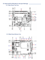
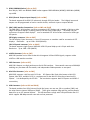
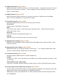
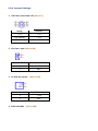
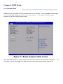
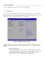
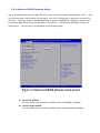
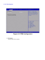
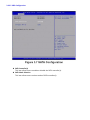
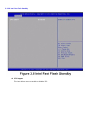
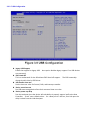
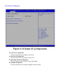
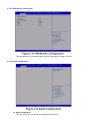
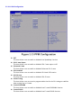
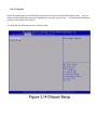
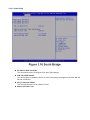
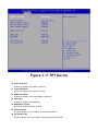
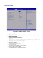
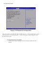
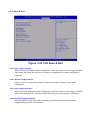
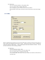
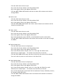
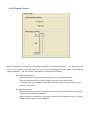
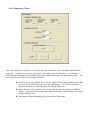
FES2213 Fanless Embedded System User Manual FES2213: Fanless Embedded System Atom N2600 Dual Core 1.6GHz Processor 14628 Central Ave, Chino, CA 91710 tel:909.597.7588, fax:909.597.1939 © Copyright 2013 Acnodes, Inc. All rights reserved. Product description and product specifications are subject to change without notice. For latest product information, please visit Acnodes’ web site at www.acnodes.com. Copyright This publi cati on c ontains inform ation that is prot ected by copyright. N o part of it m ay be reproduced i n any form or by any m eans or used to make any transform ation/adaptation without the prior written permission from the copyr ight holde rs. The manufacturer reserves the right to revise this publication and m ake changes to its contents at any time, w ithout obl igation to noti fy any person or entity of such revisions or changes. ©201 3. Al l Rights Reserved. Trademarks Al l tradem arks and registered trademarks of products appearing in this m anual are the properties of their respective holders. Notice: 1. The chan ges o r modification s n ot expressly a ppro ved by th e p arty r espo nsible fo r compliance cou ld void th e user ’s auth ority to op erate t he eq uipment . 2. Shielded int erfa ce ca bles must be used in or de r to comply wit h t he emission limits. Static Electricity Precautions It is quite easy to inadvertently dam age the system board, c omponents or devices e ven before i nstal ling them i n your system unit. Static electri cal discharg e can dam age computer com ponents wi thout causing any signs of physi cal dam age . You must take extra care in handl ing them to ensure against el ectrostatic bui ld up. 1. To prevent electrostatic bui ld up, le ave the system board i n i ts anti-static bag unti l you are ready to install it. 2. Wear an antistatic wrist st rap. 3. Do all preparation w ork on a stati c-free surface. 4. Hold the device only by its edges. Be careful not to touch any of the components, contac ts or connections. 5. Avoi d touching the pins or contacting all m odul es and connectors. Hold modules or connectors by the ir ends. Impo rt ant: Elect rost atic d ischa rge (ESD) can damage you r p rocessor, disk dr ive an d ot her compo nents. Perform t he up grade instru ct ion pr ocedures describ ed at an ESD wor kstation on ly. If such a sta tion is no t availab le, yo u can provide some ESD protection by wear in g a n ant istatic wrist st rap and attaching it to a met al part of the system chassis. If a wr ist strap is una vailab le, es tab lish an d maintain contact with the syst em chassis th roug hout any p rocedures req uiring ESD protection. FES2213 Fanless Embedded System Safety Measures To avoid dam age to the system : • Use the correct A C input vol tage range to reduce the risk of ele ctric shock. • Unplug the power cord before rem oving the system chassis cover for install ati on or servi cing. After instal lation or servicing, cover the system chassis bef ore plugging the power cord. Batte ry: • Dange r of expl osion if battery incorrectly replaced. • Repl ac e only w ith the same or e quival ent type re com mend by the manufacture r. • Dispose of used batteries according to l ocal ordinance. Warranty 1. Warranty does not cover dam ages or fai lures caused by m isuse of the product, inabili ty to use the product, unauthorized replacem ent or any kind of alterations of components and product specif ications. 2. The warranty i s voided if the product has been exposed to physi cal abuse , improper instal lation, a ny kind of modific ation, acc idents or unauthorized repair of the product. 3. Unl ess otherwise instructed in this user m anual, the user m ay not, under any ci rcum stances, attem pt to perform servi ce , adjustm ents or repairs on the product him se lf, whether the product is sti ll covered by warranty or not. It must be returned to the place i t was purchased at, the fa ctory or an authorized se rvic e agency for any re pai r work. 4. We w il l not be l iabl e for any indi re ct, spe cial, incidental or conseque nt damages to the product that has be en m odif ied or alte red. 14628 Central Ave, Chino, CA 91710 tel:909.597.7588, fax:909.597.1939 © Copyright 2013 Acnodes, Inc. All rights reserved. Product description and product specifications are subject to change without notice. For latest product information, please visit Acnodes’ web site at www.acnodes.com. FES2213 Fanless Embedded System Table of Contents Copyright ........................................................................ .......................................... Tradem arks ............................................................................................................... Static Electr icity P recautions .................................................................................... Safety Me asures ....................................................................................................... Warranty ................................................................................................................... Chapter 1: Introduction 1-1 Overvi ew.............................................................................................................. 1-2 Product Specification........................................................................................... 1-3 System Block Diagram......................................................................................... 1-4 Mechani cal D iagram ........................................................................................... 1-5 Front, Top, & Bottom Panel I/O………................................................................... Chapter 2: Pin Definition & Jumper Settings 2-1 Front panel P in Definition…………………………………………………….............…………… 2-2 Front, Top, and Bottom Panel P in Definition…………………………………….…………… 2-3 Internal Pin Definition & Jum per Settings………………………………………………………. 2-3.1 M B Top V iew………………………………….……………………………………………….…. 2-3.2 M B Bottom V iew………………………………….………… …………………………………. 2-3.3 M B P in Definition…………………………….…………………………………………………. 2-3.4 Jum per Setting.……………………………….…………………………………………………. Chapter 3: BIOS Setup 3-1 Introduction……………………….…………………………………………………………………………. 3-2 Enteri ng BIO S…………………………………………………………………………………….…………… 3-2.1 M ai n Setup…….……….…..………………………………………………………………….…… 3-2.2 A dvanced BIOS Features………………..………………………………………….………… 3-2.3 Chipset.…………………………………………………………………………………….………… 3-2.4 Boot Se tting………………………………………………………………………………………… 3-2.5 Securi ty Setup.…………………….……………………………………………………………… 3-2.6 Save & Exit…...…………………….……………………………………………………………… Chapter 4 : Software Support 4-1 Software Appl ications………..…………………………………………………………………………. 4-2 Instal lation Guide…..………………………………………………………………………………… …… Appendix A: WatchDog T imer Sam ple Code…………………..………………………………………………… GP IO Sample Code………………………………… …..………………………………………………… 14628 Central Ave, Chino, CA 91710 tel:909.597.7588, fax:909.597.1939 2 2 2 3 3 5 6 8 9 10 11 11 12 12 12 13 17 27 28 28 29 39 43 44 45 47 49 56 58 © Copyright 2013 Acnodes, Inc. All rights reserved. Product description and product specifications are subject to change without notice. For latest product information, please visit Acnodes’ web site at www.acnodes.com. FES2213 Fanless Embedded System Chapter 1: Introduction 1-1 Overview Acnodes’ FE S2213 is the latest released model with outstanding size along with reliable functionality embedded system in low power and low operating temperature. FES2213is equipped with Atom N2600 Dual-core 1.6 GHz processor with supported by the NM10 South Bridge chipset. I t pro vides to r each t he maximum memory size up to 4 GB DDR 3- 800 with one SODIMM. FES2213 supports for VGA display function in 1920 x 1200 ( 1080p) resolution while as 18/ 24b-bit 1366 x 768 LVDS features reserved internally. In order to meet t he network stability, FES2213uses one 82583V 100/ 1000 Mbps LAN wit h Wake-On LAN & DMI 2500 VDC isolation protected. It provides 2.5” SATA HDD and 1Mini-PCI-E mSATA for fulfilling the storage. FES2213enables for expansion flexibility for one half size of Mini-PCI-E expansion slot even with its easy- to-carry and mini size of W66.5mm x H130mm x D100mm. GPI O feature is reserved internally by t he SMSCSCH3114 controller, which provides 8bit programming GPI O with TTL level. The system designed with two DB-9 for supporting for RS-232 interface, and each port supports for 16 Byte FIFO (optional 5V DC output). I t also provides a software programming Watchdog (WDT) wit h timer range from 1 to 255 seconds. The power supply is capable for DC power input of 12V or 24V (optional). The power consumption is able to r each up to 10W in maximum. The construction of FES2213is designed as DIN Rail Heavy-duty steel embedded platform. The system is valuable for all t he embedded applications, and also well support with the Window 7, Windows XP and Linux Operation system. FES2213is the latest embedded system from Acnodes’ wit h low power consumption, low operating temperature, and particularly with its extraordinary size of total weight of 1.5kg. Acnodes is proud to announce and welcome you to experience our mini -sized but stable functionalized FES2213. 14628 Central Ave, Chino, CA 91710 tel:909.597.7588, fax:909.597.1939 © Copyright 2013 Acnodes, Inc. All rights reserved. Product description and product specifications are subject to change without notice. For latest product information, please visit Acnodes’ web site at www.acnodes.com. 1-2 Product Sp ecification P rocessor & Chipset Sup port Atom N2600 Dual-core 1.6 GHz Processo r NM10 Sou th Brid ge Chip set Graphic Engine Graphic core 400 Mhz Sup port AVC/ H.264, VC1/ WMV9, MPEG2 HW engine HD CP 1.3 ans PAVP 1.1C content protection su pport Sup port Microsoft DXVA 2.0 and Overlay DD MS COPP an d PVP-OPM supp ort Enablin g Key ISVs-Corel, Cyb erLink, ArcSoft Sup ports OpenGL 3.0 and Microsoft DirectX 9 Display Function VGA supp ort 1920 x 1200 (1080P) resolution Internal reserved 18/24bit 1366 x 768 LVD S feature S ystem Memory 1 SODIMM Socket, up to 4GB 800 MHz DDR3 Memo ry BIOS AMI EFI BIOS. Support Power On after Power Failu re E xpansion 1 half size Mini-PCI-E expansio n slot E thernet 1 8253V 100/1000 Mbps L AN with Wake-On LAN & D MI 2500VD C isolation protection Disk Drive Storage 2.5” SATA HDD 1 Mini-PCI-E mSATA Internal Reserved Audio Feature Audio feature, ALC892 HD Codec sup port Audio Mic-in, Line-Out, Line-In feature Watchdog Time Programmab le WDT from 1 to 255 seconds/minutes Setup by software Power Management Full ACPI 3.0 Sup port S1, S3, S4, S5 Sup port Wake on LAN Internal Reserved GPIO Feature Con troller: SMSC SCH3114 8 bit Programmin g GPIO with TTL level RS-232 Supports 2 DB-9 for RS-232 with auto -flow control Each por t support 16 Byte FI FO, optional 5V DC outpu t Front Panel Extend I/O Ports Screw-Lock DC power input connector 2 male DB-9 for 2 RS-232 DB-15 VGA disp lay interface 2 USB, 1 RJ-45 100/1000 Mbit L AN con nector Power, HDD led, Power button Reserved 2 DB-9/15 (top & bottom p anel) for optional expansion Internal Reserved Feature Audio Mic-in, Line-o ut, Line-in 18/24 bit LVDS 8 bit GPIO Those reserved featu re may optio nal sup port by request Power Supply DC 12V inp ut o r op tional DC 24V inp ut. 24VDC/ 0.85A, 12VDC/1.7A, AT/ATX power type Power ad apter : AC to DC , DC 12V/5A 60W ( Optional ) Power Consumption (with HDD) Typ ical Power Consump tion: 7W Maximum Power Consu mption: 10W Environment Operation Temperature: - With extend temperature HDD: -20°C~45°C - With extend temperature SSD: -20°C~60°C Storage Temp erature: -20°C~80°C Relative Humidity: 10%~90% (Non-condensin g) Mechanical Dimension W x H x D : 66.5mm x 130 mm x 100mm Moun ting: Din Rail mount Con struction: DIN Rail Heavy-Duty Steel Emb edded Platform Weight (Net/ Gross): 1.5KG / 2.2KG Certification CE/FCC Class A OS Supports Windows 7, Win XP, Lin ux 1-3 System Block Diagram FES 2213 1-4 Mechanical Diagrams FES 2213 1-5 Front I/O Front Panel Top & Bottom Panel Chapter 2: Pin Definition & Jumper Settings 2-1 Front Panel Pin Definition 1. Power Switch 2. LAN port 3. Two RS-232 ports (COM1 & COM2) Pin Def initi on Pin Definition 1 DCD 2 RX 3 TX 4 DTR 5 GND 6 DSR 7 RTS 8 CTS 9 RI 4. Two USB por ts Pin Definition 1 5V 2 D- 3 D+ 4 G ND 5. Power & HDD ON/Off LED - Power LED indicator would li ght when power is on. - HDD LED indicator for hard disk access is an active low signal. 2-2 Top & Bottom Panel Pin Definition 1. One DR-9 reser ved for Top & Bottom panel as optional expansion. 2-3 Internal Pin Definition & Ju mper Settings 2-3.1 Main Board Top View 2-3.2 Main Board Bottom V iew 2-3.3 Main Board Pin Definition 1. Battery Connector [refer to BH1] MIO-2261 supports Lithium 3V/210 mAH CR2 032 battery with w ire via batte ry connector (BH1). Note: How to clear CMOS: (Must fol low below steps) (1) Turn off system power (2) (3) (4) (5) Unpl ug CR2032 battery cable on BH1 Waiting for 15se c or short BH1 pin1 -2 Connect battery cable on BH1 Turn on system power 2. 12 V Power Input Connector [refer to CN 1] Main power connector supports single 12V input , and there is an optional choice of DC/ Jack (CN2, co-layout with 2pin power connector) . 3. DDRIII SODIM M Socket [refer to CN 3] One 204-pin/ H9.2 mm DDRIUII DIMM socket supports DDR3 800 MHz (N26 00)/ 106 6 MHz (N2800 ) up to 4GB. 4. GPIO (General Purpose Input Output) [refer to CN4] The board supports 8-bit GPIO ( 5V tolerance) through GPIO pin heade r. The 8 digital inputs and outputs can be programmed to read or control devices, wi th each input or output defined. 5. VGA/ LVDS Interface Connections [refer to CN5 a nd CN 18] The MIO-2261’s VGA interface can drive conventional CRT displays and is capable of driving a wide range of flat panel displays, including passive LCD and active LCD displays. The board has t wo connectors to support these displays: one for standard CRT VGA m oni tors and one for LVDS type LCD panels. CRT display connector [refer to CN 5] The CRT display 1 5pins connector is a rear I/O connector on coastline used for conventional CRT displays. Resolution: up to 1 920 x 12 00 (WUXGA). LVDS LCD panel connector [refer to CN 18] The board supports single channel 18/24 -bit LVDS LCD pane l displ ays via 14*1pin wafer box. Resoluti on: up to 1366 x 768 ( WXGA). 6. mSATA Connector [refe r to CN6] MIO-226 0 provides a mini-P CIe socket which integrates USB and SATAII signals, supports either mSATA or USB interface modules. 7. SATA Connector [refer to CN 7] MIO-226 1 features one high perform ance Se rial ATA interfaces. Data transfer rates up to 300 MB/s enabling very fast data and fi le transfer, and independent DMA operation on two ports. 8. M ini PCIe Connector [refer to CN8 ] MIIO-2261 supports a half size mini PCI2 slot. PCI Express Mini Card (also known as Mini PCI Express, Mini PCI2, and M ini PCI-E) is a repl acem ent for the Mini P CI form factor based on P CI Express. It is developed by the PCI-SIG. The host device supports both PCI Express and USB 2.0 connectivity. 9. USB Connectors [refer to CN9 and CN 10] The board provides four USB (Universal Se rial Bus) ports, two are rear I/O on coastline ( CN9); and the other two are internal USB ports ( CN10) . These gives complete Plug and Pl ay, and hot attach/ detach for up to 127 external devices. The USB interfaces comply with USB specification Rev 2.0 which support 480 Mbps transfer rate and are fuse protected. 10. COM Port Connectors [refe r to CN11] MIO-226 1 provides 2 x RS-232 serial ports in 10* 2pi n pin header. It provides connections for serial devices or a com munication network. The pin assignments for the COM port connector can be found in Jumper Setting. 11. SMBus Connector [refer to CN1 2] MIO-226 1 provides SM Bus connector for customer connection to SM Bus protocol em bedded device. It can be configured to I²C by customer’s request. 12. Front Panel Connector [refer to CN13] MIO-226 1 integrates below functi ons as front panel 6pin connector. Power Button Supports powe r on/off button in ATX mode. Reset If you install a reset switch, it should be an open si ngle pole switch. M omentarily pressing the switch will acti vate a reset. Power LED Power LED indi cator would light when power is on. HDD LED HDD LED indicator for hard disk access is an active low signal. 13. Gigabit Ethernet Connector [refer to CN14] MIO-226 1 uses Intel®82583 C Ethernet chip (10/ 100/ 1000 Mbps) l ined to dedicat ed PCI2 x 1 lane via RJ-45 connector. 14. High De finition Audio Interface [refer to CN 15] MIO-226 1 provides one 5x 2 pin box header for audio device. stereo by customized audio module that has codec onboard. It can support high definition audio 15. Front Panel Conne ctor [refer to CN13] MIO-226 1 supports MIO2 connector to extend flexible I/Os. Interface 2 x USB 2.0, 2 x P CIe x 1, LPC, HD Audio line-out, SMBus, DP (or HDMI, supported by request), 5 Vsb/ 12 Vsb power. Total peripheral power supply output 5V @ 3A for CPU board and MI/O Extension module totally, 1 2V @ 2A for M I/O Extension module. 16. Inverter Power/ Internal SATA Power Connector [refer to CN17] The LCD inve rter is connected to CN17 via a 5-pin connector to provide +5V/ +12V power to the LCD display, and 5 V powe r can be provided for 2.5” SATA HDD via CN17. SATA powe r’s current is only sufficient for 2.5” HDD, and LVDS inverter ’s cur rent is 5V @ less than 1A, 12V @500mA. 2-3.4 Jum per Settings 1. LCD Power/ Auto Power ON [refer to J1] Setting Function ( 1-2) +5V (3-4) (default) +3.3 V (5-6) (default) Auto Power On 2. 1 2V Powe r Input [refer to CN1 ] PIN PIN N ame 1 +12V 2 GND 3. D C JACK (by request) [refer to CN 2] PIN PIN N ame 1 +VIN 2 GND 4. D DR3 SO-DIMM [refer to CN3 ] 5 . GPIO [refer to CN4] PIN PIN Name 1 +5V 2 GPIO4 3 GPIO0 4 GPIO5 5 GPIO1 6 GPIO6 7 GPIO2 8 GPIO7 9 GPIO3 10 GND 6 . VGA [refer to CN5 ] PIN PIN Name 1 RED 2 GREEN 3 BLUE 4 5 NC GND 6 GND 7 GND 8 GND 9 NC 10 GND 11 NC 12 DDAT 13 HSYNC 14 VSYNC 15 DCLK 7 . mSATA [refer to CN 6] PIN PIN Name PIN PIN Name 1 NC 27 GND 2 +3.3 V 28 +1.5V 3 NC 29 GND 4 GN A 30 SMB_CLK 5 NC 31 A- 6 +1.5 V 32 SMB_DAT 7 NC 33 A+ 8 NC 34 GND 9 GND 35 GND 10 NC 36 USB D- 11 NC 37 GND 12 NC 38 USB D+ 13 NC 39 +3.3V 14 NC 40 GND 15 GND 41 +3.3V 16 NC 42 NC 17 NC 43 NC 18 GND 44 NC 19 NC 45 NC 20 NC 46 NC 21 GND 47 NC 22 NC 48 +1.5V 23 B+ 49 NC 24 +3.3 V 50 GND 25 B- 51 NC 26 GND 52 +3.3V 8 . SATA [re fer to CN7 ] PIN PIN Name 1 GND 2 TX+ 3 4 TX- GND 5 RX- 6 RX+ 7 GND 9 . Mini PCIe [refer to CN 8] PIN PIN Name PIN PIN Name 1 WAKE# 27 GND 2 +3.3VSB 28 +1.5V 3 NC 29 GND 4 GND 30 SMB_CLK 5 NC 31 PETn0 6 +1.5 V 32 SMB_DAT 7 NC 33 PETp0 8 NC 34 GND 9 GND 35 GND 10 NC 36 USB D- 11 REFCLK- 37 GND 12 NC 38 USB D+ 13 REFCLK+ 39 +3.3 VSB 14 NC 40 GND 15 GND 41 +3.3 VSB 16 NC 42 NC 17 NC 43 GND 18 GND 44 NC 19 NC 45 NC 20 NC 46 NC 21 GND 47 NC 22 P ERST# 48 +1.5V 23 P ERn0 49 NC 24 +3.3VSB 50 GND 25 P ERp0 51 NC 26 GND 52 +3.3VSB 1 0. External USB [refer to CN9] PIN PIN Name 1 +5V 2 D- 3 4 D+ GND 1 1. Internal USB [refer to CN10] PIN PIN Name 1 +5V 2 +5V 3 A_D- 4 B_ D- 5 A_D+ 6 B_ D+ 7 GND 8 GND 9 GND PIN PIN N ame PIN PIN Name 1 DCD1# 11 DCD2# 2 DSR1# 12 DSR2# 3 RXD1 13 RXD2 4 RTS1 # 14 RTS2# 5 TXD1 15 TXD2 6 CTS1# 16 CTS2# 7 DTR1# 17 DTR2# 8 RI1# 18 RI2 # 9 GND 19 GND 10 GND 20 GND 1 3. SMBus (or I²C, by request) [refer to CN 12] PIN PIN N ame 1 GND 2 SMB_DA T 3 SMB_CLK 4 +5V 1 4. Front Panel [refer to CN 13] PIN PIN N ame 1 Power Button P in1 2 3 Power LED+ Power/ Reset Button P in2 4 HDD LED + 5 Reset Button Pin1 6 HDD LED- 1 5. Gigabyte Ethernet [refer to CN 14] PIN PIN N ame 1 BI_ DA+(GHz) 2 BI_ DA-(GHz) 3 BI_DB+( GHz) 4 BI_DC+( GHz) 5 BI_DC-( GHz) 6 BI_DB-( GHz) 7 BI_DD+(GHz) 8 BI_DD-(GHz) H3 GND H4 GND 1 6. HD Audio [refer to CN15] PIN PIN N ame 1 LOUTR 2 LINR 3 GND 4 GND 5 LOUTL 6 LINL 7 NC 8 NC 9 NC 10 NC 1 7. MIOe [refer to CN16 ] 1 8. Inve rter Power/ Internal SATA Power [refer to CN 17] PIN PIN N ame 1 +12V 2 GND 3 ENABKL 4 VBR 5 +5V 1 9. 24 bits LVDS Panel [refer to CN 18] PIN PIN N ame 1 GND 2 GND 3 LCDS0_CLK- 4 LCDS0_CLK+ 5 LCDS0_D3- 6 LCDS0_D3+ 7 LCDS0_D2- 8 LCDS0_D2+ 9 LCDS0_D1- 10 LCDS0_D1+ 11 LCDS0_D0- 12 LCDS0_D0+ 13 +5V or +3.3V 14 +5V or +3.3V Chapter 3: BIOS Se tup 3-1 Introduction AMIBIOS has been integrated into m any motherboards for ove r a decade. With the AMIBIOS Setup program, user can modify BIOS setti ngs and control various system features. This chapter describes the basic navi gation of the MIO-2261 BIOS setup screens. AMI’s BIOS ROM has a built-in Se tup program that allows users to modify the basic system confi guration. Information is stored i n flash ROM so it retains the Setup information when the power is turned off. This 3-2 Entering BIOS Turn on the computer and then press < F2> or <DEL> to enter Setup menu. 3-2.1 Main Setup When user fi rst ente r the BIO S Setup Uti lity, users wi ll enter the Mai n setup screen. Users can always return to the Main setup screen by selecting the M ain tab. The re are two Main Setup options. They are described in this section. The Main BIO S Setup screen is shown bel ow. The Main BIOS setup screen has two main fram es. The left fram e displays all the options that can be confi gured. Grayed-out options cannot be configured; options in blue can. The right fram e di splays the key legend. System time/ System date Use this option to change the system tim e and date. Highlight System Ti me or System Date using the <A rrow> keys. Enter new values through the keyboard. P ress the <Tab> key or the <Arrow> keys to m ove betwee n fields. The date must be entered in MM /DD/YY format. The time must be entered in HH:MM:SS form at. 3-2.2 Advanced BIOS Features Setup Select the Advanced tab from the MIO -520 setup screen to enter the Advanced BIOS Setup screen. Use rs can sel ect any item in the l eft fram e of the screen, such as CPU Configuration, to go to the sub m enu for that i tem. Users can display an Advanced BIOS Setup option by highl ighting it using the <Arrow> keys. A ll Advanced BIOS Setup options are described in this section. The Advanced BIOS Setup screens are shown below. The sub menus are described on the foll owing pages. Launch PXE OpROM This i tem al lows users to enable or disable launch P XE OpROM if available. Launch Storage OpROM This i tem allows users to enable or disable launch storage OpRO M if available. 3 -2.2.1 Advanced BIOS Update V1.3 This item al lows users to flash BIOS. 3 -2.2.2 ACPI Settings Enable ACPI Auto Configuration This item al lows users to enable or disabl e BIOS ACPI auto configurati on. Enable Hibernation This item al lows user to enable or disable hibernation. ACPI Sle ep State This item al lows users to set the A CPI sleep state. Lock Legacy Resources This item al lows users to lock le gacy devices’ resources. S3 Vide o Report This item al lows users to enable or di sable S3 resume for VBIOS. 3-2.2.3 TPM Configuration TPM Support Di sabl e/ Enable TPM if available. 3-2.2.4 CPU Configuration Hyper Threading Technology This item allows users to enable or disable Intel Hyper Threading technology. Execute Disable Bit This item allows users to enable or disable the No-Execution page protect ion. Limit CPUID Maximum This item allows users to enable or disable limit CPUID max imum for Windows XP. 3-2.2.5 SATA Configuration SATA Controller(s) This item allows users to enable or disable the SATA controller( s). SATA Mode Selection This item allows users to select mode of SATA controller(s). 3-2.2.6 Inte l Fast Flash Standby IFFS Support This item allows users to enable or disable iFFs. 3 -2.2.7 USB Configuration Legacy USB Support Enabl e the support for legacy USB. Auto option di sables legacy support if no USB devices are connected. EHCI Hand-Off This is a workaround for the OS without EHCI hand-off support. The EHCI ownership change should claim by EGCI driver. USB transfer time-out Set the time-out value for Control, Bulk, and Interrupt transfers. Device reset t ime-out Set USB mass storage devi ce Start Unit com mand time -out value. Device power-up delay Sets the m axi mum ti me the device wi ll take before it properly reports i tself to the Host Controlle r. “A uto” uses a default value: for a Root port it is 100 m s, for a Hub port the delay is taken from the Hub descriptor. 3 -2.2.8 Super IO Configuration Serial Port 1 Configuration This item al lows users to configure serial port 1. Serial Port 2 Configuration This item al lows users to configure serial port 2. Watch Dog Function Configuration This item al lows users to configure watch dog se ttings Backlight Configuration This item al lows users to configure backlight control settings. 3 -2.2.9 H/W Monitor Configuration This page di splay all inform ation about system Temperature/ Voltage/ Current. 3 -2.2.10 AOAC Configuration AOAC Configuration This item al lows users to enable or di sabled AOAC function. 3-2.2.1 1 PPM Configuration EIST This item allows users to enable or disabled Intel SpeedStep functi on. CPU C state Report This item allows users to enable or disabled CPU C state report to OS. Enhanced C state This item allows users to enable or disabled Enhanced CP U C state. CPU Hard C4E This item allows users to enable or disabled CP U Hard C4E function. CPU C6 state This item allows users to enable or disabled CPU C6 state. C4 Exit T iming This item allows users to control a program mable ti me for the CP U voltage to stabi lize when exiting from a C4 state. C-state POPDOWN This item allows users to enable or disabled Intel C-state POPDOWN funct ion. C-state POPUP This item allows users to enable or disabled Intel C-state POPUP functi on. 3-2.3 Chipset Select the Chipset tab from the M IO-2661 setup screen to enter the Chipset BIO S Setup screen. You can display a Chipset BIOS Setup option by highlighting it using the <Arrow> keys. Al l Plug and P lay BIO S Setup options are described i n this section. This Plug and Pl ay BIO S Setup screen is shown bel ow. 3 -2.3.1 Host Bridge / Intel IGD Configuration Auto Disable IGD This item al lows users to auto disable IGD upon ex ternal GFX detected. IGFX-Boot Type This item al lows users to select which output devi ce during POST. LCD Panel Type This item al lows users to select LCD panel by internal graphic device. Panel Scaling This item al lows users to select LCD panel scali ng by internal graphi c devi ce. Backlight Control This item al lows users to select backlight control setting. Active LFP This item al lows users to select the active LFP configuration. IGD Clock Source This item al lows users to select IGD clock. Fixed Graphics Memory Size This item al lows users to configure fixed graphic m emory size. ALS Support This item al lows users to select ASL support for ACPI. Backlight Control Support This item al lows users to select backlight control support. BIA This item al lows users to select BIA with selected aggressiveness level . 3-2.3.2 South Bridge PCI Expr ess Root Port 0/1/2 This item allows users to configure P CIe port 0/1/2 settings. DMI Link ASPM Control This item enables or disables control of active state power m anagem ent on both NB and SB side of DMI link. SLP_S4 Assertion Width This item allows users to set a delay of sorts. Restore AC Powe r Loss Azalia Controller Enabl es or disables the azalea control le r. Select USB Mode Sele ct U SB mode by controllers or ports. SMBus Controller Enabl es or disables the onchip SM Bus controller. SIRQ Logic Enabl es or disables the SIRQ logi c. MSATA/PCIe Switch Enabl es for M SATA disables for PCIe. LAN1 Controller This item allows users to enables or disabl es LA N device. PCI Express PM E This item allows users to enables or disabl es PCIe PME function. 3-2.4 Boot Settings Setup Prompt T imeout This i tem al lows users to select the num ber of seconds to wait for setup activation key. Bootup NumLock State Select the Power-on state for Numl ock. Quick Boot If this option i s set to Disabled, the BIOS displays normal P OST messages. If Enabled, and O EM Logo is show n instead of POST messages. Option ROM Message Set display mode for option ROM. Interrupt 19 Capture This i tem al lows option RO Ms to trap interrupt 19. 1st/ 2 nd/ 3r d/ 4th/ 5th/ 6 th/ 7t h Boot This i tem al lows users to set boot device priori ty. 3-2.5 Security Setup Select Security Setup from the MIO-2261 Setup main BIOS setup m enu. All Security Setup options, such as passw ord protection is descri bed in this section. To access the sub menu for the foll owing item s, sele ct the item and press <Enter>: Change Administrator/ User Password Select this opti on and press <EN TER> to access the sub menu, and then type in the password. 3-2.6 Save & Exit 3-2.6.1 Save Changes and Exit When users have completed system configuration, select this option to save changes, exit BIOS setup menu and reboot the computer if necessary to take effect of al l system configuration parameter. 3-2.6.2 Discard Changes and Exit Select this opti on to quit Setup wi thout m aking any perm anent changes to the system configuration. 3-2.6.3 Save Changes and Reset When users have completed system configuration, select this option to save changes, exit BIOS setup menu and reboot the computer to take effect of al l system configuration parameters. 3-2.6.4 Discaard Changes and Reset Select this opti on to quit Setup without making any permanent changes to the system configuration and reboot the computer. 3 -2.6.5 Save Changes When users have compl eted system configuration, select this option to save changes, without exiting the BIOS setup menu. 3 -2.6.6 Discard Changes Se lect this option to discard any current changes and load previous system configuration. 3 -2.6.7 Restore De faults The MIO-22 61 automatical ly configures al l setup items to optim al settings whe n users select this option. Optim al Defaults are designed for m aximum system perform ance, but may not work best for all computer appli cations. In particular, do not use the Opti mal Defaults if the user ’s computer is experiencing system configurati on problems. 3 -2.6.8 Save User Defaults When users have compl eted system configuration, select this option to save changes as user defaults without exit the BIOS setup m enu. 3 -2.6.9 Restore User Defaults The users can select this option to restore user defaul ts. 3 -2.6.10 Boot Overridde You select device you want to do boot override. Cha pter 4: Software Support 4 -1. Software Application s 4-1.1 The GP IO Application General purpose Input/ Output i s a flexible parallel inte rface that all ows of custom conne cti ons. It allows users to monitor the level of signal input or set the output status to switch on/off a device. A program mable GPIO allows developers to dynam ical ly set the GPIO input or output status. 4-1.2 The I²C Application I²C is a bi-directional two-wi re bus that was developed by Phil ips for use in their televisions in the 1980s and nowadays in used in various types of e mbedded system s. 4-1.3 The SMBus Application The Syste m Management Bus (SMBus) is a two-w ire interface defined by Intel Corporation in 1995. It is based on the same pr inciples of operation of I²C and is used in personal computers and servers for low-speed system m anagem ent communications. 4-1.4 The Display Control Application There are two kinds of VGA control applications, backlight on/off control a nd brightness control. Backlight on/off control al lows a developer to turn on or off the backl ight, and to control brightness smoothly. Brightness Control The brightness control appl ication all ows a developer to inte rface wi th an em bedded device to easily control br ightness. Backlight Control The backlight application al lows a de veloper to control the backlight ( screen) on/off in an embedded device. 4-1.5 The Watchdog Application A watchdog timer ( abbreviated as WDT) is a hardware device which triggers an action, e.g. rebooting the system, if the system does not rese t the timer within a spec ific period of ti me. The WDT application provides developers with functi ons such as starting the tim er, resetting the tim er, and setting the tim eout val ue i f the hardware requi res customized timeout values. 4-1.6 The Hardware Monitor Application The hardware monitor ( abbreviated as HWM) is a system he alth supervision capabili ty achieved by placing certai n I/O chips al ong with sensors for i nspe cti ng the target of inte rests for certain conditi on indexes, such as fan speed, tem perature and voltage etc. 4-1.7 The Power Saving A pplication CP U Speed Make use of Intel SpeedStep technology to reduce power consum ption. The system w ill automatically adjust the CPU speed depending on system loading. System Throttling Refers to a series of methods for reduci ng power consumption in com puters by l owering the clock frequency. Applications allow the user to lower the clock from 87.5% to 1 2.5%. 4-2. Installation Guide 4-2.1 GP IO When the appl ication is executed, it wil l display GPIO inform ation i n the GP IO IN FORMATION group box. It displays the number of i nput pi ns and output pi ns. You can click the radio button to choose to rest either the single pi n function or multipl e pin functions. Test Read Single Input Pi n - Click the radio button-Single-P in. - Key in the pi n number to read the value of the input pin. The Pin number starts from “0”. - Click the READ GPIO DATA button and the status of the GPIO pin will be displayed in (R/W) Result field. Test Read Mul ti ple Input Pi ns - Click the radio button-Multiple-Pins. - Key in the pin number from “0x01” to “0x0 F” to re ad the value of the input pin. The pin numbers are ordered bitwise, i.e. bit 0 stands for GPIO 0, bit 1 stands for GP IO 1, etc. For example, if you want to read pin 0, 1 and 3, t he pin numbers should be “0 x0B”. - Click READ GPIO DATA button and the statuses of the GP IO pins wi ll be displayed in (R/W) Result field. Test Write Single Output Pi n - Click the radio button-Single-P in. - Key in the pin numbers you want to write. Pin numbers start from “0”. - Key in the value either “0” or “1” in (R/W) Result fiel d to write the output pin you chose above step. - Click the WRITE GPIO DATA button to write the GP IO output pin. Test Write Multiple Output Pi ns - Click the radio button-M ultiple-Pins. - Key in the pin number from “0x01” to “0x0F” to choose the multiple pin numbe rs to write the value of the output pin. The pin numbers are ordered bitwise, i.e. bit 0 stands for GP IO 0, bit 1 stands for GPIO 1, etc. For exam ple, if you want to write pin 0, 1, and 3 , the pin numbe rs should be “0x0B”. - Key in the value in (R/W) Result field from “ 0x01” to “0x0F” to write the value of the output pin. The pin numbers are orde red bitwise, i.e . bit 0 stands for GPIO 0 , bit 1 stands for GP IO 1, etc. For example, if you want to set pin 0 and 1 high, 3 to low, the pin numbe r should be “0x0B/, and then you should key in the value “0xxA” to write. - Click the WRITE GPIO DATA button to write the GP IO output pins. 4-2.2 I²C When the appl ication is executed, you can read or write a byte of data through I²C devices. be read or written in hexadecimal system. All data must Read a byte - Key in the sl ave device address in Salve address fie ld. - Key in the regi ster offset in Register Offset field. - Click the READ A BYTE button and then a bute of data from the device wi ll be shown on the Result field. Write a byte - Key in the sl ave device address in Salve address fie ld. - Key in the regi ster offset in Register Offset field. - Key in the desirous of data in Result fiel d to wr ite to the device. - Click the WRITE A BYTE button and then the data will be wri tten to the device though I²C. 4-2.3 SMBus When the appl ication has executed, you can cli ck the radio button to choose to test each access mode, i.e. Access a byte, Access Multiple bytes and Access a word. All data must be read or written in hexadecimal except the numbers for radio button: Access multiple bytes m ode must be written i n decimal. You can test the functionalities of the watchdog as follows: Read a byte - Click the radio button-Access a byte. - Key in the salve device address i n the Salve address field. - Key in the regi ster offset in the Re gister Offset field. - Click the READ SMBus DATA button and a byte of data from the device wi ll be shown on the Result field. - Cli ck the radio button-Access a byte. - Key in the salve devi ce address in the Sal ve address field. - Key in the register offset i n the Register Offset field. - Cli ck the WRITE SMBus DATA button and then the data will be wri tten to the devic e through SMBus. Read a word - Cli ck the radio button-Access a word. - Key in the salve devi ce address in the Sal ve address field. - Key in the register offset i n the Register Offset field. - Cli ck the READ SMBus DATA button and a then a word of data from the devi ce wil l be shown on the Result field. Write a word - Cli ck the radio button-Access a word. - Key in the salve devi ce address i n the Salve address field. - Key in the register offset i n the Register Offset field. - Key in the desi red data, such as 0x1234, in the Result field to wri te to the device. - Cli ck the WRITE SMBus DATA button and the data wi ll be written to the devi ce through the SMBus. Read mul ti ple bytes - Cli ck the radio button-Access m ultiple bytes. - Key in the salve devi ce address in the Sal ve address field. - Key in the register offset i n the Register Offset field. - Key in the desi red number of bytes, such as 3, in the ri ght side fie ld of radio button-Access m ultiple bytes. The number must be w ritten in dec imal. - Cl ick the READ SMBus DATA button and then a ll data from the device wi ll be divided from each other by comm as and be shown in the Result field. Write Multiple bytes - Cli ck the radi o button-Access m ultiple bytes. - Key in the salve devi ce address in the Sal ve address field. - Key in the register offset i n the Register Offset field. - Key in the desi red number of bytes, such as 3, in the ri ght side fie ld of the radio button-Access m ultiple bytes. The number must be w ritten in dec imal. - Key in all the desired data in the Result field in hexadecimal format, di vided by commas, for example, 0x50, 0x60 , 0x7A . - Cli ck the WRITE SMBus DATA button and all of the data wi ll be writte n to the devi ce though the SM Bus. 4-2.4 Display Control When the appl ication is executed, it wil l display two blocks of VGA control functions. The application can turn on or turn off the sc reen shot freely, and it al so can tune the brightness of the panels if your platform is being supported. You can test the functionaliti es of VGA control as follows: Screen on/off control - Click the radio button O N or push the key F11 to turn on the panel screen. - Click the radio button OFF or push the key F12 to turn off the panel screen. - The display chip of your platform must be in the support list in jum pe r setting, or this function cannot work. Brightness control - Move the slider in inc rements, using eithe r the mouse or the di rection keys, or cli ck the UP button to i ncrease the brightness. - Move the slider in decrements, using either the mouse or the di rection keys, or cli ck the DOWN button to decrease the brightness. 4-2.5 Watchdog Timer When the appl ication is executed, it wil l display watchdog information in the WATCHDOG INFORMATION group box. It displays max tim eout, min timeout, and timeout steps in mi lliseconds. For example, a 1~255 seconds watchdog wil l have 255000 max ti meout, 1000 min timeout, and 10 00 timeout steps. You can test the functionality of the watchdog as follows: Set the ti me out value 3 000 (3 sec.) in the SET TIM EO UT fie ld and set the del ay value 2000 (2 sec.) in the SET DELAY field, the n cli ck the START button. The T imeout Countdown field wi ll countdown the watchdog timer and displ ay 5000 ( 5 sec.). Before the timer counts dow n to zero, you can reset the timer by cli cking the REFRESH button. After you cl ick this button, the T imeout Countdown field wi ll display the val ue of the SET TIMEOUT field. If you want to stop the watchdog tim er, just click the STOP button. 4-2.6 Hardware Monitor When the Monitor application is executed by clicking the button, hardware monitori ng data val ues w ill be di splayed. If certain data values are not supported by the platform , the correspondent data field wi ll be grayed-out wi th a value of 0. APPENDIX A Watchdog Timer Sample Code Watchdog function: The SCH3114 Runtime base I/O address is 6 00h Setting WatchDog time val ue l ocati on at offset 66h If set value “0 ”, it is mean disable WatchDog function. Superi o_GPIO_P ort= 600h m ov dx, Superio_GP IO_Port + 6 6h m ov al, 00h .model small .486p .stack 256 .data SCH3114_IO EQU 600h .code org 100h .STARTup ;=========== ============================= ========================== ===== == ;47H ;enable WDT function bit [0]=0 Ch ;=========== ============================= ============== =================== m ov dx, SCH331 14_IO + 47h m ov al, 0Ch out dx, al ;=========== ============================= ========================== ===== == ;65H ;bit [1:0]=Reserved ;bit [6:2] Reserve=00000 ;bit [7] WDT ti me-out Value Units Select ;Minutes=0 (default) Seconds=1 ;=========== ============================= ========================== ===== == m ov dx, SCH311 4_IO + 65h; m ov al, 080h out dx, al ;=========== ============================= ============== =================== ;66H ;WDT ti mer time-out value ;bit[7:0 ]=0~255 ;================ ===== ======================== ===== ======================= mov dx,SCH3114_IO + 66h mov al, 01h out dx, al ;============== ============================ =============================== ;bit[0] status bit R/W ;WD timeout occurred =1 ;WD timer counting =0 ;================ ===== ======================== ===== ======================= mov dx,SCH3114_IO + 68h mov al, 01h out dx, al .exi t END GPIO Sample Code The SCH31 14 Runtim e base I/O address is 600h .model small .486p .stack2 56 .data SCH3114_IO EQU 6 00h .code org 100h .STARTup ;================= ===== ======================== ; Configuration GPIO as GPI or GPO by below register: ; GPIO0=23H, GPIO4=27H ; GPIO1=24H, GPIO5=29H ; GPIO2=25H, GPIO6=2AH ; GPIO3=26H, GPIO7=2BH ; Set 00H as output type, set 01H as input type ;================= ===== ======================== ;================= ===== ======================== ; Register 4BH configuration GP O value as high or low: ; 1= HIGH ; 0= LOW ;================= ===== ======================== mov dx,SCH3114_IO + 23h ;GPIO 0 mov al, 00h ;Se t GP IO 0 as output type out dx, a l mov dx,SCH3114_IO + 4Bh mov al, 01h ;Se t GP IO 0 as high value out dx, a l .exit END ===== ======================= ===== ======================= ===== ======================= ===== =======================