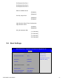
1
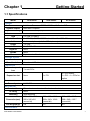
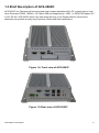
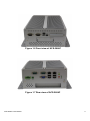
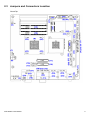
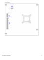
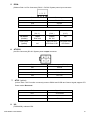
ACS-266XC Box PC User Manual Revision Date Version July. 2014 V1.1 Oct. 2014 V1.2 ® 2014 Aplex Technology, Inc. Remark Operating and Storage Temperature revised All Rights Reserved. Published in Taiwan Aplex Technology, Inc. 15F-1, No.186, Jian Yi Road, Zhonghe District, New Taipei City 235, Taiwan Tel: 886-2-82262881 Fax: 886-2-82262883 E-mail: [email protected] ACS-266XC User Manual URL: www.aplex.com.tw 1 Warning!___________________________________ This equipment generates, uses and can radiate radio frequency energy and if not installed and used in accordance with the instructions manual, it may cause interference to radio communications. It has been tested and found to comply with the limits for a Class A computing device pursuant to FCC Rules, which are designed to provide reasonable protection against such interference when operated in a commercial environment. Operation of this equipment in a residential area is likely to cause interference in which case the user at his own expense will be required to take whatever measures may be required to correct the interference. Electric Shock Hazard – Do not operate the machine with its back cover removed. There are dangerous high voltages inside. Disclaimer This information in this document is subject to change without notice. In no event shall Aplex Technology Inc. be liable for damages of any kind, whether incidental or consequential, arising from either the use or misuse of information in this document or in any related materials. ACS-266XC User Manual 2 Table of Contents______________________ Warning!…………………………………………………………………………….……..….2 Disclaimer………………………………………………………………….…………………2 Chapter 1 Getting Started 1.1 Specifications……………………………………….……………………..5 1.2 Dimensions………………………………...………………………….......6 1.3 Brief Description…………………………………………………….……10 Chapter 2 Hardware 2.1 Specifications……………..…….……………………………………..…..13 2.2 Board Dimensions…………………………………………………………15 2.2 Jumpers and Connectors Location……………………………………...17 2.3 Jumpers and Connectors………………………...………………………19 Chapter 3 BIOS Setup 3.1 Operations after POST Screen..........................................................44 3.2 BIOS SETUP UTILITY..........................................................................44 3.3 Main Settings…....................................................................................45 3.4 Advanced Settings............................................................................... 46 3.5 Chipset Settings……………................................................................. 52 3.6 Boot Settings....................................................................................... 55 3.7 Security Settings.................................................................................. 57 3.8 Save & Exit Settings.………………………...…………………………….59 Chapter 4 Installation of Drivers 4.1 Intel Chipset Driver.…………………………...…………………………62 4.2 Intel Graphics Media Accelerator Driver...…………………..…………..65 4.3 Intel 82583V Network Adapter……………………………………….….68 4.4 Realtek HD Audio Driver Installation…….…………..…………………71 Figures Figure Figure Figure Figure Figure ACS-266XC User Manual 1.1:Dimensions of ACS-2663C…………………………………..…....7 1.2:Dimensions of ACS-2664C…………………………………..…....8 1.3:Dimensions of ACS-2665C…………………………………..…....9 1.4:Front view of ACS-2663C…………………………………..…....10 1.5:Rear view of ACS-2663C…………………………………..…....10 3 Figure 1.6: Front view of ACS-2664C…………………………………………11 Figure 1.7: Rear view of ACS-2664C…………………………………………11 Figure 1.8: Front view of ACS-2665C…………………………………………12 Figure 1.9: Rear view of ACS-2665C………………………….…………….12 ACS-266XC User Manual 4 Chapter 1 Getting Started 1.1 Specifications Model ACS-2663C ACS-2664C ACS-2665C System Processor Intel Atom Processor D2550 1.86GHz , L2 Cache 1MB System chipset Intel NM10 Express System memory 1 x SO-DIMM 204pin, up to 4GB DDR3 800/1066MHz FSB IO Port USB Serial/Parallel 4 x USB 2.0 type A 3 x RS-232, 1 x RS-422/485 selectable default RS-485 Audio 1 x Line out phone jack, 1 x MIC in phone jack Graph 1 x VGA LAN 2 x GbE R-J45 Digitl I/O None KB/MS None Power 3 pins terminal block Storage Space HDD Movable device 1 x 2.5” SATA 1 x external CF slot Expansion On board expansion 1 x mini PCIe bus Expansion slot None 1 x PCI 2 x PCI default, 1 x PCI + 1 x PCIe for option Power Power input 9~36V DC Mechanical Construction Sliver aluminum chassis with aluminum heat-sink IP rating None Mounting Wall Mounting Dimension(mm) 268 x 195 x 74.6 268 x 240 x 80 (mount kit) 268 x 195 x 101.8 268 x 240 x 104.8 (mount kit) 268 x 195 x122.7 268 x 240 x 125.7 (mount kit) Net weight(Kgs) 4.8 5.0 5.5 Environment ACS-266XC User Manual 5 Operating temperature(°C) Storage temperature(°C) Storage humidity Certification Operating System Support Standard: 0°C to 50°C WT1: -20°C to 60°C for option WT2: -20°C to 70°C for option -20°C to 60°C -40°C to 70°C for WT1 and WT2 option 10 to 90%@ 40℃, non-condensing CE / FCC Class A Win 7, WES7, XP, WIN CE 6.0 1.2 Dimensions ACS-266XC User Manual 6 Figure 1.1: Dimensions of ACS-2663C ACS-266XC User Manual 7 Figure 1.2: Dimensions of ACS-2664C ACS-266XC User Manual 8 Figure 1.3: Dimensions of ACS-2665C ACS-266XC User Manual 9 1.3 Brief Description of ACS-266XC ACS-266XC is a Fan-less wall mounting and ultra-compact standalone Box PC, powered by an Intel Atom Processor D2550 1.86GHz , L2 Cache 1MB and supporting 4 x USB, 1 x SATA HDD space, DC 9~32V DC etc. ACS-266XC works very well along with any of our Display Monitor series and it absolutely can provide an easy way to perform control and field maintenance. Figure 1.4: Front view of ACS-2663C Figure 1.5:Rear view of ACS-2663C ACS-266XC User Manual 10 Figure 1.6 Front view of ACS-2664C Figure 1.7 Rear view of ACS-2664C ACS-266XC User Manual 11 Figure 1.8:Front view of ACS-2665C Figure 1.9:Rear view of ACS-2665C ACS-266XC User Manual 12 Chapter 2 Hardware ASB-M7101 is a Mini-ITX industrial motherboard developed on the basis of Intel D2550 and NM10, which provides abundant peripheral interfaces to meet the needs of different customers. Also, it features dual 1000M LAN port, 6-COM port and one Mini PCIE configuration. To satisfy the special needs of high-end customers, PC104+ socket (capable of adjusting IO voltage) richer extension functions. The product is widely used in various sectors of industrial control. 2.1 Specifications Specifications Board Size 170mm x 170mm CPU Support Intel Atom D2550 /1.86GHz (2cores,10W, onboard) Intel Atom N2800 /1.86GHz (2cores,6.5W, option) Intel Atom N2600 /1.60GHz (2cores,3.5W, option) Chipset Intel NM10 Express Memory Support 2 x SO-DIMM (204pins) D2550:up to 4GB DDRIII 800/1066MHz FSB N2800:up to 4GB DDRIII 1066MHz FSB N2600:up to 2GB DDRIII 800MHz FSB Graphics Integrated Intel GMA 3650 (D2550/N2800) Integrated Intel GMA 3600 (N2600) Display Mode 1 x CRT Port (VGA or VGA_PH) 1 x LVDS1 (18/24-bit single LVDS, option) 1 x LVDS2 (24-bit dual LVDS, option) Support Up to 1920 x 1200 for CRT Resolution Up to 1440 x 900 for LVDS1 (D2550) Up to 1366 x 768 for LVDS1 (N2600/N2800) Up to 1920 x 1200 for LVDS2 (D2550) Up to 1600 x 1200 for LVDS2 (N2600/N2800) Dual Display CRT+LVDS1 CRT+LVDS2 Super I/O Winbond W83627UHG BIOS AMIBIOS Storage 2 x SATA Connector ACS-266XC User Manual 13 1 x Compact Flash II Slot for TB-522 or TB-523 (option) Ethernet 2 x PCIe Gbe LAN by Intel 82583V 4 x USB 2.0 stack ports for external USB 3 x USB 2.0 box Pin header for MIO1 1 x USB 2.0 internal for mini PCIe 1 x RS232/422/485 port, DB9 connector for external (COM1) pin 9 w/5V/12V/Ring select 1 x RS232 port, DB9 connector for external (COM2) pin 9 w/5V/12V/Ring select Serial 1 x RS232 header for internal (COM5) 1 x RS232 header for internal (COM6),pin 10 w/5V/12V select I/O Card TB-522/TB-523: 1 x 422/485 select header for internal MIO1 (COM3) 1 x RS232 header for internal MIO1 (COM4) Digital I/O 8-bit digital I/O by Pin header for MIO2 4-bit digital Input 4-bit digital Output Battery Support CR2477 Li battery by 2-pin header Audio Support Audio via Realtek ALC662 HD audio codec Support Line-out, MIC by JACK Support Line-in, Line-out, MIC by 2x6-pin header Keyboard /Mouse PS2 K/B and Mouse by MIO2 1 x PS/2 keyboard 1 x PS/2 mouse Expansion Bus 1 x PC 104+ connector (PCI master 4, jumper for +3.3V & 5V select) 2 x PCI-express 1X extend by 4x10 pin socket (PCIe1 option) 1 x mini-PCI-express slot (PCIe1 option:MPCIE or PCIE1X) 1 x CRT 2x6 Pin Header Power 1 x 3-pin power input connector (Wide range DC+9V~32V) Management DC12V output by 2x2 pin Connectors Switches and Power on/off switch by TB-522 or TB-523 LED Indicators Reset switch by MIO2 Power LED status by MIO2 HDD LED status by MIO2 External I/O port 2 x COM Ports (COM1/COM2) 4 x USB 2.0 Ports (stack) 2 x RJ45 GbE LAN Ports ACS-266XC User Manual 14 1 x CRT DB15 Port 1 x Audio Ports (mic, line out) Watchdog Timer Temperature Humidity Power Consumption EMI/EMS ACS-266XC User Manual Software programmable 1 – 255 second by Super I/O Operating: -20℃ to 70℃ Storage: -40℃ to 85℃ 10% - 90%, non-condensing, operating 12V /1.25A (Intel Atom D2550 processor with 2GB DDR3 DRAM) 12V /1.18A (Intel Atom N2800 processor with 2GB DDR3 DRAM) 12V /0.95A (Intel Atom N2600 processor with 2GB DDR3 DRAM) Meet CE/FCC class A 15 2.2 Board Dimensions ACS-266XC User Manual 16 2.3 Jumpers and Connectors Location Board Top ACS-266XC User Manual 17 Board Bottom ACS-266XC User Manual 18 2.4 Jumpers Setting and Connectors 1. JP1: (2.0mm Pitch 1X3 Pin Header)CMOS clear jumper, CMOS clear operation will permanently reset old BIOS settings to factory defaults. JP1 CMOS Close 1-2 NORMAL (Default) Close 2-3 Clear CMOS Procedures of CMOS clear: a) Turn off the system and unplug the power cord from the power outlet. b) To clear the CMOS settings, use the jumper cap to close pins2 and 3 for about 3 seconds then reinstall the jumper clip back to pins open. c) Power on the system again. d) When entering the POST screen, press the <F1> or <DEL> key to enter CMOS Setup Utility to load optimal defaults. e) After the above operations, save changes and exit BIOS Setup. 2. BAT1: (1.25mm Pitch 1X2 Pin wafer connector) 3.0V Li battery is embedded to provide power for CMOS. 3. Pin# Signal Name Pin1 VBAT PIN2 Ground PS_SEL1(option): (2.0mm Pitch 1X3 Pin Header),DC in Power and ATX 12V IN Power jumper setting. PS_SEL1 Close 1-2 Close 2-3 4. Mode DC IN Power (Default) ATX 12V_IN (ATX Power) PS_ON: (2.0mm Pitch 1X3 Pin Header),ATX Power and Auto Power on jumper setting. JP2 Close 1-2 Close 2-3 or Open 1-2 ACS-266XC User Manual Mode (DC_IN) Auto Power on (Default) ATX Power 19 5. DCIN: (5.08mm Pitch 1x3 Pin Connector),DC9V ~ DC32V System power input connector。 Power Mode Pin# Power Input Pin1 DC+9V~32V Pin2 Ground Pin3 PG Location : DCIN Location: ATX12V Location: ATX1 (5.4.5.) (5.4.6.) (5.4.7.) DC INPUT input output NC (Default) DC9~32V DC 12V ATX Power (option) 6. NC Input (DC12V) PSON,GND,5VSB ATX Power 2*2P ATX Power ATX12V: (2x2 Pin Connector),DC12V System power output connector. 7. Pin# Power output (DCIN) Pin1 Ground Pin2 Ground Pin3 DC+12V Pin4 DC+12V ATX1 (option): (2.0mm Pitch 1X3 Pin wafer connector),connect PSON and 5VSB and Ground signal,support ATX Power model. Reserved. 8. Pin# Signal Name Pin1 ATX PSON PIN2 ATX Ground PIN3 ATX 5VSB U2: (FCBGA559), onboard CPU . ACS-266XC User Manual 20 MODEL 9. CPU ASB-M7101T-D2550 Intel Atom D2550 1.86GHz ASB-M7101B-D2550 (option) Intel Atom D2550 1.86GHz ASB-M7101T-N2800 (option) Intel Atom N2800 1.86GHz ASB-M7101B-N2800 (option) Intel Atom N2800 1.86GHz ASB-M7101T-N2600 (option) Intel Atom N2600 1.60GHz ASB-M7101B-N2600 (option) Intel Atom N2600 1.60GHz CPU_FAN/SYS_FAN: (2.54mm Pitch 1x3 Pin wafer connector),Fan connector, cooling fans can be connected directly for use. You may set the rotation condition of cooling fan in menu of BIOS CMOS Setup. Pin# Signal Name 1 Ground 2 VCC 3 Rotation detection Note: Output power of cooling fan must be limited under 5W. 10. SODIMM1/SODIMM2: (SO-DIMM 204Pin socket), DDRIII memory socket, the socket is located at the Top of the board and supports 204Pin 1.5V DDRIII 800/1066MHz FSB SO-DIMM memory module up to 4GB or 2GB. The single RAM use SODIMM1 Slot. MODEL 11. Socket Memory ASB-M7101-D2550 SODIMM1/SODIMM2 Up to 4GB ASB-M7101-N2800 SODIMM1/SODIMM2 Up to 4GB ASB-M7101-N2600 SODIMM1 Up to 2GB VGA: (CRT DB15 Connector),Video Graphic Array Port, provide high-quality video output. they can not work at the same time for VGA and VGA_PH. ACS-266XC User Manual 21 12. VGA_PH(option): (CRT 2.0mm Pitch 2X6 Pin Header), Video Graphic Array Port, Provide 2x5Pin cable to VGA Port, they can not work at the same time for VGA and VGA_PH. Signal Name Pin# Pin# Signal Name CRT_RED 1 2 Ground CRT_GREEN 3 4 Ground CRT_BLUE 5 6 VGA_EN CRT_H_SYNC 7 8 CRT_DDCDATA CRT_V_SYNC 9 10 CRT_DDCCLK Ground 11 12 Ground VGA hot plug setting for Windows XP: Function VGA1(Pin Header) Pin4-Pin6(Close) VGA Simulation Disabled Pin4-Pin6(Open) VGA Simulation Enabled use the 2.0mm jumper cap to close pin 4 and pin6 13. INVT1: (2.0mm Pitch 1x6 Pin wafer connector), Backlight control connector for LVDS1. Pin# Signal Name 1 +DC12V 2 +DC12V 3 Ground 4 Ground 5 BKLT_EN 6 BKLT_CTRL Note: Pin6 is backlight control signal, support DC or PWM mode, mode select at BIOS CMOS menu. ACS-266XC User Manual 22 14. LVDS1: (1.25mm Pitch 2x20 Connector, DF13A-40DP-1.25V),For 18/24-bit LVDS1 output connector, Fully supported by U2 Intel Processor, the interface features single channel 18/24-bit output. Low Voltage Differential Signaling, A high speed, low power data transmission standard used for display connections to LCD panels. Signal Name Pin# Pin# LVDS1_VDD5 2 1 LVDS1_VDD5 Ground 4 3 Ground LVDS1_VDD33 6 5 LVDS1_VDD33 NC 8 7 LVDS_TX0_DN NC 10 9 LVDS_TX0_DP Ground 12 11 Ground NC 14 13 LVDS_TX1_DN NC 16 15 LVDS_TX1_DP Ground 18 17 Ground NC 20 19 LVDS_TX2_DN NC 22 21 LVDS_TX2_DP Ground 24 23 Ground NC 26 25 LVDS_CLK_DN NC 28 27 LVDS_CLK_DP Ground 30 29 Ground 32 31 LVDS_DDC_CLK Ground 34 33 Ground NC 36 35 LVDS_TX3_DN NC 38 37 LVDS_TX3_DP NC 40 39 NC LVLVDS_DDC_DATA 15. Signal Name U13: (2.54mm Pitch 2x4Pin Socket), AT24C02 socket, The EEPROM is set for the resolution of LVDS2. The resolution default is:1280*1024. According to the needs of customers set. 16. INVT2: (2.0mm Pitch 1x6 Pin wafer connector), Backlight control connector for LVDS2. Pin# ACS-266XC User Manual Signal Name 23 1 +DC12V 2 +DC12V 3 Ground 4 Ground 5 BKLT_EN 6 BKLT_CTRL Note: Pin6 is backlight control signal, support DC or PWM mode, mode select at BIOS CMOS menu. 17. LVDS2(option): (1.25mm Pitch 2x20 Connector, DF13A-40DP-1.25V), For 18/24-bit LVDS2 output connector, Fully supported by Parad PS8625(DP to LVDS), the interface features dual channel 24-bit output. Low Voltage Differential Signaling, A high speed, low power data transmission standard used for display connections to LCD panels. Signal Name 19. Pin# Pin# Signal Name LVDS2_VDD5 2 1 LVDS2_VDD5 Ground 4 3 Ground LVDS2_VDD33 6 5 LVDS2_VDD33 LB_D0_N 8 7 LA_D0_N LB_D0_P 10 9 LA_D0_P Ground 12 11 Ground LB_D1_N 14 13 LA_D1_N LB_D1_P 16 15 LA_D1_P Ground 18 17 Ground LB_D2_N 20 19 LA_D2_N LB_D2_P 22 21 LA_D2_P Ground 24 23 Ground LB_CLKN 26 25 LA_CLKN LB_CLKP 28 27 LA_CLKP Ground 30 29 Ground LVDS2_DDC_DATA 32 31 LVDS2_DDC_CLK Ground 34 33 Ground LB_D3_N 36 35 LA_D3_N LB_D3_P 38 37 LA_D3_P NC 40 39 NC BTN: POWER on/off Button, They are used to connect power switch button. The two pins are ACS-266XC User Manual 24 disconnected under normal condition. You may short them temporarily to realize system startup & shutdown or awaken the system from sleep state. 20. JP2: (2.0mm Pitch 2x3 Pin Header),COM1 jumper setting, pin 1~6 are used to select signal out of pin 9 of COM1 port. JP2 Pin# 21. Function Close 1-2 COM1 RI (Ring Indicator) (default) Close 3-4 COM1 Pin9=+5V (option) Close 5-6 COM1 Pin9=+12V (option) JP1A: (2.0mm Pitch 2x10 Pin Header),COM1 jumper setting, it provides selectable RS232 / RS422/RS485 and hardware flow control serial signal output. Function RS232 JP1A Pin# Close: (Default) RS422 Pin2-4, Pin7-9, Pin8-10, Pin13-14 Close: Pin3-5, (option) RS485 Pin1-3, Pin4-6, Pin9-11, Pin10-12, Pin4-6, Pin9-11, Pin10-12, Pin17-18 Close: Pin3-5, (option) Pin15-16, Hardware Flow Controll Jumper Setting 22. JP1A Pin# Hardware Flow Controll Pin19-Pin20 Close (Yes) default Pin19-Pin20 Open (No) COM1: (Type DB9),Rear serial port, standard DB9 Male serial port is provided to make a direct connection to serial devices. COM1 port is controlled by pins No.1~6 of JP2,select output Signal RI or 5V or 12v, For details, please refer to description of JP2. COM1/RS232 (Default): Pin# 1 ACS-266XC User Manual Signal Name DCD# (Data Carrier Detect) 25 2 RXD (Received Data) 3 TXD (Transmit Data) 4 DTR (Data Terminal Ready) 5 Ground 6 DSR (Data Set Ready) 7 RTS (Request To Send) 8 CTS (Clear To Send) 9 RI/5V/12V (JP2 select Setting) COM1/RS422 (option): Pin# Signal Name 1 422_RX+ 2 422_RX- 3 422_TX- 4 422_TX+ 5 Ground 6 NC 7 NC 8 NC 9 5V/12V (JP2 select Setting) COM1/RS485 (option): Pin# Signal Name 1 NC 2 NC 3 485- 4 485+ 5 Ground 6 NC 7 NC 8 NC 9 23. 5V/12V (JP2 select Setting) JP3: (2.0mm Pitch 2x3 Pin Header),COM2 jumper setting, pin 1~6 are used to select signal out of pin 9 of COM2 port. JP3 Pin# ACS-266XC User Manual Function Close 1-2 COM2 RI (Ring Indicator) (default) Close 3-4 COM2 Pin9=+5V (option) 26 Close 5-6 24. COM2 Pin9=+12V (option) COM2: (Type DB9),Rear serial port, standard DB9 Male serial port is provided to make a direct connection to serial devices. Pin# 25. Signal Name 1 DCD# (Data Carrier Detect) 2 RXD (Received Data) 3 TXD (Transmit Data) 4 DTR (Data Terminal Ready) 5 Ground 6 DSR (Data Set Ready) 7 RTS (Request To Send) 8 CTS (Clear To Send) 9 RI/5V/12V (JP3 select Setting) COM5: (2.0mm Pitch 2X5 Pin Header),COM5 Port, standard RS232 ports are provided. They can be used directly via COM cable connection. 26. Signal Name Pin# Pin# Signal Name DCD 1 2 RXD TXD 3 4 DTR Ground 5 6 DSR RTS 7 8 CTS RI 9 10 NC JP4: (2.0mm Pitch 2x3 Pin Header) COM6 setting jumper, pin 1~6 are used to select signal out of pin 9 of COM6 port. JP4 Pin# 27. Function Close 1-2 COM6 RI (Ring Indicator) (default) Close 3-4 COM6 Pin9=+5V (option) Close 5-6 COM6 Pin9=+12V (option) COM6: ACS-266XC User Manual 27 (2.0mm Pitch 2X5 Pin Header), COM6 Port, standard RS232 ports are provided. They can be used directly via COM cable connection. COM6 port is controlled by pins No.1~6 of JP4,select output Signal 5V or 12v, For details, please refer to description of JP4. 28. Signal Name Pin# Pin# Signal Name DCD 1 2 RXD TXD 3 4 DTR Ground 5 6 DSR RTS 7 8 CTS RI/5V/12V (JP4 select Setting) 9 10 NC USB4/USB5/USB6/USB7: (Double stack USB type A), Rear USB connector, it provides up to 4 USB2.0 ports, speed up to 480Mb/s. Each USB Type A Receptacle (2 Ports) Current limited value is 1.5A. If the external USB device current exceeds 1.5A, please separate connectors into different Receptacle. 29. LAN1/LAN2: (RJ45 Connector), Rear LAN port, Two standard 10/100/1000M RJ-45 Ethernet ports are provided. Used Intel 82583V chipset, LINK LED (green) and ACTIVE LED (yellow) respectively located at the left-hand and right-hand side of the Ethernet port indicate the activity and transmission state of LAN. 30. JACK: (Diameter 3.5mm Double stack Jack), HD Audio port, An onboard Realtek ALC662 codec is used to provide high quality audio I/O ports. Line Out can be connected to a headphone or amplifier, MIC is the port for microphone input audio. ACS-266XC User Manual 28 31. AUDIO(option): (2.0mm Pitch 2X6 Pin Header), Front Audio, An onboard Realtek ALC662 codec is used to provide high-quality audio I/O ports. Line Out can be connected to a headphone or amplifier. Line In is used for the connection of external audio source via a Line in cable. MIC is the port for microphone input audio. Signal Name 32. Pin# Pin# Signal Name SPK_OUTL_P 1 2 SPK_OUTR_P SPK_OUTL_N 3 4 SPK_OUTR_N FRONT_JD 5 6 LINE1_JD LINE-IN-L 7 8 LINE-IN-R MIC2-IN-L 9 10 MIC2-IN-R Ground 11 12 MIC2_JD BUZZ: Onboard buzzer. 33. JP_104P: (2.0mm Pitch 1X3 Pin Header) PC104+ port voltage selection jumper, select voltage for PCI-104 Plus devices. The default for this jumper is “all open”,meaning the user must select the voltage to be used. 34. JP_104P Pin# PC104+ VIO Voltage All Open Default Close 1-2 +3.3V PCI Card Close 2-3 +5V PCI Card PC104+ (option): (4x30 Pin), PC104 plus connector, it conforms to standard PC104+ specification. Can expand support four PCI devices. ACS-266XC User Manual Model PC104+ Connector ASB-M7101T-D2550 Top ASB-M7101B-D2550 Bottom (option) ASB-M7101T-N2800 Top (option) 29 35. ASB-M7101B-N2800 Bottom (option) ASB-M7101T-N2600 Top (option) ASB-M7101B-N2600 Bottom (option) PCIE1X (option): (4x10 Pin), PCIe bus connector, it conforms to standard PCI Express x1 specification. Can expand support two PCIe devices. PCIe1 Signal for PCIE1X or MPCIE Socket. PCIe4 Signal for PCIE1X Socket. 36. Model PCIE1X Connector ASB-M7101T-D2550 Top ASB-M7101B-D2550 Bottom (option) ASB-M7101T-N2800 Top (option) ASB-M7101B-N2800 Bottom (option) ASB-M7101T-N2600 Top (option) ASB-M7101B-N2600 Bottom (option) MPCIE: (Socket 52Pin),mini PCIe socket, it is located at the top, it supports mini PCIe devices with USB2.0,Smbus,SIM and PCIe signal. MPCIe card size is 30x30mm or 30x50.95mm. PCIe1 Signal for PCIE1X or MPCIE Socket. 37. LED1: LED1:Power LED Status. 38. LED2: LED2:LED Status. Green LED for Motherboard Standby Power Good status, Yellow LED for HDD status. 39. MIO1: (DF13-40P Connector),For expand output connector, It provides two RS232 ports or one RS485 port, three USB ports, one power led, one power button, via a dedicated cable connected to TB-522 MIO1or TB-523 MIO1. Function Signal Name Pin# Pin# Signal Name Function 422RX+ 1 2 485+ / 422TX+ COM3 COM3 422RX- 3 4 485- / 422TX- RS422 or 485 RS422 Ground 5 6 WLAN_LED+ WLAN LED NC 7 8 WLAN_LED- ACS-266XC User Manual 30 5V_S5 9 10 5V_S5 DCD4- 11 12 RXD4 TXD4 13 14 DTR4- COM4 Ground 15 16 DSR4- COM4 RS232 RTS4- 17 18 CTS4- RS232 RI4- 19 20 5V_S5 5V_S5 21 22 5V_USB_01 USB3_N 23 24 USB0_N USB3_P 25 26 USB0_P Ground 27 28 Ground Ground 29 30 Ground 5V_USB_01 31 32 PWR_LED+ USB1_N 33 34 PWR_LED- USB1_P 35 36 MIO_PSON Power Ground 37 38 Ground Button NC 39 40 AUTO_PS_ON USB3 USB1 40. USB0 Power LED MIO2: (DF13-40P Connector),Front panel connector. Function Signal Name Signal Name Function H_LED+ HDD_LED 1 2 PWR-LED P_LED+ NC 3 4 Ground P_LED- NC 5 6 MIO_PSON- PSON+ RESET+ RESET 7 8 Ground PSON- BUZZER+ BUZZER+ 9 10 BUZZER- BUZZER- GPIO_IN_1 SIO_GPIO60 11 12 SIO_GPIO20 GPIO_OUT_1 GPIO_IN_2 SIO_GPIO61 13 14 SIO_GPIO21 GPIO_OUT_2 GPIO_IN_3 SIO_GPIO62 15 16 SIO_GPIO22 GPIO_OUT_3 GPIO_IN_4 SIO_GPIO63 17 18 SIO_GPIO23 GPIO_OUT_4 Ground 19 20 5V_S5_USB PS2_KBDATA 21 22 PS2_MSDATA PS2_KBCLK 23 24 PS2_MSCLK 5V_S5_USB 25 26 5V_S5_USB NC 27 28 NC NC 29 30 NC Ground 31 32 Ground 5V_S5_USB 33 34 5V_S5_USB NC 35 36 NC NC 37 38 NC PS2_K/B ACS-266XC User Manual Pin# Pin# PS2_Mouse 31 Ground 39 40 Ground Pin1/Ground: HDD LED, They are used to connect hard disk activity LED. The LED blinks when the hard disk is reading or writing data. Pin2/Pin4: POWER LED, They are used to connect power LED. When the system is powered on or under S0/S1 state, the LED is normally on, when the system is under S4/S5 state, the LED is off. Pin7/Ground: RESET Button, They are used to connect reset button. The two pins are disconnected under normal condition. You may short them temporarily to realize system reset. Pin6/Pin8: POWER on/off Button, They are used to connect power switch button. The two pins are disconnected under normal condition. You may short them temporarily to realize system startup & shutdown or awaken the system from sleep state. Pin9/Pin10: BUZZER, They are used to connect an external buzzer. Pin11~Pin18: GPIO IN/GPIO OUT, General-purpose input/output port, it provides a group of self-programming interfaces to customers for flexible use. Pin19~Pin24: PS2 KB/MS, PS/2 keyboard and mouse port, the port can be connected to PS/2 keyboard and mouse via a dedicated cable for direct used. Note: When connecting LEDs and buzzer and GPIO and USB, pay special attention to the signal polarity. Make sure that the connector pins have a one-to-one correspondence with chassis wiring, or it may cause boot up failure. 41. SATA_P1/SATA_P2: (2.5mm Pitch 1x2 Pin wafer connector), Two onboard 5V output connectors are reserved to provide power for SATA devices. Pin# Signal Name 1 +DC5V 2 Ground Note: Output current of the connector must not be above 1A. ACS-266XC User Manual 32 42. SATA1/SATA2: (SATA 7P), SATA Connectors, Two SATA connectors are provided, with transfer speed up to 3.0Gb/s. 43. CON1(option): (2.0mm Pitch 1x4 Pin wafer connector),Smbus Signal connector. 44. Pin# Signal Name 1 SMB_CLK_MAIN_IO 2 3.3V 3 Ground 4 SMB_DATA_MAIN_IO SIM1(option): (SIM Socket 7Pin), Support SIM Card devices. 45. HS1/HS2/HS3/HS4(CPU SCREW HOLES): CPU FAN SCREW HOLES, Four screw holes for fixed CPU Cooler assemble. 46. H5/H6: MPCIE1 SCREW HOLES, H5 for mini PCIE card (30mmx30mm) assemble. H6 for mini PCIE card (30mmx50.95mm) assemble. 47. TB-522: ASB-M7101 I/O Card, via a dedicated cable connected to ASB-M7101 MIO1. LED2: CF Card LED status. S1: ACS-266XC User Manual 33 PWR BT: POWER on/off Button, They are used to connect power switch button. The two pins are disconnected under normal condition. You may short them temporarily to realize system startup & shutdown or awaken the system from sleep state. PWR LED: POWER LED status. COM3: (Type DB9),I/O serial port, it provides selectable RS422/RS485 serial signal output. RS422 Type (option) RS485 Type (option) Signal Name Pin# Pin# Signal Name 422_RX+ 1 1 NC 422_RX- 2 2 NC 422_TX- 3 3 485- 422_TX+ 4 4 485+ Ground 5 5 Ground NC 6 6 NC NC 7 7 NC NC 8 8 NC NC 9 9 NC Note: Use COM3 RS422 or RS485 Function, please enter BIOS CMOS Setup. Path: BIOS Setup Utility \ Advanced /Super IO Configuration \ Serial Port3 Type: [RS-485] [RS-422] COM4: (Type DB9),Rear serial port, standard DB9 Male serial port is provided to make a direct connection to serial devices. Pin# ACS-266XC User Manual Signal Name 34 1 DCD# (Data Carrier Detect) 2 RXD (Received Data) 3 TXD (Transmit Data) 4 DTR (Data Terminal Ready) 5 Ground 6 DSR (Data Set Ready) 7 RTS (Request To Send) 8 CTS (Clear To Send) 9 RI (Ring Indicator) USB10,USB11: (Double stack USB type A), I/O USB connector, it provides up to 2 USB2.0 ports, speed up to 480Mb/s. USB10 and USB11 connected to ASB-M7101 MIO1 USB0 and USB1. Each USB Type A Receptacle (2 Ports) Current limited value is 1.5A. If the external USB device current exceeds 1.5A, please separate connectors into different Receptacle. CF: (CF Card socket), it is located at TB-522 and serves as an insert interface for Type I and Type II Compact Flash card. The operating voltage of CF card can be set as 3.3V or 5V. The default setting of the product is 5V. MIO1: (DF13-40P) TB-522 MIO1 via a dedicated cable connected to ASB-M7101 MIO1. Signal Name ACS-266XC User Manual Pin# Signal Name 422_RX+ 1 2 485+_422TX+ 422_RX- 3 4 485-_422TX- Ground 5 6 NC NC 7 8 NC 35 48. NC 9 10 5V_S5 DCD4- 11 12 RXD4 TXD4 13 14 DTR4- Ground 15 16 DSR4- RTS4- 17 18 CTS4- RI4- 19 20 5V_S5 5V_S5 21 22 5V_USB01 USB3_N 23 24 USB0_N USB3_P 25 26 USB0_P Ground 27 28 Ground Ground 29 30 Ground 5V_USB01 31 32 PWR_LED+ USB1_N 33 34 PWR_LED- USB1_P 35 36 PS_ON- Ground 37 38 Ground Ground 39 40 Ground TB-520P1: TB-520P1 connect to ASB-M7101T PC104+ connector, PC104+ is located at the top, It provides one PCI slot. 49. TB-520P2: TB-520P2 connect to ASB-M7101T PC104+ connector, PC104+ is located at the top, It provides two PCI slots. ACS-266XC User Manual 36 50. TB-520P1E1: TB-520P1E1 connect to ASB-M7101T PC104+ and PCIE1X connector,PC104+ and PCIE1X are located at the top, It provides one PCI slot and one PCIE slot. 51. TB-520E1: TB-520E1 connect to ASB-M7101T PCIE1X connector, PCIE1X are located at the top, It provides one PCIE slot. 52. TB-521P1: TB-521P1 connect to ASB-M7101B PC104+ connector, PC104+ is located at the Bottom, It provides one PCI slot. ACS-266XC User Manual 37 53. TB-521P2: TB-521P2 connect to ASB-M7101B PC104+ connector, PC104+ is located at the Bottom, It provides two PCI slots. 54. TB-521P1E1: TB-521P1E1 connect to ASB-M7101B PC104+ and PCIE1X connector,PC104+ and PCIE1X are located at the Bottom, It provides one PCI slot and one PCIE slot. ACS-266XC User Manual 38 55. TB-521P1E12: TB-521P1E12 connect to ASB-M7101B PC104+ and PCIE1X connector,PC104+ and PCIE1X are located at the Bottom, It provides one PCI slot and two PCIE slots. PCIe1 Signal for PCIE1X or MPCIE Socket. 56. TB-523: ASB-M7101 I/O Card, via a dedicated cable connected to ASB-M7101 MIO1 and MIO2. TB-523 Top: TB-523 Bottom: ACS-266XC User Manual 39 LED2: CF Card LED status. S1: PWR BT: POWER on/off Button, They are used to connect power switch button. The two pins are disconnected under normal condition. You may short them temporarily to realize system startup & shutdown or awaken the system from sleep state. PWR LED: POWER LED status. COM3: (Type DB9),I/O serial port, it provides selectable RS422/RS485 serial signal output. RS422 Type (option) RS485 Type (option) Signal Name Pin# Pin# Signal Name 422_RX+ 1 1 NC 422_RX- 2 2 NC 422_TX- 3 3 485- 422_TX+ 4 4 485+ Ground 5 5 Ground NC 6 6 NC NC 7 7 NC NC 8 8 NC NC 9 9 NC Note: Use COM3 RS422 or RS485 Function, please enter BIOS CMOS Setup. Path: BIOS Setup Utility \ Advanced /Super IO Configuration \ Serial Port3 Type: ACS-266XC User Manual 40 [RS-485] [RS-422] JP4: (2.0mm Pitch 2x10 Pin Header) COM4 function setting jumper. Function JP4 Pin# RS232 Close: 3-5,4-6,10-12,11-13 (Default) RS422 Close: 1-3,2-4,5-7,8-10,9-11,12-14,18-20 (option) RS485 Close: 5-7,8-10,9-11,12-14,16-18 (option) COM4: (Type DB9), I/O serial port, it provides selectable RS232/RS422/RS485 serial signal output. COM4 RS232 Type (Default): Pin# Signal Name 1 DCD# (Data Carrier Detect) 2 RXD (Received Data) 3 TXD (Transmit Data) 4 DTR (Data Terminal Ready) 5 Ground 6 DSR (Data Set Ready) 7 RTS (Request To Send) 8 CTS (Clear To Send) 9 RI (Ring Indicator) COM4 RS422 Type (option) ACS-266XC User Manual COM4 RS485 Type (option) Signal Name Pin# Pin# Signal Name 422_RX+ 1 1 NC 422_RX- 2 2 NC 422_TX- 3 3 485- 422_TX+ 4 4 485+ Ground 5 5 Ground NC 6 6 NC NC 7 7 NC NC 8 8 NC NC 9 9 NC 41 USB10: (Single stack USB type A), I/O USB connector, it provides one USB2.0 port, speed up to 480Mb/s. USB11: (2.0mm Pitch 1x4 box Pin Header), I/O USB connector, it provides one USB2.0 port, speed up to 480Mb/s. USB10 and USB11 connected to ASB-M7101 MIO1 USB0 and USB1. Pin# Signal Name 1 5V_USB01 2 USB1_N 3 USB1_P 4 Ground USB10 and USB11 current limited value is 1.5A. If the external USB device current exceeds 1.5A, please separate connectors into different Receptacle. CF: (CF Card socket), it is located at TB-523 and serves as an insert interface for Type I and Type II Compact Flash card. The operating voltage of CF card can be set as 3.3V or 5V. The default setting of the product is 5V. GPIO: (3.5mm Pitch 2x5 Pin Connector),General-purpose input/output port, it provides a group of self-programming interfaces to customers for flexible use. Function ACS-266XC User Manual Pin# Function 42 +5V 1 2 Ground GPIO_IN1 3 4 GPIO_IN2 GPIO_IN3 5 6 GPIO_IN4 GPIO_OUT1 7 8 GPIO_OUT2 GPIO_OUT3 9 10 GPIO_OUT4 MIO1: (DF13-40P) TB-523 MIO1 via a dedicated Y cable connected to ASB-M801 MIO1 and MIO2. Signal Name Pin# Signal Name 422_RX+ 1 2 485+_422TX+ 422_RX- 3 4 485-_422TX- Ground 5 6 GPIO_IN1 GPIO_IN2 7 8 GPIO_IN3 GPIO_IN4 9 10 5V_S5 DCD4- 11 12 RXD4 TXD4 13 14 DTR4- Ground 15 16 DSR4- RTS4- 17 18 CTS4- RI4- 19 20 5V_S5 5V_S5 21 22 5V_USB01 USB3_N 23 24 USB0_N USB3_P 25 26 USB0_P Ground 27 28 Ground GPIO_OUT1 29 30 GPIO_OUT2 5V_USB01 31 32 SO_POWER_SENSE USB1_N 33 34 PWR_LED- USB1_P 35 36 PS_ON- Ground 37 38 Ground GPIO_OUT3 39 40 GPIO_OUT4 ACS-266XC User Manual 43 Chapter 3 3.1 BIOS Setup Operations after POST Screen After CMOS discharge or BIOS flashing operation,.Press [Delete] key to enter CMOS Setup. Version 2.15.1226. Copyright (C) 2012 American Megatrends, Inc. BIOS Date: 05/14/2013 22:29:02 Ver: M7101V006 Press 〈DEL〉or〈ESC〉to enter setup A3 After optimizing and exiting CMOS Setup, the POST screen displayed for the first time is as follows and includes basic information on BIOS, CPU, memory, and storage devices. Press F11 to load default values and continue 3.2 0085 BIOS SETUP UTILITY Press [Delete] key to enter BIOS Setup utility during POST, and then a main menu containing system summary information will appear. ACS-266XC User Manual 44 Aptio Setup Utility – Copyright (C) 2012 American Megatrends, Inc. Main Advanced Chipset Boot Security BIOS Information Save & Exit Intel Reference Code BIOS Vendor American Megatrends Core Version 4.6.5.3 Compliancy UEFI 2.3; PI 1.2 Project Version 7101V006 Version ►Intel RC Version System Language →←: Select Screen [English] ↑↓ : Select Item System Date [Sun 01/01/2012] Enter: System Time [00:00:09] +/- : Charge Opt. Select F1 : General Help Access Level Administrator F2: Previous Values F3:Optimized Defaults F4:Save and Exit ESC Exit Version 2.15.1226. Copyright (C) 2012 American Megatrends , Inc. 3.3 Main Settings Aptio Setup Utility – Copyright (C) 2012 American Megatrends, Inc. Main Advanced Chipset Boot Security BIOS Information Save & Exit Intel Reference Code BIOS Vendor American Megatrends Core Version 4.6.5.3 Compliancy UEFI 2.3; PI 1.2 Project Version 7101V006 Version ►Intel RC Version ACS-266XC User Manual 45 System Language →←: Select Screen [English] ↑↓ : Select Item System Date [Sun 01/01/2012] Enter: Select System Time [00:00:09] +/- : Charge Opt. F1 : General Help Access Level Administrator F2: Previous Values F3:Optimized Defaults F4:Save and Exit ESC Exit Version 2.15.1226. Copyright (C) 2012 American Megatrends , Inc. System Time: Set the system time, the time format is: Hour : 0 to 23 Minute : 0 to 59 Second : 0 to 59 System Date: Set the system date, the date format is: Day: Note that the ‘Day’ automatically changes when you set the date. Month: 01 to 12 Date: 01 to 31 Year: 1998 to 2099 3.4 Advanced Settings Aptio Setup Utility – Copyright (C) 2012 American Megatrends, Inc. Main Advanced Chipset Boot Security Save & Exit PCI,PCI-X and PCI ►PCI Subsystem Settings Express Settings ►ACPI Settings ►CPU Configuration ►Thermal Configuration ►IDE Configuration ►USB Configuration ►W83627UHG Super IO Configuration ACS-266XC User Manual 46 ►W83627UHG HW Monitor →←: Select Screen ►Serial Port Console Redirection ↑↓ ►PPM Configuration Enter: : Select Item Select +/- : Charge Opt. F1 : General Help F2: Previous Values F3:Optimized Defaults F4:Save and Exit ESC Exit Version 2.15.1226. Copyright (C) 2012 American Megatrends , Inc. 3.4.1 PCI Subsystem Settings PCI Bus Driver Versio V2.05.02 PCI Common Settings: PCI Latency Timer: [32 PCI Bus Clocks] [64 PCI Bus Clocks] [96 PCI Bus Clocks] [128 PCI Bus Clocks] [160 PCI Bus Clocks] [192 PCI Bus Clocks] [224 PCI Bus Clocks] [248 PCI Bus Clocks] VGA Palette Snoop: [Disabled] [Enabled] PERR# Generation: [Disabled] [Enabled] SERR# Generation: [Disabled] [Enabled] 3.4.2 ACPI Settings Enable ACPI Auto Conf: [Disabled] [Enabled] ACS-266XC User Manual 47 Enable Hibernation: [Enabled] [Disabled] ACPI Sleep State: [Both S1 and S3 available for OS to choose from] [Suspend Disabled] [S1 only (CPU Stop Clock)] [S3 only (Suspend to RAM) ] Lock Legacy Resources: [Disabled] [Enabled] S3 Video Repost: [Disabled] [Enabled] 3.4.3 CPU Configuration Processor Type Intel(R) Atom(TM) CPU EMT64 Not Supported Processor Speed 1865 MHz System Bus Speed 533 MHz Ratio Status 14 Actual Ratio 14 System Bus Speed 533 MHz Processor Stepping 30661 Microcode Revision 269 L1 Cache RAM 2x56 k L2 Cache RAM 2x512 k Processor Core Dual Hyper-Threading Supported Hyper-Threading: [Enabled] [Disabled] Execute Disable Bit: [Enabled] [Disabled] ACS-266XC User Manual 48 Limit CPUID Maximum: [Disabled] [Enabled] 3.4.4 Thermal Configuration CPU Thermal Configuration DTS SMM [Disabled] [Enabled] Platform Thermal Configuration Critical Trip Point [15C] Active Trip Point Lo [55 C] 3.4.5 Active Trip Point Hi [71C] Passive Trip Point [95] Passive TC1 Value 1 Passive TC2 Value 5 Passive TSP Value 10 IDE Configuration SATA Port0 Not Present SATA Port1 Not Present SATA Controller(S): [Enabled] [Disabled] Configure SATA as: [IDE] [AHCI] Misc Configuration for hard disk 3.4.6 USB Configuration USB Configuration USB Devices: 1 keyboard Legacy USB Support: [Enabled] [Disabled] EHCI Hand-off: [Disabled] [Enabled] ACS-266XC User Manual 49 USB hardware delays a USB transfer time-out: [20 sec] [10 sec] [5 sec] [1 sec] Device reset time-out: [20 sec] [10 sec] [30 sec] [40 sec] Device power-up delay [Auto] [Manual] 3.4.7 W83627UHG Super IO Ch Configuration W83627UHG Super IO ch W83627UHG Serial Port 1 Configuration Serial Port 2 Configuration Serial Port 3 Configuration Serial Port 4 Configuration Serial Port 5 Configuration Serial Port 6 Configuration 3.4.8 W83627UHG HW Monitor PC Health Status Smart Fan Mode Configuration 3.4.9 System temperature1 : +46 C System Speed : N/A CPU Fan Speed : 5000 RPM VCORE : +1.184 V +12V : +12.512 V +3.3V : +3.288 V +1.5V : +1.528 V AVCC : +5.170 V VCC5V : +5.182 V VSB5 : +5.170 V VBAT : +3.368 V Serial Port Console Redirection ACS-266XC User Manual 50 COM0 Console Redirection [Enabled] [Disabled] Console Redirection Settings Serial Port for Out-of-Band Management/ Windows Emergency Management Services (EMS) Console Redirection [Disabled] [Enabled] Console Redirection Settings 3.4.10 PPM Configuration PPM Configuration EIST: [Enabled] [Disabled] CPU C state Report [Enabled] [Disabled] Enhanced C state [Enabled] [Disabled] CPU Hard C4E [Enabled] [Disabled] CPU C6 state [Enabled] [Disabled] C4 Exit Timing [Fast] [Default] [Slow] C-state POPDOWN [Enabled] [Disabled] C-state POPUP [Enabled] [Disabled] ACS-266XC User Manual 51 3.5 Chipset Settings Aptio Setup Utility – Copyright (C) 2012 American Megatrends, Inc. Main Advanced Chipset Boot Security Save & Exit Host Bridge Parameters ►Host Bridge ►South Bridge →←: Select Screen ↑↓ : Select Item Enter: Select +/- : Charge Opt. F1 : General Help F2: Previous Values F3:Optimized Defaults F4:Save and Exit ESC Exit Version 2.15.1226. Copyright (C) 2012 American Megatrends , Inc. 3.5.1 Host Bridge ►Memory Frequency and Timing ►Intel IGD Configuration ******* Memory Information ******* Memory Frequency 1067 MHz(DDR3) Total Memory 2048 MB DIMM#0 Not Present DIMM#1 2048 MB Memory Frequency and Timing MRC Fast Boot [Enabled] [Disabled] Max TOLUD [Dynamic] [1GB] ACS-266XC User Manual 52 [1.25GB] [1.5GB] [1.75GB] [2GB] [2.25GB] [2.5GB] [2.75GB] [3GB] [3.25GB] Intel IGD Configuration IGFX – Boot Type [VBIOS Default] [CRT] [LVDS1] [LVDS2] [VGA + LVDS] LCD Panel Type [VBIOS Default] [640x480,18bit] [800x480,18bit] [800x600,18bit] [1024x600,18bit] [1024x768,18bit] [1280x768,18bit] [1280x800,18bit] [1280x1024,18bit] [1366x768,18bit ] [1024x768,24bit ] [1280x768,24bit ] [1280x800,24bit ] [1280x1024,24bit ] [1366x768,24bit ] Active LFP [LVDS] [No LVDS] [EDP] IGD Clock Source [Internal Clock] [External Clock] ACS-266XC User Manual 53 Fixed Graphics Memory [128MB] [256MB] ALS Support [Disabled] [Enabled] Back light Control [DC] [PWM] Backlight Logic [Positive] [Negative] Backlight Control Lev [Level 8] [Level 0] [Level 1] [Level 2] [Level 3] [Level 4] [Level 5] [Level 6] [Level 7] [Level 9] [Level 10] [Level 11] [Level 12] [Level 13] [Level 14] [Level 15] LVDS1 Setting: IGFX – Boot Type: [LVDS1] or [CRT+LVDS] Active LFP: [LVDS] LVDS2 Setting: 3.5.2 IGFX – Boot Type: [LVDS2] or [CRT+LVDS] Active LFP: [EDP] South Bridge TPT Devices PCI Express Root Port 0 ACS-266XC User Manual 54 PCI Express Root Port 1 PCI Express Root Port 2 PCI Express Root Port 3 DMI Link ASPM Control [Enabled] [Disabled] PCI-Exp. High Priorit [Disabled] [Enabled] High Precision Event Timer Configuration High Precision Timer [Enabled] [Disabled] SLP_S4 Assertion Widt [1-2 Seconds] [2-3 Seconds] [3-4 Seconds] [4-5 Seconds] 3.6 Boot Settings Aptio Setup Utility – Copyright (C) 2012 American Megatrends, Inc. Main Advanced Chipset Boot Security Boot Configuration Save & Exit Number of seconds to Setup Prompt Timeout 1 Wait for setup Bootup Numlock State [On] Activation key. 65535(0xFFFF)means Quiet Boot [Disabled] Fast Boot [Disabled] CSM16 Module Version 07.69 Gatea20 Active [Upon Request] Option ROM Messages [Force BIOS] Interrupt 19 Capture [Immediate] ACS-266XC User Manual Indef inite waiting. 55 →←: Select Screen Driver Option Priorities ↑↓ Boot Option Priorities Enter: : Select Item Select Boot Option #1 [SATA PM: Hitachi…] +/- : Charge Opt. Boot Option #2 […] F1 : General Help Hard Drive BBS Priorities F2: Previous Values F3:Optimized Defaults ►CSM Parameters F4:Save and Exit ESC Exit Version 2.15.1226. Copyright (C) 2012 American Megatrends , Inc. Setup Prompt Timeout [1] Bootup Numlock State [On] [off] Quiet Boot [Disabled] [Enabled] Fast Boot [Disabled] [Enabled] CSM16 Module Version 07.69 Gatea20 Active [Upon Request] [Always] Option ROM Messages [Force BIOS] [Keep Current] Interrupt 19 Capture [Enabled] [Disabled] Boot Option #1 Boot Option #2 …… Sets the system boot order ACS-266XC User Manual 56 Hard Drive BBS Priorities [SATA PM:*** … ] Boot Option #1 SATA PM:***… ****** Disabled CSM Parameters Launch CSM [Always] [Never] Boot option filter [UEFI and Legacy] [Legacy only] [UEFI only] Launch PXE OpROM poli [Legacy only] [Do not Launch] [UEFI only] Launch Storage OpROM [Legacy only] [Do not Launch] [UEFI only] Launch Video OpROM po [Do not Launch] [UEFI only] [Legacy only] Other PCI device ROM [UEFI OpROM] [Legacy OpROM] 3.7 Security Settings Aptio Setup Utility – Copyright (C) 2012 American Megatrends, Inc. Main ACS-266XC User Manual Advanced Chipset Boot Security Save & Exit 57 Password Description Set Administrator Password If ONLY the Administrator’s password is set, Then this only limits access to Setup and is Only asked for when entering Setup. If ONLY the User’s password is set, then this Is a power on password and must be entered to Is a power on password and must be entered to Boot or enter Setup. In Setup the User will Have Administrator rights. →←: Select Screen The password length must be ↑↓ In the following range: Enter: : Select Item Select Minimum length 3 +/- : Charge Opt. Maximum length 20 F1 : General Help F2: Previous Values Administrator Password F3:Optimized Defaults User Password F4:Save and Exit ESC Exit Version 2.15.1226. Copyright (C) 2012 American Megatrends , Inc. 3.7.1 Administrator Password 3.7.2 User Password Type the password with up to 20 characters and then press Enter key. This will clear all previously typed CMOS passwords. You will be requested to confirm the password. Type the password again and press Enter key. You may press Esc key to abandon password entry operation. To clear the password, just press Enter key when password input window pops up. A confirmation message will be shown on the screen as to whether the password will be disabled. You will have direct access to BIOS setup without typing any password after system reboot once the password is disabled. Once the password feature is used, you will be requested to type the password each time you enter BIOS setup. This will prevent unauthorized persons from changing your system configurations. Also, the feature is capable of requesting users to enter the password prior to system boot to control unauthorized access to your computer. Users may enable the feature in Security Option of Advanced BIOS Features. If Security Option is set to System, you will be requested to enter ACS-266XC User Manual 58 the password before system boot and when entering BIOS setup; if Security Option is set to Setup, you will be requested for password for entering BIOS setup. 3.8 Save & Exit Settings Aptio Setup Utility – Copyright (C) 2012 American Megatrends, Inc. Main Advanced Chipset Boot Security Save & Exit Save Changes and Exit Exit system setup after Discard Changes and Exit Saving the changes. Save Changes and Reset Discard Changes and Reset Save Options Save Changes Discard Changes Restore Defaults →←: Select Screen Save user Defaults ↑↓ Restore user Defaults Enter: : Select Item Select +/- : Charge Opt. Boot Override F1 : General Help SATA PM:*** … F2: Previous Values Launch EFI Shell from filesystem device F3:Optimized Defaults F4:Save and Exit ESC Exit Version 2.15.1226. Copyright (C) 2012 American Megatrends , Inc. Save Changes and Exit Save & Exit Setup save Configuration and exit ? [Yes] [No] Discard Changes and Ext Exit Without Saving Quit without saving? [Yes] [No] Save Changes and Reset Save & reset Save Configuration and reset? [Yes] [No] Discard Changes and Reset ACS-266XC User Manual 59 Reset Without Saving Reset without saving? [Yes] [No] Save Changes Save Setup Values Save configuration? [Yes] [No] Discard Changes Load Previous Values Load Previous Values? [Yes] [No] Restore Defaults Load Optimized Defaults Load optimized Defaults? [Yes] [No] Save user Defaults Save Values as User Defaults Save configuration? [Yes] [No] Restore user Defaults Restore User Defaults Restore User Defaults? [Yes] [No] Launch EFI Shell from filesystem device WARNING Not Found [ok] ACS-266XC User Manual 60 Chapter 4 Installation of Drivers This chapter describes the installation procedures for software and drivers under the windows XP. The software and drivers are included with the motherboard. The contents include Intel chipset driver, VGA driver, LAN drivers, Audio driver. Installation instructions are given below. Important Note: After installing your Windows operating system (Windows XP), you must install first the Intel Chipset Software Installation Utility before proceeding with the installation of drivers. I ACS-266XC User Manual 61 4.1 Intel Chipset Driver To install the Intel chipset driver, please follow the steps below. Step 1. Select Intel(R) Chipset Atom D525 + Intel ICH8M from the list Step 2. Click Next to setup program. ACS-266XC User Manual 62 Step 3. Read the license agreement. Click Yes to accept the terms of the license agreement. Step 4. Click Next to continue. ACS-266XC User Manual 63 Step 5. Click Next. Step 6. Select Yes, I want to restart this computer now. media from the drivers. ACS-266XC User Manual Click Finish then remove any installation 64 4.2 Intel Graphics Media Accelerator Driver To install the VGA drivers, follow the steps below to proceed with the installation. Step 1. Select Intel (R) GMA 3150 VGA Chipset. Step 2. Click Next to continue. ACS-266XC User Manual 65 Step 3. Click I agree. Step 4. Click Continue Anyway. ACS-266XC User Manual 66 Step 5. Click Continue Anyway. Step 6. Click Yes to restart the computer. ACS-266XC User Manual 67 4.3 Intel(R) 8253V Network Adapter To install the Intel (R) 8253V Network Adapter connect device driver, please follow the steps below. Step 1. Select Intel (R) 8253V Network Adapter from the list Step 2. Click Next to continue. ACS-266XC User Manual 68 Step 3. Read the license agreement. Select I accept the terms in the license agreement then click Next to continue. Step 4. Select Drivers, Intel(R) PROSet for Windows* Device Manager, Advanced Network Services. Click Next to continue. ACS-266XC User Manual 69 Step 5. Click Install to begin installation. Step 6. Click Finish to complete the installation. ACS-266XC User Manual 70 4.4 Realtek HD Audio Driver Installation To install the Realtek High Definition (HD) Audio driver, please follow the steps below. Step 1. Select Realtek ALC662 HD Audio Driver from the list Step 2. Click Next to continue the installation. ACS-266XC User Manual 71 Step 3. Click Yes. ACS-266XC User Manual 72