1
Video and Image Processing Suite User
Guide
Subscribe
Send Feedback
UG-VIPSUITE
2015.05.04
101 Innovation Drive
San Jose, CA 95134
www.altera.com
TOC-2
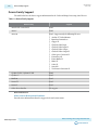
Contents
Video and Image Processing Suite Overview..................................................... 1-1
Release Information.....................................................................................................................................1-3
Device Family Support................................................................................................................................ 1-4
Latency...........................................................................................................................................................1-5
In-System Performance and Resource Guidance....................................................................................1-8
Stall Behavior and Error Recovery.......................................................................................................... 1-12
Interfaces............................................................................................................. 2-1
Video Formats.............................................................................................................................................. 2-2
Avalon-ST Video Protocol..........................................................................................................................2-7
Video Data Packets........................................................................................................................ 2-11
Static Parameters of Video Data Packets....................................................................................2-11
Control Data Packets.....................................................................................................................2-15
Ancillary Data Packets.................................................................................................................. 2-19
User-Defined and Altera-Reserved Packets............................................................................... 2-19
Packet Propagation........................................................................................................................ 2-19
Transmission of Avalon-ST Video Over Avalon-ST Interfaces..............................................2-20
Packet Transfer Examples.............................................................................................................2-21
Avalon-MM Slave Interfaces....................................................................................................................2-25
Specification of the Type of Avalon-MM Slave Interfaces.......................................................2-27
Avalon-MM Master Interfaces.................................................................................................................2-28
Specification of the Type of Avalon-MM Master Interfaces....................................................2-28
Buffering of Non-Image Data Packets in Memory............................................................................... 2-29
Getting Started.................................................................................................... 3-1
IP Catalog and Parameter Editor...............................................................................................................3-1
Specifying IP Core Parameters and Options................................................................................3-2
Installing and Licensing IP Cores.............................................................................................................. 3-2
OpenCore Plus IP Evaluation........................................................................................................ 3-3
Clocked Video Interface IP Cores.......................................................................4-1
Control Port..................................................................................................................................................4-1
Clocked Video Input Format Detection................................................................................................... 4-2
Interrupts.......................................................................................................................................... 4-5
Clocked Video Output Video Modes........................................................................................................4-5
Interrupts.......................................................................................................................................... 4-9
Generator Lock.............................................................................................................................................4-9
Underflow and Overflow.......................................................................................................................... 4-11
Timing Constraints....................................................................................................................................4-12
Handling Ancillary Packets...................................................................................................................... 4-12
Altera Corporation
TOC-3
Modules for Clocked Video Input II IP Core........................................................................................ 4-15
Clocked Video Interface Parameter Settings......................................................................................... 4-18
Clocked Video Interface Signals.............................................................................................................. 4-26
Clocked Video Interface Control Registers............................................................................................4-36
2D FIR Filter IP Core.......................................................................................... 5-1
Calculation Precision...................................................................................................................................5-1
Coefficient Precision....................................................................................................................................5-2
Result to Output Data Type Conversion.................................................................................................. 5-2
2D FIR IP Core Parameter Settings...........................................................................................................5-2
2D FIR Filter Signals....................................................................................................................................5-4
2D FIR Filter Control Registers................................................................................................................. 5-5
Video Mixing IP Cores........................................................................................ 6-1
Alpha Blending.............................................................................................................................................6-2
Video Mixing Parameter Settings..............................................................................................................6-3
Video Mixing Signals...................................................................................................................................6-5
Video Mixing Control Registers................................................................................................................ 6-8
Chroma Resampler IP Core................................................................................ 7-1
Horizontal Resampling (4:2:2)................................................................................................................... 7-1
4:4:4 to 4:2:2...................................................................................................................................... 7-2
4:2:2 to 4:4:4...................................................................................................................................... 7-2
Vertical Resampling (4:2:0)........................................................................................................................ 7-3
Chroma Resampler Parameter Settings.................................................................................................... 7-4
Chroma Resampler Signals.........................................................................................................................7-5
Video Clipping IP Cores..................................................................................... 8-1
Video Clipping Parameter Settings........................................................................................................... 8-1
Video Clipping Signals................................................................................................................................8-4
Video Clipping Control Registers..............................................................................................................8-6
Color Plane Sequencer IP Core...........................................................................9-1
Combining Color Patterns..........................................................................................................................9-1
Rearranging Color Patterns........................................................................................................................9-2
Splitting and Duplicating............................................................................................................................9-3
Subsampled Data..........................................................................................................................................9-4
Color Plane Sequencer Parameter Settings.............................................................................................. 9-4
Color Plane Sequencer Signals................................................................................................................... 9-5
Color Space Conversion IP Cores..................................................................... 10-1
Input and Output Data Types.................................................................................................................. 10-2
Color Space Conversion............................................................................................................................10-2
Result of Output Data Type Conversion................................................................................................ 10-3
Altera Corporation
TOC-4
Color Space Conversion Parameter Settings..........................................................................................10-4
Color Space Conversion Signals.............................................................................................................. 10-8
Color Space Conversion Control Registers..........................................................................................10-10
Control Synchronizer IP Core.......................................................................... 11-1
Using the Control Synchronizer IP Core............................................................................................... 11-2
Control Synchronizer Parameter Settings..............................................................................................11-4
Control Synchronizer Signals...................................................................................................................11-5
Control Synchronizer Control Registers................................................................................................ 11-6
Deinterlacing IP Cores...................................................................................... 12-1
Deinterlacing Methods..............................................................................................................................12-2
Bob with Scanline Duplication.....................................................................................................12-3
Bob with Scanline Interpolation.................................................................................................. 12-3
Weave.............................................................................................................................................. 12-3
Motion-Adaptive........................................................................................................................... 12-3
Pass-Through Mode for Progressive Frames.............................................................................12-6
Frame Buffering......................................................................................................................................... 12-6
Frame Rate Conversion.............................................................................................................................12-8
Bandwidth Requirement Calculations for 10-bit YCbCr Video......................................................... 12-8
Behavior When Unexpected Fields are Received.................................................................................. 12-9
Handling of Avalon-ST Video Control Packets.................................................................................. 12-10
Deinterlacing Parameter Settings.......................................................................................................... 12-10
Deinterlacing Signals...............................................................................................................................12-17
Deinterlacing Control Registers............................................................................................................ 12-23
Design Guidelines for Broadcast Deinterlacer IP Core......................................................................12-30
Tuning Motion Shift....................................................................................................................12-32
Active Video Threshold Adjustment........................................................................................ 12-32
Frame Reader IP Core....................................................................................... 13-1
Single-Cycle Color Patterns......................................................................................................................13-1
Frame Reader Output Pattern and Memory Organization..................................................................13-2
Frame Reader Parameter Settings............................................................................................................13-3
Frame Reader Signals................................................................................................................................ 13-3
Frame Reader Control Registers..............................................................................................................13-5
Frame Buffer IP Cores.......................................................................................14-1
Double Buffering........................................................................................................................................14-2
Triple Buffering..........................................................................................................................................14-2
Locked Frame Rate Conversion...............................................................................................................14-3
Handling of Avalon-ST Video Control Packets.................................................................................... 14-3
Color Format.............................................................................................................................................. 14-4
Frame Buffer Parameter Settings.............................................................................................................14-5
Frame Buffer Signals..................................................................................................................................14-9
Frame Buffer Control Registers............................................................................................................. 14-13
Altera Corporation
TOC-5
Gamma Corrector IP Core................................................................................ 15-1
Gamma Corrector Parameter Settings....................................................................................................15-1
Gamma Corrector Signals........................................................................................................................ 15-2
Gamma Corrector Control Registers...................................................................................................... 15-3
Interlacer IP Core.............................................................................................. 16-1
Interlacer Parameter Settings................................................................................................................... 16-2
Interlacer Signals........................................................................................................................................16-2
Interlacer Control Registers..................................................................................................................... 16-4
Scaler II IP Core.................................................................................................17-1
Nearest Neighbor Algorithm................................................................................................................... 17-1
Bilinear Algorithm.....................................................................................................................................17-2
Bilinear Algorithmic Description................................................................................................ 17-2
Polyphase and Bicubic Algorithm........................................................................................................... 17-3
Double-Buffering........................................................................................................................... 17-5
Polyphase Algorithmic Description............................................................................................ 17-6
Choosing and Loading Coefficients............................................................................................ 17-6
Edge-Adaptive Scaling Algorithm...........................................................................................................17-8
Scaler II Parameter Settings......................................................................................................................17-9
Scaler II Signals........................................................................................................................................ 17-12
Scaler II Control Registers...................................................................................................................... 17-14
Video Switching IP Cores..................................................................................18-1
Mixer Layer Switching.............................................................................................................................. 18-2
Video Switching Parameter Settings....................................................................................................... 18-3
Video Switching Signals............................................................................................................................18-3
Video Switching Control Registers......................................................................................................... 18-5
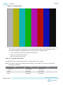
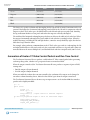
Test Pattern Generator IP Cores.......................................................................19-1
Test Pattern.................................................................................................................................................19-1
Generation of Avalon-ST Video Control Packets and Run-Time Control....................................... 19-3
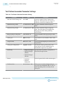
Test Pattern Generator Parameter Settings............................................................................................19-4
Test Pattern Generator Signals................................................................................................................ 19-6
Test Pattern Generator Control Registers.............................................................................................. 19-8
Trace System IP Core........................................................................................ 20-1
Trace System Parameter Settings.............................................................................................................20-2
Trace System Signals................................................................................................................................. 20-3
Operating the Trace System from System Console...............................................................................20-4
Loading the Project and Connecting to the Hardware.............................................................20-5
Trace Within System Console......................................................................................................20-6
TCL Shell Commands................................................................................................................... 20-7
Altera Corporation
TOC-6
Avalon-ST Video Monitor IP Core................................................................... 21-1
Packet Visualization.................................................................................................................................. 21-2
Monitor Settings........................................................................................................................................ 21-3
Avalon-ST Video Monitor Parameter Settings......................................................................................21-3
Avalon-ST Video Monitor Signals.......................................................................................................... 21-4
Avalon-ST Video Monitor Control Registers........................................................................................21-6
Avalon-ST Video Verification IP Suite..............................................................A-1
Avalon-ST Video Class Library.................................................................................................................A-2
Running the Tests....................................................................................................................................... A-7
Video File Reader Test................................................................................................................. A-10
Constrained Random Test...........................................................................................................A-15
Complete Class Reference........................................................................................................................A-19
c_av_st_video_control ................................................................................................................ A-19
c_av_st_video_data ......................................................................................................................A-21
c_av_st_video_file_io .................................................................................................................. A-21
c_av_st_video_item ..................................................................................................................... A-26
c_av_st_video_source_sink_base .............................................................................................. A-27
c_av_st_video_sink_bfm_’SINK ................................................................................................A-28
c_av_st_video_source_bfm_’SOURCE .....................................................................................A-29
c_av_st_video_user_packet ........................................................................................................ A-30
c_pixel ............................................................................................................................................A-31
Raw Video Data Format...........................................................................................................................A-31
Choosing the Correct Deinterlacer.................................................................... B-1
Cadence Detection and Reverse Pulldown in the Deinterlacer II IP Core..........................................B-3
Additional Information......................................................................................C-1
Document Revision History...................................................................................................................... C-1
How to Contact Altera............................................................................................................................... C-5
Altera Corporation
1
Video and Image Processing Suite Overview
2015.05.04
UG-VIPSUITE
Send Feedback
Subscribe
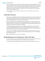
The Altera® Video and Image Processing Suite collection of IP cores ease the development of video and
image processing designs.
You can use these IP cores in a wide variety of image processing and display applications.
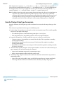
Attention: Altera has scheduled the following IP cores for product obsolescence and will discontinue
support for it.
• Clipper
• Test Pattern Generator
Altera recommends that you do not use these IP cores in new designs. For more information
about Altera’s current IP offering, visit the Altera Intellectual Property web page.
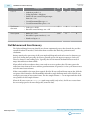
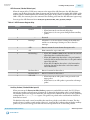
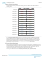
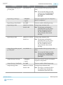
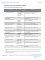
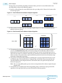
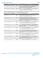
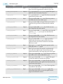
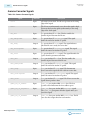
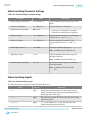
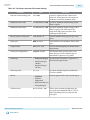
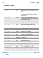
Table 1-1: Video and Image Processing Suite IP Core Features
The table lists the IP cores in the Video and Image Processing Suite.
IP Core
(1)
(2)
Feature Support
Pixels in Parallel
4:2:2 Support
Interlaced
2D FIR Filter
No
No
No
Alpha Blending
Mixer
No
Yes
Yes (1)
Chroma Resampler
No
Yes
No
Clipper
No
Yes
Yes (2)
Clipper II
Yes
Yes
Yes (2)
Clocked Video
Input (CVI)
No
Yes
Yes
Clocked Video
Input II (CVI II)
Yes
Yes
Yes
The IP core accepts interlaced input streams but they are treated as progressive inputs. Consequently, you
require external logic to synchronize the input fields and prevent the mixing of F0 fields with F1 fields.
The IP core accepts interlaced inputs but they are treated as progressive inputs.
2015 Altera Corporation. All rights reserved. ALTERA, ARRIA, CYCLONE, ENPIRION, MAX, MEGACORE, NIOS, QUARTUS and STRATIX words and logos are
trademarks of Altera Corporation and registered in the U.S. Patent and Trademark Office and in other countries. All other words and logos identified as
trademarks or service marks are the property of their respective holders as described at www.altera.com/common/legal.html. Altera warrants performance
of its semiconductor products to current specifications in accordance with Altera's standard warranty, but reserves the right to make changes to any
products and services at any time without notice. Altera assumes no responsibility or liability arising out of the application or use of any information,
product, or service described herein except as expressly agreed to in writing by Altera. Altera customers are advised to obtain the latest version of device
specifications before relying on any published information and before placing orders for products or services.
©
www.altera.com
101 Innovation Drive, San Jose, CA 95134
ISO
9001:2008
Registered
1-2
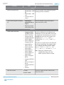
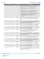
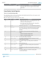
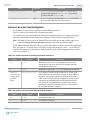
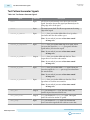
IP Core
(3)
(4)
UG-VIPSUITE
2015.05.04
Video and Image Processing Suite Overview
Feature Support
Pixels in Parallel
4:2:2 Support
Interlaced
Clocked Video
Output (CVO)
No
Yes
Yes
Clocked Video
Output II (CVO II)
Yes
Yes
Yes
Color Plane
Sequencer
No
Yes
Yes
Color Space
Converter (CSC)
No
No
Yes
Color Space
Converter II (CSC
II)
Yes
No
Yes
Control Synchron‐
izer
No
Yes
Yes
Deinterlacer
No
Yes
Yes
Deinterlacer II
No
Yes
Yes
Broadcast Deinter‐
lacer
No
Yes
Yes
Frame Buffer
No
Yes
Yes
Frame Buffer II
Yes
Yes
Yes
Frame Reader
No
Yes
Yes
Gamma Corrector
No
Yes
Yes
Interlacer
No
Yes
Yes (3)
Mixer II
Yes
Yes
Yes (1)
Scaler II
No
Yes
Yes (2)
Switch
No
Yes
Yes
Switch II
Yes
Yes
Yes
Test Pattern
Generator
No
Yes
Yes (4)
Test Pattern
Generator II
Yes
Yes
Yes (4)
The IP core either discards or propagates without change the interlaced data if you select Pass-through
mode in the parameter editor.
For interlaced data NTSC, mismatched line counts of F0 and F1 are not supported.
Altera Corporation
Video and Image Processing Suite Overview
Send Feedback
UG-VIPSUITE
2015.05.04
Release Information
1-3
Release Information
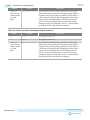
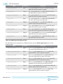
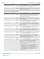
The following table lists information about this release of the Video and Image Processing Suite.
Table 1-2: Release Information
Item
Version
Description
15.0
Release Date May 2015
Ordering
Code
IPS-VIDEO (Video and Image Processing Suite)
Product ID
00B3 (2D FIR Filter)
00B5 (Alpha Blending
Mixer)
0115 (Mixer II)
00D1 (Avalon-ST Video
Monitor)
00B1 (Chroma Resampler)
00C8 (Clipper)
0115 (Clipper II)
00C4 (Clocked Video
Input)
00F1 (Clocked Video
Input II)
00C5 (Clocked Video
Output)
Vendor ID
00EF (Clocked Video
Output II)
00C9 (Color Plane
Sequencer)
0003 (Color Space
Converter)
00F2 (Color Space
Converter II)
00D0 (Control Synchron‐
izer)
00B6 (Deinterlacer)
0115 (Frame Buffer II)
00B2 (Gamma Corrector)
00DC (Interlacer)
00E9 (Scaler II)
00CF (Switch)
00F4 (Switch II)
00CA (Test Pattern Generator)
00F3 (Test Pattern Generator II)
00ED (Trace System)
00EE (Deinterlacer II)
0114 (Broadcast Deinter‐
lacer)
0112 (Frame Reader)
00C3 (Frame Buffer)
6AF7
Altera verifies that the current version of the Quartus II software compiles the previous version of each IP
core, if this IP core was included in the previous release. Any exceptions to this verification are reported in
the MegaCore IP Library Release Notes and Errata. Altera does not verify compilation with IP core
versions older than the previous release.
Related Information
• Altera IP Library Release Notes
• Errata for VIP Suite in the Knowledge Base
Video and Image Processing Suite Overview
Send Feedback
Altera Corporation
1-4
UG-VIPSUITE
2015.05.04
Device Family Support
Device Family Support
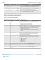
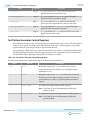
The table below lists the device support information for the Video and Image Processing Suite IP cores.
Table 1-3: Device Family Support
Device Family
Support
Arria II GX / Arria II GZ
Final
Arria V
Final
Arria 10
Final—Supports only the following IP cores:
•
•
•
•
•
•
•
•
•
•
•
•
•
•
Avalon-ST Video Monitor
Broadcast Deinterlacer
Clipper II
Clocked Video Input
Clocked Video Input II
Clocked Video Output
Clocked Video Output II
Color Space Converter II
Deinterlacer II
Frame Buffer II
Mixer II
Scaler II
Switch II
Test Pattern Generator II
Cyclone IV ES / Cyclone IV GX
Final
Cyclone V
Final
MAX 10
Final
Stratix IV
Final
Stratix V
Final
Other device families
No support
Related Information
What's New for IP in Quartus II Software
Provides more information about the support levels and current status.
Altera Corporation
Video and Image Processing Suite Overview
Send Feedback
UG-VIPSUITE
2015.05.04
Latency
1-5
Latency
You can use the latency information to predict the approximate latency between the input and the output
of your video processing pipeline.
The latency is described using one or more of the following measures:
•
•
•
•
the number of progressive frames
the number of interlaced fields
the number of lines when less than a field of latency
a small number of cycles O (cycles)
Note: O refers to a small number of clock cycles, and is not of zero value.
The latency is measured with the assumption that the IP core is not being stalled by other functions on the
data path; (the output ready signal is high).
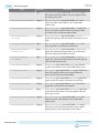
Table 1-4: Video and Image Processing Suite Latency
The table below lists the approximate latency from the video data input to the video data output for typical usage
modes of the Video and Image Processing Suite IP cores.
IP Core
Mode
Latency
2D FIR Filter Latency
Filter size: N × N
(N–1) lines + O (cycles)
Alpha Blending Mixer/ Mixer II
All modes
O (cycles)
Input format: 4:2:2; Output
format: 4:4:4
O (cycles)
Input format: 4:2:0; Output
format: 4:4:4 or 4:2:2
1 line + O (cycles)
Clipper/ Clipper II
All modes
O (cycles)
Clocked Video Input
• Synchronization signals:
Embedded in video
• Video in and out use the
same clock: On
8 cycles
• Synchronization signals: On
separate wires
• Video in and out use the
same clock: On
5 cycles
Chroma Resampler
Note: Add 1 cycle if you turned
on the Allow color planes
in sequence input
parameter.
Video and Image Processing Suite Overview
Send Feedback
Altera Corporation
1-6
UG-VIPSUITE
2015.05.04
Latency
IP Core
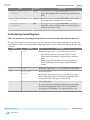
Clocked Video Input II
Clocked Video Output/
Clocked Video Output II
Note: Add 1 cycle if you turned
on the Allow color planes
in sequence input
parameter.
Mode
Latency
• Synchronization signals:
Embedded in video
• Video in and out use the
same clock: On
10 cycles
• Synchronization signals: On
separate wires
• Video in and out use the
same clock: On
6 cycles
All modes with video in and out 3 cycles
use the same clock: On
Note: Note: Minimum latency
case when video input
and output rates are
synchronized.
Color Plane Sequencer
All modes
O (cycles)
Color Space Converter (CSC)/
All modes
O (cycles)
All modes
O (cycles)
Color Space Converter II
Control Synchronizer
Altera Corporation
Video and Image Processing Suite Overview
Send Feedback
UG-VIPSUITE
2015.05.04
Latency
IP Core
Deinterlacer
Deinterlacer II
Video and Image Processing Suite Overview
Send Feedback
Mode
1-7
Latency
• Method: Bob
• Frame buffering: None
O (cycles)
• Method: Motion-adaptive or
Weave
• Frame buffering: Double or
triple buffering with rate
conversion
• Output frame rate: As input
frame rate
1 frame + O (lines)
• Method: Motion-adaptive or
Weave
• Frame buffering: Double or
triple buffering with rate
conversion
• Output frame rate: As input
field rate
1 field + O (lines)
• Method: All
• Frame buffering: Double or
triple buffering with rate
conversion
• Passthrough mode
(propagate progressive
frames unchanged): On.
1 frame + O (lines)
• Method: Motion-adaptive
• Frame buffering: None
• Output frame rate: As input
field rate
2 lines
Altera Corporation
1-8
UG-VIPSUITE
2015.05.04
In-System Performance and Resource Guidance
IP Core
Broadcast Deinterlacer
Mode
Latency
• Method: Motion-adaptive
• Frame buffering: None
• Output frame rate: As input
field rate
1 field + 2 lines
• Method: Motion-adaptive,
video-over-film mode
• Frame buffering: 3 input
fields are buffered
• Output frame rate: As input
field rate
1 field + 2 lines, or 2 lines
40% to 60% (depending on
phasing) of the time, the core
performs a weave forward so
there is no initial field of latency.
Frame Buffer/ Frame Buffer II
All modes
1 frame + O (lines)
Frame Reader
No latency issues.
Gamma Corrector
All modes
O (cycles)
Interlacer
All modes
O (cycles)
Scaler II
• Scaling algorithm: Polyphase (N–1) lines + O (cycles)
• Number of vertical taps: N
Switch/ Switch II
All modes
Test Pattern Generator/
No latency issues.
2 cycles
Test Pattern Generator II
In-System Performance and Resource Guidance
The performance and resource data provided for your guidance.
Note: Run your own synthesis and fMAX trials to confirm the listed IP cores meet your system require‐
ments.
Altera Corporation
Video and Image Processing Suite Overview
Send Feedback
UG-VIPSUITE
2015.05.04
1-9
In-System Performance and Resource Guidance
Table 1-5: Performance and Resource Data Using Arria V Devices
The following data are obtained through a 4K test design example using an Arria V device (5AGXFB3H4F35C4).
The general settings for the design is 8 bits per color plane; 2 pixels in parallel. The target fMAX is 148.5 MHz.
IP Core
Configuration
ALM
RAM
DSP
Mixer II
•
•
•
•
Number of color planes in parallel = 3
Inputs = 4
Output = 1
Internal Test Pattern Generator
1,591
0
0
Clocked Video
Input II
•
•
•
•
Number of color planes in parallel = 3
Sync signals = On separate wires
Pixel FIFO size = 4096 pixels
Use control port = On
540
26
0
Clocked Video
Output II
•
•
•
•
•
Number of color planes in parallel = 3
Sync signals = On separate wires
Pixel FIFO size = 4096 pixels
Use control port = On
Run-time configurable video modes = 4
2,504
49
0
Color Space
Converter II
• Run-time control = On
• Color model conversion = RGb to YCbCr
1,515
0
18
Broadcast Deinter‐ • Number of color planes in parallel = 2
lacer
• Avalon-MM master local ports width =
256
• FIFO depths = 512
• Run-time control = Off
11,516
145
34
Frame Buffer II
•
•
•
•
•
1,472
19
0
Test Pattern
Generator II
• Color space = RGB
• Run-time control of image size = On
135
0
0
Number of color planes in parallel = 2
Avalon-MM master ports width = 256
Read/write FIFO depth = 128
Frame dropping = On
Frame repeating = On
Video and Image Processing Suite Overview
Send Feedback
Altera Corporation
1-10
UG-VIPSUITE
2015.05.04
In-System Performance and Resource Guidance
Table 1-6: Performance and Resource Data Using Cyclone V Devices
The following data are obtained through a video design example using a Cyclone V device (5CGTFD9E5F35C7).
The general setting for the design is 8 bits per color plane. The target fMAX is 100 MHz.
IP Core
Configuration
ALM
RAM
DSP
Number of color planes in sequence = 3
Filter size = 3×3
Runtime control = On
Integer bits = 4
Fractional bits = 3
581
10
3
2D FIR Filter
•
•
•
•
•
Avalon-ST Video
Monitor
• Number of color planes in parallel = 3
• Capture video pixel data = On
1,035
10
0
Avalon-ST Video
Monitor
• Number of color planes in parallel = 3
• Capture video pixel data = Off
479
9
0
Alpha Blending
Mixer
• Number of color planes in parallel = 3
• Number of layers being mixed = 5
• Alpha blending = On
1,324
1
24
Chroma
Resampler
• 4:2:2, number of color planes in parallel
(din) = 2
• 4:4:4, number of color planes in parallel
(dout) = 3
• Horizontal filtering algorithm = Filtered
• Luma adaptive = On
591
0
0
Clipper II
• Number of pixels (color planes) in parallel
=3
• Clipping method = Rectangle
• Enable runtime control of clipping
parameters = On
402
0
0
Clocked Video
Input
•
•
•
•
Number of color planes in parallel = 3
Sync signals = On separate wires
Pixel FIFO size = 2048 pixels
Use control port = On
257
13
0
Clocked Video
Input
•
•
•
•
Number of color planes in sequence = 2
Sync signals = Embedded
Pixel FIFO size = 2048 pixels
Use control port = On
317
9
0
Altera Corporation
Video and Image Processing Suite Overview
Send Feedback
UG-VIPSUITE
2015.05.04
1-11
In-System Performance and Resource Guidance
IP Core
Configuration
ALM
RAM
DSP
Number of color planes in parallel = 3
Sync signals = On separate wires
Pixel FIFO size = 1024 pixels
Use control port = On
Run-time configurable video modes = 1
512
5
0
Clocked Video
Output
•
•
•
•
•
Color Plane
Sequencer
• din0: Color planes in parallel = 4
• dout0: Color planes in parallel = 3
• dout1: Color planes in parallel = 1
104
0
0
Color Space
Converter
• Color plane configuration = Three color
planes in parallel
• Run-time control = Off
• Color model conversion = CbCrY': SDTV
to Computer B'G'R'
• Coefficients integer bits = 2
• Summands integer bits = 9
• Coefficient and summand fractional bits =
8
284
0
9
Deinterlacer II
•
•
•
•
Number of color planes in parallel = 3
Deinterlace algorithm = Motion adaptive
Cadence detection algorithm = 3:2 detector
Avalon-MM master local ports width =
128
• FIFO depths = 64
3,655
67
3
Frame Buffer
•
•
•
•
•
Number of color planes in parallel = 3
Avalon-MM master ports width = 128
Read/write FIFO depth = 64
Frame dropping = On
Frame repetition = On
1,084
19
0
Frame Reader
•
•
•
•
Number of color planes in parallel = 4
Avalon-MM master port width = 128
Read master FIFO depth = 64
Use separate clocks for the Avalon-MM
master interfaces = On
756
6
0
142
3
0
Gamma Corrector Number of color planes in parallel = 3
Video and Image Processing Suite Overview
Send Feedback
Altera Corporation
1-12
UG-VIPSUITE
2015.05.04
Stall Behavior and Error Recovery
IP Core
Configuration
ALM
RAM
DSP
1,010
12
12
Scaler II
• Symbols in parallel = 3
• Scaling algorithm = Polyphase
• Enable run-time control of input/output
frame size = On
• Vertical/horizontal filter taps = 4
• Vertical/horizontal filter phases = 14
Test Pattern
Generator
• Color space = RGB
• Run-time control of image size = Off
65
0
0
Trace System
• Buffer size = 8192
• Bit width of capture interface(s) = 32
• Number of inputs = 2
1,224
12
0
Stall Behavior and Error Recovery
The Video and Image Processing Suite IP cores do not continuously process data. Instead, they use flowcontrolled Avalon-ST interfaces, which allow them to stall the data while they perform internal
calculations.
During control packet processing, the IP cores might stall frequently and read or write less than once per
clock cycle. During data processing, the IP cores generally process one input or output per clock cycle.
There are, however, some stalling cycles. Typically, these are for internal calculations between rows of
image data and between frames/fields.
When stalled, an IP core indicates that it is not ready to receive or produce data. The time spent in the
stalled state varies between IP cores and their parameterizations. In general, it is a few cycles between rows
and a few more between frames.
If data is not available at the input when required, all of the IP cores stall and do not output data. With the
exceptions of the Deinterlacer and Frame Buffer in double or triple-buffering mode, none of the IP cores
overlap the processing of consecutive frames. The first sample of frame F + 1 is not input until after the IP
cores produce the last sample of frame F.
When the IP cores receive an endofpacket signal unexpectedly (early or late), the IP cores recover from
the error and prepare for the next valid packet (control or data).
Altera Corporation
Video and Image Processing Suite Overview
Send Feedback
UG-VIPSUITE
2015.05.04
Stall Behavior and Error Recovery
IP Core
2D FIR Filter
Stall Behavior
• Has a delay of a little more than N–1
lines between data input and output in
the case of a N×N 2D FIR Filter.
• Delay caused by line buffering internal
to the IP core.
1-13
Error Recovery
• Resolution is not configurable at run
time.
• Does not read the control packets
passed through it.
An error condition occurs if an
endofpacket signal is received too early
or too late for the compile time
configured frame size. In either case, the
2D FIR Filter always creates output
video packets of the configured size.
• If an input video packet has a late
endofpacket signal, then the extra
data is discarded.
• If an input video packet has an early
endofpacket signal, then the video
frame is padded with an undefined
combination of the last input pixels.
Video and Image Processing Suite Overview
Send Feedback
Altera Corporation
1-14
UG-VIPSUITE
2015.05.04
Stall Behavior and Error Recovery
IP Core
Alpha Blending
Mixer/
Mixer II
Altera Corporation
Stall Behavior
Error Recovery
The Alpha Blending Mixer IP core
processes video packets from the
background layer until the end of packet
Between frames, the IP core processes nonis received.
image data packets from its input layers in
sequential order. The core may exert
• Receiving an endofpacket signal too
backpressure during the process until the
early for the background layer—the
image data header has been received for all
IP core enters error mode and
its input.
continues writing data until it has
reached the end of the current line.
During the mixing of a frame, the IP core:
The endofpacket signal is then set
• Reads from the background input for
with the last pixel sent.
each non-stalled cycle.
• Receiving an endofpacket signal
• Reads from the input ports associated
early for one of the foreground layers
with layers that currently cover the
or for one of the alpha layers—the IP
background image.
core stops pulling data out of the
corresponding input and pads the
Because of pipelining, the foreground pixel
incomplete frame with undefined
of layer N is read approximately N active
samples.
cycles after the corresponding background
• Receiving an endofpacket signal late
pixel has been read.
for the background layer, one or
• If the output is applying backpressure or
more foreground layers, or one or
if one input is stalling, the pipeline stalls
more alpha layers—the IP core enters
and the backpressure propagates to all
error mode.
active inputs.
This error recovery process maintains
• When alpha blending is enabled, one
the synchronization between all the
data sample is read from each alpha port
inputs and is started once the output
once each time that a whole pixel of data
frame is completed. A large number of
is read from the corresponding input
samples may have to be discarded
port.
during the operation and backpressure
There is no internal buffering in the IP core, can be applied for a long time on most
so the delay from input to output is just a
input layers. Consequently, this error
few clock cycles and increases linearly with recovery mechanism could trigger an
the number of inputs.
overflow at the input of the system.
All modes stall for a few cycles after each
output frame and between output lines.
Video and Image Processing Suite Overview
Send Feedback
UG-VIPSUITE
2015.05.04
Stall Behavior and Error Recovery
IP Core
Chroma
Resampler
Stall Behavior
All modes stall for a few cycles between
frames and between lines.
Latency from input to output varies
depending on the operation mode of the IP
core.
• The only modes with latency of more
than a few cycles are 4:2:0 to 4:2:2 and
4:2:0 to 4:4:4—corresponding to one line
of 4:2:0 data
• The quantities of data input and output
are not equal because this is a ratechanging function.
• Always produces the same number of
lines that it accepts—but the number of
samples in each line varies according to
the subsampling pattern used.
1-15
Error Recovery
• Receiving an early endofpacket
signal—the IP core stalls its input but
continues writing data until it has
sent an entire frame.
• Not receiving an endofpacket signal
at the end of a frame—the IP core
discards data until it finds end-ofpacket.
When not stalled, always processes one
sample from the more fully sampled side on
each clock cycle. For example, the
subsampled side pauses for one third of the
clock cycles in the 4:2:2 case or half of the
clock cycles in the 4:2:0 case.
Clipper/
Clipper II
Clocked Video
Input/
Clocked Video
Input II
• Stalls for a few cycles between lines and
between frames.
• Internal latency is less than 10 cycles.
• During the processing of a line, it reads
continuously but only writes when
inside the active picture area as defined
by the clipping window.
• Receiving an early endofpacket
signal—the IP core stalls its input but
continues writing data until it has
sent an entire frame.
• Not receiving an endofpacket signal
at the end of a frame—the IP core
discards data until it finds end of
packet.
• Dictated by incoming video.
• If its output FIFO is empty, during
horizontal and vertical blanking periods
the IP core does not produce any video
data.
If an overflow is caused by a
downstream core failing to receive data
at the rate of the incoming video, the
Clocked Video Input sends an
endofpacket signal and restart sending
video data at the start of the next frame
or field.
Video and Image Processing Suite Overview
Send Feedback
Altera Corporation
1-16
UG-VIPSUITE
2015.05.04
Stall Behavior and Error Recovery
IP Core
Clocked Video
Output/
Clocked Video
Output II
Color Plane
Sequencer
Stall Behavior
Error Recovery
• Dictated by outgoing video.
• Receiving an early endofpacket
signal— the IP core resynchronizes
• If its input FIFO is empty, during
the outgoing video data to the
horizontal and vertical blanking periods
incoming video data on the next start
the IP core stalls and does not take in
of packet it receives.
any more video data.
• Receiving a late endofpacket— the
IP core resynchronizes the outgoing
video data to the incoming video
immediately.
• If Genlock functionality is enabled—
the IP core does not resynchronize to
the incoming video.
• Stalls for approximately 10 cycles after
processing each line of a video frame.
• Between frames the IP core stalls for
approximately 30 cycles
• Processes video packets per line until
the IP core receives an endofpacket
signal on din0—the line width is
taken from the control packets on
din0.
• Receiving an endofpacket signal on
either din0 or din1— the IP core
ceases to produce output.
For the number of cycles left to finish
the line, the IP core continues to drain
the inputs that have not indicated end of
packet.
• Drains din0 until it receives an
endofpacket signal on this port
(unless it has already indicated end of
packet), and stalls for up to one line
after this endofpacket signal.
• Signals end of packet on its outputs
and continue to drain its inputs that
have not indicated end of packet.
Color Space
Converter/
Color Space
Converter II
Altera Corporation
• Only stalls between frames and not
between rows.
• It has no internal buffering apart from
the registers of its processing pipeline—
only a few clock cycles of latency.
• Processes video packets until the IP
core receives an endofpacket signal
—the control packets are not used.
• Any mismatch of the endofpacket
signal and the frame size is
propagated unchanged to the next IP
core.
Video and Image Processing Suite Overview
Send Feedback
UG-VIPSUITE
2015.05.04
Stall Behavior and Error Recovery
IP Core
Stall Behavior
1-17
Error Recovery
Control
Synchronizer
• Stalls for several cycles between packets. • Processes video packets until the IP
core receives an endofpacket signal
• Stalls when it enters a triggered state
—the
image width, height and
while it writes to the Avalon-MM Slave
interlaced fields of the control data
ports of other IP cores.
packets are not compared against the
• If the slaves do not provide a wait
following
video data packet.
request signal, the stall lasts for no more
than 50 clock cycles. Otherwise the stall • Any mismatch of the endofpacket
signal and the frame size of video
is of unknown length.
data packet is propagated unchanged
to the next IP core.
Deinterlacer
• Receiving an endofpacket signal too
early or too late is relative to the field
• While the bob algorithm (with no
dimensions contained in the last
buffering) is producing an output
control packet processed.
frame, it alternates between simulta‐
• Receiving an endofpacket signal too
neously between
late—discards extra data in all
• receiving a row on the input port
configurations.
and producing a row of data on
• Receiving an early endofpacket
the output port
signal when it is configured for no
• just producing a row of data on
buffering—the IP core interrupts its
the output port without reading
processing within one or two lines
any data from the input port
sending undefined pixels, before
propagating the endofpacket signal.
The delay from input to output is just
•
Receiving an early endofpacket
a few clock cycles.
signal when it is configured to buffer
• While a field is being discarded, input
data in external memory—the input
is read at the maximum rate and no
side of the IP core stops processing
output is generated.
input pixels. It is then ready to
• Weave algorithm
process the next frame after writing
• The IP core may stall for longer than
undefined pixels for the remainder of
the usual periods between each
the current line into external RAM.
output row of the image.
The output side of the IP core
assumes that incomplete fields have
• The delays may possibly stretch up to
been fully received and pads the
45 clock cycles due to the time taken
incomplete fields to build a frame,
for internal processing in between
using the undefined content of the
lines.
memory.
• Motion-adaptive algorithm
• Bob algorithm
• The IP core may stall up to 90 clock
cycles.
Video and Image Processing Suite Overview
Send Feedback
Altera Corporation
1-18
UG-VIPSUITE
2015.05.04
Stall Behavior and Error Recovery
IP Core
Deinterlacer II/
Broadcast
Deinterlacer
Stall Behavior
Stores input video fields in the external
memory and concurrently uses these input
video fields to construct deinterlaced
frames.
• Stalls up to 50 clock cycles for the first
output frame.
• Additional delay of one line for second
output frame because the IP core
generates the last line of the output
frame before accepting the first line of
the next input field.
• Delay of two lines for the following
output frames, which includes the one
line delay from the second output frame.
• For all subsequent fields, the delay
alternates between one and two lines.
Frame Reader
Altera Corporation
Error Recovery
• Receiving an endofpacket signal too
early :
• The IP core generates a line with
the correct length.
• The video data in the output
frame is valid up to the point
where the IP core receives the
endofpacket signal.
• The IP core then stops generating
output until it receives the next
startofpacket signal.
• Receiving a late endofpacket signal:
• The IP core completes generating
the current output frame with the
correct number of lines as
indicated by the last control
packet.
• The IP core discards the
subsequent input lines.
• Once it receives a startofpacket
signal, the IP core performs a soft
reset and it loses the stored
cadence or motion values.
• The IP core resumes deinterlacing
when it receives the next
startofpacket signal.
• Stalls the output for several tens of cycles The IP core can be stalled due to
before producing each video data packet. backpressure, without consequences and
it does not require error recovery.
• Stalls the output where there is
contention for access to external
memory.
Video and Image Processing Suite Overview
Send Feedback
UG-VIPSUITE
2015.05.04
Stall Behavior and Error Recovery
IP Core
Frame Buffer/
Frame Buffer II
Stall Behavior
1-19
Error Recovery
• May stall frequently and read or write
• Does not rely on the content of the
less than once per clock cycle during
control packets to determine the size
control packet processing.
of the image data packets.
• During data processing at the input or at • Any early or late endofpacket signal
the output, the stall behavior of the IP
and any mismatch between the size
core is largely decided by contention on
of the image data packet and the
the memory bus.
content of the control packet are
propagated unchanged to the next IP
core.
• Does not write outside the memory
allocated for each non-image and
image Avalon-ST video packet—
packets are truncated if they are
larger than the maximum size
defined at compile time.
Gamma
Corrector
• Stalls only between frames and not
• Processes video packets until the IP
between rows.
core receives an endofpacket signal
—non-image packets are propagated
• Has no internal buffering aside from the
but the content of control packets is
registers of its processing pipeline— only
ignored.
a few clock cycles of latency
• Any mismatch of the endofpacket
signal and the frame size is
propagated unchanged to the next IP
core.
Interlacer
• Alternates between propagating and
• Receiving endofpacket signal later
discarding a row from the input port
than expected—discards extra data.
while producing an interlaced output
• Receiving an early endofpacket
field—the output port is inactive every
signal—the current output field is
other row.
interrupted as soon as possible and
• The delay from input to output is a few
may be padded with a single
clock cycles when pixels are propagated.
undefined pixel.
Video and Image Processing Suite Overview
Send Feedback
Altera Corporation
1-20
UG-VIPSUITE
2015.05.04
Stall Behavior and Error Recovery
IP Core
Scaler II
Stall Behavior
Error Recovery
• The ratio of reads to writes is
• Receiving an early endofpacket
proportional to the scaling ratio and
signal at the end of an input line—the
occurs on both a per-pixel and a per-line
IP core stalls its input but continues
basis.
writing data until it has sent on
further output line.
• The frequency of lines where reads and
writes occur is proportional to the
• Receiving an early endofpacket
vertical scaling ratio.
signal part way through an input line
—the IP core stalls its input for as
• For example scaling up vertically by a
long as it would take for the open
factor of 2 results in the input being
input line to complete; completing
stalled every other line for the length of
any output line that may accompany
time it takes to write one line of output;
that input line. Then continues to
scaling down vertically by a factor of 2
stall the input, and writes one further
results in the output being stalled every
output line.
other line for the length of time it takes
• Not receiving an endofpacket signal
to read one line of input.
at the end of a frame—the IP core
• In a line that has both input and output
discards
extra data until it finds an
active, the ratio of reads and writes is
end of packet.
proportional to the horizontal scaling
ratio. For example, scaling from 64×64
to 128×128 causes 128 lines of output,
where only 64 of these lines have any
reads in them. For each of these 64 lines,
there are two writes to every read.
The internal latency of the IP core depends
on the scaling algorithm and whether any
run time control is enabled. The scaling
algorithm impacts stalling as follows:
• Bilinear mode: a complete line of input
is read into a buffer before any output is
produced. At the end of a frame there
are no reads as this buffer is drained.
The exact number of possible writes
during this time depends on the scaling
ratio.
• Polyphase mode with Nv vertical taps: Nv
– 1 lines of input are read into line
buffers before any output is ready. The
scaling ratio depends on the time at the
end of a frame where no reads are
required as the buffers are drained.
Altera Corporation
Video and Image Processing Suite Overview
Send Feedback
UG-VIPSUITE
2015.05.04
Stall Behavior and Error Recovery
IP Core
Stall Behavior
1-21
Error Recovery
Enabling run-time control of resolutions
affects stalling between frames:
• With no run-time control: about 10
cycles of delay before the stall behavior
begins, and about 20 cycles of further
stalling between each output line.
• With run-time control of resolutions:
about additional 25 cycles of delay
between frames.
Switch/
Switch II
Test Pattern
Generator/
Test Pattern
Generator II
• Only stalls its inputs when performing
an output switch.
• Before switching its outputs, the IP core
synchronizes all its inputs and the inputs
may be stalled during this synchroniza‐
tion.
—
• All modes stall for a few cycles after a
field control packet, and between lines.
• When producing a line of image data,
the IP core produces one sample output
on every clock cycle, but it can be stalled
without consequences if other functions
down the data path are not ready and
exert backpressure.
—
Video and Image Processing Suite Overview
Send Feedback
Altera Corporation
Interfaces
2
2015.05.04
UG-VIPSUITE
Subscribe
Send Feedback
The IP cores in the Video and Image Processing Suite use standard interfaces for data input and output,
control input, and access to external memory. These standard interfaces ensure that video systems can be
quickly and easily assembled by connecting IP cores together.
The IP cores use the following types of interface:
• Avalon-ST interface—a streaming interface that supports backpressure. The Avalon-ST Video
protocol transmits video and configuration data. This interface type allows the simple creation of video
processing data paths, where IP cores can be connected together to perform a series of video
processing functions.
• Avalon-MM slave interface—provides a means to monitor and control the properties of the IP cores.
• Avalon-MM master interface—when the IP cores require access to a slave interface, for example an
external memory controller.
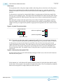
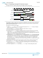
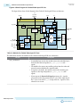
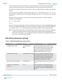
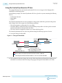
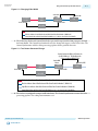
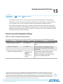
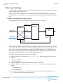
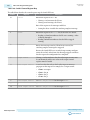
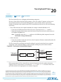
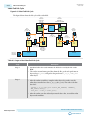
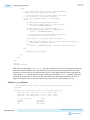
Figure 2-1: Abstracted Block Diagram Showing Avalon-ST and Avalon-MM Connections
The figure below shows an example of video processing data paths using the Avalon-ST and Avalon-MM
interfaces.
Avalon ST Connection
DDR 2 SDRAM
Controller with UniPHY
IP Core
Clocked Video Input
IP Core
Deinterlacer
IP Core
Avalon MM Master to Slave Connection
Scaler II
IP Core
Clocked Video Output
IP Core
Nios II
Processor
Note: This abstracted view is similar to that provided in the Qsys tool, where interface wires are grouped
together as single connections.
© 2015 Altera Corporation. All rights reserved. ALTERA, ARRIA, CYCLONE, ENPIRION, MAX, MEGACORE, NIOS, QUARTUS and STRATIX words and logos are
trademarks of Altera Corporation and registered in the U.S. Patent and Trademark Office and in other countries. All other words and logos identified as
trademarks or service marks are the property of their respective holders as described at www.altera.com/common/legal.html. Altera warrants performance
of its semiconductor products to current specifications in accordance with Altera's standard warranty, but reserves the right to make changes to any
products and services at any time without notice. Altera assumes no responsibility or liability arising out of the application or use of any information,
product, or service described herein except as expressly agreed to in writing by Altera. Altera customers are advised to obtain the latest version of device
specifications before relying on any published information and before placing orders for products or services.
www.altera.com
101 Innovation Drive, San Jose, CA 95134
ISO
9001:2008
Registered
2-2
UG-VIPSUITE
2015.05.04
Video Formats
The Clocked Video Input and Clocked Video Output IP cores also have external interfaces that support
clocked video standards. These IP cores can connect between the function’s Avalon-ST interfaces and
functions using clocked video standards such as BT.656.
Related Information
Avalon Interface Specifications
Provides more information about these interface types.
Video Formats
The Clocked Video Output IP cores create clocked video formats, and Clocked Video Input IP cores
accept clocked video formats.
The IP cores create and accept the following formats:
• Video with synchronization information embedded in the data (in BT656 or BT1120 format)
• Video with separate synchronization (H sync, V sync) signals
The CVO IP cores create a video frame consisting of horizontal and vertical blanking (containing syncs)
and areas of active picture (taken from the Avalon-ST Video input).
• Video with synchronization information embedded in the data (in BT656 or BT1120 format)
• Video with separate synchronization (H sync, V sync) signals
Altera Corporation
Interfaces
Send Feedback
UG-VIPSUITE
2015.05.04
Video Formats
2-3
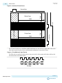
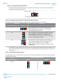
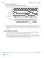
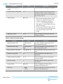
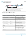
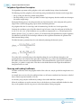
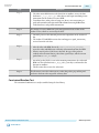
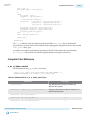
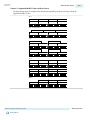
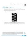
Figure 2-2: Progressive Frame Format
Width
Vertical Sync
Horizontal Blanking
F0 Active Picture
Height
Horizontal Sync
Vertical Blanking
Interfaces
Send Feedback
Altera Corporation
2-4
UG-VIPSUITE
2015.05.04
Video Formats
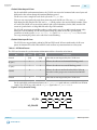
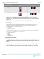
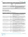
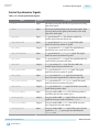
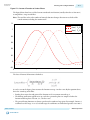
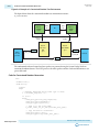
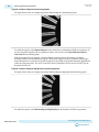
Figure 2-3: Interlaced Frame Format
Horizontal Sync
Height
F0 Active Picture
Field
Width
Width
Vertical Sync
F1 Active Picture
Height
Horizontal Blanking
F0 Vertical Blanking
Vertical Blanking
For CVI and CVO IP cores, the BT656 and BT1120 formats use time reference signal (TRS) codes in the
video data to mark the places where synchronization information is inserted in the data.
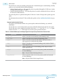
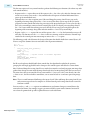
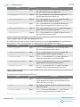
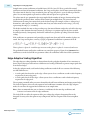
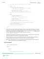
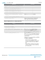
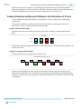
Figure 2-4: Time Reference Signal Format
The TRS codes are made up of values that are not present in the video portion of the data, and they take
the format shown in the figure below.
3FF
0
0
XYZ
TRS (10bit)
Altera Corporation
Interfaces
Send Feedback
UG-VIPSUITE
2015.05.04
Video Formats
2-5
Clocked Video Output IP Cores
For the embedded synchronization format, the CVO IP cores insert the horizontal and vertical syncs and
field into the data stream during the horizontal blanking period.
The IP cores create a sample for each clock cycle on the vid_data bus.
There are two extra signals only used when connecting to the SDI IP core. They are vid_trs, which is
high during the 3FF sample of the TRS, and vid_ln, which produces the current SDI line number. These
are used by the SDI IP core to insert line numbers and cyclical redundancy checks (CRC) into the SDI
stream as specified in the 1.5 Gbps HD SDI and 3 Gbps SDI standards.
The CVO IP cores insert any ancillary packets (packets with a type of 13 or 0xD) into the output video
during the vertical blanking. The IP cores begin inserting the packets on the lines specified in its
parameters or mode registers (ModeN Ancillary Line and ModeN F0 Ancillary Line). The CVO IP
cores stop inserting the packets at the end of the vertical blanking.
Clocked Video Input IP Cores
The CVI IP cores support both 8 and 10-bit TRS and XYZ words. When in 10-bit mode, the IP cores
ignore the bottom 2 bits of the TRS and XYZ words to allow easy transition from an 8-bit system.
Table 2-1: XYZ Word Format
The XYZ word contains the synchronization information and the relevant bits of its format.
Bits
10-bit
8-bit
Description
Unused
[5:0]
[3:0]
H (sync)
6
4
When 1, the video is in a horizontal blanking period.
V (sync)
7
5
When 1, the video is in a vertical blanking period.
F (field)
8
6
When 1, the video is interlaced and in field 1. When 0,
the video is either progressive or interlaced and in field
0.
Unused
9
7
These bits are not inspected by the CVI IP cores.
These bits are not inspected by the CVI IP cores.
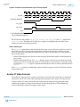
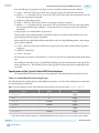
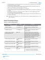
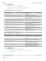
For the embedded synchronization format, the vid_datavalid signal indicates a valid BT656 or BT1120
sample. The CVI IP cores only read the vid_data signal when vid_datavalid is 1.
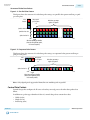
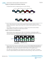
Figure 2-5: Vid_datavalid Timing
vid_data
D0
D1
vid_datavalid
Interfaces
Send Feedback
Altera Corporation
2-6
UG-VIPSUITE
2015.05.04
Video Formats
The CVI IP cores extract any ancillary packets from the Y channel during the vertical blanking. Ancillary
packets are not extracted from the horizontal blanking.
• Clocked Video Input IP core—The extracted packets are produced through the CVI IP cores’ AvalonST output with a packet type of 13 (0xD).
• Clocked Video Input II IP core— The extracted packets are stored in a RAM in the IP core, which can
be read via the control interface.
The extracted packets are produced through the CVI IP cores’ Avalon-ST output with a packet type of 13
(0xD).
For information about Avalon-ST Video ancillary data packets, refer to Ancillary Data Packets on page
2-19.
Separate Synchronization Format
The separate synchronization format uses separate signals to indicate the blanking, sync, and field
information.
The CVO IP cores create horizontal and vertical syncs and field information through their own signals.
The CVO IP cores create a sample for each clock cycle on the vid_data bus. The vid_datavalid signal
indicates when the vid_data video output is in an active picture period of the frame.
Table 2-2: Clocked Video Input and Output Signals for Separate Synchronization Format Video
Signal Name
Description
vid_h_sync
When 1, the video is in a horizontal synchronization period.
vid_v_sync
When 1, the video is in a vertical synchronization period.
vid_f
vid_h
vid_v
vid_de
When 1, the video is interlaced and in field 1. When 0, the video is
either progressive or interlaced and in field 0.
When 1, the video is in a horizontal blanking period, (only for Clocked
Video Output IP core).
When 1, the video is in a vertical blanking period, (only for Clocked
Video Output IP core).
When asserted, the video is in an active picture period (not horizontal
or vertical blanking).
Note: Only for Clocked Video Input IP cores.
vid_datavalid
When asserted, the video is in an active picture period (not horizontal
or vertical blanking).
Note: Only for Clocked Video Output IP cores.
Altera Corporation
Interfaces
Send Feedback
UG-VIPSUITE
2015.05.04
2-7
Avalon-ST Video Protocol
Figure 2-6: Separate Synchronization Signals Timing Diagram
vid_data
D0
D1
DN
Dn+1
Dn+2
vid_de/vid_datavalid (1)
vid_v_sync
vid_h_sync
vid_f
(1): vid_datavalid: Clocked Video Output IP core
vid_de: Clocked Video Input IP core
The CVI IP cores only read the vid_data, vid_de, vid_h_sync, vid_v_sync, and vid_f signals when
vid_datavalid is 1. This allows the CVI IP cores to support oversampling where the video clock is
running at a higher rate than the pixel clock.
Video Locked Signal
The vid_locked signal indicates that the clocked video stream is active. When the signal has a value of 1,
the CVI IP cores take the input clocked video signals as valid, and read and process them as normal.
When the signal has a value of 0 (if for example the video cable is disconnected or the video interface is
not receiving a signal):
• Clocked Video Input IP core: The IP core takes the input clocked video signals as invalid and do not
process them.
• Clocked Video Input II IP core: The vid_clk domain registers of the IP core are held in reset and no
video is processed. The control and Avalon-ST Video interfaces are not held in reset and will respond
as normal. The vid_locked signal is synchronized internally to the IP core and is asynchronous to the
vid_clk.
If the vid_locked signal goes invalid while a frame of video is being processed, the CVI IP cores end the
frame of video early.
Avalon-ST Video Protocol
The Avalon-ST Video protocol is a packet-oriented way to send video and control data over Avalon-ST
connections. The IP cores in the Video and Image Processing Suite use the Avalon-ST Video protocol.
Using the Avalon-ST Video protocol allows the construction of image processing data paths which
automatically configure to changes in the format of the video being processed. This minimizes the
external control logic required to configure a video system.
Interfaces
Send Feedback
Altera Corporation
2-8
UG-VIPSUITE
2015.05.04
Avalon-ST Video Protocol
Table 2-3: Avalon-ST Video Protocol Parameters
Parameter Values
IP Cores
Frame Width/
Height
Interlaced/
Progressive
Bits per Color
Sample
Color Pattern
2D FIR Filter
User-defined— Progressive
through
parameter editor
User-defined— One, two, or three
through
channels in sequence.
parameter editor
Alpha Blending Mixer
Run-time
controlled
Progressive
User-defined— • din and dout: One,
through
two or three
parameter editor
channels in
sequence
Specified
•
alpha_in: A single
separately for
color plane
image data and
representing the
alpha blending.
alpha value for each
pixel
Mixer II
No run-time
control
Progressive
User-defined— Two or three channels
through
in parallel.
parameter editor
Chroma Resampler
Run-time
controlled
Progressive
User-defined— User-defined—through
through
parameter editor
parameter editor
Clipper/Clipper II
Run-time
controlled
Either one—
User-defined—
interlaced inputs through
are accepted but parameter editor
treated as
progressive
inputs.
Any combination of
one, two, three, or four
channels in each of
sequence or parallel.
Color Plane Sequencer Run-time
controlled
Either one
User-defined— User-defined—through
through
parameter editor
parameter editor
Color Space Converter Run-time
controlled
Either one
User-defined— Three color planes in
through
parallel or sequence
parameter editor
Color Space Converter No run-time
II
control
Either one
User-defined— Three color planes in
through
parallel or sequence
parameter editor
Control Synchronizer
Run-time
controlled
User-defined— Up to four color planes
through
in parallel, with any
parameter editor number of color planes
in sequence.
Altera Corporation
Run-time
controlled
Interfaces
Send Feedback
UG-VIPSUITE
2015.05.04
Avalon-ST Video Protocol
2-9
Parameter Values
IP Cores
Frame Width/
Height
Interlaced/
Progressive
Bits per Color
Sample
Color Pattern
Deinterlacer
Run-time
controlled
Interlaced input
and progressive
output (plus
optional
passthrough
mode for
progressive
input)
User-defined— • One, two, or three
through
channels in
parameter editor
sequence
• alpha_in: A single
color plane
representing the
alpha value for each
pixel
Deinterlacer II
Run-time
controlled
Interlaced input
and progressive
output (plus
passthrough
mode for
progressive
input)
User-defined— Any combination of
through
two or three channels
parameter editor in each of parallel.
Broadcast Deinterlacer Run-time
controlled
Interlaced input
and progressive
output (plus
passthrough
mode for
progressive
input)
User-defined— Two channels in
through
parallel (4:2:2 only)
parameter editor
Frame Reader
User-defined—
through AvalonMM slave
control port
User-defined— User-defined—
through Avalon- through
MM slave
parameter editor
control port
Frame Buffer
Run-time
controlled
Progressive; in
some cases
interlaced data
accepted
User-defined— Any combination of
through
one, two, three, or four
parameter editor channels in each of
sequence or parallel.
Frame Buffer II
No run-time
control
Progressive
inputs only
User-defined— Any combination of
through
one, two, three, or four
parameter editor channels in each of
parallel.
Gamma Corrector
Run-time
controlled
Either one
User-defined— One, two or three
through
channels in sequence
parameter editor or parallel.
Interfaces
Send Feedback
Up to four color planes
in parallel, with up to
three color planes in
sequence.
Altera Corporation
2-10
UG-VIPSUITE
2015.05.04
Avalon-ST Video Protocol
Parameter Values
IP Cores
Interlacer
Frame Width/
Height
Run-time
controlled
Interlaced/
Progressive
Bits per Color
Sample
Color Pattern
Progressive;
User-defined— One, two or three
interlaced data is through
channels in sequence
either discarded parameter editor or parallel.
or propagated
without change
in parameter
editor
Test Pattern Generator User-defined— User-defined— User-defined— One, two or three
through
through
through
channels in sequence
parameter editor parameter editor parameter editor or parallel.
or run-time
controlled
Test Pattern Generator User-defined— User-defined— User-defined— RGB 4:4:4 or YCbCr
II
through
through
through
4:4:4, 4:2:2 or 4:2:0 in
parameter editor parameter editor parameter editor parallel or sequence.
or run-time
controlled
Packets
The packets of the Avalon-ST Video protocol are split into symbols—each symbol represents a single
piece of data. For all packet types on a particular Avalon-ST interface, the number of symbols sent in
parallel (that is, on one clock cycle) and the bit width of all symbols is fixed. The symbol bit width and
number of symbols sent in parallel defines the structure of the packets.
The functions predefine the following three types of packet:
• Video data packets containing only uncompressed video data
• Control data packets containing the control data configure the cores for incoming video data packets
• Ancillary (non-video) data packets containing ancillary packets from the vertical blanking period of a
video frame
Another seven packet types are reserved for users, and five packet types reserved for future definition by
Altera.
The packet type is defined by a 4-bit packet type identifier. This type identifier is the first value of any
packet. It is the symbol in the least significant bits of the interface. Functions do not use any symbols in
parallel with the type identifier.
Table 2-4: Avalon-ST Video Packet Types
Type Identifier
Description
0
Video data packet
1–8
User packet types
9–12
Reserved for future Altera use
Altera Corporation
Interfaces
Send Feedback
UG-VIPSUITE
2015.05.04
Video Data Packets
Type Identifier
2-11
Description
13
Ancillary data packet
14
Reserved for future Altera use
15
Control data packet
Figure 2-7: Packet Structure
Data of the packet
(Split into symbols)
X
Start
Symbols can be
transmitted in parallel
(2 in this example)
End
Packet type identifier
(4 bits in least significant symbol,
X’s for unused symbols)
The Avalon-ST Video protocol is designed to be most efficient for transferring video data, therefore the
symbol bit width and the number of symbols transferred in parallel (that is, in one clock cycle) are defined
by the parameters of the video data packet types.
Video Data Packets
Video data packets transmit video data between the IP cores.
A video data packet contains the color plane values of the pixels for an entire progressive frame or an
entire interlaced field.
The IP core sends the video data per pixel in a raster scan order. The pixel order is as follows:
1.
2.
3.
4.
From the top left of the image right wards along the horizontal line.
At the end of the current line, jump to the left most pixel of the next horizontal line down.
Go rightwards along the horizontal line.
Repeat steps 2 and 3 until the bottom right pixel is reached and the frame has been sent.
Static Parameters of Video Data Packets
Two static parameters specify the Avalon-ST interface that video systems use—bits per pixel per color
plane and color pattern.
Bits Per Pixel Per Color Plane
The maximum number of bits that represent each color plane value within each pixel. For example,
R’G’B’ data of eight bits per sample (24 bits per pixel) would use eight bits per pixel per color plane.
Note: This parameter also defines the bit width of symbols for all packet types on a particular Avalon-ST
interface. An Avalon-ST interface must be at least four bits wide to fully support the Avalon-ST
Video protocol.
Interfaces
Send Feedback
Altera Corporation
2-12
UG-VIPSUITE
2015.05.04
Static Parameters of Video Data Packets
Color Pattern
The organization of the color plane samples within a video data packet is referred to as the color pattern.
This parameter also defines the bit width of symbols for all packet types on a particular Avalon-ST
interface. An Avalon-ST interface must be at least four bits wide to fully support the Avalon-ST Video
protocol.
A color pattern is represented as a matrix which defines a repeating pattern of color plane samples that
make up a pixel (or multiple pixels). The height of the matrix indicates the number of color plane samples
transmitted in parallel, the width determines how many cycles of data are transmitted before the pattern
repeats.
Each color plane sample in the color pattern maps to an Avalon-ST symbol. The mapping is such that
color plane samples on the left of the color pattern matrix are the symbols transmitted first. Color plane
samples on the top are assigned to the symbols occupying the most significant bits of the Avalon-ST data
signal.
Figure 2-8: Symbol Transmission Order
Symbol transmitted first
B
G
Symbol in most significant bits
R
R
G
Symbol in least significant bits
Symbol transmitted last
B
Note: The number of color plane samples transmitted in parallel (that is, in one clock cycle) defines the
number of symbols transmitted in parallel for all packet types on a particular Avalon-ST interface.
A color pattern can represent more than one pixel. This is the case when consecutive pixels contain
samples from different color planes. There must always be at least one common color plane between all
pixels in the same color pattern. Color patterns representing more than one pixel are identifiable by a
repeated color plane name. The number of times a color plane name is repeated is the number of pixels
represented.
Figure 2-9: Horizontally Subsampled Y'CbCr
The figure below shows two pixels of horizontally subsampled Y'CbCr (4:2:2) where Cb and Cr alternate
between consecutive pixels.
Y
Y
Cb Cr
In the common case, each element of the matrix contains the name of a color plane from which a sample
must be taken. The exception is for vertically sub sampled color planes. These are indicated by writing the
names of two color planes in a single element, one above the other.
Altera Corporation
Interfaces
Send Feedback
UG-VIPSUITE
2015.05.04
Static Parameters of Video Data Packets
2-13
Figure 2-10: Vertically Subsampled Y'CbCr
The figure below samples from the upper color plane transmitted on even rows and samples from the
lower plane transmitted on odd rows.
Plane for even rows
Y
Cb
Cr
Y
Plane for odd rows
Table 2-5: Examples of Static Avalon-ST Video Data Packet Parameters
The table below lists the static parameters and gives some examples of how you can use them.
Parameter
Bits per Color Sample
8
Description
Color Pattern
B
G
10
Three color planes, B’, G’, and R’ are transmitted in
alternating sequence and each B’, G’, or R’ sample is
represented using 8 bits of data.
R
Three color planes are transmitted in parallel, leading to
higher throughput than when transmitted in sequence,
usually at higher cost. Each R’, G’, or B’ sample is
represented using 10 bits of data, so that, in total, 30 bits
of data are transmitted in parallel.
R
G
B
10
Y
4:2:2 video in the Y’CbCr color space, where there are
twice as many Y’ samples as Cb or Cr samples. One Y’
sample and one of either a Cb or a Cr sample is
transmitted in parallel. Each sample is represented using
10 bits of data.
Y
Cb Cr
The Avalon-ST Video protocol does not force the use of specific color patterns, however a few IP cores of
the Video and Image Processing Suite only process video data packets correctly if they use a certain set of
color patterns.
Table 2-6: Recommended Color Patterns
The table below lists the recommended color patterns for common combinations of color spaces and color planes
in parallel and sequence.
Parameter
Bits per Color Sample
R’G’B
Recommended Color Patterns
Parallel
R
Sequence
B
G
R
G
B
Interfaces
Send Feedback
Altera Corporation
2-14
UG-VIPSUITE
2015.05.04
Static Parameters of Video Data Packets
Parameter
Bits per Color Sample
Recommended Color Patterns
Parallel
Y’CbCr
Sequence
Cb Cr
Y
Y
Cr
Cb
4:2:2 Y’CbCr
Y
Y
Cb
Y
Cr
Y
Cb Cr
Following these recommendations, ensures compatibility minimizing the need for color pattern
rearranging. These color patterns are designed to be compatible with common clocked video standards
where possible.
Note: If you must rearrange color patterns, use the Color Plane Sequencer IP core.
4:2:2 Mode Support
Some of the IP cores in the Video and Image Processing Suite do not support 4:2:2 mode. You can
parameterize the IP cores to 2 symbols in parallel or sequence to make them appear like 4:2:2.
The following IP cores do not support 4:2:2 mode:
• 2D FIR Filter
• Color Space Converter
Some IP cores use 2-pixel alignment of 4:2:2. These IP cores send pixels in “pairs” to get a complete “Y,
Cb and Cr”. The following IP cores use 2-pixel alignment:
•
•
•
•
Alpha Blending Mixer
Clipper
Clipper II
Gamma Corrector
Specifying Color Pattern Options
You can specify parameters in the parameter editor that allow you to describe a color pattern that has its
color planes entirely in sequence (one per cycle) or entirely in parallel (all in one cycle). You can select the
number of color planes per pixel, and whether the planes of the color pattern transmit in sequence or in
parallel.
Some of the IP cores' user interfaces provide controls allowing you to describe a color pattern that has
color plane samples in parallel with each other and in sequence such that it extends over multiple clock
cycles. You can select the number of color planes of the color pattern in parallel (number of rows of the
color pattern) and the number of color planes in sequence (number of columns of the color pattern).
Altera Corporation
Interfaces
Send Feedback
UG-VIPSUITE
2015.05.04
Control Data Packets
2-15
Structure of Video Data Packets
Figure 2-11: Parallel Color Pattern
This figure shows the structure of a video data packet using a set parallel color pattern and bits per pixel
per color plane.
Color
Pattern
Bits per pixel
per color plane
=8
R
G
Video Data, repeating a
regular color pattern
B
Symbols on bits 23:16
X
R
R
R
R
R
R
R
R
R
R
Symbols on bits 15:8
X
G
G
G
G
G
G
G
G
G
G
Symbols on bits 7:0
0
B
B
B
B
B
B
B
B
B
B
Start
End
Video data packet type identifier
(4 bits in least significant symbol,
X’s for unused symbols)
Figure 2-12: Sequence Color Pattern
This figure shows the structure of a video data packet using a set sequential color pattern and bits per
pixel per color plane.
Color
Pattern
B
G
Symbols on bits 7:0
R
Bits per pixel
per color plane
=8
0
B
G
R
Video Data, repeating a
regular color pattern
B
G
R
B
G
R
B
G
R
Start
End
Video data packet type identifier
(4 bits in least significant symbol,
X’s for unused symbols)
Note: Only aligned pixels supported of frame/line size modular pixels in parallel.
Control Data Packets
Control data packets configure the IP cores so that they correctly process the video data packets that
follow.
In addition to a packet type identifier of value 15, control data packets contain these data:
• Width (16 bit)
• Height (16 bit)
• Interlacing (4 bit)
Interfaces
Send Feedback
Altera Corporation
2-16
UG-VIPSUITE
2015.05.04
Control Data Packets
The width and height values are the dimensions of the video data packets that follow. The width refers to
the width in pixels of the lines of a frame. The height refers to the number of lines in a frame or field. For
example, a field of interlaced 1920×1080 (1080i) would have a width of 1920 and a height of 540, and a
frame of 1920×1080 (1080p) would have a width of 1920 and a height of 1080.
When a video data packet uses a subsampled color pattern, the individual color planes of the video data
packet have different dimensions. For example:
• 4:2:2 has one full width, full height plane and two half width, full height planes
• 4:2:0 has one full width, full height plane and two half width, half height planes
In these cases, you must configure the width and height fields of the control data packet for the fully
sampled, full width, and full height plane.
The interlacing value in the control packet indicates whether the video data packets that follow contain
progressing or interlaced video. The most significant two bits of the interlacing nibble describe whether
the next video data packet is either progressive, interlaced field 0 (F0) containing lines 0, 2, 4.... or
interlaced field 1 (F1) containing lines 1, 3, 5... 00 means progressive, 10 means interlaced F0, and 11
means interlaced F1.
The meaning of the second two bits is dependent on the first two bits. If the first two bits are set to 10 (F0)
or 11 (F1), the second two bits describe the synchronization of interlaced data. Use the synchronization
bits for progressive segmented frame (PsF) content, where progressive frames are transmitted as two
interlaced fields.
Synchronizing on F0 means that a video frame should be constructed from an F1 followed by an F0.
Similarly, synchronizing on F1 means that a video frame should be constructed from an F0 followed by an
F1. The other synchronization options are don't care when there is no difference in combining an F1 then
F0, or an F0 then F1. The final option is don't know to indicate that the synchronization of the interlaced
fields is unknown. The encoding for these options are 00 for synchronize on F0, 01 for synchronize on F1,
11 for don't care, and 10 for don't know.
Note: The synchronization bits do not affect the behavior of the Deinterlacing IP cores because the
synchronization field is fixed at compile time. However, they do affect the behavior of the Frame
Buffer IP core when dropping and repeating pairs of fields.
If the first two bits indicate a progressive frame, the second two bits indicate the type of the last field that
the progressive frame was deinterlaced from. The encoding for this is 10 for unknown or 11 for not
deinterlaced, 00 for F0 last, and 01 for F1 last.
Table 2-7: Examples of Control Data Packet Parameters
Parameters
Description
Type
Width
Height
Interlacin
g
15
1920
1080
0011
The frames that follow are progressive with a
resolution of 1920×1080.
15
640
480
0011
The frames that follow are progressive with a
resolution of 640×480.
Altera Corporation
Interfaces
Send Feedback
UG-VIPSUITE
2015.05.04
Control Data Packets
2-17
Parameters
Description
Type
Width
Height
Interlacin
g
15
640
480
0000
The frames that follow are progressive with a
resolution of 640×480. The frames were deinterlaced
using F0 as the last field.
15
640
480
0001
The frames that follow are progressive with a
resolution of 640×480. The frames were deinterlaced
using F1 as the last field.
15
640
240
1000
The fields that follow are 640 pixels wide and 240
pixels high. The next field is F0 (even lines) and it is
paired with the F1 field that precedes it.
15
1920
540
1100
The fields that follow are 1920 pixels wide and 540
pixels high. The next field is F1 (odd lines) and it is
paired with the F0 field that follows it.
15
1920
540
1101
The fields that follow are 1920 pixels wide and 540
pixels high. The next field is F1 (odd lines) and it is
paired with the F0 field that precedes it.
15
1920
540
1011
The fields that follow are 1920 pixels wide and 540
pixels high. The next field is F0 (even lines) and you
must handle the stream as genuine interlaced video
material where the fields are all temporally disjoint.
15
1920
540
1010
The fields that follow are 1920 pixels wide and 540
pixels high. The next field is F0 (even lines) and you
must handle the stream as genuine interlaced video
content although it may originate from a progressive
source converted with a pull-down.
Use of Control Data Packets
A control data packet must immediately precede every video data packet. To facilitate this, any IP
function that generates control data packets must do so once before each video data packet. Additionally
all other IP cores in the processing pipeline must either pass on a control data packet or generate a new
one before each video data packet. If the function receives more than one control data packet before a
video data packet, it uses the parameters from the last received control data packet. If the function receives
a video data packet with no preceding control data packet, the current functions keep the settings from
the last control data packet received, with the exception of the next interlaced field type—toggling
between F0 and F1 for each new video data packet that it receives.
Note: This behavior may not be supported in future releases. Altera recommends for forward compati‐
bility that functions implementing the protocol ensure there is a control data packet immediately
preceding each video data packet.
Interfaces
Send Feedback
Altera Corporation
2-18
UG-VIPSUITE
2015.05.04
Control Data Packets
Structure of a Control Data Packet
A control data packet complies with the standard of a packet type identifier followed by a data payload.
The data payload is split into nibbles of 4 bits; each data nibble is part of a symbol. If the width of a
symbol is greater than 4 bits, the function does not use the most significant bits of the symbol.
Order
Symbol
Order
Symbol
1
width[15..12]
6
height[11..8]
2
width[11..8]
7
height[7..4]
3
width[7..4]
8
height[3..0]
4
width[3..0]
9
interlacing[3..0]
5
height[15..12]
—
—
If the number of symbols transmitted in one cycle of the Avalon-ST interface is more than one, then the
nibbles are distributed such that the symbols occupying the least significant bits are populated first.
The following figures show examples of control data packets, and how they are split into symbols.
Figure 2-13: Three Symbols in Parallel
Control data, reference numbers to Table 4-5
Start
End
X
3
6
9
Symbols in most significant bits
X
2
5
8
Symbols in middle significant bits
15
1
4
7
Symbols in least significant bits
Control data packet type identifier
(4 bits in least significant symbol,
X’s for unused symbols)
Figure 2-14: Two Symbols in Parallel
Control data, reference numbers to Table 4-5
Start
End
X
2
4
6
8
X
Symbols in most significant bits
15
1
3
5
7
9
Symbols in least significant bits
Control data packet type identifier
(4 bits in least significant symbol,
X’s for unused symbols)
Altera Corporation
Interfaces
Send Feedback
UG-VIPSUITE
2015.05.04
Ancillary Data Packets
2-19
Figure 2-15: One Symbol in Parallel
Control data, reference numbers to Table 4-5
Start
15
1
2
3
4
5
6
7
8
End
9
Control data packet type identifier
(4 bits in least significant symbol,
X’s for unused symbols)
Ancillary Data Packets
Ancillary data packets send ancillary packets between IP cores.
Ancillary data packets are typically placed between a control data packet and a video data packet and
contain information that describes the video data packet, for example active format description codes.
An ancillary data packet can contain one or more ancillary packets; each ancillary packet starts with the
hexadecimal code 0, 3FF, 3FF.
Note: The format of ancillary packets is defined in the SMPTE S291M standard.
IP cores are not required to understand or process ancillary data packets, but must forward them on, as is
done with user-defined and Altera-reserved packets.
User-Defined and Altera-Reserved Packets
The Avalon-ST Video protocol specifies seven packet types reserved for use by users and five packet types
reserved for future use by Altera.
The data content of all of these packets is undefined. However the structure must follow the rule that the
packets are split into symbols as defined by the number color plane samples sent in one cycle of the color
pattern.
Unlike control data packets, user packets are not restricted to four bits of data per symbol. However when
a core reduces the bits per pixel per color plane (and thus the bit width of the symbols) to less than the
number of bits in use per symbol, data is lost.
Packet Propagation
The Avalon-ST Video protocol is optimized for the transfer of video data while still providing a flexible
way to transfer control data and other information.
Interfaces
Send Feedback
Altera Corporation
2-20
UG-VIPSUITE
2015.05.04
Transmission of Avalon-ST Video Over Avalon-ST Interfaces
To make the protocol flexible and extensible, the Video and Image Processing IP cores obey the following
rules about propagating non-video packets:
• The IP cores must propagate user packets until they receive an end of packet signal. Nevertheless, the
IP cores that buffer packets into external memory may introduce a maximum size due to limited
storage space.
• The IP cores can propagate control packets or modify them on the fly. The IP cores can also cancel a
control packet by following it with a new control packet.
• When the bits per color sample change from the input to the output side of an IP core, the non-video
packets are truncated or padded. Otherwise, the full bit width is transferred.
• The IP cores that can change the color pattern of a video data packet may also pad non-video data
packets with extra data. When defining a packet type where the length is variable and meaningful, it is
recommended to send the length at the start of the packet.
Transmission of Avalon-ST Video Over Avalon-ST Interfaces
Avalon-ST Video is a protocol transmitted over Avalon-ST interfaces.
Table 2-8: Avalon-ST Interface Parameters
The table below lists the values of these parameters that are defined for transmission of the Avalon-ST Video
protocol. All parameters not explicitly listed in the table have undefined values.
Parameter Name
Value
Variable. Always equal to the Bits per Color Sample parameter value of
the stream of pixel data being transferred.
BITS_PER_SYMBOL
Variable. Always equal to the number of pixels transferred in parallel.
PIXELS_IN_PARALLEL
Note: Only aligned pixels supported of frame/line size module
pixels in parallel.
Variable. Always equal to the number of color samples being
transferred in parallel. This is equivalent to the number of rows in the
color pattern parameter value of the stream of pixel data being
transferred.
SYMBOLS_PER_BEAT
1
READY_LATENCY
Table 2-9: Avalon-ST Interface Signal Types
The table below lists the signals for transmitting Avalon-ST Video. The unused signals are not listed.
Signal
Width
Direction
ready
1
Sink to Source
valid
1
Source to Sink
bits_per_symbol × symbols_per_beat ×
pixels_in_parallel
Source to Sink
empty
1–8
Source to Sink
startofpacket
1
Source to Sink
data
Altera Corporation
Interfaces
Send Feedback
UG-VIPSUITE
2015.05.04
Packet Transfer Examples
Signal
Width
1
endofpacket
2-21
Direction
Source to Sink
Related Information
Avalon Interface Specifications
Provides more information about these interface types.
Packet Transfer Examples
All packets are transferred using the Avalon-ST signals in the same way.
Example 1 (Data Transferred in Parallel)
This example shows the transfer of a video data packet in to and then out of a generic IP core that
supports the Avalon-ST Video protocol.
In this case, both the input and output video data packets have a parallel color pattern and eight bits per
pixel per color plane.
Table 2-10: Parameters for Example of Data Transferred in Parallel
Parameter
Value
Bits per Pixel per Color Plane
8
R
Color Pattern
G
B
Interfaces
Send Feedback
Altera Corporation
2-22
UG-VIPSUITE
2015.05.04
Packet Transfer Examples
Figure 2-16: Timing Diagram Showing R’G’B’ Transferred in Parallel
The figure below shows how the first few pixels of a frame are processed.
1.
2.
4.
3.
5.
6.
n.
7.
clock
din_ready
din_valid
din_startofpacket
din_endofpacket
23:16
din_data 15:8
7:0
X
X
0
R 0,0
G 0,0
B 0,0
R 1,0
G 1,0
B 1,0
B 2,0
G 2,0
B 2,0
X
X
0
R 0,0
G 0,0
B 0,0
R x,y
G x,y
B x,y
dout_ready
dout_valid
dout_startofpacket
dout_endofpacket
23:16
dout_data 15:8
7:0
This example has one Avalon-ST port named din and one Avalon-ST port named dout. Data flows into
the IP core through din, is processed and flows out of the IP core through dout.
There are five signals types—ready, valid, data, startofpacket, and endofpacket—associated with each port.
The din_ready signal is an output from the IP core and indicates when the input port is ready to receive
data. The din_valid and din_data signals are both inputs. The source connected to the input port sets
din_valid to logic '1' when din_data has useful information that must be sampled. The din_startofpacket signal is an input that is raised to indicate the start of a packet, with din_endofpacket signaling
the end of a packet. The five output port signals have equivalent but opposite semantics.
The sequence of events for this example:
1. Initially, din_ready is logic '0', indicating that the IP core is not ready to receive data on the next cycle.
Many of the Video and Image Processing Suite IP cores are not ready for a few clock cycles in between
rows of image data or in between video frames.
2. The IP core sets din_ready to logic '1', indicating that the input port is ready to receive data one clock
cycle later. The number of clock cycles of delay which must be applied to a ready signal is referred to as
Altera Corporation
Interfaces
Send Feedback
UG-VIPSUITE
2015.05.04
Packet Transfer Examples
3.
4.
5.
6.
7.
8.
2-23
ready latency in the Avalon Interface Specifications. All the Avalon-ST interfaces used by the Video
and Image Processing Suite IP cores have a ready latency of one clock cycle.
The source feeding the input port sets din_valid to logic '1' indicating that it is sending data on the
data port and sets din_startofpacket to logic '1' indicating that the data is the first value of a new
packet. The data is 0, indicating that the packet is video data.
The source feeding the input port holds din_valid at logic '1' and drops din_startofpacket
indicating that it is now sending the body of the packet. It puts all three color values of the top left pixel
of the frame on to din_data.
No data is transmitted for a cycle even though din_ready was logic '1' during the previous clock cycle
and therefore the input port is still asserting that it is ready for data. This could be because the source
has no data to transfer. For example, if the source is a FIFO, it may have become empty.
Data transmission resumes on the input port: din_valid transitions to logic '1' and the second pixel is
transferred on din_data. Simultaneously, the IP core begins transferring data on the output port. The
example IP core has an internal latency of three clock cycles so the first output is transferred three
cycles after being received. This output is the type identifier for a video packet being passed along the
datapath.
The third pixel is input and the first processed pixel is output.
For the final sample of a frame, the source sets din_endofpacket to logic '1', din_valid to '1', and puts
the bottom-right pixel of the frame on to din_data.
Example 2 (Data Transferred in Sequence)
This example shows how a number of pixels from the middle of a frame could be processed by another IP
core. This time handling a color pattern that has planes B'G'R' in sequence. This example does not show
the start of packet and end of packet signals because these signals are always low during the middle of a
packet.
Table 2-11: Parameters for Example of Data Transferred in Sequence
The table below lists the bits per pixel per color plane and color pattern.
Parameter
Value
Bits per Color Sample
8
Color Pattern
Interfaces
Send Feedback
B
G
R
Altera Corporation
2-24
UG-VIPSUITE
2015.05.04
Packet Transfer Examples
Figure 2-17: Timing Diagram Showing R’G’B’ Transferred in Sequence
The figure shows how a number of pixels from the middle of a frame are processed.
2.
1.
3.
4.
5.
6.
7.
8.
9.
clock
din_ready
din_valid
din_data 7:0
B m,n
G m,n
0,0
R m,n B m+1,n GGm+1,n
1,0
R m+1,n
dout_ready
dout_valid
dout_data 7:0
B m,n
G m,n
0,0
R m,n
This example is similar to example one except that it is configured to accept data in sequence rather than
parallel. The signals shown in the timing diagram are therefore the same but with the exception that the
two data ports are only 8 bits wide.
The sequence of events for this example:
1. Initially, din_ready is logic '1'. The source driving the input port sets din_valid to logic '1' and puts
the blue color value Bm,n on the din_data port.
2. The source holds din_valid at logic '1' and the green color value Gm,n is input.
3. The corresponding red color value Rm,n is input.
4. The IP core sets dout_valid to logic '1' and outputs the blue color value of the first processed color
sample on the dout_data port. Simultaneously the sink connected to the output port sets dout_ready
to logic '0'. The Avalon Interface Specifications state that sinks may set ready to logic '0' at any time, for
example because the sink is a FIFO and it has become full.
5. The IP core sets dout_valid to logic '0' and stops putting data on the dout_data port because the sink
is not ready for data. The IP core also sets din_ready to logic '0' because there is no way to output data
and the IP core must stop the source from sending more data before it uses all internal buffer space.
The sink holds din_valid at logic '1' and transmits one more color sample Gm+1,n, which is legal
because the ready latency of the interface means that the change in the IP core's readiness does not take
effect for one clock cycle.
6. Both the input and output interfaces do not transfer any data: the IP core stalls to wait for the sink.
7. The sink sets dout_ready to logic '1'. This could be because space has been cleared in a FIFO.
8. The IP core sets dout_valid to logic '1' and resumes transmitting data. Now that the flow of data is
unimpeded again, it sets din_ready to logic '1'.
9. The source responds to din_ready by setting din_valid to logic '1' and resuming data transfer.
Altera Corporation
Interfaces
Send Feedback
UG-VIPSUITE
2015.05.04
Avalon-MM Slave Interfaces
2-25
Example 3 (Control Data Transfer)
Figure 2-18: Timing Diagram Showing Control Packet Transfer
This figure shows the transfer of a control packet for a field of 720×480 video (with field height 240).
clock
din_valid
din_startofpacket
din_endofpacket
CbCr din_data(13:10)
Y din_data(3:0)
0xF
0x2
0x0
0x0
0x0
0x0
0xD
0x0
0xF
720(0x02D0)
240(0x00F0)
10xx
if0
0x0
binary
f0 - 10xx
f1 - 11xx
p - 00xx
image data
The packet is transferred over an interface configured for 10-bit data with two color planes in parallel.
Each word of the control packet is transferred in the lowest four bits of a color plane, starting with bits 3:0,
then 13:10.
Avalon-MM Slave Interfaces
The Video and Image Processing Suite IP cores that permit run-time control of some aspects of their
behavior, use a common type of Avalon-MM slave interface for this purpose.
Each slave interface provides access to a set of control registers which must be set by external hardware.
You must assume that these registers power up in an undefined state. The set of available control registers
and the width in binary bits of each register varies with each control interface.
Interfaces
Send Feedback
Altera Corporation
2-26
Avalon-MM Slave Interfaces
UG-VIPSUITE
2015.05.04
The first two registers of every control interface perform the following two functions (the others vary with
each control interface):
• Register 0 is the Go register. Bit zero of this register is the Go bit. A few cycles after the function comes
out of reset, it writes a zero in the Go bit (remember that all registers in Avalon-MM control slaves
power up in an undefined state).
• Although there are a few exceptions, most Video and Image Processing Suite IP cores stop at the
beginning of an image data packet if the Go bit is set to 0. This allows you to stop the IP core and to
program run-time control data before the processing of the image data begins. A few cycles after the Go
bit is set by external logic connected to the control port, the IP core begins processing image data. If
the Go bit is unset while data is being processed, then the IP core stops processing data again at the
beginning of the next image data packet and waits until the Go bit is set by external logic.
• Register 1 is the Status register. Bit zero of this register is the Status bit; the function does not use all
other bits. The function sets the Status bit to 1 when it is running, and zero otherwise. External logic
attached to the control port must not attempt to write to the Status register.
The following pseudo-code illustrates the design of functions that double-buffer their control (that is, all
IP cores except the Gamma Corrector and some Scaler II parameterizations):
go = 0;
while (true)
{
read_non_image_data_packets();
status = 0;
while (go != 1)
wait;
read_control(); // Copies control to internal registers
status = 1;
send_image_data_header();
process_frame();
}
For IP cores that do not double buffer their control data, the algorithm described in the previous
paragraph is still largely applicable but the changes to the control register will affect the current frame.
Most Video and Image Processing Suite IP cores with a slave interface read and propagate non-image data
packets from the input stream until the image data header (0) of an image data packet has been received.
The status bit is then set to 0 and the IP core waits until the Go bit is set to 1 if it is not already. Once the
Go bit is set to 1, the IP core buffers control data, sets its status bit back to 1, and starts processing image
data.
Note: There is a small amount of buffering at the input of each Video and Image Processing Suite IP core
and you must expect that a few samples are read and stored past the image data header even if the
function is stalled.
You can use the Go and Status registers in combination to synchronize changes in control data to the
start and end of frames. For example, suppose you want to build a system with a Gamma Corrector IP
core where the gamma look-up table is updated between each video frame.
Altera Corporation
Interfaces
Send Feedback
UG-VIPSUITE
2015.05.04
Specification of the Type of Avalon-MM Slave Interfaces
2-27
You can build logic (or program a Nios II processor) to control the gamma corrector as follows:
1. Set the Go bit to zero. This causes the IP core to stop processing at the end of the current frame.
2. Poll the Status bit until the IP core sets it to zero. This occurs at the end of the current frame, after the
IP core has stopped processing data.
3. Update the gamma look-up table.
4. Set the Go bit to one. This causes the IP core to start processing the next frame.
5. Poll the Status bit until the IP core sets it to one. This occurs when the IP core has started processing
the next frame (and therefore setting the Go bit to zero causes it to stop processing at the end of the
next frame).
6. Repeat steps 1 to 5 until all frames are processed.
This procedure ensures that the update is performed exactly once per frame and that the IP core is not
processing data while the update is performed.
When using IP cores which double-buffer control data, such as the Alpha Blending Mixer, a more simple
process may be sufficient:
1. Set the Go bit to zero. This causes the IP core to stop if it gets to the end of a frame while the update is
in progress.
2. Update the control data.
3. Set the Go bit to one.
The next time a new frame is started after the Go bit is set to one, the new control data is loaded into the IP
core.
The reading on non-video packets is performed by handling any packet until one arrives with type 0. This
means that when the Go bit is checked, the non-video type has been taken out of the stream but the video
is retained.
Specification of the Type of Avalon-MM Slave Interfaces
The Avalon-MM slave interfaces only use certain signals for Video and Image Processing Suite IP cores.
Table 2-12: Avalon-MM Slave Interface Signal Types
The table below lists the signals that the Avalon-MM slave interfaces use in the Video and Image Processing Suite.
The unused signals are not listed.
Note: The slave interfaces of the Video and Image Processing IP cores may use either chipselect or read.
Signal
Width
Direction
chipselect
1
Input
read
1
Input
address
Variable
Input
readdata
Variable
Output
1
Input
Variable
Input
write
writedata(5)
(5)
For slave interfaces that do not have a predefined number of wait cycles to service a read or a write request.
Interfaces
Send Feedback
Altera Corporation
2-28
UG-VIPSUITE
2015.05.04
Avalon-MM Master Interfaces
Signal
Width
Direction
waitrequest
1
Output
irq(6)
1
Output
Note: The list does not include clock and reset signal types. The Video and Image Processing Suite IP
cores do not support Avalon-MM interfaces in multiple clock domains. Instead, the Avalon-MM
slave interfaces must operate synchronously to the main clock and reset signals of the IP core. The
Avalon-MM slave interfaces must operate synchronously to this clock.
The control interfaces of the Video and Image Processing Suite IP cores that do not use a waitrequest
signal, exhibit the following transfer properties:
• Zero wait states on write operations
• Two wait states on read operation
Avalon-MM Master Interfaces
The Video and Image Processing Suite IP cores use a common type of Avalon-MM master interface for
access to external memory.
Connect these master interfaces to external memory resources through arbitration logic such as that
provided by the system interconnect fabric.
Specification of the Type of Avalon-MM Master Interfaces
The Avalon-MM master interfaces only use certain signals for Video and Image Processing Suite IP cores.
Table 2-13: Avalon-MM Master Interface Signal Types
The table below lists the signals that the Avalon-MM master interfaces use in the Video and Image Processing
Suite IP cores. The unused signals are not listed.
Signal
clock
readdata
Direction
Usage
1
Input
Read-Write (optional)
Variable
Output
Read-only
readdatavalid
1
Read-only
reset
1
Read-Write (optional)
waitrequest
1
Output
Read-Write
address
32
Input
Read-Write
burstcount
Variable
Read-Write
read
1
Input
Read-only
write
1
Input
Write-only
Variable
Input
Write-only
writedata
(6)
Width
For slave interfaces with an interrupt request line.
Altera Corporation
Interfaces
Send Feedback
UG-VIPSUITE
2015.05.04
Buffering of Non-Image Data Packets in Memory
2-29
Note: The clock and reset signal types are optional. The Avalon-MM master interfaces can operate on a
different clock from the IP core and its other interfaces by selecting the relevant option in the
parameter editor when and if it is available.
A master interface that only performs write transactions do not require the read-only signals. A master
interface that only performs read transactions do not require the write-only signals. To simplify the
Avalon-MM master interfaces and improve efficiency, read-only ports are not present in write-only
masters, and write-only ports are not present in read-only masters. Read-write ports are present in all
Avalon-MM master interfaces.
The external memory access interfaces of the Video and Image Processing Suite IP cores have pipeline
with variable latency feature.
Related Information
Avalon Interface Specifications
Provides more information about these interface types.
Buffering of Non-Image Data Packets in Memory
The Frame Buffer and the Deinterlacing IP cores (when buffering is enabled) route the video stream
through an external memory. Non-image data packets must be buffered and delayed along with the frame
or field they relate to and extra memory space has to be allocated. You must specify the maximum
number of packets per field and the maximum size of each packet to cover this requirement.
The maximum size of a packet is given as a number of symbols, header included. For instance, the size of
an Avalon-ST Video control packet is 10. This size does not depend on the number of channels
transmitted in parallel. Packets larger than this maximum limit may be truncated as extra data is
discarded.
The maximum number of packets is the number of packets that can be stored with each field or frame.
Older packets are discarded first in case of overflow. When frame dropping is enabled, the packets
associated with a field that has been dropped are automatically transferred to the next field and count
towards this limit.
The Frame Buffer and the Deinterlacing IP cores handle Avalon-ST Video control packets differently. The
Frame Buffer processes and discards incoming control packets whereas the Deinterlacing IP cores process
and buffer incoming control packets in memory before propagating them. Because both IP cores generate
a new updated control packet before outputting an image data packet, this difference must be of little
consequence as the last control packet always takes precedence
Note: Altera recommends that you keep the default values for Number of packets buffered per frame
and Maximum packet length parameters, unless you intend to extend the Avalon-ST Video
protocol with custom packets.
Interfaces
Send Feedback
Altera Corporation
3
Getting Started
2015.05.04
UG-VIPSUITE
Subscribe
Send Feedback
The Video and Image Processing Suite IP cores are installed as part of the Quartus II installation process.
IP Catalog and Parameter Editor
The Video and Image Processing Suite IP cores are available only through the Qsys IP Catalog. The Qsys
IP Catalog (Tools > Qsys) and parameter editor help you easily customize and integrate IP cores into
your project. You can use the Qsys IP Catalog and parameter editor to select, customize, and generate files
representing your custom IP variation.
Double-click on any IP core name to launch the parameter editor and generate files representing your IP
variation. The parameter editor prompts you to specify your IP variation name, optional ports, architec‐
ture features, and output file generation options. The parameter editor generates a top-level .qsys file
representing the IP core in your project. Alternatively, you can define an IP variation without an open
Quartus II project. When no project is open, select the Device Family directly in IP Catalog to filter IP
cores by device.
Use the following features to help you quickly locate and select an IP core:
• Search to locate any full or partial IP core name in IP Catalog.
• Right-click an IP core name in IP Catalog to display details about supported devices, installation
location, and links to documentation.
Note: The IP Catalog and parameter editor replace the MegaWizard Plug-In Manager in the Quartus II
software. The Quartus II software may generate messages that refer to the MegaWizard Plug-In
Manager. Substitute "IP Catalog and parameter editor" for "MegaWizard Plug-In Manager" in these
messages.
™
Upgrading VIP Designs
In Quartus, if you open a design from previous versions that contains VIP components in a Qsys system,
Quartus may show a warning message with the title "Upgrade IP Components". This message is just
letting you know that VIP components within your Qsys system need to be updated to their latest
versions, and to do this the Qsys system must be regenerated before the design can be compiled within
Quartus. The recommended way of doing this with a VIP system is to close the warning message and
open the design in Qsys so that it is easier to spot any errors or potential errors that have arisen because of
the design being upgraded.
Related Information
Creating a System With Qsys
For more information on how to simulate Qsys designs.
© 2015 Altera Corporation. All rights reserved. ALTERA, ARRIA, CYCLONE, ENPIRION, MAX, MEGACORE, NIOS, QUARTUS and STRATIX words and logos are
trademarks of Altera Corporation and registered in the U.S. Patent and Trademark Office and in other countries. All other words and logos identified as
trademarks or service marks are the property of their respective holders as described at www.altera.com/common/legal.html. Altera warrants performance
of its semiconductor products to current specifications in accordance with Altera's standard warranty, but reserves the right to make changes to any
products and services at any time without notice. Altera assumes no responsibility or liability arising out of the application or use of any information,
product, or service described herein except as expressly agreed to in writing by Altera. Altera customers are advised to obtain the latest version of device
specifications before relying on any published information and before placing orders for products or services.
www.altera.com
101 Innovation Drive, San Jose, CA 95134
ISO
9001:2008
Registered
3-2
Specifying IP Core Parameters and Options
UG-VIPSUITE
2015.05.04
Specifying IP Core Parameters and Options
Follow these steps to specify IP core parameters and options.
1. In the Qsys IP Catalog (Tools > IP Catalog), locate and double-click the name of the IP core to
customize. The parameter editor appears.
2. Specify a top-level name for your custom IP variation. This name identifies the IP core variation files
in your project. If prompted, also specify the target Altera device family and output file HDL
preference. Click OK.
3. Specify parameters and options for your IP variation:
• Optionally select preset parameter values. Presets specify all initial parameter values for specific
applications (where provided).
• Specify parameters defining the IP core functionality, port configurations, and device-specific
features.
• Specify options for generation of a timing netlist, simulation model, testbench, or example design
(where applicable).
• Specify options for processing the IP core files in other EDA tools.
4. Click Finish to generate synthesis and other optional files matching your IP variation specifications.
The parameter editor generates the top-level .qsys IP variation file and HDL files for synthesis and
simulation. Some IP cores also simultaneously generate a testbench or example design for hardware
testing.
5. To generate a simulation testbench, click Generate > Generate Testbench System. Generate
Testbench System is not available for some IP cores that do not provide a simulation testbench.
6. To generate a top-level HDL example for hardware verification, click Generate > HDL Example.
Generate > HDL Example is not available for some IP cores.
The top-level IP variation is added to the current Quartus II project. Click Project > Add/Remove Files
in Project to manually add a .qsys file to a project. Make appropriate pin assignments to connect ports.
Installing and Licensing IP Cores
The Altera IP Library provides many useful IP core functions for your production use without purchasing
an additional license. Some Altera MegaCore® IP functions require that you purchase a separate license
for production use. However, the OpenCore® feature allows evaluation of any Altera® IP core in
simulation and compilation in the Quartus® II software. After you are satisfied with functionality and
perfformance, visit the Self Service Licensing Center to obtain a license number for any Altera product.
Figure 3-1: IP Core Installation Path
acds
quartus - Contains the Quartus II software
ip - Contains the Altera IP Library and third-party IP cores
altera - Contains the Altera IP Library source code
<IP core name> - Contains the IP core source files
Note: The default IP installation directory on Windows is <drive>:\altera\<version number>; on Linux it is
<home directory>/altera/ <version number>.
Altera Corporation
Getting Started
Send Feedback
UG-VIPSUITE
2015.05.04
OpenCore Plus IP Evaluation
3-3
Related Information
• Altera Licensing Site
• Altera Software Installation and Licensing Manual
OpenCore Plus IP Evaluation
Altera's free OpenCore Plus feature allows you to evaluate licensed MegaCore IP cores in simulation and
hardware before purchase. You need only purchase a license for MegaCore IP cores if you decide to take
your design to production. OpenCore Plus supports the following evaluations:
•
•
•
•
Simulate the behavior of a licensed IP core in your system.
Verify the functionality, size, and speed of the IP core quickly and easily.
Generate time-limited device programming files for designs that include IP cores.
Program a device with your IP core and verify your design in hardware.
OpenCore Plus evaluation supports the following two operation modes:
• Untethered—run the design containing the licensed IP for a limited time.
• Tethered—run the design containing the licensed IP for a longer time or indefinitely. This requires a
connection between your board and the host computer.
Note: All IP cores that use OpenCore Plus time out simultaneously when any IP core in the design times
out.
Getting Started
Send Feedback
Altera Corporation
Clocked Video Interface IP Cores
4
2015.05.04
UG-VIPSUITE
Subscribe
Send Feedback
The Clocked Video Interface IP cores convert clocked video formats (such as BT656, BT1120, and DVI)
to Avalon-ST Video; and vice versa. You can configure these IP cores at run time using an Avalon-MM
slave interface.
Table 4-1: Clocked Video Interface IP Cores
IP Cores
CVI IP cores
• Clocked Video Input
• Clocked Video Input II
CVO IP cores
• Clocked Video Output
• Clocked Video Output II
Feature
• Converts clocked video formats (such as BT656, BT1120,
and DVI) to Avalon-ST Video.
• Provides clock crossing capabilities to allow video
formats running at different frequencies to enter the
system.
• Strips incoming clocked video of horizontal and vertical
blanking, leaving only active picture data.
• Converts data from the flow controlled Avalon-ST Video
protocol to clocked video.
• Formats Avalon-ST Video into clocked video by
inserting horizontal and vertical blanking and generating
horizontal and vertical synchronization information
using the Avalon-ST Video control and active picture
packets.
• Provides clock crossing capabilities to allow video
formats running at different frequencies to be created
from the system.
Control Port
To configure a clocked video IP core using an Avalon-MM slave interface, turn on Use control port in
the parameter editor.
Initially, the IP core is disabled and does not output any data or video. However, the Clocked Video Input
IP cores still detect the format of the clocked video input and raises interrupts; and the Clocked Video
© 2015 Altera Corporation. All rights reserved. ALTERA, ARRIA, CYCLONE, ENPIRION, MAX, MEGACORE, NIOS, QUARTUS and STRATIX words and logos are
trademarks of Altera Corporation and registered in the U.S. Patent and Trademark Office and in other countries. All other words and logos identified as
trademarks or service marks are the property of their respective holders as described at www.altera.com/common/legal.html. Altera warrants performance
of its semiconductor products to current specifications in accordance with Altera's standard warranty, but reserves the right to make changes to any
products and services at any time without notice. Altera assumes no responsibility or liability arising out of the application or use of any information,
product, or service described herein except as expressly agreed to in writing by Altera. Altera customers are advised to obtain the latest version of device
specifications before relying on any published information and before placing orders for products or services.
www.altera.com
101 Innovation Drive, San Jose, CA 95134
ISO
9001:2008
Registered
4-2
UG-VIPSUITE
2015.05.04
Clocked Video Input Format Detection
Output IP cores still accept data on the Avalon-ST Video interface for as long as there is space in the input
FIFO.
The sequence for starting the output of the IP core:
1. Write a 1 to Control register bit 0.
2. Read Status register bit 0. When this bit is 1, the IP core produces data or video. This occurs on the
next start of frame or field boundary.
Note: For CVI IP cores, the frame or field matches the Field order parameter settings.
The sequence for stopping the output of the IP core:
1. Write a 0 to Control register bit 0.
2. Read Status register bit 0. When this bit is 0, the IP core has stopped data output. This occurs on the
next start of frame or field boundary
Note: For CVI IP cores, the frame or field matches the Field order parameter settings.
The starting and stopping of the IP core is synchronized to a frame or field boundary.
Table 4-2: Synchronization Settings for Clocked Video Input IP Cores
The table below lists the output of the CVI IP cores with the different Field order settings.
Video Format
Field Order
Output
Interlaced
F1 first
Start, F1, F0, ..., F1, F0, Stop
Interlaced
F0 first
Start, F0, F1, ..., F0, F1, Stop
Interlaced
Any field first
Start, F0 or F1, ... F0 or F1, Stop
Progressive
F1 first
No output
Progressive
F0 first
Start, F0, F0, ..., F0, F0, Stop
Progressive
Any field first
Start, F0, F0, ..., F0, F0, Stop
Clocked Video Input Format Detection
The CVI IP cores detect the format of the incoming clocked video and use it to create the Avalon-ST
Video control packet. The cores also provide this information in a set of registers.
Table 4-3: Format Detection
The CVI IP cores can detect different aspects of the incoming video stream.
Format
Picture width (in samples)
Altera Corporation
Description
• The IP core counts the total number of samples per line,
and the number of samples in the active picture period.
• One full line of video is required before the IP core can
determine the width.
Clocked Video Interface IP Cores
Send Feedback
UG-VIPSUITE
2015.05.04
Clocked Video Input Format Detection
Format
4-3
Description
Picture height (in lines)
• The IP core counts the total number of lines per frame or
field, and the number of lines in the active picture
period.
• One full frame or field of video is required before the IP
core can determine the height.
Interlaced/Progressive
• The IP core detects whether the incoming video is
interlaced or progressive.
• If it is interlaced, separate height values are stored for
both fields.
• One full frame or field of video and a line from a second
frame or field are required before the IP core can
determine whether the source is interlaced or progres‐
sive.
Standard
• The IP core provides the contents of the vid_std bus via
the Standard register.
• When connected to the rx_std signal of an SDI IP core,
for example, these values can be used to report the
standard (SD, HD, or 3G) of the incoming video.
Clocked Video Interface IP Cores
Send Feedback
Altera Corporation
4-4
UG-VIPSUITE
2015.05.04
Clocked Video Input Format Detection
• Clocked Video Input IP core
After reset, if the IP core has not yet determined the format of the incoming video, it uses the values
specified under the Avalon-ST Video Initial/Default Control Packet section in the parameter editor.
After determining an aspect of the incoming videos format, the IP core enters the value in the
respective register, sets the registers valid bit in the Status register, and triggers the respective
interrupts.
Table 4-4: Resolution Detection Sequence for a 1080i Incoming Video Stream
The table lists the sequence for a 1080i incoming video stream.
Status
Interru
pt
Active
Sample
Count
F0
Active
Line
Count
F1
Active
Line
Count
F0
F1
Total
Total
Total
Sample
Sample Sample
Count
Count Count
00000000000
000
0
0
0
0
0
0
Start of incoming
video.
00000001000
000
1,920
0
0
2,200
0
0
End of first line of
video.
00100001000
100
1,920
0
0
2,200
0
0
Stable bit set and
interrupt fired —
Two of last three
lines had the same
sample count.
00100011000
100
1,920
540
0
2,200
563
0
End of first field of
video.
00110011000
100
1,920
540
0
2,200
563
0
Interlaced bit set—
Start of second field
of video.
00111011000
100
1,920
540
540
2,200
563
562
End of second field
of video.
10111011000
110
1,920
540
540
2,200
563
562
Resolution valid bit
set and interrupt
fired.
Description
• Clocked Video Input II IP core
When the IP core detects a resolution, it uses the resolution to generate the Avalon-ST Video control
packets until a new resolution is detected. When the resolution valid bit in the Status register is 1, the
Active Sample Count, F0 Active Line Count, F1 Active Line Count, Total Sample Count, F0
Total Line Count, F1 Total Line Count, and Standard registers are valid and contain readable
values. The interlaced bit of the Status register is also valid and can be read.
Altera Corporation
Clocked Video Interface IP Cores
Send Feedback
UG-VIPSUITE
2015.05.04
Interrupts
4-5
Interrupts
The CVI IP cores produce a single interrupt line.
Table 4-5: Internal Interrupts
The table below lists the internal interrupts of the interrupt line.
IP Core
Internal Interrupts
Description
Status update interrupt Triggers when a change of resolution in the
incoming video is detected.
Stable video interrupt
Clocked Video Input IP core
• Triggers when the incoming video is
detected as stable (has a consistent sample
length in two of the last three lines) or
unstable (if, for example, the video cable is
removed).
• The incoming video is always detected as
unstable when the vid_locked signal is
low.
Status update interrupt Triggers when the stable bit, the vid locked
bit or the resolution valid bit of the Status
register changes value.
End of field/frame
interrupt
Clocked Video Input II IP core
• If the synchronization settings are set to
Any field first, triggers on the falling edge
of the v sync.
• If the synchronization settings are set to
F1 first, triggers on the falling edge of the
F1 v sync.
• If the synchronization settings are set to
F0 first, you can use the interrupt to
trigger the reading of the ancillary packets
from the control interface before they are
overwritten by the next frame.
These interrupts can be independently enabled using bits [2:1] of the Control register. Their values can be
read using bits [2:1] of the Interrupt register. Writing 1 to either of these bits clears the respective
interrupt.
Clocked Video Output Video Modes
The video frame is described using the mode registers that are accessed through the Avalon-MM control
port.
If you turn off Use control port in the parameter editor for the CVO IP cores, then the output video
format always has the format specified in the parameter editor.
Clocked Video Interface IP Cores
Send Feedback
Altera Corporation
4-6
Clocked Video Output Video Modes
UG-VIPSUITE
2015.05.04
The CVO IP cores can be configured to support between 1 to 14 different modes and each mode has a
bank of registers that describe the output frame.
• Clocked Video Output IP Core
• When the IP core receives a new control packet on the Avalon-ST Video input, it searches the
mode registers for a mode that is valid. The valid mode must have a field width and height that
matches the width and height in the control packet.
• The Video Mode Match register shows the selected mode.
• If a matching mode is found, it restarts the video output with those format settings.
• If a matching mode is not found, the video output format is unchanged and a restart does not
occur.
• Clocked Video Output II IP Core
• When the IP core receives a new control packet on the Avalon-ST Video input, it searches the
mode registers for a mode that is valid. The valid mode must have a field width and height that
matches the width and height in the control packet.
• The Video Mode Match register shows the selected mode.
• If a matching mode is found, it completes the current frame; duplicating data if needed before
commencing output with the new settings at the beginning of the next frame.
• If a matching mode is not found, the video output format is unchanged.
Altera Corporation
Clocked Video Interface IP Cores
Send Feedback
UG-VIPSUITE
2015.05.04
4-7
Clocked Video Output Video Modes
Figure 4-1: Progressive Frame Parameters
The figure shows how the register values map to the progressive frame format.
F0 active picture
V front
porch
V sync
V back
porch
Ancillary line
H front H H back
porch sync porch
V blanking
Active lines
Active
picture line
Active samples
H blanking
Clocked Video Interface IP Cores
Send Feedback
Altera Corporation
4-8
UG-VIPSUITE
2015.05.04
Clocked Video Output Video Modes
Figure 4-2: Interlaced Frame Parameters
The figure shows how the register values map to the interlaced frame format.
F1 active lines
F0 V front
porch
F0 V sync
F0 V back
porch
F1 active picture
V front
porch
V sync
V back
porch
F falling
edge line
Ancillary line
H front H H back
porch sync porch
V blanking
F0 V rising
edge line
F rising
edge line
F0 ancillary line
Active lines
F0 active picture
F0 V blank
F0 active lines
Active
picture line
Active samples
H blanking
The mode registers can only be written to if a mode is marked as invalid.
Altera Corporation
Clocked Video Interface IP Cores
Send Feedback
UG-VIPSUITE
2015.05.04
Interrupts
4-9
• For Clocked Video Output IP Core, the following steps reconfigure mode 1:
1. Write 0 to the Mode1 Valid register.
2. Write to the Mode 1 configuration registers.
3. Write 1 to the Mode1 Valid register. The mode is now valid and can be selected.
• For Clocked Video Output II IP Core, the following steps reconfigure mode 1:
1. Write 1 to the Bank Select register.
2. Write 0 to the Mode N Valid configuration register.
3. Write to the Mode N configuration registers, the Clocked Video Input II IP Core mirrors these
writes internally to the selected bank.
4. Write 1 to the Mode N Valid register. The mode is now valid and can be selected.
You can configure a currently-selected mode in this way without affecting the video output of the CVO IP
cores.
If there are multiple modes that match the resolution, the function selects the lowest mode. For example,
the function selects Mode1 over Mode2 if both modes match. To allow the function to select Mode2,
invalidate Mode1 by writing a 0 to its mode valid register. Invalidating a mode does not clear its configu‐
ration.
Interrupts
The CVO IP cores produce a single interrupt line.
This interrupt line is the OR of the following internal interrupts:
• Status update interrupt—Triggers when the Video Mode Match register is updated by a new video
mode being selected.
• Locked interrupt—Triggers when the outgoing video SOF is aligned to the incoming SOF.
Both interrupts can be independently enabled using bits [2:1] of the Control register. Their values can be
read using bits [2:1] of the Interrupt register. Writing 1 to either of these bits clears the respective
interrupt.
Generator Lock
Generator lock (Genlock) is the technique for locking the timing of video outputs to a reference source.
Sources that are locked to the same reference can be switched between cleanly, on a frame boundary.
You can configure the IP cores to output, using vcoclk_div for CVO IP cores and refclk_div for CVI
IP cores. With the exception of Clocked Video Input II IP core, these signals are divided down versions of
vid_clk (vcoclk) and vid_clk (refclk) aligned to the start of frame (SOF). By setting the divided down
value to be the length in samples of a video line, you can configure these signals to produce a horizontal
reference.
For CVI IP cores, the phase-locked loop (PLL) can align its output clock to this horizontal reference. By
tracking changes in refclk_div, the PLL can then ensure that its output clock is locked to the incoming
video clock.
Note: For Clocked Video Input II IP core, the refclk_div signal is a pulse on the rising edge of the H
sync which a PLL can align its output clock to.
Clocked Video Interface IP Cores
Send Feedback
Altera Corporation
4-10
UG-VIPSUITE
2015.05.04
Generator Lock
A CVI IP core can take in the locked PLL clock and the SOF signal and align the output video to these
signals. This produces an output video frame that is synchronized to the incoming video frame.
Clocked Video Input IP Core
For Clocked Video Input IP core, you can compare vcoclk_div to refclk_div, using a phase frequency
detector (PFD) that controls a voltage controlled oscillator (VCXO). By controlling the VCXO, the PFD
can align its output clock (vcoclk) to the reference clock (refclk). By tracking changes in the
refclk_div signal, the PFD can then ensure that the output clock is locked to the incoming video clock.
You can set the SOF signal to any position within the incoming video frame. The registers used to
configure the SOF signal are measured from the rising edge of the F0 vertical sync. Due to registering
inside the settings of the CVI IP cores, the SOF Sample and SOF Line registers to 0 results in a SOF signal
rising edge:
• six cycles after the rising edge of the V sync in embedded synchronization mode
• three cycles after the rising edge of the V sync in separate synchronization mode
A rising edge on the SOF signal (0 to 1) indicates the start of frame.
Table 4-6: Example of Clocked Video Input To Output an SOF Signal
The table below list an example of how to set up the Clocked Video Input IP core to output an SOF signal aligned
to the incoming video synchronization (in embedded synchronization mode).
Altera Corporation
Format
SOF Sample Register
SOF Line Register
Refclk Divider Register
720p60
1644 << 2
749
1649
1080i60
2194 << 2
1124
2199
NTSC
856 << 2
524
857
Clocked Video Interface IP Cores
Send Feedback
UG-VIPSUITE
2015.05.04
Underflow and Overflow
4-11
Figure 4-3: Genlock Example Configuration
The figure shows an example of a Genlock configuration for Clocked Video Input IP core.
F
V Sync
Data
SubSample
Cb
Y
Cr
Y
Cb
Y
Cr
Y
Cb
0
1
0
1
0
1
0
1
0
Sample
856
Line
857
524
0
1
2
0
SOF
(SOFSubSample = 0,
SOFSample = 0, SOFLine = 0)
SOF
(SOFSubSample = 1,
SOFSample = 1, SOFLine = 1)
Clocked Video Input II IP Core
For Clocked Video Input II IP core, the SOF signal produces a pulse on the rising edge of the V sync. For
interlaced video, the pulse is only produced on the rising edge of the F0 field, not the F1 field. A start of
frame is indicated by a rising edge on the SOF signal (0 to 1).
Underflow and Overflow
Moving between the domain of clocked video and the flow controlled world of Avalon-ST Video can
cause flow problems. The Clocked Video Interface IP cores contain a FIFO can accommodate any bursts
in the flow data when set to a large enough value. The FIFO can accommodate any bursts as long as the
input/output rate of the upstream/downstream Avalon-ST Video components is equal to or higher than
that of the incoming/outgoing clocked video.
Underflow
The FIFO can accommodate any bursts as long as the output rate of the downstream Avalon-ST Video
components is equal to or higher than that of the outgoing clocked video. If this is not the case, the FIFO
underflows. If underflow occurs, the CVO IP cores continue to produce video and resynchronizing the
startofpacket for the next image packet, from the Avalon-ST Video interface with the start of the next
frame. You can detect the underflow by looking at bit 2 of the Status register. This bit is sticky and if an
underflow occurs, it stays at 1 until the bit is cleared by writing a 1 to it.
Clocked Video Interface IP Cores
Send Feedback
Altera Corporation
4-12
UG-VIPSUITE
2015.05.04
Timing Constraints
Note: For Clocked Video Output IP core, you can also read the current level of the FIFO from the Used
Words register. This register is not available for Clocked Video Output II IP core.
Overflow
The FIFO can accommodate any bursts as long as the input rate of the upstream Avalon-ST Video
components is equal to or higher than that of the incoming clocked video. If this is not the case, the FIFO
overflows. If overflow occurs, the CVI IP cores produce an early endofpacket signal to complete the
current frame. It then waits for the next start of frame (or field) before resynchronizing to the incoming
clocked video and beginning to produce data again. The overflow is recorded in bit [9] of the Status
register. This bit is sticky, and if an overflow occurs, it stays at 1 until the bit is cleared by writing a 0 to it.
In addition to the overflow bit, you can read the current level of the FIFO from the Used Words register.
The height and width parameters at the point the frame was completed early will be used in the control
packet of the subsequent frame. If you are reading back the detected resolution, then these unusual
resolution values can make the CVI IP cores seem to be operating incorrectly where in fact, the
downstream system is failing to service the CVI IP cores at the necessary rate.
Timing Constraints
You need to constrain the Clocked Video Interface IP cores.
Clocked Video Input and Clocked Video Output IP Cores
To constrain these IP cores correctly, add the following files to your Quartus II project:
• <install_dir>\ip\altera\clocked_video_input\ alt_vip_cvi.sdc
• <install_dir>\ip\altera\clocked_video_output\alt_vip_cvo.sdc
When you apply the .sdc file, you may see some warning messages similar to the format below:
• Warning: At least one of the filters had some problems and could not be matched.
• Warning: * could not be matched with a keeper.
These warnings are expected, because in certain configurations the Quartus II software optimizes unused
registers and they no longer remain in your design.
Clocked Video Input II and Clocked Video Output II IP Cores
For these IP cores, the .sdc files are automatically included by their respective .qip files. After adding the
Qsys system to your design in Quartus, verify that the alt_vip_cvi_core.sdc or alt_vip_cvo_core.sdc has been
included.
Altera recommends that you place a frame buffer in any CVI to CVO system. Because the CVO II IP core
generates sync signals for a complete frame, even when video frames end early, it is possible for the CVO
II IP core to continually generate backpressure to the CVI II IP core so that it keeps ending packets early.
Handling Ancillary Packets
The Clocked Video Interface IP cores use Active Format Description (AFD) Extractor and Inserter
examples to handle ancillary packets.
Altera Corporation
Clocked Video Interface IP Cores
Send Feedback
UG-VIPSUITE
2015.05.04
Handling Ancillary Packets
4-13
AFD Extractor (Clocked Video Input)
When the output of the CVI IP cores connects to the input of the AFD Extractor, the AFD Extractor
removes any ancillary data packets from the stream and checks the DID and secondary DID (SDID) of the
ancillary packets contained within each ancillary data packet. If the packet is an AFD packet (DID = 0x41,
SDID = 0x5), the extractor places the contents of the ancillary packet into the AFD Extractor register map.
You can get the AFD Extractor from <install_dir>\ip\altera\clocked_video_input\afd_example.
Table 4-7: AFD Extractor Register Map
Address
0
Register
Control
1
Description
• When bit 0 is 0, the core discards all packets.
• When bit 0 is 1, the core passes through all non-ancillary
packets.
—
Reserved.
2
Interrupt
When bit 1 is 1, the core detects a change to the AFD data
and the sets an interrupt. Writing a 1 to bit 1 clears the
interrupt.
3
AFD
Bits 0-3 contain the active format description code.
4
AR
Bit 0 contains the aspect ratio code.
5
Bar data flags
• When AFD is 0000 or 0100, bits 0-3 describe the contents
of bar data value 1 and bar data value 2.
• When AFD is 0011, bar data value 1 is the pixel number
end of the left bar and bar data value 2 is the pixel number
start of the right bar.
• When AFD is 1100, bar data value 1 is the line number
end of top bar and bar data value 2 is the line number
start of bottom bar.
6
Bar data value 1
Bits 0-15 contain bar data value 1
7
Bar data value 2
Bits 0-15 contain bar data value 2
8
AFD valid
• When bit 0 is 0, an AFD packet is not present for each
image packet.
• When bit 0 is 1, an AFD packet is present for each image
packet.
Ancillary Packets (Clocked Video Input II)
When you turn on the Extract Ancillary Packets parameter in embedded sync mode, the CVO IP core
extracts any ancillary packets that are present in the Y channel of the incoming video's vertical blanking.
The ancillary packets are stripped of their TRS code and placed in a RAM. You can access these packets by
reading from the Ancillary Packet register. The packets are packed end to end from their Data ID to
their final user word.
The RAM is 16 bits wide—two 8-bit ancillary data words are packed at each address location. The first
word is at bits 0–7 and the second word is at bits 8–15. A word of all 1's indicates that no further ancillary
packets are present and can appear in either the first word position or the second word position.
Clocked Video Interface IP Cores
Send Feedback
Altera Corporation
4-14
UG-VIPSUITE
2015.05.04
Handling Ancillary Packets
Figure 4-4: Ancillary Packet Register
The figure below shows the position of the ancillary packets. The different colors indicate different
ancillary packets.
Bits 15–8
Bits 7–0
Ancillary Address
2nd Data ID
Data ID
Ancillary Address +1
User Word 1
Data Count = 4
Ancillary Address +2
User Word 3
User Word 2
Ancillary Address +3
Data ID
User Word 4
Ancillary Address +4
Data Count = 5
2nd Data ID
Ancillary Address +5
User Word 2
User Word 1
Ancillary Address +6
User Word 4
User Word 3
Ancillary Address +7
Data ID
User Word 5
Ancillary Address +8
Data Count = 7
2nd Data ID
Ancillary Address +9
User Word 2
User Word 1
Ancillary Address +10
User Word 4
User Word 3
Ancillary Address +11
User Word 6
User Word 5
Ancillary Address +12
0×FF
User Word 7
Use the Depth of ancillary memory parameter to control the depth of the ancillary RAM. If available
space is insufficient for all the ancillary packets, then excess packets will be lost. The ancillary RAM is
filled from the lowest memory address to the highest during each vertical blanking period—the packets
from the previous blanking periods are overwritten. To avoid missing ancillary packets, the ancillary
RAM should be read every time the End of field/frame interrupt register triggers.
AFD Inserter (Clocked Video Output)
When the output of the AFD Inserter connects to the input of the CVO IP cores, the AFD Inserter inserts
an Avalon-ST Video ancillary data packet into the stream after each control packet. The AFD Inserter sets
the DID and SDID of the ancillary packet to make it an AFD packet (DID = 0x41, SDID = 0x5). The
contents of the ancillary packet are controlled by the AFD Inserter register map.
You can get the AFD Extractor from <install_dir>\ip\altera\clocked_video_output\afd_example.
Altera Corporation
Clocked Video Interface IP Cores
Send Feedback
UG-VIPSUITE
2015.05.04
Modules for Clocked Video Input II IP Core
4-15
Table 4-8: AFD Inserter Register Map
Address
0
Register
Control
Description
• When bit 0 is 0, the core discards all packets.
• When bit 0 is 1, the core passes through all non-ancillary
packets.
1
—
Reserved.
2
—
Reserved.
3
AFD
Bits 0-3 contain the active format description code.
4
AR
Bit 0 contains the aspect ratio code.
5
Bar data flags
Bits 0-3 contain the bar data flags to insert.
6
Bar data value 1
Bits 0-15 contain bar data value 1 to insert.
7
Bar data value 2
Bits 0-15 contain bar data value 2 to insert.
8
AFD valid
• When bit 0 is 0, an AFD packet is not present for each
image packet.
• When bit 0 is 1, an AFD packet is present for each image
packet.
Modules for Clocked Video Input II IP Core
The architecture for the Clocked Video Input II IP core differs from the existing Clocked Video Input IP
core.
Clocked Video Interface IP Cores
Send Feedback
Altera Corporation
4-16
UG-VIPSUITE
2015.05.04
Modules for Clocked Video Input II IP Core
Figure 4-5: Block Diagram for Clocked Video Input II IP Core
The figure below shows a block diagram of the Clocked Video Input II IP core architecture.
sof
sof_locked
refclk_div
vid_clk
ls_clk
rst
Core
Reset
vid_locked
Reset
Control
Auxiliary Packets
Resolution Width
Detection Height
Sync Conditioner
vid_data
vid_datavalid
vid_v_sync
vid_h_sync
vid_f
Embedded
Sync Extractor
Sync
Sync
Signals
Polarity
Convertor
Video
Data
h_sync
v_sync
f
de
RAM
Avalon-MM
Slave
Registers
rdreq
Write Buffer Video
FIFO
Data
State
Machine
Control
Packets
Video
Packets
Video
Output
Bridge
Avalon-ST
Video
Avalon-ST Output
Table 4-9: Modules for Clocked Video Input II IP Core
The table below describes the modules in the Clocked Video Input II IP core architecture.
Modules
Sync_conditioner
Altera Corporation
Description
• In embedded sync mode, this module extracts the embedded syncs
from the video data and produces h_sync, v_sync, de, and f
signals.
• The module also extracts any ancillary packets from the video and
writes them into a RAM in the control module.
• In separate sync modes, this module converts the incoming sync
signals to active high and produces h_sync, v_sync, de, and f
signals.
• If you turn on the Extract field signal parameter, the f signal is
generated based on the position of the V-sync. If the rising edge of
the V-sync occurs when h_sync is high, then the f signal is set to 1,
otherwise it is set to 0.
Clocked Video Interface IP Cores
Send Feedback
UG-VIPSUITE
2015.05.04
Modules for Clocked Video Input II IP Core
Modules
Resolution_detection
4-17
Description
• This module uses the h_sync, v_sync, de, and f signals to detect the
resolution of the incoming video.
• The resolution consists of:
•
•
•
•
width of the line
width of the active picture region of the line (in samples)
height of the frame (or fields in the case of interlaced video)
height of the active picture region of the frame or fields (in lines)
The resolutions are then written into a RAM in the control module.
• The resolution detection module also produces some additional
information.
• It detects whether the video is interlaced by looking at the f signal.
It detects whether the video is stable by comparing the length of the
lines. If two outputs of the last three lines have the same length.
then the video is considered stable.
• Finally, it determines if the resolution of the video is valid by
checking that the width and height of the various regions of the
frame has not changed.
Write_buffer_fifo
• This module writes the active picture data, marked by the de signal,
into a FIFO that is used to cross over into the is_clk clock domain.
• If you set the Color plane transmission format parameter to
Parallel for the output, then the write_buffer_fifo will also convert
any incoming sequential video, marked by the hd_sdn signal, into
parallel video before writing it into the FIFO.
• The Go bit of the Control register must be 1 on the falling edge of
the v_sync signal before the write_buffer_fifo module starts writing
data into the FIFO.
• If an overflow occurs due to insufficient room in the FIFO, then the
module stops writing active picture data into the FIFO.
• It waits for the start of the next frame before attempting to write in
video data again.
Control
• This module provides the register file that is used to control the IP
core through an Avalon-MM slave interface.
• It also holds the RAM that contains the detected resolution of the
incoming video and the extracted auxiliary packet which is read by
the av_st_output module, to form the control packets, and can also
be read from the Avalon-MM slave interface.
• The RAM provides the clock crossing between the vid_clk and is_
clk clock domains.
Clocked Video Interface IP Cores
Send Feedback
Altera Corporation
4-18
UG-VIPSUITE
2015.05.04
Clocked Video Interface Parameter Settings
Modules
Av_st_output
Description
• This module creates the control packets, from the detected
resolution read from the control module, and the video packets,
from the active picture data read from the write_buffer_fifo
module.
• The packets are sent to the Video Output Bridge which turns them
into Avalon-ST video packets.
Clocked Video Interface Parameter Settings
Table 4-10: Clocked Video Input Parameter Settings
Parameter
Value
Description
Bits per pixel per color plane
4–20, Default = 8
Select the number of bits per pixel (per color
plane).
Number of color planes
1–4, Default = 3
Select the number of color planes.
Color plane transmission format • Sequence
• Parallel
Specify whether to transmit the color planes
in sequence or in parallel.
Field order
• Field 0 first
• Field 1 first
• Any field first
Specify the field to synchronize first when
starting or stopping the output.
Sync signals
• Embedded in video
• On separate wires
Specify whether to embed the synchroniza‐
tion signal in the video stream or provide on
a separate wire.
Add data enable signal
On or Off
Turn on if you want to use the data enable
signal, vid_de. This option is only available if
you choose the DVI 1080p60 preset.
Allow color planes in sequence
input
On or Off
Turn on if you want to allow run-time
switching between sequential and parallel
color plane transmission formats. The format
is controlled by the vid_hd_sdn signal.
Use vid_std bus
On or Off
Turn on if you want to use the video
standard, vid_std.
Width of vid_std bus
1–16, Default = 1
Select the width of the vid_std bus, in bits.
Extract ancillary packets
On or Off
Select on to extract the ancillary packets in
embedded sync mode.
Interlaced or progressive
• Progressive
• Interlaced
Specify the format to be used when no format
is automatically detected.
Altera Corporation
Clocked Video Interface IP Cores
Send Feedback
UG-VIPSUITE
2015.05.04
Clocked Video Interface Parameter Settings
Parameter
Value
4-19
Description
Width
32–65,536, Default =
1920
Specify the image width to be used when no
format is automatically detected.
Height – frame/field 0
32–65,536, Default =
1080
Specify the image height to be used when no
format is automatically detected.
Height – field 1
32–65,536, Default =
1080
Specify the image height for interlaced field 1
to be used when no format is automatically
detected.
Pixel FIFO size
32–(memory limit),
Default = 1920
Specify the required FIFO depth in pixels,
(limited by the available on-chip memory).
Video in and out use the same
clock
On or Off
Turn on if you want to use the same signal for
the input and output video image stream
clocks.
Use control port
On or Off
Turn on to use the optional stop/go control
port.
Generate synchronization
outputs
• No
• Yes
• Only
Specifies whether the Avalon-ST output and
synchronization outputs (sof, sof_locked,
refclk_div) are generated:
• No—Only Avalon-ST Video output
• Yes—Avalon-ST Video output and
synchronization outputs
• Only—Only synchronization outputs
Table 4-11: Clocked Video Input II Parameter Settings
Parameter
Value
Description
Bits per pixel per color plane
4–20, Default = 8
Select the number of bits per pixel (per color
plane).
Number of color planes
1–4, Default = 3
Select the number of color planes.
Color plane transmission format • Sequence
• Parallel
Specify whether to transmit the color planes
in sequence or in parallel. If you select
multiple pixels in parallel, then select
Parallel.
Number of pixels in parallel
1, 2, or 4
Specify the number of pixels transmitted or
received in parallel.
Field order
• Field 0 first
• Field 1 first
• Any field first
Specify the field to synchronize first when
starting or stopping the output.
Clocked Video Interface IP Cores
Send Feedback
Altera Corporation
4-20
UG-VIPSUITE
2015.05.04
Clocked Video Interface Parameter Settings
Parameter
Value
Description
Sync signals
• Embedded in video
• On separate wires
Specify whether to embed the synchroniza‐
tion signal in the video stream or provide on
a separate wire.
Allow color planes in sequence
input
On or Off
Turn on if you want to allow run-time
switching between sequential and parallel
color plane transmission formats. The format
is controlled by the vid_hd_sdn signal.
Extract field signal
On or Off
Turn on to internally generate the field signal
from the position of the V sync rising edge.
Use vid_std bus
On or Off
Turn on if you want to use the video
standard, vid_std.
Width of vid_std bus
1–16, Default = 1
Specify the width of the vid_std bus, in bits.
Extract ancillary packets
On or Off
Turn on to extract the ancillary packets in
embedded sync mode.
Depth of the ancillary memory
0–4096, Default = 0
Specify the depth of the ancillary packet
RAM, in words.
Extract the total resolution
On or Off
Turn on to extract total resolution from the
video stream.
Enable HDMI duplicate pixel
removal
• No duplicate pixel
removal
• Remove duplicate
pixel
Specify whether to enable a block to remove
duplicate pixels for low rate resolutions.
Note: The remove duplicate pixel feature
is not supported for 14.1. Set this
parameter to No duplicate pixel
removal.
Interlaced or progressive
• Progressive
• Interlaced
Specify the format to be used when no format
is automatically detected.
Width
32–65,536, Default =
1920
Specify the image width to be used when no
format is automatically detected.
Height – frame/field 0
32–65,536, Default =
1080
Specify the image height to be used when no
format is automatically detected.
Height – field 1
32–65,536, Default =
480
Specify the image height for interlaced field 1
to be used when no format is automatically
detected.
Pixel FIFO size
32–(memory limit),
Default = 2048
Specify the required FIFO depth in pixels,
(limited by the available on-chip memory).
Video in and out use the same
clock
On or Off
Turn on if you want to use the same signal for
the input and output video image stream
clocks.
Altera Corporation
Clocked Video Interface IP Cores
Send Feedback
UG-VIPSUITE
2015.05.04
Clocked Video Interface Parameter Settings
Parameter
Use control port
Value
On or Off
4-21
Description
Turn on to use the optional stop/go control
port.
Table 4-12: Clocked Video Output Parameter Settings
Parameter
Value
Description
Select preset to load
•
•
•
•
•
Image width/Active pixels
32–65536, Default =
1920
Specify the image width by choosing the
number of active pixels.
Image height/Active lines
32–65536, Default =
1080
Specify the image height by choosing the
number of active lines.
Bits per pixel per color plane
4–20, Default = 8
Select the number of bits per pixel (per color
plane).
Number of color planes
1–4, Default = 3
Select the number of color planes.
DVI 1080p60
SDI 1080i60
SDI 1080p60
NTSC
PAL
Color plane transmission format • Sequence
• Parallel
Select from a list of preset conversions or use
the other fields in the dialog box to set up
custom parameter values. If you click Load
values into controls, the dialog box is initial‐
ized with values for the selected preset
conversion.
Specify whether to transmit the color planes
in sequence or in parallel.
Allow output of color planes in
sequence
On or Off
Turn on if you want to allow run-time
switching between sequential formats, such as
NTSC, and parallel color plane transmission
formats, such as 1080p. The format is
controlled by the ModeXControl registers.
Interlaced video
On or Off
Turn on if you want to use interlaced video. If
you turn on, set the additional Interlaced and
Field 0 parameters.
Sync signals
• Embedded in video
• On separate wires
Specify whether to embed the synchroniza‐
tion signal in the video stream or to provide
the synchronization signal on a separate wire.
• Embedded in video: You can set the active
picture line, horizontal blanking, and
vertical blanking values.
• On separate wires: You can set horizontal
and vertical values for sync, front porch,
and back porch.
Active picture line
Clocked Video Interface IP Cores
Send Feedback
32–65536, Default = 0
Specify the start of active picture line for
Frame.
Altera Corporation
4-22
UG-VIPSUITE
2015.05.04
Clocked Video Interface Parameter Settings
Parameter
Value
Description
Frame/Field 1: Ancillary packet
insertion line
32–65536, Default = 0
Specify the line where ancillary packet
insertion starts.
Frame/Field 1: Horizontal
blanking
32–65536, Default = 0
Specify the size of the horizontal blanking
period in pixels for Frame/Field 1.
Frame/Field 1: Vertical blanking 32–65536, Default = 0
Specify the size of the vertical blanking period
in pixels for Frame/Field 1.
Frame/Field 1: Horizontal sync
32–65536, Default = 60 Specify the size of the horizontal synchroni‐
zation period in pixels for Frame/Field 1.
Frame/Field 1: Horizontal front
porch
32–65536, Default = 20 Specify the size of the horizontal front porch
period in pixels for Frame/Field 1.
Frame/Field 1: Horizontal back
porch
32–65536, Default =
192
Specify the size of the horizontal back porch
in pixels for Frame/Field 1.
Frame/Field 1: Vertical sync
32–65536, Default = 5
Specify the number of lines in the vertical
synchronization period for Frame/Field 1.
Frame/Field 1: Vertical front
porch
32–65536, Default = 4
Specify the number of lines in the vertical
front porch period in pixels for Frame/Field
1.
Frame/Field 1: Vertical back
porch
32–65536, Default = 36 Specify the number of lines in the vertical
back porch in pixels for Frame/Field 1.
Interlaced and Field 0: F rising
edge line
32–65536, Default = 0
Interlaced and Field 0: F falling
edge line
32–65536, Default = 18 Specify the line when the falling edge of the
field bit occurs for Interlaced and Field 0.
Interlaced and Field 0: Vertical
blanking rising edge line
32–65536, Default = 0
Specify the line when the rising edge of the
vertical blanking bit for Field 0 occurs for
Interlaced and Field 0.
Interlaced and Field 0: Ancillary
packet insertion line
32–65536, Default = 0
Specify the line where ancillary packet
insertion starts.
Interlaced and Field 0: Vertical
blanking
32–65536, Default = 0
Specify the size of the vertical blanking period
in pixels for Interlaced and Field 0.
Interlaced and Field 0: Vertical
sync
32–65536, Default = 0
Specify the number of lines in the vertical
synchronization period for Interlaced and
Field 0.
Interlaced and Field 0: Vertical
front porch
32–65536, Default = 0
Specify the number of lines in the vertical
front porch period for Interlaced and Field 0.
Interlaced and Field 0: Vertical
back porch
32–65536, Default = 0
Specify the number of lines in the vertical
back porch period for Interlaced and Field 0.
Altera Corporation
Specify the line when the rising edge of the
field bit occurs for Interlaced and Field 0.
Clocked Video Interface IP Cores
Send Feedback
UG-VIPSUITE
2015.05.04
Clocked Video Interface Parameter Settings
Parameter
Value
4-23
Description
Pixel FIFO size
32–(memory limit),
Default = 1920
Specify the required FIFO depth in pixels,
(limited by the available on-chip memory).
FIFO level at which to start
output
0–(memory limit),
Default = 0
Specify the fill level that the FIFO must have
reached before the output video starts.
Video in and out use the same
clock
On or Off
Turn on if you want to use the same signal for
the input and output video image stream
clocks.
Use control port
On or Off
Turn on to use the optional Avalon-MM
control port.
Run-time configurable video
modes
1–14, Default = 1
Specify the number of run-time configurable
video output modes that are required when
you are using the Avalon-MM control port.
Note: This parameter is available only
when you turn on Use control
port.
Accept synchronization outputs
Specifies whether the synchronization
outputs (sof, sof_locked) from the CVI IP
cores are used:
• No
• Yes
• No—Synchronization outputs are not
used
• Yes—Synchronization outputs are used
Width of vid_std
1–16, Default = 1
Select the width of the vid_std bus, in bits.
Table 4-13: Clocked Video Output II Parameter Settings
Parameter
Value
Description
Image width/Active pixels
32–8192, Default =
1920
Specify the image width by choosing the
number of active pixels.
Image height/Active lines
32–8192, Default =
1200
Specify the image height by choosing the
number of active lines.
Bits per pixel per color plane
4–20, Default = 8
Select the number of bits per pixel (per color
plane).
Number of color planes
1–4, Default = 3
Select the number of color planes.
Color plane transmission format • Sequence
• Parallel
Clocked Video Interface IP Cores
Send Feedback
Specify whether to transmit the color planes
in sequence or in parallel. If you select
multiple pixels in parallel, then select
Parallel.
Altera Corporation
4-24
UG-VIPSUITE
2015.05.04
Clocked Video Interface Parameter Settings
Parameter
Value
Description
Allow output of color planes in
sequence
On or Off
• Turn on if you want to allow run-time
switching between sequential formats,
such as NTSC, and parallel color plane
transmission formats, such as 1080p. The
format is controlled by the ModeXControl
registers.
• Turn off if you are using multiple pixels in
parallel.
Number of pixels in parallel
1, 2, or 4
Specify the number of pixels transmitted or
received in parallel.
Interlaced video
On or Off
Turn off to use progressive video.
Sync signals
• Embedded in video
• On separate wires
Specify whether to embed the synchroniza‐
tion signal in the video stream or to provide
the synchronization signal on a separate wire.
• Embedded in video: You can set the active
picture line, horizontal blanking, and
vertical blanking values.
• On separate wires: You can set horizontal
and vertical values for sync, front porch,
and back porch.
Active picture line
32–65536, Default = 0
Specify the start of active picture line for
Frame.
Frame/Field 1: Ancillary packet
insertion line
32–65536, Default = 0
Specify the line where ancillary packet
insertion starts.
Embedded syncs only - Frame/
Field 1: Horizontal blanking
32–65536, Default = 0
Specify the size of the horizontal blanking
period in pixels for Frame/Field 1.
Embedded syncs only - Frame/
Field 1: Vertical blanking
32–65536, Default = 0
Specify the size of the vertical blanking period
in pixels for Frame/Field 1.
Separate syncs only - Frame/
Field 1: Horizontal sync
32–65536, Default = 44 Specify the size of the horizontal synchroni‐
zation period in pixels for Frame/Field 1.
Separate syncs only - Frame/
Field 1: Horizontal front porch
32–65536, Default = 88 Specify the size of the horizontal front porch
period in pixels for Frame/Field 1.
Separate syncs only - Frame/
Field 1: Horizontal back porch
32–65536, Default =
148
Specify the size of the horizontal back porch
in pixels for Frame/Field 1.
Separate syncs only - Frame/
Field 1: Vertical sync
32–65536, Default = 5
Specify the number of lines in the vertical
synchronization period for Frame/Field 1.
Separate syncs only - Frame/
Field 1: Vertical front porch
32–65536, Default = 4
Specify the number of lines in the vertical
front porch period in pixels for Frame/Field
1.
Altera Corporation
Clocked Video Interface IP Cores
Send Feedback
UG-VIPSUITE
2015.05.04
Clocked Video Interface Parameter Settings
Parameter
Value
4-25
Description
Separate syncs only - Frame/
Field 1: Vertical back porch
32–65536, Default = 36 Specify the number of lines in the vertical
back porch in pixels for Frame/Field 1.
Interlaced and Field 0: F rising
edge line
32–65536, Default = 0
Specify the line when the rising edge of the
field bit occurs for Interlaced and Field 0.
Interlaced and Field 0: F falling
edge line
32–65536, Default = 0
Specify the line when the falling edge of the
field bit occurs for Interlaced and Field 0.
Interlaced and Field 0: Vertical
blanking rising edge line
32–65536, Default = 0
Specify the line when the rising edge of the
vertical blanking bit for Field 0 occurs for
Interlaced and Field 0.
Interlaced and Field 0: Ancillary
packet insertion line
32–65536, Default = 0
Specify the line where ancillary packet
insertion starts.
Embedded syncs only - Field 0:
Vertical blanking
32–65536, Default = 0
Specify the size of the vertical blanking period
in pixels for Interlaced and Field 0.
Separate syncs only - Field 0:
Vertical sync
32–65536, Default = 0
Specify the number of lines in the vertical
synchronization period for Interlaced and
Field 0.
Separate syncs only - Field 0:
Vertical front porch
32–65536, Default = 0
Specify the number of lines in the vertical
front porch period for Interlaced and Field 0.
Separate syncs only - Field 0:
Vertical back porch
32–65536, Default = 0
Specify the number of lines in the vertical
back porch period for Interlaced and Field 0.
Pixel FIFO size
32–(memory limit),
Default = 1920
Specify the required FIFO depth in pixels,
(limited by the available on-chip memory).
FIFO level at which to start
output
0–(memory limit),
Default = 1919
Specify the fill level that the FIFO must have
reached before the output video starts.
Video in and out use the same
clock
On or Off
Turn on if you want to use the same signal for
the input and output video image stream
clocks.
Use control port
On or Off
Turn on to use the optional Avalon-MM
control port.
Accept synchronization outputs
On or Off
Turn on to use the synchronization outputs
(sof, sof_locked) from the CVI IP cores.
Run-time configurable video
modes
1–14, Default = 1
Specify the number of run-time configurable
video output modes that are required when
you are using the Avalon-MM control port.
Note: This parameter is available only
when you turn on Use control
port.
Width of vid_std bus
Clocked Video Interface IP Cores
Send Feedback
1–16, Default = 1
Select the width of the vid_std bus, in bits.
Altera Corporation
4-26
UG-VIPSUITE
2015.05.04
Clocked Video Interface Signals
Clocked Video Interface Signals
Table 4-14: Control Signals for CVI and CVO IP Cores
Signal
av_address
Direction
Input
Description
control slave port Avalon-MM address bus. Specifies a
word offset into the slave address space.
Note: Present only if you turn on Use control port.
Input
av_read
control slave port Avalon-MM read signal. When you
assert this signal, the control port drives new data onto
the read data bus.
Note: Present only if you turn on Use control port.
av_readdata
Output
control slave port Avalon-MM read data bus. These
output lines are used for read transfers.
Note: Present only if you turn on Use control port.
av_waitrequest
Output
Only available for CVO IP cores.
control slave port Avalon-MM wait request bus. When
this signal is asserted, the control port cannot accept new
transactions.
Note: Present only if you turn on Use control port.
Input
av_write
control slave port Avalon-MM write signal. When you
assert this signal, the control port accepts new data from
the write data bus.
Note: Present only if you turn on Use control port.
av_writedata
Input
control slave port Avalon-MM write data bus. These
input lines are used for write transfers.
Note: Present only if you turn on Use control port.
Table 4-15: Control Signals for CVI II and CVO II IP Cores
Signal
av_address
Direction
Input
Description
control slave port Avalon-MM address bus. Specifies a
word offset into the slave address space.
Note: Present only if you turn on Use control port.
Altera Corporation
Clocked Video Interface IP Cores
Send Feedback
UG-VIPSUITE
2015.05.04
Clocked Video Interface Signals
Signal
Direction
Input
av_read
4-27
Description
control slave port Avalon-MM read signal. When you
assert this signal, the control port drives new data onto
the read data bus.
Note: Present only if you turn on Use control port.
av_readdata
Output
control slave port Avalon-MM read data bus. These
output lines are used for read transfers.
Note: Present only if you turn on Use control port.
av_waitrequest
Output
control slave port Avalon-MM wait request bus. This
signal indicates that the slave is stalling the master transac‐
tion.
Note: Present only if you turn on Use control port.
Input
av_write
control slave port Avalon-MM write signal. When you
assert this signal, the control port accepts new data from
the write data bus.
Note: Present only if you turn on Use control port.
av_writedata
Input
control slave port Avalon-MM write data bus. These
input lines are used for write transfers.
Note: Present only if you turn on Use control port.
av_byteenable
Input
control slave port Avalon-MM byteenable bus. These
lines indicate which bytes are selected for write and read
transactions.
Table 4-16: Clocked Video Input Signals
Signal
Direction
Description
rst
Input
The IP core asynchronously resets when you assert this
signal. You must deassert this signal synchronously to the
rising edge of the clock signal.
is_clk
Input
Clock signal for Avalon-ST ports dout and control. The
IP core operates on the rising edge of the is_clk signal.
is_data
Output
dout port Avalon-ST data bus. This bus enables the
Output
dout port Avalon-ST endofpacket signal. This signal is
is_eop
is_ready
Clocked Video Interface IP Cores
Send Feedback
Input
transfer of pixel data out of the IP core.
asserted when the IP core is ending a frame.
dout port Avalon-ST ready signal. The downstream
device asserts this signal when it is able to receive data.
Altera Corporation
4-28
UG-VIPSUITE
2015.05.04
Clocked Video Interface Signals
Signal
Direction
Description
is_sop
Output
dout port Avalon-ST startofpacket signal. This signal is
asserted when the IP core is starting a new frame.
is_valid
Output
dout port Avalon-ST valid signal. This signal is asserted
Output
Clocked video overflow signal. A signal corresponding to
the overflow sticky bit of the Status register synchronized
to vid_clk. This signal is for information only and no
action is required if it is asserted.
overflow
when the IP core produces data.
Note: Present only if you turn on Use control port.
refclk_div
Output
A single cycle pulse in-line with the rising edge of the h
sync.
sof
Output
Start of frame signal. A change of 0 to 1 indicates the start
of the video frame as configured by the SOF registers.
Connecting this signal to a CVO IP core allows the
function to synchronize its output video to this signal.
sof_locked
Output
Start of frame locked signal. When asserted, the sof signal
is valid and can be used.
status_update_int
Output
control slave port Avalon-MM interrupt signal. When
asserted, the status registers of the IP core have been
updated and the master must read them to determine
what has occurred.
Note: Present only if you turn on Use control port.
vid_clk
Input
Clocked video clock. All the video input signals are
synchronous to this clock.
vid_data
Input
Clocked video data bus. This bus enables the transfer of
video data into the IP core.
vid_datavalid
Input
Clocked video data valid signal. Assert this signal when a
valid sample of video data is present on vid_data.
vid_f
Input
Clocked video field signal. For interlaced input, this signal
distinguishes between field 0 and field 1. For progressive
video, you must deassert this signal.
Note: For separate synchronization mode only.
vid_h_sync
Input
Clocked video horizontal synchronization signal. Assert
this signal during the horizontal synchronization period of
the video stream.
Note: For separate synchronization mode only.
Altera Corporation
Clocked Video Interface IP Cores
Send Feedback
UG-VIPSUITE
2015.05.04
Clocked Video Interface Signals
Signal
vid_hd_sdn
Direction
Input
4-29
Description
Clocked video color plane format selection signal. This
signal distinguishes between sequential (when low) and
parallel (when high) color plane formats.
Note: For run-time switching of color plane
transmission formats mode only.
vid_v_sync
Input
Clocked video vertical synchronization signal. Assert this
signal during the vertical synchronization period of the
video stream.
Note: For separate synchronization mode only.
vid_locked
Input
Clocked video locked signal. Assert this signal when a
stable video stream is present on the input. Deassert this
signal when the video stream is removed.
CVO II IP core: When 0 this signal is used to reset the
vid_clk clock domain registers, it is synchronized to the
vid_clk internally so no external synchronization is
required.
vid_std
Input
Video standard bus. Can be connected to the rx_std
signal of the SDI IP core (or any other interface) to read
from the Standard register.
vid_de
Input
This signal is asserted when you turn on Add data enable
signal. This signal indicates the active picture region of an
incoming line.
Table 4-17: Clocked Input II Signals
Signal
Direction
Description
main_reset_reset
Input
The IP core asynchronously resets when you assert this
signal. You must deassert this signal synchronously to the
rising edge of the clock signal.
main_clock_clk
Input
The main system clock. The IP core operates on the rising
edge of this signal.
dout_data
Output
dout port Avalon-ST data bus. This bus enables the
transfer of pixel data out of the IP core.
dout_endofpacket
Output
dout port Avalon-ST endofpacket signal. This signal is
dout_ready
dout_startofpacket
Clocked Video Interface IP Cores
Send Feedback
asserted when the IP core is ending a frame.
Input
dout port Avalon-ST ready signal. The downstream
Output
dout port Avalon-ST startofpacket signal. This signal is
device asserts this signal when it is able to receive data.
asserted when the IP core is starting a new frame.
Altera Corporation
4-30
UG-VIPSUITE
2015.05.04
Clocked Video Interface Signals
Signal
dout_valid
status_update_int
Direction
Description
Output
dout port Avalon-ST valid signal. This signal is asserted
Output
control slave port Avalon-MM interrupt signal. When
when the IP core produces data.
asserted, the status registers of the IP core have been
updated and the master must read them to determine
what has occurred.
Note: Present only if you turn on Use control port.
vid_clk
Input
Clocked video clock. All the video input signals are
synchronous to this clock.
vid_data
Input
Clocked video data bus. This bus enables the transfer of
video data into the IP core.
vid_de
Input
This signal is asserted when you turn on Add data enable
signal. This signal indicates the active picture region of an
incoming line.
vid_datavalid
Input
Clocked video data valid signal. Assert this signal when a
valid sample of video data is present on vid_data.
vid_locked
Input
Clocked video locked signal. Assert this signal when a
stable video stream is present on the input. Deassert this
signal when the video stream is removed.
CVO II IP core: When 0 this signal is used to reset the
vid_clk clock domain registers, it is synchronized to the
vid_clk internally so no external synchronization is
required.
vid_f
Input
Clocked video field signal. For interlaced input, this signal
distinguishes between field 0 and field 1. For progressive
video, you must deassert this signal.
Note: For separate synchronization mode only.
vid_v_sync
Input
Clocked video vertical synchronization signal. Assert this
signal during the vertical synchronization period of the
video stream.
Note: For separate synchronization mode only.
vid_h_sync
Input
Clocked video horizontal synchronization signal. Assert
this signal during the horizontal synchronization period of
the video stream.
Note: For separate synchronization mode only.
Altera Corporation
Clocked Video Interface IP Cores
Send Feedback
UG-VIPSUITE
2015.05.04
Clocked Video Interface Signals
Signal
vid_hd_sdn
Direction
Input
4-31
Description
Clocked video color plane format selection signal . This
signal distinguishes between sequential (when low) and
parallel (when high) color plane formats.
Note: For run-time switching of color plane
transmission formats mode only.
vid_std
Input
Video standard bus. Can be connected to the rx_std
signal of the SDI IP core (or any other interface) to read
from the Standard register.
sof
Output
Start of frame signal. A change of 0 to 1 indicates the start
of the video frame as configured by the SOF registers.
Connecting this signal to a CVO IP core allows the
function to synchronize its output video to this signal.
sof_locked
Output
Start of frame locked signal. When asserted, the sof signal
is valid and can be used.
refclk_div
Output
A single cycle pulse in-line with the rising edge of the h
sync.
overflow
Output
Clocked video overflow signal. A signal corresponding to
the overflow sticky bit of the Status register synchronized
to vid_clk. This signal is for information only and no
action is required if it is asserted.
Note: Present only if you turn on Use control port.
vid_hdmi_duplication[3:0]
Input
If you select Remove duplicate pixels in the parameter,
this 4-bit bus is added to the CVI II interface. You can
drive this bus based on the number of times each pixel is
duplicated in the stream (HDMI-standard compliant).
Table 4-18: Clocked Video Output Signals
Signal
rst
Direction
Input
Description
The IP core asynchronously resets when you assert this
signal. You must deassert this signal synchronously to the
rising edge of the clock signal.
Note: When the video in and video out do not use the
same clock, this signal is resynchronized to the
output clock to be used in the output clock
domain.
is_clk
Input
Clock signal for Avalon-ST ports dout and control. The
IP core operates on the rising edge of the is_clk signal.
is_data
Input
dout port Avalon-ST data bus. This bus enables the
Clocked Video Interface IP Cores
Send Feedback
transfer of pixel data into the IP core.
Altera Corporation
4-32
UG-VIPSUITE
2015.05.04
Clocked Video Interface Signals
Signal
is_eop
is_ready
is_sop
is_valid
underflow
Direction
Description
Input
dout port Avalon-ST endofpacket signal. This signal is
Output
dout port Avalon-ST ready signal. This signal is asserted
Input
dout port Avalon-ST startofpacket signal. Assert this
asserted when the downstream device is ending a frame.
when the IP core function is able to receive data.
signal when the downstream device is starting a new
frame.
Input
dout port Avalon-ST valid signal. Assert this signal when
Output
Clocked video underflow signal. A signal corresponding to
the underflow sticky bit of the Status register synchron‐
ized to vid_clk. This signal is for information only and
no action is required if it is asserted.
the downstream device produces data.
Note: Present only if you turn on Use control port.
vcoclk_div
Output
A divided down version of vid_clk (vcoclk). Setting the
Vcoclk Divider register to be the number of samples in a
line produces a horizontal reference on this signal. A PLL
uses this horizontal reference to synchronize its output
clock.
sof
Input
Start of frame signal. A rising edge (0 to 1) indicates the
start of the video frame as configured by the SOF registers.
Connecting this signal to a CVI IP core allows the output
video to be synchronized to this signal.
sof_locked
Output
Start of frame locked signal. When asserted, the sof signal
is valid and can be used.
status_update_int
Output
control slave port Avalon-MM interrupt signal. When
asserted, the status registers of the IP core have been
updated and the master must read them to determine
what has occurred.
Note: Present only if you turn on Use control port.
vid_clk
Input
Clocked video clock. All the video output signals are
synchronous to this clock.
vid_data
Output
Clocked video data bus. This bus transfers video data into
the IP core.
vid_datavalid
Output
Clocked video data valid signal. Assert this signal when a
valid sample of video data is present on vid_data.
Altera Corporation
Clocked Video Interface IP Cores
Send Feedback
UG-VIPSUITE
2015.05.04
Clocked Video Interface Signals
Signal
vid_f
Direction
Output
4-33
Description
Clocked video field signal. For interlaced input, this signal
distinguishes between field 0 and field 1. For progressive
video, this signal is unused.
Note: For separate synchronization mode only.
vid_h
Output
Clocked video horizontal blanking signal. This signal is
asserted during the horizontal blanking period of the
video stream.
Note: For separate synchronization mode only.
vid_h_sync
Output
Clocked video horizontal synchronization signal. This
signal is asserted during the horizontal synchronization
period of the video stream.
Note: For separate synchronization mode only.
vid_ln
Output
Clocked video line number signal. Used with the SDI IP
core to indicate the current line number when the vid_
trs signal is asserted.
Note: For embedded synchronization mode only.
vid_mode_change
Output
Clocked video mode change signal. This signal is asserted
on the cycle before a mode change occurs.
vid_sof
Output
Start of frame signal. A rising edge (0 to 1) indicates the
start of the video frame as configured by the SOF registers.
vid_sof_locked
Output
Start of frame locked signal. When asserted, the vid_sof
signal is valid and can be used.
vid_std
Output
Video standard bus. Can be connected to the tx_std
signal of the SDI IP core (or any other interface) to read
from the Standard register.
vid_trs
Output
Clocked video time reference signal (TRS) signal. Used
with the SDI IP core to indicate a TRS, when asserted.
Note: For embedded synchronization mode only.
vid_v
Output
Clocked video vertical blanking signal. This signal is
asserted during the vertical blanking period of the video
stream.
Note: For separate synchronization mode only.
vid_v_sync
Output
Clocked video vertical synchronization signal. This signal
is asserted during the vertical synchronization period of
the video stream.
Note: For separate synchronization mode only.
Clocked Video Interface IP Cores
Send Feedback
Altera Corporation
4-34
UG-VIPSUITE
2015.05.04
Clocked Video Interface Signals
Table 4-19: Clocked Video Output II Signals
Signal
Direction
Description
main_reset_reset
Input
The IP core asynchronously resets when you assert this
signal. You must deassert this signal synchronously to the
rising edge of the clock signal.
main_clock_clk
Input
The main system clock. The IP core operates on the rising
edge of this signal.
din_data
Input
din port Avalon-ST data bus. This bus enables the
din_endofpacket
Input
dout port Avalon-ST endofpacket signal. This signal is
asserted when the downstream device is ending a frame.
din_ready
Output
din port Avalon-ST ready signal. This signal is asserted
din_startofpacket
Input
din port Avalon-ST startofpacket signal. Assert this
signal when the downstream device is starting a new
frame.
din_valid
Input
din port Avalon-ST valid signal. Assert this signal when
din_empty
Input
underflow
Output
transfer of pixel data into the IP core.
when the IP core function is able to receive data.
the downstream device produces data.
Clocked video underflow signal. A signal corresponding to
the underflow sticky bit of the Status register synchron‐
ized to vid_clk. This signal is for information only and
no action is required if it is asserted.
Note: Present only if you turn on Use control port.
vcoclk_div
Output
A divided down version of vid_clk (vcoclk). Setting the
Vcoclk Divider register to be the number of samples in a
line produces a horizontal reference on this signal. A PLL
uses this horizontal reference to synchronize its output
clock.
sof
Input
Start of frame signal. A rising edge (0 to 1) indicates the
start of the video frame as configured by the SOF registers.
Connecting this signal to a CVI IP core allows the output
video to be synchronized to this signal.
sof_locked
Output
Start of frame locked signal. When asserted, the sof signal
is valid and can be used.
Altera Corporation
Clocked Video Interface IP Cores
Send Feedback
UG-VIPSUITE
2015.05.04
Clocked Video Interface Signals
Signal
status_update_int
Direction
Output
4-35
Description
control slave port Avalon-MM interrupt signal. When
asserted, the status registers of the IP core have been
updated and the master must read them to determine
what has occurred.
Note: Present only if you turn on Use control port.
vid_clk
Input
Clocked video clock. All the video output signals are
synchronous to this clock.
vid_data
Output
Clocked video data bus. This bus transfers video data into
the IP core.
vid_datavalid
Output
Clocked video data valid signal. Assert this signal when a
valid sample of video data is present on vid_data.
vid_f
Output
Clocked video field signal. For interlaced input, this signal
distinguishes between field 0 and field 1. For progressive
video, this signal is unused.
Note: For separate synchronization mode only.
vid_h
Output
Clocked video horizontal blanking signal. This signal is
asserted during the horizontal blanking period of the
video stream.
Note: For separate synchronization mode only.
vid_h_sync
Output
Clocked video horizontal synchronization signal. This
signal is asserted during the horizontal synchronization
period of the video stream.
Note: For separate synchronization mode only.
vid_ln
Output
Clocked video line number signal. Used with the SDI IP
core to indicate the current line number when the vid_
trs signal is asserted.
Note: For embedded synchronization mode only.
vid_mode_change
Output
Clocked video mode change signal. This signal is asserted
on the cycle before a mode change occurs.
vid_sof
Output
Start of frame signal. A rising edge (0 to 1) indicates the
start of the video frame as configured by the SOF registers.
vid_sof_locked
Output
Start of frame locked signal. When asserted, the vid_sof
signal is valid and can be used.
vid_std
Output
Video standard bus. Can be connected to the tx_std
signal of the SDI IP core (or any other interface) to read
from the Standard register.
Clocked Video Interface IP Cores
Send Feedback
Altera Corporation
4-36
UG-VIPSUITE
2015.05.04
Clocked Video Interface Control Registers
Signal
Direction
Output
vid_trs
Description
Clocked video time reference signal (TRS) signal. Used
with the SDI IP core to indicate a TRS, when asserted.
Note: For embedded synchronization mode only.
Output
vid_v
Clocked video vertical blanking signal. This signal is
asserted during the vertical blanking period of the video
stream.
Note: For separate synchronization mode only.
Output
vid_v_sync
Clocked video vertical synchronization signal. This signal
is asserted during the vertical synchronization period of
the video stream.
Note: For separate synchronization mode only.
Clocked Video Interface Control Registers
Table 4-20: Clocked Video Input Registers
Address
0
Register
Control
Description
• Bit 0 of this register is the Go bit:
• Setting this bit to 1 causes the CVI IP core start data
output on the next video frame boundary.
• Bits 3, 2, and 1 of the Control register are the interrupt
enables:
• Setting bit 1 to 1, enables the status update interrupt.
• Setting bit 2 to 1, enables the stable video interrupt.
• Setting bit 3 to 1, enables the synchronization outputs
(sof, sof_locked, refclk_div).
Altera Corporation
Clocked Video Interface IP Cores
Send Feedback
UG-VIPSUITE
2015.05.04
Clocked Video Interface Control Registers
Address
1
Register
Status
4-37
Description
• Bit 0 of this register is the Status bit.
• This bit is asserted when the CVI IP core is producing
data.
• Bits 5, 2, and 1 of the Status register are unused.
• Bits 6, 4, and 3 are the resolution valid bits.
• When bit 3 is asserted, the SampleCount register is
valid.
• When bit 4 is asserted, the F0LineCount register is
valid.
• When bit 6 is asserted, the F1LineCount register is
valid.
• Bit 7 is the interlaced bit:
• When asserted, the input video stream is interlaced.
• Bit 8 is the stable bit:
• When asserted, the input video stream has had a
consistent line length for two of the last three lines.
• Bit 9 is the overflow sticky bit:
• When asserted, the input FIFO has overflowed. The
overflow sticky bit stays asserted until a 1 is written to
this bit.
• Bit 10 is the resolution bit:
• When asserted, indicates a valid resolution in the
sample and line count registers.
2
Interrupt
Bits 2 and 1 are the interrupt status bits:
• When bit 1 is asserted, the status update interrupt has
triggered.
• When bit 2 is asserted, the stable video interrupt has
triggered.
• The interrupts stay asserted until a 1 is written to these
bits.
3
Used Words
4
Active Sample Count
5
F0 Active Line Count
6
F1 Active Line Count
Clocked Video Interface IP Cores
Send Feedback
The used words level of the input FIFO.
The detected sample count of the video streams excluding
blanking.
The detected line count of the video streams F0 field
excluding blanking.
The detected line count of the video streams F1 field
excluding blanking.
Altera Corporation
4-38
UG-VIPSUITE
2015.05.04
Clocked Video Interface Control Registers
Address
Register
7
Total Sample Count
8
F0 Total Line Count
9
F1 Total Line Count
10
Standard
11
SOF Sample
12
SOF Line
13
Refclk Divider
Description
The detected sample count of the video streams including
blanking.
The detected line count of the video streams F0 field including
blanking.
The detected line count of the video streams F1 field including
blanking.
The contents of the vid_std signal.
Start of frame line register. The line upon which the SOF
occurs measured from the rising edge of the F0 vertical sync.
SOF line register. The line upon which the SOF occurs
measured from the rising edge of the F0 vertical sync.
Number of cycles of vid_clk (refclk) before refclk_div
signal triggers.
Table 4-21: Clocked Video Input II Registers
Address
0
Register
Control
Description
• Bit 0 of this register is the Go bit:
• Setting this bit to 1 causes the CVI II IP core to start
data output on the next video frame boundary.
• Bits 3, 2, and 1 of the Control register are the interrupt
enables:
• Setting bit 1 to 1, enables the status update interrupt.
• Setting bit 2 to 1, enables the end of field/frame video
interrupt.
Altera Corporation
Clocked Video Interface IP Cores
Send Feedback
UG-VIPSUITE
2015.05.04
Clocked Video Interface Control Registers
Address
1
Register
Status
4-39
Description
• Bit 0 of this register is the Status bit.
• This bit is asserted when the CVI IP core is producing
data.
• Bits 6–1 of the Status register are unused.
• Bit 7 is the interlaced bit:
• When asserted, the input video stream is interlaced.
• Bit 8 is the stable bit:
• When asserted, the input video stream has had a
consistent line length for two of the last three lines.
• Bit 9 is the overflow sticky bit:
• When asserted, the input FIFO has overflowed. The
overflow sticky bit stays asserted until a 1 is written to
this bit.
• Bit 10 is the resolution bit:
• When asserted, indicates a valid resolution in the
sample and line count registers.
• Bit 11 is the vid_locked bit:
• When asserted, indicates current signal value of the
vid_locked signal.
2
Interrupt
Bits 2 and 1 are the interrupt status bits:
• When bit 1 is asserted, the status update interrupt has
triggered.
• When bit 2 is asserted, the end of field/frame interrupt has
triggered.
• The interrupts stay asserted until a 1 is written to these
bits.
3
Used Words
4
Active Sample Count
5
F0 Active Line Count
6
F1 Active Line Count
7
Total Sample Count
8
F0 Total Line Count
Clocked Video Interface IP Cores
Send Feedback
The used words level of the input FIFO.
The detected sample count of the video streams excluding
blanking.
The detected line count of the video streams F0 field
excluding blanking.
The detected line count of the video streams F1 field
excluding blanking.
The detected sample count of the video streams including
blanking.
The detected line count of the video streams F0 field including
blanking.
Altera Corporation
4-40
UG-VIPSUITE
2015.05.04
Clocked Video Interface Control Registers
Address
Register
9
F1 Total Line Count
10
Standard
11
SOF Sample
12
SOF Line
13
Refclk Divider
14
Reserved
15
Ancillary Packet
15 + Depth of
ancillary
memory
Description
The detected line count of the video streams F1 field including
blanking.
The contents of the vid_std signal.
Start of frame line register. The line upon which the SOF
occurs measured from the rising edge of the F0 vertical sync.
SOF line register. The line upon which the SOF occurs
measured from the rising edge of the F0 vertical sync.
Number of cycles of vid_clk (refclk) before refclk_div
signal triggers.
Reserved for future use.
Start of the ancillary packets that have been extracted from the
incoming video.
End of the ancillary packets that have been extracted from the
incoming video.
Table 4-22: Clocked Video Output Registers
The rows in the table are repeated in ascending order for each video mode. All of the ModeN registers are write
only.
Address
0
Register
Control
Description
• Bit 0 of this register is the Go bit:
• Setting this bit to 1 causes the CVO IP core start video
data output.
• Bits 3, 2, and 1 of the Control register are the interrupt
enables:
• Setting bit 1 to 1, enables the status update interrupt.
• Setting bit 2 to 1, enables the locked interrupt.
• Setting bit 3 to 1, enables the synchronization outputs
(vid_sof, vid_sof_locked, vcoclk_div).
• When bit 3 is set to 1, setting bit 4 to 1, enables frame
locking. The CVO IP core attempts to align its vid_sof
signal to the sof signal from the CVI IP core.
Altera Corporation
Clocked Video Interface IP Cores
Send Feedback
UG-VIPSUITE
2015.05.04
Clocked Video Interface Control Registers
Address
1
Register
Status
4-41
Description
• Bit 0 of this register is the Status bit.
• This bit is asserted when the CVO IP core is producing
data.
• Bit 1 of the Status register is unused.
• Bit 2 is the underflow sticky bit.
• When bit 2 is asserted, the output FIFO has
underflowed. The underflow sticky bit stays asserted
until a 1 is written to this bit.
• Bit 3 is the frame locked bit.
• When bit 3 is asserted, the CVO IP core has aligned its
start of frame to the incoming sof signal.
2
Interrupt
Bits 2 and 1 are the interrupt status bits:
• When bit 1 is asserted, the status update interrupt has
triggered.
• When bit 2 is asserted, the locked interrupt has triggered.
• The interrupts stay asserted until a 1 is written to these
bits.
3
Used Words
The used words level of the output FIFO.
4
Video Mode Match
One-hot register that indicates the video mode that is selected.
5
ModeX Control
Video Mode 1 Control.
• Bit 0 of this register is the Interlaced bit:
• Set to 1 for interlaced. Set to 0 for progressive.
• Bit 1 of this register is the sequential output control bit
(only if the Allow output of color planes in sequence
compile-time parameter is enabled).
• Setting bit 1 to 1, enables sequential output from the
CVO IP core (NTSC). Setting bit 1 to a 0, enables
parallel output from the CVO IP core (1080p).
6
Mode1 Sample Count
7
Mode1 F0 Line Count
8
Mode1 F1 Line Count
9
Mode1 Horizontal
Front Porch
Clocked Video Interface IP Cores
Send Feedback
Video mode 1 sample count. Specifies the active picture width
of the field.
Video mode 1 field 0/progressive line count. Specifies the
active picture height of the field.
Video mode 1 field 1 line count (interlaced video only).
Specifies the active picture height of the field.
Video mode 1 horizontal front porch. Specifies the length of
the horizontal front porch in samples.
Altera Corporation
4-42
UG-VIPSUITE
2015.05.04
Clocked Video Interface Control Registers
Address
10
11
12
13
14
15
16
17
18
19
Register
Description
Mode1 Horizontal
Sync Length
Video mode 1 horizontal synchronization length. Specifies the
length of the horizontal synchronization length in samples.
Mode1 Horizontal
Blanking
Video mode 1 horizontal blanking period. Specifies the length
of the horizontal blanking period in samples.
Mode1 Vertical Front
Porch
Video mode 1 vertical front porch. Specifies the length of the
vertical front porch in lines.
Mode1 Vertical Sync
Length
Video mode 1 vertical synchronization length. Specifies the
length of the vertical synchronization length in lines.
Mode1 Vertical
Blanking
Video mode 1 vertical blanking period. Specifies the length of
the vertical blanking period in lines.
Mode1 F0 Vertical
Front Porch
Video mode 1 field 0 vertical front porch (interlaced video
only). Specifies the length of the vertical front porch in lines.
Mode1 F0 Vertical
Sync Length
Mode1 F0 Vertical
Blanking
Video mode 1 field 0 vertical synchronization length
(interlaced video only). Specifies the length of the vertical
synchronization length in lines.
Video mode 1 field 0 vertical blanking period (interlaced
video only). Specifies the length of the vertical blanking period
in lines.
Mode1 Active Picture
Line
Video mode 1 active picture line. Specifies the line number
given to the first line of active picture.
Mode1 F0 Vertical
Rising
Video mode 1 field 0 vertical blanking rising edge. Specifies
the line number given to the start of field 0's vertical blanking.
20
Mode1 Field Rising
21
Mode1 Field Falling
22
Mode1 Standard
23
Mode1 SOF Sample
Video mode 1 field rising edge. Specifies the line number
given to the end of Field 0 and the start of Field 1.
Video mode 1 field falling edge. Specifies the line number
given to the end of Field 0 and the start of Field 1.
The value output on the vid_std signal.
Start of frame sample register. The sample and subsample
upon which the SOF occurs (and the vid_sof signal triggers):
• Bits 0–1 are the subsample value.
• Bits 2–15 are the sample value.
24
Mode1 SOF Line
25
Mode1 Vcoclk Divider
26
Mode1 Ancillary Line
Altera Corporation
SOF line register. The line upon which the SOF occurs
measured from the rising edge of the F0 vertical sync.
Number of cycles of vid_clk (vcoclk) before vcoclk_div
signal triggers.
The line to start inserting ancillary data packets.
Clocked Video Interface IP Cores
Send Feedback
UG-VIPSUITE
2015.05.04
Clocked Video Interface Control Registers
Address
27
Register
Mode1 F0 Ancillary
Line
28
Mode1 Valid
29
ModeN Control ...
4-43
Description
The line in field F0 to start inserting ancillary data packets.
Video mode 1 valid. Set to indicate that this mode is valid and
can be used for video output.
...
Table 4-23: Clocked Video Output II Registers
The rows in the table are repeated in ascending order for each video mode. All of the ModeN registers are write
only.
Address
0
Register
Control
Description
• Bit 0 of this register is the Go bit:
• Setting this bit to 1 causes the CVO IP core start video
data output.
• Bits 3, 2, and 1 of the Control register are the interrupt
enables:
• Setting bit 1 to 1, enables the status update interrupt.
• Setting bit 2 to 1, enables the locked interrupt.
• Setting bit 3 to 1, enables the synchronization outputs
(vid_sof, vid_sof_locked, vcoclk_div).
• When bit 3 is set to 1, setting bit 4 to 1, enables frame
locking. The CVO IP core attempts to align its vid_sof
signal to the sof signal from the CVI IP core.
1
Status
• Bit 0 of this register is the Status bit.
• This bit is asserted when the CVO IP core is producing
data.
• Bit 1 of the Status register is unused.
• Bit 2 is the underflow sticky bit.
• When bit 2 is asserted, the output FIFO has
underflowed. The underflow sticky bit stays asserted
until a 1 is written to this bit.
• Bit 3 is the frame locked bit.
• When bit 3 is asserted, the CVO IP core has aligned its
start of frame to the incoming sof signal.
Clocked Video Interface IP Cores
Send Feedback
Altera Corporation
4-44
UG-VIPSUITE
2015.05.04
Clocked Video Interface Control Registers
Address
2
Register
Interrupt
Description
Bits 2 and 1 are the interrupt status bits:
• When bit 1 is asserted, the status update interrupt has
triggered.
• When bit 2 is asserted, the locked interrupt has triggered.
• The interrupts stay asserted until a 1 is written to these
bits.
3
Video Mode Match
4
Bank Select
5
ModeX Control
One-hot register that indicates the video mode that is selected.
Selects which mode bank will be accessed by the proceeding
writes. One-hot register with up to 16 banks available.
Video Mode 1 Control.
• Bit 0 of this register is the Interlaced bit:
• Set to 1 for interlaced. Set to 0 for progressive.
• Bit 1 of this register is the sequential output control bit
(only if the Allow output of color planes in sequence
compile-time parameter is enabled).
• Setting bit 1 to 1, enables sequential output from the
CVO IP core (NTSC). Setting bit 1 to a 0, enables
parallel output from the CVO IP core (1080p).
6
Mode1 Sample Count
7
Mode1 F0 Line Count
8
Mode1 F1 Line Count
9
10
11
12
13
14
Altera Corporation
Video mode 1 sample count. Specifies the active picture width
of the field.
Video mode 1 field 0/progressive line count. Specifies the
active picture height of the field.
Video mode 1 field 1 line count (interlaced video only).
Specifies the active picture height of the field.
Mode1 Horizontal
Front Porch
Video mode 1 horizontal front porch. Specifies the length of
the horizontal front porch in samples.
Mode1 Horizontal
Sync Length
Video mode 1 horizontal synchronization length. Specifies the
length of the horizontal synchronization length in samples.
Mode1 Horizontal
Blanking
Video mode 1 horizontal blanking period. Specifies the length
of the horizontal blanking period in samples.
Mode1 Vertical Front
Porch
Video mode 1 vertical front porch. Specifies the length of the
vertical front porch in lines.
Mode1 Vertical Sync
Length
Video mode 1 vertical synchronization length. Specifies the
length of the vertical synchronization length in lines.
Mode1 Vertical
Blanking
Video mode 1 vertical blanking period. Specifies the length of
the vertical blanking period in lines.
Clocked Video Interface IP Cores
Send Feedback
UG-VIPSUITE
2015.05.04
Clocked Video Interface Control Registers
Address
15
16
17
18
19
Register
Mode1 F0 Vertical
Front Porch
Mode1 F0 Vertical
Sync Length
Mode1 F0 Vertical
Blanking
4-45
Description
Video mode 1 field 0 vertical front porch (interlaced video
only). Specifies the length of the vertical front porch in lines.
Video mode 1 field 0 vertical synchronization length
(interlaced video only). Specifies the length of the vertical
synchronization length in lines.
Video mode 1 field 0 vertical blanking period (interlaced
video only). Specifies the length of the vertical blanking period
in lines.
Mode1 Active Picture
Line
Video mode 1 active picture line. Specifies the line number
given to the first line of active picture.
Mode1 F0 Vertical
Rising
Video mode 1 field 0 vertical blanking rising edge. Specifies
the line number given to the start of field 0's vertical blanking.
20
Mode1 Field Rising
21
Mode1 Field Falling
22
Mode1 Standard
23
Mode1 SOF Sample
Video mode 1 field rising edge. Specifies the line number
given to the end of Field 0 and the start of Field 1.
Video mode 1 field falling edge. Specifies the line number
given to the end of Field 0 and the start of Field 1.
The value output on the vid_std signal.
Start of frame sample register. The sample and subsample
upon which the SOF occurs (and the vid_sof signal triggers):
• Bits 0–1 are the subsample value.
• Bits 2–15 are the sample value.
24
Mode1 SOF Line
25
Mode1 Vcoclk Divider
26
Mode1 Ancillary Line
27
28
29
30
Mode1 F0 Ancillary
Line
ModeN H-Sync
Polarity
ModeN V-Sync
Polarity
ModeN Valid
Clocked Video Interface IP Cores
Send Feedback
SOF line register. The line upon which the SOF occurs
measured from the rising edge of the F0 vertical sync.
Number of cycles of vid_clk (vcoclk) before vcoclk_div
signal triggers.
The line to start inserting ancillary data packets.
The line in field F0 to start inserting ancillary data packets.
Specify positive or negative polarity for the horizontal sync.
• Bit 0 for falling edge pulses.
• Bit 1 for rising edge hsync pulses.
Specify positive or negative polarity for the vertical sync.
• Bit 0 for falling edge pulses.
• Bit 1 for rising edge vsync pulses.
Video mode valid. Set to indicate that this mode is valid and
can be used for video output.
Altera Corporation
4-46
UG-VIPSUITE
2015.05.04
Clocked Video Interface Control Registers
Note: For the Clocked Video Output IP cores, to ensure the vid_f signal rises at the Field 0 blanking
period and falls at the Field 1, use the following equation:
F rising edge line > = Vertical blanking rising edge line
F rising edge line < Vertical blanking rising edge line + (Vertical sync +
Vertical front porch + Vertical back porch)
F falling edge line < active picture line
Altera Corporation
Clocked Video Interface IP Cores
Send Feedback
5
2D FIR Filter IP Core
2015.05.04
UG-VIPSUITE
Subscribe
Send Feedback
The 2D FIR Filter IP core performs 2D convolution using matrices of 3×3, 5×5, or 7×7 coefficients.
The 2D FIR Filter IP core retains full precision throughout the calculation while making efficient use of
FPGA resources. With suitable coefficients, the IP core performs operations such as sharpening,
smoothing, and edge detection. You can configure the 2D FIR Filter to change coefficient values at run
time with an Avalon-MM slave interface.
The 2D FIR Filter IP core calculates an output pixel from the multiplication of input pixels in a filter size
grid (kernel) by their corresponding coefficient in the filter. These values are summed together. To
produce the output, the IP core:
1.
2.
3.
4.
Scales the input.
Removes the fractional bits.
Converts the input to the desired output data type.
Finally, constrains the output to a specified range.
The position of the output pixel corresponds to the mid-point of the kernel. If the kernel runs over the
edge of an image, the IP core uses zeros for the out of range pixels.
The 2D FIR Filter IP core fully defines its input, output and coefficient data types.
• Input and output: constraints 4 to 20 bits per pixel per color plane.
• Coefficients: constraints up to 35 bits per pixel per color plane.
The 2D FIR Filter IP core supports symmetric coefficients—reduces the number of multipliers, resulting
in smaller hardware. You can set the Coefficients can be set at compile time, or changed at run time using
an Avalon-MM slave interface.
Calculation Precision
The 2D FIR Filter IP core does not lose calculation precision during the FIR calculation.
The calculation and result data types are derived from the range of input values (as specified by the input
data type, or input guard bands if provided), the coefficient fixed point type and the coefficient values. If
scaling is selected, then the result data type is scaled up appropriately such that precision is not lost.
© 2015 Altera Corporation. All rights reserved. ALTERA, ARRIA, CYCLONE, ENPIRION, MAX, MEGACORE, NIOS, QUARTUS and STRATIX words and logos are
trademarks of Altera Corporation and registered in the U.S. Patent and Trademark Office and in other countries. All other words and logos identified as
trademarks or service marks are the property of their respective holders as described at www.altera.com/common/legal.html. Altera warrants performance
of its semiconductor products to current specifications in accordance with Altera's standard warranty, but reserves the right to make changes to any
products and services at any time without notice. Altera assumes no responsibility or liability arising out of the application or use of any information,
product, or service described herein except as expressly agreed to in writing by Altera. Altera customers are advised to obtain the latest version of device
specifications before relying on any published information and before placing orders for products or services.
www.altera.com
101 Innovation Drive, San Jose, CA 95134
ISO
9001:2008
Registered
5-2
UG-VIPSUITE
2015.05.04
Coefficient Precision
Coefficient Precision
The 2D FIR Filter IP core requires a fixed point type to be defined for the coefficients.
The user-entered coefficients (shown as white boxes in the parameter editor) are rounded to fit in the
chosen coefficient fixed point type (shown as purple boxes in the parameter editor).
Result to Output Data Type Conversion
After calculation, the fixed point type of the results must be converted to the integer data type of the
output.
The conversion is performed in four stages, in the following order:
1. Result scaling—scaling is useful to quickly increase the color depth of the output.
• The available options are a shift of the binary point right –16 to +16 places.
• Scaling is implemented as a simple shift operation so it does not require multipliers.
2. Removal of fractional bits—if any fractional bits exist, you can choose to remove them through these
methods:
• Truncate to integer—fractional bits are removed from the data; equivalent to rounding towards
negative infinity.
• Round - Half up—round up to the nearest integer. If the fractional bits equal 0.5, rounding is
towards positive infinity.
• Round - Half even—round to the nearest integer. If the fractional bits equal 0.5, rounding is
towards the nearest even integer.
3. Conversion from signed to unsigned— if any negative numbers exist in the results and the output type
is unsigned, you can convert to unsigned through these methods:.
• Saturate to the minimum output value (constraining to range).
• Replace negative numbers with their absolute positive value.
4. Constrain to range—if any of the results are beyond a specific range, logic to saturate the results to the
minimum and maximum output values is automatically added. The specific range is the specified
range of the output guard bands, or if unspecified, the minimum and maximum values allowed by the
output bits per pixel.
2D FIR IP Core Parameter Settings
Table 5-1: 2D FIR Parameter Settings
Parameter
Value
Description
Maximum image width
32-2600, Default = 640 Specify the maximum image width in pixels.
Number of color planes in
sequence
1, 2, 3
Altera Corporation
Select the number of color planes that are
sent in sequence over one data connection.
For example, a value of 3 for R'G'B' R'G'B'
R'G'B'.
2D FIR Filter IP Core
Send Feedback
UG-VIPSUITE
2015.05.04
2D FIR IP Core Parameter Settings
Parameter
Input data type: Bits per pixel
per color plane
Value
4-20, Default = 8
5-3
Description
Select the number of bits per pixel (per color
plane).
Note: You can specify a higher precision
output by increasing Bits per pixel
per color plane and Move binary
point right.
Input data type: Data type
• Unsigned
• Signed
Select if you want the input to be unsigned or
signed 2's complement.
Input data type: Guard bands
On or Off
Turn on to enable a defined input range.
Input data type: Max
1,048,575 to -524,288,
Set input range maximum value.
Default = 255
Note: The maximum and minimum
guard band values specify a range
in which the input must always
fall. The 2D FIR filter behaves
unexpectedly for values outside
this range.
1,048,575 to -524,288,
Set input range minimum value.
Default = 0
Note: The maximum and minimum
guard band values specify a range
in which the input must always
fall. The 2D FIR filter behaves
unexpectedly for values outside
this range.
4–20, Default = 8
Select the number of bits per pixel (per color
plane).
Input data type: Min
Output data type: Bits per pixel
per color plane
Note: You can specify a higher precision
output by increasing Bits per pixel
per color plane and Move binary
point right.
Output data type: Data type
• Unsigned
• Signed
Select if you want the output to be unsigned
or signed 2's complement.
Output data type: Guard bands
On or Off
Turn on to enable a defined output range.
Output data type: Max
1,048,575 to -524,288,
Set output range maximum value.
Default = 255
Note: The output is constrained to fall in
the specified range of maximum
and minimum guard band values.
2D FIR Filter IP Core
Send Feedback
Altera Corporation
5-4
UG-VIPSUITE
2015.05.04
2D FIR Filter Signals
Parameter
Output data type: Min
Move binary point right
Value
Description
1,048,575 to -524,288,
Set output range minimum value.
Default = 0
Note: The output is constrained to fall in
the specified range of maximum
and minimum guard band values.
-16 to +16, Default = 0
Specify the number of places to move the
binary point. This can be useful if you require
a wider range output on an existing
coefficient set.
Note: You can specify a higher precision
output by increasing Bits per pixel
per color plane and Move binary
point right.
Remove fraction bits by
• Round values - Half Select the method to discard the fractional
bits resulting from the FIR calculation.
up
• Round values - Half
even
• Truncate values to
integer
Convert from signed to unsigned • Saturating to
by
minimum value at
stage 4
• Replacing negative
with absolute value
Select the method to convert the signed FIR
results to unsigned .
2D FIR Filter Signals
Table 5-2: 2D FIR Filter Signals
The table below lists the signals for 2D FIR Filter IP cores.
Signal
Direction
Description
reset
Input
The IP core asynchronously resets when you assert this
signal. You must deassert this signal synchronously to the
rising edge of the clock signal.
clock
Input
The main system clock. The IP core operates on the rising
edge of this signal.
din_data
Input
din_N port Avalon-ST data bus. This bus enables the
Input
din_N port Avalon-ST endofpacket signal. This signal
din_endofpacket
Altera Corporation
transfer of pixel data into the IP core.
marks the end of an Avalon-ST packet.
2D FIR Filter IP Core
Send Feedback
UG-VIPSUITE
2015.05.04
2D FIR Filter Control Registers
Signal
Direction
din_ready
din_startofpacket
din_valid
dout_data
dout_endofpacket
dout_ready
dout_startofpacket
dout_valid
5-5
Description
Output
din_N port Avalon-ST ready signal. The IP core asserts
Input
din_N port Avalon-ST startofpacket signal. This signal
Input
din_N port Avalon-ST valid signal. This signal identifies
Output
dout port Avalon-ST data bus. This bus enables the
this signal when it is able to receive data.
marks the start of an Avalon-ST packet.
the cycles when the port must input data.
transfer of pixel data out of the IP core.
Output
dout_N port Avalon-ST endofpacket signal. This signal
Input
dout_N port Avalon-ST ready signal. The downstream
Output
dout_N port Avalon-ST startofpacket signal. This signal
Output
dout_N port Avalon-ST valid signal. The IP core asserts
marks the end of an Avalon-ST packet.
device asserts this signal when it is able to receive data.
marks the start of an Avalon-ST packet.
this signal when it produces data.
2D FIR Filter Control Registers
Table 5-3: 2D FIR Filter Control Register Map
The width of each register in the 2D FIR Filter control register map is 32 bits. The coefficient registers use integer,
signed 2’s complement numbers. To convert from fractional values, simply move the binary point right by the
number of fractional bits specified in the parameter editor.
Note: The control data is read once at the start of each frame and is buffered inside the IP core, so the registers
can be safely updated during the processing of a frame.
Address
Register
Description
0
Control
1
Status
Bit 0 of this register is the Status bit, all other bits are unused.
2
Coefficient 0
The coefficient at the top left (origin) of the filter kernel.
3
Coefficient 1
The coefficient at the origin across to the right by one.
4
Coefficient 2
The coefficient at the origin across to the right by two.
2D FIR Filter IP Core
Send Feedback
Bit 0 of this register is the Go bit, all other bits are unused.
Setting this bit to 0 causes the IP core to stop the next time
control information is read.
Altera Corporation
5-6
UG-VIPSUITE
2015.05.04
2D FIR Filter Control Registers
Address
n
Register
Coefficient n
Description
The coefficient at position:
• Row (where 0 is the top row of the kernel) is the integer
value through the truncation of (n–2) / (filter kernel width)
.
• Column (where 0 is the far left row of the kernel) is the
remainder of (n–2) / (filter kernel width).
Altera Corporation
2D FIR Filter IP Core
Send Feedback
6
Video Mixing IP Cores
2015.05.04
UG-VIPSUITE
Subscribe
Send Feedback
The Video Mixing IP cores mix together multiple image layers .
This run-time control is partly provided by an Avalon-MM slave port with registers for the location, and
on or off status of each foreground layer. The dimensions of each layer are then specified by Avalon-ST
Video control packets.
Note: It is expected that each foreground layer fits in the boundaries of the background layer.
IP Cores
Feature
Alpha Blending Mixer
• Supports picture-in-picture and image blending with per
pixel alpha support.
• Supports dynamic changing of location and size of each
layer during run time.
• Allows the individual layers to be switched on and off.
• Supports 1 pixel per transmission.
Mixer II
• Supports picture-in-picture mixing.
• Supports dynamic changing of location and size of each
layer during run time.
• Allows the individual layers to be switched on and off.
• Supports up to 4 pixels in parallel.
• Includes built in test pattern generator as background
layer
The Video Mixing IP cores read the control data in two steps at the start of each frame. The buffering
happens inside the IP core so that the control data can be updated during the frame processing without
unexpected side effects.
The first step occurs after the IP core processes and transmits all the non-image data packets of the
background layer, and it has received the header of an image data packet of type 0 for the background. At
this stage, the on/off status of each layer is read. A layer can be disabled (0), active and displayed (1) or
consumed but not displayed (2). The maximum number of image layers mixed cannot be changed
dynamically and must be set in the parameter editor.
The IP core processes the non-image data packets of each active foreground layer, displayed or consumed,
in a sequential order, layer 1 first. The IP core integrally transmits the non-image data packets from the
© 2015 Altera Corporation. All rights reserved. ALTERA, ARRIA, CYCLONE, ENPIRION, MAX, MEGACORE, NIOS, QUARTUS and STRATIX words and logos are
trademarks of Altera Corporation and registered in the U.S. Patent and Trademark Office and in other countries. All other words and logos identified as
trademarks or service marks are the property of their respective holders as described at www.altera.com/common/legal.html. Altera warrants performance
of its semiconductor products to current specifications in accordance with Altera's standard warranty, but reserves the right to make changes to any
products and services at any time without notice. Altera assumes no responsibility or liability arising out of the application or use of any information,
product, or service described herein except as expressly agreed to in writing by Altera. Altera customers are advised to obtain the latest version of device
specifications before relying on any published information and before placing orders for products or services.
www.altera.com
101 Innovation Drive, San Jose, CA 95134
ISO
9001:2008
Registered
6-2
UG-VIPSUITE
2015.05.04
Alpha Blending
background layer. The IP core treats the non-image data packets from the foreground layers differently
depending on their type.
• Control packets (type 15)— processed to extract the width and height of each layer and are discarded
on the fly.
• Other/user packets (types 1–14)—propagated unchanged.
The second step corresponds to the usual behavior of other Video and Image Processing IP cores that
have an Avalon-MM slave interface. After the IP core has processed and/or propagated the non-image
data packets from the background layer and the foreground layers, it waits for the Go bit to be set to 1
before reading the top left position of each layer.
Consequently, the behavior of the Alpha Blending Mixer and Mixer II IP cores differ slightly from the
other Video and Image Processing IP cores. The behavior of the Video Mixing IP cores is illustrated by
the following pseudo-code:
go = 0;
while (true)
{
status = 0;
read_non_image_data_packet_from background_layer();
read_control_first_pass(); // Check layer status
(disable/displayed/consumed)
for_each_layer layer_id
{
// process non-image data packets for displayed or consumed
layers
if (layer_id is not disabled)
{
handle_non_image_packet_from_foreground_layer(layer_id);
}
}
while (go != 1)
wait;
status = 1;
read_control_second_pass(); // Copies top-left coordinates to
internal registers
send_image_data_header();
process_frame();
}
Alpha Blending
The alpha frames contain a single color plane and are transmitted in video data packets.
When you turn on Alpha blending in the Alpha Blending Mixer parameter editor, the Avalon-ST input
ports for the alpha channels expect a video stream compliant with the Avalon-ST Video protocol. The
first value in each packet, transmitted while the startofpacket signal is high, contains the packet type
identifier 0. This condition holds true even when the width of the alpha channels data ports is less than 4
bits wide. The last alpha value for the bottom-right pixel is transmitted while the endofpacket signal is
high.
It is not necessary to send control packets to the ports of the alpha channels. The width and height of each
alpha layer are assumed to match with the dimensions of the corresponding foreground layer. The Alpha
Blending Mixer IP core recovers cleanly if there is a mismatch, although there may be throughput issues
Altera Corporation
Video Mixing IP Cores
Send Feedback
UG-VIPSUITE
2015.05.04
Video Mixing Parameter Settings
6-3
at the system-level if erroneous pixels have to be discarded. The IP core ignores all non-image data
packets (including control packets) and discards them just before the processing of a frame starts.
The valid range of alpha coefficients is 0 to 1, where 1 represents full translucence, and 0 represents fully
opaque.
For n-bit alpha values (RGBAn) coefficients range from 0 to 2n–1. The model interprets (2n–1) as 1, and
all other values as (Alpha value)/2n. For example, 8-bit alpha value 255 > 1, 254 > 254/256, 253 > 253/256,
and so on.
The value of an output pixel ON, where N is the maximum number of layers, is deduced from the
following recursive formula:
ON = (1 – aN)pN + aNON–1
O0 = p0
where pN is the input pixel for layer N and aN is the alpha pixel for layer N. The Alpha Blending Mixer IP
core skips consumed and disabled layers. The IP core does not use alpha values for the background layer
(a0); you must tie the alpha0 port off to 0 when you instantiate the IP core in the parameter editor.
Note: All input data samples must be in unsigned format. If the number of bits per pixel per color plane
is N, then each sample consists of N bits of data which are interpreted as an unsigned binary
number in the range [0, 2N–1]. All output data samples produced by the Alpha Blending Mixer IP
core are also in the same unsigned format.
Video Mixing Parameter Settings
Table 6-1: Alpha Blending Mixer Parameter Settings
Parameter
Value
Description
Maximum layer width
32-2600, Default =
1024
Maximum layer height
32-2600, Default = 768 Specify the maximum image height for the
layer background in pixels. No layer height
can be greater than the background layer
height. The maximum image height is the
default height for all layers at start-up.
Bits per pixel per color plane
4-20, Default = 8
Select the number of bits per pixel (per color
plane).
Number of color planes in
sequence
1, 2, 3
Select the number of color planes that are
sent in sequence over one data connection.
For example, a value of 3 for R'G'B' R'G'B'
R'G'B'.
Video Mixing IP Cores
Send Feedback
Specify the maximum image width for the
layer background in pixels. No layer width
can be greater than the background layer
width. The maximum image width is the
default width for all layers at start-up.
Altera Corporation
6-4
UG-VIPSUITE
2015.05.04
Video Mixing Parameter Settings
Parameter
Value
Description
Number of color planes in
parallel
1, 2, 3
Select the number of color planes in parallel.
Number of layers being mixed
2–12
Select the number of image layers to overlay.
The higher number layers are mixed on top
of the lower number layers. The background
layer is always layer 0.
Alpha blending
On or Off
• When you turn on this parameter, the IP
core generates alpha data sink ports for
each layer (including an unused port
alpha_in_0 for the background layer).
This requires a stream of alpha values; one
value for each pixel.
• When you turn off this parameter, the IP
core does not generate any alpha data sink
ports, and the image layers are fully
opaque.
Alpha bits per pixel
2, 4, 8
Select the number of bits used to represent
the alpha coefficient.
Table 6-2: Mixer II Parameter Settings
Parameter
Value
Description
Maximum frame width
32-4096, Default =
1920
Specify the maximum image width for the
layer background in pixels.
Maximum frame height
32-2160, Default =
1080
Specify the maximum image height for the
layer background in pixels.
Bits per pixel per color plane
4-20, Default = 8
Select the number of bits per pixel (per color
plane).
Number of color planes
2, 3
Select the number of color planes to be
transmitted.
Number of pixels in parallel
1, 2, 4
Select the number of pixels transmitted or
received in parallel.
Run-time control
1
The Mixer II IP core always requires runtime control.
Output format
4:4:4, 4:2:2
Select the sampling rate format for the
background test pattern layer.
Colorspace
• RGB
• YCbCr
Select the color space you want to use for the
background test pattern layer.
Altera Corporation
Video Mixing IP Cores
Send Feedback
UG-VIPSUITE
2015.05.04
Video Mixing Signals
Parameter
Value
6-5
Description
Pattern
• Color bars
• Uniform
background
Select the pattern you want to use for the
background test pattern layer.
Uniform values
0-255; Default = 0 (R/
Y); 128 (G/Cb/B/Cr)
When pattern is uniform background, you
can specify the individual R'G'B' or Y' Cb' Cr'
values depending on the currently selected
color space.
Video Mixing Signals
Table 6-3: Alpha Blending Mixer Signals
The table below lists the signals for Alpha Blending Mixer IP core.
Signal
Direction
Description
reset
Input
The IP core asynchronously resets when you assert this
signal. You must deassert this signal synchronously to the
rising edge of the clock signal.
clock
Input
The main system clock. The IP core operates on the rising
edge of this signal.
control_av_address
Input
control slave port Avalon-MM address bus. This bus
control_av_chipselect
Input
specifies a word offset into the slave address space.
control slave port Avalon-MM chipselect signal. The
control port ignores all other signals unless you assert
this signal.
Output
control slave port Avalon-MM readdata bus. The IP
control_av_write
Input
slave port Avalon-MM write signal. When you
assert this signal, the control port accepts new data from
the writedata bus.
control_av_writedata
Input
control
din_N_data
Input
din_N port Avalon-ST data bus. This bus enables the
Input
din_N port Avalon-ST endofpacket signal. This signal
Output
din_N port Avalon-ST ready signal. The IP core asserts
Input
din_N port Avalon-ST startofpacket signal. This signal
control_av_readdata
din_N_endofpacket
din_N_ready
din_N_startofpacket
Video Mixing IP Cores
Send Feedback
core uses these output lines for read transfers.
control
slave port Avalon-MM writedata bus. The IP
core uses these input lines for write transfers.
transfer of pixel data into the IP core.
marks the end of an Avalon-ST packet.
this signal when it is able to receive data.
marks the start of an Avalon-ST packet.
Altera Corporation
6-6
UG-VIPSUITE
2015.05.04
Video Mixing Signals
Signal
din_N_valid
dout_N_data
dout_N_endofpacket
dout_N_ready
dout_N_startofpacket
dout_N_valid
Direction
Description
Input
din_N port Avalon-ST valid signal. This signal identifies
Output
dout port Avalon-ST data bus. This bus enables the
Output
dout_N port Avalon-ST endofpacket signal. This signal
Input
the cycles when the port must input data.
transfer of pixel data out of the IP core.
marks the end of an Avalon-ST packet.
dout_N port Avalon-ST ready signal. The downstream
device asserts this signal when it is able to receive data.
Output
dout_N port Avalon-ST startofpacket signal. This signal
Output
dout_N port Avalon-ST valid signal. The IP core asserts
this signal when it produces data.
marks the start of an Avalon-ST packet.
Table 6-4: Alpha Signals for Alpha Blending Mixer IP Core
The table below lists the signals that are available only when you turn on Alpha blending in the Alpha Blending
Mixer parameter editor. These signals that are available only for Alpha Blending Mixer IP core.
Signal
Direction
Description
alpha_in_N_data
Input
alpha_in_N port Avalon-ST data bus. This bus enables
the transfer of pixel data into the IP core.
alpha_in_N_endofpacket
Input
alpha_in_N port Avalon-ST endofpacket signal. This
Output
alpha_in_N port Avalon-ST ready signal. The IP core
alpha_in_N_ready
signal marks the end of an Avalon-ST packet.
asserts this signal when it is able to receive data.
alpha_in_N_startofpacket
Input
alpha_in_N port Avalon-ST startofpacket signal. This
signal marks the start of an Avalon-ST packet.
alpha_in_N_valid
Input
alpha_in_N port Avalon-ST valid signal. This signal
identifies the cycles when the port must insert data.
Table 6-5: Mixer II Signals
The table below lists the signals for Mixer II IP core.
Signal
Direction
Description
reset
Input
The IP core asynchronously resets when you assert this
signal. You must deassert this signal synchronously to the
rising edge of the clock signal.
clock
Input
The main system clock. The IP core operates on the rising
edge of this signal.
control_address
Input
control slave port Avalon-MM address bus. This bus
Altera Corporation
specifies a word offset into the slave address space.
Video Mixing IP Cores
Send Feedback
UG-VIPSUITE
2015.05.04
Video Mixing Signals
Signal
control_read
Direction
Output
6-7
Description
control slave port Avalon-MM read signal. When you
assert this signal, the control port produces new data at
readdata.
Output
control slave port Avalon-MM readdata bus. The IP
control_readdatavalid
Output
control slave port Avalon-MM readdata bus. The IP
core asserts this signal when the readdata bus contains
valid data in response to the read signal.
control_write
Input
control slave port Avalon-MM write signal. When you
assert this signal, the control port accepts new data from
the writedata bus.
control_writedata
Input
control
control_waitrequest
Output
control slave port Avalon-MM waitrequest signal.
control_byteenable
Output
control slave port Avalon-MM byteenable bus. This bus
enables specific byte lane or lanes during transfers.
control_readdata
core uses these output lines for read transfers.
slave port Avalon-MM writedata bus. The IP
core uses these input lines for write transfers.
Each bit in byteenable corresponds to a byte in
writedata and readdata.
• During writes, byteenable specifies which bytes are
being written to; the slave ignores other bytes.
• During reads, byteenable indicates which bytes the
master is reading. Slaves that simply return readdata
with no side effects are free to ignore byteenable
during reads.
Input
din_N port Avalon-ST data bus. This bus enables the
Input
din_N port Avalon-ST endofpacket signal. This signal
Output
din_N port Avalon-ST ready signal. The IP core asserts
din_N_startofpacket
Input
din_N port Avalon-ST startofpacket signal. This signal
marks the start of an Avalon-ST packet.
din_N_valid
Input
din_N port Avalon-ST valid signal. This signal identifies
dout_N_data
Output
dout port Avalon-ST data bus. This bus enables the
transfer of pixel data out of the IP core.
dout_N_endofpacket
Output
dout_N port Avalon-ST endofpacket signal. This signal
din_N_data
din_N_endofpacket
din_N_ready
Video Mixing IP Cores
Send Feedback
transfer of pixel data into the IP core.
marks the end of an Avalon-ST packet.
this signal when it is able to receive data.
the cycles when the port must input data.
marks the end of an Avalon-ST packet.
Altera Corporation
6-8
UG-VIPSUITE
2015.05.04
Video Mixing Control Registers
Signal
Direction
Description
dout_N_ready
Input
dout_N port Avalon-ST ready signal. The downstream
device asserts this signal when it is able to receive data.
dout_N_startofpacket
Output
dout_N port Avalon-ST startofpacket signal. This signal
Output
dout_N port Avalon-ST valid signal. The IP core asserts
dout_N_valid
marks the start of an Avalon-ST packet.
this signal when it produces data.
Video Mixing Control Registers
For efficiency reasons, the Video and Image Processing Suite IP cores buffer a few samples from the input
stream even if they are not immediately processed. This implies that the Avalon-ST inputs for foreground
layers assert ready high, and buffer a few samples even if the corresponding layer has been deactivated.
Table 6-6: Alpha Blending Mixer Control Register Map
The table below describes the control register map for Alpha Blending Mixer IP core.
Address
Register
0
Control
1
Status
2
Layer 1 X
3
Layer 1 Y
4
Layer 1 Active
Description
Bit 0 of this register is the Go bit, all other bits are unused.
Setting this bit to 0 causes the IP core to stop the next time
control information is read.
Bit 0 of this register is the Status bit, all other bits are unused.
Offset in pixels from the left edge of the background layer to
the left edge of layer 1.
Offset in pixels from the top edge of the background layer to
the top edge of layer 1.
• If set to 0—data from the input stream is not pulled out.
• If set to 1—layer 1 is displayed.
• If set to 2—data in the input stream is consumed but not
displayed. The IP core still propagates the Avalon-ST
packets of type 2 to 14 as usual.
The value of this register is checked at the start of each frame.
If the register is changed during the processing of a video
frame, the change does not take effect until the start of the
next frame.
5
Altera Corporation
Layer 2 X
The rows in the table are repeated in ascending order for each
layer from 1 to the foreground layer...
Video Mixing IP Cores
Send Feedback
UG-VIPSUITE
2015.05.04
Video Mixing Control Registers
6-9
Table 6-7: Mixer II Control Register Map
The table below describes the control register map for Mixer II IP core.
Address
Register
Description
0
Control
Bit 0 of this register is the Go bit, all other bits are unused.
Setting this bit to 0 causes the IP core to stop the next time
control information is read.
1
Status
Bit 0 of this register is the Status bit, all other bits are unused.
2
Interrupt
Unused.
3
Input 0 X
X offset in pixels from the left edge of the background layer to
the left edge of input 0.
Y offset in pixels from the top edge of the background layer to
the top edge of input 0.
5
Input 0 enable
• Set to bit 0 to enable Input 0.
• Set to bit 1 to enable consume mode.
6
Reserved
Reserved for future use.
7
Reserved
Reserved for future use.
8
Input 1 X
9
Input 1 Y
10
Input 1 enable
• Set to bit 0 to enable Input 1.
• Set to bit 1 to enable consume mode.
11
Reserved
Reserved for future use.
12
Reserved
Reserved for future use.
13
Input 2 X
14
Input 2 Y
15
Input 2 enable
• Set to bit 0 to enable Input 2.
• Set to bit 1 to enable consume mode.
16
Reserved
Reserved for future use.
17
Reserved
Reserved for future use.
18
Input 3 X
19
Input 3 Y
Video Mixing IP Cores
Send Feedback
X offset in pixels from the left edge of the background layer to
the left edge of input 1.
Y offset in pixels from the top edge of the background layer to
the top edge of input 1.
X offset in pixels from the left edge of the background layer to
the left edge of input 2.
Y offset in pixels from the top edge of the background layer to
the top edge of input 2.
X offset in pixels from the left edge of the background layer to
the left edge of input 3.
Y offset in pixels from the top edge of the background layer to
the top edge of input 3.
Altera Corporation
6-10
UG-VIPSUITE
2015.05.04
Video Mixing Control Registers
Address
Register
Description
20
Input 3 enable
• Set to bit 0 to enable Input 3.
• Set to bit 1 to enable consume mode.
21
Reserved
Reserved for future use.
22
Reserved
Reserved for future use.
Altera Corporation
Video Mixing IP Cores
Send Feedback
Chroma Resampler IP Core
7
2015.05.04
UG-VIPSUITE
Subscribe
Send Feedback
The Chroma Resampler IP core resamples video data to and from common sampling formats.
The human eye is more sensitive to brightness than tone. Taking advantage of this characteristic, video
transmitted in the Y’CbCr color space often subsamples the color components (Cb and Cr) to save on
data bandwidth.
The Chroma Resampler IP core allows you to change between 4:4:4, 4:2:2 and 4:2:0 sampling rates where:
• 4:4:4 specifies full resolution in planes 1, 2, and 3.
• 4:2:2 specifies full resolution in plane 1; half width resolution in planes 2 and 3.
• 4:2:0 specifies full resolution in plane 1; half width and height resolution in planes 2 and 3.
All modes of the Chroma Resampler IP core assume the chrominance (chroma) and luminance (luma)
samples are co-sited (their values are sampled at the same time).
• Horizontal resampling process supports nearest-neighbor and filtered algorithms.
• Vertical resampling process supports only the nearest-neighbor algorithm.
You can configure the Chroma Resampler IP core to change image size at run time using control packets.
Horizontal Resampling (4:2:2)
Horizontal resampling process supports nearest-neighbor and filtered algorithms.
Conversion from sampling rate 4:4:4 to 4:2:2 and back are scaling operations on the chroma channels.
This means that these operations are affected by some of the same issues as the Scaler II IP core. However,
because the scaling ratio is fixed as 2× up or 2× down, the Chroma Resampler IP core is highly optimized
for these cases.
© 2015 Altera Corporation. All rights reserved. ALTERA, ARRIA, CYCLONE, ENPIRION, MAX, MEGACORE, NIOS, QUARTUS and STRATIX words and logos are
trademarks of Altera Corporation and registered in the U.S. Patent and Trademark Office and in other countries. All other words and logos identified as
trademarks or service marks are the property of their respective holders as described at www.altera.com/common/legal.html. Altera warrants performance
of its semiconductor products to current specifications in accordance with Altera's standard warranty, but reserves the right to make changes to any
products and services at any time without notice. Altera assumes no responsibility or liability arising out of the application or use of any information,
product, or service described herein except as expressly agreed to in writing by Altera. Altera customers are advised to obtain the latest version of device
specifications before relying on any published information and before placing orders for products or services.
www.altera.com
101 Innovation Drive, San Jose, CA 95134
ISO
9001:2008
Registered
7-2
UG-VIPSUITE
2015.05.04
4:4:4 to 4:2:2
Figure 7-1: Resampling 4.4.4 to a 4.2.2 Image
The figure below shows the location of samples in a co-sited 4:2:2 image.
3
5
7
+
+
+
6
+
+
4
+
+
2
+
+
+
+
+
8
+
3
+
2
+
+
+
1
+
+++
+
= Y’
= Cb
= Cr
= CbCr
= Y’CbCr
Sample No
1
4
The Chroma Resampler IP core supports only the cosited form of horizontal resampling—the form for
4:2:2 data in ITU Recommendation BT.601, MPEG-2, and other standards.
Note: For more information about the ITU standard, refer to Recommendation ITU-R BT.601, Encoding
Parameters of Digital Television for Studios, 1992, International Telecommunications Union,
Geneva.
You can configure the Chroma Resampler IP core to change image size at run time using control packets.
4:4:4 to 4:2:2
The nearest-neighbor algorithm is the simplest way to down-scale the chroma channels. The nearestneighbor algorithm discards the Cb and Cr samples that occur on even columns (assuming the first
column is numbered 1). This algorithm is very fast and cheap but, due to aliasing effects, it does not
produce the best image quality.
To get the best results when down-scaling, apply a filter to remove high-frequency data and thus avoid
possible aliasing. The filtered algorithm for horizontal subsampling uses a 9-tap filter with a fixed set of
coefficients. The coefficients are based on a Lanczos-2 function that the Scaler II IP core uses. Their
quantized form is known as the Turkowski Decimator.
4:2:2 to 4:4:4
The nearest-neighbor algorithm is the simplest way to up-scale the chroma channels. The nearestneighbor algorithm duplicates each incoming Cb and Cr sample to fill in the missing data. This algorithm
is very fast and cheap, but it tends to produce sharp jagged edges in the chroma channels.
The filtered algorithm uses the same upscaling method as the Scaler II IP core—that is a four-tap filter
with Lanczos-2 coefficients. Use this filter with a phase offset of 0 for the odd output columns (those with
existing data) and an offset of one-half for the even columns (those without direct input data). A filter
with phase offset 0 has no effect, so the function implements it as a pass-through filter. A filter with phase
offset of one-half interpolates the missing values and has fixed coefficients that bit-shifts and additions
implement. This algorithm performs suitable upsampling and does not use memory or multipliers. It uses
more logic elements than the nearest-neighbor algorithm and is not the highest quality available.
The best image quality for upsampling is obtained by using the filtered algorithm with luma-adaptive
mode enabled. This mode looks at the luma channel during interpolation and uses this to detect edges.
Edges in the luma channel make appropriate phase-shifts in the interpolation coefficients for the chroma
channels.
Altera Corporation
Chroma Resampler IP Core
Send Feedback
UG-VIPSUITE
2015.05.04
Vertical Resampling (4:2:0)
7-3
Figure 7-2: 4:2:2 Data at an Edge Transition
The figure below shows 4:2:2 data at an edge transition. Without taking any account of the luma, the
interpolation to produce chroma values for sample 4 would weight samples 3 and 5 equally. From the
luma, you can see that sample 4 falls on an the low side of an edge, so sample 5 is more significant than
sample 3.
CbCr Color
Value
+
+
+
+
+
+
Y’ Intensity
3
2
+
5
+
Sample No
7
6
+
+
+
4
+
+
1
+
+++
= Cr
+ = CbCr
+ = Y’CbCr
+
+
= Y’
+ = Cb
The luma-adaptive mode looks for such situations and chooses how to adjust the interpolation filter.
From phase 0, it can shift to -1/4, 0, or 1/4; from phase 1/2, it can shift to 1/4, 1/2, or 3/4. This makes the
interpolated chroma samples line up better with edges in the luma channel and is particularly noticeable
for bold synthetic edges such as text. The luma-adaptive mode does not use memory or multipliers, but
requires more logic elements than the straightforward filtered algorithm.
Vertical Resampling (4:2:0)
The Chroma Resampler IP core does not distinguish interlaced data with its vertical resampling mode. It
only supports the co-sited form of vertical resampling.
Figure 7-3: Resampling 4.4.4 to a 4.2.0 Image
The figure below shows the co-sited form of vertical resampling.
3
5
7
+
+
+
6
+
+
4
+
+
2
+
+
+
+
+
8
+
3
+
2
+
+
+
1
+
+++
+
= Y’
= Cb
= Cr
= CbCr
= Y’CbCr
Sample No
1
4
For both upsampling and downsampling, the vertical resampling algorithm is fixed at nearest-neighbor.
The algorithm does not use any multipliers.
• Upsampling—uses four line buffers, each buffer being half the width of the image.
• Downsampling—uses one line buffer, which is half the width of the image.
Chroma Resampler IP Core
Send Feedback
Altera Corporation
7-4
UG-VIPSUITE
2015.05.04
Chroma Resampler Parameter Settings
Note: All input data samples must be in unsigned format. If the number of bits per pixel per color plane
is N, this means that each sample consists of N bits of data which are interpreted as an unsigned
binary number in the range [0, 2N–1]. All output data samples are also in the same unsigned
format.
Chroma Resampler Parameter Settings
Table 7-1: Chroma Resampler Parameter Settings
Parameter
Value
Description
Maximum width
32–2600, Default = 256 Specify the maximum image width in pixels.
Maximum height
32–2600, Default = 256 Specify the maximum image height in pixels.
Bits per pixel per color plane
4–20, Default = 8
Select the number of bits per pixel (per color
plane).
Color plane configuration
• Sequence
• Parallel
There must always be three color planes for
this function but you can select whether the
three color planes are transmitted in sequence
or in parallel.
Input format
• 4:4:4
• 4:2:2
• 4:2:0
Select the format or sampling rate format for
the input frames.
Output format
• 4:4:4
• 4:2:2
• 4:2:0
Note: The input and output formats
must be different. A warning is
issued when the same values are
selected for both.
Select the format or sampling rate format for
the output frames.
Note: The input and output formats
must be different. A warning is
issued when the same values are
selected for both.
Horizontal filtering algorithm
• Nearest Neighbor
• Filtered
Select the algorithm to use in the horizontal
direction when you resample data to or from
4:4:4.
Luma adaptive
On or Off
Turn on to enable luma-adaptive mode. This
mode looks at the luma channel during
interpolation and detects edges.
Altera Corporation
Chroma Resampler IP Core
Send Feedback
UG-VIPSUITE
2015.05.04
Chroma Resampler Signals
7-5
Chroma Resampler Signals
Table 7-2: Chroma Resampler Signals
Signal
Direction
Description
clock
Input
The main system clock. The IP core operates on the rising
edge of this signal.
reset
Input
The IP core asynchronously resets when this signal is high.
You must deassert this signal synchronously to the rising
edge of the clock signal.
din_data
Input
din port Avalon-ST data bus. This bus enables the
din_endofpacket
Input
din port Avalon-ST endofpacket signal. This signal
marks the end of an Avalon-ST packet.
din_ready
Output
din port Avalon-ST ready signal. This signal indicates
Input
din port Avalon-ST startofpacket signal. This signal
din_startofpacket
din_valid
dout_data
dout_endofpacket
dout_ready
dout_startofpacket
dout_valid
Chroma Resampler IP Core
Send Feedback
transfer of pixel data into the IP core.
when the IP core is ready to receive data.
marks the start of an Avalon-ST packet.
Input
din port Avalon-ST valid signal. This signal identifies the
Output
dout port Avalon-ST data bus. This bus enables the
Output
dout port Avalon-ST endofpacket signal. This signal
Input
dout port Avalon-ST ready signal. The downstream
Output
dout port Avalon-ST startofpacket signal. This signal
Output
cycles when the port must enter data.
transfer of pixel data out of the IP core.
marks the end of an Avalon-ST packet.
device asserts this signal when it is able to receive data.
marks the start of an Avalon-ST packet.
dout port Avalon-ST valid signal. The IP core asserts this
signal when it produces data.
Altera Corporation
8
Video Clipping IP Cores
2015.05.04
UG-VIPSUITE
Send Feedback
Subscribe
The Video Clipping IP cores clip video streams. You can configure these IP cores at compile time, or run
time using an Avalon-MM slave interface.
The Video Clipping IP cores—Clipper and Clipper II—provide a means to select an active area from a
video stream and discard the remainder. You can specify the active region by providing the offsets from
each border or a point to be the top-left corner of the active region along with the region's width and
height.
The Video Clipping IP cores handle changing input resolutions by reading Avalon-ST Video control
packets. An optional Avalon-MM interface allows the clipping settings to be changed at run time.
Compared to the Clipper IP core, the Clipper II IP core potentially uses less area while delivering higher
performance.
Video Clipping Parameter Settings
Table 8-1: Clipper Parameter Settings
Parameter
Maximum width
Value
32 to input image
width,
Default = 1024
Maximum height
32 to input image
width,
Default = 768
Description
Specify the maximum frame width of the
clipping rectangle for the input field (progres‐
sive or interlaced).
Specify the maximum height of the clipping
rectangle for the input field (progressive or
interlaced).
Bits per pixel per color plane
4–20, Default = 8
Select the number of bits per pixel (per color
plane).
Number of color planes in
sequence
1–3, Default = 3
Select the number of color planes that are
sent in sequence over one data connection.
For example, a value of 3 for R'G'B' R'G'B'
R'G'B'.
© 2015 Altera Corporation. All rights reserved. ALTERA, ARRIA, CYCLONE, ENPIRION, MAX, MEGACORE, NIOS, QUARTUS and STRATIX words and logos are
trademarks of Altera Corporation and registered in the U.S. Patent and Trademark Office and in other countries. All other words and logos identified as
trademarks or service marks are the property of their respective holders as described at www.altera.com/common/legal.html. Altera warrants performance
of its semiconductor products to current specifications in accordance with Altera's standard warranty, but reserves the right to make changes to any
products and services at any time without notice. Altera assumes no responsibility or liability arising out of the application or use of any information,
product, or service described herein except as expressly agreed to in writing by Altera. Altera customers are advised to obtain the latest version of device
specifications before relying on any published information and before placing orders for products or services.
www.altera.com
101 Innovation Drive, San Jose, CA 95134
ISO
9001:2008
Registered
8-2
UG-VIPSUITE
2015.05.04
Video Clipping Parameter Settings
Parameter
Value
Description
Number of color planes in
parallel
1–3, Default = 1
Select the number of color planes in parallel.
Include Avalon-MM interface
On or Off
Turn on if you want to specify clipping offsets
using the Avalon-MM interface.
Clipping method
• Offsets
• Rectangle
Specify the clipping area as offsets from the
edge of the input area or as a fixed rectangle.
Left offset
Positive integer,
Specify the x coordinate for the left edge of
the clipping rectangle. 0 is the left edge of the
input area.
Default = 10
Note: The left and right offset values
must be less than or equal to the
input image width.
Right offset
Positive integer,
Default = 10
Specify the x coordinate for the right edge of
the clipping rectangle. 0 is the right edge of
the input area.
Note: The left and right offset values
must be less than or equal to the
input image width.
Width
Positive integer,
Specify the width of the clipping rectangle.
Default = 10
Top offset
Positive integer,
Default = 10
Specify the y coordinate for the top edge of
the clipping rectangle. 0 is the top edge of the
input area.
Note: The top and bottom offset values
must be less than or equal to the
input image height.
Bottom offset
Positive integer,
Default = 10
Specify the y coordinate for the bottom edge
of the clipping rectangle. 0 is the bottom edge
of the input area.
Note: The top and bottom offset values
must be less than or equal to the
input image height.
Height
Positive integer,
Specify the height of the clipping rectangle.
Default = 10
Altera Corporation
Video Clipping IP Cores
Send Feedback
UG-VIPSUITE
2015.05.04
Video Clipping Parameter Settings
8-3
Table 8-2: Clipper II Parameter Settings
Parameter
Value
Description
Maximum input frame width
32–4096, Default =
1920
Specify the maximum frame width of the
clipping rectangle for the input field (progres‐
sive or interlaced).
Maximum input frame height
32–4096, Default =
1080
Specify the maximum height of the clipping
rectangle for the input field (progressive or
interlaced).
Bits per symbol
4–20, Default = 10
Select the number of bits per pixel (per color
plane).
Number of color planes
1–4, Default = 3
Select the number of color planes that are
sent over one data connection. The meaning
of this value depends on whether the color
planes are in parallel or serial. For example, a
value of 3 when the color planes are in serial
would mean R'G'B' R'G'B' R'G'B'.
Number of pixels in parallel
1, 2, 4
Select the number of color planes in parallel.
Color planes transmitted in
parallel
On or Off
Select whether to send the color planes in
parallel or serial. If you turn on this
parameter, and set the number of color
planes to 3, the IP core sends the R’G’B’s with
every beat of data.
Enable runtime control of
clipping parameters
On or Off
Turn on if you want to specify clipping offsets
using the Avalon-MM interface.
Clipping method
• OFFSETS
• RECTANGLE
Specify the clipping area as offsets from the
edge of the input area or as a fixed rectangle.
Left offset
0–1920, Default = 10
Specify the x coordinate for the left edge of
the clipping rectangle. 0 is the left edge of the
input area.
Note: The left and right offset values
must be less than or equal to the
input image width.
Top offset
0–1080, Default = 10
Specify the y coordinate for the top edge of
the clipping rectangle. 0 is the top edge of the
input area.
Note: The top and bottom offset values
must be less than or equal to the
input image height.
Video Clipping IP Cores
Send Feedback
Altera Corporation
8-4
UG-VIPSUITE
2015.05.04
Video Clipping Signals
Parameter
Value
0–1080, Default = 10
Right offset
Description
Specify the x coordinate for the right edge of
the clipping rectangle. 0 is the right edge of
the input area.
Note: The left and right offset values
must be less than or equal to the
input image width.
Bottom offset
0–1080, Default = 10
Specify the y coordinate for the bottom edge
of the clipping rectangle. 0 is the bottom edge
of the input area.
Note: The top and bottom offset values
must be less than or equal to the
input image height.
Width
0–1920, Default = 10
Specify the width of the clipping rectangle.
Height
0–1080, Default = 10
Specify the height of the clipping rectangle.
Video Clipping Signals
Table 8-3: Common Signals
These signals apply to both Clipper and Clipper II IP cores.
Signal
Direction
Description
• clock (Clipper)
• main_clock (Clipper II)
Input
The main system clock. The IP core operates on the rising
edge of this signal.
• reset (Clipper)
• main_reset (Clipper II)
Input
The IP core asynchronously resets when this signal is high.
You must deassert this signal synchronously to the rising
edge of the clock signal.
din_data
Input
din port Avalon-ST data bus. This bus enables the
transfer of pixel data into the IP core.
din_endofpacket
Input
din port Avalon-ST endofpacket signal. This signal
marks the end of an Avalon-ST packet.
din_ready
Output
din port Avalon-ST ready signal. This signal indicates
din_startofpacket
Input
din port Avalon-ST startofpacket signal. This signal
marks the start of an Avalon-ST packet.
din_valid
Input
din port Avalon-ST valid signal. This signal identifies the
Output
dout port Avalon-ST data bus. This bus enables the
dout_data
Altera Corporation
when the IP core is ready to receive data.
cycles when the port must enter data.
transfer of pixel data out of the IP core.
Video Clipping IP Cores
Send Feedback
UG-VIPSUITE
2015.05.04
Video Clipping Signals
Signal
Direction
Description
dout_endofpacket
Output
dout port Avalon-ST endofpacket signal. This signal
marks the end of an Avalon-ST packet.
dout_ready
Input
dout port Avalon-ST ready signal. The downstream
Output
dout port Avalon-ST startofpacket signal. This signal
dout_startofpacket
dout_valid
Output
8-5
device asserts this signal when it is able to receive data.
marks the start of an Avalon-ST packet.
dout port Avalon-ST valid signal. The IP core asserts this
signal when it produces data.
Table 8-4: Signals for Clipper IP Core
These signals are present only if you turn on Include Avalon-MM interface in the Clipper parameter editor.
Signal
control_av_address
control_av_chipselect
Direction
Description
Input
control slave port Avalon-MM address bus. This bus
Input
control slave port Avalon-MM chipselect signal. The
control port ignores all other signals unless you assert
specifies a word offset into the slave address space.
this signal.
Output
control slave port Avalon-MM readdata bus. The IP
control_av_waitrequest
Output
control slave port Avalon-MM waitrequest signal.
control_av_write
Input
control slave port Avalon-MM write signal. When you
assert this signal, the control port accepts new data from
the writedata bus.
control_av_writedata
Input
control_av_readdata
core uses these output lines for read transfers.
slave port Avalon-MM writedata bus. The IP
core uses these input lines for write transfers.
control
Table 8-5: Signals for Clipper II IP Core
Note: These signals are present only if you turn on Enable runtime of clipping parameters in the Clipper II
parameter editor.
Signal
control_address
Video Clipping IP Cores
Send Feedback
Direction
Input
Description
control slave port Avalon-MM address bus. This bus
specifies a word offset into the slave address space.
Altera Corporation
8-6
UG-VIPSUITE
2015.05.04
Video Clipping Control Registers
Signal
Direction
Input
control_byteenable
Description
control slave port Avalon-MM byteenable bus. This bus
enables specific byte lane or lanes during transfers. Each
bit in byteenable corresponds to a byte in writedata and
readdata.
During writes, byteenable specifies which bytes are being
written to; other bytes are ignored by the slave. Slaves that
simply return readdata with no side effects are free to
ignore byteenable during reads.
control_read
Output
control slave port Avalon-MM read signal. When you
assert this signal, the control port sends new data at
readdata.
control_readdata
Output
control slave port Avalon-MM control_data bus. The
control_readdatavalid
Output
control slave port Avalon-MM readdata bus. When you
assert this signal, the control port sends new data at
control_readdata.
control_waitrequest
Output
control slave port Avalon-MM waitrequest signal.
control_write
Input
control slave port Avalon-MM write signal. When you
assert this signal, the control port accepts new data from
the writedata bus.
control_writedata
Input
control slave port Avalon-MM writedata bus. The IP
core uses these input lines for write transfers.
IP core uses these output lines for read transfers.
Video Clipping Control Registers
Table 8-6: Clipper Control Register Map
The control data is read once at the start of each frame and is buffered inside the IP core, so the registers can be
safely updated during the processing of a frame.
Note: All Clipper registers are write-only except at address 1.
Address
Register
0
Control
1
Status
Altera Corporation
Description
Bit 0 of this register is the Go bit, all other bits are unused.
Setting this bit to 0 causes the IP core to stop the next time
control information is read.
Bit 0 of this register is the Status bit, all other bits are unused.
The Clipper IP core sets this address to 0 between frames. It is
set to 1 while the IP core is processing data and cannot be
stopped.
Video Clipping IP Cores
Send Feedback
UG-VIPSUITE
2015.05.04
Video Clipping Control Registers
Address
2
Register
Left Offset
8-7
Description
The left offset, in pixels, of the clipping window/rectangle.
Note: The left and right offset values must be less than or
equal to the input image width.
3
Right Offset or
Width
In clipping window mode, the right offset of the window. In
clipping rectangle mode, the width of the rectangle.
Note: The left and right offset values must be less than or
equal to the input image width.
4
Top Offset
The top offset, in pixels, of the clipping window/rectangle.
Note: The top and bottom offset values must be less than
or equal to the input image height.
5
Bottom Offset or
Height
In clipping window mode, the bottom offset of the window. In
clipping rectangle mode, the height of the rectangle.
Note: The top and bottom offset values must be less than
or equal to the input image height.
Table 8-7: Clipper II Control Register Map
The control data is read once at the start of each frame and is buffered inside the IP core, so the registers can be
safely updated during the processing of a frame.
Note: The run-time control register map for the Clipper II IP core is altered and does not match the register map
of the Clipper IP core.
Address
Register
0
Control
1
Status
2
Interrupt
3
Left Offset
Description
Bit 0 of this register is the Go bit, all other bits are unused.
Setting this bit to 0 causes the IP core to stop the next time
control information is read.
Bit 0 of this register is the Status bit, all other bits are unused.
The Clipper IP core sets this address to 0 between frames. It is
set to 1 while the IP core is processing data and cannot be
stopped.
This bit is not used because the IP core does not generate any
interrupts.
The left offset, in pixels, of the clipping window/rectangle.
Note: The left and right offset values must be less than or
equal to the input image width.
Video Clipping IP Cores
Send Feedback
Altera Corporation
8-8
UG-VIPSUITE
2015.05.04
Video Clipping Control Registers
Address
4
Register
Right Offset or
Width
Description
In clipping window mode, the right offset of the window. In
clipping rectangle mode, the width of the rectangle.
Note: The left and right offset values must be less than or
equal to the input image width.
5
Top Offset
The top offset, in pixels, of the clipping window/rectangle.
Note: The top and bottom offset values must be less than
or equal to the input image height.
6
Bottom Offset or
Height
In clipping window mode, the bottom offset of the window. In
clipping rectangle mode, the height of the rectangle.
Note: The top and bottom offset values must be less than
or equal to the input image height.
Altera Corporation
Video Clipping IP Cores
Send Feedback
9
Color Plane Sequencer IP Core
2015.05.04
UG-VIPSUITE
Subscribe
Send Feedback
The Color Plane Sequencer IP core changes how color plane samples are transmitted across the AvalonST interface.
You can configure the channel order in sequence or in parallel. The Color Plane Sequencer IP core
rearranges the color pattern used to transmit Avalon-ST Video data packets over an Avalon-ST
connection (stream). The Color Plane Sequencer can also split or duplicate a single Avalon-ST Video
stream into two or, conversely, combine two input streams into a single stream.
A color pattern is a matrix that defines a repeating pattern of color samples
Combining Color Patterns
The Color Plane Sequencer IP core combines two Avalon-ST Video streams into a single stream.
In this mode of operation, the IP core combines two input color patterns (one for each input stream) and
arranges to the output stream color pattern in a user-defined way, as long as it contains a valid combina‐
tion of channels in sequence and parallel.
In addition to this combination and arrangement, color planes can also be dropped. Avalon-ST Video
packets other than video data packets can be forwarded to the single output stream with the following
options:
• Packets from input stream 0 (port din0) and input stream 1 (port din1) forwarded, input stream 0
packets being transmitted last. (The last control packet received is the one an Avalon-ST Video
compliant IP core uses.)
• Packets from input stream 0 forwarded, packets from input stream 1 dropped.
• Packets from input stream 1 forwarded, packets from input stream 0 dropped.
© 2015 Altera Corporation. All rights reserved. ALTERA, ARRIA, CYCLONE, ENPIRION, MAX, MEGACORE, NIOS, QUARTUS and STRATIX words and logos are
trademarks of Altera Corporation and registered in the U.S. Patent and Trademark Office and in other countries. All other words and logos identified as
trademarks or service marks are the property of their respective holders as described at www.altera.com/common/legal.html. Altera warrants performance
of its semiconductor products to current specifications in accordance with Altera's standard warranty, but reserves the right to make changes to any
products and services at any time without notice. Altera assumes no responsibility or liability arising out of the application or use of any information,
product, or service described herein except as expressly agreed to in writing by Altera. Altera customers are advised to obtain the latest version of device
specifications before relying on any published information and before placing orders for products or services.
www.altera.com
101 Innovation Drive, San Jose, CA 95134
ISO
9001:2008
Registered
9-2
UG-VIPSUITE
2015.05.04
Rearranging Color Patterns
Figure 9-1: Example of Combining Color Patterns
The figure shows an example of combining and rearranging two color patterns.
R
G
B
Color pattern of a video data
packet on input stream 0
3 color plane samples in sequence
R
X
Y
G
Color pattern of a video data
packet on the output stream
2 color plane samples in parallel
and sequence
X
Y
Z
Z
Color pattern of a video data
packet on input stream 1
3 color plane samples in parallel
B
Planes unused between the
input and output are dropped
Rearranging Color Patterns
The Color Plane Sequencer IP core can rearrange the color pattern of a video packet and drop color
planes.
The Color Plane Sequencer IP core rearranges the color pattern of a video data packet in any valid
combination of channels in sequence and parallel. The IP core also drops color planes. Avalon-ST Video
packets of types other than video data packets are forwarded unchanged.
Figure 9-2: Example of Rearranging Color Patterns
The figure shows an example that rearranges the color pattern of a video data packet which transmits
color planes in sequence to transmit color planes in parallel.
R
R
G
B
Color pattern of a video data
packet on the input stream
3 color plane samples in sequence
G
B
Color pattern of a video data
packet on the output stream
3 color plane samples in parallel
Note: When the color pattern of a video data packet changes from the input to the output side of a block,
the Color Plane Sequencer IP core adds padding to the end of non-video data packets with extra
Altera Corporation
Color Plane Sequencer IP Core
Send Feedback
UG-VIPSUITE
2015.05.04
Splitting and Duplicating
9-3
data. Altera recommends that when you define a packet type where the length is variable and
meaningful, you send the length at the start of the packet.
Splitting and Duplicating
The Color Plane Sequencer IP core splits a single Avalon-ST Video input stream into two Avalon-ST
Video output streams..
In this mode of operation, the IP core arranges the color patterns of video data packets on the output
streams in a user-defined way using any of the color planes of the input color pattern.
The color planes of the input color pattern are available for use on either, both, or neither of the outputs.
This allows for splitting of video data packets, duplication of video data packets, or a mix of splitting and
duplication. The output color patterns are independent of each other, so the arrangement of one output
stream's color pattern places no limitation on the arrangement of the other output stream's color pattern.
The Color Plane Sequencer IP core duplicates Avalon-ST Video packets, other than video data packets, to
both outputs.
Figure 9-3: Example of Splitting and Duplicating Color Patterns
The figure shows an example of partially splitting and duplicating an input color pattern.
R
G
B
Color pattern of a video data
packet on input stream 0
3 color plane samples in sequence
X
Y
Z
Color pattern of a video data
packet on input stream 1
3 color plane samples in parallel
R
X
Y
G
Color pattern of a video data
packet on the output stream
2 color plane samples in parallel
and sequence
Z
B
Planes unused between the
input and output are dropped
Caution: A deadlock may happen when the sequencer splits, processes independently and then joins
back the color planes, or when the sequencer splits the color planes in front of another Video
Image Processing IP core. To avoid this issue, add small FIFO buffers at the output of the Color
Plane Sequencer IP core that are configured as splitters.
Color Plane Sequencer IP Core
Send Feedback
Altera Corporation
9-4
UG-VIPSUITE
2015.05.04
Subsampled Data
Subsampled Data
In addition to fully sampled color patterns, the Color Plane Sequencer IP core also supports 4:2:2
subsampled data.
For the Color Plane Sequencer IP core to support 4:2:2 subsampled data, you can configure the IP core
with two color patterns in sequence, so that subsampled planes can be specified individually.
When splitting subsampled planes from fully-sampled planes, the Avalon-ST Video control packet for the
subsampled video data packet can have its width value halved, so that the subsampled planes can be
processed by other IP cores as if fully sampled. This halving can be applied to control packets on port
dout0 and port dout1, or control packets on port dout0 only.
Color Plane Sequencer Parameter Settings
Table 9-1: Color Plane Sequencer Parameter Settings
Parameter
Value
Description
Bits per pixel per color plane
4-20, Default = 8
Select the number of bits per pixel (per color
plane).
Two pixels per port
On or Off
Turn on to enable two pixels on each port.
• Turn on this parameter if you want to
treat Cb and Cr separately because it
requires two pixels worth of data.
• Alternatively, you can turn off this
parameter and use channel names C, Y
instead of Cb, Y, Cr, Y.
din0: Color planes in sequence
1, 2, 3, 4
Select the number of color planes in sequence
for input port din0.
din0: Color planes in parallel
1, 2, 3, 4
Select the number of color planes in parallel
for input port din0.
din1: Port enabled
On or Off
Turn on to enable input port din1.
din1: Color planes in sequence
1, 2, 3, 4
Select the number of color planes in sequence
for input port din1.
din1: Color planes in parallel
1, 2, 3, 4
Select the number of color planes in parallel
for input port din1.
dout0: Non-image packet source • din 0
• din 1
• din 0 and din 1
dout0: Color planes in sequence
Altera Corporation
1, 2, 3, 4
Select the source port(s) that are enabled for
non-image packets for output port dout0.
Select the number of color planes in sequence
for input port dout0.
Color Plane Sequencer IP Core
Send Feedback
UG-VIPSUITE
2015.05.04
Color Plane Sequencer Signals
Parameter
Value
9-5
Description
dout0: Color planes in parallel
1, 2, 3, 4
Select the number of color planes in parallel
for input port dout0.
dout0: Halve control packet
width
On or Off
Turn on to halve the Avalon-ST Video
control packet width for output port dout0.
Turn on this parameter when stream contains
two subsampled channels.
Note: For other IP cores to be able to
treat these channels as two fully
sampled channels in sequence, the
control packet width must be
halved.
This option can be useful if you want to split
a subsampled color plane from a fully
sampled color plane. The subsampled color
plane can then be processed by other
functions as if fully sampled.
dout1: Port enabled
On or Off
Turn on to enable input port dout1.
dout1: Non-image packet source • din 0
• din 1
• din 0 and din 1
Select the source port(s) that are enabled for
non-image packets for output port dout1.
dout1: Color planes in sequence
1, 2, 3, 4
Select the number of color planes in sequence
for input port dout1.
dout1: Color planes in parallel
1, 2, 3, 4
Select the number of color planes in parallel
for input port dout1.
dout1: Halve control packet
width
On or Off
Turn on to halve the Avalon-ST Video
control packet width for output port dout1.
This option can be useful if you want to split
a subsampled color plane from a fully
sampled color plane. The subsampled color
plane can then be processed by other
functions as if fully sampled.
Color Plane Sequencer Signals
Table 9-2: Signals for Color Plane Sequencer IP Core
Signal
clock
Color Plane Sequencer IP Core
Send Feedback
Direction
Input
Description
The main system clock. The IP core operates on the rising
edge of this signal.
Altera Corporation
9-6
UG-VIPSUITE
2015.05.04
Color Plane Sequencer Signals
Signal
Direction
Description
reset
Input
The IP core asynchronously resets when this signal is high.
You must deassert this signal synchronously to the rising
edge of the clock signal.
dinN_data
Input
dinN port Avalon-ST data bus. This bus enables the
Input
dinN port Avalon-ST endofpacket signal. This signal
Output
dinN port Avalon-ST ready signal. This signal indicates
Input
dinN port Avalon-ST startofpacket signal. This signal
Input
dinN port Avalon-ST valid signal. This signal identifies
Output
doutN port Avalon-ST data bus. This bus enables the
dinN_endofpacket
dinN_ready
dinN_startofpacket
dinN_valid
doutN_data
doutN_endofpacket
doutN_ready
doutN_startofpacket
doutN_valid
Altera Corporation
transfer of pixel data into the IP core.
marks the end of an Avalon-ST packet.
when the IP core is ready to receive data.
marks the start of an Avalon-ST packet.
the cycles when the port must enter data.
transfer of pixel data out of the IP core.
Output
doutN port Avalon-ST endofpacket signal. This signal
Input
doutN port Avalon-ST ready signal. The downstream
Output
doutN port Avalon-ST startofpacket signal. This signal
Output
doutN port Avalon-ST valid signal. The IP core asserts
marks the end of an Avalon-ST packet.
device asserts this signal when it is able to receive data.
marks the start of an Avalon-ST packet.
this signal when it produces data.
Color Plane Sequencer IP Core
Send Feedback
Color Space Conversion IP Cores
10
2015.05.04
UG-VIPSUITE
Subscribe
Send Feedback
The Color Space Conversion IP cores transform video data between color spaces. The color spaces allow
you to specify colors using three coordinate values.
You can configure these IP cores to change conversion values at run time using an Avalon-MM slave
interface.
IP Cores
Feature
Color Space Converter (CSC)
• Provides a flexible and efficient means to convert image
data from one color space to another.
• Supports a number of predefined conversions between
standard color spaces.
• Allows the entry of custom coefficients to translate
between any two three-valued color spaces.
• Supports 1 pixel per transmission.
Color Space Converter II
• Provides a flexible and efficient means to convert image
data from one color space to another.
• Supports a number of predefined conversions between
standard color spaces.
• Allows the entry of custom coefficients to translate
between any two three-valued color spaces.
• Supports up to 4 pixels per transmission.
A color space is a method for precisely specifying the display of color using a three-dimensional
coordinate system. Different color spaces are best for different devices, such as R'G'B' (red-green-blue) for
computer monitors or Y'CbCr (luminance-chrominance) for digital television.
Color space conversion is often necessary when transferring data between devices that use different color
space models. For example, to transfer a television image to a computer monitor, you are required to
convert the image from the Y'CbCr color space to the R'G'B' color space. Conversely, transferring an
image from a computer display to a television may require a transformation from the R'G'B' color space to
Y'CbCr.
Different conversions may be required for standard definition television (SDTV) and high definition
television (HDTV). You may also want to convert to or from the Y'IQ (luminance-color) color model for
© 2015 Altera Corporation. All rights reserved. ALTERA, ARRIA, CYCLONE, ENPIRION, MAX, MEGACORE, NIOS, QUARTUS and STRATIX words and logos are
trademarks of Altera Corporation and registered in the U.S. Patent and Trademark Office and in other countries. All other words and logos identified as
trademarks or service marks are the property of their respective holders as described at www.altera.com/common/legal.html. Altera warrants performance
of its semiconductor products to current specifications in accordance with Altera's standard warranty, but reserves the right to make changes to any
products and services at any time without notice. Altera assumes no responsibility or liability arising out of the application or use of any information,
product, or service described herein except as expressly agreed to in writing by Altera. Altera customers are advised to obtain the latest version of device
specifications before relying on any published information and before placing orders for products or services.
www.altera.com
101 Innovation Drive, San Jose, CA 95134
ISO
9001:2008
Registered
10-2
UG-VIPSUITE
2015.05.04
Input and Output Data Types
National Television System Committee (NTSC) systems or the Y'UV (luminance-bandwidthchrominance) color model for Phase Alternation Line (PAL) systems.
Input and Output Data Types
The inputs and outputs of the Color Space Conversion IP cores support signed or unsigned data and 4 to
20 bits per pixel per color plane. The IP cores also support minimum and maximum guard bands.
The guard bands specify ranges of values that must never be received by, or transmitted from the IP cores.
Using output guard bands allows the output to be constrained, such that it does not enter the guard
bands.
Color Space Conversion
You convert between color spaces by providing an array of nine coefficients and three summands that
relate the color spaces.
• Color Space Converter (CSC) IP core: You can set these coefficients and summands at compile time,
or at runtime using the Avalon-MM slave interface.
• Color Space Converter II IP core: You can set these coefficients and summands at compile time.
Given a set of nine coefficients [A0, A1, A2, B0, B1, B2, C0, C1, C2] and a set of three summands [S0, S1, S2],
the IP cores calculate the output values on channels 0, 1, and 2 (denoted dout_0, dout_1, and dout_2):
dout_0 = (A0 × din_0) + (B0 × din_1) + (C0 × din_2) + S0
dout_1 = (A1 × din_0) + (B1 × din_1) + (C1 × din_2) + S1
dout_2 = (A2 × din_0) + (din_0B2 × din_1) + (C2 × din_2) + S2
Note: din_0, din_1, and din_2 are inputs read from channels 0, 1, and 2.
The Color Space Converter (CSC) IP core supports user-specified custom constants and the following
predefined conversions:
•
•
•
•
•
•
•
•
•
•
•
•
Computer B’G’R’ to CbCrY’: SDTV
CbCrY’: SDTV to Computer B’G’R’
Computer B’G’R’ to CbCrY’: HDTV
CbCrY’: HDTV to Computer B’G’R’
Studio B’G’R’ to CbCrY’: SDTV
CbCrY’: SDTV to Studio B’G’R’
Studio B’G’R’ to CbCrY’: HDTV
CbCrY’: HDTV to Studio B’G’R’
IQY' to Computer B'G'R'
Computer B'G'R' to IQY'
UVY' to Computer B'G'R'
Computer B'G'R' to UVY'
The values are assigned in the order indicated by the conversion name. For example, if you select
Computer B’G’R’ to CbCrY’: SDTV, din_0 = B’, din_1 = G’, din_2 = R’, dout_0 = Cb’, dout_1 = Cr, and
dout_2 = Y’.
Altera Corporation
Color Space Conversion IP Cores
Send Feedback
UG-VIPSUITE
2015.05.04
Result of Output Data Type Conversion
10-3
If the channels are in sequence, din_0 is first, then din_1, and din_2. If the channels are in parallel, din_0
occupies the least significant bits of the word, din_1 the middle bits, and din_2 the most significant bits.
For example, if there are 8 bits per sample and one of the predefined conversions inputs B’G’R’, din_0
carries B’ in bits 0–7, din_1 carries G’ in bits 8–15, and din_2 carries R’ in bits 16–23.
Note: Predefined conversions only support unsigned input and output data. If you select signed input or
output data, the predefined conversion produces incorrect results. When using a predefined
conversion, the precision of the constants must still be defined. Predefined conversions are based
on the input bits per pixel per color plane. If using different input and output bits per pixel per
color plane, you must scale the results by the correct number of binary places to compensate.
Result of Output Data Type Conversion
After the calculation, the fixed point type of the results must be converted to the integer data type of the
output.
This conversion is performed in four stages, in the following order:
1. Result scaling—You can choose to scale up the results, increasing their range. This is useful to quickly
increase the color depth of the output.
• The available options are a shift of the binary point right –16 to +16 places.
• This is implemented as a simple shift operation so it does not require multipliers.
2. Removal of fractional bits—If any fractional bits exist, you can choose to remove them:
• Truncate to integer—Fractional bits are removed from the data. This is equivalent to rounding
towards negative infinity.
• Round-half up—Round up to the nearest integer. If the fractional bits equal 0.5, rounding is
towards positive infinity.
• Round-half even. Round to the nearest integer. If the fractional bits equal 0.5, rounding is towards
the nearest even integer.
3. Conversion from signed to unsigned—If any negative numbers can exist in the results and the output
type is unsigned, you can choose how they are converted:
• Saturate to the minimum output value (constraining to range).
• Replace negative numbers with their absolute positive value.
4. Constrain to range—logic that saturates the results to the minimum and maximum output values is
automatically added:
• if any of the results are beyond the range specified by the output data type (output guard bands)
• if the unspecified the minimum and maximum values allowed by the output bits per pixel
Color Space Conversion IP Cores
Send Feedback
Altera Corporation
10-4
UG-VIPSUITE
2015.05.04
Color Space Conversion Parameter Settings
Color Space Conversion Parameter Settings
Table 10-1: Color Space Converter Parameter Settings
Parameter
Value
Description
General
Color plane configuration
• Three color planes
in sequence
• Three color planes
in parallel
Specify whether to transmit the three color
planes in sequence or in parallel.
Input data type: Bits per pixel
per color plane
4–20, Default = 8
Specify the number of input bits per pixel
(per color plane).
Input data type: Data type (7)
• Unsigned
• Signed
Specify whether the input is unsigned or
signed 2's complement.
Input data type: Guard bands (8)
On or Off
Turn to use a defined input range.
Input data type: Max (8)
-524288–1048575,
Specifies the input range maximum value.
Default = 255
Input data type: Min (8)
-524288–1048575,
Specifies the input range minimum value.
Default = 0
Output data type: Bits per pixel
per color plane (7)
4–20, Default = 8
Select the number of output bits per pixel
(per color plane).
Output data type: Data type
• Unsigned
• Signed
Specify whether the output is unsigned or
signed 2's complement.
Output data type: Guard
bands (8)
On or Off
Turn on to enable a defined output range.
Output data type: Max (8)
-524288–1048575,
Specify the output range maximum value.
Default = 255
Output data type: Min (8)
-524288–1048575,
Specify the output range minimum value.
Default = 0
Move binary point right (7)
(7)
(8)
-16 to +16, Default = 0
Specify the number of places to move the
binary point.
You can specify a higher precision output by increasing Bits per pixel per color plane and Move binary point
right.
When you turn on Guard bands, the IP core never receives or sends data outside of the specified minimum
and maximum input range.
Altera Corporation
Color Space Conversion IP Cores
Send Feedback
UG-VIPSUITE
2015.05.04
Color Space Conversion Parameter Settings
Parameter
Value
10-5
Description
General
Remove fraction bits by
• Round values - Half Select the method of discarding fraction bits
resulting from the calculation.
up
• Round values - Half
even
• Truncate values to
integer
Convert from signed to unsigned • Saturating to
by
minimum value at
stage 4
• Replacing negative
with absolute value
Select the method of signed to unsigned
conversion for the results.
Operands
Color model conversion
Run-time control
• Computer B’G’R’
to CbCrY’: SDTV
• CbCrY’: SDTV to
Computer B’G’R’
• Computer B’G’R’ to
CbCrY’: HDTV
• CbCrY’: HDTV to
Computer B’G’R’
• Studio B’G’R’ to
CbCrY’: SDTV
• CbCrY’: SDTV to
Studio B’G’R’
• Studio B’G’R’ to
CbCrY’: HDTV
• CbCrY’: HDTV to
Studio B’G’R’
• IQY' to Computer
B'G'R'
• Computer B'G'R' to
IQY'
• UVY' to Computer
B'G'R'
• Computer B'G'R' to
UVY',
• Custom
32–4096,
Default = 1920
Color Space Conversion IP Cores
Send Feedback
Specify a predefined set of coefficients and
summands to use for color model conversion
at compile time. Alternatively, you can select
Custom and create your own custom set by
modifying the din_0, din_1, and din_2
coefficients for dout_0, dout_1, and dout_2
separately.
The values are assigned in the order indicated
by the conversion name. For example, if you
select Computer B’G’R’ to CbCrY’: SDTV,
then din_0 = B’, din_1 = G’, din_2 = R’,
dout_0 = Cb, dout_1 = Cr, and dout_2 = Y’.
Note: Editing the coefficient values
automatically changes the color
model conversion value to custom.
Turn on to enable run-time control of the
conversion values.
Altera Corporation
10-6
UG-VIPSUITE
2015.05.04
Color Space Conversion Parameter Settings
Operands
Coefficient and summands
12 fixed-point values
A0, B0, C0, S0
A1, B1, C1, S1
A2, B2, C2, S2
Each coefficient or summand is represented
by a white cell with a purple cell underneath.
The value in the white cell is the desired
value, and is editable. The value in the purple
cell is the actual value, determined by the
fixed-point type specified. The purple cells
are not editable. You can create a custom
coefficient and summand set by specifying
one fixed-point value for each entry.
You can paste custom coefficients into the
table from a spreadsheet (such as Microsoft
Excel). Blank lines must be left in your input
data for the non-editable cells.
Coefficients: Signed (9)
On or Off
Turn on to set the fixed point type used to
store the constant coefficients as having a
sign bit.
Coefficients: Integer bits (9)
0–16,
Specifies the number of integer bits for the
fixed point type used to store the constant
coefficients.
Default = 10
Summands: Signed (9)
On or Off
Turn on to set the fixed point type used to
store the constant summands as having a sign
bit.
Summands: Integer bits (9)
0–22,
Specifies the number of integer bits for the
fixed point type used to store the constant
summands.
Default = 10
Coefficient and summand
fractional bits (9)
0–34, Default = 8
Specify the number of fraction bits for the
fixed point type used to store the coefficients
and summands.
Table 10-2: Color Space Converter II Parameter Settings
Parameter
Value
Description
General
Maximum input frame width
32–4096,
Default = 1920
(9)
Specify the maximum width of input images
or video frames in pixels.
Editing these values change the actual coefficients and summands and the results values on the General
page. Signed coefficients allow negative values; increasing the integer bits increases the magnitude range;
and increasing the fraction bits increases the precision.
Altera Corporation
Color Space Conversion IP Cores
Send Feedback
UG-VIPSUITE
2015.05.04
Color Space Conversion Parameter Settings
Parameter
Value
10-7
Description
General
Maximum input frame height
32–4096,
Default = 1080
Specify the maximum height of input images
or video frames in pixels.
Number of color planes
1–4, Default = 3
Specify the number of color planes.
Color planes transmitted in
parallel
On or Off
Turn on to transmit the color planes in
parallel.
Pixels in parallel
1, 2, or 4
Specify the number of pixels transmitted or
received in parallel.
Input data type: Bits per pixel
per color plane
4–20, Default = 8
Specify the number of input bits per pixel
(per color plane).
Input data type: Signed
On or Off
Turn to specify the output as signed 2's
complement.
Input data type: Guard bands
On or Off
Turn to use a defined input range.
Input data type: Max
-524288–1048575,
Specify the input range maximum value.
Default = 255
Input data type: Min
-524288–1048575,
Specify the input range minimum value.
Default = 0
Output data type: Bits per pixel
per color plane
4–20, Default = 8
Select the number of output bits per pixel
(per color plane).
Output data type: Signed
On or Off
Turn to specify the output as signed 2's
complement.
Output data type: Guard bands
On or Off
Turn on to enable a defined output range.
Output data type: Max
-524288–1048575,
Specify the output range maximum value.
Default = 255
Output data type: Min
-524288–1048575,
Specify the output range minimum value.
Default = 0
Move binary point right
-16 to +16, Default = 0
Remove fraction bits by
• Round values - Half Select the method of discarding fraction bits
resulting from the calculation.
up
• Round values - Half
even
• Truncate values to
integer
Color Space Conversion IP Cores
Send Feedback
Specify the number of places to move the
binary point.
Altera Corporation
10-8
UG-VIPSUITE
2015.05.04
Color Space Conversion Signals
Parameter
Value
Description
General
Convert from signed to unsigned • Saturating to
by
minimum value at
stage 4
• Replacing negative
with absolute value
Select the method of signed to unsigned
conversion for the results.
Operands
Run-time control
32–4096,
Default = 1920
Turn on to enable run-time control of the
conversion values.
Coefficient and summand
fractional bits
0–34, Default = 8
Specify the number of fraction bits for the
fixed point type used to store the coefficients
and summands.
Coefficient precision: Signed
On or Off
Turn on to set the fixed point type used to
store the constant coefficients as having a
sign bit.
Coefficient precision: Integer
bits
0–16,
Specifies the number of integer bits for the
fixed point type used to store the constant
coefficients.
Summand precision: Signed
On or Off
Default = 10
Summand precision: Integer bits 0–22,
Default = 10
Turn on to set the fixed point type used to
store the constant summands as having a sign
bit.
Specifies the number of integer bits for the
fixed point type used to store the constant
summands.
Color Space Conversion Signals
Table 10-3: Color Space Conversion Signals
The table below lists the signals for Color Space Converter and Color Space Converter II IP cores.
Signal
Direction
Description
reset
Input
The IP core asynchronously resets when you assert this
signal. You must deassert this signal synchronously to the
rising edge of the clock signal.
clock
Input
The main system clock. The IP core operates on the rising
edge of this signal.
din_data
Input
din port Avalon-ST data bus. This bus enables the
Altera Corporation
transfer of pixel data into the IP core.
Color Space Conversion IP Cores
Send Feedback
UG-VIPSUITE
2015.05.04
Color Space Conversion Signals
Signal
Direction
Description
din_endofpacket
Input
din port Avalon-ST endofpacket signal. This signal
marks the end of an Avalon-ST packet.
din_ready
Output
din port Avalon-ST ready signal. This signal indicates
Input
din port Avalon-ST startofpacket signal. This signal
din_startofpacket
10-9
when the IP core is ready to receive data.
marks the start of an Avalon-ST packet.
Input
din port Avalon-ST valid signal. This signal identifies the
Output
dout port Avalon-ST data bus. This bus enables the
dout_endofpacket
Output
dout port Avalon-ST endofpacket signal. This signal
marks the end of an Avalon-ST packet.
dout_ready
Input
dout port Avalon-ST ready signal. The downstream
Output
dout port Avalon-ST startofpacket signal. This signal
din_valid
dout_data
dout_startofpacket
cycles when the port must insert data.
transfer of pixel data out of the IP core.
device asserts this signal when it is able to receive data.
marks the start of an Avalon-ST packet.
dout_valid
Output
dout port Avalon-ST valid signal. The IP core asserts this
signal when it produces data.
control_address
Input
control slave port Avalon-MM address bus. This bus
control_write
Input
controlslave port Avalon-MM write signal. When you
assert this signal, the control port accepts new data from
the writedata bus.
control_writedata
Input
controlslave port Avalon-MM writedata bus. The IP
core uses these input lines for write transfers.
control_read
Output
control slave port Avalon-MM read signal. When you
specifies a word offset into the slave address space.
assert this signal, the control port produces new data at
readdata.
Output
control slave port Avalon-MM readdatavalid bus. The
control_readdatavalid
Output
control slave port Avalon-MM readdata bus. The IP
core asserts this signal when the readdata bus contains
valid data in response to the read signal.
control_waitrequest
Output
control slave port Avalon-MM waitrequest signal.
control_readdata
Color Space Conversion IP Cores
Send Feedback
IP core uses these output lines for read transfers.
Altera Corporation
10-10
UG-VIPSUITE
2015.05.04
Color Space Conversion Control Registers
Signal
Direction
Output
control_byteenable
Description
control slave port Avalon-MM byteenable bus. This bus
enables specific byte lane or lanes during transfers.
Each bit in byteenable corresponds to a byte in
writedata and readdata.
• During writes, byteenable specifies which bytes are
being written to; the slave ignores other bytes.
• During reads, byteenable indicates which bytes the
master is reading. Slaves that simply return readdata
with no side effects are free to ignore byteenable
during reads.
Color Space Conversion Control Registers
The width of each register in the Color Space Conversion control register map is 32 bits. To convert from
fractional values, simply move the binary point right by the number of fractional bits specified in the user
interface.
The control data is read once at the start of each frame and is buffered inside the IP cores, so the registers
can be safely updated during the processing of a frame.
Table 10-4: Color Space Converter (CSC) Control Register
The table below describes the control register map for Color Space Converter IP core.
Address
Register
0
Control
1
Status
Altera Corporation
Description
Bit 0 of this register is the Go bit, all other bits are unused.
Setting this bit to 0 causes the IP core to stop the next time
control information is read.
Bit 0 of this register is the Status bit, all other bits are unused.
Color Space Conversion IP Cores
Send Feedback
UG-VIPSUITE
2015.05.04
Color Space Conversion Control Registers
Address
Register
2
Coefficient A0
3
Coefficient B0
4
Coefficient C0
5
Coefficient A1
6
Coefficient B1
7
Coefficient C1
8
Coefficient A2
9
Coefficient B2
10
Coefficient C2
11
Summand S0
12
Summand S1
13
Summand S2
10-11
Description
The coefficient and summand registers use integer, signed 2’s
complement numbers. Refer to Color Space Conversion on
page 10-2.
Table 10-5: Color Space Converter II Control Register
The table below describes the control register map for Color Space Converter II IP core.
Address
Register
Description
0
Control
1
Status
Bit 0 of this register is the Status bit, all other bits are unused.
2
Interrupts
Unused.
3
Coeff-commit
Commit mode.
Color Space Conversion IP Cores
Send Feedback
Bit 0 of this register is the Go bit, all other bits are unused.
Setting this bit to 0 causes the IP core to stop the next time
control information is read.
Altera Corporation
10-12
UG-VIPSUITE
2015.05.04
Color Space Conversion Control Registers
Address
Register
4
Coefficient A0
5
Coefficient B0
6
Coefficient C0
7
Coefficient A1
8
Coefficient B1
9
Coefficient C1
10
Coefficient A2
11
Coefficient B2
12
Coefficient C2
13
Summand S0
14
Summand S1
15
Summand S2
Altera Corporation
Description
The coefficient and summand registers use integer, signed 2’s
complement numbers. Refer to Color Space Conversion on
page 10-2.
Color Space Conversion IP Cores
Send Feedback
Control Synchronizer IP Core
11
2015.05.04
UG-VIPSUITE
Subscribe
Send Feedback
The Control Synchronizer IP core synchronizes the configuration change of IP cores with an event in a
video stream. For example, the IP core can synchronize the changing of a position of a video layer with
the changing of the size of the layer.
The Control Synchronizer IP core has the following ports:
• Avalon Video Streaming Input and Output port—passes through Avalon-ST Video data, and monitors
the data for trigger events.
• Avalon Master port—writes data to the Avalon Slave control ports of other IP cores when the Control
Synchronizer IP core detects a trigger event.
• Avalon Slave port—sets the data to be written and the addresses that the data must be written to when
the IP core detects a trigger event.
• Avalon Slave Control port—disables or enables the trigger condition. You can configure the IP core
before compilation to disable this port after every trigger event; disabling this port is useful if you want
the IP core to trigger only on a single event.
The following events trigger the Control Synchronizer IP core:
• the start of a video data packet.
• a change in the width or height field of a control data packet that describes the next video data packet.
When the Control Synchronizer IP core detects a trigger event, the following sequence of events take
place:
1. The IP core immediately stalls the Avalon-ST video data flowing through the IP core.
2. The stall freezes the state of other IP cores on the same video processing data path that do not have
buffering in between.
3. The IP core then writes the data stored in its Avalon Slave register map to the addresses that are also
specified in the register map.
4. After writing is complete, the IP core resumes the Avalon-ST video data flowing through it. This
ensures that any cores after the Control Synchronizer IP core have their control data updated before
the start of the video data packet to which the control data applies.
5. When all the writes from a Control Synchronizer IP core trigger are complete, an interrupt is triggered
or is initiated, which is the “completion of writes” interrupt.
© 2015 Altera Corporation. All rights reserved. ALTERA, ARRIA, CYCLONE, ENPIRION, MAX, MEGACORE, NIOS, QUARTUS and STRATIX words and logos are
trademarks of Altera Corporation and registered in the U.S. Patent and Trademark Office and in other countries. All other words and logos identified as
trademarks or service marks are the property of their respective holders as described at www.altera.com/common/legal.html. Altera warrants performance
of its semiconductor products to current specifications in accordance with Altera's standard warranty, but reserves the right to make changes to any
products and services at any time without notice. Altera assumes no responsibility or liability arising out of the application or use of any information,
product, or service described herein except as expressly agreed to in writing by Altera. Altera customers are advised to obtain the latest version of device
specifications before relying on any published information and before placing orders for products or services.
www.altera.com
101 Innovation Drive, San Jose, CA 95134
ISO
9001:2008
Registered
11-2
UG-VIPSUITE
2015.05.04
Using the Control Synchronizer IP Core
Using the Control Synchronizer IP Core
The example illustrates how the Control Synchronizer IP Core is set to trigger on the changing of the
width field of control data packets.
In the following example, the Control Synchronizer IP Core is placed in a system containing the following
IP cores:
• Test Pattern Generator
• Frame Buffer
• Scaler II
The Control Synchronizer IP core must synchronize a change of the width of the generated video packets
with a change to the Scaler output size in the following conditions:
• The Scaler maintains a scaling ratio of 1:1 (no scaling)
• The Frame Buffer is configured to drop and repeat making it impossible to calculate packets streamed
into the frame buffer are streamed out to the Scaler.
• The Scaler cannot be configured in advance of a certain video data packet.
The Control Synchronizer IP Core solves the problem through the following sequence of events:
1. Sets up the change of video width.
Figure 11-1: Change of Video Width
Test Pattern
Generator
Avalon MM
Frame
Buffer
Avalon MM
Master
Control
Synchronizer
Avalon MM
Avalon MM
Scaler
Nios II CPU
CPU Writes to
CPU Writes to Control
Test Pattern
Synchronizer, Configures it to
Generator,
Change Scaler Output Size to 320 Width
changing frame width to 320
When a Change in Width is Detected
Red Line Indicates Control Data Packet and Video Data Packet Pair Number 4 (Width 640)
Blue Line Indicates Control Data Packet and Video Data Packet Pair Number 0 (Width 640)
Control Data packet and Video Data Packet Pair Numbers 1, 2 and 3 are Stored in the Frame Buffer
2. The Test Pattern Generator changes the size of its Video Data Packet and Control Data Packet pairs to
320 width. It is not known when this change will propagate through the Frame Buffer to the Scaler.
Altera Corporation
Control Synchronizer IP Core
Send Feedback
UG-VIPSUITE
2015.05.04
Using the Control Synchronizer IP Core
11-3
Figure 11-2: Changing Video Width
Test Pattern
Generator
Avalon MM
Frame
Buffer
Avalon MM
Master
Control
Synchronizer
Avalon MM
Avalon MM
Scaler
Nios II CPU
Red Line Indicates Control Data Packet and Video Data Packet Pair Number 5 (Width 320)
Blue Line Indicates Control Data Packet and Video Data Packet Pair Number 1 (Width 640)
Control Data Packet and Video Data Packet Pair Numbers 2, 3, and 4 are Stored in the Frame Buffer
3. The Video Data Packet and Control Data Packet pair with changed width of 320 propagates through
the Frame Buffer. The Control Synchronizer detects the change and triggers a write to the Scaler. The
Control Synchronizer stalls the video processing pipeline while it performs the write.
Figure 11-3: Test Pattern Generator Change
Test Pattern
Generator
Avalon MM
Frame
Buffer
Control Synchronizer Writes the Data to the
Specified Addresses. This Configures the
Scaler to an Output Width of 320
Avalon MM
Avalon MM
Master
Control
Scaler
Synchronizer
Avalon MM
Nios II CPU
Red Line Indicates Control Data Packet and Video Data Packet Pair Number 14 (Width 320)
Blue Line Indicates Control Data Packet and Video Data Packet Pair Number 5 (Width 320)
Light Blue Line Indicates Control Data Packet and Video Data Packet Pair Number 4 (Width 640)
Control Data Packet and Video Data Packet Pair Numbers 6 to 13 are Stored in the Frame Buffer
4. The Scaler is reconfigured to output width 320 frames. The Control Synchronizer resumes the video
processing pipeline. The scaling ratio maintains at 1:1.
Control Synchronizer IP Core
Send Feedback
Altera Corporation
11-4
UG-VIPSUITE
2015.05.04
Control Synchronizer Parameter Settings
Figure 11-4: Reconfigured Scaler II
Test Pattern
Generator
Avalon MM
Frame
Buffer
Avalon MM
Master
Control
Synchronizer
Avalon MM
Avalon MM
Scaler
Nios II CPU
Red Line Indicates Control Data Packet and Video Data Packet Pair Number 14 (Width 320)
Blue Line Indicates Control Data Packet and Video Data Packet Pair Number 5 (Width 320)
Control Data Packet and Video Data Packet Pair Numbers 6 to 13 are Stored in the Frame Buffer
Control Synchronizer Parameter Settings
Table 11-1: Control Synchronizer Parameter Settings
Parameter
Value
Description
Bits per pixel per color plane
4-20, Default = 8
Select the number of bits per pixel (per color
plane).
Number of color planes
1–4, Default = 3
Select the number of color planes that are
sent over one data connection. For example, a
value of 3 for R'G'B' R'G'B' R'G'B' in serial.
Color planes are in parallel
On or Off
• Turn on to set colors planes in parallel.
• Turn off to set colors planes in series.
Trigger on width change
On or Off
Turn on to start transfer of control data when
there is a change in width value.
Trigger on height change
On or Off
Turn on to start transfer of control data when
there is a change in height value.
Trigger on start of video data
packet
On or Off
Turn on to start transfer of control data when
the core receives the start of video data
packet.
Require trigger reset via control
port
On or Off
Turn on to disable the trigger once triggered.
If you turn on this parameter, you need to
enable the trigger using the control port.
Maximum number of control
data entries
1–10, Default = 3
Specify the maximum number of control data
entries that can be written to other cores.
Altera Corporation
Control Synchronizer IP Core
Send Feedback
UG-VIPSUITE
2015.05.04
Control Synchronizer Signals
11-5
Control Synchronizer Signals
Table 11-2: Control Synchronizer Signals
Signal
Direction
Description
clock
Input
The main system clock. The IP core operates on the rising
edge of this signal.
reset
Input
The IP core asynchronously resets when this signal is high.
You must deassert this signal synchronously to the rising
edge of the clock signal.
din_data
Input
din port Avalon-ST data bus. This bus enables the
din_endofpacket
Input
din port Avalon-ST endofpacket signal. This signal
marks the end of an Avalon-ST packet.
din_ready
Output
din port Avalon-ST ready signal. This signal indicates
Input
din port Avalon-ST startofpacket signal. This signal
din_startofpacket
din_valid
dout_data
dout_endofpacket
dout_ready
dout_startofpacket
transfer of pixel data into the IP core.
when the IP core is ready to receive data.
marks the start of an Avalon-ST packet.
Input
din port Avalon-ST valid signal. This signal identifies the
Output
dout port Avalon-ST data bus. This bus enables the
Output
dout port Avalon-ST endofpacket signal. This signal
Input
dout port Avalon-ST ready signal. The downstream
Output
dout port Avalon-ST startofpacket signal. This signal
cycles when the port must enter data.
transfer of pixel data out of the IP core.
marks the end of an Avalon-ST packet.
device asserts this signal when it is able to receive data.
marks the start of an Avalon-ST packet.
Output
dout port Avalon-ST valid signal. The IP core asserts this
slave_av_address
Input
slave port Avalon-MM address bus. This bus specifies a
word offset into the slave address space.
slave_av_read
Output
slave port Avalon-MM read signal. When you assert this
signal, the slave port sends new data at readdata.
slave_av_readdata
Output
slave port Avalon-MM readdata bus. The IP core uses
these output lines for read transfers.
slave_av_write
Input
slave port Avalon-MM write signal. When you assert this
signal, the gamma_lut port accepts new data from the
writedata bus.
dout_valid
Control Synchronizer IP Core
Send Feedback
signal when it produces data.
Altera Corporation
11-6
UG-VIPSUITE
2015.05.04
Control Synchronizer Control Registers
Signal
Direction
Description
slave_av_writedata
Input
slave port Avalon-MM writedata bus. The IP core uses
these input lines for write transfers.
status_update_int_w
Output
slave port Avalon-MM interrupt signal. Asserted to
indicate that the interrupt registers of the IP core are
updated; and the master must read them to determine
what has occurred.
master_av_address
Output
master port Avalon-MM address bus. This bus specifies a
word offset into the Avalon-MM address space.
master_av_writedata
Output
master port Avalon-MM writedata bus. The IP core uses
these output lines for write transfers.
master_av_write
Output
master port Avalon-MM write signal. Asserted to
indicate write requests from the master to the system
interconnect fabric.
master_av_waitrequest
Input
master port Avalon-MM waitrequest signal. The system
interconnect fabric asserts this signal to cause the master
port to wait.
Control Synchronizer Control Registers
Table 11-3: Control Synchronizer Register Map
The control data is read once at the start of each frame and is buffered inside the IP core, so the registers can be
safely updated during the processing of a frame.
Note: The width of each register of the frame reader is 32 bits.
Address
Register
0
Control
1
Status
2
Interrupt
Altera Corporation
Description
• Bit 0 of this register is the Go bit. Setting this bit to 0 causes
the IP core to start passing through data.
• Bit 1 of this register is the interrupt enable. Setting this bit
to 1 enables the completion of writes interrupt.
Bit 0 of this register is the Status bit, all other bits are unused.
Bit 1 of this register is the completion of writes interrupt bit,
all other bits are unused. Writing a 1 to bit 1 resets the
completion of writes interrupt.
Control Synchronizer IP Core
Send Feedback
UG-VIPSUITE
2015.05.04
Control Synchronizer Control Registers
Address
3
Register
Disable Trigger
11-7
Description
• Setting this register to 1 disables the trigger condition of
the control synchronizer.
• Setting this register to 0 enables the trigger condition of the
control synchronizer.
When you turn on the Require trigger reset via control port
parameter, this register value is automatically set to 1 every
time the control synchronizer triggers.
4
Number of writes
5
Address 0
Address where word 0 must be written on trigger condition.
6
Word 0
The word to write to address 0 on trigger condition.
7
Address 1
Address where word 1 must be written on trigger condition.
8
Word 1
The word to write to address 1 on trigger condition.
9
Address 2
Address where word 2 must be written on trigger condition.
10
Word 2
The word to write to address 2 on trigger condition.
11
Address 3
Address where word 3 must be written on trigger condition.
12
Word 3
The word to write to address 3 on trigger condition.
13
Address 4
Address where word 4 must be written on trigger condition.
14
Word 4
The word to write to address 4 on trigger condition.
15
Address 5
Address where word 5 must be written on trigger condition.
16
Word 5
The word to write to address 5 on trigger condition.
17
Address 6
Address where word 6 must be written on trigger condition.
18
Word 6
The word to write to address 6 on trigger condition.
19
Address 7
Address where word 7 must be written on trigger condition.
20
Word 7
The word to write to address 7 on trigger condition.
21
Address 8
Address where word 8 must be written on trigger condition.
22
Word 8
The word to write to address 8 on trigger condition.
23
Address 9
Address where word 9 must be written on trigger condition.
24
Word 9
The word to write to address 9 on trigger condition.
Control Synchronizer IP Core
Send Feedback
This register sets how many write operations, starting with
address and word 0, are written when the control synchron‐
izer triggers.
Altera Corporation
Deinterlacing IP Cores
12
2015.05.04
UG-VIPSUITE
Subscribe
Send Feedback
The Deinterlacing IP cores provide deinterlacing algorithms.
Interlaced video is commonly used in television standards such as phase alternation line (PAL) and
national television system committee (NTSC), but progressive video is required by LCD displays and is
often more useful for subsequent image processing functions.
Additionally these cores also provide double -buffering or triple-buffering in external RAM. Doublebuffering helps solve throughput problems (burstiness) in video systems. Triple-buffering provides simple
frame rate conversion.
IP Cores
Feature
Deinterlacer
• Converts interlaced video to progressive video using a
bob, weave, or simple motion-adaptive algorithm
• Provides double -buffering or triple-buffering in external
RAM
Deinterlacer II
• Converts interlaced video to progressive video using
high quality motion-adaptive algorithm. This algorithm
uses a kernel of pixels and significantly enhances the
edge-adaptive reconstruction to improve image quality
• Provides double -buffering in external RAM
• Stores the input video fields in the external memory and
concurrently uses these input video fields to construct
deinterlaced frames
• Provides the option to detect both 3:2 and 2:2 cadences
in the input video sequence and perform a reverse
telecine operation for perfect restoration of the original
progressive video
© 2015 Altera Corporation. All rights reserved. ALTERA, ARRIA, CYCLONE, ENPIRION, MAX, MEGACORE, NIOS, QUARTUS and STRATIX words and logos are
trademarks of Altera Corporation and registered in the U.S. Patent and Trademark Office and in other countries. All other words and logos identified as
trademarks or service marks are the property of their respective holders as described at www.altera.com/common/legal.html. Altera warrants performance
of its semiconductor products to current specifications in accordance with Altera's standard warranty, but reserves the right to make changes to any
products and services at any time without notice. Altera assumes no responsibility or liability arising out of the application or use of any information,
product, or service described herein except as expressly agreed to in writing by Altera. Altera customers are advised to obtain the latest version of device
specifications before relying on any published information and before placing orders for products or services.
www.altera.com
101 Innovation Drive, San Jose, CA 95134
ISO
9001:2008
Registered
12-2
UG-VIPSUITE
2015.05.04
Deinterlacing Methods
IP Cores
Feature
Broadcast Deinterlacer
• Converts interlaced video to progressive video using
high quality motion-adaptive algorithm. This algorithm
enhances the edge-adaptive reconstruction and improves
image quality, with significantly enhanced performance
for combined video and film sequences
• Provides double -buffering in external RAM
• Stores the input video fields in the external memory and
concurrently uses these input video fields to construct
deinterlaced frames; buffers one field of video before
commencing deinterlacing
• Provides the option to detect both 3:2 and 2:2 cadences
in the input video sequence, and perform a reverse
telecine operation for perfect restoration of the original
progressive video
• Supports only YCbCr 422 color space with 8, 9, or 10 bits
of data per color plane
• Bad edit detection and correction
• Visualization modes for motion and film content to
enable fine tuning of deinterlaced output
• Motion calculation that replaces motion estimation
• Dedicated scene change detection logic
Deinterlacing Methods
Altera provides four deinterlacing methods.
•
•
•
•
Bob with scanline duplication
Bob with scanline interpolation
Weave
Motion-adaptive
Table 12-1: Deinterlacing Methods
Methods
Deinterlacer
Deinterlacer II
Broadcast Deinterlacer
Bob with scanline duplica‐
tion
Yes
No
No
Bob with scanline interpola‐
tion
Yes
No
No
Weave
Yes
No
No
Motion-adaptive
Yes—simple
algorithm
Yes—high quality
algorithm
Yes—high quality algorithm
Altera Corporation
Deinterlacing IP Cores
Send Feedback
UG-VIPSUITE
2015.05.04
Bob with Scanline Duplication
12-3
Bob with Scanline Duplication
The bob with scanline duplication algorithm is the simplest and cheapest in terms of logic.
The bob with scanline duplication algorithm is the simplest and cheapest in terms of logic. Output frames
are produced by simply repeating every line in the current field twice. The function uses only the current
field, therefore if the output frame rate is the same as the input frame rate, the function discards half of the
input fields.
Bob with Scanline Interpolation
The bob with scanline interpolation algorithm has a slightly higher logic cost than bob with scanline
duplication but offers significantly better quality.
Output frames are produced by filling in the missing lines from the current field with the linear interpola‐
tion of the lines above and below them. At the top of an F1 field or the bottom of an F0 field there is only
one line available so it is just duplicated. The function only uses the current field, therefore if the output
frame rate is the same as the input frame rate, the function discards half of the input fields.
Weave
Weave deinterlacing creates an output frame by filling all of the missing lines in the current field with
lines from the previous field.
This option gives good results for still parts of an image but unpleasant artefacts in moving parts. The
weave algorithm requires external memory, so either double or triple-buffering must be selected. This
makes it significantly more expensive in logic elements and external RAM bandwidth than either of the
bob algorithms, if external buffering is not otherwise required.
The results of the weave algorithm can sometimes be perfect, in the instance where pairs of interlaced
fields have been created from original progressive frames. Weave simply stitches the frames back together
and the results are the same as the original, as long as output frame rate equal to input frame rate is
selected and the correct pairs of fields are put together. Usually progressive sources split each frame into a
pair consisting of an F0 field followed by an F1 field, so selecting F1 to be the current field often yields the
best results
Motion-Adaptive
Motion-adaptive algorithm is the most sophisticated of the algorithms provided but also the most
expensive, both in terms of logic area and external memory bandwidth requirement.
This algorithm avoids the weaknesses of bob and weave algorithms by using a form of bob deinterlacing
for moving areas of the image and weave style deinterlacing for still areas.
Select the Motion bleed algorithm to prevent the motion value from falling too fast at a specific pixel
position. If the motion computed from the current and the previous pixels is higher than the stored
motion value, the stored motion value is irrelevant and the function uses the computed motion in the
blending algorithm, which becomes the next stored motion value. However, if the computed motion value
is lower than the stored motion value, the following actions occur:
• The blending algorithm uses the stored motion value.
• The next stored motion value is an average of the computed motion and of the stored motion.
This computed motion means that the motion that the blending algorithm uses climbs up immediately,
but takes about four or five frames to stabilize. The motion-adaptive algorithm fills in the rows that are
Deinterlacing IP Cores
Send Feedback
Altera Corporation
12-4
UG-VIPSUITE
2015.05.04
Motion-Adaptive
missing in the current field by calculating a function of other pixels in the current field and the three
preceding fields as shown in the following sequence:
1. Pixels are collected from the current field and the three preceding it (the X denotes the location of the
desired output pixel).
Figure 12-1: Pixel Collection for the Motion-Adaptive Algorithm
C-3
C-2
Current Field (C)
C-1
X
2. These pixels are assembled into two 3×3 groups of pixels. Figure 15–3shows the minimum absolute
difference of the two groups.
Figure 12-2: Pixel Assembly for the Motion-Adaptive Algorithm
Current Frame
Previous Frame
Motion = MAD
,
3. The minimum absolute difference value is normalized into the same range as the input pixel data. If
you select the Motion bleed algorithm, the function compares the motion value with a recorded
motion value for the same location in the previous frame. If it is greater, the function keeps the new
value; if the new value is less than the stored value, the function uses the motion value that is the mean
of the two values. This action reduces unpleasant flickering artefacts but increases the memory usage
and memory bandwidth requirements.
4. Two pixels are selected for interpolation by examining the 3×3 group of pixels from the more recent
two fields for edges. If the function detects a diagonal edge, the function selects two pixels from the
current field that lie on the diagonal, otherwise the function chooses the pixels directly above and
below the output pixel.
Note: The 4:2:2 compatibility mode prevents incorrect interpolation of the chroma samples along the
diagonal edges.
5. The function uses a weighted mean of the interpolation pixels to calculate the output pixel and the
equivalent to the output pixel in the previous field with the following equation:
Altera Corporation
Deinterlacing IP Cores
Send Feedback
UG-VIPSUITE
2015.05.04
Sobel-Based HQ Mode
12-5
The motion-adaptive algorithm requires the buffering of two frames of data before it can produce any
output. The Deinterlacer always consumes the three first fields it receives at start up and after a change
of resolution without producing any output.
Note: The weave and motion-adaptive algorithms cannot handle fields of different sizes (for example,
244 lines for F0 and 243 lines for F1). Both implementations discard input fields and do not
produce an output frame until they receive a sufficient number of consecutive fields with matching
sizes.
Sobel-Based HQ Mode
The Broadcast Deinterlacer and Deinterlacer II IP cores use a new Sobel edge detection-based algorithm,
which improves image quality.
The improvement is most noticeable when upscaling Secure Digital (SD) video to High Definition (HD)
video. Other Deinterlacer II improvements include the reduction of motion shadow and high quality
output from the first frame.
Figure 12-3: Deinterlacer II High Quality Mode Zoneplate
The figure shows the difference between the Deinterlacer II HQ mode zoneplate version 12.0 and later
versions of the IP core.
Version 12.0
Deinterlacing IP Cores
Send Feedback
Version 12.1 and later
Altera Corporation
12-6
UG-VIPSUITE
2015.05.04
Pass-Through Mode for Progressive Frames
Pass-Through Mode for Progressive Frames
In its default configuration, the Deinterlacing IP cores discard progressive frames.
Change this behavior if you want a datapath compatible with both progressive and interlaced inputs and
where run-time switching between the two types of input is allowed. When the Deinterlacing IP cores let
progressive frames pass through, the deinterlacing algorithm in use (bob, weave or motion-adaptive)
propagates progressive frames unchanged. The function maintains the double or triple-buffering function
while propagating progressive frames.
Note: Enabling the propagation of progressive frames impacts memory usage in all the parameterizations
of the bob algorithm that use buffering.
Frame Buffering
The Deinterlacing IP cores allow frame buffering in external RAM, which you can configure at compile
time.
• Deinterlacer IP core
• When using either of the two bob algorithm subtypes, you can select no buffering, doublebuffering, or triple-buffering.
• The weave and motion-adaptive algorithms require some external frame buffering, and in those
cases only select double-buffering or triple-buffering.
• Deinterlacer II and Broadcast Deinterlacer IP cores
• The motion-adaptive algorithms require some external frame buffering, and does not support
triple-buffering.
Table 12-2: Types of Frame Buffering
Types
No buffering
Altera Corporation
Description
When you select no buffering, input pixels flow into the Deinterlacing IP core
through its input port and, after some delay, calculated output pixels flow out
through the output port.
Deinterlacing IP Cores
Send Feedback
UG-VIPSUITE
2015.05.04
Frame Buffering
Types
12-7
Description
Double-buffering
• When you select double-buffering, external RAM uses two frame buffers.
Input pixels flow through the input port and into one buffer while pixels are
read from the other buffer, processed and output.
• When both the input and output sides have finished processing a frame, the
buffers swap roles so that the frame that the output can use the frame that
you have just input. You can overwrite the frame that the function uses to
create the output with a fresh input.
• The motion-adaptive algorithm uses four fields to build a progressive output
frame and the output side has to read pixels from two frame buffers rather
than one. Consequently, the motion-adaptive algorithm actually uses three
frame buffers in external RAM when you select double-buffering.
• When the input and output sides finish processing a frame, the output side
exchanges its buffer containing the oldest frame, frame n-2, with the frame it
receives at the input side, frame n. It keeps frame n-1 for one extra iteration
because it uses it with frame n to produce the next output.
Triple-buffering
• When you use triple-buffering, external RAM usually uses three frame
buffers. The function uses four frame buffers when you select the motionadaptive algorithm. At any time, one buffer is in use by the input and one
(two for the motion adaptive case) is (are) in use by the output in the same
way as the double-buffering case. The last frame buffer is spare.
• This configuration allows the input and output sides to swap asynchronously.
When the input finishes, it swaps with the spare frame if the spare frame
contains data that the output frame uses. Otherwise the function drops the
frame which you have just wrote and the function writes a fresh frame over
the dropped frame.
• When the output finishes, it also swaps with the spare frame and continues if
the spare frame contains fresh data from the input side. Otherwise it does not
swap and just repeats the last frame.
• Triple-buffering allows simple frame rate conversion. For example, suppose
you connect the Deinterlacing IP core’s input to a HDTV video stream in
1080i60 format and connect its output i to a 1080p50 monitor. The input has
60 interlaced fields per second, but the output tries to pull 50 progressive
frames per second.
If you configure the Deinterlacing IP cores to output one frame for each input field, it produces 60 frames
of output per second. If you enable triple-buffering, on average the function drops one frame in six so that
it produces 50 frames per second. If you select one frame output for every pair of fields input, the Deinter‐
lacing IP cores produce 30 frames per second output and triple-buffering leads to the function repeating
two out of every three frames on average.
When you select double or triple-buffering, the Deinterlacing IP cores have two or more Avalon-MM
master ports. These must be connected to an external memory with enough space for all of the frame
buffers required. The amount of space varies depending on the type of buffering and algorithm selected.
An estimate of the required memory is shown in the Deinterlacing IP cores parameter editor.
Deinterlacing IP Cores
Send Feedback
Altera Corporation
12-8
Frame Rate Conversion
UG-VIPSUITE
2015.05.04
If the external memory in your system runs at a different clock rate to the Deinterlacing IP cores, you can
turn on an option to use a separate clock for the Avalon-MM master interfaces and use the memory clock
to drive these interfaces. To prevent memory read and write bursts from being spread across two adjacent
memory rows, you can turn on an option to align the initial address of each read and write burst to a
multiple of the burst target used for the read and write masters (or the maximum of the read and write
burst targets if using different values).
Note: Turning on this option may have a negative impact on memory usage but increases memory
efficiency.
Frame Rate Conversion
When you select triple-buffering, the decision to drop and repeat frames is based on the status of the spare
buffer. Because the input and output sides are not tightly synchronized, the behavior of the Deinterlacer is
not completely deterministic and can be affected by the burstiness of the data in the video system. This
may cause undesirable glitches or jerky motion in the video output.
By using a double-buffer and controlling the dropping/repeating behavior, the input and output can be
kept synchronized. For example, if the input has 60 interlaced fields per second, but the output requires
50 progressive frames per second (fps), setting the input frame rate to 30 fps and the output frame rate at
50 fps guarantees that exactly one frame in six is dropped.
To control the dropping/repeating behavior and to synchronize the input and output sides, you must
select double-buffering mode and turn on Run-time control for locked frame rate conversion in the
Parameter Settings tab of the parameter editor. The input and output rates can be selected and changed at
run time. Table 15–5 on page 15–15 lists the control register map.
The rate conversion algorithm is fully compatible with a progressive input stream when the progressive
passthrough mode is enabled but it cannot be enabled simultaneously with the run-time override of the
motion-adaptive algorithm.
Note: Only Deinterlacer IP core supports triple-buffering.
Bandwidth Requirement Calculations for 10-bit YCbCr Video
Because the memory subsystem packs 20-bit colors in 256-bit data words, some of the bits in a data word
are unused. These bits must be factored into the bandwidth requirement calculations.
The bandwidth calculation slightly differs for the Deinterlacer II and Broadcast Deinterlacer IP cores.
Altera Corporation
Deinterlacing IP Cores
Send Feedback
UG-VIPSUITE
2015.05.04
Behavior When Unexpected Fields are Received
12-9
• Deinterlacer II processing 1080i60 input data
• Phase 1: Read 2 lines = 1920 × 10 bits × 2 (YCbCr) × 2 × 1.0665 (inefficiency) = 81, 907.2 bits per
line
• Phase 2: Write 1 line, read 1 line = 1920 × 10 bits × 2 × 2 × 1.0665 = 81, 907.2 bits per line
Read and write motion = 1920 × 8 bits × 2 × (one read and one write) = 30, 720 bits per line
• Image data = Phase 1 + phase 2 accesses = 163, 814.4 bits of image data per line pair × 540 pairs =
88, 459,776 bits per output frame
• Motion data = 30, 720 bits per line pair
30, 720 × 540 pairs = 16,588,800 bits per output frame
16,588,800 × 60 frames per second = 995,328,000 = 0.995 GBps of motion data written/read
Total = 5.307 + 0.995 = 6.302 GBps
• Broadcast Deinterlacer processing 1080i60 input data
• Phase 1: Read 2 lines = 1920 × 10 bits × 2 (YCbCr) × 2 × 1.0665 (inefficiency) = 81, 907.2 bits per
line
• Phase 2: Write 1 line, read 1 line = 1920 × 10 bits × 2 × 2 × 1.0665 = 81, 907.2 bits per line
Read and write motion, and video over film context bits = 1920 × 32 bits × 2 = 122, 880 bits per line
• Image data = Phase 1 + phase 2 accesses = 163, 814.4 bits of image data per line pair × 540 pairs =
88, 459, 776 bits per output frame
88, 459, 776 × 60 frames per second = 5, 307, 586, 560 = 5.307 GBps of image data read/written
• Motion/video-over-film data = 122, 880 bits per line pair
122, 880 × 540 pairs = 66, 355, 200 bits per output frame
66, 355, 200 × 60 frames per second = 3, 981, 312, 000 = 3.981 GBps of motion data written/read
Total = 5.307 + 3.981 = 9.288 GBps
Behavior When Unexpected Fields are Received
So far, the behavior of the Deinterlacer has been described assuming an uninterrupted sequence of pairs
of interlaced fields (F0, F1, F0, …) each having the same height. Some video streams might not follow this
rule and the Deinterlacer adapts its behavior in such cases.
The dimensions and type of a field (progressive, interlaced F0, or interlaced F1) are identified using
information contained in Avalon-ST Video control packets. When a field is received without control
packets, its type is defined by the type of the previous field. A field following a progressive field is assumed
to be a progressive field and a field following an interlaced F0 or F1 field is respectively assumed to be an
interlaced F1 or F0 field. If the first field received after reset is not preceded by a control packet, it is
assumed to be an interlaced field and the default initial field (F0 or F1) specified in the parameter editor is
used.
When the weave or the motion-adaptive algorithms are used, a regular sequence of pairs of fields is
expected. Subsequent F0 fields received after an initial F0 field or subsequent F1 fields received after an
initial F1 field are immediately discarded.
Deinterlacing IP Cores
Send Feedback
Altera Corporation
12-10
UG-VIPSUITE
2015.05.04
Handling of Avalon-ST Video Control Packets
When the bob algorithm is used and synchronization is done on a specific field (input frame rate = output
frame rate), the field that is constantly unused is always discarded. The other field is used to build a
progressive frame, unless it is dropped by the triple-buffering algorithm.
When the bob algorithm is used and synchronization is done on both fields (input field rate = output
frame rate), the behavior is dependent on whether buffering is used. If double or triple-buffering is used,
the bob algorithm behaves like the weave and motion-adaptive algorithms and a strict sequence of F0 and
F1 fields is expected. If two or more fields of the same type are received successively, the extra fields are
dropped. When buffering is not used, the bob algorithm always builds an output frame for each interlaced
input field received regardless of its type.
If passthrough mode for progressive frames has not been selected, the Deinterlacer immediately discards
progressive fields in all its parameterizations.
Handling of Avalon-ST Video Control Packets
When buffering is used, the Deinterlacing IP cores store non-image data packets in memory. Control
packets and user packets are never repeated and they are not dropped or truncated as long as memory
space is sufficient. This behavior also applies for the parameterizations that do not use buffering in
external memory; incoming control and user packets are passed through without modification.
In all parameterizations, the Deinterlacing IP cores generate a new and updated control packet just before
the processed image data packet. This packet contains the correct frame height and the proper interlace
flag so that the following image data packet is interpreted correctly by the following IP cores.
Note: The Deinterlacing IP cores use 0010 and 0011 to encode interlacing values into the generated
Avalon-ST Video packets. These flags mark the output as being progressive and record informa‐
tion about the deinterlacing process. The interlacing is encoded as 0000 when the Deinterlacing IP
cores pass a progressive frame through.
Deinterlacing Parameter Settings
Table 12-3: Deinterlacer Parameter Settings
Parameter
Maximum image width
Altera Corporation
Value
Description
32–2600, Default = 640 Specify the maximum frame width in pixels.
The maximum frame width is the default
width at start-up.
Deinterlacing IP Cores
Send Feedback
UG-VIPSUITE
2015.05.04
Deinterlacing Parameter Settings
Parameter
Maximum image height
Value
12-11
Description
32–2600, Default = 480 Specify the maximum progressive frame
height in pixels. The maximum frame height
is the default progressive height at start-up.
Note: This IP core does not support
interlaced streams where fields are
not of the same size (for example,
for NTSC, F0 has 244 lines, and F1
has 243 lines). Altera recommends
that you use the Clipper IP cores
to crop the extra line in F0.
Bits per pixel per color plane
4–20, Default = 8
Select the number of bits per pixel (per color
plane).
Number of color planes in
sequence
1–3, Default = 3
Select the number of color planes that are
sent in sequence over one data connection.
For example, a value of 3 for R'G'B' R'G'B'
R'G'B'.
Number of color planes in
parallel
1–3, Default = 1
Select the number of color planes sent in
parallel.
Default initial field
• F0
• F1
Select a default type for the initial field. The
default value is not used if the first field is
preceded by an Avalon-ST Control packet.
Deinterlacing method
• Bob - Scanline
Duplication
• Bob - Scanline
Interpolation
• Weave
• Motion Adaptive
Select the method you want to use.
The weave and motion-adaptive algorithms
stitch together F1 fields with the F0 fields that
precede rather than follow them.
For more information, refer to Deinterlacing
Methods on page 12-2.
Note: You must select double or triplebuffering mode before you can
select the Weave or Motion
Adaptive.
Deinterlacing IP Cores
Send Feedback
Altera Corporation
12-12
UG-VIPSUITE
2015.05.04
Deinterlacing Parameter Settings
Parameter
Value
Description
Frame buffering mode
Specify whether to use external frame buffers.
• No buffering
• Double buffering
• No buffering: data is piped directly from
• Triple buffering
input to output without using external
with rate conversion
memory. This is possible only with the
bob method.
• Double-buffering: routes data via a pair of
buffers in external memory. This is
required by the weave and motionadaptive methods, and can ease
throughput issues for the bob method.
• Triple-buffering: uses three buffers in
external memory and has the advantage
over double-buffering that the Deinter‐
lacer can drop or repeat frames, to
perform simple frame rate conversion.
Output frame rate
• As input frame rate
(F0 synchronized)
• As input frame rate
(F1 synchronized)
• As input field rate
Specify whether to produce a frame out for
every field which is input, or a frame output
for every frame (pair of fields) input. Each
deinterlacing method is defined in terms of
its processing of the current field and some
number of preceding fields.
In the case where a frame is produced only
for every two input fields, the current field is
either always an F1 field or always an F0 field.
Note: NTSC video transmits 60
interlaced fields per second(30
frames per second). Selecting the
as input frame options ensures
that the output is 30 frames per
second.
Passthrough mode
On or Off
Turn on to propagate progressive frames
unchanged. When turned off, the progressive
frames are discarded.
Run-time control for locked
frame rate conversion
On or Off
Turn on to add an Avalon-MM slave
interface that synchronizes the input and
output frame rates.
You cannot enable both run-time control
interfaces at the same time.
Note: Available only when you select
Double buffering, and Motion
Adaptive as the deinterlacing
method.
Altera Corporation
Deinterlacing IP Cores
Send Feedback
UG-VIPSUITE
2015.05.04
Deinterlacing Parameter Settings
Parameter
4:2:2 support for motion
adaptive algorithm
Value
On or Off
12-13
Description
Turn on to avoid color artefacts when
processing 4:2:2 Y'CbCr data when you select
Motion Adaptive deinterlacing method.
You cannot turn on this parameter if you are
not using either two channels in sequence or
two channels in parallel.
Note: Available only when you select
Motion Adaptive as the deinter‐
lacing method.
Motion bleed
On or Off
Turn on to compare the motion value with
the corresponding motion value for the same
location in the previous frame. If it is greater,
the new value is kept, but if the new value is
less than the stored value, the motion value
used is the mean of the two values. This
reduces unpleasant flickering artefacts but
increases the memory usage and memory
bandwidth requirements.
Note: Available only when you select
Motion Adaptive as the deinter‐
lacing method.
Run-time control of the motion- On or Off
adaptive blending
Turn on to add an Avalon-MM slave
interface that controls the behavior of the
motion adaptive algorithm at run time. The
pixel-based motion value computed by the
algorithm can be replaced by a user selected
frame-based motion value that varies between
the two extremes of being entirely bob or
entirely weave.
You cannot enable both run-time control
interfaces at the same time.
Note: Available only when you select
Double buffering.
Number of packets buffered per
field
1–32, Default = 1
Specify the number of packets that can be
buffered with each field. Older packets are
discarded first in case of an overflow.
Note: You must select double or triplebuffering mode if you want to
control the buffering of non-image
data packets.
Deinterlacing IP Cores
Send Feedback
Altera Corporation
12-14
UG-VIPSUITE
2015.05.04
Deinterlacing Parameter Settings
Parameter
Maximum packet length
Value
10–1024, Default = 10
Description
Select the maximum packet length as a
number of symbols. The minimum value is
10 because this is the size of an Avalon-ST
control packet (header included). Extra
samples are discarded if packets are larger
than allowed.
Note: You must select double or triplebuffering mode if you want to
control the buffering of non-image
data packets.
Use separate clocks for the
Avalon-MM master interfaces
On or Off
Turn on to add a separate clock signal for the
Avalon-MM master interfaces so that they
can run at a different speed to the Avalon-ST
processing. This decouples the memory speed
from the speed of the data path and is
sometimes necessary to reach performance
target.
Avalon-MM master ports width
•
•
•
•
•
Specify the width of the Avalon-MM ports
used to access external memory when you use
double-buffering or triple-buffering.
16
32
64
128
256
Note: Available only when you select
Double buffering or Triple
buffering with rate conversion.
Read-only master(s) interface
FIFO depth
16–1024, Default = 64
Choose the FIFO depth of the read-only
Avalon-MM interface.
Read-only master(s) interface
burst target
2–256, Default = 32
Choose the burst target for the read-only
Avalon-MM interface.
Write-only master(s) interface
FIFO depth
16–1024, Default = 64
Choose the FIFO depth of the write-only
Avalon-MM interface.
Write-only master(s) interface
burst target
8–256, Default = 32
Choose the burst target for the write-only
Avalon-MM interface.
Base address of frame buffers
Any 32-bit value,
Default = 0×00000000
Select a hexadecimal address of the frame
buffers in external memory when buffering is
used.
The total memory required at the specified
base address is displayed under the base
address.
Note: Available only when you select
Double buffering or Triple
buffering with rate conversion.
Altera Corporation
Deinterlacing IP Cores
Send Feedback
UG-VIPSUITE
2015.05.04
Deinterlacing Parameter Settings
Parameter
Align read/write bursts with
burst boundaries
Value
On or Off
12-15
Description
Turn on to avoid initiating read and write
bursts at a position that would cause the
crossing of a memory row boundary.
Note: Available only when you select
Double buffering or Triple
buffering with rate conversion.
Table 12-4: Deinterlacer II and Broadcast Deinterlacer Parameter Settings
Parameter
Value
Description
Maximum frame width
20–2600, Default =
1920
Specify the maximum frame width in pixels.
The maximum frame width is the default
width at start-up.
Maximum frame height
32–2600, Default =
1080
Specify the maximum progressive frame
height in pixels. The maximum frame height
is the default progressive height at start-up.
Bits per pixel per color plane
4–20, Default = 8
Select the number of bits per pixel (per color
plane).
Symbols in parallel
1–4, Default = 2
• Deinterlacer II: Select the number of color
planes that are sent in parallel over one
data connection. For example, a value of 3
for R'G'B' R'G'B R'G'B'.
• Broadcast Deinterlacer: Only supports
YCbCr 422 color space only.
4:2:2 support
On or Off
• Deinterlacer II: Turn on to use the 4:2:2
data format; turn off to use 4:4:4 video
format.
• Broadcast Deinterlacer: Only supports
4:2:2 data format.
Deinterlace algorithm
• Motion Adaptive
• Motion Adaptive
High Quality
Select the deinterlacing algorithm you want
to use.
• Deinterlacer II: For high quality progres‐
sive video sequence, select Motion
Adaptive High Quality.
• Broadcast Deinterlacer: Supports only
Motion Adaptive High Quality algorithm.
For high quality progressive video sequence,
select Motion Adaptive High Quality.
Deinterlacing IP Cores
Send Feedback
Altera Corporation
12-16
UG-VIPSUITE
2015.05.04
Deinterlacing Parameter Settings
Parameter
Run-time control
Value
On or Off
Description
Turn on to enable run-time control for the
cadence detection and reverse pulldown.
• Deinterlacer II : When turned off, the IP
core always performs cadence detection
and reverse pulldown if you turn on the
Cadence detection and reverse pulldown
parameter.
• Broadcast Deinterlacer: When turned off,
the IP core always performs cadence
detection and reverse pulldown and
enables video over film detection.
Cadence detection and reverse
pulldown
On or Off
Turn on to enable automatic cadence
detection and reverse pulldown.
The Broadcast Deinterlacer always supports
automatic cadence detection and reverse
pulldown, and video over film detection.
Cadence detection algorithm
• 3:2 detector
• 2:2 detector
• 3:2 & 2:2 detector
Select the cadence detection algorithm you
want to use.
Avalon-MM master(s) local
ports width
•
•
•
•
•
Specify the width of the Avalon-MM ports
used to access external memory.
Use separate clock for the
Avalon-MM master interface(s)
On or Off
Turn on to add a separate clock signal for the
Avalon-MM master interface(s) so that they
can run at a different speed to the Avalon-ST
processing. The separation decouples the
memory speed from the speed of the data
path and is sometimes necessary to reach
performance target.
Base address of storage space in
memory
0–0×7FFFFFFF,
Default = 0×00000000
Select a hexadecimal address of the frame
buffers in external memory.
Write master FIFO depth
8–512, Default = 64
Select the FIFO depth of the Avalon-MM
write master interface.
Write master FIFO burst target
2–256, Default = 32
Select the burst target for the Avalon-MM
write master interface.
Altera Corporation
16
32
64
128
256
The Broadcast Deinterlacer always performs
both 2:2 and 3:2 per-pixel cadence detection.
Deinterlacing IP Cores
Send Feedback
UG-VIPSUITE
2015.05.04
Deinterlacing Signals
Parameter
Value
12-17
Description
EDI read master FIFO depth
8–512, Default = 64
Select the FIFO depth of the edge-dependent
interpolation (EDI) Avalon-MM read master
interface.
EDI read master FIFO burst
target
2–256, Default = 32
Select the burst target for EDI Avalon-MM
read master interface.
MA read master FIFO depth
8–512, Default = 64
Select the FIFO depth of the motion-adaptive
(MA) Avalon-MM read master interface.
MA read master FIFO burst
target
2–256, Default = 32
Select the burst target for MA Avalon-MM
read master interface.
Motion write master FIFO depth 8–512, Default = 64
Select the FIFO depth of the motion AvalonMM write master interface.
Motion write master FIFO burst 2–256, Default = 32
target
Select the burst target for the motion AvalonMM write master interface.
Motion read master FIFO depth
8–512, Default = 64
Select the FIFO depth of the motion AvalonMM read master interface.
Motion read master FIFO burst
target
2–256, Default = 32
Select the burst target for motion AvalonMM read master interface.
Deinterlacing Signals
Table 12-5: Common Signals
These signals apply to all Deinterlacing IP cores.
Signal
Direction
Description
Input
• clock (Deinterlacer)
• av_st_clock (Deinterlacer II
and Broadcast Deinterlacer)
The main system clock. The IP core operates on the rising
edge of this signal.
Input
• reset (Deinterlacer)
• av_st_reset (Deinterlacer II
and Broadcast Deinterlacer)
The IP core asynchronously resets when this signal is high.
You must deassert this signal synchronously to the rising
edge of the clock signal.
din_data
Input
din port Avalon-ST data bus. This bus enables the
transfer of pixel data into the IP core.
din_endofpacket
Input
din port Avalon-ST endofpacket signal. This signal
marks the end of an Avalon-ST packet.
din_ready
Output
din port Avalon-ST ready signal. This signal indicates
Input
din port Avalon-ST startofpacket signal. This signal
din_startofpacket
Deinterlacing IP Cores
Send Feedback
when the IP core is ready to receive data.
marks the start of an Avalon-ST packet.
Altera Corporation
12-18
UG-VIPSUITE
2015.05.04
Deinterlacing Signals
Signal
Direction
Description
din_valid
Input
din port Avalon-ST valid signal. This signal identifies the
cycles when the port must enter data.
dout_data
Output
dout port Avalon-ST data bus. This bus enables the
Output
dout port Avalon-ST endofpacket signal. This signal
dout_endofpacket
dout_ready
dout_startofpacket
dout_valid
transfer of pixel data out of the IP core.
marks the end of an Avalon-ST packet.
Input
dout port Avalon-ST ready signal. The downstream
Output
dout port Avalon-ST startofpacket signal. This signal
Output
dout port Avalon-ST valid signal. The IP core asserts this
device asserts this signal when it is able to receive data.
marks the start of an Avalon-ST packet.
signal when it produces data.
Table 12-6: Signals for Deinterlacer IP Core
Signal
ker_writer_control_av_
address
ker_writer_control_av_
chipselect
Direction
Description
Input
ker_writer_control slave port Avalon-MM address
Input
ker_writer_control slave port Avalon-MM chipselect
signal. The ker_writer_control port ignores all other
bus. This bus specifies a word offset into the slave address
space.
signals unless you assert this signal.
ker_writer_control_av_
readdata
ker_writer_control_av_
waitrequest
ker_writer_control_av_write
ker_writer_control_av_
writedata
Output
ker_writer_control slave port Avalon-MM readdata
Output
ker_writer_control slave port Avalon-MM
waitrequest signal.
Input
ker_writer_control slave port Avalon-MM write
signal. When you assert this signal, the ker_writer_
control port accepts new data from the writedata bus.
Input
slave port Avalon-MM writedata
bus. The IP core uses these input lines for write transfers.
ma_control_av_address
Input
ma_control_av_chipselect
Input
bus. The IP core uses these output lines for read transfers.
ker_writer_control
slave port Avalon-MM address bus. This
bus specifies a word offset into the slave address space.
ma_control
control slave port Avalon-MM chipselect signal. The
ma_control port ignores all other signals unless you assert
this signal.
ma_control_av_readdata
ma_control_av_waitrequest
Altera Corporation
Output
ma_control slave port Avalon-MM readdata bus. The IP
Output
ma_control slave port Avalon-MM waitrequest signal.
core uses these output lines for read transfers.
Deinterlacing IP Cores
Send Feedback
UG-VIPSUITE
2015.05.04
Deinterlacing Signals
Signal
Direction
12-19
Description
ma_control_av_write
Input
ma_control_av_writedata
Input
read_master_N_av_address
Output
read_master_N port Avalon-MM address bus. This bus
specifies a byte address in the Avalon-MM address space.
read_master_N_av_burstcount
Output
read_master_N port Avalon-MM burstcount signal.
This signal specifies the number of transfers in each burst.
read_master_N_av_clock
Input
read_master_N port clock signal. The interface operates
on the rising edge of the clock signal.
read_master_N_av_read
Output
read_master_N port Avalon-MM read signal. The IP core
Input
read_master_N port Avalon-MM readdata bus. These
Input
read_master_N port Avalon-MM readdatavalid signal.
The system interconnect fabric asserts this signal when the
requested read data has arrived.
Input
read_master_N port reset signal. The interface asynchro‐
read_master_N_av_readdata
read_master_N_av_readdatavalid
read_master_N_av_reset
read_master_N_av_
waitrequest
Input
ma_control slave port Avalon-MM write signal. When
you assert this signal, the ma_control port accepts new
data from the writedata bus.
slave port Avalon-MM writedata bus. The
IP core uses these input lines for write transfers.
ma_control
asserts this signal to indicate read requests from the
master to the system interconnect fabric.
input lines carry data for read transfers.
nously resets when this signal is high. You must deassert
this signal synchronously to the rising edge of the clock
signal.
read_master_N port Avalon-MM waitrequest signal.
The system interconnect fabric asserts this signal to cause
the master port to wait.
Output
write_master port Avalon-MM address bus. This bus
write_master_av_burstcount
Output
write_master port Avalon-MM burstcount signal. This
signal specifies the number of transfers in each burst.
write_master_av_clock
Input
write_master port clocksignal. The interface operates on
the rising edge of the clock signal.
write_master_av_reset
Input
write_master port reset signal. The interface asynchro‐
write_master_av_address
write_master_av_waitrequest
Deinterlacing IP Cores
Send Feedback
Input
specifies a byte address in the Avalon-MM address space.
nously resets when this signal is high. You must deassert
this signal synchronously to the rising edge of the clock
signal.
write_master port Avalon-MM waitrequest signal. The
system interconnect fabric asserts this signal to cause the
master port to wait.
Altera Corporation
12-20
UG-VIPSUITE
2015.05.04
Deinterlacing Signals
Signal
write_master_av_write
write_master_av_writedata
Direction
Description
Output
write_master port Avalon-MM write signal. The IP core
Output
write_master port Avalon-MM writedata bus. These
asserts this signal to indicate write requests from the
master to the system interconnect fabric.
output lines carry data for write transfers.
Table 12-7: Signals for Deinterlacer II and Broadcast Deinterlacer IP Cores
Signal
Direction
Description
av_mm_clock
Input
Clock for the Avalon-MM interfaces. The interfaces
operate on the rising edge of this signal.
av_mm_reset
Input
Reset for the Avalon-MM interfaces. The interfaces
asynchronously reset when you assert this signal. You
must deassert this signal synchronously to the rising edge
of the av_mm_clock signal.
control_address
Input
control slave port Avalon-MM address bus. This bus
specifies a word offset into the slave address space.
control_write
Input
controlslave port Avalon-MM write signal. When you
assert this signal, the control port accepts new data from
the writedata bus.
control_writedata
Input
controlslave port Avalon-MM writedata bus. The IP
core uses these input lines for write transfers.
control_read
Output
control slave port Avalon-MM read signal. When you
assert this signal, the control port produces new data at
readdata.
Output
control slave port Avalon-MM readdatavalid bus. The
control_readdatavalid
Output
control slave port Avalon-MM readdata bus. The IP
core asserts this signal when the readdata bus contains
valid data in response to the read signal.
control_waitrequest
Output
control slave port Avalon-MM waitrequest signal.
control_readdata
Altera Corporation
IP core uses these output lines for read transfers.
Deinterlacing IP Cores
Send Feedback
UG-VIPSUITE
2015.05.04
Deinterlacing Signals
Signal
control_byteenable
Direction
Output
12-21
Description
control slave port Avalon-MM byteenable bus. This bus
enables specific byte lane or lanes during transfers.
Each bit in byteenable corresponds to a byte in
writedata and readdata.
• During writes, byteenable specifies which bytes are
being written to; the slave ignores other bytes.
• During reads, byteenable indicates which bytes the
master is reading. Slaves that simply return readdata
with no side effects are free to ignore byteenable
during reads.
edi_read_master_address
Output
edi_read_master port Avalon-MM address bus. This
bus specifies a byte address in the Avalon-MM address
space.
edi_read_master_read
Output
edi_read_master port Avalon-MM read signal. The IP
edi_read_master_burstcount
Output
edi_read_master port Avalon-MM burstcount signal.
This signal specifies the number of transfers in each burst.
edi_read_master_readdata
Input
edi_read_master port Avalon-MM readdata bus. These
edi_read_master_readdatavalid
Input
core asserts this signal to indicate read requests from the
master to the system interconnect fabric.
input lines carry data for read transfers.
edi_read_master port Avalon-MM readdatavalid
signal. The system interconnect fabric asserts this signal
when the requested read data has arrived.
edi_read_master_waitrequest
Input
edi_read_master port Avalon-MM waitrequest signal.
The system interconnect fabric asserts this signal to cause
the master port to wait.
ma_read_master_address
Output
ma_read_master port Avalon-MM address bus. This bus
Output
ma_read_master port Avalon-MM read signal. The IP
Output
ma_read_master port Avalon-MM burstcount signal.
Input
ma_read_master port Avalon-MM readdata bus. These
ma_read_master_read
ma_read_master_burstcount
ma_read_master_readdata
ma_read_master_readdatavalid
Deinterlacing IP Cores
Send Feedback
Input
specifies a byte address in the Avalon-MM address space.
core asserts this signal to indicate read requests from the
master to the system interconnect fabric.
This signal specifies the number of transfers in each burst.
input lines carry data for read transfers.
ma_read_master port Avalon-MM readdatavalid signal.
The system interconnect fabric asserts this signal when the
requested read data has arrived.
Altera Corporation
12-22
UG-VIPSUITE
2015.05.04
Deinterlacing Signals
Signal
Direction
Description
ma_read_master_waitrequest
Input
ma_read_master port Avalon-MM waitrequest signal.
The system interconnect fabric asserts this signal to cause
the master port to wait.
motion_read_master_address
Output
motion_read_master port Avalon-MM address bus.
Output
motion_read_master port Avalon-MM read signal. The
IP core asserts this signal to indicate read requests from
the master to the system interconnect fabric.
Output
motion_read_master port Avalon-MM burstcount
Input
motion_read_master port Avalon-MM readdata bus.
Input
motion_read_master port Avalon-MM readdatavalid
Input
motion_read_master port Avalon-MM waitrequest
write_master_address
Output
write_master port Avalon-MM address bus. This bus
specifies a byte address in the Avalon-MM address space.
write_master_write
Output
write_master port Avalon-MM write signal. The IP core
write_master_burstcount
Output
write_master port Avalon-MM burstcount signal. This
signal specifies the number of transfers in each burst.
write_master_writedata
Output
write_master port Avalon-MM writedata bus. These
Input
write_master port Avalon-MM waitrequest signal. The
motion_read_master_read
motion_read_master_
burstcount
motion_read_master_readdata
motion_read_master_
readdatavalid
motion_read_master_
waitrequest
write_master_waitrequest
This bus specifies a byte address in the Avalon-MM
address space.
signal. This signal specifies the number of transfers in each
burst.
These input lines carry data for read transfers.
signal. The system interconnect fabric asserts this signal
when the requested read data has arrived.
signal. The system interconnect fabric asserts this signal to
cause the master port to wait.
asserts this signal to indicate write requests from the
master to the system interconnect fabric.
output lines carry data for write transfers.
system interconnect fabric asserts this signal to cause the
master port to wait.
motion_write_master_address
Output
motion_write_master port Avalon-MM address bus.
This bus specifies a byte address in the Avalon-MM
address space.
motion_write_master_write
Output
motion_write_master port Avalon-MM write signal.
Altera Corporation
The IP core asserts this signal to indicate write requests
from the master to the system interconnect fabric.
Deinterlacing IP Cores
Send Feedback
UG-VIPSUITE
2015.05.04
Deinterlacing Control Registers
Signal
Direction
motion_write_master_
burstcount
motion_write_master_
writedata
motion_write_master_
waitrequest
12-23
Description
Output
motion_write_master port Avalon-MM burstcount
Output
motion_write_master port Avalon-MM writedata bus.
Input
motion_write_master port Avalon-MM waitrequest
signal. This signal specifies the number of transfers in each
burst.
These output lines carry data for write transfers.
signal. The system interconnect fabric asserts this signal to
cause the master port to wait.
Deinterlacing Control Registers
Table 12-8: Deinterlacer Control Register Map for Run-Time Control of the Motion-Adaptive Algorithm
The table below describes the control register map that controls the motion-adaptive algorithm at run time. The
control data is read once and registered before outputting a frame. It can be safely updated during the processing
of a frame.
Address
0
Register
Control
Description
Bit 0 of this register is the Go bit, all other bits are unused.
• Setting this bit to 0 causes Deinterlacer IP core to stop
before control information is read and before producing a
frame.
• While stopped, the Deinterlacer IP core may continue to
receive and drop frames at its input if triple-buffering is
enabled.
1
2
3
Status
Motion value
override
Blending coefficient
Bit 0 of this register is the Status bit, all other bits are unused.
Write-only register.
Bit 0 of this register must be set to 1 to override the per-pixel
motion value computed by the deinterlacing algorithm with a
user specified value. This register cannot be read.
Write-only register.
The 16-bit value that overrides the motion value computed by
the deinterlacing algorithm. This value can vary between 0
(weaving) to 65535 (bobbing). The register cannot be read.
Deinterlacing IP Cores
Send Feedback
Altera Corporation
12-24
UG-VIPSUITE
2015.05.04
Deinterlacing Control Registers
Table 12-9: Deinterlacer Control Register Map for Synchronizing the Input and Output Frame Rates
The table below describes the control register map that synchronizes the input and output frame rates. The
control data is read and registered when receiving the image data header that signals new frame. It can be safely
updated during the processing of a frame.
Note: The behavior of the rate conversion algorithm is not directly affected by a particular choice of input and
output rates but only by their ratio. 23.976—29.970 is equivalent to 24—30.
Address
0
Register
Description
Bit 0 of this register is the Go bit, all other bits are unused.
Control
• Setting this bit to 0 causes the Deinterlacer IP core to stop
before control information is read and before receiving
and buffering the next frame.
• While stopped, the Deinterlacer IP core may freeze the
output and repeat a static frame if triple-buffering is
enabled.
1
Status
Bit 0 of this register is the Status bit, all other bits are unused.
2
Input frame rate
Write-only register.
An 8-bit integer value for the input frame rate. This register
cannot be read.
3
Output frame rate
Write-only register.
An 8-bit integer value for the output frame rate. This register
cannot be read.
Table 12-10: Deinterlacer II Control Register Map for Run-Time Control of the Motion-Adaptive Algorithm
The table below describes the control register map that controls the motion-adaptive algorithm at run time. The
control data is read once and registered before outputting a frame. It can be safely updated during the processing
of a frame.
Address
0
Register
Control
Description
Bit 0 of this register is the Go bit, all other bits are unused.
Setting this bit to 0 causes the Deinterlacer II IP core to stop
after generating the current output frame.
1
Status
Bit 0 of this register is the Status bit, all other bits are unused.
When this bit is set to 0, it either gets disabled through the Go
bit or waits to receive video data.
2
Reserved
This register is reserved for future use.
3
Cadence detect on
• Setting bit 0 of this register to 1 enables cadence detection.
• Setting bit 0 of this register to 0 disables cadence detection.
• Cadence detection is disabled on reset.
Altera Corporation
Deinterlacing IP Cores
Send Feedback
UG-VIPSUITE
2015.05.04
Deinterlacing Control Registers
Address
4
Register
Cadence detected
12-25
Description
• Reading a 1 from bit 0, indicates that the Deinterlacer II IP
core has detected a cadence and is performing reverse
telecine.
• Reading a 0 indicates otherwise.
Table 12-11: Broadcast Deinterlacer Control Register Map
The table below describes the Broadcast Deinterlacer IP core control register map for runtime control of the
motion-adaptive algorithm. The Broadcast Deinterlacer reads the control data once at the start of each frame and
buffers the data inside the IP core. The registers may safely update during the processing of a frame. Use these
registers in software to obtain the best deinterlacing quality.
Address
0
Register
Control
RO/RW
RW
Description
Bit 0 of this register is the Go bit, all other bits are
unused.
Setting this bit to 0 causes the Broadcast Deinterlacer
IP core to stop the next time that control information
is read.
Power on value: 0
1
Status
RO
Bit 0 of this register is the Status bit, all other bits are
unused.
• The Broadcast Deinterlacer IP core sets this address
to 0 between frames when the Go bit is set to 0.
• The Broadcast Deinterlacer IP core sets this address
to 1 while the core is processing data and cannot be
stopped.
Power on value: 0
2
Reserved
RO
This register is reserved for future use.
3
Cadence Detected
RO
• When polled, the least significant bit (LSB) to 1,
indicates the Broadcast Deinterlacer IP core has
detected a 3:3 or 2:2 cadence and is performing
reverse telecine.
• Bit 0 indicates otherwise.
Range: 0–1
Power on value: 0
Deinterlacing IP Cores
Send Feedback
Altera Corporation
12-26
UG-VIPSUITE
2015.05.04
Deinterlacing Control Registers
Address
4
Register
3:2 Cadence State
(VOF State)
RO/RW
RO
Description
Indicates overall 3:2 cadence state. May be a decoder to
determine whether the core is performing a weave with
previous or incoming field.
• 0 indicates that no 3:2 cadence is detected.
• 2 indicates weave with previous field.
• 3 indicates weave with incoming field.
Range: 0–3
Power on value: 0
5
3:2 Cadence Film
Pixels locked
RO
Number of pixels displaying film content in a given
field.
Range: 0–(232–1)
Power on value: 0
6
Motion in field
RO
Total motion detected in the current field, computed
from the sum of absolute differences (SAD) in Luma to
the previous field of the same type, plus the Luma SAD
of the previous field, and the next field, divided by 16.
Range: 0–(232–1)
Power on value: 0
7
8
9
10
11
Altera Corporation
3:2 Cadence VOF
Histogram Total
Phase 1
3:2 Cadence VOF
Histogram Total
Phase 2
3:2 Cadence VOF
Histogram Total
Phase 3
3:2 Cadence VOF
Histogram Total
Phase 4
RO
Histogram of locked pixels, that is used for debugging
purposes before the VOF lock. Indicates the number of
pixels showing the presence of a potential cadence for
this phase. If one phasing shows more pixels with a
cadence present compared to other phasing by a factor
4 or more, all pixels in the field will be locked. Reverse
telecine on per-pixel basis will commence VOF Lock
Delay fields after the lock.
Range: 0–(232–1)
Power on value: 0
3:2 Cadence VOF
Histogram Total
Phase 5
Deinterlacing IP Cores
Send Feedback
UG-VIPSUITE
2015.05.04
Deinterlacing Control Registers
Address
12
Register
Cadence Detect On
RO/RW
RW
12-27
Description
• Setting the LSB of this register to 1 enables cadence
detection.
• Setting the LSB of this register to 0 disables cadence
detection.
• Cadence detection is disabled on reset.
Range: 0–1
Power on value: 0
13
Video Threshold
RW
The most important register to tune the video over
film features. Set lower values for more emphasis on
video and higher values for more emphasis on film.
Range: 0–255
Power on value: 160
14
Film Lock
Threshold
RW
3:2 cadence is rechecked at every 5th field.
• If a given pixel fulfils the requirements for a
cadence on a given field, the core increments its
lock count.
• If the lock count reaches the value of this register,
then the given pixel is locked.
Set lower values for greater sensitivity to cadenced
sequences. If lock is declared for a pixel, then the core
performs reverse telecine during deinterlacing.
Range: 3–7
Power on value: 3
15
Film Unlock
Threshold
RW
3:2 cadence is rechecked at every 5th field.
• If a given pixel fulfils the requirements for a
cadence on a given field, the core decrements its
lock count.
• If the lock count reaches the value of this register,
then the given pixel loses its lock.
Set lower values to cater for bad edits and poor film
qualities. The value for this register must be set lower
than the Film Lock Threshold register. The core
performs standard motion adaptive deinterlacing for
unlocked pixels.
Range: 0–5
Power on value: 0
Deinterlacing IP Cores
Send Feedback
Altera Corporation
12-28
UG-VIPSUITE
2015.05.04
Deinterlacing Control Registers
Address
16
Register
VOF Lock Delay
RO/RW
RW
Description
Specifies the number of fields elapsed after the core
detects a cadence, but before reverse telecine begins.
The delay allows for any video to drop out. If you set a
value less than five, the core locks to cadence quicker
but costs potential film artefacts.
Range: 0–31
Power on value: 5
17
Minimum Pixels
Locked
RW
Specifies the least number of pixels showing a cadence
for lock to occur.
Range: 0–(232–1)
Power on value: 256
18
Min Valid SAD
Value
RW
When considering whether pixels should remain
locked, the SAD values less than this range are ignored.
Set this value high to prevent film pixels from decaying
over time if they do not show a strong 3:2 cadence.
Range: 0–255
Power on value: 1
19
Scene Change
Threshold/Bad Edit
Detection
RW
The Broadcast Deinterlacer IP core detects scene
changes or bad edits, and resets the cadence state
accordingly. The default value of 2 indicates that if
there is 2^2(4) times as much motion detected in the
next field, then a new scene or bad edit is flagged.
Range: 0–15
Power on value: 2
20
21
Reserved
Minimum Pixel
Kernel SAD for
Field Repeats
RW
This register is reserved for future use.
RW
Once a video achieves cadence lock, every pixel in the
frame will either maintain or lose lock independently
from then on. If the SAD value is less than the value for
this register, then its lock count will be incremented. If
it is higher than this value, its lock count will either
remain unchanged or be decremented (if less than min
valid SAD value).
Range: 0–255
Power on value: 80
Altera Corporation
Deinterlacing IP Cores
Send Feedback
UG-VIPSUITE
2015.05.04
Deinterlacing Control Registers
Address
22
Register
History Minimum
Value
RO/RW
RW
12-29
Description
The cadence bias for a given pixel. Setting a lower value
biases the pixels toward film, and setting a higher value
biases the pixels toward video. The pixel SAD values
are scaled according to the recent history that gives the
frames an affinity for their historical state.
Range: 0–3
Power on value: 3
23
History Maximum
Value
RW
The cadence bias for a given pixel. Setting a lower value
bias the pixels toward film and setting a higher bias the
pixels toward video. The value for this register must be
higher than the value for the History Minimum Value
register.
Range: 3–7
Power on value: 7
24
SAD Mask
RW
When detecting cadences, the SAD values are AND’ed
with this value. This value allows the LSBs to be
masked off to provide protection from noise.
For example, use binary 11_1111_0000 to ignore the
lower 4 bits of the SAD data when detecting cadences.
This register works orthogonally from the Motion
Shift register (Offset 25), which affects both motion
calculation in general AND cadence detection.
Range: 512–1023
Power on value: 960
Deinterlacing IP Cores
Send Feedback
Altera Corporation
12-30
UG-VIPSUITE
2015.05.04
Design Guidelines for Broadcast Deinterlacer IP Core
Address
25
Register
Motion Shift
RO/RW
RW
Description
Specifies the amount of raw motion (SAD) data that is
right-shifted. Shifting is used to reduce sensitivity to
noise when calculating motion (SAD) data for both
bob and weave decisions and cadence detection.
Note: It is very important to set this register
correctly for good deinterlacing perform‐
ance.
Tune this register in conjunction with the motion
visualization feature. Higher values decrease sensitivity
to noise when calculating motion, but may start to
introduce weave artefacts if the value used is too high.
To improve video-over-film mode quality, consider
using software to check the 3:2 Cadence State (VOF
State) register, and to add one or two to the motion
shift register's value when deinterlacing cadenced
content.
Range: 0–7
Power on value: 4
26
Visualize Film
Pixels
RW
Specifies the film pixels in the current field to be
colored green for debugging purposes. Use this register
in conjunction with the various VOF tuning registers.
Range: 0–1
Power on value: 0
27
Visualize Motion
Values€
RW
Specifies the motion values for pixels represented with
pink for debugging purposes. The greater the
luminance of pink, the more motion is detected.
Range: 0–1
Power on value: 0
Design Guidelines for Broadcast Deinterlacer IP Core
The Broadcast Deinterlacer has a comprehensive set of CSR registers that allow precise tuning of the
deinterlaced output. The exact register values used depend on the end system.
Altera Corporation
Deinterlacing IP Cores
Send Feedback
UG-VIPSUITE
2015.05.04
Design Guidelines for Broadcast Deinterlacer IP Core
12-31
Table 12-12: Suggested Register Settings For Altera UDX Reference Design
The table below shows the suggested register settings for Altera’s High-Definition Video (UDX) reference design
with 10-bit YCbCr video.
Note: To ensure good quality, use these register settings after system reset. However, Altera recommends you to
refine these settings, especially the motion shift register.
Register Address
(Decimal)
Register
Suggested
Settings
Comments
12
Cadence Detect On
1
• Set this register to 0 to disable
cadence detection.
• Set this register to 1 to enable 2:2,
3:3,and video-over-film deinter‐
lacing.
13
Video Threshold
65
For best results, adjust the video
threshold based on the cadence state.
Refer to Active Video Threshold
Adjustment on page 12-32.
16
VOF Lock Delay
14
17
18
19
21
22
23
Minimum Pixels
Locked
Min Valid SAD Value
Scene Change
Threshold/Bad Edit
Detection
Minimum Pixel Kernel
SAD for Field
Repeats
History Minimum
Value
History Maximum
Value
24
SAD Mask
25
Motion Shift
Deinterlacing IP Cores
Send Feedback
2000
—
For HD resolutions, try setting to
10,000 instead.
2
—
2
—
230
—
5
—
7
—
960
—
5
Requires tuning. Refer to Tuning
Motion Shift on page 12-32.
Altera Corporation
12-32
UG-VIPSUITE
2015.05.04
Tuning Motion Shift
Tuning Motion Shift
To tune the motion shift register, follow these steps:
1. Enable motion visualization; set Visualize Motion Values register to 1.
2. Disable cadence detection to ensure pure deinterlacing function is being observed; set Cadence
Detect On register to 0.
3. Feed the Broadcast Deinterlacer IP core with the sequence of interest, ideally one with static areas and
areas in motion, such as a waving flag sequence. Areas in the image where motion is detected will
appear in pink, with the luminance in proportion to the amount of motion detected.
4. Adjust the Motion Shift register through software when the Broadcast Deinterlacer IP core runs, to
observe the effect on the motion detected. Choose a motion shift value that does not cause any motion
to be detected in static areas of the image.
Active Video Threshold Adjustment
For best video-over-film results, Altera recommends that the system processor performs the following
steps:
• Polls the 3:2 Cadence State (VOF State) register at least once per field.
• Sets the Video Threshold register:
• to a high value, for instance 250, if the 3:2 Cadence State (VOF State) register is 0
• to a low value, for instance 1, if the 3:2 Cadence State (VOF State) register is 1
Altera Corporation
Deinterlacing IP Cores
Send Feedback
Frame Reader IP Core
13
2015.05.04
UG-VIPSUITE
Subscribe
Send Feedback
The Frame Reader IP core reads video frames stored in external memory and outputs them as a video
stream. You can configure the IP core to read multiple video frames using an Avalon-MM slave interface.
The Frame Reader reads video frames stored in external memory and produces them using the Avalon-ST
Video protocol.
• Avalon-MM read master—reads data from an external memory.
• Avalon-ST source—on which the IP core streams video data.
• Avalon slave—provides the configuration data to the IP core.
Video frames are stored in external memory as raw video data (pixel values only). Immediately before the
Frame Reader IP core reads video data from external memory, it generates a control packet and the
header of a video data packet on its Avalon-ST source. The video data from external memory is then
streamed as the payload of the video data packet. The content of the control data packet is set via the
Avalon Slave port. This process is repeated for every video frame read from external memory.
You can configure the Frame Reader IP core during compilation to produce a fixed number of color
planes in parallel, and a fixed number of bits per pixel per color plane. In terms of Avalon-ST Video, these
parameters describe the structure of one cycle of a color pattern, also known as the single-cycle color
pattern.
Note: You can also configure the Frame Reader IP core with the number of channels in sequence; this
parameter does not contribute to the definition of the single-cycle color pattern.
Single-Cycle Color Patterns
To configure the Frame Reader IP core to read a frame from memory, the IP core must know how many
single-cycle color patterns make up the frame.
If each single-cycle color pattern represents a pixel; the quantity is simply the number of pixels in the
frame. Otherwise, the quantity is the number of pixels in the frame, multiplied by the number of singlecycle color patterns required to represent a pixel. For example,
• For 4:4:4, single-cycle color pattern would be the number of {Y,Cb,Cr} or {R,G,B} sets/pixels
For 4:2:2, single-cycle color pattern would be the number of {Y,Cb} or {Y,Cr} pairs
You must also specify the number of words the Frame Reader IP core must read from memory. The width
of the word is the same as the Avalon-MM read Master port width parameter. You can configure this
© 2015 Altera Corporation. All rights reserved. ALTERA, ARRIA, CYCLONE, ENPIRION, MAX, MEGACORE, NIOS, QUARTUS and STRATIX words and logos are
trademarks of Altera Corporation and registered in the U.S. Patent and Trademark Office and in other countries. All other words and logos identified as
trademarks or service marks are the property of their respective holders as described at www.altera.com/common/legal.html. Altera warrants performance
of its semiconductor products to current specifications in accordance with Altera's standard warranty, but reserves the right to make changes to any
products and services at any time without notice. Altera assumes no responsibility or liability arising out of the application or use of any information,
product, or service described herein except as expressly agreed to in writing by Altera. Altera customers are advised to obtain the latest version of device
specifications before relying on any published information and before placing orders for products or services.
www.altera.com
101 Innovation Drive, San Jose, CA 95134
ISO
9001:2008
Registered
13-2
UG-VIPSUITE
2015.05.04
Frame Reader Output Pattern and Memory Organization
width during compilation. Each word can only contain whole single-cycle color patterns. The words
cannot contain partial single-cycle color patterns. Any bits of the word that cannot fit another whole
single-cycle color pattern are not used.
Also, you must configure the Frame Reader IP core with the starting address of the video frame in
memory, and the width, height, and interlaced values of the control data packet to be produced as outputs
before each video data packet.
The raw data that comprises a video frame in external memory is stored as a set of single-cycle color
patterns. In memory, the single-cycle color patterns must be organized into word-sized sections. Each of
these word-sized sections must contain as many whole samples as possible, with no partial single-cycle
color patterns. Unused bits are in the most significant portion of the word-sized sections. Single-cycle
color patterns in the least significant bits are output first. The frame is read with words at the starting
address first.
Frame Reader Output Pattern and Memory Organization
Figure 13-1: Frame Reader Output Pattern and Memory Organization
The figure shows the output pattern and memory organization for a Frame Reader IP core, which is
configured for 8 bits per pixel per color plane, 3 color planes on parallel, and master port width of 64.
Start
Address
24
25
26
27
28
29
30
31
32
33
34
35
12
13
14
15
16
17
18
19
20
21
22
23
0
1
2
3
4
5
6
7
8
9
10
11
External Memory
64-Bit Word
Cycle 2
Cycle 1
Cycle 0
Avalon
Streaming Output
Cycle 3
Frame Reader
MegaCore
Cycle 4
Avalon Memory Map
Read Master Port
12
11
8
5
2
8 Bits
13
10
7
4
1
8 Bits
14
9
6
3
0
8 Bits
Single Cycle Color
The Avalon Slave control port allows the specification of up to two memory locations, each containing a
video frame. Switching between these memory locations is performed with a single register. This allows
the Frame Reader IP core to read a series of frames from different memory addresses without having to
set multiple registers within the period of a single frame. This feature is useful when reading very small
frames, and helps to simplify control timing. To aid the timing of control instructions and to monitor the
Altera Corporation
Frame Reader IP Core
Send Feedback
UG-VIPSUITE
2015.05.04
Frame Reader Parameter Settings
13-3
core, the Frame Reader IP core also has an interrupt that fires once per video data packet output, which is
the frame completed interrupt.
Frame Reader Parameter Settings
Table 13-1: Frame Reader Parameter Settings
Parameter
Value
Description
Bits per pixel per color plane
4–20, Default = 8
Select the number of bits per pixel (per color
plane).
Number of color planes in
parallel
1–4, Default = 3
Select the number of color planes that are
sent in parallel.
Number of color planes in
sequence
1–3, Default = 1
Select the number of color planes that are
sent in sequence.
Maximum image width
32–2600, Default = 640 Specify the maximum image or video frame
width in pixels.
Maximum image height
32–2600, Default = 480 Specify the maximum image or video frame
height in pixels.
Master port width
16–256, Default = 256
Specify the width of the master port used to
access external memory.
Read master FIFO depth
16–1024, Default = 64
Choose the depth of the read master FIFO.
Read master FIFO burst target
2–256, Default = 32
Choose the burst target size of the read
master.
Use separate clocks for the
Avalon-MM master interfaces
On or Off
Turn on to add a separate clock signal for the
Avalon-MM master interfaces.
Frame Reader Signals
Table 13-2: Frame Reader Signals
Signal
Direction
Description
clock
Input
The main system clock. The IP core operates on the rising
edge of this signal.
reset
Input
The IP core asynchronously resets when this signal is high.
You must deassert this signal synchronously to the rising
edge of the clock signal.
dout_data
Output
dout port Avalon-ST data bus. This bus enables the
Output
dout port Avalon-ST endofpacket signal. This signal
dout_endofpacket
Frame Reader IP Core
Send Feedback
transfer of pixel data out of the IP core.
marks the end of an Avalon-ST packet.
Altera Corporation
13-4
UG-VIPSUITE
2015.05.04
Frame Reader Signals
Signal
Direction
Description
Input
dout port Avalon-ST ready signal. The downstream
dout_startofpacket
Output
dout port Avalon-ST startofpacket signal. This signal
marks the start of an Avalon-ST packet.
dout_valid
Output
dout port Avalon-ST valid signal. The IP core asserts this
dout_ready
device asserts this signal when it is able to receive data.
signal when it produces data.
slave_av_address
Input
slave port Avalon-MM address bus. This bus specifies a
word offset into the slave address space.
slave_av_read
Input
slave port Avalon-MM read signal. When you assert this
signal, the slave port drives new data onto the read data
bus.
slave_av_readdata
Output
slave port Avalon-MM readdata bus. The IP core uses
these output lines for read transfers.
slave_av_write
Input
slave port Avalon-MM write signal. When you assert this
signal, the gamma_lut port accepts new data from the
writedata bus.
slave_av_writedata
Input
slave port Avalon-MM writedata bus. The IP core uses
these input lines for write transfers.
slave_av_irq
Output
slave port Avalon-MM interrupt signal. Asserted to
indicate that the interrupt registers of the IP core are
updated; and the master must read them to determine
what has occurred.
master_av_clock
Input
master port clock signal. The interface operates on the
rising edge of the clock signal.
master_av_reset
Input
master port reset signal. The interface asynchronously
resets when this signal is high. You must deassert this
signal synchronously to the rising edge of the clock signal.
master_av_address
Output
master port Avalon-MM address bus. This bus specifies a
byte address in the Avalon-MM address space.
master_av_burstcount
Output
master port Avalon-MM burstcount signal. This signal
specifies the number of transfers in each burst.
master_av_read
Output
master port Avalon-MM read signal. The IP core asserts
this signal to indicate read requests from the master to the
system interconnect fabric.
master_av_readdata
Input
master port Avalon-MM readdata bus. These input lines
carry data for read transfers.
master_av_readdatavalid
Input
master port Avalon-MM readdatavalid signal. The
system interconnect fabric asserts this signal when the
requested read data has arrived.
Altera Corporation
Frame Reader IP Core
Send Feedback
UG-VIPSUITE
2015.05.04
Frame Reader Control Registers
Signal
Direction
master_av_waitrequest
Input
13-5
Description
master port Avalon-MM waitrequest signal. The system
interconnect fabric asserts this signal to cause the master
port to wait.
Frame Reader Control Registers
Table 13-3: Frame Reader Register Map
The control data is read once at the start of each frame and is buffered inside the IP core, so the registers can be
safely updated during the processing of a frame.
Note: The width of each register of the frame reader is 32 bits.
Address
Register
0
Control
1
Status
2
Interrupt
3
Frame Select
Description
• Bit 0 of this register is the Go bit. Setting this bit to 1 causes
the IP core to start producing data.
• Bit 1 of this register is the interrupt enable. Setting this bit
to 1 enables the end of frame interrupt.
Bit 0 of this register is the Status bit, all other bits are unused.
Bit 1 of this register is the end of frame interrupt bit, all other
bits are unused. Writing a 1 to bit 1 resets the end of frame
interrupt.
This register selects between frame 0 and frame 1 for next
output.
• Frame 0 is selected by writing a 0 here.
• Frame 1 is selected by writing a 1 here.
4
Frame 0 Base Address
5
Frame 0 Words
6
The 32-bit base address of the frame.
The number of words (reads from the master port) to read
from memory for the frame.
Frame 0 Single Cycle
Color Patterns
The number of single-cycle color patterns to read for the
frame.
7
Frame 0 Reserved
Reserved for future use.
8
Frame 0 Width
9
Frame 0 Height
10
Frame 0 Interlaced
Frame Reader IP Core
Send Feedback
The width to be used for the control packet associated with
frame 0.
The height to be used for the control packet associated with
frame 0.
The interlace nibble to be used for the control packet
associated with frame 0.
Altera Corporation
13-6
UG-VIPSUITE
2015.05.04
Frame Reader Control Registers
Address
Register
11
Frame 1 Base Address
12
Frame 1 Words
13
Description
The 32-bit base address of the frame.
The number of words (reads from the master port) to read
from memory for the frame.
Frame 1 Single Cycle
Color Patterns
The number of single-cycle color patterns to read for the
frame.
14
Frame 1 Reserved
Reserved for future use.
15
Frame 1 Width
16
Frame 1 Height
17
Frame 1 Interlaced
Altera Corporation
The width to be used for the control packet associated with
frame 1.
The height to be used for the control packet associated with
frame 1.
The interlace nibble to be used for the control packet
associated with frame 1.
Frame Reader IP Core
Send Feedback
Frame Buffer IP Cores
14
2015.05.04
UG-VIPSUITE
Subscribe
Send Feedback
The Frame Buffer IP cores buffer video frames into external RAM.
IP Cores
Feature
Frame Buffer
• Buffers progressive and interlaced video fields.
• Supports double and triple buffering with a range of
options for frame dropping and repeating
• Supports 1 pixel per transmission.
Frame Buffer II
• Buffers progressive and interlaced video fields.
• Supports double and triple buffering with a range of
options for frame dropping and repeating
• Supports up to 4 pixels per transmission.
• When frame dropping and frame repeating are not allowed—the IP core provides a double-buffering
function that can help solve throughput issues in the data path.
• When frame dropping and/or frame repeating are allowed—the IP core provides a triple-buffering
function that can be used to perform simple frame rate conversion.
The Frame Buffer IP cores have two basic blocks:
• a writer which stores input pixels in memory
• a reader which retrieves video frames from the memory and produces them as outputs
© 2015 Altera Corporation. All rights reserved. ALTERA, ARRIA, CYCLONE, ENPIRION, MAX, MEGACORE, NIOS, QUARTUS and STRATIX words and logos are
trademarks of Altera Corporation and registered in the U.S. Patent and Trademark Office and in other countries. All other words and logos identified as
trademarks or service marks are the property of their respective holders as described at www.altera.com/common/legal.html. Altera warrants performance
of its semiconductor products to current specifications in accordance with Altera's standard warranty, but reserves the right to make changes to any
products and services at any time without notice. Altera assumes no responsibility or liability arising out of the application or use of any information,
product, or service described herein except as expressly agreed to in writing by Altera. Altera customers are advised to obtain the latest version of device
specifications before relying on any published information and before placing orders for products or services.
www.altera.com
101 Innovation Drive, San Jose, CA 95134
ISO
9001:2008
Registered
14-2
UG-VIPSUITE
2015.05.04
Double Buffering
Figure 14-1: Frame Buffer Block Diagram
Avalon-ST Input
(din)
Memory
Writer
Memory
Reader
Avalon-MM Master
(write_master)
Avalon-ST Output
(dout)
Avalon-MM Master
(read_master)
Arbitration Logic
DDR2
Double Buffering
For double-buffering, the IP cores use two frame buffers in external RAM.
•
•
•
•
The writer uses one buffer to store input pixels.
The reader locks the second buffer that reads the output pixels from the memory.
When both writer and reader complete processing a frame, the buffers are exchanged.
The input frame can then be read back from the memory and sent to the output, while the buffer that
has just been used to create the output can be overwritten with fresh input.
• This feature used when:
• The frame rate is the same both at the input and at the output sides but the pixel rate is highly
irregular at one or both sides.
• A frame has to be received or sent in a short period of time compared with the overall frame rate.
For example, after the Clipper IP core or before one of the foreground layers of the Alpha Blending
Mixer IP core.
Triple Buffering
For triple-buffering, the IP cores use three frame buffers in external RAM.
Altera Corporation
Frame Buffer IP Cores
Send Feedback
UG-VIPSUITE
2015.05.04
Locked Frame Rate Conversion
14-3
• The writer uses one buffer to store input pixels.
• The reader locks the second buffer that reads the output pixels from the memory.
• The third buffer is a spare buffer that allows the input and the output sides to swap buffers asynchro‐
nously. The spare buffer can be clean or dirty.
• Considered clean if it contains a fresh frame that has not been sent.
• Considered dirty if it contains an old frame that has already been sent by the reader component.
• When the writer completes storing a frame in memory, it swaps its buffer with the spare buffer if the
spare buffer is dirty.
• The buffer locked by the writer becomes the new spare buffer and is clean because it contains a fresh
frame.
• If the spare buffer is already clean when the writer completes writing the current input frame:
• If dropping frames is allowed—the writer drops the newly received frame and overwrites its buffer
with the next incoming frame.
• If dropping frames is not allowed—the writer stalls until the reader completes its frame and
replaces the spare buffer with a dirty buffer.
• When the reader completes reading and produces a frame from memory, it swaps its buffer with the
spare buffer if the spare buffer is clean.
• The buffer locked by the reader becomes the new spare buffer; and is dirty because it contains an old
frame that has been sent previously.
• If the spare buffer is already dirty when the reader completes the current output frame:
• If repeating frames is allowed—the reader immediately repeats the frame that has just been sent.
• If repeating frames is not allowed—the reader stalls until the writer completes its frame and
replaces the spare buffer with a clean buffer.
Locked Frame Rate Conversion
The locked frame rate conversion allows the IP core to synchronize the input and output frame rates
through an Avalon-MM slave interface.
The decision to drop and repeat frames for triple-buffering is based on the status of the spare buffer.
Because the input and output sides are not tightly synchronized, the behavior of the Frame Buffer IP core
is not completely deterministic and can be affected by the burstiness of the data in the video system. This
may cause undesirable glitches or jerky motion in the video output, especially if the data path contains
more than one triple buffer.
By controlling the dropping or repeating behavior, the IP core can keep the input and output synchron‐
ized. To control the dropping or repeating behavior, you must select triple-buffering mode and turn on
Support for locked frame rate conversion in the Frame Buffer parameter editor.
You can select and change the input and output rates at run time. Using the slave interface, it is also
possible to enable or disable synchronization at run time to switch between the user-controlled and flowcontrolled triple-buffering algorithms as necessary.
Handling of Avalon-ST Video Control Packets
The Frame Buffer IP core stores non-image data packets in memory.
Frame Buffer IP Cores
Send Feedback
Altera Corporation
14-4
UG-VIPSUITE
2015.05.04
Color Format
The user packets are never repeated and they are not dropped as long as memory space is sufficient. The
control packets are not stored in memory.
• The input control packets are processed and discarded by the writer.
• The output control packets are regenerated by the reader.
When a frame is dropped by the writer, it keeps the preceding non-image data packets and sends with the
next frame that is not dropped. When a frame is repeated by the reader, it is repeated without the packets
that preceded it.
The behavior of the Frame Buffer IP core is not determined by the field dimensions announced in the
Avalon-ST Video control packets and relies exclusively on the startofpacket and endofpacket signals
to delimit the frame boundaries. The Frame Buffer IP core can consequently handle and propagate
mislabeled frames. You can use this feature in a system where dropping frame is not an acceptable option.
The latency introduced during the buffering could provide enough time to correct the invalid control
packet.
The buffering and propagation of image data packets incompatible with preceding control packets is an
undesired behavior in most systems. Dropping invalid frames is often a convenient and acceptable way of
dealing with glitches from the video input. You can parameterize the Frame Buffer IP core to drop all
mislabeled fields or frames at compile time. Turning on the Frame repetition parameter guarantees that
the reader keeps on repeating the last valid received frame— freezes the output—when the input drops.
Color Format
Color definitions for YCbCr and RGB combinations are different.
Table 14-1: Color Definition for 8-bit YCbCr and RGB Combinations
Any value from 0 to 255 that is not valid for YCbCr format may be valid for RGB format.
Color
8-bit YCbCr
8-bit RGB
Light gray
180, 128, 128
180, 180, 180
Yellow
162, 44, 142
180, 180, 16
Cyan
131, 156, 44
16, 180, 180
Green
112, 72, 58
16, 180, 16
Magenta
84, 184, 198
180, 16, 180
Red
65, 100, 212
180, 16, 16
Blue
35, 212, 114
16, 180, 16
White
235, 128, 128
235, 235, 235
Black
16, 128, 128
16, 16, 16
Altera Corporation
Frame Buffer IP Cores
Send Feedback
UG-VIPSUITE
2015.05.04
Frame Buffer Parameter Settings
14-5
Frame Buffer Parameter Settings
Table 14-2: Frame Buffer Parameter Settings
Parameter
Value
Description
Maximum image width
32–2600, Default = 640 Specify the maximum frame width in pixels.
Maximum image height
32–2600, Default = 480 Specify the maximum progressive frame
height in pixels.
In general, you should set this value to the full
height of a progressive frame.
However, you can set the value to the height
of an interlaced field for double-buffering on
a field-by-field basis when the support for
interlaced inputs has been turned off.
Bits per pixel per color plane
4–20, Default = 8
Select the number of bits per pixel (per color
plane).
Number of color planes in
sequence
1–3, Default = 3
Select the number of color planes that are
sent in sequence.
Number of color planes in
parallel
1–3, Default = 1
Select the number of color planes in parallel.
Frame dropping
On or Off
Turn on to allow frame dropping.
Discard invalid frames/fields
On or Off
Turn on to drop image data packets that have
lengths which are not compatible with the
dimensions declared in the last control
packet.
Frame repetition
On or Off
Turn on to allow frame repetition.
Run-time control for the writer
thread
On or Off
Turn on to enable run-time control for the
write interfaces.
Run-time control for the reader
thread
On or Off
Turn on to enable run-time control for the
read interfaces.
Support for locked frame rate
conversion
On or Off
Turn on to add an Avalon-MM slave
interface that synchronizes the input and
output frame rates.
Note: You can only turn on this
parameter if you also turn on
Frame dropping, Frame
repetition, and Run-time control
for the writer thread parameters.
Frame Buffer IP Cores
Send Feedback
Altera Corporation
14-6
UG-VIPSUITE
2015.05.04
Frame Buffer Parameter Settings
Parameter
Support for interlaced streams
Value
On or Off
Description
Turn on to support consistent dropping and
repeating of fields in an interlaced video
stream.
Note: You must not turn on this
parameter for double-buffering of
an interlaced input stream on a
field-by-field basis.
Number of packets buffered per
frame
0–32, Default = 0
Specify the number of non-image, noncontrol, Avalon-ST Video packets that can be
buffered with each frame. Older packets are
discarded first in case of an overflow.
Note: The Maximum packet length
parameter is disabled when you
specify the number of packets
buffered per frame to 0.
Maximum packet length
10–1024, Default = 10
Select the maximum packet length as a
number of symbols. The minimum value is
10 because this is the size of an Avalon-ST
control packet (header included). Extra
samples are discarded if packets are larger
than allowed.
Use separate clocks for the
Avalon-MM master interfaces
On or Off
Turn on to add a separate clock signal for the
Avalon-MM master interfaces so that they
can run at a different speed to the Avalon-ST
processing. This decouples the memory speed
from the speed of the data path and is
sometimes necessary to reach performance
target.
Avalon-MM master ports width
16–256, Default = 64
Specify the width of the Avalon-MM ports
used to access external memory.
Write-only master interface
FIFO depth
16–1024, Default = 64
Select the FIFO depth of the write-only
Avalon-MM interface.
Write-only master interface
burst target
2–256, Default = 32
Select the burst target for the write-only
Avalon-MM interface.
Read-only master interface FIFO 16–1024, Default = 64
depth
Select the FIFO depth of the read-only
Avalon-MM interface.
Read-only master interface burst 2–256, Default = 32
target
Select the burst target for the read-only
Avalon-MM interface.
Altera Corporation
Frame Buffer IP Cores
Send Feedback
UG-VIPSUITE
2015.05.04
Frame Buffer Parameter Settings
Parameter
Value
Base address of frame buffers
Any 32-bit value,
Default = 0×00000000
14-7
Description
Select a hexadecimal address of the frame
buffers in external memory when buffering is
used.
The number of frame buffers and the total
memory required at the specified base
address is displayed under the base address.
On or Off
Align read/write bursts with
burst boundaries
Turn on to avoid initiating read and write
bursts at a position that would cause the
crossing of a memory row boundary.
Table 14-3: Frame Buffer II Parameter Settings
Parameter
Value
Description
Maximum frame width 32–4096,
Default =
4096
Specify the maximum frame width in pixels.
Maximum frame
height
32–4096,
Default =
2160
Specify the maximum progressive frame height in pixels.
Bits per pixel per color
plane
4–20, Default Select the number of bits per pixel (per color plane).
=8
Number of color planes 1–4, Default
=3
Select the number of color planes that are sent in sequence.
Color planes
transmitted in parallel
On or Off
• Turn on to transmit color planes in parallel.
• Turn off to transmit color planes in series.
Pixels in parallel
1, 2, or 4
Specify the number of pixels transmitted or received in parallel.
Interlace support
On or Off
Turn on to support consistent dropping and repeating of fields in
an interlaced video stream.
Note: Do not turn on this parameter to double-buffer an
interlaced input stream on a field-by-field basis.
Use separate clocks for
the Avalon-MM
master(s) interfaces
On or Off
Avalon-MM master(s)
local ports width
16-512,
Specify the width of the Avalon-MM ports used to access
Default = 256 external memory.
Write FIFO depth
16–1024,
Default = 64
Frame Buffer IP Cores
Send Feedback
Turn on to add a separate clock signal for the Avalon-MM
master interfaces so that they can run at a different speed to the
Avalon-ST processing. This decouples the memory speed from
the speed of the data path, and is sometimes necessary to reach
performance target.
Select the FIFO depth of the write-only Avalon-MM interface.
Altera Corporation
14-8
UG-VIPSUITE
2015.05.04
Frame Buffer Parameter Settings
Parameter
Value
Description
Write FIFO burst target 2–256,
Default = 32
Select the burst target for the write-only Avalon-MM interface.
Read FIFO depth
Select the FIFO depth of the read-only Avalon-MM interface.
16–1024,
Default = 64
Read FIFO burst target 2–256,
Default = 32
Select the burst target for the read-only Avalon-MM interface.
Align read/write bursts On or Off
on read boundaries
Turn on to avoid initiating read and write bursts at a position
that would cause the crossing of a memory row boundary.
Frame buffer memory
base address
Any 32-bit
value, Default
=
0x00000000
Select a hexadecimal address of the frame buffers in external
memory when buffering is used. The information message
displays the number of frame buffers and the total memory
required at the specified base address.
Maximum ancillary
packets per frame
Any 32-bit
Specify the number of non-image, non-control, Avalon-ST Video
value, Default packets that can be buffered with each frame. Older packets are
=0
discarded first in case of an overflow.
Note: The Maximum length ancillary packets in symbols
parameter is disabled or unused when you specify the
number of packets buffered per frame to 0.
User packets are no longer delayed through the DDR memory (as
with the Frame Buffer I IP core). The packets are instead grouped
at the output immediately following the next control packet.
Then the video packets swap places with the user packets which
arrive before the next control packet.
Maximum length
ancillary packets in
symbols
10–
1024,Default
= 10
Select the maximum packet length as a number of symbols. The
minimum value is 10 because this is the size of an Avalon-ST
control packet (header included). Extra samples are discarded if
the packets are larger than allowed.
Frame dropping
On or Off
Turn on to allow frame dropping.
Frame repeating
On or Off
Turn on to allow frame repetition.
Locked rate support
On or Off
Turn on to add an Avalon-MM slave interface that synchronizes
the input and output frame rates.
Note: You can only turn on this parameter if you also turn
on Frame dropping, Frame repeating, and Run-time
writer control parameters.
Drop invalid frames
On or Off
Turn on to drop image data packets that have lengths that are not
compatible with the dimensions declared in the last control
packet.
Run-time writer
control
On or Off
Run-time control for the write interface.
Altera Corporation
Frame Buffer IP Cores
Send Feedback
UG-VIPSUITE
2015.05.04
Frame Buffer Signals
Parameter
Value
Description
Run-time reader
control
On or Off
Run-time control for the read interface.
Avalon-MM master
local ports width
16–256,
Specify the width of the Avalon-MM ports used to access
Default = 256 external memory.
14-9
Frame Buffer Signals
Table 14-4: Common Signals for Frame Buffer IP Core
The table lists the input and output signals for the Frame Buffer IP core.
Note: The additional clock and reset signals are available when you turn on Use separate clocks for the AvalonMM master interfaces.
Signal
Direction
Description
clock
Input
The main system clock. The IP core operates on the rising
edge of this signal.
reset
Input
The IP core asynchronously resets when this signal is high.
You must deassert this signal synchronously to the rising
edge of the clock signal.
din_data
Input
din port Avalon-ST data bus. This bus enables the
Input
din port Avalon-ST endofpacket signal. This signal
din_endofpacket
transfer of pixel data into the IP core.
marks the end of an Avalon-ST packet.
Output
din port Avalon-ST ready signal. This signal indicates
din_startofpacket
Input
din port Avalon-ST startofpacket signal. This signal
marks the start of an Avalon-ST packet.
din_valid
Input
din port Avalon-ST valid signal. This signal identifies the
Output
dout port Avalon-ST data bus. This bus enables the
Output
dout port Avalon-ST endofpacket signal. This signal
Input
dout port Avalon-ST ready signal. The downstream
dout_startofpacket
Output
dout port Avalon-ST startofpacket signal. This signal
marks the start of an Avalon-ST packet.
dout_valid
Output
dout port Avalon-ST valid signal. The IP core asserts this
din_ready
dout_data
dout_endofpacket
dout_ready
Frame Buffer IP Cores
Send Feedback
when the IP core is ready to receive data.
cycles when the port must enter data.
transfer of pixel data out of the IP core.
marks the end of an Avalon-ST packet.
device asserts this signal when it is able to receive data.
signal when it produces data.
Altera Corporation
14-10
UG-VIPSUITE
2015.05.04
Frame Buffer Signals
Signal
Direction
Description
read_master_av_clock
Input
read_master port clock signal. The interface operates on
the rising edge of the clock signal.
read_master_av_reset
Input
read_master port reset signal. The interface asynchro‐
nously resets when this signal is high. You must deassert
this signal synchronously to the rising edge of the clock
signal.
read_master_av_address
Output
read_master port Avalon-MM address bus. This bus
Output
read_master port Avalon-MM burstcount signal. This
Output
read_master port Avalon-MM read signal. The IP core
read_master_av_burstcount
read_master_av_read
specifies a byte address in the Avalon-MM address space.
signal specifies the number of transfers in each burst.
asserts this signal to indicate read requests from the
master to the system interconnect fabric.
Input
read_master port Avalon-MM readdata bus. These
Input
read_master port Avalon-MM readdatavalid signal.
The system interconnect fabric asserts this signal when the
requested read data has arrived.
read_master_av_waitrequest
Input
read_master port Avalon-MM waitrequest signal. The
system interconnect fabric asserts this signal to cause the
master port to wait.
write_master_av_clock
Input
write_master port clocksignal. The interface operates on
the rising edge of the clock signal.
write_master_av_reset
Input
write_master port reset signal. The interface asynchro‐
read_master_av_readdata
read_master_av_readdatavalid
input lines carry data for read transfers.
nously resets when this signal is high. You must deassert
this signal synchronously to the rising edge of the clock
signal.
write_master_av_address
Output
write_master port Avalon-MM address bus. This bus
specifies a byte address in the Avalon-MM address space.
write_master_av_burstcount
Output
write_master port Avalon-MM burstcount signal. This
signal specifies the number of transfers in each burst.
write_master_av_waitrequest
Input
write_master port Avalon-MM waitrequest signal. The
system interconnect fabric asserts this signal to cause the
master port to wait.
write_master_av_write
Output
write_master port Avalon-MM write signal. The IP core
Output
write_master port Avalon-MM writedata bus. These
write_master_av_writedata
Altera Corporation
asserts this signal to indicate write requests from the
master to the system interconnect fabric.
output lines carry data for write transfers.
Frame Buffer IP Cores
Send Feedback
UG-VIPSUITE
2015.05.04
Frame Buffer Signals
14-11
Table 14-5: Reader Control Interface Signals for Frame Buffer IP Core
These signals are present only if you turned on the control interface for the reader.
Signal
reader_control_av_
chipselect
reader_control_av_readdata
Direction
Description
Input
reader control slave port Avalon-MM chipselect
signal. The reader control port ignores all other signals
unless you assert this signal.
Output
reader control slave port Avalon-MM readdata bus.
The IP core uses these output lines for read transfers.
reader_control_av_write
Input
reader control slave port Avalon-MM write signal.
When you assert this signal, the reader control port
accepts new data from the writedata bus.
reader_control_av_writedata
Input
reader controlslave port Avalon-MM writedata bus.
The IP core uses these input lines for write transfers.
Table 14-6: Writer Control Interface Signals for Frame Buffer IP Core
These signals are present only if you enabled the control interface for the writer.
Signal
writer_control_av_
chipselect
writer_control_av_readdata
Direction
Description
Input
writer_control slave port Avalon-MM chipselect
signal. The writer_control port ignores all other signals
unless you assert this signal.
Output
writer_control slave port Avalon-MM readdata bus.
The IP core uses these output lines for read transfers.
writer_control_av_write
Input
writer_controlslave port Avalon-MM write signal.
When you assert this signal, the ker_writer_control
port accepts new data from the writedata bus.
writer_control_av_writedata
Input
writer_controlslave port Avalon-MM writedata bus.
The IP core uses these input lines for write transfers.
Table 14-7: Signals for Frame Buffer II IP Core
The table lists the input and output signals for the Frame Buffer IP II cores.
Signal
Direction
Description
main_clock
Input
The main system clock. The IP core operates on the rising
edge of this signal.
main_reset
Input
The IP core asynchronously resets when this signal is high.
You must deassert this signal synchronously to the rising
edge of the clock signal.
mem_clock
Input
mem_master port clocksignal. The interface operates on
the rising edge of the clock signal.
Frame Buffer IP Cores
Send Feedback
Altera Corporation
14-12
UG-VIPSUITE
2015.05.04
Frame Buffer Signals
Signal
Direction
Description
mem_reset
Input
mem_master port reset signal. The interface asynchro‐
nously resets when this signal is high. You must deassert
this signal synchronously to the rising edge of the clock
signal.
din_data
Input
din port Avalon-ST data bus. This bus enables the
transfer of pixel data into the IP core.
din_endofpacket
Input
din port Avalon-ST endofpacket signal. This signal
marks the end of an Avalon-ST packet.
din_ready
Output
din port Avalon-ST ready signal. This signal indicates
Input
din port Avalon-ST startofpacket signal. This signal
din_startofpacket
din_valid
dout_data
dout_endofpacket
dout_ready
dout_startofpacket
when the IP core is ready to receive data.
marks the start of an Avalon-ST packet.
Input
din port Avalon-ST valid signal. This signal identifies the
Output
dout port Avalon-ST data bus. This bus enables the
Output
dout port Avalon-ST endofpacket signal. This signal
Input
dout port Avalon-ST ready signal. The downstream
Output
dout port Avalon-ST startofpacket signal. This signal
cycles when the port must enter data.
transfer of pixel data out of the IP core.
marks the end of an Avalon-ST packet.
device asserts this signal when it is able to receive data.
marks the start of an Avalon-ST packet.
Output
dout port Avalon-ST valid signal. The IP core asserts this
Output
mem_master_rd port Avalon-MM address bus. This bus
mem_master_rd_burstcount
Output
mem_master_rd port Avalon-MM burstcount signal.
This signal specifies the number of transfers in each burst.
mem_master_rd_read
Output
mem_master_rd port Avalon-MM read signal. The IP core
Input
mem_master_rd port Avalon-MM readdata bus. These
Input
read_master port Avalon-MM readdatavalid signal.
Input
mem_master_rd port Avalon-MM waitrequest signal.
The system interconnect fabric asserts this signal to cause
the master port to wait.
dout_valid
mem_master_rd_address
mem_master_rd_readdata
mem_master_rd_readdatavalid
mem_master_rd_waitrequest
Altera Corporation
signal when it produces data.
specifies a byte address in the Avalon-MM address space.
asserts this signal to indicate read requests from the
master to the system interconnect fabric.
input lines carry data for read transfers.
The system interconnect fabric asserts this signal when the
requested read data has arrived.
Frame Buffer IP Cores
Send Feedback
UG-VIPSUITE
2015.05.04
Frame Buffer Control Registers
Signal
Direction
14-13
Description
Output
mem_master_wr port Avalon-MM address bus. This bus
mem_master_wr_burstcount
Output
mem_master_wr port Avalon-MM burstcount signal.
This signal specifies the number of transfers in each burst.
mem_master_wr_waitrequest
Input
mem_master_wr port Avalon-MM waitrequest signal.
mem_master_wr_address
specifies a byte address in the Avalon-MM address space.
The system interconnect fabric asserts this signal to cause
the master port to wait.
mem_master_wr_write
Output
write_master port Avalon-MM write signal. The IP core
asserts this signal to indicate write requests from the
master to the system interconnect fabric.
mem_master_wr_writedata
Output
mem_master_wr port Avalon-MM writedata bus. These
mem_master_wr_byteenable
output lines carry data for write transfers.
Output
mem_master_wr slave port Avalon-MM byteenable bus.
This bus enables specific byte lane or lanes during
transfers.
Each bit in byteenable corresponds to a byte in
writedata and readdata.
• During writes, byteenable specifies which bytes are
being written to; the slave ignores other bytes.
• During reads, byteenable indicates which bytes the
master is reading. Slaves that simply return readdata
with no side effects are free to ignore byteenable
during reads.
Frame Buffer Control Registers
A run-time control can be attached to either the writer component or the reader component of the Frame
Buffer IP cores but not to both. The width of each register is 16 bits.
Table 14-8: Frame Buffer Control Register Map for the Writer
The table below describes the control register map for the writer component.
Note: Addresses 4, 5, and 6 are optional and only visible on the control interface when you turn on Support lock
frame rate conversion in the parameter editor.
Address
Register
0
Control
1
Status
Frame Buffer IP Cores
Send Feedback
Description
Bit 0 of this register is the Go bit, all other bits are unused.
Setting this bit to 0 causes the IP core to stop the next time
control information is read.
Bit 0 of this register is the Status bit, all other bits are unused.
Altera Corporation
14-14
UG-VIPSUITE
2015.05.04
Frame Buffer Control Registers
Address
Register
2
Frame Counter
3
Drop Counter
4
Controlled Rate
Conversion
5
Input Frame Rate
6
Output Frame Rate
Description
Read-only register updated at the end of each frame processed
by the writer. The counter is incremented if the frame is not
dropped and passed to the reader.
Read-only register updated at the end of each frame processed
by the writer. The counter is incremented if the frame is
dropped.
Bit 0 of this register determines whether dropping and
repeating of frames or fields is tightly controlled by the
specified input and output frame rates. Setting this bit to 0
switches off the controlled rate conversion, and returns the
triple-buffering algorithm to a free regime where dropping
and repeating is only determined by the status of the spare
buffer.
Write-only register. A 16-bit integer value for the input frame
rate. This register cannot be read.
Write-only register. A 16-bit integer value for the output
frame rate. This register cannot be read.
Table 14-9: Frame Buffer Control Register Map for the Reader
The table below describes the control register map for the reader component.
Address
Register
0
Control
1
Status
2
Frame Counter
3
Repeat Counter
Altera Corporation
Description
Bit 0 of this register is the Go bit, all other bits are unused.
Setting this bit to 0 causes the IP core to stop the next time
control information is updated. While stopped, the IP core
may continue to receive and drop frame at its input if you
enable frame dropping.
Bit 0 of this register is the Status bit, all other bits are unused.
Read-only register updated at the end of each frame processed
by the reader. The counter is incremented if the frame is not
repeated.
Read-only register updated at the end of each frame processed
by the reader. The counter is incremented if the frame is
about to be repeated.
Frame Buffer IP Cores
Send Feedback
UG-VIPSUITE
2015.05.04
Frame Buffer Control Registers
14-15
Table 14-10: Frame Buffer II Control Register Map for the Writer
The table below describes the control register map for the writer component.
Note: Addresses 4, 5, and 6 are optional and only visible on the control interface when you turn on Locked rate
support in the parameter editor.
Address
Register
Description
0
Control
1
Status
Bit 0 of this register is the Status bit, all other bits are unused.
2
Interrupt
Unused.
3
Frame Counter
4
Drop Counter
5
Bit 0 of this register is the Go bit, all other bits are unused.
Setting this bit to 0 causes the IP core to stop the next time
control information is read.
Controlled Rate
Conversion
6
Input Frame Rate
7
Output Frame Rate
Read-only register updated at the end of each frame processed
by the writer. The counter is incremented if the frame is not
dropped and passed to the reader.
Read-only register updated at the end of each frame processed
by the writer. The counter is incremented if the frame is
dropped.
Bit 0 of this register determines whether dropping and
repeating of frames or fields is tightly controlled by the
specified input and output frame rates. Setting this bit to 0
switches off the controlled rate conversion, and returns the
triple-buffering algorithm to a free regime where dropping
and repeating is only determined by the status of the spare
buffer.
Write-only register. A 16-bit integer value for the input frame
rate. This register cannot be read.
Write-only register. A 16-bit integer value for the output
frame rate. This register cannot be read.
Table 14-11: Frame Buffer II Control Register Map for the Reader
The table below describes the control register map for the reader component.
Address
Register
0
Control
1
Status
Frame Buffer IP Cores
Send Feedback
Description
Bit 0 of this register is the Go bit, all other bits are unused.
Setting this bit to 0 causes the IP core to stop the next time
control information is updated. While stopped, the IP core
may continue to receive and drop frame at its input if you
enable frame dropping.
Bit 0 of this register is the Status bit, all other bits are unused.
Altera Corporation
14-16
UG-VIPSUITE
2015.05.04
Frame Buffer Control Registers
Address
2
Register
Interrupt
Description
Bits 2 and 1 are the interrupt status bits:
• When bit 1 is asserted, the status update interrupt has
triggered.
• When bit 2 is asserted, the stable video interrupt has
triggered.
• The interrupts stay asserted until a 1 is written to these
bits.
3
Frame Counter
4
Repeat Counter
Altera Corporation
Read-only register updated at the end of each frame processed
by the reader. The counter is incremented if the frame is not
repeated.
Read-only register updated at the end of each frame processed
by the reader. The counter is incremented if the frame is
about to be repeated.
Frame Buffer IP Cores
Send Feedback
Gamma Corrector IP Core
15
2015.05.04
UG-VIPSUITE
Subscribe
Send Feedback
The Gamma Corrector IP core corrects video streams for the physical properties of display devices.
The Gamma Corrector IP core provides a look-up table (LUT) accessed through an Avalon-MM slave
port. The gamma values can be entered in the LUT by external hardware using this interface.
For example, the brightness displayed by a cathode-ray tube monitor has a nonlinear response to the
voltage of a video signal. You can configure the Gamma Corrector with a look-up table that models the
nonlinear function to compensate for the non linearity. The look-up table can then transform the video
data and give the best image on the display.
Gamma Corrector Parameter Settings
Table 15-1: Gamma Corrector Parameter Settings
You program the actual gamma corrected intensity values at run time using the Avalon-MM slave interface.
Parameter
Value
Description
Bits per pixel per color plane
4–16, Default = 8
Select the number of bits per pixel (per color
plane).
Number of color planes
1–3, Default = 3
Select the number of color planes that are
sent in sequence or parallel over one data
connection.
Color plane transmission format • Color planes in
sequence
• Color planes in
parallel
Select whether to transmit the specified
number of color planes in sequence or in
parallel. For example, a value of 3 planes in
sequence for R'G'B' R'G'B' R'G'B'.
© 2015 Altera Corporation. All rights reserved. ALTERA, ARRIA, CYCLONE, ENPIRION, MAX, MEGACORE, NIOS, QUARTUS and STRATIX words and logos are
trademarks of Altera Corporation and registered in the U.S. Patent and Trademark Office and in other countries. All other words and logos identified as
trademarks or service marks are the property of their respective holders as described at www.altera.com/common/legal.html. Altera warrants performance
of its semiconductor products to current specifications in accordance with Altera's standard warranty, but reserves the right to make changes to any
products and services at any time without notice. Altera assumes no responsibility or liability arising out of the application or use of any information,
product, or service described herein except as expressly agreed to in writing by Altera. Altera customers are advised to obtain the latest version of device
specifications before relying on any published information and before placing orders for products or services.
www.altera.com
101 Innovation Drive, San Jose, CA 95134
ISO
9001:2008
Registered
15-2
UG-VIPSUITE
2015.05.04
Gamma Corrector Signals
Gamma Corrector Signals
Table 15-2: Gamma Corrector Signals
Signal
Direction
Description
clock
Input
The main system clock. The IP core operates on the rising
edge of this signal.
reset
Input
The IP core asynchronously resets when this signal is high.
You must deassert this signal synchronously to the rising
edge of the clock signal.
din_data
Input
din port Avalon-ST data bus. This bus enables the
din_endofpacket
Input
din port Avalon-ST endofpacket signal. This signal
marks the end of an Avalon-ST packet.
din_ready
Output
din port Avalon-ST ready signal. This signal indicates
Input
din port Avalon-ST startofpacket signal. This signal
din_startofpacket
din_valid
dout_data
dout_endofpacket
dout_ready
dout_startofpacket
dout_valid
gamma_lut_av_address
gamma_lut_av_chipselect
transfer of pixel data into the IP core.
when the IP core is ready to receive data.
marks the start of an Avalon-ST packet.
Input
din port Avalon-ST valid signal. This signal identifies the
Output
dout port Avalon-ST data bus. This bus enables the
Output
dout port Avalon-ST endofpacket signal. This signal
Input
dout port Avalon-ST ready signal. The downstream
Output
dout port Avalon-ST startofpacket signal. This signal
cycles when the port must enter data.
transfer of pixel data out of the IP core.
marks the end of an Avalon-ST packet.
device asserts this signal when it is able to receive data.
marks the start of an Avalon-ST packet.
Output
dout port Avalon-ST valid signal. The IP core asserts this
Input
gamma_lut port Avalon-MM address bus. This bus
Input
gamma_lut slave port Avalon-MM chipselect signal.
The gamma_lut port ignores all other signals unless you
signal when it produces data.
specifies a word offset into the slave address space.
assert this signal.
gamma_lut_av_readdata
Altera Corporation
Output
gamma_lut slave port Avalon-MM readdata bus. The IP
core uses these output lines for read transfers.
Gamma Corrector IP Core
Send Feedback
UG-VIPSUITE
2015.05.04
Gamma Corrector Control Registers
Signal
Direction
15-3
Description
gamma_lut_av_write
Input
gamma_lut slave port Avalon-MM write signal. When
you assert this signal, the reader control port accepts
new data from the writedata bus.
gamma_lut_av_writedata
Input
gamma_lutslave port Avalon-MM writedata bus. The IP
core uses these input lines for write transfers.
Gamma Corrector Control Registers
The Gamma Corrector can have up to three Avalon-MM slave interfaces.
There is a separate slave interface for each channel in parallel.
The control registers are read continuously during the operation of the IP core, so making a change to
part of the Gamma look-up table during the processing of a frame always has immediate effect.
Note: The width of each register in the Gamma Corrector control register map is always equal to the
value of the Bits per pixel per color plane parameter selected in the parameter editor.
When dealing with image data with N bits per pixel per color plane, the address space of the Avalon-MM
slave port spans 2N + 2 registers where each register is N bits wide. Registers 2 to 2N + 1 are the look-up
values for the gamma correction function. Image data with a value x will be mapped to whatever value is
in the LUT at address x + 2.
Table 15-3: Gamma Corrector Control Register Map for Interface 0
Address
Register
0
Control
1
Status
Description
Bit 0 of this register is the Go bit, all other bits are unused.
Setting this bit to 0 causes the IP core to stop the next time
control information is read.
Bit 0 of this register is the Status bit, all other bits are unused.
2 to 2N +1
Gamma Look-Up Table
where N is the
number of bits
per color
plane.
These registers contain a look-up table that is used to apply
gamma correction to video data. An input intensity value of x
is gamma corrected by replacing it with the contents of the (x
+1)th entry in the look-up table. Changing the values of these
registers has an immediate effect on the behavior of the IP
core. To ensure that gamma look-up values do not change
during processing of a video frame, use the Go bit to stop the
IP core while the table is changed.
Table 15-4: Gamma Corrector Control Register Map for Interface 1
Address
Register
Description
0
Unused
This register is not used.
1
Unused
This register is not used.
Gamma Corrector IP Core
Send Feedback
Altera Corporation
15-4
UG-VIPSUITE
2015.05.04
Gamma Corrector Control Registers
Address
Register
2 to 2N +1
Gamma Look-Up Table
where N is the
number of bits
per color
plane.
Description
These registers contain a look-up table that is used to apply
gamma correction to video data. An input intensity value of x
is gamma corrected by replacing it with the contents of the (x
+1)th entry in the look-up table. Changing the values of these
registers has an immediate effect on the behavior of the IP
core. To ensure that gamma look-up values do not change
during processing of a video frame, use the Go bit in Interface
0 to stop the IP core while the table is changed.
Table 15-5: Gamma Corrector Control Register Map for Interface 2
Address
Register
Description
0
Unused
This register is not used.
1
Unused
This register is not used.
2 to 2N +1
Gamma Look-Up Table
where N is the
number of bits
per color
plane.
Altera Corporation
These registers contain a look-up table that is used to apply
gamma correction to video data. An input intensity value of x
is gamma corrected by replacing it with the contents of the (x
+1)th entry in the look-up table. Changing the values of these
registers has an immediate effect on the behavior of the IP
core. To ensure that gamma look-up values do not change
during processing of a video frame, use the Go bit in Interface
0 to stop the IP core while the table is changed.
Gamma Corrector IP Core
Send Feedback
Interlacer IP Core
16
2015.05.04
UG-VIPSUITE
Subscribe
Send Feedback
The Interlacer IP core converts progressive video to interlaced video by dropping half the lines of
incoming progressive frames.
The Interlacer IP core generates an interlaced stream by dropping half the lines of each progressive input
frame. The IP core drops odd and even lines in successive order to produce an alternating sequence of F0
and F1 fields. The output field rate is consequently equal to the input frame rate.
The Interlacer IP core handles changing input resolutions by reading the content of Avalon-ST Video
control packets. The IP core supports incoming streams where the height of the progressive input frames
is an odd value. In such a case, the height of the output F0 fields are one line higher than the height of the
output F1 fields.
When the input stream is already interlaced, the IP core either discards the incoming interlaced fields or
propagates the fields without modification, based on the compile time parameters you specify. When you
turn on Run-time control in the parameter editor, you can also deactivate the Interlacer IP core at run
time to prevent the interlacing and propagate a progressive video stream without modification.
At start up or after a change of input resolution, the Interlacer IP core begins the interlaced output stream
by dropping odd lines to construct a F0 field or by dropping even lines to construct a F1 field, based on
the compile time parameters you specify.
Alternatively, when you turn on Control packets override field selection parameter and the interlace
nibble indicates that the progressive input previously went through a deinterlacer (0000 or 0001), the
Interlacer IP core produces:
• a F0 field if the interlace nibble is 0000
• a F1 field if the interlace nibble is 0001
Note: For most systems, turn off Control packets override field selection parameter to guarantee the
Interlacer IP core produces a valid interlaced video output stream where F0 and F1 fields alternate
in regular succession.
© 2015 Altera Corporation. All rights reserved. ALTERA, ARRIA, CYCLONE, ENPIRION, MAX, MEGACORE, NIOS, QUARTUS and STRATIX words and logos are
trademarks of Altera Corporation and registered in the U.S. Patent and Trademark Office and in other countries. All other words and logos identified as
trademarks or service marks are the property of their respective holders as described at www.altera.com/common/legal.html. Altera warrants performance
of its semiconductor products to current specifications in accordance with Altera's standard warranty, but reserves the right to make changes to any
products and services at any time without notice. Altera assumes no responsibility or liability arising out of the application or use of any information,
product, or service described herein except as expressly agreed to in writing by Altera. Altera customers are advised to obtain the latest version of device
specifications before relying on any published information and before placing orders for products or services.
www.altera.com
101 Innovation Drive, San Jose, CA 95134
ISO
9001:2008
Registered
16-2
UG-VIPSUITE
2015.05.04
Interlacer Parameter Settings
Interlacer Parameter Settings
Table 16-1: Interlacer Parameter Settings
Parameter
Value
Description
Maximum image width
32–2600, Default = 640 Specify the maximum frame width in pixels.
The maximum frame width is the default
width at start-up.
Maximum image height
32–2600, Default = 480 Specify the maximum progressive frame
height in pixels. The maximum frame height
is the default progressive height at start-up.
Bits per pixel per color plane
4–20, Default = 8
Select the number of bits per pixel (per color
plane).
Number of color planes in
sequence
1–3, Default = 3
Select the number of color planes that are
sent in sequence over one data connection.
For example, a value of 3 for R'G'B' R'G'B'
R'G'B'.
Number of color planes in
parallel
1–3, Default = 1
Select the number of color planes sent in
parallel.
Initial field
• F0
• F1
Select the type for the first field output after
reset, or after a resolution change.
Passthrough mode
On or Off
• Turn on to propagate interlaced fields
unchanged.
• Turn off to discard the interlaced input.
Run-time control (enable/disable On or Off
frame interlacing at run-time)
Control packets override field
selection
On or Off
Turn on to enable run-time control.
Turn on when the content of the control
packet specifies which lines to drop when
converting a progressive frame into an
interlaced field.
Interlacer Signals
Table 16-2: Interlacer Common Signals
Signal
clock
Altera Corporation
Direction
Input
Description
The main system clock. The IP core operates on the rising
edge of this signal.
Interlacer IP Core
Send Feedback
UG-VIPSUITE
2015.05.04
Interlacer Signals
Signal
Direction
16-3
Description
reset
Input
The IP core asynchronously resets when this signal is high.
You must deassert this signal synchronously to the rising
edge of the clock signal.
din_data
Input
din port Avalon-ST data bus. This bus enables the
din_endofpacket
Input
din port Avalon-ST endofpacket signal. This signal
marks the end of an Avalon-ST packet.
din_ready
Output
din port Avalon-ST ready signal. This signal indicates
when the IP core is ready to receive data.
din_startofpacket
Input
din port Avalon-ST startofpacket signal. This signal
marks the start of an Avalon-ST packet.
din_valid
Input
din port Avalon-ST valid signal. This signal identifies the
Output
dout port Avalon-ST data bus. This bus enables the
dout_endofpacket
Output
dout port Avalon-ST endofpacket signal. This signal
marks the end of an Avalon-ST packet.
dout_ready
Input
dout port Avalon-ST ready signal. The downstream
dout_startofpacket
Output
dout port Avalon-ST startofpacket signal. This signal
marks the start of an Avalon-ST packet.
dout_valid
Output
dout port Avalon-ST valid signal. The IP core asserts this
dout_data
transfer of pixel data into the IP core.
cycles when the port must enter data.
transfer of pixel data out of the IP core.
device asserts this signal when it is able to receive data.
signal when it produces data.
Table 16-3: Interlacer Control Interface Signals
These signals are present only if you turn on Pass-through mode.
Signal
control_av_address
control_av_chipselect
Direction
Description
Input
control slave port Avalon-MM address bus. This bus
Input
control slave port Avalon-MM chipselect signal. The
control port ignores all other signals unless you assert
specifies a word offset into the slave address space.
this signal.
Output
control slave port Avalon-MM readdata bus. The IP
control_av_waitrequest
Output
control slave port Avalon-MM waitrequest signal.
control_av_write
Input
control slave port Avalon-MM write signal. When you
assert this signal, the control port accepts new data from
the writedata bus.
control_av_readdata
Interlacer IP Core
Send Feedback
core uses these output lines for read transfers.
Altera Corporation
16-4
UG-VIPSUITE
2015.05.04
Interlacer Control Registers
Signal
Direction
Input
control_av_writedata
Description
control slave port Avalon-MM writedata bus. The IP
core uses these input lines for write transfers.
Interlacer Control Registers
Table 16-4: Interlacer Register Map
The control interface is 8 bits wide but the Interlacer IP core only uses bit 0 of each addressable register.
Address
Register
0
Control
1
Status
2
Altera Corporation
Progressive passthrough
Description
Bit 0 of this register is the Go bit. All other bits are unused.
Setting this bit to 1 causes the IP core to pass data through
without modification.
Bit 0 of this register is the Status bit, all other bits are unused.
Setting bit 0 to 1 disables the Interlacer IP core. When
disabled, progressive inputs are propagated without modifica‐
tion.
Interlacer IP Core
Send Feedback
Scaler II IP Core
17
2015.05.04
UG-VIPSUITE
Subscribe
Send Feedback
The Scaler II IP core resizes video streams, and supports nearest neighbor, bilinear, bicubic and polyphase
scaling algorithms. The Scaler II algorithms provide a simple edge-adaptive scaling and 4:2:2 sampled
video data.
You can configure the Scaler II IP core to change the input resolution using control packets. You can also
configure the IP core to change the output resolution and/or filter coefficients at run time using an
Avalon-MM slave interface.
Table 17-1: Formal definitions of the Scaling Algorithms
Algorithm
Definition
win
Input image width
hin
Input image height
wout
Output image width
hout
Output image height
F
Function that returns an intensity value for a given point on the
input image
O
Function that returns an intensity value on the output image
Nearest Neighbor Algorithm
Nearest-neighbor algorithm is the lowest quality method, and uses the fewest resources.
If you use the nearest-neighbor algorithm, jagged edges may be visible in the output image as no blending
takes place. However, this algorithm requires no DSP blocks, and uses fewer logic elements than the other
methods.
• Scaling down requires no on-chip memory.
• Scaling up requires one line buffer of the same size as one line from the clipped input image—taking
account of the number of color planes being processed.
For example, up scaling an image which is 100 pixels wide and uses 8-bit data with 3 colors in sequence
but is clipped at 80 pixels wide, requires 8 × 3 × 80 = 1920 bits of memory. Similarly, if the 3 color planes
are in parallel, the memory requirement is still 1920 bits.
© 2015 Altera Corporation. All rights reserved. ALTERA, ARRIA, CYCLONE, ENPIRION, MAX, MEGACORE, NIOS, QUARTUS and STRATIX words and logos are
trademarks of Altera Corporation and registered in the U.S. Patent and Trademark Office and in other countries. All other words and logos identified as
trademarks or service marks are the property of their respective holders as described at www.altera.com/common/legal.html. Altera warrants performance
of its semiconductor products to current specifications in accordance with Altera's standard warranty, but reserves the right to make changes to any
products and services at any time without notice. Altera assumes no responsibility or liability arising out of the application or use of any information,
product, or service described herein except as expressly agreed to in writing by Altera. Altera customers are advised to obtain the latest version of device
specifications before relying on any published information and before placing orders for products or services.
www.altera.com
101 Innovation Drive, San Jose, CA 95134
ISO
9001:2008
Registered
17-2
UG-VIPSUITE
2015.05.04
Bilinear Algorithm
For each output pixel, the nearest-neighbor method picks the value of the nearest input pixel to the
correct input position. Formally, to find a value for an output pixel located at (i, j), the nearest-neighbor
method picks the value of the nearest input pixel to ((i+0.5) win/wout, (j+0.5) hin/hout).
The 0.5 values in this equation come from considering the coordinates of an image array to be on the lines
of a 2D grid, but the pixels to be equally spaced between the grid lines that is, at half values.
This equation gives an answer relative to the mid-point of the input pixel. You must subtract 0.5 to
translate from pixel positions to grid positions. However, this 0.5 would then be added again so that later
truncation performs rounding to the nearest integer. Therefore no change is required.
The calculation performed by the Scaler II is equivalent to the following integer calculation:
Bilinear Algorithm
Bilinear algorithm is of higher quality and more expensive than the nearest-neighbor algorithm.
If you use the bilinear algorithm, the jagged edges of the nearest-neighbor method are smoothed out.
However, this is at the expense of losing some sharpness on edges.
The bilinear algorithm uses four multipliers per channel in parallel. The size of each multiplier is either
the sum of the horizontal and vertical fraction bits plus two, or the input data bit width, whichever is
greater. For example, with four horizontal fraction bits, three vertical fraction bits, and eight-bit input
data, the multipliers are nine-bit.
With the same configuration but 10-bit input data, the multipliers are 10-bit. The function uses two line
buffers. As in nearest-neighbor mode, each of line buffers is the size of a clipped line from the input
image. The logic area is more than the nearest-neighbor method.
Bilinear Algorithmic Description
The algorithmic operations of the bilinear method can be modeled using a frame-based method.
To find a value for an output pixel located at (i, j), we first calculate the corresponding location on the
input:
The integer solutions
input pixels to be summed.
to these equations provide the location of the top-left corner of the four
The differences between ini, inj, and
are a measure of the error in how far the top-left input
pixel is from the real-valued position that we want to read from. Call these errors erri and errj. The
Altera Corporation
Scaler II IP Core
Send Feedback
UG-VIPSUITE
2015.05.04
Polyphase and Bicubic Algorithm
17-3
precision of each error variable is determined by the number of fraction bits chosen by the user, Bfh and
Bfv, respectively.
Their values can be calculated using the following equation:
The sum is then weighted proportionally to these errors.
Note: Because these values are measured from the top-left pixel, the weights for this pixel are one minus
the error.
That is, in fixed-point precision:
and
The sum is then:
Polyphase and Bicubic Algorithm
Polyphase and bicubic algorithms offer the best image quality, but use more resources than the other
modes of the Scaler II.
The polyphase and bicubic algorithms allow scaling to be performed in such a way as to preserve sharp
edges, but without losing the smooth interpolation effect on graduated areas. For down scaling, a long
polyphase filter can reduce aliasing effects.
The bicubic and polyphase algorithms use different mathematics to derive their filter coefficients. The
implementation of the bicubic algorithm is just the polyphase algorithm with four vertical and four
horizontal taps. In the following discussion, all comments relating to the polyphase algorithm are
applicable to the bicubic algorithm assuming 4×4 taps.
Scaler II IP Core
Send Feedback
Altera Corporation
17-4
UG-VIPSUITE
2015.05.04
Polyphase and Bicubic Algorithm
Figure 17-1: Polyphase Mode Scaler Block Diagram
The figure below shows the flow of data through an instance of the Scaler II in polyphase mode.
Line Buffer
Delay
Line Buffer
Delay
Cv 0
Cv Nv
Cv 1
∑
Bit Narrowing
Register Delay
Register Delay
Ch 0
Ch 1
Ch Nh
∑
Bit Narrowing
Data from multiple lines of the input image are assembled into line buffers–one for each vertical tap.
These data are then fed into parallel multipliers, before summation and possible loss of precision. The
results are gathered into registers–one for each horizontal tap. These are again multiplied and summed
before precision loss down to the output data bit width.
Note: The progress of data through the taps (line buffer and register delays) and the coefficient values in
the multiplication are controlled by logic that is not present in the diagram.
Consider the following for an instance of the polyphase scaler.
Altera Corporation
Scaler II IP Core
Send Feedback
UG-VIPSUITE
2015.05.04
Double-Buffering
•
•
•
•
•
•
•
•
•
17-5
Nv = vertical taps
Nh = horizontal taps
Bdata = bit width of the data samples
Bv = bit width of the vertical coefficients
Bh = bit width of the horizontal coefficients
Pv = user-defined number of vertical phases for each coefficient set (must be a power of 2)
Ph = user-defined number of horizontal phases for each coefficient set (must be a power of 2)
Cv = number of vertical coefficient banks
Ch = number of horizontal coefficient banks
The total number of multipliers is Nv + Nh per channel in parallel.
The width of each vertical multiplier is max(Bdata, Bv)
The width of each horizontal multiplier is the maximum of the horizontal coefficient width, Bh, and the
bit width of the horizontal kernel, Bkh.
The bit width of the horizontal kernel determines the precision of the results of vertical filtering and is
user-configurable.
The memory requirement is Nv line-buffers plus vertical and horizontal coefficient banks. As in the
nearest-neighbor and bilinear methods, each line buffer is the same size as one line from the clipped input
image.
The vertical coefficient banks are stored in memory that is Bv bits wide and Pv×Nv×Cv words deep. The
horizontal coefficient banks are stored in memory that is Bh×Nh bits wide and Ph×Ch words deep. For
each coefficient type, the Quartus II software maps these appropriately to physical on-chip RAM or logic
elements as constrained by the width and depth requirements.
Note: If the horizontal and vertical coefficients are identical, they are stored in the horizontal memory (as
defined above). If you turn on Share horizontal /vertical coefficients in the parameter editor, this
setting is forced even when the coefficients are loaded at run time.
Double-Buffering
Using multiple coefficient banks allows double-buffering, fast swapping, or direct writing to the scaler’s
coefficient memories. he coefficient bank to be read during video data processing and the bank to be
written by the Avalon-MM interface are specified separately at run time.
Choosing to have more memory banks allows for each bank to contain coefficients for a specific scaling
ratio and for coefficient changes to be accomplished very quickly by changing the read bank. Alterna‐
tively, for memory-sensitive applications, use a single bank and coefficient writes have an immediate
effect on data processing.
To accomplish double-buffering:
1.
2.
3.
4.
Select two memory banks at compile time.
At start-up run time, select a bank to write into (for example 0) and write the coefficients.
Set the chosen bank (0) to be the read bank for the Scaler II IP core, and start processing.
For subsequent changes, write to the unused bank (1) and swap the read and write banks between
frames.
Scaler II IP Core
Send Feedback
Altera Corporation
17-6
UG-VIPSUITE
2015.05.04
Polyphase Algorithmic Description
Polyphase Algorithmic Description
The algorithmic operations of the polyphase scaler can be modeled using a frame-based method.
The filtering part of the polyphase scaler works by passing a windowed sinc function over the input data.
• For up scaling, this function performs interpolation.
• For down scaling, it acts as a low-pass filter to remove high-frequency data that would cause aliasing in
the smaller output image.
During the filtering process, the mid-point of the sinc function must be at the mid-point of the pixel to
output. This is achieved by applying a phase shift to the filtering function.
If a polyphase filter has Nv vertical taps and Nh horizontal taps, the filter is a Nv×Nh square filter.
Counting the coordinate space of the filter from the top-left corner, (0, 0), the mid-point of the filter lies
at ((Nv–1)/2, (Nh–1)/2). As in the bilinear case, to produce an output pixel at (i, j), the mid-point of the
where ini and inj are calculated using the algorithmic description equations.
kernel is placed at
The difference between the real and integer solutions to these equations determines the position of the
filter function during scaling.
The filter function is positioned over the real solution by adjusting the function’s phase:
The results of the vertical filtering are then found by taking the set of coefficients from phasej and
applying them to each column in the square filter. Each of these Nh results is then divided down to fit in
the number of bits chosen for the horizontal kernel. The horizontal kernel is applied to the coefficients
from phasei, to produce a single value. This value is then divided down to the output bit width before
being written out as a result.
Choosing and Loading Coefficients
The filter coefficients, which the polyphase mode of the scaler uses, may be specified at compile time or at
run time.
At compile time, you can select the coefficients from a set of Lanczos-windowed sinc functions, or loaded
from a comma-separated variable (CSV) file.
At run time, you specify the coefficients by writing to the Avalon-MM slave control port.
When the coefficients are read at run time, they are checked once per frame and double-buffered so that
they can be updated as the IP core processes active data without causing corruption.
Altera Corporation
Scaler II IP Core
Send Feedback
UG-VIPSUITE
2015.05.04
Choosing and Loading Coefficients
17-7
Figure 17-2: Lanczos 2 Function at Various Phases
The figure below shows how a 2-lobe Lanczos-windowed sinc function (usually referred to as Lanczos 2)
is sampled for a 4-tap vertical filter.
Note: The two lobes refer to the number of times the function changes direction on each side of the
central maxima, including the maxima itself.
1. 2
phase(0)
phase( P v /2)
phase( P v −1)
1
0. 8
0. 6
0. 4
0. 2
0
−0.2
0
1
2
3
The class of Lanczos N functions is defined as:
As can be seen in the figure, phase 0 centers the function over tap 1 on the x-axis. By the equation above,
this is the central tap of the filter.
• Further phases move the mid-point of the function in 1/Pv increments towards tap 2.
• The filtering coefficients applied in a 4-tap scaler for a particular phase are samples of where the
function with that phase crosses 0, 1, 2, 3 on the x-axis.
• The preset filtering functions are always spread over the number of taps given. For example, Lanczos 2
is defined over the range –2 to +2, but with 8 taps the coefficients are shifted and spread to cover 0 to 7.
Scaler II IP Core
Send Feedback
Altera Corporation
17-8
UG-VIPSUITE
2015.05.04
Edge-Adaptive Scaling Algorithm
Compile-time custom coefficients are loaded from a CSV file. One CSV file is specified for vertical
coefficients and one for horizontal coefficients. For N taps and P phases, the file must contain N×P values.
The values must be listed as N taps in order for phase 0, N taps for phase 1, up to the Nth tap of the Pth
phase. You are not required to present these values with each phase on a separate line.
The values must be pre-quantized in the range implied by the number of integer, fraction and sign bits
specified in the parameter editor, and have their fraction part multiplied out. The sum of any two
coefficients in the same phase must also be in the declared range. For example, if there is 1 integer bit, 7
fraction bits, and a sign bit, each value and the sum of any two values must be in the range [–256, 255]
representing the range [–2, 1.9921875].
The bicubic method does not use the preceding steps, but instead obtains weights for each of the four taps
to sample a cubic function that runs between tap 1 and tap 2 at a position equal to the phase variable
described previously. Consequently, the bicubic coefficients are good for up scaling, but not for down
scaling.
If the coefficients are symmetric and provided at compile time, then only half the number of phases are
stored. For N taps and P phases, an array, C[P][N], of quantized coefficients is symmetric if for all
and
.
That is, phase 1 is phase P–1 with the taps in reverse order, phase 2 is phase P–2 reversed, and so on.
The predefined Lanczos and bicubic coefficient sets satisfy this property. If you select Symmetric for a
coefficients set in the Scaler II IP core parameter editor, the coefficients will be forced to be symmetric.
Edge-Adaptive Scaling Algorithm
The edge-adaptive scaling algorithm is almost identical to the polyphase algorithm. It has extensions to
detect edges in the input video and uses a different set of scaling coefficients to generate output pixels that
lie on detected edges.
In the edge-adaptive mode, each bank of scaling coefficients inside the IP core consists of the following
two full coefficient sets:
• A set for pixels that do not lie on the edge—allows you to select a coefficient set with a softer frequency
response for the non-edge pixels.
• A set for pixels that lie on the edges—allows you to select a coefficient set with a harsher frequency
response for the edge pixels.
These options potentially offer you a more favorable trade-off between blurring and ringing around edges.
The Scaler II requires you to select the option to load coefficients at runtime to use the edge-adaptive
mode; the core does not support fixed coefficients set at compile time.
Note: Altera recommends that you use Lanczos-2 coefficients for the non-edge coefficients and
Lanczos-3 or Lanczos-4 for the edge coefficients.
The Scaler II IP core offers the option to add a post-scaling edge-adaptive sharpening filter to the
datapath. You may select this option in any scaling mode, with the exception of the nearest neighbor
mode.
Altera Corporation
Scaler II IP Core
Send Feedback
UG-VIPSUITE
2015.05.04
Scaler II Parameter Settings
17-9
• The sharpening filter is primarily for downscale, but you may also use it with upscale. You may enable
or disable this functionality at runtime.
• The edge-adaptive sharpening filter attempts to detect blurred edge in the scaling video stream, and
applies a sharpening filter where blurred edges are detected.
• The areas that are not detected as blurred edges are left unaltered.
• The blurred edge detection uses upper and lower blur thresholds, which you may alter at compile time
or runtime.
• The sharpening engine detects a blurred edge where the difference between neighboring pixels falls
between the upper and lower blur thresholds.
• As with the edge threshold for the edge-adaptive scaling, the upper and lower blur threshold values are
specified per color plane.
Note: Altera does not recommend you to use this option with nearest-neighbor algorithm because it is of
little or no benefit.
Scaler II Parameter Settings
Table 17-2: Scaler II Parameter Settings
Parameter
Value
Description
Bits per symbol
4–20, Default = 10
Select the number of bits per color plane.
Symbols in parallel
1–4, Default = 2
Select the number of color planes sent in
parallel.
Symbols in sequence
1–4, Default = 1
Select the number of color planes that are
sent in sequence.
Enable run-time control of
input/output frame size
On or Off
Turn on to enable run-time control of the
image size. If you do not turn on this option,
the Scaler II IP core does not respond to the
resolution changes in control packets; and the
input and output resolutions are set to the
maximum values you specify.
Maximum input frame width
32–2600, Default =
1920
Select the maximum width for the input
frames (in pixels).
Maximum input frame height
32–2600, Default =
1080
Select the maximum height for the input
frames (in pixels).
Maximum output frame width
32–2600, Default =
1920
Select the maximum width for the output
frames (in pixels).
Maximum output frame height
32–2600, Default =
1080
Select the maximum height for the output
frames (in pixels).
4:2:2 video data
On or Off
• Turn on to use the 4:2:2 data format.
• Turn off to use the 4:4:4 video format.
Scaler II IP Core
Send Feedback
Altera Corporation
17-10
UG-VIPSUITE
2015.05.04
Scaler II Parameter Settings
Parameter
Value
Description
No blanking in video
On or Off
Turn on if the input video does not contain
vertical blanking at its point of conversion to
the Avalon-ST video protocol.
Scaling algorithm
•
•
•
•
•
Select the scaling algorithm.
Enable post scaling sharpen
On or Off
Turn on to include a post-scaling edgeadaptive sharpening filter.
Always downscale or passthrough
On or Off
Turn on if you want the output frame height
to be less than or equal to the input frame
height, which reduces the size of the line
buffer by one line.
Nearest Neighbor
Bilinear
Bicubic
Polyphase
Edge Adaptive
If the input height becomes less than the
specified output height for any reason, the
output video is undefined but it must still
have the correct dimensions and the core
must not crash.
Share horizontal and vertical
coefficients
On or Off
Turn on to force the bicubic and polyphase
algorithms to share the same horizontal and
vertical scaling coefficient data.
Vertical filter taps
4–64, Default = 8
Select the number of vertical filter taps for the
bicubic and polyphase algorithms.
Vertical filter phases
1–256, Default = 16
Select the number of vertical filter phases for
the bicubic and polyphase algorithms.
Horizontal filter taps
4–64, Default = 8
Select the number of horizontal filter taps for
the bicubic and polyphase algorithms.
Horizontal filter phases
1–256, Default = 16
Select the number of horizontal filter phases
for the bicubic and polyphase algorithms.
Default edge threshold
0 to 2bits per symbol–1,
Default = 7
Specify the default value for the edge-adaptive
scaling mode. This value will be the fixed
edge threshold value if you do not turn on
Enable run-time control of input/output
frame size and edge/blur thresholds.
Altera Corporation
Scaler II IP Core
Send Feedback
UG-VIPSUITE
2015.05.04
Scaler II Parameter Settings
Parameter
Value
17-11
Description
Default upper blur limit (per
color plane)
0 to 2bits per symbol–1,
Default = 15
Specify the default value for the blurred-edge
upper threshold in edge-adaptive sharpening.
This value will be the fixed edge threshold
value if you do not turn on Enable run-time
control of input/output frame size and
edge/blur thresholds.
Default lower blur limit (per
color plane)
0 to 2bits per symbol–1,
Default = 0
Specify the default value for the blurred-edge
lower threshold in edge-adaptive sharpening.
This value will be the fixed edge threshold
value if you do not turn on Enable run-time
control of input/output frame size and
edge/blur thresholds.
Vertical coefficients signed
On or Off
Turn on to force the algorithm to use signed
vertical coefficient data.
Vertical coefficient integer bits
0–32, Default = 1
Select the number of integer bits for each
vertical coefficient.
Vertical coefficient fraction bits
1–32, Default = 7
Select the number of fraction bits for each
vertical coefficient.
Horizontal coefficients signed
On or Off
Turn on to force the algorithm to use signed
horizontal coefficient data.
Horizontal coefficient integer
bits
0–32, Default = 1
Select the number of integer bits for each
horizontal coefficient.
Horizontal coefficient fraction
bits
1–32, Default = 7
Select the number of fraction bits for each
horizontal coefficient.
Fractional bits preserved
0–32, Default = 0
Select the number of fractional bits you want
to preserve between the horizontal and
vertical filtering.
Load scaler coefficients at run
time
On or Off
Turn on to update the scaler coefficient data
at run time.
Vertical coefficient banks
1–32, Default = 1
Select the number of banks of vertical filter
coefficients for polyphase algorithms.
Vertical coefficient function
• Lanczos_2
• Lanczos_3
• Custom
Select the function used to generate the
vertical scaling coefficients. Select either one
for the pre-defined Lanczos functions or
choose Custom to use the coefficients saved
in a custom coefficients file.
Vertical coefficients file
User-specified
When a custom function is selected, you can
browse for a comma-separated value file
containing custom coefficients. Key in the
path for the file that contains these custom
coefficients.
Scaler II IP Core
Send Feedback
Altera Corporation
17-12
UG-VIPSUITE
2015.05.04
Scaler II Signals
Parameter
Value
Description
Horizontal coefficient banks
1–32, Default = 1
Select the number of banks of horizontal filter
coefficients for polyphase algorithms.
Horizontal coefficient function
• Lanczos_2
• Lanczos_3
• Custom
Select the function used to generate the
horizontal scaling coefficients. Select either
one for the pre-defined Lanczos functions or
choose Custom to use the coefficients saved
in a custom coefficients file.
Horizontal coefficients file
User-specified
When a custom function is selected, you can
browse for a comma-separated value file
containing custom coefficients. Key in the
path for the file that contains these custom
coefficients.
Add extra pipelining registers
On or Off
Turn on to add extra pipeline stage registers
to the data path.
You must to turn on this option to achieve:
• frequency of 150 MHz for Cyclone III or
Cyclone IV devices
• frequencies above 250 MHz for Arria II,
Stratix IV, or Stratix V devices
Scaler II Signals
Table 17-3: Common Signals
Signal
Direction
Description
main_clock
Input
The main system clock. The IP core operates on the rising
edge of this signal.
main_reset
Input
The IP core asynchronously resets when you assert this
signal. You must deassert this signal synchronously to the
rising edge of the main_clock signal.
din_data
Input
din port Avalon-ST data bus. This bus enables the
Input
din port Avalon-ST endofpacket signal. This signal
din_endofpacket
din_ready
din_startofpacket
Altera Corporation
transfer of pixel data into the IP core.
marks the end of an Avalon-ST packet.
Output
din port Avalon-ST ready signal. This signal indicates
Input
din port Avalon-ST startofpacket signal. This signal
marks the start of an Avalon-ST packet.
when the IP core is ready to receive data.
Scaler II IP Core
Send Feedback
UG-VIPSUITE
2015.05.04
Scaler II Signals
Signal
Direction
17-13
Description
din_valid
Input
din port Avalon-ST valid signal. This signal identifies the
cycles when the port must enter data.
dout_data
Output
dout port Avalon-ST data bus. This bus enables the
Output
dout port Avalon-ST endofpacket signal. This signal
dout_endofpacket
dout_ready
dout_startofpacket
dout_valid
transfer of pixel data out of the IP core.
marks the end of an Avalon-ST packet.
Input
dout port Avalon-ST ready signal. The downstream
Output
dout port Avalon-ST startofpacket signal. This signal
Output
dout port Avalon-ST valid signal. The IP core asserts this
device asserts this signal when it is able to receive data.
marks the start of an Avalon-ST packet.
signal when it produces data.
Table 17-4: Control Signals
Note: These signals are present only if you turn on Enable run-time control of input/output frame size and
turn off Bilinear for Scaling algorithm in the Scaler II parameter editor.
Signal
Direction
Description
control_address
Input
control slave port Avalon-MM address bus. This bus
specifies a word offset in the Avalon-MM address space.
control_byteenable
Input
control slave port Avalon-MM byteenable bus. This bus
enables specific byte lane or lanes during transfers. Each
bit in byteenable corresponds to a byte in writedata and
readdata.
• During writes, this bus specifies which bytes are being
written to; other bytes are ignored by the slave.
• During reads, this bus indicates which bytes the master
is reading. Slaves that simply return readdata with no
side effects are free to ignore this bus during reads.
control_read
Output
control slave port Avalon-MM read signal. When you
assert this signal, the control port sends new data at
readdata.
control_readdata
Output
control slave port Avalon-MM control_data bus. The
control_readdatavalid
Output
control slave port Avalon-MM readdata bus. When you
assert this signal, the control port sends new data at
control_readdata.
control_waitrequest
Output
control slave port Avalon-MM waitrequest signal.
Scaler II IP Core
Send Feedback
IP core uses these output lines for read transfers.
Altera Corporation
17-14
UG-VIPSUITE
2015.05.04
Scaler II Control Registers
Signal
Direction
Description
control_write
Input
control slave port Avalon-MM write signal. When you
assert this signal, the control port accepts new data from
the writedata bus.
control_writedata
Input
slave port Avalon-MM writedata bus. The IP
core uses these input lines for write transfers.
control
Scaler II Control Registers
The control data is read once at the start of each frame and is buffered inside the IP core, so the registers
can be safely updated during the processing of a frame.
Table 17-5: Scaler II Control Register Map
The coefficient bank that is being read by the IP core must not be written to unless the core is in a stopped state.
To change the contents of the coefficient bank while the IP core is in a running state, you must use multiple
coefficient banks to allow an inactive bank to be changed without affecting the frame currently being processed.
The Scaler II IP core allows for dynamic bus sizing on the slave interface. The slave interface includes a 4-bit byte
enable signal, and the width of the data on the slave interface is 32 bits.
Note: The Ntaps is the number of horizontal or vertical filter taps, whichever is larger.
Address
Register
0
Control
1
Status
Description
• Bit 0 of this register is the Go bit, all other bits are unused.
Setting this bit to 0 causes the IP core to stop the next time
control information is read.
• Bit 1 enables the edge adaptive coefficient selection—set to
1 to enable this feature.
• Bit 2 enables edge adaptive sharpening—set to 1 to enable
this feature.
Bit 0 of this register is the Status bit, all other bits are unused.
• It is set to 0 if the IP core has not been started.
• It is set to 1 while the IP core is processing data and cannot
be stopped.
2
Interrupt
3
Output Width
The width of the output frames in pixels.
4
Output Height
The height of the output frames in pixels.
5
Edge Threshold
Altera Corporation
This bit is not used because the IP core does not generate any
interrupts.
Specifies the minimum difference between neighboring pixels
beyond which the edge-adaptive algorithm switches to using
the edge coefficient set. To get the threshold used internally,
this value is multiplied by the number of color planes per
pixel.
Scaler II IP Core
Send Feedback
UG-VIPSUITE
2015.05.04
Scaler II Control Registers
Address
Register
6
Lower Blur Threshold
7
Upper Blur Threshold
8
9
10
11
12
Horizontal
Coefficient Write
Bank
Horizontal
Coefficient Read
Bank
17-15
Description
Specifies the minimum difference between two pixels for a
blurred edge to be detected between the pixels during post
scaling edge-adaptive sharpening. To get the threshold used
internally, this value is multiplied by the number of color
planes per pixel.
Specifies the maximum difference between two pixels for a
blurred edge to be detected between the pixels during post
scaling edge-adaptive sharpening. To get the threshold used
internally, this value is multiplied by the number of color
planes per pixel.
Specifies which memory bank horizontal coefficient writes
from the Avalon-MM interface are made into.
Specifies which memory bank is used for horizontal
coefficient reads during data processing.
Vertical Coefficient
Write Bank
Specifies which memory bank vertical coefficient writes from
the Avalon-MM interface are made into.
Vertical Coefficient
Read Bank
Specifies which memory bank is used for vertical coefficient
reads during data processing.
Horizontal Phase
Specifies which horizontal phase the coefficient tap data in the
Coefficient Data register applies to. Writing to this
location, commits the writing of coefficient tap data. This
write must be made even if the phase value does not change
between successive sets of coefficient tap data.
To commit to an edge phase, write the horizontal phase
number +32768. For example, set bit 15 of the register to 1.
13
Vertical Phase
Specifies which vertical phase the coefficient tap data in the
Coefficient Data register applies to. Writing to this
location, commits the writing of coefficient tap data. This
write must be made even if the phase value does not change
between successive sets of coefficient tap data.
To commit to an edge phase, write the vertical phase number
+32768. For example, set bit 15 of the register to 1.
14 to 14+Ntaps
Scaler II IP Core
Send Feedback
Coefficient Data
Specifies values for the coefficients at each tap of a particular
horizontal or vertical phase. Write these values first, then the
Horizontal Phase or Vertical Phase, to commit the write.
Altera Corporation
Video Switching IP Cores
18
2015.05.04
UG-VIPSUITE
Subscribe
Send Feedback
The Video Switching IP cores allow the connection of up to twelve input video streams to twelve output
video streams.
You can configure the connections at run time through a control input.
Table 18-1: Video Switching IP Cores
IP Cores
Feature
Switch
• Connects up to twelve input videos to 12 output videos.
• Does not duplicate or combine streams.
• Each output driven by one input and every input to the
IP core can drive only one output. Any input can be
disabled—not routed to an output, which stalls the input
by pulling it's ready signal low.
• Supports 1 pixel per transmission.
Switch II
• Connects up to twelve input videos to 12 output videos.
• Does not duplicate or combine streams.
• Each output driven by one input and every input to the
IP core can drive only one output. Any input can be
disabled—not routed to an output, which stalls the input
by pulling it's ready signal low.
• Supports up to 4 pixels per transmission.
The routing configuration of the Video Switching IP cores is run-time configurable through the use of an
Avalon-MM slave control port. You can write to the registers of the control port at anytime but the IP
cores load the new values only when it is stopped. Stopping the IP cores causes all the input streams to be
synchronized at the end of an Avalon-ST Video image packet.
You can load a new configuration in one of the following ways:
• Writing a 0 to the Go register, waiting for the Status register to read 0 and then writing a 1 to the Go
register.
• Writing a 1 to the Output Switch register performs the same sequence but without the need for user
intervention. This the recommended way to load a new configuration.
© 2015 Altera Corporation. All rights reserved. ALTERA, ARRIA, CYCLONE, ENPIRION, MAX, MEGACORE, NIOS, QUARTUS and STRATIX words and logos are
trademarks of Altera Corporation and registered in the U.S. Patent and Trademark Office and in other countries. All other words and logos identified as
trademarks or service marks are the property of their respective holders as described at www.altera.com/common/legal.html. Altera warrants performance
of its semiconductor products to current specifications in accordance with Altera's standard warranty, but reserves the right to make changes to any
products and services at any time without notice. Altera assumes no responsibility or liability arising out of the application or use of any information,
product, or service described herein except as expressly agreed to in writing by Altera. Altera customers are advised to obtain the latest version of device
specifications before relying on any published information and before placing orders for products or services.
www.altera.com
101 Innovation Drive, San Jose, CA 95134
ISO
9001:2008
Registered
18-2
UG-VIPSUITE
2015.05.04
Mixer Layer Switching
Mixer Layer Switching
Layer switching is the ability to change the layer that a video stream is on, moving it in front of or behind
the other video streams being mixed.
You can use the Video Switching IP cores in conjunction with the Alpha Blending Mixer and Control
Synchronizer IP cores to perform run-time configurable layer switching in the Alpha Blending Mixer IP
core.
Figure 18-1: Example of a Layer Switching System
The figure below shows the system configuration used to achieve layer switching.
Background Layer
Alpha Blending
Mixer IP Core
Switch IP Core
Video Stream 1
Layer 1
Video Stream 2
Layer 2
Control
Synchronizer
IP Core
Avalon-MM
Master
Avalon-MM
Slave Control
The Control Synchronizer IP core ensures that the switch of the video streams is performed at a safe place
in the streams. Performing the switch when the Alpha Blending Mixer IP core is producing the start of an
image packet, ensures that the video streams entering the Video Switching IP core are all on the same
frame. They can then be switched on the next image end-of-packet without causing a deadlock situation
between the Video Switching IP core and the Alpha Blending Mixer IP core.
The following sequence shows an example of layer switching:
1. Video Switching IP core—Write to the DoutN Output Control registers setting up the outputs. For
example:
• Write 1 to address 3
• Write 2 to address 4
2. Video Switching IP core—Enable the function by writing 1 to address 0.
3. Video Switching IP core—Write to the DoutN Output Control registers to switch the outputs. For
example:
• Write 2 to address 3
• Write 1 to address 4
4. Control Synchronizer IP core—Set up the IP core to write a 1 to the Video Switching IP core’s Output
Switch register on the next start of an image packet.
Altera Corporation
Video Switching IP Cores
Send Feedback
UG-VIPSUITE
2015.05.04
Video Switching Parameter Settings
18-3
Video Switching Parameter Settings
Table 18-2: Video Switching Parameter Settings
Parameter
Value
Description
Bits per pixel per color plane
4–20, Default = 8
Select the number of bits per pixel (per color
plane).
Number of color planes
1–3, Default = 3
Select the number of color planes.
Color planes are in parallel
On or Off
• Turn on to set colors planes in parallel.
• Turn off to set colors planes in sequence.
Number of inputs
1–12, Default = 2
Select the number of Avalon-ST video inputs
to the IP core (din and alpha_in).
Number of outputs
1–12, Default = 2
Select the number of Avalon-ST video
outputs from the IP core(dout and alpha_
out).
Enable alpha channel
On or Off
Turn on to enable the alpha ports.
Note: Available only for Switch IP core.
Alpha bits per pixel
2, 4, 8
Select the number of bits used to represent
the alpha coefficient.
Note: Available only for Switch IP core.
Number of pixels in parallel
1, 2, or 4
Specify the number of pixels transmitted or
received in parallel.
Note: Available only for Switch II IP
core.
Video Switching Signals
Table 18-3: Video Switching Signals
The table below lists the signals for Switch and Switch II IP cores.
Signal
Direction
Description
reset
Input
The IP core asynchronously resets when you assert this
signal. You must deassert this signal synchronously to the
rising edge of the clock signal.
clock
Input
The main system clock. The IP core operates on the rising
edge of this signal.
din_N_data
Input
din_N port Avalon-ST data bus. This bus enables the
Video Switching IP Cores
Send Feedback
transfer of pixel data into the IP core.
Altera Corporation
18-4
UG-VIPSUITE
2015.05.04
Video Switching Signals
Signal
Direction
Description
Input
din_N port Avalon-ST endofpacket signal. This signal
Output
din_N port Avalon-ST ready signal. The IP core asserts
Input
din_N port Avalon-ST startofpacket signal. This signal
Input
din_N port Avalon-ST valid signal. This signal identifies
Output
dout port Avalon-ST data bus. This bus enables the
dout_N_endofpacket
Output
dout_N port Avalon-ST endofpacket signal. This signal
marks the end of an Avalon-ST packet.
dout_N_ready
Input
dout_N port Avalon-ST ready signal. The downstream
device asserts this signal when it is able to receive data.
dout_N_startofpacket
Output
dout_N port Avalon-ST startofpacket signal. This signal
Output
dout_N port Avalon-ST valid signal. The IP core asserts
this signal when it produces data.
din_N_endofpacket
din_N_ready
din_N_startofpacket
din_N_valid
dout_N_data
dout_N_valid
marks the end of an Avalon-ST packet.
this signal when it is able to receive data.
marks the start of an Avalon-ST packet.
the cycles when the port must input data.
transfer of pixel data out of the IP core.
marks the start of an Avalon-ST packet.
Table 18-4: Alpha Signals for Switch IP Core
The table below lists the signals that are available only when you turn Enable alpha channel in the Switch
parameter editor.
Signal
Direction
Description
alpha_in_N_data
Input
alpha_in_N port Avalon-ST data bus. This bus enables
the transfer of pixel data into the IP core.
alpha_in_N_endofpacket
Input
alpha_in_N port Avalon-ST endofpacket signal. This
alpha_in_N_ready
Output
alpha_in_N port Avalon-ST ready signal. The IP core
asserts this signal when it is able to receive data.
alpha_in_N_startofpacket
Input
alpha_in_N port Avalon-ST startofpacket signal. This
signal marks the end of an Avalon-ST packet.
signal marks the start of an Avalon-ST packet.
alpha_in_N_valid
Input
alpha_in_N port Avalon-ST valid signal. This signal
identifies the cycles when the port must insert data.
alpha_out_N_data
Output
alpha_out port Avalon-ST data bus. This bus enables the
transfer of pixel data out of the IP core.
alpha_out_N_endofpacket
Output
alpha_out port Avalon-ST endofpacket signal. This
signal marks the end of an Avalon-ST packet.
Altera Corporation
Video Switching IP Cores
Send Feedback
UG-VIPSUITE
2015.05.04
Video Switching Control Registers
Signal
Direction
18-5
Description
Input
alpha_out port Avalon-ST ready signal. The downstream
alpha_out_N_startofpacket
Output
alpha_out port Avalon-ST startofpacket signal. This
signal marks the start of an Avalon-ST packet.
alpha_out_N_valid
Output
alpha_out port Avalon-ST valid signal. The IP core
alpha_out_N_ready
device asserts this signal when it is able to receive data.
asserts this signal when it produces data.
Video Switching Control Registers
Table 18-5: Switch Control Register Map
The table below describes the control register map for Switch IP core.
Address
0
Register
Control
Description
Bit 0 of this register is the Go bit, all other bits are unused.
• Writing a 1 to bit 0 starts the IP core.
• Writing a 0 to bit 0 stops the IP core.
1
Status
Bit 0 of this register is the Status bit, all other bits are unused.
• Reading a 1 from bit 0 indicates the IP core is running—
video is flowing through it.
• Reading a 0 from bit 0 indicates that the IP has stopped
running.
2
Output Switch
3
Dout0 Output Control
Writing a 1 to bit 0 indicates that the video output streams
must be synchronized; and the new values in the output
control registers must be loaded.
A one-hot value that selects which video input stream must
propagate to this output. For example, for a 3-input switch:
•
•
•
•
3'b000 = no output
3'b001 = din_0
3'b010 = din_1
3'b100 = din_2
4
Dout1 Output Control
As Dout0 Output Control but for output dout1.
...
...
...
15
Video Switching IP Cores
Send Feedback
Dout12 Output
Control
As Dout0 Output Control but for output dout12.
Altera Corporation
18-6
UG-VIPSUITE
2015.05.04
Video Switching Control Registers
Table 18-6: Switch II Control Register Map
The table below describes the control register map for Switch II IP core.
Address
0
Register
Control
Description
Bit 0 of this register is the Go bit.
• Writing a 1 to bit 0 starts the IP core.
• Writing a 0 to bit 0 stops the IP core.
Bit 1 of this register is the interrupt enable bit.
• Setting this bit to 1 enables the switching complete interrupt.
1
Status
Bit 0 of this register is the Status bit, all other bits are unused.
• Reading a 1 from bit 0 indicates the IP core is running—video
is flowing through it.
• Reading a 0 from bit 0 indicates that the IP has stopped
running.
2
Interrupt
Bit 0 is the interrupt status bit. When bit 0 is asserted, the
switching complete interrupt has triggered.
Because the Switch II IP core can only change routing configura‐
tion at the end of a video frame, this interrupt triggers to indicate
that the requested reconfiguration has completed.
3
Output Switch
4
Dout0 Output Control
Writing a 1 to bit 0 indicates that the video output streams must
be synchronized; and the new values in the output control
registers must be loaded.
A one-hot value that selects which video input stream must
propagate to this output. For example, for a 3-input switch:
•
•
•
•
3'b000 = no output
3'b001 = din_0
3'b010 = din_1
3'b100 = din_2
5
Dout1 Output Control
As Dout0 Output Control but for output dout1.
...
...
...
15
Dout11 Output Control
As Dout0 Output Control but for output dout11.
Altera Corporation
Video Switching IP Cores
Send Feedback
Test Pattern Generator IP Cores
19
2015.05.04
UG-VIPSUITE
Subscribe
Send Feedback
The Test Pattern Generator IP cores generate a video stream that displays either color bars for use as a test
pattern or a constant color for use as a uniform background. You can use these IP cores during the design
cycle to validate a video system without the possible throughput issues associated with a real video input.
IP Cores
Feature
Test Pattern Generator
• Produces a video stream that feeds a video system during
its design cycle.
• Compliant with the Avalon-ST Video protocol.
• Produces data on request and consequently permits
easier debugging of a video data path without the risks of
overflow or misconfiguration associated with the use of
the Clocked Video Input IP core or of a custom
component using a genuine video input.
• Supports 1 pixel per cycle.
Test Pattern Generator II
• Produces a video stream that feeds a video system during
its design cycle.
• Compliant with the Avalon-ST Video protocol.
• Produces data on request and consequently permits
easier debugging of a video data path without the risks of
overflow or misconfiguration associated with the use of
the Clocked Video Input IP core or of a custom
component using a genuine video input.
• Supports up to 4 pixels per cycle.
Test Pattern
The Test Pattern Generator IP core can generate either a uniform image using a constant color specified
by the user at compile time or a set of predefined color bars .
Both patterns are delimited by a black rectangular border. The color bar pattern is a still image composed
with a set of eight vertical color bars of 75% intensity (white, yellow, cyan, green, magenta, red, blue,
black).
© 2015 Altera Corporation. All rights reserved. ALTERA, ARRIA, CYCLONE, ENPIRION, MAX, MEGACORE, NIOS, QUARTUS and STRATIX words and logos are
trademarks of Altera Corporation and registered in the U.S. Patent and Trademark Office and in other countries. All other words and logos identified as
trademarks or service marks are the property of their respective holders as described at www.altera.com/common/legal.html. Altera warrants performance
of its semiconductor products to current specifications in accordance with Altera's standard warranty, but reserves the right to make changes to any
products and services at any time without notice. Altera assumes no responsibility or liability arising out of the application or use of any information,
product, or service described herein except as expressly agreed to in writing by Altera. Altera customers are advised to obtain the latest version of device
specifications before relying on any published information and before placing orders for products or services.
www.altera.com
101 Innovation Drive, San Jose, CA 95134
ISO
9001:2008
Registered
19-2
UG-VIPSUITE
2015.05.04
Test Pattern
Figure 19-1: Color Bar Pattern
The sequence to produce a static image runs through the eight possible on or off combinations of the
three color components of the RGB color space starting with a 75% amplitude white.
• Green: on for the first four bars and off for the last four bars
• Red: cycles on and off every two bars
• Blue: cycles on and off every bar
Table 19-1: Test Pattern Color Values
The table below lists the actual numerical values—assuming 8 bits per color samples.
Note: If the output is requested in a different number of bits per color sample, these values are converted by
truncation or promotion.
Color
R'G'B'
Y'CbCr
White/Grey
(180,180,180)
(180,128,128)
Yellow
(180,180,16)
(162,44,142)
Cyan
(16,180,180)
(131,156,44)
Altera Corporation
Test Pattern Generator IP Cores
Send Feedback
UG-VIPSUITE
2015.05.04
Generation of Avalon-ST Video Control Packets and Run-Time Control
Color
R'G'B'
19-3
Y'CbCr
Green
(16,180,16)
(112,72,58)
Magenta
(180,16,180)
(84,184,198)
Red
(180,16,16)
(65,100,212)
Blue
(16,16,180)
(35,212,114)
Black
(16,16,16)
(16,128,128)
The choice of a specific resolution and subsampling for the output leads to natural constraints on the test
pattern. If the format has a horizontal subsampling period of two for the Cb and Cr components when the
output is in the Y’CbCr color space, the black borders at the left and right are two pixels wide. Similarly,
the top and bottom borders are two pixels wide when the output is vertically subsampled.
The width and the horizontal subsampling may also have an effect on the width of each color bar. When
the output is horizontally subsampled, the pixel-width of each color bar is a multiple of two. When the
width of the image (excluding the left and right borders) cannot be exactly divided by eight, then the last
black bar is larger than the others.
For example, when producing a 640×480 frame in the Y’CbCr color space with 4:2:2 subsampling, the left
and right black borders are two pixels wide each, the seven initial color bars are 78 pixels wide ((640–4)/8
truncated down to the nearest multiple of 2) and the final black color bar is 90 pixels wide (640–7×78–4).
Generation of Avalon-ST Video Control Packets and Run-Time Control
The Test Pattern Generator IP cores produce a valid Avalon-ST Video control packet before generating
each image data packet , whether it is a progressive frame or an interlaced field.
When the output is interlaced, the Test Pattern Generator IP cores produce a sequence of pairs of field,
starting with:
• F0 if the output is F1 synchronized.
• F1 if the output is F0 synchronized.
When you enable the Avalon slave run-time controller, the resolution of the output can be changed at
run-time at a frame boundary, that is, before the first field of a pair when the output is interlaced.
The Test Pattern Generator IP cores do not accept an input stream—so the Avalon-MM slave interface
pseudo-code is slightly modified:
go = 0;
while (true)
{
status = 0;
while (go != 1 )
wait();
read_control(); //Copies control to internal register
status = 1;
do once for progressive output or twice for interlaced output
{
send_control_packet();
send_image_data_header();
output_test_pattern ();
Test Pattern Generator IP Cores
Send Feedback
Altera Corporation
19-4
UG-VIPSUITE
2015.05.04
Test Pattern Generator Parameter Settings
}
}
Test Pattern Generator Parameter Settings
Table 19-2: Test Pattern Generator Parameter Settings
Parameter
Value
Description
Run-time control of image size
On or Off
Maximum image width
32-2600, Default = 640 Specify the maximum width of output in
pixels.
Maximum image height
32-2600, Default = 480 Specify the maximum height of output in
pixels. This value must be the height of the
full progressive frame when producing
interlaced data.
Bits per pixel per color plane
4-20, Default = 8
Select the number of bits per pixel (per color
plane).
Color space
RGB or YCbCr
Select whether to use an RGB or YCbCr color
space.
Output format
4:4:4, 4:2:2, 4:2:0
Select the format/sampling rate format for the
output frames.
Color plane configuration
Sequence, Parallel
This function always produces three color
planes but you can select whether they are
transmitted in sequence or in parallel.
Interlacing
• Progressive output Specify whether to produce a progressive or
an interlaced output stream.
• Interlaced output
(F0 first)
• Interlaced output
(F1 first)
Pattern
• Color bars
• Uniform
background
Select the pattern for the video stream output.
Uniform values
0-255, Default = 128
When pattern is uniform background, you
can specify the individual R'G'B' or Y' Cb' Cr'
values depending on the currently selected
color space.
Altera Corporation
Turn on to enable run-time control of the
image size. When turned on, the output size
parameters control the maximum values.
Test Pattern Generator IP Cores
Send Feedback
UG-VIPSUITE
2015.05.04
Test Pattern Generator Parameter Settings
19-5
Table 19-3: Test Pattern Generator II Parameter Settings
Parameter
Value
Description
Run-time control of image size
On or Off
Maximum frame width
32-2600, Default = 640 Specify the maximum width of images/video
frames in pixels.
Maximum frame height
32-2600, Default = 480 Specify the maximum height of images/video
frames in pixels. This value must be the
height of the full progressive frame when
producing interlaced data.
Bits per pixel per color plane
4-20, Default = 8
Select the number of bits per pixel (per color
plane).
Color space
RGB or YCbCr
Select whether to use an RGB or YCbCr color
space.
Output format
4:4:4, 4:2:2, 4:2:0
Select the format/sampling rate format for the
output frames.
Color plane configuration
Sequence, Parallel
This function always produces three color
planes but you can select whether they are
transmitted in sequence or in parallel.
Interlacing
• Progressive output Specify whether to produce a progressive or
an interlaced output stream.
• Interlaced output
(F0 first)
• Interlaced output
(F1 first)
Pixels in parallel
1, 2, or 4
Pattern
Select the pattern for the video stream output.
• Color bars
• Uniform
background
• Black and white bars
• SDI pathological
Uniform values
0-255, Default = 128
Test Pattern Generator IP Cores
Send Feedback
Turn on to enable run-time control of the
image size. When turned on, the output size
parameters control the maximum values.
Specify the number of pixels transmitted or
received in parallel.
When pattern is uniform background, you
can specify the individual R'G'B' or Y' Cb' Cr'
values depending on the currently selected
color space.
Altera Corporation
19-6
UG-VIPSUITE
2015.05.04
Test Pattern Generator Signals
Test Pattern Generator Signals
Table 19-4: Test Pattern Generator Signals
Signal
Direction
Description
reset
Input
The IP core asynchronously resets when you assert this
signal. You must deassert this signal synchronously to the
rising edge of the clock signal.
clock
Input
The main system clock. The IP core operates on the rising
edge of this signal.
control_av_address
Input
control slave port Avalon-MM address bus. Specifies a
word offset into the slave address space.
Note: Present only if you turn on Run-time control
of image size..
control_av_chipselect
Input
control slave port Avalon-MM chip select signal. When
you assert this signal, the control port ignores all other
signals unless you assert this signal.
Note: Present only if you turn on Run-time control
of image size..
control_av_readdata
Output
control slave port Avalon-MM read data bus. These
output lines are used for read transfers.
Note: Present only if you turn on Run-time control
of image size..
control_av_write
Input
control slave port Avalon-MM write signal. When you
assert this signal, the control port accepts new data from
the write data bus.
Note: Present only if you turn on Run-time control
of image size..
control_av_writedata
Input
control slave port Avalon-MM write data bus. These
input lines are used for write transfers.
Note: Present only if you turn on Run-time control
of image size..
dout_data
dout_endofpacket
dout_ready
Altera Corporation
Output
dout port Avalon-ST data bus. This bus enables the
Output
dout port Avalon-ST endofpacket signal. This signal
Input
transfer of pixel data out of the IP core.
marks the end of an Avalon-ST packet.
dout port Avalon-ST ready signal. The downstream
device asserts this signal when it is able to receive data.
Test Pattern Generator IP Cores
Send Feedback
UG-VIPSUITE
2015.05.04
Test Pattern Generator Signals
Signal
dout_startofpacket
dout_valid
Direction
19-7
Description
Output
dout port Avalon-ST startofpacket signal. This signal
Output
dout port Avalon-ST valid signal. The IP core asserts this
marks the start of an Avalon-ST packet.
signal when it produces data.
Table 19-5: Test Pattern Generator II Signals
Signal
Direction
Description
reset
Input
The IP core asynchronously resets when you assert this
signal. You must deassert this signal synchronously to the
rising edge of the clock signal.
clock
Input
The main system clock. The IP core operates on the rising
edge of this signal.
control_address
Input
control slave port Avalon-MM address bus. This bus
specifies a word offset into the slave address space.
control_write
Input
controlslave port Avalon-MM write signal. When you
assert this signal, the control port accepts new data from
the writedata bus.
control_writedata
Input
controlslave port Avalon-MM writedata bus. The IP
core uses these input lines for write transfers.
control_read
Output
control slave port Avalon-MM read signal. When you
assert this signal, the control port produces new data at
readdata.
Output
control slave port Avalon-MM readdatavalid bus. The
control_readdatavalid
Output
control slave port Avalon-MM readdata bus. The IP
core asserts this signal when the readdata bus contains
valid data in response to the read signal.
control_waitrequest
Output
control slave port Avalon-MM waitrequest signal.
control_byteenable
Output
control slave port Avalon-MM byteenable bus. This bus
control_readdata
IP core uses these output lines for read transfers.
enables specific byte lane or lanes during transfers.
Each bit in byteenable corresponds to a byte in
writedata and readdata.
• During writes, byteenable specifies which bytes are
being written to; the slave ignores other bytes.
• During reads, byteenable indicates which bytes the
master is reading. Slaves that simply return readdata
with no side effects are free to ignore byteenable
during reads.
Test Pattern Generator IP Cores
Send Feedback
Altera Corporation
19-8
UG-VIPSUITE
2015.05.04
Test Pattern Generator Control Registers
Signal
Direction
dout_data
dout_endofpacket
dout_ready
dout_startofpacket
dout_valid
Description
Output
dout port Avalon-ST data bus. This bus enables the
Output
dout port Avalon-ST endofpacket signal. This signal
Input
dout port Avalon-ST ready signal. The downstream
Output
dout port Avalon-ST startofpacket signal. This signal
Output
dout port Avalon-ST valid signal. The IP core asserts this
transfer of pixel data out of the IP core.
marks the end of an Avalon-ST packet.
device asserts this signal when it is able to receive data.
marks the start of an Avalon-ST packet.
signal when it produces data.
Test Pattern Generator Control Registers
The width of each register in the Test Pattern Generator control register map is 16 bits. The control data is
read once at the start of each frame and is buffered inside the IP cores, so that the registers can be safely
updated during the processing of a frame or pair of interlaced fields.
After reading the control data, the Test Pattern Generator IP cores produce a control packet that describes
the following image data packet. When the output is interlaced, the control data is processed only before
the first field of a frame, although a control packet is sent before each field.
Table 19-6: Test Pattern Generator Control Register Map
The table below describes the control register map for Test Pattern Generator IP core.
Address
0
Register
Control
Description
Bit 0 of this register is the Go bit, all other bits are unused.
Setting this bit to 0 causes the IP core to stop before control
information is read.
1
Status
Bit 0 of this register is the Status bit, all other bits are unused.
The IP core sets this address to 0 between frames. The IP core
sets this address to 1 while it is producing data and cannot be
stopped.
2
Output Width
The width of the output frames or fields in pixels.
Note: Value from 32 up to the maximum specified in the
parameter editor.
3
Output Height
The progressive height of the output frames or fields in pixels.
Note: Value from 32 up to the maximum specified in the
parameter editor.
Altera Corporation
Test Pattern Generator IP Cores
Send Feedback
UG-VIPSUITE
2015.05.04
Test Pattern Generator Control Registers
Address
4
Register
19-9
Description
The value of the R (or Y) color sample when the test pattern is
a uniform color background.
R/Y
Note: Available only when the IP core is configured to
produce a uniform color background and run-time
control interface is enabled.
5
The value of the G (or Cb) color sample when the test pattern
is a uniform color background.
G/Cb
Note: Available only when the IP core is configured to
produce a uniform color background and run-time
control interface is enabled.
6
The value of the B (or Cr) color sample when the test pattern
is a uniform color background.
B/Cr
Note: Available only when the IP core is configured to
produce a uniform color background and run-time
control interface is enabled.
Table 19-7: Test Pattern Generator II Control Register Map
The table below describes the control register map for Test Pattern Generator II IP core.
Address
0
Register
Control
Description
Bit 0 of this register is the Go bit, all other bits are unused.
Setting this bit to 0 causes the IP core to stop before control
information is read.
1
Status
Bit 0 of this register is the Status bit, all other bits are unused.
The IP core sets this address to 0 between frames. The IP core
sets this address to 1 while it is producing data and cannot be
stopped.
2
Interrupt
Unused.
3
Output Width
The width of the output frames or fields in pixels.
Note: Value from 32 up to the maximum specified in the
parameter editor.
4
Output Height
The progressive height of the output frames or fields in pixels.
Note: Value from 32 up to the maximum specified in the
parameter editor.
Test Pattern Generator IP Cores
Send Feedback
Altera Corporation
19-10
UG-VIPSUITE
2015.05.04
Test Pattern Generator Control Registers
Address
5
Register
R/Y
Description
The value of the R (or Y) color sample when the test pattern is
a uniform color background.
Note: Available only when the IP core is configured to
produce a uniform color background and run-time
control interface is enabled.
6
G/Cb
The value of the G (or Cb) color sample when the test pattern
is a uniform color background.
Note: Available only when the IP core is configured to
produce a uniform color background and run-time
control interface is enabled.
7
B/Cr
The value of the B (or Cr) color sample when the test pattern
is a uniform color background.
Note: Available only when the IP core is configured to
produce a uniform color background and run-time
control interface is enabled.
Altera Corporation
Test Pattern Generator IP Cores
Send Feedback
Trace System IP Core
20
2015.05.04
UG-VIPSUITE
Subscribe
Send Feedback
The Trace System IP core is a debugging and monitoring component.
The trace system collects data from various monitors, such as the Avalon-ST monitor, and passes it to
System Console software on the attached debugging host. System Console software captures and
visualizes the behavior of the attached system. You can transfer data to the host over one of the following
connections:
• Direct USB connection with a higher bandwidth; for example On-Board USB-Blaster™ II
• If you select the USB connection to the host, the trace system exposes the usb_if interface.
• Export this interface from the Qsys system and connect to the pins on the device that connects to
the On-Board USB-Blaster II.
Note: To manually connect the usb_if conduit, use the USB Debug Link component, located in
Verification > Debug & Performance.
• JTAG connection
• If you select the JTAG connection to the host, then the Quartus II software automatically makes the
pin connection during synthesis.
The Trace System IP core transports messages describing the captured events from the trace monitor
components, such as the Frame Reader, to a host computer running the System Console software.
Figure 20-1: Trace System Functional Block Diagram
Altera Trace System
Conduit for connection
to pins (USB only)
Link to Host
Buffering
Avalon-ST Source
(capture)
Monitor #1
Avalon-MM Slave
(control)
Monitor #2
When you instantiate the Trace System IP core, turn on the option to select the number of monitors
required. The trace system exposes a set of interfaces: capturen and controln. You must connect each
pair of the interfaces to the appropriate trace monitor component.
© 2015 Altera Corporation. All rights reserved. ALTERA, ARRIA, CYCLONE, ENPIRION, MAX, MEGACORE, NIOS, QUARTUS and STRATIX words and logos are
trademarks of Altera Corporation and registered in the U.S. Patent and Trademark Office and in other countries. All other words and logos identified as
trademarks or service marks are the property of their respective holders as described at www.altera.com/common/legal.html. Altera warrants performance
of its semiconductor products to current specifications in accordance with Altera's standard warranty, but reserves the right to make changes to any
products and services at any time without notice. Altera assumes no responsibility or liability arising out of the application or use of any information,
product, or service described herein except as expressly agreed to in writing by Altera. Altera customers are advised to obtain the latest version of device
specifications before relying on any published information and before placing orders for products or services.
www.altera.com
101 Innovation Drive, San Jose, CA 95134
ISO
9001:2008
Registered
20-2
UG-VIPSUITE
2015.05.04
Trace System Parameter Settings
The IP core provides access to the control interfaces on the monitors. You can use these control ports to
change the capture settings on the monitors; for example, to control the type of information captured by
the monitors or to control the maximum data rate sent by the monitor.
Note: Each type of monitor is different. Refer to the relevant documentation of the monitors for more
information.
Each trace monitor sends information about interesting events through its capture interface. The trace
system multiplexes these data streams together and, if the trace system is running, stores them into a FIFO
buffer. The contents of this buffer are streamed to the host using as much as the available trace
bandwidth.
The amount of buffering required depends on the amount of jitter inserted by the link, in most cases, the
default value of 32Kbytes is sufficient.
Note: The System Console uses the sopcinfo file written by Qsys to discover the connections between the
Trace System IP core and the monitors. If you instantiate and manually connect the Trace System
IP core and the monitors using HDL, the System Console will not detect them.
Trace System Parameter Settings
Table 20-1: Trace System Parameter Settings
Parameter
Value
Description
Export interfaces for connection Yes or No
to manual debug fabric
If you select USB as the connection to host,
selecting Yes shows the usb_if conduit—
enables you to manually connect this
interface.
Connection to host
• JTAG
• USB
Select the type of connection to the host
running the System Console.
Bit width of capture interface(s)
8–128, Default = 32
Select the data bus width of the Avalon-ST
interface sending the captured information.
Number of inputs
2–16, Default = 2
Select the number of trace monitors which
will be connected to this trace system.
Buffer size
8192–65536, Default =
32768
Select the size of the jitter buffer in bytes.
Insert pipeline stages
On or Off
Turn on to insert the pipeline stages within
the trace system. Turning on this parameter
gives a higher fmax but uses more logic.
Altera Corporation
Trace System IP Core
Send Feedback
UG-VIPSUITE
2015.05.04
Trace System Signals
20-3
Trace System Signals
Table 20-2: Trace System Signals
Signal
clk_clk
Direction
Input
Description
All signals on the trace system are synchronous to this
clock.
Do not insert clock crossing between the monitor and
the trace system components. You must drive the
trace monitors’ clocks from the same source which
drives this signal.
reset_reset
Output
This signal is asserted when the IP core is being reset
by the debugging host. Connect this signal to the reset
inputs on the trace monitors.
Do not reset parts of the system being monitored with
this signal because this will interfere with function‐
ality of the system.
usb_if_clk
Input
Clock provided by On-Board USB-Blaster II.
All usb_if signals are synchronous to this clock; the
trace system provides clock crossing internally.
usb_if_reset_n
Input
Reset driven by On-Board USB-Blaster II.
usb_if_full
Output
Host to the target full signal.
usb_if_empty
Output
Target to the host empty signal.
usb_if_wr_n
Input
Write enable to the host to target FIFO.
usb_if_rd_n
Input
Read enable to the target to host FIFO.
usb_if_oe_n
Input
Output enable for data signals.
usb_if_data
Bidirectional
Shared data bus.
usb_if_scl
Input
Management interface clock.
usb_if_sda
Input
Management interface data.
capturen_data
Input
capturen port Avalon-ST data bus. This bus enables
the transfer of data out of the IP core.
Input
capturen port Avalon-ST endofpacket signal. This
capturen_empty
Input
capturen port Avalon-ST empty signal.
capturen_ready
Output
capturen port Avalon-ST ready signal. The
downstream device asserts this signal when it is able
to receive data.
capturen_endofpacket
Trace System IP Core
Send Feedback
signal marks the end of an Avalon-ST packet.
Altera Corporation
20-4
UG-VIPSUITE
2015.05.04
Operating the Trace System from System Console
Signal
Direction
Description
Input
capturen port Avalon-ST startofpacket signal.
capturen_valid
Input
capturen port Avalon-ST valid signal. The IP core
asserts this signal when it produces data.
controln_address
Output
controln slave port Avalon-MM address bus. This
Output
controln slave port Avalon-MM burstcount signal.
controln_byteenable
Output
controln slave port Avalon-MM byteenable bus.
controln_debugaccess
Output
controln slave port Avalon-MM debugaccess signal.
controln_read
Output
controln slave port Avalon-MM read signal. The IP
core asserts this signal to indicate read requests from
the master to the system interconnect fabric.
controln_readdata
Input
controln slave port Avalon-MM readdata bus.
These input lines carry data for read transfers.
controln_readdatavalid
Input
controln slave port Avalon-MM readdatavalid
Output
controln slave port Avalon-MM write signal. The IP
capturen_startofpacket
controln_burstcount
controln_write
controln_writedata
controln_waitrequest
This signal marks the start of an Avalon-ST packet.
bus specifies a byte address in the Avalon-MM
address space.
This signal specifies the number of transfers in each
burst.
signal. The system interconnect fabric asserts this
signal when the requested read data has arrived.
core asserts this signal to indicate write requests from
the master to the system interconnect fabric.
Output
controln slave port Avalon-MM write signal. The IP
Input
controln slave port Avalon-MM waitrequest signal.
The system interconnect fabric asserts this signal to
cause the master port to wait.
core uses these input lines for write transfers.
Operating the Trace System from System Console
System Console provides a GUI and a TCL-scripting API that you can use to control the trace system.
Altera Corporation
Trace System IP Core
Send Feedback
UG-VIPSUITE
2015.05.04
Loading the Project and Connecting to the Hardware
20-5
To start System Console, do one of the following steps:
• Run system-console from the command line.
• In Qsys, on the Tools menu, select Systems Debugging Tools > System Console.
• In the Quartus II software, on the Tools menu, select Transceiver Toolkit.
Note: Close the transceiver toolkit panes within System Console.
Loading the Project and Connecting to the Hardware
To connect to the Trace System, System Console needs access to the hardware and to the information
about what the board does.
To enable access for System Console, follow these steps:
1. Connect to the host.
• Connect the On-Board USB-Blaster II to the host with the USB cable.
• Connect the JTAG pins to the host with a USB-Blaster, Ethernet Blaster, or a similar cable.
2. Start System Console and make sure that it detects your device.
The figure below shows the System Explorer pane with the connections and devices folders expanded,
with an On-Board USB-Blaster II cable connected. The individual connections appear in the
connections folder, in this case the JTAG connection and the direct USB connections provided by the
USB-Blaster II. System Console discovers which connections go to the same device and creates a node
in the devices folder for each unique device which visible at any time. If both connections go to the
same device, then the device only appears once.
3. Load your design into System Console.
Trace System IP Core
Send Feedback
Altera Corporation
20-6
UG-VIPSUITE
2015.05.04
Trace Within System Console
• In the System Console window, on the File menu, select Load Design. Open the Quartus II Project
File (.qpf) for your design.
• From the System Console TCL shell, type the following command:
[design_load</path/to/project.qpf>]
You will get a full list of loaded designs by opening the designs’ node within the System Explorer pane
on the System Console window, or by typing the following command on the System Console TCL
shell:
[get_service_paths design]
4. After loading your design, link it to the devices detected by System Console.
• In the System Console window, right click on the device folder, and click Link device to. Then
select your uploaded design. If your design has a JTAG USERCODE, System Console is able to
match it to the device and automatically links it after design is loaded.
Note: To set a JTAG USERCODE, in the Quartus II software, under Device Assignments menu,
click Device and Pin Options > General Category, and turn on Auto Usercode.
• From the System Console TCL shell, type the following command to manually link the design:
[design_link <design> <device>]
Note: Both <design> and <device> are System Console paths as returned by, for example:
[lindex [get_service_paths design] 0].
When the design is loaded and linked, the nodes representing the Trace System and the monitors are
visible.
Trace Within System Console
When System Console detects a trace system, the Tools menu shows Trace Table View. Select this option
to display the trace table view configuration dialogue box.
Each detected trace system contains an entry at the Select hardware drop down menu. Select one of them
and the available settings for its monitors will display. Each type of monitor provides a different set of
settings, which can be changed by clicking on the Value column.
Figure 20-2: Trace Control Bar Icons
The figure shows the trace control bar, which lets you control the acquisition of data through the trace
system.
START
SETTINGS
Altera Corporation
PAUSE
STOP
FILTER CONTROL
SAVE
EXPORT
FILTER
Trace System IP Core
Send Feedback
UG-VIPSUITE
2015.05.04
TCL Shell Commands
20-7
Table 20-3: Functions of Trace Control Bar Icons
The table lists the trace control bar, which lets you control the acquisition of data through the trace system.
Icon
Function
Settings
Displays the configuration dialog box again.
Start
Tells the trace system to start acquiring data. Data is displayed in the
table view as soon as possible after it is acquired.
Stop
Stops acquiring data.
Pause
Stops the display from updating data, but does not affect data acquisi‐
tion. If you want to examine some data for a length of time, it good to
pause so that your data is not aged out of the underlying database.
Save
Saves the raw captured data as a trace database file. You can reload this
file using the Open file icon in the configuration dialogue.
Filter Control
Lets you filter the captured items to be displayed, but it does not affect
acquisition. The filter accepts standard regular expression syntax—you
can use filters such as blue/white to select either color.
Filter
Opens the filter settings dialogue, that allows you to select the parts of
the captured data you want to display.
Export
Exports a text file containing the current contents of the trace table
view. Filters affect the contents of this file.
TCL Shell Commands
You can control the Trace System IP core components from the TCL scripting interface using trace
service.
Table 20-4: Trace System Commands
Command
Arguments
get_service_paths
trace
claim_service
trace
<service_path>
Function
Returns the System Console names for all the
Trace System IP core components which are
currently visible.
Opens a connection to the specified trace
service so it can be used. Returns a new path
to the opened service.
<library_name>
close_service
trace
Closes the service so that its resources can be
reused.
<open_service>
trace_get_monitors
Trace System IP Core
Send Feedback
<open_service>
Returns a list of monitor IDs—one for each
monitor that is available on this trace system.
Altera Corporation
20-8
UG-VIPSUITE
2015.05.04
TCL Shell Commands
Command
trace_get_monitor_info
Arguments
<open_service>
<monitor_id>
trace_read_monitor
<open_service>
<monitor_id>
Function
Returns a serialized array containing
information about the specified monitor. You
can use the array set command to convert this
into a TCL array.
Reads a 32-bit value from configuration space
within the specified monitor.
<index>
trace_write_monitor
<open_service>
<monitor_id>
Writes a 32-bit value from configuration
space within the specified monitor.
<index>
<value>
trace_get_max_db_size
<open_service>
trace_set_max_db_size
<open_service>
<size>
trace_start
<open_service>
Gets the maximum (in memory) trace
database size set for this trace system. If the
trace database size exceeds this value, then
the oldest values are discarded.
Returns the current maximum trace database
size. Trace database sizes are approximate but
can be used to prevent a high data rate
monitor from using up all available memory.
Starts capturing with the specified trace
system in real time (FIFO) mode.
fifo
trace_stop
<open_service>
trace_get_status
<open_service>
trace_get_db_size
<open_service>
trace_save
<open_service>
Stops capturing with the specified trace
system.
Returns the current status (idle or running)
of the trace system. In future, new status
values may be added.
Returns the approximate size of the database
for the specified trace system.
Saves the trace database to disk.
<filename>
Altera Corporation
Trace System IP Core
Send Feedback
UG-VIPSUITE
2015.05.04
TCL Shell Commands
Command
trace_load
Arguments
<filename>
20-9
Function
Loads a trace database from disk. This returns
a new service path, which can be viewed as if
it is a trace system. However, at this point, the
start, stop and other commands will
obviously not work on a file-based node.
If you load a new trace database with the
trace_load command, the trace user
interface becomes visible if it was previously
hidden.
Trace System IP Core
Send Feedback
Altera Corporation
Avalon-ST Video Monitor IP Core
21
2015.05.04
UG-VIPSUITE
Subscribe
Send Feedback
The Avalon-ST Video Monitor IP core is a debugging and monitoring component.
The Avalon-ST Video Monitor IP core together with the associated software in System Console captures
and visualizes the flow of video data in a system. You can inspect the video data flow at multiple levels of
abstraction from the Avalon-ST video protocol level down to raw packet data level.
The Avalon-ST Video Monitor IP core enables the visibility of the Avalon-ST video control and data
packets streaming between video IP components. To monitor the video control and data packets, you
must insert the monitor components into a system.
Figure 21-1: Avalon-ST Video Monitor Functional Block Diagram
The figure below shows the monitor components in a system.
Avalon-ST Sink
(din)
Video IP
Avalon-ST Video Monitor
Avalon-ST Source
(dout)
Video IP
Statistics and
Date Capture
Avalon-MM Slave
(control)
Avalon-ST Source
(capture)
Altera Trace System
The monitored Avalon-ST video stream enters the monitor through the din Avalon-ST sink port and
leaves the monitor through the dout Avalon-ST source port. The monitor does not modify, delay, or stall
the video stream in any way. Inside the monitor, the stream is tapped for you to gather statistics and
sample data. The statistics and sampled data are then transmitted through the capture Avalon-ST source
port to the trace system component. The trace system component then transmits the received information
to the host. You may connect multiple monitors to the Trace System IP core.
© 2015 Altera Corporation. All rights reserved. ALTERA, ARRIA, CYCLONE, ENPIRION, MAX, MEGACORE, NIOS, QUARTUS and STRATIX words and logos are
trademarks of Altera Corporation and registered in the U.S. Patent and Trademark Office and in other countries. All other words and logos identified as
trademarks or service marks are the property of their respective holders as described at www.altera.com/common/legal.html. Altera warrants performance
of its semiconductor products to current specifications in accordance with Altera's standard warranty, but reserves the right to make changes to any
products and services at any time without notice. Altera assumes no responsibility or liability arising out of the application or use of any information,
product, or service described herein except as expressly agreed to in writing by Altera. Altera customers are advised to obtain the latest version of device
specifications before relying on any published information and before placing orders for products or services.
www.altera.com
101 Innovation Drive, San Jose, CA 95134
ISO
9001:2008
Registered
21-2
UG-VIPSUITE
2015.05.04
Packet Visualization
Note: System Console uses the sopcinfo file (written by Qsys) or the .sof (written by the Quartus II
software) to discover the connections between the trace system and the monitors. If you instantiate
and manually connect the trace system and the monitors using HDL, System Console will not
detect them.
Packet Visualization
System Console's Trace Table View contains a tabular view for displaying the information the monitors
send out.
You can inspect the details of a video packet when you select a row in the trace table. The table offers the
following detailed information:
• Statistics—Data flow statistics such as backpressure.
• Data—The sampled values for up to first 6 beats on the Avalon-ST data bus. [n] is the nth beat on the
bus.
• Video control—Information about Avalon-ST video control packet.
• Video data—Packet size, the number of beats of the packet.
Note: When you turn the pixel capture feature, the packet displays a sub-sampled version of the real-time
image packet in the video data section.
Table 21-1: Statistics
The table below lists the description of the available data flow statistics.
Statistics
Description
Data transfer cycles (beats)
The number of cycles transferring data.
Not ready and valid cycles (backpressure)
The number of cycles between start of packet and end of
packet—the sink is not ready to receive data but the source
has data to send.
Ready and not valid cycles (sink waiting)
The number of cycles between start of packet and end of
packet—the sink is ready to receive data but the source has
no data to send.
Not ready and not valid cycles
The number of cycles between start of packet and end of
packet— the sink is not ready to receive data and the source
has no data to send.
Inter packet valid cycles (backpressure)
The number of cycles before start of packet—the sink is not
ready to receive data but the source has data to send.
Inter packet ready cycles
The number of cycles before start of packet—the sink is
ready to receive data but the source has no data to send.
Backpressure
[(Not ready and valid cycles + Inter packet valid cycles) /
(Data transfer cycles + Not ready and valid cycles + Ready
and not valid cycles + Not ready and not valid cycles + Inter
packet valid cycles)] × 100
Note: Inter packet ready cycles are not included in the
packet duration. A packet begins when a source
is ready to send data.
Altera Corporation
Avalon-ST Video Monitor IP Core
Send Feedback
UG-VIPSUITE
2015.05.04
Monitor Settings
Statistics
Utilization
21-3
Description
[Data transfer cycles / (Data transfer cycles + Not ready and
valid cycles + Ready and not valid cycles + Not ready and
not valid cycles + Inter packet valid cycles)] × 100
Note: Inter packet ready cycles are not included in the
packet duration. A packet begins when a source
is ready to send data.
Monitor Settings
The capture settings panel of the trace table provides convenient access to the monitor settings.
You can change the monitor settings with the trace_write_monitor and trace_read_monitor TCL
commands. At the hardware level, you can access the register map through the control Avalon-MM slave
port of the monitor component.
The capture settings panel offers three options.
• Enable—sends of statistics and sampled data.
• Disable—blocks the sending of statistics and sampled data.
• Enable with pixel capture— the monitor starts sampling the actual pixel data in the video data
packets, and displays the captured pixels in the detailed event view.
The Capture Rate per 1000000 parameter controls the pixel percentage from randomly sampled data
packets. A higher capture rate (closer to 1000000) displays a higher pixel percentage in the sample.
• If the capture rate is 5000 out of 1000000 pixels, the monitor attempts to sample one in every 200
pixels.
• If the monitor captures all the 1000000 pixels available, the monitor samples every pixel in the image.
• If there is not enough bandwidth to sample every pixel in the image, the reconstructed image may have
a black and purple checkerboard pattern.
Assign a smaller capture rate value to allow the trace system to send all the debugging information
through and avoid the checkerboard pattern.
Avalon-ST Video Monitor Parameter Settings
Table 21-2: Avalon-ST Video Monitor Parameter Settings
Parameter
Value
Description
Bits per pixel per color plane
4–20, Default = 8
Select the number of bits per pixel (per color
plane).
Number of color planes
1–3, Default = 3
Specify the number of color planes
transmitted.
Avalon-ST Video Monitor IP Core
Send Feedback
Altera Corporation
21-4
UG-VIPSUITE
2015.05.04
Avalon-ST Video Monitor Signals
Parameter
Value
Description
Color planes transmitted in
parallel
On or Off
• Turn on to transmit all the color planes at
the same time in parallel.
• Turn off to transmit all the color planes in
series.
Pixels in parallel
1, 2, or 4
Specify the number of pixels in parallel that
the video pipeline is configured for.
Note: You must specify this parameter
value to 1 to capture video data
frames.
Bit width of capture interface(s)
•
•
•
•
•
8
16
32
64
128
Select the data bus width of the Avalon-ST
interface sending the captured information.
Capture video pixel data
On or Off
Turn on to enable the inclusion of hardware
that allows the monitor to capture video data
frames.
Note: This parameter only functions if
you specify the number of pixels in
parallel to a value of 1.
Avalon-ST Video Monitor Signals
Table 21-3: Avalon-ST Video Monitor Signals
Signal
clock_clk
Direction
Input
Description
All signals on the monitor are synchronous to this clock.
Drive this signal from the clock which drives the video
components that are being monitored.
Note: Do not insert clock crossing between the
monitor and the trace system component. You
must drive the trace system’s clock from the
same source which drives this signal.
reset_reset
Altera Corporation
Input
This signal only resets the debugging parts of the monitor.
It does not affect the system being monitored. Drive this
signal directly from the reset_reset output of the trace
system component.
Avalon-ST Video Monitor IP Core
Send Feedback
UG-VIPSUITE
2015.05.04
Avalon-ST Video Monitor Signals
Signal
Direction
Description
din_data
Input
din port Avalon-ST data bus. This bus enables the
transfer of pixel data into the IP core.
din_endofpacket
Input
din port Avalon-ST endofpacket signal. This signal
marks the end of an Avalon-ST packet.
din_ready
Output
din port Avalon-ST ready signal. This signal indicates
Input
din port Avalon-ST startofpacket signal. This signal
din_startofpacket
21-5
when the IP core is ready to receive data.
marks the start of an Avalon-ST packet.
Input
din port Avalon-ST valid signal. This signal identifies the
Output
dout port Avalon-ST data bus. This bus enables the
Output
dout port Avalon-ST endofpacket signal. This signal
Input
dout port Avalon-ST ready signal. The downstream
dout_startofpacket
Output
dout port Avalon-ST startofpacket signal. This signal
marks the start of an Avalon-ST packet.
dout_valid
Output
dout port Avalon-ST valid signal. The IP core asserts this
Output
capture port Avalon-ST data bus. This bus enables the
Output
capture port Avalon-ST endofpacket signal. This signal
capture_empty
Output
capture port Avalon-ST empty signal.
capture_ready
Input
capture port Avalon-ST ready signal. The downstream
din_valid
dout_data
dout_endofpacket
dout_ready
capture_data
capture_endofpacket
cycles when the port must enter data.
transfer of pixel data out of the IP core.
marks the end of an Avalon-ST packet.
device asserts this signal when it is able to receive data.
signal when it produces data.
transfer of data out of the IP core.
marks the end of an Avalon-ST packet.
device asserts this signal when it is able to receive data.
Output
capture port Avalon-ST startofpacket signal. This
capture_valid
Output
capture port Avalon-ST valid signal. The IP core asserts
this signal when it produces data.
control_address
Input
control slave port Avalon-MM address bus. This bus
specifies a byte address in the Avalon-MM address space.
control_burstcount
Input
control slave port Avalon-MM burstcount signal. This
capture_startofpacket
signal marks the start of an Avalon-ST packet.
signal specifies the number of transfers in each burst.
control_byteenable
Input
control slave port Avalon-MM byteenable bus.
control_debugaccess
Input
control slave port Avalon-MM debugaccess signal.
Avalon-ST Video Monitor IP Core
Send Feedback
Altera Corporation
21-6
UG-VIPSUITE
2015.05.04
Avalon-ST Video Monitor Control Registers
Signal
Direction
control_read
controlreaddata
Description
Input
control slave port Avalon-MM read signal. The IP core
Output
control slave port Avalon-MM readdata bus. These
asserts this signal to indicate read requests from the
master to the system interconnect fabric.
input lines carry data for read transfers.
Output
control slave port Avalon-MM readdatavalid signal.
control_write
Input
control slave port Avalon-MM write signal. The IP core
asserts this signal to indicate write requests from the
master to the system interconnect fabric.
control_writedata
Input
control slave port Avalon-MM write signal. The IP core
uses these input lines for write transfers.
control_waitrequest
Output
control slave port Avalon-MM waitrequest signal. The
control_readdatavalid
The system interconnect fabric asserts this signal when the
requested read data has arrived.
system interconnect fabric asserts this signal to cause the
master port to wait.
Avalon-ST Video Monitor Control Registers
Table 21-4: Avalon-ST Video Monitor Register Map
Address
0
Register
Identity
Description
Read only register—manufacturer and monitor identities.
• Bits 11:0 are identities for the manufacturer, Altera = 0×6E
• Bits 27:12 are identities for the monitor, Avalon-ST video
monitor = 0×110
1
2
3
4
Altera Corporation
Configuration
Information
Configuration
Information
Configuration
Information
Control
For use of System Console only.
For use of System Console only.
For use of System Console only.
• Setting bits 0 and 8 to 1 sends statistic counters.
• Setting bits 0 and 9 to 1 sends up to first 6 beats on the
Avalon-ST data bus.
• Setting bit 0 to 0 disables both the statistics and beats.
Avalon-ST Video Monitor IP Core
Send Feedback
UG-VIPSUITE
2015.05.04
Avalon-ST Video Monitor Control Registers
Address
5
Register
Control
Avalon-ST Video Monitor IP Core
Send Feedback
21-7
Description
• Bits 15:0 control the linear feedback shift register (LFSR)
mask for the pixel capture randomness function. The
larger the mask, the less randomness is used to calculate
the position of the next pixel to sample.
• Bits 31:16 control the minimum gap between sampled
pixels. The larger the gap, the more constant is applied to
calculate the position of the next pixel.
Altera Corporation
Avalon-ST Video Verification IP Suite
A
2015.05.04
UG-VIPSUITE
Send Feedback
Subscribe
The Avalon-ST Video Verification IP Suite provides a set of SystemVerilog classes (the class library) that
you can use to ensure that a video IP conforms to the Avalon-ST video standard.
Figure A-1: Test Environment for the Avalon-ST Video Class Library
The figure below shows the elements in the Avalon-ST Video Verification IP Suite. Yellow indicates the
class library components of the test environment, green indicates the Avalon-ST bus functional model
(BFM), and blue indicates the device under test (DUT) and the test method calls themselves.
tb_test.v (test environment)
tb.v (netlist)
AV-ST
bus
Avalon-ST
Source BFM
module
AV-ST
bus
Avalon-ST
Sink BFM
module
function call
interface
Input
File
Avalon-ST
Video file
I/O
object (1)
DUT
mailbox
Avalon-ST
Video
Source BFM
object (1)
method calls to file reader object ( 1) :
open_file()
read_file()
set_readiness_probability()
function call
interface
Avalon-ST
Video
Sink BFM
object (1)
Output
File
mailbox
Avalon-ST
Video file
I/O
object (1)
method calls to file writer object (1):
open_file()
wait_for_and_write
video_packet_to_file()
set_readiness_probability()
(1) Objects are built using the Avalon-ST Video Class Library
The DUT is fed with Avalon-ST Video-compliant video packets and control packets. The responses from
the DUT are collected, analyzed, and the resultant video written to an output file.
© 2015 Altera Corporation. All rights reserved. ALTERA, ARRIA, CYCLONE, ENPIRION, MAX, MEGACORE, NIOS, QUARTUS and STRATIX words and logos are
trademarks of Altera Corporation and registered in the U.S. Patent and Trademark Office and in other countries. All other words and logos identified as
trademarks or service marks are the property of their respective holders as described at www.altera.com/common/legal.html. Altera warrants performance
of its semiconductor products to current specifications in accordance with Altera's standard warranty, but reserves the right to make changes to any
products and services at any time without notice. Altera assumes no responsibility or liability arising out of the application or use of any information,
product, or service described herein except as expressly agreed to in writing by Altera. Altera customers are advised to obtain the latest version of device
specifications before relying on any published information and before placing orders for products or services.
www.altera.com
101 Innovation Drive, San Jose, CA 95134
ISO
9001:2008
Registered
A-2
Avalon-ST Video Class Library
UG-VIPSUITE
2015.05.04
Although the test environment in the example shows a simple example of using the class library, other test
environments can conform to this test structure; with respect to the Verilog module-level connectivity
and object/class-level connectivity.
The class library uses the Avalon-ST source and sink BFM [1] and provides the following functionality:
• Embodies the Avalon-ST Video standard to facilitate compliance testing.
• Implements a host of common Avalon-ST Video protocol failures that the DUT can be tested against.
You can configure these using simple method calls to the class library.
• Implements file reader or file writer functionality to facilitate DUT testing with real video sequences.
• Offers a class library that is built from a fresh code-base, designed from the ground-up from newlydefined objects such as pixels and video packets:
• The library code is easily understandable for new users.
• The library code has all the properties of good object-oriented code design, so it is easily extensible
to meet any further requirements.
• Uses SystemVerilog’s powerful verification features such as mailboxes and randomization of objects.
These features allow you to easily construct complex and noisy bus environments for rigorous stresstesting of DUTs.
Avalon-ST Video Class Library
The class library is a unified modeling language (UML)-styled class structure broken down into individual
files and packages.
Altera Corporation
Avalon-ST Video Verification IP Suite
Send Feedback
UG-VIPSUITE
2015.05.04
Avalon-ST Video Class Library
A-3
Figure A-2: UML-Style Class Diagram
The figure shows a unified modeling language (UML)-styled diagram of the class structure of the library
and how these break down into individual files and packages.
av _st _video _source _bfm _class .sv
av _st _video _sink _bfm _class .sv
c _av _st _video _source _bfm _`SOURCE
composition
The class /task with the
diamond instances the
other class
specialization
The class with the arrow is
the superclass , which is
inherited by the other class
start
send _video
av _st _video _file _io _class package
c _av _st _video _source _sink _base
c _av _st _video _file _io
Avalon-ST Video Verification IP Suite
Send Feedback
start
receive _video
mailbox #(c_av _st _video _item)
pixel _transport
name
readiness _probability
long _delay _probability
long _delay _duration
long _delay _duration _min_beats
long _delay _duration _max _beats
mailbox #(c_av _st _video _item)
video _packets _handled
control _packets _handled
user _packets _handled
object _name
early _eop _probability
late _eop _probability
user _packet _probability
contol _packet _probability
send _control _packets
send _user _packets
send _early _eop _packets
send _late _eop _packets
send _garbage _after _control _packets
set _send _control _packets
get _send _control _packets
set _send _user _packets
get _send _user _packets
set _send _early _eop _packets
get _send _early _eop _packets
set _early _eop _probability
get _early _eop _probability
set _send _late _eop _packets
get _send _late _eop _packets
set _late _eop _probability
get _late _eop _probability
set _user _packet _probability
get _user _packet _probability
set _control _packet _probability
get _control _packet _probability
set _send _garbage _after _control _packets
get _send _garbage _after _control _packets
set _object _name
get _object _name
get _filename
set _image _height
get _image _height
set _image _width
get _image _width
set _video _data _type
get _video _data _type
get _video _packets _handled
get _control _packets _handled
get _user _packets _handled
open _file
close _file
read _file
send _control _packet
send _user _packet
read _video _packet
wait_for_and _write_video _packet _to_file
generate _spc _file
decode _fourcc
c _av _st _video _sink _bfm _`SINK
set _readiness _probability
get _readiness _probability
set _long _delay _probability
get _long _delay _probability
set _long _delay _probability _min_beats
get _long _delay _probability _min_beats
set _long _delay _probability _max _beats
get _long _delay _probability _max _beats
set _pixel _transport
get _pixel _transport
set _name
get _name
c _av _st _video _
item
packet _type
set _packet _type
get _packet _type
c _av _st _video _
user _packet
data [$]
identifier
max _length
copy
compare
set _max _length
get _length
get _identifier
pop _data
query _data
push _data
c _av _st _video _ control
width
height
interlace
get _width
get _height
get _interlacing
set _width
set _height
set _interlacing
get _append _garbage
get _garbage _probability
set _append _garbage
set _garbage _probability
info
c _pixel
channel [1-N]
get _data ,
set _data ,
copy
c _av _st _video _
data
pixels [$]
video _length
video _max _
length
set _max _length
get _length
unpopulate
pop _pixel
query _pixel
push _pixel
av _st _video _classes package
Altera Corporation
A-4
UG-VIPSUITE
2015.05.04
Avalon-ST Video Class Library
Table A-1: Class Description
The table describes each of the classes in the av_st_video_classes package.
Note: The classes listed do not contain information about the physical transport mechanism and the Avalon-ST
Video protocol. To foster advanced verification techniques, Altera uses a high-level abstract view.
Class
class c_av_st_video_item
Description
The most fundamental of all the classes.
Represents any item that is sent over the Avalon-ST bus and
contains a packet_type field.
You can set the field to video_packet, control_packet, or user_
packet types. These three packet types are represented by classes
which extend this base class.
Structuring the classes in this way allows you to define the
mailboxes and queues of c_av_st_video_item. Then, you can send
any type of packet in the order that they appear on the bus.
class c_pixel
Fundamental and parameterized class.
Comprises of an array of channels that contains pixel data. For
example, a pixel from an RGB24 video system comprises an array
of three channels (8 bits per channel).
A pixel for a YcbCr system comprises two channels. An individual
channel either represents a luminance or chroma-type component
of video data, one RGB component, or one alpha component. The
class provides “getters”, “setters”, and “copy” methods.
The parameters for this class are BITS_PER_CHANNEL and
CHANNELS_PER_PIXEL.
class c_av_st_video_data
Parameterized class.
Contains a queue of pixel elements. This class library is used by
other classes to represent fields of video and line (or smaller) units
of video. It extends c_av_video_item. The class provides methods
to push and pop pixels on and off the queue.
The parameters for this class are BITS_PER_CHANNEL and
CHANNELS_PER_PIXEL.
Altera Corporation
Avalon-ST Video Verification IP Suite
Send Feedback
UG-VIPSUITE
2015.05.04
Avalon-ST Video Class Library
Class
class c_av_st_video_control
A-5
Description
Parameterized class.
Extends c_av_video_item. Comprises of width, height, and
interlaced bits (the fields found in an Avalon-ST video control
packet). It also contains data types and methods that control the
addition of garbage beats that are used by other classes. The class
provides methods to get and set the individual fields.
The parameters for this class are BITS_PER_CHANNEL and
CHANNELS_PER_PIXEL.
class c_av_st_user_packet
Parameterized class.
Contains a queue of data and is used by the other classes to
represent packets of user data. It extends c_av_video_item. The
class provides methods to push and pop data on and off the queue.
The parameters for this class are BITS_PER_CHANNEL and
CHANNELS_PER_PIXEL.
Table A-2: Additional Class Description
The table describes the classes included in the av_st_video_file_io_class package, and the source and sink class
packages.
Class
Description
class c_av_st_video_source_sink_base Designed to be extended by source and sink BFM classes.
Contains a mailbox of c_av_st_video_item, together with various
fields that define the transport mechanism (serial or parallel),
record the numbers of packets sent, and define the service quality
(readiness) of the source or sink.
Avalon-ST Video Verification IP Suite
Send Feedback
Altera Corporation
A-6
UG-VIPSUITE
2015.05.04
Avalon-ST Video Class Library
Class
class c_av_st_video_source_bfm_
’SOURCE
Description
Extends c_av_st_video_source_sink_base.
Named according to the instance names of the Avalon-ST source
and sink BFMs in the SystemVerilog netlist. This is because you
must access the API functions in the Avalon-ST BFMs by directly
calling them through the design hierarchy. Therefore, this
hierarchy information is required in the Avalon-ST video source
and sink classes. This means that a unique class with the correct
design hierarchy information for target source or sink is required
for every object created of that class type.
To overcome this limitation, create the source and sink class files
(av_st_video_bfm_class.sv and av_st_video_sink_bfm_class.sv)
which are designed to be ‘included into the test environment with
‘defines set to point to the correct hierarchy.
The source class comprises of a simple start() task and a send_
video task (called by the start task). The send_video task
continually polls its mailbox. When a video_item arrives, the
video_item is assembled into a set of transactions according to its
type and the transport mechanism specified. Then, the video_
item is sent to the Avalon-ST BFM.
One Avalon-ST BFM transaction is considered as one beat on the
Avalon-ST bus, comprised of the logic levels on the SOP, EOP,
READY, VALID signals, as well as the data on the bus in a given
clock cycle. For example, a video packet is sent to the BFM
preceded by a 0x0 on the LSB of the first transaction, as per the
Avalon-ST video protocol. A control packet is preceded by a 0xf
on the LSB. Then, the height, width and interlacing fields are sent
in subsequent transaction in accordance to the Avalon-ST Video
protocol.
The class c_av_st_video_source_bfm_`SOURCE requires you to
create an object from it and to call the start() task as it automati‐
cally handles any video_item sent to its mailbox. No other
interaction is required.
class c_av_st_video_sink_bfm_’SINK
Operates in the same way as the source class, except it contains a
receive_video() task and performs the opposite function to the
source.
This class receives incoming transactions from the Avalon-ST sink
BFM, decoding their type, assembling them into the relevant
objects (control, video, or user packets), and pushing them out of
its mailbox. No further interaction is required from the user.
Altera Corporation
Avalon-ST Video Verification IP Suite
Send Feedback
UG-VIPSUITE
2015.05.04
Running the Tests
Class
class c_av_st_video_file_io
A-7
Description
Parameterized class.
Extends c_av_video_item. Comprises of width, height, and
interlaced bits (the fields found in an Avalon-ST video control
packet). It also contains data types and methods that control the
addition of garbage beats that are used by other classes. The class
provides methods to get and set the individual fields.
class c_av_st_user_packet
This parameterized class is defined in a separate file (av_st_video_
file_io_class.sv) because some test environments do not use video
data from a file, using constrained random data generated by the
other classes instead.
This class provides the following methods:
• to read and write video files (in .raw format)
• to send or receive videos and control packet objects to or from
the mailbox.
Variables that govern the file I/O details include the ability to
artificially lengthen and shorten video packets and to introduce
garbage beats into control packets by various get and set method
calls.
Typical usage of the file I/O class is to construct two objects—a
reader and a writer, call the open file methods for both, call the
read_file method for the reader, and repeatedly call the wait_
for_and_write_video_packet_to_file method in the writer.
The parameters for this class are BITS_PER_CHANNEL and
CHANNELS_PER_PIXEL.
Running the Tests
This example system is available in the Quartus II install directory.
• For example video files test:
$(QUARTUS_ROOTDIR)/../ip/altera/vip/verification/example_video_files
• For constrained random test:
$(QUARTUS_ROOTDIR)/../ip/altera/vip/verification/
example_constrained_random
Note: The actual commands used in this section are for a Linux example. However, the same flow applies
for Windows users.
1. Automatically generate the tb.v netlist from the Qsys system integration tool in the Quartus II
software.
Avalon-ST Video Verification IP Suite
Send Feedback
Altera Corporation
A-8
UG-VIPSUITE
2015.05.04
Running the Tests
a. Copy the verification files to a local directory and cd to the testbench directory.
>cp $(QUARTUS_ROOTDIR)/../ip/altera/vip/verification $ALTERA_VIDEO_VERIFICATION >cd $ALTERA_VIDEO_VERIFICATION/testbench
b. Start the Qsys system integration tool from the Quartus II software (tools > Qsys or through
command line.
G:\altera\14.0\quartus\sopc_builder\bin>qsys-edit
c. Load the Qsys project. Double-click tb.qsys.
d. Update the IP search path by selecting from the Tools menu > Options > Add. Navigate to one
directory higher and into the dut directory.
e. Click Open, then Finish.
The system refreshes and shows the RGBtogreyscaleconvertor (in between Avalon-ST source and
sink BFMs), which is our example DUT. You can easily replaced this example by any other user IP
function.
Figure A-3: Qsys Dialog Box
f. Create the tb.v netlist from the Qsys project by selecting Generation, set Create simulation model
to Verilog. Select Generate. Close the generate completed dialog box, and exit Qsys.
Qsys has now generated the tb.v netlist and all the required simulation files.
Altera Corporation
Avalon-ST Video Verification IP Suite
Send Feedback
UG-VIPSUITE
2015.05.04
Running the Tests
A-9
Figure A-4: tb.v Netlist
2. Run the test by changing to the example video files test or example constrained random test directory
and start the QuestaSim™ software.
Note: You can also run this test with the ModelSim software but this test does not support the
ModelSim-Altera Edition (AE) or ModelSim-Altera Starter Edition (ASE) softwares.
®
• For example video files test:
>cd $ALTERA_VIDEO_VERIFICATION/example_video_files
>vsim –do run.tcl
• For constrained random test:
>cd $ALTERA_VIDEO_VERIFICATION/example_constrained_random
>vsim –do run.tcl
Note: To run with other simulators, edit the run.tcl file as provided by Qsys (including the appropriate
TCL script for that vendor’s simulator). The test runs and completes with the following
message:
“Simulation complete. To view resultant video, now run the windows raw2avi
application.”
The example video files test produces a raw output video file (vip_car_out.raw). Together with an .spc
file (vip_car_out.spc), you can use the vip_car_out.raw to generate an .avi file for viewing.
Avalon-ST Video Verification IP Suite
Send Feedback
Altera Corporation
A-10
UG-VIPSUITE
2015.05.04
Video File Reader Test
To generate the .avi file, open a DOS command prompt from a Windows machine and run the
following convertor utility:
C:>raw2avi.exe vip_car_out.raw video.avi
You can view the video.avi file with a media player. The media player shows a grayscale version of the
source video file (vip_car_0.avi) that you can also play to see the full color video. You can view the full
sequence from which the clip is taken in the vip_car.avi file.
Video File Reader Test
The video file reader test is the simplest way of using the class library.
The video file reader test reads and translates the video file into video_item objects, streams to the DUT
using the BFM, and then retranslates video file back to video, and writes to the file again.
The test environment itself is set up through the tb_test.v file (found in the example_video_files directory),
which instantiates the Qsys generated netlist, creates the necessary classes, and sets the test running.
The test has four main features of code.
tb_test.sv—first section of the code.
`timescale 1ns / 1ns
module tb_test;
`define CHANNELS_PER_PIXEL
`define BITS_PER_CHANNEL
3
8
import av_st_video_classes::*;
import av_st_video_file_io_class::*;
// Create clock and reset:
logic clk, reset;
initial
clk <= 1'b0;
always
#2.5 clk <= ~clk; //200 MHz
initial
begin
reset <= 1'b1;
#10 @(posedge clk) reset <= 1'b0;
end
// Instantiate "netlist" :
`define NETLIST netlist
tb `NETLIST (.reset(reset),.clk(clk));
// Create some useful objects from our defined
c_av_st_video_data
#(`BITS_PER_CHANNEL,
video_data_pkt1;
c_av_st_video_control
#(`BITS_PER_CHANNEL,
video_control_pkt1;
c_av_st_video_user_packet #(`BITS_PER_CHANNEL,
user_pkt1;
Altera Corporation
classes :
`CHANNELS_PER_PIXEL)
`CHANNELS_PER_PIXEL)
`CHANNELS_PER_PIXEL)
Avalon-ST Video Verification IP Suite
Send Feedback
UG-VIPSUITE
2015.05.04
Video File Reader Test
A-11
First, the test must define the numbers of bits per channel and channels per pixel, because most of the
classes require this information. Next, the class packages are imported, the clock and reset defined, and
the netlist itself instantiated with connections for clock and reset in place.
Note: The BFM resets are all active high. If an active low reset is required, it may be necessary to invert
the reset at the DUT input.
The final part of the this section of the code creates some objects from the class library which are used
later in the code. The parameterization is standard across all object instances of the classes as the bits per
channel and channels per pixel is constant in any given system.
tb_test.sv—second section of the code.
//
//
//
//
This creates a class with a names specific to `SOURCE0, which is needed
because the class calls functions for that specific `SOURCE0. A class
is used so that individual mailboxes can be easily associated with
individual sources/sinks :
// This names MUST match the instance name of the source in tb.v :
`define SOURCE st_source_bfm_0
`define SOURCE_STR "st_source_bfm_0"
`define SOURCE_HIERARCHY_NAME `NETLIST.`SOURCE
`include "av_st_video_source_bfm_class.sv"
// Create an object of name `SOURCE of class av_st_video_source_bfm_`SOURCE :
`define CLASSNAME c_av_st_video_source_bfm_`SOURCE
`CLASSNAME `SOURCE;
`undef CLASSNAME
// This names MUST match the instance name of the sink in tb.v :
`define SINK st_sink_bfm_0
`define SINK_STR "st_sink_bfm_0"
`define SINK_HIERARCHY_NAME `NETLIST.`SINK
`include "av_st_video_sink_bfm_class.sv"
// Create an object of name `SINK of class av_st_video_sink_bfm_`SINK :
`define CLASSNAME c_av_st_video_sink_bfm_`SINK
`CLASSNAME `SINK;
`undef CLASSNAME
// Create mailboxes to transfer video packets and control packets :
mailbox #(c_av_st_video_item) m_video_items_for_src_bfm = new(0);
mailbox #(c_av_st_video_item) m_video_items_for_sink_bfm = new(0);
// Now create file I/O objects to read and write :
c_av_st_video_file_io #(`BITS_PER_CHANNEL, `CHANNELS_PER_PIXEL) video_file_reader;
c_av_st_video_file_io #(`BITS_PER_CHANNEL, `CHANNELS_PER_PIXEL) video_file_writer;
int r;
int fields_read;
When creating your own tests, ensure that the correct `defines are in place and the av_st_video_source_
bfm_class.sv and av_st_video_sink_bfm_class.sv files are in the correct directory as required by the `include.
After the source and sink BFMs are declared, two mailboxes are declared—m_video_items_for_src_bfm
and m_video_items_for_sink_bfm, each of type c_av_st_video_item. These shall be used to pass video
items from the file reader into the source BFM and from the sink BFM to the file writer.
When creating your own tests, ensure that the correct `defines are in place and the av_st_video_source_
bfm_class.sv and av_st_video_sink_bfm_class.sv files are in the correct directory as required by the `include.
After the source and sink BFMs are declared, two mailboxes are declared—m_video_items_for_src_bfm
Avalon-ST Video Verification IP Suite
Send Feedback
Altera Corporation
A-12
UG-VIPSUITE
2015.05.04
Video File Reader Test
and m_video_items_for_sink_bfm, each of type c_av_st_video_item. These shall be used to pass video
items from the file reader into the source BFM and from the sink BFM to the file writer.
At the end of this section, the file I/O class is used to declare the file reader and file writer objects.
tb_test.sv—third section of the code.
initial
begin
wait (resetn == 1'b1)
repeat (4) @ (posedge (clk));
// Constructors associate the mailboxes with the source and sink classes
`SOURCE = new(m_video_items_for_src_bfm);
`SINK
= new(m_video_items_for_sink_bfm);
`SOURCE.set_pixel_transport(`TRANSPORT);
`SINK.set_pixel_transport(`TRANSPORT);
`SOURCE.set_name(`SOURCE_STR);
`SINK.set_name( `SINK_STR);
`SOURCE.set_readiness_probability(90);
`SINK.set_readiness_probability(90);
`SOURCE.set_long_delay_probability(0.01);
`SINK.set_long_delay_probability(0.01);
In this code, after reset has gone high, the video source and sink BFM objects are constructed with the
previously declared mailboxes. Then, some method calls are made to configure the transport mechanism,
name the objects (for reporting purposes), and set some attributes regarding readiness and probability of
long delays.
tb_test.sv—final section of the code
fork
`SOURCE.start();
`SINK.start();
begin
// File reader :
// Associate the source BFM's video in mailbox with the video
// file reader object via the file reader's constructor :
video_file_reader = new(m_video_items_for_src_bfm);
video_file_reader.set_object_name("file_reader_0");
video_file_reader.open_file("flag_i_crop.raw",read, 60, 100, 4'b1100);
video_file_reader.read_file();
video_file_reader.close_file();
fields_read = video_file_reader.get_video_packets_handled();
// File writer :
video_file_writer = new(m_video_items_for_sink_bfm);
video_file_writer.set_object_name("file_writer_0");
video_file_writer.open_file("data_out.raw", write, 60, 100, 4'b1100);
// Write the video output packets to a file :
Altera Corporation
Avalon-ST Video Verification IP Suite
Send Feedback
UG-VIPSUITE
2015.05.04
Example Test Environment
A-13
do
begin
video_file_writer.wait_for_and_write_video_packet_to_file();
end
while ( video_file_writer.get_video_packets_handled() < fields_read );
video_file_writer.close_file();
$finish;
end
The final section of the code is a three parallel blocks. The first and second blocks call the start methods
for the source and sink video BFMs. After started, the source waits for an entry into its mailbox to appear,
and the sink waits for a transaction from the Avalon-ST sink BFM to appear. The third block constructs
the file reader object, which is connected to the video source BFM’s mailbox by its constructor. Then,
method calls are made to name the reader, open a video file, read the file, and close the file. After the file
has been read and closed, a final method call returns the number of fields read.
The use of mailboxes allows you to set up events without concern as to whether a particular source or sink
is ready. This allows you to issue all the commands to the file reader before constructing the file writer.
The writer is constructed, named, and an output file specified.
wait_for_and_write_video_packets_to_file method is then called. This method call handles one
video packet at a time. Therefore, this method is called once for every field of video that the reader reads.
After every field has been read, the output file is closed and the test finishes.
Example Test Environment
The Avalon-ST Video Verification IP Suite offers two types of example test environment: video file reader
test and constrained random test.
The video file reader test is useful for checking the video functionality of the DUT for any video types.
However, this test is not suitable to test the DUT with a variety of differently-sized and formatted video
fields. Altera recommends a constrained random approach that is easily accomplished using the class
library.
Avalon-ST Video Verification IP Suite
Send Feedback
Altera Corporation
A-14
UG-VIPSUITE
2015.05.04
Video Field Life Cycle
Video Field Life Cycle
Figure A-5: Video Field Life Cycle
The figure below shows the life cycle of the video field.
Stage 5:
Field stored as
Height x width +1
transactions from the sink BFM
Stage 4:
Field stored as
Height x width +1
beats on the
Avalon-ST bus
Field
Avalon
Source BFM
Stage 1:
Field stored as
c_av_st_video_data
Field
Avalon
Sink BFM
DUT
Stage 8:
Field stored as
binary data
Field
Field
Input
File
Video
Source BFM
Field
Field
Field
File
reader
BFM
Before stage 1:
Field stored as
binary file data
Stage 6:
Field stored as
c_av_st_video_data
mailbox
Stage 2:
Field stored as
c_av_st_video_item
Stage 7:
Field stored as
c_av_st_video_item
Output
File
Field
Field
Video
Sink BFM
mailbox
File
writer
Stage 3:
Field stored as
Height x width +1
transactions to the
source BFM
Method calls
Method calls
Table A-3: Stages of the Video Field Life Cycle
Stage
Description
Stage 1
• A method call to the reader initiates the field to be read by the file reader
BFM.
• The reader streams binary pixel data from the file, packs each pixel into an
object of type c_pixel, and pushes the pixels into a c_av_st_video_data
video object.
Stage 2
• After the reader assembles a complete video object, the reader casts the
video object into the base class (c_av_st_video_item). This code is for this
base class:
typedef c_av_st_video_data #(BITS_PER_CHANNEL, CHANNELS_
PER_PIXEL) video_t;
item_data = video_t'(video_data);
• After the reader casts the video object into the base class, it sends the video
object to the mailbox.
Altera Corporation
Avalon-ST Video Verification IP Suite
Send Feedback
UG-VIPSUITE
2015.05.04
Constrained Random Test
Stage
A-15
Description
Stage 3
• The video source BFM retrieves the data from its mailbox, recasts the data
back into a c_av_st_video_data video object, and begins translating it into
transactions for the Avalon-ST source BFM.
• To indicate that a video packet is being sent, there is one transaction per
pixel and an initial transaction with LSBs of 0×0 when using RGB24 data,
24-bit data buses, and parallel transmission.
Stage 4
The Avalon-ST source BFM turns each transaction into beats of data on the
Avalon-ST bus, which are received by the DUT.
Stage 5
• The DUT processes the data and presents the output data on the Avalon-ST
bus.
• The Avalon-ST Sink BFM receives these and triggers a signal_transaction_
received event for each beat.
Stage 6
• After the video sink BFM detects the signal_transaction_received
event, the video sink BFM starts collecting transaction data from the BFM.
• When a start of packet (SOP) beat is detected, the type of the packet is
verified, and transaction data is pushed into a pixel object, which is in turn
pushed into a video_data object.
Stage 7
• An end of packet (EOP) is seen in the incoming transactions, the video sink
BFM casts the video data into a c_av_st_video_item object, and transfers the
data into its mailbox.
• The file writer then receives the video item.
Stage 8
The file writer recasts the video item to a video data packet, pops off the pixel,
and writes the data to the output file as binary data.
Constrained Random Test
The constrained random test is easily assembled using the class library.
Avalon-ST Video Verification IP Suite
Send Feedback
Altera Corporation
A-16
UG-VIPSUITE
2015.05.04
Code for Constrained Random Generation
Figure A-6: Example of a Constrained Random Test Environment
The figure below shows the constrained random test environment structure.
tb_test.v (test environment)
tb.v (netlist)
Avalon-ST
Source BFM
module
AV-ST
bus
DUT
mailbox
m_video_items_for_src_bfm
Avalon-ST
Sink BFM
module
function call
interface
function call
interface
Random
video item
generation
AV-ST
bus
Avalon-ST
Video Source
BFM
object
Avalon-ST
Video Sink BFM
object
mailbox
m_video_items_
for_sink_bfm
Scoreboard
mailbox
m_video_items_for_scoreboard
The randomized video and control and user packets are generated using the SystemVerilog’s built-in
constrained random features. The DUT processes the video packets and the scoreboard determines a test
pass or fail result.
Code for Constrained Random Generation
fork
`SOURCE.start();
`SINK.start();
forever
begin
// Randomly determine which packet type to send :
r = $urandom_range(100, 0);
if (r>67)
begin
video_data_pkt1.set_max_length(100);
video_data_pkt1.randomize();
video_data_pkt1.populate();
// Send it to the source BFM :
m_video_items_for_src_bfm.put(video_data_pkt1);
// Copy and send to scoreboard :
video_data_pkt2 = new();
video_data_pkt2.copy(video_data_pkt1);
Altera Corporation
Avalon-ST Video Verification IP Suite
Send Feedback
UG-VIPSUITE
2015.05.04
Code for Scoreboards
A-17
m_video_items_for_scoreboard.put(video_data_pkt2);
end
else if (r>34)
begin
video_control_pkt1.randomize();
m_video_items_for_src_bfm.put(video_control_pkt1);
// Copy and send to scoreboard :
video_control_pkt2 = new();
video_control_pkt2.copy(video_control_pkt1);
m_video_items_for_scoreboard.put(video_control_pkt2);
end
else
begin
user_pkt1.set_max_length(33);
user_pkt1.randomize() ;
m_video_items_for_src_bfm.put(user_pkt1);
// Copy and send to scoreboard :
user_pkt2 = new();
user_pkt2.copy(user_pkt1);
m_video_items_for_scoreboard.put(user_pkt2);
end
// Video items have been sent to the DUT and the scoreboard,
//wait for the analysis :
-> event_constrained_random_generation;
wait(event_dut_output_analyzed);
end
join
This code starts the source and sink, then randomly generates either a video data, control or user packet.
Generation is achieved by simply calling randomize() on the objects previously created at the end of this
code, putting the objects in the source BFM’s mailbox (m_video_items_for_src_bfm), making a copy of
the objects, and putting that in a reference mailbox used by the scoreboard
(m_video_items_for_scoreboard).
Finally, the code signals to the scoreboard that a video item has been sent and waits for the output of the
DUT to be analyzed, also signalled by an event from the scoreboard.
All that remains now is to create the scoreboard, which retrieves the video item objects from the two
scoreboard mailboxes and compares the ones from the DUT with the reference objects.
Note: The scoreboard expects to see the DUT returning greyscale video data. You must customize the
data to mirror the behavior of individual DUTs exactly.
Code for Scoreboards
c_av_st_video_item ref_pkt;
c_av_st_video_item dut_pkt;
initial
begin
forever
begin
@event_constrained_random_generation
Avalon-ST Video Verification IP Suite
Send Feedback
Altera Corporation
A-18
UG-VIPSUITE
2015.05.04
Code for to_grey Function
begin
// Get the reference item from the scoreboard mailbox :
m_video_items_for_scoreboard.get(ref_pkt);
// If the reference item is a video packet, then check
// for the control & video packet response :
if (ref_pkt.get_packet_type() == video_packet)
begin
m_video_items_for_sink_bfm.get(dut_pkt);
if (dut_pkt.get_packet_type() != control_packet)
$fatal(1,"SCOREBOARD ERROR”);
m_video_items_for_sink_bfm.get(dut_pkt);
if (dut_pkt.get_packet_type() != video_packet)
$fatal(1, "SCOREBOARD ERROR”);
// A video packet has been received, as expected.
// Now compare the video data itself :
dut_video_pkt = c_av_st_video_data'(dut_pkt);
if (dut_video_pkt.compare (to_grey(c_av_st_video_data'(ref_pkt))))
$display("%t Scoreboard match”);
else
$fatal(1, "SCOREBOARD ERROR : Incorrect video packet.\n");
end
-> event_dut_output_analyzed;
end
end
end
initial
#1000000 $finish;
If the reference video item is a video_packet type, this scoreboard code receives the reference video item
from the scoreboard mailbox. This code then receives two consecutive items from the DUT and checks
whether or not these items are a control and video packet. To check that grayscale video is generated the
code calls the to_grey function on the reference video item and calls the compare() method. If the items
matched, the code returns a 1. If the items does not matched, the code returns an 0. Then, the result is
output to the display. You can run the test for as long as you have to. In this example, it is 1 µs.
Code for to_grey Function
// The scoreboard calls a function which models the behaviour of the video
algorithm
function c_av_st_video_data to_grey (c_av_st_video_data rgb) ;
const bit [7:0]
red_factor = 76; // 255 * 0.299
const bit [7:0] green_factor = 150; // 255 * 0.587;
const bit [7:0] blue_factor = 29; // 255 * 0.114;
c_av_st_video_data
c_pixel
c_pixel
int
Altera Corporation
grey;
rgb_pixel;
grey_pixel;
grey_value;
Avalon-ST Video Verification IP Suite
Send Feedback
UG-VIPSUITE
2015.05.04
Complete Class Reference
A-19
grey = new ();
grey.packet_type = video_packet;
do
begin
grey_pixel = new();
rgb_pixel = rgb.pop_pixel();
// Turn RGB into greyscale
grey_value = ( red_factor
green_factor
blue_factor
:
* rgb_pixel.get_data(2) +
* rgb_pixel.get_data(1) +
* rgb_pixel.get_data(0));
grey_pixel.set_data(2, grey_value[15:8]);
grey_pixel.set_data(1, grey_value[15:8]);
grey_pixel.set_data(0, grey_value[15:8]);
grey.push_pixel(grey_pixel);
end
while (rgb.get_length()>0);
return grey;
endfunction
The to_grey function reads each pixel in turn from the RGB video_packet object, calculates the
grayscale value, writes the value to each channel of the outgoing pixel, and pushes that on to the returned
video_packet object, gray.
A complete test would set up functional coverpoints in the DUT code and use the SystemVerilog’s
get_coverage() call to run the test until the required amount of coverage has been seen.
Complete Class Reference
c_av_st_video_control
The declaration for the c_av_st_video_control class:
class c_av_st_video_control #(parameter BITS_PER_CHANNEL = 8,
CHANNELS_PER_PIXEL = 3) extends c_av_st_video_item;
Table A-4: Method Calls for c_av_st_video_control Class
Method Call
function new();
function bit compare (c_av_st_video_control r)
;
Description
The PHY RX and TX latency numbers for
different PCS options.
Compares this instance to object r. Returns 1 if
identical, 0 if otherwise.
function bit [15:0] get_width ();
—
function bit [15:0] get_height ();
—
function bit [3:0] get_interlacing ();
—
Avalon-ST Video Verification IP Suite
Send Feedback
Altera Corporation
A-20
UG-VIPSUITE
2015.05.04
c_av_st_video_control
Method Call
function t_packet_control get_append_garbage
();
Description
—
function int get_garbage_probability ();
—
function void set_width (bit [15:0] w);
—
function void set_height (bit [15:0] h);
—
function void set_interlacing (bit [3:0] i);
—
function void set_append_garbage (t_packet_
control i);
function void set_garbage_probability (int i);
function string info();
Refer to append_garbage member.
—
Returns a formatted string containing the
width, height and interlacing members.
Table A-5: Members of c_av_st_video_control Class
Member
Description
rand bit[15:0] width;
—
rand bit[15:0] height;
—
rand bit[3:0] interlace;
—
rand t_packet_control append_garbage = off;
The append_garbage control is of type t_
packet_control, defined as: typedef
enum{on,off,random} t_packet_control;
rand int garbage_probability = 50;
The source BFM uses garbage_probability
and append_garbage to determine whether or
not to append garbage beats to the end of the
control packets.
Garbage beats are generated with a probability
of Garbage_probability%.
• When a stream of garbage is being
generated, the probability that the stream
terminates is fixed in the source BFM at
10%.
• When garbage is produced, this typically
produces around 1 to 30 beats of garbage
per control packet.
Altera Corporation
Avalon-ST Video Verification IP Suite
Send Feedback
UG-VIPSUITE
2015.05.04
c_av_st_video_data
A-21
c_av_st_video_data
The declaration for the c_av_st_video_data class:
class c_av_st_video_data#(parameter BITS_PER_CHANNEL = 8,
CHANNELS_PER_PIXEL = 3) extends c_av_st_video_item;
Table A-6: Method Calls for c_av_st_video_data Class
Method Call
Description
function new();
Constructor
function void copy (c_av_st_video_data c);
Copies object c into this object.
function bit compare (c_av_st_video_data r);
Compares this instance to object r. Returns 1 if
identical, 0 if otherwise.
function void set_max_length(int length);
—
function int get_length();
—
function c_pixel #(BITS_PER_CHANNEL,CHANNELS_
PER_PIXEL) pop_pixel();
Returns a pixel object from the packet in first
in first out (FIFO) order.
function c_pixel #(BITS_PER_CHANNEL,CHANNELS_
PER_PIXEL) query_pixel(int i);
Returns a pixel object from the packet at index
i, without removing the pixel.
function void unpopulate(bit display);
function void push_pixel(c_pixel #(BITS_PER_
CHANNEL, CHANNELS_PER_PEXEL)pixel);
Pops all pixels from the packet, displaying
them if display = 1.
Pushes a pixel into the packet.
Table A-7: Members of c_av_st_video_data Class
Member
Description
c_pixel #(BITS_PER_CHANNEL,CHANNELS_PER_PIXEL)
pixels [$];
The video data is held in a queue of pixel
objects.
c_pixel #(BITS_PER_CHANNEL,CHANNELS_PER_PIXEL)
pixel, new_pixel, r_pixel;
Pixel objects used for storing intermediate
data.
rand int video_length;
int video_max_length = 10;
The length of the video packet (used for
constrained random generation only).
Maximum length of video packet (used for
constrained random generation only).
c_av_st_video_file_io
The declaration for the c_av_st_video_file_io class:
class c_av_st_video_file_io#(parameter BITS_PER_CHANNEL = 8,
CHANNELS_PER_PIXEL = 3);
Avalon-ST Video Verification IP Suite
Send Feedback
Altera Corporation
A-22
UG-VIPSUITE
2015.05.04
c_av_st_video_file_io
Table A-8: Method Calls for c_av_st_video_file_io Class
Method Call
function void set_send_control_packets(t_
packet_controls);
Description
If this method is used to set the send_
control_packet control to off, then one
control packet is sent at the beginning of video
data, but no further control packets are sent.
function t_packet_control get_send_control_
packets();
function void set_send_user_packets(t_packet_
control s);
function t_packet_control get_send_user_
packets();
function void set_send_early_eop_packets(t_
packet_control s);
function t_packet_control get_send_early_eop_
packets();
function void set_early_eop_probability(int s)
;
function int get_early_eop_probability();
function void set_send_late_eop_packets(t_
packet_controls);
function t_packet_control get_send_late_eop_
packets();
function void set_late_eop_probability (int s)
;
function int get_late_eop_probability ();
Altera Corporation
—
If the send_user_packets control is off, no
user packets at all are sent. Otherwise, user
packets are sent before and after any control
packets.
—
If the send_eop_packets control is off, all
packets are of the correct length (or longer).
Otherwise, early EOP are sent of a length
determined by the constraints on early_eop_
packet_length.
—
If the send_early_eop_packets control is set
to random, the early_eop_probability
control determines what proportion of video
packets are terminated early.
—
If the send_late_eop_packets control is off,
all packets are of the correct length (or longer).
Otherwise, late EOP are sent of a length
determined by the constraints on late_eop_
packet_length.
—
If the send_late_eop_packets control is set
to random, the late_eop_probability
control determines what proportion of video
packets are terminated late.
—
Avalon-ST Video Verification IP Suite
Send Feedback
UG-VIPSUITE
2015.05.04
c_av_st_video_file_io
Method Call
function void set_user_packet_probability (int
s);
function int get_user_packet_probability ();
function void set_control_packet_
probability(int s);
function int get_control_packet_probability();
function void set_send_garbage_after_control_
packets (t_packet_control s);
function t_packet_control get_send_garbage_
after_control_packets();
function void set_object_name(string s);
function string get_object_name();
function string get_filename();
Description
If the send_user_packets is set to random,
the user_packet_probability control
determines the probability that a user packet
being sent before a control packet. It also
determines the probability that a user packet
will be sent after a control packet.
—
If the send_control_packets control is set to
random, the control_packet_probability
control determines the probability of a control
packet being sent before a video packet.
—
When the send_control_packet() method
puts a control packet into the m_video_item_
out mailbox, the append_garbage member of
the control packet object is set to the value of
send_garbage_after_control_packets.
—
You can use object_name to name a given
object instance of a class to ensure any
reporting that the class generates is labeled
with the originating object’s name.
—
This returns the filename associated with the
object, by the open_file call.
function void set_image_
height(bit[15:0]height);
—
function bit[15:0]get_image_height();
—
function void set_image_width(bit[15:0] width)
;
—
function bit[15:] get_image_width();
—
Avalon-ST Video Verification IP Suite
Send Feedback
A-23
Altera Corporation
A-24
UG-VIPSUITE
2015.05.04
c_av_st_video_file_io
Method Call
function void set_video_data_type(string s);
Description
Sets the fourcc[3] code associated with the
raw video data. The following are the
supported four character code (FOURCC)
codes:
•
•
•
•
•
•
function string get_video_data_type();
RGB32
IYU2
YUY2
Y410
A2R10GB10
Y210
Returns the FOURCC code (for example,
RGB32) being used for the raw video data.
function int get_video_packets_handled();
—
function int get_control_packets_handled();
—
function int get_user_packets_handled();
—
function new(mailbox #(c_av_st_video_item)m_
vid_out);
function void open_file(string fname, t_rwrw);
Constructor. The mailbox is used to pass all
packets in and out of the file I/O object.
Files are opened using this method. For
example:
video_file_reader.open_file(‘’vip_car_
0.bin”, read);
t_rw is an enumerated type with values read or
write.
NB. The read fails if there is no associated .spc
file, for example, vip_car_o.spc).
function void close_file();
For example, video_file_reader.close_
file();
task read_file();
task send_control_packet();
task send_user_packet();
task_generate_spc_file();
Altera Corporation
Read_file() optionally calls send_user_
packet() and send_control_packet(), then
calls read_video_packet().
The control packet sent is derived from the
image height, width, and interlace fields as
provided by open_file().
The user packet sent is always comprised of
random data and had a maximum length
hard-coded to 33 data items.
When writing a file, this call creates the
necessary associated .spc file.
Avalon-ST Video Verification IP Suite
Send Feedback
UG-VIPSUITE
2015.05.04
c_av_st_video_file_io
Method Call
task read_video_packet();
task wait_for_and_write_video_packet_to_file()
;
A-25
Description
The main file reading method call. Binary data
is read from the file and packed into pixel
objects according to the settings of ycbr_
pixel_order and endianism. Pixel objects are
packed into a video data object, with some
pixels optionally added or discarded if late/
early EOP is being applied. When one
complete field of video has been read (as
determined by the height and width controls),
the video_data object is put in the mailbox.
When called, this method waits for an object
to be put in the mailbox (usually from a sink
BFM). When a control or a user packet object
arrives, this call is reported and ignored. When
a video packet arrives, the video data is written
to the open file in little endianism format.
Table A-9: Members of c_av_st_video_file_io Class
Member
Description
local int video_packets_handled = 0;
video_packets_handled is added whenever a
local int control_packets_handled = 0;
control_packets_handled is added
packet is read or written to or from the file.
whenever a control packet is put in the object’s
mailbox.
local int user_packets_handled = 0;
user_packets_handled is added whenever a
user packet is put in the object's mailbox.
local reg[15:0] image_height;
—
local reg[15:0] image_width;
—
local reg[3:0] image_interlaced;
—
string image_fourcc;
—
local string object_name = "file_io";
—
local string filename;
—
local string spc_filename;
—
local int fourcc_channels_per_pixel;
Set when the associate .spc file is read.
local int fourcc_bits_per_channel;
Set when the associate .spc file is read.
local int fourcc_pixels_per_word;
Set when the associate .spc file is read.
local int fourcc_channel_lsb;
Set when the associate .spc file is read.
int early_eop_probability = 20;
Avalon-ST Video Verification IP Suite
Send Feedback
—
Altera Corporation
A-26
UG-VIPSUITE
2015.05.04
c_av_st_video_item
Member
Description
Int late_eop_probability = 20;
—
int user_packet_probability = 20;
—
int control_packet_probability = 20;
—
mailbox #(c_av_st_video_item) m_video_item_out
= new(0);
The mailbox is used to pass all packets in/out
of the file i/o object.
rand t_packet_control send_control_packets =
on;
—
rand t_packet_control send_user_packets = off;
—
rand t_packet_control send_early_eop_packets =
off;
—
rand t_packet_control send_late_eop_packets =
off;
If both send_late_eop_packets and send_
early_eop_packets are set to random, a late
EOP will only be generated if an early EOP has
not been generated.
rand t_packet_control send_garbage_after_
control_packets = off;
—
rand int early_eop_packet_length = 20;
constraint early_eop_length { early_
eop_packet_length dist {1:= 10,
[2:image_height*image_width-1]:/90};
early_eop_packet_length inside
{[1:image_height*image_width]}; }
rand int late_eop_packet_length = 20;
constraint late_eop_length { late_eop_
packet_length inside {[1:100]}; }
c_av_st_video_item
The declaration for the c_av_st_video_item class:
class c_av_st_video_item;
Table A-10: Method Calls for c_av_st_video_item Class
Method Call
Description
function new();
Constructor
function void copy (c_av_st_video_item c);
Sets this.packet_type to match that of c.
function void set_packet_type (t_packet_types
ptype);
—
function t_packet_typesget_packet_type();
—
Altera Corporation
Avalon-ST Video Verification IP Suite
Send Feedback
UG-VIPSUITE
2015.05.04
c_av_st_video_source_sink_base
A-27
Table A-11: Members of c_av_st_video_item Class
Member
t_packet_types packet_type;
Description
Packet_type must be one of the following:
•
•
•
•
•
video_packet
control_packet
user_packet
generic_packet
undefined
c_av_st_video_source_sink_base
The declaration for the c_av_st_video_source_sink_base class:
class c_av_st_video_source_sink_base;
Table A-12: Method Calls for c_av_st_video_source_sink_base Class
Method Call
function new(mailbox #(c_av_st_video_item)m_
vid);
function void set_readiness_probability(int
percentage);
function int get_readiness_probability();
function void set_long_delay_probability(real
percentage);
function real get_long_delay_probability();
function void set_long_delay_duration_min_
beats(int percentage);
function int get_long_delay_duration_min_
beats();
function void set_long_delay_duration_max_
beats(int percentage);
function int get_long_delay_duration_max_
beats();
function void set_pixel_transport(t_pixel_
format in_parallel);
Description
Constructor. The video source and sink classes
transfer video objects through their mailboxes.
—
—
—
—
—
—
—
—
—
function t_pixel_format get_pixel_transport();
—
function void set_name(string s);
—
function string get_name();
—
Avalon-ST Video Verification IP Suite
Send Feedback
Altera Corporation
A-28
UG-VIPSUITE
2015.05.04
c_av_st_video_sink_bfm_’SINK
Table A-13: Members of c_av_st_video_source_sink_base Class
Member
mailbox # (c_av_st_video_item) m_video_items=
new(0);
Description
The Avalon-ST video standard allows you to
send symbols in serial or parallel format. You
can set this control to either format.
t_pixel_format pixel_transport = parallel;
—
string name = "undefined";
—
int video_packets_sent = 0;
—
int control_packets_sent = 0;
—
int user_packets_sent = 0;
—
int readiness_probability = 80;
real long_delay_probability = 0.01;
rand int long_delay_duration_min_beats= 100;
Determines the probability of when a sink or
source is ready to receive or send data in any
given clock cycle, as manifested on the bus by
the READY and VALID signals, respectively.
• The readiness_probability control
provides a steady state readiness condition.
• The long_delay_probability allows for
the possibility of a much rarer and longer
period of unreadiness, of durations of the
order of the raster line period or even field
period.
This control sets the minimum duration (as
measured in data beats of) a long delay.
Note: If pixel_transport = parallel than
one data beats = one pixel = one
clock cycle.
rand int long_delay_duration_max_beats = 1000;
rand int long_delay_duration = 80;
This control sets the maximum duration (as
measured in data beats) of a long delay.
constraint c1 {long_delay_duration
inside [long_delay_duration_min_beats:
long_delay_duration_max_beats]};}
c_av_st_video_sink_bfm_’SINK
The declaration for the c_av_st_video_sink_bfm_’SINK class:
‘define CLASSNAME c_av_st_video_sink_bfm_’SINK;
class ‘CLASSNAME extends c_av_st_video_source_sink_base;
Altera Corporation
Avalon-ST Video Verification IP Suite
Send Feedback
UG-VIPSUITE
2015.05.04
c_av_st_video_source_bfm_’SOURCE
A-29
Table A-14: Method Calls for c_av_st_video_sink_bfm_’SINK Class
This class does not have additional members to those of the base class.
Method Call
function new(mailbox#(c_av_st_video_item)m_
vid);
Description
Constructor.
The start method simply waits until the reset
of the Avalon-ST sink BFM goes inactive, then
calls the receive_video()task.
task start;
task receive_video;
The receive_video task continually drives
the Avalon-ST sink BFM’s ready signal in
accordance with the probability settings in the
base class. It also continually captures signal_
received_transaction events from the
Avalon-ST sink BFM and uses the Avalon-ST
sink BFM API to read bus data.
Bus data is decoded according to the AvalonST video specification and data is packed into
an object of the appropriate type (video,
control or, user). The object is then put into
the mailbox.
c_av_st_video_source_bfm_’SOURCE
The declaration for the c_av_st_video_source_bfm_’SOURCE class:
‘define CLASSNAME c_av_st_video_source_bfm_’SOURCE
class ‘CLASSNAME extends c_av_st_video_source_sink_base;
Table A-15: Method Calls for c_av_st_video_source_bfm_’SOURCE Class
This class does not have additional members to those of the base class.
Method Call
function new(mailbox#(c_av_st_video_item)m_
vid)
task start;
Avalon-ST Video Verification IP Suite
Send Feedback
Description
Constructor.
The start method simply waits until the reset
of the Avalon-ST source BFM goes inactive,
then continually calls the send_video() task.
Altera Corporation
A-30
UG-VIPSUITE
2015.05.04
c_av_st_video_user_packet
Method Call
Description
The send_video() task waits until a video
item is put into the mailbox, then it drives the
Avalon-ST sink BFM's API accordingly.
task send_video;
The set_transaction_idles() call is used to
set the valid signal in accordance with the
probability settings in the base class. The
mailbox object is categorized according to
object type.
Each object is presented to the bus according
to the Avalon-ST Video specification and the
setting of the pixel_transport control.
c_av_st_video_user_packet
The declaration for the c_av_st_video_user_packet class:
class c_av_st_video_user_packet#(parameters BITS_PER_CHANNEL=8,
CHANNELS_PER_PIXEL=3) extends c_av_st_video_item;
Table A-16: Method Calls for c_av_st_video_user_packet Class
Method Call
function new();
function void copy (c_av_st_video_user_packet
c);
function bit compare (c_av_st_video_user_
packet r);
function void set_max_length(int l);
function int get_length();
function bit[3:0] get_identifier();
function bit [BITS_PER_CHANNEL*CHANNELS_PER_
PIXEL-1:0] pop_data();
function bit [BITS_PER_CHANNEL*CHANNELS_PER_
PIXEL-1:0] query_data(int i);;
function void push_data(bit [BITS_PER_
CHANNEL*CHANNELS_PER_PIXEL-1:0] d);
Altera Corporation
Description
Constructor.
Copies object c into this object.
Compares this instance to object r. Returns 1 if
identical, 0 for otherwise.
For constrained random generation, this
method is used to apply a maximum length to
the user packets.
—
The identifier is the Avalon-ST video packet
identifier. 0x0 indicates video, 0xf indicates a
control packet and the user packets take
random values from 0x4 to 0xe.
Returns the next beat of user data.
Returns the next beat of user data without
removing it from the object.
—
Avalon-ST Video Verification IP Suite
Send Feedback
UG-VIPSUITE
2015.05.04
c_pixel
A-31
Table A-17: Members of c_av_st_video_user_packet Class
Member
rand bit[BITS_PER_CHANNEL*CHANNELS_PER_PIXEL1:0]data[$]
Description
User data is stored as a queue of words.
rand bit[3:0] identifier;
constraint c2 {identifier inside
{[4:14]};}
int max_length = 10;
constraint c1 {data.size() inside
{[1:max_length]};}
c_pixel
The declaration for the c_pixel class:
class c_pixel#(parameters BITS_PER_CHANNEL=8, CHANNELS_PER_PIXEL=3);
Table A-18: Method Calls for c_pixel Class
Method Call
function new();
function void copy(c_pixel #(BITS_PER_CHANNEL,
CHANNELS_PER_PIXEL) pix);
function bit[BITS_PER_CHANNEL-1:0] get_
data(int id);
function void set_data(int id, bit [BITS_PER_
CHANNEL-1:0] data);
Description
Constructor.
Copies object pixel into this object.
Returns pixel data for channel id.
Sets pixel data for channel id.
Raw Video Data Format
Altera provides and recommends two Microsoft Windows utilities for translating between .avi and .raw
file formats.
You can use the following examples to translate file formats.
Convert .raw to .avi files.
>avi2raw.exe vip_car_0.avi vip_car_0.raw
"dshow" decoder created
Information on the input file:
filename: vip_car_0.avi
fourcc = ARGB32
width = 160
height = 120
stride = 640
inversed = yes
endianness = little_endian
frame_rate = 25
Choose output dimensions, 0 to keep original values (this will apply a crop/pad,
not a scaling):
Avalon-ST Video Verification IP Suite
Send Feedback
Altera Corporation
A-32
Raw Video Data Format
UG-VIPSUITE
2015.05.04
width (160) = 0
height (120) = 0
Choose output colorspace:
1.RGB
2.YCbCr
3.MONO
1
Choose output bps (8, 10)
8
Choose output interlacing:
1.progressive
2.interlaced F0 first
3.interlaced F1 first
1
Choose a number of frames to skip at the start of the sequence (use 0 to start t
he decoding from the beginning) :
0
Choose the maximum number of frames to decode (use 0 to decode up to the end of
the video) :
0
"raw" encoder created
Decoding in progress.......
7 fields extracted
deleting decoding chain
deleting encoder
press a key to exit
1
Produce a .raw file and an.spc file that contains the FOURCC information.
> more vip_car_0.spc
fourcc = RGB32
width = 160
height = 120
stride = 640
frame_rate = 25
To decode the data, the file I/O class reader must see both the .raw and .spc files. The file I/O class reader
writes a .raw/.spc file pair that you can view using the .avi encoder utility.
> raw2avi.exe vip_car_1.raw vip_car_1.avi
"raw" decoder created
vip_car_1.raw:
RGB32 160*120, progressive, 25fps
"dshow" encoder created
AVI encoder created
Encoding in progress.......
7 frames encoded
deleting conversion chain
deleting encoder
press a key to exit
1
If you don't have any Windows machine available to run the utilities, you must then provide the video
data in the correct format by some other means.
Altera Corporation
Avalon-ST Video Verification IP Suite
Send Feedback
UG-VIPSUITE
2015.05.04
Raw Video Data Format
A-33
Figure A-7: Supported FOURCC Codes and Data Format
The figure below shows an example of the data format required by the file I/O class for each of the
supported FOURCC codes.
YUY 2
Y
U
Y
Byte 0
Byte 1
Byte 2
Byte 3
7
6
5
4
3
2
1
0
7
6
5
4
3
2
1
0
7
6
5
4
3
2
1
0
7
6
5
4
3
2
1
0
V
Y 410 / A 2R 10 G 10 B 10
U or B 10
Byte 1
V or B 10
Byte 2
Byte 3
7
6
5
4
3
2
1
0
7
6
5
4
3
2
1
0
7
6
5
4
3
2
1
0
7
6
5
4
3
2
1
0
Byte 0
Y or G 10
Y 210
Y
Byte 1
Byte 2
Byte 3
7
6
5
4
3
2
1
0
7
6
5
4
3
2
1
0
7
6
5
4
3
2
1
0
7
6
5
4
3
2
1
0
Byte 0
U
Y
Byte 5
Byte 6
Byte 7
7
6
5
4
3
2
1
0
7
6
5
4
3
2
1
0
7
6
5
4
3
2
1
0
7
6
5
4
3
2
1
0
Byte 4
V
IYU 2
Y0
V0
U1
Byte 0
Byte 1
Byte 2
Byte 3
7
6
5
4
3
2
1
0
7
6
5
4
3
2
1
0
7
6
5
4
3
2
1
0
7
6
5
4
3
2
1
0
U0
V1
U2
Y2
Byte 4
Byte 5
Byte 6
Byte 7
7
6
5
4
3
2
1
0
7
6
5
4
3
2
1
0
7
6
5
4
3
2
1
0
7
6
5
4
3
2
1
0
Y1
RGB 32
G
R
Byte 1
Byte 2
Byte 3
7
6
5
4
3
2
1
0
7
6
5
4
3
2
1
0
7
6
5
4
3
2
1
0
7
6
5
4
3
2
1
0
Byte 0
B
Avalon-ST Video Verification IP Suite
Send Feedback
Altera Corporation
Choosing the Correct Deinterlacer
B
2015.05.04
UG-VIPSUITE
Subscribe
Send Feedback
You should choose the right deinterlacer based on the quality of the output needed.
The simple Bob deinterlacing option produces the lowest quality outputs; and the motion adaptive high
quality (HQ) option produces the highest quality outputs.
Figure B-1: Bob Deinterlacing Option
The figure below shows an example output from Bob deinterlacing option.
To enable this option, select Bob Scanline Interpolation in the Deinterlacer IP core parameter editor.
With this moving Dial test sequence, a Bob deinterlacer produces the characteristic staircasing effect on
the edges of these diagonal lines. The area is 454 look-up tables (LUTs).
© 2015 Altera Corporation. All rights reserved. ALTERA, ARRIA, CYCLONE, ENPIRION, MAX, MEGACORE, NIOS, QUARTUS and STRATIX words and logos are
trademarks of Altera Corporation and registered in the U.S. Patent and Trademark Office and in other countries. All other words and logos identified as
trademarks or service marks are the property of their respective holders as described at www.altera.com/common/legal.html. Altera warrants performance
of its semiconductor products to current specifications in accordance with Altera's standard warranty, but reserves the right to make changes to any
products and services at any time without notice. Altera assumes no responsibility or liability arising out of the application or use of any information,
product, or service described herein except as expressly agreed to in writing by Altera. Altera customers are advised to obtain the latest version of device
specifications before relying on any published information and before placing orders for products or services.
www.altera.com
101 Innovation Drive, San Jose, CA 95134
ISO
9001:2008
Registered
B-2
UG-VIPSUITE
2015.05.04
Choosing the Correct Deinterlacer
Figure B-2: Motion Adaptive Deinterlacing Option
The figure below shows an example output from Motion Adaptive deinterlacing option.
To enable this option, select Motion Adaptive in the Deinterlacer or Deinterlacer II IP core parameter. If
you are using the Deinterlacer IP core parameter editor, you need to select Triple buffering with rate
conversion for the buffering mode.
With the moving Dial test sequence, a motion-adaptive interlacer detects the motion, preventing
incoming artifacts that would otherwise appear. The motion-adaptive interlacer performs a Bob interpo‐
lation and operates on a 3x3 kernel of pixels, therefore has the ability to interpolate along the diagonal and
reduce the staircasing effect. The area is 5,188 LUTs for the Deinterlacer IP core and 3, 696 LUTs for the
Deinterlacer II IP core.
Figure B-3: Motion Adaptive High Quality Deinterlacing Option
The figure below shows an example output from Motion Adaptive High Quality deinterlacing option.
To enable this option, select Motion Adaptive High Quality in the Deinterlacer II IP core parameter.
Altera Corporation
Choosing the Correct Deinterlacer
Send Feedback
UG-VIPSUITE
2015.05.04
Cadence Detection and Reverse Pulldown in the Deinterlacer II IP Core
B-3
With the moving Dial test sequence, the motion adaptive HQ mode improves the Bob interpolation
further by operating on a 17×3 kernel of pixels. This allows much lower angles to be detected and interpo‐
lated, thus eliminating the staircasing effect almost completely. The area is 8,252 LUTs.
Cadence Detection and Reverse Pulldown in the Deinterlacer II IP Core
You can configure the Deinterlacer II IP core to implement a 3:2 or 2:2 cadence detect mode during
compile time.
When images from film are transferred to NTSC or PAL for broadcast (which requires frame-rate
conversion), a cadence is introduced into the interlaced video.
Figure B-4: Odd and Even Fields
The figure below shows an example of four frames from a film; each frame is split into odd and even
fields.
Original film
Odd lines
1
2
3
4
Even lines
1
2
3
4
For broadcast, a telecine is applied to minimize artifacts due to the rate conversion, which introduces a 3:2
cadence to the field.
Figure B-5: Incoming Interlaced Video
The figure below shows an example of the interlaced video.
Incoming interlaced video with 3:2 telecine
1
1
1
3
2
2
3
3
2
4
3
3
4
2
You may correctly handle such video sequence by detecting the cadence and reconstructing (reverse
pulldown) the original film. You can achieve this by comparing each field with the preceding field of the
same type (3:2 detection) or detecting possible comb artifacts that occurs if weaving two consecutive fields
(2:2 detection)
Choosing the Correct Deinterlacer
Send Feedback
Altera Corporation
B-4
UG-VIPSUITE
2015.05.04
Cadence Detection and Reverse Pulldown in the Deinterlacer II IP Core
Figure B-6: 3:2 Detection and 2:2 Detection Comparison
The figure below shows the comparison between 3:2 and 2:2 detection.
3
1
1
7
5
1
2
1
3
2
3
2
3
1
3
8
5
2
7
3
1
4
6
4
1
4
4
2
3
2
4
4
6
The 3:2 cadence detector tries to detect matches separated by four mismatches. When 3:2 cadence
detector sees this pattern a couple of times, it locks. The 3:2 cadence detector unlocks after 11 successive
mismatches.
After six fields of cadenced video is presented, the 2:2 cadence detector locks. After three fields of
uncadenced data is presented, the 2:2 cadence detector unlocks.
Figure B-7: Weave Current and Weave Past
When the cadence detect component enters a lock state, the deinterlacer continuously assembles a
coherent frame from the incoming fields, by either weaving the current incoming field with the previous
one (weave current) or by weaving the two past fields together (weave past).
3
3
4
3
Normal deinterlacing
Normal
Normal
Normal
Scheduler behavior deinterlace deinterlace deinterlace
Cadence detection declares
telecine lock at this point
(after the field was processed)
5
4
Weave
Weave
past (3) current (4)
5
5
Weave
past (4)
Weave
current (5)
6
6
Weave
past (5)
Weave
past (5)
Inverse telecine deinterlacing
Weave
current (6)
The deinterlacer starts to use cadence
information to weave fields correctly
If the incoming video contains any cadenced video, you must enable the Cadence detection and reverse
pulldown option. Then, select the cadence detection algorithm according to the type of content you are
expecting. If the incoming video contains both 3:2 and 2:2 cadences, select 3:2 & 2:2 detector.
The cadence detection algorithms are also designed to be robust to false-lock scenarios—for example:
features on adjacent fields may trick other detection schemes into detecting a cadence where there is none.
Altera Corporation
Choosing the Correct Deinterlacer
Send Feedback
C
Additional Information
2015.05.04
UG-VIPSUITE
Subscribe
Send Feedback
Additional information about the document and Altera.
Document Revision History
Date
May 2015
Version
2015.05.04
Changes
• Edited the description of the Input (0-3) Enable registers for the
Mixer II IP core. The 1-bit registers are changed to 2-bit registers:
• Set to bit 0 of the registers to display input 0.
• Set to bit 1 of the registers to enable consume mode.
• Edited the description of the Interrupt register to unused for the
Color Space Converter II, Frame Buffer II (writer), and Test Pattern
Generator II IP cores.
• Edited the register information for the Switch II IP core:
• Changed the description of the Interrupt register to state that bit
0 is the interrupt status bit.
• Updated the description of the Control register to add that bit 1
of the register is the interrupt enable bit.
• Edited the typo in address 15 of the Switch II IP core— Dout12
Output Control changed to Dout11 Output Control.
• Edited the typos in the descriptions for Output Width and Output
Height registers for the Test Pattern Generator IP cores.
© 2015 Altera Corporation. All rights reserved. ALTERA, ARRIA, CYCLONE, ENPIRION, MAX, MEGACORE, NIOS, QUARTUS and STRATIX words and logos are
trademarks of Altera Corporation and registered in the U.S. Patent and Trademark Office and in other countries. All other words and logos identified as
trademarks or service marks are the property of their respective holders as described at www.altera.com/common/legal.html. Altera warrants performance
of its semiconductor products to current specifications in accordance with Altera's standard warranty, but reserves the right to make changes to any
products and services at any time without notice. Altera assumes no responsibility or liability arising out of the application or use of any information,
product, or service described herein except as expressly agreed to in writing by Altera. Altera customers are advised to obtain the latest version of device
specifications before relying on any published information and before placing orders for products or services.
www.altera.com
101 Innovation Drive, San Jose, CA 95134
ISO
9001:2008
Registered
C-2
UG-VIPSUITE
2015.05.04
Document Revision History
Date
Version
Changes
• Edited the parameter settings information for the Mixer II IP core.
• Added description for new parameter Pattern which enables you
to select the pattern for the background layer.
• Removed information about Color planes transmitted in
parallel . This feature is now default and internally handled
through the hardware TCL file.
• Edited the parameter settings information for the Frame Buffer II IP
core.
• Added descriptions for parameters that were not supported in the
previous version: Maximum ancillary packets per frame,
Interlace support, Locked rate support, Run-time writer
control, andRun-time reader control
• Removed information about Ready latency and Delay length
(frames). These features are fixed to 1 and internally handled
through the hardware TCL file.
• Edited the parameter settings information for the Avalon-ST Video
Monitor IP core.
• Added description for new parameters: Color planes transmitted
in parallel and Pixels in parallel.
• Removed information about the Number of color planes in
sequence parameter. You can specify whether to transmit the
planes in parallel or in series using the Color planes transmitted
in parallel parameter.
• Added a note that the Capture video pixel data feature only
functions if you specify the number of pixels transmitted in
parallel to 1.
January 2015
Altera Corporation
2015.01.23
• Added support for Arria 10 and MAX 10 devices. Arria 10 devices
support only the following IP cores: Avalon-ST Video Monitor,
Broadcast Deinterlacer, Clipper II, Clocked Video Input, Clocked
Video Input II, Clocked Video Output, Clocked Video Output II,
Color Space Converter II, Deinterlacer II, Frame Buffer II, Mixer II,
Scaler II, Switch II, and Test Pattern Generator II.
• Removed the Generate Display Port output parameter from the
Clocked Video Output II IP core. This feature is now default and
internally handled through the hardware TCL file.
• Added description for a new signal for Clocked Video Input II IP
core: vid_hdmi_duplication[3:0].
• Added information for the missed out Coeff-commit control register
for the Color Space Converter II IP core.
• Edited the description for the Frame Buffer II parameters.
Additional Information
Send Feedback
UG-VIPSUITE
2015.05.04
Document Revision History
C-3
Date
Version
Changes
August 2014
14.0
• Added new IP cores: Clocked Video Output II, Clocked Video Input
II, Color Space Converter II, Mixer II, Frame Buffer II, Switch II, and
Test Pattern Generator II.
• Revised the performance and resource data for different configura‐
tions using Arria V and Cyclone V devices.
• Added information about IP catalog and removed information about
MegaWizard Plug-In Manager.
• Updated bit 5 of the Status register as unused for the Clocked Video
Input IP core.
• Corrected the formula for adjusting the filter function’s phase for the
Scaler II IP core.
• Consolidated the latency information for all IP cores in the Overview
chapter.
• Consolidated the stall behavior and error recovery information for all
IP cores in the Overview chapter.
• Moved the 'Video Formats' section from Clocked Video Input and
Output chapters to the Interfaces chapter.
February 2014
13.1
• Added information on 4:2:2 support.
• Added Design Guidelines section for the Broadcast Deinterlacer IP
core.
• Removed information about Arria GX, Cyclone, Cyclone II, Stratix,
Stratix GX, Stratix II, Stratix II GX, and all HardCopy devices. Altera
no longer supports these devices.
July 2013
13.0
• Added new IP cores: Broadcast Deinterlacer and Clipper II
• Removed Scaler IP core. This core is no longer supported in version
13.0 and later.
• Added information about the Add data enable signal parameter and
the vid_de signal for Clocked Video Input IP core.
April 2013
12.1.1
Added the following information for the Avalon-ST Video Monitor IP
core.
• Added description for packet visualization.
• Added explanation for Capture Rate per 1000000 option for monitor
settings.
• Added Capture video pixel data parameter.
• Added Control Bits entry to the register map.
Additional Information
Send Feedback
Altera Corporation
C-4
UG-VIPSUITE
2015.05.04
Document Revision History
Date
Version
January 2013
12.1
• Added Deinterlacer II Sobel-Based HQ Mode information for the
Deinterlacer II IP core.
• Updated Table 1–17 to include latest Deinterlacer II IP core perform‐
ance figures for Cyclone IV and Stratix V devices.
• Edited the description of the rst signal for the Clocked Video Output
IP core.
• Added a note to explain that addresses 4, 5, and 6 in the Frame Buffer
control register map are optional and visible only when the GUI
option is checked.
• Updated Table 23–4 to include the functionality of address 0 in the
register map.
July 2012
12.0
• Added new IP cores: Avalon-ST Video Monitor and Trace System.
• Added information on the edge-adaptive scaling algorithm feature for
the Scaler II IP core.
February 2012
11.1
• Reorganized the user guide.
• Added new appendixes: “Avalon-ST Video Verification IP Suite” and
“Choosing the Correct Deinterlacer”.
• Updated Table 1-1 and Table 1-3.
May 2011
11.0
• Added new IP core: Deinterlacer II.
• Added new polyphase calculation method for Scaler II IP core.
• Final support for Arria II GX, Arria II GZ, and Stratix V devices.
January 2011
10.1
• Added new IP core: Scaler II.
• Updated the performance figures for Cyclone IV GX and Stratix V
devices.
July 2010
10.0
• Preliminary support for Stratix V devices.
• Added new IP core: Interlacer.
• Updated Clocked Video Output and Clocked Video Input IP cores to
insert and extract ancillary packets.
Altera Corporation
Changes
Additional Information
Send Feedback
UG-VIPSUITE
2015.05.04
How to Contact Altera
Date
Version
C-5
Changes
November
2009
9.1
• Added new IP cores: Frame Reader, Control Synchronizer, and
Switch.
• The Frame Buffer IP core supports controlled frame dropping or
repeating to keep the input and output frame rates locked together.
The IP core also supports buffering of interlaced video streams.
• The Clipper, Frame Buffer, and Color Plane Sequencer IP cores now
support four channels in parallel.
• The Deinterlacer IP core supports a new 4:2:2 motion-adaptive mode
and an option to align read/write bursts on burst boundaries.
• The Line Buffer Compiler IP core has been obsoleted.
• The Interfaces chapter has been re-written.
March 2009
8.0
• The Deinterlacer IP core supports controlled frame dropping or
repeating to keep the input and output frame rates locked together.
• The Test Pattern Generator IP core can generate a user-specified
constant color that can be used as a uniform background.
• Preliminary support for Arria II GX devices.
How to Contact Altera
Table C-1: Altera Contact Information
Contact(10)
Contact Method
Technical support
Website
www.altera.com/support
Website
www.altera.com/training
Email
[email protected]
Website
www.altera.com/literature
General
Email
[email protected]
Software
licensing
Email
[email protected]
Technical training
Product literature
Nontechnical support
Address
Related Information
• www.altera.com/support
• www.altera.com/training
• www.altera.com/literature
(10)
You can also contact your local Altera sales office or sales representative.
Additional Information
Send Feedback
Altera Corporation