1
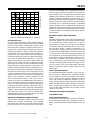
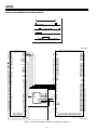
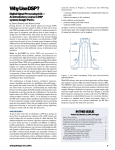
a
ONE TECHNOLOGY WAY
• P.O.
AN-524
APPLICATION NOTE
BOX 9106
• NORWOOD,
MASSACHUSETTS 02062-9106
• 781/329-4700
ADV601 Bin Width Calculation in ADSP-21xx DSP
by David Starr
INTRODUCTION
This application note is for hardware and software designers integrating an Analog Devices ADSP-21xx family Digital Signal Processor (DSP) into an ADV601
design. It describes software to control video compression in the ADV601 Video Codec chip via the auxiliary
serial port. Using this note and the information in the
ADV601 Video Codec data sheet you can do the following:
LOW PASS SUB-BAND
LOWEST HIGH PASS BAND
SECOND HIGH PASS SUB-BAND
THIRD HIGH PASS SUB-BAND
FOURTH HIGH PASS SUB-BAND
FIFTH HIGH PASS SUB-BAND
6.75
3.37
1.68
0.84
Since Chroma is sampled at one-half the rate of Luma,
the frequency range of the chroma sub-bands is half that
of the corresponding Luma sub-bands.
LOW PASS SUB-BAND
LOWEST HIGH PASS BAND
SECOND HIGH PASS SUB-BAND
THIRD HIGH PASS SUB-BAND
FOURTH HIGH PASS SUB-BAND
3.37
1.68
FIFTH HIGH PASS SUB-BAND
0.84
WHAT IS A BIN WIDTH CALCULATOR?
The ADV601 Video Codec chip has two main parts, a
Wavelet Filter Bank and a run length/Huffman encoder.
On compression (encoding) the video is transformed
into the Wavelet domain and then run length/Huffman
encoded. The Wavelet transform is analogous to the
Fourier transform. The Fourier transform is reversible
and can be, but seldom is, realized as a bank of bandpass filters. The output of each Fourier filter is often
called a “bin.” After Fourier transformation the signal is
said to be in the frequency domain. Like the Fourier
transform, the Wavelet transform is reversible. Unlike
Fourier, it is realized as a bank of band pass filters that
divides the input signal into “sub-bands.” The sub-band
width is logarithmic in frequency. The highest sub-band
contains the top half of the input signal frequency. The
next sub-band contains the middle quarter, and so on.
Figure 1. ADV601 Luma Sub-Band Frequency Limits
0.42
ftp://ftp.analog.com/pub/dsp/adv601/
VIDEO FREQUENCY – MHz
0
0.1
0.21
The design examples in this application note refer to the
ADV601-based Videolab demonstration board, but you
can apply the techniques used in these examples to any
ADV601-based design. The software source code and
hardware schematics mentioned in this note are available on the Analog Devices computer products FTP site,
whose Uniform Resource Locator (URL) is:
0
0.21
0.42
Design the DSP to ADV601 interface
Program the DSP
VIDEO FREQUENCY – MHz
Figure 2. Chroma Sub-Band Frequency Limits
AN-524
42 RECIPROCAL BIN
WIDTH REGISTERS
RAW VIDEO IN
RUN LENGTH &
HUFFMAN ENCODER
WAVELET TRANSFORM
COMPRESSED
VIDEO OUT
ADAPTIVE QUANTIZER
Figure 3. Block Diagram Encoding
RAW VIDEO
OUT
RUN LENGTH &
HUFFMAN ENCODER
WAVELET TRANSFORM
COMPRESSED
VIDEO IN
ADAPTIVE QUANTIZER
42 BIN WIDTH
REGISTERS
Figure 4. Block Diagram Decoding
length encoder will efficiently convert the long runs of
zeros into a single short code group, and the image will
compress tremendously. Other video (e.g., an actor
wearing a plaid shirt) has significant high frequency detail. When the TV broadcaster cuts from simple video to
complex video, or even from one scene to another, or to
a commercial, the bit rate will change substantially unless something is done. That "something" is handled by
the Bin Width Calculator, which must respond to the
video change by altering the bin-width register settings
to achieve the desired bit rate.
To reverse the Wavelet transform and recover the original signal, simply add all the sub-bands back together. If
all the bits in all the sub-bands are preserved, there is a
loss less transformation and the original signal is recovered intact. This gives about 3:1 loss less compression,
which is not really enough for many applications. The
signal in the highest frequency sub-band will contain
small amplitude wiggles that are mostly high frequency
noise and a few high amplitude spikes that represent
sharp edges in the picture.
To obtain more compression we discard low order bits
in the high frequency sub-bands. This gives longer runs
of zeros that the run length encoder converts into a very
short code. Multiplying every data point in each subband by a fraction, called the reciprocal bin width, discards the low order bits. This is the adaptive quantizer
located in between the Wavelet filter bank and the run
length/Huffman encoder. There are 42 different subbands and each one has a reciprocal bin width register,
permitting independent quantization of each sub-band.
On decode, we restore the quantized signal to its proper
amplitude by multiplying each data point by a factor
called the bin width. Again there are 42 bin width registers. The duty of the “Bin Width Calculator” program is
to set all 42 bin width and 42 reciprocal bin width register with the proper fraction to achieve the desired compression ratio.
Constant Bit Rate
A constant bit rate Bin Width Calculator is needed when
video must go through a fixed bit rate communications
link. If the video bit rate from the ADV601 exceeds the
communication link bit rate, video will be lost. If the bit
rate from the ADV601 is less than the communications
link can handle, the viewer at the far end of the link is not
receiving the best possible picture. A better picture
would be obtained if more bits were sent. The constant
bit rate Bin Width Calculator adjusts the bin width registers on every frame to achieve the programmed target
bit rate as closely as possible.
Constant Quality
It is also possible to create a constant quality Bin Width
Calculator. If the objective is to maximize the amount of
video stored on a hard disk, the problem is a bit less demanding. Plain and simple video that compresses well
can be allowed to do so and only the busy and complex
video needs be trimmed down to size. The savings in
disk space are worthwhile, and might permit a longer
video capture before the hard drive is filled.
DESIRABLE FEATURES IN A BIN WIDTH CALCULATOR
Bit Rate Depends On Video Signal
Simple video (e.g., a shot of a cloudless blue sky) has
very little high frequency detail. Every pixel is the same
(blue). The high pass sub-bands will all be zero. The run
–2–
AN-524
registers in the ADV601. From the DSP port a processor
can only read the statistics registers and write the bin
width registers. This is a subset of all the registers in the
ADV601. This program was tested on a system with a
Pentium®-based PC interfaced to the host port and a
ADSP-21xx DSP interfaced to the DSP port. The DSP performed only the bin width calculation and the host did
everything else. In a stand-alone design or embedded
system, the DSP could be interfaced through the host
port and thus have access to all the other registers in the
ADV601. In a stand-alone design, the DSP must be able
to read and write to the ADV601 mode control register,
among others.
0.9
0.8
0.6
SERIES 1
0.5
0.4
0.3
RECIPROCAL BIN WIDTH
0.7
0.2
0.1
SERIES 2
41
35
29
23
17
11
SUB-BAND NUMBER
5
0
–1
Advantages of DSP Bin Width Computation
Speed
This DSP program takes a time critical computation out
of the host. The DSP can compute new bin widths within
the 1.2 milliseconds vertical retrace time, so the bin
width settings are right up to date. This can be difficult
to achieve in the host because Windows® is not a realtime operating system. It makes no guarantees of response time to anything. Tasks can hog the CPU and
prevent a host-based Bin Width Calculator from running
in a timely fashion. Windows 95 interrupt handlers are
not permitted to use the hardware floating point unit.
A Windows 95 interrupt handler that relies upon Windows calls to schedule a Bin Width Calculator run as
soon as possible may find that Windows occasionally
schedules something other than the Bin Width Calculator to run next. In this case, the Bin Width Calculator
cannot compute the new bin widths before the next
frame begins.
Figure 5. Sub-Band Quantization vs. Frequency
The Quantizing Curve
For reasonable compression, all the wavelet sub-bands
must be quantized to some degree. Given a fixed budget
of bits to encode a field, the Bin Width Calculator must
allocate the bits to produce a pleasing picture upon reconstruction. This Bin Width Calculator favors the low
frequency sub-bands. It always increases the quantization (discards more low order bits) as the frequency increases. The eye is most critical of the low frequency
information and does not really miss the higher frequencies. Stored in the Bin Width Calculator is a set of bin
widths that preserves a maximum number of bits and
creates a high quality minimum compression image.
Also stored is a second set of bin widths that discards
most of the bits to achieve maximum compression. The
program varies the actual bit rate by interpolating an intermediate curve that lies somewhere between the two
extremes. The max and min curves used by the program
could be modified to make various trade-offs of picture
quality versus bit rate. For instance, the highest frequency Luma sub-bands contain information in the
3.37 to 6.75 Megahertz band. If the video source is
known to roll off at say 3.58 Megahertz, then signal energy in the highest frequency bin is likely to be noise. In
such a case, better performance might be obtained by
multiplying the highest frequency sub-bands by zero to
discard ALL the bits in the bin. In this way, the limited bit
budget is directed toward encoding real picture rather
than video noise (snow or on color TV, confetti) Some
experimentation with the quantizing curves may yield
worthwhile performance improvements.
Easier Program Development
The important Bin Width Calculator is one small program running in a dedicated CPU. If bit rate problems
are encountered, you know just where to look and the
code is small and self contained. Windows 95 device
driver and systems programming expertise is not required. Timing issues are easier to deal with because the
DSP does nothing but bin width calculation. Under Windows, if some other program has control of the machine, the Bin Width Calculator may be locked out and
unable to run in time.
Advantages of Host-Based Computations
Cost (No DSP to Buy)
Easier Program Development
Programmers may be more familiar with the host architecture and programming tools. Operating system expertise may be abundant and DSP experience may be
slim.
DSP-Based vs. Host-Based Bin Width Calculators
The bin width calculation problem remains the same
whether the calculator is interfaced to the ADV601
through the DSP serial port or through the Host parallel
port. From the host port, a processor can access all the
All trademarks are the property of their respective holders.
–3–
AN-524
ADV601 TO DSP HARDWARE AND SOFTWARE INTERFACE
ONE FIELD TIME (16.66 MILLISECONDS)
DIRQ INTERRUPT
LAST CODE INTERRUPT
(CAN OCCUR ANYWHERE; DEPENDS ON HOW RAPIDLY HOST READS FIFO)
STATISTICS REGISTER DATA INTO DSP
BIN WIDTH REGISTER DATA OUT OF DSP
101
102
103
104
105
106
107
108
109
110
113
114
115
116
117
118
IAD15
IAD14
IAD13
IAD12
IAD11
IAD10
IAD9
IAD8
IAD7
IAD6
IAD5
IAD4
IAD3
IAD2
IAD1
IAD0
37
125
124
99
100
IACK/
IAL
IS/
IWR/
IRD/
19
20
XTAL
CLKIN
35
32
BMODE
MMAP
22
WR/
RD/
CMS/
IOMS/
BMS/
DMS/
PMS/
2
3
7
4
5
6
10
BR/
BGH/
BG/
66
38
68
A13
A12
A11
A10
A9
A8
A7
A6
A5
A4
A3
A2
A1
A0
30
29
28
27
26
25
18
17
16
15
14
13
12
11
GND
GND
GND
GND
GND
GND
GND
GND
GND
GND
GND
PF7
PF6
PF5
PF4
PF3
PF2
PF1
PF0
FL2
FL1
FL0
8
21
23
40
54
75
86
88
98
112
123
119
120
121
122
126
127
128
1
45
44
43
CLKOUT
D23
D22
D21
D20
D19
D18
D17
D16
D15
D14
D13
D12
D11
D10
D9
D8
D7
D6
D5
D4
D3
D2
D1
D0
97
96
95
94
93
92
91
90
89
85
84
83
82
81
80
79
78
77
76
74
73
72
71
70
VCC
U?
14
13
12
11
15
QA
QB
QC
QD
RCO
A
B
C
D
ENP
ENT
CLK
LOAD
CLR
3
4
5
6
XTAL
VCLK
VCLKO
119
118
117
116
115
114
111
110
109
108
93
92
91
90
87
86
85
84
83
82
VDATA0
VDATA1
VDATA2
VDATA3
VDATA4
VDATA5
VDATA6
VDATA7
VDATA8
VDATA9
VDATA10
VDATA11
VDATA12
VDATA13
VDATA14
VDATA15
VDATA16
VDATA17
VDATA18
VDATA19
105
104
103
97
95
VSYNC
HSYNC
FIELD
ENC/DEC
CREF
32
32
36
36
34
34
33
33
37
37
31
31
TXD
RXD
TCLK
TF
RF
DIRQ/
11
12
ADR1
ADR0
17
16
15
JP9-49 14
25
JP9-3 9
8
7
10
2
9
1
74HC161
BE0/
BE1/
BE2/
BE3/
LCODE
WR/
RD/
26
28
27
29
FIFO_ERR
FIFO_SRQ
FIFO_STP
STATS_RDY
21
24
10
ACK/
HIRQ/
CS/
19
REST/
VDD
VDD
VDD
94
99
107
113
125
137
144
146
156
PWDACK
PWD/
51
52
53
55
56
56
VDD
VDD
VDD
VDD
VDD
VDD
36
33
DT1/F0
TFS1/IRQ1
RFS1/IRQ0
DR1/F1
SCLK1
100
101
98
VDD
VDD
VDD
VDD
VDD
VDD
RESET/
IRQ2/
IRQL1/
IRQL0/
IRQE/
46
47
48
49
50
6
20
22
30
39
46
51
57
59
69
75
88
58
34
42
41
31
DT0
TFS0
RFS0
DR0
SCLK0
VDD
VDD
VDD
VDD
VDD
VDD
EBG/
EBR/
EINT/
ELIN
ELOUT
ECLK
EE
EMS/
ERESET/
VIDEOLAB U9
DADR8
DADR7
DADR6
DADR5
DADR4
DADR3
DADR2
DADR1
DADR0
40
41
42
43
44
45
48
49
50
DDAT0
DDAT1
DDAT2
DDAT3
DDAT4
DDAT5
DDAT6
DDAT7
DDAT8
DDAT9
DDAT10
DDAT11
DDAT12
DDAT13
DDAT14
DDAT15
80
79
78
77
76
73
72
71
70
67
66
65
64
62
61
60
RAS/
CAS/
WE/
53
54
55
DATA0
DATA1
DATA2
DATA3
DATA4
DATA5
DATA6
DATA7
DATA8
DATA9
DATA10
DATA11
DATA12
DATA13
DATA14
DATA15
DATA16
DATA17
DATA18
DATA19
DATA20
DATA21
DATA22
DATA23
DATA24
DATA25
DATA26
DATA27
DATA28
DATA29
DATA30
DATA31
5
4
3
2
1
160
159
158
157
154
153
152
151
149
148
147
141
140
139
138
135
134
133
132
130
129
128
127
124
123
122
121
GND
GND
GND
GND
GND
GND
GND
GND
GND
GND
GND
GND
GND
GND
GND
GND
GND
GND
GND
GND
GND
GND
GND
GND
GND
GND
GND
GND
67
65
64
63
62
61
60
59
57
EZKIT U3
7
13
18
23
35
38
47
52
56
58
63
68
74
81
96
89
102
106
112
120
126
131
136
142
143
145
150
155
VDD
VDD
VDD
VDD
VDD
VDD
9
24
39
69
87
111
Figure 6. Field Timing Diagram
ADSP-2181
ADV601_PQFP
Figure 7. Electrical Schematic–ADSP-2181 to ADV601 Connections
–4–
AN-524
DSP Serial Port
DSP Interrupt Service Request (DIRQ) Interrupt
The ADV601 asserts the DIRQ interrupt when the Wavelet transform has completed and the statistics of this
field are available. It starts transmitting the statistics
registers after the DIRQ interrupt, which serves as a
"heads-up" to the DSP. The DSP configures the serial
port to receive when it sees the DIRQ interrupt. In principle, the DIRQ interrupt signal is not absolutely necessary. The DSP could keep the serial port configured to
receive, and use the “data ready” interrupt from the serial port itself to indicate start of statistics register transmission. This example program uses the DIRQ interrupt
line to ensure DSP program activity in case a fault in the
DSP serial port programming kills the serial port’s “data
ready” interrupt.
every 16 FIFO reads. The DSP counts these interrupts to
determine field size. The DSP does not care about the
serial data, it does not even look at it, it just wants to
know how many FIFO read strobes occurred. There is a
limit on DSP serial port clocks of 13.824 MHz (see ADSP2100 Family User Manual Section 5.5). The PCI bus mastering interface on the Videolab card reads the FIFO
much faster than that. The 74HC161 counter was added
to reduce the frequency seen by the serial port clock input to less than the 13.824 MHz limit. In a real design a
PAL or an FPGA could easily be used.
Last Code Interrupt (LCODE)
The DSP uses the last code interrupt to start and stop the
FIFO read strobe count. Each time Last Code occurs, the
DSP resets its software FIFO read strobe counter, and
passes the finished count to the servo loop for processing. Last code is asserted when the host reads the nextto-last word from the FIFO and stays asserted until the
last word is read. This time can be quite short (10s of
nanoseconds) and the repetition rate is low (60 Hz) making the LCODE signal difficult to observe on an oscilloscope. Since LCODE occurs when the host gets around
to reading the FIFO, it can occur anywhere during the
field time and, as the host begins to fall behind writing
the disc, it will move farther and farther down the field
until eventually the host begins to drop data. The timing
diagram shows LCODE coming early, but it can be anywhere and move around from field to field.
Statistics Read
Following the DSP interrupt, the ADV601 will transmit
the Compression ratio register, the 42 sum of squares
registers, a Luma and two Chroma “sums” registers,
and finally the six Max and Min registers. The Compression ratio register lets the Host computer communicate
with the DSP. The communication is one-way (Host to
DSP) and contains whatever bits the host program cared
to write into compression ratio register via the host parallel port. This DSP program expects to find the desired
bits per pixel coded into the lower 8 bits of the compression ratio register. Possible values range from 16 bits
per pixel (coded as 0FF Hex) down to 1/16th bit per pixel
(coded as 1). This is purely a software convention, the
ADV601 just passes the bits from the host to the DSP. It
is mentioned here merely as an aid to understanding
operation of this particular program. Other coding
schemes could be readily devised.
PROGRAM THEORY OF OPERATION
PIDBWC.DSP
This is the main routine. It contains the interrupt vector
table, including the power-on reset vector. The initialization code configures SPORT1 as a serial port that disables the alternate functions (IRQ0 IRQ1 FlagIN and
FlagOut) of the SPORT1 pins. SPORT1 will be used to
count FIFO read strobes. The internal timer is set up to
give interrupts at the video frame rate (30 Hz). Programmable I/O pins PF1 through PF7 are programmed as output pins. Important routines toggle these pins so
program activity can be observed on an oscilloscope.
PF0 is set to input, and monitored to exit the program
and return control to the EZ-KIT® monitor. The EZ-KIT
monitor permits display of program variables at the end
of a run, if you return to it. If you do not return, but reset
the EZ-KIT instead, the monitor power-on self-test overwrites all data memory with a test pattern.
Bin Width Register Write
The ADV601 has a simple state machine to operate the
DSP serial port. It transmits the statistics registers and
then receives the new bin width registers. The DSP must
wait until the last statistics register is read before it can
write the bin width and reciprocal bin width registers.
The ADV601 will become confused if this rule is not
obeyed. Bin width registers and reciprocal bin width
registers are interleaved with Register 0 being a reciprocal bin width register and Register 1 being its corresponding bin width register. Register order is given in
ADV601 data sheet Figure 9.
Field Size Measurement
This example program uses one DSP serial port to count
the number of ADV601 FIFO reads to give the DSP program the size of each compressed field. The FIFO/rd
strobe from the Videolab evaluation board is connected
to the clock line of the serial port. The serial port interrupts the DSP each time it thinks it has a word ready in
the serial port received data register, which happens
The main loop does very little. It merely calls the
rite_reg routine to transmit the new bin width and reciprocal bin widths to the ADV601 after the statistics
read is done. Variable recvflg from the statistics read
routine in forms the main loop when statistics read is
done. The main loop does NOT call the bwcalc routine
to update the servo loop and compute a new bin width
curve. Bwcalc is called on the last code interrupt to
EZ-KIT is a registered trademark of Analog Devices, Inc.
–5–
AN-524
strobes to clock the serial port. The fldsiz routine programs SPORT1 for 16-bit words, which means SPORT1
will generate the RX data ready interrupt after 16 SCLKS
(16 FIFO read strobes).
insure that the servo loop is updated just once each
time a new compressed field size becomes available.
This leads to an interesting initialization problem. The
first DSP interrupt will occur BEFORE last code
(LCODE) occurs, since the Wavelet transform must
complete before the host can even start (let alone finish) reading the compressed field from the ADV601
FIFO. This program initializes the bin width/recip bin
width registers to a reasonable value. This initialization
is accomplished by the single call to bwcalc in the initialization code. All subsequent calls to bwcalc are
from the LCODE interrupt routine inside module
fldsiz.dsp.
Routine cntpara services the SPORT1 RX data ready interrupt. It merely bumps variable intaccum on each entrance. The other code toggles a debug bit that can be
observed with an oscilloscope to show that the interrupt
is unmasked and active, and that FIFO reads are actually
being seen by the program.
Routine newfield services the LCODE interrupt. On
each interrupt it copies intaccum into sportints and
resets intaccum. Then it calls bwcalc to update the
servo loop. Newfield currently uses Data Address Generator (DAG) registers I2 and M2 to write the debug
buffer fieldsz. It does not save the register contents in
memory when it returns from interrupt. Should some
other code alter I2 it could cause trouble. A released version of sport0.dsp might want to disable the fieldsz
writes for safety’s sake.
The watch_dog routine gains control on timer tick with
initialization set for 30 Hz. Watch_dog is looking for
start and stop of incoming video. When the video
stops, watch_dog zeros out the servo loop error integrator. This prevents a sizable error integral from one
video clip biasing the servo loop hard over at the beginning of the next clip. This is largely for convenience in
studying servo loop startup transients. You can stop
the video tape player, rewind and start over again and
have the servo start up the same way each time. Otherwise the startup on the second video clip depends upon
the previous video clip. Watch_dog detects video stop
by watching the field_cnt variable. When video
stops, the host stops reading the FIFO and the LCODE
interrupt stops occurring. This causes field_cnt to
stop changing. If field_cnt does not change after two
field times, watch_dog concludes that video has
stopped coming in.
Sportints needs proper scaling to yield field size in
pixels. Scaling must account for the 16:1 division done
in the serial port, the two pixels per 32-bit long word,
and the 4:1 hardware divider placed between the FIFO
read strobe and the serial port SCLK pin.
sport0.dsp
Sport0 handles reception of ADV601 statistics and transmission of bin width and reciprocal bin width register
data. As the name implies, it uses Serial Port 0 (SPORT0)
for the task. Sport0 writes recvflg and xmitflg to let
the rest of the system know when statistics read (receive) and bin width write (transmit) is active. The flags
are nonzero while transmit or receive is going on, and
zero when inactive. Pidbwc.dsp (main) uses recvflg to
start up transmission after the last statistics register is
read. Statistics are placed into array stats601 and bin
widths are transmitted out of array bw_recip_bw.
fldsiz.dsp
The fldsiz module updates variable sportints,
which is proportional to compressed field size, on each
Last Code (LCODE) interrupt. Despite some obsolete
comments in early versions of the code, sportints is
unscaled. It is just the raw interrupt count and must be
scaled into bytes by the user routine. The other variables in fldsiz are either local scratch variables or a
debug “history buffer” like fieldsz, and are not used
outside the fldsiz module. If compressed field size is
measured by other means, software changes will be
confined to this module.
Routine sport0_start is the one-time initialization
routine. It loads the SPORT0 control registers, initializes
variables and handles the first field problem. The system does not know which compression ratio is required
until it can see the compression ratio register. The compression ratio register will not be available until the first
statistics read occurs. Therefore, sport_start initializes the compression ratio register to a reasonable number to avoid trouble that might occur should the system
try to process a random value of compression ratio.
Serial Port 1 (SPORT1) is used by the EZ-KIT monitor to
load code and dump memory to the host, whereas the
Bin Width Calculator uses SPORT1 to count FIFO read
strobes. The fldsiz_start entry saves the settings of
all the SPORT1 control registers and the fldsiz_stop
routine restores them so the monitor will function after
a bin width calculation run and dump ram variables for
debug and test. For debugging in the software simulator, setting the ISCLK bit in the SPORT1 control register
causes simulated SPORT1 interrupts to occur. To function in real hardware the ISCLK bit (Internal Serial Port
Clock) must be clear, to allow the external FIFO read
Routine rite-reg is called by pidbwc.dsp (main) to
start up bin width register transmission. The advanced
“autobuffering” feature of ADSP-21xx family serial
ports is used to more input directly to data ram without
processor intervention. Rite_reg loads the Data
Address Generator (DAG) registers needed for autobuffering, turns on autobuffering, loads only the first
–6–
AN-524
The err, err_dir and err_int computation is a critical
section done with interrupts locked out. The error integral variable is a persistent long term history type state
variable. When the video changes, this history becomes
invalid, requiring an integrator reset to zero. This reset is
done from interrupt. Locking out interrupts prevents interrupt service routines from zeroing the variable in the
middle of the read-modify-write sequence which would
nullify the reset. A second reason for locking out interrupts is to prevent interrupt routines from unexpectedly
running with the ALU hardware saturation feature ON. I
believe that interrupt service routines will in fact function properly with ALU saturation ON or OFF, but it is
better to be safe than sorry.
word of the bw_recip_bw array into the transmit data
register and returns. The serial port hardware will push
the entire array out of the serial port with no more processor intervention and issue the TX data done interrupt
when done. The interrupt will transfer control to the
rite_reg_done routine. This code just turns off
autobuffering and clears the transmit flag.
Routine read_reg is the inverse of rite_reg. It uses
the same DAG registers to autobuffer receive the statistics.
It is hooked to the DSP interrupt and thus automatically
starts on every field. After starting up the autobuffered
receive, read_reg returns control. When the stats601
buffer is full (last statistic is read) SPORT0 will create the
RX data ready interrupt which is hooked to routine
read_reg_done. This code, like rite_reg_done, shuts
down autobuffering and clears recvflg to let main
know it can start up. To improve servo loop response,
read-reg-done will zero the servo loop error integrator
should the compression ratio change. Otherwise, a large
error built up over many fields might take an unreasonable length of time to respond to the new target compression ratio.
Next output variable scrunch is computed from the following formula.
scrunch = loop_gain × err + int_gain × err_int + dir_gain ×
err_dir
(1)
Scrunch goes to the bin width curve generator. Full
scale positive will select a maximum bit rate, minimum
compression set of bin widths. Full-scale negative selects the opposite (min bit rate). Intermediate values of
scrunch cause the curve generator to interpolate intermediate compromise curves somewhere in-between the
max and min compression curves.
servo.dsp
This module does a textbook Proportional-Integral-Derivative (PID) servo loop. The Compression ratio register
gives the routine the target bits per pixel. This register is
written by the host through the ADV601 parallel host
port, and passed to the DSP via the serial link. Module
Sport0 receives the compression ratio register contents
and makes it available to servo.dsp in the first word of
array stats601. Variable sportints from fldsiz.dsp
tells servo.dsp how big the last compressed field really
was. Servo.dsp converts both the bits-per pixel compression ratio register and interrupt count into pixels
per field, scaled down by 8 (3-bit right shift) to avoid
overflow in 16-bit arithmetic. Symbol TGT SCALE defines size of this scaling shift.
The three gain terms are scaled 16.8 (8 bits of integer,
8 bits of fraction). Unity is 256 (100 Hex). This permits
each of the three terms to either amplify or attenuate
their contribution to the final answer. The MAC is used
to do the multiply and accumulate the sum 32 bits wide.
After doing the three multiply accumulates, the 32-bit
MR register hardware saturation instruction (if MV sat
MR) is executed, but probably not needed. The program
now rescales the 32-bit answer into a 16-bit variable. It
does this by picking the middle 16 bits out of the 32-bit
MR register. The program does an 8-bit left shift and
takes the high order word. Overflow is checked by shifting the top nine bits of MR into the extension register
MR2. If they are not all the same (zero or one) then
scrunch has overflowed and must be saturated.
After normalizing bit rate target and interrupt count into
a common scale, the bit rate error (variable err) is computed by subtracting actual field size from target field
size. If err is positive, the compressed field was too
small, if err is negative, the compressed field was too
big. After calculation of err, the module computes the
derivative of err by subtracting the previous value of
err from the new value of err and storing the result in
variable err_dir. It also computes the integral of err
by adding err to variable err_int. Hardware saturation in the ALU is required to prevent arithmetic overflow from wrapping around. If err, or especially
err_int, gets large, it is OK to peg out at full scale plus
or minus, but wrapping around from plus to minus is a
disaster that will cause sustained full-scale oscillation of
the bit rate.
To aid debugging, servo saves (but never uses) a second
copy of the error integral called back_int. This can be
dumped after a video compression run to see the last
value of err_int. Fldsiz.dsp is constantly looking for
end of video to zero out err_int, meaning that
err_int will always read zero after a compression run.
The module also writes the values of err_int to circular buffer debug, to permit post compression of analysis
of servo loop transient response. Both features may be
deactivated to save space. The conditional SWEEP feature disables the entire feedback loop and sweeps
scrunch from minus full scale to plus full scale to check
the open loop response of the system.
–7–
AN-524
Tune Proportional Gain First with No Integral and
Derivative Gain
PID servo loops are tuned by adjusting the loop gain for
best performance. Tune the gains one by one, proportional first. Set the integral gain and derivative gain to
zero. Increase the proportional gain until the system oscillates and then back off a reasonable amount. Then re
check for loop stability at high and low bit rates, and on
a variety of video material. Measure the peak and average bit rate errors over a representative video sample.
Then, attempt to improve the performance with integral
gain. Integral feedback will improve long-term accuracy
at the expense of transient response. Finally try derivative feedback to improve transient response. The
changes in loop performance are hard to observe by
eye, you really need a numerical figure of merit to guide
your tuning efforts.
bin width[i] = scrunch × min[i] + (1 - scrunch) × max(i) (2)
This creates an output bin width curve that is a linear
interpolation between the two extremes. Then the reciprocal bin width values are computed with Equation 3 in
the DO recip loop.
(3)
The results are placed in array bw_recip_bw for
sport0.dsp to transmit to the ADV601.
Testing and Tuning Plotting Performance
2
1.8
BITS PER PIXEL
1.6
FURTHER IMPROVEMENTS
After servo loop tuning, a smarter program might take
advantage of the statistical data to eliminate those one
field wide spikes that occur on scene change. One
scheme might maintain a running average of all the 42
sum of squares figures. Upon each statistics update
compare the new statistics with the running average of
prior statistics. A radical difference indicates a scene
change. Upon scene change the servo module might
just ask for heavy compression for the next field to avoid
data over run. Or the “statistics difference” signal just
developed might be fed into the servo module in place
of the computed err_dir signal. The statistics see a
scene change one field earlier, and thus allow the servo
module to anticipate a change in bit rate before it happens. The present computed err_dir signal is always
one field behind the video.
1.4
1.2
1
0.8
0.6
0.4
0.2
0
1
571
1141
1711
2281
2851
FIELD NUMBER
3421
3991
Figure 8. Beauty Video at 1 Bit per Pixel
The Raw2avi program can be used to measure the performance of the Bin Width Calculator. While doing its
primary job of converting raw ADV601 video into videofor-windows.avi files, the program finds the size of every field in the compressed video (.601) file. Raw2avi
records the field number, the field size, the compression
ratio and the number of bits per pixel of each field in a
side disk file named vid_siz.dat. The file is in ASCII,
and the following plot was generated from the side file
using a spread sheet. The target bit rate was 1 bit per
pixel. The input video was the Analog Devices
Beauty.601 file (distributed on the Videolab kit CDROM). Variable loop_gain was 8 (800 Hex after scaling). Int_gain and dir_gain were zero. Each scene
The program might compute the 42 differences between
this sum-of-squares and the last sum-of-squares. It
should then square or absolute value the 42 differences
(to prevent plus and minus differences from canceling
each other) and sum them to obtain a single measure of
image “change.” If this number is then divided by the
sum of all 42 bin width registers is will be normalized in
a useful fashion.
The present program changes the bin widths on every
field. The video might look better if field one and field
two were always quantized with the same bin width
numbers.
–8–
PRINTED IN U.S.A.
Recip_bw[i] = 1 / bin width[i]
E3170–.5–2/98
change causes an abrupt bit rate change. The narrow
spikes are only one field wide, corresponding to the one
field delay around the feedback loop.
curve.dsp
Module curve.dsp has a pair of 42 element bin width
register curves (arrays max and min) stored as constants in program memory. For each of the 42 bin width
registers curve.dsp computes the value from Equation 2
in the DO interp loop.