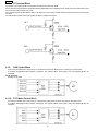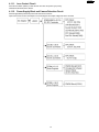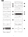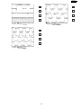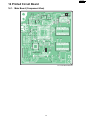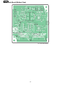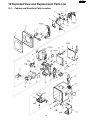
1
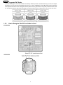
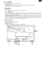
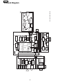
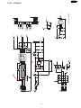
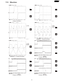
ORDER NO. KMS1001748CE
F15
Network Camera
Model No. BL-C230A
(for U.S.A.)
www.electronicsrepair.net
BL-C230A
TABLE OF CONTENTS
PAGE
1 Warning --------------------------------------------------------------3
1.1. Battery Caution ---------------------------------------------3
1.2. About Lead Free Solder (PbF: Pb free) --------------3
1.3. For Service Technicians ----------------------------------5
1.4. Trademarks --------------------------------------------------5
2 Specifications ------------------------------------------------------6
2.1. Internal Memory Capacity for Buffered Images-----7
2.2. Compatible Panasonic VIERA TVs --------------------7
3 Features --------------------------------------------------------------8
4 Technical Descriptions------------------------------------------9
4.1. Main Board---------------------------------------------------9
5 Location of Controls and Components------------------ 17
5.1. Understanding the Camera Indicators -------------- 17
6 Installation Instructions--------------------------------------- 18
7 Operating Instructions ---------------------------------------- 20
7.1. Preparation ------------------------------------------------ 20
7.2. Connection------------------------------------------------- 21
7.3. Setup Guide ----------------------------------------------- 22
7.4. Setup Guide (for VIERA connection)---------------- 24
8 Troubleshooting Guide---------------------------------------- 26
8.1. Starting Up Operation ----------------------------------- 26
8.2. Indicator view Check ----------------------------------- 27
8.3. LAN Block Check----------------------------------------- 28
8.4. LENS Block Check--------------------------------------- 31
8.5. Power Supply Block Check ---------------------------- 32
8.6. Other Operation Check --------------------------------- 33
8.7. Pyroelectric Infrared Sensor Check ----------------- 34
8.8. Sound Block Check-------------------------------------- 35
8.9. RF Block check ------------------------------------------- 36
8.10. Other Problem (External Sensor input /
External output)------------------------------------------- 36
8.11. The Inspection After The Repair --------------------- 36
8.12. Diagnosis NG Check ------------------------------------ 37
8.13. In Case Where the Main Board Is Replaced
and a New MAC Address Label Is Used ----------- 37
8.14. Update Firmware ----------------------------------------- 37
8.15. How To Change MAC Address Label --------------- 38
8.16. How to Replace a Flat Package IC ------------------ 39
9 Disassembly and Assembly Instructions --------------- 40
9.1. Disassembly Instructions------------------------------- 40
10 Maintenance ------------------------------------------------------ 46
10.1. Cleaning the Camera------------------------------------ 46
11 Factory Setting--------------------------------------------------- 47
11.1. Resetting the Camera----------------------------------- 47
11.2. Resetting the Camera Using the FACTORY
DEFAULT RESET Button ------------------------------ 47
12 Block Diagram --------------------------------------------------- 48
13 Schematic Diagram--------------------------------------------- 49
13.1. For The Schematic Diagram -------------------------- 49
13.2. Schematic Diagram-------------------------------------- 50
13.3. Waveform -------------------------------------------------- 57
14 Printed Circuit Board ------------------------------------------ 61
14.1. Main Board (Component View) ----------------------- 61
14.2. Main Board (Bottom View) ----------------------------- 62
14.3. Lens Board (Component View) ----------------------- 63
14.4. Lens Board (Bottom View) ----------------------------- 63
14.5. I/O Board (Component View) ------------------------- 65
14.6. I/O Board (Bottom View) ------------------------------- 66
PAGE
14.7. Sensor Board (Component View) ------------------- 67
14.8. Sensor Board (Bottom View) ------------------------- 67
15 Appendix Information of Schematic Diagram -------- 68
15.1. Terminal Guide of ICS, Transistors and
Diodes ------------------------------------------------------ 68
16 Exploded View and Replacement Parts List----------- 69
16.1. Cabinet and Electrical Parts Location -------------- 69
16.2. Accessories and Packing Materials----------------- 70
16.3. Replacement Parts List -------------------------------- 71
2
BL-C230A
1 Warning
1.1.
Battery Caution
Danger of explosion if the battery is replaced incorrectly. Replace only with the same or equivalent type recommended by the
manufacturer. Discard used batteries according to following caution:
Disposal or transportation of lithium batteries should be performed by permitted, in accordance with federal, state and local
guidelines.
A battery continues to have no transportation limitations as long as it is separated to prevent short circuits and packed in strong
packaging.
Commercial firms that dispose of any quantity of lithium cells should have a mechanism in place to account for their ultimate disposition. This is a good practice for all types of commercial or industrial waste.
When the lithium battery is exchanged, the clock settings are cleared. In this case, make clock settings again.
Recommend Type Number:
N4BCY48Y0001(CR2032NT23) (BT901) Manufactured by HITACHI MAXELL
CR Coin Cell Lithium Battery Information:
This product contains a CR Coin Cell Lithium Battery which contains Perchlorate Material-special handling may apply.
See www.dtsc.ca.gov/hazardouswaste/perchlorate
1.2.
About Lead Free Solder (PbF: Pb free)
Note:
In the information below, Pb, the symbol for lead in the periodic table of elements, will refer to standard solder or solder that contains lead.
We will use PbF solder when discussing the lead free solder used in our manufacturing process which is made from Tin, (Sn),
Silver, (Ag), and Copper, (Cu).
This model, and others like it, manufactured using lead free solder will have PbF stamped on the PCB. For service and repair
work we suggest using the same type of solder.
Caution
• PbF solder has a melting point that is 50° F ~ 70° F (30° C ~ 40° C) higher than Pb solder. Please use a soldering iron with temperature control and adjust it to 700° F ± 20° F (370° C ± 10°C).
• Exercise care while using higher temperature soldering irons.:
Do not heat the PCB for too long time in order to prevent solder splash or damage to the PCB.
• PbF solder will tend to splash if it is heated much higher than its melting point, approximately 1100°F, (600°C).
• When applying PbF solder to double layered boards, please check the component side for excess which may flow onto the
opposite side (See figure, below).
3
BL-C230A
1.2.1.
Suggested PbF Solder
There are several types of PbF solder available commercially. While this product is manufactured using Tin, Silver, and Copper,
(Sn+Ag+Cu), you can also use Tin and Copper, (Sn+Cu), or Tin, Zinc, and Bismuth, (Sn+Zn+Bi). Please check the manufacturer’s specific instructions for the melting points of their products and any precautions for using their product with other materials. The following lead free (PbF) solder wire gauge are recommended for service of this product: 0.3mm, 0.6mm and 1.0mm.
1.2.2.
How to Recognize That Pb Free Solder is Used
MAIN BOARD
LENS BOARD
4
BL-C230A
IO BOARD
SENSOR BOARD
1.3.
For Service Technicians
Repair service shall be provided in accordance with repair technology information such as service manual so as to prevent fires, injury or electric shock, which can be caused by improper repair work.
1. When repair services are provided, neither the products nor their parts or members shall be remodeled.
2. If a lead wire assembly is supplied as a repair part, the lead wire assembly shall be replaced.
3. FASTON terminals shall be plugged straight in and unplugged straight out.
ICs and LSIs are vulnerable to static electricity.
When replacing, the following precautions will help to prevent recurring malfunctions.
1. Cover the plastic parts with aluminum foil.
2. Ground the soldering irons.
3. Use a conductive mat on the work-table.
4. Do not grasp IC or LSI pins with bare fingers.
1.4.
Trademarks
• Microsoft, Windows, Windows Vista, Hotmail, ActiveX, Internet Explorer, Windows Media, DirectShow, and DirectDraw are either
registered trademarks or trademarks of Microsoft Corporation in the United States and/or other countries.
• Screen shots reprinted with permission from Microsoft Corporation.
• VIERA Link™ is a trademark of Panasonic Corporation.
• VIERA CAST™ is a trademark of Panasonic Corporation.
• All other trademarks identified herein are the property of their respective owners.
5
BL-C230A
2 Specifications
Camera Specifications
Items
Zoom
Pan/Tilt Angle
Image Sensor
Illuminance
White Balance
Lens Brightness
Focus
Minimum Object Distance
Aperture (F No.)
Horizontal Viewing Angle
Vertical Viewing Angle
Exposure
Specifications
3x (by length) ActiveX zoom
Pan: -41 ° to +41 °, Tilt: -32 ° to +10 °
1/4 inch CMOS sensor, 320,000 pixels
5-10,000 lx (3-10,000 lx when in Color Night View mode)
Auto/Manual/Hold
9 levels
Fixed, 0.3 m- Infinity
0.3 m (1 foot)
F2.8
58 °
45 °
Auto
Other Specifications
Items
Image Compression
Image Resolution
Buffered Images*1
Audio Communication
Audio Compression Format
Audio Bandwidth
Audio Reception Method
Audio Reception Decoding
Audio Input
Audio Output
External Input/Output Interface
Frame Rate*2
Communication Protocols
Image Buffer/Transfer Triggers
Image Transfer Method
Wired LAN Interface
Sensor Detection Method
Sensor Detection Range*4
POWER Indicator Display
AV LINK Indicator Display
Dimensions (W x H x D)
Weight (Main Unit Only)
Power Supply
Maximum Power Consumption
Operating Temperature
Operating Humidity
Specifications
JPEG (3 levels), MPEG-4, H.264
640 x 480, 320 x 240, 192 x 144
About 1160 frames (320 x 240, standard image quality) with time display
Camera to PC
H.264: MPEG-2 AAC (AAC-LC) 64 Kbps
MPEG-4/MJPEG: ADPCM 32 kbps
300 Hz-3.4 KHz
ActiveX
ActiveX
Built-in microphone
Built-in speaker
External sensor input × 2
External output × 1
Max. 30 frames/second (640 x 480, 320 x 240, 192 x 144)
IPv4/IPv6 Dual-Stack
IPv4:
TCP, UDP, IP, HTTP, FTP, SMTP, DHCP, DNS, ARP, ICMP, POP3, NTP, UPnPTM, SMTP Authentication,
RTP, RTSP, RTCP, HTTPS, SSL, TLS, Auto IP
IPv6:
TCP, UDP, IP, HTTP, FTP, SMTP, DNS, ICMPv6, POP3, NDP, NTP, RTP, RTSP, RTCP, HTTPS, SSL,
TLS
Timer, Sensor, Alarm 1, Alarm 2, Motion Detection, Sound Detection
SMTP*3, FTP, HTTP
10Base-T/100Base-TX Ethernet RJ-45 connector
Pyroelectric Infrared Sensor
Horizontal: About 28 °
Vertical: About 71 °
Distance: About 5 m (16 feet 5 inches) when in a 20 °C (68 °F) environment
Power
Camera Operation
Ethernet Link
AV Link
74 mm x 74 mm x 101 mm
(2 15/16 inches x 2 15/16 inches x 4 inches)
260 g (0.57 lb.)
AC adaptor (order no. PQLV206Y)
Input 100-240 V AC, 50/60 Hz
Output 9 V DC, 750 mA
About 4.0 W (7.7 W during pan/tilt scan)
Operation: +0 °C (+32 °F) to +40 °C (+104 °F)
Storage: -10 °C (+14 °F) to +50 °C (+122 °F)
Operation: 20 %-80 % (no condensation)
Storage: 20 %-90 % (no condensation)
6
BL-C230A
Wireless Specifications
Items
Communication Standard
Data Transfer Mode
Frequency Range
Channel
Security
Specifications
IEEE 802.11b, 802.11b/g, 802.11g exclusive
IEEE 802.11b: Direct Sequence Spectrum Spread (DS-SS)
IEEE 802.11g: Orthogonal Frequency Division Multiplexing (OFDM)
2.412-2.462 GHz
1-11
SSID, WEP (64/128/152 bit), WPA-PSK (TKIP), WPA2-PSK (AES)
*1) See 2.1. for details.
*2) Frame rate may decrease in the following situations.
-When buffering images
-When using color night view mode
-When many users are viewing camera images
*3) The camera supports POP Before SMTP Authentication and SMTP Authentication. PLAIN, LOGIN, and CRAM-MD5 SMTP
Authentication are supported. SSL supports SMTP over SSL. STARTTLS is not supported.
*4) When the temperature is 20 °C (68 °F)
2.1.
Internal Memory Capacity for Buffered Images
The camera‘s internal memory can buffer images according to the table below.
Note
• All values are approximate.
• H.264 images cannot be buffered to the camera’s internal memory.
JPEG images (videos and still images)
Resolution
640 x 480
320 x 240
192 x 144
Specification
File Size
No. of Images
File Size
No. of Images
File Size
No. of Images
Snapshot
Favor Clarity
50 KB
360
25 KB
730
10 KB
1880
50 KB
(Saved to PC)
25 KB
(Saved to PC)
10 KB
(Saved to PC)
Image Quality
Standard
35 KB
520
16 KB
1160
7 KB
2710
Favor Motion
27 KB
680
10 KB
1880
5 KB
3850
Note
• The maximum number of images that can be buffered depends on image resolution and image quality.
MPEG-4 videos
For information about MPEG-4 image capacity, see the Panasonic Network Camera support site at
http://panasonic.net/pcc/support/netwkcam/.
Note
• The maximum amount of video that can be buffered depends on image resolution, network bandwidth, and the frame rate and bit
rate set for the streaming method.
2.2.
Compatible Panasonic VIERA TVs
The camera is compatible with the following Panasonic VIERA TVs (as of October, 2009).
G10 series, G15 series, V10 series, Z1 series
7
BL-C230A
3 Features
On-site and remote camera monitoring
Camera images can be monitored from a PC, both on-site and over the Internet. You can even use your mobile phone to view
still images when you’re out of the house.
H.264, MPEG-4 and Motion JPEG (MJPEG) support
Live camera images can be viewed and buffered (i.e., stored in memory) in H.264, MPEG-4 and JPEG (MJPEG) formats, allowing you to select the video format that best suits your needs.
Built-in sensor (human detection sensor)
The camera features a built-in pyroelectric infrared sensor, which uses infrared rays to detect temperature differences within its
range that are emitted naturally by people, animals, etc. The sensor can be used to trigger the camera to buffer (i.e., temporarily
store) camera images in its memory. You can view these images later as desired. The sensor can also be used to trigger the
camera to transfer images to someone or somewhere, by FTP, E-mail, or HTTP.
Backlight Correction features
When this feature is enabled, the camera can automatically correct the contrast in dark areas of the camera image. This means
even when there is backlight or a large amount of contrast in the image, the camera can correct the image to provide a more
consistent, natural image.
Audio features
The camera features a built-in microphone that allows you to monitor the audio while viewing live camera images using your PC.
Detection feature
The camera’s motion or sound detection feature allows you to buffer or transfer camera images when the camera detects
motion or sound in the camera image.
Camera image buffering and playback
Camera images can be automatically buffered at specific times, when the camera’s external sensors (customer-provided) are
triggered, or when the camera detects motion. You can program the camera to buffer these camera images, and then you can
play back these images later while accessing the camera or save them to your PC. You can also program the camera to transfer
images by E-mail or upload them to an FTP or HTTP server as they are being buffered.
Digital zoom
When viewing camera images from a PC, you can zoom up to 3× (by length) and get a closer look. You can use your mouse to
zoom in and out simply.
Protecting your privacy
Simply press the camera’s PRIVACY button to hide the lens from view and protect your privacy. You can even activate the privacy mode while away from home.
UPnPTM support
When connecting the camera to a UPnPTM compatible router, the camera’s network settings can be automatically configured,
making setup quick and easy.
Viewnetcam.com support
After registering your camera with the Viewnetcam.com service, you can access the camera while away from home using an
easy to remember Internet address of your choosing, such as ***.viewnetcam.com.
Multi-language support
All camera pages can be displayed in English, French, German, Italian, Spanish, Russian, Simplified Chinese, and Japanese.
The most commonly used camera pages can be displayed in Korean.
Wireless connectivity
The BL-C230 supports wireless standards IEEE 802.11b and IEEE 802.11g, giving you the option of using the camera in either
wired or wireless mode. When used in wireless mode, WEP, WPA-PSK(TKIP), and WPA2-PSK(AES) support ensures that
access to the camera is secure.
8
BL-C230A
4 Technical Descriptions
4.1.
Main Board
4.1.1.
CPU Block
CPU (IC101)
Operating Power Supply: 3.3 V (for I/O) 1.2 V (for Core)
Package: 433 pin Ball BGA
Outline of Operation: This LSI encodes a picture signal input from a camera into a JPEG, an MPEG4 or an H.264 format and an
audio signal input from a microphone into a AAC-LC format, and then it distributes the data to the terminal on the IPV4 or IPV6
network using the network server function achieved by processing the software of a built-in processor.
CMOS sensor (IC712), Audio codec (IC709) and Real Time Clock IC (IC902) are accessed by I2C I/F.
Ethernet PHY (IC301) is accessed by MII (Media Independent Interface) I/F.
FLASH MEMORY (IC102)
Operating Power Supply: +3.3 V
Package: 18 pin Ball BGA
Capacity: 64 Mbit
Access Time: 70 ns
Outline of Operation: Stores programs for CPU operation, MAC address and customer setup data. Version up is available from
Ethernet I/F.
DDR2 SDRAM (IC103/IC104)
Operating Power Supply: 1.8 V
Package: 84 pin Ball BGA
Capacity: 512 Mbit
Outline of Operation: Stores the memory for CPU work and temporary saved images.
RESET IC (IC105)
Reset voltage: 2.9 V
Package: 5 pin SOT-23-5
Outline of Operation: When 3.3V power starts up, it emits about 50ms reset pulse after detecting 2.9V.
Clear Setting Button (SW903)
Outline of Operation: It is possible to bring back the setting value of a Network Camera to a factory-shipments state, when you
push.
9
BL-C230A
4.1.2.
LAN Block
Consists of IC101 (CPU), IC301 (ETHER-PHY), T901 (Trans) and JK901 (RJ45).
T901 (Trans) insulates sets and Ethernet.
ETHER-PHV (IC301)
Operating Power Supply: 3.3 V
Package: 32 pin QFN
IC101 (CPU) and IC301 (ETHER-PHY) are connected by a signal called MIIBus which it makes it possible to transmit/receive
Ethernet data.
IC301 has Auto Negotiation Function which changes 100BASE-T or 10BASE-TX automatically.
Transmitting Operation
Electric signal from IC101 is changed to Ethernet data on IC301 and it is sent through T901 from JK901.
Receiving Operation
Ethernet data from JK901 is change to electrical signal on IC301 and it is received by IC101.
JK901 is including the Power Supply (DC9 V) from the Power Supply Unit which is different from the Ethernet data mentioned
above.
10
BL-C230A
4.1.3.
RTC block
Real Time Clock (IC902)
Operating Power Supply: 3.3 V (3 V battery for back up)
Package: 10 pin SOP
Outline of Operation: Stores Clock Data and resonates Clock Signal from CPU (IC101) when it starts up.
Backup Battery provides power when power supply is out.
Lithium Battery (BT901)
Output Voltage: 3 V
Capacity: 240 mAh
Outline of Operation: A backup power supply for Real Time Clock (IC902).
4.1.4.
CMOS Block
This CMOS image sensor which consolidates sensor section and image process DSP consists of one chip. Each pixel has a
micro lens for increased sensibility. It changes optical energy to analogue voltage. After that, analogue pixel voltage is converted
into digital using the 10 bit AD Converter (ADC).
Analogue pixel voltage data which is converted to digital colored image signal is finished using DSP. Those signals are sent out
as digital format 8 bit span YUV with PCLK, HD and VD signals as a timing interface. In addition, the Image Processing Function
of AE (Auto Iris) and AWB (Auto White Balance) is installed and it is automatically operated following an algorithm in the chip.
Setting up of each chip register is set at I2C by CPU (IC101) on Main Board.
CMOS sensor module (IC401)
Package: 27 pin module
Available Number of Pixels: 640 x 480 pixels
Image Area: 1/4 inch Optical Size
Input Clock: 13.5 MHz
Operating Power Supply: AVDD=+3.1 V DOVDD=+1.8 V DVDD=+1.8 V
11
BL-C230A
4.1.5.
Sound Block
Microphone(MIC701)
Input sound.
PCM Codec (IC702)
Power Supply Voltage: 3.3 V
IC702 with built-in microphone amplifier, speaker amplifier and video amplifier is a low powered, compact, monaural codec.
A regulator to stabilize the characteristics of the codec which is sensitive to noise is equipped.
IC702 can keep the audio performance unchanged by the characteristics of the power supply circuit.
In digital signal processing, HPF, notch filter and 5 Band Equalizer are equipped for noise reduction in some bandwidth and this
makes sound effect processing more flexible.
Flow of Sound Signal
[Microphone sound]
1. The sound data input from the microphone is amplified by the amplifier in the PCM Codec (IC702) and built-in ALC. The data
is converted to the digital signal by the ADC, then the PCM data in the form of 8 KHz/8 bit is output through the Serial I/F to the
IC101 on the CPU board as the 64kbps data.
2. The PCM Codec (IC702) supplied 12MHz CLK from the host CPU (IC101), generates 8KHz and 56KHz in the built-in PLL circuit and transfers the serial data.
IC702 is controlled by CPU (IC101) using the I2C and registered.
[Speaker sound]
The PCM Codec (IC702) receives the data of the speaker sound which has been previously assigned and outputs it to the
speaker through DAC.
4.1.6.
Pyroelectric Infrared Sensor Block
Pyroelectric Infrared Sensor (IC704)
Operating Power Supply: +3.1 V (+A3.1 VS)
Package: 3 pin Board Insertion Type
Changes temperature variation into analogue signal which it emits when a heat source, such as a person, comes into detection
area.
The analogue signal is amplified by Operational Amplifier (IC703).
Circuits Built-in Operational Amplifier (IC703)
Operating Power Supply: +3.1 V (+A3.1 VS)
Amplifies analogue signal from Pyroelectric Infrared Sensor (IC704).
Amplified analogue signal input the AD input terminal in CPU (IC101)
Analogue Switch (IC701)
Operating Power Supply: +3.1 V (+A3.1 VS)
Package: 8 pin SSOP
Switches the gain setting of the Operational Amplifier(IC703). The terminal status below shows each gain setting.
12
BL-C230A
GAIN1 (IC701-7pin)
0
1
0
1
GAIN2 (IC701-3pin)
0
0
1
1
GAIN
71.2
63.4
60.2
57.2
Operation of Pyroelectric Infrared Sensor
1. Pyroelectric Infrared Sensor (IC704) emits analogue signal, when a heat source, such as a person, moves into the detection
area.
2. Above signal is amplified by Operation Amplifier (IC703) which emits analogue signal.
3. Above signal is input to AD of CPU (IC101) and the signal amplitude exceeds the specified voltage range, a reaction occurs.
4.1.7.
LED Control Block
LED is controlled by CPU which is mounted on Main Board. Control data is input into LED Control Circuit. (Three color LED is
employed.)
LED_R
L
L
H
H
LED_G
L
H
L
H
Color of LED
OFF
Green
Red
Orange
LED is controlled by CPU which is mounted on Main Board. Control data is input into LED Control Circuit. (Three color LED is
employed.)
LED_R
L
L
H
H
LED_G
L
H
L
H
13
Color of LED
OFF
Green
Red
Orange
BL-C230A
4.1.8.
I/O Terminal Block
The system of the Input terminal is connected to the Input Port of the IC101 GPIO.
Due to Internal Pull-up Resistance, the PNP Transistor (Q905,Q904) on the following level is usually in the OFF state and the Input
Port connected to the collector is at L level.
If the terminal is short-circuited with the GND, or the signal of L level is input, the PNP Transistor goes ON and the Input Port goes
to H level.
The CPU checks the state of this port regularly to detect a change in this signal.
4.1.9.
PAN Control Block
A pan motor is initiated when CPU (IC101) on a Main Board controls the Motor Driver IC (IC303) on the same board.
A Constant Voltage Bipolar Drive System is employed. The Voltage of Motor Power (VM) is 3.3V. ø15 Stepping Motors are
employed.
DC-DC Converter
Package: 24 pin SOP
4.1.10. TILT Motor Control Block
A Tilt motor is initiated when CPU (IC101) on a main board controls the motor driver IC (IC303) on the same board.
A Constant Voltage Bipolar Drive System is employed. The Voltage of Motor Power (VM) is 3.3V. ø15 Stepping Motors are
employed.
14
BL-C230A
4.1.11.
Lens Control Circuit
Press the lens button (SW101) to hide the lens from view and protect your privacy.
CPU detects the status of the SW101.
4.1.12. Power Supply Block and Camera Detection Circuit
Power Supply Block provides the power that each block consumes.
Input is DC9 V/750 mA from AC adaptor. The circuit diagram and output voltage are shown as below.
15
BL-C230A
4.1.13. RF block
The digital section of RF block consists of transceiver IC & MAC/BB IC(IC601), SDRAM(IC603), Flash ROM(IC602), and
IEEE802.3(u) Ethernet PHY(IC661).
The analog/RF section consists of a 2.4GHz channel for 802.11b/g. The analog/RF section consists of a transceiver IC, a power
amplifier(IC501), and a low noise amplifier(Q501), in addition to matching and filtering elements.
Ethernet-PHY on the RF Board and Ethernet-PHY on the Main Board are connected with a switch and data communications are
performed between CPU and MAC/BB IC.
Analog/RF Section
• a) Transmit
Transceiver IC receives in-phase and quad-phase signal from MAC/BB IC. Frequency is changed by two steps of mixers inside
IC. The 1st mixer outputs 1.6GHz. The 2nd mixer outputs 2.4GHz. The 2.4GHz transmit signal is amplified with a power amplifier.The power amplifier drives a coupler/detector assembly. The Coupler /detector’s function is to sample the transmit signal and
rectify it. The rectified signal is proportional to the output power and is used for power leveling and control.
The RF transmit signal then passes through a dual band switch. This switch enables the connection of the input to external
antenna.
• b) Receive
The 2.4GHz receive signal is transferred in a reverse order from the antenna through the switch. It is amplified by a low noise
amplifier and fed back into MAC/BB IC.
Frequency is changed by two steps of mixers inside IC. The 1st mixer outputs 1.6GHz. The 2nd mixer outputs base-band signal.
MAC/BB IC receives in-phase and quad-phase signal from Transceiver IC.
• Digital Section
1. MAC/BB IC(IC601)
MAC/BB IC implements a half-duplex, Orthogonal Frequency Division Multiplexing (OFDM) base- band processor supporting IEEE802.11b/g data rate.
It provides one MII-compatible interface.
2. SDRAM(IC603)
Operation power supply : +3.3V
Memory size : 64Mbit
Operation : It operates as a work memory of MAC/BB IC.
3. Flash ROM (IC602)
Operation power supply : +3.3V
Memory size : 16Mbit
Access time : 50ns
Operation : The program for CPU operating are stored.
4. Ethernet-PHY(IC661)
Ethernet-PHY is connected to MAC/BB IC by MII interface. By connecting PHY on the Main Board, data is exchanged
between MAC/BB IC as CPU on the Main board.
16
BL-C230A
5 Location of Controls and Components
5.1.
Understanding the Camera Indicators
The camera’s indicators light as follows according to the status of the camera. Understanding how and when the indicators light can
help you troubleshoot problems with the camera.
The POWER indicator
Camera Status or Operation
Normal Operation
When power is turned on (camera is starting up)
Obtaining IP address via DHCP
LAN cable not connected or no LAN connection
Automatic Setup
Updating firmware
Factory reset (by software or by pressing the FACTORY
DEFAULT RESET button)
UPnP™ port forwarding error
Privacy mode activated
Camera failure
Indicator Color and Pattern
Green
Orange→Flashing orange
Flashing green
Orange
Flashing green→Green
Flashing orange
Flashing orange→Off→(The camera restarts)
Flashing orange (2-second intervals)
Red
Flashing red
The AV LINK indicator
Camera Status or Operation
No TVs are registered to the camera
The camera can communicate with at least one TV in its device
list
The camera cannot communicate with any of the TVs in its
device list
The camera is in registration mode
Indicator Color and Pattern
Off
Green
Orange
Flashing orange
17
BL-C230A
6 Installation Instructions
18
BL-C230A
19
BL-C230A
7 Operating Instructions
7.1.
•
•
•
•
Preparation
Prepare the following before connecting the Network Camera.
Set up software (Setup CD-ROM)
PC to fulfill the system requirements.
Ethernet Router for LAN Connection.
Ethernet cable (two pieces of Category 5 straight cable).
System Requirements
Your PC and network must meet the following technical specifications in order for the camera to function properly.
Item
Operating System
CPU
RAM
Video RAM
Display
Protocol
Requirement
Microsoft® Windows Vista®, Windows® XP Service Pack 2 or later
3.2 GHz Pentium® 4 or faster (2.13 GHz Intel® Core™ 2 Duo or faster when viewing the multi camera page)
512 MB or more; 1 GB or more recommended (1 GB or more recommended when viewing the multi
camera page)
256 MB or more
1024 x 768 resolution or higher
For IPv4 Connection
TCP/IP protocol (HTTP, TCP, UDP, IP, DNS, ARP, ICMP)
For IPv6 Connection*1
TCP/IP protocol (HTTP, TCP, UDP, IP, DNS, ICMPv6, NDP)
Interface
10/100 Mbps network card
Wireless Interface
IEEE 802.11b/g (Embedded)
Web Browser
Internet Explorer® 6, Internet Explorer 7, Internet Explorer 8
Audio
PC speaker or headphones (required to use the Listen feature)
Additional Software (For Viewing For Windows Vista
Buffered MPEG-4 Images)
Windows Media® Player 11 or later
For Windows XP
Windows Media Player 9 or later
*1) What is IPv6?
・IPv6 is short for “Internet Protocol Version 6”.
・ IPv6 was created to provide the additional IP addresses that will be needed as the Internet continues to expand.
・ IPv6 is expected to gradually replace IPv4, with the 2 coexisting for a number of years during a transition period.
・ Though most ISPs (Internet Service Providers) do not yet support IPv6, many local networks already use it. When your ISP
supports IPv6, your Panasonic Network Camera will be ready!
・ For more information, visit http://www.ipv6.org/.
Note:
Refer to the Panasonic Network Camera website at http://panasonic.net/pcc/support/netwkcam/ for details about network
environment.
20
BL-C230A
7.2.
Connection
21
BL-C230A
7.3.
Setup Guide
22
BL-C230A
23
BL-C230A
7.4.
Setup Guide (for VIERA connection)
24
BL-C230A
25
BL-C230A
8 Troubleshooting Guide
8.1.
Starting Up Operation
*1 It does not turn on, when LED mode is “OFF” on web setup menu.
26
BL-C230A
8.2.
Indicator view Check
27
BL-C230A
8.3.
8.3.1.
LAN Block Check
Green Light On
28
BL-C230A
8.3.2.
Orange Light Blinking (1)
29
BL-C230A
8.3.3.
Orange Light Blinking (2)
30
BL-C230A
8.4.
LENS Block Check
31
BL-C230A
8.5.
Power Supply Block Check
32
BL-C230A
8.6.
Other Operation Check
8.6.1.
PAN Operation Check
8.6.2.
TILT Operation Check
33
BL-C230A
8.7.
Pyroelectric Infrared Sensor Check
34
BL-C230A
8.8.
Sound Block Check
35
BL-C230A
8.9.
RF Block check
8.10. Other Problem (External Sensor input / External output)
When External Sensor input / External output does not work as Specifications in Operating Instructions, Confirm the connection
of the functions connected and the camera. If there is no problem with the connection, replace CPU board.
8.11. The Inspection After The Repair
•
•
•
•
Inspect the following items after the repair.
Confirm the status (specially MAC Address) refer to Diagnosis NG Check.
PAN/TILT operation
Pyroelectric Infrared Sensor
Video quality
36
BL-C230A
8.12. Diagnosis NG Check
When turning on the power, CPU makes a check using the self-diagnosis function. Check being able to the access to the device
described below.
When the self-diagnosis function of the device described below is NG turning on the power, CPU makes a check using the LED
indicator red-blinks.
8.13. In Case Where the Main Board Is Replaced and a New MAC Address
Label Is Used
Rewrite the MAC Address of the RF board
1. Turn on the power after replacing the main board (after a new MAC has been written to the main board).
2. Press the Factory Default Reset button after 5 minutes have passed since the power was turned on.
* Do not turn the power off during execution of work.
3. Renew the MAC Address label.
8.14. Update Firmware
8.14.1. Firmware Trouble Shouting
The firmware updating is not completed due to power off, network failure or other causes.
37
BL-C230A
8.15. How To Change MAC Address Label
MAC address label caution
When you replace the main board, you must also attach the new MAC address label (included with the main board). Attach the
new MAC address label to the unit by placing over the old MAC address label. Make sure the old address cannot be seen.
Throw away the old main board. It cannot be reused.
(If the MAC address of the old main board is already registered via DDNS and thenused in a different camera, the camera cannot be used with DDNS service.)
38
BL-C230A
8.16. How to Replace a Flat Package IC
8.16.1. Preparation
8.16.3. Removing Solder from Between
Pins
• PbF (: Pb free) Solder
• Soldering Iron
Tip Temperature of 700°F ± 20°F (370°C ± 10°C)
Note: We recommend a 30 to 40 Watt soldering iron. An
expert may be able to use a 60 to 80 Watt iron where someone with less experience could overheat and damage the
PCB foil.
• Flux
Recommended Flux: Specific Gravity → 0.82.
Type → RMA (lower residue, non-cleaning type)
1. Add a small amount of solder to the bridged pins.
2. With a hot iron, use a sweeping motion along the flat part
of the pin to draw the solder from between the adjacent
pads.
Note: See About Lead Free Solder (PbF: Pb free) (P.3).
8.16.2. Procedure
1. Tack the flat pack IC to the PCB by temporarily soldering
two diagonally opposite pins in the correct positions on
the PCB.
Be certain each pin is located over the correct pad on the PCB.
2. Apply flux to all of the pins on the IC.
3. Being careful to not unsolder the tack points, slide the soldering iron along the tips of the pins while feeding enough
solder to the tip so that it flows under the pins as they are
heated.
39
BL-C230A
9 Disassembly and Assembly Instructions
MAC address label caution
When you replace the main board, you must also attach the new MAC address label (included with the main board). Attach the
new MAC address label to the unit by placing over the old MAC address label. Make sure the old address cannot be seen.
Throw away the old main board. It cannot be reused.
(If the MAC address of the old main board is already registered via DDNS and thenused in a different camera, the camera cannot be used with DDNS service.)
Refer to How to change MAC Address Label (p.38)
9.1.
9.1.1.
Disassembly Instructions
How To Remove Front Cabinet [No.1] (Procedure No.1)
1. Remove the LAN Cover.
2. Remove a Screw (D) and the Antenna Cover.
3. Remove two Screws (A).
4. Remove the Front Cabinet from the Rear Cabinet.
9.1.2.
How To Remove I/O Board [No.2] (Procedure No.1→2)
1. Remove two Screws (B) and a Washer (E).
2. Remove a Flat Cable and the IO Board.
40
BL-C230A
9.1.3.
How To Remove RF Board [No.3] (Procedure No.1→2→3)
1. Remove two Screws (A, D) and a Washer (E).
2. Remove the RF Board.
9.1.4.
How To Remove Main Board [No.4] (Procedure No.1→2→3→4)
1. Remove two Screws (B) and a Washer (E).
2. Remove an Earth Plate.
3. Remove the Slide Button from the Main Board.
4. Remove four Flat Cables and the Main Board.
41
BL-C230A
9.1.5.
How To Remove Chassis [No.5] (Procedure No.1→2→3→4→5)
1. Remove four Screws (D).
2. Remove the Chassis from the Front Cabinet.
9.1.6.
How To Remove Sensor Board [No.6] (Procedure No.1→2→3→4→5→6)
1. Remove the Sensor Board from the Front Cabinet.
42
BL-C230A
9.1.7.
How To Remove Pan Motor [No.7] (Procedure No.1→2→3→4→5→7)
1. Remove two Screws (B).
2. Remove the Eye Block from the Chassis.
3. Remove two Screws (B).
4. Remove the Pan Motor from the Chassis.
43
BL-C230A
9.1.8.
How To Remove Tilt Motor and Lens Board Unit [No.8]
(Procedure No.1→2→3→4→5→8)
1. Remove two Screws (B).
2. Remove the Eye Block from the Chassis
3. Remove the Pan Cap and the Pan Gear from the Eye Block.
4. Remove four Screws (C).
44
BL-C230A
5. Remove the Eye Right Cover, Eye Center Cover and the Eye Left
Cover.
6. Remove a Flat Cable and remove the Tilt Motor.
7. Remove two Screws (C) and remove the Lens Board.
9.1.9.
How To Remove Speaker Holder Ass’y [No.9] (Procedure No.1→9)
1. Remove two Screws (B).
2. Remove the Speaker Lead and the Speaker Holder Ass’y.
45
BL-C230A
10 Maintenance
10.1. Cleaning the Camera
For best performance, we recommend cleaning the camera periodically. Turn the camera off before cleaning it.
10.1.1. Cleaning the main unit
Clean the unit with a dry and soft cloth.
Note:
• Do not use alcohol, polishing powder, cleanser, benzine, thinner, wax, petroleum products, pesticides, glass cleaners, hair spray,
or hot water when cleaning the camera, as they may cause a change in the shape or color of the camera.
• Do not directly touch the lens cover. Fingerprints may cause the image to be out of focus.
• If the built-in sensor has dust on it, it may not make detections properly. Keep the built-in sensor clean.
46
BL-C230A
11 Factory Setting
11.1. Resetting the Camera
You can reset all of the camera's settings to their factory default settings.
1. Click the [Maintenance] tab.
2. On the left side of the screen under [Maintenance], click [Reset to Factory Default].
3. Click [Execute].
• The POWER indicator flashes orange, and then turns off for a few seconds.
Note:
• Do not turn off the camera while the camera is being reset. When the lens finishes panning and tilting, it is safe to turn off the
camera.
• When the camera is reset, the following information will be deleted:
- All images buffered in the internal memory
- All alarm logs
- All camera settings (including the user name, password, IP address, subnet mask etc.)
The network connection mode changes to [Automatic Setup]. Reconfigure the camera by referring to the Setup Guide.
• When the camera is reset, the internal clock will not be reset, but the time format will be set to AM/PM mode. Change the setting
if necessary.
11.2. Resetting the Camera Using the FACTORY DEFAULT RESET Button
You can also reset all of the camera’s settings to their factory default settings by pressing the FACTORY DEFAULT RESET button
for about one second with a pointed object.
47
S
P
48
Tilt
Motor
1/4 VGA
CMOS
Sensor
module
[Sunny]
LENS Board
Sensor
[ IC704 ]
2pin
[CN702]
MIC
[MIC701]
Status LED
[ LED702 ]
Power LED
[ LED701 ]
THERM
[TH701]
Sensor Board
27 27
P
P
I
I
NF N
P
C CN
HSENS
IIC
CMOS/IIC
AMP
&
Gain
L701
3.1V A
Audio
Codec
[IC702]
KIKILED
LED
THERM
27
Pin
21
Pin
31
Pin
21
Pin
CMOS
Camera
Audio
JPEG
MPEG
H.264
Battery
BAT1
[BT901]
Power
Memory
I/F
Controller
Motor
Driver
[IC303]
IO IN1/2/OUT
[CN903]
DC9V
AC-ADAPTOR
DC JACK
[JK902]
RJ45
[JK901]
Trans
[T901]
TX/RX /TCT
3.3V DC-DC
Converter
[IC901]
30pin CN
P-MOT
L302
3.3V M
25MHz
CN
20
pin
CN
303
4
pin
TX /RX
Srial,RST,PDO WN,LINK
Ethernet PHY
(KSZ8041)
[IC301, MICREL]
DEFAUL
IN1/IN2/
OUT
SW101
L302
3.3V PHY
Privacy
1.2V DC-DC
Converter
[IC107]
1.8V DC-DC
Converter
[IC106]
DRDBUS
DRABUS
512Mbit SDRAM
x2
[IC103,IC104]
30pin CN
MII
SW903
T-MOT
1.8V
Regulator
[IC302]
Ethernet
MAC
32.768kHz
RTC IC
[IC902]
IICBUS
I/O Board
64Mbit Flash
[IC102]
CPUAD BUS
CPUDQ BUS
IIC
GPIO / AD
[IC101]
UniPhierS
Reset IC
[IC105]
3.1V
Regulator
[IC304]
24MHz
Main Board
Pan
Motor
20pin
[CN661]
16Mbit
Flash
[IC602]
3.3V & 1.8V
DC-DC
Converter
40MHz X’tal
BPF
25MHz
BPF
LNA
[Q501]
Power AMP
[IC501]
Diversity
Switch
[IC502]
BL-C230A BLOCK DIAGRAM
Ethernet PHY
[IC661]
MAC/BBIC/RF
[IC601]
64Mbit
SDRAM
[IC603]
RF Board(BL-C230 only)
BL-C230A
12 Block Diagram
BL-C230A
13 Schematic Diagram
13.1. For The Schematic Diagram
Note:
1. DC voltage measurements are taken with an oscilloscope or a tester with a ground.
2. The schematic diagrams and circuit board may be modified at any time with the development of new technology.
49
BL-C230A
13.2. Schematic Diagram
13.2.1. Main Board
CCD[0-15]
+3.3V
IC101
D14
E11
D10
E8
E9
AA8
AB8
( )
( )
C107 0.1u
10k
R121
R122 10k
CAM_1.8V
F4
1u
0.1u
C147
100p
C142
C136
N4
+3.3V
+AVDD_3.3V
C138
Y12
AVSS_AD0
AD15
AVSS_AD1
Y16
AVSS_AD2
10u
C137
AA18
AVDD_DA
AB18
AVSS_DA
AC18
AVDD_AD0
AA15
AVDD_AD1
AD12
AVDD_AD2
0.1u
C148
L101
100p
C143
+3.3V
HSENS_G11
HSENS_G21
IIC_SCL
IIC_SDA
AA13
USBAVSS1
AA12
USBAVSS2
0.1u
C149
C139
AC10
USBAVDD1
AB11
USBAVDD2
100p
C144
L102
AA11
USBPVDD
AB10
USBPVSS
1u
PAN1_PH1
PAN2_DIS1
PAN3_PH2
PAN4_DIS2
LED_G
LED_R
12MHz
IOSEN_OUT
RF_SDIN
RF_SDOUT
+1.8V
( )
( )
( )
( )
A5
B11
B16
B20
F23
G2
K23
L1
L23
P24
R1
V23
W2
AC11
AD8
AD19
( )
( )
( )
( )
( )
C119
C120
C121
C122
C123
C124
C125
C126
C127
C128
C129
C130
C131
C132
C133
C134
0.1u
0.1u
0.1u
0.1u
0.1u
0.1u
0.1u
0.1u
0.1u
0.1u
0.1u
0.1u
0.1u
0.1u
0.1u
0.1u
GPIO51
GPIO52
GPIO53
GPIO54
GPIO55
GPIO56
GPIO57
GPIO58
GPIO59
GPIO60
GPIO61
GPIO62
GPIO63
GPIO64
GPIO65
GPIO66
GPIO67
GPIO68
GPIO69
GPIO70
GPIO71
GPIO72
GPIO73
GPIO74
GPIO75
GPIO76
GPIO77
GPIO78
GPIO79
GPIO80
GPIO81
GPIO82
GPIO83
Y2
V2
Y1
V1
U3
W1
V22
T20
V5
U5
U4
W5
W4
AB1
T3
R5
R2
D5
E6
B3
D6
B4
E7
A3
D7
A4
B5
D8
C8
B6
A6
E10
B7
DRBA0
DRBA1
DRDQM0
DRDQM1
DRDQM2
DRDQM3
MII_MDIO
MII_MDC
MII_CRS
MII_COL
MII_RXCLK
MII_RXER
MII_RXDV
MII_RXD3
MII_RXD2
MII_RXD1
MII_RXD0
MII_TXCLK
MII_TXEN
MII_TXD3
MII_TXD2
MII_TXD1
MII_TXD0
TMOT1
TMOT2
TMOT3
TMOT4
CCD[0]
CCD[1]
CCD[2]
CCD[3]
CCD[4]
CCD[5]
CCD[6]
CCD[7]
CCD[8]
CCD[9]
CCD[10]
CCD[11]
CCD[12]
CCD[13]
CCD[14]
CCD[15]
B
E17
GPIO_108
A21
GPIO_109
A16
GPIO_148
RF_NRST
A_RST
CCDCLK
CCDHD
CCDVD
DEFAUL_SW
KAKULENZ_SW
+1.2V
+AVDD_3.3V
R146 10k
R145 NC
AC_STOP
C156 0.1u
RF_LINK
IOSEN_IN1
HUMAN_SENS
C351 0.1u
THERM
C352 0.1u
IOSEN_IN2
GND
C183
0.1u
C354 0.1u
+3.3V
GND
L103
C101
0.1u
C102
0.1u
GPIO4
GPIO5
GPIO6
GPIO7
GPIO8
GPIO9
GPIO10
GPIO11
GPIO12
GPIO13
GPIO14
GPIO15
GPIO16
GPIO17
GPIO18
GPIO19
GPIO20
GPIO21
GPIO22
GPIO23
GPIO24
GPIO25
GPIO26
GPIO27
GPIO28
GPIO29
GPIO30
GPIO31
GPIO32
GPIO33
GPIO34
GPIO35
GPIO36
GPIO37
GPIO38
GPIO39
GPIO40
GPIO41
GPIO42
GPIO43
GPIO44
GPIO45
GPIO46
GPIO47
GPIO48
GPIO49
GPIO50
R115 4.3k
CAM_RST
+AVDD_3.3V
CAM_CLK
CAM_PD
R118 10k
C103 0.1u
R103 24k
C152
0
NRESET
R104 47k
R105 47k
A1
+3.3V
R128 C153
100 2000000u
+3.3
10k
DBGD
G23
G24
T21
N24
J21
M21
DRBA0
DRBA1
DRDQM0
DRDQM1
DRDQM2
DRDQM3
CPUAD0
CPUAD1
CPUAD2
CPUAD3
CPUAD4
CPUAD5
CPUAD6
DRDQS0
U22
DRDQS0
CPUAD7
DRDQS1
N23
DRDQS1
CPUAD8
DRDQS2
H23
DRDQS2
CPUAD9
DRDQS3
L20
DRDQS3
CPUAD10
CPUAD11
XDCS
N20
XDCS
CPUAD12
DRCKE
V24
DRCKE
CPUAD13
R151 33
CPUAD14
DRAMFCKX
L24
DRAMFCKX CPUAD15
DRAMFCK
K24
DRAMFCK CPUAD16
R152 33
CPUAD17
DRCASB
B21
DRCASB
CPUAD18
DRWEB
C19
DRWEB
CPUAD19
DRRASB
E18
DRRASB
CPUAD20
CPUAD21
H1
CCD0
H2
CCD1
CPUD16
H3
CCD2
CPUD17
J3
CCD3
CPUD18
J1
CCD4
CPUD19
J2
CCD5
CPUD20
J4
CCD6
CPUD21
K5
CCD7
CPUD22
K1
CCD8
CPUD23
K2
CCD9
CPUD24
K4
CCD10
CPUD25
K3
CCD11
CPUD26
L4
CCD12
CPUD27
L3
CCD13
CPUD28
L2
CCD14
CPUD29
M1
CCD15
CPUD30
CPUD31
P2
FCK
P4
CCDHD
FR_ALE
P3
CCDVD
CPUREB
P1
AFE_CS
FR_RB
N3
AFE_SDO
FR_WP
N2
AFE_SCK FROM_CS
FR_CLE
AB14
LENADC0 CPUWE2B
AC14
LENADC1 FROM_SEL
Y14
LENADC2 CPUWE3B
AD14
LENADC3
AA14
LENADC4
DRA0
AC13
LENADC5
DRA1
AB13
LENADC6
DRA2
AD13
LENADC7
DRA3
Y13
LENADC8
DRA4
AC12
LENADC9
DRA5
GND AB12
LENADC10
DRA6
DRA7
Y17
ADC0
DRA8
AD18
ADC1
DRA9
AB16
ADC2
DRA10
AC17
ADC3
DRA11
AA17
ADC4
DRA12
AD17
ADC5
DRA13
AA16
ADC6
AC16
ADC7
DRD0
AB15
ADC8
DRD1
AD16
ADC9
DRD2
Y15
ADC10
DRD3
AC15
ADC11
DRD4
DRD5
G4
LCDOUT0
DRD6
E1
LCDOUT1
DRD7
F3
LCDOUT2
DRD8
D3
LCDOUT3
DRD9
H5
LCDOUT4
DRD10
E3
LCDOUT5
DRD11
D2
LCDOUT6
DRD12
C2
LCDOUT7
DRD13
L111
C1
LCDCLK
DRD14
D1
LCDVD
DRD15
G5
LCDHD
DRD16
DRD17
DRD18
DRD19
DRD20
DRD21
DRD22
DRD23
DRD24
DRD25
DRD26
DRD27
DRD28
DRD29
DRD30
DRD31
E16
B17
A17
C17
B18
D17
D11
B10
C11
A10
E12
C12
A11
D12
D9
A7
C9
B8
A8
C10
B9
A9
D15
B15
C15
A14
B14
C14
A13
E13
D18
C18
D19
C20
A18
A20
A19
B19
(1)
(2)
(3)
(4)
(5)
(6)
(7)
(8)
(9)
(10)
(11)
(12)
(13)
(14)
(15)
(16)
(17)
(18)
(19)
(20)
(21)
(22)
(23)
(24)
(25)
(26)
(27)
(28)
(29)
(30)
(31)
(32)
(33)
(34)
(35)
(36)
(37)
A12
A15
B12
B13
C13
D13
D16
E19
C16
(38)
(39)
(40)
(41)
(42)
(43)
(44)
A22
B22
E21
C23
C24
F20
G20
D23
D24
E23
F21
E24
F24
H22
(45)
(46)
(47)
(48)
(49)
(50)
(51)
(52)
(53)
(54)
(55)
(56)
(57)
N22
N21
P21
R22
P20
R21
T22
R20
P22
P23
R24
R23
T24
T23
U24
U23
H24
J23
K21
J24
L21
M22
M24
M23
H20
G21
H21
J20
J22
K20
K22
L22
(58)
(59)
(60)
(61)
(62)
(63)
(64)
(65)
(66)
(67)
(68)
(69)
(70)
(71)
(72)
(73)
(74)
(75)
(76)
(77)
(78)
(79)
(80)
(81)
(82)
(83)
(84)
(85)
(86)
(87)
(88)
(89)
A2
RST
VDD 2
CD
OUT 1
5
NRESET
0.1u
4.7k 1.2k
NC
GND 3
C157
R101 R112
0.1u
4
R148 10k
IC105
DBGCK
47k
C155
0.01u
16
47k
C154
W22 R111
TRACEON
AA23
DBGD
AB23
DBGCK
R119
1u
24M
C135
AB24
AA24
AA2
U20
V20
AC21
AD10
AD11
AC9
AD9 R108
AC19
AB17
AD21
W24 R110
1M
Y18
VREF_DA
AC20
IREF_DA
AD20
COMP_DA
( )
0.1u
0.1u
0.1u
0.1u
0.1u
0.1u
0.1u
0.1u
0.1u
0.1u
R127
AA19
PLLVSS1
AD22
PLLVSS2
AC22
PLLVSS3
( )
( )
C109
C110
C111
C112
C113
C114
C115
C116
C117
C118
10u
Y19
PLLVDD1
AB19
PLLVDD2
AB20
PLLVDD3
MCK24I
MCK24O
RSTB
TEST0
PLLBYPASS
PLLTESTIO
USBSIGDM
USBSIGDP
RREFEXT
GPANAIO
VIDEOOUT
HD_PBOUT
HD_PROUT
CPUSEL
( )
0.1u
C151
VDDI1
VDDI2
VDDI3
VDDI4
VDDI5
VDDI6
VDDI7
VDDI8
VDDI9
VDDI10
VDDI11
VDDI12
VDDI13
VDDI14
VDDI15
VDDI16
G19
H19
J19
K19
L19
M19
M20
N19
P19
R19
T19
A_BCLK
A_DR
A_DX
A_FS
PHY_NRST
1u
N5
VSS_LVDS0
P5
VSS_LVDS1
0.1u
C150
L5
VDD_LVDS0
M5
VDD_LVDS1
X101
U19
VDD0_0
V19
VDD0_1
R4
VDD1_0
J5
VDD2_0
VDDQ1
VDDQ2
VDDQ3
VDDQ4
VDDQ5
VDDQ6
VDDQ7
VDDQ8
VDDQ9
VDDQ10
VDDQ11
KIKILED_G
KIKILED_R
C108 0.1u
0.1u
VDD_LCD
M4
M3
M2
N1
U2
T2
T4
V4
T1
V3
U1
R3
AA1
W23
Y24
V21
Y23
U21
W21
G1
H4
F2
F1
G3
E2
Y11
AC7
AD7
AC6
AA10
AD6
AB7
AB6
AA9
AD5
Y10
AC5
AD4
AC4
Y8
AD3
AA7
Y7
AA6
AB3
Y4
AB2
C104 0.1u
C105 0.1u
C106 0.1u
AC8
USBVDD
AB9
USBVSS
VDD_CCD_0
IC101
IC101
L106
VDD_CPU0
VDD_CPU1
VDD_CPU2
VDD_GPIO0_0
VDD_GPIO0_1
VDD_GPIO1_0
VDD_GPIO1_1
C140
( )
100p
C145
GND1
GND2
GND3
GND4
GND5
GND6
GND7
GND8
GND9
GND10
GND11
GND12
GND13
GND14
GND15
GND16
GND17
GND18
GND19
GND20
GND21
GND22
GND23
GND24
GND25
GND26
GND27
GND28
GND29
GND30
GND31
GND32
GND33
GND34
GND35
GND36
GND37
GND38
GND39
GND40
GND41
GND42
GND43
GND44
GND45
GND46
GND47
GND48
GND49
GND50
GND51
GND52
GND53
GND54
GND55
GND56
GND57
GND58
GND59
GND60
GND61
GND62
GND63
GND64
GND65
GND66
GND67
GND68
GND69
GND70
GND71
GND72
GND73
GND74
GND75
GND76
GND77
GND78
GND79
GND80
GND81
GND82
GND83
GND84
GND85
GND86
GND87
GND88
GND89
GND90
GND91
GND92
GND93
GND94
GND95
GND96
GND97
GND98
C141
( )
100p
C146
A1
A2
A23
A24
B1
B2
B23
B24
C3
C4
C5
C6
C7
C21
C22
D4
D20
D21
D22
E4
E5
E14
E15
E20
E22
F5
F6
F7
F8
F9
F10
F11
F12
F13
F14
F15
F16
F17
F18
F19
F22
G6
G7
G22
H6
J6
K6
L6
M6
N6
P6
R6
T5
T6
U6
V6
W3
W6
W7
W8
W9
W10
W11
W12
W13
W14
W15
W16
W17
W18
W19
W20
Y3
Y5
Y6
Y9
Y20
Y21
Y22
AA3
AA4
AA5
AA20
AA21
AA22
AB4
AB5
AB21
AB22
AC1
AC2
AC3
AC23
AC24
AD1
AD2
AD23
AD24
(90)
GND
BL-C230A MAIN BOARD No.1 (1/2)
50
BL-C230A
+3.3V
IC106
5
LX
3 CE
4
VOUT
VSS
A3
10u
0.1u
RA102
GND2
8
7
6
5
+1.2V
+1.2V
L105 4.7n
C205
VSS
2
0.1u
RA104
10u
5
LX
3 CE
4
VOUT
8
7
6
5
C335
47k
C334
1
2
3
4
A4
0.1u
IC107
C202
47k
22u
CPUDQ[8] 1
CPUDQ[10] 2
CPUDQ[13] 3
CPUDQ[5] 4
CPUDQ[7]
CPUDQ[14]
CPUDQ[12]
CPUDQ[11]
L
10u
C204
8
7
6
5
C201
47k
0.1u
1
2
3
4
1 VIN
L107 10u
+1.8V
L104 4.7n
1 VIN
RA103
G4
H1
VSS1
H6
VSS2
+1.8V
+3.3V
8
7
6
5
2
CPUDQ[15]
CPUDQ[6]
CPUDQ[4]
CPUDQ[3]
D101
VCC
47k
RA101
A3
0.1u
C160
*E
*G
*W
VPP/*WP
*RP
*BYTE
GND1
GND
RF_NPD
IC103
VSSDL
VSS1
VSS2
VSS3
VSS4
VSS5
VSSQ1
VSSQ2
VSSQ3
VSSQ4
VSSQ5
VSSQ6
VSSQ7
VSSQ8
VSSQ9
VSSQ10
J2
J1
J7
DRAMFCK
DRAMFCKX
0
XDCS
DRCKE
K9
ODT
L8
*CS
K2
CKE
( )
NC
0.1u
0.1u
0.1u
0.1u
0.1u
0.1u
0.1u
0.1u
0.1u
F3
LDM
B3
UDM
J8
CK
K8
*CK
A2
E2
R3
R7
R8
NC1
NC2
NC4
NC5
NC6
VDD1
VDD2
VDD3
VDD4
VDD5
VDDQ1
VDDQ2
VDDQ3
VDDQ4
VDDQ5
VDDQ6
VDDQ7
VDDQ8
VDDQ9
VDDQ10
VREF
VDDL
VSSDL
A3
E3
J3
N1
P9
VSS1
VSS2
VSS3
VSS4
VSS5
A7
B2
B8
D2
D8
E7
F2
F8
H2
H8
C175 0.1u
C176 0.1u
VSSQ1
VSSQ2
VSSQ3
VSSQ4
VSSQ5
VSSQ6
VSSQ7
VSSQ8
VSSQ9
VSSQ10
A1
E1
J9
M9
R1
A9
C1
C3
C7
C9
E9
G1
G3
G7
G9
( )
( )
(
(
(
(
(
)
)
)
)
)
J2
J1
J7
+1.8V
DRDQS3
R187 1k
C186
C187
C188
C189
0.1u
0.1u
0.1u
0.1u
C190
C191
C192
C193
C194
C195
C196
C197
C198
C199
0.1u
0.1u
0.1u
0.1u
0.1u
0.1u
0.1u
0.1u
0.1u
0.1u
0.1u
( )
C166
C167
C168
C169
C170
C171
C172
C173
C174
DRDQM2
DRDQM3
DRDQS2
F7
LDQS
E8
*LDQS
B7 R186 1k
UDQS
A8
*UDQS
100p
C206
VDDL
( )
( )
0.1u
0.1u
0.1u
0.1u
0.1u
DRD[16]
DRD[17]
DRD[18]
DRD[19]
DRD[20]
DRD[21]
DRD[22]
DRD[23]
DRD[24]
DRD[25]
DRD[26]
DRD[27]
DRD[28]
DRD[29]
DRD[30]
DRD[31]
G8
G2
H7
H3
H1
H9
F1
F9
C8
C2
D7
D3
D1
D9
B1
B9
C203
VREF
( )
( )
( )
C161
C162
C163
C164
C165
DQ0
DQ1
DQ2
DQ3
DQ4
DQ5
DQ6
DQ7
DQ8
DQ9
DQ10
DQ11
DQ12
DQ13
DQ14
DQ15
0.1u
NC1
NC2
NC4
NC5
NC6
A9
C1
C3
C7
C9
E9
G1
G3
G7
G9
K7
*RAS
L7
*CAS
K3
*WE
A0
A1
A2
A3
A4
A5
A6
A7
A8
A9
A10
A11
A12
C200
A2
E2
R3
R7
R8
VDDQ1
VDDQ2
VDDQ3
VDDQ4
VDDQ5
VDDQ6
VDDQ7
VDDQ8
VDDQ9
VDDQ10
1k
( )
DRRASB
DRCASB
DRWEB
R184
DRAMFCKX
J8
CK
K8
*CK
A1
E1
J9
M9
R1
DRDQS1
1u
DRAMFCK
VDD1
VDD2
VDD3
VDD4
VDD5
1k
0.1u
XDCS
DRCKE
K9
ODT
L8
*CS
K2
CKE
L2
BA0
L3
BA1
L1
NC3
0.1u
F3
LDM
B3
UDM
DRBA0
DRBA1
DRDQS0
0.1u
C180
DRDQM0
DRDQM1
M8
M3
M7
N2
N8
N3
N7
P2
P8
P3
M2
P7
R2
1k
C181
K7
*RAS
L7
*CAS
K3
*WE
F7
LDQS
E8 R164
*LDQS
B7
UDQS
A8 R165
*UDQS
DRA[0]
DRA[1]
DRA[2]
DRA[3]
DRA[4]
DRA[5]
DRA[6]
DRA[7]
DRA[8]
DRA[9]
DRA[10]
DRA[11]
DRA[12]
1k
C182
DRRASB
DRCASB
DRWEB
DRD[0]
DRD[1]
DRD[2]
DRD[3]
DRD[4]
DRD[5]
DRD[6]
DRD[7]
DRD[8]
DRD[9]
DRD[10]
DRD[11]
DRD[12]
DRD[13]
DRD[14]
DRD[15]
G8
G2
H7
H3
H1
H9
F1
F9
C8
C2
D7
D3
D1
D9
B1
B9
C178
( )
100p
C179
L2
BA0
L3
BA1
L1
NC3
IC104
DQ0
DQ1
DQ2
DQ3
DQ4
DQ5
DQ6
DQ7
DQ8
DQ9
DQ10
DQ11
DQ12
DQ13
DQ14
DQ15
R166
DRBA0
DRBA1
A0
A1
A2
A3
A4
A5
A6
A7
A8
A9
A10
A11
A12
R167
DRD[0]
DRD[1]
DRD[2]
DRD[3]
DRD[4]
DRD[5]
DRD[6]
DRD[7]
DRD[8]
DRD[9]
DRD[10]
DRD[11]
DRD[12]
DRD[13]
DRD[14]
DRD[15]
DRD[16]
DRD[17]
DRD[18]
DRD[19]
DRD[20]
DRD[21]
DRD[22]
DRD[23]
DRD[24]
DRD[25]
DRD[26]
DRD[27]
DRD[28]
DRD[29]
DRD[30]
DRD[31]
M8
M3
M7
N2
N8
N3
N7
P2
P8
P3
M2
P7
R2
0.1u
DRA[0]
DRA[1]
DRA[2]
DRA[3]
DRA[4]
DRA[5]
DRA[6]
DRA[7]
DRA[8]
DRA[9]
DRA[10]
DRA[11]
DRA[12]
DRA[0]
DRA[1]
DRA[2]
DRA[3]
DRA[4]
DRA[5]
DRA[6]
DRA[7]
DRA[8]
DRA[9]
DRA[10]
DRA[11]
DRA[12]
C177
R153
47k
CPUAD[22]
0
(58)
(59)
(60)
(61)
(62)
(63)
(64)
(65)
(66)
(67)
(68)
(69)
(70)
(71)
(72)
(73)
(74)
(75)
(76)
(77)
(78)
(79)
(80)
(81)
(82)
(83)
(84)
(85)
(86)
(87)
(88)
(89)
CPUDQ[0]
CPUDQ[1]
CPUDQ[2]
CPUDQ[3]
CPUDQ[4]
CPUDQ[5]
CPUDQ[6]
CPUDQ[7]
CPUDQ[8]
CPUDQ[9]
CPUDQ[10]
CPUDQ[11]
CPUDQ[12]
CPUDQ[13]
CPUDQ[14]
CPUDQ[15]
E2
H2
E3
H3
H4
E4
H5
E5
F2
G2
F3
G3
F4
G5
F5
G6
+3.3V
R*B
R162 ( )
NC
(45)
(46)
(47)
(48)
(49)
(50)
(51)
(52)
(53)
(54)
(55)
(56)
(57)
DQ0
DQ1
DQ2
DQ3
DQ4
DQ5
DQ6
DQ7
DQ8
DQ9
DQ10
DQ11
DQ12
DQ13
DQ14
DQ15/A-1
1
2
3
4
R197 10k
+3.3V
(38)
(39)
(40)
(41)
(42)
(43)
(44)
A0
A1
A2
A3
A4
A5
A6
A7
A8
A9
A10
A11
A12
A13
A14
A15
A16
A17
A18
A19
A20
A21
C158
( )
100p
C159
E1
D1
C1
A1
B1
D2
C2
A2
B5
A5
C5
D5
B6
A6
C6
D6
E6
B2
C3
D4
D3
C4
F1
G1
A4
B3
B4
F6
R195
CPUDQ[0]
CPUDQ[1]
CPUDQ[2]
CPUDQ[3]
CPUDQ[4]
CPUDQ[5]
CPUDQ[6]
CPUDQ[7]
CPUDQ[8]
CPUDQ[9]
CPUDQ[10]
CPUDQ[11]
CPUDQ[12]
CPUDQ[13]
CPUDQ[14]
CPUDQ[15]
CPUAD[1]
CPUAD[2]
CPUAD[3]
CPUAD[4]
CPUAD[5]
CPUAD[6]
CPUAD[7]
CPUAD[8]
CPUAD[9]
CPUAD[10]
CPUAD[11]
CPUAD[12]
CPUAD[13]
CPUAD[14]
CPUAD[15]
CPUAD[16]
CPUAD[17]
CPUAD[18]
CPUAD[19]
CPUAD[20]
CPUAD[21]
CPUAD[22]
47k
(1)
(2)
(3)
(4)
(5)
(6)
(7)
(8)
(9)
(10)
(11)
(12)
(13)
(14)
(15)
(16)
(17)
(18)
(19)
(20)
(21)
(22)
(23)
(24)
(25)
(26)
(27)
(28)
(29)
(30)
(31)
(32)
(33)
(34)
(35)
(36)
(37)
CPUAD[1]
CPUAD[2]
CPUAD[3]
CPUAD[4]
CPUAD[5]
CPUAD[6]
CPUAD[7]
CPUAD[8]
CPUAD[9]
CPUAD[10]
CPUAD[11]
CPUAD[12]
CPUAD[13]
CPUAD[14]
CPUAD[15]
CPUAD[16]
CPUAD[17]
CPUAD[18]
CPUAD[19]
CPUAD[20]
CPUAD[21]
CPUDQ[0]
CPUDQ[2]
CPUDQ[9]
CPUDQ[1]
C184
IC102
A3
E3
J3
N1
P9
A7
B2
B8
D2
D8
E7
F2
F8
H2
H8
(90)
GND
BL-C230A MAIN BOARD No.1 (2/2)
51
BL-C230A
10k R367
+3.3V
R310
KAKULENZ_SW
0.1u
C346
SW101
1
2
0
O1
R390 0
GND
O2
F_GND
CN303
O3
1
2
O4
3
4
P4
+3.3V
TMOT_4
P3
TMOT_3
P1
+3.3VM
L301
TMOT_1
7
8
9
TMOT1
TMOT2
TMOT3
TMOT4
10
11
0.1u
C304
12
OUT1B
PGND1
PGND4
OUT2A
OUT2B
OUT3A
VM23
PGND2
OUT3B
OUT4A
PGND3
VM4
OUT4B
IN1
IN8
IN2
IN7
IN3
IN6
IN4
IN5
P2
TMOT_2
23
22
21
20
19
18
17
16
PAN4_DIS2
PAN3_PH2
PAN2_DIS1
PAN1_PH1
15
14
+9V
13
IC303
CN305
RF_NPD
GND
1
20
2
19
3
18
4
17
5
16
6
15
7
14
8
13
9
12
0.1u
6
10u
10u
C302
C301
5
VDD
OUT1A
C311
4
VM1
0.1u
3
0.1u
C303
2
24
C308
1
+3.3V
R389 10k
10u
RF_NRST
+3.3V
RF_SDOUT
L305
0.1u
C320
MII_TXD2
MII_TXD3
C310
MII_COL
0.1u
10u
0.1u
1000p
C328
49.9
C326
R306
C318
( )
100p
C319
SW301
9 3 2
10
6 5
0.1u
MII_TXD1
GND
TCT
C327
25
26
27
28
29
30
31
32
MII_TXD0
8
7
6
5
4
3
2
1
49.9
25MHz
XO
TX+
TXRX+
RXVDDA_3.3
VDDPLL_1.8
GND
R307
MII_TXEN
L304
TXN-RF
GND
49.9
MII_TXCLK
VDDIO_3.3
RXDV/CRSDV/CONFIG2
RXC
RXER/RX_ER/ISO
*INT
TXC
TXEN/TX_EN
TXD0/TXD0
TXP-RF
0.1u
C317
( )
100p
R308
L303
MII_RXER
17
18
19
20
21
22
23
24
RF_SDIN
C315
1u
C316
49.9
100p
RF_LINK
Q107
10 11
R309
MII_RXCLK
GND
MII_RXDV
0.1u
C307
R303 1M
16
15
14
13
12
11
10
9
1u
C306
RXD0/RXD0/DUPLEX
RXD1/RXD1/PHYAD2
RXD2/PHYAD1
RXD3/PHYAD0
MDC
MDIO
REXT
XI/REFCLK
C305
MII_RXD0
25M
TXD1/TXD1
TXD2
TXD3
COL/CONFIG0
CRS/CONFIG1
LED0/NWAYEN
LED1/SPEED
*RST
MII_RXD1
IC301
MII_RXD2
RXP-RF
X301
R302
MII_RXD3
RXN-RF
C312
9p
6.49k
MII_MDC
R304 1k
MII_MDIO
C309
10k
R301
1000p
C329
L302
1u
33
C2
R388
100k
Q106
TXP-RF
TXP-IO
1 7
8
4
TXN-IO
TXN-RF
RXP-RF
RXP-IO
SW302
4
5 6
8
7 1
2 3
10
9
RXN-IO
RXN-RF
MII_CRS
PHY_NRST
GND
C1
D1
GND
BL-C230A MAIN BOARD No.2 (1/2)
52
BL-C230A
H1
CAM_1.8V
+A3.1VS
H2
R363
R362
5.6k
5.6k
820 R328
27
R329 0
TMOT_2
TMOT_1
H3
26
Q105
Q104
H4
24
23
G1
22
CCDVD
21
CCDHD
20
27MHz
R334 47
CAM_CLK
GND
TMOT_3
28
25
IIC_SDA
4.7u
10u
C339
IIC_SCL
IC304
19
D3
18
CAM_RST
CAM_PD
+3.3V
29
CCDCLK
CAM_A3.1V
10u
0.1u
C338
NC
4
CAM_A3.1V
L314
C336
3 CE
5.6k R327
+A3.1VS
1 VIN
5
VOUT
2
VSS
0.1u
C330
+3.3V
TMOT_4
30
R335 0
17
R336 0
16
D2
15
14
CAM_1.8V
13
12
NC
4
CAM_1.8V
8
7
0.1u
3 CE
10
9
C337
0.1u
C331
11
1 VIN
5
VOUT
2
VSS
CAM_1.8V
CAM_A3.1V
6
IC302
5
RA305
47
CCD[7]
CCD[6] 5
CCD[5] 6
CCD[4] 7
4
4
3
2
8
1
RA306
47
GND
CCD[3]
CCD[2] 5
CCD[1] 6
CCD[0] 7
8
C347
3
4.7u
2
C342
4.7u
C343
0.1u
C348
0.1u
1
CN301
4
3
2
1
CCD[0-15]
GND
+9V
+3.3V
+A3.1VS
CN302
1
C332
2
C333
( )
0.1u
1u
3
4
5
TCT
RXN-IO
RXP-IO
TXN-IO
TXP-IO
AC_STOP
IOSEN_IN1
DEFAUL_SW
IOSEN_IN2
IOSEN_OUT
IIC_SCL
IIC_SDA
6
C341
0.1u
C340
4.7u
21
C345
0.1u
C344
10u
20
7
8
HUMAN_SENS
9
THERM
19
18
17
10
11
HSENS_G11
12
HSENS_G21
13
LED_G
14
LED_R
15
KIKILED_G
16
17
KIKILED_R
12MHz
18
A_DX
19
A_FS
20
A_DR
21
A_BCLK
+3.3V
22
IIC_SCL
23
IIC_SDA
24
A_RST
16
15
14
13
12
11
10
R385 330
L112
R343
120
R342
120
R341
120
R340
120
9
8
7
6
G3
N1
N2
N3
N4
5
4
3
D4
2
25
1
26
CN304
27
28
29
30
GND
GND
BL-C230A MAIN BOARD No.2 (2/2)
53
BL-C230A
13.2.2. Lens Board
L411
27
27
RA401
8
1
7
2
6
3
5
4
26
25
24
23
26
25
24
23
47
22
22
R402 0
21
21
20
19
CAM_CLK
R403 0
20
R404 0
19
18
17
CAM_RST
16
CAM_PD
FL401
10
18
17
C412
16
100n
CMOS[9]
1
9
14
CMOS[8]
2
8
14
13
CMOS[7]
3
7
13
12
CMOS[6]
4
6
11
CMOS[5]
1
9
11
10
CMOS[4]
2
8
10
9
CMOS[3]
3
7
9
8
CMOS[2]
4
6
8
7
FL402
5
5
10
15
15
12
7
6
6
5
5
4
4
3
3
2
2
CAM_1.8V
CAM_A3.1V
1
100n
100p
C410
4.7u
C404
C408
C406
100n
100p
CN401
4.7u
C407
1
C401
C411
( )
NC
CN402
GND
GND
BL-C230A LENS BOARD
54
C901
9
1000p
1000
L908
L910
L912
L911
5
L909
IO_IN2
IO_IN1
FG1 DC1
32
F901
6 IO_12V
1
3
2
TX+
5 IO_OUT
4
3
2
1
CN903
JK902
L901
1
2
3
4
5
6
7
8
RX+
C904
0.1u
FGND
+9V
L2
L1
2
L902
GND
GND
D905
+9V
L903
1
2
L.F
R901 10
GND
4
3
FL902
4
3
Q905
Q904
Q901
GND
GND
FB 3
VSS
2
VIN
CE/CSS 1
R903 100
GND
+3.3V
5
4
EXT/
IC901
K
13 NC4
12 NC3
9 RX-
10 RXCT
11 RX1+
14 TX1-
15 TXCT
16 TX1+
D908
IOSEN_OUT
IOSEN_IN2
IOSEN_IN1
C915
JK901
10
R911
1
4
D903
3
1
2
3
75
R912
0.1u
CF902
75
R918
0.1u
C916
1u
1
2
C910
2200u
16
C911
10u
L914 C907
C909
D914
3
1
2
R917
75
R919
C926
10
0.1u
TX-
L904
TD+ 1
R926 0.1
R925 0.1
NC2 5
NC1 4
RD- 8
RCT 7
RD+ 6
TD- 3
TCT 2
C919
150p
1000p
1000
0.1u
R947
C921
22u
1000p
D909
L905
C922
D911
D913
0.1u
D910
D912
C923
L907
L906
GND
+3.3V
C924
C918
R927 33k
R928 12k
RX-
0.1u
T901
+3.3V
0.1u
FL901
10u
C925
GND1
+3.3V
2
1
2
1
GND2
BT901
3
D902
RX-
RX+
TX-
TX+
TCT
TX+
TX-
RX+
RX-
TCT
IIC_SDA
IIC_SCL
IOSEN_OUT
IOSEN_IN2
DEFAUL_SW
IOSEN_IN1
C903
75
D906
D904
3
1
2
C934
C914
R902
+3.3V
BAT
10k R910
R940 1k
0.1u
C931
29
5
4
3
2
1
0.1u
NC
10u
1u
NC
0.1u
+9V
+3.3V
GND
32KHz
DEFAUL_SW
( )
( )
IIC_SDA
IIC_SCL
BL-C230A IO BOARD
10 VDD
32KOUT
9 OSCIN
SCL
8 OSCOUT
SDA
7 CLKC
*INTRB
6 *INTRA
VSS
IC902
GND
GND
C933
1
CN901
C932
2
3
4
5
6
7
8
9
10
11
12
13 C945
14
15
16
17
18
19
20
21
22
23
24
25
26
27
28
C930
30
0.1u
L.F
R920 10k
100p
C913
C928
10k
C912
10k
C929
0.1u
C905
0.1u
Q902
1.2k
0.1u
0.1u
C908
1000p
R907 D901
10k R930
2
1
X901
L913
C902
CF901
32.768k
3
1
SW903
4
2
55
C906
C927
L
BL-C230A
13.2.3. I/O Board
0.1u
1000p
L701 4.7u
+A3.1VS
GND
+3.3V
NC
BL-C230CE/E
+A3.1VA
Mounting
21
20
19
18
17
16
15
14
13
12
11
10
9
8
7
6
5
4
3
2
1
CN701
LED702,R704,R705,Q703,Q704
Reference
THERM
HUMAN_SENS
HSENS_G1
HSENS_G2
LED_G
LED_R
KIKILED_G
KIKILED_R
12MHz
A_DX
A_FS
A_DR
A_BCLK
IIC_SCL_A
IIC_SDA_A
A_RESET
*R705 100
HUMAN_SENS
THERM
G
*LED702
R
1
2 *R704 430
3
4
GND1 GND2
+3.3V
R703 100
+A3.1VS
*Q704
*Q703
Q702
GND
HSENS_G2
HSENS_G1
KIKILED_G
KIKILED_R
LED_G
5
6
7
8
+A3.1VS
B1
OE2
GND
OE1
B2
A2
IC701
A1
C783
VCC
A_RESET
IIC_SDA_A
IIC_SCL_A
A_DR
A_BCLK
A_FS
12MHz
A_DX
4
3
2
1
10k R711
AMP
390k R713
680k R712
M
GND
17
18
19
20
21
22
23
24
SAI_LRCLK
MDSCLKO
MCLKO
SAI_SDIN
SAI_BCLK
IOVDD
SDATA/SD
SCLK/SCL
IC702
+A3.1VA
10k R710
R782 470
GND
100p
0.1u
BL-C230A
4.7u
100p
C784
Model
C701
+A3.1VS
0.1u C707
1M R718
22u
C705
GND
R716
R717
G
C702
0.1u
R702 430
0.1u
C703
C706
470k
C709
R721
470k
C704
C712
0.22u
C711
2200p
R722
1.2k
16
15
14
13
12
11
10
9
FIN
C710
5
6
7
8
+A3.1VS
15k R725
C714
0.1u
( )
( )
C715
0.1u
C720
0.1u
IC703
GND
A+IN
A-IN
4
3
2
1
R726
AOUT
C719
22u
B+IN
B-IN
0
C713
C718
22u
8
7
6
5
4
3
2
1
BOUT
V+
NC1
HGND2
HVDD2
VIDEOOUT
VIDEOIN
LIN
LOUT
VMID
GND
D703
C722
0.1u C725
R727 820k
C723
1u
1u
0.1u
SAI_SDOUT
MDIN
MCLKI
IFSEL
PLLC
MICBIAS
SPOUTSPOUT+
CSB
RESETB
HVDD1
HGND1
REGOUT
MIN+
MINNC2
2.2u
100k
(
C708
4.7u
4.7u
C721
LED_R
1000p
Q701
CF701
R730 47k
0.022u
R734
R733
+A3.1VS
GND
GND
1
2
1 D
2 S
3 G
IC704
MIC701
2
1
CN702
BL-C230A SENSOR BOARD
R729
0
15k R728
22u
C728
12
C730
1000p
LED701
R
1
2
3
4
C733
25
26
27
28
29
) 30
31
R723 32
10k
33
10u
TH701
R701 22k
C726
22u
C729
R732
2.2k
10p
( )
C732
R731 10k
1000p
56
C731
+3.3V
BL-C230A
13.2.4. Sensor Board
100p
C785
0.1u
BL-C230A
13.3. Waveform
A1
A3
A2
A4
(Power ON Start)
C1
B
C2
(10BASE-T Communication)
A2
C1
D1
C2
D2
(100BASE-TX Communication)
(Power ON Start)
A2
A2
D1
D1
D3
D4
(Power ON Start)
(Power ON Start)
57
BL-C230A
H1
G1
G2
H2
G3
H3
J1
J2
H4
K
L
(10BASE-T Communication)
L
M
(100BASE-TX Communication)
58
BL-C230A
N1
O1
N2
O2
N3
O3
N4
O4
(PAN SCAN)
P1
P2
P3
P4
(TILT SCAN)
59
BL-C230A
Memo:
60
BL-C230A
14 Printed Circuit Board
14.1. Main Board (Component View)
L107
C160
RA101 RA103
C337
IC302
D101
C159
C344
C158
C331
IC304
L314
R388
C311
C330
C336
C338
C339
Q106
R389
IC102
RA102
RA104
R153
Q107
CN305
R197
R195
SW302
R187
R186
R165
R164
L111
+3.3V
C155
IC105
R148
IC104
R152
IC101
R151
C157
C154
R121
R122
IC303
R110
R111
C135
IC103
R390
DBGCK
DBGD
R104
PbF R310
C183
C103
R115
R118
R108
R112
IC301
C310
CN303
PNLB1739ZA
R105
R103
C156
R146
R145
C138
R101
L112
L303
RST
L304
C354
C178
C179
R167
C182
C205
C201
C180
C202
C204
CN302
A
BL-C230A MAIN BOARD
61
BL-C230A
14.2. Main Board (Bottom View)
L104
L105
C335
C334
L101
C333
C332
C327
C326
C346
C165
C177
X101
X301
R304 R303
R301
R302
C319
C318
C164
C163
C175
C171
C170
C166
L305
C306
C305
C309
C307
R119
R127 R128 C153
C161
C167
C162
C172
C176
C181
R166
C151
L103
R367
C146
R309
R308
R307
R306
C312
C152
C141
C328
C184
C329
SW101
C189
C200
C196
C186
C191
C203
C107
L106
C188
C187
C199
C195
C194
C190
C343
C123
C122
C124
C120
C121
C104 C119
C105
C106
C139
C142
CAM_1.8V
C147
C144
C136
C149
L102
+1.8V
GND1
C101
C102
C113
C114
C108
L302
C308
R329
R334
R335
R336
R343
R342
R341
R340
R328
R327
R385
C341
C340
R363
Q104
R362
CN301
62
RA306 RA305
C348
C198
SW301
CN304
C352
C303
C347
C345
CAM_A3.1V
C342
C197
C193
R184
C192
C127
C125
C129
C174
C320
C126
C128
C132
C173
C169
+3.3VM
C133
C351
C206
C130
C112
C111
C110
C109
C140
C150
C134
27MHz
+1.2V
Q105
25MHz
C115
C116
C117
C118
C145
C131
R162
C304
C148
GND2
L301
C301
IC106
IC107
C137
C168
C316
C315
C302
C317
+3.3V
C143
BL-C230A MAIN BOARD
BL-C230A
14.3. Lens Board (Component View)
C410
C404
C408
PbF
PNLB1744Z -c
CN402
L411
A
C411
BL-C230A LENS BOARD
14.4. Lens Board (Bottom View)
RA401
R402
R403
R404
C412
CN401
FL401
GND
FL402
C406
C407
C401
BL-C230A LENS BOARD
63
BL-C230A
Memo:
64
BL-C230A
14.5. I/O Board (Component View)
D911
D910
D912
T901
D913
C902
D902
L907
C910
L906
R907
IC902
R910
D901
L913
R928
C919
R927
CN901
R917 C914
IC901
JK901
R940
L908
F901
C904
L909
CN903
L910
R930
JK902
SW903
L911
C927
CF901
65
L902
CF902
BL-C230A IO BOARD
L912
IO_IN1
66
D903
Q905
C909
L903
C925
C924
D908
Q901
C915
C933
C923
+3.3V
R925
C931
C932
L904
R912
R911
FL902
RX-
RX+
FL901
L914
X901
BAT
R918
R919
L901
C918
C921
D909
C906
C903
L905
GND2
A
32KHz
C930
TX-
C901
BT901
PbF
PNLB1744Z -b
Q902
R902
C905
C929
R947
D905
C913
C911
GND1
IO_IN2
Q904
D906
R920
C928
C912
R901
TX+
C907
C908 R903
C916
IO_OUT
D914
C926
FG1
IO_12V
D904
C934
DC1
BL-C230A
14.6. I/O Board (Bottom View)
R926
C922
C945
BL-C230A IO BOARD
BL-C230A
14.7. Sensor Board (Component View)
PbF
R701
C702
PNLB1744Z -a
TH701
C711
C712
IC704
C728
C729
R727 R728
LED701
C725 C726
R703
D703
C718
R725
R702
Q702
R704
R705
Q704
LED702
R734
Q701
Q703
C705
R733
R710
R711
C704
C783
C719
L701
R722
MIC701
A
BL-C230A SENSOR BOARD
14.8. Sensor Board (Bottom View)
R729 C733 R731
C731
C730
R730
R712
R713
R718
C707
C701
C706
IC701
GND2
IC702
IC703
AMP
R782
C784
R732
C708
C732 C723
C713
GND1
CF701
R723
R726
C785
C709 R716
R721 C720
R717 C703
C710
CN702
CN701
C721
C715
C714
C722
BL-C230A SENSOR BOARD
67
BL-C230A
15 Appendix Information of Schematic Diagram
15.1. Terminal Guide of ICS, Transistors and Diodes
68
BL-C230A
16 Exploded View and Replacement Parts List
16.1. Cabinet and Electrical Parts Location
69
BL-C230A
16.2. Accessories and Packing Materials
70
BL-C230A
16.3. Replacement Parts List
Safety
Note:
1. RTL (Retention Time Limited)
The marking (RTL) indicates that the Retention Time is
limited for this item.
After the discontinuation of this assembly in production,
the item will continue to be available for a specific period
of time. The retention period of availability depends on
the type of assembly and the laws governing parts and
product retention. At the end of this period, the assembly
will no longer be available.
2. Important safety notice
Components identified by the
mark indicates special
characteristics important for safety. When replacing any
of these components, only use specified manufacture's
parts.
3. The S mark means the part is one of some identical parts.
For that reason, it may be different from the installed part.
4. ISO code (Example: ABS-94HB) of the remarks column
shows quality of the material and a flame resisting grade
about plastics.
5. RESISTORS & CAPACITORS
Unless otherwise specified;
All resistors are in ohms (Ω), k=1000Ω, M=1000kΩ
All capacitors are in MICRO FARADS (µF), p=µ(µF)
*Type & Wattage of Resistor
Ref.
No.
1
2
3
4
5
6
7
8
9
10
11
12
13
14
15
16
17
Part No.
PNKV1050W
PNKM1095Y1
PNMH1056Z
PNUS1095Z
PNMG1002Z
PNKV1051Z1
PNKE1034Z1
PNHR1151Z
PNHR1152Z
PNKE1033Z1
PNKV1053Z1
PNHR1153Z
PNHR1150Z
PNWQCM210
PNWQC210A
PNHX1201Z
PNLB1691Z
Safety
Part Name & Description Remarks
DOME
FRONT CABINET
CONNECT PLATE
MOTOR SPRING
MIC RUBBER
EYE CENTER COVER
EYE LEFT COVER
PAN CAP
PAN GEAR
EYE RIGHT COVER
LENS COVER
TILT GEAR
EYE LOCK
PAN MOTOR
TILT MOTOR
PROTECTION SHEET
TILT FPC
Part No.
Part Name & Description Remarks
PNUA1018Z
CHASSIS
19
20
21
22
23
24
25
26
27
28
29
30
31
32
33
A
B
C
D
E
PNWHC230A
PNJE1042Z
PNMH1082Z
PNBC1306Z1
PNJE1041Z
PNBC1310Z1
PNBC1309Z1
PNQT1705Z
PNHA1008Z
PNHX1186Z
PNKV1075Z1
PNKF1088Z1
PNGT2582Z
PNQT1706Z
PNKV1071Z1
XTW2+4LFJ45
XTB2+6GFJ
XQN16+CJ6FJ
XTW2+R8PFJ
XWA2BFJ
SPEAKER HOLDER ASSY
FLAT CABLE
EARTH PLATE
SLIDE BUTTON
FLAT CABLE
LENS BUTTOM
LENS BUTTON TOP
INDICATION PLATE-LABEL
RUBBER PARTS
LIGHT SHIELDING SHEET
ANTENNA COVER
REAR CABINET
NAME PLATE
INDICATION PLATE-LABEL
LAN COVER
SCREW
SCREW
SCREW
SCREW
WASHER
ABS-HBGF20
ABS-HB
ABS-HB
ABS-HB
ABS-HB
ABS-HB
16.3.2. Accessories and Packing Materials
16.3.1. Cabinet and Electrical Parts
Safety
Ref.
No.
18
PC-HB
ABS-HB
Ref.
No.
A1
A2
A3
A4
A5
A6
A7
Part No.
Part Name & Description Remarks
XWG4F16VW
XWG26D12VW
XWG35FJ
XTB4+20AFJ
XTB26+10GFJ
PQHE5004X
PQLV206Y
WASHER
WASHER
WASHER
WOOD SCREW
SMALL SCREW
WOOD SCREW
AC ADAPTOR
A8
A9
A10
A11
A12
PQME10080Z
PNQC1016P
PNQW1846Y
PNQW1943Z
PNQX1991X
A13
PNQX1992Y
A14
PNQX2272Z
A15
PNQX2377Y
A16
A17
PNKL1008Z
XTB4+20AFJ
P1
P2
P3
P4
P5
P6
P7
P8
P9
PNPE1017Z
PNPE1019Z
PNPE1018Z
PNPN1163Z
PNPD1350Z
XZB20X30A05
PNPK2636Z
XZB05X08A03
PNHT1001Z
SAFETY WIRE
INSTRUCTION BOOK, CD-ROM
LEAFLET
LEAFLET
INSTRUCTION BOOK, IMPORTANT INFORMATION
INSTRUCTION BOOK, SETUP
GUIDE
INSTRUCTION BOOK,
INSTALLATION GUIDE
INSTRUCTION BOOK, SETUP
GUIDE (FOR VIERA)
STAND (for Service)
TAPPING SCREW (for Service)
BLISTER TOP
BACK GROUND SHEET
BLISTER BOTTOM
CUSHION
CUSHION
PROTECTION COVER
GIFT BOX
PROTECTION COVER
SECURITY TAG
16.3.3. Main Board Parts
Safety
ABS-HB
ABS-HB
POM-HB
POM-HB
ABS-HB
ABS-HB
POM-HB
ABS-HB
Ref.
No.
PCB1
IC101
IC102
IC103
IC104
IC105
IC106
71
Part No.
PNWP1C230A
Part Name & Description Remarks
MAIN BOARD ASS’Y (RTL)
(ICS)
MN2PS00003RF IC
There is no parts supply of only IC102 please
order PCB1(PNWP1C230A).
C3ABSY000052 IC
C3ABSY000052 IC
C0EBE0000350 IC
C0DBAYY00341 IC
BL-C230A
Safety
Ref.
No.
IC107
IC301
IC302
IC303
IC304
Part No.
C0DBAYY00555
C1CB00002566
C0DBFYY00034
C0GBE0000015
C0DBFYY00103
IC
IC
IC
IC
IC
Q104
Q105
Q106
Q107
B1CFFB000001
B1CFFB000001
PQVTDTA143TU
PQVTDTA143TU
(TRANSISTORS)
TRANSISTOR(SI)
TRANSISTOR(SI)
TRANSISTOR(SI)
TRANSISTOR(SI)
S
S
D101
MA8043
(DIODE)
DIODE(SI)
S
C101
C102
C103
C105
C107
C108
C109
C111
C113
C115
C117
C119
C122
C124
C127
C129
C130
C132
C134
C135
C136
C137
C138
C139
C142
C143
C144
C145
C146
C147
C148
C149
C150
C151
C152
C153
C154
C155
C156
C157
C159
C160
C161
C162
C164
C165
C169
C170
C173
C175
C176
C177
C179
C180
C181
C182
C183
ECUE1C104ZFQ
ECUE1C104ZFQ
ECUE1C104ZFQ
ECUE1C104ZFQ
ECUE1C104ZFQ
ECUE1C104ZFQ
ECUE1C104ZFQ
ECUE1C104ZFQ
ECUE1C104ZFQ
ECUE1C104ZFQ
ECUE1C104ZFQ
ECUE1C104ZFQ
ECUE1C104ZFQ
ECUE1C104ZFQ
ECUE1C104ZFQ
ECUE1C104ZFQ
ECUE1C104ZFQ
ECUE1C104ZFQ
ECUE1C104ZFQ
ECUV0J105KBV
ECUE1H101JCQ
ECUE1H101JCQ
ECUE1C104ZFQ
ECUE1H101JCQ
ECUE1C104ZFQ
ECUE1C104ZFQ
ECUE1C104ZFQ
ECUE1C104ZFQ
ECUE1C104ZFQ
ECUE0J105KBQ
F1J0J1060006
ECUE0J105KBQ
ECUE0J105KBQ
F1J0J1060006
ECUE1H3R0CCQ
ECUE1H2R0CCQ
ECUE1C104ZFQ
ECUE1C103KBQ
ECUE1C104ZFQ
ECUE1C104ZFQ
ECUE1C104ZFQ
F1J0J1060006
ECUE1C104ZFQ
ECUE1C104ZFQ
ECUE1C104ZFQ
ECUE1C104ZFQ
ECUE1C104ZFQ
ECUE1C104ZFQ
ECUE1C104ZFQ
ECUE1C104ZFQ
ECUE1C104ZFQ
ECUE1C104ZFQ
ECUE1C104ZFQ
ECUE0J105KBQ
ECUE1C104ZFQ
ECUE1C104ZFQ
ECUE1C104ZFQ
(CAPACITORS)
0.1
0.1
0.1
0.1
0.1
0.1
0.1
0.1
0.1
0.1
0.1
0.1
0.1
0.1
0.1
0.1
0.1
0.1
0.1
1
100p
100p
0.1
100p
0.1
0.1
0.1
0.1
0.1
1
10
1
1
10
3
2
0.1
0.01
0.1
0.1
0.1
10
0.1
0.1
0.1
0.1
0.1
0.1
0.1
0.1
0.1
0.1
0.1
1
0.1
0.1
0.1
Safety
Part Name & Description Remarks
Ref.
No.
C184
C186
C188
C189
C190
C192
C198
C199
C200
C201
C202
C203
C204
C205
C206
C301
C302
C303
C304
C305
C306
C307
C308
C309
C310
C311
C312
C315
C316
C319
C320
C326
C327
C328
C329
C330
C331
C333
C334
C335
C336
C337
C338
C339
C340
C341
C342
C343
C344
C345
C346
C347
C348
C351
C352
C354
ECUE1C104ZFQ
ECUE1C104ZFQ
ECUE1C104ZFQ
ECUE1C104ZFQ
ECUE1C104ZFQ
ECUE1C104ZFQ
ECUE1C104ZFQ
ECUE1C104ZFQ
ECUE1C104ZFQ
ECUE1C104ZFQ
ECUE1C104ZFQ
ECUE1H101JCQ
F1J0J1060006
F1J0J2260004
ECUE1C104ZFQ
F1J0J1060006
F1J0J1060006
ECUE1C104ZFQ
ECUE1C104ZFQ
ECUE0J105KBQ
ECUE1C104ZFQ
ECUE1H101JCQ
ECUE1C104ZFQ
ECUE1H100CCQ
ECUE1C104ZFQ
ECUE1C104ZFQ
ECUE1H9R0CCQ
ECUE0J105KBQ
ECUE1C104ZFQ
ECUE1C104ZFQ
F1J0J1060006
ECUE1H102KBQ
ECUE1H102KBQ
ECUE1C104ZFQ
ECUE1C104ZFQ
ECUE1C104ZFQ
ECUE1C104ZFQ
ECUV1C105KBV
F1J0J1060006
ECUE1C104ZFQ
ECUE1C104ZFQ
ECUE1C104ZFQ
F1J0J1060006
F1H0G4750001
F1H0G4750001
ECUE1C104ZFQ
F1H0G4750001
ECUE1C104ZFQ
F1J0J1060006
ECUE1C104ZFQ
ECUE1C104ZFQ
F1H0G4750001
ECUE1C104ZFQ
ECUE1C104ZFQ
ECUE1C104ZFQ
ECUE1C104ZFQ
0.1
0.1
0.1
0.1
0.1
0.1
0.1
0.1
0.1
0.1
0.1
100p
10
22
0.1
10
10
0.1
0.1
1
0.1
100p
0.1
10p
0.1
0.1
9
1
0.1
0.1
10
0.001
0.001
0.1
0.1
0.1
0.1
1
10
0.1
0.1
0.1
10
4.7
4.7
0.1
4.7
0.1
10
0.1
0.1
4.7
0.1
0.1
0.1
0.1
CN301
CN302
CN303
CN304
CN305
K1MN30B00137
K1MN30B00137
K1MY04AA0057
K1MN21BA0184
K1KB20A00142
(CONNECTORS)
CONNECTOR
CONNECTOR
CONNECTOR
CONNECTOR
CONNECTOR
J0JBC0000071
J0JBC0000071
J0JBC0000071
G1C4R7MA0203
G1C4R7MA0203
J0JBC0000071
G1C100KA0066
(COILS
TERS)
CERAMIC
CERAMIC
CERAMIC
COIL
COIL
CERAMIC
COIL
L101
L102
L103
L104
L105
L106
L107
72
Part No.
Part Name & Description Remarks
AND CERAMIC FILFILTER
FILTER
FILTER
FILTER
BL-C230A
Safety
Ref.
No.
L111
L112
L301
L302
L303
L304
L305
L314
J0JYC0000061
J0JYC0000053
G1C100K00031
G1C1R0JA0041
J0JYC0000047
J0JYC0000047
J0JBC0000071
G1C100KA0066
IC FILTER
IC FILTER
COIL
COIL
IC FILTER
IC FILTER
CERAMIC FILTER
COIL
R101
R103
R104
R105
R108
R110
R111
R112
R115
R118
R119
R121
R122
R127
R128
R146
R148
R151
R152
R153
R164
R165
R166
R167
R186
R187
R195
R197
R301
R302
R303
R304
R306
R307
R308
R309
R310
R327
R328
R329
R334
R335
R336
R340
R341
R342
R343
R362
R363
R367
R385
R388
R389
R390
ERJ2GEJ472X
ERJ2RKF2402
ERJ2GEJ473
ERJ2GEJ473
ERJ2GEJ103
ERJ2GEJ473
ERJ2GEJ473
ERJ2GEJ122
ERJ2RKF4301
ERJ2RKF1002
ERJ2GE0R00
ERJ2GEJ103
ERJ2GEJ103
ERJ2GEJ105X
ERJ2GEJ101
ERJ2GEJ103
ERJ2GEJ103
ERJ2GEJ330
ERJ2GEJ330
ERJ2GEJ473
ERJ2GEJ102
ERJ2GEJ102
ERJ2GEJ102
ERJ2GEJ102
ERJ2GEJ102
ERJ2GEJ102
ERJ2GEJ473
ERJ2GEJ103
ERJ2GEJ103
ERJ2RKF6491
ERJ2GEJ105X
ERJ2GEJ102
ERJ3EKF49R9
ERJ3EKF49R9
ERJ3EKF49R9
ERJ3EKF49R9
ERJ2GE0R00
ERJ2GEJ562X
ERJ2GEJ821
ERJ2GE0R00
ERJ2GEJ470
ERJ2GE0R00
ERJ2GE0R00
ERJ2GEJ121
ERJ2GEJ121
ERJ2GEJ121
ERJ2GEJ121
ERJ2GEJ562X
ERJ2GEJ562X
ERJ2GEJ103
ERJ2GEJ331
ERJ2GEJ104
ERJ2GEJ103
ERJ2GE0R00
(RESISTORS)
4.7k
24k
47k
47k
10k
47k
47k
1.2k
4.3k
10k
0
10k
10k
1M
100
10k
10k
33
33
47k
1k
1k
1k
1k
1k
1k
47k
10k
10k
6.49k
1M
1k
49.9
49.9
49.9
49.9
0
5.6k
820
0
47
0
0
120
120
120
120
5.6k
5.6k
10k
330
100k
10k
0
D1H84734A024
D1H84734A024
D1H84734A024
D1H84734A024
D1H84704A024
D1H84704A024
(COMPONENTS PARTS)
RESSISTOR ARRAY
RESSISTOR ARRAY
RESSISTOR ARRAY
RESSISTOR ARRAY
RESSISTOR ARRAY
RESSISTOR ARRAY
RA101
RA102
RA103
RA104
RA305
RA306
Part No.
Safety
Part Name & Description Remarks
Ref.
No.
Part No.
Part Name & Description Remarks
SW101
SW301
SW302
(SWITCHES)
K0H1BB000094 PUSH SWITCH
K0D122A00098 SLIDE SWITCH
K0D122A00098 SLIDE SWITCH
X101
X301
(CRYSTAL OSCILLATORS)
H0J240500062 CRYSTAL OSCILLATOR
H0J250500061 CRYSTAL OSCILLATOR
16.3.4. Sensor Board Parts
Safety
Ref.
No.
PCB2
Part No.
Part Name & Description Remarks
PNWP2C230A
SENSOR BOARD ASS’Y (RTL)
IC701
IC702
IC703
IC704
C0JBAS000229
C1AB00003196
C0ABBA000186
L2CD00000045
(ICS)
IC
IC
IC
PHOTO
DUCER
Q701
Q702
Q703
Q704
PQVTDTC143E
PQVTDTC143E
PQVTDTC143E
PQVTDTC143E
ELECTRIC
TRANS-
(TRANSISTORS)
TRANSISTOR(SI)
TRANSISTOR(SI)
TRANSISTOR(SI)
TRANSISTOR(SI)
(DIODES)
D703
MA111
DIODE(SI)
LED701 PQVDBRPY1204 DIODE(SI)
LED702 PQVDBRPY1204 DIODE(SI)
73
(CAPACITORS)
4.7
0.1
0.1
0.1
22
0.1
0.1
4.7
2.2
10
0.0022
0.22
4.7
22
22
0.1
1
0.1
1
0.1
0.001
22
22
0.022
0.001
0.001
100p
100p
100p
C701
C702
C703
C704
C705
C706
C707
C708
C709
C710
C711
C712
C713
C718
C719
C720
C721
C722
C723
C725
C726
C728
C729
C730
C731
C733
C783
C784
C785
F1H0G4750001
ECUE1C104ZFQ
ECUE1C104ZFQ
ECUE1C104ZFQ
F1J0J2260004
ECUE1C104ZFQ
ECUE1A104KBQ
F1H0G4750001
F1G0J225A008
F1J0J1060006
ECUE1H222KBQ
ECUV1A224KBV
F1H0G4750001
F1J0J2260004
F1J0J2260004
ECUE1A104KBQ
ECUV1C105KBV
ECUE1C104ZFQ
ECUE0J105KBQ
ECUE1A104KBQ
ECUE1H102KBQ
F1J0J2260004
F1J0J2260004
ECUE1C223KBQ
ECUE1H102KBQ
ECUE1H102KBQ
ECUE1H101JCQ
ECUE1H101JCQ
ECUE1H101JCQ
CN701
CN702
(CONNECTORS)
K1MN21AA0058 CONNECTOR
K1KA02AA0229 CONNECTOR
L701
R733
R734
(COILS AND CERAMIC FILTERS)
G1C4R7MA0098 COIL
J0JYC0000060 IC FILTER
J0JYC0000060 IC FILTER
S
S
S
S
S
S
S
BL-C230A
Safety
Ref.
No.
Part No.
Part Name & Description Remarks
Safety
(RESISTORS)
22k
430
100
430
100
10k
10k
680k
390k
470k
470k
1M
100k
1.2k
15k
0
820k
15k
0
47k
10k
2.2k
470
R701
R702
R703
R704
R705
R710
R711
R712
R713
R716
R717
R718
R721
R722
R725
R726
R727
R728
R729
R730
R731
R732
R782
ERJ2RKF2202
ERJ2GEJ431
ERJ2GEJ101
ERJ2GEJ431
ERJ2GEJ101
ERJ2GEJ103
ERJ2GEJ103
ERJ2RKF6803
ERJ2RKF3903
ERJ2RKF4703
ERJ2RKF4703
ERJ2RKF1004
ERJ2GEJ104
ERJ2GEJ122
ERJ2RKF1502
ERJ2GE0R00
ERJ2RKF8203
ERJ2RKF1502
ERJ2GE0R00
ERJ2GEJ473
ERJ2GEJ103
ERJ2GEJ222
ERJ2GEJ471
CF701
(VARISTOR)
D4ZZ00000024 VARISTOR
(OTHERS)
MIC701 L0CBAY000018 BUILTIN-MICROPHONE
TH701 D4CC14730006 THERMISTOR
Ref.
No.
C906
C907
C908
C909
C910
C911
C912
C913
C914
C915
C916
C918
C919
C921
C922
C923
C924
C925
C926
C927
C928
C929
C931
C932
C934
C945
Part No.
ECUE1H3R0CCQ
F1K3A102A002
ECUE1H102KBQ
ECUE1C104ZFQ
F2A1C2220070
F1K1C1060001
ECUE1C104ZFQ
ECUE1C104ZFQ
ECUE1H101JCQ
ECUV1C105KBV
ECUE1C104ZFQ
ECUE1H102KBQ
ECUV1H151JCV
ECUE1H102KBQ
F1J0J2260004
ECUE1C104ZFQ
F1J0J1060006
ECUE1C104ZFQ
ECUE1C104ZFQ
ECUE1C104ZFQ
ECUE1C104ZFQ
ECUE1C104ZFQ
ECUV1C105KBV
F1J0J1060006
ECUE1C104ZFQ
ECUE1C104ZFQ
3
0.001
0.001
0.1
2200
10
0.1
0.1
100p
1
0.1
0.001
150p
0.001
22
0.1
10
0.1
0.1
0.1
0.1
0.1
1
10
0.1
0.1
CN901
CN903
JK901
JK902
K1MN30B00137
K4AC06A00018
K2LC108A0007
K2EC2A000001
(JACK AND CONNECTORS)
CONNECTOR
TERMINAL-TERMINAL PLATE
JACK/SOCKET
JACK/SOCKET
FL901
FL902
L901
L902
L903
L904
L905
L906
L907
L908
L909
L910
L911
L912
L913
L914
J0MAB0000185
J0MAB0000185
J0JCC0000368
G0B150G00002
J0JGC0000020
PQLE1G5K3220
J0JBC0000107
J0JBC0000107
J0JBC0000107
J0JCC0000079
J0JCC0000079
J0JCC0000079
J0JCC0000079
J0JCC0000079
J0JYC0000060
J0JYC0000060
(COILS AND CERAMIC FILTERS)
IC FILTER
IC FILTER
CERAMIC FILTER
COIL
IC FILTER
COIL
IC FILTER
IC FILTER
IC FILTER
CERAMIC FILTER
CERAMIC FILTER
CERAMIC FILTER
CERAMIC FILTER
CERAMIC FILTER
IC FILTER
IC FILTER
CF902
F901
(FUSES)
D4FBR200A003 FUSE
K5H502Y00002 FUSE
R901
R902
R903
R907
R910
R911
R912
R917
R918
R919
R920
R925
R926
R927
R928
R930
PQ4R18XJ100
ERJ2GEJ103
ERJ3GEYJ101
ERJ2GEJ122
ERJ2GEJ103
ERJ3GEYJ750
ERJ3GEYJ750
ERJ2GEJ100
ERJ3GEYJ750
ERJ3GEYJ750
ERJ2GEJ103
ERJ3BSFR10V
ERJ3BSFR10V
ERJ3EKF3302
ERJ3EKF1202
ERJ2GEJ103
16.3.5. I/O Board Parts
Safety
Ref.
No.
PCB3
Part No.
Part Name & Description Remarks
PNWP3C230A
IC901
IC902
(ICS)
C0DBAYY00289 IC
C1ZBZ0003864 IC
Q901
Q902
Q904
Q905
B1DHBD000005
B1GBGFCJ0002
PQVTDTA143EU
PQVTDTA143EU
(TRANSISTORS)
TRANSISTOR(SI)
TRANSISTOR(SI)
TRANSISTOR(SI)
TRANSISTOR(SI)
D901
D902
D903
D904
D905
D906
D908
D909
D910
D911
D912
D913
D914
MA111
MA741WK
MA143A
MA143A
MA22D2800L
MA8043
MA22D2800L
MA8043
MA8043
MA8043
MA8043
MA8043
MA143A
(DIODES)
DIODE(SI)
DIODE(SI)
DIODE(SI)
DIODE(SI)
DIODE(SI)
DIODE(SI)
DIODE(SI)
DIODE(SI)
DIODE(SI)
DIODE(SI)
DIODE(SI)
DIODE(SI)
DIODE(SI)
BT901
(BATTERY)
N4BCY48Y0001 BATTERY
C901
C902
C903
C904
C905
F1K3A102A002
ECUE1C104ZFQ
ECUE1H3R0CCQ
ECUE1C104ZFQ
ECUE1C104ZFQ
IO BOARD ASS’Y (RTL)
S
S
S
S
S
S
S
S
S
S
S
S
S
(CAPACITORS)
0.001
0.1
3
0.1
0.1
74
Part Name & Description Remarks
(RESISTORS)
10
10k
100
1.2k
10k
75
75
10
75
75
10k
0.1
0.1
33k
12k
10k
S
S
BL-C230A
Safety
Ref.
No.
R940
R947
Part No.
Part Name & Description Remarks
ERJ2GEJ102
ERJ2GEJ103
CF901
(VARISTOR)
D4ZZ00000024 VARISTOR
SW903
(SWITCH)
K0H1BB000063 PUSH SWITCH
T901
(TRANSFORMER)
G5BYC0000030 TRANSFORMER
X901
(CRYSTAL OSCILLATOR)
H0A327200165 CRYSTAL OSCILLATOR
1k
10k
16.3.6. LENS Board Parts
Safety
Ref.
No.
PCB4
Part No.
Part Name & Description Remarks
PNWP4C230A
IC401
LENS BOARD ASS’Y (RTL)
(IC)
C4ZZ00000056 IC
C401
C404
C406
C407
C408
C410
C412
F1H0G4750001
ECUE1C104ZFQ
ECUE1H101JCQ
ECUE1C104ZFQ
F1H0G4750001
ECUE1H101JCQ
ECUE1C104ZFQ
CN401
CN402
(CONNECTORS)
K1MN27AA0058 CONNECTOR
K1MN27AA0058 CONNECTOR
FL401
FL402
L411
(COIL AND
TERS)
J0HAYY000047 IC FILTER
J0HAYY000047 IC FILTER
J0JYC0000055 COIL
R402
R403
R404
ERJ2GE0R00
ERJ2GE0R00
ERJ2GE0R00
RA401
(COMPONENTS PART)
D1H84704A024 RESSISTOR ARRAY
(CAPACITORS)
4.7
0.1
100p
0.1
4.7
100p
0.1
CERAMIC
FIL-
(RESISTORS)
0
0
0
16.3.7. RF Board Parts
Safety
Ref.
No.
PCB5
Part No.
PNWP5C230A
Part Name & Description Remarks
RF BOARD ASS’Y (RTL)
T
BLC230A
75