1
D1000 SERIES USERS MANUAL
REVISED: 10/1/97
DGH CORPORATION
P. O. BOX 5638
MANCHESTER, NH 03108
TELEPHONE: 603-622-0452
FAX: 603-622-0487
URL: http://www.dghcorp.com
The information in this publication has been carefully checked and is
believed to be accurate; however, no responsibility is assumed for possible
inaccuracies or omissions. Applications information in this manual is intended as suggestions for possible use of the products and not as explicit
performance in a specific application. Specifications may be subject to
change without notice.
D1000 modules are not intrinsically safe devices and should not be used in
an explosive environment unless enclosed in approved explosion-proof
housings.
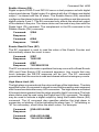
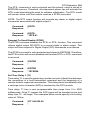
Warranty
CHAPTER 1
CHAPTER 2
CHAPTER 3
CHAPTER 4
CHAPTER 5
CHAPTER 6
CHAPTER 7
CHAPTER 8
CHAPTER 9
Appendix A
Appendix B
Appendix C
Appendix D
Appendix E
Appendix F
Appendix G
Appendix H
TABLE OF CONTENTS
4
Getting Started
Default Mode 1-1
Quick Hook-Up 1-2
Functional Description
Block Diagram 2-4
Communications
Data Format 3-2
RS-232 3-2
Multi-party Connection 3-3
Software Considerations 3-4
Changing Baud Rate 3-5
Using a Daisy-Chain With a Dumb Terminal
RS-485 3-6
RS-485 Multidrop System 3-8
Command Set
Table of Commands 4-6
User Commands 4-7
Error Messages 4-18
Setup Information and Command
Command Syntax 5-2
Setup Hints 5-11
Digital I/O Function
Digital Outputs 6-1
Digital Inputs 6-2
Events Counter 6-3
Alarm Outputs 6-4
On-Off Controller 6-5
Setpoint 6-9
Power Supply
Troubleshooting
Calibration
(ASCII TABLE )
D1600 Data Sheet
D1400 Data Sheet
D1500 Data Sheet
D2000 Series
Continuous Operation
RTS Operation
D1000/2000 Specifications
3-5
WARRANTY
DGH warrants each D1000 and D2000 series module to be free from defects
in materials and workmanship under normal conditions of use and service
and will replace any component found to be defective, on its return to DGH,
transportation charges prepaid within one year of its original purchase. DGH
assumes no liability, expressed or implied, beyond its obligation to replace
any component involved. Such warranty is in lieu of all other warranties
expressed or implied.
WARNING
The circuits and software contained in D1000 and D2000 series
modules are proprietary. Purchase of these products does not transfer
any rights or grant any license to the circuits or software used in these
products. Disassembling or decompiling of the software program is
explicitly prohibited. Reproduction of the software program by any
means is illegal.
As explained in the setup section, all setups are performed entirely
from the outside of the D1000 module. There is no need to open the
module because there are no user-serviceable parts inside. Removing
the cover or tampering with, modifying, or repairing by unauthorized
personnel will automatically void the warranty. DGH is not responsible
for any consequential damages.
RETURNS
When returning products for any reason, contact the factory and request a
Return Authorization Number and shipping instructions. Write the Return
Authorization Number on the outside of the shipping box. DGH strongly
recommends that you insure the product for value prior to shipping. Items
should not be returned collect as they will not be accepted.
Shipping Address:
DGH Corporation
Hillhaven Industrial Park
146 Londonderry Turnpike
Hooksett, NH 03106
Chapter 1
Getting Started
Default Mode
All D1000 modules contain an EEPROM (Electrically Erasable Programmable Read Only Memory) to store setup information and calibration
constants. The EEPROM replaces the usual array of switches and pots
necessary to specify baud rate, address, parity, etc. The memory is
nonvolatile which means that the information is retained even if power is
removed. No batteries are used so it is never necessary to open the module
case.
The EEPROM provides tremendous system flexibility since all of the
module’s setup parameters may be configured remotely through the communications port without having to physically change switch and pot
settings. There is one minor drawback in using EEPROM instead of
switches; there is no visual indication of the setup information in the module.
It is impossible to tell just by looking at the module what the baud rate,
address, parity and other settings are. It is difficult to establish communications with a module whose address and baud rate are unknown. To
overcome this, each module has an input pin labeled DEFAULT*. By
connecting this pin to Ground, the module is put in a known communications
setup called Default Mode.
The Default Mode setup is: 300 baud, one start bit, eight data bits, one
stop bit, no parity, any address is recognized.
Grounding the DEFAULT* pin does not change any of the setups stored in
EEPROM. The setup may be read back with the Read Setup (RS) command
to determine all of the setups stored in the module. In Default Mode, all
commands are available.
A module in Default Mode will respond to any address except the six
identified illegal values (NULL, CR, $, #, {, }). A dummy address must be
included in every command for proper responses. The ASCII value of the
module address may be read back with the RS command. An easy way to
determine the address character is to deliberately generate an error
message. The error message outputs the module’s address directly after
the “?” prompt.
Setup information in a module may be changed at will with the SetUp (SU)
command. Baud rate and parity setups may be changed without affecting
the Default values of 300 baud and no parity. When the DEFAULT* pin is
released, the module automatically performs a program reset and configures itself to the baud rate and parity stored in the setup information.
The Default Mode is intended to be used with a single module connected to
a terminal or computer for the purpose of identifying and modifying setup
Getting Started 1-2
values. In most cases, a module in Default Mode may not be used in a string
with other modules.
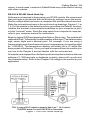
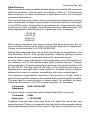
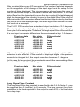
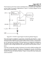
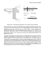
RS-232 & RS-485 Quick Hook-Up
Software is not required to begin using your D1000 module. We recommend
that you begin to get familiar with the module by setting it up on the bench.
Start by using a dumb terminal or a computer that acts like a dumb terminal.
Make the connections shown in the quick hook-up drawings, Figures 1.1 or
1.2. Put the module in the default mode by grounding the Default* terminal.
Initialize the terminal communications package on your computer to put it
into the “terminal” mode. Since this step varies from computer to computer,
refer to your computer manual for instructions.
Begin by typing $1RD and pressing the Enter or Return key. The module will
respond with an * followed by the data reading at the input. The data includes
sign, seven digits and a decimal point. For example, if you are using a
thermocouple module and measuring room temperature your reading might
be *+00025.00. The temperature reading will initially be in °C which has
been preset at the factory. Once you have a response from the module you
can turn to the Chapter 4 and get familiar with the command set.
All modules are shipped from the factory with a setup that includes a channel
address of 1, 300 baud rate, no linefeeds, no parity, alarms off, no echo and
two-character delay. Refer to the Chapter 5 to configure the module to your
application.
Figure 1.1 RS-232C Quick Hook-Up.
Getting Started 1-3
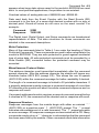
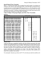
Figure 1.2 RS-485 Quick Hook-Up.
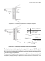
RS-485 Quick Hook-up to a RS-232 port
An RS-485 module may be easily interfaced to an RS-232C terminal for
evaluation purposes. This connection is only suitable for benchtop operation
and should never be used for a permanent installation. Figure 1.3 shows the
hook-up. This connection will work provided the RS-232C transmit output is
current limited to less than 50mA and the RS-232C receive threshold is
greater than 0V. All terminals that use 1488 and 1489 style interface IC’s will
satisfy this requirement. With this connection, characters generated by the
terminal will be echoed back. To avoid double characters, the local echo on
the terminal should be turned off.
If the current limiting capability of the RS-232C output is uncertain, insert a
100Ω to 1kΩ resistor in series with the RS-232 output.
In some rare cases it may be necessary to connect the module’s DATA
pin to ground through a 100Ω to 1kΩ resistor.
Getting Started 1-4
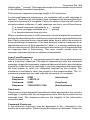
Figure 1.3 RS-485 Quick Hook-Up with RS-232C Port.
Chapter 2
Functional Description
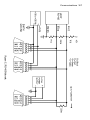
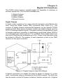
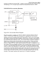
A functional diagram of a typical module is shown in Figure 2.1. It is a useful
reference that shows the data path in the module and to explain the function
of many of the module’s commands.
The first step is to acquire the sensor signal and convert it to digital data. In
Figure 2.1, all the signal conditioning circuitry has been lumped into one
block, the analog/digital converter (A/D). Autozero and autocalibration is
performed internally and is transparent to the user.
The full-scale output of the A/D converter may be trimmed using the Trim
Span (TS) command. The TS command adjusts calibration values stored
internally in the EEPROM. The TS command should only be used to trim the
accuracy of the unit with a laboratory standard reference applied to the
sensor input.
The trimmed data flows into either of two digital filters. The filter selection is
performed automatically by the microprocessor after every A/D conversion.
The filter selection depends on the difference of the current A/D output data
and the previous data stored in the output data register. If the least significant
decimal digit from the A/D differs from the old output data by more than 10
counts, the large signal filter is selected. If the change is less than 10 counts,
the small signal filter is used.
The two-filter system allows for different degrees of filtering depending on
the rate of the input change. For steady-state signals, the small-signal filter
averages out noise and small input changes to give a stable steady-state
output. The large-signal filter is activated by step changes or very noisy input
signals. The time constants for the two filters can be specified independently
with the SetUp (SU) command. The filter values are stored in nonvolatile
memory. Typically, the small-signal filter is set to a larger time constant than
the large-signal filter. This gives very good noise rejection along with fast
response to step inputs.
The modules allow user selectable output scaling in °C or °F on temperature
data. This selection is shown in Figure 2.1 as a switch following the digital
filters. The default scaling in the modules is °C, but this may be converted
to °F by feeding the data through a conversion routine. The switch position
is controlled by a bit in the setup data and may be changed with the SetUp
(SU) command. The scaling selection is nonvolatile. In non-temperature
applications, °C should always be selected.
The scaled data is summed with data stored in the Output Offset Register
to obtain the final output value. The output offset is controlled by the user and
has many purposes. The data in the Output Offset Register may be used to
trim any offsets caused by the input sensor. It may be used to null out
Functional Description 2-2
undesired signal such as a tare weight. The Trim Zero (TZ) command is used
to adjust the output to any desired value by loading the appropriate value in
the offset register. The offset register data is nonvolatile.
The output offset may also be modified using the Set Point (SP) command.
The data value specified by the SP command is multiplied by -1 before being
loaded into the register. The Set Point command specifies a null value that
is subtracted from the input data. The output reading becomes a deviation
value from the downloaded setpoint. This feature is very useful in on-off
controllers as described in Chapter 6 of this manual.
The value stored in the offset register may be read back using the Read Zero
(RZ) command. Data loaded in with the SP command will be read back with
the sign changed. The output register may be reset to zero with the Clear
Zero (CZ) command.
The output data may be read with the Read Data (RD) command. In some
cases when a computer is used as a host, the same data value may be read
back several times before it is updated with a new A/D conversion. To
guarantee that the same data is not read more than once, the New Data (ND)
command is used. Each time an RD or ND command is performed, the New
Data Flag is cleared. The flag is set each time the output data register is
loaded as the result of a new A/D conversion. The ND command waits until
the flag is set before it outputs the data reading.
The remainder of Figure 2.1 shows several functions: a versatile alarm
function, an event counter and general-purpose digital inputs and outputs.
These functions are described in detail in Chapter 6.
The alarm section consists of two registers that are used to store high and
low alarm limit values. These registers may be down-loaded with data
values by using the HI and LO alarm commands. The alarm values are
loaded with the same data format that is used with the output data. The high
and low alarm registers are nonvolatile so they will not be lost when the unit
is powered down. The values held in the alarm registers may be read back
at any time with the Read High (RH) and Read Low (RL) commands.
The data held in the alarm registers is continually compared with the
calculated output data. The result of the comparison is used to trip alarms
that may be used as control outputs. The high alarm is turned on when the
output data exceeds the high limit value. The low alarm is activated if the
output data is less than the low alarm value. Each alarm has two user
selectable modes, either Momentary (M) or Latching (L). Momentary alarms
are activated only while the alarm condition is met; if the output data returns
within limits, the alarm is turned off. Conversely, when latching alarms are
activated, they remain on even if the output data returns within limits.
Functional Description 2-3
Latching alarms are turned off with the Clear Alarms (CA) command or if the
opposite alarm limit is exceeded.
The state of the alarms may be read with the Digital Input (DI) command.
Also, the alarm outputs may be used to activate digital outputs on the module
to turn on alarms or to perform simple control functions. The alarm outputs
are shared with the general purpose digital output bits DO0 and DO1. To
connect the alarm outputs to the module connector, the Enable Alarm (EA)
command is used. The connector pins may be switched back to the generalpurpose digital outputs using the Disable Alarms (DA) command. The EA/
DA selection is nonvolatile.
The general-purpose digital outputs are open-collector transistor switches
that may be controlled by the host with the Digital Output (DO) command.
They are designed to activate external solid-state relays to control AC or DC
power circuits. The output may also be used to interface to other logic-level
devices. The number of digital outputs available depends on the module
type.
The Digital Input (DI) command is used to sense the logic levels on the digital
input pins DI0-DI7. The digital inputs are used to read logic levels generated
by other devices. They are also useful to sense the state of electromechanical limit switches. The number of digital inputs available varies with
the module type.
The DI0 input is shared with the input to the Event Counter. The Event
Counter accumulates the number of positive transitions that occur on the
DI0/EV connector pin. The counter can accumulate up to 9999999 (decimal)
events and may be read with the Read Events (RE) command. The counter
input is filtered and uses a Schmitt-trigger input to provide a bounce-free
input for mechanical switches. The counter value may be zeroed with the
Clear Events (CE) command or the write-protected Events Clear (EC)
command.
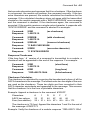
Functional Description 2-4
Chapter 3
Communications
Introduction
The D1000 modules has been carefully designed to be easy to interface to
all popular computers and terminals. All communications to and from the
modules are performed with printable ASCII characters. This allows the
information to be processed with string functions common to most high-level
languages such as BASIC. For computers that support RS-232C, no special
machine language software drivers are necessary for operation. The
modules can be connected to auto-answer modems for long-distance
operation without the need for a supervisory computer. The ASCII format
makes system debugging easy with a dumb terminal.
This system allows multiple modules to be connected to a communications
port with a single 4-wire cable. Up to 32 RS-485 modules may be strung
together on one cable; 122 with repeaters. A practical limit for RS-232C units
is about ten, although a string of 122 units is possible. The modules
communicate with the host on a polling system; that is, each module
responds to its own unique address and must be interrogated by the host.
A module can never initiate a communications sequence. A simple command/response protocol must be strictly observed to avoid communications
collisions and data errors.
Communications to the D1000 modules is performed with two-character
ASCII command codes such as RD to Read Data from the analog input. A
complete description of all commands is given in the Chapter 4. A typical
command/response sequence would look like this:
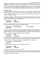
Command:
Response:
$1RD
*+00123.00
A command/response sequence is not complete until a valid response is
received. The host may not initiate a new command until the response from
a previous command is complete. Failure to observe this rule will result in
communications collisions. A valid response can be in one of three forms:
1) a normal response indicated by a ‘ * ‘ prompt
2) an error message indicated by a ‘ ? ‘ prompt
3) a communications time-out error
When a module receives a valid command, it must interpret the command,
perform the desired function, and then communicate the response back to
the host. Each command has an associated delay time in which the module
is busy calculating the response. If the host does not receive a response in
an appropriate amount of time specified in Table 3.1, a communications
time-out error has occurred. After the communications time-out it is assumed that no response data is forthcoming. This error usually results when
Communications 3-2
an improper command prompt or address is transmitted. The table below
lists the timeout specification for each command:
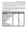
Mnemonic
Timeout
DI,DO,RD
ND
All other commands
10 mS
See text
100 mS
Table 3.1 Response Timeout Specifications.
The timeout specification is the turn-around time from the receipt of a
command to when the module starts to transmit a response.
Data Format
All modules communicate in standard NRZ asynchronous data format. This format provides one start bit, seven data bits, one parity bit
and one stop bit for each character.
RS-232C
RS-232C is the most widely used communications standard for information
transfer between computing equipment. RS-232C versions of the D1000 will
interface to virtually all popular computers without any additional hardware.
Although the RS-232C standard is designed to connect a single piece of
equipment to a computer, the D1000 system allows for several modules to
be connected in a daisy-chain network structure.The advantages offered by
the RS-232C standard are:
1) widely used by all computing equipment
2) no additional interface hardware in most cases
3) separate transmit and receive lines ease debugging
4) compatible with dumb terminals
However, RS-232C suffers from several disadvantages:
1) low noise immunity
2) short usable distance
3) greater communications delay in multiple-module systems
4) less reliable–loss of one module; communications are lost
5) wiring is slightly more complex than RS-485
6) host software must handle echo characters
Single Module Connection
Communications 3-3
Figure 1.1 shows the connections necessary to attach one module to a host.
Use the Default Mode to enter the desired address, baud rate, and other
setups (see Setups). The use of echo is not necessary when using a single
module on the communications line.
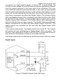
Multi-party Connection
RS-232C is not designed to be used in a multiparty system; however the
D1000 modules can be daisy-chained to allow many modules to be
connected to a single communications port. The wiring necessary to create
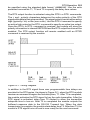
the daisy-chain is shown in Figure 3.1. Notice that starting with the host,
each Transmit output is wired to the Receive input of the next module in the
daisy chain. This wiring sequence must be followed until the output of the last
module in the chain is wired to the Receive input of the host. All modules in
the chain must be setup to the same baud rate and must echo all received
data (see Setups). Each module must be setup with its own unique address
to avoid communications collisions (see Setups). In this network, any
characters transmitted by the host are received by each module in the chain
and passed on to the next station until the information is echoed back to the
Receive input of the host. In this manner all the commands given by the host
are examined by every module. If a module in the chain is correctly
addressed and receives a valid command, it will respond by transmitting the
response on the daisy chain network. The response data will be ripple
through any other modules in the chain until it reaches its final destination,
the Receive input of the host.
The daisy chain network must be carefully implemented to avoid the pitfalls
Figure 3.1 RS-232 Daisy Chain Network.
Communications 3-4
inherent in its structure. The daisy-chain is a series-connected structure and
any break in the communications link will bring down the whole system.
Several rules must be observed to create a working chain:
1. All wiring connections must be secure; any break in the wiring,
power, ground or communications breaks the chain.
2. All modules must be plugged into their own connectors.
3. All modules must be setup for the same baud rate.
4. All modules must be setup for echo.
Software Considerations
If the host device is a computer, it must be able to handle the echoed
command messages on its Receive input along with the responses from the
module. This can be handled by software string functions by observing that
a module response always begins with a ‘ * ‘ or ‘ ? ‘ character and ends with
a carriage return.
A properly addressed D1000 module in a daisy chain will echo all of the
characters in the command including the terminating carriage return. Upon
receiving the carriage return, the module will immediately calculate and
transmit the response to the command. During this time, the module will not
echo any characters that appear on its receive input. However, if a character
is received during this computation period, it will be stored in the module’s
internal receive buffer. This character will be echoed after the response
string is transmitted by the module. This situation will occur if the host
computer appends a linefeed character on the command carriage return. In
this case the linefeed character will be echoed after the response string has
been transmitted.
The daisy chain also affects the command timeout specifications. When a
module in the chain receives a character it is echoed by retransmitting the
character through the module’s internal UART. This method is used to
provide more reliable communications since the UART eliminates any
slewing errors caused by the transmission lines. However, this method
creates a delay in propagating the character through the chain. The delay
is equal to the time necessary to retransmit one character using the baud
rate setup in the module:
Baud Rate
300
600
1200
2400
4800
Delay
33.30ms
16.70ms
8.33ms
4.17ms
2.08ms
Baud Rate
9600
19200
38400
57600
115200
Delay
1.04ms
0.52ms
0.26ms
173.6µs
86.8µs
One delay time is accumulated for each module in the chain. For example,
Communications 3-5
if four modules are used in a chain operating at 1200 baud, the accumulated
delay time is 4 X 8.33 mS = 33.3 mS This time must be added to the times
listed in Table 3.1 to calculate the correct communications time-out error.
For modules with RS-232C outputs, the programmed communications
delay specified in the setup data (see Chapter 5) is implemented by sending
a NULL character (00) followed by an idle line condition for one character
time. This results in a delay of two character periods. For longer delay times
specified in the setup data, this sequence is repeated. Programmed
communications delay is seldom necessary in an RS-232C daisy chain
since each module in the chain adds one character of communications
delay.
Changing Baud Rate
It is possible to change the baud rate of an RS-232C daisy chain on-line. This
process must be done carefully to avoid breaking the communications link.
1. Use the SetUp (SU) command to change the baud rate setup on each
module in the chain. Be careful not to generate a reset during this process.
A reset can be caused by the Remote Reset (RR) command or power
interruptions.
2. Verify that all the modules in the chain contain the new baud rate setup
using the Read Setup (RS) command. Every module in the chain must be
setup for the same baud rate.
3. Remove power from all the modules for at least 10 seconds. Restore
power to the modules. This generates a power-up reset in each module and
loads in the new baud rate.
4. Change the host baud rate to the new value and check communications.
5. Be sure to compensate for a different communications delay as a
result of the new baud rate.
Using A Daisy-Chain With A Dumb Terminal
A dumb terminal can be used to communicate to a daisy-chained system.
The terminal is connected in the same manner as a computer used as a host.
Any commands typed into the dumb terminal will be echoed by the daisy
chain. To avoid double characters when typing commands, set the terminal
to full duplex mode or turn off the local echo. The daisy chain will provide the
input command echo.
Communications 3-6
RS-485
RS-485 is a recently developed communications standard to satisfy the
need for multidropped systems that can communicate at high data rates
over long distances. RS-485 is similar to RS-422 in that it uses a balanced
differential pair of wires switching from 0 to 5V to communicate data. RS-485
receivers can handle common mode voltages from -7V to +12V without loss
of data, making them ideal for transmission over great distances. RS-485
differs from RS-422 by using one balanced pair of wires for both transmitting
and receiving. Since an RS-485 system cannot transmit and receive at the
same time it is inherently a half-duplex system. RS-485 offers many
advantages over RS-232C:
1) balanced line gives excellent noise immunity
2) can communicate with D1000 modules at 115200 baud
3) communications distances up to 4,000 feet.
4) true multidrop; modules are connected in parallel
5) can disconnect modules without losing communications
6) up to 32 modules on one line; 122 with repeaters
7) no communications delay due to multiple modules
8) simplified wiring using standard telephone cable
RS-485 does have disadvantages. Very few computers or terminals have
built-in support for this new standard. Interface boards are available for the
IBM PC and compatibles and other RS-485 equipment will become available as the standard gains popularity. An RS-485 system usually requires
an interface.
We offer the A1000 and A2000 interface converters that will convert RS-232
signals to RS-485 or repeat RS-485 signals. The A1000 converters also
include a +24Vdc, one amp power supply for powering D1000 series
modules. The A1000 or A2000 connected as an RS-485 repeater can be
used to extend an existing RS-485 network or connect up to 122 modules
on one serial communications port.
Communications 3-7
Communications 3-8
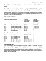
RS-485 Multidrop System
Figure 3.2 illustrates the wiring required for multiple-module RS-485 system. Notice that every module has a direct connection to the host system.
Any number of modules may be unplugged without affecting the remaining
modules. Each module must be setup with a unique address and the
addresses can be in any order. All RS-485 modules must be setup for no
echo to avoid bus conflicts (see Setup). Also note that the connector pins on
each module are labelled with notations (B), (R), (G), and (Y). This
designates the colors used on standard 4-wire telephone cable:
Label
Color
(B) GND
(R) V+
(G) DATA* (-)
(Y) DATA (+)
Black
Red
Green
Yellow
This color convention is used to simplify installation. If standard 4-wire
telephone cable is used, it is only necessary to match the labeled pins with
the wire color to guarantee correct installation.
DATA* on the label is the complement of DATA (negative true).
To minimize unwanted reflections on the transmission line, the bus should
be arranged as a line going from one module to the next. ‘Tree’ or random
structures of the transmission line should be avoided. When using long
transmission lines and/or high baud rates, the data lines should be terminated at each end with 200 ohm resistors. Standard values of 180 ohms or
220 ohms are acceptable.
During normal operation, there are periods of time where all RS-485 drivers
are off and the communications lines are in an 'idle' high impedance
condition. During this condition, the lines are susceptible to noise pickup
which may be interpreted as random characters on the communications
line. To prevent noise pickup, all RS-485 systems should incorporate 1K
ohm bias resistors as shown in Figure 3.2. The resistors will maintain the
data lines in a 'mark' condition when all drivers are off.
A1000 series converter boxes have the 1KΩ resistors built-in. The resistors
are user-selectable via dip switch located on the rear panel of the A1000.
Special care must be taken with very long busses (greater than 1000 feet)
to ensure error-free operation. Long busses must be terminated as described above. The use of twisted cable for the DATA and DATA* lines will
greatly enhance signal fidelity. Use parity and checksums along with the ‘#’
form of all commands to detect transmission errors. In situations where
many modules are used on a long line, voltage drops in the power leads
Communications 3-9
becomes an important consideration. The GND wire is used both as a power
connection and the common reference for the transmission line receivers in
the modules. Voltage drops in the GND leads appear as a common-mode
voltage to the receivers. The receivers are rated for a maximum of -7V. of
common-mode voltage. For reliable operation, the common mode voltage
should be kept below -5V.
To avoid problems with voltage drops, modules may be powered locally
rather than transmitting the power from the host. Inexpensive 'calculator'
type power supplies are useful in remote locations. When local supplies are
used, be sure to provide a ground reference with a third wire to the host or
through a good earth ground. With local supplies and an earth ground, only
two wires for the data connections are necessary.
Communications Delay
All D1000 modules with RS-485 outputs are setup at the factory to provide
two units of communications delay after a command has been received (see
Chapter 5). This delay is necessary when using host computers that transmit
a carriage return as a carriage return-linefeed string. Without the delay, the
linefeed character may collide with the first transmitted character from the
module, resulting in garbled data. If the host computer transmits a carriage
return as a single character, the delay may be set to zero to improve
communications response time.
Chapter 4
Command Set
The D1000 modules operate with a simple command/response protocol to
control all module functions. A command must be transmitted to the module
by the host computer or terminal before the module will respond with useful
data. A module can never initiate a communications sequence. A variety of
commands exists to exploit the full functionality of the modules. A list of
available commands and a sample format for each command is listed in
Table 4.1.
Command Structure
Each command message from the host must begin with a command prompt
character to signal to the modules that a command message is to follow.
There are four valid prompt characters; a dollar sign character ($) is used to
generate a short response message from the module. A short response is
the minimum amount of data necessary to complete the command. The
second prompt character is the pound sign character (#) which generates
long responses (will be covered later in this chapter). The other two prompt
characters: left curly brace ({ ) and right curly brace ( }) are part of the
Extended Addressing mode described in chapter 10
The prompt character must be followed by a single address character
identifying the module to which the command is directed. Each module
attached to a common communications port must be setup with its own
unique address so that commands may be directed to the proper unit.
Module addresses are assigned by the user with the SetUp (SU) command.
Printable ASCII characters such as ‘1’ (ASCII $31) or ‘A’ (ASCII $41) are the
best choices for address characters.
The address character is followed by a two-character command that
identifies the function to be performed by the module. All of the available
commands are listed in Table 4.1 along with a short function definition. All
commands are described in Chapter 4. Commands must be transmitted as
upper-case characters.
A two-character checksum may be appended to any command message as
a user option. See ‘Checksum’ in Chapter 4 .
All commands must be terminated by a Carriage Return character (ASCII
$0D). (In all command examples in this text the Carriage Return is either
implied or denoted by the symbol ‘CR’.)
In addition to the command structure discussed above there is a special
command format called Extended Addressing. This mode uses a different prompt, either '{' or '}' to distinguish it from the regular command
syntax. The Extended Addressing mode is described in chapter 10.
Command Set 4-2
Data Structure
Many commands require additional data values to complete the command
definition as shown in the example commands in Table 4.1. The particular
data necessary for these commands is described in full in the complete
command descriptions.
The most common type of data used in commands and responses is analog
data. Analog data is always represented in the same format for all models
in the D1000 series. Analog data is represented as a nine-character string
consisting of a sign, five digits, decimal point, and two additional digits. The
string represents a decimal value in engineering units. Examples:
+12345.68
+00100.00
-00072.10
-00000.00
When using commands that require analog data as an argument, the full
nine-character string must be used, even if some digits are not significant.
Failure to do this results in a SYNTAX ERROR.
Analog data responses from the module will always be transmitted in the
nine-character format. This greatly simplifies software parsing routines
since all analog data is in the same format for all module types.
In many cases, some of the digits in the analog data may not be significant.
For instance, the D1300 thermocouple input modules feature 1 degree
output resolution. A typical analog data value from this type of module could
be +00123.00. The two digits to the right of the decimal point have no
significance in this particular model. However, the data format is always
adhered to in order to maintain compatibility with other module types.
The maximum computational resolution of the module is 16 bits, which is
less than the resolution that may be represented by an analog data variable.
This may lead to round-off errors in some cases. For example, an alarm
value may be stored in a D1000 module using the ‘HI’ command:
Command:
Response:
$1HI+12345.67M
*
The alarm value is read back with the Read High (RH) command:
Command:
Response:
$1RH
*+12345.60M
It appears that the data read back does not match the value that was
originally saved. The error is caused by the fact that the value saved exceeds
the computational resolution of the module. This type of round-off error only
Command Set 4-3
appears when large data values saved in the module’s EEPROM are read
back. In most practical applications, the problem is non-existent.
Overload values of analog data are +99999.99 and -99999.99 .
Data read back from the Event Counter with the Read Events (RE)
command is in the form of a seven-digit decimal number with no sign or
decimal point. Round-off errors do not occur on the event counter. For
example:
Command:
Response:
$1RE
*0000123
The Digital Input, Digital Output, and Setup commands use hexadecimal
representations of data. The data structures for these commands are
detailed in the command descriptions.
Write Protection
Many of the commands listed in Table 4.1 are under the heading of ‘Write
Protected Commands’. These commands are used to alter setup data in the
module’s EEPROM. They are write protected to guard against accidental
loss of setup data. All write-protected commands must be preceded by a
Write Enable (WE) command before the protected command may be
executed.
Miscellaneous Protocol Notes
The address character must transmitted immediately after the command
prompt character. After the address character the module will ignore any
character below ASCII $23 (except CR). This allows the use of spaces
(ASCII $20) within the command message for better readability if desired.
The length of a command message is limited to 20 printable characters. If
a properly addressed module receives a command message of more than
20 characters the module will abort the whole command sequence and no
response will result.
If a properly addressed module receives a second command prompt before
it receives a CR, the command will be aborted and no response will result.
Response Structure
Response messages from the module begin with either an asterisk ‘ * ‘
(ASCII $2A) or a question mark ‘ ? ‘ (ASCII $3F) prompt. The ‘ * ‘ prompt
indicates acknowledgment of a valid command. The ‘ ? ‘ prompt precedes
an error message. All response messages are terminated with a CR. Many
commands simply return a ‘ * ‘ character to acknowledge that the command
has been executed by the module. Other commands send data information
Command Set 4-4
following the ‘ * ‘ prompt. The response format of all commands may be found
in the detailed command description.
The maximum response message length is 20 characters.
A command/response sequence is not complete until a valid response is
received. The host may not initiate a new command until the response from
a previous command is complete. Failure to observe this rule will result in
communications collisions. A valid response can be in one of three forms:
1) a normal response indicated by a ‘ * ‘ prompt
2) an error message indicated by a ‘ ? ‘ prompt
3) a communications time-out error
When a module receives a valid command, it must interpret the command,
perform the desired function, and the communicate the response back to the
host. Each command has an associated delay time in which the module is
busy calculating the response. If the host does not receive a response in an
appropriate amount of time specified in Table 4.1, a communications timeout error has occurred. After the communications time-out it is assumed that
no response data is forthcoming. This error usually results when an
improper command prompt or address is transmitted.
Long Form Responses
When the pound sign ‘ # ‘ command prompt is used, the module responds
with a ‘long form’ response. This type of response will echo the command
message, supply the necessary response data and will add a two-character
checksum to the end of the message. Long form responses are used when
the host wishes to verify the command received by the module. The
checksum is included to verify the integrity of the response data. The ‘ # ‘
command prompt may be used with any command. For example:
Command:
Response:
$1RD
*+00072.10
(short form)
Command:
Response:
#1RD
*1RD+00072.10A4
(long form)
(A4=checksum)
Checksum
Checksum is a two character hexadecimal value appended to the end of a
message. It verifies that the message received is exactly the same as the
message sent. The checksum ensures the integrity of the information
communicated.
Command Checksum
A two-character checksum may be appended to any command to the
module as a user option. When a module interprets a command, it looks for
Command Set 4-5
the two extra characters and assumes that it is a checksum. If the checksum
is not present, the module will perform the command normally. If the two
extra characters are present, the module calculates the checksum for the
message. If the calculated checksum does not agree with the transmitted
checksum, the module responds with a ‘BAD CHECKSUM’ error message
and the command is aborted. If the checksums agree, the command is
executed. If the module receives a single extra character, it responds with
‘SYNTAX ERROR’ and the command is aborted For example:
Command:
Response:
$1RD
*+00072.10
(no checksum)
Command:
Response:
$1RDEB
*+00072.10
(with checksum)
Command:
Response:
$1RDAB
(incorrect checksum)
?1 BAD CHECKSUM
Command:
Response:
$1RDE
(one extra character)
?1 SYNTAX ERROR
Response Checksums
If the long form ‘ # ‘ version of a command is transmitted to a module, a
checksum will be appended to the end of the response. For example:
Command:
Response:
$1RD
*+00072.10
(short form)
Command:
Response:
#1RD
*1RD+00072.10A4
(long form)
(A4=checksum)
Checksum Calculation
The checksum is calculated by summing the hexadecimal values of all the
ASCII characters in the message. The lowest order two hex digits of the sum
are used as the checksum. These two digits are then converted to their
ASCII character equivalents and appended to the message. This ensures
that the checksum is in the form of printable characters.
Example: Append a checksum to the command #1DOFF
Characters:
ASCII hex values:
Sum (hex addition)
#
1
D
O
F
F
23
31
44
4F
46
46
23 + 31 + 44 + 4F + 46 + 46 = 173
The checksum is 73 (hex). Append the characters 7 and 3 to the end of
the message: #1DOFF73
Example: Verify the checksum of a module response *1RD+00072.10A4
Command Set 4-6
The checksum is the two characters preceding the CR: A4
Add the remaining character values:
*
1
R
D
+
0
0
0
7
2
.
1 0
2A + 31 + 52 + 44 + 2B + 30 + 30 + 30 + 37 + 32 + 2E + 31 + 30 = A4
The two lowest-order hex digits of the sum are A4 which agrees with the
transmitted checksum.
The transmitted checksum is the character string equivalent to the calculated hex integer. The variables must be converted to like types in the host
software to determine equivalency.
If checksums do not agree, a communications error has occurred.
If a module is setup to provide linefeeds, the linefeed characters are not
included in the checksum calculation.
Parity bits are never included in the checksum calculation.
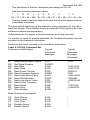
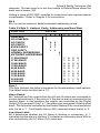
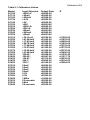
Table 4.1 D1000 Command Set
Command and Definition
DI
DO
ND
RD
RE
REA
RH
RID
RL
RPT
RS
RZ
WE
Read Alarms/Digital Inputs
Set Digital Outputs
New Data
Read Data
Read Event Counter
Read Extended Address
Read High Alarm Value
Read IDentification
Read Low Alarm Value
Read Pulse Transition
Read Setup
Read Zero
Write Enable
Typical
Command
Message
Typical
Response
Message
($ prompt)
$1DI
$1DOFF
$1ND
$1RD
$1RE
$1REA
$1RH
$1RID
$1RL
$1RPT
$1RS
$1RZ
$1WE
*0003
*
*+00072.00
*+00072.00
*0000107
*3031
*+00510.00L
* BOILER
*+00000.00L
*+*31070142
*+00000.00
*
$1CA
$1CE
$1CZ
$1DA
$1EA
*
*
*
*
*
Write Protected Commands
CA
CE
CZ
DA
EA
Clear Alarms
Clear Events
Clear Zero
Disable Alarms
Enable Alarms
Command Set 4-7
EC
HI
ID
LO
PT
RR
SU
SP
TS
TZ
WEA
Events Read & Clear
Set High Alarm Limit
IDentification
Set Low Alarm Limit
Pulse Transition
Remote Reset
Setup Module
Set Setpoint
Trim Span
Trim Zero
Write Extended Address
$1EC
$1HI+12345.67L
$1ID BOILER
$1LO+12345.67L
$1PT+$1RR
$1SU31070142
$1SP+00600.00
$1TS+00600.00
$1TZ+00000.00
$1WEA3031
*0000107
*
*
*
*
*
*
*
*
*
*
D1000 User Commands
Note that in all command and response examples given below, a carriage
return is implied after every character string.
Clear Alarms (CA)
The clear alarms command turns both the HI and LO alarms OFF. This
command does not affect the enable/disable or momentary/latching alarm
conditions. The alarms will continue to be compared to the input data after
the CA command is given. In cases where the alarm condition persists, the
alarms will be set at the end of the next input data conversion. The primary
purpose of the CA command is to clear latching alarms. See the Alarm
Output section of Chapter 6 for more information.
Command:
Response:
$1CA
*
Command:
Response:
#1CA
*1CADF
Clear Events (CE)
Clear Events command clears the events counter to 0000000.
Command:
Response:
$1CE
*
Command:
Response:
#1
*1CEE3
Note: When the events counter reaches 9999999, it stops counting. A CE
command must be sent to resume counting.
Clear Zero (CZ)
The Clear Zero command clears the output offset register value to
+00000.00. This command clears any data resulting from a Trim Zero (TZ)
Command Set 4-8
or SetPoint (SP) command.
Command:
Response:
$1CZ
*
Command:
Response:
#1CZ
*1CZF8
Disable Alarms (DA)
Most D1000 modules feature LO/DO0 and HI/DO1 pins on the module
connector. These pins serve a dual function and can be used to output either
the alarm outputs or digital outputs 0 and 1. The Disable Alarms command
is used to connect the digital outputs 0 and 1 to the connector pins. The alarm
settings are not affected in any way except that the alarm outputs are
disconnected from the module connector. The alarm status can still be read
with the Digital Input (DI) command. The complement to the DA command
is the Enable Alarms (EA) command.
Command:
Response:
$1DA
*
Command:
Response:
#1DA
*1DAE0
Digital Input (DI)
The DI command reads the status of the digital inputs and the alarms. The
response to the DI command is four hex characters representing two bytes
of data. The first byte contains the alarm status. The second byte contains
the digital input data.
Command:
Response:
$1DI
*0003
Command:
Response:
#1DI
*1DI0003AB
Listed below are the four possible alarm states in the first digital input byte
and their hex values.
00
01
02
03
Both HI and LO alarms off.
HI alarm off. LO alarm on.
HI alarm on. LO alarm off.
Both HI and LO alarms on.
The second byte displays the hex value of the digital input status. The
number of digital inputs varies depending on module type.
Digital Inputs
Data Bits
DI7
7
DI6
6
DI5
5
DI4
4
DI3
3
DI2
2
DI1
1
DI0
0
Command Set 4-9
For example: A typical response from a $1DI command could be: *01FE.
This response indicates that the HI alarm is off, the LO alarm is on, DI0 = 0
and all other digital inputs are = 1
All digital inputs that are not implemented or left unconnected are read as
‘1’
Digital input 0 serves a dual function. It is both a digital input and the Event
Counter input.
When reading digital inputs with a checksum, be sure not to confuse the
checksum with the data.
Digital Output (DO)
The DO command controls eight bits of digital outputs on the module
connector. The number of digital outputs implemented depends on the
model used. The digital outputs allow the module to control external circuits
under host command. The DO command requires an argument of two hex
characters specifying the eight bits of output data.
Digital Outputs DO7 DO6 DO5 DO4 DO3 DO2 DO1 DO0
Data Bits
7
6
5
4
3
2
1
0
The electrical implementation of the digital output consists of open-collector
transistors wired to the module connector. If a digital output is set to ‘1’ the
corresponding transistor is turned on and sinks current. Note that when a
digital output bit is set to ‘1’ the electrical output is near 0 volts. If a digital
output is set to ‘0’ the corresponding transistor is turned off and sinks no
current.
Assume a module has two digital outputs, and you wish to turn both outputs
on (sinking current). Set data bit 0 and data bit 1 to ‘1’. Since the module has
only two digital outputs, all the other bits are ‘don’t cares’. For example, this
command will turn both outputs ‘on’:
Command:
Response:
$1DOFF
*
To turn both outputs off you could use the command:
Command:
Response:
$1DO00
*
Digital outputs 0 and 1 share connector pins with the HI and LO alarms. The
Disable Alarms (DA) command is used to configure these pins as digital
outputs.
Digital output settings are not stored in nonvolatile memory. If a power failure
occurs, all digital outputs will be 0 upon power up.
Command Set 4-10
Enable Alarms (EA)
Digital outputs DO0/LO and DO1/HI serve a dual purpose as both digital
outputs and alarms. Digital output 0 is shared with the LO alarm and digital
output 1 is shared with the HI alarm. The Enable Alarms (EA) command
configures the shared outputs to indicate alarm conditions and disconnects
digital outputs 0 and 1. The EA command only affects the electrical output
of the alarms to the pins. The alarm status can be read at any time with the
Digital Input (DI) command. The complement to the EA command is the
Disable Alarms (DA) command.
Command:
Response:
$1EA
*
Command:
Response:
#1EA
*1EAE1
Events Read & Clear (EC)
The EC command is used to read the value of the Events Counter and
automatically clears the count to zero:
Command:
Response:
$1EC
*0000123
Command:
Response:
#1EC
*1EC000012339
The EC command eliminates a problem that may occur with a Read Events
(RE) and Clear Events (CE) command sequence. Any counts that may
occur between the RE-CE sequence will be lost. The EC command
guarantees that the counter is read and cleared without missing any counts.
High Alarm Limit (HI)
The high alarm command sets the value and type of the high alarm. The data
specified by the HI command is stored in nonvolatile memory and compared
with the sensor data after every A/D conversion. The high alarm is activated
if the input data is greater than the value stored by the HI command. The high
alarm status may be read using the Digital Input (DI) command. The alarm
may be used to activate a digital output by using the Enable Alarms (EA)
command. The HI command also specifies whether the high alarm is
momentary or latching. A letter indicating the alarm type, “L” for latching or
“M” for momentary, must follow the alarm value. For example:
Command:
Response:
$1HI+00100.00M
*
Command:
Response:
#1HI+00100.00M
*1HI+00100.00ME3
Command Set 4-11
The alarm limit should be set within the output range of the module. If the
alarm limit is set beyond the output range, the alarm will be activated only
on an overload condition.
The high alarm value may be read back with the Read High Alarm (RH)
command.
A latched alarm may be cleared with the Clear Alarms (CA) command. More
information on alarms may be found in Chapter 6.
IDentification (ID)
The IDentification command allows the user to write a message into the
internal nonvolatile memory which may be read back at any time using the
Read IDentification (RID) command. The message may be up to 16
characters long and has no affect on the module operation. Useful information such as the module location, calibration date or model number may be
stored for later retrieval.
The ID command is write protected and checksums are not supported. The
module will abandon any ID command with a message length in excess of
16 characters.
Command:
Response:
$1IDBOILER ROOM
*
Command:
Response:
#1IDBOILER ROOM
*1IDBOILER ROOM02
Low Alarm Limit (LO)
The low alarm command sets the value and type of the low alarm. The data
specified with the LO command is stored in nonvolatile memory and
compared with the sensor data after every A/D conversion. If the input data
is less than the low limit, the low alarm is activated. The low alarm status may
be read using the Digital Input (DI) command. The alarm may be used to
activate a digital output by using the Enable Alarms (EA) command. A letter
indicating the alarm type, “L” for latching or “M” for momentary, must follow
the alarm value. For example:
Command:
Response:
$1LO+00000.00M
*
Command:
Response:
#1LO+00000.00M
*1LO+00000.00MEC
The alarm limit should be set within the output range of the module. If the
alarm limit is set beyond the output range, the alarm will be activated only
on an overload condition.
Command Set 4-12
The low limit value may be read back with the Read Low Limit (RL)
command. More information on alarms may be found in Chapter 6.
New Data Command (ND)
The New Data (ND) command is a variation of the Read Data (RD)
command used to read sensor data from the module. The ND command
guarantees that the output data has not been previously read.
The D1000 module acquires analog input data eight times a second and
stores the result in the output buffer (see Figure 2.1). The Read Data (RD)
command simply reads the results stored in the output buffer. A fast host
communicating at a high baud rate could possibly read the output buffer
several times before the information is updated with a new A/D conversion.
This results in redundant information which may be confusing or may be a
waste of host processor time.
Associated with the output buffer is the New Data Flag (see Figure 2.1). This
flag is cleared each time an RD or ND command is performed. The flag is
set when the module’s microprocessor loads the output buffer with the result
of the most recent A/D conversion. The ND command will output data only
when the New Data Flag is set. If the flag is cleared when an ND command
is received, the module will wait until new data is present in the output buffer
before responding to the command. Thus, the output data obtained with an
ND command is always the result of a new A/D conversion.
The ND command is especially useful with computers that handle communications on an interrupt basis. The ND command is used to get maximum
throughput without producing redundant data.
Command:
Response:
$1ND
*+00072.00
Command:
Response:
#1ND
*1ND+00072.009F
A special condition exists when using the ND command with the D1600
frequency/pulse modules. These modules differ from the other sensor input
modules in that they require an input trigger signal to obtain new data. If no
signal exists on the input of the D1600, an ND command will wait indefinitely
for new data and the module will not respond.
In order to escape this condition, a single control-C ($03) may be issued by
the host to abort the ND command. The aborted ND command will respond
with the data value currently stored in the output buffer. Be aware that on an
RS-485 system, the control-C character may interfere with the ND output
data, causing a communications collision.
Command Set 4-13
Pulse Transition (PT)
The Pulse Transition command is used on Frequency and Timer input
modules. It is used to set the direction of the edge used to trigger the
measurement cycle. There are four possible edge transitions: (+ to -), (- to
+), (- to -), (+ to +). For example:
Command:
Response:
$1PT+ *
Command:
#1PT
Response:
*1PT+ -50
Read Data (RD)
The read data command is the basic command used to read the buffered
sensor data. The output buffer (Figure 2.1) allows the data to be read
immediately without waiting for an input A/D conversion. For example:
Command:
Response:
$1RD
*+00072.00
Command:
Response:
#1RD
*1RD+00072.10A4
Since the RD command is the most frequently used command in normal
operation, a special shortened version of the command is available. If a
module is addressed without a two-letter command, the module interprets
the string as an RD command.
Command:
Response:
$1
*+00072.10
Command:
Response:
#1
*1RD+00072.10A4
Read Events (RE)
The Read Events command reads the number of events that have been
accumulated in the Events Counter. The output is a seven-digit decimal
number. For example:
Command:
Response:
$1RE
*0000107
Command:
Response:
#1RE
*1RE00001074A
The maximum accumulated count is 9999999. When this count is reached,
the Events Counter stops counting. The counter may be cleared at any time
with the Clear Events (CE) command.
The Event Counter count is stored in volatile memory. If power is removed,
the Event Counter will reset to all 0’s upon power up.
Command Set 4-14
The Remote Reset (RR) command or a line break does not effect the value
of the Event Counter.
When reading the Event Counter with a checksum, be sure not to confuse
the checksum with the data.
Read Extended Address (REA)
The Read Extended Address is used to read back two character address
stored by the Extended Address (EA) command. The response message is
four characters representing the hex ASCII codes for the two-character
address :
Command:
Response:
$1REA
*3031
Command:
Response:
#1REA
*1REA3031FA
In this example the '30' and '31' are the hex ASCII codes for the characters
'0' and '1' respectively. The Extended Address is '01'.
Read High Alarm (RH)
The Read High alarm command reads the value and type of the high alarm
previously loaded by the HI command. The alarm type can be either latching
or momentary. A letter indicating the alarm type, “L” for latching or “M” for
momentary, will follow the alarm value. For example:
Command:
Response:
$1RH
*+00510.00L
Command:
Response:
#1RH
*1RH+00510.00LF0
The RH command may be used to verify the data loaded into nonvolatile
memory by the HI command.
Read IDentification (RID)
The Read Identification (RID) command is used to read data previously
stored by the ID command. The RID command response message length
is variable depending on the stored message length. The maximum response length can be up to 25 characters using the long form prompt and
linefeeds enabled.
Command:
Response:
$1RID
*BOILER ROOM
Command:
Response:
#1RID
*1RIDBOILER ROOM54
Command Set 4-15
Read Low Alarm (RL)
The Read Low alarm command reads the value and type of the low alarm.
The alarm type can be either latching or momentary. A letter indicating the
alarm type, “L” for latching or “M” for momentary, will follow the alarm value.
For example:
Command:
Response:
Command:
$1RL
*+00000.00L
#1RL
Response:
*1RL+00000.00LEE
The RL command may be used to verify data loaded into the nonvolatile
memory with the LO command.
Read Pulse Transition (RPT)
The Read Pulse Transition command is used on the Timer and Frequency
input modules. The RPT command reads the direction of the edge used to
trigger the measurement cycle. The direction of the pulse transition is set by
the user using the Pulse Transition (PT) command. There are four possible
edge transitions: (+ to -), (- to +), (- to -), (+ to +). For example:
Command:
Response:
Command:
$1RPT
*+ #1RPT
Response:
*1RPT+ -A2
Remote Reset (RR)
The reset command allows the host to perform a program reset on the
module’s microprocessor. This may be necessary if the module’s internal
program is disrupted by static or other electrical disturbances. Once a reset
command is received, the module will recalibrate itself. The calibration
process takes approximately 3 seconds. For example:
Command:
Response:
$1RR
*
Command:
Response:
#1RR
*1RRFF
In general, the state of the digital outputs and the event counter will not be
affected by the RR command. However, if data in the microprocessor’s RAM
(Random Access Memory) has been lost, the RR command will result in a
full power-up reset.
Any commands sent to the module during the self-calibration sequence will
result in a NOT READY error.
Command Set 4-16
Read Setup (RS)
The read setup command reads back the setup information loaded into the
module’s nonvolatile memory with the SetUp (SU) command. The response
to the RS command is four bytes of information formatted as eight hex
characters.
Command:
Response:
$1RS
*31070142
Command:
Response:
#1RS
*1RS3107014292
The response contains the module’s channel address, baud rate and other
parameters. Refer to the setup command (SU), and Chapter 5 for a list of
parameters in the setup information.
When reading the setup with a checksum, be sure not to confuse the
checksum with the setup information.
Read Zero (RZ)
The Read Zero command reads back the value stored in the Output Offset
Register (Figure 2.1).
Command:
Response:
$1RZ
*+00000.00
Command:
Response:
#1RZ
*1RZ+00000.00B0
The data read back from the Output Offset Register may be interpreted in
several ways. The commands that affect this value are: Trim Zero (TZ),
SetPoint (SP) and Clear Zero (CZ).
Setpoint (SP)
Data specified by the setpoint command is multiplied by -1 and loaded into
the Output Offset Register (Figure 2.1). The SP command is useful in on-off
controllers—see Chapter 6. The SP command may be used to null out
sensor data to obtain a deviation output when using RD or ND commands.
Command:
Response:
$1SP+00450.00
*
Command:
Response:
#1SP+00450.00
*1SP+00450.00B0
It is possible to load setpoint data that is beyond the output range of the
sensor. In this case, the setpoint is never reached by the sensor data unless
an overload is present.
Command Set 4-17
To clear a setpoint, use the Clear Zero (CZ) command.
The SP command writes over data written into the Output Offset Register by
the Trim Zero (TZ) command. If the Output Offset Register is used as a trim
value, this must be accounted for by the host before using the SP command.
The value stored in this register may be read back using the Read Zero (RZ)
command.
The setpoint data or trim data in the Output Offset Register is saved in
nonvolatile memory.
Setup Command (SU)
Each D1000 module contains an EEPROM (Electrically Erasable Programmable Read Only Memory) which is used to store module setup information
such as address, baud rate, parity, etc. The EEPROM is a special type of
memory that will retain information even if power is removed from the
module. The EEPROM is used to replace the usual array of DIP switches
normally used to configure electronic equipment.
The SetUp command is used to modify the user-specified parameters
contained in the EEPROM to tailor the module to your application. Since the
SetUp command is so important to the proper operation of a module, a whole
section of this manual has been devoted to its description. See Chapter 5.
The SU command requires an argument of eight hexadecimal digits to
describe four bytes of setup information:
Command:
Response:
$1SU31070182
*
Command:
Response:
#1SU31070182
*1SU3107018299
Trim Span (TS)
The trim span command is the basic means of trimming the accuracy of a
D1000 module. The TS command loads a calibration factor into nonvolatile
memory to trim the full-scale output of the signal conditioning circuitry. It is
intended only to compensate for long-term drifts due to aging of the analog
circuits, and has a useful trim value of ±10% of the nominal calibration set
at the factory. It is not to be used to change the basic transfer function of the
module. Full information on the use of the TS command may be found in
Chapter 9.
Command:
Response:
$1TS+00500.00
*
Command:
Response:
#1TS+00500.00
*1TS+00500.00B0
Command Set 4-18
Caution! TS is the only command associated with the span trim. There is no
provision to read back or clear errors loaded by the TS command. Misuse
of the TS command may destroy the calibration of the unit which can only
be restored by using laboratory calibration instruments in a controlled
environment. An input signal must be applied when using this command.
Trim Zero (TZ)
The Trim Zero command is used to load a value into the Output Offset
Register (Figure 2.1) to null out an offset in the output data. It may be used
to trim offsets created by sensors. It may also be used to null out data to
create a deviation output.
Example: Assume a D1511 bridge input module is being used with a load
cell for weight measurement. An initial reading of the load cell with no weight
applied may reveal an initial offset error:
Command:
Response:
$1RD
*+00005.00
With no weight applied, trim the output to read zero. To trim, use the TZ
command and specify the desired output reading:
Command:
Response:
$1TZ+00000.00
*
(zero output)
The TZ command will load a data value into the Output Offset Register to
force the output to read zero. The module will compensate for any previous
value loaded into the Output Offset Register. If another output reading is
taken, it will show that the offset has been eliminated:
Command:
Response:
$1RD
*+00000.00
Although the TZ command is most commonly used to null an output to zero,
it may be used to offset the output to any specified value. Assume that with
the previously nulled load cell system we performed this command:
Command:
Response:
$1TZ-00100.00
*
The new data output with no load applied would be:
Command:
Response:
$1RD
*-00100.00
The load cell output is now offset by -100.
The offset value stored by the TZ command is stored in nonvolatile memory
and may be read back with the Read Zero (RZ) command and cleared with
the Clear Zero (CZ) command.
Command Set 4-19
The SetPoint (SP) command will write over any value loaded by the TZ
command.
Write Enable (WE)
Each module is write protected against accidental changing of alarms,
limits, setup, or span and zero trims. To change any of these write protected
parameters, the WE command must precede the write-protected command.
The response to the WE command is an asterisk indicating that the module
is ready to accept a write-protected command. After the write-protected
command is successfully completed, the module becomes automatically
write disabled. Each write-protected command must be preceded individually with a WE command. For example:
Command:
Response:
$1WE
*
Command:
Response:
#1WE
*1WEF7
If a module is write enabled and the execution of a command results in an
error message other than WRITE PROTECTED, the module will remain
write enabled until a command is successfully completed resulting in an ‘ *
‘ prompt. This allows the user to correct the command error without having
to execute another WE command.
Write Extended Address (WEA)
The Write Extended Address (WEA) command allows the user to set the
two-byte address to be used with Extended Addressing (see Chapter 7). The
argument of the command specifies the hex ASCII values of the two
characters to be used as the Extended Address. For example, if the address
is to be set for characters '01':
Command:
Response:
$1WEA3031
*
Command:
Response:
#1WEA3031
*1WEA3031FF
Note that '30' and '31' are the hex ASCII values for characters '0' and '1'
respectively.
The EA command is write-protected and must be preceded with a WE
command.
The address data may be read back with the Read Extended Address (REA)
command.
Command Set 4-20
ERROR MESSAGES
The D1000 modules feature extensive error checking on input commands
to avoid erroneous operation. Any errors detected will result in an error
message and the command will be aborted.
All error messages begin with “?”, followed by the channel address, a space
and error description. The error messages have the same format for either
the ‘ $ ‘ or ‘ # ‘ prompts. For example:
?1 SYNTAX ERROR
There are eight error messages, and each error message begins with a
different character. It is easy for a computer program to identify the error
without having to read the entire string.
ADDRESS ERROR
There are six ASCII values that are illegal for use as a module address:
NULL ($00), CR ($0D), $ ($24), # ($23), { ($7B) and } ($7D). The ADDRESS
ERROR will occur when an attempt is made to load an illegal address into
a module with the SetUp (SU) command. An attempt to load an address
greater than $7F will produce an error.
BAD CHECKSUM
This error is caused by an incorrect checksum included in the command
string. The module recognizes any two hex characters appended to a
command string as a checksum. Usually a BAD CHECKSUM error is due to
noise or interference on the communications line. Often, repeating the
command solves the problem. If the error persists, either the checksum is
calculated incorrectly or there is a problem with the communications
channel. More reliable transmissions might be obtained by using a lower
baud rate.
COMMAND ERROR
This error occurs when the two-character command is not recognized by the
module. Often this error results when the command is sent with lower-case
letters. All valid commands are upper-case.
NOT READY
If a module is reset, it performs a self-calibration routine which takes 2-3
seconds to complete. Any commands sent to the module during the selfcalibration period will result in a NOT READY error. When this occurs, simply
wait a couple seconds and repeat the command.
The module may be reset in three ways: a power-up reset, a Remote Reset
(RR) command, or an internal reset. All modules contain a ‘watchdog’ timer
Command Set 4-21
to ensure proper operation of the microprocessor. The timer may be tripped
if the microprocessor is executing its program improperly due to power
transients or static discharge.
If the NOT READY error persists for more than 30 seconds, check the power
supply to be sure it is within specifications.
PARITY ERROR
A parity error can only occur if the module is setup with parity on (see Setup).
Usually a parity error results from a bit error caused by interference on the
communications line. Random parity errors are usually overcome by simply
repeating the command. If too many errors occur, the communications
channel may have to be improved or a slower baud rate may be used.
A consistent parity error will result if the host parity does not match the
module parity. In this situation, the easiest solution may be to change the
parity in the host to obtain communication. At this point the parity in the
module may be changed to the desired value with the SetUp (SU) command.
The parity may be changed or turned off by using Default Mode.
SYNTAX ERROR
A SYNTAX ERROR will result if the structure of the command is not correct.
This is caused by having too few or too many characters, signs or decimal
points missing or in the wrong place. Table 4.1 lists the correct syntax for all
the commands.
VALUE ERROR
This error results when an incorrect character is used as a numerical value.
Data values can only contain decimal digits 0-9. Hex values used in the
SetUp (SU) and Digital Output (DO) commands can range from 0-F.
WRITE PROTECTED
All commands that write data into nonvolatile memory are write-protected to
prevent accidental erasures. These commands must be preceded with a
Write Enable (WE) command or else a WRITE PROTECTED error will
result.
Chapter 5
Setup Information/SetUp Command
The D1000 modules feature a wide choice of user configurable options
which gives them the flexibility to operate on virtually any computer or
terminal based system. The user options include a choice of baud rate,
parity, address, and many other parameters. The particular choice of
options for a module is referred to as the setup information.
The setup information is loaded into the module using the SetUp (SU)
command. The SU command stores 4 bytes (32 bits) of setup information
into a nonvolatile memory contained in the module. Once the information is
stored, the module can be powered down indefinitely (10 years minimum)
without losing the setup data. The nonvolatile memory is implemented with
EEPROM so there are no batteries to replace.
The EEPROM has many advantages over DIP switches or jumpers normally
used for option selection. The module never has to be opened because all
of the options are selected through the communications port. This allows the
setup to be changed at any time even though the module may be located
thousands of feet away from the host computer or terminal. The setup
information stored in a module may be read back at any time using the Read
Setup command (RS).
The following options can be specified by the SetUp command:
Channel address (122 values)
Linefeeds
Parity (odd, even, none)
Baud rate (300 to 115,200)
Addressing Mode: Extended/Normal
Alarm enable/disable
Alarm momentary / latching
CJC disable (D1300 series)
RTD 3/4 wire (D1400 series)
Fahrenheit / Celsius
Echo
Communication delay (0-6 characters)
Number of displayed digits
Large-signal filter constant
Small-signal filter constant
Each of these options will be described in detail below. For a quick look-up
chart on all options, refer to Tables 5.1-4.
Setup & SetUp Command 5-2
Command Syntax
The general format for the SetUp (SU) command is:
$1SU[byte1][byte 2][byte 3][byte 4]
A typical SetUp command would look like: $1SU31070182.
Notice that each byte is represented by its two-character ASCII equivalent.
In this example, byte 1 is described by the ASCII characters ‘31’ which is the
equivalent of binary 0011 0001 (31 hex). The operand of a SU command
must contain exactly 8 hex (0-F) characters. Any deviation from this format
will result in a SYNTAX ERROR. The Appendix contains a convenient hexto-binary conversion chart.
For the purposes of describing the SetUp command, ‘bit 7’ refers to the
highest-order bit of a byte of data. ‘Bit 0’ refers to lowest-order bit:
‘bit number’:
binary data:
7
0
6
0
5
1
4
1
3
0
2
0
1
0
0
1 = $31 (hex)
The SU command is write protected to guard against erroneous changes in
the setup data; therefore each SU command must be preceded by a Write
Enable (WE) command. To abort an SU command in progress, simply send
a non-hex character (an ‘X’ for example) to generate a SYNTAX ERROR,
and try again.
CAUTION:
Care must be exercised in using the SU command. Improper use
may result in changing communications parameters (address, baud rate,
parity) which will result in a loss of communications between the host and
the module. In some cases the user may have to resort to using Default
Mode to restore the proper setups. The recommended procedure is to first
use the Read Setup (RS) command to to examine the existing setup data
before proceeding with the SU command.
Byte 1
Byte 1 contains the module (channel) address. The address is stored as the
ASCII code for the string character used to address the module. In our
example command $1SU31070080 , the first byte ‘31’ is the ASCII code for
the character ‘1’. If our sample command is sent to a module, the EEPROM
will be loaded with the address ‘1’, which in this particular case remains
unchanged. To change the module address to ‘2’ , byte 1 of the SetUp
command becomes ‘32’, which is the ASCII code for the character ‘2’. Now
the command will look like this: $1SU32070080. When this command is
sent, the module address is changed from ‘1’ to ‘2’ and will no longer respond
to address ‘1’.
Setup & SetUp Command 5-3
When using the SU command to change the address of a module, be sure
to record the new address in a place that is easily retrievable. The only way
to communicate with a module with an unknown address is with the Default
Mode.
The most significant bit of byte 1 (bit 7) must be set to ‘0’. In addition, there
are six ASCII codes that are illegal for use as an address. These codes are
$00, $0D, $24, $23, $7B, $7D which are ASCII codes for the characters
NUL, CR, $, #, { and }. Using these codes for an address will cause an
ADDRESS ERROR and the setup data will remain unchanged. This leaves
a total of 122 possible addresses that can be loaded with the SU command.
It is highly recommended that only ASCII codes for printable characters be
used ($21 to $7E) which greatly simplifies system debugging with a dumb
terminal. Refer to Appendix A for a list of ASCII codes. Table 5.1 lists the
printable ASCII codes that may be used as addresses.
Table 5.1 Byte 1 ASCII Printable Characters.
HEX ASCII HEX
ASCII HEX
ASCII HEX
ASCII
21
22
25
26
27
28
29
2A
2B
2C
2D
2E
2F
30
31
32
33
34
35
36
37
38
39
:
;
<
=
>
?
@
A
B
C
D
E
F
G
H
I
J
K
L
M
N
O
P
Q
R
S
T
U
V
W
X
Y
Z
[
\
]
^
_
‘
a
b
c
d
e
f
g
h
i
j
k
l
m
n
o
p
q
r
s
t
u
v
w
x
y
z
{
|
}
~
!
“
%
&
‘
(
)
*
+
,
.
/
0
1
2
3
4
5
6
7
8
9
3A
3B
3C
3D
3E
3F
40
41
42
43
44
45
46
47
48
49
4A
4B
4C
4D
4E
4F
50
51
52
53
54
55
56
57
58
59
5A
5B
5C
5D
5E
5F
60
61
62
63
64
65
66
67
68
69
6A
6B
6C
6D
6E
6F
70
71
72
73
74
75
76
77
78
79
7A
7B
7C
7D
7E
Setup & SetUp Command 5-4
Byte 2
Byte 2 is used to configure some of the characteristics of the communications channel; linefeeds, parity, and baud rate.
Linefeeds
The most significant bit of byte 2 (bit 7) controls linefeed generation by the
module. This option can be useful when using the module with a dumb
terminal. All responses from the D1000 are terminated with a carriage return
(ASCII $0D). Most terminals will generate a automatic linefeed when a
carriage return is detected. However, for terminals that do not have this
capability, the D1000 module can generate the linefeed if desired. By setting
bit 7 to ‘1’ the module will send a linefeed (ASCII $0A) before and after each
response. If bit 7 is cleared (0), no linefeeds are transmitted.
When using the ‘#’ command prompt, the linefeed characters are not
included in the checksum calculation.
Parity
Bits 5 and 6 select the parity to be used by the module. Bit 5 turns the parity
on and off. If bit 5 is ‘0’, the parity of the command string is ignored and the
parity bit of characters transmitted by the module is set to ‘1’.
If bit 5 is ‘1’, the parity of command strings is checked and the parity of
characters output by the module is calculated as specified by bit 6.
If bit 6 is ‘0’, parity is even; if bit 6 is ‘1’, parity is odd.
If a parity error is detected by the module, it will respond with a PARITY
ERROR message. This is usually caused by noise on the communications
line.
If parity setup values are changed with the SU command, the response to
the SU command will be transmitted with the old parity setup. The new parity
setup becomes effective immediately after the response message from the
SU command.
Baud Rate
Bits 0-3 specify the communications baud rate. The baud rate can be
selected from ten values between 300 and 115200 baud. Refer to Table 5.2
for the desired code.
The baud rate selection is the only setup data that is not implemented
directly after an SU command. In order for the baud rate to be actually
changed, a module reset must occur. A reset is performed by sending a
Remote Reset (RR) command (see Communications) or powering down.
This extra level of write protection is necessary to ensure that communications to the module is not accidently lost. This is very important when
Setup & SetUp Command 5-5
changing the baud rate of an RS-232C string. For more information on
changing baud rate, refer to Chapter 3.
Let’s run through an example of changing the baud rate. Assume our sample
module contains the setup data value of ‘31070080’. Byte 2 is ‘07’. By
referring to the SU command chart we can determine that the module is set
for no linefeeds, no parity, and baud rate 300. If we perform the Read Setup
command with this module we would get:
Command:
Response:
$1RS
*31070080
Let’s say we wish to change the baud rate to 9600 baud. The code for 9600
baud is ‘0010’ (from Table 5.2). This would change byte 2 to ‘02’. To perform
the SU command we must first send a Write Enable command because SU
is write protected:
Command:
Response:
$1WE
*
Command:
Response:
$1SU31020080
*
This sequence of messages is done in 300 baud because that was the
original baud rate of the module. The module remains in 300 baud after this
sequence. We can use the Read Setup (RS) command to check the setup
data:
Command:
Response:
$1RS
*31020080
Notice that although the module is communicating in 300 baud, the setup
data indicates a baud rate of 9600 (byte 2 = ‘02’). To actually change the
baud rate to 9600, send a Remote Reset (RR) command (RR is write
protected):
Command:
Response:
$1WE
*
Command:
Response:
$1RR
*
Up to this point all communications have been sent at 300 baud. The module
will not respond to any further communications at 300 baud because it is now
running at 9600 baud. At this point the host computer or terminal must be set
to 9600 baud to continue operation.
If the module does not respond to the new baud rate, most likely the setup
data is incorrect. Try various baud rates from the host until the module
Setup & SetUp Command 5-6
responds. The last resort is to set the module to Default Mode where the
baud rate is always 300.
Setting a string of RS-232C modules to a new baud rate requires special
consideration. Refer to Chapter 3 for instructions.
Bit 4
Bit 4 is used to enable or disable extended addressing mode.
Table 5.2 Byte 2: Linefeed, Parity, Addressing and Baud Rate.
FUNCTION
LINEFEED
NO LINEFEED
NO PARITY
NO PARITY
EVEN PARITY
ODD PARITY
NORMAL ADDRESSING
EXTENDED ADDRESSING
115200 BAUD
57600 BAUD
38400 BAUD
19200 BAUD
9600 BAUD
4800 BAUD
2400 BAUD
1200 BAUD
600 BAUD
300 BAUD
DATA BIT
7 6 5 4
1
0
0 0
1 0
0 1
1 1
0
1
3
2
1
0
1
1
0
0
0
0
0
0
0
0
0
0
0
0
0
0
1
1
1
1
0
0
0
0
1
1
0
0
1
1
0
1
0
1
0
1
0
1
0
1
Byte 3
This byte contains the setup information for several seldom-used options.
The default value for this byte is ‘01’.
Alarm Enable
Bit 7 determines if the outputs from the LO and HI alarms are connected to
module terminal block. If the value is ‘0’ the alarms are not connected to the
terminal block. In this condition the outputs are controlled by the Digital
Output (DO) command. If bit 7 is ‘1’ the alarms are connected to the terminal
block. This bit is also controlled by the Enable Alarms (EA) command which
sets the bit to ‘1’. The Disable Alarms (DA) command clears the bit to ‘0’.
Low Alarm Latch
Bit 6 determines whether the LO Alarm is latching or momentary. A ‘1’
indicates that the alarm is latching; ‘0’ indicates a momentary alarm. Bit 6 is
also controlled by the LO Alarm (LO) command.
Setup & SetUp Command 5-7
High Alarm Latch
Bit 5 determines whether the HI Alarm is latching or momentary. A’1'
indicates latching. Bit 5 is also controlled individually by the HI Alarm (HI)
command.
Disable CJC
RTD 3/4 Wire
Trigger Edge Select
The setup information stored in bit 4 has different meanings depending on
the D1000 model number.
Disable CJC; this function pertains only to the D1300 series of thermocouple input modules. If the bit is set to ‘1’ the Cold Junction Compensation
is disabled. The module calculates the temperature output with a fixed cold
junction temperature of 0 degrees Celsius. This setup is useful for calibrating
the module or in cases where remote CJC is used. Normally this bit is cleared
to ‘0’.
RTD 3/4 Wire; this function pertains only to the D1400 series of RTD input
modules. If the bit is set to ‘1’, the module provides the correct leadcompensation calculation for 4-wire RTD’s. If the bit is cleared to ‘0’, the
module calculates the correct lead compensation for 3-wire RTD’s. Measurement errors may result if the module is not set to the correct sensor type.
This function has no affect on D145X or D146X Thermistor inputs.
Celsius/Fahrenheit
The default scaling for temperature output modules is Celsius which is
selected by making bit 3 = 0. To change the scaling to Fahrenheit, set bit 3
to ‘1’. All modules that do not have temperature output must have bit 3
cleared to zero. The scaling factors are operative only on the sensor data;
HI and LO limits and setpoints must be modified by appropriate commands
to reflect a scaling change (see Figure 2.1).
Echo
When bit 2 is set to ‘1’, the D1000 module will retransmit any characters it
has received on the communications line. This option is necessary to ‘daisychain’ multiple RS-232C modules. Echo is optional for systems with a single
RS-232C module. Bit 2 must be cleared to ‘0’ on RS-485 models. See
Chapter 3 for a more complete description.
Delay
Bits 0 and 1 specify a minimum turn-around delay between a command and
the module response. This delay time is useful on host systems that are not
fast enough to capture data from quick-responding commands such as RD.
This is particularly true for systems that use software UART’s. The specified
Setup & SetUp Command 5-8
delay is added to the typical command delays listed in the Software
Considerations section of Chapter 3. Each unit of delay specified by bits 0
and 1 is equal to the amount of time required to transmit one character with
the baud rate specified in byte 2. For example, one unit of delay at 300 baud
is 33.3 mS; for 38.4 kilobaud the delay is 0.26 mS. The number of delay units
is selectable from 0 to 6 as shown in Table 5.3.
In some systems, such as IBM BASIC, a carriage return (CR) is always
followed by a linefeed (LF). The D1000 modules will respond immediately
after a command terminated by a CR and will ignore the linefeed. To avoid
a communications collision between the linefeed and the module response,
the module should be setup to delay by 2 units.
Table 5.3 Byte 3 Options.
FUNCTION
ALARMS OFF
ALARMS ON
HIGH ALARM MOMENTARY
HIGH ALARM LATCHING
LOW ALARM MOMENTARY
LOW ALARM LATCHING
CJC ( D1300’S )
NO CJC ( D1300’S )
3 WIRE ( D1400’S )
4 WIRE ( D1400’S )
CELSIUS
FAHRENHEIT
NO ECHO
ECHO
NO DELAYS
2 BYTE TIME DELAYS
4 BYTE TIME DELAYS
6 BYTE TIME DELAYS
DATA BIT
7 6 5 4
0
1
0
1
0
1
0
1
0
1
3
2
1
0
0
0
1
1
0
1
0
1
0
1
0
1
Setup & SetUp Command 5-9
Byte 4
This setup byte specifies the number of displayed digits and the digital filter
time constants.
Number of displayed digits
For ease of use, the data outputs of all modules are standardized to a
common 7-digit output consisting of sign, 5 digits, decimal point, and two
more digits. Typical output data looks like: +00100.00. However, best-case
resolution of the A/D converter is 1 part in 32,768. In some cases, the
resolution of the output format is much greater than the resolution of the
measurement system. In such cases, the trailing digits of the response
would display meaningless information. Bits 6 and 7 are used to insert
trailing zeros into the output data to limit the output resolution and mask off
meaningless digits.
Bit 7
Bit 6
0
0
1
1
0
1
0
1
XXXX0.00
XXXXX.00
XXXXX.X0
XXXXX.XX
(4 displayed digits)
(5 displayed digits)
(6 displayed digits)
(7 displayed digits)
For example, the D1411 model for RTD’s has 0.1 degree output resolution.
The appropriate number of digits for this module is 6, to mask off the 0.01
digit which has no meaningful data. In some cases, the user may want to limit
the output resolution to 1 degree. To do this, select bits 6 and 7 to display
5 digits. With this selection, the right-most two digits will always be set to ‘0’.
The number of displayed digits affects only data received from an RD or ND
command.
Large Signal Filter, Bits 3,4,5
Small Signal Filter, Bits 0,1,2
The modules contain a versatile single-pole, low-pass digital filter to smooth
out unwanted noise caused by interference or small signal variations. The
digital filter offers many advantages over traditional analog filters. The
filtering action is done completely in firmware and is not affected by
component drifts, offsets, and circuit noise typically found in analog filters.
The filter time constant is programmable through the SetUp (SU) command
and can be changed at any time, even if the module is remote from the host.
The digital filter features separate time constants for large and small signal
variations. The Large Signal Filter time constant is controlled by bits 3,4,5.
This time constant is used when large signal variations are present on the
input. The Small Signal Filter time constant is controlled by bits 0,1,2. This
filter time constant is automatically selected when input signal variations are
small. The microprocessor in the module automatically selects the correct
Setup & SetUp Command 5-10
filter constant after every A/D conversion. The constant selected depends
on the magnitude of the change of the input signal and the setup for the
number of digits displayed. The microprocessor always keeps the value of
the last calculated output to compare to a new data conversion. If the new
data differs from the last output by more than ten counts of the last displayed
digit, the large signal time constant is used in the digital filter. If the result of
the most recent A/D conversion differs from the last output value by less than
ten counts of the last displayed digit, the small signal time constant is used.
Let’s look at an example:
The D1411 RTD module has a standard output resolution of 0.1 degrees.
The standard number-of-displayed-digits setup for this module is 6 digits,
from byte 4 of the setup data. Therefore, the large signal filter will be selected
if a new input conversion differs from the previous value by > 1.0 degree:
Previous data
+00100.00
+00100.00
+00100.00
+00100.00
-00050.50
-00050.50
New data
+00100.50
+00101.50
+00099.90
+00098.90
-00050.00
-00060.00
Filter selected
small
large
small
large
small
small
If the number of displayed digits is changed to reduce output resolution, filter
selection is also affected. If the number of displayed digits in the previous
example is changed to 5, the output resolution becomes 1.0 degree.
In this case the large signal time constant is used if the new reading differs
from the old by more than 10.0 degrees:
Previous data
+00100.00
+00100.00
+00100.00
+00100.00
-00050.00
-00050.00
New data
+00105.00
+00111.00
+00091.00
+00085.00
-00045.00
-00039.00
Filter selected
small
large
small
large
small
large
Large Signal Time Constant
The large signal filter time constant is specified by bits 3,4,5 of byte 4. It may
be specified from 0 (no filter) to 16 seconds. The time constant for a firstorder filter is the time required for the output to reach 63% of its final value
for a step input.
Setup & SetUp Command 5-11
Small Signal Time Constant
Bits 0,1, 2 specify the filter time constant for small signals. Its values are
similar to the ones for the large signal filter. Most sensors can benefit from
a small amount of small signal filtering such as T = 0.5 seconds In most
applications, the small signal time constant should be larger than the large
signal time constant. This gives stable readings for steady-state inputs while
providing fast response to large signal changes.
Table 5.4 Byte 4 Displayed Digits and Filter Time Constants.
BYTE 4
FUNCTION
+XXXX0.00 DISPLAYED DIGITS
+XXXXX.00 DISPLAYED DIGITS
+XXXXX.X0 DISPLAYED DIGITS
+XXXXX.XX DISPLAYED DIGITS
NO LARGE SIGNAL FILTERING
0.25 SECOND TIME CONSTANT
0.5 SECOND TIME CONSTANT
1.0 SECOND TIME CONSTANT
2.0 SECOND TIME CONSTANT
4.0 SECOND TIME CONSTANT
8.0 SECOND TIME CONSTANT
16.0 SECOND TIME CONSTANT
NO SMALL SIGNAL FILTERING
0.25 SECOND TIME CONSTANT
0.5 SECOND TIME CONSTANT
1.0 SECOND TIME CONSTANT
2.0 SECOND TIME CONSTANT
4.0 SECOND TIME CONSTANT
8.0 SECOND TIME CONSTANT
16.0 SECOND TIME CONSTANT
DATA BIT
7 6 5 4
0 0
0 1
1 0
1 1
0 0
0 0
0 1
0 1
1 0
1 0
1 1
1 1
3 2 1 0
0
1
0
1
0
1
0
1
0
0
0
0
1
1
1
1
0
0
1
1
0
0
1
1
0
1
0
1
0
1
0
1
Setup Hints
Until you become completely familiar with the SetUp command, the best
method of changing setups is to change one parameter at a time and to verify
that the change has been made correctly. Attempting to modify all the setups
at once can often lead to confusion. If you reach a state of total confusion,
the best recourse is to reload the factory setup shown in Table 5.5 and try
again, changing one parameter at a time. Use the Read Setup (RS)
command to examine the setup information currently in the module as a
basis for creating a new setup.
For example: Assume you have a D1111 unit and you wish to set the unit
Setup & SetUp Command 5-12
to echo so that it may be used in a daisy-chain (See Communications). Read
out the current setup with the Read Setup command:
Command:
Response:
$1RS
*310701C2
By referring to Table 5.3, we find that the echo is controlled by bit 2 of byte
3. From the RS command we see that byte 3 is currently set to 01. This is
the hexadecimal representation of binary 0000 0001. To set echo, bit 2 must
be set to ‘1’. This results in binary 0000 0101. The new hexadecimal value
of byte 3 is 05. To perform the SU command, use the data read out with the
RS command, changing only byte 3:
Command:
Response:
$1WE (SU is write-protected)
*
Command:
Response:
$1SU310705C2
*
Verify that the module is echoing characters and the setup is correct.
By using the RS command and changing one setup parameter at a time, any
problems associated with incorrect setups may be identified immediately.
Once a satisfactory setup has been developed, record the setup value and
use it to configure similar modules.
If you commit an error in using the SetUp command, it is possible to lose
communications with the module. In this case, it may be necessary to use
the Default Mode to re-establish communications.
The DA, EA, HI, and LO commands affect some of the bits of the setup data
that are associated with alarms. If these commands are performed, the
setup data read back with the Read Setup command may not correspond
exactly with the data previously written with the SetUp command.
Table 5.5 Factory Setups by Model.
(All modules from the factory are set for address ‘1’, 300 baud, no parity)
Model
Setup Message
D111X, D115X, D121X, D123X, D125X
D112X, D124X
D110X, D113X, D114X
D13XX, D155X, D156X
D141X, D142X, D143X, D146X
D145X, D15XX
D16XX
D170X
310701C2
31070182
31070142
31070142
31070182
310701C2
310701C0
31070100
Chapter 6
Digital I/O Functions
The D1000 series features versatile digital I/O capability to interface to
auxiliary equipment. The functions available are:
1) Digital Outputs
2) Digital Inputs
3) Alarm Outputs
4) Events Counter
Digital Outputs
A digital output consists of an open-collector transistor controlled by the
host, using the Digital Output (DO) command (See Figure 6.1). The
number of digital outputs implemented depends on the specific D1000
model number. Most sensor modules contain two digital outputs and the
D1701/2 has eight digital outputs. The open-collector configuration is used
to provide maximum versatility in interfacing to solid state relays (SSR’s)
or to standard logic levels such as TTL or CMOS. Each digital output can
sink up to 30mA and can withstand up to 30V. Power in the transistor must
be limited to 300mW. The emitter of each transistor is tied to the GND
terminal on the input connector.
Figure 6.1 Digital Outputs Used With Relays
A typical connection of a digital I/O output is shown in Figure 6.1. In this
case, a solid state relay is controlled by the D1000 module. The SSR can
then be used to control AC power to alarms, heaters, pumps, etc. A typical
Digital I/O Functions 6-2
connection to a logic input is shown in Figure 6.2. In some cases, the
common-mode voltage of the GND terminal may be significantly different
from the ground potential of the logic input to be interfaced. This may
occur when the module is powered remotely. In this case, an opto-isolator
may be used to eliminate the common-mode voltage. See Figure 6.2. In all
cases, the current switched by the transistor may not be more than 30mA.
Only three commands can effect the Digital Output. The Enable Alarms
(EA) and Disable Alarms (DA) commands select the function of the DOØ/
LO and DO1/HI pin outputs. To route digital outputs to these pins, use the
Disable Alarms (DA) command. The Enable Alarms (EA) command configures these two pins as alarm outputs. The Enable Alarms and Disable
Alarms commands do not affect the other digital outputs, DO2-DO7. The
digital outputs are controlled by the host with the Digital Output (DO)
command.
If the module loses power, the digital outputs are turned off. The outputs
will remain off until switched by a Digital Output (DO) command. The
function of the shared pins, DOØ/LO and DO1/HI is not affected if power is
lost, since this information is stored in nonvolatile memory.
The digital outputs are not affected by the Remote Reset (RR) command.
Digital Inputs
Figure 6.2 Digital Outputs Used With Logic
Digital I/O Functions 6-3
Digital inputs are used to sense switch closures and the state of digital
signals. The inputs are protected to voltages up to ±30V and are normally
pulled up to the logic “1” condition (see Figure 6.3). Digital inputs can be
read by the Digital Input (DI) command. Voltage inputs less than 1 V are
read back as ‘0’. Signals greater than 3.5 V are read as ‘1’. No other
commands have any affect on the inputs.
Switch closures can be read by the digital input by simply connecting the
switch between GND terminal and a digital input. Internal pull-ups are
used so additional parts are unnecessary.
The pull-ups supply only 0.5ma; therefore, self-wiping switches designed
for low current operation should be used. For other types of switches, it
may be necessary to provide extra pull-up current with an external resistor. The resistor should be tied between the switch and +V.
Connection to logic outputs is shown in Figure 6.2. Opto-isolation is used
for isolation and where common-mode exists between the D1000 module
and the signal being sensed.
Digital inputs may be used to sense AC voltages by using isolated sensing
modules offered by many manufacturers.
Figure 6.3 Digital Inputs
Event Counter
The Event Counter input is connected to the Digital Input 0 terminal. It can
be used to count any low speed event that occurs on the DIØ/EV input.
Any of the interfacing techniques described for Digital Inputs may be used.
The input pulses must meet the specifications in Figure 6.4 to avoid
missing counts. Switch inputs are filtered to eliminate contact bounce.
Digital I/O Functions 6-4
The Event Counter is read by using the Read Events (RE) command. The
maximum accumulated count is 9,999,999. If the maximum count is
reached, counting stops. The Event Counter may be cleared to zero with
the Clear Events (CE)or Events Read & Clear (EC) command.
The Event Counter is not nonvolatile and the count will be lost if power to
the module goes down. Upon power up, the counter is cleared to zero.
The Remote Reset (RR) command or a line break will not affect the
counter.
ALARM OUTPUTS
Figure 6.4 Events Counter Circuit
The D1000 sensor input modules perform HI/LO limit checking by comparing the sensor input value to downloaded HI/LO limit values stored in
memory (see HI and LO commands). The result of the limit check can be
used to control special HI and LO digital outputs.
The DOØ/LO and DO1/HI output pins can be configured to be alarm
outputs by using the Enable Alarms (EA) command. After performing an
EA command, the state of the DOØ/LO and DO1/HI pins will be controlled
by the alarm settings. The EA command does not affect the other digital
outputs, DO2-DO8. The Disable Alarms (DA) command is used to disconnect the alarms from the output pins whereupon they are controlled by the
Digital Output (DO) command.
Since the Alarm Outputs share the same circuits with the Digital Outputs,
all electrical interfacing considerations are the same.
Digital I/O Functions 6-5
Alarm limit values are loaded into the module with the Low limit (LO) and
Hi limit (HI) commands. The limit values are stored in nonvolatile memory
so they will not be lost when power is removed. The HI and LO commands
are also used to specify whether the alarms are momentary or latching. If
an alarm is specified as momentary, the alarm is activated as long as the
alarm condition exists. The alarm output will turn off when the input is
within limits. A Latching alarm is activated when the specified limit is
exceeded and will remain on even if the input value returns within limits. A
Latching alarm can be turned off with the Clear Alarms (CA) command.
The HI alarm output is turned on (sinking current) when the measured
sensor input is greater than the high limit loaded in with the HI command.
The LO alarm output is turned on (sinking current) when the input value is
less than the stored low limit.
The alarm limit values may be read back at any time using the Read Low
(RL) or Read High (RH) commands.
ON-OFF CONTROLLERS
The alarm capabilities of the D1000 sensor-input modules may be utilized
to construct simple ON-OFF controllers that operate without host intervention. In fact, since all the alarm information is stored in nonvolatile memory,
the module can act as a stand-alone controller with the communications
lines disconnected.
The simplest controller connection is to use a momentary alarm output to
control the process. A typical application would have a temperature input
module controlling a heater, as shown in Figure 6.5. To maintain a constant temperature, set the low limit to the setpoint desired and specify the
alarm output to be momentary. Use the LO alarm output to control the
heater. If the temperature measurement exceeds the low limit, the heater
will be turned off. When the temperature goes below the limit, the LO
alarm output goes on, turning on the heater. The negative feedback action
of the control output will keep the temperature at the desired value. The
high limit is still available to activate an alarm or shut down the system if
the temperature goes out of limit.
Digital I/O Functions 6-6
Figure 6.5 On-Off Controller
ON-OFF CONTROLLER WITH HYSTERESIS
The simple single-value controller, by its very nature, suffers from erratic
output that may not be acceptable, particularly when high-power equipment is being controlled. To lengthen the control cycle and to make the
control action smoother, hysteresis (dead band) is often used in on-off
controllers. With hysteresis, the process variable is controlled between the
two setpoints in order to lengthen the duty cycle of the control output. To
increase the control duty cycle, the hysteresis, or difference between the
setpoints, must be increased. Figure 6.6 shows the effect of hysteresis on
the control output.
Digital I/O Functions 6-7
The high and low alarm limits on the D1000 sensor modules may be set to
provide on-off control with hysteresis. The two limits specify the two
control setpoints. The difference between the high limit and the low limit is
the hysteresis value. The high limit must be greater than the low limit for
proper operation. The alarm output used to control the process must be
set to the Latching mode. If the control output is turned on, it will remain on
until the input data exceeds the second alarm value. At this point the
control output is turned off.
A typical example of a controller with hysteresis is illustrated in Figure 6.5.
A J-Thermocouple input module such as a D1311 maybe used to regulate
the temperature of an oven. The thermocouple is used to sense the oven
temperature. The LO alarm output controls a solid state relay (SSR) which
in turn controls the oven heater. The Enable Alarms (EA) command must
be used to activate the alarm outputs. In this case the desired regulated
temperature is 100°C. The Lo alarm is set to 95°C in the latching mode
with the LO command. The HI alarm command is used to set the upper
limit to 105°C in the momentary mode. The total hysteresis is the difference between the two alarm values, or 10°C. In the steady state condition,
the oven temperature will oscillate between 95°C and 100°C (ideally).
Assume the oven temperature is below 95°C. This value is less than the
value loaded into the low limit, therefore the LO alarm output is turned on.
Since the low alarm is set for latching mode, the control output stays on
even as the oven temperature goes above the 95°C low limit. The control
output will stay on until the temperature reaches the value loaded into the
high limit, in this case 105°C. At this point the latched LO alarm is turned
off, turning off the heater. The control output will remain off as the oven
cools down through heat losses. When the oven cools to 95°C, the LO
alarm is again turned on, and the control process repeats indefinitely. The
control signals are shown in Figure 6.6.
In this case the high alarm was set to momentary mode. The high alarm
could have been set to the latching mode without affecting the LO alarm
output. However, the output at the HI alarm terminal would change. If the
high alarm is set to Latching, the alarm output is simply the complement of
the LO alarm. Either alarm output may be used for control depending on
which one will result in negative feedback. For example, in a refrigeration
system, the HI output may be used to control the refrigeration compressor
and the low alarm value is used only to set the desired hysteresis value.
Digital I/O Functions 6-8
Digital I/O Functions 6-9
SETPOINT
In the preceding example, the low and high alarm limits are used to specify
a hysteresis value around a desired setpoint. To change the desired
setpoint, both the low and high alarm values must be changed. In this type
of controller operation, the Read Data (RD) or New Data (ND) commands
will read out the actual value of the process variable.
The D1000 modules provide a means of downloading a setpoint value
without affecting the desired hysteresis by using the Setpoint (SP) command. The Setpoint command is used to load the desired control value
into the output offset register (see Figure 2.1). The value in the output
offset register is always added to the data derived from the sensor input.
For instance, if the sensor data is +00100.00 and the output offset register
contains +00050.00, a Read Data command will yield an output of
+00150.00. The Setpoint command loads a value into the offset register to
null out the sensor data. If the command $1SP+00100.00 is given to a
module with address 1, the effect of the command is to load the output
offset register with -00100.00. An RD command will now result in the
deviation of the input data from the downloaded setpoint value.
A careful look at Figure 2.1 will reveal that the alarm limits are checked
after the output offset is added the input data. To construct a controller
using the SP command, the high and low alarms must be loaded with the
hysteresis values referred to the deviation from the setpoint value. In the
oven controller example, the hysteresis was set to ±5°C from the desired
control temperature of 100°C. When using the SP command, the high limit
would be set to +00005.00 and the low limit would be set to -00005.00 to
get the same hysteresis affect. The Latching modes of the alarm limits are
used in the same manner as previously described.
Let’s look at the oven controller again using the Setpoint command. The
desired oven temperature is 100°C. This time we’ll use the SP command
to load the 100°C value into the temperature module. As before, we would
like a hysteresis band of ±5°C from the nominal temperature of 100°C. In
this case, set the low limit to -00005.00 latching and the high limit to
+00005.00. The high and low limits are now used solely to define the
hysteresis band. If the oven temperature is low, say 90°C, the resulting
deviation from the setpoint of 100°C is -10°C. This value exceeds the low
limit and the LO alarm control output is turned on to activate the heater.
The latched LO alarm will stay on until the measured temperature exceeds
105°C. At this point the deviation from the setpoint is greater than ±5°C,
the value loaded into the high limit. When the high limit is exceeded, the
latched LO alarm output is turned off, turning off the heater. The control
action is identical to the controller described in Figure 6.6.
Digital I/O Functions 6-10
The benefit of using SP command is that only one command is necessary
to change the setpoint value. The hysteresis is stored in the HI and LO
alarm registers and does not have to be changed when a new setpoint is
used.
The SP command makes it particularly easy to construct a controller
whose setpoint is a time varying function downloaded from a host computer. The SP command can also be used without control functions
whenever a deviation output is desired.
The setpoint value may be read back by using the Read Zero (RZ)
command. The RZ simply reads back the contents of the output offset
register. The RZ command will always read back the setpoint value with
the sign changed.
The setpoint value is stored in the same register as the output offset trim
(see TZ command). In cases where the output offset register is used to
hold a calibration trim value, the SP command will erase the trim. In most
cases, an offset calibration trim is not necessary and the trim value would
read back as +00000.00 using the Read Zero (RZ) command. If the trim is
non-zero, it must be read and stored by the host before the SP command
is executed. To download setpoint values the host must then subtract the
trim value from the desired setpoint to derive the proper data for the SP
command. To restore the trim, use the SP command to download the
negative of the trim that was previously read back with the RZ command.
Chapter 7
Power Supply
D1000 modules may be powered with an unregulated +10 to +30Vdc.
Power-supply ripple must be limited to 5V peak-to-peak, and the instantaneous ripple voltage must be maintained between the 10 and 30 volt limits
at all times. The modules contain a low voltage detection circuit that shuts
down all circuits in the module at approximately 9.5 Vdc. All power supply
specifications are referred to the module connector; the effects of line
voltage drops must be considered when the module is powered remotely.
All D1000 modules employ an on-board switching regulator to maintain
good efficiency over the 10 to 30 volt input range; therefore the actual current
draw is inversely proportional to the line voltage. D1000 modules without
sensor excitation consume a maximum of .75 watts and this figure should
be used in determining the power supply current requirement. For example,
assume a 24 volt power supply will be used to power four modules. The total
power requirement is 4 X .75 = 3 watts. The power supply must be able to
provide 3 / 24 = 0.125 amps.
For modules with sensor excitation, consult individual data sheets for power
requirements.
The low voltage detection circuit shuts down the module at approximately
9.5Vdc. If the module is interrogated while in a low power supply condition,
the module will not respond. Random NOT READY error messages could
indicate that the power supply voltage is periodically drooping below the 10V
minimum.
In some cases, a small number of modules may be operated by “stealing”
power from a host computer or terminal.
Small systems may be powered by using wall-mounted calculator-type
modular power supplies. These units are inexpensive and may be obtained
from many retail electronics outlets.
Chapter 8
Troubleshooting
Symptom:
RS-232 Module is not responding to commands
RS-485 Module is not responding to commands
Events counter not counting properly.
Error in displayed value.
Read Data (RD) values are factor of two times normal values.
Module responds with ?1 COMMAND ERROR to every command.
Characters in each response message appear as graphics characters
• RS-232 Module is not responding to commands
1. Using a voltmeter, measure the power supply voltage at the
+Vs and GND terminals to verify the power supply voltage is constantly
between +10 and +30Vdc.
2. Verify using an ohmmeter that there are no breaks in the
communications data lines.
3. Connect the module to the host computer and power-up each device
(module and computer) then using a voltmeter measure the voltage between RECEIVE and GND. This voltage should be approximately - 10Vdc.
Repeat the measurement between TRANSMIT and GND terminals and
confirm the voltage value to be approximately -10Vdc. If either of the two
readings is approximately 0.0Vdc then the communications data lines are
wired backwards. Proper communications levels on both TRANSMIT and
RECEIVE terminals should idle at -10Vdc.
4. If you are using a serial communications converter (A1000) ensure that
the communications Baud Rate switch is set to the proper Baud Rate value.
5. Confirm software communications settings in Host computer match
those values being used by the connected module(s).
6. If the Baud Rate value being used in the application is greater than 300
Baud and the module will only communicate 300 Baud then make sure that
the DEFAULT* terminal is not connected to Ground (GND).
7. If the module(s) are being used in a RS-232 daisy-chain communications configuration then ensure that the "Echo Bit" is enabled in the
setup(SU) message of each module.
8. If the problem is not corrected after completing the steps above then
connect the module by itself to a Host computer as outlined in Chapter 1.0
under "Quick Hook-up". Start the supplied Utility software and please call the
factory for further assistance.
• RS-485 Module is not responding to commands
1. Perform steps 1, 2, 4, 5 and 6 listed above.
2. Ensure that module RS-485 "Data" line (module terminal pin #7) is
connected to the Host RS-485 "Data+" line.
3. Ensure that module RS-485 "Data*" line (module terminal pin #8) is
connected to the Host RS-485 "Data-" line.
4. If the problem is not corrected after completing the steps above then
connect the module by itself to a Host computer as outlined in Chapter 1.0
under "Quick Hook-up". Start the supplied Utility software and please call the
factory for further assistance.
• Events counter not counting properly.
1. Check that the frequency of the signal, being counted is less than 60Hz.
2. Ensure that the signal levels are swinging below +1.0Vdc and greater
than +3.5Vdc.
• Error in displayed value
Make sure that the °C/°F bit is set to a 0. Otherwise the values will be
scaled by the °F equation.
• Read Data (RD) values are factor of two times normal values
Ensure that the Degree C/Degree F bit in the setup (SU) message is set
to Degree C.
• Module responds with ?1 COMMAND ERROR to every command
Ensure that characters in the command message are uppercase characters. All commands consist of uppercase characters only.
• Characters in each response message appear as graphics characters
1. Set the communications software parity setting to "M" for 'MARK' parity
type and 7 data bits. Or, utilize any parity type in both the module and
software other than "NO" parity.
2. In custom written software routines, mask off the most significant bit of
each received character to logic "0". Thus forcing the received character to
7-bit ASCII value.
Chapter 9
Calibration
The D1000 module is initially calibrated at the factory and has a recommended calibration interval of one year. Calibration constants are stored in
the EEPROM and may be trimmed using the Trim Span (TS) and Trim Zero
(TZ) commands. There are no pots to adjust. Calibration procedure is as
follows.
Voltage and current inputs: clear the output offset register using the Clear
Zero (CZ) command. Zero trims are not neccessary due to the built-in autozero function. Apply a known calibrated voltage or current to the input of the
module. The calibrated stimulus should be adjusted to be near 90% of the
full scale output of the modules for best results. Obviously, the accuracy of
the calibrated voltage or current must be better than the rated accuracy of
the module, which in most cases is 0.02% of full scale. Use the Read Data
(RD) command to obtain an output reading. If the output corresponds to the
applied input, no calibration is necessary. If the output is in overload, check
the circuit connections or use a different input value to obtain an output within
the operating range of the module.
To trim the output, use the Trim Span (TS) command. The argument of the
TS command should correspond to the desired module output. After
performing the TS command, verify the trim with the RD command. For
example to trim a D1121 module:
1. Clear the output offset register.
Command:
Response:
$1WE
*
(CZ is write protected)
Command:
Response:
$1CZ
*
2. Apply an input voltage near 90% of rated full scale. In this case we will use
a +900mV input voltage that is accurate to at least 0.02%. Obtain an output
reading.
Command:
Response:
$1RD
*+00900.30
In this case, the output of the module is off by 300µV. To trim:
Command:
Response:
$1WE
*
(TS is write protected)
Command:
Response:
$1TS+00900.00
*
Calibration 9-2
This sequence will trim the output to +00900.00. Verify:
Command:
Response:
$1RD
*+00900.00
The module is calibrated.
Thermocouples: Disable the cold junction compensation by setting bit 4 in
byte 3 of the setup data with the SetUp (SU) command. The module may
now be calibrated using a known input voltage. Perform the calibration as
described for a voltage input module. Table 9.1 gives recommended
calibration points. Due to the nonlinear nature of thermocouples, it may be
necessary to repeat the TS command to obtain the desired output. After
calibration is complete, enable the cold junction compensation by clearing
bit 4 in byte 3 of the setup data.
RTD: Use a calibrated resistor mounted directly on the module connector to
avoid lead resistance errors. The resistor must be accurate to 0.01% for
proper calibration. Recommended calibration points are listed in Table 9.1.
Follow the command sequence described for voltage inputs to calibrate the
module. Due to the nonlinear nature of RTD’s it may be necessary to repeat
the TS command to obtain the desired output.
Calibration 9-3
Table 9.1 Calibration Values
Model
D110X
D111X
D112X
D113X
D114X
D115X
D121X
D122X
D123X
D124X
D125X
D131X
D132X
D133X
D134X
D135X
D136X
D137X
D138X
D141X
D142X
D143X
D145X
D146X
D151X
D152X
D153X
D154X
D155X
D156X
D160X
D161X
D163X
D164X
Input Stimulus
+9000µV
+90mV
+900mV
+4.5V
+9V
+90V
+9000µA
+900µA
+90mA
+900mA
+20mA
+39.13mV
+41.269mV
+17.816mV
+68.783mV
+17.445mV
+15.576mV
+10.094mV
+33.442mV
300.00Ω
300.00Ω
134.91Ω
206.1Ω
3018Ω
25mV
25mV
90mV
90mV
5.5V
5.5V
18Khz
25 seconds
9Khz
25 seconds
Output Data
+09000.00
+00090.00
+00900.00
+04500.00
+09000.00
+00090.00
+09000.00
+00900.00
+00090.00
+00900.00
+00020.00
+00700.00
+01000.00
+00350.00
+01000.00
+01500.00
+01500.00
+01500.00
+01982.00
+00558.00
+00547.60
+00115.00
+00090.00
+00140.00
+00025.00
+00025.00
+00090.00
+00090.00
+05500.00
+05500.00
+18000.00
+25000.00
+09000.00
+25000.00
°F
+01292.00
+01832.00
+00662.00
+01832.00
+02732.00
+02732.00
+02732.00
+03600.00
+01036.40
+01017.70
+00239.00
+00194.00
+00284.00
Chapter 10
Extended Addressing
The D1000 may be configured to a special command format called
Extended Addressing. This mode uses a different prompt, either '{' or '}'
to distinguish it from the regular command syntax. The major difference
in syntax for the Extended Addressing mode is that it uses a two-character address. A typical command in Extended Address mode would look
like this:
Command:
Response:
{01WE
*
Both the command and response are terminated with carriage returns.
Note that the command uses a two-character address, '01.'
There are two benefits to using Extended Addressing with the D1000:
1) Greatly expanded addressing capability.
2) Allow for a more structured addressing method in
large systems.
With single-byte addressing of the normal command structure, address
space is limited to 122 points. Extended addressing allows an addressing range of 249 points.
Structured Addressing
Even for a relatively small system, it can be advantageous to employ a
hierarchical addressing system as used in Fig. 7.1. This is particularly
true in systems that consist of many sites that are identical. From a host
software standpoint, each site can be treated identically with the same
module addresses, with each site having a different D1000 address.
Extended Address Syntax
The command syntax used with Extended Addressing is quite similar to
the normal protocol. The Extended Address commands are initiated with
a '{' character (left curly brace, ASCII $7B), or a '}' character (right curly
brace, ASCII $7E). The '{' prompt is analogous to the '$' prompt in that it
returns the shortest possible response to complete the command. The '}'
prompt is similar to the '#' prompt in that the command is echoed and a
checksum is generated along with the other data necessary to complete
the response. The '*' response prompt is used in all command forms.
The Extended Address commands use a two-character ASCII address,
each character may be one of 122 legal possibilities. Illegal characters
are: NULL ($00), CR ($0D), $ ($24), # ($23), { ($7B), and } ($7E).
Command examples with Extended Address '01':
Command:
Response:
{01WE
*
Command:
Response:
}01WE
*01WE27
Command:
Response:
{01RS
*31070000
Command:
Response:
}01RS
*01RS31070000BB
(typical)
(typical)
Checksums may be appended to commands:
Command:
Response:
{01WE78
*
All commands that are available with single-byte addressing may be
accessed with Extended Addressing, and vice-versa.
Appendix A
ASCII Table
Table of ASCII characters (A) and their equivalent values in Decimal (D),
Hexadecimal (Hex), andBinary.Claret (^) represents Control function.
A
^@
^A
^B
^C
^D
^E
^F
^G
^H
^I
^J
^K
^L
^M
^N
^O
^P
^Q
^R
^S
^T
^U
^V
^W
^X
^Y
^Z
^[
^\
^]
^^
^_
!
“
D
0
1
2
3
4
5
6
7
8
9
10
11
12
13
14
15
16
17
18
19
20
21
22
23
24
25
26
27
28
29
30
31
32
33
34
Hex
00
01
02
03
04
05
06
07
08
09
0A
0B
0C
0D
0E
0F
10
11
12
13
14
15
16
17
18
19
1A
1B
1C
1D
1E
1F
20
21
22
Binary
00000000
00000001
00000010
00000011
00000100
00000101
00000110
00000111
00001000
00001001
00001010
00001011
00001100
00001101
00001110
00001111
00010000
00010001
00010010
00010011
00010100
00010101
00010110
00010111
00011000
00011001
00011010
00011011
00011100
00011101
00011110
00011111
00100000
00100001
00100010
D
128
129
130
131
132
133
134
135
136
137
138
139
140
141
142
143
144
145
146
147
148
149
150
151
152
153
154
155
156
157
158
159
160
161
162
Hex
80
81
82
83
84
85
86
87
88
89
8A
8B
8C
8D
8E
8F
90
91
92
93
94
95
96
97
98
99
9A
9B
9C
9D
9E
9F
A0
A1
A2
Binary
10000000
10000001
10000010
10000011
10000100
10000101
10000110
10000111
10001000
10001001
10001010
10001011
10001100
10001101
10001110
10001111
10010000
10010001
10010010
10010011
10010100
10010101
10010110
10010111
10011000
10011001
10011010
10011011
10011100
10011101
10011110
10011111
10100000
10100001
10100010
A
#
$
%
&
‘
(
)
*
+
,
.
/
0
1
2
3
4
5
6
7
8
9
:
;
<
=
>
?
@
A
B
C
D
E
F
G
H
I
J
K
D
35
36
37
38
39
40
41
42
43
44
45
46
47
48
49
50
51
52
53
54
55
56
57
58
59
60
61
62
63
64
65
66
67
68
69
70
71
72
73
74
75
Hex
23
24
25
26
27
28
29
2A
2B
2C
2D
2E
2F
30
31
32
33
34
35
36
37
38
39
3A
3B
3C
3D
3E
3F
40
41
42
43
44
45
46
47
48
49
4A
4B
Binary
00100011
00100100
00100101
00100110
00100111
00101000
00101001
00101010
00101011
00101100
00101101
00101110
00101111
00110000
00110001
00110010
00110011
00110100
00110101
00110110
00110111
00111000
00111001
00111010
00111011
00111100
00111101
00111110
00111111
01000000
01000001
01000010
01000011
01000100
01000101
01000110
01000111
01001000
01001001
01001010
01001011
D
163
164
165
166
167
168
169
170
171
172
173
174
175
176
177
178
179
180
181
182
183
184
185
186
187
188
189
190
191
192
193
194
195
196
197
198
199
200
201
202
203
Hex
A3
A4
A5
A6
A7
A8
A9
AA
AB
AC
AD
AE
AF
B0
B1
B2
B3
B4
B5
B6
B7
B8
B9
BA
BB
BC
BD
BE
BF
C0
C1
C2
C3
C4
C5
C6
C7
C8
C9
CA
CB
ASCII Tables A-2
Binary
10100011
10100100
10100101
10100110
10100111
10101000
10101001
10101010
10101011
10101100
10101101
10101110
10101111
10110000
10110001
10110010
10110011
10110100
10110101
10110110
10110111
10111000
10111001
10111010
10111011
10111100
10111101
10111110
10111111
11000000
11000001
11000010
11000011
11000100
11000101
11000110
11000111
11001000
11001001
11001010
11001011
A
L
M
N
O
P
Q
R
S
T
U
V
W
X
Y
Z
[
\
]
^
_
‘
a
b
c
d
e
f
g
h
i
j
k
l
m
n
o
p
q
r
s
t
D
76
77
78
79
80
81
82
83
84
85
86
87
88
89
90
91
92
93
94
95
96
97
98
99
100
101
102
103
104
105
106
107
108
109
110
111
112
113
114
115
116
Hex
4C
4D
4E
4F
50
51
52
53
54
55
56
57
58
59
5A
5B
5C
5D
5E
5F
60
61
62
63
64
65
66
67
68
69
6A
6B
6C
6D
6E
6F
70
71
72
73
74
Binary
01001100
01001101
01001110
01001111
01010000
01010001
01010010
01010011
01010100
01010101
01010110
01010111
01011000
01011001
01011010
01011011
01011100
01011101
01011110
01011111
01100000
01100001
01100010
01100011
01100100
01100101
01100110
01100111
01101000
01101001
01101010
01101011
01101100
01101101
01101110
01101111
01110000
01110001
01110010
01110011
01110100
D
204
205
206
207
208
209
210
211
212
213
214
215
216
217
218
219
220
221
222
223
224
225
226
227
228
229
230
231
232
233
234
235
236
237
238
239
240
241
242
243
244
Hex
CC
CD
CE
CF
D0
D1
D2
D3
D4
D5
D6
D7
D8
D9
DA
DB
DC
DD
DE
DF
E0
E1
E2
E3
E4
E5
E6
E7
E8
E9
EA
EB
EC
ED
EE
EF
F0
F1
F2
F3
F4
ASCII Tables A-3
Binary
11001100
11001101
11001110
11001111
11010000
11010001
11010010
11010011
11010100
11010101
11010110
11010111
11011000
11011001
11011010
11011011
11011100
11011101
11011110
11011111
11100000
11100001
11100010
11100011
11100100
11100101
11100110
11100111
11101000
11101001
11101010
11101011
11101100
11101101
11101110
11101111
11110000
11110001
11110010
11110011
11110100
A
u
v
w
x
y
z
{
|
}
~
D
117
118
119
120
121
122
123
124
125
126
127
Hex
75
76
77
78
79
7A
7B
7C
7D
7E
7F
Binary
01110101
01110110
01110111
01111000
01111001
01111010
01111011
01111100
01111101
01111110
01111111
D
245
246
247
248
249
250
251
252
253
254
255
Hex
F5
F6
F7
F8
F9
FA
FB
FC
FD
FE
FF
ASCII Tables A-4
Binary
11110101
11110110
11110111
11111000
11111001
11111010
11111011
11111100
11111101
11111110
11111111
Appendix B
D1600 Data Sheet
The Frequency and Timer Input modules feature a versatile input stage that
can be used in a variety of applications. Figure 1 is a block diagram of the
input signal conditioning.
Figure B-1. D1601/2 Input Signal Conditioning Block Diagram.
The input signal is applied to a precision comparator through the + input.
Input protection is provided to withstand inputs up to 230Vac. The comparator output is then fed through an opto-isolator to the module’s microprocessor for scaling and formatting. The input section is completely isolated from
the power and communications lines. The isolation allows up to 500V of
common-mode voltage between the input ground and the power connections.
The input comparator employs hysteresis to provide reliable readings with
noisy or slow input signals. The amount of hysteresis may be controlled by
connecting the hysteresis control line (HYSTR) to ground or the 2.5V
terminal through an external resistor. Figure 2 shows the most frequently
used connection.
D1600 Data Sheet B-2
R
Vswitching ± Vhysteresis
Open 2.5V ± 0.5V
ØΩ
2.5V ± 5mV
For Vhysteresis
>5mV and
<0.5V:
34 Vhysteresis
R (in KΩ) =
0.5 -Vhysteresis
Figure B-2. Controlling Hysteresis For Positive-Going Signals
This connection is used for unipolar positive-going frequency signals. The
hysteresis is centered around a +2.5V switching level. If R is left open, the
switching levels are +3V and +2V, or 2.5V ±0.5V. If R is shorted, the
hysteresis decreases with resulting switching levels of 2.5V ±5mV. Any
hysteresis value from ±5mV to ±0.5V may be obtained by selecting an
appropriate value for R. Figure B-2 shows the relationship between the
hysteresis and R.
The input comparator may be setup for comparisons around zero volts by
using the connections in Figure B-3. This connection is useful for AC or
bipolar signals. Since the input section is isolated, the +2.5V pin may be
connected to any signal with a common-mode voltage up to 500V. With the
hysteresis control connected as in Figure B-3, the switching points occur
symmetrically on either side of the +2.5V level. Since the low side of the input
signal is connected to the +2.5V pin, the switching points appear to be
symmetrical to zero, as referenced to the input signal. The hysteresis may
be varied from ±5mV to ±0.5V as shown in Figure B-2.
D1600 Data Sheet B-3
Figure B-3. Controlling Hysteresis For Bipolar Signals.
R
Open
ØΩ
Vswitching ± Vhysteresis
2.5V ± 0.5V
1.7V ± 5mV
For Vhysteresis >5mV and <0.5V:
34 Vhysteresis
R (in KΩ) =
0.5 - Vhysteresis
Vswitching = 2.5 -
14
17 + R
Figure B-4. Controlling Switching Level and Hysteresis.
The hysteresis control may also be connected to ground (GND), which
produces another set of switching levels. This connection is shown in figure
B-4. If the HYSTR terminal is shorted to GND the nominal switching point is
1.6V with ±5mV of hysteresis.
To measure AC signals super-imposed on a DC value, the input may be AC
coupled by simply placing a capacitor in series with the +IN terminal. The
D1600 Data Sheet B-4
module contains an internal 1MΩ resistor connected from the +IN to +2.5V
for biasing. A .01 uf cap may be used for frequencies down to 10HZ.
D1630/D1640 Accumulator Modules
Figure B-5. Accumulator Block Diagram.
The Accumulator models are: D1631, D2631, D1632, D2632, D1641,
D2641, D1642 and D2642 are designed for applications that require
reading and accumulating pulse type information. They can accumulate
the output of pulse type flow meters or keep track of power consumption
by interfacing with a power meter. The Accumulator modules combine a
frequency or pulse input circuit with an event counter. These modules
allow a host computer to read both rate and total count of events. As
shown in figure B-5 the input signal is passed through a comparator and
the output of the comparator is sent to the microprocesor and to an event
counter. Use the Read Data (RD) command to read the instantaneous
value or rate of the frequency or pulse input. Use the Read Events (RE)
command to read the total of events since the last time the event counter
was cleared. Use the Events Clear (EC) command to read the total of
events since the last time the event counter was cleared and clear the
counter. The event counter will count up to 10 million transitions.
D1600 Data Sheet B-5
Event Counter
The Event Counter input is connected to the Digital Input 0 terminal. It can
be used to count any low speed event that occurs on the DIØ/EV input.
Any of the interfacing techniques described for Digital Inputs may be used.
The input pulses must meet the specifications in Figure 6.4 to avoid
missing counts. Switch inputs are filtered to eliminate contact bounce.
The Event Counter is read by using the Read Events (RE) command. The
maximum accumulated count is 9,999,999. If the maximum count is
reached, counting stops. The Event Counter may be cleared to zero with
the Clear Events (CE)or Events Read & Clear (EC) command. The Events
Read & Clear (EC) command reads the number of events since the
counter was last cleared and automatically clears the count to zero..The
EC command eliminates a problem that may occur with a Read Events
(RE) and Clear Events (CE) command sequence. Any counts that may
occur between the RE-CE sequence will be lost. The EC command
guarantees that the counter is read and cleared without missing any
counts.
The Event Counter is not nonvolatile and the count will be lost if power to
the module goes down. Upon power up, the counter is cleared to zero.
The Remote Reset (RR) command or a line break will not affect the
counter.
Figure B-6 Events Counter Cicuit.
Appendix C
D1400 Data Sheet
SPECIFICATIONS: (Typical @ 25°C, V+ = +15V)
RTD Types: =.00385, .00388, .00392 100Ω @ 0°C
Resolution: 0.1°
Accuracy: ±0.3°C
Input connections: 2, 3, or 4 wire
Excitation current: .25 mA
Max. Lead resistance: 50Ω
Input protection to 120Vac
Automatic linearization and lead compensation
User selectable °C or °F
Lead resistance effect: 3 wire—2.5°C per Ω of imbalance
4 wire—Negligible
1 Digital Output
Sensor Hookups
The RTD sensor must be connected as shown in the accompanying
diagrams to insure proper operation.
3-Wire: The D1400 modules are shipped from the factory configured for 3wire operation. Connect the RTD sensor as shown in the diagram. The wires
connected to the +I and -I terminals should be matched in length and gauged
for proper lead compensation. The +I and +SENSE terminals must be tied
together at the connector with a short wire jumper. For proper 3-wire lead
compensation, the RTD 3/4 wire set-up bit must be 0 (see Set-Up (SU)
command). A typical set-up for 3-wire operation would be 31070182.
J1,J2 = Wire Jumper
J3 = Wire Jumper
Figure C-1. 3-wire RTD Configuration
4-Wire: For 4-wire operation, connect the RTD as shown in the diagram. If
the RTD has heavy excitation wires, they should be connected to the +I and
-I terminals. For proper 4-wire operation, the RTD set-up bit must be set to
1 (see Set-Up (SU) command). A typical set-up for 4-wire operation would
be 31071182.
Figure C-2. 4-Wire RTD Configuration.
2-Wire: The 2-wire connection requires two jumpers on the connector (J1
& J2) as shown in the diagram. This connection provides no lead compensation. The RTD set-up bit can be either 0 or 1 for this connection.
Figure C-3. 2-Wire RTD Configuration.
Start-Up: During normal operation, the RTD lead resistance is periodically
scanned and filtered by the D1400 module. This may result in large initial
errors if the RTD sensor is connected while the D1400 is powered up. To
avoid this error, the sensor should be wired to the connector before power
is applied. The error may also be eliminated by performing a Remote Reset
(RR) command.
Lead Resistance Overload: If the lead resistance exceeds 50Ω, the output
data is set to +99999.99.
Sensor Grounding: The sensor input is electrically isolated from the power
and communications inputs for common-mode voltages up to 500V. If the
sensor is to be grounded or shielded, the ground connection should be made
to the -I terminal.
Appendix D
D1500 Data Sheet
The D1500 Bridge Sensor Interface Modules contain all of the signal
conditioning functions necessary to interface Strain Gage and other resistive bridge devices to an RS-232C or RS-485 computer port. Each module
contains excitation, an instrumentation amplifier, and a smart analog to
digital converter to convert resistive bridge sensor signals to ASCII data.
The user should become familiar with the generic D1000 information
described in the D1000 User’s Manual before attempting any of the
procedures outlined below.
Data Format
The ASCII output data is expressed in millivolts with 10 microvolt resolution.
For Example:
Command:
Response:
$1RD
(Read Data)
*+00012.34
In this case, the output data is 12.34 millivolts.
Modules that are configured for
±30mV and have a usable span of ±60mV.
Modules configured for ±100mV have a usable span of ±120mV. The extra
overhead is used to trim any bridge offsets. Modules configured for 1-6V
have a usable span of 0-6V with a resolution of 1mV.
Setup Data
The factory setup for all versions of D1500 modules is 310701C2
Sensor Connections
See Figure 1 for the proper bridge sensor connections. Shields or grounds
should be connected to the -Excitation terminal.
Offset Trim
TheD1500modulesdonotprovideanymeansoftrimmingtheanalogoffset
of the sensor bridge. However, sensor offsets may be nulled from the output
data with the Trim Zero (TZ) command. This method of trimming is
convenientbecausetheoffsetmaybetrimmedthroughthecommunications
port at any time. There is no need to have access to the module since the
trimming is performed remotely.
The input signal conditioning circuitry of the D1500 modules have a wide
input range to accommodate large sensor offsets without the need for
external trims. Modules rated for
±30mV. have an input range capability of
±60mV. Modules rated for ±100mV have an input range of
±120mV.
D1500 Data Sheet
D-2
Figure D-1 Bridge Circuit Wiring
To perform an initial offset trim, attach the bridge unit to the module (as
shown in Figure 1). Clear out any previous offset trims with the Clear Zero
(CZ) command. Apply the desired zero condition to the bridge sensor. For
a Strain Gage Bridge this would be the relaxed or unstrained condition. For
load cells, the zero condition could include any tare weight due to a weighing
platform or other attachments that would affect the zero balance. Obtain an
initial reading using the Read Data (RD) command. The output data will
indicate the total offset of the system. Subtract the offset value from the
usable input range of your module, either
±60mV or ±120mV. The result is
the maximum usable “input overhead”. If the overhead is not sufficient for
your application, the bridge must be trimmed externally to lower the offset
to an acceptable value. The bridge may be trimmed with a small series
resistance or a large shunt resistance to the appropriate leg of the bridge (as
shown is Figure 2). If the initial offset is acceptable, the offset may be
trimmed with the Trim Zero (TZ) command.
D1500 Data Sheet
D-3
Figure D-2 Bridge Circuit Trim
Example 1:
A load cell to be used in a weighing application is mated to a D1521 module.
Theloadcellisratedfor3mV/V,whichresultsinamaximum
±30mVwith10V
excitation. However, in this application, the load cell is used only in tension
so its ideal output will be from 0 to +30mV.
The load cell is mounted in position with the weighing attachments. Clear
any offset data that may be stored in the D1521 module:
Command:
Response:
$1WE
*
(CZ is write-protected)
Command:
Response:
$1CZ
*
(Clear Zero)
Verify that the Zero Trim is cleared:
Command:
Response:
$1RZ
(Read Zero)
*+00000.00
Obtain an initial offset reading from the load cell with no weight attached:
Command:
Response:
$1RD
(Read Data)
*+00002.34
D1500 Data Sheet D-4
The initial offset is +2.34mV. The D1521 has a useful input range of
±60mV.
Aftersubtractingtheoffsetthe“inputoverhead”is-62.34mVand+57.66mV.
The expected 0 to +30mV output of the load cell easily falls within the
overhead range and no external trimming is necessary.
To Trim Zero:
Command:
Response:
$1WE
*
(TZ is write protected)
Command:
Response:
$1TZ+00000.00
*
(zero output)
Now read the data output to verify the trim:
Command:
Response:
$1RD
(Read Data)
*+00000.00
The load cell system has been trimmed to zero.
Example 2:
A strain gage bridge will be used to measure both compression and tensile
strains on a structural member. The bridge is attached to a D1521 module
and the ideal output from the bridge is
±30mV full scale.
Clear the Zero Trim:
Command:
Response:
$1WE
*
Command:
Response:
$1CZ
*
(Clear Zero)
Measure the initial offset from the bridge:
Command:
Response:
$1RD
*-00043.21
Inthiscase,thebridgeexhibitsalargeinitialoffsetof-43.21mV.Subtractthis
value from the ± 60mV useful range of the D1521 to obtain and “input
overhead” value of -16.79mV to 103.21mV. In this case the -16.79mV
overhead is not large enough to cover the -30mV that may be obtained from
thebridge.Thebridgemustbetrimmedexternallytobringtheoffsettowithin
±30mV. It is not necessary to obtain an exact zero with the external trim.
After the external trim has been performed, check the offset:
Command:
Response:
$1RD
*-00022.22
D1500 Data Sheet D-5
This value is within the ±30mV offset necessary to provide enough headroom for the strain gage bridge.
Trim out the remaining offset with the Trim Zero (TZ) command:
Command:
Response:
$1WE
*
Command:
Response:
$1TZ+00000.00
*
The bridge is now trimmed to zero. Verify:
Command:
Response:
$1RD
* +00000.00
The Trim Zero (TZ) command may be used at any time to balance out offsets
due to temperature, residual stress, tare, etc.
Excitation
D1500 modules may be ordered with either 5V or 10V excitation. Maximum
excitation current available is 60mA. Modules with 10V excitation may be
used with bridges that have input impedances of 166 ohms or greater. Halfbridges of 120 Ω strain gages may be used with 10V excitation if the bridge
is completed with 350 Ω resistors. Modules with 5V excitation will source
bridges of 85 Ω and up.
The actual excitation voltage may vary
±0.5V from the nominal values of
+10V and +5V. However, the module’s internal microprocessor constantly
monitors the actual excitation voltage and provides compensation for any
deviation from the nominal value. This results in a constant data output for
a constant bridge load even if the excitation changes. From a user’s point
of view, the excitation voltage will appear to be exactly +10V or +5V.
Calibration
Since the D1500 modules use a ratiometric technique to compensate for
variances in the excitation voltage, special consideration is required to
properly calibrate the unit. Figure 3 shows the calibration setup. The Digital
Voltmeter (DVM) must be capable of measuring the excitation voltage to 4
digit accuracy. The voltage source must be able to provide millivolt signals
accurateto ±5microvolts.Theresistivedividermaybeconstructedfrom1%
resistors of equal value from 100 to 1000
Ω. The resistor divider places the
voltage source in the center of the common-mode range of the input
amplifier for best accuracy.
D1500 Data Sheet
Figure D-3 D1500 Calibration
Step 1: power up the unit under test and let it warm up for at least two
minutes.
Step 2: set the voltage source to 0 volts (short). Perform a TZ+00000.00
(Trim Zero) command to eliminate any common-mode offset errors.
Step3:measuretheexcitationvoltagewiththeDVM.Dividetheresultbythe
nominal excitation voltage, either 10V or 5V, to obtain a “compensation
factor” = CF.
Step 4: calculate the correct calibration voltage to apply to the unit.
For ±30mV units the voltage is V = +50mV X CF
For ± 100mV units the voltage is V = +100mV X CF
Set the voltage source to the calculated voltage V.
Step 5: trim the unit with the Trim Span (TS) command.
For ±30mV modules the command is $1TS+00050.00
For ±100mV modules the command is $1TS+00100.00
Step 6: verify the trim using the $1RD command. The result should be either
*+00050.00or*+00100.00
D-6
D1500 Data Sheet
Calibration Example:
We wish to calibrate a D1511 module. This unit contains 5V excitation and
a ±30mVinput.
Step 1 is straightforward and needs no further explanation.
Step 2: set the voltage source to 0 volts. Trim zero:
Command:
Response:
$1WE
*
Command:
Response:
$1TZ+00000.00
*
Step 3: measure the excitation voltage with the DVM. In this example the
measured voltage is 4.954V Calculate the “compensation factor”:
CF = 4.954 / 5 = 0.9908
Step 4: calculate the calibration voltage:
V=+50mVX0.9908=+49.54mV.
Set the voltage standard to +49.54mV.
Step 5: perform the Trim Span command:
Command:
Response:
$1WE
*
Command:
Response:
$1TS+00050.00
*
Step 6: verify the calibration, continuing to apply +49.54mV to the input:
Command:
Response:
$1RD
*+00050.00
The span trim is now complete. The Trim Zero (TZ) command may be used
to trim sensor offsets without affecting the span trim.
Options
AllD1500unitscomestandardwithaDigitalOutput/LowAlarmoutput.This
connector pin may be factory configured for a Digital Input /Event Counter
input. Consult factory.
Continuous Output
AnyoftheD1000sensorinputmodulesmaybefactoryconfiguredtoprovide
continuous output data without interrogation from the host. This option is
ideal for use with LED display panels to provide a continuous visual output.
D-7
D1500 Data Sheet
Tospecifycontinuousoutput,adda“C”suffixtothemodelnumber;D1511C
for example.
Programmable Scaling
The D2500 series of interface modules are bridge units similar to the D1500
seriesexceptthattheinput/outputtransferfunctionmaybeprogrammedby
the user. Output data may be scaled to any desired engineering units such
as pounds, psi, Newtons, etc. Nonlinear functions may also be programmed
into the module. All scaling data is stored in nonvolatile memory and may be
reprogrammed any number of times. Call factory for details.
Bridge Completion Resistors
For convenience, standard bridge completion resistors may be obtained
from the factory. Standard values available are 120
Ω and 350 Ω.
D-8
Appendix E
D2000 Series
The D2000 series is an enhancement of the D1000 series. As shipped from
the factory, the D2000 modules operate in the same manner as their D1000
counterparts. For example, a D2111 shipped from the factory contains the
same transfer function as a D1111 module; in this case they are both ±100
mV inputs and communicate with RS-232C.
Before any attempt is made to program a D2000, you must first be
familiar with the operation of a D1000 module as described in this
manual. That is why you received both the D1000 manual and the
D2000 programming manual with your purchase of the D2000. Please
refer to Chapter 1 "Getting Started" of this manual.
The D2000 series hardware is similar to the D1000 series in every respect
except that the D2000 contains built-in commands to create custom inputto-output transfer functions. All programming is performed through the
communications port of the D2000 module. There is never any need to open
the module case. Modules may be re-ranged remotely as many times as
desired. Function data is stored in nonvolatile memory to retain the scaling
even if power is removed.
Appendix F
D1000/2000 Continuous Operation
All D1000/2000 computer interface modules may be factory-configured to
provide continuous output of analog input data. A D1000/2000 continuous
module is intended for applications where no host computer is present. The
limitation to the continuous mode is that only one module can be on the
communications line.
Continuous output may be ordered by adding a “C” suffix to the model
number. For example, a D1111 with the continuous output option may be
ordered by specifying model number D1111C.
Interfaces with the “C” option have one connector pin labeled CONT*. This
input pin is used to activate the continuous mode. The “*” in CONT* label
indicates that the signal is active low. The CONT* signal is pulled up
internally in the module and is voltage protected up to ±30Vdc.
If the CONT* line is left open or pulled high (>3.5Vdc), the module will
operate normally as described in the manual. The only change is that the
CONT* input occupies a pin normally used for a digital input or output.
If the CONT* input is pulled low or shorted to GND, the module will
continuously output the analog input data. The data output is transmitted in
the “short form” response format. For example, a typical output would look
like *+00100.00. Each data message starts with an asterisk (*) and is
terminated with a carriage return. Communication delays and line feeds may
be added if necessary using the Set Up Command (see manual).
When the CONT* input is held low, the module will not respond to any input
commands. Usually this is not a problem since in most cases a continuousoutput module is used in a dedicated output-only application. If it is
necessary to send commands to the module, some means of switching the
CONT* line must be employed. This may be in the form of a simple toggle
switch between the CONT* line and GND. The switch may be located local
to the module or a dedicated wire may be run from the module to the host.
If a module with RS-232 communications is used with a host computer, the
continuous mode may be controlled by running a wire from the CONT* pin
to an RS-232 control signal, such as Request To Send (RTS). The RTS
signal may be turned on and off by the computer to select continuous or
normal mode. The CONT* input will handle the RS-232 voltage levels since
it is protected to ±30Vdc.
Continuous Operation F-2
For dedicated output-only applications the RECEIVE input of RS-232
modules serves no purpose and may be disconnected to eliminate one wire
connection to the host. In this case, be sure to connect the RECEIVE input
to GND to prevent a line break condition.
In continuous mode, a module will output data after every A/D conversion,
or approximately eight times a second. For baud rates of 300 and 600, the
repetition rate is limited by the time required for communications.
When using higher baud rates, you may notice a slight pause in the data
output after every 15 conversions. This pause is created when the module
performs an internal auto-calibration cycle and is part of normal operation.
Setup with computer
The first issue before configuring the modules is to determine the
application baud rate. This is the data rate for communicating information
from the analog input module to the analog output module. This value is
normally governed by the modems being used or the length of cable in
hard-wired systems. Some modems communicate at many baud rates
while others are limited to one or two baud rate values. Hard-wired
systems that run over long distance should consider baud rates of 9600
baud or less. Remember, only eight new readings will be transmitted
from the analog input module in one second and those readings will be
transmitted about once every 125 milliseconds. Therefore, the highest
baud rates are not really necessary.
Once baud rate is determined, the modules can be properly configured.
In most cases, the majority of other pre-installed factory settings in both
the analog input and output module will work “as is”. The Baud Rate is
the only parameter that must be changed in the analog input module.
The Baud Rate and “Continuous Enabled” bit must be changed in the
analog output module.
Step1. The S1000 utility software is the best way to alter the setup
message in each module. This program will run on any personal computer that is DOS compatible. The configuration process for both modules should take about 10 minutes after all wiring connections have been
made.
Connect the analog input module to a computer serial port (either COM1:
or COM2:) using the “Figure 1.1 RS-232C Quick Hook-Up” drawing in
Chapter 1 of this users manual. Note that a power supply is also required. Once the connections are made turn the power supply on and
Continuous Operation F-3
execute the S1000 utility software (filename = 100030.exe). At the main
menu, select HOST and specify the correct serial computer port. All
remaining host values should not have to be changed. Press <ESC> key
and return to main menu when port selection is complete.
Step 2. Select main menu “SETUP” and enter a module address and
model number. If the module “DEFAULT*” pin is grounded (connected to
GND terminal) then enter address “1” and press <ENTER>. Enter the
correct model number located on the module label and press <ENTER>.
The module setup information will then be read and displayed for editing.
The Baud Rate value is the only value that must change in most cases.
With the mouse pointer, double-click on the Baud Rate box and increment to the desired value. Press the “+” key to increment the value if a
mouse is not available. After the value has been changed, depress the
<F10> function key to download the new setup value. Press “N” not to
reset the remote device. The analog input module is now configured.
Press the <ESC> key and return to the main menu. Turn the module
power supply off and remove the black screw terminal plug from the side
of the analog input module.
Step 3. Plug the screw terminal plug, that is connected to the computer,
into the side of the analog output module and turn the power supply on.
Select main menu “SETUP” and re-enter the address and new model
number. If the “DEFAULT*” pin is grounded, enter address “1” and press
<ENTER>. Enter the analog output module model number and press
<ENTER>.
The Baud Rate value and “Continuous Enabled” bit are the only values
that must change in most cases. With the mouse pointer, double-click on
the Baud Rate box and increment to the desired value. Double-click on
the “Continuous Input” selection box to “enable” that option. Press the “+”
key to increment either value if a mouse is not available. After the values
have been changed, depress the <F10> function key to download the
new values. Press “N” not to reset the remote device.
The analog output module is now configured. Press the <ESC> key and
return to the main menu. Turn the module power supply off and remove
the black screw terminal plug from the side of the analog output module.
Both modules are now properly configured.
Continuous Operation F-4
Install/Test the configuration
The module setup modifications are complete. Both modules may now
be bench tested or installed into the final application. The module power
supply and communications connections should be straight forward
during installation.
Make sure that the “DEFAULT*” pin on each module IS NOT connected
to ground. For proper “continuous” operation, another pin on each
module MUST BE connected to ground. The “CONT*” pin on the analog
input module and the “DI2” pin on the analog output module must both
be connected to ground (GND pin).
Turn the power supplies on for both modules, apply an test or real signal
input into the analog input module and some corresponding signal level
should be output from the output module.
Appendix G
RTS Operation
The D1000R/2000R series analog input modules interface to radio and
leased telephone line modems. Many of these modems require an RS-232
signal to activate, or “key-up”, the transmitter. They also require adequate
delay time for the transmitter to turn on before transmitting data. The amount
of delay time required varies between modem types and manufacturers.
Typical time periods range from 150ms for leased line modems to 500ms for
radio modems.
D1000/2000 modules have a quick response turnaround time. After a
module receives a valid command, it takes typically 10ms (RD command)
for a module to begin transmitting data. This response time is much too fast
for the transmitter delays associated with radio frequency and leased-line
modems. The R series is designed to solve this problem.
The D1000R/2000R series modules each contain a Request-To-Send
(RTS) output to synchronize RS-232 data to radio frequency or leased-line
modems. The RTS signal is used as a hand-shaking signal to activate and
deactivate a modem transmitter. Once the transmitter turns on, it is safe to
transmit the data. The RTS signal normally remains on until immediately
after the last data character is transmitted.
The D1000R/2000R series modules are designed for applications that
contain one analog process point per modem. For applications containing
multiple analog points per modem the A2400 Radio Modem Interface is
recommended. The A2400 converts RS-232 modem data to RS-485 and
provides RS-232 handshaking signals to the modem. The A2400 is used
with standard D1000R/2000R series RS-485 modules.
The D1000R/2000R series is similar to the standard D1000/2000 series.
This manual is an appendix to the D1000 series manual. Users of the
D1000R/2000R RTS modules should read the D1000 series manual. The
commands listed below are additional commands found only in the D1000R/
2000R series.
THEORY OF OPERATION
The D1000R/2000R series analog input modules each contain an RS-232
Request-To-Send (RTS) output signal. The RTS signal may be activated
using simple ASCII commands. The RTS output signal works together with
three user programmable time delays that control the operation of the RTS
signal. Each delay has a user-programmable range of 0 to 2000ms and may
be set to 1ms resolution. The delay values are stored in EEPROM and must
RTS Operation G-2
be specified using the standard data format ‘+#####.##’. Use the write
protected commands T1, T2 and T3 to specify the delay time values.
The RTS output function is activated using the RTS+ or RTS- commands.
The + and - polarity characters determine the active polarity of the RTS
signal while data is being transmitted. The signal polarity can be either active
high (typically +Vs) or low (zero volts). Use the RTS+ command to specify
an active high output or the RTS- command to specify an active low output.
Once the RTS+ or RTS- command is received, the module will store the
polarity information in internal EEPROM and the RTS output function will be
enabled. The RTS output function will remain enabled until an RTSD
command is received by the module.
Figure G-1. Timing Diagram.
In addition to the RTS signal three user programmable time delays are
provided in the RTS series. As shown in Figure G-1, when the RTS module
receives a command it begins the first delay time, T1. After T1 is completed,
the module activates the RTS signal to key the radio transmitter. After the
RTS signal is activated, delay time T2 started to allow the transmitter
adequate time to turn-on. After T2 is completed the module outputs the
buffered response data to the RS-232 Transmit line. When the data
transmission is complete, the module starts delay time T3. After time T3, the
module’s RTS signal turns off and is now ready for the next command.
RTS Operation G-3
The RTS output and the delay time values are disabled while in Default
Mode.
The RTS output is located on digital output bit 0 (DO0/RTS). The digital
output is an open-collector transistor and will require an external pull-up
resistor. The external pull-up may be eliminated if a module contains one
unused digital input bit. All D1000R/2000R series digital input bits contain
an internal 10K ohm pull-up resistor to +5Vdc. Simply connect the DO0/RTS
terminal to the unused digital input.
RTS COMMAND SET
Command and Definition
Typical
Command
Message
Typical
Response
Message
($ prompt)
RID
RT1
RT2
RT3
WE
$1RID
$1RT1
$1RT2
$1RT3
$1WE
*BOILER
*+00300.00
*+00155.00
*+00035.00
*
$1ID BOILER
$1RTS+
$1RTS$1RTSD
$1T1+00300.00
$1T2+00250.00
$1T3+00035.00
*
*
*
*
*
*
*
Read Identification
Read Time Delay #1
Read Time Delay #2
Read Time Delay #3
Write Enable
Write Protected Commands
ID
RTS+
RTSRTSD
T1
T2
T3
Identification
RTS Active HIGH
RTS Active LOW
RTS Disable
Set Time Delay #1
Set Time Delay #2
Set Time Delay #3
IDentification (ID)
The IDentification command allows the user to write a message into the
internal nonvolatile memory which may be read back at any time using the
Read IDentification (RID) command. The message may be up to 16
characters long and has no affect on the module operation. Useful information such as the module location, calibration date or model number may be
stored for later retrieval.
RTS Operation G-4
The ID command is write protected and checksums are not supported. The
module will abandon any ID command with a message length in excess of
16 characters.
Command:
Response:
$1IDBOILER ROOM
*
Command:
Response:
#1IDBOILER ROOM
*1IDBOILER ROOM02
Read IDentification (RID)
The Read Identification (RID) command is used to read data previously
stored by the ID command. The RID command response message length
is variable depending on the stored message length. The maximum response length can be up to 25 characters using the long form prompt and
linefeeds enabled.
Command:
Response:
$1RID
*BOILER ROOM
Command:
Response:
#1RID
*1RIDBOILER ROOM54
Read Time Delay 1 (RT1)
The RT1 command is used to read the time delay value previously stored
with the T1 command. The value returned is scaled in milliseconds and has
a range of 0 to 2000ms.
Command:
Response:
$1RT1
*+00100.00
Command:
Response:
#1RT1
*1RT1+00100.00DC
Read Time Delay 2 (RT2)
The RT2 command is used to read the time delay value previously stored
with the T2 command. The value returned is scaled in milliseconds and has
a range of 0 to 2000ms.
Command:
Response:
$1RT2
*+00550.00
RTS Operation G-5
Command:
Response:
#1RT2
*1RT2+00550.00E6
Read Time Delay 3 (RT3)
The RT3 command is used to read the time delay value previously stored
with the T3 command. The value returned is scaled in milliseconds and has
a range of 0 to 2000ms.
Command:
Response:
$1RT3
*+00035.00
Command:
Response:
#1RT3
*RT3+00035.00E5
Request-To-Send+ (RTS+)
The RTS+ command enables the RTS output function and sets the active
signal polarity to high (positive voltage). The RTS+ command should be
selected for modems that require a positive signal level to enable the
transmitter. During the idle state, while no data is being transmitted, the RTS
output terminal will be low (zero volts).
The RTS+ command is write protected and the polarity value is stored in
EEPROM memory. Therefore, all subsequent power ups will activate the
RTS+ mode eliminating the need for software initialization. The RTS+ mode
will remain active until the module receives a RTSD command.
NOTE: The RTS output function will override any alarm or digital output
commands associated with digital output 0.
Command:
Response:
$1RTS+
*
Command:
Response:
#1RTS+
*1RTS+7F
Request-To-Send- (RTS-)
The RTS- command enables the RTS output function and sets the active
signal polarity to low (zero volts). The RTS- command should be selected
for modems that require a low signal level to enable the transmitter. During
the idle state, while no data is being transmitted, the RTS output terminal will
be high (positive voltage).
RTS Operation G-6
The RTS- command is write protected and the polarity value is stored in
EEPROM memory. Therefore, all subsequent power ups will activate the
RTS- mode eliminating the need for software initialization. The RTS- mode
will remain active until the module receives a RTSD command.
NOTE: The RTS output function will override any alarm or digital output
commands associated with digital output 0.
Command:
Response:
$1RTS*
Command:
Response:
#1RTS*1RTS-81
Request-To-Send Disable (RTSD)
The RTSD command disables the RTS+ or RTS- function. This command
returns digital output DO0/RTS to a normal digital or alarm output. This
output will now respond to Digital Output (DO) commands or as alarms.
The RTSD command is write protected and stored in EEPROM. Therefore,
the RTS function will remain disabled until another RTS+ or RTS- command
is received.
Command:
Response:
$1RTSD
*
Command:
Response:
#1RTSD
*1RTSD98
Set Time Delay 1 (T1)
Time delay T1 is used to guarantee a certain amount of dead time between
the completion of a host transmitted command and the beginning of a
remote module response transmission. This delay starts immediately after
a carriage return character ($0D) is received by the RTS module.
Time delay T1 has a user programmable time range from 0 to 2000
milliseconds. Once T1 expires the RTS signal will be asserted active and
delay time T2 will begin. The examples below would specify a time delay
value of 100ms.
Command:
Response:
$1T1+00100.00
*
RTS Operation G-7
Command:
Response:
#1T1+00100.00
*1T1+00100.008A
Set Time Delay 2 (T2)
Time delay T2 is used to ensure adequate time is allowed for the modem
transmitter to turn on before any data is transmitted. Delay T2 starts
immediately after the RTS signal is enabled. Once T2 expires, RS-232 data
will be transmitted thru the modem to the host computer. The amount of
delay time required is hardware specific and can usually be found in the
modem users manual.
Time delay T2 has a user programmable time range from 0 to 2000
milliseconds. The examples below would specify a time delay value of
450ms.
Command:
Response:
$1T2+00450.00
*
Command:
Response:
#1T2+00450.00
*1T2+00450.0093
Set Time Delay 3 (T3)
Time delay T3 is required to hold the RTS signal active for a short period of
time after the response data transmission is complete. Delay T3 begins
immediately after the module has transmitted the last response message
character. Once T3 expires the RTS signal will return to the disabled (off)
state.
Time delay T3 has a user programmable time range from 0 to 2000
milliseconds. The examples below would specify a time delay value of 35ms.
Command:
Response:
$1T3+00035.00
*
Command:
Response:
#1T3+00035.00
*1T3+00035.0093
Write Enable (WE)
The EEPROM in each RTS module is write protected against accidental
changes of setup or time delay data. To change these write protected
values, the WE command must precede each write protected command.
RTS Operation G-8
The response to a WE command is an asterisk indicating that the module
is ready to accept a write protected command. Once the write protected
command is successfully completed, the module will automatically become
write disabled. Each write protected command must be individually preceded by a WE command.
If a module is write enabled and the execution of a command results in an
error message other than WRITE PROTECTED, the module will remain
write enabled until a command is successfully completed resulting in a ‘*’
response.
Command:
Response:
$1WE
*
Command:
Response:
#1WE
*1WEF7
Appendix H
D1000/2000 Specifications
Specifications (typical @ +25° C and nominal power supply unless
otherwise noted.)
Analog
• Single channel analog input.
• Maximum CMV, input to output at 60Hz: 500V rms.
• Leakage current, input to output at 115Vrms, 60Hz: <2µA rms.
• 15 bit measurement resolution.
• 8 conversions per second.
• Autozero & autocalibration—no adjustment pots.
Digital
• 8-bit CMOS microcomputer.
• Digital scaling, linearization and calibration.
• Nonvolatile memory eliminates pots and switches.
Digital filtering
• Small and large signal with user selectable time
constants from 0 to 16 seconds.
Events counter
• Up to 10 million positive transitions at 60Hz max., filtered for switch
debounce.
Digital inputs
• Voltage levels: ±30V without damage.
• Switching levels: High, 3.5V min., Low, 1.0V max.
• Internal pull up resistors for direct switch input.
Digital outputs
• Open collector to 30V, 30mA max. load.
Alarm outputs
• HI/LO limit checking by comparing input values to down-loaded HI/LO
limit values stored in memory.
• Alarms: latching (stays on if input returns to within limits) or momentary
(turns off if input returns to within limits).
Communications
• Communications in ASCII via RS-232C, RS-485 ports.
• Selectable baud rates: 300, 600, 1200, 2400, 4800, 9600, 19200,
38400, 57600, 115200.
• NRZ asynchronous data format; 1 start bit, 7 data bits, 1 parity bit and 1
stop bit.
Specifications H-2
• Parity: odd, even, none.
• User selectable channel address.
• ASCII format command/response protocol.
• Up to 122 multidrop modules per host serial port.
• Communications distance up to 4,000 feet (RS-485).
• Transient suppression on RS-485 communications lines.
• Communications error checking via checksum.
• Can be used with "dumb terminal".
• Scan up to 250 channels per second.
• All communications setups stored in EEPROM.
Power
Requirements: Unregulated +10V to +30Vdc, 0.75W max (D1500/D2500,
2.0W max.).
Internal switching regulator.
Protected against power supply reversals.
Environmental
Temperature Range: Operating -25°C to +70°C.
Storage -25°C to +85°C.
Relative Humidity: 0 to 95% noncondensing.
Warranty
12 months on workmanship and material.
D1100/D2100 Voltage Inputs
• Voltage ranges: ±10mV, ±1V, ±5V, ±10V, ±100Vdc.
• Resolution: 0.01% of FS (4 digits).
• Accuracy: ±0.02% of FS max.
• Common mode rejection: 100dB at 50/60Hz.
• Zero drift: ±1 count max (autozero).
• Span tempco: ±50ppm/°C max.
• Input burnout protection to 250Vac .
• Input impedance: ≤ ±1V input = 100MΩ min.
≥ ±5V input = 1MΩ min.
• 1 Digital input/Event counter, 2 Digital outputs.
D1200/D2200 Current Inputs
• Current ranges: ±1mA, ±10mA, ±100mA, ±1A, 4-20mAdc.
• Resolution: 0.01% of FS (4 digits), 0.04% of FS (4-20mA).
• Accuracy: ±0.02% of FS, 0.04% of FS (4-20mA).
• Common mode rejection: 100dB at 50/60Hz.
• Zero drift: ±1 count max (autozero).
• Span tempco: ±50ppm/°C max. (±1A = ±80 ppm/°C max.)
• Voltage drop: ±0.1V max.
• 1 Digital input/Event counter, 2 Digital outputs.
Specifications H-3
D1300 Thermocouple Inputs
• Thermocouple types: J, K, T, E, R, S, B, C (factory set).
• Ranges: J = -200°C to +760°C
B = 0°C to +1820°C
K = -150°C to +1250°C S = 0°C to +1750°C
T = -200°C to +400°C
R = 0°C to +1750°C
E = -100°C to +1000°C C = 0°C to +2315°C
• Resolution: ±1°.
• Overall Accuracy (error from all sources) from 0 to +40°C ambient:
±1.0 °C max (J, K, T, E).
±2.5 °C max (R, S, B, C)(300°C TO FS).
• Common mode rejection: 100dB at 50/60Hz.
• Input impedance: 100MΩ min.
• Lead resistance effect: <20µV per 350Ω.
• Open thermocouple indication.
• Input burnout protection to 250Vac.
• User selectable °C or °F.
• Overrange indication.
• Automatic cold junction compensation and linearization.
• 2 Digital inputs, Event counter, 3 Digital outputs.
D1400RTDInputs
• RTD types: α = .00385, .00392, 100Ω at 0°C,
.00388, 100Ω at 25°C.
• Ranges: .00385 = -200°C to +850°C.
.00392 = -200°C to +600°C.
.00388 = -100°C to +125°C.
• Resolution: 0.1°.
• Accuracy: ±0.3°C.
• Span tempco: ±50 ppm/°C max.
• Common mode rejection: 100dB at 50/60Hz.
• Input connections: 2, 3, or 4 wire.
• Excitation current: 0.25mA.
• Lead resistance effect:3 wire - 2.5°C per Ω of imbalance.
4 wire - negligible.
• Max lead resistance: 50Ω.
• Input burnout protection to 120Vac .
• Automatic linearization and lead compensation.
• User selectable °C or °F.
• 1 Digital output.
D1450 Thermistor Inputs
• Thermistor types: 2252Ω at 25°C, TD Series
• Ranges: 2252Ω = -0°C to +100°C.
TD = -40°C to +150°C.
• Resolution: 2252Ω = 0.01°C or F.
TD = 0.1°C or F
• Accuracy: 2252Ω = ±0.1°C.
TD = ±0.2°C
• Common mode rejection: 100dB at 50/60Hz.
• Input protection to 30Vdc .
• User selectable °C or °F.
• 1 Digital input/ Event counter, 2 Digital outputs.
D1500/D2500 Bridge Inputs
• Voltage Ranges: ±30mV, ±100mV, 1-6Vdc.
• Resolution: 10µV (mV spans).
0.02% of FS (V span).
• Accuracy: ±0.05% of FS max.
• Common mode rejection: 100dB at 50/60Hz.
• Input burnout protection to 30Vdc .
• Offset Control: Full input range.
• Excitation Voltage: 5V, 8V, 10Vdc, 60mA max.
• Zero drift: ±1µV/°C max.
• Span tempco: ±50ppm/°C max.
• 1 Digital output.
D1600/D2600 Timer and Frequency Inputs
• Input impedance: 1M Ω.
• Switching level: selectable 0V, +2.5V.
•Hysteresis:Adjustable10mV-1.0V.
•Inputburnoutprotection:250Vac.
•1Digitalinput/Eventcounter.
Frequency Input
• Range: 1Hz to 20KHz.
• Resolution: 0.005% of reading + 0.01Hz.
•Accuracy: ±0.01%ofreading ±0.01Hz.
•Tempco: ±20ppm/ °C.
Timer Input
• Range: 100 µs to 30s.
• Resolution: 0.005% of reading +10
µs.
• Accuracy: ±0.01% of reading ±10 µs.
•Tempco: ±20ppm/ °C.
Event Counter Input
• Input Bandwidth: 60Hz, (optional 20KHz max)
• Up to 10 million positive transitions.
Accumulator Input
• Input Frequency Range: 1Hz to 10KHz.
.
Specifications H-4
• Input Timer Range: 100 µs to 30s.
• Pulse Count: Up to 10 million positive transitions.
• Resolution: 0.005% of reading +0.01Hz (Frequency).
0.005% of reading +10 µs (Timer) .
•Accuracy: ±0.01% of frequency reading ±0.01Hz.
±0.01% of timer reading ±10µs.
• Tempco: ±20ppm/°C.
Specifications H-5
D1700 Digital Inputs/Outputs
D1711, D1712: 15 digital input/output bits.
• User can define any bit as an input or an output.
• Input voltage levels: 0-30V without damage.
• Input switching levels: High, 3.5V min., Low, 1.0V max.
• Outputs: Open collector to 30V, 100mA max. load.
• Vsat: 1.0V max @ 100mA.
• Single bit or parallel I/O addressing.
D1701, D1702: 7 digital inputs and 8 digital outputs.
• Input voltage levels: ±30V without damage.
• Input switching levels: High,3.5V min.,Low,1.0V max.
• Outputs: open collector to 30V, 30mA max. load.
• Vsat: 0.2V max @ 30mA.
• Internal pull up resistors for direct switch input.
• Inputs/Outputs are read/set in parallel.