1
Aspire
easyStore H341/H342
Service Guide
PRINTED IN TAIWAN
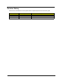
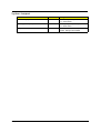
Revision History
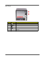
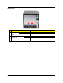
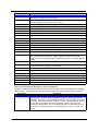
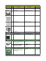
Please refer to the table below for the updates made on Aspire easyStore H341/342 service guide.
Date
ii
Chapter
Updates
Copyright
Copyright © 2010 by Acer Incorporated. All rights reserved. No part of this publication may be reproduced,
transmitted, transcribed, stored in a retrieval system, or translated into any language or computer language, in
any form or by any means, electronic, mechanical, magnetic, optical, chemical, manual or otherwise, without
the prior written permission of Acer Incorporated.
iii
Disclaimer
The information in this guide is subject to change without notice.
Acer Incorporated makes no representations or warranties, either expressed or implied, with respect to the
contents hereof and specifically disclaims any warranties of merchantability or fitness for any particular
purpose. Any Acer Incorporated software described in this manual is sold or licensed "as is". Should the
programs prove defective following their purchase, the buyer (and not Acer Incorporated, its distributor, or its
dealer) assumes the entire cost of all necessary servicing, repair, and any incidental or consequential
damages resulting from any defect in the software.
Acer is a registered trademark of Acer Corporation.
Intel is a registered trademark of Intel Corporation.
Other brand and product names are trademarks and/or registered trademarks of their respective holders.
iv
Conventions
The following conventions are used in this manual:
SCREEN
MESSAGES
Denotes actual messages that appear on screen.
NOTE
Gives additional information related to the current topic.
WARNING
Alerts you to any physical risk or system damage that might result from doing
or not doing specific actions.
CAUTION
Gives precautionary measures to avoid possible hardware or software
problems.
IMPORTANT
Reminds you to do specific actions relevant to the accomplishment of
procedures.
v
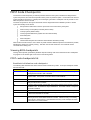
Service Guide Coverage
This Service Guide provides you with all technical information relating to the BASIC CONFIGURATION
decided for Acer's "global" product offering. To better fit local market requirements and enhance product
competitiveness, your regional office MAY have decided to extend the functionality of a machine (e.g. add-on
card, modem, or extra memory capability). These LOCALIZED FEATURES will NOT be covered in this generic
service guide. In such cases, please contact your regional offices or the responsible personnel/channel to
provide you with further technical details.
FRU Information
Please note WHEN ORDERING FRU PARTS, that you should check the most up-to-date information available
on your regional web or channel. If, for whatever reason, a part number change is made, it will not be noted in
the printed Service Guide. For ACER-AUTHORIZED SERVICE PROVIDERS, your Acer office may have a
DIFFERENT part number code to those given in the FRU list of this printed Service Guide. You MUST use the
list provided by your regional Acer office to order FRU parts for repair and service of customer machines.
vi
Table of Contents
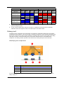
System Tour
Features
System Tour
Front Panel
Rear Panel
Internal Components
System LED Indicators
System Utilities
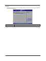
AMI BIOS Setup Utility
Entering the BIOS Setup Utility
Navigating Through the Setup Utility
Setup Utility Menus
System Disassembly
Disassembly Requirements
Pre-disassembly Procedure
Main Unit Disassembly
Removing the Hard Disk
Removing the System Cover
Removing the Front Bezel
Removing the Front I/O Board
Removing the Backplane Board
Removing the Power Supply
Removing the Fan
Removing the Memory Module
Removing the Mainboard
Removing the HDD Access LED cables
System Troubleshooting
Hardware Diagnostic Procedure
System Check Procedures
Power system check
System external inspection
System internal inspection
System Diagnosis
Hardware diagnostic program
Debug card
POST Code Checkpoints
Viewing BIOS checkpoints
POST code checkpoints list
System Status Error Codes
BIOS Recovery
Clearing CMOS
Undetermined Problems
System Block Diagram and Board Layout
System Block Diagram
Board Layout
Mainboard
System Jumpers
1
1
2
2
3
4
5
9
9
10
11
12
19
19
20
21
22
25
26
28
30
33
36
37
39
40
41
41
42
42
42
42
43
43
44
45
45
45
50
51
52
53
55
55
56
56
57
vii
FRU (Field Replaceable Unit) List
59
Exploded Diagram
FRU List
60
62
Technical Specifications
viii
65
Chapter 1
System Tour
Features
Below is a brief summary of the home server’s many feature:
NOTE: The features listed in this section is for your reference only. The exact configuration of the server
depends on the model purchased.
Processor
Onboard Intel Atom D410/D510 processor
Chipset
Intel 82801IR I/O Controller Hub (ICH 9R) (Southbridge)
Memory subsystem
Supports DDR2 unbuffered SDRAM
Media storage
Up to four 3.5-inch hot-swappable SATA hard disk drives
Networking
One Gigabit Ethernet LAN port (RJ-45)
I/O ports
USB 2.0 ports (1 front and 4 rear)
Gigabit LAN port
eSATA port
Power supply
220-watts (100/240 Vac) Energy Star compliant power supply
Operating system and software
Operating system:
Windows Home Server
Applications
Windows Home Server Connector
Lights Out Client
Software Update
Server Recovery
PC Recovery
Physical dimensions
WxHxD: 200 x 180 x 212 mm
Weight (without HDD): 4.5 kg (with 1 HDD): 5.1 kg
Chapter 1
1
System Tour
This section is a virtual tour of the system’s interior and exterior components.
Front Panel
No.
2
Icon
Component
1
Power button/power indicator
2
Network indicator
3
Hard disk drive (HDD) status indicator
4
System status indicator
5
USB backup button/USB backup indicator
6
USB 2.0 port
7
Front door
Open the door to access the hot-swappable HDDs.
8
HDD access indicators
Chapter 1
Rear Panel
No.
Icon
Component
1
Recovery/reset button
2
eSATA port
3
Gigabit Ethernet port
4
USB ports
5
Power connector
6
Power fan
Chapter 1
3
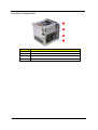
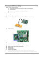
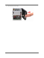
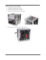
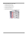
Internal Components
4
No.
Component
1
Backplane board
2
Power supply
3
Memory module
4
Mainboard
Chapter 1
System LED Indicators
Front panel
This section describes the different system LED indicators.
No.
LED indicator
Color
LED status
Description
1
Power
Blue
On
System is connected to the power supply and turned on
and ready for use.
Random blink
None
2
3
Network
HDD status
Blue
Off
System is booting
System is in S3 sleep state (suspend to memory)
•
System is not powered on
•
System initialize operation in progress
On
Link between system and network
Random blink
Network access
None
Off
Network disconnected
Purple
On
•
System not initialized
•
HDD is not mounted into the drive bay
•
HDD is mounted into the drive bay and is in the
process of being manually added into the server
storage
•
HDD is in the process of being removed from the
server storage.
Random blink
Blue
On
Red
Random blink
None
Chapter 1
•
•
Off
HDD is mounted into the drive bay and added into the
server storage
•
HDD failure
•
Windows Home Server cannot find HDD
No HDD mounted in the drive bay
5
No.
LED indicator
Color
LED status
Description
4
System status
Blue
Random blink
•
System is booting
•
System is shutting down
On
System initialize operation completed.
Blue and
purple
Random blink
System is booting from a USB device (Reserved for
BIOS update while boot block has been active)
Red
On
May indicate the following states:
•
System failure
•
HDD failure
•
SATA controller failure
•
USB controller failure
•
LAN controller failure
•
Fan failure
•
Memory failure
•
Boot device not found
Refer to “System Status Error Codes” on page 50 for
more information.
Random blink
5
USB device
backup
Blue
On
Random blink
6
6
HDD access
System recovery or reset is in progress
•
USB storage device is connected to the USB port
•
Backup completed
System is backing up files from a USB storage device
None
Off
USB storage device unmounted
Blue
Blink
HDD is in use
None
Off
No HDD activity
Chapter 1
Rear panel
No.
LED indicator
Color
LED status
Description
1
LAN port
network speed
LED
Amber
On
1000 Mbps network access
Green
On
100 Mbps link network access
None
Off
10 Mbps link network access
LAN port
activity LED
Green
2
None
Chapter 1
On
Active network link
Random blink
Transmit or receive activity
Off
No network connection
7
8
Chapter 1
Chapter 2
System Utilities
AMI BIOS Setup Utility
BIOS setup is a hardware configuration program built into the system's Basic Input/Output System (BIOS).
Since most systems are already properly configured and optimized, there is no need to run this utility. You will
need to run this utility under the following conditions.
When changing the system configuration settings
When redefining the communication ports to prevent any conflicts
When modifying the power management configuration
When changing the password or making other changes to the security setup
When a configuration error is detected by the system and you are prompted ("Run Setup"
message) to make changes to the BIOS setup
NOTE: If you repeatedly receive Run Setup messages, the battery may be bad. In this case, the system
cannot retain configuration values in CMOS. Ask a qualified technician for assistance.
BIOS setup loads the configuration values in a battery-backed nonvolatile memory called CMOS RAM. This
memory area is not part of the system RAM which allows configuration data to be retained when power is
turned off.
Before you run the AMI BIOS Setup Utility, make sure that you have saved all open files. The system reboots
immediately after you close the Setup.
NOTE: AMI BIOS Setup Utility will be simply referred to as "Setup" or "Setup utility" in this guide.
The screenshots used in this guide display default system values. These values may not be the same
those found in your system.
Chapter 2
9
Entering the BIOS Setup Utility
Before you begin, prepare the following:
Wrist grounding strap and conductive mat for preventing electrostatic discharge
Philips screwdriver
Debug card - Refer to page 44 for details about the debug card.
Debug card cable
1.
Turn off the computer and all attached devices.
2.
Remove the cover. See “Removing the System Cover” on page 25.
3.
Connect the debug card cable to the debug card cable connector on the mainboard.
4.
Locate the JP1 Debug/User mode jumper on the mainboard.
5.
Close the jumper to enable system for debug mode.
6.
Connect the power cable to the rear panel.
7.
Connect a PS/2 keyboard to the PS/2 keyboard port on the debug card.
8.
Connect a monitor to the VGA port on the debug card.
9.
Restart the system.
10. Turn on the monitor.
11. During POST, press <Delete>.
If you fail to press <Delete> before POST is completed, you will need to restart the system.
When the Setup Utility screen displays, use the left and right arrow keys to move through the menus.
10
Chapter 2
Navigating Through the Setup Utility
Use the following keys to move around the Setup utility.
Left and Right arrow keys – Move between selections on the menu bar.
Up and Down arrow keys – Move the cursor to the field you want.
Pg Up and Pg Dn keys – Move the cursor to the previous and next page of a multiple page menu.
Home – Move the cursor to the first page of a multiple page menu.
End – Move the cursor to the last page of a multiple page menu.
+ and - keys – Select a value for the currently selected field (only if it is user-configurable). Press
these keys repeatedly to display each possible entry, or the Enter key to choose from a pop-up
menu.
NOTE: Grayed-out fields are not user-configurable.
Enter key – Display a submenu screen.
NOTE: Availability of submenu screen is indicated by a (>).
Chapter 2
Esc – If you press this key:
On one of the primary menu screens, the Exit menu displays.
On a submenu screen, the previous screen displays.
When you are making selections from a pop-up menu, closes the pop-up without making a
selection.
F1 – Display the BIOS setup General Help panel.
F2 or F3 – Press to change setup menu colors.
F7 – Press to discard changes.
F9 – Press to load optimized default system values.
F10 – Save changes made the Setup and close the utility.
11
Setup Utility Menus
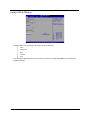
The Setup Main menu includes the following main setup categories.
Main
Advanced
Boot
Chipset
Exit
In the descriptive table following each of the menu screenshots, settings in boldface are the default and
suggested settings.
12
Chapter 2
Main
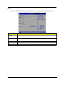
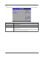
The Main menu displays basic information about the system and lets you set the system date and time.
Parameter
Description
AMIBIOS
Version number of the BIOS Setup Utility. Date when the BIOS Setup Utility was created.
Build Date
ID
Processor
Displays the processor speed in MHz.
Speed
System Memory
Total size of system memory detected during POST.
System Time
Set the system time following the hour-minute-second format.
System Date
Set the date following the month-day-year format.
Chapter 2
13
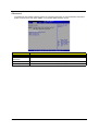
Advanced
The Advanced menu display submenu options for configuring the function of various hardware components.
Select a submenu item, then press <Enter> to access the related submenu screen.
Parameter
Description
IDE Configuration
Press <Enter> to select options for the IDE Configuration settings.
Hardware Health
Configuration
Press <Enter> to select options for the Hardware Health Configuration.
ACPI Configuration
Press <Enter> to select options for ACPI Configuration settings.
AHCI Configuration
Press <Enter> to select options for AHCI Configuration settings.
14
Chapter 2
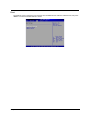
Boot
Use the Boot menu to specify the boot sequence from available devices. Select a submenu item, then press
<Enter> to access the related submenu screen.
Chapter 2
15
Chipset
Use the Chipset menu to configure the south bridge chipset. Select the submenu item, then press <Enter> to
access the submenu screen.
Parameter
Description
South Bridge Configuration
Press <Enter> to select options for the South Bridge Configuration settings.
16
Chapter 2
Exit
The Exit menu lists options for quitting the Setup Utility. Highlight any of the exit options, then press <Enter>.
Parameter
Description
Save Changes and Exit
Saves changes made and closes the utility.
Keyboard shortcut: F10
Discard Changes and Exit
Discards changes made and closes the utility.
Discard Changes
Discards all changes made to the utility and load previous configuration settings.
Load Optimal Defaults
Loads the factory default settings for all setup parameters.
Keyboard shortcut: F9
Setup Defaults are quite demanding in terms of resources consumption. If you are using lowspeed memory chips or other kinds of low-performance components and you choose to load
these settings, the system might not function properly.
Chapter 2
17
18
Chapter 2
Chapter 3
System Disassembly
This chapter contains step-by-step procedures on how to disassemble the desktop computer for maintenance
and troubleshooting.
Disassembly Requirements
To disassemble the computer, you need the following tools:
Wrist grounding strap and conductive mat for preventing electrostatic discharge
Flat-blade screwdriver
Philips screwdriver
Hex screwdriver
Plastic flat-blade screwdriver
Plastic tweezers
NOTE: The screws for the different components vary in size. During the disassembly process, group the
screws with the corresponding components to avoid mismatch when putting back the components.
Chapter 3
19
Pre-disassembly Procedure
Before proceeding with the disassembly procedure, perform the steps listed below:
20
1.
Turn off the system and all the peripherals connected to it.
2.
Unplug the power cord from the power outlets.
3.
Unplug the power cord from the system.
4.
Unplug all peripheral cables from the system.
5.
Place the system unit on a flat, stable surface.
Chapter 3
Main Unit Disassembly
MAIN UNIT DISASSEMBLY
TURN OFF POWER
DRIVE CARRIER
HARD DISK DRIVE
MODULE
HARD DISK DRIVE
Ax3
SYSTEM COVER
FRONT BEZEL
Bx4
Cx4
FRONT I/O BRACKET
FRONT I/O BOARD
BACKPLANE BOARD
BRACKET
BACKPLANE BOARD
Cx7
Ax4
POWER SUPPLY
Ax4
SYSTEM FAN
MAINBOARD
CARRIER
MEMORY MODULE
Cx4
MAINBOARD
HOUSING FRAME
HDD ACCESS
LED CABLES
Screw List
Chapter 3
Code
Screw
Part No.
A
M3-0.5*4
86.1A524.4R0
B
M3*6L
86.VA524.6R0
C
M3*0.5*4L
86.19534.4R0
21
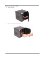
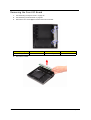
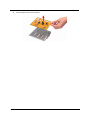
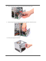
Removing the Hard Disk
22
1.
Open the front panel.
2.
Press to release the hard drive carrier handle.
Chapter 3
3.
Flex the carrier handle.
4.
Slide the hard drive carrier out of the HDD bay.
Chapter 3
23
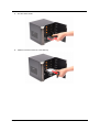
5.
24
Remove the carrier by gently prying open the left rail of the carrier (1) and lift the hard disk off the
carrier (2) .
Chapter 3
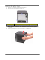
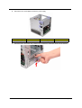
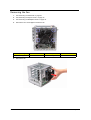
Removing the System Cover
1.
Perform the pre-disassembly procedure described on page 20.
2.
Remove the three screws (A) that secure system cover.
Screw (Quantity)
Color
Torque
Part No.
M3-0.5*4 (3)
Silver
5.1 to 6.9 kgf-cm
86.1A524.4R0
3.
Slide the system cover toward the back of the chassis until the tabs on the cover disengage with the slots
on the chassis.
4.
Lift the side panel away from the server and put it aside for reinstallation later.
Chapter 3
25
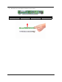
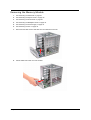
Removing the Front Bezel
26
1.
Remove the system cover. Refer to the previous section for instructions.
2.
Release the front bezel retention tabs from the chassis interior.
3.
Pull the bezel slightly outward, then disconnect the front I/O board cable.
Chapter 3
4.
Pull the bezel away from the chassis.
Chapter 3
27
Removing the Front I/O Board
1.
See “Removing the System Cover” on page 25.
2.
See “Removing the Front Bezel” on page 26.
3.
Remove the four screws (B) that secures the front I/O bracket.
4.
28
Screw (Quantity)
Color
Torque
Part No.
M3*6L (4)
Silver
5.1 to 6.9 kgf-cm
86.VA524.6R0
Remove the bracket.
Chapter 3
5.
6.
Remove the four screws (C) that secure the front I/O board.
Screw (Quantity)
Color
Torque
Part No.
M3*0.5*4L (4)
Silver
5.1 to 6.9 kgf-cm
86.19534.4R0
Remove the front I/O board.
Chapter 3
29
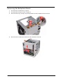
Removing the Backplane Board
30
1.
See “Removing the Hard Disk” on page 22.
2.
See “Removing the System Cover” on page 25.
3.
Disconnect the fan (1), LED (2), and power (3) cables from their backplane board connectors.
4.
Disconnect the four HDD SATA cables from their mainboard connectors.
Chapter 3
5.
Pull the backplane board bracket out of the chassis.
6.
Detach the four HDD SATA cables from their backplane board connectors.
7.
Remove the seven screws (C) that secure the backplane board.
Screw (Quantity)
Color
Torque
Part No.
M3*0.5*4L (7)
Silver
5.1 to 6.9 kgf-cm
86.19534.4R0
Chapter 3
31
8.
32
Lift the backplane board off the bracket.
Chapter 3
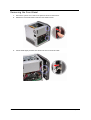
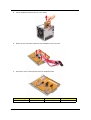
Removing the Power Supply
1.
See “Removing the Hard Disk” on page 22.
2.
See “Removing the System Cover” on page 25.
3.
See “Removing the Backplane Board” on page 30.
4.
Release the power cables from the cable ties, as shown.
5.
Disconnect the 4-pin power cable from its mainboard connector.
Chapter 3
33
6.
7.
34
Remove the four screws (A) that secure the power supply.
Screw (Quantity)
Color
Torque
Part No.
M3-0.5*4 (4)
Silver
5.1 to 6.9 kgf-cm
86.1A524.4R0
With the thumb in the thumb hole, press the tab to release the mainboard carrier from the chassis.
Chapter 3
8.
Slide the mainboard carrier out slightly, until you have access to the power cable.
9.
While pressing the tab on the 24-pin power cable, pull the cable off the mainboard connector.
10. Pull the power supply out of the chassis.
Chapter 3
35
Removing the Fan
1.
See “Removing the Hard Disk” on page 22.
2.
See “Removing the System Cover” on page 25.
3.
See “Removing the Backplane Board” on page 30.
4.
Remove the four screws (A) that secure the fan.
5.
36
Screw (Quantity)
Color
Torque
Part No.
M3-0.5*4 (3)
Silver
5.1 to 6.9 kgf-cm
86.1A524.4R0
Remove the fan.
Chapter 3
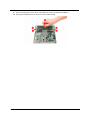
Removing the Memory Module
1.
See “Removing the Hard Disk” on page 22.
2.
See “Removing the System Cover” on page 25.
3.
See “Removing the Front Bezel” on page 26.
4.
See “Removing the Backplane Board” on page 30.
5.
See “Removing the Power Supply” on page 33.
6.
See “Removing the Fan” on page 36.
7.
Disconnect the HDD access LED cable from its mainboard connector.
8.
Pull the mainboard carrier out of the chassis.
Chapter 3
37
9.
Press the holding clips on both sides of the DIMM slot outward to release the DIMM (1).
10. Gently pull the DIMM upward to remove it from the DIMM slot (2).
38
Chapter 3
Removing the Mainboard
1.
See “Removing the Hard Disk” on page 22.
2.
See “Removing the System Cover” on page 25.
3.
See “Removing the Front Bezel” on page 26.
4.
See “Removing the Backplane Board” on page 30.
5.
See “Removing the Power Supply” on page 33.
6.
See “Removing the Fan” on page 36.
7.
Remove the four screws (C) that secure the mainboard.
8.
Screw (Quantity)
Color
Torque
Part No.
M3*0.5*4L (4)
Silver
5.1 to 6.9 kgf-cm
86.19534.4R0
Lift the mainboard off the mainboard carrier.
Chapter 3
39
Removing the HDD Access LED cables
40
1.
See “Removing the Hard Disk” on page 22.
2.
See “Removing the System Cover” on page 25.
3.
See “Removing the Front Bezel” on page 26.
4.
See “Removing the Backplane Board” on page 30.
5.
See “Removing the Power Supply” on page 33.
6.
See “Removing the Fan” on page 36.
7.
See “Removing the Mainboard” on page 39.
8.
Press the release tabs on the HDD access LED cables, then detach the cables.
Chapter 3
Chapter 4
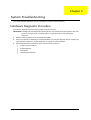
System Troubleshooting
This chapter provides instructions on how to troubleshoot system hardware problems.
Hardware Diagnostic Procedure
The system’s diagnostic function monitors system activity and performs
IMPORTANT:The diagnostic tests described in this chapter are only intended to test Acer products. Non-Acer
products, prototype cards, or modified options can give false errors and invalid system
responses.
1.
Obtain the failing symptoms in as much detail as possible.
2.
Verify the symptoms by attempting to recreate the failure by running the diagnostic tests or repeating the
same operation. Refer to the “System Diagnosis” on page 43 for more information.
3.
Refer to the table below to determine which corrective action to perform.
Chapter 4
System Check Procedures
System Diagnosis
Checkpoints
Undertermined Problems
41
System Check Procedures
Power system check
If the system will power on, skip this section. Refer to System External Inspection.
If the system will not power on, check if the power cable is properly connected to the system and AC source.
System external inspection
1.
Inspect the LED indicators on the front panel, which can indicate the malfunction. For the LED locations
and description of their behaviour, see “System LED Indicators” on page 5.
2.
Make sure that air flow is not blocked.
3.
Make sure nothing in the system is making contact that could short out power.
4.
If the problem is not evident, continue with System Internal Inspection.
System internal inspection
1.
Turn off the system and all the peripherals connected to it.
2.
Unplug the power cord from the power outlets.
3.
Unplug the power cord from the system.
4.
Unplug all peripheral cables from the system.
5.
Place the system unit on a flat, stable surface.
6.
Remove the system cover. For instructions on removing system cover, refer to “Removing the System
Cover” on page 25.
7.
Verify that components are properly seated.
8.
Verify that all cable connectors inside the system are firmly and correctly attached to their appropriate
connectors.
9.
Verify that all components are Acer-qualified and supported.
10. Replace the system cover.
11. Power on the system.
12. If the problem with the system is not evident, you can try viewing the POST messages and BIOS event
logs during the system startup.
42
Chapter 4
System Diagnosis
Hardware diagnostic program
The purpose of the hardware diagnostic program is to check hardware problems. It executes simple tests of
each hardware component to make sure the hardware is not the source of the problem. If hardware problems,
such as a fan, LED board, hard disk drive, memory; are confirmed, the diagnostic program can detect the
specific component causing the problem. The program needs to saved in a bootable USB device.
To run the diagnostic program:
1.
Turn off the system.
2.
Prepare a bootable USB device by copying or downloading the “ANNIE.GHO” diagnostic utility to the USB
device. The diagnostic utility may be obtained from the CD that came with the system.
3.
Plug the bootable USB device to any USB port on the rear of the system.
4.
Power on the system. The system status indicator blinks blue.
5.
Immediately press and release the Recovery/reset button with the paper clip end. The system status
indicator blinks red and immediately starts the diagnostic process:
a.
Onboard memory flash check
b.
HDD account check
c.
Memory size check (1024 or 2048 MB)
d.
Fan speed check
e.
CPU temperature check
f.
MB voltage check
g.
Backplane board temperature check
h.
PQAF system test
i.
PQAF memory test
j.
PQAF HDD test
k.
Read SN from DMI data check
l.
End test
During the diagnostic process, the result of the test displays on the HDD status indicators. The
indicator(s) blinks blue when the system has passed each diagnostic test and blinks red when an error
condition occurs. After the system has completed the diagnostic procedure the HDD status indicators light
purple.
Test Items
Boot from
USB disk
HDD LED status (normal)
HDD 0
HDD 1
HDD 2
HDD 3
HDD LED status (failed)
HDD 0
HDD 1
HDD 2
HDD 3
Onboard memory
flash check
HDD account
check
Memory size check
Fan speed check
CPU temperature
check
MB voltage check
Chapter 4
43
Test Items
Boot from
USB disk
HDD LED status (normal)
HDD 0
HDD 1
HDD 2
HDD 3
HDD LED status (failed)
HDD 0
HDD 1
HDD 2
HDD 3
Backplane board
temperature check
PQAF system test
PQAF memory test
PQAF HDD test
Read SN from
DMI data check
End test
6.
After the diagnostic routine is completed, the HDD status indicator lights purple indicating the system has
passed all diagnostic tests.
7.
A copy of the test result will be saved as a log file (i.e., 66380AC3.LOG) and stored in the Results
folder.The name of the log file is based on the last 8 bytes of the serial number
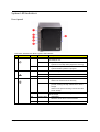
Debug card
The debug card is a diagnostic tool for technicians to configure the system BIOS settings and conveniently
troubleshoot various problems. This card can help you track the progress of a Power-On Self Test (POST) and
discover the cause of errors during system operations. The debug card connects to the system via its debug
card cable connector. It includes a VGA port for connecting an external monitor to view BIOS output
checkpoints. The debug card also provides a PS/2 mouse port, PS/2 keyboard port and a serial port.
Identifying the components
No.
Component
1
Debug card cable connector
2
PS/2 mouse and keyboard port
3
VGA/monitor port
4
Serial port
For more information on how to connect the debug card to the system, refer to “Entering the BIOS Setup
Utility” on page 10.
44
Chapter 4
POST Code Checkpoints
The Power-On Self Test (POST) is a BIOS procedure that boots the system, initializes and diagnoses the
system components, and controls the operation of the power-on password option. If POST discovers errors in
system operations at power-on, it displays error messages, generates a checkpoint code at port 80h or even
halts the system if the error is fatal.
The main components on the system board that must be diagnosed and/or initialized by POST to ensure
system functionality are as follows:
Microprocessor with built-in numeric coprocessor and cache memory subsystem
Direct memory access (DMA) controller (8237 module)
Interrupt system (8259 module)
Three programmable timers (system timer and 8254 module)
ROM subsystem
RAM subsystem
CMOS RAM subsystem and real time clock/calendar with battery backup
When POST executes a task, it uses a series of preset numbers called checkpoints to be latched at port 80h,
indicating the stages it is currently running. This latch can be read and shown on an external monitor
connected to the debug card.
Viewing BIOS checkpoints
Viewing all checkpoints generated by the BIOS requires a debug card and an external monitor. Checkpoints
may appear on the bottom right corner of the screen during POST.
POST code checkpoints list
Bootblock initialization code checkpoint
The following table describes the Award common tasks carried out by POST. An unique checkpoint number
denotes each task. .
Checkpoint
Description
Before D1
Early chipset initialization is done. Early super I/O initialization is done including RTC
and keyboard controller. NMI is disabled.
D1
Perform keyboard controller BAT test. Check if waking up from power management
suspend state. Save power-on CPUID value in scratch CMOS.
D0
Go to flat mode with 4GB limit and GA20 enabled. Verify the bootblock checksum.
D2
Disable CACHE before memory detection. Execute full memory sizing module.
Verify that flat mode is enabled.
D3
If memory sizing module not executed, start memory refresh and do memory sizing in
Bootblock code. Do additional chipset initialization. Re-enable CACHE. Verify that
flat mode is enabled.
D4
Test base 512KB memory. Adjust policies and cache first 8MB. Set stack.
D5
Bootblock code is copied from ROM to lower system memory and control is given to
it. BIOS now executes out of RAM.
D6
Both key sequence and OEM specific method is checked to determine if BIOS
recovery is forced. Main BIOS checksum is tested. If BIOS recovery is necessary,
control flows to checkpoint E0. See Bootblock Recovery Code Checkpoints section
of document for more information.
Chapter 4
45
Checkpoint
Description
D7
Restore CPUID value back into register. The Bootblock-Runtime interface module is
moved to system memory and control is given to it. Determine whether to execute
serial flash.
D8
The Runtime module is uncompressed into memory. CPUID information is stored in
memory.
D9
Store the Uncompressed pointer for future use in PMM. Copying Main BIOS into
memory. Leaves all RAM below 1MB Read-Write including E000 and F000 shadow
areas but closing SMRAM.
DA
Restore CPUID value back into register. Give control to BIOS POST
(ExecutePOSTKernel). See POST Code Checkpoints section of document for more
information.
Bootblock recovery code checkpoints
The Bootblock recovery code gets control when the BIOS determines that a BIOS recovery needs to occur
because the user has forced the update or the BIOS checksum is corrupt. The following table describes the
type of checkpoints that may occur during the Bootblock recovery portion of the BIOS:
Checkpoint
46
Description
E0
Initialize the floppy controller in the super I/O. Some interrupt vectors are initialized.
DMA controller is initialized. 8259 interrupt controller is initialized. L1 cache is
enabled.
E9
Set up floppy controller and data. Attempt to read from floppy.
EA
Enable ATAPI hardware. Attempt to read from ARMD and ATAPI CDROM.
EB
Disable ATAPI hardware. Jump back to checkpoint E9.
EF
Read error occurred on media. Jump back to checkpoint EB.
E9 no EA
Determine information about root directory of recovery media.
F0
Search for pre-defined recovery file name in root directory.
F1
Recovery file not found.
F2
Start reading FAT table and analyze FAT to find the clusters occupied by the recovery
file.
F3
Start reading the recovery file cluster by cluster.
F5
Disable L1 cache.
FA
Check the validity of the recovery file configuration to the current configuration of the
flash part.
FB
Make flash write enabled through chipset and OEM specific method. Detect proper
flash part. Verify that the found flash part size equals the recovery file size.
F4
The recovery file size does not equal the found flash part size.
FC
Erase the flash part.
FD
Program the flash part.
FF
The flash has been updated successfully. Make flash write disabled. Disable ATAPI
hardware. Restore CPUID value back into register. Give control to F000 ROM at
F000:FFF0h.
Chapter 4
POST code checkpoints
The POST code checkpoints are the largest set of checkpoints during the BIOS pre-boot process. The
following table describes the type of checkpoints that may occur during the POST portion of the BIOS:
Checkpoint
Description
03
Disable NMI, Parity, video for EGA, and DMA controllers. Initialize BIOS, POST,
Runtime data area. Also initialize BIOS modules on POST entry and GPNV area.
Initialized CMOS as mentioned in the Kernel Variable "wCMOSFlags."
04
Check CMOS diagnostic byte to determine if battery power is OK and CMOS
checksum is OK. Verify CMOS checksum manually by reading storage area. If the
CMOS checksum is bad, update CMOS with power-on default values and clear
passwords. Initialize status register A.
Initializes data variables that are based on CMOS setup questions. Initializes both
the 8259 compatible PICs in the system.
05
Initializes the interrupt controlling hardware (generally PIC) and interrupt vector table.
06
Do R/W test to CH-2 count reg. Initialize CH-0 as system timer. Install the
POSTINT1Ch handler. Enable IRQ-0 in PIC for system timer interrupt.
Traps INT1Ch vector to "POSTINT1ChHandlerBlock."
08
Initializes the CPU. The BAT test is being done on KBC. Program the keyboard
controller command byte is being done after Auto detection of KB/MS using
AMI KB-5.
0A
Initializes the 8042 compatible Key Board Controller.
0B
Detects the presence of PS/2 mouse.
0C
Detects the presence of Keyboard in KBC port.
0E
Testing and initialization of different Input Devices. Also, update the Kernel Variables.
Traps the INT09h vector, so that the POST INT09h handler gets control for IRQ1.
Uncompress all available language, BIOS logo, and Silent logo modules.
13
Early POST initialization of chipset registers.
24
Uncompress and initialize any platform specific BIOS modules.
30
Initialize System Management Interrupt.
2A
Initializes different devices through DIM.
See DIM Code Checkpoints section of document for more information.
2C
Initializes different devices. Detects and initializes the video adapter installed in the
system that have optional ROMs.
2E
Initializes all the output devices.
31
Allocate memory for ADM module and uncompress it. Give control to ADM module
for initialization. Initialize language and font modules for ADM. Activate ADM
module.
33
Initializes the silent boot module. Set the window for displaying text information.
37
Displaying sign-on message, CPU information, setup key message, and any OEM
specific information.
38
Initializes different devices through DIM. See DIM Code Checkpoints section of
document for more information.
39
Initializes DMAC-1 & DMAC-2.
3A
Initialize RTC date/time.
3B
Test for total memory installed in the system. Also, Check for DEL or ESC keys to
limit memory test. Display total memory in the system.
3C
Mid POST initialization of chipset registers.
40
Detect different devices (Parallel ports, serial ports, and coprocessor in CPU, … etc.)
successfully installed in the system and update the BDA, EBDA…etc.
Chapter 4
47
Checkpoint
Description
50
Programming the memory hole or any kind of implementation that needs an
adjustment in system RAM size if needed.
52
Updates CMOS memory size from memory found in memory test. Allocates memory
for Extended BIOS Data Area from base memory.
60
Initializes NUM-LOCK status and programs the KBD typematic rate.
75
Initialize Int-13 and prepare for IPL detection.
78
Initializes IPL devices controlled by BIOS and option ROMs.
7A
Initializes remaining option ROMs.
7C
Generate and write contents of ESCD in NVRam.
84
Log errors encountered during POST.
85
Display errors to the user and gets the user response for error.
87
Execute BIOS setup if needed / requested.
8C
Late POST initialization of chipset registers.
8E
Program the peripheral parameters. Enable/Disable NMI as selected
90
Late POST initialization of system management interrupt.
A0
Check boot password if installed.
A1
Clean-up work needed before booting to OS.
A2
Takes care of runtime image preparation for different BIOS modules. Fill the free
area in F000h segment with 0FFh. Initializes the Microsoft IRQ Routing Table.
Prepares the runtime language module. Disables the system configuration display if
needed.
A4
Initialize runtime language module.
A7
Displays the system configuration screen if enabled. Initialize the CPU's before boot,
which includes the programming of the MTRR's.
A8
Prepare CPU for OS boot including final MTRR values.
A9
Wait for user input at config display if needed.
AA
Uninstall POST INT1Ch vector and INT09h vector. Deinitializes the ADM module.
AB
Prepare BBS for Int 19 boot.
AC
End of POST initialization of chipset registers.
B1
Save system context for ACPI.
00
Passes control to OS Loader (typically INT19h).
Device Initialization Manager code checkpoints
The Device Initialization Manager (DIM) module gets control at various times during BIOS POST to initialize
different BUSes. The following table describes the main checkpoints where the DIM module is accessed:
Checkpoint
2A
48
Description
Initialize different buses and perform the following functions: Reset, Detect, and
Disable (function 0); Static Device Initialization (function 1); Boot Output Device
Initialization (function 2). Function 0 disables all device nodes, PCI devices, and PnP
ISA cards. It also assigns PCI bus numbers. Function 1 initializes all static devices
that include manual configured onboard peripherals, memory and I/O decode
windows in PCI-PCI bridges, and noncompliant PCI devices. Static resources are
also reserved. Function 2 searches for and initializes any PnP, PCI, or AGP video
devices.
Chapter 4
Checkpoint
38
Description
Initialize different buses and perform the following functions: Boot Input Device
Initialization (function 3); IPL Device Initialization (function 4); General Device
Initialization (function 5). Function 3 searches for and configures PCI input devices
and detects if system has standard keyboard controller. Function 4 searches for and
configures all PnP and PCI boot devices. Function 5 configures all onboard
peripherals that are set to an automatic configuration and configures all remaining
PnP and PCI devices.
While control is in the different functions, additional checkpoints are output to port 80h as a word value to
identify the routines under execution. The low byte value indicates the main POST Code Checkpoint. The
high byte is divided into two nibbles and contains two fields. The details of the high byte of these checkpoints
are as follows:
HIGH BYTE XY
The upper nibble 'X' indicates the function number that is being executed. 'X' can be from 0 to 7.
0 = func#0, disable all devices on the BUS concerned.
1 = func#1, static devices initialization on the BUS concerned.
2 = func#2, output device initialization on the BUS concerned.
3 = func#3, input device initialization on the BUS concerned.
4 = func#4, IPL device initialization on the BUS concerned.
5 = func#5, general device initialization on the BUS concerned.
6 = func#6, error reporting for the BUS concerned.
7 = func#7, add-on ROM initialization for all BUSes.
8 = func#8, BBS ROM initialization for all BUSes.
The lower nibble 'Y' indicates the BUS on which the different routines are being executed. 'Y' can be from
0 to 5.
0 = Generic DIM (Device Initialization Manager).
1 = On-board System devices.
2 = ISA devices.
3 = EISA devices.
4 = ISA PnP devices.
5 = PCI devices
Chapter 4
49
System Status Error Codes
NOTE: Perform the FRU replacement or actions in the sequence shown in FRU/Action column, if the FRU
replacement does not solve the problem, put the original part back in the computer. Do not replace a
non-defective FRU.
The error messages in the following table indicate the error signals on the HDD access LED indicators on the
front panel and the error symptoms.
Operating condition
System is booting
HDD LED error codes
1
2
3
Description
4
SATA controller failed
USB controller failed
LAN controller failed
Fan failed
Memory failed
Boot device not found
System has booted
50
Disk failure
Chapter 4
BIOS Recovery
Perform the BIOS recovery if the BIOS flash ROM has become corrupted. The following sections provide
instructions on how to recover BIOS settings.
To create a BIOS Recovery disk:
1.
Prepare a USB storage device.
2.
Connect the USB storage device to a USB port on your computer.
3.
Copy the target BIOS ROM file to a USB storage device.
4.
Rename the target BIOS to “AMIBoot.ROM”.
5.
Unplug the device.
To perform a BIOS recovery:
1.
Create the BIOS Recovery disk as described in the previous section.
2.
Connect the BIOS Recovery disk on the USB port on the system.
3.
Depending on the current state of the system, do either of the following:
If the system has crashed:
Power on the system. The system initializes the BIOS recovery process and the system will reboot
automatically after the flash update is completed.
If the system has not crashed or if you want to revert BIOS to previous settings:
During POST, press <Ctrl> + <Home> during POST. This action will flash the BIOS from the USB
storage device to the system and reboot automatically after the flash update is completed.
4.
Remove the BIOS Recovery disk.
Chapter 4
51
Clearing CMOS
To clear the BIOS configuration you need to short the JP3 Clear CMOS jumper on the mainboard.
52
1.
Turn off the computer and all attached devices.
2.
Remove the system cover. See “Removing the System Cover” on page 25.
3.
Locate the JP3 Clear CMOS jumper on the mainboard.
4.
Remove the jumper from the default position.
5.
Replace the jumper to connect the 2nd and 3rd pins.
6.
Access the BIOS Setup Utility by connecting a debug card, keyboard, and a monitor to the system.
Perform steps 3 and 7 through 10 of the “Entering the BIOS Setup Utility” on page 10.
7.
Press <F9> to load the system default values.
8.
Press <F10> to save the changes made and close the Setup Utility.
Chapter 4
Undetermined Problems
The diagnostic problems does not identify which adapter or device failed, which installed devices are incorrect,
whether a short circuit is suspected, or whether the system is inoperative.
NOTE: Verify that all attached devices are supported by the computer.
NOTE: Verify that the power supply being used at the time of the failure is operating correctly. (See “Power
system check” on page 42.)
Follow procedures below to isolate the failing FRU. Do not isolate non-defective FRU.
1.
Power off the computer.
2.
Visually check them for damage. If any problems are found, replace the FRU.
3.
Remove or disconnect all of the following devices:
Non-Acer devices
Printer, mouse, and other external devices
Hard disk drive
DIMM
CD/DVD-ROM drive
Adapter cards
4.
Power on the computer.
5.
Determine if the problem has been resolved.
6.
If the problem does not recur, reconnect the removed devices one at a time until you find the failed FRU.
7.
If the problem persists, replace the FRU one at a time. Do not replace a non-defective FRU.
Chapter 4
53
54
Chapter 4
Chapter 5
System Block Diagram and Board Layout
System Block Diagram
Chapter 5
55
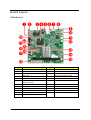
Board Layout
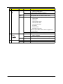
Mainboard
56
No
Description
No
Description
1
SATA 1 port
13
Intel Atom D410/D510 processor
2
SATA 3 port
14
HDD access LED cable connector
3
SATA 4 port
15
DDR2 DIMM slot
4
SATA 2 port
16
24-pin power cable connector
5
USB ports
17
Front I/O board cable connector
6
Gigabit Ethernet port (top)
USB ports (bottom)
18
System type select jumper
7
eSATA port
19
Clear CMOS jumper
8
Recovery/reset button
20
Battery
9
Debug card cable connector
21
Debug/user mode jumper
10
Backplane board LED cable connector
22
x1 PCI Express slot
11
4-pin power cable connector
23
Intel ICH9R chipset (south bridge)
12
Fan cable connector (reserved)
Chapter 5
System Jumpers
Name
Location
Settings
Clear CMOS jumper
JP3
1-2 Normal (default)
2-3 Clear CMOS
System type select jumper
JP2
1-2 Aspire system (default)
2-3 Other model
Debug/user mode jumper
JP1
Open User mode enabled (default)
Closed Debug mode enabled
Chapter 5
57
58
Chapter 5
Chapter 6
FRU (Field Replaceable Unit) List
This chapter offers the FRU (Field Replaceable Unit) list in global configuration of the home server. Refer to
this chapter whenever ordering the parts to repair or for RMA (Return Merchandise Authorization).
NOTES:
Chapter 6
When ordering FRU parts, check the most up-to-date information available on your regional web
or channel. For whatever reasons a part number is changed, it will NOT be noted on the printed
Service Guide. For Acer authorized service providers, your Acer office may have a different part
number code from those given in the FRU list of this printed Service Guide. You MUST use the
local FRU list provided by your regional Acer office to order FRU parts for service.
To scrap or to return the defective parts, follow the local government ordinance or regulations on
how to dispose it properly, or follow the rules set by your regional Acer office on how to return it.
This document will be updated as more information about the FRU list becomes available.
59
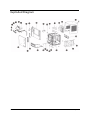
Exploded Diagram
60
Chapter 6
Item
Part No.
Part Name
QTY.
1
42.60P02.001
Handle HDD carrier HT-361
1
2
42.60P03.001
Latch HDD carrier HT-361
1
3
34.60P07.001
Axis HDD carrier HT-361
1
4
34.60P05.001
SPG HDD carrier HT-361
1
5
34.60P04.001
EMI HDD carrier HT-361
1
6
47.60M06.001
HDD ear rubber pin HT-360
4
7
42.60P01.001
HDD carrier HT-361
1
8
40.60P04.001
PLT as Icon HT-361
1
9
40.60P03.001
PLT as power HT-361
1
10
41.60P02.001
Bezel as main HT-361
1
11
42.55S13.001
Tie mount HU-139
1
12
42.91F07.001
Wire saddle CHF-8 HU122G
2
13
42.5E309.001
LED housing CLED-1A
4
14
50.60P04.001
C.A. HDD LED B/R HT-361
1
15
33.60P09.001
BRKT PCI LP dummy HT-361
1
16
33.60P05.001
BRKT BP HT-361
1
17
30.60P02.001
CAS UP HT-361
1
18
86.1A524.4R0
SCRW MACH PAN M3-0.5*4 NI
4
19
60.60P14.001
ASSY rear I/O cover HT-361
1
20
86.1A524.4R0
SCRW MACH PAN M3-0.5*4 NI
4
21
60.60P11.001
ASSY fan 120x120x25 S15
1
22
33.60P04.001
BRKT fan HT-361
2
23
60.60P02.001
ASSY main chassis HT-361
1
24
45.00049.001
Label spec dummy art UB series
1
25
42.60P11.001
Rubber foot R1907 19D7H
4
26
47.60P05.001
Sponge HDD LED HT-361
4
27
38.09008.001
Dessicant silica gel 30G H25
1
28
40.60P07.001
LBL 24*8MM warning HT-361
2
29
60.60P03.001
ASSY MB tray HT-361
1
30
40.60P06.001
PLT AS USB HT-361
1
31
42.60P17.001
Lens as door HT-361
1
32
42.60P16.001
Door as bezel HT-361
1
Chapter 6
61
FRU List
Component
QTY
Part Name
Description
Acer
Part Number
Board
Front I/O board
1
FRONT I/O BOARD
S15I ASPIRE FRONT I/O BD DIP
55.R3601.002
Backplane board
1
BACKPLANE BOARD
S15I BACKPLANE BOARD DIP
55.R3601.001
Backplane board
cable
1
BACKPLANE BOARD CABLE
C.A. 2CON 10PIN HT361
50.R3601.001
HDD SATA cable
1
HDD SATA CABLE
C.A. HDD SATA CABLE HT-361
50.R3601.003
Front I/O board
cable
1
FRONT I/O BOARD CABLE
C.A. 2CON 26PIN HT361
50.R3601.002
HDD LED CABLE
C.A. HDD LED B/R HT-361
50.R3601.004
1
POWER CORD 2.5A 250V 1800MM
BLACK UK SING
CORD AC UK/SING 2.5A250V 1800
27.R3601.003
2
POWER CORD 1800MM BLACK
EUR
CORD PWR AC LINE EUR 1.8M
BLK
27.R3601.002
POWER CORD 7A 125V 1800MM
BLACK US
CORD SVT 10A 125V 1800MM BLK
27.R3601.001
POWER CORD 7A 125V JAPAN
CORD VCTF 3G 7A/125V(JAPAN)
27.01518.181
POWER CORD 250V 10A 1800MM
SWISS
CORD 250V 10A 1800MM SWISS
27.01518.251
EXTERNAL ETHERNET CAT5E
CABLE BLACK 2M
C.A. CAT5E STRAI BLACK_2M BIZ
50.R3601.005
Cable
HDD access LED
cable
Power cord
Case/Cover/Bracket Assembly
Front I/O dummy
bracket
1
FRONT I/O DUMMY BRACKET
BRKT FRONT I/O HT-361
33.R3601.003
Power supply
support bracket
1
POWER SUPPLY SUPPORT
BRACKET
BRKT PSU SUPPORT HT-361
33.R3601.002
Front bezel
1
FRONT BEZEL W/KEY LOCK&KEY
ASSY ASPIRE BEZEL HT-361
60.R3601.002
Housing frame
2
ASSEMBLY CHASSIS W/HDD LED
CABLE&FAN&UPPER
CASE&LOWER CASE&HDD
BRACKET&MAIN BOARD
CARRIRE&FAN BRACKET
HOUSING ASSY HT-361
60.R3601.001
62
Chapter 6
Component
QTY
Part Name
Description
Acer
Part Number
Front I/O bracket
FRONT I/O BOARD BRACKET
ASSY BRKT AS FRONT I/O HT-361
33.R3601.001
HDD carrier
HDD CARRIER
ASSY HDD CARRIER HT-361
42.R3601.001
Backplane bracket
Backplane bracket
BRKT BP HT361
N/A
Mainboard carrier
Mainboard carrier
ASSY MB TRAY HT-361
N/A
System cover
System cover
CAS UP HT-361
N/A
Key
MASTER KEY
DK103-KY05 MASTER KEY HT-361
33.R3601.004
FAN W/FAN RUBBER
ASSY FAN 120X120X25 S15
23.R3601.001
1
HDD SEAGATE 3.5" 7200RPM
1000GB ST31000333AS BRINKS
SATA II LF F/W:SD45
HDD 1TB SGT ST31000333AS
7.2KR
KH.01K01.005
1
HDD SEAGATE 3.5" 7200RPM
640GB ST3640623AS BRINKS
SATA II 16MB LF F/W:SD43
HDD 640GB 3.5" SGT
ST3640623AS
KH.64001.001
1
MAINBOARD S15I INTEL ATOM
D410/D510 ICH9R V1.0 LF FOR
ASPIRE/ALTOS ESAYSTORE W/
CPU&HEATSINK
S15I GEN2 MAIN BOARD W/O
CPU,DIMM D
MB.TIA01.001
MB.T1B01.001
Fan
Hard disk drive
Mainboard
Chapter 6
63
Component
QTY
Part Name
Description
Acer
Part Number
Memory
1
MEMORY UNIFOSA UNB-DIMM
DDRII 800 1GB
GU341G0ALEPR6B2C6CE LF
DIMM 1G
GU341G0ALEPR6B2C6CE
KN.51203.034
1
MEMORY UNIFOSA UNB-DIMM
DDRII 800MHZ 1GB
GU341G0ALEPR6B2C6CE LF
DIMM 1G
GU341G0ALEPR6B2C6CE
KN.1GB0H.009
1
PSU DELTA GPS-200AB B 200W
100-240V S1
SPS 200W 1U DELTA GPS-200AB B
PY.20009.001
1
SCRW TAP PAN M3*6L 2LEAD NI
SCRW TAP PAN M3*6L 2LEAD NI
86.VA524.6R0
1
SCRW MACH P/WS M3*0.5*4L NI
SCRW MACH P/WS M3*0.5*4L NI
86.19534.4R0
1
SCRW MACH PAN M3-0.5*4 NI
SCRW MACH PAN M3-0.5*4 NI
86.1A524.4R0
Power supply
Screws
64
Chapter 6
Appendix A
Technical Specifications
This section provides technical specifications for the system.
Processor
Item
Specification
Type
Onboard Intel Atom series
Model number
D410
D510
Core
1
2
Threads
2
4
Clock speed (GHz)
1.66
1.66
L2 cache size
512 KB
1 MB
Bus type
DMI
DMI
Manufacturing tech
(CMOS)
45 nm
45 nm
Max TDP (W)
10
13
Socket type
Micro-FCBGA8559
Micro-FCBGA8559
Embedded
Yes
Yes
System Board Major Chips
Item
Specification
System core logic
Intel Atom D410/D510 processor + Intel ICH9R
Storage controller
Intel ICH9R
Graphics memory
controller
Integrated in the Intel Atom D410/D510 processor
Flash disk controller
Intel ICH9R + SM321
LAN controller
Intel ICH9R + Marvell Yukon 88E8071
Hardware sensors
monitor
Intel ICH9R + SMSC SCH5127 Super I/O
Appendix A
65
System Memory
Item
Specification
Memory type
DDR2-800 unbuffered DIMM
Organization
Unbuffered, non-ECC
Pin count
240
DIMM sockets
1
DIMM size
1 GB or 2 GB
Minimum memory
1 GB
Maximum memory
2 GB
Vendor
Unifosa
Model name
GU341G0ALEPR6B2C6CE
GU342G0ALEPR692C6CE
System BIOS
Item
Specification
BIOS vendor
AMI
BIOS version
D05
Flash memory
256 MB
PCI Interface
Item
Specification
PCI Express controller
Intel ICH9R
Number of slots
One PCI Express x 1 slot
Network Interface
Item
Specification
LAN controller
Intel ICH9R + Marvell Yukon 88E8071
Supports LAN protocol
10/100/1000 Mbps
LAN connector type
RJ45
SATA Interface
66
Item
Specification
SATA controller
SATA: Intel ICH9R
eSATA: Intel ICH7R + Marvell 88SE6111
Connectors
•
Four SATA ports
•
One eSATA port (optional)
Appendix A