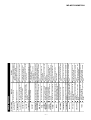
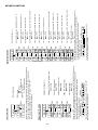
1
MD-MS701H/MS702H
SERVICE MANUAL
No. SX789MDMS702H
MD-MS701H
MD-MS702H(BL)
MD-MS702H(GY)
• In the interests of user-safety the set should be restored to its original condition
and only parts identical to those specified should be used.
Illustration: MD-MS701H
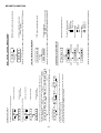
CONTENTS
Page
SAFETY PRECAUTION FOR SERVICE MANUAL ............................................................................................................... 2
SPECIFICATIONS ................................................................................................................................................................. 3
NAMES OF PARTS ............................................................................................................................................................... 4
OPERATION MANUAL .......................................................................................................................................................... 5
DISASSEMBLY ...................................................................................................................................................................... 8
REMOVING AND REINSTALLING THE MAIN PARTS ......................................................................................................... 9
ADJUSTMENT ...................................................................................................................................................................... 10
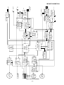
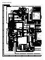
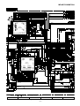
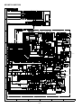
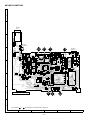
NOTES ON SCHEMATIC DIAGRAM .................................................................................................................................. 28
BLOCK DIAGRAM ............................................................................................................................................................... 29
SCHEMATIC DIAGRAM/WIRING SIDE OF P.W.BOARD ................................................................................................... 30
WAVEFORMS OF CD CIRCUIT .......................................................................................................................................... 39
TROUBLE SHOOTING ........................................................................................................................................................ 40
FUNCTION TABLE OF IC .................................................................................................................................................... 43
PARTS GUIDE/EXPLODED VIEW
PACKING METHOD (FOR UK ONLY)
SHARP CORPORATION
–1–
This document has been published to be used
for after sales service only.
The contents are subject to change without notice.
MD-MS701H/MS702H
SAFETY PRECAUTION FOR SERVICE MANUAL
Precaution to be taken when replacing and servicing the
Laser Pickup.
The AEL (Accessible Emission Level) of Laser Power Output for
this model is specified to be lower than Class I Requirements.
However, the following precautions must be observed during
servicing to protect your eyes against exposure to the laser
beam.
(1) When the cabinet has been removed, the power is turned
on without a compact disc, and the Pickup is on a
position outer than the lead-in position, the Laser will
light for several seconds to detect a disc. Do not look into
the Pickup Lens.
(2) The Laser Power Output of the Pickup inside the unit and
replacement service parts have already been adjusted
prior to shipping.
(3) No adjustment to the Laser Power should be attempted
when replacing or servicing the Pickup.
(4) Under no circumstances look directly into the Pickup
Lens at any time.
(5) CAUTION - Use of controls or adjustments, or performance
of procedures other than those specified herein may
result in hazardous radiation exposure.
LASER KLASSE 1
LUOKAN 1 LASERLAITE
KLASS 1 LASERAPPARAT
Laser Diode Properties
Material: GaAIAs
Wavelength: 785 nm
Pulse time:
Read mode: 0.8 mW Continuous
Write mode: max 10 mW 0.5
min cycle 1.5S
Repetition
CAUTION - INVISIBLE LASER RADIATION WHEN OPEN AND INTERLOCKS DEFEATED
AVOID EXPOSURE TO BEAM .
VARNING - OSYNLIG LASERSTRÅLNING NÄR DENNA DEL ÄR ÖPPNAD OCH SPÄRRAR
ÄR URKOPPLADE. STRÅLEN ÄR FARLIG.
ADVARSEL - USYNLIG LASERSTRÅLING NÅR DEKSEL ÅPNES OG SIKKERHEDSLÅS
BRYTES. UNNGÅ EKSPONERING FOR STRÅLEN.
VARO! AVATTAESSA JA SUOJALUKITUS OHITETTAESSA OLET ALTTIINA
NÄKYMÄTÖN LASERSÄTEILYLLE. ÄLÄ KATSO SÄTEESEN.
VARNING - OSYNLIG LASERSTRÅLING NÄR DENNA DEL ÄR ÖPPNAD OCH SPÄRREN
ÄR URKOPPLAD. BETRAKTA EJ STRÅLEN.
ADVARSEL - USYNLIG LASERSTRÅLING VED ÅBNING NÅR SIKKERHEDSAFBRYDERE
ER UDE AF FUNKTION. UNDGÅ UDSETTELSE FOR STRÅLING.
VAROITUS! LAITTEEN KÄYTTÄMINEN MUULLA KUIN TÄSSÄ KÄYTTÖOHJEESSA
MAINITULLA TAVALLA SAATTAA ALTISTAA
KÄYTTÄJÄN TURVALLISUUSLUOKAN 1 YLITTÄVÄLLE
NÄKYMÄTTÖMÄLLE LASERSÄTEILYLLE.
VARNING - OM APPARATEN ANVÄNDS PÅ ANNAT SÄTT ÄN I DENNA BRUKSANVISNING
SPECIFICERAS. KAN ANVÄNDAREN UTSÄTTAS FÖR OSYNLIG LASERSTRÅLNING, SOM
ÖVERSKRIDER GRÄNSEN FÖR LASERKLASS 1.
VARO !
VARNING!
Avattaessa ja suojalukitus ohitettaessa olet alttiina näkymättömälle lasersäteilylle. Älä katso säteeseen.
Osynlig laserstralning när denna del är öppnad och spärren är urkopplad. Betrakta ej strälen.
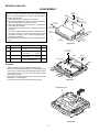
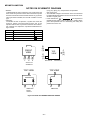
Precaution to be taken when replacing and servicing the laser pickup.
The following precautions must be observed during servicing to protect your eyesagainst exposure to the laser.
Warning of possible eye damage when repairing:
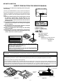
If the AC adaptor or batteries are connected when the top houising (disc cover) of the unit is removed, and the PLAY key is
pressed, the laser will light up during docus access (2-3 seconds). (Fig. 2-1) During the operation, the laser will lesk from the
opening btween the magnetic head and the mechanical chassis (Fig. 2-2). In order to protect your eyes, you most not look
at the laser durnd repaor. Before repaoring be sure to disconnect the AC adaptor and remove the batteries.
Magnet head
Magnet Head
Lasar Beam
Mechanism
Chassis
Main PWB
Optical pick-up
Disc motor
Figure 2-1
Optical Pick-Up
Figure 2-2
Disc cover
–2–
MD-MS701H/MS702H
FOR A COMPLETE DESCRIPTION OF THE OPERATION OF THIS UNIT, PLEASE REFER TO
THE OPERATION MANUAL.
SPECIFICATIONS
General
Power source:
Weight:
DC 3.6 V (rechargeable lithium-ion
battery x 1)
DC 5 V (AC adaptor)
AC 110 - 240V, 50/60 Hz
DC 3V: Separately available battery
case, AD-M70BC
(commercially available, "AA"
size, alkaline battery x 2)
DC 4.5V: Separately available car
adaptor, AD-CA20X
(for cars with a 12-24V DC
negative earth electrical
system)
0.15 A (AC adaptor)
4W
RMS; 20 mW (10 mW + 10mW)
(0.2% T.H.D.)
Approx. 2.5 hours
(When using the AC adaptor included
with the unit)
Power consumption:
Output power:
Charging time:
Input socket:
Output socket:
MiniDisc Recorder
Type:
Signal readout:
Audio channels:
Frequency response:
Rotation speed:
Error correction:
Coding:
Battery life:
When using the
rechargeable battery (fully
charged) included with the
unit
When using two,
commerically available,
high capacity, "AA" size,
alkaline batteries (in the
separately available battry
case)
When using two, commercially
available, high capacity, "AA"
size batteries with the
rechargeable battery (fully
charged)
Continuous recording:
Approx. 3.5 hours
Continuous recording:
Approx. 4 hours
Continuous recording:
Approx. 7.5 hours
Continuous play:
Approx. 5 hours
Continuous play:
Approx. 8 hours
Continuous play:
Approx. 13 hours
Recording
level
Reference input
level
Input
impedance
MIC H
0.25 mV
10 k ohms
MIC L
2.5 mV
10 k ohms
LINE
100 mV
20 k ohms
Output level:
Headphones
LINE
Dimensions:
Recording method:
Sampling frequency:
Wow and flutter:
The continuous recording time is for analogue input when the
volume level is set to "VOL 0".
The continuous play time shows the value when the volume level is
set to "VOL 15".
The above values are the standard values when the unit is charged
and used at an ambient temperature of 20oC.
The operating time when using alkaline batteries may be different,
depending on the type and manufacturer of the batteries, and on
the operating temperature.
Input sensitivity:
MD-MS701H: 216 g (0.48 lbs.) with
rechargeable battery
MD-MS702H: 219 g (0.49 lbs.) with
rechargeable battery
Line/Mic/optical digital, microphone
(powered by the main unit)
Headphones (impedance: 32
ohms)/remote control unit
Specified
output
Maximum
output level
Load
impedance
—
10 mW +
10 mW
32 ohms
300mV
(-12dB)
—
50 kohms
Width: 87.0 mm (3-7/16")
Height: 29.4 mm (1-3/16")
Depth: 81.5 mm (3-7/32")
–3–
Portable MiniDisc recorder
Non-contact, 3-beam semi-coductor
laser pick-up
Stereo 2 channels/monaural (longplay mode) 1 channel
20 - 20,000 Hz (± 3 dB)
Approx 400 - 900 rpm
ACIRC (Advanced Cross Interleave
Reed-Solomon Code)
ATRAC (Adaptive TRansform
Acoustic Coding), 24-bit computed
type
Magnetic modulation overwrite
method
44.1 kHz (32 kHz and 48 kHz
signals are converted to 44/1 kHz,
and then recorded.)
Unmeasurable (less than ±0.001%
W.peek)
Specifications for this model are subject to change
without prior notice
MD-MS701H/MS702H
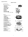
NAME OF PARTS
Remote Control Unit
1. Synchro Recording Indicator
2. Character/Time Information Indicator
3. Record Indicator
4. Repeat Indicator:
5. Random Indicator
6. Disc Mode Indicator
7. Total Track Number Display
8. Track Number Indicator
9. Battery Indicator:
10. Headpones Socket
11. Hold Switch
12. Play Mode Button
13. Volume Buttons: +, 14. Bass Button
15. Display Button
16. Play/Pause Button:
17. Stop/Power Off Button:
18. Fast Reverse/Fast Forward Buttons:
2
1
3
SYNC REC
6
1
RANDOM
TOTAL
7
8
4
5
9
10
11
15
12
16
17
18
13
/
14
Main Unit
1
1. Monaural Long-Play Mode Indicator
2. Record Indicator
3. Level Meter
4. Repeat Indicator:
5. TOC Indicator
6. Battery Indicator:
7. Random Indicator
8. Track Number Indicator
9. Character/Time Information Indicator
10. Synchro Recording Indicator
11. Disc Mode Indicator
12. Disc Name Indicator
13. Track Name Indicator
14. Remaining Recording Time Indicator
15. Total Track Number Display
2
3 4 5
6
10
11
12
13
7
8
9
14 15
16. Record/Track Mark Button
17. Volume/Name Select Buttons: +, 18. Display/Lowercase Characters Button
19. Character Button
20. Stop/Power Off/Charge Button: /:OFF
21. Play/Pause Button:
22. Fast Reverse/Fast Forward/Recording Level
Control/Cursor Buttons:
/
23. Enter/Fast Play/Synchro Button
24. Editer/Auto Mark/Time Mark Button
25. Eject Lever
26. Bass/Delete Button
27. Mode/Insert Button
16
17 18 19 20 21
22
23 24 25 26 27
28
28. Microphone Input Socket
29. Hold Switch
30. Rechargeable Lithium-Ion Battery
Compartment
31. Optical/Line Input Soket
32. Headphones Soket
33. 5V DC Input Sokets
34. Battert Case Connection Terminals
–4–
29
30
31
34
32
33
–5–
:OFF
4
AC 110-240V, 50/60 Hz
Insert
securely,
all the
way in.
Mark
Notes:
After charging has been completed, the
AC adaptor may be left connected. (For
example, when charging at night)
The battery will not be charged whenever the power to the main unit is
turned on.
If the AC adaptor is removed from the
main unit or from the AC socket whilst
charging, “
” will not disappear for
about 1 minute. This is normal.
To the
DC IN 5V
socket
5
2
1
/:OFF button twice to begin
Do not force open the rechargeable
battery cover too wide.
Do not fit the separately available battery case when charging the internal
battery.
charging.
“
” will appear, and the battery will
begin charging.
Battery charging will be complete in 2.5
hours. When the charging is complete, “
” will go out.
5 Press the
the AC adaptor into the AC
socket, and then insert the plug on the
AC adaptor lead into the DC IN 5V
socket.
4 Plug
partment cover.
3 Close the rechargeable battery com-
Insert the side with the arrow first.
2 Insert the rechargeable battery.
the rechargeable battery compartment cover.
1 Open
When the rechargeable battery is used for
the first time or when you want to use it
after a long period of disuse, be sure to
charge it fully.
Rechargeable battery power
This unit can be used with 4 different power sources: a rechargeable battery, an AC
adaptor, a separately available battery case (AD-M70BC), and a separately available car
adaptor (AD-CA20X).
POWER SOURCE
OPERATION MANUAL
When the number of tracks used
reaches the limit, regardless of the
remaining recording time, further
recording will be impossible.
(Maximum number of tracks: 254)
If a MiniDisc has been recorded or
edited repeatedly or if a MiniDisc has
scratches on it, it may not be possible
to record the maximum number of
tracks on it.
If there are scratches on a disc, the
unit will automatically avoid recording
in those areas. The recording time will
be reduced.
When the remaining recording time of
a disc is displayed, short tracks less
than 8 seconds long may not be
included in the total.
For MiniDiscs on which repeated
recording and editing operations were
performed, the COMBINE function
may not work.
A cluster (about 2 seconds) is
normally the minimum unit of
recording. So, even if a track is less
than 2 seconds long, it will use about
2 seconds of space on the disc.
Therefore, the time actually available
for recording may be less than the
remaining time displayed.
If there are scratches on discs, those
sections will be automatically avoided
(no recording will be placed in those
sections). Therefore, the recording
time will be reduced.
For MiniDiscs on which repeated
recording and editing were performed,
some sounds may be skipped whilst
cueing and reviewing.
If there are scratches or dust on a
MiniDisc, the track numbers following
that track will be increased by one.
Even if the maximum recording
time of a MiniDisc has not been
reached, “DISC FULL” or “TOC
FULL” may be displayed.
Even if the number of tracks and
the recording time have not
reached the limit, “DISC FULL” may
be displayed.
Even if several short tracks are
erased, the remaining recording
time may not show an increase.
Two tracks may not be combined in
editing.
The total of the recorded time and
time remaining on a disc may not
add up to the maximum possible
recording time.
When recorded tracks are played
back using the cue and review
operations, some sounds may be
skipped.
A track number can be created in
the middle of a track.
MiniDiscs are recorded using a different system than is used for cassette tapes or DAT
recordings. Therefore, the following conditions may be encountered, depending on how
the disc has been recorded or edited. These are due to system limitations, and should
be considered normal.
MINIDISC SYSTEM LIMITATIONS
MD-MS701H/MS702H
When the unit has condensation inside,
the disc signals cannot be read, and the
unit may not function properly.
If this happens, remove the disc.
The condensation should evaporate in
approximately 1 hour. The unit will then
function properly.
–6–
Is the unit in the safety mode?
Is the battery exhausted?
Is the remote control unit plug or the headphone plug
inserted firmly?
Is the battery exhausted?
Is the unit being subjected to excessive vibration?
Has the track number or character information been
written on the disc yet?
Is the unit in the recording or editing mode?
Is the MiniDisc protected against accidental erasure?
Is the unit connected properly to the other equipment?
Is the AC adaptor unplugged or did a power failure
occur whilst recording or editing?
Is the unit in the safety mode?
No sound is heard
from the headphones.
When the operation
buttons are pressed,
the unit does not
respond.
Some sounds are
skipped.
The MiniDisc cannot
be ejected.
Recording and editing
are impossible.
When this product is subjected to strong
external interference (mechanical shock,
excessive static electricity, abnormal supply voltage due to lightning, etc.) or if it is
operated incorrectly, it may malfunction. If
such a problem occurs, do the following:
1. Unplug the AC adaptor from the AC
socket.
2. Remove the battery.
3. Leave the unit completely unpowered
for approximately 30 seconds.
If strange sounds, smell or smoke come
out of the unit or an object is dropped into
the unit, remove the AC adaptor from the
AC socket immediately and contact an authorised Sharp service centre.
4. Plug the AC adaptor back into the AC
socket and retry the operation.
Is the volume set too low?
Is the remote control unit or the headphones plugged
in?
Are you trying to play a MiniDisc with data on it
instead of a MiniDisc containing music?
The unit does not turn
on.
If trouble occurs
CAUSE
Is the AC adaptor disconnected?
Is the battery exhausted?
Is the unit in the safety mode?
Has condensation formed inside the unit?
Is the unit being influenced by mechanical shock or by
static electricity?
PROBLEM
Many potential “problems” can be resolved by the owner without calling a service technician. If something seems to be wrong with this product, check the following before
calling your authorised SHARP dealer or service centre.
Shortly after turning on a heater.
When the unit is placed in a room
where there is excessive steam or
moisture.
When the unit is moved from a cool
place to a warm place.
In the following cases, condensation
may form inside the unit.
Moisture condensation
TROUBLESHOOTING
Charging is
needed.
When the battery needs charging, it is
impossible to start recording or editing.
When the battery is
completely charged
< How to read the battery indicator >
Battery indicator
The remaining amount of battery charge is
shown by the battery indicator (
) during operation.
Checking the remaining
amount of battery charge
Digital cable
Recording
Digital cable
Recording
Analogue recording is
possible.
Playback
Digitally recorded MiniDisc
CD player, MD
player, etc.
Playback
When the AC adaptor included with this
unit or a separately available car adaptor
is used, the battery indicator will not be
shown.
The number of bars shown in the battery
indicator may increase or decrease, depending on the operation being performed. This is normal.
When the rechargeable battery and the
alkaline batteries are used at the same
time, the rechargeable battery is used first,
and then the alkaline batteries.
Since the battery indicator shows the remaining amount of the particular battery
being used, the number of bars will increase when the unit switches to the alkaline batteries.
Notes:
When the battery is completely discharged, the whole battery indicator will
flash. Recharge the battery or replace
the alkaline batteries with new ones.
When the battery has run completely
out, “BATT EMPTY” (main unit) and “Lo
BATT” (remote control unit) will appear.
Then, the power will be disconnected
automatically.
CONVENIENT OPERATION OF THE UNIT
When you attempt to make a new digital
recording from a track that was digitally
recorded on a MiniDisc
MiniDiscs are designed so that only
first generation digital copies can
made, further digital copies are prevented by the SCMS (Serial Copy Management System).
In the following cases digital recording is
impossible, even if you are using digital
cables.
There are cases where digital
recording may be impossible.
RECORDING USING A SEPARATELY AVAILABLE DIGITAL
CABLE
MD-MS701H/MS702H
–7–
? DISC
U TOC ERROR
Tr. Protect
TOC FULL
TOC ERROR
TEMP OVER
SYSTEM ERR
SORRY
POWER ?
PB DISC
PROTECTED
LOCKED
LOCK ERROR
NO DISC
HOLD
DISC FULL
Din UNLOCK
DISC ERROR
DEFECT
Can't WRITE
Can't REC
Can't EDIT
Can't COPY
BLANK DISC
BATT EMPTY
Error messages
A large portion of the disc has been
damaged.
There is no space left for recording
character information (track names,
disc names, etc.).
The track has been protected from
being erased.
A large portion of the disc has been
damaged.
There is an error in the recorded
signal.
A disc which contains data other
than music was played.
There is an error in the signal from
the disc.
The temperature is too high.
Since a track number is currently
being located or written to, the unit
cannot accept your command.
You have come to the conclusion
that the unit is out of order.
The EJECT lever was moved
during recording or editing.
A disc has not been loaded.
The disc is write protected.
You tried to record on a playbackonly disc.
Improper power is being supplied.
The unit is in the safety mode.
Poor connection of the digital cable.
The disc is damaged.
The disc is out of recording space.
Recording cannot be performed
correctly due to vibration or shock
in the unit.
Editing is impossible.
The disc is scratched.
No copy can be made because of
the SCMS copyright system.
A track cannot be edited.
Nothing is recorded.
Meaning
The battery run down.
ERROR MESSAGES
Edit the track with the device on
which it was recorded.
Replace it with another recorded
disc.
Erase all of the signal errors, and
then try recording again.
A disc which contains non-music
data cannot be played.
Replace it with another recorded
disc.
To have it repaired, go to the
distributor where you purchased the
unit.
Turn off the power, and wait for a
while.
Replace it with another recorded
disc.
Replace it with another recordable
disc.
Check the number of tracks.
If the sound you hear is not right,
try recording again.
Replace the disc with another
recordable disc.
Connect the digital cable securely.
Reload the disc or replace it.
Replace it with another recordable
disc.
Return the HOLD switch to its
original position.
Turn off the power and remove the
MiniDisc.
Load a disc.
Move the write protection knob
back to its original position.
Replace it with a recordable disc.
Use one of the specified power
sources.
Wait for a while and try the
operation again.
Change the stop position of the
track and then try editing it.
Re-record or replace it with another
recordable disc.
Remedy
Charge the rechargeable battery or
replace the alkaline batteries (or use
the AC adaptor for power).
Replace the disc with a recorded
disc.
Record using the analogue cable.
MD-MS701H/MS702H
MD-MS701H/MS702H
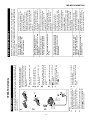
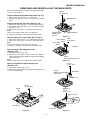
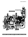
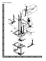
DISASSEMBLY
Caution on Disassembly
Follow the below-mentioned notes when disassembling
the unit and reassembling it, to keep it safe and ensure
excellent performance:
1. Take the battery and minidisc out of the unit.
2. When disassembling the machine, be sure to withdraw
the power plug from the socket in advance.
3. When disassemble the parts, remove the nylon band or
wire holder as necessary.
To assemble after repair, be sure to arrange the wires as
they were.
If a screw of different length is fitted to the MD mechanism (the screw of the part to be fitted to the MD
mechanism chassis), it may contact the optical pickup,
resulting in malfunction.
4. When repairing, pay due attention to electrostatic charges
of IC.
(A1)x2
Ø1.4x2mm
Pull
(A1)x1
Ø1.4x2mm
(B1)x1
Ø1.4x2mm
(A1)x1
Ø1.4x2mm
Bottom Cabinet
(B1)x1
Ø1.4x2mm
(A1)x2
Ø1.4x2mm
Center
Cabinet
(B1)x2
Ø1.4x2mm
Top Cabinet
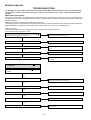
Figu re 8-1
STEP
REMOVAL
PROCEDURE
FIGURE
1
Bottom Cabinet
1. Open the battery Lid.
2. Screw ..................... (A1) x6
8-1
2
Top Cabinet
1. Screw ..................... (B1) x4
2. Flat Cable ............... (B2) x2
8-1
3
Main PWB
1. Screw .................... (C1) x2
2. Flat Cable ............... (C2) x3
8-2
4
Mechanism Unit
1. Lift the left side, and remove
in the arrow direction.
8-3
(C1)x1
Ø1.7x2.5mm
(C2)x1
Main PWB
Pull
(B2)x1
Pull
Caution:
1. Handle carefully the main PWB and flexible PWB.
After removing the flexible PWB (*1) for optical pickup from
the connector, wrap the front end of flexible PWB in conductive aluminum foil so as to protect the optical pickup from
electrostatic damage.
2. When removing the mechanism from the cabinet or when
installing it, it is advisable to
rotate the unit lock plate to lower the holder section.
(C1)x1
Ø1.7x2.5mm
Pull
Pull
(C2)x1
Pull
Pull
Pull
(C2)x1
Figure 8-2
Mechanism Unit
Figure 8-3
–8–
Pull
(B2)x1
MD-MS701H/MS702H
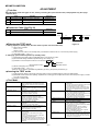
REMOVING AND REINSTALLING THE MAIN PARTS
Remove the mechanism according to the disassembling methods 1 to 3. (See Page 8.)
(A2)x3
ø1.4x2.8mm
How to remove the spindle motor (See Fig. 9-1.)
1. Remove the solder joint (A1) x 1 of flex PWB.
2. Remove the stop (A2) x 3 pcs. and remove the spindle
motor.
Spindle Motor
How to remove the lift motor (See Fig. 9-2.)
1. Remove the solder joint (B1) x 2 of slide motor lead wire.
2. Remove the stop washer (B2) x 1 pc., and remove the drive
gear (B3) x 1 PC.
3. Remove the screw (B4) x 1, and remove the lift motor.
Note:
Take care so that the motor gear is not damaged.
(If the gear is damaged, noise is raised in search mode.)
Flexible PWB
solder joint
(A1) x1
How to remove the sled motor (See Fig. 9-3.)
1. Remove the solder joint (C1) x 2 of slide motor lead wire.
2. Remove the screw (C2) x 2, and remove the sled motor.
Note:
Take care so that the motor gear is not damaged.
(If the gear is damaged, noise is raised in search mode.)
MDMechanism
Figure 9-1
Stop Washer
(B2)x1
Drive Gear
(B3)x1
(B4)x1
ø1.4x2.2mm
Lift Motor
How to remove the magnetic head
(See Fig. 9-4.)
1. Remove the screw (D1) x 2 pc.
2. Remove the screw (D2) x1 which connects the magnetic
head to the head relay flex PWB, and remove the soldering
joint (D3) x2 pcs.
Note:
Mount carefully so as not to damage the magnetic head.
(B1)x2
Remove the solder joint
Figure 9-2
(C1)x2
ø1.4x1.2mm
How to reinstall the optical pickup unit
(See Fig. 9-5.)
1. Remove the screws (E1) x 1 pcs.
2. Remove the soldering joint (C2) x2 places of flex PWB, and
remove the sled motor.
(C2)x2
Mecha Flexible PWB
solder joint
Sled Motor
Washer x2
(E1)x1
ø1.7x2.5mm
Figure 9-3
Shaft
(D1)x2
Ø1.4x1.8mm
Magnetic Head
(D1)x1
Ø1.4x1.5mm
Pickup Unit
Pickup Unit
Figure 9-5
Figure 9-4
–9–
Solder
joint
(D3)x2
MD-MS701H/MS702H
ADJUSTMENT
Test disc
MD adjustment needs two types of disc, namely recording disc (low reflection disc) and playback-only disc (high
reflection disc).
Type
Test disc
Parts No.
1
High reflection disc MMD-110 (TEAC Test MD)
88GMMD-110
2
Lowreflection disc
MMD-212 (TEAC Test MD)
88GMMD-212
3
Low reflection disc
Recording minidisc
UDSKM0001AFZZ
Note: Use the low reflection disc on which music has been recorded.
Extension Cable (See Fig.10)
Parts No.
Flat Cable for servicing 16Pin
QCNWK0110AFZZ
2
Extension Connector for Service 16Pin
RUNTK0460AFZZ
Price Code
PWB side
CN601
Type
1
16 pin
Mecha Flexible PWB
16 PIn
QCNWK0110AFZZ
16pin Flat Cable
RUNTK0460AFZZ
Extension PWB for servicing 16pin
Entering the TEST mode
Figure 10
1. Setting at port (in standby state, disc-free state or power nonconnected state)
(1) Set the port as follows.
TEST1 : "Low"
TEST0 : "High"
(2) Press the PLAY button in the standby state (it is allowed to insert the disc or to connect the power supply).
(3) Test Mode STOP [ _ T E S T _ ]
2. Setting by special button operation (in standby state)
(1) Holding down the DISP button and ENTER button, press the PLAY button.
(2) Normal mode setting initialization (BASS setting, VOL setting, etc.)
(3) Indication of microcomputer version for one second [
]
Destination
Microcomputer version
EEPROM version
(4) Whole LCD lighting for 2 seconds
(5) Test Mode STOP [ _ T E S T _ ]
*When the PLAY button is pressed during indication (3) and (4), the process proceeds to (5).
Leaving the TEST mode
(1) Press the STOP button in the TEST mode stop state or version indicating state or whole LCD lighting state.
(2) EEPROM rewrite-enable area updating, adjustment error setting (so as to adjust all the items when the power supply is turned
on in the normal mode)
(3) Change to standby state
Test Mode
1. AUTO 1 Mode
2. AUTO 2 Mode
3. MANUAL 1 Mode
4. MANUAL 2 Mode
5. RESULT 1 Mode
6. RESULT 2 Mode
7. TEST-PLAY Mode
• Perform preliminary automatic adjustment.
• If the combination of mechanism and pickup
PWB has been changed, be sure to start from
AUTO1.
• Perform ATT (attenuator) automatic adjustment.
• Perform continuous playback (error rate display,
jump test)
• Temperature is displayed. (Updating in real time)
• Seeing the displayed adjustment value, perform
preliminary manual adjustment.
(Error rate indication, jump test)
• Temperature is displayed. (Updating in real time)
• Seeing the displayed adjustment value
perform manfully the preliminary adjustment.
(Error rate indication, jump test)
• Continuous playback is performed
(error rate display, jump test).
• The value adjusted in AUTO1 or MANUAL1 is
indicated.
• (Execution in servo "OFF" state").
• The value adjusted in AUTO 2 or MANUAL 2 is
indicated.
• Adjustment value is changed manually.
(error rate display, jump test).
• Continuous playback from the specified address
is performed.
• 1 line, 10 lines or 400 lines manual jump is
performed.
• C1 error rate display (pit section), ADIP error
rate display (groove section)
• The temperature correction is performed only
when servo start is performed, but the posture
correction is not performed during continuous
playback.
8. TEST-REC Mode
9. NORMAL Mode
10. DIGITAL INPUT mode
11. ERROR INFORMATION
Mode
12. E2-PROM Mode
13. INNER Mode
– 10 –
• Continuous record from the specified address is
performed.
• Change of record laser output(servo gain is also
changed according to laser output).
• The temperature correction is performed only
when servo start is performed, but the posture
correction is not performed during continuous
recording.
• The mode is changed from the TEST mode to
the normal mode without adjustment.
• In the normal mode the internal operation mode,
memory capacity, etc. areindicated.
• In the normal mode both temperature correction
and posture correction are perfomed.
• Digital input information is displayed.
• Error information is displayed.
• Error information is initialized
• Factors of digital servo are changed manually.
(Each servo is turned on individually.)
• Cut-off frequency of BASS1, BASS2 and BASS3
is selected manually.
• Temperature detection terminal voltage is
measured, and the reference value is set.
• Defaults are selected and set.
• Setting of EEPROM protect area is updated.
(In case of protect releasing)
• Determine the position where the INNER switch
is turned on. (only high reflection disc).
• The temperature correction is performed only
when servo start is performed, but the posture
correction is not performed.
MD-MS701H/MS702H
Operation in each TEST mode
1. AUTO1 Mode
• When the STOP button is pressed while the AUTO1 menu appears or during automatic adjustment, the mode changes to the TEST mode
stop state. At this time the adjustment value is not output.
• Be sure to adjust, using the specified disc MMD-212.
At this time release the EEPROM (IC402) protection. (Refer to EEPROM write procedure.)
• Adjustment NG; Adjustment item out of range, focus ON failure, and adjustment error
• When the PLAY button is pressed while ADJ. OK is displayed, AUTO2 is executed.
2. AUTO2 Mode
• When the STOP button is pressed while the AUTO2 menu appears or during automatic adjustment, the mode changes to the TEST mode
stop state. At this time the adjustment value is not output.
• Adjustment NG; Adjustment item out of range, and adjustment error
3. MANUAL1 Mode
• Adjustment item to be made in AUTO1 mode is performed manually.
• When the VOL UP button is pressed during adjustment, the setting increases, and the new setting is output.
• If the VOL DOWN button is pressed during adjustment, the setting decreases and the new setting is output.
• If the VOLUP/DOWN button is held down, the setting changes continuously with 100 ms cycle.
• If the setting is within the allowable range, the RANDOM display lights.
• When the STOP button is pressed during MANUAL1 MENU or measurement or adjustment, the state is changed to the TEST mode stop
state.
4. MANUAL2 Mode
• Adjustment item to be made in AUTO2 mode is performed manually.
• When the VOL UP button is pressed during adjustment, the setting increases, and the new setting is output.
• If the VOL DOWN button is pressed during adjustment, the setting decreases and the new setting is output.
• If the VOLUP/DOWN button is held down, the setting changes continuously with 100 ms cycle.
• If the setting is within the allowable range, the RANDOM display lights.
• When the STOP button is pressed during MANUAL2 MENU or measurement or adjustment, the state is changed to the TEST mode stop
state.
• When the PLAY button is pressed in B-ATT set state, the mode is changed to the continuous playback mode.
• As for operation during continuous playback refer to "TEST-PLAY mode explanation".
5. RESULT1 Mode
• The measurement value and set value of adjustment items for AUTO1 and MANUAL 1 are displayed.
• If the VOL UP button is pressed during setting indication, the setting increases. If the VOL DOWN button is pressed, the setting reduces.
And then the new setting is stored in the RAM.
• When the VOL UP/DOWN button is held down, the setting changes continuously, one cycle being 100 ms.
• If the STOP button is pressed during RESULT1 menu or measurement value indication or set value indication, the state is changed to the
TEST mode STOOP state.
6. RESULT2 Mode
• The measurement value and set value of adjustment items for AUTO2 and MANUAL 2 are displayed.
• If the VOL UP button is pressed during setting indication, the setting increases. If the VOL DOWN button is pressed, the setting reduces.
And then the new setting is stored in the RAM.
• When the VOL UP/DOWN button is held down, the setting changes continuously, one cycle being 100 ms.
• If the STOP button is pressed during RESULT2 menu or measurement value indication or set value indication, the state is changed to the
TEST mode STOOP state.
7. TEST-PLAY Mode
•When the STOP button is pressed while the TEST-PLAY menu appears, or in TEST-PLAY or continuous playback mode, the mode changes
to the TEST mode stop state.
• When the PLAY button is pressed while the TEST-PLAY menu appears,continuous playback is initiated from the current pickup position.
• Whenever the DISP button is pressed in the TEST-PLAY mode, the address changes as follows.
0050 — 03C0 — 0700 — 08A0 — 0050 —
• Whenever the BASS key is pressed in the TEST-PLAY mode, the digit which is changed by the SKIP UP/DOWN button changes as follows.
0050 — 0050 — 0050 — 0050 — 0050 —
• When the SKIP UP button is pressed in the TEST-PLAY mode, the digit of address specified by the BASS button is set to +1h. (0 to F)
• When the SKIP DOWN button is pressed in the TEST-PLAY mode, the digit of address specified by the BASS button is set to -1h. (0 to F)
* When the SKIP UP/DOWN button is held down, the setting changes continuously, one cycle being 100 ms.
• When the BASS button is pressed in the continuous playback mode, the number of jump lines changes as follows.
1 — 10 — 400 — 1
* After the number of jump lines is indicated for one second, the address indication is restored.
[
T R _ ]
• When the SKIP UP button is pressed in the continuous playback mode, the specified number of lines is jumped in the FWD direction.
• When the SKIP DOWN button is pressed in the continuous playback mode, the specified number of lines is jumped in the REV direction.
* When the SKIP UP/DOWN button is held down, jump is repeated every approx. 100 ms.
– 11 –
MD-MS701H/MS702H
•Whenever the DISP button is pressed in the continuous playback mode, the indication changes as follows.
* Pit section
Continuous playback (SUBQ address indication)
[ S Q
]
|
Continuous playback (C1 error indication)
[ C E
]
|
Continuous playback (SUBQ address indication)
[ S Q
]
* Groove section
Continuous playback (ADIP address indication)
[ A P
]
|
Continuous playback (C1 error indication)
[ C E
]
|
Continuous playback (ADIP error indication)
[ A E
]
|
Continuous playback (ADIP address indication)
[ A P
]
8. TEST-REC Mode
• When the STOP button is pressed while the TEST-REC menu appears, or in the TEST-REC mode or continuous record mode, the mode
changes to the TEST mode stop state.
• When the PLAY button is pressed while the TEST-REC menu appears, the continuous record is initiated from the current pickup position.
• Whenever the DISP button is pressed in the TEST-REC mode, the address changes as follows.
0050 — 03C0 — 0700 — 08A0 — 0050 —
• Whenever the BASS button is pressed in the TEST-REC mode, the digit which is changed by the SKIP UP/DOWN button changes as
follows.
0050 — 0050 — 0050 — 0050 — 0050 —
• When the SKIP UP button s pressed in the TEST-REC mode, the digit of address specified by the BASS button is set to +1h.(0 to F)
• When the SKIP DOWN button is pressed in the TEST-REC mode, the digit of address specified by the BASS button is set to -1h. (0 to F)
* When the SKIP UP/DOWN button is held down, the setting changes continuously, one cycle being 100 ms.
• When the VOL UP/DOWN button is pressed in the TEST-REC mode or continuous record mode, the laser record power changes.
(Servo gain changes also according to record power.)
* After the laser record power is indicated for one second, the address indication is restored.
[ R P W
]
•
: Address
•
: Laser power cord
• Operation is disabled if the premastered disc or disc is in miserase-protected state.
9. NORMAL Mode
• When the STOP button is pressed while the NORMAl menu appears, the mode changes to the TEST mode stop state.
• Indication during operation
Indication of memory capacity on main unit LCD [
] + Level meter
: Internal mode
: Address (Cluster section)
: Address (Sector section)
• Selection of sound volume, BASS, etc. is possible (without indication)
• Recording is also possible.
10. Digital input display Mode (Din Mon)
• When the STOP button is pressed while the digital input indication menu appears or during digital input information indication, the mode
changes to the TEST mode stop state.
• In case of analog input or digital input unlocking the indication data is _.
11. Error data display Mode
• Reversing when SKIP DOWN button is pressed
• When the STOP button is pressed while the error data indication menu appears or during error data indication, the mode changes to the
TEST mode stop state.
• Error data 0 is the latest error.
• Error which occurred in the TEST mode is also stored in the memory.
• When the DISP button is pressed while the error data indication menu appears, the error data is initialized. [ C L E A R _ ]
•
: Error Code
Explanation of error history code
12h : RF side FG, TG, and TCRS adjustment termination failure
13h : Adjustment servo retraction excessive retrial
17h : A, B, E, F, and TCRSO offset measurement value out of tolerable range
21h : Focus retraction completion allowable time-over
23h : Track search completion allowable time-over
32h : P-TOC read failure
42h : U-TOC read failure
44h : U-TOC write data write disabled/read check error
52h : SD write data write disabled
71h : Pickup position initialization time-over
– 12 –
MD-MS701H/MS702H
72h : EEPROM data read check sum error
73h : Record head drive disabled (by EJECT lever)
82h : Power overvoltage detection
91h : Ambient temperature is higher that the allowable temperature.
12. INNER Mode
• when the STOP button is pressed on the INNER menu (SQ______ ), the state is changed to the TEST mode STOP state.
•
: Address
E2-PROM (IC402) writing procedure
1. Procedure to replace E2-PROM and write initial value of microcomputer in E2-PROM
(1)
(2)
(3)
(4)
(5)
(6)
(7)
(8)
(9)
(10)
(11)
(12)
(13)
(14)
(15)
Replace E2-PROM.
Deprive E2-PROM of protection (connect the pins 8 and 6 of IC402).
Refer to the latest E2-PROM data list.
Press the Display/Lower-case Character button, Enter/Synchro button and Play/Pause button to start the test mode.
Version display
[Ver.
]
E2-PROM version (C ~ Z)
Microcomputer ROM version
The whole LCD lights.
Test mode stop state
[ T E S T ]
Press the "BASS" button, and press twice the "SKIP DOWN" button.
[ E E P R O M ]
Perform the operation to display "E2-PROM SETTING MODE CHART", compare the E2-PROM DATA LIST with the
display, and set according to the E2-PROM DATA LIST with the VOL UP or VOL DOWN key.
Set the temperature reference. (Refer to the Temperature Reference Setting Method.)
Set according to the E2-PROM DATA LIST.
Press the Stop button.
[ T E S T ]
Press the Stop button.
After data is written in E2-PROM, turn off power .
Restore protection of E2-PROM (Disconnect connection made in Step (2) above).
2. Temperature reference setting method
[1] Measurement, calculation and setting procedure
(1) Set the TEST mode.
• Set TEST 1, 0 = '01', and turn on power (or set PLAY ON in standby state).
(2) Start the EEPROM mode 'Temp' menu.
• In the TEST mode STOP state, press the keys as follows: BASS, SKIP-DOWN x 2 times, PLAY, SKIP-DOWN x 4 times,
and PLAY in this order.
• 'TM$$%%' is displayed. ($$= Temperature code, %% = Temperature reference)
(3) Once press SKIP-UP, and determine the displayed microcomputer TEMP input AD value.
• 'TPin##' is displayed. (## = TEMP input AD value)
(4) At the ambient temperature, determine the temperature corrected value from the temperature measurement value
correction table.
(5) Determine the temperature reference, using the following formula.
• Temperature reference = Microcomputer TEMP input AD value + Temperature corrected value
• An example: Environmental temperature is 22°C and set voltage is 1.25V.
– 13 –
MD-MS701H/MS702H
[2] Temperature measurement value correction table
Temperature correction
Ambient temperature
o
o
Center temperature
+14 C ~ +16 C
+17oC ~ +19oC
+20oC ~ +22oC
- 03h
- 02h
- 01h
+ 15.0oC
+ 17.8oC
+ 20.7oC
+23oC ~ +25oC
+26oC ~ +27oC
+28oC ~ +30oC
± 00h
+ 01h
+ 02h
+ 23.6oC
+ 26.5oC
+ 29.4oC
*Meaning of values
• Temperature reference = Value to be predicted to be measured by the microcomputer at reference temperature
(+23.6oC)
• Temperature correction = Value to convert to measurement value at reference temperature (+23.6¯C)
*Determining the temperature correction value
• Temperature detection characteristics formula
Ambient temperature (oC) = (-2.876 x TEMP input AD value) + 463
Hence, TEMP input AD value = (463 - Ambient temperature)/2.876
• The reference temperature (+23.6oC) is taken as a reference. (it is taken as '0'). Whenever the input AD value changes
by '1', temperature is determined.
For temperature correction, the input AD value is +/- inverted.
[3] Power IC VREF feed control output
• Test/R-ROM write power input
Ambient temperature
-5oC ~ +9oC
o
o
+6 C ~ +21 C
+17oC ~ +32oC
+29oC ~ +44oC
Temperature correction
Center temperature
08h
+ 0.5oC
07h
06h
05h
+ 12.5oC
+ 23.6oC
+ 35.0oC
– 14 –
MD-MS701H/MS702H
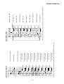
E2-PROM DATA LIST
TEMP setting
Sled setting
Item display
T M _ _
Set values
Item display
Calculate values
BASS setting
Item display
Set values
Set values
S L G _
94
H
S L 2 _
30
H
S L M _
4F
H
S L V _
36
H
B S 1 _
02
S K k _
43
H
B S 2 _
A4H
S K t _
40
H
B S 3 _
C4H
S K m _
43
H
H
Fucus setting
ADJ. SET setting
Item display
Set values
Item display
Set values
F G _ _
63
H
C O K _
A0
F F 1 _
70
H
F A T _
C0
H
F F 2 _
F0
H
T A T _
3F
H
F Z H _
ED
C A T _
20
H
F L n _
09
H
F A B _
00
H
D J G _
14
H
F R V _
00
H
F P f _
88
H
F L V _
19
H
H Q 1 _
90
H
W T f _
20
H
H Q 2 _
90
H
F S S _
02
H
H S G _
11
H
H S O _
FD
L Q 1 _
90
H
H
EQ. SET setting
Item display
Tracking setting
Item display
H
Set values
H
Set values
L Q 2 _
90
H
T G _ _
26
H
L S G _
11
H
T F 1 _
70
H
L S O _
00
H
T F 2 _
E0H
G Q 1 _
98
H
T F S _
00
H
G Q 2 _
84
H
T B o _
2BH
G S G _
11
H
T B t _
17
H
G S O _
00
H
T K o _
2BH
G Q R _
00
H
T K t _
19
H
T D o _
67
H
T D t _
2AH
S C o _
00
H
C T 0 _
48
S C t _
40
H
C T 1 _
E0
H
00
H
H
Control setting
Item display
Set values
H
S C m _
53
H
P W L _
D B O _
00
H
R C 0 _
C0
C L p _
12
H
R C 1 _
FE
H
C L r _
24
H
S Y C _
A6
H
W T m _
E0H
D R 1 _
A0
H
D R 2 _
A6
H
I N 1 _
D4
H
Set values
I N 2 _
67
H
S P G _
14
H
C T R _
6D
H
S P i
AAH
C T 2 _
14
H
S P m _
79
H
C T 3 _
03
H
S P o _
4F
H
C T 4 _
64
H
S P 1 _
10
H
C T 5 _
74
H
S P 2 _
60
H
C T 6 _
08
H
S P 3 _
F2
H
C T 7 _
00
H
S P 4 _
F2
H
S P M _
00
H
S P 5 _
10
H
M S L _
80
H
S P D _
61
H
R S L _
00
H
S P R _
C4H
Spindle setting
Item display
_
– 15 –
– 16 –
REC
SKIP DOWN
SKIP DOWN
PLAY
SKIP DOWN
SKIP DOWN
SKIP DOWN
SKIP DOWN
SKIP DOWN
SKIP DOWN
SKIP DOWN
SKIP DOWN
SKIP DOWN
SKIP DOWN
DATA
SKIP DOWN
: INNER switch position measurement menu
: EEPROM setting menu
: Error history display menu
: Digital input signal monitor menu (record/playback machine only)
: Test mode normal playback menu
: Continuous record menu (record/playback machine only)
: Continuous playback menu
: ATT adjustment value check menu
: Preadjustment value check menu
: ATT manual adjustment menu
: Pre-manual adjustment menu
: ATT autoadjustment menu
: Pre-autoadjustment menu
: Test Mode STOP
* When the "STOP" button is pressed in specific menu, the TEST MODE STOP state is set.
SKIP UP
INNER
SKIP UP
EEPROM
SKIP UP
E
SKIP UP
Din Mon
SKIP UP
NORMAL
SKIP UP
T
SKIP UP
T
SKIP UP
RSLT2
SKIP UP
RSLT1
SKIP UP
MANU2
SKIP UP
MANU1
SKIP UP
AUTO2
SKIP UP
SKIP DOWN
Slide internal
periphery move
AUTO1
BASS
Slide external
periphery move
SKIP UP
TEST
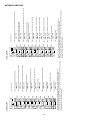
Test Mode Change Chart
Tset Mode Menu
ADJ. NG
Adjustment error
: During ATT automatic adjustment
: Preadjustment normal end (adjustment value output)
: Preadjustment error (adjustment value output)
: During preadjustment adjustment
: Preautomatic Adjustment menu
* When the "STOP" button is pressed in specific menu, the TEST MODE STOP state is set.
*"
" represent the adjustment number as follows.
0 0 : Innermost periphery move
0 2 : ABEF offset tentative measurement
0 4 : RF side focus gain coarse adjustment
0 5 : Focus ATT tentative setting
0 6 : RF side bit section tracking gain adjustment
0 7 : COUT level setting for pit section adjustment
0 8 : External periphery move
0 9 : RF side groove section tracking gain adjustment
1 0 : COUT level setting for groove section adjustment
1 1 : RF side TCRS gain adjustment
1 2 : Tracking ATT initial setting
1 3 : RF side focus gain minor adjustment
1 4 : Focus ATT initial setting
1 5 : S gain "High" ABEF offset measurement
1 6 : TCRS offset measurement
1 7 : S gain "Low" ABEF offset measurement
AT2
PLAY
ADJ. OK
Normal end
AT1
PLAY
AUTO1
Preautomatic Adjustment
MD-MS701H/MS702H
ADJ. NG
Adjustment error
: Continuous playback (high reflection)
: Continuous playback (low reflection)
: ATT adjustment normal end (adjustment value output)
: ATT adjustment error (adjustment value output)
: During ATT autoadjustment
: ATT Autoadjustment menu
* When the "STOP" button is pressed in specific menu, the TEST MODE STOP state is set.
*"
" represent the adjustment number as follows.
0 0 : Innermost periphery move
0 3 : Pit section tracking ATT setting
0 4 : Pit section focus ATT setting
0 6 : External periphery move
(low reflection only)
0 7 : TCRS ATT setting
(low reflection only)
0 8 : Groove section tracking ATT setting (low reflection only)
0 9 : Groove section focus ATT setting
(low reflection only)
SQ####
AP####
PLAY
ADJ. OK
Normal end
AT2
PLAY
AUTO2
ATT Autoadjustment
– 17 –
SKIP DOWN
SKIP DOWN
SKIP DOWN
SKIP DOWN
SKIP DOWN
SKIP DOWN
SKIP DOWN
SKIP DOWN
SKIP DOWN
SKIP DOWN
SKIP DOWN
P
SKIP DOWN
SKIP DOWN
SKIP DOWN
SKIP DOWN
SKIP DOWN
$ $
Continued to
the next page
SKIP UP
SF
SKIP UP
SE
SKIP UP
RCG
SKIP UP
GCH
SKIP UP
GTG
SKIP UP
PCH
SKIP UP
PTG
SKIP UP
Sb
SKIP UP
Sa
SKIP UP
RFg
SKIP UP
LON
SKIP UP
Fh
SKIP UP
Eh
SKIP UP
Bh
SKIP UP
Ah
SKIP UP
TMP
PLAY
MANU1
Pre-Manual Adjustment
: F-ATT (tracking) initial setting
: ATT setting
: E-ATT (tracking) initial setting
: ATT setting
: RF side TCRS gain adjustment
: Gain setting
: Groove section adjustment COUT level setting
: COUT level setting
RF side groove section tracking gain adjustment
: Gain setting
: Pit section adjustment COUT level setting
: COUT level setting
: RF side pit section tracking gain adjustment
: Gain setting
: B-ATT (focus) tentative setting
: ATT setting
: A-ATT (focus) tentative setting
: ATT setting
: RF side focus gain coarse adjustment
: Gain setting
: Laser On (Play Power)
: F signal offset (FINO) tentative measurement
: Measurement value
: E signal offset (EINO) tentative measurement
: Measurement value
: B signal offset (BINO) tentative measurement
: Measurement value
: A signal offset (AINO) tentative measurement
: Measurement value
: Temperature code display
$ $ : Temperature code
: Pre-Manual Adjustment menu
MD-MS701H/MS702H
– 18 –
SKIP DOWN
SKIP DOWN
SKIP DOWN
SKIP DOWN
SKIP DOWN
SKIP DOWN
SKIP DOWN
SKIP DOWN
SKIP DOWN
SKIP DOWN
SKIP DOWN
SKIP DOWN
: S gain "Low" E signal offset (EINO) measurement
: Measurement value
: S gain "Low" B signal offset (BINO) measurement
: Measurement value
: S gain "Low" A signal offset (AINO) measurement
: Measurement value
TCRS signal offset (TCRSO) measurement
: ATT setting
: S gain "High" F signal offset (FINO) measurement
: Measurement value
: S gain "High" E signal offset (EINO) measurement
: Measurement value
: S gain "High" B signal offset (BINO) measurement
: Measurement value
: S gain "High" A signal offset (AINO) measurement
: Measurement value
: B-ATT (focus) initial setting
: ATT setting
: A-ATT (focus) initial setting
: ATT setting
: RF side focus gain minor adjustment
: Gain setting
P
BASS
LON
M
Max. power
BASS
BASS
LON
R
Record power
• 3-rd digit setting
1st digit (initial value)
P-MODE
P-MODE
P-MODE
2nd value
P-MODE
P-MODE
3rd digit
* In the specific setting display state the setting change digit changes when the [P-MODE] key is pressed.
(In case of RF side gain setting change does not occur since there is only one digit.)
• 2-digit setting
1st digit (initial value)
2nd value
LON
Play power
FL
: S gain "Low" F signal offset (FINO) measurement
: Measurement value
* When the "STOP" button is pressed in specific menu, the TEST MODE STOP state is set.
* In laser ON state (without disc) the laser power is changed as follows when the [BASS] key is pressed.
SKIP UP
EL
SKIP UP
BL
SKIP UP
AL
SKIP UP
TH
SKIP UP
FH
SKIP UP
EH
SKIP UP
BH
SKIP UP
AH
SKIP UP
SB
SKIP UP
SA
SKIP UP
RFG
SKIP UP
Continued from the
preceding page
DISP
DISP
DISP
DISP
: RF side TCRS gain adjustment
: LPFEFO measurement value display
"REPEAT" mark lighting
: RF side pit section tracking gain adjustment
: Pit section adjustment COUT level setting
: RF side groove section tracking gain adjustment
: Groove section adjustment COUT level setting
: LPFABO measurement value display
"REPEAT" mark lighting
: RF side focus gain coarse adjustment
: A-ATT (focus) initial setting
: B-ATT (focus) initial setting
: ABMXO measurement value display
"REPEAT" mark lighting
: RF side focus gain coarse adjustment
: A-ATT (focus) tentative setting
: B-ATT (focus) tentative setting
DISP
: EFMIO measurement value display
"REPEAT", "1" mark lighting
: LPFEINO measurement value display
"REPEAT" mark lighting
: E-ATT (tracking) initial setting
EF
DISP
f i
DISP
SF
DISP
: EFMIO measurement value display
"REPEAT", "1" mark lighting
: LPFEINO measurement value display
"REPEAT" mark lighting
: F-ATT (tracking) initial setting
• LPFEINO/EFMIO Measurement value
EF
DISP
e i
DISP
SE
TC
: TCRSMIO measurement value display
"REPEAT" mark lighting
• LPFEINO/EFMIO Measurement value
DISP
RCG
• TCRSMIO Measurement value
ef
DISP
PTG
PCH
GTG
GCH
• LPFEFO Measurement value
ab
DISP
RFG
SA
SB
• LPFABO Measurement value
AB
DISP
RFg
Sa
Sb
• ABMAXO Measurement value
* In the setting display sate the value of selected digit changes in the range of
"0h to Fh" when [VOL UP/DOWN] key is pressed.
However, the RF side gain setting changed in the range of "0h to 6h".
* When the [DISP] key is pressed, the display changes as follows.
MD-MS701H/MS702H
– 19 –
SKIP DOWN
SKIP DOWN
SKIP DOWN
SKIP DOWN
SKIP DOWN
SKIP DOWN
SKIP DOWN
SKIP DOWN
SKIP DOWN
P
SKIP DOWN
$ $
: Low reflection: A-ATT (focus) setting
: ATT setting
:Groove section F-ATT (tracking) setting
: ATT setting
:Groove section E-ATT (tracking) setting
: ATT setting
: TCRS ATT setting
: ATT setting
: High reflection: B-ATT (focus) setting
: Low reflection: B-ATT (focus) setting
: ATT setting
: High reflection: A-ATT (focus) setting
: Low reflection: A-ATT (focus) setting
: ATT setting
: Pit section E-ATT (tracking) setting
: ATT setting
: Pit section E-ATT (tracking) setting
: ATT setting
: Laser ON (Play Power)
: Temperature code display
$ $ : Temperature code
P-MODE
LON
M
LON
: High reflection pit section B-ATT (focus) setting
: Low reflection pit section B-ATT (focus) setting
: Low reflection groove section B-ATT (focus) setting
: ATT setting
LON
P
BASS
Continuous playback (pit section)
SQ####
Continuous playback (groove section)
AP####
# # # # : Address
* In laser ON state (without disc) the laser power is changed as follows if the [BASS] key is pressed
(record/playback machine only).
Play power
Max. power
Record power
BASS
BASS
PLAY
HB
Lb
LB
R
: Temperature code displayATT manual adjustment menu
: Low reflection: B-ATT (focus) setting
LB
: ATT setting
* When the "STOP" button is pressed in specific menu, the TEST MODE STOP state is set.
* In B-ATT setting state, the continuous playback is started when the [PLAY] key is pressed.
When in the continuous playback state the ATT manual adjustment B-ATT setting state is
started when the [P-MODE] key is pressed in continuous playback state.
SKIP UP
LA
SKIP UP
GF
SKIP UP
GE
SKIP UP
GC
SKIP UP
HB
Lb
SKIP UP
HA
La
SKIP UP
PF
SKIP UP
PE
SKIP UP
LON
SKIP UP
TMP
PLAY
MANU2
ATT Manual Adjustment
P-MODE
P-MODE
DISP
DISP
: TCRSMIO measurement value display
"REPEAT" mark lighting
: TCRS ATT setting
: LPFABO measurement value display
"REPEAT" mark lighting
: High reflection pit section A-ATT (focus) setting
: High reflection pit section B-ATT (focus) setting
: Low reflection pit section A-ATT (focus) setting
: Low reflection pit section B-ATT (focus) setting
: Low reflection groove section A-ATT (focus) setting
: Low reflection groove section B-ATT (focus) setting
DISP
: EFMIO measurement value display
"REPEAT", "1" mark lighting
: LPFEINO measurement value display
"REPEAT" mark lighting
: Pit section E-ATT (tracking) setting
: Groove section E-ATT (tracking) setting
EF
DISP
f i
DISP
P F
G F
DISP
: EFMIO measurement value display
"REPEAT", "1" mark lighting
: LPFEINO measurement value display
"REPEAT" mark lighting
: Pit section F-ATT (tracking) setting
: Groove section F-ATT (tracking) setting
• LPFEINO/FEMIO Measurement value
EF
DISP
e i
DISP
PE
GE
• LPFEINO/FEMIO Measurement value
TC
DISP
GC
• TCRSMIO Measurement value
ab
DISP
HA
HB
La
Lb
LA
LB
* In the specific setting display state the selection digit value changes in the range of "0h to Fh"
when [VOL UP/DOWN] key is operated.
* When the [DISP] key is pressed, the display changes as follows.
• LPFABO Measurement value
P-MODE
* In the specific setting display state the setting change digit changes when the [P-MODE] key is pressed.
1st digit (initial value)
2nd value
3rd digit
MD-MS701H/MS702H
– 20 –
SKIP DOWN
SKIP DOWN
SKIP DOWN
SKIP DOWN
SKIP DOWN
SKIP DOWN
SKIP DOWN
SKIP DOWN
SKIP DOWN
SKIP DOWN
SKIP DOWN
SKIP DOWN
SKIP DOWN
SKIP DOWN
SKIP DOWN
SKIP DOWN
Continued to the
next page
SKIP UP
SA
SKIP UP
GCH
SKIP UP
PCH
SKIP UP
RFG
SKIP UP
RCG
SKIP UP
GTG
SKIP UP
PTG
SKIP UP
TH
SKIP UP
FL
SKIP UP
EL
SKIP UP
BL
SKIP UP
AL
SKIP UP
FH
SKIP UP
EH
SKIP UP
BH
SKIP UP
AH
PLAY
RSLT1
: A-ATT (focus) initial setting
: Groove section adjustment COUT level setting
: Pit section adjustment COUT level setting
: RF side focus gain setting
: RF side TCR gain setting
: RF side groove section tracking gain setting
: RF side pit section tracking gain setting
: TCRS signal offset measurement value
: S gain "Low" F signal offset measurement value (setting)
: S gain "Low" E signal offset measurement value (setting)
: S gain "Low" B signal offset measurement value (setting)
: S gain "Low" A signal offset measurement value (setting)
: S gain "High" F signal offset measurement value (setting)
: S gain "High" E signal offset measurement value (setting)
: S gain "High" B signal offset measurement value (setting)
: S gain "High" A signal offset measurement value (setting)
: Pre-Adjustment Value Check menu
Pre-Adjustment Value Check
P-MODE
SKIP DOWN
SKIP DOWN
SKIP DOWN
: F-ATT (tracking) initial setting
: E-ATT (tracking) initial setting
: B-ATT (focus) initial setting
P-MODE
P-MODE
2nd digit
P-MODE
P-MODE
3rd digit
* In the specific setting display state the value of selected digit changes in the range of "0h to Fh" when the [VOL UP/DOWN] key is pressed.
However, the RF side gain setting changes in the range of "0h to 6h".
• 3-digit setting
1st digit (initial value)
* When the "STOP" button is pressed in specific menu, the TEST MODE STOP state is set.
* In the specific setting display state the setting change digit changes when the [P-MODE] key is pressed.
(For RF side gain setting only one digit is provided. Therefore change does not occur.)
• 2-digit setting
1st digit (initial value)
2nd digit
SF
SKIP UP
SE
SKIP UP
SB
SKIP UP
Continued from
the preceding page
MD-MS701H/MS702H
– 21 –
P-MODE
SKIP DOWN
SKIP DOWN
SKIP DOWN
SKIP DOWN
SKIP DOWN
SKIP DOWN
SKIP DOWN
SKIP DOWN
: TCRS-ATT setting
P-MODE
: Low-reflection B-ATT (focus) setting
: Low-reflection A-ATT (focus) setting
: High-reflection B-ATT (focus) setting
: High-reflection A-ATT (focus) setting
: Groove section F-ATT (tracking) setting
: Groove section E-ATT (tracking) setting
: Pit section F-ATT (tracking) setting
: Pit section E-ATT (tracking) setting
: ATT Setting Check
PLAY
: Continuous playback menu
PLAY
: Continuous playback (pit section)
: Continuous playback (groove section)
# # # # : Address
: Start address setting
: Continuous playback menu
BASS
DISP
Ad0 3 C 0
BASS
DISP
Ad0 7 9 0
DISP
DISP
Ad0 8 A 0
Ad0 0 5 0
Ad0 0 5 0
BASS
Ad0 0 5 0
* In the start address setting state the start address change digit changes when the [BASS] key is pressed.
1st digit (initial value)
2nd digit
3rd digit
Ad0 0 5 0
* When the "STOP" button is pressed in specific menu, the TEST MODE STOP state is set.
* In the start address set state the start address changes as follows when the [DISP] key is pressed.
03C0 H
0 0 5 0 H (initial value)
0700H
08A0H
SQ####
AP####
PLAY
Ad 0 0 5 0
DISP
T
: Continuous playback (pit section)
: Continuous playback (groove section)
# # # # : Address
• Continuous playback from any address
SQ####
AP####
PLAY
T
• Continuous playback from current pickup position
Continuous Playback
* In the specific setting display state the value of selection digit changes in the range of "0h to Fh"
when the [VOL UP/DOWN] key is pressed.
P-MODE
BASS
: High reflection pit section B-ATT (focus) setting
: High reflection groovesection B-ATT (focus) setting
: ATT setting
: Continuous playback (pit section)
: Continuous playback (groove section)
# # # # : Address
10TR
BASS
BASS
4 0 0TR
* In the continuous playback state, jump ocurs in the specified number external periphery direction.
If the key is held down, jump occurs continuously with 100 ms period.
1TR
* In the continuous playback state the number of jump lines changes as follows shown
the [BASS] key is pressed.
1 (initial value)
10
400
HB
LB
P-MODE
SQ####
AP####
* When the "STOP" button is pressed in specific menu, the TEST MODE STOP state is set.
* In the start address set state the value of selection digit changes in the range of "0h to Fh"
* In the specific setting display state the setting change digit changes when the [P-MODE] key is pressed. when the [SKIP UP/DOWN" key is pressed.
• 3-digit setting
* In the continuous playback state the state is changed to ATT manual adjustment B-ATT setting state
1st digit (initial value)
2nd digit
3rd digit
when the [P-MODE] key is pressed.
GC
SKIP UP
LB
SKIP UP
LA
SKIP UP
HB
SKIP UP
HA
SKIP UP
GF
SKIP UP
GE
SKIP UP
PF
SKIP UP
PE
PLAY
RSLT2
ATT Setting Check
MD-MS701H/MS702H
PLAY
REC
: Continuous record menu
REC
PLAY
: Continuous record
# # # #: Address
: Start address setting
: Continuous record menu
Ad0 3 c 0
Ad0 7 0 0
Ad0 8 A 0
DISP
– 22 –
BASS
Ad0 0 5 0
2nd digit
BASS
BASS
Ad0 0 5 0
3rd digit
* In the start address set state the value of selection digit changes in the range of 0h to Fh wh
en the [SKIP UP/DOWN] key is pressed.
* In the continuous record state and start address set state the record laser power changes in t
he range of "0h to Fh" when the [VOL UP/DOWN] key is pressed.
Ad0 0 5 0
1st digit (initial value)
* In the start address setting state the start address change digit changes when the [BASS] key is pressed.
Ad0 0 5 0
* When the "STOP" button is pressed in specific menu, the TEST MODE STOP state is set.
* In the start address set state the start address changes as follows when the [DISP] key is pressed.
0 0 5 0 H (initial value)
03C0 H
0700H
08A0H
DISP
DISP
DISP
AP# # # #
PLAY
Ad 0 0 5 0
T
AP# # # #
: Continuous record
# # # #: Address
• Continuous record playback from any address
T
• Continuous record from the current pickup position
Continuous Rrecord
: INNER switch position measurement menu
: TEST mode normal playback menu
SKIP DOWN
SKIP DOWN
: U bit 2 data display
: TIME (min.)
: TIME (sec.)
: U bit 1 data display
: TNO
: INDEX
: FS code, C bit data display
: Address
: Control code
: Category code
: Digital input single monitor menu
* When the "STOP" button is pressed in specific menu, the TEST MODE STOP state is set.
U2
SKIP UP
U1
SKIP UP
C
PLAY
DinMon
Digital Input Signal Monitor
: Continuous playback
@@@@@: Mode and address display
* When the "STOP" button is pressed in specific menu, the TEST MODE STOP state is set.
@@@@@
PLAY
NORMAL
Test Mode Normal Playback
: Continuous playback (pit section)
# # # # : Address
* When the "STOP" button is pressed in specific menu, the TEST MODE STOP state is set.
SQ####
PLAY
INNER
Inner Switch Position Measurement
MD-MS701H/MS702H
DATA
– 23 –
SKIP DOWN
SKIP DOWN
SKIP DOWN
SKIP DOWN
SKIP DOWN
SKIP DOWN
SKIP DOWN
SKIP DOWN
: Error history 9 display
§ § : Error code
: Error history 8 display
§ § : Error code
: Error history 7 display
§ § : Error code
: Error history 6 display
§ § : Error code
: Error history 5 display
§ § : Error code
: Error history 4 display
§ § : Error code
: Error history 3 display
§ § : Error code
: Error history 2 display
§ § : Error code
: Error history 1 display
§ § : Error code
: Error history 0 display
§ § : Error code
: Error history display menu
: Error history clear
: Error history display menu
* When the "STOP" button is pressed in specific menu, the TEST MODE STOP state is set.
E9§§
SKIP UP
E8§§
SKIP UP
E7§§
SKIP UP
E6§§
SKIP UP
E5§§
SKIP UP
E4§§
SKIP UP
E3§§
SKIP UP
E2§§
SKIP UP
E1§§
SKIP UP
E0§§
SKIP DOWN
DATA
PLAY
E
• Error history display
CLEAR
PLAY
E
• Error history clear
Error History Display
SKIP DOWN
SKIP DOWN
SKIP DOWN
SKIP DOWN
SKIP DOWN
SKIP DOWN
SKIP DOWN
: Control setting menu
: Digital EQ setting menu
: Adjustment setting menu
: TEMP setting menu
: BASS setting menu
: Sled setting menu
: Tracking setting menu
: Spin setting menu
: Focus setting menu
: EEPROM setting menu
* When the "STOP" button is pressed in specific menu, the TEST MODE STOP state is set.
CTRL
SKIP UP
SKIP UP
DEQSET
SKIP UP
SKIP DOWN
SKIP DOWN
ADJSET
SKIP UP
Temp
SKIP UP
Bass
SKIP UP
Sled
SKIP UP
Track
SKIP UP
Spin
SKIP UP
Focus
PLAY
EEPROM
EEPROM Setting
MD-MS701H/MS702H
– 24 –
SKIP DOWN
SKIP DOWN
SKIP DOWN
SKIP DOWN
SKIP DOWN
SKIP DOWN
SKIP DOWN
SKIP DOWN
SKIP DOWN
SKIP DOWN
: Focus search inclination
: setting
: Auto-focus retraction waiting time setting
: setting
: Focus servo amptitude
: setting
: FOK generation LPF factor setting (when focus "ON")
: setting
: Focus-related other settings
: setting
: DISC-ID judgment high-reflection lower-limit level
: setting
: FOK generation comparison level setting (normal)
: setting
: FZC detection hysteresis level setting
: setting
Focus system loop filter f-characteristics constant 2 setting
: setting
: Focus system loop filter f-characteristics constant 1 setting
: setting
: Focus system loop filter gain constant setting
: setting
* When the "STOP" button is pressed in specific menu, the TEST MODE STOP state is set.
* In the specific state pressing the [DISP] key causes change to "focus setting menu".
* In specific state the setting changed in the range of "00h to FFh" when the [VOL UP/DOWN" key is pressed.
(The upper limit varies depending on the items)
FFS
SKIP UP
WTf
SKIP UP
FLV
SKIP UP
FP f
SKIP UP
FRV
SKIP UP
DJG
SKIP UP
FLn
SKIP UP
FZH
SKIP UP
FF2
SKIP UP
FF1
SKIP UP
FG
PLAY
SKIP DOWN
SKIP DOWN
SKIP DOWN
SKIP DOWN
SKIP DOWN
SKIP DOWN
SKIP DOWN
SKIP DOWN
SKIP DOWN
SKIP DOWN
: Spin-related other settings
: setting
: Spin drive PWM duty limiter setting
: setting
Spin system loop filter f-chracteristics constant 5 setting
: setting
Spin system loop filter f-chracteristics constant 4setting
: setting
Spin system loop filter f-chracteristics constant 3 setting
: setting
Spin system loop filter f-chracteristics constant 2 setting
: setting
: Spin system loop filter f-chracteristics constant 1 setting
: setting
: Spin system loop filter gain constant setting
(after servo is turned on, externalperiphery)
: setting
: Spin system loop filter gain constant setting (after servo is turned on, center)
: setting
: Spin system loop filter again constant setting
(after servo is turned on, internal periphery)
: setting
: Spin system loop filter gain constant setting (until servo is turned on)
: setting
: Spin setting menu
* When the "STOP" button is pressed in specific menu, the TEST MODE STOP state is set.
* In the specific state pressing the [DISP] key causes change to "focus setting menu".
* In specific state the setting changed in the range of "00h to FFh" when the [VOL UP/DOWN" key is pressed.
(The upper limit varies depending on the items)
SPR
SKIP UP
SPD
SKIP UP
SP5
SKIP UP
SP4
SKIP UP
SP3
SKIP UP
SP 2
SKIP UP
SP 1
SKIP UP
SP o
SKIP UP
SP m
SKIP UP
SP i
SKIP UP
SPG
PLAY
S p i n
Focus
: Focus setting menu
Spin Setting
Focus Setting
MD-MS701H/MS702H
– 25 –
SKIP DOWN
SKIP DOWN
SKIP DOWN
SKIP DOWN
SKIP DOWN
SKIP DOWN
SKIP DOWN
SKIP DOWN
SKIP DOWN
SKIP DOWN
SKIP DOWN
SKIP DOWN
SKIP DOWN
SKIP DOWN
SKIP DOWN
SKIP DOWN
Auto-move waiting time setting
: setting
COUT generation comparison level setting (REC)
: setting
: COUT generation comparison level setting (PLAY)
: setting
: PWM output offset setting
: setting
: Tracking slip stop time setting (move)
: setting
: Tracking slip stop time setting (10 line jump)
: setting
: Tracking slip stop time setting (1 line jump)
: setting
: Tracking drive pulse width time setting (10 line jump)
: setting
: Tracking drive pulse width time setting (1 line jump)
: setting
: Tracking kick level setting (10 line jump)
: setting
: Tracking kick level setting (1 line jump)
: setting
: Tracking brake level setting (10 line jump)
: setting
: Tracking brake level setting (1 line jump)
: setting
: Tracking system filter selection switch setting
: setting
: Tracking system loop filter f-characteristics constant 2 setting (normal)
: setting
: Tracking system loop filter f-characteristics constant 1 setting (normal)
: setting
* When the "STOP" button is pressed in specific menu, the TEST MODE STOP state is set.
* In the specific state pressing the [DISP] key causes change to "focus setting menu".
* In the specific state the setting changes in the range of "00h to FFh"
when the [VOL UP/DOWN] key is pressed.
(The upper limit varies depending on the items)
WTm
SKIP UP
CLr
SKIP UP
CLp
SKIP UP
DBO
SKIP UP
SCm
SKIP UP
SC t
SKIP UP
SCo
SKIP UP
TDt
SKIP UP
TDo
SKIP UP
TKt
SKIP UP
TKo
SKIP UP
TB t
SKIP UP
TB o
SKIP UP
TFS
SKIP UP
TF 2
SKIP UP
TF 1
SKIP UP
TG
: Tracking system loop filter gain constant setting (normal)
: setting
SKIP DOWN
SKIP DOWN
SKIP DOWN
SKIP DOWN
SKIP DOWN
SKIP DOWN
: Slide kick pulse level setting (move)
: setting
: Slide kick pulse level setting (for 10 lines jump auxiliary)
: setting
: Slide kick pulse level setting (forced shift)
: setting
: Slide serve output dead zone level setting
: setting
: Slide drive PWM duty limiter setting
: setting
: Slide system filter specific constant 2 setting
: setting
: Slide system loop filter gain constant setting
: setting
: Slide setting menu
SKIP DOWN
SKIP DOWN
: BASS3 characteristics setting
: setting
: BASS2 characteristics setting
: setting
: BASS1 characteristics setting
: setting
: BASS setting menu
* When the "STOP" button is pressed in specific menu, the TEST MODE STOP state is set.
* In the specific state pressing the [DISP] key causes change to "focus setting menu".
* In the specific state the setting changes in the range of "00h to FFh"
when the [VOL UP/DOWN] key is pressed.
(The upper limit varies depending on the items)
BS3
SKIP UP
BS2
SKIP UP
BS1
PLAY
Bass
BASS setting
* When the "STOP" button is pressed in specific menu, the TEST MODE STOP state is set.
* In the specific state pressing the [DISP] key causes change to "focus setting menu".
* In the specific state the setting changes in the range of "00h to FFh"
when the [VOL UP/DOWN] key is pressed.
(The upper limit varies depending on the items)
SKm
SKIP UP
SK t
SKIP UP
SK k
SKIP UP
SLV
SKIP UP
SLM
SKIP UP
SL2
SKIP UP
SLG
PLAY
S l e d
: Tracking setting menu
T r a c k
PLAY
Slide Setting
Tracking setting
MD-MS701H/MS702H
SKIP DOWN
: TEMP setting
: setting
§ § : Temperature code
: TEMP A/D input value
: Measurement value
: Temp setting menu
– 26 –
SKIP DOWN
SKIP DOWN
SKIP DOWN
SKIP DOWN
: Focus balance factor
: setting
: TCRS ATT reference value
: setting
: Tracking ATT reference value
: setting
: Focus ATT reference value
: setting
: Adjustment COUT level reference value
: setting
: Adjustment setting menu
* In the specific state the setting changes in the range of "0h to Fh"
when the [VOL UP/DOWN" key is pressed.
P-MODE
* When the "STOP" button is pressed in specific menu, the TEST MODE STOP state is set.
* In specific state pressing the [DISP] key causes change to "focus setting menu".
* In the specific setting display state the setting change digit changes
when the [P-MODE] key is pressed.
1st digit (initial value) P-MODE
2nd digit
FAB
SKIP UP
CAT
SKIP UP
TAT
SKIP UP
FAT
SKIP UP
COK
PLAY
ADJSET
Adjustment Setting
* When the "STOP" button is pressed in specific menu, the TEST MODE STOP state is set.
* In the specific state pressing the [DISP] key causes change to "focus setting menu".
* In the specific state the setting changes in the range of "00h to FFh"
when the [VOL UP/DOWN] key is pressed.
T p i n
SKIP UP
TM§§
PLAY
Temp
TEMP Setting
SKIP DOWN
SKIP DOWN
SKIP DOWN
SKIP DOWN
SKIP DOWN
SKIP DOWN
SKIP DOWN
SKIP DOWN
SKIP DOWN
SKIP DOWN
SKIP DOWN
SKIP DOWN
: Digital EQ-related other settings
: setting
: Low-reflection groove section Autolevel slicer slice level offset
: setting
: Low-reflection groove section Autolevel slicer gain
: setting
: Low-reflection groove section digital EQ tap factor B, C
: setting
: Low-reflection groove section digital EQ tap factor A, D
: setting
: Low-reflection pit section Autolevel slicer slice level offset
: setting
: Low-reflection pit section Autolevel slicer gain
: setting
: Lows-reflection pit section Digital EQ tap factor B, C
: setting
: Lows-reflection pit section Digital EQ tap factor A, D
: setting
: High-reflection pit section Autolevel slicer slice level offset
: setting
: High-reflection pit section Autolevel slicer gain
: setting
: High-reflection pit section Digital EQ tap factor B, C
: setting
: High-reflection pit section Digital EQ tap factor A, D
: setting
: Digital EQ setting menu
* In the specific state the setting changes in the range of "0h to Fh"
when the [VOL UP/DOWN" key is pressed.
P-MODE
* When the "STOP" button is pressed in specific menu, the TEST MODE STOP state is set.
* In specific state pressing the [DISP] key causes change to "focus setting menu".
* In the specific setting display state the setting change digit changes
when the [P-MODE] key is pressed.
1st digit (initial value) P-MODE
2nd digit
DQR
SKIP UP
GSO
SKIP UP
GSG
SKIP UP
GQ2
SKIP UP
GQ 1
SKIP UP
LSO
SKIP UP
LSG
SKIP UP
LQ 2
SKIP UP
LQ 1
SKIP UP
HSO
SKIP UP
HSG
SKIP UP
HQ2
SKIP UP
HQ 1
PLAY
DEQSET
Digital EQ Setting
MD-MS701H/MS702H
– 27 –
SKIP DOWN
SKIP DOWN
SKIP DOWN
SKIP DOWN
SKIP DOWN
SKIP DOWN
SKIP DOWN
SKIP DOWN
SKIP DOWN
SKIP DOWN
SKIP DOWN
SKIP DOWN
SKIP DOWN
SKIP DOWN
SKIP DOWN
SKIP DOWN
Continued to
the next page
SKIP UP
CT 6
SKIP UP
CT 5
SKIP UP
CT 4
SKIP UP
CT 3
SKIP UP
CT 2
SKIP UP
INR
SKIP UP
IN 2
SKIP UP
IN 1
SKIP UP
DR2
SKIP UP
DR1
SKIP UP
SYC
SKIP UP
RC1
SKIP UP
RC0
SKIP UP
PWL
SKIP UP
CT1
SKIP UP
CT0
PLAY
CTRL
: Control setting 6
: setting
: Control setting 5
: setting
: Control setting 4
: setting
: Control setting 3
: setting
: Control setting 2
: setting
: Intermittent servo restart accumulation sector number setting
: setting
: Built-in battery exhaustion detection level setting 2
: setting
: Built-in battery exhaustion detection level setting 1
: setting
: Dry cell exhaustion detection level setting 2
: setting
: Dry cell exhaustion detection level setting 1
: setting
: Syncro level selection
: setting
: Recording bit distribution parameter 1
: setting
: REC superposition, EL existence/nonexistence, move start minimum number,
high-speed jump over-run
: setting
: DC-IN existence/nonexistence judgment level, AC adapter judgment level,
built-in battery full judgment level
: setting
: Recording bit distribution parameter 0
: setting
: Play start SD number, EEPROM version
: setting
: Control setting menu
Control Setting (record/playback machine)
SKIP DOWN
SKIP DOWN
: Monitor selection data (unprotect area)
: setting
: Special mode selection data (unprotect area)
: setting
: Control setting 2
: setting
* In the specific state the setting changes in the range of "0h to Fh"
when the [VOL UP/DOWN" key is pressed.
P-MODE
: Control-related other setting data (unprotect area)
: setting
* When the "STOP" button is pressed in specific menu, the TEST MODE STOP state is set.
* In specific state pressing the [DISP] key causes change to "focus setting menu".
* In the specific setting display state the setting change digit changes
when the [P-MODE] key is pressed.
1st digit (initial value) P-MODE
2nd digit
RSL
MSL
SPM
SKIP UP
CT 7
SKIP UP
Continued from
the preceding page
MD-MS701H/MS702H
MD-MS701H/MS702H
NOTES ON SCHEMATIC DIAGRAM
(CH), (TH), (RH), (UJ): Temperature compensation
(ML): Mylar type
• The indicated voltage in each section is the one measured
by Digital Multimeter between such a section and the chassis with no signal given.
• Parts marked with “
”(
) are important for
maintaining the safety of the set. Be sure to replace these
parts with specified ones for maintaining the safety and
performance of the set.
• Resistor:
To differentiate the units of resistors, such symbol as K and
M are used: the symbol K means 1000 ohm and the symbol
M means 1000 kohm and the resistor without any symbol is
ohm-type resistor. Besides, the one with “Fusible” is a fuse
type.
• Capacitor:
To indicate the unit of capacitor, a symbol P is used: this
symbol P means micro-micro-farad and the unit of the
capacitor without such a symbol is microfarad. As to electrolytic capacitor, the expression “capacitance/withstand voltage” is used.
DESCRIPTION
REF. NO
POSITION
SW401
EJECT
OFF—ON
SW402
HOLD
OFF—ON
SW901
DISC IN
OFF—ON
SW902
DISC PROTECT
OFF—ON
FRONT
VIEW
(G) (D) (S)
1 2 3
B
(D)
(3)
TOP
VIEW
E
(G)
(1)
DTC144 TE
2SC4213 B
2SA1314 C
2SA2982 C
TOP VIEW
TOP VIEW
SB00703Q
SB0209CP
DA221
1SS373
Figure 28 TYPES OF TRANSISTORS AND DIODES
– 28 –
C
(S)
(2)
T
Figure 29 BLOCK DIAGRAM
– 29 –
SLED
MOTOR
SPINDLE
MOTOR
F
LASER
OPIC
PICK
HEAD
LIFT
MOTOR
SPINDLE
MOTOR
DRIVER
(BA6965FV)
IC901
+2.5
+2.5
+2.8
IC351
RF SIGNAL
PROCESSOR
(IR3R55)
IC101
+2.5
PICK COIL
DRIVER
VCC VM
IC601
+2.5
+2.5
HEAD VCC
DRIVER
VS
(74ACT02)
+2.5
MOTOR
DRIVER
VCC VS
(LB1638) IC651
E2-PROM
IC402
IC401
+2.2
+2.5
OPERATION UNIT
+2.8
DISPLAY UNIT
SYSTEM
MICROCOMPUTER
+2.5
IC201
ENDEC
ATRAC
(LB37648B)
4M
D-RAM
(IC202)
+2.5
+2.5
+2.8
VCC
IC771
IC875
2.5V REGULATOR
(ON/OFF)
+2.5
POWER DRIVER
(IR3M09) VCC
IC821
IC841
POWER
DRIVER
(IR3M09)
+2.8V
-2.8V
2.5V
REGULATOR
+2.5P
AD/DA
CONVERTER
IC501
-2.8V
IC871
-2.8V
+1.8~5.5V
3~5V
(1.8~3.4V)
3V
DC/DCONVERTER
+6~8
+2.8V
(IR3R54N)
AUDIO AMP.
VCC VEE
+2.8V
(IR3R54N)
AUDIO AMP.
VCC VEE
+4.5
MIC IN
RECHARGEABLE
BATTERY
DC JACK
(4~5.5V)
J801
(2.9~4.1V)
VOLTAGE
REGULATOR
CONSTANT
CURRENT DRIVE
IC800,805,Q801
REMOTE CONTROL
HEAD PHONES
LINE OUT
J703
IC702
J702
LINE INPUT
DIGITAL INPUT
4.5V
REGULATOR
(ON/OFF)
POWER SELECT
CHARGE DRIVER
BATTERY
J701
RIPPLE
Q721
FILTER
DC IN
J701
POWER SELECT
N-ch MOS FET
IC801,803,804
IC703
IC701
OPTICAL
INPUT UNIT
MD-MS701H/MS702H
MD-MS701H/MS702H
P30 P31 P32
MAIN PWB-A1
LPF
HPF
TCGO
AIN
AOUT
BIN
BOUT
EOUT
C161
1/6.3
DATA
DVCC
DTEMP
FOUT
22 23
24
CK104
TP145
CLOCK
DGND
20 21
LATCH
19
CK103
Q101
2SA17457
17 18
SGAIN
15 16
DISC
14
AGND
LOGIC
TP209
TP210
TP211
CK201
CK202
CK203
FOK CK204
SENSE
CIN CK205
MCCK CK206
DINT
C203
0.1
XRT
SYD0 R204
SYD1 1K
SYD2
SYD3
SYD4
SYD5
SYD6
SYD7
SYWR
SYRD
SYRS
31
CK108
30
CK107
29
TP133
R104
22K
R103
TP131 R10222K
26
22K
28
27
25
TP132
TP130 R101
22K
TP100
C122
270P
(CH)
R154
1.2K
C123
390P
RADAT
RACLK
RFLAT
TEMP
LDON
LDVAR
OPICGA
C130
0.1
TP114
TP115
TP116
TP117
TP118
TP119
TP120
C165
0.033
F–
F+
T+
T–
TP121
C124
390P
76
77
78
79
80
81
82
83
84
85
86
87
88
89
90
91
92
93
94
95
96
97
98
99
100
SBO
SBSY
SFSY
FOK
SENSE
COUT
MCCK
DINTX
VDD1
DGND
RSTX
SYSD0
SYSD1
SYSD2
SYSD3
SYSD4
SYSD5
SYSD6
TOTMON
TEMON
SBCK
76
77
78
100
1 2 3 4 5 6 7 8 9
10 11 12 13 14 15 16 17 18 19 20 21 22
1 2 3 4 5 6 7 8 9
10 11 12 13 14 15 16 17 18 19 20 21 22
LDCNT2
LDCNT1
DCNT1
C212
5P(CH)
SYSD7
SYWRX
SYRDX
SYRS
1 2 3 4 5 6 7 8 9
R161
1.2K
EFMO
PLCK
ACRCER
50
49
48
IC201
LR37648B
97
98
99
TP201
TP122
CN101
R222
1M
75 74 73 72 71 70 69 68 67 66 65 64 63 62 61 60 59 58 57 56 55 54 53 52 51
RAA1
RAA2
RAA3
28
27
26
TCRS
RAD0
RAD1
RAWEX
RARASX
RAA9
RAD3
RAD2
RACASX
DGND
RAOEX
RAA8
RAA7
RAA6
RAA5
RAA4
VDD2
RAA10
RAA0
50
49
48
47
46
45
44
43
42
41
40
39
38
37
36
35
34
33
32
31
30
29
28
27
26
10 11 12 13 14 15 16 17 18 19 20 21 22 23 24 25
TP206
C205
0.1
R206
220K
L100
10µH
R205
560K
TP108
TP109
TP110
TP111
TP105
TP106
TP101
TP102
TP103
C
L204
CK207
R207
680
CK109
33
32
LDCNT2
LDCNT1
X700KO
22KI
X176KO
FODRF
FODRR
TRDRF
TRDRR
SLDRF
SLDRR
SPDRF
SPDRR
22KO
TCGI
13
XL201
33.8688MHz
C20
1
TP207
ADLPFO
ADIP
AGC
BIAS
FIN
CK110
34
WBO
EIN
R106
CK111 56K
36
35
C100
10/6.3
ADIPI
C211
5P(CH)
C207
0.1
37
ADAGC
TP208
38
FEMON
DADATA
ADDATA
DFCK
BCLK
LRCK
DGND
VDD3
DOUT
DIN
X1O
X1I
DGND
VDD1
VPD
VXI
ADPON
DAPON
OPTCNT
DCNT1
EMPH1
39
EFMMON
AVCC
EFMI
AGND
AIN
EIN
TCG
BIN
FIN
VBAT
WBI
VDD1
DGND
TEST0
TEST1
TEST2
X176KO
FODRF
FODRR
TRDRF
TRDRR
SLDRF
SLDRR
SPDRF
SPDRR
EFMI
40
ADIPO
IC101
IR3R55
REFO
RFADD
41
EFMO
RF2-1
42
R203
100
TP139
C131
330P(CH)
C106
0.22/16
C121
270P(CH)
DIFF
REFI
43
EFMAGC
RF4
AVCC
AGND
EFMAGI
GOUT
11
12
DIFF
SW
C107
0.012
C109
1/6.3
EMF
AGC
R
AVCC
B
10
RF3
44
and
STBY
C102
4
1/6.3
5
C103 TP144
6
1/6.3
7
C104
0.027
8
R105
390K 9
RF2
CK102
3
RF1
BIAS
2
46 45
CK101
1
47
TTR
ROUT 48
CK112
C111
0.0033
A
ADAG
C110
0.22/16
C112
0.033
C442
680P
BEEP
DSPSTB
DSPDAT
DSPSCK
TP403
R424
22K
RMDAT
HSTOP
BEEP
DSPSTB
DSPDAT
DSPSCK
SYD0
SYD1
SYD2
51 52 53 54
7
51 52 53 54 55 56 57 58 59 60 61 62 63 64
RPLAY
RACLK
LDON
OPICGA
RFLAT
9 8 7 6 5 4 3 2 1
IC601
MPC17A39
W
U
V
L608
47µH
M
SLDRR
SLDRF
SPDRF
12
13
14
15
16
17
18
RO3
VD3
VD4
RO4
PGND
FO4
VD4
RI3
FI3
FI4
RI4
36
35
34
33
32
31
30
29
28
27
26
25
24
23
22
21
20
19
NC
C622
2.2
1
2
3
L604
47µH F+
L603
47µH F–
TP610
L602
47µH T–
L601
47µH T+
FODRR
FODRF
TRDRF
TRDRR
C601
1/6.3
LDCNT2
LDCNT1
M901
SPINDLE
MOTOR
C651
1
VCC
GND
5
4
IC404
7SH00FU
NAND GATE
5 4 3 2 1
C604
1/6.3
G
O2 I2
VS VCC
O1 I1
NC G
TP601
C608
3.3/10
10
NC 11
VG
VC
LG
GND
VD3
FO3
PGND
NC
C609
1/6.3
L610
47µH
AGND
CLK
PS
OE
VD1
FO1
PGND
RO1
VD1
VD2
RO2
PGND
FO2
VD2
RI1
FI1
FI2
RI2
L600
2.2µH
R601
56K
C610
1/6.3
1
2
3
4
5
6
7
8
9
C600
15/10
M
M902
SLED MOTOR
COM
–
L609
47µH
+
M
+
PH901
X176KO
DCNT1
C602
1/6.3
–
M903
LIFT MOTOR
SW901
DISC
IN
1
SW902
DISC
PROTECT
HEAD
16
6 7 8 9
C603
1/6.3
10
IC651
LB1638M
MOTOR DRIVE
L651
0.47µH
H
NOTES ON SCHEMATIC DIAGRAM can be found on page 28.
1
XRT
FOK
SENSE
DINT
RESET
XT1
XT2
VSS
IC401
IX2680A
SYD3
SYD4
SYD5
SYD6
SYD7
FLEXIBLE
PWB
G
25 24 23 22
INPGCK
CLOCK
R407
10K
TP666
TP665
TP664
TP663
TP662
TP661
TP660
TP659
TP658
TP657
TP656
TP655
TP654
TP653
TP652
16 15 14 13 12 11 10
HKEY2
R425
22K
XRT
FOK
SENSE
DINT
R404 150K
LDVAR
31
32
33
34
TP401 35
36
SYWR 37
SYRD
38
SYRS 39
RKEY
40
41
42
HSTOP
43
44
45
46
47
SYD0
48
SYD1
49
SYD2
50
PLVDCI
PLVDRY
RKEY
HKEY1
HKEY2
TEMP
CNTRY
AVSS
LDVAR
MDOUT
AVREF1
SYWR
SYRD
SYRS
SYD3
SYD4
SYD5
SYD6
R403
22K
TEMP
R409
100K
TP402
NC
RKEY
28
HKEY1
29
HKEY2 30
HDON
25 24 23 22 21 20 19 18 17 16 15 14 13 12
26
27
TP651
CN601
RKEY
8
PLVINN
AVREF0
AVDD
VLIM
7
SYD7
EJECT
KHOLD
RPLAY
HFON
LDON
OPICGA
RFLAT
RACLK
RADAT
6
CIN
R444
2.7K
C441
10P(CH)
SW401
EJECT
C911
0.1
HKEY1
1
R441
12K
IC441
TC7W14FU
INVERTER
5
R406
100K
SW402
HOLD
2
R408
100K
R361
8.2
D351
SB0209CP
Q351
2SK2909
R443
39K
C908
0.47
C905
0.0022
C906
0.0022
3
R405
10K
IC901
BA6965FV
7
6
5
4
3
2
1
R426
100K
R442
100K
4
C443
0.47/10
C951
47/4
CST
COM
WIN
VIN
UIN
RF
UOUT
C952
47/4
C909
C910 0.047
0.047
GND 10
CSL2 9
CSL1 8
C907
0.0022
C361
0.039
D352
SB0209CP
INNSW
R922 PDCNT
100K
R921
330
DISCIN
DISCPR
Q352
2SK2911
C903
3.3/10
Q353
2SK2909
R908
100K
R901
1
C351
100P(CH)
C354
0.1
FG
BRK–
BRK+
STBY
RIB
VCC
VM
NC
WOUT
VOUT
SPDRR
R904
22K
C353
Q354 10/6.3
2SK2911
R903
150
11
12
13
14
15
16
17
18
19
20
C902
0.01
R902
1
R905
100K
IC351
74ACT02F
HEAD DRIVE
E
F
R909
10K
R906
270K
C357
0.1
R907
180K
GND 7
6
5
4
3
2
VCC
1
TP901
10
11
12
13
14
PLVINN
MCCK
EFMO
8
9
R423
22K
OPIC
PICKUP UNIT
TP413
D
PLVDRY
PLVDCI
A
B
COM
CVCC
VCC
DGND
DGND
LDON
LDVAR
RF2
MP/R
AGND
VCC
RF4
RF3
F
E
RF1
T+
F–
T–
F+
FLEXIBLE
PWB
2
3
4
Figure 30 SCHEMATIC DIAGRAM (1/4)
– 30 –
5
6
MD-MS701H/MS702H
P30 P31 P32
TP451
DADATA
ADDATA
DFCK
BCLK
LRCK
DIN
ADPON
DAPON
OPTCNT
EFMO
HKEY1
TP205
R451 R452 R453
5.6K 8.2K 18K
EMPH1
LDCNT2
LDCNT1
X700KO
X176KO
FODRF
FODRR
TRDRF
TRDRR
SLDRF
SLDRR
SPDRF
SPDRR
6
7
8
9
A0
A1
A2
A3
VCC
A8
A7
A6
A5
A4
15
14
10
DSPSTB
DSPSCK
DSPDAT
CN4
13
12
11
JACK PWB-A2
4M D-RAM
L772
4.7µH
C201
1
D201
1SS369
C508
C886
10/10
R422
33K
R421
100K
HSTOP
BEEP
DSPSTB
DSPDAT
DSPSCK
SYD0
SYD1
SYD2
SLCNT1
SLCNT4
SLCNT6
SLCNT2
SWPUP
70 71 72 73 74 75
SPIN
VDD
EPCS
EEPK RTCCK
EEPD RTCDT
RTCWR
RTCCE
Q401
2SA17457
9
8
7
6
5
4
3
2
1
RKEY
RPLAY
RMDAT
1
PO
R400
3.9K
CLOCK
L862
47
HREC
HPLAY
51 52 53 54 55 56 57 58 59 60 61 62 63 64 65 66 67 68 69 70 71 72 73 74 75
C774 C
1
0
RCAULT
AUDATA
AUSCLK
PBAULT
BEEP
PBMUTE
RESET
PWAD
PWDA
MCLK
LRCK
SCLK
STDO
STDI
DEM1
DEM0
R849
33K
XRT
FOK
SENSE
DINT
RESET
XT1
XT2
VSS
X1
X2
VDD
OEM
SLCNT3
SLCNT5
HDON
51 52 53 54
PSLDRY
PSLDCI
PSLINN
TEST1
TEST0
RKEY
RPLAY
TP581
TP580
TP579
TP578
TP577
TP576
TP575
TP574
TP573
TP572
TP571
TP570
TP569
TP568
TP567
TP566
TP565
TP564
TP563
TP562
TP561
SYD3
SYD4
SYD5
SYD6
SYD7
C869
33/6.3
C172
33/6.3
C864
33/6.3
3
2
4
L863
4.7
C865
1/10
1
5
C863
1/10
R861
100K
D862
RB521S30
C866
1/10
R843
100K
D861
RB491D
1
2
R841
100K
3
R846
10K
C842 4
22P(CH)
5
R848
220K
6
V
D
E
E
E
G
C
1
L842
10
BEEP
DSPSTB
DSPDAT
DSPSCK
RMDAT
R420 PDCNT
1K DISCPR
99
INNSW
98
DISCIN
97
R419
96
1K TP412
PCNT2
95
94
PCNT1
93
C401
PHOLD
92
0.1
91
TP406
90
89
PSLDRY
88
PSLDCI
87
R411
PSLINN
86
100K
85 TP405
R413
84
1K TP407
1 CS VCC 8
83 TP404
R414 TP408
82
2 SK
7
1K
TP411
81
R412
3 DO PRTCT 6
80
10K
79
4 DI GND 5
78
TP409 IC402
R415
77
S29L294A
1K
76
VCC2.8X
OPTCNT
DIN
TP582
TP410
R407
10K
TP403
IC401
IX2680AF
INPGCK
RCPCNT
VSS
EMPH0
HPLAY
HREC
CLOCK
31
32
33
34
TP401 35
36
SYWR 37
SYRD
38
SYRS 39
RKEY
40
41
42
HSTOP
43
44
45
46
47
SYD0
48
SYD1
49
SYD2
50
100
TP586
TP585
TP584
R847
330K
XRT
FOK
SENSE
DINT
R409
100K
R404 150K
LDVAR
25 24 23 22
PDCNT
DISCPR
INNSW
5 4 3 2 1 DISCIN
CKSTP
PCNT2
VPP
PCNT1
PHOLD
CIN
ELON
R500
4.7
VCC2.8
D841
F1J2F
3
TP588
C850
0.001
VDD NC
9 8 7 6 5 4 3 2 1
SYD3
SYD4
SYD5
SYD6
R403
22K
TEMP
PLVDCI
PLVDRY
RKEY
HKEY1
HKEY2
TEMP
CNTRY
AVSS
LDVAR
MDOUT
AVREF1
SYWR
SYRD
SYRS
PLVINN
AVREF0
AVDD
VLIM
26
27
RKEY
28
HKEY1
29
HKEY2 30
9 8 7
C507
10/6.3
R852
C845 1.5M
47P
(CH)
2
MCPGIN
INPGIN
INPGCK
VCCMIC
C847
10/10
4
R402
10K
25 24 23 22 21 20 19 18 17 16 15 14 13 12 11 10
R408
100K
NC
TP402
R406
100K
CIN
8
C441
10P(CH)
SW401
EJECT
TP413
R444
2.7K
SYD7
EJECT
KHOLD
RPLAY
HFON
LDON
OPICGA
RFLAT
RACLK
RADAT
PBLAT
RCLAT
PBOPON
MCPGIN
INPGIN
7
R405
10K
C443
0.47/10
6
OUT VSS
TP593
TP592
TP591
TP590
IC702
TK71345M
R431
330K
1
RCLAT TP781
RADAT TP780
RACLK TP779
PBLAT TP778
BEEP
TP777
PBOPONTP776
TP775
ADPON TP774
DAPON TP773
DFCK TP772
LRCK
TP771
BCLK
TP770
ADDATA TP769
DADATA TP768
EMPH1 TP767
EMPH0 TP766
TP765
TP764
TP763
TP762
TP761
1
R441
12K
IC441
TC7W14FU
INVERTER
5
TP787
IC431
S80821LN
33
33
32
31
30
29
28
27
26
25
24
23
22
21
20
19
18
17
16
15
14
13
12
11
10
OPTCNTTP785
DIN
TP784
TP783
R442
100K
2
TP793
TP792
TP791
TP790
TP789
C868
1
R424
22K
HKEY2
R425
22K
RKEY
D431
1SS361
R426
100K
C431
0.047
C442
680P
SW402
HOLD
HKEY1
R423
22K
PLVINN
PLVDRY
PLVDCI
L886
0.47µH
MCPGIN
INPGIN
INPGCK
MCCK
12 11 10
13 14 15 16 17 18
C171
33/6.3
R205
560K
20
19
18
17
16
C202
10/6.3
L202
10µH
10 11 12 13 14 15 16 17 18 19 20 21 22 23 24 25
TP206
C205
0.1
R206
220K
L100
10µH
GND
I/O4
I/O3
CAS
OE
R504
28
27
26
I/O1
I/O2
WE
RAS
A9
PWDA
PWAD
RAA1
RAA2
RAA3
1
2
3
4
5
CN701
100
SYSD7
SYWRX
SYRDX
SYRS
TP202
SDTO
SCLK
LRCK
MCLK
IC201
LR37648B
97
98
99
TCRS
RAD0
RAD1
RAWEX
RARASX
RAA9
RAD3
RAD2
RACASX
DGND
RAOEX
RAA8
RAA7
RAA6
RAA5
RAA4
VDD2
RAA10
RAA0
IC501
AK4514VF
50
49
48
CN4
R481 C481 TP487
36K 0.1 TP486
TP485
TP484
R482
TP483
18K
TP482
TP481
TP204
TP203
IC202
IX2567AF
EFMO
PLCK
ACRCER
50
49
48
47
46
45
44
43
42
41
40
39
38
37
36
35
34
33
32
31
30
29
28
27
26
TP200
TOTMON
TEMON
SBCK
76
77
78
C207
0.1
TP201
3
R454
56K
DGND
VD
SDTI
CMODE
DEM1
DEM0
LDCNT2
LDCNT1
DCNT1
R222
1M
HREC
HSTOP
HPLAY
L201
0.47µH
SBO
SBSY
SFSY
FOK
SENSE
COUT
MCCK
DINTX
VDD1
DGND
RSTX
SYSD0
SYSD1
SYSD2
SYSD3
SYSD4
SYSD5
SYSD6
1 2 3 4 5 6 7 8 9
4
R458
56K
TP207
100
R455 R456 R457
5.6K 8.2K 18K
HKEY2
75 74 73 72 71 70 69 68 67 66 65 64 63 62 61 60 59 58 57 56 55 54 53 52 51
C100
10/6.3
76
77
78
79
80
81
82
83
84
85
86
87
88
89
90
91
92
93
94
95
96
97
98
99
FEMON
DADATA
ADDATA
DFCK
BCLK
LRCK
DGND
VDD3
DOUT
DIN
X1O
X1I
DGND
VDD1
VPD
VXI
ADPON
DAPON
OPTCNT
DCNT1
EMPH1
TP209
TP210
TP211
CK201
CK202
CK203
FOK CK204
SENSE
CIN CK205
MCCK CK206
DINT
C203
0.1
XRT
SYD0 R204
SYD1 1K
SYD2
SYD3
SYD4
SYD5
SYD6
SYD7
SYWR
SYRD
SYRS
EFMMON
AVCC
EFMI
AGND
AIN
EIN
TCG
BIN
FIN
VBAT
WBI
VDD1
DGND
TEST0
TEST1
TEST2
X176KO
FODRF
FODRR
TRDRF
TRDRR
SLDRF
SLDRR
SPDRF
SPDRR
TP208
XL201
33.8688MHz
C212
5P(CH)
C211
5P(CH)
L204
CK207
R207
680
R203
100
TP452
TP453
TP454
TP455
TP456
TP457
TP458
TP459
TP460
TP461
TP462
TP463
TP464
L171
10
RCPCNT
R823
100K
R811
180K
D831
1SS372 TP811
G
O2 I2
VS VCC
O1 I1
NC G
C600
15/10
NC
6 7 8 9
10
IC651
LB1638M
MOTOR DRIVE
C832
0.1
L651
0.47µH
C831
0.1
C821
220/4
The numbers 1 to 18 are waveform numbers shown in page 39.
7
8
9
10
Figure 31 SCHEMATIC DIAGRAM (2/4)
– 31 –
11
C825
68P
(CH)
12
R829
33K
1
2
3
C822 4
39P
(CH)
5
R828
270K
6
V
D
E
E
E
G
C
L822
10
R810
180K
PCNT1
R827
300K
TP810
C810
0.33/10
5 4 3 2 1
C604
/6.3
R821
100K
PSLDCI
PSLINN
PSLDRY
PLVDCI
PLVINN
PLVDRY
RCPCNT
R826
10K
D821
F1J2F
IC404
7SH00FU
NAND GATE
PCNT1
4
C830
0.001
R832
3.3M
L600
2.2µH
TP610
GND
5
P
C827
3.3/10
C651
1
VCC
PHOLD
PCNT2
1
2
3
RPLAY
HREC
HPLAY
RACLK
RADAT
PBLAT
RCLAT
PBOPON
MCPGIN
INPGIN
INPGCK
LDON
OPICGA
RFLAT
EMPH0
RPLAY
MD-MS701H/MS702H
P30 P31 P32
TP451
R455 R456 R457
5.6K 8.2K 18K
EY2
R458
56K
A
EC
TOP
LAY
EY1
R451 R452 R453
5.6K 8.2K 18K
VOL UP
VOL DOWN
SKIP DOWN
SKIP UP
ENTER
EDIT
DISPLY
C-MODE
REC
STOP
PLAY
GND
BASS
P-MODE
10
11
12
13
14
14
CN451 FLEXIBLE
PWB
R454
56K
R481 C481 TP487
36K 0.1 TP486
TP485
TP484
R482
TP483
18K
TP482
TP481
DSPSTB
DSPSCK
DSPDAT
1
1
2
3
4
5
6
7
8
9
TP452
TP453
TP454
TP455
TP456
TP457
TP458
TP459
TP460
TP461
TP462
TP463
TP464
LCD
KEY FLEXIBLE
PWB UNIT
7
7
6
5
4
3
2
1
LCD
DRIVER
1
CN482 FLEXIBLE
PWB
B
JACK PWB-A2
NC
NC
3 2 1
L713 TP713
R-CH
L712 TP712
C735
0.001
C724
0.001
TP711
J702
MIC IN
2
3
1
L711
C736
0.01
VCC
D494
15AZ7.5Y
L491
4.7µH
C767
0.22/16
R752
82
R751
82
R767
1K
R768
1K R766
C752
10
0.082
R-CH
C768
0.22/16
L752
47µH
R765
15 L-CH
D491
015Z5.1Y
C755
0.01
TP726
KEY L456
6
PLAY TP725
5
L452 TP729 TP722
C491
2
L454 TP724
0.1
4
L453 TP723
3
TP721
R492
1
DATA L457 TP 727
1K
7
8
L458 TP728
J703
HEADPHONE
D493
015Z5.1Y
23 24
C751
0.082
22
D492
015Z5.1Y
21
L751
47µH
C753
1
L714 TP714
4
L-CH
C723
0.001
LI
20
19
R724
6.8K
R701
100
17 18
16
4
5
RI
R753
150K
C710
0.1
6
AGND
LOUT
LIHP
ROUT
RIHP
DGND
14 15
7
8
R727 R723
10K 6.8K
C722
3.3/10
R730
2.7K
R725
100
R726
39K
C731
0.22
C721
3.3/10
R729
2.7K
C758
3.3/10
C756
0.68
C757
0.68
9
11 10
MCPGIN
J701
LINE
C725
3.3/10
C727
1
R728
1K
C726
3.3/10
23 24
AUDIO AMP.
IC701
IR3R54N
VCC
R702
100
22
C703
0.01
LIHP
AGND
VEE
NC
21
R703
150K
C754
1
C821
220/4
ROSC
10
9
R824
15K
8
OUT
7
C828
1/6.3
R882
100K
L821
4.7
Q822
NDS335N
C803 R801
0.1 680K
R831
100K
D822
RB521S30
5
1
3
VSS
OUT
VDD NC
1
2
5
2
3 GND
4
C879
IC874
TC7S00FU 1/6.3
CHARGE DRIVER
R876
100K
R877
100K
C802
1
R808
39K
C808
1/6.3
C871
1/6.3
D873
1SS372
D871
RB491D
1
2
D875
1SS378
BATTERY
TERMINAL
TP804
R807 TP805
27K
C873
1
4
R806
680K
C807
0.1
TP807
TP808
TP809
C875
0.22/16
VCC
R805
470K
D802
SB10015C
8
7
6
5
C877
10/6.3
MICOM2.5V
VCC
J801
DC IN
3
L887
CORE
Q801
2SD1950
3 NC
EXT.BATTERY
TERMINAL
TP806
47
5
Q871
NDS335N
4
IC871
S8327B30
C878
3.3/10
VCC 8
7 R873
1K
6
5
R875
100K
IC872
TC7W32FU
R874
IC876
470K
RN4904
4
3
2
5
1
6
1
2
3
4 GND
C872
1/6.3
4
GND
C826
1/10
Q873
2SJ305
R881
100K
OSC
11
STATE
1
2
3
4
R809
100K
IC875
R878 TK71325M
100K
C823
100P(CH)
C824
100P(CH)
12
PWM
EAOUT
3
2
1
D877
1SS360
C831
0.1
EAIN+
EAIN–
R816
1.2K
R803
100K
R804
100K
4
5
6
C849
0.01
D800
RB491D
L888
CORE
1
TP801
2
TP802
TP803
IC803
NDH831N
R872
100K
OSCOUT
DB
L822
10
C832
0.1
C825
68P
(CH)
R827
300K
D831
1SS372 TP811
3
C822 4
39P
(CH)
5
R828
270K
6
C827
3.3/10
R811
180K
R832
3.3M
R823
100K
D821
F1J2F
PCNT1
2
IC801
HAT1025R
CONSTANT
CURRENT DRIVE
3 2 1
C829
0.01
R829
33K
R821
100K
C830
0.001
OSCIN
VREF
5
IC804
RN4904
POWER DRIVE
IC821
IR3M09N
1
6
4
Q803
DTC144 EE
C846
1/10
L841
4.7
R851
100K
7
3
D801
CONSTANT R814 015Z5.1Y
CURRENT DRIVE 3.9K
IC800
R817
HN1C03FU
680
1
6
2
5
3
4 R818
10K
R815
3.9K
IC805
R819
UMD3N
270
4
3
2
5
1
6
R802
390K
C880
0.01
7
2
IC873
S80827LN
8
GND
8
C881
1/6.3
VCC
OUT
EAOUT
R844
15K
1
Q872
DTC144 EE
9
Q842
NDS335N
C810
0.33/10
R810
180K
10
STATE
C848
1/6.3
OSC
EAIN–
L171
10
R826
10K
TP810
ROSC
EAIN+
Q802
DTC144 EE
R880
100K
R879
100K
D861
RB491D
DB
C843
100P(CH) X700K
C844
100P(CH)
11
12
D842
RB521S30
C863
1/10
3
R846
10K
C842 4
22P(CH)
5
R848
220K
6
OSCOUT
L842
10
C866
1/10
R843
100K
OSCIN
VREF
C804
1/6.3
C874
10/10
L801
1
C806
3.3/10
PWM
R849
33K
C865
1/10
D862
RB521S30
5
R841
100K
R847
330K
4
1
1
2
D841
F1J2F
2
R861
100K
C850
0.001
3
L863
4.7
C868
1
RCPCNT
PCNT1
20
C451
0.001
PSLDCI
PSLINN
PSLDRY
PLVDCI
PLVINN
PLVDRY
C172
33/6.3
C171
33/6.3
C869
33/6.3
RPLAY
HREC
HPLAY
19
RKEY
RPLAY
RMDAT
R852
C845 1.5M
47P
(CH)
L862
47
PHOLD
PCNT2
12
13
C847
10/10
IC702
TK71345M
CLOCK
G
18
TP707
7
C715
Q711
9
0.1
RN1444A
TP709 8
C713
R713 TP708
10K TP701
1/6.3
1
L702
L-CH
TP702 2
R-CH
TP703 3
L703
C711 R714 TP704
INPGCK R715
4
100P
100K
10K TP705
(CH)
5
C712
C714 L704
INPGIN R716 100P
Q721
1/6.3
100K (CH)
2SC4213B
(CH)
OPTCNT
LI
1
R400
3.9K
C864
33/6.3
ROUT
R757
C771
33/6.3
POWER DRIVE
IC841
IR3M09N
F
RI
NC
C501
0.0022
C502
0.0022
C503
3.3/10
C504
3.3/10
L771
47µH
L710
0.47µH
6
VEE
C774 C773
1
0.22/16
RCAULT
AUDATA
AUSCLK
PBAULT
BEEP
PBMUTE
RESET
PWAD
PWDA
MCLK
LRCK
SCLK
STDO
STDI
DEM1
DEM0
R756
27K
5
27K
IC703
IR3R54N
AUDIO AMP.
4
C759
0.056
VCC2.8X
OPTCNT
DIN
7
17
BEEP
RCAULT
AUSCLK
AUDATA
PBAULT
9
8
7
6
5
4
3
2
1
16
C805
100/6.3
Q401
2SA17457
3 2 1
TP582
TP581
TP580
TP579
TP578
TP577
TP576
TP575
TP574
TP573
TP572
TP571
TP570
TP569
TP568
TP567
TP566
TP565
TP564
TP563
TP562
TP561
15
C775
0.01
VCC2.8
TP586
TP585
TP584
CN701
E
TP588
14
C507
10/6.3
R500
4.7
8
R717
1K
DIN
C702
10/6.3C701
10/6.3
R762
3.3K
C762
1/6.3
C761 R754 R761
1/6.3 330K 3.3K
RESET
PBMUTE
RCLAT TP781
RADAT TP780
RACLK TP779
PBLAT TP778
BEEP
TP777
PBOPON TP776
TP775
ADPON TP774
DAPON TP773
DFCK TP772
LRCK
TP771
BCLK
TP770
ADDATA TP769
DADATA TP768
EMPH1 TP767
EMPH0 TP766
TP765
TP764
TP763
TP762
TP761
MCPGIN
INPGIN
INPGCK
VCCMIC
9
10
L500
4.7µH
IC771
TK71225M
OPTCNTTP785
DIN
TP784
TP783
TP593
TP592
TP591
TP590
11
TP500
C772
33/6.3
TP787
D
33
33
32
31
30
29
28
27
26
25
24
23
22
21
20
19
18
17
16
15
14
13
12
11
10
13
C500
10/6.3
C508
1/6.3
TP793
TP792
TP791
TP790
TP789
MCPGIN
INPGIN
INPGCK
12
DGND
13 14 15 16 17 18 19 20 21 22 23 24
R712
5.6K
R711
C734 5.6K C733
0.1
0.1
5 4 3 2 1
R719
8.2K
RIHP
R503
20K
R504
20K
PWDA
PWAD
AINL
VCML
VCMR
AINR
VRAD
VRDA
SDTO
SCLK
LRCK
MCLK
9 8 7 6 5 4 3 2 1
DGND
VD
SDTI
CMODE
DEM1
DEM0
AOUTL
AOUTR
VCOM
AGND
VB
VA
IC501
AK4514VF
C
12 11 10
R502
470
R720
8.2K
C509
2.2
C510
2.2
LOUT
R501
470
L772
4.7µH
H
NOTES ON SCHEMATIC DIAGRAM can be found on page 28.
1
2
3
4
Figure 32 SCHEMATIC DIAGRAM (3/4)
– 32 –
5
6
MD-MS701H/MS702H
IC101
PIN VOLTAGE
NO.
1 0.7V
2 0.7V
3 0.7V
4 0.7V
5 1.29V
6 1.26V
7 0.7V
8 1.26V
9 1.26V
10 1.26V
11 1.26V
12 1.26V
13 2.52V
14 2.52V
15 0.18V
16 2.52V
17 2.52V
18 0V
19 0V
20 1.46V
21 2.52V
22 0V
23 0V
24 2.51V
25 1.26V
26 1.26V
27 1.26V
28 1.26V
29 1.26V
30 1.8V
31 1.26V
32 1.26V
33 1.26V
34 0V
35 1.26V
36 1.26V
37 0V
38 1.26V
39 1.26V
40 1.26V
41 1.26V
42 2.52V
43 0V
44 0V
45 1.0V
46 1.0V
47 1.0V
48 1.0V
IC201
PIN VOLTAGE PIN VOLTAGE
NO.
NO.
1.0V
1
51 0V
2.5V
2
52 0V
1.27V
3
53 0V
0V
4
54 0V
1.27V
5
55 0V
1.27V
6
56 2.15V
1.27V
7
57 0V
1.27V
8
58 0V
1.26V
9
59 0V
60 0V
10 2.2V
61 0.8V
11 1.43V
62 2.15V
12 2.15V
63 0V
13 0V
64 1.0V
14 0V
15 0V
65 1.0V
16 0V
66 2.3V
17 1.0V
67 2.15V
18 0V
68 2.15V
19 0V
69 0V
20 0V
70 1.0V
21 0V
71 1.0V
22 0V
72 0V
23 0V
73 0V
24 0V
74 0V
25 0V
75 0V
26 0.6V
76 0V
27 0.6V
77 0V
28 0.6V
78 2.15V
29 1.4V
79 0V
30 0.9V
80 2.15V
31 2.5V
81 1.0V
32 2.5V
82 2.15V
33 0.8V
83 0V
34 0.9V
84 0V
35 0.9V
85 1.0V
36 1.0V
86 2.15V
37 1.8V
87 2.15V
38 0V
88 0V
39 2.0V
89 2.5V
40 1.3V
90 0.5V
1.5V
41
91 0.6V
42 1.1V
92 0.5V
43 1.7V
93 1.0V
44 2.5V
94 1.2V
45 1.6V
95 0.9V
46 1.6V
96 1.2V
47 0V
97 0.4V
48 2.0V
98 2.45V
49 1.0V
99 2.5V
50 0.9V
100 0V
KIC1
PIN VOLTAGE
NO.
1 5.14V
2 5.14V
3 5.09V
4 0V
5 5.09V
6 5.15V
7 5.16V
8 10.33V
KIC2
PIN VOLTAGE
NO.
1 5.16V
2 5.16V
3 5.16V
4 0V
5 5.16V
6 5.16V
7 5.16V
8 10.34V
IC202
PIN VOLTAGE
NO.
1.5V
1
1.7V
2
2.5V
3
1.9V
4
0.9V
5
1.4V
6
0.6V
7
0.6V
8
0.6V
9
10 2.53V
11 0.6V
12 1.0V
13 1.0V
14 1.0V
15 1.0V
16 1.8V
17 2.0V
18 1.6V
19 1.7V
20 0V
IC351
PIN VOLTAGE
NO.
0V
1
0V
2
2.5V
3
0V
4
0V
5
2.5V
6
0V
7
1.0V
8
2.5V
9
10 0V
11 1.0V
12 2.5V
13 0V
14 4.5V
IC703
PIN VOLTAGE
NO.
1 1.3V
2 0V
3 0V
4 0V
5 0V
6 0V
7 0V
8 0.95V
9 0V
10 1.9V
11 0V
12 1.95V
13 2.5V
14 0V
15 0V
16 0V
17 –2.85V
18 0V
19 0V
20 2.78V
21 0.83V
22 0V
23 0V
24 0V
IC701
PIN VOLTAGE
NO.
1 0V
2 0V
3 0V
4 0V
5 0V
6 0V
7 0V
8 0V
9 0V
10 0V
11 0V
12 0V
13 0V
14 0V
15 0V
16 0V
17 –2.85V
18 0V
19 0V
20 2.75V
21 0.8V
22 0V
23 0V
24 0V
IC702
PIN VOLTAGE
NO.
1 0V
2 0V
3 0V
4 4.5V
5 7.7V
IC771
PIN VOLTAGE
NO.
1 1.4V
2 0V
3 0V
4 2.5V
5 2.8V
IC402
PIN VOLTAGE
NO.
1 2.5V
2 0V
3 1.2V
4 1.2V
5 0V
6 2.5V
7 0V
8 2.5V
IC401
PIN VOLTAGE PIN VOLTAGE
NO.
NO.
2.5V
1
51 0.95V
0V
2
52 1.1V
0V
3
53 0.95V
0V
4
54 1.1V
0V
5
55 0.8V
0V
6
56 0V
0V
7
57 2.47V
2.5V
8
58 2.96V
2.5V
9
59 0V
60 0V
10 1.18V
61 0V
11 0V
62 2.5V
12 0V
63 0V
13 1.18V
64 0V
14 1.18V
15 2.42V
65 2.5V
16 2.1V
66 0V
17 0V
67 2.5V
18 2.1V
68 2.35V
19 2.5V
69 2.75V
20 0V
70 2.75V
21 2.5V
71 0V
22 0V
72 0V
23 0V
73 0V
24 0V
74 3.12V
25 2.9V
75 3.12V
26 1.8V
76 0V
27 0V
77 0V
28 2.5V
78 0.4V
29 2.5V
79 0V
30 2.5V
80 2.5V
31 1.48V
81 2.5V
32 2.5V
82 2.5V
33 0V
83 0V
0V
34
84 2.5V
35 0V
85 2.5V
36 2.5V
86 2.5V
37 2.46V
87 2.5V
38 2.5V
88 0V
39 0V
89 0V
40 2.5V
90 2.0V
0.27V
41
91 0V
42 1.5V
92 2.5V
2.47V
43
93 2.5V
44 2.5V
94 0V
45 2.2V
95 0V
46 2.43V
96 1.2V
47 0.7V
97 0V
48 0.8V
98 0.45V
49 0.8V
99 2.5V
50 0.8V
100 0.3V
IC801
PIN VOLTAGE
NO.
1 5.0V
2 0V
3 5.0V
4 0V
5 5.0V
6 5.0V
7 5.0V
8 5.0V
IC803
PIN VOLTAGE
NO.
1 5.0V
2 5.0V
3 5.0V
4 0V
5 0V
6 5.0V
7 5.0V
8 0V
IC804
PIN VOLTAGE
NO.
1 7.7V
2 7.6V
3 7.6V
4 0V
5 0V
6 0V
IC821
PIN VOLTAGE
NO.
1 1.25V
2 0.9V
3 1.25V
4 1.23V
5 1.1V
6 0V
7 0.8V
8 4.8V
9 0V
10 0.4V
11 1.0V
12 1.0V
IC841
PIN VOLTAGE
NO.
1 1.25V
2 0.9V
3 1.33V
4 1.22V
5 1.22V
6 0V
7 0V
8 4.8V
9 0V
10 0.4V
11 1.0V
12 1.0V
IC404
PIN VOLTAGE
NO.
1 0.25V
2 0.25V
3 0V
4 2.23V
5 2.5V
IC441
PIN VOLTAGE
NO.
1 1.0V
2 1.2V
3 1.1V
4 0V
5 1.1V
6 1.2V
7 1.3V
8 2.5V
IC872
PIN VOLTAGE
NO.
1 5.0V
2 0V
3 5.0V
4 0V
5 5.0V
6 5.0V
7 5. 0V
8 5.0V
IC871
PIN VOLTAGE
NO.
1 5.0V
2 4.8V
3 0V
4 0V
5 0V
IC875
PIN VOLTAGE
NO.
1 0V
2 0V
3 0V
4 2.5V
5 4.8V
IC501
PIN VOLTAGE
NO.
1 2.5V
2 2.5V
3 0V
4 0V
5 0V
6 0V
7 1.0V
8 1.0V
9 1.0V
10 1.0V
11 1.0V
12 0V
13 0V
14 2.5V
15 0V
16 0V
17 0.95V
18 0V
19 0.35V
20 .035V
21 0V
22 0V
23 2.5V
24 2.5V
IC431
PIN VOLTAGE
NO.
1 2.5V
2 2.5V
3 0V
4 0V
IC873
PIN VOLTAGE
NO.
1 4.8V
2 4.8V
3 0V
4 0V
IC874
PIN VOLTAGE
NO.
1 3.5V
2 2.97V
3 0V
4 0V
5 4.9V
IC876
PIN VOLTAGE
NO.
1 5.0V
2 0V
3 0V
4 0V
5 2.5V
6 5.0V
IC601
PIN VOLTAGE
NO.
1 0V
2 1.0V
3 2.1V
4 0V
5 5.0V
6 0V
7 0V
8 0V
9 5.0V
10 5.0V
11 0V
12 0V
13 0V
14 5.0V
15 0V
16 0V
17 0V
18 0V
19 0V
20 0V
21 0V
22 0V
23 5.0V
24 0V
25 0V
26 0V
27 5.0V
28 5.0V
29 0V
30 0V
31 0V
32 5.0V
33 0V
34 0V
35 2.5V
36 10.8V
IC651
PIN VOLTAGE
NO.
1 0V
2 0V
3 2.5V
4 0V
5 0V
6 0V
7 1.2V
8 2.5V
9 1.2V
10 0V
IC901
PIN VOLTAGE
NO.
1 0V
2 0V
3 0V
4 0V
5 0V
6 0V
7 2.4V
8 2.45V
9 1.87V
10 0V
11 2.5V
12 2.1V
13 0V
14 2.1V
15 0V
16 2.5V
17 2.5V
18 0V
19 0V
20 0V
The numbers 1 to 18 are waveform numbers shown in page 39.
7
8
9
10
Figure 33 SCHEMATIC DIAGRAM (4/4)
– 33 –
11
12
MD-MS701H/MS702H
A
DC IN
B
J801
C
D800
BATTERY
TERMINAL (+)
BATTERY
TERMINAL (-)
C622
C600
25
15
C608 C130
R601
85
40
C601
C202
20
1
5
35
15
30
15
20
26
25
10
11
4 3
12
R154
C172
C161
L171
R441
19
51
50
60 55
IC201
C602
20
18
45
90
L602 L601
10
L202
C609
C610
30
IC601
IC202
R204
70 65
L604 L603
5
80
R443 C442
95
C441
5 4
5
8 R411
5
10
100
8 1
C443
1
IC441
R400
D201
R442
C171
Q401
3
4
5
1
IC404
MAIN PWB-A1 (TOP)
C357
XL201
R222
C211
C651
76
36
35
75
C203
R415
1
L608 L610 L609
Q354
Q353
8
C212
L651
R207
IC651
R431
10
C604
Q101
R412
L600
14
IC351
Q351
D822
R413
R414
C603
C353
D352
D351
1
6
R210
2 C431
L204
1
C401
C843
4
C886
C866
C829
R831
Q803
L886
3
4
5
R203
1
7
10
R444
5
7
IC431
3
R861
1
1
C848
C354
5
C821
C828
C842 6
D862
R824
12
Q352
L801
7
IC402
R852
4
R843
R847
C845
C849
D842
R851
R408
IC702
R849
R828
C850 1
C824
D431
C822
6
Q802
12 C823
R844
R823
R810
R848 R841
R407
R803
IC821
C825
R832
R827
R846
G
13
C806 C351
C844
D802
1
8
R805
R821
R829 1
R806
R826
E
4
IC801
5
C803
R809
IC804 C804
6
1
3
4
1
R804
8
C805
4
IC841
C808
R801
R802
IC803
5
C830
R815
C874
R807
R808
C807
R811
R813
C810
F
1
R818
6
4
1
3
IC800
D
10 11
D801
R814
R817
H
The numbers 1 to 18 are waveform numbers shown in page 39.
1
2
3
4
Figure 34 WIRING OF P.W.BOARD (1/5)
– 34 –
5
6
MD-MS701H/MS702H
P40 4-H
FROM LCD
FLEXIBLE PWB
1
7
C802
TP802
EXT. BATTERY TERMINAL
(220)
MAIN PWB-A1 (BOTTOM)
TP801
L887
L888
16
14
TP805
TP806
TP803
1
22
18 2 16
IC872
R873
R874
R881
C881
1
C847
IC873
C877
R877 C872
C879
Q871
D841
C863
C827
C846
L841 L842
1
R5
33
CN701
R6
R7
R8
TP792
TP787
C868
TP790
TP784
TP779
TP774
C864
SW402
HOLD
D861
TP791
C869
C826
TP764
C952
R11
R10
R9
1
TP793
TP781
TP785
TP778
TP780
TP777
TP773
TP763
TP762
TP761
TP775
TP211
R161
TP776
R1
R2
R3
R4
TP403
TP772
C121
4
IC875
C865
TP771
R104
R103
R102
TP108
R101
TP408
TP409
TP770
TP201 TP206
FROM PICKUP
FLEXIBLE PWB
P40 1-D
7
TP411
TP410
TP106
CN482
7
TP489
TP769
50
TP122
TP120
TP115
TP407
TP768
CN101
TP103
L822
D821
TP210
R816
R819 TP483
Q842
TP209
30 26
25
35
3
L862 L863
C951
TP766
40
3
2
TP404
20
55 45
51
22
TP405
TP208
15
TP109
1
L821
R421
TP767
60
IC876
3 4
5 IC874 D877
R875 4 3
5 1
R879
R880 R882 TP807
TP486
TP481
C875
C481 R481 TP482
4 1 5
R482
D873
1
R872
TP485 TP484
6
1
IC805
TP808
TP487
TP765
TP101
R419
C165
C104
IC401
Q822
8
TP412
10
C201
15
TP102
65
D875
Q801
TP809
C878
1
4
R876
C873 Q872
TP659 TP810
TP664
5
C880
Q873
TP653
L201
TP116
95
L871
D871
TP401
37
C131 TP203
36
35
R106
30
20 24
25
90
1
100 1
70
TP145
TP117
13
TP105
R105
10
R403
85
TP901
C123
5
12
TP655
TP654
C911TP652
TP651
TP413
16
TP601
R205
R206
C205
45
IC101
TP114
TP110
TP139
TP111
C110
C109
C103 C102
1
TP144
17
C106
C111
TP100
C112
R423
75 80
R404
C107
46
15
11
C122 C124
TP811
C100
TP118
TP657
R909
C902
R402
C910 TP205
R451 TP456 TP406
R426
R424 76
TP119
TP121
TP401
TP661
R904 R922
D831
C909
10
C361
IC871
5
1
4
3
C832 C871
R878
C831
C905
R452
R409
L100
R406
R405
C908 C906
R425
R453
TP665
TP656TP660 R921
TP451
R455
TP453
SW401
EJECT
9
5
TP458
TP454 TP452
TP658
20
R361
CN601
TP207 R901
R454 C907
1
R906
1
P40 6-C
FROM MECHA
FLEXIBLE PWB (8)
1
TP666
R420
R422
R902
TP457
IC901
CN451
R458
R457
R456
TP460
R905
14
TP455
TP459
TP462
TP610
TP662
TP663
TP804
R907
R908
R903
C903
TP464
TP463
TP461
15 14
P40 5-F
FROM KEY
FLEXIBLE PWB (231)
1
TP783
33
FROM AUDIO FLEXIBLE PWB (254)
P39 9-H
8
9
10
Figure 35 WIRING OF P.W.BOARD (2/5)
– 35 –
11
12
MD-MS701H/MS702H
C757
C510
J701
LINE
R717
12
J702
MIC IN
7
C771
R720
R719
R712
R711
IC701
8
C733
C703
L714
R724
6
L500
R504
C504
C701
L704
R701
12
C509
R503 C503
C702
13 R702
L703
C507
IC501
C759
13
C501
1
R501
R502
R757
R756
R500 R754
24
R762
C758
R761 C761
R715 C508
C502
C713
D
C756
C768
R752
1
C715
D492
R713
R492
C762
24
C754
R714 C753
L702 R716
C711
L491
C714
C491
Q711
5
12
IC703
C767
C755
D494
C
13
C500
J703
HEADPHONES
R753
B
R765 R768
R751
L454
L751
C752
R767R766
L752
L453
L458
C751
L457
D493
D491
A
R703 24
C772
1 C734
R727
R728
L710
C726
R729
R730
C721
C722
C731
C725
C736
C710
E
IC771
C773
L771
C775
C774
JACK PWB-A2(TOP)
F
G
H
1
2
3
4
Figure 36 WIRING OF P.W.BOARD (3/5)
– 36 –
5
6
MD-MS701H/MS702H
JACK PWB-A2(BOTTOM)
TP721
TP728
TP727
TP723
TP722
TP729
TP725
TP591
TP701
TP702
TP576
C451
TP726
L456
TP592
TP500
L452
TP724
TP707
TP580
TP708
TP575
TP709
C712
TP705
L712
C724
TP590
TP714
TP703
1
TP593 L713
TP711
C735
R723
L772
L711
TP713TP712
C723
TP582
TP573
TP564 TP570
TP574
TP567
TP586
TP572
TP566 TP569
TP704
TP588
TP568
TP577
TP579
TP561
TP563
TP571
TP584
TP562
TP581
TP585
TP565
TP578
R726
R725
Q721
C727
AUDIO FLEXIBLE PWB(254)
1
33
CN701
MD-SS702H
PWBPOW_B
TO MAIN PWB
P37 10-H
7
8
9
10
Figure 37 WIRING OF P.W.BOARD (4/5)
– 37 –
11
12
MD-MS701H/MS702H
PICKUP UNIT (15)
A
M902
SLED MOTOR
B
M901
SPINDLE MOTOR
M903
LIFT MOTOR
BK
RD
SW901
DISC IN
C
CN601
SW902
DISC PROTECT
TO MAIN PWB
P37 10-D
MECHA FLEXIBLE PWB UNIT (8)
CN101
D
TO MAIN PWB
P37 8-G
MAGNETIC HEAD
FLEXIBLE PWB (23)
E
MAGNETIC HEAD
(32)
KEY FLEXIBLE PWB UNIT (231)
CN451
F
TO MAIN PWB
P37 8-D
G
CN482
TO MAIN PWB
P37 12-D
LCD (232)
H
1
2
3
4
Figure 38 WIRING OF P.W.BOARD (5/5)
– 38 –
5
6
MD-MS701H/MS702H
WAVEFORMS OF MD CIRCUIT
T
Stopped
CH1=1mV
DC 10:1
1
CH2=500mV
DC 10:1
CH3=5V
DC 10:1
TP208
(FEOUT)
5
3
CK205
(SENSE)
T
Stopped
CH1=1V
DC 10:1
1994 / 12 / 16 00:24:17
CH4=2V
50us/div
DC 10:1
(50us/div)
NORM:100MS / s
CH2=2V
DC 10:1
CH3=500mV
DC 10:1
1994 / 12 / 16 01:03:40
2ms/div
(2ms/div)
ENV
9
TP139
(EFM)
10
TP210
(TEOUT)
11
TP209
(TOTAL)
SCLK
1
2
T
2
4
CH3=2V
DC 10:1
1
6
TP122
(F+)
CH2=2V
DC 10:1
SDTi
1
2
T
Stopped
CH1=2V
DC 10:1
1994 / 12 / 15 22:54:19
CH4=2V
50ms/div
DC 10:1
(50ms/div)
NORM:200kS / s
CK204
(FOK)
7
2
3
8
T
T
LRCK
3
MCLK
4
4
=Filter=
Smoothiing : OFF
BW : FULL
=Offset=
CH1 :
0.00V
CH2 :
0.000V
CH3 :
0.00V
CH4 :
0.00V
=Record Length=
Main :
10K
Zoom : 10K
T
Stopped
CH1=2V
DC 10:1
CH2=2V
DC 10:1
=Trigger=
Mode : NORMAL
Type : EDGE CH4
Detay :
0.0ns
Hold OFF :
MINIMUM
=Filter=
Smoothiing : OFF
BW : FULL
1994 / 12 / 15 23:31:21
50ms/div
(50ms/div)
ENV
Stopped
CH1=2V
DC 10:1
CH1
CH2
CH3
CH4
=Offset=
:
0.00V
:
0.00V
:
0.00V
:
0.00V
CH2=2V
DC 10:1
=Record Length=
Main :
5K
Zoom : 5K
CH3=2V
DC 10:1
=Trigger=
Mode : AUTO
Type : EDGE CH3
Detay :
0.0ns
Hold OFF :
MINIMUM
=Filter=
Smoothiing : OFF
BW : FULL
1994 / 12 / 18 09:26:46
CH4=2V
1s/div
DC 10:1
(1s/div)
ENV
=Offset=
:
0.00V
:
0.00V
:
0.000V
:
0.00V
CH1
CH2
CH3
CH4
=Record Length=
Main :
10K
Zoom : 10K
Stopped
CH1=2V
DC 10:1
=Trigger=
Mode : NORMAL
Type : EDGE CH2
Detay :
0.0ns
Hold OFF :
MINIMUM
1994 / 12 / 16 01:23:16
500ms/div
(500ms/div)
MORM:200MS/s
T
12
13
1
SPDRR
1
TP601
(VM)
TP208
(FEOUT)
1
10
TP210
(TEOUT)
14
TP651
(SL+)
15
TP652
(SL-)
9
T
TP139
(EFM)
T
2
2
3
1
=Tracel=
4
Bandwidth
FULL
20MHz
=Filter=
Smoothiing : OFF
BW : FULL
CH1
CH2
CH3
CH4
=Offset=
:
0.00V
:
0.00V
:
0.00V
:
0.00V
=Record Length=
Main :
10K
Zoom : 10K
T
Stopped
CH1=2V
DC 10:1
CH2=2V
DC 10:1
CH3=500mV
DC 10:1
=Trigger=
Mode : NORMAL
Type : EDGE CH1
Detay :
0.0ns
Hold OFF :
MINIMUM
=Filter=
Smoothiing : OFF
BW : FULL
1994 / 12 / 15 08:57:26
2ms/div
(2ms/div)
ENV
CH1
CH2
CH3
CH4
P-P
1.280V
Smooth
OFF ON
=Offset=
:
0.00V
:
0.00V
:
0.00V
:
0.00V
Stopped
CH1=2V
DC 10:1
CH2=2V
DC 10:1
=Record Length=
Main :
10K
Zoom : 10K
CH3=2V
DC 10:1
=Trigger=
Mode : AUTO
Type : EDGE CH2
Detay :
0.0ns
Hold OFF :
MINIMUM
=Filter=
Smoothiing : OFF
BW : FULL
1994 / 12 / 15 09:58:45
CH4=2V
1s/div
DC 10:1
(1s/div)
ENV
Stopped
CH1=2V
DC 10:1
CH1
CH2
CH3
CH4
=Offset=
:
0.000V
:
0.00V
:
0.00V
:
0.00V
CH2=2V
DC 10:1
=Record Length=
Main :
1K
Zoom : 1K
CH3=2V
DC 10:1
=Trigger=
Mode : AUTO
Type : EDGE CH1
Detay :
0.0ns
Hold OFF :
MINIMUM
1994 / 12 / 15 08:39:46
1s/div
(1s/div)
NORM:1kS/s
T
9
TP139
(EFM)
1
TP208
(FEOUT)
10
TP210
(TEOUT)
12
SPDRR
1
10
2
10
TP210
(TEOUT)
11
TP209
(TOTAL)
2
T
13
=Filter=
Smoothiing : OFF
BW : FULL
CH1
CH2
CH3
CH4
Stopped
CH1=500mV
DC 10:1
=Offset=
:
0.00V
:
0.00V
:
0.000V
:
0.0V
=Record Length=
Main :
10K
Zoom : 10K
3
TP601
(VM)
=Trigger=
Mode : NORMAL
Type : EDGE CH1
Detay :
0.0ns
Hold OFF :
MINIMUM
=Filter=
Smoothiing : OFF
BW : FULL
CH1
CH2
CH3
CH4
9
TP139
(EFM)
10
TP210
(TEOUT)
=Offset=
:
0.00V
:
0.00V
:
0.00V
:
0.00V
=Record Length=
Main :
10K
Zoom : 10K
T
Stopped
CH1=2V
DC 10:1
1994 / 12 / 15 09:10:03
20us/div
(20us/div)
ENV
CH2=2V
DC 10:1
CH2=2V
DC 10:1
CH3=1V
DC 10:1
=Trigger=
Mode : AUTO
Type : EDGE CH1
Detay :
0.0ns
Hold OFF :
MINIMUM
1994 / 12 / 15 21:54:52
CH4=1V
500us/div
DC 10:1
(500us/div)
ENV
1
CK110
(HPFO)
T
2
11
1
CK108
(WBO)
TP219
(T+)
3
2
18
=Filter=
Smoothiing : OFF
BW : FULL
CH1
CH2
CH3
CH4
=Offset=
:
0.000V
:
0.00V
:
0.000V
:
0.0V
=Record Length=
Main :
4K
Zoom : 4K
=Trigger=
Mode : NORMAL
Type : EDGE CH1
Detay :
0.0ns
Hold OFF :
MINIMUM
TP121
(T-)
14
TP651
(SL+)
15
TP652
(SL-)
2
3
4
T
17
T
1
1
16
TP210
(TEOUT)
4
=Filter=
Smoothiing : OFF
BW : FULL
CH1
CH2
CH3
CH4
=Offset=
:
0.00V
:
0.00V
:
0.00V
:
0.00V
– 39 –
=Record Length=
Main :
10K
Zoom : 10K
=Trigger=
Mode : NORMAL
Type : EDGE CH2
Detay :
0.0ns
Hold OFF :
MINIMUM
=Filter=
Smoothiing : OFF
BW : FULL
CH1
CH2
CH3
CH4
=Offset=
:
0.00V
:
0.00V
:
0.00V
:
0.0V
=Record Length=
Main :
10K
Zoom : 10K
=Trigger=
Mode : AUTO
Type : EDGE CH1
Detay :
0.0ns
Hold OFF :
MINIMUM
MD-MS701H/MS702H
TROUBLESHOOTING
It is advisable to use the TEST mode (refer to Error Data Display Mode, P15) indicating the causes of troubles before
starting repair. Causes of operation errors (up to 10 errors) are recorded as error codes. This information is useful
for repair.
When does not function
When the CD section does not operate When the objective lens of the optical pickup is dirty,this section may not operate.Clean
the objective lens,and check the playback operation.When this section does not operate even after the above step is taken,check
the following items.
Remove the cabinet and follow the troubleshooting instructions.
"Track skipping and/or no TOC(Table Of Contents) may be caused by build up of dust other foreign matter on the laser pickup lens.
Before attempting any adjustment make certain that the lens is clean. If not, clean it as mentioned below."
Turn the power off.
Gently clean the lens with a lens cleaning tissue and a small amount of isopropyl alcohol.
Do not touch the lens with the bare hand.
Is the power supply turned on when the remote control
button or main unit
button is pressed?
No
Perform the check stated in item "Power is not turned on
when the PLAY button is pressed".
Yes
Does the display operate normally?
Perform the check stated in item "Abnormal display".
No
Yes
Is playback state set?
No
Yes
Perform the check stated in item "Playback state connot be
set".
Perform the check stated in item "Audio playback circuit".
Is audio output normal?
No
Yes
Is recording/playback operation normal?
• Power is not turned on when the
is pressed.
/
Is power turned on when the remote control
pressed?
No
Perform the check stated in item "Recording/playback
operation".
Yes
Check the periphery of remote controller and main unit
headphone terminal (J703) and IC401.
button
button is
No
Is operation normal when the main body button is pressed?
No
Is the pin 5 of IC401 in H state?
Check the position of Hold switch.
No
Yes
Are IC401 pin 50 set to "L"?
No
Check the DISC IN (SW901) switch of mechanism PWB.
Yes
Is clock supplied to the pins 11 and 14 of IC401?
No
Check that voltage is applied to the periphery of IC403.
Yes
Is 2.5V applied to TP801?
No
– 40 –
Check whether there is solder touch of part connected to
the +2.5V line.
MD-MS701H/MS702H
• Abnormal display
Is waveform output from CNS 482 pins 1 to 3?
Are the pin7 (VCC) and pin 6 (GND) normal?
Is waveform output from IC 401 pins 45 to 47?
No
No
Yes
Check the periphery of IC401.
Check between IC401 and
CNS482.
Yes
Check for pattern breakage of flexible PWB, check for
defects of display microcomputer (replace the display unit).
• Playback state cannot be set
When it has been ascertained that the address up to cluster address is normal in the TEST mode.
Is initialization performed normally in case of high- reflection
disc playback?
Yes
Does the playback time display advance?
No
No
Check IC201 and IC202 connection line.
Is the lead-in photointerrupter set to OFF when the optical
pickup moves to the innermost periphery in NORMAL mode?
(Is TP660 in H level?).
No
Check the lead-in photointerrupter, mechanical flex
PWB soldering and CNS601 connection.
Yes
Ia an attempt to repeat repeatedly the TOC part performed
on the low-reflection disc?
No
Replace the disc.
Yes
Position check in INNER mode
• Audio playback clrcult
Although the playback time display is acting., no sound is given during playback in the normal mode.
Is audio wavefrom output from IC501 pins 19 and 20?
No
Check IC201 pins 70 to 72, pin 74 and IC501 pins 9, 10, 11,
15
Yes
Is audio wavefrom output from IC703 pins 18 and 19.
No
Check the pins 5 and 6 of IC703.
Yes
Is audio wavefrom output from J703 pins 3 and 4.
No
Yes
Check headphones jack,and periphery of headphone.
– 41 –
Check whether there is defective solder joint of audio signal
line between IC703 and J703
MD-MS701H/MS702H
• The spindle motor fails to run.Does the head move
Does the waveform appear on the IC201 pins 24 and 25 after
TEST mode AUTO2 completion and in this state?
No
Check the IC201 periphery.
Yes
Does waveform appear on the IC601 pin 13?
No
Replace. IC601
Yes
Does waveform appear on IC901 pins 1, 19 and 20?
No
L608, IC201, IC901, CN601 and flex, etc. soldering check
Yes
Replace the spindle motor.
• Recording/playback operation
Insert a low reflection disc, and ascertain audio output by normal playback, and then set TEST REC mode.
Does the head move down, failing to start record even
when the continuous record mode is set after address?
Yes
Check voltage of pins 52 and 53 of IC201, pins 2, 4, 7, and 9 of
IC651, pins 3 and 14 of CNS601. Check whether disc is recordinhibited.
No
Does the RF waveform of TP201 appear when playback is
Yes
No
Does level of pins 34 of IC401 and pin 17 of IC101 change
depending on record and playback?
No
Check periphery of IC401 and IC101.
Yes
Is RF pattern output from IC201 pin 50?
No
Check for soldering failure of IC201 .
Yes
Check whether there is any damage in IC101, periphery of
laser diode.
Check for defects of IC351 in head drive flexible PWB,
Q351 to 354, head, flexible PWB.
Is audio monitor output given in normal mode LINE IN
record?
Yes
Check waveforms of pins 9 to 12 of IC501, pins 70 to 73 of
IC201.
No
Is waveform obtained on IC501 pins 3 and 6?
Yes
Check whether the pin 7 of IC501 and the pin 59 of IC201 are in
H state.
No
Does voltage on the IC701 pins 13 to 15 change in case of
record VOLUME UP/DWN?
No
Is audio waveform observed on the pins 18 and 19 of
IC703?
Yes
Check whether input waveform is observed on the pins 5
and 6 of IC703.
– 42 –
MD-MS701H/MS702H
FUNCTION TABLE OF IC
IC401 RH-iX2680AF03(IX2680AF):System Microcomputer (1/2)
Pin No.
Port Name
Terminal Name Input/Output
Function
1
P120
SWP UP
Output
Asterisk input Output for pull-up
2*~7*
P121~P126
P121~P126
Output
Not used
8
P127
OEM
Input
Product brand ID input
9
VDD
VDD
Input
Positive power supply
10*
X2
X2
Input
Not used
11
X1
X1
Input
Main system clock input
12
VSS
VSS
Input
Ground potential
13*
XT2
XT2
Input
Not used
14
XT1
XT1
Input
Subsystem clock input
15
RESET
RESET
Input
Microcomputer hard reset input
16
INPUT0
DINT
Input
System LSI interruption request input
17
P01
SENSE
Input
System LSI servo sense input
18
P02
FOK
19
P03
XRST
Outout
System LSI hard reset output
20*
P04
P04
Output
Not used
21
P05
HDON
Output
Record head current control output
22
P06
VLIM
Intput
Volume limiting switch input
23
AVDD
AVDD
Input
A/D converter analog positive power
24
AVREF0
AVREF0
Input
A/D converter reference voltage input
25
ANI0
PLVINN
Input
Built-in battery voltage detection input
26
ANI1
PLVDCI
Input
DC jack voltage detection input
27
ANI2
PLVDRY
Input
Dry cell voltage detection input
28
ANI3
RKEY
Input
Remote controller key operation detection input
29
ANI4
HKEY1
Input
Main unit key operation detection input 1
30
ANI5
HKEY2
Input
Main unit key operation detection input 2
31
ANI6
TEMP
Input
Ambient temperature detection input
32
ANI7
CNTRY
Intput
Product destination ID input
33
AVSS
AVSS
Intput
A/D converter ground potential
34
ANO0
LDVAR
Output
P.U. laser power set output
35*
ANO1
MDOUT
Output
Internal motion mode output
36
AVREF1
AVREF1
Output
D/A converter reference voltage input
37
P70
SYWR
Output
System LSI write enable output
38
P71
SYRD
Output
System LSI read enable output
39
P72
SYRS
Output
System LSI register selection output
40
P20
-
Output
Not used
41
SO1
RMDAT
Output
Remote controller display data output
42
P22
-
Output
43
P23
HSTOP
44
P24/BUZ
BEEP
Output
Beep tone pulse output
45
P25
DSPSTB
Output
Main unit display control strobe output
46
SO0
DSPDAT
Output
Main unit display control serial data output
47
SCK0
DSPSCK
Output
Main unit display control serial clock output
48~55
P80~P87
SYD0~SYD7
56
P40
EJECT
Input
Eject lever operation detection input *
57
P41
KHOLD
Input
Main unit key hold switch input
58
P42
RPLAY
Input
Remote controller PLAY key operation detection input
59*
P43
HFON
Output
Input
Input
In/Output
Focus OK signal input
Main unit STOP key operation detection input
System LSI parallel data bus
P.U. high frequency superposition control output
In this unit, the terminal with asterisk mark (*) is (open) terminal which is not connected to the outside.
– 43 –
MD-MS701H/MS702H
IC401 RH-iX2680AF03(IX2680AF):System Microcomputer (2/2)
Pin No.
Port Name
Terminal Name Input/Output
Output
Function
60
P44
LDON
61
P45
OPICGA
Output
P.U. detection sensitivity selection output
62
P46
RFLAT
Output
RF amp. IC data latch output
63
P47
RACLK
Output
RF/audio IC data clock output
64
P50
RADAT
Output
RF/audio IC serial data output
65
P51
PBLAT
Output
Playback audio IC data latch output
66
P52
RCLAT
Output
Record audio IC data latch output
67
P53
PBOPON
Output
Audio IC output stage control output
68
P54
MCPGIN
Input
Mic plug insertion detection input
69
P55
INPGIN
Input
Line/digital plug insertion detection
70
P56
INPGCK
Input
Line/digital plug type detection
71
P57
RCPCNT
Output
72
VSS
VSS
Output
Ground potential
73
P60
EMPHO
Output
Audio emphasis control output 0
74
P61
HPLAY
Input
Main unit PLAY key operation detection input
75
P62
HREC
Input
Main unit REC key operation detection input
76*
P63
RTCCE
Output
Output
P.U. laser ON/OFF control output
Record circuit power control output
Clock IC chip enable control output
77*
P64
RTCWR
78
P65
CEDT
79
P66
CECK
Output
Clock/EEPROM serial data input/output
80
P67
EPCS
Output
EEPROM chip selection output
81
VDD
VDD
Output
82
T15
SPIN
Inout
83*
P101
P101
Output
84*
P102
TEST0
Input
85*
P103
TEST1
Input
86
P30
PSLINN
Output
Built-in battery power selection output
87
P31
PSLDCI
Output
DC jack power selection output
88
P32
PSLDRY
Output
Dry cell power selection output
89*
P33
P33
Output
Spare for sled motor control
90
P34
ELON
Output
Remote controller EL light control output
91
T100
CIN
92
P36
93
94
In/Output
Clock IC read/write control output
Clock/EEPROM serial data input/output
Positive power supply
Spindle motor FG pulse detection input
Spare for sled motor control
Test mode setting input 0
Test mode setting input 1
Input
Truck cross signal detection input
PHOLD
Output
Dry cell power ON holding output
P37
PCNT1
Output
Power IC VREF feed control output
TEST/VPP
VPP
Output
Test/R-ROM write power input
95
P90
PCNT2
Output
Power IC VCC feed control output
96
P91
CKSTP
Output
Main clock stop control output
97
P92
DISCIN
Input
Disk insertion detection input
98
P93
INNSW
Input
Mechanism inner SW position detection input
99
P94
DISCPR
Input
Record enable/disable switch detection input
100
P95
PDCNT
Output
PD current control output for inner detection
In this unit, the terminal with asterisk mark (*) is (open) terminal which is not connected to the outside.
– 44 –
MD-MS701H/MS702H
PARTS GUIDE
MODEL
MD-MS701H
MD-MS702H(BL)
MD-MS702H(GY)
“HOW TO ORDER REPLACEMENT PARTS”
To have your order filled promptly and correctly, please furnish the
following information.
1. MODEL NUMBER
2. REF. No.
3. PART NO.
4. DESCRIPTION
For U.S.A. only
Contact your nearest SHARP Parts Distributor to order.
For location of SHARP Parts Distributor,
Please call Toll-Free;
1-800-BE-SHARP
MARK: SPARE PARTS-DELIVERY SECTION
Explanation of capacitors/resistors parts codes
Capacitors
Resistors
VCC ....................... Ceramic type
VCK ........................ Ceramic type
VCT ........................ Semiconductor type
VC • • MF ............... Cylindrical type (without lead wire)
VC • • MN ............... Cylindrical type (without lead wire)
VC • • TV ................ Square type (without lead wire)
VC • • TQ ............... Square type (without lead wire)
VC • • CY ............... Square type (without lead wire)
VC • • CZ ............... Square type (without lead wire)
VC • • • • • • • • • J .. The 13th character represents capacity difference.
("J" ±5%, "K" ±10%, "M" ±20%, "N" ±30%,
"C" ±0.25 pF, "D" ±0.5 pF, "Z" +80-20%.)
VRD ....................... Carbon-film type
VRS ........................ Carbon-film type
VRN ....................... Metal-film type
VR • • MF ............... Cylindrical type (without lead wire)
VR • • MN ............... Cylindrical type (without lead wire)
VR • • TV ................ Square type (without lead wire)
VR • • TQ ............... Square type (without lead wire)
VR • • CY ............... Square type (without lead wire)
VR • • CZ ............... Square type (without lead wire)
VR • • • • • • • • • J .. The 13th character represents error.
("J" ±5%, "F" ±1%, "D" ±0.5%.)
If there are no indications for the electrolytic capacitors, error is ±20%.
If there are no indications for other parts, the resistors are ±5%
carbon-film type.
NOTE:
Parts marked with “
” are important for maintaining the safety of the set.
Be sure to replace parts with specified ones for maintaining the safety and performance of the set.
– 45 –
MD-MS701H/MS702H
NO.
PRICE
RANK
PART CODE
DESCRIPTION
INTEGRATED CIRCUITS
IC101
IC201
IC202
IC351
IC401
VHIIR3R55//-1
VHILR37648B-1
RH-IX2567AFZZ
VHI74ACT02F-1
RH-IX2680AF03
J
J
J
J
J
AQ
BD
BA
AF
AX
IC402
IC404
IC431
IC441
IC501
IC601
IC651
IC701
IC702
VHIS29L294A-1
VHI7SH00FU/-1
VHIS80821LN-1
VHITC7W14FU-1
VHIAK4514VF-1
VHIMPC17A39-1
VHILB1638M/-1
VHIIR3R54N/-1
VHITK71345M-1
J
J
J
J
J
J
J
J
J
AH
AE
AE
AF
AT
AQ
AH
AQ
AE
IC703
IC771
IC800
IC801
IC803
IC804
VHIIR3R54N/-1
VHITK71225M-1
VHIHN1C03FU-1
VHIHAT1025R-1
VHINDH831N/-1
VHIRN4904//-1
J
J
J
J
J
J
AQ
AE
AD
AK
AH
AD
IC805
IC821
IC841
IC871
IC872
IC873
IC874
IC875
VHIUMD3N///-1
VHIIR3M09N/-1
VHIIR3M09N/-1
VHIS8327B30-1
VHITC7W32FU-1
VHIS80827LN-1
VHITC7S00FU-1
VHITK71325M-1
J
J
J
J
J
J
J
J
AC
AL
AL
AG
AE
AE
AD
AE
IC876
VHIRN4904//-1
J
AD
IC901
VHIBA6965FV-1
J
AN
RF Signal,Processor,IR3R55
ENDEC,LR37648B
4M D-RAM,IX2567AF
Head Driver,74ACT02F
System Microcomputer,
IX2680AF
E2-PROM,S29L294A
NAND Gate,7SH00FU
2.1V Reset,S80821LN
Inverter,TC7W14FU
AD/DA Converter,AK4514VF
Pickup Coil Driver,MPC17439
Motor Drive,LB1638M
Audio Amp.,IR3R54N
4.5V Regulator (ON/OFF),
TK71354M
Audio Amp.,IR3R54N
2.5V Regulator,TK71225M
Voltage Regulator,HN1C03FU
Power Select,HAT1025R
N-ch MOS FET,NDH831N
Power Select Charge Drive,
RN4904
Constant Current Drive,UMD3N
Power Drive,IR3M09N
Power Drive,IR3M09N
3V DC/DC Converter,S8327B30
C-MOS Logic,TC7W32FU
2.7V Reset,S80827LN
Charge Drive,TC7S00FU
2.5V Regulator (ON/OFF),
TK71325M
Power Select Charge Drive,
RN4904
Spindle Motor Driver,BA6965FV
J
J
J
J
J
J
J
J
J
J
J
J
J
J
J
AB
AE
AE
AE
AE
AB
AC
AC
AD
AB
AF
AF
AF
AB
AF
Silicon,PNP,2SA17457
FET,2SK2909
FET,2SK2911
FET,2SK2909
FET,2SK2911
Silicon,PNP,2SA17457
Digital,NPN,RN1444 A
Silicon,NPN,2SC4213 B
Silicon,NPN,2SD1950
Digital,NPN,DTC144 EE
FET,NDS335N
FET,NDS335N
FET,NDS335N
Digital,NPN,DTC144 EE
FET,2SJ305
VHD1SS369//-1
VHDSB0209CP-1
VHD1SS361//-1
VHE015Z5R1Y-1
VHE15AZ7R5Y-1
VHDRB491D//-1
VHE015Z5R1Y-1
VHDSB10015C-1
VHDF1J2F///-1
VHDRB521S30-1
VHD1SS372//-1
VHDF1J2F///-1
VHDRB521S30-1
VHDRB491D//-1
VHDRB521S30-1
VHDRB491D//-1
VHD1SS372//-1
VHD1SS378//-1
VHD1SS360//-1
VHPGP1S93K/-1
J
J
J
J
J
J
J
J
J
J
J
J
J
J
J
J
J
J
J
J
AD
AC
AB
AD
AC
AD
AD
AD
AE
AC
AD
AE
AC
AD
AC
AD
AD
AC
AB
AF
Silicon,1SS369
Silicon,SB0209CP
Silicon,1SS361
Zener,5.1V,015Z5.1Y
Zener,7.5V,15AZ7.5Y
Silicon,RB491D
Zener,5.1V,015Z5.1Y
Silicon,SB10015C
Silicon,F1J2F
Silicon,RB521S30
Silicon,1SS372
Silicon,F1J2F
Silicon,RB521S30
Silicon,RB491D
Silicon,RB521S30
Silicon,RB491D
Silicon,1SS372
Silicon,1SS378
Silicon,1SS360
Photo Interrupter,GP1S93K
VPBNN100M0000
J
AC 10 µH
COILS
L100
PRICE
RANK
PARTS CODE
RCILC0333AFZZ
VPBNNR47M0000
VPBNN100M0000
RCILC0353AFZZ
RCILC0352AFZZ
RCILC0290AFZZ
RCILC0290AFZZ
RCILC0290AFZZ
VPBNN4R7M0000
VPANM4R7J0000
RCILC0331AFZZ
RCILR0559AFZZ
RCILC0246AFZZ
RCILR0559AFZZ
VPBNNR47M0000
RCILC0290AFZZ
RCILC0352AFZZ
VPBNNR47M0000
RCILC0352AFZZ
RCILC0290AFZZ
RCILC0290AFZZ
RCILC0344AFZZ
RCILR0559AFZZ
VPANM4R7J0000
RCILC0330AFZZ
RCILC0332AFZZ
RCILC0333AFZZ
RCILC0332AFZZ
RCILC0333AFZZ
RCILR0559AFZZ
RCILC0332AFZZ
RCILR0559AFZZ
VPBNNR47M0000
RCORF0112AFZZ
DESCRIPTION
10 µH,Choke
0.47 µH
10 µH
Tip Impeder
Tip Impeder
Tip Solid Induction,200mA
Tip Solid Induction,200mA
Tip Solid Induction,200mA
4.7 µH
4.7 µH
2.2 µH,Choke
47 µH
100 µH,Choke
47 µH
0.47 µH
Tip Solid Induction,200mA
Tip Impeder
0.47 µH
Tip Impeder
Tip Solid Induction,200mA
Tip Solid Induction,200mA
47 µH,Choke
47 µH
4.7 µH
1 µH,Choke
4.7 µH,Choke
10 µH,Choke
4.7 µH,Choke
10 µH,Choke
47 µH
4.7 µH,Choke
47 µH
0.47 µH
Core
J
J
J
J
J
J
J
J
J
J
J
J
J
J
J
J
J
J
J
J
J
J
J
J
J
J
J
J
J
J
J
J
J
J
AC
AC
AC
AB
AB
AC
AC
AC
AC
AC
AC
AC
AC
AC
AC
AC
AB
AC
AB
AC
AC
AC
AC
AC
AC
AC
AC
AC
AC
AC
AC
AC
AC
AC
J
AK Crystal,33.8688 MHz
J
J
J
J
J
J
J
J
J
J
J
J
J
J
J
J
J
J
J
J
J
J
J
J
J
J
J
J
J
J
J
J
J
J
J
J
J
J
J
J
J
AD
AC
AB
AC
AB
AC
AC
AA
AA
AA
AA
AA
AA
AC
AA
AE
AB
AD
AB
AB
AB
AA
AA
AD
AB
AB
AB
AB
AA
AA
AA
AC
AA
AB
AA
AD
AA
AD
AD
AC
AC
VIBRATOR
RCRSC0023AFZZ
CAPACITORS
VS2SA17457/-1
VS2SK2909//-1
VS2SK2911//-1
VS2SK2909//-1
VS2SK2911//-1
VS2SA17457/-1
VSRN1444A//-1
VS2SC4213B/-1
VS2SD1950//-1
VSDTC144EE/-1
VHINDS335N/-1
VHINDS3335N/-1
VHINDS335N/-1
VSDTC144EE/-1
VS2SJ305///-1
DIODES
D201
D351,352
D431
D491~493
D494
D800
D801
D802
D821
D822
D831
D841
D842
D861
D862
D871
D873
D875
D877
PH901
L171
L201
L202
L204
L452
L453,454
L456
L457,458
L491
L500
L600
L601~604
L608
L609,610
L651
L702,703
L704
L710
L711
L712,713
L714
L751,752
L771
L772
L801
L821
L822
L841
L842
L862
L863
L871
L886
L887,888
XL201
TRANSISTORS
Q101
Q351
Q352
Q353
Q354
Q401
Q711
Q721
Q801
Q802,803
Q822
Q842
Q871
Q872
Q873
NO.
C100
C102,103
C104
C106
C107
C109
C110
C111
C112
C121,122
C123,124
C130
C131
C161
C165
C171,172
C201
C202
C203
C205
C207
C211,212
C351
C353
C354
C357
C361
C401
C431
C441
C442
C443
C451
C481
C491
C500
C501,502
C503,504
C507
C508
C509,510
–1–
VCSAFA0JJ106M
RC-KZ1193AFZZ
VCKYTV1EB273K
RC-KZ1189AFZZ
VCKYTV1EB123K
RC-KZ1193AFZZ
RC-KZ1189AFZZ
VCKYCY1HB332K
VCKYCY1CB333K
VCCCCY1HH271J
VCCSCY1HL391J
VCKYTV1CB104K
VCCCCY1HH331J
RC-KZ1193AFZZ
VCKYCY1CB333K
VCSAFB0JJ336M
VCKYTV1CF105Z
VCSAFA0JJ106M
VCKYCY1CB104K
VCKYCY1CB104K
VCKYCY1CB104K
VCCCCY1HH5R0C
VCCCCY1HH101J
VCSAFA0JJ106M
VCKYCY1CB104K
VCKYCY1CB104K
VCKYTV1HB393K
VCKYCY1CB104K
VCKYCY1CB473K
VCCCCY1HH100D
VCKYCY1HB681K
RC-KZ1191AFZZ
VCKYCY1HB102K
VCKYCY1CB104K
VCKYTV1CB104K
VCSAFA0JJ106M
VCKYCY1HB222K
VCSAFA1AJ335M
VCSAFA0JJ106M
RC-KZ1193AFZZ
VCKYTV1CF225Z
10 µF,6.3V,Electrolytic,Tantalum
1 µF,6.3V,Electrolytic
0.027 µF,25V
0.22 µF,16V,Electrolytic
0.012 µF,25V
1 µF,6.3V,Electrolytic
0.22 µF,16V,Electrolytic
0.0033 µF,50V
0.033 µF,16V
270 pF (CH),50V
390 pF,50V
0.1 µF,16V
330 pF (CH),50V
1 µF,6.3V,Electrolytic
0.033 µF,16V
33 µF,6.3V,Electrolytic,Tantalum
1 µF,16V
10 µF,6.3V,Electrolytic,Tantalum
0.1 µF,16V
0.1 µF,16V
0.1 µF,16V
5 pF (CH),50V
100 pF (CH),50V
10 µF,6.3V,Electrolytic,Tantalum
0.1 µF,16V
0.1 µF,16V
0.039 µF,50V
0.1 µF,16V
0.047 µF,16V
10 pF (CH),50V
680 pF,50V
0.47 µF,10V,Electrolytic
1000 pF,50V
0.1 µF,16V
0.1 µF,16V
10 µF,6.3V,Electrolytic,Tantalum
0.0022 µF,50V
3.3 µF,10V
10 µF,6.3V,Electrolytic,Tantalum
1 µF,6.3V,Electrolytic
2.2 µF,16V
MD-MS701H/MS702H
NO.
C600
C601~604
C608
C609,610
C622
C651
C701,702
C703
C710
C711,712
C713,714
C715
C721,722
C723,724
C725,726
C727
C731
C733,734
C735
C736
C751,752
C753,754
C755
C756,757
C758
C759
C761,762
C767,768
C771,772
C773
C774
C775
C802
C803
C804
C805
C806
C807
C808
C810
C821
C822
C823,824
C825
C826
C827
C828
C829
C830
C831,832
C842
C843,844
C845
C846
C847
C848
C849
C850
C863
C864
C865,866
C868
C869
C871,872
C873
C874
C875
C877
C878
C879
C880
C881
C886
C902
C903
C905~907
C908
C909,910
C911
C951,952
PRICE
RANK
PART CODE
VCSAFB1AJ156M
RC-KZ1193AFZZ
RC-KZ1216AFZZ
RC-KZ1193AFZZ
VCKYTV1CF225Z
VCKYTV1CF105Z
VCSAFA0JJ106M
VCKYCY1EB103K
VCKYCY1CB104K
VCCCCY1HH101J
RC-KZ1193AFZZ
VCKYCY1CB104K
VCSAFA1AJ335M
VCKYCY1HB102K
VCSAFA1AJ335M
VCKYTV1CF105Z
VCKYCY1CF224Z
VCKYTV1CB104K
VCKYCY1HB102K
VCKYCY1EB103K
VCKYTV1EB823K
VCKYTV1CF105Z
VCKYCY1EB103K
VCKYTV1AB684K
VCSAFA1AJ335M
VCKYCY1CB563K
RC-KZ1193AFZZ
RC-KZ1189AFZZ
VCSAFB0JJ336M
RC-KZ1189AFZZ
VCKYTV1CF105Z
VCKYCY1EB103K
VCKYTV1CF105Z
VCKYTV1CB104K
RC-KZ1193AFZZ
VCEAPW0JW107M
RC-KZ1216AFZZ
VCKYTV1CB104K
RC-KZ1193AFZZ
RC-KZ1190AFZZ
VCEAPW0GW227M
VCCCCY1HH390J
VCCCCY1HH101J
VCCCCY1HH680J
RC-KZ1198AFZZ
RC-KZ1216AFZZ
RC-KZ1193AFZZ
VCKYCY1EB103K
VCKYCY1HB102K
VCKYCY1CB104K
VCCCCY1HH220J
VCCCCY1HH101J
VCCCCY1HH470J
RC-KZ1198AFZZ
RC-KZ1217AFZZ
RC-KZ1193AFZZ
VCKYCY1EB103K
VCKYCY1HB102K
RC-KZ1198AFZZ
VCSAFB0JJ336M
RC-KZ1198AFZZ
VCKYTV1CF105Z
VCSAFB0JJ336M
RC-KZ1193AFZZ
VCKYTV1CF105Z
VCSAFA1AJ106M
RC-KZ1189AFZZ
VCSAFA0JJ106M
RC-KZ1216AFZZ
RC-KZ1193AFZZ
VCKYCY1EB103K
RC-KZ1193AFZZ
VCSAFA1AJ106M
VCKYCY1EB103K
RC-KZ1216AFZZ
VCKYCY1HB222K
RC-KZ1191AFZZ
VCKYCY1CB473K
VCKYCY1CB104K
VCSAFE0GJ476M
J
J
J
J
J
J
J
J
J
J
J
J
J
J
J
J
J
J
J
J
J
J
J
J
J
J
J
J
J
J
J
J
J
J
J
J
J
J
J
J
J
J
J
J
J
J
J
J
J
J
J
J
J
J
J
J
J
J
J
J
J
J
J
J
J
J
J
J
J
J
J
J
J
J
J
J
J
J
J
J
AE
AC
AD
AC
AC
AB
AD
AA
AB
AA
AC
AB
AD
AA
AD
AB
AB
AA
AA
AA
AB
AB
AA
AC
AD
AB
AC
AC
AE
AC
AB
AA
AB
AA
AC
AD
AD
AA
AC
AC
AD
AA
AA
AA
AC
AD
AC
AA
AA
AB
AA
AA
AA
AC
AE
AC
AA
AA
AC
AE
AC
AB
AE
AC
AB
AD
AC
AD
AD
AC
AA
AC
AD
AA
AD
AA
AC
AA
AB
AE
DESCRIPTION
NO.
15 µF,10V,Electrolytic,Tantalum
1 µF,6.3V,Electrolytic
3.3 µF,10V,Electrolytic
1 µF,6.3V,Electrolytic
2.2 µF,16V
1 µF,16V
10 µF,6.3V,Electrolytic,Tantalum
0.01 µF,25V
0.1 µF,16V
100 pF (CH),50V
1 µF,6.3V,Electrolytic
0.1 µF,16V
3.3 µF,10V
1000 pF,50V
3.3 µF,10V
1 µF,16V
0.22 µF,16V
0.1 µF,16V
1000 pF,50V
0.01 µF,25V
0.082 µF,25V
1 µF,16V
0.01 µF,25V
0.68 µF,10V
3.3 µF,10V
0.056 µF,16V
1 µF,6.3V,Electrolytic
0.22 µF,16V,Electrolytic
33 µF,6.3V,Electrolytic,Tantalum
0.22 µF,16V,Electrolytic
1 µF,16V
0.01 µF,25V
1 µF,16V
0.1 µF,16V
1 µF,6.3V,Electrolytic
100 µF,6.3V,Electrolytic
3.3 µF,10V,Electrolytic
0.1 µF,16V
1 µF,6.3V,Electrolytic
0.33 µF,10V,Electrolytic
220 µF,4.0V,Electrolytic
39 pF (CH),50V
100 pF (CH),50V
68 pF (CH),50V
1 µF,10V,Electrolytic
3.3 µF,10V,Electrolytic
1 µF,6.3V,Electrolytic
0.01 µF,25V
1000 pF,50V
0.1 µF,16V
22 pF (CH),50V
100 pF (CH),50V
47 pF (CH),50V
1 µF,10V,Electrolytic
10 µF,10V,Electrolytic
1 µF,6.3V,Electrolytic
0.01 µF,25V
1000 pF,50V
1 µF,10V,Electrolytic
33 µF,6.3V,Electrolytic,Tantalum
1 µF,10V,Electrolytic
1 µF,16V
33 µF,6.3V,Electrolytic,Tantalum
1 µF,6.3V,Electrolytic
1 µF,16V
10 µF,10V,Electrolytic,Tantalum
0.22 µF,16V,Electrolytic
10 µF,6.3V,Electrolytic,Tantalum
3.3 µF,10V,Electrolytic
1 µF,6.3V,Electrolytic
0.01 µF,25V
1 µF,6.3V,Electrolytic
10 µF,10V,Electrolytic,Tantalum
0.01 µF,25V
3.3 µF,10V,Electrolytic
0.0022 µF,50V
0.47 µF,10V,Electrolytic
0.047 µF,16V
0.1 µF,16V
47 µF,4.0V,Electrolytic,Tantalum
–2–
PRICE
RANK
PARTS CODE
DESCRIPTION
RESISTORS
R101~104
R105
R106
R154
R161
R203
R204
R205
R206
R207
R222
R361
R400
R402
R403
R404
R405
R406
R407
R408,409
R411
R412
R413~415
R419,420
R421
R422
R423
R424,425
R426
R431
R441
R442
R443
R444
R451
R452
R453
R454
R455
R456
R457
R458
R481
R482
R492
R500
R501,502
R503,504
R601
R701,702
R703
R711,712
R713,714
R715,716
R717
R719,720
R723,724
R725
R726
R727
R728
R729,730
R751,752
R753
R754
R756,757
R761,762
R765,766
R767,768
R801
R802
R803,804
R805
R806
R807
R808
R809
VRS-CY1JB000J
J
VRS-TV2AB000J
VRS-CY1JB223J
VRS-CY1JB394J
VRS-CY1JB563J
VRS-CY1JB122J
VRS-CY1JB122J
VRS-CY1JB101J
VRS-CY1JB102J
VRS-CY1JB564D
VRS-CY1JB224D
VRS-CY1JB681J
VRS-CY1JB105J
VRS-TQ2BB8R2J
VRS-CY1JB392J
VRS-CY1JB103J
VRS-CY1JB223J
VRS-CY1JB154J
VRS-CY1JB103J
VRS-CY1JB104J
VRS-CY1JB103J
VRS-CY1JB104J
VRS-CY1JB104J
VRS-CY1JB103J
VRS-CY1JB102J
VRS-CY1JB102J
VRS-CY1JB104J
VRS-CY1JB333J
VRS-CY1JB223D
VRS-CY1JB223J
VRS-CY1JB104J
VRS-CY1JB334J
VRS-CY1JB123J
VRS-CY1JB104J
VRS-CY1JB393J
VRS-CY1JB272J
VRS-CY1JB562J
VRS-CY1JB822J
VRS-CY1JB183J
VRS-CY1JB563J
VRS-CY1JB562J
VRS-CY1JB822J
VRS-CY1JB183J
VRS-CY1JB563J
VRS-CY1JB363D
VRS-CY1JB183D
VRS-CY1JB102J
VRS-CY1JB4R7J
VRS-CY1JB471J
VRS-CY1JB203J
VRS-CY1JB563J
VRS-CY1JB101J
VRS-CY1JB154J
VRS-CY1JB562J
VRS-CY1JB103J
VRS-CY1JB104J
VRS-CY1JB102J
VRS-CY1JB822J
VRS-CY1JB682J
VRS-CY1JB101J
VRS-CY1JB393J
VRS-CY1JB103J
VRS-CY1JB102J
VRS-CY1JB272J
VRS-CY1JB820J
VRS-CY1JB154J
VRS-CY1JB334J
VRS-CY1JB273J
VRS-CY1JB332J
VRS-CY1JB150J
VRS-CY1JB102J
VRS-CY1JB684D
VRS-CY1JB394D
VRS-CY1JB104J
VRS-CY1JB474D
VRS-CY1JB684D
VRS-CY1JB273D
VRS-CY1JB393D
VRS-CY1JB104J
J
J
J
J
J
J
J
J
J
J
J
J
J
J
J
J
J
J
J
J
J
J
J
J
J
J
J
J
J
J
J
J
J
J
J
J
J
J
J
J
J
J
J
J
J
J
J
J
J
J
J
J
J
J
J
J
J
J
J
J
J
J
J
J
J
J
J
J
J
J
J
J
J
J
J
J
J
J
AA 0 ohm,Jumper,0.8×1.55mm,
Green
AA 0 ohm,Jumper,1.25×2mm,Green
AA 22 kohms,1/16W
AA 390 kohms,1/16W
AA 56 kohms,1/16W
AA 1.2 kohms,1/16W
AA 1.2 kohms,1/16W
AA 100 ohm,1/16W
AA 1 kohm,1/16W
AA 560 kohms,1/16W
AA 220 kohms,1/16W
AA 680 ohms,1/16W
AA 1 Mohm,1/16W
AB 8.2 ohms,1/8W
AA 3.9 kohms,1/16W
AA 10 kohm,1/16W
AA 22 kohms,1/16W
AA 150 kohms,1/16W
AA 10 kohm,1/16W
AA 100 kohm,1/16W
AA 10 kohm,1/16W
AA 100 kohm,1/16W
AA 100 kohm,1/16W
AA 10 kohm,1/16W
AA 1 kohm,1/16W
AA 1 kohm,1/16W
AA 100 kohm,1/16W
AA 33 kohms,1/16W
AA 22 kohms,1/16W
AA 22 kohms,1/16W
AA 100 kohm,1/16W
AA 330 kohms,1/16W
AA 12 kohms,1/16W
AA 100 kohm,1/16W
AA 39 kohms,1/16W
AA 2.7 kohms,1/16W
AA 5.6 kohms,1/16W
AA 8.2 kohms,1/16W
AA 18 kohms,1/16W
AA 56 kohms,1/16W
AA 5.6 kohms,1/16W
AA 8.2 kohms,1/16W
AA 18 kohms,1/16W
AA 56 kohms,1/16W
AA 36 kohms,1/16W
AA 18 kohms,1/16W
AA 1 kohm,1/16W
AA 4.7 ohms,1/16W
AA 470 ohms,1/16W
AA 20 kohms,1/16W
AA 56 kohms,1/16W
AA 100 ohm,1/16W
AA 150 kohms,1/16W
AA 5.6 kohms,1/16W
AA 10 kohm,1/16W
AA 100 kohm,1/16W
AA 1 kohm,1/16W
AA 8.2 kohms,1/16W
AA 6.8 kohms,1/16W
AA 100 ohm,1/16W
AA 39 kohms,1/16W
AA 10 kohm,1/16W
AA 1 kohm,1/16W
AA 2.7 kohms,1/16W
AA 82 ohms,1/16W
AA 150 kohms,1/16W
AA 330 kohms,1/16W
AA 27 kohms,1/16W
AA 3.3 kohms,1/16W
AB 15 ohms,1/16W
AA 1 kohm,1/16W
AA 680 kohms,1/16W
AA 390 kohms,1/16W
AA 100 kohm,1/16W
AA 470 kohms,1/16W
AA 680 kohms,1/16W
AA 27 kohms,1/16W
AA 39 kohms,1/16W
AA 100 kohm,1/16W
MD-MS701H/MS702H
NO.
R810,811
R814,815
R816
R817
R818
R819
R821
R823
R824
R826
R827
R828
R829
R831
R832
R841
R843
R844
R846
R847
R848
R849
R851
R852
R861
R872
R873
R874
R875~882
R901,902
R903
R904
R905
R906
R907
R908
R909
R921
R922
PRICE
RANK
PART CODE
VRS-CY1JB184D
VRS-CY1JB392D
VRS-CY1JB122D
VRS-TV2AB223J
VRS-CY1JB103J
VRS-CY1JB271J
VRS-CY1JB104J
VRS-CY1JB104J
VRS-CY1JB153J
VRS-CY1JB103J
VRS-CY1JB304D
VRS-CY1JB274D
VRS-CY1JB333J
VRS-CY1JB104J
VRS-CY1JB335J
VRS-CY1JB104J
VRS-CY1JB104J
VRS-CY1JB153J
VRS-CY1JB103J
VRS-CY1JB334D
VRS-CY1JB224D
VRS-CY1JB333J
VRS-CY1JB104J
VRS-CY1JB155J
VRS-CY1JB104J
VRS-CY1JB104J
VRS-CY1JB102J
VRS-CY1JB474J
VRS-CY1JB104J
VRS-CY1JB1R0J
VRS-CY1JB151J
VRS-CY1JB223J
VRS-CY1JB104J
VRS-CY1JB274J
VRS-CY1JB184J
VRS-CY1JB104J
VRS-CY1JB103J
VRS-CY1JB331J
VRS-CY1JB104J
J
J
J
J
J
J
J
J
J
J
J
J
J
J
J
J
J
J
J
J
J
J
J
J
J
J
J
J
J
J
J
J
J
J
J
J
J
J
J
DESCRIPTION
AA
AA
AA
AA
AA
AA
AA
AA
AA
AA
AA
AA
AA
AA
AA
AA
AA
AA
AA
AA
AA
AA
AA
AA
AA
AA
AA
AA
AA
AA
AA
AA
AA
AA
AA
AA
AA
AA
AA
180 kohms,1/16W
3.9 kohms,1/16W
1.2 kohms,1/16W
22 kohms,1/10W
10 kohm,1/16W
270 ohms,1/16W
100 kohm,1/16W
100 kohm,1/16W
15 kohms,1/16W
10 kohm,1/16W
300 kohms,1/16W
270 kohms,1/16W
33 kohms,1/16W
100 kohm,1/16W
3.3 Mohms,1/16W
100 kohm,1/16W
100 kohm,1/16W
15 kohms,1/16W
10 kohm,1/16W
330 kohms,1/16W
220 kohms,1/16W
33 kohms,1/16W
100 kohm,1/16W
1.5 Mohms,1/16W
100 kohm,1/16W
100 kohm,1/16W
1 kohm,1/16W
470 kohms,1/16W
100 kohm,1/16W
1 ohm,1/16W
150 ohms,1/16W
22 kohms,1/16W
100 kohm,1/16W
270 kohms,1/16W
180 kohms,1/16W
100 kohm,1/16W
10 kohm,1/16W
330 ohms,1/16W
100 kohm,1/16W
AH
AE
AD
AE
AE
AP
AE
AH
AD
AT
AF
AS
AC
AC
AD
AD
Socket,22Pin
Socket,14Pin
Socket,7Pin
Socket,16Pin
Socket,33Pin
Jack,LINE
Jack,MIC IN
Jack,Headphones
Jack,DC IN
Motor Ass’y [Spindle]
Motor Ass’y [Sled]
Motor Ass’y [Lift]
Switch,Push Type [EJECT]
Switch,Slide Type [HOLD]
Switch,Push Type [Disc In]
Switch,Push Type [Disc Protect]
Wheel,Drive
Screw,Drive
Cartridge Holder Ass’y
Spring,Cancel Lever
Lever,Eject
Main Chassis Ass’y
Cushion
Mechanism Flexible PWB Ass’y
Mechanism Flexible PWB
(Not Replacement Item)
Switch,Push Type [Disc In]
Switch,Push Type [Disc Protect]
Photo Interrupter,GP1S93K
Spring,
Gear,Drive
Optical Pickup Unit
Spring,Drive Grip
Shaft,Guide
Spring,Eject Lever
Magnetic Head Flexible PWB
Lift Lever Ass’y
OTHER CIRCUITRY PARTS
CN101
CN451
CN482
CN601
CN701
J701
J702
J703
J801
M901
M902
M903
SW401
SW402
SW901
SW902
QCNCW801XAFZZ J
QCNCW749PAFZZ J
QCNCW804GAFZZ J
QCNCW804RAFZZ J
QCNCWWQ33AFZZ J
VHPGP1FB65R-1 J
QJAKM0189AFZZ J
QJAKM0201AFZZ J
QJAKC0136AFZZ J
RMOTV0500AFZZ J
RMOTV0503AFZZ J
RMOTV0501AFM1 J
QSW-M0171AFZZ J
QSW-S0948AFZZ J
QSW-M0169AFZZ J
QSW-M0170AFZZ J
MECHANICAL PARTS
1
2
3
4
5
6
7
8
8- 1
NGERH0597AFZZ
NSFTD0328AFZZ
LHLDX3136AFM1
MSPRT1607AFFJ
MLEVF2598AFFW
LCHSM0931AFM1
PCUSG0599AFZZ
QPWBH0306AFM1
————
J
J
J
J
J
J
J
J
J
AC
AE
AH
AB
AD
AN
AB
AQ
—
8- 2(SW901)
8- 3(SW902)
8- 4(PH901)
11
13
15
16
18
20
23
25
QSW-M0169AFZZ
QSW-M0170AFZZ
VHPGP1S93K/-1
MSPRP0881AFFJ
NGERH0596AFZZ
RCTRH8175AFZZ
MSPRP0880AFFJ
NSFTM0292AFFW
MSPRT1604AFFJ
QPWBH0307AFZZ
MLEVF2599AFM1
J
J
J
J
J
J
J
J
J
J
J
AD
AD
AF
AB
AD
BM
AC
AC
AB
AF
AE
NO.
26
28
29
30
32
501
502
503
504
505
506
507
508
509
510
511
512
513
M901
M902
M903
PRICE
RANK
PARTS CODE
NGERH0595AFZZ
MLEVF2600AFFW
MSPRD1353AFFJ
LANGF1588AFFW
RCILH0109AFZZ
XSPSN14P01800
LX-JZ0154AFZZ
LX-BZ0823AFZZ
LX-WZ9290AFZZ
LX-BZ0800AFZZ
LX-JZ0146AFZZ
LX-BZ0804AFFF
LX-BZ0960AFZZ
XSPSN14P01200
LX-WZ9164AFZZ
LX-BZ0959AFZZ
LX-WZ9293AFZZ
LX-WZ9294AFZZ
RMOTV0500AFZZ
RMOTV0503AFZZ
RMOTV0501AFM1
DESCRIPTION
J
J
J
J
J
J
J
J
J
J
J
J
J
J
J
J
J
J
J
J
J
AC
AD
AB
AD
AN
AA
AA
AA
AA
AA
AA
AA
AB
AA
AA
AB
AA
AA
AT
AF
AS
Gear,Lift Drive
Lever,Lift
Spring,Lift Lever
Bracket,Pickup
Magnetic Head
Screw,ø1.4×1.8mm
Screw,ø1.4×2.8mm
Screw,ø1.4×1.2mm
Washer,ø0.8×ø2.4×0.25mm
Screw,ø1.4×2.5mm
Screw,ø1.7×2.5mm
Screw,ø1.4×2.2mm
Screw,ø1.4×1.5mm
Screw,ø1.4×1.2mm
Washer,ø1×ø2.4×0.25mm
Screw,ø1.4×1.8mm
Washer,ø2.7×ø5×0.25mm
Washer,ø1×ø2.4×0.15mm
Motor Ass’y [Spindle]
Motor Ass’y [Sled]
Motor Ass’y [Lift]
Front Cabinet [702H GY]
Front Cabinet [701H]
Front Cabinet [702H BL]
Bottom Cabinet Ass’y [702H GY]
Bottom Cabinet Ass’y [702H BL]
Bottom Cabinet Ass’y [701H]
Bottom Cabinet
(Not Replacement Item)
Cover,DC Jack
Knob,HOLD
Sheet,Bottom Cabinet
Lid,Battery [701H]
Lid,Battery [702H GY]
Lid,Battery [702H BL]
Cover,Eject [701H]
Cover,EJECT [702H GY]
Cover,EJECT [702H BL]
Battery Terminal,Battery Terminal,+
Knob,Eject
Main Frame Ass’y
Cushion Machanism
Sheet
Eject Bracket Ass’y
Rubber,Preventive Vibration B
Rubber,Preventive Vibration C
Center Cabinet [701H]
Center Cabinet [702H GY]
Center Cabinet [702H BL]
Rubber,Preventive Vibration
Sheet,Extention Battery Terminal
Extention Battery Terminal
Top Cabinet Ass’y [701H]
Top Cabinet Ass’y [702H GY]
Top Cabinet Ass’y [702H BL]
Top Cabinet
Transparent Plate [701H]
Transparent Plate [702H]
Decoration Plate [701H]
Decoration Plate [702H]
Sheet,Transparent Plate
Sheet,Decoration Plate
Bracket,Knob
Holder,LCD
Cushion,LCD
Cushion,Bracket
Key Flexible PWB Ass’y
LCD
Knob,Operation A [701H]
Knob,Oparetion A [702H]
Knob,Operation D [701H]
Knob,Operation D [702H GY]
Knob,Operation D [702H BL]
Knob,Operation B
Knob,REC [701H]
Knob,REC [702H]
Cushion A
Cushion,Bracket
CABINET PARTS
201
201
201
202
202
202
202- 1
GCABB2841AFSB
GCABB2841AFSC
GCABB2841AFSG
CCABD4342AF01
CCABD4342AF03
CCABD4352AF01
————
J
J
J
J
J
J
AG
AG
AG
AX
AX
AX
—
202- 2
202- 3
202- 4
203
203
203
205
205
205
206
207
208
209
210
211
213
214
215
216
216
216
217
219
220
221
221
221
221- 1
221- 2
221- 2
221- 3
221- 3
221- 4
221- 5
226
227
228
229
231
232
233
233
234
234
234
235
236
236
237
238
GCOVA2218AFSA
JKNBZ2040AFSA
PSHET0371AFZZ
GFTAB1348AFSA
GFTAB1348AFSB
GFTAB1348AFSG
GCOVA2217AFSA
GCOVA2217AFSB
GCOVA2217AFSF
QTANZ9150AFFQ
QTANZ9149AFFQ
JKNBK0526AFSA
LANGK0934AFM1
PCUSG0649AFZZ
PSHET0373AFZZ
LANGZ0334AFM1
PCUSG0635AFZZ
PCUSG0636AFZZ
GCABA2839AFSA
GCABA2839AFSB
GCABA2839AFSF
PCUSG0534AFZZ
PSHET0378AFZZ
QTANZ9151AFFQ
CCABC4329AF01
CCABC4330AF01
CCABC4330AF05
————
HDECQ0528AFSA
HDECQ0533AFSA
HDECQ0529AFSA
HDECQ0529AFSB
PSHEZ0817AFZZ
PSHEZ0818AFZZ
LANGK0935AFFW
LHLDZ1706AFZZ
PCUSG0648AFZZ
PCUSG0651AFZZ
RUNTK0442AFZZ
RUNTZ0655AFZZ
JKNBZ2042AFSA
JKNBZ2042AFSB
JKNBZ2043AFSA
JKNBZ2047AFSA
JKNBZ2047AFSB
JKNBZ2044AFSA
JKNBZ2045AFSA
JKNBZ2048AFSA
PCUSG0637AFZZ
PCUSG0652AFZZ
J
J
J
J
J
J
J
J
J
J
J
J
J
J
J
J
J
J
J
J
J
J
J
J
J
J
J
AB
AD
AC
AC
AC
AF
AD
AD
AD
AC
AC
AE
AN
AB
AC
AN
AA
AA
AF
AF
AF
AC
AB
AG
AY
AZ
BA
—
AG
AG
AM
AM
AC
AC
AH
AD
AB
AB
AP
AZ
AK
AF
AE
AG
AH
AC
AC
AC
AB
AB
–3–
J
J
J
J
J
J
J
J
J
J
J
J
J
J
J
J
J
J
J
J
J
J
MD-MS701H/MS702H
NO.
239
240
241
242
242
244
245
246
247
248
249
250
251
253
254
255
256
257
258
601
603
605
606
608
610
PRICE
RANK
PART CODE
PSPAZ0532AFZZ
PSHET0375AFZZ
HDECB0458AFSA
HDECQ0530AFSA
HDECQ0530AFSB
PCUSG0646AFZZ
PCUSG0649AFZZ
PSHEZ0851AFZZ
PCUSG0646AFZZ
GFTAC3135AFSA
LANGZ0335AFFW
PCUSG0638AFZZ
PGIDM0256AFSA
PCUSG0647AFZZ
QPWBH0308AFZZ
PSPAZ0532AFZZ
PSHET0382AFZZ
TLABS0465AFZZ
TLABS0497AFZZ
LX-BZ0908AFF3
LX-CZ0107AFFF
LX-CZ0126AFFF
LX-BZ0877AFF3
LX-BZ0805AFFN
LX-BZ0908AFFC
J
J
J
J
J
J
J
J
J
J
J
J
J
J
J
J
J
J
J
J
J
J
J
J
J
AC
AB
AB
AL
AN
AB
AB
AC
AB
AG
AB
AA
AB
AB
AE
AC
AB
AB
AA
AA
AA
AA
AB
AB
DESCRIPTION
NO.
Spacer Mechanism
Sheet,LCD
Decoration Screw [702H Only]
Decoration Ring [702H GY]
Decoration Ring [702H BL]
Cushion,Jack
Cushion,Switch
Bracket,Eject Knob
Rubber,Prevention Vibration
Cover,MD
Bracket,Disc Guide
Rubber,Prevention Vibration D
Guide (Left)
Cushion DC
Audio Flexible PWB
Mechanism Spacer
Sheet,Jack
Label,Laser Mark
Label,Laser Caution
Screw,ø1.4×2.0mm
Screw,ø1.2×2.5mm
Screw,ø1.4×2.0mm
Screw,ø1.4×1.5mm
Screw,ø1.7×2.5mm
Screw,ø1.4×2mm
ACCESSORIES/PACKING PARTS
1
2
3
3
4
5
6
7
7
7
8
9
10
11
11
12
13
14
15
SPAKZ0475AFZZ
QCNWG0382AFZZ
RADPA7407AFZZ
RADPA8404AFZZ
RPHOH0176AFZZ
RRMCW0024AFZZ
SPAKA2679AFZZ
SPAKC6529AFZZ
SPAKC6530AFZZ
SPAKC6552AFZZ
SSAKH0314AFZZ
TCADS0085AFZZ
SPAKZ0479AFZZ
TINSE1633AFZZ
TINSZ1336AFZZ
TLABM0592AFZZ
SPAKZ0465AFZZ
UBAGC0076AFSA
UBATI0060AFSA
J
J
J
J
J
J
J
J
J
J
J
J
J
J
J
J
J
J
J
AK
BF
BK
AR
BB
AD
AL
AD
AD
AH
AR
AD
AH
BH
Pad,Operation Manual
Connecting Cord,RCA Type
AC Adaptor [For Europe]
AC Adaptor [For UK]
Headphones
Remote Control
Packing Add.
Packing Case [702H GY]
Packing Case [702H BL]
Packing Case [701H]
Polyethylene Bag,Unit
Service Card [For UK Only]
Sheet
Operation Manual [For UK]
Operation Manual [For Europe]
Label,Feature
Pad,AC Adaptor
Carrying Bag
Rechargeable,Battery
P.W.B. ASSEMBLY (Not Replacement Item)
PWB-A1,2
DCYO-3035AF93
J
––
Main/Jack (Combined Ass’y)
OTHER SERVICE PARTS
QCNWK0110AFZZ J
RUNTK0460AFZZ J
UDSKM0001AFZZ
88GMMD-110
J
J
88GMMD-212
J
Flat Cable for Service,16Pin
Extention Connector Unit for
Service,16Pin
AZ Recording Mini Disc
BV High Reflection,MMD-110
(TEAC Test MD)
BU Low Reflection,MMD-212
(TEAC Test MD)
–4–
PARTS CODE
PRICE
RANK
DESCRIPTION
MD-MS701H/MS702H
506
8
A
8-1
8-4
8-3
(SW902)
506
B
8-2
(SW901)
502
505
11
501
16
2
M901
18
504
503x2
13
M902
1
C
513
25 513
15
510
507
26
512
D
M903
7
507
509
508
E
23
6
28
511x2
29
F
3
32
30
4
G
20
H
5
1
2
3
4
Figure 5 MD MECHANISM EXPLODED VIEW
–5–
5
6
MD-MS701H/MS702H
221-2
221-4
A
MD Mechanism
242
MS702H Only
B
220
247
241x3
219
221-3
216
221-5
217
209
221
217
C
251
610x2
215
605 210
606
221-1
248 603
610
217
606
214
249
201
D
234
240
205
PWB–A2
211
208
606
244
256
255
253
234
236
MS701H
601
246
250
235
610
203
213
207
MS702H
E
608x2
254
228
233
206
232
PWB–A1
239
245
608x2
227
202
F
237
257
229
231
202-4
202-1
202-2
610x2
G
226
610
237
606
601
238
258
H
1
2
202-3
610x2
3
4
Figure 6 CABINET EXPLODED VIEW
–6–
5
610
6
MD-MS701H/MS702H
PACKING METHOD (FOR UK ONLY)
1. QCNMG0382AFZZ
2. RADPA8404AFZZ
3. RPHOH0176AFZZ
4. RRMCW0024AFZZ
5. SPAKA2679AFZZ
6. SPAKC6529AFZZ
6. SPAKC6530AFZZ
6. SPAKC6552AFZZ
7. SSAKH0314AFZZ
8. TCADS0085AFZZ
9. TiNSE1633AFZZ
10. TLABM0592AFZZ
11. SPAKZ0465AFZZ
12. UBAGC0076AFSA
13. UBATi0060AFSA
14. SPAKZ0475AFZZ
15. SPAKZ0479AFZZ
SETTING POSITION OF SWITCHES AND KNOBS
UNIT
HOLD
OFF
Remote
Control
HOLD
CANCEL
12
9
Connecting Cord, RCA Type
AC Adaptor
Headphones
Remote Control
Packing Add.
Packing Case [702H GY]
Packing Case [702H BL]
Packing Case [701H]
Polyethylene Bag, Unit
Service Card
Operation Manual
Label, Feature [701 Only]
Pad, AC Adaptor
Carrying Bag
Rechargeable, Battery
Pad, Operation Manual
Sheet
1
8
4
14
3
10
11
MD-MS701H
7
13
15
2
5
6
COPYRIGHT
©
1997 BY SHARP COPORATION
ALL RIGHTS RESERVED.
No part of this publication may be reproduced,
stored in a retrieval system, or transmitted in
any from or by any means, electronic, mechanical,
photocopying, recording, or otherwise, without
prior written permission of the publisher.
–7–
SHARP CORPORATION
Audio-Visual Systems Group
Quality & Reliability Control Center
Higashihiroshima, Hiroshima 739-01, Japan
Printed in U.K.
A9711-2895NS•HA•J
SG • SK