1
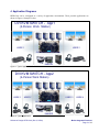
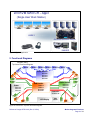
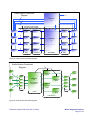
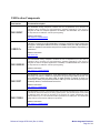
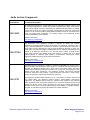
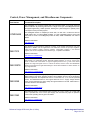
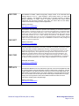
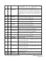
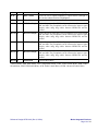
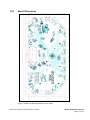
Reference Design:
HFRD-34.0
Rev. 3; 05/08
REFERENCE DESIGN
4 x 4 DVI KVM Switch
Maxim Integrated Products
4 x 4 DVI™ KVM Switch
1 Table of Contents
2. Features....................................................... 2
3. Overview .................................................... 2
4. Application Diagrams................................. 3
5. Functional Diagrams................................... 4
6. IC Summary................................................ 7
7. Navigation Menu ........................................ 12
8. Schematics, Component List and
Layout Drawings ........................................ 15
9. Gerber Files and Firmware ......................... 15
10. Design Notes ............................................ 15
11. Evaluation/Use Notes ............................... 16
12. Layer Profile............................................. 16
13. Board Dimensions .................................... 17
2 Features
•
•
•
•
•
•
•
4 x 4 video, audio, and USB switch
Fully buffered signals for extended reach
Supports DVI resolutions up to 1920 x
1200 per port
Simple navigation switch/LCD control
DVI data-input equalization and
adjustable data-output preemphasis
Schematics and Bill of Materials provided
Firmware and Gerber files available
Reference Design HFRD-34.0 (Rev.3, 05/08)
3 Overview
High-Frequency Reference Design (HFRD)-34.0
is a fully buffered 4 x 4 DVI KVM switch. The
design switches high-resolution DVI video (up to
1920 x 1200 resolution), analog audio, and USB
signals from one to four inputs to one to four
outputs. HFRD-34.0 supports both video and
audio fanout operation (one source to multiple
outputs). The reference design also provides 1:2
hubs on each USB port for keyboard and mouse
connections of up to four different users.
All signals are fully buffered, allowing extended
connection distances. Additionally, equalization is
provided on all DVI data input signals and
adjustable preemphasis on all DVI data outputs.
All control and configuration selections are made
through a simple navigational switch and LCD
display.
This document provides an overview of the design
and operation of HFRD-34.0.
Maxim Integrated Products
Page 2 of 17
4 Application Diagrams
HFRD-34.0 can be configured in a variety of application environments. Three possible applications are
shown in Figures 1 through 3 below.
DVI KVM SWITCH - App1
(2-Person Work Station)
USER 2
USER 1
SHARED
Figure 1. Typical application.
DVI KVM SWITCH - App2
(4-Person Work Station)
USER 1
USER 2
USER 3
USER 4
SHARED
Figure 2. Typical application.
Reference Design HFRD-34.0 (Rev.3, 05/08)
Maxim Integrated Products
Page 3 of 18
DVI KVM SWITCH - App3
(Single User Work Station)
USER 1
SHARED
Figure 3. Typical application.
5 Functional Diagrams
HFRD-34.0
Top-Level Functional Diagram
DVI In2
B
US 1
In
DVI Out2
DVI Out3
DVI Out4
DV
II
n4
Video Section
B
US 2
In
US
In B
3
MAX3845
MAX4814
MAX3814
MAX3208
Audio
In2
Audio
In1
USB2512
USB2513
MAX4906
MAX3207
MAX1953
MAX1563
MAX1853
Audio Section
Audio
Out1
LCD Display
Audio
In4
MAX4550
MAX9723
MAX9728
Controller
ATMEGA168
USB
HUB1
US
In B
4
Audio
In3
USB Section
Power
o
di
Au ut3
O
B
US B3
HU
DVI In3
NAV
Switch
Audio
Out2
DV
DVI Out1
n1
II
USB
HUB2
Au
Ou dio
t4
U
HU SB
B4
Figure 4. HFRD-34.0 Top-level functional diagram.
Reference Design HFRD-34.0 (Rev.3, 05/08)
Maxim Integrated Products
Page 4 of 18
Video-Section Functional
Diagram
I2C
5
MAX4814
x2
5
5
5
Low-Speed Video Signals
High-Speed Video Signals
8
DVI In1
8
DVI In2
8
DVI In3
8
DVI In4
MAX3208
x2
MAX3814
MAX3208
x2
DVI Out1
MAX3208
x2
MAX3814
MAX3208
x2
DVI Out2
MAX3208
x2
MAX3814
MAX3208
x2
DVI Out3
MAX3208
x2
MAX3814
MAX3208
x2
DVI Out4
ESD
Equalizers
MAX3845
x2
Switch/MUX
ESD
Figure 5. Video-section functional diagram.
Audio-Section Functional
Diagram
Audio
In1
MAX9723
2
Audio
In2
2
2
Audio
In3
Audio
In4
I2C
2
Audio
Out1
Headphone
Driver
TVS
TVS
TVS
MAX4550
x2
With Click/Pop
Suppression
TVS
ESD
MAX9723
TVS
Headphone
Driver
TVS
MAX9728
TVS
Line Out
Driver
TVS
MAX9728
Switch
Line Out
Driver
Audio
Out2
Audio
Out3
ESD
Audio
Out4
Audio Buffers
Figure 6. Audio-section functional diagram.
Reference Design HFRD-34.0 (Rev.3, 05/08)
Maxim Integrated Products
Page 5 of 18
USB-Section Functional
Diagram
I2C
2
USB 1
4
MAX3207
USB2512
MAX3207
USB2512
2
USB 2
MAX4906
x8
MAX3208
USB HUB 2
2 - Port
MAX3208
USB HUB 3
2 - Port
USB HUB 4
2 - Port
4
MAX3207
USB2512
MAX3207
USB2513
MAX3208
HUB
Controllers
ESD
2
USB 4
USB HUB 1
2 - Port
4
2
USB 3
MAX3208
4
ESD
Switches
Data
Power
2
MAX1558
2
MOSFETs
x12
MAX1558
2
MAX1558
Power
Switches
2
Main Supply
MAX1558
Overcurrent
Protection
Figure 7. USB-section functional diagram.
Reference Design HFRD-34.0 (Rev.3, 05/08)
Maxim Integrated Products
Page 6 of 18
6 IC Summary
A summary of the ICs used in this reference
design is provided below, along with links to
additional information for each device.
HFRD-34.0 demonstrates the operation of a small
sample of Maxim’s digital and analog switches,
digital video equalizers, power-management
products, and audio drivers. For additional
information about other Maxim products for this
and many other applications, please visit:
www.maxim-ic.com.
Video Section Components
Part Number
Functional Description
MAX3845
The MAX3845 is a TMDS® 2-to-4 fanout switch and cable driver for multimonitor distribution
of DVI or HDMI™ (high-definition multimedia interface) signaling up to 1.65Gbps. Both inputs
and outputs are standard TMDS signaling, as per DVI and HDMI standards. Because TMDS
links are “point-to-point,” buffering is required for fanout applications. Four DVI/HDMI TMDS
outputs are provided for fanout distribution. Each TMDS output can be independently
sourced from either input or can be turned off. Each TMDS input or output is composed of
four differential channels that can be arbitrarily assigned to the three data signals and the
1/10th-rate clock. The data rate depends on resolution, but it can vary from 250Mbps (VGA)
to 1.65Gbps (UXGA or 1080p/60).
Typical applications include multiroom display of the same video source, and industrial and
commercial signage applications such as airport monitors or trading-room floor displays. The
MAX3845 includes selectable output preemphasis that extends output cable reach up to an
additional 7m.
Additional information:
www.maxim-ic.com/MAX3845
MAX3814
The MAX3814 TMDS EQ/driver compensates for FR-4 and cable losses to the DVI/HDMI
transmit connector, and provides a fully compliant DVI/HDMI TMDS output. The device can
also be used in DVI/HDMI cable applications to extend reach and improve jitter margin of
cable channels at the receive-side connector.
Additional information:
www.maxim-ic.com/MAX3814
MAX4814E
The MAX4814E bidirectional 2:4 HDMI switch provides routing for low-frequency signals. The
MAX4814E operates from a single +5.0V ±10% supply voltage and is ideal for connecting
multiple HDMI sources to multiple loads.
Additional information:
www.maxim-ic.com/MAX4814
MAX3208
The MAX3208E is a low-capacitance, ±15kV ESD-protection diode array with an integrated
transient voltage suppressor (TVS) clamp. The device is suitable for high-speed and generalsignal ESD protection. Low input capacitance makes this device ideal for ESD protection of
signals in HDTV; PC monitors (DVI, HDMI); PC peripherals (FireWire®, USB 2.0); server
interconnect (PCI Express®, Infiniband®); datacom; and interchassis interconnect.
Additional information:
www.maxim-ic.com/MAX3208
Reference Design HFRD-34.0 (Rev.3, 05/08)
Maxim Integrated Products
Page 7 of 18
USB Section Components
Part Number
MAX4906F
Functional Description
The MAX4906F analog multiplexer combines the low on-capacitance (CON) and low onresistance (RON) necessary for high-performance switching applications. This device is
designed for USB 2.0 Hi-Speed applications at 480Mbps. The MAX4906F also handles all
the requirements for USB low- and full-speed signaling.
Additional information:
www.maxim-ic.com/MAX4906F
USB251x
SMSC’s USB251x is a family of versatile, cost-effective, and power-efficient USB 2.0 hub
controllers. Leveraging innovative MultiTRAK™ technology that delivers industry-leading data
throughput in mixed-speed USB environments, the USB251x family is a USB port-expansion
solution for applications that demand low power and small footprint without compromising on
performance.
Additional information:
www.smsc.com
MAX4899AE
The MAX4899AE analog multiplexer combines the low on-capacitance (CON) and low onresistance (RON) necessary for high-performance switching applications. This device is
designed for USB 2.0 Hi-Speed applications at 480Mbps. The MAX4899AE also handles all
the requirements for USB low- and full-speed signaling.
Additional information:
www.maxim-ic.com/MAX4899AE
MAX3207
The MAX3207E is a low-capacitance, ±15kV ESD-protection diode array with an integrated
TVS clamp. The device is suitable for high-speed and general-signal ESD protection. Low
input capacitance makes this device ideal for ESD protection of signals in HDTV; PC
monitors (DVI, HDMI); PC peripherals (FireWire, USB 2.0); server interconnect (PCI Express,
Infiniband); datacom; and interchassis interconnect.
Additional information:
www.maxim-ic.com/MAX3207
MAX1558H
The MAX1558H is a dual, current-limited switch with autoreset that latches the switch off if it
is shorted for more than 20ms, thus saving system power. The shorted output is then tested
to determine when the short is removed so the channel can restart automatically. Each
channel delivers up to 1.2A and meets all IEC specifications for USB ports. The MAX1558H
safety features ensure that the USB port is protected.
Additional information:
www.maxim-ic.com/MAX1558H
Reference Design HFRD-34.0 (Rev.3, 05/08)
Maxim Integrated Products
Page 8 of 18
Audio Section Components
Part Number
MAX4550
Functional Description
The MAX4550 serial-interface, programmable, dual 4x2 audio/video crosspoint switch is ideal
for multimedia applications. It contains two identical crosspoint switch arrays, each with four
inputs and two outputs. To improve off-isolation, the additional crosspoint inputs, SA and SB,
can be used as shunts. The output is selectively programmable for clickless or regular mode
operation. A set of internal resistive voltage-dividers supplies DC bias for each output when
using AC-coupled inputs. Additionally, four auxiliary outputs control additional circuitry
through the MAX4550’s 2-wire interface.
Additional information:
www.maxim-ic.com/MAX4550
MAX9728A
The MAX9728A stereo headphone amplifier is designed for display and notebook
applications or portable equipment where board space is at a premium. This device uses a
unique, patented DirectDrive™ architecture to produce a ground-referenced output from a
single supply, thereby eliminating the need for large DC-blocking capacitors. It saves cost,
board space, and component height. The MAX9728A offers an externally adjustable gain and
delivers up to 60mW per channel into a 32Ω load with 0.02% THD+N. An 80dB at 1kHz
power-supply rejection ratio (PSRR) allows these devices to operate from noisy digital
supplies without an additional linear regulator. Comprehensive click-and-pop circuitry
suppresses audible clicks and pops at startup and shutdown.
Additional information:
www.maxim-ic.com/MAX9728A
The MAX9723 stereo DirectDrive™ headphone amplifier with BassMax and volume control is
ideal for portable audio applications where space is at a premium and high performance is
essential. The MAX9723 operates from a single 1.8V to 3.6V power supply. The device
includes features that reduce external component count, system cost, and board space; other
features improve audio reproduction. The headphone amplifier uses Maxim’s patented
DirectDrive architecture that produces a ground-referenced output from a single supply,
thereby eliminating the need for large DC-blocking capacitors.
MAX9723
The headphone amplifiers deliver 62mW into a 16Ω load, feature low 0.006% THD+N, and
high 90dB PSRR. The MAX9723 features Maxim’s industry-leading click-and-pop
suppression. The BassMax feature boosts the amplifier’s bass response, thus improving
audio reproduction when inexpensive headphones are used. The integrated volume control
features 32 discrete volume levels, eliminating the need for an external potentiometer.
BassMax and the volume control are enabled through the I2C/SMBus™-compatible interface.
Shutdown is controlled through either the hardware or software interfaces.
Additional information:
www.maxim-ic.com/MAX9723
Reference Design HFRD-34.0 (Rev.3, 05/08)
Maxim Integrated Products
Page 9 of 18
Control, Power Management, and Miscellaneous Components
Part Number
Functional Description
The ATMega48 is a low-power CMOS 8-bit microcontroller based on the AVR enhanced
RISC architecture. By executing instructions in a single clock cycle, the ATMega48 achieves
throughputs approaching 1 MIPS per MHz, allowing the system designer to optimize power
consumption versus processing speed.
ATMEGA48
The ATMega48 features a multiple-input 10-bit ADC, an 8-bit and a 16-bit timer with two
PWM outputs each, an internal 8MHz oscillator, a 2-wire compatible interface, and a POR
and brown-out circuit. The ATMega48 provides 4k flash, 256B of EEPROM, and 512B of
SRAM.
Additional information:
www.atmel.com
MAX7312
The MAX7312 2-wire-interfaced expander provides 16-bit parallel input/output (I/O) port
expansion in SMBus and I2C applications. The MAX7312 consists of input port registers,
output port registers, polarity inversion registers, configuration registers, a bus timeout
register, and an I2C-compatible serial interface logic, compatible with SMBus.
Additional information:
www.maxim-ic.com/MAX7312
MAX3397E
The MAX3397E ±15kV ESD-protected, bidirectional level translator provides level shifting for
data transfer in a multivoltage system. Externally applied voltages, VCC and VL, set the logic
levels on either side of the device. A logic-low signal present on the VL side of the device
appears as a logic-low signal on the VCC side of the device, and vice versa. The MAX3397E
utilizes a transmission and gate-based design to allow data translation in either direction on
any single data line.
Additional information:
www.maxim-ic.com/MAX3397E
MAX6348
The MAX6348 microprocessor ( P) supervisory circuit monitors the power supplies in P and
digital systems. This device provides excellent circuit reliability and low cost by eliminating
external components and adjustments when it is used with 2.5, 3, 3.3, and 5V powered
circuits. The MAX6348 asserts a reset signal whenever the VCC supply voltage declines
below a preset threshold; the device keeps the signal asserted for at least 100ms after VCC
has risen above the reset threshold.
Additional information:
www.maxim-ic.com/MAX6348
MAX1563
The MAX1563 single, current-limited switch provides up to 4A to power up to eight USB
ports. It operates from a 4V to 5.5V input supply, and consumes only 40 A of quiescent
current when operating and only 3 A in shutdown.
Additional information:
www.maxim-ic.com/MAX1563
Reference Design HFRD-34.0 (Rev.3, 05/08)
Maxim Integrated Products
Page 10 of 18
MAX1853
The MAX1853 monolithic, CMOS charge-pump voltage inverter in the ultra-small SC70
package features a low 15Ω output resistance, which permits loads up to 30mA with
maximum efficiency. The MAX1853 is available with an operating frequency of 200kHz,
allowing optimization of supply current or external component size. Small external
components and micropower shutdown mode make this device ideal for both batterypowered and board-level voltage conversion applications.
Additional information:
www.maxim-ic.com/MAX1853
MAX6817
The MAX6817 dual switch debouncer provides clean interfacing of mechanical switches to
digital systems. The device accepts one or more bouncing inputs from a mechanical switch
and produces a clean digital output after a short, preset qualification delay. Both the switch
opening and closing bounces are removed. Robust switch inputs handle ±25V levels and are
±15kV ESD protected for use in harsh industrial environments. The MAX6817 features
single-supply operation from +2.7V to +5.5V. Undervoltage lockout circuitry ensures that the
output is in the correct state upon power-up. The MAX6817 is offered in a SOT package and
requires no external components.
Additional information:
www.maxim-ic.com/MAX6817
MAX1953
The MAX1953/MAX1954/MAX1957 is a family of versatile, economical, synchronous currentmode, pulse-width modulation (PWM) buck controllers. These step-down controllers are
targeted for applications where cost and size are critical. The MAX1953 operates at a fixed
1MHz switching frequency, thus significantly reducing external component size and cost.
Additionally, excellent transient response is obtained using less output capacitance. The
MAX1953 operates from low 3V to 5.5V input voltage and can supply up to 10A of output
current. Selectable current limit is provided to tailor to the external MOSFETs’ on-resistance
for optimal cost and performance. The output voltage is adjustable from 0.8V to 0.86VIN.
Additional information:
www.maxim-ic.com/MAX1953
MAX4070
The MAX4069–MAX4072 low-cost, bidirectional, high-side, current-sense amplifiers are ideal
for monitoring battery charge and discharge currents in notebook PCs, cell phones, and other
portable equipment. The devices feature up to 24V input common-mode voltage range, low
100 A supply current (which drops to only 10 A in shutdown), and a total output error of less
than 1.5%. The wide 1.35V to 24V input common-mode range is independent of the supply
voltage, thus ensuring that the current-sense feedback remains accurate even when
connected to a battery pack in deep discharge.
Additional information:
www.maxim-ic.com/MAX4070
Reference Design HFRD-34.0 (Rev.3, 05/08)
Maxim Integrated Products
Page 11 of 18
MAX3420
The MAX3420E contains the digital logic and analog circuitry necessary to implement a fullspeed USB peripheral compliant to USB specification rev 2.0. A built-in full-speed transceiver
features ±15kV ESD protection and programmable USB connect and disconnect. An internal
serial-interface engine (SIE) handles low-level USB protocol details such as error checking
and bus retries. The MAX3420E operates using a register set accessed by an SPI™
interface that operates up to 26MHz. Any SPI master (microprocessor, ASIC, DSP, etc.) can
add USB functionality by using the simple 3- or 4-wire SPI interface.
Additional information:
www.maxim-ic.com/MAX3420
MAX4788
The MAX4785–MAX4788 family of switches feature internal current limiting to prevent host
devices from being damaged due to faulty load conditions. These analog switches have a low
0.7Ω on-resistance and operate from a 2.3V to 5.5V input voltage range. They are available
with guaranteed 50mA and 100mA current limits, making them ideal for load-switching
applications.
Additional information:
www.maxim-ic.com/MAX4788
7 Navigation Menu
HFRD-34.0 is controlled through an easy-to-use
navigation switch (up, down, left, right, and push
to select) and LCD display. Through this menu-
based interface, the user can set, save, and load
configurations and control a variety of other
features available in the reference design. The
table below details the menu options available.
Table 1. Navigation Menu Details
Menu*
Index
LCD Label
Action Taken by Pushing “Select” on Menu Item
MM
1
Configuration
Configuration Menu (CM) is opened
MM
2
Video Switch
Video Switch Menu (VSM) is opened
MM
3
Audio Switch
Audio Switch Menu (ASM) is opened
MM
4
USB Switch
USB Switch Menu (USM) is opened
MM
5
Audio Control
Audio Control Menu (ACM) is opened
MM
6
Advanced Ctrl
Advanced Control Menu (ADVM) is opened
CM
1
Load Config
Opens a menu to allow the user to load one of four saved
configurations.
CM
2
Save Config
Opens menu to allow the user to save the current configuration to
one of four memory locations. Saved configurations are retained
during power cycles.
Reference Design HFRD-34.0 (Rev.3, 05/08)
Maxim Integrated Products
Page 12 of 18
CM
3
Default
Sets the default configuration for the reference
(Audio/Video/USB
In1
to
Audio/Video/USB
Audio/Video/USB In2 to Audio/Video/USB Out2, etc.)
CM
4
Demo Mode
Puts the reference design into a demonstration mode. When in this
mode, the controller will loop through the default and saved
configurations at a preset time interval. This operation allows for
automatic switching of the DVI and audio signals. Please note: The
USB configuration is not switched in demo mode (only DVI and
Audio).
CM
5
Main Menu
Return to Main Menu
VSM
1
DVI Out1
Allows the user to switch DVI output 1 to any DVI input (1 through
4). The current switch selection is highlighted.
VSM
2
DVI Out2
Allows the user to switch DVI output 2 to any DVI input (1 through
4). The current switch selection is highlighted.
VSM
3
DVI Out3
Allows the user to switch DVI output 3 to any DVI input (1through
4). The current switch selection is highlighted.
VSM
4
DVI Out4
Allows the user to switch DVI output 4 to any DVI input (1through
4). The current switch selection is highlighted.
VSM
5
Main Menu
Return to Main Menu
ASM
1
HeadphoneOut1
Allows the user to switch headphone output 1 to any audio input (1
through 4). The current switch selection is highlighted.
ASM
2
HeadphoneOut1
Allows the user to switch headphone output 2 to any audio input (1
through 4). The current switch selection is highlighted.
ASM
3
Line Out1
Allows the user to switch line output 1 to any audio input (1 through
4). The current switch selection is highlighted.
ASM
4
Line Out2
Allows the user to switch line output 2 to any audio input (1 through
4). The current switch selection is highlighted.
ASM
5
Main Menu
Return to Main Menu
USM
1
USB HUB1 Out
Allows the user to switch USB hub 1 to any USB input (1 through
4). The current switch selection is highlighted. Note: Fanout is not
supported in the USB switch.
USM
2
USB HUB2 Out
Allows the user to switch USB hub 2 to any USB input (1 through
4). The current switch selection is highlighted. Note: Fanout is not
supported in the USB switch.
USM
3
USB HUB3 Out
Allows the user to switch USB hub 3 to any USB input (1 through
4). The current switch selection is highlighted. Note: Fanout is not
supported in the USB switch.
USM
4
USB HUB4 Out
Allows the user to switch USB hub 4 to any USB input (1through 4).
The current switch selection is highlighted. Note: Fanout is not
supported in the USB switch.
USM
5
Main Menu
Return to Main Menu
ACM
1
HP1 Volume
Allows the user to adjust headphone 1 output volume (1 through 7).
Reference Design HFRD-34.0 (Rev.3, 05/08)
design
Out1;
Maxim Integrated Products
Page 13 of 18
The current volume selection is highlighted.
ACM
2
HP2 Volume
Allows the user to adjust headphone 2 output volume (1through 7).
The current volume selection is highlighted.
ACM
3
Main Menu
Return to Main Menu
ADVM
1
DVI1 Pre-Emph
Allows the user to adjust DVI Out 1 preemphasis level between 0dB,
3dB, and 6dB. The preemphasis can be increased to improve signal
integrity when using long cables between HFRD-34.0 and the
monitor.
ADVM
2
DVI2 Pre-Emph
Allows the user to adjust DVI Out 2 preemphasis level between 0dB,
3dB, and 6dB. The preemphasis can be increased to improve signal
integrity when using long cables between HFRD-34.0 and the
monitor.
ADVM
3
DVI3 Pre-Emph
Allows the user to adjust DVI Out 3 preemphasis level between 0dB,
3dB, and 6dB. The preemphasis can be increased to improve signal
integrity when using long cables between HFRD-34.0 and the
monitor.
ADVM
4
DVI4 Pre-Emph
Allows the user to adjust DVI Out 4 preemphasis level between 0dB,
3dB, and 6dB. The preemphasis can be increased to improve signal
integrity when using long cables between HFRD-34.0 and the
monitor.
ADVM
5
Main Menu
Return to Main Menu
*Abbreviations: MM: Main Menu; CM: Configuration Menu; VSM: Video Switch Menu; ASM: Audio
Switch Menu; USM: USB Switch Menu; ACM: Audio Control Menu; ADVM: Advanced Control Menu.
Reference Design HFRD-34.0 (Rev.3, 05/08)
Maxim Integrated Products
Page 14 of 18
8 Schematics, Component List,
and Layout Drawings
The full schematics, component list, and PCB
layout drawings are available to download in PDF
format at:
http://www.maximic.com/tools/other/appnotes/4232/4232_softwar
e.zip.
See sections 10 and 11 for additional details
regarding the use of the schematics and layout
drawings for new designs.
9 Gerber Files and Firmware
The Gerber files and firmware assist design
engineers in developing their projects, and are
available to Maxim customers upon request. See
sections 10 and 11 for additional details regarding
the use of Gerber files and firmware. To receive
the Gerber or firmware files, please send an email
to [email protected] with HFRD34.0 in the subject line. Include the following
information:
1.
2.
3.
4.
Your name
Company name
Company website
Brief description of your project
10 Design Notes
Please review the following design notes:
1. Line Out1 and Line Out2 are designed to
drive an audio line impedance (> 1kΩ)
with typical line-out voltage levels. These
two audio outputs can be optimized to
drive headphone loads by changing
external component values. See the
MAX9728 data sheet for additional
information.
2. The USB hub controllers (U26, U27,
U36, and U39) have configurations and
settings that can be adjusted through a 2wire bus controlled by the C. Currently
Reference Design HFRD-34.0 (Rev.3, 05/08)
these features and configurations are set
through the C firmware.
3. The USB HUB reset connection for the
four HUBs (pin 26 of USB2512 and
USB2513 devices) are tied together on the
current version of the reference design.
Splitting these connections to have
individual control will improve the
overall USB switching operation.
4. If desired, U47 (MAX3420) is provided
to facilitate control of the switch through
a USB interface. Currently these features
are not preprogrammed into the reference
design.
5. USB HUB 4 is a self-powered HUB
(power is drawn from the HFRD-34.0
supply). USB HUBs 1-3 are powered
from the host. All USB HUBs include
overcurrent shutdown protection.
6. It is recommended that you increase the
supply filtering (i.e., add series inductance
and bulk capacitance) of the host USB
power supplies (for HUBs 1-3) in order to
reduce crosstalk from the USB powersupply noise to the audio outputs.
7. The power MOSFET transistors (Q2Q13) used for switching the USB host
power are flipped over due to a layout
error in the pin order. When copying this
section of the design, the transistor
footprint should be corrected.
8. The ATMEL C (U49, ATMEGA168)
can be in-circuit reprogrammed to
perform custom features. Use the
AVRISP-MKII programmer and the
connections provided through J15.
9. A 10kΩ pull-up resistor should be added
to pin 9 of the MAX3420 (U47) in any
design revisions.
10. Connecting pins 14 and 16 together on
each DVI input will increase the
Maxim Integrated Products
Page 15 of 18
compatibility of the reference design with
a wider variety of DVI video cards.
11 Evaluation/Use Notes
This reference design aids designers and is not
intended to replace the entire design process. The
designer should evaluate the reference design and
modify it, as necessary, to meet the specification
for a particular project. The designer should also
carefully consider safety and EMI issues related to
the specific application.
2. 0.5oz copper foil before platting.
3. For USB signal-transmission lines: 10mil
W, 8mil S -> 90Ω
Ω Differential
4. For DVI signal-transmission lines: 8mil
W, 8mil S -> 100Ω
Ω Differential
Table 2. HFRD-34.0 Layer Profile
Layer
Dielectric
Thickness
(inches)
1
Copper
Clad
Layer
Desc.
0.5
SIGNAL
0.5
PLANE
0.5
SIGNAL
0.5
SIGNAL
0.5
PLANE
0.5
SIGNAL
0.5
PLANE
0.5
SIGNAL
0.5
PLANE
0.5
SIGNAL
0.0081
2
0.005
Maxim cannot assume responsibility for use of
any circuitry other than circuitry entirely
embodied in a Maxim product. No circuit patent
licenses are implied. Maxim reserves the right to
change the circuitry and specifications without
notice at any time.
3
0.0036
4
0.005
5
0.0088
6
12 Layer Profile
The HFRD-34.0 DVI KVM switch includes
controlled-impedance transmission lines. The
layer profile is based on the following
assumptions:
1. Dielectric material is FR-4 with a
dielectric constant of ~ 4.2.
0.005
7
0.0036
8
0.005
9
0.0081
10
Maxim cannot assume responsibility for use of any circuitry other than circuitry entirely embodied in a Maxim
product. No circuit patent licenses are implied. Maxim reserves the right to change the circuitry and
specifications without notice at any time.
Reference Design HFRD-34.0 (Rev.3, 05/08)
Maxim Integrated Products
Page 16 of 18
1312
Board Dimensions
Figure 8. HFRD-34.0 Board dimensions (not to scale).
Reference Design HFRD-34.0 (Rev.3, 05/08)
Maxim Integrated Products
Page 17 of 18
DVI is a trademark of Digital Display Working Group (DDWG).
FireWire is a registered trademark of Apple Computer, Inc.
HDMI is a trademark of HDMI Licensing, LLC.
InfiniBand is a registered trademark of InfiniBand Trade Association.
MultiTRAK is a trademark of Standard Microsystems Corporation.
PCI Express is a registered trademark of PCI-SIG Corp.
SMBus is a trademark of Intel Corporation.
SPI is a trademark of Motorola, Inc.
TMDS is a registered trademark of Silicon Image, Inc.
Reference Design HFRD-34.0 (Rev.3, 05/08)
Maxim Integrated Products
Page 18 of 18