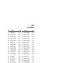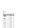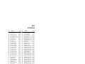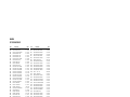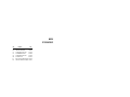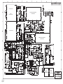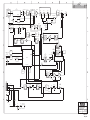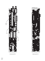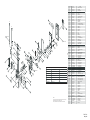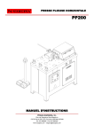
1
SP-300 Series
SERVICE
MANUAL
Maxon America, Inc. 10828 N.W. Airworld Dr. Kansas City, MO 64153 Tel: 816-891-6320 Fax: 816-891-8815
Part Number: 680-100-0155
April 2001
MAXON
SP-300 HAND HELD
TABLE OF CONTENTS
SPECIFICATIONS . . . . . . . . . . . . . . . . . . . . . . . . . . . . . . . . . . . . . . . . . . . . . . . . 1
INTRODUCTION . . . . . . . . . . . . . . . . . . . . . . . . . . . . . . . . . . . . . . . . . . . . . . . . . 5
FEATURES . . . . . . . . . . . . . . . . . . . . . . . . . . . . . . . . . . . . . . . . . . . . . . . . . . . . . . . 5
DESCRIPTION OF CONTROLS. . . . . . . . . . . . . . . . . . . . . . . . . . . . . . . . . . . . . 8
THEORY OF OPERATION . . . . . . . . . . . . . . . . . . . . . . . . . . . . . . . . . . . . . . . . . 9
DIGITAL CIRCUITS . . . . . . . . . . . . . . . . . . . . . . . . . . . . . . . . . . . . . . . . . . . . 9
RF CIRCUITS . . . . . . . . . . . . . . . . . . . . . . . . . . . . . . . . . . . . . . . . . . . . . . . . . . 10
RF CIRCUITS PLL SYNTHESIZER . . . . . . . . . . . . . . . . . . . . . . . . . . . . . . . . 11
RECEIVER . . . . . . . . . . . . . . . . . . . . . . . . . . . . . . . . . . . . . . . . . . . . . . . . . . . . 11
MAINTENANCE AND REPAIR . . . . . . . . . . . . . . . . . . . . . . . . . . . . . . . . . . . . . 13
GENERAL . . . . . . . . . . . . . . . . . . . . . . . . . . . . . . . . . . . . . . . . . . . . . . . . . . . . . 13
REMOVING & REPLACING THE BELT CLIP . . . . . . . . . . . . . . . . . . . . . . . 13
REMOVING & REPLACING THE BATTERY . . . . . . . . . . . . . . . . . . . . . . . 14
REMOVING & REPLACING PTT ASSY. . . . . . . . . . . . . . . . . . . . . . . . . . . . 14
REMOVING & REPLACING THE ACCESSORY CONNECTOR . . . . . . . . 15
REMOVING & REPLACING THE ANTENNA & CONTROL KNOBS . . . . 15
REMOVING & REPLACING THE BACK COVER . . . . . . . . . . . . . . . . . . . . 16
REMOVING & REPLACING THE MAIN BOARD . . . . . . . . . . . . . . . . . . . . 17
REMOVING & REPLACING THE DAUGHTER BOARDS . . . . . . . . . . . . . 19
REMOVING & REPLACING THE SPEAKER . . . . . . . . . . . . . . . . . . . . . . . . 19
COMPONENT REPLACEMENT . . . . . . . . . . . . . . . . . . . . . . . . . . . . . . . . . . . . 19
PROGRAMMING . . . . . . . . . . . . . . . . . . . . . . . . . . . . . . . . . . . . . . . . . . . . . . . . . 21
ALIGNMENT PROCEDURE . . . . . . . . . . . . . . . . . . . . . . . . . . . . . . . . . . . . . . . . 21
TEST EQUIPMENT SETUP. . . . . . . . . . . . . . . . . . . . . . . . . . . . . . . . . . . . . . . . . 23
ALIGNMENT POINTS DIAGRAM . . . . . . . . . . . . . . . . . . . . . . . . . . . . . . . . . . 24
VOLTAGE CHARTS. . . . . . . . . . . . . . . . . . . . . . . . . . . . . . . . . . . . . . . . . . . . . . . 26
SP-300 SERIES UHF & VHF DIGITAL SECTION PARTS LIST . . . . . . . . . 29
SP-300 SERIES VHF RF SECTION PARTS LIST . . . . . . . . . . . . . . . . . . . . . . 31
SP-300 SERIES UHF RF SECTION PARTS LIST . . . . . . . . . . . . . . . . . . . . . . 34
COMPONENT PINOUT . . . . . . . . . . . . . . . . . . . . . . . . . . . . . . . . . . . . . . . . . . . . 38
SCHEMATICS & BLOCK DIAGRAM. . . . . . . . . . . . . . . . . . . . . . . . . . . . . . . . 41
VHF FRONT-END . . . . . . . . . . . . . . . . . . . . . . . . . . . . . . . . . . . . . . . . . . . . . . 41
VHF POWER AMP . . . . . . . . . . . . . . . . . . . . . . . . . . . . . . . . . . . . . . . . . . . . . . 41
UHF POWER AMP . . . . . . . . . . . . . . . . . . . . . . . . . . . . . . . . . . . . . . . . . . . . . . 41
UHF FRONT-END . . . . . . . . . . . . . . . . . . . . . . . . . . . . . . . . . . . . . . . . . . . . . . 41
VHF V.C.O. . . . . . . . . . . . . . . . . . . . . . . . . . . . . . . . . . . . . . . . . . . . . . . . . . . . . 42
UHF V.C.O. . . . . . . . . . . . . . . . . . . . . . . . . . . . . . . . . . . . . . . . . . . . . . . . . . . . . 42
TCXO . . . . . . . . . . . . . . . . . . . . . . . . . . . . . . . . . . . . . . . . . . . . . . . . . . . . . . . . . 43
ACC-200 BATTERY . . . . . . . . . . . . . . . . . . . . . . . . . . . . . . . . . . . . . . . . . . . . 43
FUSE . . . . . . . . . . . . . . . . . . . . . . . . . . . . . . . . . . . . . . . . . . . . . . . . . . . . . . . . . 43
P.T.T. . . . . . . . . . . . . . . . . . . . . . . . . . . . . . . . . . . . . . . . . . . . . . . . . . . . . . . . . . 43
Digital Schematic . . . . . . . . . . . . . . . . . . . . . . . . . . . . . . . . . . . . . . . . . . . . . . . . 44
VHF RF Schematic . . . . . . . . . . . . . . . . . . . . . . . . . . . . . . . . . . . . . . . . . . . . . . 45
UHF RF Schematic . . . . . . . . . . . . . . . . . . . . . . . . . . . . . . . . . . . . . . . . . . . . . . 46
Block Diagram . . . . . . . . . . . . . . . . . . . . . . . . . . . . . . . . . . . . . . . . . . . . . . . . . . 47
PCB LAYOUTS . . . . . . . . . . . . . . . . . . . . . . . . . . . . . . . . . . . . . . . . . . . . . . . . . . . 48
Page -iMay 2001
MAXON
SP-300 HAND HELD
Board Layout . . . . . . . . . . . . . . . . . . . . . . . . . . . . . . . . . . . . . . . . . . . . . . . . . . . 48
Exploded View. . . . . . . . . . . . . . . . . . . . . . . . . . . . . . . . . . . . . . . . . . . . . . . . . . . . . 49
Page -iiMay 2001
MAXON
SP-300 HAND HELD
SPECIFICATIONS
GENERAL
Equipment Type . . . . . . . . . . . . . . . . . . . . . . . . . . . . . . . . . . . . . . . Hand portable
Band . . . . . . . . . . . . . . . . . . . . . . . . . . . . . . . . . . . . . . . . . . . . . . . . . UHF/ VHF
Channel Spacings . . . . . . . . . . . . . . . . . . . . . . . . . . . . . . . . . . . . . . 12.5 kHz, 25 kHz programmable
RF Output Power . . . . . . . . . . . . . . . . . . . . . . . . . . . . . . . . . . . . . . 5/ 1 watt
Modulation Type . . . . . . . . . . . . . . . . . . . . . . . . . . . . . . . . . . . . . . . F3E
Audio Power . . . . . . . . . . . . . . . . . . . . . . . . . . . . . . . . . . . . . . . . . . 400 mW (Ext with 8 ohm)
400 mW (Int with 2 ohm)
Intermediate Frequency . . . . . . . . . . . . . . . . . . . . . . . . . . . . . . . . . 45.1 MHz & 455 kHz
Number of Channels . . . . . . . . . . . . . . . . . . . . . . . . . . . . . . . . . . . . 16/ 4
Frequency Source . . . . . . . . . . . . . . . . . . . . . . . . . . . . . . . . . . . . . . Synthesizer
Operation Rating . . . . . . . . . . . . . . . . . . . . . . . . . . . . . . . . . . . . . . Intermittent
90 : 5 : 5 (Standby: RX: TX)
Power Supply. . . . . . . . . . . . . . . . . . . . . . . . . . . . . . . . . . . . . . . . . . Rechargeable Nickel-metal Hydride
Battery, 7.5 VDC +/- 10 %
TEMPERATURE RANGE
Storage . . . . . . . . . . . . . . . . . . . . . . . . . . . . . . . . . . . . . . . . . . . . . . . From - 40° C to + 80° C
Operating . . . . . . . . . . . . . . . . . . . . . . . . . . . . . . . . . . . . . . . . . . . . . From - 30° C to + 60° C
CURRENT CONSUMPTION
Off. . . . . . . . . . . . . . . . . . . . . . . . . . . . . . . . . . . . . . . . . . . . . . . . . . . < 1 mA
Standby (Muted) . . . . . . . . . . . . . . . . . . . . . . . . . . . . . . . . . . . . . . . < 30 mA (Battery Save On)
< 60 mA (Battery Save Off)
Unmuted, 100 % Max AF Power . . . . . . . . . . . . . . . . . . . . . . . . . < 500 mA
Transmit 5 Watt RF Power . . . . . . . . . . . . . . . . . . . . . . . . . . . . . . < 2.4 A
BATTERY LIFE (5-5-90% Duty Cycle)
1350 mAh . . . . . . . . . . . . . . . . . . . . . . . . . . . . . . . . . . . . . . . . . . . . . 9 Hrs @ 5 W
Page -1May 2001
MAXON
SP-300 HAND HELD
FREQUENCY BANDS
RX
TX
VHF: V2
148.000 - 174.000 MHz
148.000 - 174.000 MHz
UHF: U2
440.000 - 470.000 MHz
440.000 - 470.000 MHz
DIMENSIONS
Radio . . . . . . . . . . . . . . . . . . . . . . . . . . . . . . . . . . . . . . . . . . . . . . . . (141mm)H x (58 mm)W x (37 mm)D
WEIGHT
Radio . . . . . . . . . . . . . . . . . . . . . . . . . . . . . . . . . . . . . . . . . . . . . . . . 225 grams
With 1350 mAh Battery . . . . . . . . . . . . . . . . . . . . . . . . . . . . . . . . . 425 grams
TRANSMITTER
Carrier Power . . . . . . . . . . . . . . . . . . . . . . . . . . . . . . . . . . . . . . . . . High: 5.0W
Low: 1.0W
AUDIO FREQUENCY DEVIATION
Without Subaudio Tone Modulation:
25 kHz Channel Spacing . . . . . . . . . . . . . . . . . . . . . . . . . . . . . . . . Max. ±5.0 kHz
12.5 kHz Channel Spacing . . . . . . . . . . . . . . . . . . . . . . . . . . . . . . . Max. ±2.5 kHz
With Subaudio Tone Modulation @ 10 % Peak Deviation
25 kHz Channel Spacing . . . . . . . . . . . . . . . . . . . . . . . . . . . . . . . . Max. ±5.0 kHz
12.5 kHz . . . . . . . . . . . . . . . . . . . . . . . . . . . . . . . . . . . . . . . . . . . . . . Max. ±2.5 kHz
Audio Frequency Response . . . . . . . . . . . . . . . . . . . . . . . . . . . . . . Within +1/-3dB of 6dB octave
ADJACENT CHANNEL POWER
25 kHz . . . . . . . . . . . . . . . . . . . . . . . . . . . . . . . . . . . . . . . . . . . . . . . < 70 dBc
12.5 kHz . . . . . . . . . . . . . . . . . . . . . . . . . . . . . . . . . . . . . . . . . . . . . . < 60 dBc
Conducted Spurious Emission . . . . . . . . . . . . . . . . . . . . . . . . . . . . < -60 dBc
Page -2May 2001
MAXON
SP-300 HAND HELD
Transmitter Audio Distortion (Without CTCSS) . . . . . . . . . . . . < 5% @ 1 kHz
Hum & Noise:
12.5 kHz Channel Spacing . . . . . . . . . . . . . . . . . . . . . . . . . . . . . . . > 40 dB (with PSOPH)
25 kHz Channel Spacing . . . . . . . . . . . . . . . . . . . . . . . . . . . . . . . . > 40 dB (with no PSOPH)
Load Stability . . . . . . . . . . . . . . . . . . . . . . . . . . . . . . . . . . . . . . . . . No osc at ³ 10:1 VSWR all phase angles
and suitable antenna
Peak Deviation @ 1 kHz (Nom. Dev +20dB)
25 kHz Channel Spacing . . . . . . . . . . . . . . . . . . . . . . . . . . . . . . . . Max. 5.0 kHz
12.5 kHz Channel Spacing . . . . . . . . . . . . . . . . . . . . . . . . . . . . . . . Max. 2.5 kHz
RECEIVER
Sensitivity (12dB Sinad) . . . . . . . . . . . . . . . . . . . . . . . . . . . . . . . . . UHF: < -117 dBm(.31µV)
VHF: < -118 dBm(.28µV)
Amplitude Characteristic. . . . . . . . . . . . . . . . . . . . . . . . . . . . . . . . < ±3 dB
Adjacent Channel Selectivity:
25 kHz Channel Spacing . . . . . . . . . . . . . . . . . . . . . . . . . . . . . . . . >60 dB
12.5 kHz Channel Spacing . . . . . . . . . . . . . . . . . . . . . . . . . . . . . . . >50 dB
Spurious Response Rejection . . . . . . . . . . . . . . . . . . . . . . . . . . . . . 70 dB
Intermodulation Response Rejection . . . . . . . . . . . . . . . . . . . . . . 65 dB
Temperature Stability. . . . . . . . . . . . . . . . . . . . . . . . . . . . . . . . . . . 0.0005% (-30°C to +60°C)
Conducted and Radiated Spurious Emission . . . . . . . . . . . . . . . . Per FCC and IC Rules and Regulations
AF Distortion. . . . . . . . . . . . . . . . . . . . . . . . . . . . . . . . . . . . . . . . . . < 5%
Frequency Response . . . . . . . . . . . . . . . . . . . . . . . . . . . . . . . . . . . . 6 dB/octave de-emphasized response in
the range 300 Hz - 3000 Hz
RX Hum & Noise:
25 kHz . . . . . . . . . . . . . . . . . . . . . . . . . . . . . . . . . . . . . . . . . . . . . . . < 40 dB
12.5 kHz . . . . . . . . . . . . . . . . . . . . . . . . . . . . . . . . . . . . . . . . . . . . . < 40 dB
Page -3May 2001
MAXON
SP-300 HAND HELD
RX TONE DEMODULATION CHARACTERISTICS
SUBAUDIO TONES - CTCSS
Tone Range . . . . . . . . . . . . . . . . . . . . . . . . . . . . . . . . . . . . . . . . . . . 67 Hz to 250.3 Hz
Non-Standard Tones . . . . . . . . . . . . . . . . . . . . . . . . . . . . . . . . . . . . 50 Hz to 260 Hz
Due to continuing research and development the company reserves the right to alter these
specifications without prior notice.
Page -4May 2001
MAXON
SP-300 Series HAND HELD
SP-300
INTRODUCTION
FEATURES
The SP-300 Series of portable radios from Maxon, utilizes
the latest technology in its design and manufacturing. Both
the VHF and UHF models are PLL (Phase Lock Loop Synthesizer) / microprocessor controlled, and offer 1 or 5 watts
of power with 4 & 16 channel capability. Multiple functions
including Scan, CTCSS / DCS signaling and 12.5 & 25 kHz
channel spacing are standard in these fully programmable
wide bandwidth handheld units.
Main Features
• Wideband
• Scan Mode
• Busy Channel Lockout/Marked Idle Enable
• Standard/Non-Standard CTCSS/DCS Signaling
• Transmit Time-Out Timer/Tx Inhibit
• Beep Tone Enable/Disable
• Low Battery Indication
• Memory Protect
• External Option Detect
• 5/1 Watts Programmable RF Power
• Battery Save Circuitry
• Locking Accessory Connector
Wideband
This software is made to work and control the wide band
receiver/transmitter boards.
Scan Mode
During programming of the radio, any channel can be
selected as a scanned channel. When a channel is selected as
a scanned channel, it becomes part of the scan list. The scan
list will be activated by switching to the channel that was
selected as the scan channel during programming of the system parameters.
The channel that was selected as the scan channel can still be
used as a receive only channel when in scan mode or receive
and transmit channel if the channel has been programmed for
“Priority Scan TX”.
Scan Channel Delete
When the unit is in scan mode the monitor button can be
pushed to delete a channel from the scan list. If the monitor
button is pushed while scanning has stopped to monitor an
active channel, that channel will be deleted from the scan
list. The channel will remain inactive in the scan list until
the scan mode is re-initiated by switching off the scan list
channel and switching back to the scan list channel. Any
number of channels can be deleted from the scan list in this
way. The scan list is always initiated with all the scan list
channels active.
Page -5May 2001
MAXON
SP-300 HAND HELD
A priority channel can be selected while programming the
radio. A priority channel is a channel that can be periodically checked or looked back to while receiving on any channel in the scan list, or in normal operation. It can also be
selected for all transmissions during scan mode.
To transmit on a channel in the scan list, the channel selector
must be placed on the channel that the transmission is to be
made on. As a system programmable option, it is possible to
transmit on a scanned channel while the channel selector is
on the scan list channel. This is the “Normal Scan TX”
option. If this option is enabled the PTT can be pushed during the scan wait time and the transmission will be on the
channel that was just activated. If this option is disabled, the
transmission will be on the priority channel (if there is no
priority channel programmed the transmission will be inhibited and out-of-lock indicator will be issued).
Any channel, whether it is in the scan list or not, can be designated as a look back channel. When a channel is designated as a look back channel, and the channel is selected, the
radio will periodically look back to the priority channel during reception on the selected channel. The radio does not
require a scan list to be entered in order to use this function,
however, the radio MUST have a priority channel selected
for the function to work.
• NOTE: The programmer must disallow the programming of a channel as a look back channel if no priority
channel was selected.
The channel scan speed is system programmable in a range
of 50 milliseconds to 2 seconds in 10 millisecond increments. The default value is 100 milliseconds.
Scan Delay Time
Scan delay time is system programmable. The scan delay is
the time the unit remains on a scanned channel, after receiving or transmitting on that channel. The time is programmable from 1 to 10 in 1 second increments. The default value is
4 seconds.
The scan delay time will be reset each time the receive channel is active and each time the PTT is pushed on that channel. As long as the conversation continues on the channel,
the receiver or the transmitter is active before the scan delay
time expires, the unit will not resume scanning.
As a programmable option, the LED on the top panel of the
unit will flash at the scan rate while in the scan mode. If the
“LED scan indication” is programmed to enable the LED
will flash. If it is programmed to disable, the LED will not
flash.
Busy Channel Lockout
If this feature is enabled, the unit will not transmit when a
carrier is present. A beep tone will sound when the PTT is
depressed.
Marked Idle Enable
If this function is enabled, the unit will transmit provided
that the correct programmed CTCSS tone or DCS code has
been decoded. This function is essential for repeater operation.
Normal/Inverted DCS
This function is selected by channel during programming of
the radio. During programming of each channel of the radio,
a selective signaling option for TX and RX is selected.
When the DCS signaling option is elected, it can be selected
as either normal or inverted. The selection can be made differently for TX and RX.
Standard/Non-Standard CTCSS
When programming a channel with CTCSS, any frequency
from 55 to 250 Hz can be selected in 0.1 Hz increments. The
radio is capable of encoding and decoding two non-standard
CTCSS tones.
Transmit Time-Out-Timer (TOT)/TX Inhibit
The time-out-timer is system programmable for 10 seconds
to 990 seconds, in 10 second increments and can also be
selected as disabled. The addition to this feature is a programmable lock-out-timer that inhibits the radio transmitter
for a specified time after the time-out time expires.
When the time-out-timer function is enabled, and the TX
inhibit function is disabled, the radio will transmit after the
time-out-timer has expired and the PTT button is released
and depressed again. With the TOT and TX inhibit, the
radio will not transmit after the time-out has expired, even if
the PTT is released and depressed again. Transmission will
not be allowed until the TX inhibit time has expired. TX
inhibit time is system programmable from 5 to 60 seconds in
5 second increments. The radio will beep one time, 5 seconds before the TOT time expires. This will indicate to the
user that the transmitter is about to be locked out. If the PTT
is released and depressed again anytime before the TOT has
expired, the TOT time will be reset. If the beep tone enable/
disable is set to disable, the one beep will not be issued. The
radio will beep 4 times when the TOT time expires. After
the TX inhibit time passes, the radio will beep one final time.
Page -6May 2001
MAXON
SP-300 Series HAND HELD
VCO Lock Time
The micro will allow more lock time for the VCO before the
out-of-lock beep indication.
Low Battery Indication
Low Battery Indication will be changed so that it does not
inhibit RX and will allow one transmission after low cell is
indicated. Low cell will not be indicated during transmit
mode. If the battery goes below specified limits during the
TX mode, low cell will be indicated immediately after
releasing the PTT button.
After the low cell indication is issued, the transmitter can
only be used one time. When the PTT is pushed again and
then released, the transmitter is locked out until the unit is
powered down and then powered back up.
Memory Protect
The software is such that if the radio is inadvertently put
into program mode it will not lose the contents of the
EEPROM memory. Data will only move in and out of the
memory when the programmer is attached.
External Option Detect
An input to the microprocessor will be available that will
indicate to the microprocessor that the external option has
been selected. This input should be connected to the external option connector. External option should be selected for
each channel. If a channel is selected during programming
for external option, this input should be active when the
channel is selected during operation of the unit.
Page -7May 2001
MAXON
SP-300 HAND HELD
DESCRIPTION OF CONTROLS
The controls, indicators and antenna connections on the VHF and UHF Scanning Handheld Series radios are all located on the
top panel. The accessories socket is located on the radio chassis right hand side. The monitor and PTT buttons are located on
the radio chassis left hand side.
ITEM
DESCRIPTION
1. Antenna Connector
1/4" UNEF socket
2. 4 Channel Select Switch
Rotary switch, used to select one of four and to engage in scanning function
3. 16 Channel Select Switch
Rotary switch, used to select one of sixteen and to engage in scanning function
4. Status Indicator (busy TX/BT)
Tri-colored LED indicator
5. ON/OFF Volume Control
Main power switch and volume control. Fully counter-clockwise is OFF position
6. Battery Lock
Used to lock the battery in place
7. Push-To-Talk Button
Push to talk, release to listen
8. Monitor Button
When pressed, monitors the chosen channel
Used for controlling installed external option
9. Option
10. Speaker
Sound reception
11. Microphone
Sound transmission
12. External Speaker
Socket used for external microphone with speaker
13. Belt Clip
Belt Clip
14. Battery
Power Supply
15. Battery Charger Contacts
Contacts used for charging battery
16. VHF Antenna
17. UHF Antenna
Antenna
Antenna
CON701 Pinouts
CH
ANT
VOL
CH
7
4
3
VOL
11
4
13
2
1
1
1
2
16
3
4
5
CON701 - Pin 1
Function
Data
Clock
N/C
+7.5V
N/C
N/C
Gnd
Mic+
N/C
Int_Spkr_Mic_Dsbl
Spkr+
N/C
16
13
17
12
7
maxon
ANT
Pin
1
2
3
4
5
6
7
8
9
10
11
12
10
6
8
9
11
14
Page -8May 2001
15
MAXON
SP-300 HAND HELD
THEORY OF OPERATION
The VHF and UHF scanning handheld series radios are comprised of one main PCB. The main PCB contains the transmitter, receiver and control circuits. The control circuits
contain the micro controller and associated digital circuits.
DIGITAL CIRCUITS
IC 411 is a digitally-controlled analog switch which internally consists of three single pole, double throw switches.
By placing a high (5V) or low (0V) on the control lines
which consists of A, B and C. A controls the X ports, B controls the Y ports and C controls the Z ports. Example: A high
on control A would connect X to X1. A low on control A
would connect X to X0.
CTCSS/DCS Decode Circuits
Discriminator audio from Pin 9 IC5 is fed into and associated parts, which are the first 2 poles of a 6th order 250 Hz
Chebeyshev low pass filter. The output from pin 1 (IC406A)
is fed into IC411 (Pin 2) and output to pin 15 (IC411). The
signal is then fed to Pin 8 (IC407) which is a 6th order low
pass Butterworth switched capacitor filter. The output from
the Butterworth filter (Pin 3 IC407) is then fed to the remaining 4 poles of the 6th order Chebeyshev, which consist of
IC406C and one of the two operational amplifiers internal to
IC407 (MF6-100) along with associated components. Both
the Chebeyshev and the Butterworth combines for a 4dB ripple low pass filter when programmed for 250 Hz. The output
of IC406C (Pin 8) is fed into the remaining operational
amplifier internal to IC407 (MF6-100) which forms the
squaring circuit for the Decode signal. The signal is output
from Pin 2 IC407 (MF6-100) and fed into IC409 (micro)
where it is matched with a preprogrammed frequency. If successful, a Decode occurs, which is shown by a green L.E.D.
on the top panel of the VHF and UHF Scanning Handheld
and audio is heard. If valid Decode was not seen, the busy
L.E.D. (Yellow) would be shown.
CTCSS/DCS Encoder Circuit
During TX encode the tone squelch digital signal is produced as a 3-bit parallel word at Pins 15, 16, and 18 of the
micro controller (IC409). The 3-bit digital signal is converted to an analog signal by resistors R478, 479 and 480.
The analog signal is fed into IC411 Pin 1. The signal is output on Pin 15 (IC411) and fed into Pin 8 of IC407 (6th order
Butterworth clock tuned low pass filter). The filtered encode
output from Pin 3 (IC407) is fed into Pin 13 (IC411) and output on Pin 14 (IC411). The filtered encode signal is fed to
IC406B and RV403 (sub-audible gain control), the output of
IC406B is then fed to the audio mixer circuit.
External Mic/PTT Control Circuit
The external microphone is connected via the CON701 connector on the right side of the handheld. The internal mic and
speaker are disabled by grounding of pin 10 of CON701.
Pulling pin 10 of CON701 low will bring the base of Q702
low, switching the transistor off. This removes the ground
from the internal microphone, shutting it off. Pulling pin 10
of CON701 low will also pull the Gate of Q701 low, turning
it off. This will disconnect the speaker from the rest of the
circuit, shutting it off. To enable transmit the Q406 base
impedance is low (below 20k ohm), Q406 and Q407 turn on
and Q407 collector is low, which is connected to IC409
(micro) Pin-24.
Channel Select Circuit
One of 16 channels(SP-330 & 340) or one of 4 channels(SP310 & SP-320) may be selected, using the channel switch on
the top panel. The channel switch encodes the channel number selected into a 4-bit binary code. The binary code plus
one is equal to the channel number. The binary code is
decoded by the micro controller enabling the appropriate RX
or TX frequency and associated data to be selected from the
EEPROM.
z NOTE: Any of the channel locations may be a scan
ning position. Refer to Operators Manual for further instructions.
Low Battery Indicator Circuit
When the battery voltage drops below 5.4 VDC, D403 and
Q417 turn on. The micro controller disables the transmitter
and at the same time enables the red LED and sends an alert
tone to warn the user. The battery should be replaced or
recharged at this time (one tx allowed after low battery).
EEPROM
RX/TX channels, CTCSS/DCS as well as other data from
the programmer are stored in the EEPROM. The data stored
is retained without power supplied. This is a non-volatile
memory. The EEPROM may have information re-programmed or erased. IC408 is an EEPROM with 2048
(8x256) capacity and data is written and read serially.
High Pass Filter
The high pass filter is an 8-pole, 1 dB Chebeyshev active filter that comprises IC410 and associated components. The
de-emphasis is provided by resistor R451 and capacitor
C471. Receive audio is passed to IC410 by Pin 4 of IC411
where sub-audible tones below 300Hz are removed. Mic
audio is also fed into IC410 via IC 411 (Pin 4) where subaudible voice products below 300Hz are also removed.
Page -9May 2001
MAXON
SP-300 HAND HELD
Mute (squelch) Circuit
The mute circuit which is controlled by the output of IC409
(micro) Pin 77 (386EN) is connected to Q34 via R122 which
mutes the LM386IC on the RF circuits. Pin 77 also controls
IC402B which mutes the audio path to the RF circuits.
TX Audio And Filter Circuits
The TX audio from the internal mic or external mic is fed
into IC411 (Pin 3). The TX audio is output on Pin 4 (IC411)
and into the high pass filter (IC410), where sub-audible
voice products are removed. The TX audio output from
IC410 is fed into IC404D & C, with associated parts form a
mic amplifier and limiter. The output from Pin 8 IC404C is
fed to RV402 (TX Modulation Level Adjust) and fed into
IC404A & B to form a 3k low pass filter. The output of
IC404A (Pin 1) is then fed into the Audio Mixer Circuit.
Analog Ground Supply
IC406D supplies (2.0V) to operational amplifiers circuits.
Audio Mixer And Inverter
IC405A is an audio mixer where audio and sub-audible tones
are combined. RV401 is used as a balance control. IC405B is
an inverter.
Monitor
The unit will contain a switch mounted on the PTT assembly
for monitor function. This will be enabled or disabled by
programming software.
RF CIRCUITS
Transmitter
The transmitter is comprised of:
1.
2.
3.
4.
5.
Buffer
P.A. Module
Low Pass Filter
Antenna Switch
A.P.C. Circuits
Buffer
VCO output level is -6 dBm and amplified to +10dBm
(UHF), +6dBm (VHF). The buffer consists of Q16 and Q17
for isolation and gain.
P.A. Module
The P.A. Module consists of Q501, Q502 and Q503. Three
stage amplifier Q501 amplifies the TX signal from +10 dBm
to 100 mW. Q502 is amplified to 1.0W. Q503 amplifies to
5W and then matched to 50 OHM using the L.C. network,
thereby reducing the harmonics by -30 dB.
Low Pass Filter
L7, L8, L11, C72, C73, C74 and C75 are the 7th order Chebyshev low pass filter. Unwanted harmonic are reduced by
-70 dBc.
Antenna Switch
When transmitting, the diodes D5 and D6 are forward biased
enabling the RF signal passage to the antenna. D6 is shorted
to ground inhibiting the RF signal to the front end. In receive
the diodes D5 and D6 are reversed biased passing the signal
from the antenna through L13 and C83 to the front end without signal loss.
Automatic Power Control (APC) Circuits
The APC circuit containing the variable resistors RV1, RV3,
IC3 and Transistors Q18,Q19,Q21 and Q22. The current
from the collector of Q503 is detected at R109, it is converted to voltage at IC3A and compared with the reference
voltage at IC3B. In transmit (+5V) is applied to the input of
IC3B via the potential divider R45 and R46. The differential
signal at the output of IC3B is passed to Q21 and Q22, This
voltage controls collector voltage of Q502 that produces a
constant power output. RV1 is used to adjust the high power
and RV3 is used to adjust the low power.
Page -10May 2001
MAXON
SP-300 HAND HELD
RF CIRCUITS PLL SYNTHESIZER
for the non-linearity of the vco due to modulation diode, and
maintain a constant modulation regardless of frequency.
12.8 MHz TCXO
The TCXO contains the 3-stage thermistor network compensation and crystal oscillator and modulation ports. Compensation is +/-5 PPM or less from -30c to +60c.
PLL IC Dual Modules Prescaler
Input frequency of 12.8 MHzto IC2 MC14519 pin 20 is
divided to 6.25 kHz or 5 kHz by the reference counter, and
then supplied to comparator. RF signal input from VCO is
divided to 1/64 at prescaler in IC2, Divided by A and N
counter in IC2 to determine frequency steps, and then supplied to the comparator. PLL comparison frequency is 6.25/5
kHz so that minimum programmable frequency step is 5/
6.25 kHz. A and N counter is programmed to obtain the
desired frequency by serial data in CPU. In comparator, the
phase difference between reference and VCO signals is compared. When the phase of reference frequency is leading, Fr
is output, but when VCO frequency is leading, Fv is the output. When Fv=Fr, phase detector out is very small 0v pulse.
64/65 modulus prescaler is comprised in IC2, and has two
output ports:
Port A pin 16: tx enable 2
Port B pin 15: prescaler power save control in PLL IC
pin 13 labeled test2 allows the technician to see the output of
the dual modules pre-scaler for trouble shooting purposes,
no connection should be made to this pin.
Level Shifter & Charge Pump
The charge pump is used for changing output signals Fr, Fv
at PLL IC from 0-5v to 0-12v necessary for controlling vco.
Reference Frequency LPF
The Loop Filter contains R12, C21 and C22. LPF settling
time is 12 mS with 1 kHz frequency. This also reduces the
residual side-band noise for the best signal-to-noise ratio.
DC to DC Converter
The DC to DC converter converts the 5v to 14-16v to supply
the necessary voltage for wide range of frequencies in the
VCO.
VCO
The VCO consist of an RX VCO and TX VCO. Is switched
TX/RX by power source. It is configured as a colpits oscillator and connected to buffer as cascade bias in order to save
power.
The varicap diode D201/D301 are low-resistance elements
and produce a change in frequency with a change in reverse
bias voltage (2-11v). L203/L303 are resonant coil, which
changes the control voltage by the tuning core. D202 modulation diode, modulates the audio signal. C204 compensate
RECEIVER
Front End
The receive signal is routed backward through the low pass
filter, then onward to Pin 1 of the Hybrid Receiver Front End
Module to a bandpass filter consisting of (VHF C622
through C608, L607 through L604) and (UHF C601 through
C610, L601 through L603) is coupled to the base of Q601
which serves as an RF amplifier. Diode D601 serves as protection from static RF overload from nearby transmitters.
The output of Q601 is then coupled to a second bandpass filter consisting of (VHF C607 through C601, L603 through
L601) and (UHF C612 through C623 and L604 through
L607). The output of Pin 6 is then coupled to the doubly balanced mixer D9. The receiver front end module is factory
pre-tuned and requires no adjustment. Repair is effected by
replacement of the entire module of the proper banded module. These are VHF 148 MHz to 174 MHz and UHF 440
MHz to 470 MHz. The receiver front end module signal pins
are as follows:
1.
2.
3.
4.
5.
6.
RF Input
Input Ground
N/A
Receive +5V
Ground
Output
First Mixer
D9, T2 and T3 are double balanced mixers which provide
the 45.1 MHz intermediate frequency output. The filtered
frequency from the front end module is coupled to T2. The
45.1 MHz IF output is matched to the input of the 2-pole
monolithic filter by L14, L31, C69 and C97. The crystal filter provides a bandwidth of +/-7.2 kHz from the operating
frequency providing a high degree of spurious and intermodulation protection. Additionally, a 90 MHz trap (XF1) is also
placed at the filter output to provide additional attenuation of
the second order IMD. The output of the filter is impedance
matched by C97 and C69 to the base of the post of filter IF
amplifier Q25.
Second Oscillator Mixer Limiter And FM Detector
The output of the post filter amplifier, Q25, is coupled, via
C98 to the input of IC5 (MC3371). IC5 is a monolithic single conversion FM transceiver, containing a mixer, the second local oscillator, limiter and quadrature detector. Crystal
X1 44.645 MHz is used to provide resultant 455 kHz signal
from the output of the second mixer. The mixer output is
then routed to CF1 (455F) or CF2 (455HT). These ceramic
Page -11May 2001
MAXON
SP-300 HAND HELD
filters provide the adjacent channel selectivity of 25 kHz or
12.5 kHz bandwidth.
Squelch (mute) Circuit
The squelch circuit switches off the power amplifier when
no audio signal is present. The squelch circuit consists of a
16 kHz band pass filter and a noise detector circuit.
16 kHz Band Pass Filter
The audio signal from Pin 9 of IC5 (MC3371) is filtered by a
16 kHz band pass filter consisting of L16 and L17. The noise
in the IF passband is accepted and voice frequencies and
their products are rejected. Any noise present at the output of
the filter is applied to the noise detector circuit via RV2.
RV2 is used to adjust the squelch circuit sensitivity and is
normally adjusted to produce a noise squelch opening sensitivity of 10 dB to 12 dB SINAD.
Noise Detector
The noise detector in conjunction with IC5 consists of Q26,
Q27, D8, D11, TH1, and their associated biasing components. Noise fed from the output of RV2 is amplified by
Q27, then rectified by D11. This output is then buffered by
Q26 and fed to Diode D8, which controls Q24 providing
ground to the mute control Pin 14 of IC5.
Low Pass Filter
A low pass filter formed by C115, C116 and R91 removes
any extraneous 455 kHz energy from the AF output of the
FM receiver chip.
Speaker Audio Amplifier
After signal detection and audio filtering, the low level audio
is returned to the RF circuit via VR3. This is then routed to
Pin 3 of IC6, (LM386N-3), to provide speaker audio. IC6 is
enabled by a logic high applied to Q34 which in turn enables
Q33, applying power to Pin 7 of IC6.
Page -12May 2001
MAXON
SP-300 HAND HELD
MAINTENANCE AND REPAIR
GENERAL
3
4
VOL
CH
ANT
1
When removing or fitting, use the Exploded View and Parts
List (Page 51) in conjunction with the following procedures:
on
x
a
m
REMOVING & REPLACING THE BELT
CLIP
2
1
Any repair or adjustment should only be made by or under the
supervision of a qualified radio service technician.
2
Removing the belt clip:
1. Depress the metal release tab located on the top of
the belt clip with one hand.
2. With the other hand push the belt clip out of the belt
clip rail.
Figure 1-Belt Clip Removal
1
To replace the belt clip:
2
1
on
max
ANT
VOL
CH
Page -13May 2001
4
Figure 2-Belt Clip Installation
3
1. With the slides of the belt clip positioned in line with
the belt clip guide rails, slide the belt clip into position until a click is heard.
MAXON
SP-300 HAND HELD
REMOVING & REPLACING THE BATTERY
To remove the battery:
1. Holding the radio chassis in one hand, press and
hold the battery release catch on the upper back of
the radio with the other hand.
1
2
1
3
4
VOL
2
1
CH
3
ANT
4
VOL
CH
ANT
2. Pull the battery back and away from the radio.
3. Remove the battery from the radio.
2
Figure 3-Battery Removal
To replace the battery:
1. Position the battery on the battery guide rail at the
bottom of the radio.
2. Move the top of the battery toward the radio until a
click is heard.
2
1
3
4
REMOVING & REPLACING PTT ASSY.
B
VOL
CH
ANT
A
To remove the PTT assembly:
1. Remove the 2 screws located at the top and bottom
of the PTT switch holder housing. This will allow
removal of the PTT holder (A) and PTT pad (B).
1
Figure 4-PTT Removal
Page -14May 2001
MAXON
SP-300 HAND HELD
2
1
3
4
VOL
2. By placing thumb under bottom of the PTT assembly
and gently pulling outward, unplug PTT Assembly
from Main Board.
CH
ANT
To replace the PTT assembly:
2
1. Reverse the steps taken to remove the PTT assembly.
2. Insure that the PTT jack is aligned properly when
inserting into Main Board.
REMOVING & REPLACING THE ACCESSORY CONNECTOR
Figure 5-PTT Installation
To remove the Accessory Connector:
l
A
C
H
2 1
L
O
V
1. Remove the Accessory Connector Cover (Item 2) by
removing the screw (Item 1).
2. Remove the Accessory Connector (Item 5) by
removing the two screws (Items 3 & 4) and pulling
outwards on the Connector (Item 5)
5
6
4
To replace the Accessory Connector:
3
1. Reverse the steps taken to remove the Accessory
Connector.
2
1
Figure 6-A/C Removal & Installation
REMOVING & REPLACING THE ANTENNA
& CONTROL KNOBS
To remove the Antenna:
1. Turn the Antenna counterclockwise and remove.
To replace the Antenna:
1. Reverse the steps taken to remove the Antenna.
To remove the Control Knobs:
1. Grip the control knobs firmly between thumb and
index finger and pull in a straight upward direction.
3
4
VOL
CH
ANT
Page -15May 2001
2
1
To replace the Control Knobs:
1. Reverse the steps taken to remove the Control
Knobs.
Figure 7-Control Knob Removal & Installation
Figure 9A-Back Cover Removal & Installation
MAXON
SP-300 HAND HELD
2
1
3
REMOVING & REPLACING THE BACK
COVER
VOL
4
CH
ANT
To remove the Back Cover:
1. Remove battery. (Refer to Removing &Replacing
the Battery)
2. Unscrew the four Back Cover mounting screws
located on the Back Cover of the radio.
Figure 8-Back Cover Removal & Installation
3. Remove the Back Cover by pulling the lower battery
bracket away from the radio.
2
1
3
4
VOL
CH
ANT
4. The Back Cover can now be removed by pulling the
Back Cover away from the radio chassis. The self
forming gasket ring (A) should remain on the Back
Cover.
To replace the Back Cover:
1. Reverse the steps taken to remove the Back Cover.
3
A
Figure 8B-Back Cover Removal & Installation
Page -16May 2001
MAXON
SP-300 HAND HELD
REMOVING & REPLACING THE MAIN
BOARD
7
To remove the Main Board:
1. Remove the Battery (Refer to Removing & Replacing the Battery).
2. Remove the PTT Assembly (Refer to Removing &
Replacing the PTT Assembly).
3. Remove the Dust Cap (Refer to Removing &
Replacing the Dust Cap).
6
4. Remove the Antenna & Control Knobs (Refer to
Removing & Replacing the Antenna & Control
Knobs).
5. Remove the Back Cover (Refer to Removing &
Replacing the Back Cover).
Figure 9-Main Board Removal & Installation
6. Insert a small straight (Flat Head) screwdriver blade
between the Main Board and the radio chassis.
7. Gently pull backward with the screwdriver until the
Main Board has been unsnapped from the lower section of the chassis.
8
8. It may be necessary to pull the Main Board up a little
more to gain easier handling for removal.
z CAUTION: If performing step 8, insure that the
screwdriver is placed on the metal frame of the Main
Board and not directly on the Main Board PCB.
Damage to the Main Board and Microprocessor
could occur.
Figure 9A-Main Board Removal & Installation
9. Grip the Main Board near the indicated arrows as
shown in Figure 9B.
10. Gently work the Main Board in an up & down
motion and pull in the direction indicated by the
arrow in Figure 9B.
9
10
z CAUTION: Do not use excess force when removing
the Main Board from the chassis. Damage to the
speaker connection could occur.
z Note: It is not necessary to remove the stud mount
antenna jack from the radio.
11. Remove the Speaker wire connector from the Main
Board connector.
Page -17May 2001
Figure 9B-Main Board Removal & Installation
MAXON
SP-300 HAND HELD
To replace the Main Board
1. Reverse the steps taken to remove the Main Board.
2. When installing the Main Board into the chassis
insure that the LED light guide is aligned properly.
11
3. When installing the Main Board into the chassis,
place 2 fingers over the black rubber control knob
dust covers to insure that the dust covers do not get
pushed out of the appropriate seating position.
Figure 9C-Main Board Removal & Installation
Page -18May 2001
MAXON
SP-300 HAND HELD
REMOVING & REPLACING THE DAUGHTER BOARDS
The Daughter Boards are soldered into the Main Board
Assy.
1. Remove the Main Board (Refer to Removing &
Replacing the Main Board).
2. Unsolder the appropriate Daughter Board from the
Main Board Assembly.
To Replace a Daughter Board:
1. Ensure that the Main Board Assembly and Daughter Board are mechanically clean.
2. Insert the daughter board in the required position.
3. Ensure the Daughter Board is properly seated in the
Main Board Assembly.
4. Solder the Daughter Board into position.
COMPONENT REPLACEMENT
Surface Mount Components
Surface mount components should always be replaced using
a temperature controlled soldering system. The soldering
tools may be either a temperature controlled soldering iron
or a temperature controlled hot-air soldering station. A hotair system is recommended for the removal of components
on these boards. With either soldering system, a temperature
of 700° F (371° C) should be maintained.
The following procedures outline the removal and replacement of surface mount components. If a hot-air soldering
system is employed, see the manufacturer’s operating
instructions for detailed information on the use of your system.
z CAUTION: Avoid applying heat to the body of any
surface mount component using standard soldering
methods. Heat should be applied only to the metalized terminals of the components. Hot-air systems
do not damage the components since the heat is
quickly and evenly distributed to the external surface of the component.
z CAUTION: To avoid damage to the Main Board
z CAUTION: The CMOS Integrated Circuit devices
Assembly, soldering must be accomplished
quickly. Refer to Component Replacement section
of manual located on this page.
used in this equipment can be destroyed by static
discharges. Before handling one of these devices,
service technicians should discharge themselves by
touching the case of a bench test instrument that has
a 3-prong power cord connected to an outlet with a
known good earth ground. When soldering or desoldering a CMOS device, the soldering equipment
should have a known good earth ground.
REMOVING & REPLACING THE
SPEAKER
To remove the speaker:
1. Remove the Main Board (Refer to Removing &
Replacing the Main Board).
2. Unscrew the two speaker mounting bracket screws
from the chassis.
3. Desolder the two pin wire harness from the speaker.
4. Remove the speaker.
To replace the speaker
Surface Mount Removal
1. Grip the component with tweezers or small needle
nose pliers.
2. Alternately heat the metalized terminal ends of the
surface mount component with the soldering iron.
If a hot-air system is used, direct the heat to the terminals of the component. Use extreme care with the
soldering equipment to prevent damage to the
printed circuit board (PCB) and the surrounding
components.
3. When the solder on all terminals is liquefied, gently
remove the component. Excessive force may cause
the PCB pads to separate from the board if all solder is not completely liquefied.
1. Reverse the steps taken to remove the speaker.
Page -19May 2001
MAXON
SP-300 HAND HELD
4. It may be necessary to remove excess solder using a
vacuum de-soldering tool or Solder wick . Again,
use great care when de-soldering or soldering on
the printed circuit boards. It may also be necessary
to remove the epoxy adhesive that was under the
surface mount component and any flux on the
printed circuit board.
the Surface Mount Component Replacement procedures. it
may not be necessary to “tin” all (or any) of the IC pins
before the installation process.
Surface Mount Component Replacement
1. “Tin” one terminal end of the new component and
the corresponding pad of the PCB. Use as little solder aspossible.
2. Place the component on the PCB pads, observing
proper polarity for capacitors, diodes, transistors,
etc.
3. Simultaneously touch the “tinned” terminal end and
the “tinned” pad with the soldering iron. Slightly
press the component down on the board as the solder liquefies. Solder all terminals, allowing the
component time to cool between each application
of heat. Do not apply heat for an excessive length of
time and do not use excessive solder.
With a hot-air system, apply hot air until all “tinned” areas
are melted and the component is seated in place. It may be
necessary to slightly press the component down on the
board. Touch-up the soldered connections with a standard
soldering iron if needed. Do not use excessive solder.
z CAUTION: Some chemicals may damage the internal and external plastic parts of the radio.
4. Allow the component and the board to cool and
then remove all flux from the area using alcohol or
another approved flux remover.
Surface Mounted Integrated Circuit Replacement
Soldering and de-soldering techniques of the surface
mounted IC’s are similar to the above outlined procedures
for the surface mounted chip components. Use extreme care
and observe static precautions when removing or replacing
the defective (or suspect) IC’s. This will prevent any damage
to the printed circuit board or the surrounding circuitry.
The hot-air soldering system is the best method of replacing
surface mount IC’s. The IC’s can easily be removed and
installed using the hot-air system. See the manufacturer’s
instructions for complete details on tip selection and other
operating instructions unique to your system. If a hot-air system is not available, the service technician may wish to clip
the pins near the body of the defective IC and remove it. The
pins can then be removed from the PCB with a standard soldering iron and tweezers, and the new IC installed following
Page -20May 2001
MAXON
SP-300 HAND HELD
PROGRAMMING
ALIGNMENT PROCEDURE
The SP-300 Series portable radios require the ACC-2300
programming cable. With the 25 pin “D” type connector
installed on the computer, take the other end of the programming cable and insert it in the receptacle located on the
opposite side of the PTT on the radio. For further information, please refer to the ACC-904 Programming Manual.
The SP-300 U/V Receiver is by design, broad band, covering UHF(440 to 470 MHz) and VHF(148-174MHz) and
should require no special alignment, unless repairs are performed on the receiver portion. The only alignment normally
required is to the squelch circuit.
Cloning
Following the steps below, the frequencies and functions can
be programmed from radio to radio by using a cloning cable.
SQUELCH ADJUSTMENT
1. Select a receiver channel that is programmed for
narrow band (12.5kHz) operation.
1. Ensure that both radios’ power switches are in the
“OFF” Position.
2. Place master radio (the radio which already has
desired program information in the EEPROM) in
the data “WRITE” mode by holding the radio’s
monitor switch and then turning radio power switch
to the “ON” position (the green LED on the radio
flashes). Release monitor switch on the fourth led
flash. (The radio LED will change to alternating red
and orange flashes.)
3. Place the slave radio (the radio which is not programmed, or has program information that will be
revised) into data “READ” mode by holding monitor switch and then turning the radio power switch
to the “ON” position (the green LED on the radio
flashes). Release the monitor switch on the third led
flash (the LED will change to alternating green and
orange flashes).
2. Set the RF signal generator to the receiver frequency. Set the AF modulation signal to 1 kHz at
1.5K deviation.
3. Adjust the RF output level of the RF signal generator until the 1kHz signal is heard.
4. Adjust the RF signal to the level desired for squelch
sensitivity as you monitor SINAD. This is usually
8dB to 12 dB sinad.
5. On the Main board, adjust RV2 until the squelch is
just unmuted (open).
6. Switch off the RF generator (squelch should close).
7. Switch on the RF generator, Squelch should open at
the SINAD point where RV2 was adjusted.
8. Select a receiver channel that is programmed for
wide band operation (25kHz).
9. Set the RF signal generator to the receiver frequency. Set the AF modulation signal to 1 kHz at
3K deviation.
4. Connect the cloning cable through mic jack.
5. Press the slave radio’s monitor switch. The alternating green and orange flashing will stop.
6. Press the master radio’s monitor switch. The alternating red and orange flashing will stop. Release
the monitor switch, the green led of both radios will
flash.
10. Adjust the RF output level of the RF signal generator until the 1kHz signal is heard.
11. Adjust the RF signal to the level desired for squelch
sensitivity as you monitor SINAD. This is usually
8dB to 12 dB SINAD.
7. After cloning, the slave radio resets and works normally with re-programmed frequency, and the master radio flashes orange led. Press monitor switch,
and then the radio will repeat step 2).
12. On the Main board, adjust RV4 until the squelch is
just unmuted (open).
8. For cloning other radios, repeat steps 3 through 7.
14. Switch on the RF generator, Squelch should open at
the SINAD point where RV4 was adjusted.
Page -21May 2001
13. Switch off the RF generator (squelch should close).
MAXON
SP-300 HAND HELD
15. Disconnect the test equipment.
Should repairs be required, the following procedures should
be applied:
1b. Switch to a channel with the same frequency and
CTCSS of 250.3Hz. Push PTT and adjust RV401 to
desired CTCSS tone deviation, same as above step.
RX VCO
1. Set the unit to the highest receive frequency, 470
MHz(UHF), 174MHz(VHF) and adjust the VCO
L303 to 10 volts.
1c. Switch between the 67Hz channel and the 250.3Hz
channel and adjust RV401 until the deviation is the
same on both channels. It may be necessary to readjust RV403 to get the desired deviation.
2. Set the unit to the lowest receive frequency 440
MHz(UHF), 148(VHF) and check that the VCO
voltage is above 2.0 volts. Adjust L303 for 2.0
volts.
2. Inject a 6mV signal of 1000Hz to the microphone
input. This should produce a 3kHz deviation for
25kHz(S) channel spacing and 1.5kHz for
12.5kHz(N) channel spacing, measure transmit distortion, that should be less than 5%. Increase the
audio input level to 20mV.
z Note: Use TP1 to measure the voltage.
3. Set the deviation by adjusting RV402 to 4.5kHz for
25kHz channel spacing(S) and to 3kHz for 12.5kHz
channel spacing(N) on a non-CTCSS or DCS channel for the initial setting. Select a CTCSS or DCS
frequency and verify that the deviation is less than
or equal to 5kHz(S) and 3kHz(N).
RECEIVER
1. Apply a standard test signal to the receiver antenna
terminals.
2. Adjust T1 for maximum sensitivity and audio output with minimum audio distortion.
TRANSMITTER
Connect the unit to a Service Monitor with the power meter
setting to the 10 W scale (or autorange).
TCXO
Set the channel selector to the mid-range frequency 460
MHz, adjust TC701(VHF) on the TCXO board, RV5 (UHF)
on the Main board, for a reading of 460 MHz +/-200 Hz (155
MHz VHF models).
4. Vary the audio frequency from 300 to 3000Hz and
verify that the deviation does not exceed 5kHz(S)
and 3kHz(N).
APC
1. Select a channel which is programmed with high
power. While transmitting, adjust RV1 in the APC
circuit for 5 watts +/- 0.1 watt.
TX VCO
1. Set the unit to the highest transmit frequency, 470
MHz(UHF), 174MHz(VHF) and adjust the VCO
L203 to 10 volts.
2. Set the unit to the lowest transmit frequency 440
MHz(UHF), 148(VHF) and check that the VCO
voltage is above 2.0 volts. If voltage is below 2.0
volts, adjust L203 for 2.0 volts or more.
CTCSS, DCS & DEVIATION ALIGNMENT
1a. Set the unit to a mid-frequency range and a CTCSS
of 67Hz. Push PTT and adjust RV403 for desired
CTCSS tone deviation.
Page -22May 2001
2. Select a channel which is programmed with low
power. While transmitting, adjust RV3 in the APC
circuit for 1watt +/-0.1 watt.
MAXON
SP-300 HAND HELD
TEST EQUIPMENT SETUP
WATT METER 20dB
AUDIO
MODULATION- METER
AUDIO GENERATOR
RADIO
OSCILLOSCOPE
DC POWER SUPPLY
SPECTRUM ANALYZER
154.625445681125661
FREQUENCY COUNTER
VOLT METER
SSG
3K Dev @ 1K (25 kHz Channel Spacing)
1.5K Dev @ 1K (12.5 kHz Channel Spacing)
OSCILLOSCOPE
RADIO
DISTORTION METER
DC POWER SUPPLY
SINAD METER
1. S.S.G. : @ 1kHz Audio:
Page -23May 2001
MAXON
SP-300 HAND HELD
ALIGNMENT POINTS DIAGRAM
RV1
RV2
RV2
RV4
RV4
RV1
T1
RV3
T1
RV3
TCXO1
RV5
TC701
L203
RV401
RV402
L203
L303
RV401
TP1
RV403
RV402
L303
TP1
RV403
ALIGNMENT POINTS UHF WITH
OUT TCXO MODULE
ALIGNMENT POINTS VHF & UHF
WITH TCXO MODULE
Page -24May 2001
MAXON
SP-300 HAND HELD
TROUBLESHOOTING GUIDE
SYMPTOMS
Unit does not Work
Warning Tone & No Work
Defective RX Audio
Bad RX Sensitivity
(-10 to -60db)
Defective RX
PLL Error
Low TX power Output
No TX power
No modulation
No s.a.t.(tone)
No programming
CAUSES
1. Complete discharge of battery (7.5v+/-10%)
2. Fuse blown up (4a)
3. 5v voltage source
1. Low battery (lower than 5.6v)
2. Pll error
3. Filtering error
4 .EEPROM fail
1. No audio at speaker
2. Busy lamp (yellow Color) is o.k. but no Audio
1. Defective ANT sw
2 .Defective front-end
3. Defective dbm
4. IF IC
5. VCO level drop
6. Change of 1st local Frequency
1. VCO frequency change or level drop
2. Defective voltage source
1. Defective 12.8 MHz TCXO
2. Voltage source for Rx VCO/TX VCO
3. Defective PLL IC
1. APC
1. TX buffer
2. Power module
3. APC control
1. Condenser mic
2. Sw IC & mic amp IC
1. 250 hz LPF
2. RV403 adjustment
1. Short protector VCC
Page -25May 2001
COUNTER MEASURES
1. Replace battery
2. Replace fuse
3. IC1 (5v+/-0.2v)
1. Replace or charge battery
2. Check TCXO/ VCO/ PLL IC
3. Check LPF (IC407)
4. Re-programming
1. Replace speaker or check wire
2. Check tone ch, audio amp(IC6) 300hz
HPF (IC410) Sw IC (IC402B, IC411)
1. Check D5,D6
2. Check Q601
3. Check D9,T2,T3
4. Replace IC5
5. Rx VCO level>2dbm
6. Retune TCXO
1. Repair RX VCO
2. Defective IF IC(IC5)
3. IC1,Q1,Q3
1. Replace TCXO
2. Check RX VCO/TX VCO
3. Replace IC2
1. Re-adjust RV1
1. Check Q16,17
2. Check Q501,502,503
3. Check Q22,D4
1. Check mic
2. Check IC411, 410, 405, 401,404
1. Check IC406,407,411
2. Re-adjust RV403
1. Check 6v on Q412, 413
2. Defective programming lead
MAXON
SP-300 HAND HELD
VOLTAGE CHARTS
CONTROL CIRCUIT
RX
REF #
B
C
Q401
4.4
Q403
0.0
Q404
Q405
TX
E
B
C
E
0.0
5.0
0.3
5.0
5.0
4.6
GND
0.0
4.6
GND
5.0
2.2
2.0
0.0
7.0
0.0
5.0
1.8
1.7
5.0
1.8
1.7
Q406
4.0
0.0
5.0
2.0
5.0
5.0
Q407
0.0
4.5
GND
5.0
0.0
GND
Q408
0.0
5.0
GND
2.0
0.0
GND
Q410
4.3
0.0
5.0
4.3
0.0
5.0
GND
Q411
0.0
-
GND
0.0
0.0
Q412
0.0
7.5
7.5
0.0
7.5
7.5
Q413
7.5
0.0
GND
7.5
0.0
GND
z NOTE: Q402 and Q409 are not fitted on this model series.
MAIN CIRCUIT
RX
TX
REF #
B
C
E
B
C
E
Q1
0.6
5.0
5.0
0.6
5.0
5.0
Q2
5.0
0.0
5.0
0.3
4.7
5.0
Q3
0.0
4.7
5.0
5.0
0.0
5.0
Q4
0.0
5.0
5.0
0.0
5.0
5.0
Q5
4.7
0.0
5.0
4.7
0.0
5.0
Q6
4.0
18.0
5.0
4.0
18.0
5.0
Q7
18.0
~3.0
18.0
18.0
~4.0
18.0
Q8
5.0
0.0
5.0
5.0
0.0
5.0
Q11
0.0
3.0
0.0
0.0
4.0
0.0
Q12
1.6
4.5
1.0
0.0
0.0
0.0
Q13
4.6
4.6
4.0
0.0
0.0
0.0
Q14
0.0
0.0
0.0
4.6
4.6
4.0
Q16
0.0
0.0
0.0
1.4
4.8
0.8
Q17
0.0
0.0
0.0
0.6
3.0
GND
Q18
0.0
0.0
0.0
5.0
0.2
GND
Q21
0.0
0.0
0.0
~3.0
~5.6
~2.4
Q22
7.5
0.0
7.5
6.9
~7.0
7.5
Q24
0.0
4.5
GND
0.0
0.0
GND
Q25
0.7
4.0
GND
0.0
0.0
GND
Q26
-
-
-
0.0
0.0
0.0
Q27
0.7
NOISE
GND
0.0
0.0
GND
Q33
7.2
4.0
7.5
6.9
7.5
7.5
Q34
0.0
6.6
GND
2.0
0.0
GND
z NOTE: Q9, 10, 15, 19, 20, 23 and 28 - 32 are not fitted on this model series.
z NOTE: ~ indicates approximate voltage. Actual voltage may vary.
Page -26May 2001
MAXON
SP-300 HAND HELD
RECEIVE STATE
PIN #
IC1
IC2
IC3
IC5
IC6
IC401
IC402
1
GND
1.6
-
2
GND
5.0
-
4.0
1.4
0.0
0.0
3.5
GND
1.0
3
GND
5.0
0.0
-
4.0
0.0
1.3
AUDIO
4
5.0
5
GND
5.0
-
4.1
GND
0.0
0.0
5.0
-
3.8
AUDIO
0.0
6
7.5
5.0
0.0
-
3.8
7.5
0.0
0.0
7
0.0
-
3.8
4.0
0.0
0.0
8
0.0
-
4.2
1.5
2.0
0.0
9
5.0
AUDIO
0.0
4.0
10
2.6
0.8
4.0
0.0
11
2.6
1.0
4.0
0.0
12
5.0
0.0
5.0
0.0
13
3.0
4.0
0.0
0.0
14
5.0
GNS
5.0
5.0
15
0.0
0.0
16
0.0
1.8
17
5.0
18
0.0
19
0.0
20
2.5
PIN #
IC404
IC406
IC407
IC408
IC410
IC411
1
-
3.0
1.9
0.0
AUDIO
2.0
2
-
1.9
0.0
0.0
AUDIO
AUDIO
3
-
1.9
1.9
0.0
AUDIO
4.0
4
-
5.0
1.9
0.0
5.0
AUDIO
5
-
1.9
1.9
GND
AUDIO
AUDIO
6
-
1.9
5.0
5.0
AUDIO
GND
7
-
1.9
1.9
5.0
AUDIO
GND
8
-
1.9
A
5.0
AUDIO
GND
9
-
1.9
CLK
AUDIO
0.0
10
-
1.9
0.0
AUDIO
0.0
11
-
GND
5.0
5.0
5.0
12
-
1.9
0.0
AUDIO
0.0
13
-
1.9
1.9
AUDIO
1.9
14
-
1.9
1.9
AUDIO
1.9
15
AUDIO
16
5.0
17
18
19
20
z NOTE: IC4, 403 and 405 are not fitted on this model series.
Page -27May 2001
MAXON
SP-300 HAND HELD
TRANSMIT STATE
PIN #
IC1
IC2
IC3
IC5
IC6
IC401
IC402
1
GND
1.6M
0.0
2
GND
5.0
0.0
-
1.3
1.9
0.0
-
GND
1.9
3
GND
5.0
0.0
0.0
-
0.0
1.9
0.0
4
5.0
5
GND
5.0
GND
-
GND
1.9
0.0
5.0
-
-
1.5
0.0
6
7.5
0.0
0.0
-
-
7.5
0.0
0.0
7
0.0
-
-
7.5
0.0
GND
8
0.0
5.0
-
1.5
1.9
0.0
9
5.0
-
1.9
2.1
10
2.6
-
2.1
0.0
11
2.6
-
2.2
0.0
12
5.0
-
2.2
0.0
13
3.0
-
5.0
0.0
14
0.0
-
5.0
5.0
15
0.0
5.0
16
5.0
5.0
17
5.0
18
0.0
19
0.0
20
2.5
PIN #
IC404
IC406
IC407
IC408
IC410
IC411
1
A
3.7
1.9
0.0
AUDIO
2.0
2
AUDIO
1.9
0.0
0.0
AUDIO
4.0
3
AUDIO
1.9
1.9
0.0
AUDIO
1.9
4
5.0
5.0
1.9
0.0
5.0
1.9
5
AUDIO
1.9
1.9
GND
AUDIO
0.0
6
AUDIO
1.9
5.0
5.0
AUDIO
GND
7
AUDIO
1.9
1.9
5.0
AUDIO
GND
8
AUDIO
1.9
A
5.0
AUDIO
GND
9
AUDIO
1.9
CLK
AUDIO
5.0
10
AUDIO
1.9
0.0
AUDIO
5.0
11
GND
0.0
5.0
GND
0.0
12
AUDIO
1.9
0.0
AUDIO
1.9
13
AUDIO
1.9
1.9
AUDIO
1.9
14
AUDIO
1.9
1.9
AUDIO
0.0
15
0.0
16
5.0
17
18
19
20
Page -28May 2001
MAXON
SP-300 HAND HELD
SP-300 SERIES UHF & VHF DIGITAL SECTION PARTS LIST
REF#
DESCRIPTION
PART#
DIGITAL SECTION VHF& UHF (COMMON PARTS)
PTT SWITCH BOARD (SEE NOTE1)
650-180-0017
FUSE BOARD ASSY
650-200-0004
C136
C400
C404
C405
C406
C413
C414
C415
C416
C417
C418
C419
C420
C421
C422
C423
C424
C425
C426
C427
C428
C429
C430
C431
C432
C433
C434
C435
C436
C437
C438
C439
C441
C442
C443
C444
C446
C448
C449
C452
C453
C454
C455
C456
C458
C459
C460
C461
C462
C463
CAP,TA,100UF 293D107X0006E2T6V
CAP,CER,0.0068UF,50V,5%,X7R,1/16W,0603
CAP,CER,.047UF,0603,
CAP,CER,0.001UF,10%,50V,X7R,0603
CAP,CER,0.1UF,+80-20%,25V,Y5V,0603
CAP,CER,470PF,10%,50V,X7R,0603
CAP,CER,470PF,10%,50V,X7R,0603
CAP,CER,470PF,10%,50V,X7R,0603
CAP,CER,470PF,10%,50V,X7R,0603
CAP,CER,220PF,5%,50V,COG,0603
CAP,CER,220PF,5%,50V,COG,0603
CAP,CER,220PF,5%,50V,COG,0603
CAP,CER,220PF,5%,50V,COG,0603
CAP,CER,220PF,5%,50V,COG,0603
CAP,CER,0.01UF,5%,50V,X7R,0603
CAP,TA,10UF,293D106X06R3A2T6.3V
CAP,CER,470PF,10%,50V,X7R,0603
CAP,CER,470PF,10%,50V,X7R,0603
CAP,CER,470PF,10%,50V,X7R,0603
CAP,CER,0.001UF,10%,50V,X7R,0603
CAP,CER,470PF,10%,50V,X7R,0603
CAP,CER,470PF,10%,50V,X7R,0603
CAP,CER,0.1UF,+80-20%,25V,Y5V,0603
CAP,TA,4.7UF,20%,10V,3216
CAP,CER,470PF,10%,50V,X7R,0603
CAP,CER,470PF,10%,50V,X7R,0603
CAP,CER,0.1UF,+80-20%,25V,Y5V,0603
CAP,CER,0.1UF,10%,50V,X7R,0603
CAP,CER,0.022UF,10%,50V,X7R,0603
CAP,CER,1UF,+80-20%,16V,Y5V,0805
CAP,CER,470PF,10%,50V,X7R,0603
CAP,CER,470PF,10%,50V,X7R,0603
CAP,CER,0.0018UF,50V,10%,X7R,1/16W,0603
CAP,CER,0.022UF,10%,50V,X7R,0603
CAP,CER,0.0047UF,10%,50V,X7R,0603
CAP,CER,0.01UF,5%,50V,X7R,0603
CAP,CER,47PF,5%,50V,COG,0603
CAP,CER,47PF,5%,50V,COG,0603
CAP,CER,0.033UF,10%,16V,X7R,0603
CAP,CER,0.1UF,10%,25V,X7R,0805
CAP,CER,0.0033UF,50V,10%,X7R,1/16W,0603
CAP,CER,.68UF,+/-20%,50V,Y5V,0805
CAP,CER,.082UF,10%,50V,X7R,0805
CAP,CER,120PF,0603,5%,50V
CAP,CER,0.1UF,10%,25V,X7R,0805
CAP,CER,0.1UF,+80-20%,25V,Y5V,0603
CAP,CER,15PF,5%,50V,COG,0603
CAP,CER,15PF,5%,50V,COG,0603
CAP,CER,.047UF,+80-20%,50V,Y5V,0805
CAP,CER,.047UF,+80-20%,50V,Y5V,0805
102-013-3107
100-521-1682
100-813-1473
100-621-1102
100-813-1104
100-621-1471
100-621-1471
100-621-1471
100-621-1471
100-520-1221
100-520-1221
100-520-1221
100-520-1221
100-520-1221
100-521-1103
102-013-0106
100-621-1471
100-621-1471
100-621-1471
100-621-1102
100-621-1471
100-621-1471
100-813-1104
102-023-0475
100-621-1471
100-621-1471
100-813-1104
100-621-1104
100-621-1223
100-803-2105
100-621-1471
100-621-1471
100-621-1181
100-621-1223
100-621-1472
100-521-1103
100-520-1470
100-520-1470
100-601-1333
100-611-2104
100-621-1332
100-723-2684
100-621-2823
100-520-1121
100-611-2104
100-813-1104
100-520-1150
100-520-1150
100-823-2473
100-823-2473
NOTES:
1. Components are not available,assembly is non-repairable.
REF#
C464
C465
C466
DESCRIPTION
CAP,CER,.033UF,10%,50V,0805
CAP,CER,.033UF,10%,50V,0805
CAP,CER,.033UF,10%,50V,0805
PART#
100-623-2333
100-623-2333
100-623-2333
C467
CAP,CER,.033UF,10%,50V,0805
100-623-2333
C468
CAP,CER,.033UF,10%,50V,0805
100-623-2333
C469
CAP,CER,.047UF,+80-20%,50V,Y5V,0805
100-823-2473
C470
CAP,CER,1UF,+80-20%,16V,Y5V,0805
100-803-2105
C471
CAP,CER,0.1UF,+80-20%,25V,Y5V,0603
100-813-1104
C472
CAP,CER,0.001UF,10%,50V,X7R,0603
100-621-1102
C474
CAP,CER,1UF,+80-20%,16V,Y5V,0805
100-803-2105
C476
CAP,CER,0.1UF,+80-20%,25V,Y5V,0603
100-813-1104
C477
CAP,CER,470PF,10%,50V,X7R,0603
100-621-1471
C478
CAP,TA,10UF,293D106X0004A2T4V
102-003-0106
C479
CAP,CER,470PF,10%,50V,X7R,0603
100-621-1471
C480
CAP,CER,470PF,10%,50V,X7R,0603
100-621-1471
C481
CAP,CER,470PF,10%,50V,X7R,0603
100-621-1471
C482
CAP,CER,470PF,10%,50V,X7R,0603
100-621-1471
C483
CAP,CER,470PF,10%,50V,X7R,0603
100-621-1471
C484
CAP,CER,470PF,10%,50V,X7R,0603
100-621-1471
C485
CAP,CER,470PF,10%,50V,X7R,0603
100-621-1471
C701
CAP,TA,10UF,293D107X0006E2T6V
102-013-3107
CH404
SW,ROTARY,EC10RP04-66(4Channel)
830-010-0010
CH404
SW,ROTARY,EC10RP04-66(16Channel)
830-010-0011
CON401
CONN, SMTSTRIPS,MMT-104-01-T-SH-P-TR
140-030-0062
CON404
SKT,14P/SIP,STR,LP,52231-1417
140-020-0032
CON406
PIN,HDR,4P/SIP,R ANG,SHROUD,WAF,
140-030-0043
CON701
CONNECTOR SOCKET
140-020-0054
D401
DIODE,SW,KDS181S,SOT-23
D402
DIODE,SW,KDS181S,SOT-23
220-010-0004
D403
DIODE,SW,KDS193,SOT-23
220-010-0003
D404
DIODE,SW,KDS184S,SOT-23
220-010-0002
D405
DIODE,ZNR,5.6V,SOT-23,0.225W,MMBZ5232
221-010-0056
D406
DIODE,ZNR,5.6V,SOT-23,0.225W,MMBZ5232
221-010-0056
D407
DIODE,ZNR,5.6V,SOT-23,0.225W,MMBZ5232
221-010-0056
D701
DIODE,ZNR,5.6V,SOT-23,0.225W,MMBZ5232
221-010-0056
IC401
IC,SW/MUX,MC14066BDR2,SO-14,A-SW
444-050-0001
IC402
IC,SW/MUX,MC14066BDR2,SO-14,A-SW
444-050-0001
IC404
IC,OPAMP,KIA324F,SO-14,QUAD
441-030-0002
IC405
IC,OPAMP,LM358M,SO-8,DUALOPAMP
441-030-0006
IC406
IC,OPAMP,KIA324F,SO-14,QUAD
441-030-0002
IC407
IC,FILTER,BLP,MF6CWM-100,SO-14
441-090-0001
IC408
IC,EEPROM,AT93C56-10SI,SO-08,2K,VCC2-5V
442-010-0003
IC409
IC,CPU,OTP,HD4074818H,FP-80A,4BIT
443-103-0001
IC410
IC411
L410
LED1
IC,OPAMP,KIA324F,SO-14,QUAD
IC,A-MUX/DEMUX,MC14053BD,SO-16,3PDT
COILCHIP,10UH:LER015T100K
LEDCHIP,SML-020MLTT86SMD
441-030-0002
440-060-0001
371-005-3103
240-030-0035
Q401
TRANS,BRT,PNP,KRA110SPK,SOT-23,SW,PK
870-010-0010
Q403
TRANS,BRT,NPN,KRC104S,SOT-23,SW,ND
870-020-0001
Q404
TRANS,BRT,NPN,KRC104S,SOT-23,SW,ND
870-020-0001
Q405
TRANS,BRT,NPN,KRC104S,SOT-23,SW,ND
870-020-0001
Q406
TRANS,PNP,BRT,KRA101S,SOT-23,SW,PA
870-010-0002
Q407
TRANS,NPN,KRC101S,BRT,SOT-23
870-020-0002
Q410
TRANS,KRA104S,SOT-23
870-010-0005
Q411
TRANS,BRT,NPN,KRC104S,SOT-23,SW,ND
870-020-0001
Q412
TRANS,KRA104S,SOT-23
870-010-0005
Page -29May 2001
SSW-106-02-G-D-RA
220-010-0004
MAXON
SP-300 HAND HELD
REF#
DESCRIPTION
Q413
TRANS,BRT,NPN,KRC104S,SOT-23,SW,ND
Q416
Q417
PART#
REF#
DESCRIPTION
PART#
870-020-0001
R461
RES,TF,1M,5%,1/16W,+/-200,0603
741-102-1105
TRANS,BRT,PNP,KRA110SPK,SOT-23,SW,PK
870-010-0010
R464
RES,TF,4.7K,5%,1/16W,+/-200,0603
741-102-1472
TRANS,PNP,KTA1504(Y),SOT-23,SW
870-100-0004
R469
RES,TF,2.2K,5%,1/16W,TC250,0603
741-102-1222
Q701
FET, 2SK 1579-TMOS
870-030-0001
R470
RES,30K,1/16W5%T 1608
741-102-1303
Q702
TRANS,,NPN,KTC3875S(BL)
870-200-0006
R471
RES,30K,1/16W5%T 1608
741-102-1303
R9
RES,TF,68,5%,1/10W,TC250,0805
741-117-2680
R472
RES,36K,1/16W5%T 1608
R9A
RES,TF,68,5%,1/10W,TC250,0805
741-117-2680
R473
RES,43K,1/10W,5%,T2012
MCR10EZH433J
R100
RES,TF,470,5%,1/16W,TC250,0603
741-102-1471
R474
RES,43K,1/10W,5%,T2012
MCR10EZH433J
R200
RES,1.2K 1/16W5%T1608
741-102-1122
R475
RES,TF,47K,5%,1/16W, +/-200,0603
R400
RES, 9.1K 1/16W 5% T 1608
741-102-1912
R476
RES,360K,1/10W,5%,T2012
741-117-2364
R401
RES,TF,680K, 5%, 1/16W, +/-200, 0603
741-102-1684
R477
RES,TF,120K,5%,1/16W, +/-200,0603
741-102-1124
R402
RES,8.2K,1/16W,5%,T 1608
741-102-1822
R483
RES,TF,2.2K,5%,1/16W,TC250,0603
741-102-1222
R403
RES,8.2K,1/16W,5%,T 1608
741-102-1822
R484
RES,TF,4.7K,5%,1/16W,+/-200,0603
741-102-1472
R404
RES,8.2K,1/16W,5%,T 1608
741-102-1822
R485
RES,TF,220K,5%,1/16W,T1608
741-102-1224
R405
RES,TF,100K,5%,1/16W,+/-200,0603
741-102-1104
R487
RES,TF,120K,5%,1/16W, +/-200,0603
741-102-1124
R406
RES,8.2K,1/16W,5%,T 1608
741-102-1822
R488
RES,TF, 0,5%,1/16W, +/-200,0603
741-102-1000
R408
RES,TF,22K,5%,1/16W, +/-200,0603
741-102-1223
R489
RES,TF,4.7K,5%,1/16W,+/-200,0603
741-102-1472
R410
RES,TF,3.3K,5%,1/16W,+/-200,0603
741-102-1332
R490
RES,TF,2.2K,5%,1/16W,TC250,0603
741-102-1222
R411
RES,TF,270K,1/16W 5%T1608
741-102-1274
R493
RES,TF,22K,5%,1/16W, +/-200,0603
741-102-1223
R412
RES,TF,22K,5%,1/16W, +/-200,0603
741-102-1223
R701
RES,TF,2.2K,5%,1/16W,TC250,0603
741-102-1222
R414
RES,TF,10K,5%,1/16W, +/-200,0603
741-102-1103
R702
RES,TF,12K,5%,1/16W T 1608
741-102-1123
R415
RES,TF,47K,5%,1/16W, +/-200,0603
741-102-1473
R703
RES,TF,12K,5%,1/16W T 1608
741-102-1123
R416
RES,TF,10K,5%,1/16W, +/-200,0603
741-102-1103
R704
RES,TF,100K,5%,1/16W,+/-200,0603
741-102-1104
R418
RES,TF,560, 5%,1/16W, +/-200,0603
741-102-1561
RV401
POT,ROTARY,47K,3MMDIA,SMD
901-001-0473
R421
RES,TF,47K,5%,1/16W, +/-200,0603
741-102-1473
RV402
POT,ROTARY, 22K,SMD
901-001-0223
R422
RES,TF,47K,5%,1/16W, +/-200,0603
741-102-1473
RV403
POT,ROTARY,47K,3MMDIA,SMD
901-001-0473
R423
RES,1.2K 1/16W5%T1608
741-102-1122
X401
XTAL,3.579545MHZ,CP12A,12PF
162-000-0036
R424
RES,TF,10K,5%,1/16W, +/-200,0603
741-102-1103
R425
RES,220K,1/16W,5%,T 1608
741-102-1224
R426
RES,1.2K,1/16W,5%,T1608
741-102-1122
R427
RES,TF,100K,5%,1/16W,+/-200,0603
741-102-1104
R428
RES,TF,10K,5%,1/16W, +/-200,0603
741-102-1103
C447
CAP,CER,0.022UF,10%,50V,X7R,0603
100-621-1223
R429
RES,27K,1/16W,5%,T1608
741-102-1273
C486
CAP,CER,470PF,10%,50V,X7R,0603
100-621-1471
R430
RES,220K,1/16W,5%,T1608
741-102-1224
R409
RES,TF,150K,5%,1/16W, +/-200,0603
741-102-1154
R431
RES,TF,47K,5%,1/16W, +/-200,0603
741-102-1473
R417
RES,TF,560, 5%,1/16W, +/-200,0603
741-102-1561
R432
RES,TF,4.7K,5%,1/16W,+/-200,0603
741-102-1472
R459
RES,1.2K 1/16W5%T1608
741-102-1122
R433
RES,TF,47K,5%,1/16W, +/-200,0603
741-102-1473
R478
RES,TF,39K,5%,1/16W,TC250,0603
741-102-1393
R434
RES,TF,47K,5%,1/16W, +/-200,0603
741-102-1473
R479
RES,TF,20K,5%,1/16W,+/-200,0603
741-102-1203
R435
RES,TF,6.8K,5%,1/16W,+/-200,0603
741-102-1682
R480
RES,TF,10K,5%,1/16W, +/-200,0603
741-102-1103
R439
RES,TF,3K,5%,1/16W,T1608
741-102-1302
R486
RES,TF,33K,5%,1/16W,+/-200,0603
741-102-1333
R440
RES,TF,4.7K,5%,1/16W,+/-200,0603
741-102-1472
R441
RES,3.9K,1/16W5%T 1608
741-102-1392
R442
RES,27K,1/16W5%T 1608
741-102-1273
R443
RES,TF,2.4K,5%,1/16W,+/-200,0603
741-102-1242
R444
RES,TF, 82K,5%,1/16W,+/-200,0603
741-102-1823
C447
CAP,CER,0.0018UF,5%,50V,X7R,0805
R446
RES,820,1/16W,5%,T1608
741-102-1821
C486
N/A
R447
RES,220K,1/16W,5%,T1608
741-102-1224
R409
RES,TF,220K,5%,1/16W,TC250,0603
741-107-1224
R449
RES,TF,20K,5%,1/16W,+/-200,0603
741-102-1203
R417
RES,TF,2.2K,5%,1/16W,TC250,0603
741-102-1222
R450
RES,TF,33K,5%,1/16W,+/-200,0603
741-102-1333
R459
RES,TF,10K,5%,1/16W, +/-200,0603
741-102-1103
R451
RES,TF,10K,5%,1/16W, +/-200,0603
741-102-1103
R478
RES,200K,1/16W,5%,T1608
741-102-1204
R452
RES,TF,2.2K,5%,1/16W,TC250,0603
741-102-1222
R479
RES,TF,100K,5%,1/16W,+/-200,0603
741-102-1104
R453
RES,TF,1M,5%,1/16W,+/-200,0603
741-102-1105
R480
RES,51K,1/16W,5%,T1608
741-102-1513
R454
RES,TF,22K,5%,1/16W, +/-200,0603
741-102-1223
R486
RES,18K,1/16W,5%,T1608
741-102-1183
R456
RES,TF,22,1/16W,5%,T 1608
741-102-1220
R457
RES,TF,22K,5%,1/16W, +/-200,0603
741-102-1223
R460
RES,TF,47K,5%,1/16W, +/-200,0603
741-102-1473
741-102-1363
741-117-2433
741-117-2433
741-102-1473
DIGITAL SECTION(VHFPARTS)
DIGITAL SECTION(UHF PARTS)
Page -30May 2001
100-621-2185
MAXON
SP-300 HAND HELD
SP-300 SERIES VHF RF SECTION PARTS LIST
REF #
DESCRIPTION
REPLACEMENT MODULES
FRONT ENDASSY, VHF(SEE NOTE 1)
VCOTX/RX ASSY, VHF (SEE NOTE 1)
POWERAMPASSY, VHF(SEE NOTE 1)
TCXO ASSY, VHF(SEE NOTE 1)
PART #
650-110-0012
650-030-0021
650-230-0012
650-100-0002
COMPONENTS
C1
CAP,CER,0.001UF,10%,50V,X7R,0603
100-621-1102
C2
CAP,TA,10UF,293D106X06R3A2T6.3V
102-013-0106
C3
CAP,CER,0.001UF,10%,50V,X7R,0603
100-621-1102
C4
CAP,CER,0.001UF,10%,50V,X7R,0603
100-621-1102
C5
CAP,CER,470PF,10%,50V,X7R,0603
100-621-1471
C6
CAP,TA,4.7UF,20%,10V,3216
102-023-0475
C7
CAP,CER,0.001UF,10%,50V,X7R,0603
100-621-1102
C8
CAP,CER,470PF,10%,50V,X7R,0603
100-621-1471
C9
CAP,CER,0.001UF,10%,50V,X7R,0603
100-621-1102
C11
CAP,CER,0.1UF,+80-20%,25V,Y5V,0603
100-813-1104
C12
C13
CAP,TA,10UF,293D106X06R3A2T6.3V
CAP,CER,0.01UF,5%,50V,X7R,0603
102-013-0106
100-521-1103
C14
CAP,CER,470PF,10%,50V,X7R,0603
100-621-1471
C15
CAP,CER,0.1UF,+80-20%,25V,Y5V,0603
100-813-1104
C16
CAP,CER,2PF,.25%,50V,COG,0603
100-020-1020
C17
CAP,CER,0.1UF,+80-20%,25V,Y5V,0603
100-813-1104
C18
CAP,CER,0.001UF,10%,50V,X7R,0603
100-621-1102
C19
CAP,CER,470PF,10%,50V,X7R,0603
100-621-1471
C20
CAP,CER,470PF,10%,50V,X7R,0603
100-621-1471
C21
CAP,METAL,POLY,0.33UF,63VBOX
083-013-2334
C22
CAP,METAL,POLY,.022UF,63VBOX
083-013-2223
C23
CAP,MYLAR,.01UF,63VKBOXTYPE
083-014-2103
C24
CAP,MYLAR,.01UF,63VKBOXTYPE
083-014-2103
C25
CAP,CER,1UF,+80-20%,16V,Y5V,0805
100-803-2105
C26
CAP,CER,0.1UF,+80-20%,25V,Y5V,0603
100-813-1104
C34
CAP,CER,220PF,5%,50V,COG,0603
100-520-1221
C35
CAP,CER,0.001UF,10%,50V,X7R,0603
100-621-1102
C36
CAP,CER,14PF,5%,50V,COG,0805
100-520-2140
C37
CAP,CER,33PF,5%,50V,COG,0603
100-520-1330
C38
CAP,CER,43PF GRM40COG430J50VPT
100-520-2430
C39
CAP,CER,0.001UF,10%,50V,X7R,0603
100-621-1102
C42
CAP,CER,0.001UF,5%,50V,COG,0805
100-520-2102
C43
C44
CAP,CER,3PF,.25PF,50V,COG,0603
CAP,TA,4.7UF,20%,10V,3216
100-020-1030
102-023-0475
C45
CAP,CER,10PF,.5%,50V,COG,0603
100-120-1100
C46
CAP,CER,8PF,50V,.5PF,COG,1/16W,0603
100-120-1080
C47
CAP,CER,470PF,10%,50V,X7R,0603
100-621-1471
C50
CAP,CER,33PF,5%,50V,COG,0603
100-520-1330
C51
CAP,CER,10PF,5%,50V,COG,0603
100-120-1100
C53
CAP,CER,1UF,+80-20%,16V,Y5V,0805
100-803-2105
C54
CAP,CER,0.001UF,10%,50V,X7R,0603
100-621-1102
C55
CAP,CER,0.001UF,10%,50V,X7R,0603
100-621-1102
C57
CAP,CER,470PF,10%,50V,X7R,0603
100-621-1471
C58
CAP,CER,470PF,10%,50V,X7R,0603
100-621-1471
REF #
DESCRIPTION
PART #
C59
CAP,CER,0.47UF GRM40Y5V474Z16VPT
100-803-2474
C60
CAP,TA,4.7UF,20%,10V,3216
102-023-0475
C61
C62
C63
C64
C65
C66
C67
C68
CAP,CER,470PF,10%,50V,X7R,0603
CAP,CER,470PF,10%,50V,X7R,0603
CAP,CER,0.01UF,5%,50V,X7R,0603
CAP,CER,470PF,10%,50V,X7R,0603
CAP,TA,10UF,20%,10V,B,3528
CAP,CER,470PF,10%,50V,X7R,0603
CAP,CER,470PF,10%,50V,X7R,0603
CAP,CER,0.001UF,5%,50V,COG,0805
100-621-1471
100-621-1471
100-521-1103
100-621-1471
102-023-1106
100-621-1471
100-621-1471
100-520-2102
C70
C72
C73
C74
C75
C76
C77
C78
C79
C81
C82
C83
C84
C86
C87
CAP,CER,1UF,+80-20%,16V,Y5V,0805
CAP,CER,6PF,0.5PF,50V,COG,0805
CAP,CER,30PF,5%,50V,COG,0805
CAP,CER,36PF GRM40COG360J50VPT
CAP,CER,24PF,5%,50V,COG,0805
CAP,CER,9PF,0.5PF,50V,COG,0805
CAP,CER,0.001UF,5%,50V,COG,0805
CAP,CER,470PF,10%,50V,X7R,0603
CAP,CER,0.1UF,+80-20%,25V,Y5V,0603
CAP,CER,470PF,10%,50V,X7R,0603
CAP,CER,470PF,10%,50V,X7R,0603
CAP,CER,7PF,.5PF,50V,COG,0603
CAP,CER,0.001UF,10%,50V,X7R,0603
CAP,CER,470PF,10%,50V,X7R,0603
CAP,CER,27PF,5%,50V,COG,0603
100-803-2105
100-120-2060
100-520-2300
100-520-2360
100-520-2240
100-020-2090
100-520-2102
100-621-1471
100-813-1104
100-621-1471
100-621-1471
100-120-1070
100-621-1102
100-621-1471
100-520-1270
C88
C90
C92
C93
C94
C95
C96
C97
C98
C102
C103
C104
C105
C106
C107
C108
C109
C111
C112
C113
C114
C115
C116
C117
C118
C121
C122
C123
C124
C125
C126
C127
CAP,CER,0.1UF,+80-20%,25V,Y5V,0603
CAP,CER,7PF,.5PF,50V,COG,0603
CAP,CER,18PF,5%,50V,COG,0603
CAP,CER,82PF,5%,COG,50V,0603
CAP,CER,1UF,+80-20%,16V,Y5V,0805
CAP,TA,4.7UF,20%,10V,3216
CAP,CER,0.01UF,5%,50V,X7R,0603
CAP,CER,30PF,5%,50V,COG,0603
CAP,CER,0.001UF,10%,50V,X7R,0603
CAP,CER,0.1UF,10%,25V,X7R,0805
CAP,CER,470PF,10%,50V,X7R,0603
CAP,CER,0.001UF,10%,50V,X7R,0603
CAP,CER,47PF,5%,50V,COG,0603
CAP,CER,0.01UF,5%,50V,X7R,0603
CAP,CER,10PF,.5%,50V,COG,0603
CAP,CER,.0015UF,GRM39X7R152K50VPT
CAP,CER,470PF,10%,50V,X7R,0603
CAP,CER,0.1UF,10%,25V,X7R,0805
CAP,CER,0.033UF,10%,16V,X7R,0603
CAP,CER,0.1UF,10%,25V,X7R,0805
CAP,CER,0.01UF,5%,50V,X7R,0603
CAP,CER,220PF,5%,50V,COG,0603
CAP,CER,0.01UF,5%,50V,X7R,0603
CAP,CER,47PF,5%,50V,COG,0603
CAP,CER,33PF,5%,50V,COG,0603
CAP,CER,20PF,5%,50V,COG,0603
CAP,CER,0.001UF,5%,50V,COG,0805
CAP,CER,0.01UF,5%,50V,X7R,0603
CAP,CER,0.1UF,10%,25V,X7R,0805
CAP,CER,0.1UF,10%,25V,X7R,0805
CAP,CER,0.01UF,5%,50V,X7R,0603
CAP,CER,0.01UF,5%,50V,X7R,0603
100-813-1104
100-120-1070
100-520-1180
100-520-1820
100-803-2105
102-023-0475
100-521-1103
100-520-2300
100-621-1102
100-611-2104
100-621-1471
100-621-1102
100-520-1470
100-521-1103
100-120-1100
100-621-1151
100-621-1471
100-611-2104
100-601-1333
100-611-2104
100-521-1103
100-520-1221
100-521-1103
100-520-1470
100-520-1330
100-520-1200
100-520-2102
100-521-1103
100-611-2104
100-611-2104
100-521-1103
100-521-1103
NOTES:
1. Components are not available,assembly is non-repairable.
Page -31May 2001
MAXON
SP-300 HAND HELD
REF #
C128
C129
C131
C132
C133
C134
C135
C136
C137
C145
C146
C901
C902
C903
C904
C905
C906
C907
C908
C910
C911
C999
CF1
CF2
CON701
D1
D5
D6
D8
D9
D11
D12
D13
D14
D15
D17
D18
D20
D901
D902
FUSE1
IC1
IC2
IC3
IC5
IC6
L1
L3
L4
L5
L6
L7
L8
L11
L13
L14
L15
L16
DESCRIPTION
CAP,TA,10UF,20%,16V,3216
CAP,ELE,10UF,16V20%3X5 5.0PT
CAP,CER,0.01UF,5%,50V,X7R,0603
CAP,TA,4.7UF,20V,3528:293D475X0020B2T20V
CAP,TA,1.0UF,20%,16V,3216
CAP, CER,.047UF,0603,
CAP, TA,10UF, 293D106X0004A2T4V
CAP, TA, 100UF, 20%, 6.3V, D
CAP, CER,470PF,10%,50V,X7R,0603
CAP, CER,470PF,10%,50V,X7R,0603
CAP, CER,220PF,5%,50V,COG,0603
CAP, CER, 0.01UF,5%,50V,X7R,0603
CAP, CER, 0.01UF,5%,50V,X7R,0603
CAP, CER, 0.01UF,5%,50V,X7R,0603
CAP, CER, 0.01UF,5%,50V,X7R,0603
CAP, CER,18PF,5%,50V,COG,0603
CAP, CER,18PF,5%,50V,COG,0603
CAP, CER, 0.1UF,5%,25V,X7R,0603
CAP,CER,33PF,5%,50V,COG,0603
CAP, CER, 0.01UF,5%,50V,X7R,0603
CAP, CER, 0.01UF,5%,50V,X7R,0603
CAP,CER,20PF,5%,50V,COG,0603
FILTER CERAMIC
LT-455FW
FILTER, CER,CF455HT,455KHZ
CONNECTOR SOCKET,SSW-106-02-G-D-RA
DIODE,SW,KDS181S,SOT-23
DIODE,PIN,UPP9401,NEEDPKG SIZE
DIODE,PIN,UPP9401,NEEDPKG SIZE
DIODE,SW,KDS193,SOT-23
DIODEVARICAPCHIP ND433G 5V (SOP-08)
DIODE,SW,KDS193,SOT-23
DIODE,SW,KDS193,SOT-23
DIODE,SW,KDS181S,SOT-23
DIODE,SW,KDS181S,SOT-23
DIODE, CHIP,SM4004,400V,1A,SMD
DIODE,SCHOTTKY,CHIP,PRLL5817,SOD87
DIODE,KDS160
DIODE,KDS160
DIODE,SW,KDS226,SOT-23
DIODE,SW,KDS226,SOT-23
FUSE,60V,4A,25NM-040-L
IC,VREG,TK11450M,+5V,SOT-23L,(R5)
IC,PLL,MC145193FR2,SO-20,RS-440
IC,OPAMP,LM358M,SO-8,DUALOPAMP
IC,VHFRCVR,MC3371D,SO-16,NWRBAND
IC,AUDIOAMP,LM386M-1,0.33W,SO-8
COIL,CHIP,47NH,20%,LL2012-F47NM
COIL,1.2UH:NL252018T-1R2J
COIL,0.1UH:NL252018T-R10J
COIL,0.1UH:NL252018T-R10J
COIL,CHIP, 1.0UH:NL252018T-1R0J
COILSPRING 3X0.55X4T:LSMD
COILSPRING 3X0.55X4T:LSMD
COILSPRING 3X0.55X4T:LSMD
COILSPRING 2.8X0.4X8T:L
COILCHIP,0.68UH:NL252018T-R68J
COILCHIP,0.15UH:NL252018T-R15J
COIL,CHIP, 1000U,300SS-102K=CP3
PART #
102-023-1106
081-032-3106
100-521-1103
102-043-1475
102-033-0105
100-813-1473
102-003-0106
102-013-3107
100-621-1471
100-621-1471
100-520-1221
100-521-1103
100-521-1103
100-521-1103
100-521-1103
100-520-1180
100-520-1180
100-813-1104
100-520-1330
100-521-1103
100-521-1103
100-520-1200
310-101-0010
310-101-0013
140-020-0054
220-010-0004
220-020-0001
220-020-0001
220-010-0003
220-040-0009
220-010-0003
220-010-0003
220-010-0004
220-010-0004
220-030-0003
220-040-0008
220-010-0017
220-010-0017
220-010-0005
220-010-0005
700-020-0002
441-010-0002
440-050-0011
441-030-0006
441-060-0007
441-040-0002
371-010-5470
371-004-31R2
371-804-3R10
371-804-3R10
371-017-3102
350-000-0104
350-000-0104
350-000-0104
350-000-0106
371-313-3681
371-004-3R15
370-013-4102
REF #
L17
L18
L19
Q1
Q2
Q3
Q4
Q5
Q6
Q7
Q8
Q11
Q12
Q13
Q14
Q16
Q17
Q18
Q19
Q21
Q22
Q23
Q24
Q25
Q26
Q27
Q28
Q31
Q32
Q33
Q34
Q901
Q902
Q903
Q904
Q905
R1
R2
R3
R4
R5
R6
R7
R8
R11
R12
R13
R14
R15
R16
R17
R21
R22
R23
R24
R25
R26
R27
R28
R35
Page -32May 2001
DESCRIPTION
COIL,CHIP, 1000U,300SS-102K=CP3
COIL,CHIP, 1.0UH:NL252018T-1R0J
COILCHIP,10UH:LER015T100K
TRANS,BRT,PNP,KRA102SPB,SOT-23,SW,(PB)
TRANS,BRT,PNP,KRA110SPK,SOT-23,SW,PK
TRANS,BRT,PNP,KRA110SPK,SOT-23,SW,PK
TRANS,BRT,PNP,KRA110SPK,SOT-23,SW,PK
TRANS,KRA104S,SOT-23
TRANS,NPN,KTC3875(BL),SOT-23,SW,(ALL)
TRANS,PNP,KTA1504(Y),SOT-23,SW
TRANS,PNP,KTA1504(Y),SOT-23,SW
TRANS,NPN,KTC3875(BL),SOT-23,SW,(ALL)
TRANS,NPN,BFR92A,SOT-23,RFAMP,(P2P)
TRANS,NPN,KTC3875(BL),SOT-23,SW,(ALL)
TRANS,NPN,KTC3875(BL),SOT-23,SW,(ALL)
TRANS,900MHZ AMP,MMB1321Q4LT1,SOT-23
TRANS,900MHZ AMP,MMB1321Q4LT1,SOT-23
TRANS,BRT,NPN,KRC104S,SOT-23,SW,ND
TRANS,NPN,KTC3875(BL),SOT-23,SW,(ALL)
TRANS,NPN,KTC3875(BL),SOT-23,SW,(ALL)
TRANS,PNP,KTA1663(Y),SOT-89,HC/SW,(HY)
TRANS,BRT,NPN,KRC104S,SOT-23,SW,ND
TRANS,BRT,NPN,KRC104S,SOT-23,SW,ND
TRANS,NPN,BFR92A,SOT-23,RFAMP,(P2P)
TRANS,NPN,KTC3875(BL),SOT-23,SW,(ALL)
TRANS,NPN,KTC3875(BL),SOT-23,SW,(ALL)
TRANS,BRT,NPN,KRC104S,SOT-23,SW,ND
TRANS,BRT,NPN,KRC104S,SOT-23,SW,ND
TRANS,BRT,NPN,KRC104S,SOT-23,SW,ND
TRANS,PNP,KTA1504(Y),SOT-23,SW
TRANS,BRT,NPN,KRC104S,SOT-23,SW,ND
TRANS,NPN,KTC4075,UMT3
TRANS,KTA2014,MAX-900K
TRANS,NPN,KTC4075,UMT3
TRANS,NPN,KTC4075,UMT3
TRANS,NPN,KTC4075,UMT3
RES,TF,10K,5%,1/16W, +/-200,0603
RES,TF,100K,5%,1/16W,+/-200,0603
RES,TF,2.2K,5%,1/16W,TC250,0603
RES,1.8K,1/16W,5%,T 1608
RES,1.8K,1/16W,5%,T 1608
RES,TF,2K, 1/16W,5%,T 1608
RES,1.8K,1/16W,5%,T 1608
RES,910,1/10W,5%,T 2012
RES,TF,100, 5%,1/16W, +/-200,0603
RES,TF,5.6K,5%,1/16W,T1608
RES,TF,2.7K,5%,1/16W,+/-200,0603
RES,TF,2.7K,5%,1/16W,+/-200,0603
RES,TF,100, 5%,1/16W, +/-200,0603
RES,910,1/10W,5%,T 2012
RES,TF,12K,5%,1/16W, +/-200,0603
RES,TF,100, 5%,1/16W, +/-200,0603
RES,TF,4.7K,5%,1/16W,+/-200,0603
RES,120 1/16W5%T 1608
RES,5.6K,1/16W,5%,T 1608
RES,TF,3.3K,5%,1/16W,+/-200,0603
RES,TF,18,1/16W, 5%,T 1608
RES,TF,4.7K,5%,1/16W,+/-200,0603
RES,56,1/16W, 5%,T 1608
RES,8.2K,1/16W,5%,T 1608
PART #
370-013-4102
371-017-3102
371-005-3103
870-010-0007
870-010-0010
870-010-0010
870-010-0010
870-010-0005
870-200-0006
870-100-0004
870-100-0004
870-200-0006
870-200-0020
870-200-0006
870-200-0006
870-200-0008
870-200-0008
870-020-0001
870-200-0006
870-200-0006
870-150-0002
870-020-0001
870-020-0001
870-200-0020
870-200-0006
870-200-0006
870-020-0001
870-020-0001
870-020-0001
870-100-0004
870-020-0001
870-200-0031
870-100-0018
870-200-0031
870-200-0031
870-200-0031
741-102-1103
741-102-1104
741-102-1222
741-102-1182
741-102-1182
741-102-1202
741-102-1182
741-117-2911
741-102-1101
741-102-1562
741-102-1272
741-102-1272
741-102-1101
741-117-2911
741-102-1123
741-102-1101
741-102-1472
741-102-1121
741-102-1562
741-102-1332
741-102-1180
741-102-1472
741-102-1560
741-102-1822
MAXON
SP-300 HAND HELD
REF #
R31
R32
R33
R34
R36
R37
R41
R42
R43
R45
R46
R47
R48
R49
R50
R51
R52
R53
R54
R55
R56
R57
R58
R59
R61
R62
R63
R64
R65
R66
R67
R68
R69
R70
R71
R72
R74
R75
R76
R77
R78
R79
R81
R82
R83
R84
R85
R86
R87
R88
R89
R91
R92
R93
R94
DESCRIPTION
RES,TF,300,1/16W,5%,T 1608
RES,TF,300,1/16W,5%,T 1608
RES,TF,3.3K,5%,1/16W,+/-200,0603
RES,TF,18,1/16W, 5%,T 1608
RES,TF, 0,5%,1/16W, +/-200,0603
RES,TF,3.3K,5%,1/16W,+/-200,0603
RES,TF,100, 5%,1/16W, +/-200,0603
RES,TF,12K,5%,1/16W, +/-200,0603
RES,TF,10K,5%,1/16W, +/-200,0603
RES,TF,12K,5%,1/16W, +/-200,0603
RES,2.2K,1/16W5%T 1608
RES,TF,2.2,5%,1/10W,TC250,0805
RES,TF,2.2,5%,1/10W,TC250,0805
RES,TF,22,1/16W,5%,T 1608
RES,TF,1M,5%,1/16W,+/-200,0603
RES,TF,2.2,5%,1/10W,TC250,0805
RES,TF,3.3K,5%,1/16W,+/-200,0603
RES,TF,10K,5%,1/16W, +/-200,0603
RES,TF,1K,5%,1/16W,+/-200,0603
RES,TF,1.5K,5%,1/16W,+/-200,0603
RES,270 1/16W5%T 1608
RES,TF,100K,5%,1/16W,+/-200,0603
RES,TF,470K,5%,1/16W,TC1608,0603
RES,TF,39,5%,50V,0603
RES,68K 1/16W1%T1608
RES,68K 1/16W1%T1608
RES,TF,150,5%,1/16W,+/-200,0603
RES,TF,22,1/16W,5%,T 1608
RES,51,1/16W, 5%,T 1608
RES,TF,100, 5%,1/16W, +/-200,0603
RES,TF,22K,5%,1/16W, +/-200,0603
RES,TF,22K,5%,1/16W, +/-200,0603
RES,TF,470K,5%,1/16W,TC1608,0603
RES,TF,470K,5%,1/16W,TC1608,0603
RES,TF,1K,5%,1/16W,+/-200,0603
RES,TF,220K,5%,1/16W,TC1608,0603
RES,TF,22K,5%,1/16W, +/-200,0603
RES,TF,47K,5%,1/16W, +/-200,0603
RES,TF,22K,5%,1/16W, +/-200,0603
RES,TF,22K,5%,1/16W, +/-200,0603
RES,TF,2.7K,5%,1/16W,+/-200,0603
RES,56,1/16W, 5%,T 1608
RES,TF,2.7K,5%,1/16W,+/-200,0603
RES,TF,10K,5%,1/16W, +/-200,0603
RES,TF,18K,1/16W5%T 1608
RES,TF,18K,1/16W5%T 1608
RES,TF,39K,5%,1/16W,TC250,0603
RES,TF,1K,5%,1/16W,+/-200,0603
RES,TF,330K,5%,1/16W,+/-200,0603
RES,TF,100, 5%,1/16W, +/-200,0603
RES,TF,22,1/16W,5%,T 1608
RES,TF,470,5%,1/16W,TC250,0603
RES,TF,2.7K,5%,1/16W,+/-200,0603
RES,TF, 0,5%,1/16W, +/-200,0603
RES,TF,1K,5%,1/16W,+/-200,0603
PART #
741-102-1301
741-102-1301
741-102-1332
741-102-1180
741-102-1000
741-102-1332
741-102-1101
741-102-1123
741-102-1103
741-102-1123
741-102-1222
741-117-2229
741-117-2229
741-102-1220
741-102-1105
741-117-2229
741-102-1332
741-102-1103
741-102-1102
741-102-1152
741-102-1271
741-102-1104
741-102-1474
741-102-1390
740-211-1683
740-211-1683
741-102-1151
741-102-1220
741-102-1510
741-102-1101
741-102-1223
741-102-1223
741-102-1474
741-102-1474
741-102-1102
741-102-1224
741-102-1223
741-102-1473
741-102-1223
741-102-1223
741-102-1272
741-102-1560
741-102-1272
741-102-1103
741-102-1183
741-102-1183
741-102-1393
741-102-1102
741-102-1334
741-102-1101
741-102-1220
741-102-1471
741-102-1272
741-102-1000
741-102-1102
REF #
R95
R96
R97
R98
R99
R102
R103
R104
R105
R106
R108
R109
R110
R111
R112
R113
R114
R115
R116
R117
R121
R122
R123
R125
R130
R135
R901
R902
R903
R904
R905
R906
R907
R908
R909
RC56
RL2
RLK2
RLK3
RLK4
RLK5
RLK7
RLK12
RLK16
RV1
RV2
RV3
RV4
T1
T2
T3
TH1
VR3
X1
XF1
Page -33May 2001
DESCRIPTION
RES,TF,82K,5%,1/16W,+/-200,0603
RES,TF,39K,5%,1/16W,TC250,0603
RES,TF,10, 5%,1/16W, +/-200,0603
RES,TF,10K,5%,1/16W, +/-200,0603
RES,TF,100K,5%,1/16W,+/-200,0603
RES,TF,22K,5%,1/16W, +/-200,0603
RES,TF,10K,5%,1/16W, +/-200,0603
RES,TF,10K,5%,1/16W, +/-200,0603
RES,TF,30K,5%,1/16W, +/-200,0603
RES,TF,22K,5%,1/16W, +/-200,0603
RES,TF,56K,1/16W,5%,T 1608,0603
RES,0.1,1W1% 1218
RES,TF,270, 5%,1/16W,+/-200,0603
RES,TF,10K,5%,1/16W, +/-200,0603
RES,TF,22K,5%,1/16W, +/-200,0603
RES,TF,470K,5%,1/16W,TC1608,0603
RES,TF,100K,5%,1/16W,+/-200,0603
RES,TF,22,1/16W,5%,T 1608
RES,TF,22K,5%,1/16W, +/-200,0603
RES,TF,22K,5%,1/16W, +/-200,0603
RES,TF,220K,5%,1/16W,1608
RES,TF,4.7K,5%,1/16W,+/-200,0603
RES,TF, 0,5%,1/16W, +/-200,0603
RES,TF,22,1/16W,5%,T 1608
RES,TF,100, 5%,1/16W, +/-200,0603
RES,TF,4.7M,5%,1/16W,+/-200,0603
RES,TF,2.2K,5%,1/16W,TC250,0603
RES,TF,2.2K,5%,1/16W,TC250,0603
RES,TF,4.7K,5%,1/16W,+/-200,0603
RES,TF,7.5K,5%,1/16W,50V,T1608,0603
RES,27K,1/16W5%T 1608
RES,TF,7.5K,5%,1/16W,50V,T1608,0603
RES,27K,1/16W5%T 1608
RES,TF,10, 5%,1/16W, +/-200,0603
RES,TF,470,5%,1/16W,TC250,0603
RES,TF, 0,5%,1/16W, +/-200,0603
RES,TF, 0,5%,1/16W, +/-200,0603
RES,TF, 0,5%,1/16W, +/-200,0603
RES,TF, 0,5%,1/16W, +/-200,0603
RES,TF, 0,5%,1/16W, +/-200,0603
RES,TF, 0,5%,1/16W, +/-200,0603
RES,TF, 0,5%,1/16W, +/-200,0603
RES,TF, 0,5%,1/16W, +/-200,0603
RES,TF, 0,5%,1/16W, +/-200,0603
RES,SEMIFIXED,10KB RH0651C100103
POT,ROTARY, 1K, 3DIAMM,SMD
RES,SEMIFIXED,10KB RH0651C100103
POT,ROTARY, 1K, 3DIAMM,SMD
COIL,IFT,SMD,455KHZQUAD
TRANSFORMERSCHIP 617PT-1019
TRANSFORMERSCHIP 617PT-1019
THERM,33K,NTCCS32163SH333KC
POT,20K,RK097111120KA
CRYSTAL,44.645M-3015PM,32P,RX 3RD,HC-45
FILTER,CRYSTAL,KFN1045AA(45.1M) (BMO-U)
PART #
741-102-1823
741-102-1393
741-102-1100
741-102-1103
741-102-1104
741-102-1223
741-102-1103
741-102-1103
741-102-1303
741-102-1223
741-102-1563
740-521-0R10
741-102-1271
741-102-1103
741-102-1223
741-102-1474
741-102-1104
741-102-1220
741-102-1223
741-102-1223
741-102-1224
741-102-1472
741-102-1000
741-102-1220
741-102-1101
741-102-1475
741-102-1222
741-102-1222
741-102-1472
741-102-1752
741-102-1273
741-102-1752
741-102-1273
741-102-1100
741-102-1471
741-102-1000
741-102-1000
741-102-1000
741-102-1000
741-102-1000
741-102-1000
741-102-1000
741-102-1000
741-102-1000
901-002-0103
901-001-0102
901-002-0103
901-001-0102
353-012-0001
840-010-0002
840-010-0002
700-050-0002
901-002-0203
168-044-6450
310-030-0015
MAXON
SP-300 HAND HELD
SP-300 SERIES UHF RF SECTION PARTS LIST
REF #
DESCRIPTION
PART #
REPLACEMENT MODULES
FRONT ENDASSY, UHF (SEE NOTE 1)
650-110-0013
VCOTX/RX ASSY, UHF (SEE NOTE 1)
650-030-0020
POWERAMPASSY, UHF (SEE NOTE 1)
650-230-0013
COMPONENTS
C1
CAP,CER,470PF,10%,50V,X7R,0603
C2
CAP,TA,10UF,293D106X06R3A2T6.3V
100-621-1471
102-013-0106
C3
CAP,CER,470PF,10%,50V,X7R,0603
100-621-1471
C4
CAP,CER,470PF,10%,50V,X7R,0603
100-621-1471
C5
CAP,CER,470PF,10%,50V,X7R,0603
100-621-1471
C6
CAP,TA,4.7UF,20%,10V,3216
102-023-0475
C7
CAP,CER,470PF,10%,50V,X7R,0603
100-621-1471
C8
CAP,CER,470PF,10%,50V,X7R,0603
100-621-1471
C9
CAP,CER,0.01UF,10%,50V,X7R,0805
100-621-2103
C11
CAP,CER,0.1UF,+80-20%,25V,Y5V,0603
100-813-1104
C12
CAP,TA,10UF,293D106X06R3A2T6.3V
102-013-0106
C13
CAP,CER,0.01UF,5%,50V,X7R,0603
100-521-1103
C14
CAP,CER,470PF,10%,50V,X7R,0603
100-621-1471
C15
CAP,CER,0.1UF,+80-20%,25V,Y5V,0603
100-813-1104
C16
CAP,CER,2PF,.25%,50V,COG,0603
100-020-1020
C17
CAP,CER,0.1UF,+80-20%,25V,Y5V,0603
100-813-1104
C18
CAP,CER,0.001UF,10%,50V,X7R,0603
100-621-1102
C19
CAP,CER,220PF,5%,50V,COG,0603
100-520-1221
C20
CAP,CER,470PF,10%,50V,X7R,0603
100-621-1471
C21
CAP,METAL,POLY,0.33UF,63VBOX
083-013-2334
C22
CAP,METAL,POLY,.022UF,63VBOX
083-013-2223
C23
CAP,MYLAR,.01UF,63VKBOXTYPE
083-014-2103
C24
CAP,MYLAR,.01UF,63VKBOXTYPE
083-014-2103
C25
CAP,CER,1UF,+80-20%,16V,Y5V,0805
100-803-2105
C26
CAP,CER,0.1UF,+80-20%,25V,Y5V,0603
100-813-1104
C34
CAP,CER,220PF,5%,50V,COG,0603
100-520-1221
C35
CAP,CER,220PF,5%,50V,COG,0603
100-520-1221
C36
CAP,CER,7PF,0.5PF,50V,COG,0805
100-110-2070
C37
CAP,CER,5.6PF,.25PF,50V,COG,0603
100-020-15R6
C38
CAP,CER,15PF,5%,50V,COG,0805
100-520-2150
C39
CAP,CER,470PF,10%,50V,X7R,0603
100-621-1471
C41
CAP,CER,6PF,0.5PF,50V,COG,0805
100-120-2060
C42
CAP,CER,27PF,5%,50V,COG,0805
100-520-2270
C43
CAP,CER,5PF,.25PF,50V,COG,0603
100-020-1050
C44
CAP,TA,4.7UF,20%,10V,3216
102-023-0475
C45
CAP,CER,220PF,5%,50V,COG,0603
100-520-1221
C46
CAP,CER,3PF,.25PF,50V,COG,0603
100-020-1030
C47
CAP,CER,220PF,5%,50V,COG,0603
100-520-1221
C49
CAP,CER,2PF,0.25PF%,50V,COG,0805
100-020-2020
C50
CAP,CER,12PF,5%,50V,COG,0603
100-520-1120
C51
CAP,CER,6PF,.25PF,50V,COG,0603
100-020-1060
C53
CAP,CER,1UF,+80-20%,16V,Y5V,0805
100-803-2105
C54
CAP,CER,220PF,5%,50V,COG,0603
100-520-1221
C55
CAP,CER,470PF,10%,50V,X7R,0603
100-621-1471
C56
CAP,CER,12PF,5%,50V,COG,0603
100-520-1120
REF #
C57
C58
C59
C60
C61
C62
C63
C64
C65
C66
C67
C68
C70
C73
C74
C75
C77
C78
C79
C81
C82
C83
C84
C86
C87
C88
C90
C92
C93
C94
C95
C96
C97
C98
C102
C103
C104
C105
C106
C107
C108
C109
C111
C112
C113
C114
C115
C116
C117
C118
C121
C122
C123
C124
C125
C126
NOTES:
1. Components are not available,assembly is non-repairable.
Page -34May 2001
DESCRIPTION
CAP,CER,470PF,10%,50V,X7R,0603
CAP,CER,470PF,10%,50V,X7R,0603
CAP,CER,0.47UF GRM40Y5V474Z16VPT
CAP,TA,4.7UF,20%,10V,3216
CAP,CER,470PF,10%,50V,X7R,0603
CAP,CER,470PF,10%,50V,X7R,0603
CAP,CER,0.01UF,5%,50V,X7R,0603
CAP,CER,470PF,10%,50V,X7R,0603
CAP,TA,10UF,20%,10V,B,3528
CAP,CER,470PF,10%,50V,X7R,0603
CAP,CER,470PF,10%,50V,X7R,0603
CAP,CER,27PF,5%,50V,COG,0805
CAP,CER,1UF,+80-20%,16V,Y5V,0805
CAP,CER,3PF,0.25PF,50V,COG,0805
CAP,CER,8PF,.25PF%,COG,50V,0805
CAP,CER,4.7PF GRM40COG4R7C50VPT
CAP,CER,470PF,10%,50V,X7R,0805
CAP,CER,470PF,10%,50V,X7R,0603
CAP,CER,0.1UF,10%,25V,X7R,0805
CAP,CER,470PF,10%,50V,X7R,0603
CAP,CER,470PF,10%,50V,X7R,0603
CAP,CER,12PF,5%,50V,COG,0603
CAP,CER,470PF,10%,50V,X7R,0603
CAP,CER,470PF,10%,50V,X7R,0603
CAP,CER,22PF,5%,50V,COG,0603
CAP,CER,0.1UF,+80-20%,25V,Y5V,0603
CAP,CER,7PF,.5PF,50V,COG,0603
CAP,CER,30PF,5%,50V,COG,0603
CAP,CER,82PF,5%,COG,50V,0603
CAP,CER,1UF,+80-20%,16V,Y5V,0805
CAP,TA,4.7UF,20%,10V,3216
CAP,CER,0.01UF,5%,50V,X7R,0603
CAP,CER,30PF,5%,50V,COG,0603
CAP,CER,0.001UF,10%,50V,X7R,0603
CAP,CER,0.1UF,10%,25V,X7R,0805
CAP,CER,470PF,10%,50V,X7R,0603
CAP,CER,0.001UF,10%,50V,X7R,0603
CAP,CER,47PF,5%,50V,COG,0603
CAP,CER,0.01UF,5%,50V,X7R,0603
CAP,CER,10PF,.5%,50V,COG,0603
CAP,CER,.0015UF,GRM39X7R152K50VPT
CAP,CER,470PF,10%,50V,X7R,0603
CAP,CER,0.1UF,10%,25V,X7R,0805
CAP,CER,0.033UF,10%,16V,X7R,0603
CAP,CER,0.1UF,10%,25V,X7R,0805
CAP,CER,0.01UF,5%,50V,X7R,0603
CAP,CER,220PF,5%,50V,COG,0603
CAP,CER,0.01UF,5%,50V,X7R,0603
CAP,CER,47PF,5%,50V,COG,0603
CAP,CER,33PF,5%,50V,COG,0603
CAP,CER,20PF,5%,50V,COG,0603
CAP,CER,0.001UF,10%,50V,X7R,0603
CAP,CER,0.01UF,5%,50V,X7R,0603
CAP,CER,0.1UF,10%,25V,X7R,0805
CAP,CER,0.1UF,10%,25V,X7R,0805
CAP,CER,0.01UF,5%,50V,X7R,0603
PART #
100-621-1471
100-621-1471
100-803-2474
102-023-0475
100-621-1471
100-621-1471
100-521-1103
100-621-1471
102-023-1106
100-621-1471
100-621-1471
100-520-2270
100-803-2105
100-020-2030
100-120-2080
100-120-24R7
100-621-2471
100-621-1471
100-611-2104
100-621-1471
100-621-1471
100-520-1120
100-621-1471
100-621-1471
100-520-1220
100-813-1104
100-120-1070
100-520-1300
100-520-1820
100-803-2105
102-023-0475
100-521-1103
100-520-1300
100-621-1102
100-611-2104
100-621-1471
100-621-1102
100-520-1470
100-521-1103
100-120-1100
100-621-1151
100-621-1471
100-611-2104
100-601-1333
100-611-2104
100-521-1103
100-520-1221
100-521-1103
100-520-1470
100-520-1330
100-520-1200
100-621-1102
100-521-1103
100-611-2104
100-611-2104
100-521-1103
MAXON
SP-300 HAND HELD
REF #
C127
C128
C129
C131
C132
C133
C134
C135
C136
C137
C145
C146
C901
C902
C903
C904
C905
C906
C907
C908
C910
C911
CF1
CF2
D1
D5
D6
D8
D9
D11
D12
D13
D14
D15
D17
D18
D20
D901
D902
IC1
IC2
IC5
L1
L2
L3
L4
L5
L6
L7
L8
L11
L12
L13
L14
DESCRIPTION
CAP, CER, 0.01UF,5%,50V,X7R,0603
CAP, TA, 4.7UF,20%,10V,3216
CAP, ELE,10UF,16V 20% 3X5 5.0PT
CAP, CER, 0.01UF,5%,50V,X7R,0603
CAP, TA,4.7UF,20V,3528:293D475X0020B2T 20V
CAP,TA,1.0UF,20%,16V,3216
CAP, CER,.047UF,0603,
CAP, TA,10UF, 293D106X0004A2T4V
CAP, TA, 100UF, 20%, 6.3V, D
CAP, CER,470PF,10%,50V,X7R,0603
CAP, CER,470PF,10%,50V,X7R,0603
CAP, CER,220PF,5%,50V,COG,0603
CAP, CER, 0.01UF,5%,50V,X7R,0603
CAP, CER, 0.01UF,5%,50V,X7R,0603
CAP, CER, 0.01UF,5%,50V,X7R,0603
CAP, CER, 0.01UF,5%,50V,X7R,0603
CAP, CER,18PF,5%,50V,COG,0603
CAP, CER,18PF,5%,50V,COG,0603
CAP, CER,0.1UF,+80-20%,25V,Y5V,0603
CAP, CER,33PF,5%,50V,COG,0603
CAP, CER, 0.01UF,5%,50V,X7R,0603
CAP, CER, 0.01UF,5%,50V,X7R,0603
FILTER, CER,CFW455F,455KHZ
FILTER, CER,CFW455HT,455KHZ
DIODE,SW,KDS181S,SOT-23
DIODE,PIN,UPP9401,NEEDPKG SIZE
DIODE,PIN,UPP9401,NEEDPKG SIZE
DIODE,SW,KDS193,SOT-23
DIODE,SCHOTTKY,CHIP,HSMS-2817#L31
DIODE,SW,KDS193,SOT-23
DIODE,SW,KDS193,SOT-23
DIODE,SW,KDS181S,SOT-23
DIODE,SW,KDS181S,SOT-23
DIODE, CHIP,SM4004,400V,1A,SMD
DIODE,SCHOTTKY,CHIP,PRLL5817,SOD87
DIODE,KDS160
DIODE,KDS160
DIODE,SW,KDS226,SOT-23
DIODE,SW,KDS226,SOT-23
IC,VREG,TK11450M,+5V,SOT-23L,(R5)
IC,PLL,MC145191FR2,SO-20,RS-440
IC,VHFRCVR,MC3371D,SO-16,NWRBAND
COIL,CHIP,18NH,20%,LL2012-F18NM
COIL,CHIP,18NH,20%,LL2012-F18NM
COIL,0.1UH:NL252018T-R10J
COIL,CHIP,18NH,20%,LL2012-F18NM
COIL,CHIP,18NH,20%,LL2012-F18NM
COILCHIP,0.82UH:NL252018T-R82J
COILSPRING, 2X0.75X3T:LSMD
COILSPRING, 2X0.75X3T:LSMD
COILSPRING, 2X0.75X3T:LSMD
COIL,1.2UH:NL252018T-1R2J
COILSPRING, 2X0.75X3T:LSMD
COILCHIP,0.47UH:NL252018T-R47J
PART #
100-521-1103
102-023-0475
081-032-3106
100-521-1103
102-043-1475
102-033-0105
100-813-1473
102-003-0106
102-013-3107
100-621-1471
100-621-1471
100-520-1221
100-521-1103
100-521-1103
100-521-1103
100-521-1103
100-520-1180
100-520-1180
100-813-1104
100-520-1330
100-521-1103
100-521-1103
310-010-0010
310-101-0009
220-010-0004
220-020-0001
220-020-0001
220-010-0003
220-040-0009
220-010-0003
220-010-0003
220-010-0004
220-010-0004
220-030-0003
220-040-0008
220-010-0017
220-010-0017
220-010-0005
220-010-0005
441-010-0002
440-050-0011
441-060-0007
371-010-5180
371-010-5180
371-804-3R10
371-010-5180
371-010-5180
371-804-3R82
350-000-0103
350-000-0103
350-000-0103
371-004-31R2
350-000-0103
371-804-3R47
REF #
L15
L16
L17
L18
L19
Q1
Q2
Q3
Q4
Q5
Q6
Q7
Q8
Q11
Q12
Q13
Q14
Q16
Q17
Q18
Q19
Q21
Q22
Q23
Q24
Q25
Q26
Q27
Q28
Q31
Q32
Q33
Q34
Q901
Q902
Q903
Q904
Q905
R1
R2
R3
R4
R5
R6
R7
R8
R11
R12
R13
R14
R15
R16
R17
R18
R21
R22
R23
R24
Page -35May 2001
DESCRIPTION
COILCHIP,0.15UH:NL252018T-R15J
COIL,CHIP, 1000U,300SS-102K=CP3
COIL,CHIP, 1000U,300SS-102K=CP3
COIL,CHIP, 1.0UH:NL252018T-1R0J
COILCHIP,10UH:LER015T100K
TRANS,BRT,PNP,KRA102SPB,SOT-23,SW,(PB)
TRANS,BRT,PNP,KRA110SPK,SOT-23,SW,PK
TRANS,BRT,PNP,KRA110SPK,SOT-23,SW,PK
TRANS,BRT,PNP,KRA110SPK,SOT-23,SW,PK
TRANS,KRA104S,SOT-23
TRANS,NPN,KTC3875(BL),SOT-23,SW,(ALL)
TRANS,PNP,KTA1504(Y),SOT-23,SW
TRANS,PNP,KTA1504(Y),SOT-23,SW
TRANS,NPN,KTC3875(BL),SOT-23,SW,(ALL)
TRANS,NPN,BFR92A,SOT-23,RFAMP,(P2P)
TRANS,NPN,KTC3875(BL),SOT-23,SW,(ALL)
TRANS,NPN,KTC3875(BL),SOT-23,SW,(ALL)
TRANS,NPN,BFR92A,SOT-23,RFAMP,(P2P)
TRANS,900MHZ AMP,MMBR951,SOT-23
TRANS,BRT,NPN,KRC104S,SOT-23,SW,ND
TRANS,NPN,KTC3875(BL),SOT-23,SW,(ALL)
TRANS,NPN,KTC3875(BL),SOT-23,SW,(ALL)
TRANS,PNP,KTA1663(Y),SOT-89,HC/SW,(HY)
TRANS,BRT,NPN,KRC104S,SOT-23,SW,ND
TRANS,BRT,NPN,KRC104S,SOT-23,SW,ND
TRANS,NPN,BFR92A,SOT-23,RFAMP,(P2P)
TRANS,NPN,KTC3875(BL),SOT-23,SW,(ALL)
TRANS,NPN,KTC3875(BL),SOT-23,SW,(ALL)
TRANS,BRT,NPN,KRC104S,SOT-23,SW,ND
TRANS,BRT,NPN,KRC104S,SOT-23,SW,ND
TRANS,BRT,NPN,KRC104S,SOT-23,SW,ND
TRANS,PNP,KTA1504(Y),SOT-23,SW
TRANS,BRT,NPN,KRC104S,SOT-23,SW,ND
TRANS,NPN,KTC4075,UMT3
TRANS,KTA2014,MAX-900K
TRANS,NPN,KTC4075,UMT3
TRANS,NPN,KTC4075,UMT3
TRANS,NPN,KTC4075,UMT3
RES,TF,10K,5%,1/16W, +/-200,0603
RES,TF,100K,5%,1/16W,+/-200,0603
RES,TF,2.2K,5%,1/16W,TC250,0603
RES,1.8K,1/16W,5%,T 1608
RES,1.8K,1/16W,5%,T 1608
RES,TF,2K, 1/16W,5%,T 1608
RES,1.8K,1/16W,5%,T 1608
RES,910,1/10W,5%,T 2012
RES,TF,100,5%,1/16W,TC250,0603
RES,5.6K,1/16W,5%,T 1608
RES,TF,2.7K,5%,1/16W,+/-200,0603
RES,TF,2.7K,5%,1/16W,+/-200,0603
RES,TF,100,5%,1/16W,TC250,0603
RES,910,1/10W,5%,T 2012
RES,TF,12K,5%,1/16W, +/-200,0603
RES,TF,10K,5%,1/16W, +/-200,0603
RES,33,1/16W5%T 1608
RES,TF,4.7K,5%,1/16W,TC250,0603
RES,TF,100,5%,1/16W,TC250,0603
RES,5.6K,1/16W,5%,T 1608
PART #
371-004-3R15
370-013-4102
370-013-4102
371-017-3102
371-005-3103
870-010-0007
870-010-0010
870-010-0010
870-010-0010
870-010-0005
870-200-0006
870-100-0004
870-100-0004
870-200-0006
870-200-0020
870-200-0006
870-200-0006
870-200-0020
870-200-0026
870-020-0001
870-200-0006
870-200-0006
870-150-0002
870-020-0001
870-020-0001
870-200-0020
870-200-0006
870-200-0006
870-020-0001
870-020-0001
870-020-0001
870-100-0004
870-020-0001
870-200-0031
870-100-0018
870-200-0031
870-200-0031
870-200-0031
741-102-1103
741-102-1104
741-102-1222
741-102-1182
741-102-1182
741-102-1202
741-102-1182
741-117-2911
741-107-1101
741-102-1562
741-102-1272
741-102-1272
741-107-1101
741-117-2911
741-102-1123
741-102-1103
741-102-1330
741-107-1472
741-107-1101
741-102-1562
MAXON
SP-300 HAND HELD
REF #
R25
R26
R27
R28
R31
R32
R33
R34
R35
R37
R41
R42
R43
R45
R47
R48
R50
R51
R52
R53
R54
R55
R56
R57
R58
R59
R61
R62
R63
R64
R65
R66
R67
R68
R69
R70
R71
R72
R74
R75
R76
R77
R78
R79
R81
R82
R83
R84
R85
R86
R87
R88
R89
R91
R92
DESCRIPTION
RES,TF,4.7K,5%,1/16W,TC250,0603
RES,TF,18,1/16W, 5%,T 1608
RES,TF,4.7K,5%,1/16W,TC250,0603
RES,TF,220,1/16W,5%,T 1608
RES,TF,300,1/16W,5%,T 1608
RES,TF,300,1/16W,5%,T 1608
RES,TF,6.8K,5%,1/16W,+/-200,0603
RES,TF,18,1/16W, 5%,T 1608
RES,5.6K,1/16W,5%,T 1608
RES,1.2K 1/16W5%T1608
RES,TF,22,1/16W,5%,T 1608
RES,TF,12K,5%,1/16W, +/-200,0603
RES,TF,10K,5%,1/16W, +/-200,0603
RES,TF,22K,5%,1/16W,TC250,0603
RES,TF,2.2,5%,1/10W,TC250,0805
RES,TF,2.2,5%,1/10W,TC250,0805
RES,TF,1M,5%,1/16W,+/-200,0603
RES,TF,2.2,5%,1/10W,TC250,0805
RES,TF,3.3K,5%,1/16W,TC250,0603
RES,TF,10K,5%,1/16W, +/-200,0603
RES,TF,1K,5%,1/16W,+/-200,0603
RES,1.2K 1/16W5%T1608
RES,270 1/16W5%T 1608
RES,100K 1/16W1%T 1608
RES,TF,470K,5%,1/16W,TC250,0603
RES,TF,39,5%,50V,0603
RES,68K 1/16W1%T1608
RES,68K 1/16W1%T1608
RES,150,1/16W,5%,T 1608
RES,TF,22,1/16W,5%,T 1608
RES,51,1/16W, 5%,T 1608
RES,TF,100,5%,1/16W,TC250,0603
RES,TF,22K,5%,1/16W,TC250,0603
RES,TF,22K,5%,1/16W,TC250,0603
RES,TF,470K,5%,1/16W,TC250,0603
RES,TF,470K,5%,1/16W,TC250,0603
RES,TF,1K,5%,1/16W,+/-200,0603
RES,TF,220K,5%,1/16W,TC250,0603
RES,TF,22K,5%,1/10W,TC250,0805
RES,TF,47K,5%,1/16W,TC250,0603
RES,TF,22K,5%,1/16W,TC250,0603
RES,TF,22K,5%,1/16W,TC250,0603
RES,TF,2.7K,5%,1/16W,+/-200,0603
RES,TF,10,5%,1/16W,+/-200,0603
RES,TF,2.7K,5%,1/16W,+/-200,0603
RES,TF,10K,5%,1/16W, +/-200,0603
RES,TF,18K,1/16W5%T 1608
RES,TF,18K,1/16W5%T 1608
RES,TF,39K,5%,1/16W,TC250,0603
RES,TF,1K,5%,1/16W,+/-200,0603
RES,TF,330K,5%,1/16W,+/-200,0603
RES,TF,100,5%,1/16W,TC250,0603
RES,TF,22,1/16W,5%,T 1608
RES,TF,470,5%,1/16W,TC250,0603
RES,TF,2.7K,5%,1/16W,+/-200,0603
PART #
741-107-1472
741-102-1180
741-107-1472
741-102-1221
741-102-1301
741-102-1301
741-102-1682
741-102-1180
741-102-1562
741-102-1122
741-102-1220
741-102-1123
741-102-1103
741-107-1223
741-117-2229
741-117-2229
741-102-1105
741-117-2229
741-107-1332
741-102-1103
741-102-1102
741-102-1122
741-102-1271
740-211-1003
741-107-1474
741-102-1390
740-211-1683
740-211-1683
741-102-1151
741-102-1220
741-102-1510
741-107-1101
741-107-1223
741-107-1223
741-107-1474
741-107-1474
741-102-1102
741-107-1224
741-117-2223
741-107-1473
741-107-1223
741-107-1223
741-102-1272
741-102-1100
741-102-1272
741-102-1103
741-102-1183
741-102-1183
741-107-1393
741-102-1102
741-102-1334
741-107-1101
741-102-1220
741-107-1471
741-102-1272
REF #
DESCRIPTION
PART #
R93
RES,TF,100,5%,1/16W,TC250,0603
R94
RES,TF,1K,5%,1/16W,+/-200,0603
741-102-1102
R95
RES,TF,82K,5%,1/16W,TC250,0603
741-107-1823
R96
RES,TF,39K,5%,1/16W,TC250,0603
741-107-1393
R97
RES,TF,10,5%,1/16W,+/-200,0603
741-102-1100
R98
RES,TF,10K,5%,1/16W, +/-200,0603
741-102-1103
R99
RES,100K 1/16W1%T 1608
740-211-1003
R102
RES,TF,22K,5%,1/16W,TC250,0603
741-107-1223
R103
RES,TF,10K,5%,1/16W, +/-200,0603
741-102-1103
R104
RES,TF,10K,5%,1/16W, +/-200,0603
741-102-1103
R105
RES,TF,22K,5%,1/16W,TC250,0603
741-107-1223
R106
RES,TF,22K,5%,1/16W,TC250,0603
741-107-1223
R108
RES,TF,56K,1/16W,5%,T 1608,0603
741-102-1563
R109
RES,0.1
R110
RES,270 1/16W5%T 1608
R111
RES,TF,10K,5%,1/16W, +/-200,0603
741-102-1103
R112
RES,TF,22K,5%,1/16W,TC250,0603
741-107-1223
R113
RES,TF,470K,5%,1/16W,TC250,0603
741-107-1474
R114
RES,TF,100K,5%,1/16W,+/-200,0603
741-102-1104
R115
RES,TF,47,5%,1/16W,50V,T1608,0603
741-102-1470
R116
RES,TF,22K,5%,1/16W,TC250,0603
741-107-1223
R117
RES,TF,22K,5%,1/16W,TC250,0603
741-107-1223
R121
RES,TF,220K,5%,1/16W,TC250,0603
741-107-1224
R122
RES,TF,4.7K,5%,1/16W,TC250,0603
741-107-1472
R125
RES,TF,22,1/16W,5%,T 1608
741-102-1220
R126
RES,TF,10K,5%,1/16W, +/-200,0603
741-102-1103
R128
RES,TF,10K,5%,1/16W, +/-200,0603
741-102-1103
R130
RES,TF,100,5%,1/16W,TC250,0603
741-107-1101
R132
RES,5.6K,1/16W,5%,T 1608
741-102-1562
R901
RES,TF,2.2K,5%,1/16W,TC250,0603
741-102-1222
R902
RES,TF,2.2K,5%,1/16W,TC250,0603
741-102-1222
R903
RES,TF,4.7K,5%,1/16W,TC250,0603
741-107-1472
R904
RES,TF,7.5K,5%,1/16W,50V,T1608,0603
741-102-1752
R905
RES,TF,27K,5%,1/16W,TC250,0603
741-107-1273
R906
RES,TF,7.5K,5%,1/16W,50V,T1608,0603
741-102-1752
R907
RES,TF,27K,5%,1/16W,TC250,0603
741-107-1273
R908
RES,TF,10,5%,1/16W,+/-200,0603
741-102-1100
R909
RES,TF,470,5%,1/16W,TC250,0603
741-107-1471
RLK2
RES,TF,0,5%,1/16W,TC250,0603
741-107-1000
RLK3
RES,TF,0,5%,1/16W,TC250,0603
741-107-1000
RLK4
RES,TF,0,5%,1/16W,TC250,0603
741-107-1000
RLK5
RES,TF,0,5%,1/16W,TC250,0603
741-107-1000
RLK7
RES,TF,0,5%,1/16W,TC250,0603
741-107-1000
RLK12
RES,TF,0,5%,1/16W,TC250,0603
741-107-1000
RLK16
RES,TF,0,5%,1/16W,TC250,0603
741-107-1000
RLK36
RES,TF,0,5%,1/16W,TC250,0603
741-107-1000
RLK49
RES,TF,0,5%,1/16W,TC250,0603
741-107-1000
RLK123
RES,TF,0,5%,1/16W,TC250,0603
741-107-1000
RLK488
RES,TF,0,5%,1/16W,TC250,0603
741-107-1000
RV1
RES,SEMIFIXED,10KB RH0651C100103
901-002-0103
RV2
POT,ROTARY, 1K, 3DIAMM,SMD
901-001-0102
RV3
RES,SEMIFIXED,10KB RH0651C100103
901-002-0103
RV4
POT,ROTARY, 1K, 3DIAMM,SMD
901-001-0102
RV5
T1
T2
T3
RES,SEMIFIXED,10KB RH0651C100103
COIL,IFT,SMD,455KHZQUAD
TRANSFORMERSCHIP 617PT-1019
TRANSFORMERSCHIP 617PT-1019
901-002-0103
353-012-0001
840-010-0002
840-010-0002
Page -36May 2001
1W1% 1218
741-107-1101
740-521-0R10
741-102-1271
MAXON
SP-300 HAND HELD
REF#
TCXO
TH1
U3
U6
U8
VR3
X1
XF1
DESCRIPTION
TCXO, KXN1343A,12.8M,2.0PPM
THERM,33K,NTCCS32163SH333KC
IC, OP AMP,LM358M,SO-8,DUAL OP AMP
IC, AUDIO AMP,LM386M-1,0.33W,SO-8
IC, OP AMP,LM358M,SO-8,DUAL OP AMP
POT, 20K,RK0971111 20KA
CRYSTAL, 44.645M -30 15PM,32P,RX 3RD,HC-45
FILTER, CRYSTAL,KFN1045AA(45.1M) (BMO-U)
PART#
150-000-0003
700-050-0002
441-030-0006
441-040-0002
441-030-0006
901-002-0203
168-044-6450
310-030-0015
Page -37May 2001
MAXON
SP-300 HAND HELD
COMPONENT PINOUT
BASE DIAGRAM
MANUFACTURER'S
PART NUMBER
REFERENCE NO.
2SC5084
Q202,203,302,303,601
MMBR951
Q16,17,501,601
SCHEMATIC
C
B
BFR92A
Q12,16,25
KTC3875S (BL)
Q6,11,13,14,21,26,27
E
C
C
KTA1504SY
B
Q7,8,33
B
E
E
KRC104S (ND)
Q18,23,24,28,31,32,34,403,
Q404,405,411,413
KRA104S (PD)
Q5,410,412
KRA101S (PA)
Q406,407
KRA110S (NK)
Q2,3,4,401,416
C
B
B
B
47K
47K
E
C
47K
E
C
47K
4.7K
E
C
KRA102S (PB)
Q1
B
10K
10K
3
1
MMBZ5232B
D405, 406, 407
KDS181 (A3)
D1,13,14,401,402,501
KDS193 (F3)
D8,11,12,403
KDS226 (C3)
D601,901,902
KDS184 (B3)
D404
UPP9401
D5,6
2
1
2
3
Page -38May 2001
E
MAXON
SP-300 HAND HELD
MANUFACTURER'S
PART NUMBER
BASE DIAGRAM
REFERENCE NO.
5
8
1
ND433G
4
D9
SCHEMATIC
5
6
4
3
7
8
2
1
C
1.BASE
2
1
2.COLLECTOR
3
4
43
2
3
Q22
B
3.EMITTER
E
1.EMITTER
C
2.BASE
1
KTA1663
BLT50
3.EMITTER
Q502
B
E
4.COLLECTOR
21
1,4,5,8:EMITTER
56
7
8
2,3:BASE
BLT52
Q503
1SV229
D201,202,301
SM4004
D15
HD4074818
IC409
6,7:COLLECTOR
A
K
41
40
60
21
20
61
80
1
Page -39May 2001
CPU IC
MAXON
SP-300 HAND HELD
BASE DIAGRAM
PIN DESCRIPTION
No Description
RF Power Amp
5
2
3
7
6
1
Input
2
GND
3
Vcc (Pre Drive)
4
Vcc Control (Drive)
5
Vcc (Final)
6
Output
7
GND
1
Input
2
GND
4
B +(4V)
5
GND
6
Output
1
Gnd
9 Gnd
17 Gnd
2
RX Out
10 Gnd
18 Gnd
3
Gnd
11 Gnd
4
RX Vcc
12 Gnd
5
Gnd
13 TX Mod
6
TX Out
14 Gnd
7
Gnd
15 Tuning
8
TX Vcc
16 Gnd
4
1
(VHF) P.A. Assy. P/N: 650-230-0012
(UHF) P.A. Assy. P/N: 650-230-0013
RX Front-End
GND
GND
1
2
GND
4
5
6
(VHF) Front-End Assy. P/N: 650-110-0012
(UHF) Front-End Assy. P/N: 650-110-0013
RX/TX VCO
8
6
7
5
3
4
2
1
R309
9
10
11
13
12
14
TOP SIDE
15
16
17
18
(VHF) V.C.O. Assy. P/N: 650-030-0021
(UHF) V.C.O. Assy. P/N: 650-030-0020
12.8 MHz TCXO
1
4
2
3
(VHF ONLY) TCXO Assy. P/N: 650-100-0002
Page -40May 2001
1
Modulation
2
GND
3
Out
4
Vcc (5V)
4
SCHEMATICS & BLOCK DIAGRAM
3
4
C605
0.001
6
C608
33pF
C621
33P
OUT
C603
56pF
L601
6T
L602
6T
C602
39pF
R601
56K
R602
6.8K
R601
180
C601
680pF
C604
100pF
RX 5V
C606
120pF
R603
820
Q601
MMBR951
L603
6T
C607
39pF
R604
2.2
C611
100pF
C612
47pF
R605
3.3K
C613
39pF
L604
6T
D601
KDS226
C616
9pF
L605
6T
C615
N/F
C614
120pF
L606
6T
C617
47P
L607
6T
C615
7P
C613
5.6P
L604
4T
C608
24P
C610
33P
R602
100
L606
4T
5
GND
C623
39pF
C623
22P
L607
4T
C620
N/F
C614
3.3P
C617
4P
C605
7P
C603
9P
C602
11P
1
C609
18P
D601
KDS226
C612
470P
C624
4P
C606
9P
IN
Q601
2SC5084
C622
18P
1
C618
N/F
C616
6P
C618
7P
6
C622
0.01uF
C621
100pF
C619
6P
L603
4T
C607
16P
C604
20P
L602
4T
L605
4T
GND
L601
4T
C601
10P
2
2
5
Notes:
1.
2.
ALL VALUES ARE IN OHMS,
MICROHENRIES OR MICROFARADS UNLESS OTHERWISE SPECIFIED.
C509
12P
Q501
MMBR951
C501
3P
C502
39P
1
L502
27NH
C504
18P
L501
56NH
C503
0.01
C505
39P
R503
200
C508
47P
N/F
C506
R510
0
8T
L509
Q503
BLT52
C507
L507
L508
4T
5T
C501
22P
C515
0.01
C517
R507
82
Q501
MMBR951
1
C513
C514
82P
24P
L501 C504
4T
7P
1.
ALL VALUES ARE IN OHMS,
MICROHENRIES OR MICROFARADS UNLESS OTHERWISE SPECIFIED.
2.
ALL RESISTORS ARE 1/10W 5%
UNLESS OTHERWISE SPECIFIED.
C515
43P
6
R506
22
L503
7T
C507
C500
220P
22P
C508
11P
L505
7T
C509
N/F
C503
C506
C512
220P
220P
220P
2
D501
KDS181
7
3
C513
C514
4P
15P
L506
N/F
7
R504
2.2K
C511
0.001
R503
6.8
R506
22
4
Q503
BLT52
C505
20P
L502
1.2UH
R502
8.2K
0.01
R505
33
L504
1.2UH
Q502
BLT50
C502
8P
22P
C512
0.01
Notes:
(440-470MHz Band Shown)
Schematic P/N: 770-110-0013 Rev. D
PCB Assy. P/N: 650-110-0013 Rev. D
ALL RESISTORS ARE 1/10W 5%
UNLESS OTHERWISE SPECIFIED.
6
R508
82
2
3
UHF FRONT-END
ALL VALUES ARE IN OHMS,
MICROHENRIES OR MICROFARADS UNLESS OTHERWISE SPECIFIED.
R501
2.7K
L505
4T
R509
56
L504
8T
2.
R505
33
L506
2.2uH
Q502
BLT50
L503
150NH
R502
8.2K
1.
(148-174MHz Band Shown)
Schematic P/N: 770-110-0012 Rev. C
PCB Assy. P/N: 650-110-0012 Rev C
ALL RESISTORS ARE 1/10W 5%
UNLESS OTHERWISE SPECIFIED.
R501
2.7K
Notes:
VHF FRONT-END
4
5
5
Notes:
VHF POWER AMP
(148-174MHz Band Shown)
Schematic P/N: 770-230-0012 Rev. A
PCB Assy. P/N: 650-230-0012 Rev. A
1.
ALL VALUES ARE IN OHMS,
MICROHENRIES OR MICROFARADS UNLESS OTHERWISE SPECIFIED.
2.
ALL RESISTORS ARE 1/10W 5%
UNLESS OTHERWISE SPECIFIED.
UHF POWER AMP
(440-470MHz Band Shown)
Schematic P/N: 770-230-0013 Rev. B
PCB Assy. P/N: 650-230-0013 Rev. B
zNote: Schematics are for reference only. Based on band selection, reference designators and part values may differ from schematics shown.
PAGE -41May 2001
9
7
9
VCC
12
VCO TX
10
C212
0.001
L205
180nH
R205
2.2K
8
R206
100
R202
100K
MOD
13
C203
1.2P
D201
1SV217
14
L201
100nH
L203
4.5t
R201
100K
R203
4.7K
C215
0.001
C201
470P
VCC
L305
100nH
R305
2.2K
C312
0.001
TUNING
R304
2.2K
R306
100
C308
2.2P
C302
11P
D301
1SV217
L303
4.5T
C315
0.001
C206
5P
C204
1.5P
L202
470nH
L204
820NH
C211
7P
R203
4.7K
R207
270
5
TUNING
R304
2.2K
C308
4P
C302
13P
C317
4P
Q303
2SC5084
(MCO)
C313
3P
C314
10P
D301
1SV229
(T8)
R303
4.7K
C306
9P
L303
1.2t
R309
OR
2.
ALL RESISTORS ARE 1/10W 5%
UNLESS OTHERWISE SPECIFIED.
C311
7P
R307
270
1
18
ALL VALUES ARE IN OHMS,
MICROHENRIES OR MICROFARADS UNLESS OTHERWISE SPECIFIED.
2
C316
220P
C311
16P
1.
OUT
(MCO)
Q302
2SC5084
17
Notes:
4
L305
33nH
R305
2.2K
L301
100nH
1
(148-174MHz Band Shown)
Schematic P/N: 770-030-0021 Rev. B
PCB Assy. P/N: 650-030-0021Rev. B
C216
220P
VCC
R307
220
VHF V.C.O.
C214
10P
C215
0.001
C312
220P
6
(MCO)
Q202
2SC5084
VCO R X
C301
220P
18
PAGE -42May 2001
L203
1.2t
OUT
(T8)
R306
100
C316
0.001
R303
4.7K
D202
1SV229
(T8)
C213
3P
8
C217
4P
Q203
2SC5084
(MCO)
2
Q302
2SC5084
L304
2.2uH
C306
0.5P
OUT
15
C314
12P
D201
1SV229
C205
0.5P
3
C313
4P
17
C301
0.001
16
4
C317
4P
Q303
2SC5084
L301
1.2uH
14
5
3
15
C203
0.75P
C211
13P
R207
220
VCO R X
16
R202
100K
13
C216
0.001
L204
2.2UH
C208
4P
C202
10P
MOD
C206
2.7P
C204
1.2P
R204
2.2K
R206
100
Q202
2SC5084
D202
1SV217
C201
0.001
OUT
C214
13P
C205
1.2P
L205
33nH
R205
2.2K
6
C213
4.7P
C208
4.7P
C202
18P
L201
1.2uH
C212
220P
VCO TX
11
11
R204
2.2K
VCC
10
C217
4P
Q203
2SC5084
7
12
UHF V.C.O.
(440-470MHz Band Shown)
Schematic P/N: 770-030-0018 Rev. D
PCB Assy. P/N: 650-030-0020 Rev. A
R706
47K
TH703
150K
TH701
10K
2
D702
MMBV109
D701
MMBV
105
R702
*
R704
R710
2.2K
R708
47K
X701
12.8MHz
LK701
*
R705
47K
R703
47K
C702
100pF
*
TH702
33K
C701
100pF
TC701
20pF
R714
2.2K
CON1
C703
91pF
R709
39K
C704
180pF
R711
4.7K
R712
39K
C401
47P
-
C706
220pF
C403
47P
C405
47P
FUSE
4A
CON1
D1
SW1
SW POLY
Q702
MMBR9426
R715
2.2K
7.5V
R1
15K
+
Q701
MMBR9426
R707
BATT
4
C705
100pF
*
R701
R713
47K
C402
470P
C404
470P
C406
470P
TH1
30K
1
3
TCXO
Schematic P/N: 770-100-0002 Rev. D
PCB Assy. P/N: 650-100-0002 Rev. D
ACC-200 BATTERY
FUSE
Schematic P/N: 770-210-0010
Shown for reference only
Schematic P/N: 770-200-0004 Rev. B
PCB Assy. P/N: 650-200-0004 Rev. B
SW401
SW402
MON
(OPTION1)
PTT
C410
470PF
PTT
GND
OPT2
OPT1
CON401
4PIN(M)
2
4
3
1
CON402
4PIN(F)
SW403
OPTION2
C411
470PF
C412
470PF
P.T.T.
Schematic P/N: 770-180-0017 Rev. A
PCB Assy. P/N: 480-042-0028
Notes:
1.
ALL VALUES ARE IN OHMS,
MICROHENRIES OR MICROFARADS UNLESS OTHERWISE SPECIFIED.
2.
ALL RESISTORS ARE 1/10W 5%
UNLESS OTHERWISE SPECIFIED.
PAGE -43May 2001
AUDIO
ALERT
RX EN
TX EN
BUSY
LOCK D/T
PLL EN
CLOCK
DATA
TCXO
MOD
REVISIONS
PWR H/L
386 EN
N/S SW
P/S 5V
VOLUME
CHARGE
SPK
REV
A
6.8K
IC402D
MC14066BD
IC401A
MC14066BD
5V
5V
1
4
1
2
1
3
RV401
47KB
R486
* 18K
6 5 +
C405
0.001
R493
22K
9
DATA
R427
100K
3
7
R422
47K
IC401B
MC14066BD
RV403
47KB
5
Q416
KRA110S
(PK)
C478
10/4
2
1
Q401
KRA110S
(PK)
IC404B
KIA324F
7
C442
0.022(K)
R402
8.2K
C441
0.0018
R403
8.2K
R404
R406
8.2K
8.2K
C443
0.0047
D401
KDS181
(A3)
14
IC404D
KIA324F
C447
0.015
D406
5.6V
4
-
1
R410
3.3K
7
R407
N/F
RV402
22KB
C406
0.1
R405
100K
8
X0
X1
68
7.5V
F
16
INH
A
B
C
C
L
K
I
N
IC401C
MC14066BD
7
8
6
9
5
4
A
G
N
D
V
O
3
F
O
U
T
1
2
1
V
O
2
R474
43KR
C
L
K
L
.
S
H
R
1
0
1
1
1
2
I
N
V
1
I
N
V
2
1
3
R473
43KR
C463
0.047U(K)
R432
4.7K
R431 TX5V
47K
2
3
5V
5V
C432
470P
Q403
KRC104S
(ND)
Q406
KRA101S
(PA)
VCC
SK
N.C
DI
ORG
DO
Q410
8
CS
R475
47K
120K
C455
0.082U
9 10
+
R477
120K
R450
33K
C437
1UF
13 12
+
13
1 IC406C
1 KIA324F
12
C467
0.033U
(K)
R485
220K
C427
0.001
14
C464
C439
470P
C434
0.1
CON404
14 PIN
14
13
12
11
N/C AUDIO OUT
C425
470P
C426
470P
-
GND
C459
0.1
C458
0.1U(K)
5
R416
10K
R415
47K
5V
LK1
LK19
LK20
R460
47K
R433
47K
R434
47K
5V
R421
47K
R478
200K*
R479
100K*
R480
51K*
1
2
3
4
5
6
7
8
9
10
11
12
13
14
15
16
17
18
19
20
C468
0.033U
(K)
R444
82K
10.INT_SPK_MIC_DSBL
11.SPKR+
R454
22K
MONITOR
LOW BATT
EXT
TEST
X1
X2(OPEN)
GND
ENCODE1
C
L
ENCODE2
O
PWR H/L
L N C
ENCODE3O EMA
CH1
N C
FL
/
KT S6 L
CH2
S
XW
F
CC PD
CDA
HHS T EEEL ES
4 8 WT T NNK T T
LK8
60
59
58
57
56
55
54
53
52
51
50
49
48
47
46
45
44
43
42
41
C471
0.1(K)
R452
2.2K
C470
1UF
R453
1M
Q405
KRC104S
(ND)
LED1
C460
15P
X401
3.579545MHz
1
R200
1.2K
LK16
R461
1M
4
2 3
+
R447
220K
C474
1UF
R100
470R
Q404
KRC104S
(ND)
D404
KDS184
R484
4.7K
CRG3 ROOV G
L XR8 ESSCN
KEN6 SCCCD
E2 1
N
DATA
EEP EN
PLL EN
ALART
DATA IN
IC409
RED LED
HD4074818P
BUSY
GRN
RED
C461
15P
22222222233333333334
12345678901234567890
R495
N/F
MONITOR
10
10UH
8777777777 7666666666
0987654321 0987654321
BUSY/SQ
CALL
7.GND
8.MIC+
IC410C
KIA324F
98
C469
10
+
1
R451
0.047U
1
10K
(K)
R449
20K
LK18
C423
10/6.3
R464
4.7K
R417
2.2K SWB+
TX TONES
4.+7.5V
R446
820
14
+
C465
5V
L410
+
6
93C56
D402
KDS181
(A3)
C424
470P
1.DATA
2.CLOCK
IC410A
0.033U(K)
KIA324F
R442
0.033U(K)
27K
IC410D
KIA324F
R443
2.4K
8
IC406D
KIA324F
5V
C453
0.0033(K)
KRA104S(PD)
7
LK4
Q407
KRC101S
(NA)
Q702
KTC3875
1
2
3
4
5
6
7
8
9
10
11
12
C420
220P
R441
3.9K
7
R440
4.7K
C466
0.033U
(K)
C456
120P
C452
0.1U(K)
1
4
-
5 +
8
C454
0.68U
N
.
I
N
V
2
IC408
4
Q417
KTA1504S
(ASY)
2 OHM/1W
CON701
12 HEADER
3
IC410B
KIA324F
3K
6
R476
360KR
R487
G
N
D
9
1
D403
KDS193
(F3)
SP1
R439
C462
0.047U(K)
MF6-100
IC407
IC401D
1
2
MIC1
C-MIC
4
Z
Z0
Z1
6
11 MC14066BD
10
R488
0
R704
100K
5
SWB+
C438
470P
R702
12K
ST
C484
470P
ST
C419 5V
IC402B
220P
14 MC14066BD
4
15
Y
V
C
C
8
LK3
CON406
+
C701
100/6V
R703
12K
Q413
KRC104S
(ND)
ST
C418
220P
D405
5.6V
DATE
5/01
14
X
Y0
Y1
A
D
J
Q402
N/F
1 IC404C
1 KIA324F
R9A
C421
220P
22
+
7
V
O
S
220K
9 10
+
R456
IC406A
KIA324F
14053
C404
0.047(K)
R409
270K
2
C476
0.1
C446
47P
R411
13 12
+
2.2K
C44
0.01
- 6
+ 5
R430
220K
C448
47P
6
11
10
9
5V
+ C431
4.7/10
C472
0.001
2.2K
R469
5V
3
R472
36K
R483
68
C136
100/6V
ST
Q412
KRA104S
(PD)
R9
BY
DGC
IC411
12
13
5
3
C477
470P
2
+ 3
R429
27K
R423
1.2K
+
C436
0.022(K)
C435
0.1(K)
IC406B
KIA324F
+ 5
- 6
R471
30K
R470
30K
R457
22K
SWB+
LK14
+
Q701
2SK1579
R490
2.2K
LK7
D701
5.6V
7
4
C449
0.033(K)
LK15
LK2 LK5
IC405B
LM358
R400
11K
C400
0.0068
R412
22K
R481
N/F
R701
2.2K
10K
R414
IC404A
KIA324F
10K
7
R408
22K
4
220K
6
R401
680K
R424
10K
R428
1 IC402C
2 MC14066BD
R459
*10K
8
TX 5V
1
11 CLOCK
10
IC405A
LM358
8
3
+
1
2 4
R425
C485
470P
D407
5.6V
C413 C430 C483
470P 0.1 470P
R489
4.7K
R482
N/F
C422
0.01
CHG
R435
LK6
R426
1.2K
DESCRIPTION
RELEASED TO MANUFACTURING
PTT IN
9
LK9
RX AUDIO IN
8
ALERT TONE OUT
7
LK17
R418
CALL LED
6
560
MIC CONTROL
5
LK21
AUDIO MUTE
4
CH404
Q411
KRC104S
(ND)
LK22
TX ENABLE
3
C415
470P
GND
2
VCC
1
C414
470P
SWB+
C433
470P
C428
470P
LK12
BCD ENCODE SW
4/16CH
C416
470P
7.5V
LINK TABLE (0R)
VHF/UHF TABLE
CON401
PTT SCHEMATIC
P/N:480-042-0028
NORMAL
LK1
LK2
LK3
LK4
LK5
LK6
LK7
LK8
LK9
N/F
FIT
FIT
FIT
FIT
N/F
FIT
N/F
N/F
LK12 LK14 LK15 LK16 LK17 LK18 LK19 LK20 LK21 LK22
FIT
N/F
N/F
FIT
N/F
N/F
N/F
N/F
N/F
N/F
R486 R459 R493 R478 R479 R480
VHF
33K
1.2K
UHF
18K
10K
22K
39K
20K
10K
22K 200K 100K
51K
C481
470P
C482
470P
C480
470P
C479
470P
TITLE
SP-300 Series
Digital Schematic Diagram
B
DOCUMENT
NUMBER
SCALE
PAGE -44May 2001
Digital Schematic
SIZE
NA
SHEET
1
OF
1
12
7
R41
100
C53
1UF
13
C54
0.001
L4
100nH
R43
10K
C46
8P
(VHF)
P/N: 650-030-0021
11 MOD
6
Q16
MMBC1321
R26
18
C57
470P
R27
4.7K
P.A. MODULE(VHF) SCHEMATIC
P/N: 650-030-0012
R32
300
3
TX 5V
R25
3.3K
+
R24
5.6K
C44
4.7/10(T)
C61
470P
VCO RX SECTION
RV3
10K
R46
2.2K
C62
470P
C63
C43
3P
L1
47nH
C42
0.001uF
L2
0R
17
C35
0.001
R23
120
R22
4.7K
R21
100
C38
43PF
C36
14PF
T3
C85
N/F
C41
N/F
C34
220P
C903
0.01
C904
0.01
C910
0.01
R901
2.2K
Q901
KTC4075
C908
33P
D902
KDS226
C901
0.01
Q903
KTC4075
R902
2.2K
Q904
KTC4075
Q905
KTC4075
C16
2P
5V
R130
100
R125
22
20
19
18
16
3
15
Q4
KRA110S
(PK)
P/N: 650-100-0002
14
13
12
11
C15
0.1
2
OSI
OSO
DT
LD
CK
*R
EN
*V
VPD
O/B
PD
RX
VCC
TST1
FIN
FIN
1.8K
2
R5
1.8K
3
R6
2K
4
R7
1.8K
10
R8
910
C18
0.001
SWB+
C1
0.001
5V
Q5
KRA104S
(PD)
C2
10/6.3
IC1
TK11450
L19
10uH
POWER SAVE
+
+
RX EN
TX 5V
2
8
1
D17
5817
C60
+ 4.7/10
0.1
1W
IC3A
LM358
Q19
KTC3875S
Q21
KTC3875S
(ALL)
R55
1.5K
RV1
10K
C78
470P
5V
8
1
4
C59
0.47
(40)
R110
270
C11
0.1
R1
10K
C12
10/6.3
C109
470P
C80
470P
+
R99
100K
1%
2
R62
68K
1%
C81
470P
C83
7P
R57
100K
1%
C82
470P
3
R61
68K
1%
R135
4.7M
3
4
7
8
N/F
FRONT-END (VHF) SCHEMATIC
P/N: 650-110-0012
R65
51
L14
470nH
IN
Q1
KRA102S 5V
(PB)
C92
30P
C90
7P
C93
82P
L15
150nH
5
GND
C24
0.01
(P)
C96
0.01
R14
2.7K
R71
1K
R12
3K
220K
Q25
BFR92A
(P2)
C21
0.33
(P)
Q2
KRA110S
(PK)
IC5
I
MC3371
1uH
TX 5V
C5
470P
C6
4.7/10
R97
10
+
R94
1K
X1
44.645M
C7
0.001
C117
47P
+
Q3
KRA110S
(PK)
RX 5V
D1
KDS181
(A3)
C4
0.001
M
U
T
E
G
N
D
C127
0.01
+
O
S
C
2
1
2
M
I
X
O
M
E
S
Q
D
R
V
I
V
C
C
3
4
L
M
T
I
1
0
1
1
1
2
1
3
1
4
1
5
M
I
X
TX 5V
F
I
L
F
I
L
O
I
D
C
O
U
P
D
C
O
U
P
6
5
C121
20P
C107
10P
Q
U
A
D
C128
4.7/10
D12
KDS193
C122
0.001
C123
0.01
2
C124 C125
0.1u(K)
10K
R95
82K
R103
10K
CF1
455F
SQ
C131
0.01
CF2
455HT
R111
R112
10K
22K
BUSY
RV2
1KB
R93
0R
Q31
KRC104S
(ND)
T1
3210796
R113
470K
+
C134
C133
1/16
TH1
33K
5
O
U
T
IC6
C112
L16
1mH
0.033(K)
7
B
.
P
C113
0.1u(K)
R91
470
R115
22
LM386N-3
G
N
D
+
I
N
3
G
A
1
I
N
2
+ C135
10/4
1
R116
22K
C137
470P
R117
22K
C114
0.01
VR3
20KA R123
0R
R122
4.7K
R92
2.7K
C116
0.1
Q34
KRC104S
(ND)
8
G
A
2
R88
100
L17
C111 1mH
0.1u(K)
C115
220P
6
V
C
C
PWR
SW
R114
100K
0.047
+
B+
SWB+
R118
N/F
LK501
N/F
R121
220K
Q28
KRC104S
(ND)
VOLUME
AF EN
ALERT
SPK
AUDIO
N/S SW
R106
R105
30K
AUDIO AMP
C132
4.7/20
R85
39K
4
1
R104
10K
D13
KDS181S
1K
RV4
1KB
R96
39K
8
R84
18K
Q27
KTC3875S
(ALL)
C106
R89
22
C129
10/16
R101
N/F
C103
470P
R83
18K
C105
47P
C104
0.001
C108
0.0015
A
F
7
R82
10K
0.01
9
C118
33P
R98
R102
22K
R81
2.7K
R86
R87
330K
1
6
L18
R77
22K
47K
C98
0.001
C23
0.01
(P)
C22
0.022
(P)
* 22K
15K-27K
R75
R72
C97
33P
D11
KDS193
(F3)
Q26
KTC3875S
(ALL)
R74
D8
KDS193
(F3)
R78
2.7K
R76
22K
C102
0.1u(K)
1
GND 2
Q33
KTA1504S (ASY)
C95
4.7/10
R68
22K
R67
22K
R69
470K
D6
UPP9401
R59
39
6 OUT
Q24
KRC104S
(ND)
2.7K
5V
C9
0.001
C49
N/F
L13
8T
C84
0.001
R64
22
C87
27P
T2
+
TP1
R13
C3
0.001
LOCK D/T
C8
470P
R11
100
5V
TCXO
P/S 5V
7
O
S
C
1
5V
C20
470P
Q7
KTA1504S
(ASY)
Q11
KTC3875S
(ALL)
8
9
C25
1uF
R15
100
Q6
KTC3875S
(ALL)
Q8
KTA1504S
(ASY)
C17
0.1
6
7
GND
TST2
R4
5
O/A
VDD
2.2K
1
MC145191F
R2
100K
TX EN
C75
24PF
B+
R66
100
C94
1uF
R16
910
IC2
17
TCXO (VHF)
12.8MHz
7.5V
R909
470
16V
R3
PLL EN
1
3
L12
1.2uH
SWB+
R908
10
R17 C26
12K 0.1
CLOCK
C13
0.01
4
6
LK100
C906
18P
R903
4.7K
Q902
KTA2014
C911
0.01
R906
7.5K
R907
27K
R904
7.5K
C905
R905
18P
27K
DATA
4
C74
36PF
1
D901
KDS226
C902
0.01
5
XF1
45.1M
L31
N/F
C69
N/F
C907
0.1
D9
ND433G
MIXER
(RL2)
C66
470P
C14
470P
R50
1M
PWR H/L
C37
33P
Q12
BFR92A
(P2)
+
B+
10K
R54
C70
1K
1uF
+
C88
C65
0.1
10/10
IC3B
LM358
7
R52
3.3K
Q18
KRC104S
(ND)
0.01
6 -
5
Q23
KRC104S
(ND)
L3
1.2uH
2
18
C73
30PF
ANT1
STUD
R58
470K
R109
R53
R79
56
C79
0.1
R45
12K
15
C19
470P
C77
0.001uF
R70
9PF
C72
6PF
5
Q22
KTA1663
(HY)
R47 2R2
R48 2R2
R51 2R2
C64
470P
R49
22R
R63
150
C39
0.001
D18
KDS160
4
TX B2
C58
470P
PRE OUT
Q13
KTC3875S (ALL)
4
D5
UPP9401
L11
4T
7
5
16
L8
4T
470K
2
R33
3.3K
DATE
4/20/01
C47
470P
C45
10P
14
C76
Q17
MMBC1321
R31
300
R28
56
C56
0R
(RC56)
C50
33P
R34
18
L7
4T
C68
0.001UF
6
1
C51
10P
R35
8.2K
MOD
BY
DGC
C67
470P
L6
1uH
L5
100nH
R42
12K
CHG
RELEASED TO MFG
R56
270
C55
0.001
D20
KDS160
R36
0R
DESCRIPTION
A
R37
3.3K
VCO TX SECTION
REVISIONS
REV
TX B2
TX 5V
Q14
KTC3875S (ALL)
22K
R107
N/F
CHARGE
C126
0.01
D15
4004
B+
R108
56K
D14
KDS181S
Q32
KRC104S
(ND)
+
C146
220P
C145
470P
FUSE
SCHEMATIC
P/N: 650-200-0004
+
-
NICAD
BATTERY
7.5V
P/N: 650-210-0010
TITLE
SP-310, SP-330
VHF RF SCHEMATIC
DOCUMENT
NUMBER
SCALE
VHF RF Schematic
SIZE
NA
SHEET
1
OF
B
1
PAGE -45May 2001
12
Q14
KTC3875S(ALL)
7
VCO TX SECTION
D20
KDS160
22
13
MOD
OUT
6
R26
18
Q16
BFR92A
(P2)
C47
220P
C45
220P
R34
18
16
+
R33
6.8K
TX5V
R45
22K
5
VCO RX SECTION
C37
5.6P
Q12
BFR92A
(P2)
2
R21
33
L1
18NH
R23
100
R22
4.7K
L2
18NH
MIXER
T3
5
C903
0.01
D901
KDS226
C910
0.01
R901
2.2K
Q901
KTC4075
Q903
KTC4075
D902
KDS226
C908
33P
C902
0.01
R902
2.2K
R903
4.7K
Q902
KTA2014
C904
0.01
R904
7.5K
R905
27K
C905
18P
R17
12K
C16
2P
R125
R130
100
22
20
19
18
17
C13
B+
0.01
16
OUT
15
TCXO1
12.8MHz
Q4
KRA110S
(PK)
GND
MOD
C15
R126
10K
8
3 +
R18
10K
R128
10K
C10
10/4
TCXO
LOCK D/T
RV5
10K
FREQ ADJUST
7.5V
OSO
OSI
DT
LD
CK
*R
*V
EN
O/A
VPD
O/B
PD
VDD
GND
TST2
RX
VCC TST1
FIN
FIN
R4
1.8K
2
R5
1.8K
3
R6
2K
4
R7
1.8K
1
Q6
KTC3875S
(ALL)
6
7
Q11
KTC3875S
(ALL)
C17
0.1
8
9
C18
0.001
R8
910
10
R11
100
5V
5V
4
C20
470P
5.6K
C11
0.1
C2 +
C1
470P
5V
Q5
KRA104S
(PD)
C25
1uF
R15
100
Q7
KTA1504S
(ASY)
Q1
KRA102S
(PB)
7
2
8
1
C109
470P
C9
0.01
C59
0.47
(40)
2.7K
R110
270
- 2
3
+
R62
68K
1%
C80 C81
470P 470P
C83
12P
C82
470P
R64
22
C84
470P
4
C93
82P
C92
18P
1
FRONT-END (UHF) SCHEMATIC
P/N: 650-110-0013
C22
0.022
(P)
R68
22K
2
+
1
5
G
N
D
O
S
C
2
1uH
R94
1K
R97
10
+
C127
0.01
Q3
KRA110S
(PK)
C4
470P
M
U
T
E
M
I
X
O
1
2
M
E
S
Q
D
R
V
I
V
C
C
3
4
L
M
T
I
1
1
1
0
C129
10/16
C128
10/10
F
I
L
O
I
D
C
O
U
P
D
C
O
U
P
6
C107
10P
7
SQ
RV2
1KB
RV4
1KB
R93
R96
39K
8
1
C118
33P
C122
.001
R98
10K
R101
N/F
R103
10K
D13
KDS181S
Q31
KRC104S
2
C123
0.01
R95
82K
T1
3210796
0.1U(K)
TH1
33K
C131
0.01
CF2
455HT
R112
10K
22K
5
6
7
8
O
U
T
V
C
C
B
.
P
G
A
2
L16
1mH
L17
1mH
C111
0.1U(K)
C113
0.1U(K)
G
N
D
+
I
N
I
N
G
A
1
4
3
2
1
C115
220P
Q34
KRC104S
(ND)
R115
47
+ C135
10/4
R116
R88
100
22K
C137
470P
C114
0.01
R91
470 C116
0.01
R114
100K
LM386N-3
IC6
C112
0.033(K)
R117
22K
VR3
20KA
R122
4.7K
R92
2.7K
R118
N/F
Q28
KRC104S
R123
0R
R121
220K
C126
0.01
22K
R107
N/F
LK501
N/F
VOLUME
AF EN
ALERT
SPK
AUDIO
N/S SW
CHARGE
D15
4004
R108
56K
+
D14
KDS181S
R111
0.047
+
B+
R105
27K
C134
C133
1/16
PWR
SW
D12
KDS193
R106
CF1
455F
R113
470K
+
C132
4.7/20
R85
39K
C106
0.01
R89
22
Q
U
A
D
R84
18K
B+
SWB+
Q33
KTA1504S(ASY)
Q27
KTC3875
(ALL)
C108
0.0015
A
F
F
I
L
5
R104
10K
R102
22K
C103
470P
9
C124 C125
+
R81
2.7K
R83
18K
C105
47P
C104
0.001
100
C121
20P
C117
47P
5V
RX 5V
X1
44.645
2
1
1
3
1
4
IC5
MC3371
I
C7
470P
KDS193
(F3)
R77
22K
R86 1K
M
I
X
C23
0.01
(P)
TX 5V
22K
18-27K
R75
R82
10K
D11
KDS193
(F3)
Q26
KTC3875S
(ALL)
R74
R87
330K
1
6
TX 5V
C6
4.7/10
D8
R78
2.7K
R76
22K
C102
0.1U(K)
47K
L18
Q2
KRA110S
(PK)
+ C95
4.7/10
C98
0.001
Q25
BFR92A
(P2)
R12
5.6K
C21
0.33
(P)
R61
68K
1%
R135
4.7M
L15
150nH
R72
220K
R69
470K
R57
100K
1%
6 OUT
R71
1K
C97
30P
C5
470P
D1
KDS181
(A3)
8
4
R55
1.2K
R65
51
L14
680NH
C90
11P
R67
22K
C96
0.01
R14
2.7K
5V
C12
10/6.3
1
C87
22P
T2
Q24
KRC104S
(ND)
POWER SAVE
+
Q19
KTC3875S
R99
100K
1%
AUDIO AMP
TP1
C24
0.01
(P)
C3
470P
10/6.3
IC1
TK11450
L19
10uH
R1
10K
3
O
S
C
1
SWB+
4
6
MC145191F
1
C78
470P
5V
IC3A
LM358
C70
1uF
Q21
KTC3875S
(ALL)
D6
UPP9401
R59
39
R66
R13
Q8
KTA1504S
(ASY)
5
R16
910
R2
100K
C8
470P
P/S 5V
TX EN
RX EN
TX 5V
BUSY
12
11
C152
470P
R132
+
13
0.1
IC8A
LM358
2 -
14
IC2
D9
ND433G
L12
N/F
100
C94
1uF
C26
0.1
R3 2.2K
PLL EN
L31
N/F
SWB+
KTC4075
C49
N/F
L13
3T
B+
C60
+ 4.7/10
5 GND
R909
470
16V
Q905
Q904
KTC4075
C906
18P
470K
C75
4.7PF
ANT1
STUD
RX 5V
LK100 N/F
R908
10
C66
470P
RV1
10K
XF1
45.1M
C35
220P
C69
N/F
C911
0.01
R906
7.5K
R907
27K
DATA
CLOCK
5V
C41
6PF
1
D17
5817
10K
R54
1K
Q18
KRC104S
(ND)
C63
0.01
R109
0.1
1W
C14
470P
C42
27PF
C38
15PF
C36
7PF
C34
220P
18
+
PWR H/L
17
C901
0.01
R46
2.2K
C62
470P
IC3B
LM358
7
R53
C88
0.1
+
C65
10/10
R52
3.3K
B+
R50
1M
C43
5P
C907
0.1
6
Q22
KTA1663
(HY)
R47 2R2
R48 2R2
R51 2R2
R79
10R
C79
0.1uF
RV3
10K
R23
KRC104S
L3
100NH
C64
470P
R49
22R
C61
470P
R63
150
C39
470P
R24
5.6K
C77
470PF
R70
C74
8PF
C73
3PF
C72
N/F
5
4
TX B2
15
OUT
Q32
KRC104S
C146
220P
C145
470P
FUSE
SCHEMATIC
P/N: 650-200-0004
+
-
NICAD
BATTERY
7.5V
P/N: 650-210-0010
TITLE
SP-320 / SP-340
UHF RF SCHEMATIC
DOCUMENT
NUMBER
SCALE
PAGE -46May 2001
DATE
04/01
R58
470K
C58
470P
C44
4.7/10(T)
C19
220P
BY
DC
7
3
D18
KDS160
D5
UPP9401
L11
3T
C76
N/F
P.A. MODULE(UHF) SCHEMATIC
P/N: 650-230-0013
2
PRE OUT
Q13
KTC3875S(ALL)
4
L8
3T
L7
3T
6
Q17
MMBR951
R32
300
R28
220
R25
4.7K
STREENG
C50
12P
1
5
14
CHG
C67
470P
L6
820NH
C68
27PF
C56
12P
R31
300
R27
4.7K
L5
18NH
R42
12K
C51
6P
C46
3P
C57
470P
DESCRIPTION
MANUFACTURING
R56
270
C55
470P
L4
18NH
R36
0R
R35
5.6K
(UHF)
P/N: 650-030-0020
TO
220P
MOD
R43
10K
REVISIONS
RELEASED
R41
C54
C53
1uF
11
TX B2
TX 5V
R37
1.2K
REV
A
UHF RF Schematic
SIZE
NA
SHEET
1
OF
B
1
REVISIONS
REV
A
RELEASED
DESCRIPTION
TO MANUFACTURING
CHG
BY
DGC
DATE
03/01
P.A. MODULE
TCXO
IC2
PLL CIRCUIT
TCXO (12.8MHz)
TX VCO
REF L.P.F.
LEVEL SHFTER
TCXO1
ANT SW
TX VCO
V
PLL EN
DATA
Q503
D5
CPU
+5V
Q5
F in
V Batt
TX 5V
Q22
CONTROL
16V
B+
INVERTER
IC3B
LOCAL LPF
BUFFER
IC411
IC406B
IC401A
1
Q12
RX BUFFER
2
1
3
L1,L2
CURRENT DETECTOR
RV3
POWER ADJUST
LOW
FROM CPU
Q302/303
RX VCO
CONT
IC3A
RV1
POWER ADJUST
HI
DC/DC CONVERTER
BALANCE
RV401
IC405B
D6
CURRENT SENSOR
MOD
TCXO MOD
ANT
Q16/Q17
Q6,7,8,11
L/D
Q502
Q202/203
CONT
Ref Freq
L.P.F.
Q501
C21,C22
R
TX BUFFER
TX B+
14053 X
RV403
TX B+
R478,479,480
6TH LPF
IC407
FRONT END
MF6
CTCSS/DCS
ENCODE
SUB AUDIO LEVEL
T2/3/D9
MIXER
FILTER
LOW NOISE AMP
14503 Y
IC406C
IC407
FILTER
Q60
IC406A
IC407
RX
5V
2ND LPF
2ND LPF
25KHz BAND PASS
2ND
LPF
CF1
L/D
CH SEL
Q403/417
LOW BATT
DETECTOR
RX +5V
3.57
XF1
1st IF FILTER
45.1MHz
SUB AUDIO
ENCODE
LED
CONT
VCC
MON
12.5KHz BAND PASS
CF2
T1
CHANNEL
TX/RX INDICATION
LED1
DUAL COLOR
Q404/405
LED
DRIVER
455KHz
X1
2nd LOCAL
44.645MHz
X401
CALL DET
IC409
CPU
LOW BATT
QUADRATURE
455KHz
1st IF AMP
IC5
MIXER
INPUT
Q25
MUTE AF OUT
MUTE
SQ IN
IF IC
FIL IN
FIL OUT
PTT
Q24
INVERTER
386 EN
OPTION
BUSY
ALERT
Q410
RESET
IC408
EEPROM
RV2
SQ LEVEL
L16/C111
FAST
INTEGRATER
Q27
NOISE AMP
Q26
NOISE FILTER
RX +5V
CON701
1
2
3
4
5
6
7
8
9
10
11
12
IC411
14503 Z
+7.5V
GND
IC410
300HZ HPF
IC404C/D
RV402
TX MOD LEVEL
AF LEVEL
IC 404A/B
3KHz LPF
R451/C471
MIC
IC402
IC6
LM386
AUDIO AMP
3
4
SPK
VR3
5
TX AF AMP
DEMPHASIS
SPLITTER FILTER
12PIN
CPU AF MUTE
MIC1
SP1
D15
CHARGE
FUSE
VCC
VCC
5V REGULATOR
V Batt
IC1
5V
TITLE
D16
REVERS PROTECTOR
DOCUMENT
NUMBER
SCALE
Block Diagram
SP-300 Series
SYSTEM ELECTRICAL
BLOCK DIAGRAM
SIZE
060-***-****
NA
SHEET
1
OF
B
1
PAGE -47May 2001
PCB LAYOUTS
LED1
CH404
C132
L13
D5
VR3
C75
R70
C701
L11
L16
RV2
C74
L17
C136
FON1
L8
C73
R93
RV4
L7
J3
T1
C76
VR1
IC5
RV3
CF1
L18
FRONT END
MODULE
Q22
X1
R53
R54
R65
C93
L15
C65
CF2
C87
T2
XF1
LK100
XF2
L14
TCXO1
C13
W1
T3
R125
C483
C484
D407
PA
MODULE
TCXO
MODULE
RX1
TX1
B+1
C19
C22
C23
C21
Q402
IC401
RV403
Q406
R421
R449
R429
C457
RV402
R450
R431
R495 R406
C404
R453
R407
R478
R479
R480
IC410
C470
IC408
C460
X401
R701
Board Layout (Top)
Main Board Assembly 416121B
PAGE -48May 2001
R461 C461
R411
C448
C425
D701
IC409
IC407
C449 R412
VCO
MODULE
C439
D406
R414
R432
C471
R452
R451
R483
C464 R441
C24
D15
R446 R442
CON404
C465
C145
C146
C478
C474
C463
TP1
R493
C57
R459
R486
R408 R439
C433
B+2
RV401
R43
C426
416121B
C428
Board Layout
Board Layout (Bottom)
Main Board Assembly 416121B
Q'TY
PART NO.
1
1
550-021-0025
2
1
490-070-0035
NAME PLATE
3
1
650-180-0021
PTT ASSEMBLY
4
1
560-130-0046
PTT TENSION PLATE
5
1
760-040-0027
PTT PAD
6
1
560-050-0058
HOLDER PTT
7
2
330-110-0134
(+)MACHINE SCREW (PH)
8
1
SEE NOTE 1
HELICAL ANT (VHF)
8-1
1
SEE NOTE 1
WHIP ANT (UHF)
9
1
330-220-0018
CH GASKET
10
1
330-220-0017
VOL GASKET
11
1
490-200-0054
TOP OVERLAY (4 CHANNEL)
11-1
1
490-200-0055
TOP OVERLAY (16 CHANNEL)
12
1
330-260-0004
SPRING(CH)
13
1
330-260-0005
SPRING(VOL)
14
1
660-090-0107
KNOB VOL.
15
1
660-090-0106
KNOB CH.
16
1
330-230-0051
FELT
17
1
330-220-0019
GASKET
18
1
050-010-0024
SPEAKER
19
1
560-090-0043
BRACKET(SPK)
20
2
330-111-0069
(+)TAPPING SCREW (BH)
21
1
330-160-0013
BUSHING(MIC)
22
1
050-020-0002
MIC CONDENSER
23
1
550-090-0010
A/C HOUSING ASS'Y
24
1
760-100-0003
CONNECTOR SEAL
25
2
330-110-0143
(+)MACHINE SCREW (PH)
26
1
660-160-0047
LENS(LED)
27
1
660-010-0175
COVER A/C
28
1
330-110-0146
(+)MACHINE SCREW (FH)
29
1
560-070-0011-C
CHASSIS
30
2
330-110-0131
(+)MACHINE SCREW (PH)
31
1
906-723
PROTECTION SHEET
32
1
480-020-0017
ANTENNA STUD KIT
33
1
650-230-0012
PA MODULE (VHF)
33-1
1
650-230-0013
PA MODULE (UHF)
34
2
560-090-0012
BRACKET
35
1
390-025-0007
INSULATION PLATE
36
1
560-132-0001
SPACER(CH SW MTG)
37
1
NOT AVAILABLE
P.C.B MAIN (SP-300)
37-1
1
NOT AVAILABLE
P.C.B MAIN (SP-310)
37-2
1
NOT AVAILABLE
P.C.B MAIN (SP-320)
37-3
1
NOT AVAILABLE
P.C.B MAIN (SP-330)
38
1
650-030-0021
VCO MODULE (VHF)
38-1
1
650-030-0020
VCO MODULE (UHF)
NO.
56
VHF
55
UHF
58
SEE NOTE 1
8
57 SEE NOTE 2
41
15
54 X4
12
53 X4
14
11
47
42
40
13
49 X2
30 X2
36
9
51 X2
26
48
50
ONLY
UHF
43
29
52 X2
45
39
46
35
10
44
37
20 X2
7 X2
4
19
31
ASSEMBLIES GUIDE
38
6
PART NO.
5
32 SEE NOTE 3
18
3
17
16
34 X2
33
2
1
DESCRIPTION
480-042-0020
A/C Interconnect Assembly
23, 24, 27 AND 2PCS OF 25
480-042-0027
Knob Kit
12, 13, 14 AND 15
480-042-0026
Front Cover Kit
1, 2, 9, 10, 11, 11-1, 16, 17 AND 26
22
21
ma
xon
25 X2
INCLUDES
PART NAME
UPPER COVER ASS'Y
39
1
650-100-0002
TCXO MODULE
40
1
650-110-0012
FRONT END MODULE (VHF)
40-1
1
650-110-0013
FRONT END MODULE (UHF)
41
1
830-010-0010
ROTARY SW (4 CHANNEL)
480-042-0028
PTT Cover Kit
4, 5, 6 AND 2 PCS OF 7
41-1
1
830-010-0011
ROTARY SW (16 CHANNEL)
550-030-0024
Back Cover Assembly
47, 48, 50, 55, 2 pcs ea of 49, 51 and 52
42
1
902-001-0203
VOLUME (ON/OFF) SWITCH
550-090-0008
PTT Pad Assy
4 and 5
43
1
140-020-0054
CONNECTOR SOCKET
44
1
560-110-0101
TERMINAL
45
1
772-363-A
SHIELD CAN
46
1
330-220-0049
GASKET RING
47
1
560-082-0007
COVER BACK
48
1
010-051-0007
DOUBLE TAPE
49
6
560-110-0100
TERMINAL
50
1
650-200-0004
SUB PCB
51
2
560-090-0072
BRACKET
52
2
600-788
(+)MACHINE SCREW (PH)
53
4
330-220-0037
GASKET RING
54
4
330-110-0130
(+)MACHINE SCREW (PH)
55
1
NOT AVAILABLE
FCC NO LABEL
56
1
NOT AVAILABLE
NAME LABEL
57
1
SEE NOTE 2
BATTERY PACK
58
1
550-070-0021
BELT CLIP
27
24
23
28
NOTES:
1. Contact Topaz3 Customer Service Department for antenna part numbers.
2. Refer to Maxon Price Guides for battery options.
3. Item 30 (Antenna Stud Kit) includes all hardware to mount antenna.
Exploded View
PAGE -49May 2001