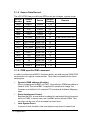
1
cPCI-6765(A)
Intel 440BX with Mobile CPU
6U Compact PCI CPU CARD
User’s Guide
Recycled Paper
©Copyright 2003 ADLINK Technology Inc;
All Rights Reserved.
Manual Rev. 1.00: January 28, 2003
Part No. 50-15015-100
The information in this document is subject to change without prior notice
in order to improve reliability, design and function and does not represent
a commitment on the part of the manufacturer.
In no event will the manufacturer be liable for direct, indirect, special,
incidental, or consequential damages arising out of the use or inability to
use the product or documentation, even if advised of the possibility of such
damages.
This document contains proprietary information protected by copyright. All
rights are reserved. No part of this manual may be reproduced by any
mechanical, electronic, or other means in any form without prior written
permission of the manufacturer.
Trademarks
cPCI-6765(A) is a registered trademark of ADLINK Technology Inc. Other
product names mentioned herein are used for identification purposes only
and may be trademarks and/or registered trademarks of their respective
companies.
Getting service from ADLINK
Customer Satisfaction is the most important priority for ADLINK Tech Inc. If
you need any help or service, please contact us.
ADLINK Technology Inc.
Web Site
http://www.adlinktech.com
Sales & Service [email protected]
NuDAQ + USBDAQ + PXI
[email protected]
Automation
[email protected]
NuIPC
[email protected]
NuPRO / EBC
[email protected]
TEL
+886-2-82265877
FAX
Address
9F, No. 166, Jian Yi Road, Chungho City, Taipei, 235 Taiwan.
Technical
Support
+886-2-82265717
Please email or FAX us of your detailed information for a prompt,
satisfactory and constant service.
Detailed Company Information
Company/Organization
Contact Person
E-mail Address
Address
Country
TEL
FAX
Web Site
Questions
Product Model
Environment to Use
Detail Description
Suggestions to ADLINK
OS:
Computer Brand:
M/B:
CPU:
Chipset:
BIOS:
Video Card:
Network Interface Card:
Other:
Table of Contents
List of Tables .......................................................................................................iv
List of Figures.......................................................................................................v
Outline of User’s Manual...................................................................................vi
Chapter 1 Introduction....................................................................................... 1
1.1
Unpacking Checklist............................................................................... 2
1.2
Features .................................................................................................... 3
1.3
Functional Block....................................................................................... 4
1.3.1
CompactPCI Bus Interface .................................................... 5
1.3.2
PCI-to-PCI Bridge (P2P) ........................................................ 5
1.3.3
Mobile Intel Pentium III Processor....................................... 5
1.3.4
Supported Memory.................................................................. 6
1.3.5
Interrupts ................................................................................... 6
1.3.6
DMA ............................................................................................ 7
1.3.7
Real-Time Clock ...................................................................... 7
1.3.8
Baseboard Management ....................................................... 7
1.3.9
Power Ramp Circuitry............................................................. 7
1.3.10 PCI Mezzanine Card (PMC) Interface................................. 8
1.3.11 Watchdog Timer....................................................................... 8
1.3.12 Ethernet Interfaces .................................................................. 8
1.3.13 Graphic Interfaces ................................................................... 8
1.3.14 IDE Hard Drive ......................................................................... 8
1.3.15 IEEE-1284 Parallel Port/Printer Interface ........................... 9
1.3.16 Universal Serial Bus (USB).................................................... 9
1.3.17 Serial I/O.................................................................................... 9
1.3.18 Keyboard/Mouse Controller................................................... 9
1.4
Specifications .........................................................................................10
1.4.1
cPCI-6765(A) Specifications ...............................................10
1.4.2
cPCI-R6765 Specifications..................................................15
1.5
Peripheral Connectivity.........................................................................16
Table of Contents • i
Chapter 2 Jumpers and Connectors............................................................17
2.1
cPCI-6765(A) Board Outline and Illustration.....................................18
2.2
Configuration ..........................................................................................19
2.2.1
SW1 (Reset)............................................................................19
2.2.2
S1, S2, S3 and S4 (Setting LAN1 and LAN2 for Front or
Rear Access)...........................................................................20
2.2.3
JP2, JP3, JP4 and JP5 (COM2 RS-232/422/485/485+
Selectable) on RTM...............................................................21
2.2.4
PMC VIO Zero Ω Shorting Resistors ..................................21
2.2.5
Clear CMOS ............................................................................22
2.3
cPCI-6765(A) Connector Pin Assignments ......................................23
2.3.1
VGA Connector (Front and RTM) ........................................23
2.3.2
Ethernet (RJ-45) Connector (Front and RTM)...................23
2.3.3
PS/2 Mouse/Keyboard Connector (Front) .........................24
2.3.4
USB Connectors (Front and RTM) ......................................24
2.3.5
COM1 Serial Ports..................................................................24
2.3.6
COM2 Serial Ports on RTM (RS-232/422/485/485+).......25
2.3.7
Parallel Port Connector (on RTM) .......................................26
2.3.8
Floppy Connector (on RTM) .................................................26
2.3.9
Primary/Secondary IDE Connector (on RTM) ..................27
2.3.10 Secondary IDE Connector (Front) ......................................28
2.3.11 PMC Connectors ....................................................................29
2.3.12 CompactPCI Connectors .....................................................31
Chapter 3 Getting Started...............................................................................35
3.1
CPU Installation .....................................................................................35
3.2
Memory Installation................................................................................35
3.3
HDD and CF Installation.......................................................................36
3.3.2
CF Installation for cPCI-6765(A).........................................36
3.3.1
HDD Installation for cPCI-6765(A) .....................................37
3.4
BIOS Configuration Overview...............................................................38
3.5
Operating System Installation .............................................................39
Chapter 4 Driver Installation...........................................................................40
4.1
VGA Drivers Installation ........................................................................41
4.1.1
Display Driver for Windows 98/ME ......................................41
4.1.2
Display Driver for Windows NT 4.0 .....................................41
4.1.3
Display Driver for Windows 2000........................................42
4.1.4
Installing Drivers for Windows XP.......................................43
ii • Table of Contents
4.2
LAN Driver Installation ..........................................................................44
4.2.1
Software and Driver Support................................................44
4.2.2
Intel 82559 Driver Installation on Windows 98 ................45
4.2.3
INTEL 82559 Driver Installation on Windows 2000 ........46
4.2.4
Intel 82559 Driver Installation on Windows XP................47
4.2.5
Intel 82559 Driver Installation on Windows NT................48
Chapter 5 Utilities .............................................................................................49
5.1
Watchdog Timer Overview ...................................................................49
5.1.1
Using the Watchdog in an Application...............................50
5.2
Hardware Doctor Utility.........................................................................51
5.3
Intel Preboot Execution Environment (PXE)......................................51
Appendix A .........................................................................................................52
A.1
CPCI-6765A System Mode Hot Swap................................................52
A.2
CPCI-6765 Peripheral Mode Hot Swap............................................52
A.2.1
Hot Swap Controller Hardware Interface...........................53
A.2.2
Insertion and Removal Process .........................................54
Appendix B .........................................................................................................56
B.1
21555 Application Notes ......................................................................56
B.2
Operating Therory..................................................................................57
B.3
Programming notes ..............................................................................59
B.3.1
Sample Code .........................................................................60
B.3.2
Search and Register device ................................................60
B.3.3
Map Bus Address to Virtual Address..................................60
B.3.4
Create Memory Buffer for Other Side.................................62
B.3.5
Syncing with Setting and Exchange Base address.........63
B.3.5
Init Interrupt Register ............................................................65
B.3.6 Driver Installation Procedures ..................................................66
Appendix C .........................................................................................................67
C.1 Baseboard Management .....................................................................67
C.1.1
Flash Organization ................................................................68
C.1.2
Host Interface .........................................................................68
C.1.3
Serial EEPROMs ....................................................................69
C.1.4
Supported IPMI functions.....................................................69
C.1.5
Sensor Data Record..............................................................74
C.1.6
OEM specific IPMI command ..............................................74
Warranty Policy.................................................................................................77
Table of Contents • iii
List of Tables
Table 1:
Table 2:
Table 3:
Table 4:
Table 5:
Table 6:
Table 7:
Table 8:
Table 9:
Table 10:
Table 11:
Table 12:
Table 13:
Table 14:
Table 15:
Table 16:
Table 17:
Table 18:
Table 19:
Table 20:
Table 21:
Table 22:
Table 23:
Table 24:
Table 25:
Table 26:
Table 27:
Power consumption with above configuration .........................14
Peripheral Connectivity Table......................................................16
Switch Cross-Reference Table...................................................19
LAN Access Configuration ...........................................................20
Setting LAN for 2.16 backplane or RTM.....................................20
JP2, JP3, JP4 and JP5 Settings ..................................................21
Zero Ω shorting resistor settings ................................................21
Clear CMOS RTC RAM..................................................................22
VGA Connector Pin Assignment.................................................23
Ethernet Connector Pin Assignment..........................................23
LED Indicators Definition on the Ethernet Connector.............23
PS/2 Keyboard Pin Assignment..................................................24
USB Connector Pin Assignment.................................................24
COM1 on front panel......................................................................24
COM1 Pin Header on RTM...........................................................25
COM2 Serial Port Pin Assignment..............................................25
Parallel Port Pin Assignment.......................................................26
Floppy Connector Pin Definition..................................................26
IDE Connector Pin Definition.......................................................27
44-pin Secondary IDE Connector ...............................................28
J11 PMC Connector Pin Definition .............................................29
PMC J12 Pin Definition .................................................................30
CompactPCI J1 Pin Definition.....................................................31
CompactPCI J2 Pin Definition.....................................................32
CompactPCI J3 Pin Definition.....................................................33
CompactPCI J5 Pin Definition.....................................................34
Features of the PCI-to-PCI Transparent Bridge.......................57
iv • List of Tables
List of Figures
Figure 1:
Figure 2:
Figure 3:
Figure 4:
Figure 5:
Figure 6:
Figure 7:
Figure 8:
Figure 9:
Figure 10:
Bock Diagram of cPCI-6765(A) ......................................................... 4
Board Layout.......................................................................................18
Mounting Location of stand-off on 2.5” HDD ................................37
Watchdog Timer Architecture ..........................................................49
l_stat Signal Implementation ..........................................................53
21555 Hot-Swap controller Insertion and Removal Process ...54
21555 Bus Addressing.....................................................................57
Setup Register ...................................................................................58
Translation of Base Registers ........................................................58
Flow Chart of Programming an Application..................................59
List of Figures • v
Outline of User’s Manual
This manual is intended to assist users with understanding and configuring
the cPCI-6765(A) 6U CompactPCI SBC and Rear I/O Transition Modules. It
is divided into 5 chapters.
Chapter 1,
“Introduction”, gives an overview of the product features,
applications, and specifications.
Chapter 2,
“Connectors and Jumpers”, this chapter outlines all the
connectors and its pin defi nitions.
Chapter 3,
“Getting Started”, this chapter gives a summary of what is
required to setup an operational system using the
CPCI-6765(A). Hardware installation and BIOS overview is
discuss.
Chapter 4,
“Driver Installation”, provides step-by-step ins tructions of how
to install the software drivers successfully.
Chapter 5,
“Utilities,” explains the operation of the WDT, PXE booting and
Hardware Doctor.
vi • Outline of User’s Manual
1
Introduction
The cPCI-6765(A) CPU Board with Mobile Intel Pentium III Processor - M is a
single board computer designed to work as a modular component in a
high-performance CompactPCI system. It utilizes the Mobile Intel Pentium III
Processor - M to provide extremely high PCI performance and the latest in
memory and I/O technology combined with low power requirements. The
cPCI-6765(A) CPU board is an ideal solution for telecommunications,
Internet, and industrial control applications with demanding performance
and system reliability requirements.
Although the cPCI-6765(A) is highly integrated, its capabilities can be further
extended with optional boards available from ADLINK. Expansion boards are
available to add IDE daughter boards such as CompactFlash. For more
information about options and accessories, please visit ADLINK’s web page
at http://www.adlinktech.com.tw
This chapter is designed to give you an overview of the cPCI-6765(A) CPU
module. The chapter covers the following topics:
•
Unpacking and Checklist
•
Features
•
Specifications
Introduction • 1
1.1
Unpacking Checklist
Check the shipping carton for any damages. If the shipping carton and
contents are damaged, notify the dealer for a replacement. Retain the
shipping carton and packing material for inspection by the dealer. Obtain
authorization before returning any product to ADLINK.
Check the following items are included in the package, if there is any missing
items, contact your dealer:
•
The cPCI-6765(A) module (May be equipped with different speed or
capacity of CPU, RAM, and HDD).
•
This User’s Manual
•
ADLINK CD
Note:
The package of the cPCI-6765A OEM version non-standard
configuration, functionality or package may vary according to the
different configuration requests
CAUTION: This board must be protected from static discharge and physical
shock. Never remove any of the socketed parts except at a
static-free workstation. Use the anti-static bag shipped with the
product to handle the board. Wear a wrist strap grounded through
one of the system's ESD Ground jacks when servicing system
components.
!
2 • Introduction
1.2 Features
•
PICMG 2.0 CompactPCI Specification R3.0 Compliant.
•
PICMG 2.1 CompactPCI Hot Swap Specification R2.0 Compliant.
•
PICMG 2.16 CompactPCI Packet Switch Backplane Specification node
slot compatible.
•
PICMG 2.9 CompactPCI System Management Specification R1.0
Compliant.
•
Design for low power BGA2 Pentium-III CPU running at FSB 100MHz.
•
Supports operation in peripheral mode, non-J4 connector for inserting
into H.110 Backplane.
•
Supports up to total 512MB with optional ECC capability
•
Space for build-in 2.5” low profile HDD
•
Supports up to one 32-bit PMC module socket
•
Supports up to 2 USB ports, 2 serial port, 1 parallel port
•
Supports 32-bit PCI at 33MHz operation
•
Supports dual 10/100Mb Ethernet ports for selectable front panel I/O,
PICMG 2.16 backplane I/O or rear panel I/O.
•
Supports Intel pre-boot execution environment (PXE) for remote boot
•
Supports CompactFlash type-II socket by removable daughter board
•
Supports rear I/O configuration
•
Supports remote console
•
Supports soft power-off triggering for Windows-based OS shut-down
•
WDT status indication
Introduction • 3
1.3
Functional Block
The following topics are an overview of the cPCI-6765(A) main features as
shown in the functional block diagram below.
Mobile CPU
Low Power
Host Bus 100MHZ
Memory
100MHZ
AGP BUS
82443 BX
66MHZ
CHIPS
M69000
SO-DIMM
PCI Bus 33MHZ
PMC
I
D
E
U
S
B
82374
HWM
W83L784R
BRIDGE
Intel
21555
INTEL
82559
ISA Bus 16MHZ
BMC
ZirconCP
BIOS
Super IO
W83977
PRT
MS
KB
COM
Figure 1: Bock Diagram of cPCI-6765(A)
4 • Introduction
FDD
1.3.1 CompactPCI Bus Interface
The cPCI-6765(A) operates in a 6U CompactPCI system. The CompactPCI
standard is electrically identical to the PCI local bus standard but has been
enhanced to work in harsh environments and support more peripheral slots.
Additionally, when used in a Hot Swap compliant backplane and in
accordance with the CompactPCI Hot Swap Specification, PICMG 2.1,
Version 1.0, the cPCI-6765(A) supports hosting hot swappable peripherals
in a powered system. The cPCI-6765(A) can also function in a standard
(non-Hot Swap) CompactPCI system without live insertion and extraction
capability.
1.3.2 PCI-to-PCI Bridge (P2P)
The cPCI-6765 features one non-transparent PCI-to-PCI bridge to support
the J1 CompactPCI buses. The Intel 21555 is compliant with the PCI Local
Bus Specification, Revision 3.0. Each bridge provides the isolation,
arbitration, and clocks for seven PCI peripheral cards without the need for an
external bridgeboard. The PCI-to-PCI Bridge is only available with the
cPCI-6765 version. Refer to Appendix B for full application details of this chip
Special features of the Intel 21555 include:
-
33 MHz PCI bus operation
-
Support for independent primary and secondary PCI clocks
-
32-bit PCI non-transparent operation with 32-bit devices from one bus
segment to another
-
Supports both 5V and 3.3V signaling
1.3.3 Mobile Intel Pentium III Processor
The cPCI-6765(A) uses the Mobile Intel Pentium III Processor. This
0.18-micron product is a highly integrated assembly containing an Intel
Pentium III mobile processor and its immediate system -level support. This
mobile version of the Pentium III processor runs at a lower voltage than the
desktop version.
The 256 KB on-die transfer L2 cache is integrated with the CPU, eliminating
the need for separate components and improving performance. The Mobile
Intel Pentium III Processor also operates with a 100 MHz Front Side Bus for
faster access to memory and data.
Introduction • 5
1.3.4 Supported Memory
The cPCI-6765(A) supports two 144-pin SO-DIMM sockets and hence can
accommodate u p to a maximum total memory size of 512MB. The memory
type must be 3.3V SDRAM and can come in size of 32MB, 64MB, 128MB or
256MB. The entire memory array may be configured as either standard
(un-buffered) SDRAM or buffered SDRAM and the DIMM sockets can be
populated in any order. ADLINK factory provides pre-mounting memory for
OEM project. Please contact ADLINK sales representatives for available
memory configurations.
1.3.5 Interrupts
Two enhanced interrupt controllers provide the cPCI-6765(A) with a total of
15 interrupt inputs. Interrupt controller features include support for:
•
Level-triggered and edge-triggered inputs
•
Individual input masking
•
Fixed and rotating priorities
Interrupt sources include:
•
Counter/Timers
•
Serial I/O
•
Keyboard
•
Printer Port
•
Floppy disk
•
IDE interface
•
Real-Time Clock
•
On-board PCI devices
Enhanced capabilities include the ability to configure each interrupt level for
active high going edge or active low-level inputs. The cPCI-6765(A)'s
interrupt controllers reside in the Intel 82371EB (PIIX4E)
6 • Introduction
1.3.6 DMA
Two enhanced DMA controllers are provided on the cPCI-6765(A) for use by
the onboard peripherals. The cPCI-6765(A)'s DMA controllers reside in the
Intel 82371EB (PIIX4E) device.
1.3.7 Real-Time Clock
The real-time clock performs timekeeping functions and includes 256 bytes
of general purpose, battery-backed, CMOS RAM. Timekeeping features
include an alarm function, a maskable periodic interrupt, and a 100-year
calendar. The system BIOS uses a portion of this RAM for BIOS setup
information. The cPCI-6765(A)'s Real-Time Clock resides in the Intel
82371EB (PIIX4E) device.
1.3.8 Baseboard Management
The Zircon CP baseboard management controller is used to manage all
aspects of the system board. The features are summarized as follows.
•
ARM7/TDMI controller with internal 14KB SRAM
•
IPMB interface
•
External 16-bit flash ROM interface with ROM size 2Mb to 8Mb
•
Six channels A-to-D converter for voltage monitoring, 10-bit resolution
•
Provide a heartbeat timer
•
Support CPU internal instruction error input (IERR#)
•
Support CPU floating point error input (FERR#)
QLogic provides a firmware suite supporting the Intelligent Platform
Management Interface (IPMI) specification, including the Intelligent Platform
Management Bus (IPMB). See appendix C for full details.
1.3.9 Power Ramp Circuitry
The cPCI-6765(A) features a power controller with power ramp circuitry to
allow the board's voltages to be ramped in a controlled fashion. The power
ramp circuitry eliminates any large voltage or current spikes caused b y hot
swapping boards (See Appendix A for an in-depth detail of the Hot Swap
feature). This controlled ramping is a requirement of the CompactPCI Hot
Swap specification, PICMG 2.1, Version 1.0. The cPCI-6765(A)'s power
controller unconditionally resets the board when it detects that the 3.3V, 5V,
and 12V supplies are below an acceptable operating limit. These limits are
defined as 4.75V (5V supply), 3.0V (3.3V supply), and 10.0V (+12V supply).
Introduction • 7
1.3.10 PCI Mezzanine Card (PMC) Interface
The cPCI-6765(A) provides a location for one on-board PMC device with front
panel access. The PMC interface is on the PCI Bus with PMC VIO default
factory setting tied to 5.0V by 0-ohm resistors R33 and R34. If R33 and R34
are removed, and R38 and R49 are installed with 0 -ohm resistors, the PMC
VIO is 3.3V.
1.3.11 Watchdog Timer
The watchdog timer optionally monitors system operation and can be
programmed for different timeout periods (from 1 seconds to 255 seconds
or 1 minute to 255 minutes). A register bit can be enabled to indicate if the
watchdog timer caused the reset event. The watchdog timer register is
cleared on power-up, enabling system software to take appropriate action if
the watchdog generated the reboot.
1.3.12 Ethernet Interfaces
The cPCI-6765(A) provides two 10/100Mbps Ethernet interfaces and is
controlled via the Intel 82559 chipset. Both Ethernet ports are assigned a
unique static MAC Address. The board’s Ethernet Address is displayed on a
label attached to the board. LED drive signals for Ethernet link status and
activity are routed to the same connector. The onboard Ethernet is wired for
Management 2.0 compliance, the rear Ethernet complies with PICMG 2.16.
Switching from front to PICMG 2.16 backplane/rear is done through
dipswitches.
1.3.13 Graphic Interfaces
The CPCI-6765(A) provides standard analog SVGA output on front and rear
IO. The video function is provided via the M69000 chip. The BIOS has a
selection in the CMOS setup to disable the onboard video allowing users to
use a PMC video as the primary video controller. The BIOS also has a
selection in the CMOS setup to disable the onboard video to allow the user to
reclaim the video memory for other applications without having to add
another video card.
1.3.14 IDE Hard Drive
The cPCI-6765(A) Bus Master IDE controller supports 2 EIDE interfaces.
Two 40-pin EIDE connectors available to the rear transition module supports
PIO Mode 3/4 and Ultra DMA/33 IDE devices and a 44-pin secondary EIDE
connector on-board allows support for a 2.5” notebook size HDD or a
Flash2000TM flash disk. The cPCI-6765(A) IDE controller resides in the Intel
82374 chipset.
8 • Introduction
1.3.15 IEEE-1284 Parallel Port/Printer Interface
The parallel I/O interface signals are routed to J5 providing signal connection
for a DB25 on the cPI-R6765. This port supports the full IEEE-1284
specifications and provides the basic printer interface.
Firmware will initialize the parallel port as LPT1 with ISA I/O base address of
378h. This default configuration also assigns the parallel port to IRQ7. The
printer interface mode (Normal, Extended, EPP, or ECP) is selectable
through the BIOS SETUP utility with the Winbond W83977 Super I/O device
managing the cPCI-6765(A)’s parallel port.
1.3.16 Universal Serial Bus (USB)
The Universal Serial Bus (USB) R1.1 provides a common interface to
lower-speed peripherals such as keyboard, mouse, speakers, printer, etc.,
simplifying the cabling requirements of computers and allowing b it rates of
up to 12Mb/s. There are in total two USB ports on the cPCI-6765(A) with one
routed for front panel access and the other is available through a Rear
Transition Module and is controlled by the Intel 82371EB (PIIX4E) device.
1.3.17 Serial I/O
Two serial ports are supported on the cPCI-6765(A). The EIA232 drivers and
receivers reside on board. COM1 is a DB9 connector on the front panel or a
pin header on the rear board. COM2 is available as a DB9 connector on the
rear board.
Both serial ports include a complete set of handshaking and modem control
signals, maskable interrupt generation, and data transfer rates up to 115.2K
Baud. COM1 serial port is RS-232 compatible with COM2 being
RS-232/422/485/485+ selectable. Both ports are configured as DTE.
Firmware will initialize the two serial ports as COM1 and COM2 with ISA I/O
base addresses of 3F8h and 2F8h respectively. This default configuration
also assigns COM1 to IRQ4 and COM2 to IRQ3
1.3.18 Keyboard/Mouse Controller
The cPCI-6765(A) includes an on-board PC/AT keyboard and mouse
controller. The keyboard/mouse signals are available through the PS/2
circular DIN on the front panel and rear panel. The cPCI-6765(A)’s
keyboard/mouse controller resides in the Winbond W83977 Super I/O device
Introduction • 9
1.4
Specifications
1.4.1 cPCI-6765(A) Specifications
General CompactPCI Features:
•
PCI Rev.2.1 compliant
•
PICMG 2.0 CompactPCI Rev. 3.0 compliant.
•
PICMG 2.1 CompactPCI Hot-swap specification Rev.2.0 compliant
•
PICMG 2.16 CompactPCI Packet Switch Backplane Specification node
slot compatible.
•
PICMG . 2.9 CompactPCI System Management Specification R1.0
Compliant.
Form Factor:
•
Standard 6U CompactPCI (board size: 233mm x 160mm)
•
1-slot (4TE/HP, 20.32mm) wide, incl. space of 2.5” ATA HDD and
memory expansion board
CPU/Cache:
•
Intel BGA2 Pentium III with 256KB on-die L2 cache at full speed 100MHz
FSB
•
Supports low power Pentium -III-700MHz or mobile Pentium-III-850MHz
•
Optional CPU speed (LP-Celeron-400, or Pentium-III-500) are available
for big quantity OEM project)
Chipset:
•
Intel 440BX AGPset
•
Intel 82443BX and 82371EB(PIIX4E)
VGA Port:
•
Onboard CHIPS M69000 (256-pins mini BGA package, 1x AGP)
controller
•
Dsub 15-pin VGA connector on front panel
10 • Introduction
CompactPCI interface:
•
cPCI-6765 is a peripheral board design, suitable in peripheral slots,
operated as a peripheral card in distributed multi -processor
architecture.
•
Intel 21555 non-transparent PCI-to-PCI bridge interface on J1.
•
32-bit/33MHz PCI operation.
•
Supports both 5V and 3.3V signaling
Host Memory:
•
Supports up to total 512MB by up to two 144-pin SO-DIMM sockets
•
Each 144-pin SO-DIMM socket supports up to 256MB PC-100 memory
module which uses 16Mx8 SDRAM technology
•
Optional ECC support (for big quantity OEM project)
BIOS: Award PnP BIOS:
•
BIOS write protection, provide anti-virus capability
•
On-board Ethernet, hardware monitoring function disable selectable
•
Customized power-on screen (for OEM project)
•
DMI BIOS Support: Desktop Management Interface (DMI) allows users
to download system hardware-level information such as CPU type, CPU
speed, internal/external frequencies and memory size.
•
Green Function: Power management via BIOS, activated through
mouse/keyboard movement.
•
Remote Console: setup console redirection to serial port (terminal
mode) with CMOS setup access
•
Diskless, keyboardless and videoless operation extensions
Hot swap support:
•
Support both system mode and peripheral mode hot swap.
•
In system mode: Ejector in handle can generate soft-off signal for
on-board system power off.
•
In peripheral mode: Ejector in handle can generate an ENUM# trigger
signal to issue hot swap interrupt to system host.
Introduction • 11
System Management Interface:
•
Qlogic Zircon CP Baseboard Management Controller (BMC) with 14
Kbytes SRAM internally.
•
Monitor onboard voltages, temperatures.
•
Support external 16-bit Flash ROM with a size of up to 1Mbyte (protected
boot block required).
IDE Ports:
•
Bus Master IDE controller supports two EIDE interfaces
•
One 44-pin secondary EIDE connector on front CPU module, supports
on-board 2.5” notebook size HDD or Flash2000TM flash disk
•
One CompactFlash type-II socket by removable daughter board on front
CPU board.
•
Two 40-pin EIDE connectors on rear transition module supports PIO
Mode 3/4 and Ultra DMA/33 IDE devices.
On Board Super I/O:
•
Winbond W83977EF
•
Supports high-speed bi-directional SPP/EPP/ECP parallel ports with
ESD protection to 4KV and downstream device protection to 30V. One
DB-25 LPT connector is located on rear I/O module routing by J5 rear I/O.
•
One floppy interface by J3 rear I/O, supports two floppy drives. One
34-pin floppy connector is available on rear I/O transition module.
•
One 16C550 UARTs compatible RS-232 COM1 port (RJ-45) with ESD
protection to 2KV on front CPU module.
•
One RS-232/422/485/485+ selectable COM2 serial ports by using of
rear transition module.
USB Interface:
•
Supports up to two USB ports, one on front panel and one on rear I/O
transition module.
•
USB Specification Rev. 1.1. Compliant
•
Individual over-current protection
12 • Introduction
Watchdog Timer:
•
Programmable I/O port 3F0h and 3F1h to configure watchdog timer,
programmable timer 1~255 seconds or 1~255 minutes
•
A LED indicator on front faceplate for watchdog timer status indication
•
Bundled easy-programming library for DOS, Windows 95, 98, NT
Hardware Monitoring:
•
Winbond W83L784, monitoring CPU temperature, system temperature
and DC Voltages
PMC module support:
•
On-board one IEEEP1386.1 PCI Mezzanine Card (PMC) interfaces for
functionality expansion
•
Supports 32-bit/33MHz PCI operation on PMC
•
+3.3V, +5V, +12V and –12V.
On-board Ethernet supporting:
•
Two Ethernet ports with two Intel 82559 Ethernet controllers.
•
IEEE 802.3 10Base-T and 100Base-TX compatible
•
IEEE 802.3u Auto-negotiation support
•
IEEE 802.3x 100Base-TX flow control support
•
Full duplex support at both 10 and 100 Mbps operation
OS Compatibility:
•
MS-DOS 6.2+, Windows 95/98/ME, Windows NT 4.0, Windows 2000,
Windows XP, Red Hat Linux 7.0+ and VxWorks
Flash Disk Supporting:
•
One CompactFlash type-II socket by removable daughter board on front
CPU board.
•
On-board space for Flash2000TM 2.5” flash disk on front CPU module
(mutual exclusive with CF adaptor.)
Safety Certificate and Test:
•
CE, FCC
•
HALT (temperature and vibration stress)
Introduction • 13
Front Panel LEDs and switch:
•
Power status (green)
•
IDE activity indicator (red)
•
Ethernet port 1&2: 10/100Mb (amber), activity (Green)
•
Watchdog timer status or Auxiliary indicator (green)
•
Hot-swap status indicator (blue)
•
On-handle limit switch for soft power-off signal triggering
•
Flush tact switch for system reset
Environment:
•
Operating temperature: 0 to 55°C
•
Storage temperature: -40 to 80°C
•
Humidity: 5% to 95% non-condensed
•
Shock: 15G peak-to-peak, 11ms duration, non-operation
•
Vibration:
•
Non-operation: 1.88Grms, 5-500Hz, each axis
•
Operation: 0.5Grms, 5-500Hz, each axis, with 2.5” HDD
Power Consumption
The values below are the measured power consumption for the cPCI board
with the listed options in the table only; the CPU is running under 100%
loading. The power for other peripheral devices such as keyboard, mouse,
add-on cards, HDD, and CD-ROM are not included.
CPU
Voltage
Current
+3.3V
2.8A
+5.0V
3.2A
+12.0V 144mA
-12.0V
68mA
Total Watts=9.24+16.0+1.73+0.82=27.8W
Pentium III 850MHZ CPU
512M RAM
Two Ethernet ports
One PMC device
Wattage
9.24W
16.0W
1.73W
0.82W
Table 1: Power consumption with above configuration
14 • Introduction
The cPCI-6765(A) is supplied with a heatsink allowing the processor to
operate between 0º and approximately 55º C ambient with a minimum of 1
meter per second of external airflow. It is the users' responsibility to ensure
that the cPCI-6765(A) is installed in a chassis capable of supplying
adequate airflow. The maximum power dissipation of the processor at
850MHz (BGA2 package) is 29W. External airflow must be provided at all
times. ADLINK has special designed chassis to allow for greater airflow,
please contact ADLINK sale representatives for more detail.
CAUTION:
The processor "core" temperature must never exceed 100°C
under any condition of ambient temperature or usage. This may
result in permanent damage to the processor.
1.4.2 cPCI-R6765 Specifications
Form Factor
•
Standard 6U CompactPCI rear I/O (board size: 233.35x80mm2)
•
1-slot width (4HP = 20.32 mm)
Available Rear I/O Ports
•
Onboard two 40-pins IDE connectors for Primary and Secondary IDE.
•
One USB version 1.1 port on rear panel.
•
One DB-25 LPT connector with full IEEE-1284 capability.
•
One standard analog SVGA output connector on rear panel.
•
Two switch-selectable Ethernet ports on rear panel.
•
Onboard floppy interface configured for PS/2 compatibility with 34-pin
header.
•
COM1 with onboard 10-pins header and RS-232/422/485/485+
selectable COM2 with DB9 connector on the rear panel.
•
Two 6-pin circular DIN connectors for keyboard and mouse on the rear
panel.
Introduction • 15
1.5
Peripheral Connectivity
I/O
Serial Port (COM1)
Serial Port (COM2)
Parallel Port
PS2 Keyboard
PS2 Mouse
Floppy
Ultra DMA33 Primary
IDE
Ultra DMA33 Secondary
IDE
VGA
USB A
USB B
PC Beeper
32bit/33MHz PMC
interface
10/100Mb Ethernet
Port1
10/100Mb Ethernet
Port1
LEDs
Reset button
CompactFlash
cPCI-6765(A)
Faceplate
Y (DB-9)
---
--
cPCI-R6765
Faceplate
-Y (J5, DB-9)
Y (J5, DB-25)
Y (J3, PS2)
Y (J3, PS2)
--
--
--
Y (Board, 44-pin)
--
Y (DB-15)
Y
---
Y (DB-15)
-Y
--
Y
--
Y (RJ-45, LED)
Y (RJ-45, LED)
Y (RJ-45, LED)
Y (RJ-45, LED)
Y
Y
Y (CF-II)
----
Y (PS2, Combo)
Table 2: Peripheral Connectivity Table
16 • Introduction
2
Jumpers and Connectors
This chapter will familiarize the user with the cPCI-6765(A) before getting
started, it will provide information about the board layout, connector
definitions, jumper setup and setting the PMC VIO, This will includes the
following information:
•
cPCI-6765(A) board outline and illustration
•
cPCI-6765(A) connectors pin assignments
•
cPCI-6765(A) jumpers setting and PMC VIO
•
cPCI-R6765 connector pin assignments
Jumpers and Connectors • 17
2.1
cPCI-6765(A) Board Outline and Illustration
Lock/release
lever
BATTERY
COM1
COM1
EIDE
VGA
VGA
J5
DIMM 1
DIMM 2
PMC Slot
PMC
PMC
Connectors
J3
Heatsink
KB/MS
KB/MS
USB
USB
LAN1
LAN1
LAN2
LAN2
RST
PW
HD
HS
WD
J2
J1
LEDS
RESET
Figure 2: Board Layout
18 • Jumpers and Connectors
2.2
Configuration
The cPCI-6765(A) has been designed for maximum flexibility and can be
configured for specific applications. Most configuration options are selected
through the BIOS Setup utility however some options cannot be software
controlled and are configured with jumpers or by other means beside
software
The cPCI-6765(A) contains a push-button switch on the faceplate and several
banks of jumper pin on the front and rear board. The switches and jumpers
are listed and briefly described in the "Switch Cross-Reference" table below.
Switch Cross-Reference Table
Switch
Function
SW1
Reset
JP1
Clear CMOS Content
S1, S2. S3, S4
R33, R34, R38, R49
JP2 ~ JP5 (cPCI-R6765)
Switch to set LAN for Front or Rear
Access
Resistors to set PMC VIO
COM2 RS-232/422/485/485+ Selectable
Table 3: Switch Cross-Reference Table
2.2.1 SW1 (Reset)
SW1 is a push-button on the front panel of the cPCI-6765(A). Pressing SW1
issues a hard reset and will reset the system
Jumpers and Connectors • 19
2.2.2 S1, S2, S3 and S4 (Setting LAN1 and LAN2 for Front or Rear
Access)
For convenience with wiring, the cPCI-6765(A) allows for either front or rear
LAN1 and LAN2 access. Note that although both LAN1 and LAN2 are
available on the front and rear, the same LAN port (e.g. LAN1 front and LAN1
rear), cannot be access simultaneously, and are set by dipswitches S1, S2,
S3 and S4. The table below lists the access configuration.
LAN1
LAN2
S1
S2
Front
All ON
All OFF
Rear or
2.16
Backplane
All OFF
All ON
S3
S4
Front
All ON
All OFF
Rear or
2.16
Backplane
All OFF
All ON
Table 4: LAN Access Configuration
Note: When switching LAN operation to the rear (Rear operation refers to
either LAN connection on a 2.16 backplane or rear I/O card), user must set S1
or S2 on the RTM module to select which plane to operate on. Refer to the
table below for correct settings of S1 and S2 of the RTM.
2.16 Backplane
LAN1
LAN2
S1
S2
All OFF
All OFF
Table 5: Setting LAN for 2.16 backplane Operation
20 • Jumpers and Connectors
2.2.3 JP2, JP3, JP4 and JP5 (COM2 RS-232/422/485/485+
Selectable) on RTM
As COM2 is RS-232/422/485 selectable, to operate in its different
communication protocols, JP2, JP3, JP4 and JP5 must be set according to
the table listed below. The numbers in the table indicate the pin number that
needs to be shorted together.
Setting
RS-232
RS-422
RS-485
RS-485+
JP2
3-5
4-6
1-3
2-4
1-3
2-4
1-3
2-4
JP3
3-5
4-6
1-3
2-4
1-3
2-4
1-3
2-4
JP4
JP5
5-6
----
3-4
1-2
1-2
3-5
4-6
3-5
4-6
1-3
2-4
Table 6: JP2, JP3, JP4 and JP5 Settings
2.2.4 PMC VIO Zero Ω Shorting Resistors
The cPCI-6765(A) contains two pairs of zero Ω shorting resistors that allow
the user to configure the PMC VIO voltage to either +5V or +3.3V. The PMC
interface is on the PCI Bus with PMC VIO default factory setting tied to +5.0V by
0-ohm resistors R33 and R34. If R33 and R34 are removed, and R38 and
R49 are installed with 0 -ohm resistors, the PMC VIO is +3.3V. Refer to the
table below:
PMC VIO
+5.0V
R38, R49
R33, R34
+3.3V
Mount
Mount (Default)
Table 7: Zero Ω shorting resistor settings
Jumpers and Connectors • 21
2.2.5 Clear CMOS
RTC status
cPCI-6765(A) JP1
Clear CMOS
1-2
3 2 1
Normal operation
2-3 (Default)
3 2 1
Table 8: Clear CMOS RTC RAM
The CMOS RAM data for real time clock (RTC) contains the date / time and
password information. The button cell battery powers the CMOS when the
system is power off.
To erase the CMOS RAM data:
1.
Unplug the cPCI-6765(A).
2.
Short pins 1 and 2 of JP1. Then reinstall the jumper back to normal
location.
3.
Plug cPCI-6765(A) back to the chassis. Turn the power on.
22 • Jumpers and Connectors
2.3
cPCI-6765(A) Connector Pin Assignments
2.3.1 VGA Connector (Front and RTM)
Signal Name
Pin
Pin
Signal Name
Red
1
2
Green
Blue
3
4
N.C.
GND
5
6
GND
GND
7
8
GND
N.C.
9
10
GND
N.C.
11
12
N.C.
HSYNC
13
14
VSYNC
NC
15
Table 9: VGA Connector Pin Assignment
2.3.2 Ethernet (RJ-45) Connector (Front and RTM)
Pin
Signal
Function
1
TDP
Transmit Data (+)
2
TDN
Transmit Data (-)
3
RDP
Receive Data (+)
4
LANCT1
Termination
5
LANCT2
Termination
6
RDN
Receive Data (-)
7
NC
No Connect
8
GND
Ground
Table 10: Ethernet Connector Pin Assignment
LED
Color
Link Speed
LED
Amber
Link / Activity
LED
Green
Status
Description
OFF
10Mbps transfer rate
ON
100Mbps transfer rate
OFF
No link
ON
Connecting
Blinking
Active/Data transferring
Table 11: LED Indicators Definition on the Ethernet Connector
Jumpers and Connectors • 23
2.3.3 PS/2 Mouse/Keyboard Connector (Front)
Pin #
Signal
Function
1
KBDATA
Keyboard data
2
MSDATA
Mouse data
3
GND
GND
4
+5V
Power
5
KBCLK
Keyboard clock
6
MSCLK
Mouse clock
Table 12: PS/2 Keyboard Pin Assignment
2.3.4 USB Connectors (Front and RTM)
Signal Name
Pin #
Vcc
1
USB-
2
USB+
3
Ground
4
Table 13: USB Connector Pin Assignment
2.3.5 COM1 Serial Ports
DB9 on front panel
6
1
5
Pin #
RS-232
1
Data Carrier Detect
2
Receive Data
3
Transmit Data
4
Data Terminal Ready
5
Ground
6
Data Set Ready
7
Request to Send
8
Clear to Send
9
Ring Indicate
Table 14: COM1 on front panel
24 • Jumpers and Connectors
Pin header on RTM
PIN
SIGNAL
FUNCTION
P1
RDCDJ1
Data Carrier Detect
P2
RDSRJ1
Data Set Ready
P3
RRXD1
Receive Data
P4
RRTSJ1
Request to Send
P5
RTXD1
Transmit Data
P6
RCTSJ1
Clear to Send
P7
RDTRJ1
Data Terminal Ready
P8
RRIJ1
Ring Indicate
P9
GND
Ground
P10
NC
No Connect
Table 15: COM1 Pin Header on RTM
2.3.6 COM2 Serial Ports on RTM (RS-232/422/485/485+)
COM2 serial port on the cPCI-R6765 can be configured as RS232, RS422,
RS485 or RS485+ by setting the appropriate jumpers , refer to section 2.2.4.
6
1
5
Pin #
RS-232
RS-422
RS-485
1
DCD, Data carrier detect
TX-
DATA-
2
RXD, Receive data
TX+
DATA+
3
TXD, Transmit data
RX+
NC
4
DTR, Data terminal ready
RX-
NC
5
GND, ground
GND
GND
6
DSR, Data set ready
NC
NC
7
RTS, Request to send
NC
NC
8
CTS, Clear to send
NC
NC
9
RI, Ring indicator
NC
NC
Table 16: COM2 Serial Port Pin Assignment
Jumpers and Connectors • 25
2.3.7 Parallel Port Connector (on RTM)
Signal Name
Pin #
Pin #
Signal Name
Line printer strobe
1
14
AutoFeed
PD0, parallel data 0
2
15
Error
PD1, parallel data 1
3
16
Initialize
PD2, parallel data 2
4
17
Select
PD3, parallel data 3
5
18
Ground
PD4, parallel data 4
6
19
Ground
PD5, parallel data 5
7
20
Ground
PD6, parallel data 6
8
21
Ground
PD7, parallel data 7
9
22
Ground
ACK, acknowledge
10
23
Ground
13
14
1
Busy
11
24
Ground
Paper empty
12
25
Ground
Select
13
N/A
N/A
Table 17: Parallel Port Pin Assignment
2.3.8 Floppy Connector (on RTM)
Pin
Function
Pin
Function
1
Ground
2
Extended Density
3
Ground
4
No Connect
5
-
6
Data Rate
7
Ground
8
Index
9
Ground
10
Motor A Select
11
Ground
12
Drive B Select
13
Ground
14
Drive A Select
15
Ground
16
Motor B Select
17
Ground
18
Step Direction
19
Ground
20
Step Pulse
21
Ground
22
Write Data
23
Ground
24
Write Gate
25
Ground
26
Track 0
27
Ground
28
Write Protect
29
Ground
30
Read Data
31
Ground
32
Side 1
33
Ground
34
Disk Change
Table 18: Floppy Connector Pin Definition
26 • Jumpers and Connectors
2.3.9 Primary/Secondary IDE Connector (on RTM)
Signal Name
Pin #
Pin #
Reset IDE
1
2
Ground
Host data 7
3
4
Host data 8
Host data 6
5
6
Host data 9
Host data 5
7
8
Host data 10
Host data 4
9
10
Host data 11
Host data 3
11
12
Host data 12
Host data 2
13
14
Host data 13
Host data 1
15
16
Host data 14
Host data 0
17
18
Host data 15
19
20
+5V
Ground
DRQ0 / DRQ1
(1)
Signal Name
(2)
21
22
Ground
Host IOW
23
24
Ground
Host IOR
25
26
Ground
IOCHRDY
27
28
Host ALE
29
30
Ground
31
32
No connect
Address 1
33
34
No connect
Address 0
35
36
Address 2
Chip select 0
37
38
Chip select 1
Activity
39
40
Ground
DACK0 / DACK1
IRQ14 / IRQ 15
(1)
(1)
Table 19: IDE Connector Pin Definition
Jumpers and Connectors • 27
2.3.10 Secondary IDE Connector (Front)
44
2
43
1
Signal
Pin
Pin
BRSTDRVJ
1
2
Signal
GND
DDP7
3
4
DDP8
DDP6
5
6
DDP9
DDP5
7
8
DDP10
DDP4
9
10
DDP11
DDP3
11
12
DDP12
DDP2
13
14
DDP13
DDP1
15
16
DDP14
DDP0
17
18
DDP15
GND
19
20
NC
PDDREQ
21
22
GND
PDIOWJ
23
24
GND
PDIORJ
25
26
GND
PIORDY
27
28
PCSEL
PDDACKJ
29
30
GND
IRQ14
31
32
NC
DAP1
33
34
DIAG
DAP0
35
36
DAP2
CS1P
37
38
CS3PJ
IDEACTPJ
39
40
GND
+5V
41
42
+5V
GND
43
44
NC
Table 20: 44-pin Secondary IDE Connector
28 • Jumpers and Connectors
2.3.11 PMC Connectors
PMC J11 Connector
Signal
Pin
Pin
TCK(3)
1
2
Signal
-12V
GND
3
4
INTA#
INTC#
INTB#
5
6
BUSMODE1#(1)
7
8
+5V
INTD#
9
10
RESERVED (1)
GND
11
12
+3.3V
CLOCK
13
14
GND
GNT#
GND
15
16
REQ#
17
18
+5V
PMCVIO (4)
19
20
AD[31]
AD[28]
21
22
AD[27]
AD[25]
23
24
GND
GND
25
26
C/BEJ[3]#
AD[22]
27
28
AD[21]
AD[19]
29
30
+5V
PMCVIO (4)
31
32
AD[17]
FRAME#
33
34
GND
GND
35
36
IRDY#
DEVSEL#
37
38
+5V
GND
39
40
LCOK#
RESERVED (1)
41
42
RESERVED
PAR
43
44
GND
PMCVIO (4)
45
46
AD[15]
AD[12]
47
48
AD[11]
AD[9]
49
50
+5V
GND
51
52
C/BEJ[0]#
AD[6]
53
54
AD[5]
AD[4]
55
56
GND
PMCVIO
(4)
57
58
AD[3]
AD[2]
59
60
AD[1]
AD[0]
61
62
+5V
GND
63
64
REQ64 #(2)
(1)
Table 21: J11 PMC Connector Pin Definition
Jumpers and Connectors • 29
PMC J12 Connector
Signal
+12V
TMS (2)
TDI (2)
GND
RESERVED (1)
BUSEMODE2# (2)
PCI RESET
+3.3V
PME
AD[30]
GND
AD[24]
IDSEL (AD[31])
+3.3V
AD18
AD16
GND
TRDY#
GND
PERR#
+3.3V
C/BEJ[1]#
AD[14]
GND
AD[8]
AD[7]
+3.3V
RESERVED (1)
RESERVED (1)
GND
ACK64# (2)
GND
Pin
1
3
5
7
9
11
13
15
17
19
21
23
25
27
29
31
33
35
37
39
41
43
45
47
49
51
53
55
57
59
61
63
Pin
2
4
6
8
10
12
14
16
18
20
22
24
26
28
30
32
34
36
38
40
42
44
46
48
50
52
54
56
58
60
62
64
Signal
TRST# (3)
RESERVED (1)
GND
RESERVED (1)
RESERVED (1)
+3.3V
BUSMODE3# (3)
BUSMODE4# (3)
GND
AD[29]
AD[26]
+3.3V
AD[23]
AD[20]
GND
C/BEJ[2]#
RESERVED (1)
+3.3V
STOP#
GND
SERR#
GND
AD13
AD10
+3.3V
RESERVED (1)
RESERVED (1)
GND
RESERVED (1)
RESERVED (1)
GND
RESERVED (1)
Table 22: PMC J12 Pin Definition
1.
These signals are not connected.
2.
These signals are pulled high on board.
3.
These signals are pulled low on board.
30 • Jumpers and Connectors
2.3.12 CompactPCI Connectors
CompactPCI J1: 32-bit PCI System/Peripheral
PIN
Z
A
B
C
D
E
F
25
GND
+5V
REQ64#
ENUM#
+3.3V
+5V
GND
24
GND
S1AD[1]
+5V
V(I/O)
S1AD[0]
ACK64#
GND
23
GND
+3.3V
S1AD[4]
S1AD[3]
+5V
S1AD[2]
GND
22
GND
S1AD[7]
GND
+3.3V
S1AD[6]
AD[5]
GND
21
GND
+3.3V
S1AD[9]
S1AD[8]
GND
S1C/B3[0]# GND
20
GND
S1AD[12]
GND
V(I/O)
S1AD[11]
S1AD[10] GND
19
GND
+3.3V
S1AD[15]
S1AD[14]
GND
S1AD[13] GND
18
GND
S1SERR#
GND
+3.3V
S1PAR
S1C/BE[1]# GND
17
GND
+3.3V
IPMB_SCL
IPMB_SDA
GND
16
GND S1DEVSEL#
GND
V(I/O)
S1STOP#
S1LOCK# GND
15
GND
+3.3V
S1FRAME#
S1IRDY#
GND
S1TRDY# GND
11
GND
S1AD[18]
S1AD[17]
S1AD[16]
GND
S1C/BE[2]# GND
10
GND
S1AD[21]
GND
+3.3V
S1AD[20]
S1AD[19] GND
9
GND
S1C/BE[3]#
GND
S1AD[23]
GND
S1AD[22] GND
8
GND
S1AD[26]
GND
V(I/O)
AD[25]
S1AD[24] GND
7
GND
S1AD[30]
S1AD[29]
S1AD[28]
GND
S1AD[27] GND
6
GND
REQ#
GND
+3.3V
S1CLK
S1AD[31] GND
5
GND BRSVP1A5 BRSVP1B5 S1PCIRST#
GND
S1GNT#
GND
4
GND
IPMB_PWR
HEALTHY#
V(I/O)
INTP
INTS
GND
3
GND
INTA#
INTB#
INTC#
+5V
INTD#
GND
2
GND
TCK
+5V
TMS
TDO
TDI
GND
1
GND
+5V
-12V
TRST#
+12V
+5V
GND
12-14
S1PERR#
GND
KEY
Table 23: CompactPCI J1 Pin Definition
Jumpers and Connectors • 31
CompactPCI J2: 64-bit PCI System/Peripheral
Pin
Z
A
B
C
D
E
F
22
GND
GA4
GA3
GA2
GA1
GA0
GND
21
GND Reserved
20
GND Reserved Reserved Reserved
19
GND
18
GND Reserved Reserved Reserved
17
GND Reserved
16
GND Reserved Reserved
DEG#
15
GND Reserved
FAL#
14
GND Reserved Reserved Reserved
13
GND Reserved
12
GND Reserved Reserved Reserved
11
GND Reserved
10
GND Reserved Reserved Reserved
9
GND Reserved
8
GND Reserved Reserved Reserved
7
GND Reserved
6
GND Reserved Reserved Reserved
5
GND Reserved
4
GND Reserved Reserved Reserved
3
GND Reserved
2
GND Reserved Reserved
SYSEN#
1
GND Reserved
Reserved Reserved Reserved GND
Pin
Z
GND
A
GND
GND
GND
GND
GND
GND
GND
GND
64EN#
GND
GND
B
Reserved Reserved Reserved GND
GND
Reserved GND
Reserved Reserved Reserved GND
GND
Reserved GND
Reserved Reserved Reserved GND
GND
Reserved GND
Reserved Reserved GND
GND
Reserved GND
Reserved Reserved Reserved GND
GND
Reserved GND
Reserved Reserved Reserved GND
GND
Reserved GND
Reserved Reserved Reserved GND
GND
Reserved GND
Reserved Reserved Reserved GND
GND
Reserved GND
Reserved Reserved Reserved GND
GND
Reserved GND
Reserved Reserved Reserved GND
C
Reserved Reserved GND
D
Table 24: CompactPCI J2 Pin Definition
32 • Jumpers and Connectors
E
F
COMPACTPCI J3: LAN, COM, KEYBOARD&MOUSE, FDD, USB, 1ST IDE
PIN
Z
A
B
C
D
E
F
19
GND
GND
GND
GND
GND
GND
GND
18
GND
LPa_DA+
(TX+)
LPa_DA (TX-)
GND
LPa_DC+
Lpa_DC-
GND
17
GND
LPa_DB+
(RX+)
LPa_DB(RX-)
GND
LPa_DD+
Lpa_DD-
GND
16
GND
LPb_DA+
(TX+)
LPb_DA (TX-)
GND
LPb_DC+
LPb_DC-
GND
15
GND
LPb_DB+
(RX+)
LPb_DB(RX-)
GND
LPb_DD+
LPb_DD-
GND
14
GND
GND
GND
GND
GND
GND
GND
13
GND
PDACT#
PDCS1#
PDCS3#
PDA0
PDA2
GND
12
GND
PPDIAG
PDCS16#
PDIRQ14
PDA1
11
GND
PDDREQ
PDIOW#
GND
PDIORDY
PDIOR#
GND
10
GND
PDD13
PDD1
PDD14
PDD0
PDD15
GND
9
GND
PDD4
PDD11
PDD3
PDD12
PDD2
GND
8
GND
PDD8
PDD6
PDD9
PDD5
PDD10
GND
7
GND
PDRST#
PDD7
OC1#
USBD1-
USBD1+
GND
6
GND
RDATA#
HDSEL#
5
GND
MTR1#
FDIR#
STEP#
4
GND
DRVDEN1
(DRATE0)
INDEX#
MTR0#
DS1#
3
GND
MSDATA
MSCLK
KBDATA
KBCLK
2
GND
RI1#
DTR1#
CTS1#
PCBEEP
+5V
GND
1
GND
TXD1
RTS1#
RXD1
DSR1#
DCD1#
GND
TRACK0# WRTPRT#
PDDACK# GND
DSKCHG# GND
WDATA# WGATE#
DS0#
GND
GND
DRVDEN0
GND
(RPM)
Table 25: CompactPCI J3 Pin Definition
Jumpers and Connectors • 33
COMPACTPCI J5: COM, Printer, USB, 2 ND IDE
PIN Z
22 GND
B
DTR2#
C
CTS2#
D
TXD2
E
RTS2#
F
GND
GND
RXD2
DSR2#
DCD2#
GND
GND
AUTOFD#
GND
19 GND
18 GND
A
RI2#
RSV
(CLK6)
RSV
(CLK5)
GND
PPD0
GND
PPD1
SLCTIN#
PPD2
17 GND
SLCT
GND
PPD4
16 GND
PBUSY
PPD5
PE
15 GND
PPD7
GND
Reserved
PINIT#
GND
RSV
(REQ6#)
GND
RSV
(REQ5#)
GND
SDA2
GND
SDD0
GND
SDD3
GND
SDD9
GND
LAN_RXD2
GND
RSV
(REQ4#)
RSV
(GNT2#)
RSV
(GNT1#)
21 GND
20 GND
14
13
12
11
10
9
8
7
6
5
4
GND PACK#
SDCS3#
GND SPDIAG
GND
GND SDIRQ15 SDCS16#
GND SDDREQ
GND
GND
SDD2
SDD14
GND
SDD4
GND
GND
SDD6
SDD10
GND
SDD8
GND
GND SIDERST#
OC2#
GND LAN_RST
GND
GND
V(I/O)
LAN_TXD2
3
GND RSV (CLK)
2
GND
1
GND
RSV
(CLK2)
RSV
(CLK1)
GND
SDCS1#
SDA1
SDDACK#
SDIOW#
SDD1
SDD12
SDD5
SDD7
LAN_RXD0
LAN_RXD1
LAN_TXD1
RSV
(GNT3#)
RSV
(CLK3)
NC
GND
RSV
(REQ1#)
ERRORP# GND
PSTROB#
PPD3
RSV
(GNT6#)
PPD6
RSV
(GNT5#)
SDACT#
SDA0
SDIORDY
SDIOR#
SDD15
SDD13
SDD11
USBD2USBD2+
LAN_CLK
LAN_TXD0
RSV
(GNT4#)
RSV
(REQ3#)
RSV
(REQ2#)
Table 26: CompactPCI J5 Pin Definition
34 • Jumpers and Connectors
GND
GND
GND
GND
GND
GND
GND
GND
GND
GND
GND
GND
GND
GND
GND
GND
GND
GND
GND
3
Getting Started
This chapter gives a summary of what is required to setup an operational
system using the cPCI-6765(A). Hardware installation and BIOS overview is
discuss.
3.1
CPU Installation
The cPCI-6765(A) CPU module supports a low power Mobile Intel
Pentium-III, with a front side bus (FSB) of 100 MHz. This product is shipped
with a CPU and a CPU heatsink pre-mounted on the board.
Note:
3.2
Before powering up the CPU board, ensure that the CPU heat sink
and the CPU top surface are in tight contact to avoid CPU
overheating problem that can cause the system to hang or crash.
Also external airflow must be provided at all times during operation
to avoid damaging the CPU. ADLINK strongly recommends the use
of ADLINK’s specially design chassis that allows greater airflow
through the system.
Memory Installation
There are two 144-pin SO-DIMM sockets: DM1 and DM2. DM1 and DM2
socket are both fairly easily accessed. The memory modules can be
pre-installed and shipped with the board. If the SODIMM is shipped with
cPCI-6765(A) this section maybe skipped.
For applications requiring 256MB or smaller memory capacity, we
recommend installing RAM module on DM1 only and leave DM2 open.
Getting Started • 35
To install memory on to DM1 socket, please follow the following procedures
carefully:
1.
Ensure the cPCI system is power off. Remove the cPCI-6765(A) from
chassis.
2.
Hold the SO-DIMM and have its edge connector at a slight angle then
insert into DM1 socket. Note that the SO-DIMM is keyed.
3.
Push the SO-DIMM into the connector horizontally until it snaps into
place and is firmly seated.
4.
Check to make sure the SO-DIMM is inserted securely.
3.3
HDD and CF Installation
The cPCI-6765(A) can be installed with a slim -type HDD mounting bracket
where a 2.5 inches IDE drive can be seated. The HDD can be pre-installed
when the equipment is shipped or optionally by the user. However, if users
wish to install the HDD, the HDD mounting kit is requited. Please contact
your nearest dealer or ADLINK sales representatives.
You may purchase off-the-shelf 2.5-inch HDD from the market. Due to space
limitation and for better ventilation consideration, low profile 2.5-inch HDD no
thicker than 9.5mm is recommended.
3.3.2 CF Installation for cPCI-6765(A)
The CompactFlash Card (or called CF storage card) is widely applied to
digital consumer devices like PDA, Digital Camera and MP3 player.
However, the CF features anti-shock, anti-vibration, better environment
tolerance, low power consumption, small form factor and higher reliability,
plus, it has been also widely accepted in the industrial and embedded
application field. Because them CF unit occupies the same location as the
HDD. One or the other can be installed but not both on the front board.
For more information about this option, please contact your nearest dealer or
ADLINK sales representatives.
36 • Getting Started
3.3.1 HDD Installation for cPCI-6765(A)
Find the HDD accessory pack inside your original package. (Users
purchasing the OEM model, non-standard, customized or special
configuration model, the HDD accessory package may not be included as
part of the packaging. Please contact ADLINK dealers or sales
representatives to purchase this accessory pack).
1.
Check the master/slave setting of your 2.5” ATA HDD
2.
Screw on 4 stand-offs to the HDD on the component side where there a
4 mounting holes available. See figure 3 b elow.
Figure 3: Mounting Location of stand-off on 2.5” HDD
3.
Align the 4 stand-offs attached to the HDD to the 4 mounting holes on the
board. Note the HDD is mounted on the component side of the board
and its IDE connector is facing away from the front panel.
4.
Using M3x5 screws, fix the HDD to the board by screwing from the
bottom side of the board.
5.
Connect the 44-pin HDD cable (44-pin), check if pin #1 of the IDE
connector, cable and the HDD are matched.
Getting Started • 37
3.4
BIOS Configuration Overview
This topic presents an introduction to the Award PnP BIOS Setup Utility. For
more detailed information about the BIOS and other utilities, see the BIOS
Manual.
The BIOS has many separately configurable features. These features are
selected by running the built-in Setup utility. System configuration settings
are saved in a portion of the battery-backed RAM in the real-time clock device
and are used by the BIOS to initialize the system at boot up or reset. The
configuration is protected by a checksum word for system integrity.
To access the Setup utility, press the "Del" key during the system RAM check
at boot time. When Setup runs, an interactive configuration screen displays.
Setup parameters are divided into different categories. The available
categories are listed in a menu. The parameters within the highlighted
(current) category are listed in the bottom portion of the Setup screen. Context
sensitive help is displayed in the right portion of the screen for each
parameter.
Use the arrow keys to select a category from the menu. To display a
submenu, highlight the category and then press the "Enter" key.
38 • Getting Started
3.5
Operating System Installation
For more detailed information about your operating system, refer to the
documentation provided by the operating system vendor.
Install peripheral devices. CompactPCI devices are automatically configured
by the BIOS during the boot sequence.
Most operating systems require initial installation on a hard drive from a
floppy or CDROM drive. These devices should be configured, installed, and
tested with the supplied drivers before attempting to load the new operating
system.
Read the release notes and installation documentation provided by the
operating system vendor. Be sure to read any README files or documents
provided on the distribution disks, as these typically note documentation
discrepancies or compatibility problems.
Select the appropriate boot device order in the SETUP boot menu depending
on the OS installation media used. For example, if the OS includes a
bootable installation floppy, select Floppy as the first boot device and reboot
the system with the installation floppy installed in the floppy drive. (Note that
if the installation requires a non-bootable CD-ROM, it is necessary to boot an
OS with the proper CD-ROM drivers in order to access the CD-ROM drive).
Proceed with the OS installation as directed, being sure to select appropriate
device types if prompted. Refer to the appropriate hardware manuals for
specific device types and compatibility modes of ADLINK NuIPC products.
When installation is complete, reboot the system and set the boot device
order in the SETUP boot menu appropriately.
Getting Started • 39
4
Driver Installation
To install the drivers for the cPCI-6765(A), refer to the installation information
in this chapter. Basic information is presented in this section, however, for
more detailed installation information for non-Windows Operating Systems,
refer to the extensive explanation inside the ADLINK CD. The drivers are
located in the following directories of the ADLINK CD:
Chipset driver
VGA/AGP relative driver
LAN relative driver
Watchdog relative library
Hardware Doctor Utility
\CHIPDRV\Chipset\440BX
\CHIPDRV\VGA\69000
\CHIPDRV\LAN\100PDISK
\CHIPDRV\WDT
\Utility\HWDoctor\I2C784R
As the Bus-mastering IDE drivers are automatically installed by most
Windows based operating systems, it will not be described.
Since Windows NT is a non plug-and-play OS, a reminder of some useful
tips for installing Windows NT drivers are suggested:
1.
Install the LAN driver before installing any service pack.
2.
Install the VGA/AGP driver after installing the service pack. Make sure
your service pack does support AGP. Service pack 6 or higher is
recommend.
3.
Windows NT boots with a warning message, check the Event Viewer to
view the source generating the warning message. If strange
phenomena’s occur and it can’t be solved, re-install the Windows NT
service pack, then install the drivers in a different sequence
40 • Driver Installation
4.1
VGA Drivers Installation
This section provides information on how to install the VGA driver that come
in the CD with the package. Please follow the instructions carefully in this
section. Note that there must be relevant software installed in your system
before you are permitted to install the VGA driver.
4.1.1 Display Driver for Windows 98/ME
The following section describes the normal procedures for installing the
display driver for Windows 98/ME.
Installing the Drivers for Windows 98/ME
1.
Boot Windows 98/ME.
2.
The driver is included in the ADLINK CD. R un the W98600.exe under the
following directory: X:\CHIPDRV\VGA\69000\win98.
3.
Click Next> on Welcome screen, and continue with the Setup program.
4.
At the “Software License Agreement” screen. Click yes> to install the
driver. Finally, click Finish to re-boot.
4.1.2 Display Driver for Windows NT 4.0
The following section describes the normal procedures for installing the
display driver for Windows NT 4.0.
Installing the Drivers for Windows NT 4.0
[IMPORTANT]: You must install Windows NT 4.0 with at least Service Pack 4
(version number: 4.00.1381) first before installing the VGA driver. If you don't
have Windows NT 4.0 Service Pack 4, contact your software vendor or
download it from Microsoft's web site.
1.
Boot Windows NT 4.0.
2.
The driver is included in the ADLINK CD. Locate the following directory:
X:\CHIPDRV\VGA\69000\winnt.
3.
Click the Start button, then go to Settings and click on Control Panel.
4.
Double-click Display icon. Select Settings tab and click Display Type…
button. Click Change button on Display Type screen.
5.
Click Have Disk, then type in the path and the folder driver files
X:\CHIPDRV\VGA\69000\winnt and click ok.
6.
Select the Video Accelerator Chipset from the Display list provided and
click ok.
Driver Installation • 41
7.
You will then see a warning panel about Third Party Drivers, Click yes to
finish the installation.
8.
Once the installation is completed, the system must be shut down and
restarted for the new drivers to take effect.
Note:
After installing the VGA/AGP drivers, and you discover the driver
does not work probably. This may be caused by not installing
Windows NT service pack beforehand. Ensure to install Windows
NT service pack 6 or higher version to enable AGP capability.
4.1.3 Display Driver for Windows 2000
The following section describes the normal procedures for installing the
display driver for Windows 2000.
Installing the Drivers for Windows 2000
1. Boot Windows 2000.
2.
The driver is included in the ADLINK CD. Locate the following directory:
X:\CHIPDRV\VGA\69000\win2K.
3.
Click the "Start" button, then select the "Settings" tab and click on
"Control Panel".
4.
Click on the "Display" icon to start the Display Properties window.
5.
Click on the "Settings" tab, and then click on the "Advanced..." button.
6.
Select the "Adapter" tab, then the "Properties" button on the same
screen.
7.
Select the "Driver" tab, and then click the "Update Driver" button.
8.
An Upgrade Device Driver Wizard window will appear, click Next>.
9.
Select Display a list of ... and click Next>. The next window shows a list
of hardware models.
10. Click the "Have Disk..." button and select the location of the driver files
X:\CHIPDRV\VGA\69000\win2K and click “ok”.
11. Select the Device Driver “Chips and Technologies (Asiliant) 69000”
and click “Next”
12. Click “Yes” to continue the installation
13. To complete the installation, click “Finish”
14. The system must be shut down and re-booted for the new drivers to take
effect
42 • Driver Installation
4.1.4 Installing Drivers for Windows XP
The following section describes the normal procedures for installing the
display driver for Windows XP.
Installing the Drivers for Windows XP
1.
Click the "Start" button, then select the "Settings" tab and click on
“Control Panel".
2.
Click on the “Performance and Maintenance” icon and select the
“system” icon
3.
Click on the “Hardware” tab, and then click on the “Device Manager”
tab
4.
Select the “Video controller” tab, and then click the “Properties”
button found on the same screen
5.
Select the "Driver" tab, and then click the "Update Driver..." button.
6.
Select the "Driver" tab, and then click the "Update Driver" button.
7.
An Upgrade Device Driver Wizard window will appear, click Next>.
8.
Select Display a list of ... and click Next>. The next window shows a list
of hardware models.
9.
Click the "Have Disk..." button and select the location of the driver files
X:\CHIPDRV\VGA\69000\winXP and click “ok”.
10. Select the Device Driver “Chips and Technologies (Asiliant) 69000”
and click “Next”
11. Click “Yes” to continue the installation.
12. To complete the installation, click “Finish”
13. The system must be shut down and re-booted for the new drivers to take
effect
Driver Installation • 43
4.2
LAN Driver Installation
This section describes the LAN driver installation procedures for the
onboard Ethernet controller Intel 82559. The Intel 82559 is a 32-bit
10/100MBps Ethernet controller for the PCI local bus-compliant PC. It
supports the bus mastering architecture, and Auto-negotiation features
which makes it possible to combine a common Ethernet cable (RJ-45
connector with twisted-pair cabling) for use with both 10Mbps and 100Mbps
connection. Drivers are available in the ADLINK CD located under
X:\CHIPDRV\LAN\100PDISK, where X: is the letter of the CD-ROM drive.
4.2.1 Software and Driver Support
The Intel 82559 driver support the following Operating Systems or platforms:
•
Windows 98, Windows XP, Windows 2000, Windows NT
•
Novell Netware, DOS Setup for Novell NetWare DOS
•
UNIX, OS2, Linux
All the above drivers are included in the ADLINK CD. In the following section,
driver installation for Windows 98, Windows XP, Windows 2000, and
Windows NT are outlined. For driver installation of non-Windows Operating
Systems, refer to the readme file inside the CD.
44 • Driver Installation
4.2.2 Intel 82559 Driver Installation on Windows 98
Windows 98 will attempt to install a standard LAN driver automatically. To
guarantee compatibility, manually install the most updated LAN driver, which
is stored in the ADLINK CD. After installing Windows 98, update to the most
updated driver using the following procedures.
1.
Boot Windows 98, Click Start. Select Settings then double-click the
Control Panel.
2.
Double-click on the System icon, click on the Device Manager tab.
3.
Double-click on the Network Adapters entry; select the Intel PRO 100+
Management Adapter entry. Click the Properties button.
4.
Click on the Driver button, then click Update Driver… button.
5.
An Update Device Driver Wizard window appears, click NEXT
6.
Select Display a list of ... and click NEXT. The next window allows the
user to specify a specific path. Insert the CD and click Have Disk.
7.
Browse
the
82559
driver
in
the
following
path:
X:\CHIPDRV\LAN\100PDISK, highlight net82557.inf, click OK. The
Update Wizard displays a message indicating it has found the driver.
Click OK again to update the driver.
Note:
Windows 98 may ask you to insert the original Windows 98 CD to
install the LAN protocols.
8.
Click NEXT button, then the Wizard summary window appears.
9.
Click the Finish button, and then restart the computer for the new driver to
take effect.
Driver Installation • 45
4.2.3 INTEL 82559 Driver Installation on Windows 2000
Windows 2000 will attempt to install a standard LAN driver automatically. To
guarantee compatibility, manually install the most updated LAN driver, which
is stored in the ADLINK CD. After installing Windows 2000, update to the
most updated driver using the following procedures
1.
Boot Windows 2000, Click Start. Select Settings then double-click on
the Control Panel.
2.
Double-click System icon, click Hardware tab, then click Device
Manager button.
3.
Double-click Network Adapters entry, Double-click the Intel PRO 100+
Management Adapter entry.
4.
Click Driver tab, then click Update Driver… button.
5.
An Upgrade Device Driver Wizard window will appear, click Next>.
6.
Select Display a list of ... and click Next>. The next window may show a
list of hardware models.
7.
Insert the CD and click Have Disk.
8.
Browse
the
LAN
driver
in
the
following
path:
X:\CHIPDRV\LAN\100PDISK, highlight oemsetup.inf, click Open, then
click OK.
9.
Highlight the model: Intel PRO 100+ Management Adapter, then click
NEXT>. An Update Driver Warning window may pop up, click Yes to
continue.
10. Click NEXT> button, a Wizard summary window will appear.
11. Click Finish, then the CLOSE button.
46 • Driver Installation
4.2.4 Intel 82559 Driver Installation on Windows XP
Windows XP will attempt to install a standard LAN driver automatically. To
guarantee compatibility, manually install the most updated LAN driver, which
is stored in the ADLINK CD. After installing Windows XP, update to the most
updated driver using the following procedures.
1.
Boot into Windows XP, Click Start. Select Settings then double-click the
Control Panel.
2.
Double-click System icon, click Hardware tab, then click the Device
Manager button.
3.
Double-click Network Adapters entry, Double-click the Intel PRO/100B
PCI Adapter entry.
4.
Click Driver tab, then click the Update Driver… button.
5.
An Upgrade Device Driver Wizard windows will appear on screen, click
Next> to continue.
6.
Select Install from a list or specific ... and click Next>.
7.
Select Don’t search; I will choose the driver to install.
8.
Insert the CD and click Have Disk, Browse the LAN driver in the following
path: X: \CHIPDRV\LAN\100PDISK, highlight the oemsetup.inf file click
Open, and then click OK.
9.
Highlight the model: Intel PRO/100B PCI Adapter and, then click
NEXT>.
10. Click the Finish button, then click CLOSE button.
11. Reboot the system to make the new driver active.
Driver Installation • 47
4.2.5 Intel 82559 Driver Installation on Windows NT
Before installing the LAN driver on Windows NT, copy the LAN driver files in
the CD to a floppy diskette. Insert a new diskette into drive A: then type the
following batch command under a DOS environment to copy the relative NT
LAN drivers X:\CHIPDRV\LAN\100PDISK.
Windows NT may ask to install a LAN driver from its own library of drivers. To
guarantee compatibility, manually updated the LAN driver, which comes with
the ADLINK CD. After installing Windows NT, update to the new driver using
the following procedures .
1.
In the Control Panel, double-click on the Network icon, a Network
Configuration window will appear. Click Yes.
2.
In the Network Setup Wizard, click Next>, click the Select From List…
button.
3.
Insert the LAN driver floppy diskette into drive A: and click Have Disk.
4.
In the dialog box of Insert Disk window, type in A: then Click OK.
5.
An OEM Selection Options window pops up, click OK, and then click
Next>.
6.
Select the necessary Network Protocols, and click Next>.
7.
Select the necessary Network Services, and click Next>.
8.
Continue to click Next> until Window NT Setup dialog box pops up. Type
in D:\i386 (drive D:\ is assumed to be where WinNT resides) in the
dialog box, then insert the original Windows NT CD, click Continue.
9.
Click OK when the setup is completed.
10. Reboot the computer.
48 • Driver Installation
5
Utilities
This chapter explains the operation of the cPCI-6765(A)’s watchdog timer.
It provides an overview of the watchdog operation and features; as well
sample codes are stored in the CD to help you learn how the watchdog
timer works.
5.1
Watchdog Timer Overview
The primary function of the watchdog timer is to monitor the
cPCI-6765(A)’s operation and to reset the system if the software fails to
function as programmed. The major features of the watchdog timer are:
•
Enabled and disabled through software control
•
Armed and strobed through software control
Address/Data
Port 2Eh
Control and
status
Register
Slow Clock
Figure 4:
Reset
Watchdog Circuit
Counter
Watchdog Timer Architecture
Utilities • 49
The cPCI-6765(A)’s custom watchdog timer circuit is implemented in a
programmable logic device. The watchdog timer contains a "Control and
Status Register". The register allows the BIOS or user applications to
determine if a watchdog time out was the source of a particular reset.
•
The watchdog times out after a selected timeout interval.
•
A hard reset occurs.
The timeout period is 1 – 255 seconds or 1 – 255 minutes.
5.1.1 Using the Watchdog in an Application
The following topic is provided to help you learn how to use the watchdog
in an application. The watchdog’s Reset function is described. The
Watchdog Reset is controlled through the watchdog’s "Control and Status
Register".
Watchdog Reset
An application using the reset feature enables the watchdog reset, sets
the terminal count period, and periodically strobes the watchdog to keep it
from resetting the system. If a strobe is missed, the watchdog times out
and resets the system hardware.
For a detailed programming sample, please refer to the sample code
provided with the CD-ROM located at :\CHIPDRV\WDT\DOS\WDT.CPP
50 • Utilities
5.2
Hardware Doctor Utility
This section introduces the Hardware Doctor Utility that comes with the
CPU board in conjunction with the onboard hardware monitoring function.
The section briefly describes the function of the utility.
Hardware Doctor is a self-diagnostic system for PC’s and must be used
with the Winbond W83L784 IC series products. It helps to protect the PC
Hardware by monitoring several critical items including Power Supply
Voltage and CPU & System temperature. These items are important to the
operation of the system; errors may result in permanent damage to the PC.
If any of the mention items are out of its normal operation range, a warning
message will appear and alert the user to take appropriate measures to
correct the abnormality.
The Hardware Doctor utility supports Windows 98 and Windows NT. The
software comes with the ADLINK CD and is located under the directory:
X:\Utility\HWDoctor\I2C784R\WIN98 and
X:\Utility\HWDoctor\I2C784R\WIN2KNT.
To install the Hardware Doctor utility, execute HI2C-98.exe or HI2C-NT.exe
respectively under Windows 98 or Windows NT.
5.3
Intel Preboot Execution Environment (PXE)
The cPCI-6765(A) series supports Intel Preboot Execution Environment
(PXE), which provides the capability of boot-up or executing an OS
installation through the Ethernet ports. There should be a DHCP server in
the network with one or more servers running PXE and MTFTP services. It
could be a Windows NT or Windows 2000 server running DHCP, PXE and
MTFTP service or a dedicated DHCP server with one or more additional
server running PXE and MTFTP service. This section describes the major
items required for building a network environment with PXE support.
1.
Setup a DHCP server with PXE tag configuration.
2.
Install the PXE and MTFTP services
3.
Make boot image file on PXE server (that is the boot server).
4.
Enable the PXE boot function on the client computer.
For more detailed information, please refer to pdkrel30.pdf under the
directory X:\Utility\PXE_PDK.
Utilities • 51
A
Appendix A
A.1
CPCI-6765A System Mode Hot Swap
Insert behavior
•
Ejector open – supplies 3.3V and 5V early voltages, hot-swap LED
turn on to indicate on-board powers off.
•
Ejector close–the LTC1643 hot swap controller turn on all supply
voltage and hot-swap LED turns off.
Removed behavior
•
Ejector open– generates a power down button signal, software
shuts down system and turns on hot-swap LED to indicate it is safe to
removed the board from the live slot.
A.2
CPCI-6765 Peripheral Mode Hot Swap
The cPCI-6765 is designed with an INTEL 21555 hot-swap controller,
which supports hot-swap event pin, p_enum_l. This signal is routed to the
host CPU through the Compact PCI connector. This signal informs the
CPU that the configuration of the system has changed; that is, the card has
been inserted or is about to be removed.
52 • Appendix A
A.2.1 Hot Swap Controller Hardware Interface
The US1010 low dropout regulator generates the 1V pre-charge voltage for
the data bus lines. The output of the US1010 is set to 1.8V, but the voltage
is further dropped by the 1N4148 diode to generate the 1V. The pre-charge
circuit is capable of sourcing and sinking 40mA.
The hot-swap controller also supports bi-directional pin, l_stat. This signal
is a micro-switch sensor input and a LED control output. The ejector
handles a n on-board micro-switch that controls the l_stat signal, which in
turn controls the LED and indicates to the 21555 when the ejector is open
or closed.
The LED may also be controlled independently of the micro-switch and
hot-swap functionality by writing the LED On/Off (LOO) control bit in the
hot-swap control register.
The figure below shows how the l_stat signal is implemented. The 21555
assumes that the local reset signal, which is asserted upon card removal
or insertion, is OR’ed with the primary bus reset on the card, and then input
to the 21555’s p_rst_l reset input.
Figure 5: l_stat Signal Implementation
Appendix A • 53
A.2.2 Insertion and Removal Process
The flow chart below is the 21555 Hot-Swap controller insertion and
removal process.
Figure 6: 21555 Hot-Swap controller Insertion and Removal Process
54 • Appendix A
The flow begins from card insertion. This occurs when reset: either p_rst_l
or s_rst_in_l, is asserted and l_stat is sampled high. In the Local Reset
state, all outputs are tristated, except the secondary reset output, s_rst_l.
The state of the micro-switch controls the state of the LED in the Local
Reset state. As long as the micro-switch is closed in this state, the LED is
on; the 21555 do not drive l_stat in this state.
When both of the reset input signals are de-asserted, the 21555 enters the
Serial Preload state. In this state, the 21555 responds to all transactions
with target retry. As long as the micro-switch is closed in this state, the LED
is on. When the micro-switch closes, l_stat is pulled low and the LED
turns off. The Hot-Swap Control register is still not accessible from the
primary side, but can be accessed from the secondary side. Therefore, it is
possible to control the LOO bit, and force the LED on, from the secondary
side.
The 21555 enters the Signal Insertion state from the Serial Preload state
when the following conditions are satisfied:
•
Serial preload is complete.
•
Primary Lockout Reset Value bit cleared.
•
Ejector handle is closed (micro-switch opens, and l_stat is sampled
low).
The cPCI-6765 has now been completely seated and the local initialization
is complete. It’s ready for host configuration and initialization. The 21555
sets the INS_STAT bit and asserts p_enum_l to the host. Upon detecting
p_enum_l asserted the host processor initializes the card. When the
initialization is complete, the host clears the INS_STAT bit. When the
INS_STAT bit is cleared, the card is ready for normal operation. When
l_stat continues to be sampled low, that indicates that the ejector handle
is closed (and the micro-switch is open), meaning the cPCI-6765 remains
fully inserted. The 21555 enters the Normal Operation state.
Appendix A • 55
B
Appendix B
B.1
21555 Application Notes
The cPCI-6765 incorporates an INTEL 21555 Non-transparent PCI-to-PCI
Bridge to operate at peripheral mode. As a peripheral card, it is recognized
as a device on the host bus as well as the local side. So an extra device
driver is needed to make it work. This is the most i mportant feature. In
order to map two separated memory spaces so it implements two sets of
type 0 PCI BARs plus some CSRs. Other different features are listed in the
table below:
Items
Address
Decode
Non-transparent PPB
Base address registers (BARs)
are used to define independent
downstream and upstream
forwarding windows.
Address
translation
Configuration
Supported for both memory and
I/O transactions.
• Downstream devices are not
visible to host.
• Does not require hierarchical
configuration code (Type 0
configuration header).
• Does not respond to Type 1
configuration transactions.
• Supports configuration access
from the secondary bus.
• Implements separate set of
configuration registers for the
secondary interface.
56 • Appendix B
Traditional PPB
PPB base and limit
address registers are
used to define
downstream
forwarding windows.
None.
• Downstream
devices are visible
to host.
• Requires
hierarchical
configuration code
(Type 1
configuration
header).
• Forwards and
converts Type 1
configuration
transactions.
Run-time
resources
Clocks
Includes features such as
doorbell interrupts, I20 message
unit, and so on that must be
managed by the device driver.
Generates secondary bus clock
output. Asynchronous secondary
clock input is also supported.
Typically has only
configuration
registers; no device
driver is required.
Generates one or
more secondary bus
clock outputs.
Table 27: Features of the PCI-to-PCI Transparent Bridge
B.2
Operating Therory
The 21555 separates bus address into two independent memory spaces
and each space has its own BARs. Addition CSRs are added to help
control the address translations and interrupt events . The illustration
below shows this basic concept.
Primary
Address Map
Secondary
Address Map
Base+Offset
Translated
Base+Offset
Figure 7: 21555 Bus Addressing
Any PCI transactions, which fall into the preset BAR window range, will be
transfer to the other side of the memory automatically. The same actions
will happen on both sides .
How do determine the actual memory range to be transacted? The 21555
implements three different classes of registers. The BARs record the
memory size and type (memory or I/O). The setup registers is used to
configure the transaction window size. Figure 7 shows how the setup
registers work.
Appendix B • 57
Figure 8: Setup Register
The translation base registers hold the addresses to be trans lated to. As
mentioned above, if an address translation is triggered, the 21555 will look
up the base register and calculate the target-translated address. Figure 8
illustrates the actions.
Figure 9: Translation of Base Registers
The 21555 also provide different methods to decode the target address.
Refer to the 21555’s user manual for advance usage.
58 • Appendix B
B.3
Programming notes
In this section, we will discuss the detailed programming techniques.
Including sample codes. If needed, modify the source to fit the actual
environment. Source codes are packed within the All-In-One CD-ROM.
Search and Register device
Map Bus Address to Virtual
Address
Create Memory Buffer for
Other Side
Fill the Base Register in
with Buffer Address
Wait for Syncing
Exchange Translation
Base Register Value
Init Interrupt Register
Ready to Work!
Figure 10: Flow Chart of Programming an Application
Appendix B • 59
B.3.1 Sample Code
Test platform: Linux kernel 2.4.18 for x86 CPU
B.3.2 Search and Register device
…
dev=pci_find_subsys(VENDOR,DEVICE,SUBSYSTEM_VENDOR,SUBSYSTEM_
DEVICE,NULL);
….
B.3.3 Map Bus Address to Virtual Address
int deviceMapMem(Spull_Dev *pDE)
{
ULONG
memSize;
ULONG
PCIaddr;
PVOID
SYSaddr;
//map BAR0(CSR)
pDE->BAR0VirtualWindowAddress = 0;
memSize = pDE->thisPhysicalMemorySize[BAR0];
PCIaddr = pDE->thisPhysicalMemoryAddr[BAR0]&0xFFFFFFF0;
SYSaddr = ioremap(PCIaddr,memSize);
if (!SYSaddr)
{
PWARN("R2D2DeviceMapMem: unable to map CSR's\n");
return ERR_MAP_FAIL;
}
else
{
pDE->BAR0VirtualWindowAddress = SYSaddr;
PDEBUG("R2D2DeviceMapMem: CSR's mapped @ %ph\n",SYSaddr);
}
// Translate and Map the Memory windows (BAR2 and BAR3)
//map BAR2
pDE->BAR2VirtualWindowAddress = 0;
memSize = pDE->thisPhysicalMemorySize[BAR2];
PCIaddr = pDE->thisPhysicalMemoryAddr[BAR2]&0xFFFFFFF0;
PDEBUG("R2D2DeviceMapMem: BAR2 physically mapped@
%08lXh\n",PCIaddr);
60 • Appendix B
PDEBUG("R2D2DeviceMapMem: calling hal translate\n");
SYSaddr = ioremap(PCIaddr,memSize);
if (SYSaddr)
{
pDE->BAR2VirtualWindowAddress = SYSaddr;
pDE->cachedDisk = false;
PDEBUG("R2D2DeviceMapMem: Remote DiskBuffer mapped in
uncacheable memory @ %p\n",SYSaddr);
}
else
{
PWARN("R2D2DeviceMapMem: unable to map Remote DiskBuffer \n");
return 1; //map failed
}
//map BAR3
pDE->BAR3VirtualWindowAddress = 0;
memSize = pDE->thisPhysicalMemorySize[BAR3];
PCIaddr = pDE->thisPhysicalMemoryAddr[BAR3]&0xFFFFFFF0;
PDEBUG("R2D2DeviceMapMem: BAR3 physically mapped @
%08lXh\n",PCIaddr);
PDEBUG("R2D2DeviceMapMem: calling hal translate\n");
SYSaddr = ioremap(PCIaddr,memSize);
if (SYSaddr)
{
pDE->BAR3VirtualWindowAddress = SYSaddr;
pDE->cachedDisk = false;
PDEBUG("R2D2DeviceMapMem: Remote DiskBuffer mapped in
uncacheable memory @ %ph\n",SYSaddr);
}
else
{
PWARN("R2D2DeviceMapMem: unable to map Remote DiskBuffer \n");
return 1; //map failed
}
pDE->TransferInProgress = false;
return 0;
}
Appendix B • 61
B.3.4 Create Memory Buffer for Other Side
int allocatePools(Spull_Dev *pDE)
{
ULONG address;
int order = bytes_to_order(SPULL_SIZE*1024);
int bytes;
do {
address = __get_free_pages(GFP_KERNEL, order);
if (address != 0) /* Success */
{
bytes = PAGE_SIZE << order;
memset((void *) address, 0, bytes);
pDE->RemoteUserBufferSize=bytes;
PDEBUG("allocatePools: Allocating Common Buffer for %0lX
bytes.\n",pDE->RemoteUserBufferSize);
pDE->RemoteUserBufferVirtualAddr=(u32 *) address;
pDE->RemoteUserBufferLogicalAddr=virt_to_bus((u32 *)address);
//phy == logical
pDE->RemoteUserBufferPhysicalAddr
=pDE->RemoteUserBufferLogicalAddr;
PDEBUG("allocatePools: common buffer virtual:%p, logical:%08lX.\n",
pDE->RemoteUserBufferVirtualAddr,
pDE->RemoteUserBufferLogicalAddr);
pDE->RemoteUserBufferLogicalAddrMax =
pDE->RemoteUserBufferLogicalAddr
+ pDE->RemoteUserBufferSize;
pDE->RemoteUserBufferOffsetAddr =
(ULONG)pDE->RemoteUserBufferVirtualAddr
- pDE->RemoteUserBufferLogicalAddr;
break;
}
if ((PAGE_SIZE << --order) < MIN_DISK_SIZE)
{
order = -1; /* Too small - give up */
PWARN("allocatePools: Failed to allocate requested any Map Registers.\n");
return ERR_ALLOC_FAIL;
}
} while (order >= 0);
return 0;
62 • Appendix B
}
B.3.5 Syncing with Setting and Exchange Base address
if (pDE->ThisInterface == PRIMARY_INTERFACE)
{
writel(pDE->RemoteUserBufferLogicalAddr,
DB_ADDR(pDE->BAR0VirtualWindowAddress,BAR_UP_BAR2_XLAT_BASE));
value = sync_wait;
done = false;
PDEBUG("R2D2FindInitDevice: Waiting for signal from Secondary
Interface.BAR_UP_BAR2_XLAT_BASE set to
%08lX\n",pDE->RemoteUserBufferLogicalAddr);
while (value-- && (!done))
{
if ((pDE->LocalDiskLogicalAddr =
readl(DB_ADDR(pDE->BAR0VirtualWindowAddress,BAR_DOWN_BAR2_XLAT_B
ASE))) != 0)
{
pDE->fullDuplex = true;
done=true;
}
}
if (!pDE->fullDuplex)
{
PWARN("R2D2FindInitDevice: Timed out Waiting for signal from
Secondary Interface.\n");
//add by scott
deviceUnMapMem(pDE);
return ERR_DEVICE_CONFIGURATION;
} else {
PDEBUG("R2D2FindInitDevice: Received signal from Secondary
Interface.BAR_DOWN_BAR2_XLAT_BASE at
%08lX\n",pDE->LocalDiskLogicalAddr);
return 0;
}
} else /* we are the secondary interface*/ {
writel(pDE->RemoteUserBufferLogicalAddr,
Appendix B • 63
DB_ADDR(pDE->BAR0VirtualWindowAddress,BAR_DOWN_BAR2_XLAT_BASE));
value = sync_wait;
done = false;
PDEBUG("R2D2FindInitDevice: Waiting for signal from Primary
Interface.BAR_DOWN_BAR2_XLAT_BASE set to
%08lx\n",pDE->RemoteUserBufferLogicalAddr);
while (value-- && (!done))
{
if ((pDE->LocalDiskLogicalAddr =
readl(DB_ADDR(pDE->BAR0VirtualWindowAddress,
BAR_UP_BAR2_XLAT_BASE))) != 0)
{
pDE->fullDuplex = true;
done=true;
}
}
if (!pDE->fullDuplex)
{
PWARN("R2D2FindInitDevice: Timed out Waiting for signal from
Primary Interface.\n");
//add by scott
deviceUnMapMem(pDE);
return ERR_DEVICE_CONFIGURATION;
} else {
PDEBUG("R2D2FindInitDevice: Received signal from Primary
Interface !.BAR_UP_BAR2_XLAT_BASE at %08lx\n",pDE->LocalDiskLogicalAddr);
return 0;
}
}
64 • Appendix B
B.3.5 Init Interrupt Register
int initializeInterrupt(Spull_Dev *pDE)
{
int result;
PDEBUG("initInterrupt: Entered Interrupt Initialization routine.\n");
if (pDE->IRQLine)
{
PDEBUG("InitInterrupt:21555 irqline %d\n",pDE->IRQLine);
disableDbInterrupt(pDE,pDE->ThisInterface,0xFFFF);
PDEBUG("InitInterrupt: 21555 interrupt disabled\n");
enableDbInterrupt(pDE,pDE->ThisInterface,0x3);
PDEBUG("InitInterrupt: 21555 interrupt enabled\n");
result=request_irq(pDE->IRQLine, interrupt_handler, SA_INTERRUPT |
SA_SHIRQ, "cPCI6765", pDE);
if(result)
{
PWARN("InitInterrupt: ERROR Could not connect to interrupt.\n");
return ERR_INT_INIT;
}
pDE->irq_handle=pDE->IRQLine;
//set irq driven request function to kernel
blk_init_queue(BLK_DEFAULT_QUEUE(MAJOR_NR),irqdriven_request);
return RET_SUCCESS;
} else {
return ERR_NO_PCI_INT;
}
}
Appendix B • 65
B.3.6 Driver Installation Procedures
Intel 21555 Sample Driver User Manual
Introduction:
This is a sample driver that enables the non-transparency PCI-to PCI
bridge mode access and maps the memory to the other side of the bridge.
We have configured its’ application as a ram disk, so no extra utilities are
required.
Installation: The driver path: X:\NuIPC\6765\Intel 21555
1.
Copy file:
copy R2d2.SYS c:\winnt\system32\drivers
2.
Update the registry:
regini r2d2.ini
3.
Reboot
Requirement:
OS: windows 2000 only
Memory: 256MB above
66 • Appendix B
C
Appendix C
C.1
Baseboard Management
The Zircon CP BMC is used to manage all aspects of system boards. The
hardware features are summarized as follows.
•
ARM7/TDMI controller with internal 14KB SRAM
•
Six channels A-to-D converter for voltage monitoring, 10-bit resolution
•
External 16-bit flash ROM interface with ROM size 8Mb
•
Provide two host interface (BT, KCS)
•
Provide two I2C bus
•
Private I2C bus with bus master capability (use I2C bus #0)
•
Support onboard hardware monitor (via I2C #0)
•
Provide IPMB interface (use I2C bus #1)
•
Provide two serial EEPROMs for SEL (64Kb, 500-record capability)
and FRU (64Kb)
QLogic provides a firmware suite supporting the Intelligent Platform
Management Interface (IPMI) specification, including the IntelligentPlatform
Management Bus (IPMB). The firmware features are summarized as follows.
•
Support IPMI version 1.0
•
Support online firmware update (via IPMI standard command)
•
Support dynamic IPMB address allocation with compact PCI GA input
•
Provide a IPMI standard watchdog timer
•
Support SEL commands
•
Support FRU commands
•
Support IPMB message bridging functions
Appendix C • 67
•
Support SDR and sensor reading
C.1.1 Flash Organization
C.1.2 Host Interface
The Host and system BIOS communicate with Zircon through the
LPC-bus. Two software interface types are provided:
•
Keyboard Controller Style Interface (KCS) – The KCS interface
model consists of a set of two registers. One of the registers is the
Data In/Out register. The other is the Command/Status register –
Com mand data is written to and Status information is read from the
register address.
68 • Appendix C
•
Block Transfer (BT) – Zircon CP’s BT interface provides 128-byte
(each) Host-to-BMC and BMC-to-Host FIFOs. The interface provides
the three-register set specified in the IPMI specification – BT_CTRL,
HOST2BMC/BMC2HOST, and BT_INTMASK. As in the KCS interfaces,
each register’s system address is programmable. The FIFOs remain
IPMI v1.1 compliant while providing an operational extension to the
specification for queued operation. More than one, or even two
messages may be queued in the FIFOs at a time, thus reducing
system overhead and lost processing power.
•
Host Address Decode Map
Interface Register Name Default Address Read/Write
Data_In
0xCA2
WO
Data_Out
0xCA2
RO
KCS
Command
0xCA3
WO
Status
0xCA3
RO
BT_CTRL
0x00E4
R/W
HOST2BMC
0x00E5
WO
BT
BMC2HOST
0x00E5
RO
BT_INTMASK
0x00E6
R/W
C.1.3 Serial EEPROMs
The cPCI-6765 provides two serial EEPROMs to store the SEL and FRU
information. Each SEL record uses 16 bytes so there are 500 records for
SEL storage. The slave address for SEL is 0xAC. FRU is used to store the
VPD data. The slave address for FRU is 0xAE.
C.1.4 Supported IPMI functions
QLogic provides a firmware suite supporting the Intelligent Platform
Management Interface (IPMI) specification v 1.0, including the Intelligent
Platform Management Bus (IPMB). The following IPMI commands are
implemented. These commands may be used by a host device drivers
and/or application software to communicate with Zircon and/or s ensors
and other management controllers in the system. Refer to the IPMI v1.0
specification for a complete description of these commands.
Appendix C • 69
C.1.4.1 Global Commands
•
GET DEVICE ID – Used to retrieve the intelligent device’s gerneral
information.
•
COLD RESET – The firmware issues a reset pulse to reset itself and to
generate a reset for FLASH memory.
•
WARM RESET - Zircon responds to this command by executing a cold
reset. This is done to ensure coherence across the system interface.
•
GET SELF-TEST RESULTS – Directs the device to return the results of
its Self-Test.
•
BROADCAST GET DEVICE ID – Provides for the discovery of intelligent
devices on the IPMB.
C.1.4.2 System Interface Support Commands
This section delineates the commands supported by the Zircon for its
System Interface.
•
SET BMC GLOBAL ENABLES – Used to enable system functions
•
GET BMC GLOBAL ENABLES – Used to retrieve the current settings of
the Global Enables.
•
CLEAR MESSAGE FLAGS – Used to flush unread data from the
Receive Message Queue or Event Message Buffer and clear the
associated Buffer Full/Message Available flags. Also clears IPMI
watchdog pre-timeout interrupt flag.
•
GET MESSAGE FLAGS – Used to retrieve the Receive Message
Queue, Event Message Buffer, and IPMI watchdog status.
•
ENABLE MESSAGE CHANNEL RECEIVE – Enables/disables
message reception on a given message channel.
•
GET MESSAGE – Used to get data from the Receive Message Queue
for channel 0.
•
SEND MESSAGE – Used to transmit IPMI messages over a particular
message channel.
•
READ EVENT MESSAGE BUFFER – Used to retrieve contents of the
Event Message Buffer.
•
GET BT INTERFACE CAPABILITIES – Returns the characteristics of
the BT interface.
70 • Appendix C
•
MASTER WRITE-READ I2C – Zircon provides access to non-intelligent
devices on the private I2C bus and IPMB behind the management
controller via the MASTER WRITEREAD I2C command.
C.1.4.3 Event Commands
The ‘Sensor/Event’ Network Function is used for device functionality
related to transmission, reception and handling of ‘Event Messages’ and
platform events. Zircon supports the following event commands:
•
SET EVENT RECEIVER – Tells a controller where to send Event
Messages.
•
PLATFORM EVENT MESSAGE – The Zircon supports reception of
event messages from both the system interface and IPMB. The
firmware also supports generation of t hese messages internally from
local sensors.
•
GET EVENT RECEIVER - This command is used to retrieve the present
setting for the Event Receiver Slave Address and LUN.
C.1.4.4 SDR Repository Device Commands
Zircon firmware supports only the repository updates. During SDR update
the only the commands listed below are supported. Commands not
supported during update mode will be responded to with a completion
code of SDR Repository Update in progress.
•
GET DEVICE ID – see section x.y.4.1 for details
•
GET SDR – Returns the sensor record specified by “Record ID”.
•
ADD SDR – Adds the specified sensor record to the SDR Repository
and returns it’s “Record ID”.
•
PARTIAL ADD SDR – Adds the partial specified sensor record to the
SDR Repository and returns it’s “Record ID”.
•
CLEAR SDR REPOSITORY – Clears all records from the SDR
Repository and reinitializes the SDR Repository subsystem.
•
EXIT SDR REPOSITORY UPDATE MODE– Used to exit the SDR
Repository Update Mode.
•
GET SDR – Returns the sensor record specified by “Record ID”.
•
GET SDR REPOSITORY ALLOCATION INFO – Returns information on
allocation unit size and availability.
Appendix C • 71
•
RESERVE SDR REPOSITORY – Sets the present “owner” of the
repository, as identified by the “Software ID” or by the requesters Slave
Address from the command.
•
GET SDR – Returns the sensor record specified by Record ID.
•
GET SDR REPOSITORY TIME – Returns the time for the SDR
Repository device.
•
SET SDR REPOSITORY TIME– Sets the time for the SDR Repository
device.
•
ENTER SDR REPOSITORY UPDATE MODE – Used to enter SDR
Repository Update Mode.
•
RUN INITIALIZATION AGENT - After power-on and system resets,
Zircon executes the initialization agent. The initialization agent reads
SDR records and initializes sensors and management controllers
whose SDR entry has the “initialization required” bit set.
C.1.4.5 Sensor Device Commands
The firmware supports digital sensors based on GPIO readings and the
following analog sensors: fan tachometers, analog to digital converters
(ADCs) and LM75 temperature readings
•
GET SENSOR READING – Returns the present reading for the
specified sensor. Source code is provided for this command.
C.1.4.6 SEL Device Commands
This section lists the commands used to support the System Event Log
(SEL).
•
GET SEL INFO - Returns the number of entries in the SEL, free space,
SEL command version, and the timestamp for the most recent entry or
clear.
•
GET SEL ALLOCATION INFO – Returns information on the SEL
allocation such as allocation unit size, total number of allocation units,
allocation units available, maximum contiguous block available, and
maximum record size.
•
RESERVE SEL - Sets the present “owner” of the SEL, as identified by
the “Software ID” or by the requesters Slave Address from the
command.
•
GET SEL ENTRY - Used to retrieve entries from the SEL specified by
Record ID.
72 • Appendix C
•
CLEAR SEL – Clears all records from the SEL and provides status of
the operation.
•
GET SEL TIME – Returns the time from the SEL device.
•
SET SEL TIME - Initializes the time in the SEL device.
C.1.4.7 Chassis Commands
•
GET POH COUNTER – The firmware returns system up time since last
power cycle.
C.1.4.8 BMC Watchdog Timer Commands
The following commands are supported for the firmware.
•
RESET WATCHDOG TIMER – Used to start and restart the watchdog
timer.
•
SET WATCHDOG TIMER – Used to initialize and configure the
watchdog timer. Also used to stop the watchdog timer.
•
GET WATCHDOG TIMER – Retrieves the current settings and present
countdown of the watchdog timer.
C.1.4.9 FRU Inventory Commands
This section lists the commands used to support the Field Replaceable
Unit (FRU) repository functions. The Zircon allows the OEM to configure the
FRU devices by editing the Configuration File and SDRR file.
•
GET FRU INVENTORY AREA INFO – Returns overall size of the FRU
Inventory area in this device, in bytes.
•
READ FRU INVENTORY DATA – Returns FRU Inventory data specified
by offset, count and FRU Device ID.
•
WRITE FRU INVENTORY DATA – Writes FRU Inventory data specified
by offset, count and FRU Device ID.
Appendix C • 73
C.1.5 Sensor Data Record
The cPCI-6765 has pre-defines SDRs such as voltages, system temp.
Sensor
Sensor
Normal
Device
Remark
Number
name
Reading
0x20
Vcore 1
Zircon
1.15
0x21
5V
Zircon
5
0x22
3.3V
Zircon
3.3
0x23
Vcore 2
Zircon
1.15
0x24
12V
Zircon
12
0x11
Int temp
ADM1026
30
Temp inside ADM1026
0x12
Vbat
ADM1026
3
0x13
CPU1 temp ADM1026
30
0x14
CPU2 temp ADM1026
30
0x15
3.3V Main ADM1026
3.3
0x16
5V
ADM1026
5
0x17
Vcore 1
ADM1026
1.15
0x18
12V
ADM1026
12
0x19
-12V
ADM1026
-12
0x1A
Vtt
ADM1026
1.25
0x1B
2.5V
ADM1026
2.5
0x1C
Vcore 2
ADM1026
1.15
C.1.6 OEM specific IPMI command
In order to enhance the BMC’s firmware ability, we add serveral OEM IPMI
commands into orginal commnad set. They can be classified into three
catalogues:
ü
Dynamic IPMB address allocation
Zircon is designed for BMC not PMC. Originally the IPMB bus addres is
fixed at 0x20. Since the BMC is applied for peripheral usage, the
firmware is modified to fit compact PCI peripheral Address Mapping
spec.
ü
Event Autoforward Control
Besides the SEL, a new feature is added to i mplement the active event
notify to CMM. In some case, we use BMC alone without CMM. This
function can be turn off to increase the react time.
ü
Host System Reset
In some critical situation, the host system may need to reset from
74 • Appendix C
outside or remote. We can us e this command to archieve this goal.
C.1.6.1 Dynamic IPMB address allocation
ü
Query current GA and I2C address
Action
Byte
Code
Description
0
0xC0
NetFn/LUN for OEM, 0
Request
1
0xF0
OEM defined command
0
Complete Code
00 means OK
1
IPMB address 0xB0-0xEC besides C2 is reserved
Response
2
GA reading
0x1-0x31 is valid
4
Internal value
Don’t care
ü
Rescan GA
In hot swap insertion time, BMC receive power from long pin but GA
pins still isolated and cause the reading incorrect. To fix up the
problem, we can force BMC to rescan GA pins and reset the IPMB.
Detailed commanf input/ouput are listed below:
Action
Request
Response
Byte
0
1
0
1
Code
0xC0
0x22
Complete Code
IPMB address
Description
NetFn/LUN for OEM, 0
OEM defined command
00 means OK
New IPMB address.
C.1.6.2 Event Autoforward Control
By default, the event autoforward function is enabled. If you want to turn it
on/off, the following commands can be issued to the BMC.
ü Enable/Disable Event Autoforward
Action
Request
Byte
0
1
2
Response
0
1
Code
0xC0
0x10
Description
NetFn/LUN for OEM , 0
OEM defined command
A nonzero value means “enable”
*TBD
otherwise zero mean “disbale”
Complete Code
00 means OK
New value
New control value
Appendix C • 75
ü Get Event Autoforward Status
Action Byte
Code
Description
0
0xC0
NetFn/LUN for OEM , 0
Request
1
0x11
OEM defined command
Respons 0 Complete Code
00 means OK
e
1
Current value
Current control value
C.1.6.3 Host System Reset
This command will pull low the reset button for one second then put it back
to high. Use this command with care!
Action Byte
Code
Description
0
0xC0
NetFn/LUN for OEM , 0
Request
1
0xF5
OEM defined command
Respons
0 Complete Code
00 means OK
e
76 • Appendix C
Warranty Policy
Thank you for choosing ADLINK. To understand your rights and enjoy all
the after-sales services we offer, please read the fo llowing carefully.
1.
Before using ADLINK’s products, please read the user manual and
follow the instructions exactly. When sending in damaged products for
repair, please attach an RMA application form.
2.
All ADLINK products come with a two-year guarantee, free of repair
charge.
3.
•
The warranty period starts from the product’s shipment date from
ADLINK’s factory
•
Peripherals and third-party products not manufactured by
ADLINK will be covered by the original manufacturers’ warranty
•
End users requiring maintenance services should contact their
local dealers. Local warranty conditions will depend on the local
dealers
Our repair service does not cover the two-year warranty, if damages
are cause by the following events:
a.
Damage caused by not following instructions in the user’s
manual.
b.
Damage caused by carelessness on the users’ part during
product transportation.
c.
Damage caused by fire, earthquakes, floods, lighte ning, pollution
and incorrect usage of voltage transformers.
d.
Damage caused by unsuitable storage environments with high
temperatures, high humidity or volatile chemicals.
e.
Damage caused by leakage of battery fluid when changing
batteries.
f.
Damages from improper repair by unauthorized technicians.
g.
Products with altered and damaged serial numbers are not
entitled to our service.
h.
Other categories not protected under our guarantees.
Warranty Policy • 77
4.
Customers are responsible for the fees regarding transportation of
damaged products to our company or to the sales office.
5.
To ensure the speed and quality of product repair, please download
an RMA application form from our company website
www.adlinktech.com. Damaged products with RMA forms attached
receive priority.
For further questions, please contact our FAE staff.
ADLINK: [email protected]
Test & Measurement Product Segment: [email protected]
Automation Product Segment: [email protected]
Computer & Communication Product Segment: [email protected];
[email protected]
78 • Warranty Policy