1
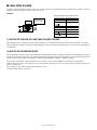
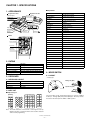
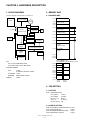
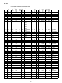
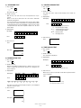
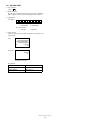
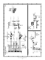
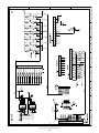
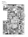
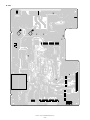
SERVICE MANUAL CODE : 00ZXEA41SUSME LEAD-FREE SOLDER MODEL ELECTRIC CASH REGISTER MODEL XE-A41S SRV KEY : Not necessary PRINTER : PR-45MII CONTENTS ■ LEAD-FREE SOLDER CHAPTER 1. SPECIFICATIONS . . . . . . . . . . . . . . . . . . . . . . . . . . . . 1 CHAPTER 2. OPTIONS . . . . . . . . . . . . . . . . . . . . . . . . . . . . . . . . . . . 4 CHAPTER 3. MASTER RESET AND PROGRAM RESET. . . . . . . . . 4 CHAPTER 4. HARDWARE DESCRIPTION . . . . . . . . . . . . . . . . . . . . 5 CHAPTER 5. DIAGNOSTIC PROGRAM . . . . . . . . . . . . . . . . . . . . . 10 CHAPTER 6. CIRCUIT DIAGRAM AND PWB LAYOUT . . . . . . . . . 15 Parts marked with "!" are important for maintaining the safety of the set. Be sure to replace these parts with specified ones for maintaining the safety and performance of the set. This document has been published to be used for after sales service only. The contents are subject to change without notice. CAUTION RISK OF EXPLOSION IF BATTERY IS REPLACED BY AN INCORRECT TYPE. DISPOSE OF USED BATTERIES ACCORDING TO THE INSTRUCTIONS. AVOID: SHORT-CIRCUITING THE BATTERY TERMINALS. KEEP THE BATTERY AWAY FROM FIRE. * WHEN DISPOSING THE BATTERY, FOLLOW THE LOCAL RULES AND REGULATIONS. “BATTERY DISPOSAL” THIS PRODUCT CONTAINS NICKEL-METAL HYDRIDE BATTERY. THIS BATTERY MUST BE DISPOSED OF PROPERLY. REMOVE THE BATTERY FROM THE PRODUCT AND CONTACT FEDERAL OR STATE ENVIRONMENTAL AGENCIES FOR INFORMATION ON RECYCLING AND DISPOSAL OPTIONS. XE-A41S ■ LEAD-FREE SOLDER The PWB’ s of this model employs lead-free solder. The “LF” marks indicated on the PWB’s and the Service Manual mean “Lead-Free” solder. The alphabet following the LF mark shows the kind of lead-free solder. Example: <Solder composition code of lead-free solder> Lead-Free 5mm Solder composition code (Refer to the table at the right.) a Solder composition Solder composition code Sn-Ag-Cu a Sn-Ag-Bi Sn-Ag-Bi-Cu b Sn-Zn-Bi z Sn-In-Ag-Bi i Sn-Cu-Ni n Sn-Ag-Sb s Bi-Sn-Ag-P Bi-Sn-Ag p (1) NOTE FOR THE USE OF LEAD-FREE SOLDER THREAD When repairing a lead-free solder PWB, use lead-free solder thread. Never use conventional lead solder thread, which may cause a breakdown or an accident. Since the melting point of lead-free solder thread is about 40°C higher than that of conventional lead solder thread, the use of the exclusive-use soldering iron is recommendable. (2) NOTE FOR SOLDERING WORK Since the melting point of lead-free solder is about 220°C, which is about 40°C higher than that of conventional lead solder, and its soldering capacity is inferior to conventional one, it is apt to keep the soldering iron in contact with the PWB for longer time. This may cause land separation or may exceed the heat-resistive temperature of components. Use enough care to separate the soldering iron from the PWB when completion of soldering is confirmed. Since lead-free solder includes a greater quantity of tin, the iron tip may corrode easily. Turn ON/OFF the soldering iron power frequently. If different-kind solder remains on the soldering iron tip, it is melted together with lead-free solder. To avoid this, clean the soldering iron tip after completion of soldering work. If the soldering iron tip is discolored black during soldering work, clean and file the tip with steel wool or a fine filer. XE-A41S LEAD-FREE SOLDER PC-UM10M CHAPTER 1. SPECIFICATIONS ■Key names 1. APPEARANCE Register front view KEY TOP Register rear view Customer display (Pop-up type) Operator display Printer cover Receipt paper Journal window AC power cord Mode switch Keyboard Drawer lock SD memory card slot Drawer USB port DESCRIPTION 2 (RECEIPT) Receipt paper feed key 2 (JOURNAL) Journal paper feed key RA/AMT RCPT/PO Received-on account/Amount key Receipt print/Paid-out key VOID Void key ESC/HELP Escape/Help key %1, %2 Percent 1and 2 key RFND Refund key - Discount key @/FOR Multiplication key n Decimal point key CL Clear key 00, 0-9 Numeric Keys PLU/SUB PLU/Sub-department key DEPT# Department code entry key DEPT SHIFT Department shift key CLK# CONV Clerk code entry/Conversion key Dept1-40 Department keys INQ Inquiry key Tax 1 SHIFT, Tax 2 SHIFT Tax 1 and 2 shift key AUTO Automatic sequence key TAX Tax key CHK Check key CH1, CH2 Charge 1 and 2 keys MDSE SBTL Merchandise subtotal key #/TM SBTL Non-add code/Time display/Subtotal key CA/AT/NS Total/Amount tender/Non Sale key Printer Take-up spool Paper roll cradle Paper chute Print head release lever 2. RATING Model Weight Dimensions Power source Power consumption Working temperature XE-A41S 12.5 kg 420 (W) x 430 (D) x 302 (H) mm AC 120V, 60Hz Stand-by 10.0W, Operating 44.0W (max.) 32 °F to 104 °F (0 °C to 40 °C) 4. MODE SWITCH 4-1. LAYOUT 3. KEYBOARD • Rotary type 3-1. KEYBOARD LAYOUT Manager key (MA) MA OP Normal keyboard STD/MAX 59 19 (W) x 19 (H) mm Fixed type MA Type Key position Key pitch Key layout REG OPX/Z OFF VOID 3-2. KEY LIST X2/Z2 Operator key (OP) OP PGM MGR X1/Z1 ■ Keyboard layout [XE-A41S] RECEIPT JOURNAL @/FOR . CL PLU /SUB DEPT # 25 30 5 RA /AMT %1 7 8 9 RCPT /PO %2 4 5 6 1 2 3 2 00 1 - NUMBER VOID RFND DC ESC /HELP BS SHIFT SPACE 0 A 10 24 4 B C 9 8 G H 7 I 14 J 20 L 13 M 19 N 18 O R 37 17 31 11 Q 38 32 12 P 39 33 26 6 K 40 34 27 21 E 15 28 22 D 35 29 23 3 F DEPT CLK# SHIFT /CONV S 36 16 T INQ AUTO U X TAX1 SHIFT TAX2 SHIFT V Y The mode switch can be operated by inserting one of the two supplied mode keys - manager (MA) and operator (OP) keys. These keys can be inserted or removed only in the “REG” or “OFF” position. TAX CH1 W Z CHK CH2 MDSE #/TM SBTL SBTL CA/AT/NS Note: The small characters on the bottom or lower right in each key indicates functions or characters which can be used for character entries for text programming. XE-A41S SPECIFICATIONS –1– PC-UM10M ■Operator display The mode switch has these settings: OFF: This mode locks all register operations. (AC power turns off.) No change occurs to register data. Function message display area Clerk code or mode name OP X/Z: To take individual clerk X or Z reports, and to take flash reports. It can be used to toggle receipt state “ON” and “OFF” by pressing he [RCP/PO] key. REG: For entering sales. PGM: To program various items. VOID: Enters into the void mode. This mode allows correction after finalizing a transaction. MGR: For manager’s entries. The manager can use this mode for an override entry. Receipt OFF indicator Numeric entry display area Repeat / Sentinel mark / Power save mark • Clerk code or Mode name The mode you are in is displayed. When a clerk is assigned, the clerk code is displayed in the REG or OP X/Z mode. For example, “*01*” is displayed when clerk 01 is assigned. X1/Z1: To take the X/Z report for various daily totals. X2/Z2: To take the X/Z report for periodic (weekly or monthly) consolidation. • Repeat The number of repeats is displayed, starting at “2” and incremental with each repeat. When you have registered ten times, the display will show “0” (2 3 3......9 3 0 3 1 3 2...) 5. DISPLAY • Sentinel mark 5-1. OPERATOR DISPLAY Display device : STN LCD module Number of line : 2 line Number of digits : 16 positions Color of display : Yellow Green / Orange Character form : 5 x 7 dots Character size : 8.0 (H) x 4.8 (W) mm When amount in the drawer reaches the amount you preprogrammed, the sentinel mark “X” is displayed to advise you to remove the money to a safe place. • Power save mark When the cash register goes into the power save mode, the power save mark (decimal point) lights up. • Function message display area Layout: Item labels of departments and PLU/UPCs and function texts you use, such as %1, (-) and CASH are displayed. When an amount is to be entered, ------ is displayed at the numeric entry area with a guidance message “ENTER PRICE”. • Numeric entry display area 5-2. CUSTOMER DISPLAY Display device : LED Number of line : 1 line Number of digits : 7 digits Color of display : Yellow Green Style : Pop up type Character form : 7 segment + Dp Character size : 14.0mm (H) x 8.0mm (W) Numbers entered using numeric keys are displayed here. Date and time display Date and time appear on the display in the OP X/Z, REG, or MGR mode. In the REG or MGR mode, press the [#/TM/SBTL] key to display the date and time. Backlight of the LCD display When an error occurs or the [RFND] or [VOID] key is pressed or enter the void mode, the green backlight will turn red. Error message Layout: When an error occurs, the corresponding error message is displayed in the function message display area. ■Customer display (Pop-up type) XE-A41S SPECIFICATIONS –2– PC-UM10M 6. USB port 7-3. LOGO STAMP [DEVICE] • No USB B Type 7-4. CUTTER [OUTLINE] • Method : Manual This ECR has 1 port. This is used in order to connect with a personal computer. 7-5. PRINTING AREA Receipt & Journal 1 3 4 Number of themal head heater elements 864 dots (688dots) 11.0 2 36 (288dots) 14 (112dots) 36 (288dots) 2.5 12.04 0.125 4.5 4 [SPECIFICATIONS] 44.5 1) Transmission rate : USB 2.0 Full Speed Max 12Mbps 2) Connector : USB B type 3) Pin assign : 1Pin 5V : 2Pin -D : 3Pin +D : 4Pin GND Receipt Journal (units;mm) [DEVICE] SD Card (Version. 1.01) 7-1. PRINTER [OUTLINE] • Part number : PR-45M II • NO. of station : 2 (Receipt and journal) • Validation : No XE-A41S has a SD Memory Card Slot. [SPECIFICATIONS] • Printing system : Line thermal • No. of dot : Receipt 288 dots Journal 288 dots • Dot pitch : Horizontal 0.125mm Vertical 0.125mm • Font : 10 dots (W) u 24 dots (H) Variable clock rate Other commands and memory access Bus Protocol Correspondence capacity Recommended manufacturer : 0-25MHz : 2.7-3.6V : SPI Bus : 256MB-512MB : SanDisk 9. DRAWER • Printing capacity : Receipt max. 24 characters Journal max. 24 characters • Character size : 1.25mm (W) u 3.0mm (H) at 10 u 24 dots [OUTLINE] • Print pitch : Column distance Row distance • Standard equipment: Yes • Print speed : Approximate 50mm/s (13.3 lines/sec) 1.5mm 3.75mm • Max. number of additional drawers: 1 • The drawer consists of: • Paper feed speed : Approximate 40mm/s (Manual feed) 1) 2) 3) 4) : Mechanism MCBF 5 million lines Head life 12.5 million characters (at 4 dots/1 character/1 element) • Paper end sensor : Set up (Receipt and journal) • Cutter 0.5 8. SD MEMORY CARD SLOT 7. PRINTER • Reliability 44.5 0.5 Drawer box (outer case) and drawer Coin case Money case Lock (attached to the drawer) [SPECIFICATION] : Manual 9-1. DRAWER BOX AND DRAWER • Near end sensor : No 7-2. PAPER Model name of the drawer box SJ423 • Paper roll dimension: 44.5 m 0.5mm in width Max. 80mm in diameter Size 420 (W) x 427 (D) x 114 (H) mm color Gray (PB-N8.0) • Paper quality Material Metal : (Journal/Receipt) High-quality paper paper thickness: 0.06 to 0.08mm Nihon seisi thermal paper : TF50KS-E Oji thermal paper : PD150R, PD160R Bell – Release lever Standard equipment: situated at the bottom Drawer open sensor – XE-A41S SPECIFICATIONS –3– PC-UM10M 10.BATTERY 9-2. MONEY CASE Separation from the drawer Disallowed Separation of the bill compartments from the coin compartments Allowed Bill separator – Number of compartments 5B/6C 10-1.MEMORY BACK UP BATTERY Type : Rechargeable battery Number of battery : 1pcs as standard RBRC license 5B/6C 9-3. LOCK (LOCK KEY : LKGIM7331BHZZ) • Location of the lock: Front • Method of locking and unlocking: To lock, insert the drawer lock key into the lock and turn it 90 degrees counter clockwise. To unlock, insert the drawer lock key and turn it 90 degrees clockwise. ck unlo Lo SK1 SK1-1 • Key No: ck CHAPTER 2. OPTIONS 1. OPTIONS (NO) 2. SERVICE OPTIONS NO 1 NAME Spill-proof cover PARTS CODE PRICE RANK XXXXXXXXXXXX XXX PARTS CODE PRICE RANK TPAPR6645RC05 AY DESCRIPTION 3. SUPPLIES NO 1 NAME Thermal roll paper DESCRIPTION 5 ROLLS/PACK 4. SPECIAL SERVICE TOOLS (NO) CHAPTER 3. MASTER RESET AND PROGRAM RESET 2. PROGRAM RESETTING (INITIALIZATION) 1. MASTER RESETTING Master resetting clears the entire memory and resumes initial values. Master resetting can be accomplished by using the following procedure: Procedure A: 1) Unplug the AC cord from the wall outlet. 2) Set the mode switch to the PGM position. 3) While holding down both the JOURNAL FEED key and [CL] key, plug in the AC cord to the wall outlet. This resetting resumes the initial program without clearing memory. This resetting can be operated at below sequence in PGM mode. Procedure: XE-A41S OPTIONS –4– 1) Unplug the AC cord from the wall outlet. 2) Set the mode switch to the PGM position. 3) While holding down both JOURNAL FEED key and RECEIPT FEED key, plug in the AC cord to the wall outlet. PC-UM10M CHAPTER 4. HARDWARE DESCRIPTION 1. BLOCK DIAGRAM 2. MEMORY MAP The block diagram of the XE-A41S is shown below. 2-1. ADDRESS MAP FRONT DISPLAY (2line LCD backlight) POWER 00000h SFR BUZZER 00400h Internal RAM 12KByte (00400h-033FFh) 033FFh 03400h RESET IC 16 MHz CPU USB ONTROLLER M66291GP Renesus 32.768kHz USB B Port M30623MEP-A93GP DECODER /CS3 16K 08000h External RAM 124KByte/512KByte /CS2 124K 27000h 4Mbit Flash ROM SD CARD 4Mbit SRAM 04000h Front Display POPUP Display POPUP DISPLAY (LED 7SEG) 28000h USB Controller /CS1 32K 30000h /CS0 832K 40000h External RAM 512KByte (256KByte x 2Bank) PRINTER DRIVER/ SENSOR KEY IF/POPUPDISPLAYIF 80000h External ROM 512KByte PRINTER KEY PR-45M MODE SW C0000h D0000h DRAWER IF FFFFFh External RAM/CS2 area: When RAMBANK=0, 48000h-66FFFh is shadow CPU 40000h Renesus-make M30623MEP-A93GP (Internal RAM 12KB, internal ROM 192KB) 48000h /CS2 area 50000h EXTERNAL MEMORY RAM FLASH ROM SPANSION PRINTER 512KB CYPRESS CY62148ELL-45ZSXIT 512KB MBM29F400TC-70PFTN 60000h 66FFFh 67000h PR45M 7FFFFh 80000h RAMBANK=0 RAMBANK=1 00000h~ 40000h~ 3FFFFh 7FFFFFh 70000h 3. CPU SETTING 3-1. OUTLINE Model : M30623MEP-A93GP Internal RAM : 12 KByte Internal ROM : 192 KByte Operation clock : 16 MHz Sub clock : 32.768 KHz External data bus : 8 bit 3-2. WEIGHT SETTING CS0# (FLASH ROM and EXTERNAL SRAM) CS1# (USB CONTROLLER) CS2# (EXTERNAL SRAM IMAGE SPACE) CS3# (FRONT/POPUP DISPLAY) XE-A41S HARDWARE DESCRIPTION –5– 3 BCLK 3 BCLK 3 BCLK 2 BCLK PC-UM10M 4. I/O M16C/24 PORT MEMORY SPACE: NORMAL MODE PROCESSOR MODE: MICRO PROCESSOR MODE It is used by (SEPARATE BUS 8bit Width) PORT PIN No. I/O Pin name Signal name Initial value OFF MODE Function PORT PIN No. I/O Pin name Signal name Initial value OFF MODE Function P00 88 I/O D0 Out L P54 42 O /HLDA (NU) P01 87 I/O D1 D1 Out L P55 41 I /HOLD /HOLD In P02 86 I/O D2 D2 Out L P56 40 O ALE (NU) Out L P03 85 I/O D3 D3 Out L P57 39 I /RDY /RDY P04 84 I/O D4 D4 Out L P60 38 O P60 DR1 P05 83 I/O D5 D5 Out L P61 37 O CLK0 FSCK(NU) L Out L FMC FSCK P06 82 I/O D6 D6 Out L P62 36 I RXD0 FRD(NU) L Out L FMC FRD P07 81 I/O D7 D7 P63 35 O TXD0 FSD (NU) L Out L FMC FSD P10 80 O P10 RAS L Out L RECEIPT PAPER FEED A P64 34 O /RTS1 /RS H Out L RS-232 /RS P11 79 O P11 RBS L Out L RECEIPT PAPER FEED B P65 33 O P65 /FRES(NU) L Out L FMC /FRES P12 78 O P12 RCS L Out L RECEIPT PAPER FEED C P66 32 I RXD1 RD In RS-232 RD P13 77 O P13 RDS L Out L RECEIPT PAPER FEED D P67 31 O TXD1 SD H Out L RS-232 SD P14 76 O P14 JAS L Out L JOURNAL PAPER FEED A P70 30 O TXD2 SO L Out L PRINTER DATA OUT P15 75 O P15 JBS L Out L JOURNAL PAPER FEED B P71 29 I RXD2 SI P16 74 O P16 JCS L Out L JOURNAL PAPER FEED C P72 28 O CLK2 PCLK P17 73 O P17 JDS L Out L JOURNAL PAPER FEED D P73 27 O P73 P20 72 O A0 A0 Out L P74 26 O P21 71 O A1 A1 Out L P75 25 I P22 70 O A2 A2 Out L P76 24 P23 69 O A3 A3 Out L P77 23 P24 68 O A4 A4 Out L P80 22 P25 67 O A5 A5 Out L P81 21 Out L Out L In L Out L DRAWER 1 DRIVE SIGNAL In PRINTER DATA IN L Out L PRINTER CLOCK DR2 L Out L DRAWER 2 DRIVE SIGNAL P74 /ER H Out L RS-232 /ER P75 /CD In RS-232 /CD I P76 /CS In RS-232 /CS I P77 /DR In RS-232 /DR O P80 BUZZER L Out L O P81 VHCOM L In PRINTER HEAD CONTROL P26 66 O A6 A6 Out L P82 20 I /INT0 POFF P27 65 O A7 A7 Out L P83 19 I /INT1 /FRDY(NU) L Out L In FMC /FRDY P30 63 O A8 A8 Out L P84 18 O P84 /BUSY(NU) L Out L FMC #BUSY P31 61 O A9 A9 Out L P85 17 I /NMI /NMI(NU) P32 60 O A10 A10 Out L P86 11 O XCOUT XCOUT P33 59 O A11 A11 Out L P87 10 I XCIN XCIN P34 58 O A12 A12 Out L P90 7 I P90 MODE In MODE KEY SENSE P35 57 O A13 A13 Out L P91 6 I P91 MSENS In MISCELLANEOUS SENSE P36 56 O A14 A14 Out L P92 5 O P92 BA1 L Out L BANK signal 1 P37 55 O A15 A15 Out L P93 4 O P93 BA0 L Out L BANK signal 0 P40 54 O A16 A16 Out L P94 3 O P94 DATA /CE L Out L LCD DATA LATCH signal P41 53 O A17 A17 Out L P95 2 O P95 BLON L Out L BACK LIGHT ON P42 52 O A18 A18 Out L P96 1 O P96 LCDON L Out L P43 51 O A19 A19 Out L P97 100 I P97 IPLON In IPL ON signal P44 50 O /CS0 /CS0 Out H P100 97 I AN0 TM In HEAD temperature monitor P45 49 O /CS1 /CS1 Out L P101 95 I AN1 VPTEST In HEAD voltage monitor P46 48 O /CS2 /CS2 Out H P102 94 I AN2 VREF In Reference voltage P47 47 O /CS3 /CS3 Out L P103 93 O AN3 /STRB1 H In PRINTER STORE SIGNAL 1 P50 46 O /WR /WR Out L P104 92 O AN4 /STRB2 H In PRINTER STORE SIGNAL 2 P51 45 O /BHE (NU) Out L P105 91 O P105 /STRB3 H In PRINTER STORE SIGNAL 3 P52 44 O /RD /RD Out L P106 90 O P106 /STRB4 H In PRINTER STORE SIGNAL 4 P53 43 O BCLK BCLK Out L P107 89 O P107 LATCH L In PRINTER LATCH SIGNAL XE-A41S HARDWARE DESCRIPTION –6– In 32.768kHz 32.768kHz LCD POWER ON PC-UM10M Power supply/CONTROL pins PORT PIN No. I/O Pin name BYTE 8 I BYTE Connected to VCC Connected to GND Function PORT PIN No. Vcc 62 Vss 64 Vss Connected to GND AVss 96 AVss Connected to GND I/O Pin name Vcc Function Connected to VCC CNVss 9 I CNVss /RESET 12 I /RESET Xout 13 O Xout OPEN Vref 98 Vref Connected to VCC Vss 14 Vss Connected to GND AVcc 99 AVcc Connected to VCC Xin 15 Vcc 16 I Xin Connected to Spectram diffusion IC Vcc Connected to VCC 5. DISPLAY 6. KEY SCAN 5-1. FRONT DISPLAY 6-1. STROBE SIGNAL The 16 strobe signals common with the display digit signal are used. The LCD display of 5 x 7dot, 2 lines, and 16 digits with the parallel IF specifications using SPLC780C. 6-2. RETURN SIGNAL LCD-related Register Function Address With the 10 return signal of the CPU port, the key status and the mode key status are detected. R/W LCD Write Data 04001h (CS3 space) W LCD Read Data 04001h (CS3 space) R LCD Control Signal Pin No. CPU PORT Signal name 46 P137 LCDE 122 P105 LCDON H : LCD ON L : LCD OFF 121 P106 LCDRW H : Data read L : Data Write 120 P107 LCDRS H : Data input L : Instruction Input 48 P135 BLON0 LCD Backlight Orange ON signal 47 P136 BLON1 LCD Backlight Yellow Green ON signal 32 P73 LCDCS# Remark Enable Signal Enable L : LCD write data latch 5-2. REAR (POPUP) DISPLAY Signal name CPU PORT KR0 P90 Key Return signal 0 Remark KR1 P91 Key Return signal 1 KR2 P92 Key Return signal 2 KR3 P93 Key Return signal 3 KR4 P94 Key Return signal 4 KR5 P95 Key Return signal 5 KR6 P96 Key Return signal 6 KR7 P97 Key Return signal 7 MODR P124 Mode key position read signal RJR P134 Receipt/Journal key read signal 7. PRINTER CONTROL The rear display is of 7-digit, 7-segment LED. 7-1. STEPPING MOTOR CONTROL Display digit signal The four signals KS0~KS3 are assigned to the CPU port, and decoded The stepping motor is driven by the STA471A made by Sanken at a constant voltage. 1step : 0.125mm, 1dot : 1step Print speed 50mm/s to the strobe signals of 16 lines externally. Function POPUP DISPLAY DIGIT signal and KEY STROBE signal Signal name CPU PORT KS0 P120 KS1 P121 Remark <CPU PORT> KS3 is decoded as MSB outside the CPU to be S0~S15. KS3 is used as the MSB. KS3~KS0 are decoded to be /S0~/S15. (KS3~KS0 are active at “H”) PIN No. CPU PORT Use signal 80 P10 RAS 79 P11 RBS 78 P12 RCS 77 P13 RDS By writing the segment data to the /CS3 space, the LED segment signal 76 P14 JAS can be outputted. 75 P15 JBS R/W 74 P16 JCS W 73 P17 JDS KS2 P122 KS3 P123 Display SEGMENT signal Function Address POPUP DISPLAY Data 04000h (CS3 space) Each bit correspondence Address Bit7 Bit6 Bit5 Bit4 Bit3 Bit2 Bir1 Bit0 04000h dp g f e d c b a XE-A41S HARDWARE DESCRIPTION –7– PC-UM10M <Drive STEP> 8-3. PRITER HEAD VOLTAGE MONITOR RECEIPT MOTOR The voltage supplied by the printer head power and passed through the printer and divided by the resistor is inputted to the AN2 pin. The printable voltage range for the printer is 15V~26.4V (282~497 in A/ D conversion value). Driver IC input (CPU output) Motor drive signal STEP RAS RBS RCS RDS /RPFA /RPFB /RPFC 1 H L L H L H H /RPFD L 2 L H L H H L H L 3 L H H L H L L H 4 H L H L L H L H 9. DRAWER CONTROL The drawer port (1CH) is provided. Drawer solenoid drive time : 45ms (min) - 50ms (max) JOURNAL MOTOR Driver IC input (CPU output) Motor drive signal STEP JAS JBS JCS JDS /JPFA /JPFB /JPFC /JPFD Function Signal name CPU PORT Remark 1 L H H L H L L H DRAWER drive signal DRAWER P141 Drawer drive at H 2 L H L H H L H L 3 H L L H L H H L 4 H L H L L H L H 10. BUZZER CONTROL The piezo-type buzzer is used. The oscillation frequency is 4.00kHz m 0.25kHz. 7-2. HEAD CONTROL HEAD : All 832 dots Printable area (Receipt side) 384 dots (Journal side) 384 dots Function Signal name CPU PORT BUZZER drive signal BUZZER P80 Remark Buzzer drive at H <CPU PORT> PIN No. CPU PORT Use signal 30 P70 SO Printer DATA signal Remark 29 P61 SI Not used 28 P72 PCLK Printer Clock signal 93 P114 /STB1 Strobe signal 1 92 P115 /STB2 Strobe signal 2 91 P116 /STB3 Strobe signal 3 90 P117 /STB4 Strobe signal 4 89 P110 LATCH Printer DATA Latch 21 P71 VHCOM Printer power control signal 11. USB I/F The Renesus-make USB general-use ASSP device, M66291, is used to perform USB data send/receive. The M66291 is mapped to the /CS1 space (28000H~2FFFFFH). M66291 5V M16C/62 Vcc IOVcc A0 A1 A6 8 8. A/D CONVERSION The following three signals are inputted to the A/D conversion port. A/D conversion is made in 9 bits. CPU PORT Use signal 128 AN0 VREF 126 AN1 HTEMP 125 AN2 VPTEST1 INT2 INT0 INT1 Dreq0 27 D+ 2 4 DGND 1.0µF USB CONNECTOR Xout <CPU PORT> No. CPU PORT Use signal Purpose 24 P83 (INT1) /DREQUSB USB DMA channel 0 DMA request signal 23 P84 (INT2) /INTUSB USB interruption 0 request signal 26 P81 /REUSB USB controller reset signal The voltage divided by the thermistor for detecting the printer head temperature and the resistor is inputted to the AN1 pin. Operation Less than -10°C 464~511 MOTOR LOCK -10°C ~ 0°C 435~464 Print in the conduction time at 0°C. 0°C ~ 70°C 116~434 Print in the conduction time specified on the PR-45M specifications. 0~115 Vbus 3 27 PRINTER HEAD temperature PRINTER HEAD voltage 8-2. PRINTER HEAD TEMPERATURE 70°C or above D- 1 24MHz The reference voltage (2.495V m 0.085V) generated by KIA431F is inputted to the AN2 pin. A/D conversion value (DEC) D+ Function Reference voltage 8-1. REFERENCE VOLTAGE HEAD temperature 1.5k CS1 RD LWR HWR/BYTE Xin PIN No. TrON D0 D7 CS1 RD WRL WRH <CPU PORT> Vbus D15/AD0 AD1 AD6 7 D0 D7 3.3V CoreVcc MOTOR LOCK XE-A41S HARDWARE DESCRIPTION –8– PC-UM10M 12. SD Card I/F One port for SD card I/F is provided as a standard provision. It is connected with UART1 of the CPU. Communication with the SD card is made in the SPI mode. <CPU PORT> Pin No. CPU PORT Use signal Purpose 31 P74 SD_WP# SD card write protect detection signal 116 P113 SD_CD# SD card insertion detection signal 118 P111 SD_CS# SD Card Chip Select signal 117 P112 SD_POWER# 36 P67 SD_TXD TxD signal 38 P66 SD_RXD RxD signal 40 P65 SD_CLK Serial CLK signal SD Card Power On signal 13. RESET The RESET signal is canceled when the voltage of the device which uses the 5V series (VCC, VDD, VLED) power reaches the operating voltage level. The RESET signal is generated under the following conditions. • The mode key switch is shifted from SRV’ to another position (except for OFF). • The power is turned ON after sec or more from power OFF and VCC reaches 5V. • The mode key switch is shifted from OFF to another position (except for SRV’) and VCC reaches 5V. (When the OFF time is 5sec or less, the RESET signal may not be generated.) 14. POFF The POFF signal is changed from 0 to 1 when the 5V series power and the 24V series power reach the operating voltage level. When it falls below the operating voltage level, it is changed from 1 to 0. POFF, RESET timing chart 4.5V 5V 24V 20.8V RESET POFF POWER ON INSTANTANEOUS STOP MODE EXCEPT MODE SRV' SRV' POWER OFF * When both the RESET signal and the POFF signal are high, all the functions are enabled. XE-A41S HARDWARE DESCRIPTION –9– PC-UM10M CHAPTER 5. DIAGNOSTIC DESCRIPTIONS 1. LIST OF TEST ITEMS AND CODES Codes Test items 1) 100 Display buzzer test 2) 102 Printer print test 3) 104 Keyboard test 4) 105 Mode switch test 5) 106 Printer sensor test 6) 107 Time display test 7) 110 Drawer open test 8) 116 LCD display test 9) 118 LCD backlight test 10) 120 External RAM test 11) 121 Internal RAM test 12) 130 External ROM test 13) 160 AD conversion port test 14) 520 USB communication test 15) 550 Sleep mode test 16) 620 SD card test 3. DESCRIPTIONS OF EACH DIAG 1) DISPLAY BUZZER TEST 1 Key operation 100 3 PO 2 Details of the test The decimal point of the LED and the cursor of the LCD are shifted from the lowest digit upward one by one. (Every 200msec) After that, all segments are lighted. (About 1sec) 3 Display/Print OP display PGM D I S P BUZZER 0 1 2 3 4 5 6 7 8 9ABCDEF Rear 4. 5. 6. 7. 8. 9. 0. 4 End of the test Press any key to terminate the test, and the following print is made. 100 2. DIAG BOOTING 2) PRINTER PRINT TEST Mode SW : PRG mode 1 Key operation Key operation : “Above code” + “PO” key 102 3 PO 2 Details of the test The following print pattern is printed. For the receipt side, the logo mark is also printed and a receipt is issued. 3 Display/Print OP display Print content R / J P R I N T E R PGM Patten enlargement * As shown above, 5 lines of 30 digits are printed. 4 End of the test After completion of printing, the test is automatically terminated. XE-A41S Diagnostic Descriptions – 10 – PC-UM10M 3) KEYBOARD TEST 5) PRINTER SENSOR TEST 1 Key operation 1 Key operation _ _ _ _104 3 PO 2 KEY sum check code 106 3 PO 2 Details of the test The paper end sensor status and the head-up sensor status are checked. 2 Details of the test With the key code sum check code, the keyboard check is performed. When no sum code is entered, the sum code check is made with default key arrangement. The sum check data of each model are entered on the upper 4 digits of the diag code, and the entered data are compared with the data accumulated until the last key (CA/AT/NS) is pressed. If those data correspond with each other, the end print is made. If not, the error print is made. 3 Display/Print OP display R / J 1 0 6 Rear KEY 1 0 4 X:1 0 Y:1 0 Z:1 0 Rear PGM *** BOARD *** Z Z 3 Display/Print. OP display SENSOR − − − − − − X PGM X Y Y Receipt side paper presence Receipt side paper empty Journal side paper presence Journal side paper empty Normal position Head-up position 4 End of the test * * * = KEY CODE Print 106 4 End of the test Print 104 6) TIME DISPLAY TEST 1 Key operation Error print KEY SUM ERROR 107 3 PO XXXX-YYYY 2 Details of the test 104 The current time is displayed. 3 Display/Print 4) MODE SWITCH TEST 1 Key operation OP display C H E C K PGM h h mm s s T I ME R 105 3 PO 2 Details of the test Rear Shift the mode SW from “PGM” position to “X2/Z2” one by one, and return to “PGM” and check that the positions are changed in the proper sequence. OP display MODE 1 0 5 * hh = hour‚ mm = minute‚ ss = sec When any key is pressed, the date and the time are printed and the test is terminated. PGM SW X Print Rear MODE: PGM VOID OFF OP X/Z REG MGR X1/Z1 X2/Z2 PGM : 1 2 9 3 4 5 6 7 * yy = year, MM = month, dd = day, hh = hour, mm = minute, ss = sec 1 The above “X” must be read in the proper sequence. (“9” is displayed when the contact is open.) 4 End of the test Error print yyMMdd - hhmmss 107 X Print mm 4 End of the test 3 Display/Print X h h 105 MODE KEY ERROR 105 XE-A41S Diagnostic Descriptions – 11 – PC-UM10M 7) DRAWER OPEN TEST 10) EXTERNAL RAM TEST 1 Key operation 1 Key operation 110 3 PO 120 3 PO 2 Details of the test The drawer is opened. 2 Details of the test The external SRAM (08000H~27FFFH area and 40000H~7FFFFH) of 512Kbyte (standard provision) is checked. The RA test is performed in the following procedures. 3 Display/Print OP display DRAWER PGM (1) Bus/decoder check 4 End of the test After opening the drawer, the end print is made and the test is automatically terminated. (2) Device check a) Test area data save b) Write "00H" Print 110 c) Rear comparison after "00H", write "55H" d) Rear comparison after "55H", write "AAH" e) Read comparison "AAH" 8) LCD DISPLAY TEST f) Save data restore 1 Key operation 3 Display/Print 116 3 PO OP display 2 Details of the test The display CG is checked. Check procedures: The built-in 256 CG’s are divided into 16 blocks, and each block of 16 characters is displayed on the dot-display for check. Check is started with CG code of 00H ~ 0FH. When any key is pressed, the following block is displayed sequentially. Print Error print 4 End of the test When any key is pressed, the test is terminated and the following print is made. RAM ERROR x *****h XX-YY 120 * x = 1 : Data error, x = 2 : Address error * XX-YY : XX is the anticipated data. YY is the read data. * In case of an error, the error address is printed on "*****" after the abnormal end print. 116 11) CPU INTERNAL RAM TEST 9) LCD BACKLIGHT TEST 1 Key operation 1 Key operation 121 3 PO 118 3 PO 2 Details of the test The backlight ON/OFF test is performed. First, the yellow and the green backlights are lighted. When any key is pressed, the orange backlight is lighted. When any key is pressed again, the backlight is turned off. 2 Details of the test The RAM (12Kbyte) in the CPU is checked. The RAM test is performed in the following procedure. Device check a) Test area data save 3 Display/Print OP display 120 PGM X Y oooooooooooooooo * X and Y: The head code of each block is displayed in hexadecimal number. Print PGM 4 End of the test After completion of the test, the end print is made and the test is automatically terminated. 3 Display/Print OP display RAM 1 2 0 b) Write "00H" BA C KL I GHT PGM c) Rear comparison after "00H", write "55H" d) Rear comparison after "55H", write "AAH" 4 End of the test e) Read comparison "AAH" When any key is pressed after turning OFF the backlight, the test is terminated and the following print is made. Print 118 f) Save data restore 3 Display/Print OP display XE-A41S Diagnostic Descriptions – 12 – RAM 1 2 1 PGM PC-UM10M 4 End of the test After completion of the test, the end print is made and the test is automatically terminated. Print 4 End of the test When any key is pressed with VPTEST displayed, the end print is made and the test is automatically terminated. 121 Error print Print *** HEAD TEMP HEAD VOLTAGE *** 160 RAM ERROR x *****h 14) USB COMMUNICATION TEST XX-YY 1 Key operation 121 * x = 1 : Data error, x = 2 : Address error * XX-YY : XX is the anticipated data. YY is the read data. * In case of an error, the error address is printed on "*****" after the abnormal end print. 520 3 PO 2 Details of the test The USB revision, the vendor ID, the product ID, and the device address assigned by the host are printed. 3 Display/Print 12) EXTERNAL ROM TEST OP display 1 Key operation 130 3 PO 2 Details of the test The check sum of the external Flash ROM is checked, and the ROM version is printed. Print 3 Display/Print OP display F L A SH 1 3 0 ROM ROM ******** ******** ROM ERROR x *****h ******** ROM ******** 1 Key operation 550 3 PO Model name Version 2 Details of the test After execution of the diag, the machine enters the sleep mode. 3 Display/Print Model name Version OP display . Rear . 4 End of the test When any key is pressed, the machine restores from the sleep mode. The following print is made and the diag is terminated. 13) AD CONVERSION PORT TEST 1 Key operation End print 160 3 PO 2 Details of the test The AD conversion port voltage is displayed. TM (printer thermal head temperature) is displayed. When any key is pressed, VPTES (printer voltage) is displayed in 9 bits. 3 Display/Print T E S T TM = PGM XXX VP = PGM XXX Press any key. A / D When the host is connected : 1~127 When the host is not connected : 0 15) SLEEP MODE TEST 140 A / D XXX XXX XXX XXX P GM 4 End of the test After completion of printing, the test is terminated. * x = 1 : Data error, x = 2 : Address error * In case of an error, the error address is printed on "*****" after the abnormal end print. OP display USB Rev. Ver. VENDOR ID PRODUCT ID DEVICE ADDRESS 520 140 Error print TE S T 1 PGM 4 End of the test After completion of the test, the end print is made and the test is automatically terminated. Print USB 5 2 0 T E S T XE-A41S Diagnostic Descriptions – 13 – 550 PC-UM10M 16) SD CARD TEST 1 Key operation 620 3 PO 2 Details of the test The SD card is detected and the write protect status is displayed. After completion of the test, the SD card register value is printed. 3 Display/Print OP display SD TEST 1 6 2 0 PGM X -Y * X = SD card detection SD card YES 0 : SD card NO * Y = WP detection WP state 0 : WP NO 4 End of the test When any key is pressed, the SD card register is read and the end print is made. Print Error print CID XXXXXXXXXXXXXXXX-XXXXXXXXXXXXXXXXh CSD XXXXXXXXXXXXXXXX-XXXXXXXXXXXXXXXXh OCR 12345678h 620 SD TEST ERROR ****** 620 * "******" = Error print Error print list Error print Error content CARD NO DETECT SD Card not detected READ ERROR SD read error XE-A41S Diagnostic Descriptions – 14 – A B C 2 VCC 2 1 VDD R94 8 3.3K 330pF C15 1 X3 CSTLS16M 3 3 D7 D6 D5 D4 D3 D2 D1 D0 1 2 3 4 1uF C3 R112 330 VCC RESET# VCC D[0..7] KIA7045AF IC2 0.1uF C98 LATCH# STRB4# STRB3# STRB2# STRB1# D[0..7] VCC EFCB322513TS RDS RCS RBS RAS JDS JCS JBS JAS 0.1uF 0.1uF FB2 C20 FB1 AVCC EFCB322513TS C18 VDD R84 1K 8 7 6 5 VCC NOT MOUNT FS781 XIN XOUT S1 LF IC3 1SS355 D1 470 4 3 2 1 R75 10K 7 33 R95 0.1uF C13 C16 91pF 10uF/10V,OS C14 + VCC CPURESET# KR[0..7] CPURESET# AVCC 0.1uF C4 VDD VDD Q1 2SC1815 12K R67 LCDRS LCDRW 5 6 7 8 103 104 105 106 107 108 109 110 111 112 113 114 115 116 117 118 LATCH# 119 LCDRS 120 LCDRW 121 122 MODEL2 123 MODEL1 124 VPTEST 125 VPTEST HTEMP 126 HTEMP 127 VREF 128 VREF RP12 33 4 3 2 1 5 6 7 8 RP11 33 RDS1 RCS1 RBS1 RAS1 RP14 2.2K 8 7 6 5 1 2 3 4 10K RP1 JDS1 JCS1 JBS1 JAS1 A7 A6 A5 A4 A3 A2 A1 A0 1 2 3 4 SDCD# SDPOWER# SDCS# LCDON VDD S0 FSOUT VSS R19 10K R113 RP9 10K 10K RP2 RDS RCS RBS RAS JDS JCS JBS JAS A[0..7] RP13 2.2K 8 7 6 5 A[0..7] 4 3 2 1 RP3 10K DR KR[0..7] 6 P1_0/D8 P0_7/AN0_7/D7 P0_6/AN0_6/D6 P0_5/AN0_5/D5 P0_4/AN0_4/D4 P0_3/AN0_3/D3 P0_2/AN0_2/D2 P0_1/AN0_1/D1 P0_0/AN0_0/D0 P11_7 P11_6 P11_5 P11_4 P11_3 P11_2 P11_1 P11_0 P10_7/AN7/K13# P10_6/AN6/K12# P10_5/AN5/K11# P10_4/AN4/K10# P10_3/AN3 P10_2/AN2 P10_1/AN1 AVSS P10_0/AN0 IC1 5 6 7 8 CPU 4 3 2 1 5 6 7 8 5 6 7 8 4 3 2 1 2 1 5 6 7 8 RP4 10K 0.1uF C1 10uF/10V,OS C2 + VDD 2 VCC RP5 10K 4 3 2 1 5 6 7 8 VCC 6 7 8 VCC M30623MEP-A93GP KR7 KR6 KR5 KR4 KR3 KR2 KR1 KR0 10K R16 DR 18pF C6 X1 2 32.768KHz 1 100K NOT MOUNT R89 330 5 27pF C7 0 R86 R70 1 D 5 3 4 3 2 1 1 2 3 4 8 7 6 5 1 CHAPTER 6. CIRCUIT DIAGRAM AND PWB LAYOUT 6 2 RP6 10K 10K R20 VCC 16MHz X2 10K R17 100pF C5 POFF# KS0 KS1 KS2 KS3 MODR BUZZER USBRESET 4 DREQUSB# INTUSB# POFF# PDATOUT VHCOM PCLK LCDCS# SDWP# HUS# RPES# JPES# SDRXD P12_5 P12_6 P12_7 P5_0/WRL#/WR# P5_1/WRH#/BHE# P5_2/RD# P5_3/BCLK P13_0 P13_1 P13_2 P13_3 P5_4/HLDA# P5_5/HOLD# P5_6//ALE P5_7/RDY#/CLKOUT P13_4 P13_5 P13_6 P13_7 P6_0/CTS0#/RTS0# P6_1/CLK0 P6_2/RXD0/SCL0 P6_3/TXD0/SDA0 P6_4/CTS1#/RTS1# P6_5/CLK1 VSS KS0 KS1 KS2 KS3 MODR 4 33pF C12 64 63 62 61 60 59 58 57 56 55 54 53 52 51 50 49 48 47 46 45 44 43 42 41 40 39 VCC 4 3 2 1 NOT MOUNT 10K R35 3 R71 PDATOUT VHCOM PCLK LCDCS# SDWP# PHUPS RPES# JPES# DREQUSB# INTUSB# NOT MOUNT 33pF C11 10K 10K 0 47K R119 10K RJR BLON0 BLON1 LCDE RTS# PDATIN KR8 KR9 KR10 KR11 RD# C10 10K R15 VCC 10K 10K 0 0 0 USBRESET# 2 1K R85 NOT MOUNT R63 R65 R69 10K 47K R189 VCC 10K 10K R18 VDD VCC R33 R34 RXD TXD 10K SDCLK SDRXD SDTXD 10K R28 VDD 2 R32 CNVSS R68 47K VCC KBR8 KBR9 KBR10 KBR11 FRDY ROMBANK RAMBANK R31 VCC A[8..19] R30 A[8..19] R60 R61 R62 R64 NOT MOUNT 0 0 0 0 A8 A9 A10 A11 A12 A13 A14 A15 A16 A17 A18 A19 1000pF FRDY ROMBANK RAMBANK WR# 10K R29 VCC RP8 10K 3 VCC 10K R26 R74 10K R27 NOT MOUNT R91 R92 VCC VCC VDD RP7 10K RJR BLON0 BLON1 LCDE RTS# PDATIN RXD TXD CTS TP1 5 6 7 8 4 3 2 1 5 102 101 100 99 98 97 96 95 94 93 92 91 90 89 88 87 86 85 84 83 82 81 80 79 78 77 76 75 74 73 72 71 70 69 68 67 66 65 P1_1/D9 P1_2/D10 P1_3/D11 P1_4/D12 P1_5/D13/INT3# P1_6/D14/INT4# P1_7/D15/INT5# P2_0/AN2_0/A0(/D0/-) P2_1/AN2_1/A1(D1/D0) P2_2/AN2_2/A2(D2/D1) P2_3/AN2_3/A3(D3/D2) P2_4/AN2_4/A4(D4/D3) P2_5/AN2_5/A5(D5/D4) P2_6/AN2_6/A6(D6/D5) P2_7/AN2_7/A7(D7/D6) VSS P3_0/A8(/-/D7) VCC2 P12_0 P12_1 P12_2 P12_3 P12_4 A3_1/A9 A3_2/A10 A3_3/A11 A3_4/A12 A3_5/A13 A3_6/A14 A3_7/A15 P4_0/A16 P4_1/A17 P4_2/A18 P4_3/A19 P4_4/CS0# P4_5/CS1# P4_6/CS2# P4_7/CS3# VREF AVCC P9_7/ADTRG#/SIN4 P9_6/ANEX1/SOUT4 P9_5/ANEX0/CLK4 P9_4/DA1/TB4IN P9_3/DA0/TB3IN P9_2/TB2IN/SOUT3 P9_1/TB1IN/SIN3 P9_0/TB0IN/CLK3 P14_1 P14_0 BYTE CNVSS P8_7/XCIN P8_6/XCOUT RESET# XOUT VSS XIN VCC1 P8_5/NMI# P8_4/INT2#/ZP P8_3/INT1# P8_2/INT0# P8_1/TA4IN//U P8_0/TA4OUT/U P7_7/TA3IN P7_6/TA3OUT P7_5/TA2IN//W P7_4/TA2OUT/W P7_3/CTS2#/RTS2#/TA1IN//V P7_2/CLK2/TA1OUT/V P7_1/RXD2/SCL2/TA0IN/TB5IN P7_0/TXD2/SDA2/TA0OUT P6_7/TXD1/SDA1 VCC1 P6_6/RXD1 1 2 3 4 5 6 7 8 9 10 11 12 13 14 15 16 17 18 19 20 21 22 23 24 25 26 27 28 29 30 31 32 33 34 35 36 37 38 4 3 2 1 5 6 7 8 7 1 2 2 – 15 – 1 XE-A41S CIRCUIT DIAGRAM AND PWB LAYOUT SP2 1SS355 D2 3 R66 47K VDD 1 CS0# CS1# CS2# CS3# WR# RD# 10K R24 R93 B + BZ1 1 RXDPRG TXDPRG VCC SHORT PIN & SOCKET CTS# NOT MOUNT NOT MOUNT 5 4 3 2 1 CN1 TEST PIN 10K R25 R90 10K VCC 1/5 10K 1 SP1 SHORT PIN & SOCKET 1 3 PIEZO BZ CS0# CS1# CS2# CS3# MODEL2 MODEL1 MODEL XE-A41S NONE R24 USE R25 NONE R90 USE R93 2 2 8 A B C D PC-UM10M A B C CS3# CNVSS 8 2 1 2 3 4 5 6 7 8 9 10 5 4 VCC 2 1 IC23A VCC Q7 D7 D6 Q6 Q5 D5 D4 Q4 CP R14 10K SN74LV32A 6 RESET# 20 19 18 17 16 15 14 13 12 11 5 4 VDD VDD IC23B WR# 6 3 7 dp D7 D6 g f D5 D4 e 2 WR# 1 2 1 IC25A VDD 3 VCC SN74LV32A 0.1uF VDD IC23D SN74LV08A 13 12 3 CS0# SN74LV32A NOT MOUNT D7 D6 D5 D4 D3 D2 D1 D0 C25 VCC IC26A VCC CS2# RAMBANK D[0..7] 0 0 0 R97 R98 R73 0 R72 SN74LV08A D[0..7] RAMA18 A17 SN74LV08A POFF# 74HCT273 MR# Q0 D0 D1 Q1 Q2 D2 D3 Q3 GND IC6 2 74LV04A IC24A A18 IC26B 1SS355 D4 1SS355 1 2 D3 1 CS3# A0 a D0 D1 b c D2 D3 d R12 10K VCC ROMBANK 1 VCC A19 A18 A17 A16 A15 A14 A13 A12 A11 A10 A9 A8 A7 A6 A5 A4 A3 A2 A1 A0 CNVSS A[0..19] 6 C8 100pF R11 10K 11 C97 0.1uF A17 A16 A14 A12 A7 A6 A5 A4 A3 A2 A1 A0 I/O0 I/O1 I/O2 GND IC4 0.1uF C26 VCC A15 A18 /WE A13 A8 A9 A11 /OE A10 /CE I/O7 I/O6 I/O5 I/O4 I/O3 32 31 30 29 28 27 26 25 24 23 22 21 20 19 18 17 IC25B VCC RJR MODR CS2# 6 KR[0..7] 5 5 8 WR# A13 A8 A9 A11 RD# A10 RAMCS# D7 D6 D5 D4 D3 A15 R124 0 R109 KR7 R107 R108 KR5 KR6 R106 R105 KR3 0 0 0 0 0 0 0 R103 0 R104 KR4 4 4 R125 KR2 R102 9 KR1 KR0 74LV04A 8 RD# WR# VCC IC24D 0.1uF C22 SN74LV08A VDD KR[0..7] 11 VCC VCC IC24E 74LV04A 10 9 10 IC24C 74LV04A CS2# 6 IC23C VDD VDD SRAM 4M CY62148ELL-45ZSXI TSOPII 1 2 3 4 5 6 7 8 9 10 11 12 13 14 15 16 SN74LV32A 5 4 RAMA18 ROMA18 CS0# A19 0.1uF C21 VDD A16 A14 A12 A7 A6 A5 A4 A3 A2 A1 A0 D0 D1 D2 + VDD 10uF/50V C17 7 D A[0..19] 14 7 14 7 14 7 14 7 5 7 MEMORY & KIF 14 7 14 7 14 7 14 7 1 2 14 14 14 7 KBR7 KBR6 KBR5 KBR4 KBR3 KBR2 KBR1 KBR0 0 13 12 IC25D 11 FRDY IC24F VCC KBR8 KBR9 KBR10 KBR11 KBR[0..7] VON# VLED 0.1uF 3 ROMA18 A8 A7 A6 A5 A4 A3 A2 WR# A16 A15 A14 A13 A12 A11 A10 A9 1 2 3 4 5 6 7 8 9 10 11 12 13 14 15 16 17 18 19 20 21 22 23 24 A15 A14 A13 A12 A11 A10 A9 A8 NC NC /WE /RESET NC NC RY/BY NC A17 A7 A6 A5 A4 A3 A2 A1 A16 /BYTE VSS DQ15/A-1 DQ7 DQ14 DQ6 DQ13 DQ5 DQ12 DQ4 VCC DQ11 DQ3 DQ10 DQ2 DQ9 DQ1 DQ8 DQ0 /OE VSS /CE A0 2 a b c d e f g dp IC24B VDD R13 10K 10 9 IC25C 2 FOR POP UP & KEY I/F CS0# 4 74LV04A 1.25-2-34P KBR0 KBR1 KBR2 KBR3 KBR4 KBR5 KBR6 KBR7 VON# KBR8 KBR9 KBR10 KBR11 34 33 32 31 30 29 28 27 26 25 24 23 22 21 20 19 18 17 16 15 14 13 12 11 10 9 8 7 6 5 4 3 2 1 CN2 CS0# KS3 KS2 KS1 KS0 RESET# 0.1uF VCC 3 VCC VDD 48 47 46 45 44 43 42 41 40 39 38 37 36 35 34 33 32 31 30 29 28 27 26 25 IC5 FROM SPANSION MBM29F400TC/400BC-70 M19 C24 VCC A19 10K 10K 10K 10K NOT MOUNT KS3 KS2 KS1 KS0 RESET# 13 10K VCC C23 3 NOT MOUNT R21 VCC SN74LV32A 74LV04A 12 VDD FRDY 14 7 14 7 14 7 6 R115 14 7 7 R114 XE-A41S CIRCUIT DIAGRAM AND PWB LAYOUT R117 – 16 – R116 14 7 8 ROMCS# + 0.1uF 1 0 R58 VDD 0 R59 2/5 C19 VCC 1 NOT MOUNT C9 10uF/50V SN74LV32A A1 D0 RD# D1 D2 D3 D4 D5 D6 A0 D7 A17 1 2 8 A B C D PC-UM10M A B C VCC CN5 1 2 3 4 10K R8 8 C43 0.47uF UBR20-4W2C00 5 6 7 8 <<USB>> BLON1 BLON0 CS3# RD# 4 1 2 6 5V --> 3.3V IC11 BA033F IC9 IC7 + 8 C37 100pF 7 22pF 22pF VCC3 0.1uF C48 D5 VCC A[0..6] + 22uF/16V C31 22uF/10V,OS C29 DB0 DB1 DB2 DB3 DB4 DB5 DB6 DB7 C28 0.1uF DB0 D0 D1 DB1 DB2 D2 D3 DB3 C27 0.1uF D6 A0 A1 A2 A3 A4 A5 A6 X4 FB31 6 1M R145 27 27 0.1uF C52 ANALOG GND LCDRS LCDRW LCDE 20 19 18 17 16 15 14 13 12 11 D0 D1 D2 D3 D4 D5 D6 D7 DB7 D7 D6 DB6 DB5 D5 D4 DB4 VCC VCC 20 19 18 17 16 15 14 13 12 11 VCC3 CSTCW24M0X11-R0 0 R129 EFCB322513TS 1uF C56 1.5K R143 R141 R142 + + VCC OE2# Y1 Y2 Y3 Y4 Y5 Y6 Y7 Y8 74LV541A OE1# A1 A2 A3 A4 A5 A6 A7 A8 GND IC10 + C36 10uF/50V 74HCT374 QE Q0 D0 D1 Q1 Q2 D2 D3 Q3 GND VCC Q7 D7 D6 Q6 Q5 D5 D4 Q4 LE + C35 10uF/50V IC8 VCC 1 2 3 4 5 6 7 8 9 10 1 2 3 4 5 6 7 8 9 10 C32 R123 2.4KF 22uF/10V,OS R122 5.6KF R120 2.4KF R118 5.6KF R7 10K C33 100pF R9 10K VCC LCDCS# UDZS 6.2B UDZS 6.2B C55 C54 5 4 BA00ASFP 5 4 BA00ASFP SN74LV32A 11 22uF/10V OS C44 L2 DLP31SN121SL2 BLM21PG221SN1D L4 L1 1 2 IC26C A6 A5 A4 A3 A2 A1 A0 SN74LV32A A[0..19] VCC BLM21PG221SN1D VLED 0.33uF C34 R10 10K 13 CS3# VCC IC26D C30 0.33uF 12 VLED 9 CS3# 10 WR# RD# CS3# WR# 1 4 2 3 14 7 D 14 7 D7 D6 D5 D4 D3 D2 D1 D0 3 6 3 6 A[0..19] 3 D[0..7] 2 1 6 2 D[0..7] 8 2 1 1 2 2 1 1 2 C40 C39 SDCLK SDPOWER# SDTXD 5 M66291GP CoreVcc Dack0# GND Dreq0# DRST# D+ CS# LWR# Vbus TrON RD# TEST INT0# Dack1# HWR#/BYTE# Dreq1# D15/A0 TC1# D14/P6 INT1#/SOF# D13/P5 IOVcc D12/P4 Xout GND IOVcc Xin GND D11/P3 CoreVcc D10/P2 A1 D9/P1 A2 D8/P0 D7 A3 A4 D6 A5 D5 A6 D4 D0 D3 D1 D2 48 47 46 45 44 43 42 41 40 39 38 37 36 35 34 33 32 31 30 29 28 27 26 25 VCC DB[0..7] LCDON SDPOWER# SDCS# SDPOWER# <<SD CARD>> 100pF 100pF 100pF C38 R126 R127 R128 NOT MOUNT IC14 1 2 3 4 5 6 7 8 9 10 11 12 13 14 15 16 17 18 19 20 21 22 23 24 0 0 0 DB[0..7] 5 VCC3 VCC3 IC12B CN3 4 R3 A0 10k D[0..7] + C47 10pF 10uF/50V C42 VCC 0.1uF C50 VCC SDRXD VCC 3 0 + 13 11 9 5 33 R140 IC13D 74HCT04 12 IC13F 74HCT04 10 IC13E IC13B 74HCT04 CD COMMON 2 ANALOG GND #10 #9 #1 #2 #3 #4 #5 #6 #7 #8 #11 SD Card Pin Layout 4 EFCB322513TS FB32 74HCT04 74HCT04 8 100K 100K 3 R136 100K R135 R134 VCC 74HCT04 6 10K 10K 7Pin : GND 14Pin : VCC R4 R5 1 VCC 2 VCC IC13C C57 100pF 2 IC13A 33 R139 R131 100K C41 1uF/50V S:1pin D:2,3,4,5pin R57 0.1uF C49 5 4 6 3 SDWP# SDCD# 51 10K HAT1089C R130 Q2 3 2 1 R6 VCC3 DREQUSB# USBRESET# CS1# WR# RD# INTUSB# VCC 10pF C45 C46 10pF DREQUSB# RST# CS1# WR# RD# INTUSB# LCD I/F TJC3-16A 1 2 3 4 5 6 7 8 9 10 11 12 13 14 15 16 74LV125 8 IC12C 74LV125 6 74LV125 3 IC12A SDPOWER# 14Pin : VCC3 7Pin : GND GND LCD5V RS RW E DB0 DB1 DB2 DB3 DB4 DB5 DB6 DB7 K D7 D6 D5 D4 D3 D2 D1 D0 9 5 2 VCC3 4 1 2 7 1 1 2 1 2 14 1 7 14 4 7 14 10 7 14 7 14 7 SD & USB 1 2 1 2 14 7 14 7 14 7 – 17 – 14 XE-A41S CIRCUIT DIAGRAM AND PWB LAYOUT 7 0.1uF C53 VCC3 100K R137 R138 #12 12 #13 GND 1 2 3 4 5 6 7 8 9 10 11 12 13 C51 3/5 CS DI VSS VDD SCLK VSS2 DO RSV RSV CD SW WP GND CN4 1uF 1 VCC3 WP 1 74LV125 11 IC12D ALPS SCDA2A0300 SD_WP# SD_CD# SD_RXD SD_CLK SD_CS SD_TXD 100K 14 13 7 8 A B C D PC-UM10M A B C D 40 39 38 37 36 35 34 33 32 31 30 29 28 27 26 25 24 23 22 21 20 19 18 17 16 15 14 13 12 11 10 9 8 7 6 5 4 3 2 1 8 VHCOM STRB4# STRB3# STRB2# STRB1# D10 D13 1SS355 2 1SS355 2 D12 1SS355 2 1SS355 2 D9 1SS355 D7 <<PRINTER SAFTY>> 2 FB7 VCC VCC 1 1 1 1 1 R148 1K 24V VH 1 2 7 C59 22uF/16V 1SS355 D8 R165 3.6KF R164 16KF VCC STRB4# STRB3# G 15K R151 VPTEST D S LATCH# STRB2# STRB1# PDATIN PCLK FB6 FB25 Q4 2SK2731 R149 5.6K 6 R166 Q3 24V 1K R167 1K NTD2955T 10K R2 1 VCC FB21 FB22 FB23 FB24 EFCB322513TS FB17 CIM31J601NE FB18 CIM31J601NE FB16 CIM31J601NE R155 2 4 6 8 C58 2200uF/35V PHUPS STA471A IC18 2 4 6 8 STA471A C73 1000pF 3 5 7 9 IC16 4.7KF C60 10uF/50V T1.6A/250V F1 3 5 7 9 FB12 CIM31J601NE FB13 CIM31J601NE PDATOUT FB8 FB9 FB11 FB10 C63 100pF EFCB322513TS EFCB322513TS FB14 CIM31J601NE D15 1SS355 FB20 EFCB322513TS EFCB322513TS T_PRINT CN(40Pin)00 6229 640 003 800 40 39 38 37 36 35 34 33 32 31 30 29 28 27 26 25 24 23 22 21 20 19 18 17 16 15 14 13 12 11 10 9 8 7 6 5 4 3 2 1 CN7 <<PRINTER>> R154 18KF 10 PRINTER DRIVING 2 1 10 VCC 1 6 3 2 4 1 2 1 1 2 FB15 JAS JBS JCS JDS HTEMP VH 5 R152 20K EFCB322513TS FB3 RAS RBS RCS RDS EFCB322513TS FB19 EFCB322513TS 0.1uF C67 5 0.1uF C68 0.1uF C66 240 R156 C77 1000pF F2 DR DR 4 1 C62 T500mA/250V SEMKO 24V EFCB322513TS FB33 <<DRAWER>> R160 100K R158 100K VCC 4 10uF/50V 2 2 5 6 3 KIA431F IC15 24V 3 1 8 4 8 1SS355 D14 470 R153 FB4 C61 0.1uF C64 330pF B C NOT MOUNT 7 E 3 Q5 2SD2212 R159 4.7K VCC IC17B 330pF C65 BA10393F 1 3 R157 4.7K VCC BA10393F IC17A 2 NOT MOUNT 4 7 + – 18 – 2 1 + - XE-A41S CIRCUIT DIAGRAM AND PWB LAYOUT 2 1 + - 8 TP2 NOT MOUNT FB5 1SR154-400 D11 RPES# JPES# VREF NOT MOUNT PCLK PDATIN PDATOUT 2 22-04-1031 TO DRAWER SOLENOID 3 2 1 CN6 2 C71 R76 10K C72 R77 10K 330pF 330pF 330pF C70 R1 10K VCC 1 1 PCLK PDATIN PDATOUT 4/5 A B C D PC-UM10M A B C 24V for USA 8 C81 220uF/50V F5 T1.0A/250V + 1 IC20 C74 MYLOR 0.033uF WITH HOLDER F3 UL,CSA T3.15A/125V 5 C82 0.01uF 2 7 L6 RB060L40 D20 180uH IPEAK>2.2A FROM TRANSFORM ER VH-2A 1 2 CN8 PQ1CG2032FZ HEAT SINK +20% INPUT & NO LOAD:VOUT<=40V 4 3 3 - 4 C80 6 1000uF /16V + TP4 KPBC102 + 1 BD1 D18 1 VLED +5.8V PTZ6.2B ZD2 1SR159-200 VLED + 2 R177 1KF 3KF R175 C79 C78 100uF/50V + 220uF/50V VON# C75 4700uF/50V F4 T2.0A/250V C69 33 R174 0.1uF 5 18K R173 330uF /16V + C83 1SR159-200 D19 1 ANALOG GND + R170 18K 5 IC19 1SR159-200 D16 TP3 5 1 2 POW ER TRANS 120V 2 1 1 2 2 1 2 1 2 2 7 KTD998 3 47uF /16V + C84 ANALOG GND C87 0.1uF R178 150 R176 180 with FUSE 4 VCC +5V 4 VDD 1 2 FROM BATTERY TJC3-2A(BLUE) TP6 VCC CN9 NOT M OUNT R172 (5.6K) R168 10(FUSE R) ANALOG GND TP5 ZD1 UDZS5.1B 6, 8 pin:N.C L:ON H:OFF LM2574HVN-ADJ 2 Q6 1 D 2 1 1 2 2 1 6 1 2 1 4 2 3 2 1 D17 R179 3.9K RB160L-60 180uH L5 24V R171 1.2KF R169 22KF 3 ANALOG GND ZD3 UDZS5.1B (1uF/50V) NOT M OUNT C86 3 R184 6.2KF + R180 9.1KF 2 3 2 - + 2 P-OFF 1 56K R183 2200uF/50V C76 ANALOG GND + IC21A BA10393F R182 10KF 1 2 POWER SUPPLY 1 2 1 2 8 7 2 1 1 2 – 19 – 4 XE-A41S CIRCUIT DIAGRAM AND PWB LAYOUT VCC VLED IC21B BA10393F R181 2.7K 24V 6 5 - + 8 4 8 7 5/5 1 ANALOG GND C85 1000pF POFF# ANALOG GND EFCB322513TS FB30 1 A B C D PC-UM10M B A A C C B D 2 3 7 8 KEY IF 8 7 6 6 5 5 4 4 3 2 1 1 1/1 D PC-UM10M XE-A41S CIRCUIT DIAGRAM AND PWB LAYOUT – 20 – B A A C C B D 2 3 7 8 POP UP 8 7 6 6 5 5 4 4 3 2 1 1 1/1 D PC-UM10M XE-A41S CIRCUIT DIAGRAM AND PWB LAYOUT – 21 – PC-UM10M PWB LAYOUT 1. MAIN PWB LAYOUT A. side XE-A41S CIRCUIT DIAGRAM AND PWB LAYOUT – 22 – PC-UM10M B. side XE-A41S CIRCUIT DIAGRAM AND PWB LAYOUT – 23 – COPYRIGHT 2006 BY SHARP CORPORATION All rights reserved. Printed in Japan. No part of this publication may be reproduced, stored in a retrieval system, or transmitted. In any form or by any means, electronic, mechanical, photocopying, recording, or otherwise, without prior written permission of the publisher. SHARP CORPORATION Information and Communication Systems Group Quality Assurance Department Yamatokoriyama, Nara 639-1186, Japan 2006 October Printed in Japan t