1
XE-A40S
SERVICE MANUAL
CODE:00ZXEA40SUSME
ELECTRONIC
CASH REGISTER
MODEL
XE-A40S
CONTENTS
CAUTION
CHAPTER 1. SPECIFICATIONS
[1] APPEARANCE............................................... 1-1
[2] RATING.......................................................... 1-1
[3] KEYBOARD ................................................... 1-1
[4] MODE SWITCH ............................................. 1-1
[5] DISPLAY ........................................................ 1-2
[6] PRINTER ....................................................... 1-3
[7] DRAWER ....................................................... 1-3
[8] BATTERY....................................................... 1-3
CHAPTER 2. OPTIONS
[1] OPTIONS (NO) .............................................. 2-1
[2] SERVICE OPTIONS (NO) ............................. 2-1
[3] SUPPLIES...................................................... 2-1
CHAPTER 3. MASTER RESET AND PROGRAM RESET
[1] MASTER RESETTING................................... 3-1
[2] PROGRAM RESETTING (INITIALIZATION) ............................................................. 3-1
CHAPTER 4. HARDWARE DESCRIPTION
[1] BLOCK DIAGRAM.........................................4-1
[2] MEMORY MAP..............................................4-1
[3] PRINTER CONTROL ....................................4-1
[4] I/O..................................................................4-2
[5] KEY-DISPLAY................................................4-4
[6] POWER SUPPLY ..........................................4-5
[7] REWRITING FLASH MEMORY ....................4-5
[8] DRAWER.......................................................4-5
[9] PRINT RATE .................................................4-5
[10] A/D CONVERSION .......................................4-5
[11] BUZZER ........................................................4-5
[12] USB I/F ..........................................................4-5
[13] RESET...........................................................4-5
CHAPTER 5. DIAGNOSTIC PROGRAM
[1] TEST ITEMS .................................................5-1
[2] DESCRIPTION OF EACH DIAG PROGRAM............................................................5-1
[3] KEY CODE TABLE ........................................5-4
CHAPTER 6. IPL FROM EP-ROM
CHAPTER 7. CIRCUIT DIAGRAM AND PWB LAYOUT
Parts marked with "
" are important for maintaining the safety of the set. Be sure to replace these parts with specified ones for
maintaining the safety and performance of the set.
SHARP CORPORATION
This document has been published to be used
for after sales service only.
The contents are subject to change without notice.
XE-A40S
XE-A40S
CAUTION
Service Manual
CAUTION
RISK OF EXPLOSION IF BATTERY IS REPLACED
BY AN INCORRECT TYPE.
DISPOSE OF USED BATTERIES ACCORDING
TO THE INSTRUCTIONS.
AVOID: SHORT-CIRCUITING THE BATTERY TERMINALS.
KEEP THE BATTERY AWAY FROM FIRE.
*
WHEN DISPOSING THE BATTERY, FOLLOW THE LOCAL
RULES AND REGULATIONS.
“BATTERY DISPOSAL”
THIS PRODUCT CONTAINS NICKEL-METAL HYDRIDE BATTERY.
THIS BATTERY MUST BE DISPOSED OF PROPERLY.
REMOVE THE BATTERY FROM THE PRODUCT AND CONTACT FEDERAL OR
STATE ENVIRONMENTAL AGENCIES FOR INFORMATION ON RECYCLING AND
DISPOSAL OPTIONS.
i
XE-A40S
CHAPTER 1. SPECIFICATIONS
XE-A40S
2.2.
Key names
Service
Manual
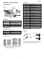
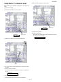
[1] APPEARANCE
Front view
Rear view
Customer display
(Pop-up type)
Operator display
Printer cover
Receipt paper
Journal window
AC power cord
Mode switch
USB connector
Drawer lock
Drawer
Keyboard
[2] RATING
XE-A40S
28.0lb (12.7kg)
420 (W) x 427 (D) x 297 (H) mm
16.5 (W) x 16.8 (D) x 11.7 (H) inches
AC 120V (m10%), 60Hz
Stand-by 8.6W, Operating 49W (max.)
0°C–40°C (32°F to 104°F)
Weight
Dimensions
Power source
Power consumption
Working temperature
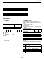
[3] KEYBOARD
DESCRIPTION
Receipt paper feed key
Journal paper feed key
Received-on account key
Receipt print/Paid-out key
Void key
Escape key
Percent 1and 2 key
Refund key
Discount key
&/FOR
•
CL
0-9,00
PLU/SUB
DEPT#
DEPT SHIFT
CLK#
Dept1-40
TAX
Tax 1 SHIFT
Tax 2 SHIFT
AUTO
CONV
CHK
CH1, CH2
MDSE SBTL
#/TM/SBTL
CA/AT/NS
Multiplication key
Decimal point key
Clear key
Numeric Keys
PLU/Subdepartment key
Department code entry key
Department shift key
Clerk code entry key
Department keys
Tax key
Tax 1 shift key
Tax 2 shift key
Automatic sequence key
Conversion key
Check key
Charge 1 and 2 keys
Merchandise subtotal key
Non-add code/Time display/Subtotal key
Total/Amount tender/Non Sale key
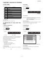
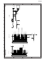
[4] MODE SWITCH
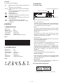
1. KEYBOARD LAYOUT
Type
Key position
Key pitch
Key layout
KEY TOP
↑ (RECEIPT)
↑ (JOURNAL)
RA
RCPT/PO
VOID
ESC
%1, %2
RFND
1. LAYOUT
Normal keyboard
STD/MAX 59
19 (W) x 19 (H) mm
Fixed type
•
Rotary type
OPX/Z
2.1. Keyboard layout
OFF
VOID
RECEIPT JOURNAL
RA %1
RCPT
/PO
%2
@/FOR
7
•
8
CL
9
25
5
4
5
6
3
VOID RFND
1
2
3
2
ESC
BS
SHIFT
SPACE
0
00
B
C
9
8
E
H
I
14
J
40
20
L
13
M
19
N
18
O
R
37
17
31
11
Q
38
32
12
P
39
33
26
6
K
34
27
7
21
1
G
CLK#
35
15
28
22
D
F
29
23
4
–
30
10
24
NUMBER
DC
A
DEPT
SHIFT
S
36
16
T
TAX AUTO
U
X
TAX1
SHIFT
TAX2
SHIFT
V
MGR
X1/Z1
X2/Z2
Operator key (OP)
Y
CONV CH1
W
REG
OP
PGM
DEPT
#
MA
2. KEY LIST
PLU
/SUB
Manager key (MA)
MA
OP
The mode switch can be operated by inserting one of the two supplied
mode keys - manager (MA) and operator (OP) keys. These keys can
be inserted or removed only in the "REG" or "OFF" position.
Z
CHK CH2
MDSE #/TM
SBTL SBTL
CA/AT/NS
NOTE: The small characters on the bottom or lower right in each key
indicates functions or characters which can be used for character entries for text programming.
1–1
XE-A40S
3. DESCRIPTION
The mode switch has these settings:
OFF:
OP X/Z:
REG:
PGM:
VOID:
MGR:
X1/Z1:
X2/Z2:
This mode locks all register operations. (AC power turns
off.)
No change occurs to register data.
To take individual clerk X or Z reports, and to take flash
reports.
It can be used to toggle receipt state "ON" and "OFF" by
pressing he [RCP/PO] key.
For entering sales.
To program various items.
Enters into the void mode. This mode allows correction
after finalizing a transaction.
For manager's entries. The manager can use this mode
for an override entry.
To take the X/Z report for various daily totals.
To take the X/Z report for periodic (weekly or monthly)
consolidation.
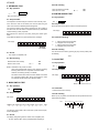
3.1. Operator display
Function message display area
Clerk code or mode name
Receipt OFF indicator
Repeat / Sentinel mark / Power save mark
•
Clerk code or Mode name
The mode you are in is displayed. When a clerk is assigned, the
clerk code is displayed in the REG or OP X/Z mode. For example,
"*01*" is displayed when clerk 01 is assigned.
[5] DISPLAY
1. OPERATOR DISPLAY
Display device
Number of line
Number of positions
Color of display
Character form
Character size
Numeric entry display area
:
:
:
:
:
:
•
Repeat
The number of repeats is displayed, starting at "2" and incremental
with each repeat. When you have registered ten times, the display
will show "0" (2→3......9→0→1→2...)
LCD
2 line
16 positions
Yellow / Green
7 segment + Dp
Approx. 8.0mm (H) x 4.8mm (W)
•
Sentinel mark
When amount in the drawer reaches the amount you preprogrammed, the sentinel mark "X" is displayed to advise you to
remove the money and put it in a safe place.
Layout:
•
Power save mark
When the cash register goes into the power save mode, the power
save mark (decimal point) lights up.
•
Function message display area
Item labels of departments and PLU/subdepartments and function
texts you use, such as %1, (-) and CASH are displayed.
When an amount is to be entered or entered, "AMOUNT" is displayed: When an amount is to be entered, ------- is displayed at the
numeric entry area with "AMOUNT". When a preset price has been
set, the price is displayed at the numeric entry area with
"AMOUNT".
2. CUSTOMER DISPLAY
Display device
Number of line
Number of positions
Color of display
Style
Character form
Character size
:
:
:
:
:
:
:
LED
1 line
7 positions
Yellow / Green
Pop up type
7 segment + Dp
14.0mm (H) x 8.0mm (W)
•
Numeric entry display area
Numbers entered using numeric keys are displayed here.
*
Date and time display
Date and time appear on the display in the OP X/Z, REG, or MGR
mode. In the REG or MGR mode, press the [#/TM/SBTL] key to
display the date and time.
Layout:
*
Error message
When an error occurs, the corresponding error message is displayed in the function message display area.
3.2. Customer display (Pop-up type)
Power save mark
(Lighting the mark only under the power save mode)
1–2
XE-A40S
[6] PRINTER
[7] DRAWER
1. PRINTER
1. OUTLINE
•
•
•
•
•
Part number
NO. of station
Validation
Printing system
No. of dot
:
:
:
:
:
•
Dot pitch
:
•
•
Font
Printing capacity
:
:
•
•
Character size
Print pitch
:
:
•
•
Print speed
:
Paper feed speed :
(Manual feed)
Reliability
: Mechanism MCBF 5 million lines
Head life 12.5 million characters
(at 4 dots/1 character/1 element)
Paper end sensor : Set up (Receipt and journal)
Cutter
: Manual
Near end sensor : No
•
•
•
•
*
PR-45M II
2 (Receipt and journal)
No
Line thermal
Receipt
288 dots
Journal
288 dots
Horizontal
0.125mm
Vertical
0.125mm
10 dots (W) x 24 dots (H)
Receipt
max. 24 characters
Journal
max. 24 characters
1.25mm (W) x 3.0mm (H) at 10 x 24 dots
Column distance
1.5mm
Row distance
3.75mm
Approximate 50mm/s (13.3 lines/sec)
Approximate 40mm/s
•
Standard equipment: Yes
•
Max. number of additional drawers: 0
•
The drawer consists of:
1) Drawer box (outer case) and drawer
2) Coin case
3) Money case
4) Lock (attached to the drawer)
2. SPECIFICATION
2.1. DRAWER BOX AND DRAWER
Model name of the drawer box SK423
Size
420 (W) x 426 (D) x 114 (H) mm
16.5 (W) x 16.8 (D) x 4.5 (H) inches
color
Gray (PB-N8.0)
Material
Metal
Bell
Release lever
Standard equipment: located at the
bottom
Drawer open sensor
Separation from the main unit -
2.2. MONEY CASE
PR-45M II is not equipped with the gear cover. It is the only difference of PR-45M II and PR-45M. When servicing PR-45M II printer
unit, the manual of PR-45M will serve as a reference.
Separation from the drawer
Separation of the bill compartments from the coin
compartments
Bill separator
Number of compartments
2. PAPER
•
Paper roll
dimension
•
Paper quality
: 44.5 m ± 0.5mm in width
Max. 80mm
in diameter
: (Journal/Receipt)
High-quality paper
paper thickness: 0.06 to 0.08mm
Nihon seisi thermal
: TF50KS-E
paper
Oji thermal paper
: PD150R,PD160R
Allowed
Allowed
Disallowed
5B/6C
5B/6C
3. LOGO STAMP
2.3. LOCK (LOCK KEY : LKGIM7331BHZZ)
•
No
4. CUTTER
•
Location of the lock: Front
•
Method of locking and unlocking:
Method : Manual
To lock, insert the drawer lock key into the lock and turn it 90
degrees counter clockwise.
5. PRINTING AREA
To unlock, insert the drawer lock key and turn it 90 degrees clockwise.
•
Key No: SK1-1
36
(288dots)
0.125
44.5
14
(112dots)
36
(288dots)
Receipt
44.5
ck
ck
[8] BATTERY
4.5
4
0.5
SK1-1
Number of themal head heater elements 864 dots
(688dots)
unlo
Receipt & Journal
Lo
•
1. MEMORY BACK UP BATTERY
0.5
Built-in battery : Rechargeable batteries, memory holding time
about 1 month (with fully charged built-in batteries,
at room temperature)
Journal (units;mm)
1–3
XE-A40S
CHAPTER 2. OPTIONS
XE-A40S
Service Manual
[1] OPTIONS (NONE)
[2] SERVICE OPTIONS (NONE)
[3] SUPPLIES
NO
1
NAME
Thermal roll paper
PARTS CODE
TPAPR6645RC05
PRICE
RANK
BA
2–1
DESCRIPTION
5 ROLLS/PACK
XE-A40S
ServiceRESET
Manual
CHAPTER 3. MASTER RESET AND PROGRAM
XE-A40S
[1] MASTER RESETTING
Master resetting clears the entire memory and resumes default values.
Master resetting can be accomplished by using the following procedure:
Procedure A:
1)
2)
3)
Unplug the AC cord from the wall outlet.
Set the mode switch to the PGM position.
While holding down both the JOURNAL FEED key
and [CL] key, plugin the AC cord to the wall outlet.
The master reset can also be accomplished in the following case.
In case power failure occurs when the machine has no battery
attached to it, the master reset operation is automatically performed
after the power has been restored.
(This is because if power failure occurs with no battery attached to the
machine, all the memory will be lost and the machine does not work
properly after power recovery; this requires the master reset operation.)
[2] PROGRAM RESETTING (INITIALIZATION)
This resetting resumes the initial program without clearing memory.
This resetting can be operated at below sequence in PGM mode.
Procedure:
1)
2)
3)
Unplug the AC cord from the wall outlet.
Set the mode switch to the PGM position.
While holding down both JOURNAL FEED key
and RECEIPT FEED key, plugin the AC cord to
the wall outlet.
NOTE: In case power failure occurs when the machine has no battery
attached to it, the master reset operation is automatically performed after the power has been restored.
3–1
XE-A40S
CHAPTER 4. HARDWARE DESCRIPTION Service
XE-A40S
[1] BLOCK DIAGRAM
Manual
[2] MEMORY MAP
1. ADDRESS MAP
DRAWER
POWER
FLASH ROM
SUPPLY
/CS0
BA0
512KB
CPU
BANK 0
0
0
BANK 1
0
1
00000h
RAM 10KB
SRAM
00400h
256KB
02C00h
DRIVER, SENSOR
Internal RAM area
10KB
Internal rserved area
04000h
LCD
16 digits x 2
External I/O
08000h
External SRAM 1
128KB
/CS2
30000h
External I/O
(USB controller)
/CS1
40000h
External SRAM 2
SEG DRIVER
28000h
POPUP
PRINTER
DIG DRIVER
7 digits
4 to 16
DECODER
128KB
50000h
KEY & SW
KEY SCAN
C0000h
/CS0
External reserved area
80000h
KEY RETURN
M66291GP
/CS3
IPL MODE
OFF: Flash ROM
ON: EP ROM
IPL MODE
OFF: EP ROM
ON: Flash RPM
USB
FFFFFh
CPU
M30620SAFP (MITSUBISHI, internal RAM 10KB)
External memory
RAM
FLASH ROM
PRINTER
USB controller
Only the BANK in /CS area(30000h-FFFFFh) is effective.
2. EXTERNAL BUS
256KB
512KB
SHARP LH28F004BVT
PR45M II
RENESAS M66291GP
External BUS Access Speed
*1BCLK=83.3ns (at 12MHz)
SRAM
FLASH
ROM
SRAM:
2BCLK
EPROM:
2BCLK
FLASH ROM:
2BCLK
External I/O:
2BCLK
/CS2 Area
address 08000h~27FFFh 128KB
/CS0 Area BANK0 address 30000h~4FFFFh 128KB
/CS0 Area BANK0 address 80000h~FFFFFh 512KB
*Moves to Bank 1 when rewritten using EPROM
[3] PRINTER CONTROL
1. STEPPING MOTOR CONTROL
The stepping motor is driven at a constant voltage by Sanken
STA471A.
1step: 0.125mm, A1dot: 1step
Printing speed 50mm/s
1.1. CPU’s PORT
No.
80
79
78
77
76
75
74
73
4–1
CPU PORT
P10
P11
P12
P13
P14
P15
P16
P17
Signal to be used
RAS
RBS
RCS
RDS
JAS
JBS
JCS
JDS
XE-A40S
2. HEAD CONTROL
1.2. Driving steps
RECEIPT MOTOR
STEP
1
2
3
4
H
L
L
H
STEP
L
H
H
L
L
L
H
H
H
H
L
L
Driver IC input
(CPU output)
JAS JBS JCS JDS
1
2
3
4
*
HEAD:
Driver IC input
(CPU output)
RAS RBS RCS RDS
L
L
H
H
H
H
L
L
H
L
L
H
L
H
H
L
Motor driving signal
/
RPFA
L
H
H
L
/
RPFB
H
L
L
H
/
RPFC
H
H
L
L
Related PORT
/
RPFD
L
L
H
H
No.
30
29
28
93
92
91
90
89
21
Motor driving signal
/
JPFA
H
H
L
L
/
JPFB
L
L
H
H
/
JPFC
L
H
H
L
832 dots in all. Printable range: 384 dots at receipt side;
384 dots at journal side
/
JPFD
H
L
L
H
CPU PORT
TXD2
RXD2
CLK2
P103
P104
P105
P106
P107
P81
Signal to be used
SO
SI
PCLK
/STRB1
/STRB2
/STRB3
/STRB4
LATCH
VHCOM
/STB1: 1 ~ 288dot: 288 dots in all
/STB2: 289 ~ 432dot: 144 dots in all
/STB3: 433 ~ 576dot: 144 dots in all
/STB4: 577 ~ 864dot: 288 dots in all
Total 864 dots
When stopping the motor, all energizing to the phase is turned off
by giving the rush current of 10ms to the same phase as a final
excitation phase. → Turn all RAS ~ RDS and JAS ~ JDS into L.
*
No energizing should be allowed at lease 30 ms after stopping the
motor before restarting.
When turning on or off the printer power supply, make sure to turn /
STB1, 2, 3, 4 to "H".
*
Do not turn on without paper.
*
THERMAL HEAD power supply control : Turns ON when P81= "H";
turns OFF when "L". (The power supply for HEAD and STEPPING
MOTOR is shared). When printing is finished (when the motor is
stopped) Athe power should be turned OFF.
*
Before printing or feeding paper, perform A/D conversion in ** ms
after the printer head is turned ON and make sure the voltage is
stable.
(The power supply of the printer head should be turned ON and
OFF by using the regulator IC.)
When the motor is started, the rush current of 10ms is given to the
first excitation phase.
[4] I/O
M16C/62 PORT
Memory space:
Processor mode:
PORT
PIN No.
I/O
P00
P01
P02
P03
P04
P05
P06
P07
P10
P11
P12
P13
P14
P15
P16
P17
P20
P21
P22
P23
P24
P25
P26
88
87
86
85
84
83
82
81
80
79
78
77
76
75
74
73
72
71
70
69
68
67
66
I/O
I/O
I/O
I/O
I/O
I/O
I/O
I/O
O
O
O
O
O
O
O
O
O
O
O
O
O
O
O
Normal mode
Use it in Micro processor mode (Separate BUS/width=8bit)
Pin name
D0
D1
D2
D3
D4
D5
D6
D7
P10
P11
P12
P13
P14
P15
P16
P17
A0
A1
A2
A3
A4
A5
A6
Signal name
Initial
value
D0
D1
D2
D3
D4
D5
D6
D7
RAS
RBS
RCS
RDS
JAS
JBS
JCS
JDS
A0
A1
A2
A3
A4
A5
A6
L
L
L
L
L
L
L
L
4–2
OFF
MODE
OUT L
OUT L
OUT L
OUT L
OUT L
OUT L
OUT L
OUT L
OUT L
OUT L
OUT L
OUT L
OUT L
OUT L
OUT L
OUT L
OUT L
OUT L
OUT L
OUT L
OUT L
OUT L
OUT L
Function
Receipt paper feed A
Receipt paper feed B
Receipt paper feed C
Receipt paper feed D
Journal paper feed A
Journal paper feed B
Journal paper feed C
Journal paper feed D
XE-A40S
PORT
PIN No.
I/O
P27
P30
P31
P32
P33
P34
P35
P36
P37
P40
P41
P42
P43
P44
P45
P46
P47
P50
P51
P52
P53
P54
P55
P56
P57
P60
P61
P62
P63
P64
P65
P66
P67
P70
P71
P72
P73
P74
P75
P76
P77
P80
P81
P82
P83
P84
P85
P86
P87
P90
P91
P92
P93
P94
P95
P96
P97
P100
P101
P102
P103
P104
P105
P106
65
63
61
60
59
58
57
56
55
54
53
52
51
50
49
48
47
46
45
44
43
42
41
40
39
38
37
36
35
34
33
32
31
30
29
28
27
26
25
24
23
22
21
20
19
18
17
11
10
7
6
5
4
3
2
1
100
97
95
94
93
92
91
90
O
O
O
O
O
O
O
O
O
O
O
O
O
O
O
O
O
O
O
O
O
O
I
O
I
I
I
I
I
I
I
I
I
O
I
O
O
O
O
O
O
O
O
I
I
I
I
O
I
I
I
O
O
O
O
O
I
I
I
I
O
O
O
O
Pin name
A7
A8
A9
A10
A11
A12
A13
A14
A15
A16
A17
A18
A19
/CS0
/CS1
/CS2
/CS3
/WR
/BHE
/RD
BCLK
/HLDA
/HOLD
ALE
/RDY
P60
P61
P62
P63
P64
P65
P66
P67
TXD2
RXD2
CLK2
P73
P74
P75
P76
P77
P80
P81
/INT0
/INT1
/INT2
/NMI
XCOUT
XCIN
P90
P91
P92
P93
P94
P95
P96
P97
AN0
AN1
AN2
AN3
AN4
P105
P106
Signal name
Initial
value
A7
A8
A9
A10
A11
A12
A13
A14
A15
A16
A17
A18
A19
/CS0
/CS1
/CS2
/CS3
/WR
(NU)
/RD
BCLK
(NU)
/HOLD
(NU)
/RDY
/KR0
/KR1
/KR2
/KR3
/KR4
/KR5
/KR6
/KR7
SO
SI
PCLK
DR1
/USBRST
(NU)
(NU)
(NU)
BUZZER
VHCOM
POFF
/DREQUSB
/INTUSB
/NMI(NU)
XCOUT
XCIN
MODE
MSENS
(NU)
BA0
DATE/CE
BLON
LCDON
IPLON
TM
VPTEST
VREF
/STRB1
/STRB2
/STRB3
/STRB4
L
L
L
L
L
L
L
L
L
L
L
L
L
L
H
H
H
H
4–3
OFF
MODE
OUT L
OUT L
OUT L
OUT L
OUT L
OUT L
OUT L
OUT L
OUT L
OUT L
OUT L
OUT L
OUT L
OUT H
OUT L
OUT H
OUT L
OUT L
OUT L
OUT L
OUT L
OUT L
IN
OUT L
IN
IN
IN
IN
IN
IN
IN
IN
IN
OUT L
IN
OUT L
OUT L
OUT L
OUT L
OUT L
OUT L
OUT L
OUT L
IN
IN
IN
IN
IN
IN
OUT L
OUT L
OUT L
OUT L
OUT L
IN
IN
IN
IN
IN
IN
IN
IN
Function
USB CONTROLLER
Key Return Signal 0
Key Return Signal 1
Key Return Signal 2
Key Return Signal 3
Key Return Signal 4
Key Return Signal 5
Key Return Signal 6
Key Return Signal 7
PRINTER DATA OUT
PRINTER DATA IN
PRINTER CLOCK
DRAWER 1 DRIVE SIGNAL
USB RESET SIGNAL
BUZZER
PRINTER HEAD CONTROL
POWER INTERRUPT
USB DMA REQUEST
USB INTERRUPT
32.768kHz
32.768kHz
MODE KEY SENSE
MISCELLANEOUS SENSE
BANK SIGNAL 0
LCD DATA LATCH SIGNAL
BACK LIGHT ON
LCD POWER ON
IPL ON SIGNAL
HEAD TEMPERATURE MONITOR
HEAD VOLTAGE MONITOR
REFERENCE VOLTAGE
PRINTER STORE SIGNAL 1
PRINTER STORE SIGNAL 2
PRINTER STORE SIGNAL 3
PRINTER STORE SIGNAL 4
XE-A40S
PORT
PIN No.
I/O
P107
89
O
Pin name
Signal name
Initial
value
L
P107
LATCH
Pin name
BYTE
CNVss
/RESET
Xout
Vss
Xin
Vcc
Vcc
Vss
AVss
Vref
Avcc
Function
Connected to VCC
Connected to GND
OFF
MODE
IN
Function
PRINTER LATCH SIGNAL
POWER SUPPLY/CONTROL TERMINAL
PORT
BYTE
CNVss
/RESET
Xout
Vss
Xin
Vcc
Vcc
Vss
Avss
Vref
Avcc
PIN No.
8
9
12
13
14
15
16
62
64
96
98
99
I/O
I
I
I
O
I
Connected to XTAL
Connected to GND
Connected to XTAL
Connected to VCC
Connected to VCC
Connected to GND
Connected to GND
Connected to VCC
Connected to VCC
[5] KEY-DISPLAY
1. LCD CONTROL
2. KEY/DISPLAY SCAN
1.1. LCD CONTROL
On the XE-A40S, the key and display scan signal is common.
KEY/DISPLAY SCAN and key read should be performed at the following timing.
LCD-related registers
Function
LCD Write Data
LCD Read Data
LCD Control Signal
Data Latch Signal
Address
04001h
04002h
04003h
CPU port P94
R/W
W
R
W
W
1) KEY/DISPLAY SCAN cycle: 10ms
2) Blanking time: 50us
3) KEY DATA READ timing: More than 10 ms from the fall of the
SCAN signal
Key / Display-related registers
1.1.1 LCD Control Signal / Key Strobe Signal
Address
04003h
Bit7 :
Bit6 :
Bit5 :
Bit4 :
Bit7
–
Bit6
E
Bit5
R/W
Bit4
RS
Bit3
–
Bit2
–
Bit1
–
Function
LED Segment Signal
Key Strobe Signal
Key Return Signal
Bit0
–
Not used
E
Address
04000h
04003h
CPU port
R/W
W
W
R
2.1. LED Segment Signal
Enable Signal
Enable
R/W
H : Data read L : Data Write
RS
H : Data input L : Instruction Input
Address
04000h
Bit7
dp
Bit6
g
Bit5
f
Bit4
e
Bit3
d
Bit2
c
Bit1
b
Bit0
a
Bit5
–
Bit4
–
Bit3
KS3
Bit2
KS2
Bit1
KS1
Bit0
KS0
2.2. Key Strobe Signal
Address
04003h
1.1.2 Data Latch Signal
L : LCD write data latch
Bit7
–
Bit6
–
Bit3 ~ 0 : KS3 ~ 0
Strobe signals for keys and POP UP Display are generated at KS3 - 0.
2.3. Key Return Signal
PIN
No.
38
37
36
35
34
33
32
31
4–4
CPU
PORT
P60
P61
P62
P63
P64
P65
P66
P67
Signal
name
KR0#
KR1#
KR2#
KR3#
KR4#
KR5#
KR6#
KR7#
Function
KEY RETURN SIGNAL 0
KEY RETURN SIGNAL 1
KEY RETURN SIGNAL 2
KEY RETURN SIGNAL 3
KEY RETURN SIGNAL 4
KEY RETURN SIGNAL 5
KEY RETURN SIGNAL 6
KEY RETURN SIGNAL 7
XE-A40S
3. KEYSCAN MATRIX
CPU
P90
P91
MODE
Others
STO
SRV
PF-R
ST1
PGM
PF-J
ST2
ST3
Time
HEAD UP
RPE
ST4
REG
JPE
ST5
MGR
ST6
X1/Z1
DRAWER
OPEN
4. DISPLAY
[9] PRINT RATE
The XE-A40S has an LCD display, 5 x 7 dots, 2 lines, at the front side
and a 7-digit LED at the pop-up side.
384 dots/1 line
ST7
X2/Z2
MRS
ST8
ST9
RS/CI
[10] A/D CONVERSION
FRONT:
The printer power supply voltage should be measured at more than 10
ms after the printer is turned ON.
[11] BUZZER
PIEZO type BUZZER
POP UP:
The oscillating frequency is 4.0kHz ± 0.5kHz
[12] USB I/F
•
Display DIGIT signal
The XE-A40S is equipped with 1 USB port (slave) as a standard provision. By use of the USB general-purpose ASSP device M66291
(RENESAS), it sends and receives USB data. The M66291 is mapped
to the /CS1 area (28000H ~ 3FFFFFH). The CPU and the M66291 are
connected as shown in the figure below.
The above ST0 ~ ST6 are display digit signals.
ST0: 1st digit ~ ST6: 7th digit
•
Display SEGMENT signal
The LED segment signal is outputted by writing SEGMENT data in
the /CS3 space.
CPU
Correspondence of DATA ~ SEGMENT
A0
A1~A6
D7 → DP
D0~D7
[6] POWER SUPPLY
Measures should be taken to restore within 10 ms after a
power failure occurs..
LM2574 +
7
Vbus
TrON
D0~D7
8
CS1
RD
WRL
WRH
INT2
CS
RD
LWR
HWR/BYTE
INT1
Dreq0
D+
D-
1.5kΩ
27Ω
1.0{F
Xin
Xout
1
3
27Ω
INT0
24V
2
4
Vbus
D+
DGND
USB Connector
24MHz
<CPU Port>
VLED
VCC 5.0V
VDD 5.0V
Pin
No.
19
CPU PORT
SIGNAL
Application
P83 (INT1)
/DREQUSE
18
26
P84 (INT2)
P74
/INTUSB
/USBRST
USB DMA CHANNEL 0 DMA
Request signal
USB Interrupt 0 Request signal
USB reset signal
/POFF detection point
BATTERY
Access from CPU to M66291 : 28000H + Register Address (00~77H)
[7] RE-WRITING FLASH MEMORY
IPL from EP-ROM:
3.3V
CoreVcc
D15/AD0
AD1~AD6
/USBRST
ON/OFF CONTROL
(MODE SW)
PQ1CG2032
IOVcc
Vcc
D0 ~ D6 → A ~ g
TRANS.
M66291
5V
Input clock uses 24MHz.
[13] RESET
After IPL Short pin is set to VCC position the
program is started from EP-ROM by turning on
the power.
The program on EP-ROM is transferred to flash
ROM by switching the banks through S-RAM.
The RESET signal is generated when:
1) The mode key switch is turned from SRV to a position other than
SRV'(excluding OFF).
2) The power is turned ON more than 10 seconds after the power is
turned OFF. (The reset signal may not be issued if the POWEROFF time is short.)
[8] DRAWER
The XE-A40S has a 1 drawer port. (No open sensor is provided.)
3) The mode key switch is turned from OFF to a position other than
OF (excluding the SRV position). (If the power-off time is less than
5 seconds, the reset signal may not be issued.)
The driving time for the DRAWER solenoid are as follows: 50ms (max)
45ms (min)
4–5
XE-A40S
XE-A40S
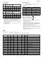
CHAPTER 5. DIAGNOSTIC PROGRAM
Service Manual
[1] TEST ITEMS
2. KEY CODE
The test items are as follows:
2.1. Key operation
1)
2)
3)
4)
5)
6)
7)
8)
9)
10)
11)
12)
13)
*
Code
100
101
102
104
105
106
107
110
120
121
130
160
520
Description
Display buzzer test
Key code
Printer test
Keyboard test
Mode switch test
Printer sensor test
Clock display test
Drawer 1 open & sensor test
External RAM test
CPU internal RAM test
FLASH ROM test
AD conversion port test
USB TEST
101
→
RCPT/PO
2.2. Test procedure
OP display
2.3. Check that:
KEY code:
Every time a key is pressed, the hard code of that key
is displayed as a decimal number.
When a key is pressed twice or pressed in an incorrect
manner, --- will be displayed.
Starting DIAG
2.4. End of testing
Key operation: Above code + “RCPT/PO” key
You can exit the test mode by turning the mode switch to a position
other than the PGM mode. The printer prints as follows:
[2] DESCRIPTION OF EACH DIAG PROGRAM
101
1. DISPLAY BUZZER TEST
3. PRINTER TEST
1.1. Key operation
3.1. Key operation
→
RCPT/PO
102
1.2. Test procedure
OP display
PGM
KEY CODE
Mode switch: PGM
100
CODE
KEY
→
RCPT/PO
3.2. Test procedure
OP display
D I S P B U Z Z E R PGM
0 1 2 3 4 5 6 7 8 9ABCDEF
R / J
P R I N T E R
4.5.6.7.8.9.0.
Rear display
PGM
Enlargement
The decimal point on the LED and the cursor on the LCD will shift from
the lower digit to the upper digit in steps of 1 digit (every 200 msec)
After that, all segments will turn on (about 1 sec).
These two modes are repeated.
At the same time, the buzzer sounds continuously.
1.3. Check that:
5 lines of 24 digits are printed.
•
Each position is correctly displayed.
•
The brightness of each number is uniform.
•
The buzzer sound is normal.
At the receipt side, the logo is also printed and the receipt is issued.
3.3. Check that:
1.4. End of testing
The print is free from contamination, blur, and uneven density.
You can exit the test mode by pressing any key. The following is
printed.
3.4. End of testing
The test will end automatically.
100
5–1
XE-A40S
4. KEYBOARD TEST
5.4. End of testing
4.1. Key operation
When the test ends normally:
When an error occurs:
_ _ _ _ 104 → RCPT/PO
↑
KEY check sum code
6. PRINTER SENSOR TEST
6.1. Key operation
4.2. Test procedure
106
The keyboard is checked using the check sum code of the key code.
If the check sum code is not entered, the check is made using the
check sum code of the default keyboard arrangement.
→
RCPT/PO
6.2. Test procedure
Check the status of the paper end sensor and head up sensor.
The check sum data for each model is entered to the front 4 digits of
the DIAG code, and that data is compared with the key data added
until the final key (CA/AT) is pressed.
OP display
R / J
1 0 6
Both data are the same, the test ends, printing the number given
below.
KEY
1 0 4
BOARD
X:
PGM
Y:
KEY CODE
1 - Paper present at the receipt side
O - No paper at the receipt side
1 - Paper present at the journal side
O - No paper at the journal side
6.4. End of testing
You can exit the test mode by pressing any key and the printer prints
the following.
4.3. Check:
•
PGM
X Y
SENSOR
6.3. Check the following
If both data are different, the printer prints the error message.
OP display
105
105
E–––
The content of completion print
106
4.4. End of testing
7. CLOCK TEST
When the test ends normally:
When an error occurs:
E–––
104
104
7.1. Key operation
107
NOTE: Calculation of key check sum data
Hard codes (hexadecimal number) at the position (excluding
feed key) where there is an input data contact are added.
→
RCPT/PO
7.2. Test procedure
However, the final key (CA/AT) is not added.
OP display
This data to which hard codes have been added is converted
into a decimal number value, which will become the check
sum data that will be entered when DIAG is started.
CHECK
T I ME R
1 0 4
Hour
5. MODE SWITCH TEST
→
"-" blinks and the clock counts up.
5.2. Test procedure
MODE
1 0 5
7.4. End of testing
SW
PGM
When any key is pressed, the date and time are printed and the test
mode will be terminated.
X
107
MODE: PGM_VOID_OFF_OP X/Z_REG_MGR_X1/Z1_X2/Z2__PGM
2
9
3
4
5
6
7
1
X : 1
X X X X X X
X X X X X X
year
month
hour
min.
day
The above X must be read in the correct order. (If the contact is open,
9 will be displayed.)
5.3. Check:
The display during testing and the content of the completion print.
*
Sec.
7.3. Check that:
RCPT/PO
OP display
Min.
Blinks at an interval of 0.5 sec.
5.1. Key operation
105
PGM
At "OFF" position state, nothing is displayed after displaying 9.
5–2
sec.
XE-A40S
8. DRAWER 1 OPEN & SENSOR TEST
9.3. Check:
•
8.1. Key operation
110
→
9.4. End of testing
RCPT/PO
The program ends after printing as follows:
8.2. Test procedure
OP display
The completion print.
When the test ends normally:
When the test end abnormally:
DRAWER
1
PGM
X
C = DRAWER CLOSED
When an error occurs, the printer outputs the error message and the
address where the error has occurred in the area *****.
8.3. Check that:
10. CPU INTERNAL RAM TEST
•
The drawer 1 opens normally.
•
Always displays O (Opened), because XE-A40S doesn't have an
open sensor.
10.1. Key operation
121
8.4. End of testing
→
RCPT/PO
10.2. Test procedure
You can exit the test mode by pressing any key. The printer prints the
following.
The test program tests internal RAM (10 Kbytes) of the CPU.
The contents of memory must be stored before and after this test.
110
RAM (00400H ~ 02BFFH area) is tested in the following procedure.
9. EXTERNAL RAM TEST
1) Store data in the test area.
9.1. Key operation
→
120
120
x = 1:Data error
x = 2:Address error
X : O = DRAWER OPENED
120
Ex – – –
*****
2) Write "00H"
3) Read and compare "00H" and then write "55H"
RCPT/PO
4) Read and compare "55H" and then write "AAH"
9.2. Test procedure
5) Read and compare "AAH"
The standard 256 Kbyte RAM is checked.
6) Restore stored data
The contents of memory must be stored before and after this test.
If an error occurs at a step, the error is printed.
RAM (08000H ~ 27FFFH area and 30000H ~ 4FFFFH area) is tested
in the following procedure:
If any error does not occur, the following addresses are checked in
turns.
1) Store data in the test areas
Addresses to be checked:
2) Write "00H"
01000H , 01001H , 01002H , 01004H , 01008H
01010H , 01020H , 01040H , 01080H ,
01100H , 01200H , 01400H , 01800H ,
02000H
3) Read and compare "00H" and then write"55H"
4) Read and compare "55H" and then write "AAH"
5) Read and compare "AAH"
6) Restore stored data
If an error occurs at a step, the error is printed.
OP display
If any error does not occur, the following addresses are checked in
turns.
Addresses to be checked:
RAM
1 2 0
RAM
PGM
10.3. Check:
10000H , 10001H , 10002H , 10004H , 10008H ,
10010H , 10020H , 10040H , 10080H ,
10100H , 10200H , 10400H , 10800H ,
11000H , 12000H , 14000H , 18000H ,
20000H
30000H , 30001H , 30002H , 30004H , 30008H ,
30010H , 30020H , 30040H , 30080H ,
30100H , 30200H , 30400H , 30800H ,
31000H , 32000H , 34000H , 38000H ,
40000H
OP display
CPU
1 2 1
The completion print.
10.4. End of testing
The test program ends after printing.
When the test ends normally:
When the test end abnormally:
Ex – – –
*****
121
121
x = 1:Data error
x = 2:Address error
If an error occurs, the printer outputs the error message and the
address where the error has occurred in the area *****.
PGM
5–3
XE-A40S
11. FLASH ROM TEST
13.3. Display print
11.1. Key operation
13.3.1 Display
130
→
RCPT/PO
OP display
11.2. Test procedure
The test program checks that the checksum of the flash ROM
(BANK0F80000H ~ FFFFFH).
F L A S H
1 3 0
ROM
T ES T 1
PGM
13.3.2 Print
The lower two digits of the check sum should be 10H.
OP display
USB
5 2 0
*
Only the journal side. The receipt side is not printed.
520
USB Rev. Ver.
VENDOR ID
PRODUCT ID
DEVICE ADDRESS
PGM
11.3. Check:
XXX
04DD
90B6
X
(Device address)
←When the host is connected: 1
←When the host is not connected: 0
The completion print.
11.4. End of testing
13.4. Test completion
The test will automatically be terminated and the printer prints as follows:
After completion of printing, the test is terminated automatically.
When the test ends normally:
ROM
When the test ends abnormally:
E––~––
ROM
[3] KEY CODE TABLE
130
******** (Model name)
******** (Version)
130
******** (Model name)
******** (Version)
XE A40S
12.1. Key operation
→
003 004
052 132 116
084 068 146 018
002 005
033 037
050 130 114
082 066 149 145
017 001
032 048
053 133 117
085 069 065 064
016 000
038 054
128 129 113
081 080 086 070
022 006
102 103 087 071
007
RF JF
12. AD CONVERSION PORT TEST
160
083 067 147 148
RCPT/PO
12.2. Test procedure
039 055
118
112
The test program displays the voltage of each AD conversion port.
CHECK SUM : 4 0 7 5
Display
OP display
T M
1 6 0
=
P GM
OP display
VRF
1 6 0
=
P GM
OP display
V P T E S T=
1 6 0
P GM
End of testing
13. USB COMMUNICATION TEST 1(ID/Address print)
13.1. Key operation
520
→
CH
13.2. Detail of the test
USB revision, Vendor ID, Product ID, and the device address assigned
by the host are printed.
5–4
XE-A40S
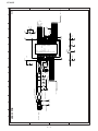
CHAPTER 6. IPL FROM EP-ROM
XE-A40S
8) Set the IPLManual
Short PIN (SP1) to GND position.
Service
Before working on the installation, unplug the AC cord from the AC
outlet.
1) Open the top cabinet.
2) Set the IPL Short PIN (SP1) to VCC position.
IPL Short PIN
VCC
GND
9) Replace the top cabinet.
10)Perform a master reset.
At the PGM mode, while holding down Journal feed key and CL
key, insert AC cord in AC outlet.
IPL Short PIN
VCC
GND
***MRS.***
3) Install the IPL ROM to the IC socket of the MAIN PWB.
1pin
IPL ROM
4) Turn the mode key switch to PGM position, and insert AC plug in
AC outlet.
5) The IPL procedure is started.
When the procedure is completed, the message of “Completed.” is
shown.
P ROM COPY
Completed.
6) Unplug the AC cord from the AC outlet.
7) Remove the IPL ROM to the IC socket of the MAIN PWB.
6–1
7–1
A
B
C
D
VCC
C21
IC5
/LATCH
/STRB4
/STRB3
/STRB2
/STRB1
R68
330
VCC
8
3
R55
C23
C24
10K
R32
C40
R57
C25
10K
R33
/FRES
/RESET
C39
R56
1SS355
1uF
C46
2
D4
C38
10Kx5(R54-R58)
C22
10K
R31
330pFx3(C38-C42)
2
2,6
2,6
2,6
2,6
NOT USED
KIA7045F
2
1
D7
D6
D5
D4
D3
D2
D1
D0
10K
33pF*8(C21-C28)
3,4,7
3,4,7
3,4,7
3,4,7
3,4,7
3,4,7
3,4,7
3,4,7
R30
10K
VCC
A7
A6
A5
A4
A3
A2
A1
A0
JDS
JCS
JBS
JAS
RDS
RCS
RBS
RAS
R29
3
3,7
3,7
3,7
3,7
3,7
3,4,7
3,4,7
6
6
6
6
6
6
6
6
C42
3
R71
1K
470
VCC
C27
10K
C1
7
0.1uF
C45
NOT USED
C2
10K
10K
33pF*8(C1-C8)
Q1
C3198
C28
10K
R36
2.2K
2.2K
2.2K
2.2K
2.2K
2.2K
2.2K
2.2K
R35
R59
R69
C41
R58
C26
10K
R34
R21
R22
R23
R24
R25
R26
R27
R28
R2
VCC
R1
3
VDD
(3.3K)
R74
1
IC2
6
1
2
3
4
D7
D6
D5
D4
D3
D2
D1
D0
AN7
AN6
AN5
AN4
AN3
AN2
AN1
AVSS
AN0
VREF
AVCC
SIN4
IC6
VDD
S0
FSOUT
VSS
(FS781)
XIN
XOUT
S1
LF
8
7
6
5
R67
33K
PLACE NEAR CPU!!!
P91
P90
2,4,6
2
81
82
83
84
85
86
87
88
89
90
91
92
93
94
95
96
97
98
99
100
M30620SAF
C8
10K
R8
P96
P95
P94
BA0
C7
10K
R7
4
4
4
3
C6
10K
R6
(CST12.0MTW)
3
2
(330pF)
C57
X3
/RES
R60
10K
VDD
TM
IPLON
6
100
100
100
100
100
100
100
100
C5
10K
R5
VREF
VPTEST
C4
10K
R4
6
2
R41
R43
R44
R46
R47
R48
R49
R50
C3
10K
R3
18pF
C47
R73
5
(10uF/10V,OS)
(0.1uF)
(33)
C54
+
VCC
C55
32.768KHz
27pF
C48
R70
330
X1
0
R64
3
CPU PWB UNIT
5
X2
NOT USED
(100pF)
C56
CST12.0MTW
1
6
2
7
80
79
78
77
76
75
74
73
72
71
70
69
68
67
66
65
64
63
62
61
60
59
58
57
56
55
54
53
52
51
D8
D9
D10
D11
D12
D13
D14
D15
A0
A1
A2
A3
A4
A5
A6
A7
VSS
A8
VCC
A9
A10
A11
A12
A13
A14
A15
A16
A17
A18
A19
SOUT4
CLK4
TB4IN
TB3IN
SOUT3
SIN3
CLK3
BYTE
CNVSS
XCIN
XCOUT
RESET
XOUT
VSS
XIN
VCC
NMI
INT2
INT1
INT0
TA4IN/U
TA4OUT/U
TB3IN
TBEOUT
TA2INW
TA2OUTW
TA1IN/V
TA1OUT/V
TB5IN
TB5OUT
1
2
3
4
5
6
7
8
9
10
11
12
13
14
15
16
17
18
19
20
21
22
23
24
25
26
27
28
29
30
8
C10
C9
R62
10K
C11
10K
R11
R63
10K
VCC
50
49
48
47
46
45
44
43
42
41
40
39
38
37
36
35
34
33
32
31
10K
10K
CS0
CS1
CS2
CS3
WR
BHE
RD
CBCLK
HLDA
HOLD
ALE
RDY
RTS0
CLK0
RXD0
TXD0
CLKS1
CLK1
RXD1
TXD1
R10
VCC
R9
C13
10K
R13
R128
10K
2.2K
4
1000pF
C114
10uF/50V
C49
+
0.1uF
C50
VDD
6
3
1K
A8
A9
A10
A11
A12
A13
A14
A15
A16
A17
A18
A19
3
3
4
B
BZ1
SO
SI
PCLK
+
2
2
2
2
4
/LE0W
A[0..19]
D[0..7]
/KR[0..7]
/CS3
3
3
3
3
3
3
3
3
3
3
3
3
PKM22EPPH4002-B0
(330pF)
NOT USED
C36
(1SS355)
D3
10K
R54
VCC
(30pF)
NOT USED
C30
R42
10k
VCC
33pF*12(C9-C20)
NOT USED
NOT USED
330pF
330pF
R65
C35
10K
R53
C20
10K
R20
C34
10K
R52
3,7
/RD
/CS2
/CS3
C19
10K
R19
3,4,7
3
7
C18
10K
R18
/WR
/CS0
/CS1
C17
10K
R17
/KR0
/KR1
/KR2
/KR3
/KR4
/KR5
/KR6
/KR7
VHCOM
/POFF
NOT USED
10K
R40
VCC
C16
10K
R16
/USBRST 7
/DREQUSB 7
/INTUSB 7
VCC
R66
DR1
C33
(30pF)
10K
R39
C15
10K
R15
C32
2
10K
C14
10K
R14
(30pF)
VDD
10K
R38
VDD
R37
C12
10K
R12
4
VCC
A16
A14
A12
A7
A6
A5
A4
A3
A2
A1
A0
D0
D1
D2
A16
A14
A12
A7
A6
A5
A4
A3
A2
A1
A0
D0
D1
D2
10K
R45
D0
D1
D2
D3
D4
D5
D6
D7
IC1
Q1
Q2
Q3
Q4
Q5
Q6
Q7
Q8
NC
A16
A14
A12
A7
A6
A5
A4
A3
A2
A1
A0
I/O0
I/O1
I/O2
VSS
IC3
VCC
A15
CS2
WE
A13
A8
A9
A11
OE
A10
CS1
T/O7
I/O6
I/O5
I/O4
I/O3
1SS355
1SS355
74HC273
CLK
CLR
D1
D2
D3
D4
D5
D6
D7
D8
32
31
30
29
28
27
26
25
24
23
22
21
20
19
18
17
/RES
IC4
NC
A16
A14
A12
A7
A6
A5
A4
A3
A2
A1
A0
I/O0
I/O1
I/O2
VSS
C43
32
31
30
29
28
27
26
25
24
23
22
21
20
19
18
17
2
C52
0.1uF
C53
+
VDD
NOT USED
(10uF/50V)
VDD
NOT USED
(10uF/50V)
VCC
A15
CS2
WE
A13
A8
A9
A11
OE
A10
CS1
T/O7
I/O6
I/O5
I/O4
I/O3
+
1MSRAM 70ns VHI621024M7-1
1
2
3
4
5
6
7
8
9
10
11
12
13
14
15
16
C37
0.1uF
VDD
VDD
/POFF
Vcc:20pin
GND:10pin
2
5
6
9
12
15
16
19
1MSRAM 70ns VHI621024M7-1
1
2
3
4
5
6
7
8
9
10
11
12
13
14
15
16
D2
D1
11
1
3
4
7
8
13
14
17
18
2
D7
D6
D5
D4
D3
A10
A13
A8
A9
A11
A15
D7
D6
D5
D4
D3
A10
A13
A8
A9
A11
A15
3
VCC
a
b
c
d
e
f
g
dp
10K
R72
C29
0.1uF
NOT USED
R61
3
/RD
/CS2
(30pF)
NOT USED
C44
10K
(30pF)
NOT USED
C51
1
VDD
VCC
/RAMCS
(30pF)
NOT USED
C31
(10K)
3,7
/WR 3,4,7
1/7
R51
2
2
2
2
2
2
2
2
VCC
a
b
c
d
e
f
g
dp
1
A
B
C
D
XE-A40S
XE-A40S
Service
Manual
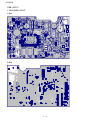
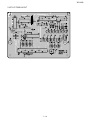
CHAPTER 7. CIRCUIT DIAGRAM AND PWB
LAYOUT
7–2
A
B
C
D
1
2
3
4
5
6
7
8
9
10
11
12
13
14
15
16
17
18
19
20
21
22
23
24
25
26
27
28
29
30
31
32
33
34
35
36
37
38
39
40
VCC
/S6
/S2
/S3
/S4
/VON
/RESET
P90
P91
a
b
c
d
e
f
g
dp
8
JST
KEY I/F RELAY CN(40Pin)40FE-BT-VK-N
1
2
3
4
5
6
7
8
9
10
11
12
13
14
15
16
17
18
19
20
21
22
23
24
25
26
27
28
29
30
31
32
33
34
35
36
37
38
39
40
CN1
KEY I/F
DRIVER PWB
/S6
/S2
/S3
/S4
4
6
6
6
5
7
4
4
4
4
1
1
1,4,6
KS3
KS2
KS1
KS0
/RESET
P90
P91
/KR0
/KR1
/KR2
/KR3
/KR4
/KR5
/KR6
/KR7
/VON
1
1
1
1
1
1
1
1
a
b
c
d
e
f
g
dp
7
1
40
39
38
37
36
35
34
33
32
31
30
29
28
27
26
25
24
23
22
21
20
19
18
17
16
15
14
13
12
11
10
9
8
7
6
5
4
3
2
1
CN2
40
39
38
37
36
35
34
33
32
31
30
29
28
27
26
25
24
23
22
21
20
19
18
17
16
15
14
13
12
11
10
9
8
7
6
5
4
3
2
1
1
6
VPTEST
T_PRINT CN(40Pin)00 6229 640 003 800
/KR[0..7]
C58
0.1uF
VLED
6
VCC
D7
1SS355
VCC
6
6
6
6
6
6
6
1
1
FB4
1
1,6 FB5
1,6 FB6
SI
PCLK
/LATCH
/STRB2
/STRB1
/RPFA
/RPFB
/RPFC
/RPFD
PHUPS
1,6 FB1
1,6 FB2
1
FB3
6
/STRB4
/STRB3
SO
VH
/RPES
VRCOM
6
6
6
6
6
6
/JPFA
/JPFB
/JPFC
/JPFD
/JPES
TM1
6
6
VJCOM
VH
5
R77
3.6KF
R76
16KF
PRINTER I/F
5
DR1
CIM31J601NE
CIM31J601NE
CIM31J601NE
CIM31J601NE
CIM31J601NE
CIM31J601NE
1
4
C60
10uF/50V
+24V
4
+
8
1SS355
1.8K
D6
R75
T400mA/250V
F2
3
2SD2170
Q2
DRAWER
C59
(0.1uF)
NOT USED
NOT USED
PATTERN SHORT
(FB1)
3
D5
1SR154-400
2
NOT USED
(FB2)
PATTERN SHORT
2
CN4
RIGHT-ANGLE CON
1
(DR CN(3Pin)5046-03A)
NOT USED
3
2
1
STRAIGHT Type
MOLEX
2/7
DR CN(3Pin)5045-03A
3
2
1
CN3
1
A
B
C
D
XE-A40S
A
B
C
1
8
R81
3.9K
IPLON
ZD1
UDZ5.1B
(1uF/50V)
NOT USED
C67
+24V
NOT USED
R82
9.1KF
R86
6.2KF
+
C65
(0.1uF)
2
3
7
IC11A
BA10393F
R85
10KF
-
+
R84
1
56K
P-OFF
R80
47K
3
VLED
R79
10K
IC8
VCC
Y0
Y1
Y2
Y3
Y4
Y5
Y6
6
6
5
74LV138A
A
B
C
G2A
G2B
G1
Y7
GND
IC11B
BA10393F
R83
2.7K
VCC
1
2
3
4
5
6
7
8
VCC
1 ROM COPY
SHORTPIN
SP1
A19
/CS0
1
1
2
BA0
1
6
-
+
8
D
FLASH ROM
7
8
4
7–3
4
8
7
16
15
14
13
12
11
10
9
C64
/POFF
VDD
1
10K
5
10K
R129 R130
0.1uF
VDD
C68
1000pF
VDD
VCC
5
7Pin:GND
14Pin:VDD
74LV11A
IC25C
74LV11A
IC25B
74LV11A
IC25A
*IC25
9
10
11
3
4
5
1
2
13
8
6
12
VDD
1,4,7 D[0..7]
4
1
1,4,7
/WR
1
/FRES
/RAMCS
1,4,7 A[0..19]
(30pF)
NOT USED
C63
10K
R78
4
3
A16
A15
A12
A7
A6
A5
A4
A3
A2
A1
A0
D0
D1
D2
VCC
A18
A8
A7
A6
A5
A4
A3
A2
A16
A15
A14
A13
A12
A11
A10
A9
3
VCC
A15
A14
A13
A12
A11
A10
A9
A8
NC
NC
WE#
RP#
VPP
WP#
RY/BY#
NC
A17
A7
A6
A5
A4
A3
A2
A1
48
47
46
45
44
43
42
41
40
39
38
37
36
35
34
33
32
31
30
29
28
27
26
25
0.1uF
A16
BYTE#
GND
DQ15/A-1
DQ7
DQ14
DQ6
DQ13
DQ5
DQ12
DQ4
VCC
DQ11
DQ3
DQ10
DQ2
DQ9
DQ1
DQ8
DQ0
OE#
GND
CE#
A0
IC9
+
C62
1
2
3
4
5
6
7
8
9
10
11
12
13
14
15
16
IC10
VCC
A18/PGM
A17
A14
A13
A8
A9
A11
OE
A10
CE
D7
D6
D5
D4
D3
0.1uF
2
IC SOCKET(4M ROM)
VPP
A16
A15
A12
A7
A6
A5
A4
A3
A2
A1
A0
D0
D1
D2
GND
C66
32
31
30
29
28
27
26
25
24
23
22
21
20
19
18
17
VCC
4M FLASH ROM LH28F400BVE-TL85
1
2
3
4
5
6
7
8
9
10
11
12
13
14
15
16
17
18
19
20
21
22
23
24
10uF/50V
C61
VCC
2
VCC
D7
D6
D5
D4
D3
A10
A18
A17
A14
A13
A8
A9
A11
A1
D0
D1
D2
D3
D4
D5
D6
A0
D7
A17
1
/RD
/RD
1
1,7
1,7
3/7
A
B
C
D
XE-A40S
7–4
A
B
C
D
8
VCC
1
1,3,7
1,3,7
1,3,7
1
/LE0W
LCD I/F PWB
A0
A1
/WR
/CS3
/CS3
A0
A1
7
0.1uF
C72
7
IC13
VCC
Y0
Y1
Y2
Y3
Y4
Y5
Y6
KS0
KS1
KS2
KS3
2
2
2
74HC138
A
B
C
G2A
G2B
G1
Y7
GND
2
1
2
3
4
5
6
7
8
+ C71
10uF/50V
16
15
14
13
12
11
10
9
VCC
100pF
C74
/LE2
R88
10K
VCC
/LE3W
/LE0W
/LE1W
C73
6
C81
100pF
100pF
VCC
VCC
1,3,7 D[0..7]
R87
10K
6
R93
10K
DB3
DB1
DB2
DB0
1
D2
D3
D0
D1
C80
0.1uF
D0
D1
D2
D3
D4
D5
D6
D7
C76
0.1uF
D2
D3
D0
D1
P94
C70
0.1uF
QE
Q0
D0
D1
Q1
Q2
D2
D3
Q3
GND
IC12
VCC
1G
B1
B2
B3
B4
B5
B6
B7
B8
VCC
Q7
D7
D6
Q6
Q5
D5
D4
Q4
LE
C79
10uF/50V
74HC374
QE
Q0
D0
D1
Q1
Q2
D2
D3
Q3
GND
IC16
+
74HC245
DIR
A1
A2
A3
A4
A5
A6
A7
A8
GND
IC15
+ C75
10uF/50V
VCC
Q7
D7
D6
Q6
Q5
D5
D4
Q4
LE
+ C69
10uF/50V
74HC374
5
1
2
3
4
5
6
7
8
9
10
1
2
3
4
5
6
7
8
9
10
1
2
3
4
5
6
7
8
9
10
5
20
19
18
17
16
15
14
13
12
11
20
19
18
17
16
15
14
13
12
11
D5
D4
D7
D6
VCC
D5
D4
D7
D6
/LE2W
VCC
/LE1
20
19
18
17
16
15
14
13
12
11
VCC
RS
4
EE
R/W
DB0
DB1
DB2
DB3
DB4
DB5
DB6
DB7
DB4
DB6
DB5
DB7
4
1,2,6
2
P91
/S6
P91
/S6
DB[0..7]
D8
1SS355
3
3
Q3
KRC111S
1
P95
P95
1
VCC
NOT USED
R94
(4.7K)
R92
22K
VLED
+
R90
10K
P96
RS
R/W
EE
2
P96
C78
22uF/16V
1
2
IC14
BA00ASFP
2
3
8
R95
12K
5
4
DB0
DB1
DB2
DB3
DB4
DB5
DB6
DB7
GND
VCC
V0
K
+
C77
4/7
1
22uF/10V,OS
LCD CN(16Pin)B16B-XH-A
JST
1
2
3
4
5
6
7
8
9
10
11
12
13
14
15
16
CN5
R91
2.4KF
R89
5.6KF
1
A
B
C
D
XE-A40S
A
B
C
D
8
1
2
CN6
7
C82
MYLOR
0.033uF
WITH HOLDER
+24V
F4
UL,CSA T3.15A/125V
PS CN(2Pin)B2P-VH
JST
+20% INPUT & NO LOAD: VOUT<=40V
POWER TRANS
for USA
120V
POWER SUPPLY PWB
-
+
6
+
2
/VON
C87
+
R98
18K
5
C92
0.01uF
5
2
TP1
VO
33
R102
0.1uF
C86
RB060L40
D13
7
Q4
KTD998
4
ZD2
UDZ5.1B
4
6,8pin:N.C
L:ON
H:OFF
LM2574HVN-ADJ
180uH
IPEAK>2.2A
L2
18K
R101
5
IC17
1SR159-200
D9
1
PQ1CG2032FZ
IC31:HEAT SINK
IC18
1
+
5
C85
100uF/50V
+
220uF/50V
C83
4700uF/50V
F6
T2.0A/250V
C91
220uF/50V
F5
T1.0A/250V
CP301
BD1
6
4
7–5
3
1
4
2
3
7
C88
1000uF
/16V
+
PTZ6.2A
ZD3
1SR159-200
D11
R100
(5.6K)
NOT USED
R96
10(FUSE R)
with FUSE
L1
D10
180uH
3
R106
1KF
3KF
R104
VLED
R99
1.2KF
D12
2
47uF
/16V
330uF
/16V
2
+
+ C89
C90
C84
2200uF/50V
R97
22KF
1SR159-200
VLED +5.8V
RB160L-60
3
+
1
8
C93
0.1uF
R105
150
R103
180
TP2
VBAT
1
2
CN7
5/7
1
JST
BT CN(2Pin)B2B-XH-A (BLUE)
VDD
VCC
VCC +5V
+24V
VH +24V
1
A
B
C
D
XE-A40S
A
B
C
/S4
P91
/S2
2
1,2,4
2
8
P91
1,2,4
2
1SS355
D21
1SS355
D19
1
1
1
1
1
1
1
1
FB7
7
IC20
3
6
5
+24V
2
240
C104
1000pF
R121
BA10393F
IC21B
7
FB13
FB14
FB15
FB16
FB8
FB10
FB11
FB12
0.1uF
C95
/RPFA
/RPFB
/RPFC
/RPFD
/JPFA
/JPFB
/JPFC
/JPFD
TM
6
100K
R120
100K
R116
3
1
KIA431F
IC22
2
2
2
2
FB19
2
2
2
2
1
FB21
6
2
0.1uF
C103 EFCB322513TS
0.1uF
C100 EFCB322513TS
EFCB322513TS(FB9-FB14)
+24V
3
5
7
9
3
5
7
9
BA10393F
IC21A
1
R119
4.7K
VCC
R108
4.7KF
IC19
R115
4.7K
VCC
C102
KRC111S
330pF
Q9
2
4
6
8
2
4
6
8
VCC
STA471A
STA471A
C99
KRC111S
330pF
Q7
RAS
RBS
RCS
RDS
JAS
JBS
JCS
JDS
EFCB322513TS
C94
100pF
1
1
TM1
R107
18KF
10
10
D
8
4
8
4
/RPES
/JPES
VREF
2
2
1
1,2
1,2
1,2
1,2
1
5
/STRB4
/STRB3
/STRB2
/STRB1
VHCOM
5
1SS355
D18
1SS355
D17
1SS355
D16
1SS355
D15
1SS355
D14
2
1,2,4
NOT USE
NOT USE
1K
R110
/S3
P91
VCC
4
1SS355
D20
22uF/16V
C98
1SS355
D25
4
R114
KRC111S
Q8
15K
G
D
S
VCC
+
PRINTER DRIVER PWB
-
7
+
7–6
-
8
1000pF
C101
Q6
2SK2731
R111
5.6K
1K
R118
+24V
3
VCC
FB20
VJCOM
PHUPS
2
VRCOM
EFCB322513TS
FB18
EFCB322513TS
FB17
T1.6A/250V
F1
C96
2200uF/35V
EFCB322513TS
1K
R117
+24V
Q5
MTD2955V
10K
R109
3
2
2
2
C97
10uF/50V
2
FB9
EFCB322513TS
R112
20K
1
VH
1
2
6/7
A
B
C
D
XE-A40S
7–7
A
B
C
D
8
1
2
3
4
L6
7
UBB-4R-D14C
5
6
7
8
CN8
BLM21PG221SN1D
USB B Type
USB I/F PWB
DLP31SN121SL2
L4
BLM21PG221SN1D
1,3,4 A[0..6]
BLM21PG221SN1D
L5
L3
6
22pF
22pF
D22
D23
UDZS 6.2B
A0
UDZS 6.2B
A1
A2
A3
A4
A5
A6
C110
C109
6
X4
5
24MHz
1uF
C108
5
1M
R126
27
27
0.1uF
C105
VCC
CSTCW24M0X11-R0
0
1.5K
R122
R123
R125
R124
3
1
2
7
C112
0.47uF
3.3V
4
Vcore
4
1
2
3
4
5
6
7
8
9
10
11
12
13
14
15
16
17
18
19
20
21
22
23
24
4
IC23
3
IC24
BA033F
6
M66291FP
+
48
47
46
45
44
43
42
41
40
39
38
37
36
35
34
33
32
31
30
29
28
27
26
25
3
33uF/16V
C111
CoreVcc
Dack0#
GND
Dreq0#
DRST#
D+
CS#
Vbus
LWR#
TrON
RD#
TEST
INT0#
Dack1#
HWR#/BYTE#
Dreq1#
D15/A0
TC1#
D14/P6
INT1#/SOF#
D13/P5
IOVcc
D12/P4
Xout
GND
Xin
IOVcc
GND
D11/P3
D10/P2
CoreVcc
A1
D9/P1
A2
D8/P0
A3
D7
A4
D6
A5
D5
A6
D4
D0
D3
D1
D2
8
8
VCC
Vcore
0.1uF
C113
+
A0
2
10k
C107
VCC
0.1uF
/DREQUSB
/RST
/CS1
/WR
/RD
/INTUSB
R127
10uF/50V
C106
VCC
2
D7
D6
D5
D4
D3
D2
D1
D0
/DREQUSB 1
/USBRST 1
/CS1
1
/WR
1,3,4
/RD
1,3
/INTUSB 1
1
1
D[0..7]
7/7
1,3,4
A
B
C
D
XE-A40S
7–8
A
B
C
D
40
39
38
37
36
35
34
33
32
31
30
29
28
27
26
25
24
23
22
21
20
19
18
17
16
15
14
13
12
11
10
9
8
7
6
5
4
3
2
1
CN1
FROM MAIN
40
39
38
37
36
35
34
33
32
31
30
29
28
27
26
25
24
23
22
21
20
19
18
17
16
15
14
13
12
11
10
9
8
7
6
5
4
3
2
1
8
/S7
G1'
G2'
G3'
G4'
G5'
G6'
G7'
A'
B'
C'
D'
E'
F'
G'
DP'
a
b
c
d
e
f
g
dp
/S2
/S3
/S4
/S5
/S6
/S7
/RESET
P90
P91
KR0
KR1
KR2
KR3
KR4
KR5
KR6
P97
/S9
/VON
VCC
1
2
3
4
5
6
7
8
1
2
3
4
5
6
7
8
15
14
13
12
11
10
9
8
7
6
5
4
3
2
1
16
15
14
13
12
11
10
9
16
15
14
13
12
11
10
9
/S8
/S9
/S0
/S1
/S2
/S3
/S4
/S5
/S6
7
/S2
/S3
/S4
/S5
/S6
/S7
KS3
KS2
KS1
KS0
/RESET
P90
P91
KR0
KR1
KR2
KR3
KR4
KR5
KR6
KR7
/S9
/VON
a
b
c
d
e
f
g
dp
7
POP UP
100uF/16V
C4
PLACE NEAR CONNECTER
74HC138
A
VCC
B
Y0
C
Y1
G2A
Y2
G2B
Y3
G1
Y4
Y7
Y5
GND Y6
IC2
74HC138
VCC
A
Y0
B
C
Y1
Y2
G2A
G2B
Y3
G1
Y4
Y7
Y5
GND Y6
IC1
CN2
POP UP CN(15Pin)52806-1510
G1'
G2'
G3'
G4'
G5'
G6'
G7'
A'
B'
C'
D'
E'
F'
G'
DP'
KEY I/F CN(40Pin)52045-4045
KS0
KS1
KS2
KS3
VCC
KEY I/F PWB
8
VCC
0.1uF
C5
VLED
0.1uF
VLED
KID65083AP
10PIN : NC
9 PIN :GND
IC3
0.1uF
C3
C2
10uF/16V
C1
VCC
d
p
1
D
P
'
1
8
6
IC3A
/S[0..6]
/S0
/S1
/S9
/S8
/S7
/S6
/S5
/S4
/S3
/S2
/S1
/S0
6
KR[0..7]
1
6
g
f
3
F
'
P91
IC3C
R8
120
R1
12K
Q14
KR[0..7]
47K*9(R16-R24)
1
7
2
CN4
KEY_CN22 52044-2245
G
'
IC3B
/S[0..6]
KRA101M*7(Q8-Q14)
1
2
3
4
5
6
7
8
9
10
11
12
CN3
KEY_CN12 52045-1245
1SS133
1SS133
1SS133
1SS133
1SS133
1SS133
1SS133
1SS133
1SS133
1SS133
1SS133
1SS133
KTA1271*7(Q1-Q7)
D12
D11
D10
D9
D8
D7
D6
D5
D4
D3
D2
D1
5
e
d
5
IC3E
c
6
1
3
IC3D
C
'
G
5
'
R11
120
Q3
IC3F
G
4
'
R23
K
R
5
7
12
24
22
31
32
33
34
35
30
14
Q11
R22
K
R
4
6
80
10
77
3
4
5
6
7
2
1
R4
12K
R21
K
R
3
5
79
78
76
71
72
73
74
75
70
69
1
4
Q12
R20
K
R
2
4
11
9
8
17
18
19
20
21
16
15
D
'
G
6
'
R3
12K
R19
K
R
1
3
26
25
23
45
46
47
48
36
29
13
R10
120
Q2
R18
K
R
0
2
40
39
38
44
60
61
49
37
28
27
XE-A401 KEYBOARD
1
5
Q13
R17
P
9
1
1
J
R
E
'
4
G
7
'
R9
120
Q1
R2
12K
R16
VCC
5
Q4
b
7
1
2
B
'
IC3G
Q10
K
R
7
9
68
67
66
57
58
63
64
65
56
55
4
R12
120
R5
12K
R24
K
R
6
8
54
53
52
43
59
62
50
51
42
41
G
3
'
/
S
7
1
0
Q5
R13
120
R6
12K
/
S
6
1
1
1
1
a
8
/
S
5
1
2
IC3H
Q9
A
'
KEYBOARD&MODE SW
4
G
2
'
R14
120
/
S
3
1
4
R7
12K
Q6
/
S
4
1
3
Q8
MODE SW
M
D
R
1
5
G
1
'
C6
Q7
P90
/
S
0
1
8
55
41
27
13
R
3
VLED
VLED
/
S
1
1
7
P90
47K
R15
100pF
VCC
/
S
2
1
6
3
1
9
56
42
28
14
J
2
0
1
2
2
/VON
/RESET
2
1
57
43
29
15
69
58
44
30
16
70
2
3
/RESET
/VON
59
45
31
17
71
60
46
32
18
72
4
2
61
47
33
19
73
2
5
62
48
34
20
74
6
63
49
35
21
75
7
64
50
36
22
76
8
65
51
37
23
77
9
78
66
52
38
24
10
79
67
53
39
25
11
1
1
68
54
40
26
12
80
1/1
A
B
C
D
XE-A40S
XE-A40S
PWB LAYOUT
1. MAIN PWB LAYOUT
A Side
B Side
7–9
XE-A40S
2. KEY I/F PWB LAYOUT
7 – 10
COPYRIGHT 2005 BY SHARP CORPORATION
All rights reserved.
Printed in Japan.
No part of this publication may be reproduced,
stored in a retrieval system, or transmitted.
In any form or by any means,
electronic, mechanical, photocopying, recording, or otherwise,
without prior written permission of the publisher.
SHARP CORPORATION
Information and Communication Systems Group
Products Quality Assurance Department
Yamatokoriyama, Nara 639-1186, Japan
March 7, 2005 t