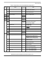
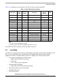
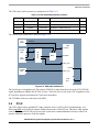
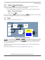
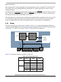
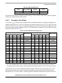
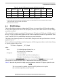
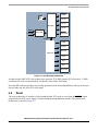
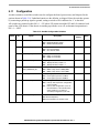
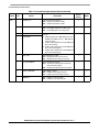
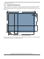
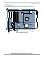
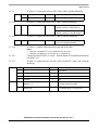
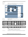
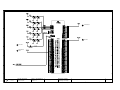
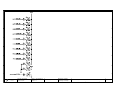
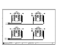
1
MPC8555E
Configurable Development System
Reference Manual
Supports
MPC8555E
MPC8541E
MPC8555CDSx3RM
Rev. 1, 11/2006
Contents
Paragraph
Number
Title
Page
Number
Contents
About This Book
Audience .......................................................................................................................... xiii
Organization..................................................................................................................... xiii
Suggested Reading........................................................................................................... xiv
General Information..................................................................................................... xiv
Signal Conventions .......................................................................................................... xiv
Acronyms and Abbreviations .......................................................................................... xiv
Chapter 1
Introduction
1.1
1.2
1.3
1.3.1
1.3.2
Background ...................................................................................................................... 1-1
Scope................................................................................................................................ 1-1
Overview.......................................................................................................................... 1-1
Features........................................................................................................................ 1-2
Diagrams...................................................................................................................... 1-4
Chapter 2
Quick Start-Up Guide
2.1
2.2
2.3
2.4
2.5
Hardware List .................................................................................................................. 2-1
Hardware Installation....................................................................................................... 2-1
Quick Start-Up ................................................................................................................. 2-5
How to Re-Flash U-Boot/Linux Image Using U-Boot .................................................... 2-6
Default Switch Configuration Table ................................................................................ 2-7
Chapter 3
CDS Carrier Architecture
3.1
3.1.1
3.1.2
3.2
3.3
3.3.1
3.3.2
3.3.2.1
3.3.2.2
Overview.......................................................................................................................... 3-1
Board Measurements ................................................................................................... 3-1
Block Diagrams ........................................................................................................... 3-1
Carrier Pinouts ................................................................................................................. 3-3
System Logic ................................................................................................................... 3-3
System Address Map ................................................................................................... 3-4
System Logic Registers ............................................................................................... 3-5
Version Register (CM_VER)................................................................................... 3-5
General Control Register (CM_CSR)...................................................................... 3-6
MPC8555E Configurable Development System Reference Manual, Rev. 1
Freescale Semiconductor
iii
Contents
Paragraph
Number
3.3.2.3
3.3.2.4
3.3.2.5
3.3.2.6
3.4
3.5
3.6
3.7
3.7.1
3.8
3.9
3.9.1
3.9.2
3.10
3.10.1
3.11
3.11.1
3.12
3.13
3.14
3.14.1
3.14.2
3.15
3.15.1
3.15.2
3.15.3
Page
Number
Title
Reset Control Register (CM_RST).......................................................................... 3-6
LED Data Register................................................................................................... 3-7
PCI Control/Status Register..................................................................................... 3-7
DMA Control Register ............................................................................................ 3-8
CPM Connections ............................................................................................................ 3-9
ATM Interfaces .............................................................................................................. 3-12
Ethernet Ports................................................................................................................. 3-12
Local Bus ....................................................................................................................... 3-15
NCDS Local Bus Signals........................................................................................... 3-17
Clock .............................................................................................................................. 3-18
PCI-X ............................................................................................................................. 3-19
PCI Arbitration .......................................................................................................... 3-20
PCI-X System Control ............................................................................................... 3-21
Exceptions...................................................................................................................... 3-21
Software Triggered Exceptions.................................................................................. 3-23
Reset............................................................................................................................... 3-23
Software Triggered Resets......................................................................................... 3-24
I2C ................................................................................................................................. 3-25
Configuration ................................................................................................................. 3-26
Power ............................................................................................................................. 3-28
+2.5-V Power............................................................................................................. 3-29
Power Management ................................................................................................... 3-29
Diagnostic Features........................................................................................................ 3-29
Analyzer Headers....................................................................................................... 3-29
Remote Debug Header............................................................................................... 3-33
Monitoring LEDs....................................................................................................... 3-33
Chapter 4
CDS Daughtercard Architecture
4.1
4.2
4.3
4.4
4.4.1
4.4.2
4.5
4.5.1
4.6
4.7
4.8
Mechanical Architecture.................................................................................................. 4-1
CDS Daughtercard (CDC) Block Diagram ..................................................................... 4-4
Processor .......................................................................................................................... 4-4
DDR Memory .................................................................................................................. 4-4
DDR Interface Termination ......................................................................................... 4-7
Recommended Part Numbers ...................................................................................... 4-8
Local Bus Interface .......................................................................................................... 4-8
Local Bus SDRAM Memory ..................................................................................... 4-10
Passive Connections ...................................................................................................... 4-10
Carrier Pinouts ............................................................................................................... 4-12
Clock .............................................................................................................................. 4-12
MPC8555E Configurable Development System Reference Manual, Rev. 1
iv
Freescale Semiconductor
Contents
Paragraph
Number
4.9
4.10
4.11
4.12
4.13
4.14
4.14.1
4.14.2
4.15
4.15.1
4.15.2
4.15.3
4.15.4
Title
Page
Number
PCI/PCI-X...................................................................................................................... 4-13
Reset............................................................................................................................... 4-13
Exceptions...................................................................................................................... 4-14
I2C ................................................................................................................................. 4-15
Configuration ................................................................................................................. 4-16
Power ............................................................................................................................. 4-16
Processor Core Power................................................................................................ 4-17
DDR VREF/Vt Power ............................................................................................... 4-18
Diagnostic Features........................................................................................................ 4-18
Logic Analyzer Header.............................................................................................. 4-18
JTAG Header ............................................................................................................. 4-19
LEDs .......................................................................................................................... 4-20
Test Points.................................................................................................................. 4-21
Chapter 5
Arcadia Motherboard Architecture
5.1
5.2
5.2.1
5.3
5.4
5.4.1
5.4.2
5.4.3
5.5
5.5.1
5.5.2
5.5.3
5.5.4
5.5.5
5.5.6
5.5.7
5.6
5.7
5.8
5.9
5.10
5.10.1
5.10.2
Features ............................................................................................................................ 5-1
Configurations ................................................................................................................. 5-2
CDS Motherboard........................................................................................................ 5-2
Architecture ..................................................................................................................... 5-3
Omni Bus ......................................................................................................................... 5-4
Parallel RapidIO .......................................................................................................... 5-5
Serial RapidIO ............................................................................................................. 5-6
PCI Express.................................................................................................................. 5-6
PCI/PCI-X Bus ................................................................................................................ 5-7
PCI Arbitration ............................................................................................................ 5-8
PCI Host Mode .......................................................................................................... 5-10
PCI Bridge ................................................................................................................. 5-10
PCI Interrupts............................................................................................................. 5-10
PCI Interrupt Bridge .................................................................................................. 5-13
PCI Configuration...................................................................................................... 5-13
PrPMC Connector...................................................................................................... 5-14
System Control .............................................................................................................. 5-14
Clocking......................................................................................................................... 5-15
Reset............................................................................................................................... 5-17
Power ............................................................................................................................. 5-18
Diagnostic Features........................................................................................................ 5-19
LEDs .......................................................................................................................... 5-19
JTAG .......................................................................................................................... 5-20
MPC8555E Configurable Development System Reference Manual, Rev. 1
Freescale Semiconductor
v
Contents
Paragraph
Number
5.11
5.11.1
5.12
5.13
5.14
Page
Number
Title
Configuration ................................................................................................................. 5-21
Power Supply Force Header ...................................................................................... 5-23
Mechanical..................................................................................................................... 5-23
Motherboard Dimensions .............................................................................................. 5-24
Placement....................................................................................................................... 5-25
Chapter 6
CDS IOCard Architecture
6.1
6.2
6.3
6.4
Mechanical Properties...................................................................................................... 6-1
IOCard Connector............................................................................................................ 6-2
IOCard Connector Pinout ................................................................................................ 6-3
IO Power .......................................................................................................................... 6-3
Chapter 7
uTCOM Architecture
7.1
7.2
7.2.1
7.2.2
7.3
Overview.......................................................................................................................... 7-1
Mechanical Architecture.................................................................................................. 7-2
uTCOM Connector ...................................................................................................... 7-2
uTCOM Connector Signals ......................................................................................... 7-2
uTCOM Pinout ................................................................................................................ 7-3
Appendix A
Revision History
A.1
Changes From Revision 0 to Revision 1 ........................................................................ A-1
Appendix B
Pinouts
B.1
B.2
B.3
Carrier/DaughterCard Connectors Pinout........................................................................B-1
IOCard Connector Pinout ................................................................................................B-5
uTCOM Connector Pinout...............................................................................................B-6
Appendix C
CDS Carrier BOM, Rev. 1.2
Appendix D
CDS Carrier Schematics, Rev. 1.2
MPC8555E Configurable Development System Reference Manual, Rev. 1
vi
Freescale Semiconductor
Contents
Paragraph
Number
Title
Page
Number
Appendix E
CDS Carrier BOM, Rev. 1.3
Appendix F
CDS Carrier Schematics, Rev. 1.3
Appendix G
CDS CDC BOM
Appendix H
CDS CPU Schematics (CDC)
Appendix I
CDS I/O Board Schematics
Appendix J
CDS uTCOM Schematics
Appendix K
CDS Arcadia BOM
Appendix L
CDS Arcadia X3 Schematics
Glossary
MPC8555E Configurable Development System Reference Manual, Rev. 1
Freescale Semiconductor
vii
Contents
Paragraph
Number
Page
Number
Title
MPC8555E Configurable Development System Reference Manual, Rev. 1
viii
Freescale Semiconductor
Figures
Figure
Number
Title
Page
Number
Figures
1-1
1-2
1-3
2-1
2-2
2-3
2-4
2-5
2-6
2-7
2-8
3-1
3-2
3-3
3-4
3-5
3-6
3-7
3-8
3-9
3-10
3-11
3-12
3-13
3-14
3-15
3-16
3-17
3-18
3-19
3-20
4-1
4-2
4-3
4-4
4-5
4-6
4-7
Carrier Block Diagram (Configuration 1)............................................................................... 1-4
Carrier Block Diagram (Configuration 2)............................................................................... 1-5
Daughtercard Block Diagram ................................................................................................. 1-5
Inserting Memory Module ...................................................................................................... 2-2
Removing Chassis Thumb Screws ......................................................................................... 2-2
Removing Chassis Top Cover................................................................................................. 2-2
Removing Chassis Side Panel................................................................................................. 2-3
Removing PCI Slot Bracket Screws ....................................................................................... 2-3
Install Carrier Card into PCI Slot............................................................................................ 2-4
Guide Pin Alignment .............................................................................................................. 2-4
Install PCI Bracket Screws ..................................................................................................... 2-5
Carrier Block Diagram (Configuration 1)............................................................................... 3-2
Carrier Block Diagram (Configuration 2)............................................................................... 3-3
Version Register (CM_VER) .................................................................................................. 3-5
Reset Control Register (CM_CSR)......................................................................................... 3-6
Reset Control Register (CM_RST) ......................................................................................... 3-6
Reset Control Register (CM_LED)......................................................................................... 3-7
PCI Control/Status Register (CM_PCI) .................................................................................. 3-7
Reset Control Register (CM_DMA) ....................................................................................... 3-8
CE/CPM Architecture ............................................................................................................. 3-9
CDS ATM Architecture ........................................................................................................ 3-12
CDS Ethernet Architecture (Configuration 1) ...................................................................... 3-14
CDS Ethernet Architecture (Configuration 2) ...................................................................... 3-14
CDS Local Bus Architecture................................................................................................. 3-16
CDS Clock Architecture ....................................................................................................... 3-19
CDS PCI Architecture........................................................................................................... 3-20
CDS Exception Architecture................................................................................................. 3-21
CDS Carrier Reset Architecture............................................................................................ 3-23
CDS Carrier I2C Architecture............................................................................................... 3-25
CDS Configuration Logic ..................................................................................................... 3-27
CDS Power Architecture....................................................................................................... 3-28
Daughtercard Placement ......................................................................................................... 4-2
CDC with 783 BGA Processor Example ................................................................................ 4-3
Daughtercard Block Diagram ................................................................................................. 4-4
CDS Memory Architecture ..................................................................................................... 4-5
CDC Memory Termination ..................................................................................................... 4-7
CDS Local Bus Architecture................................................................................................... 4-9
CDS Dual-PCI Architecture.................................................................................................. 4-13
MPC8555E Configurable Development System Reference Manual, Rev. 1
Freescale Semiconductor
ix
Figures
Figure
Number
4-8
4-9
5-1
5-2
5-3
5-4
5-5
5-6
5-7
5-8
5-9
6-1
6-2
7-1
Page
Number
Title
CDS Daughtercard Reset Architecture ................................................................................. 4-14
CDS Daughtercard I2C Architecture .................................................................................... 4-15
CDS-Compatible Arcadia Block Diagram.............................................................................. 5-3
Arcadia RapidIO Port Connections......................................................................................... 5-5
Arcadia PCI Arbitration Domains........................................................................................... 5-9
Arcadia PCI Interrupts Domains........................................................................................... 5-11
Arcadia PCI Clock Domains................................................................................................. 5-15
Arcadia Clock Architecture .................................................................................................. 5-17
Arcadia Reset Architecture ................................................................................................... 5-18
Arcadia ATX Chassis Mounting Holes ................................................................................. 5-24
Component Placement .......................................................................................................... 5-25
CDS IOCard Block Diagram .................................................................................................. 6-1
CDS IOCard Physical Dimensions ......................................................................................... 6-2
CDS uTCOM/TCOM Interface .............................................................................................. 7-1
MPC8555E Configurable Development System Reference Manual, Rev. 1
x
Freescale Semiconductor
Tables
Table
Number
Title
Page
Number
Tables
2-1
2-2
2-3
3-1
3-2
3-3
3-4
3-5
3-6
3-7
3-8
3-9
3-10
3-11
3-12
3-13
3-14
3-15
3-16
3-17
3-18
3-19
3-20
3-21
3-22
3-23
3-24
3-25
3-26
3-27
3-28
3-29
3-30
3-31
3-32
4-1
4-2
4-3
Default Status of Processor Board (CPU Card) Switches....................................................... 2-7
Default Status of Carrier Board Switches (Configuration 1) .................................................. 2-9
Default Status of Arcadia Board Switches (Arcadia C3.n)................................................... 2-10
Memory Map........................................................................................................................... 3-4
Cadmus Address Map ............................................................................................................. 3-5
CM_VER Field Descriptions .................................................................................................. 3-5
CM_CSR Field Descriptions .................................................................................................. 3-6
CM_RST Field Descriptions................................................................................................... 3-6
CM_LED Field Descriptions .................................................................................................. 3-7
CM_PCI Field Descriptions.................................................................................................... 3-8
CM_DMA Field Descriptions................................................................................................. 3-9
CDS CPM/CE Connection Options ...................................................................................... 3-10
CPM Port Routing for FCC1 in ATM622/UTOPIA 8 Mode................................................ 3-10
CPM Port Routing for FCC2 in ATM155 Mode................................................................... 3-10
CPM/CE Switch Summary ................................................................................................... 3-11
ATM Port Overview.............................................................................................................. 3-12
PHY Address Options (Configuration 1) ............................................................................ 3-13
CDS TSEC Interface Summary ............................................................................................ 3-15
CDS Carrier Local Bus Signals ............................................................................................ 3-16
CDS Cxx Local Bus Signals ................................................................................................ 3-17
CLA Mapping ....................................................................................................................... 3-18
CDS Clock Requirements Summary..................................................................................... 3-19
CDS PCI Properties .............................................................................................................. 3-20
CDS Exception Properties .................................................................................................... 3-22
CDS Reset Sources ............................................................................................................... 3-24
CDS Reset Outputs ............................................................................................................... 3-24
CDS I2C Bus Properties ....................................................................................................... 3-26
CDS Configuration Parameters............................................................................................. 3-26
CDS Available Power ........................................................................................................... 3-28
CDS Local Bus ‘STAT’ Header Definition........................................................................... 3-30
CDS Local Bus ‘ADDR’ Header Definition......................................................................... 3-31
CDS Local Bus ‘DATA’ Header Definition .......................................................................... 3-32
CDS Remote Header ............................................................................................................. 3-33
CDS Debug Header Definition ............................................................................................. 3-33
CDS LEDs............................................................................................................................. 3-33
CDS DDR SDRAM Properties ............................................................................................... 4-6
CDS DDR SDRAM Compatibility ......................................................................................... 4-8
CDS Daughtercard Local Bus Signals .................................................................................. 4-10
MPC8555E Configurable Development System Reference Manual, Rev. 1
Freescale Semiconductor
xi
Tables
Table
Number
4-4
4-5
4-6
4-7
4-8
4-9
4-10
4-11
4-12
4-13
4-14
4-15
4-16
5-1
5-2
5-3
5-4
5-5
5-6
5-7
5-8
5-9
5-10
5-11
5-12
5-13
5-14
5-15
6-1
7-1
7-2
7-3
B-1
B-2
B-3
B-4
B-5
F-1
Page
Number
Title
CDS Daughtercard Connector Overview.............................................................................. 4-11
CDC Clocks .......................................................................................................................... 4-12
CDC PCI2 IDSEL Mapping ................................................................................................. 4-13
CDS Exception Properties .................................................................................................... 4-15
CDS Daughtercard I2C Bus Properties................................................................................. 4-16
CDC Available Power ........................................................................................................... 4-17
CDC VDD (Vcore) Encoding Table ..................................................................................... 4-17
CDC ADC Current Measurement Conversion Table............................................................ 4-18
CDS Daughtercard P6860 Analyzer Header Definition ....................................................... 4-19
CDS JTAG Header................................................................................................................ 4-19
CDS COP Header Definition ................................................................................................ 4-20
CDC Diagnostic LEDs.......................................................................................................... 4-20
CDS Test Point List............................................................................................................... 4-21
Arcadia Architecture Feature Summary ................................................................................. 5-4
Arcadia Parallel RapidIO Connector Definition ..................................................................... 5-5
Arcadia Serial RapidIO Connector Definition........................................................................ 5-6
Arcadia PCIExpress Connector Definition ............................................................................. 5-6
Arcadia PCIBus Name Examples ........................................................................................... 5-8
PCI Arbitration Ports .............................................................................................................. 5-9
Arcadia 3.1 Interrupt Assignments ....................................................................................... 5-12
PCI Configuration Addresses................................................................................................ 5-14
PCI Clock Domain Summary ............................................................................................... 5-16
Arcadia Slot Power Availability............................................................................................ 5-19
Arcadia Diagnostic LEDs ..................................................................................................... 5-19
Arcadia Diagnostic LEDs: PCI Speed Encoding .................................................................. 5-20
Arcadia JTAG Chain ............................................................................................................. 5-20
Arcadia Configuration Switches ........................................................................................... 5-21
Arcadia Power Supply Force Header.................................................................................... 5-23
CDS IOCard Connector Details .............................................................................................. 6-2
CDS uTCOM Connector Details ............................................................................................ 7-2
uTCOM Pin Routing to TCOM Board (P1 Connector) .......................................................... 7-3
uTCOM Pin Routing to TCOM Board (P2 Connector) .......................................................... 7-5
Daughtercard Connector (Left) Definition and Pinout ...........................................................B-1
Daughtercard Connector (Right) Definition and Pinout .........................................................B-2
Daughtercard High-Speed Connector Definition and Pinout .................................................B-3
IOCard Connector Definition and Pinout ...............................................................................B-5
uTCOM Connector (Right) Definition and Pinout .................................................................B-6
Differences Between Carrier Card Rev. 1.2 and Rev. 1.3....................................................... F-1
MPC8555E Configurable Development System Reference Manual, Rev. 1
xii
Freescale Semiconductor
About This Book
The primary objective of this reference manual is to define the functionality of the MPC8555E
configurable development system (CDS). It is also intended to describe in detail the configurability of the
CDS through the description of individual components and their interchangeability. Included is detailed
descriptions of the physical design, device architecture, and testing/debugging procedures.
Audience
It is assumed that the reader understands operating systems, microprocessor system design, and the basic
principles of RISC processing.
Organization
Following is a summary and a brief description of the major parts of this reference manual:
• Chapter 1, “Introduction,” provides a high-level description of features and functionality of the
CDS. Included is a list of the configurable features, as well as basic block diagrams.
• Chapter 2, “Quick Start-Up Guide,” describes step-by-step how to bring up a CDS development
board.
• Chapter 3, “CDS Carrier Architecture,” describes in detail the CDS carrier system. It describes the
physical layout and assembly, as well as basic and detailed system architecture. It elaborates on
usage and testing/debugging procedures.
• Chapter 4, “CDS Daughtercard Architecture,” covers the CDS daughtercard design in more detail.
It describes the physical layout as well as part connections and device interfaces. It includes a
detailed description of the system architecture, along with the device configuration and debugging
procedures.
• Chapter 5, “Arcadia Motherboard Architecture,” describes the design information on the Arcadia
reference platform.
• Chapter 6, “CDS IOCard Architecture,” describes in detail the IOCard. It elaborates on the
physical architecture and device connections, as well as the power management and usage.
• Chapter 7, “uTCOM Architecture,” describes the uTCOM interface, as well as its physical
properties.
• Appendix A, “Revision History,” describes the major differences between revisions of this
reference manual.
• Appendix B, “Pinouts,” contains detailed pinout specifications for the CDS. It includes:
— Carrier/daughtercard connectors pinout
— IOCard connector pinout
— uTCOM connector pinout
MPC8555E Configurable Development System Reference Manual, Rev. 1
Freescale Semiconductor
xiii
About This Book
•
•
•
•
•
•
•
•
•
•
•
Appendix C, “CDS Carrier BOM, Rev. 1.2”
Appendix D, “CDS Carrier Schematics, Rev. 1.2”
Appendix E, “CDS Carrier BOM, Rev. 1.3”
Appendix F, “CDS Carrier Schematics, Rev. 1.3”
Appendix G, “CDS CDC BOM”
Appendix H, “CDS CPU Schematics (CDC)”
Appendix I, “CDS I/O Board Schematics”
Appendix J, “CDS uTCOM Schematics”
Appendix K, “CDS Arcadia BOM”
Appendix L, “CDS Arcadia X3 Schematics”
This reference manual also includes a glossary.
Suggested Reading
This section lists additional reading that provides background for the information in this manual as well as
general information about the architecture.
General Information
The following documentation provides useful information about the CDS architecture:
• The PowerPC Architecture: A Specification for a New Family of RISC Processors, Second Edition,
by International Business Machines, Inc.
For updates to the specification, see http://www.austin.ibm.com/tech/ppc-chg.html.
• Computer Architecture: A Quantitative Approach, Third Edition, by John L. Hennessy and
David A. Patterson.
• Computer Organization and Design: The Hardware/Software Interface, Second Edition, by
David A. Patterson and John L. Hennessy.
Signal Conventions
OVERBAR
lowercase_italics
lowercase_plaintext
An overbar indicates that a signal is active-low.
Lowercase italics is used to indicate internal signals.
Lowercase plain text is used to indicate signals that are used for configuration.
Acronyms and Abbreviations
Table i contains acronyms and abbreviations used in this document.
MPC8555E Configurable Development System Reference Manual, Rev. 1
xiv
Freescale Semiconductor
About This Book
Table i. Glossary of Terms
Term
ATM
CARRIER
Description
Asynchronous transfer mode
HIP-compliant HIPcard such as CDS, Elysium, etc.
CDC
CPU daughtercard
CDS
Configurable development system; customer development system
CPM
Communications processing machine
Daughtercard
CPU-specific daughtercard which connects to a carrier board
DDR
Double-data rate
GMII
Gigabit media-independent interface
HIP
Hardware interoperability platform
IOCARD
LB
MAC
MII
Motherboard
OUI
IO breakout card for a carrier board
Local bus (that is, Flash/SRAM/SDRAM interface)
Media access control
Media-independent interface
HIP-compliant motherboard such as Arcadia, etc.
Organizationally unique identifier
PC-1600
DDR providing 1600 MB/s bandwidth (@8 bytes/clk = 200 MHz)
PC-2100
DDR providing 2100 MB/s bandwidth (@8 bytes/clk = 266 MHz)
PHY
Physical interface
PM
Performance monitor
RIO
RapidIO
TSEC
Triple-speed Ethernet controller (10/100/1G speeds)
TWG
Technical working group
MPC8555E Configurable Development System Reference Manual, Rev. 1
Freescale Semiconductor
xv
About This Book
MPC8555E Configurable Development System Reference Manual, Rev. 1
xvi
Freescale Semiconductor
Chapter 1
Introduction
1.1
Background
The configurable development system (CDS) was developed to support a wide range of Power
Architecture™ processors, such as the MPC8555E and the MPC8541E. . The system is primarily a
development and evaluation system, which is enhanced by its modular design, making it highly
configurable.
1.2
Scope
This reference manual describes the Freescale CDS development platform. It provides details on the
MPC8555E CDS hardware configuration and functionality. It is intended primarily as a guide for hardware
and software designers.
1.3
Overview
The CDS system is the middle ground between evaluation and test boards. It is more configurable and
flexible than an evaluation board, but it is not as configurable as a test board, in which every component
can be tested and examined. Where it lacks configurability, its design has options for the most common
settings.
Two MPC8555E CDS development system configurations are described. The configurations consist of
different board revisions which are referenced throughout this manual as Configuration 1 or
Configuration 2. The configurations are:
• Configuration 1
— Arcadia, Rev. 3.1
— Carrier card, Rev. 1.2
— CPU card, Rev. 1.1
— I/O card, Rev. 1.1
• Configuration 2
— Arcadia, Rev. 3.1
— Carrier card, Rev. 1.3
— CPU card, Rev. 1.1
Refer to Appendix F, “CDS Carrier Schematics, Rev. 1.3,” Table F-1, for hardware differences between
carrier card, Rev. 1.2 and Rev. 1.3.
MPC8555E Configurable Development System Reference Manual, Rev. 1
Freescale Semiconductor
1-1
Introduction
1.3.1
Features
NOTE
The CDS system can be configured to boot as MPC8555E or MPC8541E.
The CDS system by default is configured as MPC8555E. To evaluate the
CDS system as MPC8541E, refer to Section 2.5, “Default Switch
Configuration Table,” switch-4, bit-4 on CPU card.
A CDS system includes the following features:
• Processor-specific daughtercard, featuring
— One or more Freescale MPC8555E processor(s)
— ECC-compatible DDR-I (processor-specific type)
— Test features (JTAG, P6880 passive probe for critical routes only)
– P6880 ‘banjo’ header probing critical signals only
– All other debug is via carrier or DIMM debug module
— Local support for secondary interfaces (such as PCI) as needed
– PCI32 header (3.3 V, 32-bit, PCI-X, 33/66 MHz compatible) where required
— Local switching power supply, supplying VDD (VCORE)
– Supplies up to 15 W (~1.1 V at 12 A)
– Derivable from +5 or +3.3 V (not +12 V)
– Programmable voltage via I2C configuration
— I2C bus
– ID EEPROM (256b) for card at 0x50
– Configurable EEPROM (8K) for CPU at 0x57
– Memory SPD EEPROM for memory at 0x51
– Voltage monitoring
– Configuration control
— Local bus generation
– Includes any necessary demultiplexing
– Local SDRAM support (as appropriate)
— High-speed/high-density connectors for all CPU signals except core power and memory
— Configuration options
– Switch programmable defaults
– I2C remote configuration/override
— Debug support
– JTAG (COP) header
– Monitoring LEDs
• Carrier board
— Supports numerous processor daughtercards
MPC8555E Configurable Development System Reference Manual, Rev. 1
1-2
Freescale Semiconductor
Introduction
— Supports two Ethernet ports on the carrier card at MII/GMII, and two Ethernet ports on the I/O
adapter at MII/GMII, 10/100 or 1G rates (Configuration 1).
NOTE
In Configuration 1, Ethernet port #4 on the I/O card is not functional.
— Supports all four Ethernet ports on the carrier card. MII/GMII on Ethernet ports #1 and #2.
RGMII on Ethernet ports #3 and #4, 10/100 or 1G rates (Configuration 2).
— Quickswitch-controlled routing of selected CPM signals between uTCOM header and local
peripherals (optical ATM OC3/OC12 and/or 10/100 console Ethernet).
— UTOPIA L2/AdTech connector for OC12 ATM port
— Supports USB connector (as wires only—USB PHY is on the daughtercard, if needed)
— Supports serial port for Linux/U-Boot console I/O
— Differential probing on receive path with Tek P6880
— PCI/PCI-X 32/64 bits, 33/66 MHz
NOTE
PCI arbitration is not supported on the carrier card. The MPC8555CDS
board does not support PCI-X mode.
— Includes IO adapter board (Configuration 1)
MPC8555E Configurable Development System Reference Manual, Rev. 1
Freescale Semiconductor
1-3
Introduction
1.3.2
Diagrams
Figure 1-1 is a diagram of the CDS system for Configuration 1.
OC12
ATM
PHY
OC3
ATM
PHY
AdTech
IOCard
MUX
uTCOM
USB
Flash
10/100
#4
NVRAM
Quad
PHY
CPU
Daughtercard
BUF
GBit
#3
DEBUG
RST
GBit
#1
Local
Clock
H/S
Clock
GBit
#2
UART
PCI-X
+2.5-V
Power
Figure 1-1. Carrier Block Diagram (Configuration 1)
MPC8555E Configurable Development System Reference Manual, Rev. 1
1-4
Freescale Semiconductor
Introduction
Figure 1-2 is a diagram of the CDS system for Configuration 2.
OC3
ATM
PHY
OC12
ATM
PHY
AdTech
MUX
uTCOM
GBit
#1
Flash
GBit
#2
GBit
#3
BUF
NVRAM
Quad
PHY
CPU
Daughtercard
DEBUG
GBit
#4
UART
Local
Clock
H/S
Clock
+2.5-V
Power
PCI-X
Figure 1-2. Carrier Block Diagram (Configuration 2)
Figure 1-3 is a diagram of a CDS daughtercard, or a CDC.
Vtt
DDR SDRAM DIMM
DEBUG
CPU
VTT
Power
Core
Power
or
PCI/X
CPU/Bridge
JTAG
LBIF
CFG
Local Mem
Header
(Right)
Header
(Left)
I2C ID
Figure 1-3. Daughtercard Block Diagram
This representation shows only one design, other daughtercards can be designed for different CPUs.
MPC8555E Configurable Development System Reference Manual, Rev. 1
Freescale Semiconductor
1-5
Introduction
MPC8555E Configurable Development System Reference Manual, Rev. 1
1-6
Freescale Semiconductor
Chapter 2
Quick Start-Up Guide
This chapter provides a step-by-step guide for bringing up a CDS.
2.1
Hardware List
The hardware configurations consist of different board revisions which are referenced throughout this
manual as Configuration 1 or Configuration 2. Refer to Appendix F, “CDS Carrier Schematics, Rev. 1.3,”
Table F-1, for hardware differences between carrier card, Rev. 1.2 and Rev. 1.3. The configurations are:
• Configuration 1
— Arcadia, Rev. 3.1
— Carrier card, Rev. 1.2
— CPU card, Rev. 1.1
— I/O card, Rev. 1.1
• Configuration 2
— Arcadia, Rev. 3.1
— Carrier card, Rev. 1.3
— CPU card, Rev. 1.1
The CDS system is installed in a PC box and includes a power supply. The CDS system is preloaded with
U-boot and Linux BSP.
2.2
Hardware Installation
Remove the CDS system chassis from the cartons and perform the following steps:
NOTE
The carrier card and processor card are packaged together.
MPC8555E Configurable Development System Reference Manual, Rev. 1
Freescale Semiconductor
2-1
Quick Start-Up Guide
1. Insert memory module, noting the correct KEYING orientation, and snap into the socket. See
Figure 2-1.
Figure 2-1. Inserting Memory Module
2. To remove the top chassis cover, stand chassis on end and remove the two top thumb screws located
in back of the chassis. See Figure 2-2.
Figure 2-2. Removing Chassis Thumb Screws
3. Slide top cover toward the back while lifting, and remove. See Figure 2-3.
Figure 2-3. Removing Chassis Top Cover
MPC8555E Configurable Development System Reference Manual, Rev. 1
2-2
Freescale Semiconductor
Quick Start-Up Guide
4. Remove both side covers by lifting straight up. See Figure 2-4.
Figure 2-4. Removing Chassis Side Panel
5. Now lay chassis on the side with the motherboard exposed.
6. Remove PCI bracket screws. See Figure 2-5.
Figure 2-5. Removing PCI Slot Bracket Screws
MPC8555E Configurable Development System Reference Manual, Rev. 1
Freescale Semiconductor
2-3
Quick Start-Up Guide
7. Insert carrier card assembly into the PCI Slot 1. See Figure 2-6 and Figure 2-7.
NOTE
The alignment pins to guide the carrier card into the proper position are on
the Arcadia motherboard.
Figure 2-6. Install Carrier Card into PCI Slot
Figure 2-7. Guide Pin Alignment
8. Push the carrier card assembly down firmly to fully seat connectors.
MPC8555E Configurable Development System Reference Manual, Rev. 1
2-4
Freescale Semiconductor
Quick Start-Up Guide
9. Re-install the PCI bracket screws. See Figure 2-8.
Figure 2-8. Install PCI Bracket Screws
2.3
Quick Start-Up
1. Connect the CDS system to a 120-V AC power source. (For outside the U.S., a 240-V power supply
must be installed in the box and connected to an AC power source.)
2. Connect the null modem serial cable between the carrier board COM1 port and the PC workstation
serial port (COM1 or COM2).
3. Start up the terminal emulator program, (i.e., HyperTerminal) and setup the PC terminal program
to use the following settings:
— Bits per second: 115200
— Data bits: 8
— Parity: none
— Stop bits: 1
— Flow control: none
4. Turn on the CDS system by pushing the power switch on the front of the PC box.
5. After power-up by default, the system autoboots in Linux. However, if the autoboot is halted, the
user should see the U-boot prompt. The following is only an example of a U-boot screen dump at
bootup. The actual screen dump may vary depending on specific system configurations.
U-Boot 1.1.3 (FSL Development) (Oct 27 2006 - 10:43:18)
CPU:
8555, Version: 1.1, (0x80790011)
Core: E500, Version: 2.0, (0x80200020)
Clock Configuration:
CPU: 833 MHz, CCB: 333 MHz,
DDR: 166 MHz, LBC: 83 MHz
L1:
D-cache 32 kB enabled
I-cache 32 kB enabled
Board: CDS Version 0x13
MPC8555E Configurable Development System Reference Manual, Rev. 1
Freescale Semiconductor
2-5
Quick Start-Up Guide
CPU Board Revision 0.0 (0x0000)
PCI1: 32 bit, 33 MHz, sync
PCI2: 32 bit, 66 MHz, async
I2C:
ready
DRAM: Initializing
SDRAM: 64 MB
DDR: 256 MB
FLASH: 16 MB
L2 cache 256KB: enabled
In:
serial
Out:
serial
Err:
serial
Net:
TSEC0: PHY is Marvell 88E1145 (1410cd4)
TSEC1: PHY is Marvell 88E1145 (1410cd4)
TSEC0, TSEC1
The IP address of the board is currently set to 169.254.113.58
The MAC address is 00:04:9F:00:28:C8
If they don't match your network environment, please change them in U-Boot and kernel
manually.
Hit any key to stop autoboot: 0
=>
6. By typing ‘boot’ at command prompt the system will boot to Linux.
2.4
How to Re-Flash U-Boot/Linux Image Using U-Boot
There are two banks of Flash memory in the CDS system, and are selected by switch 2, bits 1 and 2 on the
carrier card. Following are the instructions to program the U-boot binary file Linux image into the bank of
Flash memory as sent from the factory:
• To re-flash the U-boot follow steps 1 to 7.
• To re-flash Linux image follow steps 8 to 12.
• Requirement:
— A running TFTP server who hosts the u-boot.bin file
— The running U-boot should have the correct ‘ipaddr’, ‘serverip’, and ‘netmask’ parameters.
The parameters can be modified by command ‘setenv <VARIABLE NAME> <VARIABLE
VALUE>’
1. Boot the CDS with U-boot, hit any key to stop the timer
2. tftp 1000000 u-boot.bin
3. prot off all
4. erase fff80000 ffffffff
5. cp.b 1000000 fff80000 80000
6. reset
7. The new U-boot will boot up, hit any key to stop the timer
8. tftp 1000000 vmlinux.219
9. tftp 2000000 ramdisk.u-boot
MPC8555E Configurable Development System Reference Manual, Rev. 1
2-6
Freescale Semiconductor
Quick Start-Up Guide
10. erase ff800000 ffdfffff
11. cp.b 1000000 ff800000 1fffff
12. cp.b 2000000 ffa00000 3fffff
Steps 13 to 16 are required to update the environment variables.
13. setenv bootargs root=/dev/ram rw console=ttyS1,115200
14. setenv bootcmd bootm ff800000 ffa00000
15. saveenv
16. reset
2.5
Default Switch Configuration Table
The CDS system has several options for the switch settings to allow users to easily change the
configuration. Table 2-1, Table 2-2, and Table 2-3 show the default switch settings for targeted
applications. For the processor board (CPU card) switches shown in Table 2-1 and the carrier board
switches shown in Table 2-2, in order to set an option value to 1, set the switch to ON; to set an option
value to 0, set the switch to OFF. For the Arcadia board switches shown in Table 2-3, in order to set an
option value to 1, set the switch to ON; to set an option value to 0, set the switch to OFF.
Table 2-1. Default Status of Processor Board (CPU Card) Switches
Name
Default
(1 = ON)
SW
Bit
1
1
PCI1 bus impedance
1
0 25 Ω
1 42 Ω (Default)
2
PCI1 debug enable
1
Default
3
DDR debug enable
1
4
Memory debug enable
1
5
Local bus hold LWE[0:1]
1
6
1
Note
00
01
10
11
One extra delay
Two extra delays
Three extra delays
Default/specified AC timing
7
PCI1 clock select
1
1 Sync (use SYSCLK) default
0 Async (use PCI1CLK)
8
PCI2 clock select
0
1 Sync (use SYSCLK)
0 Async (use PCI2CLK) default
MPC8555E Configurable Development System Reference Manual, Rev. 1
Freescale Semiconductor
2-7
Quick Start-Up Guide
Table 2-1. Default Status of Processor Board (CPU Card) Switches (continued)
SW
Bit
2
1
3
Name
Core voltage
1
2
0
3
0
4
1
5
1
Note
10011 1.200 V
6
Local bus size
1
0 8-bit Flash
1 16-bit Flash (default)
7
Memory ECC Mux
1
0 Switch MECC to debug header
1 Connect MECC to DIMM, normally
8
PCI dual
1
1 PCI1 is 32-bit, PCI2 is 32-bit
0 PCI1 is 64-bit (or 32-bit), PCI2 is OFF
1
Reserved
0
00 (default) Reserved
2
3
0
Core clock PLL[0:1]
4
5
4
Default
(1 = ON)
0
1
CCB clock PLL[0:3]
1
6
0
7
1
8
0
1
Boot sequencer [0:1]
2
1
1
00
01
10
11
2:1
5:2 (default)
3:1
7:2
0000
0010
0011
0100
0101
0110
1000
1001
1010
1100
Rest
16:1
2:1
3:1
4:1
5:1
6:1
8:1
9:1
10:1(default)
12:1
Reserved
01 Standard I2C EEPROM
10 Extended I2C EEPROM
11 No EEPROM
3
CPU boot enable
1
Halt CPU until external host enable it
Allow CPU to run immediately after reset
4
Processor identity
—
0 MPC8541E
1 MPC8555E
5
PCI host/agent
1
0 = Agent
1 = Host (default)
6
Boot location
1
000
001
010
101
110
111
7
1
8
0
Boot from PCI bus #1
Boot from DDR
Boot from PCI bus #2
Boot from local bus, 8-bit
Boot from local bus, 16-bit
Boot from local bus, 32-bit
MPC8555E Configurable Development System Reference Manual, Rev. 1
2-8
Freescale Semiconductor
Quick Start-Up Guide
Table 2-2. Default Status of Carrier Board Switches (Configuration 1)
Name
Default
(1 = ON)
SW
Bit
1
1
SYSCLK SEL
0
0 PCICLK used for SYSCLK
1 LCLCLK used for SYSCLK
2
Synchronizer
1
1 Must be 1 at all times
(PHY CLK/FPGA CLK)
3
Reserved
1
See Note 1
4
Local clock S(2:0)
0
01 Part of 33 MHz SYSCLK
5
1
6
1
7
Local clock R(4:3)
8
2
1
00 Part of 33 MHz SYSCLK
0
Boot select
2
0
0
00
01
10
11
Flash bank 1, bank 2 available
Flash bank 2, bank 1 available
Promjet, bank 1 available
Promjet, bank 2 available
3
NVRAM enable
1
0 NVRAM disable
1 NVRAM available
4
Event select
1
0 UDE
1 SRESET
5
Reserved
1
1 Reserved
6
Reserved
1
1 Reserved, see Note 2
7
User defined
0
00 User defined, software readable
8
3
0
Note
0
1
Reserved
1
1 Reserved
2
DUART output select
1
0 DUART channel #2 to 2x5 (AT) header
DUART channel #1 to DB9 connector
1 DUART channel #2 to DB9 connector
DUART channel #1 to 2x5 (AT) header
3
ATM 2 enable
1
0 ATM2/155 enabled
1 ATM2/155 disabled
4
ATM 1 width
1
0 ATM1/16-bit IO enabled
1 ATM1/16-bit IO disabled
5
ADTech select
0
0 AdTech disabled
1 AdTech enabled
6
FE select
0
0 FCC3->Cicada MII#4 enabled
1 FCC3->Cicada MII#4 disabled
7
ATM2 select
1
0 FCC2->PMC 155M ATM enabled
1 FCC2->PMC 155M ATM disabled
8
ATM1 select
1
0 FCC1->PMC 625M ATM enabled
1 FCC1->PMC 625M ATM disabled
MPC8555E Configurable Development System Reference Manual, Rev. 1
Freescale Semiconductor
2-9
Quick Start-Up Guide
Table 2-2. Default Status of Carrier Board Switches (Configuration 1) (continued)
SW
Bit
4
1
Name
Local clock R(2:1)
2
3
Default
(1 = ON)
1
Note
10 Part of 33 MHz SYSCLK
0
Local clock V(6:1)
0
4
0
5
1
6
0
7
0
8
0
001000 Part of 33 MHz SYSCLK
Notes:
1. SW1(3) for Configuration 2 is PCI CLK SEL and must be set to 1.
2. SW2(6) for Configuration 2 is PCI Select PCI = 1 and PCIX = 0.
b
Table 2-3. Default Status of Arcadia Board Switches (Arcadia C3.n)
Name
Default
(1 = ON)
SW
Bit
Note
1
1
TSI310: BAR_EN
0
0 BAR0 disabled
1 BAR0 enabled
2
Secondary bus internal arbiter enable
TSI310: S_INT_ARB_EN
0
0 Use internal arbiter
1 Use external arbiter
3
Physical width of the PCI-X device
TSI310: 64_BIT_DEVICE
0
0 Bridge is a 64-bit bus
1 Bridge is a 32-bit bus
4
Opaque region enable
TSI310: OPAQUE_EN
0
0 Opaque memory enable
1 Opaque memory enable
5
Secondary PCI IDSEL remap
TSI310: IDSEL_REROUTE_EN
0
0 IDSEL remap mask is 0000_0000
1 IDSEL remap mask is 22F2_0000
6
Secondary high-speed rate select
TSI310: S_SEL100
1
0 PCI-X highest speed is 133 MHz
1 PCI-X highest speed is 100 MHz
7
Primary configuration busy
TSI310: P_CFG_BUSY
0
0 Primary side responds to configuration cycles
normally
1 Primary side configuration cycles are retried until
bit 2 of the miscellaneous control registers is set
to 0 by a secondary configuration cycle write
8
Primary driver mode control
TSI310: P_DRVR_MODE
0
0 Normal impedance
1 Lower impedance for heavier loads
MPC8555E Configurable Development System Reference Manual, Rev. 1
2-10
Freescale Semiconductor
Quick Start-Up Guide
Table 2-3. Default Status of Arcadia Board Switches (Arcadia C3.n) (continued)
Bit
2
1
ARC0
0
0 SIOINT -> PCIB3_INT0
1 SIOINT -> PCIB3_INT1
2
ARC1
1
Reserved
3
3
Name
Default
(1 = ON)
SW
Note
ARC2
1
Reserved
4
1
G0
1
User defined
5
1
G1
1
User defined
6
2
LPCWP*
1
User defined
7
Reserved
1
N/A
8
Reserved
1
N/A
1
Isolate slow PCI bus segment
ISOLATE_3_4
0
0 PCIB3 connected to PCIB4
1 PCIB3 isolated from PCIB4
2
TSI310 PCI bridge enable
BRIDGE_EN*
0
0 PCI bridge responds to config cycles
1 PCI bridge ignores all config cycles
3
PCI A (fast) bus speed force
PCIA_FRC1
11
4
PCI A (fast) bus speed force
PCIA_FRC0
00 AUTO (33 MHz when M66_EN input is 0 or
66 MHz when M66_EN is a 1 (M66_EN pin is
three-stated)
01 PCIA forced to 66 MHz PCI mode (M66_EN pin
is three-stated)
10 PCIA forced to 33 MHz PCI mode (M66_EN pin
is driven with logic 0)
11 PCIA forced to 33 MHz PCI mode (M66_EN pin
is driven with logic 0)
5
RTK8139 Ethernet enable
ENET_DIS*
1
0 RealTek 8139 may be accessed
1 RealTek 8139 cannot be accessed
6
PCI bus interrupt connection
PCI_INT_BRIDGE*
0
0 PCIA and PCIB interrupts are directly connected
(wire-or’d)
1 PCIA and PCIB interrupts are isolated
73
PrPMC IDSEL enabled
PRPMC_IDSELEN*
1
0 PrPMC can be target selected
1 PrPMC cannot be target selected
84
MONARCH*
1
0 PrPMC is PCIB controller
1 PrPMC is not PCIB controller
Notes:
1. Software-defined switches.
2. Optional feature.
3. Some PCI devices do not allow their own IDSEL to be asserted when operating as the PCI host; if so, use this switch to
disable IDSEL. Not applicable for PCI agents.
4. This switch configures the MPMC card into the system controller, a mode which is required for normal PCI use. Disabling is
provided for testing purposes only.
MPC8555E Configurable Development System Reference Manual, Rev. 1
Freescale Semiconductor
2-11
Quick Start-Up Guide
MPC8555E Configurable Development System Reference Manual, Rev. 1
2-12
Freescale Semiconductor
Chapter 3
CDS Carrier Architecture
This chapter describes in detail the CDS carrier system. It describes the physical layout and assembly, as
well as basic and detailed system architecture. This chapter elaborates on usage and testing/debugging
procedures.
The CDS carrier is the backbone of the CDS system. It facilitates communication between the components
as well as with outside parts through the PCI port.
3.1
Overview
The following sections give the CDS board measurements and block diagram.
3.1.1
Board Measurements
For the CDS carrier, the mechanical dimensions are driven by the RapidIO Hardware Interoperability
Platform standard. The placement of the RapidIO header (redefined for the CDS system as a flexible
high-speed port), the additional power connectors, and the guide pins are detailed in this manual.
3.1.2
Block Diagrams
Figure 3-1 is a diagram of the CDS board for Configuration 1.
MPC8555E Configurable Development System Reference Manual, Rev. 1
Freescale Semiconductor
3-1
CDS Carrier Architecture
OC3
ATM
PHY
OC12
ATM
PHY
AdTech
IOCard
MUX
uTCOM
USB
Flash
10/100
#4
NVRAM
Quad
PHY
CPU
Daughtercard
BUF
GBit
#3
DEBUG
RST
GBit
#1
Local
Clock
H/S
Clock
GBit
#2
UART
PCI-X
+2.5 V
Power
Figure 3-1. Carrier Block Diagram (Configuration 1)
MPC8555E Configurable Development System Reference Manual, Rev. 1
3-2
Freescale Semiconductor
CDS Carrier Architecture
Figure 3-2 is a diagram of the CDS system for Configuration 2.
OC3
ATM
PHY
OC12
ATM
PHY
AdTech
MUX
uTCOM
GBit
#1
Flash
GBit
#2
GBit
#3
CPU
Daughtercard
BUF
NVRAM
Quad
PHY
DEBUG
GBit
#4
UART
Local
Clock
H/S
Clock
PCI-X
+2.5-V
Power
Figure 3-2. Carrier Block Diagram (Configuration 2)
3.2
Carrier Pinouts
For a detailed pinout, including the numbering, refer to Appendix B.1, “Carrier/DaughterCard Connectors
Pinout.”
3.3
System Logic
The CDS board contains an FPGA/CPLD called Cadmus which collects various logic and performs system
control functions, including:
• System reset sequencer
• System logic address map
• PCI bus speed monitor
• LED monitors
• Peripheral bus development (chip select, address align)
• System controls
MPC8555E Configurable Development System Reference Manual, Rev. 1
Freescale Semiconductor
3-3
CDS Carrier Architecture
3.3.1
System Address Map
Table 3-1 describes the CDS memory map as implemented for U-Boot and Linux platform. Cadmus uses
the local bus chip selects to implement the following two critical features:
• Boot flash redirection
• Cadmus register intervention
Table 3-1. Memory Map
Chip
Select
Description
LCS0
Flash (boot bank)
0xFF80_0000 -----0xFFFF_FFFF
8M
LCS1
Flash (2nd bank)
0xFF00_0000 -----0xFF7F_FFFF
8M
LCS3
NVRAM/CADMUS1
0xF800_0000 ----- 0xF80F_FFFF
1M
LCS2
SDRAM2
0xF000_0000 ----- 0xF7FF_FFFF
128M
—
PCI2 IO
0xE300_0000 ----- 0xE3FF_FFFF
16M
—
PCI1 IO
0xE200_0000 ----- 0xE2FF_FFFF
16M
—
CCSR
0xE000_0000 ----- 0xE00F_FFFF
1M
—
PCI2 MEM
0xA000_0000 ----- 0xBFFF_FFFF
512M
—
PCI1 MEM
0x8000_0000 ----- 0x9FFF_FFFF
512M
—
DDR
0x0000_0000 ----- 0x7FFF_FFFF
2G
LCS4
Reserved
LCS5
UTCOM
LCS6
UTCOM
LCS7
Reserved
Base Address1
Size
1
The CADMUS registers are connected to CS3 on the CDS. The new memory
map places CADMUS at 0xF8000000.
2
Base Register 2 and Option Register 2 configure the SDRAM. The SDRAM base
address, CFG_LBC_SDRAM_BASE, is 0xF0000000.
Note: These addresses are specific to the addresses specified by Linux, other
OS/Boot code may/will use different base addresses.
Note: Addresses may vary widely by processor and bridge logic that is present on
the CDC; refer to the specification for details.
Most chip-selects are passed through to the device as-is, with the exception of LCS3. This chip-select is
used to implement the Cadmus register set and is shared with the external 4-KB NVRAM device.
MPC8555E Configurable Development System Reference Manual, Rev. 1
3-4
Freescale Semiconductor
CDS Carrier Architecture
3.3.2
System Logic Registers
The system logic contains several software-accessible registers which are accessed from the base address
described in Section 3.3.1, “System Address Map.” Table 3-2 shows the address map of the Cadmus
device.
Table 3-2. Cadmus Address Map
Base Address
Offset
Access
Reset
R
0x11
0x00
System version register (CM_VER)
0x01
General control/status register (CM_CSR)
R/W
0x00
0x02
Reset control register (CM_RST)
R/W
0x00
0x03
Reserved
—
—
0x04
Reserved
—
—
0x05
LED data register (CM_LED)
R/W
0x00
0x06
PCI control/status register (CM_PCI)
R/W
0x00
0x07
DMA control register (CM_DMA)
R/W
0x77
Reserved
Undefined
0x08-0xFF
3.3.2.1
Register
Reserved
Version Register (CM_VER)
The version register contains the board and CPLD revision information.
0
1
2
R
3
4
ID
5
6
7
VER
W
Reset
0x10
Offset
0x00
Figure 3-3. Version Register (CM_VER)
Table 3-3. CM_VER Field Descriptions
Bits
Name
0–3
ID
4–7
REV
Description
Board identification
Revision number (starts with 0)
NOTE
The board revision applies only to the carrier, because different CPU
daughtercards could be present. The I2C-based CDC ID EEPROM can be
queried for further details.
MPC8555E Configurable Development System Reference Manual, Rev. 1
Freescale Semiconductor
3-5
CDS Carrier Architecture
3.3.2.2
General Control Register (CM_CSR)
The CM_CSR register contains various control and status fields, as described below.
0
R
1
USER
2
3
-rsv-
-rsv-
0
0
4
5
6
7
EPHY(4:2)
LED
W
Reset
0
0
Offset
0
0
0
0
0x01
Figure 3-4. Reset Control Register (CM_CSR)
Table 3-4. CM_CSR Field Descriptions
Bits
Name
Description
0–1
USER
Reflects the settings of the USER switches on the carrier. Software may make use of these bits; CDS
does not do anything with them.
2–3
Reserved
4–6
EPHY
This field sets the most-significant 3 bits of the Ethernet PHY address (the least 2 bits are internally
used to select 1 of 4 PHY devices).
7
LED
If set, the internal LED buffers are driven by the contents of the CM_LEDCTL register; if clear (default),
the contents are driven by various activities.
3.3.2.3
Reset Control Register (CM_RST)
The reset control register contains enables and assertion bits for reset controls.
R
0
1
2
3
4
5
6
7
XRSTEN
PHYRST
ATM1RST
ATM2RST
MEMRST
UTRST
-rsv-
SRESET
0
0
0
0
0
0
0
0
W
Reset
Offset
0x02
Figure 3-5. Reset Control Register (CM_RST)
Table 3-5. CM_RST Field Descriptions
Bits
Name
Description
0
XRSTEN
This bit, if set, allows the NVRAM watchdog timer to function as a general reset input.
1
PHYRST
This bit allows software to issue a reset to the Ethernet PHY.
2
ATM1RST
This bit allows software to issue a reset to the FCC1/ATM1 PHY.
3
ATM2RST
This bit allows software to issue a reset to the FCC2/ATM2 PHY.
4
MEMRST
This bit allows memory devices on the daughtercard to be reset (the carrier does not make use of it).
5
UTRST
This bit allows the TCOM/ECOM boards (via the uTCOM adapter) to be individually reset.
MPC8555E Configurable Development System Reference Manual, Rev. 1
3-6
Freescale Semiconductor
CDS Carrier Architecture
Table 3-5. CM_RST Field Descriptions (continued)
Bits
Name
6
HRESET
This bit allows a device to assert HRESET to itself. As HRESET may be a level-sensitive signal
(device-dependent), it is a self-resetting bit.
7
SRESET
This bit allows a device to assert SRESET to itself. As SRESET may be a level-sensitive signal
(device-dependent), it is a self-resetting bit.
3.3.2.4
Description
LED Data Register
The LED data register can be used to directly control the LED monitoring outputs, when
CM_XCSR[LED] is set to one.
0
1
2
3
R
4
5
6
7
0
0
0
0
LED
W
Reset
0
0
0
0
Offset
0x05
Figure 3-6. Reset Control Register (CM_LED)
Table 3-6. CM_LED Field Descriptions
Bits
Name
0–7
LED
3.3.2.5
Description
Corresponding values for CDC monitoring LEDs L0–L7. Setting a bit to one illuminates the LED.
PCI Control/Status Register
The PCI control/status register monitors and controls the PCI environment.
0
1
2
3
R
M66O
PCIXCO
M66S
DUAL
W
0
0
Reset
0
0
0
0
Offset
4
5
PSPEED
0
0
6
7
PCIX
PCIEN
0
0
0x06
Figure 3-7. PCI Control/Status Register (CM_PCI)
MPC8555E Configurable Development System Reference Manual, Rev. 1
Freescale Semiconductor
3-7
CDS Carrier Architecture
Table 3-7. CM_PCI Field Descriptions
Bits
Name
Description
0
M66O
If set, the M66EN signal is forced low; otherwise, the M66EN pin is three-stated and the PCI bus
speed is set by the daughtercard settings and/or the PCIXCAP/PCIXCO settings.
Note: It is a violation of PCI protocol to change M66EN after PCIRST has been released; the effects
of this bit are system-dependent.
1
PCIXCO
If set, the PCIXCAP signal is forced low; otherwise, the PCIXCAP pin is three-stated and the PCI
bus speed is set by the daughtercard settings and/or the M66EN/M66O settings.
Note: It is a violation of PCI protocol to change PCIXCAP after PCIRST has been released; the
effects of this bit are system-dependent.
2
M66S
M66EN sense. If set to 1, PCI V2.3 mode or earlier is operating at 66 MHz; otherwise, 33 MHz is
selected.
3
DUAL
Daughtercard has selected dual PCI-mode (if any).
4–5
PSPEED
6
PCIX
If set, the PCI edge connector is connected to a PCI-X backplane; otherwise, conventional PCI is
active.
7
PCIEN
Reflects the status of the PCIEN switch. If 0, the PCI backplane is assumed active; otherwise, it may
not be present.
3.3.2.6
PSPEED indicates the detected PCI speed, as follows:
PCI:
00 33 MHz
01 66 MHz
1X Reserved
PCI-X:
00 33 MHz
01 66 MHz
1X Reserved
DMA Control Register
The DMACTL register allows limited control and exercise of the DMA interface of various processors
(where supported).
R
0
1
2
3
4
5
6
7
-rsv-
DMARQ0
DMACK0
DMADN0
-rsv-
DMARQ1
DMACK1
DMADN1
0
1
1
1
0
1
1
1
W
Reset
Offset
0x07
Figure 3-8. Reset Control Register (CM_DMA)
MPC8555E Configurable Development System Reference Manual, Rev. 1
3-8
Freescale Semiconductor
CDS Carrier Architecture
Table 3-8. CM_DMA Field Descriptions
Bits
Name
1
5
DMARQ0
DMARQ1
Sets the corresponding DMARQ line to the value written
2
6
DMACK0
DMACK1
Reflects the status of the corresponding DMACK line
3
7
DMADN0
DMADN1
Reflects the status of the corresponding DMADN line
3.4
Description
CPM Connections
The CDS carrier supports some peripherals for evaluating Ethernet and ATM interfaces for those
processors which support CPM or CPM-compatible communications machines. If the CPUCard does not
support this interface, the signals are simply ignored (that is, MPC8555E CDS daughterboard only
supports FCC1 and FCC2; FCC3 is not supported on the MPC8555E device).
All other interfaces are evaluated and supported on external IO cards, such as the ECOM and TCOM. This
allows evaluation of the SCC, multi-PHY, and other interfaces. To support this facility, selected signals are
extracted from the CPM pins and either routed to the appropriate interface or to the uTCOM header. The
overall logic is shown in Figure 3-9.
FCC1
FCC2
FCC3
(Not Supported
on MPC8555E/41E)
Others
⊗
ATM
622 Mbps
PHY
⊗
ATM
155 Mbps
PHY
⊗
Enet
10/100bT
PHY
uTCOM Header
Figure 3-9. CE/CPM Architecture
The processor CE/CPM (if any) signals are largely routed directly to the uTCOM connector, with the
exceptions noted in Table 3-9.
MPC8555E Configurable Development System Reference Manual, Rev. 1
Freescale Semiconductor
3-9
CDS Carrier Architecture
Table 3-9. CDS CPM/CE Connection Options
CE/CPM
Port
Definition
Switch
FCC1
OC12
SW3–8
622 Mbps ATM PHY
uTCOM
UTOPIA 8 only
Adtech support
FCC2
OC3
SW3–7
155 Mbps ATM PHY
uTCOM
No UTOPIA connection
No Adtech support
FCC3
10/100
SW3–6
FEthernet
uTCOM
FCC 3 not supported on
MPC8555E/41E
Switch = 0
Definition
Switch = 1
Definition
Notes
The specific CPM/CE port bits that need to be switched for each mode are listed in Table 3-10 and
Table 3-11.
Table 3-10. CPM Port Routing for FCC1 in ATM622/UTOPIA 8 Mode
Group Bit
ATM Signal
15
14
13
12
11
10
9
8
TXDATA(15:0)
TXSOC
7
6
5
4
3
2
1
0
PA18
PA19
PA20
PA21
PA22
PA23
PA24
PA25
PD19
PD7
PC7
PC13
PC15
PA14
PA13
PA12
PA11
PA10
PD18
PD29
PC6
PC12
PC14
PA29
TXENB
PA31
TXPRTY
PD16
TXADD(4:0)
TXCLAV
PA30
TXCLK
PC20
RXDATA(15:0)
PA17
RXSOC
PA16
PA15
PA27
RXENB
PA28
RXPRTY
PD17
RXADD(4:0)
RXCLAV
PA26
RXCLK
PC21
Table 3-11. CPM Port Routing for FCC2 in ATM155 Mode
Group Bit
ATM Signal
15
TXDATA(15:0)
14
13
12
11
n/a
10
9
8
7
6
5
4
3
2
1
0
PB22
PB23
PB24
PB25
PD31
PD22
PB26
PB27
TXSOC
PB30
TXENB
PD30
TXPRTY
PC4
TXADD(4:0)
PD7
PD19
PC9
PC11
TXCLAV
PD25
TXCLK
RXDATA(15:0)
PC17
PC18
N/A
PB21
PB20
PB19
PB18
PD21
PD20
PD15
PD14
RXSOC
PB31
RXENB
PD24
RXPRTY
PC1
MPC8555E Configurable Development System Reference Manual, Rev. 1
3-10
Freescale Semiconductor
CDS Carrier Architecture
Table 3-11. CPM Port Routing for FCC2 in ATM155 Mode (continued)
Group Bit
ATM Signal
15
14
13
12
11
10
9
8
7
6
RXADD(4:0)
5
4
3
2
1
0
PD29
PD18
PC10
PC23
PC16
RXCLAV
PB29
RXCLK
PC19
Because not all of the CPM signals are optionally re-routed, some of the connections sent to the uTCOM
header are from the switch device, and others are from the CPM port of the processor. This is summarized
in Table 3-12.
Table 3-12. CPM/CE Switch Summary
Port
Bits
Type
PA
0-5
Switched
6-9
Pass-through
10-31
Switched
4-6
Switched
7
Pass
8-27
SW
28
Pass-through
29-31
Switched
0-1
Pass-through
2-21
Switched
22-31
Pass-through
4
Pass-through
5-6
Switched
7
Pass-through
8-11
Switched
12-13
Pass-through
14-18
Switched
19
Pass-through
20
Switched
21
SW
22-28
Pass
29
Pass-through
30
Switched
31
Pass-through
PB
PC
PD
MPC8555E Configurable Development System Reference Manual, Rev. 1
Freescale Semiconductor
3-11
CDS Carrier Architecture
3.5
ATM Interfaces
AdTech
From Daughtercard
The CDS carrier card provides two dedicated ATM ports, one at 622 Mbps and the other at 155 Mbps. The
general architecture is shown in Figure 3-10.
FCC1
FCC2
PM5357
622 Mbps
HFBR58208M
PM5384
155 Mbps
HFBR5805
Figure 3-10. CDS ATM Architecture
Table 3-13 describes the details of the ATM interface.
Table 3-13. ATM Port Overview
3.6
Feature
ATM1
ATM2
CE/CPM connection
FCC1
FCC2
UTOPIA interface
16
8
Adtech support?
Yes
No
PHY
PMC-Sierra PM5357
PMC-Sierra PM5384
Optical transceiver
Agilent HFBR-5208M
Agilent HFBR-5805
Ethernet Ports
In Configuration 1, the CDS carrier card provides four 10/100 1GB-baseT Ethernet ports. Two are located
on the basic carrier board and the other two on the IOCard expansion. The four ports are controlled by a
Cicada CS8204 quad-PHY, which in turn receives data from three dedicated MII/GMII daughtercard
connections.
In Configuration 2, all four Ethernet ports on the carrier card are supported by a Marvell 88E1145.
MII/GMII on Ethernet ports #1 and #2. RGMII on Ethernet ports #3 and #4, 10/100 or 1G rates.
MPC8555E Configurable Development System Reference Manual, Rev. 1
3-12
Freescale Semiconductor
CDS Carrier Architecture
NOTE
In Configuration 1, TBI, RTBI, RMII, and RGMII interface modes are not
supported.
In Configuration 1, Ethernet port #4 on the I/O card is not functional.
In Configuration 2, RGMII is supported only on Ethernet ports #3 and #4.
The fourth port is optionally extracted from the FCC3 pins on port B pins of the CPM engine as detailed
in Section 3.4, “CPM Connections.” In addition to the special pins, the fourth port is only connected as a
10/100baseT port.
The PHY addresses are numbered 0–3, corresponding with the 4 internal PHY devices. The MSB bits (3
of them) of the address can be changed by writing to the CM register, however the lower 2 bits are always
mapped internally by the CIS8204 as shown in Table 3-14. The Ethernet PHY addresses are fixed in
Configuration 2.
Table 3-14. PHY Address Options (Configuration 1)
CM_CSR EPHY[4:2]
CIS8204 Port
PHY Address
000 (Default)
0
0x00
1
0x01
2
0x02
3
0x03
0
0x04
1
0x05
2
0x06
3
0x07
...
...
...
111
0
0x1C
1
0x1D
2
0x1E
3
0x1F
001
These connections and the interface logic are shown in Figure 3-11 for Configuration 1 and Figure 3-12
for Configuration 2.
MPC8555E Configurable Development System Reference Manual, Rev. 1
Freescale Semiconductor
3-13
CDS Carrier Architecture
MI
RJ45 +
MAG
Daughtercard
TSEC1
Port
0
TSEC2
CIS8204
1
PHY
2
RJ45 +
MAG
RJ45 +
MAG
3
10/100
⊗
RJ45 +
MAG
EPHY_ADR[4:2]
IOCard
125 MHz
CADMUS
Figure 3-11. CDS Ethernet Architecture (Configuration 1)
MI
RJ45 +
MAG
Daughtercard
GMI/RGMII
TSEC1
Port
0
GMII TSEC2
Marvell
88E1145
RGMII 10/100
1
2
3
RGMII
RJ45 +
MAG
⊗
RJ45 +
MAG
RJ45 +
MAG
125 MHz
Figure 3-12. CDS Ethernet Architecture (Configuration 2)
MPC8555E Configurable Development System Reference Manual, Rev. 1
3-14
Freescale Semiconductor
CDS Carrier Architecture
Table 3-15 summarizes the connections to the TSEC interface and associated PHY.
Table 3-15. CDS TSEC Interface Summary
TSEC
Signal
Type
TSECx Bus
Connect
Description
CS8204 PHY or
Marvell
88E1145
Notes
TSECx_TXD[7:0]
O
7–0
Transmit data inputs
TXD[7:0]
3
TSECx_TX_EN
O
8
Transmit enable input
TX_EN
TSECx_TX_ER
O
9
Transmit error input
TX_ER
TSECx_TX_CLK
I
10
N/A
N/A
TSECx_GTX_CLK
O
11
Transmit clock output
GTX_CLK
TSECx_CRS
I
12
Carrier sense
CRS
TSECx_COL
I
13
Collision detect
COL
TSECx_RXD[7:0]
I
21–14
Receiver data output
RXD[7:0]
TSECx_RX_DV
I
22
Receiver data valid output
RX_DV
TSECx_RX_ER
I
23
Receiver error output
RX_ER
TSECx_RX_CLK
I
24
Receiver clock output
RX_CK
MDC
O
Management data clock
MDC
MDIO
I/O
Management data I/O
MDIO
I
Reference 125 MHz clock
N/A
TSEC Signal
GTX_CLK125
1
2
Notes:
1. TX_CLK is not used in GMII mode, only MII.
2. Reference clock is derived from the global 125-MHz reference clock.
Each TSEC has LEDs to monitor activity in the RJ45 connector.
3.7
Local Bus
The CDS carrier card provides a local bus, which supports commonly required memory and other devices.
It does so at a significantly slower speed than the CPU daughtercard, and only expects that the
daughtercard present a consistent address interface at a high bus load. The local bus includes:
• Two separate, bootable banks of Flash memory
— AMD Am29LV641DH-120 (or faster)
— 64 Mb each
— 8- or 16-bit access sizes supported
• One bank of RTC/NVRAM
— Maxim DS1553WP, 8KB with battery backup
• Three Mictor headers for local bus debug
• uTCOM interface port
• ATM PHY registers
MPC8555E Configurable Development System Reference Manual, Rev. 1
Freescale Semiconductor
3-15
CDS Carrier Architecture
The bus is treated as a general-purpose interface and leaves decisions such as chip select to the
daughtercard. The connections and accompanying interface logic is shown in Figure 3-13.
Flash #1
CLA
ADDR
Flash #2
CADMUS
Daughtercard
CS[0:7]
PromJet
NVRAM
OTHER
Logic An.
PHYs
uTCOM
DATA
Figure 3-13. CDS Local Bus Architecture
Table 3-16 lists the pins of the daughtercard connector.
Table 3-16. CDS Carrier Local Bus Signals
Signal Group
Signal Name
Signal Count
Notes
Address
LB_A(0:31)
32
LB_A0 is MSB
Data
LB_D(0:31)
32
LB_D0 is MSB
Data parity
LB_DP(0:3)
4
LB_DP(0) pairs with LB_D(0:7), etc.
Output enable
LB_OE
1
Write strobes
LB_WE(0:3)
4
MPC8555E Configurable Development System Reference Manual, Rev. 1
3-16
Freescale Semiconductor
CDS Carrier Architecture
Table 3-16. CDS Carrier Local Bus Signals (continued)
Signal Group
Signal Name
Signal Count
Chip selects
LB_CS0
8
Notes
Connects to Flash device #1 (carrier card)
LB_CS1
Connects to Flash device #2 (carrier card)
LB_CS2
Connects to SRAM/SDRAM port (CPU card)
LB_CS3
Connects to RTC/NVRAM
LB_CS4
Connects to uTCOM port
LB_CS5
Reserved
LB_CS6
Reserved
LB_CS7
Reserved
Address latch
LALE
4
Control
LBCTL
1
Misc
LGP(0:5)
6
Clock
LB_CLK
1
Signals such as LB_CLK(1:2) are optional
Device size
LBSZ(0:1)
2
Local bus device width control:
00 = 8-bit
01 = 16-bit
10 = 32-bit
11 = Reserved
Subtotal
95
Spares
5
Total
100
For systems with multiple LALE signals implemented only LALE is
guaranteed; LALE(1:n) are for reference purposes only.
Note: The signal names do not necessarily map directly to the equivalent signal names on the daughtercard.
3.7.1
NCDS Local Bus Signals
The CDS local bus generates several signals in the pins of Table 3-16. Table 3-17 describes these signals.
Table 3-17. CDS Cxx Local Bus Signals
Signal Name
CLA(23:0)
Description
CDS local address
LB_RD
Local bus read/output enable
LB_WR
Local bus write
Notes
CLA(23) is MSB
FLASH0_CS
Flash bank 0 chip select
Default boot device
FLASH1_CS
Flash bank 1 chip select
Alternate boot
PromJet chip select
External boot select
PJET_CS
NVRAM_CS
NVRAM/RTC chip select
MPC8555E Configurable Development System Reference Manual, Rev. 1
Freescale Semiconductor
3-17
CDS Carrier Architecture
Table 3-17. CDS Cxx Local Bus Signals (continued)
Signal Name
Description
Notes
ATM1_CS
ATM PHY #1 chip select
ATM622 Mbps device
ATM2_CS
ATM PHY #2 chip select
ATM155 Mbps device
ATM1X_CS
AdTech PHY chip select
AdTech external chip select
Table 3-18 is an example of how the local bus address (LB_A(0:31)) is converted into the size-aligned
address suitable for the local bus.
Table 3-18. CLA Mapping
LBSZ(0:1) Setting
00 (8-bit)
CLA(23) = LB_A(8)
CLA(22) = LB_A(9)
...
CLA(01) = LB_A(30)
CLA(00) = LB_A(31)
01 (16-bit)
CLA(23) = LB_A(7)
CLA(22) = LB_A(8)
...
CLA(01) = LB_A(29)
CLA(00) = LB_A(30)
10 (32-bit)
CLA(23) = LB_A(6)
CLA(22) = LB_A(7)
...
CLA(01) = LB_A(28)
CLA(00) = LB_A(29)
11
3.8
CLS Generation
Reserved
Clock
The CDS carrier board contains four independent clock domains:
SYSCLK
–for CPU and/or alternate PCI clock
PCICLK
–for primary PCI bus
125-MHz reference
–for PHY reference clocks
Timebase/performance monitor clock –miscellaneous
Note that the daughtercard may elect to generate or derive any other subsidiary clocks for its own purpose.
The SYSCLK signal is generally the primary clock source for the Freescale PowerPC processor and is
typically related to the PCICLK of the carrier board by some configurable ratio.
In a HIP environment, the PCICLK source from the PCI edge connector may be 0 MHz (that is, PCI
disabled), 33, or 66 MHz.
The 125-MHz PHY reference clock (fixed frequency), the 16-MHz timebase reference (fixed frequency),
and the external high-speed reference clock are independent.
MPC8555E Configurable Development System Reference Manual, Rev. 1
3-18
Freescale Semiconductor
CDS Carrier Architecture
The CDS carrier clock resources are summarized in Table 3-19.
Table 3-19. CDS Clock Requirements Summary
Clock Signal
Frequency Range
Voltage Level
Require
Notes
PCICLK
33/66 MHz
3.3V LVTTL
SYSCLK
10–200 MHz
3.3V LVTTL
PHYCLK
125 MHz
3.3V LVTTL
QuadPHY on CDS main board
RTC_CLK
16 MHz
3.3V LVTTL
Timing base for the performance monitor
PCI interface of daughtercard
The overall clock architecture is shown in Figure 3-14.
PCICLK
PCI
SLOT
CDC
PCICLK
ICS525-02
16 MHz
OSC
I2C/
Switch
MUX
SYSCLK
RTC_CLK
LBCLK
125 MHz
GTX_CLK
OSC
Local
Bus
Figure 3-14. CDS Clock Architecture
The clock logic is straightforward. The primary SYSCLK is taken from the local clock (ICS I CPICLK
signal, depending on whether the PCI bus is active. The local clock is sent to the CDC (regardless of the
PCI clock) to support asynchronous PCI/processor operations.
The 125-MHz clocks are used to drive the PHYs.
3.9
PCI-X
The CDS card provides a standard PCI edge connector for use in PCI or PCI-X motherboards. As a
HIP-compatible card, CDS must operate without the presence of the PCI bus. Therefore, while signals
such as PCIRST and PCICLK may be used, the carrier must contain additional circuitry to allow it to
operate without the presence of the bus signals
MPC8555E Configurable Development System Reference Manual, Rev. 1
Freescale Semiconductor
3-19
CDS Carrier Architecture
NOTE
It is not possible to disable the PCI bus when an active PCI bus is present on
the motherboard; that is, there is no isolation circuitry between the processor
PCI interface and the PCI edge connector, so when CDS is plugged into a
PCI slot, it must be configured to be PCI enabled.
Local
Reset
PCIRST
Local
Clock
SYSCLK
Daughtercard
Connector
The general PCI architecture is shown for Rev. 1.1 CDC in Figure 3-15.
other
PCI
PCICLK
PCI Edge Connector
Figure 3-15. CDS PCI Architecture
The connections for the PCI bus are summarized in Table 3-20. Except as noted, connections are point to
point from the card edge connector to the daughtercard connector.
Table 3-20. CDS PCI Properties
Edge Connection
Destination
Notes
PCICLK
To local clock/PCI clock switch
1
PCIRST
CM FPGA for local/debug reset merging, then to daughtercard (as
HRESET)
C/BE[7:0]FRAME STOP To daughtercard
PERR SERR IDSEL PAR
PAR64 REQ64 ACK64
REQ GNT
DEVSEL IRDY TRDY
M66EN PCIXCAP
To daughtercard and CM (through passive probes)
Note:
1. Per the PCI specifications, the effective clock trace length from the edge connector to the MPC85X0
(including intervening connection control logic) must be 5 cm (2.5”).
3.9.1
PCI Arbitration
PCI cards cannot provide system-side bus arbitration and HIP cards do not even require the bus to be
present. Due to this, CDS does not provide any sort of PCI arbitration controls, even if the processor or
daughtercard could handle it. Regardless of the ability to supply arbitration, the CPU or the bridge on the
MPC8555E Configurable Development System Reference Manual, Rev. 1
3-20
Freescale Semiconductor
CDS Carrier Architecture
daughtercard can be configured to act as a system host: accepting inbound PCI traffic and performing
system enumerations.
This does not mean that the CDS cannot function as the PCI host, in fact in most shipped system, the CDS
will be the PCI host. Arbitration and host/agent functions are associated, but entirely separable.
3.9.2
PCI-X System Control
PCIXCAP settings are determined by the daughtercard. The CM FPGA has the capability to overdrive the
PCIXCAP and M66EN signals (to force them low). See the system logic registers for further details.
This is only useful if the card will be asserting system reset for other devices, and making changes is only
useful before a reset.
3.10
Exceptions
CDS collects several exception (interrupts and signals) from various resources and presents them to the
daughtercard for handling. Monitored interrupt sources include:
• PCI interrupts INT(A:D)
• Ethernet Quad-PHY
• ATM PHYs
• Periodic timer interrupt
• Debug events
Figure 3-16 shows the overall interrupt architecture.
IOCard
Quad
ENet PHY
ATM PHYS
CPUCard
PCI_VIO
SRESET
2
IRQ0:11
PB
SW
INTC
INTD
INTA
INTB
UDE
RMT
RTC/RAM
PCIX EDGE
Figure 3-16. CDS Exception Architecture
MPC8555E Configurable Development System Reference Manual, Rev. 1
Freescale Semiconductor
3-21
CDS Carrier Architecture
The resulting connections and notes are listed in Table 3-21.
Table 3-21. CDS Exception Properties
CDC Signal
Connection
Routing
Notes
IRQ0
INTA
PCI edge connector INTA
1, 2
IRQ1
INTB
PCI edge connector INTB
PCI2 slot connector INTB
1, 2, 7
IRQ2
INTC
PCI edge connector INTC
PCI2 slot connector INTC
1, 2, 7
IRQ3
INTD
PCI edge connector INTD
PCI2 slot connector INTD
1, 2, 7
IRQ4
Reserved
IRQ5
Reserved
3
MDINT
On-board QuadPHY
3
IRQ6
ATMINT
ATM PHY interrupt
3
IRQ7
CMINT
CPLD interrupt (typically DMA)
3
IRQ8
Reserved
Reserved
3
IRQ9
NVINT
NVRAM/RTC periodic interval timer
3
IRQ10
DEBUG
Debug event switch (s/w managed)
5
IRQ11
PCI2_INTA
UDE
UDE
Open-drain drive from remote header
SRESET
EVE1
Debounced push button switch
Second PCI bus slot interrupts
3, 4
6
Notes:
1. PCI interrupts INTA–INTD are very weakly pulled-up with a 100-KΩ resistor so that the
signals do not float low. This is in technically a violation of the PCI specification for
plug-in cards, but is required for PCI-based HIP cards. The maximum of 4 slots
produces a maximum effective pullup of 50 KΩ in addition to the HIP motherboard
pullup, if any. The overall effect is deemed negligible. INTA–INTD must be driven, if at
all, on the daughtercard with an open-drain driver in order to assert interrupts to
remote hosts. The carrier does not enforce how this is implemented.
2. These interrupts should be programmed to active-low, level-sensitive modes for PCI
compatibility.
3. Unused interrupts are pulled high; the carrier need not add pullups to unused
resources.
4. PCI2 interrupts are optional sources, from daughtercards with secondary PCI slot
capability.
5. The software debug event is strictly a debounced switch from the viewpoint of the
board and the processor; software must handle the ‘debug’ aspects. Or, just ignore it.
6. The event switch is assignable to IRQ10 or SRESET.
7. For the second PCI/PCI2 slot, if any.
MPC8555E Configurable Development System Reference Manual, Rev. 1
3-22
Freescale Semiconductor
CDS Carrier Architecture
3.10.1
Software Triggered Exceptions
Software can trigger an IRQ9 event by writing to appropriate registers in the Dallas DS1553WP
non-volatile SRAM/RTC. The following sequence is recommended:
Set the WatchDog Register (offset 0x1FF7 from the LCS2* base (typically 0xFD00_0000)) to
RB(1:0) = %00 (1/16 second resolution)
BMB(4:0) = %00001 (minimum delay)
WDS = %0 (assert IRQ9)
After 1/16 of a second, the IRQ9 interrupt will be asserted. The IRQ9 handler must clear the interrupt by
disabling the WatchDog timer, by writing a zero to the WatchDog Register.
3.11
Reset
The reset architecture of CDS is shown in Figure 3-17.
Power
On
Reset
CTL
POR_RST
Config
Logic
Debug
Port
Reset
CTL
IO
Card
Reset
Sequencer
Various
Resets
Reset
Force
Figure 3-17. CDS Carrier Reset Architecture
The CDS has two separate resets, POR_RST and SYS_RST. The only difference between the two is that
POR_RST resets the I2C configuration-override logic. This allows software to configure the board and
still assert reset to begin repeatable tests. Asserting POR_RST removes software overrides and then
equivalently resets the target.
In addition, the system logic contains software-programmable registers which allow individual reset
outputs to be asserted.
Reset sources are listed in Table 3-22, while reset outputs are listed in Table 3-23.
MPC8555E Configurable Development System Reference Manual, Rev. 1
Freescale Semiconductor
3-23
CDS Carrier Architecture
Table 3-22. CDS Reset Sources
Source
How Asserted
Type
Carrier
Power cycle
POR_RST
Remote control port
High-to-low transition of RMT_POR
POR_RST
Remote control port
High-to-low transition of RMT_RST
SYS_RST
Processor
High-to-low transition of HRESET_REQ
SYS_RST
NVRAM watchdog
High-to-low transition of NVRST (maskable)
SYS_RST
Table 3-23. CDS Reset Outputs
Signal
Description
How Asserted
Notes
CFGRST
Configuration logic reset
Power cycle or RMT_POR assertion
HRESET
Processor hard reset
Power cycle, HRESET_REQ, RMT_POR or RMT_RST
CFGDRV
Configuration logic
HRESET (asserted for one extra cycle)
ATM1_RST
Reset ATM1 PHY device
HRESET or CM_RST[ATM1_RST] asserted
ATM2_RST
Reset ATM2 PHY device
HRESET or CM_RST[ATM2_RST] asserted
ENET_RST
Reset quad Ethernet PHY
HRESET or CM_RST[ENET_RST] asserted
1
Motherboard reset
HRESET or CM_RST[SYS_RST] asserted
2
Memory device reset
HRESET or CM_RST[MEM_RST] asserted
3
UTCOM_RST
HRESET or CM_RST[UTC_RST] asserted
SYSRST
MEM_RST
UTCOM_RST
Notes:
1. Reset will affect all (up to four) Ethernet devices using the four-port PHY.
2. Non-standard on true HIP motherboard, but implemented on Arcadia-class motherboard.
3, If any; mostly only registered DIMMs will implement the reset input.
3.11.1
Software Triggered Resets
Software can trigger most reset events by writing to a register in the system logic. A self-reset can be
achieved in the following ways:
• Assert the HRESET_REQ signal (processor-dependent)
• Assert the CM_RST[SYS_RST] bit (motherboard-dependent)
• Use the NVRAM watchdog timer
The first option is processor-specific, consult the processor’s reference manual for details. The second
option is detailed in the system logic section (refer to Section 3.3, “System Logic”). For a detailed pinout,
including the numbering, refer to Appendix B.1, “Carrier/DaughterCard Connectors Pinout.”
The third option, using the NVRAM watchdog timer, can be triggered by writing to appropriate registers
in the Dallas DS1553WP non-volatile SRAM/RTC. The following sequence is recommended:
1. Enable the WatchDog reset in the System Control register CM_RST (see Section 3.3.2, “System
Logic Registers”).
MPC8555E Configurable Development System Reference Manual, Rev. 1
3-24
Freescale Semiconductor
CDS Carrier Architecture
2. Set the WatchDog Register (offset 0x1FF7 from the LCS2* base (typically 0xFD00_0000)) to:
RB(1:0) = %00 (1/16 second resolution)
BMB(4:0) = %00001 (minimum delay)
WDS = %1 (assert NVRST (which will assert HRESET to the processor and other devices)).
NOTE
The system startup code must initialize the WatchDog timer by writing a
zero to the WatchDog register. Otherwise, the system will continually reset
until power is cycled (because this is, as you might have guessed, a
watchdog timer).
3.12
I2C
CDS makes extensive use of the I2C bus for a variety of purposes, including:
• System configuration
• Non-PCI (local) clock speed selection
• Remote control bus
• Module and system identification
Many of these functions are also available on the daughtercard, so familiarity with the CDC card in use is
assumed. All current carrier cards implement the architecture of the I2C bus as shown in Figure 3-18.
I2C
Buffer
ID
EEPROM
CADMUS
Remote
Control
Drive
Debug
Control
Conn.
To
Daughtercard
Offboard
Configs
Figure 3-18. CDS Carrier I2C Architecture
Table 3-24 contains a summary of the various features of the I2C devices. Refer to the programming
manual for detailed programming information, and refer to other sections of this manual for details on how
the I2C-control features are implemented (specifically, Section 3.13, “Configuration”).
MPC8555E Configurable Development System Reference Manual, Rev. 1
Freescale Semiconductor
3-25
CDS Carrier Architecture
Table 3-24. CDS I2C Bus Properties
I2C Device
I2C Device
I2C Address
Data Size
CDC system ID EEPROM
AT24C64A
0x56 (1010_110x)
8192
Remote control/configuration port
PCA9557
0x1C (0011_100x)
0x1D (0011_101x)
0x1E (0011_110x)
0x1F (0011_111x)
8
Notes
1, 2
Notes:
1. CDC daughtercards may also have configuration switches, at addresses 0x18.01B.
2. These devices are at different addresses and have different programming sequences as compared to
the Elysium use of dual PCF9555s.
3.13
Configuration
The CDS contains many configuration options to allow it to adapt to the user's application. Many of these
options are static: set at startup and remain unchanged. Others are asserted during the reset sequence
(generally, this occurs on the processor/system bridge, that is, on the CDC) and after reset is concluded,
revert to some other function.
Table 3-25. CDS Configuration Parameters
Configuration Option
Config. Signal
Control
Method
I2C Config Port
Switch
Default
Dev
Bits
0x24
0
SW3(8)
1 = CPM->ATM1
ATM1 mux disable
ATM1_SEL
Switch or I2C
ATM2 mux disable
ATM2_SEL
Switch or I2C
1
SW3(7)
1 = CPM->ATM2
FE mux disable
FE_SEL
Switch or I2C
2
SW3(6)
1 = CPM->FE
ADTech select
ADT_SEL
Switch or I2C
3
SW3(5)
0 = AdTech NOT active
ATM1_16BIT
Switch or I2C
4
SW3(4)
1 = ATM1 16-bit IO
ATM2_EN
Switch or I2C
5
SW3(3)
1 = ATM2 enabled
Uart_Sel
Switch or I2C
6
SW3(2)
1 = Uart_Sel
Reserved
Switch or I2C
7
SW3(1)
1 = Reserved
1–0
SW2(8:7)
ATM1 width
ATM2 enable
User-defined
USERMODE(0:1)
Switch or I2C
0x25
00 = User defined
Reserved
Switch or I2C
2
SW2(6)
1 = Reserved 1
Reserved
Switch or I2C
3
SW2(5)
1 = Reserved
EVE_SEL
Switch or I2C
4
SW2(4)
1 = EVE = SRESET
NVRAM disable
NVRAM_DIS
Switch or I2C
5
SW2(3)
1 = NVRAM available
Flash boot select
ROMMODE(0:1)
Switch or I2C
7–6
SW2(2:1)
00 = Standard Flash
Local clock V(6:1) select
LCLK_V(6:1)
Switch or I2C
5–0
SW4(3:8)
001000 = Part of 33MHz
SYSCLK
Local clock R(2:1) select
LCLK_R(2:1)
Switch or I2C
7–6
SW4(1:2)
10 = Part of 33MHz
SYSCLK
Event select
0x26
MPC8555E Configurable Development System Reference Manual, Rev. 1
3-26
Freescale Semiconductor
CDS Carrier Architecture
Table 3-25. CDS Configuration Parameters
Configuration Option
Config. Signal
I2C Config Port
Control
Method
Switch
Default
Dev
Bits
0x27
1–0
SW1(7:8)
00
011
Local clock R(4:3) select
LCLK_R(4:3)
Switch or I2C
Local clock S(2:0) select
LCLK_S(2:0)
Switch or I2C
4–2
SW1(4:6)
Switch or I2C
5
SW1(3)
1 = Reserved 2
SYNCHRO
Switch or I2C
6
SW1(2)
1 = Non-synchronized
PCIEN
Switch
7
SW1(1)
0 = PCI environment
MCLK_DIS
Install R168
Reserved
Synchronizer
PCI enable
Ext ref clock enable
0Ω
Notes:
1. SW1(3) for Configuration 2 is PCI CLK SEL and must be set to 1.
2. SW2(6) for Configuration 2 is PCI Select PCI = 1 and PCIX = 0.
CDS uses part of the reset sequence to support the options in the table above, as well as to allow
hardware/software to easily change the configuration. The reset logic is executed by three-state
transceivers receiving signals from the MPC85xx. The transceivers are, in turn, controlled by the
CFGDRV signal, as in Table 3-25. The reset values which are configured using I2C switches, are shown
in Figure 3-19.
OVDD
Processor
or
Device
Ground
or
CFG_DRV
I2C
CTL
I2C
cfg_pin
CFGRST
Figure 3-19. CDS Configuration Logic
The output buffer depends on the inputs, whether multipurpose or dedicated. The buffer is driven only
during CFGDRV for multi-purpose inputs, but always driven for dedicated inputs.
The I2C control device powers up as an input, preventing it from interfering with either the weak external
pulldown or the switch-selected, normal-strength pullup resistors. The exception is when the active drive
is enabled. With the I2C three-stated, the buffer converts a resistive high or low into a clean LVTTL
configuration level.
MPC8555E Configurable Development System Reference Manual, Rev. 1
Freescale Semiconductor
3-27
CDS Carrier Architecture
Once a particular I2C control output has been programmed, the rail-to-rail output FETs in the PCA9557
will overdrive the weaker pullup/pulldowns, granting the I2C output register direct control over the
configuration logic.
Note that the I2C I/O controller outputs remain constant even when HRESET is asserted. Only a power-up
reset, or the special POR_RST signal (effectively CFGRST) can reset the I2C I/O device to three-state,
allowing the user-specified switch settings to take effect.
This allows the remote control system to configure the board but not have to monitor reset events (via COP
or switch) and be required to intervene and reconfigure the board. This allows for the remote control
system to configure the board, while removing the need for a reset monitor or reconfiguration.
3.14
Power
The power provided to the CDS system is standard, 5 and 3.3 V. It is delivered through the HIP power
connectors, though additional power (if necessary) must be obtained from the PCI/PCI-X connector which
can provide 5, 3.3, and 12 V as required. Table 3-20 shows the power architecture.
CDS
CDC
VCore
Switcher
CPU
OVDD
(+2.5 V)
Switcher
+3.3 V
+5 V
HIP
PCI
Figure 3-20. CDS Power Architecture
Table 3-26 summarizes the power available to CDS cards.
Table 3-26. CDS Available Power
Power
Source
Current
Power
5V
HIP
2 x 7.8 A
78 W
PCI
5A
25 W
Total
20.6 A
103 W
HIP
2 x 7.8 A
52 W
PCI
7.6 A
25 W
Total
23.2 A
77 W
3.3 V
MPC8555E Configurable Development System Reference Manual, Rev. 1
3-28
Freescale Semiconductor
CDS Carrier Architecture
Table 3-26. CDS Available Power (continued)
Power
Source
Current
Power
+12 V
HIP
—
—
PCI
1A
12 W
Total
1A
12 W
HIP
—
—
PCI
1A
12 W
Total
1A
12 W
–12 V
The power budget must be compared to the two separate 5-/3.3-V rating limits (78 W + 52 W and
103 W + 77 W, respectively) to determine if the board can be operated in a non-PCI-based environment.
3.14.1
+2.5-V Power
The +2.5-V power source is supplied by a switching power supply module. It supplies +2.5-V power to
components on the carrier as well as the daughtercard, generally for I/O power or miscellaneous discrete
logic. The output voltage is not digitally adjustable, though resistor options are provided for minor
tweaking/experimentation. The current is measured in the same way as the processor core power.
3.14.2
Power Management
There are no power management facilities on CDS.
3.15
Diagnostic Features
CDS contains as many debug/analysis support features as may be reasonably accommodated in the
compact size allocated to it. The following features are supported:
• Local bus analyzer header
• Remote control port
• LEDs
Note that features such as DDR memory bus and COP/JTAG ports are handled on the daughtercard; see
the respective section/reference manual for details.
3.15.1
Analyzer Headers
The local bus may be debugged using three Mictor headers, compatible with Tektronix and Agilent logic
analyzers. No shrouds are provided, but a dual footprint is provided to support installation of either the
small Tektronix or the larger Agilent shrouds. Table 3-27, Table 3-28, and Table 3-29 show the pinouts for
the local-bus debug headers.
MPC8555E Configurable Development System Reference Manual, Rev. 1
Freescale Semiconductor
3-29
CDS Carrier Architecture
Table 3-27. CDS Local Bus ‘STAT’ Header Definition
Pin
Signal
Mictor Definition
3
LBCLK2
Even clock
4
LBCTL
Even D15 (MSB)
5
WE3/BS3
Even D14
6
WE2/BS2
Even D13
7
WE1/BS1
Even D12
8
WE0/BS0
Even D11
9
CDC_SPR1
Even D10
10
CDC_SPR2
Even D9
11
Even D8
12
Even D7
13
Even D6
14
GPL5
Even D5
15
GPL4
Even D4
16
GPL3
Even D3
17
GPL2
Even D2
18
GPL1
Even D1
19
GPL0
Even D0 (LSB)
36
LALE
Odd clock
35
Odd D15 (MSB)
34
RD
Odd D14
33
WR
Odd D13
32
DP3
Odd D12
31
DP2
Odd D11
30
DP1
Odd D10
29
DP0
Odd D9
28
Odd D8
27
CS7
Odd D7
26
CS6
Odd D6
25
CS5
Odd D5
24
CS4
Odd D4
23
CS3
Odd D3
22
CS2
Odd D2
21
CS1
Odd D1
20
CS0
Odd D0 (LSB)
MPC8555E Configurable Development System Reference Manual, Rev. 1
3-30
Freescale Semiconductor
CDS Carrier Architecture
Table 3-28. CDS Local Bus ‘ADDR’ Header Definition
Pin
Signal
Mictor Definition
3
LACLK
Even clock
4
LCL_RST
Even D15 (MSB)
5
IRQ0
Even D14
6
TP28
Even D13
7
Even D12
8
Even D11
9
Even D10
10
Even D9
11
Even D8
12
CLA23 (MSB)
Even D7
13
CLA22
Even D6
14
CLA21
Even D5
15
CLA20
Even D4
16
CLA19
Even D3
17
CLA18
Even D2
18
CLA17
Even D1
19
CLA16
Even D0 (LSB)
36
PCICLK
Odd clock
35
CLA15
Odd D15 (MSB)
34
CLA14
Odd D14
33
CLA13
Odd D13
32
CLA12
Odd D12
31
CLA11
Odd D11
30
CLA10
Odd D10
29
CLA9
Odd D9
28
CLA8
Odd D8
27
CLA7
Odd D7
26
CLA6
Odd D6
25
CLA5
Odd D5
24
CLA4
Odd D4
23
CLA3
Odd D3
22
CLA2
Odd D2
21
CLA1
Odd D1
20
CLA0 (LSB)
Odd D0 (LSB)
MPC8555E Configurable Development System Reference Manual, Rev. 1
Freescale Semiconductor
3-31
CDS Carrier Architecture
Table 3-29. CDS Local Bus ‘DATA’ Header Definition
Pin
Signal
3
Mictor Definition
Even clock
4
LB_D0 (MSB)
Even D15 (MSB)
5
LB_D1
Even D14
6
LB_D2
Even D13
7
LB_D3
Even D12
8
LB_D4
Even D11
9
LB_D5
Even D10
10
LB_D6
Even D9
11
LB_D7
Even D8
12
LB_D8
Even D7
13
LB_D9
Even D6
14
LB_D10
Even D5
15
LB_D11
Even D4
16
LB_D12
Even D3
17
LB_D13
Even D2
18
LB_D14
Even D1
19
LB_D15
Even D0 (LSB)
36
Odd clock
35
LB_D16
Odd D15 (MSB)
34
LB_D17
Odd D14
33
LB_D18
Odd D13
32
LB_D19
Odd D12
31
LB_D20
Odd D11
30
LB_D21
Odd D10
29
LB_D22
Odd D9
28
LB_D23
Odd D8
27
LB_D24
Odd D7
26
LB_D25
Odd D6
25
LB_D26
Odd D5
24
LB_D27
Odd D4
23
LB_D28
Odd D3
22
LB_D29
Odd D2
21
LB_D30
Odd D1
20
LB_D31
Odd D0 (LSB)
MPC8555E Configurable Development System Reference Manual, Rev. 1
3-32
Freescale Semiconductor
CDS Carrier Architecture
3.15.2
Remote Debug Header
This 2x5-pin right-angle Berg header is used for special test environments. Table 3-30 shows the pin
definitions.
Table 3-30. CDS Remote Header
Pin
Signal
Definition
1
SCL
I2C serial clock
2
SDA
I2C serial data
3
GND
System ground
4
GND
System ground
5
N/C
6
N/C
7
RMT_UDE
8
N/C
9
RMT_RST
Open-collector active-low reset input. Pulled up to ~3 V.
10
RMT_POR
Open-collector active-low power-on reset input. Pulled up to ~3 V.
UDE drive (open-drain). Pulled up to 3.3 V.
The connectors are physically arranged as shown in Table 3-31.
Table 3-31. CDS Debug Header Definition
3.15.3
1
2
3
4
5
6
7
8
9
10
Monitoring LEDs
CDS has numerous LEDs dedicated to monitoring system status, as described in Table 3-32.
Table 3-32. CDS LEDs
LED Label
LED No.
Definition
OVDD
N/A
OVDD (+2.5-V power) operational
VDD3
N/A
VDD3 (+3.3-V power) operational
L0_VDD
0
VDD (processor core) power operational
L1_PCIEN
1
PCI bus enabled
L2_PCI
2
PCI bus activity detected
L3_SLEEP
3
Processor halted/idle
L4_RESET
4
Reset asserted
MPC8555E Configurable Development System Reference Manual, Rev. 1
Freescale Semiconductor
3-33
CDS Carrier Architecture
Table 3-32. CDS LEDs (continued)
LED Label
LED No.
Definition
L5_CLK
5
Clock active
L6_MEM
6
Flash/local-bus memory active
L7_MISC
7
Miscellaneous reporting
Note that software can override the functions of LEDs 0–7 and replace them with user-defined activity.
MPC8555E Configurable Development System Reference Manual, Rev. 1
3-34
Freescale Semiconductor
Chapter 4
CDS Daughtercard Architecture
The following sections will cover the CDS daughtercard (CDC) design in more detail. Note that, because
the daughtercard is the most interchangeable part of the CDS system, this section will be more general.
Refer to the data sheets for more detail on a particular daughtercard.
The CDS system supports a variety of processors, both individual and integrated devices. Since there is
one unique daughtercard for each unique processor footprint, each card will be slightly different.
This chapter provides details on what is supported on specific cards for the processor-specific
daughtercard hardware.
4.1
Mechanical Architecture
The CPU daughtercard is sized and placed as shown in Figure 4-1.
MPC8555E Configurable Development System Reference Manual, Rev. 1
Freescale Semiconductor
4-1
NVRAM
Mictor
HIP
Power
HIP
P6880
P6880
FPGA
AdTech
ATM
PHY
ATM
PHY
Flash
Mictor
HFBR
HFBR
Flash
PromJET
CDS Daughtercard Architecture
FCI Right
QPHY
Daughtercard
FCI uTCOM (Rear)
335 [13.25]
Quick
Switch
Samtec Diff
FCI Left
UART
130
[5.2]
RJ45
RJ45
IO Module
Samtec
Figure 4-1. Daughtercard Placement
MPC8555E Configurable Development System Reference Manual, Rev. 1
4-2
Freescale Semiconductor
CDS Daughtercard Architecture
The daughtercard’s large dimension allows multiple cards to be inserted into the Arcadia HIP
motherboard, but it is not big enough to restrict access to the carrier communication components. The CDC
dimensions are as follows:
• Component height at the top: 15 mm
• Component height at the bottom: 4 mm
Figure 4-2 shows the placement of the processor on the daughtercard.
.
Right-Angle PCI
90°-Angle DIMM
102.0
[4.0]
120.0
[4.7]
Heatsink/Fan
P6880
18.0
130.0 [5.1]
160.0 [6.3]
1 in.2
1 cm2
Figure 4-2. CDC with 783 BGA Processor Example
MPC8555E Configurable Development System Reference Manual, Rev. 1
Freescale Semiconductor
4-3
CDS Daughtercard Architecture
4.2
CDS Daughtercard (CDC) Block Diagram
Figure 4-3 is a diagram of a CDS daughtercard or a CDC.
Vtt
DDR SDRAM DIMM
DEBUG
VTT
Power
Core
Power
CPU
or
PCI/X/Ex
CPU/Bridge
JTAG
LBIF
CFG
Local Mem
Header
(Right)
Header
(Left)
I2C ID
Figure 4-3. Daughtercard Block Diagram
This representation is only one, others can be designed for different CPUs.
4.3
Processor
The different processors is the primary reason for the existence of the daughtercard, and thus will vary
widely in different CDCs. In general, each daughtercard will connect most of its signals to the appropriate
ports on the high-density connector. Any bus which does not interface smoothly with the
daughtercard/carrier architecture will be handled locally on the daughtercard. This can include:
• Secondary PCI buses
• Special power management interface
• Compact Flash/IDE interface
• Wireless interfaces
4.4
DDR Memory
The SDRAM connection of DDR-I is handled locally on the CDC. On CDS boards, the processor/DDR
interface is connected to the JEDEC DDR SDRAM DIMM socket, capable of holding a maximum of 2 GB
of memory. The memory interface includes all the necessary power and is routed to achieve maximum
performance on the memory bus.
Further debugging support is handled by expansion logic analyzer interface cards installed in the DIMM
socket.
The general DDR SDRAM architecture is shown in Figure 4-4.
MPC8555E Configurable Development System Reference Manual, Rev. 1
4-4
Freescale Semiconductor
CDS Daughtercard Architecture
MDQS[8:0]
MDM[8:0]
MDQ[63:0]
RAS
CAS
WE
CKE[1:0]
S[1:0]
S[3:2]
A[14:0]
BA[1:0]
DQS[0:8]
DM[8:0]
DQ[63:0]
MCK[0:1]
MCK[0:1]
MCK[2:3]
MCK[2:3]
Rterm
CK[0:1]
CK[0:1]
MSYNC_OUT
MSYNC_IN
MEM_RST
RESET
I2C_SDA
I2C_SCK
SDA
SCL
MVREF
VREF
CB[7:0]
Rterm
MECC[7:0]
Vterm Resistors and Decoupling
MRAS
MCAS
MWE
MCKE[1:0]
MCS[1:0]
MCS[2:3]
MA[14:0]
MBA[1:0]
Rterm
DDR DIMM
Rterm
Processor
MDBG
MDEBUG
VTT
QS
Header
VREF’
VDDQ
LP2995
Figure 4-4. CDS Memory Architecture
The memory subsystem bus is single-endedly terminated via series and parallel terminations. Power for
the termination plane (VTT) is supplied through a National LP2995, which supplies up to 1.5 A
continuously (3 A transient response). This is sufficient for the upper limit generally expected for DDR
termination, while actual termination power requirements are significantly less.
In addition, the LP2995 supplies VREF to the processor and DIMMs. The VREF/VTT levels are adjustable
using a resistor to alter the threshold slightly. By default, VREF is set to 1.25 V.
As shown in Figure 4-4, the DDR SDRAM parity/ECC pins (MECC[7:0]) are used to display debugging
information in certain debug modes. In such a case, the MECC pins must be disconnected from the
memory interface (since CB[7:0] from the DDR memories are bidirectional) and routed to the debugging
interface connector.
The processor supplies two differential clocks to the memory modules. These signals are not parallel
terminated. The signals are described in Table 4-1.
MPC8555E Configurable Development System Reference Manual, Rev. 1
Freescale Semiconductor
4-5
CDS Daughtercard Architecture
Table 4-1. CDS DDR SDRAM Properties
DDR SDRAM
Signal
Description
JEDEC DDR SDRAM Module Pin
MRAS
Row address strobe
RAS
154
MCAS
Column address strobe
CAS
65
MCS0
MCS1
Module bank 0 chip select
Module bank 1 chip select
S0
S1
157
158
MCS2
MCS3
Module bank 2 chip select
Module bank 3 chip select
S2
S3
71, 163
MWE
Write enable
WE
63
MCKE[0:1]
Clock enable
CKE0
CKE1
21
111
MDA[0:13]
Address
A[0:13]
48, 43, 41, 130, 37, 32, 125, 29,
122, 27, 141, 118, 115, 103,
MDA14
Address
A14
MBA[0:1]
N/A
Notes
1
Bank select
BA0, BA1
59, 52
MDQ[0:63]
Memory data
DQ[0:63]
2, 4, 6, 8, 94, 95, 98, 99,
12, 13, 19, 20, 105, 106, 109, 110,
23, 24, 28, 31, 114, 117, 121, 123,
33, 35, 39, 40, 126, 127, 131, 133,
53, 55, 57, 60, 146, 147, 150, 151,
61, 64, 68, 69, 153, 155, 161, 162,
72, 73, 79, 80, 165, 166, 170, 171,
83, 84, 87, 88, 174, 175, 178, 179
MDQS[0:8]
Data strobes (low)
DQS[0:8]
5, 14, 25, 36, 56, 67, 78, 86, 47
MDM[0:8]
Data strobes (high)/data mask
MECC[0:7]
ECC data/check bits/debug
MCK[0]
MCK_B[0]
Differential clocks
CK0
CK0
137,
138
3
MCK[1]
MCK_B[1]
Differential clocks
CK1
CK1
16,
17
3
MCK[2]
MCK_B[2]
Differential clocks
CK2
CK2
76,
75
3
MCK[3:5]
MCK_B[3:5]
Differential clocks
N/A
Reference clock output
N/A
Reference clock input
N/A
MSYNC_OUT
MSYNC_IN
MVREF
MEM_RST
I2C_SDA
SSTL-2 reference voltage
Reset
SPD I2C SDA
DM[0:8]
97, 107, 119, 129, 149, 159, 169, 177, 140
(DQS[9:17])
CB[0:7]
44, 45, 49, 51, 134, 135, 142, 144
3
VREF
1
RESET
10
SDA
91
MPC8555E Configurable Development System Reference Manual, Rev. 1
4-6
Freescale Semiconductor
CDS Daughtercard Architecture
Table 4-1. CDS DDR SDRAM Properties (continued)
DDR SDRAM
Signal
I2C_SCK
N/A
Description
JEDEC DDR SDRAM Module Pin
SPD I2C SCK
SCL
92
SPD write protect
WP
90
<var>
SPD address
GVDD
Memory IO power
GVDD
Memory power
VDD
7, 38, 46, 70, 85, 108, 120,148
Ground
GND
3, 11, 18, 26, 34, 42, 50, 58, 66, 74, 81, 89, 93,
100, 116, 124, 132, 139, 145, 152, 160, 176
NC
VDDID
82
VDDSPD
184
GND
SA[0:2]
Notes
VDDQ
SPD EEPROM power
181, 182, 183
2
15, 22, 30, 54, 62, 77, 96, 104, 112, 128, 136,
143, 156, 164, 172, 180
Notes:
1. MA14 unused with current JEDEC DDR modules. MA14 is brought out to a termination resistor in the event a standard MA14
is defined for DDR SDRAM modules.
2. Address = 3B001 for DIMMs #1.
3. Clock (0:2) for DIMM #1 only. The remaining clock outputs are terminated to ground through a capacitor.
4.4.1
DDR Interface Termination
The termination of the DDR interface is critically important because of its ability to operate at high speeds.
The general architecture of the termination is shown in Figure 4-5.
Processor
DIMM
VTT
0.1 μF
Optional
Control
Signal
27 Ω
27 pF
22 Ω
Data
Signal
0.1 μF
22W
22 Ω
27 Ω
0.1 μF
Figure 4-5. CDC Memory Termination
Unlike most series termination usage, for DDR control signals, the 22-Ω termination resistors (1%) are
placed near the DDR DIMM. This facilitates routing breakout, which improves the signal integrity of data.
This improvement matches the loaded impedance of unidirectional signals on the DIMM (address,
command, chip-select).
MPC8555E Configurable Development System Reference Manual, Rev. 1
Freescale Semiconductor
4-7
CDS Daughtercard Architecture
A 22-Ω resistor is selected to match the processor impedance to the PWB impedance, but can be trimmed
or altered as necessary. After daisy-chaining the control signals, the line is extended to a 27-Ω resistor (also
1%) which connects directly to the VTT termination plane.
4.4.2
Recommended Part Numbers
For performance and compatibility purposes, only the devices shown in Table 4-2 are guaranteed to work.
Other devices may operate, but architectural issues may affect performance.
Table 4-2. CDS DDR SDRAM Compatibility
Manufacturer
Size
Type
Speed
Part Number
Samsung
512 MB
Unbuff, nonECC
DDR400
M368L6523BTM-C(L)CC/C4
M368L6423FTN-C(L)CC
DDR333
M368L6423FTN-C(L)B3
DDR266
M368L6423FTN-C(L)AA
DDR400
M381L6423FTN-C(L)CC
DDR333
M381L6423FTN-C(L)B3
DDR266
M381L6423FTN-C(L)AA
Unbuff, nonECC
DDR400
M368L2923BTM-C(L)CC/C4
Unbuff, ECC
DDR400
M381L2923BTM-C(L)CC/C4
Unbuff, nonECC
DDR400
HYMD564646A8J-D43
512 MB
1 GB
Hynix
512 MB
1 GB
4.5
Unbuff, ECC
Unbuff, ECC
HYMD564726A8J-D43
Unbuff, nonECC
HYMD512646A8J-D43
Unbuff, ECC
HYMD512726A8J-D43
Local Bus Interface
The local bus interface of many processors varies widely, including:
• Direct connections for the Tsi106/Tsi107 family
• 32-bit multiplexed address/data of the MPC85xx family
To accommodate this flexibility, each daughtercard is responsible for presenting an abstract interface to
the carrier board. This interface is designed around a typical Flash/IO-device interface.
For processors which may support high-speed SRAM or SDRAM on their local bus, the daughtercard is
responsible for isolating the high-speed devices from the relatively slower-speed local bus (with respect to
the carrier board). This has the advantage of supporting the flexibility of the processor local bus interface.
It also electrically isolates the high-speed devices from the carrier, which tends to reduce the upper bound
of their operating speed.
In addition to the standard interface signals, an additional set of signals (LB_SIZ(1:0)) are generated on
the daughtercard. These signals indicate the width of the access to the boot flash and other carrier
peripherals. The carrier is responsible for adjusting the local bus interface to those devices, so that they
MPC8555E Configurable Development System Reference Manual, Rev. 1
4-8
Freescale Semiconductor
CDS Daughtercard Architecture
interface properly with the peripherals supported on the carrier. If differing access sizes are needed,
LB_SIZ can be generated dynamically, however, it is typically only set to one particular size.
NOTE
The data bus size option only affects how the CDC and carrier provide
access to Flash memory (particularly for boot code). It does not affect the
ability to generate cycles of any size to other devices; in particular, to the
uTCOM/TCOM devices and/or anything else attached to the CPM
interface.
Figure 4-6 shows the local bus implementation for the CDC. See Table 3-16 for a description of the local
bus interface signals.
SDRAM
LBSYNC
Delay
CLK
LBCLK
LA[27:31]
LMA[0:31]
LAD[0:31]
LCS2
LCS[0:7]
DQ[31:0]
CS
A10, WE,
RAS, CAS
LGPL
Q
A
Buf
LB_A[0:26]
LB_A[27:31]
LBCTL
LALE
DIR
B
LB_D[0:31]
LE
Latch
DeMux
Buf
D
Y
LB_CLK
LB_OE, LB_WE
LB_GPL
LB_CS
LB_LALE
LB_LBCTL
Buf
LDP[0:7]
LB Connector
Processor
A[15:0]
LB_DP[0:7]
Buf
Constant
LB_SZ[0:1]
Figure 4-6. CDS Local Bus Architecture
MPC8555E Configurable Development System Reference Manual, Rev. 1
Freescale Semiconductor
4-9
CDS Daughtercard Architecture
Table 4-3 lists the daughtercard connector pins.
Table 4-3. CDS Daughtercard Local Bus Signals
Signal Name
Maximum
HSBus
Load
Minimum
LSBus
Load
LA(27:31)
4
4
LAD(0:31)
3
4
LDP(0:3)
2
4
LALE(0:3)
3
2
LBCTL
4
2
LWE(0:3)
2
1
LB_CS0
1
1
Cadmus (for Flash array #1)
LB_CS1
1
1
Cadmus (for Flash array #2)
LB_CS2
4
0
SDRAM
LB_CS3
1
0
Cadmus (for NVRAM/RTC/Cadmus regs)
LB_CS4
1
0
LB_CS5
1
0
Typically TCOM interface
LB_CS6
1
1
Typically TCOM interface
LB_CS7
1
0
LCKE
4
0
LCLK(0:1)
2
0
LCLK(2)
1
1
LGPL
4
2
LSYNC
1
0
Notes
+1 for config connection
The local bus should be routed with careful attention to loading, which is nominally from 6–24 pF. The
design goal is 166-MHz operation. The buffered local bus signals are much less critical, typically operating
90–120 ns Flash devices, etc.
4.5.1
Local Bus SDRAM Memory
NOTE
Parity/ECC is not supported on this interface.
4.6
Passive Connections
Almost all buses on the processor are routed to the carrier board through a high-speed, high-density
connection. The exceptions are DDR memory, local bus demultiplexing, local bus memory, and an
MPC8555E Configurable Development System Reference Manual, Rev. 1
4-10
Freescale Semiconductor
CDS Daughtercard Architecture
optional second PCI slot. There are two separate connectors to provide easier routing and vacate the area
under the processor for mechanical reasons.
The connectors and brief pinout are described in Table 4-4.
Table 4-4. CDS Daughtercard Connector Overview
Signal Group
CPM base
CPM expansion
PCI
Enet MI
I2C
Signals
PA(0:31), PB(4:31), PC(0:31), PD(4:31)
Left Pin
Count
Right Pin
Count
60
60
CX(0:59)
32
AD[63:0] C_BE[7:0] PAR PAR64 FRAME_B
TRDY_B IRDY_B STOP_B DEVSEL_B
IDSEL REQ64_B ACK64_B PERR_B
SERR_B REQ_B GNT_B LOCK M66EN
PCIXCAP PCIRST PCI_DUAL
89
MDC, MDIO
2
SDA, SCL
TSEC1(24:0)
25
TSEC2
TSEC2(24:0)
25
TSEC3
TSEC3(24:0)
25
DMA
Interrupt
System Control
DUART
I2C
Clock
Misc
Expansion for CE engines
2
2
TSEC1
Local Bus
Notes
LB_A(0:31) LB_D(0:31) LB_DP(0:3)
LB_WE(0:3) LB_CS(0:7) LALE LBCTL
LGPL(0:5) LB_CLK LBSIZ(0:1)
91
DMARQ(0:1)
DMACK(0:1)
DMADN(0:1)
6
IRQ(0:11)
12
PWRGD, MCP, UDE, HRESET, SRESET,
CFGRST, CFGDRV, HRESETREQ,
ASLEEP
6
S1_SI, S1_SO, S1_RTS, S1_CTS
S2_SI, S2_SO, S2_RTS, S2_CTS
8
SDA, SCK
2
SYSCLK
1
PCICLK
1
GTXCLK
1
2
125 MHz PHY clock
RTC
1
OVM
1
Power 5.0V
VCC_5
0
16
Imax = 7.2 A, Pmax = 36.0 W
Power 3.3V
VCC_3.3
17
13
Imax = 13.5 A, Pmax = 44.5 W
Power 2.5V
VCC_2.5
22
19
Imax = 18.5 A, Pmax = 46.2 W
MPC8555E Configurable Development System Reference Manual, Rev. 1
Freescale Semiconductor
4-11
CDS Daughtercard Architecture
Table 4-4. CDS Daughtercard Connector Overview (continued)
Signal Group
Signals
Left Pin
Count
Right Pin
Count
Notes
Power +12V
VCC_12V
2
0
Imax = 0.9 A, Pmax = 10.8 W
Power –12V
VCC_12N
0
1
Imax = 0.5 A, Pmax = 5.4 W
Ground
GND
95
86
USB 2.0
U1_TP, U1_TN, U1_OC
U2_TP, U2_TN, U2_OC
6
Subtotal
387
344
Spares
13
56
Total
400
400
Bring up to next connector size
Note: The FCI connector supports 0.45 A/pin.
4.7
Carrier Pinouts
For a detailed pinout, including numbering, refer to Appendix B.1, “Carrier/DaughterCard Connectors
Pinout.”
4.8
Clock
There are five pre-defined clock sources available to the CDC, as detailed in Table 4-5.
Table 4-5. CDC Clocks
Clock Signal
Interface
Rate
Notes
PCICLK
LVTTL
33–66 MHz
Generally supplied by either the PCI clock of the HIP motherboard, or the
local clock of the carrier. Used by processors/bridge logic which operate
synchronous to the PCI interface.
PCICLK2
LVTTL
66 MHz
SYSCLK
LVTTL
0–300 MHz
RTCCLK
512 MB
16 MHz
Timebase clock
GTXCLK
1 GB
125 MHz
Clock for GBit Ethernet PHYs and/or interfaces.
Created by the CDC for cards with secondary PCI slots. An on-board
oscillator is provided to generate this clock (which is independent of all
other clocks).
Supplied by the HIP motherboard, independent of the PCICLK rate. Used
by processors/bridge logic which operate asynchronous to the PCI
interface.
As discussed in Section 3.8, “Clock,” clocks may or may not be synchronous to any other clock. Also, they
may or may not be synchronous to the de-assertion timing of HRESET. Such an environment is determined
by the carrier board.
MPC8555E Configurable Development System Reference Manual, Rev. 1
4-12
Freescale Semiconductor
CDS Daughtercard Architecture
4.9
PCI/PCI-X
The PCI/PCI-X signals from the primary PCI interface of the processor are connected to the edge
connector of the CDS carrier board. In addition, some processors have a secondary PCI interface, which
may operate independently of the primary PCI bus. If implemented, the optional PCI interface is connected
to a PCI connector on the CDC, and is completely independent of the primary PCI interface.
For systems which switch between one 64-bit and two 32-bit PCI interfaces, isolation logic is necessary
to isolate the secondary PCI interface from the 64-bit PCI extensions, as shown in Figure 4-7.
Processor
Primary
PCI
PCI #1 (32bit part)
PCI #1 (64-Bit Part))
(via Carrier
Edge Fingers)
PCI #2 (32-Bit Part)
Secondary
PCI
(via RightAngle Slot)
Figure 4-7. CDS Dual-PCI Architecture
NOTE
The secondary PCI interface does not detect the bus speed via
M66EN/PCIXCAP; instead these settings are specified manually.
The resulting connections and notes are listed in Table 4-6.
Table 4-6. CDC PCI2 IDSEL Mapping
4.10
PCI2
IDSEL
Device
20
Processor
21
PCI2 slot
Reset
The daughtercard receives a reset signal (HRESET) from the carrier board and sends it to the processor(s),
bridge logic, and memory. This reset signal is merged with the JTAG header JTAG_HRST to allow either
source to reset the processor.
MPC8555E Configurable Development System Reference Manual, Rev. 1
Freescale Semiconductor
4-13
CDS Daughtercard Architecture
A second reset (CFGRST) is optionally asserted along with HRESET. They have the same period and edge
rate, but CFGRST is delayed one clock cycle. This signal is used to drive configuration data onto
processor/bridge configuration pins, which in turn are sampled at the rising edge of HRESET.
The daughtercard can also drive a reset to the carrier using the signal HRST_REQ, and possibly to the
motherboard (this is motherboard-dependent). Processors may use this to reset themselves, and optionally
the entire system as well.
The general reset architecture is shown in Figure 4-8.
CDS
CDC
Processor
HRESET
HRESET
COP_HRESET
SRESET
SRESET
CFGRST
TRST
HRST_REQ
HRST_REQ
JTAG
JTAG_HRST
JTAG_SRST
SW
CFG_PIN
JTAG_TRST
Figure 4-8. CDS Daughtercard Reset Architecture
4.11
Exceptions
Interrupts are generally handled transparently on the carrier, with little interference by the CDC. One
exception is when special-purpose localized interfaces are present on the CDC (such as a second PCI
interface, special PHY or other interrupt-generating device), on dedicated interfaces or the local bus.
The carrier connections and notes were previously described in Table 3-21, but they also apply to local
CDC connections. Note that the CDCs are allowed considerable leeway in assigning/sharing localized and
global interrupts, as long as sharing is compatible, and documented. Table 4-7 shows the properties of the
local CDS exceptions as they apply to the CDC.
MPC8555E Configurable Development System Reference Manual, Rev. 1
4-14
Freescale Semiconductor
CDS Daughtercard Architecture
Table 4-7. CDS Exception Properties
CDS
Signal
Carrier
Connection
IRQ0
INTA
IRQ1
INTB
IRQ2
INTC
IRQ3
INTD
IRQ4
Reserved
IRQ5
MDINT
On-board QuadPHY
IRQ6
ATMINT
ATM PHY interrupt
IRQ7
CMINT
CPLD interrupt (typically DMA)
IRQ8
Reserved
IRQ9
PERINT
NVRAM/RTC periodic interval timer
IRQ10
DEBUG
Debug event switch (s/w managed)
Routing
PCI edge connector INT(A:D)
Reserved
Reserved
IRQ11
4.12
CPUCard
Connection
PCI2_INTA#
Second PCI bus slot interrupts
I2C
The processor module generally supports one or more I2C ports for storage of initialization and
configuration settings. The overall block diagram of the CDC I2C bus is shown in Figure 4-9.
Processor
INIT
EEPROM
DDR SPD
EEPROM
#1
Monitor
ADCS
CONFIG/
Remote
Control
CDC ID
EEPROM
I2C
VCORE, THERM, etc.
To Carrier
To Switches
Figure 4-9. CDS Daughtercard I2C Architecture
MPC8555E Configurable Development System Reference Manual, Rev. 1
Freescale Semiconductor
4-15
CDS Daughtercard Architecture
The CDC provides the I2C resources listed in Table 4-8.
Table 4-8. CDS Daughtercard I2C Bus Properties
I2C Device
I2C Device
I2C Address
Data Size
Notes
Remote control/configuration port
PCA9555
0x18 (0011_000x)
0x19 (0011_001x)
0x1A (0011_010x)
0x1B (0011_011x)
8
System configuration EEPROM
AT24C64A
0x50 (1010_000x)
8192
1
DDR SDRAM SPD EEPROM
AT24LC02
0x51 (1010_001x)
256
2
CDC ID EEPROM
AT24C64A
0x57 (1010_111x)
8192
Voltage monitor ADCs
MAX1036
0xC8 (1100_100x)
16
Notes:
1. Only extended address I2C EEPROM devices are supported.
2. Device shown is just a compatible example; this device is actually on the DIMM memory module.
4.13
Configuration
As with the CDS, CDCs include a large number of configuration options. Due to a variance in
configuration needs of processors/bridge logic, this section is dependent on the CDC processor.
Some options are designed to be easily changeable, and use the same I2C-overrideable switch
configuration logic used on the carrier (see Section 3.13, “Configuration”). Other infrequently used
options are implemented with optional resistor installation, requiring removal and/or installation of SMT
resistors.
Configuration options fall into two classes: persistent and dynamic. Persistent configuration values are
connected to dedicated pins which have no other function. These signals can be connected to resistors or
switches, but no other help is needed. Dynamic configuration values are determined by sampling a pin at
reset, after which time the pin reverts to some other function.
4.14
Power
Power for the processor core, as well as other logic on the daughtercard, comes from the +2.5- and +3.3-V
power supplies. A +12 V power supply is also available for fan-sink power and switching gate drive, but
not in sufficient amperage to derive any significant power from it. Table 4-9 summarizes the available
power to HIP cards.
Table 4-9. CDC Available Power
Power
Pins × Current
Current
Power
+2.5 V
41 × 0.45 A
18.5 A
46.2 W
+3.3 V
30 × 0.45 A
13.5 A
44.5 W
+5.0 V
16 × 0.45 A
7.2 A
36.0 W
MPC8555E Configurable Development System Reference Manual, Rev. 1
4-16
Freescale Semiconductor
CDS Daughtercard Architecture
Table 4-9. CDC Available Power
Power
Pins × Current
Current
Power
+12 V
2 × 0.45 A
0.9 A
10.8 W
Total
137.5 W
The power budget must be compared to approximately 170 W available to the carrier, and to the portion
of that power required for the carrier itself.
4.14.1
Processor Core Power
Core power (VDD) to the processor is supplied using a switching regulator. It is capable of supplying core
voltages in the range 0.925–2.0 V in 25-mV steps over the lower range (0.925 to 1.275 V), and 5-mV steps
elsewhere. Up to 15 A (14–30 W) is available, though most processors use much less than that. The core
power is trimmed using the standard switch +I2C override method, or using the low-power VRM encoding
standards as shown in Table 4-10.
Table 4-10. CDC VDD (Vcore) Encoding Table
VID
VID
Output Voltage
4
3
2
1
0
1
1
1
1
1
1
1
1
1
1
1
1
1
1
1
Output Voltage
4
3
2
1
0
OFF1
0
1
1
1
1
OFF1
0
0.925 V
0
1
1
1
0
1.300 V
0
1
0.950 V
0
1
1
0
1
1.350 V
1
0
0
0.975 V
0
1
1
0
0
1.400V
1
0
1
1
1.000 V
0
1
0
1
1
1.450 V
1
1
0
1
0
1.025 V
0
1
0
1
0
1.500 V
1
1
0
0
1
1.050 V
0
1
0
0
1
1.550 V
1
1
0
0
0
1.075 V
0
1
0
0
0
1.600 V
1
0
1
1
1
1.100 V
0
0
1
1
1
1.650 V
1
0
1
1
0
1.125 V
0
0
1
1
0
1.700 V
1
0
1
0
1
1.150 V
0
0
1
0
1
1.750 V
1
0
1
0
0
1.175 V
0
0
1
0
0
1.800 V
1
0
0
1
1
1.200 V
0
0
0
1
1
1.850 V
1
0
0
1
0
1.225 V
0
0
0
1
0
1.900 V
1
0
0
0
1
1.250 V
0
0
0
0
1
1.950 V
1
0
0
0
0
1.275 V
0
0
0
0
0
2.000 V
Note:
1. The 1.250- and 0.900-V options may be selected by configuring the MAX1813 to 50-mV step mode (remove resistor R___)
and setting the code to 01010 or 10011, respectively. Refer to the MAX1813 datasheet for other codes when in this mode.
The processor core power flows through a Maxim (MAX4372FEUK) current-measuring device. This
analog measurement circuit outputs a voltage corresponding to the current demand of the processor,
measured across a low-ohm resistor. The analog signal is conditioned and measured with an I2C-based
MPC8555E Configurable Development System Reference Manual, Rev. 1
Freescale Semiconductor
4-17
CDS Daughtercard Architecture
ADC (Maxim MAX1037EKAT, channel 0). The resulting measurement is compared to a 2.048-V
reference, and produces a value from 0 to 2048, corresponding to the current shown in Table 4-11.
Table 4-11. CDC ADC Current Measurement Conversion Table
CPU Current
I-to-V Output
Conditioned
ADC Input
ADC
Measurement
0.0 A
0.00 V
0.0 V
0
1.0 A
0.25 V
0.1 V
100
1.0 V
1000
1.5 V
1500
2.0 V
2000
...
10.0 A
2.50 V
...
15.0 A
3.75 V
...
20.0 A
5.00 V
Since the ADC uses an external reference derived from the same power plane as the measured VDD power
controller, resulting in some inaccuracy. Software can calibrate the ADC periodically to remove the error.
4.14.2
DDR VREF/Vt Power
The DDR memory reference (MVREF) and termination power is supplied (by an LP2995) 1.5-A
steady-state, and up to 3.0-A transient.
4.15
Diagnostic Features
Due to space limitations, the CDC is generally restricted in how much debugger support can be provided.
Where possible, debug support was deferred to external devices, such as JTAG emulation, DDR module
adapters, etc. However, a certain minimal amount of debug support is included on the CDC to support
initialization, and to avoid routing signals to the carrier for debug purposes.
4.15.1
Logic Analyzer Header
The majority of the debug facilities are located on the carrier board (local bus, etc.), and some are
debugged through adapter modules (DDR DIMM adapter). The few signals debugged on the daughtercard
are listed in Table 4-12.
Table 4-12. CDS Daughtercard P6860 Analyzer Header Definition
Pin
Signal
A1
MSRCID[0]
A3
MSRCID[1]
A4
MSRCID[2]
A6
MSRCID[3]
Description
MPC8555E Configurable Development System Reference Manual, Rev. 1
4-18
Freescale Semiconductor
CDS Daughtercard Architecture
Table 4-12. CDS Daughtercard P6860 Analyzer Header Definition (continued)
4.15.2
Pin
Signal
A7
MSRCID[4]
A9
MDVAL
A10
TRIG_OUT
A12
TRIG_IN
A13
CLK_OUT
A15
HRESET
B1
MDBG(0)
B3
MDBG(1)
B4
MDBG(2)
B6
MDBG(3)
B7
MDBG(4)
B9
MDBG(5)
B10
MDBG(6)
B12
MDBG(7)
Description
JTAG Header
This 2x10-pin Berg header is typically used with JTAG/ICE controllers to download target code and
control code execution from a remote computer. The pinout is shown in Table 4-13.
Table 4-13. CDS JTAG Header
Pin
Signal
Definition
1
TDO
2
n/c
Pulled up to OVDD
3
TDI
CPU JTAG TDI input
4
TRST
5
N/C
Pulled up to OVDD
6
VDD
+3.3 V power
7
TCK
CPU JTAG TCK input
8
CKSTP_I
9
TMS
CPU JTAG TMS input
10
N/C
N/C
11
SRST
CPU SRESET input
12
GND
Ground (non-standard)
CPU JTAG TDO output
CPU JTAG TRST input
CPU CHKSTP_IN input
MPC8555E Configurable Development System Reference Manual, Rev. 1
Freescale Semiconductor
4-19
CDS Daughtercard Architecture
Table 4-13. CDS JTAG Header (continued)
Pin
Signal
Definition
13
HRST
14
KEY
15
CKSTP_O
16
GND
CPU HRESET input
No pin present
CPU CHKSTP_OUT output
Ground
The connector is physically arranged as shown in Table 4-14. Other pin numbering schemes are popular,
however, the correspondence between each pin and the ‘picture’ in Table 4-14 is correct, whatever the pin
number may be.
Table 4-14. CDS COP Header Definition
4.15.3
1
2
3
4
5
6
7
8
9
10
11
12
13
14
15
16
LEDs
Table 4-15 describes the diagnostic LEDs on the CDC card.
Table 4-15. CDC Diagnostic LEDs
PCB Label
LED
Definition
Activation Method
VDD3
D4
+3.3-V power active
Power applied
OVDD
D2
+2.5-V power active
Power applied
VCORE
D3
VDD (Vcore) power active
Power applied
BOOT
D10
LCS0* active
Boot/read/write to local bus Flash
MEM
D9
LCS2* active
Read/write/refresh to DDR SDRAM
SLEEP
D8
CPU asleep (or PLL not locked)
ASLEEP asserted
PCI1
D6
PCI 1 bus activity
PCI1_DEVSEL# (resistively sampled near CPU)
PCI2
D5
PCI 2 bus activity
PCI2_DEVSEL# (resistively sampled near CPU)
DUAL
D1
PCI dual bus modes
Switch selected
CLOCK
D7
Clock active
SYSCLK and/or PCICLK running
RESET
D11
Reset active
HRESET asserted
MPC8555E Configurable Development System Reference Manual, Rev. 1
4-20
Freescale Semiconductor
CDS Daughtercard Architecture
4.15.4
Test Points
Test points are added to critical signals to aid in bringup and testing. The test point list is shown in
Table 4-16.
Table 4-16. CDS Test Point List
Test Point
Definition
TP6
CPU Spare01
TP8
CPU Spare02
TP10
CPU Spare10
TP7
CPU Spare13
TP11
WP for I2C EEPROM
U7
Spare analog ADC input
U2
Spare left connector
TP1
Spare left connector
U30
Spare right connector
U31
Spare right connector
MPC8555E Configurable Development System Reference Manual, Rev. 1
Freescale Semiconductor
4-21
CDS Daughtercard Architecture
MPC8555E Configurable Development System Reference Manual, Rev. 1
4-22
Freescale Semiconductor
Chapter 5
Arcadia Motherboard Architecture
The following sections describe information on the Arcadia Version 3 reference platform, also referred to
as Arcadia x3 or Arcadia V3. Arcadia is a flexible evaluation and development platform support, and
serves several support purposes:
• As a backplane for evaluation of CDS-based boards (PowerQUICC III network host processors)
• As a backplane for high-speed communications protocols (RapidIO, PCI Express, and others)
between hardware interoperability platform (HIP) compliant boards.
• Arcadia contains a pair of HIP-compliant slots, four PCI/PCI-X slots, one PrPMC connector, and
sufficient system resources (clock, power, arbitration, IDE disk access, PS/2 ports) to allow the
system to boot an operating system (Linux).
5.1
Features
The Arcadia development platform supports many combinations of HIP cards, PrPMC modules (including
MPMC cards), and PCI/PCI-X cards (hereafter, PCI-X will be used unless PCI is specifically referred to).
Accordingly, Arcadia includes the following features:
• Two RapidIO HIP slots
— 40 differential pairs
— Protocol-free
— Unlimited speed
• Six PCI slots
— Four 3 3-V PCI-X slots and PCI bridge at 66-MHz speeds (all 32- or 64-bit)
— Two 5-V, 32-bit PCI slots at 33-MHz speeds
• PrPMC connector
— 33-MHz bus speeds
— 5-V interfaces
— PrPMC/MPMC compatible
• PCI-X/PCI bridge
— 66-MHz PCI-X to 33-MHz PCI bridge
— Allows fast PCI/PCI-X traffic without being limited by VIA PIPC
• PCI integrated peripheral controller (PIPC)
— Dual UDMA100 IDE disk controller
— Dual USB interface
MPC8555E Configurable Development System Reference Manual, Rev. 1
Freescale Semiconductor
5-1
Arcadia Motherboard Architecture
•
— Floppy disk controller
— Dual serial ports
ATX motherboard form-factor
Figure 5-1 shows a block diagram of the Arcadia motherboard.
5.2
Configurations
Arcadia’s flexible, non-specific motherboard allows it to be used for several purposes, such as:
• CDS motherboard for CDS development purposes
• HIP-compatible parallel/serial RapidIO motherboard
With the on-board VIA PIPC and Ethernet, operating systems such as Linux, QNX, VxWorks,
ENEA/OSE, and others can be easily ported. The use of industry-standard components means that porting
existing Sandpoint BSP and application code should be relatively easy, though it is not code compatible.
5.2.1
CDS Motherboard
As a CDS motherboard, Arcadia also supports the use of CDS development/evaluation boards, such as the
CDS for the MPC8555E, MPC8541E, MPC8548E, the PowerQUICC III family, and others; PMC cards
such as the MPC7447-Valis, MPC7410-Altimus, MPC8245-Unity, and other network/control processor
cards; and HIP boards such as the Freescale MARS:Elysium, the Freescale MARS:Auxo, and the Tundra
TSI500 evaluation boards, as well as any other HIP-compatible boards.
Figure 5-1 shows an example usage in this mode.
MPC8555E Configurable Development System Reference Manual, Rev. 1
5-2
Freescale Semiconductor
Arcadia Motherboard Architecture
HIPSlot 2
HIPSlot 1
Slot 7 Slot 6 Slot 5 Slot 4 Slot 3 Slot 2
IDE/USB
System
I/O
RealTek
Ethernet
PCI1
PCI3
ISO1(+Shift)
PCI-X/
PCI
Bridge
Omni
Pwr HMZD
Pwr HMZD
ARC
System Control
and PCIBoot
PCI4
Clock
PCI4
PCI3
PCI/PCIX
5V
33 MHz
32-Bit
PrPMC
PCI1
PCI
3V
33 MHz
32-Bit
PCI/PCIX
3V
33–66 MHz
64-Bit
Omni
LVDS
0–3 GHz
40-Bit
Figure 5-1. CDS-Compatible Arcadia Block Diagram
In general, the CDS view of the system exposes all the hardware resource features.
5.3
Architecture
The following sections cover the Arcadia design in more detail. The general features of Arcadia are
summarized in Table 5-1.
MPC8555E Configurable Development System Reference Manual, Rev. 1
Freescale Semiconductor
5-3
Arcadia Motherboard Architecture
Table 5-1. Arcadia Architecture Feature Summary
Bus
Connections
Size
Theoretical
Maximum
Speed
40 differential pairs
3.2 GHz
8-bit parallel RapidIO
16-bit parallel RapidIO
1x serial RapidIO
4x serial RapidIO
PCI Express
33 MHz
PCI/PCI-X data bus
Description
Omni
HIPSlot #1
HIPSlot #2
PCI 3/
PCI 4
PrPMC
Slot #6
Slot #7
PCI bridge secondary
VIA PIPC
Ethernet
32-bit
PCI 1
Slot #2
Slot #3
Slot #4
Slot #5
PCI bridge primary
System Control
64-bit
Clocks
PrPMC and PCI
1-bit
33 MHz
Interrupts
PrPMC and PCI
4-bit
N/A
Interrupt bus
Reset
PrPMC and PCI
1-bit
N/A
PCI reset signal
Power
HIP, PCI, and PrPMC
N/A
N/A
Card power
Notes
33–66 MHz PCI/PCI-X data bus
1
2
Reference clock
Notes:
1. The maximum speed of the Omni port is limited only by the rates of the HIP cards used, and by skew and
cross-talk issues on the Arcadia connector traces (if any).
2. Non-MPMC cards, such as VITA PrPMC cards, are not supported.
5.4
Omni Bus
The Arcadia platform supports a protocol-independent connection called the Omni bus. The Omni bus is
a set of 40 pairs of LVDS signals, grouped into a set of unidirectional transmit and receive sets (20 pair).
As long as two cards can transmit all signals on the transmit pairs, and receive correspondingly on the
receive pairs, they can communicate using any protocol that will fit.
This is also the case if both the boards agree that certain signals are:
• Inputs only
• Bidirectional but open-drain driven (for example, interrupts)
Figure 5-2 shows an example of the cross-over connection that allows the two slots to communicate
without the requirement of an intermediary interface (which would restrict the connection to only one type
of protocol).
MPC8555E Configurable Development System Reference Manual, Rev. 1
5-4
Freescale Semiconductor
Arcadia Motherboard Architecture
.
Slot 2
Slot 1
Path A
Transmit
Transmit
Receive
Receive
Path B
Figure 5-2. Arcadia RapidIO Port Connections
5.4.1
Parallel RapidIO
Table 5-2 describes the pinout of the high-speed port connector, when the parallel RapidIO protocol is in
use. This pinout is as defined by the RapidIO Trade Association TWG document, RapidIO Hardware
Interoperability Platform (HIP) Specification.
Table 5-2. Arcadia Parallel RapidIO Connector Definition
Pin
Definition
Pin
Definition
Pin
Definition
Pin
Definition
A1, B1
RD0, RD0
C1, D1
RD8, RD8
E1, F1
TFRM1, TFRM1
G1, H1
TFRM, TFRM
A2, B2
RD1, RD1
C2, D2
RD9, RD9
E2, F2
TD15, TD15
G2, H2
TD7, TD7
A3, B3
RD2, RD2
C3, D3
RD10, RD10
E3, F3
TD14, TD14
G3, H3
TD6, TD6
A4, B4
RD3, RD3
C4, D4
RD11, RD11
E4, F4
TD13, TD13
G4, H4
TD5, TD5
A5, B5
RCLK0, RCLK0
C5, D5
RCLK1, RCLK1
E5, F5
TD12, TD12
G5, H5
TD4, TD4
A6, B6
RD4, RD4
C6, D6
RD12, RD12
E6, F6
TCK1, TCK1
G6, H6
TCK0, TCK0
A7, B7
RD5, RD5
C7, D7
RD13, RD13
E7, F7
TD11, TD11
G7, H7
TD3, TD3
A8, B8
RD6, RD6
C8, D8
RD14, RD14
E8, F8
TD10, TD10
G8, H8
TD2, TD2
A9, B9
RD7, RD7
C9, D9
RD15, RD15
E9, F9
TD9, TD9
G9, H9
TD1, TD1
A10, B10
RFRM, RFRM
C10, D10
RFRM1, RFRM1
E10, F10
TD8, TD8
G10, H10
TD0, TD0
Note:
1. BG(1:10), DG(1:10), FG(1:10), and HG(1:10) are all connected to system ground.
MPC8555E Configurable Development System Reference Manual, Rev. 1
Freescale Semiconductor
5-5
Arcadia Motherboard Architecture
5.4.2
Serial RapidIO
Table 5-3 describes the pinout of the high-speed port connector, when the parallel RapidIO protocol is in
use. This pinout is as defined by the RapidIO Trade Association TWG document, RapidIO Hardware
Interoperability Platform (HIP) Specification.
Table 5-3. Arcadia Serial RapidIO Connector Definition
Pin
Definition
Pin
Definition
Pin
Definition
Pin
Definition
A1, B1
R1D1, R1D1
C1, D1
R3D1, R3D1
E1, F1
G1, H1
A2, B2
C2, D2
E2, F2
G2, H2
A3, B3
C3, D3
E3, F3
G3, H3
A4, B4
C4, D4
E4, F4
G4, H4
A5, B5
C5, D5
E5, F5
A6, B6
R2D1, R2D1
C6, D6
R4D1, R4D1
T4D1, T4D1
G5, H5
E6, F6
G6, H6
A7, B7
C7, D7
E7, F7
G7, H7
A8, B8
C8, D8
E8, F8
G8, H8
A9, B9
C9, D9
E9, F9
G9, H9
A10, B10
C10, D10
E10, F10
T3D1, T3D1
G10, H10
T2D1, T2D1
T1D1, T1D1
Notes:
1. BG(1:10), DG(1:10), FG(1:10), and HG(1:10) are all connected to system ground.
2. Blank cells are no connect.
5.4.3
PCI Express
Table 5-4 describes the pinout of the high-speed port connector when the PCI Express protocol is used.
NOTE
This is not a standard currently supported on HIP platforms and careful
interoperability setup is required.
Table 5-4. Arcadia PCIExpress Connector Definition
Pin
Definition
Pin
Definition
Pin
Definition
Pin
Definition
A1, B1
rx0 (p,n)
C1, D1
rx8 (p,n)
E1, F1
A2, B2
rx1 (p,n)
C2, D2
rx9 (p,n)
E2, F2
tx15 (n,p)
G2, H2
tx7 (n,p)
A3, B3
rx2 (p,n)
C3, D3
rx10 (p,n)
E3, F3
tx14 (n,p)
G3, H3
tx6 (n,p)
A4, B4
rx3 (p,n)
C4, D4
rx11 (p,n)
E4, F4
tx13 (n,p)
G4, H4
tx5 (n,p)
A5, B5
CLK125, n/a
C5, D5
E5, F5
tx12 (n,p)
G5, H5
tx4 (n,p)
A6, B6
rx4 (p,n)
C6, D6
rx12 (p,n)
E6, F6
A7, B7
rx5 (p,n)
C7, D7
rx13 (p,n)
E7, F7
G1, H1
G6, H6
tx11 (n,p)
G7, H7
tx3 (n,p)
MPC8555E Configurable Development System Reference Manual, Rev. 1
5-6
Freescale Semiconductor
Arcadia Motherboard Architecture
Table 5-4. Arcadia PCIExpress Connector Definition (continued)
Pin
Definition
Pin
Definition
Pin
Definition
Pin
Definition
A8, B8
rx6 (p,n)
C8, D8
rx14 (p,n)
E8, F8
tx10 (n,p)
G8, H8
tx2 (n,p)
A9, B9
rx7 (p,n)
C9, D9
rx15 (p,n)
E9, F9
tx9 (n,p)
G9, H9
tx1 (n,p)
A10, B10
RST#, n/a
C10, D10
E10, F10
tx8 (n,p)
G10, H10
tx0 (n,p)
Notes:
1. BG(1:10), DG(1:10), FG(1:10), and HG(1:10) are all connected to system ground.
2. The notation (p,n) refers to positive and negative halves of the differential pair, and are assigned to the respective
pin. The notation (n,p) is the same, but reversed.
3. Blank cells are no connect.
5.5
PCI/PCI-X Bus
The Arcadia platform contains two independent PCI buses: a low-speed legacy PCI bus (the secondary
PCI bus) and a high-speed PCI/PCI-X bus (the primary PCI bus). The Tundra TSI310 PCI-to-PCI bridge
spans these two buses.
All cards and devices on the secondary PCI bus operates in PCI mode (no PCI-X) and at 33 MHz only (if
this is a 5-V bus); 66 MHz can be supplied, but this is not in compliance with the PCI specifications. Slots
6 and 7, the PIPC (PCI I/O), and Ethernet interfaces are present on this bus.
The primary bus supports operation at 33 and 66 MHz, using bus mode and speed detection to select the
appropriate speed.
Because of the numerous PCI buses and bus-fragments, the following nomenclature is used when referring
to specific portions of the PCI bus:
PCI <Bus> <Fragment> ‘_’ PCI_Signal
where:
<Bus>
‘A’ for the high-speed primary bus, or
‘B’ for the slower secondary bus.
‘1’ for primary bus
‘4’ for the PrPMC part of the secondary bus, or
‘3’ for the 3-V isolated part of the secondary bus.
<Fragment>
Thus, a signal such as PCIA3_FRAME refers to the conventional PCI FRAME signal that is routed
between the ISO 3 buffer and slots 4 and 5. This notation is also used on the schematics.
Table 5-5 describes the pinout of the high-speed port connector when the PCI Express protocol is used.
NOTE
This is not currently a standard supported on HIP platforms and so implies
that careful interoperability setup is required.
MPC8555E Configurable Development System Reference Manual, Rev. 1
Freescale Semiconductor
5-7
Arcadia Motherboard Architecture
Table 5-5. Arcadia PCIBus Name Examples
PCI Signal
5.5.1
Connects to
PCIA_FRAME
or
PCIA1_FRAME
PCIBridge primary side,
HIPSlot 1 (PCI Slot 2),
PCI Slot 4,
HIPSlot 1 (PCI Slot 5)
PCIB3_FRAME
PCIBridge secondary side,
ARC PCI interface,
PCI B isolation buffer 3
PCIB4
PCI B isolation buffer 4,
Ethernet
VIA PIPC
PrPMC
PCI Slot 6
PCI Slot 7
PCI Arbitration
The Arcadia contains two separate PCI buses (separated by the PCI bridge). Figure 5-3 shows a block
diagram of the PCI arbitration domains.
MPC8555E Configurable Development System Reference Manual, Rev. 1
5-8
Freescale Semiconductor
Arcadia Motherboard Architecture
HIPSlot 2
HIPSlot 1
Slot 7 Slot 6 Slot 5 Slot 4 Slot 3 Slot 2
IDE/USB
System
I/O
RealTek
Ethernet
PCI1
ARC
System Control
and PCIBoot
Pwr HMZD
Pwr HMZD
PCI A
Omni
Shifter
PCI3
PCI-X/
PCI
Bridge
PCI4
PrPMC
Clock
PCI B
PCI4
PCI3
PCI/PCIX
5V
33 MHz
32-Bit
PCI1
PCI
3V
33 MHz
32-Bit
PCI/PCIX
3V
33–66 MHz
64-Bit
Omni
LVDS
0–3 GHz
40-Bit
Figure 5-3. Arcadia PCI Arbitration Domains
For PCI A, the PCI/PCI-X high-speed bus, the arbitration is handled by the system control logic which
provides transparent, high-speed access. For PCI B, the slow-speed bus, arbitration is handled by the
Tundra TSI310.
Table 5-6. PCI Arbitration Ports
Component
Bus
Arbiter
Port
Notes
PrPMC
B4
PCIB4_REQ/GNT*(1:5)
4
Secondary PCI Bridge
B3
PCIB3_REQ/GNT*(1:5)
N/A
Internally port 0
ARC
B3
N/A
N/A
Non-bus-master
RTK8139 Ethernet
B4
PCIB4_REQ/GNT*(1:5)
2
VIA 82C686B
B4
PCIB4_REQ/GNT*(1:5)
3
Slot 6
B4
PCIB4_REQ/GNT*(1:5)
1
Slot 7
B4
PCIB4_REQ/GNT*(1:5)
5
MPC8555E Configurable Development System Reference Manual, Rev. 1
Freescale Semiconductor
5-9
Arcadia Motherboard Architecture
Table 5-6. PCI Arbitration Ports (continued)
Component
5.5.2
Bus
Arbiter
Port
Primary PCI Bridge
A
PCIA_REQ/GNT*(0:4)
0
Slot 2
A
1
Slot 3
A
2
Slot 4
A
3
Slot 5
A
4
Notes
PCI Host Mode
As with all HIP systems, all components on the board are peers. That is, any one (or multiple) HIP and/or
PrPMC cards can service interrupt requests. This is essential, as in some configurations, a HIP card or a
PrPMC card may not be present.
To accommodate this maximum flexibility, Arcadia does not enforce which slot/device will serve as host.
Configuration and design ensure that each device is capable of servicing an interrupt from any location.
NOTE
Despite common belief, the concept of host is not inextricably tied to being
the arbiter. The arbiter can be, and indeed is, located on a central resource
(the system logic) completely independent of whatever card is designated as
the host.
Only one device on each PCI domain is allowed to perform configuration cycles. This is enforced by
software and/or hardware slot detection.
5.5.3
PCI Bridge
The PCI/PCIX slots are isolated from the PIPC, PrPMC, and Ethernet by the Tundra TSI310 PCI-to-PCI
bridge. The primary (PCI-X) interface runs at up to 66 MHz, while the secondary is limited to 33 MHz to
match the capabilities of the VIA PIPC.
5.5.4
PCI Interrupts
Arcadia has several interrupt sources, including:
• Four PCI slot interrupts (shared among six slots). Four slots on primary bus and two slots on the
secondary bus.
• Ethernet interrupt
• VIA southbridge interrupt (USB and IDE)
• PrPMC interrupts
Figure 5-4 shows a block diagram of the PCI interrupt flow.
MPC8555E Configurable Development System Reference Manual, Rev. 1
5-10
Freescale Semiconductor
Arcadia Motherboard Architecture
HIPSlot 2
HIPSlot 1
Slot 7 Slot 6 Slot 5 Slot 4 Slot 3 Slot 2
IDE/USB
System
I/O
RealTek
Ethernet
PCI A
PCI1
Omni
Pwr HMZD
Pwr HMZD
Int.
Bridge
ARC
System Control
and PCIBoot
Clock
PCI4
PCI3
PCI/PCIX
5V
33 MHz
32-Bit
PCI3
Shifter
PCI-X/
PCI
Bridge
PrPMC
PCI4
PCI1
PCI
3V
33 MHz
32-Bit
PCI/PCIX
3V
33–66 MHz
64-Bit
Omni
LVDS
0–3 GHz
40-Bit
Figure 5-4. Arcadia PCI Interrupts Domains
To allow the PrPMC to service interrupts from PCI1, or HIP cards to service interrupts from the PrPMC,
Southbridge, or Ethernet, the system logic contains interrupt steering logic to allow interrupts to be
replicated in one direction or the other (depending on where the host is placed).
NOTE
As the PMC slot is typically occupied by a control-plane Freescale PrPMC,
the standard software from Freescale and many legacy board support
packages reflect this viewpoint in software initialization sequences. For a
shared co-processing environment, a more complicated interrupt allocation
software will be required.
The slot interrupts are assigned in a conventional rotating pattern, where the INTA output of each card is
assigned to successive portions of the common INT(0:3) bus, respectively.
MPC8555E Configurable Development System Reference Manual, Rev. 1
Freescale Semiconductor
5-11
Arcadia Motherboard Architecture
Table 5-7. Arcadia 3.1 Interrupt Assignments
Device
PCI INT
Pin
CDS Interrupt
Bus
Slot #2
INTA#
PCIA1_INT0
Slot2 INTA# | Slot3 INTD# | Slot4 INTC# | Slot 5 INTA#
INTB#
PCIA1_INT1
Slot2 INTB# | Slot3 INTA# | Slot4 INTD# | Slot 5 INTB#
INTC#
PCIA1_INT2
Slot2 INTC# | Slot3 INTB# | Slot4 INTA# | Slot 5 INTC#
INTD#
PCIA1_INT3
Slot2 INTD# | Slot3 INTC# | Slot4 INTB# | Slot 5 INTD#
INTA#
PCIA1_INT1
Slot2 INTB# | Slot3 INTA# | Slot4 INTD# | Slot 5 INTB#
INTB#
PCIA1_INT2
Slot2 INTC# | Slot3 INTB# | Slot4 INTA# | Slot 5 INTC#
INTC#
PCIA1_INT3
Slot2 INTD# | Slot3 INTC# | Slot4 INTB# | Slot 5 INTD#
INTD#
PCIA1_INT0
Slot2 INTA# | Slot3 INTD# | Slot4 INTC# | Slot 5 INTA#
INTA#
PCIA1_INT2
Slot2 INTC# | Slot3 INTB# | Slot4 INTA# | Slot 5 INTC#
INTB#
PCIA1_INT3
Slot2 INTD# | Slot3 INTC# | Slot4 INTB# | Slot 5 INTD#
INTC#
PCIA1_INT0
Slot2 INTA# | Slot3 INTD# | Slot4 INTC# | Slot 5 INTA#
INTD#
PCIA1_INT1
Slot2 INTB# | Slot3 INTA# | Slot4 INTD# | Slot 5 INTB#
INTA#
PCIA1_INT3
Slot2 INTD# | Slot3 INTC# | Slot4 INTB# | Slot 5 INTD#
INTB#
PCIA1_INT0
Slot2 INTA# | Slot3 INTD# | Slot4 INTC# | Slot 5 INTA#
INTC#
PCIA1_INT1
Slot2 INTB# | Slot3 INTA# | Slot4 INTD# | Slot 5 INTB#
INTD#
PCIA1_INT2
Slot2 INTC# | Slot3 INTB# | Slot4 INTA# | Slot 5 INTC#
INTA#
PCIB4_INT0
PrPMC_INTA# | VIA_INTA# | ARC_INTA# | Slot6 INTC# | Slot7 INTB#
INTB#
PCIB4_INT1
PrPMC_INTB# | VIA_INTB# | ARC_INTB# | Slot6 INTD# | Slot7 INTC#
INTC#
PCIB4_INT2
PrPMC_INTC# | VIA_INTC# |
| Slot6 INTA# | Slot7 INTD#
INTD#
PCIB4_INT3
PrPMC_INTD# | VIA_INTD# |
| Slot6 INTB# | Slot7 INTA#
SIOINT
PCIB4_INT0
PCIB4_INT1
PrPMC_INTA# | VIA_INTA# | ARC_INTA# | Slot6 INTC# | Slot7 INTB#
Ethernet
INTA#
PCIB4_INT1
PrPMC_INTB# | VIA_INTB# | ARC_INTB# | Slot6 INTD# | Slot7 INTC#
Slot #6
INTA#
PCIB4_INT2
PrPMC_INTC# | VIA_INTC# |
| Slot6 INTA# | Slot7 INTD#
INTB#
PCIB4_INT3
PrPMC_INTD# | VIA_INTD# |
| Slot6 INTB# | Slot7 INTA#
INTC#
PCIB4_INT0
PrPMC_INTA# | VIA_INTA# | ARC_INTA# | Slot6 INTC# | Slot7 INTB#
INTD#
PCIB4_INT1
PrPMC_INTB# | VIA_INTB# | ARC_INTB# | Slot6 INTD# | Slot7 INTC#
Slot #3
Slot #4
Slot #5
PrPMC
VIA
VIA
Attached Devices by Connection
Notes
2
2
2
2
1
MPC8555E Configurable Development System Reference Manual, Rev. 1
5-12
Freescale Semiconductor
Arcadia Motherboard Architecture
Table 5-7. Arcadia 3.1 Interrupt Assignments (continued)
Device
PCI INT
Pin
CDS Interrupt
Bus
Slot #7
INTA#
PCIB4_INT3
PrPMC_INTD# | VIA_INTD# |
INTB#
PCIB4_INT0
PrPMC_INTA# | VIA_INTA# | ARC_INTA# | Slot6 INTC# | Slot7 INTB#
INTC#
PCIB4_INT1
PrPMC_INTB# | VIA_INTB# | ARC_INTB# | Slot6 INTD# | Slot7 INTC#
INTD#
PCIB4_INT2
PrPMC_INTC# | VIA_INTC# |
INTA#
PCIB3_INT0
PrPMC_INTA# | VIA_INTA# | ARC_INTA# | Slot6 INTA# | Slot7 INTB#
INTB#
PCIB3_INT1
PrPMC_INTB# | VIA_INTB# | ARC_INTB# | Slot6 INTD# | Slot7 INTC#
ARC
Attached Devices by Connection
Notes
| Slot6 INTB# | Slot7 INTA#
| Slot6 INTA# | Slot7 INTD#
1
Notes:
1. Note that the SIOINT signal from the VIA is converted to PCI levels and shared with other PCI devices onto PCIB3_INT
bus signal 0 or 1 (software selectable).
2. Note that slots 2, 4, and 5 (the HIP/CDS slots) have paralleling interrupts in order to allow easier peer-interrupt
management (i.e., the CDS cards do not need to know what slot it is in to source interrupt assignments).
NOTE
As the VIA PIPC is located behind a PCI-to-PCI bridge, interrupt
acknowledge cycles cannot be used (such cycles are not forwarded across a
bridge). Interrupt servicing routines for the VIA must identify interrupting
resources (the 8259 core in the VIA) directly.
5.5.5
PCI Interrupt Bridge
Arcadia includes an optional switch to connect/disconnect the PCI domain interrupt pins. Connecting them
via the PCI_INT_BRIDGE* switch (see Section 5.11, “Configuration”) allows interrupts to be asserted
and handled on either side. Opening the bridge maintains each domain as a separate (independent) entity.
NOTE
Per the PCI bridge specification, PCI bridges such as the Tsi310 do not
forward interrupt acknowledge cycles. Thus, interrupt handlers attempting
to span the bridge will need to poll and/or handle interrupt clearing via
software.
5.5.6
PCI Configuration
Each PCI device accessible as a target has an associated bus and device number. PCI device numbers are
not globally unique, and must include the bus number. Bus 1 is the main PCI/PCI-X bus (primary), while
bus 2 is the secondary, 33-MHz (nominal) PCI bus.
Although the PCI-to-PCI bridge is nominally transparent, allowing data to flow in either direction, PCI
configuration cycles are one exception: only the primary PCI bus interface of the bridge converts type1
configuration cycles to type0 configuration cycles. Consequently, the high-speed PCI-X bridge (connected
to the HIP/CDS slots) is the PCI bridge primary connection, allowing those cards to configure the
MPC8555E Configurable Development System Reference Manual, Rev. 1
Freescale Semiconductor
5-13
Arcadia Motherboard Architecture
secondary devices if needed. Devices on the secondary interface cannot configure anything on slots 2, 3,
4, and 5.
Table 5-8. PCI Configuration Addresses
Bus
Schematic
Device
Number
Notes
PrPMC IDSEL #1
B4
16
1
Secondary PCI bridge
B3
17
2
ARC
B3
18
RTK8139 Ethernet
B4
21
VIA 82C686B
B4
20
Slot 6
B4
22
Slot 7
B4
23
Primary PCI bridge
A
28
Slot 2
A
20
Slot 3
A
21
Slot 4
A
22
Slot 5
A
24
Component
Notes:
1. IDSEL for PCI interface provided for PCI test card probing only;
performing PCI configuration cycles to self may or may not be
valid.
2. A configuration option; normally IDSEL is disabled on the
secondary PCI bridge.
5.5.7
PrPMC Connector
The Arcadia platform contains connectors for the direct attachment of any of the Freescale PrPMC
processor mezzanine cards. These cards are available with a broad spectrum of embedded processors, from
the MPC603e-based, to the MPC7448-based.
The PrPMC connectors are compliant with PCI 2.3 standards. Standard 5-V PMC I/O cards such as
Ethernet cards, video cards, etc., are, therefore, usable in this slot. The 5-V bus interfacing allows direct
installation of existing PrPMC cards.
5.6
System Control
The Arcadia contains a second FPGA called ARC, which implements the following functions:
• Reset controller
• PCI1 bus arbitration
MPC8555E Configurable Development System Reference Manual, Rev. 1
5-14
Freescale Semiconductor
Arcadia Motherboard Architecture
•
•
•
5.7
VIA SIOINT to PCIB interrupt mapping
PCIA speed detection and control
Optional: PCI boot for PrPMCs
Clocking
Arcadia provides clocks to the PCI/PCI-X slots and devices (both buses), the AGP slot, the PrPMC
connector, the arbiter/system logic, and the PCI bridge. With multiple PCI domains, each domain may
operate at a different frequency than the others, as shown in Figure 5-5.
HIPSlot 2
HIPSlot 1
Ethernet
10/100
Base
Slot 7 Slot 6 Slot 5 Slot 4 Slot 3 Slot 2
IDE/USB
System
I/O
PCI 1
ARC
System
Control
PCI-X/
PCI
Bridge
ISO+Shift
HMZD
Clock
PMC/PrPMC
Pwr
Pwr
HMZD
PCI Boot
512–8 MB
Flash/CF
PCI 2
Figure 5-5. Arcadia PCI Clock Domains
The VIA PIPC is fixed at a 33-MHz frequency, so the ‘standard’ speed of the secondary PCI bus is also
33 MHz and, therefore, is the secondary interface of the PCI bridge. The PCI bridge accepts asynchronous
primary and secondary clocks, so the bridge and the PIPC devices are clocked with a simple, fixed 33-MHz
clock buffer.
MPC8555E Configurable Development System Reference Manual, Rev. 1
Freescale Semiconductor
5-15
Arcadia Motherboard Architecture
Table 5-9. PCI Clock Domain Summary
PCI
Domain
PCI
Group
Device
PCI Clock
PCI Speed
Range
PCI A
1
PCI bridge
PCIA_CLK(0)
33–66
Slot 2/HIP 1
PCIA_CLK(1)
33–66
ARC
PCIA_CLK(2)
33–66
Slot 3
PCIA_CLK(5)
33–66
Slot 4
PCIA_CLK(3)
33–66
Slot 5/HIP 2
PCIA_CLK(4)
33–66
PCI bridge
PCIB_CLK(0)
33
ARC
PCIB_CLK(1)
Ethernet
PCIB_CLK(2)
VIA PIPC
PCIB_CLK(3)
PrPMC
PCIB_CLK(4)
Slot 6
PCIB_CLK(5)
Slot 7
PCIB_CLK(6)
PCI B
3
4
Speed Detection
Notes
PCIA_M66E, PCIA_PCIXCAP,
PCIA_SPEED(0:1)
2
N/A
1
Notes:
1. PCI B is fixed at 33 MHz.
2. Used to clock the primary arbiter.
The primary PCI clock varies depending on the devices installed in the PCI slots. The M66EN signal is
used to select 33 or 66 MHz, while PCIXCAP is used to select between PCI and PCI-X mode, as well as
for 66-MHz operation.
Configuration switches select the frequency used for the high-speed PCI clock rate. Since Arcadia lacks
intelligent PCI configuration, and is not anticipated to readily support PCI-X at 133 MHz due to the
number of PCI slots needed, no automatic high-speed PCI-X clock configuration is supported. Arcadia is
only guaranteed to work at 66 MHz PCI/PCI-X rates; all other settings are experimental.
Lastly, the entire clock system can be switched to an external clock source for complete control over the
PCICLK signals sent to cards. The overall clock architecture is shown in Figure 5-6.
MPC8555E Configurable Development System Reference Manual, Rev. 1
5-16
Freescale Semiconductor
Arcadia Motherboard Architecture
Bridge
33
MHz
PCI #2
PCI #4
MPC9855
PCI #5
M66EN
PCIXCAP
ARC FPGA
ARC FPGA
33 MHz
Bridge
PrPMC
MPC9109
Ethernet
PSIPC
Slot 6
Slot 7
ARC FPGA
Figure 5-6. Arcadia Clock Architecture
Arcadia uses the MPC9855 clock synthesizer to generate 33/66 MHz primary PCI clock rates; 33 MHz
secondary PCI clocks are generated by a buffered version of the clock input.
Note that HIP cards provide their own, locally-generated clocks for the RapidIO bus, and may or may not
elect to make any use of the PCI clock signal.
5.8
Reset
The reset architecture of Arcadia is fairly straightforward. PCI cards are reset from the PCIRST signal,
generated by the ATX power supply, or chassis/motherboard pushbutton switches. The general reset
architecture is shown in Figure 5-7.
MPC8555E Configurable Development System Reference Manual, Rev. 1
Freescale Semiconductor
5-17
Arcadia Motherboard Architecture
PrPMC
PCI A
Switch
ATX
PSU
ARC
TSI310
PCI B
Clock
VIA
Port 92H
Figure 5-7. Arcadia Reset Architecture
In operation, the assertion of any the reset pushbutton switches, the power supply, or a signal from the
MPMC card may initiate a system reset and cause the reset controller to drive the global reset signals low.
Note that, as PCI is optional, the HIP cards do not have a reset definition. non-PCI RapidIO cards typically
use one of the following resources:
• Local reset controller (based on RapidIO power supply or local switch)
• PCIRST (even if PCI not supported, PCIRST signal may be referenced)
• RapidIO maintenance packets (software-based reset)
Since PCI is not a required feature of the RapidIO HIP platform, HIP cards should generally not rely on
the PCIRST signal being available. To ease the implementation of PCIRST, Arcadia includes strong
drivers for the PCIRST signal, to allow HIP cards to place a pullup on the PCIRST signal such that the
signal may be used on an HIP card and still operate in the absence of the PCI bus.
5.9
Power
HIP cards are provided with 5 and 3.3 V through the HIP power connectors; additional power may be
obtained from the (optional) PCI/PCI-X connector, which also has 5, 3.3, and 12 V as required by the PCI
V2.2 specification. Table 5-10 summarizes the available power to HIP cards.
MPC8555E Configurable Development System Reference Manual, Rev. 1
5-18
Freescale Semiconductor
Arcadia Motherboard Architecture
Table 5-10. Arcadia Slot Power Availability
Power
Source
Current
Power
5V
HIP
2 × 7.8 A
78 W
PCI
5A
25 W
Total
20.6 A
103 W
HIP
2 × 7.8 A
52 W
PCI
7.6 A
25 W
Total
23.2 A
77 W
HIP
—
—
PCI
0.5 A
6W
Total
0.5 A
6W
HIP
—
—
PCI
0.1 A
1.2 W
Total
0.1 A
1.2 W
3.3 V
12 V
–12 V
Note that if a RapidIO HIP card requires +12 or –12 V, it will have to tap into the PCI slot or synthesize
its own power using an energy conversion device. As PCI is a non-required feature of the RapidIO HIP
platform, the latter is recommended.
All power is provided by the external ATX/ATX-12 V power supply, except for +2.5 V which is locally
created.
5.10
Diagnostic Features
The Arcadia motherboard contains few diagnostic and debug features. PCI debug is easily facilitated
through the PCI and PMC connectors, and RapidIO debug is handled on the HIP cards using a dedicated
logic analyzer tap PCB pattern.
5.10.1
LEDs
Table 5-11 describes the diagnostic LEDs on the Arcadia motherboard.
Table 5-11. Arcadia Diagnostic LEDs
LED
PCB Label
Definition
D13
HOT_3V
Standby 3.3 V power working
D16
HOT_5V
Standby 5 V power working (from ATX power)
D6
3.3V
Power on, 3.3 V working
D1
2.5V
2.5-V regulator for Actel and Tsi310 working
D3
ISO
PCIB3 has been isolated from the PCIB4 domain
D14
CLKSTAT
Clock is stable
MPC8555E Configurable Development System Reference Manual, Rev. 1
Freescale Semiconductor
5-19
Arcadia Motherboard Architecture
Table 5-11. Arcadia Diagnostic LEDs (continued)
LED
PCB Label
Definition
D15
PWRGD
D17
IDE
D8
L1_VIA
VIA status LED
D9
L2_ISO
Bus domains are isolated
D10
L3_ARB
Arbitration activity
D11
L4_BOOT
Access to PCI Boot space detected
D12
L5_PSPD0
PCIA speed detect or user_defined
D13
L6_PSPD1
PCIA speed detect or user_defined
D14
L7_PCIA
PCIA activity detected or user_defined
D15
L8_PCIB
PCIB activity detected or user_defined
Power is stable from ATX power supply
IDE disk activity detected
PCIA speed detect is encoded as shown in Table 5-12.
Table 5-12. Arcadia Diagnostic LEDs: PCI Speed Encoding
PSPD(1:0)
5.10.2
Speed
OFF
OFF
33-MHz PCI
OFF
ON
66-MHz PCI
ON
OFF
NA
ON
ON
NA
JTAG
Table 5-13 describes the diagnostic LEDs on the Arcadia motherboard.
Table 5-13. Arcadia JTAG Chain
Device
TDI Input Name
TDO Output Name
FPGA
(from header)
ARC_TDO
PrPMC
ARC_TDO
PRPMC_TDO
Tundra
PRPMC_TDO
TSI310_TDO
Slot 2
TSI310_TDO
SLOT2_TDO
Slot 4
SLOT2_TDO
SLOT4_TDO
Slot 5
SLOT4_TDO
SLOT5_TDO
Slot 6
SLOT5_TDO
SLOT6_TDO
Slot 7
SLOT6_TDO
SLOT7_TDO
Notes
Slot 7 TDO test pad near FPGA header
MPC8555E Configurable Development System Reference Manual, Rev. 1
5-20
Freescale Semiconductor
Arcadia Motherboard Architecture
5.11
Configuration
Arcadia contains several slide-switches used to configure the board, processors(s) and chipsets for the
options shown in Table 5-14. Underlined entries are the defaults, as shipped. Since the switches operate
by connecting a pulled-up signal to ground, setting a switch to ON is indicated as ‘1’ in the table.
All switches are oriented so that ON = 1 = UP, where UP means toward the PCI and I/O connector back
panel of the ATX chassis. If the chassis is standing up with the cover off, an alternate interpretation is
ON = 1 = LEFT.
Table 5-14. Arcadia Configuration Switches
Switch
SW1
No.
Option
Description
Default
Setting
1
TSI310: BAR_EN
Default 1MB BAR enable
0/OFF: BAR0 disabled by default
1/ON: BAR0 enabled by default
0
2
TSI310: S_INT_ARB_EN
Secondary bus internal arbiter enable
0/OFF: Use internal arbiter
1/ON: Use external arbiter
0
3
TSI310: 64_BIT_DEVICE
Physical width of the PCI-X device
0/OFF: Bridge is a 64-bit bus
1/ON: Bridge is a 32-bit bus
0
4
TSI310: OPAQUE_EN
Opaque region enable
0/OFF: Opaque memory enable = 0
1/ON: Opaque memory enable = 1
0
5
TSI310:
IDSEL_REROUTE_EN
Secondary PCI IDSEL remap
0/OFF: IDSEL remap mask is 0000_0000
1/ON: IDSEL remap mask is 22F2_0000
0
6
TSI310: S_SEL100
Secondary high-speed rate select
0/OFF: PCI-X highest speed is 133 MHz
1/ON: PCI-X highest speed is 100 MHz
1
7
TSI310: P_CFG_BUSY
Primary configuration busy
0/OFF: Primary side responds to configuration
cycles normally.
1/ON: Primary side configuration cycles are
retried until bit 2 of the miscellaneous
control registers is set to 0 by a
secondary configuration cycle write.
0
8
TSI310: P_DRVR_MODE
Primary Driver mode control
0/OFF:Normal impedance
1/ON:Lower impedance for heavier loads
0
Notes
MPC8555E Configurable Development System Reference Manual, Rev. 1
Freescale Semiconductor
5-21
Arcadia Motherboard Architecture
Table 5-14. Arcadia Configuration Switches (continued)
Switch
SW3
No.
Option
Default
Setting
Description
Notes
1
ISOLATE_3_4
Isolate slow PCI bus segment
0/OFF: PCIB3 connected to PCIB4
1/ON: PCIB3 isolated from PCIB4
1
2
BRIDGE_EN*
TSI310 PCI bridge enable
0/OFF: PCI bridge responds to config cycles
1/ON: PCI bridge ignores all config cycles
1
3
PCIA_FRC1
11
4
PCIA_FRC0
PCI A (Fast) bus speed force
FRC(1:0)
0 0 AUTO (33 MHz when M66_EN input is 0 or
66 MHz when M66_EN is a 1. M66_EN pin
is three-stated.)
0 1 PCIA forced to 66 MHz PCI mode (M66_EN
pin is three-stated)
1 0 PCIA forced to 33 MHz PCI mode (M66_EN
pin is driven with logic 0)
1 1 PCIA forced to 33 MHz PCI mode (M66_EN
pin is driven with logic 0)
5
ENET_DIS*
RTK8139 Ethernet enable
0/OFF RealTek 8139 may be accessed
1/ON: RealTek 8139 cannot be accessed
1
6
PCI_INT_BRIDGE*
PCI bus interrupt connection
0/OFF: PCIA and PCIB interrupts are directly
connected (wire-OR’d)
1/ON: PCIA and PCIB interrupts are isolated
1
7
PRPMC_IDSELEN*
PrPMC IDSEL enabled
0/OFF: PrPMC can be target selected
1/ON: PrPMC cannot be target selected
1
5
8
MONARCH*
0/OFF: PrPMC is PCIB controller
1/ON: PrPMC is not PCIB controller
1
1
2
MPC8555E Configurable Development System Reference Manual, Rev. 1
5-22
Freescale Semiconductor
Arcadia Motherboard Architecture
Table 5-14. Arcadia Configuration Switches (continued)
Switch
SW2
No.
Option
Description
Default
Setting
Notes
1
ARC0
0/OFF: SIOINT -> PCIB3_INT0
1/ON: SIOINT -> PCIB3_INT1
0
2
ARC1
Reserved
1
3
ARC2
Reserved
1
4
G0
Switch readable on VIA GPI5
1
3
5
G1
Switch readable on VIA GPI6
1
3
6
LPCWP*
0/ON: LPC flash is write-protected
1/OFF: LPC flash is write-enabled
1
4
7
rsvd
N/A
1
8
rsvd
N/A
1
Notes:
1. This switch configures the MPMC card into system controller, a mode which is required for normal PCI use. Disabling is
provided for testing purposes only.
2. This switch allows software that does not wish to deal with PCI bridges ignore them, at the cost of access to the other PCI
domain.
3. Software-defined switches.
4. Optional feature.
5. Some PCI devices do not allow their own IDSEL to be asserted when operating as the PCI host; if so, use this switch to
disable IDSEL. Not applicable for PCI agents.
5.11.1
Power Supply Force Header
This 2-pin Berg header allows installation of a shorting header. When not installed, as is the default, the
chassis power switch is used to turn power ON and OFF. If a header is installed across pins 1 and 2, the
ATX power supply will be forced into the ON state at all times. This feature is used with non-ATX power
supplies, as well as with systems requiring systems to power-up in the ON state.
Table 5-15. Arcadia Power Supply Force Header
Pin
5.12
Definition
1
PSON; open-drain signal pulled up to 5 V
2
Chassis ground
Mechanical
The following sections discuss mechanical issues of the Arcadia board, including board layout,
thermal/heatsink issues, and placement. Nothing in this section should be considered a substitute for
mechanical drawings.
MPC8555E Configurable Development System Reference Manual, Rev. 1
Freescale Semiconductor
5-23
Arcadia Motherboard Architecture
5.13
Motherboard Dimensions
Arcadia is a standard 12.0 × 9.6 inch (305 × 244 cm (the specification is written in inches)) motherboard, and follows
standard ATX 2.01 clearance requirements. Arcadia implements the standard set of mounting holes for chassis
attachment, with the addition of ATX 2.01 mounting hole F, located near the communications port adapter as shown
in Figure 5-8.
12.0 in.
F
8.95 in.
9.6 in.
6.1 in.
0.9 in.
3.1 in.
4.9 in.
11.1 in.
Figure 5-8. Arcadia ATX Chassis Mounting Holes
Hole F is required for ATX 2.01 standards and is needed for mechanical rigidity for Arcadia; most standard
chassis punchouts implement the standard support area.
MPC8555E Configurable Development System Reference Manual, Rev. 1
5-24
Freescale Semiconductor
Arcadia Motherboard Architecture
5.14
Placement
The general placement of components on the Arcadia motherboard is shown in Figure 5-9.
12.0 in.
F
RTK
FPGA
0.9 in.
TSI310
8.95 in,
9.6 in.
6.1 in,
PrPMC
VIA
3.1 in.
4.9 in.
11.1 in.
Figure 5-9. Component Placement
MPC8555E Configurable Development System Reference Manual, Rev. 1
Freescale Semiconductor
5-25
Arcadia Motherboard Architecture
MPC8555E Configurable Development System Reference Manual, Rev. 1
5-26
Freescale Semiconductor
Chapter 6
CDS IOCard Architecture
This chapter describes the IOCard in detail. It elaborates on the physical architecture and device
connections, as well as the power management and usage.
6.1
Mechanical Properties
The CDS IOCard is essentially a PCB and connector implementing a passive but high-quality, balanced
connection between communications devices and the connectors. To maximize the available back-panel
I/O space available with a double-width PCI form-factor, CDS uses a small card near the IO escape end of
the board. The use of small modules to allow flexibility on the CPM interface is the primary driving factor
behind the connector solution. The module must be positioned such that any I/O from a module will be
properly aligned with the adjacent PCI slot (recall that HIP cards are twice the PCI card width). The CDS
system routes its dedicated I/O to the first slot in the chassis opening. The optical connectors are routed to
the adjacent opening.
Figure 6-1 shows a block diagram of a CDS daughtercard, for reference purposes.
RJ45 +
MAG
Connector
RJ45 +
MAG
Dual
USB
USB
Power
Events
Figure 6-1. CDS IOCard Block Diagram
MPC8555E Configurable Development System Reference Manual, Rev. 1
Freescale Semiconductor
6-1
CDS IOCard Architecture
The approximate placement and component sizes of the CDS IOCard are shown in Figure 6-2.
38 [1.5]
RJ45
107
[4.2]
RIser
RJ45
USB
USB
9.5 [0.375]
PWR
1 in.2
1 cm2
Cutout to
allow adjacent
PCI slots
9.5 [0.375]
Figure 6-2. CDS IOCard Physical Dimensions
6.2
IOCard Connector
The IOCard uses a high-speed, high-density connector. Table 6-1 lists the pins of the daughtercard
connector.
Table 6-1. CDS IOCard Connector Details
Signal Group
Signal
Pin Count
TSEC3
T3_TXI[P,N][A:D]
8
Differential routing matched-length routing
T3_LED(1:4)
4
—
T4_TXI[P,N][A:D]
8
Differential routing matched-length routing
T4_LED(1:4)
4
—
U1_TN, U1_TP
2
Differential routing matched-length routing
U2_TN, U2_TP
2
Differential routing matched-length routing
U1_OC, U2_OC
2
—
Signal
EVENT1, EVENT2
2
Reset/IRQ/event signal
Power
VCC_3.3
10
—
VCC_5
6
Needed for USB power
GND
46
—
Total
94
—
TSEC4
USB
Total
Notes
MPC8555E Configurable Development System Reference Manual, Rev. 1
6-2
Freescale Semiconductor
CDS IOCard Architecture
Table 6-1. CDS IOCard Connector Details (continued)
6.3
Signal Group
Signal
Pin Count
Spares
Spares
6
Total
Total
100
Notes
Bring up to next connector size
—
IOCard Connector Pinout
For a detailed pinout, including numbering, refer to Appendix B.2, “IOCard Connector Pinout.”
6.4
IO Power
IO power is obtained from the carrier, which supplies +2.5- and +3.3-V power. This power is shared with
numerous resources, excluding the daughtercard, which derives its power separately.
MPC8555E Configurable Development System Reference Manual, Rev. 1
Freescale Semiconductor
6-3
CDS IOCard Architecture
MPC8555E Configurable Development System Reference Manual, Rev. 1
6-4
Freescale Semiconductor
Chapter 7
uTCOM Architecture
This chapter describes the interface of the uTCOM, as well as its physical properties. The uTCOM is an
adaptation of the TCOM expansion board. Essentially, it is the same, just shrunk to fit the CDC. The
uTCOM board is a separate adapter, with its own specification document.
7.1
Overview
CPM/CE Signals
DIN128
The general uTCOM interface architecture is shown in Figure 7-1.
uTCOM
TCOM
Connectors
DIN128
-to60XBus
Figure 7-1. CDS uTCOM/TCOM Interface
MPC8555E Configurable Development System Reference Manual, Rev. 1
Freescale Semiconductor
7-1
uTCOM Architecture
7.2
7.2.1
•
•
•
•
•
7.2.2
Mechanical Architecture
uTCOM Connector
The uTCOM connector is used to connect the CDS carrier card to one of several special-purpose
test/evaluation boards, most commonly the TCOM board. This card has numerous I/O, debug and
communications configurations, and is connected to via two 128-pin DIN connectors. These
connectors are too large to be accommodated on the CDS carrier, therefore, CDS uses a 400-pin
connector on the back of the board (the same FCI connector is used for the daughtercard
connection). This connector mates to a special adapter board, which converts the FCI footprint to
the TCOM footprint. The adapter board also contains:
Interface logic that allows the CDS local bus to communicate with the TCOM
Optional USB 1.1 interface to support certain processors
Additional power supply access points
Mechanical bracing mechanisms for rigidity
uTCOM Connector Signals
Table 7-1 lists the signals of the uTCOM connector.
Table 7-1. CDS uTCOM Connector Details
Signal
Notes
PA(0:31)
PB(4:31)
PC(0:31)
PD(4:31)
CX(0:60)
CE/future expansion
LB_A(0:15)
Lower 16 addresses
LB_D(0:15)
16-bit data bus
LB_CS(6:7)
LB_BS/WE(0:3)
LALE
LBCTL
LGP(0:5)
LBCLK
CFGDRV
TCM_RST
IRQ(6:7)
MDIO
MPC8555E Configurable Development System Reference Manual, Rev. 1
7-2
Freescale Semiconductor
uTCOM Architecture
Table 7-1. CDS uTCOM Connector Details (continued)
Signal
Notes
MDC
5V
3.3V
Ground
Total
Spares
Bring up to next connector size
Total
7.3
uTCOM Pinout
For a detailed pinout, including numbering, refer to Appendix B.3, “uTCOM Connector Pinout.”
The following tables detail the pinout interface between CDS uTCOM board P1 and P2 connector, to
TCOM board (Table 7-2 and Table 7-3).
Table 7-2. uTCOM Pin Routing to TCOM Board (P1 Connector)
MPC8555E
CPM
(Port Name)
Male
uTCOM
Sweezler
<->
Female
TCOM
(Port Name)
PA31–PA26
FCC1–FEC
A31–PA26
PA21–PA14
FCC1–FEC
PA21–PA14
PA21–PA14
FCC1–FEC
PA21–PA14
PC21
CLK11
FCC1-FEC
RXCLK
PC21
PC20
CLK12
FCC1-FEC
TXCLK
PC20
PB30
FCC2-FEC
RxDV
FCC3-FEC
PB17
PB28
FCC2-FEC
RxER
FCC3-FEC
PB16
PB31
FCC2-FEC
TxER
FCC3-FEC
PB15
PB29
FCC2-FEC
TxEN
FCC3-FEC
PB14
PB27
FCC2-FEC
COL
FCC3-FEC
PB13
PB26
FCC2-FEC
CRS
FCC3-FEC
PB12
PB18
FCC2-FEC
RxD3
FCC3-FEC
PB11
PB19
FCC2-FEC
RxD2
FCC3-FEC
PB10
PB20
FCC2-FEC
RxD1
FCC3-FEC
PB9
PB21
FCC2-FEC
RxD0
FCC3-FEC
PB8
PB22
FCC2-FEC
TxD0
FCC3-FEC
PB7
PB23
FCC2-FEC
TxD1
FCC3-FEC
PB6
MPC8555E Configurable Development System Reference Manual, Rev. 1
Freescale Semiconductor
7-3
uTCOM Architecture
Table 7-2. uTCOM Pin Routing to TCOM Board (P1 Connector) (continued)
MPC8555E
CPM
(Port Name)
Male
uTCOM
Sweezler
<->
Female
TCOM
(Port Name)
PB24
FCC2-FEC
TxD2
FCC3-FEC
PB5
PB25
FCC2-FEC
TxD3
FCC3-FEC
PB4
PC17
CLK15
FCC2-FEC
RXCLK
PC17
PC16
CLK16
FCC2-FEC
TXCLK
PC16
PD22
TDMA2
TxD
TDMB1
PD13
PD21
TDMA2
RxD
TDMB1
PD12
PC9
TDMA2
Tsync
TDMB1
PD11
PD20
TDMA2
Rsync
TDMB1
PD10
PD30
EN_T1_2
PD5
PC27
CLK5
TDMA2
T1_2_RXCLK
PC23
PC26
CLK6
TDMA2
T1_2_TXCLK
PC22
PB27
TDMB2
TxD
TDMB2
PB31
PB26
TDMB2
RxD
TDMB2
PB30
PB25
TDMB2
Tsync
TDMB2
PB28
PB24
TDMB2
Rsync
TDMB2
PB29
PD31
EN_T1_6
PD9
PC29
CLK3
TDMB2
T1_6_RXCLK
PC17
PC28
CLK4
TDMB2
T1_6_TXCLK
PC16
PA9
TDMC2
TxD
TDMA1
PA9
PA8
TDMC2
RxD
TDMA1
PA8
PB28
TDMC2
Tsync
TDMA1
PA7
PC1
TDMC2
Rsync
TDMA1
PA6
PD29
EN_T1_1
PD4
PC19
CLK13
TDMC2
T1_1_RXCLK
PC31
PC18
CLK14
TDMC2
T1_1_TXCLK
PC30
—
VCC
—
—
GND
—
—
VCC
VDS3EN1
PD25
—
VCC
VDS3EN2
PA4
—
GND
DS3 LB
PA5
—
GND
DS3LB
PC13
MPC8555E Configurable Development System Reference Manual, Rev. 1
7-4
Freescale Semiconductor
uTCOM Architecture
Table 7-2. uTCOM Pin Routing to TCOM Board (P1 Connector) (continued)
MPC8555E
CPM
(Port Name)
Male
uTCOM
Sweezler
<->
Female
TCOM
(Port Name)
PD23
EN_T1_3
PD6
PD24
EN_T1_4
PD7
PD25
EN_T1_5
PD8
PD14
EN_T1_7
PD18
PD15
EN_T1_8
PD19
All other
—
NC
—
All other
PC9
—
MIIMDIO
—
PC9
PC10
—
MIIMDC
—
PC10
Table 7-3. uTCOM Pin Routing to TCOM Board (P2 Connector)
MPC8555E
CPM
(Port Name)
Male
uTCOM
Sweezler
<->
Female
TCOM
(Port Name)
—
MIIMDIO
MIIMDIO
Connector P1
PC9
—
MIIMDC
MIIMDC
Connector P1
PC10
All other
—
Pin-to-pin
—
All other
NOTE
The MIIMDIO and MIIMDC signals of the TCOM are connected to both
uTCOM expansions, P1 and P2 (for compatibility reasons).
MPC8555E Configurable Development System Reference Manual, Rev. 1
Freescale Semiconductor
7-5
uTCOM Architecture
MPC8555E Configurable Development System Reference Manual, Rev. 1
7-6
Freescale Semiconductor
Appendix A
Revision History
This appendix provides a list of the major differences between the MPC8555E Configurable Development
System Reference Manual, Revision 0 through the MPC8555E Configurable Development System
Reference Manual, Revision 1.
A.1
Changes From Revision 0 to Revision 1
Major changes to the MPC8555E Configurable Development System Reference Manual, from Revision 0
to Revision 1 are as follows:
Section, Page
Changes
Book
Change 33-66 MHz to 33/66 MHz.
About This Book, xiv In the “Organization” section, change the nineth and tenth bullets to read
• Appendix C, “CDS Carrier BOM, Rev. 1.2”
• Appendix D, “CDS Carrier Schematics, Rev. 1.2”
After the tenth bullet, insert two new bullets and renumber the remaining
appendices as follows:
• Appendix E, “CDS Carrier BOM, Rev. 1.3”
• Appendix F, “CDS Carrier Schematics, Rev. 1.3”
1.1, 1-1
Replace the first sentence with the following:
The configurable development system (CDS) was developed to support a wide
range of Power Architecture™ processors, such as the MPC8555E and the
MPC8541E.
1.2, 1-1
Replace the first paragraph with the following:
This reference manual describes the Freescale CDS development platform. It
provides details on the MPC8555E CDS hardware configuration and
functionality. It is intended primarily as a guide for hardware and software
designers.
Replace the entire section with the following:
The CDS system is the middle ground between evaluation and test boards. It is
more configurable and flexible than an evaluation board, but it is not as
configurable as a test board, in which every component can be tested and
examined. Where it lacks configurability, its design has options for the most
common settings.
Two MPC8555E CDS development system configurations are described. The
configurations consist of different board revisions which are referenced
1.3, 1-1
MPC8555E Configurable Development System Reference Manual, Rev. 1
Freescale Semiconductor
A-1
Revision History
1.3.1, 1.2
throughout this manual as Configuration 1 or Configuration 2. The configurations
are:
• Configuration 1
— Arcadia, Rev. 3.1
— Carrier card, Rev. 1.2
— CPU card, Rev. 1.1
— I/O card, Rev. 1.1
• Configuration 2
— Arcadia, Rev. 3.1
— Carrier card, Rev. 1.3
— CPU card, Rev. 1.1
Refer to Appendix F, “CDS Carrier Schematics, Rev. 1.3,” Table F-1, for
hardware differences between carrier card, Rev. 1.2 and Rev. 1.3.
Last bullet, second dash, replace with the following:
— Supports two Ethernet ports on the carrier card at MII/GMII, and two
Ethernet ports on the I/O adapter at MII/GMII, 10/100 or 1G rates
(Configuration 1).
NOTE
In Configuration 1, Ethernet port #4 on the I/O card
is not functional.
1.3.1, 1-2
1.3.1, 1-3
1.3.2, 1-3
1.3.2, 1-3
— Supports all four Ethernet ports on the carrier card. MII/GMII on ports #1
and #2. Ethernet ports #3 and #4, 10/100 or 1G rates (Configuration 2).
Last dash on page, replace with the following:
— PCI/PCI-X 32/64 bits, 33/66 MHz
Last two bullets, replace with the following:
— Includes I/O adapter board (Configuration_1)
Replace the first paragraph with the following:
Figure 1-1 is a diagram of the CDS system for Configuration 1.
Change Figure 1-1 caption to the following:
Figure 1-1. Carrier Block Diagram (Configuration 1)
1.3.2, 1-3
After Figure 1-1, add the following paragraph and figure:
Figure 1-2 is a diagram of the CDS system for Configuration 2.
MPC8555E Configurable Development System Reference Manual, Rev. 1
A-2
Freescale Semiconductor
Revision History
OC3
ATM
PHY
OC12
ATM
PHY
AdTech
MUX
uTCOM
GBit
#1
Flash
GBit
#2
GBit
#3
CPU
Daughtercard
BUF
NVRAM
Quad
PHY
DEBUG
GBit
#4
UART
Local
Clock
H/S
Clock
PCI-X
+2.5-V
Power
Figure 1-2. Carrier Block Diagram (Configuration 2)
1.3.2, 1-4
Chapter 2, 2-1
Renumber Figure 1-2 to Figure 1-3.
Replace the first paragraph with the following:
This chapter provides a step-by-step guide for bringing up a CDS.
Replace the first paragraph, four bullets, and note with the following:
The hardware configurations consist of different board revisions which are
referenced throughout this manual as Configuration 1 or Configuration 2. Refer to
Appendix F, “CDS Carrier Schematics, Rev. 1.3,” Table F-1, for hardware
differences between carrier card, Rev. 1.2 and Rev. 1.3. The configurations are:
• Configuration 1
— Arcadia, Rev. 3.1
— Carrier card, Rev. 1.2
— CPU card, Rev. 1.1
— I/O card, Rev. 1.1
• Configuration 2
— Arcadia, Rev. 3.1
— Carrier card, Rev. 1.3
— CPU card, Rev. 1.1
2.1, 2-1
MPC8555E Configurable Development System Reference Manual, Rev. 1
Freescale Semiconductor
A-3
Revision History
2.2,2-1
Replace the first sentence in the note to read:
The carrier card and processor card are packaged together.
2.2, 2-1
2.3, 2-5
Delete Step 1 and renumber the rest.
Item No. 5, replace the U-boot screen dump with the following:
U-Boot 1.1.3 (FSL Development) (Oct 27 2006 - 10:43:18)
CPU:
8555, Version: 1.1, (0x80790011)
Core: E500, Version: 2.0, (0x80200020)
Clock Configuration:
CPU: 833 MHz, CCB: 333 MHz,
DDR: 166 MHz, LBC: 83 MHz
L1:
D-cache 32 kB enabled
I-cache 32 kB enabled
Board: CDS Version 0x13
CPU Board Revision 0.0 (0x0000)
PCI1: 32 bit, 33 MHz, sync
PCI2: 32 bit, 66 MHz, async
I2C:
ready
DRAM: Initializing
SDRAM: 64 MB
DDR: 256 MB
FLASH: 16 MB
L2 cache 256KB: enabled
In:
serial
Out:
serial
Err:
serial
Net:
TSEC0: PHY is Marvell 88E1145 (1410cd4)
TSEC1: PHY is Marvell 88E1145 (1410cd4)
TSEC0, TSEC1
The IP address of the board is currently set to 169.254.113.58
The MAC address is 00:04:9F:00:28:C8
If they don't match your network environment, please change them in U-Boot and kernel
manually.
Hit any key to stop autoboot: 0
=>
2.5, 2-9
Change the title of Table 2-2 to read: “Default Status of Carrier Board Switches
(Configuration 1).”
In Table 2-2, replace the rows for SW 1, Bits 2 and 3 with the following:
2.5, 2-9
1
2
Synchronizer
1
1 Must be 1 at all times
(PHY CLK/FPGA CLK)
3
Reserved
1
See Note 1
MPC8555E Configurable Development System Reference Manual, Rev. 1
A-4
Freescale Semiconductor
Revision History
2.5, 2-9
In Table 2-2, replace the rows for SW 2, Bits 5 and 6 with the following:
2
5
Reserved
1
1 Reserved
6
Reserved
1
1 Reserved, see Note 2
2.5, 2-10
In Table 2-2, replace the row for SW 3, Bit 2 with the following:
3
2
DUART output select
1
0 DUART channel #2 to 2x5 (AT) header
DUART channel #1 to DB9 connector
1 DUART channel #2 to DB9 connector
DUART channel #1 to 2x5 (AT) header
2.5, 2-10
In Table 2-2, replace the row for SW 3, Bits 6 with the following:
3
6
2.5, 2-10
FE select
0
0 FCC3->Cicada MII#4 enabled
1 FCC3->Cicada MII#4 disabled
In Table 2-2, add the following notes to the end of the table:
Notes:
1. SW1(3) for Configuration 2 is PCI CLK SEL and must be set to 1.
2. SW2(6) for Configuration 2 is PCI Select PCI = 1 and PCIX = 0.
2.5, 2-11
Change the title of Table 2-3 to read: “Default Status of Arcadia Board Switches
(Arcadia C3.n).”
In Table 2-3, replace the rows for SW 2, Bits 4–8 and SW 3, Bits 1 and 2 with the
following:
2.5, 2-11
2
3
41
G0
1
User defined
51
G1
1
User defined
62
LPCWP*
1
User defined
7
Reserved
1
N/A
8
Reserved
1
N/A
1
Isolate slow PCI bus segment
ISOLATE_3_4
0
0 PCIB3 connected to PCIB4
1 PCIB3 isolated from PCIB4
2
TSI310 PCI bridge enable
BRIDGE_EN*
0
0 PCI bridge responds to config cycles
1 PCI bridge ignores all config cycles
MPC8555E Configurable Development System Reference Manual, Rev. 1
Freescale Semiconductor
A-5
Revision History
2.5, 2-11
3
In Table 2-3, replace the rows for SW 3, Bits 6, 7, and 8; and replace the notes with
the following:
5
RTK8139 Ethernet enable
ENET_DIS*
1
0 RealTek 8139 may be accessed
1 RealTek 8139 cannot be accessed
6
PCI bus interrupt connection
PCI_INT_BRIDGE*
0
0 PCIA and PCIB interrupts are directly
connected (wire-or’d)
1 PCIA and PCIB interrupts are isolated
73
PrPMC IDSEL enabled
PRPMC_IDSELEN*
1
0 PrPMC can be target selected
1 PrPMC cannot be target selected
84
MONARCH*
1
0 PrPMC is PCIB controller
1 PrPMC is not PCIB controller
Notes:
1. Software-defined switches.
2. Optional feature.
3. Some PCI devices do not allow their own IDSEL to be asserted when operating as the PCI host; if so, use this switch to
disable IDSEL. Not applicable for PCI agents.
4. This switch configures the MPMC card into the system controller, a mode which is required for normal PCI use. Disabling is
provided for testing purposes only.
3.1.1, 3-1
3.1.2, 3-2
3.1.2, 3-2
Delete the first 2 paragraphs, 2 bullets, and Figure 3-1.
Replace the first paragraph with the following:
Figure 3-1 is a diagram of the CDS board for Configuration 1.
Change Figure 3-2 caption to the following:
Figure 3-1. Carrier Block Diagram (Configuration 1)
MPC8555E Configurable Development System Reference Manual, Rev. 1
A-6
Freescale Semiconductor
Revision History
3.1.2, 3-2
After Figure 3-2, add the following paragraph and figure:
Figure 3-2 is a diagram of the CDS system for Configuration 2.
OC3
ATM
PHY
OC12
ATM
PHY
AdTech
MUX
uTCOM
GBit
#1
Flash
GBit
#2
GBit
#3
BUF
NVRAM
Quad
PHY
CPU
Daughtercard
DEBUG
GBit
#4
UART
Local
Clock
H/S
Clock
+2.5-V
Power
PCI-X
Figure 3-2. Carrier Block Diagram (Configuration 2)
3.3.2, 3-4
In Table 3-2, replace offset rows 0x03 and 0x04 with the following:
0x03
Reserved
—
—
0x04
Reserved
—
—
3.3.2.3, 3-5
1
In Table 3-5, replace row for bit 1 with the following:
PHYRST
This bit allows software to issue a reset to the Ethernet PHY.
3.3.2.4, 3-6
3.3.2.5, 3-6
Delete Section 3.3.2.4, Figure 3-6, and Table 3-6.
Delete Section 3.3.2.5, Figure 3-7, and Table 3-7. Renumber the remaining
sections, figures, and tables.
In Figure 3-12, replace the label HFBR-5805 with HFBR-5208M. Replace the
label HFBR-58208M with HFBR-5805.
In Table 3-15, replace feature row for optical transceiver with the following:
3.5, 3-12
3.5, 3-12
Optical transceiver
Agilent HFBR-5208M
Agilent HFBR-5805
MPC8555E Configurable Development System Reference Manual, Rev. 1
Freescale Semiconductor
A-7
Revision History
3.6, 3-12
Replace the first paragraph and note with the following:
In Configuration 1, the CDS carrier card provides four 10/100 1GB-baseT
Ethernet ports. Two are located on the basic carrier board and the other two on the
IOCard expansion. The four ports are controlled by a Cicada CS8204 quad-PHY,
which in turn receives data from three dedicated MII/GMII daughtercard
connections.
In Configuration 2, all four Ethernet ports on the carrier card are supported by a
Marvell 88E1145. MII/GMII on Ethernet ports #1 and #2. RGMII on Ethernet
ports #3 and #4, 10/100 or 1G rates.
3.6, 3-13
3.6, 3-13
NOTE
In Configuration 1, TBI, RTBI, RMII, and RGMII
interface modes are not supported.
In Configuration 1, Ethernet port #4 on the I/O card is
not functional.
In Configuration 2, RGMII is supported only on
Ethernet ports #3 and #4.
Add the following sentence to the paragraph before Table 3-16:
The Ethernet PHY addresses are fixed in Configuration 2.
Change Table 3-16 caption to the following:
Table 3-16. Phy Address Options (Configuration 1)
3.6, 3-13
3.6, 3-14
After Table 3-16, replace the paragraph with the following:
These connections and the interface logic are shown in Figure 3-11 for
Configuration 1 and Figure 3-12. for Configuration 2.
Change Figure 3-13 caption to the following:
Figure 3-11. CDS Ethernet Architecture (Configuration 1)
MPC8555E Configurable Development System Reference Manual, Rev. 1
A-8
Freescale Semiconductor
Revision History
3.6, 3-14
After Figure 3-13, add the following figure:
MI
RJ45 +
MAG
Daughtercard
GMI/RGMII
TSEC1
Port
0
GMII TSEC2
1
Marvell
88E1145
2
3
RGMII
RGMII 10/100
RJ45 +
MAG
⊗
RJ45 +
MAG
RJ45 +
MAG
125 MHz
Figure 3-12. CDS Ethernet Architecture (Configuration 2)
3.6, 3-14
In Table 3-17 change the fifth column heading to read: ‘CS8204 PHY or Marvell
88E1145’. Remove the references to note 3 in the table and note 3 at the end of the
table.
Table 3-18, replace the Chip selects rows with the following:
3.7, 3-16
Chip selects
LB_CS0
8
Connects to Flash device #1 (carrier card)
LB_CS1
Connects to Flash device #2 (carrier card)
LB_CS2
Connects to SRAM/SDRAM port (CPU card)
LB_CS3
Connects to RTC/NVRAM
LB_CS4
Connects to uTCOM port
LB_CS5
Reserved
LB_CS6
Reserved
LB_CS7
Reserved
3.8, 3-18
Change the first paragraph to the following:
The CDS carrier board contains four independent clock domains:
After the first paragraph delete the fourth item.
Table 3-21, change the PCICK row with the following:
3.8, 3-18
3.8, 3-19
PCICLK
33/66 MHz
3.3V LVTTL
PCI interface of daughtercard
MPC8555E Configurable Development System Reference Manual, Rev. 1
Freescale Semiconductor
A-9
Revision History
3.8, 3-19
3.8, 3-19
Table 3-21, remove the HS_CLK row and note 1 at the end of the table.
Replace Figure 3-15 with the following:
PCICLK
PCI
SLOT
CDC
16 MHz
OSC
I2C/
Switch
ICS525-02
PCICLK
MUX
SYSCLK
RTC_CLK
LBCLK
125 MHz
GTX_CLK
OSC
Local
Bus
3.8, 3-21
3.8.1, 3-21
3.13, 3-27
In the last paragraph, delete the first sentence.
Delete Section 3.8.1.
Table 3-27, replace the seventh through eleventh rows with the following:
Uart_Sel
Switch or I2C
6
SW3(2)
1 = Uart_Sel
Reserved
Switch or I2C
7
SW3(1)
1 = Reserved
1–0
SW2(8:7)
User-defined
USERMODE(0:1)
Switch or I2C
0x25
00 = User defined
Reserved
Switch or I2C
2
SW2(6)
1 = Reserved 1
Reserved
Switch or I2C
3
SW2(5)
1 = Reserved
3.13, 3-28
Reserved
3.13, 3-28
Table 3-27, replace the fourth from the bottom row with the following:
Switch or I2C
5
SW1(3)
1 = Reserved 2
Table 3-27, add the following notes to the end of the table:
Notes:
1. SW1(3) for Configuration 2 is PCI CLK SEL and must be set to 1.
2. SW2(6) for Configuration 2 is PCI Select PCI = 1 and PCIX = 0.
3.14.1, 3-30
Delete Section 3.14.1 and Table 3-29. Renumber remaining sections and tables.
MPC8555E Configurable Development System Reference Manual, Rev. 1
A-10
Freescale Semiconductor
Revision History
5.5.4, 5-12
Slot #2
Slot #3
Slot #4
Slot #5
In Table 5-7, for Slots #2, #3, #4, and #5, the Slot 5 information has changed in
the ‘Attached Devices by Connection’ column. Replace these rows with the
following:
INTA#
PCIA1_INT0
Slot2 INTA# | Slot3 INTD# | Slot4 INTC# | Slot 5 INTA#
INTB#
PCIA1_INT1
Slot2 INTB# | Slot3 INTA# | Slot4 INTD# | Slot 5 INTB#
INTC#
PCIA1_INT2
Slot2 INTC# | Slot3 INTB# | Slot4 INTA# | Slot 5 INTC#
INTD#
PCIA1_INT3
Slot2 INTD# | Slot3 INTC# | Slot4 INTB# | Slot 5 INTD#
INTA#
PCIA1_INT1
Slot2 INTB# | Slot3 INTA# | Slot4 INTD# | Slot 5 INTB#
INTB#
PCIA1_INT2
Slot2 INTC# | Slot3 INTB# | Slot4 INTA# | Slot 5 INTC#
INTC#
PCIA1_INT3
Slot2 INTD# | Slot3 INTC# | Slot4 INTB# | Slot 5 INTD#
INTD#
PCIA1_INT0
Slot2 INTA# | Slot3 INTD# | Slot4 INTC# | Slot 5 INTA#
INTA#
PCIA1_INT2
Slot2 INTC# | Slot3 INTB# | Slot4 INTA# | Slot 5 INTC#
INTB#
PCIA1_INT3
Slot2 INTD# | Slot3 INTC# | Slot4 INTB# | Slot 5 INTD#
INTC#
PCIA1_INT0
Slot2 INTA# | Slot3 INTD# | Slot4 INTC# | Slot 5 INTA#
INTD#
PCIA1_INT1
Slot2 INTB# | Slot3 INTA# | Slot4 INTD# | Slot 5 INTB#
INTA#
PCIA1_INT3
Slot2 INTD# | Slot3 INTC# | Slot4 INTB# | Slot 5 INTD#
INTB#
PCIA1_INT0
Slot2 INTA# | Slot3 INTD# | Slot4 INTC# | Slot 5 INTA#
INTC#
PCIA1_INT1
Slot2 INTB# | Slot3 INTA# | Slot4 INTD# | Slot 5 INTB#
INTD#
PCIA1_INT2
Slot2 INTC# | Slot3 INTB# | Slot4 INTA# | Slot 5 INTC#
5.5.6, 5-15
2
2
2
2
In Table 5-9, replace the last nine rows with the following:
5.7, 5-18
RTK8139 Ethernet
B4
21
VIA 82C686B
B4
20
Slot 6
B4
22
Slot 7
B4
23
Primary PCI bridge
A
28
Slot 2
A
20
Slot 3
A
21
Slot 4
A
22
Slot 5
A
24
In the first paragraph after Table 5-9, replace the second sentence with the
following:
The M66EN signal is used to select 33 or 66 MHz, while PCIXCAP is used to
select between PCI and PCI-X mode, as well as for 66-MHz operation.
Replace title and paragraph as follows:
Appendix C, C-1
MPC8555E Configurable Development System Reference Manual, Rev. 1
Freescale Semiconductor
A-11
Revision History
Appendix C
CDS Carrier BOM, Rev. 1.2
Appendix D, D-1
This appendix provides CDS Carrier BOM for Rev. 1.2.
Replace title and paragraph as follows:
Appendix D
CDS Carrier Schematics, Rev. 1.2
Appendix E, E-1
This appendix provides CDS Carrier board schematics for Rev. 1.2.
Add new appendices E and F (renumber remaining appendices):
Appendix E
CDS Carrier BOM, Rev. 1.3
This appendix provides CDS Carrier BOM for Rev. 1.3.
Appendix F
CDS Carrier Schematics, Rev. 1.3
This appendix provides CDS Carrier board schematics for Rev. 1.3.
MPC8555E Configurable Development System Reference Manual, Rev. 1
A-12
Freescale Semiconductor
Appendix B
Pinouts
B.1
Carrier/DaughterCard Connectors Pinout
Table B-1. Daughtercard Connector (Left) Definition and Pinout
Pin
A
1
GND
2
U1_TP
B
VCC_2.5
C
D
E
F
G
H
J
K
U1_SI
GND
PA0
PA1
GND
PA2
PA3
VCC_2.5
U1_SO
U2_SI
GND
PA4
PA5
GND
PA6
PA7
3
U1_TN
U1_OC
GND
U2_SO
PA8
GND
PA9
PA10
VCC_2.5
PA11
4
VCC_2.5
U2_OC
U1_RTS
GND
PA12
PA13
GND
PA14
PA15
GND
5
U2_TP
GND
U1_CTS
U2_RTS
GND
PA16
PA17
VCC_2.5
PA18
PA19
6
U2_TN
VCC_2.5
U2_CTS
PA20
GND
PA21
PA22
GND
PA23
7
GND
TS1_0
TS1_1
GND
PA24
PA25
GND
PA26
PA27
VCC_2.5
8
TS1_2
VCC_2.5
TS1_3
TS1_4
GND
PA28
PA29
GND
PA30
PA31
9
TS1_5
TS1_6
GND
TS1_7
PB4
GND
PB5
PB6
VCC_2.5
PB7
10
VCC_2.5
TS1_8
TS1_9
GND
PB8
PB9
GND
PB10
PB11
GND
11
TS1_10
GND
TS1_11
TS1_12
GND
PB12
PB13
VCC_2.5
PB14
PB15
12
TS1_13
TS1_14
VCC_2.5
TS1_15
PB16
GND
PB17
PB18
GND
PB19
13
GND
TS1_16
TS1_17
GND
TS1_18
PB20
GND
PB21
PB22
VCC_2.5
14
TS1_19
VCC_2.5
TS1_20
TS1_21
GND
PB23
PB24
GND
PB25
PB26
15
TS1_22
TS1_23
GND
TS1_24
PB27
GND
PB28
PB29
VCC_2.5
PB30
16
VCC_2.5
TS2_0
TS2_1
GND
TS2_2
PB31
GND
17
TS2_3
GND
TS2_4
TS2_5
GND
18
TS2_6
TS2_7
VCC_2.5
TS2_8
TS2_9
GND
VCC_2.5
GND
SLEEP
MDIO
GND
UDE
19
GND
TS2_10
TS2_11
GND
TS2_12
GND
MDC
20
TS2_13
VCC_2.5
TS2_14
TS2_15
GND
GTXCLK
GND
21
TS2_16
TS2_17
GND
TS2_18
TS2_19
22
VCC_2.5
TS2_20
TS2_21
GND
TS2_22
23
TS2_23
GND
TS2_24
TS3_0
GND
24
TS3_1
TS3_2
GND
TS3_3
TS3_4
GND
25
GND
TS3_5
TS3_6
GND
TS3_7
PERR
26
TS3_8
VCC_2.5
TS3_9
TS3_10
GND
27
TS3_11
TS3_12
GND
TS3_13
28
VCC_2.5
TS3_15
TS3_16
GND
29
TS3_18
GND
TS3_19
TS3_20
30
TS3_21
TS3_22
VCC_3.3
TS3_23
GND
PCICLK2
VCC_3.3
PCICLK2
VCC_3.3
AD57
AD43
AD50
GND
VCC_3.3
AD51
AD58
AD44
GND
AD59
GND
AD45
AD52
VCC_3.3
AD32
PAR64
GND
AD53
AD60
TS3_14
GND
AD36
AD46
VCC_3.3
AD61
TS3_17
AD33
GND
AD47
AD54
GND
GND
AD34
AD37
VCC_3.3
AD55
AD62
TS3_24
GND
AD38
AD48
GND
AD63
GND
MPC8555E Configurable Development System Reference Manual, Rev. 1
Freescale Semiconductor
B-1
Pinouts
Table B-1. Daughtercard Connector (Left) Definition and Pinout (continued)
Pin
A
31
GND
32
GNT#
33
C
D
E
F
G
H
J
K
AD31
GND
PAR
AD35
GND
AD49
AD56
VCC_3.3
VCC_3.3
AD30
C_BE0
GND
C_BE3
AD39
GND
AD11
AD5
REQ#
GNT64#
GND
C_BE1
C_BE2
GND
AD40
C_BE6
VCC_3.3
AD4
34
VCC_3.3
REQ64#
AD29
GND
AD20
IDSEL
GND
C_BE4
AD10
GND
35
M66EN
GND
AD28
AD24
GND
DEVSEL
AD41
VCC_3.3
AD9
AD3
36
PCIXCAP
SERR#
VCC_3.3
AD23
AD19
GND
AD42
AD15
GND
AD2
37
GND
STOP#
AD27
GND
AD18
TRDY
GND
AD14
AD8
VCC_3.3
38
+12V
VCC_3.3
AD26
AD22
GND
IRDY
C_BE7
GND
AD7
AD1
39
+12V
LOCK#
GND
AD21
AD17
GND
C_BE5
AD13
VCC_3.3
AD0
VCC_3.3
SYSCLK1
AD25
GND
AD16
FRAME
GND
AD12
AD6
GND
40
B
NOTES:
1) Was PCICLK on V1.0 carriers.
2) Was SYSCLK on V1.0 carriers.
Table B-2. Daughtercard Connector (Right) Definition and Pinout
Pin
A
B
C
D
E
F
G
H
J
K
1
GND
PC0
PC1
GND
PC2
PC3
GND
CX0
CX1
VCC_2.5
2
PC4
VCC_2.5
PC5
PC6
GND
PC7
PC8
GND
CX3
CX4
3
PC9
PC10
GND
PC11
PC12
GND
PC13
CX5
VCC_2.5
CX6
4
VCC_2.5
PC14
PC15
GND
PC16
PC17
GND
CX7
CX8
GND
5
PC18
GND
PC19
PC20
GND
PC20
PC21
VCC_2.5
CX9
CX10
6
PC22
PC23
VCC_2.5
PC24
PC25
GND
PC26
CX11
GND
CX12
7
GND
PC27
PC28
GND
PC29
PC30
GND
CX13
CX14
VCC_2.5
8
PC31
VCC_2.5
PD4
GND
CX15
CX16
9
PD5
PD6
GND
PD7
PD8
GND
PD9
CX17
VCC_2.5
CX18
10
VCC_2.5
PD10
PD11
GND
PD12
PD13
GND
CX19
CX20
GND
11
PD14
GND
PD15
PD16
GND
PD17
PD18
VCC_2.5
CX21
CX22
12
PD19
PD20
VCC_2.5
PD21
PD22
GND
PD23
CX23
GND
CX24
13
GND
PD24
PD25
GND
PD26
PD27
GND
CX25
CX26
VCC_2.5
14
PD28
VCC_2.5
PD29
PD30
GND
PD31
CX35
GND
CX27
CX28
15
CX29
CX30
GND
CX31
CX32
GND
CX33
CX34
VCC_2.5
CX35
16
VCC_2.5
CX36
CX37
GND
CX38
CX39
GND
CX40
CX41
GND
17
CX42
GND
CX43
CX44
GND
CX45
CX46
VCC_2.5
CX47
CX48
18
CX49
CX50
VCC_2.5
CX51
CX52
GND
CX53
CX54
GND
CX55
19
GND
CX56
CX57
GND
CX58
GND
CX59
LBCTL
GND
LB_OE
LALE3
GND
GND
LB_GP0
LB_CS7
GND
LALE2
LALE0
VCC_3.3
LCLK0
GND
LB_CS6
LB_A0
GND
LB_W3
LB_W2
GND
LB_GP1
GND
LB_A1
LALE1
VCC_3.3
LB_W1
LB_W0
VCC_3.3
LB_GP2
LB_CS5
GND
LB_A8
LB_A14
GND
LB_A26
DMACK1
GND
LB_CS4
LB_A2
GND
LB_A15
LB_A20
VCC_3.3
20
GND
VCC_3.3
21
OVM
22
VCC_3.3
23
SRESET
24
HRESET
25
GND
GND
HR_REQ
VCC_2.5
LCLK1
MPC8555E Configurable Development System Reference Manual, Rev. 1
B-2
Freescale Semiconductor
Pinouts
Table B-2. Daughtercard Connector (Right) Definition and Pinout (continued)
Pin
A
B
C
D
E
F
G
H
J
K
26
PCIRST#
VCC_3.3
DMACK0
LB_GP3
GND
LB_A3
LB_A9
GND
LB_A21
LB_A27
27
CFGRST
DMADN1
GND
LB_GP4
LB_CS3
GND
LB_A10
LB_A16
VCC_3.3
LB_A28
28
VCC_3.3
DMADN0
DMARQ1
GND
LB_CS2
LB_A4
GND
LB_A17
LB_A22
GND
LB_GP5
29
MCP
GND
DMARQ0
30
INT13
INT14
VCC_3.3
31
GND
INT11
INT15
32
INT10
VCC_3.3
33
INT7
34
VCC_3.3
35
GND
LB_A5
LB_A11
VCC_3.3
LB_A23
LB_A29
LB_CS1
GND
LB_A12
LB_A18
GND
LB_A30
GND
LB_CS0
LB_A6
GND
LB_A19
LB_A24
VCC_3.3
INT12
LB_DP0
GND
LB_A7
LB_A13
GND
LB_A25
LB_A31
INT8
GND
LB_DP1
LB_D0
GND
LB_D11
LB_D16
VCC_3.3
LB_D27
INT5
INT9
GND
LB_D1
LB_D6
GND
LB_D17
LB_D22
GND
INT4
GND
INT6
LB_DP2
GND
LB_D7
LB_D12
VCC_3.3
LB_D23
LB_D28
36
INT0
INT1
VCC_3.3
LB_DP3
LB_D2
GND
LB_D13
LB_D18
GND
LB_D29
37
GND
INT2
INT3
GND
LB_D3
LB_D8
GND
LB_D19
LB_D24
VCC_3.3
38
RTC
VCC_3.3
PCIRED
LB_SIZ0
GND
LB_D9
LB_D14
GND
LB_D25
LB_D30
39
PWRGD
CFGDRV
GND
LB_SIZ1
LB_D4
GND
LB_D15
LB_D20
VCC_3.3
LB_D31
40
VCC_3.3
SDA
SCK
GND
LB_D5
LB_D10
GND
LB_D21
LB_D26
GND
.
Table B-3. Daughtercard High-Speed Connector Definition and Pinout
A
B
C
1
HS_A2p
GND
HS_A1p
2
HS_B2n
GND
HS_B1n
3
GND
GND
GND
4
HS_C2p
GND
HS_C1p
5
HS_D2n
GND
HS_D1n
6
GND
GND
GND
7
HS_A4p
GND
HS_A3p
8
HS_B4n
GND
HS_B3n
9
GND
GND
GND
10
HS_C4p
GND
HS_C3p
11
HS_D4n
GND
HS_D3n
12
GND
GND
GND
13
HS_A6p
GND
HS_A5p
14
HS_B6n
GND
HS_B5n
15
GND
GND
GND
16
HS_C6p
GND
HS_C5p
17
HS_D6n
GND
HS_D5n
18
GND
GND
GND
19
HS_A8p
GND
HS_A7p
20
HS_B8n
GND
HS_B7n
21
GND
GND
GND
22
HS_C8p
GND
HS_C7p
MPC8555E Configurable Development System Reference Manual, Rev. 1
Freescale Semiconductor
B-3
Pinouts
Table B-3. Daughtercard High-Speed Connector Definition and Pinout (continued)
A
B
C
23
HS_D8n
GND
HS_D7n
24
GND
GND
GND
25
HS_A10p
GND
HS_A9p
26
HS_B10n
GND
HS_B9n
27
GND
GND
GND
28
HS_C10p
GND
HS_C9p
29
HS_D10n
GND
HS_D9n
30
GND
GND
GND
31
HS_E2p
GND
HS_E1p
32
HS_F2n
GND
HS_F1n
33
GND
GND
GND
34
HS_G2p
GND
HS_G1p
35
HS_H2n
GND
HS_H1n
36
GND
GND
GND
37
HS_E4p
GND
HS_E3p
38
HS_F4n
GND
HS_F3n
39
GND
GND
GND
40
HS_G4p
GND
HS_G3p
41
HS_H4n
GND
HS_H3n
42
GND
GND
GND
43
HS_E6p
GND
HS_E5p
44
HS_F6n
GND
HS_F5n
45
GND
GND
GND
46
HS_G6p
GND
HS_G5p
47
HS_H6n
GND
HS_H5n
48
GND
GND
GND
49
HS_E8p
GND
HS_E7p
50
HS_F8n
GND
HS_F7n
51
GND
GND
GND
52
HS_G8p
GND
HS_G7p
53
HS_H8n
GND
HS_H7n
54
GND
GND
GND
55
HS_E10p
GND
HS_E9p
56
HS_F10n
GND
HS_F9n
57
GND
GND
GND
58
HS_G10p
GND
HS_G9p
59
HS_H10n
GND
HS_H9n
60
GND
GND
GND
61
GND
62
GND
MPC8555E Configurable Development System Reference Manual, Rev. 1
B-4
Freescale Semiconductor
Pinouts
Table B-3. Daughtercard High-Speed Connector Definition and Pinout (continued)
A
B
C
63
GND
GND
GND
64
HS_X2p
GND
HS_X1p
65
HS_X2n
GND
HS_X1n
66
GND
GND
GND
67
HS_X4p
GND
HS_X3p
68
HS_X4n
GND
HS_X3n
69
GND
GND
GND
70
GND
71
GND
72
GND
73
GND
GND
GND
77
GND
GND
GND
79
GND
80
GND
81
GND
GND
82
GND
83
GND
84
GND
85
GND
GND
GND
GND
GND
GND
86
B.2
GND
76
78
GND
GND
74
75
GND
GND
87
GND
GND
88
HSCLKp
GND
89
HSCLKn
GND
90
GND
GND
GND
GND
IOCard Connector Pinout
Table B-4. IOCard Connector Definition and Pinout
Pin
A
B
C
D
E
1
T3_TXIP_A
GND
T3_TXIP_B
VCC_3.3
T3_LED1A
2
T3_TXIN_A
GND
T3_TXIN_B
VCC_3.3
T3_LED1C
3
GND
GND
GND
VCC_3.3
T3_LED2A
4
T3_TXIP_C
GND
T3_TXIP_D
VCC_3.3
T3_LED2C
5
T3_TXIN_C
GND
T3_TXIN_D
VCC_3.3
T3_LED3A
6
GND
GND
GND
VCC_3.3
T3_LED3C
MPC8555E Configurable Development System Reference Manual, Rev. 1
Freescale Semiconductor
B-5
Pinouts
Table B-4. IOCard Connector Definition and Pinout (continued)
Pin
A
B
C
D
E
7
GND
EVENT1
VCC_3.3
T3_LED4A
8
GND
EVENT2
VCC_3.3
T3_LED4C
9
GND
GND
GND
VCC_3.3
GND
10
T4_TXIP_A
GND
T4_TXIP_B
VCC_3.3
T4_LED1A
11
T4_TXIN_A
GND
T4_TXIN_B
VCC_5
T4_LED1C
12
GND
GND
GND
VCC_5
T4_LED2A
13
T4_TXIN_C
GND
T4_TXIP_D
VCC_5
T4_LED2C
14
T4_TXIN_C
GND
T4_TXIN_D
VCC_5
T4_LED3A
15
GND
GND
GND
VCC_5
T4_LED3C
VCC_5
T4_LED4A
16
GND
17
B.3
GND
T4_LED4C
18
GND
GND
GND
GND
GND
GND
19
U1_TN
GND
U2_TN
GND
U1_OC
20
U1_TP
GND
U2_TP
GND
U2_OC
uTCOM Connector Pinout
Table B-5. uTCOM Connector (Right) Definition and Pinout
Pin
A
B
C
1
PA0
PA16
GND
2
PA1
GND
3
GND
PA17
4
PA2
PA18
E
F
PB16
PC0
PB17
VCC_3.3
VCC_3.3
PC1
PC17
PB18
PC2
GND
5
PA3
6
VCC_3.3
VCC_3.3
PB19
GND
PC18
VCC_5
CX19
PA19
GND
PC3
PC19
VCC_5
PD19
GND
7
PA4
PA20
GND
PB20
PC4
VCC_5
PD4
PD20
GND
CX20
8
PA5
GND
PB4
PB21
VCC_3.3
PC20
PD5
GND
CX4
CX21
9
GND
10
PA6
PA21
PB5
VCC_3.3
PC5
PC21
GND
PD21
CX5
VCC_5
PA22
VCC_3.3
PB22
PC6
GND
PD6
PD22
VCC_5
CX22
11
PA7
VCC_3.3
PB6
PB23
GND
PC22
PD7
VCC_5
CX6
CX23
12
VCC_3.3
PA23
PB7
GND
PC7
PC23
VCC_5
PD23
CX7
GND
13
PA8
PA24
GND
PB24
PC8
VCC_5
PD8
PD24
GND
CX24
14
PA9
GND
PB8
PB25
VCC_3.3
PC24
PD9
GND
CX8
CX25
15
GND
PA25
PB9
VCC_3.3
PC9
PC25
GND
PD25
CX9
VCC_5
16
PA10
PA26
VCC_3.3
PB26
PC10
GND
PD10
PD26
VCC_5
CX26
17
PA11
VCC_3.3
PB10
PB27
GND
PC26
PD11
VCC_5
CX10
CX27
18
VCC_3.3
PA27
PB11
GND
PC11
PC27
VCC_5
PD27
CX11
GND
19
PA12
PA28
GND
PB28
PC12
VCC_5
PD12
PD28
GND
CX28
20
PA13
GND
PB12
PB29
VCC_3.3
PC28
PD13
GND
CX12
CX29
VCC_3.3
D
G
H
J
VCC_5
PD16
GND
PC16
GND
CX17
PD17
VCC_5
GND
PD18
VCC_5
K
CX16
CX18
MPC8555E Configurable Development System Reference Manual, Rev. 1
B-6
Freescale Semiconductor
Pinouts
Table B-5. uTCOM Connector (Right) Definition and Pinout (continued)
Pin
A
B
C
D
E
F
G
H
J
K
21
GND
PA29
PB13
VCC_3.3
PC13
PC29
GND
PD29
CX13
VCC_5
22
PA14
PA30
VCC_3.3
PB30
PC14
GND
PD14
PD30
VCC_5
CX30
23
PA15
VCC_3.3
PB14
PB31
GND
PC30
PD15
VCC_5
CX14
CX31
24
VCC_3.3
PA31
PB15
GND
PC15
PC31
VCC_5
PD31
CX15
GND
25
SDA
26
SCK
27
GND
28
MDIO
29
MDC
30
VCC_3.3
31
LB_GP0
32
LB_GP1
33
GND
INT7
VCC_3.3
34
LB_GP2
VCC_3.3
LB_W3
35
LB_GP3
36
VCC_3.3
LB_CS7
37
LB_GP4
LB_CS6
38
LB_GP5
GND
39
GND
PWRGD
CFGDRV
VCC_3.3
40
TCMRST
CFGRST
VCC_3.3
LBCTL
GND
VCC_5
GND
VCC_3.3
GND
VCC_3.3
GND
VCC_3.3
GND
GND
GND
VCC_5
INT6
VCC_3.3
VCC_3.3
LB_W2
GND
GND
GND
GND
VCC_5
GND
VCC_3.3
GND
GND
LB_W1
LB_W0
VCC_5
VCC_3.3
LALE0
GND
VCC_5
LB_A8
LB_D0
VCC_5
LB_A0
LB_A9
VCC_5
LB_D8
LB_A1
GND
LB_D1
LB_D9
GND
LB_A10
LB_D2
GND
LB_A2
LB_A11
GND
LB_D10
LB_A3
VCC_5
LB_D3
LB_D11
VCC_5
LB_A12
LB_D4
VCC_5
LB_A4
LB_A13
VCC_5
LB_D12
LB_A5
GND
LB_D5
LB_D13
GND
LB_A14
LB_D6
GND
LB_A6
LB_A15
GND
LB_D14
LB_A7
VCC_5
LB_D7
LB_D15
VCC_5
LCLK0
MPC8555E Configurable Development System Reference Manual, Rev. 1
Freescale Semiconductor
B-7
Pinouts
MPC8555E Configurable Development System Reference Manual, Rev. 1
B-8
Freescale Semiconductor
Appendix C
CDS Carrier BOM, Rev. 1.2
This appendix provides CDS Carrier BOM for Rev. 1.2.
MPC8555E Configurable Development System Reference Manual, Rev. 1
Freescale Semiconductor
C-1
Board Station BOM file
Date : NOV 1 2005
Variant : CDS_Carrier rev 1.2
Line item 68, J12, is now a NO POP component
ITEM_NOCOMPANY PART NO.
1
2
3
4
5
6
1-1605458-1
103167-2
103309-1
105-1089-00
1210YG106ZAT2A
7
8
9
10
11
12
13
GEOMETRY
pcb_carrier
conn_rj45_mag_led
header_ra_2x5
header_2x5_shrouded
BOM CDS Carrier rev 1.2a updated 12_MAY_05
BOM CDS Carrier rev 1.2B updated 1_SEP_05
BOM CDS Carrier rev 1.2C updated 1_NOV_05
COUNT DESCRIPTION
cc1210
1
2
1
1
3
9
conn.rj45_cat5_mag_led.ra, TransPower
header.ra.2x5, AMP
header.2x5, AMP
Latch_Housing_Tektronix
cap, 10uF, AVX
1469001-1
218-8LPST
223961-1
223986-1
293D105X9016A2T
293D106X9016C2T
293D226X9016C2T
conn_hmzd40pr_recpt_ra
sw_som16
conamp_223961-1
guide_mod
cct3216
cct6032
cct6032
1
4
2
2
2
2
5
conn.amp.HMZd.40pr.recpt.ra, Tyco
sw.8spst.cts, CTS
conn.pwr.3pos.ra, AMP
guide_module.keyed.ra, AMP
cap_tant, 1uF, SPRAGUE
cap_tant, 10uF, SPRAGUE
cap_tant, 22uF, SPRAGUE
14
15
293D476X9016D2T
597-5112-40X
cct7343
led_0603
1
12
cap_tant, 47uF, SPRAGUE
led, Dialight, Red
16
17
18
19
597-5312-40X
74390-001
767054-1
AM29LV641DH120REI
led_0603
connFCI_recp_10x40_sm
conn_mictor38
tsop48w
2
3
3
2
led, Dialight, Green
conn.megarray.10x40.1of5, FCI
conn.mictor.38, Amp
am29lv641d.tsop48w, AMD
REFERENCE
J6 J8
J1
J2
C117 C162 C165
C255 C257 C282
C298 C300 C302
P7
SW1 SW2 SW3 SW4
P5 P6
GM1 GM2
C2 C96
C60 C69
C1 C15 C83 C196
C285
C132
D1 D2 D3 D4 D5 D6
D7 D8 D11 D12 D13
D14
D9 D10
J3 J10 J11
J14 J16 J17
U49 U54
20
21
22
23
24
25
26
27
28
APA150-FG256
AT24C64AN-10SI-2.7
CY7B9950AC
DEM9PL
DS1553WP-120
DS1834S
DS9034PCX
E13W1F2C-77.760M
EEFUE0G221R
fbga256
so8
tqfp32
conn_db9_plg_ra
pcm34
so8
osc_smd_e13j1
cc_7.3x4.3_ue
1
1
1
1
1
2
1
1
19
apa150.1of2.fbga256, ACTEL
at24c64a.s08, ATMEL
cy7b9950ac.tqfp32, CYPRESS
conn.db9.plug.rta, ITT Cannon
ds1553wp_120.pcm34, DallasSemi
ds1834s.so8, DALLAS SEMI.
POWERCAP
osc.3_3v.diff.smd, 77.760MHz, ECLIPTEK
cap_tant, 220uF, PANASONIC
29
30
31
32
33
34
35
36
37
38
EH2645TS-125.000M
EH2645TS-16.000M
EH2645TS-19.440M
ETQP6F1R1BFA
FTR-125-01-S-D
FTSH-113-01-L-DV-K
G3B15AH-x-XA
HFBR-5208M
HFBR-5805
HI1206N101R-00
osc_smd_5x7mm
osc_smd_5x7mm
osc_smd_5x7mm
inductor_12.5x12.5
header_2x25_05sp_smt
conn_2x13_050_sma
sw_sm_spdt_ra
1x9mezz
1x9mezz
ferrite_1206
1
1
1
2
1
1
1
1
1
7
osc.3_3v.smd, 125.00MHz, ECLIPTEK
osc.3_3v.smd, 16.000MHz, ECLIPTEK
osc.3_3v.smd, 19.440MHz, ECLIPTEK
inductor, 1.1uH, Panasonic
header_2x25_05sp, Samtec
conn.2x13, Samtec
sw.1spdt, NKK
hfbr_5xxx.1x9mezz, AGILENT
hfbr_5xxx.1x9mezz, AGILENT
ferrite_bead_1206, Steward
39
40
ICS525R-02I
IDTQS3VH16233PA
ssop28_pit635mm
tssop56
1
6
ics525_02.ssop28, ICS
idtqs3vh16233pa.tssop56, IDT
41
42
43
44
IDTQS3VH257PA
IRF6604
IRF6607
LMK107F105ZA
tssop16
irf6604
irf6607
cc0603
2
1
1
9
idtqs3vh257.tssop16, IDT
irf66xx.dirfet, IRF
irf66xx.dirfet, IRF
cap, 1.0uF, TAIYO_YUDEN
45
46
47
LT1331CG
LT1587CM-1.5
LTC4300-1CMS8
ssop28
ddpak3
ms8
2
1
1
lt1331cg.ssop28, Linear
lt1587-1.5v.ddpak3, Linear Technology
ltc4300_1.ms8, Linear Tech
U24
U1
U50
J15
U51
U34 U37
U22
C18 C62 C86 C87
C91 C127 C135 C136
C146 C192 C193
C208 C212 C278
C289 C291 C292
C297 C306
Y1
U44
U27
L1 L2
J13
J9
SW5
U12
U13
FB1 FB2 FB3 FB4
FB5 FB6 FB7
U42
U7 U8 U17 U18 U20
U21
U19 U41
Q2
Q1
C34 C35 C55 C90
C128 C129 C134
C304 C305
U16 U47
U31
U2
48
49
50
51
MAX4372FEUK-T
MBRS140T3
MCCA101K0NRT
MCCA104K0NRT
sot23_5p
smb_403a
cc0402
cc0402
1
1
1
240
max4372f.sot23_5, Maxim
mbrs140t3.smb, MOT
cap, 100pF, SMEC
cap, 0.1uF, SMEC
U14
CR1
C54
C3 C5 C7 C8 C11
C13 C16 C19 C20
C22 C24 C25 C27
C29 C32 C36 C37
C39 C41 C42 C43
C45 C46 C47 C48
C50 C51 C53 C57
C58 C66 C67 C68
C70 C71 C72 C76
C77 C78 C79 C82
C84 C85 C88 C89
C92 C93 C94 C95
C97 C100 C102 C105
C107 C108 C110
C111 C112 C113
C114 C115 C116
C118 C119 C120
C121 C122 C123
C124 C125 C130
C131 C137 C141
C142 C143 C144
C145 C147 C148
C149 C150 C151
C152 C153 C154
C155 C156 C157
C159 C160 C161
C163 C164 C166
C167 C168 C169
C170 C171 C172
C173 C174 C175
C176 C177 C178
C179 C180 C181
C182 C183 C184
C185 C186 C187
C188 C189 C190
C191 C194 C195
C197 C199 C200
C201 C202 C203
C204 C205 C206
C207 C209 C210
C213 C214 C215
C216 C217 C218
C219 C220 C221
C222 C223 C224
C225 C226 C227
C228 C229 C230
C231 C232 C233
C236 C237 C238
C239 C240 C241
C242 C243 C244
C245 C246 C248
C249 C250 C251
C252 C253 C256
C258 C259 C260
C261 C262 C263
C264 C265 C266
C267 C268 C269
C270 C271 C272
C273 C274 C275
C276 C277 C279
C280 C281 C283
C284 C287 C288
C294 C295 C296
C299 C301 C303
C309 C311 C312
C313 C314 C315
C316 C317 C318
C319 C320 C321
C322 C323 C324
C325 C326 C327
C328 C329 C330
52
53
MCCA470K0NRT
MCCE102KONRT
cc0402
cc0402
3
34
cap, 47pF, SMEC
cap, 1000pF, SMEC
54
55
56
57
58
59
MCCE103KONRT
MCR10-EZHM-J-5R0
MMSZ6V2T1
MPC9259FA
MPC962308DT-1H
NOT_A_COMPONENT
cc0402
rc0805
sod_123
lqfp32
tssop16
tp_pth
1
1
1
1
2
31
cap, 0.01uF, SMEC
res, 5, Rohm
MMSZ6V2T1.sod123, Motorola
mpc9259fa.lqfp32, MOTOROLA
mpc962308, Freescale
test.pth, None
60
61
62
63
64
65
Not_a_component
P6880
PCA9557PW
PM5357-B1
PM5384NI
QSE-020-01-L-D-A
jump_2x1_1mil
conn_banjo
tssop16
sbga304_1.27mm
stpbga196_1mm
qse_2x20_gnd
1
3
4
1
1
2
splice.1, PCB
conn.banjo, Tektronix
pca9557pw.tssop16, PHILIPS
pm5357.main.1of3.sbga304, PMC-SIERRA
pm5384.main.1of2.stpbga196, PMC-SIERRA
conn.qse.2x20, SAMTEC
C331 C333 C334
C335 C336 C337
C338 C339 C340
C341 C342 C343
C345
C211 C235 C307
C4 C6 C9 C10 C12
C14 C17 C21 C23
C26 C28 C30 C31
C33 C38 C40 C44
C49 C56 C59 C63
C64 C65 C73 C74
C75 C80 C81 C98
C99 C101 C103 C104
C106
C286
R176
CR2
U29
U9 U11
TP14 TP15 TP16
TP17 TP18 TP19
TP20 TP21 TP22
TP23 TP24 TP25
TP26 TP29 TP30
TP31 TP32 TP33
TP34 TP35 TP36
TP37 TP38 TP39
TP40 TP41 TP42
TP43 TP44 TP45
TP46
SP1
P1 P3 P4
U48 U52 U53 U55
U23
U25
J4 J5
67
68
RC5051M
RC73L2Z000JT
sol20
rc0402
1
29
rc5051m.so20, Raytheon
res, 0, SMEC
69
RC73L2Z100JT
rc0402
5
res, 10, SMEC
70
RC73L2Z101JT
rc0402
17
res, 100, SMEC
71
72
RC73L2Z102JT
RC73L2Z103JT
rc0402
rc0402
3
9
res, 1K, SMEC
res, 10K, SMEC
73
74
75
76
RC73L2Z104JT
RC73L2Z181JT
RC73L2Z202JT
RC73L2Z221JT
rc0402
rc0402
rc0402
rc0402
3
4
1
10
res, 100K, SMEC
res, 180, SMEC
res, 2K, SMEC
res, 220, SMEC
77
RC73L2Z330JT
rc0402
11
res, 33, SMEC
78
79
80
RC73L2Z331JT
RC73L2Z470JT
RC73L2Z472JT
rc0402
rc0402
rc0402
2
1
40
res, 330, SMEC
res, 47, SMEC
res, 4.7K, SMEC
U15
R56 R63 R67 R68
R69 R70 R74 R77
R85 R104 R105 R111
R112 R114 R126
R127 R133 R134
R139 R147 R154
R158 R161 R162
R169 R205 R207
R208 R204
R150 R177 R201
R202 R203
R36 R37 R41 R49
R61 R121 R132 R137
R140 R144 R170
R171 R175 R178
R179 R180 R182
R45 R46 R117
R75 R119 R122 R123
R124 R125 R128
R129 R130
R135 R153 R163
R53 R54 R59 R60
R65
R28 R29 R30 R31
R32 R33 R34 R35
R78 R80
R146 R148 R164
R165 R166 R167
R173 R174 R186
R197 R198
R79 R81
R91
R47 R48 R51 R52
R57 R58 R82 R83
R84 R92 R93 R94
81
82
RK73H1ETTP1500F
RK73H1ETTP1580F
rc0402
rc0402
3
4
res, 150, KOA
res, 158, KOA
83
84
85
86
RK73H1ETTP15R0F
RK73H1ETTP2001F
RK73H1ETTP2R70F
RK73H1ETTP3010F
rc0402
rc0402
rc0402
rc0402
3
1
2
5
res, 15, KOA
res, 2.00K, KOA
res, 2.7, KOA
res, 301, KOA
87
RK73H1ETTP47R5F
rc0402
35
res, 47.5, KOA
88
89
90
91
92
93
94
RK73H1ETTP49R9F
RK73H1ETTP4R70F
RNA4A8E102JT
RNA4A8E472JT
SN74CBTLV1G125DBVR
SN74LVC16244ADGG
SN74LVC1G125DCKR
rc0402
rc0402
rna4a
rna4a
sop5
tssop48
sc70
4
2
4
4
2
2
13
res, 49.9, KOA
res, 4.7, KOA
rnet8.bussed.rna4a, 1K, AVX
rnet8.bussed.rna4a, 4.7K, AVX
74cbtlv1g125dbv.so5, TI
74lvc16244adgg.tssop48, TI
74lvc1g125.sc70, TI
95
96
SN74LVTH273PW
T510X337M010AS
tssop20
cct_casee
2
14
74lvth273, TI
cap_tant, 330uF, Kemet
R95 R96 R103 R115
R118 R136 R141
R142 R143 R151
R152 R155 R156
R157 R168 R183
R184 R185 R189
R190 R191 R192
R193 R194 R195
R196 R199 R200
R100 R101 R102
R106 R107 R108
R109
R145 R159 R160
R131
R116 R138
R97 R98 R110 R113
R120
R1 R2 R3 R4 R5 R6
R7 R8 R9 R10 R11
R12 R13 R14 R15
R16 R17 R18 R19
R20 R21 R22 R23
R24 R25 R26 R27
R38 R39 R40 R42
R43 R50 R55 R62
R86 R87 R88 R89
R99 R149
RN1 RN5 RN6 RN7
RN2 RN3 RN4 RN8
U56 U57
U40 U46
U3 U4 U26 U28 U30
U32 U33 U35 U36
U38 U39 U43 U45
U5 U10
C52 C61 C126 C133
C138 C139 C140
97
98
99
100
101
102
103
T510X477M006AS
TPSE227K010R0100
VSC8204VX
WSL2512R010F
YFS-20-03-H-05-SB-K
pcix_econ_64b_3.3v
screw
QTH-090-02-F-D-A
RC73L2Z000JT
RC73L2Z330JT
cct_casee
cct_casee
pbga388_35x35
rc2512
header_array_5x20
econ_pcix64b_3.3v_Signal8_
NO POP Components
qth_2x90_gnd
rc0402
rc0402
1
3
1
1
1
1
2
cap_tant, 470uF, Kemet
cap_tant, 220uF, AVX
cis8204.ports.1of3.pbga388, CICADA
res, 0.010, DALE
header.5x20.1of3, Samtec
pcix_edgeconn_64bit, MOT
screw
0
0
0
conn.qsh.2x90.1of3, SAMTEC
res, 0, SMEC
res, 33, SMEC
C198 C254 C290
C308 C332 C344
C346
C310
C234 C247 C293
U6
R44
J7
P8
J12
R205,R206
R198
CDS Carrier BOM, Rev. 1.2
MPC8555E Configurable Development System Reference Manual, Rev. 1
C-10
Freescale Semiconductor
Appendix D
CDS Carrier Schematics, Rev. 1.2
This appendix provides CDS carrier board schematics for Rev. 1.2.
MPC8555E Configurable Development System Reference Manual, Rev. 1
Freescale Semiconductor
D-1
1
2
4
3
5
6
7
8
A
A
B
B
Carrier
C
C
D
D
Freescale Semiconductor
freescale
TM
semiconductor
1
7700 W. Parmer Ln
Austin, Texas 78729
2
Project:
CDS_Carrier
Date Changed: 11/8/2005
Engineer:
Revision:
Title: Cover Story
Gary Milliorn
Page:
01
Time Changed: 10:25:20 am
1.2
3
4
5
6
7
8
_
1
2
3
4
5
6
1. Unless otherwise specified:
All resistors are SMD0402, in ohms, 0.08W, +/-5%
All capacitors are SMD0402, in microfarads (uF), +/-20%.
All inductances are in microhenries (uH).
All ferrites are Z=50 ohms at 100 MHz.
All fuses are self-resetting polyswitch (PTC) devices.
Board impedance is 55 +/- 5 ohms.
A
2.
Integrated circuits have default connections to power
and ground unless explicitly shown otherwise. Global power
connections are:
3.
Part numbers used are for reference only; compatible
parts may be used; refer to the bill of materials.
4.
Freescale and the Freescale logo are registered
trademarks of Freescale Semiconductor. PowerPC is a trademark
of IBM. Other trademarks are the respective property of their
respective copyright holders. For Kristi, with love.
All rights reserved. No warranty is made, express or implied.
5.
The sheet-to-sheet cross reference format is:
Sheet VertZoneLetter HorizZoneNumber
Components with the label "No_Stuff" are not to be installed by
default; they are for test or manufacturing purposes only.
VCC_3.3
VCC_5
No_Stuff
6.
VCC_2.5
VCC_1.2
7.
GND
VCORE
null
C123
33pF
All buses follow big-endian bit numbering order (bit 0 is
the most-significant bit), except where industry standards
apply (i.e. PCI). Little-endian numbering is noted at the
source component.
null1
B
Carrier
C
D
This schematic is provided for reference purposes only.
All information is subject to change without notice.
No warranty, expressed or applied, is made as to the
accuracy of the information contained herein. Contact
Freescale Sale/FAEs to obtain the latest information on
this product.
freescale
TM
semiconductor
1
Freescale Semiconductor
7700 W. Parmer Ln
Austin, Texas 78729
2
Project:
8
Contents
Cover Page
General Information
Block Diagram
Placement and PCB Stackup
Configuration
A
System Logic (part I)
System Logic (part II)
Local Power Supply
Local (non-PCI) Resources: Clock, Reset
Local High-Speed Clock
Misc: LEDs, Debug Port, I2C
DaughterCard Connector (Left, Part I)
DaughterCard Connector (Left, Part II)
DaughterCard Connector (Right, Part I)
DaughterCard Connector (Right, Part II)
DaughterCard High-Speed Connector
HMZD Connector + Banjo Headers
B
PCI Bus #1 Edge Connector
Quad Ethernet PHY MAC Interface
Quad Enet PHY Power/System Interface
Ethernet Ports #1 and #2
IOCard Connector
Serial Port
CPM Routing: ATM1
CPM Routing: ATM2 and FE
uTCOM Header, part I
uTCOM Header, part II
AdTech Adapter Connector
FCC1/ATM1 (622Mbps) Interface
FCC1/ATM1: PHY Power
C
FCC2/ATM2: (155Mbps) Interface
FCC2/ATM2: PHY Power
LocalBus Flash
LocalBus NVRAM/Debug
--reserved-Bypass Capacitors
CHANGES
REV
DATE
D
V1.0 03Nov03 Initial version
V1.1 04Apr08 Errata fix; see errata.
V1.2 04Oct04 Errata fix; see errata.
CDS_Carrier
Date Changed: 11/8/2005
Engineer:
Revision:
7
Page
01
02
03
04
05
06
07
08
09
10
11
12
13
14
15
16
17
18
19
20
21
22
23
24
25
26
27
28
29
30
31
32
33
34
35
36
Schematic Notes
Gary Milliorn
1.2
Title: Information, please
Page:
02
Time Changed: 10:25:33 am
3
4
5
6
7
8
_
1
2
3
4
5
6
7
8
A
A
Configuration
Logic
uTCOM
Connector
05
ATM PHYs
26-27
29-32
System
Logic
06-07
10/100/1000baseT
Connectors
21
Power
Supplies
B
CPM Select
LocalBus
Debug
24-25
34
B
08
Local Bus
Flash + NVRAM
Quad Ethernet
PHY
Clocks
19-20
33-34
09-10
Mezzanine
Connectors
I2C Devices
High-Speed
Connector
IOCard
Connector
11
22
15-16
12-14
Test Access
C
C
PCI/PCI-X
Connector
11, 34
HmZd
Interface
18
17
D
D
freescale
TM
semiconductor
1
Freescale Semiconductor
7700 W. Parmer Ln
Austin, Texas 78729
2
Project:
CDS_Carrier
Date Changed: 11/8/2005
Engineer:
Revision:
Title: Block Diagram
Gary Milliorn
Page:
03
Time Changed: 10:25:43 am
1.2
3
4
5
6
7
8
_
1
2
3
5
4
6
7
8
335mm [13.25]
A
A
LEDs
Opto
FCI
Opto
QS
QS
QS
QS
QPHY
AdTech
RJ45
QS
QS
MISC POWER
ATM
ATM
PHY 1
PHY 2
RJ45
130mm
CPLD
FCI
FCI
UART
B
Samtec
[5.2]
FLASH
PromJet
FLASH
CLK
SWITCH
B
Mictor
SWITCH
P6880
Mictor
P6880
SWITCH
HMZD
SWITCH
KEY
KEY
POWER
NVRAM
Mictor
C
C
.062
D
Freescale Semiconductor
freescale
TM
semiconductor
1
7700 W. Parmer Ln
Austin, Texas 78729
2
LAYER
LAYER
LAYER
LAYER
LAYER
LAYER
LAYER
LAYER
LAYER
LAYER
LAYER
LAYER
LAYER
LAYER
LAYER
LAYER
LAYER
LAYER
Project:
1
2
3
4
5
6
7
8
9
10
11
12
13
14
15
16
17
18
COMP
SIGNAL
SIGNAL
PLANE
SIGNAL
SIGNAL
PLANE
PLANE
SIGNAL
SIGNAL
PLANE
SIGNAL
SIGNAL
PLANE
SIGNAL
SIGNAL
SOLDER
0.5oz
0.5oz
0.5oz
0.5oz
0.5oz
0.5oz
0.5oz
0.5oz
0.5oz
0.5oz
0.5oz
0.5oz
0.5oz
0.5oz
0.5oz
0.5oz
0.5oz
0.5oz
PLANE: GND
SIGNAL: 1
SIGNAL: 3
PLANE: VCC_2.5
PLANE: GND
SIGNAL: 5
SIGNAL: 6
PLANE: VCC_3.3
PLANE: GND
SIGNAL: 7
SIGNAL: 8
PLANE: VCC_3.3
SIGNAL: 9
SIGNAL: 10
PLANE: VCC_2.5
SIGNAL: 4
SIGNAL: 2
PLANE: GND
BURIED CAPACITANCE LAYER
D
Date Changed: 11/8/2005
Carrier
Engineer:
Revision:
BURIED CAPACITANCE LAYER
Gary Milliorn
Title: Placement (approximate) and PCB Stackup
Page:
04
Time Changed: 10:25:53 am
1.2
3
4
5
6
7
8
_
1
2
3
4
5
7
6
8
VCC_3.3
SCL
IO0
SDA
IO1
2
1K
1K
16
15
14
13
12
11
10
9
1_ON
2_ON
3_ON
4_ON
5_ON
6_ON
7_ON
8_ON
2C
3C
4C
5C
6C
7C
8C
2
3
4
5
6
7
8
8_ON
8C
8
SW3
10
7_ON
7C
7
1C
11
9
6_ON
6C
1
12
5_ON
5C
sw.8spst.cts
13
4_ON
4C
8
6
7
5
6
4
5
15
4
14
3
16
2
3_ON
1
2_ON
8
1_ON
7
3C
6
3
5
2C
4
SW2
1
RN5
RN6
7B8,11A8,26C1
3
1C
pca9557pw.tssop16
SCL
SDA
2
2
VCC_3.3
7B8,11A8,26C1
1
1
A
9
10
9
A
sw.8spst.cts
10
U46
74lvc16244adgg.tssop48
47
46
6
7
SW_1
43
9
SW_2
1
IO2
3
4
U48
A1
IO4
5
10
SW_3
11
SW_4
41
12
SW_5
40
13
SW_6
38
14
SW_7
37
IO6
15
RESET
IO7
8
FENET DEMUX SELECT
6
ATM1 ADTECH SELECT
8
ATM1 WIDTH
9
ATM2 ENABLE
11
UART SELECT
ATM1_SEL
ATM2_SEL
FE_SEL
ADT_SEL
24C1
25C1
25D1
7C1
IO1
IO2
3
U53
A1
23B1
Y3
USERMODE(0:1)
0
7D8
1
14
A3
33
16
TP39
9
SW_10
32
10
SW_11
25
11
SW_12
12
SW_13
30
19
13
SW_14
29
20
NVRAM DISABLE
14
SW_15
27
22
ROMMODE
17
TP40
OE3
B
IO4
5
IO5
A2
USERMODE
13
35
SW_9
7
IO3
A0
4
7C1,31C8
12
36
IO0
SDA
29B1
OE2
6
SCL
ATM1_16BIT*
ATM2_EN*
UART_SEL
48
pca9557pw.tssop16
2
Y2
A2
VDD
1
REMOTE CONTROL 1+2
ADDR=0x18+0x19
ATM2 DEMUX SELECT
NC
16
GND
B
ATM1 DEMUX SELECT
3
OE1
IO5
A2
CFGRST*
2
5
IO3
A0
7A1,10A1,14C1,26D1
Y1
A1
44
IO6
15
RESET
IO7
GND
VDD
16
8
A4
Y4
26
4
3
2
1
8
7
6
5
1
2
3
4
5
6
7
8
EVE_SEL
NVRAM_DIS*
FLASHSEL(0:1)
EVENT SELECT
0
6C1
7B8
6B1
1
23
24
9
10
4.7K
RN3
RN4
4.7K
OE4
10
tssop48
CFG_RST*
CFG_UDE*
REMOTE HRESET
9
REMOTE UDE
2
3
4
14
12
9
11
10
2_ON
3_ON
4_ON
5_ON
6_ON
7_ON
8_ON
2C
3C
4C
5C
6C
7C
8C
2
4
5
6
7
8
SW4
3
15
1
13
1K
RN7
8
16
7
1_ON
6
1C
pca9557pw.tssop16
1
5
1
C
sw.8spst.cts
8_ON
8C
8
9
7_ON
7C
7
10
6_ON
6C
6
11
5_ON
5C
5
12
4_ON
4C
4
13
3_ON
3C
3
14
1K
RN1
SW1
15
1
16
2
2_ON
3
1_ON
4
2C
8
1C
7
2
6
1
5
U40
74lvc16244adgg.tssop48
46
SCL
IO0
SDA
IO1
44
NC
7
SW_16
43
9
SW_17
1
10
SW_18
IO2
3
U52
A1
11
SW_19
41
12
SW_20
40
13
SW_21
38
14
SW_22
37
IO4
5
IO5
A2
IO6
15
RESET
IO7
GND
VDD
16
8
REMOTE CONTROL 3+4
ADDR=0x1A+0x1B
SDA
IO1
U55
A1
5
33
9
SW_24
32
10
SW_25
25
5
6
CLOCK R
11
LCLK_R(4:1)
1
10D1
2
12
3
13
4
14
A3
Y3
CLOCK S
16
LCLK_S(2:0)
0
10D1
1
17
OE3
11
SW_26
12
SW_27
30
13
SW_28
29
14
SW_31
27
IO6
15
RESET
IO7
GND
VDD
2
19
20
TP31
16
8
D
4
C
10D1
IO4
IO5
A2
6
9
Y2
35
SW_23
IO3
4
3
NC
7
IO2
3
2
5
8
A2
36
IO0
LCLK_V(6:1)
1
3
OE2
6
SCL
A0
Y1
48
pca9557pw.tssop16
1
2
A1
OE1
IO3
A0
4
CLOCK V
2
47
6
2
11C1
9
10
sw.8spst.cts
9
10
11C1
A4
Y4
26
4
3
2
1
7
8
5
6
4
3
2
1
5
6
7
8
22
SYNCHONIZED CLOCKS
23
PCI ENABLE
SYNCHRO*
PCIEN*
10A1
7C1,9B1
D
24
10
freescale
TM
semiconductor
1
Freescale Semiconductor
7700 W. Parmer Ln
Austin, Texas 78729
2
Project:
9
4.7K
10
tssop48
9
Date Changed: 11/8/2005
CDS_Carrier
Engineer:
Revision:
RN2
RN8
4.7K
OE4
Gary Milliorn
Page:
Title: Carrier Configuration
Time Changed: 10:26:07 am
1.2
3
4
5
6
7
8
05
1
2
3
5
4
VCC_3.3
6
7
8
VCC_2.5
U24
apa150.1of2.fbga256
E6
F7
VDDP_1
VDD_1
VDDP_2
VDD_2
VDDP_3
VDD_3
VDDP_4
VDD_4
VDDP_5
VDD_5
F8
E7
C237
0.1uF
C229
0.1uF
C178
0.1uF
C157
0.1uF
C179
0.1uF
C156
0.1uF
F9
E10
C199
0.1uF
C209
0.1uF
E11
A
K5
J9
conn.2x13
R162
$V
VDDP_6
VDD_6
VDDP_7
VDD_7
VDDP_8
VDD_8
L12
5
6
M6
7
8
M7
9
10
M10
11
12
M11
13
14
15
16
P14
17
18
R15
19
20
P13
21
22
R14
23
24
R16
25
$V
26
T15
NC
NC
ACTEL PROGRAMMING HEADER
Locate within 3" of device.
VDDP_9
VDD_9
C273
0.1uF
C272
0.1uF
C274
0.1uF
C275
0.1uF
A
H11
J6
K6
VDDP_10
VDD_10
VDDP_11
VDD_11
VDDP_12
VDD_12
VDDP_13
VDD_13
VDDP_14
VDD_14
VDDP_15
VDD_15
K11
L5
2
4
C271
0.1uF
H6
K12
0
1
3
NC
C239
0.1uF
C230
0.1uF
G11
G5
G12
C210
0.1uF
C238
0.1uF
F10
G6
F5
F12
L7
L8
L9
L10
J11
VDDP_16
VDD_16
VPP
AVDD_1
VPN
AVDD_2
VCC_2.5
NC
NC
NC
R154
0 $V
NC
J15
TCK
NC
VCC_2.5
J3
C214
0.1uF
C213
0.1uF
TDI
TDO
TMS
C252
0.1uF
N14
C253
0.1uF
H4
RCK
AGND_1
TRST
AGND_2
P15
H15
A2
B
EPHY_ADR(4:2)
ENET_RST*
20A1
20A1,21D1
IO_A2
NC
CLA(23:0)
7B1,28B1,29D8,31D8,33B1,34B1
3
A3
7
A4
8
A5
C13
IO_A3
IO_C13
IO_A4
IO_C14
IO_A5
IO_C15
A6
2
IO_A6
IO_C16
NC
IO_A7
D1
IO_A8
7A1,14C8,15D8,27D1
NC
C16
A8
5B8
7A1,14D1,18A8,20A1,26D1,28C1,29C8,31C8,34B8
B
NC
C15
A7
HSCLK_DATA
FLASHSEL(0:1)
LB_A(0:31)
10A1
IRQ*(11:0)
7
C14
A9
A10
1
10K
VCC_3.3
13
A11
18
A12
15
A13
19
A14
25
A15
TP17
IO_D1
IO_A9
IO_D2
IO_A10
IO_D3
IO_A11
IO_D4
IO_A12
IO_D5
IO_A13
IO_D6
IO_A14
IO_D7
IO_A15
IO_D8
D2
TP26
D3
TP25
D4
TP24
D5
NC
D6
20
COP_HRST*
EVENT1*
D7
D8
D9
16
D10
20
D11
21
12B8
22C1
R123
IO_D9
B1
B2
NC
FLASH1_CS*
9
B3
5
B4
4
B5
CTLCLK
B6
$V
B7
4
IO_B2
IO_D11
IO_B3
IO_D12
IO_B4
IO_D13
1
D12
D13
TP23
D14
IO_B5
IO_D14
IO_B6
IO_D15
IO_B7
IO_D16
TP22
D15
TP21
D16
IO_B8
C
5B8
10A1
B9
23
B11
14
B12
26
B13
10
B14
11
B15
No_Stuff
7A1,14A8,26C1,34C1
E1
IO_B9
IO_E1
IO_B10
IO_E2
IO_B11
IO_E3
IO_B12
IO_E4
IO_B13
IO_E5
IO_B14
IO_E8
IO_B15
IO_E9
C
18
E3
NC
E4
21
E5
NC
FLASH0_CS*
E8
B16
2
17
E2
B10
C158
27pF
LB_GPL(0:5)
VCC_3.3
TP19
B8
0
EVE_SEL
HSCLK_CLK
10K
10B8
IO_D10
R122
33B1
IO_B1
NC
E9
33B1
27
E12
IO_B16
IO_E12
NC
E13
IO_E13
C1
NC
C2
NC
C3
6
NC
E14
IO_C1
IO_E14
IO_C2
IO_E15
IO_C3
IO_E16
NC
UDE*
E15
13D1
E16
NC
C4
IO_C4
NC
0
6
IO_C5
IO_F1
IO_C6
IO_F2
IO_C7
IO_F3
IO_C8
IO_F4
C7
C9
22
C10
24
C11
12
C12
NC
F3
NC
F4
C8
17
19
F2
C6
3
HSCLK_LD*
10A1
F1
C5
22
SRESET*
F13
IO_C9
IO_F13
IO_C10
IO_F14
14B1
F14
IO_C11
IO_F15
NC
POR_RST*
F15
9D1,11D1
F16
IO_C12
IO_F16
NC
D
D
freescale
TM
semiconductor
1
Freescale Semiconductor
7700 W. Parmer Ln
Austin, Texas 78729
2
Project:
Date Changed: 11/8/2005
CDS_Carrier
Engineer:
Revision:
Gary Milliorn
Title: System Control Logic (part I)
Page:
Time Changed: 10:29:52 am
1.2
3
4
5
6
7
8
06
1
2
4
3
5
6
7
8
LB_A(0:31)
6B1,14C8,15D8,27D1
VCC_3.3
10K
10K
R124
U24
R129
LB_GPL(0:5)
6C1,14A8,26C1,34C1
apa150.2of2.fbga256
A
A
G1
NC
2
G2
23
G3
18A1
6B8,14D1,18A8,20A1,26D1,28C1,29C8,31C8,34B8
14D8
CFGRST*
SENSE_TRDY*
IRQ*(11:0)
LB_SIZ(0:1)
IO_N1
IO_G2
IO_N2
G13
IO_G3
IO_N3
IO_G4
IO_N4
IO_G13
IO_N5
G16
IO_N8
IO_N10
IO_N11
IO_H3_GLMX1
IO_N12
IO_H5
IO_N13
IO_H12
IO_N15
H5
11D1
N16
H13
26C1
CDC_SPR1
CDC_SPR2
PCI_DUAL
N13
N15
H12
IO_H13_GLMX2
34A1
3
N12
H3
16
33B1
28
N10
GL1
NPECL1
11C1
1
N9
N11
NC
14
EVENT2*
UTCOM_RST*
RMT_UDE*
PJET_CS*
NVRAM_CS*
LEDS(0:7)
0
N8
H1
14C1
5
N5
N7
IO_N7
IO_G16
H2
22C1
PWRGD_CDC
IO_N6
IO_G15
IO_N9
31
TP20
N6
IO_G14
G15
1
TP18
N2
N4
G14
10
N1
N3
G4
15
5B1,10A1,14C1,26D1
IO_G1
12B8,34C1
12B8,34C1
14D1
0
IO_N16
H14
SYSRST*
18A8
NPECL2
NC
H16
IO_P1
GL4
ROBO_BANDEN*
ROBO_BAND
P1
P2
IO_P2
P3
J1
13
GL2
IO_P3
PPECL1
IO_P4
14D1,26D1
B
6B1,28B1,29D8,31D8,33B1,34B1
J4
0
IO_J4
IO_P5
IO_J5
IO_P6
IO_J12
IO_P7
PPECL2
IO_P8
0
P7
J12
J13
NC
29 J14
VCC_3.3
P5
P6
J5
30
SCL
SDA
NVRAM_DIS*
P4
J2
NC
CFGDRV*
CLA(23:0)
IO_P9
IO_J14
LCL_RST*
LB_RD*
P9
P10
B
5B8
9D8,34B1
28C1,29C8,31C8,33B1,34B1
8
IO_P11
10K
10K
5A1,11A8,26C1
2
P11
10K
5A1,11A8,26C1
IO_P10
GL3
10K
9C1
1
P8
J16
9C1
3
10
K1
11
K2
1
K3
12
K4
P12
IO_K1
IO_P12
IO_K2
IO_P16
NC
PCI_M66EN
P16
12C1,18B1
R125
R130
R128
R119
IO_K3
11C1
5D8,9B1
R2
K13
LB_WE*(0:3)
RMT_FLASH*
PCIEN*
15D8,26D1,34C1
IO_R1
IO_K4
1
0
K14
PWRGD_OVDD
PCIRST*
SENSE_STOP*
MEM_RST*
R1
IO_K13
IO_R2
IO_K14
IO_R3
IO_K15
IO_R4
R3
R4
K15
K16
R5
7
R6
4
8B1,26D1
14C1,18A1
18A1
33B1
IO_R5
IO_K16
IO_R6
ATM2_EN*
ATM1X_CS*
ATM1_CS*
ATM2_CS*
5B8,31C8
28C1
29C8
31C8
L1
IO_L1
IO_R7
IO_L2
IO_R8
IO_L3
IO_R9
IO_L4
IO_R10
IO_L13
IO_R11
IO_L14
IO_R12
IO_L15
IO_R13
L2
L3
L13
1
L14
$V
PCIEN
7
R9
3
PCI_PCIXCAP
R11
R12
28D1,29C8,31C8,33B1,34B1
12C1,18B1
1
7
R13
L15
9B1
R8
R10
L4
1
LB_WR*
R7
LB_CS*(0:7)
0
14D8,26D1,34D1
L16
C
IO_T2
ATM2_RST*
ADT_SEL
ASLEEP
ATM1_RST*
31C8
5A8
13B8
28C1,29C8
IO_T3
IO_M1
T4
M2
IO_M2
IO_T4
IO_M3
IO_T5
IO_M4
IO_T6
M3
M4
M5
M8
M9
NC
DMACK*(0:1)
14D1
0
IO_M12
IO_T10
IO_M13
IO_T11
IO_M14
IO_T12
HRESET*
DMARQ*(0:1)
14D1
M15
0
M16
T8
5
T9
4
T10
0
IO_M15
IO_T13
IO_M16
IO_T14
T12
M14
14C1
2
T11
M13
NC
6
T7
34B8
IO_T9
IO_M9
M12
3
T6
14C1
IO_T8
IO_M8
6
T5
18A1
IO_T7
IO_M5
5
SENSE_IRDY*
MCP*
NVWD_RST*
T2
T3
M1
4
C
IO_L16
NC
LB_D(0:31)
14D8,15D8,27D1,28D1,29C8,31C8,33D1,34A8
2
9
T13
0
T14
1
USERMODE(0:1)
5B8
DMADN*(0:1)
14D1
D
D
freescale
TM
semiconductor
1
Freescale Semiconductor
7700 W. Parmer Ln
Austin, Texas 78729
2
Project:
Date Changed: 11/8/2005
CDC_Carrier
Engineer:
Revision:
Gary Milliorn
Title: System Logic (part II)
Page:
Time Changed: 10:30:06 am
1.2
3
4
5
6
7
8
07
1
2
3
4
5
6
7
8
VCC_5
L2
AREA_FILL
AREA_FILL
FILT_VCC
1.1uH
+
C145
0.1uF
C136
220uF
10V
+
+
C62
220uF
10V
C192
220uF
10V
+
C91
220uF
10V
+
+
C135
220uF
10V
+
C193
220uF
10V
C146
220uF
10V
C128
1.0uF
C129
1.0uF
C134
1.0uF
C147
0.1uF
A
A
CR2
VCC_12
MMSZ6V2T1
VCC_5
sod_123
R91
POWER_TRACE
POWER_TRACE
THERMAL HEATSINK PLANE FILL
10 cm^2 on top layer
VCCQP
47
6
7
R75
13
1
C90
1.0uF
VCCA
VCCP
C55
1.0uF
VCCQP
10K
2
3
4
Q2
7
IRF6604
irf6604
2
NC
PWRGD_OVDD
7B8,26D1
3
VREF
SHORT
16
CEXT
SHORT
1
ENABLE
HIDRV
12
HIDRV
SHORT
5
PWRGD
L1
VREF
LODRV
9
LODRV
SHORT
SWCOM
B
17
SHORT
18
VID1
SHORT
19
VID0
SHORT
20
VID3
IFB
0
No_Stuff
R76
R77
0
0
No_Stuff
R71
R70
0
0
AREA_FILL
0.010
1%
1W
4
4
7
+
+
C292
220uF
+
C291
220uF
+
C18
220uF
C212
220uF
+
C208
220uF
+
C127
220uF
B
IRF6607
irf6607
VID1
VFB
5
C109
0.1uF
5
CR1
MBRS140T3
smb_403a
6
+
No_Stuff
VID0
GNDA
R90
3
VID2
GNDD
GNDP1
GNDP2
11
SHORT
VID2
2
IFB
Q1
10
VID3
1
VID4
14
C54
100pF
8
R44
AREA_FILL
1.1uH
15
C72
0.1uF
SHORT
AREA_FILL
CEXT
U15
rc5051m.so20
VID4
VCC_2.5
6
+
C278
220uF
+
C86
220uF
+
C306
220uF
C289
220uF
+
C87
220uF
+
C297
220uF
No_Stuff
PWR_KELVIN
PWR_KELVIN
VCC_3.3
U14
VCC
R69
MAX4372FEUK-T
sot23_5p
1
C
RSn
5
RSp
4
3
OVM
2
OUT
14C1
0
GND
C
R64
22K
No_Stuff
VCC_1.5
VCC_3.3
U31
LT1587CM-1.5
3
+
C234
220uF
D
2
VIN
POWER_TRACE
VOUT
VOUT_TAB
1
4
GND
ddpak3
+
+
C247
220uF
C293
220uF
C304
1.0uF
C305
1.0uF
POWER SUPPLY LAYOUT RULES
1. All components in the power path (large/red bus)
should be on the same layer, with area filled connections.
2. No vias or thermal reliefs allowed on power path components.
3. Ground plane connections should be made with two vias close
to the component.
freescale
TM
semiconductor
1
Freescale Semiconductor
7700 W. Parmer Ln
Austin, Texas 78729
2
Project:
D
Date Changed: 11/8/2005
CDS_Carrier
Engineer:
Revision:
Title: System +2.5V Power Supply
Gary Milliorn
Page:
Time Changed: 10:28:43 am
1.2
3
4
5
6
7
8
08
1
2
4
3
7
6
5
R164
UT_CDCPCICLK
33
8
CDC_PCICLK
13B8
1CM_MAX
R198
UT_CDCSYSCLK
33
CDC_SYSCLK
12C1
1CM_MAX
A
A
PCICLK_COPY
VCC_3.3
29
330
B
1
100
31
R187
22
100
NC
0
23
U57
SN74CBTLV1G125DBVR
26
A
R182
No_Stuff
B
4
B
100
R188
100
No_Stuff
5
VCC
2
No_Stuff
NC
0
2Q0
U50
CY7B9950AC
tqfp32
24
1F1
R207
30
2Q1
GND
sop5
No_Stuff
1F0
VDDQ3
2F1
3Q1
2F0
3Q0
25
R180
NC
100
R197
15
33
LA_PCICLK
34B1
1CM_MAX
16
NC
10
11
NC
B
4Q1
2
sop5
4F0
8
NC
4Q0
6
NC
7
NC
28
NC
4F1
GND5
3
3
18
GND
GND4
OE
VDDQ4
GND3
1
13B8
5
3F0
GND2
NC
GND1
0
CDC_PCICLK2
3F1
NC
9
R208
33
1CM_MAX
20
1
17
SYSCLK
R186
19
12
32
10C8
21
FS
SOE
3
OE
R206
R181
No_Stuff
A
4
1CM_MAX
1CM_MAX
1Q0
PE_HD
NC
No_Stuff
18A1
2
1Q1
4
VCC
0
VDDQ12
FB
TEST
27
5
R205
REF
13
U56
SN74CBTLV1G125DBVR
PCICLK
VCC1
R204
14
SPECIAL LAYOUT
0402 as a 2x5 array of pads.
VCC_3.3
VCC2
VCC_3.3
PCIEN*
PCIEN
5D8,7C1
7C1
PHASEFIX_PCICLK
74lvc1g125.sc70
7B8
ROBO_BANDEN*
1
ROBO_BAND
2
74lvc1g125.sc70
1
7B8
U45
4
SHORT
2
CDC_LBCLKOUT
15B8
U38
4
SHORT
R167
4
SHORT
R173
33
LB_LACLK
34B1
SHORT
74lvc1g125.sc70
1
C
2
C
U43
33
UTCOM_LBCLK
27D1
LOCAL RESET
11C1
Non-re-config reset.
RMT_RST*
VCC_5
VCC_3.3
VCC_3.3
U37
R168
ds1834s.so8
4.7K
14D1
1
74lvc1g125.sc70
HRESET_REQ*
1
2
3
U39
4
5
4
D
VCC_5
VCC_3.3
TOL5V
TOL3V
PBRST
RST5V
GND
RST3V
74lvc1g125.sc70
6D8,11D1
POR_RST*
freescale
TM
semiconductor
1
Freescale Semiconductor
7700 W. Parmer Ln
Austin, Texas 78729
2
Project:
2
NC
LCL_RST*
7
7B8,34B1
D
100K
U35
CDS_Carrier
4
Date Changed: 11/8/2005
Engineer:
Revision:
6
R163
1
2
8
Title: Local (non-PCI) Resources: System Clock, System Reset
Gary Milliorn
Page:
Time Changed: 10:30:22 am
1.2
3
4
5
6
7
8
09
1
2
3
4
5
6
7
8
SYNCHRO*
5D8
U29
mpc9259fa.lqfp32
8
HIGH-SPEED EXTERNAL CLOCK
XTAL_IN
NC
Optional high-speed/flexible
clock source.
9
A
XTAL_OUT
NC
31
DP_HSCLK
HSCLK
30
DP_HSCLK
HSCLK
HS_TXCLKp
HS_TXCLKn
FOUT
FOUTn
7
16D1
A
16D1
FREF_EXT
20
XTAL_SEL
NC1
CFGRST*
HSCLK_LD*
5B1,7A1,14C1,26D1
6D1
11
3
NC2
NC3
TEST
HSCLK_DATA
HSCLK_CLK
6B1
6C1
VCC_3.3
16
NC
21
P_LOAD
S_LOAD
NC
24
NC
SYNC_CLK
26
74lvc1g125.sc70
2
1
SDATA
VCC_3.3
1
SCLK
2
12
NC
VCC1
M1
VCC2
M2
VCC3
28
14
NC
15
NC
DEFAULT=124MHz
17
NC
4
U28
27
M0
13
NC
32
C249
0.1uF
M3
C268
0.1uF
74lvc1g125.sc70
74lvc1g125.sc70
1
M4
1
25
18
M5
GND1
29
19
2
GND2
M6
4
U30
2
U32
4
VCC_3.3
22
R148
33
PHY_CLK0
20B1
SHORT
N0
23
NC
N1
VCC_3.3
SHORT
R150
6
B
R140
NC
100
NC
4
PWR_DOWN
VCC_PLL1
OE
VCC_PLL2
10
74lvc1g125.sc70
SHORT_POWER
5
+
C286
0.01uF
4
C285
22uF
V3.3V
74lvc1g125.sc70
1
Y1
125.00MHz
10
1
B
R127
OUT
3
SHORT
2
4
U26
2
U33
GND
OE
R146
33
CTLCLK
6C1
SHORT
0
2
4
1
NC
R135
100K
VCC_3.3
R177
10
POWER_TRACE
+
C310
470uF
C312
C309
C311
0.1uF
0.1uF
0.1uF
4
C317
0.1uF
2
V3.3V
GND
OUT
OE
20
U44
16.000MHz
C
9
6
VCC_3.3
23
P2
conn.sma
No_Stuff
C
VDD1
3
REF16
1
MCLK_DIS*
1CM_MAX
7
VDD2
GND1
GND2
CLK
X1_ICLK
21
UTSYSCLKO
1CM_MAX
R174
22
UTRTCCLKO
1CM_MAX
R165
33
33
SYSCLK
1CM_MAX
REF_CLK
2CM_MAX
SYSCLK
9B1
REF
8
X2
NC
U42
ics525_02.ssop28
18
2
R6
V8
R5
V7
R4
V6
R3
V5
R2
V4
R1
V3
17
1
4
28
3
27
2
26
1
25
24
R0
74lvc1g125.sc70
16
6
15
5
14
4
13
3
12
2
1
2
U36
4
R166
SHORT
33
RTC_CLK
14C1
SHORT
V2
R170
R171
100
100
1
11
V1
R172
R178
R179
R175
100
100
100
100
2
5
1
4
0
3
S2
V0
10
NC
S1
No_Stuff
S0
LOCAL SYSTEM CLOCK
19
NC
LCLK_R(4:1)
5C8
D
D
LCLK_S(2:0)
5D8
LCLK_V(6:1)
5C8
freescale
TM
semiconductor
1
Used on non-PCI HIP boards or stand-alone.
PDTS
Freescale Semiconductor
7700 W. Parmer Ln
Austin, Texas 78729
2
Project:
Date Changed: 11/8/2005
CDS_Carrier
Engineer:
Revision:
Title: High-Speed Clock Generation
Gary Milliorn
Page:
Time Changed: 10:30:37 am
1.2
3
4
5
6
7
8
10
1
3
2
VCC_3.3
4
6
7
8
VCC_3.3
VCC_3.3
VCC_3.3
5
8
A
A
VCC
U2
ltc4300_1.ms8
CDC_SCL
14D1
3
CDC_SDA
14C1
SCL_I
SCL_O
SDA_I
SDA_O
6
R48
R47
4.7K
4.7K
2
SCL
7
SDA
5A1,7B8,26C1
5A1,7B8,26C1
5
1
READY
ENABLE
NC
GND
4
U1
VCC_2.5
at24c64a.s08
R37
100
D10
5
DATA
CARRIER CONFIG
Addr=0x56
6
CLK
Green OVdd
A0
A2
R36
100
D9
1
3
2
WC
A1
7
NC
B
B
Green Vdd3
VCC_3.3
R28
220
VCC_3.3
REMOTE CONTROL ACCESS HEADER
D1
0
VCC_3.3
R45
R46
R58
R52
R57
1K
1K
4.7K
4.7K
4.7K
RMT_FLASH*
RMT_UDE*
RMT_RST*
7C1
7A8
9D1
VCC_3.3
J1
header.ra.2x5
1
2
3
4
5
6
Red
VCC_5
VCC_3.3
8
9
10
ds1834s.so8
1
3
Red
VCC_5
VCC_3.3
TOL5V
TOL3V
5
PBRST
RST5V
GND
RST3V
6
R30
220
7
SW5
Red
100K
R31
220
3
4
U4
5B8
2
D4
3
C
NC
Red
74lvc1g125.sc70
1
CFG_UDE*
L2_PCI
R153
1
2
2
C
D3
2
2
sw.1spdt
74lvc1g125.sc70
1
L1_PCIEn
8
NC
CFG_RST*
D2
1
U34
4.7K
4
5B8
L0_Vdd
R51
NC
7
R29
220
4
R32
220
POWER-ON RESET
U3
L3_Sleep
D5
4
Re-config reset.
Red
R33
220
L4_Reset
D6
5
POR_RST*
6D8,9D1
Red
R34
220
L5_Clk
D7
6
Red
D
LEDS(0:7)
7A8
D8
7
Red
freescale
TM
semiconductor
1
L6_Mem
D
R35
220
Freescale Semiconductor
7700 W. Parmer Ln
Austin, Texas 78729
2
Project:
Date Changed: 11/8/2005
CDS_Carrier
Engineer:
Revision:
L7_I2C
Title: Miscellaneous: LEDs, Debug Port and I2C Devices
Gary Milliorn
Page:
Time Changed: 10:30:52 am
1.2
3
4
5
6
7
8
11
1
2
13A1,25A1,26A1
4
5
6
7
8
CPM_CLASS
CPM_CLASS
UART1(0:3)
UART2(0:3)
23A1
23C1
TSEC1(0:24)
TSEC2(0:24)
TSEC3(0:24)
19A1
19D1
19A8
A
3
PA(0:31)
PB(4:31)
13A1,24A1,26A1
A
USB1(0:2)
USB2(0:2)
22C1
22C1
VCC_2.5
VCC_2.5
VCC_2.5
J10
conn.megarray.10x40.2of5
J10
conn.megarray.10x40.1of5
FCI 74390-001
A1
B1
0
A2
B2
1
A3
B3
A4
B4
A5
B5
FCI
J10
conn.megarray.10x40.3of5
74390-001
FCI
0
C1
D1
1
C2
D2
0
1
NC
0
1
A6
B6
A7
B7
A8
B8
A9
C3
D3
2
C4
D4
3
C5
D5
2
3
2
2
8
0
B9
6
A10
B10
8
10
A11
B11
13
A12
5
B12
14
A13
B13
16
19
A14
B14
22
A15
B15
A16
B16
3
A17
B17
6
A18
B18
7
A19
B19
10
13
A20
B20
16
A21
B21
17
A22
B22
20
A23
B23
A24
B24
2
A25
B25
5
8
A26
B26
11
A27
B27
B
C6
D6
1
C7
D7
3
C8
D8
C9
D9
9
C10
D10
11
C11
D11
12
15
23
0
4
7
C12
D12
17
C13
D13
20
C14
D14
21
C15
D15
24
1
C16
D16
4
C17
23
18
D17
5
C18
D18
8
C19
D19
14
C20
D20
15
C21
D21
18
C22
D22
C23
D23
0
3
24
F3
E14
F14
E15
F15
E16
F16
E17
F17
9
E18
F18
12
E19
F19
E20
F20
19
E21
F21
22
E22
F22
E23
F23
4
E24
F24
7
E25
F25
B
23
DEFAULT_NET_TYPE
27
2
11
21
E3
F4
13
E4
DEFAULT_NET_TYPE
DEFAULT_NET_TYPE
F5
16
E5
DEFAULT_NET_TYPE
F6
20
E6
DEFAULT_NET_TYPE
F7
25
24DEFAULT_NET_TYPE
E7
DEFAULT_NET_TYPE
F8
28
E8
DEFAULT_NET_TYPE
F9
4
E9
DEFAULT_NET_TYPE
F10
8
9
E10
DEFAULT_NET_TYPE
DEFAULT_NET_TYPE
F11
12
E11
DEFAULT_NET_TYPE
F12
16
E12
DEFAULT_NET_TYPE
F13
20
E13
DEFAULT_NET_TYPE
DEFAULT_NET_TYPE
12
NC
2
74390-001
DEFAULT_NET_TYPE
DEFAULT_NET_TYPE
F1
0
1
E1
DEFAULT_NET_TYPE
F2
4
E2
DEFAULT_NET_TYPE
CDC_SPR1
CDC_SPR2
COP_HRST*
7B8,34C1
7B8,34C1
6C8
TP32
TP35
NC
1
18B1
C
7C8,18B1
D25
9
C26
D26
10
C27
D27
13
16
C28
D28
19
C29
D29
20
C30
D30
23
31
C31
D31
30
C32
D32
0
C33
D33
1
VCC_3.3
A28
B28
A29
B29
21
A30
B30
A31
B31
A32
B32
A33
B33
A34
B34
29
C34
D34
A35
B35
28
C35
D35
24
A36
B36
C36
D36
23
A37
B37
27
C37
D37
A38
B38
26
C38
D38
22
A39
pwr
B39
C39
D39
21
A40
B40
C40
D40
15
22
PCI_PERR*
E26
F26
14
E27
F27
17
E28
F28
33
E29
F29
34
E30
F30
E31
F31
E32
F32
E33
F33
E34
F34
24
18A1
32
35
NC
PCI_M66EN
PCI_PCIXCAP
7B8,18B1
VCC_3.3
D24
C25
18
PCI_GNT*
PCI_REQ*
18B1
12
C24
6
VCC_3.3
VCC_12
2
20
E35
F35
19
E36
F36
18
E37
F37
E38
F38
17
E39
F39
16
E40
F40
3
NC
25
PCI_IDSEL
PCI_DEVSEL*
18B1
PCI_TRDY*
PCI_IRDY*
18A1
PCI_FRAME*
18A1
C
18A1
18A1
CDC_SYSCLK
9A8
PCI_STOP*
PCI_SERR*
18A1
18A1
PCI_REQ64*
PCI_ACK64*
18B1
18B1
PCI_PAR
PCI_AD(63:0)
PCI_CBE*(7:0)
18B8
D
13D1,18D8
13D1,18B8
freescale
TM
semiconductor
1
D
Freescale Semiconductor
7700 W. Parmer Ln
Austin, Texas 78729
2
Project:
CDS_Carrier
Date Changed: 11/8/2005
Engineer:
Revision:
Gary Milliorn
1.2
Title: CDC DaughterCard Connector (Left, Part I)
Page:
Time Changed: 10:26:51 am
3
4
5
6
7
8
12
1
2
3
4
PA(0:31)
PB(4:31)
12A1,24A1,26A1
12A1,25A1,26A1
5
6
7
8
CPM_CLASS
CPM_CLASS
MDIO
MDC
A
A
20A1,26C1
20A1,26C1
J10
J10
conn.megarray.10x40.5of5
conn.megarray.10x40.4of5
FCI
G1
74390-001
FCI
DEFAULT_NET_TYPE
H1
3
2
DEFAULT_NET_TYPE
H2
G2
DEFAULT_NET_TYPE
H3DEFAULT_NET_TYPE
10
9
G3
H4
14
G4
DEFAULT_NET_TYPE
H5
17
G5
DEFAULT_NET_TYPE
H6
22
21
G6
DEFAULT_NET_TYPE
DEFAULT_NET_TYPE
H7DEFAULT_NET_TYPE
26
G7
H8
29
G8
DEFAULT_NET_TYPE
H9
6
5
G9
DEFAULT_NET_TYPE
DEFAULT_NET_TYPE
H10
10
G10
DEFAULT_NET_TYPE
H11
13
G11
DEFAULT_NET_TYPE
H12
18
17
G12
DEFAULT_NET_TYPE
DEFAULT_NET_TYPE
VCC_2.5
H13
21
G13
DEFAULT_NET_TYPE
H14
24
G14
DEFAULT_NET_TYPE
DEFAULT_NET_TYPE
H15
28
29
G15
DEFAULT_NET_TYPE
6
5
B
G16
H16
G17
H17
G18
G19
G20
74390-001
DEFAULT_NET_TYPE
K1
J1
DEFAULT_NET_TYPE
DEFAULT_NET_TYPE
J2
K2
7
K3
11
J3
DEFAULT_NET_TYPE
K4
J4
DEFAULT_NET_TYPE
K5
18
19
J5
DEFAULT_NET_TYPE
DEFAULT_NET_TYPE
K6
23
J6
DEFAULT_NET_TYPE
K7
27DEFAULT_NET_TYPE
J7
K8
31
30
J8
DEFAULT_NET_TYPE
DEFAULT_NET_TYPE
K9
7
J9
DEFAULT_NET_TYPE
K10
11
J10
DEFAULT_NET_TYPE
K11
14
15
J11
DEFAULT_NET_TYPE
DEFAULT_NET_TYPE
K12
19
J12
DEFAULT_NET_TYPE
VCC_2.5
K13
22
J13
DEFAULT_NET_TYPE
K14
25
26
J14
DEFAULT_NET_TYPE
DEFAULT_NET_TYPE
K15
30
J15
DEFAULT_NET_TYPE
K16
31DEFAULT_NET_TYPE
J16
15
VCC_2.5
NC
J17
K17
H18
J18
K18
H19
J19
K19
H20
J20
K20
NC
B
ASLEEP
CDC_PCICLK
NC
NC
GTXCLK125
20B1
CDC_PCICLK2
NC
G21
H21
G22
H22
G23
H23
G24
H24
44
G25
H25
45
G26
H26
G27
NC
J21
K21
50
J22
K22
51
J23
K23
7C1
9A8
9B8
57
NC
43
58
NC
J24
K24
52
J25
K25
53
J26
K26
59
NC
PCI_PAR64
18B8
H27
46
G28
H28
47
37
G29
H29
38
G30
H30
48
G31
H31
49
G32
H32
36
39
G33
H33
6
G34
H34
4
41
G35
H35
42
G36
H36
15
G37
H37
14
7
G38
H38
5
G39
H39
13
G40
H40
12
40
C
J27
K27
54
J28
K28
55
J29
K29
62
63
61
J30
K30
56
J31
K31
11
J32
K32
5
4
J33
K33
10
J34
K34
9
J35
K35
3
2
VCC_3.3
J36
K36
8
J37
K37
7
J38
K38
1
J39
K39
0
J40
K40
6
VCC_3.3
C
UDE*
6C8
D
D
PCI_AD(63:0)
PCI_CBE*(7:0)
12D1,18D8
12D1,18B8
freescale
TM
semiconductor
1
VCC_3.3
60
Freescale Semiconductor
7700 W. Parmer Ln
Austin, Texas 78729
2
Project:
Date Changed: 11/8/2005
CDS_Carrier
Engineer:
Revision:
Gary Milliorn
Title: CPU DaughterCard Connector (Left, part II)
Page:
Time Changed: 10:27:06 am
1.2
3
4
5
6
7
8
13
1
2
4
3
5
6
7
8
PC(0:31)
PD(4:31)
CX(0:31)
15A1,24A1,25A1,26A1
15A1,24A1,25A1,27A1
15A1,27A1
A
A
LB_LBCTL
LB_GPL(0:5)
J11
conn.megarray.10x40.2of5
J11
conn.megarray.10x40.1of5
FCI 74390-001
VCC_2.5
FCI
A1
B1
4
A2
B2
9
A3
B3
10
14
0
VCC_2.5
A4
B4
18
A5
B5
22
A6
B6
23
A7
B7
27
A8
B8
A9
B9
31
VCC_2.5
C1
D1
C2
D2
6
C3
D3
11
15
C4
D4
19
C5
D5
20
C6
D6
24
C7
D7
C8
D8
C9
D9
6
A10
B10
14
A11
B11
19
A12
B12
20
A13
B13
24
A14
B14
A15
B15
A16
B16
A17
B17
B
28
29
10
J11
FCI
5
NC
5
74390-001
F1
3
E2
F2
7
12
E3
F3
16
E4
F4
17
E5
F5
20
E6
F6
E7
F7
2
E1
25
29
E8
30
F8
NC
NC
7
11
C10
D10
15
C11
D11
16
C12
D12
21
25
C13
D13
29
C14
D14
C15
D15
C16
D16
C17
D17
C18
D18
C19
D19
30
6C1,7A1,26C1,34C1
conn.megarray.10x40.3of5
74390-001
1
28
26D1,34B1
8
E9
12
F9
E10
F10
13
17
E11
F11
22
E12
F12
26
E13
F13
27
E14
F14
31
E15
F15
E16
F16
E17
F17
E18
F18
E19
F19
30
31
B
NC
NC
NC
NC
VCC_12N
B18
B19
A20
B20
A21
B21
A22
B22
A23
B23
A24
B24
A25
B25
1
A26
B26
0
A27
B27
1
A28
B28
0
A29
B29
A30
B30
A31
B31
10
A32
B32
7
A33
B33
8
A34
B34
5
4
A35
B35
0
A36
B36
1
A37
B37
2
A38
NC
VCC_5
NC
NC
VCC_3.3
NC
NC
NC
NC
VCC_5
NC
NC
NC
A18
A19
NC
VCC_5
C20
D20
TP33
C21
D21
TP34
C22
D22
C23
D23
1
C24
D24
2
C25
D25
C26
D26
3
C27
D27
4
1
C28
D28
0
C29
D29
C30
D30
C31
D31
C32
D32
0
C33
D33
1
9
C34
D34
6
C35
D35
2
C36
D36
3
C37
D37
B38
C38
D38
0
A39
B39
C39
D39
1
A40
B40
C40
D40
NC
VCC_5
NC
E20
F20
7
E21
F21
6
E22
F22
0
1
2
NC
SRESET*
HRESET*
6D8
7D1
0
NC
E23
F23
5
E24
F24
4
E25
F25
E26
F26
3
E27
F27
2
E28
F28
4
5
NC
NC
PCIRST*
CFGRST*
7B8,18A1
5B1,7A1,10A1,26D1
MCP*
7C8
NC
OVM
8C8
E29
F29
1
E30
F30
0
E31
F31
5
2
3
NC
NC
11
6
NC
E32
F32
0
E33
F33
1
E34
F34
7
NC
C
RTC_CLK
PWRGD_CDC
10D8
7A8
3
6
E35
F35
2
E36
F36
3
E37
F37
8
E38
F38
9
4
E39
F39
5
E40
F40
7
C
10
CDC_SDA
CDC_SCL
11A1
11A1
LB_A(0:31)
LB_D(0:31)
LB_CS*(0:7)
CFGDRV*
HRESET_REQ*
PCI_DUAL
IRQ*(11:0)
7B1,26D1
9D1
7B8
6B8,7A1,18A8,20A1,26D1,28C1,29C8,31C8,34B8
LB_DP(0:3)
LB_SIZ(0:1)
6B1,7A1,15D8,27D1
7C8,15D8,27D1,28D1,29C8,31C8,33D1,34A8
7C8,26D1,34D1
34C1
7A1
DMADN*(0:1)
DMACK*(0:1)
DMARQ*(0:1)
7D1
7C1
7D1
D
D
freescale
TM
semiconductor
1
Freescale Semiconductor
7700 W. Parmer Ln
Austin, Texas 78729
2
Project:
Date Changed: 11/8/2005
CDS_Carrier
Engineer:
Revision:
Gary Milliorn
1.2
Title: CDC DaughterCard Connector (Right, Part I)
Page:
Time Changed: 10:27:20 am
3
4
5
6
7
8
14
1
2
3
5
4
6
7
8
PC(0:31)
PD(4:31)
CX(0:31)
14A1,24A1,25A1,26A1
14A1,24A1,25A1,27A1
14A1,27A1
A
A
J11
J11
VCC_2.5
VCC_2.5
conn.megarray.10x40.4of5
FCI
8
H1
G2
H2
FCI
0
G3
H3
5
G4
H4
7
21
G5
H5
26
G6
H6
11
G7
H7
13
G8
H8
13
4
H9
17
G10
H10
19
18
G11
H11
23
G12
H12
23
G13
H13
25
G14
H14
G15
G16
9
G9
B
VCC_2.5
conn.megarray.10x40.5of5
74390-001
G1
74390-001
1
J1
K1
3
J2
K2
4
J3
K3
8
J4
K4
9
J5
K5
10
K6
12
J6
6
14
J7
K7
15
J8
K8
16
J9
K9
18
20
J10
K10
21
J11
K11
22
J12
K12
24
26
J13
K13
27
J14
K14
H15
J15
K15
H16
J16
K16
G17
H17
J17
K17
G18
H18
J18
K18
G19
H19
J19
K19
G20
H20
J20
K20
J21
K21
2
J22
K22
1
J23
K23
2
NC
28
B
CDC_LBCLKOUT
NC
G21
H21
G22
H22
G23
H23
G24
9C1
TP36
NC
3
0
NC
H24
14
G25
H25
15
9
G26
H26
10
G27
8
H27
16
G28
H28
17
11
G29
H29
12
G30
H30
18
G31
H31
19
G32
H32
G33
H33
16
G34
H34
17
12
G35
H35
13
G36
13
11
C
H36
18
G37
H37
19
14
G38
H38
15
G39
H39
20
G40
H40
21
VCC_3.3
J24
K24
20
J25
K25
21
J26
K26
27
28
26
J27
K27
22
J28
K28
23
J29
K29
29
30
J30
K30
24
J31
K31
25
J32
K32
VCC_3.3
31
J33
K33
22
J34
K34
23
J35
K35
28
29
J36
K36
24
J37
K37
25
J38
K38
30
J39
K39
31
J40
K40
26
VCC_3.3
27
C
LB_A(0:31)
LB_D(0:31)
LB_WE*(0:3)
6B1,7A1,14C8,27D1
7C8,14D8,27D1,28D1,29C8,31C8,33D1,34A8
7C1,26D1,34C1
D
D
LB_LALE
freescale
TM
semiconductor
1
Freescale Semiconductor
7700 W. Parmer Ln
Austin, Texas 78729
2
Project:
Date Changed: 11/8/2005
CDS_Carrier
Engineer:
Revision:
26D1,34C1
Gary Milliorn
Title: CDC DaughterCard Connector (Right, Part II)
Page:
Time Changed: 10:27:33 am
1.2
3
4
5
6
7
8
15
1
2
4
3
5
6
7
8
A
A
J12
J12
J12
conn.qsh.2x90.1of3
conn.qsh.2x90.2of3
conn.qsh.2x90.3of3
QTH-090-02-F-D-A
QTH-090-02-F-D-A
QTH-090-02-F-D-A
2
A1
B1
0
2
A31
B31
0
3
A2
B2
1
3
A32
B32
1
A3
B3
A33
B33
A4
B4
4
6
A34
B34
4
A5
B5
5
7
A35
B35
5
A6
B6
A36
B36
A7
B7
8
10
A37
B37
A38
B38
A61
B61
A62
B62
A63
B63
A64
B64
A65
B65
A66
B66
A67
B67
A68
B68
A69
B69
A70
B70
A71
B71
A72
B72
A73
B73
A74
B74
A75
B75
A76
B76
A77
B77
A78
B78
A79
B79
A80
B80
A81
B81
A82
B82
A83
B83
A84
B84
A85
B85
A86
B86
A87
B87
NC
NC
NC
6
NC
TP37
NC
7
TP38
NC
10
8
TP41
NC
11
A8
B8
9
11
A9
B9
A39
B39
14
A10
B10
12
14
A40
B40
12
15
A11
B11
13
15
A41
B41
13
9
TP42
NC
NC
B
NC
NC
A12
B12
A42
B42
18
A13
B13
16
18
A43
B43
16
19
A14
B14
17
19
A44
B44
17
NC
NC
A15
B15
A45
B45
22
A16
B16
20
22
A46
B46
20
23
A17
B17
21
23
A47
B47
21
NC
NC
B18
A48
B48
A19
B19
24
26
A49
B49
24
27
A20
B20
25
27
A50
B50
25
A21
B21
A51
B51
A22
B22
28
30
A52
B52
NC
NC
NC
NC
NC
30
28
NC
A23
B23
A24
B24
34
A25
B25
32
35
A26
B26
33
A27
B27
38
A28
B28
36
39
A29
B29
37
A30
B30
31
29
NC
A53
B53
A54
B54
34
A55
B55
32
35
A56
B56
33
A57
B57
38
A58
B58
36
A88
B88
39
A59
B59
37
A89
B89
A60
B60
A90
B90
31
29
Expansion Ports
NC
NC
A18
26
B
NC
NC
NC
NC
NC
NC
NC
NC
NC
NC
GND1
C
C
HS_RD(0:39)
17A1
HS_TD(0:39)
17A1
HS_TXCLKp
HS_TXCLKn
10A8
10A8
D
D
freescale
TM
semiconductor
1
Freescale Semiconductor
7700 W. Parmer Ln
Austin, Texas 78729
2
Project:
Date Changed: 11/8/2005
CDS_Carrier
Engineer:
Revision:
Title: High-Speed IO Daughtercard Connector
Gary Milliorn
Page:
Time Changed: 10:27:47 am
1.2
3
4
5
6
7
8
16
1
2
3
4
5
6
7
8
HS_TD(0:39)
16D1
HS_RD(0:39)
16C1
P4
conn.banjo
19
A
A15
P7
CLK_QUAL18
RFRM
A
A13
CLK_QUAL+
17
B12
16
B10
15
A12
conn.amp.HMZd.40pr.recpt.ra
0
HSDIFF_R
RD0
A1
1
HSDIFF_R
RD0
B1
2
HSDIFF_R
RD1
A2
D7+
D7D6-
14
A10
13
B9
3
HSDIFF_R
RD1
B2
4
HSDIFF_R
RD2
A3
5
HSDIFF_R
RD2
B3
6
HSDIFF_R
RD3
A4
7
HSDIFF_R
RD3
B4
8
HSDIFF_R
RCLK0
A5
D6+
D5+
12
B7
11
A9
10
A7
D5D4-
7
D4+
B6
D3+
6
B4
9
HSDIFF_R
RCLK0
B5
10
HSDIFF_R
RD4
A6
11
HSDIFF_R
RD4
B6
12
HSDIFF_R
RD5
A7
13
HSDIFF_R
RD5
B7
14
HSDIFF_R
RD6
A8
15
HSDIFF_R
RD6
B8
D35
A6
D2-
4
A4
3
B3
2
D2+
D1+
B1
D1-
1
A3
0
A1
D0D0+
P3
conn.banjo
B
16
HSDIFF_R
RD7
A9
17
HSDIFF_R
RD7
B9
18
HSDIFF_R
RFRM
19
9
A15
8
A13
HSDIFF_R
RFRM
A10
ABG1
ABG2
ABG3
ABG4
ABG5
ABG6
ABG7
ABG8
ABG9
ABG10
B10
39
HSDIFF_T
TAUX
E1
38
HSDIFF_T
TAUX
F1
37
HSDIFF_T
TD15
E2
36
HSDIFF_T
TD15
F2
35
HSDIFF_T
TD14
E3
34
HSDIFF_T
TD14
F3
33
HSDIFF_T
TD13
E4
32
HSDIFF_T
TD13
F4
31
HSDIFF_T
TD12
E5
30
HSDIFF_T
TD12
F5
29
HSDIFF_T
TCLK1
E6
28
HSDIFF_T
TCLK1
F6
27
HSDIFF_T
TD11
E7
26
HSDIFF_T
TD11
F7
25
HSDIFF_T
TD10
E8
24
HSDIFF_T
TD10
F8
23
HSDIFF_T
TD9
E9
22
HSDIFF_T
TD9
F9
21
HSDIFF_T
TD8
E10
20
HSDIFF_T
TD8
F10
EFG1
EFG2
VCC_3.3
EFG3
P5
223961-1
conn.pwr.3pos.ra
A1
A2
EFG4
A3
A4
EFG5
B1
B2
EFG6
B3
B4
EFG7
C1
C2
EFG8
C3
C4
EFG9
EFG10
B
CLK_QUALCLK_QUAL+
37
B12
36
P6
223961-1
conn.pwr.3pos.ra
D7+
B10
The high-speed protocol signals 35are
34
routed THROUGH the Tek P6880
connectors, despite appearances!33
20
HSDIFF_R
RD8
C1
21
HSDIFF_R
RD8
D1
22
HSDIFF_R
RD9
C2
D7A12
D6A10
D6+
B9
32
B7
31
A9
23
HSDIFF_R
RD9
D2
24
HSDIFF_R
RD10
C3
25
HSDIFF_R
RD10
D3
D5+
D5D4-
30
Yes, the connector connections are
connected correctly! Polarity 27
26
differences are handled in the 25
disassembler.
24
A7
D4+
B6
26
HSDIFF_R
RD11
C4
27
HSDIFF_R
RD11
D4
28
HSDIFF_R
RCLK1
C5
D3+
B4
D3A6
29
HSDIFF_R
RCLK1
D5
30
HSDIFF_R
RD12
C6
31
HSDIFF_R
RD12
D6
D2A4
D2+
23
B3
22
B1
21
D1+
32
HSDIFF_R
RD13
C7
33
HSDIFF_R
RD13
D7
34
HSDIFF_R
RD14
C8
35
HSDIFF_R
RD14
D8
36
HSDIFF_R
RD15
C9
37
HSDIFF_R
RD15
D9
38
HSDIFF_R
RAUX
C10
39
HSDIFF_R
RAUX
D10
D1-
A3
D0-
20
A1
C
D0+
P1
conn.banjo
29
A15
28
A13
CDG1
CDG2
CDG3
CDG4
CDG5
CDG6
CDG7
19
HSDIFF_T
TFRM
G1
18
HSDIFF_T
TFRM
H1
17
HSDIFF_T
TD7
G2
HSDIFF_T
TD7
H2
15
HSDIFF_T
TD6
G3
14
HSDIFF_T
TD6
H3
13
HSDIFF_T
TD5
G4
12
HSDIFF_T
TD5
H4
11
HSDIFF_T
TD4
G5
16
10
HSDIFF_T
TD4
H5
9
HSDIFF_T
TCLK0
G6
8
HSDIFF_T
TCLK0
H6
7
HSDIFF_T
TD3
G7
6
HSDIFF_T
TD3
H7
5
CDG8
CDG9
CDG10
TD2
G8
4
HSDIFF_T
TD2
H8
3
HSDIFF_T
HSDIFF_T
TD1
G9
2
HSDIFF_T
TD1
H9
1
HSDIFF_T
TD0
G10
0
HSDIFF_T
TD0
H10
A1
GHG1
A2
A3
GHG2
A4
B1
GHG3
B2
B3
GHG4
B4
C1
GHG5
VCC_5
C2
C3
GHG6
C4
GHG7
GHG8
C
GHG9
GM2
GHG10
223986-1
guide_module.keyed.ra
CLK_QUALCLK_QUAL+
B12
NC
B10
NC
D7+
D7-
A12
D6-
NC
GM1
A10
D6+
NC
B9
D5+
NC
B7
NC
Receive Path
To processor from motherboard/target.
D5-
A9
D4-
NC
A7
Transmit Path
From processor to motherboard/target.
223986-1
guide_module.keyed.ra
D4+
NC
B6
D3+
NC
B4
NC
D3-
A6
D2-
NC
A4
D2+
NC
B3
D
B1
39
NC
38
D
D1+
NC
A3
D1D0-
A1
D0+
freescale
TM
semiconductor
1
Freescale Semiconductor
7700 W. Parmer Ln
Austin, Texas 78729
2
Project:
Date Changed: 11/8/2005
CDS_Carrier
Engineer:
Revision:
Title: High-Speed Differential IO, HMZD/HIP Interface and P6880 "Banjo" Receive
Page: probes
17
Gary Milliorn
Time Changed: 10:28:00 am
1.2
3
4
5
6
7
8
1
2
3
4
5
6
7
8
Place sense Rs within 1cm of edge connector
SENSE_IRDY*
SENSE_TRDY*
SENSE_STOP*
7C8
7A1
7C8
A
PCICLK
PCIRST*
9B1
R201
10
PCI_EDGE
R202
10
PCI_EDGE
R203
10
PCI_EDGE
P8
pcix_edgeconn_64bit
B16
B9
CLK
PCI
B11
RST
PCI_FRAME*
PCI_DEVSEL*
PCI_IRDY*
PCI_TRDY*
PCI_STOP*
12C8
12C8
12C8
12C8
12D1
PCI
A34
PCI
B37
PCI
B35
PCI
A36
PCI
A
PRSNT1
A15
7B8,14C1
PRSNT2
NC
A4
FRAME
TDI
DEVSEL
TDO
IRDY
TCK
TRDY
TMS
STOP
TRST
B4
NON-STANDARD
B2
Allow PCI/HIP card to reset motherboard
(motherboard-dependant option also).
NC
A3
A38
NC
R161
A1
0
SYSRST*
7B1
B39
NC
PCI_PERR*
PCI_SERR*
12C8
LOCK
PCI
B40
PCI
INTA
SERR
INTB
B42
12D1
IRQ*(11:0)
0
A6
PERR
6B8,7A1,14D1,20A1,26D1,28C1,29C8,31C8,34B8
1
B7
A7
2
B8
3
INTC
A40
SDONE
NC
INTD
A41
SBO
NC
PCI_M66EN
B49
PCI
7B8,12C1
M66EN
A64
PCI
B65
PCI
6
A65
PCI
5
B66
PCI
4
B26
PCI
3
B33
PCI
2
B44
PCI
1
A52
PCI
0
A43
PCI
A67
PCI
PCI_CBE*(7:0)
7
C_BE7
12D1,13D1
C_BE6
PCI_GNT*
PCI_REQ*
PCI_REQ64*
PCI_ACK64*
12C1
12C1
12D1
PCI
A17
PCI
B18
PCI
A60
PCI
B60
12D1
GNT
C_BE5
REQ
C_BE4
REQ64
C_BE3
ACK64
C_BE2
C_BE1
7C8,12C1
PCI_PCIXCAP
PCI
B38
PCI_IDSEL
PCI
A26
PCIXCAP
B
12C8
C_BE0
IDSEL
PCI_PAR
PCI_PAR64
PAR
PAR64
31
PCI
B20
30
PCI
A20
29
PCI
B21
PCI
A23
PCI
B24
PCI
B27
22
PCI
A28
21
PCI
B29
A32
PCI
A44
PCI
B45
9
PCI
A49
8
PCI
B52
7
PCI
B53
6
PCI
A54
AD55
AD22
AD54
AD21
AD53
AD20
AD52
AD19
AD51
AD18
AD50
AD17
AD49
AD16
AD48
AD15
AD47
AD14
AD46
AD13
AD45
AD12
AD44
AD11
AD43
AD10
AD42
AD9
AD41
AD8
AD40
AD7
AD39
AD6
AD38
AD5
AD37
AD4
AD36
AD3
AD35
AD2
AD34
AD1
AD33
AD0
AD32
B55
PCI
A55
PCI
B56
PCI
A57
PCI
B58
PCI
B88
B59
B79
B70
A75
A58
PCI
A10
0
AD23
B19
1
AD56
A47
PCI
B48
2
AD24
B47
PCI
PCI
3
AD57
A46
PCI
10
4
AD25
B32
PCI
PCI
5
AD58
A31
PCI
14
11
AD26
B30
PCI
15
12
AD59
A29
PCI
16
13
C
AD27
A84
17
AD60
A66
18
AD28
A25
PCI
23
19
AD61
B23
PCI
25
20
AD62
AD29
A22
PCI
26
24
AD63
AD30
A59
27
AD31
A16
28
B68
PCI
63
A68
PCI
62
B69
PCI
61
A70
PCI
B71
PCI
A71
PCI
58
B72
PCI
57
A73
PCI
56
60
59
B74
PCI
55
A74
PCI
54
B75
PCI
53
A76
PCI
B77
PCI
51
A77
PCI
50
B78
PCI
49
A79
52
PCI
48
B80
PCI
47
A80
PCI
46
B81
PCI
45
A82
PCI
B83
PCI
43
A83
PCI
42
C
44
B84
PCI
41
A85
PCI
40
B86
PCI
39
A86
PCI
38
B87
PCI
37
A88
PCI
B89
PCI
35
A89
PCI
34
B90
PCI
33
A91
PCI
32
36
VCC_3.3
D
PCI_AD(63:0)
freescale
TM
semiconductor
1
Freescale Semiconductor
7700 W. Parmer Ln
Austin, Texas 78729
2
Project:
D
12D1,13D1
Date Changed: 11/8/2005
CDS_Carrier
Engineer:
Revision:
B
12D1
13C1
Title: Primary PCI/PCI-X Edge Connector
Gary Milliorn
Page:
Time Changed: 10:28:15 am
1.2
3
4
5
6
7
8
18
1
2
4
3
5
6
7
8
A
A
U6
cis8204.macs.2of3.pbga388
TSEC1(0:24)
12A1
7
TSEC1
T26
6
TSEC1
R26
5
TSEC1
R25
4
TSEC1
P25
3
TSEC1
P26
2
TSEC1
N26
1
TSEC1
N25
0
TSEC1
M25
TXD7_0
TXD7_2
TXD6_0
TXD6_2
TXD5_0
TXD5_2
TXD4_0
TXD4_2
TXD3_0
TXD3_2
TXD2_0
TXD2_2
TXD1_0
TXD1_2
TXD0_0
11
TSEC1
U26
8
TSEC1
T25
9
TSEC1
U25
10
TSEC1
GTX_CLK_0
13
TSEC1
AD26
TSEC1
AD25
21
B
TSEC1
TX_EN_2
TX_ER_2
TSEC1
AA25
19
TSEC1
Y25
18
TSEC1
Y26
17
TSEC1
W25
16
TSEC1
W26
15
TSEC1
V25
14
TSEC1
V26
24
TSEC1
AC25
22
TSEC1
AB26
23
TSEC1
AB25
COL_0
COL_2
CRS_0
CRS_2
RXD7_0
RXD7_2
RXD6_0
RXD6_2
RXD5_0
RXD5_2
RXD4_0
RXD4_2
RXD3_0
RXD3_2
RXD2_0
RXD2_2
RXD1_0
RXD1_2
RXD0_0
RXD0_2
RX_CLK_0
7
TSEC2
AD24
6
TSEC2
AD23
5
TSEC2
AF24
4
TSEC2
AE24
2
1
0
TSEC2
TSEC2
TSEC2
TSEC2
AF23
TSEC2
AD22
AE23
10
TSEC2
AE17
13
TSEC2
AF17
12
TSEC2
AF16
21
TSEC2
AF19
TSEC2
AF20
TSEC2
AE20
18
TSEC2
AF21
17
TSEC2
AE21
16
TSEC2
AF22
15
TSEC2
AE22
14
TSEC2
AD21
24
TSEC2
AF18
TSEC2(0:24)
22
TSEC2
AE19
23
TSEC2
AE18
TSEC3
1
AE16
TSEC3
0
AF11
TSEC3
11
AE12
TSEC3
AE11
TSEC3
9
AE5
TSEC3
10
8
AF5
TSEC3
13
AF4
TSEC3
12
AE7
TSEC3
21
AF7
TSEC3
20
AE8
TSEC3
19
AF8
TSEC3
18
AE9
TSEC3
17
AF9
TSEC3
16
AE10
TSEC3
15
AF10
TSEC3
14
AD6
TSEC3
24
AF6
TSEC3
22
AE6
TSEC3
23
TXD7_3
AF2S
TSEC4
7
TXD6_3
AE2S
TSEC4
6
TXD5_1
TXD5_3
AD3S
TSEC4
5
AD4
TSEC4
4
TXD4_1
TXD4_3
AE3
TSEC4
TXD3_1
TXD3_3
AF3
TSEC4
2
TXD2_1
TXD2_3
AD5
TSEC4
1
TXD1_1
TXD1_3
AE4
TSEC4
0
TXD0_1
TXD0_3
AD2
TSEC4
11
AF1
TSEC4
AE1
TSEC4
9
V2
TSEC4
10
V1
TSEC4
13
U1
TSEC4
12
Y1
S
AA1
S
AA2
S
AB1
S
TSEC4
21
TSEC4
20
TSEC4
19
TSEC4
18
AB2
TSEC4
17
AC1
TSEC4
16
AC2
TSEC4
15
AD1
TSEC4
14
W2
TSEC4
24
Y2
TSEC4
22
W1
TSEC4
23
TX_EN_3
TX_ER_1
TX_ER_3
COL_1
S
S
GTX_CLK_3
TX_EN_1
TX_CLK_1
12A1
2
TXD6_1
TX_CLK_3
COL_3
B
3
8
C
CRS_3
RXD7_1
RXD7_3
RXD6_1
RXD6_3
RXD5_1
RXD5_3
RXD4_1
RXD4_3
RXD3_1
RXD3_3
RXD2_1
RXD2_3
RXD1_1
RXD1_3
RXD0_1
RXD0_3
RX_CLK_1
12A1
AE15
TXD7_1
CRS_1
20
3
TSEC3
RX_ER_2
GTX_CLK_1
19
4
TSEC3
AF15
RX_DV_2
AF26
TSEC2
TSEC3
AF14
TSEC3(0:24)
RX_CLK_2
AE26
TSEC2
AE14
RX_ER_0
AE25
9
5
RX_DV_0
AF25
8
11
C
6
TSEC3
TX_CLK_2
AA26
20
3
GTX_CLK_2
TX_ER_0
AC26
12
7
TSEC3
TXD0_2
TX_EN_0
TX_CLK_0
TSEC3
AF13
AE13
AF12
RX_CLK_3
RX_DV_1
RX_DV_3
RX_ER_1
RX_ER_3
TSEC4(0:24)
25D8
D
D
Freescale Semiconductor
freescale
TM
semiconductor
1
7700 W. Parmer Ln
Austin, Texas 78729
2
Project:
Date Changed: 11/8/2005
CDS_Carrier
Engineer:
Revision:
Title: Quad 10/100/GB PHY MAC Interfaces
Gary Milliorn
Page:
19
Time Changed: 10:31:05 am
1.2
3
4
5
6
7
8
_
2
1
3
4
VCC_3.3
VCC_3.3
5
6
7
8
VCC_3.3
R65
U6
2K
VCC_L
cis8204.sys_pwr.3of3.pbga388
MDC
MDIO
IRQ*(11:0)
13A8,26C1
A
13A8,26C1
R1
VREFP
P2
G25
MDIO
R2
5
6B8,7A1,14D1,18A8,26D1,28C1,29C8,31C8,34B8
EPHY_ADR(4:2)
6B1
H23
MDC
4
N1
3
N2
2
P1
1CM_MAX
A
REF_FILT
R50
47.5
MDINT
PHYADDR4
REF_REXT
PHYADDR3
VREFN
G26
C35
1.0uF
C34
1.0uF
$V 1%
1CM_MAX
H26
PHYADDR2
H24
VSSREF
R72
0
T2
PWDN
ENET_RST*
6B1,21D1
T1
No_Stuff
PHY_CLK0
10B8
F2
R41
100
F1
GTXCLK125
13B1
H25
RESET
U2
TP7
REG_OUT
REFCLK
PLLMODE
VDD15_3
CLK125
VDD15_2
VCC_1.5
VCC_A
F4
G4
FB2
HI1206N101R-00
K23
VDD15_1
J26
J23
TDI
NC
PWR
VDD15_0
K26
TDO
NC
K25
VCC_3.3
R61
100
R49
100
C16
0.1uF
TMS
NC
L25
D13
TCK
C8
0.1uF
C17
1000pF
C33
1000pF
C39
0.1uF
C40
1000pF
ferrite_1206
+
C1
22uF
VDDPLL15
J25
TRST
J4
B
C13
VDDIO_0
L4
+
+
C196
22uF
C36
0.1uF
C96
1uF
C74
1000pF
C97
0.1uF
C98
1000pF
C101
1000pF
C100
0.1uF
N4
U4
B
VSSPLL15
VDDIO_1
VDDIO_2
VDDIO_3
VSS15_3
VSS15_2
W4
F3
G3
VCC_L
K24
VDDIO_4
VSS15_1
AA4
J24
VDDIO_5
VSS15_0
VDDIO_6
VDDPLL33
AB4
E4
AC4
VDDIO_7
C43
0.1uF
C106
1000pF
C105
0.1uF
C104
1000pF
C102
0.1uF
C103
1000pF
AC5
VDDIO_8
E3
AC6
VDDIO_9
VSSPLL33
VDDIO_10
VDDREC_0
VDDIO_11
VDDREC_1
VDDIO_12
VDDREC_2
VDDIO_13
VDDREC_3
AC8
AC10
AC12
L23
C41
0.1uF
C73
1000pF
C107
0.1uF
C99
1000pF
C44
1000pF
C19
0.1uF
N23
C32
0.1uF
C31
1000pF
D4
VCC_L
D12
D14
G23
VDDIO_14
U23
D3
VDDIO_15
VSSREC_1
VDDIO_16
VSSREC_2
VDDIO_17
VSSREC_3
W23
C12
AA23
C25
0.1uF
C26
1000pF
C27
0.1uF
C28
1000pF
C29
0.1uF
C30
1000pF
C14
AC14
VDDIO_18
AC16
H4
VDDIO_19
VDDDIG_0
VDDIO_20
VDDDIG_1
VDDIO_21
VDDDIG_2
VDDIO_22
VDDDIG_3
VDDIO_23
VDDDIG_4
VDDIO_24
VDDDIG_5
AC18
K4
M4
AC20
P4
AC22
C
VCC_3.3
AC23
VCC_L
FB1
AB23
HI1206N101R-00
VDDDIG_6
VDDLD_0
VDDDIG_7
VDDLD_1
VDDDIG_8
VDDLD_2
VDDDIG_9
VDDLD_3
VDDDIG_10
C15
22uF
C37
0.1uF
C2
1uF
C38
1000pF
C20
0.1uF
C21
1000pF
C22
0.1uF
C23
1000pF
AC9
D6
AC11
D7
VDDLD_4
VDDLD_5
VDDDIG_12
VDDLD_6
VDDDIG_13
VDDLD_7
VDDDIG_14
VDDLD_8
VDDDIG_15
C14
1000pF
D15
D16
D17
VDDLD_9
VDDDIG_16
VDDLD_10
VDDDIG_17
VDDLD_11
VDDDIG_18
VDDLD_12
VDDDIG_19
VDDLD_13
VDDDIG_20
VDDLD_14
VDDDIG_21
C6
1000pF
C7
0.1uF
C9
1000pF
C64
1000pF
C58
0.1uF
C59
1000pF
C50
0.1uF
C81
1000pF
C77
0.1uF
C75
1000pF
C79
0.1uF
C80
1000pF
C76
0.1uF
C56
1000pF
C82
0.1uF
C65
1000pF
ferrite_1206
+
C83
22uF
VDDLD_15
VDDDIG_22
R23
T23
V23
AC15
AC17
D20
C5
0.1uF
C78
0.1uF
Y23
D19
C4
1000pF
C63
1000pF
P23
D18
C3
0.1uF
C57
0.1uF
M23
D11
C13
0.1uF
C49
1000pF
F23
D10
C12
1000pF
C11
0.1uF
C48
0.1uF
VDDDIG_11
D9
C10
1000pF
HI1206N101R-00
AC13
D8
C24
0.1uF
FB3
V4
AC7
D5
ferrite_1206
T4
Y4
C4
+
+
C
VCC_1.5
R4
AC19
D21
AC21
D22
D
D
Freescale Semiconductor
freescale
TM
semiconductor
1
7700 W. Parmer Ln
Austin, Texas 78729
2
Project:
Date Changed: 11/8/2005
CDS_Carrier
Engineer:
Revision:
Gary Milliorn
Title: Quad 10/100/Gb PHY Power/System Interface
Page:
20
Time Changed: 10:31:19 am
1.2
3
4
5
6
7
8
_
1
2
3
4
5
6
7
R54
16
8
D12
Red
180
R60
Gb_0
D14
Red
14
180
A
10b_0
A
U6
cis8204.ports.1of3.pbga388
TP11
TP10
TP8
K1
$V
K2
$V
L1
$V
J6
MODE1_2
MODE1_0
G1
G2
MODE0_2
MODE0_0
H2
DUPLEX_2
DUPLEX_0
$V
$V
$V
conn.rj45_cat5_mag_led.ra
TP2
13
TP1
TP5
D1
L1A
D2
L1K
100baseT
1
TP13
TP9
TP12
T3_TXIP_A
B14
R14
R13
47.5
47.5
1%
1CM_MAX
1%
1CM_MAX
T3_TXIN_A
T3_TXIP_B
22B1
22A1
R12
47.5
1%
1CM_MAX
A12
R11
47.5
1%
1CM_MAX
A11
22A1
47.5
1%
1CM_MAX
A10
R9
47.5
1%
1CM_MAX
A9
B9
B8
R8
47.5
1%
1CM_MAX
R7
47.5
1%
1CM_MAX
1%
1CM_MAX
A6
1%
1CM_MAX
A5
TXVN_A_0
TXIN_A_0
TXIP_B_0
TXVP_B_2
TXVP_B_0
TXVN_B_2
TXVN_B_0
1%
1CM_MAX
A4
47.5
1%
1CM_MAX
A3
B3
TXIN_B_0
TXIP_C_2
TXIP_C_0
R1
47.5
1%
1%
1CM_MAX
1CM_MAX
T4_TXIN_C
T4_TXIP_D
TXVP_C_0
TXVN_C_0
TXIN_C_2
TXIN_C_0
TXIP_D_0
TXIP_D_2
TXVP_D_2
TXVP_D_0
TXVN_D_2
TXVN_D_0
TXIN_D_2
TXIN_D_0
R25
47.5
1%
1%
T4_TXIN_D
1CM_MAX
1CM_MAX
DIFF_PHY
3
DP-1B
4
DP-1B
7
T1_TXIP_C
DIFF_PHY
DP-1C
F26
E26
1CM_MAX
R42
E25
1CM_MAX
R43
47.5
T1_TXIN_C
DIFF_PHY
DP-1C
1%
6
T1_TXIP_D
DIFF_PHY
DP-1D
8
47.5
1%
T1_TXIN_D
DIFF_PHY
DP-1D
ETHERNET PORT #1
5
9
10
15
C26
1CM_MAX
R39
47.5
1%
C25
1CM_MAX
R40
47.5
1%
D3
L2A
D4
L2K
Activity
SHIELD
C235
S1 S2
A26
1CM_MAX
R26
47.5
1%
A25
1CM_MAX
R27
47.5
1%
47pF
B
B25
R139
B24
A24
1CM_MAX
R24
47.5
1%
A23
1CM_MAX
R23
47.5
1%
0
B22
TXVP_A_1
TXVN_A_1
TXIN_A_3
TXIN_A_1
A22
1CM_MAX
R22
47.5
1%
A21
1CM_MAX
R21
47.5
1%
B21
B20
TXIP_B_1
TXVP_B_3
TXVP_B_1
TXVN_B_3
TXVN_B_1
TXIN_B_3
TXIN_B_1
TXIP_C_3
TXIP_C_1
A20
1CM_MAX
R20
47.5
1%
A19
1CM_MAX
R19
47.5
1%
A18
1CM_MAX
R18
47.5
1%
A17
1CM_MAX
R17
47.5
1%
R53
B19
TXVP_C_3
TXVP_C_1
TXVN_C_3
TXVN_C_1
A1
180
R59
TXIN_C_1
TXIP_D_1
TXVP_D_3
TXVP_D_1
B16
C2
C1
TXVN_D_3
TXVN_D_1
TXIN_D_3
TXIN_D_1
180
A16
1CM_MAX
R16
47.5
1%
A15
1CM_MAX
R15
47.5
1%
LED_DATA
10b_1
conn.rj45_cat5_mag_led.ra
9
D1
L1A
D2
L1K
T2_TXIP_A
DIFF_PHY
DP-2A
2
R62
47.5 1%
1CM_MAX
T2_TXIN_A
DIFF_PHY
DP-2A
3
R55
47.5 1%
1CM_MAX
T2_TXIP_B
DIFF_PHY
DP-2B
4
T2_TXIN_B
DIFF_PHY
DP-2B
7
T2_TXIP_C
DIFF_PHY
DP-2C
5
T2_TXIN_C
DIFF_PHY
DP-2C
6
T2_TXIP_D
DIFF_PHY
DP-2D
T2_TXIN_D
DIFF_PHY
DP-2D
VCC_3.3
VCC_3.3
U10
74lvth273
U5
74lvth273
3
1
4
2
7
3
8
4
13
5
D1
Q1
D2
Q2
D3
Q3
D4
Q4
D5
Q5
14
6
17
7
18
2
1
8
3
5
2
9
4
6
3
10
7
9
4
11
8
12
5
12
13
15
D6
Q6
D7
Q7
D8
Q8
C
100baseT
1
L26
M26
D13
J8
B15
D1
Gb_1
Red
10
B17
TXIN_C_3
TXIP_D_3
D11
Red
12
B18
A2
22D1
DP-1A
DIFF_PHY
DIFF_PHY
TP4
TXIP_A_1
TXVP_A_3
TXVN_A_3
B1
47.5
T1_TXIN_A
T1_TXIP_B
T1_TXIN_B
TP6
B23
D2
R38
2
B26
TXVP_C_2
TXVN_C_2
B2
47.5
DP-1A
D25
TXIN_B_2
TXIP_B_3
47.5
R3
DIFF_PHY
TP3
D26
B4
R4
$V
H1
$V
J2
$V
F25
TXIN_A_2
B5
22D1
C
TXVN_A_2
TXIP_B_2
TXIP_A_3
47.5
47.5
R2
22B1
TXVP_A_0
A7
R6
T4_TXIN_B
T4_TXIP_C
22B1
TXVP_A_2
B6
22D1
22D1
A8
R5
T4_TXIN_A
T4_TXIP_B
22B1
TXIP_A_0
TXIP_A_2
B7
T4_TXIP_A
22B1
DUPLEX_1
B10
R10
T3_TXIN_D
22A1
DUPLEX_3
B11
T3_TXIN_C
T3_TXIP_D
22B1
MODE0_1
MODE0_3
B13
22B1
B
A13
MODE1_1
B12
T3_TXIN_B
T3_TXIP_C
22A1
A14
T1_TXIP_A
J1
MODE1_3
LED_CLK
22B1
M2
$V
L2
$V
M1
$V
6
13
D1
Q1
D2
Q2
D3
Q3
D4
Q4
D5
Q5
14
16
7
14
17
19
8
15
18
D6
Q6
D7
Q7
D8
Q8
2
9
5
10
6
11
9
12
12
13
15
14
16
15
19
16
ETHERNET PORT #2
8
9
10
11
D3
L2A
D4
L2K
Activity
SHIELD
C307
S1 S2
47pF
20
11
CLK
1
20
CLK
10
RST
11
VCC
GND
R169
VCC
1
10
RST
GND
0
D
tssop20
D
tssop20
ENET_LEDS(1:16)
ENET_RST*
22A1
6B1,20A1
Freescale Semiconductor
freescale
TM
semiconductor
1
7700 W. Parmer Ln
Austin, Texas 78729
2
Project:
Date Changed: 11/8/2005
CDS_Carrier
Engineer:
Revision:
Gary Milliorn
Title: Ethernet Ports #1 and #2
Page:
21
Time Changed: 10:26:36 am
1.2
3
4
5
6
7
8
_
2
1
21D1
3
5
4
6
7
8
ENET_LEDS(1:16)
A
A
21B1
T3_TXIP_B
T3_TXIN_B
DIFF_PHY
DP-3B
DIFF_PHY
DP-3B
T3_TXIP_D
T3_TXIN_D
DIFF_PHY
DP-3D
DIFF_PHY
DP-3D
21B1
21B1
21B1
J7
header.5x20.2of3
YFS-20-03-H-05-SB-K
T3_TXIP_A
T3_TXIN_A
21B1
DIFF_PHY
DP-3A
A1
DIFF_PHY
DP-3A
A2
21B1
A3
T3_TXIP_C
T3_TXIN_C
21B1
DIFF_PHY
DP-3C
A4
DIFF_PHY
DP-3C
A5
21B1
A6
A7
B
NC
A8
NC
A9
21B1
T4_TXIP_A
T4_TXIN_A
DIFF_PHY
DP-4A
A10
DIFF_PHY
DP-4A
A11
T4_TXIP_C
T4_TXIN_C
DIFF_PHY
DP-4C
21B1
A12
21C1
DIFF_PHY
A13
DP-4C
A14
21C1
A15
TP27
A16
TP28
A17
A18
1
DIFF_USB
DP_USB1
A19
0
DIFF_USB
DP_USB1
A20
VCC_3.3
J7
header.5x20.1of3
B1
A1
B1
A2
B2
A3
B3
A4
B4
A5
B5
A6
B6
A7
C1
B2
C2
B3
C3
B4
C4
B5
C5
B6
C6
B7
C7
B8
C8
B9
C9
B7
A8
B8
A9
B9
A10
B10
A11
B11
A12
B12
A13
B13
A14
B14
A15
B15
A16
B16
A17
B17
B10
C10
B11
C11
B12
C12
B13
C13
B14
C14
B15
C15
B16
C16
NC
B17
C17
NC
B18
A18
C18
B18
B19
A19
B19
A20
B20
J7
header.5x20.3of3
YFS-20-03-H-05-SB-K
YFS-20-03-H-05-SB-K
B20
1
DIFF_USB
DP_USB2
C19
0
DIFF_USB
DP_USB2
C20
D1
C1
D1
C2
D2
C3
D3
C4
D4
C5
D5
C6
D6
C7
D7
C8
D8
C9
D9
5
D2
7
D4
8
D6
D7
6
VCC_5
D10
D11
C12
D12
E9
1
D11
3
D13
D13
C14
D14
C15
D15
C16
D16
C17
D17
4
D15
2
E17
D18
E18
D19
C20
D20
E16
D17
D18
D19
E14
E15
D16
C19
E12
E13
D14
C18
E10
E11
D12
C13
E7
E8
D9
C11
E5
E6
D10
C10
E3
E4
D5
D8
E1
E2
D3
2
D20
E19
2
E20
E1
E2
E3
E4
E5
E6
B
E7
E8
E9
E10
E11
E12
E13
E14
E15
E16
E17
E18
E19
E20
USB1(0:2)
12A1
USB2(0:2)
12A1
C
C
EVENT1*
EVENT2*
6C8
7B1
21C1
21C1
21C1
T4_TXIP_B
T4_TXIN_B
DIFF_PHY
DP-4B
DIFF_PHY
DP-4B
T4_TXIP_D
T4_TXIN_D
DIFF_PHY
DP-4D
DIFF_PHY
DP-4D
21C1
D
D
Freescale Semiconductor
freescale
TM
semiconductor
1
7700 W. Parmer Ln
Austin, Texas 78729
2
Project:
Date Changed: 11/8/2005
CDS_Carrier
Engineer:
Revision:
Title: Carrier-to-IOCard Connector
Gary Milliorn
Page:
22
Time Changed: 10:26:22 am
1.2
3
4
5
6
7
8
_
2
1
3
4
5
6
VCC_5
VCC_5
7
8
VCC_3.3
U47
lt1331cg.ssop28
A
SOUT0
25
23
U41
idtqs3vh257.tssop16
UART1(0:3)
1
2
12A1
1
3
YA
A0
RTS0
19
4
16
NC
24
5
2
6
B0
YB
SIN0
7
22
21
B1
NC
CTS0
0
11
0
10
3
14
3
5B8
13
UART_SEL
1
$V
15
A
D1OUT
D2IN
D2OUT
D3IN
D3OUT
5
SHORT_SERIAL
7
SHORT_SERIAL
11
SHORT_SERIAL
J15
conn.db9.plug.rta
1
2
3
4
5
DRVDIS
A1
NC
2
D1IN
YC
C0
20
18
9
NC
13
C1
YD
D0
VCC_3.3
C328
0.1uF
SEL
VCC
EN
GND
C329
0.1uF
26
C315
0.1uF
R2IN
R3OUT
R3IN
R4OUT
R4IN
R5OUT
R5IN
C1+
VCC
C1-
VL
C2+
V+
C2-
V-
4
16
8
R1IN
C316
0.1uF
6
SHORT_SERIAL
8
SHORT_SERIAL
9
SHORT_SERIAL
10
SHORT_SERIAL
12
SHORT_SERIAL
SERIAL PORT #1
Primary Serial Port
ON
3
12
D1
R1OUT
R2OUT
6
7
8
9
27
GND
2
14
1
28
NC
17
15
C314
0.1uF
NC
B
C327
0.1uF
B
VCC_5
VCC_3.3
VCC_5
U16
lt1331cg.ssop28
SOUT1
25
23
U19
idtqs3vh257.tssop16
C
UART2(0:3)
1
2
12A1
1
3
A0
YA
RTS1
19
16
4
NC
5
6
B0
YB
SIN1
7
22
21
B1
NC
CTS1
0
11
0
10
3
14
3
13
1
$V
15
D2OUT
D3IN
D3OUT
J2
header.2x5
SHORT_SERIAL
5
7
NC
C0
YC
20
9
18
NC
13
C1
D0
1
2
3
4
5
6
7
8
NC
SHORT_SERIAL
11
NC
YD
VCC_3.3
C112
0.1uF
SEL
VCC
EN
GND
C111
0.1uF
8
C121
0.1uF
C122
0.1uF
R1IN
R2IN
R3OUT
R3IN
R4OUT
R4IN
R5OUT
R5IN
C1+
VCC
C1-
VL
C2+
V+
C2-
V-
4
26
16
R1OUT
R2OUT
9
6
C
NC
10
NC
SHORT_SERIAL
8
9
SHORT_SERIAL
10
12
ON
3
12
D1
SERIAL PORT #2
Secondary Serial Port
DRVDIS
NC
NC
2
D1OUT
D2IN
A1
24
2
D1IN
27
GND
17
2
14
1
28
NC
15
NC
C130
0.1uF
C94
0.1uF
D
D
freescale
TM
semiconductor
1
Freescale Semiconductor
7700 W. Parmer Ln
Austin, Texas 78729
2
Project:
Date Changed: 11/8/2005
CDS_Carrier
Engineer:
Revision:
Title: Serial Ports
Gary Milliorn
Page:
Time Changed: 10:28:29 am
1.2
3
4
5
6
7
8
23
1
2
3
4
5
6
7
8
PA(0:31)
12A1,13A1,26A1
PC(0:31)
PD(4:31)
14A1,15A1,25A1,26A1
14A1,15A1,25A1,27A1
18
A
U18
idtqs3vh16233pa.tssop56
1
19
54
20
4
21
51
22
7
23
48
24
25
10
45
28
15
25
40
22
18
6
37
5
21
10
34
9
24
8
31
A1
1B1
A2
1B2
A3
1B3
A4
1B4
A5
1B5
A6
1B6
A7
1B7
A8
1B8
A9
1B9
A10
1B10
A11
1B11
A12
1B12
A13
1B13
A14
1B14
A15
1B15
A16
1B16
2B1
2B2
2B3
VCC_3.3
2B4
2B5
14
B
C131
0.1uF
43
C155
0.1uF
ATM1_TXDATA(15:0)
ATM1_RXDATA(15:0)
U21
idtqs3vh16233pa.tssop56
13
44
VCC1
2B6
VCC2
2B7
GND1
2B8
2B9
GND2
2B10
2B11
2B12
27
28
30
29
2B13
TEST1
TEST2
2B14
SEL1
2B15
SEL2
2B16
56
ATM1
2
ATM1
14
16
54
53
ATM1
13
15
4
5
ATM1
12
14
50
ATM1
11
13
7
8
ATM1
10
12
48
47
ATM1
9
11
11
ATM1
42
ATM1
7
27
15
16
ATM1
6
26
40
39
ATM1
19
ATM1
36
ATM1
22
ATM1
33
ATM1
1
25
ATM1
0
55
UTCOM
3
UTCOM
52
UTCOM
20
6
UTCOM
21
49
UTCOM
9
UTCOM
15
10
8
5
24
4
1
51
10
45
18
23
37
3
21
21
2
20
34
15
24
14
31
A1
1B1
A2
1B2
A3
1B3
A4
1B4
A5
1B5
A6
1B6
A7
1B7
A8
1B8
A9
1B9
A10
1B10
A11
1B11
A12
1B12
A13
1B13
A14
1B14
A15
1B15
A16
1B16
18
2B1
19
2B2
2B3
VCC_3.3
2B4
22
2B5
23
UTCOM
24
12
UTCOM
25
46
17
14
C85
0.1uF
C124
0.1uF
28
43
13
41
UTCOM
17
UTCOM
25
38
UTCOM
22
20
UTCOM
6
35
UTCOM
23
UTCOM
10
28
32
UTCOM
9
30
26
UTCOM
8
29
44
VCC1
2B6
VCC2
2B7
GND1
2B8
GND2
2B9
2B10
2B11
2B12
5
27
TEST1
2B13
TEST2
2B14
SEL1
2B15
SEL2
2B16
56
ATM1
15
2
ATM1
14
53
ATM1
13
28A1,29A1
28A1,29C1
A
5
ATM1
12
50
ATM1
11
8
ATM1
10
47
ATM1
9
11
ATM1
8
42
ATM1
16
ATM1
6
39
ATM1
5
19
ATM1
4
36
ATM1
3
22
ATM1
2
33
ATM1
1
25
ATM1
55
UTCOM
17
3
UTCOM
16
52
UTCOM
6
UTCOM
14
49
UTCOM
13
9
UTCOM
12
46
UTCOM
11
12
UTCOM
10
41
UTCOM
27
17
UTCOM
26
7
0
15
B
24
38
UTCOM
20
UTCOM
23
35
UTCOM
21
23
UTCOM
20
32
UTCOM
15
26
UTCOM
14
ATM1_SEL
5A8
R112
0
U8
idtqs3vh16233pa.tssop56
31
30
54
29
4
28
E2
C
1
51
27
7
26
48
6
10
12
45
14
15
7
40
13
18
15
37
19
21
21
34
16
24
17
31
A1
1B1
A2
1B2
A3
1B3
A4
1B4
A5
1B5
A6
1B6
A7
1B7
A8
1B8
A9
1B9
A10
1B10
A11
1B11
A12
1B12
A13
1B13
A14
1B14
A15
1B15
A16
1B16
2B1
2B2
2B3
VCC_3.3
2B4
2B5
14
C46
0.1uF
43
C67
0.1uF
13
44
VCC1
2B6
VCC2
2B7
GND1
2B8
GND2
2B9
2B10
2B11
D
2B12
27
28
30
29
Freescale Semiconductor
freescale
TM
semiconductor
1
7700 W. Parmer Ln
Austin, Texas 78729
2
Project:
TEST1
TEST2
2B13
2B14
SEL1
2B15
SEL2
2B16
56
ATM1
2
ATM1
53
ATM1
5
ATM1
50
ATM1
8
ATM1
47
ATM1
2
11
ATM1
1
42
ATM1
0
16
ATM1
2
39
ATM1
1
19
ATM1
0
36
ATM1
22
ATM1
33
ATM1
25
ATM1
55
UTCOM
31
3
UTCOM
30
ATM1_TXADD(2:0)
ATM1_TXCLK
ATM1_RXCLK
ATM1_TXPRTY
ATM1_RXPRTY
52
UTCOM
29
6
UTCOM
28
49
UTCOM
27
9
UTCOM
26
46
UTCOM
6
12
UTCOM
12
14
XPA(10:31)
41
UTCOM
17
UTCOM
7
38
UTCOM
13
XPC(1,4,6:17,19,21:22)
XPD(5:6,14:17,20:28,30:31)
UTCOM
15
35
UTCOM
19
23
UTCOM
21
32
UTCOM
16
26
UTCOM
17
20
28D1,29B1
28D1,29B1
28A1,29B1
28C1,29C1
28B1,29C1
28B1,29D1
28A1
C
28A1
28D1,29A1
28C1,29C1
28A1,29B1
28B1,29C1
26A1
25C8,26A1
25C8,27A1
D
Date Changed: 11/8/2005
CDS_Carrier
Engineer:
Revision:
ATM1_TXENB*
ATM1_TXCLAV
ATM1_TXSOC
ATM1_RXENB*
ATM1_RXSOC
ATM1_RXCLAV
ATM1_RXADD(2:0)
Title: CPM Routing for ATM1
Gary Milliorn
Page:
24
Time Changed: 10:31:33 am
1.2
3
4
5
6
7
8
_
1
3
2
4
6
5
7
PB(4:31)
PC(0:31)
PD(4:31)
14A1,15A1,24A1,27A1
9
E3
A
U17
idtqs3vh16233pa.tssop56
1
11
54
17
4
21
51
4
48
25
7
30
10
30
45
22
15
23
40
24
18
25
37
31
21
22
34
26
24
27
31
A1
1B1
A2
1B2
A3
1B3
A4
1B4
A5
1B5
A6
1B6
A7
1B7
A8
1B8
1B9
A9
A10
1B10
A11
1B11
A12
1B12
A13
1B13
A14
1B14
A15
1B15
A16
1B16
2B1
2B2
2B3
VCC_3.3
2B4
2B5
14
B
43
C45
0.1uF
C66
0.1uF
ATM2_TXDATA(7:0)
ATM2_RXDATA(7:0)
U7
idtqs3vh16233pa.tssop56
13
44
VCC1
2B6
VCC2
2B7
GND1
2B8
2B9
GND2
2B10
2B11
2B12
27
28
30
29
2B13
TEST1
TEST2
2B14
SEL1
2B15
SEL2
2B16
2
56
ATM2
2
ATM2
1
53
ATM2
0
10
E8
12A1,13A1,26A1
14A1,15A1,24A1,26A1
1
23
54
16
4
19
5
ATM2
50
ATM2
8
ATM2
47
ATM2
11
ATM2
31
45
42
ATM2
7
21
15
16
ATM2
6
20
40
39
ATM2
5
19
ATM2
4
36
ATM2
3
21
21
22
ATM2
2
20
34
33
ATM2
1
15
24
25
ATM2
0
14
31
55
UTCOM
51
29
1
7
48
24
10
19
18
18
37
A1
1B1
A2
1B2
A3
1B3
A4
1B4
A5
1B5
A6
1B6
A7
1B7
A8
1B8
A9
1B9
A10
1B10
A11
1B11
A12
1B12
A13
1B13
A14
1B14
A15
1B15
A16
1B16
9
2B1
3
UTCOM
11
52
UTCOM
17
6
UTCOM
49
UTCOM
9
UTCOM
46
UTCOM
12
UTCOM
30
41
UTCOM
22
17
UTCOM
23
38
UTCOM
24
20
UTCOM
25
35
UTCOM
31
27
23
UTCOM
22
28
32
UTCOM
26
UTCOM
2B2
2B3
VCC_3.3
21
2B4
25
2B5
4
14
30
C123
0.1uF
C84
0.1uF
43
13
44
VCC1
2B6
VCC2
2B7
GND1
2B8
GND2
2B9
2B10
2B11
2B12
26
30
27
29
TEST1
2B13
TEST2
2B14
SEL1
2B15
SEL2
2B16
56
ATM2
2
2
ATM2
1
53
ATM2
0
5
ATM2
50
ATM2
8
ATM2
47
ATM2
ATM2_RXADD(2:0)
ATM2_RXCLK
ATM2_RXCLAV
ATM2_RXPRTY
ATM2_RXENB*
ATM2_RXSOC
11
ATM2
42
ATM2
7
16
ATM2
6
5
39
ATM2
19
ATM2
36
ATM2
3
22
ATM2
2
33
ATM2
1
25
ATM2
0
55
UTCOM
31A1
31C1
31D1
A
31C1
31D1
31C1
31C1
31C1
4
10
3
UTCOM
52
UTCOM
16
6
UTCOM
19
49
UTCOM
9
UTCOM
46
UTCOM
12
UTCOM
31
21
23
29
24
B
1
41
UTCOM
17
UTCOM
20
38
UTCOM
19
20
UTCOM
18
35
UTCOM
21
23
UTCOM
20
32
UTCOM
15
26
UTCOM
14
ATM2_SEL
5A8
0
R111
ATM2_TXADD(2:0)
ATM2_TXCLK
ATM2_TXCLAV
ATM2_TXPRTY
ATM2_TXENB*
ATM2_TXSOC
U20
idtqs3vh16233pa.tssop56
A15
1B15
A16
1B16
2B1
2B2
2B3
VCC_3.3
2B4
2B5
14
C154
0.1uF
43
C137
0.1uF
13
44
VCC1
2B6
VCC2
2B7
GND1
GND2
2B8
2B9
2B10
2B11
D
2B12
27
28
FE_SEL
5A8
30
29
Freescale Semiconductor
freescale
TM
semiconductor
7700 W. Parmer Ln
Austin, Texas 78729
2
Project:
TEST1
TEST2
2B13
2B14
SEL1
2B15
SEL2
2B16
16
TSEC4
15
36
TSEC4
14
22
TSEC4
22
33
TSEC4
23
25
TSEC4
24
55
UTCOM
4
3
UTCOM
5
52
UTCOM
6
6
UTCOM
7
49
UTCOM
14
9
UTCOM
15
46
UTCOM
12
UTCOM
41
UTCOM
12
17
UTCOM
11
38
UTCOM
10
20
UTCOM
35
UTCOM
8
23
UTCOM
17
32
UTCOM
16
26
UTCOM
31B1
26A1
24D8,26A1
24D8,27A1
VCC_3.3
13
9
L L L L L L L L L
D
TSEC4(0:24)
19D8
17
Date Changed: 11/8/2005
CDS_Carrier
Engineer:
Revision:
31B1
16
4.7K
1B14
TSEC4
19
31B1
4.7K
A14
39
31B1
C
XPB(4:27,29:31)
XPC(1,4,6:17,19,21:22)
XPD(5:6,14:17,20:28,30:31)
4.7K
1B13
16
17
31A1
R82
A13
12
TSEC4
R83
1B12
13
TSEC4
R84
31
1B11
A12
10
TSEC4
42
31B1
21
24
1B10
A11
TSEC4
11
20
16
17
A10
47
19
34
1B9
4.7K
17
1B8
A9
9
4.7K
21
1B7
A8
8
TSEC4
4.7K
37
A7
TSEC4
8
R93
18
8
1B6
50
R94
40
10
9
A6
0
18
15
11
1B5
TSEC4
11
45
12
A5
5
4.7K
10
13
1B4
1
4.7K
16
C
A4
2
TSEC4
R103
7
48
1B3
TSEC4
53
7
14
15
A3
2
4.7K
51
1B2
3
R95
7
A2
TSEC4
R92
4
56
R96
54
6
1B1
6
5
A1
5
1
4
4
1
8
Title: CPM Routing for ATM2 and FastEthernet
Gary Milliorn
Page:
25
Time Changed: 10:32:02 am
1.2
3
4
5
6
7
8
_
1
4
5
6
7
8
XPA(10:31)
XPB(4:27,29:31)
XPC(1,4,6:17,19,21:22)
24D8
25C8
24D8,25C8
PA(0:31)
PB(4:31)
PC(0:31)
12A1,13A1,24A1
12A1,13A1,25A1
A
3
2
14A1,15A1,24A1,25A1
A
VCC_5
VCC_3.3
VCC_3.3
VCC_3.3
J3
conn.megarray.10x40.1of5
FCI 74390-001
0
A1
B1
1
A2
B2
A3
B3
VCC_3.3
VCC_3.3
J3
J3
conn.megarray.10x40.2of5
FCI
16
conn.megarray.10x40.3of5
74390-001
FCI
C1
D1
16
C2
D2
17
C3
D3
C4
D4
18
C5
D5
19
C6
D6
C7
D7
20
C8
D8
21
C9
D9
0
74390-001
E1
F1
E2
F2
16
E3
F3
17
E4
F4
E5
F5
NC
17
1
NC
2
A4
B4
3
A5
B5
A6
B6
4
DEFAULT_NET_TYPE
B7
A7
DEFAULT_NET_TYPE
18
2
18
NC
5
A8
B8
A9
B9
6
DEFAULT_NET_TYPE
B10
A10
DEFAULT_NET_TYPE
7
8
B
B12
4
21
A14
B14
23
B15
25
A16
B16
26
11
A17
B17
A18
B18
27
A19
B19
28
A20
B20
A21
B21
29
A22
B22
30
A23
B23
A24
B24
A25
B25
A26
B26
14
15
SDA
SCL
D10
22
6
C11
D11
23
7
C12
D12
C13
D13
24
8
C14
D14
25
9
C15
D15
C16
D16
26
10
C17
D17
27
11
C18
D18
C19
D19
12
C20
D20
13
C21
D21
31
A27
B27
A28
B28
A29
B29
D22
30
C23
D23
31
15
C24
D24
C25
D25
C26
D26
NC
A30
B30
0
A31
B31
1
A32
B32
F8
E9
F9
E10
F10
19
C27
D27
C28
D28
C29
D29
F11
E12
F12
E13
F13
E14
F14
24
9
E15
F15
25
10
E16
F16
D30
C31
D31
C32
D32
E17
F17
26
E18
F18
27
E19
F19
E20
F20
13
E21
F21
14
E22
F22
E23
F23
E24
F24
E25
F25
E26
F26
E27
F27
E28
F28
E29
F29
NC
E30
F30
E31
F31
E32
F32
NC
NC
NC
NC
NC
A33
B33
A34
B34
A35
B35
6
7
4
7
C33
D33
C34
D34
3
C35
D35
2
C36
D36
C37
D37
1
C38
D38
0
E33
F33
E34
F34
E35
F35
E36
F36
E37
F37
E38
F38
E39
F39
E40
F40
NC
NC
5
31
NC
NC
2
28
29
30
NC
NC
3
B
12
NC
C30
23
11
NC
NC
22
NC
NC
6
E11
8
NC
NC
NC
20
21
7
NC
NC
LB_GPL(0:5)
E8
6
15
NC
NC
6C1,7A1,14A8,34C1
F7
29
C22
NC
MDIO
MDC
13A8,20A1
DEFAULT_NET_TYPE
28
14
NC
13A8,20A1
F6
E7
5
C10
24
A15
13
5
22
10
12
5A1,7B8,11A8
B11
A12
E6
4
3
NC
20
DEFAULT_NET_TYPE
B13
A13
DEFAULT_NET_TYPE
9
5A1,7B8,11A8
A11
19
NC
C
NC
C
NC
A36
B36
4
A37
B37
5
A38
B38
A39
B39
C39
D39
A40
B40
C40
D40
NC
NC
NC
NC
NC
NC
NC
uTCOM_RST*
7B1
NC
CFGRST*
PWRGD_OVDD
CFGDRV*
LB_LBCTL
LB_LALE
5B1,7A1,10A1,14C1
7B8,8B1
7B1,14D1
14A8,34B1
15D8,34C1
LB_CS*(0:7)
IRQ*(11:0)
LB_WE*(0:3)
7C8,14D8,34D1
6B8,7A1,14D1,18A8,20A1,28C1,29C8,31C8,34B8
7C1,15D8,34C1
D
D
freescale
TM
semiconductor
1
Freescale Semiconductor
7700 W. Parmer Ln
Austin, Texas 78729
2
Project:
Date Changed: 11/8/2005
CDS_Carrier
Engineer:
Revision:
Title: uTCOM Connector (part I)
Gary Milliorn
Page:
Time Changed: 10:32:45 am
1.2
3
4
5
6
7
8
26
2
1
3
4
5
6
7
8
PD(4:31)
14A1,15A1,24A1,25A1
XPD(5:6,14:17,20:28,30:31)
24D8,25C8
A
A
CX(0:31)
14A1,15A1
VCC_5
VCC_5
VCC_5
VCC_5
J3
J3
conn.megarray.10x40.4of5
FCI
conn.megarray.10x40.5of5
74390-001
FCI
G1
H1
G2
H2
G3
H3
G4
H4
G5
H5
G6
H6
G7
H7
G8
H8
G9
H9
21
G10
H10
22
G11
H11
G12
H12
23
8
G13
H13
24
9
G14
H14
G15
H15
25
10
G16
H16
26
11
G17
H17
74390-001
J1
K1
0
J2
K2
1
J3
K3
J4
K4
18
2
J5
K5
19
3
J6
K6
J7
K7
20
4
J8
K8
21
5
J9
K9
16
16
NC
17
NC
17
18
NC
NC
4
5
6
7
B
19
20
G18
H18
27
12
G19
H19
28
13
G20
H20
G21
H21
G22
H22
G23
H23
G24
H24
G25
H25
G26
H26
G27
H27
G28
H28
G29
H29
G30
H30
1
G31
H31
2
G32
H32
G33
H33
10
3
G34
H34
11
4
G35
H35
G36
H36
12
5
G37
H37
13
6
G38
H38
G39
H39
14
7
G40
H40
15
14
15
NC
29
J10
K10
22
6
J11
K11
23
7
J12
K12
J13
K13
24
8
J14
K14
25
9
J15
K15
J16
K16
26
10
J17
K17
27
11
J18
K18
J19
K19
28
12
J20
K20
29
13
J21
K21
J22
K22
30
14
J23
K23
31
15
J24
K24
J25
K25
J26
K26
J27
K27
J28
K28
24
16
J29
K29
25
17
J30
K30
30
31
NC
NC
NC
NC
NC
C
NC
NC
NC
NC
0
B
8
J31
K31
26
18
J32
K32
27
19
J33
K33
J34
K34
28
20
J35
K35
29
21
J36
K36
J37
K37
30
22
J38
K38
31
23
J39
K39
J40
K40
9
C
LB_D(0:31)
7C8,14D8,15D8,28D1,29C8,31C8,33D1,34A8
LB_A(0:31)
6B1,7A1,14C8,15D8
UTCOM_LBCLK
9C8
D
D
freescale
TM
semiconductor
1
Freescale Semiconductor
7700 W. Parmer Ln
Austin, Texas 78729
2
Project:
Date Changed: 11/8/2005
CDS_Carrier
Engineer:
Revision:
Title: uTCOM Connector (part II)
Gary Milliorn
Page:
Time Changed: 10:32:59 am
1.2
3
4
5
6
7
8
27
2
1
3
4
5
6
ADTECH RX
7
8
ADTECH TX
A
A
ATM1_TXSOC
24C8,29B1
ATM1_TXDATA(15:0)
ATM1_TXPRTY
24A8,29A1
24C8,29B1
ATM1_TXADD(2:0)
ATM1_RXADD(2:0)
ATM1_RXDATA(15:0)
24C8
24C8
24A8,29C1
Place and Group Connectors per spec
ATM1_RXSOC
24C8,29C1
J4
QSE-020-01-L-D-A
J5
QSE-020-01-L-D-A
B
0
1
2
1
0
2
1
2
3
4
3
2
3
4
3
5
5
6
4
5
5
6
4
7
7
8
6
7
7
8
8
9
10
9
8
9
10
9
10
11
12
11
10
11
12
11
13
13
14
12
13
13
14
12
15
15
16
14
15
15
16
14
17
18
17
18
19
20
21
22
23
24
ATM1_RXPRTY
VCC_3.3
1
6
B
24C8,29C1
0
6B1,7B1,29D8,31D8,33B1,34B1
1
19
20
7
2
21
22
6
23
24
25
26
4
27
28
3
29
30
31
32
33
34
NC
ATM1_RXCLAV
CLA(23:0)
24C8,29D1
7
25
26
NC
NC
VCC_3.3
6
27
28
5
29
30
0
2
4
31
32
3
33
34
5
1
2
NC
NC
2
35
1
37
38
0
39
40
36
NC
35
36
1
37
38
0
39
40
C
G4
G3
G2
G1
6
G4
G3
G2
G1
NC
C
ATM1_RXCLK
ATM1_RXENB*
24C8,29C1
24C8,29C1
IRQ*(11:0)
6B8,7A1,14D1,18A8,20A1,26D1,29C8,31C8,34B8
ATM1X_CS*
ATM1_RST*
7C1
7C1,29C8
LB_RD*
LB_WR*
7B8,29C8,31C8,33B1,34B1
7C8,29C8,31C8,33B1,34B1
ATM1_TXCLK
24C8,29A1
ATM1_TXENB*
24C8,29B1
ATM1_TXCLAV
24C8,29B1
D
D
LB_D(0:31)
7C8,14D8,15D8,27D1,29C8,31C8,33D1,34A8
freescale
TM
semiconductor
1
Freescale Semiconductor
7700 W. Parmer Ln
Austin, Texas 78729
2
Project:
Date Changed: 11/8/2005
CDS_Carrier
Engineer:
Revision:
Title: FCC1/ATM1: AdTech Adapter Connector
Gary Milliorn
Page:
Time Changed: 10:33:28 am
1.2
3
4
5
6
7
8
28
1
3
2
4
5
6
7
8
VCC_3.3
VCC_3.3
FB4
AREA_FILL
R78
R79
220
330
AREA_FILL
HI1206N101R-00
SHORT_POWER
C113
0.1uF
U9
5
12
VDD1
VDD2
FBK
6
7
24C8,28D1
24C8,28A1
K20
J23
4
J22
5
J21
6
H22
7
H21
0 IN 21424900 11369040 8
16
NC
G23
10
G22
11
G21
12
G20
13
F22
14
F21
15
E23
TDAT1
SD
TDAT3
RXDp
TDAT4
RXDn
TDAT5
TDREF0
TDAT6
TDREF1
TDAT7
APS0
TDAT8
APS1
TDAT9
APS2
TDAT10
APS3
TDAT11
APS4
TDAT12
RALRM
TDAT13
RCLK
TDAT14
RFPO
TDAT15
TCLK
R106
0.1uF
R107
158
158
1%
DIFF_SERIES
FIB1T3
8
1%
DIFF_SERIES
FIB1T3
7
DIFF_SERIES
FIB1T2
4
2
3
K1
SHORT
K2
SHORT
2.00K
R131
A19 R155
4.7K
C18 R157
4.7K
B18 R156
R120
301
1%
R97
301
1%
R98
301
1%
SD
RXDp
RXDn
6
U12
1
A
HFBR-5208M
9
10 11
4.7K
D17 R143
4.7K
C17 R142
4.7K
AA19
1%
TXDp
TXDn
TP15
TP14
AB19
TPRTY
TFPO
TENB
TFPI
NC
TP29
TSOC
OOF
NC
VCC_3.3
A21
AA18
NC
C23
LIFSEL
D22
TERR
PECLV
TMOD
RSDCLK
RSD
TCA
RLDCLK
ATM1_16BIT*
FIB1R
B19
TEOP
5B8
C115
0.1uF
A20
D23
24C8,28D1
FIB1R
DIFF_FIB
AC20
E22
L23
DIFF_SERIES
FIB1T1
DIFF_FIB
FIB1T2
DIFF_SERIES
V2
L21
K23
C227
L1
W1
L22
ATM1_TXCLAV
0.1uF
R2
TDAT2
L20
B
C69
10uF
16V
VCCT
TXDn
TDAT0
5
DIFF_SERIES
C217
L2
VCCR
NC
NC
AC14
TXDp
H20
9
+
HI1206N101R-00
FIB1T1
FPOUT
NC
NC
NC
NC
AB12
Y13
AA13
AB13
AC13
AA12
POUT7
K21
2
3
POUT6
1
11
ATM1_TXDATA(15:0)
ATM1_TXPRTY
ATM1_TXENB*
ATM1_TXSOC
24C8,28A1
K22
10
$V
24A8,28A1
0
POUT5
0
TFCLK
POUT4
R63
AB14
NC
M22
POUT3
15
8.435 4.476 1
GND1
GND2
AA14
ATM_RTCLK
POUT2
ATM_RTCLK
0
FB5
EGND1
EGND2
13
C53
0.1uF
CLKB1
CLKB2
CLKB3
CLKB4
0
R68
14
C114
0.1uF
R86
49.9
1%
VEET
4
R56
3
R87
49.9
1%
VEER
8
VCC_3.3
S1
S2
2
POUT0
9
CLKA1
CLKA2
CLKA3
CLKA4
REF
ATM_RTCLK
1
1CM_MAX
A
POUT1
MPC962308DT-1H
NC
C70
0.1uF
B
AB20
NC
AC21
NC
Y19
NC
AA20
AA23
SYSSEL
RLD
NC
B20
TSDCLK
AC19
PICLK
TSD
PTCLK
TLDCLK
Y14
C19
E2
A9
TCK
NC
D10
TMS
M21
No_Stuff
0
W21
1
W22
2
W23
TDI
RFCLK
RDAT0
TDO
RDAT1
TRST
RDAT2
C0
RDAT3
C1
V21
3
4
V22
5
U20
6
U21
7
U22
0
POS_ATMB
PM5357-B1
pm5357.main.1of3.sbga304
ATM1_RXDATA(15:0)
24A8,28A1
R114
Y21
0
R66
NC
TLD
F3
ATP1
ATM1_RXCLK
5B8
0
D19
U23
ATP0
R67
ATM1_TXCLK
24C8,28D1
NC
C20
NC
C10
NC
C9
NC
B9
R158
P3
SHORT
P2
SHORT
0
C211
47pF
RDAT4
IRQ*(11:0)
6
C14
INT
RDAT5
6B8,7A1,14D1,18A8,20A1,26D1,28C1,31C8,34B8
RDAT6
8
U23
9
T20
B10
ATM1_RST*
C11
ATM1_CS*
LB_RD*
LB_WR*
RST
RDAT7
7C1,28C1
RDAT8
C
10
T21
11
T22
12
R21
13
R22
14
R23
15
P20
ATM1_RXPRTY
ATM1_RXENB*
ATM1_RXSOC
24C8,28B1
24C8,28C1
RDAT9
CS
RDAT10
RD
RDAT11
WR
RDAT12
ALE
RDAT13
D0
RDAT14
D1
RDAT15
D2
RPRTY
D3
RENB
D4
RSOC
D5
REOP
D6
RERR
D7
P21
N23
P23
24C8,28B1
P22
NC
VCC_3.3
N22
NC
Y23
NC
N21
NC
ATM1_RXCLAV
24C8,28B1
N20
B11
A11
A10
7C1
C
7B8,28C1,31C8,33B1,34B1
7C8,28D1,31C8,33B1,34B1
TP30
B17
7
A17
6
C16
5
B16
4
C15
3
B15
2
A15
1
D14
0
LB_D(0:31)
7C8,14D8,15D8,27D1,28D1,31C8,33D1,34A8
RMOD
RVAL
A0
RCA
A1
B14
0
A14
1
D13
2
C13
3
B13
4
A13
5
C12
6
B12
7
D11
8
CLA(23:0)
6B1,7B1,28B1,31D8,33B1,34B1
A2
VCC_3.3
U22
E13W1F2C-77.760M
OUTp
R115
4.7K
U2
R141
4.7K
E21
ATM1CLK
1
A5
ATM1CLK
Y2
A7
7700 W. Parmer Ln
Austin, Texas 78729
2
Project:
FPIN
PIN7
A8
D
AB17
PIN6
PIN5
CDS_Carrier
Date Changed: 11/8/2005
Engineer:
Revision:
AA15
301
1%
AB15
301
1%
AC15
R110
AB18
R113
PIN4
REFCLKn
PIN3
AA1
Y16
ATM1CLK
AA16
ATM1CLK
1
AB16
OUTn
PIN2
REFCLKp
Freescale Semiconductor
TM
semiconductor
A4
PIN1
GND
A3
RRCLKn
A6
77.760MHz
2
RRCLKp
RBYP
3
D
freescale
U1
PIN0
C153
0.1uF
V3.3V
4.7K
AA17
4
R118
Title: FCC1/ATM1: 622 Mbps Interface
Gary Milliorn
Page:
29
Time Changed: 10:31:48 am
1.2
3
4
5
6
7
8
_
2
1
3
4
5
6
7
8
VCC_3.3
R144
100
C242
0.1uF
R145
15
A
VCC_3.3
U23
C255
10uF
VCC_3.3
PM5357-B1
1%
A
U23
C256
0.1uF
PM5357-B1
pm5357.vdd.2of3.sbga304
pm5357.vss.3of3.sbga304
R117
A1
W20
VDD0
E20
VDD1
C182
0.1uF
C183
0.1uF
C184
0.1uF
C186
0.1uF
C185
0.1uF
C187
0.1uF
VDD2
AA21
W2
VDD3
PBIAS0
VDD4
PBIAS1
VDD5
PBIAS2
AB2
AB22
AC1
B2
C241
0.1uF
C240
0.1uF
C223
0.1uF
C202
0.1uF
C224
0.1uF
C215
0.1uF
B22
A16
R3
A18
A22
PBIAS3
QAVD0
VDD9
QAVD1
E3
AA2
C225
0.1uF
SHORT_POWER
R1
AB1
D3
AB21
C21
VDD11
AVD0
VDD12
AVD1
VDD13
AVD2
D6
AVD3
VDD15
AVD4
VDD16
AVD5
VDD17
AVD6
VDD18
AVD7
VDD19
AVD8
D18
VDD20
AVD9
J4
VSS5
AVS5
VSS6
AVS6
VSS7
AVS7
VSS8
AVS8
VSS9
AVS9
VSS10
AVS10
VSS11
AVS11
VSS12
AVS12
VSS13
AVS13
VSS14
AVS14
VSS15
AVS15
VSS16
AVS16
VSS17
AVS17
VSS18
AVS18
VSS19
AVS19
G2
G1
H2
K4
AC12
K3
AC16
C216
0.1uF
L3
P1
AC18
R99
4.7
AVD10
AVD11
W3
VDD23
AVD12
M20
C132
47uF
16V
C117
10uF
VDD25
AVD14
VDD26
AVD15
VDD27
AVD16
R20
V4
V20
AVD17
VDD29
AVD18
VDD30
AVD19
VDD31
AVD20
VDD32
AVD21
Y12
AC3
C22
AA5
D21
AB5
F1
C203
0.1uF
H1
AB7
H23
AA8
M1
AVD22
VDD34
AVD23
VDD35
AVD24
Y18
C7
AVS23
VSS24
AVS24
VSS25
AVS25
VSS26
AVS26
VSS27
AVS27
VSS28
AVS28
VSS29
AVS29
VSS30
AVS30
VSS31
AVS31
VSS32
AVS32
VSS33
AVS33
VSS34
AVS34
VSS35
AVS35
VSS36
AVS36
B6
AC4
AA6
Y7
AB6
Y8
AC7
AB8
SHORT_POWER
SHORT_POWER
SHORT_POWER
AB9
AA10
AC10
A7
B7
A5
D7
C6
B4
QAVS0
AVS38
QAVS1
AVS39
P4
B5
C4
Y5
AB4
D1
AVD28
A3
Y3
AVS37
AVD27
A4
B
W4
C5
C151
0.1uF
AVD26
AVD31
AVS22
VSS23
V1
D8
AVD30
AVS21
VSS22
V23
AVD25
AVD29
AVS20
VSS21
T23
AB10
C
VSS20
T1
AC9
Y20
U4
M23
C152
0.1uF
Y10
VDD33
F23
AA7
AA9
Y15
T3
C2
AC5
VDD28
T2
B23
AVD13
R4
N4
B21
C116
0.1uF
AA4
VDD24
N3
B3
+
Y1
M4
L4
N2
B1
1%
J1
N1
AC22
SHORT_POWER
T4
J3
M3
AC8
U3
VDD21
VDD22
J20
Y9
AVS4
AC6
J2
D15
Y6
H4
AVS3
VSS4
AC2
H3
VDD14
D12
Y4
G3
VSS3
AB23
C226
0.1uF
F2
D9
F4
SHORT_POWER
D2
D4
F20
C1
AB3
C3
D20
AVS2
AA22
VDD10
B
AVS1
A12
V3
VDD7
VDD8
AVS0
VSS1
VSS2
A8
C243
0.1uF
C188
0.1uF
M2
VDD6
E4
VSS0
A6
1K
VBIAS1
AA3
AC23
A2
SHORT_POWER
VBIAS0
A23
D5
C
C150
0.1uF
C276
0.1uF
R159
C298
10uF
C299
0.1uF
C300
10uF
C301
0.1uF
C282
10uF
C283
0.1uF
R160
R149
15
1%
15
1%
SENSITIVE POWER FILTERS’
Capacitors without VCC_3.3V resistors
MUST be placed near corresponding power pad.
4.7
1%
D
D
C302
10uF
Freescale Semiconductor
freescale
TM
semiconductor
1
7700 W. Parmer Ln
Austin, Texas 78729
2
Project:
CDS_Carrier
Date Changed: 11/8/2005
Engineer:
Revision:
Title: FCC1/ATM1:PHY Power
Gary Milliorn
Page:
30
Time Changed: 10:33:14 am
1.2
3
4
5
6
7
8
_
1
2
3
4
5
6
7
8
VCC_3.3
VCC_3.3
FB6
AREA_FILL
R80
R81
220
330
AREA_FILL
SHORT_POWER
C71
0.1uF
5
12
6
NC
7
B14
2
B13
3
A14
4
A13
10
5
A12
6
B12
7
A11
NC
NC
NC
NC
NC
P3
P2
P4
N5
SD
TDAT3
RXDp
TDAT7
SDTTL
TDAT8
SPECLV
A10
TDAT9
APECLV
APSIp
TDAT12
APSIn
TDAT13
APSOp
TDAT14
1%
DIFF_SERIES
FIB2T3
7
H3
DIFF_SERIES
FIB2T1
H1
DIFF_FIB
FIB2R
2
H2
DIFF_FIB
FIB2R
DIFF_SERIES
FIB2T2
3
E4
SHORT
4
TXDp
TXDn
SD
RXDp
RXDn
6
A
U13
HFBR-5805
R121
100
VCC_3.3
R102
150
1%
R100
150
1%
R101
150
1%
1
9
10 11
J1
SHORT
R137
100
J2
SHORT
R132
100
APSOn
NC
D2
NC
TDAT15
L1
E9
RALRM
TPRTY
D11
TENB
RCLK
TSOC
RFPO
R74
ATM2_TXCLK
0
VCC_3.3
0
E13
1
E12
2
F11
TEOP
TCLK
TERR
TFPO
TMOD
TFPI
TADR0
RDCLK
ATM2_RXCLK
0
NC
B
NC
P7
G9
P1
NC
N2
TADR1
RDCC
TADR2
TDCLK
NC
N1
NC
M1
TADR3
R126
0
NC
M9
F10
R73
NC
N9
P8
XOFF
ATM2_TXADD(2:0)
NC
P9
C13
E14
C12
TDCC
F9
TADR4
M3
No_Stuff
TCK
E11
E10
TCA
TMS
ATM2_RXDATA(7:0)
0
L9
1
K9
2
J9
3
P10
NC
L3
TDI
NC
M2
pm5384.main.1of2.stpbga196
G14
NC
L2
U25
PM5384NI
STPA
NC
ATM2_TXCLAV
25C8
25A8
8
D9
B
25A8
FIB2T3
D1
D14
25C8
DIFF_SERIES
J5
TDAT11
C9
ATM2_TXDATA(7:0)
ATM2_TXPRTY
ATM2_TXENB*
ATM2_TXSOC
25C8
158
1%
TDAT10
B9
25C8
R109
J6
C11
16
A9
25C8
0.1uF
158
RXDn
B11
D10
25C8
5
DIFF_SERIES
R108
TDAT6
NC
$V
25A8
C125
0.1uF
TDAT5
NC
11
FBK
TDAT2
FIB2T2
0.1uF
C219
F2
TDAT1
TDAT4
NC
8.989 4.301 2 270 IN 22832060 10924540
GND1
GND2
TXDn
C60
10uF
16V
VCCT
1
TDAT0
C218
F1
VCCR
C14
TXDp
+
HI1206N101R-00
FIB2T1
DIFF_SERIES
RPOHCLK
0
RPOH
0
TFCLK
RPOHFP
R85
P5
P6
F14
RTOH
ATM_RTCLK
FB7
EGND1
EGND2
13
C68
0.1uF
ATM_RTCLK
0
15
CLKB1
CLKB2
CLKB3
CLKB4
VDD1
VDD2
0
R104
C119
0.1uF
R88
49.9
1%
VEET
4
R105
14 NC
R89
49.9
1%
VEER
8
VCC_3.3
S1
S2
2
3
RTOHFP
9
CLKA1
CLKA2
CLKA3
CLKA4
REF
RTOHCLK
1
ATM_RTCLK
1CM_MAX
NC
MPC962308DT-1H
A
HI1206N101R-00
C118
0.1uF
U11
TDO
TRST
RFCLK
L4
NC
R147
0
R133
0
RDAT0
RDAT1
TSEN
RDAT2
POS_ATMB
ATM2_EN*
F7
J8
5B8,7C1
RDAT3
4
L10
5
K10
6
P11
C3
IRQ*(11:0)
6
INT
RDAT4
6B8,7A1,14D1,18A8,20A1,26D1,28C1,29C8,34B8
RDAT5
RDAT6
B3
ATM2_RST*
A2
ATM2_CS*
LB_RD*
LB_WR*
RST
7C1
N11
7
RDAT7
M11
NC
RDAT8
CS
RDAT9
RD
RDAT10
WR
L11
C
NC
P12
NC
P13
NC
M14
NC
A3
ALE
RDAT11
D0
RDAT12
RDAT13
D1
RDAT14
D2
L13
NC
L12
NC
ATM2_RXPRTY
ATM2_RXENB*
ATM2_RXSOC
25A8
25A8
RDAT15
D3
RPRTY
D4
RENB
D5
RSOC
D6
REOP
D7
J11
J14
J10
25A8
J12
NC
A4
A8
D8
M13
NC
B2
7C1
7B8,28C1,29C8,33B1,34B1
C
7C8,28D1,29C8,33B1,34B1
TP16
LB_D(0:31)
7
7C8,14D8,15D8,27D1,28D1,29C8,33D1,34A8
6
E8
5
A7
4
B7
3
C7
2
D7
1
E7
0
F6
0
E6
1
D6
2
A6
3
E5
4
D5
5
C5
6
B5
7
A5
8
D4
9
J13
RERR
NC
K14
NC
L14
NC
ATM2_RXADD(2:0)
25A8
0
G11
1
G10
RMOD
A0
RVAL
A1
RADR0
A2
H14
2
A4
RADR2
H11
R134
VCC_3.3
Freescale Semiconductor
freescale
TM
semiconductor
1
7700 W. Parmer Ln
Austin, Texas 78729
2
A7
Project:
TTOH
TTOHEN
D
L8
K8
L7
TTOHFP
TTOHCLK
K7
TPOH
TPOHEN
TPOHFP
A9
Date Changed: 11/8/2005
CDS_Carrier
Engineer:
Revision:
A8
NC
NC
NC
1
L5
REFCLK
TPOHCLK
K1
M5
SHORT
3
K6
OE
RCA
L6
GND
A6
NC
2
OUT
A5
RADR4
NC
C231
0.1uF
D
V3.3V
RADR3
H10
K11
U27
19.440MHz
4
0
6B1,7B1,28B1,29D8,33B1,34B1
A3
RADR1
VCC_3.3
ATM2_RXCLAV
25A8
CLA(23:0)
Title: ATM2: 155Mbps Interface
Gary Milliorn
Page:
31
Time Changed: 10:32:17 am
1.2
3
4
5
6
7
8
_
1
2
3
5
4
6
7
8
A
A
U25
PM5384NI
pm5384.pwr.2of2.stpbga196
VCC_3.3
VCC_3.3
C1
VDDO0
R138
2.7
1%
K5
SHORT_POWER
C257
10uF
C4
AVD0
VDDO1
AVD1
VDDO2
C6
H5
PWR
C10
C244
0.1uF
C258
0.1uF
C232
0.1uF
C245
0.1uF
C206
0.1uF
C190
0.1uF
C265
0.1uF
C259
0.1uF
C262
0.1uF
C191
0.1uF
C207
0.1uF
C233
0.1uF
C246
0.1uF
C260
0.1uF
C261
0.1uF
C263
0.1uF
C264
0.1uF
C189
0.1uF
C204
0.1uF
VDDO3
D12
VDDO4
E1
K4
AVS0
VDDO5
AVS1
VDDO6
E3
H4
F3
VDDO7
J4
QAVD
VDDO8
VDDO9
VDDO10
VCC_2.5
F12
G1
G3
H12
J3
QAVS
VDDO11
K3
VDDO12
K12
C8
VDDI0
VDDO13
VDDI1
VDDO14
VDDI2
VDDO15
VDDI3
VDDO16
M4
G12
C166
0.1uF
C167
0.1uF
C164
0.1uF
C168
0.1uF
C163
0.1uF
M6
F5
C165
10uF
M8
M7
M10
VDDO17
M12
B
B
VDDO18
B8
G13
VCC_3.3
G5
VSSI0
VSSI1
VSSO0
VSSI2
VSSO1
VSSI3
VSSO2
N7
B4
B6
B10
C2
VSSO3
R116
2.7
1%
SHORT_POWER
PWR
D3
A1
VDDQ0
VSSO4
VDDQ1
VSSO5
D13
P14
C162
10uF
E2
C205
0.1uF
VSSO6
F4
VSSO7
F13
B1
VSSQ0
VSSO8
G2
N14
VSSQ1
VSSO9
VSSO10
H6
ATP
VSSO11
VSSO12
F8
VSSO13
THERM_NC1
VSSO14
THERM_NC2
VSSO15
THERM_NC3
VSSO16
THERM_NC4
VSSO17
THERM_NC5
VSSO18
THERM_NC6
VSSO19
THERM_NC7
VSSO20
N4
G8
N6
H7
N8
H8
C
K2
N3
G7
J7
H13
K13
THERM_NC0
G6
H9
G4
N10
N12
N13
C
D
D
Freescale Semiconductor
freescale
TM
semiconductor
1
7700 W. Parmer Ln
Austin, Texas 78729
2
Project:
CDS_Carrier
Date Changed: 11/8/2005
Engineer:
Revision:
Gary Milliorn
1.2
Title: FCC2/ATM2: PHY Power
Page:
32
Time Changed: 10:32:32 am
3
4
5
6
7
8
_
1
2
3
4
5
6
7
8
A
A
CLA(23:0)
6B1,7B1,28B1,29D8,31D8,34B1
FLASH0_CS*
FLASH1_CS*
PJET_CS*
LB_RD*
LB_WR*
6C8
6C1
7A8
B
7B8,28C1,29C8,31C8,34B1
7C8,28D1,29C8,31C8,34B1
B
MEM_RST*
7C8
VCC_3.3
25
1
24
am29lv641d.tsop48w
47
0
25
1
24
VIO
A0
23
3
22
4
21
5
C
19
7
18
8
8
9
7
10
6
11
5
12
4
13
3
14
A2
DQ0
A3
DQ1
A4
DQ2
A5
DQ3
1
16
48
17
17
18
16
19
15
20
10
29
15
2
23
31
14
3
22
33
13
4
21
35
A6
DQ4
A7
DQ5
A8
DQ6
A9
DQ7
A10
DQ8
A11
DQ9
A12
DQ10
A13
DQ11
A14
DQ12
A15
DQ13
2
15
38
11
40
42
44
DQ14
A17
DQ15
5
6
19
10
7
18
9
8
8
8
9
7
7
10
6
32
6
11
5
34
5
12
4
36
4
13
3
3
14
2
15
1
43
1
16
48
45
0
VCC_3.3
DQ1
A4
DQ2
A5
DQ3
A6
DQ4
A7
DQ5
A8
DQ6
A9
DQ7
A10
DQ8
A11
DQ9
A12
DQ10
A13
DQ11
A14
DQ12
A15
DQ13
17
17
18
16
19
15
20
10
A16
DQ14
A17
DQ15
29
15
31
14
33
13
35
12
38
11
40
10
42
9
44
8
30
7
32
6
15
VCC_3.3
R176
2
3
4
5
6
A19
A20
R199
R200
A21
4.7K
4.7K
11
WE
ACC
CE
WP
28
21
11
14
26
12
5
12
13
14
4
15
16
11
3
17
18
10
2
19
20
9
1
21
22
8
0
23
24
25
26
16
6
34
5
14
27
28
15
36
4
12
29
30
13
39
3
10
31
32
11
41
2
8
33
34
9
43
1
20
35
36
21
45
0
37
38
VCC_3.3
VCC_3.3
23
C
NC
A19
A20
R185
R191
A21
4.7K
4.7K
WE
ACC
CE
WP
39
40
22
18
41
42
19
7
43
44
17
5
45
46
6
3
47
48
13
4
1
49
50
2
14
12
OE
RESET
10
11
NC
28
12
OE
8
9
13
NC
9
13
7
7
14
5
A18
9
26
DQ0
A3
2
41
VCC_3.3
A2
20
30
39
A16
12
A18
21
1
VIO
A1
20
6
0
47
A0
A1
2
header_2x25_05sp
U49
am29lv641d.tsop48w
0
J13
VCC_3.3
U54
RESET
LB_D(0:31)
7C8,14D8,15D8,27D1,28D1,29C8,31C8,34A8
FLASH BANK 2
FLASH BANK 1
Flash Emulator
(PromJet 16NVS)
D
D
freescale
TM
semiconductor
1
Freescale Semiconductor
7700 W. Parmer Ln
Austin, Texas 78729
2
Project:
Date Changed: 11/8/2005
CDC_Carrier
Engineer:
Revision:
Gary Milliorn
Page:
Title: Flash Memory + Flash Emulator
Time Changed: 10:28:57 am
1.2
3
4
5
6
7
8
33
1
2
3
4
6
5
7
8
VCC_3.3
U51
DS1553WP-120
12
30
11
29
10
28
5
pcm34
VCC
A12
VCC_3.3
A11
A10
9
27
17
GND
A9
A
8
26
7
25
6
24
5
23
4
22
3
21
2
20
A
A8
0
18
NVRAM_CS*
LB_RD*
LB_WR*
7B8,28C1,29C8,31C8,33B1
4.7K
4.7K
4.7K
10 R152
11 R184
4.7K
4.7K
4.7K
R183
R151
R136
R190
9
8
7
6
R189
4.7K
IRQ*(11:0)
NVWD_RST*
4.7K
11
4.7K
1
4.7K
LB_D(0:31)
4.7K
7
4.7K
6
16
7C8,14D8,15D8,27D1,28D1,29C8,31C8,33D1
8
CE
7
OE
IRQ_FT
WR
RST
6
4
6B8,7A1,14D1,18A8,20A1,26D1,28C1,29C8,31C8
7C8
0
7C8,28D1,29C8,31C8,33B1
5
15
DQ0
A0
7A8
4
14
5
DQ1
3
13
R195
A1
19
1
12
R192
DQ2
4
DQ3
A2
2
3
DQ4
A3
1
11
R193
DQ5
A4
0
10
R196
A5
9
R194
DQ6
2
A6
1
DQ7
0
A7
LB_LACLK
LA_PCICLK
LCL_RST*
CLA(23:0)
9C8
9B8
7B8,9D8
B
6B1,7B1,28B1,29D8,31D8,33B1
B
ADDR
J16
STAT
J14
conn.mictor.38
conn.mictor.38
1
38
NC
37
NC
TP43
7B8,12B8
7B8,12B8
NC
SDA
NC
37
3
3
4
4
LA5V
NC
38
SCL
NC
SDA
NC
37
SCL
SDA
3
3
5
2
6
1
7
TP46
0
4
5
1
5
6
2
6
7
3
7
8
4
9
5
9
10
6
10
11
7
11
NC
LB_WE*(0:3)
CDC_SPR1
CDC_SPR2
7C1,15D8,26D1
38
SCL
1
LA5V
NC
NC
LB_LBCTL
14A8,26D1
conn.mictor.38
1
LA5V
NC
DATA
J17
0
8
8
NC
9
NC
10
NC
11
NC
NC
12
23
12
8
12
13
22
13
9
13
14
21
14
10
14
4
15
20
15
11
15
3
16
19
16
12
16
2
17
18
17
13
17
1
18
17
18
14
18
0
19
16
19
15
19
35
15
35
16
35
34
14
34
17
34
33
13
33
18
33
3
32
12
32
19
32
2
31
11
31
20
31
1
30
10
30
21
30
0
29
9
29
22
29
28
8
28
23
28
27
7
27
24
27
6
26
6
26
25
26
5
25
5
25
26
25
4
24
4
24
27
24
3
23
3
23
28
23
2
22
2
22
29
22
1
21
1
21
30
21
0
20
0
20
31
20
NC
NC
LB_GPL(0:5)
6C1,7A1,14A8,26C1
C
5
LB_LALE
15D8,26D1
36
36
C
36
NC
TP44
LB_DP(0:3)
14D8
TP45
7
LB_CS*(0:7)
7C8,14D8,26D1
D
D
2
freescale
TM
semiconductor
1
Freescale Semiconductor
7700 W. Parmer Ln
Austin, Texas 78729
2
Project:
2
GROUND
GROUND
Date Changed: 11/8/2005
CDS_Carrier
Engineer:
Revision:
2
GROUND
Gary Milliorn
Title: Local Bus NVRAM/Debug Connectors
Page:
Time Changed: 10:29:11 am
1.2
3
4
5
6
7
8
34
1
3
2
4
5
6
7
8
A
A
B
B
C
C
D
D
freescale
TM
semiconductor
1
Freescale Semiconductor
7700 W. Parmer Ln
Austin, Texas 78729
2
Project:
CDS_Carrier
Date Changed: 11/8/2005
Engineer:
Revision:
Title: --reserved--
Gary Milliorn
Page:
Time Changed: 10:29:23 am
1.2
3
4
5
6
7
8
35
1
2
A
3
4
5
6
7
8
A
VCC_3.3
C330
C337
C266
C340
C47
C331
C334
C333
C341
C325
C336
C174
C320
C173
C172
C171
C170
C176
0.1uF
0.1uF
0.1uF
0.1uF
0.1uF
0.1uF
0.1uF
0.1uF
0.1uF
0.1uF
0.1uF
0.1uF
0.1uF
0.1uF
0.1uF
0.1uF
0.1uF
0.1uF
C339
C335
C324
C169
C92
C194
C345
C343
C319
C342
C326
C338
C177
C51
C195
C42
0.1uF
0.1uF
0.1uF
0.1uF
0.1uF
0.1uF
0.1uF
0.1uF
0.1uF
0.1uF
0.1uF
0.1uF
0.1uF
0.1uF
0.1uF
0.1uF
+
C346
+
C308
+
330uF
330uF
C332
+
330uF
C254
330uF
+
C290
330uF
+
C138
330uF
VCC_3.3
B
B
VCC_5
GLOBAL BYPASS CAPS.
Add or subtract based on density.
C322
C303
C120
C318
C197
C175
C93
C281
C313
C108
C321
C110
C323
C95
0.1uF
0.1uF
0.1uF
0.1uF
0.1uF
0.1uF
0.1uF
0.1uF
0.1uF
0.1uF
0.1uF
0.1uF
0.1uF
0.1uF
330uF
330uF
330uF
330uF
+
C61
+
C133
+
C344
+
C52
VCC_2.5
C228
C296
C280
C294
C288
C159
C270
C160
C277
C284
C248
C143
C142
C144
C250
C236
C141
C221
0.1uF
0.1uF
0.1uF
0.1uF
0.1uF
0.1uF
0.1uF
0.1uF
0.1uF
0.1uF
0.1uF
0.1uF
0.1uF
0.1uF
0.1uF
0.1uF
0.1uF
0.1uF
+
C126
330uF
+
C139
330uF
+
C198
330uF
+
C140
330uF
C
C
VCC_2.5
C149
C201
C200
C148
C220
C295
C279
C181
C88
C89
C287
C267
C222
C269
C251
C161
C180
0.1uF
0.1uF
0.1uF
0.1uF
0.1uF
0.1uF
0.1uF
0.1uF
0.1uF
0.1uF
0.1uF
0.1uF
0.1uF
0.1uF
0.1uF
0.1uF
0.1uF
D
D
freescale
TM
semiconductor
1
Freescale Semiconductor
7700 W. Parmer Ln
Austin, Texas 78729
2
Project:
Date Changed: 11/8/2005
CDS_Carrier
Engineer:
Revision:
Title: Bypass Capacitors
Gary Milliorn
Page:
Time Changed: 10:29:37 am
1.2
3
4
5
6
7
8
36
CDS Carrier Schematics, Rev. 1.2
MPC8555E Configurable Development System Reference Manual, Rev. 1
D-38
Freescale Semiconductor
Appendix E
CDS Carrier BOM, Rev. 1.3
This appendix provides CDS Carrier BOM for Rev. 1.3.
MPC8555E Configurable Development System Reference Manual, Rev. 1
Freescale Semiconductor
E-1
Item Number:
750-21600
Description:
SUB ASSEMBLY, SCHEMATIC PARTS,700-21600.
CARRIER 1.3
C ECO13129
Item Revision:
Item
1
2
Description
SUB ASSEMBLY, SCHEMATIC PARTS,700-21600.
CARRIER 1.3
CAP CER 0.01UF 50V 10% X7R 0402
Qty
Ref Des
38 C286,C360-C396
3
CAP TANT ESR=0.035 OHMS 330UF 10V 20% -- 7343- 13 C52,C133,C138-C140,C198,C254,C290,C308,C310,C332,C344,C346
43
4
CAP TANT 10UF 16V 10% -- 6032-28
2
C60,C69
5
CAP CER 10UF 16V +80%/-20% Y5V 1210
9
C117,C162,C165,C255,C257,C282,C298,C300,C302
6
CAP TANT 22UF 16V 10% -- 6032-28
1
C285
7
CAP TANT 47UF 16V 10% -- 7343-31
1
C132
8
CAP CER 47PF 50V 5% C0G 0402
1
C211
9
CAP CER 0.10UF 16V 10% X7R 0402
238 C8,C16,C25,C27,C36,C39,C41-C43,C45-C48,C50,C51,C53,C57,C58,C66-C68,C70C72,C77,C78,C84,C85,C92-C95,C97,C100,C102,C105,C108,C110-C116,C118C125,C130,C131,C137,C141-C145,C147-C157,C159-C161,C163,C164,C166C191,C194,C195,C197,C199-C207,C209,C210,C213-C233,C236-C246,C248C253,C256,C258-C277,C279-C281,C283,C284,C287,C288,C294C296,C299,C301,C303,C309,C311-C331,C333-C343,C345,C401-C414,C418,C419
10
CAP CER 1000PF 50V 10% X7R 0402
21 C17,C26,C33,C40,C49,C59,C63,C64,C74,C75,C81,C98,C101,C103,C104,C106,C415C417,C420,C421
11
CAP CER 10UF 16V 10% X5R 0805
7
C353-C359
12
CAP CER 1.0UF 10V +80%/-20% Y5V 0603
5
C34,C35,C128,C129,C134
13
CAP ALEL 220UF 4.0V 20% -- 7343
14 C62,C86,C87,C127,C136,C146,C192,C212,C278,C289,C291,C292,C297,C306
Notes
14
CAP TANT LOW ESR 22UF 6.3V 10% 0805
7
15
CAP TANT LOW ESR 68UF 25V CASE D
2
C83,C196,C347-C351
C352,C422
16
IND FER BEAD 330OHM@100MHZ 2.5A 25%
8
FB8-FB15
17
IND FER BEAD 100 OHM@100MHZ 3A -- 1206
4
FB4-FB7
18
IND PWR CHK 1.06UH@100KHZ 16A 20% 0505
1
L2
19
CON 8X10 RA SHLD SKT TH 2.5MM SP AU
1
P7
20
CON 3 PWR PLUG RA SHRD TH -- AU
2
P5,P6
21
CON 1X2 GIG MAG-JACK TAB-UP WITH LEDS
2
J18,J19
22
HDR 2X5 TH 100 MIL CTR .100H AU
2
J1,J2
23
CON DSUB 9POS PLUG RA
1
J15
24
CON 2X20 SHRD SKT SMT 50MIL SP AU
2
J4,J5
25
CON 2X13 SMT .05 IN CTR WITH KEY
1
J9
26
CON 38 SKT 25MIL CTR AU
3
J14,J16,J17
27
CON 10X40 SKT SMT 50MIL CTR AU
3
J3,J10,J11
28
HDR 2 X 25 .050 CTR AU SMT
1
J13
29
OSC 125.000MHZ VCO 3.3V SMT
1
Y1
30
OSC 16.000MHZ VCO 3.3V SMT
1
U44
31
OSC 19.440MHZ VCO 3.3V SMT
1
U27
32
OSC 77.760MHZ FIXED 3.3V 7.0MM X 5.0MM
1
U22
33
CON 1 PWR SKT TH -- --
2
GM1,GM2
34
IC ATM-SONET AND POS SGL CHNL 155.52MBS --
1
U25
35
IC MUX CLK 200MHZ 3-5.5V TSSOP 16
2
U56,U57
36
IC VSUP 2 1.2-5.5V SOIC 8
4
U34,U37,U63,U64
37
IC CTLR 8BIT 400KHZ 2.3-5.5V TSSOP 16
4
U48,U52,U53,U55
38
IC BUF TS 1.65-5.5V SC-70
13 U3,U4,U26,U28,U30,U32,U33,U35,U36,U38,U39,U43,U45
39
IC BUF 200MHZ 2.5/3.3V TQFP 32
1
U50
40
IC XCVR SONET 4.75-5.25V SIP 1X9
1
U12
41
IC BUF 400KHZ 2.7-5.5V MSOP 8
1
U2
42
IC XCVR -- 5/3.3V SOIC 28
2
U16,U47
43
IC LIN SW 32BIT:16BIT 500MHZ 2.3-3.6V TSSOP 56
6
U7,U8,U17,U18,U20,U21
44
IC LIN SW 2BIT:1BIT 500MHZ 2.3-3.6V TSSOP 16
2
U19,U41
45
IC BUF DRV 16BIT TS 1.65-3.6V TSSOP 48
2
U40,U46
46
IC VREG LDO ADJ VOLTAGE 3A S-PAK-5
1
U67
47
IC BUF 0.25NS 3-3.6V TSSOP 16
2
U9,U11
48
IC XCVR MULTIMODE LOW COST 1 X 9 PKG
1
U13
49
IC CLOCK GEN 200MHZ 3-5.5V SSOP 28
1
U42
50
IC BUS SWITCH LOW VOLTAGE QSOP20
3
U58,U59,U62
51
IC VREG LDO 2IN ADJ 1.5A 1.4-6.5V S-PAK 5
1
U66
52
IC LIN COMP 2 2-36V SOIC 8
1
U68
53
IC MEM SRAM 8KX8 3.3V POWERCAP 34
1
U51
54
POWER CAP MODULE WITH CRYSTAL SM, ROHS
COMPLIANT
1
U51A
Unsolder and lift up the IC lead of U7, pin 4 away from
the pad on the PCB. Please make sure pins 3 and pin 5
of U7 is not shorted
55
1
56
IC XCVR QUAD GIG E HSLBGA364 ROHS
COMPLIANT
IC LIN AMP HIGH SIDE CURRENT SENSING SOT-23
U65
1
U14
57
IC LIN NON ISOLATED DC/DC CONVERTER DIP 12
1
U80
58
IC ATM-SONET PHY -- 3.3V SBGA 304
1
U23
59
IC FPGA 150K GATE 3.3V BGA-256
1
U24
60
IC,EEPROM,NOR
FLASH,4MX16,CMOS,TSSOP,48PIN,PLASTIC, ROHS
COMPLIANT
2
U49,U54
61
IC MEM EEPROM 8192X8 400KHZ 2.7-5.5V SOIC 8
1
U1
62
LED GRN SGL 2.2V 20MA 0603
2
D9,D10
63
LED RED SGL 1.8V 25MA 0603
20 D1-D8,D11-D22
64
RES MF 22.1 OHM 1/16W 1% 0402
34 R250-R283
65
RES MF 100 OHM 1/16W 0.1% 0402
12 R36,R37,R121,R132,R137,R140,R144,R170,R171,R175,R178,R179
66
RNET BUS 8 1.0K 1/16W 5% 1608
4
RN1,RN5-RN7
67
RNET BUS 8 4.7K 1/16W 5% 1608
4
RN2-RN4,RN8
68
RES MF 5.6K 1/16W 5% 0402
1
R216
69
RES MF 150 OHM 1/16W 1% 0402
4
R100-R102,R249
70
RES MF 158 OHM 1/16W 1% 0402
4
R106-R109
71
RES MF 15.0 OHM 1/16W 1% 0402
3
R145,R159,R160
72
RES MF 2.00K 1/16W 1% 0402
1
R131
73
RES MF 2.70 OHM 1/16W 1% 0402
2
R116,R138
74
RES MF 301 OHM 1/16W 1% 0402
5
R97,R98,R110,R113,R120
75
RES MF 49.9 OHM 1/16W 1% 0402
36 R86-R89,R217-R248
76
RES MF 4.70 OHM 1/16W 1% 0402
2
77
RES MF ZERO OHM 1/16W -- 0402
37 R56,R63,R67,R68,R74,R85,R104,R105,R111,R112,R114,R126,R127,R133,R134,R147,R
154,R158,R161,R162,R284-R289,R304,R306-R311,R352,R383,R384,R387
78
RES MF ZERO OHM 1/8W -- 0805
3
79
RES MF 10K 1/16W 5% 0402
12 R75,R119,R122-R125,R128-R130,R296-R298
80
RES MF 100K 1/16W 5% 0402
5
81
RES MF 220 OHM 1/16W 5% 0402
10 R28-R35,R78,R80
82
RES MF 330 OHM 1/16W 5% 0402
14 R53,R54,R59,R60,R79,R81,R373-R380
83
RES MF 4.7K 1/16W 5% 0402
65 R47,R48,R51,R52,R57,R58,R82-R84,R92-R96,R103,R115,R118,R136,R141R143,R151,R152,R155-R157,R168,R183-R185,R189-R196,R199,R200,R314-R320,R355R372
84
RES MF 47 OHM 1/16W 5% 0402
8
85
RES MF 33 OHM 1/16W 5% 0402
12 R146,R148,R164-R167,R173,R174,R186,R197,R198,R351
86
RES MF 2.2K 1/16W 5% 0402
16 R321-R328,R332,R336-R342
87
RES MS 0.01 OHM 1.0W 1% 1206
3
R44,R313,R386
88
RES MF 10.0 OHM 1/8W 1% 0805
2
R150,R207
R99,R149
R208-R210
R135,R153,R163,R294,R295
R343-R350
89
RES MF 2.7K 1/16W 5% 0402
2
R211,R212
90
RES MF 10.0 OHM 1/16W 1% 0402
3
R201-R203
91
RES MF 1.0K 1/16W 5% 0402
7
R25,R45,R46,R90,R117,R299,R385
92
RES MF 5.11K 1/16W 1% 0402
4
R290-R293
93
RES MF 511 OHM 1/16W 1% 0402
1
R215
94
RES MF 5.0 OHM 1/8W 5% 0805
1
R176
95
RES MF 4.75K 1/16W 1% 0402
1
R214
96
RES MF 147 1/16W 1% 0402
1
R213
97
SW SPST DIP 50V 100MA SMT
4
SW1-SW4
98
SW SPDT ULTRA-MIN PUSHBUTTOM GULL R ANGLE
3
SW5-SW7
Created By:
Create Time:
CDS Carrier BOM, Rev. 1.3
MPC8555E Configurable Development System Reference Manual, Rev. 1
E-6
Freescale Semiconductor
Appendix F
CDS Carrier Schematics, Rev. 1.3
This appendix provides CDS carrier board schematics for Rev. 1.3.
Table F-1 lists the hardware differences between carrier card Rev. 1.2 and Rev. 1.3.
Table F-1. Differences Between Carrier Card Rev. 1.2 and Rev. 1.3
Item No.
What is Changed on CDS Carrier Card Rev. 1.3
Schematic
Sheet No.
1
Replace Cicada Quad PHY with MARVELL Quad PHY. Also added level shifters. All four
Ethernet ports are connected with the PHY.
19–22
2
Moved all the IO card functionality except the USB port to the carrier. The USB port was not
connected to anything on Rev. 1.2.
22
3
Replace the obsolete RC5051M DC-DC converter to Belfuse SRDB-30B1AH. It will convert 5 V
to 2.5 V.
8
4
Update the existing clock structure to support MPC8555E SYSCLK and PCICLK signals.
9
5
Power pin filtering for clock drivers and oscillator.
6
Remove IO card connector J7 (see schematic ver. 1.2a) since there is no RoHS compliant
replacement from Samtec.
22
7
Replaced obsolete 77.76 MHz oscillator (U22) with a different package that has multiple source.
29
8
Convert BOM to use RoHS compliant part number (lead free)
All
9
Allow I2C communication with the Arcadia to gather information such as FPGA version from the
Arcadia.
7, 18
10
Connect unused DIP switch pin to the FPGA for future use.
5, 6
9, 10
MPC8555E Configurable Development System Reference Manual, Rev. 1
Freescale Semiconductor
F-1
Carrier
freescale
semiconductor
Freescale Semiconductor
TM
7700 W. Parmer Ln
Austin, Texas 78729
Project:
Revision:
CDS_Carrier
1.3
Date Changed: 2/23/2006
Engineer:
Gary Milliorn
Time Changed: 1:00:46 pm
Title: Cover Story
Page:
01
Page
01
02
03
04
05
06
07
08
09
10
11
12
13
14
15
16
17
18
19
20
21
22
23
24
25
26
27
28
29
30
31
32
33
34
35
36
Schematic Notes
1.
Unless otherwise specified:
All resistors are SMD0402, in ohms, 0.08W, +/-5%
All capacitors are SMD0402, in microfarads (uF), +/-20%.
All inductances are in microhenries (uH).
All ferrites are Z=50 ohms at 100 MHz.
All fuses are self-resetting polyswitch (PTC) devices.
Board impedance is 55 +/- 5 ohms.
2.
Integrated circuits have default connections to power
and ground unless explicitly shown otherwise. Global power
connections are:
3.
Part numbers used are for reference only; compatible
parts may be used; refer to the bill of materials.
4.
Freescale and the Freescale logo are registered
trademarks of Freescale Semiconductor. PowerPC is a trademark
of IBM. Other trademarks are the respective property of their
respective copyright holders. For Kristi, with love.
All rights reserved. No warranty is made, express or implied.
VCC_3.3
VCC_5
5.
6.
7.
VCC_2.5
VCC_1.2
GND
VCORE
The sheet-to-sheet cross reference format is:
Sheet VertZoneLetter HorizZoneNumber
Components with the label "No_Stuff" are not to be installed by
default; they are for test or manufacturing purposes only.
All buses follow big-endian bit numbering order (bit 0 is
the most-significant bit), except where industry standards
apply (i.e. PCI). Little-endian numbering is noted at the
source component.
Carrier
REV
This schematic is provided for reference purposes only.
All information is subject to change without notice.
No warranty, expressed or applied, is made as to the
accuracy of the information contained herein. Contact
Freescale Sale/FAEs to obtain the latest information on
this product.
freescale
semiconductor
Freescale Semiconductor
TM
7700 W. Parmer Ln
Austin, Texas 78729
Project:
Revision:
CDS_Carrier
1.3
Contents
Cover Page
General Information
Block Diagram
Placement and PCB Stackup
Configuration
System Logic (part I)
System Logic (part II)
Local Power Supply
Local (non-PCI) Resources: Clock, Reset
Local High-Speed Clock
Misc: LEDs, Debug Port, I2C
DaughterCard Connector (Left, Part I)
DaughterCard Connector (Left, Part II)
DaughterCard Connector (Right, Part I)
DaughterCard Connector (Right, Part II)
DaughterCard High-Speed Connector
HMZD Connector + Banjo Headers
PCI Bus #1 Edge Connector
Quad Ethernet PHY MAC Interface
Quad Enet PHY Power/System Interface
Ethernet Ports #1 and #2
IOCard Connector
Serial Port
CPM Routing: ATM1
CPM Routing: ATM2 and FE
uTCOM Header, part I
uTCOM Header, part II
AdTech Adapter Connector
FCC1/ATM1 (622Mbps) Interface
FCC1/ATM1: PHY Power
FCC2/ATM2: (155Mbps) Interface
FCC2/ATM2: PHY Power
LocalBus Flash
LocalBus NVRAM/Debug
PCI/PCIX
Bypass Capacitors
DATE
CHANGES
V1.0 03Nov03
V1.1 04Apr08
Initial version
Errata fix; see errata.
V1.2 04Oct04
V1.3 27Jan06
Errata fix; see errata.
Replace Ethernet PHY, RoHS
Date Changed: 2/23/2006
Engineer:
Gary Milliorn
Time Changed: 1:01:30 pm
Title: Information, please
Page:
02
Configuration
Logic
uTCOM
Connector
05
ATM PHYs
26-27
29-32
System
Logic
06-07
10/100/1000baseT
Connectors
19
Power
Supplies
LocalBus
Debug
CPM Select
24-25
34
08
Quad Ethernet
PHY
Clocks
Local Bus
Flash + NVRAM
19-22
09-10
33-34
Mezzanine
Connectors
I2C Devices
High-Speed
Connector
11
12-14
15-16
Test Access
HmZd
Interface
PCI/PCI-X
Connector
11, 34
18
freescale
semiconductor
Freescale Semiconductor
TM
7700 W. Parmer Ln
Austin, Texas 78729
Project:
Revision:
CDS_Carrier
1.3
17
Date Changed: 2/23/2006
Engineer:
Gary Milliorn
Time Changed: 1:02:04 pm
Title: Block Diagram
Page:
03
.062
freescale
semiconductor
Freescale Semiconductor
TM
7700 W. Parmer Ln
Austin, Texas 78729
LAYER 1
LAYER 2
LAYER 3
LAYER 4
LAYER 5
LAYER 6
LAYER 7
LAYER 8
LAYER 9
LAYER 10
LAYER 11
LAYER 12
LAYER 13
LAYER 14
LAYER 15
LAYER 16
LAYER 17
LAYER 18
Project:
Revision:
COMP
SIGNAL
SIGNAL
PLANE
SIGNAL
SIGNAL
PLANE
PLANE
SIGNAL
SIGNAL
PLANE
SIGNAL
SIGNAL
PLANE
SIGNAL
SIGNAL
SOLDER
0.5oz
0.5oz
0.5oz
0.5oz
0.5oz
0.5oz
0.5oz
0.5oz
0.5oz
0.5oz
0.5oz
0.5oz
0.5oz
0.5oz
0.5oz
0.5oz
0.5oz
0.5oz
PLANE: GND
SIGNAL: 1
SIGNAL: 3
PLANE: VCC_2.5
PLANE: GND
SIGNAL: 5
SIGNAL: 6
PLANE: VCC_3.3
PLANE: GND
SIGNAL: 7
SIGNAL: 8
PLANE: VCC_3.3
SIGNAL: 9
SIGNAL: 10
PLANE: VCC_2.5
SIGNAL: 4
SIGNAL: 2
PLANE: GND
BURIED CAPACITANCE LAYER
BURIED CAPACITANCE LAYER
Carrier
1.3
Date Changed: 2/23/2006
Engineer:
Gary Milliorn
Time Changed: 1:02:42 pm
Title: Placement (approximate) and PCB Stackup
Page:
04
REMOTE CONTROL 1+2
ADDR=0x18+0x19
REMOTE CONTROL 3+4
ADDR=0x1A+0x1B
freescale
semiconductor
Freescale Semiconductor
TM
7700 W. Parmer Ln
Austin, Texas 78729
Project:
Revision:
Date Changed: 2/23/2006
CDS_Carrier
1.3
Engineer:
Gary Milliorn
Time Changed: 1:03:18 pm
Title: Carrier Configuration
Page:
05
ACTEL PROGRAMMING HEADER
Locate within 3" of device.
freescale
semiconductor
Freescale Semiconductor
TM
7700 W. Parmer Ln
Austin, Texas 78729
Project:
Revision:
Date Changed: 2/23/2006
CDS_Carrier
1.3
Engineer:
Gary Milliorn
Time Changed: 1:03:59 pm
Title: System Control Logic (part I)
Page:
06
freescale
semiconductor
Freescale Semiconductor
TM
7700 W. Parmer Ln
Austin, Texas 78729
Project:
Revision:
CDC_Carrier
1.3
Date Changed: 2/23/2006
Engineer:
Gary Milliorn
Time Changed: 1:04:56 pm
Title: System Logic (part II)
Page:
07
THERMAL HEATSINK PLANE FILL
10 cm^2 on top layer
POWER SUPPLY LAYOUT RULES
1. All components in the power path (large/red bus)
should be on the same layer, with area filled connections.
2. No vias or thermal reliefs allowed on power path components.
3. Ground plane connections should be made with two vias close
to the component.
freescale
semiconductor
Freescale Semiconductor
TM
7700 W. Parmer Ln
Austin, Texas 78729
Project:
Revision:
Date Changed: 2/23/2006
CDS_Carrier
1.3
Engineer:
Gary Milliorn
Time Changed: 1:07:50 pm
Title: System +2.5V Power Supply
Page:
08
SPECIAL PLACEMENT
PLACE BOTH ICS580 NEXT TO EACH OTHER
LOCAL RESET
Non-re-config reset.
freescale
semiconductor
Freescale Semiconductor
TM
7700 W. Parmer Ln
Austin, Texas 78729
Project:
Revision:
Date Changed: 2/23/2006
CDS_Carrier
1.3
Engineer:
Gary Milliorn
Time Changed: 2:04:26 pm
Title: Local (non-PCI) Resources: System Clock, System Reset
Page:
09
HIGH-SPEED EXTERNAL CLOCK
Optional high-speed/flexible
clock source.
DEFAULT=124MHz
LOCAL SYSTEM CLOCK
Used on non-PCI HIP boards or stand-alone.
freescale
semiconductor
Freescale Semiconductor
TM
7700 W. Parmer Ln
Austin, Texas 78729
Project:
Revision:
Date Changed: 2/23/2006
CDS_Carrier
1.3
Engineer:
Gary Milliorn
Time Changed: 1:11:54 pm
Title: High-Speed Clock Generation
Page:
10
CARRIER CONFIG
Addr=0x56
REMOTE CONTROL ACCESS HEADER
POWER-ON RESET
Re-config reset.
freescale
semiconductor
Freescale Semiconductor
TM
7700 W. Parmer Ln
Austin, Texas 78729
Project:
Revision:
Date Changed: 2/23/2006
CDS_Carrier
1.3
Engineer:
Gary Milliorn
Time Changed: 1:12:47 pm
Title: Miscellaneous: LEDs, Debug Port and I2C Devices
Page:
11
freescale
semiconductor
Freescale Semiconductor
TM
7700 W. Parmer Ln
Austin, Texas 78729
Project:
Revision:
Date Changed: 1/27/2006
CDS_Carrier
1.3
Engineer:
Gary Milliorn
Time Changed: 2:13:56 pm
Title: CDC DaughterCard Connector (Left, Part I)
Page:
12
freescale
semiconductor
Freescale Semiconductor
TM
7700 W. Parmer Ln
Austin, Texas 78729
Project:
Revision:
Date Changed: 2/23/2006
CDS_Carrier
1.3
Engineer:
Gary Milliorn
Time Changed: 1:13:38 pm
Title: CPU DaughterCard Connector (Left, part II)
Page:
13
freescale
semiconductor
Freescale Semiconductor
TM
7700 W. Parmer Ln
Austin, Texas 78729
Project:
Revision:
Date Changed: 2/23/2006
CDS_Carrier
1.2
Engineer:
Gary Milliorn
Time Changed: 1:14:17 pm
Title: CDC DaughterCard Connector (Right, Part I)
Page:
14
freescale
semiconductor
Freescale Semiconductor
TM
7700 W. Parmer Ln
Austin, Texas 78729
Project:
Revision:
CDS_Carrier
1.2
Date Changed: 2/23/2006
Engineer:
Gary Milliorn
Time Changed: 1:28:53 pm
Title: CDC DaughterCard Connector (Right, Part II)
Page:
15
Expansion Ports
freescale
semiconductor
Freescale Semiconductor
TM
7700 W. Parmer Ln
Austin, Texas 78729
Project:
Revision:
Date Changed: 2/23/2006
CDS_Carrier
1.3
Engineer:
Gary Milliorn
Time Changed: 1:39:59 pm
Title: High-Speed IO Daughtercard Connector
Page:
16
The high-speed protocol signals are
routed THROUGH the Tek P6880
connectors, despite appearances!
Yes, the connector connections are
connected correctly! Polarity
differences are handled in the
disassembler.
Receive Path
To processor from motherboard/target.
freescale
semiconductor
Freescale Semiconductor
TM
7700 W. Parmer Ln
Austin, Texas 78729
Project:
Revision:
CDS_Carrier
1.3
Date Changed: 2/23/2006
Engineer:
Gary Milliorn
Time Changed: 1:43:55 pm
Transmit Path
From processor to motherboard/target.
Title: High-Speed Differential IO, HMZD/HIP Interface and P6880 "Banjo" Receive probes
Page:
17
Place sense Rs within 1cm of edge connector
NON-STANDARD
Allow PCI/HIP card to reset motherboard
(motherboard-dependant option also).
freescale
semiconductor
Freescale Semiconductor
TM
7700 W. Parmer Ln
Austin, Texas 78729
Project:
Revision:
Date Changed: 2/23/2006
CDS_Carrier
1.3
Engineer:
Gary Milliorn
Time Changed: 1:44:34 pm
Title: Primary PCI/PCI-X Edge Connector
Page:
18
ETHERNET PORT #1
ETHERNET PORT #2
freescale
semiconductor
Freescale Semiconductor
TM
7700 W. Parmer Ln
Austin, Texas 78729
Project:
Revision:
Date Changed: 2/23/2006
CDS_Carrier
1.3
Engineer:
Gary Milliorn
Time Changed: 1:45:31 pm
Title: Quad 10/100/GB PHY MAC Interfaces
Page:
19
+2.5V
+1.0V
freescale
semiconductor
Freescale Semiconductor
TM
7700 W. Parmer Ln
Austin, Texas 78729
Project:
Revision:
Date Changed: 2/23/2006
CDS_Carrier
1.3
Engineer:
Gary Milliorn
Time Changed: 2:00:40 pm
Title: Quad 10/100/Gb PHY Power/System Interface
Page:
20
ETHERNET PORT #3
ETHERNET PORT #4
freescale
semiconductor
Freescale Semiconductor
TM
7700 W. Parmer Ln
Austin, Texas 78729
Project:
Revision:
CDS_Carrier
1.3
Date Changed: 2/23/2006
Engineer:
Gary Milliorn
Time Changed: 2:02:03 pm
Title: Ethernet Ports #3 and #4
Page:
21
freescale
semiconductor
Freescale Semiconductor
TM
7700 W. Parmer Ln
Austin, Texas 78729
Project:
Revision:
CDS_Carrier
1.3
Date Changed: 1/27/2006
Engineer:
Gary Milliorn
Time Changed: 2:11:35 pm
Title: Carrier-to-IOCard Connector
Page:
22
SERIAL PORT #1
Primary Serial Port
SERIAL PORT #2
Secondary Serial Port
freescale
semiconductor
Freescale Semiconductor
TM
7700 W. Parmer Ln
Austin, Texas 78729
Project:
Revision:
Date Changed: 2/23/2006
CDS_Carrier
1.3
Engineer:
Gary Milliorn
Time Changed: 2:03:23 pm
Title: Serial Ports
Page:
23
freescale
semiconductor
Freescale Semiconductor
TM
7700 W. Parmer Ln
Austin, Texas 78729
Project:
Revision:
CDS_Carrier
1.3
Date Changed: 2/23/2006
Engineer:
Gary Milliorn
Time Changed: 2:05:09 pm
Title: CPM Routing for ATM1
Page:
24
freescale
semiconductor
Freescale Semiconductor
TM
7700 W. Parmer Ln
Austin, Texas 78729
Project:
Revision:
Date Changed: 2/23/2006
CDS_Carrier
1.3
Engineer:
Gary Milliorn
Time Changed: 2:05:58 pm
Title: CPM Routing for ATM2 and FastEthernet
Page:
25
freescale
semiconductor
Freescale Semiconductor
TM
7700 W. Parmer Ln
Austin, Texas 78729
Project:
Revision:
Date Changed: 2/23/2006
CDS_Carrier
1.3
Engineer:
Gary Milliorn
Time Changed: 2:09:47 pm
Title: uTCOM Connector (part I)
Page:
26
freescale
semiconductor
Freescale Semiconductor
TM
7700 W. Parmer Ln
Austin, Texas 78729
Project:
Revision:
CDS_Carrier
1.3
Date Changed: 2/23/2006
Engineer:
Gary Milliorn
Time Changed: 2:10:31 pm
Title: uTCOM Connector (part II)
Page:
27
ADTECH RX
ADTECH TX
Place and Group Connectors per spec
freescale
semiconductor
Freescale Semiconductor
TM
7700 W. Parmer Ln
Austin, Texas 78729
Project:
Revision:
Date Changed: 2/23/2006
CDS_Carrier
1.3
Engineer:
Gary Milliorn
Time Changed: 2:11:41 pm
Title: FCC1/ATM1: AdTech Adapter Connector
Page:
28
freescale
semiconductor
Freescale Semiconductor
TM
7700 W. Parmer Ln
Austin, Texas 78729
Project:
Revision:
CDS_Carrier
1.3
Date Changed: 2/23/2006
Engineer:
Gary Milliorn
Time Changed: 2:12:40 pm
Title: FCC1/ATM1: 622 Mbps Interface
Page:
29
SENSITIVE POWER FILTERS’
Capacitors without VCC_3.3V resistors
MUST be placed near corresponding power pad.
freescale
semiconductor
Freescale Semiconductor
TM
7700 W. Parmer Ln
Austin, Texas 78729
Project:
Revision:
Date Changed: 2/23/2006
CDS_Carrier
1.3
Engineer:
Gary Milliorn
Time Changed: 2:13:27 pm
Title: FCC1/ATM1:PHY Power
Page:
30
freescale
semiconductor
Freescale Semiconductor
TM
7700 W. Parmer Ln
Austin, Texas 78729
Project:
Revision:
Date Changed: 2/23/2006
CDS_Carrier
1.3
Engineer:
Gary Milliorn
Time Changed: 2:14:04 pm
Title: ATM2: 155Mbps Interface
Page:
31
freescale
semiconductor
Freescale Semiconductor
TM
7700 W. Parmer Ln
Austin, Texas 78729
Project:
Revision:
CDS_Carrier
1.3
Date Changed: 1/27/2006
Engineer:
Gary Milliorn
Time Changed: 2:12:39 pm
Title: FCC2/ATM2: PHY Power
Page:
32
FLASH BANK 2
FLASH BANK 1
freescale
semiconductor
Freescale Semiconductor
TM
7700 W. Parmer Ln
Austin, Texas 78729
Project:
Revision:
Date Changed: 2/23/2006
CDC_Carrier
1.3
Flash Emulator
(PromJet 16NVS)
Engineer:
Gary Milliorn
Time Changed: 2:14:39 pm
Title: Flash Memory + Flash Emulator
Page:
33
freescale
semiconductor
Freescale Semiconductor
TM
7700 W. Parmer Ln
Austin, Texas 78729
Project:
Revision:
Date Changed: 2/23/2006
CDS_Carrier
1.3
Engineer:
Gary Milliorn
Time Changed: 2:15:30 pm
Title: Local Bus NVRAM/Debug Connectors
Page:
34
freescale
semiconductor
Freescale Semiconductor
TM
7700 W. Parmer Ln
Austin, Texas 78729
Project:
Revision:
CDS_Carrier
1.2
Date Changed: 2/23/2006
Engineer:
Gary Milliorn
Time Changed: 2:16:14 pm
Title: --reserved--
Page:
35
GLOBAL BYPASS CAPS.
Add or subtract based on density.
freescale
semiconductor
Freescale Semiconductor
TM
7700 W. Parmer Ln
Austin, Texas 78729
Project:
Revision:
CDS_Carrier
1.2
Date Changed: 2/23/2006
Engineer:
Gary Milliorn
Time Changed: 2:16:47 pm
Title: Bypass Capacitors
Page:
36
CDS Carrier Schematics, Rev. 1.3
MPC8555E Configurable Development System Reference Manual, Rev. 1
F-38
Freescale Semiconductor
Appendix G
CDS CDC BOM
This appendix provides CDC BOM for Rev. 1.1.
MPC8555E Configurable Development System Reference Manual, Rev. 1
Freescale Semiconductor
G-1
# Board Station BOM file
# date : Tuesday July 6, 2004; 12:09:48
# Variant : No_Stuff
ITEM_NO COMPANY PART NO.
1
2
3
4
5
6
7
8
GEOMETRY
COUNT DESCRIPTION
REFERENCE
led_0603
1
1
1
1
4
1
1
12
conn_184ddr_Molexdimm_vert
so14
1
1
11
12
13
14
15
71243-3002
SN74LVC74APW
sub SN74LV74APW
74lv08d
84740-002
981131-120-2MCF
AT24C64AN-10SI-2.7
EEFUE0E221R
D1 D2 D3 D4 D5 D6
D7 D8 D9 D10 D11
D12
conn_184_ddr_dimm_2.5v_angled_1of2, AMP P3
sn74lvc74a.sso14, TI
U2
so14
connFCI_array_10x40_sm
pciconn_3.3v_ra_32bit
so8
cc_7.3x4.3_ue
1
2
1
2
6
74lv08d.so14, TI
conn.megarray.10x40.1of5, FCI
pciconn_3.3V_ra_32bit_block, MERITEC
at24c64a.s08, ATMEL
cap_tant, 220uF, PANSONIC
16
17
18
19
20
21
22
23
EH2645TS-66.000M
EMK107F224ZA
ERJM1WTJ1M5U
EXCCL4532U1
IDTQS3VH257PA
IRF6604
IRF6607
JMK107F225ZA
osc_smd_5x7mm
cc0603
rc2512
induct_4532
tssop16
irf6604
irf6607
cc0603
1
1
2
1
2
2
2
10
osc.3_3v.smd, 66.666MHz, ECLIPTEK
cap, .22uF, TAIYO_YUDEN
res, 1.5mohm, PANASONIC
exccl4532.smd, PANASONIC
idtqs3vh257.tssop16, IDT
irf66xx.dirfet, IRF
irf66xx.dirfet, IRF
cap, 2.2uF, TAIYO_YUDEN
9
10
0603YC104JAT2A
102972-3
103309-3
218-8LPST
293D476X9016D2T
33-40111-1
597-5112-40X
PCB
cc0603
header_1x3
header_riscwatch
sw_som16
cct7343
CDS MPC85XX V 1.1 BOM
Updated on 8/18/04
cap, 0.1uF, AVX
header.1x3, AMP
header.2x8
sw.8spst.cts, CTS
cap_tant, 47uF, SPRAGUE
pbga_28x28_socket_tecknit
led, Dialight, Red
C47
J3
J1
SW1 SW2 SW3 SW4
C8
U5
J4 J5
J2
U25 U31
C79 C80 C94 C179
C209 C210
U3
C15
R149 R266
L2
U10 U11
Q1 Q2
Q3 Q4
C169 C170 C171
C172 C173 C174
C175 C185 C186
C187
24
25
26
27
28
29
30
31
32
33
K4S561632E-TC75
LM358D
LMK107F105ZA
LP2995M
MAX1037EKA-T
MAX1813EEI
MAX4372FEUK-T
MBRS140T3
MBRS340T3
MCCA104K0NRT
tsop54
so8
cc0603
so8
sot23_8p
ssop28_pit635mm
sot23_5p
smb_403a
smb_403
cc0402
2
1
3
1
1
1
1
1
1
140
sdram.sdr.jedec.tsop54, VAR
lm358d.so8, NATSEMI
cap, 1.0uF, TAIYO_YUDEN
lp2995m.so8, National Semi
max1037eka_t.sot23_8, Maxim
max1813eei.qsop28, MAXIM
max4372f.sot23_5, Maxim
mbrs140t3.smb, MOT
mbrs340t3.smb, MOT
cap, 0.1uF, SMEC
U15 U17
U27
C13 C14 C46
U8
U26
U9
U13
CR1
CR2
C1 C2 C3 C4 C5 C6
C9 C10 C16 C17 C18
C19 C20 C21 C22
C23 C24 C25 C26
C27 C28 C29 C30
C31 C33 C34 C35
C36 C37 C38 C39
C40 C41 C42 C52
C81 C82 C83 C87
C88 C89 C90 C91
C92 C95 C96 C97
C98 C99 C100 C101
C102 C103 C104
C105 C106 C107
C108 C109 C110
C111 C112 C113
C114 C115 C116
C117 C119 C120
C121 C123 C124
C125 C126 C127
C128 C129 C130
C131 C132 C133
C134 C135 C136
C137 C138 C139
C140 C141 C142
C143 C144 C145
C146 C147 C148
C149 C150 C151
34
35
36
37
38
39
40
41
MCCA470K0NRT
MCCE102KONRT
MNR14-EOAB-J-390
MPC8555
Not_a_component
P6880
PCA9557PW
RC73L2Z000JT
cc0402
cc0402
rnet1632
pbga_28x28_1mm_skt
jump_2x1_1mil
conn_banjo
tssop16
rc0402
1
2
4
1
1
1
4
11
cap, 47pF, SMEC
cap, 1000pF, muRATA
rnet, 39, Rohm
dracomLITE.1of9.ddr.pbga783, Motorola
splice.1, PCB
conn.banjo_alt, Tektronix
pca9557pw.tssop16, PHILIPS
res, 0, KOA
42
RC73L2Z100JT
rc0402
6
res, 10, KOA
43
RC73L2Z101JT
rc0402
6
res, 100, KOA
44
RC73L2Z102JT
rc0402
13
res, 1K, KOA
45
46
RC73L2Z103JT
RC73L2Z104JT
rc0402
rc0402
3
11
res, 10K, KOA
res, 100K, KOA
C152 C153 C154
C155 C156 C160
C161 C162 C163
C164 C165 C166
C168 C176 C177
C178 C180 C181
C182 C183 C184
C188 C189 C190
C191 C192 C193
C194 C195 C196
C197 C198 C199
C200 C201 C202
C203 C204 C206
C207 C208
C50
C48 C49
RN4 RN5 RN6 RN7
U19
SP1
P2
U23 U24 U28 U30
R145 R222 R223
R302 R303 R307
R317 R320 R322
R334 R346
R87 R319 R327 R329
R332 R336
R8 R146 R148 R295
R296 R341
R19 R26 R284 R288
R293 R294 R304
R305 R306 R315
R337 R339
R25 R344 R345
R22 R283 R291 R292
R297 R310 R311
R312 R313 R314
47
48
49
50
RC73L2Z124JT
RC73L2Z154JT
RC73L2Z200JT
RC73L2Z220JT
rc0402
rc0402
rc0402
rc0402
1
1
2
129
res, 120K, KOA
res, 150K, KOA
res, 20, KOA
res, 22, KOA
R324
R147
R24
R20 R318
R3 R4 R150 R151
R152 R153 R154
R155 R156 R157
R158 R159 R160
R161 R162 R163
R164 R165 R166
R167 R168 R169
R170 R171 R172
R173 R174 R175
R176 R177 R178
R179 R180 R181
R182 R183 R184
R185 R186 R187
R188 R189 R190
R191 R192 R193
R194 R195 R196
R197 R198 R199
R200 R201 R202
R203 R204 R205
R206 R207 R208
R209 R210 R211
R212 R213 R214
R215 R216 R217
R218 R219 R220
R221 R224 R225
R226 R227 R228
R229 R230 R231
R232 R233 R234
R235 R236 R237
R238 R239 R240
R241 R242 R243
R244 R245 R246
R247 R248 R249
51
RC73L2Z221JT
rc0402
12
res, 220, KOA
52
53
RC73L2Z223JT
RC73L2Z270JT
rc0402
rc0402
2
116
res, 22K, KOA
res, 27, KOA
R250 R251 R252
R253 R254 R255
R256 R257 R258
R259 R260 R261
R262 R263 R264
R265 R269 R270
R271 R272 R273
R274 R275 R276
R277 R290 R298
R300 R301
R6 R7 R9 R10 R11
R12 R13 R14 R15
R16 R17 R18
R279 R343
R27 R28 R29 R30
R31 R32 R33 R34
R35 R36 R37 R38
R39 R40 R41 R42
R43 R44 R45 R46
R48 R49 R50 R51
R52 R53 R54 R55
R56 R57 R58 R59
R60 R61 R62 R63
R64 R65 R66 R67
R68 R69 R70 R71
R72 R73 R74 R75
R76 R77 R78 R79
R80 R81 R82 R83
R84 R85 R86 R88
R89 R90 R91 R92
R93 R94 R95 R96
R97 R98 R99 R100
R101 R102 R103
R104 R105 R106
R107 R108 R109
R110 R111 R112
R113 R114 R115
54
55
56
57
58
59
60
61
RC73L2Z331JT
RC73L2Z333JT
RC73L2Z390JT
RC73L2Z391JT
RC73L2Z472JT
RC73L2Z563JT
RC73L2Z862JT
RNA4A8E102JT
rc0402
rc0402
rc0402
rc0402
rc0402
rc0402
rc0402
rna4a
1
1
2
1
1
1
1
4
res, 330, KOA
res, 33K, KOA
res, 39, KOA
res, 390, KOA
res, 4.7K, KOA
res, 56K, KOA
res, 8.6K, KOA
rnet8.bussed.rna4a, 1K, AVX
62
RNA4A8E472JT
rna4a
4
rnet8.bussed.rna4a, 4.7K, AVX
63
RNA4A8E472JT
rna4a
7
rnpullup_3.3v.rna4a, 4.7K, AVX
64
65
66
67
68
69
70
71
SN74ALVCH32973KR
SN74CBT16211ADGGR
SN74LVC04APW
SN74LVC16244ADGG
SN74LVC1G04DCKR
SN74LVC1G125DCKR
SN74LVCH32244GKER
T510X337M010AS
lfbga96
ssop56_20mil
tssop14
tssop48
sot_5p
sc70
lfbga96
cct_casee
2
2
1
2
1
3
1
6
74alvch32973kr.lfbga96, TI
74cbt16211dggr.ssop56, TI
74lvc04a.tssop14, TI
74lvc16244adgg.tssop48, TI
sn74lvc1g04.sot_5p, TI
74lvc1g125.sc70, TI
sn74lvch32244gker.lfbga96, TI
cap_tant, 330uF, Kemet
72
TMK432BJ106MM
cc1812
7
cap, 10uF, TAIYO_YUDEN
73
74
75
TPSE227K010R0100
RC73L2Z000JT
ETQP6F0R6BFA
cct_casee
rc0402
induct_12.5x12.5
3
1
1
cap_tant, 220uF, AVX
res, 0 ohm, KOA
indutor, 0.6IH
R116 R117 R118
R119 R120 R121
R122 R123 R124
R125 R126 R127
R128 R129 R130
R131 R132 R133
R134 R135 R136
R137 R138 R139
R140 R141 R142
R143 R144
R5
R280
R281 R282
R299
R47
R342
R340
RN12 RN15 RN17
RN18
RN13 RN14 RN16
RN19
RN1 RN2 RN3 RN8
RN9 RN10 RN11
U16 U20
U14 U18
U7
U22 U29
U6
U1 U4 U21
U12
C84 C85 C86 C122
C167 C205
C11 C12 C43 C44
C45 C93 C118
C7 C32 C51
R21 R23
L1
CDS CDC BOM
MPC8555E Configurable Development System Reference Manual, Rev. 1
G-8
Freescale Semiconductor
Appendix H
CDS CPU Schematics (CDC)
This appendix provides CPU board schematics for Rev. 1.1.
MPC8555E Configurable Development System Reference Manual, Rev. 1
Freescale Semiconductor
H-1
CDC_MPC85xx
freescale
semiconductor
TM
Freescale Semiconductor
7700 W. Parmer Ln
Austin, Texas 78729
Date Changed: 6/11/2004
Project: CDC_MPC85xx_783
Revision: 1.1
Engineer: Gary Milliorn
Time Changed: 2:36:16 pm
Title: Cover Story
Page: 01 of 35
Schematic Notes
1.
Unless otherwise specified:
All resistors are SMD0402, in ohms, 0.08W, +/-5%
All capacitors are SMD0402, in microfarads (uF), +/-20%.
All inductances are in microhenries (uH).
All ferrites are Z=50 ohms at 100 MHz.
All fuses are self-resetting polyswitch (PTC) devices.
Board impedance is 55 +/- 5 ohms.
2.
Integrated circuits have default connections to power
and ground unless explicitly shown otherwise. Global power
connections are:
GND
VCC_2.5
VCC_3.3
OVDD
VCORE
VCC_12
VCC_5
3.
Part numbers used are for reference only; compatible
parts may be used; refer to the bill of materials.
4.
Freescale Semiconductor and the Freescale logo are registered
trademarks of Motorola. PowerPC is a trademark of
IBM. Other trademarks are the respective property of their
respective copyright holders. Don't wait for tomorrow. All rights
reserved. No warranty is made, express or implied.
5.
The sheet-to-sheet cross reference format is:
Sheet VertZoneLetter HorizZoneNumber
6.
Components with the visible property "NO STUFF" are
not to be installed by default; they are for test or manufacturing
purposes only.
7.
All buses follow big-endian bit numbering order (bit 0 is
the most-significant bit), except where industry standards
apply (i.e. PCI). Little-endian numbering is noted at the
source component.
8.
Team CDS is:
Jon Burnett...............Simulation/Program Management
Cindy Callis..............CAD/Layout
Gary Milliorn.............Hardware Design
Tony Saucedo..........Purchasing
Margarito Trevino.....Tech/Debug
Alex Milliorn..............Best Buddy
Page
01
02
03
04
New P/S ----> 05
06
07
08
09
10
11
12
13
14
15
16
17
18
19
20
21
22
23
24
25
26
27
28
CDC_MPC85xx
This schematic is provided for reference purposes only.
All information is subject to change without notice.
No warranty, expressed or applied, is made as to the
accuracy of the information contained herein.
freescale
semiconductor
TM
Freescale Semiconductor
7700 W. Parmer Ln
Austin, Texas 78729
REV
DATE
CHANGES
V1.0 03SEP25 Initial version
V1.1 04APR04 Errata fixes
Project: CDC_MPC85xx_783
Revision: 1.1
Contents
Cover Page
General Information
Block Diagram
Routing and Layout Information
Power Supply
Processor Power
Processor System Interface
Processor Configuration
Clock/JTAG/Debug Interface
Processor DDR Interface
ECC Breakout
DDR DIMM #1
DDR Termination and Term Power
Processor PCI #0 Interface
Processor PCI #1 Interface
Secondary PCI Slot
Processor CPM/CE Interface
Processor TSEC Interface
Processor LocalBus Interface
LocalBus Memory
I2C Devices
Daughtercard Connector (left, part I)
Daughtercard Connector (left, part II)
Daughtercard Connector (right, part I)
Daughtercard Connector (right, part II)
High-Speed Differential Connector
Miscellany
Capacitors
Date Changed: 6/11/2004
Engineer: Gary Milliorn
Time Changed: 1:19:38 pm
Title: Cover Story
Page:
02
DDR Termination
13
Configuration
Logic
Power
Supplies
DDR DIMM
Socket
08
12
05
Local PCI Bus
Connector
LocalBus
Memory
20
Clocks
16
Processor X
09
LocalBus
Demux/Buffer
I2C Devices
19
06/10/14/15/17-19
12
Mezzanine
Connector
Test Access
09/11
freescale
semiconductor
TM
Freescale Semiconductor
7700 W. Parmer Ln
Austin, Texas 78729
Project: CDC_MPC85x_783
Revision: 1.1
22-25
High-Speed
Connector
26
Date Changed: 6/11/2004
Engineer: Gary Milliorn
Time Changed: 1:20:22 pm
Title: Block Diagram
Page:
03
160.0 mm [6.3in]
120.0 mm
[4.7in]
130.0 mm [5.1in]
.095
freescale
semiconductor
TM
Freescale Semiconductor
7700 W. Parmer Ln
Austin, Texas 78729
LAYER 1
LAYER 2
LAYER 3
LAYER 4
LAYER 5
LAYER 6
LAYER 7
LAYER 8
LAYER 9
LAYER 10
LAYER 11
LAYER 12
LAYER 13
LAYER 14
LAYER 15
LAYER 16
COMP
PLANE
SIGNAL
SIGNAL
PLANE
SIGNAL
SIGNAL
PLANE
PLANE
SIGNAL
SIGNAL
PLANE
SIGNAL
SIGNAL
PLANE
SOLDER
1.0oz
0.5oz
0.5oz
0.5oz
0.5oz
0.5oz
0.5oz
0.5oz
0.5oz
0.5oz
0.5oz
0.5oz
0.5oz
0.5oz
0.5oz
1.0oz
SIGNAL: 1
PLANE: GND
SIGNAL: 3
SIGNAL: 4
PLANE: VCC_2.5
SIGNAL: 5
SIGNAL: 6
PLANE: VCORE
PLANE: GND
SIGNAL: 7
SIGNAL: 8
PLANE: VCC_3.3 + OVDD
SIGNAL: 9
SIGNAL: 10
PLANE: GND
SIGNAL: 2
BURIED CAPACITANCE LAYER
Project: CDC_MPC85xx_783
Revision: 1.1
Date Changed: 6/11/2004
Engineer: Gary Milliorn
Time Changed: 12:20:26 pm
Title: Cover Story
Page:
04
THERMAL HEATSINK PLANE FILL
10 cm^2 on top layer
VCORE Output
18A Maximum
FANSINK HEADER
1A Maximum
POWER SUPPLY LAYOUT RULES
1. All components in the power path (large/red bus)
should be on the same layer, with area filled connections.
2. No vias or thermal reliefs allowed on power path components.
3. Ground plane connections should be made with two vias close
to the component.
freescale
semiconductor
TM
Freescale Semiconductor
7700 W. Parmer Ln
Austin, Texas 78729
Project: CDC_MPC85xx_783
Revision: 1.1
Date Changed: 6/11/2004
Engineer: Gary Milliorn
Time Changed: 2:52:16 pm
Title: Processor Core Power Supply
Page:
05
CORE POWER, GUH
DDR POWER
TSEC POWER
EVERYTHING ELSE
POWER
freescale
semiconductor
TM
Freescale Semiconductor
7700 W. Parmer Ln
Austin, Texas 78729
Project: CDC_MPC85xx_783
Revision: 1.1
Date Changed: 6/11/2004
Engineer: Gary Milliorn
Time Changed: 2:51:02 pm
Title: Processor Power Connections
Page:
06
CONFIG OPTIONS
Reserved for
Freescale only.
freescale
semiconductor
TM
Freescale Semiconductor
7700 W. Parmer Ln
Austin, Texas 78729
Project: CDC_MPC85xx_783
Revision: 1.1
Date Changed: 6/11/2004
Engineer: Gary Milliorn
Time Changed: 11:34:54 am
Title: System Interface
Page:
07
NOTE: Due to PCA9557 Issues
I2C Control pins are re-arranged.
See V1.0 errata or V1.1 User's Manual
REMOTE CONTROL 0+1
ADDR=0x20+0x21
REMOTE CONTROL 2+3
ADDR=0x22+0x23
freescale
semiconductor
TM
Freescale Semiconductor
7700 W. Parmer Ln
Austin, Texas 78729
Project: CDC_MPC85xx_783
Revision: 1.1
Date Changed: 10/30/2003
Engineer: Gary Milliorn
Time Changed: 10:33:15 am
Title: DaughterCard Configuration
Page:
08
CPU JTAG Header
freescale
semiconductor
TM
Freescale Semiconductor
7700 W. Parmer Ln
Austin, Texas 78729
Project: CDC_MPC85xx_783
Revision: 1.1
Date Changed: 6/11/2004
Engineer: Gary Milliorn
Time Changed: 11:30:39 am
Title: PCI2 Clock Gen, Debug Interfaces, Reset
Page:
09
freescale
semiconductor
TM
Freescale Semiconductor
7700 W. Parmer Ln
Austin, Texas 78729
Project: CDC_MPC85xx_783
Revision: 1.1
Date Changed: 6/11/2004
Engineer: Gary Milliorn
Time Changed: 3:11:01 pm
Title: Processor DDR Interface
Page: 10
PATH t
PD
= 0.25ns
Compensation required on non-ECC/CB datapaths.
freescale
semiconductor
TM
Freescale Semiconductor
7700 W. Parmer Ln
Austin, Texas 78729
Project: CDC_MPC85xx_783
Revision: 1.1
Date Changed: 7/27/2004
Engineer: Gary Milliorn
Time Changed: 3:18:28 pm
Title: ECC Debug Access Breakout
Page:
11
DIMM #1 SPD
ADDR=0x51
freescale
semiconductor
TM
Freescale Semiconductor
7700 W. Parmer Ln
Austin, Texas 78729
Project: CDC_MPC85xx_783
Revision: 1.1
Date Changed: 6/11/2004
Engineer: Gary Milliorn
Time Changed: 1:23:21 pm
Title: DDR SDRAM DIMM #1
Page:
12
VTT TERMINATION PLANE
Place resistors immediately behind DIMM on a plane
Place capacitors behind or intermingled with resistors.
Attach at mid-point of plane.
freescale
semiconductor
TM
Freescale Semiconductor
7700 W. Parmer Ln
Austin, Texas 78729
Project: CDC_MPC85xx_783
Revision: 1.1
Date Changed: 6/11/2004
Engineer: Gary Milliorn
Time Changed: 1:24:27 pm
Title: VTT+Termination Power and Termination Array
Page:
13
PCI PULLUPS/PULLDOWNS
Not PCI compliant, yet required for non-PCI HIP.
Minimal interference with actively driven signals.
PCI-X SPEED ENCODING
10K installed: PCI-X + 66 MHz
10K removed: PCI-X + 133 MHz
freescale
semiconductor
TM
Freescale Semiconductor
7700 W. Parmer Ln
Austin, Texas 78729
Project: CDC_MPC85xx_783
Revision: 1.1
Date Changed: 6/11/2004
Engineer: Gary Milliorn
Time Changed: 3:17:32 pm
Title: PCI Interface #1
Page: 14 of 35
freescale
semiconductor
TM
Freescale Semiconductor
7700 W. Parmer Ln
Austin, Texas 78729
Project: CDC_MPC85xx_783
Revision: 1.1
Date Changed: 6/11/2004
Engineer: Gary Milliorn
Time Changed: 1:44:27 pm
Title: PCI Interface #2
Page: 15
freescale
semiconductor
TM
Freescale Semiconductor
7700 W. Parmer Ln
Austin, Texas 78729
Project: CDC_MPC85xx_783
Revision: 1.1
Date Changed: 6/11/2004
Engineer: Gary Milliorn
Time Changed: 2:08:26 pm
Title: Secondary PCI Slot
Page: 16
freescale
semiconductor
TM
Freescale Semiconductor
7700 W. Parmer Ln
Austin, Texas 78729
Project: CDC_MPC85xx_783
Revision: 1.1
Date Changed: 6/11/2004
Engineer: Gary Milliorn
Time Changed: 2:09:56 pm
Title: Processor CPM/CE Interface
Page:
17
freescale
semiconductor
TM
Freescale Semiconductor
7700 W. Parmer Ln
Austin, Texas 78729
Date Changed: 6/11/2004
Project: CDC_MPC85xx_783
Revision: 1.1
Engineer: Gary Milliorn
Time Changed: 2:11:21 pm
Title: TSEC Ethernet Interface
Page:
18
ADDRESS LATCH/BUFFER
Note: The admittedly convoluted buffering scheme
attempts to minimize loading on the address pins
of the local SDRAM, at a small cost to the remote/
slower local bus.
NOTE: LALE LENGTH
LALE (LBUS_SHORT) must be
1ns (6cm) shorter than LBUS
routes.
CDS LOCAL BUS WIDTH
Always 8 or 16 bits; see config
for LB_SIZ(1) control.
freescale
semiconductor
TM
Freescale Semiconductor
7700 W. Parmer Ln
Austin, Texas 78729
Project: CDC_MPC85xx_783
Revision: 1.1
Date Changed: 6/11/2004
Engineer: Gary Milliorn
Time Changed: 2:12:40 pm
Title: Processor LocalBus and DeMux
Page: 19
freescale
semiconductor
TM
Freescale Semiconductor
7700 W. Parmer Ln
Austin, Texas 78729
Project: CDC_MPC85xx_783
Revision: 1.1
Date Changed: 6/11/2004
Engineer: Gary Milliorn
Time Changed: 3:00:27 pm
Title: LocalBus SDRAM and Buffers
Page: 20
BOOT SEQUENCER MEMORY
ID = 0x50
MODULE ID MEMORY
ID = 0x57
THERM AMPLIFIER
freescale
semiconductor
TM
Freescale Semiconductor
7700 W. Parmer Ln
Austin, Texas 78729
Project: CDC_MPC85xx_783
Revision: 1.1
Date Changed: 6/11/2004
Engineer: Gary Milliorn
Time Changed: 2:16:23 pm
Title: I2C Bus and Components
Page:
21
freescale
semiconductor
TM
Freescale Semiconductor
7700 W. Parmer Ln
Austin, Texas 78729
Project: CDC_MPC85xx_783
Revision: 1.1
Date Changed: 6/11/2004
Engineer: Gary Milliorn
Time Changed: 2:20:19 pm
Title: CDC DaughterCard Connector (Left, Part I)
Page: 22
freescale
semiconductor
TM
Freescale Semiconductor
7700 W. Parmer Ln
Austin, Texas 78729
Project: CDC_MPC85xx_783
Revision: 1.1
Date Changed: 6/11/2004
Engineer: Gary Milliorn
Time Changed: 2:21:38 pm
Title: CPU DaughterCard Connector (Left, part II)
Page:
23
freescale
semiconductor
TM
Freescale Semiconductor
7700 W. Parmer Ln
Austin, Texas 78729
Project: CDC_MPC85xx_783
Revision: 1.1
Date Changed: 6/11/2004
Engineer: Gary Milliorn
Time Changed: 2:22:18 pm
Title: CDC DaughterCard Connector (Right, Part I)
Page:
24
freescale
semiconductor
TM
Freescale Semiconductor
7700 W. Parmer Ln
Austin, Texas 78729
Project: CDC_MPC85xx_783
Revision: 1.1
Date Changed: 6/11/2004
Engineer: Gary Milliorn
Time Changed: 2:24:22 pm
Title: CDC DaughterCard Connector (Right, Part II)
Page:
25
freescale
semiconductor
TM
Freescale Semiconductor
7700 W. Parmer Ln
Austin, Texas 78729
Project: CDC_MPC85xx_783
Revision: 1.1
Date Changed: 6/11/2004
Engineer: Gary Milliorn
Time Changed: 2:27:25 pm
Title: High-Speed Differential Connector
Page:
26
freescale
semiconductor
TM
Freescale Semiconductor
7700 W. Parmer Ln
Austin, Texas 78729
Project: CDC_MPC85xx_783
Revision: 1.1
Date Changed: 6/11/2004
Engineer: Gary Milliorn
Time Changed: 2:33:23 pm
Title: Miscellany
Page: 27
GLOBAL BYPASS CAPS.
Add or subtract based on density.
freescale
semiconductor
TM
Freescale Semiconductor
7700 W. Parmer Ln
Austin, Texas 78729
Project: CDC_MPC85xx_783
Revision: 1.1
Date Changed: 6/11/2004
Engineer: Gary Milliorn
Time Changed: 2:34:52 pm
Title: Bypass Capacitors
Page:
28
CDS CPU Schematics (CDC)
MPC8555E Configurable Development System Reference Manual, Rev. 1
H-30
Freescale Semiconductor
Appendix I
CDS I/O Board Schematics
This appendix provides CDS I/O board schematics.
MPC8555E Configurable Development System Reference Manual, Rev. 1
Freescale Semiconductor
I-1
IOCard
freescale
TM
semiconductor
Freescale Semiconductor
7700 W. Parmer Ln
Austin, Texas 78729
Project: CDS_IOCard
Revision: 1.1
Date Changed: 6/11/2004
Engineer:
Gary Milliorn
Time Changed: 9:30:23 am
Title: Cover Story
Page:
01
Page
01
02
03
04
05
06
07
08
09
Schematic Notes
1.
Unless otherwise specified:
All resistors are SMD0402, in ohms, 0.08W, +/-5%
All capacitors are SMD0402, in microfarads (uF), +/-20%.
All inductances are in microhenries (uH).
All ferrites are Z=50 ohms at 100 MHz.
All fuses are self-resetting polyswitch (PTC) devices.
Board impedance is 55 +/- 5 ohms.
2.
Integrated circuits have default connections to power
and ground unless explicitly shown otherwise. Global power
connections are:
3.
Part numbers used are for reference only; compatible
parts may be used; refer to the bill of materials.
4.
Freescale Semiconductor and the Freescale logo are registered
trademarks of Freescale Semiconductor. PowerPC is a trademark
of IBM. Other trademarks are the respective property of their
respective copyright holders.
All rights reserved. No warranty is made, express or implied.
VCC_3.3
VCC_5
5.
6.
7.
VCC_2.5
VCC_1.2
GND
VCORE
Contents
Cover Page
General Information
Block Diagram
Placement and PCB Stackup
CDS Carrier Connector
Ethernet Ports #3 and #4
USB Interface
Event Switches
Miscellaneous
The sheet-to-sheet cross reference format is:
Sheet VertZoneLetter HorizZoneNumber
Components with the label "No_Stuff" are not to be installed by
default; they are for test or manufacturing purposes only.
All buses follow big-endian bit numbering order (bit 0 is
the most-significant bit), except where industry standards
apply (i.e. PCI). Little-endian numbering is noted at the
source component.
IOCard
This schematic is provided for reference purposes only.
All information is subject to change without notice.
No warranty, expressed or applied, is made as to the
accuracy of the information contained herein.
freescale
TM
semiconductor
Freescale Semiconductor
7700 W. Parmer Ln
Austin, Texas 78729
REV
DATE
CHANGES
V1.0 03SEP25 Initial version
V1.1 04JUN11 Switch and RJ45 pinout fixes.
Project: CDS_IOCard
Revision: 1.1
Date Changed: 6/11/2004
Engineer:
Gary Milliorn
Time Changed: 9:32:25 am
Title: Information, please.
Page:
02
Ethernet RJ45
Connectors
USB Ports
CDS DC
Connector
07
freescale
TM
semiconductor
Freescale Semiconductor
7700 W. Parmer Ln
Austin, Texas 78729
Project: CDS_IOCard
Revision: 1.1
06
Event Switches
05
08
Date Changed: 6/11/2004
Engineer:
Gary Milliorn
Time Changed: 9:13:59 am
Title: Block Diagram
Page:
03
#3
RJ45
SAMTE C
RJ45
#4
USB
USB
SW1
POWER
SW2
.062
freescale
TM
semiconductor
Freescale Semiconductor
7700 W. Parmer Ln
Austin, Texas 78729
LAYER 1
LAYER 2
LAYER 3
LAYER 4
LAYER 5
LAYER 6
LAYER 7
LAYER 8
LAYER 9
LAYER 10
LAYER 11
COMP
PLANE
SIGNAL
SIGNAL
PLANE
SIGNAL
SIGNAL
PLANE
SIGNAL
PLANE
SIGNAL
0.25oz
0.5oz
0.5oz
0.5oz
0.5oz
0.5oz
0.5oz
0.5oz
0.5oz
0.5oz
0.5oz
SIGNAL: 1
PLANE: GND
SIGNAL: 3
SIGNAL: 4
PLANE: VCC_2.5
SIGNAL: 5
SIGNAL: 6
PLANE: VCC_3.3
SIGNAL: 7
PLANE: GND
SIGNAL: 8
Project: CDS_IOCard
Revision: 1.1
Date Changed: 6/11/2004
Engineer:
Gary Milliorn
Time Changed: 9:12:28 am
Title: Placement and Stackup
Page:
04
freescale
TM
semiconductor
Freescale Semiconductor
7700 W. Parmer Ln
Austin, Texas 78729
Project: CDS_IOCard
Revision: 1.1
Date Changed: 6/11/2004
Engineer:
Gary Milliorn
Time Changed: 9:09:53 am
Title: Carrier-to-IOCard Connector
Page:
05
ETHERNET PORT #3
ETHERNET PORT #4
freescale
TM
semiconductor
Freescale Semiconductor
7700 W. Parmer Ln
Austin, Texas 78729
Project: CDS_IOCard
Revision: 1.1
Date Changed: 4/9/2004
Engineer:
Gary Milliorn
Time Changed: 1:54:15 pm
Title: Ethernet Ports #3 and #4
Page:
01
USB PORTS #1 and #2
freescale
TM
semiconductor
Freescale Semiconductor
7700 W. Parmer Ln
Austin, Texas 78729
Project: CDS_IOCard
Revision: 1.1
Date Changed: 4/9/2004
Engineer:
Gary Milliorn
Time Changed: 1:54:15 pm
Title: USB Ports and Power
Page:
01
EVENT 1
EVENT 2
freescale
TM
semiconductor
Freescale Semiconductor
7700 W. Parmer Ln
Austin, Texas 78729
Project: CDS_IOCard
Revision: 1.1
Date Changed: 6/11/2004
Engineer:
Gary Milliorn
Time Changed: 9:53:24 am
Title: Event Switches
Page:
08
POWER
freescale
TM
semiconductor
Freescale Semiconductor
7700 W. Parmer Ln
Austin, Texas 78729
Project: CDS_IOCard
Revision: 1.1
Date Changed: 6/11/2004
Engineer:
Gary Milliorn
Time Changed: 10:19:09 am
Title: Miscellaneous
Page:
09
Appendix J
CDS uTCOM Schematics
This appendix provides uTCOM schematics.
MPC8555E Configurable Development System Reference Manual, Rev. 1
Freescale Semiconductor
J-1
uTCOM
MOTOROLA
MOTOROLA INC.
7700 W. Parmer Ln
Austin, Texas 78729
Project: CDS_uTCOM
Revision: 1.0
Date Changed: 1/12/2004
Engineer:
Mark S. Harris
Time Changed: 2:20:33 pm
Title: Title Page
Page:
01
Page
01
02
03
04
05
06
07
08
09
10
11
12
Schematic Notes
1.
Unless otherwise specified:
All resistors are SMD0603, in ohms, +/-5%
All capacitors are SMD0402, in microfarads (uF), +/-20%.
All inductances are in microhenries (uH).
All ferrites are Z=50 ohms at 100 MHz.
All fuses are self-resetting polyswitch (PTC) devices.
Board impedance is 55 +/- 5 ohms.
2.
Integrated circuits have default connections to power
and ground unless explicitly shown otherwise. Global power
connections are:
3.
Part numbers used are for reference only; compatible
parts may be used; refer to the bill of materials.
4.
Motorola and the Motorola logo are registered
trademarks of Motorola. PowerPC is a trademark of
IBM. Other trademarks are the respective property of their
respective copyright holders.
All rights reserved. No warranty is made, express or implied.
5.
The sheet-to-sheet cross reference format is:
Sheet VertZoneLetter HorizZoneNumber
Components with the label "No_Stuff" are not to be installed by
default; they are for test or manufacturing purposes only.
VCC_3.3
VCC_5
6.
7.
VCC_2.5
VCC_1.2
GND
VCORE
Contents
Cover Page
General Information
Block Diagram
Placement and PCB Stackup
Carrier-to-uTCOM Connector, 1st page
Carrier-to-uTCOM Connector, 2nd page
ADS Local Bus CPLD
CPLD pull-ups/pull-downs
CPM Signal Swap Area
TCOM Connectors
USB Interface
Logic Analyzer Connectors
All buses follow big-endian bit numbering order (bit 0 is
the most-significant bit), except where industry standards
apply (i.e. PCI). Little-endian numbering is noted at the
source component.
uTCOM Adapter
This schematic is provided for reference purposes only.
All information is subject to change without notice.
No warranty, expressed or applied, is made as to the
accuracy of the information contained herein. Contact
Motorola Sale/FAEs to obtain the latest information on
this product.
MOTOROLA
MOTOROLA INC.
7700 W. Parmer Ln
Austin, Texas 78729
REV
DATE
28Jan04
X1
Project: CDS_uTCOM
Revision: 1.0
CHANGES
Initial version
Date Changed: 1/28/2004
Engineer:
Mark S. Harris
Time Changed: 12:20:17 pm
Title: General Information
Page:
02
TCOM LB Connector
TCOM CPM Connector
<10>
<10>
USB,
USB Connector
<11>
CPM Signal Swap Area
<09>
ADS CPM CPLD
<07-08>
Logic Analyzer
Banjo Headers
<12>
uTCOM Connector
<05-06>
MOTOROLA
MOTOROLA INC.
7700 W. Parmer Ln
Austin, Texas 78729
Project: CDS_uTCOM
Revision: 1.0
Date Changed: 1/28/2004
Engineer:
Mark S. Harris
Time Changed: 2:15:53 pm
Title: Block Diagram
Page:
03
.062
MOTOROLA
MOTOROLA INC.
7700 W. Parmer Ln
Austin, Texas 78729
LAYER 1
LAYER 2
LAYER 3
LAYER 4
LAYER 5
LAYER 6
LAYER 7
LAYER 8
LAYER 9
LAYER 10
LAYER 11
LAYER 12
COMP
PLANE
SIGNAL
PLANE
PLANE
SIGNAL
SIGNAL
PLANE
PLANE
SIGNAL
PLANE
SOLDER
0.5oz
0.5oz
0.5oz
0.5oz
0.5oz
0.5oz
0.5oz
0.5oz
0.5oz
0.5oz
0.5oz
0.5oz
SIGNAL: 1
PLANE: GND
SIGNAL: 3
PLANE: VCC_3.3
PLANE: GND
SIGNAL: 4
SIGNAL: 5
PLANE: VCC_5
PLANE: GND
SIGNAL: 6
PLANE: GND
SIGNAL: 2
BURIED CAPACITANCE LAYER
BURIED CAPACITANCE LAYER
Project: CDS_uTCOM
Revision: 1.0
Date Changed: 2/18/2004
Engineer: Mark S. Harris
Time Changed: 6:22:57 pm
Title: Placement and PCB Stackup
Page:
04
MOTOROLA
MOTOROLA INC.
7700 W. Parmer Ln
Austin, Texas 78729
Project: CDS_uTCOM
Revision: 1.0
Date Changed: 2/18/2004
Engineer:
Mark S. Harris
Time Changed: 2:40:22 pm
Title: Carrier-to-uTCOM Connector
Page:
05
MOTOROLA
MOTOROLA INC.
7700 W. Parmer Ln
Austin, Texas 78729
Project: CDS_uTCOM
Revision: 1.0
Date Changed: 2/18/2004
Engineer:
Mark S. Harris
Time Changed: 2:46:19 pm
Title: Carrier-to-uTCOM Connector
Page:
06
S ch e m a tic N o te s
* A D S F P G A p in o u t is id e n tica l
to th e M S IL d e sig n o n th e A D S b o a rd
F P G A S IG N A L S
In p u ts
LB_A_(29:31)
LB_WE*(0)
LB_GPL(2)
LB_CS*(4)
LB_CS*(7:6)
uTCOM_RST*
O u tp u ts
ADS_LBBOE2*
ATMEN*
ATMRST*
FETHRST*
B id ir
LB_D(0:7)
DS3_TR1*
DS3_RT1*
DS3_TR2*
DS3_RT2*
ENDS3_1
ENDS3_2
TOOLREV(0:3)
TOOLID(0:3)
MOTOROLA
JT A G
TDI
TMS
TCLK
TDO
MOTOROLA INC.
7700 W. Parmer Ln
Austin, Texas 78729
U n u se d In p u ts
ADS_LCS0_PU
ADS_LCS3_PU
ADS_BLA20_PU
ADS_BLA21_PU
ADS_BLA22_PU
ADS_D_ATM2_16_PD
ADS_D_ATM2_8_PD
ADS_D_ATM1_PD
ADS_D_FE2_PD
ADS_D_FE3_PD
ADS_D_UTP1_UTP2_PD
ADS_D_RS232_1_PD
ADS_D_RS232_2_PD
ADS_D_SELRSTXD1_PD
ADS_D_SELRSCTS1_PD
ADS_D_SELRSTXD2_PD
ADS_D_SELRSCTS2_PD
ADS_D_SELRSRXD2_PD
ADS_D_PC21_CKEN_PD
ADS_D_PC20_EXP_EN_PD
ADS_D_CNT_PD
ADS_D_DRACO_PD
ADS_INPUT_GCLRN_PD
ADS_INPUT_OE2_GCLK2_PD
RST_ADS_SRESET*
Project: CDS_uTCOM
Revision: 1.0
Date Changed: 2/18/2004
Engineer:
Mark S. Harris
Time Changed: 5:52:37 pm
Title: ADS Local Bus FPGA
Page:
07
* L B e xp a n sio n co n n e cto r sig n a ls
* P la ce n e a re xp a n sio n co n n e cto r
* In p u ts to A D S C P L D fro m e xp a n sio n co n n e cto r
* P la ce n e a r th e C P L D .
* A D S C P L D in p u ts a n d o u tp u ts
* P la ce n e a r th e A D S C P L D
* U n u se d A D S C P L D in p u ts
* P la ce n e a r th e A D S C P L D
MOTOROLA
MOTOROLA INC.
7700 W. Parmer Ln
Austin, Texas 78729
Project: CDS_uTCOM
Revision: 1.0
Date Changed: 2/18/2004
Engineer:
Mark S. Harris
Time Changed: 2:53:45 pm
Title: Expansion Connector and CPLD Termination
Page:
08
MOTOROLA
MOTOROLA INC.
7700 W. Parmer Ln
Austin, Texas 78729
Project: CDS_uTCOM
Revision: 1.0
Date Changed: 2/18/2004
Engineer:
Mark S. Harris
Time Changed: 2:58:37 pm
Title: CPM Signal Swap Area
Page:
09
D o u b le ch e ck o rie n ta tio n
CONNECTOR
KEYSIDE
ERNI023762
D 32 C 32 B 32 A 32
NC
5V
5V
GND
NC
5V
5V
V P P _ IN (N C )
D2
GND
D1
GND
C2
GND
C1
GND
B2
GND
B1
GND
A2
ADDR17
A1
ADDR16
CONNECTOR
KEYSIDE
CONNECTOR
KEYSIDE
ERNI023762
D 32 C 32 B 32 A 32
PC0
GND
PA0
3.3V
D 31 C 31 B 31 A 31
C PM SIG N ALS
PC1
D2
GND
C2
PC30
PB30
D1
C1
PC31
PB31
PA1
3.3V
B2
A2
PA30
B1
PA31
uTC O M BO AR D
LO C AL BU S SIG N ALS
GND
D 31 C 31 B 31 A 31
PD30
A1
PD31
CONNECTOR
KEYSIDE
A S V IE W E D F R O M T O P E D G E
O F uT C O M A D A P T E R C A R D
S C H E M A T IC N O T E S
1 . IR Q 6 + 7 m u st n o t b e a ctive ly
d rive n b e ca u se o f o p e n d ra in o u tp u ts
o n th e e xp a n sio n ca rd
2 . V P P _ IN w a s a 1 2 V p o w e r in p u t to su p p ly
th e A D S b o a rd fo r fla sh p ro g ra m m in g
MOTOROLA
MOTOROLA INC.
7700 W. Parmer Ln
Austin, Texas 78729
Project: CDS_uTCOM
Revision: 1.0
Date Changed: 1/29/2004
Engineer:
Mark S. Harris
Time Changed: 11:49:00 am
Title: TCOM Connectors
Page:
10
MOTOROLA
MOTOROLA INC.
7700 W. Parmer Ln
Austin, Texas 78729
Project: CDS_uTCOM
Revision: 1.0
Date Changed: 2/18/2004
Engineer:
Mark S. Harris
Time Changed: 3:08:10 pm
Title: USB Interface
Page:
11
MOTOROLA
MOTOROLA INC.
7700 W. Parmer Ln
Austin, Texas 78729
Project: CDS_uTCOM
Revision: 1.0
Date Changed: 2/18/2004
Engineer:
Mark S. Harris
Time Changed: 3:10:18 pm
Title: Visibility
Page:
12
CDS uTCOM Schematics
MPC8555E Configurable Development System Reference Manual, Rev. 1
J-14
Freescale Semiconductor
Appendix K
CDS Arcadia BOM
This appendix provides Arcadia X3 BOM for Rev. 3.1.
MPC8555E Configurable Development System Reference Manual, Rev. 1
Freescale Semiconductor
K-1
Board Station BOM file
date : June 30, 2005; 15:09:37
Variant : No_Stuff
ITEM_NO
Updated on 08/19/05
Arcadia Rev X3.1
COMPANY PART NO.
GEOMETRY
COUNT
1
2
0603YC104JAT2A
PCB_arcadia
cc0603
3
102972-2
4
5
6
7
8
9
10
DESCRIPTION
REFERENCE
1
12
cap, 0.1uF, AVX, 5%
header_1x2
10
header.1x2, AMP
102972-3
103309-7
103309-8
120521-1
120591-1
145154-4
145165-1
header_1x3
header_2x17_shrouded
header_2x20_shrouded
recp2x32_amp_fh
conn_battery
conamp_145154_4
conamp_univ_14516x
4
1
2
3
1
2
4
header.1x3, AMP
header.2x17, AMP
header.vertical.shrouded.2x20, AMP
conn.2x32.ieee1386, AMP
conn.battery, Keystone
pciconn_5V_32bit_block, AMP
pcix_conn_univ_64bit_block, AMP
11
12
13
14
15
1469002-1
218-8LPST
223955-2
223985-1
293D106X9016C2T
conn_hmzd_4x10
sw_som16
conamp_223955-2
guide_pin
cct6032
2
3
4
4
5
conn.amp.HM-Zd.40pr.plug.vert, Tyco
sw.8spst.cts, CTS
conn.pwr.3pos.vert, AMP
guide_pin.keyed, AMP
cap_tant, 10uF, SPRAGUE, 10%
16
293D226X9016C2T
cct6032
7
cap_tant, 22uF, SPRAGUE, 10%
17
18
19
20
21
293D476X9016D2T
39-29-3206
39-29-9042
440173-3
597-5312-40X
cct7343
atxpwr_2x10_vert
conn_atx12v_2x2
conn_dual_stacked_din
led_0603
2
1
1
1
17
cap_tant, 47uF, SPRAGUE, 10%
atxpwr_2x10vert_nopeg, Molex
atxpwr_12v_2x2vert, Molex
conn.din6.dual.stacked.ra, AMP
led, Dialight
22
23
24
25
26
27
28
29
74AHCT74DB
74LVT244APW
APA150-FG256
BAS16LT1
DEM9PL
ECE-V1CA331P
ECPSM310T1_32_768KTR
EH2645TS-133.000M
so14
tssop20
fbga256
sot23
conn_db9_plg_ra
lytic_case_g
sm_xtal_4p
osc_smd_5x7mm
1
1
1
4
2
1
1
1
74ahct74db.sso14, TI
74lvt244.tssop20, Phillips
apa150.1of2.fbga256, ACTEL
bas16lt1.sot23, MOT
conn.db9.plug.rta, ITT Cannon
cap_lytic, 330uF, Panasonic, 20%
smdxtal_32kHz, Ecliptek
osc.3_3v.smd, 133.33MHz, Ecliptek
C11 C12 C14 C15
C18 C19 C20 C21
C22 C23 C30 C31
J10 J11 J13 J14
J15 J16 J17 J18
J20 J23
J21 J25 J27 J28
J19
J22 J26
J6 J7 J8
J24
SLOT6 SLOT7
SLOT2 SLOT3 SLOT4
SLOT5
P3 P4
SW1 SW2 SW3
P5 P6 P7 P8
P1 P2 P9 P10
C261 C266 C275
C298 C302
C89 C154 C155 C216
C231 C276 C287
C291 C296
J12
J9
J3
D1 D2 D3 D4 D5 D6
D7 D8 D9 D10 D11
D12 D13 D14 D15
D16 D17
U30
U32
U14
CR4 CR5 CR6 CR7
J1 J2
C210
Y5
U11
30
EMK107F224ZA
cc0603
8
cap, .22uF, TAIYO_YUDEN, +80-20%
31
EXCCL4532U1
induct_4532
19
exccl4532.smd, PANASONIC
32
33
34
35
36
37
38
39
40
41
42
43
44
FPX250F-20
FTSH-113-01-L-DV-K
GRM39X7R104K050AD
GSP-B-S2-GG-9100
HC49SD33.333
HF30ACB453215-T
IS24C02-3G
LM393M
LMK107F105ZA
LT1117CST-3.3
LT1331CG
MBRS360T3
MCCA104K0NRT
crystal_4pin_smd
conn_2x13_050_sma
cc0603
rj45led_usbdual_over_ra
crystal_2pin_smd
induct_4532
so8
so8
cc0603
sot223
ssop28
smc_403
cc0402
1
1
1
1
1
2
2
1
1
1
2
3
216
crystal_4pin.smd, 25MHZ, FOX
conn.2x13, Samtec
cap, 0.1uF, muRATA, 10%
conn.rj45led_over_dualusb.ra, KYCON
crystal.2pin.smd, Fox
ferrite, TDK
is24c02-3g.so8, ISSI
lm393m.so8, NATIONAL
cap, 1.0uF, TAIYO_YUDEN, +80-20%
lt1117cst_3.3.sot223, Linear Tech.
lt1331cg.ssop28, Linear
mbrs360t3.smb, ONSEMI
cap, 0.1uF, SMEC, 10%
C2 C3 C4 C5 C107
C111 C218 C224
F1 F2 F4 FB1 FB2
FB3 FB4 FB5 FB6
FB7 FB8 FB9 FB10
FB11 FB12 FB13
FB14 FB15 FB16
Y1
J5
C300
J4
Y3
F5 F6
U26 U27
U13
C272
U31
U1 U2
CR1 CR2 CR3
C8 C26 C29 C32 C33
C35 C36 C40 C42
C43 C44 C45 C46
C49 C50 C51 C52
C53 C54 C55 C56
C57 C60 C61 C62
C63 C64 C65 C66
C69 C70 C71 C72
C75 C76 C78 C79
C80 C81 C82 C83
C84 C85 C86 C87
C88 C90 C91 C92
C93 C94 C95 C96
C97 C98 C99 C100
C101 C102 C103
C104 C105 C108
C109 C110 C114
C116 C117 C118
C119 C120 C121
C122 C123 C124
C125 C126 C127
C128 C129 C130
C131 C132 C133
C134 C135 C136
C139 C142 C143
C144 C145 C146
C147 C148 C149
45
46
MCCA180K0NRT
MCCA270K0NRT
cc0402
cc0402
2
7
cap, 18pF, SMEC, 10%
cap, 27pF, SMEC, 10%
47
48
49
MCCA470K0NRT
MCCE100JONRT
MCR03-EZH-F-49R9
cc0402
cc0402
rc0603
5
2
4
cap, 47pF, SMEC, 10%
cap, 10pF, muRATA, 5%
res, 49.9, Rohm, 1%
C150 C151 C152
C153 C156 C157
C158 C159 C160
C161 C162 C163
C164 C165 C166
C167 C168 C169
C170 C171 C172
C173 C174 C175
C176 C177 C178
C179 C180 C181
C183 C185 C187
C189 C190 C192
C193 C194 C195
C196 C197 C198
C199 C200 C201
C202 C203 C204
C205 C206 C207
C208 C209 C211
C212 C213 C214
C215 C217 C219
C220 C221 C222
C223 C225 C226
C227 C228 C229
C230 C232 C233
C234 C235 C236
C237 C238 C239
C240 C241 C242
C243 C244 C245
C246 C247 C248
C251 C252 C253
C254 C255 C256
C257 C258 C259
C260 C262 C263
C264 C267 C268
C269 C270 C273
C274 C277 C279
C280 C281 C282
C284 C285 C286
C290 C293 C294
C295 C301 C303
C24 C25
C1 C13 C16 C17 C27
C28 C34
C6 C7 C9 C10 C278
C265 C271
R10 R11 R12 R13
50
51
52
53
54
MIC2526-2
MIC29152BU
MMBT3904
MNR14-EOAB-J-102
MNR14-EOAB-J-330
so8
to263_5p
sot23
rnet1632
rnet1632
1
1
1
1
12
mic2526_2.so8, MICREL
mic29152bu.to263_5, MICREL
mmbt3904_npn.sot23, Motorola
rnet, 1K, Rohm, 5%
rnet, 33, Rohm, 5%
55
56
57
MPC9109FA
MPC9855VF
NOT_A_COMPONENT
lqfp32
bga_10x10
tp_pth
1
1
9
mpc9109fa.lqfp32, Freescale
mpc9855.bga_10x10, Freescale
test.pth, None
58
59
60
RC73A2Z1000FT
RC73A2Z1002FT
RC73L2Z000JT
rc0402
rc0402
rc0402
1
2
7
res, 100, SMEC, 1%
res, 10.0K, SMEC, 1%
res, 0, SMEC, 5%
61
62
63
64
RC73L2Z050JT
RC73L2Z100JT
RC73L2Z101JT
RC73L2Z102JT
rc0402
rc0402
rc0402
rc0402
1
1
4
22
res, 5, SMEC, 5%
res, 10, SMEC, 5%
res, 100, SMEC, 5%
res, 1K, SMEC, 5%
65
RC73L2Z103JT
rc0402
13
res, 10K, SMEC, 5%
66
67
68
69
RC73L2Z471JT
RC73L2Z153JT
RC73L2Z220JT
RC73L2Z221JT
rc0402
rc0402
rc0402
rc0402
1
4
4
18
res, 470, SMEC, 5%
res, 15K, SMEC, 5%
res, 22, SMEC, 5%
res, 220, SMEC, 5%
70
71
72
73
RC73L2Z222JT
RC73L2Z270JT
RC73L2Z272JT
RC73L2Z330JT
rc0402
rc0402
rc0402
rc0402
2
4
2
33
res, 2.2K, SMEC, 5%
res, 27, SMEC, 5%
res, 2.7K, SMEC, 5%
res, 33, SMEC, 5%
U3
U20
Q1
RN17
RN25 RN26 RN27
RN28 RN29 RN30
RN31 RN32 RN33
RN34 RN35 RN36
U24
U25
TP1 TP2 TP3 TP4
TP5 TP6 TP7 TP8
TP9
R275
R41 R45
R34 R40 R198 R201
R244 R245 R147
R33
R58
R18 R19 R291 R294
R15 R16 R17 R27
R35 R56 R88 R110
R125 R126 R145
R204 R220 R229
R238 R243 R254
R261 R265 R273
R281 R285
R28 R29 R30 R197
R202 R203 R221
R224 R228 R235
R264 R282 R283
R66
R2 R4 R6 R9
R32 R189 R196 R280
R5 R54 R185 R186
R246 R249 R250
R251 R255 R256
R257 R258 R259
R260 R262 R270
R271 R272
R31 R55
R1 R3 R7 R8
R22 R24
R20 R26 R36 R37
R38 R39 R43
R148 R149 R150
74
RC73L2Z331JT
rc0402
5
res, 330, SMEC, 5%
75
76
77
RC73L2Z332JT
RC73L2Z470JT
RC73L2Z471JT
rc0402
rc0402
rc0402
2
1
6
res, 3.3K, SMEC, 5%
res, 47, SMEC, 5%
res, 470, SMEC, 5%
78
RC73L2Z472JT
rc0402
39
res, 4.7K, SMEC, 5%
79
80
81
82
83
RC73L2Z562JT
RC73L2Z563JT
RC73L2Z682JT
RC73L2Z750JT
RC73L2Z822JT
rc0402
rc0402
rc0402
rc0402
rc0402
1
1
1
2
103
res, 5.6K, SMEC, 5%
res, 56K, SMEC, 5%
res, 6.8K, SMEC, 5%
res, 75, SMEC, 5%
res, 8.2K, SMEC, 5%
R151 R152 R153
R156 R175 R176
R177 R179 R180
R182 R183 R190
R191 R192 R193
R194 R266 R267
R274 R286 R288
R292
R14 R205 R241 R242
R253
R237 R278
R231
R69 R222 R269 R276
R287 R295
R25 R100 R178 R181
R184 R195 R199
R200 R206 R207
R208 R209 R210
R211 R212 R213
R214 R215 R216
R217 R218 R219
R223 R225 R226
R227 R230 R232
R233 R234 R239
R240 R247 R252
R268 R279 R289
R290 R293
R23
R146
R277
R263 R284
R44 R48 R49 R50
R51 R52 R53 R57
R60 R61 R63 R64
R65 R67 R68 R70
R71 R72 R73 R74
R75 R76 R77 R78
R79 R80 R81 R82
R83 R84 R85 R86
R87 R89 R90 R91
R92 R93 R94 R95
R96 R97 R98 R99
R101 R102 R103
R104 R105 R106
R107 R108 R109
R111 R112 R113
84
85
86
87
88
89
90
91
RK73H2AT1602F
RM73B1JT050JF
RM73B1JT100J
RM73B1JT150J
RM73B2ETE-100J
RNA4A8E102JT
RNA4A8E103JT
RNA4A8E472JT
rc0805
rc0603
rc0603
rc0603
rc1210
rna4a
rna4a
rna4a
1
4
2
1
1
3
2
14
res, 16K, KOA, 1%
res, 5, KOA, 5%
res, 10, KOA, 5%
res, 15, KOA, 5%
res, 10, KOA, 5%
rnet8.bussed.rna4a, 1K, AVX, 5%
rnpullup_3.3v.rna4a, 10K, AVX, 5%
rnpullup_3.3v.rna4a, 4.7K, AVX, 5%
92
93
94
95
96
97
98
99
RNA4A8E472JT
RNA4A8E472JT
RTL8139D
SG615P-14.318
SG615P-48.000
SMD100
SN74CBTD16211CDGGR
SN74CBTLV1G125DBVR
rna4a
rna4a
pqfp100
osc_smd-sg8002ja
osc_smd-sg8002ja
sm_case_c
tssop56
sop5
3
1
1
1
1
1
3
6
rnet8.bussed.rna4a, 4.7K, AVX, 5%
rnpullup_vcc5.rna4a, 4.7K, AVX, 5%
rtl8139d.pqfp100, REALTEK
osc.smd-sg8002ja, 14.318MHz, EPSON
osc.smd-sg8002ja, 48.000MHz, EPSON
ptc_smd100, RAYCHEM
74cbt16211dggr.ssop56, TI
74cbtlv1g125dbv.so5, TI
100
SN74LVC1G125DCKR
sc70
5
74lvc1g125.sc70, TI
101
T510X337M010AS
cct_casee
6
cap_tant, 330uF, Kemet, 20%
102
103
104
105
TP-105-01-00
TP12SH9ABE
TSI310A-133CE
UWX1C470MCR
tp025
sw_th_spdt
pbga304
lytic_case250_smd
3
2
1
26
tp.black, Components Corporation
sw.1spdt, C&K
tsi310.1of4.pci_p.pbga304, Tundra
cap_lytic, 47uF, Nichicon, 20%
R114 R115 R116
R117 R118 R119
R120 R121 R122
R123 R124 R127
R128 R129 R130
R131 R132 R133
R134 R135 R136
R137 R138 R139
R140 R141 R142
R143 R144 R157
R158 R159 R160
R161 R162 R163
R164 R165 R166
R167 R168 R169
R170 R171 R172
R173 R174
R236
R21 R154 R187 R188
R46 R47
R155
R62
RN5 RN7 RN9
RN3 RN10
RN2 RN11 RN12 RN13
RN14 RN15 RN16
RN18 RN19 RN20
RN21 RN22 RN23
RN24
RN4 RN6 RN8
RN1
U7
Y4
Y2
F3
U16 U17 U18
U5 U8 U9 U10 U19
U23
U12 U15 U21 U33
U34
C283 C288 C289
C292 C297 C299
G1 G2 G3
SW4 SW5
U22
C37 C38 C39 C41
C47 C48 C58 C59
106
VT82C686B
pbga352
1
vt82c686b.1of3.pbga352, VIA
C67 C68 C73 C74
C77 C106 C112 C113
C115 C137 C138
C140 C141 C182
C184 C186 C188
C191
U29
Appendix L
CDS Arcadia X3 Schematics
This appendix provides Arcadia X3 schematics for Rev. 3.1.
MPC8555E Configurable Development System Reference Manual, Rev. 1
Freescale Semiconductor
L-1
1
2
3
4
5
6
7
8
A
A
freescale
TM
semiconductor
B
B
C
C
D
D
freescale
semiconductor
1
Freescale Semiconductor
TM
7700 W. Parmer Ln
Austin, Texas 78729
2
Project:
Revision:
Arcadia
Date Changed: Thursday, October 20, 2005
Engineer:
V3.1
3
Gary Milliorn
4
Title: Cover Story
Time Changed: 2:49:23 pm
5
6
Page:
7
8
01
1
2
3
4
5
6
Schematic Notes
1.
A
Unless otherwise specified:
All resistors are SMD0603, in ohms, 0.08W, +/-5%
All capacitors are SMD0603, in microfarads (uF), +/-20%.
All inductances are in microhenries (uH).
All ferrites are Z=50 ohms at 100 MHz.
All fuses are self-resetting polyswitch (PTC) devices.
Board impedance is 55 +/- 5 ohms.
2.
Integrated circuits have default connections to power
and ground unless explicitly shown otherwise. Global power
connections are:
3.
Part numbers used are for reference only; compatible
parts may be used; refer to the bill of materials.
4.
Motorola and the Motorola logo are registered
trademarks of Motorola. PowerPC is a trademark of
IBM. Other trademarks are the respective property of their
respective copyright holders. Under the sycamore trees.
All rights reserved. No warranty is made, express or implied.
5.
The sheet-to-sheet cross reference format is:
Sheet "-" VertZoneLetter HorizZoneNumber
Components with the label "No_Stuff" are not to be installed by
default; they are for test or manufacturing purposes only.
VCC_2.5
GND
VCC_3.3
VCC_5
6.
No_Stuff
null
7.
C123
33pF
All buses follow big-endian bit numbering order (bit 0 is
the most-significant bit), except where industry standards
apply (i.e. PCI). Little-endian numbering is noted at the
source component.
null1
B
7
Page
01
02
03
04
05
06
07
08
09
10
11
12
13
14
15
16
17
18
19
20
21
22
23
24
25
26
27
28
29
30
31
32
33
This schematic is provided for reference purposes only.
All information is subject to change without notice.
No warranty, expressed or applied, is made as to the
accuracy of the information contained herein. Contact
Freescale Sale/FAEs to obtain the latest information on
this product.
C
8
Contents
Cover Page
General Information
Block Diagram
Routing and Layout Information
A
Main Power, Reset
Arcadia System Logic
Arcadia System Logic
Clocks
More Clocks
LEDs, Configuration
PrPMC Connector
PrPMC Connector
South Bridge: USB, PS2
South Bridge: IDE
South Bridge: IDE ports
South Bridge: Miscellany
South Bridge: Serial Ports
B
Ethernet Controller
Ethernet IO
PCIB Isolator (PCIB3:PCIB4)
PCI-X Bridge: Primary Port
PCI-X Bridge: Secondary Port
PCI-X Bridge: Control Logic
PCI-X Bridge: Power
Slot2/HIP1 - RapidIO Connectors + Power
Slot2/HIP1 - PCI-X Connectors
PCI3-PCI4 Isolator
Slot 4
Slot5/HIP2 - RapidIO Connectors + Power
C
Slot5/HIP2 - PCI-X Connectors
Slot 6: PCI 33 MHz
Slot 7: PCI 33 MHz
Bypass Capacitors
CHANGES
REV
DATE
X1
15APR02 Initial version
D
D
X2
30JUL02 Updates.
3.0 01DEC04 PCI bridge replaced.
V3.1 11OCT05 Updates
freescale
semiconductor
1
Freescale Semiconductor
TM
7700 W. Parmer Ln
Austin, Texas 78729
2
Project:
Revision:
Arcadia
Date Changed: Thursday, October 20, 2005
Engineer:
V3.1
3
Gary Milliorn
4
Title: Information, Please
Time Changed: 2:49:55 pm
5
6
Page:
7
8
02
1
3
2
4
System Control
PCI Config
33 MHz
A
PCI
33 MHz
5
Slot #5
33 MHz 3V BUS
PCI
33 MHz
Slot #6
<31>
Isolation
Buffer
<06-07>
6
7
PCI
33 MHz
8
PrPMC
A
<32>
<10-11>
33 MHz 5V BUS
<20>
PCI Bridge
B
Ethernet
PCI / PCI-X
33-66 MHz
IO
<21-24>
B
VIA South Bridge
USB/IDE/PS2/SER/Floppy
Realtek
<18-19>
<13-16>
System Power Supply
2.5V @ 2 A
<24>
66 MHz 3V BUS
System Clocks
CPU, Mem & PCI
<09>
Slot #1/HIP #1
C
Slot #3
Slot #2
PCI/PCI-X
33-66 MHz
PCI/PCI-X
33-66 MHz
<25-26>
Slot #4/HIP #2
<27>
C
PCI/PCI-X
33-66 MHz
PCI/PCI-X
33-66 MHz
<28>
<29-30>
RapidIO
1GHz
RapidIO
1GHz
OmniBus
D
D
freescale
semiconductor
1
Freescale Semiconductor
TM
7700 W. Parmer Ln
Austin, Texas 78729
2
Project:
Revision:
Date Changed: Thursday, October 20, 2005
Arcadia
Engineer:
V3.1
3
Gary Milliorn
4
Title: Block Diagram
Time Changed: 2:50:26 pm
5
6
Page:
7
8
03
1
2
3
4
5
6
7
8
Align per Gasket #4, #21 or #40
A
A
ENET
over
Dual
DIN6
USB
HIPSLOT
2
HIPSLOT
1
PCI-X
PCI-X
PCIX 3V 64b
PCIX 3V 64b
B
PCI 5V 32b
PCI 5V 32b
RTK8139
B
TSI310
MPMC
MPMC Expansion
ATX
CPLD
C
C
Rapid
Rapid
IO
VIA
IO
ATX
D
D
freescale
semiconductor
1
Freescale Semiconductor
TM
7700 W. Parmer Ln
Austin, Texas 78729
2
Project:
Revision:
Arcadia
Date Changed: Thursday, October 20, 2005
Engineer:
V3.1
3
Gary Milliorn
4
Title: Placement
Time Changed: 2:52:01 pm
5
6
Page:
7
8
04
1
2
VCC_12
3
VCC_12N
VCC_5
VCC_3.3
2
GND1
P12V4
GND2
P12V3
VCC_5
VCC_12 VCC_HOT_5
VCC_5
7
8
VCC_5
atxpwr_2x10vert_nopeg
11
4
12
3
13
1
+3.3V_P11
+3.3V_P1
-12V_P12
+3.3V_P2
GND_P13
GND_P3
15
GND_P15
16
GND_P16
17
GND_P17
18
-5V_P18
C274
330uF
C196
330uF
25V
+ 25V
+
2
NC
5
3
R283
GND_P5
6
J22
header.1x3
ATX Chassis Header
Power LED Cable
POWER
4.7K
VCC_P6
7
GND_P7
8
PWRGOOD
9
VCC_P19
VSTDBY
VCC_P20
+12V_P10
2CM_MAX
10
20
+
A
1
4
VCC_P4
19
ATX Chassis Power
Route VCC and VCC3.3 on
separate planes.
470
3
PS_ON
NC
R276
2
14
ATX POWER
1
VCC_3.3
6
5
J15
J10
atxpwr_12v_2x2vert
A
4
+
C291
330uF
25V
+
C292
330uF
25V
+
C298
330uF
25V
C300
330uF
25V
R228
470
1
ATX Chassis Header
Standby Power LED
J13
2
STDBY
R230
4.7K
B
B
Local Reset Switch
R282
SW4
3.3K
sw.1spdt
ATX Chassis Header
System Reset Switch
J19
1
1
2CM_MAX
2
R281
2
RESET
3
1CM_MAX
22
R277
2CM_MAX
PWRGD
100
6.8K
Debug Mode
Force PSU On Always
J14
10B1,13D1
(3V)
R280
+
C297
0.1uF
C296
10uF
1
2
ON
Local Power Switch
SW5
sw.1spdt
ATX Chassis Header
System Power Switch
J21
1
1
2CM_MAX
2
2
POWER
PWRSW*
3
16B1
C
C
Q1
R227
SUSC*
13D8
+
MMBT3904
1K
C260
10uF
sot23
GROUND TEST POINTS
Chassis Mounting Holes
Optional
VCC_3.3
G4
tp.black
VCC_3.3
G5
tp.black
G2
tp.black
G7
tp.black
G3
tp.black
G6
tp.black
G1
tp.black
MH1
MH2
MH4
MH7
MH8
MH9
MH5
MH6
MH3
MH10
U24
74cbtlv1g125dbv.so5
VCC
R90
4.7K
2
A
B
5
4
<,,,annot_deleted,>
RESTART*
6B8
1
OE
GND
3
sop5
D
D
freescale
semiconductor
1
Freescale Semiconductor
TM
7700 W. Parmer Ln
Austin, Texas 78729
2
Project:
Revision:
Arcadia
Date Changed: Thursday, October 20, 2005
Engineer:
V3.1
3
Gary Milliorn
4
Title: Power Entry, Reset
Time Changed: 2:52:52 pm
5
6
Page:
7
8
05
1
3
2
4
5
VCC_3.3
K5
J6
conn.2x13
NC
NC
NC
NC
NC
NC
K12
1
2
L5
3
4
L12
5
6
7
8
9
10
11
12
13
14
15
16
17
18
19
20
21
22
23
24
25
26
M6
10CM_MAX
10CM_MAX
M10
M11
10CM_MAX
10CM_MAX
R43
0
P14
10CM_MAX
R15
10CM_MAX
P13
10CM_MAX
R14
10CM_MAX
R16
T15
R47
+
C2
10uF
M7
C3
C5
0
N14
0.1uF
16V
0.1uF
16V
No_Stuff
P15
C9
0.1uF
VCC_3.3
B
A2
R44
R49
10.0K
10.0K
NC
A3
NC
A4
NC
A5
NC
TCK
TMS
SLOT7_TDO
11A1,23C1,26A8,27A8,28A8,30A8,31A8,32A8
11A1,23C1,26A8,27A8,28A8,30A8,31A8,32A8
32A8
A6
NC
A7
NC
A8
A9
ARC_TDO
TRST*
11A1
11B8,23C1,26A8,27A8,28A8,30A8,31A8,32A8
A10
R37
0
A11
A12
NC
A13
R38
A14
1K
NC
A15
NC
VDD_2
VDD_3
VDD_4
VDDP_5
VDD_5
VDDP_6
VDD_6
VDDP_7
VDD_7
VDDP_8
VDD_8
VDDP_9
VDD_9
VDDP_10
VDD_10
VDDP_11
VDD_11
VDDP_12
VDD_12
VDDP_13
VDD_13
VDDP_14
VDD_14
VDDP_15
VDD_15
VDDP_16
VDD_16
VPP
AVDD_1
VPN
AVDD_2
ARC_LED
10B1
PCIA_CLKSET(0:5)
PCIA_PCIXS_1
PCIA_PCIXS_0
PCIA_M66EN
PCIA_FRC0
PCIA_FRC1
8C1
9D8
9D8
C
26B1,27B1,28B1,30B1
10D8
10D8
B1
1
B2
2
B3
3
B4
4
B5
5
B6
B7
B8
B9
PCI_A1
B10
B11
B12
B13
B14
SW_SPARE1
SW_SPARE2
10C8
10C8
B15
B16
13B8
23B8
13D8
14C1
15A1
22D1
11C8
21B1
21D1,26A1,27A1,28A1,30A1
11C1,18D1,31A1,32A1
NC
CPURST*
SCLKRDY
VIARST*
RSTDRV
IDERST*
TSI310_PCIRST_OUT*
PRPMC_SYSRST*
PCIA_REQ64_DRV*
PCIA_PCIRST*
PCIB_PCIRST*
C2
C3
C4
C5
C6
C7
C8
PCI_A1
C9
PCI_A1
C10
PCI_B4
C11
C12
NC
C86
0.1uF
C100
0.1uF
F10
C84
0.1uF
C120
0.1uF
C109
0.1uF
C108
0.1uF
C91
0.1uF
C104
0.1uF
C116
0.1uF
G6
G11
A
H6
H11
J6
K6
K11
L7
L8
L9
L10
J11
VCC_2.5
J3
R35
J15
2CM_MAX
5
C111
.22uF
TDI
C106
.22uF
TDO
TMS
RCK
AGND_1
TRST
AGND_2
H4
H15
IO_A2
IO_A3
IO_C13
IO_A4
IO_C14
IO_A5
IO_C15
IO_A6
IO_C16
ARC0
ARC1
ARC2
C13
C14
C15
IO_A8
IO_D1
IO_A9
IO_D2
IO_A10
IO_D3
IO_A11
IO_D4
IO_A12
IO_D5
IO_A13
IO_D6
IO_A14
IO_D7
IO_A15
IO_D8
IO_B1
IO_D10
IO_B2
IO_D11
IO_B3
IO_D12
IO_B4
IO_D13
IO_B5
IO_D14
IO_B6
IO_D15
IO_B7
IO_D16
RESTART*
VSTAT
SUSB*
D2
D3
IO_B10
IO_E2
IO_B11
IO_E3
IO_B12
IO_E4
IO_B13
IO_E5
IO_B14
IO_E8
IO_B15
IO_E9
IO_B16
IO_E12
IO_C1
IO_E14
IO_C2
IO_E15
IO_C3
IO_E16
LRST*
LCLK
LINIT*
LFRAME*
SIOINT
PCIB3_INT*(0:3)
LEDS(7:0)
LPCWP*
D5
D6
D7
D8
NC
D9
D10
PC_B3
0
D11
PC_B3
1
D12
PC_B3
2
D13
PC_B3
3
SST49LF004B-33-4C-NHE
D15
lpc_flash
IO_F1
IO_F2
IO_C7
IO_F3
IO_C8
IO_F4
IO_C9
IO_F13
IO_C10
IO_F14
IO_C11
IO_F15
IO_C12
IO_F16
10C1
10C1
10C1
10D1
13B8
9B8,20D7
10A1
10C8
plcc32_skt
D16
7
3
E2
6
4
E3
5
5
E1
GPI4 (A10)
(DQ7)
RES4
GPI3 (A9)
(DQ6)
RES3
GPI2 (A8)
(DQ5)
RES2
GPI1 (A7)
(DQ4)
RES1
GPI0 (A6)
(DQ3)
LAD3
(DQ2)
LAD2
(DQ1)
LAD1
(DQ0)
LAD0
E4
4
E5
3
E8
2
9
<,,,annot_deleted,>
ID3 (A3)
E9
1
10
E12
0
11
6
E13
12
NC
ID2
(A2)
ID1
(A1)
ID0
(A0)
21
20
19
18
NC
C
NC
NC
NC
17
3
15
2
14
1
13
0
E14
NC
E15
24
E16
23
7
IO_C6
13D8
U4
D14
IO_C4
IO_C5
5D1
15C1
D4
30
IO_E1
10C8
NC
D1
IO_B8
IO_B9
B
10C8
10C8
C16
IO_A7
IO_E13
C1
F9
TCK
IO_D9
0
F8
F1
8
NC
INIT
(OE)
NC1
LFRAME
(WE)
NC2
WP
(A5)
NC3
TBL
A4)
NC4
1
22
26
27
NC
NC
NC
NC
F2
NC
F3
2
F4
31
RST
F13
3
F14
2
F15
1
F16
0
VCC_3.3
(R_C*)
LCLK
MODE
29
VSS2
G12
See MapFile
VSS1
G5
VCC_2.5
GND
VDDP_4
28
A
VDDP_3
VDD2
F12
VDDP_2
16
E11
F7
VDD1
E10
C105
0.1uF
C118
0.1uF
C92
0.1uF
C102
0.1uF
C101
0.1uF
F5
NC
VCC_2.5
VDD_1
32
C103
0.1uF
VDDP_1
25
E7
C121
0.1uF
C85
0.1uF
NC
8
U14
apa150.1of2.fbga256
E6
ACTEL PROGRAMMING HEADER
Locate within 3" of device.
7
6
C46
0.1uF
D
D
LAD(3:0)
freescale
semiconductor
1
Freescale Semiconductor
TM
7700 W. Parmer Ln
Austin, Texas 78729
2
Project:
Revision:
Arcadia
3
10C1
Date Changed: Friday, October 21, 2005
Engineer:
V3.1
LAD(3:0)
Gary Milliorn
4
Title: System Logic, part 1
Time Changed: 4:00:31 pm
5
6
Page:
7
8
06
1
2
3
4
6
5
7
8
U14
apa150.2of2.fbga256
A
TP7
G2
TP8
G3
TP3
MPC9855_RST*
8D1
G1
TP4
G4
G13
TP1
TP2
PCIB_CLK(0:6)
9A8,11B1,13D1,18D1,22D1,31A1,32A1
G14
G15
TP6
G16
TP5
VCC_3.3
U11
133.33MHz
R23
SHORT_POWER
+
C87
22uF
<,,,annot_deleted,>
<,,,annot_deleted,>
4
C93
0.1uF
V3.3V
OUT
H1
1
2CM_MAX
3
R34
H2
NC
H3
22
2
GND
OE
1
NC
H5
NC
NC
H12
NC
H13
NC
H14
NC
H16
2CM_MAX
8C8
J1
NC
CLKSTAT
J4
J5
B
NC
J12
NC
J13
28
8B8,21D1,26A1,27A1,28A1,30A1
21C1,26B1,27B1,28B1,30B1
R36
33 1CM_MAX
NC
J14
PCIA_CLK(0:5)
4
J16
PCIA_REQ*(0:4)
4
K1
IO_G3
IO_N3
IO_G4
IO_N4
IO_G13
IO_N5
IO_G14
IO_N6
IO_G15
IO_N7
IO_G16
IO_N8
GL1
IO_N10
NPECL1
IO_N11
IO_H3_GLMX1
IO_N12
IO_H5
IO_N13
IO_H12
IO_N15
IO_H13_GLMX2
IO_N16
K2
K3
2
PCIA_GNT*(0:4)
1
K4
0
K13
4
K14
3
K15
2
K16
IO_P1
GL2
IO_P3
PPECL1
IO_P4
IO_J4
IO_P5
IO_J5
IO_P6
IO_J12
IO_P7
PPECL2
IO_P8
IO_J14
IO_P9
GL3
IO_P10
IO_K1
IO_P12
IO_K2
L2
21A1,26B8,27B8,28B8,30B8
21A1,26A1,27A1,28A1,30A1
21A1,26A1,27A1,28A1,30A1
21B1,26A1,27A1,28A1,30A1
21B1,26A1,27A1,28A1,30A1
C
21B1,26A1,27A1,28A1,30A1
21B1,26B8,27B8,28B8,30B8
21D8,26D1,27D1,28D1,30D1
PCI_A1
IO_P16
IO_K4
IO_R1
IO_K13
IO_R2
IO_K14
IO_R3
IO_K15
IO_R4
IO_K16
IO_R5
PCI_A1
L4
PCI_A1
L13
PCI_A1
L14
PCI_A1
L15
PCI_A1
L16
IO_L1
IO_R7
IO_L2
IO_R8
IO_L3
IO_R9
IO_L4
IO_R10
IO_L13
IO_R11
IO_L14
IO_R12
IO_L15
PCIA_AD(31:0)
7
5
4
3
PCI_A1
M1
2
PCI_A1
M2
1
PCI_A1
M3
0
PCI_A1
M4
PCI_A1
M5
PCI_A1
PCI_A1
PCI_A1
M8
M9
M12
3
PCI_A1
M13
2
PCI_A1
M14
1
PCI_A1
M15
0
PCI_A1
M16
30
N3
29
N4
28
N5
27
N6
26
N7
25
N8
24
N9
23
N10
22
N11
A
20D7,22D8
21
N12
20
N13
19
N15
18
N16
17
P1
16
15
P2
P3
14
P4
13
P5
12
P6
11
P7
10
P8
9
P9
8
P10
7
P11
6
P12
5
P16
4
R1
3
B
IO_R13
2
R2
R3
1
R4
0
33
R5
R48
18
PCIB3_CBE*(3:0)
3
R6
R7
2
R8
1
R9
0
PCIB3_FRAME*
PCIB3_IRDY*
PCIB3_TRDY*
PCIB3_DEVSEL*
R10
R11
R12
R13
IO_L16
IO_T2
PCIA_CBE*(7:0)
6
21C8
L3
PCIB3_AD(31:0)
31
N2
IO_K3
IO_R6
L1
1
0
PCIA_PAR
PCIA_DEVSEL*
PCIA_FRAME*
PCIA_IRDY*
PCIA_TRDY*
PCIA_STOP*
N1
NPECL2
GL4
IO_P11
3
21C1,26B1,27B1,28B1,30B1
IO_N2
IO_P2
REFCLK
J2
10B1
IO_N1
IO_G2
IO_N9
5
PWR
IO_G1
IO_M1
IO_T3
IO_M2
IO_T4
IO_M3
IO_T5
IO_M4
IO_T6
IO_M5
IO_T7
IO_M8
IO_T8
IO_M9
IO_T9
IO_M12
IO_T10
IO_M13
IO_T11
IO_M14
IO_T12
IO_M15
IO_T13
IO_M16
IO_T14
PCIB3_STOP*
PCIB3_PAR
PCIB3_SERR*
T2
T3
T4
T5
TP9
PCIB3_PERR*
T6
20D7,22B1
20B7,22A1
20B7,22B1
20B7,22B1
20B7,22A1
C
20B7,22B1
20D7,22A1
20B7,22B1
20B7,22B1
T7
NC
T8
NC
T9
NC
T10
NC
T11
NC
T12
NC
T13
NC
T14
TSIPGM_EN*
D
D
freescale
semiconductor
1
Freescale Semiconductor
TM
7700 W. Parmer Ln
Austin, Texas 78729
2
Project:
Revision:
Arcadia
Date Changed: Friday, October 21, 2005
Engineer:
V3.1
3
Gary Milliorn
4
5
Page:
Title: System Logic, part 2
Time Changed: 3:21:54 pm
6
7
8
07
1
2
4
3
5
6
7
8
VCC_3.3
R160
1
SHORT_POWER
SHORT_POWER
+
C230
22uF
VCC_3.3
VCC_3.3
R193
A
SHORT_POWER
R161
PWR
SHORT_POWER
rc0603
5
A1
C218
0.1uF
C233
0.1uF
A9
A10
B1
B2
B7
C249
B9
B10
C217
.22uF
C207
0.1uF
C209
0.1uF
D2
D1
K6
C224
.22uF
VDDA1
VDDA2
H7
H6
H8
VDD23
VDD24
H5
H4
H3
VDD18
VDD19
VDD20
VDD21
VDD22
F8
G8
F3
G3
E8
E3
E9
D8
D3
C9
C8
VDDOA1
VDDOA2
VDDOA3
VDDOA4
VDDOA5
VDDOA6
VDDOA7
VDDOA8
VDDOA9
VDD12
VDD13
VDD14
VDD15
VDD16
VDD17
VDD1
SHORT_POWER
A2
C239
0.1uF
C7
C223
0.1uF
PWR
C234
0.1uF
C211
0.1uF
VDD7
VDD8
VDD9
VDD10
VDD11
C228
0.1uF
C212
0.1uF
C6
C245
0.1uF
C241
0.1uF
C5
C240
0.1uF
C4
C213
0.1uF
C3
C235
0.1uF
A6
C210
0.1uF
VDD2
VDD3
VDD4
VDD5
VDD6
C238
0.1uF
C236
0.1uF
A
15
VDDOB1
VDDOB2
VDDOB3
VDDOB4
VDDOB5
VDDOB6
VDDOB7
VDDOB8
VDDOB9
U27
mpc9855.bga_10x10
SHORT_POWER
J1
J2
J7
C208
0.1uF
J9
C221
0.1uF
C243
0.1uF
C244
0.1uF
C246
0.1uF
C226
0.1uF
C227
0.1uF
J10
K1
K2
K9
K10
No_Stuff
10pF
Y3
HC49SD33.333
crystal.2pin.smd
B
H1
1CM_MAX
H2
1CM_MAX
C248
XTAL_IN
XTAL_OUT
<,,,annot_deleted,>
TP12
No_Stuff
TP13
10pF
F2
33
PCLK (pd)
PCLK_N
1
TP15
VCC_3.3
G1
CLK_SEL
A7
1CM_MAX
PCICLK_A
0
PCICLK_A
1
PCICLK_A
2
PCICLK_A
3
PCICLK_A
4
$P
PCICLK_A
5
PCIA_CLK(0:5)
7B1,21D1,26A1,27A1,28A1,30A1
33
QA1
15.87
to
0
P11
conn.sma
1CM_MAX
R155
PLL
0
CLK (pd)
B6
2 GHz
1
(pu/d)
0
E2
B
R154
OSC
QA0
F1
1
(pd)
$P
R156
33
250
QA2
MHz
A8
1CM_MAX
R157
33
R187
4.7K
E1
R191
4.7K
G2
No_Stuff
220
R190
XTAL_SEL (pd)
QA3
REF_33MHz
B8
1CM_MAX
(pd)
$P
R188
33
G9
PLL_BYPASS
QB0
(pu)
J6
1CM_MAX
R198
33
PCIA_CLKSET(0:5)
6C1
C
0
B3
1
A3
2
B4
3
A4
4
B5
5
A5
(pu)
QB1
15.87
to
(pu)
0
J3
1
K3
J4
3
K4
4
J5
K5
VCC_3.3
CLK_B0
CLK_B1
CLK_B2
CLK_B3
CLK_B4
CLK_B5
250
(pu)
QB2
$P
1CM_MAX
C10
1CM_MAX
TP17
C
R194
33
TP16
(pu)
(pu)
R184
33
(pu)
REF_OUT0
(pu)
(pu)
PCIB_CLKSRC
DEFAULT_NET_TYPE
9A1
R186
33
(pu)
D10
REFCLK
1CM_MAX
7B1
(pd)
REF_OUT1_E
G7
GND14
GND15
GND16
GND17
G6
G5
G4
F7
F6
F5
F4
E10
GND8
GND9
GND10
GND11
GND12
GND13
E7
E6
E5
E4
D5
D4
GND3
GND4
GND5
GND6
GND7
(pu)
D7
MR
1CM_MAX
J8
(pu)
GND1
GND2
G10
K8
MHz
(pu)
D6
TP14
MPC9855_RST*
7A1
H10
1CM_MAX
R199
REF_OUT1
220
R192
K7
33
(pu)
QB3
2
5
CLK_A0
CLK_A1
CLK_A2
CLK_A3
CLK_A4
CLK_A5
D
D
freescale
semiconductor
1
Freescale Semiconductor
TM
7700 W. Parmer Ln
Austin, Texas 78729
2
Project:
Revision:
Arcadia
Date Changed: Wednesday, October 19, 2005
Engineer:
V3.1
3
Gary Milliorn
4
Title: Clocks
Time Changed: 5:53:52 pm
5
6
Page:
7
8
08
2
1
3
4
5
6
7
8
U26
mpc9109fa.lqfp32
R182
4.7K
4
8
PWR
16
29
VCC_3.3
R158
5
7
SHORT_POWER
PWR
C215
22uF
C219
0.1uF
C220
0.1uF
C225
0.1uF
C231
0.1uF
Q9
Q10
Q11
Q12
Q13
Q14
VCCO_1
VCCO_2
VCCO_3
VCCI_1
VCCI_2
C232
0.1uF
2
+
21
Q4
Q5
Q6
Q7
Q8
LVCMOS_CLK_SEL
GNDI
SHORT_POWER
LVCMOS_CLK
GNDO_3
GNDO_4
3
VCC_3.3
GNDO_1
GNDO_2
PCIB_CLKSRC
8C8
1
A
Q15
Q16
Q17
32
R189
33
R185
33
NC
30
NC
27
R181
33
R159
33
NC
24
R152
33
NC
22
R153
$P
NC
19
1CM_MAX
18
NC
R180
15
NC
2
33
GND
VCC
OE1
OUT
4
C237
6
$P
1
33
R201
CLK14P318MHZ
3
1CM_MAX
14C1
22
0.1uF
TP11
1CM_MAX
11
Y4
14.318MHz
5
PCICLK_B
PCICLK_B
R183
13
4
33
1CM_MAX
14
VCC_5
PCICLK_B
1CM_MAX
20
VCC_5
3
PCICLK_B
1CM_MAX
23
A
2
PCICLK_B
1CM_MAX
26
7A1,11B1,13D1,18D1,22D1,31A1,32A1
1
PCICLK_B
1CM_MAX
28
PCIB_CLK(0:6)
0
PCICLK_B
1CM_MAX
31
Y2
48.000MHz
NC
10
NC
9
2
NC
GND
VCC
OE1
OUT
4
C259
1
25
NC
Q0
Q1
Q2
Q3
PECL_P
PECL_N
17
6
12
5
NC
R195
USBCLK
3
1CM_MAX
13D1
22
0.1uF
<,,,annot_deleted,>
B
B
VCC_3.3
U6
74cbtlv1g125dbv.so5
VCC
PCIA_INT*(0:3)
26B8,27B8,28B8,30B8
0 PCI_A1
PCI_INT_BRIDGE*
10D8
2
1
A
B
OE
GND
5
4
PCIB3_INT*(0:3)
0
6C8,20D7
3
U7
74cbtlv1g125dbv.so5
VCC
1 PCI_A1
2
1
A
B
OE
GND
5
1
4
3
U8
C
C
74cbtlv1g125dbv.so5
VCC
2 PCI_A1
VCC_3.3
VCC_3.3
2
VCC_3.3
1
R25
R32
R31
5.6K
10K
10K
8
R24
R26
2.7K
2.7K
A
OE
B
GND
VCC
3 PCI_A1
AP
AO
2
1CM_MAX
4
PC_B3
2
PC_B3
3
3
U9
74cbtlv1g125dbv.so5
VCC
3
5
2
A
B
5
4
1
1
AN
OE
GND
3
U13
LM393M
PCIA_PCIXCAP
26B1,27B1,28B1,30B1
PCI_A1
5
BP
BO
6
1CM_MAX
7
BN
GND
R30
R33
10K
2.2K
4
D
PCIA_PCIXS_0
PCIA_PCIXS_1
freescale
semiconductor
1
Freescale Semiconductor
TM
7700 W. Parmer Ln
Austin, Texas 78729
2
Project:
Revision:
Arcadia
3
6C1
Date Changed: Wednesday, October 19, 2005
Engineer:
V3.1
D
6C1
Gary Milliorn
4
Title: PCI2 Clocks, Misc Clocks, Interrupt Bridge
Time Changed: 5:59:51 pm
5
6
7
Page:
8
09
1
2
4
3
5
6
7
8
VCC_3.3
U33
74lvt244.tssop20
LEDS(7:0)
2
0
A
1
4
2
6
3
8
1
VCC_HOT_3.3
D15
R268
4
11
5
13
Green
6
15
HOT_3V
7
17
1CM_MAX
220
1
19
R298
D17
1Y3
1A4
1Y4
16
2Y1
2A2
2Y2
2A3
2Y3
2A4
2Y4
220
1CM_MAX
L2_ARC
7
R241
5
3
L3_ARB
L4_BOOT
1CM_MAX
74lvc1g125.sc70
R237
R266
4
1CM_MAX
74lvc1g125.sc70
220
R236
CLK
1CM_MAX
220
L8_PCIB
VCC_3.3
PWRGD
D16
SW2
sw.8spst.cts
RN8
1
330
1CM_MAX
Green
8
220
5
6
7
8
5
6
7
IDE
1
16
2
15
3
14
4
13
5
12
6
11
7
10
8
9
ARC0
ARC1
ARC2
G0
G1
LPCWP*
SW_SPARE1
SW_SPARE2
RN9
1
330
2
3
4
1
2
3
6B8
15C1
15C1
6C8
6C1
6C1
2.7K
C
7
6
8
5
7
6
5
VCC_3.3
3
2
1
8
0
6D8
6B8
RN6
2.7K
LRST*
LAD(3:0)
6B8
6B8
4
RN7
LINIT*
6C8
LCLK
6B8
NC
NC
NC
50
48
46
NC
NC
NC
NC
NC
NC
NC
NC
NC
44
42
40
38
36
34
30
32
28
NC
NC
NC
26
24
20
22
NC
16
10
14
12
8
6
4
2
NC
VCC_3.3
18
1
2
15
3
3
14
4
4
13
1
6
5
16
2
5
12
2
8
7
6
7
8
5
31
NC
33
NC
35
NC
37
NC
39
NC
41
NC
43
NC
45
NC
47
NC
49
NC
15
NC
17
NC
19
NC
21
NC
23
NC
25
NC
27
NC
29
7
9
NC
11
NC
13
NC
1
3
5
NC
NC
1
6
11
3
330
LFRAME*
6C8
SW3
sw.8spst.cts
RN13
J5
header_2x25_05sp
7
10
4
C
Green
Green
R269
IDELED*
D6
1
1
1CM_MAX
74lvc1g125.sc70
1CM_MAX
220
D14
2
U34
1
Green
R267
4
B
1
3
2
D7
Green
L7_PCIA
D13
1CM_MAX
1
PWRGD
1
1CM_MAX
220
4
U35
1
ARC
1
2
D8
Green
L6_PSPD1
Green
1
CLKSTAT
1
1CM_MAX
220
D3
1CM_MAX
220
D5
Green
1
2.5V
4
U15
1
L5_PSPD0
2
2
Green
1CM_MAX
220
Green
R57
D12
1
3
ARC_LED
B
1
1CM_MAX
R238
1CM_MAX
D11
Green
EN2
220
D1
220
1
1CM_MAX
220
3.3V
1
A
Green
9
Green
R5
Green
L1_VIA
R240
R235
1CM_MAX
1
D10
12
1
D4
220
D9
14
EN1
2A1
1
1CM_MAX
Green
VCC_2.5
15D1
1Y2
1A3
HOT_5V
R203
5B8,13D1
1A2
R239
18
R242
1CM_MAX
220
VCC_3.3
7B1
1Y1
220
VCC_HOT_5
6C1
1A1
4
6C8
8
9
PBRIDGE_EN*
SBRIDGE_EN*
PCIA_FRC1
PCIA_FRC0
ENETDIS*
PCI_INT_BRIDGE*
PRPMC_IDSELEN*
MONARCH*
RN12
330
1
2
3
4
1
2
3
4
8
7
6
5
8
7
6
5
21A1
22A1
6C1
6C1
18D1
9C1
11C1
11C8
RN11
RN10
2.7K
2.7K
D
D
freescale
semiconductor
1
Freescale Semiconductor
TM
7700 W. Parmer Ln
Austin, Texas 78729
2
Project:
Revision:
Arcadia
Date Changed: Thursday, October 20, 2005
Engineer:
V3.1
3
Gary Milliorn
4
Title: Options, LEDs
Time Changed: 2:39:10 pm
5
6
Page:
7
8
10
1
2
3
4
6
5
8
7
TMS
ARC_TDO
TCK
6B1,23C1,26A8,27A8,28A8,30A8,31A8,32A8
6B1
6B1,23C1,26A8,27A8,28A8,30A8,31A8,32A8
A
A
PCIB4_GNT*(1:5)
PCIB4_IRDY*
PCIB4_LOCK*
J8
VCC_12N
120521-1
conn.2x32.ieee1386
VCC_5
1
3
1
3
7A1,9A8,13D1,18D1,22D1,31A1,32A1
13D1,18C1,20C1,31B1,32B1
PCIB_CLK(0:5)
4
PCIB4_REQ*(1:5)
4
13C1,18C1,20B1,31A1,32A1
13C1,18C1,20B1,31A1,32A1
PCI_B4
25
PCI_B4
22
PCI_B4
19
PCI_B4
PCIB4_FRAME*
PCI_B4
PCIB4_DEVSEL*
PCI_B4
PCIB4_PAR
13C1,18C1,20B1,31B8,32B8
PCI_B4
PCI_B4
28
B
PCI_B4
12
9
4
6
7
8
9
10
11
12
13
14
15
16
17
18
19
20
21
22
23
24
25
26
27
28
29
30
31
32
33
34
35
36
37
38
NC
39
40
41
42
43
44
PCI_B4
6
PCI_B4
4
PCI_B4
2
PCI_B4
0
PCI_B4
VCC_12
0
PCI_B4
2
VCC_5
NC
R27
4
PCI_B4
PCI_B4
NC
4.7K
31
R29
27
1K
NC
30
PCI_B4
1
24
3
PCI_B4
PCI_B4
21
PCI_B4
17
16
PCI_B4
2
U12
4
R28
PCI_B4
33
1CM_MAX
1CM_MAX
18
74lvc1g125.sc70
20B1,31B1,32B1
10D8
13C1,18C1,20B1,31A1,32A1
18C1,20B1,31B1,32B1
31B1,32B1
20B1,31B1,32B1
PCIB4_REQ64*
PCIB_PCIRST*
PRPMC_IDSELEN*
PCI_B4
PCIB4_TRDY*
PCIB4_PERR*
PCIB4_M66EN
PCIB4_ACK64*
PCI_B4
1
2
3
4
5
6
45
46
47
48
7
8
NC
9
10
NC
11
12
13
14
15
16
17
18
19
20
21
22
23
24
PCI_B4
25
26
27
28
29
30
31
32
PCI_B4
33
34
35
36
PCI_B4
NC
PCI_B4
15
PCI_B4
11
1
14
PCI_B4
PCI_B4
37
38
39
40
41
42
43
44
45
46
M66EN
49
50
51
52
53
54
55
56
57
58
59
60
61
63
0
PCI_B4
PCI_B4
5
8
PCI_B4
7
PCI_B4
26
PCI_B4
PCIB4_STOP*
PCI_B4
PCIB4_SERR*
PCI_B4
13
PCI_B4
10
NC
58
62
59
60
64
61
62
63
64
23
33
NC
56
R22
PCI_B4
52
54
B
2
PCI_B4
50
57
100
20
PCI_B4
48
55
100
R21
NC
PRPMC_SYSRST*
MONARCH*
1
13C1,18C1,20B1,31B1,32B1
6D1
C
10D8
PCI_B4
PCI_B4
PCI_B4
Freescale Semiconductor
TM
13C1,18C1,20B1,31A1,32A1
PCI_B4
PCIB4_CBE*(3:0)
PCIB4_AD(31:0)
PCIB4_INT*(0:3)
semiconductor
6B1,23C1,26A8,27A8,28A8,30A8,31A8,32A8
23C1
23
51
53
1
PCI_B4
47
NC
3
PCI_B4
29
49
NC
PCI_B4
PCI_B4
R20
D
freescale
20B1,31A1,32A1
VCC_3.3
TRST*
PRPMC_TDO
IDSEL
C
6D1,18D1,31A1,32A1
J7
120521-1
conn.2x32.ieee1386
VCC_3.3
16
NC
PCI_B4
PCI_B4
VCC_HOT_3.3
PCI_B4
PCI_B4
13C1,18C1,20B1,31A1,32A1
VCC_5
2
5
13D1,18C1,20C1,31B1,32B1
7700 W. Parmer Ln
Austin, Texas 78729
2
Project:
Revision:
Arcadia
3
D
Date Changed: Thursday, October 20, 2005
Engineer:
V3.1
13C1,18C1,20B1,31B8,32B8
13A1,18A1,20B1,31D1,32D1
13C1,18C1,20B1,31B8,32B8
Gary Milliorn
4
Title: PrPMC Connectors
Time Changed: 3:35:30 pm
5
6
Page:
7
8
11
1
2
3
4
5
6
7
8
A
A
VCC_5
J9
120521-1
conn.2x32.ieee1386
NC
2
3
4
5
6
7
64-bit PrPMC connector
used for additional 5V
power only - 64bit PCI not
supported.
B
1
C
8
9
10
11
12
13
14
15
16
17
<,,,annot_deleted,>
B
18
19
20
21
22
23
24
25
26
27
28
29
30
31
32
33
34
35
36
37
38
39
40
41
42
43
44
45
46
47
48
49
50
51
52
53
54
55
56
57
58
NC
59
60
NC
61
62
63
64
C
NC
NC
D
D
freescale
semiconductor
1
Freescale Semiconductor
TM
7700 W. Parmer Ln
Austin, Texas 78729
2
Project:
Revision:
Arcadia
Date Changed: Wednesday, October 19, 2005
Engineer:
V3.1
3
Gary Milliorn
4
Title: PrPMC connectors
Time Changed: 6:38:33 pm
5
6
Page:
7
8
12
3
4
5
Y5
smdxtal_32kHz
4
2CM_MAX
C263
10pF
C254
0.1uF
C99
0.1uF
C272
0.1uF
C273
0.1uF
RTCX2
F9
FB13
2CM_MAX
+
D20
20
E17
19
E18
18
E19
17
E20
16
F16
15
H16
14
H17
13
H18
12
H19
11
H20
10
J16
9
J17
8
J18
7
J20
6
K16
5
K17
4
K18
3
K19
2
K20
1
L16
0
L17
R196
11D8,18C1,20B1,31B8,32B8
C
C20
3
C19
2
F17
1
G20
0
J19
PCIB4_FRAME*
PCIB4_IRDY*
PCIB4_TRDY*
PCIB4_DEVSEL*
PCIB4_STOP*
PCIB4_PAR
PCIB4_SERR*
11B1,18C1,20B1,31A1,32A1
11A8,18C1,20B1,31A1,32A1
11D1,18C1,20B1,31A1,32A1
11B1,18C1,20B1,31A1,32A1
11B8,18C1,20B1,31A1,32A1
11C1,18C1,20B1,31B8,32B8
11C8,18C1,20B1,31B1,32B1
F18
F19
F20
G16
G17
G19
G18
PCIB4_INT*(0:3)
11D8,18C1,20B1,31B8,32B8
USBP3P
vt82c686b.1of3.pbga352
USB
USB_DP1
DIFF_PAIR
B4
A4
E6
B5
RN22 4.7K
RN22 4.7K
RN22 4.7K
RN22 4.7K
AD21
AD20
PCI SuperIO
CPURST
AD19
AD18
INTR
AD17
NMI
AD16
INIT
STPCLK
AD15
SMI
AD14
AD13
FERR
AD12
IGNNE
SLP_GPO7
AD11
AD10
A20M
3.3V
AD9
SMBCLK
H15 J15 K15 M15
AD8
SMBDATA
AD7
N15 R7 R8 R11
XDIR_GPO12
AD6
R14 F7 F10 F12
SOE_GPO13
AD5
MSCK_IRQ1
F13 F14 H6 J6
AD4
MSDT_IRQ12
K6 M6 N6
AD3
KBCK
KBDT_KBRC
AD2
VCC_ VCC_
3.3
3.3
2
1
5
W8
RN20 4.7K
U6
RN17 4.7K
V7
T6
W7
Y8
T7
Y7
U9
RN17 4.7K
RN17 4.7K
RN17 4.7K
RN20 4.7K
RN22 4.7K
T9
T5
19B1
CPURST*
SIOINT
6C1
19B1
19B1
19B1
VCC_
3.3
V8
U7
USB_P1N
USB_P1P
USB_P2N
USB_P2P
VCC_HOT_3.3
6C8
VCC_5
B
R205
0
R208
0
R206
R207
R224
R233
R225
R232
4.7K
4.7K
4.7K
4.7K
4.7K
4.7K
SMBCLK
SMBDAT
PCI_B4
PCI_B4
16C8,26B1,27B1,28B1,30B1,31B1,32B1
16C8,26B1,27B1,28B1,30B1,31B1,32B1
VXD1
U5
VOE1
MCLK
MDAT
KCLK
KDAT
D5
C5
E5
A5
AD1
VCC_HBR_I
VCC_2.5
19C1
19C1
19D1
19D1
VCC_3.3
VCC_5
AD0
33
20
PCIB4_CBE*(3:0)
AD22
USBP3N
C4
RN20 4.7K
21
USBP2P
U30
AD23
DIFF_PAIR
3.3
3.3
3.3
3.3
VCC_ VCC_ VCC_ VCC_
D19
AD24
DIFF_PAIR
USB_DP1
3.3
VCC_
22
USBP2N
AD25
DIFF_PAIR
USB_DP0
USB
3.3
3.3
3.3
3.3
3.3
3.3
VCC_ VCC_ VCC_ VCC_ VCC_ VCC_
D18
USBP1P
USB_DP0
USB
D4
1
B20
AD26
USB
A3
2
A20
USBP1N
4
25
24
23
USBP0P
AD27
3
A19
AD28
3
26
USBP0N
AD29
4
B19
exccl4532.smd
FB14
2CM_MAX
B3
6
A18
27
A
C264
10uF
F8
AD30
7
28
GNDUSB
AD31
8
B18
4
C18
29
6
B
A17
30
C95
0.1uF
exccl4532.smd
VCCUSB
C265
0.1uF
31
8
VCC_3.3
W5
2CM_MAX
Y5
RTCX1
A
PCIB4_AD(31:0)
7
1
C270
10pF
11D8,18A1,20B1,31D1,32D1
6
VCC_3.3
RN17 4.7K
2
RN20 4.7K
1
0
A16
1
D17
2
C17
3
B17
PWR
IDSEL
GND
F15 G15 L15 P15
R15 F6 F11 G6
J9 J10 J11 J12
K9 K10 K11 K12
L6 L9 L10 L11
L12 M9 M10 M11
M12 P6 R6
C_BE3
C_BE2
C_BE1
C_BE0
FRAME
IRDY
IN12
IN5
IN2A
UN2B
IRQ0_CHAS_GPIO10
TRDY
TSEN1
Y14
VREF
TSEN2
R251
R209
0
0
16K
10K
U13
V13
V14
W13
C
2CM_MAX
R200
10K
R210
10K
T13
PAR
SERR
R257
W14
DEVSEL
STOP
R258
Y13
2CM_MAX
R12
2CM_MAX
R13
2CM_MAX
J11
FB12
J12
FB11
VCC_3.3
R259
<,,,annot_deleted,>
10K
FB15
INTA
INTB
VSSHWM
INTC
+
C282
0.1uF
INTD
C275
10uF
C281
0.1uF
C280
0.1uF
C279
0.1uF
FB16
SUSC
SUSB_GPO2
SUSA_GPO1
FAN1
FAN2_GPIO9
PCIRST
T12
VCC_HOT_3.3
U12
B16
Y9
VCC_HOT_3.3
V9
USBCLK
W9
PCICLK
RSMRST
C3
V6
E16
PWRBTN
3
Y11
PCIB_CLK(0:5)
USBCLK
GNT
VBAT
L19
PWRGD
PCI_B4
W6
3
GNDHWM
REQ
Y6
L18
VCCS1
9B8
PCI_B4
VCCS2
7A1,9A8,11B1,18D1,22D1,31A1,32A1
3
R9
11A8,18C1,20C1,31B1,32B1
PCIB4_REQ*(1:5)
PCIB4_GNT*(1:5)
R10
11B1,18C1,20C1,31B1,32B1
4.7K
4.7K
R216
R219
2CM_MAX
D
VBAT_3V
PWRGD
PWRBTN*
RSMRST*
16A8
5B8,10B1
16B8
16B8
freescale
semiconductor
1
2CM_MAX
2CM_MAX
2CM_MAX
Freescale Semiconductor
TM
FANSPD1
FANSPD2
VIARST*
SUSC*
SUSB*
2CM_MAX
7700 W. Parmer Ln
Austin, Texas 78729
2
Project:
Revision:
Arcadia
3
16A1
5C1
6B8
Date Changed: Thursday, October 20, 2005
Engineer:
V3.1
D
16A1
6D1
Gary Milliorn
4
Title: System IO: PCI, USB and PS/2
Time Changed: 3:36:12 pm
5
6
7
Page:
8
13
_
1
2
3
5
4
6
7
8
4.7K
4.7K
4.7K
4.7K
4.7K
4.7K
TP20
VCC_5
3
Y4
V3
4
W3
3
Y3
2
W2
1
Y2
0
Y1
R248
L3
R253
D3
R262
R261
E2
R250
R249
M1
DRQ0
SA15
SD6
SA14
PCI Super IO
SA13
SD4
SA12
SD3
SA11
SD2
SA10
SD1
SA9
SD0
SA8
SA7
4.7K RN23
4.7K RN23
1
B
D1
2
VCC_ VCC_
3.3
3.3
F2
C2
U4
V4
VMR1
VMW1
VME1
A1
B1
H2
F3
F1
F4
A2
E3
C278
VEN1
B2
H1
CKM1
CLK14P318MHZ
RSTDRV
9A8
6D1
47pF
H5
E4
J1
SBHE
SA6
IOR
SA5
IOW
SA4
MEMR
SA3
MEMW
SA2
SMEMR
SA1
SMEMW
SA0
R4
11
R5
10
RN24 4.7K
RN24 4.7K
RN24 4.7K
RN24 4.7K
RN24 4.7K
RN15 4.7K
4
5
6
7
8
1
13
14
15
RN24 4.7K
RN24 4.7K
3
12
RN27 4.7K
RN27 4.7K
RN27 4.7K
RN27 4.7K
6
11
12
5
RN24 4.7K
R3
4
10
13
3
9
14
R2
2
7
8
1
2
8
R1
RN27 4.7K
7
15
6
RN28 4.7K
RN28 4.7K
P5
5
P4
RN27 4.7K
P3
VCC_ VCC_ VCC_ VCC_ VCC_ VCC_ VCC_ VCC_ VCC_ VCC_ VCC_ VCC_ VCC_ VCC_ VCC_ VCC_
3.3
3.3
3.3
3.3
3.3
3.3
3.3
3.3
3.3
3.3
3.3
3.3
3.3
3.3
3.3
3.3
RN27 4.7K
2
3
RN28 4.7K
4
SA16
vt82c686b.2of3.pbga352
RN28 4.7K
RN28 4.7K
K2
RN27 4.7K
SA17
U30
SD8
RN28 4.7K
K1
2
SD9
RN28 4.7K
J5
1
SA18
J4
4
SA19
SD10
J3
5
DRQ1
H3
DRQ3
DRQ5
DRQ6
SD11
SD5
C255
0.1uF
NC
DRQ7
DACK3
DACK5
LA20
SD12
SD7
C267
0.1uF
0
W4
5
1K
8
L5
7
6
R256
RN26 4.7K
VCC_
3.3
RN25 4.7K
330
R255
330
R263
1K
1K
R264
R254
R245
330
VCC_
3.3
M2
8
C262
0.1uF
3.3
3.3
3.3
3.3
3.3
3.3
3.3
3.3
VCC_ VCC_ VCC_ VCC_ VCC_ VCC_ VCC_ VCC_
9
VCC_5
LA21
6
M4
LA23
LA22
7
10
SD13
8
N1
SD14
C261
0.1uF
A
J2
1
11
SD15
DRQ2_OC1_GPIOE
N3
IDEIRQA_DACK0
P1
N5
12
IDEIRQB_DACK1
RN26 4.7K
14
13
DACK2_OC0_GPIOF
RN26 4.7K
8
P2
USBIRQA_DACK6
RN26 4.7K
RN26 4.7K
7
1
6
0
RN26 4.7K
5
2
RN25 4.7K
RN26 4.7K
4
3
2
4
RN25 4.7K
RN26 4.7K
1
5
RN25 4.7K
7
6
RN25 4.7K
7
RN25 4.7K
6
8
RN25 4.7K
5
11
4
9
RN25 4.7K
3
10
4.7K
4.7K
RN2
RN2
2
13
1
12
8
14
15
SD(15:0)
7
15
USBIRQB_DACK7
A
VCC_ VCC_ VCC_ VCC_ VCC_ VCC_ VCC_ VCC_ VCC_ VCC_ VCC_ VCC_ VCC_ VCC_ VCC_ VCC_
3.3
3.3
3.3
3.3
3.3
3.3
3.3
3.3
3.3
3.3
3.3
3.3
3.3
3.3
3.3
3.3
M5
NC
E1
L2
NC
G5
M3
N2
D2
L4
NC
19A8
N4
C258
0.1uF
OC0*
OC1*
19A8
3
TP21
VCC_3.3
SDD(15:0)
15D1
9
T1
T2
8
T3
7
T4
6
U1
5
U2
4
U3
3
V1
2
V2
1
W1
0
VCC_3.3
VCC_HOT_3.3
B
R252
4.7K
R229
R223
R213
R226
4.7K
4.7K
4.7K
4.7K
BALE
IOCS16
ROMCS
MEMCS16
IOCHK_GPI0
IRRX_GPO15
IOCHRDY
IRTX_GPO14
SPKR
REFRESH
AEN
RING_GPI7
TC
CLKRUN
BCLK
CPUSTP_GPO4
OSC
PCISTP_GPO5
SUSST1_GPO3
RSTDRV
SUSCLK
C1
D12
E12
V5
V11
TP19
W12
Y12
V12
CKS1
NC
V10
T10
J20
header.2x17
2
D9
3
4
5
6
7
8
D7
9
10
E9
11
12
A8
D6
NC
DTR1
RTS1
4
2
3
8
5
7
6
RN21
3
4
5
6
7
8
1
1K
3.3
3.3
3.3
VCC_ VCC_ VCC_
+
D
F5
R265
1K
W11
1
3.3
VCC_
RI2
IRQ15
IRQ14
DSKCHG
L1
C6
D11
B11
C11
C12
A12
E11
B12
RXD2
TXD2
DTR2
RTS2
CTS2
DSR2
DCD2
RI2
RXD2
D10
B9
E10
A9
C10
A10
C9
B10
VCC_HOT_3.3
K5
34
HDSEL
DCD2
IRQ11
33
RDATA
IRQ10
C7
K4
32
DSR2
4.7K RN28
31
WRTPRT
K3
B6
CTS2
4.7K RN23
A6
30
TRAK00
IRQ9
28
29
RTS2
H4
27
WGATE
4.7K RN23
E7
IRQ8_GPI1
B7
26
DTR2
G2
24
25
TXD2
WDATA
4.7K RN23
23
STEP
4.7K RN23
A7
G3
E8
22
RXD1
TXD1
DTR1
RTS1
CTS1
DSR1
DCD1
RI1
RXD1
A11
DIR
G4
20
21
MTR1
4.7K RN23
19
RI1
DS0
IRQ7
D8
DCD1
DS1
IRQ6_SLPBTN
C8
18
DSR1
IRQ5
B8
16
17
MTR0
G1
14
15
CTS1
INDEX
IRQ4
13
VCC_5
TXD1
DRVDEN1
4.7K RN23
C
DRVDEN0
IRQ3
1
17A1
17A1
17A1
C
17B1
17B1
17B1
17B1
17B1
17C1
17C1
17C1
17C1
17C1
17C1
17C1
17C1
VCC_3.3
R211
330
PWR
3.3
3.3
3.3
VCC_ VCC_ VCC_
R220
R221
4.7K
4.7K
P_80P
IRQ15
IRQ14
C283
330uF
D
15A1
15D1
15A1
J18
freescale
semiconductor
1
Freescale Semiconductor
TM
7700 W. Parmer Ln
Austin, Texas 78729
2
Project:
Revision:
Arcadia
Date Changed: Wednesday, October 19, 2005
Engineer:
V3.1
3
Gary Milliorn
4
Title: System IO: Floppy, IDE
Time Changed: 6:37:59 pm
5
6
Page:
7
8
14
1
2
3
4
5
6
7
VCC_5 VCC_5 VCC_5
IDERST*
6D1
8
IRQ14
P_80P
R297
A
PDA2
SDA1
SLCT
SDA0
1
U19
0
R271
R279
R272
10K
1K
Y20
1K
R274
W19
2
3
4
5
6
7
7
8
5
6
7
8
7
0
1
6
RN39 33
4
3
2
1
3
1
1
5
2
11
7
3
15
13
2
4
17
9
8
6
10
16
12
14
18
3
4
9
8
5
2
10
6
RN40
1
11
7
2
33
8
3
1
5
6
7
7
8
7
4
RN33 33
1
3
1
8
6
9
4
2
6
5
10
16
7
18
12
14
2
1
3
20
33
4
shrouded
33
8
17
19
21
23
25
header_2x20_shrouded
22
1
24
2
8
2
31
3
7
32
4
1
33
33
34
33
6
35
EXT SMI
RN29
5
37
0
0
39
R273
C269
0.1uF
36
C266
0.1uF
38
C268
0.1uF
40
PWR
C256
0.1uF
J23
NC
1
R294
2
R275
470
4.7K
D
Freescale Semiconductor
TM
7700 W. Parmer Ln
Austin, Texas 78729
2
Project:
Revision:
Arcadia
3
6
7
8
RN34
1
2
3
4
11
10
9
8
Date Changed: Wednesday, October 19, 2005
Engineer:
V3.1
12
SDD(15:0)
14B8
13
15
IRQ15
14D8
14
RN31
5
IDELED*
10B1
1
8
VCC_3.3
DISK
semiconductor
10K
2
J16
R231
3
75
4
R270
GPO0
5
GPIOD
NC
freescale
7
C
1
GPIOA_GPIO8
SDCS(1:0)
J24
5
8
RN38 33
V20
SMBALT_GPI6
C257
0.1uF
D
4
33
W20
LID_GPI3
VCC_5
470
7
SECONDARY
33
6
SDIOW
SDIORDY
R278
5
SDIOR
PME_GPI5
BATLOW_GPI2
1
V19
3
EXTSMI
0
U18
2
SDDACK
STROBE
U17
1
SDCS3
0
SDCS1
SLCTIN
10K
R284
6
33
5
RN36
bas16lt1.sot23
PINIT
AUTOFD
SDA(2:0)
R204
3
VCC_5 VCC_5 VCC_5
CR4
ERROR
7
T8
2
V18
8
U8
VSTAT
6B8
4
PDD(15:0)
SDA2
PE
U20
7
T14
N18
N16
6
W10
bas16lt1.sot23
N17
ACK
BUSY
6
PDIOW
PRD7
4.7K
N19
15
PDIOR
PRD6
R293
M20
12
PDDREQ
13
PDDACK
PRD5
CR5
14
PRD4
1
33
4
PDCS3
PRD3
0
M16
27
G1
10C8
U10
B
R300
L20
5
T11
U11
S_80P
0
1
G0
10C8
C
1
M17
J28
470
PDCS1
PRD2
SDDREQ
Y10
M19
shrouded
NC
2
E15
D16
NC
2
M18
3
C16
4.7K RN18
header_2x20_shrouded
15
C15
4.7K RN18
1
11
6
7
8
4
1
4.7K RN18
4.7K RN18
2
8
2
29
4.7K
3
7
26
R215
4.7K
6
28
R214
1K
A15
4
0
1
30
R212
4.7K
E13
4.7K RN18
2
R217
4.7K
4.7K RN18
3
R218
4.7K
D13
5
R202
4.7K
VCC_ VCC_ VCC_ VCC_ VCC_ VCC_ VCC_ VCC_ VCC_
3.3
3.3
3.3
3.3
3.3
3.3
3.3
3.3
3.3
R222
4.7K RN19
PDCS(1:0)
13
A13
B13
C13
4.7K RN19
0
RN37
5
4.7K RN19
4.7K RN19
1
P16
PRD1
PDIORDY
VCC_HOT_3.3
10K
33
33
RN32 33
E14
P18
R291
RN35
5
0
4
D14
2
8
C14
PDA0
PRD0
3
P20
1
6
7
8
4
4.7K RN19
B14
1
4.7K RN19
4.7K RN19
A14
2
4.7K RN19
D15
3
4.7K RN16
B15
6
VCC_3.3
4.7K RN16
4.7K RN16
5
VCC_ VCC_ VCC_ VCC_ VCC_ VCC_ VCC_ VCC_
3.3
3.3
3.3
3.3
3.3
3.3
3.3
3.3
PDA1
B
R17
19
PDD0
4
20
PDD1
MSI
5
R19
21
MSO
T16
22
PDD2
1
JBB1
23
PDD3
R287
6
T18
24
JBB2
2
PDD4
25
PDD5
JAB1
7
75
27
PDD6
JAB2
T20
R289
29
PDD7
JAX
8
26
JAY
9
28
Y19
PDD8
10
T19
30
Y18
JBX
R20
T17
1
PDA(2:0)
7
5
VCC_
3.3
NC
4.7K RN16
PDD9
11
6
W17
PDD10
R18
2
4.7K RN16
U16
2
4.7K RN16
ACRST
JBY
12
3
T15
W16
4.7K RN16
PDD11
13
R16
35
8
4.7K RN16
4
V15
4.7K RN15
PDD12
Super IO
ACSDO
14
P19
31
Y15
ACSYNC
P17
32
5
U14
1
4.7K RN15
W15
6
4.7K RN15
7
4.7K RN15
3
VCC_ VCC_ VCC_ VCC_ VCC_ VCC_ VCC_ VCC_
3.3
3.3
3.3
3.3
3.3
3.3
3.3
3.3
TOP
PDD13
33
5
U15
VTR1
PDD14
vt82c686b.3of3.pbga352
ACSDI2
RN30
4
Y16
PDD15
U30
ACSDI
A
15
N20
37
NC
ACBTCK
PRIMARY
33
NC
V16
1K
33
34
Y17
R290
1K
39
V17
R286
10K
40
2
4.7K RN15
3
4.7K RN15
W18
4
VCC_ VCC_ VCC_
3.3
3.3
3.3
R292
4.7K RN15
R288
33
36
14D8
38
14D8
Gary Milliorn
4
Title: IDE Interface
Time Changed: 6:36:51 pm
5
6
Page:
7
8
15
1
2
3
5
4
VCC_3.3
6
8
7
VCC_12
VCC_HOT_3.3
A
R296
R285
4.7K
4.7K
13D8
BAS16LT1
CR6
BAS16LT1
VBAT_3V
13D1
J26
conn.battery
A
FANSPD1
FANSPD2
13D8
CR7
1
R295
J25
2
1
C299
0.1uF
100
3
1
-
+
1CM_MAX
+
C302
0.1uF
2
2
C301
10uF
R299
100
1CM_MAX
J29
header.1x3
3
1CM_MAX
1
J27
2
VCC_HOT_3.3
3
R243
4.7K
R244
PWRSW*
5C8
PWRBTN*
13D1
47
C276
0.1uF
B
B
VCC_HOT_5
VCC_HOT_3.3
R260
4.7K
R234
4
2
1Q
10
U28
12
256 x 8 serial EEPROM
11
DATA
CLK
A2
A1
A0
WC
5
C271
1.0uF
6
13D1
NC
C284
0.1uF
R246
U31
2Q
3.3K
NC
2D
2QB
13
8
NC
2CLR
GND
7
7
TP18
3
1
C
2
VCC_3.3
6
74AHCT74DB
so14
9
2PRE
is24c02-3g.so8
2CM_MAX
1K
1QB
1CLR
1CM_MAX
I2C ADDR=7
C
1CM_MAX
1
SYSTEM ID EEPROM
RSMRST*
5
1D
3
GND
4
R247
VCC
1PRE
VCC_3.3
8
No_Stuff
14
10K
SMBDAT
SMBCLK
MAC INFO EEPROM
13B8,26B1,27B1,28B1,30B1,31B1,32B1
13B8,26B1,27B1,28B1,30B1,31B1,32B1
I2C ADDR=4
U29
is24c02-3g.so8
256 x 8 serial EEPROM
A2
A1
VCC_HOT_5
VCC_
3.3
CLK
WC
5
6
VCC_HOT_3.3
U32
10K
DATA
lt1117cst_3.3.sot223
1
7
3
2
IN
+
J17
3
2
1
VCC_3.3
A0
GND
4
RN14
VCC_3.3
8
C277
22uF
OUT
GND
1
SHORT_POWER
+
C287
22uF
D
D
freescale
semiconductor
1
Freescale Semiconductor
TM
7700 W. Parmer Ln
Austin, Texas 78729
2
Project:
Revision:
Arcadia
Date Changed: Wednesday, October 19, 2005
Engineer:
V3.1
3
Gary Milliorn
4
Title: System IO: Power and Support Logic
Time Changed: 6:36:12 pm
5
6
7
Page:
8
16
1
3
2
4
5
6
7
8
A
A
VCC_5
VCC_5
VCC_3.3
U1
lt1331cg.ssop28
SYS
LINE
TXD1
DTR1
RTS1
14C8
14C8
14C8
25
23
19
NC
DCD1
RXD1
RI1
CTS1
DSR1
14C8
14C8
14C8
14C8
14C8
16
24
21
20
18
C13
0.1uF
C12
0.1uF
1CM_MAX
1CM_MAX
C15
0.1uF
C14
0.1uF
1CM_MAX
D2OUT
D3IN
D3OUT
R1IN
R2OUT
R2IN
R3OUT
R3IN
R4OUT
R4IN
R5IN
4
26
27
C1+
VCC
C1-
VL
C2+
V+
V-
C2GND
NC
15
NC
VCC_5
2CM_MAX
7
2CM_MAX
2CM_MAX
J1
conn.db9.plug.rta
1
2
3
4
5
6
2CM_MAX
8
2CM_MAX
9
2CM_MAX
10
2CM_MAX
12
2CM_MAX
6
7
8
9
Serial Port #1
COM1: Leftmost (rear view)
ON
3
17
VCC_5
5
11
DRVDIS
R5OUT
13
B
D1OUT
D2IN
R1OUT
22
1CM_MAX
D1IN
2
14
B
1
1CM_MAX
28
1CM_MAX
C26
0.1uF
C22
0.1uF
VCC_3.3
U2
lt1331cg.ssop28
SYS
LINE
TXD2
DTR2
RTS2
14C8
14C8
14C8
25
23
19
NC
DCD2
RXD2
RI2
CTS2
DSR2
14D8
14D8
14D8
14C8
14C8
16
24
22
21
20
18
13
C
1CM_MAX
C20
0.1uF
C21
0.1uF
1CM_MAX
1CM_MAX
C19
0.1uF
C18
0.1uF
1CM_MAX
D1IN
PWR
D1OUT
D2IN
D2OUT
D3IN
D3OUT
5
2CM_MAX
7
2CM_MAX
11
2CM_MAX
J2
conn.db9.plug.rta
1
2
3
4
5
DRVDIS
R1OUT
R1IN
R2OUT
R2IN
R3OUT
R3IN
R4OUT
R4IN
R5OUT
R5IN
6
2CM_MAX
8
2CM_MAX
9
2CM_MAX
10
2CM_MAX
12
2CM_MAX
6
7
8
9
Serial Port #2
COM2: Rightmost (rear view)
C
ON
3
4
26
27
C1+
VCC
C1-
VL
C2+
V+
C2-
VGND
17
2
14
1
1CM_MAX
28
1CM_MAX
NC
15
C30
0.1uF
C29
0.1uF
NC
<,,,annot_deleted,>
D
D
freescale
semiconductor
1
Freescale Semiconductor
TM
7700 W. Parmer Ln
Austin, Texas 78729
2
Project:
Revision:
Arcadia
Date Changed: Wednesday, October 19, 2005
Engineer:
V3.1
3
Gary Milliorn
4
Title: Serial Transceivers and Connectors
Time Changed: 6:34:55 pm
5
6
7
Page:
8
17
1
2
3
4
5
6
8
7
28
91
27
92
26
93
25
94
24
95
23
100
22
1
21
3
20
4
19
5
18
B
8
17
9
16
10
15
23
14
24
13
25
12
26
11
27
10
28
9
29
8
30
7
33
6
36
5
37
4
38
3
41
2
42
1
44
0
45
R197
99
1CM_MAX
11A8,13C1,20B1,31A1,32A1
11D1,13C1,20B1,31A1,32A1
11B1,13C1,20B1,31A1,32A1
11B8,13C1,20B1,31A1,32A1
11C1,13C1,20B1,31B8,32B8
C
3
98
2
11
1
21
0
32
PCIB4_FRAME*
PCIB4_IRDY*
PCIB4_TRDY*
PCIB4_DEVSEL*
PCIB4_STOP*
PCIB4_PAR
PCIB4_PERR*
PCIB4_SERR*
11B1,13C1,20B1,31A1,32A1
11D1,20B1,31B1,32B1
11C8,13C1,20B1,31B1,32B1
12
13
14
15
17
20
18
19
PCIB4_INT*(0:3)
11C8,13C1,20A1,31B1,32B1
1
PCIB4_REQ*(1:5)
PCIB4_GNT*(1:5)
11B1,13D1,20C1,31B1,32B1
11A8,13D1,20C1,31B1,32B1
59
70
97
90
39
34
22
75
TXDP
TXDN
RXINP
RXINN
72
ENET_DIFF
ENET_TX
DIFF_PAIR
71
ENET_DIFF
ENET_TX
DIFF_PAIR
68
ENET_DIFF
ENET_RX
DIFF_PAIR
67
ENET_DIFF
ENET_RX
DIFF_PAIR
81
2
PCI_B4
85
2
PCI_B4
84
X1
19A1
ENET_RXDP
ENET_RXDN
19B1
19B1
A
19B1
61 1CM_MAX
27pF
NC
Y1
25MHZ
X2
60 1CM_MAX
C17
NC
27pF
VCC_3.3
VCC_3.3
U10
1
EESK
EEDI
EEDO
EECS
48
2CM_MAX
2
47
2CM_MAX
3
46
2CM_MAX
4
49
2CM_MAX
CS
93lc56c
VCC
NC
CLK
DI
DO
ORG_N
GND
8
7
6
NC
C164
0.1uF
NC
5
C60
0.1uF
C69
0.1uF
C72
0.1uF
C43
0.1uF
C41
0.1uF
C55
0.1uF
C71
0.1uF
B
dip8_skt
U5
rtl8139d.pqfp100
VCC_
3.3
IDSEL2
REQ2
GNT2
IDSEL
CBE3
CBE2
CBE1
CBE0
FRAME
IRDY
TRDY
DEVSEL
STOP
PAR
PERR
SERR
78
NC
1
53
54
NC
R14
LED0
LED1
LED2
LWAKE
ROMCS_OE
RTT3
RTSET
NC1
NC2
NC3
NC4
INTA
REQ
GNT
ENET_TXDP
ENET_TXDN
C16
33
21
PCIB4_CBE*(3:0)
11D8,13C1,20B1,31B8,32B8
AD31
AD30
AD29
AD28
AD27
AD26
AD25
AD24
AD23
AD22
AD21
AD20
AD19
AD18
AD17
AD16
AD15
AD14
AD13
AD12
AD11
AD10
AD9
AD8
AD7
AD6
AD5
AD4
AD3
AD2
AD1
AD0
NC2
89
NC1
87
29
10K
86
30
RN4
31
AVDD_1
AVDD_2
AVDD_3
PCIB4_AD(31:0)
11D8,13A1,20B1,31D1,32D1
A
VDD_1
VDD_2
VDD_3
VDD_4
VDD_5
VDD_6
6
VCC_3.3
GROUND
2 16 31
80
R15
ENET_LED_TXRX
ENET_LED_LINK
79
77
NC
63
C
R16
NC
R18
NC
65
7
19A1
330
VCC_3.3
D2
64
35
19A1
330
330
Green
1K
NC
40
NC
69
NC
76
NC
43 56 62
66 73 88
RN4
57
R19
1K
<,,,annot_deleted,>
52
83
ISOLATE
PME
CLKRUN
CLK
50
1K
51
2
VCC_2.5
R17
AUX
AVDD25
10K
PCIB_CLK(0:5)
7A1,9A8,11B1,13D1,22D1,31A1,32A1
RST
VCNTRL
55
NC
F2
58
74
96
82
ENETDIS*
VDD25_1
VDD25_2
PCIB_PCIRST*
VCC_
3.3
10D8
2
6D1,11C1,31A1,32A1
F4
F1
EXCCL4532U1
EXCCL4532U1
EXCCL4532U1
C37
0.1uF
C63
0.1uF
C31
0.1uF
SHORT_POWER
SHORT_POWER
SHORT_POWER
D
D
freescale
semiconductor
1
Freescale Semiconductor
TM
7700 W. Parmer Ln
Austin, Texas 78729
2
Project:
Revision:
Arcadia
Date Changed: Wednesday, October 19, 2005
Engineer:
V3.1
3
Gary Milliorn
4
Title: Ethernet Interface
Time Changed: 6:33:47 pm
5
6
Page:
7
8
18
2
3
RN1
U3
mic2526_2.so8
3
7
SHORT_POWER
5
1
8
SHORT_POWER
SHORT_POWER
SHORT_POWER
FB8
OC0*
OC1*
2
ENA
FLGA
4
A
7
FB9
OUTA
OUTB
C44
0.1uF
6
2
8
IN
5
4.7K
VCC_5
4
VCC
_5V
4.7K
VCC
_5V
RN1
1
3
ENB
FLGB
14A1
14A1
A
GND
+
6
C80
47uF
+
C66
47uF
J4
conn.rj45led_over_dualusb.ra
ENET_LED_TXRX
ENET_LED_LINK
18C7
18C7
P7
Yellow
P8
P1
ENET_TXDP
ENET_TXDN
ENET_RXDP
ENET_RXDN
18A8
18A8
18A8
18A8
P2
A+
RJ-1
A-
RJ-2
B+
RJ-3
B-
RJ-6
C+
RJ-4
C-
RJ-5
D+
RJ-7
D-
RJ-8
P3
P4
P5
C23
18pF
49.9
49.9
49.9
VCC_3.3
49.9
P6
S1
C24
18pF
HVCap
S2
S4
R13
R12
R10
R11
S3
FB4
SHORT_POWER
B
C32
0.1uF
C33
0.1uF
C25
0.1uF
R9
27
R6
27
P9
USB
B1
B2
USB_P2N
USB_P2P
USB_P1N
USB_P1P
13A8
13A8
27
R1
27
USB_DP0T
USB
B3
USB_DP0T
B4
USB
A1
C10
47pF
C8
47pF
C6
47pF
C4
47pF
R8
R7
R3
15K
15K
15K
R2
USB_DP1T
15K
USB_DP1T
SHORT_POWER
13A8
R4
SHORT_POWER
13A8
B
Amber
P10
USB
C7
0.1uF
A2
A3
A4
TV
TN
TOP
TP
TG
BV
BN
BP
BOTTOM
BG
FB3
VCC_5
F3
ptc_smd100
FB2
exccl4532.smd
POLYSW
SHORT_POWER
SHORT_POWER
C45
0.1uF
C
C
J3
conn.din6.dual.stacked.ra
TOP
MCLK
13B8
FB6
2CM_MAX
MDAT
13B8
FB1
T5
T6
T3
T4
T1
T2
2CM_MAX
C28
27pF
C11
27pF
2CM_MAX
KCLK
B5
B6
B3
B4
B1
B2
NC
NC
FB5
2CM_MAX
KDAT
13C8
NC
BOTTOM
FB7
13B8
NC
CGND
FB10
CGND1
2CM_MAX
C1
C34
27pF
C27
27pF
D
D
27pF
freescale
semiconductor
1
Freescale Semiconductor
TM
7700 W. Parmer Ln
Austin, Texas 78729
2
Project:
Revision:
Arcadia
Date Changed: Wednesday, October 19, 2005
Engineer:
V3.1
3
Gary Milliorn
4
Title: USB and Ethernet Connectors
Time Changed: 6:31:38 pm
5
6
7
Page:
8
19
1
2
3
4
5
6
7
8
A
A
VCC_5
C131
0.1uF
U18
SN74CBTD16211CDGGR
56
1OE
55
11B1,13C1,18C1,31A1,32A1
11B1,13C1,18C1,31A1,32A1
11A8,13C1,18C1,31A1,32A1
11D1,13C1,18C1,31A1,32A1
11B8,13C1,18C1,31A1,32A1
11A8,31A1,32A1
11D1,18C1,31B1,32B1
11C8,13C1,18C1,31B1,32B1
PCIB4_FRAME*
PCIB4_DEVSEL*
PCIB4_IRDY*
PCIB4_TRDY*
PCIB4_STOP*
PCIB4_LOCK*
PCIB4_PERR*
PCIB4_SERR*
2
3
4
5
6
7
9
10
11
NC
B
11D8,13A1,18A1,31D1,32D1
NC
PCIB4_AD(31:0)
NC
NC
NC
11C1,13C1,18C1,31B8,32B8
11C1,31B1,32B1
11D1,31B1,32B1
11D8,13C1,18C1,31B8,32B8
11D8,13C1,18C1,31B8,32B8
11B1,13D1,18C1,31B1,32B1
11A8,13D1,18C1,31B1,32B1
NC
PCIB4_PAR
NC
PCIB4_REQ64*
PCIB4_ACK64*
PCIB4_INT*(0:3)
PCIB4_CBE*(3:0)
NC
31
12
13
14
15
16
18
20
21
30
22
29
23
28
24
27
25
26
26
25
27
24
28
PCIB4_REQ*(1:5)
PCIB4_GNT*(1:5)
VCC
2OE
NC
1A1
1B1
1A2
1B2
1A3
1B3
1A4
VCC
1B4
1A5
17
1B5
1A6
1B6
1A7
1B7
1A8
1B8
1A9
GROUND
1B9
1A10
8
1B10
1A11
19
1B11
1A12
38
1B12
49
2A1
2B1
2A2
2B2
2A3
2B3
2A4
2B4
2A5
NC
2B5
2A6
1
2B6
2A7
2B7
2A8
2B8
2A9
2B9
2A10
2B10
2A11
2B11
2A12
2B12
17
1
NC
PCIB3_FRAME*
PCIB3_DEVSEL*
PCIB3_IRDY*
PCIB3_TRDY*
PCIB3_STOP*
PCIB3_LOCK*
PCIB3_PERR*
PCIB3_SERR*
54
53
52
51
50
48
47
46
45
44
43
42
41
40
39
37
VCC_5
23
C
3
21
4
20
5
19
6
18
7
16
15
9
10
11
14
12
13
13
12
14
11
15
10
16
9
18
8
7
D
2
22
17
20
21
6
22
5
23
4
24
3
25
2
26
1
27
0
28
1OE
VCC
2OE
NC
7C8,22B1
22B1
7C8,22B1
7C8,22B1
NC
NC
B
NC
NC
NC
NC
NC
NC
36
31
35
30
34
29
33
28
32
27
26
31
30
25
29
24
1A1
1B1
1A2
1B2
1A3
1B3
1A4
VCC
1B4
1A5
17
1B5
1A6
1B6
1A7
1B7
1A8
1B8
1A9
GROUND
1B9
1A10
8
1B10
1A11
19
1B11
1A12
38
2A1
49
1B12
2B1
2A2
2B2
2A3
2B3
2A4
2B4
2A5
NC
2B5
2A6
1
2B6
2A7
2B7
2A8
2B8
2A9
2B9
2A10
2B10
2A11
2B11
2A12
2B12
SN74CBTD16211CDGGR
17
1
56
NC
54
23
53
22
52
21
51
50
1OE
55
1
C132
0.1uF
20
2
2
3
3
4
4
19
5
48
18
1
47
17
2
46
16
45
15
4
44
14
5
43
13
42
12
41
11
40
10
39
9
37
8
36
7
5
PCI_B4
6
7
9
3
10
11
PCI_B4
12
NC
NC
NC
13
14
15
16
18
20
0
21
6
1
22
34
5
2
23
33
4
3
24
35
3
0
25
31
2
1
26
30
1
2
27
29
0
3
28
32
tssop56
VCC
2OE
NC
1A1
1B1
1A2
1B2
1A3
1B3
1A4
VCC
1B4
1A5
17
1B5
1A6
1B6
1A7
1B7
1A8
1B8
1A9
GROUND
1B9
1A10
8
1B10
1A11
19
1B11
1A12
38
2A1
49
1B12
2B1
2A2
2B2
2A3
2B3
2A4
2B4
2A5
NC
2B5
2A6
1
2B6
2A7
2A8
2B7
2B8
2A9
2B9
2A10
2B10
2A11
2A12
2B11
2B12
17
1
NC
54
1
53
2
52
3
51
4
50
5
48
1
47
2
46
3
45
4
42
41
PCIB3_GNT*(1:5)
7700 W. Parmer Ln
Austin, Texas 78729
2
Project:
Revision:
22B1
C
22C1
5
44
43
PCIB3_REQ*(1:5)
NC
NC
NC
PCIB3_PAR
PCIB3_REQ64*
PCIB3_ACK64*
PCIB3_INT*(0:3)
40
39
37
0
36
7C8,22A1
22B1
22B1
6C8,9B8
1
35
34
2
33
3
0
32
31
1
30
2
29
3
PCIB3_CBE*(3:0)
7C8,22B1
D
tssop56
PCIB3_AD(31:0)
Freescale Semiconductor
TM
7C8,22B1
U17
SN74CBTD16211CDGGR
55
semiconductor
7C8,22B1
C133
0.1uF
56
1
7C8,22A1
tssop56
U16
freescale
7C8,22A1
Arcadia
Engineer:
V3.1
3
7A8,22D8
Date Changed: Wednesday, October 19, 2005
Gary Milliorn
4
Title: PCI1-PCI2 Bus Isolator
Time Changed: 6:05:28 pm
5
6
Page:
7
8
20
1
2
4
3
5
6
7
8
VCC_3.3
PBRIDGE_EN*
10D8
U20
74cbtlv1g125dbv.so5
VCC_3.3
3
1
OE
GND
2
8.2K
B
8.2K
8.2K
8.2K
8.2K
8.2K
8.2K
8.2K
8.2K
8.2K
8.2K
8.2K
8.2K
8.2K
8.2K
R59
4
A
R60
4.7K
A
28
5
33
VCC
VCC_3.3
A
U23
tsi310.1of4.pci_p.pbga304
26B8,27B8,28B8,30B8
7C1,26A1,27A1,28A1,30A1
7C1,26A1,27A1,28A1,30A1
7C1,26A1,27A1,28A1,30A1
7C1,26A1,27A1,28A1,30A1
7C1,26A1,27A1,28A1,30A1
26A1,27A1,28A1,30A1
R83
PCIA_PAR
PCIA_PAR64
PCI_A1
PCIA_FRAME*
PCIA_DEVSEL*
PCIA_IRDY*
PCIA_TRDY*
PCIA_STOP*
PCIA_LOCK*
PCI_A1
26B1,27B1,28B1,30B1
PCIA_REQ64*
PCIA_ACK64*
26B1,27B1,28B1,30B1
26B1,27B1,28B1,30B1
C18
PCI_A1
PCIA_PERR*
PCIA_SERR*
26B1,27B1,28B1,30B1
TSI310A-133CE
P_IDSEL
R118
R81
R127
R102
R76
R97
R91
R116
R80
R77
R119
R75
R50
7C1,26B8,27B8,28B8,30B8
R64
B19
A9
A17
PCI_A1
D21
PCI_A1
A16
PCI_A1
B15
PCI_A1
C4
PCI_A1
C14
PCI_A1
C8
PCI_A1
B4
PCI_A1
C12
PCI_A1
A2
P_PAR
P_PAR64
P_FRAME
P_DEVSEL
P_IRDY
P_TRDY
P_STOP
P_LOCK
P_PERR
P_SERR
P_REQ64
P_ACK64
B
PCIA_CBE*(7:0)
7C1,26B8,27B8,28B8,30B8
PCIA_REQ64_DRV*
6D1
1
2
U22
4
74lvc1g125.sc70
NEAR_SLOT
PCIA_REQ*(0:4)
PCIA_GNT*(0:4)
7B1,26B1,27B1,28B1,30B1
7C1,26B1,27B1,28B1,30B1
7
PCI_A1
A7
6
PCI_A1
B12
5
PCI_A1
C11
4
PCI_A1
A5
3
PCI_A1
A15
2
PCI_A1
D14
1
PCI_A1
B18
0
PCI_A1
A13
0
PCI_A1
B21
0
PCI_A1
C20
P_CBE7
P_CBE6
P_CBE5
P_CBE4
P_CBE3
P_CBE2
P_CBE1
P_CBE0
P_REQ
P_GNT
C
PCIA_PCIRST*
6D1,26A1,27A1,28A1,30A1
D
E22
PCIA_CLK(0:5)
7B1,8B8,26A1,27A1,28A1,30A1
5
E21
P_RST
P_CLK
PRIMARY PCI
P_AD63
P_AD62
P_AD61
P_AD60
P_AD59
P_AD58
P_AD57
P_AD56
P_AD55
P_AD54
P_AD53
P_AD52
P_AD51
P_AD50
P_AD49
P_AD48
P_AD47
P_AD46
P_AD45
P_AD44
P_AD43
P_AD42
P_AD41
P_AD40
P_AD39
P_AD38
P_AD37
P_AD36
P_AD35
P_AD34
P_AD33
P_AD32
P_AD31
P_AD30
P_AD29
P_AD28
P_AD27
P_AD26
P_AD25
P_AD24
P_AD23
P_AD22
P_AD21
P_AD20
P_AD19
P_AD18
P_AD17
P_AD16
P_AD15
P_AD14
P_AD13
P_AD12
P_AD11
P_AD10
P_AD9
P_AD8
P_AD7
P_AD6
P_AD5
P_AD4
P_AD3
P_AD2
P_AD1
P_AD0
R86
8.2K
B11
63
63
D10
62
62
C10
61
61
R82
8.2K
A4
60
60
R121
8.2K
B10
59
59
R87
C9
58
58
R88
8.2K
B9
57
57
R93
8.2K
A3
56
56
R125
8.2K
B8
55
55
R98
8.2K
B3
54
54
R123
C7
53
53
R108
B7
52
52
R103
8.2K
D6
51
51
R99
8.2K
B6
50
50
R106
8.2K
B5
49
49
R115
C2
48
48
R162
8.2K
D2
47
47
R163
8.2K
F4
46
46
R101
8.2K
E3
45
45
F3
44
44
R132
8.2K
B1
43
43
R128
8.2K
F2
42
42
R164
8.2K
G3
41
41
R165
8.2K
H3
8.2K
R84
8.2K
8.2K
8.2K
8.2K
8.2K
R113
8.2K
40
40
R166
H2
39
39
R167
8.2K
E1
38
38
R131
8.2K
37
37
R136
8.2K
G1
36
36
R133
8.2K
H1
35
35
R134
J2
34
34
R168
8.2K
J1
33
33
R135
8.2K
L1
32
32
R137
8.2K
J23
31
M21
30
J3
M22
B
8.2K
VCC_5
29
U25
SN74CBTD16211CDGGR
L21
28
L22
27
G23
26
K20
25
55
E23
24
54
53
K21
23
53
52
D23
22
52
51
K22
21
51
50
J21
20
50
48
J22
19
49
47
H21
18
48
46
H22
17
47
45
16
46
G21
17
NC
1
54
44
B20
15
45
43
G22
14
44
42
F20
13
43
41
F22
12
42
D18
11
41
39
C19
10
40
37
9
39
C17
40
36
B17
8
38
A20
7
37
34
C16
6
36
33
B16
5
35
A19
4
34
31
C15
3
33
30
B14
2
32
C13
1
B13
0
35
32
29
VCC
1OE
NC
2OE
1B1
VCC
1A4
1B5
17
1A5
1B6
9
10
8
1A10
1B11
19
1A11
1B12
38
1A12
49
11
1A9
1B10
12
13
14
15
2A1
2B2
2A2
2B3
2A3
2B4
2A4
2B6
7
1A8
GROUND
NC
2A5
1
2A6
2B7
2A7
2B8
2A8
2B9
2A9
2B10
2A10
2B11
2A11
2B12
2A12
C
6
1A7
1B8
2B5
5
1A6
1B7
2B1
4
1A3
1B4
16
18
20
21
22
23
24
25
26
27
28
tssop56
<,,,annot_deleted,>
PCIA_AD(63:0)
freescale
semiconductor
1
Freescale Semiconductor
TM
7700 W. Parmer Ln
Austin, Texas 78729
2
Project:
Revision:
Arcadia
3
D
7C1,26D1,27D1,28D1,30D1
Date Changed: Friday, October 21, 2005
Engineer:
V3.1
7D1
3
1A2
1B3
TSIPGM_EN*
55
1A1
1B2
1B9
56
2
Gary Milliorn
4
Title: PCIBridge Primary Interface
Time Changed: 4:01:00 pm
5
6
Page:
7
8
21
1
2
3
4
5
6
7
8
VCC_3.3
U19
74cbtlv1g125dbv.so5
SBRIDGE_EN*
10D8
VCC_3.3
1
3
OE
GND
2
4
A
B
5
8.2K
8.2K
R58
4.7K
A
R56
R124
R55
R54
R179
R53
R85
R92
R100
R96
R51
R52
R72
R74
R67
R79
R69
R71
R65
R89
R78
S_IDSEL
PCIB3_PAR
PCIB3_FRAME*
PCIB3_DEVSEL*
PCIB3_IRDY*
PCIB3_TRDY*
PCIB3_STOP*
PCIB3_LOCK*
PCIB3_PERR*
PCIB3_SERR*
PCIB3_REQ64*
PCIB3_ACK64*
7C8,20B7
7C8,20B7
7C8,20B7
7C8,20B7
20B7
7C8,20B7
7C8,20B7
20D7
20D7
B
PCIB3_CBE*(3:0)
7C8,20D7
PCIB3_REQ*(1:6)
20C7
PCIB3_GNT*(1:6)
20C7
C
PCI_B3
AA17
PCI_B3
AA10
PCI_B3
AA14
PCI_B3
AC21
PCI_B3
AC19
PCI_B3
Y14
PCI_B3
AB20
PCI_B3
AC20
PCI_B3
AB17
PCI_B3
AB19
PCI_B3
AB13
PCI_B3
AA8
PCI_B3
Y10
PCI_B3
AB10
PCI_B3
AA11
PCI_B3
AC8
3
PCI_B3
AA15
2
PCI_B3
AB14
1
PCI_B3
AB16
0
PCI_B3
AB12
6
PCI_B3
AC3
5
PCI_B3
AB5
4
PCI_B3
3
PCI_B3
W2
2
PCI_B3
AA2
AB3
PCI_B3
1
AA23
6
PCI_B3
AC4
5
PCI_B3
AB4
AC5
4
PCI_B3
3
PCI_B3
Y2
2
PCI_B3
AB1
1
PCI_B3
AA19
SECONDARY PCI
TSI310A-133CE
S_PAR
S_PAR64
S_FRAME
S_DEVSEL
S_IRDY
S_TRDY
S_STOP
S_LOCK
S_PERR
S_SERR
S_REQ64
S_ACK64
S_CBE7
S_CBE6
S_CBE5
S_CBE4
S_CBE3
S_CBE2
S_CBE1
S_CBE0
S_REQ6
S_REQ5
S_REQ4
S_REQ3
S_REQ2
S_REQ1GNT
S_GNT6
S_GNT5
S_GNT4
S_GNT3
S_GNT2
S_GNT1REQ
VCC_3.3
R150
56K
0.1uF
C206
Secondary PCI Speed
Fixed 33 MHz
semiconductor
1
R149
1K
1CM_MAX
R23
1CM_MAX
AA1
U23
PCIB_CLK(0:5)
7A1,9A8,11B1,13D1,18D1,31A1,32A1
freescale
0
TSI310_PCIRST_OUT*
6D1
D
R151
0
Freescale Semiconductor
TM
7700 W. Parmer Ln
Austin, Texas 78729
2
Project:
Revision:
AB23
FreeServe I
3
S_PCIXCAP
S_PCIXCAP_PU
S_RST
S_CLK
S_AD63
S_AD62
S_AD61
S_AD60
S_AD59
S_AD58
S_AD57
S_AD56
S_AD55
S_AD54
S_AD53
S_AD52
S_AD51
S_AD50
S_AD49
S_AD48
S_AD47
S_AD46
S_AD45
S_AD44
S_AD43
S_AD42
S_AD41
S_AD40
S_AD39
S_AD38
S_AD37
S_AD36
S_AD35
S_AD34
S_AD33
S_AD32
S_AD31
S_AD30
S_AD29
S_AD28
S_AD27
S_AD26
S_AD25
S_AD24
S_AD23
S_AD22
S_AD21
S_AD20
S_AD19
S_AD18
S_AD17
S_AD16
S_AD15
S_AD14
S_AD13
S_AD12
S_AD11
S_AD10
S_AD9
S_AD8
S_AD7
S_AD6
S_AD5
S_AD4
S_AD3
S_AD2
S_AD1
S_AD0
AB8
PCI_B3
63
AB7
PCI_B3
62
AA7
PCI_B3
AB6
PCI_B3
60
AA6
PCI_B3
59
AA5
PCI_B3
58
Y6
PCI_B3
57
Y3
PCI_B3
56
V2
PCI_B3
55
V4
PCI_B3
U2
PCI_B3
53
U3
PCI_B3
52
T2
PCI_B3
51
T3
PCI_B3
50
R2
PCI_B3
49
R3
PCI_B3
P2
PCI_B3
47
Y1
PCI_B3
46
P3
PCI_B3
45
W1
PCI_B3
44
P4
PCI_B3
43
U1
PCI_B3
42
N2
PCI_B3
41
N3
PCI_B3
40
M2
PCI_B3
39
M3
PCI_B3
38
R1
PCI_B3
37
L2
PCI_B3
36
L3
PCI_B3
35
62
R107
8.2K
K2
PCI_B3
34
61
R104
8.2K
K3
PCI_B3
33
60
K4
PCI_B3
32
N22
PCI_B3
61
54
48
B
VCC_3.3
63
R95
8.2K
R111
8.2K
59
R117
8.2K
31
58
R120
8.2K
R105
8.2K
N21
PCI_B3
30
57
P22
PCI_B3
29
56
R126
8.2K
P21
PCI_B3
28
55
R146
8.2K
M23
PCI_B3
27
54
R114
8.2K
P20
PCI_B3
26
53
R178
8.2K
N23
PCI_B3
25
52
R145
8.2K
R22
PCI_B3
24
51
R176
8.2K
T23
PCI_B3
23
50
R177
8.2K
R21
PCI_B3
22
49
R175
8.2K
W23
PCI_B3
21
48
R143
8.2K
T22
PCI_B3
20
47
R141
8.2K
U22
PCI_B3
19
46
R148
8.2K
U21
PCI_B3
18
45
R174
8.2K
V22
PCI_B3
17
44
R147
8.2K
R110
8.2K
8.2K
V21
PCI_B3
16
43
W21
PCI_B3
15
42
R144
V20
PCI_B3
14
41
R140
AA20
PCI_B3
13
40
R173
8.2K
AB18
PCI_B3
12
39
R171
8.2K
Y18
PCI_B3
11
38
R172
8.2K
AA16
PCI_B3
10
37
R142
8.2K
AB15
PCI_B3
9
36
R138
8.2K
AC17
PCI_B3
8
35
R139
8.2K
AA13
PCI_B3
7
34
R169
8.2K
AA12
PCI_B3
6
33
R170
8.2K
AC15
PCI_B3
5
32
R109
8.2K
AB11
PCI_B3
4
AC11
PCI_B3
3
AC9
PCI_B3
2
AB9
PCI_B3
1
AA9
PCI_B3
0
C
8.2K
PCIB3_AD(31:0)
7A8,20D7
D
Date Changed: Tuesday, March 8, 2005
Engineer:
V3.1
A
tsi310.2of4.pci_s.pbga304
AA22
7C8,20B7
17
10
U23
<,,,annot_deleted,>
7C8,20D7
R63
PWR
8.2K
8.2K
8.2K
8.2K
8.2K
8.2K
8.2K
8.2K
8.2K
8.2K
8.2K
8.2K
8.2K
8.2K
8.2K
8.2K
8.2K
8.2K
8.2K
VCC
Gary Milliorn
4
Title: PCIBridge Secondary Interface
Time Changed: 4:26:59 pm
5
6
7
Page:
8
22
1
2
3
4
5
7
6
8
A
A
8.2K
R122
8.2K
8.2K
R62
VCC_3.3
U23
R68
tsi310.3of4.control.pbga304
CONTROL
VCC_3.3
PWR
PCI Bridge Options
SW1
sw.8spst.cts
RN5
15
T21
3
14
Y22
8
16
2
6
5
12
6
11
7
10
8
9
2
3
4
5
AC22
V3
2CM_MAX
C6
E2
1
10
AA18
13
4
B
G2
1
7
9
330
AC7
8
7
6
5
4
3
2
1
RN3
2.7k
2CM_MAX
9
10
<,,,annot_deleted,>
2CM_MAX
Y21
2CM_MAX
AA4
2CM_MAX
C1
2CM_MAX
W22
2CM_MAX
PRPMC_TDO
TMS
TSI310_TDO
TRST*
TCK
11B8
6B1,11A1,26A8,27A8,28A8,30A8,31A8,32A8
26A8
6B1,11B8,26A8,27A8,28A8,30A8,31A8,32A8
C
6B1,11A1,26A8,27A8,28A8,30A8,31A8,32A8
Y23
D1
C22
D22
B23
C23
F21
BAR_EN
S_INT_ARB_EN
64_BIT_DEVICE
OPAQUE_EN
IDSEL_REROUTE_EN
S_SEL100
P_CFG_BUSY
P_DRVR_MODE
S_DRVR_MODE
XCLK_OUT
S_CLK_STABLE
D3
TP10
B
SCLKRDY
W3
6D1
TEST_CE0
T_DI1
T_DI2
T_MODECTL
T_RI
RESERVED
JTG_TDI
JTG_TMS
JTG_TDO
JTG_TRST
JTG_TCK
C
R94
R61
R129
R130
R112
1K
1K
1K
1K
1K
D
D
freescale
semiconductor
1
Freescale Semiconductor
TM
7700 W. Parmer Ln
Austin, Texas 78729
2
Project:
Revision:
Arcadia
Date Changed: Wednesday, October 19, 2005
Engineer:
V3.1
3
Gary Milliorn
4
Title: PCI Bridge Control/Options
Time Changed: 6:10:37 pm
5
6
Page:
7
8
23
1
2
3
4
5
7
6
8
VCC_5
VCC_2.5
CR1
CR2
CR3
MBRS360T3
MBRS360T3
MBRS360T3
1
2
1
2
2
PWR
R66
10
1
rc1210
smc_403
A
smc_403
smc_403
A
U21
mic29152bu.to263_5
1
4
IN1
OUT1
IN2
OUT2
3
+
SHORT_POWER
5 1CM_MAX
GND2
GND1
2
R70
U23
tsi310.4of4.power.pbga304
6
470
+
C154
22uF
R73
C153
22uF
16V
470
16V
POWER
TSI310A-133CE
F6
<,,,annot_deleted,>
2CM_MAX
HF30ACB453215-T
70 ohms
300mA
B
P_AVDD
C155
0.1uF
F5
2CM_MAX
HF30ACB453215-T
70 ohms
300mA
A21
AB21
S_AVDD
VDDCORE1
VDDCORE2
VDDCORE3
VDDCORE4
VDDCORE5
VDDCORE6
VDDCORE7
VDDCORE8
VDDCORE9
VDDCORE10
VDDCORE11
VDDCORE12
VDDCORE13
VDDCORE14
VDDCORE15
VDDCORE16
D9
D11
D13
D15
C173
0.1uF
C162
0.1uF
C166
0.1uF
C200
0.1uF
C163
0.1uF
C161
0.1uF
C170
0.1uF
C179
0.1uF
J4
J20
L4
L20
N4
N20
R4
R20
Y9
Y11
B
Y13
Y15
C152
0.1uF
VCC_3.3
VSS
A1 A6 A10 A11
A14 A18 A23 B2
B22 C3 C21 D4
D8 D12 D16 D20
F1 F23 H4 H20
K1 K23 L23 M4
M20 N1 P1 P23
C
T4 T20 V1 V23
Y4 Y8 Y12 Y16
Y20 AA3 AA21 AB2
AB22 AC1 AC6
AC10 AC13 AC14
AC18 AC23
VDDIO1
VDDIO2
VDDIO3
VDDIO4
VDDIO5
VDDIO6
VDDIO7
VDDIO8
VDDIO9
VDDIO10
VDDIO11
VDDIO12
VDDIO13
VDDIO14
VDDIO15
VDDIO16
VDDIO17
VDDIO18
VDDIO19
VDDIO20
VDDIO21
VDDIO22
VDDIO23
VDDIO24
VDDIO25
VDDIO26
A8
A12
A22
C5
C199
0.1uF
C169
0.1uF
C157
0.1uF
C201
0.1uF
C195
0.1uF
C184
0.1uF
C178
0.1uF
D5
D7
D17
D19
E4
E20
PWR
G4
G20
H23
C192
0.1uF
M1
T1
U4
C
U20
W4
W20
Y5
Y7
Y17
Y19
AC2
AC12
AC16
D
D
freescale
semiconductor
1
Freescale Semiconductor
TM
7700 W. Parmer Ln
Austin, Texas 78729
2
Project:
Revision:
Arcadia
Date Changed: Wednesday, October 19, 2005
Engineer:
V3.1
3
Gary Milliorn
4
Title: PCI Bridge: Power
Time Changed: 6:14:42 pm
5
6
Page:
7
8
24
1
2
3
4
5
6
7
8
P4
conn.amp.HM-Zd.40pr.plug.vert
VCC_3.3
A
0
1
RAPIDIO_RD
S1RD-0
2
RAPIDIO_RD
S1RD-0
3
RAPIDIO_RD
S1RD-1
4
RAPIDIO_RD
S1RD-1
5
RAPIDIO_RD
S1RD-2
6
RAPIDIO_RD
S1RD-2
7
RAPIDIO_RD
S1RD-3
RAPIDIO_RD
S1RD-3
RAPIDIO_RD
S1RCLK-1
8
RAPIDIO_RD
S1RCLK-1
9
RAPIDIO_RD
S1RD-4
RB1_RCLK0
RB1_RCLK0N
29D1
29D1
10
RAPIDIO_RD
S1RD-4
11
RAPIDIO_RD
S1RD-5
12
RAPIDIO_RD
S1RD-5
13
RAPIDIO_RD
S1RD-6
14
RAPIDIO_RD
S1RD-6
15
RAPIDIO_RD
S1RD-7
RAPIDIO_RD
S1RD-7
RAPIDIO_RD
S1RFM-1
RAPIDIO_RD
S1RFM-1
RB1_RFRM
RB1_RFRMN
29D1
29D1
A1
ABG1
E1
S1TFM-2
B1
A2
ABG2
S1TFM-2
31
30
RAPIDIO_TD
S1TD-15
29
RAPIDIO_TD
S1TD-15
B3
28
RAPIDIO_TD
S1TD-14
A4
27
RAPIDIO_TD
S1TD-14
26
RAPIDIO_TD
S1TD-13
25
RAPIDIO_TD
S1TD-13
24
RAPIDIO_TD
S1TD-12
RAPIDIO_TD
S1TD-12
RAPIDIO_TD
S1TCLK-2
B2
A3
ABG3
ABG4
B4
A5
ABG5
B5
A6
ABG6
B6
A7
B7
A8
ABG8
B8
A9
ABG9
B9
A10
RAPIDIO_TD
S1TCLK-2
22
23
RAPIDIO_TD
S1TD-11
21
RAPIDIO_TD
S1TD-11
20
ABG7
ABG10
B10
RAPIDIO_TD
S1TD-10
19
RAPIDIO_TD
S1TD-10
18
RAPIDIO_TD
S1TD-9
17
RAPIDIO_TD
S1TD-9
16
RAPIDIO_TD
S1TD-8
RAPIDIO_TD
S1TD-8
A
P6
conn.pwr.3pos.vert
EFG1
A1
F1
E2
A2
EFG2
A3
F2
E3
A4
EFG3
B1
F3
E4
B2
EFG4
B3
F4
E5
B4
EFG5
C1
F5
E6
C2
EFG6
C3
F6
E7
C4
EFG7
F7
E8
EFG8
F8
E9
EFG9
F9
E10
EFG10
F10
VCC_5
B
B
P8
conn.pwr.3pos.vert
A1
<,,,annot_deleted,>
A2
A3
16
RAPIDIO_RD
S1RD-8
18
RAPIDIO_RD
S1RD-8
19
RAPIDIO_RD
S1RD-9
20
RAPIDIO_RD
S1RD-9
21
RAPIDIO_RD
S1RD-10
22
RAPIDIO_RD
S1RD-10
23
RAPIDIO_RD
S1RD-11
RAPIDIO_RD
S1RD-11
RAPIDIO_RD
S1RCLK-2
RB1_RCLK1
RB1_RCLK1N
29D1
29D1
C
RB1_RD(0:31)
RB1_RFRM1
RB1_RFRM1N
29D1
29C1
29C1
C1
17
24
RAPIDIO_RD
S1RCLK-2
25
RAPIDIO_RD
S1RD-12
26
RAPIDIO_RD
S1RD-12
27
RAPIDIO_RD
S1RD-13
28
RAPIDIO_RD
S1RD-13
29
RAPIDIO_RD
S1RD-14
30
RAPIDIO_RD
S1RD-14
31
RAPIDIO_RD
S1RD-15
RAPIDIO_RD
S1RD-15
RAPIDIO_RD
S1RFM-2
RAPIDIO_RD
S1RFM-2
CDG1
G1
RAPIDIO_TD
S1TFM
15
RAPIDIO_TD
S1TFM
14
RAPIDIO_TD
S1TD-7
13
RAPIDIO_TD
S1TD-7
12
RAPIDIO_TD
S1TD-6
11
RAPIDIO_TD
S1TD-6
D4
10
RAPIDIO_TD
S1TD-5
C5
9
RAPIDIO_TD
S1TD-5
8
RAPIDIO_TD
S1TD-4
D1
C2
CDG2
D2
C3
CDG3
D3
C4
CDG4
CDG5
D5
C6
CDG6
D6
C7
S1TCLK-1
7
RAPIDIO_TD
6
RAPIDIO_TD
5
RAPIDIO_TD
S1TD-3
4
RAPIDIO_TD
S1TD-2
3
RAPIDIO_TD
S1TD-2
2
RAPIDIO_TD
1
RAPIDIO_TD
S1TD-1
0
RAPIDIO_TD
S1TD-0
RAPIDIO_TD
S1TD-0
CDG9
D9
C10
S1TCLK-1
CDG8
D8
C9
S1TD-4
RAPIDIO_TD
CDG7
D7
C8
RAPIDIO_TD
CDG10
D10
S1TD-3
S1TD-1
A4
GHG1
B1
H1
G2
B2
GHG2
B3
H2
G3
B4
GHG3
C1
H3
G4
C2
GHG4
C3
H4
G5
C4
GHG5
H5
G6
GHG6
H6
G7
GHG7
H7
G8
GHG8
H8
G9
P10
guide_pin.keyed
GHG9
H9
G10
C
guide_pin
GHG10
H10
RB1_TFRM1N
RB1_TFRM1
29C1
29C1
P2
guide_pin.keyed
RB1_TCLK1N
RB1_TCLK1
29C1
29C1
guide_pin
RB1_TFRMN
RB1_TFRM
29B1
29B1
RB1_TCLK0N
RB1_TCLK0
29B1
29A1
RB1_TD(0:31)
29C1
D
D
freescale
semiconductor
1
Freescale Semiconductor
TM
7700 W. Parmer Ln
Austin, Texas 78729
2
Project:
Revision:
Arcadia
Date Changed: Wednesday, October 19, 2005
Engineer:
V3.1
3
Gary Milliorn
4
Title: Slot 2/HIP 1 : LVDS Connection and Power
Time Changed: 6:15:10 pm
5
6
7
Page:
8
25
1
2
3
4
5
6
7
8
VCC_HOT_3.3
SLOT2
pcix_conn_univ_64bit_block
A
PCIA_CLK(0:5)
PCIA_PCIRST*
7B1,8B8,21D1,27A1,28A1,30A1
6D1,21D1,27A1,28A1,30A1
3
A
B16
B9
CLK
PRSNT1
A15
NC
B11
PRSNT2
RST
NC
A14
P3.3V_AUX
PCIA_FRAME*
PCIA_DEVSEL*
PCIA_IRDY*
PCIA_TRDY*
PCIA_STOP*
PCIA_LOCK*
PCIA_PERR*
PCIA_SERR*
7C1,21A1,27A1,28A1,30A1
7C1,21A1,27A1,28A1,30A1
7C1,21B1,27A1,28A1,30A1
7C1,21B1,27A1,28A1,30A1
7C1,21B1,27A1,28A1,30A1
21B1,27A1,28A1,30A1
21B1,27B1,28B1,30B1
A34
TDI
DEVSEL
TDO
IRDY
TCK
TRDY
TMS
STOP
TRST
B4
B35
B2
A3
A36
A38
A1
PERR
INTA
SERR
INTB
B42
A6
0
B7
1
A7
2
B8
3
PCIA_INT*(0:3)
9B1,27B8,28B8,30B8
SMBCLK
INTD
A41
SMBDAT
A64
PCIA_CBE*(7:0)
7
C_BE7
PCIA_GNT*(0:4)
PCIA_REQ*(0:4)
PCIA_REQ64*
PCIA_ACK64*
21B1,27B1,28B1,30B1
6B1,11A1,23C1,27A8,28A8,30A8,31A8,32A8
INTC
A40
13B8,16C8,27B1,28B1,30B1,31B1,32B1
7B1,21C1,27B1,28B1,30B1
27A8
6B1,11A1,23C1,27A8,28A8,30A8,31A8,32A8
LOCK
B40
SMBCLK
SMBDAT
7C1,21C1,27B1,28B1,30B1
23C1
6B1,11B8,23C1,27A8,28A8,30A8,31A8,32A8
B39
21B1,27B1,28B1,30B1
13B8,16C8,27B1,28B1,30B1,31B1,32B1
TSI310_TDO
SLOT2_TDO
TCK
TMS
TRST*
A4
FRAME
B37
1
A17
1
B18
GNT
C_BE6
REQ
C_BE5
REQ64
C_BE4
ACK64
C_BE3
A60
B60
21B1,27B1,28B1,30B1
B65
6
A65
5
B66
4
B26
3
B33
2
B44
1
A52
0
7C1,21B1,27B8,28B8,30B8
C_BE2
B
PCIA_M66EN
PCIA_PCIXCAP
6C1,27B1,28B1,30B1
9D1,27B1,28B1,30B1
B49
M66EN
C_BE1
PCIXCAP
C_BE0
B38
20
R45
A26
IDSEL
1CM_MAX
PAR
A67
10
31
PAR64
B20
AD31
30
A20
29
B21
28
A22
27
B23
+5V
A23
B24
+12V
A2
AD23
-12V
AD54
AD21
B1
AD53
AD20
GND
AD52
AD22
A29
B30
A18
A24 A30 A35 A37 A42
A48 A56 A63 A69 A72
A78 A81 A87 A90 B3
B15 B17 B22 B28 B34
B46 B57 B64 B67
AD19
18
A31
AD18
17
B32
AD17
16
A32
AD16
15
C
A44
AD15
14
B45
13
A46
AD13
12
B47
A47
10
B48
B53
A54
5
B55
4
3
B56
2
A57
B58
0
52
51
A77
50
B78
49
A79
48
B80
47
A80
46
B81
45
A82
44
B83
43
C
AD46
AD45
AD44
AD43
A83
AD10
AD42
AD9
AD41
AD8
AD40
AD7
AD39
AD6
AD38
AD5
AD37
AD4
AD36
AD3
AD35
AD2
AD34
AD1
AD33
A58
AD0
42
B84
41
A85
40
B86
A55
1
53
B77
AD47
B52
6
B75
A76
AD48
A49
7
54
AD49
A9 A11 A14 A19 A92
A94 B10 B14 B92 B93
B63
AD11
8
A74
AD50
NC
AD12
9
56
55
AD51
B73 B76 B82 B85 B91
A93 B94
AD14
11
57
B74
AD55
A28
B29
58
A73
AD56
B27
19
59
AD57
AD24
20
60
A71
B72
B6 B61 B62
A25
21
61
B71
AD58
AD25
22
B69
A70
AD59
A5 A8 A61 A62 B5
AD26
24
62
21A1,27B8,28B8,30B8
AD60
AD27
23
A68
7C1,21A1,27B8,28B8,30B8
AD61
AD28
25
63
AD62
A21 A27 A33 A39 A45
A53 B25 B31 B36 B41
B43 B54
AD29
B68
AD63
+3.3V
AD30
26
B
PCIA_PAR
PCIA_PAR64
A43
39
A86
38
B87
37
A88
36
B89
35
A89
34
B90
33
A91
32
AD32
D
semiconductor
1
B88
B59
B70
B79
A75
B19
A84
A66
A59
VCC_3.3
D
PCIA_AD(63:0)
7C1,21D8,27D1,28D1,30D1
freescale
A16
A10
VIO: 3.3V or 5V
Freescale Semiconductor
TM
7700 W. Parmer Ln
Austin, Texas 78729
2
Project:
Revision:
Arcadia
Date Changed: Friday, October 21, 2005
Engineer:
V3.1
3
Gary Milliorn
4
Title: Slot 2 / HIP 1 : PCI-X Connections
Time Changed: 4:13:00 pm
5
6
7
Page:
8
26
1
2
3
4
5
7
6
8
VCC_HOT_3.3
SLOT3
pcix_conn_univ_64bit_block
A
PCIA_CLK(0:5)
PCIA_PCIRST*
7B1,8B8,21D1,26A1,28A1,30A1
6D1,21D1,26A1,28A1,30A1
2
ML-3
A
B16
B9
CLK
PRSNT1
A15
NC
B11
PRSNT2
RST
NC
A14
P3.3V_AUX
7C1,21A1,26A1,28A1,30A1
7C1,21A1,26A1,28A1,30A1
7C1,21B1,26A1,28A1,30A1
7C1,21B1,26A1,28A1,30A1
7C1,21B1,26A1,28A1,30A1
21B1,26A1,28A1,30A1
21B1,26B1,28B1,30B1
PCIA_FRAME*
PCIA_DEVSEL*
PCIA_IRDY*
PCIA_TRDY*
PCIA_STOP*
PCIA_LOCK*
PCIA_PERR*
PCIA_SERR*
A34
SMBCLK
SMBDAT
A40
TDI
DEVSEL
TDO
IRDY
TCK
TRDY
TMS
STOP
TRST
B4
B35
B2
A36
A3
A38
A1
A6
PERR
INTA
SERR
INTB
B42
PCIA_INT*(0:3)
1
B7
2
A7
3
B8
0
6B1,11A1,23C1,26A8,28A8,30A8,31A8,32A8
A64
7
B65
6
A65
5
9B1,26B8,28B8,30B8
SMBCLK
INTD
A41
SMBDAT
PCIA_CBE*(7:0)
C_BE7
21B1,26B1,28B1,30B1
6B1,11A1,23C1,26A8,28A8,30A8,31A8,32A8
INTC
PCIA_GNT*(0:4)
PCIA_REQ*(0:4)
PCIA_REQ64*
PCIA_ACK64*
7B1,21C1,26B1,28B1,30B1
28A8
LOCK
B40
13B8,16C8,26B1,28B1,30B1,31B1,32B1
7C1,21C1,26B1,28B1,30B1
26A8
6B1,11B8,23C1,26A8,28A8,30A8,31A8,32A8
B39
21B1,26B1,28B1,30B1
13B8,16C8,26B1,28B1,30B1,31B1,32B1
SLOT2_TDO
SLOT3_TDO
TCK
TMS
TRST*
A4
FRAME
B37
2
A17
2
B18
GNT
C_BE6
REQ
C_BE5
REQ64
C_BE4
ACK64
C_BE3
A60
B60
21B1,26B1,28B1,30B1
B66
4
B26
3
B33
2
B44
1
A52
0
7C1,21B1,26B8,28B8,30B8
C_BE2
B
PCIA_M66EN
PCIA_PCIXCAP
6C1,26B1,28B1,30B1
9D1,26B1,28B1,30B1
B49
M66EN
C_BE1
PCIXCAP
C_BE0
B38
21
R46
A26
IDSEL
1CM_MAX
PAR
A67
10
31
PAR64
B20
AD31
30
A20
29
B21
28
A22
27
B23
B24
B6 B61 B62
+12V
AD24
B27
A28
B29
A29
A2
-12V
AD54
AD21
B1
AD53
B30
AD18
B32
16
A32
15
A44
AD17
AD16
AD15
14
B45
13
A46
AD13
B47
11
A47
10
B48
8
B52
B53
A54
5
B55
4
A55
3
B56
2
B58
0
A58
50
B78
49
A79
48
47
B80
C
AD47
A80
46
B81
45
AD46
AD45
44
A82
AD44
B83
43
A83
42
B84
41
AD43
AD10
AD42
AD9
AD41
AD8
AD40
AD7
AD39
AD6
AD38
AD5
AD37
AD4
AD36
AD3
AD35
AD2
AD34
A85
40
B86
39
A86
38
37
B87
A57
1
52
51
A77
AD48
A49
6
53
B77
AD49
A9 A11 A14 A19 A92
A94 B10 B14 B92 B93
B63
AD11
7
54
AD50
NC
AD12
9
55
B75
AD51
B73 B76 B82 B85 B91
A93 B94
AD14
12
B74
A74
AD52
A18
A24 A30 A35 A37 A42
A48 A56 A63 A69 A72
A78 A81 A87 A90 B3
B15 B17 B22 B28 B34
B46 B57 B64 B67
A31
17
56
A76
GND
AD19
C
A73
AD55
AD22
AD20
18
57
AD56
AD23
19
58
B72
AD57
A25
20
59
A71
AD58
AD25
21
60
AD59
A5 A8 A61 A62 B5
AD26
22
61
B71
+5V
A23
23
62
B69
A70
21A1,26B8,28B8,30B8
AD60
AD27
24
A68
7C1,21A1,26B8,28B8,30B8
AD61
AD28
25
63
AD62
A21 A27 A33 A39 A45
A53 B25 B31 B36 B41
B43 B54
AD29
B68
AD63
+3.3V
AD30
26
B
PCIA_PAR
PCIA_PAR64
A43
AD1
A88
36
B89
35
A89
34
B90
33
A91
32
AD33
AD0
AD32
B88
B59
B79
B70
A75
B19
A84
A66
A10
A59
A16
VIO: 3.3V or 5V
VCC_3.3
PWR
D
7C1,21D8,26D1,28D1,30D1
freescale
semiconductor
1
D
PCIA_AD(63:0)
Freescale Semiconductor
TM
7700 W. Parmer Ln
Austin, Texas 78729
2
Project:
Revision:
Arcadia
Date Changed: Friday, October 21, 2005
Engineer:
V3.1
3
Gary Milliorn
4
Title: Slot 3
Time Changed: 4:15:17 pm
5
6
Page:
7
8
27
1
2
3
4
5
6
7
8
VCC_HOT_3.3
SLOT4
pcix_conn_univ_64bit_block
A
PCIA_CLK(0:5)
PCIA_PCIRST*
7B1,8B8,21D1,26A1,27A1,30A1
6D1,21D1,26A1,27A1,30A1
1
A
B16
B9
CLK
PCI_A1
A15
PCIA_FRAME*
PCIA_DEVSEL*
PCIA_IRDY*
PCIA_TRDY*
PCIA_STOP*
PCIA_LOCK*
PCIA_PERR*
PCIA_SERR*
PCI_A1
A34
PCI_A1
B37
PCI_A1
B42
SMBCLK
SMBDAT
PCI_A1
A40
PRSNT1
NC
B11
PRSNT2
RST
NC
A14
P3.3V_AUX
7C1,21A1,26A1,27A1,30A1
7C1,21A1,26A1,27A1,30A1
7C1,21B1,26A1,27A1,30A1
7C1,21B1,26A1,27A1,30A1
7C1,21B1,26A1,27A1,30A1
21B1,26A1,27A1,30A1
21B1,26B1,27B1,30B1
21B1,26B1,27B1,30B1
13B8,16C8,26B1,27B1,30B1,31B1,32B1
PCI_A1
PCI_A1
TDI
DEVSEL
TDO
IRDY
TCK
TRDY
TMS
STOP
TRST
B4
B35
B2
A36
PCI_A1
A38
PCI_A1
B39
PCI_A1
B40
SLOT3_TDO
SLOT4_TDO
TCK
TMS
TRST*
A4
FRAME
A3
A1
PERR
INTA
SERR
INTB
A6
PCI_A1
2
B7
PCI_A1
3
A7
PCI_A1
0
B8
PCI_A1
1
A64
PCI_A1
7
B65
PCI_A1
6
A65
PCI_A1
5
B66
PCI_A1
4
B26
PCI_A1
3
B33
PCI_A1
2
B44
PCI_A1
1
A52
PCI_A1
0
A43
PCI_A1
A67
PCI_A1
B68
PCI_A1
A68
PCIA_INT*(0:3)
PCI_A1
21B1,26B1,27B1,30B1
6B1,11A1,23C1,26A8,27A8,30A8,31A8,32A8
6B1,11B8,23C1,26A8,27A8,30A8,31A8,32A8
9B1,26B8,27B8,30B8
INTD
A41
SMBDAT
PCIA_GNT*(0:4)
PCIA_REQ*(0:4)
PCIA_REQ64*
PCIA_ACK64*
21B1,26B1,27B1,30B1
6B1,11A1,23C1,26A8,27A8,30A8,31A8,32A8
INTC
SMBCLK
PCIA_CBE*(7:0)
C_BE7
7B1,21C1,26B1,27B1,30B1
30A8
LOCK
13B8,16C8,26B1,27B1,30B1,31B1,32B1
7C1,21C1,26B1,27B1,30B1
27A8
3
PCI_A1
A17
3
PCI_A1
B18
PCI_A1
A60
PCI_A1
B60
GNT
C_BE6
REQ
C_BE5
REQ64
C_BE4
ACK64
C_BE3
7C1,21B1,26B8,27B8,30B8
C_BE2
B
PCIA_M66EN
PCIA_PCIXCAP
6C1,26B1,27B1,30B1
9D1,26B1,27B1,30B1
PCI_A1
B49
PCI_A1
B38
M66EN
C_BE1
PCIXCAP
C_BE0
B
R42
22
33
31
PCI_A1
A26
1CM_MAX
PAR
IDSEL
PAR64
B20
AD31
30
PCI_A1
A20
29
B21
PCI_A1
A22
PCI_A1
B23
26
PCI_A1
A23
25
PCI_A1
B24
+5V
+12V
B27
PCI_A1
A28
PCI_A1
B29
PCI_A1
A29
A2
AD23
PCI_A1
-12V
AD54
AD21
B1
AD53
GND
B30
PCI_A1
A31
17
PCI_A1
B32
16
PCI_A1
A32
AD18
AD17
AD16
C
15
PCI_A1
A44
14
PCI_A1
B45
13
PCI_A1
A46
AD15
AD13
12
PCI_A1
B47
PCI_A1
A47
10
PCI_A1
B48
PCI_A1
A49
PCI_A1
B52
7
PCI_A1
B53
6
PCI_A1
A54
5
PCI_A1
B55
4
PCI_A1
PCI_A1
B56
2
PCI_A1
A57
1
PCI_A1
B58
0
PCI_A1
B74
PCI_A1
A74
55
PCI_A1
54
B75
PCI_A1
53
A76
PCI_A1
52
B77
PCI_A1
51
A77
C62
0.1uF
C97
0.1uF
C198
0.1uF
C145
0.1uF
C135
0.1uF
C64
0.1uF
C250
0.1uF
C128
0.1uF
PCI_A1
50
B78
PCI_A1
49
A79
PCI_A1
48
AD48
B80
PCI_A1
A80
PCI_A1
46
B81
PCI_A1
45
A82
47
AD47
C
VCC_3.3
AD46
AD45
PCI_A1
44
B83
PCI_A1
43
A83
PCI_A1
42
PWR
AD44
AD43
AD10
AD42
AD9
AD41
AD8
AD40
AD7
AD39
AD6
AD38
AD5
AD37
AD4
AD36
AD3
AD35
AD2
AD34
AD1
AD33
A55
3
VCC_5
AD49
A9 A11 A14 A19 A92
A94 B10 B14 B92 B93
B63
AD11
8
56
AD50
NC
AD12
9
PCI_A1
AD51
B73 B76 B82 B85 B91
A93 B94
AD14
11
57
A73
AD52
A18
A24 A30 A35 A37 A42
A48 A56 A63 A69 A72
A78 A81 A87 A90 B3
B15 B17 B22 B28 B34
B46 B57 B64 B67
AD19
18
58
PCI_A1
AD55
AD22
AD20
19
PCI_A1
B72
AD56
AD24
PCI_A1
59
A71
AD57
A25
20
60
PCI_A1
AD58
B6 B61 B62
AD25
21
61
PCI_A1
AD59
A5 A8 A61 A62 B5
AD26
22
62
PCI_A1
B71
AD60
AD27
PCI_A1
PCI_A1
B69
A70
AD61
AD28
23
21A1,26B8,27B8,30B8
AD62
A21 A27 A33 A39 A45
A53 B25 B31 B36 B41
B43 B54
AD29
7C1,21A1,26B8,27B8,30B8
63
AD63
+3.3V
AD30
PCI_A1
28
27
24
PCIA_PAR
PCIA_PAR64
A58
AD0
B84
PCI_A1
41
A85
PCI_A1
40
B86
PCI_A1
A86
PCI_A1
38
B87
PCI_A1
37
A88
PCI_A1
36
C90
0.1uF
C222
0.1uF
C150
0.1uF
C183
0.1uF
C123
0.1uF
C110
0.1uF
C253
0.1uF
C229
0.1uF
<,,,annot_deleted,>
39
B89
PCI_A1
A89
PCI_A1
34
B90
PCI_A1
33
A91
PCI_A1
32
35
AD32
D
semiconductor
1
B88
B59
B79
B70
A75
B19
A84
A66
A59
VCC_3.3
D
PCIA_AD(63:0)
7C1,21D8,26D1,27D1,30D1
freescale
A16
A10
VIO: 3.3V or 5V
Freescale Semiconductor
TM
7700 W. Parmer Ln
Austin, Texas 78729
2
Project:
Revision:
Arcadia
Date Changed: Friday, October 21, 2005
Engineer:
V3.1
3
Gary Milliorn
4
Title: Slot 4: PCI-X, 3V, 64bit, 100 MHz.
Time Changed: 4:15:51 pm
5
6
7
Page:
8
28
1
2
3
4
6
5
7
8
P3
conn.amp.HM-Zd.40pr.plug.vert
VCC_3.3
A
0
1
RAPIDIO_TD
RAPIDIO_TD
B1
2
RAPIDIO_TD
A2
3
RAPIDIO_TD
B2
4
RAPIDIO_TD
A3
5
RAPIDIO_TD
25D1
25D1
25D1
E1
RAPIDIO_RD
31
RAPIDIO_RD
RAPIDIO_RD
30
RAPIDIO_RD
F2
29
RAPIDIO_RD
E3
B3
28
RAPIDIO_RD
F3
27
RAPIDIO_RD
E4
26
RAPIDIO_RD
F4
25
RAPIDIO_RD
E5
24
RAPIDIO_RD
F5
RAPIDIO_RD
E6
RAPIDIO_RD
F6
A4
7
RAPIDIO_TD
B4
RAPIDIO_TD
A5
RAPIDIO_TD
B5
8
RAPIDIO_TD
A6
9
RAPIDIO_TD
B6
10
RAPIDIO_TD
A7
11
RAPIDIO_TD
B7
12
RAPIDIO_TD
A8
13
RAPIDIO_TD
B8
14
RAPIDIO_TD
A9
15
RAPIDIO_TD
B9
RAPIDIO_TD
A10
RAPIDIO_TD
B10
ABG4
ABG5
ABG6
ABG8
ABG9
ABG10
E2
RAPIDIO_RD
E7
22
23
RAPIDIO_RD
F7
21
RAPIDIO_RD
E8
20
RAPIDIO_RD
F8
19
RAPIDIO_RD
E9
18
RAPIDIO_RD
F9
17
RAPIDIO_RD
E10
16
RAPIDIO_RD
F10
ABG7
A
P5
conn.pwr.3pos.vert
EFG1
A1
F1
ABG3
RAPIDIO_TD
RB1_TFRM
RB1_TFRMN
ABG1
ABG2
6
RB1_TCLK0
RB1_TCLK0N
25D1
A1
A2
EFG2
A3
A4
EFG3
B1
B2
EFG4
B3
B4
EFG5
C1
C2
EFG6
C3
C4
EFG7
EFG8
EFG9
EFG10
VCC_5
B
B
P7
conn.pwr.3pos.vert
A1
A2
<,,,annot_deleted,>
A3
16
RAPIDIO_TD
C1
17
RAPIDIO_TD
D1
18
RAPIDIO_TD
C2
19
RAPIDIO_TD
D2
20
RAPIDIO_TD
C3
21
RAPIDIO_TD
D3
22
RAPIDIO_TD
C4
23
RAPIDIO_TD
RAPIDIO_RD
G1
RAPIDIO_RD
H1
15
RAPIDIO_RD
G2
14
RAPIDIO_RD
H2
13
RAPIDIO_RD
G3
12
RAPIDIO_RD
H3
11
RAPIDIO_RD
G4
D4
10
RAPIDIO_RD
H4
RAPIDIO_TD
C5
9
RAPIDIO_RD
G5
RAPIDIO_TD
D5
8
RAPIDIO_RD
H5
24
RAPIDIO_TD
C6
RAPIDIO_RD
G6
25
RAPIDIO_TD
D6
RAPIDIO_RD
H6
26
RAPIDIO_TD
C7
7
RAPIDIO_RD
G7
27
RAPIDIO_TD
D7
6
RAPIDIO_RD
H7
28
RAPIDIO_TD
C8
5
RAPIDIO_RD
G8
4
RAPIDIO_RD
H8
3
RAPIDIO_RD
G9
2
RAPIDIO_RD
H9
1
RAPIDIO_RD
G10
0
RAPIDIO_RD
H10
RB1_TCLK1
RB1_TCLK1N
25D1
25D1
C
RB1_TD(0:31)
RB1_TFRM1
RB1_TFRM1N
25D1
25C1
25C1
29
RAPIDIO_TD
D8
30
RAPIDIO_TD
C9
31
RAPIDIO_TD
D9
RAPIDIO_TD
C10
RAPIDIO_TD
D10
CDG1
CDG2
CDG3
CDG4
CDG5
CDG6
CDG7
CDG8
CDG9
CDG10
A4
GHG1
B1
B2
GHG2
B3
B4
GHG3
C1
C2
GHG4
C3
C4
GHG5
GHG6
GHG7
GHG8
P9
guide_pin.keyed
GHG9
C
guide_pin
GHG10
RB1_RFRM1N
RB1_RFRM1
25C1
25C1
P1
guide_pin.keyed
RB1_RCLK1N
RB1_RCLK1
25C1
25C1
guide_pin
RB1_RFRMN
RB1_RFRM
25B1
25B1
RB1_RCLK0N
RB1_RCLK0
25B1
25A1
RB1_RD(0:31)
25C1
D
D
freescale
semiconductor
1
Freescale Semiconductor
TM
7700 W. Parmer Ln
Austin, Texas 78729
2
Project:
Revision:
Arcadia
Date Changed: Wednesday, October 19, 2005
Engineer:
V3.1
3
Gary Milliorn
4
Title: Slot 5 / HIP 2 : LVDS Connector and Power
Time Changed: 6:19:26 pm
5
6
7
Page:
8
29
1
2
3
4
5
6
7
8
VCC_HOT_3.3
SLOT5
pcix_conn_univ_64bit_block
A
PCIA_CLK(0:5)
PCIA_PCIRST*
7B1,8B8,21D1,26A1,27A1,28A1
6D1,21D1,26A1,27A1,28A1
0
A
B9
B16
CLK
PRSNT1
NC
B11
A15
RST
PRSNT2
NC
A14
P3.3V_AUX
7C1,21A1,26A1,27A1,28A1
7C1,21A1,26A1,27A1,28A1
7C1,21B1,26A1,27A1,28A1
7C1,21B1,26A1,27A1,28A1
7C1,21B1,26A1,27A1,28A1
21B1,26A1,27A1,28A1
21B1,26B1,27B1,28B1
21B1,26B1,27B1,28B1
13B8,16C8,26B1,27B1,28B1,31B1,32B1
PCIA_FRAME*
PCIA_DEVSEL*
PCIA_IRDY*
PCIA_TRDY*
PCIA_STOP*
PCIA_LOCK*
PCIA_PERR*
PCIA_SERR*
A34
SMBCLK
SMBDAT
A40
SLOT4_TDO
SLOT5_TDO
TCK
TMS
TRST*
A4
FRAME
TDI
DEVSEL
TDO
IRDY
TCK
TRDY
TMS
STOP
TRST
B37
B4
B35
B2
A36
A3
A38
A1
PERR
INTA
SERR
INTB
B42
A6
0
B7
1
A7
2
B8
3
PCIA_INT*(0:3)
21B1,26B1,27B1,28B1
6B1,11A1,23C1,26A8,27A8,28A8,31A8,32A8
6B1,11B8,23C1,26A8,27A8,28A8,31A8,32A8
9B1,26B8,27B8,28B8
INTC
SMBCLK
INTD
A41
SMBDAT
A64
7
B65
6
A65
5
PCIA_CBE*(7:0)
C_BE7
21B1,26B1,27B1,28B1
6B1,11A1,23C1,26A8,27A8,28A8,31A8,32A8
LOCK
B40
PCIA_GNT*(0:4)
PCIA_REQ*(0:4)
PCIA_REQ64*
PCIA_ACK64*
7C1,21C1,26B1,27B1,28B1
31A8
B39
13B8,16C8,26B1,27B1,28B1,31B1,32B1
7B1,21C1,26B1,27B1,28B1
28A8
4
A17
4
B18
GNT
C_BE6
REQ
C_BE5
REQ64
C_BE4
ACK64
C_BE3
A60
B66
B60
7C1,21B1,26B8,27B8,28B8
4
B26
3
B33
2
B44
1
A52
0
C_BE2
B
PCIA_M66EN
PCIA_PCIXCAP
6C1,26B1,27B1,28B1
9D1,26B1,27B1,28B1
B49
M66EN
C_BE1
PCIXCAP
C_BE0
B38
B
R39
24
33
31
IDSEL
1CM_MAX
PAR
A67
PAR64
B68
B20
AD31
30
A20
B21
A22
27
B23
A68
B69
+5V
AD27
A2
AD23
-12V
AD22
B29
A29
19
B30
B1
AD53
AD20
GND
AD52
AD18
17
B32
AD17
A32
15
A44
14
B45
13
A46
AD16
C
AD15
AD13
12
B47
11
A47
10
B48
B52
6
A54
5
B55
4
A55
3
B56
2
A57
1
B58
0
A58
52
51
A77
50
B78
49
A79
48
C197
0.1uF
C172
0.1uF
C303
0.1uF
C124
0.1uF
C76
0.1uF
C205
0.1uF
C242
0.1uF
C252
0.1uF
AD48
B80
47
A80
46
B81
45
A82
44
C
AD47
AD46
AD45
VCC_3.3
AD44
B83
43
A83
42
AD43
AD10
AD42
AD9
AD41
AD8
AD40
A49
B53
53
B77
AD49
A9 A11 A14 A19 A92
A94 B10 B14 B92 B93
B63
AD11
7
B75
VCC_5
AD50
NC
AD12
8
54
AD51
B73 B76 B82 B85 B91
A93 B94
AD14
9
55
A76
A18
A24 A30 A35 A37 A42
A48 A56 A63 A69 A72
A78 A81 A87 A90 B3
B15 B17 B22 B28 B34
B46 B57 B64 B67
A31
16
56
A74
AD54
AD21
AD19
18
57
B74
AD55
A28
20
58
B72
A73
AD56
B27
21
A71
AD57
+12V
AD24
22
59
AD58
B6 B61 B62
AD25
23
60
B71
AD59
A5 A8 A61 A62 B5
AD26
B24
A25
A70
AD60
A23
24
62
61
AD61
AD28
25
21A1,26B8,27B8,28B8
AD62
A21 A27 A33 A39 A45
A53 B25 B31 B36 B41
B43 B54
AD29
7C1,21A1,26B8,27B8,28B8
63
AD63
+3.3V
AD30
29
28
26
PCIA_PAR
PCIA_PAR64
A43
A26
B84
AD7
AD39
AD6
AD38
AD5
AD37
AD4
AD36
AD3
AD35
AD2
PWR
41
A85
40
B86
39
A86
38
B87
37
A88
36
B89
35
A89
34
B90
33
A91
32
C187
0.1uF
C159
0.1uF
C94
0.1uF
C129
0.1uF
C204
0.1uF
C216
0.1uF
C251
0.1uF
C247
0.1uF
<,,,annot_deleted,>
AD34
AD1
AD33
AD32
AD0
semiconductor
1
B88
B59
B70
B79
A75
B19
A84
A66
VCC_3.3
D
PCIA_AD(63:0)
7C1,21D8,26D1,27D1,28D1
freescale
A59
A10
D
A16
VIO: 3.3V or 5V
Freescale Semiconductor
TM
7700 W. Parmer Ln
Austin, Texas 78729
2
Project:
Revision:
Arcadia
Date Changed: Friday, October 21, 2005
Engineer:
V3.1
3
Gary Milliorn
4
Title: Slot 5 / HIP 2 : PCI-X Connections
Time Changed: 4:16:32 pm
5
6
7
Page:
8
30
1
2
3
4
5
6
7
8
SLOT6
A
PCIB_CLK(0:6)
PCIB_PCIRST*
7A1,9A8,11B1,13D1,18D1,22D1,32A1
6D1,11C1,18D1,32A1
11B1,13C1,18C1,20B1,32A1
11B1,13C1,18C1,20B1,32A1
11A8,13C1,18C1,20B1,32A1
11D1,13C1,18C1,20B1,32A1
11B8,13C1,18C1,20B1,32A1
11A8,20B1,32A1
11D1,18C1,20B1,32B1
11C8,13C1,18C1,20B1,32B1
13B8,16C8,26B1,27B1,28B1,30B1,32B1
13B8,16C8,26B1,27B1,28B1,30B1,32B1
11D1,32B1
5
11B1,13D1,18C1,20C1,32B1
B16
PCI_B4
A15
PCI_B4
A34
PCI_B4
B37
PCI_B4
B42
SMBCLK
SMBDAT
PCIB4_M66EN
PCI_B4
A40
PCI_B4
A41
PCI_B4
B49
PCI_B4
PCI_B4
PRSNT1
PRSNT2
TDI
DEVSEL
TDO
IRDY
TCK
A38
B39
PCI_B4
B40
SLOT5_TDO
SLOT6_TDO
TCK
TMS
TRST*
TRDY
TMS
STOP
TRST
B4
B2
A36
PCI_B4
NC
A4
FRAME
B35
PCI_B4
NC
B11
5V: 145154-1
RST
PCIB4_FRAME*
PCIB4_DEVSEL*
PCIB4_IRDY*
PCIB4_TRDY*
PCIB4_STOP*
PCIB4_LOCK*
PCIB4_PERR*
PCIB4_SERR*
A
B9
3V: 145154-1
CLK
A3
A1
PERR
INTA
SERR
INTB
A6
2
B7
3
A7
0
B8
1
PCIB4_INT*(0:3)
SDONE
11D1,20B1,32B1
6B1,11A1,23C1,26A8,27A8,28A8,30A8,32A8
6B1,11B8,23C1,26A8,27A8,28A8,30A8,32A8
11D8,13C1,18C1,20B1,32B8
INTD
SBO
M66EN
1
PCI_B4
A17
1
PCI_B4
B18
PCI_B4
A60
PCI_B4
B60
GNT
REQ
B26
PCI_B4
3
B33
PCI_B4
2
B44
PCI_B4
1
A52
PCI_B4
0
A43
PCI_B4
PCIB4_CBE*(3:0)
C_BE3
B
32A8
INTC
PCIB4_REQ64*
PCIB4_ACK64*
11C1,20B1,32B1
30A8
6B1,11A1,23C1,26A8,27A8,28A8,30A8,32A8
LOCK
PCIB4_GNT*(1:5)
PCIB4_REQ*(1:5)
11A8,13D1,18C1,20C1,32B1
PCI_B4
REQ64
C_BE2
ACK64
C_BE1
11D8,13C1,18C1,20B1,32B8
B
C_BE0
R40
22
A26
IDSEL
PCIB4_PAR
PAR
11C1,13C1,18C1,20B1,32B8
33
31
PCI_B4
B20
30
PCI_B4
A20
29
PCI_B4
B21
28
PCI_B4
A22
27
PCI_B4
B23
26
PCI_B4
A23
25
PCI_B4
B24
24
PCI_B4
A25
AD31
+3.3V
AD30
A21 A27 A33 A39 A45
A53 B25 B31 B36 B41
B43 B54
AD29
AD28
+5V
AD27
A5 A8 A61 A62 B5
AD26
B6 B61 B62
AD25
VCC_5
+12V
AD24
23
PCI_B4
B27
A2
AD23
22
PCI_B4
A28
-12V
AD22
21
PCI_B4
B29
20
PCI_B4
A29
19
PCI_B4
B30
AD21
B1
AD20
GND
18
PCI_B4
A31
17
PCI_B4
B32
AD18
AD17
16
PCI_B4
A32
15
PCI_B4
A44
14
PCI_B4
B45
13
PCI_B4
A46
AD16
C
C127
0.1uF
A12 A13 B12 B13 A18
A24 A30 A35 A37 A42
A48 A56 B3 B15 B17
B22 B28 B34 B38 B46
B57
AD19
PCI_B4
B47
PCI_B4
A47
PCI_B4
B48
C35
0.1uF
C77
0.1uF
C185
0.1uF
C160
0.1uF
<,,,annot_deleted,>
C
AD13
10
C79
0.1uF
A9 A11 A14 A19
B10 B14
AD14
11
C98
0.1uF
NC
AD15
12
C130
0.1uF
VCC_3.3
AD12
AD11
PWR
AD10
9
PCI_B4
A49
8
PCI_B4
B52
7
PCI_B4
B53
6
PCI_B4
A54
AD9
C149
0.1uF
AD8
C117
0.1uF
C50
0.1uF
C88
0.1uF
C49
0.1uF
C191
0.1uF
C167
0.1uF
C144
0.1uF
AD7
AD6
5
PCI_B4
B55
4
PCI_B4
A55
3
PCI_B4
B56
2
PCI_B4
A57
1
PCI_B4
B58
0
PCI_B4
A58
AD5
AD4
AD3
AD2
AD1
AD0
D
semiconductor
1
B59
B19
A59
VCC_5
D
PCIB4_AD(31:0)
11D8,13A1,18A1,20B1,32D1
freescale
A16
A10
VIO: 3.3V or 5V
Freescale Semiconductor
TM
7700 W. Parmer Ln
Austin, Texas 78729
2
Project:
Revision:
Arcadia
Date Changed: Wednesday, October 19, 2005
Engineer:
V3.1
3
Gary Milliorn
4
Title: Slot 6: PCI 1, 5V< 33 MHz
Time Changed: 6:21:24 pm
5
6
Page:
7
8
31
1
2
3
4
5
6
7
8
SLOT7
A
PCIB_CLK(0:6)
PCIB_PCIRST*
7A1,9A8,11B1,13D1,18D1,22D1,31A1
6D1,11C1,18D1,31A1
11B1,13C1,18C1,20B1,31A1
11B1,13C1,18C1,20B1,31A1
11A8,13C1,18C1,20B1,31A1
11D1,13C1,18C1,20B1,31A1
11B8,13C1,18C1,20B1,31A1
11A8,20B1,31A1
11D1,18C1,20B1,31B1
11C8,13C1,18C1,20B1,31B1
13B8,16C8,26B1,27B1,28B1,30B1,31B1
13B8,16C8,26B1,27B1,28B1,30B1,31B1
11D1,31B1
6
A34
SMBCLK
SMBDAT
PCIB4_M66EN
A40
11B1,13D1,18C1,20C1,31B1
PRSNT1
NC
B11
5V: 145154-1
RST
PCIB4_FRAME*
PCIB4_DEVSEL*
PCIB4_IRDY*
PCIB4_TRDY*
PCIB4_STOP*
PCIB4_LOCK*
PCIB4_PERR*
PCIB4_SERR*
A
B9
3V: 145154-1
CLK
A15
PRSNT2
NC
SLOT6_TDO
SLOT7_TDO
TCK
TMS
TRST*
A4
FRAME
TDI
DEVSEL
TDO
IRDY
TCK
TRDY
TMS
STOP
TRST
B37
B4
B35
B2
A36
A3
A38
A1
PERR
INTA
SERR
INTB
B42
A6
3
B7
0
A7
1
B8
2
B26
3
B33
2
B44
1
A52
0
PCIB4_INT*(0:3)
11D1,20B1,31B1
6B1,11A1,23C1,26A8,27A8,28A8,30A8,31A8
6B1,11A1,23C1,26A8,27A8,28A8,30A8,31A8
6B1,11B8,23C1,26A8,27A8,28A8,30A8,31A8
11D8,13C1,18C1,20B1,31B8
INTC
SDONE
INTD
A41
SBO
B49
M66EN
5
A17
5
B18
GNT
REQ
PCIB4_CBE*(3:0)
C_BE3
B
6B1
LOCK
B40
PCIB4_REQ64*
PCIB4_ACK64*
11C1,20B1,31B1
31A8
B39
PCIB4_GNT*(1:5)
PCIB4_REQ*(1:5)
11A8,13D1,18C1,20C1,31B1
B16
A60
REQ64
C_BE2
ACK64
C_BE1
B60
11D8,13C1,18C1,20B1,31B8
B
C_BE0
R41
23
A26
33
31
IDSEL
1CM_MAX
PCIB4_PAR
A43
PAR
11C1,13C1,18C1,20B1,31B8
B20
AD31
30
+3.3V
A20
AD30
29
B21
28
A22
27
B23
26
A23
25
B24
A21 A27 A33 A39 A45
A53 B25 B31 B36 B41
B43 B54
AD29
AD28
VCC_5
+5V
AD27
A5 A8 A61 A62 B5
AD26
B6 B61 B62
AD25
24
A25
23
B27
22
A28
+12V
AD24
A2
AD23
21
B29
20
A29
19
B30
18
A31
17
B32
AD21
B1
AD20
GND
AD18
AD17
A32
15
A44
14
B45
13
A46
AD16
C
C176
0.1uF
C119
0.1uF
C96
0.1uF
C54
0.1uF
C134
0.1uF
C83
0.1uF
C74
0.1uF
A12 A13 B12 B13 A18
A24 A30 A35 A37 A42
A48 A56 B3 B15 B17
B22 B28 B34 B38 B46
B57
AD19
16
C181
0.1uF
-12V
AD22
VCC_3.3
NC
AD15
C
A9 A11 A14 A19
B10 B14
AD14
AD13
12
B47
11
A47
10
B48
PWR
AD12
C168
0.1uF
AD11
C141
0.1uF
C56
0.1uF
C125
0.1uF
AD10
9
C78
0.1uF
C147
0.1uF
C151
0.1uF
C165
0.1uF
<,,,annot_deleted,>
A49
AD9
8
B52
7
B53
6
A54
5
B55
4
A55
3
B56
2
A57
1
B58
0
A58
AD8
AD7
AD6
AD5
AD4
AD3
AD2
AD1
AD0
D
semiconductor
1
B59
B19
A59
VCC_5
D
PCIB4_AD(31:0)
11D8,13A1,18A1,20B1,31D1
freescale
A16
A10
VIO: 3.3V or 5V
Freescale Semiconductor
TM
7700 W. Parmer Ln
Austin, Texas 78729
2
Project:
Revision:
Arcadia
Date Changed: Wednesday, October 19, 2005
Engineer:
V3.1
3
Gary Milliorn
4
Title: Slot 7: PCI1, 5V, 33 MHz
Time Changed: 6:22:10 pm
5
6
Page:
7
8
32
VCC_5
VCC_3.3
C186
VCC_12
C139
47uF
47uF
C190
C115
C68
47uF
C48
0.1uF
0.1uF
0.1uF
0.1uF
+
47uF
C53
+
47uF
C61
+
47uF
C140
+
47uF
47uF
8
A
C182
47uF
7
C39
47uF
47uF
47uF
C142
C177
0.1uF
0.1uF
0.1uF
0.1uF
C194
C174
C81
C156
C193
6
VCC_12N
C70
+
C42
5
+
VCC_12N
C75
+
+
VCC_12
C113
+
VCC_3.3
C58
+
VCC_5
A
4
+
3
2
+
1
C146
0.1uF
0.1uF
0.1uF
0.1uF
C89
C148
C203
C114
0.1uF
0.1uF
0.1uF
0.1uF
B
B
C40
47uF
47uF
47uF
47uF
C47
C188
C107
C51
C36
0.1uF
0.1uF
0.1uF
0.1uF
47uF
C175
47uF
47uF
C126
C189
C289
47uF
C288
47uF
C295
+
47uF
C59
+
47uF
C112
+
47uF
C180
+
47uF
VCC_5
C293
+
VCC_3.3
VCC_12N
C73
+
+
VCC_12
C137
+
VCC_3.3
C52
+
VCC_5
C38
+
VCC_12N
C67
+
+
VCC_12
C138
+
VCC_3.3
C57
+
VCC_5
47uF
0.1uF
C286
C136
0.1uF
0.1uF
0.1uF
0.1uF
C82
C171
C214
C158
0.1uF
0.1uF
0.1uF
0.1uF
C202
C143
C65
C122
0.1uF
0.1uF
0.1uF
0.1uF
0.1uF
C290
0.1uF
C294
0.1uF
C285
C
C
0.1uF
0.1uF
D
D
freescale
semiconductor
1
Freescale Semiconductor
TM
7700 W. Parmer Ln
Austin, Texas 78729
2
Project:
Revision:
Arcadia
Date Changed: Wednesday, October 19, 2005
Engineer:
V3.1
3
Gary Milliorn
4
Title: Global Bypass Capacitors
Time Changed: 6:22:41 pm
5
6
Page:
7
8
33
Glossary
The glossary contains an alphabetical list of terms, phrases, and abbreviations used in this reference
manual.
A
Architecture. A detailed specification of requirements for a processor or computer
system. It does not specify details of how the processor or computer system must
be implemented; instead it provides a template for a family of compatible
most-significant byte.
Atomic access. A bus access that attempts to be part of a read-write operation to the same
address uninterrupted by any other access to that address (the term refers to the
fact that the transactions are indivisible). The Power Architecture technology
implements atomic accesses through the lwarx/stwcx. instruction pair.
Autobaud. The process of determining a serial data rate by timing the width of a single
bit.
B
Beat.
A single state on the MPC603e bus interface that may extend across multiple bus
cycles. A MPC603e transaction can be composed of multiple address or data
beats.
Big-endian. A byte-ordering method in memory where the address n of a word
corresponds to the most-significant byte. In an addressed memory word, the bytes
are ordered (left to right) 0, 1, 2, 3, with 0 being the most-significant byte. See
Secondary cache.
Boundedly undefined. A characteristic of certain operation results that are not rigidly
prescribed by the Power Architecture technology. Boundedly-undefined results
for a given operation may vary among implementations and between execution
attempts in the same implementation.
Although the architecture does not prescribe the exact behavior for when results
are allowed to be boundedly undefined, the results of executing instructions in
contexts where results are allowed to be boundedly undefined are constrained to
ones that could have been achieved by executing an arbitrary sequence of defined
instructions, in valid form, starting in the state the machine was in before
attempting to execute the given instruction.
Breakpoint. A programmable event that forces the core to take a breakpoint exception.
Burst.
A multiple-beat data transfer whose total size is typically equal to a cache block.
MPC8555E Configurable Development System Reference Manual, Rev. 1
Freescale Semiconductor
Glossary-1
Glossary
Bus clock. Clock that causes the bus state transitions.
Bus master. The owner of the address or data bus; the device that initiates or requests the
transaction.
C
Cache. High-speed memory containing recently accessed data or instructions (subset of
main memory).
Cache block. A small region of contiguous memory that is copied from memory into a
cache. The size of a cache block may vary among processors; the maximum block
size is one page. In Power Architecture processors, cache coherency is maintained
on a cache-block basis. Note that the term ‘cache block’ is often used
interchangeably with ‘cache line.’
Cache coherency. An attribute wherein an accurate and common view of memory is
provided to all devices that share the same memory system. Caches are coherent
if a processor performing a read from its cache is supplied with data corresponding
to the most recent value written to memory or to another processor’s cache.
Cache flush. An operation that removes from a cache any data from a specified address
range. This operation ensures that any modified data within the specified address
range is written back to main memory. This operation is generated typically by a
Data Cache Block Flush (dcbf) instruction.
Caching-inhibited. A memory update policy in which the cache is bypassed and the load
or store is performed to or from main memory.
Cast out. A cache block that must be written to memory when a cache miss causes a
cache block to be replaced.
Changed bit. One of two page history bits found in each page table entry (PTE). The
processor sets the changed bit if any store is performed into the page. See also
page access history bits and referenced bit.
Clean. An operation that causes a cache block to be written to memory, if modified, and
then left in a valid, unmodified state in the cache.
Clear. To cause a bit or bit field to register a value of zero. See also set.
Completer. In PCI-X, a completer is the device addressed by a transaction (other than a
split completion transaction). If a target terminates a transaction with a split
response, the completer becomes the initiator of the subsequent split completion.
MPC8555E Configurable Development System Reference Manual, Rev. 1
Glossary-2
Freescale Semiconductor
Glossary
Context synchronization. An operation that ensures that all instructions in execution
complete past the point where they can produce an exception, that all instructions
in execution complete in the context in which they began execution, and that all
subsequent instructions are fetched and executed in the new context. Context
synchronization may result from executing specific instructions (such as isync or
rfi) or when certain events occur (such as an exception).
Copy-back operation. A cache operation in which a cache line is copied back to memory
to enforce cache coherency. Copy-back operations consist of snoop push-out
operations and cache cast-out operations.
D
Denormalized number. A nonzero floating-point number whose exponent has a
reserved value, usually the format's minimum, and whose explicit or implicit
leading significand bit is zero.
Direct-mapped cache. A cache in which each main memory address can appear in only
one location within the cache, operates more quickly when the memory request is
a cache hit.
Double data rate. Memory that allows data transfers at the start and end of a clock cycle,
thereby, doubling the data rate.
E
Effective address (EA). The 32-bit address specified for a load, store, or an instruction
fetch. This address is then submitted to the MMU for translation to either a
physical memory address or an I/O address.
Exception. A condition encountered by the processor that requires special,
supervisor-level processing.
Exception handler. A software routine that executes when an exception is taken.
Normally, the exception handler corrects the condition that caused the exception,
or performs some other meaningful task (that may include aborting the program
that caused the exception). The address for each exception handler is identified by
an exception vector offset defined by the architecture and a prefix selected via the
MSR.
Exclusive state. MEI state (E) in which only one caching device contains data that is also
in system memory.
F
Frame-check sequence (FCS). Specifies the standard 32-bit cyclic redundancy check
(CRC) obtained using the standard CCITT-CRC polynomial on all fields except
the preamble, SFD, and CRC.
Fetch.
Retrieving instructions from either the cache or main memory and placing them
into the instruction queue.
MPC8555E Configurable Development System Reference Manual, Rev. 1
Freescale Semiconductor
Glossary-3
Glossary
Flush. An operation that causes a cache block to be invalidated and the data, if modified,
to be written to memory.
G
General-purpose register (GPR). Any of the 32 registers in the general-purpose register
file. These registers provide the source operands and destination results for all
integer data manipulation instructions. Integer load instructions move data from
memory to GPRs and store instructions move data from GPRs to memory.
Gigabit media-independent interface (GMII) sublayer. Sublayer that provides a
standard interface between the MAC layer and the physical layer for 1000-Mbps
operation. It isolates the MAC layer and the physical layer, enabling the MAC
layer to be used with various implementations of the physical layer.
Guarded. The guarded attribute pertains to out-of-order execution. When a page is
designated as guarded, instructions and data cannot be accessed out-of-order.
H
Harvard architecture. An architectural model featuring separate caches and other
memory management resources for instructions and data.
I
IEEE 754. A standard written by the Institute of Electrical and Electronics Engineers that
defines operations and representations of binary floating-point numbers.
Illegal instructions. A class of instructions that are not implemented for a particular
processor. These include instructions not defined by the architecture. In addition,
for 32-bit implementations, instructions that are defined only for 64-bit
implementations are considered to be illegal instructions. For 64-bit
implementations instructions that are defined only for 32-bit implementations are
considered to be illegal instructions.
Implementation. A particular processor that conforms to the architecture, but may differ
from other architecture-compliant implementations (for example, in design,
feature set, and implementation of optional features).
Inbound ATMU windows. Mappings that perform address translation from the external
address space to the local address space, attach attributes and transaction types to
the transaction, and map the transaction to its target interface.
Inter-packet gap. The gap between the end of one Ethernet packet and the beginning of
the next transmitted packet.
Integer unit. An execution unit in the core responsible for executing integer instructions.
In-order. An aspect of an operation that adheres to a sequential model. An operation is
said to be performed in-order if, at the time that it is performed, it is known to be
required by the sequential execution model. See Out-of-order.
MPC8555E Configurable Development System Reference Manual, Rev. 1
Glossary-4
Freescale Semiconductor
Glossary
Instruction latency. The total number of clock cycles necessary to execute an instruction
and make ready the results of that instruction.
K
Kill. An operation that causes a cache block to be invalidated without writing any
modified data to memory.
L
Latency. The number of clock cycles necessary to execute an instruction and make ready
the results of that execution for a subsequent instruction.
L2 cache.
Level-2 cache. See Secondary cache.
Least-significant bit (lsb). The bit of least value in an address, register, field, data
element, or instruction encoding.
Least-significant byte (LSB). The byte of least value in an address, register, data
element, or instruction encoding.
Little-endian. A byte-ordering method in memory where the address n of a word
corresponds to the least-significant byte. In an addressed memory word, the bytes
are ordered (left to right) 3, 2, 1, 0, with 3 being the most-significant byte. See
Big-endian.
Local access window. Mapping used to translate a region of memory to a particular
target interface, such as the DDR SDRAM controller or the PCI controller. The
local memory map is defined by a set of eight local access windows. The size of
each window can be configured from 4 Kbytes to 2 Gbytes.
M
Media access control (MAC) sublayer. Sublayer that provides a logical connection
between the MAC and its peer station. Its primary responsibility is to initialize,
control, and manage the connection with the peer station.
Medium-dependent interface (MDI) sublayer. Sublayer that defines different
connector types for different physical media and PMD devices.
Media-independent interface (MII) sublayer. Sublayer that provides a standard
interface between the MAC layer and the physical layer for 10/100-Mbps
operations. It isolates the MAC layer and the physical layer, enabling the MAC
layer to be used with various implementations of the physical layer.
Memory access ordering. The specific order in which the processor performs load and
store memory accesses and the order in which those accesses complete.
Memory-mapped accesses. Accesses whose addresses use the page or block address
translation mechanisms provided by the MMU and that occur externally with the
bus protocol defined for memory.
MPC8555E Configurable Development System Reference Manual, Rev. 1
Freescale Semiconductor
Glossary-5
Glossary
Memory coherency. An aspect of caching in which it is ensured that an accurate view of
memory is provided to all devices that share system memory.
Memory consistency. Refers to agreement of levels of memory with respect to a single
processor and system memory (for example, on-chip cache, secondary cache, and
system memory).
Memory management unit (MMU). The functional unit that is capable of translating an
effective address (logical address) to a physical address, providing protection
mechanisms, and defining caching methods.
Modified/exclusive/invalid (MEI). Cache coherency protocol used to manage caches on
different devices that share a memory system. Note that the architecture does not
specify the implementation of a MEI protocol to ensure cache coherency.
Modified state. MEI state (M) in which one, and only one, caching device has the valid
data for that address. The data at this address in external memory is not valid.
Most-significant bit (msb). The highest-order bit in an address, registers, data element,
or instruction encoding.
Most-significant byte (MSB). The highest-order byte in an address, registers, data
element, or instruction encoding.
N
O
NaN.
An abbreviation for not a number; a symbolic entity encoded in floating-point
format. There are two types of NaNs—signaling NaNs and quiet NaNs.
No-op.
No-operation. A single-cycle operation that does not affect registers or generate
bus activity.
OCeaN.
On-chip network. Non-blocking crossbar switch fabric. Enables full duplex port
connections at 128 Gb/s concurrent throughput and independent per port
transaction queuing and flow control. Permits high bandwidth, high performance,
as well as the execution of multiple data transactions.
Out-of-order. Operation is said to be out-of-order when it is not guaranteed to be
required by the sequential execution model, such as the execution of an instruction
that follows another instruction that may alter the instruction flow. For example,
execution of instructions in an unresolved branch is said to be out-of-order, as is
the execution of an instruction behind another instruction that may yet cause an
exception. The results of operations that are performed out-of-order are not
committed to architected resources until it can be ensured that these results adhere
to the in-order, or sequential execution model.
MPC8555E Configurable Development System Reference Manual, Rev. 1
Glossary-6
Freescale Semiconductor
Glossary
Outbound ATMU windows. Mappings that perform address translations from local
32-bit address space to the address spaces of RapidIO or PCI/PCI-X, which may
be much larger than the local space. Outbound ATMU windows also map
attributes such as transaction type or priority level.
P
Packet. A unit of binary data that can be routed through a network. Sometimes packet is
used to refer to the frame plus the preamble and start frame delimiter (SFD).
Page. A region in memory. The OEA defines a page as a 4-Kbyte area of memory,
aligned on a 4-Kbyte boundary.
Page access history bits. The changed bits and referenced bits in the PTE keep track of
the access history within the page. The referenced bit is set by the MMU whenever
the page is accessed for a read or write operation. The changed bit is set when the
page is stored into. See changed bit and referenced bit.
Page fault. A page fault is a condition that occurs when the processor attempts to access
a memory location that does not reside within a page not currently resident in
physical memory. On PowerPC processors, a page fault exception condition
occurs when a matching, valid page table entry (PTE[V] = 1) cannot be located.
Page table. A table in memory is comprised of page table entrys, or PTEs. It is further
organized into eight PTEs per PTEG (page table entry group). The number of
PTEGs in the page table depends on the size of the page table (as specified in the
SDR1 register).
Page table entry (PTE). Data structures containing information used to translate
effective address to physical address on a 4-Kbyte page basis. A PTE consists of
8 bytes of information in a 32-bit processor and 16 bytes of information in a 64-bit
processor.
Physical coding sublayer (PCS). Sublayer responsible for encoding and decoding data
stream to and from the MAC sublayer. Medium (1000BASEX) 8B/10B coding is
used for fiber. Medium (1000BASET) 8B1Q coding is used for unshielded twisted
pair (UTP).
Physical medium attachment (PMA) sublayer. Sublayer responsible for serializing
code groups into a bit stream suitable for serial bit-oriented physical devices
(SerDes) and vice versa. Synchronization is also performed for proper data
decoding in this sublayer. The PMA sits between the PCS and the PMD sublayers.
For fiber medium (1000BASEX) the interface on the PMD side of the PMA is a
1-bit 1250-MHz signal, while on the PMA PCS side the interface is a 10-bit
interface (TBI) at 125 MHz. The TBI is an alternative to the GMII interface. If the
TBI is used, the gigabit Ethernet controller must be capable of performing the PCS
function. For UTP medium, the PMD interface side of the PMA consists of 4 pair
of 62.5-MHz PAM5 encoded signals, while the PCS side provides the 1250-Mbps
input to a 8B1Q4 PCS.
MPC8555E Configurable Development System Reference Manual, Rev. 1
Freescale Semiconductor
Glossary-7
Glossary
Physical medium dependent (PMD) sublayer. Sublayer responsible for signal
transmission. The typical PMD functionality includes amplifier, modulation, and
wave shaping. Different PMD devices may support different media.
Physical memory. The actual memory that can be accessed through the system’s
memory bus.
Pipelining. A technique that breaks operations, such as instruction processing or bus
transactions, into smaller distinct stages or tenures (respectively) so that a
subsequent operation can begin before the previous one has completed.
Precise exceptions. A category of exception for which the pipeline can be stopped so
instructions that preceded the faulting instruction can complete and subsequent
instructions can be flushed and redispatched after exception handling has
completed.
Primary opcode. The most-significant 6 bits (bits 0–5) of the instruction encoding that
identifies the type of instruction.
Program order. The order of instructions in an executing program. More specifically,
this term is used to refer to the original order in which program instructions are
fetched into the instruction queue from the cache.
Protection boundary. A boundary between protection domains.
Protection domain. A protection domain is a segment, a virtual page, a BAT area, or a
range of unmapped effective addresses. It is defined only when the appropriate
relocate bit in the MSR (IR or DR) is 1.
Q
Quad word.
A group of 16 contiguous locations starting at an address divisible by 16.
Quiesce. To come to rest. The processor is said to quiesce when an exception is taken or
a sync instruction is executed. The instruction stream is stopped at the decode
stage and executing instructions are allowed to complete to create a controlled
context for instructions that may be affected by out-of-order, parallel execution.
See Context synchronizations.
R
rA. The rA instruction field is used to specify a GPR to be used as a source or destination.
rB. The rB instruction field is used to specify a GPR to be used as a source.
rD. The rD instruction field is used to specify a GPR to be used as a destination.
rS.
The rS instruction field is used to specify a GPR to be used as a source.
MPC8555E Configurable Development System Reference Manual, Rev. 1
Glossary-8
Freescale Semiconductor
Glossary
RapidIO. High-performance, packet-switched, interconnect architecture that provides
reliability, increased bandwidth, and faster bus speeds in an intra-system
interconnect. Designed to be compatible with integrated communications
processors, host processors, and networking digital signal processors,
Record bit. Bit 31 (or the Rc bit) in the instruction encoding. When it is set, updates the
condition register (CR) to reflect the result of the operation.
Reconciliation sublayer. Sublayer that maps the terminology and commands used in the
MAC layer into electrical formats appropriate for the physical layer entities.
Reduced instruction set computing (RISC). An architecture characterized by
fixed-length instructions with nonoverlapping functionality and by a separate set
of load and store instructions that perform memory accesses.
Referenced bit. One of two page history bits found in each page table entry. The
processor sets the referenced bit whenever the page is accessed for a read or write.
See also page access history bits.
Requester. In PCI-X, a requester is an initiator that first introduces a transaction into the
PCI-X domain.If a transaction is terminated with a split response, the requester
becomes the target of the subsequent split completion.
Reservation. The processor establishes a reservation on a cache block of memory space
when it executes an lwarx instruction to read a memory semaphore into a GPR.
Reservation station. A buffer between the dispatch and execute stages that allows
instructions to be dispatched even though the results of instructions on which the
dispatched instruction may depend are not available.
S
Secondary cache. A cache memory that is typically larger and has a longer access time
than the primary cache. A secondary cache may be shared by multiple devices.
Also referred to as L2, or level-2, cache.
Sequence. In PCI-X, a sequence is one or more transactions associated with carrying out
a single logical transfer by a requester. Each transaction in the same sequence
carries the same unique sequence ID.
Set (v).
To write a nonzero value to a bit or bit field; the opposite of clear. The term ‘set’
may also be used to generally describe the updating of a bit or bit field.
Set (n). A subdivision of a cache. Cacheable data can be stored in a given location in one
of the sets, typically corresponding to its lower-order address bits. Because several
memory locations can map to the same location, cached data is typically placed in
the set whose cache block corresponding to that address was used least recently.
See Set-associative.
MPC8555E Configurable Development System Reference Manual, Rev. 1
Freescale Semiconductor
Glossary-9
Glossary
Set-associative. Aspect of cache organization in which the cache space is divided into
sections, called sets. The cache controller associates a particular main memory
address with the contents of a particular set, or region, within the cache.
Slave. The device addressed by a master device. The slave is identified in the address
tenure and is responsible for supplying or latching the requested data for the
master during the data tenure.
Snooping. Monitoring addresses driven by a bus master to detect the need for coherency
actions.
Snoop push. Response to a snooped transaction that hits a modified cache block. The
cache block is written to memory and made available to the snooping device.
Stall. An occurrence when an instruction cannot proceed to the next stage.
Sticky bit. A bit that when set must be cleared explicitly.
Superscalar machine. A machine that can issue multiple instructions concurrently from
a conventional linear instruction stream.
Supervisor mode. The privileged operation state of a processor. In supervisor mode,
software, typically the operating system, can access all control registers and can
access the supervisor memory space, among other privileged operations.
Synchronization. A process to ensure that operations occur strictly in order. See Context
synchronizations.
Synchronous exception. An exception that is generated by the execution of a particular
instruction or instruction sequence. There are two types of synchronous
exceptions, precise exceptions and imprecise.
System memory. The physical memory available to a processor.
T
Time-division multiplex (TDM). A single serial channel used by several channels
taking turns.
Tenure. The period of bus mastership. For the 603e, there can be separate address bus
tenures and data bus tenures. A tenure consists of three phases: arbitration,
transfer, and termination.
Throughput. The measure of the number of instructions that are processed per clock
cycle.
Transaction. A complete exchange between two bus devices. A transaction is typically
comprised of an address tenure and one or more data tenures, which may overlap
or occur separately from the address tenure. A transaction may be minimally
comprised of an address tenure only.
MPC8555E Configurable Development System Reference Manual, Rev. 1
Glossary-10
Freescale Semiconductor
Glossary
Transfer termination. Signal that refers to both signals that acknowledge the transfer of
individual beats (of both single-beat transfer and individual beats of a burst
transfer) and to signals that mark the end of the tenure.
Translation lookaside buffer (TLB). A cache that holds recently-used page table entry.
U
User mode. The operating state of a processor used typically by application software. In
user mode, software can access only certain control registers and can access only
user memory space. No privileged operations can be performed. Also referred to
as problem state.
V
Virtual address. An intermediate address used in the translation of an effective address
to a physical address.
Virtual memory. The address space created using the memory management facilities of
the processor. Program access to virtual memory is possible only when it coincides
with physical memory.
W
Way.
Word.
A location in the cache that holds a cache block, its tags, and status bits.
A 32-bit data element.
Write-back. A cache memory update policy in which processor write cycles are directly
written only to the cache. External memory is updated only indirectly, for
example, when a modified cache block is cast out to make room for newer data.
Write-through. A cache memory update policy in which all processor write cycles are
written to both the cache and memory.
MPC8555E Configurable Development System Reference Manual, Rev. 1
Freescale Semiconductor
Glossary-11
Glossary
MPC8555E Configurable Development System Reference Manual, Rev. 1
Glossary-12
Freescale Semiconductor
How to Reach Us:
Home Page:
www.freescale.com
Web Support:
http://www.freescale.com/support
USA/Europe or Locations Not Listed:
Freescale Semiconductor, Inc.
Technical Information Center, EL516
2100 East Elliot Road
Tempe, Arizona 85284
+1-800-521-6274 or
+1-480-768-2130
www.freescale.com/support
Europe, Middle East, and Africa:
Freescale Halbleiter Deutschland GmbH
Technical Information Center
Schatzbogen 7
81829 Muenchen, Germany
+44 1296 380 456 (English)
+46 8 52200080 (English)
+49 89 92103 559 (German)
+33 1 69 35 48 48 (French)
www.freescale.com/support
Japan:
Freescale Semiconductor Japan Ltd.
Headquarters
ARCO Tower 15F
1-8-1, Shimo-Meguro, Meguro-ku
Tokyo 153-0064, Japan
0120 191014 or
+81 3 5437 9125
[email protected]
Asia/Pacific:
Freescale Semiconductor Hong Kong Ltd.
Technical Information Center
2 Dai King Street
Tai Po Industrial Estate
Tai Po, N.T., Hong Kong
+800 2666 8080
[email protected]
For Literature Requests Only:
Freescale Semiconductor
Literature Distribution Center
P.O. Box 5405
Denver, Colorado 80217
+1-800 441-2447 or
+1-303-675-2140
Fax: +1-303-675-2150
LDCForFreescaleSemiconductor
@hibbertgroup.com
PN 924-75516, Rev. B
Document Number: MPC8555CDSx3RM
Rev. 1, 11/2006
Information in this document is provided solely to enable system and software
implementers to use Freescale Semiconductor products. There are no express or
implied copyright licenses granted hereunder to design or fabricate any integrated
circuits or integrated circuits based on the information in this document.
Freescale Semiconductor reserves the right to make changes without further notice to
any products herein. Freescale Semiconductor makes no warranty, representation or
guarantee regarding the suitability of its products for any particular purpose, nor does
Freescale Semiconductor assume any liability arising out of the application or use of
any product or circuit, and specifically disclaims any and all liability, including without
limitation consequential or incidental damages. “Typical” parameters which may be
provided in Freescale Semiconductor data sheets and/or specifications can and do
vary in different applications and actual performance may vary over time. All operating
parameters, including “Typicals” must be validated for each customer application by
customer’s technical experts. Freescale Semiconductor does not convey any license
under its patent rights nor the rights of others. Freescale Semiconductor products are
not designed, intended, or authorized for use as components in systems intended for
surgical implant into the body, or other applications intended to support or sustain life,
or for any other application in which the failure of the Freescale Semiconductor product
could create a situation where personal injury or death may occur. Should Buyer
purchase or use Freescale Semiconductor products for any such unintended or
unauthorized application, Buyer shall indemnify and hold Freescale Semiconductor
and its officers, employees, subsidiaries, affiliates, and distributors harmless against all
claims, costs, damages, and expenses, and reasonable attorney fees arising out of,
directly or indirectly, any claim of personal injury or death associated with such
unintended or unauthorized use, even if such claim alleges that Freescale
Semiconductor was negligent regarding the design or manufacture of the part.
Freescale™ and the Freescale logo are trademarks of Freescale Semiconductor, Inc.
The Power Architecture and Power.org word marks and the Power and Power.org logos
and related marks are trademarks and service marks licensed by Power.org. The
PowerPC name is a trademark of IBM Corp. and is used under license. All other
product or service names are the property of their respective owners.
© Freescale Semiconductor, Inc., 2006. All rights reserved.