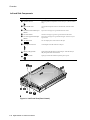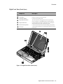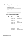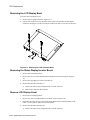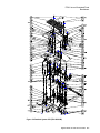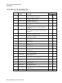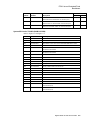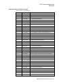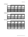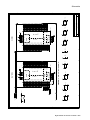
1
Digital HiNote VP 500 Series
Service Guide
Part Number:
ER-PB1WF-SM. A01
Digital Equipment Corporation
Maynard, Massachusetts
September 1996
The information in this document is subject to change without notice and should not be construed as a commitment by
Digital Equipment Corporation.
Digital Equipment Corporation assumes no responsibility for any errors that might appear in this document.
The software described in this document is furnished under a license and may be used or copied only in accordance
with the terms of such license. No responsibility is assumed for the use or reliability of software or equipment that is
not supplied by Digital Equipment Corporation or its affiliated companies.
Restricted Rights: Use, duplication, or disclosure by the U.S. Government is subject to restrictions as set forth in
subparagraph (c) (1) (ii) of the Rights in Technical Data and Computer Software clause at DFARS 252.227-7013.
© Digital Equipment Corporation 1996. All Rights Reserved.
DEC, HiNote, ThinWire, and the Digital logo are trademarks of Digital Equipment Corporation.
ESS is a registered trademark of ESS Corp.
Pentium is a registered trademark of Intel Corporation.
Microsoft, MS-DOS and Windows are registered trademarks of Microsoft Corporation.
All other trademarks and registered trademarks are the property of their respective holders.
The FCC wants you to know...
This equipment has been tested and found to comply with the limits for a Class B digital
device, pursuant to Part 15 of the FCC rules. These limits are designed to provide reasonable
protection against harmful interference in a residential installation.
Any changes or modifications made to this equipment may void the user's authority to
operate this equipment.
This equipment generates, uses, and can radiate radio frequency energy and, if not installed
and used in accordance with the instructions, may cause harmful interference to radio
communications. However, there is no guarantee that interference will not occur in a
particular installation. If this equipment does cause harmful interference to radio or
television reception, which can be determined by turning the equipment off and on, the user
is encouraged to try to correct the interference by one or more of the following measures:
•
Reorient or relocate the receiving antenna.
•
Increase the separation between the equipment and receiver.
•
Connect the equipment into an outlet on a circuit different from that to which the
receiver is connected.
•
Consult the dealer or an experienced radio/TV technician for help.
All external cables connecting to this basic unit must be shielded. For cables connecting to PCMCIA cards, see the
option manual or installation instructions.
Table of Contents
1 Overview
System Overview................................................................................................................................... 1–1
CPU and Chip Set ........................................................................................................................... 1–1
Memory .......................................................................................................................................... 1–2
BIOS............................................................................................................................................... 1–2
Video Controller Chip ..................................................................................................................... 1–2
I/O Ports.......................................................................................................................................... 1–3
Option Modules............................................................................................................................... 1–4
Components, Controls and Indicators ..................................................................................................... 1–4
Front and Side Components (Panel Closed)..................................................................................... 1–4
Rear View ....................................................................................................................................... 1–5
Left and Side Components .............................................................................................................. 1–6
Right Front View (Panel Open) ....................................................................................................... 1–7
Controlling Power ........................................................................................................................... 1–8
Battery Charge Gauge (in LCD Status Display)............................................................................... 1–8
LCD Status Display......................................................................................................................... 1–9
Keyboard Hot Keys ....................................................................................................................... 1–10
Related Information ............................................................................................................................. 1–10
Documentation.............................................................................................................................. 1–10
World Wide Web .......................................................................................................................... 1–10
Bulletin Boards ............................................................................................................................. 1–10
2 System BIOS
BIOS Setup Program.............................................................................................................................. 2–1
Accessing the BIOS Setup Program................................................................................................. 2–2
Menu Bar ................................................................................................................................. 2–2
Item Specific Help.................................................................................................................... 2–2
Legend Bar............................................................................................................................... 2–2
Launching Submenus ...................................................................................................................... 2–3
General Help ................................................................................................................................... 2–3
The Main Menu ..................................................................................................................................... 2–4
The Peripherals Menu ............................................................................................................................ 2–5
Integrated Peripherals (Peripherals submenu)......................................................................................... 2–6
The Security Menu................................................................................................................................. 2–7
Setting Admin. Password ................................................................................................................ 2–8
Changing Admin. Password ............................................................................................................ 2–8
Disabling Admin. Password ............................................................................................................ 2–8
The Power Menu.................................................................................................................................... 2–9
The Exit Menu..................................................................................................................................... 2–10
v
Modifying Flash BIOS ......................................................................................................................... 2–12
Updating Flash BIOS .................................................................................................................... 2–12
Restoring the Flash BIOS .............................................................................................................. 2–12
3 Troubleshooting
Troubleshooting Tips .............................................................................................................................3–1
System Start Failure ........................................................................................................................3–2
Power Supply Failure ......................................................................................................................3–2
Boot-up Failure ...............................................................................................................................3–3
Post Failure .....................................................................................................................................3–3
LCD Panel Failure...........................................................................................................................3–3
CRT Failure ....................................................................................................................................3–4
Notebook Keyboard Failure.............................................................................................................3–4
External Keyboard or PS/2 Mouse Failure.......................................................................................3–4
HDD Failure....................................................................................................................................3–5
FDD Failure ....................................................................................................................................3–5
Battery Failure ................................................................................................................................3–5
Check Points and Error Messages...........................................................................................................3–6
Phoenix BIOS Test Points ...............................................................................................................3–6
Warning Messages ..........................................................................................................................3–9
4 FRU Replacement
Required Tools ......................................................................................................................................4–1
Removing the Battery ............................................................................................................................4–1
Removing FDD/CD Modules and Supplementary Battery ......................................................................4–3
Removing the HDD Assembly ...............................................................................................................4–4
Removing the Keyboard.........................................................................................................................4–6
Removing the CPU ................................................................................................................................4–7
Removing the LCD Assembly and Keyboard Deck ................................................................................4–8
Removing the LCD Display Bezel ....................................................................................................... 4–12
Removing the Status Display/Inverter Board........................................................................................ 4–12
Remove LCD Display Panel................................................................................................................. 4–12
Removing the Touch Pad ..................................................................................................................... 4–14
Removing the DC-to-DC Converter Board ........................................................................................... 4–14
Removing the System BIOS Chip ........................................................................................................ 4–14
Removing the Audio Board.................................................................................................................. 4–15
Removing the Motherboard.................................................................................................................. 4–15
5 FRU List and Illustrated Parts Breakdown
FRU List................................................................................................................................................5–1
LCD Display Assemblies, Panels, Boards, Housing.........................................................................5–1
Motherboards, Daughterboards, Cache, IR, Power...........................................................................5–2
Housings, Heatsinks, Miscellaneous Parts .......................................................................................5–2
Trackpad .........................................................................................................................................5–2
Batteries ..........................................................................................................................................5–3
Keyboards .......................................................................................................................................5–3
Disk Drives .....................................................................................................................................5–3
Option List.............................................................................................................................................5–4
Illustrated Parts Breakdown....................................................................................................................5–6
System IPBs for TS31GS/O/M ........................................................................................................5–6
System IPB List for TS31GS (54CB010YYKx)........................................................................5–8
vi
System IPB List for TS31GO (54CB110YYKM)...................................................................... 5–9
System IPB List for TS31GM (54CB410YYKN).................................................................... 5–10
Mechanical Parts List TS31G - All Units................................................................................ 5–11
System IPBs for TS31GA/I ........................................................................................................... 5–13
System IPB List for TS31GA/I ............................................................................................... 5–15
Mechanical Parts List TS31G - All Units................................................................................ 5–16
LCD Assembly IPB for TS31GS/O ............................................................................................... 5–18
LCD Assembly Listing for TS31GS/O.................................................................................... 5–19
LCD Assembly IPB for TS31GA/I ................................................................................................ 5–21
LCD Assembly Listing for TS31GA/I .................................................................................... 5–22
A Specifications
Base Unit ............................................................................................................................................... A–1
Ports....................................................................................................................................................... A–2
Audio..................................................................................................................................................... A–2
LCD Display.......................................................................................................................................... A–3
PCMCIA (PCI) ...................................................................................................................................... A–3
BIOS Support......................................................................................................................................... A–3
Battery, Status Display, Keyboard.......................................................................................................... A–4
Physical ................................................................................................................................................. A–4
B Device Mapping
Memory Map .............................................................................................. Error! Bookmark not defined.
DMA Channel Assignments ................................................................................................................... B–1
Notebook Computer Interrupt Levels ..................................................................................................... B–2
I/O Address Map.................................................................................................................................... B–3
C System Connector Pin Assignments
System Interconnection Diagram ........................................................................................................... C–1
External KBD Connector – JP1.............................................................................................................. C–2
Docking Connector – JP2A, JP2B, JP2C, JP2D, JP2E ............................................................................ C–2
CRT Connector – JP3............................................................................................................................. C–5
Parallel Port Connector – JP4................................................................................................................. C–5
IR Connector – JP5 ................................................................................................................................ C–5
Serial Port(COM 1) – JP6....................................................................................................................... C–6
DC-to-DC Connector – JP7.................................................................................................................... C–6
LCD Connector – JP8 ............................................................................................................................ C–6
PCMCIA Slot A – JP10.......................................................................................................................... C–8
PCMCIA Slot B – JP11.......................................................................................................................... C–9
DC-to-DC Connector – JP12 Conn2..................................................................................................... C–10
FDD Connector – JP13......................................................................................................................... C–10
Audio IN/OUT Connector – JP14......................................................................................................... C–11
IDE Connector – JP15.......................................................................................................................... C–11
CD_ROM Driver Connector – JP18 ..................................................................................................... C–12
Track Pad Connector – JP2 .................................................................................................................. C–12
Audio Daughter Board Connector – JP20............................................................................................. C–13
Cache Connector – JP22 ...................................................................................................................... C–14
Extend DRAM Connector – JP24......................................................................................................... C–15
Cache Connector – JP23 ...................................................................................................................... C–16
Extend DRAM Connector – JP25......................................................................................................... C–17
Main Battery Connector – JP29............................................................................................................ C–18
vii
CPU Daughter-Board Connector – J1................................................................................................... C–18
CPU Daughter-Board Connector – J2................................................................................................... C–20
Internal Keyboard Connector – J3 ........................................................................................................ C–22
D Schematics
viii
Figures
Figure 1-1 Functional Block Diagram .................................................................................................... 1–2
Figure 1-2 Right Front View (Panel Closed) .......................................................................................... 1–4
Figure 1-3 Rear View............................................................................................................................. 1–5
Figure 1-4 Left Front View (Panel Closed)............................................................................................. 1–6
Figure 1-5 Right Front View (Panel open).............................................................................................. 1–7
Figure 2-1 BIOS Setup Main Menu ........................................................................................................ 2–2
Figure 2-2 The BIOS Setup Main Menu ................................................................................................. 2–4
Figure 2-3 The BIOS Setup Peripherals Menu........................................................................................ 2–5
Figure 2-4 The BIOS Setup Integrated Peripherals Menu ....................................................................... 2–6
Figure 2-5 The BIOS Setup Security Menu ............................................................................................ 2–7
Figure 2-6 The BIOS Setup Power Menu ............................................................................................... 2–9
Figure 2-7 The BIOS Setup Exit Menu................................................................................................. 2–10
Figure 4-1 Removing the Battery ........................................................................................................... 4–2
Figure 4-2 Removing the FDD Module, CD Module, Supplementary Battery ........................................ 4–3
Figure 4-3 Removing HDD .................................................................................................................... 4–5
Figure 4-4 Removing Keyboard Screw Caps and Screws ....................................................................... 4–6
Figure 4-5 Removing Heatsink and Keyboard ........................................................................................ 4–7
Figure 4-6 Removing the CPU Daughter Card ....................................................................................... 4–8
Figure 4-7 Removing LCD Assembly End Caps and Hinge Screws........................................................ 4–9
Figure 4-8 Removing the Keyboard Deck (Part 1)................................................................................ 4–10
Figure 4-9 Removing the Keyboard Deck (Part 2)................................................................................ 4–11
Figure 4-10 Disconnecting the LCD Assembly Cable........................................................................... 4–11
Figure 4-11 Removing the LCD Assembly Bezel ................................................................................. 4–12
Figure 4-12 Removing the LCD Panel and Status/Inverter Board ......................................................... 4–13
Figure 4-13 Removing I/O Panel Screws.............................................................................................. 4–16
Figure 4-14 Removing the Motherboard............................................................................................... 4–16
Figure 5-1 System Unit IPB (TS31GS/O/M) .......................................................................................... 5–6
Figure 5-2 Detailed System IPB (TS31GS/O/M) ..................................................................................... 5–7
Figure 5-3 System Unit IPB (TS31GA/I)............................................................................................... 5–13
Figure 5-4 Detailed System IPB (TS31GA/I) ....................................................................................... 5–14
Figure 5-5 LCD Assembly IPB for GS/GO Panel ................................................................................. 5–18
Figure 5-6 LCD Assembly IPB for GA/GI Panel ................................................................................. 5–21
Figure C-1 System Connector Locations ............................................................................................... C–1
ix
Preface
This guide describes how to test, troubleshoot, and remove and replace the Digital HiNote VP
500 series notebook computer Field Replaceable Units (FRUs).
Audience
This service guide is written specifically for service engineers.
Organization
This guide contains the following:
•
Chapter 1: Overview – This chapter introduces the Digital HiNote VP 500 series
notebook computers. It provides a system overview and describes the controls,
indicators, and hot keys.
•
Chapter 2: System BIOS – This chapter provides information related to the system BIOS
and its Setup program.
•
Chapter 3: Troubleshooting – This chapter provides a systematic method of isolating
problems with the Digital HiNote VP 500 series of notebook computers.
•
Chapter 4: FRU Replacement – This chapter provides detailed procedures for replacing
the Digital HiNote VP 500 series notebook computer Field Replaceable Units (FRUs).
•
Chapter 5: FRU List and Illustrated Parts Breakdown – This chapter provides a list of
the Field Replaceable Units (FRUs) and a parts breakdown and parts list for the Digital
HiNote VP 500 series notebook computer.
•
Appendix A: Specifications – This appendix lists the notebook computer’s
specifications.
•
Appendix B: Device Mapping – This appendix contains tables listing the default settings
for of the notebook computer’s memory map, I/O address map, interrupt map, and DMA
map.
•
Appendix C: System Connector Pin Assignments – This appendix shows the location of
the connectors on the system motherboard and provides a listing of the pinouts for these
connectors.
•
Appendix D: Schematics – This appendix contains the schematic drawings for the
system.
Digital HiNote VP 500 Service Guide xi
1
Overview
This chapter introduces the Digital HiNote VP 500 series notebook computers. It provides a
system overview and describes the controls, indicators, and hot keys.
System Overview
The HiNote VP 500 series are high-performance portable computers designed for the mobile
professional.
Figure 1-1 shows a functional block diagram of the notebook computer. The following
sections provide an overview of the different functions.
CPU and Chip Set
The HiNote VP 500 series notebook computers use the Intel P54LM 100 and P54CSLM
120/133 processors mounted on a daughter card.
The following chip set is used to implement the core functions of the system.
•
Intel Mobile Triton chip set provides system controller & PCI IDE controller functions
•
SMC665IR/669 provides support for floppy disk controller (FDC), two serial ports (one
serial port and one SIR) and one parallel port
•
Intel 80C51SL provides the keyboard controller and scanner and the battery management
unit
•
Cirrus CL-PD6730 is used as the PCI PCMCIA controller
•
ESS ES1688 for the audio subsystem
Digital HiNote VP 500 Service Guide 1–1
Overview
Figure 1-1 Functional Block Diagram
Memory
The system comes with 8MB of on-board DRAM for system memory and 256KB of L2
cache memory (on selected models).
System memory can be upgraded to a total of 16MB, 24MB and 40MB. The upgrade is
performed by installing two 4MB, 8MB, or 16MB DIMM modules. Two identical memory
modules must be installed when adding additional memory.
BIOS
The system has a 256KB Flash ROM for system BIOS (Phoenix BIOS 4.04). The BIOS
provides support for the following:
•
Suspend to RAM/Disk
•
Full APM 1.1 supported
•
Password protection(System and HDD)
•
Auto-configured with replicator/docking/modules
•
Windows 95 ready with PnP
•
32KB ROM for 51SL keyboard controller
•
Gas-gauge for battery status information
•
Various hot-keys for system control
Video Controller Chip
Video support is provided by the Neo Magic NM2090 VGA Controller Chip. This chip
provides the following functions:
•
PCI Bus support
•
Simultaneous display supported
1–2 Digital HiNote VP 500 Service Guide
Overview
•
Integrated 128-bit wide, 7Mbits Display Memory – 1.1MB of Video RAM
•
Integrated programmable linear address feature accelerates GUI performance
•
Supports NON-interlaced CRT monitors with resolutions up to 1024 x 768/256 colors
•
Advanced power management features minimize power consumption during:
−
Normal operation
−
Standby mode
−
SUSPEND mode
−
VESA DPMS for monitor by 2090 (option)
•
Graphic accelerator for WINDOWS application
•
3.3V/5V panel Interface support
•
−
bit BLT Engine
−
Memory mapped I/O
−
Linear addressing
−
Color expansion
−
64x64 hardware cursor
−
64x64 or 128x128 hardware ICON
High resolution SVGA (800x600) panel
−
TFT displays support a maximum of 64K colors
−
DSTN displays support a maximum of 256 colors
I/O Ports
The system has the following I/O ports:
•
One 9 pin Serial port, 16550A compatible
•
One 25 pin Parallel port, EPP/ECP Capability
•
One 15 pin CRT port
•
6 pin external full keyboard/numeric key-pad / PS/2 mouse connector
•
One microphone in port & one speaker out port
•
240 pin docking connector that supports PS2 mouse port, AT-keyboard, 1S1P, CRT,
audio ports, MIDI port, and AC jack.
•
Built-in microphone
•
Built-in IRDA SIR transmitter-receiver (on selected models)
Digital HiNote VP 500 Service Guide 1–3
Overview
Option Modules
The following options can be installed in the system:
•
6X CD-ROM Module
•
Supplementary Battery
Components, Controls and Indicators
This section shows the locations and provides a description of the different components,
controls, and indicators on your Digital notebook computer.
Front and Side Components (Panel Closed)
Component
Description
➊
➋
Removable Hard Drive
Easily removable and upgradable.
Lid Release
Slide the two latches located on either side of the notebook toward you
to open the LCD panel.
➌
➍
Main Battery Module
Removable battery module that can be replaced with a charged battery.
Expansion bay
Supports the FDD, CD-ROM and optional lithium-ion secondary
battery module.
Figure 1-2 Right Front View (Panel Closed)
1–4 Digital HiNote VP 500 Service Guide
Overview
Rear View
Component
Description
➊
Infrared Interface
Allows wireless data transfer between the notebook and other IR
devices. (Selected models only)
➋
Serial (COM) Port
A serial device connects to this port.
➌
Parallel LPT Port
A parallel device, such as a printer, connects to this port.
➍
Reset Button
Using a pen or paper clip, press this button to reboot the system. All
unsaved data will be lost.
➎
VGA Display Port
An external VGA or SVGA monitor connects to this port.
➏
Minidock Port
This 240-pin port allows you to connect the notebook to the Minidock
Port Replicator.
➐
External Keyboard or PS/2
Mouse Port
An external keyboard or PS/2 mouse connects to this port.
Figure 1-3 Rear View
Digital HiNote VP 500 Service Guide 1–5
Overview
Left and Side Components
Component
Description
➊
Speaker-out Port
External speakers or headphones connect to this port. (Selected models
only)
➋
External Mic Port
An external microphone connects to the notebook. (Selected models
only)
➌
PC Card Lower Socket Eject
Button
Ejects a PC Card Type I or Type II from the lower socket.
➍
➎
PC Card Socket
Insert PC Card Type I, Type II or Type III cards into this socket.
PC Card Upper Socket Eject
Button
Ejects a PC Card Type I or Type II from the upper socket or to eject a
Type III card.
➏
AC Power Port
The AC Adapter power cord connects to this port.
➐
Kensington Lock Port
A Kensington Lock cable connects to this port.
Battery Charger LED
Lights amber when the battery is being charged. When the battery is
fully charged the amber LED turns off.
AC Power LED
Lights green when the notebook is operating on AC power.
Figure 1-4 Left Front View (Panel Closed)
1–6 Digital HiNote VP 500 Service Guide
Overview
Right Front View (Panel Open)
Component
Description
➊
➋
➌
➍
Internal Microphone
Used to record music, voice and sound files.
LCD Display
DSTN or TFT Super VGA back-lit display.
LCD Status Display
Provides system operating status.
Suspend/Resume Button
Turns the notebook on and toggles between the suspend/resume
mode. Press the [fn + Suspend/Resume] to turn off the notebook.
➎
Suspend Lid Switch
Close the notebook’s LCD lid to suspend the system. Pressing the
Suspend/ Resume button again will resume the system.
➏
Internal Stereo Speakers
Used to hear sound files and system sounds through stereo speakers.
Touch pad
A touch sensitive pointing device providing all the functions of a twobutton mouse.
Figure 1-5 Right Front View (Panel open)
Digital HiNote VP 500 Service Guide 1–7
Overview
Controlling Power
Unique to Digital notebook’s, the suspend/resume button not only enables you to take
advantage of the built-in power saving features but also turns the notebook on and off.
Action
How to...
On
Press the Suspend/Resume button to turn the system on.
Suspend
Press this button to place your system in Suspend mode.
Resume
If you want to resume normal operation from the Suspend mode, press
the Suspend/Resume button.
Off
To completely shut off your notebook, press and hold [fn +
suspend/resume] button until a system beep sounds, indicating that the
system has been successfully turned off.
Suspend
Lid Switch
Closing the LCD lid will also enter the notebook into Suspend mode.
Battery Charge Gauge (in LCD Status Display)
Icon
When Displayed, Indicates…
76% to 100% battery operating time remaining. When the lines within
this icon are rotating, it indicates that the battery is being charged. When
the rotating stops, the battery is fully charged.
51% to 75% battery operating time remaining.
26% to 50% battery operating time remaining.
Low battery to 25% battery operating time remaining. The system’s
warning beep will sound. Save your work, replace the low battery with a
fully charged one or use an AC power source to run the notebook. The
[fn + F7] keys shut off the warning beep. It also mutes all audio.
System has ceased charging the battery. An abnormal condition exists
causing the core of the battery to reach its maximum temperature and
battery charging has been suspended..
1–8 Digital HiNote VP 500 Service Guide
Overview
LCD Status Display
Icon
When Displayed Indicates...
Embedded Numeric Keypad is enabled by hot key combination. If blinking,
the system is prompting you to enter your resume from suspend password.
Scroll Lock is enabled by a hot key combination.
Num Lock is enabled by a hot key combination.
Caps Lock is enabled.
Hard Disk Drive/CD-ROM is being accessed by the system.
Floppy Disk Drive is being accessed by the system.
The external monitor (CRT) or Simul mode is enabled. If blinking, the system
is in Save to RAM mode.
Digital HiNote VP 500 Service Guide 1–9
Overview
Keyboard Hot Keys
Hot keys are activated by holding down the [fn] key (located in the lower left corner of the
keyboard) and pressing the desired function key.
[fn] +
Function
[fn + esc]
Places the computer in Standby Mode.
[fn + F1]
Decreases brightness level.
[fn + F2]
Increases brightness level.
[Fn + F3]
Places the system in to suspend to disk mode (0V suspend)
[fn + F4]
Enables and disables the notebook’s external display port and the LCD
display. There are three display modes:
•
LCD Display
•
LCD Display and External Monitor (Simul scan)
•
External Monitor only
Each time you press this hot key the computer changes to the next display
setting.
[fn + F5]
Decreases the display contrast (DSTN screens only).
[fn + F6]
Increases the display contrast (DSTN screens only).
[fn + F7]
Enables or disables audio/speaker output including system beep indicating
low battery.
[fn + F8]
Enables and disables the keyboards embedded key pad. This hot key is used
in conjunction with the [F9] hot key to control the embedded keypad.
[fn + F9]
Toggles Num Lock on and off. This hot key is used in conjunction with the
[F8] hot key to control the embedded keypad.
[fn + F10]
Toggles Scroll Lock on and off. The state of the Scroll Lock feature is
shown in the LCD Status Display.
[fn + home/pause]
Pauses the display output. Pressing any other key on the keyboard causes
the display output to resume.
[fn + end/break]
If Break is enabled, pressing this hot key sends a system break.
[fn + PrScr/ SysReq]
Determined by application software.
[fn + ↑]
Increases the audio volume.
[fn + ↓]
Decreases the audio volume.
Related Information
Documentation
Digital HiNote VP 500 Series User’s Guide
ER-PB1WF-UA
Digital HiNote VP 500 Series Quick Reference Card
ER-PB1WF-BA
Quick Setup Guide
ER-PB1WF-IM
World Wide Web
Information such as drivers, BIOS updates, and on-line documentation is available from
Digital’s World Wide Web Site. The URL for the site is:
HTTP://WWW.PC.DIGITAL.COM/
Bulletin Boards
Digital maintains a BBS for its customers. This BBS has information such as drivers, BIOS
updates, and on-line documentation. The BBS number is: (508)496-8800
1–10 Digital HiNote VP 500 Service Guide
2
System BIOS
This chapter provides information related to the system BIOS and its Setup program.
BIOS Setup Program
The BIOS (Basic Input and Output System) Setup program is a menu driven utility that is
used to make changes to the system’s configuration and tailor the operation of the notebook
computer. It is a ROM-based (Read only Memory) configuration utility that displays the
system’s configuration status and provides a tool to set system parameters. These parameters
are stored in non-volatile battery backed-up CMOS RAM, which saves this information even
when the power is turned off. When the system is turned back on, the system is configured
with the values found in CMOS.
_____________________________ Note____________________________
The CMOS battery receives a charge when the system is being operated on AC
power. If the system is off for more than one year, the CMOS battery will drain
and the ROM data will be lost.
______________________________________________________________
The Setup Program is menu driven and can be used to configure items such as:
•
•
•
Hard drives, diskette drives and peripherals
Password protection from unauthorized use
Power Management Features
The settings made in the Setup program affect how the notebook computer performs. It is
important, to understand how the different Setup options affect the operation of the notebook
computer.
When turning on the Notebook for the first time you may get a message prompting you to run
the BIOS Setup program. A warning message may appear on the screen if the hardware
configuration is changed or the Power On Self-Test (POST) fails. This message will inform
you of any errors or invalid settings and prompt you to run the Setup program to correct the
problem.
Digital HiNote VP 500 Service Guide 2–1
Accessing the BIOS Setup Program
To access the BIOS Setup program, press the F2 key when prompted during bootup. There
are three essential elements to the BIOS screens (Figure 2-1): Menu Bar, Item Specific Help
Window and Legend Bar.
Figure 2-1 BIOS Setup Main Menu
Menu Bar
The top of the screen (Figure 2-1) has a menu bar with the following selections:
Main
Changes to the basic system configuration are made from within this menu.
Peripherals
Use this menu to enable and make changes to the system port addresses and
modes.
Security
Sets System and Boot/Resume password.
Power
From within this menu, you will be able to configure and enables Power
Management features.
Exit
Use this menu to save changes, set factory defaults and exit the Setup
program.
Item Specific Help
Note that on the right side of each BIOS Setup screen, there is a section labeled Item Specific
Help. While moving through the Setup program, note that explanations for the currently
highlighted field appear in the Item Specific Help window.
Legend Bar
At the bottom of the BIOS Setup screen there is a legend bar. The keys identified on the
legend bar are used to navigate through individual setup menus. The following table lists the
keys found in the Legend Bar with their corresponding alternates and functions.
Legend Key
Alternate Key
Function
F1
Alt + H
Displays the General Help window.
ESC
Exits the current menu and returns you to the
previous screen.
← or →
Selects a different menu bar items.
↑ or ↓
Moves the cursor up and down between fields.
<Tab>
Cycles the cursor forward through the particular
highlighted field. If the field has only one value,
the Tab key will move the selection cell down to
the next field.
<Shift + Tab>
Cycles the cursor backward through the
particular highlighted field . If the field has only
2–2 Digital HiNote VP 500 Service Guide
Legend Key
Alternate Key
Function
one value, the [Tab + Shift] key combination will
move the selection cell up to the previous field.
- minus key
F5
Scrolls backwards through the values for the
highlighted field.
+ plus key
F6
Scrolls forward through the values for the
highlighted field.
F9
Sets the fields for the current active menu to their
default values.
F10
Sets the fields for the current active menu to their
previous values.
<Enter>
Executes commands or selects a submenu.
Launching Submenus
Some menu items or fields an associated submenu. This is indicated with a pointer that looks
like a triangle on its side. For example, open the Peripherals Menu and you will see a pointer
that resembles a triangle on its side next to the Integrated Peripherals field. This symbol
indicates that a submenu can be launched from this field. A submenu contains additional
options. To launch a submenu:
1.
Use the navigation keys to select the menu item that has a submenu and press <Enter> to
open the submenu.
2.
Use the navigation keys to move around the screen and make the needed configuration
changes.
3.
When finished making changes, press the [ESC] key to exit the submenu and return to
the main screen.
General Help
In addition to the Item Specific Help window, the BIOS setup program also provides a
General Help screen. This screen can be accessed from any menu by pressing the F1 key or
[Alt + H]. The General Help screen lists the legend keys with their corresponding alternates
and functions.
When a scroll bar appears to the right of a help window, this indicates there is more
information to be displayed. Use the PgUp and PgDn keys or the up and down arrow keys (↑
↓)to scroll through the entire help document. Press <Home> to display the first page, press
<End> to go to the last page. To exit the help window, press <Enter> or the <ESC> key.
Digital HiNote VP 500 Service Guide 2–3
The Main Menu
The following settings are available in the Main Menu screen of the BIOS Setup Program
(Figure 2-2).
Figure 2-2 The BIOS Setup Main Menu
Field
Settings
Description
Date
Enter current date: month, day,
year format
Sets the system date.
Time
Enter current time: hour,
minute, second format
Sets the system time.
Diskette A
2.88 MB, 3½"
1.44 MB, 3½"*
720 KB, 3½"
1.2 MB, 5¼"
360 KB, 5¼"
Not Installed
Sets the capacity and size of the FDD
Hard Disk Drive
Display only field
Indicates the size of your notebook’s
hard drive.
Boot Sequence
Instructs the system where to look at
boot up.
Diskette First *
The system will attempt to boot from
drive A. If the drive is empty of a nonsystem disk is present, the system will
attempt to boot from drive C.
Hard Disk Only
The system will attempt to boot from
the hard disk, drive C, only.
Total Memory
Display only field
Indicates the amount of total (RAM)
memory.
Video Memory
Display only field
Indicates the amount of system video
memory.
* Default value.
2–4 Digital HiNote VP 500 Service Guide
The Peripherals Menu
Notice the pointer icon next to the words Integrated Peripherals. This indicates the presence
of a submenu.
The following settings are available in the Peripherals Menu screen of the BIOS Setup
Program (Figure 2-3).
Figure 2-3 The BIOS Setup Peripherals Menu
Field
Settings
Description
Integrated
Peripherals
Submenu
Sets the following port addresses and
modes:
Video Mode
Touch Pad
−
Serial Port
−
Infrared Port
−
Parallel Mode
Sets the Video mode
Simul Mode
Allows simultaneous viewing of
externally connected monitor (CRT)
and the notebook’s LCD display.
LCD Mode*
Allows viewing of the notebook’s LCD
only.
CRT Mode
Allows viewing of the CRT only.
Enabled *
Connecting a mouse to the serial port
will disable the Touch Pad.
Disabled
* Default value.
Digital HiNote VP 500 Service Guide 2–5
Integrated Peripherals (Peripherals submenu)
Move the highlighted cell to this field and press <Enter> to open the submenu.
The following settings are available in the Integrated Peripherals Menu screen of the BIOS
Setup Program(Figure 2-4).
Figure 2-4 The BIOS Setup Integrated Peripherals Menu
Field
Settings
Description
Serial Port
Auto
Enables, configures or disables the
serial port.
Disabled
COM 1 (3F8h - IRQ4) *
COM 2 (2F8h - IRQ3)
Set the serial port to disable to
increase the battery run time.
COM 3 (3E8h - IRQ4)
COM 4 (2E8h - IRQ3)
Infrared
Auto
Disabled*
COM 1 (3F8h - IRQ4)
COM 2 (2F8h - IRQ3)
Enables, configures or disables the
infrared port.
Set the infrared port to disable to
increase the battery run time.
COM 3 (3E8h - IRQ4)
COM 4 (2E8h - IRQ3)
Parallel Mode
* Default value.
2–6 Digital HiNote VP 500 Service Guide
Disabled
Disables the parallel port.
Normal
Parallel port is set for data-out mode
only.
Bi-Directional *
Parallel port permits both data
output and data input.
EPP Mode
(Extended Parallel Port)
Operates only with EPP aware
peripherals.
ECP
(Extended Capabilities)
Operates only with ECP aware
peripherals. See your parallel device
user’s guide.
The Security Menu
Select Security from the menu bar to display the following menu (Figure 2-5).
Figure 2-5 The BIOS Setup Security Menu
Field
Settings
Description
Admin.
Password :
[Press Enter]
Setting the Admin. Password will limit
unauthorized access to the notebook,
including the BIOS Setup Program..
Backup
Password
[Execute]
Backs up Admin. password to diskette.
Password on
Boot
Enabled
When enabled, the system will require
the Admin. Password during system
boot
Password on
Resume
Enabled
Disabled *
Disabled *
When enabled, the system will
required the Admin. Password when
resuming from suspend. The keypad
icon in the LCD Status Display will
blink, prompting for the Password.
* Default value.
Digital HiNote VP 500 Service Guide 2–7
Setting Admin. Password
To set the Admin. Password, move the highlighted cell to the Admin. Password field and
press <Enter>. The following dialogue box will appear:
Set Admin. Password
Enter new password:
[
]
Confirm new password:
[
]
1.
Type in your password and press <Enter>. The password can be up to seven
alphanumeric characters. Symbols and other keys are ignored.
2.
Type the password in a second time to confirm. Press <Enter> a second time. The
System Password is now set.
Changing Admin. Password
To change the Admin. Password, move the highlighted cell to the Admin. Password field and
press <Enter>. When the Admin. Password dialogue box appears, enter the new password.
Enter it a second time to confirm. The new password is now set.
Disabling Admin. Password
To disable the Admin. Password:
1.
Open the Admin. Password dialogue box.
2.
Continue to press the <space bar> until the cursor moves to the end of the Confirm new
password field.
3.
Continue to press the <back space> key until the cursor returns to the beginning of the
Enter New Password field. Press <Enter>. This erases the password.
4.
Complete the same steps in the New Password field to confirm the task. The old
password is erased and Admin. Password is disabled.
2–8 Digital HiNote VP 500 Service Guide
The Power Menu
The Power Menu (Figure 2-6) allows you to enable and adjust the notebook’s power saving
features. Enabling these features will extend the battery run time.
Figure 2-6 The BIOS Setup Power Menu
Field
Settings
Power Savings
Description
Sets the Power Management Mode.
Disables all Power Management
Off
Customize *
Maximum Performance
Allows you to customize the Power
Management fields (Standby, Suspend, Suspend
to Disk, Hard Disk Time-out) to suit your
individual work needs.
Power Management fields will be set with predefined values to provide best system
performance with some power conservation.
Power Management fields will be set with predefined values to ensure maximum battery run
time.
Maximum Battery Life
AC Power
Save
On *
Standby Timeout
Disabled
Off
1 Min.
2 Min.
When enabled all system power management is
enabled, when operating on AC power. If
disabled, all system power management is
disabled when operating on AC power.
Indicates the amount of time the system needs
to be idle before entering Standby mode.
In order to make customized changes to this
field, Power Savings must be set to Customize.
3 Min. *
5 10, 15, 30 Min.
Suspend Timeout
Disabled
1 Min.
2 Min.
3 Min. *
Indicates the amount of time the system needs
to be idle before entering Suspend (to RAM)
mode.
Power Savings must be Customize to change
these values.
5, 10, 15, 30 Min.
Suspend-toDisk
Time-out
Disabled
1, 2, 3, 5 Min.
10 Min. *
Indicates the amount of time the system needs
to be idle before entering Suspend-to-Disk
mode.
In order to make customized changes to this
Digital HiNote VP 500 Service Guide 2–9
Field
Settings
15, 20, 30 Min.
Hard Disk
Time-Out
Disabled
1 Min.
2 Min. *
Description
field, Power Savings must be set to Customize.
Indicates the amount of time the hard disk
needs to be inactive before it is turned off.
In order to make customized changes to this
field, Power Savings must be set to Customize.
3 Min.
5, 10, 15, 20 Min.
DIM Mode
Time-out
Disabled
15 Sec.
30 Sec. *
Indicates the amount of time the keyboard
needs to be inactive before LCD panel
brightness is gradually decreased.
60 Sec.
Alarm Resume
Off *
Enables or Disables Alarm Resume Time
On
Alarm Resume
Time
Enter time in a 24 hour
format.
13:00 = 1:00 p.m.
Allows you to specify the time the system will
resume.
* Default value.
The Exit Menu
Enter the Exit Menu (Figure 2-7) to save changes, set factory defaults or exit the Setup
program.
Figure 2-7 The BIOS Setup Exit Menu
2–10 Digital HiNote VP 500 Service Guide
Field
Action
Description
Save
Changes & Exit
<Enter>
Saves the current changes and exits the BIOS
Setup Program.
Discard
Changes & Exit
<Enter>
Discards the current changes and exits the BIOS
Setup Program.
Get Default Values
<Enter>
Loads the factory default values for each of the
fields in the BIOS Setup Program.
To keep default values and exit the BIOS Setup
Program, you must move the highlighted cell to
the Save Changes & Exit field and press the
<Enter> key.
Load Previous Values
<Enter>
Discards any changes made during the current
BIOS configuration session, and loads the prior
sessions values.
You cannot exit the BIOS through this field.
Saves Changes
<Enter>
Saves the changes made during the current BIOS
configuration session.
You cannot exit the BIOS through this field.
Digital HiNote VP 500 Service Guide 2–11
Modifying Flash BIOS
The Digital HiNote VP 500 Series notebook computer has a flash updatable system BIOS. As
improvements are made to the system BIOS they are made available from Digital’s Web site
or BBS.
Web Site: HTTP://WWW.PC.DIGITAL.COM
BBS: (508)496-8800
Updating Flash BIOS
The Flash BIOS update come as a self-extracting file that creates a bootable floppy disk.
After downloading the update procedure you restore the update image to floppy disk. This
procedure creates a bootable floppy with the PHLASH update program. The BIOS update is
provided with a set of instructions on how to use it.
Before running the BIOS update procedure set up the notebook computer as follows:
•
•
•
Connect the AC adapter. For the BIOS update to run the system has to be running from
its AC power source.
Remove any peripheral devices from the system:
−
PCMCIA devices
−
Port Replicator
Set the System BIOS to its factory default settings
To run the BIOS update:
1.
Insert the BIOS Update disk in the floppy drive.
2.
Cold boot the system.
a)
Press the [fn] + Suspend/Resume button to power off the system
b) Press the Suspend/Resume button to cold boot the system
3.
Follow the instructions provided by the update program.
Restoring the Flash BIOS
If for some reason the system BIOS becomes corrupted the BIOS chip located under the DCto-DC converter on the system motherboard will have to be replaced.
2–12 Digital HiNote VP 500 Service Guide
3
Troubleshooting
This chapter provides a systematic method of isolating problems with the Digital HiNote VP
500 series of notebook computers. It is assumed that you have a basic understanding of DOSbased computer systems as well as a knowledge of standard troubleshooting procedures. This
manual is written under the assumption that the problems are indeed related to the notebook
computer itself. The improper usage of the system and application software problems are
excluded in this chapter.
The system BIOS power on self-tests (POST) are integral to the system and detect certain
errors with the system board. They use a series of beep codes to identify certain system board
problems.
The troubleshooting procedures when followed step by step, can help isolate system
problems.
Troubleshooting Tips
In general, troubleshooting involves an organized system of approach to problem solving.
Try to isolate the problem and identify the defective device (hardware) or improper setting
(software). When you have a problem, you should do a thorough visual inspection of the
Notebook.
•
If none of the indicators are lit and you cannot hear the HDD spinning, then the
Notebook is probably not receiving power.
•
Make sure the power cord is plugged in, and the AC adapter is securely connected.
•
If you are using a power strip or surge protector, ensure that these devices are turned on.
Often problems are caused by improperly connected cables.
•
If you are using peripherals such as the mouse or keyboard, make sure they are properly
connected to their respective ports. Ensure that none of the connectors’ pins are bent or
broken.
•
Check all cables connected to the Notebook. If any are cut, frayed, or damaged in any
way, replace them right away. Never use a damaged cable. A damaged cable is not only
a fire hazard, it may also cause a short circuit, resulting in irreparable damage to the
Notebook.
•
Check all internal connections to ensure that they are secure. Often problems can occur
because a connection is loose or backwards. Most connections have a “key” to ensure
that they go in correctly, but some may not have a key.
Verify that all test equipment works before using it to test a malfunctioning component (for
example, a floppy disk drive).
Digital HiNote VP 500 Service Guide 3–1
Troubleshooting
Verify that a component is the only malfunctioning part of the computer by replacing the
malfunctioning component with a good one, and then try to run the system. For example, if
you have tested an FDD in a test computer and found it to be bad, you should also try a good
FDD in the malfunctioning FDD’s computer to be sure that another component (such as the
FDD controller) is not bad as well.
As with assembly and disassembly, make sure you have adequate lighting, the right tools, and
a stable clean working environment.
The examples that follow provide useful tips and information that will help isolate and solve
some of the more common problems that may be encountered.
System Start Failure
When you turn on the computer, the system hangs before completing or starting the POST
(power on self test). Power supply failure, post failure, and boot-up failure can result in a
system start failure.
Power Supply Failure
Problem
Troubleshooting Procedure
You turn on the power switch and the following
conditions apply:
• There is no panel display
If you are operating the Notebook using the
battery:
• The battery connection is loose. Replace
the battery.
•
There is no noise coming from the HDD
•
The power indicator light is off.
•
The battery power is depleted or the battery
is bad. Plug in the AC adapter, or replace
the battery.
If you are operating the Notebook using the AC
adapter:
• Check that the AC adapter is plugged into
an operational power supply.
•
Check that the AC adapter is connected
securely to the Notebook’s AC adapter
socket.
•
Check to see if the Power LED on the
computer is lit. If it is not lit, then the AC
adapter is bad. Replace the AC adapter,
and test the Notebook again.
Press the system's "Reset Button" located on the
back of the unit between the serial and parallel
port connectors.
If the above items are functioning, then the
Notebook’s internal power circuit is probably
damaged. Check the power circuit of the
Notebook.
3–2 Digital HiNote VP 500 Service Guide
Troubleshooting
Boot-up Failure
Problem
Troubleshooting Procedure
You turn on the Notebook and the following
conditions apply:
• The Notebook’s power is on.
Turn on the power switch:
• Check the DRAM connections to be sure
that they are secure.
•
•
Check the LCD connections.
•
Check the system board power circuit.
There is no screen display
Post Failure
Problem
Troubleshooting Procedure
You turn on the computer and the following
happens:
• There is power to the system.
•
A POST failure usually indicates a
keyboard, memory, or HDD failure.
•
Check the error code or message against
the error codes and messages in this
chapter..
•
The HDD seems to be spinning.
•
The screen is operational, and error codes
and messages are displayed.
LCD Panel Failure
Problem
Troubleshooting Procedure
You turn on the computer and one of the
following conditions apply:
• The system is working, but there is no LCD
panel display.
•
Make sure that the LCD cables are securely
connected.
•
Make sure that the LCD cables are securely
connected to the inverter.
•
If the cables are securely connected and the
LCD still doesn’t work, replace the LCD
panel and test the system again.
•
If the display is garbled, there is probably a
VGA chip failure. Replace the
motherboard.
•
The system is working, but the LCD panel
display vertical or horizontal lines.
•
The backlight comes on, but there is no
display.
•
There is a display, but you have garbled
characters on the screen.
Digital HiNote VP 500 Service Guide 3–3
Troubleshooting
CRT Failure
Problem
Troubleshooting Procedure
The Notebook has power, the Notebook’s LCD
panel is working and one of the following
conditions apply:
• The Notebook’s LCD panel is working.
•
Make sure the CRT output is enabled.
•
Make sure that the CRT’s power is on.
•
Make sure that the CRT’s power cables are
securely connected, and that there are no
bent or damaged pins on the connectors.
•
Make sure that the CRT to Notebook cable
connection is secure. Check the CRT port
on the Notebook to make sure the
connection is secure, and that there are no
damaged pins or connectors.
•
If the CRT still doesn’t work, change to a
different CRT and try again.
•
If the color is bad, adjust the Monitor’s
color controls (if any).
•
There is no display on the CRT.
•
The color of the CRT is wrong.
•
There is a display, but the display is not
stable.
Notebook Keyboard Failure
Problem
Troubleshooting Procedure
The Notebook is fully powered-on. However,
when pressing on the keyboard, one of the
following events occurs:
• Pressing on the key doesn’t have any effect.
•
Make sure that the keyboard cable is
securely connected into the keyboard
connector.
•
Check the keyboard circuit.
•
Replace the keyboard and check again.
•
If incorrect characters are displayed, check
the COUNTRY.SYS settings in the
operating system to see if an incorrect
language is being used by the system.
•
Replace the keyboard controller BIOS chip
located in the memory compartment on the
bottom of the system unit.
•
Incorrect characters are displayed on the
screen.
•
One stroke of a key produces too many
characters on the screen.
External Keyboard or PS/2 Mouse Failure
Problem
Troubleshooting Procedure
The Notebook’s power is on, and the keyboard
is working. One of the following conditions
occur:
• Pressing keys on the external keyboard has
no effect.
•
Make sure that the external mouse or
keyboard’s connection to the Notebook’s
PS/2 mini-DIN connector is secure.
•
Replace the external mouse or keyboard
and try again.
•
Pressing the key on the external keyboard
gives incorrect characters.
•
•
If the system still doesn’t work, test the
mini-DIN keyboard circuit.
The mouse cursor on the screen doesn’t
move in conjunction with the external
mouse.
•
If incorrect characters are displayed, check
the COUNTRY.SYS settings in DOS to see
if an incorrect language is being used by
the system.
3–4 Digital HiNote VP 500 Service Guide
Troubleshooting
HDD Failure
Problem
Troubleshooting Procedure
When you try to access the HDD, one of the
following conditions occur:
• There is a message indicating that the HDD
doesn’t exist.
•
Check to make sure that the BIOS settings
are correct. Refer to Chapter 2 for BIOS
information.
•
Make sure that the HDD connection is
secure.
•
Install the HDD into another Notebook and
test it.
•
If the HDD works in a test Notebook, the
HDD controller on the motherboard is
probably bad. Test the motherboard.
•
You can’t read from the HDD.
•
You can’t write to the HDD.
FDD Failure
Problem
Troubleshooting Procedure
The Notebook’s power is on. The HDD is
functioning correctly. When you try to access
the FDD, one of the following conditions
occurs:
• You can’t read from the FDD.
•
Make sure the FDD is properly seated.
•
Switch to a different floppy disk and try
again. Make sure that the floppy isn’t write
protected.
•
You can’t write to the FDD.
•
Clean the FDD’s heads.
•
You can’t hear the FDD motor spinning,
and the LED indicator light isn’t on.
•
Change the FDD and test again.
•
If the FDD is OK, than there is probably an
I/O chipset failure. Replace the main
board.
Battery Failure
Problem
Troubleshooting Procedure
The Notebook’s AC power works. When trying
to use battery power, the Notebook doesn’t
operate. However, when the AC Adapter is
connected, the battery charge indicator flashes.
•
Make sure that the battery contacts are in
good condition.
•
Make sure that the battery terminals are
clean. If need be, clean the terminals with
contact cleaner.
•
Change the battery and try again.
•
Check to make sure that the AC power
supply (the AC adapter and AC adapter
cord) are OK. If they are not supplying the
correct voltage, it could damage the system.
Digital HiNote VP 500 Service Guide 3–5
Troubleshooting
Check Points and Error Messages
At the beginning of each POST routine, the BIOS outputs the test point error code to I/O
address 80h. Use this code during troubleshooting to establish at what point the system failed
and what routine was being performed.
If the BIOS detects a terminal error condition, it halts POST after:
•
Issuing a terminal error beep code and
•
Attempting to display the error code on upper left corner of the screen and on the port
80h LED display
If the system hangs before the BIOS can process the error, the code displayed at port 80h is
that of the last test performed. In this case, the screen does not display the error code.
Phoenix BIOS Test Points
The following is a list of the checkpoint codes written at the start of each test and the beep
codes issued for terminal errors:
Code
Beeps
POST Routine Description
02
Verify Real Mode
04
Get CPU type
06
Initialize system hardware
08
Initialize chipset registers with initial POST values
09
Set in POST flag
0A
Initialize CPU registers
0C
Initialize cache to initial POST values
0E
Initialize I/O
0F
Initialize the local bus IDE
10
Initialize Power Management
11
Load alternate registers with initial POST values
12
Jump to UserPatch0
14
16
Initialize keyboard controller
2-2-3
BIOS ROM checksum
18
8254 timer initialization
1A
8237 DMA controller initialization
1C
Reset Programmable Interrupt Controller
20
3-1-1
Test DRAM refresh
22
3-1-3
Test 8742 Keyboard Controller
24
Set ES segment register to 4 GB
28
Autosize DRAM
2A
Clear 512K base RAM
2C
3-4-1
Test 512K base address lines
2E
3-4-3
Test 512K base memory
30
Base 64K RAM Error
32
Test CPU bus-clock frequency
34
Test CMOS RAM
35
Initialize alternate chipset registers
37
Reinitialize the chipset
38
Shadow system BIOS ROM
3–6 Digital HiNote VP 500 Service Guide
Troubleshooting
Code
Beeps
POST Routine Description
39
Reinitialize the cache
3A
Autosize cache
3C
Configure advanced chipset registers
3D
Load alternate registers with CMOS values
40
Set Initial CPU speed
42
Initialize interrupt vectors
44
46
Initialize BIOS interrupts
2-1-2-3
Check ROM copyright notice
47
Initialize manager for PCI Option ROMs
48
Check video configuration against CMOS
49
Initialize PCI bus and devices
4A
Initialize all video adapters in system
4C
Shadow video BIOS ROM
4E
Display copyright notice
50
Display CPU type and speed
51
Initialize EISA board
52
Test keyboard
54
Set key click if enabled
56
58
Enable keyboard
2-2-3-1
Test for unexpected interrupts
5A
Display prompt "Press F2 to enter SETUP"
5C
Test RAM between 512 and 640k
60
Test extended memory
62
Test extended memory address lines
64
Jump to UserPatch1
66
Configure advanced cache registers
68
Enable external and CPU caches
6A
Display external cache size
6C
Display shadow message
6E
Display non-disposable segments
70
Display error messages
72
Check for configuration errors
74
Test real-time clock
76
Check for keyboard errors
7C
Set up hardware interrupt vectors
7E
Test coprocessor if present
80
Disable onboard I/O ports
82
Detect and install external RS232 ports
84
Detect and install external parallel ports
86
Re-initialize onboard I/O ports
88
Initialize BIOS Data Area
8A
Initialize Extended BIOS Data Area
8C
Initialize floppy controller
90
Initialize hard-disk controller
91
Initialize local-bus hard-disk controller
Digital HiNote VP 500 Service Guide 3–7
Troubleshooting
Code
Beeps
POST Routine Description
92
Jump to UserPatch2
94
Disable A20 address line
96
Clear huge ES segment register
98
Search for option ROMs
9A
Shadow option ROMs
9C
Set up Power Management
9E
Enable hardware interrupts
A0
Set time of day
A2
Check key lock
A4
Initialize typematic rate
A8
Erase F2 prompt
AA
Scan for F2 key stroke
AC
Enter SETUP
AE
Clear in-POST flag
B0
Check for errors
B2
POST done-prepare to boot operating system
B4
One beep
B6
Check password (optional)
B8
Clear global descriptor table
BC
Clear parity checkers
BE
Clear screen (optional)
BF
Check virus and backup reminders
C0
Try to boot with INT 19
DO
Interrupt handler error
D2
Unknown interrupt error
D4
Pending interrupt error
D6
Initialize option ROM error
D8
Shutdown error
DA
Extended Block Move
DC
Shutdown 10 error
E2
Initialize the chipset
E3
Initialize refresh counter
E4
Check for Forced Flash
E5
Check HW status of ROM
E6
BIOS ROM is OK
E7
Do a complete RAM test
E8
Do OEM initialization
E9
Initialize interrupt controller
EA
Read in the bootstrap code
EB
Initialize all vectors
EC
Boot the Flash program
ED
Initialize the boot device
EE
Boot code was read OK
3–8 Digital HiNote VP 500 Service Guide
Troubleshooting
If the BIOS detects error 2C, 2E, or 30 (base 64K RAM error), it displays an additional word
of information reflecting the bit or address line that failed. For example, if "2C 0002" is
displayed, address line 1 (represented by bit one) has failed. If "2E 1020" is displayed, then
data bits 12 and 5 have failed in the upper 16 bits.
The BIOS sends the same information to the port 80h LED display. The check point code is
followed by a delay, the high order byte, another delay, and then the low order byte of the
error. This is be repeated continuously.
Warning Messages
The following is an alphabetic list of error and status messages which the PhoenixBIOS can
generate and an explanation of each message. Many of the messages below refer to the built
in Setup program.
Message
Description
nnnn Cache SRAM Passed
nnnn is the amount of system cache in kilobytes
successfully tested.
Diskette drive A error
Drive A: is present but fails the BIOS POST diskette
tests. Check to see that the drive is defined with the
proper diskette type in Setup and that the diskette
drive is attached correctly.
Entering SETUP
Starting Setup program
Extended RAM Failed at offset: nnnn
Extended memory not working or not configured
properly.
nnnn Extended RAM Passed
nnnn is the amount of RAM in kilobytes successfully
tested.
Failing Bits: nnnn
The hex number nnnn is a map of the bits at the
RAM address (in System, Extended, or Shadow
memory) which failed the memory test. Each 1 (one)
in the map indicates a failed bit.
Fixed Disk 0 Failure or Fixed Disk 1
Failure or Fixed Disk Controller
Failure
Fixed disk is not working or not configured properly.
Check to see if fixed disk is attached properly. Run
Setup to ensure that the fixed-disk type is correctly
identified.
Incorrect Drive A type run SETUP
Type of floppy drive A: not correctly identified in
Setup.
Invalid NVRAM media type
Problem with NVRAM access.
Keyboard controller error
The keyboard controller failed test. You may have to
replace keyboard or controller.
Keyboard error
Keyboard not working.
Keyboard error nn
BIOS discovered a stuck key and displays the scan
code for the stuck key.
Keyboard locked Unlock key switch
Unlock the system to proceed.
Monitor type does not match CMOS
Run SETUP Monitor type not correctly identified in
Setup
Operating system not found
Operating system cannot be located on either drive
A: or drive C:. Enter Setup and see if fixed disk and
drive A: are properly identified.
Parity Check 1 nnnn Parity error
found in the system bus
BIOS attempts to locate the address but failed and
display it on the screen.
Parity Check 2 nnnn Parity error
found in the I/O bus
BIOS attempts to locate the address but failed and
display it on the screen.
Digital HiNote VP 500 Service Guide 3–9
Troubleshooting
Message
Description
Press <F1> to resume, <F2> to
Setup
Displayed after any recoverable error message: Press
<F1> to start the boot process or <F2> to enter Setup
and change any settings. <F2> Press <F2> to enter
SETUP Optional message displayed during POST.
Previous boot incomplete
Default configuration used
Previous POST did not complete
successfully
POST loads default values and offers to run Setup. If
the failure was caused by incorrect values and they
are not corrected, the next boot will likely fail.
Real time clock error
Real-time clock fails BIOS test. May require board
repair.
Shadow RAM Failed at offset: nnnn
Shadow RAM failed at offset nnnn of the 64k block
at which the error was detected.
nnnn Shadow RAM Passed
Where nnnn is the amount of shadow RAM in
kilobytes successfully tested.
System battery is dead - Replace and
run SETUP
The CMOS clock battery indicator shows the battery
is dead. Replace the battery and run Setup to
reconfigure the system.
System BIOS shadowed
System BIOS copied to shadow RAM.
System cache error
Cache disable RAM cache failed the BIOS test. BIOS
disabled the cache.
System CMOS checksum bad - run
SETUP
System CMOS has been corrupted or modified
incorrectly, perhaps by an application program that
changes data stored in CMOS. Run Setup and
reconfigure the system.
System RAM Failed at offset: nnnn
System RAM failed at offset nnnn of in the 64k block
at which the error was detected.
nnnn System RAM Passed
nnnn is the amount of system RAM in kilobytes
successfully tested.
System timer error
The timer test failed. Requires repair of system
board.
UMB upper limit segment address:
nnnn
Displays the address of the upper limit of Upper
Memory Blocks, indicating released segments of the
BIOS which may be reclaimed by a virtual memory
manager.
Video BIOS shadowed
Video BIOS successfully copied to shadow RAM.
3–10 Digital HiNote VP 500 Service Guide
4
FRU Replacement
This chapter provides detailed procedures for replacing the Digital HiNote VP 500 series
notebook computer Field Replaceable Units (FRUs). Unless otherwise noted the replacement
procedures for the FRUs are the reverse of the removal procedures.
Required Tools
You will need the following tools to remove and replace the HiNote VP 500 series FRUs.:
•
#0 and #1 Phillips Head Screwdrivers
•
3/16 inch and 7/32 inch Nut Drivers
Removing the Battery
The battery is located on the right side of the system unit (Figure 4-1).
To remove the battery pack:
1.
Slide the battery lock/release clip to the release position.
2.
Pull the Battery Pack out of the system unit as shown.
Digital HiNote VP 500 Service Guide 4–1
FRU Replacement
Figure 4-1 Removing the Battery
4–2 Digital HiNote VP 500 Service Guide
FRU Replacement
Removing FDD/CD Modules and Supplementary Battery
To remove the FDD module, CD module or supplementary battery:
1.
Slide the locking button (1), located on the bottom of the system, in the direction shown
(Figure 4-2).
2.
Slide and hold the module release latch (2) in the direction shown.
3.
While holding the module release latch in position, slide the module out of the system
unit (3).
Figure 4-2 Removing the FDD Module, CD Module, Supplementary Battery
Digital HiNote VP 500 Service Guide 4–3
FRU Replacement
Removing the HDD Assembly
To remove the HDD:
1.
Slide the HDD module plastic cover (1) in the direction shown (Figure 4-3).
2.
Remove the two Philips head screws (2) located on the bottom of the notebook computer.
They secure the HDD assembly in the system unit and prevent it from being damaged.
3.
Gently remove the HDD from its housing, by pulling on its handle in the direction shown
(3).
________________________ Installation Note _______________________
If the HDD assembly is slide installed upside down, the screws on the assembly
may get caught on some plastic inside the system. To remove the drive slide a
piece of paper (yellow sticky) between the unit and the plastic and slide out the
HDD assembly.
______________________________________________________________
4–4 Digital HiNote VP 500 Service Guide
FRU Replacement
Figure 4-3 Removing HDD
Digital HiNote VP 500 Service Guide 4–5
FRU Replacement
Removing the Keyboard
To remove the keyboard:
1.
Remove the keyboard screw caps by pulling them toward the front of the system and then
up as shown (Figure 4-4).
2.
Remove the two screws that hold the keyboard in place.
3.
Lift the keyboard up and rotate it toward the LCD display. The keyboard cable is
removed in step 5.
___________________________ CAUTION __________________________
Be careful not to damage the keyboard cable when lifting up the keyboard.
______________________________________________________________
4.
Remove the heatsink (Figure 4-5).
a)
Remove the two screws that hold the heatsink in place.
b) Carefully lift the heatsink up and remove it from the system sliding the keyboard
cable through the slot in the heatsink.
5.
Disconnect the keyboard cable.
a)
Release the cable latch by flipping it up. The latch is located across the back of the
connector.
b) Pull the cable out of the connector.
Figure 4-4 Removing Keyboard Screw Caps and Screws
4–6 Digital HiNote VP 500 Service Guide
FRU Replacement
Figure 4-5 Removing Heatsink and Keyboard
Removing the CPU
The CPU daughter card is located under the heatsink. To remove the CPU daughter card:
1.
Remove the keyboard and heatsink
2.
Pull up on the CPU daughter card to remove if from the system (Figure 4-6).
________________________ Installation Note ______________________
When installing the CPU daughter card, align each of the connectors with the
mating connector on the motherboard.
______________________________________________________________
Digital HiNote VP 500 Service Guide 4–7
FRU Replacement
Figure 4-6 Removing the CPU Daughter Card
Removing the LCD Assembly and Keyboard Deck
To remove the LCD Assembly:
1.
Remove the Battery
2.
Remove the FDD/CD Module or Secondary Battery
3.
Remove the HDD Assembly (recommended)
4.
Remove the Keyboard and Heatsink
5.
As a part of this procedure you will remove the Keyboard Deck. Before starting, close
the LCD Assembly, turn the system unit over, and remove the screw located at the top of
battery compartment (Figure 4-9).
6.
Open the LCD assembly and remove the left and right end caps by sliding them ¼ inch
toward the outside of the system unit and then up (Figure 4-7).
___________________________ CAUTION __________________________
On systems with IR support, the IR receiver/transmitter assembly is located under
the right end cap. Care should be taken when removing the right end cap.
______________________________________________________________
7.
Remove the screw located under the right end cap. On systems with an IR
receiver/transmitter you will have to move the IR board to access the screw.
8.
Remove the four hinge screws.
4–8 Digital HiNote VP 500 Service Guide
FRU Replacement
Figure 4-7 Removing LCD Assembly End Caps and Hinge Screws
9.
Remove the center cap and the LCD Assembly from the system unit as follows:
a)
Press in at the base of the center cap to release the catches.
b) Lift straight up on the LCD assembly and remove the Center cap as you remove the
LCD assembly from the system unit. The LCD cable is still attached to the system
unit.
c)
Lay the panel on the work surface behind the system unit being careful not to
damage the cable.
_____________________________ Note____________________________
There are two catches on the back of the center cap that hook on to nibs on the
Keyboard Deck. You may have to slide the cover forward to get these catches to
release.
______________________________________________________________
10. Remove the three screws across the back of the keyboard deck (Figure 4-8).
11. Remove the screw that secures the Keyboard Deck to the motherboard. This screw is
located by the Touch Pad.
12. Disconnect the Touch Pad cable from the motherboard
Digital HiNote VP 500 Service Guide 4–9
FRU Replacement
Figure 4-8 Removing the Keyboard Deck (Part 1)
13. Remove the Keyboard Deck by releasing the catches as shown (Figure 4-9) and lift the
Keyboard deck off the system housing.
14. Disconnect the cable that goes to the System Suspend/Resume button assembly from the
motherboard.
15. Lay the Keyboard deck on the LCD assembly.
___________________________ CAUTION __________________________
Be careful no to damage the LCD cable assembly.
______________________________________________________________
15. Remove the DC-to-DC Converter Board by pulling it straight up off its connectors. The
DC-to-DC converter board is located to the right of the PCMCIA slots.
16. Remove the two screws that hold the LCD cable assembly in place. Note the location of
the ground wire (Figure 4-10).
17. Disconnect the LCD cable assembly from the Motherboard by lifting up on the cable
connector.
_____________________________ Note ____________________________
The metal shield surrounding the cable connector is not a part of the LCD cable
assembly.
______________________________________________________________
4–10 Digital HiNote VP 500 Service Guide
FRU Replacement
________________________ Installation Notes ______________________
1.
2.
Be sure to reconnect the ground wire.
When installing the end caps removed in step 2, make sure the nibs inside the
end caps slide into the appropriate catch on the Keyboard Deck.
3. The center cap has two catches that slide over nibs on the Keyboard Deck.
______________________________________________________________
Figure 4-9 Removing the Keyboard Deck (Part 2)
Figure 4-10 Disconnecting the LCD Assembly Cable
Digital HiNote VP 500 Service Guide 4–11
FRU Replacement
Removing the LCD Display Bezel
To remove the LCD display bezel:
1.
Remove the two plugs and screws (Figure 4-11).
2.
Pull one side of the bezel away from the center of the LCD assembly until the plastic
latches are disengaged. Do this on each side of the bezel until you can remove the bezel.
Figure 4-11 Removing the LCD Assembly Bezel
Removing the Status Display/Inverter Board
1.
Remove the LCD Display Bezel.
2.
Remove the two screws that hold the Status Display/Inverter Board in place (Figure 412).
3.
Remove the cable that goes to the LCD Panel (A).
4.
Remove the flat cable assembly (C).
a)
Release the cable lock by sliding the lock out of the connector.
b) Remove the cable from the connector.
Remove LCD Display Panel
1.
Remove the LCD Display Bezel
2.
Remove the four screws that hold the LCD Panel in place (Figure 4-12).
3.
Disconnect the cable that goes between the Status Display/Inverter Board and the LCD
Panel. You may have to remove the Inverter Board.
4.
Remove the flat cable assembly (B).
a)
Release the cable lock by sliding the lock out of the connector.
4–12 Digital HiNote VP 500 Service Guide
FRU Replacement
b) Remove the cable from the connector.
___________________________ Important _________________________
LCD panels used in the Digital HiNote 500 series notebook computer are supplied
by different manufacturer’s. Each LCD panel uses a unique cable assembly. Do
Not mix an LCD panel with a cable assembly from a different manufacturer.
______________________________________________________________
Figure 4-12 Removing the LCD Panel and Status/Inverter Board
Digital HiNote VP 500 Service Guide 4–13
FRU Replacement
Removing the Touch Pad
To remove the Touch Pad:
1.
Remove the LCD Assembly and the Keyboard Deck.
2.
Remove the screw that holds the Touch Pad in place.
3.
Remove the Touch Pad by disengaging the two catches that hold it in place. You will
have to work at carefully releasing these catches.
Removing the DC-to-DC Converter Board
To remove the DC-to-DC Converter board:
1.
Remove the LCD Assembly and the Keyboard Deck.
2.
Locate the DC-to-DC Converter board. It is by the PCMCIA card slots at the back of the
system unit.
3.
Remove the board by pulling it straight up off its connectors.
Removing the System BIOS Chip
The system BIOS chip is located under the DC-to-DC Converter board. To remove the
system BIOS chip:
1.
Remove the LCD Assembly and the Keyboard Deck.
2.
Locate the DC-to-DC Converter board. It is by the PCMCIA card slots at the back of the
system unit.
3.
Remove the board by pulling it straight up off its connectors.
4.
Using a chip puller, remove the BIOS chip.
___________________________ CAUTION __________________________
When installing the BIOS chip, make sure pin 1 is properly aligned. Failure to do
this will damage the chip, make the system not run, and possibly damage the
system.
______________________________________________________________
4–14 Digital HiNote VP 500 Service Guide
FRU Replacement
Removing the Audio Board
To remove the Audio Board:
1.
Remove the LCD Assembly and the Keyboard Deck.
2.
Locate the Audio board. It is located over the HDD bay at the front of the system unit.
3.
Disconnect the cable that goes between the Audio board and the audio jacks.
a)
Release the cable lock by sliding the lock out of the connector.
b) Remove the cable from the connector.
_____________________________ Note____________________________
The Audio jacks are soldered to the motherboard and cannot be removed.
______________________________________________________________
4.
Remove the board by pulling it straight up off its connectors.
Removing the Motherboard
1.
Remove the Battery.
2.
Remove the FDD/CD Module or Secondary Battery.
3.
Remove the HDD Assembly.
4.
Remove the Keyboard and CPU daughter card
5.
Remove the LCD Assembly and the Keyboard Deck.
6.
Remove the Audio Board.
_____________________________ Note____________________________
The Audio jacks are soldered to the motherboard and cannot be removed.
______________________________________________________________
7.
Remove the nuts that secure the I/O ports and Docking connector to the back of the
system unit (Figure 4-13).
8.
Remove the five screws that secure the motherboard to the system housing (Figure 4-14).
9.
–
Three screws are located across the back of the motherboard.
–
One screw is located in the PCMCIA card slot.
–
One screw is located under the Audio card.
Remove the Motherboard from the system housing.
_____________________________ Note____________________________
1.
For the Audio jacks to clear the side of the housing you will have to flex the
side of the housing.
2. For the FDD and CD connectors to clear their shields you have to flex the
shields out of the way.
______________________________________________________________
Digital HiNote VP 500 Service Guide 4–15
FRU Replacement
Figure 4-13 Removing I/O Panel Screws
Figure 4-14 Removing the Motherboard
4–16 Digital HiNote VP 500 Service Guide
5
FRU List and Illustrated Parts
Breakdown
This chapter provides a list of the Field Replaceable Units (FRUs) and a parts breakdown and
parts list for the Digital HiNote VP 500 series notebook computer.
FRU List
The following sections provide a list of FRUs and their part numbers for the Digital HiNote
VP 500 Series notebook computer.
LCD Display Assemblies, Panels, Boards, Housing
Digital FRU P/N
Compal P/N
Description
30-47904-01
2604071A01N
Assy, LCD Display 11.3", GS
30-47905-01
2604071A02M
Assy, LCD Display 11.3", GO
30-47967-01
2604211A01N
Assy, LCD Display 12.1", GM
30-48058-01
Assy, LCD Display 12.1", GL (LG)
30-47906-01
2604081A01T
Assy, LCD Display Bezel, 11.3", GS
30-47907-01
2604081A02R
Assy, LCD Display Bezel, 11.3", GO
30-47974-01
2604221A01T
Assy, LCD Display Bezel, 12.1", GM
30-47910-01
2604161A01M
Assy, Housing Display Cover 11.3", GS
30-47911-01
2604161A02L
Assy, Housing Display Cover 11.3", GO
30-47978-01
2604231A01M
Assy, Housing Display Cover 12.1", GM
30-48059-01
Assy, Housing Display Cover 12.1", GL (LG)
30-47914-01
2604101A01Q
Assy, Inverter Board, 11.3/12.1"
30-47908-01
2604091A01M
LCD Panel, 11.3" Sanyo (FE53)
30-47909-01
2604091A02L
LCD Panel, 11.3" Hosiden (1108)
30-47986-01
2604271A01L
LCD Panel, 12.1" IBM (3.3v ITSV50D)
30-48057-01
LCD Panel, 12.1" GL (LG)
30-47942-01
2604111A02T
Assy, Cable, LCD/INV/MIC, 11.3" GS
30-47943-01
2604111A03R
Assy, Cable, LCD/INV/MIC, 11.3" GO
30-47944-01
2604351A01Q
Assy, Cable, LCD/INV/MIC, 12.1" GM
30-48060-01
30-47915-01
Assy, Cable, LCD/INV/MIC, 12.1" GL (LG)
2604181A01M
Bezel Screw Cap
Digital HiNote VP 500 Service Guide 5–1
FRU List and Illustrated Parts
Breakdown
Motherboards, Daughterboards, Cache, IR, Power
Digital FRU P/N
Compal P/N
Description
30-47913-01
2603971A01N
Assy, DC/DC Converter
30-47916-01
2603901A01M
Assy, PWR SW Board/Cable
30-47920-01
2604001A02V
Assy, MLB 100MHz, NM2090 (-IR, -CPU)
30-47921-01
2604001A01M
Assy, MLB 120MHz, NM2090 (+IR, -CPU)
30-48021-01
2604241A01S
Assy, MLB 133MHz, NM2090 (+IR,+Res Wire+
L2 Cache, -CPU)
30-48022-01
2604291A01V
Assy, L2 Cache Board
30-48023-01
2604261A01R
Assy, IR Board
30-47924-01
2604061A01U
CPU Daughter Card 100MHz/Intel
30-47925-01
2604061A02S
CPU Daughter Card 120MHz/Intel
30-47926-01
2604251A01M
CPU Daughter Card 133MHz/Intel
30-47937-01
2603911A01R
Assy, Audio Board
Housings, Heatsinks, Miscellaneous Parts
Digital FRU P/N
Compal P/N
Description
30-47912-01
2604051A01P
Assy, I/O Door
30-47917-01
2603871A01V
Screw Cover, Keyboard Deck, 11.3/12.1"
30-47918-01
2603891A01U
Assy, Deck, Keyboard, 11.3/12.1"
30-47919-01
2604041A01V
Assy, Housing, Lower Main, 11.3/12.1"
30-47923-01
2603961A01U
Assy, Heatsink
30-47927-01
2603861A02N
Hinge, Cover set w/o IR lens
30-47928-01
2603861A01Q
Hinge, Cover set w/ IR lens
30-47929-01
2604141A01N
Hinge, Support Bracket
30-47930-01
2604151A01T
Assy, Hinge (L/R)
74-51658-01
2604011A01R
Assy, PCMCIA Door
74-51669-01
2604021A01L
Tilt Leg (L/R)
30-47931-01
2604031A01Q
Assy, Memory Door
30-47932-01
2604171A01S
Feet, Rubber
30-47938-01
2604131A01U
Assy, Hook Knob
30-47933-01
2603881A01P
Assy, Speaker L/R
Digital FRU P/N
Compal P/N
Description
30-47934-01
2603931A01Q
Assy, Trackpad
30-47935-01
2603941A01V
Assy, Trackpad Button Board
Trackpad
5–2 Digital HiNote VP 500 Service Guide
FRU List and Illustrated Parts
Breakdown
Batteries
Digital FRU P/N
Compal P/N
Description
30-47939-01
2604191A01R
Battery, RTC, HiNote VP5h
30-47940-01
2603771A01R
Assy, Advanced Metal Battery (NiMH), HiNote
VP5h
Digital FRU P/N
Compal P/N
Description
30-47960-01
2603811A07M
Keyboard, US/American, HiNote VP5h
30-47961-01
2603811A06N
Keyboard, Japanese, HiNote VP5h
30-47962-01
2603811A05Q
Keyboard, UK/British, HiNote VP5h
30-47963-01
2603811A04S
Keyboard, German, HiNote VP5h
30-47964-01
2603811A03U
Keyboard, French, HiNote VP5h
30-47965-01
2603811A02L
Keyboard, Italian, HiNote VP5h
30-47966-01
2603811A01M
Keyboard, Spanish, HiNote VP5h
30-47968-01
2604201A05M
Keyboard, Belgian, HiNote VP5h
30-47969-01
2604201A04N
Keyboard, Danish, HiNote VP5h
30-47970-01
2604201A03Q
Keyboard, Norwegian, HiNote VP5h
30-47971-01
2604201A02S
Keyboard, Swedish/Finnish, HiNote VP5h
30-47972-01
2604201A01U
Keyboard, Portuguese, HiNote VP5h
30-47973-01
2604201A06U
Keyboard, Swiss, HiNote VP5h
Digital FRU P/N
Compal P/N
Description
30-47936-01
2603741A01M
FDD Module 1.44MB (Mitsumi D353)
74-51657-01
2603781A01L
Door, HDD
30-47945-01
2603791A01Q
Assy, HDD Bracket/Cable (w/o HDD)
30-47946-01
2603921A01L
Holder, HDD (L)
Keyboards
Disk Drives
30-47979-01
1
30-47947-01
1
2604281A01Q
HDD, 1.08Gb, 2.5" x .5" H (Fujitsu - M2714TAM)
w/bracket assy
30-47948-01
1
2603801A01T
HDD, 1.44Gb, 2.5" x .5" H (IBM - DMCA-21440)
w/bracket assy
1.
HDD, 1.08Gb, 2.5" x .5" H (IBM - DSOA-21080)
w/bracket assy
Packaged with the HDD Bracket Assembly (30-47945-01) attached.
Digital HiNote VP 500 Service Guide 5–3
FRU List and Illustrated Parts
Breakdown
Option List
Digital Opt P/N
Digital FRU P/N
Compal P/N
FR-PCP9E-BA
30-47949-01
Mini Dock w/o NIC, PR-1,
HiNote VP5h
FR-PCP9E-BB
30-47950-01
Mini Dock w/ NIC, PR-2,
HiNote VP5h
FR-PCP9H-BA
30-47922-01
Car Adapter, DC line cord,
HiNote VP5h
FR-PCP9H-BE
30-47951-01
Battery Charger, DC line cord,
HiNote VP5h
FR-PCP9H-BD
30-47953-01
OPT Li-Ion Battery, HiNote
VP5h
FR-PCP9H-BW
30-47980-01
2603831A01M
30-47980-01
30-47941-01
Description
Intl AC Adapter, w/o AC
Cord, HiNote VP5h
Intl AC Adapter, w/o AC
Cord, HiNote VP5h
2603821A01S
AC Adapter Module, Adapter
Only, HiNote VP5h
FR-PCP9H-BB
30-47981-01
Intl AC Adapter, US/Amer,
AC/DC Cord, HiNote VP5h
FR-PCP9H-BJ
30-47984-01
Intl AC Adapter, Japanese,
AC/DC Cord, HiNote VP5h
FR-PCP9H-BH
30-47985-01
Intl AC Adapter,
Australian/NZ, AC/DC Cord,
HiNote VP5h
FR-PCP9R-BA
30-47954-01
FR-PCPXR-BA
30-47955-01
FR-PCP9M-BA
30-47957-01
N/A
Memory Module, 8MB,
HiNote VP5h (2/4Mb)
FR-PCP9M-BB
30-47958-01
N/A
Memory Module, 16MB,
HiNote VP5h (2/8Mb)
FR-PCP9M-BC
30-47959-01
N/A
Memory Module, 32MB,
HiNote VP5h (2/16Mb)
FR-PCP9H-BF
30-47982-01
N/A
Intl AC Adapter, Cent Euro,
AC/DC Cord, HiNote VP5h
FR-PCP9H-BG
30-47983-01
N/A
Intl AC Adapter, UK/Brit,
AC/DC Cord, HiNote VP5h
5–4 Digital HiNote VP 500 Service Guide
2604301A01M
Removable 1.44Gb HDD
Module, HiNote VP5h
CD-ROM, 6X (Sanyo CDN16-F), HiNote VP5h
FRU List and Illustrated Parts
Breakdown
Digital Opt P/N
Digital FRU P/N
Compal P/N
Description
30-46538-01
2601631A01U
HDD, 1.08Gb, 2.5" x .5" H
(IBM - DSOA-21080)
30-48047-01
N/A
HDD, 1.08Gb, 2.5" x .5" H
(Fujitsu - M2714TAM)
30-46539-01
N/A
HDD, 1.44Gb, 2.5" x .5" H
(IBM - DMCA-21440)
30-48024-01
N/A
Keyboard, Blank, HiNote
VP5h
17-04105-01
N/A
Power Cord, US/American
17-04105-02
N/A
Power Cord, Central European
17-04105-03
N/A
Power Cord, UK/British
17-04105-06
N/A
Power Cord, Japanese
17-04105-07
N/A
Power Cord, Australian/New
Zealand
Digital HiNote VP 500 Service Guide 5–5
FRU List and Illustrated Parts
Breakdown
Illustrated Parts Breakdown
The following sections provide an illustrated parts breakdown of the Digital HiNote VP 500
series notebook computer. Each drawing has one or more tables with a parts description.
System IPBs for TS31GS/O/M
Figure 5-1 System Unit IPB (TS31GS/O/M)
5–6 Digital HiNote VP 500 Service Guide
FRU List and Illustrated Parts
Breakdown
Figure 5-2 Detailed System IPB (TS31GS/O/M)
Digital HiNote VP 500 Service Guide 5–7
FRU List and Illustrated Parts
Breakdown
System IPB List for TS31GS (54CB010YYKx)
Refer to Figure 5-1 and Figure 5-2.
Compal
54CB010YYKx
Callout
Number
Description
U
N
001
CG0P4008003
SPEAKER
0.4W 8 OHM KR-23-8AB (23mm)
X
X
003
DA3S31GL415
FLEXIBLE PCB
TS31G LF-194 REV1 T.PAD
X
X
005
DC020102507
HOUSING CONN. SET
TS30G SPEAKER-MB RIGHT
X
X
007
EC30G0BJ101
CPU HEAT SINK ASS'Y
30G0BJ REV01
X
X
008
HGTS30P0604
80C51SL BIOS LABEL
TS30P SYSTEMSOFT 51SL LABEL WITHOUT
DRAWING
X
X
009
HGTS31A0016
SYSTEM BIOS LABEL
TS31A PHOENIX NOTEBIOS LABEL WITHOUT
DRAWING
X
X
011
PK090000308
TRACK PAD
SYNAPTICS TM1002SU D-GRY
X
X
014
DC020109609
HOUSING CONN. SET
TS31G SPK-L WIRESET
X
X
* 251
4351200011U
SMT ASSY, AUDIO BD.
LS-144 TS31G
X
X
254
4530780001M
PCBA,DC-DC CONVERTER
PQ-331 TS30G
X
X
255
4551800001Q
PCBA, I/R TEMIC
LS-194 TS31G
-
X
256
4551790001M
PCBA, TRACK PAD
LS-192 TS31G
X
X
258
4551780001T
PCBA, POWER SW BD.
LS-193 TS31G
X
X
* 260
4610630001M
CPCBA, W/FIRMWARE
LA141 TS31G (W/O,IR)
X
-
260
4610630002L
CPCBA, W/FIRMWARE
LA141 TS31G
-
X
261
5103450001R
LCD ASSY
TS31GS (WG013) (W/O AUDIO,IR)
X
-
261
5103450002P
LCD ASSY
TS31GS (WG013)
-
X
262
5103460001L
FDD MODULE
TS31G (WG013)
X
X
266
X661090001V
MECHANICAL ASSY
TS31G (WG013) (W/O AUDIO,IR)
X
-
266
X661090002T
MECHANICAL ASSY
TS31G (WG013)
-
X
267
X660790001M
SCREW SET REAL PANEL SCREW
X
X
5–8 Digital HiNote VP 500 Service Guide
FRU List and Illustrated Parts
Breakdown
Compal
54CB010YYKx
Callout
Number
Description
U
269
24CW01
K/B SET
30G PART NO PLEASE REF NO.24CW01(103)
270
510283
HDD BRACKET ASSY
TS30G PART NO PLEASE REF NO.24CW01(255)
271
435131
CPU MODULE
TS30G PLEASE REF PART NO NO.24CW01(256)
System IPB List for TS31GO (54CB110YYKM)
Refer to Figure 5-1 and Figure 5-2.
Callout
Compal Number
Description
001
CG0P4008003
SPEAKER0.4W 8 OHM KR-23-8AB (23mm)
003
DA3S31GL415
FLEXIBLE PCB TS31G LF-194 REV1 T.PAD
005
DC020102507
HOUSING CONN. SET TS30G SPEAKER-MB RIGHT CBL2
007
EC30G0BJ101
CPU HEAT SINK ASS'Y30G0BJ REV01
008
HGTS30P0604
80C51SL BIOS LABEL TS30P SYSTEMSOFT 51SL LABEL
WITHOUT DRAWING
009
HGTS31A0016
SYSTEM BIOS LABEL TS31A PHOENIX NOTEBIOS LABEL
WITHOUT DRAWING
011
PK090000308
TRACK PAD SYNAPTICS TM1002SU D-GRY
014
DC020109609
HOUSING CONN. SET TS31G SPK-L WIRESET
251
4351200011U
SMT ASSY, AUDIO BD. LS-144 TS31G
254
4530780001M
PCBA,DC-DC CONVERTER PQ-331 TS30G
255
4551800001Q
PCBA, I/R TEMIC LS-194 TS31G
256
4551790001M
PCBA, TRACK PAD LS-192 TS31G
258
4551780001T
PCBA, POWER SW BD. LS-193 TS31G
260
4610630002L
CPCBA, W/FIRMWARE LA191 TS31G
261
5103450011N
LCD ASSY TS31GO (WG013)
262
5103460001L
FDD MODULE TS31G (WG013)
266
X661090002T
MECHANICAL ASSY TS31G (WG013)
267
X660790001M
SCREW SET REAL PANEL SCREW
269
24CW01
K/B SET 30G PART NO PLEASE REF NO.24CW01(103)
270
510283
HDD BRACKET ASSY TS30G PART NO PLEASE REF
NO.24CW01(255)
271
435131
CPU MODULE PART NO TS30G PLEASE REF
NO.24CW01(256)
Digital HiNote VP 500 Service Guide 5–9
N
FRU List and Illustrated Parts
Breakdown
System IPB List for TS31GM (54CB410YYKN)
Refer to Figure 5-1 and Figure 5-2.
Callout
Compal Number
Description
001
CG0P4008003
SPEAKER 0.4W 8 OHM KR-23-8AB (23mm)
003
DA3S31GL415
FLEXIBLE PCB TS31G LF-194 REV1 T.PAD
005
DC020102507
HOUSING CONN. SET TS30G SPEAKER-MB RIGHT
007
EC30G0BJ101
CPU HEAT SINK ASS'Y 30G0BJ REV01
008
HGTS30P0604
80C51SL BIOS LABEL TS30P SYSTEMSOFT 51SL LABEL
WITHOUT DRAWING
009
HGTS31A0016
SYSTEM BIOS LABEL TS31A PHOENIX NOTEBIOS LABEL
WITHOUT DRAWING
011
PK090000308
TRACK PAD SYNAPTICS TM1002SU D-GRY
014
DC020109609
HOUSING CONN. SET TS31G SPK-L WIRESET
251
4351200011U
SMT ASSY, AUDIO BD LS-144 TS31G.
252
4351260001U
SMT ASSY, CACHE BD. LS-146 TS30G
254
4530780001M
PCBA,DC-DC CONVERTER PQ-331 TS30G
255
4551800001Q
PCBA, I/R TEMIC LS-194 TS31G
256
4551790001M
PCBA, TRACK PAD LS-192 TS31G
258
4551780001T
PCBA, POWER SW BD. LS-193 TS31G
260
4610630003U
CPCBA, W/FIRMWARE LA-191 TS31GM
261
5103450041Q
LCD ASSY TS31GM (WG013)
262
5103460001L
FDD MODULE TS31G (WG013)
266
X661090002T
MECHANICAL ASSY TS31G (WG013)
267
X660790001M
SCREW SET REAL PANEL SCREW
269
24CW01
K/B SET 30G PART NO PLEASE REF NO.24CW01(103)
270
510283
HDD BRACKET ASSY TS30G PART NO PLEASE REF
NO.24CW01(255)
271
435131
CPU MODULE TS 30G PART NO PLEASE REF
NO.24CW01(256)
5–10 Digital HiNote VP 500 Service Guide
FRU List and Illustrated Parts
Breakdown
Mechanical Parts List TS31G - All Units
Refer to Figure 5-1 and Figure 5-2.
Callout
Compal Number
Description
303
EC31G037001
TRACK PAD BRACKET31G037 REV01
308
EL30G08H102
I/O MYLAR30G08H REV01
311
EC31G04R007
RELEASE MODULE31G04R REV01
312
EC31G021008
I.O BRACKET 31G021 REV01
315
FC31G04B000
IR LENS31G04B REV01
316
FC31G03G002
RAM COVER 31G03G REV01 WG013(DECK269)
317
FC30G08E204
HDD HOLDER L 30G08E REV02
318
FB31G041000
TRACK PAD KNOB(D) 31G041 REV01 (WG015)(DECK271)
320
FA31G015001
LGOIC-LOWER31G015 REV01 (WG013)(DECK269)
322
EL30G0CW104
HDD PVC MYLAR30G0CW REV01
323
FB31G043002
POWER KONB31G043 REV01 (WG015)(DECK271)
324
FC31G04J009
I/O DOOR HINGE 31G04J REV01 WG013(DECK269)
326
FA31G014004
LGOIC-UPPER31G014 REV01 (WG014)(DECK270)
329
FB31G042006
TRACK PAD KNOB(H) 31G042 REV01 (WG015)(DECK271)
332
FC30G03V109
MPEG PLATE 30G03V REV01 (WG016)
337
FH30G0BQ108
NON-WOVEN (SPEAKER) 30G0BQ REV01
338
EE30G071108
RAM COVER EMI 30G071 REV01 (BK)
347
EL30G0C7108
DOCKING MYLAR 30G0C7 REV01
348
LC1031D0607
AUDIO GASKET 5X5X5
350
FB31G04L006
LOCK KNOB 31G04L REV01 WG013(DECK269)
351
FB31G04M002
MODULE LOCK KNOB 31G04M REV01 WG013(DECK269)
359
FH30G0C8105
I/O SPONGE 30G0C8 REV01
362
FC31G03P009
I/O DOOR ASS'Y 31G03P REV01 (WG013)(DEC269)
365
EL31G04Y005
BLACK MYLAR 31G04Y REV01
366
EL30G08N109
TRACK PAD MYLAR 30G08N REV01
367
FH31G04X002
SPONG (IR) 31G04X REV01
370
FC31G035009
HINGE COVER(L) 31G035 REV01 (WG013)(DECK269)
371
FC31G036005
HINGE CENTRAL CAP 31G036 REV01
372
FC31G03H006
HING-COVER(R)(W/OIR) 31G03H REV01 (DEC269)
372
FC31G034002
HINGE COVER(R) 31G034 REV01 (WG013)(DECK269)
373
FC31G044008
SCREW COVER 31G044 REV01 (WG014)(DECK270)
374
EC31G038008
LOCK BRACKET 31G038 REV01 (KENSINGITON)
375
FB31G047008
PCMCIA KNOB 31G047 REV01
376
FC31G033006
PCMCIA DOOR 31G033 REV01
377
FC31G048003
TILT LEGS(R) 31G048 REV01
378
FC31G049000
TILT LEGS(L) 31G049 REV01
379
FH31D04Q104
RUBBER (AUDIO) 31D04Q REV01
* 380
FH31G04U008
TRACKPAD SPONG 1 31G04U REV01
* 381
FH31G04T005
TRACKPAD SPONG 2 31G04T REV01
* 382
EC31G03Q005
SUPPORT-BRACKET 31G03Q REV01
* 383
MAB10025304
SCREW TPB-2.0X4FP-ZK
Digital HiNote VP 500 Service Guide 5–11
FRU List and Illustrated Parts
Breakdown
Callout
Compal Number
Description
* 384
FH31G04Z000
IO-DOOR RUBBER 31G04Z REV01
507
MAAA0001406
SCREW M3.0X0.5+5FP-MC
508
MAAA0002305
SCREW M2X0.4+3FP-ZK
509
MAAA0003409
SCREW M3X0.5+3FP-MC
* 511
MAAA0303208
SCREW M3X0.5+5FP-MC
512
MAA10023402
SCREW M2X0.4+3F-ZK
513
MAAA0003301
SCREW M3X0.5+5FP-ZK
514
MAA10000003
SCREW M2.0X0.4+6F-NI
515
MAAA0004413
SCREW M2X0.4+6P-MC
516
MAB10024006
TAPING SCREW TPB-2.0+5F-NI
523
FC30G0CZ101
SPEAKER PLATE-R 30G0CZ REV01
524
FC30G0D1100
SPEAKER PLATE-L 30G0D1 REV01
526
MAAA0006301
SCREW M2X0.4+10FP-ZK
527
MAA20006209
SCREW M3.0X0.5+15P-NI
528
MAA10026401
SCREW M2.6X0.45+6F-ZK
529
MACA0308409
SCREW M3X0.5+8FP-NI
5–12 Digital HiNote VP 500 Service Guide
FRU List and Illustrated Parts
Breakdown
System IPBs for TS31GA/I
Figure 5-3 System Unit IPB (TS31GA/I)
Digital HiNote VP 500 Service Guide 5–13
FRU List and Illustrated Parts
Breakdown
Figure 5-4 Detailed System IPB (TS31GA/I)
5–14 Digital HiNote VP 500 Service Guide
FRU List and Illustrated Parts
Breakdown
System IPB List for TS31GA/I
Refer to Figure 5-3 and Figure 5-4.
Callou
t
Compal
Number
Description
TS31 GA
54CB210YYK
TS31 GI
54CB310YYK
001
CG0P4008003
SPEAKER
0.4W 8 OHM KR-23-8AB (23mm)
X
X
* 003
DA3S31GL415
FLEXIBLE PCB
TS31G LF-194 REV1 T.PAD
X
X
005
DC020102507
HOUSING CONN. SET
TS30G SPEAKER-MB RIGHT
X
X
007
EC30G0BJ101
CPU HEAT SINK ASS'Y
30G0BJ REV01
X
X
008
HGTS30P0604
80C51SL BIOS LABEL
TS30P SYSTEMSOFT 51SL LABEL
WITHOUT DRAWING
X
X
009
HGTS31A0016
SYSTEM BIOS LABEL
TS31A PHOENIX NOTEBIOS
LABEL WITHOUT DRAWING
X
X
011
PK090000308
TRACK PAD
SYNAPTICS TM1002SU D-GRY
X
X
014
DC020109609
HOUSING CONN. SET
TS31G SPK-L WIRESET
X
X
* 251
4551810001V
PCBA, AUDIO BOARD
LS-203 TS31G2
X
X
252
4351260001U
SMT ASSY, CACHE BD.
LS-146 TS30G
X
X
254
4530980001U
PCBA,DC-DC CONVERTER
PQ-33C TS31G2
X
X
255
4551820001P
PCBA, I/R TEMIC
LS-202 TS31G2
X
X
256
4551790001M
PCBA, TRACK PAD
LS-192 TS31G
X
X
258
4551830001U
PCBA, POWER SW BD.
LS-201 TS31G2
X
X
* 260
4610640001S
CPCBA, W/FIRMWARE
LA201 TS31G2
X
X
261
5103450021L
LCD ASSY
TS31GA (WG013)
X
-
261
5103450031T
LCD ASSY
TS31GI (WG013)
-
X
262
5103460001L
FDD MODULE
TS31G (WG013)
X
X
266
X661090002T
MECHANICAL ASSY
TS31G (WG013)
X
X
267
X660790001M
SCREW SET REAL PANEL SCREW
X
X
269
24CB21
K/B SET
30G PART NO PLEASE REF
NO.24CB21(103)
270
510283
HDD BRACKET ASSY
TS30G PART NO PLEASE REF
NO.24CB21(255)
Digital HiNote VP 500 Service Guide 5–15
FRU List and Illustrated Parts
Breakdown
Mechanical Parts List TS31G - All Units
Refer to Figure 5-3 and Figure 5-4.
Callout
Compal Number
Description
303
EC31G037001
TRACK PAD BRACKET31G037 REV01
308
EL30G08H102
I/O MYLAR30G08H REV01
311
EC31G04R007
RELEASE MODULE31G04R REV01
312
EC31G021008
I.O BRACKET 31G021 REV01
315
FC31G04B000
IR LENS31G04B REV01
316
FC31G03G002
RAM COVER 31G03G REV01 WG013(DECK269)
317
FC30G08E204
HDD HOLDER L 30G08E REV02
318
FB31G041000
TRACK PAD KNOB(D) 31G041 REV01 (WG015)(DECK271)
320
FA31G015001
LGOIC-LOWER31G015 REV01 (WG013)(DECK269)
322
EL30G0CW104
HDD PVC MYLAR30G0CW REV01
323
FB31G043002
POWER KONB31G043 REV01 (WG015)(DECK271)
324
FC31G04J009
I/O DOOR HINGE 31G04J REV01 WG013(DECK269)
326
FA31G014004
LGOIC-UPPER31G014 REV01 (WG014)(DECK270)
329
FB31G042006
TRACK PAD KNOB(H) 31G042 REV01 (WG015)(DECK271)
332
FC30G03V109
MPEG PLATE 30G03V REV01 (WG016)
337
FH30G0BQ108
NON-WOVEN (SPEAKER) 30G0BQ REV01
338
EE30G071108
RAM COVER EMI 30G071 REV01 (BK)
347
EL30G0C7108
DOCKING MYLAR 30G0C7 REV01
348
LC1031D0607
AUDIO GASKET 5X5X5
350
FB31G04L006
LOCK KNOB 31G04L REV01 WG013(DECK269)
351
FB31G04M002
MODULE LOCK KNOB 31G04M REV01 WG013(DECK269)
359
FH30G0C8105
I/O SPONGE 30G0C8 REV01
362
FC31G03P009
I/O DOOR ASS'Y 31G03P REV01 (WG013)(DEC269)
365
EL31G04Y005
BLACK MYLAR 31G04Y REV01
366
EL30G08N109
TRACK PAD MYLAR 30G08N REV01
367
FH31G04X002
SPONG (IR) 31G04X REV01
370
FC31G035009
HINGE COVER(L) 31G035 REV01 (WG013)(DECK269)
371
FC31G036005
HINGE CENTRAL CAP 31G036 REV01
372
FC31G03H006
HING-COVER(R)(W/OIR) 31G03H REV01 (DEC269)
372
FC31G034002
HINGE COVER(R) 31G034 REV01 (WG013)(DECK269)
373
FC31G044008
SCREW COVER 31G044 REV01 (WG014)(DECK270)
374
EC31G038008
LOCK BRACKET 31G038 REV01 (KENSINGITON)
375
FB31G047008
PCMCIA KNOB 31G047 REV01
376
FC31G033006
PCMCIA DOOR 31G033 REV01
377
FC31G048003
TILT LEGS(R) 31G048 REV01
378
FC31G049000
TILT LEGS(L) 31G049 REV01
379
FH31D04Q104
RUBBER (AUDIO) 31D04Q REV01
* 380
FH31G04U008
TRACKPAD SPONG 1 31G04U REV01
* 381
FH31G04T005
TRACKPAD SPONG 2 31G04T REV01
* 382
EC31G03Q005
SUPPORT-BRACKET 31G03Q REV01
* 383
MAB10025304
SCREW TPB-2.0X4FP-ZK
5–16 Digital HiNote VP 500 Service Guide
FRU List and Illustrated Parts
Breakdown
Callout
Compal Number
Description
* 384
FH31G04Z000
IO-DOOR RUBBER 31G04Z REV01
507
MAAA0001406
SCREW M3.0X0.5+5FP-MC
508
MAAA0002305
SCREW M2X0.4+3FP-ZK
509
MAAA0003409
SCREW M3X0.5+3FP-MC
* 511
MAAA0303208
SCREW M3X0.5+5FP-MC
512
MAA10023402
SCREW M2X0.4+3F-ZK
513
MAAA0003301
SCREW M3X0.5+5FP-ZK
514
MAA10000003
SCREW M2.0X0.4+6F-NI
515
MAAA0004413
SCREW M2X0.4+6P-MC
516
MAB10024006
TAPING SCREW TPB-2.0+5F-NI
523
FC30G0CZ101
SPEAKER PLATE-R 30G0CZ REV01
524
FC30G0D1100
SPEAKER PLATE-L 30G0D1 REV01
526
MAAA0006301
SCREW M2X0.4+10FP-ZK
527
MAA20006209
SCREW M3.0X0.5+15P-NI
528
MAA10026401
SCREW M2.6X0.45+6F-ZK
529
MACA0308409
SCREW M3X0.5+8FP-NI
Digital HiNote VP 500 Service Guide 5–17
FRU List and Illustrated Parts
Breakdown
LCD Assembly IPB for TS31GS/O
Figure 5-5 LCD Assembly IPB for GS/GO Panel
5–18 Digital HiNote VP 500 Service Guide
FRU List and Illustrated Parts
Breakdown
LCD Assembly Listing for TS31GS/O
Refer to Figure 5-5.
Compal
5103450XXX
Call Out
Number
Description
001
002
011
041
001
AC600003008
LCD MODULE
LM-FE53-22NTS (SANYO) PANEL
X
X
-
-
* 001
AC600004403
LCD MODULE
HLD1108 11.3" (HOSIDEN)
-
-
X
-
001
AC600003806
LCD MODULE
ITSV50D 12.1" (IBM)
-
-
-
X
002
EC31G039101
HINGE SUPPORT
31G039 REV01 (BRACKET)
X
X
X
X
003
EC31G04C003
MIC HOLDER
31G04C REV01
-
X
X
X
004
EC31G04F004
HINGE(R)
31G04E REV01
X
X
X
X
005
EC31G04E001
HINGE(L)
31G04F REV01
X
X
X
X
006
EF31G04Q008
SPRING
31G04Q REV01
X
X
X
X
007
EFTS387E007
HIMELON (SPEAKER)
TS387E REV01
X
X
X
X
* 008
FA31G013008
LCD-BEZEL(11.3")
31G013 REV01
(WG013)(DECK269)
X
X
X
-
008
FA31G012001
LCD-BEZEL(12.1")
31G012 REV01
-
-
-
X
* 009
FA31G011005
LCD-COVER
31G011 REV01
(WG013)(DECK269)
X
X
-
-
* 009
FA31G011404
LCD-COVER
31G011 REV01 (FUJITSA 11.3)
-
-
X
-
009
FA31G011307
LCD-COVER
31G011 REV01 (IBM 12.1)
-
-
-
X
010
FB31G045005
HOOK KNOB(R)
31G045 REV01
(WG013)(DECK269)
X
X
X
X
011
FB31G046001
HOOK KNOB(L)
31G046 REV01
(WG013)(DECK269)
X
X
X
X
012
FC31G04A002
LED LENS
31G04A REV01
X
X
XX
X
013
FC31G04G008
FPC HOLDER(L)
31G04G REV01
X
X
X
X
014
FC31G04H001
FPC HOLDER (R)
31G04H REV01
X
X
X
X
015
FH31D049103
RUBBER PAD
31D049 REV01
X
X
X
X
017
LC31G04I005
FPC HOLDER SCREW
31G04I REV01 (NUT)
X
X
X
X
018
MAAA0001406
SCREW
M3.0X0.5+5FP-MC
X
X
X
X
Digital HiNote VP 500 Service Guide 5–19
FRU List and Illustrated Parts
Breakdown
Compal
5103450XXX
Call Out
Number
Description
001
002
011
041
* 019
MACA0000404
SCREW
M3X0.5+5FP-MC
X
X
X
X
* 020
MAAA0005304
SCREW
M3X0.5+8FP-MC(NL)
X
X
X
X
* 021
DA3S31GL024
FLEXIBLE PCB
TS31G LF-191 REV2 FE53
X
X
-
-
* 021
DA3S31GL211
FLEXIBLE PCB
TS31G LF-193 REV1 TFT 11.3
-
-
X
-
* 021
DA3S31GL318
FLEXIBLE PCB TS31G LF-193
REV1 TFT 12.1
-
-
-
X
251
4530950001Q
PCBA, INVERTER
PQ-33B TS31G
X
X
X
X
5–20 Digital HiNote VP 500 Service Guide
FRU List and Illustrated Parts
Breakdown
LCD Assembly IPB for TS31GA/I
Figure 5-6 LCD Assembly IPB for GA/GI Panel
Digital HiNote VP 500 Service Guide 5–21
FRU List and Illustrated Parts
Breakdown
LCD Assembly Listing for TS31GA/I
Refer to Figure 5-6.
Compal
5103450XXX
Callout
Number
Description
021
031
001
AC600004306
LCD MODULE
LM-JA53-22NTK (SANYO)
X
-
001
AC600003806
LCD MODULE
ITSV50D 12.1" (IBM)
-
X
002
EC31G039101
HINGE SUPPORT
31G039 REV01 (BRACKET)
X
X
003
EC31G04C003
MIC HOLDER
31G04C REV01
X
X
004
EC31G04F004
HINGE(R)
31G04E REV01
X
X
005
EC31G04E001
HINGE(L)
31G04F REV01
X
X
006
EF31G04Q008
SPRING
31G04Q REV01
X
X
007
EFTS387E007
HIMELON (SPEAKER)
TS387E REV01
X
X
* 008
FA31G012001
LCD-BEZEL(12.1")
31G012 REV01
X
X
* 009
FA31G011005
LCD-COVER
31G011 REV01 (WG013)(DECK269)
X
X
010
FB31G045005
HOOK KNOB(R)
31G045 REV01 (WG013)(DECK269)
X
X
011
FB31G046001
HOOK KNOB(L)
31G046 REV01 (WG013)(DECK269)
X
X
012
FC31G04A002
LED LENS
31G04A REV01
X
X
013
FC31G04G008
FPC HOLDER(L)
31G04G REV01
X
X
014
FC31G04H001
FPC HOLDER (R)
31G04H REV01
X
X
015
FH31D049103
RUBBER PAD
31D049 REV01
X
X
017
LC31G04I005
FPC HOLDER SCREW
31G04I REV01 (NUT)
X
X
* 018
MAAA0001406
SCREW
M3.0X0.5+5FP-MC
X
X
* 019
MACA0000404
SCREW
M3X0.5+5FP-MC
X
X
* 020
MAAA0005304
SCREW
M3X0.5+8FP-MC(NL)
X
X
* 021
DA331G2L107
FLEXIBLE PCB
TS31G2 LF-202 REV0 SA JA53
X
-
* 021
DA3S31GL318
FLEXIBLE PCB
TS31G LF-193 REV1 TFT 12.1
-
X
251
4530950001Q
PCBA, INVERTER
PQ-33B TS31G
X
X
5–22 Digital HiNote VP 500 Service Guide
A
Specifications
Base Unit
Model
Feature
HiNote VP 5100
LSS5100
1.08GB drive,
w/o CD
HiNote VP 5200
LSS5120
1.08GB drive,
6X CD
HiNote VP 5250
LTS5120
1.08GB drive
6X CD
HiNote VP 5350
VTS5133
1.44GB drive
6X CD
CPU
P54 CSLM
Pentium (100 MHz
to 133 MHz
supported
P54 CSLM
Pentium (100 MHz
to 133 MHz
supported
P54 CSLM
Pentium (100 MHz
to 133 MHz
supported
P54 CSLM
Pentium (100 MHz
to 133 MHz
supported
CPU Speed
100 MHz
120 MHz
120 MHz
133 MHz
Cache L1
16KB Internal
16KB Internal
16KB Internal
16KB Internal
Cache L2
N/A
N/A
N/A
256KB
Architecture
(Mobile Triton)
PCI
PCI
PCI
PCI
Standard RAM
8MB (EDO)
8MB (EDO)
8MB (EDO)
8MB (EDO)
Maximum RAM
40MB
40MB
40MB
40MB
RAM Upgrade
DIMM
DIMM
DIMM
DIMM
Diskette Drive
Removable 3.5"
Removable 3.5"
Removable 3.5"
Removable 3.5"
Supports Japanese
Mode
Yes
Yes
Yes
Yes
HDD Size
2.5"
12.5mm height
2.5"
12.5mm height
2.5"
12.5mm height
2.5"
12.5mm height
HDD (user
upgradable)
1.08GB
1.08GB
1.08GB
1.44GB
CD-ROM
Optional
6X
6X
6X
Integrated Pointing
Device
Trackpad
Trackpad
Trackpad
Trackpad
Digital HiNote VP 500 Service Guide A–1
Specifications
Ports
Model
Port
HiNote VP 5100
LSS5100
1.08GB drive,
w/o CD
HiNote VP 5200
LSS5120
1.08GB drive,
6X CD
HiNote VP 5250
LTS5120
1.08GB drive
6X CD
HiNote VP 5350
VTS5133
1.44GB drive
6X CD
Keyboard/Mouse
Port
PS/2
PS/2
PS/2
PS/2
External Video
Interface
SVGA
SVGA
SVGA
SVGA
External Video,
Maximum
Resolution
1024x768
256 Colors
1024x768
256 Colors
1024x768
256 Colors
1024x768
256 Colors
External Video,
Maximum Refresh
85 Hz
85 Hz
85 Hz
85 Hz
Serial Port
Yes
Yes
Yes
Yes
Parallel Port
ECP/EPP
ECP/EPP
ECP/EPP
ECP/EPP
Serial IR link
N/A
Yes
Yes
Yes
Microphone Jack
Yes
Yes
Yes
Yes
Feature
HiNote VP 5100
LSS5100
1.08GB drive,
w/o CD
HiNote VP 5200
LSS5120
1.08GB drive,
6X CD
HiNote VP 5250
LTS5120
1.08GB drive
6X CD
HiNote VP 5350
VTS5133
1.44GB drive
6X CD
Audio
16-bit Stereo
16-bit Stereo
16-bit Stereo
16-bit Stereo
Audio Controller
ESS 1688
ESS 1688
ESS 1688
ESS 1688
Audio
Compatibility
WSS and
SoundBlaster
with OPL3
Compatibility
WSS and
SoundBlaster
with OPL3
Compatibility
WSS and
SoundBlaster
with OPL3
Compatibility
WSS and
SoundBlaster
with OPL3
Compatibility
Audio Volume
Control
Hot Key
Hot Key
Hot Key
Hot Key
Built-in
Microphone
Yes
Yes
Yes
Yes
Built-in Stereo
Speakers
Yes
Yes
Yes
Yes
Audio
Model
A–2 Digital HiNote VP 500 Service Guide
Specifications
LCD Display
Model
Feature
HiNote VP 5100
LSS5100
1.08GB drive,
w/o CD
HiNote VP 5200
LSS5120
1.08GB drive,
6X CD
HiNote VP 5250
LTS5120
1.08GB drive
6X CD
HiNote VP 5350
VTS5133
1.44GB drive
6X CD
Display Type
11.3" SVGA DSTN
Color
11.3" SVGA DSTN
Color
11.3" SVGA
TFT Color
11.3" SVGA
TFT Color
Video Processor
NM2090
NM2090
NM2090
NM2090
Video Accelerator
BitBLT Hardware
BitBLT Hardware
BitBLT Hardware
BitBLT Hardware
Video RAM
Pseudo 1.1MB
Pseudo 1.1MB
Pseudo 1.1MB
Pseudo 1.1MB
Graphic Resolution
800x600
800x600
800x600
800x600
Colors
256
256
64,000
64,000
Feature
HiNote VP 5100
LSS5100
1.08GB drive,
w/o CD
HiNote VP 5200
LSS5120
1.08GB drive,
6X CD
HiNote VP 5250
LTS5120
1.08GB drive
6X CD
HiNote VP 5350
VTS5133
1.44GB drive
6X CD
PCMCIA Type
II/III Support
2 type I or
1 Type II
2 type I or
1 Type II
2 type I or
1 Type II
2 type I or
1 Type II
Revision Support
2.1
2.1
2.1
2.1
Controller
6730
6730
6730
6730
Feature
HiNote VP 5100
LSS5100
1.08GB drive,
w/o CD
HiNote VP 5200
LSS5120
1.08GB drive,
6X CD
HiNote VP 5250
LTS5120
1.08GB drive
6X CD
HiNote VP 5350
VTS5133
1.44GB drive
6X CD
Supplier
Phoenix 4.04
Phoenix 4.04
Phoenix 4.04
Phoenix 4.04
PC '95 Compliant
Yes
Yes
Yes
Yes
Flash ROM Size
256KB
256KB
256KB
256KB
Suspend to RAM
Yes
Yes
Yes
Yes
Suspend to Disk
Yes
Yes
Yes
Yes
Password
On boot,
On resume
On boot,
On resume
On boot,
On resume
On boot,
On resume
Power
Management
APM 1.1
APM 1.1
APM 1.1
APM 1.1
PCMCIA (PCI)
Model
BIOS Support
Model
Digital HiNote VP 500 Service Guide A–3
Specifications
Battery, Status Display, Keyboard
Model
Feature
HiNote VP 5100
LSS5100
1.08GB drive,
w/o CD
HiNote VP 5200
LSS5120
1.08GB drive,
6X CD
HiNote VP 5250
LTS5120
1.08GB drive
6X CD
Main Battery
9 cell ENiMH (32.4 WHr)
Battery recharge
with system OFF
2 hours for single battery
Battery recharge
with system ON
3.5 hours for single battery
Yes
Yes
HiNote VP 5350
VTS5133
1.44GB drive
6X CD
Real time
clock/calendar
Yes
Status LCD
Battery Gas Gauge, HDD/CD Activity, FDD Activity, CRT/LCD/SIMUL, Caps Lock,
NUM Lock, OVR, Scroll Lock, LED for AC and Battery charging
Standard Keyboard
83 Keys + 2 Win 95 Keys
Japanese Keyboard
85 Keys + 2 Win 95 Keys
Yes
Physical
Model
Feature
HiNote VP 5100
LSS5100
1.08GB drive,
w/o CD
HiNote VP 5200
LSS5120
1.08GB drive,
6X CD
HiNote VP 5250
LTS5120
1.08GB drive
6X CD
HiNote VP 5350
VTS5133
1.44GB drive
6X CD
Dimensions
11.8x8.9x1.9
11.8x8.9x1.9
11.8x8.9x1.9
11.8x8.9x1.9
Weight with FDD
7.11 lbs
7.11 lbs
7.11 lbs
7.11 lbs
Weight with CDROM
7.17 lbs
7.17 lbs
7.17 lbs
7.17 lbs
WxDxH inches
A–4 Digital HiNote VP 500 Service Guide
B
Device Mapping
Memory Map
Range
Name
Function
0h to 9FFFFh
640KB System Memory
System Memory Space
A0000h to BFFFFh
128K Video Memory
Graphics Display Memory Buffer
C0000h to C7FFFh
32KB Video BIOS ROM
Shadow BIOS of VGA
C8000h to DFFFFh
96KB I/O Expansion ROM
Reserved ROM Space for I/O
Adapter
E0000h to FFFFFh
128KB System ROM
BIOS of System and VGA
100000h to 27FFFFFh
Additional Memory Space
Extended Memory Space, Size
from 8MB up to 40MB
DMA Channel Assignments
Channel
Controller
Function
0
1
Not used
1
1
Sound
2
1
Diskette controller
3
1
Not used
4
2
Cascade DMA
5
2
Not used
6
2
Not used
7
2
Not used
Digital HiNote VP 500 Service Guide B–1
Device Mapping
Notebook Computer Interrupt Levels
IRQ
Normal Assignments (FIS)
0
System Timer
1
Keyboard
2
Programmable Interrupt Controller
3
Serial Port Com2
4
Serial Port Com1
5
Audio
6
Floppy Disk Controller
7
Parallel Port LPT1
8
CMOS/Real time clock
9
Available
10
Available
11
Available
12
Track Pad
13
Numeric data processor
14
Hard disk controller
15
Available
1. IR port assignment if enabled
B–2 Digital HiNote VP 500 Service Guide
Device Mapping
I/O Address Map
Range
(hexadecimal)
Function
000 - 00F
DMA controller A
020 - 021
Master interrupt controller
024
Index register - system board
026
Data register - system board
040 - 043
Interval timer
060 - 06F
Keyboard controller
070 - 07F
Real-time clock (RTC), NMI
080 - 08F
DMA page register
0A0 - 0A1
Slave interrupt controller
0C0 - 0CF
DMA controller B
0F0
Clear math coprocessor
0F1
Reset math coprocessor
0F8 - 0FF
Math coprocessor
1F0 - 1F7
IDE controller
220-22F
On-board sound (1688)
278 - 27F
*
COM4
*
COM2
*
LPT1
2F8 - 2FF
378 - 37F
LPT2
*
2E8 - 2EF
3B0 - 3DF
Mono VGA registers
*
3BC - 3BE
LPT3
3C0 - 3DF
Mono VGA
3D0 - 3DF
Color VGA registers
3E8 - 3EF
COM 3
3F0 - 3F7
*
Diskette controller
3F6 - 3F7
*
IDE controller (alt status, device address)
*
COM1
3F8 - 3FF
*
*
Enabled and disabled using the Setup Utility or Windows 95
Digital HiNote VP 500 Service Guide B–3
C
System Connector Pin Assignments
System Interconnection Diagram
Figure C-1 shows the location of the motherboard connectors. The following sections
provide a tabular listing the pin assignments for each of these connectors.
Figure C-1 System Connector Locations
Digital HiNote VP 500 Service Guide C–1
System Connector Pin Assignments
External KBD Connector – JP1
PIN NO
SIGNAL
PIN NO
SIGNAL
1.
KB/PS2_D
2.
NC
3.
GND
4.
+5VS
5.
KB/PS2_D
6.
NC
Docking Connector – JP2A, JP2B, JP2C, JP2D, JP2E
PIN NO
SIGNAL
PIN NO
SIGNAL
1.
GND
2.
PREMATE#
3.
CONA#
4.
AUD_GND
5.
DGNTA#
6.
MOD_IDO
7.
MOD_ID2
8.
AOUT_L
9.
+5VS
10.
PCLK/DOCK
11.
C_BE0#
12.
CBE2#
13.
CBE3#
14.
DADO
15.
DAD4
16.
GND
17.
DLOCK#
18.
DAD10
19..
DAD14
20.
DPERR#
21.
+5VS
22.
DAD18
23.
DAD22
24.
REQ3#
25.
GNT3#
26.
Q_BFVCC
27.
INTC#
28.
GND
29.
DAD26
30.
DAD30
31.
DD0
32.
DD1
33.
DD3
34.
DD4
35.
+3VS
36.
PDIAG#
37.
HDDLED#
38.
GND
39.
PIRQ2
40.
IRQ4
41.
IRQ6
42.
DDC_DATA
43.
MUXSEL
44.
INSPKOFF#
45.
+5VS
46.
DSR1#
47.
RXD1
48.
CTS1#
49.
RI1#
50.
LPD5
51.
LPD1
52.
NC
53.
HSYNC
54.
CRT_GND
55.
CRT_GND
56.
CRT_GND
57.
VIN
58.
CHG/AC#
59.
PREMATE#
60.
DCGND
61.
GND
62.
GND
63.
LINE_IN_L
64.
LIN_IN_R
65.
GND
66.
MOD_ID1
67.
AOUT_R
68.
DPCIRST#
69.
WAKE_UP#
70.
GND
C–2 Digital HiNote VP 500 Service Guide
System Connector Pin Assignments
PIN NO
SIGNAL
PIN NO
SIGNAL
71.
C_BE1#
72.
+3VS
73.
DDEVSEL#
74.
DAD2
75.
DAD6
76.
DFRAME#
77.
DAD8
78.
DAD12
79.
GND
80.
DSTOP#
81.
DAD16
82.
DAD20
83.
GND
84.
DREQ#1
85.
DGNT#1
86.
INTA#
87.
DCLKRUN#
88.
DAD24
89.
DAD28
90.
GND
91.
DERQA#
92.
DD2
93.
GND
94.
DD6
95.
SUSP#
96.
RST_BTN#
97.
EN_CHG#
98.
DD_CLK
99.
IRQ3
100.
IRQ5
101.
GND
102.
IRQ7
103.
IRQ9
104.
EXTFDD
105.
DCD1#
106.
TXD1
107.
DTR1#
108.
RTS1#
109.
LPD7
110.
LPD3
111.
NC
112.
VSYNC
113.
G
114.
R
115.
B
116.
ACCON
117.
VIN
118.
C/CP#/G#
119.
DCGND
120.
DCGND
121.
DOCK_SPK_R1
122.
CD_L
123.
MIC
124.
CD_R
125.
M_SEN2#
126.
MIDI_IN
127.
FAX_SPK
128.
DOCKON
129.
IDERST#
130.
DIOR#
131.
SA0
132.
SA1
133.
FDDA#
134.
+3VS
135.
DAD5
136.
DIRDY#
137.
DAD9
138.
DAD13
139.
GND
140.
DTRDY#
141.
DAD17
142.
DAD21
143.
GND
144.
DREQ#0
145.
+3VS
146.
INTB#
147.
S/RBTN
148.
DAD25
149.
DAD29
150.
+3VS
151.
KBD_CLK
152.
AUX_DATA
153.
DD5
154.
DD8
155.
DD10
156.
DCS1#
Digital HiNote VP 500 Service Guide C–3
System Connector Pin Assignments
PIN NO
SIGNAL
PIN NO
SIGNAL
157.
IOCS16#
158.
DD11
159.
DD13
160.
DD15
161.
IRQ10
162.
IRQ12
163.
IRQ15
164.
+3VS
165.
RTSB#
166.
TXDB
167.
DTRB#
168.
RIB#
169.
KEY_LOCK#
170.
LPD4
171.
LPD2
172.
LPTSLCT
173
LPTPE
174.
LPTACK#
175.
LPTERR#
176.
CONA#
177.
VIN
178.
CP/G#
179..
QVCC_OK
180.
DCGND
181.
DOCK_SPK_L1
182.
AUD_GND
183.
AUD_GND
184.
AUD_GND
185.
+12VS
186.
S_UNDOCK
187.
MIDI_OUT
188.
DOCKED#
189.
NIC_PR#
190.
DIOW#
191.
IRQ14
192.
ON/OFFBTN
193.
SA2
194.
DAD1
195.
DAD3
196.
DAD7
197.
DPAR
198.
DAD11
199.
DAD15
200.
DSERR#
201.
+5VS
202.
DAD19
203.
DAD23
204.
DREQ#2
205.
DGNT#2
206.
DGNT#0
207.
INTD#
208.
GND
209.
DAD27
210.
DAD31
211.
KBD_DATA
212.
AUX_CLK
213.
+5VS
214.
DD7
215.
DD9
216.
GND
217.
DCS3#
218.
DIORDY
219.
DD12
220.
DD14
221.
GND
222.
IRQ11
223.
UNDOCK
224.
PMIRQ
225.
DCDB#
226.
DSRB#
227.
RXDB
228.
CTSB#
229.
+5VS
230.
LPD6
231.
LPTBUSY
232.
LPD0
233.
AUTOFD#
234.
INIT#
235.
SLCTIN#
236.
TSR2_FDD#
237.
VIN
238.
VIN
239.
QVCC_OK
240.
DCGND
C–4 Digital HiNote VP 500 Service Guide
System Connector Pin Assignments
CRT Connector – JP3
PIN NO
SIGNAL
PIN NO
SIGNAL
1.
R
2.
G
3.
B
4.
NC
5.
CRTGND
6.
CRTGND
7.
CRTGND
8.
CRTGND
9.
NC
10.
CRTGND
11.
NC
12.
DDCDATA1
13.
HSYNC1
14.
VSYNC1
15.
DDCCLK1
Parallel Port Connector – JP4
PIN NO
SIGNAL
PIN NO
SIGNAL
1.
LPTSTB#
2.
FD0
3.
FD1
4.
FD2
5.
FD3
6.
FD4
7.
FD5
8.
FD6
9.
FD7
10.
LPTACK#
11.
LPTBUSY
12.
LPTPE
13.
LTPSLCT#
14.
LPTAFD#
15.
LPTERR#
16.
LPTINIT#
17.
LPTSLCTIN#
18.
GND
19.
GND
20.
GND
21.
GND
22.
GND
23.
GND
24.
GND
25.
GND
IR Connector – JP5
PIN NO
SIGNAL
PIN NO
SIGNAL
1.
+5VS
2.
IRTX
3.
GND
4.
IRRX
5
GND
6
INT_SP_R1
7.
INT_SP_R2
8.
+5V51
9.
SW_CLK
10.
SW_DATA
11.
ON/OFFBTN
12.
S/RBTN
13.
INT_SP_L1
14.
INT_SP_L1
Digital HiNote VP 500 Service Guide C–5
System Connector Pin Assignments
Serial Port(COM 1) – JP6
PIN NO
SIGNAL
PIN NO
SIGNAL
1.
DCD1#
2.
RXD1#
3.
TXD1
4.
DTR1#
5.
GND
6.
DSR1#
7.
RTS1#
8.
CTS1#
9.
RI1#
DC-to-DC Connector – JP7
PIN NO
SIGNAL
PIN NO
SIGNAL
1.
VIN
2.
VIN
3.
VIN
4.
ACOFF#
5.
DCGND
6.
TRICKLEB#
7.
DCGND
8.
BBATT
9.
DCGND
10.
ACCON
11.
B+
12.
ACIN#
13.
B+
14.
A/B#USE
15.
VBTA
16.
FAST#
17.
VBTB
18.
SUSP#
19..
CHGI
20.
+5V51
21.
GND
22.
VS
23.
GND
24.
SYSON#
25.
POK
26.
51ON#
27.
VOLTID3
28.
TRICKLEA#
29.
GND
30.
LI/NIMH#
PIN NO
SIGNAL
PIN NO
SIGNAL
1.
FLM
2.
LCD3
3.
DISPOFF#
4.
LCD1
5.
LP
6.
LCD10
7.
GND
8.
LCD12
9.
SHFCLK
10.
LCD0
11.
GND
12.
LCD6
13.
LCD8
14.
GND
15.
LCD9
16.
GND
17.
LCD10
18.
GND
19..
LCD11
20.
LCD18
21.
LCD0
22.
LCD19
23.
LCD1
24.
LCD20
25.
LCD2
26.
LCD21
27
LCD3
28
LCD22
LCD Connector – JP8
C–6 Digital HiNote VP 500 Service Guide
System Connector Pin Assignments
PIN NO
SIGNAL
PIN NO
SIGNAL
29
LCD12
30
LCD23
31
LCD13
32
PID0
33
LCD14
34
PID1
35
LCD15
36
SW_CLK
37
LCD4
38
SW_DATA
39
LCD5
40
AUD_GND
41
LCD6
42
INT_MIC
43
LCD7
44
AUD_GND
45
LCD14
46
B+
47
GND
48
B+
49
GND
50
B+
51
LCD4
52
GND
53
LCD13
54
GND
55
LCD VDD
56
GND
57
LCD VDD
58
INV_CLK
59
LCD VDD
60
INV_RST
61
DC
62
INV_DATA
63
LCD16
64
GND
65
LCD8
66
GND
67
LCD11
68
+5VS
69
LCD5
70
SUSP_LCD
71
LCD17
72
DISPOFF#
73
LCD9
74
GND
75
GND
76
GND
Digital HiNote VP 500 Service Guide C–7
System Connector Pin Assignments
PCMCIA Slot A – JP10
PIN NO
SIGNAL
PIN NO
SIGNAL
1.
GND
2
A_D3
3.
A_D4
4
A_D5
5.
A_D6
6
A_D7
7.
ACE1\
8
A_A10
9.
A_OE\
10
A_A11
11.
A_A9
12
A_A8
13.
A_A13
14
A_A14
15.
A_WE\
16
A_RDY/IRQ\
17.
A_SLOT VCC
18
A_VPP
19..
A_A16
20
A_A15
21.
A_A12
22
A_A7
23.
A_A6
24
A_A5
25.
A_A4
26
A_A3
27.
A_A2
28
A_A1
29.
A_A0
30
A_D0
31.
A_D1
32
A_D2
33.
A_WP/IO16\
34
GND
35.
GND
36
A_CD1
37.
A_D11
38
A_D12
39.
A_D13
40
A_D14
41.
A_D15
42
A_CE2\
43.
A_VS1
44
A_IORD\
45.
A_IORW\
46
A_A17
47.
A_A18
48
A_A19
49.
A_A20
50
A_A21
51.
A_SOLT VCC
52
A_VPP
53.
A_A22
54
A_A23
55.
A_A24
56
A_A25
57.
A_VS2
58
A_RESET
59.
A_WAIT\
60
A_INPACK\
61.
A_REG\
62
A_BVD1/SPKR\
63.
A_BVD1/STS\
64
A_D8
65.
A_D9
66
A_D10
67.
A_CD2\
68
GND
C–8 Digital HiNote VP 500 Service Guide
System Connector Pin Assignments
PCMCIA Slot B – JP11
PIN NO
SIGNAL
PIN NO
SIGNAL
1.
GND
2.
B_D3
3.
B_D4
4.
B_D5
5.
B_D6
6.
B_D7
7.
BCE1\
8.
B_A10
9.
B_OE\
10.
B_A11
11.
B_A9
12.
B_A8
13.
B_A13
14.
B_A14
15.
B_WE\
16.
B_RDY/IRQ\
17.
B_SLOT VCC
18.
B_VPP
19..
B_A16
20.
B_A15
21.
B_A12
22.
B_A7
23.
B_A6
24.
B_A5
25.
B_A4
26.
B_A3
27.
B_A2
28.
B_A1
29.
B_A0
30.
B_D0
31.
B_D1
32.
B_D2
33.
B_WP/IO16\
34.
GND
35.
GND
36.
B_CD1
37.
B_D11
38.
B_D12
39.
B_D13
40.
B_D14
41.
B_D15
42.
B_CE2\
43.
B_VS1
44.
B_IORD\
45.
B_IORW\
46.
B_A17
47.
B_A18
48.
B_A19
49.
B_A20
50.
B_A21
51.
B_SOLT VCC
52.
B_VPP
53.
B_A22
54.
B_A23
55.
B_A24
56.
B_A25
57.
B_VS2
58.
B_RESET
59.
B_WAIT\
60.
B_INPACK\
61.
B_REG\
62.
B_BVD2/SPKR\
63.
B_BVD1/STS\
64.
B_D8
65.
B_D9
66.
B_D10
67.
B_CD2\
68.
GND
Digital HiNote VP 500 Service Guide C–9
System Connector Pin Assignments
DC-to-DC Connector – JP12 Conn2
PIN NO
SIGNAL
PIN NO
SIGNAL
1.
VMBA
2.
VMBA
3.
VMBA
4.
VMBA
5.
VMBA
6.
VMBA
7.
VMBB
8.
VMBB
9.
VMBB
10.
VMBB
11.
GND
12.
GND
13.
GND
14.
GND
15.
CPUVCC
16.
VCCCPU
17.
CPUVCC
18.
VCCCPU
19..
CPUVCC
20.
+5V
21.
+5V
22.
+5V
23.
GND
24.
GND
25.
GND
26.
GND
27.
+3V
28.
+3V
29.
+12V
30.
+3V
PIN NO
SIGNAL
PIN NO
SIGNAL
1.
MBB
2.
DCGND
3.
MBB
4.
DCGND
5.
MBB
6.
DCGND
7.
MBB
8.
DCGND
9.
MBB
10.
DCGND
11.
SMDB
12.
NC
13.
TEMPB
14.
NC
15.
CHG/AC#
16.
NC
17.
ACCON
18.
NC
19.
SMCB
20.
NC
21.
+5V
22.
GND
23.
+5V
24.
WDATA
25.
DSKCHG#
26.
NC
27.
MTRO#
28.
FDDIR
29.
STEP#
30.
3MODE#
31.
INDEX#
32.
HDSEL#
33.
WGATE#
34.
WP#
35.
TRACK0
36.
DRVO#
37.
GND
38.
FDDA#
39.
RDATA
40.
GND
FDD Connector – JP13
C–10 Digital HiNote VP 500 Service Guide
System Connector Pin Assignments
Audio IN/OUT Connector – JP14
PIN NO
SIGNAL
PIN NO
SIGNAL
1.
SPKOUT_L1
2.
EXT_SPK_L
3.
DCGND
4.
DIS_MIC
5.
DCGNDT
6
AUD_GND
7.
ACCON
8.
MIC
9.
DCGND
10.
AUD_GND
11.
VIN
12.
NC
13.
SPKOUT_R1
14.
EXT_SPK_R
PIN NO
SIGNAL
PIN NO
SIGNAL
1.
+5VS
2.
GND
3.
+5VS
4.
+5VS
5.
GND
6.
HDDLED#
7.
DCS3#
8.
DCS1#
9.
SA2
10.
SA0
11.
GND
12.
SA1
13.
PDIAG#
14.
IRQ14
15.
NC
16.
IORDY
17.
GND
18.
DIOR#
19.
GND
20.
DIOW#
21.
GND
22.
GND
23.
DD15
24.
DD0
25.
DD14
26.
DD1
27.
DD13
28.
DD2
29.
DD12
30.
DD3
31.
DD11
32.
DD4
33.
DD10
34.
DD5
35.
DD9
36.
DD6
37.
DD8
38.
DD7
39.
GND
40.
IDERST#
IDE Connector – JP15
Digital HiNote VP 500 Service Guide C–11
System Connector Pin Assignments
CD_ROM Driver Connector – JP18
PIN NO
SIGNAL
PIN NO
SIGNAL
1.
IDERST#
2.
GND
3.
DD7
4.
DD8
5.
DD6
6.
DD9
7.
DD5
8.
DD10
9.
DD4
10.
DD11
11.
DD3
12.
DD12
13.
DD2
14.
DD13
15.
DD1
16.
DD14
17.
DD0
18.
DD15
19..
GND
20.
NC
21.
NC
22.
GND
23.
DIOW#
24.
GND
25.
DIOR#
26.
GND
27.
DIORDY
28.
NC
29.
NC
30.
GND
31.
IRQ14
32.
NC
33.
SA1
34.
PDIAG
35.
SA0
36.
SA2
37.
DCS1#
38.
DCS3#
39.
HDDLED#
40.
GND
41.
+5V
42.
+5VS
43.
GND
44.
NC
45.
NC
46.
NC
47.
CD_R
48.
GND
49.
CD_L
50.
GND
Track Pad Connector – JP2
PIN NO
SIGNAL
PIN NO
SIGNAL
1.
VCC
2.
TP_CLK
3.
TP_DATA
4.
GND
C–12 Digital HiNote VP 500 Service Guide
System Connector Pin Assignments
Audio Daughter Board Connector – JP20
PIN NO
SIGNAL
PIN NO
SIGNAL
1.
SA0
2.
AUDGND
3.
SA1
4.
MIC
5.
SA2
6.
AUDGND
7.
SA3
8.
NC
9.
SA4
10.
AUDGND
11.
SA5
12.
SA10
13.
SA6
14.
SD0
15.
SA7
16.
SD1
17.
SA8
18.
SD2
19..
SA9
20.
SD3
21.
NC
22.
SD4
23.
IOR#
24.
SD5
25.
IOW#
26.
SD6
27.
AEN
28.
SD7
29.
RSTDRV
30.
PMIRQ
31.
GND
32.
PMDRQ0
33.
PMDAK0#
34.
CD_R
35.
LINE_IN_R
36.
CD_L
37.
LINE_IN_L
38.
SA11
39.
GND
40.
MIDI_IN
41.
14.3M_AUD
42.
MIDI_OUT
43.
GND
44.
JOYR#
45.
AOUT_R
46.
JOYW#
47.
AOUT_L
48.
EXTSPK_R
49.
GND
50.
SPKOUT_R2
51.
AUD_OFF
52.
+5VS
53.
TC
54.
+5VS
55.
+12VS
56.
+5VS
57.
EXTSPK_L
58.
NC
59.
SPKOUT_L2
60.
SYS_SPKR
Digital HiNote VP 500 Service Guide C–13
System Connector Pin Assignments
Cache Connector – JP22
PIN NO
SIGNAL
PIN NO
SIGNAL
1.
+3VS
2.
D20
3.
D0
4.
D21
5.
D1
6.
D22
7.
D2
8.
D23
9.
D3
10.
+3VS
11.
GND
12.
D24
13.
D4
14.
D25
15.
D5
16.
D26
17.
D6
18.
D27
19..
D7
20.
GND
21.
+3VS
22.
D28
23.
D8
24.
D29
25.
D9
26.
D30
27.
DD10
28.
D31
29.
D11
30.
+3VS
31.
GND
32.
ADS#
33.
D12
34.
CADS#
35.
D13
36.
CADV#
37.
D14
38.
COE#
39.
D15
40.
GND
41.
+3VS
42.
CCS#
43.
D16
44.
CWE#0
45.
D17
46.
CWE#1
47.
D18
48.
CWE#2
49.
D19
50.
A30
C–14 Digital HiNote VP 500 Service Guide
System Connector Pin Assignments
Extend DRAM Connector – JP24
PIN NO
SIGNAL
PIN NO
SIGNAL
1.
GND
2.
MD32
3.
MD33
4.
MD34
5.
MD35
6.
MD36
7.
MD37
8.
MD38
9.
MD39
10.
MEMVCC
11.
DPU0
12.
MMA0B
13.
MMA1B
14.
MMA2
15.
MMA3
16.
MMA4
17.
MMA5
18.
MMA6
19..
MMA10
20.
NC
21.
MD40
22.
MD41
23.
MD42
24.
MD43
25.
MD44
26.
MD45
27.
MD46
28.
MMA7
29.
MMA11
30.
MEMVCC
31.
MMA8
32.
MMA9
33.
RAS#2
34.
RAS#1
35.
MD47
36.
NC
37.
MD48
38.
MD49
39.
GND
40.
CAS#4
41.
CAS#6
42.
CAS#7
43.
CAS#5
44.
RAS#1
45.
CAS#2
46.
NC
47.
MWEB#
48.
NC
49.
MD50
50.
MD51
51.
MD 52
52.
MD53
53.
MD 54
54.
MD55
55.
NC
56.
MD56
57.
MD 57
58.
MD58
59.
MD 60
60.
MD59
61.
+MEMVCC
62.
MD61
63.
MD62
64.
MD63
65.
NC
66.
DPU1
67.
DPU2
68.
DPU3
69.
DPU4
70.
DPU5
71.
DPU6
72.
GND
Digital HiNote VP 500 Service Guide C–15
System Connector Pin Assignments
Cache Connector – JP23
PIN NO
SIGNAL
PIN NO
SIGNAL
1.
+3VS
2.
D56
3.
D32
4.
57
5.
D33
6.
58
7.
D34
8.
59
9.
D35
10.
+3VS
11.
GND
12.
D60
13.
D36
14.
61
15.
D37
16.
62
17.
D38
18.
63
19..
D39
20.
GND
21.
+3VS
22.
A16
23.
D40
24.
A17
25.
D41
26.
A18
27.
D42
28.
A3
29.
D43
30.
+3VS
31.
GND
32.
A4
33.
D44
34.
A5
35.
D45
36.
A6
37.
D46
38.
A7
39.
D47
40.
GND
41.
+3VS
42.
A8
43.
D48
44.
A9
45.
D49
46.
A10
47.
D50
48.
A11
49.
D51
50.
+3VS
51.
GND
52.
A12
53.
D52
54.
A13
55.
D53
56.
A14
57.
D54
58.
A15
59.
D55
60.
GND
61.
+3VS
62.
TA4
63.
TA0
64.
TA5
65.
TA1
66.
TA6
67.
TA2
68.
TA7
69.
TA3
70.
+3VS
71.
GND
72.
CWE#6
73.
CWE#3
74.
CWE#7
75.
CWE#4
76.
GND
77.
CWE#5
78.
HCLK_SRAMO
79.
TWE#
80.
GND
C–16 Digital HiNote VP 500 Service Guide
System Connector Pin Assignments
Extend DRAM Connector – JP25
PIN NO
SIGNAL
PIN NO
SIGNAL
1.
GND
2.
MD0
3.
MD1
4.
MD2
5.
MD3
6.
MD4
7.
MD5
8.
MD6
9.
MD7
10.
+MEMVCC
11.
DPU0
12.
MMAOB
13.
MMA1B
14.
MMA2
15.
MMA3
16.
MMA4
17.
MMA5
18.
MMA6
19..
MMA10
20.
NC
21.
MD8
22.
MD9
23.
MD10
24.
MD11
25.
MD12
26.
MD13
27.
MD14
28.
MMA7
29.
MMA11
30.
+MEMVCC
31.
MMA8
32.
MMA9
33.
RAS#2
34.
RAS#1
35.
MD15
36.
NC
37.
MD16
38.
MD17
39.
GND
40.
CAS#0
41.
CAS#2
42.
CAS#3
43.
CAS#1
44.
RAS#1
45.
RAS#2
46.
NC
47.
MWEB#
48.
NC
49.
MD18
50.
MD19
51.
MD20
52.
MD21
53.
MD22
54.
MD23
55.
NC
56.
MD24
57.
MD25
58.
MD26
59.
MD28
60.
MD27
61.
+MEMVCC
62.
MD29
63.
MD30
64.
MD31
65.
NC
66.
DPU1
67.
DPU2
68.
DPU3
69.
DPU4
70.
DPU5
71.
DPU6
72.
GND
Digital HiNote VP 500 Service Guide C–17
System Connector Pin Assignments
Main Battery Connector – JP29
PIN NO
SIGNAL
PIN NO
SIGNAL
1.
MBA
2.
SMCA
3.
SMDA
4.
TEMPA
5.
DCGND
CPU Daughter-Board Connector – J1
PIN NO
SIGNAL
PIN NO
SIGNAL
1.
BE#3
2.
BE#2
3.
BE#1
4.
BE#0
5.
A20M#
6.
FLUSH#
7.
+3VSCPUC
8.
+3VSCPUC
9.
GND
10.
GND
11.
BUSCHK#
12.
W/R#
13.
NC
14.
HITM#
15.
ADS#
16.
EADS#
17.
+3VSCPUC
18.
+3VSCPUC
19..
GND
20.
GND
21.
D/C#
22.
NC
23.
NC
24.
LOCK#
25.
AP
26.
NC
27.
+3VSCPUC
28.
+3VSCPUC
29.
GND
30.
GND
31.
NC
32.
NC
33.
NC
34.
NC
35.
SMIACT#
36.
HOLD
37.
+3VSCPUC
38.
+3VSCPUC
39.
GND
40.
GND
41.
WB/WT#
42.
NA#
43.
BOFF#
44.
BRDY#
45.
KEN#
46.
AHOLD
47.
+3VSCPUC
48.
+3VSCPUC
49.
GND
50.
GND
51.
KEN#
52.
EWBE#
53.
CACHE#
54.
M/IO#
55.
NC
56.
NC
57.
+3VSCPUC
58.
+3VSCPUC
59.
GND
60.
GND
61.
NC
62.
NC
63.
FERR#
64.
NC
65.
DP7
66.
D63
67.
+3VSCPUC
68.
+3VSCPUC
69.
GND
70.
GND
C–18 Digital HiNote VP 500 Service Guide
System Connector Pin Assignments
PIN NO
SIGNAL
PIN NO
SIGNAL
71.
D62
72.
D61
73.
D60
74.
D59
75.
D58
76.
D57
77.
+3VSCPUC
78.
+3VSCPUC
79.
GND
80.
GND
81.
D56
82.
DP6
83.
D55
84.
D54
85.
D53
86.
D52
87.
+3VSCPUC
88.
+3VSCPUC
89.
GND
90.
GND
91.
D51
92.
D50
93.
D49
94.
D48
95.
DP5
96.
D47
97.
+3VSCPUC
98.
+3VSCPUC
99.
GND
100.
GND
101.
D46
102.
D45
103.
D44
104.
D43
105.
D42
106.
D41
107.
+3VSCPUC
108.
+3VSCPUC
109.
GND
110.
GND
111.
D40
112.
DP4
113.
D39
114.
D38
115.
D37
116.
D36
117.
+3VSCPUC
118.
+3VSCPUC
119.
GND
120.
GND
121.
D35
122.
D34
123.
D33
124.
D32
125.
DP3
126.
D31
127.
+3VSCPUC
128.
+3VSCPUC
129.
GND
130.
GND
131.
D30
132.
D29
133.
D29
134.
D27
135.
D26
136.
D25
137.
+3VSCPUC
138.
+3VSCPUC
139.
GND
140.
GND
141.
D24
142.
DP2
143.
D23
144.
D22
145.
D21
146.
D20
147.
+3VSCPUC
148.
+3VSCPUC
149.
GND
150.
GND
151.
NC
152.
NC
153.
+3VSCPUC
154.
+3VSCPUC
155.
GND
156.
GND
Digital HiNote VP 500 Service Guide C–19
System Connector Pin Assignments
PIN NO
SIGNAL
PIN NO
SIGNAL
157.
VOLTID1
158.
VOLTID2
159.
VOLTID3
160.
+5VS
CPU Daughter-Board Connector – J2
PIN NO
SIGNAL
PIN NO
SIGNAL
1.
GND
2.
GND
3.
CORE_VCCCPU
4.
CORE_VCCCPU
5.
D19
6.
D18
7.
D17
8.
D16
9.
GND
10.
GND
11.
CORE_VCCCPU
12.
CORE_VCCCPU
13.
DP1
14.
D15
15.
D14
16.
D13
17.
GND
18.
GND
19..
CORE_VCCCPU
20.
CORE_VCCCPU
21.
D12
22.
D11
23.
D10
24.
D9
25.
GND
26.
GND
27.
CORE_VCCCPU
28.
CORE_VCCCPU
29.
D8
30.
DP0
31.
D7
32.
D6
33.
GND
34.
GND
35.
CORE_VCCCPU
36.
CORE_VCCCPU
37.
D5
38.
D4
39.
D3
40.
D2
41.
GND
42.
GND
43.
CORE_VCCCPU
44.
CORE_VCCCPU
45.
D1
46.
D0
47.
NC
48.
NC
49.
GND
50.
GND
51.
CORE_VCCCPU
52.
CORE_VCCCPU
53.
NC
54.
NC
55.
NC
56.
NC
57.
GND
58.
GND
59.
CORE_VCCCPU
60.
CORE_VCCCPU
61.
NC
62.
NC
63.
CPU_TEMP
64.
STPCLK#
65.
GND
66.
GND
67.
CORE_VCCCPU
68.
CORE_VCCCPU
69.
CORE_VCCCPU
70.
CORE_VCCCPU
71.
BF1
72.
PEN#
73.
GND
74.
GND
C–20 Digital HiNote VP 500 Service Guide
System Connector Pin Assignments
PIN NO
SIGNAL
PIN NO
SIGNAL
75.
CORE_VCCCPU
76.
CORE_VCCCPU
77.
CPUINIT
78.
IGNNE#
79.
SMI#
80.
INTR
81.
GND
82.
GND
83.
CORE_VCCCPU
84.
CORE_VCCCPU
85.
NC
86.
NMI
87.
A21
88.
A22
89.
GND
90.
GND
91.
CORE_VCCCPU
92.
CORE_VCCCPU
93.
A23
94.
A24
95.
A25
96.
A26
97.
GND
98.
GND
99.
CORE_VCCCPU
100.
CORE_VCCCPU
101.
A27
102.
A28
103.
A29
104.
A30
105.
GND
106.
GND
107.
CORE_VCCCPU
108.
CORE_VCCCPU
109.
A31
110.
A3
111.
A4
112.
A5
113.
GND
114.
GND
115.
CORE_VCCCPU
116.
CORE_VCCCPU
117.
A6
118.
A7
119.
A8
120.
A9
121.
GND
122.
GND
123.
CORE_VCCCPU
124.
CORE_VCCCPU
125.
A10
126.
A11
127.
A12
128.
A13
129.
GND
130.
GND
131.
CORE_VCCCPU
132.
CORE_VCCCPU
133.
A14
134.
A15
135.
A16
136.
A17
137.
GND
138.
GND
139.
CORE_VCCCPU
140.
CORE_VCCCPU
141.
A18
142.
A19
143.
A20
144.
CORE_VCCCPU
145.
CPURST
146.
HCLKP54LM
147.
CORE_VCCCPU
148.
CORE_VCCCPU
149.
GND
150.
GND
Digital HiNote VP 500 Service Guide C–21
System Connector Pin Assignments
PIN NO
SIGNAL
PIN NO
SIGNAL
151.
NC
152.
BE#7
153.
BE#6
154.
GND
155.
CORE_VCCCPU
156.
CORE_VCCCPU
157.
BE#4
158.
BE#5
159.
CORE_VCCCPU
160.
CORE_VCCCPU
Internal Keyboard Connector – J3
PIN NO
SIGNAL
PIN NO
SIGNAL
1.
KSO0
2.
KSO1
3.
KSO2
4.
KSO3
5.
KSO4
6.
KSO5
7.
KSO6
8.
KSO7
9.
KSO8
10.
KSO9
11.
KSO10
12.
KSO11
13.
KSO12
14.
KSO13
15.
KSO14
16.
KSO15
17.
KSI0
18.
KSI1
19.
KSI2
20.
KSI3
21.
KSI4
22.
KSI5
23.
KSI6
24
KSI7
C–22 Digital HiNote VP 500 Service Guide
D
Schematics
The following functional diagram gives the schematic sheet number(s) for each functional
block.
CLOCK
CIRCUIT
Sheet 9
CPU
Sheet 2,3
CPU BUS
CACHE
MTSC
DRAM
MTDP
Sheet 6
Sheet 4
Sheet 7-8
Sheet 5
PCI BUS
LCD I/F
Sheet 11
VGA
Sheet 10
PCMCIA
CONTROLLER
Sheet 12,13
DOCKING
MPIIX
IDE
Sheet 15
CONNECTOR
Sheet 14
Sheet 22
MPEG
Sheet 20
BUFFER
ISA BUS
1S1P
Sheet 17
SUPER I/O
Sheet 16
50C51SL
Sheet 18,19
AUDIO
Sheet 20
RTC &
MODULE I/F
Sheet 21
DC &
INVERTER
Sheet 23
KEYBOARD
TRACK PAD
Digital HiNote VP 500 Service Guide D–1
D–2 Digital HiNote VP 500 Service Guide
A
B
C
D
+3VS
8
C134
10UF_A
6.3V
8
1
2
3
4
1
2
3
4
1
2
3
4
8
7
6
5
8
7
6
5
R220
R222
R219
D[0..63]
0
0
NA#
DP4
DP5
DP6
DP7
7
HOLD
EWBE#
BRDY#
AP
FLUSH#
BUSCHK#
WB/WT#
DP4
DP5
DP6
DP7
4.7K
4.7K
8P4R-10K
RP30
8P4R-10K
RP31
DP0
DP1
DP2
DP3
DP0
DP1
DP2
DP3
C355
.1UF
BE#[0..7]
CPU_METER
8P4R-10K
RP33
8
7
6
5
C353
.1UF
19
R221
3,5,6
+3VS
C352
.1UF
3,4
7
2,9
VOLTID2
2,4
C358
.1UF
D[0..63]
HOLD
EWBE#
BRDY#
NA#
AP
FLUSH#
BUSCHK#
WB/WT#
3
3
*
* R223
C354
.1UF
2,4
2
4
LOCK#
W/R#
HITM#
EADS#
FLUSH#
+5VS
M/IO#
2,4
NA#
BRDY#
AHOLD
4
4
4
100K
4
2,4
4
2
BE#[0..7]
6
6
VOLTID2
DP2
D22
D20
D29
D27
D25
D34
D32
D31
DP4
D38
D36
D45
D43
D41
D50
D48
D47
DP6
D54
D52
D61
D59
D57
D63
EWBE#
M/IO#
NA#
BRDY#
AHOLD
HOLD
LOCK#
W/R#
HITM#
EADS#
BE#2
BE#0
FLUSH#
2
4
6
8
10
12
14
16
18
20
22
24
26
28
30
32
34
36
38
40
42
44
46
48
50
52
54
56
58
60
62
64
66
68
70
72
74
76
78
80
82
84
86
88
90
92
94
96
98
100
102
104
106
108
110
112
114
116
118
120
122
124
126
128
130
132
134
136
138
140
142
144
146
148
150
152
154
156
158
160
HEADER 2X80 M
Y1
Y2
Y3
Y4
Y5
Y6
Y7
Y8
Y9
Y10
Y11
Y12
Y13
Y14
Y15
Y16
Y17
Y18
Y19
Y20
Y21
Y22
Y23
Y24
Y25
Y26
Y27
Y28
Y29
Y30
Y31
Y32
Y33
Y34
Y35
Y36
Y37
Y38
Y39
Y40
Y41
Y42
Y43
Y44
Y45
Y46
Y47
Y48
Y49
Y50
Y51
Y52
Y53
Y54
Y55
Y56
Y57
Y58
Y59
Y60
Y61
Y62
Y63
Y64
Y65
Y66
Y67
Y68
Y69
Y70
Y71
Y72
Y73
Y74
Y75
Y76
Y77
Y78
Y79
Y80
JP17
5
MALE CONN.
+3VS
5
Z1
Z2
Z3
Z4
Z5
Z6
Z7
Z8
Z9
Z10
Z11
Z12
Z13
Z14
Z15
Z16
Z17
Z18
Z19
Z20
Z21
Z22
Z23
Z24
Z25
Z26
Z27
Z28
Z29
Z30
Z31
Z32
Z33
Z34
Z35
Z36
Z37
Z38
Z39
Z40
Z41
Z42
Z43
Z44
Z45
Z46
Z47
Z48
Z49
Z50
Z51
Z52
Z53
Z54
Z55
Z56
Z57
Z58
Z59
Z60
Z61
Z62
Z63
Z64
Z65
Z66
Z67
Z68
Z69
Z70
Z71
Z72
Z73
Z74
Z75
Z76
Z77
Z78
Z79
Z80
1
3
5
7
9
11
13
15
17
19
21
23
25
27
29
31
33
35
37
39
41
43
45
47
49
51
53
55
57
59
61
63
65
67
69
71
73
75
77
79
81
83
85
87
89
91
93
95
97
99
101
103
105
107
109
111
113
115
117
119
121
123
125
127
129
131
133
135
137
139
141
143
145
147
149
151
153
155
157
159
+3VS
4
VOLTID1
VOLTID3
D24
D23
D21
D30
D28
D26
D35
D33
DP3
D40
D39
D37
D46
D44
D42
D51
D49
DP5
D56
D55
D53
D62
D60
D58
FERR#
DP7
INV
CACHE#
WB/WT#
BOFF#
KEN#
SMIACT#
AP
D/C#
ADS#
BUSCHK#
BE#3
BE#1
A20M#
4
FERR#
CACHE#
BOFF#
KEN#
SMIACT#
D/C#
ADS#
A20M#
4
4
4
VOLTID1
VOLTID3
14
4
3,4
4,6
3,18
3
2,9,14
2,23
3
+3VS
+3VS
6.3V
10UF_A
C380
C356
.1UF
Date:
B
Size
Title
+5VS
C349
.1UF
C381
.1UF
July 19, 1996
2
SCHMETIC, TS31G1
C348
.1UF
C383
.1UF
Sheet
CPU 160 PINS MALE CONNECTOR
COMPAL ELECTRONICS, INC.
C331
.1UF
C351
.1UF
Document Number
C384
.1UF
C382
.1UF
C350
.1UF
2
2
1
1
of
1.0
REV
23
A
B
C
D
Schematics
A
B
C
D
8
VCCCPU
8
+3VS
C141
.1UF
8
7
6
5
INTR
NMI
IGNNE#
SMIACT#
PEN#
SMI#
STPCLK#
A20M#
C127
.1UF
A[3..31]
BE#[0..7]
8P4R-4.7K
8P4R-4.7K
RP29
8
7
6
5
4,6
2,4
1
2
3
4
1
2
3
4
RP16
C129
.1UF
A[3..31]
BE#[0..7]
INTR
NMI
IGNNE#
SMIACT#
C120
.1UF
3,14
3,14
3,14
2,4
3,14
2,18
3
3,14
D[0..63]
PEN#
SMI#
STPCLK#
A20M#
7
2,5,6
7
9
3,14
3,14
2
3
PEN#
STPCLK#
DP0
6
BE#5
BE#7
NMI
HCLK_CPU
3,14
IGNNE#
3,14
INTR
D[0..63]
6
C123
15PF
R76
A19
A15
A17
A11
A13
A7
A9
A3
A5
A28
A30
A24
A26
NMI
A22
IGNNE#
INTR
PEN#
2
4
6
8
10
12
14
16
18
20
22
24
26
28
30
32
34
36
38
40
42
44
46
48
50
52
54
56
58
60
62
64
66
68
70
72
74
76
78
80
82
84
86
88
90
92
94
96
98
100
102
104
106
108
110
112
114
116
118
120
122
124
126
128
130
132
134
136
138
140
142
144
146
148
150
152
154
156
158
160
HEADER 2X80 F
Y1
Y2
Y3
Y4
Y5
Y6
Y7
Y8
Y9
Y10
Y11
Y12
Y13
Y14
Y15
Y16
Y17
Y18
Y19
Y20
Y21
Y22
Y23
Y24
Y25
Y26
Y27
Y28
Y29
Y30
Y31
Y32
Y33
Y34
Y35
Y36
Y37
Y38
Y39
Y40
Y41
Y42
Y43
Y44
Y45
Y46
Y47
Y48
Y49
Y50
Y51
Y52
Y53
Y54
Y55
Y56
Y57
Y58
Y59
Y60
Y61
Y62
Y63
Y64
Y65
Y66
Y67
Y68
Y69
Y70
Y71
Y72
Y73
Y74
Y75
Y76
Y77
Y78
Y79
Y80
JP16
5
FEMALE CONN.
10
STPCLK#
D0
D4
D2
DP0
D6
D11
D9
D15
D13
D18
D16
VCCCPU
5
Z1
Z2
Z3
Z4
Z5
Z6
Z7
Z8
Z9
Z10
Z11
Z12
Z13
Z14
Z15
Z16
Z17
Z18
Z19
Z20
Z21
Z22
Z23
Z24
Z25
Z26
Z27
Z28
Z29
Z30
Z31
Z32
Z33
Z34
Z35
Z36
Z37
Z38
Z39
Z40
Z41
Z42
Z43
Z44
Z45
Z46
Z47
Z48
Z49
Z50
Z51
Z52
Z53
Z54
Z55
Z56
Z57
Z58
Z59
Z60
Z61
Z62
Z63
Z64
Z65
Z66
Z67
Z68
Z69
Z70
Z71
Z72
Z73
Z74
Z75
Z76
Z77
Z78
Z79
Z80
1
3
5
7
9
11
13
15
17
19
21
23
25
27
29
31
33
35
37
39
41
43
45
47
49
51
53
55
57
59
61
63
65
67
69
71
73
75
77
79
81
83
85
87
89
91
93
95
97
99
101
103
105
107
109
111
113
115
117
119
121
123
125
127
129
131
133
135
137
139
141
143
145
147
149
151
153
155
157
159
4
VCCCPU
4
BE#4
BE#6
A18
A20
A14
A16
A10
A12
A6
A8
A31
A4
A27
A29
A23
A25
A21
SMI#
BF
CPU_TEMP
D1
D5
D3
D8
D7
D12
D10
DP1
D14
D19
D17
470
R217
ATF
CPURST
CPUINIT
SMI#
*
NEAR TO 51SL
2
18
3,14
19
DP1
14
3
3
VCCCPU
VCCCPU
Date:
B
Size
Title
C376
47UF_B
C342
47UF_B
C122
.1UF
C320
47UF_B
C373
47UF_B
C126
.1UF
COMPAL ELECTORNICS, INC.
C374
47UF_B
C375
47UF_B
C128
.1UF
SCHMETIC, TS31G1
July 19, 1996
2
Document Number
Sheet
CPU 160 PINS FEMALE CONNECTOR
2
3
1
C121
47UF_B
C372
47UF_B
C124
.1UF
1
of
1.0
REV
23
A
B
C
D
Schematics
Digital HiNote VP 500 Service Guide D–3
D–4 Digital HiNote VP 500 Service Guide
A
B
C
D
C177
.1UF
+5V51
C153
.1UF
1
8
C178
.1UF
POK
1
4
+5V51
R86
51K
8
7
6
5
A[3..31]
TA[0..7]
1
RP32
C15 1
.1U F
11
PCLK_MTSC
9
3
U16A
7 4HCT125
5
R1 10
10 K
2
2
2
HIT M#
M/I O#
D/C #
W/R #
2
LOC K#
2 CAC HE#
2,3
SMI ACT#
2,6
ADS #
2
4
6
7
74HCT125
U16B
SUSPWROFF#
POK
1
4
2
2
2
2
2
2
2
BRD Y#
NA#
AHO LD
EAD S#
BOF F#
KEN #
SUS P
4 ,10,23
A 28
A 29
A 30
A 31
S USP
BE#[0..7]
+5V51
1
CONSUSOFF#
10
SU SP#
SUS P#
14,17,19,22,23
1
4
2
7
A [3..31]
TA [0..7]
+5V51
SUSP
74HC14
U13A
4,14, 18
4,9,10,12,19,23
RTCCL K
HCLK_MTSC
9,1 4
2
74HC14
U13E
9
BE#[0. .7]
1
2
3
4
1
4
U12A
74HCT04
+5V51
1
4
+5V51
R82
0
3,6
6
8P4R-22K
2,3
SUSP
C149
.1UF
+5V51
+5VS
+3VS
SUSPEND#
SUSP
+5V51
8
R109
10K
15PF
SU SPWROFF#
15PF
C343
10
10
C332
R218
128
129
130
154
76
71
61
70
72
60
62
73
69
74
79
80
81
82
83
84
85
65
66
64
68
67
63
36
39
42
41
40
43
55
45
44
56
58
57
59
46
47
48
49
50
28
31
25
29
33
32
30
34
38
37
35
R205
BE#0
BE#1
BE#2
BE#3
BE#4
BE#5
BE#6
BE#7
A3
A4
A5
A6
A7
A8
A9
A10
A11
A12
A13
A14
A15
A16
A17
A18
A19
A20
A21
A22
A23
A24
A25
A26
A27
A28
A29
A30
A31
4,14,18
PWROK
PWRSD
RTCCLK
PCLKIN
HCLKIN
HITM#
M/IO#
D/C#
W/R#
HLOCK#
CACHE#
SMIACT#
ADS#
BE0#
BE1#
BE2#
BE3#
BE4#
BE5#
BE6#
BE7#
I82437
T
I
O
2
7 1 1
8 0 0
5 6
RRAS#[0..3]
MA[0..11]
1 2 2 5 5
6 1 2
G G G
N N N
D D D
7
6
T
I
O
1
GND
G G G G G
N N N N N
D D D D D
7
T
I
O
0
T T T T T T T T
A A A A A A A A
0 1 2 3 4 5 6 7
T
I
O
3
T
I
O
4
T
I
O
6
T
I
O
7
T
W
E
#
5
MWE#
C
O
E
#
5
RRAS#[0..3]
RCAS#[0..7]
C
A
D
V
#
C
C
S
#
/
C
A
B
4
C
A
D
S
#
/
C
A
A
3
R72
22
1
1
3
W
E
#
C
A
D
V
#
/
C
A
A
4
1 2 1 1
5 4 4 3
C
C C A
O C D
E S S
# # #
C
A
C
H
E
1
2
T
W
E
#
MA[0..11]
7,8
1 1 1 1 1 1
3 5 5 6 8 9
1 5 6 9 2 5
G G G G G G
N N N N N N
D D D D D D
T
I
O
5
4 5 6 1 1 9 8 7
1 0
MISC
C
P
U
CADV#
CADS#
CCS#
COE#
TWE#
RCAS#[0..7]
6
6
6
7
BRDY#
NA#
AHOLD
EADS#
BOFF#
KEN#/INV
A3
A4
A5
A6
A7
A8
A9
A10
A11
A12
A13
A14
A15
A16
A17
A18
A19
A20
A21
A22
A23
A24
A25
A26
A27
A28
A29
A30
A31
6
6
6
C
W
E
#
2
C
W
E
#
3
C
W
E
#
4
C
W
E
#
5
C
W
E
#
6
C
W
E
1
#
C
W
E
2
#
C
W
E
4
#
C
W
E
5
#
C
W
E
6
#
C
W
E
7
#
+
3
V
S
+
3
V
S
M M M M M M M M M M M M
A A A A A A A A A A A A
0 1 2 3 4 5 6 7 8 9 1 1
0 1
1 1 1 1 1 1 1 1 1 1 1 1
1 1 1 1 1 1 2 2 2 2 2 2
4 5 6 7 8 9 0 1 2 4 5 6
+
5
V
S
+
5
V
S
+
5
V
S
+
5
V
S
+
5
V
S
+
5
V
S
4
C
A
S
1
#
C
A
S
2
#
C
A
S
3
#
C
A
S
4
#
C
A
S
5
#
C
A
S
6
#
C
A
S
7
#
R
C
A
S
#
0
R
C
A
S
#
1
R
C
A
S
#
2
R
C
A
S
#
3
R
C
A
S
#
4
R
C
A
S
#
5
R
C
A
S
#
6
+
5
V
S
+
5
V
S
+
5
V
S
R
C
A
S
#
7
R
A
S
1
#
R
A
S
2
#
R
A
S
3
#
+ +
5 5
V V
S
R
R
A
S
#
0
R
R
A
S
#
1
R
R
A
S
#
2
R
R
A
S
#
3
1 1 1 1
3 3 3 3
4 5 2 3
R
A
S
0
#
P
C
I
1 1 1 1 1 1 1 1
4 3 4 3 4 3 4 3
2 9 4 7 1 8 3 6
C
A
S
0
#
+5V
M
S
T
B
#
P
C
I
R
S
T
#
M
A
D
V
#
P
H
L
D
#
H
O
E
#
7 1
7 5
3
3
M
O
E
#
P
O
E
#
R
E
Q
0
#
3
C/BE0#
C/BE1#
C/BE2#
C/BE3#
R
E
Q
2
#
POE#
MOE#
HOE#
MADV#
MSTB#
PHLDA#
PCMD0
PCMD1
GNT0#
GNT1#
GNT2#
DEV SEL#
FRAME#
IRDY#
TRDY#
STOP#
PAR
LOCK#
CLK RUN#
PLINK0
PLINK1
PLINK2
PLINK3
PLINK4
PLINK5
PLINK6
PLINK7
PLINK8
PLINK9
PLI NK10
PLI NK11
PLI NK12
PLI NK13
PLI NK14
PLI NK15
R
E
Q
1
#
AD0
AD1
AD2
AD3
AD4
AD5
AD6
AD7
AD8
AD9
AD10
AD11
AD12
AD13
AD14
AD15
AD16
AD17
AD18
AD19
AD20
AD21
AD22
AD23
AD24
AD25
AD26
AD27
AD28
AD29
AD30
AD31
PCIRST#
PHLD#
REQ#0
REQ#1
REQ#2
1 1 1
5 4 4
1 9 7
1 1 1 1 1 1
5 0 0 1 1 1
2 8 9 0 2 1
P
H
L
D
A
#
+5VS
5 7 1 1 1 1 1 1 2 2 1
4 5 0 5 5 7 8 9 0 0 2
3 7 8 0 3 6 7 8 7
+5VS
BLM21A10
L20
PWR
+ + +
3 3 3
V V V
S
DRAM
C
W
E
3
#
+3V
.1UF
C344
2 5 1 1 1
7 3 0 2 4
4 3 0
C
W +3VS
E
#
7
M M
M M M M M M M M M M A A
A A A A A A A A A A 1 1
0 1 2 3 4 5 6 7 8 9 0 1
C
W
E
0
#
C
W
E
#
1
2 2 2 2 1 1 1 1
0 1 2 3 6 7 8 9
C
W
E
#
0
4
5
5
5
5
5
Date:
B
Size
Title
14
C132
4.7UF_A
10V
C125
.1UF
5
5
C347
.1UF
+5V
Mobile Tritin - MTSC
S heet
Schematics, TS31G1
Jul y 19, 1996
2
6
C131
.1UF
1
4
of
C130
.01UF
PLINK[0..15]
C346
.1UF
10,12,14, 20,22
10,12,14, 20,22
10,12,14, 20,22
10,12,14, 20,22
10,12,14, 20,22
10,12,14,20,22
12,14,22
10,12,14, 22
12,22
20,22
22
C321
.1UF
10,12,14,20,22
10,12,14,20,22
10,12,14,20,22
10,12,14,20,22
COMPAL ELECTRONICS, INC.
+5V S
PCMD0
PCMD1
GNT#0
GNT#1
GNT#2
DEVSEL#
FRAME#
IRDY#
TRDY#
STOP#
PAR
PLOCK#
CLKRUN#
1
C133
.01UF
5
23
1.0
REV
C96
.01UF
C345
.01UF
AD[0..31]
10,12,14 ,20,22
CWE#[0..7]
C379
10UF_A
6.3V
+3V
PLINK[0..15]
C/BE0#
C/BE1#
C/BE2#
C/BE3#
+3 VS
AD[0..31]
Doc ument Number
PLOCK#
PLINK0
PLINK1
PLINK2
PLINK3
PLINK4
PLINK5
PLINK6
PLINK7
PLINK8
PLINK9
PLINK10
PLINK11
PLINK12
PLINK13
PLINK14
PLINK15
CWE#[0..7]
13,14,20,2 2
14
12,22
20,22
22
C/BE0#
C/BE1#
C/BE2#
C/BE3#
AD0
AD1
AD2
AD3
AD4
AD5
AD6
AD7
AD8
AD9
AD10
AD11
AD12
AD13
AD14
AD15
AD16
AD17
AD18
AD19
AD20
AD21
AD22
AD23
AD24
AD25
AD26
AD27
AD28
AD29
AD30
AD31
MTSC
SB82437
102
107
150
148
146
184
179
180
181
185
187
186
145
86
87
88
89
90
91
92
93
94
95
96
97
98
99
100
101
199
188
178
167
3
206
205
204
203
202
201
200
198
197
194
193
192
191
190
189
177
176
175
174
173
172
171
168
166
165
164
163
162
161
160
159
U41
PC IRST#
PH LD#
RE Q#0
RE Q#1
RE Q#2
2
A
B
C
D
Schematics
A
B
C
D
+3VS
+5VS
8
D[0..63]
C370
.1UF
PLINK[0..15]
0_0805
0_0805
MD[0..63]
R78
R226
+5VS
4
*
7,8
2,3,6
8
7
+3VS
15PF
C116
HCLK
HOE#
MOE#
POE#
PCMD0
PCMD1
MSTB#
MADV#
HD0
HD1
HD2
HD3
HD4
HD5
HD6
HD7
HD8
HD9
HD10
HD11
HD12
HD13
HD14
HD15
HD16
HD17
HD18
HD19
HD20
HD21
HD22
HD23
HD24
HD25
HD26
HD27
HD28
HD29
HD30
HD31
+
3
V
S
+
3
V
S
+
5
V
S
+
5
V
S
GND
I82438
MISC
C
P
U
+
5
V
S
2 5 8
9 2 6
PWR
+
3
V
S
+5VS
+
V
C
C
D
_
T
D
P
1 1 2 3 3 4 5 6 8 8
9 8 1 7 9 3 5 0 7
D
R
A
M
+
V
C
C
D
_
T
D
P
4 6 7
8 4 6
+
V
C
C
D
_
T
D
P
G G G G G G G G G G
N N N N N N N N N N
D D D D D D D D D D
+
3
V
S
2 2 3 7
4 6 9
+3VS
EVEN
6
PLINK0
PLINK1
PLINK2
PLINK3
PLINK4
PLINK5
PLINK6
PLINK7
MD0
MD1
MD2
MD3
MD4
MD5
MD6
MD7
MD8
MD9
MD10
MD11
MD12
MD13
MD14
MD15
MD16
MD17
MD18
MD19
MD20
MD21
MD22
MD23
MD24
MD25
MD26
MD27
MD28
MD29
MD30
MD31
DPVCC
MTDP
FA82438
95
94
93
92
91
90
89
88
41
45
51
57
61
63
69
73
39
43
47
55
59
67
71
75
40
44
50
56
60
62
68
72
38
42
46
54
58
66
70
74
U11
5
PLINK0
PLINK1
PLINK2
PLINK3
PLINK4
PLINK5
PLINK6
PLINK7
MD0
MD1
MD2
MD3
MD4
MD5
MD6
MD7
MD16
MD17
MD18
MD19
MD20
MD21
MD22
MD23
MD32
MD33
MD34
MD35
MD36
MD37
MD38
MD39
MD48
MD49
MD50
MD51
MD52
MD53
MD54
MD55
C371
.01UF
DPVCC
6
C363
.1UF
C365
.01UF
5
C69
1UF
+5VS
C135
1UF
MEMORY DATA BUFFERS
R68
10
30
81
77
78
85
84
HOE#
MOE#
POE#
83
82
PCMD0
PCMD1
96
97
98
99
100
3
4
5
6
7
8
9
10
11
12
13
14
15
16
17
18
20
21
22
23
25
26
27
32
33
34
35
MSTB#
MADV#
D0
D1
D2
D3
D4
D5
D6
D7
D16
D17
D18
D19
D20
D21
D22
D23
D32
D33
D34
D35
D36
D37
D38
D39
D48
D49
D50
D51
D52
D53
D54
D55
HCLKTDP
C368
.1UF
PLINK[0..15]
HCLK_MTDP
C367
.01UF
9
HOE#
MOE#
POE#
PCMD0
PCMD1
4
4
4
4
4
MSTB#
MADV#
4
4
DPVCC
MD[0..63]
D[0..63]
7
+3VS
C369
10UF_A
6.3V
4
4
DPVCC
C361
4.7UF_A
10V
HCLKTDP
HOE#
MOE#
POE#
PCMD0
PCMD1
MSTB#
MADV#
D8
D9
D10
D11
D12
D13
D14
D15
D24
D25
D26
D27
D28
D29
D30
D31
D40
D41
D42
D43
D44
D45
D46
D47
D56
D57
D58
D59
D60
D61
D62
D63
30
81
77
78
85
84
83
82
+5VS
96
97
98
99
100
3
4
5
6
7
8
9
10
11
12
13
14
15
16
17
18
20
21
22
23
25
26
27
32
33
34
35
3
C362
.1UF
HCLK
HOE#
MOE#
POE#
PCMD0
PCMD1
MSTB#
MADV#
HD0
HD1
HD2
HD3
HD4
HD5
HD6
HD7
HD8
HD9
HD10
HD11
HD12
HD13
HD14
HD15
HD16
HD17
HD18
HD19
HD20
HD21
HD22
HD23
HD24
HD25
HD26
HD27
HD28
HD29
HD30
HD31
3
+
3
V
S
+
3
V
S
+
5
V
S
+
5
V
S
GND
I82438
MISC
C
P
U
+
5
V
S
2 5 8
9 2 6
PWR
+
3
V
S
2 2 3 7
4 6 9
+5VS
Date:
B
Size
Title
+3VS
1 1 2 3 3 4 5 6 8 8
9 8 1 7 9 3 5 0 7
C360
.01UF
+
V
C
C
D
_
T
D
P
D
R
A
M
+
V
C
C
D
_
T
D
P
4 6 7
8 4 6
+
V
C
C
D
_
T
D
P
G G G G G G G G G G
N N N N N N N N N N
D D D D D D D D D D
+
3
V
S
+3VS
ODD
DPVCC
PLINK8
PLINK9
PLINK10
PLINK11
PLINK12
PLINK13
PLINK14
PLINK15
MD8
MD9
MD10
MD11
MD12
MD13
MD14
MD15
MD24
MD25
MD26
MD27
MD28
MD29
MD30
MD31
MD40
MD41
MD42
MD43
MD44
MD45
MD46
MD47
MD56
MD57
MD58
MD59
MD60
MD61
MD62
MD63
C364
.1UF
Mobile Triton - MTDP
Schematics, TS31G1
July 19, 1996
2
Sheet
COMPAL ELECTRONICS, INC.
C136
.01UF
MTDP
FA82438
95
94
93
92
91
90
89
88
41
45
51
57
61
63
69
73
39
43
47
55
59
67
71
75
40
44
50
56
60
62
68
72
38
42
46
54
58
66
70
74
U10
Document Number
C137
.1UF
PLINK0
PLINK1
PLINK2
PLINK3
PLINK4
PLINK5
PLINK6
PLINK7
MD0
MD1
MD2
MD3
MD4
MD5
MD6
MD7
MD8
MD9
MD10
MD11
MD12
MD13
MD14
MD15
MD16
MD17
MD18
MD19
MD20
MD21
MD22
MD23
MD24
MD25
MD26
MD27
MD28
MD29
MD30
MD31
DPVCC
2
C366
.01UF
5
1
1
of
1.0
REV
23
A
B
C
D
Schematics
Digital HiNote VP 500 Service Guide D–5
D–6 Digital HiNote VP 500 Service Guide
A
B
C
D
D0
D1
D2
D3
D4
D5
D6
D7
D8
D9
D10
D11
D12
D13
D14
D15
D16
D17
D18
D19
2,3,5
2,3,5
2,3,5
2,3,5
2,3,5
2,3,5
2,3,5
2,3,5
2,3,5
2,3,5
2,3,5
2,3,5
2,3,5
2,3,5
2,3,5
2,3,5
2,3,5
2,3,5
2,3,5
2,3,5
8
8
+3VS
4
2
4
6
8
10
12
14
16
18
20
22
24
26
28
30
32
34
36
38
40
42
44
46
48
50
CWE#[0..7]
CACHE50P
1
3
5
7
9
11
13
15
17
19
21
23
25
27
29
31
33
35
37
39
41
43
45
47
49
JP22
7
7
CWE#[0..7]
A30
3,4
CWE#0
CWE#1
CWE#2
6
by 10K on CacheBoard
A30 be pull down
4
CCS#
2,3,5
2,3,5
2,3,5
2,3,5
D28
D29
D30
D31
2,4
4
4
4
2,3,5
2,3,5
2,3,5
2,3,5
D24
D25
D26
D27
ADS#
CADS#
CADV#
COE#
2,3,5
2,3,5
2,3,5
2,3,5
C162
.1UF
D20
D21
D22
D23
+3VS
6
4
4
4
4
TA0
TA1
TA2
TA3
D52
D53
D54
D55
D44
D45
D46
D47
2,3,5
2,3,5
2,3,5
2,3,5
2,3,5
2,3,5
2,3,5
2,3,5
D40
D41
D42
D43
2,3,5
2,3,5
2,3,5
2,3,5
D48
D49
D50
D51
D36
D37
D38
D39
2,3,5
2,3,5
2,3,5
2,3,5
2,3,5
2,3,5
2,3,5
2,3,5
D32
D33
D34
D35
C163
.1UF
2,3,5
2,3,5
2,3,5
2,3,5
C164
.1UF
4
5
TWE#
CWE#3
CWE#4
CWE#5
TA0
TA1
TA2
TA3
C378
.1UF
5
7
3
9
11
13
15
17
19
21
23
25
27
29
31
33
35
37
39
41
43
45
47
49
51
53
55
57
59
61
63
65
67
69
71
73
75
77
79
5
1
C165
.1UF
CACHE80P
1
3
5
7
9
11
13
15
17
19
21
23
25
27
29
31
33
35
37
39
41
43
45
47
49
51
53
55
57
59
61
63
65
67
69
71
73
75
77
79
JP23
C103
.1UF
2
4
6
8
10
12
14
16
18
20
22
24
26
28
30
32
34
36
38
40
42
44
46
48
50
52
54
56
58
60
62
64
66
68
70
72
74
76
78
80
4
4
2
4
6
8
10
12
14
16
18
20
22
24
26
28
30
32
34
36
38
40
42
44
46
48
50
52
54
56
58
60
62
64
66
68
70
72
74
76
78
80
TA4
TA5
TA6
TA7
CWE#6
CWE#7
+3VS
C327
.1UF
C328
.1UF
TA4
TA5
TA6
TA7
A12
A13
A14
A15
A8
A9
A10
A11
A4
A5
A6
A7
C390
15PF
3
HCLK_SRAM0
R236
10
4
4
4
4
3,4
3,4
3,4
3,4
3,4
3,4
3,4
3,4
3,4
3,4
3,4
3,4
3,4
3,4
3,4
3,4
2,3,5
2,3,5
2,3,5
2,3,5
D60
D61
D62
D63
A16
A17
A18
A3
2,3,5
2,3,5
2,3,5
2,3,5
D56
D57
D58
D59
C330
.1UF
3
C105
.1UF
9
Date:
B
Size
Title
C104
.1UF
CACHE Connector
July 19, 1996
2
Schematics, TS31G1
Document Number
Sheet
Compal Electronics, Inc.
C377
.1UF
2
6
1
1
of
1.0
REV
23
A
B
C
D
Schematics
A
B
C
D
RCAS#2
RCAS#3
RCAS#4
RCAS#5
RCAS#6
4
4
4
4
4
MA[0..11 ]
8
RCAS#7
RCAS#1
4
4
RCAS#0
4
8
+3V
4
4
4
4
MA[0..11]
RRAS# 0
RRAS# 1
RRAS# 2
RRAS# 3
RCA S#7
RCA S#6
RCA S#5
RCA S#4
RCA S#3
RCA S#2
RCA S#1
RCA S#0
R92
R71
R77
R74
R79
R83
R84
R90
R91
1 0K
7
C AS#7
C AS#6
C AS#5
C AS#4
C AS#3
C AS#2
C AS#1
R93
10K
1
24
48
25
47
46
44
43
41
40
38
37
36
35
33
32
30
29
27
26
C118
1UF
C AS#0
M A0
M A1
M A2
M A3
M A4
M A5
M A6
M A7
M A8
M A9
M A10
M A11
RRAS#0
RRAS#1
RRAS#2
RRAS#3
22
22
22
22
22
22
22
22
VCCDRAM
7
GND
GND
GND
GND
GND
GND
GND
GND
V V V V 1B1
C C C C 1B2
C C C C 1B3
1B4
1B5
1B6
1B7
1B8
2B1
2B2
2B3
2B4
2B5
2B6
2B7
2B8
U46
74FCT163245
1DIR
2DIR
1OE
2OE
1A1
1A2
1A3
1A4
1A5
1A6
1A7
1A8
2A1
2A2
2A3
2A4
2A5
2A6
2A7
2A8
7,8
7,8
7,8
7,8
7,8
7,8
7,8
7,8
7 1 3 4
8 1 2
+3 V
CA S#7
CA S#6
CA S#5
CA S#4
CA S#3
CA S#2
CA S#1
CA S#0
C115
1UF
4
10
15
21
28
34
39
45
2
3
5
6
8
9
11
12
13
14
16
17
19
20
22
23
+3V
6
C157
1UF
6
RP18
8
7
6
5
8
7
6
5
8
7
6
5
8
7
6
5
8P4R-33
RP19
8P4R-33
1
2
3
4
1
2
3
4
1
2
3
4
1
2
3
4
C161
.1UF
7,8
C148
1UF
MMA0
MMA1
MMA2
MMA3
MMA4
MMA5
MMA6
MMA7
MMA8
MMA9
MMA10
MMA11
7,8
RAS#0
CAS#[0..7]
C154
.1UF
5
RAS#0
RAS#1
RAS#2
8P4R-33
RP24
8P4R-33
RP20
C156
.1UF
7,8
8
8
CAS#[0..7]
MMA[0.. 11]
C395
.1UF
5
MWE#
5,8
MMA[0..1 1]
4,8
C386
.1UF
4
10K
R85
MWE#
RAS# 0
CAS# 2
CAS# 3
MMA0
MMA1
MMA2
MMA3
MMA4
MMA5
MMA6
MMA7
MMA8
MMA9
MWE#
RAS# 0
CAS# 0
CAS# 1
MMA0
MMA1
MMA2
MMA3
MMA4
MMA5
MMA6
MMA7
MMA8
MMA9
C147
.1UF
MD[0..6 3]
8
R89
10K
4
11
15
16
19
20
36
40
17
33
18
35
34
21
22
23
24
27
28
29
30
31
32
11
15
16
19
20
36
40
17
33
18
35
34
21
22
23
24
27
28
29
30
31
32
2
1 6 5
V V V
C C C
C C C
3
VSS
VSS
VSS
DQ0
DQ1
DQ2
DQ3
DQ4
DQ5
DQ6
DQ7
DQ8
DQ9
D Q10
D Q11
D Q12
D Q13
D Q14
D Q15
VSS
VSS
VSS
DQ0
DQ1
DQ2
DQ3
DQ4
DQ5
DQ6
DQ7
DQ8
DQ9
D Q10
D Q11
D Q12
D Q13
D Q14
D Q15
2
1 6 5
V V V
C C C
C C C
U44
1MX16 TSOPII
NC
NC
NC
NC
NC
NC
NC
WR #
OE #
RA S#
LC AS#
UC AS#
A0
A1
A2
A3
A4
A5
A6
A7
A8
A9
VC CDRAM
MD [0..63]
U45
1MX16 TSOPII
NC
NC
NC
NC
NC
NC
NC
WR#
OE#
RAS#
LCAS#
UCAS#
A0
A1
A2
A3
A4
A5
A6
A7
A8
A9
VCCDRAM
3
50
45
26
2
3
4
5
7
8
9
10
41
42
43
44
46
47
48
49
50
45
26
2
3
4
5
7
8
9
10
41
42
43
44
46
47
48
49
MD16
MD17
MD18
MD19
MD20
MD21
MD22
MD23
MD24
MD25
MD26
MD27
MD28
MD29
MD30
MD31
MD0
MD1
MD2
MD3
MD4
MD5
MD6
MD7
MD8
MD9
MD10
MD11
MD12
MD13
MD14
MD15
Date:
B
Size
Title
R70
10K
10K
R73
2
1 6 5
V V V
C C C
C C C
2
1 6 5
V V V
C C C
C C C
U42
1MX16 TSOPII
NC
NC
NC
NC
NC
NC
NC
WR#
OE#
RAS#
LCAS#
UCAS#
A0
A1
A2
A3
A4
A5
A6
A7
A8
A9
VCCDRAM
U43
1MX16 TSOPII
NC
NC
NC
NC
NC
NC
NC
WR#
OE#
RAS#
LCAS#
UCAS#
A0
A1
A2
A3
A4
A5
A6
A7
A8
A9
VCCDRAM
VSS
VSS
VSS
DQ0
DQ1
DQ2
DQ3
DQ4
DQ5
DQ6
DQ7
DQ8
DQ9
DQ10
DQ11
DQ12
DQ13
DQ14
DQ15
VSS
VSS
VSS
DQ0
DQ1
DQ2
DQ3
DQ4
DQ5
DQ6
DQ7
DQ8
DQ9
DQ10
DQ11
DQ12
DQ13
DQ14
DQ15
ON BOAR D DRAM 8MB
Compal Electronics, Inc.
11
15
16
19
20
36
40
17
33
18
35
34
21
22
23
24
27
28
29
30
31
32
11
15
16
19
20
36
40
17
33
18
35
34
21
22
23
24
27
28
29
30
31
32
July 19, 1996
2
Sheet
Schemat ics, TS31G1
Doc ument Number
MWE#
RAS#0
CAS#6
CAS#7
MMA0
MMA1
MMA2
MMA3
MMA4
MMA5
MMA6
MMA7
MMA8
MMA9
MWE#
RAS#0
CAS#4
CAS#5
MMA0
MMA1
MMA2
MMA3
MMA4
MMA5
MMA6
MMA7
MMA8
MMA9
2
50
45
26
2
3
4
5
7
8
9
10
41
42
43
44
46
47
48
49
50
45
26
2
3
4
5
7
8
9
10
41
42
43
44
46
47
48
49
1
7
MD48
MD49
MD50
MD51
MD52
MD53
MD54
MD55
MD56
MD57
MD58
MD59
MD60
MD61
MD62
MD63
MD32
MD33
MD34
MD35
MD36
MD37
MD38
MD39
MD40
MD41
MD42
MD43
MD44
MD45
MD46
MD47
1
of
23
1.0
REV
A
B
C
D
Schematics
Digital HiNote VP 500 Service Guide D–7
D–8 Digital HiNote VP 500 Service Guide
A
B
C
D
8
7
7
VCCDRAM
8
8
7
6
5
1
2
3
4
CAS#[0..7]
RAS#[0..2]
8P4R-10K
RP21
8P4R-10K
8
7
6
5
RP17
MD[0..63]
1
2
3
4
5,7
DPU4
DPU5
DPU6
DPU0
DPU1
DPU2
DPU3
7
CAS#[0..7]
4,7
MD[0..63]
+3V
+5V
RAS#[0..2]
7
7
7
7
7
7
7
0_0805
R81
0_0805
* R108
VCCDRAM
MWE#
MMA11
MMA8
MMA1
MMA3
MMA5
MMA10
VCCDRAM
6
6
1
3
5
7
9
11
13
15
17
19
21
23
25
27
29
31
33
35
37
39
41
43
45
47
49
51
53
55
57
59
61
63
65
67
69
71
DQ0
DQ2
DQ4
DQ6
VCC
A0
A2
A4
A6
NC
DQ9
DQ11
DQ13
A7
VCC
A9
RAS#2
NC
DQ17
CAS#0
CAS#3
RAS#0
A12
A13
DQ19
DQ21
DQ23
DQ24
DQ26
DQ27
DQ29
DQ31
PD1
PD3
PD5
VSS
CONN72P_DIMM
VSS
DQ1
DQ3
DQ5
DQ7
PD0
A1
A3
A5
A10
DQ8
DQ10
DQ12
DQ14
A11
A8
RAS#3
DQ15
DQ16
VSS
CAS#2
CAS#1
RAS#1
WR#
DQ18
DQ20
DQ22
NC
DQ25
DQ28
VCC
DQ30
NC
PD2
PD4
PD6
JP25
C181
.1UF
MD19
MD21
MD23
MD24
MD26
MD27
MD29
MD31
DPU1
DPU3
DPU5
MD17
CAS#0
CAS#3
RAS#1
MMA9
RAS#1
MD9
MD11
MD13
MMA7
MMA0
MMA2
MMA4
MMA6
MD0
MD2
MD4
MD6
VCCDRAM
C171
.1UF
MMA9
MMA7
MMA0
MMA2
MMA4
MMA6
7
7
7
7
7
7
C180
.01UF
4
VCCDRAM
5
4
EXT. DRAM CONNECTOR
2
4
6
8
10
12
14
16
18
20
22
24
26
28
30
32
34
36
38
40
42
44
46
48
50
52
54
56
58
60
62
64
66
68
70
72
ROW 2/3 LOW
C182
1UF
PD0-PD6 : Presence Detection Pins
DPU2
DPU4
DPU6
MD30
MD25
MD28
CAS#2
CAS#1
RAS#2
MWE#
MD18
MD20
MD22
MD1
MD3
MD5
MD7
DPU0
MMA1
MMA3
MMA5
MMA10
MD8
MD10
MD12
MD14
MMA11
MMA8
RAS#2
MD15
MD16
C179
1UF
VCCDRAM
5
C170
1UF
DPU2
DPU4
DPU6
MD62
MD57
MD60
CAS#6
CAS#5
RAS#2
MWE#
MD50
MD52
MD54
MD33
MD35
MD37
MD39
DPU0
MMA1
MMA3
MMA5
MMA10
MD40
MD42
MD44
MD46
MMA11
MMA8
RAS#2
MD47
MD48
VCCDRAM
3
C150
.1UF
1
3
5
7
9
11
13
15
17
19
21
23
25
27
29
31
33
35
37
39
41
43
45
47
49
51
53
55
57
59
61
63
65
67
69
71
DQ0
DQ2
DQ4
DQ6
VCC
A0
A2
A4
A6
NC
DQ9
DQ11
DQ13
A7
VCC
A9
RAS#2
NC
DQ17
CAS#0
CAS#3
RAS#0
A12
A13
DQ19
DQ21
DQ23
DQ24
DQ26
DQ27
DQ29
DQ31
PD1
PD3
PD5
VSS
Date:
B
Size
Title
CONN72P_DIMM
VSS
DQ1
DQ3
DQ5
DQ7
PD0
A1
A3
A5
A10
DQ8
DQ10
DQ12
DQ14
A11
A8
RAS#3
DQ15
DQ16
VSS
CAS#2
CAS#1
RAS#1
WR#
DQ18
DQ20
DQ22
NC
DQ25
DQ28
VCC
DQ30
NC
PD2
PD4
PD6
JP24
ROW 2/3 HIGH
C160
1UF
3
Schematics, TS31G1
July 19, 1996
2
Sheet
SO-DIMM Ext. DRAM Connector
Compal Electronics, Inc.
MD51
MD53
MD55
MD56
MD58
MD59
MD61
MD63
DPU1
DPU3
DPU5
MD49
CAS#4
CAS#7
RAS#1
MMA9
RAS#1
MD41
MD43
MD45
MMA7
MMA0
MMA2
MMA4
MMA6
MD32
MD34
MD36
MD38
VCCDRAM
C158
.01UF
Document Number
2
4
6
8
10
12
14
16
18
20
22
24
26
28
30
32
34
36
38
40
42
44
46
48
50
52
54
56
58
60
62
64
66
68
70
72
C159
.1UF
2
8
1
1
of
1.0
REV
23
A
B
C
D
Schematics
A
B
C
D
1
U9A
4069
1
4
+5V
2
X3
8
C339
.1UF
13
J2
1
4
1
R214
12
1M
R 59
1 0K
1
4
7
5
U9E
4069
10
285PF
4,10,12,19,23
11
15.7 5K
R225
4
9
U9C
4069
1
4
+5V
BLM21 A10
6
PO K
9
14
PO K#
+5V51
GND
GND
VCC
VCC
2XCPUCL K
8MHZ
14.318MHZ
24MHZ
W48C54A- 23
SOP
L10
AGND
OE
SLOWCPU
X2
X1/ICLK
SCLK20
SCLK21
SCLK22
U35
7
C341
U9B
4069
1
4
8
9
15
2
3
1
16
10
R215
3
+5VOSC
U9F
4069
15PF
C340
C80
10PF
JOPEN
2
157.5K
32.768KHZ
+5V
2
C85
10PF
2M
R 58
X4
VOLTID 1
VOLTID 2
14.318MHZ
2,14
8
12
1
4
R187
8
U9D
4069
1
4
6
U12F
74HCT 04
1
4
1
3
12
9
11
8
1
4
1
0
8
U16C
74HCT125
22PF
C409
5
POK#
14
HCLKCO
6
9
R69
74ACT04
U38C
C84
1000PF
1
4
+5VS
14
SQW
10,12,13
.1UF
C78
22
22
U38D
74ACT04
1
4
U17D
74HCT 125
VGARTC
+5V51
13
9
R186
.1UF
C83
P CICLKO
5
12
4
13
14
7
11
6
+5VS
6
R195
R196
5
15PF
C325
0
.1UF
C100
15PF
10
22
R199
FBM-11-20
RTCCLK
15
2
1
16
10K
R63
15
2
1
16
10K
X1
1
5 9 3
1
3 7 1
G G G
N N N
D D D
V V V
D D D
D D D
1
5 9 3
1
3 7 1
G G G
N N N
D D D
4,14
EN1
EN2
X2
X1
EN1
EN2
X2
V V V
D D D
D D D
Q0
Q1
Q2
Q3
Q4
Q5
U36
4
Q0
Q1
Q2
Q3
Q4
Q5
W40C 06
4
6
8
10
12
14
U37
C293
10P F
W40C 06
4
6
8
10
12
14
.1UF
100PF
*
C317
10PF
R60
+5 VS
C89
10V
4.7UF_A
C79
BLM21A10
L9
FBM-11-20
4
C90
+5VOSC
R193
R192
C319
10
*
R192,R193 change to L for EMI
C82
.01UF
5
C292
1000PF
R19 1
R62
R171
R197
R198
R64
R194
R190
R189
R188
C91
1000PF
33PF
*
C77
22
22
22
22
22
22
22
22
22
22
3
33PF
*
C99
C 291
.01UF
33PF
33PF
C322
L11
*
33PF
*
C324
C290
4.7UF_A
10V
B LM21A10
L7
33PF
*
C86
C318
10UF_A
6.3V
BLM21A10
33PF
*
C93
*
C95
C 92
. 01UF
33PF
*
C94
3
14
Da te:
B
Si ze
Ti tle
33PF
*
C323
+5VS
33PF
*
C87
+3VS
HC LK
24 MOSC
14 MOSC
14 .3M_AUD
14 M_VGA
33PF
C88
20
C97
C287
33PF
4
5
6
Clock Ge nerator and Buffers
Sheet
Schemat ics, TS31G1
July 19, 1996
2
50
60
66
1
9
1
14
22
12,13
10
20
4
2XCPUCLK(MH Z)
PCLK_MTSC
PCLK_MPIIX
PCLK_DOCK
PCLK_PCM
PCLK_VGA
PCLK_MPEG
3
1
1
1
SCLK22
Compal Electr onics, Inc.
*
HCLK_SRAM0
33PF
*
1
0
1
SC LK21
HCLK_CPU
HCLK_MTSC
HCLK_MTDP
1
0
0
SCLK20
Document Number
33PF
*
C288
*
16
14
10
2
of
23
1.0
REV
A
B
C
D
Schematics
Digital HiNote VP 500 Service Guide D–9
D–10 Digital HiNote VP 500 Service Guide
A
B
C
D
10UF_A
6.3V
1000PF
C413
V
I
N
L19
2
3
14,18,22
4,12,14,20 ,22
4,12,14,20,22
9
L 18
.1UF
C250
L16
10UF_A
6.3V
C57
11,22
9
4,9,12,19,23
R44
15K
PAR
PERR#
TRD Y#
STO P#
DEVSEL#
C/BE 0#
C/BE 1#
C/BE 2#
C/BE 3#
M_SEN
SUS P
+5V
PIRQ1
IRDY#
PCLK _VGA
FRAM E#
11
4,23
AD[0..31]
LCD[0..23]
4,12,14,20 ,22
12,14,22
4,12,14,20 ,22
4,12,14,20 ,22
4,12,14,20,22
C58
1 0UF_A
6.3V
.1UF
C239
8
*
Q7
2N7002S
1
*
+5VS
7
7
.1UF
C246
+5V
C55
10UF_A
6.3V
CRTGND
14M_ VGA
+5V
15PF
C304
LCD18
LCD19
LCD20
LCD21
LCD22
LCD23
R4 6
15 K
J5
.1 UF
1
10PF
C233
AVDDX1
AVDDV
AVDDM
AVDDR1
2
0
10K
JOPEN
2
X1
10K
330
R174
R175
100K
1N4148
10K
10
6
C234
10PF
92
93
91
104
105
99
100
94
103
106
95
102
84
85
86
87
88
81
82
83
76
77
79
73
74
75
71
72
65
66
67
68
69
70
31
40
51
63
C/BE0#
C/BE1#
C/BE2#
C/BE3#
169
170
171
172
174
176
2
3
4
5
6
7
8
9
11
12
13
14
15
16
17
18
19
20
21
22
24
26
28
30
32
33
34
35
36
37
38
39
41
43
45
46
47
48
49
50
52
53
54
55
56
58
60
61
68
68
N/C
N/C
N/C
N/C
N/C
N/C
N/C
N/C
N/C
N/C
N/C
N/C
N/C
N/C
1K
8 P4R-68
8
7
6
5
6
* R42
* R41
AD0
AD1
AD2
AD3
AD4
AD5
AD6
AD7
AD8
AD9
AD10
AD11
AD12
AD13
AD14
AD15
AD16
AD17
AD18
AD19
AD20
AD21
AD22
AD23
AD24
AD25
AD26
AD27
AD28
AD29
AD30
AD31
*
R45
* RP28
1
2
3
4
*
C236
R39
R283
* D6
1
* R173
* R172
R43
14.318MHZ
POK
10,14
VGADIS#
4 ,10,12,14,20,22
AD13
9,12, 13
VGAR TC
BL M21A10
+5V
*
U56
XC62 AP
Q8
2N7002S
3
*
R40
100 K
4,12,14,20, 22
4,12,14,20, 22
4,12,14,20, 22
4,12,14,20, 22
*
2
+12VS
1
AD[0.. 31]
LCD[0.. 23]
L17
2
C56
3
V
O
U
T
+3V
1
G
N
D
10,11
DDC_CLK
DDC_DATA
8
NM2090
XTAL2
XTAL1
AVSSX1
AVSSV
AVSSM
AVSSR1
AVSSR2
AVDDX1
AVDDV
AVDDM
AVDDR1
AVDDR2
RESETN
PVCLKI
PMCLKI
MTESTN
BUSSEL
IDSEL
RTC32K
XCKEN
STANDBY
SUSPEND
VID2/(N/C)
RDYTRN#/(IRDY#)
W/R#/(N/C)
ACTIVITY
LCLK/(BCLK)
ADS#/(FRAME#)
M/IO#/(PAR)
BLAST#/(PERR#)
BRDY#/(TRDY#)
LRDY#/(STOP#)
DEVSEL#
INTR9#/(INTA#)
BE0#/(C/BE0#)
BE1#/(C/BE1#)
BE2#/(C/BE2#)
BE3#/(C/BE3#)
D0/(AD0)
D1/(AD1)
D2/(AD2)
D3/(AD3)
D4/(AD4)
D5/(AD5)
D6/(AD6)
D7/(AD7)
D8/(AD8)
D9/(AD9)
D10/(AD10)
D11/(AD11)
D12/(AD12)
D13/(AD13)
D14/(AD14)
D15/(AD15)
D16/(AD16)
D17/(AD17)
D18/(AD18)
D19/(AD19)
D20/(AD20)
D21/(AD21)
D22/(AD22)
D23/(AD23)
D24/(AD24)
D25/(AD25)
D26/(AD26)
D27/(AD27)
D28/(AD28)
D29/(AD29)
D30/(AD30)
D31/(AD31)
A2
A3
A4
A5
A6
A7
A8/(P16)
A9/(P17)
A10/(P18)
A11/(P19)
A12/(P20)
A13/(P21)
A14/(P22)
A15/(P23)
A16/(P24)
A17/(P25)
A18/(P26)
A19/(P27)
A20/(P28)
A21/(P29)
A22/(P30)
A23/(P31)
U29
P0
P1
P2
P3
P4
P5
P6
P7
P8
P9
P10
P11
P12
P13
P14
P15
5
VSSP
VSSP
VSSP
VSSP
VSSP
VSSP
VSSP
VSSP
VSSP
HVDD
HVDD
HVDD
HVDD
GND
GND
GND
VDD
VDD
VDD
DVSS
DVSS
DVSS
DVDD
DVDD
DVDD
HMVDD
LVDD
LVDD
VBB
MMVDD
REXT
HSYNC
VSYNC
R
G
B
FPBAC K
MOD
FPHDE
FLM
LP
CSYNC /SCLKI
SCLK
FPVCC
FPVEE
PDATA 0
PDATA 1
PDATA 2
PDATA 3
PDATA 4
PDATA 5
PDATA 6
PDATA 7
PDATA 8
PDATA 9
PDATA10
PDATA11
PDATA12
PDATA13
PDATA14
PDATA15
PDATA16
PDATA17
VCLK
EVIDEO#
OFFSET(0 )
BLANK #
DCLK
5
10
29
44
59
80
114
125
138
153
25
42
57
78
23
64
109
27
62
107
136
154
173
134
156
175
1
116
132
133
157
101
89
90
98
97
96
108
110
111
112
113
115
141
142
143
140
139
137
135
131
130
129
128
127
126
124
123
122
121
120
119
118
117
168
144
145
146
147
148
149
150
151
152
155
158
159
160
161
162
163
164
165
166
167
+5V
P0
P1
P2
P3
P4
P5
P6
P7
P8
P9
P10
P11
P12
P13
P14
P15
P16
P17
*
RP14
0
*
8
7
6
5
LCD0
LCD1
LCD2
LCD3
LCD4
LCD5
LCD6
LCD7
LCD8
LCD9
LCD10
LCD11
LCD12
LCD13
LCD14
LCD15
LCD16
LCD17
C269
.1UF
C107
. 01UF
.1UF
C308
.1UF
C260
C108
4.7U F_A
10V
C272
0
.01UF
R153
+5VS
SHFC LK
ENVD D
ENVE E
3
.1UF
C106
C306
.1UF
C303
.01UF
.1UF
C300
.1UF
C63
BKOFF#
0
(FOR +3V)
R152
19
10,14
11
11
19
3
+3VS
VGAD IS#
11
DE
11
FLM
11
LP
4,12,14,22
(FOR +5V)
11
11
SHFCLK
ENVDD
ENVEE
11,22
11,22
11,22
33
.01UF
C59
.1UF
C305
68
0
33
33
0
DE
FLM
LP
CLKRUN#
8P4R-68
RP11
HSYNC1
VSYNC1
R
G
B
4
10K
8
7
6
5
8P4R-68
RP13
R150
1
2
3
4
R145
* R48
R147
R146
R148
R149
68
R23
8P4R-68
8
7
6
5
1
2
8P4R-68
3
RP12 4
1
8
2
7
3
6
4
5
1
2
3
4
R47
4
1
Date:
B
Size
Title
.1UF
C61
D5
2
2
C53
LCDVDD
NM209 0 VGA CONTRO LLER
Compal Electronics, Inc.
C240
1 00PF
DISPOFF#
R24
4.7K
LCD[0..23]
100PF
Jul y 22, 1996
2
10,11
C243
100PF
S heet
Schematics, TS31G1
Doc ument Number
+5V
+3V
+3V
1N4148
D21
1N4148
1
LCD[0..23]
2
10
1
100PF
C54
AVDDX1
AVDDV
AVDDM
AVDDR1
DISPOFF#
1
of
23
1.0
REV
11
A
B
C
D
Schematics
A
B
C
D
10
ENVDD
8
8
DTC124EK
Q25
2
LCDVDD
SHFCLK
LP
FLM
DE
DISPOFF#
*
*
R154
10K
3
3
1
+12VS
7
DTC124EK
Q24
R155
100K
+5V
C278
4.7UF_A
10V
R25
0_0805
(FOR +5V)
C275
.1UF
2
1
+5VS
33PF
33PF
C237
33PF
C238
33PF
C256
33PF
C247
C245
7
(FOR +3V)
R26
0_0805
C276
.1UF
U4
SI9956DY
4 3 2 1
G S G S
2 2 1 1
D D D D
2 2 1 1
5 6 7 8
+3V
LCDVDD
C33
1UF
0805
10
DE
LCD16
10,11
LCD8
10,11
LCD11
10,11
LCD5
10
LCD17
10,11
LCD9
10
LCD4
LCD13
10,11
10,11
SHFCLK
LCD8
LCD9
LCD10
LCD11
LCD0
LCD1
LCD2
LCD3
LCD12
LCD13
LCD14
LCD15
LCD4
LCD5
LCD6
LCD7
LCD14
10
10
FLM
DISPOFF#
10
LP
10,11
10,11
10,11
10,11
10,11
10,11
10
10,11
10,11
10,11
10,11
10
10,11
10,11
10,11
10
10,11
10,11
6
6
10
10
10,22
10,22
10,22
10
10,22
22
CRTGND
VSYNC1
HSYNC1
B
G
M_SEN
R
M_SEN#
R2
75
R127
2
4
6
8
10
12
14
16
18
20
22
24
26
28
30
32
34
36
38
40
42
44
46
48
50
52
54
56
58
60
62
64
66
68
70
72
74
76
LCD/FPC 76P
1
3
5
7
9
11
13
15
17
19
21
23
25
27
29
31
33
35
37
39
41
43
45
47
49
51
53
55
57
59
61
63
65
67
69
71
73
75
JP8
75
GND
R128
0
5
LCD18
LCD19
LCD20
LCD21
LCD22
LCD23
PID0
PID1
LCD3
LCD1
LCD10
LCD12
LCD0
LCD6
0
+12VS
*
+5VS
SUSP_LED
DISPOFF#
INV_CLK
INV_RST
INV_DATA
18
19
100PF
0
C2
11
10,11
19
100K
R129
3
2
4
LCD5
LCD4
LCD3
LCD2
LCD1
LCD0
2
23
1
L15
L3
10,22
100PF
C193
BLM11A05
BLM11A05
L14
Q23
2N7002
4
3
1
L1
BLM11A05
L2
B+
SW_CLK
SW_DATA
C277
1UF
100PF
*
C1
Q6
2N7002
100PF
*
19
19
11,20,21,22
20
11,20,21,22
R266
CRTGND
10
10
10
10
10
10
10,11
10,11
10,11
10,11
10,11
10,11
C195
AUD_GND
INT_MIC
AUD_GND
R267
75
R1
5
68PF
C4
DDC_CLK
100PF
C3
.1UF
*
C262
RB420D
*
D18
LCD11
LCD10
LCD9
LCD8
LCD7
BLM21A05
68PF
*
19
3
220PF
C5
DDC_DATA
3
2
+5VS
C197
3
LCD6
BLM21A05
100PF
C196
10,22
33PF
33PF
C271
33PF
C268
33PF
C259
33PF
C257
33PF
C244
C254
1A
F3
C400
100PF
LED_ON#
33PF
33PF
C251
33PF
C241
33PF
C261
33PF
C242
33PF
C274
C273
Date:
B
Size
Title
*
Q5
VSYNC
HSYNC
6
11
1
7
12
2
8
13
3
9
14
4
10
15
5
C270
.1UF
11
22
22
CRT CONN.
JP3
SUSP_LED
DTA114EK
LCD23
LCD22
LCD21
LCD20
LCD19
LCD18
July 22, 1996
2
Sheet
Schematics, TS31G1
LCD & CRT CONN.
COMPAL ELECTRONICS, INC.
100PF
C401
*
1
3
+5V51
33PF
33PF
C266
33PF
C32
33PF
C267
33PF
C265
33PF
C264
C248
Document Number
C194
220PF
2
LCD17
LCD16
LCD15
LCD14
LCD13
LCD12
2
1
11
1
R280
0 0805
31G
33PF
33PF
* C60
33PF
* C263
33PF
* C258
33PF
* C255
33PF
* C253
* C249
of
1.0
REV
23
A
B
C
D
Schematics
Digital HiNote VP 500 Service Guide D–11
D–12 Digital HiNote VP 500 Service Guide
A
B
C
D
13
+5V
RP10
8
7
6
5
C41
.01 UF
B_VS1
B_VS2
B_CD1\
B_CD2\
8
0
12,13
12,13
1 2,13
1 2,13
B_D[0..15]
AD[0..31]
C42
.1UF
PCMLED#
13,19
20
+5V
7
*
0
7
10K
B_D0
B_D1
B_D2
B_D3
B_D4
B_D5
B_D6
B_D7
B_D8
B_D9
B_D10
B_D11
B_D12
B_D13
B_D14
B_D15
B_A0
B_A1
B_A2
B_A3
B_A4
B_A5
B_A6
B_A7
B_A8
B_A9
B_A10
B_A11
B_A12
B_A13
B_A14
B_A15
B_A16
B_A17
B_A18
B_A19
B_A20
B_A21
B_A22
B_A23
B_A24
B_A25
C45
.1UF
10K
R32
+5V
6
*
133
128
143
160
180
200
182
184
186
152
179
201
154
156
151
165
192
190
136
202
147
150
167
188
194
196
198
135
137
139
141
144
195
197
199
138
140
142
145
148
191
189
187
185
183
181
178
175
157
155
149
153
173
159
162
171
169
158
161
164
166
168
170
172
174
176
RESET
-WAIT
-INPACK
VS1/GPSTB 1
VS2/GPSTB 2
WP/-IOIS1 6
-IORD
-IOWR
-OE
-WE
BVD1/-STS CHG
BVD2/-SPK R
-CD1
-CD2
-CE1
-CE2
RDY/-IRQ
-REG
C40
1000PF
0
6
LED_OUT*
SPKR_OUT*
V V V V
C C C C
C C C C
P P P P
C C C C
I I I I
2 3 5
6 1 7 0
* R30
R29
V
D
D
R
I
#
/
I
N
T
B
#
/
I
R
Q
1
0
S
O
U
T
#
/
I
N
T
C
#
/
I
S
L
S
I
N
#
/
I
N
T
D
#
/
I
S
D
A
P C
C L
I K
R
C U
L N
K #
2
0
1 8
15PF
C314
10
R 185
INTC#,INTD# --> PIRQ B#
INTA# --> PIRQA#
I
N
T
A
#
/
I
R
Q
9
2 2 2 2
0 0 0 0
3 4 5 6
*
R18
0
*
G
N
T
#
R
E
Q
#
2 3
0
L
O
C
K
#
R21
0
*
R13
F
R
A
M
E
#
D
E
V
S
E
L
#
R
S
T
#
T
R
D
Y
#
I
R
D
Y
#
S
T
O
P
#
2
5 2 3 0 3 2 3
8 7 1 7 0 9 2
5
A A A A A A A A A A A A A A A A A A A A A A A A A A A A A A A A
D D D D D D D D D D D D D D D D D D D D D D D D D D D D D D D D
0 1 2 3 4 5 6 7 8 9 1 1 1 1 1 1 1 1 1 1 2 2 2 2 2 2 2 2 2 2 3 3
0 1 2 3 4 5 6 7 8 9 0 1 2 3 4 5 6 7 8 9 0 1
5 5 5 5 5 5 4 4 4 4 4 4 4 4 3 3 2 2 2 2 1 1 1 1 1 1 1
6 5 4 3 2 1 9 8 6 5 3 2 1 0 9 8 4 3 2 0 9 8 7 6 2 1 0 9 8 7 5 4
C
/
B
E
C
/
B
E
C
/
B
E
4 3 2 1
7 6 5 3
4
4
*
P
E
R
R
#
10K
S P
E A
R R
R
#
3 3 3
3 4 5
10K
SER_ LATCH
SER_ DATA
R33
R34
*
1 1 1
3 3 3
2 1 0
S
L
A
T
C
H
/
S
M
B
C
L
K
0 1 2 3
# # # #
C
/
B
E
S
D
A
T
A
/
S
M
S B
C D
L A
K T
CL-PD6730
C +
O 5
R V
E
1 1
3 2
4 7
0
0
5
A A A A A A A A A A A A A A A A A A A A A A
A A A A A A A A A A D D D D D D D D D D D D D D D D D D D D D D
D D D D D D D D D D 1 1 1 1 1 1 1 1 1 1 2 2 2 2 2 2 2 2 2 2 3 3
0 1 2 3 4 5 6 7 8 9 0 1 2 3 4 5 6 7 8 9 0 1 2 3 4 5 6 7 8 9 0 1
B_SOCKET_VC C
B_SOCKET_VC C
B_SOCKET_VC C
B_SOCKET_VC C
B
B
B
B
B
B
B
B
B
B
B
B
B
B
B
B
B
B
B_D0
B_D1
B_D2
B_D3
B_D4
B_D5
B_D6
B_D7
B_D8
B_D9
B_D10
B_D11
B_D12
B_D13
B_D14
B_D15
B_A0
B_A1
B_A2
B_A3
B_A4
B_A5
B_A6
B_A7
B_A8
B_A9
B_A10
B_A11
B_A12
B_A13
B_A14
B_A15
B_A16
B_A17
B_A18
B_A19
B_A20
B_A21
B_A22
B_A23
B_A24
B_A25
C43
.01UF
R14
C LKRUN#
P CLK_PCM
13
ISDA
13
ISLD
17
P CM_RI#
14,16,2 2
IRQ10
14,2 2
IRQ9
4,10, 14,22
9,13
A D[0..31]
* R36
PCMSPK#
R37
B_A[0..25]
C44
.1UF
R35
B_VS1
B_VS2
B_CD1\
B_CD2\
*
13
B_RE SET
13
B_WA IT\
13
B_INP ACK\
12,13
B_VS 1
12,13
B_VS 2
13
B_WP/IO16\
13
B_IO RD\
13
B_IO WR\
13
B_OE \
13
B_WE \
13
B_BVD1/STS\
13
B_VD2/SPKR
12,13
B_CD 1\
12,13
B_CD 2\
13
B_CE 1\
13
B_CE 2\
13
B_RDY/IRQ\
13
B_RE G\
B_D[0..15]
B_A[0..25]
4,10,14,20,2 2
B_SLOT_VCC
8P4R-100K
1
2
3
4
13
13
+3V
8
R
I
N
G
R
I
N
G
R
I
N
G
R
I
N
G
R
I
N
G
R
I
N
G
R
I
N
G
330
A_D0
A_D1
A_D2
A_D3
A_D4
A_D5
A_D6
A_D7
A_D8
A_D9
A_D10
A_D11
A_D12
A_D13
A_D14
A_D15
A_A0
A_A1
A_A2
A_A3
A_A4
A_A5
A_A6
A_A7
A_A8
A_A9
A_A10
A_A11
A_A12
A_A13
A_A14
A_A15
A_A16
A_A17
A_A18
A_A19
A_A20
A_A21
A_A22
A_A23
A_A24
A_A25
G
N
D
2
6
3
0
13
13
9 ,10,13
R16
A_SO CKET_VCC
A_SO CKET_VCC
A_SO CKET_VCC
A_SO CKET_VCC
RING GND
RING GND
C
RING GND
O
RING GND
R
E
RING GND
SER_ LATCH
SER_ DATA
VGAR TC
1 2 4 5 7 8 1 1
4 8 4 7 2 7 0 1
1 5
+5V
R15
A R ESET
A - WAIT
A -INPACK
A VS 1/GPSTB1
A VS 2/GPSTB2
A WP /-IOIS16
A - IORD
A - IOWR
A -OE
A -WE
A BVD1/-STSCHG
A BV D2/-SPKR
A -CD1
A -CD2
A -CE1
A -CE2
A RDY/ -IRQ
A -REG
G G G G G G G G
N N N N N N N N
D D D D D D D D
R
I
N
G
I
D
S
E
L
1
5
3
AD15
6730
117
98
79
60
163
146
129
177
193
106
108
110
76
104
125
78
81
75
89
118
114
61
126
70
74
91
112
119
121
123
59
62
64
66
68
120
122
124
63
65
67
69
71
116
113
111
109
107
105
103
100
82
80
73
77
97
84
86
95
93
83
85
88
90
92
94
96
99
102
U27
GNT# 0
4,22
REQ# 0
4,22
PLOC K#
4,14,22
FRAM E#
4,10,14,20,22
DEVS EL#
4,10,14,20,22
POK
4,9,10,19,23
TRDY #
4 ,10,14,20,22
IRDY #
4 ,10,14,20,22
STOP #
4 ,10,14,20,22
C/BE 0#
4,10,14,20,22
C/BE 1#
4,10,14,20,22
C/BE 2#
4,10,14,20,22
C/BE 3#
4,10,14,20,22
PERR #
1 0,14,22
SERR #
1 4,20,22
PAR
4 ,10,14,20,22
Da te:
B
Si ze
Ti tle
A_SLOT_VCC
Jul y 22, 1996
2
Sheet
Schemat ics, TS31G1
Doc ument Number
Cirrus CL-6730 PCI PCMCIA controller
Compal Electr onics, Inc.
C26
.1UF
A_D[0..15]
A_CD1\
A_CD2\
A_VS1
A_A[0..25]
13
A_VS1
A_VS2_C
A_CD1\
A_CD2\
A_D[0..15]
12,13
12,20
12,13
12,13
A_A[0..25]
13
A _RESET
A _WAIT#
13
A _INPACK\
13
A _VS1
12,13
A _VS2_C
12,20
A _WP/IO16\
13
A _IORD\
13
A _IOWR\
13
A _OE\
13
A _WE\
13
A _BVD1/STS\
13
A _VD2/SPKR_C
20
A _CD1\
12,13
A _CD2\
12,13
A _CE1\
13
A _CE2\
13
A _RDY/IRQ\
13
A _REG\
13
A_D0
A_D1
A_D2
A_D3
A_D4
A_D5
A_D6
A_D7
A_D8
A_D9
A_D10
A_D11
A_D12
A_D13
A_D14
A_D15
A_A0
A_A1
A_A2
A_A3
A_A4
A_A5
A_A6
A_A7
A_A8
A_A9
A_A10
A_A11
A_A12
A_A13
A_A14
A_A15
A_A16
A_A17
A_A18
A_A19
A_A20
A_A21
A_A22
A_A23
A_A24
A_A25
2
RP8
12
1
of
13
8P4R-100K
1
2
3
4
13
1
8
7
6
5
23
1.0
REV
+5V
A
B
C
D
Schematics
A
B
C
D
+12V
SER_DATA
VGARTC
SER_LATCH
20
12
12
12
12
20
12
13
8
A_CD1\
12
C295
4.7UF
R38
A_CD1\
A_D11
A_D12
A_D13
A_D14
A_D15
A_CE2\
3
4
5
13
19
18
0
*
C47
+5V
C296
4.7UF
A_RDY/IRQ\
A_RESET
A_WAIT#
A_INPACK\
A_REG\
A_BVD2
A_BVD1
A_D8
A_D9
A_D10
A_CD2\
A_IORD\
A_IOWR\
A_A17
A_A18
A_A19
A_A20
A_A21
A_SLOT_VCC
A_VPP
A_A22
A_A23
A_A24
A_A25
100PF
C51
.1UF
A_VPP
A_CD2\
A_VS2
A_RESET
A_WAIT#
A_INPACK\
A_REG\
A_VD2/SPKR
A_BVD1/STS\
A_VPP
12
A_CE2\
12
A_VS1
12
A_IORD\
12
A_IOWR\
12
A_RDY/IRQ\
8
12
2
5
7
G
N
D
1
2
2
7 4
1 1
2 2
V V
1 2 2 2 2
6 4 6 7 8 9
N N N N N N
C C C C C C
APWR_GOOD#
BPWR_GOOD#
OC#
5 5 5
V V V
P1
P2
P3
P4
P5
P6
P7
P8
P9
P10
P11
P12
P13
P14
P15
P16
P17
P18
P19
P20
P21
P22
P23
P24
P25
P26
P27
P28
P29
P30
P31
P32
P33
P34
C48
.01UF
BVPP
BVCC
BVCC
BVCC
AVPP
AVCC
AVCC
AVCC
3 3 3
V V V
1 1 1
5 6 7
+3V
B_VPP
+12V
C49
.1UF
SLOT A
P35
P36
P37
P38
P39
P40
P41
P42
P43
P44
P45
P46
P47
P48
P49
P50
P51
P52
P53
P54
P55
P56
P57
P58
P59
P60
P61
P62
P63
P64
P65
P66
P67
P68
JP10
3
1 2 0
+5V
DATA
CLOCK
LATCH
V
D
D
C289
4.7UF
C297
.1UF
7
23
22
21
20
8
9
10
11
A_WE\
A_OE\
A_CE1\
C294
C301
.1UF
B_VPP
A_VPP
6.3V
A_VPP
12
12
C298
4.7UF
B_SLOT_VCC
B_VPP
A_SLOT_VCC
+3V
A_WP/IO16\
10UF_A
6
C299
.1UF
TPS2202
U28
C302
4.7UF
A_D3
A_D4
A_D5
A_D6
A_D7
A_CE1\
A_A10
A_OE\
A_A11
A_A9
A_A8
A_A13
A_A14
A_WE\
A_RDY/IRQ\
A_SLOT_VCC
A_VPP
A_A16
A_A15
A_A12
A_A7
A_A6
A_A5
A_A4
A_A3
A_A2
A_A1
A_A0
A_D0
A_D1
A_D2
A_WP
6
12
12
13
5
12
12
12
A_D[0..15]
B_CD1\
B_VPP
12
B_CE2\
B_VS1
B_IORD\
B_IOWR\
12
A_A[0..25]
C226
4.7UF
C50
.01UF
B_CD2\
B_SLOT_VCC
A_SLOT_VCC
12
12
12
B_CE1\
12
12
3
A_CE1\
*
U55A
74HCT02
U55B
74HCT02
1
4
+5V
*
4
ISLD
9,12
4,14,20,22
6
5
2
1
4
+5V
B_RESET
B_WAIT\
B_INPACK\
B_REG\
B_BVD2
B_BVD1
B_D8
B_D9
B_D10
B_CD2\
B_IORD\
B_IOWR\
B_A17
B_A18
B_A19
B_A20
B_A21
B_SLOT_VCC
B_VPP
B_A22
B_A23
B_A24
B_A25
B_CD1\
4
B_CD1\
B_D11
B_D12
B_D13
B_D14
B_D15
B_CE2\
12
A_CD1\
B_VS2
B_RESET
B_WAIT\
B_INPACK\
B_REG\
12
B_VD2/SPKR
12
B_BVD1/STS\
12
12
12
12
12
13
A_A[0..25]
C46
.1UF
C52
.1UF
13
5
A_D[0..15]
P1
P2
P3
P4
P5
P6
P7
P8
P9
P10
P11
P12
P13
P14
P15
P16
P17
P18
P19
P20
P21
P22
P23
P24
P25
P26
P27
P28
P29
P30
P31
P32
P33
P34
2
3
5
+5VS
12
ISDA
PCLK_PCM
PCIRST#
4
1
SLOT B
P35
P36
P37
P38
P39
P40
P41
P42
P43
P44
P45
P46
P47
P48
P49
P50
P51
P52
P53
P54
P55
P56
P57
P58
P59
P60
P61
P62
P63
P64
P65
P66
P67
P68
JP11
TC7S04F
4
U54
9
8
3
+5VS
B_OE\
B_CE1\
10
11
6
7
2
4
18
19
16
1
5
15
3
C76
.1UF
+5V
B_VPP_PGM
B_VPP_VCC
A_VPP_PGM
A_VPP_VCC
VCC_ACT
VPP_ACT
SDATA
SCLK
SLATCH
SIN#
PCI_CLK
RST#
SOUT#
10
C408
.1UF
B_WP/IO16\
* U55C
74HCT02
1
4
+5V
B_SLOT_VCC
B_VPP
B_A16
B_A15
B_A12
B_A7
B_A6
B_A5
B_A4
B_A3
B_A2
B_A1
B_A0
B_D0
B_D1
B_D2
B_WP
B_D3
B_D4
B_D5
B_D6
B_D7
B_CE1\
B_A10
B_OE\
B_A11
B_A9
B_A8
B_A13
B_A14
3
Date:
B
Size
Title
1
7
N
C
V
C
C
2
8
+5VS
12
B_D[0..15]
IRQ3
IRQ4
IRQ5
IRQ7
IRQ11
IRQ12
IRQ14
IRQ15
Schematics, TS31G1
12
13
1
12
of
14,16,22
14,16,22
14,22
14,16,22
14,20,22
14,18,22
14,15,16,21,22
14,16,21,22
Sheet
PCMCIA Socket and Power control
July 22, 1996
2
12
1
B_WE\
12
B_RDY/IRQ\
B_A[0..25]
Compal Electronics, Inc.
IPCC
28C20
8
9
12
13
27
26
25
24
23
22
21
20
U33
12,19
B_WE\
B_RDY/IRQ\
Document Number
1
4
G
N
D
A_VCC_5
A_VCC_3
B_VCC_5
B_VCC_3
IRQ3
IRQ4
IRQ5
IRQ7
IRQ11
IRQ12
IRQ14
IRQ15
PCMLED#
12
12
B_A[0..25]
B_D[0..15]
2
1.0
REV
23
A
B
C
D
Schematics
Digital HiNote VP 500 Service Guide D–13
D–14 Digital HiNote VP 500 Service Guide
A
B
C
D
.22UF
C338
8
7
6
5
PIR QA#
PIR QB#
PHL D#
CLK RUN#
C34
.1UF
8
+5V
R52
1K
20K
20K
3
SRB TN#
PMD RQ2
PMD RQ1
U13B
74HC14
1
4
330
4
C 284
. 1UF
7
RTCRST
9
9 SQW
RTCCLK
5
3
3
3
6
RTCRST#
0
22
18,22,2 3
* R177
R56
22
FE RR#
IG NNE#
IN TR
3
NMI
3
SM I#
ST PCLK#
CP URST
PI IXINIT
3
GN TA#
6
R55
15PF
C75
10
10K
50
51
111
101
90
62
56
57
58
59
60
61
54
55
118
119
154
73
103
116
117
149
151
150
153
102
152
124
3
74
166
155
146
137
174
173
172
171
170
169
168
167
165
164
163
160
159
158
157
156
145
144
143
142
141
140
139
138
136
135
130
129
128
127
126
125
15PF
C37
10
R28
6
SYSON#
PHLD#
R167
SERR#
FRAME#
TRDY#
IRDY#
STOP#
CLKRUN#
DEVSEL#
AD0
AD1
AD2
AD3
AD4
AD5
AD6
AD7
AD8
AD9
AD10
AD11
AD12
AD13
AD14
AD15
AD16
AD17
AD18
AD19
AD20
AD21
AD22
AD23
AD24
AD25
AD26
AD27
AD28
AD29
AD30
AD31
MPIIX
PAR
PH LD#
PC IRST#
RE QA#
SE RR#
PH LDA#
R179
2
22
4
22
4
U12C
74HCT04
1
4
+5V51
7
18
9 HCLK
HCLKCO
PCLK_MPIIX
9 PCICLKO
4,9
9
4,13,2 0,22
4,10,12,20,22
+5VS
12,20,22
FR AME#
TR DY#
IR DY#
ST OP#
CL KRUN#
DE VSEL#
C/ BE0#
C/ BE1#
C/ BE2#
C/ BE3#
C283
.01UF
AD[0..31]
4,10,12,20,22
4,10,12,20,22
4,10,12,20,22
4,10,12,20,22
4,10,12,22
4,10,12,20,22
4,12,22
10,12,22
4,10,12,20,22
4,10,12,20,22
4,10,12,20,22
4,10,12,20,22
C38
.1UF
AD[0 ..31]
PLOCK#
PERR#
R12
C286
.1UF
PMD RQ0
10K
AD1 2
IOR DY
IOC HRDY
ZWS #
+5V51
2 0K
1K
3 30
8P4R-2.7K
8P4R-2.7K
RP27
SER R#
8
STO P#
7
PLO CK#
6
5
PER R#
8P4R-2.7K
RP26
FRA ME#
8
IRD Y#
7
TRD Y#
6
DEV SEL#
5
RP15
R169
R8
C312
.01UF
4,10,12,20, 22
C313
.1UF
8
R5 7
+5V
R163
R157
R166
1
2
3
4
1
2
3
4
1
2
3
4
R213
100K
+5VS
C2 81
4. 7UF
LEAKAGE
+5VS
+3VS
2
RTCCLK
RTCCLKO
PCICLK
PCICLKO
HCLK
HCLKO
FERR#
IGNNE#
INTR
NMI
SMI#
STPCLK#
CPUREST
INIT
GNTA#
GNTB#
PAR
PHOLD#
PCIRST#
REQA#
REQB#
FRAME#
TRDY#
IRDY#
STOP#
CLKRUN#
DEVSEL#
IDSEL
SERR
PHLDA#
C/BE0#
C/BE1#
C/BE2#
C/BE3#
AD0
AD1
AD2
AD3
AD4
AD5
AD6
AD7
AD8
AD9
AD10
AD11
AD12
AD13
AD14
AD15
AD16
AD17
AD18
AD19
AD20
AD21
AD22
AD23
AD24
AD25
AD26
AD27
AD28
AD29
AD30
AD31
+
5
V
S
+5VS
3
1
+
5
V
S
+
5
V
S
+
5
V
S
+
5
V
S
+
5
V
S
+
5
V
S
+
5
V
S
+
5
V
S
+
5
V
S
+
5
V
S
5
V
D
D
3
P
W
R
O
K
A
L
T
A
2
0
M
I
S
A
E
X
T
S
M
I
#
R
S
M
R
S
T
#
B
A
T
L
O
W
#
C
O
M
R
I
#
S
R
B
T
N
#
S
U
S
T
A
T
#
*
R
T
C
R
S
T
#
R26 3
S
R
B
T
N
#
9 4 4 4 4 4 4
5 2 8 7 3 6 9
S
Y
S
A
C
T
#
PM
S
M
O
U
T
0
SD0/DD0
SD1/DD1
SD2/DD2
SD3/DD3
SD4/DD4
SD5/DD5
SD6/DD6
SD7/DD7
R183
1M
ALTA20M
SUSPWR OFF#
S
M
O
U
T
1
S
M
O
U
T
2
S
M
O
U
T
3
0
4
* R251
* R272
R271
51_SMI#
PCMLED#
BATLOW#
0
0
31G
0
M DAK0#
M DAK1#
M DAK2#
MIR Q
DREQ2
D ACK2#
TC
P IRQA#
P IRQB#
IRQ 1
IRQ 3
IRQ 4
IRQ 5
IRQ 6
IRQ 7
IRQ8#
IRQ 9
IRQ10
IRQ11
IRQ12/M
IRQ14
IRQ15
MDRQ0
MDRQ1
MDRQ2
OSC
BIOSCS#
KBCS#
RTCALE/SMOUT 4
SPK R
IORDY
DIOR#
DIOW#
DOE#/SMOUT5
IOCHRDY
ZEROWS#
SDI R
R STDRV
S YSCLK
IOR #
IOW #
MEMR#
MEMW#
SA0/DA0
SA1/DA1
SA2/DA2
SA3
SA4
SA5
SA6/ DCS3#
SA7/ DCS1#
SA8/DD8
SA9/DD9
SA10 /DD10
SA11 /DD11
SA12 /DD12
SA13 /DD13
SA14 /DD14
SA15 /DD15
SA16/RTCCS#
SA17 /PCS#
4
9 9 9 9
6 7 8 9
TEST
T
E
S
T
I
N
#
4 5 6
0 3 4
IRQ/DMA
1 2 2 3 4 8 9 1 1 1 1 1
6 8 4 9 1 1 3 3 4 6
2 1 2 7 1
Q18
2N7002S
V
D
D
O
3
/
5
5
2
+3VS
4
5
+5V
I/O DEVICE
G G G G G G G G G G G G
N N N N N N N N N N N N
D D D D D D D D D D D D
GND
CLOCK
CPU
P
C
I
PWR
+
5
V
S
LEAKAGE
+
5
V
S
2 3 6 8 8 1 1 1 1 1 1 1 1
7 9 3 7 8 1 1 3 3 4 6 7 7
0 3 3 4 8 2 5 6
5
R165
PI RQA#
PI RQB#
PMDRQ0
PMDRQ1
PMDRQ2
19
19
BQ_E XTRAM
VGAD IS#
MUXS EL
3
21
3MODE#
AUD_OFF
SUSPEND#
19
22
20
15
22
15PF
20
20
16
18
21
9
22
Da te:
B
Si ze
Ti tle
4,17,19 ,22,23
16,17,21
19
4
20
20
16
16
16
16,20
20,22
20,22
R31
P CS#
1
4
10
4
C310
.1UF
1
2
3
4
5
6
7
8
9
10
11
12
13
14
15
16
IOR#
IOW#
R207
2N 7002
Q27
2
R206
47K
10 0K
3
1
2
VCC
WE*
A17
A14
A13
A8
A9
A11
OE*
A10
CE*
DQ7
DQ6
DQ5
DQ4
DQ3
July 22, 1996
2
MEMW#
SA17
SA14
SA13
SA8
SA9
SA11
MEMR#
SA10
BIOSCS#
SD7
SD6
SD5
SD4
SD3
C335
.1UF
14
1
of
+12VS
+5VS
C109
.1UF
2,9
23
1.0
REV
C62
.1UF
15,21,2 2
VOLTID1
+12VS
IDERST#
1
3
Q28
NDS352P
1
Sheet
Schem atic, TS31G1
Mobil e Triton - MPIIX
Document Number
32
31
30
29
28
27
26
25
24
23
22
21
20
19
18
17
11
+ 12V
Compal Electronics, Inc.
SUSP#
2
1
28F02 0
VPP
A16
A15
A12
A7
A6
A5
A4
A3
A2
A1
A0
DQ0
DQ1
DQ2
VSS
U7
C110
4.7UF
15,16,18,20,21
15,16,18,20,21
1
4
+ 5VS
C311
.01UF
U38E
74AC T04
U38B
74ACT 04
16,20,21
RSTDRV
3
+5V
15,16,18,20,21
15,16,18,20,21,22
+5VS
3.3K
2
C410
2.2 UF
SA16
SA15
SA12
SA7
SA6
SA5
SA4
SA3
SA2
SA1
SA0
SD0
SD1
SD2
+12VS
IOR#
IOW#
15,21,22
15,21,22
15,21,22
C36
R182
22
16,21
*
R162
10K
S D[0..7]
S A[0..17]
+5VS
10,18,22
13,16,22
13,16,22
13,22
16,22
13,16,22
21
12,22
12,16,22
13,20,22
13,18,22
13,15,16,21,2 2
13,16,21,22
PMDRQ0
PMDRQ1
PMDRQ2
0
R160
21
15
14MOSC
BIOSCS#
KBCS#
RTCALE
SPKR
PIRQ A#
PIRQ B#
PIRQ 1
IRQ3
IRQ4
IRQ5
IRQ6
IRQ7
IRQ8 #
IRQ9
IRQ1 0
IRQ1 1
IRQ1 2
IRQ1 4
IRQ1 5
10
DIORDY
DIOR#
DIOW#
DOE#
MEMR#
MEMW#
R181
IOCHRDY
ZWS#
SDIR
SA17
*
SD[0..7]
SA[0..17]
PMIR Q
PDRE Q2
PDACK2#
TC
22
PMDAK0#
PMDAK1#
PMDAK2#
BIOSCS#
R54
IO RDY
MPIIX
FA82371
115
114
109
120
67
70
69
121
122
77
83
82
81
80
79
41
78
84
85
86
94
93
108
107
106
92
104
105
100
75
5
6
7
4
RS TDRV
SY SCLK
RI OR#
RI OW#
ME MR#
ME MW#
IO CHRDY
ZW S#
SA0
SA1
SA2
SA3
SA4
SA5
SA6
SA7
SA8
SA9
SA10
SA11
SA12
SA13
SA14
SA15
SA16
SA17
13
15
14
12
11
10
9
8
35
34
33
32
31
30
29
28
17
16
37
36
76
68
123
65
66
71
72
SD0
SD1
SD2
SD3
SD4
SD5
SD6
SD7
4, 18
18
19
20
21
22
23
24
25
U6
18
3
A
B
C
D
Schematics
A
B
C
D
+5VS
+5VS
SD[0..7]
SA[0..17]
C315
.1UF
C117
.1UF
8
21,22
8
19
MIRQA
MIRQB
MIRQC
MIRQEN
R276
19
19
19
DD[0..15]
SD[0..7]
1K
.1UF
2
3
4
5
6
7
8
9
19
1
DOE#
SDIR
4
5
6
1
2
3
7
E1#
E2#
E3
A
B
C
19
1
2
3
4
5
6
7
8
9
SA[0..17]
SA8
SA9
SA10
SA11
SA12
SA13
SA14
SA15
8
V Q0#
C Q1#
C Q2#
Q3#
Q4#
Q5#
G
N Q6#
D Q7#
1
6
+5VS
DD[0..15]
DOE#
SDIR
C415
14
14
SD0
SD1
SD2
SD3
SD4
SD5
SD6
SD7
DOE#
SDIR
7
V B1
C B2
C B3
B4
B5
B6
B7
B8
V B1
C B2
C B3
B4
B5
B6
B7
B8
HCT138
15
14
13
12
11
10
9
7
MIRQ9
MIRQ5
MIRQ7
MIRQ10
MIRQ11
U34
74HCT245
G
DIR
A1
A2
A3
A4
A5
A6
A7
A8
U57
A_PMIRQ
R278
10K
2
1
4
1
6
20
9
12
9
5
5
U1C
74HCT125
8
U58D
74HCT125
1
1
4
0
11
U58C
74HCT125
1
1
4
3
8
U58B
74HCT125
1
1
4
0
6
U58A
74HCT125
1
4
4
3
R277
0
MIRQ11
MIRQ7
MIRQ10
MIRQ5
MIRQ9
14,16,18,20,21
U5C
74HCT32
14,16,18,20,21
10
1
4
8
U5B
74HCT32
6
IOW#
IRQ11
IRQ7
IRQ10
IRQ5
IRQ9
14
14
4
14
14
14
SA16
1
3
13
12
2
1
11
3
D27
11
2
RTCRD#
+5VS
R216
DIOW#
DIOR#
DIORDY
IRQ14
IDERST#
RB420D
*
3
U5A
74HCT32
*
R252
0
3
3
+5VS
SA10
R253
470
RTCWR#
SA10BK
Date:
B
Size
Title
SA10
RTCWR#
39
37
35
33
31
29
27
25
23
21
19
17
15
13
11
9
7
5
3
1
12
11
IDE HDD connector
9
1
4
+5V51
15
1
8
13
+5VS
of
C81
.1UF
21,22
1
74HC14
U13D
U55D
74HCT02
1
4
Sheet
Schematics, TS31G1
July 22, 1996
2
SA2
DCS3#
PDIAG#
DD8
DD9
DD10
DD11
DD12
DD13
DD14
DD15
+5V
Compal Electronics, Inc.
IDE 40P
40
38
36
34
32
30
28
26
24
22
20
18
16
14
12
10
8
6
4
2
JP15
Document Number
21
21
HDDLEDIN#
RTCRD#
*
C411
2200PF
*
R254
1M
2
IDE CONNECTOR
10K
DIOW#
DIOR#
IORDY
IRQ14
SA1
SA0
DCS1#
DSAP#
DD7
DD6
DD5
DD4
DD3
DD2
DD1
DD0
RTC DECODE LOGIC
U5D
74HCT32
1
4
+5VS
21,22
21,22
U1D
74HCT125
1
4
+5VS
IOR#
DCS1#
DCS3#
HDDLED#
12
IOW#
IOR#
DCS1#
DCS3#
19,21,22
14,21,22
14,21,22
14,21,22
14,21,22
13,14,16,21,22
1
4
+5VS
SA7
9
+5VS
C280
.1UF
2
0
DD8
DD9
DD10
DD11
DD12
DD13
DD14
DD15
DD0
DD1
DD2
DD3
DD4
DD5
DD6
DD7
5
4
1
4
+5VS
+5VS
4
+5VS
18
17
16
15
14
13
12
11
18
17
16
15
14
13
12
11
SA6
DOE#
5
+5VS
U32
74HCT245
G
DIR
A1
A2
A3
A4
A5
A6
A7
A8
2
0
+5VS
6
23
1.0
REV
C316
4.7UF
A
B
C
D
Schematics
Digital HiNote VP 500 Service Guide D–15
D–16 Digital HiNote VP 500 Service Guide
A
B
C
D
24MOSC
14,17,21
9
AEN
3MODE#
8
RP9
R245
8P4R-1K
1
2
3
4
R246
+5VS
ONLY FOR 669
21
1K
1K
8
7
6
5
DRV0#
INDEX#
MTR0#
0
PMDR Q2
FDDIR
STEP#
WDATA
WGAT E#
TRACK0#
21
WP#
21
RDAT A
21
HDSEL
21
DSKCHG#
IRQ14
INDEX#
DSKCHG#
TRACK0#
DRV0#
WP#
RDATA
21
21
21
21
21
19,21
21
R135
14,16
13,1 4,15,21,22
+5VS
RSTDRV
IOCH RDY
AEN
TC
14,20
IRQ7
IRQ15
IRQ6
IRQ3
IRQ4
PDACK2#
D22
R168
PMDRQ2
PDRE Q2
14,15,18,20,21
14,15,18,20,21
14,20,21
14,21
14,16
13,14,22
1 3,14,21,22
14,22
2
PMDAK2#
14
+5VS
14,16
14
SA10B K
SA[0..17]
SD[0..7]
13,14,22
13,14,22
ONLY FOR 669
10
15PF
PMDAK2#
U38A
74ACT04
14,16
R161
1
1
4
+5VS
C73
.1UF
C282
+5VS
SA[0.. 17]
SD[0.. 7]
8
1
*
1K
R7
7
R184
F DDIR
S TEP#
W DATA
W GATE#
T RACK0#
W P#
R DATA
H DSEL
D SKCHG#
D RV0#
I NDEX#
M TR0#
R255
*
IOR #
IOW #
A EN
0
0
28
29
30
31
32
33
34
41
42
43
97
SA0
SA1
SA2
SA3
SA4
SA5
SA6
SA7
SA8
SA9
1
12
2
5
4
3
7
8
9
10
13
14
16
11
17
19
18
21
20
44
45
57
100
46
35
39
94
40
37
38
96
36
99
52
48
49
50
51
53
54
55
56
2
6
FDC37C665IR
DRVDEN0
INDEX#
MTR0#
MTR1#
DR0#
DR1#
DIR#
STEP#
WDATA#
WGATE#
TRK0#
WP#
RDATA#
HDSEL#
DSKCHG#
IRQ_A
DRVDEN1
DRQ_A
X1/OSC
RD#(IOR#)
WR#(IOW#)
RESET
IOCHRDY
AEN
TC
PINTR1(IRQ_E )
DRV2/ADRX/IR Q_B
FINTR(IRQ_F)
IRQ3(IRQ_C)
IRQ4(IRQ_D)
PDACK#(DACK_ C)
DACK#(DACK_B )
PDRQ(DRQ_C)
FDRQ(DRQ_B)
A0
A1
A2
A3
A4
A5
A6
A7
A8
A9
A10
D0
D1
D2
D3
D4
D5
D6
D7
U20
6
IRQIN
IDEEN/IRQ_H
HDCS0#
HDCS1#
CS
DACK_A
PWRGD
DTR1#
CTS1#
RTS1#
DSR1#
TXD1
RXD1
DCD1#
RI1#
DTR2#
CTS2#
RTS2#
DSR2#
TXD2/IRTX
RXD2/IRRX
DCD2#
RI2#
VSS
VSS
VSS
VSS
VDDIO _5V
VDD_3V
VDD_3V
PD0
PD1
PD2
PD3
PD4
PD5
PD6
PD7
STROBE#
AUTOFD#
ERR#
INIT#
SLCTIN#
ACK#
BUSY
PE
SLCT
SUPER I/O
SD0
SD1
SD2
SD3
SD4
SD5
SD6
SD7
1N4148
4.7K
7
23
24
25
26
27
22
58
83
82
81
80
79
78
85
84
93
92
91
90
89
88
87
86
6
47
67
95
98
15
72
71
70
69
68
66
65
64
63
77
76
75
74
73
62
61
60
59
R27
1K
*
R170
5
0
C35
.1UF
0
SA11
+5V S
IRQ10
DCDA#
PMDAK2#
0
16
16
C219
4.7UF
DTRA#
CTSA#
RTSA#
DSRA#
TXDA
IRTX
IRRX
0 _0805
*
R 248
17
+3VS
17
17,22
17,22
22
22
17,22
17,22
17,22
17,22
LPD[0..7]
LPTSTB#
AUTOFD#
LPTERR#
INIT#
SLCTIN#
LPTACK#
LPTBUSY
LPTPE
LPTSLCT
R136
C220
.1UF
0
* R159
* R158
BADDR1
BADDR0
RTSA#
TXDA
SIN1
CFG1
DTRA#
R11
1K
IRTX
IRRX
0_ 0805
R2 47
C285
1000PF
+5VS
LPD0
LPD1
LPD2
LPD3
LPD4
LPD5
LPD6
LPD7
LPTSTB#
AUTOFD#
LPTERR#
INIT#
SLCTIN#
LPTACK#
LPTBUSY
LPTPE
LPTSLCT
5
+5VS
4
14,1 6
17, 22
10K
R9
ONLY FOR 669
ONLY FOR 669
12,14 ,22
17
17
17
17
17
LPD[0.. 7]
4
2
1N4148
D1
1
3
R IA#
R XDA
3
20
20
RIA #
RXD A
22,23
20
20
17
17
Si ze
Ti tle
Da te:
B
16
16
C9
1UF
0805
33
33
8
7
6
5
68PF
C11
+5V51
LPTACK#
LPTBUSY
LPTPE
LPTSLCT
+5 VS
+ 5VS
FDC37C665IR SUPER I/O
Jul y 22, 1996
2
S heet
Schematics, TS31G1
Document Number
17
1
16
1
HEA DER 14
1
2
3
4
5
6
7
8
9
10
11
12
13
14
JP5
C215
.1UF
LPTSLCTIN#
LPTINIT#
Compal Electr onics, Inc.
68PF
C10
IRRX
IRTX
I NT_SP_R1
I NT_SP_R2
C8
.1UF
R131
R5
19
SW_CLK
19
SW_DATA
ON /OFFBTN
19
S/ RBTN
IN T_SP_L1
IN T_SP_L2
SLCTIN#
INIT#
RP6
8P4R-2.7K
1
2
3
4
+5V_PRN
2
17
of
23
1.0
REV
A
B
C
D
Schematics
A
B
C
D
8
17,18
P/F#
LPD[0..7]
2.7K
R10
5
U1A
1
3
4
6
2
100K
R130
3
1
+12VS
LPD[0..7]
U1B
74HCT125
1
4
74HCT125
1
4
+5VS
2
+5VS
1
Q22
2N7002
1N4148
1N4148
D2
2
PCM_RI#
1N4148
D3
2
1
RIA#
EXTFDD
2
1N4148
D20
2
D4
1
1
MOD_RI#
WAKE_UP#
P/F#
3MODE#
16,22
17,18
12
EXTFDD
AUTOFD#
17,22
MOD_RI#
22
8
7
LPTAFD#
C198
0.1UF
0805
+5VFDD
+12VS
LPD3
LPD2
LPD1
LPD0
LPD7
LPD6
LPD5
LPD4
C18
.1UF
8
7
6
5
+5V
SUSP#
1
2
3
4
LPTSLCT
16,22
6
+5V_PRN
FD4
FD5
FD6
FD7
FD0
FD1
FD2
FD3
RIA#
C230
.1UF
8P4R-2.7K
1
2
3
4
LPTAFD#
+5V_PRN
C199
1UF
0805
8
7
6
5
R6
FD3
FD2
FD1
FD0
FD7
FD6
FD5
FD4
*
8P4R-2.7K
RP1
AFD#
8
LPTERR#
7
LPTINIT#
6
LPTSLCTIN#
5
AUTOFD#
SI9956DY
S1
G1
S2
G2
D1
D1
D2
D2
LPTPE
16,22
U19
LPTBUSY
8
7
6
5
10K
8P4R-2.7K
RP5
8
7
6
5
RP3
R141
C228
1UF
0805
8P4R-68
LPTACK#
+5VS
C403
100PF
RP4
1
2
3
4
1
2
3
4
1
2
3
4
16,22
8
7
6
5
17
6
16,22
1
2
3
4
8P4R-68
RP2
17
RXDA
DCDA#
RIA#
16
16
16
+5V_PRN
DTRA#
CTSA#
RTSA#
DSRA#
TXDA
19
16
16
16
16
16
RING#
4,14,19,22,23
R137
10K
+5VFDD
LPTAFD#
+5VS
+5V
7
33
26
24
13
14
15
7
8
11
9
12
10
4
5
2
V
D
D
1
V
C
C
5
+5VS
VCHA
C4VSS
C4+
FD7
FD6
FD5
FD4
FD3
FD2
FD1
FD0
FD7
FD6
FD5
FD4
FD3
FD2
FD1
FD0
R256
16
3
RB420D
* D19
29
6
18
17
16
23
20
22
19
21
25
28
27
30
16
220PF
C207
C210
220PF
220PF
220PF
220PF
C206
220PF
220PF
4
LPTSLCT
LPTPE
LPTBUSY
C201
C209
R4
LPTACK#
LPTINIT#
C30
1UF
0805
33
LPTSLCTIN#
LPTINIT#
LPTERR#
FBM-11-16
L23
LPTERR#
AFD#
220PF
C208
RXD1
DCD1#
RI1#
C232
1UF
0805
C202
C204
4
DTR1#
CTS1#
RTS1#
DSR1#
TXD1
AFD#
LPTSTB#
R22
10K
LPTSLCTIN#
16
16,22
33
LPTSTB#
2
GND
GND
RXI3
RXI4
RXI5
DRVO1
RXI1
DRVO2
RXI2
DRVO3
3
+5V
UPD4724GS-GJG
STBY
EN
RXO3
RXO4
RXO5
C5DRVI1
RXO1
DRVI2
RXO2
DRVI3
C1C5+
C1+
U25
0805
1UF
C229
5
100PF
C402
EXTFDD
1
14
2
15
3
16
4
17
5
18
6
19
7
20
8
21
9
22
10
23
11
24
12
25
13
1
6
2
7
3
8
4
9
5
C17
C16
C15
C14
C13
C218
C12
C217
(1)
(6)
(2)
(7)
(3)
(8)
(4)
(9)
(5)
220PF
220PF
220PF
220PF
220PF
220PF
220PF
220PF
COM-DB9
JP6
DCD1#
DSR1#
RXD1
RTS1#
TXD1
CTS1#
DTR1#
RI1#
3
100K
R132
EXTFDD
LPTCN-25
JP4
+5VFDD
+5V_PRN
R3
2.7K
DCD1#
DSR1#
RXD1
RTS1#
TXD1
CTS1#
DTR1#
RI1#
DCD1#
DSR1#
RXD1
RTS1#
TXD1
CTS1#
DTR1#
RI1#
DCD1#
DSR1#
RXD1
RTS1#
TXD1
CTS1#
DTR1#
RI1#
3
39K
R258
100K
R257
C200
220PF
6
5
Date:
B
Size
7
U38F
74ACT04
Compal Electronics, Inc.
13
1
4
+5VS
LPTSLCT
LPTPE
LPTBUSY
LPTACK#
LPTSLCTIN#
LPTINIT#
LPTERR#
AFD#
COM, LPT/Ext. FDD connector
July 19, 1996
2
Sheet
Schematics, TS31G1
Document Number
LM358
U39B
22
Title
+5VS
TSR2_FDD
22
22
22
22
22
22
22
22
2
12
C101
.1UF
17
1
220PF
220PF
C214
220PF
C213
220PF
C212
220PF
C211
220PF
C205
220PF
C203
220PF
C7
C6
1
of
P/F#
1.0
REV
23
A
B
C
D
Schematics
Digital HiNote VP 500 Service Guide D–17
D–18 Digital HiNote VP 500 Service Guide
A
B
C
D
2
1
+5V51
19
23
11
51GN DA
C155
1UF
0805
D8
1N41 48
23
21
2
1
6
4, 14
8
7
4 -A7
SUS PWROFF#
D9
.01UF
10K
R121
2
9
U12D
74HCT0 4
1
4
+5V51
SA[0..17]
CPUINIT
R99
1K
6
6
8
2
1
4
3
X5
1
C183
10PF
1M
C187
2
R244
21
JOPEN
J4
SMCA
10K
67
66
63
62
61
60
59
58
SD0
SD1
SD2
SD3
SD4
SD5
SD6
SD7
RST
A0
CS
EA
XTAL2
XTAL1
AIN0
AIN1
AIN2
AIN3
WR
RD
5
+5 V51
A
V
C
C
8
0
+5V51
L13
A
G
N
D
8
1
51GNDA
GATEA20
4
C175
64
57
95
71
29
27
28
100
99
98
97
40
41
42
43
44
45
46
47
91
90
89
88
87
86
85
84
10K
KBD_ DATA
KBD_ CLK
KB/P S2_D
EN_M OUSE
KB/P S2_C
+5V51A
AD B0
AD B1
AD B2
AD B3
AD B4
AD B5
AD B6
AD B7
14
10K
R243
SRAM _WR#
SRAM _RD#
AU X_DATA
AU X_CLK
KB D_CLK
KB D_DATA
KS I0
KS I1
KS I2
KS I3
KS I4
KS I5
KS I6
KS I7
KS O0
KS O1
KS O2
KS O3
KS O4
KS O5
KS O6
KS O7
KS O8
KS O9
KS O10
KS O11
KS O12
KS O13
KS O14
KS O15
R106
RC#
22
22
18,19
19
18,19
1
2
3
4
5
6
7
8
9
10
11
12
15
16
17
18
.1UF
RC
PCOBF
PSEN
ALE
MEMCS
LED0
LED1
LED2
LED3
ADB0
ADB1
ADB2
ADB3
ADB4
ADB5
ADB6
ADB7
P30
P31
P32
P33
P34
P35
P36
P37
KSO0
KSO1
KS02
KSO3
KSO4
KSO5
KSO6
KSO7
KSO8
KSO9
KSO10
KSO11
KSO12
KSO13
KSO14
KSO15
LOADREN
U50
KSI[0 ..7]
(SEPARATE ANALOG POWER)
BLM21A10
4
+5V51A
BLM21A10
L12
1 3 3 5 8 9 9
3 8 9 6 3 3 6
G G G G G G G
N N N N N N N
D D D D D D D
80C51SL
PQFP
V V V V
C C C C
C C C C
P20/A8
P21/A9
P22/A10
P23/A11
P24/A12
P25/A13
P26/A14
P27/LED 4
P10/A0
P11/A1
P12/A2
P13/A3
P14/A4
P15/A5
P16/A6
P17/A7
PCDB0
PCDB1
PCDB2
PCDB3
PCDB4
PCDB5
PCDB6
PCDB7
KSI0
KSI1
KSI2
KSI3
KSI4
KSI5
KSI6
KSI7
1 6 8 9
4 5 2 2
L22
BL M32A06
R104
10K
EXT. RO M
68
75
72
94
69
70
79
78
77
76
74
73
48
49
50
51
52
53
54
55
30
31
32
33
34
35
36
37
19
20
21
22
23
24
25
26
SMDA
SMDB
SYSON#
1
1000P
C188
5
KSI0
KSI1
KSI2
KSI3
KSI4
KSI5
KSI6
KSI7
.01UF
ISO51
U1 7A
74 HCT125
3
C 169
10PF
IOW#
IOR#
SA2
17
P/F#
ACOFF#
.1 UF
C396
KBA8
KBA9
KBA10
KBA11
KBA12
KBA13
KBA14
16MHZ
R97
23
0805
1U F
C398
14,15,16,20 ,21
14,15,16,20 ,21
+3VS
KBA[8..14]
RB420D
C172
18,22,23
14
SA[ 0..17]
.01UF
C173
0
0
3
KBCS#
10K
KBA [8..14]
R269
* R268
1 2 3 4
R123
S D[0..7]
8 7 6 5
RST_ BTN#
74HC14
SW 1
RE SET_BTN
R8 7
0
5
47K
1
4
U13C
C 174
.01UF
.01UF
19
7
U14C
74ACT32
1
4
C176
+5V51
R88
10
9
+5V51
RP25
8P4R-10K
+5V51
14,15,16,20,21,22
METER/ATF
BATT_TEMP
23
VBATT
23
BATTI
8
10
SD[0. .7]
U12E
74HCT04
1
4
+5V51
PIIXIN IT
C39 7
.1U F
SMDA
SMDB
14,22,23
SYSON #
22,23
51ON
23
FAST#
23
SMCA
S_UND OCK
NIC_P R#
14,15,16,20,21
RC#
14
+5V51
8
3
19
19
17
18
19
20
21
22
23
24
1
2
3
4
5
6
7
8
9
10
11
12
13
14
15
16
J3
PSE N#
ALT A20M
19
1
2
3
4
5
6
7
8
+5V51
19
5
4
Date:
B
Size
Title
6
2
RB420D
D10
R105
4.7K
Intel 80C51SL-AH
July 19, 1996
2
R117
2,3
10K
10K
of
23
1.0
REV
19
18,19
22
19
18,19
22
10,14,2 2
18
1
19
13,14,22
1B1
R115
1A1
Sheet
Schemat ics, TS31G1
1
TP_CLK
KB/PS2_C
AUX_CLK
TP_DATA
KB/PS2_D
AUX_DATA
PIRQ1
R98
4.7K
A20M#
+ 5VS
ADB[0..7]
IRQ12
RB420D
2
RB420D
2
11
+5 VS
R116
1K
AUX_DATA
AUX_CLK
+5 VS
Compal Electronics, Inc.
3
3
D14
Doc ument Number
U14B
74ACT32
1
4
+5V51
1 2 3 4
D11
3
PID0
R103
100K
ADB[0..7]
8 7 6 5 *
RP23
8P4R-10K
4 3 2 1
+5V51
C185
16
15
14
13
12
11
10
9
.1UF
VCC
E#
1D0
1D1
YD
1C0
1C1
YC
2
+5V S
PI5C32 57
S
1A0
1A1
YA
1B0
1B1
YB
GND
U18
5 6 7 8
+5VS
RP22
8P4R-4.7K
KB_CN 24
1B1
KBD_DATA
1A1
KBD_CLK
MEM CS#
+5V51
3
A
B
C
D
Schematics
A
B
C
D
18,19
18
R259
R270
2
SRAM_RD#
8
1
U13F
74HC14
1
4
+5V51
1
4
12
C
OC
D0
D1
D2
D3
D4
D5
D6
D7
23
23
U15A
3
7
6
2
U48
19
ACIN#
SUSP#
CD-ROM#
FDDA#
QVCC_OK
POK
ON/OFF
C191
.1UF
SET_CPU
+12VS
1G
2G
2
0
*
+5V51
2
18
16
14
12
9
7
5
3
23
25
11
10
9
8
7
6
5
4
29
28
24
27
3
30
31
ADB0
ADB1
ADB2
ADB3
ADB4
ADB5
ADB6
ADB7
C399
.1UF
C192
.1UF
2
1
19
2
4
6
8
11
13
15
17
6
1
1G
2G
1A1
1A2
1A3
1A4
2A1
2A2
2A3
2A4
CE
OE
2
0
V 1Y1
C 1Y2
C 1Y3
1Y4
2Y1
2Y2
2Y3
2Y4
V
C
C
2
NC
NC
NC
NC
O0
O1
O2
O3
O4
O5
O6
O7
VPP
ADB0
ADB1
ADB2
ADB3
ADB4
ADB5
ADB6
ADB7
Q41 *
2N7002
4,9,10,12,19,23
18
16
14
12
9
7
5
3
3
1
3
22
2
1
5
3
KBA14
2
POK
DOCKED#
18,19
1
18,19
18,19
9
2
100K
18
18
3
1
+5V51
R111
Q19
2N7002
R125
100K
KBA14
SRAM_WR#
+12VS
3
8
R94
4.7K
4
4
100K
1
2
+5V51
R102
19
1
4
1
0
11
ADB1
100K
R120
3
C394
.1UF
11
11
16
16
19
11
1
Date:
B
Size
.1UF
C21
G
N
D
1
0
V Q0
C Q1
C Q2
Q3
Q4
Q5
Q6
Q7
2
0
2
0
51 BIOS & I/O Extension
14
22
22
23
Sheet
Schematics, TS31G1
July 19, 1996
2
0
PID1
A/B#USE
VBATTA/B#
TRICKLEA#
TRICKLEB#
LI/NIMH#
BATLOW#
DOCKON
QBUFEN#
R279
LED_ON#
BKOFF#
R274
MIRQA
MIRQB
MIRQC
C168
.1UF
BLM21A10
L4
BLM21A10
L5
74HCT273
2
5
6
9
12
15
16
19
74HCT273
2
5
6
9
12
15
16
19
U52
100K
R107
1
0
+5V51
U49
L6
FBM-11-45
Compal Electronics, Inc.
G
N
D
V Q0
C Q1
C Q2
Q3
Q4
Q5
Q6
Q7
Document Number
CLK
CLR
D0
D1
D2
D3
D4
D5
D6
D7
+5V51
+5V51
CLK
CLR
D0
D1
D2
D3
D4
D5
D6
D7
+5V51
KB/PS2_C
3
4
7
8
13
14
17
18
2
FUSE 1A
F1
KB/PS2_D
+5VS
Title
11
1
3
4
7
8
13
14
17
18
12
1
4
U16D
74HCT125
1
3
CLR273
11
18
18,19
18,19
14
ADB0
ADB1
ADB2
ADB3
ADB4
ADB5
ADB6
ADB7
C189
.1UF
11
EN_MOUSE
51_SMI#
INV_DATA
INV_CLK
INV_RST
SW_CLK
SW_DATA
SET_CPU
CLR273
11
CLR273
ADB0
ADB1
ADB2
ADB3
ADB4
ADB5
ADB6
ADB7
3
3
+5V51
74HCT273
2
5
6
9
12
15
16
19
U47
TP 4
1
2
3
4
U14D
74ACT32
18,19
U14A
74ACT32
1
4
G
N
D
V Q0
C Q1
C Q2
Q3
Q4
Q5
Q6
Q7
+5V51
12
13
CLK
CLR
D0
D1
D2
D3
D4
D5
D6
D7
2
0
+5VS
JP19
4.7K
4.7K
R80
4.7K
+5V51
R118
U15D
74HCT32
1
4
DOCK#
13
12
+5V51
+5V51
KBA12
SRAM_RD#
KBA12
11
1
3
4
7
8
13
14
17
18
+5VS
+5V51
ADB0
ADB1
ADB2
ADB3
ADB4
ADB5
ADB6
ADB7
SRAM_WR#
CLR273
TP_CLK
TP_DATA
KB/PS2_C
KB/PS2_D
U15C
74HCT32
ATF
R229
10
1
4
+5V51
+5V51
Q40
2N7002
KBA13
SRAM_WR#
1K
R75
ADB0
ADB1
ADB2
ADB3
ADB4
ADB5
ADB6
ADB7
C119
.1UF
5
Q16
2N7002
27PC256
SOCKET
2
1
12
17
26
13
14
15
18
19
20
21
22
+5V51
KBA13
SRAM_WR#
1
6
G
N
D
18,19
18
A0
A1
A2
A3
A4
A5
A6
A7
A8
A9
A10
A11
A12
A13
A14
3
2 U40
+5V51
Q17
DTC124EK
+5V51
*
2
3
U51
74HCT244
3
1
1
METER/ATF
Q15
Q14
*
2N7002
2N7002
R119
10K
100K
6
+5V51
+5V51
* R231
3
18
V 1Y1
C 1Y2
C 1Y3
1Y4
2Y1
2Y2
2Y3
2Y4
U53
74HCT244
CPU_METER
1
19
1A1
1A2
1A3
1A4
2A1
2A2
2A3
2A4
+5V51
PSEN#
74HCT373
2
KBA0
5
KBA1
6
KBA2
9
KBA3
12
KBA4
15
KBA5
16
KBA6
19
KBA7
KBA8
KBA9
KBA10
KBA11
KBA12
KBA13
KBA14
2
4
6
8
11
13
15
17
PSEN#
1
0
+5V51
DOCK#
KEY_LOCK#
PCMLED#
HDDLEDIN#
100K
R124
18
21
21
22
4,9,10,12,19,23
74HCT32
G
N
D
V Q0
C Q1
C Q2
Q3
Q4
Q5
Q6
Q7
2
0
+5V51
KBA[8..14]
10K
R122
11
1
3
4
7
8
13
14
17
18
U15B
74HCT32
4,14,17,22,23
5
SRAM_RD#
1
4
+5V51
PSEN#
ADB0
ADB1
ADB2
ADB3
ADB4
ADB5
ADB6
ADB7
+5V51
0
4
13
R233
100K
0
0
KBA[8..14]
MEMCS#
ADB[0..7]
KBA13
R126
100K
KBA14
C152
.1UF
+5V51
SRAM_RD#
+5V51
S/RBTN
18
UNDOCK
MIC_CNT#
HDDLEDIN#
ADB[0..7]
HDDLED#
16,21
DRV0#
12,13
PCMLED#
* R273
17
RING#
19
DOCK#
22
KEY_LOCK#
10
ENVEE
15,21,22
18,19
7
51-ROM & SYSTEM WINDOW
8
23
23
23
23
19
1
+5V51
MIRQEN
20
14
of
C190
.1UF
BEEP#
AUD_OFF
C19
220PF
C20
220PF
11
11
10
0
5
6
MINIDIM 6
4
2
1
3
JP1
1
1.0
REV
23
A
B
C
D
Schematics
Digital HiNote VP 500 Service Guide D–19
D–20 Digital HiNote VP 500 Service Guide
A
B
C
D
U17B
MPEG_R
MPEG_L
20
20
LINE_IN_ L
8
1
47UF_B
47UF_B
C166
47UF_B
C139
47UF_B
C140
C138
14,15,16,18,21,22
DOCK_SPK_L1
16
INT_SP_ L1
20
EXT_SPK _R1
SPKOUT_ L2
0
R264
INT_SP_ L2
20K
R11 3
* Q43
5
1
4
+5V51
2 N7002
C216
.1UF
INSPKOF F#
+5V
74HCT125
BEEP#
LINE_IN_ R
22
20
16
22
19
8
2
4
3
C184
Q44
1
+5V
3
9
7
C389
.1UF
20
14,20
PMDAK0#
RSTDRV
EXT_SPK_R1
SPKOUT_L2
AUD_OFF
14,16
TC
AO UT_R
AO UT_L
14.3M_AUD
14
2
PIRQB#
IO R#
IO W#
SA[0..9]
22
20,22
20
3
DOC K_SPK_R1
INT _SP_R1
EXT _SPK_L1
14,16,21
+12VS
Q45
2
PC MSPK#
12
FA X_SPK
SP KR
2N7002
*
R133
100K
1
*
U12B
74HCT04
R101
10K
4
14
21,22
3
1
4
+5V51
14,22
14 ,15,16,18,21
14 ,15,16,18,21
SA[0 ..9]
2N7002
2
.027UF
3
*
6
R100
100K
+5V
7
16
13
IOR#
IOW#
10K
RSTDRV
SA0
SA1
SA2
SA3
SA4
SA5
SA6
SA7
SA8
SA9
15PF
C387
R235
10
AOUT_R
AOUT_L
14.3M_AUD
R 234
20
22
SPKOUT_R2
0
6
DTC124EK
Q36
2
R240
R239
R238
R237
INT_SP_R2
R265
2N7002
1
*
Q46
14,20
A UD_OFF
1UF
0805
1UF
0805
C145
C144
1UF
0805
C143
1UF
0805
C142
6
0
0
12
3
1
20
2
2
4
6
8
10
12
14
16
18
20
22
24
26
28
30
32
34
36
38
40
42
44
46
48
50
52
54
56
58
60
AUDIO CONN 30X2
1
3
5
7
9
11
13
15
17
19
21
23
25
27
29
31
33
35
37
39
41
43
45
47
49
51
53
55
57
59
13
MIC
12
20,22
JP20
20,21 ,22
20
16
0
0
Q37
DTC124EK
100K
R260
3
2
SD0
SD1
SD2
SD3
SD4
SD5
SD6
SD7
5
0
33K
MIC
SA11
MIDI_IN
MIDI_OU T
R275
SA10
.1 UF
R201
.1UF
C392
.1UF
C391
4
8
+5VS
R203
LM35 8
1
U39A
330K
4,10,12,14,22
4,10,12,14,22
4,10,12,14,22
4,10,12,14, 22
4,10,12,14,22
4,10,12,14,22
4,10,12,14, 22
4,10,12,14, 22
AUD_GND
11,2 0,21,22
MIC
20,21,22
AUD_GND
11,2 0,21,22
MIC_CNT#
20
SA10
14,1 5,16,18
1M
R200
2
3
100K
R202
C98
.1UF
AD[0 ..31]
4,10,12,14,22
4
A_PMIRQ
C388
.1UF
+5V S
PMDAK1#
PMDRQ1
15
14,20
14
4
MIC_CNT#
PAR
C/BE1#
DEVSEL#
STOP#
C/BE2#
FRAME#
IRDY#
TRDY#
C/BE3#
3
3
2200PF
C 71
A_V S2_C
A_V S2
AOU T_L
A_VD 2/SPKR_C
A_VD2/SPKR
SD[0..7]
SD[0..7 ]
14,15,16,18,21
PMIRQ
DCGND
14,15
PMDRQ0
14
21,22,23
ACCON
CD_R
21,22
22,23
VIN
CD_L
21,22
SA11
14,15 ,16,18
MIDI_IN
22
C72
MIDI_OUT
22
IRQ11
13,14 ,22
2200PF
INT_MIC
11
EXT_SPK_L1
20
SPKOUT_R2
20
+5V
AOUT_R
AOUT_L
AD[0..31 ]
DTC124EK
Q38
R228
10K
C329
.1UF
3
1
+5V
+5VS
C3 26
R227
10K
4,10,12,14,20,22
1
+5V
5
8
7
6
5
L8
1
2
3
4
.1UF
C102
+5VS
1
2
3
4
Date:
B
Size
Title
DCGND
1
2
3
4
5
6
7
8
R250
10K
C74
4.7UF_1206
COM_CHOCKA
8
7
6
5
PAR
C/BE1#
AD15
AD14
AD13
AD12
AD11
AD10
DEVSEL#
STOP#
AD22
AD21
AD20
AD19
AD18
AD17
AD16
C/BE2#
FRAME#
IRDY#
TRDY#
AD31
AD30
AD29
AD28
AD27
AD26
AD25
AD24
C/BE3#
AD23
+5VS
.1UF
C405
16
15
14
13
12
11
10
9
AUDIO Amplifier
July 22, 1996
2
11,20,21,22
20
11,20,21,22
20
11,20,21,22
14,22
14,20
12,14,22
2
4
6
8
10
12
14
20
1
of
DCGND
DC-IN 14P
1
3
5
7
9
11
13
JP14
1K
R61
PCIRST#
4,13,14 ,22
PCLK_MPEG
*
C167
15PF
Sheet
Schemat ics, TS31G1
C/BE0#
4,22
4,22
4,10,12, 14,20,22
*
R96
10
AUD_GND
MPEG_L
AUD_GND
MPEG_R
AUD_GND
AD14
PIRQA#
PMDAK1#
SERR#
C407
10PF
1
4,10,12, 14,22
GNT#1
REQ#1
AD0
AD9
AD8
C/BE0#
AD7
AD6
AD5
AD4
AD3
AD2
AD1
+5V
+5 VS
Compal Electronics, Inc.
10PF
C406
VCC
E#
1D0
1D1
YD
1C0
1C1
YC
Doc ument Number
.1UF
C404
PI5C32 57
S
1A0
1A1
YA
1B0
1B1
YB
GND
U8
2
4
6
8
10
12
14
16
18
20
22
24
26
28
30
32
34
36
38
40
42
44
46
48
50
52
54
56
58
60
62
64
66
68
70
72
74
76
78
80
MPEG 80P
1
3
5
7
9
11
13
15
17
19
21
23
25
27
29
31
33
35
37
39
41
43
45
47
49
51
53
55
57
59
61
63
65
67
69
71
73
75
77
79
*
JP21
2
9
23
1.0
REV
A
B
C
D
Schematics
A
B
C
D
U17C
74HCT125
8
20,22
20,22
8
CD_R
CD_L
7
.1UF
C33 7
DD7
DD6
DD5
DD4
DD3
DD2
DD1
DD0
+5V
1
3
5
7
9
11
13
15
17
19
21
23
25
27
29
31
33
35
37
39
41
43
45
47
49
S D0
S D1
S D2
S D3
S D4
S D5
S D6
S D7
7
CDROM-50
R ESET
D D7
D D6
D D5
D D4
D D3
D D2
D D1
D D0
G
D MARQ
D IOW
D IOR
I ORDY
D MACK
I NTRQ
D A1
D A0
C S1FX
D ASP
+ 5V(L)
G
NC
A UD-R
A UD-L
JP18
14
IRQ8#
14
RTCA LE
15
RTCW R#
15
RTCR D#
R164
10K
SD[0..7]
+5V
1
1
G
DD8
DD9
DD10
DD11
DD12
DD13
DD14
DD15
NC
G
G
G
NC
G
IOCS16
PDIAG
DA2
CS3FX
G
+5V(M)
TYPE
NC
G
G
T4
CS
IRQ
ALE
WR
RD
AD0
AD1
AD2
AD3
AD4
AD5
AD6
AD7
T3
13
19
14
15
17
4
5
6
7
8
9
10
11
C70
.1UF
2
4
6
8
10
12
14
16
18
20
22
24
26
28
30
32
34
36
38
40
42
44
46
48
50
1 1
2 6
G G
N N
D D
V
C
C
2
4
6
18
L21
6
C359
1UF
0805
BLM 21A10
0
PDIAG#
SA2
DCS3#
*
0
1M
R51
C67
10PF
*
*
R180
AUD_GND
14
+RTCVCC
15,22
5
11,20,2 1,22
+5VS
3
14,15,16,18,20,21,22
14,15,16,18,20,21,22
14,15,1 6,18,20
2
2
Q42
1
2SC2412 K
3
R230
10K
Q39
2SA1037K
4
MBB
4
+5V51
10K
R95
51K
6
SCREW
7
8
5
4
2
4
6
8
10
12
14
16
18
20
22
24
26
28
30
C393
.1UF
1
3
2
4
6
8
10
12
14
16
18
20
22
24
26
28
30
32
34
36
38
40
3
3
4
5
M2
SA6
+5VS
5
4
3
11,20,21,22
14
14,15,16,18, 20
3 MODE#
F DDIR
W GATE#
H DSEL
2
RB420D
2
7
8
9
M3
5
4
3
Date:
B
Size
Title
SCREW
7
8
9
M1
SCR EW
Mod ule Connecto rs and RTC
S heet
Schematics, TS31G1
Jul y 20, 1996
2
7
8
4
5
9
2 1
6
7
8
9
M6
M7
SCREW
2 1
6
7
M5
C279
1UF
0805
SCREW
3
5
4
3
6
8
4
5
9
2 1
3
+5V
MOD_BUSY#
+5V
+5VS
FDDA#
R49
100K
Compal Electronics, Inc.
6
2 1
Doc ument Number
R241
1.8K_0805
R242
750_0805
SCREW
+5V51
6
2 1
0
20,22
14,16,17
16
16
16
DCGND
SD1
14,15,16,18, 20,21
14,15,16,18, 20,21
SD3
14,15,16,18, 20,21
SD5
14,15,16,18, 20,21
SD7
14,15,16,18,2 0
13,14,16,22
IRQ15
17
MOD_RI#
14,15,16,18, 20,21,22
SA1
14,15,16,18, 20
SA8
SA7
AUD _GND
ZWS#
IOR #
R156
D24
FDD 40P
1
3
5
7
9
11
13
15
17
19
21
23
25
27
29
31
33
35
37
39
JP13
FDD I/O
BT 1
BA TTERY
SCREW 4 HOLE
3
2
HEADER 15X2
1
3
5
7
9
11
13
15
17
19
21
23
25
27
29
JP9
M4
9
2 1
SMCB
CHG/AC#
MODEM I/F
3
R232
+5VS
TRACK0#
WDATA
STEP#
MTR0#
DSKCHG#
DRV0#
INDEX#
WP#
RDATA
ACCON
SMDB
TEMPB
23
16
18
SBATT
SA0
SA2
SA4
SD0
SD2
SD4
SD6
IOCHRDY
SA9
IOW#
FAX_SPK
RSTDRV
RB420D
D23
16
16
16
16
23
16
16,19
16
16
20,22,23
+RT CVCC
14,15,16,1 8,20,21
14,15,16,1 8,20,21
14,15,16,1 8,20,21
14,15,16,1 8,20,21
14,16
14,15,16,18,20
14,15,1 6,18,20
*
C68
10PF
20,22
14,1 6,20,21
R53
32.768KHZ
X2
BQ_EXTRAM
C146
4.7UF
1 0K
+RTCVCC
C385
.1UF
5
15,22
14,15,16 ,18,20,21,22
15,22
19
DD[0..15]
C357
1UF
0805
CD-ROM#
100K
R178
JOPEN
3
J1
1
2
2
23
21
22
R224
DD8
DD9
DD10
DD11
DD12
DD13
DD14
DD15
U31
DS1685S
1
DD[0..15]
1
T5
KS
X2
X1
SQW
RCLR
V
B PWR
A
T
VAUX
2
0
+RTCVCC
+5V
REAL TIME CLOCK
IRQ14
SA1
SA0
15,22
DCS1#
DSAP#
HDDLED#
+5V S
9
1
4
1
0
SD[0..7]
+5V51
DIOW#
DIOR#
DIORDY
IDERST#
ISO51
RSTDRV
18
8
21
1
0805
1UF
C336
19
1
of
23
1.0
REV
A
B
C
D
Schematics
Digital HiNote VP 500 Service Guide D–21
D–22 Digital HiNote VP 500 Service Guide
A
B
C
D
8
12
2
5
6
9
10
15
16
19
20
23
Q_BFVCC
C29
.1UF
AD10
AD11
AD12
AD13
AD14
AD15
AD16
AD17
AD18
AD19
Q_BFVCC
PIRQA#
DCLKRUN#
Q_BFVCC
C223
15PF
Q_BFVCC
BEA
BEB
VCC
1A1
1A2
1A3
1A4
1A5
2A1
2A2
2A3
2A4
2A5
C28
.1UF
74QST3384
GND
1B1
1B2
1B3
1B4
1B5
2B1
2B2
2B3
2B4
2B5
U21
C27
.1UF
+3VS
AOUT_R
AOUT_L
WAKE_UP#
20
20
1
13
24
3
4
7
8
11
14
17
18
21
22
22
CONA#
LINE_IN_L
AUD_GND
LINE_IN_R
PREMATE#
AD[0..31]
C222
.1UF
10
R139
17
14,20
+5VS
AD[0..31]
+5VS
22
20
11,20,21,22
20
8
U2
1
61
2
62
3
63
4
64
5
65
6
66
7
67
8
68
9
69
10
70
11
71
12
72
13
73
14
74
15
75
16
76
17
77
18
78
19
79
20
80
21
81
22
82
23
83
24
84
25
85
26
86
27
87
28
88
29
89
30
90
12
2
5
6
9
10
15
16
19
20
23
QBUFEN#
DAD10
DAD11
DAD12
DAD13
DAD14
DAD15
DAD16
DAD17
DAD18
DAD19
Q_BFVCC
AD0
AD1
AD2
AD3
AD4
AD5
AD6
AD7
AD8
AD9
7
BEA
BEB
VCC
1A1
1A2
1A3
1A4
1A5
2A1
2A2
2A3
2A4
2A5
_____
_____
JP2A
JP2B
1
13
24
3
4
7
8
11
14
17
18
21
22
181
121
182
122
183
123
184
124
185
125
186
126
187
127
188
128
189
129
190
130
191
131
192
132
193
133
194
134
195
135
196
136
197
137
198
138
199
139
200
140
201
141
202
142
203
143
204
144
205
145
206
146
207
147
208
148
209
149
210
150
4,20
4,13,14,20
4,10,12,14,20
4,12,14
4,10,12,14,20
4,10,12,14,20
4,10,12,14,20
4,10,12,14,20
74QST3384
GND
1B1
1B2
1B3
1B4
1B5
2B1
2B2
2B3
2B4
2B5
LEFT
DAD24
DAD26
DAD28
DAD30
INTA#
INTC#
DCLKRUN#
REQ3#
DREQ#1
GNT3#
DGNT#1
DAD16
DAD18
DAD20
DAD22
DPERR#
DSTOP#
DFRAME#
DLOCK#
DAD8
DAD10
DAD12
DAD14
C_BE3#
DDEVSEL#
DAD0
DAD2
DAD4
DAD6
C_BE0#
C_BE1#
C_BE2#
PCLK/DOCK
DPCIRST#
MOD_ID0
MOD_ID1
MOD_ID2
DGNTA#
7
6
C/BE0#
C/BE1#
C/BE2#
C/BE3#
REQ#1
PCIRST#
FRAME#
PLOCK#
QBUFEN#
Q_BFVCC
DAD0
DAD1
DAD2
DAD3
DAD4
DAD5
DAD6
DAD7
DAD8
DAD9
+3VS
+5VS
AD30
AD31
AD20
AD21
AD22
AD23
AD24
AD25
AD26
AD27
AD28
AD29
PIRQB#
12
2
5
6
9
10
15
16
19
20
23
12
2
5
6
9
10
15
16
19
20
23
+3VS
51ON
BEA
BEB
VCC
1A1
1A2
1A3
1A4
1A5
2A1
2A2
2A3
2A4
2A5
BEA
BEB
VCC
1A1
1A2
1A3
1A4
1A5
2A1
2A2
2A3
2A4
2A5
74QST3384
GND
1B1
1B2
1B3
1B4
1B5
2B1
2B2
2B3
2B4
2B5
74QST3384
U22
GND
1B1
1B2
1B3
1B4
1B5
2B1
2B2
2B3
2B4
2B5
U3
C23
.1UF
SYSON#
18,23
M_SEN#
S_UNDOCK
MIDI_IN
MIDI_OUT
FAX_SPK
DOCKED#
DOCKON
NIC_PR#
IDERST#
14,15,21
DIOW#
14,15,21
DIOR#
14,15,21
13,14,15,16,21
IRQ14
14,15,16,18,20,21
SA0
16,23
ON/OFFBTN
14,15,16,18,20,21
SA1
14,15,16,18,20,21
SA2
+3VS
5
4
1
13
24
3
4
7
8
11
14
17
18
21
22
5
1
13
24
3
4
7
8
11
14
17
18
21
22
2
3
1
*
QBUFEN#
Q_BFVCC
C39
.1UF
4
4,12
14
14
4,12
14,20
+5VS
17
SERR#
REQ#2
REQ#0
GNT#2
GNT#0
REQA#
GNTA#
4
17
17
17
22
17
17
17
DCGND
C22
.1UF
12
2
5
6
9
10
15
16
19
20
23
DSAP#
EN_CHG#
C225
15PF
BEA
BEB
VCC
1A1
1A2
1A3
1A4
1A5
2A1
2A2
2A3
2A4
2A5
74QST3384
GND
1B1
1B2
1B3
1B4
1B5
2B1
2B2
2B3
2B4
2B5
U24
DREQA#
CHG/AC#
C/CP#/G#
VSYNC
HSYNC
G
CRTGND
R
CRTGND
B
CRTGND
ACCON
VIN
DCD1#
DSR1#
TXD1
RXD1
DTR1#
CTS1#
RTS1#
RI1#
LPD7
LPD5
LPD3
LPD1
3
3
1
13
24
3
4
7
8
11
14
17
18
21
22
10
12
2
5
6
9
10
15
16
19
20
23
QBUFEN#
DSERR#
DREQ#2
DREQ#0
DGNT#2
DGNT#0
DREQA#
DGNTA#
Q_BFVCC
R140
RIGHT
PREMATE#
11
11
10,11
10,11,22
10,11
10,11,22
10,11
10,11,22
20,21,23
20,22,23
16,17
16,17
16,17
16,17
C25
.1UF
17
17
10,11
DDC_DATA
13,14,16
IRQ7
14 MUXSEL
12,14
IRQ9
20
INSPKOFF#
EXTFDD
10,11
DDC_CLK
10,14,18
PIRQ1
13,14,16
IRQ3
13,14,16
IRQ4
13,14
IRQ5
14,16
IRQ6
IRDY#
TRDY#
PCLK_DOCK
DEVSEL#
PERR#
STOP#
4,20
GNT#1
4,10,12,14,20
PAR
4,10,12,14
CLKRUN#
Q_BFVCC
DD4
DD6
DD1
DD2
DD3
DD0
SUSP#
PDIAG#
RST_BTN#
HDDLED#
15,21
15,21
15,21
15,21
15,21
15,21
4,14,17,19,23
15,21
18,23
15,19,21
4,10,12,14,20
4,10,12,14,20
9
4,10,12,14,20
10,12,14
4,10,12,14,20
4
SYSON
+3VS
12,14,20
Q_BFVCC
Q_BFVCC
*
Q1
DTC124EK
SYSON
R138
10K
QBUFEN#
DAD20
DAD21
DAD22
DAD23
DAD24
DAD25
DAD26
DAD27
DAD28
DAD29
C221
.1UF
DAD30
DAD31
C_BE0#
C_BE1#
C_BE2#
C_BE3#
DREQ#1
DPCIRST#
DFRAME#
DLOCK#
+12VS
LONG PIN: 1, 2, 59, 60, 61, 62, 119, 120
DOCKING 240 PIN
DOCK_SPK_L1
20
DOCK_SPK_R1
20
AUD_GND
11,20,21,22
CD_L
20,21
AUD_GND
11,20,21,22
MIC
20,21
AUD_GND
11,20,21,22
CD_R
20,21
DOCKING 240
JP2C
DAD25
DAD27
DAD29
DAD31
DGNT#0
INTB#
INTD#
S/RBTN
DREQ#2
DREQ#0
DGNT#2
DAD17
DAD19
DAD21
DAD23
DSERR#
DTRDY#
DAD3
DAD5
DAD7
DIRDY#
DPAR
DAD9
DAD11
DAD13
DAD15
FDDA#
DAD1
DOCKED#
6
JP2F
_____
_____
BEA
BEB
VCC
1A1
1A2
1A3
1A4
1A5
2A1
2A2
2A3
2A4
2A5
Date:
B
Size
Title
74QST3384
GND
1B1
1B2
1B3
1B4
1B5
2B1
2B2
2B3
2B4
2B5
U23
DOCKING 240
31
91
32
92
33
93
34
94
35
95
36
96
37
97
38
98
39
99
40
100
41
101
42
102
43
103
44
104
45
105
46
106
47
107
48
108
49
109
50
110
51
111
52
112
53
113
54
114
55
115
56
116
57
117
58
118
59
119
60
120
JP2D
JP2E
CP/G#
51RX
DCDB#
RTSB#
DSRB#
TXDB
RXDB
DTRB#
CTSB#
RIB#
IOCS16#
R144
QBUFEN#
DOCKING Connector
Schematics, TS31G1
July 20, 1996
2
18
18
18
18
1
Sheet
C24
.1UF
19
22
1
of
19
C227
.1UF
23
1.0
REV
C231
.1UF
C224
.1UF
+3VS
+5VS
+5VS
QVCC_OK
19
16,17
16,17
16,17
16,17
16,17
16,17
16,17
16,17
16
16,17
16
16,17
17
22
20,22,23
12,14,16
13,14,20
13,14,18
19
13,14,16,21
14,20
14,15,21
15,21
15,21
15,21
15,21
15,21
15,21
15,21
15,21
15,21
15,21
15,21
15,21
Q_BFVCC
100K
DCGND
KEY_LOCK#
LPD6
LPD4
LPTBUSY
LPD2
LPD0
LPTSLCT
AFD#
LPTPE
INIT#
LPTACK#
SLCTIN#
LPTERR#
TSR2_FDD
CONA#
VIN
IRQ10
IRQ11
IRQ12
UNDOCK
IRQ15
PMIRQ
DIORDY
DD11
DD12
DD13
DD14
DD15
DCS1#
DCS3#
DD5
DD7
DD8
DD9
DD10
KBD_DATA
KBD_CLK
AUX_CLK
AUX_DATA
Compal Electronics, Inc.
QBUFEN#
DIRDY#
DTRDY#
PCLK/DOCK
DDEVSEL#
DPERR#
DSTOP#
DGNT#1
DPAR
DCLKRUN#
Q_BFVCC
Document Number
1
13
24
3
4
7
8
11
14
17
18
21
22
DOCKING 240
211
151
212
152
213
153
214
154
215
155
216
156
217
157
218
158
219
159
220
160
221
161
222
162
223
163
224
164
225
165
226
166
227
167
228
168
229
169
230
170
231
171
232
172
233
173
234
174
235
175
236
176
237
177
238
178
239
179
240
180
2
A
B
C
D
Schematics
A
B
C
D
VBATTA/ B#
8
VBTB
A/B#USE
ON/OFFBTN
19
19,23
8
18,22
+5V51
VS
2
R66
1
2
2
3
1
1
2
+5V51
3
Q 21
2
7
2 N7002
2
D16
2
3
1
4,10,23
1N4148
1
2
1
Q34
2N7002
Q20
DTC124EK
2
1K
R65
19
T EMPB
51ON#
ON/OFF
SU SP
1K
R208
TEMPB
3
1
R212
6.49K
0805
BATT_TEMP
+5V51
Q 30
D TC124EK
D 15
1 N4148
R 114
1 00K
3
1
3
Q29
100K
51ON
R67
100 K
VBTB
2
18
VBATT
2 N7002
18
Q 31
DTC124EK
Q11
3
1
R2 10
22 0K
2N 7002
VS
7
2
2N7002
Q35
1
Q26
2N7002S
3
4,10,23
6
2
2
3
R204
470
51ON#
1
2N7002
Q32
3
TEMPA
2
RB420D
D7
21
3
1
6
SUSP
23
3
1
3
1
+12V
2
22UF
C412
VS
3
1
5
DTC1 24EK
Q9
R176
100K
+5VS
+ 3V
+ 5V
C334
.1UF
SMCA
SMDA
+3VS
VBTA
18
18
C113
10UF_A
6.3V
+12V
VCCCPU
100K
VBTA
2N7002
Q33
R20 9
1
C111
.1UF
2
Q13
Q12
2N7002
3
2
R211
220K
2N7002
+5V51
VS
5
D1
D1
D2
D2
SI9936DY
S1
G1
S2
G2
U30
R262
C114
4.7UF
CPUVCC
CPUVCC
CPUVCC
C307
.1UF
1
2
3
4
B+
8
7
6
5
VMBB
R112
18
4
2
4
6
8
10
12
14
16
18
20
22
24
26
28
30
POK
+3V
+5V
1K
C65
10U F_A
6.3 V
C64
4.7 UF_A
10V
VM BA
VM BA
VM BB
VM BB
VM BB
B+
B+
VB TA
VB TB
CH GI
GN D
GN D
PO K
VI N
VI N
VMBB
330P
C414
VMB A
DC-DC CONN2
1
3
5
7
9
11
13
15
17
19
21
23
25
27
29
JP12
VOLTID3
BATTI
DCGN D
D13
RB420D
1K
4
VMBA
D12
RB420D
4,9,10,12,19
2
VMBA
VMBA
VMBA
VMBB
VMBB
*
2
3
2
DCGND
11
SMCA
SMDA
3
+5V51
C66
.1UF
C3 09
.1 UF
FUSE 7A
F2
D25
RB420D
3
3
1
+3V
VCCCPU
3
2
4
6
8
10
12
14
16
18
20
22
24
26
28
30
1K
21
2
2N7002S
Q2
R17
470
C112
.1UF
C333
.1UF
DC-DC CONN1
1
3
5
7
9
11
13
15
17
19
21
23
25
27
29
JP7
MBB
DCGND
RB420D
D26
R 151
1 0K
2
3
R261
FU 2
SE 7A
F4
3
+5V51
Date:
B
Size
Title
SY SON#
LI/NIMH#
SYSON#
51ON#
+5 V
1
2
3
4
5
JP26
20,22
0
23
C31
.1UF
+5V 51
19
19
14,18,22,23
20,21,22
19
19,23
18
4,14,17,1 9,22
19
R142
DC & Inver ter Connector
Compal Electronics, Inc.
14,18,22,23
C252
.1UF
VS
SYSON#
51ON#
TRICKLEA#
LI/NIMH#
ACCON
ACIN#
A/B#USE
FAST#
SUSP#
TRICKLEB#
VIN
R143
10K
July 20, 1996
2
S heet
Schematics, TS31G1
Document Number
+5V51
MAIN BATTERY
ACCON
ACIN#
A/B#USE
FAST#
SUSP#
+5V51
VIN
TEMPA
MBA
2
C235
4.7UF_A
10V
23
1
+5V51
ACOFF#
1
of
T1
1
23
1.0
REV
18
A
B
C
D
Schematics
Digital HiNote VP 500 Service Guide D–23
D–24 Digital HiNote VP 500 Service Guide
A
B
C
D
10K
10K
8
R13
R5
+5VS
8
10K
1 0K
AUD_CL K
R4
R3
+5VS
+5VS
4.7UF
BC4
PM DAKO#
PM DRQ0
MIC
AUDVCC
C1
47UF
R2
15K
R1
2.2K
14 .3M_AUD
PM IRQ
BA SE0
DR QS1
IR QS0
S A9
S A8
S A7
S A6
S A5
S A4
S A3
S A2
S A1
S A0
S D7
S D6
S D5
S D4
S D3
S D2
S D1
S D0
BC6
.1UF
IOR#
IOW#
AEN
MI DI_OUT
MI C_CONT
MI DI_IN
R1 6
10 K
PMIRQ
RSTDRV
BC 5
.1 UF
7
0
R22
79
81
82
80
53
54
17
16
15
14
13
12
11
10
70
69
68
67
83
7
6
5
2
1
100
99
98
97
96
21
73
74
8
65
63
59
66
64
62
58
57
56
55
23
22
25
24
27
26
18
84
71
72
33
32
7
BC7
.1UF
L1
BLM32A06
*
BC2
AUDVCC
G
N
D
D
G
N
D
D
V
D
D
D
V
D
D
D
V
D
D
A
VREF
V
D
D
D
G
N
D
D
G
N
D
D
G
N
D
D
G
N
D
A
CMR
PCSPKO
A10
A11
CE
MIC
LINE L
LINE R
AUXL
AUXR
FDXO
FDXI
MSD
NCMCLK
SE
AOUT L
DCLK
DR
DX
AOUT R
GP01
FSR
FSX
CINL
FOUT L
CINR
FOUT R
REFSEL
V
D
D
D
MIC_OUT
BLM21A05
L6
4 1 2 5 6 7 7 3
9 9 2 1 6 7 7
EXTCLK
SCLK
XI
G G
N N
XO D D
D D
JOYRDB
JOYWRB
V
D
D
D
40
30
41
31
38
42
U4
C7
R18
R17
R12
1UF
C10
1UF
C33
.1UF
C9
.1UF
C8
.1UF
6
ESS1688
43
50
94
95
9
36
44
45
34
35
49
48
91
92
93
46
88
89
90
47
85
86
87
4.7UF
2 2 5 6 7 7 3
3 0 8 1 0 5 8 9
D7 V V
D6 D D
D5 D D
D D
D4
D3
D2
D1
D0
IRQA
IRQB
IRQC
IRQD
RST
A9
A8
A7
A6
A5
A4
A3
A2
A1
A0
AMODE
IORB
IOWB
AEN
DRQA
DRQB
DRQC
DACKBA
DACKBB
DACKBC
MS0
GPO0
MSI
GPI
IS1
IS0
AS1
AS0
DS1
DS0
ENB245
RSTB
IRQE
PCSPKI
AUXB_R
AUXB_L
+5VS
6
C41
C 40
C38
C39
C13
C1 2
+12VS
10K
R20
VIN
AGND
AGND
NC
C5
.1UF
L
+12VS
.1U F
.1U F
. 1UF
.1UF
8
7
6
5
SA0
SA1
SA2
SA3
SA4
SA5
SA6
SA7
SA8
SA9
PIRQB#
IOR#
IOW#
AEN
RSTDRV
5
14.3M_ AUD
0
* R21
1 UF
1688R-J L-OR1
OL2
AUD_OFF
AOUT_R
AOUT_L
AUD_CLK
+ 12VS
C 34
LINE_IN_L
LINE_IN_R
AUX_IN_L
AUX_IN_R
1688L
1688R
PMDAKO#
LINE_IN _R
LINE_IN _L
C4
0.47U
.1UF 0805
C31
.1UF 0805
C26
.0022U F
.0022UF
LM78L05 SO-8
VOUT
AGND
AGND
NC
U1
SA10
0
SA11
0
4.7K
+5VS
1UF
C11
1UF
C32
1UF
C3
1UF
C2
.1UF
BC 3
1
2
3
4
5
C17
1
3
5
7
9
11
13
15
17
19
21
23
25
27
29
31
33
35
37
39
41
43
45
47
49
51
53
55
57
59
JP1
2
4
6
8
10
12
14
16
18
20
22
24
26
28
30
32
34
36
38
40
42
44
46
48
50
52
54
56
58
60
1UF 0805
1UF 0805
*C51
4.7UF
4
AUDIO CONN 30X2
MIC_OUT
MIC
BC1
.1UF
4
C18
1688L-JR
1688R-JL
+5 VS
PMDAK1#
PMDRQ1
SA 10
SD 0
SD 1
SD 2
SD 3
SD 4
SD 5
SD 6
SD 7
PMIRQ
PMDRQ0
AUX_IN_R
AUX_IN_L
SA 11
MIDI_IN
MIDI_OUT
IRQ11
INT_MIC
1688L-JR-OL1
OR2
MIC_CONT
MIC_OUT
C2 4
.1 UF
3
+5VS
AUD_OFF
20K
R11
C14
.1UF
AUD_OFF
20K
R9
3
R19
10K
1
2
3
4
47K
R8
1
2
3
4
47K
R7
U2
.1UF
LM4861
+5VS
V
D
D
V
D
D
C16
Da te:
B
Si ze
Ti tle
6
.1UF
6
+5VS
SHUTDOWN
BYPASS
+IN
-IN
LM4861
SHUTDOWN
BYPASS
+IN
C6
R
U3
-IN
+5VS
C15
L
R
BC8
7
8
5
HEADE R 8
1
2
3
4
5
6
7
8
JP2
L3
L5
1688L-JR
1688L
1688R
1688R-JL
INT_MIC
AUD_GND
MIC
AUD_GND
TS30G LS144
L4
BLM21A 05
BLM21A 05
S heet
SC HEMATIC, AUDI O BD.
Marc h 26, 1996
2
L2
BLM21A05
BLM21A05
COMPAL ELECTRONICS, INC.
>
>
4.7UF
BC9
7
8
5
4.7UF
Document Number
L
R
GND
VO2
VO1
GND
VO2
VO1
.1UF
2
1
1
of
OL2
1688L-JR -OL1
OR2
1688R-JL -OR1
1
1
3
REV
A
B
C
D
Schematics
A
B
C
D
8
8
7
7
TP_C ONN
1
2
3
4
5
6
7
8
JP1
VCC
6
6
10K
R2
VCC
TP_DATA
TP_CLK
BUT_R
BUT_L
SW1
SW2
2
LEFT-BU T
5
1000PF
C2
1
2
VCC
RIGH-BUT
1000PF
C1
1
10 K
R1
5
C3
.1UF
1
2
3
4
JP2
4
TP_WILE
4
3
3
Date:
B
Size
Title
Jul y 22, 1996
2
S heet
Sc hmetic, TS31G 1
LS-192 TRACKPAD BD.
Compal Electronics, Inc.
Doc ument Number
2
1
1
1
of
1
1.0
REV
A
B
C
D
Schematics
Digital HiNote VP 500 Service Guide D–25
D–26 Digital HiNote VP 500 Service Guide
8
7
J2
JOPEN
SPEAK_L
6
C2
1000PF
C1
1000PF
C3
47UF
C_TYPE
1
2
SW1
ON/OFF BTN
1
J1
JOPEN
IR_CONN
1
2
5
S/R BUTN
SW2
SPEAK_R
1
2
JP3
3
2
4
4
3
3
Title
2
Compal Electricons, Inc.
1
1
1
of
REV
C
D
Date:
B
Size
Schmetic, TS31G1
July 22, 1996
2
Document Number
LS-193 POWER SW BD.
Sheet
1
1.0
A
1
2
1
2
JP4
2
1
1
2
3
4
JP2
5
A
SPK_R1
SPK_R2
+5V51
SW_CLK
SW_DATA
ON/OFFBTN
S/RBTN
SPK_L1
SPK_L2
IRRX
+5VS
IRTX
6
B
HEADER 14
1
2
3
4
5
6
7
8
9
10
11
12
13
14
JP1
7
B
C
D
8
Schematics
A
B
C
D
8
8
7
7
IRTX
+IRVCC
.1U F
C3
6
R5
1.96K
100
R1
6
6.8UF
C2
2
1
IRRX
R4
2 87
6
2
7
5
SD
RDX
TXD
C1
.1UF
5
G
N
D
V
C
C
4
3
TFDS3000
LEDC
LEDA
U1
1
8
+IR VCC
IRTX
IRRX
R3
5.6
4
C4
.1 UF
4
R2
2K
+IRVCC
3
HEADER 4
1
2
3
4
JP1
3
Date:
B
Size
Title
July 22, 1996
2
Sheet
Schmetic, TS31G1
LS-194 IR BD.
Compal Electricons, Inc.
Doc ument Number
2
1
1
1
of
1
1.0
REV
A
B
C
D
Schematics
Digital HiNote VP 500 Service Guide D–27
D–28 Digital HiNote VP 500 Service Guide
A
B
C
D
HLD1103
STN
8
FE53
8
0
0
0
(P74)
(P7 6)
0
PID2
PID 3
1
0
( P34)
P ID1
SW _CLK
SW _DATA
7
7
0
0
( P32)
P ID0
+5VS
+5V51
ENDSP
PID2
PID3
INV_GND
+5VS
+5V51
INV_GND
INV_CLK
INV_RST
INV_DATA
B+
LCD18
LCD19
LCD20
LCD21
LCD22
LCD23
PID0
PID1
SW_CLK
SW_DATA
AUD_GND
INT_MIC
AUD_GND
LCD3
LCD1
LCD10
LCD12
LCD0
LCD6
AUD_GND
INT_MIC
6
6
1
3
5
7
9
11
13
15
17
19
21
23
25
27
29
31
33
35
37
39
41
43
45
47
49
51
53
55
57
59
61
63
65
67
69
71
73
75
LCD/FPC 76P
2
4
6
8
10
12
14
16
18
20
22
24
26
28
30
32
34
36
38
40
42
44
46
48
50
52
54
56
58
60
62
64
66
68
70
72
74
76
JP1
MICR OPHONE
JP4
LP
FLM
DE
LCD16
LCD8
LCD11
LCD5
LCD17
LCD9
LCD4
LCD13
LCD8
LCD9
LCD10
LCD11
LCD0
LCD1
LCD2
LCD3
LCD12
LCD13
LCD14
LCD15
LCD4
LCD5
LCD6
LCD7
LCD14
SHFCLK
DISPOFF#
5
5
1
H1
H OLE
LCDV DD
4
VCON
ENDSP
VCON
4
INV_GND
VCON
B+
B+
INV_GND
INV_GND
INV_CLK
INV_RST
INV_DATA
INV_GND
+5VS
+5V51
SW_CLK
SW_DATA
VCO N
LCD 8
LCD 9
LCD 10
LCD 11
LCD 0
LCD 1
LCD 2
LCD 3
LCD 12
LCD 13
LCD 14
LCD 15
LCD 4
LCD 5
LCD 6
LCD 7
SHF CLK
DIS POFF#
LP
FLM
LCDVDD
3
INV. FPC 16
1
2
3
4
5
6
7
8
9
10
11
12
13
14
15
16
JP3
LCD FPC 30
1
2
3
4
5
6
7
8
9
10
11
12
13
14
15
16
17
18
19
20
21
22
23
24
25
26
27
28
29
30
JP2
3
Da te:
B
Si ze
Ti tle
LF191 FE53 L CD
Sheet
Sc hmetic, TS31G 1
Jul y 22, 1996
2
Doc ument Number
2
1
1
of
1
1.0
REV
A
B
C
D
Schematics
A
B
C
D
8
PIN
8
1
2
2
74
0
76
0
1
34
0
32
PID3 PID2 PID1 PID0
J1
1
R0
R2
R3
R5
G0
G2
7
+5VS
+5V51
DSPEN#
7
11.3
INV_GND
+5VS
+5V51
DSPOFF#
PID2
PID3
INV_GND
INV_CLK
INV_RST
INV_DATA
B+
LCD18
LCD19
LCD20
LCD21
LCD22
LCD23
PID0
PID1
SW_CLK
SW_DATA
AUD_GND
INT_MIC
AUD_GND
LCD3
LCD1
LCD10
LCD12
LCD0
LCD6
AUD_GND
INT_MIC
1
3
5
7
9
11
13
15
17
19
21
23
25
27
29
31
33
35
37
39
41
43
45
47
49
51
53
55
57
59
61
63
65
67
69
71
73
75
6
MICROPHONE
JP4
LCD/FPC 76P
2
4
6
8
10
12
14
16
18
20
22
24
26
28
30
32
34
36
38
40
42
44
46
48
50
52
54
56
58
60
62
64
66
68
70
72
74
76
JP1
6
DE
LCD16
LCD8
LCD11
LCD5
LCD17
LCD9
LCD4
LCD13
LCD8
LCD9
LCD10
LCD11
LCD0
LCD1
LCD2
LCD3
LCD12
LCD13
LCD14
LCD15
LCD4
LCD5
LCD6
LCD7
LCD14
SHFCLK
FLM
DSPOFF#
LP
5
1
H1
HOLE
LCDVDD
DTMG
B5
B3
B2
B0
G5
G3
B1
B4
G1
G4
R4
R1
DCLK
HS
VS
5
LCDVDD
B4
B1
G4
G1
R4
R1
DCLK
HS
DSPEN#
NC
LCD13
LCD4
LCD14
LCD7
LCD15
LCD2
SHFCLK
LP
4
4
INV_GND
NC
INV_GND
INV_CLK
INV_RST
INV_DATA
INV_GND
+5VS
+5V51
B+
SW_CLK
SW_DATA
1
3
5
7
9
11
13
15
17
19
21
23
25
27
29
31
33
35
37
39
41
HEADER 41
2
4
6
8
10
12
14
16
18
20
22
24
26
28
30
32
34
36
38
40
JP2
3
INV. FPC 16
1
2
3
4
5
6
7
8
9
10
11
12
13
14
15
16
JP3
3
NC
FLM
LCD5
LCD11
LCD8
LCD16
DE
LCD0
LCD6
LCD9
LCD17
LCD3
LCD1
LCD10
LCD12
Date:
B
Size
LF193 LCD
Schmetic, TS31G1
July 22, 1996
2
Document Number
LCDVDD
Title
B0
B2
B3
B5
DTMG
G0
G2
G3
G5
R0
R2
R3
R5
VS
2
Sheet
1
1
of
1.0
REV
A
B
C
D
Schematics
Digital HiNote VP 500 Service Guide D–29
Index
5100, A–1
5200, A–1
5250, A–1
5350, A–1
AC Adapter, 1–6
AC Power Port, 1–6
Addresses, I/O Address Map, B–3
Admin. Password, 2–7, 2–8
Audio, A–2
Audio Board, 4–15
Back Components, 1–5
Batteries, 5–3
Battery, 1–4, 1–8, 1–10, 2–1, 2–6, 2–9, 3–2, 3–5, A–
4
Battery Life, 2–9
battery run time, 2–6, 2–9
Battery, Removing, 4–1
Beep Codes, 3–6
BIOS, 1–2, 2–12, 3–6, 4–14, A–3
Exit Menu, 2–10
Help, 2–2
Integrated Peripherals Submenu, 2–6
Legend Bar, 2–2
Main Menu, 2–4
Menu Bar, 2–2
Menus, 2–3
Peripherals Menu, 2–5
Power Menu, 2–9
Restoring, 2–12
Security Menu, 2–7
BIOS Setup, 2–1
BIOS Setup Program, 2–2, 2–4, 2–5, 2–6, 2–7, 2–11
BIOS Test Points, 3–6
BIOS, Updating, 2–12
Boards, 5–2
Cache, A–1
CD, 4–3
CD-ROM, 1–4, 1–9
charging the battery, 1–8
Connector
Audio Card - JP20, C–13
Audio In/Out - JP14, C–11
Cache - JP22, C–14
Cache - JP23, C–16
CD-ROM - JP18, C–12
CPU - J1, C–18
CPU - J2, C–20
CRT - JP3, C–5
DC-to-DC Converter - JP12, C–10
DC-to-DC ConverterJP7, C–6
Docking - JP2, C–2
Extend DRAM - JP24, C–15
Extend DRAM - JP25, C–17
External Keyboard - JP1, C–2
FDD - JP13, C–10
IDE - JP15, C–11
Internal Keyboard - J3, C–22
IR - JP5, C–5
LCD - JP8, C–6
Main Battery - JP29, C–18
Parallel Port - JP4, C–5
PCMCIA Slot A - JP10, C–8
PCMCIA Slot A - JP11, C–9
Serial Port - JP6, C–6
Trackpad - JP2, C–12
Connector Pin Assignments, C–1
Controls and Indicators, 1–4
Front and Side Components, 1–4
Left and Side, 1–6
Rear View, 1–5
Right Front, 1–7
CPU, 4–7, A–1
CPU and Chip Set, 1–1
DC-to-DC Converter, 4–14
Device mapping
DMA channel assignments, B–1
I/O address, B–3
interrupt levels, B–2
memory map, B–1
Disk, 3–5, 4–4, A–1
Disks, 5–3
Display, A–3
Display Bezel, 4–12
Displays, 5–1
Digital HiNote VP 500 Service Guide Index-1
Index
Documentation, 1–10
Error Messages, 3–6
Exit Menu, 2–10
External Keyboard, 1–5
external mic, 1–6
External Monitor, 1–10
FDD, 1–4
Field Replacable Units. See FRU
Flash BIOS, 2–12
Floppy Disk, 1–9, 3–5, 4–3
Floppy Disk Drive, 1–9
Front Components, 1–4
FRU, 4–1
FRU List, 5–1
FRU Removal
Audio Board, 4–15
Battery, 4–1
BIOS Chip, 4–14
CPU, 4–7
DC-to-DC Converter, 4–14
Floppy Disk/CD, 4–3
Hard Disk, 4–4
Inverter Board, 4–12
Keyboard, 4–6
Keyboard Deck, 4–8
LCD, 4–8
LCD Display Bezel, 4–12
LCD Panel, 4–12
Motherboard, 4–15
Status Display, 4–12
Touch Pad, 4–14
Function Keys. See Hot Key
Functional Description, 1–1
BIOS, 1–2
Memory, 1–2
Video, 1–2
Functionl Description
CPU and Chip Set, 1–1
I/O Ports, 1–3
Hard Disk, 1–9, 2–4, 2–9, 2–10, 3–5, 4–4
Hard Disk Drive, 1–9, 2–4
Hard Drive, 1–4
HDD, 4–4
HDD Assembly, 4–4
Heatsinks, 5–2
hot key, 1–9, 1–10
Housings, 5–2
I/O Panel, 4–16
I/O Ports, 1–3, A–2
Illustrated Parts Breakdown. See IPB
Indicators. See Controls and Indicators
Infrared Port, 2–5, 2–6
Integrated Peripherals, 2–3, 2–5, 2–6
Interconnect, System, C–1
Index-2 Digital HiNote VP 500 Service Guide
Internal Mic, 1–7
Internal Microphone, 1–7
Interrupts
levels, B–2
Inverter Board, 4–12
IPB, 5–6
LCD Assembly, TS31GA/I, 5–21, 5–22
LCD Assembly, TS31GS/O, 5–18, 5–19
Mechanical Parts, TS31G, 5–11
System, TS31GA/I, 5–13, 5–15
System, TS31GM, 5–10
System, TS31GO, 5–9
System, TS31GS, 5–8
System, TS31GS/O/M, 5–6
IR, 1–5
Keyboard, 3–4, 4–6, A–4
Keyboard Deck, 4–8
Keyboards, 5–3
LCD Display, 1–7, 1–10
LCD Panel, 3–3, 4–8, 4–12, 5–1, 5–18, 5–19, 5–21,
5–22, A–3
LCD Status Display, 1–7, 1–8, 1–9, 1–10
Left Components, 1–6
Legend Bar, 2–2
LSS5100, A–1
LSS5120, A–1
LST5120, A–1
Main Menu, 2–4
Mapping
device memory mapping, B–1
I/O address map, B–3
Memory, 1–2, 2–1, 2–4, A–1
Memory mapping
device memory mapping, B–1
Menu Bar, 2–2
Messages, 3–6
Warning, 3–9
Minidock, 1–5
Minidock Port Replicator, 1–5
Modules, 1–4
Motherboard, 4–15, 5–2
On-Line Information, 1–10
Option List, 5–4
Options, 1–4
Parallel Port, 2–6
Parts, 5–2
Password, 2–1, 2–7, 2–8
Password on Boot, 2–7
Password on Resume, 2–7
PC Card, 1–6
PCMCIA, A–3
Peripherals Menu, 2–3, 2–5, 2–6
PHLASH, 2–12
Physical Specifications, A–4
Index
Port 80h, 3–6
Port Replicator, 1–5
POST, 3–6
Power Button. See Suspend/Resume Button
Power Menu, 2–9
Power Supply Failure, 3–2
Power, Controlling, 1–8
printer, 1–5
RAM, 2–1, 2–9
Rear Components, 1–5
Reset Button, location of, 1–5
Right Front Components, 1–7
Security Menu, 2–7
Serial Port, 2–5, 2–6
Side Components, 1–4, 1–6
Speaker-out, 1–6
Specifications, A–1
Standby, 1–10, 2–9
Status Display, 4–12
Suspend, 1–7, 1–8, 2–9, 2–9
Suspend Lid Switch, 1–7
Suspend Time-out, 2–9
Suspend/Resume, 1–7, 1–8
Suspend/Resume Button, 1–7
System Interconnect, C–1
System Start Failure, 3–2
Test Points, 3–6
Tools, 4–1
Touch Pad, 4–14, 5–2
Trackpad, 4–14
Troubleshooting, 3–1
Battery, 3–5
Boot Failure, 3–3
Disk, 3–5
External Keyboard/Mouse, 3–4
Floppy Disk, 3–5
Keyboard, 3–4
LCD Panel, 3–3
Monitor, 3–4
Post Failure, 3–3
Power Supply, 3–2
System Start Failure, 3–2
Tips, 3–1
TS31G, 5–11
TS31GA/I, 5–13, 5–15, 5–21, 5–22
TS31GM, 5–10
TS31GO, 5–9
TS31GS, 5–8
TS31GS/O, 5–18, 5–19
TS31GS/O/M, 5–6
Updating Flash BIOS, 2–12
Video, 1–2
VTS5133, A–1
Warning Messages, 3–9
Digital HiNote VP 500 Service Guide Index-3