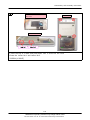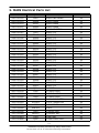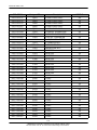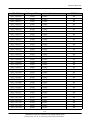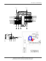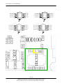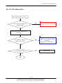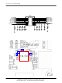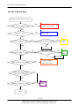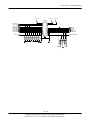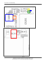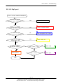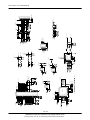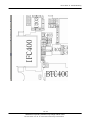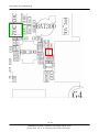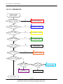
1
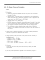
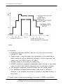
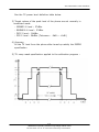
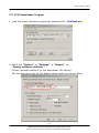
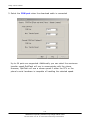
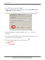
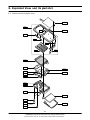
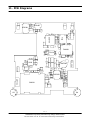
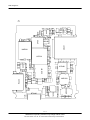
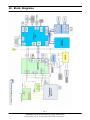
GSM TELEPHONE
SGH-T519
GSM TELEPHONE
CONTENTS
1.
Safety Precautions
2.
General Introduction
3.
Specification
4.
Product Funtion
5.
Circuit Description
6.
Test Command & Test Procedure
7.
Array course control
8.
Exploded View and its Parts list
9.
MAIN Electrical Parts List
10.
Flow Chart of Troubleshooting and
Circuit Diagrams
11.
PCB Diagrams
12.
Block Diagrams
13.
Reference data
Contents
1. Safety Precautions
1-1. Repair Precaution ...........................................................................1-1
1-2. ESD(Electrostatically Sensitive Devices) Precaution ...........................1-2
2. General Introduction
3. Specification
3-1. GSM General Specification ..............................................................3-1
3-2. GSM TX Power class ......................................................................3-2
3-3. EDGE TX Poser Level .....................................................................3-3
4. Product Function
4-1. Main Function ................................................................................4-1
5. Circuit Description
6. TEST Command & Test Procedure
6-1. Calibration Equipment ....................................................................6-1
6-2. Calibration Program .......................................................................6-1
6-3. TX Power Tune up procedure .........................................................6-2
7. Array course control
7-1. Downloading Binary Files ................................................................7-2
7-2. Pre-requsite for Downloading ..........................................................7-2
7-3. S/W Downloader Program ...............................................................7-3
7-4. How to Download ..........................................................................7-5
8. Exploded View and its Parts list
8-1. Cellular phone Exploded View .........................................................8-1
8-2. Cellular phone parts list .................................................................8-2
8-3. Disassembly ..................................................................................8-4
8-4. Assembly ......................................................................................8-7
Contents
9. MAIM Electrical parts list
10. Flow Chart of Troubleshooting and Circuit Diagrams
10-1. Baseband
10-1-1. Power on ..............................................................................10-1
10-1-2. Initial ....................................................................................10-3
10-1-3. Sim Part ...............................................................................10-4
10-1-4. Charging Part ........................................................................10-5
10-1-5. Microphone Part .....................................................................10-7
10-1-6. Speaker Part .........................................................................10-9
10-1-7. Camera Part ........................................................................10-13
10-2. RF
10-2-1. GSM850/EGSM900 RX ..........................................................10-15
10-2-2. PCS RX ...............................................................................10-16
10-2-3. DCS RX ...............................................................................10-17
10-2-4. GSM850/EGSM900 TX ...........................................................10-18
10-2-5. DCS/PCS TX ........................................................................10-19
10-2-6. BLUETOOTH .........................................................................10-20
11. PCB Diagrams
12. Block Diagrams
12-1. RF Solution Block Diagram ..........................................................12-1
12-2. Base Band Solution Block Diagram ..............................................12-2
13. Reference data
This Service Manual is a property of Samsung Electronics Co.,Ltd.
Any unauthorized use of Manual can be punished under applicable
International and/or domestic law.
ⓒ Samsung Electronics Co.,Ltd.
Code No.: GH68-12034A
2006. 08. Rev.1.0
1. Safety Precautions
1-1. Repair Precaution
● Repair in Shield Box, during detailed tuning.
Take specially care of tuning or test,
because specipicty of cellular phone is sensitive for surrounding interference(RF noise).
● Be careful to use a kind of magnetic object or tool,
because performance of parts is damaged by the influence of manetic force.
● Surely use a standard screwdriver when you disassemble this product,
otherwise screw will be worn away.
● Use a thicken twisted wire when you measure level.
A thicken twisted wire has low resistance, therefore error of measurement is few.
● Repair after separate Test Pack and Set because for short danger (for example an
overcurrent and furious flames of parts etc) when you repair board in condition of
connecting Test Pack and tuning on.
● Take specially care of soldering, because Land of PCB is small and weak in heat.
● Surely tune on/off while using AC power plug, because a repair of battery charger is
dangerous when tuning ON/OFF PBA and Connector after disassembing charger.
● Don't use as you pleases after change other material than replacement registered on
SEC System.
Otherwise engineer in charge isn't charged with problem that you don't keep this rules.
1-1
SAMSUNG Proprietary-Contents may change without notice
This Document can not be used without Samsung's authorization
Safety Precautions
1-2. ESD(Electrostatically Sensitive Devices) Precaution
Several semiconductor may be damaged easilly by static electricity. Such parts are called by
ESD(Electrostatically Sensitive Devices), for example IC,BGA chip etc. Read Precaution below.
You can prevent from ESD damage by static electricity.
● Remove static electricity remained your body before you touch semiconductor or parts with
semiconductor. There are ways that you touch an earthed place or wear static electricity
prevention string on wrist.
● Use earthed soldering steel when you connect or disconnect ESD.
● Use soldering removing tool to break static electricity. otherwise ESD will be damaged by
static electricity.
● Don't unpack until you set up ESD on product. Because most of ESD are packed by box
and aluminum plate to have conductive power,they are prevented from static electricity.
● You must maintain electric contact between ESD and place due to be set up until ESD is
connected completely to the proper place or a circuit board.
1-2
SAMSUNG Proprietary-Contents may change without notice
This Document can not be used without Samsung's authorization
2. General Introduction
The SGH-T519 Quad Band phone functions as digital phone working in GSM
(Global System for Mobile communications)850,EGSM900, DCS1800 and
PCS(PersonalCommunication System)1900 modes.
<Specification>
●
●
●
●
●
●
●
●
Dimension
Weight
LCD
R/F band
Vocoder
Antenna
SIM
BLUETOOTH
: 113 x 50 x 8.6 mm (with Standard Battery)
: 76g (with Standard Battery)
: LCD 260K TFT Color LCD (176 x 220) 1.93"
: GSM850 / EGSM 900 / DCS1800 / PCS1900
: EFR + FR + HR + AMR
: Fixed type
: 3 Voltage operation
: VER 1.0
<GPRS/EGPRS Factor>
●
●
●
●
●
●
MS Class
GPRS Phase
Multi-slot
SMG
Coding scheme
Power class
●
WAP 2.0 Browser
●
SIM AT(Application Toolkit)
●
40 Polyphonic Ringtone
:
:
:
:
:
:
Class B
GSM Phase II+
GPRS/EGPRS Class 10 (2 Up-link, 4 Down-link, 5 Sum)
SMG #31
CS1 - CS4(GPRS), MCS5 - MCS9(EGPRS) support
GSM850
- Class 4 (2W)
EGSM900 - Class 4 (2W)
DCS1800 - Class 1 (1W)
PCS1900 - Class 1 (1W)
< Basic Package >
●
Handset + Standard Battery + TA
+ User Guide + Handstrap
< Option Item >
● Travel Adapter
● Ear Microphone
● Bluetooth Headset
● Bluetooth Hands Free Kit
● Car Charger/Adapter
2-1
SAMSUNG Proprietary-Contents may change without notice
This Document can not be used without Samsung's authorization
3. Specification
3-1. GSM General Specification
GSM850
EGSM900
DCS1800
PCS1900
F r e q . Ba n d [ M Hz ]
Uplink/ Downlink
824~849
869~894
880~915
925~960
1710~1785
1805~1880
1850~1910
1930~1990
A RFCN rang e
128~251
0~124&
975~1023
512~885
512~810
T x /Rx s pacing
45 MHz
45 MHz
95 MHz
80 M Hz
GP RS
270.833 Kb ps
3. 692 us
270.833 Kb ps
3. 692 us
270.833 Kb ps
3. 692 us
270.833 Kbp s
3.692 us
EDGE
812.5 K b ps
3. 692 us
812.5 K b ps
3. 692 us
812.5 K b ps
3. 692 us
812.5 K bp s
3.692 us
576. 9 u s
4.615 ms
576. 9 u s
4.615 ms
576. 9 u s
4.615 ms
576.9 u s
4.615 ms
GP RS
0.3 G M SK
0.3 G M SK
0.3 G M SK
0.3 G MS K
EDGE
8 PSK
8 PSK
8 PSK
8 PSK
GP RS
33 d Bm~5 d Bm
33 d Bm~5 d Bm
30 d Bm~0 d Bm
30 dBm~0 d Bm
ED G E
27~5 dBm
27~5 dBm
26~0 dBm
26~0 dBm
GP RS
5~19(class4)
5~19(class4)
0~15(class1)
0~15(class1)
ED G E
8~19( class E 2)
8~19( class E 2)
2~15(class E2)
2~15(class E2)
Sens itivity
- 102 dBm
- 102 dBm
- 100 dBm
-102 d Bm
T D MA Mux
8
8
8
8
Cell Radius
35 Km
35 Km
2 Km
2 Km
Mod. Bit
r ate/
Bit P eriod
Time Slot
Period/ Fr ame Period
Modu lation
M S P o wer
P ower L evel
3-1
SAMSUNG Proprietary-Contents may change without notice
This Document can not be used without Samsung's authorization
Specification
3-2. GSM TX power class
TX
Power
control
level
GSM850
5
33±2 dBm
6
31±2 dBm
7
29±2 dBm
8
27±2 dBm
9
25±2 dBm
10
23±2 dBm
11
21±2 dBm
12
19±2 dBm
13
17±2 dBm
14
15±2 dBm
15
13±2 dBm
16
11±2 dBm
17
9±2 dBm
18
7±2 dBm
19
5±2 dBm
DCS1800
TX
Power
control
level
PCS1900
0
30±3 dBm
0
30±3 dBm
31±2 dBm
1
28±3 dBm
1
28±3 dBm
7
29±2 dBm
2
26±3 dBm
2
26±3 dBm
8
27±2 dBm
3
24±3 dBm
3
24±3 dBm
9
25±2 dBm
4
22±3 dBm
4
22±3 dBm
10
23±2 dBm
5
20±3 dBm
5
20±3 dBm
11
21±2 dBm
6
18±3 dBm
6
18±3 dBm
12
19±2 dBm
7
16±3 dBm
7
16±3 dBm
13
17±2 dBm
8
14±3 dBm
8
14±3 dBm
14
15±2 dBm
9
12±4 dBm
9
12±4 dBm
15
13±2 dBm
10
10±4 dBm
10
10±4 dBm
16
11±2 dBm
11
8±4 dBm
11
8±4 dBm
17
9±2 dBm
12
6±4 dBm
12
6±4 dBm
18
7±2 dBm
13
4±4 dBm
13
4±4 dBm
19
5±2 dBm
14
2±5 dBm
14
2±5 dBm
15
0±5 dBm
15
0±5 dBm
TX
Power
control
level
EGSM900
TX
Power
control
level
5
33±2 dBm
6
3-2
SAMSUNG Proprietary-Contents may change without notice
This Document can not be used without Samsung's authorization
Specification
3-3. EDGE TX Power Level
TX
Power
control
level
GSM850
TX
Power
control
level
EGSM900
TX
Power
control
level
DCS1800
TX
Power
control
level
PCS1900
8
27±3 dBm
8
27±3 dBm
2
26±3 dBm
2
26±3 dBm
9
25±3 dBm
9
25±3 dBm
3
24±3 dBm
3
24±3 dBm
10
23±3 dBm
10
23±3 dBm
4
22±3 dBm
4
22±3 dBm
11
21±3 dBm
11
21±3 dBm
5
20±3 dBm
5
20±3 dBm
12
19±3 dBm
12
19±3 dBm
6
18±3 dBm
6
18±3 dBm
13
17±3 dBm
13
17±3 dBm
7
16±3 dBm
7
16±3 dBm
14
15±3 dBm
14
15±3 dBm
8
14±3 dBm
8
14±3 dBm
15
13±3 dBm
15
13±3 dBm
9
12±4 dBm
9
12±4 dBm
16
11±5 dBm
16
11±5 dBm
10
10±4 dBm
10
10±4 dBm
17
9±5 dBm
17
9±5 dBm
11
8±4 dBm
11
8±4 dBm
18
7±5 dBm
18
7±5 dBm
12
6±4 dBm
12
6±4 dBm
19
5±5 dBm
19
5±5 dBm
13
4±4 dBm
13
4±4 dBm
14
2±5 dBm
14
2±5 dBm
15
0±5 dBm
15
0±5 dBm
3-3
SAMSUNG Proprietary-Contents may change without notice
This Document can not be used without Samsung's authorization
4. Product Function
Main Function
-1.3 Megapixel Camera and Camcorder
-Bluetooth® Wireless Technology
-Instant Messageing capability
-Multimedia capability
-Fun & Apps featureprovides My Files, music player, games,
alarms, calendar, task list, calculator, world time, unit conversion, timer,
and stopwatch.
4-1
SAMSUNG Proprietary-Contents may change without notice
This Document can not be used without Samsung's authorization
5. Circuit Description
< RF Circuit Description of SGH-T519 >
1. FEM (F100)
==> Switching Tx, Rx path for GSM850, EGSM900, DCS1800 and PCS1900
controlled by logic.
Integration of GSM850, EGSM900, DCS1800 and PCS1900 RX SAW Filters.
To convert Electromagnetic Field Wave to Acoustic Wave and the pass the specific
frequency band.
- for filtering the frequency band 824 ~ 849 / 869 ~ 894 MHz
- for filtering the frequency band 880 ~ 915 / 925 ~ 960 MHz
- for filtering the frequency band 1710 ~ 1785 / 1805 ~ 1880 MHz
- for filtering the frequency band 1850 ~ 1910 / 1930 ~ 1990 MHz
2. FEM Control Logic
==> Truth Table
VC1
VC2
VC3
GSM850 Rx Mode
L
L
H
EGSM900
L
L
L
GSM850/EGSM900 Tx Mode
L
H
L
DCS/PCS Rx Mode
L
L
L
DCS/PCS Tx Mode
H
L
L
3. VC-TCXO(TCX400)
==> To generate the 26 MHz reference clock to drive the logic and RF.
4. SKY74137 (UCD100)
==> The sky74137 is a RF tranceiver IC for GS850, EGSM900 DCS1800
and PCS1900 quardband cellular systems, and incorporates EDGE tranceiver
capabillity, and integrates most of the low power silicon functions of a tranceiver.
The receive path implements a direct downconversion architecture. The transceiver
consists of four integrated Low Noise Amplifiers (LNAs), a quadrature demodulator,
selectable baseband filter bandwidths, and lowdroop DC Offset Correction (DCOC)
sequencer.
- RX Function
Four LNAs which support different bands of operation have separated differential
inputs. The LNA outputs feed into a quadrature demodulator that down-converts
the RF signals directly to baseband. The baseband I and Q paths consist of
cascaded amplifiers and low pass filter sections. All baseband filtering is provided
on-chip using no external capacitors.
5-1
SAMSUNG Proprietary-Contents may change without notice
This Document can not be used without Samsung's authorization
Circuit Description
- TX Function
The device implements Skyworks Polar Loop transmit architecture. This architecture
autonomously splits the amplitude and phase within the device using the traditional
analog In-Phase and Quadrature (I/Q) signals. The filter-saving advantage of the
translation-loop approach is embedded in the architecture. Also included is an AM loop
that provides both signal AM and power level control. The transmitter is provided a
coupled feedback signal from the PA and downconverts it to an IF. Following an IF VGA,
this feedback signal is fed to both loops. The reference for both loops is a transmit IF
signal produced by an I/Q modulator
5. POWER AMP (PAM400)
The module consists of a EGSM850/900 PA block and a DCS1800/PCS1900 PA block,
Both PA blocks share common power supply pins to distribute current. The subsystem
consists of two parts : a Power Amplifier Control (PAC) block, and an Integrated Coupler.
To select GSM900/850 and GMS1800/1900 as determined from the Band Select
(BAND_SEL) signal. SKY77331 contains band select switching circuitry to select GSM
(BAND_SEL is low) and DCS/PCS (BAND_SEL is HIGH) as determined from the Band
Select (BAND_SEL) signal. The BAND_SEL pad selects the PA output (DPCS_OUT or
GSM_OUT) while the Power Control (VPC) controls the level of output power. The
integrated power amplifier control (PAC) function provides envelope amplitude control by
reducing sensitivity to input drive, temperature, power supply, and process variation.
< Baseband
Circuit description of SGH-D407 >
1. CSP2750 (UCD301)
==> The CSP2750 has two major logical components power management and
conversion signal processing.
The PSC component is responsible for all power-related functionality, including the
following;
● Power management for RF, BB and ancillary devices within the GSM/GPRS
● Battery-charge management
● Reset control
● SIM card voltage-level shifting
The CSP component is responsible for the following ;
● Intraframe event scheduling
● Voice band processing, including voice band ADC and DAC
● Analog baseband processing, including baseband ADC and DAC
● Providing RF interface for Trident digital baseband device
● Transmitter Power control
● Automatic frequency control
● A5 ciphering
● Low-power sleep mode and wake-up control
5-2
The CSP2750 has the following major physical
components;
SAMSUNG Proprietary-Contents may change without notice
This Document can not be used without Samsung's authorization
Circuit Description
● Timing and control unit
● RF serial interface
● Low-power sleep mode controller
● Baseband Transmitter / Receiver
● Voice input and output
2. WM8955L(UCD401)
==> The WM8955L is a low power, high quality stereo DAC with intergrated headphone
and loudspwaker amplifiers, designed to reduce external component
requirements in portable digital audio application.
The on-chip headsphone amplifiers can deliver 40mW into a 16Ω load. Advanced
on-chip digital signal processing performs bass and treble tone comtrol.
The WM8955L can operate as a master or a slave, and include an on-chip PLL. It
can use most master clock frequencies commonly found in portable systems,
including USB,GSM, CDMA or PDC clocks, or standard 256fs, clock rates.
Different audio sample rates such as 48khz, 44.1khz, 8khz and many other are
supported.
The WM8955L operates on supply voltages from 1.8V up to 3.6V, although the
digital core can operates on a separate supply down to 1.42V, saving power.
Different section of the chip can also be powered down under software control.
3. HPE(UCP201)
==> The Trident-HPE digital baseband processor is a complete system IC designed for
wireless terminals that includes two digital signal processor(DSP) cores
optimized for low-power communications applications and a powerful,
highperformance,
industry-standard microcontroller core along with a rich set of peripherals.
The Trident-HPE digital baseband processor achieves best-in-class signal processing
performance while maintaining the efficient software code density, low power
consumption, and small physical size required for GSM/GPRS terminals
ARM946E-S microcontroller core;
● 101 MHz system bus, 16 kbyte instruction and 16kbyte data caches.
● 8 kbyte tightly coupled zero wait-state instruction and 4kbyte tightly coupled zero waitstate data memory
● direct memory access controller for transparent transfer between memory and
peripherals.
● External Memory interface with asynchronous
burst mode support
5-3
SAMSUNG Proprietary-Contents may change without notice
This Document can not be used without Samsung's authorization
Circuit Description
● Synchronous serial port supporting
● Programmable 48-bit general-purpose IO unit, keyboard interface, programmable interval
timer and real-time clock.
● SD/MMC controller that supports interfacing to secure digital/multimedia memory card.
Two DSP16000 dual-MAC DSP cores;● Up to 404 million MACs per second at 101 MHz.
● Memory complement;
- DSP0 : 144K X 16-bit ROM, 40k X 16-bit RAM.
- DSP1 : 96K X 16-bit ROM, 16k X 16-bit RAM.
JTAG boundary scan and integrated H/W developement system Low power;
● Ultralow leakage process technology for best-in-class standby
power
● Flexible power management modes to allow for maximum active power management
Interprocessor communication hardware support between ARM, DSP0 and DSP1.
Supported by Trident-HPE digital baseband processor software and hardware
developement tools as well as industry standard ARM software and hardware
developement tools Two on-chip, programmable, PLL clock synthesizers;
- one for ARM and DSP, the other one for USB.
5-4
SAMSUNG Proprietary-Contents may change without notice
This Document can not be used without Samsung's authorization
6. Test Command & Test Procedure
6-1. Calibration Equipment
-
HP 8960
DC Power Supply
Test Jig
Configuration
HP8960
RF
DC POWER SUPPLY
GPIB
+
+
--
PC
TEST JIG
GPIB
Serial
Serial
6-2. Calibration Program
- Samsung internal software
6-1
SAMSUNG Proprietary-Contents may change without notice
This Document can not be used without Samsung's authorization
Test Command & Test Procedure
6-3. Tx Power Tune up Procedure
- GMSK
1) Procedure:
a. Calibraion equipment HP8960 and the cell phone are connected
through RF cable.
b. Target power ( required power level according to the specification
which should be set by calibration program) is set to equipment as
power level (ex: GSM 5 level is 32.5 dBm).
c. Activate phone in Tx_Mode_Only.
d. HP8960 equipment measures transmitted power through rf test cable
from the phone and reports measured level to calibration program.
e. The program compares measured power with the target power.
f. The calibration program decides power code which is defined in
advance in the program and writes the codes to the flash memory in
the phone.
2) Target value is defined according to the value of GSM specification.
See the TX power level definition table below.
3) Target values of the peak level of the phone are set normally in
conducted mode
- GSM850 5 level : 32.5dBm
- EGSM900 5 level : 32.5dBm
- DCS 0 level : 29.5dBm
- PCS 0 level : 29.5dBm (Tolerance : -2dB ~ +1dB )
4) Accuracy
All the TX level from the phone after tuned-up satisfy the GSM
specification
5) TX ramp mask specification applied to the calibration program :
6-2
SAMSUNG Proprietary-Contents may change without notice
This Document can not be used without Samsung's authorization
Test Command & Test Procedure
- 8PSK
1) Procedure:
a. Calibraion equipment HP8960 and the cell phone are connected
through RF cable.
b. Target power ( required power level according to the specification
which should be set by calibration program) is set to equipment as
power level (ex: GSM 8 level is 27 dBm).
c. Activate phone in Cont_8psk_Tx_Mode_Only.
d. HP8960 equipment measures transmitted power through rf test cable
from the phone and reports measured level to calibration program.
e. The program compares measured power with the target power.
f. The calibration program decides power code which is defined in
advance in the program and writes the codes to the flash memory in
the phone.
2) Target value is defined according to the value of EGPRS specification.
6-3
SAMSUNG Proprietary-Contents may change without notice
This Document can not be used without Samsung's authorization
Test Command & Test Procedure
See the TX power level definition table below.
3) Target values of the peak level of the phone are set normally in
conducted mode
- GSM850 8 level : 27dBm
- EGSM900 8 level : 27dBm
- DCS 2 level : 26dBm
- PCS 2 level : 26dBm (Tolerance : -2dB ~ +1dB )
4) Accuracy
All the TX level from the phone after tuned-up satisfy the EGPRS
specification
5) TX ramp mask specification applied to the calibration program :
6-4
SAMSUNG Proprietary-Contents may change without notice
This Document can not be used without Samsung's authorization
7. Array course control
Test Jig (GH80-03307A)
Test Cable (GH39-00478A)
RF Test Cable (GH39-00397A)
7-1
SAMSUNG Proprietary-Contents may change without notice
This Document can not be used without Samsung's authorization
Array course control
Software Downloading
7-1. Downloading Binary Files
• Two binary files for downloading T519.
– T519XXYY.s3 : Main source code binary.
7-2. Pre-requsite for Downloading
• Downloader Program(OptiFlash.exe)
• T519 Mobile Phone
• Data Cable
• Binary files
7-2
SAMSUNG Proprietary-Contents may change without notice
This Document can not be used without Samsung's authorization
Array course control
7-3. S/W Downloader Program
1. Load the binary download programby executing the “OptiFlash.exe”
2. Select the “Options” -> “Settings” -> “Generic” ->
“Specify hardware platform”.
Choose hardware platform for the downloader file setting.
Set the everything else as the default values which are shown below
7-3
SAMSUNG Proprietary-Contents may change without notice
This Document can not be used without Samsung's authorization
Array course control
3. Select the COM port when the download cable is connected
Up to 64 ports are supported. Additionally you can select the maximum
transfer speed OptiFlash will use to communicate with the phone.
However, OptiFlash will use a slower speed if either the PC’s or the
phone’s serial hardware is incapable of handling the selected speed.
7-4
SAMSUNG Proprietary-Contents may change without notice
This Document can not be used without Samsung's authorization
Array course control
4. Select the“Flash&Verify” -> “Browse”
Set the directory path and choose the latest s/w binary, for example
“T519XXYY.s3”,for the downloader binary setting.
In case of D407 the reserved regions are not a necessity.
(It is defined in platform.def file)
7-5
SAMSUNG Proprietary-Contents may change without notice
This Document can not be used without Samsung's authorization
Array course control
5. Click “OK” button then press “Flash”.
(Before pressing ‘Flash’ button, push the button ‘*’and ‘END’ at the
same time. Then press ‘Flash’.)
Downloader will upload the binary file as below for the downloading.
6. When downloading is finished successfully, there is a “All is well”
message. 7. After finishing downloading, Certain memory resets should be done to
guarantee the normal performance.
8. Confirm the downloaded version name and etc. :
*#1234#
Full Reset : *2767*3855#
7-6
SAMSUNG Proprietary-Contents may change without notice
This Document can not be used without Samsung's authorization
8. Exploded View and its Partslist
8-1. Cellular phone Exploded View
QME01
QFR01
QSD01
QCK01
QVO01
QRF03
QMI03
QCR06
QKP01
QLC01
QFL06
QCA02
QVK01
QMP01
QAN02
QCA01
QME03
QRE01
QCW01
QBA01
QCR06
QSC01
QBA00
QSC02
QRF01
8-3
SAMSUNG Proprietary-Contents may change without notice
This Document can not be used without Samsung's authorization
Exploded view and its Part list
8-2. Cellular phone Parts list
QAN02
INTENNA-SGHT519
GH42-01022A
QBA00
ASSY CASE-BATT
GH98-02621B
QBA01
INNER BATTERY PACK-800MAH, BLK
GH43-02612A
QCA01
UNIT-CAMERA
GH59-03182A
QCA02
UNIT-CAMERA KEY
GH59-03176A
QCK01
ASSY KEY-CAMERA
GH98-00889B
QCR04
SCREW-MACHINE
6001-001479
QCR06
SCREW-MACHINE
6001-001155
QCR06
SCREW-MACHINE
6001-001155
QCW01
PMO-WINDOW CAMERA
GH72-30568A
QFL06
ASSY CASE-CARRIER LOWER
GH98-01899A
QFR01
ASSY CASE-FRONT
GH98-01888B
QKP01
ASSY KEYPAD-MAIN(CHE/BLK)
GH98-01901B
QLC01
LCD-M/S SGHT519
GH07-01002A
QME01
UNIT-EL KEY PBA
GH59-03177A
QME03
UNIT-SPK_MOT FPCB
GH59-03183A
QMI03
RMO-RUBBER MIC HOLDER
GH73-07779A
QMI05
ASSY CASE-MIC SUB
GH98-01889B
QMP01
A/S MATERIAL ASSY-PBA MAIN
GH82-02168A
QRE01
ASSY CASE-REAR
GH98-01900B
QRF01
PMO-COVER RF
GH72-33517B
QRF03
PMO-COVER EAR JACK
GH72-30563B
QSC01
PMO-COVER SCREW L
GH72-33519B
QSC02
PMO-COVER SCREW R
GH72-33526B
QSD01
PMO-COVER MICRO SD
GH72-30562B
QVK01
UNIT-VOLUME KEY
GH59-03175A
QVO01
ASSY KEY-VOLUME
GH98-00890B
8-2
SAMSUNG Proprietary-Contents may change without notice
This Document can not be used without Samsung's authorization
Exploded view and its Part list
CBF INTERFACE-DATA LINK CABLE
GH39-00514A
CHARGER-SGHD820 TA (LTA)
GH44-01174A
UNIT-EARPHONE(BLK)
GH59-02499A
MPR-VINYL BOHO T MAIN WINDOW
GH74-26613B
AS-LCD WINDOW TAPE
GH81-05218A
AS-LCD WINDOW
GH81-05937A
RMO-RUBBER LCD CONN
GH73-07778A
RMO-RUBBER EAR JACK
GH73-07780A
RMO-RUBBER BGA
GH73-07922A
RMO-RUBBER CSP
GH73-08343A
MPR-TAPE CAMERA KEY
GH74-25950A
MPR-TAPE VOLUME KEY
GH74-25951A
MPR-SPONGE BT
GH74-26377A
MPR-TAPE, 3X3XT3.5, W290TCNG
GH74-26380A
MPR-TAPE, 8X6XT0.25, ABSORBER
GH74-26382A
MPR-SPONGE BD
GH74-26717A
MPR-TAPE LCD FRONT
GH74-27607A
MPR-INSU TAPE
GH74-27608A
MPR-TAPE
GH74-28264A
MPR-TAPE BRAKET B
GH74-28265A
RMO-RUBBER BATTERY
GH73-08571A
MPR-VINYL BOHO KEYPAD
GH74-22928A
LABEL(R)-WATER SOAK T_MOBILE
GH68-05914A
AS-TAPEKEYPAD
GH81-04637A
PMO-DECORATION REAR
GH72-30564B
MPR-VINYL BOHO REAR
GH74-21012A
LABEL(R)-WATER SOAK T_MOBILE
GH68-05914A
RMO-RUBBER EAR JACK
GH73-07780A
MPR-VINYL BOHO MAIN WINDOW
GH74-21905A
BAG PE
6902-000634
LABEL(P)-IMEI
GH68-01335D
LABEL(R)-MAIN(LTN)
GH68-12700A
BOX-UNIT(VMT)
GH69-04523E
CUSHION-CASE(MEXC)
GH69-04535A
S/W CD-SAMSUNG PC STUDIO 3.0
GH46-00247A
MANUAL USERS-LTN SPANISH
GH68-13488A
8-3
SAMSUNG Proprietary-Contents may change without notice
This Document can not be used without Samsung's authorization
Disassembly and Assembly instructions
8-3. Disassembly
1
2
1.Unscrew 4 points of a rear.
1.Disjoint a top of the rear with a tool.
※ caution
※ caution
1.Be careful not to do damage and scratch the phone.
1.Be careful not to do damage and scratch the phone.
3
4
1.Remove both side keys,then detach the EL
KEY FPCB CONNECTOR.
1.Lift up a board carefully and detach a PBA.
1.Be careful not to cut both side keys and damage to camera
connector pins
1.Be careful not to cut both side keys and damage to camera
connector pins
※ caution
※ caution
5
6
1.Remove a camera and SPK/MOT connector.
※ caution
1.Be careful not to damage to camera connector pins
1.Detach a PBA Ass'y from LCD Module.
※ caution
1.Be careful not to do damage to intenna and scratch the
LCD.
8-4
SAMSUNG Proprietary-Contents may change without notice
This Document can not be used without Samsung's authorization
Disassembly and Assembly instructions
7
1. Detach a LCD from LCD braket.
※ caution
1.Be careful not to do damage and scratch the phone.
8-5
SAMSUNG Proprietary-Contents may change without notice
This Document can not be used without Samsung's authorization
Disassembly and Assembly instructions
8-4. Assembly
1
2
1. Attach an EL sheet
2. Attach a key pad
2. Press a camera
window.
1. Attach a rear deco.
and camera window
A.
B.
C.
D.
E.
Remove a adhesive tape of EL sheet.
Attach a EL sheet
Attach a mic cover
Attach a key pad
Press a key pad
2
- Pressure kgf : 6 ± 1 kgf/cm
A. Examine the surface of rear,and attach a
rear deco. and camera window.
B. Press a camera window.
2
- Pressure kgf : 6 ± 1 kgf/cm
3
1. Attach a SPK_MOT FPCB
2. Place a SPK_MOT FPCB
Place part printed +,-into a groove
Connection part
of SPK and MOT
F-PCB
Remove a
adhesive tape
Base line when
Place F-PCB가 inside Intenna
attaching SPK F-PCB
A. Connect SPK and MOT with FPCB and paste another FPBC along the baseline.
B. Place SPK_MOT F-PCB inside intenna.
8-6
SAMSUNG Proprietary-Contents may change without notice
This Document can not be used without Samsung's authorization
Disassembly and Assembly instructions
4
1. Examnine the surface of
2. Place LCD and sponge
CARRIER LOWER
CAMERA SPONGE
LCD place hole
SHORT PREVENTION TAPE
Baseline
ABSORBER
Attach keeping away from
soldering part.
completion
A.Place a LCD inserting LCD connector on the front of CARRIER LOWER.
B.Place a LCD into place hole of CARRIER LOWER correctly.
C.Press carefully the top (SAMSUNG logo) and bottom( T-Mobile logo) of LCD .
D.Attach a LCD sponge to CARRIER LOWER along the base line (the right side and bottom)
5
1. Soler side keys and stick a friction tape
A. Solder side keys with soldering jig.
B. Stick a friction tape along the baseline.
8-5
SAMSUNG Proprietary-Contents may change without notice
This Document can not be used without Samsung's authorization
Disassembly and Assembly instructions
6
1. Place a PBA
Press the connector horizontally to a
PBA
A. Press carefully the top of PBA with your right hand grasping CARRIER LOWER with your
left hand.
B. Press both sides of PBA until it clicks into the CARRIER LOWER.
(Grasp the edge of LCD during work)
C. Press the LCD connector to the CARRIER LOWER horizontally.
7
1. Place the intenna
A.Press the intenna until it clicks into the PBA
B.Put the SPK CONNECTER horizontally
C.Place the soldering part of INTENNA to a groove
8-6
SAMSUNG Proprietary-Contents may change without notice
This Document can not be used without Samsung's authorization
Disassembly and Assembly instructions
8
1. Solder the intenna
2. Place the camera
A. Solder the intenna with soldering jig
B. Place the camera into a groove of CARRIER LOWER.
C. Press carefully after placing camera module.
9
1.Place the PBA side keys
A. Place the PBA on the FRONT.
B. Remove the camera protection film.
C. Place side keys into place.
8-5
SAMSUNG Proprietary-Contents may change without notice
This Document can not be used without Samsung's authorization
Disassembly and Assembly instructions
10
1. Remove the protection film inside
3. SCREW
CAMERA WINDOW
2. Place the REAR
Locker No.1
Locker No.2
A. Place the top of a REAR and press down until it clicks into the Front
B.Press the Locker No.1 and Locker No.2
C.SCREW.(4 POINT)
8-6
SAMSUNG Proprietary-Contents may change without notice
This Document can not be used without Samsung's authorization
9. MAIN Electrical Parts List
SEC CODE
Design LOC
0401-001141
D401
0403-001411
Discription
STATUS
DIODE-SWITCHING
SA
ZD406
DIODE-ZENER
SA
0403-001511
ZD301
DIODE-ZENER
SA
0403-001547
ZD402
DIODE-ZENER
SA
0404-001245
D302
DIODE-SCHOTTKY
SA
0406-001167
U201
DIODE-TVS
SA
0406-001190
ZD403
DIODE-TVS
SA
0406-001190
ZD404
DIODE-TVS
SA
0406-001210
ZD203
DIODE-TVS
SA
0406-001210
ZD400
DIODE-TVS
SA
0406-001210
ZD401
DIODE-TVS
SA
0406-001223
ZD310
DIODE-TVS
SA
0406-001223
ZD311
DIODE-TVS
SA
0406-001241
ZD303
DIODE-TVS
SA
0406-001241
ZD304
DIODE-TVS
SA
0406-001254
ZD305
DIODE-TVS
SA
0406-001254
ZD306
DIODE-TVS
SA
0406-001254
ZD307
DIODE-TVS
SA
0406-001254
ZD308
DIODE-TVS
SA
0406-001254
ZD309
DIODE-TVS
SA
0406-001254
ZD407
DIODE-TVS
SA
0406-001254
ZD408
DIODE-TVS
SA
0406-001254
ZD409
DIODE-TVS
SA
0406-001254
ZD410
DIODE-TVS
SA
0406-001254
ZD411
DIODE-TVS
SA
0504-000168
Q301
TR-DIGITAL
SA
0801-002529
U300
IC-CMOS LOGIC
SA
0801-002958
U101
IC-CMOS LOGIC
SA
0801-002958
U204
IC-CMOS LOGIC
SA
1001-001371
U402
IC-ANALOG SWITCH
SA
1002-001441
UCD401
IC-D/A CONVERTER
SA
1003-001716
U305
IC-EL DRIVER
SA
1108-000068
UME201
IC-MCP
SA
1201-002240
U401
IC-AUDIO AMP
SA
1201-002368
PAM101
IC-POWER AMP
SA
1203-003663
U304
IC-BATTERY
SA
1203-003688
Q100
IC-POSI.FIXED REG.
SA
9-1
SAMSUNG Proprietary-Contents may change without notice
This Document can not be used without Samsung's authorization
Electrical Parts List
SEC CODE
Design LOC
Discription
1203-003737
Q401
IC-POSI.FIXED REG.
SA
1203-003737
Q402
IC-POSI.FIXED REG.
SA
1203-003737
U405
IC-POSI.FIXED REG.
SA
1203-003767
Q400
IC-POSI.FIXED REG.
SA
1203-003787
Q403
IC-POSI.FIXED REG.
SA
1203-003789
U202
IC-POWER SUPERVISOR
SA
1203-004119
UCD301
IC-POWER SUPERVISOR
SA
1203-004164
U302
IC-DC/DC CONVERTER
SA
1203-004172
U404
IC-DC/DC CONVERTER
SA
1205-002272
U203
IC-TRANSCEIVER
SA
1205-002944
UCD100
IC-TRANSCEIVER
SA
1404-001165
U301
THERMISTOR-NTC
SA
1405-001082
V402
VARISTOR
SA
1405-001082
V403
VARISTOR
SA
1405-001082
VR200
VARISTOR
SA
1405-001108
V306
VARISTOR
SA
1405-001108
V307
VARISTOR
SA
1405-001108
V309
VARISTOR
SA
1405-001108
V310
VARISTOR
SA
1405-001108
V311
VARISTOR
SA
1405-001108
V312
VARISTOR
SA
2007-000137
R439
R-CHIP
SA
2007-000138
R440
R-CHIP
SA
2007-000139
R101
R-CHIP
SA
2007-000139
R102
R-CHIP
SA
2007-000140
R321
R-CHIP
SA
2007-000140
R433
R-CHIP
SA
2007-000141
R402
R-CHIP
SA
2007-000141
R418
R-CHIP
SA
2007-000142
R412
R-CHIP
SA
2007-000142
R425
R-CHIP
SA
2007-000148
R205
R-CHIP
SA
2007-000148
R216
R-CHIP
SA
2007-000148
R430
R-CHIP
SA
2007-000148
R431
R-CHIP
SA
2007-000148
R441
R-CHIP
SA
2007-000157
R122
R-CHIP
SA
9-2
SAMSUNG Proprietary-Contents may change without notice
This Document can not be used without Samsung's authorization
STATUS
Electrical Parts List
SEC CODE
Design LOC
Discription
2007-000157
R428
R-CHIP
SA
2007-000157
R429
R-CHIP
SA
2007-000171
R105
R-CHIP
SA
2007-000171
R106
R-CHIP
SA
2007-000171
R114
R-CHIP
SA
2007-000171
R135
R-CHIP
SA
2007-000171
R136
R-CHIP
SA
2007-000171
R225
R-CHIP
SA
2007-000171
R227
R-CHIP
SA
2007-000171
R305
R-CHIP
SA
2007-000171
R410
R-CHIP
SA
2007-000171
R411
R-CHIP
SA
2007-000171
R452
R-CHIP
SA
2007-000171
R453
R-CHIP
SA
2007-000172
R213
R-CHIP
SA
2007-000172
R214
R-CHIP
SA
2007-000172
R436
R-CHIP
SA
2007-000242
R220
R-CHIP
SA
2007-000690
R319
R-CHIP
SA
2007-000775
R301
R-CHIP
SA
2007-000831
R442
R-CHIP
SA
2007-001119
R400
R-CHIP
SA
2007-001119
R415
R-CHIP
SA
2007-001284
R201
R-CHIP
SA
2007-001290
R100
R-CHIP
SA
2007-001290
R445
R-CHIP
SA
2007-001290
R446
R-CHIP
SA
2007-001292
R226
R-CHIP
SA
2007-001292
R228
R-CHIP
SA
2007-001320
R447
R-CHIP
SA
2007-007107
R421
R-CHIP
SA
2007-007107
R426
R-CHIP
SA
2007-007134
R111
R-CHIP
SA
2007-007142
R300
R-CHIP
SA
2007-007311
R315
R-CHIP
SA
2007-007312
R437
R-CHIP
SA
2007-007312
R438
R-CHIP
SA
9-3
SAMSUNG Proprietary-Contents may change without notice
This Document can not be used without Samsung's authorization
STATUS
Electrical Parts List
SEC CODE
Design LOC
Discription
2007-007316
R304
R-CHIP
SA
2007-007317
R104
R-CHIP
SA
2007-007468
R403
R-CHIP
SA
2007-007468
R409
R-CHIP
SA
2007-007489
R316
R-CHIP
SA
2007-007590
R310
R-CHIP
SA
2007-007741
R109
R-CHIP
SA
2007-007741
R217
R-CHIP
SA
2007-007741
R401
R-CHIP
SA
2007-007741
R408
R-CHIP
SA
2007-007741
R420
R-CHIP
SA
2007-007741
R423
R-CHIP
SA
2007-007798
R215
R-CHIP
SA
2007-008045
R115
R-CHIP
SA
2007-008045
R125
R-CHIP
SA
2007-008045
R137
R-CHIP
SA
2007-008052
R117
R-CHIP
SA
2007-008054
R427
R-CHIP
SA
2007-008055
R200
R-CHIP
SA
2007-008055
R202
R-CHIP
SA
2007-008055
R306
R-CHIP
SA
2007-008055
R320
R-CHIP
SA
2007-008055
R322
R-CHIP
SA
2007-008055
R449
R-CHIP
SA
2007-008419
R413
R-CHIP
SA
2007-008419
R414
R-CHIP
SA
2007-008419
R416
R-CHIP
SA
2007-008483
R210
R-CHIP
SA
2007-008483
R219
R-CHIP
SA
2007-008483
R221
R-CHIP
SA
2007-008483
R222
R-CHIP
SA
2007-008483
R223
R-CHIP
SA
2007-008483
R224
R-CHIP
SA
2007-008483
R229
R-CHIP
SA
2007-008483
R230
R-CHIP
SA
2007-008483
R231
R-CHIP
SA
2007-008483
R309
R-CHIP
SA
9-4
SAMSUNG Proprietary-Contents may change without notice
This Document can not be used without Samsung's authorization
STATUS
Electrical Parts List
SEC CODE
Design LOC
Discription
2007-008483
R312
R-CHIP
SA
2007-008483
R314
R-CHIP
SA
2007-008483
R317
R-CHIP
SA
2007-008483
R404
R-CHIP
SA
2007-008486
R235
R-CHIP
SA
2007-008516
R120
R-CHIP
SA
2007-008531
R116
R-CHIP
SA
2007-008531
R419
R-CHIP
SA
2007-008542
R112
R-CHIP
SA
2007-008542
R124
R-CHIP
SA
2007-008542
R127
R-CHIP
SA
2007-008542
R130
R-CHIP
SA
2007-008542
R318
R-CHIP
SA
2007-008542
R450
R-CHIP
SA
2007-008542
R451
R-CHIP
SA
2007-008587
R123
R-CHIP
SA
2007-008588
R406
R-CHIP
SA
2007-008588
R407
R-CHIP
SA
2007-008672
R443
R-CHIP
SA
2007-008672
R444
R-CHIP
SA
2007-008786
R218
R-CHIP
SA
2007-009084
R424
R-CHIP
SA
2007-009115
R417
R-CHIP
SA
2007-009117
R434
R-CHIP
SA
2007-009117
R435
R-CHIP
SA
2007-009166
R422
R-CHIP
SA
2007-009167
R302
R-CHIP
SA
2007-009170
R308
R-CHIP
SA
2007-009170
R432
R-CHIP
SA
2007-009314
R126
R-CHIP
SA
2203-000233
C312
C-CER,CHIP
SA
2203-000254
C200
C-CER,CHIP
SA
2203-000254
C203
C-CER,CHIP
SA
2203-000254
C204
C-CER,CHIP
SA
2203-000254
C208
C-CER,CHIP
SA
2203-000254
C209
C-CER,CHIP
SA
2203-000254
C210
C-CER,CHIP
SA
9-5
SAMSUNG Proprietary-Contents may change without notice
This Document can not be used without Samsung's authorization
STATUS
Electrical Parts List
SEC CODE
Design LOC
Discription
2203-000254
C213
C-CER,CHIP
SA
2203-000254
C214
C-CER,CHIP
SA
2203-000254
C216
C-CER,CHIP
SA
2203-000254
C217
C-CER,CHIP
SA
2203-000254
C232
C-CER,CHIP
SA
2203-000254
C233
C-CER,CHIP
SA
2203-000254
C332
C-CER,CHIP
SA
2203-000311
C128
C-CER,CHIP
SA
2203-000330
C102
C-CER,CHIP
SA
2203-000330
C222
C-CER,CHIP
SA
2203-000330
C223
C-CER,CHIP
SA
2203-000438
C447
C-CER,CHIP
SA
2203-000438
C450
C-CER,CHIP
SA
2203-000438
C452
C-CER,CHIP
SA
2203-000550
C417
C-CER,CHIP
SA
2203-000550
C418
C-CER,CHIP
SA
2203-000628
C454
C-CER,CHIP
SA
2203-000812
C107
C-CER,CHIP
SA
2203-000812
C310
C-CER,CHIP
SA
2203-000812
C311
C-CER,CHIP
SA
2203-000812
C402
C-CER,CHIP
SA
2203-000812
C406
C-CER,CHIP
SA
2203-000812
C407
C-CER,CHIP
SA
2203-000812
C415
C-CER,CHIP
SA
2203-001072
C303
C-CER,CHIP
SA
2203-001153
C359
C-CER,CHIP
SA
2203-002677
C120
C-CER,CHIP
SA
2203-002677
C121
C-CER,CHIP
SA
2203-002709
C426
C-CER,CHIP
SA
2203-002982
C360
C-CER,CHIP
SA
2203-003019
C448
C-CER,CHIP
SA
2203-003019
C449
C-CER,CHIP
SA
2203-005061
C335
C-CER,CHIP
SA
2203-005061
C443
C-CER,CHIP
SA
2203-005061
C444
C-CER,CHIP
SA
2203-005061
C445
C-CER,CHIP
SA
2203-005061
C446
C-CER,CHIP
SA
9-6
SAMSUNG Proprietary-Contents may change without notice
This Document can not be used without Samsung's authorization
STATUS
Electrical Parts List
SEC CODE
Design LOC
Discription
2203-005061
C451
C-CER,CHIP
SA
2203-005061
C453
C-CER,CHIP
SA
2203-005481
C405
C-CER,CHIP
SA
2203-005481
C413
C-CER,CHIP
SA
2203-005482
C206
C-CER,CHIP
SA
2203-005482
C207
C-CER,CHIP
SA
2203-005482
C221
C-CER,CHIP
SA
2203-005482
C224
C-CER,CHIP
SA
2203-005482
C225
C-CER,CHIP
SA
2203-005482
C228
C-CER,CHIP
SA
2203-005482
C230
C-CER,CHIP
SA
2203-005482
C231
C-CER,CHIP
SA
2203-005482
C302
C-CER,CHIP
SA
2203-005482
C422
C-CER,CHIP
SA
2203-005482
C455
C-CER,CHIP
SA
2203-005682
C110
C-CER,CHIP
SA
2203-005682
C136
C-CER,CHIP
SA
2203-005682
C305
C-CER,CHIP
SA
2203-005682
C308
C-CER,CHIP
SA
2203-005682
C309
C-CER,CHIP
SA
2203-005682
C324
C-CER,CHIP
SA
2203-005682
C325
C-CER,CHIP
SA
2203-005682
C326
C-CER,CHIP
SA
2203-005682
C327
C-CER,CHIP
SA
2203-005682
C328
C-CER,CHIP
SA
2203-005682
C329
C-CER,CHIP
SA
2203-005682
C330
C-CER,CHIP
SA
2203-005682
C331
C-CER,CHIP
SA
2203-005725
C115
C-CER,CHIP
SA
2203-005731
C100
C-CER,CHIP
SA
2203-005732
C300
C-CER,CHIP
SA
2203-005736
C126
C-CER,CHIP
SA
2203-005808
C124
C-CER,CHIP
SA
2203-005819
C218
C-CER,CHIP
SA
2203-006048
C439
C-CER,CHIP
SA
2203-006048
C440
C-CER,CHIP
SA
2203-006121
C111
C-CER,CHIP
SA
9-7
SAMSUNG Proprietary-Contents may change without notice
This Document can not be used without Samsung's authorization
STATUS
Electrical Parts List
SEC CODE
Design LOC
Discription
2203-006121
C306
C-CER,CHIP
SA
2203-006137
C212
C-CER,CHIP
SA
2203-006137
C333
C-CER,CHIP
SA
2203-006137
C334
C-CER,CHIP
SA
2203-006137
C404
C-CER,CHIP
SA
2203-006194
C109
C-CER,CHIP
SA
2203-006194
C129
C-CER,CHIP
SA
2203-006194
C134
C-CER,CHIP
SA
2203-006194
C135
C-CER,CHIP
SA
2203-006194
C408
C-CER,CHIP
SA
2203-006257
C219
C-CER,CHIP
SA
2203-006257
C339
C-CER,CHIP
SA
2203-006260
C205
C-CER,CHIP
SA
2203-006260
C314
C-CER,CHIP
SA
2203-006260
C400
C-CER,CHIP
SA
2203-006260
C401
C-CER,CHIP
SA
2203-006305
C118
C-CER,CHIP
SA
2203-006305
C119
C-CER,CHIP
SA
2203-006305
C133
C-CER,CHIP
SA
2203-006305
C142
C-CER,CHIP
SA
2203-006324
C116
C-CER,CHIP
SA
2203-006324
C138
C-CER,CHIP
SA
2203-006324
C304
C-CER,CHIP
SA
2203-006324
C321
C-CER,CHIP
SA
2203-006348
C410
C-CER,CHIP
SA
2203-006348
C456
C-CER,CHIP
SA
2203-006361
C108
C-CER,CHIP
SA
2203-006361
C112
C-CER,CHIP
SA
2203-006361
C432
C-CER,CHIP
SA
2203-006377
C364
C-CER,CHIP
SA
2203-006423
C113
C-CER,CHIP
SA
2203-006423
C122
C-CER,CHIP
SA
2203-006423
C137
C-CER,CHIP
SA
2203-006423
C139
C-CER,CHIP
SA
2203-006423
C201
C-CER,CHIP
SA
2203-006423
C211
C-CER,CHIP
SA
2203-006423
C215
C-CER,CHIP
SA
9-8
SAMSUNG Proprietary-Contents may change without notice
This Document can not be used without Samsung's authorization
STATUS
Electrical Parts List
SEC CODE
Design LOC
Discription
2203-006423
C301
C-CER,CHIP
SA
2203-006423
C307
C-CER,CHIP
SA
2203-006423
C340
C-CER,CHIP
SA
2203-006423
C421
C-CER,CHIP
SA
2203-006423
C424
C-CER,CHIP
SA
2203-006466
C409
C-CER,CHIP
SA
2203-006562
C130
C-CER,CHIP
SA
2203-006562
C132
C-CER,CHIP
SA
2203-006562
C229
C-CER,CHIP
SA
2203-006562
C313
C-CER,CHIP
SA
2203-006562
C316
C-CER,CHIP
SA
2203-006562
C318
C-CER,CHIP
SA
2203-006562
C319
C-CER,CHIP
SA
2203-006562
C336
C-CER,CHIP
SA
2203-006562
C367
C-CER,CHIP
SA
2203-006562
C412
C-CER,CHIP
SA
2203-006562
C416
C-CER,CHIP
SA
2203-006562
C419
C-CER,CHIP
SA
2203-006562
C420
C-CER,CHIP
SA
2203-006562
C423
C-CER,CHIP
SA
2203-006562
C427
C-CER,CHIP
SA
2203-006562
C428
C-CER,CHIP
SA
2203-006562
C430
C-CER,CHIP
SA
2203-006562
C431
C-CER,CHIP
SA
2203-006562
C433
C-CER,CHIP
SA
2203-006562
C434
C-CER,CHIP
SA
2203-006626
C338
C-CER,CHIP
SA
2203-006626
C390
C-CER,CHIP
SA
2203-006636
C220
C-CER,CHIP
SA
2203-006642
C388
C-CER,CHIP
SA
2203-006642
C389
C-CER,CHIP
SA
2203-006681
C411
C-CER,CHIP
SA
2203-006708
C363
C-CER,CHIP
SA
2203-006824
C315
C-CER,CHIP
SA
2203-006824
C317
C-CER,CHIP
SA
2203-006824
C358
C-CER,CHIP
SA
2203-006824
C429
C-CER,CHIP
SA
9-9
SAMSUNG Proprietary-Contents may change without notice
This Document can not be used without Samsung's authorization
STATUS
Electrical Parts List
SEC CODE
Design LOC
Discription
2203-006824
C435
C-CER,CHIP
SA
2203-006824
C441
C-CER,CHIP
SA
2203-006824
C442
C-CER,CHIP
SA
2203-006825
C343
C-CER,CHIP
SA
2203-006825
C345
C-CER,CHIP
SA
2203-006838
C202
C-CER,CHIP
SA
2203-006846
C106
C-CER,CHIP
SA
2404-001348
C457
C-TA,CHIP
SA
2404-001348
C458
C-TA,CHIP
SA
2404-001352
C403
C-TA,CHIP
SA
2404-001352
C459
C-TA,CHIP
SA
2404-001352
C460
C-TA,CHIP
SA
2404-001381
C414
C-TA,CHIP
SA
2404-001381
C438
C-TA,CHIP
SA
2404-001381
TA302
C-TA,CHIP
SA
2404-001406
C425
C-TA,CHIP
SA
2703-001868
L402
INDUCTOR-SMD
SA
2703-001868
L403
INDUCTOR-SMD
SA
2703-002199
L106
INDUCTOR-SMD
SA
2703-002205
L103
INDUCTOR-SMD
SA
2703-002269
L107
INDUCTOR-SMD
SA
2703-002597
L104
INDUCTOR-SMD
SA
2703-002597
L105
INDUCTOR-SMD
SA
2703-002597
L108
INDUCTOR-SMD
SA
2703-002597
L109
INDUCTOR-SMD
SA
2703-002700
L110
INDUCTOR-SMD
SA
2703-002700
L111
INDUCTOR-SMD
SA
2703-002709
L302
INDUCTOR-SMD
SA
2703-002734
L304
INDUCTOR-SMD
SA
2703-002749
L303
INDUCTOR-SMD
SA
2703-002794
L114
INDUCTOR-SMD
SA
2703-002824
L200
INDUCTOR-SMD
SA
2703-002910
L102
INDUCTOR-SMD
SA
2703-003064
L407
INDUCTOR-SMD
SA
2703-003064
L408
INDUCTOR-SMD
SA
2801-004285
OSC401
CRYSTAL-SMD
SA
2801-004466
OSC201
CRYSTAL-SMD
SA
9-10
SAMSUNG Proprietary-Contents may change without notice
This Document can not be used without Samsung's authorization
STATUS
Electrical Parts List
SEC CODE
Design LOC
2809-001293
TCX101
2901-001377
Discription
STATUS
OSCILLATOR-VCTCXO
SA
F301
FILTER-EMI SMD
SA
2901-001377
F302
FILTER-EMI SMD
SA
2901-001377
F303
FILTER-EMI SMD
SA
2901-001377
F304
FILTER-EMI SMD
SA
2911-000051
F100
DUPLEXER-FEM
SA
3301-001158
L405
BEAD-SMD
SA
3301-001158
L406
BEAD-SMD
SA
3301-001208
L112
BEAD-SMD
SA
3301-001534
F401
BEAD-SMD
SA
3301-001659
L404
BEAD-SMD
SA
3705-001421
RFS101
CONNECTOR-COAXIAL
SA
3709-001427
CN201
CONNECTOR-CARD EDGE
SA
3709-001447
SIM301
CONNECTOR-CARD EDGE
SA
3710-002363
IFC400
SOCKET-INTERFACE
SA
3711-005550
HDC401
HEADER-BOARD TO BOARD
SA
3711-005643
HDC301
HEADER-BOARD TO BOARD
SA
3711-005659
HDC300
HEADER-BOARD TO BOARD
SA
3711-005728
HDC302
HEADER-BOARD TO BOARD
SA
3711-006256
BTC400
HEADER-BATTERY
SA
4202-001169
ANT102
ANTENNA-CHIP
SA
4302-001158
BAT300
BATTERY-LI(2ND)
SA
4709-001372
MOD100
BLUETOOTH MODULE
SA
GH09-00044A
UCP201
IC MICOM
SA
GH13-00038A
U400
IC ASIC-SGHE380
SA
9-11
SAMSUNG Proprietary-Contents may change without notice
This Document can not be used without Samsung's authorization
10. Flow Chart of Troubleshooting
10-1.Baseband
10-1-1. Power ON
'Power ON' Does not work
Check the current consumption
Current consumption
NO
Download again
≥100mA ?
YES
Check the V bat. voltage
NO
Voltage ≥ 3.3V ?
Charge the Battery
YES
Check the pins of UCD301
①
NO
C316 ≥ 1.8V ?
Check UCD301 and C316
YES
C318 and C315 = 2.8V?
NO
YES
NO
C312=1.5V?
②
Check UCD301 and C312
YES
Check the clock signal
NO
at pin #3 of TCX101 or C129
Check the clock generation
circuit (TCX101, U101 pin#4)
Freq.=26MHz,Vrms ≥300mV
YES
Check the Initial operation
END
10-1
SAMSUNG Proprietary-Contents may change without notice
This Document can not be used without Samsung's authorization
Flow Chart of Troubleshooting
VCCA_2.9V
VCCD_2.9V
VBAT
VCCD_1.8V
VCCD_2.9V
C300
C301
C303
C302
C304
EAR_CHECK
B4
C4
P13
L 11
F6
A6
M10
N11
P6
R2
K4
G5
J4
N5
N6
M3
J3
F11
K15
B15
E8
B13
C10
SIMCLK
SIMRST
SIMDATA
VSIM
VCCD_1.8V_EN
VCCB_2.9V
VCCA_2.9V
VRF_2.9V
VCCD_2.9V
R300
DCS_TX_EN
GSM_TX_EN
BAT300
VBAT
C312
UP_CS
UP_SCLK
UP_SDO
UP_SDI
E14
E13
E11
F12
D14
C316
C317
C313
C314
C315
C318
C321
C319
VCCB_2.9V
ICHRG
U301
ADC_AUX2 D15
ADC_AUX1 E10
VREF A10
CREF E9
RTC_ALMN H10
R301
PWR_SW2
PWR_SW1N
PSW1_BUF
RESET_O
MODE
PWR_KEEP
INTRQ
VIB_RNG_EN
ADC_AUX4
DINTR
VRTC_1.5V
SIM_IO
SIM_RST
SIM_CLK
POS
1
K12
H11
G12
G13
F13
F15
C12
A14
C9
D10
B10
B11
A12
B12
A13
J12
G11
F14
C14
C15
L7
K9
N10
M9
L 10
L9
D9
E7
VSIM
VRTC
LED2_DRV
LED1_DRV
RING_DRV
VIB_DRV
VLDO_7
VLDO_6
VL5S_B
VL5S_A
VLDO_5
VL4S_B
VL4S_A
VLDO_4
VLDO_3
VLDO_2
VLDO_1
VACC
VEXT
VBAT
CH_BDRV
CH_ISEN
CH_RES
RTC_CLK
XOENAQ
MC
SERLE1
SERLE2
SERDA
SERCK
N9
R10
P10
J11
K11
K14
CSN_PSC K8
SCLK_PSC L8
SDO_PSC N7
SDI_PSC M7
N4
D1
R6
P5
P3
B1
A2
C1
C2
VDD34 C11
VDD12 J13
UP_CLK
UP_RST
UP_IO
SIM_IO
SIM_RST
SIM_CLK
NEG
2
OCTL0
OCTL1
OCTL2
OCTL3
OCTL4
OCTL5
OCTL6
OCTL7
GND_OCTL
VDD_OCTL
GNDV
VDDV
GNDB
VDDB
GNDD
VDDD
VSS4
VSS3
VSS2
VSS1
VDD_IO2
VDD_IO1
VDD3
VDD2
VDD1
GND_HCUR
GND_PSC2
GND_PSC1
GNDQ
VDD67
VDD5
E6
C5
F5
E5
A4
G6
B3
A3
AFC
TXP
SERLE
SERDAT
SERCLK
R318
AOUTAP
AOUTAN
AOUTBP
AOUTBN
MICINP
MICINN
MICOUTP
MICOUTN
AUXINP
AUXINN
AUXOUTP
AUXOUTN
VXVCM
VREGP
VREGN
DAICK
DAIRN
DAIDI
DAIDO
PCS_RX_EN
BAND_SEL
MOD_SEL
TX_EN
XOENA
SX_EN
PAC_EN
RX_EN
UCD301
P11
N12
R12
P12
N14
M14
N15
P15
M15
L 14
K13
L 13
R13
M13
R14
R4
P4
L6
M6
DSP_IO
DSP_RWN
FLASH_RESET
DB15
DB14
DB13
DB12
DB11
DB10
DB9
DB8
DB7
DB6
DB5
DB4
DB3
DB2
DB1
DB0
AB8
AB7
AB6
AB5
AB4
AB3
AB2
AB1
AB0
I|O
RWN
RESETN_CSP
RAREF2
RAREF1
RXTXIP
RXTXIN
RXTXQP
RXTXQN
DSP_AB(8)
DSP_AB(7)
DSP_AB(6)
DSP_AB(5)
DSP_AB(4)
DSP_AB(3)
DSP_AB(2)
DSP_AB(1)
DSP_AB(0)
D2
D3
E3
E2
F3
F2
F1
F4
G4
G3
H5
J6
J5
K3
K2
K1
K5
K7
M1
M2
N2
N1
L5
P1
K6
L3
L2
R3
B5
B6
D7
D6
C7
C6
DSP_AB(0:8)
DSP_DB(15)
DSP_DB(14)
DSP_DB(13)
DSP_DB(12)
DSP_DB(11)
DSP_DB(10)
DSP_DB(9)
DSP_DB(8)
DSP_DB(7)
DSP_DB(6)
DSP_DB(5)
DSP_DB(4)
DSP_DB(3)
DSP_DB(2)
DSP_DB(1)
DSP_DB(0)
NC6
NC5
GNDS17
GNDS16
GNDS15
GNDS14
GNDS13
GNDS12
GNDS11
GNDS10
GNDS9
GNDS8
GNDS7
GNDS6
GNDS5
GNDS4
GNDS3
GNDS2
GNDS1
AUX_A DC3
2
1
K10
J 10
J9
J8
J7
H9
H8
H7
H6
G10
G9
G8
G7
F10
F9
F8
F7
D13
DSP_DB(0:15)
C332
C334
AFC
VAPC
R302
C333
R304
RTCALARM
C335
VBAT
A OUTA P
A O U TA N
A OUTB P
A O U TB N
MICINP
MICINN
MICOUTP
MICOUTN
A UXINP
A UXINN
A UXOUTP
A UXOUTN
RTX_IP
RTX_IN
RTX_QP
RTX_QN
INTRQ
PWR_KEEP
C336
R305
RST
PSW1_BUF
PWR_ON
JIG_ON
DSP_INT
CLK13M_MC
XOENAQ
CLK32K
10-2
SAMSUNG Proprietary-Contents may change without notice
This Document can not be used without Samsung's authorization
Flow Chart of Troubleshooting
10-3
SAMSUNG Proprietary-Contents may change without notice
This Document can not be used without Samsung's authorization
Flow Chart of Troubleshooting
10-1-2. Initial
Initial Failure
NO
The voltage at the C316=1.8V?
The voltage at the C315=2.8V?
Check the UCD301
(If it has some problem,
it has to be replaced.)
YES
NO
The voltage at the C216
" Low --> High" ?
Check the UCD301
(If it has some problem,
it has to be replaced.)
YES
①
NO
There is 32.768KHz wave
form at the C222, C223 ?
Check the UCP201
YES
The voltage is 2.8V
NO
at the C317,C313,C315,C318 ?
Check the UCD301
YES
NO
LCD Display OK ?
Check the LCD module
YES
NO
Sound operation OK ?
Check the Audio part
YES
END
10-4
SAMSUNG Proprietary-Contents may change without notice
This Document can not be used without Samsung's authorization
Flow Chart of Troubleshooting
VCCD_1.6V
VCCD_1.8V
VRTC_1.5V
VCCD_1.6V
R201
C202
C203
C232
C233
C212
C213
C205
C204
CLK13M_TR
TR_RST
VR200
R205
NC2
NC1
D(0:15)
B7
C8
D8
A6
C6
C5
D7
E7
C4
C2
A3
B3
B1
D6
D5
D3
E8
F8
E6
D2
E4
E3
F5
F4
F3
F2
A8
E9
F9
G10
G11
F11
E11
G12
D11
E12
C12
A12
F12
D12
E13
D13
D14
B14
E14
H14
A14
C15
G14
J14
D15
C16
F15
B17
H16
A17
D(0)
D(1)
D(2)
D(3)
D(4)
D(5)
D(6)
D(7)
D(8)
D(9)
D(10)
D(11)
D(12)
D(13)
D(14)
D(15)
CP_WEN
CP_OEN
T_FLASH_ON
FLASH_RESET
ROM1_CS
ROM2_CS
RAM1_CS
MV3020_CS
F18
F17
R11
T11
M12
M11
M10
M9
M8
L8
L7
K8
J 12
H12
H11
H10
H9
H8
G9
G8
A 18
A2
V13
V7
N18
M2
H18
G2
B 13
B8
W18
W8
U12
U5
U1
T18
P1
L 16
L4
F1
D18
D9
C14
C1
B 16
B 12
B6
B4
G18
W12
G15
W14
R12
TDO
TDI
TCK
CKO_IACK
IOBIT1_PIO06
IOBIT0_PIO05
SPFS1_PIO15
SPTXD1_I2SD_PIO16
SPRXD1_PIO17
SPCLK1_PIO18
INT0
IO
RWN
D_D15
D_D14
D_D13
D_D12
D_D11
D_D10
D_D9
D_D8
D_D7
D_D6
D_D5
D_D4
D_D3
D_D2
D_D1
D_D0
D_A8
D_A7
D_A6
D_A5
D_A4
D_A3
D_A2
D_A1
D_A0
TEST3
TEST2
TEST1
CPTSTSTOP_CKO
ATDO_PWM2
ATDI_RTS1
ATCK_CTS1
ATMS_PIO45
PIO31_IRQ6
PIO00_IRQ5
IRQ4
IRQ3
IRQ2
IRQ1
PIO47
PIO34
PIO33
UCP201
T12
V14
U14
N12
N11
V12
N15
N16
M17
M18
T15
W6
V6
P11
N10
N9
N8
P9
P8
R9
T9
T8
U8
V8
R8
T7
R7
T6
U6
R6
N6
V4
T5
U4
V3
W3
W2
V1
V16
T14
U15
T17
T13
L5
M4
K12
P12
P16
P18
P17
M19
M16
J16
R14
U18
PCM_FSYNC
PCM_TXD
PCM_RXD
PCM_FCLK
DSP_INT
DSP_IO
DSP_RWN
DSP_DB(0:15)
DSP_DB(15)
DSP_DB(14)
DSP_DB(13)
DSP_DB(12)
DSP_DB(11)
DSP_DB(10)
DSP_DB(9)
DSP_DB(8)
DSP_DB(7)
DSP_DB(6)
DSP_DB(5)
DSP_DB(4)
DSP_DB(3)
DSP_DB(2)
DSP_DB(1)
DSP_DB(0)
DSP_AB(8)
DSP_AB(7)
DSP_AB(6)
DSP_AB(5)
DSP_AB(4)
DSP_AB(3)
DSP_AB(2)
DSP_AB(1)
DSP_AB(0)
DSP_AB(0:8)
VCCD_1.8V
TP215
CP_TDO
CP_TDI
CP_TCK
CP_TMS
CARD_DETECT
R216
BATTERY_OPEN_CHECK
MV3020_INT
TP216
JACK_INT
INTRQ
KEY_EL_EN
USB_CON
WM_SDIN
P4
T2
P5
B 19
C19
C18
D17
E16
F16
E17
R3
R4
U2
T3
P3
P2
N4
N2
M3
M1
M6
N5
R16
R17
K7
L6
J7
J6
J5
J4
J8
H6
H4
H1
H3
G6
G4
H2
J1 5
J1 3
K 13
L12
L13
L15
L14
M14
N14
H19
F19
H17
G16
P15
P19
G5
V17
V19
U16
U19
W17
R13
LOWER_BYTE
UPPER_BYTE
A_A0
A_A1
A_A2
A_A3
A_A4
A_A5
A_A6
A_A7
A_A8
A_A9
A_A10
A_A11
A_A12
A_A13
A_A14
A_A15
A_A16
A_A17
A_A18
A_A19
A_A20
A_A21
A_A22
A_A23
A_A24
PIO35_A_A25_BOOTSEL
A_D0
A_D1
A_D2
A_D3
A_D4
A_D5
A_D6
A_D7
A_D8
A_D9
A_D10
A_D11
A_D12
A_D13
A_D14
A_D15
A_WEN
A_OEN
PIO30_WAITN
FLASHRSTN
A_CS0N
A_CS1N
A_CS2N
A_CS3N
A_CS4N
A_CS5N
A_CS6N
A_CS7N
A_BE0N
A_BE1N
SIMCLK
SIMIO
PIO14_SIMRST
PIO07_USB _SUSP
PIO09_USB _VPI
PIO11_USB _VMI
PIO12_USB _VPO
PIO13_USB _VMO
PIO36_USB _OEN
PIO37_USB _DA TA
SPCL K 0
SPRXD0
SPTXD0_I2SD
SPFS0
RIO_PIO01
DSR0_PIO02
DTR0_PIO03
RTS0_PIO04
TX0
RX0_IRQ28
CTS0_PIO29
DCD0_PIO44
PIO41_IRDA TX
PIO42_IRDA RX
TX1
RX1_IRQ28
K EYB RD0
K EYB RD1
K EYB RD2
K EYB RD3
K EYB RD4
K EYB RD5_PSW1_B UF
K EYB RD6
K EYB RD7
K EYB RD8
K EYB RD9
K EYB RD10
K EYB RD11
PIO38_MCI_CL K
PIO08_MCI_CMD
PIO21_MCI_DA T0
PIO22_MCI_DA T1
PIO23_MCI_DA T2
PIO24_MCI_DA T3
PIO39_MCI_CMD_EN
PIO40_MCI_DA T_EN
PIO43_MCI_DA T0_EN
X1RTC
X2RTC
RTCA L ARMN
OSC32OUT
PIO19_PWRKEEP
PIO20_SYSCL K REQ
PWM1_PIO46
PIO10
PIO25
PIO26
PIO27
PIO28
PIO32
A(0)
A(1)
A(2)
A(3)
A(4)
A(5)
A(6)
A(7)
A(8)
A(9)
A(10)
A(11)
A(12)
A(13)
A(14)
A(15)
A(16)
A(17)
A(18)
A(19)
A(20)
A(21)
A(22)
A(23)
A(24)
A(25)
VSSA _U
VDDA _U
VSSA _D
VDDA _D
VSS18
VSS17
VSS16
VSS15
VSS14
VSS13
VSS12
VSS11
VSS10
VSS9
VSS8
VSS7
VSS6
VSS5
VSS4
VSS3
VSS2
VSS1
VDD_CORE8
VDD_CORE7
VDD_CORE6
VDD_CORE5
VDD_CORE4
VDD_CORE3
VDD_CORE2
VDD_CORE1
VDD_IO_1P8_18
VDD_IO_1P8_17
VDD_IO_1P8_16
VDD_IO_1P8_15
VDD_IO_1P8_14
VDD_IO_1P8_13
VDD_IO_1P8_12
VDD_IO_1P8_11
VDD_IO_1P8_10
VDD_IO_1P8_9
VDD_IO_1P8_8
VDD_IO_1P8_7
VDD_IO_1P8_6
VDD_IO_1P8_5
VDD_IO_1P8_4
VDD_IO_1P8_3
VDD_IO_1P8_2
VDD_IO_1P8_1
VRTC
CK I
RESTN
TMS
TRSTN
2
1
A(0:25)
WM_SCLK
EAR_SWITCH
WM_CSB
ASW_SPEAKER
CHG_DET
DACPW_ON
LCD_BRIGHTNESS
XOENAQ
PWR_KEEP
CLK32K
RTCALARM
SIMCLK
SIMDATA
SIMRST
USB_SUSP
USB_DET
CAM_IC_RST
USB_VPO
USB_VMO
USB_OEN
USB_DATA
UP_SCLK
UP_SDO
UP_SDI
UP_CS
BT_EN
AMP_EN
DEBUG_RTS
DEBUG_TXD
DEBUG_RXD
DEBUG_CTS
CRE
CHG_ON
VIB_EN
SDS_TXD
SDS_RXD
KEY_COL(0:4)
OSC201
1
C222
2
C223
MCI_DAT0_EN
MCI_DAT_EN
MCI_CMD_EN
KEY_COL(0)
KEY_COL(1)
KEY_COL(2)
KEY_COL(3)
KEY_COL(4)
MCI_DAT0
MCI_CMD
MCI_CLK
PSW1_BUF
KEY_ROW(0:4)
KEY_ROW(0)
KEY_ROW(1)
KEY_ROW(2)
KEY_ROW(3)
KEY_ROW(4)
10-5
SAMSUNG Proprietary-Contents may change without notice
This Document can not be used without Samsung's authorization
Flow Chart of Troubleshooting
10-1-3. Sim Part
"Insert SIM" is displayed on the LCD
NO
The voltage is 2.8V at C306?
Check the UCD301
YES
Is there any signal
NO
pin C305, C308, C309?
Check the UCD301 & UCP201
YES
Check the SIM Card
END
10-6
SAMSUNG Proprietary-Contents may change without notice
This Document can not be used without Samsung's authorization
Flow Chart of Troubleshooting
ZD302
4
5
6
CH3
CH2
CH4
3
VN
CH5
2
CH1
1
SIM301
VSIM
SIM_RST
SIM_CLK
C306 C307 C308 C309
1
2
3
1
2
3
7
8
9
7
8
9
6 6
5 5
4 4
12 12
11 11
10 10
G G G G
16 15 14 13
SIM_IO
C305
10-7
SAMSUNG Proprietary-Contents may change without notice
This Document can not be used without Samsung's authorization
Flow Chart of Troubleshooting
10-1-4. LCD Display part
LCD display is abnormal
Check LCD connection
and replace LCD
LCD Backlight is on?
NO
pin#14 of HDC302
YES
Check LCD
Check HDC302
is high?
NO
YES
pin#7 of U404
YES
is high?
NO
①
NO
C218 > 3.5V?
Check C218
Recharge Bat.
YES
pin#6 of U404
NO
is high?
② YES
CHeck U404
C338, C340 is 2.9V?
NO
YES
Check UCD301
③
pin#4 of ZD304
NO
is LOW?
Check U400
YES
Are there anysignal
NO
at pin#6 of ZD304?
YES
IS there any
problem at F301,
F302, F303, F304
④
YES
Replace or resolve
F301, F302, F303, F304
NO
Check U400
10-8
SAMSUNG Proprietary-Contents may change without notice
This Document can not be used without Samsung's authorization
Check UCP201
Flow Chart of Troubleshooting
VCCD_2.9V
VCCD_2.9V
1
6
2
5
3
4
ZD304
R320
1
3
5
7
9
11
13
15
17
19
21
23
25
27
1
3
5
7
9
11
13
15
17
19
21
23
25
27
29 29
LCD_DATA(13)
LCD_DATA(14)
LCD_DATA(15)
31
32 NC
NC
LCD_DATA(12)
LCD_DATA(11)
LCD_DATA(10)
LCD_DATA(9)
LCD_DATA(8)
LCD_DATA(7)
LCD_DATA(6)
LCD_DATA(5)
C338
2
4
6
8
10
12
14
16
18
20
22
24
26
28
30
2
4
6
8
10
12
14
16
18
20
22
24
26
28
30
LCD_DATA(4)
LCD_DATA(3)
LCD_DATA(2)
LCD_DATA(1)
LCD_DATA(0)
LED+_13.5V
MLCD_CS
LCD_ADS
LCD_WEN
HDC302
C340
C339
VBAT
L200
U404
1 SW
CAP 8
2 GND
LED 7
3 GND
CTRL 6
4 GND
VIN 5
C220
R215
LED+_13.5V
R217
C218
R218
LCD_BRIGHTNESS
C219
10-9
SAMSUNG Proprietary-Contents may change without notice
This Document can not be used without Samsung's authorization
Flow Chart of Troubleshooting
F304
F303
5 OUT1
IN1 1
LCD_D(9)
LCD_DATA(10)
6 OUT2
IN2 2
LCD_D(10)
LCD_D(7)
LCD_DATA(11)
7 OUT3
IN3 3
LCD_D(11)
LCD_D(8)
LCD_DATA(12)
8 OUT4
IN4 4
GNDGND
LCD_D(12)
LCD_DATA(5)
5 OUT1
IN1 1
LCD_D(5)
LCD_DATA(9)
LCD_DATA(6)
6 OUT2
IN2 2
LCD_D(6)
LCD_DATA(7)
7 OUT3
IN3 3
LCD_DATA(8)
8 OUT4
IN4 4
GND GND
9 10
9 10
F301
F302
LCD_DATA(15)
5 OUT1
IN1 1
LCD_DATA(14)
6 OUT2
IN2 2
LCD_DATA(13)
7 OUT3
IN3 3
LCD_D(4)
LCD_DATA(4)
8 OUT4
IN4 4
GND GND
LCD_DATA(3)
5 OUT1
IN1 1
LCD_D(3)
LCD_D(14)
LCD_DATA(2)
6 OUT2
IN2 2
LCD_D(2)
LCD_D(13)
LCD_DATA(1)
7 OUT3
IN3 3
LCD_D(1)
LCD_DATA(0)
8 OUT4
IN4 4
GND GND
LCD_D(0)
LCD_D(15)
9 10
9 10
10-10
SAMSUNG Proprietary-Contents may change without notice
This Document can not be used without Samsung's authorization
Flow Chart of Troubleshooting
10-1-5. Microphone Part
Micro-phone does not work
①
NO
Is the connection status of
HDC300 O.K?
Reconnect connector of HDC300
YES
Check the DC bias voltage on
Mic path.
②
NO
The voltage of C406 is
about 2.2V±10%?
Solder the microphone again
or Replace
R406, R415, R418, R425
YES
NO
Is microphone OK?
Check UCD301
YES
END
10-11
SAMSUNG Proprietary-Contents may change without notice
This Document can not be used without Samsung's authorization
Flow Chart of Troubleshooting
20
18
16
14
12 12
10 10
8 8
6 6
4 4
2 2
MIC+
19
17
15
13
11
9
7
5
3
1
PWR_ON
KEY_ROW(0)
KEY_ROW(1)
KEY_ROW(2)
KEY_ROW(3)
KEY_ROW(4)
19
17
15
13
11
9
7
5
3
1
MIC-
ZD310
C310
C311
V306 V307
V311
V309 V310
10-12
SAMSUNG Proprietary-Contents may change without notice
This Document can not be used without Samsung's authorization
ZD311
20
18
16
14
V312
EL_PWR
EL_PWR
KEY_COL(0)
KEY_COL(1)
KEY_COL(2)
KEY_COL(3)
KEY_COL(4)
NC 22
NC 21
HDC300
Flow Chart of Troubleshooting
10-1-6. Speaker Part
There is no sound from speaker
NO
Is the connector
HDC401 O.K?
①
Reconnect HDC401
YES
yes
Are there any signal at
L405, L406?
Check & Replace
L402, L403, HDC401
NO
NO
Are there any signal at
R437, R438?
NO
R442 is high?
YES
NO
The voltage at
L404 >3.7V??
NO
NO
YES
YES
Pin #2 of UCD401
is Low?
Check & replace L404
Check & replace U401
The type of sound from the speaker
is Melody, Mp3?
Are there any signal
at the pin #15, 16 of UCD401?
②
③
YES
YES
Check UCP201
NO
Are there any signal
at the pin #3,9 of U402?
YES
Check UCP201
④
NO
Are there any signal
at the pin #5,6,7 of UCD401?
NO
YES
Check UCP201
NO
⑤
The frequency at R433
is 13MHz?
YES
Check U101,
R124, C140
NO
C453 = 3.3V?
⑥
YES
Check Q401
NO
Check and replace
U402 & R427
C445 & C446 = 1.8V?
⑦
Check U302
⑧
Replace UCD401
Replace UCD401
10-13
SAMSUNG Proprietary-Contents may change without notice
This Document can not be used without Samsung's authorization
NO
Flow Chart of Troubleshooting
VRF_2.9V
U101
13M_BUF
1 NC
VCC 6
2 A
NC 5
3 GND
R124
Y4
R123
R125
C137
R126
C133
CLK13M_TR
C136
CLK13M_MC
CLK13M_WM
C140
VCCD_1.8V_EN
VBAT
VCCD_1.8V
U302
1 VIN
R314
SW
2 AVIN
PGND
10
L303
9
3 EN
8
MODE/SYNC
4 NC
AGND 7
5
C365
NC
VOUT
GND
11
C362
6
10-14
SAMSUNG Proprietary-Contents may change without notice
This Document can not be used without Samsung's authorization
Flow Chart of Troubleshooting
10-15
SAMSUNG Proprietary-Contents may change without notice
This Document can not be used without Samsung's authorization
Flow Chart of Troubleshooting
10-1-7. Receiver Part
There is no sound from receiver.
NO
Is the connection of HDC401 OK?
Replace the Connection
or change receiver module
YES
Are there any signal
Are there any signal
NO
NO
at R445, R446 ?
at L407, L408 ?
YES
YES
Check UCD301
①
Change receiver module
Replace L407, L408
END
10-16
SAMSUNG Proprietary-Contents may change without notice
This Document can not be used without Samsung's authorization
Flow Chart of Troubleshooting
10-17
SAMSUNG Proprietary-Contents may change without notice
This Document can not be used without Samsung's authorization
Flow Chart of Troubleshooting
10-1-8. Camera part
Camera function does not work
①
NO
Is the connect HDC301 ok?
YES
Connect the HDC301
②
NO
C452 IS HIGH?
Check U400
YES
Pin #3 of Q400 = 1.5V?
③
NO
YES
Pin #1 of Q400 IS HIGH?
Check
Q400
NO
YES
Check Bat.
④
Pin #3 of Q403 = 2.8V?
NO
NO
Pin #1 of Q403 = High?
YES
Q401
Check Bat.
⑤
Pin#3 of OSC401 is 24MHz?
Replace OSC401
NO
and check U400
YES
Is that clock signal at the
pin #23 of HDC301?
NO
YES
⑥
Pin#24 of HDC301 is High?
NO
Check
Check
U400
END
10-18
SAMSUNG Proprietary-Contents may change without notice
This Document can not be used without Samsung's authorization
Flow Chart of Troubleshooting
VCAMIO_2.8V
VCAM_1.5V VCAMA_2.8V
HDC301
1
3
5
7
9
11
13
15
17
19
21
23
CAM_D(0)
CAM_D(1)
CAM_D(2)
CAM_D(3)
CAM_D(4)
CAM_D(5)
CAM_D(6)
CAM_D(7)
MCLK
1
2
3
4
5
6
7
8
10
9
11
12
13
14
15
16
17
18
19
20
21
22
23
24
NC NC
2
4
6
8
10
12
14
16
18
20
22
24
VSYNC
HREF
PCLK
CAM_SCL
CAM_SDA
CAM_RESET
6
5
4
1
2
3
C331
C330
C329
C328
C327
C326
C324
C325
25 26
ZD303
10-19
SAMSUNG Proprietary-Contents may change without notice
This Document can not be used without Samsung's authorization
Flow Chart of Troubleshooting
10-20
SAMSUNG Proprietary-Contents may change without notice
This Document can not be used without Samsung's authorization
Flow Chart of Troubleshooting
10-1-9. Mp3 part
There is no MP3 sound from Earphone
Are there any signal
at the pin #5,7 of IFC400?
YES
Replace the Earphone
NO
①
YES
Are there any signal
at R410, R411?
Check & Replace ZD403
NO
②
YES
Are there any signal
at the pin #10,13 of UCD401?
Check & Replace C457, C458
NO
③
YES
Are there any signal
at the C407, 417?
Check C416, 417
NO
Are there any signal
at the PIN #5,6,7?
⑤
YES
NO
C445 & C446 =1.8V ?
NO
④
Check U302
YES
⑥
Check UCP201
C445 =3.3V ?
NO
YES
END
10-21
SAMSUNG Proprietary-Contents may change without notice
This Document can not be used without Samsung's authorization
Check Q401
PCM_FSYNC
PCM_FCLK
PCM_TXD
CLK13M_WM
R440
C454
C445
C422
R441
R439
C446
VCCD_1.8V
C420
C424
VCCD_1.8V
C419
A(1)
A(2)
CP_WEN
CP_OEN
MV3020_CS
MV3020_INT
C416
D(15)
D(14)
D(13)
D(12)
D(11)
D(10)
D(9)
D(8)
D(7)
D(6)
D(5)
D(4)
D(3)
D(2)
D(1)
D(0)
R447
R433
WM_CSB
WM_SDIN
WM_SCLK
C421
VCCD_2.9V
D(0:15)
CAM_SCL
CAM_SDA
PCLK
MCLK
CAM_D(7)
CAM_D(6)
CAM_D(5)
CAM_D(4)
CAM_D(3)
A5
B5
A6
B6
B7
DI4
DI3
DI6
DI5
LD6
LD7
LD8
PCLK
SMCLK
LD14
GPIO6
GPIO7|MD17
DVSS
DVSS
DVSS
DVSS
DVSS
NC
SVDD
SVDD
34 33
NC4
NC5
GND
35
2 DCVDD
3 DBVDD
31
10
K5
M7
2
1
M8
M5
L5
K2
J10
F3
H9
D3
C9
C8
B3
A7
F10
B1
B2
C2
C4
C5
C7
D8
D10
E9
A1
H10
G10
M4
M3
F8
F9
G8
G9
H8
J8
J9
K7
K8
K9
K10
L8
L9
L10
M9
M10
L6
K6
M6
28
27
11
12
13
14
UCD401
29
R428
AOUT_SW_ N
9
8 CLKOUT
7 DACLRC
6 DACDAT
5 BCLK
4 DGND
32
R431
R430
DACPW_ON
30
DVSS
LVDD
NC
DVSS
DVSS
MVDD
LVDD
MVDD
CVDD
DVSS
CVDD
DVSS
CVDD
DVSS
CVDD
DVSS
AVSS
GPIO8|MD16
RVDD
1 MCLK
38
37
36
PWMA|GPIO4
PWMB|GPIO5
RVDD
MD15
MD14
MD13
MD12
MD11
MD10
GPIO1
GPIO3
GPIO0
MD9
RESET
STROBE|GPIO2
MD8
MD5
MD7
MD6
CLKI
CLKO
MD4
MD3
MD2
LD17
LD16
LD15
MCS
MD1
MD0
MINT
LD12
LD11
LD13
LD10
MA0
MWEN
MREN
MA1
LD9
LD5
SDA
LD4
LD3
LD2
LD1
LD0
LCS2
LCS1
SCL
DI7
C423
B8
A2
K4
D9
L3
C3
L7
E10
L4
C6
G3
E8
K3
K1
J3
J2
J1
H3
H2
H1
G2
G1
F2
F1
E3
E2
E1
D2
L2
L1
M1
M2
C1
D1
C10
A8
A10
B10
GND
R407
GND
R406
DI2
DI1
GND
A4
SDIN
MONOOUT
CAM_D(2)
CSB
OUT3
CAM_D(1)
LRS
LREN
LWEN
HREF
MODE
ROUT1
26
25
6
5
16
R443
C458
C457
15
HPVDD
AVDD
AGND
VREF
VMID
NC2
HPDETECT
17
18
19
20
21
22
23
24
CE
C460
VDD
GND GND
4 NC VOUT
NC3
C408
Q401
MLCD_CS
LCD_ADS
LCD_WEN
R417
R419
MONOIN+
R OUT2
DI0
L I NEINR
HPGN D
VSYNC
LCD_D(10)
LCD_D(9)
LCD_D(8)
LCD_D(7)
C459
EAR_R
EAR_L
AMP_IN_N
AMP_IN_P
C453
C442
C430
2
R444
C443
C429
CAM_ON
CAM_ON
AOUT_SW_P
VDAC_3.3V
OSC401
1
HOT GND1
4
3
GND2 HOT
CAM_RESET
CAM_ON
CAM_IC_RST
LCD_D(0:15)
VBAT VDAC_3.3V
C418
R424
C444
C417
R422
LCD_D(15)
LCD_D(14)
LCD_D(13)
LCD_D(12)
C441
1
LCD_D(5)
LCD_D(6)
LCD_D(11)
3
2
LCD_D(0)
LCD_D(4)
LCD_D(3)
LCD_D(2)
LCD_D(1)
WM_SP
WM_SN
C452
AMP_EN
R451
AMP_IN_P
AMP_IN_N
R450
C438
R442
R435
R438
C449
R434
C434
C435
VCAMA_2.8V
VBAT
C428
R437
C440
R421
R426
R408
R401
F401
C427
VBAT VCAM_1.5V
C415
C407
R409
C448
C439
VOUT
4 NC
3
GND GND
5
2
CE VDD
1
6
Q403
NC VOUT
4
3
5 GND GND 2
CE VDD
1
6
Q400
MICINN
MICOUTN
MICINP
MICOUTP
AUXINN
AUXOUTN
AUXINP
AUXOUTP
R403
C413
C405
C403
C402
R402
17
EN
VIP
VIM
C456
4
3
2
5
18 NC
19 NC
1
VREF
16
VBAT
VCAMIO_2.8V
R423
R420
R412
C401
C400
R400
15
L404
6
U401
7
14
VOP 9
AOUT_SW_P
AOUTBP
WM_SP
C414
MIC-
MIC+
ASW_SPEAKER
VSS 10
VSS 11
VOM 12
C455
8
13
R425
C406
R418
R415
VCCA_2.9V
EAR_MICN
EAR_MICP
L406
L405
R427
VCCD_2.9V
C450
C447
IN2 7
GND 6
4 NC1
5 IN1
GND
11
NC2 8
NO2 10
COM2 9
3 COM1
U402
VCC
2 NO1
1
JIG_ON_IF
USB_D+
USB_D-
EAR_L
EAR_SWITCH
JACK_INT
EAR_CHECK
SDS_TXD
SDS_RXD
EAR_MICP
EAR_MICN
EAR_R
C451
R436
C404
V403
SPK_OUT_P
SPK_OUT_N
AOUTAP
AOUTAN
AOUT_SW_N
AOUTBN
WM_SN
R411
R410
R445
R446
SPK_OUT_P
SPK_OUT_N
3
8
2
7
1
4
5
6
4
8
3
6
5
ZD404
ZD403
7
2
1
ZD407
A9
SCL K
PL L GND
L INEINL
L OUT1
MON OINL OUT2
A3
VDD
B9
G ND
VSS
B4
VDD
HREF
VSYNC
ZD400
CAM_D(0)
ZD401
VCAMIO_2.8V
VDD
VSS
SAMSUNG Proprietary-Contents may change without notice
VDD
This Document can not be used without Samsung's authorization
VDD
10-22
VDD
R432
L403
L402
L408
L407
ZD406
R416
R413
R414
R449
VCCD_1.8V
V402
CAM_D(0:7)
ZD410
VCCA_2.9V
ZD408
U400
1
3
5
7
9
1
2
3
4
5
6
7
8
9 10
NC NC
11 12
HDC401
C410
C409
R404
2
4
6
8
10
C411
L401
L400
TA_VEXT_5.1V
USB_5V
MOT+_3.3V
MOT-
C412
VBAT
13
14
15
16
17
18
19
20
21
22
23
24
1
2
3
4
5
6
7
8
9
10
11
12
1
2
3
4
5
6
7
8
9
10
11
12
13
14
15
16
17
18
19
20
NC
NC
NC
NC
SDS_TXD_J
SDS_RXD_J
IFC400
Flow Chart of Troubleshooting
ZD409
Flow Chart of Troubleshooting
10-23
SAMSUNG Proprietary-Contents may change without notice
This Document can not be used without Samsung's authorization
Flow Chart of Troubleshooting
10-24
SAMSUNG Proprietary-Contents may change without notice
This Document can not be used without Samsung's authorization
Flow Chart of Troubleshooting
10-2. RF
10-2-1. GSM900 RX
Continuous RX ON
RF Input : 62 CH
AMP : -50dBm
①
NO
NORMAL CONDITION
Catch the channel ?
Check soldered status of
L103, C101, C104, L101
YES
②
NO
F100 Check
Pin #17 ≥ -65dBm ?
RFS101, C100
Resolder or Change
YES
③
NO
F100 Check
Pin #5,6 ≥ -65dBm ?
F100 Resolder or Change
YES
NO
UCD100 Check
Pin#6,7 ≥ -65dBm ?
④
Check soldered status of
L108, L109, C121
YES
NO
UCD100 Check
Pin#27 =1.8V ?
CHECK UCD301
YES
⑤
UCD100 Check
Pin#34 =Clean 2.8V?
NO
C113, UCD301
Check or resolder
YES
UCD100 Check
Pin#35,36,37,38=100mV?
NO
YES
UCD100 Check
Pin #21 : 26MHz ?
Vpp : 1.1V?
⑦
NO
TCX101 Check
Pn#3 : Freq =26MHz,
Vpp=1.2V?
NO
YES
YES
⑥
UCD100
Change or resolder
UCD100
Check & resolder
Check UCD301
10-25
SAMSUNG Proprietary-Contents may change without notice
This Document can not be used without Samsung's authorization
TCX101
Check & resolder
Flow Chart of Troubleshooting
10-26
SAMSUNG Proprietary-Contents may change without notice
This Document can not be used without Samsung's authorization
Flow Chart of Troubleshooting
10-2-2. GSM1800 RX
Continuous RX ON
RF Input : 62 CH
AMP : -50dBm
①
NO
NORMAL CONDITION
Catch the channel ?
Check soldered status of
L103, C101, C104, L101
YES
②
NO
F100 Check
Pin #17 ≥ -65dBm ?
RFS101, C100
Resolder or Change
YES
③
NO
F100 Check
Pin #3,4 ≥ -65dBm ?
F100 Resolder or Change
YES
NO
UCD100 Check
Pin#8,9 ≥ -65dBm ?
④
Check soldered status of
R135, R136, L106
YES
NO
UCD100 Check
Pin#27 =1.8V ?
CHECK UCD301
YES
⑤
UCD100 Check
Pin#34 =Clean 2.8V?
NO
C113, UCD301
Check or resolder
YES
UCD100 Check
Pin#35,36,37,38=100mV?
NO
YES
UCD100 Check
Pin #21 : 26MHz ?
Vpp : 1.1V?
⑦
NO
TCX101 Check
Pn#3 : Freq =26MHz,
Vpp=1.2V?
NO
YES
YES
⑥
UCD100
Change or resolder
UCD100
Check & resolder
Check UCD301
10-27
SAMSUNG Proprietary-Contents may change without notice
This Document can not be used without Samsung's authorization
TCX101
Check & resolder
Flow Chart of Troubleshooting
10-2-3. GSM1900 RX
Continuous RX ON
RF Input : 62 CH
AMP : -50dBm
①
NO
NORMAL CONDITION
Catch the channel ?
Check soldered status of
L103, C101, C104, L101
YES
②
NO
F100 Check
Pin #17 ≥ -65dBm ?
RFS101, C100
Resolder or Change
YES
③
NO
F100 Check
Pin #1,2 ≥ -65dBm ?
F100 Resolder or Change
YES
NO
UCD100 Check
Pin#10,11 ≥-65dBm ?
④
Check soldered status of
L110, L111, L107
YES
NO
UCD100 Check
Pin#27 =1.8V ?
CHECK UCD301
YES
⑤
UCD100 Check
Pin#34 =Clean 2.8V?
NO
C113, UCD301
Check or resolder
YES
UCD100 Check
Pin#35,36,37,38=100mV?
NO
YES
UCD100 Check
Pin #21 : 26MHz ?
Vpp : 1.1V?
⑦
NO
TCX101 Check
Pn#3 : Freq =26MHz,
Vpp=1.2V?
NO
YES
YES
⑥
UCD100
Change or resolder
UCD100
Check & resolder
Check UCD301
10-28
SAMSUNG Proprietary-Contents may change without notice
This Document can not be used without Samsung's authorization
TCX101
Check & resolder
Flow Chart of Troubleshooting
10-2-4. GSM850 RX
Continuous RX ON
RF Input : 62 CH
AMP : -50dBm
①
NO
NORMAL CONDITION
Catch the channel ?
Check soldered status of
L103, C101, C104, L101
YES
NO
F100 Check
Pin #17 ≥ -65dBm ?
②
RFS101, C100
Resolder or Change
YES
③
NO
F100 Check
Pin #7,8 ≥ -65dBm ?
F100 Resolder or Change
YES
NO
UCD100 Check
Pin#4,5 ≥ -65dBm ?
④
Check soldered status of
L104, L105, C120
YES
NO
UCD100 Check
Pin#27 =1.8V ?
CHECK UCD301
YES
⑤
UCD100 Check
Pin#34 =Clean 2.8V?
NO
C113, UCD301
Check or resolder
YES
UCD100 Check
Pin#35,36,37,38=100mV?
NO
YES
UCD100 Check
Pin #21 : 26MHz ?
Vpp : 1.1V?
⑦
NO
TCX101 Check
Pn#3 : Freq =26MHz,
Vpp=1.2V?
NO
YES
YES
⑥
UCD100
Change or resolder
UCD100
Check & resolder
Check UCD301
10-29
SAMSUNG Proprietary-Contents may change without notice
This Document can not be used without Samsung's authorization
TCX101
Check & resolder
Flow Chart of Troubleshooting
10-2-5. GSM850 / GSM900 TX
①
NO
F100 Pin#17
About 2~3 dBm?
NO
F100
Pin#13 = High?
UCD301
Check / Change
YES
YES
RFS101, C100
Check / Change
Level of
F100 Pin#12 is
4~5dBm ?
NO
YES
②
F100
Check & Change
NO
C108
= 3.7V?
Check the
Battery Block
YES
③
NO
Level of
PAM101
Pin #6 is
1.2V?
YES
Check
UCD100 pin#3
is high?
NO
Check UCD301 TXP
YES
④
YES
R104
Check & Resolder
PAM101
pin#12
About -5 dBm?
NO
PAM101 pin#1
High ?
NO
①
Check UCD301
YES
⑤
Change PAM101
⑥
NO
UCD100 Check
Pin#34 ≥ 2.8V ?
C113, UCD301
Check or resolder
YES
⑦
UCD100 Check
Pin #21 : 26MHz ?
Vpp : 1.2V?
NO
TCX101 Check
Pn#1 : Freq=26MHz,
Vpp=1.2V?
YES
NO
TCX101
Check & resolder
YES
⑧
NO
⑨
Check U102
UCD100 Pin
#38, = 1.7V?
⑤
UCD100
Check & resolder
YES
Change PAM101
10-30
SAMSUNG Proprietary-Contents may change without notice
This Document can not be used without Samsung's authorization
Flow Chart of Troubleshooting
10-31
SAMSUNG Proprietary-Contents may change without notice
This Document can not be used without Samsung's authorization
Flow Chart of Troubleshooting
10-2-6. DCS1800 & PCS1900 TX
①
NO
F100 Pin#17
About 2~3 dBm?
NO
F100
Pin#11 = High?
UCD301
Check / Change
YES
YES
RFS101, C100
Check / Change
Level of
F100 Pin#10 is
4~5dBm ?
NO
YES
②
F100
Check & Change
NO
C108
= 3.7V?
Check the
Battery Block
YES
③
NO
Level of
PAM101
Pin #6 is
1.2V?
YES
Check
UCD100 pin#3
is high?
NO
Check UCD301 TXP
YES
④
YES
R104
Check & Resolder
PAM101
pin#12
About -5 dBm?
NO
PAM101 pin#1
High ?
NO
①
Check UCD301
YES
⑤
Change PAM101
⑥
NO
UCD100 Check
Pin#34 ≥ 2.8V ?
C113, UCD301
Check or resolder
YES
⑦
UCD100 Check
Pin #21 : 26MHz ?
Vpp : 1.2V?
NO
TCX101 Check
Pn#1 : Freq=26MHz,
Vpp=1.2V?
YES
NO
TCX101
Check & resolder
YES
⑧
NO
⑨
Check U102
UCD100 Pin
#38, = 1.7V?
⑤
UCD100
Check & resolder
YES
Change PAM101
10-32
SAMSUNG Proprietary-Contents may change without notice
This Document can not be used without Samsung's authorization
AFC
SAT_DET
GSM74137_OUT
VPC
BAND_SEL
DCS74137_OUT
PAC_EN
C134
R120
2
1
C107
GND
OUT
VCON VCC
TCX101
R128
R104
R118
R127
3
4
R116
C135
VRF_2.9V
R107
L115
C129
R112
C111
R115
C102
C109
CLK26M_RF
C108
C110
GND 9
GND
17
GND 10
8 RSVD
GND 11
GSM_OUT 12
GND 13
DCS|PCS_OUT 14
7 GSMIN
6 VPC
13M_BUF
R108
3 BS
5 VBATT
4 VSUP
GND 15
COUP_OUT 16
PAM101
2 DCS|PCS_IN
1 ENA
Y4
NC 5
VCC 6
R126
3 GND
2 A
1 NC
U101
C137
VRF_2.9V
DPCS_OUT
GSM_OUT
GSM_TX_EN
DCS_TX_EN
PCS_RX_EN
R124
L114
R130
C141
L116
*
R101
C118
DPCS_OUT
R125
R123
C136
C133
C140
C142
GSM_OUT
C119
C106
R102
10
12
ANT
17
This Document can not be used without Samsung's authorization
CLK13M_WM
CLK13M_MC
CLK13M_TR
9 14 16 18
G G G G
GSM1800/1900-TX
GSM850/900-TX
13 VC1
11 VC2
15 VC3
F100
GSM1900-RX
GSM1900-RX
GSM1800-RX
GSM1800-RX
GSM900-RX
GSM900-RX
GSM850-RX
GSM850-RX
C103
1
2
3
4
5
6
7
8
2
RFS101
R114
PCM_FCLK
PCM_TXD
PCM_RXD
PCM_FSYNC
3
C
3
A
2
G
1
G
4
ANT102
1
L102
C100
L107
L106
C121
C120
L101
15
10
6
7
4
3
25
1
20
9
13
16
22
L111
L110
R136
R135
L109
L108
L105
L104
VDD_REG
GND
PIO_7_UART_RX2
GND
GND
PIO_6_UART_CTS2
GND
GND
VDD_UART
PIO_5_UART_RTS2
PIO_4_UART_TX2
PIO_3
PIO_2
PIO_1
VDD_1.8V
UART_TX
PIO_0
UART_RX
PCM_OUT
PCM_SYNC
UART_CTS
UART_RTS
PCM_CLK
RESETB
MOD100
U406
PCM_IN
ANT
L103
C101
C104
ANT100
8
26
24
23
19
12
5
11
18
21
2
17
14
ANT
C138
R117
VBT_1.8V
SAT_DET
RX_EN
TX_FB
VAPC
TX_EN
VPC
ANT101
C139
TXENA
VCC1
1900LNA_P
1900LNA_N
1800LNA_P
1800LNA_N
900LNA_P
900LNA_N
850LNA_P
850LNA_N
VPC
R109
DEBUG_TXD
DEBUG_RXD
C124
11
10
9
8
7
6
5
4
3
2
1
GSM74137_OUT
DCS74137_OUT
C126
39
38
33
UCD100
TXL B
VA PC
15
40
GND
VCC4
13
QP|TX_QP
COMPP
R111
C128
16
TX_FB
18
TXHB
TXRFIN
14
37
QM| TX_Q M
COMPN
17
CLK
SXENA
CHIPENA
NC
NC
NC
BT_EN
XTAL
VCC2
DATAIN
C122
21
22
23
24
25
26
27
28
29
30
31
R122
C113
MOD_SEL
RTX_QP
RTX_QN
RTX_IN
RTX_IP
NC
LATCHENABLE
VCC3
32
L OM ON
36
L PFA DJ
R100
1 3MHZ_26MHZ|XB UF
19
41
RXENA
12
IP| TX_I P
35
IM|TX_I M
34
VDIGENA
XTUNE
20
VBAT
L 112
4
NC VOUT
3
1
6
CE VDD
5
2
GND GND
Q100
13M_BUF
C115 C116
VRF_2.9V
C112
C130
VBT_1.8V
C132
VBAT
CLK26M_RF
XOENA
SX_EN
SERCLK
SERLE
SERDAT
VBAT
Flow Chart of Troubleshooting
10-33
SAMSUNG Proprietary-Contents may change without notice
11. PCB Diagrams
ZD410
U406
HDC301
ANT101
ANT100
ZD409
ZD303
HDC401
R F S1 0 1
F100
U C D 100
PAM101
U101
U204
U404
BAT300
ZD302
TP208
TP200
TP203
TP201
TP202
TP204TP205TP206
V309
V310
V312
SIM301
Q301
ZD310
V403
V402
V311
V307
V306
ZD404
ZD406
ANT102
U304
HDC300
ZD403
ZD311
FPC_CAM
FPC_VOL
U303 U302
U201
ZD203
U202
TCX101
G3
G4
11-1
SAMSUNG Proprietary-Contents may change without notice
This Document can not be used without Samsung's authorization
PCB Diagrams
TP301
Q402
Q400
F401
U 401
ZD401
ZD407
Q403
D401
ZD408
U 400
ZD400
CN201
OSC401
O SC 2 0 1
UME201
UCP201
TP216
TP215
Q401
UCD301
UCD401
ZD305
F301
H D C 30 2
ZD301
MOD100
ZD304
Q100
U301
U 305
BTC400
ZD306
U405 ZD402
U300 U402
V401
IFC400
ZD309
U203
ZD308
V R 200
ZD307
F302 F303F304
11-2
SAMSUNG Proprietary-Contents may change without notice
This Document can not be used without Samsung's authorization
12. Block Diagrams
12-1
SAMSUNG Proprietary-Contents may change without notice
This Document can not be used without Samsung's authorization
13. Reference data
13-1. Reference Abbreviate
AAC: Advanced Audio Coding.
AVC : Advanced Video Coding.
BER : Bit Error Rate
BPSK: Binary Phase Shift Keying
CA : Conditional Access
CDM : Code Division Multiplexing
C/I : Carrier to Interference
DMB : Digital Multimedia Broadcasting
EN : European Standard
ES : Elementary Stream
ETSI: European Telecommunications Standards Institute
MPEG: Moving Picture Experts Group
PN : Pseudo-random Noise
PS : Pilot Symbol
QPSK: Quadrature Phase Shift Keying
RS : Reed-Solomon
SI : Service Information
TDM : Time Division Multiplexing
TS : Transport Stream
13-1
SAMSUNG Proprietary-Contents may change without notice
This Document can not be used without Samsung's authorization