1
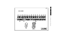
DVD-Video Recorder
DVDR880 & DVDR890
/001 /021 /051
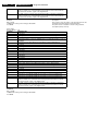
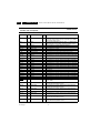
Contents
1
2
3
4
5
6
7
Page
Technical Specifications and
Connection Facilities
Safety Information, General Notes
Directions for Use
Mechanical Instructions
Diagnostic Software
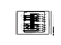
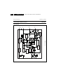
Block Diagrams, Waveforms, Wiring Diagram
Wiring Diagram
Waveforms
Electrical Diagrams And Print-Layouts
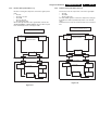
Display Panel
(Diagram 1)
Front Connector Panel (FC)
(Diagram 2)
Key Panel (KEY)
(Diagram 3)
Record Key Panel (REC)
(Diagram 4)
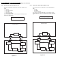
Analog Board:Fronted Video (FV) (Diagram 1)
Analog Board: In / Out Video (IOV)(Diagram 2)
Analog Board: In / Out Audio (IOA)(Diagram 3)
Analog Board: Power Supply (PS) (Diagram 4)
Analog Board: Multi Sound Processing (MSP)
(Diagram 5)
Analog Board: VPS (VPS)
(Diagram 6)
Analog Board: Follow Me (FOME)(Diagram 7)
Analog Board: Digital In / Out (DIGIO)
(Diagram 8)
Analog Board: Audio Converter (DAC_ADC)
(Diagram 9)
4
6
8
45
51
81
83
84
93
93
97
99
100
101
102
103
104
105
106
106
107
108
©
Copyright 2002 Philips Consumer Electronics B.V. Eindhoven, The Netherlands.
All rights reserved. No part of this publication may be reproduced, stored in a
retrieval system or transmitted, in any form or by any means, electronic,
mechanical, photocopying, or otherwise without the prior permission of Philips.
Published by GH 0266 Service PaCE
Printed in the Netherlands
Contents
Page
UPC 12 Sub PCB: Centra Controler (CECO)
(Diagram 10)
UPC 12 Sub PCB: Fan Control (FACO)
(Diagram 11)
DVIO Front Board
(Diagram 1)
DVIO Board: 1394 Interface
(Diagram 2)
DVIO Board: Microprocessor
(Diagram 3)
DVIO Board: FIFO & Control
(Diagram 4)
DVIO Board: DVCODEC
(Diagram 5)
DVIO Board: A & V Output
(Diagram 6)
Digital Board: VSM Buffer Memmory and Bit
Engine Interface
(Diagram 1)
Digital Board: AV Dec. STI5508 (Diagram 2)
Digital Board: AV Decoder Mem. (Diagram 3)
Digital Board: Video Enc. Empress(Diagram 4)
Digital Board: VIP CVBS Y/C Video Input
(Diagram 5)
Digital Board: Analog Board Cons. Video In/Out
(Diagram 6)
Digital Board: Progressive Scan (Diagram 7)
Digital Board: Progressive Scan (Diagram 8)
Digital Board: Power, Clock and Reset Audio
Clock
(Diagram 9)
8 Alignments
9 Circuit-, IC Descriptions and List
of Abbreviations
10 Spare Part List
Subject to modification
114
115
118
119
120
121
122
123
128
129
130
131
132
133
134
135
136
145
148
212
EN 3122 785 12200
EN 4
1.
DVDR880-890 /0X1
Technical Specifications and Connection Facilities
1. Technical Specifications and Connection Facilities
1.1
General:
Mains voltage
Mains frequency
Power consumption mains
Power consumption standby
Power consumption low power
stand-by
1.2
1.2.7
Automatic Search Tuning
scanning time without antenna
stop level (vision carrier)
Maximum tuning error of a recalled
program
Maximum tuning error during
operation
: 198V-276V
: 43 Hz - 63Hz
: 28 W
: <7W
: <3W
RF Tuner
System:
PAL B/G, PAL D/K, SECAM L/L’, PAL I
1.2.2
1.2.3
Analogue Inputs
1.3.1
SCART 1 (Connected to TV)
: 45 MHz - 860 MHz
: -6 dB to 0dB
: no limit
Receiver:
PLL tuning with AFC for optimum reception
Frequency range:
: 45.25 MHz - 857 MHz
Sensitivity at 40 dB S/N
: ≥ 60dBµV at 75Ω
(video unweighted )
1.2.5
Video Performance:
Channel 25 / 503,25 MHz,
Test pattern: PAL BG PHILIPS standard test pattern,
RF Level 74 dBV
Measured on SCART 1
Frequency response:
: 0 - 4.00 MHz +0-4dB
Group delay ( 0.1 MHz - 4.4 MHz ) : 0 nsec ± 150nsec
1.2.6
Audio Performance:
Audio Performance Analogue - HiFi:
Frequency response at SCART 1
(L+R) output:
: 100 Hz - 12 kHz / 0±
3dB
S/N according to DIN 45405, 7, 1967 :
and PHILIPS standard test pattern
video signal:
: FM: ≥ 50dB; AM ≥
45dB, unweighted
Harmonic distortion ( 1 kHz, ± 25
kHz deviation ):
: FM ≤ 1.5%; AM ≤ 2%
Audio Performance NICAM:
Frequency response at SCART
1(L+R) output:
: 40 Hz - 15 kHz 0 ±
3dB
S/N according to DIN 45405, 7, 1967 :
and PHILIPS standard test pattern
video signal:
: ≥ 60 dB unweighted
Harmonic distortion (1 kHz):
: ≤ 0.5 %
typ. 3 min. PAL
≥ 37dB µV
: ± 62.5 kHz
: ± 100 kHz
Pin Signals:
1
- Audio R
1.8V RMS
2
- Audio R
3
- Audio L
1.8V RMS
4
- Audio GND
5
- Blue/Chroma
GND
6
- Audio L
7
- Blue out/
Chroma in
0.7Vpp ± 0.1V into 75 Ohm (*)
8
- Function
switch
<2V = TV
>4.5V / <7V = asp. ratio 16:9 DVD
>9.5V / <12V = asp. ratio 4:3 DVD
9
- Green GND
10 - P50 control
11 - Green
0.7Vpp ± 0.1V into 75 Ohm (*)
12 - Nc
13 - Red/Chroma
GND
14 - fast switch
GND
15 - Red out/
Chroma out
0.7Vpp ± 0.1V into 75 Ohm (*)
± 3dB 0.3Vpp Chroma (burst)
16 - fast switch
RGB/ CVBS
or Y <0.4V into 75 Ohm = CVBS
>1V / <3V into 75 Ohm = RGB
17 - Y/CVBS GND
OUT
18 - Y/CVBS GND
IN
19 - CVBS/Y
1Vpp ± 0.1V into 75 Ohm (*)
20 - CVBS/Y
21 - Shield
Radio Interference:
input voltage /3 tone method (+40
dB min)
1.2.4
1.3
RF - Loop Through:
Frequency range
Gain: (ANT IN - ANT OUT)
:
:
Tuning Principle
automatic B,G, I, DK and L/L’detection
manual selection in "STORE" mode
Test equipment:Fluke 54200 TV Signal generator
Test streams:PAL BG Philips Standard test pattern
1.2.1
Tuning
1.3.2
SCART 2 (Connected to AUX)
Pin Signals:
1
-Audio R
1.8V RMS
2
-Audio R
3
-Audio L
1.8V RMS
4
-Audio GND
5
-Blue/Chroma
GND
6
-Audio L
7
-Blue in/
Chroma out ± 3dB 0.3Vpp Chroma (burst)
8
-Function
switch
9
-Green GND
10 -P50 control
Technical Specifications and Connection Facilities
11 -Green
12 -Nc
13 -Red/Chroma
GND
14 -fast switch
GND
15 -Red in/
Chroma in
16 -fast switch
RGB/ CVBS or
Y
17 -CVBS GND
OUT
18 -CVBS GND
IN
19 -CVBS/Y/RGB
sync
1Vpp ± 0.1V into 75 Ohm (*)
20 -CVBS/Y
21 -Shield
DVDR880-890 /0X1
Crosstalk 1kHz
Crosstalk 20Hz-20kHz
Frequency response 20Hz- 20kHz
Signal to noise ratio
Dynamic range 1kHz
Dynamic range 20Hz-20kHz
Distortion and noise 1kHz
Distortion and noise 20Hz-20kHz
Intermodulation distortion
Mute (spin-up, pause, access)
Outband attenuation:
1.6
Digital Output
1.6.1
Coaxial
CDDA/ LPCM (incl MPEG1)
MPEG2, AC3 audio
DTS
(*) for 100% white
1.3.3
Audio/Video Front Input Connectors
Audio
Input voltage
Input impedance
: 2 Vrms
: >10kΩ
Video - Cinch
Input voltage
Input impedance
: 1 Vpp ± 3dB
: 75 Ω
Video - YC (Hosiden)
Input voltage Y
Input impedance Y
Input voltage C
Input impedance C
: 1Vpp ± 3dB
: 75 Ω
: burst 300 mVpp ± 3
dB
: 75 Ω
1.
:
:
:
:
:
:
:
:
:
:
:
EN 5
>85dB
>70dB
± 0.2dB max
>85 dB
>75dB
>70dB
>75dB
>65dB
>70dB
>85dB
>40dB above 25kHz
: according IEC958
: according IEC1937
: according IEC1937,
amendment 1
1.7
Digital Video Input (IEEE 1394)
1.7.1
Applicable Standards
Implementation according:
IEEE Std 1394-1995
IEC 61883 - Part 1
IEC 61883 - Part 2 SD-DVCR (02-01-1997)
Specification of consumer use digital VCR’s using 6.3 mm
magnetic tape - dec.1994
Mechanical connection according:
Annex A of 61883-1
1.8
P50 System Control
Via SCART pin nr 10
1.4
Video Performance
1.9
All outputs loaded with 75 Ohm
SNR measurements over full bandwidth without weighting.
1.4.1
Dimensions and Weight
Height of feet
Apparatus tray closed
SCART (RGB)
Apparatus tray open
SNR
Bandwidth
1.5
Audio Performance CD
1.5.1
Cinch Output Rear
Output voltage 2 channel mode
Channel unbalance (1kHz)
Crosstalk 1kHz
Crosstalk 20Hz-20kHz
Frequency response 20Hz- 20kHz
Signal to noise ratio
Dynamic range 1kHz
Dynamic range 20Hz-20kHz
Distortion and noise 1kHz
Distortion and noise 20Hz-20kHz
Intermodulation distortion
Mute
Outband attenuation:
1.5.2
: > -65 dB on all output
: 4.8 MHz ± 2dB
1.10 Laser Output Power & Wavelength
1.10.1 DVD
:
:
:
:
:
:
:
:
:
:
:
:
:
2Vrms ± 2dB
<1dB
>95dB
>85dB
±0.2dB max
>95 dB
>85dB
>80dB
>85dB
>75dB
>77dB
>95dB
>40dB above 30kHz
Scart Audio
Output voltage 2 channel mode
Channel unbalance (1kHz)
Weight without packaging
Weight in packaging
: 10mm
: WxDxH :435 x 324.5 x
88cm
: WxDxH :435 x 366 x
88cm
: app. 4 kg ± 0.5 kg
: app. 6.5 kg
: 1.6Vrms ± 2dB
: <1dB
Output power during reading
Output power during writing
Wavelength
: 0.8mW
: 20mW
: 660nm
1.10.2 CD
Output power
Wavelength
: 0.3mW
: 780nm
EN 6
2.
DVDR880-890 /0X1
Safety Information, General Notes
2. Safety Information, General Notes
2.1
Safety Instructions
2.2
Warnings
2.1.1
General Safety
2.2.1
General
Safety regulations require that during a repair:
• Connect the unit to the mains via an isolation transformer.
• Replace safety components, indicated by the symbol
,
only by components identical to the original ones. Any
other component substitution (other than original type) may
increase risk of fire or electrical shock hazard.
Safety regulations require that after a repair, you must return
the unit in its original condition. Pay, in particular, attention to
the following points:
• Route the wires/cables correctly, and fix them with the
mounted cable clamps.
• Check the insulation of the mains lead for external
damage.
• Check the electrical DC resistance between the mains plug
and the secondary side:
1. Unplug the mains cord, and connect a wire between
the two pins of the mains plug.
2. Set the mains switch to the 'on' position (keep the
mains cord unplugged!).
3. Measure the resistance value between the mains plug
and the front panel, controls, and chassis bottom.
4. Repair or correct unit when the resistance
measurement is less than 1 MΩ.
5. Verify this, before you return the unit to the customer/
user (ref. UL-standard no. 1492).
6. Switch the unit ‘off’, and remove the wire between the
two pins of the mains plug.
•
•
•
2.2.2
Laser
•
•
2.1.2
Laser Safety
•
This unit employs a laser. Only qualified service personnel may
remove the cover, or attempt to service this device (due to
possible eye injury).
Laser Device Unit
Type
: Semiconductor laser
GaAlAs
: 650 nm (DVD)
: 780 nm (VCD/CD)
: 20 mW
(DVD+RW writing)
: 0.8 mW
(DVD reading)
: 0.3 mW
(VCD/CD reading)
: 60 degree
Wavelength
Output Power
Beam divergence
All ICs and many other semiconductors are susceptible to
electrostatic discharges (ESD, ). Careless handling
during repair can reduce life drastically. Make sure that,
during repair, you are at the same potential as the mass of
the set by a wristband with resistance. Keep components
and tools at this same potential.
Available ESD protection equipment:
– Complete kit ESD3 (small tablemat, wristband,
connection box, extension cable and earth cable) 4822
310 10671.
– Wristband tester 4822 344 13999.
Be careful during measurements in the live voltage section.
The primary side of the power supply (pos. 1005), including
the heatsink, carries live mains voltage when you connect
the player to the mains (even when the player is 'off'!). It is
possible to touch copper tracks and/or components in this
unshielded primary area, when you service the player.
Service personnel must take precautions to prevent
touching this area or components in this area. A 'lightning
stroke' and a stripe-marked printing on the printed wiring
board, indicate the primary side of the power supply.
Never replace modules, or components, while the unit is
‘on’.
•
The use of optical instruments with this product, will
increase eye hazard.
Only qualified service personnel may remove the cover or
attempt to service this device, due to possible eye injury.
Repair handling should take place as much as possible
with a disc loaded inside the player.
Text below is placed inside the unit, on the laser cover
shield:
CAUTION VISIBLE AND INVISIBLE LASER RADIATI ON WHEN OPEN AVO ID EXPOSURE TO BEAM
ADVARSEL SYNLIG OG USYNLIG LASERSTRÅLING VED ÅBNING UNDGÅ UDSÆTTELSE FOR STRÅLING
!
ADVARSEL SYNLIG OG USYNLIG LASERSTRÅLING NÅR DEKSEL
ÅPNES UNNGÅ EKSPONERING FOR STRÅLEN
VARNING SYNLIG OCH OSYNLIG LASERSTRÅLNING NÄR DENNA DEL ÄR ÖPPNAD BETRAKTA EJ STRÅLEN
VARO! AVATT AESSA OLET ALTTIINA NÄKYVÄLLE JA NÄKYMÄTT ÖMÄLLE LASER SÄTEILYLLE. ÄLÄ KAT SO SÄT EESEEN
VORSICHT SICHTBARE UND UNSICHTBARE LASERSTRAHLUNG WENN ABDECKUNG GEÖFFNET NICHT DEM STRAHL AUSSETSEN
DANGER VISIBLE AND INVISIBLE LASER RADIATI ON WHEN OPEN AVO ID DIRECT EXPOSURE TO BEAM
AT TENTION RAYO NNEMENT LASER VISIBLE ET INVISIBLE EN CAS D'OUVERTURE EXPOSITION DANGEREUSE AU FAISCEAU
Figure 2-2
2.2.3
Notes
Dolby
Manufactered under licence from Dolby Laboratories. “Dolby”,
“Pro Logic” and the double-D symbol are trademarks of Dolby
Laboratories. Confidential Unpublished Works.
©1992-1997 Dolby Laboratories, Inc. All rights reserved.
Figure 2-3
Figure 2-1
Note: Use of controls or adjustments or performance of
procedure other than those specified herein, may result in
hazardous radiation exposure. Avoid direct exposure to beam.
Trusurround
TRUSURROUND, SRS and symbol (fig 2-4) are trademarks of
SRS Labs, Inc. TRUSURROUND technology is manufactured
under licence frm SRS labs, Inc.
Figure 2-4
Safety Information, General Notes
Video Plus
“Video Plus+” and “PlusCode” are registered trademarks of the
Gemstar Development Corporation. The “Video Plus+” system
is manufactored under licence from the Gemstar Development
Corporation.
Figure 2-5
Macrovision
This product incorporates copyright protection technology that
is protected by method claims of certain U.S. patents and other
intellectual property rights owned by Macrovision Corporation
and other rights owners.
Use of this copyright protection technology must be autorized
by Macrovision Corporation, and is intended for home and
other limited viewing uses only unless otherwise authorized by
Macrovision Corporation. Reverse engineering or disassembly
is prohibited.
DVDR880-890 /0X1
2.
EN 7
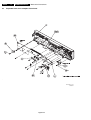
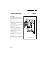
Mechanical Instructions
DVDR880-890 /0X1
4.
EN 45
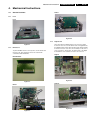
4. Mechanical Instructions
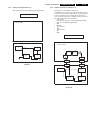
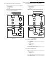
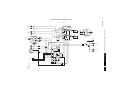
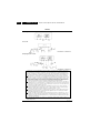
4.1
Service Positions
4.1.1
Front
DVIO 2
Front
Figure 4-4
4.1.3
Figure 4-1
4.1.2
DVIO board
To put the DVIO board in a service position, an extender board
must be used. This extender board can be ordered with
codenumber 3104 128 07770.
Digital board
After demounting of DVIO board, the top side of the digital
board is in reach. To reach the bottom side of the digital board,
the DVDR module must be demounted together with the digital
board. Connected to each other, the assembly can be set in a
service position. In this position, the bottom side of the digital
board and the servo board are in reach to be serviced.
Digital 1
DVIO Extender
Figure 4-5
Figure 4-2
Digital 2
DVIO 1
Figure 4-6
Figure 4-3
EN 46
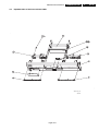
4.1.4
4.
DVDR880-890 /0X1
Mechanical Instructions
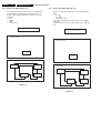
Analog board
Europe
To put the analog board in service position, demount the
assembly of analog board and backplate as follows:
1. Remove the screw from the backplate to the mains inlet of
the power supply
2. Remove the screw safety holder
3. Remove the 3 screws of the analog board to the frame
4. Release the snap of the spacer of the analog board to the
frame.
Turn the assembly of the back plate and the analog board
against the loader.
Analog Europe
Figure 4-9
NAFTA
Figure 4-7
Analog NAFTA
Figure 4-10
Figure 4-8
4.1.5
Cable Routing
Take care of the correct cable routing. See pictures below.
4.2
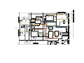
Exploded View of the Set
Mechanical Instructions
Figure 4-11
DVDR880-890 /0X1
4.
TR 01002_001
080502
EN 47
EN 48
4.3
4.
DVDR880-890 /0X1
Mechanical Instructions
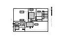
Exploded View of the complete Front Panel
TR 01003_001
080502
Figure 4-12
Mechanical Instructions
4.4
DVDR880-890 /0X1
Exploded View of the Front without PWBs
TR 01004_001
080502
Figure 4-13
4.
EN 49
4.
DVDR880-890 /0X1
Dismantling Instructions
EN 50
4.5
Mechanical Instructions
Figure 4-14
Diagnostic Software
DVDR880-890 /0X1
5.
EN 51
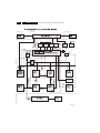
5. Diagnostic Software
Due to the complexity of the DVD recorder, the time to find a
defect in the recorder can become long. To reduce this time,
the recorder has been equipped with Diagnostic and Service
software (DS). The DS offers functionality to diagnose the
DVDR hardware and tests the following:
• Interconnections between components
• Accessibility of components
• Functionality of the audio and video paths
This functionality can be accessed via several interfaces:
1. End user/Dealer script interface
2. Player script interface
3. Menu and command interface
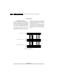
5.1
End User/Dealer Script Interface
5.1.1
Description
5.1.2
Contents
Unplug the power cord
Hold key <PLAY> pressed
while you plug the recorder
During the test, the following display
is shown: the counter counts down
from the number of nuclei to be run
before the test finishes. Example:
SET O.K.?
NO
YES
The End user/Dealer script interface gives a diagnosis on a
stand alone DVD recorder; no other equipment is needed.
During this mode, a number of hardware tests (nuclei) are
automatically executed to check if the recorder is faulty. The
diagnosis is simply a "fail" or "pass" message. If the message
"FAIL" appears on the display, there is apparently a failure in
the recorder. If the message "PASS" appears, the nuclei in this
mode have been executed successfully. There can be still a
failure in the recorder because the nuclei in this mode don't
cover the complete functionality of the recorder.
To exit DEALER SCRIPT, unplug the power cord
CL 16532095_068.eps
150801
Figure 5-1
The End use/Dealer script executes all diagnostic nuclei that
do not need any user interaction and are meaningful on a
standalone DVD recorder. The nuclei called in the End user/
Dealer script are the following:
Counter
Nucleus Name
22
104
HostdSdramWrR
Description
checks all memory locations of the 4MB SDRAM
21
106
HostdDramWrR
checks all the DRAM connected to the microprocessor of the digital board
20
123
HostdI2cNvram
checks the data line (SDA) and the clock line (SCL) of the I2C bus between the host decoder
and NVRAM
19
202
SAA7118I2c
checks the interface between the Host I2C controller and the AVENC SAA7118 Video Input
Processor
18
200
VideoEncI2c
checks the interface between the host I2C controller and Empress SAA6752
17
207
AudioEncI2c
checks the I2C connection between the host decoder and Empress SAA6752
16
204
AudioEncAccess
tests the HIO8 interface lines between the host decoder and the audio encoder
15
203
AudioEncSramAccess
checks the access of the SRAM by the audio encoder (address and data lines).
14
205
AudioEncSramWrR
tests the SRAM connected to the audio encoder
13
206
AudioEncInterrupt
tests the interrupt line between the host decoder and the audio encoder
12
300
VsmAccess
checks whether the VSM interrupt controllers and DRAM are accessible
11
303
VsmInterrupt
checks both interrupt lines between the VSM and the host decoder
10
302
VsmSdramWrR
tests the entire SDRAM of the VSM
9
1400
Clock11_289MHz
switches the A_CLK of the micro clock to 11.2896 MHz
8
1401
Clock12_288MHz
switches the A_CLK of the micro clock to 12.288 MHz
7
601
BeS2Bengine
checks the S2B interface with the Basic Engine by sending an echo command
6
500
DisplayEcho
checks the interface between the host processor and the slave processor on the display
board
5
700
AnalogueEcho
checks the interface between the host processor and the microprocessor on the analogue
board
4
711
AnalogueNvram
checks the NVRAM on the analogue board
3
706
AnalogueTuner
checks whether the tuner on the analogue board is accessible
2
901
LoopAudioUserDealer
This nucleus tests the components on the audio signal path The host decoder
- The analogue board
- The audio encoder
- The VSM
On the analogue board the audio is internally looped back to the digital board
1
906
LoopVideoUserDealer
Nucleus for testing the components on the video signal system path:
- The VIP
- The video encoder
- The VSM
- The host decoder
- The analogue board
On the analogue the video signal is internally routed back to the digital board.
EN 52
5.
DVDR880-890 /0X1
5.2
Player Script Interface
5.2.1
Description
Diagnostic Software
5.2.2
The Player script will give the opportunity to perform a test that
will determine which of the DVD recorder's modules are faulty,
to read the error log and to perform an endurance loop test. To
successfully perform the tests, the DVD recorder must be
connected to a TV set.
To be able to check results of certain nuclei, the player script
expects some interaction of the user (i.e. to approve a test
picture or a test sound). Some nuclei (e.g. nuclei that test
functionality of the DVDR module) require that a DVD+RW disc
is inserted.
Only tests within the scope of the diagnostic software will be
executed hence only faults within this scope can be detected.
Structure of the Player Script
The player script consists of a set of nuclei testing the hardware
modules in the DVD recorder: the Display PWB, the Digital
PWB, the Analogue In/Out PWB and the DVDR module.
Nuclei run by the player test need some user interaction; in the
next table this interaction is described. The player test is done
in two phases:
• Interactive tests: this part of the player test depends
strongly on user interaction and input to determine nucleus
results and to progress through the full test. Reading the
error log information can be useful to determine any errors
that occurred recently during normal operation of the DVD
player.
• The loop test will perform the same nuclei as the dealer
test, but it will loop through the list of nuclei indefinitely.
STEP DESCRIPTION
NUCLEUS
1
Press OPEN/CLOSE and PLAY at the same time and POWER ON the recorder to start the playerscript
2
2
The local display shows FPSEGMENTS. Press PLAY to start the test.
502
First the starburst pattern is lit, then the horizontal segments are lit, followed by the vertical segments and the
last test is light all segments test. After each of the 4 tests the user has to confirm that the correct pattern was
lit.
Press PLAY to confirm that the correct pattern was lit (four times if the FPSEGMENTS test was successful).
Press RECORD to indicate that the correct pattern was not successfully lit.
Press STOP to skip this nucleus.
3
The local display shows FPLABELS. Press PLAY to start the test.
Press PLAY to confirm that all labels are lit.
Press RECORD to indicate that not all labels are lit.
Press STOP to skip this nucleus.
503
4
The local display shows FPLIGHT ALL. Press PLAY to start the test.
Press PLAY to confirm that everything was lit.
Press RECORD to indicate that not all patterns are lit.
Press STOP to skip this nucleus.
520
5
The local display shows FPLED. Press PLAY to start the test.
Press PLAY to confirm that the led is lit.
Press RECORD to indicate that the led is not lit.
Press STOP to skip this nucleus.
504
6
The local display shows FPFLAP OPEN. Press PLAY to start the test.
Press PLAY to confirm that the flap has opened.
Press RECORD to indicate that the flap did not open.
Press STOP to skip this nucleus.
522
7
The local display shows FPKEYBOARD. Press PLAY to start the test.
505
Attention all keys have to be pressed to get a positive result!
Press PLAY for more than one second to confirm that all the keys were pressed and shown on the local display. If not all the keys were pressed, a FAIL message will appear on the local display.
Press RECORD for more than one second to indicate that not all keys were pressed and shown on the local
display.
Press STOP for more than one second to skip this nucleus.
8
The local display shows FPREMOTE CONTROL. Press PLAY to start the test.
506
Press PLAY to confirm that a key on the remote control was pressed and shown on the local display. Only
one key has to be pressed to get a successful result.
Press RECORD to indicate that the key on the remote control was pressed but not shown on the local display.
Press STOP to skip this nucleus.
9
The local display shows FPDIMMER. Press PLAY to start the test.
Press PLAY to confirm that the text on the local display was dimmed.
Press RECORD to indicate that the text on the local display was not dimmed.
Press STOP to skip this nucleus.
518
10
The local display shows FPBEEPER. Press PLAY to start the test.
Press PLAY to confirm that the beeper on the front panel sounded.
Press RECORD to indicate that the beeper on the front panel did not sound.
Press STOP to skip this nucleus.
514
11
The local display shows FPFLAP CLOSE. Press PLAY to start the test.
Press STOP to skip this nucleus.
523
12
The local display shows ROUTE VIDEO. Press PLAY to start the test.
Press STOP to skip this nucleus.
712
13
The local display shows ROUTE AUDIO. Press PLAY to start the test.
Press STOP to skip this nucleus.
713
14
The local display shows COLOUR-BAR ON. Press PLAY to start the test.
Press STOP to skip this nucleus.
120
Diagnostic Software
DVDR880-890 /0X1
5.
STEP DESCRIPTION
NUCLEUS
15
The local display shows PINK NOISE ON. Press PLAY to start the test.
Press STOP to skip this nucleus.
115
16
The local display shows PINK NOISE OFF. Press PLAY to start the test.
Press STOP to skip this nucleus.
116
17
The local display shows SINE ON. Press PLAY to start the test.
Press STOP to stop the sine.
Press STOP to skip this nucleus.
117
18
The local display shows COLOUR-BAR OFF. Press PLAY to start the test.
Press STOP to skip this nucleus.
121
19
The local display shows BERESET. Press PLAY to start the test.
Press STOP to skip this nucleus.
603
20
The local display shows BETRAY OPEN. Press PLAY to start the test.
Press STOP to skip this nucleus.
616
21
The local display shows BETRAY CLOSE. Press PLAY to start the test.
Press STOP to skip this nucleus.
615
22
The local display shows BEWRITE READ. Press PLAY to start the test.
Press STOP to skip this nucleus.
617
23
The local display shows BETRAY OPEN. Press PLAY to start the test.
Press STOP to skip this nucleus.
616
24
The local display shows BETRAY CLOSE. Press PLAY to start the test.
Press STOP to skip this nucleus.
615
25
The local display shows READ ERRORLOG. Press PLAY to start the test.
Press STOP to skip this nucleus.
If the player test succeeded, the user/dealer script will start in an endless loop.
If the player test failed, the local display will display FAIL and the error code
633
Remark
In case of failure, the display shows " FAIL XXXXXX ". The
description of the shown error code can be retrieved in the
survey of Nuclei Error Codes (paragraph 5.4). Once an error
occurs, it is not possible to continue the player script. Unplug
the set and restart the player script. By pressing the STOP key,
it is possible to jump over the failure and to continue the player
script.
EN 53
EN 54
Unplug the power cord
Hold 2 keys
<OPEN/CLOSE> + <PLAY>
simultaneously pressed while
you plug the recorder
5.
PRESS <PLAY>
TO START TEST
PRESS <STOP>
TO SKIP TEST
PRESS <PLAY>
TO START TEST
PRESS <STOP>
TO SKIP TEST
PRESS <PLAY>
TO START TEST
HEXADECIMAL
KEY CODE
PRESS <PLAY> IF OK
PRESS <RECORD> IF NOT OK
PRESS ALL KEYS AT LEAST ONCE
SEE TABLE FOR KEY CODES
Figure 5-2
PRESS <PLAY> MORE THAN 1S IF TEST IS OK
PRESS <RECORD> MORE THAN 1S IF TEST IS NOT OK
PRESS <PLAY> IF OK
PRESS <STOP> TO ABORT
PRESS <PLAY>
TO START TEST
PRESS <PLAY>
TO START TEST
PRESS <STOP>
TO SKIP TEST
HEXADECIMAL
RC KEY CODE
TO EXIT TEST: PRESS ONE OF FOLLOWING KEYS
ON THE LOCAL KEYBOARD
PRESS <PLAY> IF TEST IS OK
PRESS <RECORD> IF TEST IS NOT OK
PRESS <PLAY> IF OK
PRESS <RECORD> IF NOT OK
PRESS <STOP>
TO SKIP TEST
FRONT KEY NAME
PRESS <PLAY> IF OK
PRESS <RECORD> IF NOT OK
PRESS <PLAY>
TO START TEST
PRESS <STOP>
TO SKIP TEST
PRESS <PLAY> IF OK
PRESS <RECORD> IF NOT OK
LED BECOMES RED
TR 01006_001
080502
PRESS <PLAY> IF OK
PRESS <RECORD> IF NOT OK
PRESS <STOP>
TO SKIP TEST
PRESS AT LEAST ONE KEY
ON THE REMOTE CONTROL
SEE TABLE FOR RC KEY CODES
RC KEY NAME
PRESS <PLAY> IF OK
PRESS <STOP> TO ABORT
PRESS <PLAY>
TO START TEST
XX TIMES
PRESSED
STANDBY/ON
OPEN/CLOSE
STOP
PLAY
RECORD
SEARCH <<
SEARCH >>
CHANNEL UP
CHANNEL DOWN
REC MODE
FRONT KEY CODE
00E
001
002
003
004
006
005
009
00A
00D
RC KEY CODE
43
TV/DVD
STANDBY
STOP
REC/OTR
PLAY
PREVIOUS
EDIT
NEXT
DISC
SYSTEM
UP
LEFT
RIGHT
DOWN
RETURN
OK
CLEAR
TIMER
SELECT
VOL +
VOL P+
P1
2
3
4
5
6
7
8
9
0
FA
ONLY FOR TV
ONLY FOR TV
1E
1F
01
02
03
04
05
06
07
08
09
00
T/C
MONITOR
PLAY MODE
REC MODE
C8
EE
1D
94
0C
31
37
2C
21
CF
20
54
0F
58
5A
5B
59
83
5C
41
FE
DIGITAL BOARD TEST
Diagnostic Software
PRESS <PLAY> IF OK
PRESS <STOP> TO ABORT
PRESS <STOP>
TO SKIP TEST
XX TIMES
PRESSED
DVDR880-890 /0X1
FRONT PANEL TEST
Diagnostic Software
FRONTPANEL
TEST
DIGITAL BOARD &
ANALOG BOARD
TEST
DVDR880-890 /0X1
5.
EN 55
BASIC ENGINE
TEST
press <PLAY> to execute
press < STOP > to skip
press <PLAY> to execute
press <NEXT > to skip
press <PLAY> to execute
press < STOP > to skip
press <PLAY> to execute
press <STOP> to skip
INSERT DVD +RW DISC TO EXECUTE
WRITE / READ TEST
press <PLAY> to execute
press < STOP > to skip
press <PLAY> to execute
press <STOP> to skip
press <PLAY> to execute
press < STOP > to skip
press <PLAY> to execute
press <STOP > to skip
press <PLAY> to execute
press <NEXT > to skip
press <PLAY> to execute
press <STOP> to skip
press <PLAY> to execute
press < STOP > to skip
press <PLAY> to execute
press <STOP> to skip
press <STOP> to continue
<PLAY>
press <STOP> to skip
press <PLAY> to execute
PRESS <STOP>
TO STEP DOWN
NO ERRORS LOGGED
PRESS <STOP>
TO STEP DOWN
PRESS <RECORD>
TO STEP UP
PRESS <RECORD>
TO STEP UP
PRESS <PLAY> TO CONTINUE
IF ERROR
To exit PLAYER SCRIPT, unplug the power cord
Figure 5-3
5.2.3
Error Log
Explanation:
The application errors will be logged in the NVRAM. The
maximum number of error bytes that will be visible is 19. The
last reported error is shown as DN D0000000, the oldest visible
error as D0000000 UP and the errors in between as DN
D0000000 UP. DN stands for DOWN, UP stands for
UPWARDS. The shown
D error codes are identical to the Nuclei Error Codes
(paragraph 5.4).
TR 01007_001
080502
EN 56
5.2.4
5.
DVDR880-890 /0X1
Diagnostic Software
Trade Mode
5.3.2
Each nucleus returns an error code. This code contains six
numerals, which means:
TRADE MODE
When the recorder is in Trade Mode, the recorder cannot be
controlled by means of the front key buttons, but only by means
of the remote control.
IF TRADE MODE OFF
CL 06532152_013.eps
051200
PRESS 2 KEYS
SIMULTANEOUSLY
<STOP> + <OPEN/CLOSE>
<STOP> + <OPEN/CLOSE>
PLUG THE RECORDER
PLUG THE RECORDER
RECORDER IS IN TRADE MODE
WHEN PRESSING FRONT
KEYS, THE RECORDER
DOESN'T RESPOND
RECORDER IS IN NORMAL MODE
WHEN PRESSING FRONT
KEYS, THE RECORDER
WILL RESPOND
CL 16532095_071.eps
150801
Figure 5-4
Virgin mode
If you want that the recorder starts up in Virgin mode, follow this
procedure:
• Unplug the recorder
• plug the recorder again while you keep the STAND BY/ON
key pressed
• the set starts up in Virgin mode.
5.3
Menu and Command Mode Interface
5.3.1
Nuclei Numeration
Each nucleus has a unique number of four digits. This number
is the input of the command mode.
[ XX YY
Error code
Nucleus number
Nucleus group number
UNPLUG THE RECORDER
PRESS 2 KEYS
SIMULTANEOUSLY
5.2.5
[ XX YY ZZ ]
IF TRADE MODE ON
UNPLUG THE RECORDER
Error Handling
]
Figure 5-6
The nucleus group numbers and nucleus numbers are the
same as above.
5.3.3
Command Mode Interface
Set-Up Physical Interface Components
Hardware required:
• Service PC
• one free COM port on the Service PC
• special cable to connect DVD recorder to Service PC
The service PC must have a terminal emulation program (e.g.
OS2 WarpTerminal or Procomm) installed and must have a
free COM port (e.g. COM1). Activate the terminal emulation
program and check that the port settings for the free COM port
are: 19200 bps, 8 data bits, no parity, 1 stop bit and no flow
control. The free COM port must be connected via a special
cable to the RS232 port of the DVD recorder. This special cable
will also connect the test pin, which is available on the
connector, to ground (i.e. activate test pin).
Code number of PC interface cable: 3122 785 90017
Activation
Plug the recorder to the mains and the following text will appear
on the screen of the terminal (program):
DVD Video Recorder Diagnostic Software version 48
Basic SDRAM Data bus test passed
Basic SDRAM Address bus test passed
Basic SDRAM Device test passed
Nucleus number
Nucleus group number
(M) enu, (C) ommand or (S) 2B-interface?
DD:>
CL 16532095_073.eps
150801
CL 06532152_012.eps
051200
Figure 5-5
The following groups are defined:
Group number Group name
0
Basic / Scripts
1
Host decoder (Sti5505 and memory)
2
Audio / video encoder (DVDR only)
3
VSM (DVDR only)
4
NVRAM
5
Front Panel
6
Basic Engine
7
Analogue board (DVDR only)
8
DVIO (DVDR only)
9
Loop nuclei (DVDR only)
10
Library sub nuclei (I2C nuclei)
11
User interface
12
Furore (SACD only)
13
DAC (SACD only)
14
Miscellaneous
[M] : @ C
Figure 5-7
The first line indicates that the Diagnostic software has been
activated and contains the version number. The next lines are
the successful result of the SDRAM interconnection test and
the basic SDRAM test. The last line allows the user to choose
between the three possible interface forms. If pressing C has
made a choice for Command Interface, the prompt ("DD>") will
appear. The diagnostic software is now ready to receive
commands. The commands that can be given are the numbers
of the nuclei.
Diagnostic Software
Command Overview
We provide an overview of the nuclei and their numbers. This
overview is preliminary and subject to modifications.
Host Decoder [01]
[xx yy] Nuclei
Number
100
Checksum Flash
101
Flash Write Access 1
102
Flash Write Access 2
103
Flash Write Read
104
SdRam Write Read
105
SdRam Write Read Fast
DVDR880-890 /0X1
[xx yy] Nuclei
Number
207
Audio Encoder I2C
208
SAA7118 select input
209
Empress Version
VSM [03]
[xx yy] Nuclei
Number
300
Register Access
301
SDRAM Access
302
SDRAM Write Read
303
Interrupt lines
304
VSM Interconnection
305
UART
106
Dram Write Read
107
Dram Write Read Fast
108
Hardware Version
109
Mute On
NVRAM [04]
110
Mute Off
115
Pink Noise On
[xx yy] Nuclei
Number
116
Pink Noise Off
400
117
Sine On
401
Read
118
Sine Burst 1kHz
402
Modify
119
Sine Burst 12kHz
403
UniqueNr Read
120
Colour-bar On
Note: Use nuclus 712 with parameter 07 to route the
signals to the analogue board output
404
Read Error Log
407
Reset Error Log
Reset
409
Line2 Region-Code Reset
410
UniqueNr Store
121
Colour-bar Off
122
NvramWrR
123
NvramI2c
130
Boot Version
131
Application Version
[xx yy] Nuclei
Number
132
Diagnostics Version
500
Echo
133
Download Version
501
Version
134
Write / read I2C message to / from digital board
502
Segment
135
Video Test Signal
OnNote: Use nuclus 712 with parameter 07 to route
the signals to the analogue board output.
Input: 135 [a] [b]
a: Number of test image,
0. Horizontal colour-bar
1. White
2. Yellow
3. Light blue
4. Green
5. Magenta
6. Red
7. Blue
8. Black
9. Colour triangle (execution time is 12 seconds)
10. Test image for progressive scan (execution time
is 6 seconds)
503
Label
b: Video standard,
0. PAL BDGHI
1. NTSC
136
Video Test Signal Off
137
Macrovision Off
Audio Video Decoder [02]
[xx yy] Nuclei
Number
200
Video Encoder I2C
202
SAA7118 I2C
203
Audio Encoder SRAM Access
204
Audio Encoder Access
205
Audio Encoder SRAM Write Read
206
Audio Encoder Interrupts
Front Panel [05]
504
Led
505
Keyboard
506
Remote-Control
507
Segment Starburst
508
Segment Vertical
509
Segment Horizontal
514
Beeper
515
Discbar
516
Discbar Dots
517
Vu / Grid
518
Dimmer
519
Blinking
520
Light All Segments
522
Flap Open
523
Flap Close
Basic Engine [06]
[xx yy] Nuclei
Number
600
S2B Pass
601
S2B Echo
602
Version
603
Reset
604
Focus On
605
Focus Off
606
Disc Motor On
607
Disc Motor Off
608
Radial On
5.
EN 57
EN 58
5.
DVDR880-890 /0X1
Diagnostic Software
[xx yy] Nuclei
Number
[xx yy] Nuclei
Number
609
Radial Off
730
Store external presets
615
Tray In
731
Get slash version
616
Tray Out
732
AFC Reference Voltage Tuner
617
Write Read
618
Write Read Endless Loop
DVIO [08]
619
Selftest
620
BE Test
[xx yy] Nuclei
Number
621
Laser Test
800
622
Spindle (Disc) Motor Test
801
Reset DVIO
623
Focus Test
802
DVIO Access
624
Sledge Motor Test
803
Get DVIO error codes
625
Sledge Motor Slow
804
Get DVIO module Ids
626
Tilt
805
627
EEPROM Read
628
EEPROM Write
Execute DVIO module SelfTestInput: 805 [a]
[b]Parameters: a=1/0…full Ram test, b=1/0…cable
connected
629
Optimise Jitter
806
Set DVIO led on.
630
Radial ATLS Calibration
807
Set DVIO led off.
Check DVIO board presence
631
Get Statistics Information
632
Reset Statistics Information
633
BE Read Error Log
[xx yy] Nuclei
Number
634
BE Reset Error Log
900
Digital Audio Loop(no function in Gen. 1.5 and Lead)
638
Get Self Test Result
901
User / Dealer Audio Loop
639
Radial Initialisation
902
Digital Video Loop
640
Get OPU info
903
Digital Video VBI Loop
904
System Video Loop
Analog Board [07]
905
System Video VBI Loop
[xx yy] Nuclei
Number
906
User / Dealer Video Loop
700
Echo
703
Boot Version
704
Hardware Version
705
Clock Adjust
Loop Nuclei [09]
907
User / Dealer Video VBI Loop
908
System Audio Loop SCART
909
System Audio Loop CINCH
910
Digital DVIO Video Loop
911
System Video Vip
706
Tuner
707
Frequency Download
Miscellanious [14]
708
Data Slicer
709
Sound Processor
[xx yy] Nuclei
Number
710
AV Selector
1400
711
Nvram
1401
Clock 12.288 MHz
712
Route Video
1412
Progressive Scan I2C
713
Route Audio
1413
Progressive Scan test image on
715
Set Slash Version
1414
Progressive Scan test image off
716
Application Version
1415
Progressive Scan Route Enable
717
Diagnostics Version
1416
Progressive Scan Route Disable
718
Download Version
720
Bargraph Level Adjustment
Scripts [00]
721
Clock correction
Clock 11.289 MHz
722
Clock reference
[xx yy] Nuclei
Number
723
Re-virginise Recorder
1
UserDealer Script
724
Flash Checksum
2
Player Script
725
Tuner frequency selection
Europe: To make video and audio signals from the
tuner available on Scart2, send command "712 08".
For Nafta/Apac: To make the black/white Video
available on Y/C Rear Out connector, send
command “712 08”
Input: 725 [frequency in MHz*16] [system]
System: NTSC=16, PAL BG=16, PAL I=32, PAL
DK=48, SEC L=64, SEC LS=80, SEC BG=96, SEC
DK=112
727
Set virgin bit
728
Clear Virgin Bit
729
Write / read I2C message to / from analogue board
Routing Audio and Video
Route Video
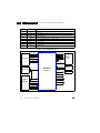
Nucleus Number: 712
Description
This nucleus routes the video signals on the analogue board to
the destination determined by the input parameters
Diagnostic Software
DVDR880-890 /0X1
The paths that are available for video routing and their description(Europe version):
Path ID
Description
00
Input signal is VIDEO(CVBS) from digital board and will be re-routed back to the
digital board.
01
Input signal is from FRONT VIDEO(CVBS) IN and will be routed to the digital board.
02
No Routing.
03
Input signal is from FRONT S-VIDEO(Y/C) and will be routed to the digital board.
04
No Routing.
05
Input signal is CVBS from SCART1 and will be routed to the digital board.
06
Input signal is CVBS from SCART2 and will be routed to the digital board.
07
Input Signal is CVBS from Digital Board and it will be routed to Scart1 and Scart2.
08
Input signal is VIDEO(CVBS) from ANTENNA IN and will be routed to SCART2.
09
Input signal is VIDEO(CVBS) from SCART1 and will be routed to SCART2.
10
Input signal is VIDEO(CVBS) from SCART2 and will be routed to SCART1.
11
Signal path is routed Fast Blank from Scart2 pin16 and will be routed Scart1 pin16
12
Input Signal is YC from Digital Board and it will be routed to Scart1.
13
No Routing.
14
No Routing.
15
Input Signal is CVBS from TUNER and it will be routed to Digital .
16
No Routing.
17
Input Signal is routed from digital board YC to REAR S-VIDEO(YC) OUT
18
Signal path is routed from digital board RGB to RGB SCART1 and from digital board
CVBS to digital board CVBS.
19
No Routing.
20
Input RGB Signal is routed from Digital Board to SCART1(RGB),Input CVBS Signal
from Digital Board to Digital Board and Fast Blanking Signal from Scart 2 to Scart1.
21
Input Y/C Signal from Digital Board is routed to Rear Y/C Connector and Input Y/c
Signal from Front Y/C connector is routed to Digital Board.
The paths that are available for video routing and their description (Nafta region):
PATH ID
DESCRIPTION
00
Input signal is VIDEO(CVBS) from digital board and will be re-routed back to the
digital board.A Cinch Cable need to be connected from Rear Cinch Out to Front
Cinch In for this Test.(Direct routing on analogue board from YUV In to YUV Out is
not Possible)
01
Input signal is from FRONT VIDEO(CVBS) IN and will be routed to the digital
board.This routing is same as the above path id.
02
Input signal is from REAR VIDEO(CVBS) IN and will be routed to the digital board.
03
Input signal is from FRONT S-VIDEO(Y/C) IN and the signal received will be routed
to the digital board.
04
Input signal is from REAR S-VIDEO(Y/C) IN and will be routed to the digital board.
05
No Routing.
06
No Routing.
07
No Routing.
08
Input signal is VIDEO(CVBS) from TUNER and will be routed to Y Pin of Rear Y/C
Connector.This will give only black/White Picture .
09
Input signal is from YUV IN and will be routed to YUV OUT.This is possible only if
Digital Board routes back YUV signal received back to the Analogue board(DENC)
10
No Routing.
11
No Routing.
12
No Routing.
13
No Routing.
14
No Routing
15
Input CVBS Signal from Tuner is routed to Digital Board..
16
No Routing
17
Input RGB Signal is routed from Digital Board to RGB Rear Out and Input CVBS
Signal is routed from Rear Cinch In 1 to Digital Board(This second step is for routing
Input CVBS Signal from Digital Board to Digital Board again - A Cinch cable need
to be connected from Rear Cinch Out1 to Rear Cinch In 1 )
18
Input Signal from CVBS Rear In is routed to Digital Board.This is same as path id 02.
19
Input Y/C signal from Digital Board is routed to Y/C Rear Out Connector and Input
signal from Y/C Rear In Connector is routed to Y/C Digital Board.
5.
EN 59
EN 60
5.
DVDR880-890 /0X1
Diagnostic Software
23
The Video signal received from the Digital board will be outputted on Modulator
channel 3. Please use command 120 for testing Video because Nuclei 120 will
generate the Colour Bar signal on the digital Board.
24
The Audio signal received from the Digital board will be outputted on Modulator
channel 4. Please use command 120 for testing Video because Nuclei 120 will
generate the Colour Bar signal on the digital Board.
Example
DD:> 712 01
71200: Video routing on the Analogue Board OK.
Test OK @
Description
This nucleus routes the audio on the analogue board to the
destination determined by the input parameters
The paths that are available for audio routing and their
description (Europe version)
Route Audio
Nucleus Number: 713
PATH ID
DESCRIPTION
00
No Routing.
01
Input signal is from FRONT AUDIO IN and will be routed to the digital board.
02
Input signal is from REAR AUDIO IN 2 and will be routed to the digital board.
03
Input Audio Signal is routed from FRONT Cinch In to Digital Board.(This is same as
path id 01)
04
Input Signal is from Rear Cinch In1 and it will be routed to Digital Board..
05
No routing.
06
No routing.
07
No routing.
08
No Routing.
09
No routing.
10
No Routing.
11
No Routing.
12
No Routing.
13
Input Signal is from Digital Board and it will be routed to the digital board.
14
No routing.
15
Input is Audio Signal from TUNER and it will be routed to Digital Board.
16
Input signal is AUDIO from dvio board and will be routed to Digital Board.
17
No routing.
18
No routing.
19
No routing.
20
Input signal is from REAR AUDIO IN 2 and will be routed to the digital board.
21
Input signal is from REAR AUDIO IN 1 and will be routed to the digital board.
22
Input signal is from REAR AUDIO IN 1 and will be routed to the digital board.
23
The Audio signal received from the Digital board will be outputted on Modulator
channel 3. Please use command 117 for testing audio because Nuclei 117 will
generate the Audio signal on the digital Board.
24
The Audio signal received from the Digital board will be outputted on Modulator
channel 4. Please use command 117 for testing audio because Nuclei 117 will
generate the Audio signal on the digital Board.
EXAMPLE
DD:> 713 00
71300: Audio routing on the Analogue Board OK.
Test OK @
Diagnostic Software
5.3.4
Menu Mode Interdace
Activation
Plug the recorder to the mains and the following text will appear
on the screen of the terminal (program):
DVD Video Recorer Diagnostic Software version 48
Basic SDRAM Data bus test passed
Basic SDRAM Address bus test passed
Basic SDRAM Device test passed
(M) enu, (C) ommand or (S) 2B-interface?
[M] : @ M
Main Menu
1.
2.
3.
4.
5.
6.
7.
8.
9.
Digital Board
Analogue Board
Front Panel
Basic Engine
DVIO
Progressive Scan Board
Loop tests
Log
Scripts
->
->
->
->
->
->
->
->
->
Select>
Figure 5-8
The first line indicates that the Diagnostic software has been
activated and contains the version number. The next lines are
the successful result of the SDRAM interconnection test and
the basic SDRAM test. The last line allows the user to choose
between the three possible interface forms. If pressing M has
made a choice for Menu Interface, the Main Menu will appear.
DVDR880-890 /0X1
5.
EN 61
EN 62
5.
DVDR880-890 /0X1
Diagnostic Software
Menu Structure
The following menu structure is given after starting up the DVD
recorder in menu mode. The symbol -> indicates that the
current menu choice will invoke the display of a submenu.
Main Menu
1.Digital Board
2.Analogue Board
3.Front Panel
4.Basic Engine
5.DVIO
6.Progressive Scan Board
7.Loop Tests
8.Log
9.Scripts
Digital Board Menu
1.Host Decoder
2.VSM
3.AVENC
4.NVRAM
Audio Mute Menu
1.Audio Mute On
2.Audio Mute Off
Colourbar Menu
1.Colourbar On
2.Colourbar Off
Pink Noise Menu
1.Pink Noise On
2.Pink Noise Off
Sine Generate Menu
1.Sine On
2.Sine Burst 1kHz
3.Sine Burst 12kHz
VSM Menu
1.Register Access
2.SDRAM Access
3.VSM SDRAM Write/Read
4.Interrupt Lines
5.VSM Interconnection
6.UART
->
->
Empress Menu
1.Version number
->
->
->
->
->
->
->
->
->
->
->
->
->
Host Decoder Menu
1.Flash Checksum
2.Flash1 Write Access
3.Flash2 Write Access
4.Flash Write/Read
5.Host SDRAM Write/Read
6.Host SDRAM Fast Write/Read
7.Host DRAM Write/Read
8.Host DRAM Fast Write/Read
9.I2C NVRAM
10.NVRAM Write/Read
11.Engine S2B Echo
12.Versions
->
13.Audio Mute
->
14.Colourbar
->
15.Pink Noise
->
16.Sine Generate
->
Digital Board Versions Menu
1.Hardware Version
2.Bootcode version
3.Applications Version
4.Diagnostics Version
5.Download Version
AVENC Menu
1.Empress
2.Video Input Processors
Video Input Processors Menu
1.SAA7118 I2C Access
NVRAM Menu
1.Read Error Log
2.Reset Error Log
3.Read DVIO Unique ID
Analogue Board Menu
1.Echo
2.Obsolete
3.Route Video Input back to Digital board
4.Route Audio Input back to Digital board
5.Flash Checksum
6.Versions
->
7.Components
->
8.Re-virginize Recorder
->
Analogue Board Versions Menu
1.Hardware Version
2.Bootcode version
3.Application version
4.Diagnostics version
5.Download version
Analogue Components Menu
1.Tuner
2.Data Slicer
3.Sound Processor
4.AV Selector
5.NVRAM
Analogue Board Re-virginize Menu
1.Re-virginize Recorder
2.Set Virgin-bit
3.Clear Virgin-bit
4.Store external presets
Front Panel Menu
1.Echo
2.Version
3.Flap Control
4.Segment Test
5.Light Labels
6.Led test
7.Keyboard test
8.Remote Control
9.Beep
10.Disc Bar
11.Disc Bar Dots
12.Vu Grid
13.Dimmer
14.Blink
15.Light All Segments
Flap Control Menu
1.Open Flap
2.Close Flap
Segment Test Menu
1.Starburst
2.Light Horizontal Segments
3.Light Vertical Segments
4.Light All Segments
->
->
Diagnostic Software
Basic Engine Menu
1.Reset
2.S2B Pass-through
3.S2B Echo
4.Focus On
5.Focus Off
6.Version
7.Self Test
8.Get Self Test Result
9.Basic Engine Test
10.Laser Test
11.Focus Test
12.Tilt Test
13.Optimise Jitter
14.Statistics Info
15.Log
16.Spindle Motor
17.Radial
18.Sledge
19.Tray
5.
EN 63
User/Dealer Loops Menu
1.User/Dealer Audio Loop
2.User/Dealer Video Loop
3.User/Dealer Video Loop VBI
System Loops Menu
1.System Video Loop
2.System Video Loop VBI
3.System Audio Loop SCART(EURO)
4.System Audio Loop CINCH (NAFTA)
Basic Engine Loops Menu
1.Basic Engine write read
2.Basic Engine write read endless loop
->
->
->
->
->
Log Menu
1.Read Error Log
2.Reset Error Log
Script Menu
1.User/Dealer Script
2.Player Script
Basic Engine Error Log
1.Read Error Log
2.Reset Error Log
5.4
Basic Engine Spindle Motor Menu
1.Spindle Motor On
2.Spindle Motor Off
3.Spindle Motor Test
Nuclei Error Codes
In the following table the error codes will be described.
Basic Engine Radial Menu
1.Radial On
2.Radial Off
3.Radial Initialisation
4.Radial ATLS Calibration
Basic Engine Sledge Menu
1.Sledge test
2.Sledge test slow
Basic Engine Tray Menu
1.Tray In
2.Tray Out
DVIO Menu
1.Check Presence
2.Reset
3.Access
4.Error Codes
5.Module Identifiers
6.Led
DVDR880-890 /0X1
Error Nr
Error String
10000
"Checksum is OK"
10001
"segment name Checksum doesn't match" or "segment name segment not found"
10100
""
10101
"FLASH 1 Write access test failed"
10200
""
10201
"FLASH 2 Write access test failed"
10300
""
10301
"FLASH write test failed"
10302
"FLASH write command failed"
10303
"FLASH write test done max. number of times"
10400
""
10401
"HostDec SDRAM Memory data bus test goes
wrong."
10402
" HostDec SDRAM Memory address bus test goes
wrong."
10403
" HostDec SDRAM Physical memory device test
goes wrong."
10500
""
10501
" HostDec SDRAM Memory data bus test goes
wrong."
DVIO Led Menu
1.Led On
2.Led Off
10502
" HostDec SDRAM Memory address bus test goes
wrong."
10503
" HostDec SDRAM Physical memory device test
goes wrong."
Progressive Scan Board Menu
1.I2C Access
2.Test Image On
3.Test Image Off
10600
""
10601
"HostDec DRAM Memory data bus test goes
wrong."
10602
"HostDec DRAM Memory address bus test goes
wrong."
10603
"HostDec DRAM Physical memory device test
goes wrong."
Loop Tests Menu
1.Digital Board Loops
2.User/Dealer Loops
3.System Loops
4.Basic Engine Loops
Digital Board Loops Menu
1.Obsolete
2.Digital Video Loop
3.Digital Video Loop VBI
->
->
->
->
->
10700
""
10701
"HostDec DRAM Memory data bus test goes
wrong."
10702
"HostDec DRAM Memory address bus test goes
wrong."
10703
"HostDec DRAM Physical memory device test
goes wrong."
EN 64
5.
DVDR880-890 /0X1
Diagnostic Software
Error Nr
Error String
Error Nr
Error String
10800
"Host Decoder version(cut) number: version
number""Digital hardware version"
20004
"No data send/received to or from Video Encoder"
20005
"SAA7118 VIP can not be initialised"
10801
"Can not find version in FLASH."
20200
""
10900
""
20201
"I2C bus busy before start"
10901
"Error muting audio"
20202
"SAA7118 VIP access time-out"
11000
""
20203
"No acknowledge from SAA7118 VIP"
11001
"Error demuting audio"
20204
"No data received from SAA7118 VIP"
11500
""
20300
""
11501
"Init of I2C failed"
20301
11502
"The selection of the clock source failed"
"Error audio encoder SRAM access cannot initialise I2C"
11504
"The demute of the audio failed"
20302
11600
""
"Error audio encoder SRAM access cannot reset
DSP through I2C"
20303
"Error audio encoder SRAM access cannot download boot"
11601
"Init of I2C failed"
11602
"The mute of the audio failed"
11700
""
20304
"Error audio encoder cannot download test code"
11701
"Init of I2C failed"
20305
"Error audio encoder cannot obtain result of test"
11702
"The muting of the audio failed"
20306
"Error audio encoder SRAM access stuck-at-zero
data line "
20307
"Error audio encoder SRAM access stuck-at-one
data line "
20308
"Error audio encoder SRAM access stuck-at-one
address line "
20309
"Error audio encoder SRAM access address line
address line x is connected to data line data line y"
20310
"Error audio encoder SRAM access address lines
address line x and address line y are connected "
20311
"Error audio encoder SRAM access data lines data
line x and data line y are connected "
20312
"Error audio encoder SRAM access illegal data received"
11703
"The demute of the audio failed"
11704
"The selection of the clock source failed"
11707
"Setup of Front panel failed"
11708
"Sine on Front panel keyboard failed"
11800
""
11801
"Init of I2C failed"
11802
"The muting of the audio failed"
11803
"The demute of the audio failed"
11804
"The selection of the clock source failed"
11805
"Error cannot start VSM audio in port"
11900
""
11901
"Init of I2C failed"
11902
"The muting of the audio failed"
11903
"The demute of the audio failed"
11904
"The selection of the clock source failed"
11905
"Error cannot start VSM audio in port"
12000
""
12001
"Invalid input
12100
""
12200
""
12201
"I2C bus busy before start"
12202
"NVRAM access time-out"
20400
""
20401
"Error audio encoder access cannot initialise I2C"
20402
"Error audio encoder access cannot reset DSP
through I2C"
20403
"Error audio encoder accessing ICR register"
20404
"Error audio encoder access stuck-at-zero of data
line "
20405
"Error audio encoder access stuck-at-one of data
line "
20406
"Audio encoder access data lines data line x and
data line y are interconnected "
12203
"No NVRAM acknowledge"
20500
""
12204
"NVRAM time-out"
20501
12205
"NVRAM Write/Read back failed"
"Error audio encoder SRAM WRR cannot initialise
I2C"
12300
""
20502
"Error audio encoder SRAM WRR cannot reset
DSP through I2C"
12301
"I2C bus busy before start"
12302
"NVRAM read access time-out"
12303
"No NVRAM read acknowledge"
12304
"NVRAM read failed"
13000
"Bootcode application version : bootversion"
13001
"Can not find version in FLASH."
13100
"Recorder application version : recorderversion"
13101
"Can not find version in FLASH."
13200
"Diagnostics application version : diagversion"
13201
"Can not find version in FLASH."
13300
"Download application version : downloadversion"
13301
"Can not find version in FLASH."
13700
""
13701
"Turning off MacroVision failed"
20000
""
20001
"I2C bus busy before start"
20002
"Video Encoder access time-out"
20003
"No acknowledge from Video Encoder"
20503
"Error audio encoder WRR cannot download boot"
20504
"Error audio encoder cannot download test code"
20505
"Error audio encoder SRAM WRR cannot obtain
result of test"
20506
"Error audio encoder WRR SRAM stuck-at-zero
data bit "
20507
"Error audio encoder WRR SRAM stuck-at-one
data bit "
20508
"Error audio encoder WRR SRAM data lines data
line x and data line y are connected"
20509
"Error audio encoder WRR SRAM illegal data received"
20600
""
20601
"Error audio encoder interrupt cannot initialise I2C"
20602
"Error audio encoder interrupt cannot reset DSP
through I2C"
20603
"Error audio encoder cannot download test code"
20604
"Error occurred accessing VSM"
20605
"Audio encoder interrupt not received"
Diagnostic Software
DVDR880-890 /0X1
5.
EN 65
Error Nr
Error String
Error Nr
Error String
20606
"Error occurred while activating the encoder"
30203
20607
"Error audio encoder interrupt cannot initialise empress"
"VSM SDRAM Bank1 Physical memory device test
goes wrong."
30204
20608
"Error occurred while getting interrupt reason"
" VSM SDRAM Bank2 Memory databus test goes
wrong."
20700
""
30205
20701
"Error audio encoder I2C cannot reset DSP
through I2C"
" VSM SDRAM Bank2 Memory addressbus test
goes wrong."
30206
" VSM SDRAM Bank2 Physical memory device
test goes wrong."
20702
"Error audio encoder cannot download boot"
20703
"Error audio encoder cannot download TEST
code"
30300
""
30301
"VSM interrupt register A has a -stuck at- error for
value:"
20704
"Error audio encoder I2C bus busy"
20705
"Error audio encoder I2C cannot write slave address"
30302
"VSM interrupt register B has a -stuck at- error for
value:"
20706
"Error audio encoder I2C no acknowledge received"
30303
"Interrupt A wasn't raised."
30304
"Interrupt B wasn't raised."
20707
"Error audio encoder I2C cannot send/receive data"
30305
"Interrupts A and B were raised."
30400
""
20708
"Error audio encoder received data through I2C
was invalid"
30401
"VSM SDRAM Bank1 Memory databus test goes
wrong."
20800
""
30402
20801
"I2C access failed."
"VSM SDRAM Bank1 Memory addressbus test
goes wrong."
20802
"SAA7118 VIP can not be initialised."
30403
20803
"Invalid input"
"VSM SDRAM Bank1 Physical memory device test
goes wrong."
20900
"B1.B2. B3.B4. B5.B6. B7.B8. B9.B10. B11.B12."
30404
20901
"Firmware download of EMPRESS failed"
" VSM SDRAM Bank2 Memory databus test goes
wrong."
20902
"I2C bus busy before start"
30405
" VSM SDRAM Bank2 Memory addressbus test
goes wrong."
20903
"EMPRESS access time-out"
30406
20904
"No acknowledge from the EMPRESS"
" VSM SDRAM Bank2 Physical memory device
test goes wrong."
20905
"No data send to the EMPRESS"
30500
""
20906
"No data received from the EMPRESS"
30501
"Communication with the analogue board fails."
30000
""
30502
30001
"VSM SDRAM Bank1 Memory databus test goes
wrong."
"Echo test to analogue board returned wrong
string."
40000
""
30002
"VSM SDRAM Bank1 Memory addressbus test
goes wrong."
40001
"NVRAM Reset; I2C failed"
40100
"NVRAM address = 0xaddress -> Byte value =
0xvalue"
30003
"VSM SDRAM Bank1 Physical memory device test
goes wrong."
40101
"NVRAM Read; I2C failed"
30004
" VSM SDRAM Bank2 Memory databus test goes
wrong."
40102
"NVRAM Read; Invalid input"
30005
" VSM SDRAM Bank2 Memory addressbus test
goes wrong."
40200
""
40201
"NVRAM Modify; I2C failed"
40202
"NVRAM Modify; Invalid input"
30006
" VSM SDRAM Bank2 Physical memory device
test goes wrong."
40300
"DV Unique ID = id"
30007
"VSM SDRAM Bank1 VSM interrupt register A has
a -stuck at- error for value:"
40301
"NVRAM Read DV Unique ID; I2C failed"
40400
"\r\n Error log:\r\n errorString \r\n Ö "
30008
"VSM SDRAM Bank2 VSM interrupt register A has
a -stuck at- error for value:"
40401
"NVRAM error log; I2C failed"
40402
"NVRAM error log is invalid"
30100
""
40403
"Front panel failed"
30101
"VSM SDRAM Bank1 Memory databus test goes
wrong."
40700
""
40701
"NVRAM error log reset; I2C failed"
"VSM SDRAM Bank1 Memory addressbus test
goes wrong."
40900
"Region code Change counter is reset"
"VSM SDRAM Bank1 Physical memory device test
goes wrong."
40901
"NVRAM region code reset; I2C failed"
41000
""
41001
"NVRAM Store DV Unique ID; I2C failed"
41002
"NVRAM Store DV Unique ID; Invalid input"
30102
30103
30104
" VSM SDRAM Bank2 Memory databus test goes
wrong."
30105
" VSM SDRAM Bank2 Memory addressbus test
goes wrong."
50000
""
50007
"Execution of the command on the analogue board
failed."
50008
"The frontpanel could not be accessed by the analogue board."
30106
" VSM SDRAM Bank2 Physical memory device
test goes wrong."
30200
""
30201
"VSM SDRAM Bank1 Memory databus test goes
wrong."
50009
"The echo from the frontpanel processor was not
correct."
30202
"VSM SDRAM Bank1 Memory addressbus test
goes wrong."
50100
" Front panel version: FPversion "
EN 66
5.
DVDR880-890 /0X1
Diagnostic Software
Error Nr
Error String
Error Nr
Error String
50102
"Execution of the command on the analogue board
failed."
50901
"Execution of the command on the analogue board
failed."
50103
"The frontpanel could not be accessed by the analogue board."
50902
"The frontpanel could not be accessed by the analogue board."
50200
""
50903
"The frontpanel did not show horizontal segments."
50204
"Execution of the command on the analogue board
failed."
50904
"The user skipped the FP-horizontal segments
test."
50205
"The frontpanel could not be accessed by the analogue board."
50905
"The user returned an unknown confirmation: confirmation "
50206
"The frontpanel did not show a starburst."
51400
""
50207
"The user skipped the FP-which pattern test."
51401
50208
"The user returned an unknown confirmation: confirmation "
"Execution of the command on the analogue board
failed."
51402
50209
"The frontpanel did not show horizontal segments."
"The frontpanel could not be accessed by the analogue board."
50210
"The frontpanel did not show vertical segments."
51403
"The beeper did not sound."
50300
""
51404
"The user skipped the FP-Beep test."
50304
"Execution of the command on the analogue board
failed."
51405
"The user returned an unknown confirmation: confirmation"
50305
"The frontpanel could not be accessed by the analogue board."
51500
""
51501
"Execution of the command on the analogue board
failed."
50306
"The frontpanel did not light all labels."
50307
"The user skipped the rest of the FP-label test."
51502
50308
"The user returned an unknown confirmation: confirmation"
"The frontpanel could not be accessed by the analogue board."
51503
"The discbar did not display properly."
""
51504
"The user skipped the discbar test."
50404
"Execution of the command on the analogue board
failed."
51505
"The user returned an unknown confirmation: confirmation"
50405
"The frontpanel could not be accessed by the analogue board."
51600
""
51601
"Execution of the command on the analogue board
failed."
50400
50406
"The LED's could not be turned on."
50407
"The user skipped the rest of the FP-LED test."
51602
50408
"The user returned an unknown confirmation: confirmation"
"The frontpanel could not be accessed by the analogue board."
51603
"The discbar dots did not display properly."
50500
""
51604
"The user skipped the discbar dots test."
50502
"Front panel Keyboard; test failed"
51605
50503
"Front panel Keyboard; test aborted"
"The user returned an unknown confirmation: confirmation"
50504
"Front panel Keyboard; not all keys were pressed"
51700
""
50505
"Front panel keyboard I2C connection failed"
51701
50506
"Unable to get slashversion"
"Execution of the command on the analogue board
failed."
50600
""
51702
"The frontpanel could not be accessed by the analogue board."
50602
"Front panel Remote control; test failed"
50603
"Front panel Remote control; test aborted"
50604
"Front panel remote control; can not access FP"
50605
"Front panel remote control; no user input received"
50700
""
50701
"Execution of the command on the analogue board
failed."
50702
"The frontpanel could not be accessed by the analogue board."
50703
"The frontpanel did not show a starburst."
50704
"The user skipped the FP-starburst test."
50705
"The user returned an unknown confirmation: confirmation "
50800
""
50801
"Execution of the command on the analogue board
failed."
50802
"The frontpanel could not be accessed by the analogue board."
50803
"The frontpanel did not show vertical segments."
50804
"The user skipped the FP-vertical segments test."
50805
"The user returned an unknown confirmation: confirmation "
50900
""
51703
"The VU grid did not display properly."
51704
"The user skipped the VU gridtest."
51705
"The user returned an unknown confirmation: confirmation"
51800
""
51801
"Execution of the command on the analogue board
failed."
51802
"The frontpanel could not be accessed by the analogue board."
51803
"The frontpanel could not be dimmed."
51804
"The user skipped the FP-Dim test."
51805
"The user returned an unknown confirmation: confirmation"
51900
""
51901
"Execution of the command on the analogue board
failed."
51902
"The frontpanel could not be accessed by the analogue board."
51903
"The frontpanel did not show segments blinking."
51904
"The user skipped the FP-blinking test."
51905
"The user returned an unknown confirmation: confirmation"
52000
""
Diagnostic Software
DVDR880-890 /0X1
5.
EN 67
Error Nr
Error String
Error Nr
Error String
52001
"Execution of the command on the analogue board
failed."
60803
"Communication time-out error"
60804
"Unexpected response from Basic Engine"
52002
"The frontpanel could not be accessed by the analogue board."
60805
"Radial loop could not be closed"
60900
""
60901
"Basic
Engine
0xerrornumber"
52003
"The frontpanel did not show all segments lit."
52004
"The user skipped the FP-light all segments test."
52005
"The user returned an unknown confirmation: confirmation"
60902
"Parity error from Basic Engine to Serial"
60903
"Communication time-out error"
52200
""
60904
"Unexpected response from Basic Engine"
52201
"Communication with Analogue Board fails."
61500
""
52202
"Frontpanel can not be accessed by the Analogue
Board."
61501
"Basic
Engine
0xerrornumber"
61502
"Parity error from Basic Engine to Serial"
61503
"Communication time-out error"
61504
"Unexpected response from Basic Engine"
52300
""
52301
"Communication with Analogue Board fails."
52302
"Frontpanel can not be accessed by the Analogue
Board."
60000
""
60100
""
60101
"Basic
Engine
0xerrornumber"
returned
error
60102
"Parity error from Basic Engine to Serial"
60103
"Communication time-out error"
60104
"Unexpected response from Basic Engine"
60105
"Echo loop could not be closed"
60106
"Wrong echo pattern received"
60200
"Version: nr1.nr2.nr3"
60201
"Basic
Engine
0xerrornumber"
60202
60203
60204
error
number
"Parity error from Basic Engine to Serial"
"Communication time-out error"
"Unexpected response from Basic Engine"
60205
"Front Panel failed."
60300
""
60301
returned
number
"Basic-Engine time-out error"
60400
""
60401
"Basic
Engine
0xerrornumber"
returned
error
number
returned
returned
error
error
61600
""
61601
"Basic
Engine
0xerrornumber"
61602
"Parity error from Basic Engine to Serial"
61603
"Communication time-out error"
61604
"Unexpected response from Basic Engine"
returned
61700
""
61701
"BE tray-in command failed"
61702
"BE read-TOC command failed"
error
61703
"BE VSM interrupt initialisation failed"
61704
"BE set irq command failed"
61705
"BE no disc or wrong disc inserted"
61706
"BE rec-pause command failed"
61707
"BE VSM BE out DMA initialisation failed"
61708
"BE VSM BE out initialisation failed"
61709
"BE VSM BE out DMA start failed"
61710
"BE VSM BE out start failed"
61711
"BE rec command failed"
61712
"BE VSM out underrun error occurred"
61713
"BE record complete interrupt not raised"
61714
"BE get irq command failed"
"BE no interrupt was raised by BE"
number
number
number
60402
"Parity error from Basic Engine to Serial"
61715
60403
"Communication time-out error"
61716
"BE VSM DMA out not finished"
60404
"Unexpected response from Basic Engine"
61717
"BE stop command after writing failed"
60405
"Focus loop could not be closed"
61718
"BE VSM Sector processor initialisation failed"
60500
""
61719
60501
"Basic
Engine
0xerrornumber"
"BE VSM sector processor DMA initialisation
failed"
61720
"BE VSM sector processor DMA start failed"
60502
"Parity error from Basic Engine to Serial"
61721
"BE VSM sector processor start failed"
60503
"Communication time-out error"
61722
"BE seek command failed"
60504
"Unexpected response from Basic Engine"
61723
"BE VSM sector processor error occurred"
61724
"BE read timeout occurred"
60600
""
60601
"Basic
Engine
0xerrornumber"
returned
returned
error
error
60602
"Parity error from Basic Engine to Serial"
60603
"Communication time-out error"
60604
"Unexpected response from Basic Engine"
60700
""
60701
"Basic
Engine
0xerrornumber"
returned
error
60702
"Parity error from Basic Engine to Serial"
60703
"Communication time-out error"
60704
"Unexpected response from Basic Engine"
60800
""
60801
"Basic
Engine
0xerrornumber"
60802
returned
error
"Parity error from Basic Engine to Serial"
number
number
number
number
61725
"BE stop command after reading failed"
61726
"BE difference found in data at disc sector
0xdiscsector"
61727
"This nucleus cannot be executed because the
Self-Test failed"
61800
""
61801
"BE i2c initialisation failed"
61802
"This nucleus cannot be executed because the
Self-Test failed"
61900
""
61901
"The SelfTest failed with result: 0xnr1 0xnr2 0xnr3"
61902
"Basic
Engine
0xerrornumber"
61903
"Parity error from Basic Engine to Serial"
61904
"Communication time-out error"
returned
error
number
EN 68
5.
DVDR880-890 /0X1
Diagnostic Software
Error Nr
Error String
Error Nr
Error String
61905
"Unexpected response from Basic Engine"
63100
" Number of times Tray went Open/Closed : nr1""
Total hours the CD laser was on : nr2"" Total hours
the DVD laser was on : nr3"" Total hours the write
laser was on : nr4"
63101
"Basic
Engine
0xerrornumber"
63102
"Parity error from Basic Engine to Serial"
62000
""
62001
"Self-Test
:
errorstring1 Laser-Test :
errorstring2 SpindleM-Test: errorstring3 SledgeM-Test : errorstring4 Focus-Test : errorstring5"
62100
"The forward sense level is 0xlevel"
62101
"Basic
Engine
0xerrornumber"
returned
error
number
returned
error
number
63103
"Communication time-out error"
"Parity error from Basic Engine to Serial"
63104
"Unexpected response from Basic Engine"
62103
"Communication time-out error"
63200
""
62104
"Unexpected response from Basic Engine"
63201
62200
""
"Basic
Engine
0xerrornumber"
62201
"The BE-self-diagnostic-spindle-motor-test failed"
63202
"Parity error from Basic Engine to Serial"
"Basic
Engine
0xerrornumber"
63203
"Communication time-out error"
63204
"Unexpected response from Basic Engine"
63300
Momentary errors (Byte 1 - Byte 7) : 0xb1 0xb2
0xb3 0xb4 0xb5 0xb6 0xb7 Cumulative errors
(Byte 1 - Byte 7): : 0xb1 0xb2 0xb3 0xb4 0xb5 0xb6
0xb7 Fatal errors (Oldest - Youngest) : : 0xb1
0xb2 0xb3 0xb4 0xb5
63301
"Basic
Engine
0xerrornumber"
63302
"Parity error from Basic Engine to Serial"
62102
62202
62203
returned
error
number
"Parity error from Basic Engine to Serial"
62204
"Communication time-out error"
62205
"Unexpected response from Basic Engine"
returned
error
62300
""
62301
"The BE-focus-test failed"
62302
"Basic
Engine
0xerrornumber"
62303
"Parity error from Basic Engine to Serial"
63303
"Communication time-out error"
62304
"Communication time-out error"
63304
"Unexpected response from Basic Engine"
62305
"Unexpected response from Basic Engine"
63400
""
62400
""
63401
62401
"The BE-self-diagnostic-sledge-motor-test failed"
"Basic
Engine
0xerrornumber"
62402
"Basic
Engine
0xerrornumber"
63402
"Parity error from Basic Engine to Serial"
returned
returned
error
error
number
number
returned
returned
error
error
63403
"Communication time-out error"
"Parity error from Basic Engine to Serial"
63404
"Unexpected response from Basic Engine"
62404
"Communication time-out error"
63500
""
62405
"Unexpected response from Basic Engine"
63501
62500
""
"Basic
Engine
0xerrornumber"
"Parity error from Basic Engine to Serial"
62403
returned
error
number
number
number
number
62600
""
63502
62700
"BE EEPROM address = address -> Byte value =
0xvalue"
63503
"Communication time-out error"
63504
"Unexpected response from Basic Engine"
62701
"Basic
Engine
0xerrornumber"
63505
"errorstring ÖThe basic engine will reject all player
commands"
62702
"Parity error from Basic Engine to Serial"
63900
""
62703
"Communication time-out error"
63901
62704
"Unexpected response from Basic Engine"
"Basic
Engine
0xerrornumber"
62705
"BE read EEPROM; invalid input"
63902
"Parity error from Basic Engine to Serial"
62800
""
63903
"Communication time-out error"
62801
"Basic
Engine
0xerrornumber"
63904
"Unexpected response from Basic Engine"
62802
"Parity error from Basic Engine to Serial"
62803
"Communication time-out error"
returned
returned
error
error
number
number
returned
error
64000
"BE OPU number = opunumber"
64001
"Basic
Engine
0xerrornumber"
"Parity error from Basic Engine to Serial"
returned
error
number
number
62804
"Unexpected response from Basic Engine"
64002
62805
"BE write EEPROM; invalid input"
64003
"Communication time-out error"
62900
""
64004
"Unexpected response from Basic Engine"
62901
"Basic
Engine
0xerrornumber"
64100
"The data was successfully written on and read
from a DVD disc"
62902
"Parity error from Basic Engine to Serial"
64101
"The tray-in command failed"
62903
"Communication time-out error"
64102
"The read-TOC command failed"
62904
"Unexpected response from Basic Engine"
64103
"The VSM interrupt initialisation failed"
62905
"Radial loop could not be closed"
64104
"The set irq command failed"
63000
""
64105
"No disc or wrong disc inserted"
63001
"Basic
Engine
0xerrornumber"
returned
returned
error
error
number
number
64106
"The rec-pause command failed"
64107
"The VSM BE out DMA initialisation failed"
63002
"Parity error from Basic Engine to Serial"
64108
"The VSM BE out initialisation failed"
63003
"Communication time-out error"
64109
"The VSM BE out DMA start failed"
63004
"Unexpected response from Basic Engine"
64110
"The VSM BE out start failed"
64111
"The rec command failed"
Diagnostic Software
DVDR880-890 /0X1
5.
EN 69
Error Nr
Error String
Error Nr
Error String
64112
"The VSM out underrun error occurred"
71001
64113
"The record complete interrupt was not raised"
"Test of the AV Selector on the Analogue Board
fails."
64114
"The get irq command failed"
71002
"Communication with Analogue Board fails"
64115
"There was no interrupt raised by BE"
71100
"NVRAM test OK"
64116
"The VSM DMA did not finished"
71101
"Test of the NVRAM on the Analogue Board fails."
"The stop command after writing failed"
71102
"Communication with Analogue Board fails"
64118
"The VSM Sector processor initialisation failed"
71200
"Video routing on the Analogue Board OK"
64119
"The VSM sector processor DMA initialisation
failed"
71201
"Routing the video on the Analogue Board fails."
71202
"Invalid input."
64120
"The VSM sector processor DMA start failed"
71203
"Communication with Analogue Board fails"
64121
"The VSM sector processor start failed"
71300
"Audio routing on the Analogue Board OK"
64122
"The seek command failed"
71301
"Routing the audio on the Analogue Board fails."
64123
"The VSM sector processor error occurred"
71302
"Invalid input."
64124
"The read timeout occurred"
71303
"Communication with Analogue Board fails"
64125
"The stop command after reading failed"
71500
""
64126
"There was a difference found in data at a specific
disc sector"
71501
"Invalid slash version, default slash version is set."
71502
64127
"The result of the self test contains errors"
"Setting the slash version on the Analogue Board
fails."
64128
"An error interrupt was raised by BE"
71503
"Communication with Analogue Board fails"
64129
"The calibrate-record command failed"
71600
"ApplicationVersion"
64130
"To many retries"
71601
64131
"BE update RAI command after writing failed"
"Can not find segment in FLASH ROM on the Analogue Board"
64132
"BE find first recordable address command failed"
71602
"Communication with Analogue Board fails"
64133
"DVD+R disc is full"
71700
"DiagnosticsVersion"
64200
""
71701
"Can not find segment in FLASH ROM on the Analogue Board"
71702
"Communication with Analogue Board fails"
71800
"DownloadVersion"
71801
"Can not find segment in FLASH ROM on the Analogue Board"
64117
64201
"BE i2c initialisation failed"
64202
"This nucleus cannot be executed because the
Self-Test failed"
70000
"Echo test OK"
70001
"Echo test returned wrong string."
70002
"Communication with Analogue Board fails"
71802
"Communication with Analogue Board fails"
"SoftwareVersion"
72300
""
"Can not find segment in FLASH ROM on the Analogue Board"
72000
""
72001
"Adjusting BarGraphLevel failed"
"Communication with Analogue Board fails"
72002
"Communication with Analogue Board fails"
"HardwareVersion"
72100
""
70401
"Can not find segment in FLASH ROM on the Analogue Board"
72101
"Storing clock correction failed"
72102
"Value out of range : default value stored "
70402
"Communication with Analogue Board fails"
72103
"Invalid input."
70500
"Clock adjusted OK"
72104
"Communication with Analogue Board fails"
70501
"Can not adjust the clock on the Analogue Board."
72200
""
70502
"Wrong date/time text size."
72201
"Initialising the 1Hz signal on the Clock IC failed"
70503
"Communication with Analogue Board fails"
72202
"Communication with Analogue Board fails"
70600
"Tuner accessibility test OK"
72301
"Clearing the NVRAM on the Analogue Board fails"
70601
"Can not access tuner on the Analogue Board."
72302
"Communication with Analogue Board fails"
70602
"Communication with Analogue Board fails"
72400
"segment checksum is : checksum which is correct" for every segment
72401
"segment could not be found" or "segment checksum is : checksumC ,however it should be : checksumE" for every segment
70300
70301
70302
70400
70700
"Frequency download OK"
70701
"Wrong frequency table size."
70702
"Can not download the frequency table into the analogue NVRAM."
70703
"Can not download the frequency table into the analogue NVRAM."
72402
"Communication with Analogue Board fails"
72900
"Date received"
70704
"Communication with Analogue Board fails"
72901
"Data returned"
70800
"Data slicer test OK"
72902
70801
"Test of the Data slicer on the Analogue Board
fails."
"Communication on I2C-bus failed on the Analogue Board fails."
72903
"Communication with Analogue Board fails"
"Communication with Analogue Board fails"
73000
""
70900
"Sound Processor test OK"
73001
70901
"Test of the Sound Processor on the Analogue
Board fails."
"Storing the external presets on the Analogue
Board fails"
73002
"Communication with Analogue Board fails"
70902
"Communication with Analogue Board fails"
73100
71000
"AV Selector test OK"
"0xslashversion" where slashversion is the slash
version read from the analogue board
73101
"Error while reading out slash version."
70802
EN 70
5.
DVDR880-890 /0X1
Diagnostic Software
Error Nr
Error String
Error Nr
Error String
73102
"I2C Write error."
80311
"I2C Read error."
"We
tried
to
receive
a
reply
DVIO_MAX_RETRIES_ACKREPLY times !!"
for
73103
73104
"Communication with Analogue Board fails"
80312
"We
tried
to
receive
a
reply
DVIO_MAX_RETRIES_REPLY times !!"
for
80313
"We
tried
to
receive
an
DVIO_MAX_RETRIES_ACK times!!"
for
73200
""
73201
"Storing the Reference Voltage for the Tuner
failed"
73202
"Invalid input."
80314
"VSM UART error timeout transmitting command"
73203
"Communication with Analogue Board fails"
80315
"VSM UART error timeout receiving reply"
80000
"The DVIO module is present in the system."
80316
80001
"The DVIO module is not present in the system."
"VSM UART frame error occurred receiving from
DVIO board"
80100
"The DVIO module has been reset OK."
80317
"VSM UART parity error occurred receiving from
DVIO board"
80101
"The DVIO module is not present in the system."
80318
80102
"The DVIO module could not be reset."
"The confirmation/indication from the DVIO module
is invalid."
Ack
80103
"Could not initialise I2C before Reset."
80400
"The accessibility of the DVIO module is OK."
80200
"The accessibility of the DVIO module is OK."
80401
"The DVIO board is not present in this DVDR."
80201
"The DVIO board is not present in this DVDR."
80402
"Could not initialise I2C."
80202
"Could not initialise I2C."
80403
"Unable to reset the DVIO module."
80203
"Unable to reset the DVIO module."
80404
80204
"Unable to receive the reset indication from the
DVIO module."
"Unable to receive the reset indication from the
DVIO module."
80405
80205
"Unable to send the configuration to the DVIO
module."
"Unable to send the configuration to the DVIO
module."
80406
80206
"Unable to download the chip ID to the DVIO module."
"Unable to download the chip ID to the DVIO module."
80407
80207
"Unable to set the mode of the DVIO module to
IDLE."
"Unable to set the mode of the DVIO module to
IDLE."
80408
80208
"Software Error in function HandleStateAwaitingReply !!"
"Software Error in function HandleStateAwaitingReply !!"
80409
80209
"Maximal number of retries reached by HandleStateSending !!"
"Maximal number of retries reached by HandleStateSending !!"
80410
80210
"Maximal number of retries (NACKs) reached
(HandleStateSending)"
"Maximal number of retries (NACKs) reached
(HandleStateSending)"
80411
"We
tried
to
receive
a
reply
DVIO_MAX_RETRIES_ACKREPLY times !!"
for
"We
tried
to
receive
a
reply
DVIO_MAX_RETRIES_ACKREPLY times !!"
for
80211
80412
"We
tried
to
receive
a
reply
DVIO_MAX_RETRIES_REPLY times !!"
for
"We
tried
to
receive
a
reply
DVIO_MAX_RETRIES_REPLY times !!"
for
80212
80413
"We
tried
to
receive
an
DVIO_MAX_RETRIES_ACK times!!"
for
"We
tried
to
receive
an
DVIO_MAX_RETRIES_ACK times!!"
for
80213
80414
"VSM UART error timeout transmitting command"
80214
"VSM UART error timeout transmitting command"
80415
"VSM UART error timeout receiving reply"
80215
"VSM UART error timeout receiving reply"
80416
80216
"VSM UART frame error occurred receiving from
DVIO board"
"VSM UART frame error occurred receiving from
DVIO board"
80417
80217
"VSM UART parity error occurred receiving from
DVIO board"
"VSM UART parity error occurred receiving from
DVIO board"
80418
80218
"The confirmation/indication from the DVIO module
is invalid."
"The confirmation/indication from the DVIO module
is invalid."
80500
""
80300
"The accessibility of the DVIO module is OK."
80501
"The DVIO board is not present in this DVDR."
80301
"The DVIO board is not present in this DVDR."
80502
"The I2C could not be initialised."
80302
"Could not initialise I2C."
80503
"The DVIO module could not be reset."
80303
"Unable to reset the DVIO module."
80504
80304
"Unable to receive the reset indication from the
DVIO module."
"Unable to receive the reset indication from the
DVIO module."
80505
80305
"Unable to send the configuration to the DVIO
module."
"Unable to send the configuration to the DVIO
module."
80506
80306
"Unable to download the chip ID to the DVIO module."
"Unable to download the chip ID to the DVIO module."
80507
80307
"Unable to set the mode of the DVIO module to
IDLE."
"Unable to set the mode of the DVIO module to
IDLE."
80508
80308
"Software Error in function HandleStateAwaitingReply !!"
"Software Error in HandleStateAwaitingReply function!"
80509
80309
"Maximal number of retries reached by HandleStateSending !!"
"Maximal number of retries reached by HandleStateSending!"
80510
80310
"Maximal number of retries (NACKs) reached
(HandleStateSending)"
"Maximal number of retries (NACK's) reached
"(HandleStateSending)
80511
"We
tried
to
receive
a
reply
DVIO_MAX_RETRIES_ACKREPLY times!"
Ack
Ack
for
Diagnostic Software
DVDR880-890 /0X1
5.
EN 71
Error Nr
Error String
Error Nr
Error String
80512
"We
tried
to
receive
a
reply
DVIO_MAX_RETRIES_REPLY times!"
for
80709
"Maximal number of retries reached by HandleStateSending!"
80513
"We tried to receive an Acknowledge
DVIO_MAX_RETRIES_ACK times!"
for
80710
"Maximal number of retries (NACK's) reached
"(HandleStateSending)
80514
"VSM UART error timeout transmitting command"
80711
"VSM UART error timeout receiving reply"
"We
tried
to
receive
a
reply
DVIO_MAX_RETRIES_ACKREPLY times!"
for
80515
80516
"VSM UART frame error occurred receiving from
DVIO board"
80712
"We
tried
to
receive
a
reply
DVIO_MAX_RETRIES_REPLY times!"
for
80517
"VSM UART parity error occurred receiving from
DVIO board"
80713
"We tried to receive an Acknowledge
DVIO_MAX_RETRIES_ACK times!"
for
80518
"The confirmation/indication from the DVIO module
is invalid."
80714
"VSM UART error timeout transmitting command"
80715
"VSM UART error timeout receiving reply"
"Setting the DVIO module in/out diagnostics mode
failed"
80716
"VSM UART frame error occurred receiving from
DVIO board"
80520
"Invalid input"
80717
80521
"Getting the errors of the self-test failed"
"VSM UART parity error occurred receiving from
DVIO board"
80522
"Self-test failed"
80718
"The confirmation/indication from the DVIO module
is invalid."
80719
"Setting the DVIO module in/out diagnostics mode
failed"
90121
"Error: audio data in host memory contains wrong
frequency: frequency Hz"
80519
80600
""
80601
"The DVIO board is not present in this DVDR."
80602
"The I2C could not be initialised."
80603
"The DVIO module could not be reset."
80604
"Unable to receive the reset indication from the
DVIO module."
90122
"Error: audio data in host memory contains silence!"
80605
"Unable to send the configuration to the DVIO
module."
90123
"There is no correct audio frame in the buffer"
80606
"Unable to download the chip ID to the DVIO module."
90124
"The audio frame has an illegal version bit"
90125
"The audio frame has an illegal bitrate-index"
80607
"Unable to set the mode of the DVIO module to
IDLE."
90126
"The audio frame has an illegal sampling rate"
90127
"The CRC of the audio frame is wrong"
"Software Error in HandleStateAwaitingReply function!"
90128
"The audio frame is not MPEG-I layer II !"
90129
"Error cannot de-mute DAC on analogue board"
"Maximal number of retries reached by HandleStateSending!"
90200
""
90201
"Initialisation of I2C failed"
80610
"Maximal number of retries (NACK's) reached
"(HandleStateSending)
90202
"Initialisation of VIP and EMPIRE failed"
90203
"Initialisation of PLL / Link failed."
80611
"We
tried
to
receive
a
reply
DVIO_MAX_RETRIES_ACKREPLY times!"
for
90204
"Next descriptor address set wrong."
80612
"We
tried
to
receive
a
reply
DVIO_MAX_RETRIES_REPLY times!"
for
80613
"We tried to receive an Acknowledge
DVIO_MAX_RETRIES_ACK times!"
for
80608
80609
80614
"VSM UART error timeout transmitting command"
80615
"VSM UART error timeout receiving reply"
80616
"VSM UART frame error occurred receiving from
DVIO board"
90205
"Turning on the colourbar failed"
90206
"No I2C communication possible to start video encoder."
90207
"Starting the video encoder failed."
90208
"Transfer of data from video encoder to VSM
failed."
90209
"Stopping the encoder failed."
90210
"Turning off the colourbar failed."
90211
"Cannot intialize hostdecoder parallel input"
90212
"Cannot initialise VSM AV-out DMA port"
"The confirmation/indication from the DVIO module
is invalid."
90213
"Cannot initialise VSM AV-out port"
90214
"Cannot start VSM AV-out DMA port"
"Setting the DVIO module in/out diagnostics mode
failed"
90215
"Cannot start VSM AV-out port"
90216
"Transfer of data from VSM to host decoder failed."
80700
""
90217
80701
"The DVIO board is not present in this DVDR."
"VSM and Hostdec memory do not match (compared after transfer)"
90218
"Decoding of the video data in the hostdecoder
memory failed"
80617
80618
80619
"VSM UART parity error occurred receiving from
DVIO board"
80702
"The I2C could not be initialised."
80703
"The DVIO module could not be reset."
80704
"Unable to receive the reset indication from the
DVIO module."
90219
"The data in the hostdecoder is not equal to a colourbar"
80705
"Unable to send the configuration to the DVIO
module."
90220
"The video encoder did not return the Group Of
Picture count."
80706
"Unable to download the chip ID to the DVIO module."
90221
"The video encoder did not receive data from the
VIP."
80707
"Unable to set the mode of the DVIO module to
IDLE."
90223
"Initialisation of VIP and EMPRESS failed"
90224
"The video encoder did not return the current status."
80708
"Software Error in HandleStateAwaitingReply function!"
EN 72
5.
DVDR880-890 /0X1
Diagnostic Software
Error Nr
Error String
Error Nr
Error String
90225
"The video encoder timed out in BUSY mode. (no
VIP input)"
90429
"The video encoder did not switch from IDLE to
STOP mode."
90226
"The video encoder did not return the current bitrate."
90500
""
90501
"Initialisation of I2C failed"
"The video encoder did not switch to ENCODING
mode."
90502
"I2C communication to VIP failed"
90503
"Initialisation of VIP failed"
90228
"The video encoder could not start from STOP/
IDLE mode."
90504
"Generation of Close Caption data failed"
90229
"The video encoder did not switch from IDLE to
STOP mode."
90505
"VIP not locked to video signal"
90506
"Initialisation of VBI Extractor failed
90507
"No CC data received"
90227
90300
""
90301
"Initialisation of I2C failed"
90302
"I2C communication to VIP failed"
90303
"Initialisation of VIP failed"
90304
"Generation of Close Caption data failed"
90305
"VIP not locked to video signal"
90306
"Initialisation of VBI Extractor failed
90307
"No CC data received"
90308
"Closed Caption data overrun"
90309
"Closed Caption data does not match"
90310
"Switch off ColourBar failed"
90400
""
90508
"Closed Caption data overrun"
90509
"Closed Caption data does not match"
90510
"Switch off ColourBar failed"
90511
"Execution of the command on the analogue board
failed."
90600
""
90601
"Initialisation of I2C failed"
90602
"Initialisation of VIP and EMPIRE failed"
90603
"Initialisation of PLL / Link failed."
90604
"Next descriptor address set wrong."
90605
"Turning on the colourbar failed"
90606
"No I2C communication possible to start video encoder."
90401
"Initialisation of I2C failed"
90402
"Initialisation of VIP and EMPIRE failed"
90607
"Starting the video encoder failed."
90403
"Initialisation of PLL / Link failed."
90608
90404
"Next descriptor address set wrong."
"Transfer of data from video encoder to VSM
failed."
"Stopping the encoder failed."
90405
"Turning on the colourbar failed"
90609
90406
"No I2C communication possible to start video encoder."
90610
"Turning off the colourbar failed."
90611
"Cannot intialize hostdecoder parallel input"
90612
"Cannot initialise VSM AV-out DMA port"
90407
"Starting the video encoder failed."
90408
"Transfer of data from video encoder to VSM
failed."
90409
"Stopping the encoder failed."
90410
"Turning off the colourbar failed."
90411
"Cannot intialize hostdecoder parallel input"
90412
"Cannot initialise VSM AV-out DMA port"
90613
"Cannot initialise VSM AV-out port"
90614
"Cannot start VSM AV-out DMA port"
90615
"Cannot start VSM AV-out port"
90616
"Transfer of data from VSM to host decoder failed."
90617
"VSM and Hostdec memory do not match (compared after transfer)"
90618
"Decoding of the video data in the hostdecoder
memory failed"
90619
"The data in the hostdecoder is not equal to a colourbar"
90413
"Cannot initialise VSM AV-out port"
90414
"Cannot start VSM AV-out DMA port"
90415
"Cannot start VSM AV-out port"
90416
"Transfer of data from VSM to host decoder failed."
90417
"VSM and Hostdec memory do not match (compared after transfer)"
90620
"The video encoder did not return the Group Of
Picture count."
90418
"Decoding of the video data in the hostdecoder
memory failed"
90621
"The video encoder did not receive data from the
VIP."
90419
"The data in the hostdecoder is not equal to a colourbar"
90622
"Execution of the command on the analogue board
failed."
90420
"The video encoder did not return the Group Of
Picture count."
90623
"Initialisation of VIP and EMPRESS failed"
90624
"The video encoder did not return the current status."
90421
"The video encoder did not receive data from the
VIP."
90625
90422
"Execution of the command on the analogue board
failed."
"The video encoder timed out in BUSY mode. (no
VIP input)"
90626
90423
"Initialisation of VIP and EMPRESS failed"
"The video encoder did not return the current bitrate."
90424
"The video encoder did not return the current status."
90627
"The video encoder did not switch to ENCODING
mode."
90425
"The video encoder timed out in BUSY mode. (no
VIP input)"
90628
"The video encoder could not start from STOP/
IDLE mode."
90426
"The video encoder did not return the current bitrate."
90629
"The video encoder did not switch from IDLE to
STOP mode."
90427
"The video encoder did not switch to ENCODING
mode."
90700
""
90701
"Initialisation of I2C failed"
"The video encoder could not start from STOP/
IDLE mode."
90702
"I2C communication to VIP failed"
90428
90703
"Initialisation of VIP failed"
90704
"Generation of Close Caption data failed"
Diagnostic Software
DVDR880-890 /0X1
5.
EN 73
Error Nr
Error String
Error Nr
Error String
90705
"VIP not locked to video signal"
90919
"Error transfer data from VSM to host decoder"
90706
"Initialisation of VBI Extractor failed
90920
90707
"No CC data received"
"Error: audio data in host memory and VSM memory differ"
90708
"Closed Caption data overrun"
90921
"Error: audio data in host memory contains wrong
frequency: frequency Hz"
90709
"Closed Caption data does not match"
90710
"Switch off ColourBar failed"
90922
90711
"Execution of the command on the analogue board
failed."
"Error: audio data in host memory contains silence!"
90923
"There is no correct audio frame in the buffer"
""
90924
"The audio frame has an illegal version bit"
90801
"Error routing the audio back to the digital board."
90925
"The audio frame has an illegal bitrate-index"
90802
"Error cannot initialise I2C"
90926
"The audio frame has an illegal sampling rate"
90803
"Error cannot initialise VIP"
90927
"The CRC of the audio frame is wrong"
90804
"Error cannot set ADC enable pin"
90928
"The audio frame is not MPEG-I layer II !"
"Error cannot set VSM audio clock"
90929
"Error cannot de-mute DAC on analogue board"
"Error preparing the 12kHz audio-sine"
140000
""
90807
"Error cannot initialise audio encoder"
140001
"I2C to Clock failed" or "I2C initialisation failed"
90808
"Error cannot initialise VSM audio in port"
140100
""
90809
"Error cannot initialise VSM audio in DMA port"
140101
"I2C to Clock failed" or "I2C initialisation failed"
90810
"Error cannot initialise VSM audio out DMA port"
141200
""
90811
"Error cannot initialise audio VSM out port"
141201
"Progressive Scan Board I2C bus busy"
90812
"Error cannot initialise host decoder audio in"
141211
"Progressive Scan Board I2C FLI2200 bus busy"
90813
"Error loop audio user/dealer cannot start audio encoder"
141212
"Progressive Scan Board I2C FLI2200 read access
time-out"
90814
"Error cannot start VSM audio in DMA port"
141213
"Progressive Scan Board I2C FLI2200 no read acknowledge"
90800
90805
90806
90815
"Error starting the 12kHz audio-sine"
90816
"Error transfer data from audio encoder to VSM"
141214
"Progressive Scan Board I2C FLI2200 read failed"
141215
"Progressive Scan Board I2C FLI2200 write access time-out"
141216
"Progressive Scan Board I2C FLI2200 no write acknowledge"
90817
"Error cannot start VSM AV out DMA port"
90818
"Error cannot start VSM AV out port"
90819
"Error transfer data from VSM to host decoder"
90820
"Error: audio data in host memory and VSM memory differ"
141217
"Progressive Scan Board I2C FLI2200 write failed"
141218
"Progressive Scan Board I2C FLI2200 failed"
"Error: audio data in host memory contains wrong
frequency: frequency Hz"
141221
"Progressive Scan Board I2C AD7196 bus busy"
141222
"Progressive Scan Board I2C AD7196 read access
time-out"
141223
"Progressive Scan Board I2C AD7196 no read acknowledge"
90821
90822
"Error: audio data in host memory contains silence!"
90823
"There is no correct audio frame in the buffer"
90824
"The audio frame has an illegal version bit"
90825
"The audio frame has an illegal bitrate-index"
90826
"The audio frame has an illegal sampling rate"
141224
"Progressive Scan Board I2C AD7196 read failed"
141225
"Progressive Scan Board I2C AD7196 write access time-out"
141226
"Progressive Scan Board I2C AD7196 no write acknowledge"
90827
"The CRC of the audio frame is wrong"
90828
"The audio frame is not MPEG-I layer II !"
90829
"Error cannot de-mute DAC on analogue board"
141227
"Progressive Scan Board I2C AD7196 write failed"
90900
""
141228
"Progressive Scan Board I2C AD7196 failed"
90901
"Error routing the audio back to the digital board."
141300
""
90902
"Error cannot initialise I2C"
141301
"Progressive Scan Route Enable failed"
90903
"Error cannot initialise VIP"
141302
"Generating test image in Hostdecoder failed"
90904
"Error cannot set ADC enable pin"
141400
""
90905
"Error cannot set VSM audio clock"
141401
"Progressive Scan Route Disable failed"
90906
"Error preparing the 12kHz audio-sine"
141402
"Turning off test image in Hostdecoder failed"
90907
"Error cannot initialise audio encoder"
141500
""
90908
"Error cannot initialise VSM audio in port"
141501
"Progressive Scan Board I2C failed"
90909
"Error cannot initialise VSM audio in DMA port"
141600
""
90910
"Error cannot initialise VSM audio out DMA port"
141601
"Progressive Scan Board I2C failed"
90911
"Error cannot initialise audio VSM out port"
90912
"Error cannot initialise host decoder audio in"
90913
"Error loop audio user/dealer cannot start audio encoder"
90914
"Error cannot start VSM audio in DMA port"
90915
"Error starting the 12kHz audio-sine"
90916
"Error transfer data from audio encoder to VSM"
90917
"Error cannot start VSM AV out DMA port"
90918
"Error cannot start VSM AV out port"
EN 74
5.
DVDR880-890 /0X1
Diagnostic Software
Error Codes Nucleus 805
5.5
Error Code
Description
Bus
0x00
No Error
-
Components
-
0x11
No link register access
PA[8:0] | PAD[7:0]
Link | uP
0x12
No link register access or link reset failed
PA[8:0] | PAD[7:0] | 1394_RSTn
Link | uP | FPGA
0x13
No link register access or link reset failed
PA[8:0] | PAD[7:0] | 1394_RSTn
Link | uP | FPGA
0x14
No link register access
PA[8:0] | PAD[7:0]
Link | uP
0x15
No link register access
PA[8:0] | PAD[7:0]
Link | uP
0x16
No link register access
PA[8:0] | PAD[7:0]
Link | uP
0x17
Link reset failed
1394_RSTn
Link | FPGA
0x18
Link reset failed
1394_RSTn
Link | FPGA
0x19
Cycle timer in link chip does not increment
-
Link
0x1A
Interrupt from Link chip does not go low at 8051
LINK_INTn | PINT1n
Link | FPGA | uP
0x1B
Interrupt from Link chip does not go high at 8051
LINK_INTn | PINT1n
Link | FPGA | uP
0x1C
Submission of read request to Phy timed out
Bus_LP
Phy
0x1D
Reception of read data from Phy timed out
Bus_LP
Phy
0x1E
Inproper Phy read address was received from Phy Bus_LP
Phy
0x1F
Phy write timed out
Bus_LP
Phy
0x20
Could not read reg #2 of Phy
Bus_LP
Phy
0x21
Could not write 0xaa to reg #1 of phy
Bus_LP
Phy
0x22
Could not write 0x55 to reg #1 of phy
Bus_LP
Phy
0x23
Read incorrect default gapcount from Phy
Bus_LP
Phy
0x24
Read incorrect updated gapcount from Phy
Bus_LP
Phy
0x25
Read incorrect gapcount from Phy after reset
F117 | F173
Phy | OptoPR
0x26
Expecting no 1394 connectivity; while Phy.CNA
indicates connection
F108 | PHY_CNA | Bus_PC
Phy | OptoCNA | FPGA
0x27
Expecting 1394 connectivity; while Phy.CNA
indicates no connection
F108 | PHY_CNA | Bus_PC
Phy | OptoCNA | FPGA
0x28
Expected port1 unconnected; but found connected Bus_PC
0x29
Phy read retry limit exceeded
-
Phy
0x2A
Expected port2 unconnected; but found connected -
Phy
0x2B
Expected port3 unconnected; but found connected -
Phy
0x2C
Expected 0x1 in lower nibble of Phy reg 7
-
Phy
0x2D
Expected CPS and C bit set in Phy reg 6
-
Phy
0x30
Internal ram problem in address lines
Internal in uP
P89C51RD2
0x31
Internal ram problem in data lines
Internal in uP
P89C51RD2
0x32
External ram problem in address lines
PA[15:0] | PAD[7:0] | PRDn | PWRn
P89C51RD2/CY62256/
74HC573
0x33
External ram problem in data lines
PAD[7:0]
P89C51RD2/CY62256/
74HC573
0x34
Problem accessing flex scratch register
PAD[7:0]
EPF6024
0x36
INT0n stuck at '0'
PINT0n
EPF6024 / P89C51RD2
0x37
INT0n stuck at '1'
PINT1n
EPF6024 / P89C51RD2
0x38
Problem accessing NW701 registers
HAD[7:0]|DV_Asn/RWn/DSUn/DSLn EPF6024 / NW701
0x39
Reset line to NW701 not functioning
DV_RSTn
0x3A
Checksum of codespace 0x0000-0xfbff is not 0x00 Incorrectly programmed
P89C51RD2
0xF4
PHY chip not responding
-
Phy
0xF5
LINK chip not responding
-
Phy
Loop tests
The following loops can be distinguished:
• Loops performed on the digital board only
• User Dealer loops performed on the digital and analogue
board
• System loops performed via an external connection:
outputs are looped back to the inputs.
Phy
EPF6024 / NW701
Diagnostic Software
5.5.2
Nucleus 900: Digital Audio Loop
This nucleus tests the audio path through the digital board
NUCLEUS 900: AUDIO LOOP DIGITAL
ANALOGUE BOARD
5.
EN 75
Nucleus 901: Audio User Dealer Loop
This Nucleus is only possible in NAFTA sets.
A PCM audio sine of 12kHz is generated in the Host Decoder
for a while and sent to the analogue board. The signal coming
from the analogue board is encoded again and sent to the
memory of the host decoder for comparison. This nucleus tests
the components on the audio signal path:
• Host decoder
• Flex connection between connector 1602 (digital board)
and connector 1900 (analogue board)
• DAC
• Op-amp
• Scart switch IC
• ADC
• Audio Encoder
• VIP
• VSM
NUCLEUS 901: AUDIO USER DEALER LOOP
DIGITAL BOARD
ANALOGUE BOARD
7500
VIP
7200
STI 5508
VIP_ICLK: 27MHz
7600
7501
MSP34xx
HEF4052
EMPRESS
7002
7100
7403
7004
VSM
ADC
7001
DAC
GND
TR 01008_001
080502
Figure 5-9
DIGITAL BOARD
connector
1900
connector
1900
connector
1602
connector
1602
I2S
I2S
7500
7200
VIP
STI 5508
VIP_ICLK: 27MHz
5.5.1
DVDR880-890 /0X1
7100
7403
EMPRESS
VSM
TR 01009_001
080502
Figure 5-10
EN 76
5.5.3
5.
DVDR880-890 /0X1
Diagnostic Software
Nucleus 902: Digital Video Loop
5.5.4
A colourbar generated in the host decoder is looped through
the VIP, Empire, and VSM and checked again in the host
decoder. The following components are tested on the video
signal path:
• VIP
• Empire
• VSM
• Host decoder
Nucleus 903: Digital Video VBI Loop
Nucleus for testing the components on the video VBI signal
path:
• The VIP
• The VSM
• The Host Decoder
This is done by using the internal test signal source (digital
board only)
Remark: this test is only successful if nucleus 121 is carried out
first.
NUCLEUS 902: DIGITAL VIDEO LOOP
NUCLEUS 903: DIGITAL VIDEO VBI LOOP
ANALOGUE BOARD
ANALOGUE BOARD
7408
STV6618
7408
STV6618
DIGITAL BOARD
7500
7200
VIP
DIGITAL BOARD
STI 5508
VIP_ICLK: 27MHz
7500
7200
VIP
STI 5508
VIP_ICLK: 27MHz
7403
EMPRESS
7100
VSM
TR 01010_001
080502
7403
EMPRESS
7100
VSM
TR 01011_001
080502
Figure 5-11
Figure 5-12
Diagnostic Software
5.5.5
Nucleus 904: System Video Loop
5.5.6
Nucleus for testing the components on the video signal system
path:
• The VIP
• The video encoder
• The VSM
• The host decoder
• The analogue board
On the analogue board the video signal will be routed to the
SCART (EUROPE) or CINCH (NAFTA). There it will be looped
back externally by means of the proper cable
DVDR880-890 /0X1
5.
EN 77
Nucleus 905: System Video VBI Loop
This nucleus tests the components on the video signal path:
• The VIP
• The VSM
• The Host Decoder
The video CVBS signal is routed to the output of the analogue
board where it will be looped back by means of an external
cable
Remark: this test is only successful if nucleus 121 is carried out
first.
NUCLEUS 905: SYSTEM VIDEO VBI LOOP
NUCLEUS 904: SYSTEM VIDEO LOOP
SCART AUX (EUR)
CINCH IN (NAFTA)
SCART AUX (EUR)
CINCH IN (NAFTA)
SCART TV (EUR)
CINCH OUT (NAFTA)
SCART TV (EUR)
CINCH OUT (NAFTA)
ANALOGUE BOARD
ANALOGUE BOARD
7408
STV6618
7408
STV6618
connector
1947
connector
1947
connector
1947
connector
1601
connector
1601
connector
1601
DIGITAL BOARD
connector
1947
DIGITAL BOARD
7500
7200
VIP
7500
7200
VIP
VIP_ICLK: 27MHz
connector
1601
VIP_ICLK: 27MHz
STI 5508
STI 5508
7403
7403
EMPRESS
7100
EMPRESS
7100
VSM
VSM
TR 01013_001
080502
TR 01012_001
080502
Figure 5-14
Figure 5-13
EN 78
5.5.7
5.
DVDR880-890 /0X1
Diagnostic Software
Nucleus 906: Video User Dealer Loop
5.5.8
Nucleus for testing the components on the video signal system
path:
• The VIP
• The video encoder
• The VSM
• The host decoder
• The analogue board
On the analogue board, the video signal is internally routed
back to the digital board.
Nucleus 907: Video VBI User Dealer Loop
This nucleus tests the components on the video VBI signal
path:
• The VIP
• The VSM
• The Host Decoder
The signal is routed back internally on the analogue board
Remark: this test is only successful if nucleus 121 is carried out
first.
NUCLEUS 907: VIDEO VBI USER DEALER LOOP
NUCLEUS 906: VIDEO USER DEALER LOOP
ANALOGUE BOARD
ANALOGUE BOARD
7408
STV6618
7408
STV6618
connector
1947
connector
1947
connector
1947
connector
1601
connector
1601
connector
1601
DIGITAL BOARD
connector
1947
DIGITAL BOARD
connector
1601
7500
7200
VIP
7500
7200
VIP
VIP_ICLK: 27MHz
VIP_ICLK: 27MHz
STI 5508
STI 5508
7403
7403
EMPRESS
7100
EMPRESS
VSM
TR 01015_001
080502
TR 01014_001
080502
Figure 5-15
7100
VSM
Figure 5-16
Diagnostic Software
Nucleus 908: System Audio Loop Scart (Europe)
5.
EN 79
5.5.10 Nucleus 909: System Audio Loop CINCH (Nafta)
Nucleus for testing the components on the audio signal path:
• The hostdecoder
• The analogue board
• The audio encoder
• The VSM
On the analogue board, audio is passed to the SCART
connector, where a SCART cable needs to be used to loop
back the audio signal to the digital board
Nucleus for testing the components on the audio signal path:
• The hostdecoder
• The analogue board
• The audio encoder
• The VSM
A parameter has to be specified to select the appropriate
output routing. This parameter is identical to nucleus 713.
NUCLEUS 909 : AUDIO USER DEALER LOOP
NUCLEUS 908 : AUDIO USER DEALER LOOP
ANALOGUE BOARD
CINCH IN
(NAFTA)
ANALOGUE BOARD
SCART AUX
CINCH OUT
(NAFTA)
SCART TV
7504
7501
HEF4052
7501
HEF4052
HEF4052
7002
7002
7004
ADC
7001
7004
DAC
ADC
7001
DAC
DIGITAL BOARD
connector
1900
connector
1900
connector
1602
connector
1602
I2S
DIGITAL BOARD
connector
1900
connector
1602
connector
1602
I2S
7200
VIP
connector
1900
I2S
7500
I2S
7500
7200
VIP
STI 5508
7100
7403
EMPRESS
VIP_ICLK: 27MHz
STI 5508
VIP_ICLK: 27MHz
5.5.9
DVDR880-890 /0X1
7100
7403
EMPRESS
VSM
VSM
TR 01017_001
080502
TR 01016_001
080502
Figure 5-18
Figure 5-17
5.5.11 Nucleus 910: DVIO Video Input
Nucleus for testing the components on the video signal path:
• The DVIO board
• The VIP
• The video encoder
• The VSM
• The host decoder
Note :This Test is not valid for Nafta in DVDR-Lead. For Europe
the sound will be available on scart 2.
5.5.12 Nucleus 911: DVIO Video VIP
Nucleus for testing the components on the video signal system
path:
• The host decoder
• The analogue board
• The VIP
On the analogue board the video signal will be routed according to the parameter. There it will be looped back externally by
means of the proper cable.
EN 80
5.
DVDR880-890 /0X1
Diagnostic Software
The correct Routing path has to be selected by a parameter:
Analog
board
Version
Selectable
parameter
Internal call to
nucleus 712
01
1
712.21
11
1
712.21
31
2
712.17
31
3
721.18
31
3
712.19
41
2
712.17
41
3
712.18
41
4
712.19
41
5
712.20
71
4
712.19
Remark: Nucleus 704 gives the analog board version
Alignments
DVDR880-890 /0X1
8.
8. Alignments
8.1
Alignment Instructions Analogue Board
Test equipment:
2 HF - AGC adjustment [3724]:
1. Dual-trace oscilloscope
Voltage range
: 0.001 ~ 50 V/div
Frequency
: DC ~ 50 MHz
Probe
: 10:1, 1:1
Service tasks after replacement of IC 7710:
Purpose: Set amplifier control.
Symptom, if incorrectly set:
Picture jitter if input level is too low and picture distortion
if input level is too high.
2. DVM (Digital voltmeter)
3. Frequency counter
TP
4. Sinus generator
Sinus
: 0 ~ 50 MHz
Tuner
1705
Pin 11
(F710,
IF-out)
5. Test pattern generator
How to read the adjustment procedures:
ADJ.
R3707
DISC
MODE
INPUT
5mV(74dBµV)
on aerial input
PAL white picture,
audio IF on,
no modulation
Set tuned to
channel 25
503.25 MHz
MEAS.EQ.
SPEC.
Oscilloscope
Video Pattern
Generator
500mVpp +/-0.5dB
(use a 10:1 probe )
3 Attenuating the 40.4 MHz [5710]:
(SECAM only)
measuring
equipment
Service tasks after replacement of coil 5710:
component
Purpose: To attenuate the band I carrier rests.
TP
ADJ.
MODE
Pin 2 of
Con.1911
(FMRV)
R3054
TUNER
DISC
MEAS.EQ.
FrequencyCounter
Disc
Measuring
equipment
adjustment
Symptom, if incorrectly set:
Bad picture quality when the filter attenuates the picture
carrier (38.9MHz).
INPUT
SPEC.
TP
3,800MHz
±10kHz
ADJ.
OFW
1701
Pin 1
(F709)
L5710
DISC
Specification
Front End (FV)
MODE
TUNER
INPUT
40.4 MHz, 200mVrms
at Tuner 1705, Pin 11
(F710, IF-out)
MEAS.EQ.
SPEC.
Oscilloscope,
Sinus Generator,
Counter
adjust minimum
amplitude
Service tasks after replacement of IC 7710, coil L5710 and L5711:
If the adjustment is correct the signal at pin 1 of OFW [1701] must be
smaller than the input signal amplitude by at least 6 dB.
1 AFC Adjustment:
Purpose: Correct adjustment of demodulator AFC - circuit
Symptom, if incorrectly set:
Bad or disturbed TV channel reception.
PAL - AFC adjustment [5711]:
TP
IC 7710
Pin 17
(F708)
ADJ.
L5711
DISC
MODE
INPUT
TUNER
38,9MHz 500mVpp
at Tuner 1705, Pin 11
(F710, IF-out)
MEAS.EQ.
SPEC.
DC Voltmeter
Frequ. Generator
2,5V ±0,1V
Storage in NVRAM via command mode interface of DSW:
After adjustment, the AFC reference value has to be stored in the NVRAM.
This reference value is 256 * measured voltage/Ucc. Ucc is 5.0V.
Store the reference value via command 732 , followed by the ref. value.
Example: DD:> 732 128
Figure 8-1
EN 145
EN 146
8.2
8.
DVDR880-890 /0X1
Alignments
Reprogramming Procedure of NVM on the
Microprocessor Sub PCB
8.2.3
The slash version is stored with command 715 followed by the
slash version as parameter.
The slash versions used in DVDR880 and DVDR890 are the
following:
• DVDR880/00X:
63
• DVDR880/02X:
63
• DVDR880/05X:
64
• DVDR890/00X:
61
• DVDR890/02X:
61
• DVDR890/05X:
62
• DVDR890/69X:
81
• DVDR890/17X:
61
Example:
DD:>715 63
The NVM, item 7808, on the Microprocessor Sub board
contains the following factory settings:
1. Clock correction factor
2. AFC reference value
3. Slash version
The settings 1,2 and 3 are stored in the NVM during the
production of the analogue board.
The slash version is stored at the end of the production line of
the set.
In case of failure, the NVM must be replaced by an empty
device. By way of commands via the Diagnostic Software or via
ComPair, the factory settings must be restored in the NVM.
8.2.1
8.2.2
Reset of Slash Version
Use command 729 to reset the analogue board to the default
setting.
Procedure:
• Put the set in DSW command mode
• Execute command 729 with the following parameters:
DD:> 729 w 0xA0 3 0x07 0xD0 0x00
• Leave the DSW command mode and start up the set in
application mode
No background is visible on the TV screen. The analogue
board is ready to accept the appropriate slash version
Clock Correction Adjustment
To guarantee an exact function of the real time clock, an
adjustment of the clock frequency is possibe. The adjustment
value is stored in the NVM.
Procedure:
•
put the set in service command mode
• execute command 722 to initiate that a signal with 32768
Hz is available on pin 3 of connector 1988
DD:>722
• measure the frequency fmeas of the Clock Crystal with an
accuracy of ± 0.1 Hz.
• Calculate the parameter to be entered: 32768/fmeas * 106
• Normally the parameter must be between 999902 and
1000097. If the parameter and therefore the frequency of
the crystal is outside this range, the crystal must be
replaced.
• Execute command 721 with the parameter as input
example:
DD:>721 1000023
8.3
Rework Procedure IEEE Unique Number
8.3.1
Scope:
The procedure describes how to upgrade sets with a unique
number after repair. This unique number is stored in the
NVRAM (item 7201) of the digital board at the end of the
production line.
This procedure is only valid or necessary when:
• The digital board is replaced
• NVRAM on the digital board is replaced
• NVRAM is cleared
In all other cases the repaired set retains its unique number.
The procedure defines several means to re-assure the unique
number depending on the possibilities of repair or the state the
faulty set is in.
AFC Reference Voltage Tuner
This function stores the reference voltage for the tuner in the
NVM. Before this value can be stored, the AFC adjustment,
described in the adjustment instructions of the analogue board,
must be carried out.
Procedure:
• Adjust AFC circuit
• Calculate the reference value
• Execute command 732 and use the calculated reference
value as parameter
example:
DD:>732 128
Slash Version
8.3.2
Handling:
State of original (defective) board:
1. The digital board starts up in Diagnostics Mode: follow
procedure A to retrieve the valid unique number
2. The digital board does NOT start up in Diagnostics Mode:
follow procedure B.
8.3.3
Procedure A
1. Connect defective digital board to PC via serial cable (3122
785 90017)
2. start up hyper terminal or any other serial terminal via the
correct settings (DSW command mode interface)
3. read out existing unique number via nucleus 403
example:
DD:> 403
40300: DV Unique ID = 00D7A1FC6C
Test OK @
4. note read out
5. program new digital board via nucleus 410
example: DD:> 410 00D7A1FC6C
41000:
Test OK @
The set has now the original unique number
Alignments
8.3.4
Procedure B
1. Note the serial number of the set
example:
VN050136130156
• VN = production centre (VN....Szekesfehervar).
According to UAW-500: V=22 and N=14
• 05 = change code (this is not used for this
calculation)
• 01 = YEAR
• 36 = Production WEEK
• 130156 = Lot and SERIAL number
2. Calculate the unique number: this number always exists
out of 10 hexadecimal numbers.
3. First 5 numbers:
First we calculate a decimal number according to the
formula below:
35828*YEAR + 676* WEEK + 26*V + N + 8788
The figures are fixed, YEAR + WEEK + factory code ( V
+ N) are variable
Example:
35828*01+676*36+26*22+14+8788 = 69538 (decimal)
Then we translate the decimal number to a hexadecimal
number.
example:
69538 (decimal) = 10FA2 (hex)
4. Last 5 numbers:
The last 5 numbers exist out of the Lot and SERIAL
number.
We have to translate the decimal number to the next 5
hexadecimal numbers:
Example:
130156 (decimal) = 1FC6C (hex)
5. Program new digital board via nucleus 410
Therefore we use the 10 hexadecimal numbers we
calculated above:
example:
DD:> 410 10D7A1FC6C
41000:
Test OK @
The set has now its original unique number
DVDR880-890 /0X1
8.
EN 147
EN 148
9.
DVDR880-890 /0X1
Circuit-, IC Descriptions and List of Abbreviations
9. Circuit-, IC Descriptions and List of Abbreviations
9.1
Display Board
9.1.1
Microcontroller
The core element of the Display Control unit is the microcontroller TMP87CH74AF [7110]. The TMP87CH74AF is an 8 bit
microcontroller fitted with 32kB ROM and 1kB RAM. It requires
5V supply and is responsible for the following functions:
• Interface to Central Controller-µP
• Evaluation of the keyboard matrix
• Decoding the remote control commands from the infra-red
receiver
• Activation and control of the local display
• Heater voltage generation
The 8 MHz resonator (Pos. 1111) generates the system clock.
The reset is generated by the CC-µP via “POR_DC”-signal
where the transistor [7106] is used as a level-shifter from 3V3
to 5V.
9.1.2
9.1.7
The REC-LED is a red LED, located on a small PCB together
with the REC-Switch and controlled via pin 3 of the
microcontroller. The POS [7180] is used as a driver for the led.
9.2
Microcontroller Sub Board (UPC12 SUB PCB)
9.2.1
General
This small PCB is directly soldered in on top of the AnalogueBoard.
It is used with no diversity in all three different basic versions
(Europe, NAFTA and APAC-Pal). Only the software being
loaded into the external Flash-memory is not the same.
9.2.2
µP-Sub-PCB is done via I2C-Interface, where the
TMP87CH74AF acts in slave-mode.
An additional wire (“INT”-line) is used to signal the Central
controller that data are ready, e.g. when a key has been
pressed.
Evaluation of the Keyboard Matrix
There are 10 different keys on the display board. A resistor
network is used to generate a specific direct voltage value,
depending on the pressed key. Via the resistors 3168 and
3169 on the analog/digital (A/D) ports (7110 pin 37 and 38) the
evaluation is done.
9.1.4
IR Receiver and Signal Evaluation
The IR receiver [7150] contains a selectively controlled amplifier as well as a photo-diode. The photo-diode changes the
received infra red transmission (approx. 940nm) to electrical
pulses, which are then amplified and demodulated. On the
output of the IR receiver [7150], a pulse sequence with TTLlevel, which corresponds to the envelope curve of the received
IR remote control command, can be measured. This pulse
sequence is fed into the controller for further processing via
port TC1 [7110, pin20].
9.1.5
Vacuum Fluorescence Display
The VFD “10-BT-242GNK” [POS 7100] is fully controlled by
the microcontroller. The µC also includes the driving stages.
Only two additional drivers [POS 7101 and 7102] are necessary for the grids 8 and 10 because of their large size.
9.1.6
VFD Heater Voltage Generator
The circuit around POS [7103, 7104 and 7105] is used to generate a proper AC-Voltage for the filament of the VFD. For this
the microcontroller generates an appropriate rectangular signal with 50% duty-cycle and a frequency of 30 kHz at pin 19.
Pos. [5193] and [2102] are acting as a resonance-circuit. Via
Zener-Diode (POS[6100]) and resistors [3100, 3103 and
3104] the two heater-pins of the VFD (“FIL1” and “FIL2”) are
clamped so that the grids and segments can be fully switched
off.
Microcontroller
The main part of the Sub-PCB is the central controller (CC) µP
[7804] TMP91CW12AF, which is a 16-bit CPU with
128kBROM and 4kB RAM.
It works with a 3V3 supply and a system clock of 24,576MHz
[1801].
The 3V3-supply is made out of the “5VSTBY” by the circuit
around [7816].
After connecting the set to the mains (power-up) the IC [7806]
generates a reset pulse. This signal (“IPOR”) is directly fed to
first priority interrupt input (pin 63) for power fail detection and
also to the Reset-Input of the CC (Pin30) via [7802], which is
necessary to generate a reset only during power-up. In case of
power fail pin 30 of the CC must be kept high (3V3).
The internal memory of the CC is too small for all necessary
demands. Therefore an external Flash-ROM [7805] with
1MByte in size and a RAM [7803] with 128kByte are necessary. Both parts are connected to the µP via a parallel
address-/data-bus. The lower eight bus-lines (AD0 to AD7) are
multiplexed by [7801] and the “ALE”-signal of the CC.
For updating of the software the external Flash-ROM can be
reprogrammed by the µP. During this process [7807] is
switched on by the “WE”-signal.
When no mains is connected, the CC is supplied via Gold-Cap
[2816] during the power backup period. The diode [6802] prevents unwanted current consumption of other components.
The internal ROM of the µP holds the program code for the
Real-Time-Clock. Only the microprocessor is supplied by the
backup cell, not the external memories and the µP operates in
a low frequency mode with the clock crystal [1805] only
(32.768 kHz). To adjust the clock the frequency can be measured at pin 87 of the µP in a special test-mode.
Interface to the Central Control µP
The communication to the main microcontroller (CC) on the
9.1.3
REC-LED
9.2.3
Control-Interfaces
The CC is communicating with the digital board via a serial
connection, which operates at a speed of 19,4 kbit/s
(“D_DATA”-, “A_DATA”, “D_RDY”- and “A_RDY”-signal on
[1986]). By generating a high level on pin 16 of the CC the digital PCB can be reset (inverter [7817] in between).
Most of the other parts are controlled by the µP via I2C-bus
(“SDA”- and “SCL”-signal). The FETs [7821] and [7822] are
used for adaptation of the 3V3-level on CC-side to the
components supplied with 5V.
The CC can also reset the display-board-µP by pulling pin 39
to high.
The transistor [7819] acts as a level shifter for the “INT”-signal.
In the European sets a bi-directional interface is established
between the recording unit and the TV device at pin 10 of the
Scart (“P50”-line/Easy Link). The processing is done via pin 14
(output) and pin 38 (input) of the CC and the circuit around
[7813], [7814] and [7815].
Circuit-, IC Descriptions and List of Abbreviations
9.2.4
EEPROM
The EEPROM M24C16 [7808] is an electrical erasable and
programmable, non-volatile memory. The EEPROM stores
data specific to the device, such as the AFC-reference value of
the Europe IF-part, the clock-correction-factor, etc. It is
accessed by the µP via the I2C-bus.
9.2.5
Sync Separator
TTo detect whether a video signal is available or not a separate IC [7825] is used to extract the sync information out of the
video signal that is also routed to the digital board for recording.
While on the input a low-pass-filter ([2823] and [3869]) limits
the bandwidth an additional filter (circuit
around [7818]) on the output avoids distortions. Afterwards the
sync-signal is routed to pin11 of the CC.
9.2.6
Fan Control
To avoid unwanted temperatures inside the set (especially the
Laser on the OPU of the drive is very sensitive) a fan is
located on top of the basic engine. The speed control is
dependent on the ambient temp. A NTC resistor [3172]
located on the display board measures the temperature. An
operational amplifier [7902-B] generates a proper voltage,
which is then fed to the engine (“BE_FAN”-line). Below 28°C
ambient temp. the fan-voltage is approx. 5V and is increased
to 10V when the ambient temperature goes up to approx.
35°C. The second part of the Op-Amp. [7902-A] prevents damage of any temperature-sensitive part in case the NTC or the
wire in between is damaged. It acts as a comparator and pulls
the “BE_FAN”-signal to 10V. As the fan has to be stopped in
case the tray of the drive is open this voltage is “killed” by the
CC (“FAN_OFF”-signal). The double-diode [6903] acts for both
Op.-Amp.-circuits.
9.2.7
Power Supply
The 5SW and 8SW supply are switched off in case of standby
from the P via the ISTBY-line. This is possible for power-save.
The ISTBY-line must be low in case of STBY. There is also a
„power fail“ circuit on the PS-schematic which is necessary to
mute AUDIO when IPFAIL is low.
9.3
Analog Board Europe
9.3.1
General
This PCB consists out of the following parts:
• Power-Supply-Unit
• Frontend (Audio & Video)
• Input/Output-switching
• Audio ADC- & DAC-processing
• VPS/PDC- and Text-Data slicer
• Analog Follow-Me Circuit
All functional groups are either controlled via I2C-bus or via
separate signal lines by the Central-Controller on the µP-SubBoard. This sub board is directly soldered in onto the analog
PCB. During Stand-By mode of the set, several parts are not
supplied (Tuner, MSP, …). The microprocessor is running and
maintains the clock of the set.
To avoid bus blockades the I2C-bus (“SCLSW” & “SDASW”) to/
from these units is decoupled via transistors [7419], [7420]
from the general bus (“SCL” & “SDA”).
DVDR880-890 /0X1
9.
EN 149
EN 150
9.
Circuit-, IC Descriptions and List of Abbreviations
DVDR880-890 /0X1
Blockdiagram Control Lines and Bus Systems
DVIO-Board
Digital Board
Basic Engine
DVIO
Digital Board
BE
WE
FBIN
I2S
µP-Subprint
BE_FAN
8
BE_FAN
A0-A7
A0-A7
Sense 3V3STBY
WE
5
A_DATA
Fan
Fan_off
ext. Latch
D_DATA
ext. RAM
ext. Flash
Reset-IC
P50
Control
A8-A19
AD0-AD7
A8-A16
AD0-AD7
D_RDY
IRESET_DIG
AD0-AD7
A_RDY
2
2
P50in
IPOR
P50out
LEVELSW
INT
only
Reset
INT, IPOR_DC
2
Central-µP
int. RAM
int. ROM
TMP91CW12AF (3,3V Supply)
I2C
I2C 3,3V
IPFAIL
KILL
>
1
=
Shifter
5
5
FBIN
AKILL
FOME
Level
I2C 5V
Analog Board
2
I2C
I2C_SW
SWITCH
2
PWONSW
PSS
SB1
SFS_TS
I2C_SW
I2C_SW
IPFAIL
I2S
8
I2C_SW
5SW
AFC
5
ADC/DAC
AGC
Frontend
(UDA1334BTS
Video
UDA1361TS)
Frontend
DataSlicer
Audio
(STV5348)
(MSP)
SIF1
I2C_SW (for NAFTA only)
2
WU
RSA2
2
P50
8SC2
IO
IO
EEPROM
(M24C16)
FBIN
I2C
I2C
( for
3
Video
EUROPE
(STV6618)
VSA1
ASC1M for EUROPE only
RSA1
WSFI
5
Follow Me
STBY
ION
2
Power
Audio
Supply
(HEF IC'S)
VSA2
only)
ASC1S
For EUROPE only
Display Control Board
AKILL
2
I2C
Front µP
Display
2
TMP87CH74F
INT
IPOR_DC
TR 01054_001
170502
Circuit-, IC Descriptions and List of Abbreviations
9.3.2
Power Supply Unit
Mains input part:
The mains input part extends from the mains socket [1931] to
the capacitor [2309]. The diodes [6301, 6302, 6305 and 6306]
rectify the AC supply voltage, which is then buffered by the
capacitor [2309]. The common mode coil [5302] and capacitor
[2302] work as a filter to block interference arising in the power
supply from the mains. Components [1302], [3306] protect the
power supply against short-term over voltages in the mains,
e.g. caused by indirect lightning.
Start-up with Mains-on:
After connecting the power cord to the mains, the capacitor
[2325] is loaded via a current source between pin 8 and pin 1
in the IC [7313]. Once the voltage on [2325] and therefore the
supply voltage Vcc of the IC [7313] has reached approx. 11V,
the IC starts up and provides pulses at its output pin 5. These
pulses are used to drive the gate of the power transistor
[7307]. The frequency of these pulses is depending on load
and mains voltage. The current consumption of the IC is
approx. 5 mA at Vcc in normal mode.
If Vcc drops to below approx. 9V (e.g. with power limitation) or if
Vac exceeds approximately 16V (e.g. interruption of the control
loop), the output of the IC [7313, pin 5] is blocked and a new
start-up cycle begins. (See also “Overload, Power Limitation,
Burst Mode“ section)
Overload, power limitation, burst mode
With the power supply in normal mode, the periodic
sequences in the circuit are divided primarily into the conductive and blocking phase of the switching transistor [7307]. During the conductive phase of the switching transistor [7307],
current flows from the rectified mains voltage at capacitor
[2309] through the primary coil of the transformer [5300, pins
7-5], the transistor [7307] and resistors [3321, 3352] to ground.
9.
EN 151
The positive voltage on pin 7 of the transformer [5300] can be
assumed as constant for a switching cycle. The current in the
primary coil of the transformer [5300] increases linearly. A
magnetic field representing a certain value of the primary current is formed inside the transformer. In this phase, the voltages on the secondary coils are polarized such that the diodes
[6300, 6303, 6307, 6308, 6310, 6313, 6317 and 6319] block.
From the controller [7315] a current is supplied into the CTRL
input on the IC [pin 3, 7313] via optocoupler [7314]. Once the
switch on time of the switching transistor [7307] - that corresponds to the current supplied into the CTRL input - has been
reached, the switching transistor [7307] is switched off.
When the switching transistor has been switched off, the
blocking phase begins. No more energy will be transferred
into the transformer. The inductivity of the transformer will still
attempt to keep the current flowing at a constant level (U=L*di/
dt). Switching off transistor [7307] interrupts the primary current circuit. The polarity of the voltages on the transformer is
reversed, which means that the diodes [6300, 6303, 6307,
6308, 6310, 6313, 6317 and 6319] become conductive and
current flows into the capacitors [2305, 2312, 2319, 2322,
2326 and 2328] and the load. This current is also rampshaped (di/dt negative, therefore decreasing).
The feedback control for the switched-mode power supply is
done by changing the conductive phase of the switching transistor so that either more or less energy is transferred from the
rectified mains voltage at [2309] into the transformer. The regulation information is provided by voltage reference [7315].
This element compares the 5V-output voltage via voltage
divider [3332, 3333, 3334] with an internal 2.5V reference voltage. The output voltage of [7315] passes via an optocoupler
[7314] for insulation of primary and secondary parts as a current value into pin 3 on the IC [7313]. The switch-on time of the
transistor [7307] is inversely proportional to the value of this
current.
Functional Principle:
This power supply works in the way of a flyback converter. In
the mains input part [1931 to 2309], the mains voltage is rectified and buffered in the capacitor [2309]. From this direct voltage at [2309] energy is transferred into the transformer [5300,
pins 7-5] during the conductive phase of the switching transistor [7307] and is stored there as magnetic energy. This energy
is passed to the secondary outputs of the power supply in the
blocking phase of the switching transistor [7307]. With the
switch-on time of the switching transistor [7307], the energy
transferred in every cycle is regulated in such a way that the
output voltages remain constant regardless of changes in the
load or mains voltage. The power transistor is driven by the
integrated circuit [7313].
Normal operation:
With increasing load on one or more of the power supply outputs, the switch-on time for the power transistor [7307]
increases, and thus also the peak value of the delta-shaped
current through this power transistor. The equivalent voltage of
this current profile is passed from resistors [3321] and [3352]
via [3365] to pin 5 of the IC [7313]. If the voltage on pin 2
reaches approx. 0.4V in one switching cycle, the conductive
phase of the switching transistor is ended immediately. The
check is done in each individual switching cycle. This process
ensures that no more than approx. 50W can be taken out from
the mains ( = power limitation ).
If the power supply reaches the power limit, the output voltages and the supply voltage Vcc on pin 1 of the IC [7313] will
be reduced following further loading. If Vcc is less than approx.
9V at any point during this process, the output of the IC [7313,
pin 6] is blocked. All output voltages and Vcc decrease and a
new start-up cycle begins. If the overload status or short-circuit remains, the power limitation will be activated immediately
and the voltages will again decrease, followed by another
start-up cycle ( Burst Mode ). The amount of power taken up
from the mains in burst mode is low.
DVDR880-890 /0X1
Standby modes:
In the ‘AV-Standby‘ operating mode of the set, the ’ION‘ control
line is primarily used to switch off all output voltages for Basic
Engine and Digital Board (supplies 3V3, 5V, 12V, 5N and 4V6
at Connectors 1932 and 1933) of the power supply. This
reduces the amount of power taken from the mains. In Low
Power Standby mode additionally the ‘STBY’ control line is
used to switch off output voltages 5SW and 8SW. This reduces
power consumption to less than 3W. The power supply will
continue operating in Standby mode with a switching frequency
of approx. 25 kHz.
9.3.3
Frontend
This unit is designed to support two basic versions, which are
distinguished by a different assembly variant only (one for multistandard and the second for Pal-I only) and comprises the
following parts:
• Tuner UV1316K [1705]
• IF amplifier & video demodulator IC TDA 9818/9817 [7710]
• Sound processor MSP3415G [7600]
Tuner and IF selection
The Tuner [1705] converts the RF-signal coming from the
antenna input to an IF-signal. The tuner is fully controlled via
I²C-bus of the CC-µP. [1705] is also equipped with a “passiveloop-through” between antenna-in and –out to save power in
stand-by of the set, when the complete part is not supplied.
The IF frequency of the video carrier is 38.9 MHz for all systems except SECAM L' (34,0 MHz).
A quasi-split audio system is used. Separate surface-wave filters (SAW) are required. [1701], [1703] for video, [1702] for
audio. [1701] is switched into the signal path for DK/I-SECAM
L/L' reception, if the signal “SFS_TS” is “high”. In this case the
switches [7704], [7705] are open and the diode [6703] is conducting. [1703] is switched into the signal path for BG reception (“SFS_TS” is “low”). Then the switch [7712] is open and
the diode [6704] is conducting. For DK/I-SECAM L/L' recep-
EN 152
9.
DVDR880-890 /0X1
Circuit-, IC Descriptions and List of Abbreviations
tion, an additional circuit for suppressing the audio carrier of
the adjacent channel is used. This circuitry is adjusted by coil
[5710] for maximum suppression at 40.4MHz.
IF demodulator
The signal from the tuner and IF-selection circuit is processed
by the demodulator IC TDA 9818/9817 [7710]. The signal
“PSS” to pin 3 switches between demodulation of positive
(SECAM only) or negative modulated video carriers. A QSSaudio-IF signal SIF1 is generated for demodulation in the
sound processor [7600]. The audio-IF carrier is selected in the
audio SAW filter [1702]. This filter is switched for SECAM L’. If
the signal “SB1” is “high”, the switch [7714] is closed and the
diode [6705] is not conducting. For all other standards the
diode [6705] is conducting and the switch [7714] is open. The
output signal of this SAW filter is firstly processed in the TDA
9818. Audio carriers are converted from the tuner IF level to
the audio IF position and further processed in the audio
demodulator [7600]. The AFC coil [5711] on the TDA 9818/
9817 is adjusted so that when a frequency of 38.90 MHz is
supplied to the IF output of the tuner, the AFC voltage on pin
17 of [7710] is 2.5V. The setting of the picture carrier
frequency for SECAM L in the TDA 9818 is achieved by
connecting pin 7 of the IC via a resistor [3710] to ground. The
switch [7701] and the signal “SB1" do this. The HF-AGC is set
using the potentiometer [3724] so that, with a sufficiently large
antenna input signal (74 dBµV), the voltage at the IF output of
the tuner [1705] pin 11 is 500 mVpp. This setting must be
carried out when the audio carrier is switched off. The
demodulated video signal appears on pin 16 of [7710]. The
AGC voltage at pin 4 is used to determine the antenna signal
strength after a buffer [7717] with the signal “AGC” and an
analog input port of the CC-µP. The trap [1704] reduces the
sound carrier remainders in the video for BG standards. The
trap [1706] works in the same way for the Pal-I standard only.
For all other standards the switch [7713] is closed via [7706]
and “SFS_TS”-line set “high" to bypass this trap. In these
cases the selectivity of the SAW filter [1701] is sufficient. The
coil [5713] for non-BG standards realizes a frequency
response correction. This correction is not desired for SECAM
L' and therefore short-circuited by [7716] (signal SB1 is “high”
and [7702] has on-status). The demodulated video signal
“VFV” is available after the buffer and limiting stage for noise
peaks [7711]. The FM-PLL demodulator function of TDA 9818
is not necessary and therefore deactivated by the resistor
[3739].
Audio demodulator
The sound demodulation is done by the MSP3415 [7600],
which is also fully controlled via I²C-bus by the CC-µP (determination of bandwidth, amplitude, standard, …).The audio signals are available at pin 30 and pin 31 of [7600] and fed as
“AFER”- & “AFEL”-line to the audio-I/O for further processing.
9.3.4
Audio IO Europa Overview
-2dB
2
AudInR
1
AudOutR
3
AudInL
AudInR
AudOutR
AudOutL
AudInL
6
1
AudOutL
2
3
Audio routing
Scart2
Scart1
6
OUT1R
AKILL
OUT2L
OUT1L
-2dB
-2dB
OUT2R
-2dB
AIN1R
AFER
KILL IPFAIL
ARDAC
VOR
16
+6dB
ARDAC
AIN1L
AFEL
DAC
from dig. board
14
VOL
+6dB
ALDAC
ALDAC
5
3
ION
H
3
2
KILL
DIKILL
45
12
HL
L
AIN2L
OUT2L
H
15
IPFAIL
2
ARDAC
LH
14
13
0dB
ALDAC
Logic
LSB
9
10
VSA1
14
15
HH
MSB
HEF4052
MSB/LSB
LL
AKILL
POS.7504
LH
AKILL
OUT1R
H
3
LL
12
5
3
0dB
L
HH
DAC_MUTE
MUTE
1
AIN2R
OUT2R
HL
11
D_DATA0
POS.7503
LH
45
UDA1334
D_DATA
1
from IOV
AKILL
MUTE
HEF4052
MSB/LSB
LL
11
HL
HH
LL
LH
H
HL
L
OUT1L
13
0dB
HH
Logic
6
MSB
LSB
9
10
ASC1S
from IOV
VSA2
0dB
L
Dig.Audio Out
6
from dig. board
IASC1M
from IOV
ARDAC
AINFR
DAC_MUTE
AINFL
AIN1L
POS.7600 MSP34XX
Tuner
SIF1
AIN2L
AINFL
2
Demodulator
AFEL
DVAL
DVIN
DVAR
DVAL
DVAR
Source select
AIN1R
37
38
40
SC1_OUT_R
AIN2R
30
AFER
SC1_OUT_L
DACM_R
41
Q.Peak Det
DACM_L
AINFR
31
AFEL
AFER
26
27
1
5
3
POS.7501
LH
H
3
2
AL
DAC_MUTE
HEF4052
MSB/LSB
LL
AR
ALDAC
HL
L
UDA1360
0dB
ARADC
45
12
14
15
11
HH
3
A_DATA
ADC
ALADC
LL
1
to dig. board
LH
H
HL
L
13
0dB
PWONSW
HH
Logic
MSB
LSB
9
10
6
13
8
9.
9
RSA2
SCL
SDA
RSA1
11.03.2002 Vers. 05
EN 153
TR 01055_001
170502
I2C Control
12
DVDR880-890 /0X1
SIF1
Circuit-, IC Descriptions and List of Abbreviations
AKILL
EN 154
9.
DVDR880-890 /0X1
Circuit-, IC Descriptions and List of Abbreviations
The processing of audio is always done in stereo (e.g. separate
left- and right-channel) and the complete switching is realized
by using HEF4052, which is a dual four-to-one multiplexer. In
principle there are three independent selectors:
a) Scart 1-Output-Path:
Pos [7504] is used to select either Scart 2-Input (“AIN2L”/
”AIN2R”) or the signal directly from the audio DAC [7001]
(“ALDAC”/”ARDAC”) as the output source for Scart 1
(“AOUT1L”/”AOUT1R”).
The control is done by means of the lines “ASC1S” coming from
[7408] (IC [7408] acts as a port expander for the CC-µP) and
“IASC1M”, which is directly coming from the CC. Pos [7412] is
used for level adaptation (3V3 to 5V) in between.
b) Scart 2-Output-Path:
Pos [7503] selects between Scart 1-Input (“AIN1L”/”AIN1R”),
signals from the internal frontend (“AFEL”/”AFER”) via MSP
[7600] or audio directly from the DAC [7001] (“ALDAC”/
”ARDAC”). The outputs of this switch are routed to Scart 2
(“AOUT2L”/AOUT2R”). This switch is controlled via “VSA1”and “VSA2”-line. These lines come from [7408] that is acting as
a port expander for the CC-µP.
c) Record-Path:
Pos [7501] selects either signals from Scart 1 (“AIN1L”/
”AIN1R”) or Scart 2 (“AIN2L”/”AIN2R”) or Cinch-Front (“AINFL”/
”AINFR”) or the MSP [7600] (“AFEL”/”AFER”) and routes to the
audio ADC [7005] (“ALADC”/”ARADC”) for record purposes.
The switch is controlled via “RSA1”- and “RSA2”-signals.
These signals come from the MSP [7600], which acts as a port
expander of the CC-µP. As there can also exist a fifth input in
case of DV-In is present the corresponding analog audio
signals from the DVIO-board are firstly routed via extra cable
and connector [1960] to the MSP. The MSP acts as a
preselector between audio from internal frontend or the DVInput.
Each of these three selectors ([7501], [7503] & [7504]) has a
separate Op-Amp on the output for level-adaptation-,
performance- and line-driving-reasons. [7505-A & -B] for
record, [7502-C & -D] for Scart 1-Output and [7502-A & -B]
respectively for Scart 2. Every audio output line on the two
Scart connectors can be “killed” (muted) by a extra transistors
([7506], [7508], [7509] &[7511]), which can be activated by the
“AKILL”-line. This signal is generated by the circuit around
[7404]/[7421] and is a combination of the “KILL”- from the CCµP and the “IPFAIL” of the power-supply-unit.
Additionally to analog audio the set is also equipped with a
digital output via cinch plug [1951]. The signal is generated on
the dig. board and routed via audio interface cable and
connector [1900] to the Ana-PCB. Here the “DAOUT”-line first
passes a 6-fold inverter [7580] being used as a driver and for
performance reasons (noise reduction, jitter, …). Afterwards a
transformer [5580] is necessary to achieve the correct level
and also to have a floating output with isolated ground before
the signal is fed via [3580] to cinch plug [1951]. The capacitor
[2580] performs an AC-coupling between connector- and setground.
9.3.5
Audio ADC/DAC
The conversion of analog audio signals from the recordselector [7501] in the I/O (“ALADC”- & “ARADC”) is done via
UDA1361TS [7005]. This IC can process input signals up to
2Vrms by using external resistors [3039], [3041] in series to the
input pins. As the level from the DVIO-Board is only 1Vrms a
6dB step can be performed by setting pin 7 of [7005] to 3,3V
via [7006] and the “PWONSW”-line controlled by the CC-µP to
use the whole dynamic range of the ADC. All required clock
signals are generated on the dig. board and only the audio
data (“A_DAT”-line) are routed from Ana- to Dig.-PCB for
further processing.
The transformation of dig. audio back into the analog domain
is done by UDA1334BTS [7001]. All necessary clock signals
are coming from the dig. board and dig. audio data
(“D_DATA0”-line) are converted into analog signals, which are
available at pin 14 and pin 16 of [7001]. Afterwards an OpAmp. [7002] (line driver & level adaptation) and a low-pass-filter to increase signal performance (noise, distortions,…). is
passed. Then both signals (“ALDAC” & “ARDAC”) are directly
routed to the rear cinch output and also used in the audio-I/O
for further processing. The DAC has also a mute possibility,
which can be activated by setting pin 8 to 3,3V via [7003]. This
mute is controlled either by the dig. board (“D_IKLL”-line) or
the “IPFAIL”-signal from power-supply-unit.
In addition to that the DAC [7001] and the cinch outputs can be
killed (muted) in case of “digital silence” by the circuit around
[7008],[7009] and [7010], when no audio data are available
(e.g. “D_DATA0”-line zero).
This function can be also activated via the “ION”-line (set to
high during any stand-by mode). To avoid signal distortions
(clipping) the mute transistors for cinch rear out [7415], [7416]
are decoupled via [7011].
20
19
15
11
7
16
8
9.3.6
Video IO Europe Overview
Scart2
Scart1
20
10
19
15
11
16
7
8
10
Video-routing
P50
to P
Wake up
from Digout 3
Slow Blk
B
Fast Blk
WU
G
VideoIn
FOME
R/C_Out
to P
to P
VideoOut
Fast Blk
B
G
R/C_In
VideoOut
VideoIn
FBIN
Slow Blk
12V
6V
0V
0V
2,2V
5V
to CECO
CVBSF_IN
NJM 2285
IN3B
11
IN2A
CTL3
CTL2
YF_IN
14
WSFI
16
OUT3
6
5
3
Y/CVBSOUT_REC
CVBS_IN1
IN1A
Y/CVBSIN_TV
Logic
DigOut4
12
Mute
Bo.Clamp
4
+6dB
75
5
Y
Y/CVBSOUT_TV
C
Mute
33
YIN_ENC
D_Y
WSRO
Bo.Clamp
7
Y/CVBSOUT_AUX
Mute
43
from DigOUT6
CVBSOUT2
25
CIN_TUN
DENC
to VIP
Av.Clamp
CIN_TV
+6dB
D_C
CIN_ENC
6
23
G/YIN_AUX
15
D_G
+6dB
Bo.Clamp
A_B
Bo/Sync/Av
17
A_G
+6dB
BIN
B/PbIN_AUX
13
G/YOUT_TV
Mute
GOUT
29
Bo/Sync
A_R
G/YIN_ENC
D_G
+6dB
D_R
Bo.Clamp
9
B/PbOUT_TV
Mute
BOUT
27
Sync.Sep
R/Pr/CIN_ENC
DVDR880-890 /0X1
10
Bo/Sync/Av
5V
B/Pb/IN_ENC
11
FBOUT_TV
0V
FBOUT
34
DigOUT6
44
DigOUT5
42
DigOUT4
28
2
14
16
18
WSRO
CTL2 NJM2285
D_Y
D_CVBS
A_B
A_G
A_R
14.11.2001
EN 155
TR 01056_001
170502
8SC1
from CECO
9.
ASC1S to IOA
38
VSA2 to IOA
37
VSA1 to IOA
SDA
SCL
FOME
DigOUT3
FBIN_AUX
35
DigOUT2
VFV
DigOUT1
Bo/Sync
C_Gate
D_B
FBIN
VPS
Sync.Sep.
31
R/Pr/CIN_AUX
RCIN
D_B
RCOUT
R/Pr/COUT_TV
Mute
Sync.Sep
Tuner
A_C
Av.Clamp
GIN
D_R
COUT_AUX
Mute
CTL1/3 NJM2285
D_C
A-YCVBS
Av.Clamp
40
D_Y
to digital board
D_CVBS
from digital board
8
CVBSOUT1
+6dB
+6dB
CVBS
4
Bo.Clamp
CVBSIN_ENC
D_CVBS
7
DigOut5
2
CTL3
75
Y/CVBSIN_AUX
19
CTL2
CTL1
+6dB
D_Y
21
Bo.Clamp
CVBS_IN2
IN1B
CVBS
1
Bo.Clamp
41
CF_IN
1
VFV
1
OUT1
D_CVBS
CVBSIN_TUN
IN2B
CTL1
NJM 2267
STV6618
A_C
OUT2
REAR OUT
9
+
Y/C
IN3A
+
8
Circuit-, IC Descriptions and List of Abbreviations
Front IN
Y/CVBSOUT_REC
A_YCVBS
CVBS
EN 156
9.
DVDR880-890 /0X1
Circuit-, IC Descriptions and List of Abbreviations
The complete Video-I/O-switching is basically realized by the
matrix switch STV6618 [7408], which is controlled via I²C-bus
by the CC. All used outputs excluding pin 21 (Y/CVBS-REC)
have a 6 dB-amplification and a 75 Ohms driver-stage inside.
This IC includes also several digital outputs, which are used for
switching purposes on the analog board. The record selector
inside the switch selects between the CVBS from frontend
(“VFV”), the input from Scart 1 (“YCVBSIN1”) or the signal from
Scart 2 (“YCVBSIN2”). Afterwards the signal passes another
switch [7411] in which a selection between signals from the
front or the preselected ones are done. The output signals of
[7411] are fed as “A_YCVBS”- and “A_C”-line to the digital
board for further processing.
To reduce the number of external presets there exists only one
preset for CVBS- and Y/C-front. The set automatically detects
between the two inputs depending on the presence of a video
signal (sync separator-circuit on mP-sub-board) where Y/C has
higher priority.
The R/G/B-inputs and the Fast-Blanking-line from Scart 2 are
directly routed to the digital PCB. These signals are also
available on the corresponding input-pins of the STV6618 to
enable a loop-through in AV-Standby. In this mode the set has
to behave like a cable between the two Scart-connectors. AVStandby is activated either by a “high” level on pin 8 of Scart 2
(“active device is present”) or by the “WU”-line (wake up). This
signal is generated out of the circuit around [7401], [7402] &
[7403] and will become “high” if there is a signal on pin 20 of
Scart 1- or Scart 2. The detection of the input level on pin 8 of
Scart 2 (“8SC2”) is done via an analog input of the CC-µP (less
than 2V means inactive; 4,5V to 7V determines a source with
16:9 picture-ratio and greater than 9,5V is an active 4:3
source).
All signals from the digital board (“D_R”, “D_G”, “D_B”, D_C”,
“D_Y” and “D_CVBS” are routed to the proper inputs of the
STV6618 for amplification and driving purpose before they can
be seen on the appropriate Scart outputs.
Parallel to this the “D_CVBS”- and the “D_Y”-line are passing
a 6 dB-amplifier and driver-IC [7410] and are then routed to the
CVBS-Cinch and Y/C-out rear. The chroma signal for this Y/C
out is coming from the STV6618 - which makes the 6 dBamplification - and a driver [7406] in between.
The detection of the picture ratio information on the Y/C-input
front is made by measuring the DC-level on the Chroma signal
via analog input of the CC-µP (“WSFI”-line). In case the level is
higher than 3,5V the input signal is a 16:9 source. If the level is
lower than 2,4V the picture ratio is 4:3.
For generation of the appropriate DC-voltage on the Y/C-out
rear the “WSRO”-line is controlled via pin 18 of [7408] by the
CC-µP (Pin 18 set to low means 4:3, pin 18 set to high
determines 16:9).
The control of the switching voltage (Pin 8 of Scart 1) is done
via 3-level-pin (nr.2) of the STV6618 [7408] and the transistors
[7405], [7407] & [7409]. A “low” on pin 2 of [7408] causes
around 11V on pin 8-Scart 1 (e.g. source with 4:3 picture-ratio
active). Medium level (2,5V) on pin 2 of the STV6618
generates medium level (approx. 6V) on pin 8-Scart 1 (e.g.
active source with 16:9) and a “high” on pin 2 of the STV6618
pushes pin 8-Scart 1 to “low” (e.g. inactive).
9.3.7
VPS/PDC- and Text-Dataslicer
For extraction of relevant information out of the video signal
(time controlled recording, net-name-identification, time- &
date- download) the STV5348 [7931] is used. Data transfer to/
from the CC is fully done via I²C-bus and the input signal for
decoding is the same as the one being routed to the digital
board for recording purposes (“A_YCVBS”-line).
9.3.8
Analog Follow-Me
This circuit compares the video signal from the internal frontend (“VFV”) of the recorder with that one of the connected TVset (“CVBS1”). The TV set delivers the signal via Scart-cable.
A comparator [7934] and several additional parts ([7932],
[7933], …) are used to compare the two video signals. In case
of both input signals are equal the output-line of this circuit
(“FOME”) is set to low. Detection is made via an input port of
the CC-µP.
9.4
Analog board NAFTA- & APAC-Pal- version
9.4.1
Frontend NAFTA
[1701] demodulates the video signal from the antenna input.
Tuner and IF-demodulator are in one unit. Also a modulator is
included in that part. The audio- and video-signal to the modulator are the ones from the selected input or the playback path
of the set (“AMCO”- and “D_CVBS”-line). The control of the
tuner is fully done via I²C-bus by the CC-µP. Via the “MSW”signal and [7701] the modulator is switched on and off. In
opposite to this the antenna loop-through is opened or closed.
In the APAC-Pal version POS [1700] is used with the difference that it demodulates only PAL- instead of NTSC-signals
and has also no modulator. The “CSW_SSW” line switches the
modulator between CH3 or CH4 in the NTSC-version.
To achieve optimal tuning the “AFC”-signal is detected by the
CC via an analog input; [3701], [3702] and [3703] are used for
level adaptation (5V to 3V3). Pos [7700] is a driver for the
video signal.
The sound demodulation is realized by the MSP34x5 [7600],
which is also fully controlled via I²C-bus by the CC-µP (determination of bandwidth, amplitude, standard, …). The audio
signals are available at pin 30 and pin 31 of [7600] and fed as
“AFER”- & “AFEL”-line to the audio-I/O for further processing.
As this PCB is used for different regions (NAFTA and APAC)
either MSP3425 or MSP3415 are assembled.
9.4.2
Audio IO NAFTA / APAC Overview
Audio routintg
12.03.2002 Vers. 05
AIN1R
Rear IN 1
AFER
AIN1L
(CVBS / YC)
1
AINFR
5
3
AINFL
AIN2L
UDA1334
VOR
D_DATA
16
+6dB
AIN1L
ARDAC
H
45
12
14
15
11
HL
L
UDA1360
0dB
ARADC
3
HH
LL
A_DATA
ADC
ALADC
1
to dig. board
LH
H
HL
L
13
0dB
PWONSW
HH
Logic
MSB
LSB
DAC
Dig.Audio Out
from dig. board
14
VOL
D_DATA0
MUTE
+6dB
9
ALDAC
10
6
from dig. board
ARDAC
AKILL
Rear Out 1
AKILL
ALDAC
KILL DIKILL IPFAIL
AINFR
AKILL
(CVBS / YC)
AL
MSP34XX
AINFL
SIF1
Modulator *
AR
AMCO
AR
2
Demodulator
Rear Out 2
(Y/UV)
SIF1
AL
DVAL
DVAR
ALDAC
ARDAC
37
38
40
DACM_R
Q.Peak Det
DVAL
AFER
30
AFEL
SC1_OUT_L
41
DVIN
APAC only
SC1_OUT_R
DACM_L
31
26
27
I2C Control
DVAR
12
13
8
9
SCL
SDA
DVDR880-890 /0X1
* NAFTA only
Source select
Tuner
Circuit-, IC Descriptions and List of Abbreviations
AFEL
AIN2L
(Y/UV)
2
AIN1R
Rear IN 2
POS.7501
LH
3
AIN2R
AIN2R
HEF4052
MSB/LSB
LL
9.
EN 157
TR 01057_001
170502
RSA2
RSA1
EN 158
9.
DVDR880-890 /0X1
Circuit-, IC Descriptions and List of Abbreviations
The sound processing is always done in stereo (that means
separate left- and right-channel). The complete selection of the
audio signal for recording is done by a HEF4052 [7501], which
is a dual four-to-one multiplexer. The Op-Amp on the output
[7504] is necessary for performance reasons and acts also as
a driver. The selected signals “ARADC” and “ALADC” are
directly fed to the Audio-ADC. The input lines for the selector
[7501] are coming either from MSP [7600] (“AFEL”/”AFER”) or
cinch rear in 1 (“AIN1L”/”AIN1R”) or cinch rear in 2 (“AIN2L”/
”AIN2R”) or the cinch in front (“AINFL”/AINFR”). The [7501] is
controlled via “RSA1”- and “RSA2”-signals coming from the
MSP [7600]. The MSP acts as a port expander of the CC-µP.
As there can exist also a fifth input in case of DV-In is present
the corresponding analog audio signals from the DVIO-board
are firstly routed via extra cable and connector [1960] to the
MSP, which acts as a preselector between audio from internal
frontend or the DV-Input.
The signals from the audio DAC part (“ARDAC”/”ALDAC”) are
directly routed to both cinch rear outputs, which are connected
in parallel. To avoid plops and any other audible noise on the
output there is a mute-stage implemented [7509], [7511] for
each channel. The activation is done via “AKILL”-line, which is
a combination of the “KILL” from CC-µP, “DAC_Mute” from
DAC-part and “IPFAIL” of the power-supply-unit. The circuit
around [6430], [6431], [7430] and [7404] generates this signal.
Additionally to analog audio the set is also equipped with a
digital output via cinch plug [1951]. The signal is generated on
the dig. board and routed via audio interface cable and
connector [1900] to the Ana-PCB. Here the “DAOUT”-line first
passes a 6-fold inverter [7580] being used as a driver and for
performance reasons (noise reduction, jitter, …). Afterwards a
transformer [5580] is necessary to achieve the correct level
and also to have a ground isolated (floating) output before the
signal is fed via [3580] to cinch plug [1951]. The capacitors
POS [2580], [2582] & [2583] perform on the one side an ACcoupling between connector- and set-ground. On the other side
they are necessary to keep radiation at a minimum for EMC
reasons.
9.4.3
Audio ADC/DAC
The conversion of analog audio signals from the recordselector [7501] in the I/O (“ALADC”- & “ARADC”) is done via
UDA1361TS [7005]. This IC can process input signals up to
2Vrms by using an external resistor [3039], [3041] in series to
the input pins. As the level from the DVIO-Board is only 1Vrms
a 6dB step can be performed by setting pin 7 of [7005] to 3,3V
via [7006] and “PWONSW”-line controlled by the CC-µP to use
the whole dynamic range of the ADC. All required clock
signals are generated on the dig. board and only the audio
data (“A_DAT”-line) are routed from Ana- to Dig.-PCB for
further processing.
The transformation of dig. audio back to the analog domain is
done by UDA1334BTS [7001]. All necessary clock signals are
coming from the dig. board and dig. audio data (“D_DATA0”line) are converted into analog signals, which are available at
pin 14 and pin 16 of [7001]. Afterwards an Op-Amp. [7002]
(line driver & level adaptation) and a low-pass-filter to increase
signal performance (noise, distortions,…). are passed. Then
both signals (“ALDAC” & “ARDAC”) are directly routed to the
rear cinch output. The DAC has also a mute possibility, which
can be activated by setting pin 8 to 3,3V via [7003]. This mute
is controlled either by the dig. board (“D_IKLL”-line) or the
“IPFAIL”-signal from power-supply-unit.
In addition to that the DAC [7001] and the cinch outputs can be
killed (muted) in case of “digital silence” by the circuit around
[7008],[7009] and [7010], when no audio data are available
(e.g. “D_DATA0”-line zero)
Y
IN
U (Pb)
Video IO NAFTA /APAC Overview
CVBS Rear IN
V (Pr)
9.4.4
Y/C Rear IN
CR_IN
YR_IN
ProgScan
Y/UV
from dig.board
CVBS
V (Pr)
Switch
Prog.Scan
Y/UV
U_OUT
V_OUT
CVBSF_IN
NJM 2285
OUT3
11
OUT2
IN2A
CTL1
OUT1
WSFI
16
1
Tuner
VFV
5
IN2B
IN1A
STV6618
A_C
3
1
Y/CVBSOUT_REC
Y/CVBSIN_TV
41
Logic
CTL2
2
12
19
Bo.Clamp
+6dB
CVBSIN_ENC
A_YG
Modulator *
Bo.Clamp
4
Y/CVBSOUT_TV
Mute
* NAFTA only
WSRO
25
DigOut5
Mute
43
Av.Clamp
40
Av.Clamp
DigOUT6
YR_OUT
Y/CVBSOUT_AUX
CIN_TUN
to VIP
CIN_TV
D_Y
+6dB
D_C
CIN_ENC
D_C
6
23
A_C
Av.Clamp
G/YIN_AUX
D_VR
15
D_YG
V_OUT
+6dB
Bo.Clamp
R/Pr/COUT_TV
P Board
Sync.Sep.
31
Mute
Sync.Sep
R/Pr/CIN_AUX
D_UB
A_U
Bo/Sync/Av
17
Y-OUT
+6dB
B/PbIN_AUX
13
G/YOUT_TV
Mute
29
Bo/Sync
G/YIN_ENC
D_YG
Bo.Clamp
27
DVDR880-890 /0X1
Bo/Sync/Av
5V
B/Pb/IN_ENC
11
FBOUT_TV
0V
FBOUT
34
DigOUT5
DigOUT6
44
DigOUT4
42
2
14
16
18
from CECO
9.
A_UB
A_YG
A_VR
14.11.2001
EN 159
TR 01058_001
170502
CTL2 NJM2285
PSCAN_KILL
38
MSW to FV
37
CSW_SSW to FV
SDA
SCL
28
DigOUT3
FBIN_AUX
35
DigOUT2
Bo/Sync
DigOUT1
D_UB
B/PbOUT_TV
Mute
Sync.Sep
R/Pr/CIN_ENC
9
A_Y
A_V
U_OUT
+6dB
10
D_VR
A-YCVBS
CR_OUT
COUT_AUX
Mute
C_Gate
DigOut4
CR_OUT
Bo.Clamp
7
+6dB
D_CVBS
33
YIN_ENC
D_Y
DENC
YR_OUT
Mute
Y/CVBSIN_AUX
CTL3
7
21
Bo.Clamp
YR_IN
CTL1
CVBSR_OUT
Bo.Clamp
CVBSR_IN
IN1B
+6dB
CVBSIN_TUN
VFV
Rear Out
14
DigOUT1
Circuit-, IC Descriptions and List of Abbreviations
YF_IN
PSCAN_KILL
6
IN3B
CTL2
CF_IN
Y-OUT
A_YCVBS
to digital board
9
CTL3
WSRO
Y/C
Y/CVBSOUT_REC
IN3A
CTL1 /3 NJM2285
8
from digital board
Front IN
OUT
U (Pb)
Video-routing
Y
CVBSR_IN
WSRI
EN 160
9.
DVDR880-890 /0X1
Circuit-, IC Descriptions and List of Abbreviations
The complete Video-I/O-switching is basically realized by the
matrix switch STV6618 [7408], which is controlled via I²C-bus
by the CC. All used outputs excluding pin 21 (Y/CVBS-REC)
have a 6dB-amplification and a 75 Ohms-driver-stage inside.
This IC also includes several digital outputs, which are used for
switching purposes on the analog board. The record selector
inside the switch selects between the CVBS from frontend, the
CVBS from Cinch-Rear or Y from the S-Video-input rear.
Afterwards the signal passes another switch [7411] in which a
selection between signals from the front or the preselected
ones is done. The output signals of [7411] are fed as
“A_YCVBS”- and “A_C”-line to the digital board for further
processing.
the DIVIO board through the connector 1603 and further also
to IC7500.
IC7500 (VIP) encodes the analog video to digital video and
processes the digital video to a digital video stream (CCIR656
format). This output stream (VIP_YUV[7:0]) goes to IC7403
SAA6752H (EMPRESS) and to IC7100 Versatile Stream
Manager. The latter uses the data for VBI (vertical blanking
interval) extraction.
IC7403 (EMPRESS) encodes the digital video stream into a
MPEG2 video stream that is fed to IC7100 (VSM).
Audio Part
I2S audio are sent from the analog board to IC7403 EMPRESS
via connector 1602. The EMPRESS compresses I2S audio
data into an AC3 audio stream which is fed to IC7100 (VSM).
To reduce the number of external presets there is only one
station for CVBS or Y/C (front and rear). The set automatically
detects between the two inputs depending on the presence of
a video signal (sync separator-circuit on mP-sub-board) where
Y/C has higher priority.
Front-End I2S
IC7100 (VSM) interfaces directly to the different hardware
modules such as Basic Engine, EMPRESS IC7403, MPEG
decoder IC7200 (Sti5508) and buffers the data streams that
are coming from or going to these hardware modules.
In IC7100 (VSM), the video MPEG2 stream and the audio AC3
stream are multiplexed into a I2S packetized stream. The serial
data are sent to the Basic Engine to be recorded.
The Y/U/V-inputs are directly routed to the digital PCB. Only
the Y-line has to be present additionally on pin 4 of [7408] for
video recognition.
The signals “D_C” and “D_Y” are fed through [7408] (6dB
amplification) and via [7406], [7409] used as driver to the SVideo output connector. The “D_CVBS” line is directly routed to
the modulator and via the circuit around [7431] and [7432]
amplified by 6dB before it is fed to the CVBS output plug.
Loop-Through
The multiplexed audio and video stream in the VSM is fed back
via the parallel front-end interface to IC7200 (Sti5508). This IC
decodes the MPEG stream into analog video and I2S audio.
The video and audio signals are routed to the analog board via
connectors 1601 and 1602. During recording, the recorded
signal is present at the outputs of the analog board.
The Y/U/V signals from the digital board are also passing
[7408] for 6dB amplification and driving purpose.
To achieve optimal picture quality the set is equipped with a
simple progressive scan function based on a so-called line
doubler. The complete generation of the signal is done on the
digital board and via a separate cable and connector [1946] the
corresponding Y/U/V lines are routed to the analog PCB. As
there is only one Y/U/V output available a switching between
interlaced and progressive output is necessary. While the
transistors [7421], [7422], [7424], [7425], [7427] and [7428] are
used as driver for Y/U/V progressive, [7423], [7426] and [7429]
together with [7405] are necessary for killing these signals via
pin 42 of [7408] in case the interlaced is selected
(“PSCAN_KILL”-line set to low). If progressive output is active
the pins 27, 29 and 31 of [7408] are set to high impedance and
“PSCAN_KILL” is also high (e.g. 5V).
The detection of the picture ratio information on the Y/C inputs
(rear or front) is done by measuring the DC-level on the
Chroma signal via an analog input of the CC-µP (“WSRI”- and
“WSFI”-line). In case the level is higher than 3,5V the input
signal is a 16:9 source, if the level is lower than 2,4V the picture
ratio is 4:3.
For generation of the appropriate DC-voltage on the Y/C output
the “WSRO”-line is controlled via pin18 of [7408] by the CC-µP
(Pin 18 set to low means 4:3, pin 18 set to high determines
16:9).
During Stand-By there is also no loop-through of any input to
any output performed.
9.5
Digital Board
9.5.1
Record Mode
Video Part
Analog Video input signals CVBS, YC and UV(RGB for EURO
and YUV for USA) are routed via the analog board to connector
1601 and sent to IC7500 SAA7118 (Video Input Processor).
Digital video input signals (DV_IN_DATA(7:0)) are sent from
9.5.2
Playback Mode
During playback, the serial data from the Basic Engine is going
directly to the Sti5505 via the serial front-end I2S interface.
The Sti5508 is a MPEG & Audio/video decoder and has the
following outputs:
• To the analog board:
– analog video RGB, YC, CVBS
– I2S audio (PCM format)
– SPDIF audio (digital audio output)
• To the Progressive scan board:
– digital video YC(7:0).
9.5.3
S2B Interface
The S2B interface between the VSM (IC7100) and the Servo
processor MACE3 controls the Basic Engine during record and
playback mode.
9.5.4
System Clock
System clocks(27MHz) of VSM, Sti5508, EMPRESS and
Progressive Scan are generated by oscillator 7906
9.5.5
Audio Clock
During record mode, the audio clock ACC_ACLK_OSC is
generated by IC7102 (PLL) because then, the audio clock must
be sychronized with the incoming video (VIP_FID) from the
VIP.
During playback mode, the audio clock ACC_ACLK_PLL is
generated by the clock synthesizer IC7900 (MK2703S).
Both ACC_ACLK_OSC(also goes to the EMPRESS as
ACLK_EMP) and ACC_ACLK_PLL are fed to the VSM. This IC
selects the appropriate clock to the STI5508. The EMPRESS
IC derives from the incoming ACLK_EMP the I2S audio
encoder clocks AE_BCLK and AE_WCLK which are sent to the
VSM.
Circuit-, IC Descriptions and List of Abbreviations
9.5.6
On/Off
The digital board is not powered in standby mode. Control
signal ION, coming from the analog board, will enable the PSU
and power the digital board.
• ION = High: the digital board is in powered down standby
mode
• ION = Low: the power supply to the digital board is enabled
9.5.7
Reset
Control signal IRESET_DIG, controlled by the microprocessor
on the analog board is sent to the RESET LOGIC circuit.
• IRESET_DIG = Low in standby mode
• IRESET_DIG = High: the whole system is reset and the
Digital board is waked up.
9.5.8
I2C Bus
Sti5508 is master of the I2C bus. The following IC's are
controlled by the I2C bus:
• IC7201 NVRAM
• IC7403 EMPRESS
• IC7500 VIP
• IC7700 FLI2200 Video Deinterlacer Line Doubler
• IC7801 ADV7196 Video Denc
9.5.9
EMI Bus
The following IC's are connected to the External Memory
Interface bus (EMI) which functions as system bus:
• IC7301 and 7302: Flash memories which contain the
application and diagnostic software
• IC7100: VSM
• IC7200: MPEG AV Decoder
DVDR880-890 /0X1
9.
EN 161
6
1600
+5V +3V3 +12V
LOAD_DVN
9
2
RESETN_DIVIO
CLOCK & SYNC
256K*16
SRAM
4
4M*16
SDRAM
7402
VERSATILE
STREAM
MANAGER
SMD(15:0)
SMA(17:0)
SM_CTRL
VIP_HS
VIP_VS
VIP_ICLK
SAA6752H
EMPRESS
AE_WCLK
A_EMPRESS(13:0)
D_EMPRESS(15:0)
SD_CTRL
5
VE_DATA(7:0)
BE_BCLK
BE_WCLK
BE_DATA_RD
BE_DATA_WR
BE_SYNC
BE_FLAG
BE_V4
2
CTRL
AE_DATAO
AE_BCLK_VSM
AE_WCL_VSM
VIDEO
FILTER
AE_BCLK
ACLK_EMP
SCL
SDA
I2C
DIGITAL VIDEO(CCIR656)
ACC_ACLK_OSC
AD_ACLK
1602
5
ACLK_EMPRESS
7102
6
Figure 9-1
8
7800
7201
NVRAM
DATA
I2C
AE_WCLK
SDRAM
64M*32
I2C BUS
2
ADDRESS
AE_BCLK
CTRL
2
AD_ACLK
(playback)
SCL
SDA
2 AD_ACLK
7801
2 AE_ACLK
7200
D_PAR_D(7:0)
D_PAR_CTRL
BE_FAN 6
6
RESETn_BE 9
LOAD_DVN
9
RSTN_BE
9
RSTN_DVIO
BE_LOADN
1
6
BE_LOADN 2
6
AD_ACLK
MPEG
AV
DECODER
STi5508
I2C
R_OUT
G_OUT
B_OUT
C_OUT
CVBS_OUT
Y_OUT
ANALOG VIDEO
AUDIO PCM I2S & SPDIF
AD_BCLK
AD_DATAO
AD_WCLK
AD_SPDIF
EMI_D(15:0)
EMI_A(21:1)
EMI_CONTROL
2
HS_IN
7701-7702
VS
EXTRACTOR
DAC_B
LOW
PASS
DAC_C
LOW
PASS
Cr
7803
SCL
SDA
Cb
9
SYSCLK_PROGSCAN
SYSCLK_PROGSCAN
Y
7803
HSOUT
VSOUT
CLK_27MHZ
VS_IN
FRAME_IN
SYSCLK_VSM_5508
LOW
PASS
V_OUT(9:0)
YUV_IN(7:0)
5508_HS
5508_ODD_EVEN
HD_M_AD(13:0)
HD_M_DQ(15:0)
HD_M_CTRL
1800
7802
DAC_A
U_OUT(9:0)
DIGITAL VIDEO
P_SCAN_YUV(7:0)
VIDEO
FILTERS AMPLIFIER
Y_OUT(9:0)
SCL
SDA
MUTEN
ANA_WE
ADV7196
VIDEO DENC
FLI2200
VIDEO
DEINTERLACER
LINE DOUBLER
ANALOG
BOARD
SCL
SDA
FRONT-END I2S
MUTEN
5
6
7700
SERVO BOARD
AE_DATAI
I 2 S AUDIO IN
1901
9
I2C
CLK_27MHZ
9
9
6
5
6
RESETn
RESET
IRESET_DIG
+3V3
7900
EMI BUS
ACC_ACLK_PLL
MK2703S
1
7301
7904
+12V
7906
2
7300
TR 01059_001
170502
7302
4M*16
SDRAM
4
1
2
7
8
SYSCLK_EMPRESS
SYSCLK_VSM_5508
CLOCK
BUFFER
OSC
27MHz
+5V
7702
RESETn_BE
RESETn_DVIO
RSTN_BE
RESET
LOGIC
-5V
1900
POWER SUPPLY
ION
7902
3
2M*16
FLASH
ANALOG
BOARD
AE_ACLK
(record)
PLL
74HCT9046AD
SERVICE
INTERFACE
ACC_PWM VIP_FID
RSTN_DVIO
SYSCLK_PROGSCAN
2
cl 26532011_025.eps
160102
Circuit-, IC Descriptions and List of Abbreviations
D_PAR_D(7:0)
D_PAR_CTRL
1601
ANALOG VIDEO
7
VIP_YUV(7:0)
EMI_D(15:0)
EMI_A(21:1)
EMI_CTRL
8
AE_DATAI
I2S AUDIO
AC3
9 SYSCLK_EMPRESS
VIP_FID
SCL
SDA
8
VIDEO MPEG2
DSn
DTACKn
VIP_YUV(7:0)
ACC_PWM
V_IN_7118
R_IN_7118
U_IN_7118
B_IN_7118
Y_IN_7118
G_IN_7118
C_IN_7118
CVBS_Y_IN_7118_A
CVBS_Y_IN_7118_B
CVBS_Y_IN_7118_C
7403
9
ION
6
ANALOG
BOARD
SERVO BOARD
UART3
IRESET_DIG
VIP_FB
VIP_YUV(7:0)
7100
UART1
UART2
SYSCLK_VSM
VIP_ICLK
VSM_M_A(13:0)
VSM_M_D(15:0)
VSM_M_CTRL
S2B
7501
DV_IN_DATA(7:0)
DV_IN_VS
DV_IN _HS
DV_IN_CLK
SAA7118
VIP
4M*16
SDRAM
ANA_WE
2
7500
VIP_HS
VIP_FID
VIP_VS
VIP_ICLK
VIP_FB
DVDR880-890 /0X1
4
7101
1100
VIP_FID
VIP_ICLK
7401
BE_FAN
5
RS232 GATEWAY TO ANALOG BOARD
24M576
1
OPTION
1
9.
RS232 DIVIO GATEWAY
ANALOG
BOARD
5
EN 162
1603
4
1
Block Diagram Digital Board
DVIO BOARD
Circuit-, IC Descriptions and List of Abbreviations
9.5.10 Progressive Scan
DVDR880-890 /0X1
9.
EN 163
Description DIVIO Module
ADC (analog PCB)
Analog
audio L+R
LED
IEEE1394
camcorder
Front DV PCB
Description
The progressive scan part is integrated in the Digital Board and
built around the SAGE Fli2200 de-interlacer / line doubler
(7701). This I2C controlled de-interlacer uses a 64Mbit SDRAM
(32bit x 2M) to perform high quality deinterlacing (meshing).
The de-interlacer gets his digital YUV input data from the
STi5508 (7200). The format of the digital YUV input to the
SAGE is CCIR656 with separated Hsync, Vsync and odd/even
signal running on 27Mhz.
Because the STi5508 doesn't have a Vsync output the odd/
even output of this IC has to be translated to a Vsync signal.
Some glue logic has been added to extract the vertical sync.
The glue logic circuit consists of Flip-Flop IC 74HC74D (7701)
and EXOR 74LVC86 (7702). The next diagram shows how the
vertical sync is extracted.
Audio
Encoder
(dig. PCB)
On/Off
DVIO Module
Digital video
CCIR656
IEEE1394
Control Misc.
HS_IN
VS_IN
CL 16532095_123.eps
150801
Figure 9-2
The output of the de-interlacer (4:4:4 progressive video) is fed
to the Analog Devices ADV71967 MacroVision compliant
DENC (7801).
The YUV current output of the DENC is fed via a low pass filter
to the single supply output opamps AD8061/8062 (7802-7803).
The analog video is fed via a 7 poled flex to the analog board
where the YUV 2FH cinch connectors are located.
9.6
Divio Board
9.6.1
Short Description of the Module:
The DVIO Module is a decoder for DV streams. The module is
intended for the Philips DVDR1000/002 en DVDR1000/172
DVD+RW recorders. Input is a stream from a DV-camcorder
IEEE1394. Outputs are CCIR656 Video and Analog audio
(L+R). A serial control interface is present.
The following picture shows the location of the DVIO Module
inside the DVDR set.
Control RS232
CL 16532095_118.eps
150801
Figure 9-3
pin 6 IC7102
Video
Encoder
(dig. PCB)
Host decoder STi5505
(dig. PCB)
Vertical Sync
FRAME_IN
(odd/even)
Digital
Audio I2S
1500
7308
CLK27M
CLOCK DELAY
7404
CLOCKGENVID
YUV(7:0)
YUV(7:0)
DV_VS
CLK27M_DV
DV_VS
DV_HS_OUT
DV_HS_OUT
DV DECODER
NW700
AUD_BCLK
AUD_WS
2
AUD_BCLK
AUD_WS
DIGITAL
VIDEO AUD_BCLK
STREAM AUD_WS
SERIAL INTERFACE
TRISTATE BUFFER
Figure 9-4
AUD_SDI
7307
7506
2
1501
ANALOG AUDIO LEFT
2
CLKAUDTMP
Tuneable audio clock
(+/- 256 x fs)
AUDIO DAC
UDA1334ATS
CLOCKGENAUD
ANALOG AUDIO RIGHT
AUD_SDO
1 1394 INTERFACE
7303
Isolated domain
7101
CLOCK27M
(SYSTEM CLOCK)
7103
AUD_SDI
1101
PDI1394
P25
PHY
4
PDI1394
L21
LINK
7301
LINK DATA
9
INPUT
LINK CONTROLE
FPGA/EPLD
SRAM
24.576 MHz
2 MICROPROCESSOR
7203
7300
LED
uP BUS
Microprocessor
P89C51RD
7304
ROM
27 MHz
7201
TR 01060_001
170502
RXD
TXD
RTSN
CTSN
SRAM
SERIAL INTERFACE
11.05 MHz
CL 16532145_020.eps
211101
Circuit-, IC Descriptions and List of Abbreviations
AUD_SDI
AUD_SDI
HOST
AD
BUS
DVDR880-890 /0X1
CLK27M_CON
Tuneable clock
(+/- 27Mhz)
7505
7500
9.
DRAM
Block Diagram
5 AUDIO & VIDEO OUTPUT
7402 - 7403
EN 164
9.6.2
4 DV CODEC
Block Diagram DVIO
3 FIFO & CONTROL
Circuit-, IC Descriptions and List of Abbreviations
The DVIO module consists of the following blocks (see
blockdiagram):
1. IEEE1394 Interface
• PDI1394P25(7101)
• PDI1394L40(7103)
2. Micro-controller
• 89C51RD2(7203)
• 32kb SRAM(7201)
3. FIFO and Control
• FPGA/EPLD(7303)
• SRAM(7301)
• Clock generation(7307, 7308)
– Independently tuneable audio and video clock,
implemented with FPGA and PLL
4. DV-Decoder
• NW700(7404)
• EDO DRAM(7402, 7403)
5. Audio & Video output
• Audio DAC UDA1334ATS(7602)
• Clock delay(7500)
• Tristate buffer(7505)
9.
EN 165
Reset
The FPGA controls the reset signals on the board. This has the
advantage that it is possible to reset the board both from
software and hardware.
Reset
SOFTWARE RESET
89C51RD+
NRESET
FPGA
PDI1394L21
DVIO BOARD
Functional Description
DIGITAL BOARD
9.6.3
DVDR880-890 /0X1
NW701
CL 16532095_120.eps
150801
IEEE1394 Interface
The 1394 interface consists of a PDI1394P25 physical layer
and a PDI1394L40 link layer.
It has the following features:
• S200 operation (200 megabit per second)
• One i.Link port (4 pin)
• AV link port
Micro-Controller
The 89C51RD2 processor has a 8051 cpu with the following
extra features:
• 64 kilobyte of flash memory as program memory
• 1 kilobyte of internal data memory
• watchdog timer
• PCA outputs
• Power control modes
• Speed allowed up to 33 MHz but used at 11.0592 MHz
• On board ISP(In Circuit Programming) functionality
ISP
By use of In Circuit Programming, it is possible to update the
software of the DVIO board that is in the 89C51RD2. ISP can
be made active by resetting the processor and keeping the
ISPN pin low during reset. During ISP, the ISPN signal on the
board has to be kept low. A programming voltage of 5V is
always present at the Vpp pin. When the ISP mode is active,
the new program can be sent to the microprocessor through
the serial port.
Figure 9-5
The board reset NRESET will reset the whole board, and the
software reset can reset everything except the microprocessor
itself. Power-on reset is implemented by adding pull-ups and
pull-downs to the reset inputs of the devices. Since the FPGA
will tri-state all the pins during configuration, reset is active
during configuration time. After configuration of the FPGA, the
reset signals are driven inactive. The NRESET signal is used
to reset the DVIO board. After reset, the tri-state buffers to
connector 1500 are disabled.
Clock Circuit
There are 2 clocks to consider in the system, this is the video
clock and the audio clock. These two clocks do not have a
relation, so these clocks must be considered independently.
The video clock is approximately 27 MHz. When data is flowing
from an external source that is supposed to have the same
frequency, it does not have exactly the same clock. Because of
this, buffers may under-run of over-run. Since the clock can not
be directly recovered from the 1394 interface, there has to be
another solution. This solution is a tuneable clock that is
adjusted to the required frequency to process at the rate of the
incoming data.
The hardware implementation of such a tuneable clock is as
follows:
Clock Circuit
Fifo and Control
In decode mode, an isochronous AV-stream is flowing through
the IEEE1394 Interface into the FPGA. The FPGA stores the
data in a FIFO buffer (ping-pong buffer type, i.e. 2 buffers that
can hold one whole frame each).
ClockGen
Raw clock
PLL
(CY2071)
regular clock
slowloopfilter
(FPGA)
CL 16532095_121.eps
150801
Figure 9-6
The same can be applied for the audio clock. For this clock, a
frequency of 8.192 MHz, 11.2896 MHz or 12.228 MHz is
required. This depends on the sample-rate frequency(32kHZ,
44.1kHZ or 48kHZ)of the audio signal.
EN 166
9.
DVDR880-890 /0X1
Circuit-, IC Descriptions and List of Abbreviations
DV Decoder
The AV-data will go from the FIFO to the NW700. The NW700
decodes the stream into video data in 656 format and audio
data in I2S format.
The microprocessor has the ability to read the status registers
of the NW700 through the FPGA. By reading these registers,
extra data from the DV stream, that is not decoded into audio
or video, can be sent to the digital board using pin TXD of the
serial interface. This data includes time stamp and some more.
Audio & Video Output
The audio I2S data are sent to audio DAC UDA1334. Analog
audio left and right signals are connected to the analog board.
The tristate buffer enables the digital video stream to the Video
Input Processor on the digital board when the DV source is
selected.
The clock delay synchronizes the AV clock with the AV data at
the output.
9.7.1
9.7
IC7100
IC’s Display Panel
Circuit-, IC Descriptions and List of Abbreviations
DVDR880-890 /0X1
9.
EN 167
EN 168
9.
DVDR880-890 /0X1
Circuit-, IC Descriptions and List of Abbreviations
Circuit-, IC Descriptions and List of Abbreviations
DVDR880-890 /0X1
9.
EN 169
EN 170
9.
DVDR880-890 /0X1
9.8
IC’s Analog Board
9.8.1
IC1705
Circuit-, IC Descriptions and List of Abbreviations
PHILIPS Components
Preliminary specification
VHF/UHF splitter-tuner
UV1316K MK3
FEATURES
• Member of UV1300 MK3 family of small-sized
UHF/VHF tuners
•
Integrated passive splitter
•
Systems CCIR: B/G, H, L, L’, I and I’; OIRT: D/K
•
Digitally-controlled (PLL) tuning via I C-bus
•
Fast 400kHz I C bus protocol compatible with
2
2
3.3V and 5V micro controllers
•
Off-air, S-cable and hyperband channels
•
World standardized mechanical dimensions and
pinning. Horizontal mounting is optionally
available.
DESCRIPTION
MARKING
The UV1316K MK3 splitter - tuner belongs to the
UV1300 MK3 family of tuners, which are designed to
meet a wide range of TV applications. It is a full band
tuner suitable for CCIR systems B/G, H, L, L’, I and I’.
The low IF output impedance is designed for direct
drive of a wide variety of SAW filters with sufficient
suppression of triple transient. In addition, it is
equipped with 2 two standard items, one a 5 level
Analog Digital Converter and the other an internal
2
wide band AGC with I C selectable TOP.
This tuner complies with the requirements of
radiation, signal handling capability and immunity
conforming to:
•
CISPR 13 (1990) incl. amendment 1 (1992) and
amendment 2 (1993) and CISPR 20
•
European standards CENELEC EN55013,
The following items of information are
printed on a sticker that is on the top
cover of the tuner:
•
Type number
•
Code number
•
Origin letter of factory
•
Change code
•
Year and week code
EN55020
ORDERING INFORMATION
TYPE
UV1316K/A I G -3
3139 149 10100
DESCRIPTION
Asymmetrical IF output; IEC connector
2
ORDER NUMBERS
3139 147 17001
Rev 1: 10.10.2000
Circuit-, IC Descriptions and List of Abbreviations
DVDR880-890 /0X1
PHILIPS Components
9.
Preliminary specification
VHF/UHF splitter-tuner
UV1316K MK3
BLOCK DIAGRAM
Tracking
filters
Prefiltering
RF i/p
Gain
controllable
Pre-amplifiers
Tracking
filters
Mix-Osc
IF amp
RF o/p
11
TV IF o/p
AGC
Detector
PLL
1
AGC
2
9
Vt
(monitor)
7
33V
3
Vcc
4
5
8
AS SCL SDA ADC**
** ADC option not available in NTSC versions
PINNING
SYMBOL
PIN
AGC
1
Gain Control Voltage
TU
2
Tuning voltage
AS
3
I C-Bus Address Select
SCL
4
I C-Bus Serial Clock
SDA
5
I C-Bus Serial Data
n.c.
6
Not Connected
Vs
7
PLL Supply Voltage +5V
n.c./ADC
8
Not Connected / ADC Input
VST
9
Fixed tuning Supply Voltage +33V
n.c
10
Do not connect
IF1
11
Asymmetrical IF Output
GND
M1,M2,M3,M4
Mounting Tags (Ground)
3139 149 10100
DESCRIPTION
2
2
2
4
(1)
Rev 1: 10.10.2000
EN 171
EN 172
9.8.2
9.
DVDR880-890 /0X1
Circuit-, IC Descriptions and List of Abbreviations
IC7408
STV6618
®
VIDEO SWITCH MATRIX FOR DVD
TARGET SPECIFICATION
FEATURES
I²C Bus C ontrol
5 Y/CVBS Input s, 3 Y/CVBS Out puts
3 C Input s, 1 C Output
2 RGB/YPrPb In puts, 1 RGB/YPrPb Output
6 dB Gain on all 150
Integrat ed 150
Buff er Output s
Buf fers
Video M uting on all Output s
Bot tom Clamp on al l CVB S/Y, Avera ge
Clamp on C Input s, Bott om Clamp on RGB,
Sync -tip Clamp on PrPb si gnals
Band width: 15 MHz
Crossta lk: 50 dB
TQFP44
(10 x 10 x 1.4 mm)
(Thin Full Plastic Quad Flat Pack)
DESCRIPTION
ORDER CODE: STV6618
The STV6618 is a highly integrated I²C buscontrolled video switch matrix, optimized for use in
recordable Digital Video Disk applications or DVD
players. It provides video routings required for
connections to two external devices (Europe 2
SCARTs), internal tuners, digital encoders and
recorders.
October 2001
Revision 1.5
STMicroelectronics Confidential
1/25
Circuit-, IC Descriptions and List of Abbreviations
1.2
DVDR880-890 /0X1
9.
EN 173
Pin Description
Pin No.
Symbol
Description
1
Y/CVBSIN_TUN
2
DIGOUT3
3
GND1
4
CVBSIN_ENC
CVBS Input from Encoder
5
DECV
Video decoupling capacitor
6
CIN_ENC
Chroma Input from Encoder
7
YIN_ENC
Y Input from Encoder
8
VCC
9
R/PR/CIN_ENC
10
G/YIN_ENC
Green or Y Input from Encoder
11
B/PBIN_ENC
Blue or Pb Input from Encoder
12
GND2
13
B/PBIN_AUX
14
DIGOUT4
15
G/YIN_AUX
Y/CVBS Input from Tuner
Digital Output Pin 3
Ground Supply 1 for Video Inputs
+5 V Power Supply for Video Inputs
Red or Pr or Chroma Input from Encoder
Ground Supply 2 for Video Inputs
Blue or Pb Input from Auxiliary (SCART2 or external Cinch)
Digital Output Pin 4
Green or Y Input from Auxiliary (SCART2 or external Cinch)
16
DIGOUT5
17
R/PR/CIN_AUX
Digital Output Pin 5
18
DIGOUT6
19
Y/CVBSIN_AUX
20
VCCB_REC
21
Y/CVBSOUT_REC
22
GNDB_REC
Ground Supply for Recorder Buffer
23
COUT_AUX
Chroma Output to Auxiliary (SCART2 or external Cinch)
24
VCCB1
25
Y/CVBSOUT_AUX
26
GNDB
27
B/PBOUT_TV
28
C_GATE
29
G/YOUT_TV
30
VCCB2
31
R/PR/COUT_TV
32
VCCB3
33
Y/CVBSOUT_TV
34
FBOUT_TV
Fast Blanking Output to TV (SCART1)
35
FBIN_AUX
Fast Blanking Input from Auxiliary (SCART2)
Red or Pr or Chroma input from Auxiliary (SCART2 or external Cinch)
Digital Output Pin 6
Y/CVBS Input from Auxiliary (SCART2 or external Cinch)
Video Output Recorder Buffer Supply Pin
Y/CVBS Output to Recorder
Video Output Buffer Supply Pin
Y/CVBS Output to Auxiliary (SCART2 or external Cinch)
Ground Supply for Video Buffer
Blue or Pb Output to TV (SCART1 or external Cinch)
External Transistor Command for Bidirectinnal B/C SCART I/O
Green or Y Output to TV (SCART1 or external Cinch)
Video Buffer
Red or Pr or Chroma Output to TV (SCART1 or external Cinch)
Video Output Buffer Supply Pin
Y/CVBS Output to TV (SCART1 or external Cinch)
STMicroelectronics Confidential
4/25
EN 174
9.
Circuit-, IC Descriptions and List of Abbreviations
DVDR880-890 /0X1
Pin No.
Symbol
Description
36
VDD
+5 V Digital Power Supply
37
SCL
I²C Bus Clock
38
SDA
I²C Bus Data
39
GNDD
40
CIN_TV
Chroma Input from TV (SCART1 or external Cinch)
41
Y/CVBSIN_TV
Y/CVBS Input from TV (SCART1 or external Cinch)
42
DIGOUT1
Digital Output Pin 1
43
CIN_TUN
Chroma Input from Tuner
44
DIGOUT2
Digital Output Pin 2
Digital Ground Supply
Figure 2: STV6618 Input/Output Diagram
R/PR/CIN_ENC
R/PR/COUT_TV
G/YIN_ENC
G/YOUT_TV
B/PBIN_ENC
B/PBOUT_TV
CVBSIN_ENC
Y/CVBSOUT_TV
FBOUT_TV
Encoder
CIN_ENC
CIN_TV
SCART1
TV
YIN_ENC
Y/CVBSIN_TV
Y/CVBSIN_TUN
Y/CVBS_REC
Recorder
COUT_REC
STV6618
(TQFP 44)
C_GATE
DIGOUT1
DIGOUT2
SCART2
(Auxiliary)
COUT_AUX
DIGOUT3
Y/CVBSOUT_AUX
DIGOUT4
DIGOUT5
R/PR/CIN_AUX
G/YIN_AUX
B/PB_AUX
FBIN_AUX
Y/CVBSIN_AUX
5/25
STMicroelectronics Confidential
Tuner
CIN_TUN
DIGOUT6
Transistor
Y/CVBS_TUN
Y/CVBS_TV
Y/CVBS_AUX
CVBSIN_ENC
YIN_ENC
CIN_TUN
CIN_TV
CIN_ENC
G/YIN_AUX
R/Pr/CIN_AUX
B/PbIN_AUX
G/YIN_ENC
R/Pr/CIN_ENC
B/PbIN_ENC
CVBSIN_TUN
Y/CVBSIN_TV
Y/CVBSIN_AUX
CVBSIN_ENC
YIN_ENC
Bo. Clamp
Y/CVBSIN_TV
Bo. Clamp
Y/CVBSIN_AUX
Bo. Clamp
CVBSIN_ENC
Bo. Clamp
mute
Y/CVBSIN_AUX
CVBSIN_ENC
YIN_ENC
CIN_TUN
Av. Clamp
CVBSIN_TUN
Y/CVBSIN_TV
CVBSIN_ENC
YIN_ENC
Av. Clamp
mute
Av. Clamp
CIN__TUN
CIN__TV
CIN_ENC
CIN_ENC
Y/CVBSOUT_TV
SCART1
6 dB
Y/CVBSOUT_AUX
SCART2
6 dB
mute
G/YIN_AUX
Bo. Clamp
CIN_ENC
R/Pr/CIN_AUX
R/Pr/CIN_ENC
Sync Sep
R/PR/CIN_AUX
Bot/sync/av.
B/PBIN_AUX
6 dB
R/Pr/COUT_TV
mute
SCART1
Bo/Sync
Bo. Clamp
6 dB
mute
G/YOUT_TV
Sync Sep
SCART1
R/PR/CIN_ENC
B/PBIN_ENC
Y/CVBSIN_TUN
Y/CVBSIN_TV
Y/CVBSIN_AUX
CVBSIN_ENC
YIN_ENC
CIN_TUN
CIN_TV
CIN_ENC
G/YIN_AUX
R/Pr/CIN_AUX
B/PbIN_AUX
G/YIN_ENC
R/Pr/CIN_ENC
B/PbIN_ENC
Bot/sync/av.
Bot/sync
FBIN_AUX
B/PbIN_AUX
B/PbIN_ENC
mute
I²C Bus
SDA
B/PbOUT_TV
SCART1
FBIN_AUX
5v
0v
SCL
6 dB
FBOUT_TV
DVDR880-890 /0X1
G/YIN_AUX
G/YIN_ENC
9.
EN 175
DIGOUT6
DIGOUT5
DIGOUT4
DIGOUT3
DIGOUT2
DIGOUT1
C_GATE
6/25
GENERAL OVERVIEW
STMicroelectronics Confidential
G/YIN_ENC
COUT_AUX
Figure 3: STV6618 Block Diagram
Bo. Clamp
Y/CVBSOUT_REC
Recorder
6 dB
mute
YIN_ENC
CIN_TV
0 dB
Circuit-, IC Descriptions and List of Abbreviations
Y/CVBSIN_TUN
STV6618
STV6618
EN 176
IC7411
9.
DVDR880-890 /0X1
Circuit-, IC Descriptions and List of Abbreviations
Circuit-, IC Descriptions and List of Abbreviations
DVDR880-890 /0X1
9.
EN 177
IC7313
p
y p
GreenChipII SMPS control IC
TEA1507
FEATURES
Distinctive features
• Universal mains supply operation (70 to 276 V AC)
• High level of integration, giving a very low external
component count.
handbook, halfpage
Green features
• Valley/zero voltage switching for minimum switching
losses
• Efficient quasi-resonant operation at high power levels
• Frequency reduction at low power standby for improved
system efficiency (<3 W)
1
8
2
7
TEA1507
• Burst mode operation for very low standby levels (<1 W)
• On-chip start-up current source.
3
6
4
5
Protection features
• Safe restart mode for system fault conditions
• Continuous mode protection by means of
demagnetization detection (zero switch-on current)
• Accurate and adjustable overvoltage protection
• Short winding protection
• Undervoltage protection (foldback during overload)
• Overtemperature protection
• Low and adjustable overcurrent protection trip level
• Soft (re)start
MGU229
• Mains voltage-dependent operation-enabling level.
APPLICATIONS
Besides typical application areas, i.e. TV and Monitor
supplies, the device can be used in all applications that
demand an efficient and cost-effective solution up to
250 W.
2000 D
05
Fig.1 Typical application.
2
2000 Dec 05
3
4
burst
detect
TEA1507
2.5 V
−1
M-level
POWER-ON
RESET
UVLO
Q
Q
S
R
LOGIC
LOGIC
short
winding
DRIVER
0.75 V
OCP
blank
soft
start
S2
OVERPOWER
PROTECTION
OVERVOLTAGE
PROTECTION
LEB
100 mV
clamp
Iss
MGU230
5
0.5 V
6
4
7
8
Isense
DRIVER
DEM
HVS
n.c.
DRAIN
Philips Semiconductors
GreenChipII SMPS control IC
Fig.2 Block diagram.
MAXIMUM
ON-TIME
PROTECTION
OVERTEMPERATURE
PROTECTION
FREQUENCY
CONTROL
VOLTAGE
CONTROLLED
OSCILLATOR
VALLEY
START-UP
CURRENT SOURCE
DVDR880-890 /0X1
CTRL
S1
internal UVLO start
supply
SUPPLY
MANAGEMENT
andbook, full pagewidth
2
1
9.
GND
VCC
This text is here in white to force landscape pages to be rotated correctly when browsing through the pdf in the Acrobat reader.This text is here in
_white to force landscape pages to be rotated correctly when browsing through the pdf in the Acrobat reader.This text is here inThis text is here in
white to force landscape pages to be rotated correctly when browsing through the pdf in the Acrobat reader. white to force landscape pages to be ...
EN 178
Circuit-, IC Descriptions and List of Abbreviations
Preliminary specification
TEA1507
BLOCK DIAGRAM
Circuit-, IC Descriptions and List of Abbreviations
9.9
IC‘sUPC12 Sub PCB
9.9.1
IC7825
DVDR880-890 /0X1
9.
EN 179
EN 180
9.
DVDR880-890 /0X1
Circuit-, IC Descriptions and List of Abbreviations
LA7213
Block Diagram
Test Circuit
Sample Application Circuit
Specifications of any and all SANYO products described or contained herein stipulate the performance,
characteristics, and functions of the described products in the independent state, and are not guarantees
of the performance, characteristics, and functions of the described products as mounted in the customer's
products or equipment. To verify symptoms and states that cannot be evaluated in an independent device,
the customer should always evaluate and test devices mounted in the customer's products or equipment.
SANYO Electric Co., Ltd. strives to supply high-quality high-reliability products. However, any and all
semiconductor products fail with some probability. It is possible that these probabilistic failures could
give rise to accidents or events that could endanger human lives, that could give rise to smoke or fire,
or that could cause damage to other property. When designing equipment, adopt safety measures so
that these kinds of accidents or events cannot occur. Such measures include but are not limited to protective
circuits and error prevention circuits for safe design, redundant design, and structural design.
In the event that any or all SANYO products(including technical data,services) described or
contained herein are controlled under any of applicable local export control laws and regulations,
such products must not be expor ted without obtaining the expor t license from the authorities
concerned in accordance with the above law.
No part of this publication may be reproduced or transmitted in any form or by any means, electronic or
mechanical, including photocopying and recording, or any information storage or retrieval system,
or otherwise, without the prior written permission of SANYO Electric Co., Ltd.
Any and all information described or contained herein are subject to change without notice due to
product/technology improvement, etc. When designing equipment, refer to the "Delivery Specification"
for the SANYO product that you intend to use.
Information (including circuit diagrams and circuit parameters) herein is for example only ; it is not
guaranteed for volume production. SANYO believes information herein is accurate and reliable, but
no guarantees are made or implied regarding its use or any infringements of intellectual property rights
or other rights of third parties.
This catalog provides information as of April, 2000. Specifications and information herein are subject to
change without notice.
PS No.2874–2/2
Circuit-, IC Descriptions and List of Abbreviations
DVDR880-890 /0X1
9.
IC7806
NCP300, NCP301
Voltage Detector Series
The NCP300 and NCP301 series are second generation ultra–low
current voltage detectors. These devices are specifically designed for
use as reset controllers in portable microprocessor based systems
where extended battery life is paramount.
Each series features a highly accurate under voltage detector with
hysteresis which prevents erratic system reset operation as the
comparator threshold is crossed.
The NCP300 series consists of complementary output devices that
are available with either an active high or active low reset output. The
NCP301 series has an open drain N–channel output with either an
active high or active low reset output.
The NCP300 and NCP301 device series are available in the
Thin SOT–23–5 package with seven standard under voltage
thresholds. Additional thresholds that range from 0.9 V to 4.9 V in 100
mV steps can be manufactured.
http://onsemi.com
5
1
THIN SOT–23–5
SN SUFFIX
CASE 483
PIN CONNECTIONS AND
MARKING DIAGRAM
Features
Quiescent Current of 0.5 µA Typical
High Accuracy Under Voltage Threshold of 2.0%
Wide Operating Voltage Range of 0.8 V to 10 V
Complementary or Open Drain Reset Output
Active Low or Active High Reset Output
Reset
Output
1
Input
2
Ground
3
Typical Applications
•
•
•
•
5 N.C.
xxxYW
•
•
•
•
•
4 N.C.
xxx = 300 or 301
Y
= Year
W = Work Week
Microprocessor Reset Controller
Low Battery Detection
Power Fail Indicator
Battery Backup Detection
(Top View)
ORDERING INFORMATION
See detailed ordering and shipping information in the ordering
information section on page 23 of this data sheet.
NCP301xSNxxT1
Open Drain Output Configuration
NCP300xSNxxT1
Complementary Output Configuration
2
2
Input
1
Input
*
Vref
Reset Output
*
1
Reset Output
Vref
3
3
Gnd
Gnd
* The representative block diagrams depict active low reset output ‘L’ suffix devices. The comparator
inputs are interchanged for the active high output ‘H’ suffix devices.
This device contains 25 active transistors.
Figure 1. Representative Block Diagrams
Semiconductor Components Industries, LLC, 2001
August, 2001 – Rev. 9
1
Publication Order Number:
NCP300/D
EN 181
EN 182
9.
DVDR880-890 /0X1
Circuit-, IC Descriptions and List of Abbreviations
NCP300, NCP301
OPERATING DESCRIPTION
high state for active high devices. After completion of the
power interruption, Vin will again return to its nominal level
and become greater than the VDET+. The voltage detector
has built–in hysteresis to prevent erratic reset operation as
the comparator threshold is crossed.
Although these device series are specifically designed for
use as reset controllers in portable microprocessor based
systems, they offer a cost–effective solution in numerous
applications where precise voltage monitoring is required.
Figure 22 through Figure 29 shows various application
examples.
The NCP300 and NCP301 series devices are second
generation ultra–low current voltage detectors. Figures 21
and 22 show a timing diagram and a typical application.
Initially consider that input voltage Vin is at a nominal level
and it is greater than the voltage detector upper threshold
(VDET+), and the reset output (Pin 1) will be in the high state
for active low devices, or in the low state for active high
devices. If there is a power interruption and Vin becomes
significantly deficient, it will fall below the lower detector
threshold (VDET–). This sequence of events causes the Reset
output to be in the low state for active low devices, or in the
Input Voltage, Pin 2
Reset Output (Active Low), Pin 1
Vin
VDET+
VDET–
Vin
VDET+
VDET–
0V
Reset Output (Active High), Pin 1
Vin
VDET+
VDET–
0V
Figure 21. Timing Waveforms
http://onsemi.com
17
Circuit-, IC Descriptions and List of Abbreviations
DVDR880-890 /0X1
9.
EN 183
9.10 IC’s Digital Board
9.10.1 IC7100: VSM
VERSATILE STREAM MANAGER
GENERAL DESCRIPTION
The Versatile Stream Manager (VSM) is an ASIC used in the first generation DVD Video
Recorder. Main function of the VSM is to interface directly to the different hardware modules
such as Basic Engine, MPEG encoders, MPEG decoders and buffering the data streams that
are coming from or going to these hardware modules.
The VSM contains a memory interface to support one 4M*16 SDRAM device. A host interface
allows a CPU to directly access this memory and the VSM s internal registers.
Handling of data streams is done using scatter / gather DMA s under software control.
Hardware support is provided in the VSM to support software MPEG AV multiplexing.
FEATURES
The VSM features include:
· SDRAM memory interface to support one 4 banks*1M*16 (64Mbit) SDRAM device.
· Glueless Host Interface for STM s STi5505.
· Glueless MPEG Decoder interface for STM s STi5505
· Glueless interface to Philips SAA6750 MPEG Video Encoder or SAA6752 MPEG AV
Encoder.
· Glueless interface to Motorola s DSP56362 used as MPEG Audio Encoder.
· Glueless interface to Philips HDR65 as part of Basic Engine interface including the Sector
Processor as also included in the STi5505.
· Audio Clock Control providing PLL loop and clock lock detection.
· Double Extraction of VBI decoded data from extended CCIR 656 stream.
· Double UART with hardware handshake and 8 byte Rx/Tx FIFO.
· Generation of additional Host Bus to support Audio Encoder DSP56362.
· Descriptor based DMA Controllers for data stream handling.
· Hardware support for software MPEG multiplex process.
· Internal Interrupt Controller to handle internal and 4 external interrupt sources.
· Operates from single 27 MHz clock input.
· JTAG for production tests.
· 3.3V logic core.
· 3.3V / 5V toleration IO pins.
· 208 PIN LQFP Package. (CR1087)
BLOCK DIAGRAM
Figure 2.1 shows the block diagram of the VSM. The hardware blocks can be divided in to
three categories:
· General modules: Host Interface, Memory Interface, Interrupt Controller.
· DMA Controllers.
· Functional Interfaces; the link between the actual external hardware interface and the DMA
Controller. Some Functional Interfaces have knowledge about the stream coming through in
order to perform for example MPEG stream characteristics extraction and insertion.
EN 184
9.
DVDR880-890 /0X1
Circuit-, IC Descriptions and List of Abbreviations
Circuit-, IC Descriptions and List of Abbreviations
DVDR880-890 /0X1
9.
EN 185
EN 186
9.
DVDR880-890 /0X1
Circuit-, IC Descriptions and List of Abbreviations
Circuit-, IC Descriptions and List of Abbreviations
DVDR880-890 /0X1
9.
EN 187
9.10.2 IC7403: SAA6752H (EMPRESS)
MPEG-2 video and MPEG-audio/AC-3 audio
encoder with multiplexer
1
1.1
SAA6752HS
FEATURES
Video input and preprocessing
• Digital YUV input according to “ITU-R BT.656” (8 bits at
27 MHz) and “ITU-R BT.601”
• Support of enhanced “ITU-R BT.656” input format
containing decoded VBI data readable via I2C-bus;
Closed Caption (CC), Wide Screen Signalling (WSS)
and copyright information [Copy Generation
Management System (CGMS)]
• Audio clock generation: 256/384 × fs (48 kHz) locked to
video frame rate (if video is present)
• Sample rate conversion to 48 kHz (locked to video
frame rate) for slave mode operation in all modes except
Digital Versatile Disc (DVD) compliant bypass.
• Processing of non broadcast video signals from analog
VCR according to IEC 756
1.4
• Two video clock input pins for switching two digital video
sources
• Dolby(1) Digital Consumer Encoding (DDCE) also
known as AC-3(2) 2 channel audio encoding at
256 kbit/s or 384 kbit/s (only for SAA6752HS/01)
• “ITU-R BT.601” format conversion to 1/2D1, 2/3D1 and
Standard Interchange Format (SIF)
• MPEG-1 layer 2 audio encoding at 256 kbit/s or
384 kbit/s
• 4 : 2 : 2 to 4 : 2 : 0 colour format conversion
• Decimation filtering for all format conversions
• Input data bypass for Linear Pulse Code Modulation
(LPCM) and compressed audio data [MPEG-1,
MPEG-2, Dolby Digital (DD) and Digital Theatre
System (DTS)] according to IEC 61937
• Adaptive median filter and motion compensated filter for
input noise reduction.
1.2
Audio compression
Video compression
• Preamble Pc, Preamble Pd and bit stream information
captured for identification of modes during bypass of
compressed audio data for MPEG-1, MPEG-2, DD and
DTS according to IEC 61937
• Real time MPEG-2 encoding compliant to Main Profile at
Main Level (MP@ML) for 625 and 525 interlaced line
systems
• Supported resolutions: D1, 2/3D1, 1/2D1 and SIF
• Audio mute via I2C-bus control for all modes except
DVD-compliant bypass.
• IPB frame, IP frame and I frame only encoding
supported at all modes
1.5
• Supported bit rates: up to 25 Mbit/s I-only encoding;
up to 15 Mbit/s IP-only or IBP encoding.
Stream multiplexer
• Multiplexing of video and audio streams according to the
MPEG-2 systems standard (“ISO 13818-1”)
• Variable video bit rate mode for constant picture quality
and constant bit rate mode to gain optimum picture
quality from a fixed channel transfer rate
• Generation and output of MPEG-2 Transport Streams
(TS), MPEG-2 Program Streams (PS), Packetized
Elementary Streams (PES) and Elementary Streams
(ES) compliant to the DVD, D-VHS and DVB standards
• Access to bit rate control parameters whilst encoding to
support external real-time control algorithms (e.g.
constrained variable bit rate control)
• Programmable Group Of Pictures (GOP) structure
• MPEG time stamp (PTS/DTS/SCR/PCR) generation
and insertion (synchronization)
• Innovative motion estimation with wide search range
• Insertion of metadata
• Adaptive quantization
• Optional generation of empty time slots for subsequent
insertion of application specific data packets
• Motion compensated noise filter.
1.3
• Optional insertion of user data in the GOP header and in
the picture header.
Audio input
• Audio inputs: I2S format or EIAJ format (16, 18 or
20 bits), master or slave mode at 32, 44.1 and 48 kHz
(1) Dolby is a registered trademark of Dolby Laboratories
Licensing Corporation.
(2) AC-3 is a registered trademark of Dolby Laboratories
Licensing Corporation.
• Two digital I2S input ports for selection between two
digital audio sources
2001 Aug 01
3
EN 188
9.
DVDR880-890 /0X1
Circuit-, IC Descriptions and List of Abbreviations
MPEG-2 video and MPEG-audio/AC-3 audio
encoder with multiplexer
1.6
Output interface
The SAA6752HS/02 is intended for customers whose
application does not require the DDCE function.
• Parallel interface 8-bit master/slave output
The SAA6752HS gives significant advantages to
customers developing digital recording applications:
• 3-state output port
• Glueless interfacing with IEEE 1394 chip sets (for
example, PDI 1394 L11)
• Fast time-to-market and low development
resources: By adding a simple external video input
processor IC, audio analog-to-digital converter, and an
external SDRAM, analog video and audio sources are
compressed into high quality MPEG-2 video and
MPEG-1 layer 2 or AC-3 audio streams, multiplexed into
a single program or transport stream for simple
connection to various storage media or broadcast
media. Hence, making design effort for our customers a
minimum, as well as removing the need for in-depth
experience in MPEG encoding.
• Data Expansion Bus Interface (DEBI) interface.
1.7
Control domain
• All control done via I2C-bus
• I2C-bus slave transceiver up to 400 kHz
• I2C-bus slave address select pin
• Host interrupt flag pin.
1.8
Other features
• Low system host resources: All video and audio
encoding algorithms and software are run on an internal
MIPS(1) processor. The SAA6752HS only requires
small amount of communication from system host
processor to set up and control required encoding
parameters via I2C-bus.
• Single external clock or single crystal 27 MHz
• Separate 27 MHz system clock output
• Interface voltage 3.3 V
• TTL compatible digital outputs
• Power supply voltage 3.3 and 2.5 V
2.2
• Boundary Scan Test (BST) supported
2.2.1
• Power-down mode
• Single SDRAM system memory (16 Mbit@16 bit or
64 Mbit@16 bit).
2
2.1
Application ?elds
DVD BASED OPTICAL DISC RECORDERS (DVD+RW,
DVD-RW, DVD-RAM)
Emerging optical disc based recording systems target to
replace the existing consumer recording (VCR) and
playback (DVD and VCD) products. The first generation
recordable DVD based products will want to maximise
recording times for the 4.7 Gbyte storage capacity. For
these systems the SAA6752HS is critical, with its superior
noise filtering and motion estimation, in enabling high
quality at low bit rates.
GENERAL DESCRIPTION
General
Philips Semiconductors' second generation real time
MPEG-2 encoder, the SAA6752HS, is a highly integrated
single chip audio and video encoding solution with very
flexible multiplexing functionality. With our expertise in two
critical areas for consumer video encoding, noise filtering
and motion estimation, we have pushed the boundaries for
video quality even further, providing enhanced quality for
low bit rates and enabling increased recording times for a
given storage capacity. The SAA6752HS will also enable
a key driver for new consumer digital recording
applications; system cost reduction. By integrating all
audio encoding and multiplexing functionality we will be
moving from a three chip to a one chip system, with cost
efficient design and process technology, thus providing a
truly low cost, high quality encoding system.
2001 Aug 01
SAA6752HS
Playback compatibility with existing DVD decoding
solutions will also be important, which is why the
SAA6752HS provides Dolby digital consumer (AC-3)
audio encoding to allow playback through existing players
implementing DDCE (AC-3) decoding dominant in current
DVD platforms.
The DVD stream is based on MPEG Program Stream
(PS). The SAA6752HS directly outputs MPEG PS
compliant to the DVD standard.
(1) MIPS is a registered trademark of MIPS Technologies.
4
Circuit-, IC Descriptions and List of Abbreviations
DVDR880-890 /0X1
MPEG-2 video and MPEG-audio/AC-3 audio
encoder with multiplexer
2.2.2
HDD BASED TIME SHIFT RECORDING
SAA6752HS
A DVHS player records streams based on MPEG
Transport Streams (TS) packed in logical tape tracks. The
SAA6752HS output streams are compliant with DVHS
standard requirements.
2.2.4
VIDEO EDITING/TRANSMISSION/SURVEILLANCE/
CONFERENCING
The SAA6752HS can operate as a stand-alone device in
all above applications. The SAA6752HS' full features and
flexibility allows customers to tailor functionality and
performance to specific application requirements. All
required control settings such as GOP size and bit rate
modes can be selected via I2C-bus.
Since HDD recorders are closed systems, the recording
format stream can be proprietary. SAA6752HS flexible
multiplexing formats, support a number of recording
stream formats for HDD including MPEG Transport
Stream (TS) or MPEG Packetized Elementary Stream
(PES).
3
EN 189
DIGITAL VCR (DVHS) RECORDING
2.2.3
Hard Disc Drive (HDD) based time-shift systems enable
Personalized TV (PTV) functionality, providing consumers
with new powers of control over what and when to watch
broadcast content. With the audio and video content
recorded digitally, identification, search and retrieval
becomes a `no brainer' task as compared to traditional
VCR functionality. Combine this with electronic program
guides and intelligent control, and the PTV can also
analyse the viewers watching habits to search for
programs likely to be of interest and automatically
recorded in anticipation of the viewers preferences.
9.
QUICK REFERENCE DATA
SYMBOL
PARAMETER
MIN.
TYP.
MAX.
UNIT
VDDP
digital supply voltage (pad cells)
3.0
3.3
3.6
V
VDDCO
digital supply voltage (core)
2.3
2.5
2.7
V
VDDA
analog supply voltage (oscillator and PLL)
2.3
2.5
2.7
V
IDD(tot)
analog + digital supply current
407
453
525
mA
Ptot
total power dissipation
1.2
1.4
1.9
W
fDCXO
quartz frequency (digital controlled tuning)
27 × (1 − 200 × 10−6)
27
27 × (1 + 200 × 10−6)
MHz
fSDRAM
SDRAM clock frequency
−
108
−
MHz
fSCL
I2C-bus
100
−
400
kHz
B
output bit-rate
1.5
−
25
Mbit/s
VIH
HIGH-level digital input voltage
1.7
−
3.6
V
input clock frequency
VIL
LOW-level digital input voltage
−0.5
−
+0.7
V
VOH
HIGH-level digital output voltage
VDDP − 0.4
−
VDDP
V
VOL
LOW-level digital output voltage
0
−
0.4
V
Tamb
ambient temperature
0
−
70
°C
4
ORDERING INFORMATION
PACKAGE
TYPE NUMBER
NAME
SAA6752HS/01(1)
SAA6752HS/02(2)
DESCRIPTION
SQFP208 plastic shrink quad ?at package; 208 leads (lead length 1.3 mm);
body 28 × 28 × 3.4 mm; high stand-off height
Notes
1. MPEG-2 video and MPEG-audio/AC-3 audio encoder with multiplexer.
2. MPEG-2 video and MPEG-audio encoder with multiplexer, but without AC-3 audio encoder.
2001 Aug 01
5
VERSION
SOT316-1
CLOCK
system
clock
reference
digital
external
clock
VIDEO
FRONT-END
RAM
digital
audio
input
AUDIO
INTER
FACE
ROM
VIDEO
COMPRESSION
STREAM
MULTIPLEXER
6
host interrupt
RESET
CONTROL
MIPS
CPU
RAM
reset
ROM
TAP
DEBUG
ONLY
boundary scan
Fig.1 Block diagram.
STATIC
MEM
SAA6752HS
I2C-bus
GPIO
MPEG
output
AUDIO
COMPRESSION
PI-bus
I2C
OUTPUT
INTER
FACE
Circuit-, IC Descriptions and List of Abbreviations
video
input
DVDR880-890 /0X1
SDRAM-INTERFACE
STREAM DOMAIN SCHEDULER
9.
SYSTEM
CLOCK
REFERENCE
MPEG-2 video and MPEG-audio/AC-3 audio
encoder with multiplexer
27 MHz
SAA6752HS
BLOCK DIAGRAM
audio clock
EN 190
5
2001 Aug 01
System Clock
Output
SDRAM
16 bit 16 Mbit or 16 bit 64 Mbit
Circuit-, IC Descriptions and List of Abbreviations
DVDR880-890 /0X1
MPEG-2 video and MPEG-audio/AC-3 audio
encoder with multiplexer
6
9.
EN 191
SAA6752HS
PINNING
SYMBOL
PIN
INPUT/OUTPUT(1)
Imax
(mA)
DESCRIPTION
VSSP
1
ground
−
pad ground
SDATA1
2
input
−
I2S-bus serial data input port 1 with internal pull-down resistor
SCLK1
3
input/output
4
I2S-bus serial clock port 1 with internal pull-down resistor
SWS1
4
input/output
4
I2S-bus word select port 1 with internal pull-down resistor
VDDP
5
supply
−
pad ring supply voltage (3.3 V)
SDATA2
6
input/output
4
I2S-bus serial data port 2 with internal pull-down resistor
SCLK2
7
input/output
4
I2S-bus serial clock port 2 with internal pull-down resistor
SWS2
8
input/output
4
I2S-bus word select port 2 with internal pull-down resistor
ACLK
9
output
4
audio clock output (256 × fs or 384 × fs)
VSSP
10
ground
−
pad ground
IDQ
11
input
−
reserved (recommended connect to pin VSSP) with internal
pull-down resistor
YUV0
12
input
−
video input signal bit 0 (LSB)
YUV1
13
input
−
video input signal bit 1
YUV2
14
input
−
video input signal bit 2
YUV3
15
input
−
video input signal bit 3
YUV4
16
input
−
video input signal bit 4
YUV5
17
input
−
video input signal bit 5
YUV6
18
input
−
video input signal bit 6
YUV7
19
input
−
video input signal bit 7 (MSB)
VSSP
20
ground
−
pad ground
HSYNC
21
input
−
horizontal sync input (video) with internal pull-down resistor
VSYNC
22
input
−
vertical sync input (video) with internal pull-down resistor
FID
23
input
−
video ?eld identi?cation input (odd/even ?eld) with internal
pull-down resistor
VCLK1
24
input
−
video clock input 1 (27 MHz) with internal pull-down resistor
VSSCO
25
ground
−
core ground
VSSCO
26
ground
−
core ground
VDDCO
27
supply
−
core supply voltage (2.5 V)
VDDCO
28
supply
−
core supply voltage (2.5 V)
VDDP
29
supply
−
pad ring supply voltage (3.3 V)
VCLK2
30
input
−
video clock input 2 (27 MHz) with internal pull-down resistor
PDOAV
31
3-state output
4
parallel stream data output for audio/video identi?er
PDIDS
32
input
−
parallel stream data input for data strobe (request for packet in
Data Expansion Bus Interface (DEBI) slave mode) with internal
pull-up resistor
PDOSYNC
33
3-state output
4
parallel stream data output for packet sync
VSSP
34
ground
−
pad ground
PDOVAL
35
3-state output
4
parallel stream data valid output with internal pull-up resistor
PDO0
36
3-state output
4
parallel stream data output bit 0 (LSB)
2001 Aug 01
7
EN 192
9.
DVDR880-890 /0X1
Circuit-, IC Descriptions and List of Abbreviations
MPEG-2 video and MPEG-audio/AC-3 audio
encoder with multiplexer
SYMBOL
PIN
INPUT/OUTPUT(1)
Imax
(mA)
SAA6752HS
DESCRIPTION
PDO1
37
3-state output
4
parallel stream data output bit 1
PDO2
38
3-state output
4
parallel stream data output bit 2
VDDP
39
supply
−
pad ring supply voltage (3.3 V)
PDO3
40
3-state output
4
parallel stream data output bit 3
PDO4
41
3-state output
4
parallel stream data output bit 4
PDO5
42
3-state output
4
parallel stream data output bit 5
PDO6
43
3-state output
4
parallel stream data output bit 6
VSSP
44
ground
−
pad ground
PDO7
45
3-state output
4
parallel stream data output bit 7 (MSB)
PDIOCLK
46
input/output
4
parallel stream clock input/output
I2CADDRSEL
47
input
−
I2C-bus address select input with internal pull-up resistor
SD_DQ15
48
input/output
8
SDRAM data input/output bit 15 (MSB)
VDDP
49
supply
−
pad ring supply voltage (3.3 V)
SD_DQ0
50
input/output
8
SDRAM data input/output bit 0 (LSB)
SD_DQ14
51
input/output
8
SDRAM data input/output bit 14
SD_DQ1
52
input/output
8
SDRAM data input/output bit 1
VSSP
53
ground
−
pad ground
SD_DQ13
54
input/output
8
SDRAM data input/output bit 13
SD_DQ2
55
input/output
8
SDRAM data input/output bit 2
SD_DQ12
56
input/output
8
SDRAM data input/output bit 12
VDDP
57
supply
−
pad ring supply voltage (3.3 V)
SD_DQ3
58
input/output
8
SDRAM data input/output bit 3
SD_DQ11
59
input/output
8
SDRAM data input/output bit 11
SD_DQ4
60
input/output
8
SDRAM data input/output bit 4
SD_DQ10
61
input/output
8
SDRAM data input/output bit 10
VSSP
62
ground
−
pad ground
SD_DQ5
63
input/output
8
SDRAM data input/output bit 5
SD_DQ9
64
input/output
8
SDRAM data input/output bit 9
SD_DQ6
65
input/output
8
SDRAM data input/output bit 6
SD_DQ8
66
input/output
8
SDRAM data input/output bit 8
VDDP
67
supply
−
pad ring supply voltage (3.3 V)
SD_DQ7
68
input/output
8
SDRAM data input/output bit 7
SD_DQM1
69
output
8
SDRAM data mask enable output bit 1
SD_DQM0
70
output
8
SDRAM data mask enable output bit 0 (LSB)
SD_WE
71
output
8
SDRAM write enable output (active LOW)
VSSP
72
ground
−
pad ground
SD_CAS
73
output
8
SDRAM column address strobe output (active LOW)
SD_CLK
74
output
8
SDRAM clock output
SD_RAS
75
output
8
SDRAM row address strobe output (active LOW)
SD_CKE
76
output
8
SDRAM clock enable output
2001 Aug 01
8
Circuit-, IC Descriptions and List of Abbreviations
DVDR880-890 /0X1
MPEG-2 video and MPEG-audio/AC-3 audio
encoder with multiplexer
SYMBOL
PIN
INPUT/OUTPUT(1)
Imax
(mA)
9.
EN 193
SAA6752HS
DESCRIPTION
VSSCO
77
ground
−
core ground
VSSCO
78
ground
−
core and substrate ground
VDDCO
79
supply
−
core supply voltage (2.5 V)
VDDCO
80
supply
−
core supply voltage (2.5 V)
VDDP
81
supply
−
pad ring supply voltage (3.3 V)
SD_CS
82
output
8
SDRAM chip select output (active LOW)
SD_A13
83
output
8
SDRAM address output bit 13 (bank selection for 64 Mbit)
SD_A9
84
output
8
SDRAM address output bit 9
SD_A8
85
output
8
SDRAM address output bit 8
VSSP
86
ground
−
pad ground
SD_A11
87
output
8
SDRAM address output bit 11 (bank selection for 16 Mbit)
SD_A7
88
output
8
SDRAM address output bit 7
SD_A12
89
output
8
SDRAM address output bit 12 (bank selection for 64 Mbit)
SD_A6
90
output
8
SDRAM address output bit 6
VDDP
91
supply
−
pad ring supply voltage (3.3 V)
SD_A10
92
output
8
SDRAM address output bit 10
SD_A5
93
output
8
SDRAM address output bit 5
SD_A0
94
output
8
SDRAM address output bit 0 (LSB)
SD_A4
95
output
8
SDRAM address output bit 4
VSSP
96
ground
−
pad ground
SD_A1
97
output
8
SDRAM address output bit 1
SD_A3
98
output
8
SDRAM address output bit 3
SD_A2
99
output
8
SDRAM address output bit 2
SD_DQM3
100
output
8
reserved (do not connect)
VDDP
101
supply
−
pad ring supply voltage (3.3 V)
SD_DQM2
102
output
8
reserved (do not connect)
SD_DQ31
103
input/output
8
reserved (do not connect)
SD_DQ16
104
input/output
8
reserved (do not connect)
VSSP
105
ground
−
pad ground
SD_DQ30
106
input/output
8
reserved (do not connect)
SD_DQ17
107
input/output
8
reserved (do not connect)
SD_DQ29
108
input/output
8
reserved (do not connect)
VDDP
109
supply
−
pad ring supply voltage (3.3 V)
SD_DQ18
110
input/output
8
reserved (do not connect)
SD_DQ28
111
input/output
8
reserved (do not connect)
SD_DQ19
112
input/output
8
reserved (do not connect)
SD_DQ27
113
input/output
8
reserved (do not connect)
VSSP
114
ground
−
pad ground
SD_DQ20
115
input/output
8
reserved (do not connect)
SD_DQ26
116
input/output
8
reserved (do not connect)
2001 Aug 01
9
EN 194
9.
DVDR880-890 /0X1
Circuit-, IC Descriptions and List of Abbreviations
MPEG-2 video and MPEG-audio/AC-3 audio
encoder with multiplexer
SYMBOL
PIN
INPUT/OUTPUT(1)
Imax
(mA)
SAA6752HS
DESCRIPTION
VSSCO
77
ground
−
core ground
VSSCO
78
ground
−
core and substrate ground
VDDCO
79
supply
−
core supply voltage (2.5 V)
VDDCO
80
supply
−
core supply voltage (2.5 V)
VDDP
81
supply
−
pad ring supply voltage (3.3 V)
SD_CS
82
output
8
SDRAM chip select output (active LOW)
SD_A13
83
output
8
SDRAM address output bit 13 (bank selection for 64 Mbit)
SD_A9
84
output
8
SDRAM address output bit 9
SD_A8
85
output
8
SDRAM address output bit 8
VSSP
86
ground
−
pad ground
SD_A11
87
output
8
SDRAM address output bit 11 (bank selection for 16 Mbit)
SD_A7
88
output
8
SDRAM address output bit 7
SD_A12
89
output
8
SDRAM address output bit 12 (bank selection for 64 Mbit)
SD_A6
90
output
8
SDRAM address output bit 6
VDDP
91
supply
−
pad ring supply voltage (3.3 V)
SD_A10
92
output
8
SDRAM address output bit 10
SD_A5
93
output
8
SDRAM address output bit 5
SD_A0
94
output
8
SDRAM address output bit 0 (LSB)
SD_A4
95
output
8
SDRAM address output bit 4
VSSP
96
ground
−
pad ground
SD_A1
97
output
8
SDRAM address output bit 1
SD_A3
98
output
8
SDRAM address output bit 3
SD_A2
99
output
8
SDRAM address output bit 2
SD_DQM3
100
output
8
reserved (do not connect)
VDDP
101
supply
−
pad ring supply voltage (3.3 V)
SD_DQM2
102
output
8
reserved (do not connect)
SD_DQ31
103
input/output
8
reserved (do not connect)
SD_DQ16
104
input/output
8
reserved (do not connect)
VSSP
105
ground
−
pad ground
SD_DQ30
106
input/output
8
reserved (do not connect)
SD_DQ17
107
input/output
8
reserved (do not connect)
SD_DQ29
108
input/output
8
reserved (do not connect)
VDDP
109
supply
−
pad ring supply voltage (3.3 V)
SD_DQ18
110
input/output
8
reserved (do not connect)
SD_DQ28
111
input/output
8
reserved (do not connect)
SD_DQ19
112
input/output
8
reserved (do not connect)
SD_DQ27
113
input/output
8
reserved (do not connect)
VSSP
114
ground
−
pad ground
SD_DQ20
115
input/output
8
reserved (do not connect)
SD_DQ26
116
input/output
8
reserved (do not connect)
2001 Aug 01
9
Circuit-, IC Descriptions and List of Abbreviations
DVDR880-890 /0X1
MPEG-2 video and MPEG-audio/AC-3 audio
encoder with multiplexer
SYMBOL
PIN
INPUT/OUTPUT(1)
Imax
(mA)
9.
EN 195
SAA6752HS
DESCRIPTION
SD_DQ21
117
input/output
8
reserved (do not connect)
SD_DQ25
118
input/output
8
reserved (do not connect)
VDDP
119
supply
−
pad ring supply voltage (3.3 V)
SD_DQ22
120
input/output
8
reserved (do not connect)
SD_DQ24
121
input/output
8
reserved (do not connect)
SD_DQ23
122
input/output
8
reserved (do not connect)
EXTCLK
123
input
−
27 MHz external clock input with internal pull-up resistor
VSSP
124
ground
−
pad ground
VSSA
125
ground
−
oscillator analog ground
XTALI
126
analog input
−
crystal oscillator input (27 MHz); note 2
XTALO
127
analog output
−
crystal oscillator output (27 MHz)
VDDA
128
supply
−
oscillator analog supply voltage (2.5 V)
VSSCO
129
ground
−
core ground
VSSCO
130
ground
−
core ground
VDDCO
131
supply
−
core supply voltage (2.5 V)
VDDCO
132
supply
−
core supply voltage (2.5 V)
VDDP
133
supply
−
pad ring supply voltage (3.3 V)
TDI
134
input
−
boundary scan test data input; pin must ?oat or set to HIGH
during normal operating; with internal pull-up resistor; note 3
TMS
135
input
−
boundary scan test mode select; pin must ?oat or set to HIGH
during normal operating; with internal pull-up resistor; note 3
TCK
136
input
−
boundary scan test clock; pin must be set to LOW during
normal operating; with internal pull-up resistor; note 3
TDO
137
3-state output
4
boundary scan test data output; pin not active during normal
operating; with 3-state output; note 3
VSSP
138
ground
−
pad ground
TRST
139
input
−
test reset input (active LOW), for boundary scan test (with
internal pull-up); notes 3 and 4
CLKOUT
140
output
4
27 MHz system clock output
TEST0
141
input/output
4
reserved (do not connect)
TEST1
142
input/output
4
reserved (do not connect)
VDDP
143
supply
−
pad ring supply voltage (3.3 V)
TEST2
144
input/output
4
reserved (do not connect)
SDA
145
input/open-drain
output
−
serial data input/output (I2C-bus)
SCL
146
input/open-drain
output
−
serial clock input/output (I2C-bus)
RESET
147
input
−
reset input (active LOW); with internal pull-up resistor
VSSP
148
ground
−
pad ground
RTS
149
output
4
reserved (do not connect); Universal Asynchronous
Receiver/Transmitter (UART) request to send output (active
LOW)
2001 Aug 01
10
EN 196
9.
DVDR880-890 /0X1
Circuit-, IC Descriptions and List of Abbreviations
MPEG-2 video and MPEG-audio/AC-3 audio
encoder with multiplexer
SYMBOL
PIN
INPUT/OUTPUT(1)
Imax
(mA)
SAA6752HS
DESCRIPTION
CTS
150
input
−
reserved (recommended connect to pin VDDP); UART clear to
send input; external static memory select input (active LOW);
with internal pull-up resistor
RXD
151
input
−
reserved (recommended connect to pin VDDP); UART receive
data; internal boot select input; with internal pull-up resistor
TXD
152
output
4
reserved (do not connect); UART transmit data
VDDP
153
supply
−
pad ring supply voltage (3.3 V)
SM_LB
154
input/output
4
reserved (do not connect)
SM_UB
155
input/output
4
reserved (do not connect)
H_IRF
156
3-state output
4
host interrupt ?ag output; with internal pull-up resistor
VSSP
157
ground
−
pad ground
SM_OE
158
output
4
reserved (do not connect), static memory output enable output
(active LOW)
SM_A9
159
output
4
reserved (do not connect), static memory address output bit 9
SM_A10
160
output
4
reserved (do not connect), static memory address output bit 10
VDDP
161
supply
−
pad ring supply voltage (3.3 V)
SM_A8
162
output
4
reserved (do not connect), static memory address output bit 8
SM_A11
163
output
4
reserved (do not connect), static memory address output bit 11
SM_A7
164
output
4
reserved (do not connect), static memory address output bit 7
SM_A12
165
output
4
reserved (do not connect), static memory address output bit 12
VSSP
166
ground
−
pad ground
SM_A6
167
output
4
reserved (do not connect), static memory address output bit 6
SM_A13
168
output
4
reserved (do not connect), static memory address output bit 13
SM_A5
169
output
4
reserved (do not connect), static memory address output bit 5
SM_A14
170
output
4
reserved (do not connect), static memory address output bit 14
VDDP
171
supply
−
pad ring supply voltage (3.3 V)
SM_WE
172
output
4
reserved (do not connect), static memory write enable output
(active LOW)
SM_D7
173
input/output
4
reserved (do not connect), static memory data input/output
bit 7 with internal pull-down resistor
SM_D8
174
input/output
4
reserved (do not connect), static memory data input/output
bit 8 with internal pull-down resistor
SM_D6
175
input/output
4
reserved (do not connect), static memory data input/output
bit 6 with internal pull-down resistor
VSSP
176
ground
−
pad ground
SM_D9
177
input/output
4
reserved (do not connect), static memory data input/output
bit 9 with internal pull-down resistor
SM_D5
178
input/output
4
reserved (do not connect), static memory data input/output
bit 5 with internal pull-down resistor
SM_D10
179
input/output
4
reserved (do not connect), static memory data input/output
bit 10 with internal pull-down resistor
2001 Aug 01
11
Circuit-, IC Descriptions and List of Abbreviations
DVDR880-890 /0X1
MPEG-2 video and MPEG-audio/AC-3 audio
encoder with multiplexer
SYMBOL
PIN
INPUT/OUTPUT(1)
Imax
(mA)
9.
EN 197
SAA6752HS
DESCRIPTION
SM_D4
180
input/output
4
reserved (do not connect), static memory data input/output
bit 4 with internal pull-down resistor
VSSCO
181
ground
−
internal pre-driver and substrate ground
VSSCO
182
ground
−
core ground
VDDCO
183
supply
−
core supply voltage (2.5 V)
VDDCO
184
supply
−
internal pre-driver supply voltage (2.5 V)
VDDP
185
supply
−
pad ring supply voltage (3.3 V)
SM_D11
186
input/output
4
reserved (do not connect), static memory data input/output
bit 11 with internal pull-down resistor
SM_D3
187
input/output
4
reserved (do not connect), static memory data input/output
bit 3 with internal pull-down resistor
SM_D12
188
input/output
4
reserved (do not connect), static memory data input/output
bit 12 with internal pull-down resistor
SM_D2
189
input/output
4
reserved (do not connect), static memory data input/output
bit 2 with internal pull-down resistor
VSSP
190
ground
−
pad ground
SM_D13
191
input/output
4
reserved (do not connect), static memory data input/output
bit 13 with internal pull-down resistor
SM_D1
192
input/output
4
reserved (do not connect), static memory data input/output
bit 1 with internal pull-down resistor
SM_D14
193
input/output
4
reserved (do not connect), static memory data input/output
bit 14 with internal pull-down resistor
SM_D0
194
input/output
4
reserved (do not connect), static memory data input/output
bit 0 (LSB) with internal pull-down resistor
VDDP
195
supply
−
pad ring supply voltage (3.3 V)
SM_D15
196
input/output
4
reserved (do not connect), static memory data input/output
bit 15 (MSB) with internal pull-down resistor
SM_CS3
197
output
4
reserved (do not connect), static memory chip select output for
external ROM or RAM (active LOW)
SM_A4
198
output
4
reserved (do not connect), static memory address output bit 4
SM_A3
199
output
4
reserved (do not connect), static memory address output bit 3
VSSP
200
ground
−
pad ground
SM_A2
201
output
4
reserved (do not connect), static memory address output bit 2
SM_A15
202
output
4
reserved (do not connect), static memory address output bit 15
SM_A1
203
output
4
reserved (do not connect), static memory address output bit 1
SM_A16
204
output
4
reserved (do not connect), static memory address output bit 16
VDDP
205
supply
−
pad ring supply voltage (3.3 V)
SM_A0
206
output
4
reserved (do not connect), static memory address output bit 0
(LSB)
SM_A17
207
output
4
reserved (do not connect), static memory address output bit 17
(MSB)
SM_CS0
208
output
4
reserved (do not connect)
2001 Aug 01
12
EN 198
9.
DVDR880-890 /0X1
Circuit-, IC Descriptions and List of Abbreviations
IC7700:FLI2200
FLI2200
Description
The FLI2200 is a single chip implementation of Faroudja
Laboratories’ award winning deinterlacing and postprocessing algorithms that produce the highest quality
progressive video output from a variety of interlaced video
inputs including 525/60 (NTSC) or 625/50 (PAL or SECAM).
It uses patented and patent pending motion-adaptive
deinterlacing that selects the optimal filtering on a per-pixel
basis. This includes detection and proper interleaving of 3:2
and 2:2 pulldown for film-base sources, including continuous
monitoring and compensation for bad edits that occur
frequently in broadcast material due to poor scene cuts or
insertion of commercials. Video material is processed by a
set of content-sensitive spatio-temporal filters that adapt to
the appropriate direction for smoothest interpolation using
the patented Faroudja DCDi™ algorithm. The FLI2200 also
includes motion-adaptive cross-color suppression that
removes highly objectionable coloration artifacts produced
by commonly used video decoders. Its internal processing
uses 10 bits per channel to maintain the highest quality. Its
inputs and outputs are 10 bits/channel for best quality but
also supports 8 bits/channel for more cost-sensitive
applications. The FLI2200 requires 4 MB of low cost SDRAM
for best quality deinterlacing, but it can also be operated in
an optimized intra-field mode without memory for more costsensitive applications. This makes possible the use of a
single design for both high-end and low-end applications.
The FLI2200 integrates a number of functions to provide
maximum flexibility in a low cost configuration. This includes
an on-chip clock generator, SDRAM controller, display
controller, input and output color-space converters. It uses
a standard 2-wire serial control interface for easy control
and access to the registers.
The FLI2200 can be connected without glue logic to the
FLI2000 video decoder and FLI2220 Enhancer and OSD
Generator to produce the highest quality video pipeline for
premium applications. It is also fully compatible with other
decoders having a ITU-R BT 656 output format.
Applications
Flat panel TV – LCD, PDP
Progressive scan TVs
Multimedia front/rear projectors
Home Theater
Scan Converters
Multimedia PCs/Workstations
DCDi™ is a Faroudja trademark
Features
Motion-adaptive cross-color suppression removes
artifacts produced by improper Y/C separation in lowcost video decoders
Motion-adaptive video deinterlacing selects optimal
filtering on a per-pixel basis
Film-mode for proper handling of 3:2 and 2:2
pulldown material
Bad-edit detection/correction compensates for poor
scene cuts and insertions common in broadcast
material
Motion-weighted interpolation for video sources
produces maximum resolution without introducing
motion artifacts
Directional Correlational Deinterlacing (DCDi™)
minimizes jaggies on angled lines
8/10-bit Y/Cb/Cr (D1) (ITU-R BT 656), 16/20-bit Y Cb/Cr
(ITU-R BT 601), 24/30-bit RGB or YCbCr/YPbPr
interlaced input options
Supports 525/60 (NTSC), 625/50 (PAL/SECAM)
Accepts up to 1100 pixels/line
8/10-bit, 16/20-bit YUV, 24/30-bit RGB or YCbCr/YPbPr
progressive output options
Supports 8- or 10-bit inputs and outputs
10-bit internal processing for highest quality
Includes color-space converters at input and output
for maximum flexibility
Auto-detection of NTSC/PAL/SECAM inputs
High-order filtering produces smooth chroma output in
4:2:2 to 4:4:4 or 4:4:4 to 4:2:2 conversions
Resolution recovery maximizes output signal-to-noise
ratio and dynamic range
Can be operated without glue logic with FLI2000 Video
Decoder and FLI2220 Enhancer and OSD Generator ICs
to produce highest quality video pipeline
Glue-less interface to most standard video decoders
Built-in display timing generator
On-chip clock generator eliminates external PLLs
On-chip SDRAM controller
Uses low cost SDRAM as field memory – 4 MB
Optimized intra-field operation allows memory-less
configuration for lowest cost applications with same
design and layout as for high-end applications
2-wire serial control interface for easy control
176-pin TQFP package
Circuit-, IC Descriptions and List of Abbreviations
DVDR880-890 /0X1
9.
EN 199
Simplified Block Diagram
Ext. Syncs
PIXCLK
10
DADDR
SDA
SCL
10
Deinterlacer Core with DCDi™,
RGB /YUV/
YCrCb/D1
Input
Signal
Formatter
2
Sync
Out
Sync
Generator
PLL/Clock
Generator
Output
Signal
Formatter
Motion Compensation,Film
Mode Detection
and Bad Edit Correction
YUV/
RGB/
YCrCb
Control
Interface and
Registers
140
150
160
1
130
10
120
20
110
30
100
80
70
60
50
40
90
DADDR0
MODE
SDA
SCL
RESETB
TEST3
TEST2
NOMEM
OE
VDD25
VSS
IFORMAT2
IFORMAT1
IFORMAT0
OFORMAT2
OFORMAT1
OFORMAT0
N/P/IN/OUT
VDD33
VSS
G/YOUT9
G/YOUT8
G/YOUT7
G/YOUT6
G/YOUT5
G/YOUT4
G/YOUT3
G/YOUT2
VDD33
VSS
G/YOUT1
G/YOUT0
R/CrOUT9
R/CrOUT8
R/CrOUT7
R/CrOUT6
R/CrOUT5
R/CrOUT4
R/CrOUT3
VDD33
VSS
R/CrOUT2
R/CrOUT1
R/CrOUT0
VDD33
VSS
HSYNCREFI
VSYNCREFI
FIELDIN
B/CbIN0
B/CbIN1
B/CbIN2
B/CbIN3
B/CbIN4
B/CbIN5
B/CbIN6
B/CbIN7
B/CbIN8
B/CbIN9
VDD25
VSS
G/YIN0
G/YIN1
G/YIN2
G/YIN3
G/YIN4
G/YIN5
G/YIN6
G/YIN7
G/YIN8
G/YIN9
R/CrIN0
R/CrIN1
R/CrIN2
R/CrIN3
R/CrIN4
VDD33
VSS
R/CrIN5
R/CrIN6
R/CrIN7
R/CrIN8
R/CrIN9
PIXCLK
TEST4
AVDD
AVSS
DADDR1
170
DATA29
DATA28
DATA27
DATA26
DATA25
DATA24
DATA23
DATA22
VSS
VDD33
DATA21
DATA20
DATA19
DATA18
DATA17
DATA16
DATA15
VSS
VDD25
DATA14
DATA13
DATA12
DATA11
DATA10
VSS
VDD33
DATA9
DATA8
DATA7
DATA6
DATA5
VSS
VDD33
DATA4
DATA3
DATA2
DATA1
DATA0
VSS
VDD33
ADDR0
ADDR1
ADDR2
ADDR3
Pin description
VSS
ADDR4
ADDR5
ADDR6
ADDR7
ADDR8
ADDR9
ADDR10
VSS
VDD33
BSEL
CASN
RASN
WEN
MEMCLKO
YCLKO
CCLKO
VSS
VDD33
TESTO0
TESTO1
TEST0
FILM
TEST1
FSYNC
VDD25
VSS
VDD33
B/CbOUT0
B/CbOUT1
B/CbOUT2
B/CbOUT3
B/CbOUT4
B/CbOUT5
B/CbOUT6
B/CbOUT7
VSS
VDD33
B/CbOUT8
B/CbOUT9
H/CSYNCO
VSYNC/CREFO
HREFO
VREFO
EN 200
Pin #
9.
DVDR880-890 /0X1
Name
Circuit-, IC Descriptions and List of Abbreviations
Description
Control Signals (contd.)
52
NOMEM
No Memory Mode control input. This pin controls the operation of the FLI2200 as follows:
When this pin is set low the device is used with external field memories and operates in the full
set of deinterlacing modes, i.e., motion adaptive video deinterlacing and full frame film source
deinterlacing using 3:2 pulldown detection (2:2 pulldown for 625/50 sources). When this pin is
set high the FLI2200 is forced into the intra-field only deinterlacing mode, which requires no
external memories, allowing the FLI2200 to be used in low-cost applications where the ultimate
video quality is not a requirement. To ensure proper startup of the SDRAMs this pin should be
set high during the power-up sequence. This can be overridden by the NMOvr bit, bit 1 in
register 05H, allowing this function to be set or changed via the I 2C bus. Please refer to the
description of register 05H for details.
Input Signals
27-18
G/YIN9-0
10-bit green or luminance signal input bus. The mode is set by the IFORMAT2-0 pins. This can
be overridden by the IFmtOvr bit, bit 3 in register 00H, allowing this function to be set or
changed via the I2C bus. Please refer to the description of register 00 H for details. This
signal is sampled on the rising edge of PIXCLK.
15-6
B/CbIN9-0
10-bit blue or Cb chroma signal input bus. The mode is set by the IFORMAT2-0 pins.
This can be overridden by the IFmtOvr bit, bit 3 in register 00 H, allowing this function to be
set or changed via the I2C bus. Please refer to the description of register 00H for details. Bits 6,
4 and 3 in register 08H specify the busses used in the multiplexed modes. In all cases the
signals are sampled on the rising edges of PIXCLK. In the Y Cb Cr and Y Pb Pr modes the Cb or
Pb signal is sampled on alternate rising edges of PIXCLK in 4:2:2 mode. The frequency of
PIXCLK will be 27 MHz in the multiplexed Y/Cb/Cr mode and 13.5 MHz in all other modes.
These pins should be tied low when not used.
39-35
32-28
R/CrIN9-0
10-bit red or Cr chroma signal input bus. The mode is set by the IFORMAT2-0 pins.
This can be overridden by the IFmtOvr bit, bit 3 in register 00H, allowing this function to be
set or changed via the I2C bus. Please refer to the description of register 00H for details. Bits 6,
4 and 3 in register 08H specify the busses used in the multiplexed modes. In all cases the
signals are sampled on the rising edges of PIXCLK. In the Y Cb Cr mode the Cr signal is
sampled on alternate rising edges of PIXCLK in 4:2:2 mode. The frequency of PIXCLK will
be 27 MHz in the multiplexed Y/Cb/Cr mode and 13.5 MHz in all other modes. These pins
should be tied low when not used.
3
HSYNCREFI
Horizontal sync or reference. The horizontal sync or reference of the input signal should be
connected to this pin. The function is programmed with bit 4 in register 00H. The polarity
and position of the sync or reference pulse relative to the start of active video are both
programmable within a small range. When the FLI2200 is used in the ITU-R BT 601/D1 input
mode with embedded syncs (IFormat = 110) this input is not used and should be tied low; in
this case all sync information will be derived from the signal.
4
VSYNCREFI
Vertical sync or reference. The vertical sync or reference of the input signal should be
connected to this pin. The function is programmed with bit 4 in register 00H. The polarity
and position of the sync or reference pulse relative to the start of active video are both
programmable within a small range. When the FLI2200 is used in the ITU-R BT 601/D1 input
mode with embedded syncs (IFormat = 110) this input is not used and should be tied low; in
this case all sync information will be derived from the signal.
5
FLDIN
Field identifier input. The field identifier output of the source signal should be connected to
this pin. A low setting signifies an even field and a high level signifies an odd field. When
bit 4 in register 00H is set low, the input timing is based on HREF and VREF and this signal
is required. When this bit is set high the input timing is based on HSYNC and VSYNC and this
signal is generated internally and is not required. When bit 5 in register 06 is set high this
signal is also used as the frame boundary identifier for 30 Hz film sources.
Circuit-, IC Descriptions and List of Abbreviations
DVDR880-890 /0X1
9.
EN 201
Pin Connections and Functions
Pin #
Name
Description
Power Supply Connections (not shown on Block diagram)
See list
VSS
Ground connections. Connect to the digital ground plane. Pins: 2, 17, 34, 55, 64, 74, 85,
96, 106, 115, 124, 132, 138, 145, 152, 159, 168
See list
VDD33
Pad Ring digital power connections. Connect to the digital 3.3 volt power supply and
decouple to the digital ground plane. Pins: 1, 33, 63, 73, 84, 95, 105, 114, 123, 137, 144,
151, 167
See list
VDD25
Core Logic digital power connections. Connect to the digital 2.5 volt power supply and
decouple to the digital ground plane. Pins: 16, 54, 107, 158
43
AVSS
Ground connection for the clock PLL circuits. Connect to the digital ground plane
42
AVDD
Analog power connections for the clock PLL circuit. Connect to a separately decoupled 2.5
volt power supply and decouple directly to the AVSS pin..
Control Signals
49
RESETB
Reset. When this input is set low it will reset all the internal registers to the default states.
Refer to the section on the control registers for details of these states. The device must be
reset after it is powered-up.
53
OE
When this pin is set high the outputs of the FLI2200 will be enabled; when it is set low the
outputs will be set into a high-impedance state.
56-58
IFORMAT2-0 Input signal format control. The settings of these pins set the format of the input signal.
This can be overridden by the IFmtOvr bit, bit 3 in register 00 H, allowing this function to be
set or changed via the I2C bus. Please refer to the description of register 00 H for details.
59-61
OFORMAT2-0 Output signal format control. The settings of these pins set the format of the output signal.
This can be overridden by the OFmtOvr bit, bit 3 in register 07 H, allowing this function to be
set or changed via the I2C bus. Please refer to the description of register 07H for details.
44-45
DADDR1-0
The settings of DADDR1-0 allow the device address of the control bus to be programmed to
prevent conflict with the other devices connected to the bus. DADDR 1-0 allow the device
address to be set to any of the following values: C0/C1H, C2/C3H, E0/E1H, E2/E3H. Please refer
to the section “Control Bus Operation and Protocol” for further information.
46
MODE
When this pin is set low the control bus will operate in the slave mode; allowing the device to
programmed from an external controller. When it is set high the FLI2200 will self-program from
an external I2C memory connected to the bus. Please refer to the “Control Bus Operation and
Control Protocol” section for more details.
47
SDA
2-wire serial control bus data. Data can be written to the control registers via this pin when it
is in the input mode and data can be read from the status registers when it is in the output
mode. Refer to the section on the serial port for timing and format details and to the section on
the registers for programming information.
48
SCL
2-wire serial control bus clock. When the control port operates in slave mode this pin will be
an input and when it operates in the self programming mode it will be an output.
40
PIXCLK
Pixel clock input. This clock is used to drive all the circuits in the FLI2200. An internal PLL is
used to upconvert this clock to provide the master clock signal and other clocks used
internally. Note that when the FLI2200 is used in the D1 input mode the PIXCLK input
should run at the rate of two cycles per pixel (one for luma and one for chroma).
62
N/P/IN/OUT NTSC/PAL input or output. The default function of this pin is NTSC/PAL signal indicator
output. When the input video signal is a 525 line signal this pin will be set high and when it
is a 625 line signal the pin is set low. This function of this pin can be programmed to be an
input according to the setting of this pin if the NPOp1-0 bits, bits 5-4 in register 03H, are set
to 00H, overriding the internal line counter. i.e., it will treat the signal as a 525 line signal
when it is set high and a 625 line signal when it is set low.
EN 202
Pin #
9.
DVDR880-890 /0X1
Name
Circuit-, IC Descriptions and List of Abbreviations
Description
Output Signals
65-72
75-76
G/YOUT9-0
Green or luminance output bus. In the RGB mode this output is the Green signal and in the
YCbCr mode it is the Y signal. The mode is set by the OFORMAT2-0 pins. This can be
overridden by the OFmtOvr bit, bit 3 in register 07 H, allowing this function to be set or
changed via the I2C bus. Please refer to the description of register 07H for details. The signal
is clocked out on the falling edge of YCLKO.
93-94
97-104
B/CbOUT9-0
Blue or Cb chrominance output bus. In the RGB mode this output is the Blue signal, in the
Y Cb Cr mode it is the Cb signal. The mode is set by the OFORMAT2-0 pins. This can be
overridden by the OFmtOvr bit, bit 3 in register 07 H, allowing this function to be set or
changed via the I2C bus. Please refer to the description of register 07H for details. The busses
used in the multiplexed modes are set by means of bit 5 in register 08H. The signal is clocked
out on the falling edge of YCLKO in the RGB and YUV 4:4:4 modes, on the falling edge of
YCLKO prior to the next rising edge of CCLKO in the YUV 4:2:2 mode, and on the rising edge of
MEMCLKO in the multiplexed YCbCr (pseudo D1) mode.
77-83
86-88
R/CrOUT9-0
Red or Cr chrominance output bus. In the RGB mode this output is the Red signal, in the
YCbCr mode it is the Cr signal. The mode is set by the OFORMAT 2-0 pins. This can be
overridden by the OFmtOvr bit, bit 3 in register 07 H, allowing this function to be set or
changed via the I2C bus. Please refer to the description of register 07H for details. The busses
used in the multiplexed modes are set by means of bit 5 in register 08H. The signal is clocked
out on the falling edge of YCLKO in the RGB and YUV 4:4:4 modes, on the falling edge of
YCLKO prior to the next rising edge of CCLKO in the YUV 4:2:2 mode, and on the rising edge of
MEMCLKO in the multiplexed YCbCr (pseudo D1) mode.
116
CCLKO
Chroma output sampling clock. This clock is derived from PIXCLK and will be at half the
frequency of YCLKO. In 30-bit 4:2:2 output mode the chroma output signals will change on
the falling edge of YCLKO prior to the next rising edge this clock.
117
YCLKO
Luma output sampling clock. This clock is derived from PIXCLK and is double the
frequency of PIXCLK. In 30-bit and 20-bit output modes the output signals will change on the
falling edge of this clock.
89
VREFO
Start of active field or frame indicator. This signal goes high to indicate the first active line
in each field or frame and goes low during the vertical blanking interval. The polarity and timing
of this signal are programmable.
90
HREFO
Start of active line indicator output. This signal goes high to indicate the first active pixel in
each line and goes low during the horizontal blanking interval. The polarity and timing of
this signal are programmable.
91
VSYNC/
CREFO
Vertical sync output. This signal provides the vertical sync function for the outputs. Its
polarity is programmable to be active high or active low. It can also be programmed to be a
composite reference for applications requiring this instead of sync.
92
H/CSYNCO Horizontal or composite sync output. This signal provides the horizontal sync function for
the outputs. Its polarity is programmable to be active high or active low. This signal can also
be programmed to be the composite sync output, CSYNC.
108
FSYNC
Film mode sync output. When film mode is detected this pin will toggle in sync with the 3:2
(NTSC) or 2:2 (PAL and 30 Hz film in NTSC) pulldown sequence detected in the source.
110
FILM
Film mode detector output. This pin will be set high when the FLI2200 detects that the video
input was converted from 24 fps film with a teleciné machine. If film mode is not detected this
pin will be set low.
Circuit-, IC Descriptions and List of Abbreviations
Pin #
Name
DVDR880-890 /0X1
9.
EN 203
Description
SDRAM Interface Signals
125-131
133-136
ADDR10-0
SDRAM Address bus. This signal bus is used to address the external SDRAM(s) used for
field memories. It should be connected to the A10-0 bus of the memory chip(s). Please refer
to the Applications section of this data sheet for further details.
176-169 DATA29-0
166-160
157-153
150-146
143-139
SDRAM Data bus. This signal bus is used to transfer the data to and from the external
SDRAM(s) used for field memories. It should be connected to the DQ29-0 bus of the memory
chip when using a 64 Mbit SDRAM. When using two 16 Mbit SDRAMs this 30-bit bus may
be connected to the two 16-bit data busses of the memories in two ways: either connect 16
lines to one chip and 14 to the other, or connect 15 to both. In all cases the two unused data
lines on the memory chip(s) should be connected to ground via 22 k resistors. Please refer
to the Applications section of this data sheet for further details.
118
MEMCLKO
SDRAM clock and 2x output sampling clock. This clock is derived from PIXCLK and will be at
double the frequency of YCLKO. This active signal should be connected to the CLK pin(s) on
the SDRAM(s). When the 10-bit output mode selected the output signals will also change at
this clock rate and this should then be used as the output clock..
119
WEN
SDRAM Write Enable. This active low signal should be connected to the WE pin(s) on the
SDRAM(s).
120
RASN
SDRAM Row Address Select. This active low signal should be connected to the RAS pin(s)
on the SDRAM(s).
121
CASN
SDRAM Column Address Select. This active low signal should be connected to the CAS
pin(s) on the SDRAM(s).
122
BSEL
SDRAM Bank Select. When using two 16 Mbit SDRAMs this signal should be connected to
the BA (also called BS or A11) pin on both SDRAMs. When using a 64 Mbit SDRAM this
signal should be connected to the BA0 (also called BS0 or A11) pin on the SDRAM and BA1/
BS1 (also called BA when BA0 is referred to as A11) should be tied low.
Test Inputs
41, 50, TEST4-0
51, 109,
111
These pins are used for test purposes only and should always be tied low for normal operation.
Test Outputs
112, 113 TESTO1-0
These pins are test outputs and should be left unconnected in normal operation.
EN 204
9.
DVDR880-890 /0X1
9.11 IC’s Divio Board
9.11.1 IC7404: NW700
Circuit-, IC Descriptions and List of Abbreviations
Circuit-, IC Descriptions and List of Abbreviations
DVDR880-890 /0X1
9.
EN 205
EN 206
9.
DVDR880-890 /0X1
Circuit-, IC Descriptions and List of Abbreviations
9.12 List of Abbreviations
Digital Board
+12V
+12V Power Supply
+2V5_FLI
+2V5 Power Supply for FLI
+2V5_PLL
+2V5 Power Supply for PLL
+3V3
+3V3 Power Supply
+3V3_ANA
+3V3 Power Supply Analogue
+3V3_DD
+3V3 Power Supply Digital
+3V3_FLI
+3V3 Power Supply for FLI
+5V
+5V Power Supply
+5V_BUFFER
+5V Power Supply for Video Filters
5508_HS
Horizontal Synchronisation from Host Decoder to Progressive
Scan
5508_ODD_EVEN
Odd - Even control from Host Decoder to Progressive Scan
-5V
-5V Power Supply
-5V_BUFFER
-5V Power Supply for Video Filters
A_EMPRESS(13:0)
EMPRESS address output to SDRAM
ACC_ACLK_OSC
Audio Clock PLL output sync with incoming video for record
ACC_ACLK_PLL
Audio Clock PLL output for play back
ACLK_EMP
EMPRESS audio clock output
AD_ACLK
Audio Decoder Clock
AD_BCLK
Audio Decoder I2S bit clock
AD_DATAO
Audio Decoder Output data (PCM)
AD_SPDIF33
Audio digital output to the analog board
AD_WCLK
Audio Decoder I2S word clock
AE_ACLK
Audio Encoder Clock
AE_ACLK_OEN
Audio Encoder Clock Output Enable
AE_BCLK
Audio Encoder I2S bit clock
AE_BCLK_DV
Audio Encoder I2S bit clock to DVIO
AE_BCLK_VSM
Audio Encoder I2S bit clock to VSM
AE_DATAI
Audio Encoder Input data (PCM)
AE_DATAI_DV
Audio Encoder Input data (PCM) from DVIO
AE_DATAO
Audio Encoder Output data (PCM)
AE_WCLK
Audio Encoder I2S word clock
AE_WCLK_DV
Audio Encoder I2S word clock to DVIO
AE_WCLK_VSM
Audio Encoder I2S word clock to VSM
ANA_WE
Analogue write enable
ANA_WE_LV
Analogue write enable Low Voltage
B_IN_VIP
Video blue input to Video Input Processor
B_OUT
Video blue output from Host Decoder
B_OUT_B
Filtered blue video output
BA
Bank Address
BCLK_CTL_SERVICE
Bitclock control Service Interface
BE_BCLK
Basic Engine I2S bit clock
BE_BCLK_VSM
Basic Engine I2S bit clock to VSM
BE_CPR
Basic Engine Control Processor ready to accept data
BE_DATA_RD
Basic Engine Data read
BE_DATA_WR
Basic Engine Data write
BE_FAN
Basic Engine FAN
BE_FLAG
Basic Engine error flag
BE_IRQN
Basic Engine interrupt request
BE_LOADN
Basic Engine LOAD(LOW active)
BE_RXD
Basic Engine S2B received data
BE_SUR
Basic Engine servo unit ready to accept data (S2B)
BE_SYNC
Basic Engine sector/abs time sync
BE_TXD
Basic Engine S2B transmitted data
BE_V4
Basic Engine versatile input pin
BE_WCLK
Basic Engine I2S word clock
C_IN
Video Chrominance input
C_IN_VIP
Chrominance input to Video Input Processor
C_OUT
Chrominance output from Host Decoder
C_OUT_B
Filtered Chrominance output
CAS
Column Address strobe
CB_OUT(9:0)
Chrominance Blue out
CLK4
SDRAM clock
CPUINT0
Control processor unit interrupt
CPUINT1
Control processor unit interrupt
CR_OUT(9:0)
Chrominance Red out
CTS1P
Clear to send (Service Interface)
CVBS_OUT
Composite video output out of the Host Decoder
CVBS_OUT_B
Filtered Composite video output
CVBS_OUT_B_VIP
Composite video output to Video Input Processor(digital board
video loop)
CVBS_Y_IN
Composite video/Luminance input
CVBS_Y_IN_A
Composite video/Luminance input to Video Input Processor
CVBS_Y_IN_B
Circuit-, IC Descriptions and List of Abbreviations
Composite video/Luminance input to Video Input Processor
CVBS_Y_IN_C
Composite video/Luminance input to Video Input Processor
D_ADDR(10:0)
Address bus
D_DATA(29:0)
Data bus
D_EMPRESS(15:0)
SDRAM data input/output of EMPRESS
D_PAR_D(7:0)
Front-end parallel interface data (record)
D_PAR_DVALID
Front-end parallel interface data valid
D_PAR_REQ
Front-end parallel interface request
D_PAR_STR
Front-end parallel interface strobe
D_PAR_SYNC
Front-end parallel interface sync
DV_IN_CLK
Digital Video in clock from DVIO board
DV_IN_DATA(7:0)
Digital Video in data bus from DVIO board
DV_IN_HS
Digital Video in horizontal synchronisation from DVIO board
DV_IN_VS
Digital Video in vertical synchronisation from DVIO board
EMI_A(21:1)
External Memory Interface Address Bus(Host Decoder)
EMI_BE0N
External Memory Interface Lower byte enable(Host Decoder)
EMI_BE1N
External Memory Interface Upper byte enable(Host Decoder)
EMI_CAS0N
External Memory Interface SDRAM column address
strobe(Host Decoder)
EMI_CE1N
External Memory Interface VSM Lower bank enable
EMI_CE2N
External Memory Interface VSM Higher bank enable
EMI_CE3N
External Memory Interface flash IC's enable
EMI_D(15:0)
External Memory Interface Data Bus(Host Decoder)
EMI_PROCCLK
External Memory Interface Processor Clock(Host Decoder)
EMI_RWN
External Memory Interface Read/Write control signal(Host
Decoder)
EMI_WAIT
External Memory Interface Wait state request(Host Decoder)
EMPRESS_BOOT
EMPRESS BOOT select input
EMPRESS_IRQN
EMPRESS Interrupt request output
FLASH_OEN
FLASH output enable control signal
G_IN_VIP
Video green input to Video Input Processor
G_OUT
Video green output from Host Decoder
G_OUT_B
Filtered green video output from Host Decoder
GNDD
Digital Ground
HD_M_AD(13:0)
Host Decoder SDRAM address bus
HD_M_CASN
Host Decoder SDRAM column address strobe
HD_M_CLK
Host Decoder SDRAM clock
HD_M_CS0N
Host Decoder SDRAM chip select
HD_M_DQ(15:0)
Host Decoder SDRAM data bus
DVDR880-890 /0X1
9.
EN 207
HD_M_DQML
Host Decoder SDRAM data mask enable(Lower)
HD_M_DQMU
Host Decoder SDRAM data mask enable(Upper)
HD_M_RASN
Host Decoder SDRAM row address strobe
HD_M_WEN
Host Decoder SDRAM write enable
HSOUT
Horizontal synchronisation OUT
ION
Inverted ON: Enable the power supply for the digital board
when LOW
IRESET_DIG
Initialisation of the digital board, HIGH when power ON
JTAG3_TCK
JTAG Test Clock
JTAG3_TD_VIP_TO_VE
JTAG Transmitted Data Video Input Processor to Video
Encoder
JTAG3_TD_VSM_TO_VIP
JTAG Transmitted Data Versatile Stream Manager to Video
Input Processor
JTAG3_TMS
JTAG Test Mode Select
JTAG3_TRSTN
JTAG Test part ResetN
LOAD_DVN
LOAD Digital Video(LOW active)
MUTEN
Mute enable
MUTEN_LV
Mute enable Low Voltage
P_SCAN_YUV(7:0)
Progressive Scan digital video bus
R_IN_VIP
Video Red input to Video Input Processor
R_OUT
Video Red output from Host Decoder
R_OUT_B
Filtered Red Video output from Host Decoder
RAS
Row Address Strobe
RESETN
Reset Host Decoder
RESETN_BE
System reset basic engine (buffered)
RESETN_DVIO
System reset Digital Video Input Output (buffered)
RESETN_VE
System reset Video Encoder
ROMH_CEN
Flash 2 chip enable
ROML_CEN
Flash 1 chip enable
RSTN_BE
Reset control of basic engine
RSTN_DVIO
Reset control of DVIO
RTS1P
Ready To Send data to service serial interface
RX1P
Receive data from service serial interface
SCL
I2C bus clock
SD_CASN
SDRAM Column Address strobe output (active LOW)
SD_CLK
SDRAM clock output
SD_CLKE
SDRAM clock enable output
SD_CSN
SDRAM
SD_DQM(1:0)
SDRAM data mask enable output
EN 208
9.
DVDR880-890 /0X1
Circuit-, IC Descriptions and List of Abbreviations
SD_RASN
SDRAM row address strobe output
SD_WEN
SDRAM write enable output
SDA
I2C bus data
SEL_ACLK1
Select audio clock(playback)
SM_CS3N
SRAM chip select
SM_LBN
SRAM lower bank
SM_OEN
SRAM output enable
SM_UBN
SRAM upper bank
SM_WEN
SRAM write enable
SMA(17:0)
SRAM address output
SMD(15:0)
SRAM data input/output
SYSCLK_EMPRESS
System clock EMPRESS
SYSCLK_PROGSCAN
System clock Progressive Scan
SYSCLK_VSM_5508
System clock VSM and Host decoder
TX1P
Transmit data to service serial interface
U_IN
Video U input
U_IN_VIP
Video U input to Video Input Processor
V_IN
Video V input
V_IN_VIP
Video V input to Video Input Processor
VCC3_CLK_BUF
Power supply 3V3 clock buffer
VCC3_VSM
Power supply 3V3 Versatile Stream Manager
VCC3_VSM_MEM
Power supply 3V3 Versatile Stream Manager Memory
VCC5_4046
Power supply 5V to PLL IC
VDD_125
Power supply 5V to buffer 7202
VDD_CORE
Sti5508 Core supply voltage 2.5V
VDD_EMP
Empress supply voltage 3.3V
VDD_EMP_CORE
Empress Core supply voltage 2.5V
VDD_FLASH_H
Flash 7301 supply voltage
VDD_FLASH_L
Flash 7302 supply voltage
VDD_LVC32
Power supply LVC32
VDD_PCM
Power supply Audio decoder of Sti5508
VDD_PLL
Power supply PLL audio decoder of Sti5508
VDD_RGB
Power supply video encoder of Sti5508
VDD_STI
Power supply of Sti5508
VDD_YCC
Power supply video encoder of Sti5508
VDD5_MK2703
Power supply MK2703
VDD5_OSC
Power supply Oscillator
VDDA1A_7118
Power supply for analog input of VIP
VDDA2A_7118
Power supply for analog input of VIP
VDDA3A_7118
Power supply for analog input of VIP
VDDA4A_7118
Power supply for analog input of VIP
VDDE_7118
Power supply digital for peripheral cells of VIP
VDDI_7118
Power supply digital for core of VIP
VDDX_7118
Power supply for crystal oscillator of VIP
VE_DATA(7:0)
Video Encoder data Bus
VE_DSN
Video Encoder Data Strobe
VE_DTACKN
Video Encoder Data Transfer acknowledge
VIP_ERROR
Video Input Processor error
VIP_FB
Video Input Processor Fast Blanking
VIP_FID_FF
Video Input Processor field indentifier to Flip Flop
VIP_HS
Video Input Processor horizontal synchronisation
VIP_ICLK
Video Input Processor input Clock
VIP_IDQ
Video Input Processor output data qualifier
VIP_IGP1
Video Input Processor input general purpose 1
VIP_INT
Video Input Processor interrupt
VIP_RTS1
Video Input Processor ready to send
VIP_VS
Video Input Processor vertical synchronisation
VIP_YUV(7:0)
Video Input Processor digital video(CCIR 656)
VS_IN
Vertical synchronisation IN
VSM_M_A(13:0)
Versatile Stream Manager SDRAM address bus
VSM_M_CASN
Versatile Stream Manager SDRAM column address strobe
VSM_M_CLKEN
Versatile Stream Manager SDRAM clock enable
VSM_M_CLKOUT
Versatile Stream Manager SDRAM clock out
VSM_M_D(15:0)
Versatile Stream Manager SDRAM data bus
VSM_M_LDQM
Versatile Stream Manager SDRAM lower data mask enable
VSM_M_RASN
Versatile Stream Manager SDRAM row address strobe
VSM_M_UDQM
Versatile Stream Manager SDRAM upper data mask enable
VSM_M_WEN
Versatile Stream Manager SDRAM write enable
VSM_UART1_CTSN
Versatile Stream Manager UART1 clear to send to analog
board (UART1 is gateway to analog board)
VSM_UART1_RTSN
Versatile Stream Manager UART2 clear to send to DVIO board
(UART2 is gateway to DIVIO board)
VSM_UART1_RX
Versatile Stream Manager UART1 ready to send to analog
board
VSM_UART1_TX
Versatile Stream Manager UART2 ready to send to DVIO
board
VSM_UART2_CTSN
Circuit-, IC Descriptions and List of Abbreviations
Versatile Stream Manager UART1 received data to analog
board
VSM_UART2_RTSN
Versatile Stream Manager UART2 received data to DVIO
board
VSM_UART2_RX
Versatile Stream Manager UART1 transmitted data to analog
board
VSM_UART2_TX
Versatile Stream Manager UART2 transmitted data to DVIO
board
VSOUT
Vertical synchronisation OUT
WE
Write Enable
Y_IN
Luminance input from analog board
Y_OUT
Luminance output from Host Decoder
Y_OUT_B
Filtered luminance output
YY_OUT(9:0)
Luminance output from FLI
Divio Board
+35V_DV_EDO
+3V3 Power supply EDO Bus IC7404
+3V3
+3V3 Power supply
+3V3_DLY
+3V3 Power supply for IC7500
+3V3_DV
+3V3 Power supply for IC7404
+3V3_FPGA
+3V3 Internal Power supply for IC7303
+3V3_FPGA_CONF
+3V3 Power supply for IC 7300
+3V3_IEEE_A
+3V3 Analogue Power supply for PHY IC 7101
+3V3_IEEE_D
+3V3 Digital Power supply for PHY IC 7101
+3V3_IEEE_PLL
+3V3 PLL Power supply for PHY IC 7101
+3V3_LINK
+3V3 Power supply IC7103
+3V3_PLL
+3V3 Power supply IC7307 & IC7308
+3V3_SRAM
+3V3 Power supply IC7301, IC7302, IC7305 & IC7306
+5V
+5V Power supply
+5V_PROC
+5V Power supply IC7200, IC7201, IC7203 & IC7208
+VCC_DV_RAM
+3V3 Power supply for DV_RAM (IC7400--> IC7404)
1394_RSTN
Reset of LINK IC (7103) and PHY IC (7101)
A(0:8)
Address lines
AUD_BCLK
Audio Bit Clock
AUD_MUTE
Audio Mute
AUD_SDI
Audio Serial Data Input
AUD_SDO_CON
Audio Serial Data Output to buffer IC 7505
AUD_SDO_DAC
Audio Serial Data Output to DAC IC 7506
AUD_WS_701
Audio Word Select to DV CODEC IC 7404
AUD_WS_OUT
Audio Word Select to buffer IC 7505
BUFENN_AUD
DVDR880-890 /0X1
9.
EN 209
Buffer Enable Audio
BUFENN_VID
Buffer Enable Video
CCLK
Configuration Clock
CLK27M
27MHz Clock
CLK27M_CON
27MHz Clock to Digital Board
CLK27M_DV
27MHz Clock Digital Video Codec
CLK27M_OSC
27MHz Clock IC7304
CLOCKGENAUD
Clock generator Audio
CLOCKGENVID
Clock generator Video
CTSN
Clear to Send
DATA
Data from config ROM
DONE
Indication of the completion of the configuration process
DOUT
Serial configuration data output
DV_ASN
DVCODEC Address Strobe
DV_DRQN
DVCODEC Data Request Interrupt
DV_DSLN
DVCODEC Data Strobe Lower 8 bits
DV_DSUN
DVCODEC Data Strobe Upper 8 Bits
DV_DTACKN
DVCODEC Data Transfer Acknowledge
DV_ERRN
DVCODEC Error Interrupt
DV_HS_IN
DVCODEC Horizontal synchronisation In
DV_HS_OUT
DVCODEC Horizontal synchronisation Out
DV_LCN
DVCODEC Last Code Interrupt
DV_PDN
DVCODEC Power Down
DV_RSTN
DVCODEC System Reset for NW701
DV_RWN
DVCODEC Read/Write control signal
DV_VS
DVCODEC Vertical synchronisation
FIFOA_A(0:15)
FIFO buffer A Address bus
FIFOA_OEN
FIFO buffer A Output enable
FIFOA_WEN
FIFO buffer A Write enable
HAD(0:7)
Host Address/Data bus for register settings of IC7404
INITN
Initiate Configuration
IO(0:30)
Data bus of IC7404
ISPN
In System Program Line (used for programming IC7203)
LCASN
Lower Column Address strobe for IC7404 DRAMS
LINK_AVCLK
LINK IC Audio/Video Interface Clock
LINK_AVFSYNC
LINK IC Audio/Video frame sync
LINK_AVREADY
LINK IC Audio/Video data ready to send
LINK_AVSYNC
LINK IC Audio/Video packet sync
EN 210
9.
DVDR880-890 /0X1
Circuit-, IC Descriptions and List of Abbreviations
LINK_AVVALID
LINK IC Audio/Video data valid
LINK_CSN
LINK IC chip select
LINK_INTN
LINK IC interrupt
LINKFIFO_DQ(0:7)
Audio Video data interface
PA(0:15)
SRAM processor address
PAD(0:7)
SRAM processor data
PALE
Processor Address Latch Enable
PHY_CNA
PHY 1394 cable not active
PHY_LPS
LINK IC power status
PINT0N
Processor interrupt 0
PINT1N
Processor interrupt 1
PRDN
Processor read
PROGRAMN
Low active input to initiate a configuration cycle
PRSTN
Processor reset
PWRN
Processor write
RASN
Row address strobe
RESETN
DVIO board reset
RTSN
System Reset
RXD
Receive Data
SRAMCE0N
SRAM processor chip enable 0
SRAMRDN
SRAM processor output enable
TCK
Boundary scan Test Clock
TDI
Boundary scan Test Data Input
TDO
Boundary scan Test Data Output
TDO_CONF
Boundary scan Test Data Output from IC 7309
TMS
Boundary scan Test Mode Select
TXD
Transmitted Data
UCASN
Upper column address strobe
WEN
Write Enable control signal to SRAM
YUV(0:7)
Digital Video
Analog Board
+5VSTBY
Permanent Supply 5V
8SC2
Pin8 Scart2 (only for Europe)
A_DATA
Data from Analog- to Digital-Board (UART-Communication)
A_RDY
Analog-board ready (status information to digital-board)
A18 - A19
Parallel Address Bus (CC - Flash-ROM and S-RAM)
A8 - A17
Parallel Address Bus (CC - Flash-ROM and S-RAM)
AD0 - AD7
Parallel Address and Data Bus (CC - Flash-ROM and S-RAM)
AFC
Automatic Frequency Control
AFEL
Audio Frontend Left
AFER
Audio Frontend Right
AGC / WSRI
Automatic Gain Control (for Europe), Wide Screen Rear In (for
NTSC)
AINFL
Audio In Front Left
AINFR
Audio In Front Right
AKILL
Audio Kill Signal
ALADC
Audio Left to ADC
ALDAC
Audio Left from DAC
ALE
Address Latch Enable
AM0
Adress-mode 0
AM1
Adress-mode 1
ARADC
Audio Right to ADC
ARDAC
Audio Right from DAC
ASCC1M
Audio Scart 1 Mute (System Clock Output for Real time ClockAdjustment)
AVCC
Power Supply for A/D-converter
AVSS
GND-Pin for A/D-converter
CFIN
Chroma Front In
CS0_
Chip Select 0 (CC - S-RAM)
CS2_
Chip Select 2 (CC - Flash-ROM)
CVBSFIN
Video Front In
D_DATA
Data from Digital- to Analog-Board (UART-Communication)
D_RDY
Digital-board ready (status information from digital-board)
DAC_MUTE
Mute Signal for DAC
DAOUT
Digital Audio Out
DVAL
Audio from Digital Video In Left
DVAR
Audio from Digital Video In Right
DVCC1
Power Supply Pin
DVCC2
Power Supply Pin
DVCC3
Power Supply Pin
DVSS1
GND Pin
DVSS2
GND Pin
DVSS3
GND Pin
FAN_OFF
Fan for Basic engine
FBIN
Fast Blanking input
FOME
Circuit-, IC Descriptions and List of Abbreviations
FOllow ME Status line (matching signals yes/no; only for
Europe)
G1…10
DISPLAY GRID
INT
Interrupt OUT for the CC
INT
Interrupt – line from Display Print
ION
Inverse ON-Line
IPFAIL
Inverse Power Fail Detection
IPOR
Inverse Power On Reset
IRESET
Inverse Reset Input
IRR
Signal from IR-Receiver
K1
Key-Input-Line
K2
Key-Input-Line
KILL
Audio Mute
P50 IN
P50 INput-line (only for Europe)
P50 OUT
P50 OUTput-line (only for Europe)
POR_DC
Power On Reset for Display Control Print (Ext_DL)
PSS
Pal/Secam-Select
PWM_FIL
Control line for Filament Voltage Generation
PWONSW
Amplifier Switch Audio A/D Converter
RD_
Output Enable ReaD (CC - Flash-ROM and S-RAM)
RECLED
Control Signal for REC-LED
RESET_DIG
Reset Line to Digital Board
RP_
Inverse Reset line to Flash-ROM
RSA1/2
Record Selector 1/2
RY/BY_
Ready/Busy – input line (from Flash-ROM)
SIF1
Sound intermediate frequency
SB1
Secam Band 1 (PCB-Test entrance)
SCL
I²C-Bus
SCLSW
Switched I²C-Bus
SDA
I²C-Bus
SDASW
Switched I²C-Bus
SFS_TS
SAW Filter Select Trap Select
STBY
Standby-Line (Flash_Toshiba)
SYNC
Video Sync input
TEMP_SENSE
Temperature Sense Line
VER
HW-version input
VFV
Video from Frontend
VKK
VFT Driver Power Supply
VREFH
DVDR880-890 /0X1
9.
Pin for Reference-voltage input to A/D-converter
VREFL
Pin for Reference-voltage input to A/D-converter
VS1/2
View Selector 1/2
WR_
Write Enable (CC - Flash-ROM and S-RAM)
WSFI
Wide Screen Signalling Front In
WU
Wake Up
X1
Oscillator Pin
X2
Oscillator Pin
XIN
Oscillator Pin
XOUT
Oscillator Pin
XT1
Low Frequency Oscillator Pin
XT2
Low Frequency Oscillator Pin
YFIN
Luminance Front In
EN 211
EN 212
10.
Spare Parts List
DVDR880-890 /0X1
10. Spare Parts List
Mechanical Parts
0001
0001
0001
0001
0010
0011
0012
0021
0026
0026
0070
0105
0300
3103 607 90062 CONTROL PANEL ASSY EU
DVIO, DVDR890
3103 607 90071 CONTROL PANEL ASSY
EU, DVDR880
3103 607 90101 CONTROL PANEL ASSY
UK, DVDR880/05x
3103 607 90112 CONTROL PANEL ASSY UK
DVIO, DVDR890/05x
3103 607 50101 KEY-SET RIGHT ASSY
3103 607 50131 KEY-SET LEFT ASSY
3103 607 50161 KEY REC ASSY
3103 607 50181 DISPLAY-DECOR-WINDOW
ASSY
3103 607 50191 FLAP ASSY , DVDR880
3103 607 50271 FLAP ASSY DVIO,
DVDR890
3103 607 90081 TRAY FRONT ASSY
3103 607 50251 FOOT ASSY
3103 607 50231 COVER ASSY
8003
8004
8005
8006
8007
8008
8009
8010
8011
3103 601 00012 FFC FOIL 22P/90/22P BD
FO
3103 601 00032 FFC FOIL 10P/100/10P AD
3103 601 00042 CBLE KR 4P/205/4P KR SHI.
3103 601 00052 FFC FOIL 22P/200/22P BD
3103 601 00062 CBLE KR 12P/115/12P KR
UL
3103 601 00072 FFC FOIL 10P/647/10P BD
UL
3104 157 11790 CWAS SPLIT FLEX 30 100
32S
3103 601 00082 CBLE KR 8P/110/8P KR UL
3103 601 00132 CBLE KR 9P/715/9P KR
SHIELDED
3104 128 92921 CABLE IEEE-1394 4P AMP
7100
Various
1111
1160
1161
1162
1163
1164
1165
1166
1170
1171
1180
1916
4822 242 82114
4822 276 13732
4822 276 13732
4822 276 13732
4822 276 13732
4822 276 13732
4822 276 13732
4822 276 13732
4822 276 13732
4822 276 13732
4822 276 13732
4822 267 11031
EFOEC8004/T4
SWITCH TACT PUSH
SWITCH TACT PUSH
SWITCH TACT PUSH
SWITCH TACT PUSH
SWITCH TACT PUSH
SWITCH TACT PUSH
SWITCH TACT PUSH
SWITCH TACT PUSH
SWITCH TACT PUSH
SWITCH TACT PUSH
10P. FEM. V
3198 017 34730
4822 124 81151
4822 121 51252
4822 124 21732
3198 017 34730
5322 126 11578
4822 126 13879
3198 017 34730
4822 124 11946
2238 586 59812
4822 124 11946
5322 126 11583
5322 126 11583
4822 051 30103
4822 116 52304
4822 116 52304
4822 051 30471
4822 051 30471
4822 051 30331
4822 051 30331
4822 051 30103
4822 051 30102
4822 116 52283
4822 050 11002
4822 051 30471
4822 116 83884
4822 050 21003
4822 051 30101
4822 116 52175
4822 116 52175
4822 050 11002
4822 116 52257
4822 116 83872
4822 051 30102
4822 051 30103
4822 051 30221
4822 051 30103
4822 051 30221
4822 051 30222
4822 051 30222
4822 116 52283
4822 051 30102
4822 117 12063
4822 117 12925
4822 051 30221
4822 051 30221
4822 117 12917
0603 16V 47nF COL
22µF 50V
470nF 5% 63V
10µF 20% 25V
0603 16V 47nF COL
1nF 10% 50V 0603
220nF 20% 16V
0603 16V 47nF COL
22µF 20% 16V
0603 50V 100NP80M
22µF 20% 16V
10nF 10% 50V 0603
10nF 10% 50V 0603
10k 5% 0.062W
82k 5% 0.5W
82k 5% 0.5W
470Ω 5% 0.062W
470Ω 5% 0.062W
330Ω 5% 0.062W
330Ω 5% 0.062W
10k 5% 0.062W
1k 5% 0.062W
4k7 5% 0.5W
1k 1% 0.4W
470Ω 5% 0.062W
47k 5% 0.5W
10k 1% 0.6W
100Ω 5% 0.062W
100Ω 5% 0.5W
100Ω 5% 0.5W
1k 1% 0.4W
22k 5% 0.5W
220Ω 5% 0.5W
1k 5% 0.062W
10k 5% 0.062W
220Ω 5% 0.062W
10k 5% 0.062W
220Ω 5% 0.062W
2k2 5% 0.062W
2k2 5% 0.062W
4k7 5% 0.5W
1k 5% 0.062W
NTC DC 5W 10k 5%
47k 1% 0.063W 0603
220Ω 5% 0.062W
220Ω 5% 0.062W
1Ω 5% 0.062W CASE0603
b
5110
5191
5192
5193
4822 157 11706 10µH 5% 2.4X3.4
2422 549 44607 IND FXD SM EMI100mH z
600RR
2422 549 44607 IND FXD SM EMI100mH z
600RR
4822 157 50964 100µH
d
6100
6180
7101
7102
7103
7104
7105
7106
7110
7150
7180
2722 171 07729 VFD 10-BT-242GNK
(FTB0)B
3198 010 42310 BC847BW
3198 010 42310 BC847BW
4822 130 40981 BC337-25
4822 130 41246 BC327-25
3198 010 42310 BC847BW
3198 010 42310 BC847BW
3103 165 13731 TMP87C874F/LDCP1
9322 155 82667 IR RECEIVER TSOP2236
4822 130 60854 DTA124EU-W
Front AV Board
Various
g
2100
2101
2102
Miscellaneous Parts
2103
2104
2105
0350 3128 147 14021 REMOTE CONTROL 25110/ 2106
01
2111
0351h 2422 070 98133 MAINSCORD EURO
2112
0351h 4822 321 10713 MAINSCORD UK
2119
0352 3103 601 00111 SCART CABLE EU
2150
0355 3103 308 92610 CABLE AUDIO 2X2RCA
2168
MALE 1.5MTR
2169
0356 4822 321 61579 VIDEO-CABLE
0357 4822 320 50377 CONNECT. CABLE PAL
0365 9307 002 60006 DVDRW/006 PHILIPS DISC f
EUROPE
3100
0380 3103 605 20011 DIR. FOR USE DVDR 880/
3101
001
3102
0380 3103 605 20031 DIR. FOR USE DVDR 880/
3103
021
3104
0380 3103 605 20051 DIR. FOR USE DVDR 880/
3105
051
3106
0380 3103 605 20061 DIR. FOR USE DVDR 890/
3107
001
3108
0380 3103 605 20101 DIR. FOR USE DVDR 890/
3109
051
3110
0381 3103 605 20021 DIR. FOR USE DVDR 880/
3111
001
3113
0381 3103 605 20041 DIR. FOR USE DVDR 880/
3120
021
3121
0381 3103 605 20071 DIR. FOR USE DVDR 890/
3122
001
3123
0381 3103 605 20091 DIR. FOR USE DVDR 890/
3127
021
3128
1001h 3103 608 50180 ANALOGUE/ POWER
3150
BOARD EURO
3151
1001h 3103 608 50240 ANALOGUE/ POWER
3160
BOARD UK
1002 3104 128 08440 PCB ASSY DIG BOARD 1.5 3161
3162
EU
3163
1003h 3104 128 08500 PCB ASSY DVIO 4323
3168
1004h 3103 608 50170 DISPLAY BOARD
3169
1005 3103 608 50320 FRONT CONNECTOR
3170
BOARD
3171
1006 3104 128 07610 PCB ASSY 4319 DVIO3172
FRONT
3180
1007
BASIC ENGINE VAE8020
3181
3182
3194
Cables
8001
ce
Display Board
4822 130 10852 BZX284-C6V8
4822 130 83092 TLHR4205
1910
1911
1912
2422 026 05301 SOC CINCH V 3P FJPJ1127
B
2422 025 10185 CON BM H 9P M 2.00 PH B
2422 026 05307 CON MDIN H 4P F YKF51 B
g
2202
2205
2206
4822 126 14241 0603 50V 330P COL R
4822 126 14241 0603 50V 330P COL R
2238 586 59812 0603 50V 100NP80M
f
3201
3202
3206
3207
3210
3211
3212
3213
4822 051 30102
4822 051 30105
4822 051 30102
4822 051 30105
4822 116 83868
4822 051 30759
4822 051 30759
4822 051 30759
1k 5% 0.062W
1M 5% 0.062W
1k 5% 0.062W
1M 5% 0.062W
150Ω 5% 0.5W
75Ω 5% 0.062W
75Ω 5% 0.062W
75Ω 5% 0.062W
d
6200
6201
6202
6203
6204
9322 146 61685 DIO REG SM DF3A6.8FU
TOSJ
9322 146 61685 DIO REG SM DF3A6.8FU
TOSJ
9322 146 61685 DIO REG SM DF3A6.8FU
TOSJ
9322 146 61685 DIO REG SM DF3A6.8FU
TOSJ
9322 146 61685 DIO REG SM DF3A6.8FU
TOSJ
Analog Board
Various
1001h 2422 086 10919 PROT DEV 65V 125MA
MP13
1302h 4822 252 11215 DSP301N-A21F
1303h 4822 071 51002 19372(1A)
1304h 2422 086 10786 FUSE,RADIAL4AMP,
1306h 2422 086 10919 PROT DEV 65V 125MA
MP13
1307h 2422 086 10954 PROT DEV 65V 1A PSC
1308h 2422 086 10951 PROT DEV 65V 500MA PSC
1309h 4822 071 58001 FUSE 800MA PSC
1600 4822 242 10434 L1101-952630E1(18,432MHz )
1701 4822 242 81436 OFWK3953M
1702 2422 549 44341 FIL SAW 38MHz 9
OFWK9656M
1703 4822 242 10307 OFWG3956M
1703 4822 242 81436 OFWK3953M
1704 2422 549 44611 FIL CER 5MHz 5
TPSR*MBQ2 BS A
1705 3139 147 17001 TUNER UV1316MK3
1706 4822 242 81572 TPS6,0MB-TF21
1900 4822 265 11154 52030-2210 (22P)
1931h 2422 030 00304 SOC SUPP AC HOR MALE
9452 B
1932 2422 025 10772 CON BM V 12P M 2.00 PH B
1933 4822 265 11352 CONN. 8P
Spare Parts List
1940
1942
1943
1945h
1947
1948
1949
1951
1960
1990
2422 033 00334 CON BM EURO H 42P F BK
GRND-L
2422 025 10769 CON BMT 9P VERT PH-B
4822 267 11031 10P. FEM. V
3103 608 50330 UP SUB PCB EURO
4822 265 11154 52030-2210 (22P)
4822 267 10994 4P, MDIN
2422 026 05308 SOC CINCH H 3P F
YEWHRD Y
4822 267 31729 CON BM CINCH H1P F BK B
2422 025 09406 CON BM 4P VERT PH-B
4822 242 73552 13,875 000 MHz
g
2001
2002
2003
2004
2005
2006
2007
2008
2009
2010
2011
2012
2013
2014
2015
2018
2019
2020
2023
2024
2025
2026
2029
2031
2032
2033
2034
2037
2038
2039
2040
2301h
2302h
2303
2304
2305
2306
2307
2308
2309h
2310
2311
2312
2313
2315h
2317
2318
2319
2320
4822 124 80483
2238 586 59812
2238 586 59812
4822 124 80483
4822 124 42234
4822 126 11785
4822 124 21732
3198 016 31020
2238 586 59812
4822 124 80483
4822 124 21732
2238 586 59812
4822 124 42234
2238 586 59812
2238 586 59812
2238 586 59812
2238 586 59812
4822 124 80483
4822 124 80483
4822 126 14225
3198 016 31020
4822 126 14225
4822 124 80483
4822 124 22652
5322 126 11583
4822 126 13881
4822 126 13881
4822 126 13193
4822 126 13193
4822 126 13193
4822 126 13193
4822 126 14088
4822 121 10512
4822 122 31175
4822 126 10206
4822 124 40849
4822 124 40184
4822 122 31175
4822 121 70386
2222 151 90053
5322 126 11578
5322 126 11578
2020 021 91506
4822 124 40184
4822 126 14525
5322 126 11578
4822 126 10206
4822 124 40849
4822 124 80791
2321
2322
2323
2324
2325
2326
2327
2328
2329
2330
2331
2332
2334
2335
2336
2337
2338
2339
2340
2238 586 59812
4822 124 41584
4822 124 42234
2238 586 59812
4822 124 81151
4822 121 41857
2238 586 59812
4822 124 81151
2238 586 59812
5322 126 11578
2238 586 59812
4822 124 22651
2238 586 59812
4822 124 21732
2238 586 59812
4822 122 33741
2238 586 59812
3198 017 41050
2020 554 90148
2341
2342
2402
2403
2404
2405
2406
2407
3198 017 41050
3198 017 41050
2238 586 59812
4822 124 80483
2238 586 59812
4822 124 80483
5322 126 11583
4822 122 33741
47µF 20% 6.3V
0603 50V 100NP80M
0603 50V 100NP80M
47µF 20% 6.3V
100µF 20% 6.3V
0603 50V 47P PM5
10µF 20% 25V
0603 25V 1nF
0603 50V 100NP80M
47µF 20% 6.3V
10µF 20% 25V
0603 50V 100NP80M
100µF 20% 6.3V
0603 50V 100NP80M
0603 50V 100NP80M
0603 50V 100NP80M
0603 50V 100NP80M
47µF 20% 6.3V
47µF 20% 6.3V
56pF 5% 50V 0603
0603 25V 1nF
56pF 5% 50V 0603
47µF 20% 6.3V
2.2µF 20% 50V
10nF 10% 50V 0603
470pF 5% 50V
470pF 5% 50V
4.7nF 10% 63V
4.7nF 10% 63V
4.7nF 10% 63V
4.7nF 10% 63V
2.2nF 20% 250V
275V 220nF 20%
1nF 10% 500V
2.2nF 10% 500V
330µF 20% 16V
1000µF 20% 10V
1nF 10% 500V
47nF 10% 250V
EL 151 400V S 68µF PM20
1nF 10% 50V 0603
1nF 10% 50V 0603
EL ZL 16V S 1000µF PM20 B
1000µF 20% 10V
47pF 5% 1KV
1nF 10% 50V 0603
2.2nF 10% 500V
330µF 20% 16V
470µF 16V 20% 105C
DXH=8X11.5
0603 50V 100NP80M
100µF 20% 10V
100µF 20% 6.3V
0603 50V 100NP80M
22µF 50V
10nF 5% 250V
0603 50V 100NP80M
22µF 50V
0603 50V 100NP80M
1nF 10% 50V 0603
0603 50V 100NP80M
1.0µF 20% 50V
0603 50V 100NP80M
10µF 20% 25V
0603 50V 100NP80M
10pF 10% 50V
0603 50V 100NP80M
0603 10V 1µF COL R
CERSAF NSA 250V S 470P
PM20
0603 10V 1µF COL R
0603 10V 1µF COL R
0603 50V 100NP80M
47µF 20% 6.3V
0603 50V 100NP80M
47µF 20% 6.3V
10nF 10% 50V 0603
10pF 10% 50V
2408
2409
2410
2411
2412
2413
2414
2416
2417
2418
2419
2420
2421
2422
2423
2424
2425
2427
2428
2429
2430
2432
2433
2434
2435
2436
2437
2438
2439
2440
2441
2442
2443
2444
2445
2446
2447
2448
2449
2450
2459
2460
2461
2462
2463
2464
2501
2502
2503
2504
2505
2506
2507
2508
2509
2510
2511
3198 017 41050
2238 586 59812
3198 017 41050
2238 586 59812
4822 122 33741
4822 124 80483
2238 586 59812
3198 017 41050
4822 124 11947
3198 017 41050
3198 017 41050
2238 586 59812
4822 124 11947
5322 126 11583
3198 017 41050
4822 124 80483
2238 586 59812
3198 017 41050
4822 124 11947
4822 124 11946
2238 586 59812
4822 124 42234
3198 017 34730
4822 124 80483
2238 586 59812
3198 017 41050
3198 017 41050
3198 017 41050
2238 586 59812
3198 017 41050
3198 017 41050
4822 124 11946
4822 124 42234
4822 126 13881
4822 126 13881
3198 017 41050
4822 126 13881
4822 126 13881
4822 126 13956
2238 586 59812
3198 017 41050
4822 124 40769
4822 124 40769
4822 124 11947
4822 124 11947
4822 124 21732
3198 017 41050
2238 586 59812
2238 586 59812
3198 017 41050
3198 017 41050
3198 017 41050
3198 017 41050
3198 017 41050
2238 586 59812
4822 124 42234
2020 009 90097
2512
2513
2514
2515
2516
2238 586 59812
3198 017 41050
2238 586 59812
3198 017 41050
2020 009 90097
2517
2518
2519
2520
2521
2522
5322 126 11578
2238 586 59812
4822 124 42234
5322 126 11578
2238 586 59812
2020 009 90097
2523
2524
2525
2526
5322 126 11578
3198 017 41050
3198 017 41050
2020 009 90097
2527
2530
2535
2536
2580
2581
2585
2586
2587
2590
2600
2601
2602
2603
2604
2605
2606
2607
5322 126 11578
2238 586 59812
2238 586 59812
2238 586 59812
2238 586 59812
4822 124 42234
2238 586 59812
5322 126 11578
3198 017 41050
4822 122 33753
4822 124 21732
5322 126 11583
4822 124 21732
2238 586 59812
5322 126 11583
4822 124 21732
2238 586 59812
4822 126 14225
0603 10V 1µF COL R
0603 50V 100NP80M
0603 10V 1µF COL R
0603 50V 100NP80M
10pF 10% 50V
47µF 20% 6.3V
0603 50V 100NP80M
0603 10V 1µF COL R
10µF 20% 16V
0603 10V 1µF COL R
0603 10V 1µF COL R
0603 50V 100NP80M
10µF 20% 16V
10nF 10% 50V 0603
0603 10V 1µF COL R
47µF 20% 6.3V
0603 50V 100NP80M
0603 10V 1µF COL R
10µF 20% 16V
22µF 20% 16V
0603 50V 100NP80M
100µF 20% 6.3V
0603 16V 47nF COL
47µF 20% 6.3V
0603 50V 100NP80M
0603 10V 1µF COL R
0603 10V 1µF COL R
0603 10V 1µF COL R
0603 50V 100NP80M
0603 10V 1µF COL R
0603 10V 1µF COL R
22µF 20% 16V
100µF 20% 6.3V
470pF 5% 50V
470pF 5% 50V
0603 10V 1µF COL R
470pF 5% 50V
470pF 5% 50V
68pF 5% 63V CASE 0603
0603 50V 100NP80M
0603 10V 1µF COL R
4.7µF 20% 100V
4.7µF 20% 100V
10µF 20% 16V
10µF 20% 16V
10µF 20% 25V
0603 10V 1µF COL R
0603 50V 100NP80M
0603 50V 100NP80M
0603 10V 1µF COL R
0603 10V 1µF COL R
0603 10V 1µF COL R
0603 10V 1µF COL R
0603 10V 1µF COL R
0603 50V 100NP80M
100µF 20% 6.3V
EL BP NA 16V S 100µF
PM20 A
0603 50V 100NP80M
0603 10V 1µF COL R
0603 50V 100NP80M
0603 10V 1µF COL R
EL BP NA 16V S 100µF
PM20 A
1nF 10% 50V 0603
0603 50V 100NP80M
100µF 20% 6.3V
1nF 10% 50V 0603
0603 50V 100NP80M
EL BP NA 16V S 100µF
PM20 A
1nF 10% 50V 0603
0603 10V 1µF COL R
0603 10V 1µF COL R
EL BP NA 16V S 100µF
PM20 A
1nF 10% 50V 0603
0603 50V 100NP80M
0603 50V 100NP80M
0603 50V 100NP80M
0603 50V 100NP80M
100µF 20% 6.3V
0603 50V 100NP80M
1nF 10% 50V 0603
0603 10V 1µF COL R
150pF 5% 50V
10µF 20% 25V
10nF 10% 50V 0603
10µF 20% 25V
0603 50V 100NP80M
10nF 10% 50V 0603
10µF 20% 25V
0603 50V 100NP80M
56pF 5% 50V 0603
DVDR880-890 /0X1
2608
2609
2610
2611
2612
2616
2617
2620
2621
2623
2626
2627
2713
2719
2720
2721
2722
2723
2724
2725
2727
2728
2729
2730
2731
2732
2733
2734
2737
2740
2741
2742
2932
2933
2934
2935
2936
2937
2938
2940
2941
2942
2943
2944
2945
2946
2947
10.
EN 213
4822 124 21732
4822 126 14225
5322 126 11583
4822 124 80231
4822 124 40769
5322 126 11578
5322 126 11578
3198 016 33380
3198 016 33380
2238 586 59812
4822 124 22652
4822 124 22652
4822 124 11946
4822 126 13883
4822 124 42234
5322 122 33861
5322 124 41379
4822 126 13881
2238 586 59812
4822 122 33761
2238 586 59812
5322 126 11583
4822 124 21732
4822 126 13879
2020 552 94523
4822 124 22652
2238 586 59812
5322 126 11578
4822 124 80483
4822 124 22652
5322 126 11578
5322 126 11578
2238 586 59812
4822 124 80483
2238 586 59812
2238 586 59812
4822 122 33761
4822 122 33761
2238 586 59812
2238 586 59812
4822 124 21732
4822 126 14238
4822 126 14508
4822 126 14238
4822 126 14508
3198 017 41050
3198 017 41050
10µF 20% 25V
56pF 5% 50V 0603
10nF 10% 50V 0603
47µF 20% 16V
4.7µF 20% 100V
1nF 10% 50V 0603
1nF 10% 50V 0603
0603 50V 3P3 COL
0603 50V 3P3 COL
0603 50V 100NP80M
2.2µF 20% 50V
2.2µF 20% 50V
22µF 20% 16V
220pF 5% 50V
100µF 20% 6.3V
120pF 10% 50V
2.2µF 20% 50V
470pF 5% 50V
0603 50V 100NP80M
22pF 5% 50V
0603 50V 100NP80M
10nF 10% 50V 0603
10µF 20% 25V
220nF 20% 16V
0603 50V 8P2 PM0P5
2.2µF 20% 50V
0603 50V 100NP80M
1nF 10% 50V 0603
47µF 20% 6.3V
2.2µF 20% 50V
1nF 10% 50V 0603
1nF 10% 50V 0603
0603 50V 100NP80M
47µF 20% 6.3V
0603 50V 100NP80M
0603 50V 100NP80M
22pF 5% 50V
22pF 5% 50V
0603 50V 100NP80M
0603 50V 100NP80M
10µF 20% 25V
0603 50V 2N2 COL R
180pF 5% 50V 0603
0603 50V 2N2 COL R
180pF 5% 50V 0603
0603 10V 1µF COL R
0603 10V 1µF COL R
3001
3002
3003
3004
3005
3006
3007
3008
3009
3010
3011
3012
4822 117 13613
4822 117 13613
4822 051 30103
4822 117 12139
4822 117 12139
4822 117 12139
4822 117 12925
4822 051 30102
5322 117 13026
4822 117 13632
4822 117 12917
5322 117 13047
3013
3014
3015
3017
3018
3019
3020
3024
3026
3027
3029
3030
4822 117 12139
4822 051 30103
4822 117 13613
4822 117 13613
4822 117 12139
4822 117 12139
4822 117 12139
4822 117 12925
4822 117 12925
5322 117 13026
4822 117 12917
5322 117 13047
3034
3035
3039
3041
3043
3044
3045
3046
3047
3048
3049
3050
3051
3052
3053
3054
3300h
4822 117 12925
4822 050 21003
4822 050 21003
4822 050 21003
4822 117 12139
4822 051 30472
4822 117 13632
4822 051 30471
4822 117 13632
4822 051 30101
4822 051 30472
4822 117 13632
4822 051 30223
4822 051 30332
4822 117 13632
4822 051 30332
4822 053 21335
2Ω2 5% 0603
2Ω2 5% 0603
10k 5% 0.062W
22Ω 5% 0.062W
22Ω 5% 0.062W
22Ω 5% 0.062W
47k 1% 0.063W 0603
1k 5% 0.062W
4k7 1% 0.063W 0603 RC22H
100k 1% 0603 0.62W
1Ω 5% 0.062W CASE0603
330Ω 1% 0.063W 0603
RC22H
22Ω 5% 0.062W
10k 5% 0.062W
2Ω2 5% 0603
2Ω2 5% 0603
22Ω 5% 0.062W
22Ω 5% 0.062W
22Ω 5% 0.062W
47k 1% 0.063W 0603
47k 1% 0.063W 0603
4k7 1% 0.063W 0603 RC22H
1Ω 5% 0.062W CASE0603
330Ω 1% 0.063W 0603
RC22H
47k 1% 0.063W 0603
10k 1% 0.6W
10k 1% 0.6W
10k 1% 0.6W
22Ω 5% 0.062W
4k7 5% 0.062W
100k 1% 0603 0.62W
470Ω 5% 0.062W
100k 1% 0603 0.62W
100Ω 5% 0.062W
4k7 5% 0.062W
100k 1% 0603 0.62W
22k 5% 0.062W
3k3 5% 0.062W
100k 1% 0603 0.62W
3k3 5% 0.062W
3M3 5% 0.5W
f
EN 214
10.
3301h
3302
3303
3304h
3305h
3306
3307
3308
3309
3310
3311
3312
3313
3314
3315
3316
3317
3318
3321
4822 053 21335
4822 051 30102
4822 051 30102
4822 051 30103
4822 053 21684
4822 116 83872
4822 051 30103
4822 116 52272
4822 116 52272
4822 116 52272
4822 051 30102
4822 051 30221
4822 116 52234
4822 117 13611
4822 117 12902
5322 117 13026
4822 051 30102
4822 116 52175
2322 193 14477
3323
3324
3325
3326h
3327
3328
3329
4822 117 12891
2322 702 60564
4822 117 12925
4822 116 52175
4822 051 30105
4822 051 30103
3198 021 32250
3330
3331
3332
4822 051 30471
4822 051 30109
2120 108 93941
3333
3335
3336
3337
3338
3339
3340
3341
3342
3343
3344
3346
3347
3348
3349
3350
3351
3352
5322 117 13026
4822 051 30471
4822 051 30471
4822 051 30102
4822 051 30221
5322 117 13026
5322 117 13026
4822 051 30683
5322 117 13026
5322 117 13026
4822 051 30683
4822 051 30222
4822 051 30472
4822 051 30681
4822 051 30479
4822 051 30102
2322 702 60564
2322 193 14687
3353
3354
3355
3356
3357
3358
3360
3361
3362
3363
3364
3365
3366
3367
3368
3371
3372
3373
3401
3402
3403
3404
3405
3406
3407
3408
3409
3410
3411
3412
3413
3414
3415
3416
3417
3418
3419
3420
3421
3422
3423
3424
3425
4822 051 30272
4822 051 30272
4822 051 30479
4822 116 52228
4822 051 30472
4822 051 30109
4822 116 52231
4822 051 30102
4822 051 30681
4822 051 30222
4822 051 30103
4822 051 30332
4822 051 30152
4822 117 12903
4822 051 30332
4822 051 30479
4822 051 30339
4822 051 30339
4822 051 30152
4822 051 30152
4822 051 30152
4822 051 30759
4822 051 30223
4822 117 12891
4822 051 30332
4822 051 30392
4822 051 30152
4822 051 30152
4822 051 30759
4822 116 52201
4822 051 30152
4822 051 30759
4822 051 30102
4822 051 30472
4822 051 30759
4822 117 13632
4822 051 30223
4822 051 30151
4822 051 30273
4822 116 52231
4822 051 30391
4822 051 30333
4822 051 30471
DVDR880-890 /0X1
3M3 5% 0.5W
1k 5% 0.062W
1k 5% 0.062W
10k 5% 0.062W
680k 5% 0.5W
220Ω 5% 0.5W
10k 5% 0.062W
330k 5% 0.5W
330k 5% 0.5W
330k 5% 0.5W
1k 5% 0.062W
220Ω 5% 0.062W
100k 5% 0.5W
1k 1% 0603 ERJ3Ω
8k2 1% 0.063W 0603
4k7 1% 0.063W 0603 RC22H
1k 5% 0.062W
100Ω 5% 0.5W
RST MFLM PR01 A 0Ω47
PM5 A
220k 1% ERJ3Ω
RST SMD 0603 560k 5%
47k 1% 0.063W 0603
100Ω 5% 0.5W
1M 5% 0.062W
10k 5% 0.062W
RST SM 0603 2M 2 PM5
COL R
470Ω 5% 0.062W
10Ω 5% 0.062W
RST SM 0603 MCR03 5k62
PM1 R
4k7 1% 0.063W 0603 RC22H
470Ω 5% 0.062W
470Ω 5% 0.062W
1k 5% 0.062W
220Ω 5% 0.062W
4k7 1% 0.063W 0603 RC22H
4k7 1% 0.063W 0603 RC22H
68k 5% 0.062W
4k7 1% 0.063W 0603 RC22H
4k7 1% 0.063W 0603 RC22H
68k 5% 0.062W
2k2 5% 0.062W
4k7 5% 0.062W
680Ω 5% 0.062W
47Ω 5% 0.062W
1k 5% 0.062W
RST SMD 0603 560k 5%
RST MFLM PR01 A 0Ω68
PM5
2k7 5% 0.062W
2k7 5% 0.062W
47Ω 5% 0.062W
680Ω 5% 0.5W
4k7 5% 0.062W
10Ω 5% 0.062W
820Ω 5% 0.5W
1k 5% 0.062W
680Ω 5% 0.062W
2k2 5% 0.062W
10k 5% 0.062W
3k3 5% 0.062W
1k5 5% 0.063W 0603
1k8 1% 0.063W 0603
3k3 5% 0.062W
47Ω 5% 0.062W
33Ω 5% 0.062W
33Ω 5% 0.062W
75Ω 1% 0.062W
75Ω 1% 0.062W
75Ω 1% 0.062W
75Ω 5% 0.062W
22k 5% 0.062W
220k 1% ERJ3Ω
3k3 5% 0.062W
3k9 5% 0.063W 0603
75Ω 1% 0.062W
75Ω 1% 0.062W
75Ω 5% 0.062W
75Ω 5% 0.5W
75Ω 1% 0.062W
75Ω 5% 0.062W
1k 5% 0.062W
4k7 5% 0.062W
75Ω 5% 0.062W
100k 1% 0603 0.62W
22k 5% 0.062W
150Ω 5% 0.062W
27k 5% 0.062W
820Ω 5% 0.5W
390Ω 5% 0.062W
33k 5% 0.062W
470Ω 5% 0.062W
Spare Parts List
3426
3427
3428
3429
3431
3432
3433
3434
3435
3436
3437
3438
3439
3440
3441
3442
3443
3444
3445
3446
3447
3448
3449
3450
3451
3452
3454
3455
3458
3459
3460
3461
4822 051 30333
4822 051 30759
4822 117 13632
4822 117 12925
4822 051 30472
4822 116 52175
4822 116 52175
4822 116 52283
4822 116 52201
4822 116 52199
4822 051 30103
4822 051 30103
4822 051 30103
4822 051 30103
4822 116 52201
4822 051 30154
4822 117 13632
4822 117 13632
4822 051 30151
4822 117 12925
4822 116 83884
4822 051 30471
4822 051 30151
4822 051 30471
4822 050 21003
4822 051 30151
4822 050 11002
4822 051 30103
4822 051 30472
4822 051 30103
4822 051 30472
2322 574 10402
3462
2322 574 10402
3463
2322 574 10402
3464
2322 574 10402
3465
2322 574 10402
3466
2322 574 10402
3467
2322 574 10402
3468
2322 574 10402
3469
3470
3471
3472
3473
3474
3475
3476
3477
3478
3487
3488
3489
3490
3491
3492
3493
3494
3495
3496
3501
3502
3503
3504
3505
3506
3507
3508
3509
3510
3511
3512
3513
3514
3515
3516
3517
3518
3519
3520
3521
3522
3523
3524
3525
3526
3527
4822 117 13632
4822 117 13632
4822 117 13632
4822 117 13632
4822 051 30101
4822 051 30101
4822 051 30101
4822 051 30101
4822 051 30101
4822 051 30101
4822 117 13632
4822 117 13632
4822 117 12864
4822 051 30151
4822 051 30151
4822 051 30151
4822 051 30151
4822 051 30151
4822 051 30472
4822 051 30472
4822 051 30102
4822 050 11002
4822 117 13632
4822 117 13632
4822 117 13632
4822 117 13632
4822 117 13632
4822 051 30102
4822 050 11002
4822 117 13632
4822 117 13632
4822 051 30102
4822 051 30102
4822 117 13632
4822 050 11002
4822 117 13632
4822 116 52283
4822 051 30102
4822 116 52283
4822 051 30221
4822 051 30221
4822 051 30221
4822 050 11002
4822 117 12968
4822 051 30221
4822 051 30102
4822 117 12968
33k 5% 0.062W
75Ω 5% 0.062W
100k 1% 0603 0.62W
47k 1% 0.063W 0603
4k7 5% 0.062W
100Ω 5% 0.5W
100Ω 5% 0.5W
4k7 5% 0.5W
75Ω 5% 0.5W
68Ω 5% 0.5W
10k 5% 0.062W
10k 5% 0.062W
10k 5% 0.062W
10k 5% 0.062W
75Ω 5% 0.5W
150k 5% 0.062W
100k 1% 0603 0.62W
100k 1% 0603 0.62W
150Ω 5% 0.062W
47k 1% 0.063W 0603
47k 5% 0.5W
470Ω 5% 0.062W
150Ω 5% 0.062W
470Ω 5% 0.062W
10k 1% 0.6W
150Ω 5% 0.062W
1k 1% 0.4W
10k 5% 0.062W
4k7 5% 0.062W
10k 5% 0.062W
4k7 5% 0.062W
VDR 0805 1M A/6V4 MAX
21VR
VDR 0805 1M A/6V4 MAX
21VR
VDR 0805 1M A/6V4 MAX
21VR
VDR 0805 1M A/6V4 MAX
21VR
VDR 0805 1M A/6V4 MAX
21VR
VDR 0805 1M A/6V4 MAX
21VR
VDR 0805 1M A/6V4 MAX
21VR
VDR 0805 1M A/6V4 MAX
21VR
100k 1% 0603 0.62W
100k 1% 0603 0.62W
100k 1% 0603 0.62W
100k 1% 0603 0.62W
100Ω 5% 0.062W
100Ω 5% 0.062W
100Ω 5% 0.062W
100Ω 5% 0.062W
100Ω 5% 0.062W
100Ω 5% 0.062W
100k 1% 0603 0.62W
100k 1% 0603 0.62W
82k 5% 0.6W
150Ω 5% 0.062W
150Ω 5% 0.062W
150Ω 5% 0.062W
150Ω 5% 0.062W
150Ω 5% 0.062W
4k7 5% 0.062W
4k7 5% 0.062W
1k 5% 0.062W
1k 1% 0.4W
100k 1% 0603 0.62W
100k 1% 0603 0.62W
100k 1% 0603 0.62W
100k 1% 0603 0.62W
100k 1% 0603 0.62W
1k 5% 0.062W
1k 1% 0.4W
100k 1% 0603 0.62W
100k 1% 0603 0.62W
1k 5% 0.062W
1k 5% 0.062W
100k 1% 0603 0.62W
1k 1% 0.4W
100k 1% 0603 0.62W
4k7 5% 0.5W
1k 5% 0.062W
4k7 5% 0.5W
220Ω 5% 0.062W
220Ω 5% 0.062W
220Ω 5% 0.062W
1k 1% 0.4W
820Ω 5% 0.62W
220Ω 5% 0.062W
1k 5% 0.062W
820Ω 5% 0.62W
3528
3529
3530
3531
3532
3533
3534
3580
3581
3582
3584
3585
3600
3601
3602
3603
3606
3607
3611
3612
3701
3702
3703
3704
3705
3710
4822 051 30472
4822 051 30472
4822 117 12968
4822 117 12968
4822 050 11002
4822 050 11002
4822 117 13632
4822 051 30759
4822 051 30222
4822 051 30331
4822 051 30471
4822 051 30561
4822 051 30103
4822 116 52175
4822 051 30472
4822 116 52175
4822 051 30102
4822 051 30102
4822 051 30101
4822 051 30101
4822 116 52228
4822 051 30471
4822 116 52245
4822 051 30221
4822 051 30103
4822 051 30562
3711
3714
3715
3716
3717
3720
3724
3725
3726
3727
3728
3729
3730
3731
3731
3732
3733
3734
3735
3736
3737
3738
3739
4822 051 30333
4822 051 30183
4822 051 30103
4822 051 30472
4822 051 30472
4822 051 30331
4822 100 12158
4822 117 12902
4822 051 30101
4822 117 12917
4822 051 30101
4822 117 12917
4822 051 30472
4822 051 30271
4822 051 30331
4822 051 30102
4822 051 30472
4822 051 30272
4822 051 30332
4822 051 30331
4822 051 30222
4822 051 30682
4822 051 30562
3740
3741
3742
3743
3744
3745
4822 051 30681
4822 051 30472
4822 051 30472
4822 051 30563
4822 117 13632
4822 051 30562
3746
4822 051 30562
3758
3931
3932
3933
3934
3935
3936
3937
3938
3939
3940
4822 051 30103
4822 117 12925
4822 117 12925
4822 117 12925
4822 051 30101
4822 051 30101
4822 051 30103
4822 051 30222
4822 051 30222
4822 051 30472
3198 021 31060
3941
3198 021 31060
3942
3943
3944
3945
3946
3947
3948
3950
3951
3952
3953
3954
3955
4822 051 30333
4822 051 30333
4822 051 30333
4822 051 30333
4822 051 30333
4822 051 30333
4822 051 30472
4822 117 13632
4822 051 30223
4822 051 30153
4822 051 30472
4822 051 30472
4822 051 30103
4k7 5% 0.062W
4k7 5% 0.062W
820Ω 5% 0.62W
820Ω 5% 0.62W
1k 1% 0.4W
1k 1% 0.4W
100k 1% 0603 0.62W
75Ω 5% 0.062W
2k2 5% 0.062W
330Ω 5% 0.062W
470Ω 5% 0.062W
560Ω 5% 0.062W
10k 5% 0.062W
100Ω 5% 0.5W
4k7 5% 0.062W
100Ω 5% 0.5W
1k 5% 0.062W
1k 5% 0.062W
100Ω 5% 0.062W
100Ω 5% 0.062W
680Ω 5% 0.5W
470Ω 5% 0.062W
150k 5% 0.5W
220Ω 5% 0.062W
10k 5% 0.062W
5k6 5% 0.063W 0603 RC21
RST SM
33k 5% 0.062W
18k 5% 0.062W
10k 5% 0.062W
4k7 5% 0.062W
4k7 5% 0.062W
330Ω 5% 0.062W
22k 30%
8k2 1% 0.063W 0603
100Ω 5% 0.062W
1Ω 5% 0.062W CASE0603
100Ω 5% 0.062W
1Ω 5% 0.062W CASE0603
4k7 5% 0.062W
270Ω 5% 0.062W
330Ω 5% 0.062W
1k 5% 0.062W
4k7 5% 0.062W
2k7 5% 0.062W
3k3 5% 0.062W
330Ω 5% 0.062W
2k2 5% 0.062W
6k8 5% 0.062W
5k6 5% 0.063W 0603 RC21
RST SM
680Ω 5% 0.062W
4k7 5% 0.062W
4k7 5% 0.062W
56k 5% 0.062W
100k 1% 0603 0.62W
5k6 5% 0.063W 0603 RC21
RST SM
5k6 5% 0.063W 0603 RC21
RST SM
10k 5% 0.062W
47k 1% 0.063W 0603
47k 1% 0.063W 0603
47k 1% 0.063W 0603
100Ω 5% 0.062W
100Ω 5% 0.062W
10k 5% 0.062W
2k2 5% 0.062W
2k2 5% 0.062W
4k7 5% 0.062W
RST SM 0603 10M PM5COL
R
RST SM 0603 10M PM5COL
R
33k 5% 0.062W
33k 5% 0.062W
33k 5% 0.062W
33k 5% 0.062W
33k 5% 0.062W
33k 5% 0.062W
4k7 5% 0.062W
100k 1% 0603 0.62W
22k 5% 0.062W
15k 5% 0.062W
4k7 5% 0.062W
4k7 5% 0.062W
10k 5% 0.062W
b
5001 4822 157 11074 100µH
5300h 2422 531 02546 TFM SMT SLOT
SRW28EC9-E01V0* B
Spare Parts List
5302h 2422 549 44509 MAINS 25mH 0A4 HF2022R
Y
5304 4822 157 70826 2.4µH
5305 4822 157 70826 2.4µH
5306 2422 535 94634 IND FXD LHL08 S 2U2 PM20
A
5307 4822 157 11737 22µH 10% 9X9.5
5308 4822 157 11737 22µH 10% 9X9.5
5309 4822 157 11737 22µH 10% 9X9.5
5401 4822 157 11706 10µH 5% 2.4X3.4
5402 4822 157 11706 10µH 5% 2.4X3.4
5403 4822 157 11706 10µH 5% 2.4X3.4
5404 4822 157 11706 10µH 5% 2.4X3.4
5406 4822 157 11706 10µH 5% 2.4X3.4
5580 2422 536 00019 TRANSFORMER 6RG
(SAGA) B
5581 4822 157 11706 10µH 5% 2.4X3.4
5600h 4822 157 11706 10µH 5% 2.4X3.4
5601h 4822 157 11706 10µH 5% 2.4X3.4
5602h 4822 157 11706 10µH 5% 2.4X3.4
5705 4822 157 11139 6.8µH 5%
5709 4822 157 11139 6.8µH 5%
5710 2422 549 44162 IND VAR 7MM Y 77M8 B
5711 2422 549 44162 IND VAR 7MM Y 77M8 B
5713 4822 157 11747 15µH 5%
5714 4822 157 11747 15µH 5%
5931 4822 157 11706 10µH 5% 2.4X3.4
5932 4822 157 11074 100µH
6422
d
7006
7008
7009
7010
7011
7301
7302
6001
6002
6003
6300
4822 130 83757
4822 130 83757
4822 130 83757
9322 182 65682
6301
6302
6303
4822 130 31603
4822 130 31603
9322 182 65682
6304
6305
6306
6307
4822 130 31878
4822 130 31603
4822 130 31603
9322 161 77682
6308
9322 161 77682
6309
9322 126 71673
6310
9322 182 65682
6311
6312
4822 130 31878
9322 129 38685
6313
6314
6315
6316
6317
6318
4822 130 10871
9322 129 39685
4822 130 83757
4822 130 30842
4822 130 42488
3198 010 53390
6319
6320
6321
6322
4822 130 42488
4822 130 11397
4822 130 10654
9322 129 38685
6324
6325
6401
4822 130 82346
4822 130 10871
9340 548 61115
6402
9340 548 61115
6403
9340 548 61115
6404
9340 548 61115
6409
9322 129 38685
6414
9322 129 38685
6415
9340 548 61115
6416
9340 548 61115
6417
9340 548 61115
6418
9340 548 61115
6419
9340 548 61115
6420
9340 548 61115
MCL4148
MCL4148
MCL4148
DIO REC STTH302-C2
(ST00) B
1N4006
1N4006
DIO REC STTH302-C2
(ST00) B
1N4003G
1N4006
1N4006
DIO REC SB540L-7024
(GI00) B
DIO REC SB540L-7024
(GI00) B
DIO REC BYT42M A (TEG0)
A
DIO REC STTH302-C2
(ST00) B
1N4003G
DIO REG SM BZM55-C6V8
(TEG0)
SBYV27-200
BZM55-C8V2
MCL4148
BAV21
BYD33D
DIO REG BZX79-B33 A COL
A
BYD33D
BAS316
BAT254
DIO REG SM BZM55-C6V8
(TEG0)
BZV55-C27
SBYV27-200
DIO REG SM PDZ12B
(PHSE) R
DIO REG SM PDZ12B
(PHSE) R
DIO REG SM PDZ12B
(PHSE) R
DIO REG SM PDZ12B
(PHSE) R
DIO REG SM BZM55-C6V8
(TEG0)
DIO REG SM BZM55-C6V8
(TEG0)
DIO REG SM PDZ12B
(PHSE) R
DIO REG SM PDZ12B
(PHSE) R
DIO REG SM PDZ12B
(PHSE) R
DIO REG SM PDZ12B
(PHSE) R
DIO REG SM PDZ12B
(PHSE) R
DIO REG SM PDZ12B
(PHSE) R
6423
6424
6425
6426
6427
6428
6429
6600
6703
6704
6705
9322 129 34685 DIO REG SM BZM55-C3V9
(TEGO )
9340 548 61115 DIO REG SM PDZ12B
(PHSE) R
9340 548 61115 DIO REG SM PDZ12B
(PHSE) R
9340 548 61115 DIO REG SM PDZ12B
(PHSE) R
9340 548 61115 DIO REG SM PDZ12B
(PHSE) R
9340 548 61115 DIO REG SM PDZ12B
(PHSE) R
9340 548 61115 DIO REG SM PDZ12B
(PHSE) R
9340 548 61115 DIO REG SM PDZ12B
(PHSE) R
4822 130 83757 MCL4148
9340 552 30115 DIO SIG SM BA591 (PHSE)
9340 552 30115 DIO SIG SM BA591 (PHSE)
9340 552 30115 DIO SIG SM BA591 (PHSE)
ce
7001
7002
7003
7005
7303
7304
7305
7306
7307
7308
7309
7310
7311
7312
7313
7314h
7315
7317
7318
7319
7320
7321
7322
7401
7402
7403
7404
7405
7406
7407
7408
7409
7410
7411
7412
7415
7416
7419
7420
7421
7501
7502
7503
7504
7505
7506
7508
7509
7511
7580
7600
7701
9352 668 47118 IC SM UDA1334BTS/N2
(PHSE) R
4822 209 62312 MC33078D
4822 130 60854 DTA124EU-W
9352 670 99118 IC SM UDA1361TS/N1
(PHSE) R
3198 010 42320 BC857BW
3198 010 42310 BC847BW
3198 010 42310 BC847BW
4822 130 61553 DTC124EU
3198 010 42320 BC857BW
4822 209 14933 TL431IZ
9322 163 75685 FET SIG SM
SI2306DS(VISH)
9322 183 38668 FET POW SM STS9NF30L
(ST00)
4822 209 14933 TL431IZ
4822 209 14933 TL431IZ
4822 130 61553 DTC124EU
9322 157 37687 FET POW STP3NC60FP
(ST00) L
4822 130 61553 DTC124EU
9322 180 12685 FET POW SM SI2312DS
(VISH) R
3198 010 42310 BC847BW
3198 010 42310 BC847BW
4822 130 41782 BF422
9352 673 56112 IC TEA1507P/N1 (PHSE) L
9965 000 09548 PHOTOCOUPLER
TCET1108G VISHAY
4822 209 14933 TL431IZ
9322 163 75685 FET SIG SM
SI2306DS(VISH)
9322 163 75685 FET SIG SM
SI2306DS(VISH)
5322 130 60159 BC846B
9322 163 75685 FET SIG SM
SI2306DS(VISH)
4822 130 61553 DTC124EU
3198 010 42320 BC857BW
3198 010 42320 BC857BW
3198 010 42310 BC847BW
3198 010 42320 BC857BW
3198 010 42320 BC857BW
3198 010 42310 BC847BW
3198 010 42320 BC857BW
3198 010 42310 BC847BW
9322 173 41668 IC SM ST6618 (ST00)R
3198 010 42310 BC847BW
9965 000 03392 NJM2267M
9322 179 71668 IC SM NJM2285M (JRC0) R
4822 130 61553 DTC124EU
4822 130 42804 BC817-25
4822 130 42804 BC817-25
9340 560 36235 BSH111
9340 560 36235 BSH111
3198 010 42310 BC847BW
5322 209 11102 HEF4052BT
4822 209 32071 MC33079D
5322 209 11102 HEF4052BT
5322 209 11102 HEF4052BT
4822 209 62312 MC33078D
4822 130 42804 BC817-25
4822 130 42804 BC817-25
4822 130 42804 BC817-25
4822 130 42804 BC817-25
5322 209 11517 PC74HCU04T
9322 167 63668 IC SM MSP3415G-QG-B8
(MIAS) R
4822 130 61553 DTC124EU
DVDR880-890 /0X1
7702
7704
7705
7706
7710
4822 130 61553
4822 130 61553
4822 130 61553
4822 130 61553
9352 606 11118
7710
9352 621 13118
7711
7712
7713
7714
7716
7717
7931
7932
7933
7934
3198 010 42320
4822 130 61553
3198 010 42320
3198 010 42310
3198 010 42320
5322 130 42755
4822 209 17505
3198 010 42310
3198 010 42310
4822 209 60177
10.
EN 215
DTC124EU
DTC124EU
DTC124EU
DTC124EU
IC SM TDA9818T/V1(PHSE)
R
IC SM TDA9817T/V1(PHSE)
R
BC857BW
DTC124EU
BC857BW
BC847BW
BC857BW
BC847C
STV5348D
BC847BW
BC847BW
LM339D
UPC12 Sub PWB
Various
1801
1805
1980
1984
1986
1987
1988
2422 543 01115 RES XTL SM 24M576 12P
CX-11F R
4822 242 70938 TA252E00 (32,768KHZ)
2422 025 17723 CON BM V 8P M2.00 C36 B
2422 025 17723 CON BM V 8P M2.00 C36 B
2422 025 16677 CON BM H 10P F 1.00 FFC
SMT R
2422 025 17723 CON BM V 8P M2.00 C36 B
2422 025 17723 CON BM V 8P M2.00 C36 B
g
2800
2801
2802
2803
2804
2805
2806
2807
2808
2809
2810
2811
2812
2813
2814
2815
2816
2817
2818
2819
2820
2821
2822
2823
2824
2825
2828
2829
2830
2831
2238 586 59812
4822 122 33752
4822 122 33752
2238 586 59812
2238 586 59812
2238 586 59812
2238 586 59812
4822 126 13879
2238 586 59812
2238 586 59812
4822 122 33741
4822 122 33741
5322 126 11583
4822 122 33741
4822 122 33741
4822 126 13883
4822 124 11968
2238 586 59812
4822 126 13883
4822 124 42234
5322 126 11583
5322 126 11583
2238 586 59812
5322 126 11578
3198 017 41050
2020 552 94427
2238 586 59812
4822 124 21732
2238 586 59812
5322 126 11583
0603 50V 100NP80M
15pF 5% 50V
15pF 5% 50V
0603 50V 100NP80M
0603 50V 100NP80M
0603 50V 100NP80M
0603 50V 100NP80M
220nF 20% 16V
0603 50V 100NP80M
0603 50V 100NP80M
10pF 10% 50V
10pF 10% 50V
10nF 10% 50V 0603
10pF 10% 50V
10pF 10% 50V
220pF 5% 50V
220mF 20% 5.5V
0603 50V 100NP80M
220pF 5% 50V
100µF 20% 6.3V
10nF 10% 50V 0603
10nF 10% 50V 0603
0603 50V 100NP80M
1nF 10% 50V 0603
0603 10V 1µF COL R
0603 50V 100P PM5 R
0603 50V 100NP80M
10µF 20% 25V
0603 50V 100NP80M
10nF 10% 50V 0603
4822 051 30223
4822 051 30103
4822 051 30223
4822 051 30102
4822 051 30103
4822 051 30101
4822 051 30223
4822 117 13632
4822 117 13632
4822 117 13632
4822 117 13632
4822 051 30101
4822 051 30223
4822 051 30103
4822 051 30103
4822 051 30183
4822 051 30103
4822 051 30103
4822 051 30103
4822 051 30103
4822 051 30102
4822 051 30103
4822 051 30103
22k 5% 0.062W
10k 5% 0.062W
22k 5% 0.062W
1k 5% 0.062W
10k 5% 0.062W
100Ω 5% 0.062W
22k 5% 0.062W
100k 1% 0603 0.62W
100k 1% 0603 0.62W
100k 1% 0603 0.62W
100k 1% 0603 0.62W
100Ω 5% 0.062W
22k 5% 0.062W
10k 5% 0.062W
10k 5% 0.062W
18k 5% 0.062W
10k 5% 0.062W
10k 5% 0.062W
10k 5% 0.062W
10k 5% 0.062W
1k 5% 0.062W
10k 5% 0.062W
10k 5% 0.062W
f
3800
3801
3802
3803
3804
3805
3806
3807
3808
3809
3810
3811
3812
3813
3814
3815
3816
3817
3818
3819
3820
3821
3822
EN 216
10.
3823
3824
3825
3826
3827
3828
3829
3830
3831
3832
3833
3834
3835
3836
3837
3838
3839
3840
3841
3842
3843
3844
3845
3846
3847
3849
3850
3851
3852
3854
3855
3856
3857
3858
3860
3861
4822 117 13632
4822 051 30102
4822 051 30101
4822 051 30102
4822 051 30102
4822 051 30103
4822 051 30103
4822 051 30102
4822 051 30102
4822 051 30333
4822 051 30102
4822 051 30102
4822 051 30102
4822 051 30101
4822 051 30123
4822 051 30102
4822 051 30273
4822 051 30472
4822 117 13632
4822 117 12891
4822 051 30333
4822 051 30221
4822 051 30102
4822 051 30333
4822 051 30103
4822 117 12925
4822 051 30183
4822 051 30103
4822 051 30103
4822 051 30103
4822 051 30471
4822 051 30103
4822 051 30103
4822 117 13632
4822 051 30222
3198 021 32250
3862
3863
3864
3865
3866
3867
3868
3869
3870
3871
3872
3873
3876
3878
3879
3881
3882
3884
3885
3886
3887
3888
3889
3916
3917
4822 051 30103
4822 117 13608
4822 117 13608
4822 117 13608
4822 117 13608
4822 051 30759
4822 051 30103
4822 051 30331
4822 117 13632
4822 051 30103
4822 051 30103
4822 051 30472
4822 051 30103
4822 051 30102
4822 051 30102
4822 117 12925
4822 117 12925
4822 051 30101
4822 051 30101
4822 051 30472
4822 051 30472
4822 051 30471
4822 051 30183
4822 051 30273
2322 704 65603
3919
3920
5322 117 13024
4822 051 30562
3921
3922
3923
3925
4822 051 30471
4822 051 30102
4822 051 30103
4822 117 12706
3927
4822 117 12864
100k 1% 0603 0.62W
1k 5% 0.062W
100Ω 5% 0.062W
1k 5% 0.062W
1k 5% 0.062W
10k 5% 0.062W
10k 5% 0.062W
1k 5% 0.062W
1k 5% 0.062W
33k 5% 0.062W
1k 5% 0.062W
1k 5% 0.062W
1k 5% 0.062W
100Ω 5% 0.062W
12k 5% 0.062W
1k 5% 0.062W
27k 5% 0.062W
4k7 5% 0.062W
100k 1% 0603 0.62W
220k 1% ERJ3Ω
33k 5% 0.062W
220Ω 5% 0.062W
1k 5% 0.062W
33k 5% 0.062W
10k 5% 0.062W
47k 1% 0.063W 0603
18k 5% 0.062W
10k 5% 0.062W
10k 5% 0.062W
10k 5% 0.062W
470Ω 5% 0.062W
10k 5% 0.062W
10k 5% 0.062W
100k 1% 0603 0.62W
2k2 5% 0.062W
RST SM 0603 2M 2 PM5
COL R
10k 5% 0.062W
4.7Ω 5% 0603 0.0016W
4.7Ω 5% 0603 0.0016W
4.7Ω 5% 0603 0.0016W
4.7Ω 5% 0603 0.0016W
75Ω 5% 0.062W
10k 5% 0.062W
330Ω 5% 0.062W
100k 1% 0603 0.62W
10k 5% 0.062W
10k 5% 0.062W
4k7 5% 0.062W
10k 5% 0.062W
1k 5% 0.062W
1k 5% 0.062W
47k 1% 0.063W 0603
47k 1% 0.063W 0603
100Ω 5% 0.062W
100Ω 5% 0.062W
4k7 5% 0.062W
4k7 5% 0.062W
470Ω 5% 0.062W
18k 5% 0.062W
27k 5% 0.062W
RST SM 0603 RC22H 56k
PM1 R
33k 1% 0.063W 0603 RC22H
5k6 5% 0.063W 0603 RC21
RST SM
470Ω 5% 0.062W
1k 5% 0.062W
10k 5% 0.062W
10k 1% 0.063W CASE0603
RC22H
82k 5% 0.6W
b
5801
5802
5803
5804
2422 549 44607 IND FXD SM EMI100mH z
600RR
2422 549 44607 IND FXD SM EMI100mH z
600RR
2422 549 44607 IND FXD SM EMI100mH z
600RR
2422 549 44607 IND FXD SM EMI100mH z
600RR
d
6800
6801
6802
6803
6804
Spare Parts List
DVDR880-890 /0X1
4822 130 11397 BAS316
9322 129 34685 DIO REG SM BZM55-C3V9
(TEGO )
4822 130 10654 BAT254
4822 130 10654 BAT254
4822 130 10654 BAT254
6901
6903
5322 130 34331 BAV70
5322 130 34331 BAV70
ce
7801
7802
7803
7804
7805
7806
7807
7808
7813
7814
7815
7816
7817
7818
7821
7822
7825
7902
9352 190 00118 IC SM 74LVC573AD (PHSE)
R
4822 130 61553 DTC124EU
9322 131 96668 IC SM CY62128VL-70SC
(CYPR) R
3103 165 13721 IC TMP91CW12AF/LIRP1
9965 000 13398 M29W800AT-80N1/
AN110021
9322 163 26685 IC SM NCP301LSN30
(ONSE) R
4822 209 73852 PMBT2369
4822 209 16907 M24C16-MN6T
3198 010 42310 BC847BW
3198 010 42310 BC847BW
3198 010 42310 BC847BW
3198 010 42310 BC847BW
3198 010 42310 BC847BW
4822 130 60854 DTA124EU-W
9340 560 36235 BSH111
9340 560 36235 BSH111
8203 107 03690 IC LA7213
5322 209 82941 LM358D
DVIO PWB DVDR890
Various
1101
1102
1200
1500
2422 025 17106 CON BM H 4P F 0.8 IEEE R
2422 543 01115 RES XTL SM 24M576 12P
CX-11F R
2422 543 01159 RES XTL SM 11M0592 20P
DSX840
2422 025 17084 CON BM V 60P F 0.80
179161 R
g
2146
2147
2148
2149
2150
2151
2152
2153
2154
2155
2156
2157
2158
2163
2170
2171
2173
2174
2175
2176
2177
2178
2181
2182
2183
2184
2187
2192
2193
2194
2195
2196
2197
2200
2202
2203
2204
2205
2206
2207
2301
2302
2303
2304
2305
2306
2307
2308
2309
2238 586 59812
2238 586 59812
2238 586 59812
2238 586 59812
2238 586 59812
2238 586 59812
2238 586 59812
2238 586 59812
2238 586 59812
2238 586 59812
2238 586 59812
2238 586 59812
3198 017 41050
4822 126 14506
4822 126 11663
4822 126 11663
4822 124 23002
2238 586 59812
4822 124 23002
2238 586 59812
2238 586 59812
2238 586 59812
4822 124 12095
4822 124 23002
2238 586 59812
2238 586 59812
2238 586 59812
2238 586 59812
2238 586 59812
2238 586 59812
2238 586 59812
2238 586 59812
2238 586 59812
4822 126 11663
2238 586 59812
2238 586 59812
2238 586 59812
4822 126 11663
2020 552 94427
2238 586 59812
2238 586 59812
4822 124 80151
2238 586 59812
2238 586 59812
2238 586 59812
2238 586 59812
2238 586 59812
2238 586 59812
2238 586 59812
0603 50V 100NP80M
0603 50V 100NP80M
0603 50V 100NP80M
0603 50V 100NP80M
0603 50V 100NP80M
0603 50V 100NP80M
0603 50V 100NP80M
0603 50V 100NP80M
0603 50V 100NP80M
0603 50V 100NP80M
0603 50V 100NP80M
0603 50V 100NP80M
0603 10V 1µF COL R
270pF 5% 50V 0603
12pF
12pF
10µF 16V
0603 50V 100NP80M
10µF 16V
0603 50V 100NP80M
0603 50V 100NP80M
0603 50V 100NP80M
100µF 20% 16V
10µF 16V
0603 50V 100NP80M
0603 50V 100NP80M
0603 50V 100NP80M
0603 50V 100NP80M
0603 50V 100NP80M
0603 50V 100NP80M
0603 50V 100NP80M
0603 50V 100NP80M
0603 50V 100NP80M
12pF
0603 50V 100NP80M
0603 50V 100NP80M
0603 50V 100NP80M
12pF
0603 50V 100P PM5 R
0603 50V 100NP80M
0603 50V 100NP80M
47µF 16V
0603 50V 100NP80M
0603 50V 100NP80M
0603 50V 100NP80M
0603 50V 100NP80M
0603 50V 100NP80M
0603 50V 100NP80M
0603 50V 100NP80M
2310
2311
2312
2313
2314
2318
2319
2324
2325
2400
2401
2402
2403
2404
2405
2406
2407
2408
2409
2410
2411
2412
2413
2414
2415
2416
2417
2418
2419
2420
2421
2500
2501
2502
2503
2504
2505
2506
2507
2508
2509
2510
2511
2512
2514
2515
2516
2517
2518
2519
2238 586 59812
2238 586 59812
2238 586 59812
2238 586 59812
4822 124 80151
2238 586 59812
2238 586 59812
2238 586 59812
2238 586 59812
2238 586 59812
2238 586 59812
2238 586 59812
2238 586 59812
2238 586 59812
2238 586 59812
2238 586 59812
2238 586 59812
2238 586 59812
2238 586 59812
2238 586 59812
2238 586 59812
2238 586 59812
2238 586 59812
2238 586 59812
2238 586 59812
2238 586 59812
2238 586 59812
2238 586 59812
2238 586 59812
2238 586 59812
2238 586 59812
2238 586 59812
2238 586 59812
2238 586 59812
2238 586 59812
2238 586 59812
4822 124 80151
2238 586 59812
4822 124 80151
2238 586 59812
2238 586 59812
2238 586 59812
4822 124 80151
4822 124 80151
4822 124 80151
4822 124 80151
5322 126 11583
5322 126 11583
4822 124 80151
2238 586 59812
0603 50V 100NP80M
0603 50V 100NP80M
0603 50V 100NP80M
0603 50V 100NP80M
47µF 16V
0603 50V 100NP80M
0603 50V 100NP80M
0603 50V 100NP80M
0603 50V 100NP80M
0603 50V 100NP80M
0603 50V 100NP80M
0603 50V 100NP80M
0603 50V 100NP80M
0603 50V 100NP80M
0603 50V 100NP80M
0603 50V 100NP80M
0603 50V 100NP80M
0603 50V 100NP80M
0603 50V 100NP80M
0603 50V 100NP80M
0603 50V 100NP80M
0603 50V 100NP80M
0603 50V 100NP80M
0603 50V 100NP80M
0603 50V 100NP80M
0603 50V 100NP80M
0603 50V 100NP80M
0603 50V 100NP80M
0603 50V 100NP80M
0603 50V 100NP80M
0603 50V 100NP80M
0603 50V 100NP80M
0603 50V 100NP80M
0603 50V 100NP80M
0603 50V 100NP80M
0603 50V 100NP80M
47µF 16V
0603 50V 100NP80M
47µF 16V
0603 50V 100NP80M
0603 50V 100NP80M
0603 50V 100NP80M
47µF 16V
47µF 16V
47µF 16V
47µF 16V
10nF 10% 50V 0603
10nF 10% 50V 0603
47µF 16V
0603 50V 100NP80M
f
3100
3101
3102
3103
3104
3105
3106
3107
3108
3109
3110
3113
3115
3116
3117
3118
3119
3120
3121
3122
3123
3124
3125
3126
3127
3128
3130
3131
3132
3133
3134
3136
3138
3140
3148
3164
3165
4822 117 12925
4822 117 12925
4822 051 30103
4822 051 30103
4822 117 12925
4822 051 30109
4822 051 30103
4822 051 30109
4822 051 30109
4822 117 12925
4822 117 12925
4822 051 30103
4822 051 30102
4822 117 12917
4822 051 30109
4822 117 12925
4822 117 12925
4822 117 12925
4822 117 12925
4822 117 12925
4822 117 12925
4822 117 12925
4822 117 12925
4822 117 12925
4822 117 12925
4822 117 12925
4822 117 12925
4822 117 12925
4822 117 12925
4822 051 30223
4822 051 30223
4822 117 12917
4822 051 30103
4822 051 30103
2322 704 66342
47k 1% 0.063W 0603
47k 1% 0.063W 0603
10k 5% 0.062W
10k 5% 0.062W
47k 1% 0.063W 0603
10Ω 5% 0.062W
10k 5% 0.062W
10Ω 5% 0.062W
10Ω 5% 0.062W
47k 1% 0.063W 0603
47k 1% 0.063W 0603
10k 5% 0.062W
1k 5% 0.062W
1Ω 5% 0.062W CASE0603
10Ω 5% 0.062W
47k 1% 0.063W 0603
47k 1% 0.063W 0603
47k 1% 0.063W 0603
47k 1% 0.063W 0603
47k 1% 0.063W 0603
47k 1% 0.063W 0603
47k 1% 0.063W 0603
47k 1% 0.063W 0603
47k 1% 0.063W 0603
47k 1% 0.063W 0603
47k 1% 0.063W 0603
47k 1% 0.063W 0603
47k 1% 0.063W 0603
47k 1% 0.063W 0603
22k 5% 0.062W
22k 5% 0.062W
1Ω 5% 0.062W CASE0603
10k 5% 0.062W
10k 5% 0.062W
RST SM 0603 RC22H 6k34
PM1 R
2322 734 65609 RST SM 0805 RC12H 56Ω
PM1 R
2322 734 65609 RST SM 0805 RC12H 56Ω
PM1 R
Spare Parts List
3171
3172
3173
3174
3176
3177
3178
3179
3188
3189
3190
3191
3192
3197
3198
3199
3201
3202
3203
3204
3205
3206
3223
3224
3225
3300
3301
3303
3305
3306
3307
3312
3313
3314
3315
3317
3318
3319
3320
3321
3322
3325
3327
3328
3329
3330
3331
3400
3401
3402
3403
3404
3405
3502
3504
3505
3506
3510
3518
3519
3520
3521
3524
3525
3526
3527
4822 051 30109 10Ω 5% 0.062W
4822 051 30109 10Ω 5% 0.062W
2322 734 65609 RST SM 0805 RC12H 56Ω
PM1 R
4822 051 30109 10Ω 5% 0.062W
4822 051 30109 10Ω 5% 0.062W
2322 704 65102 RST SM 0603 RC22H 5k1
PM1
2322 734 65609 RST SM 0805 RC12H 56Ω
PM1 R
4822 051 30103 10k 5% 0.062W
4822 051 30479 47Ω 5% 0.062W
4822 051 30109 10Ω 5% 0.062W
4822 051 30479 47Ω 5% 0.062W
4822 051 30109 10Ω 5% 0.062W
4822 117 12925 47k 1% 0.063W 0603
4822 117 12925 47k 1% 0.063W 0603
4822 117 12925 47k 1% 0.063W 0603
4822 117 12925 47k 1% 0.063W 0603
4822 051 30479 47Ω 5% 0.062W
4822 051 30103 10k 5% 0.062W
4822 051 30102 1k 5% 0.062W
4822 051 30103 10k 5% 0.062W
4822 117 12925 47k 1% 0.063W 0603
4822 117 12925 47k 1% 0.063W 0603
4822 051 30472 4k7 5% 0.062W
4822 051 30331 330Ω 5% 0.062W
4822 051 30109 10Ω 5% 0.062W
4822 051 30109 10Ω 5% 0.062W
4822 051 30102 1k 5% 0.062W
4822 051 30102 1k 5% 0.062W
4822 051 30102 1k 5% 0.062W
4822 051 30102 1k 5% 0.062W
4822 051 30102 1k 5% 0.062W
4822 051 30109 10Ω 5% 0.062W
4822 051 30103 10k 5% 0.062W
4822 051 30103 10k 5% 0.062W
4822 051 30339 33Ω 5% 0.062W
4822 051 30339 33Ω 5% 0.062W
4822 051 30339 33Ω 5% 0.062W
4822 051 30339 33Ω 5% 0.062W
4822 051 30479 47Ω 5% 0.062W
4822 051 30479 47Ω 5% 0.062W
4822 051 30479 47Ω 5% 0.062W
4822 051 30479 47Ω 5% 0.062W
4822 051 30479 47Ω 5% 0.062W
4822 051 30103 10k 5% 0.062W
4822 051 30103 10k 5% 0.062W
4822 051 30479 47Ω 5% 0.062W
4822 051 30479 47Ω 5% 0.062W
4822 051 30103 10k 5% 0.062W
4822 117 13573 NETW 4 X 47Ω 5% MNR14
4822 117 13573 NETW 4 X 47Ω 5% MNR14
4822 051 30479 47Ω 5% 0.062W
4822 051 30479 47Ω 5% 0.062W
4822 051 30479 47Ω 5% 0.062W
4822 051 30339 33Ω 5% 0.062W
4822 117 13576 NETW 4 X 33Ω 5% 1206
4822 117 13576 NETW 4 X 33Ω 5% 1206
4822 051 30339 33Ω 5% 0.062W
4822 051 30479 47Ω 5% 0.062W
4822 051 30101 100Ω 5% 0.062W
4822 051 30101 100Ω 5% 0.062W
4822 117 12891 220k 1% ERJ3Ω
4822 117 12891 220k 1% ERJ3Ω
4822 051 30339 33Ω 5% 0.062W
4822 051 30339 33Ω 5% 0.062W
4822 051 30339 33Ω 5% 0.062W
4822 051 30339 33Ω 5% 0.062W
1600
d
6300
5103
5106
5109
5110
5200
5300
5301
5302
5303
5304
5402
5403
5404
5500
5501
5502
5503
1602
7101
7103
7201
7202
7204
7207
7208
7300
7301
7303
7304
7307
7308
7402
7403
7404
7500
7505
7506
BLM11P600SPT
BLM11P600SPT
BLM11P600SPT
BLM11P600SPT
BLM11P600SPT
BLM11P600SPT
BLM11P600SPT
BLM11P600SPT
BLM11P600SPT
BLM11P600SPT
BLM11P600SPT
BLM11P600SPT
BLM11P600SPT
BLM11P600SPT
BLM11P600SPT
BLM11P600SPT
BLM11P600SPT
1603
9352 683 02157 IC SM PDI1394P25BD
(PHSE) Y
9352 682 52557 IC SM PDI1394L40 (PHSE)
Y
4822 209 91023 UM62256EM-70LL
5322 130 60159 BC846B
9337 331 10215 FET SIG SM BST82 (PHSE)
R
5322 130 60159 BC846B
9352 456 40115 IC SM 74HCT1G04GW
(PHSE) R
3104 123 96640 IC ROM XC17S30XL DVIO
1.5
9322 166 64668 IC SM CY7C1019BV3310VC(CYPR)R
9322 169 90671 IC SM XCS30XL-4TQ144C
(XILI) Y
4822 242 10838 27MHZ 120P FX0-31FT
3104 123 96620 IC FLASH PLL CY2071A
DVIO 1.5
3104 123 96620 IC FLASH PLL CY2071A
DVIO 1.5
9322 182 57668 MT4LC1M16E5DJ-5
9322 182 57668 MT4LC1M16E5DJ-5
9322 179 31671 IC SM NW700
9352 424 20118 IC SM 74LVC04APW
(PHSE) R
9352 351 50118 IC SM 74LVC16244ADGG
(PHSE) R
9352 668 39118 IC SM UDA1334ATS/N2
(PHSE) R
Front DV Board DVDR890
Various
1000
1001
2422 033 00363 CON BM H 4P F 0.8 B
2422 025 17106 CON BM H 4P F 0.8 IEEE R
g
2000
2001
2002
2002
2003
2003
2004
2005
2204
2205
5322 126 10511
5322 126 10511
2020 557 90732
2222 580 19815
2020 557 90732
2222 580 19815
2020 557 90732
2020 557 90732
2222 867 15339
2222 867 15339
1nF 5% 50V
1nF 5% 50V
250V 4N7 PM10 R
50V 330nF P8020 R
250V 4N7 PM10 R
50V 330nF P8020 R
250V 4N7 PM10 R
250V 4N7 PM10 R
0603 50V 33P PM5
0603 50V 33P PM5
f
3000
4822 051 20105 1M 5% 0.1W
b
5001
4822 157 11499
4822 157 11499
4822 157 11499
4822 157 11499
4822 157 11499
4822 157 11499
4822 157 11499
4822 157 11499
4822 157 11499
4822 157 11499
4822 157 11499
4822 157 11499
4822 157 11499
4822 157 11499
4822 157 11499
4822 157 11499
4822 157 11499
1601
4822 209 17398 LD1117DT33
ce
5000
b
DVDR880-890 /0X1
2422 549 44768 IND FXD SM EMI 100mH z
90R R
2422 549 44768 IND FXD SM EMI 100mH z
90R R
d
6000
6001
4822 130 11395 TLMH3100
9322 172 97668 DIO SUP SM6T39CA (ST00)
R
Digital Board 1.5
Various
1100
1101
1200
1500
2422 025 17018 CON BM V 15P F 1.00 FFC
0.3 R
2422 025 17018 CON BM V 15P F 1.00 FFC
0.3 R
2422 025 16794 CON BM V 7P F 1.00 FFC
0.3 R
2422 543 01115 RES XTL SM 24M576 12P
CX-11F R
10.
EN 217
2422 025 16729 CON BM V 10P F 1.00 FFC
0.3 R
2422 025 16389 CON BM V 22P F 1.00 FFC
0.3 R
2422 025 16389 CON BM V 22P F 1.00 FFC
0.3 R
2422 025 16939 CON BM V 60P F 0.80 84616
R
g
2100
2101
2102
2103
2104
2105
2106
2107
2108
2109
2110
2111
2112
2113
2114
2115
2116
2117
2118
2119
2238 586 59812
2238 586 59812
2238 586 59812
2238 586 59812
2238 586 59812
2238 586 59812
2238 586 59812
2238 586 59812
2238 586 59812
2238 586 59812
2238 586 59812
2238 586 59812
2238 586 59812
2238 586 59812
2238 586 59812
2238 586 59812
2238 586 59812
2238 586 59812
2238 586 59812
3198 030 74780
2120
2121
2122
2123
2124
2125
2126
2127
2238 586 59812
2238 586 59812
2238 586 59812
2238 586 59812
2238 586 59812
2238 586 59812
2238 586 59812
3198 030 74780
2128
2129
2130
3198 016 31020
4822 126 13956
3198 030 82280
2131
2132
2135
5322 124 41945
2238 586 59812
3198 030 74780
2136
2137
2139
2141
2146
2200
2201
2202
2203
4822 126 11785
2238 586 59812
2238 586 59812
4822 126 11785
2238 586 59812
3198 016 31020
4822 126 14494
2238 586 59812
3198 030 74780
2204
2205
2206
2207
2208
2209
2210
2211
2212
2213
2214
2215
2216
2217
2218
2222 867 15339
2238 586 59812
2238 586 59812
2222 867 15339
2238 586 59812
2238 586 59812
2238 586 59812
2238 586 59812
2238 586 59812
2238 586 59812
2238 586 59812
2238 586 59812
2238 586 59812
2238 586 59812
3198 030 74780
2220
2221
2222
2223
2224
2225
2226
2227
2228
2229
2230
2238 586 59812
2238 586 59812
2238 586 59812
2238 586 59812
2238 586 59812
2238 586 59812
2238 586 59812
2238 586 59812
2238 586 59812
2238 586 59812
3198 030 74780
2231
2300
2301
2302
2303
2238 586 59812
2238 586 59812
2238 586 59812
2238 586 59812
2238 586 59812
0603 50V 100NP80M
0603 50V 100NP80M
0603 50V 100NP80M
0603 50V 100NP80M
0603 50V 100NP80M
0603 50V 100NP80M
0603 50V 100NP80M
0603 50V 100NP80M
0603 50V 100NP80M
0603 50V 100NP80M
0603 50V 100NP80M
0603 50V 100NP80M
0603 50V 100NP80M
0603 50V 100NP80M
0603 50V 100NP80M
0603 50V 100NP80M
0603 50V 100NP80M
0603 50V 100NP80M
0603 50V 100NP80M
EL SM 35V 4U7 PM20 COL
R
0603 50V 100NP80M
0603 50V 100NP80M
0603 50V 100NP80M
0603 50V 100NP80M
0603 50V 100NP80M
0603 50V 100NP80M
0603 50V 100NP80M
EL SM 35V 4U7 PM20 COL
R
0603 25V 1nF
68pF 5% 63V CASE 0603
EL SM 50V 2U2 PM20 COL
R
22µF 20% 35V
0603 50V 100NP80M
EL SM 35V 4U7 PM20 COL
R
0603 50V 47P PM5
0603 50V 100NP80M
0603 50V 100NP80M
0603 50V 47P PM5
0603 50V 100NP80M
0603 25V 1nF
22nF 10% 25V 0603
0603 50V 100NP80M
EL SM 35V 4U7 PM20 COL
R
0603 50V 33P PM5
0603 50V 100NP80M
0603 50V 100NP80M
0603 50V 33P PM5
0603 50V 100NP80M
0603 50V 100NP80M
0603 50V 100NP80M
0603 50V 100NP80M
0603 50V 100NP80M
0603 50V 100NP80M
0603 50V 100NP80M
0603 50V 100NP80M
0603 50V 100NP80M
0603 50V 100NP80M
EL SM 35V 4U7 PM20 COL
R
0603 50V 100NP80M
0603 50V 100NP80M
0603 50V 100NP80M
0603 50V 100NP80M
0603 50V 100NP80M
0603 50V 100NP80M
0603 50V 100NP80M
0603 50V 100NP80M
0603 50V 100NP80M
0603 50V 100NP80M
EL SM 35V 4U7 PM20 COL
R
0603 50V 100NP80M
0603 50V 100NP80M
0603 50V 100NP80M
0603 50V 100NP80M
0603 50V 100NP80M
EN 218
2304
2305
2306
2307
2308
2309
2310
2311
2312
2402
2403
2404
2405
2406
2407
2408
2409
2410
2411
2412
2413
2414
2415
2416
2417
2418
2419
2420
2421
2422
2423
2424
2425
2426
2427
2428
2429
2430
2431
2432
2433
2434
2435
2436
2437
2438
2439
2440
2441
2442
2443
2444
2446
2500
2501
2502
2503
2504
2505
2506
2507
2508
2509
2510
2510
2511
2511
2512
2513
2514
2515
2516
2517
2518
2519
2520
2521
2522
2523
2524
2525
2526
2527
10.
DVDR880-890 /0X1
3198 030 74780 EL SM 35V 4U7 PM20 COL
R
3198 030 74780 EL SM 35V 4U7 PM20 COL
R
2238 586 59812 0603 50V 100NP80M
2238 586 59812 0603 50V 100NP80M
2238 586 59812 0603 50V 100NP80M
2238 586 59812 0603 50V 100NP80M
2238 586 59812 0603 50V 100NP80M
3198 030 74780 EL SM 35V 4U7 PM20 COL
R
2238 586 59812 0603 50V 100NP80M
2238 586 59812 0603 50V 100NP80M
3198 030 74780 EL SM 35V 4U7 PM20 COL
R
2238 586 59812 0603 50V 100NP80M
2238 586 59812 0603 50V 100NP80M
2238 586 59812 0603 50V 100NP80M
2238 586 59812 0603 50V 100NP80M
2238 586 59812 0603 50V 100NP80M
2238 586 59812 0603 50V 100NP80M
2238 586 59812 0603 50V 100NP80M
3198 030 74780 EL SM 35V 4U7 PM20 COL
R
2238 586 59812 0603 50V 100NP80M
2238 586 59812 0603 50V 100NP80M
2238 586 59812 0603 50V 100NP80M
2238 586 59812 0603 50V 100NP80M
2238 586 59812 0603 50V 100NP80M
2238 586 59812 0603 50V 100NP80M
2238 586 59812 0603 50V 100NP80M
2238 586 59812 0603 50V 100NP80M
2238 586 59812 0603 50V 100NP80M
2238 586 59812 0603 50V 100NP80M
2238 586 59812 0603 50V 100NP80M
2238 586 59812 0603 50V 100NP80M
2238 586 59812 0603 50V 100NP80M
2238 586 59812 0603 50V 100NP80M
2238 586 59812 0603 50V 100NP80M
2238 586 59812 0603 50V 100NP80M
2238 586 59812 0603 50V 100NP80M
2238 586 59812 0603 50V 100NP80M
2238 586 59812 0603 50V 100NP80M
3198 030 74780 EL SM 35V 4U7 PM20 COL
R
2238 586 59812 0603 50V 100NP80M
2238 586 59812 0603 50V 100NP80M
2238 586 59812 0603 50V 100NP80M
2238 586 59812 0603 50V 100NP80M
2238 586 59812 0603 50V 100NP80M
2238 586 59812 0603 50V 100NP80M
2238 586 59812 0603 50V 100NP80M
2238 586 59812 0603 50V 100NP80M
2238 586 59812 0603 50V 100NP80M
3198 030 74780 EL SM 35V 4U7 PM20 COL
R
2238 586 59812 0603 50V 100NP80M
4822 122 33741 10pF 10% 50V
2238 586 59812 0603 50V 100NP80M
3198 016 31020 0603 25V 1nF
3198 016 31020 0603 25V 1nF
2238 586 59812 0603 50V 100NP80M
2238 586 59812 0603 50V 100NP80M
2238 586 59812 0603 50V 100NP80M
2238 586 59812 0603 50V 100NP80M
2238 586 59812 0603 50V 100NP80M
2238 586 59812 0603 50V 100NP80M
2238 586 59812 0603 50V 100NP80M
2238 586 59812 0603 50V 100NP80M
2238 586 59812 0603 50V 100NP80M
4822 122 33761 22pF 5% 50V
4822 126 14507 18pF 5% 50V 0603
4822 122 33741 10pF 10% 50V
4822 126 14507 18pF 5% 50V 0603
2238 586 59812 0603 50V 100NP80M
2238 586 59812 0603 50V 100NP80M
2238 586 59812 0603 50V 100NP80M
2238 586 59812 0603 50V 100NP80M
2238 586 59812 0603 50V 100NP80M
3198 030 74780 EL SM 35V 4U7 PM20 COL
R
3198 030 74780 EL SM 35V 4U7 PM20 COL
R
3198 030 74780 EL SM 35V 4U7 PM20 COL
R
3198 030 74780 EL SM 35V 4U7 PM20 COL
R
2238 586 59812 0603 50V 100NP80M
2238 586 59812 0603 50V 100NP80M
2238 586 59812 0603 50V 100NP80M
2238 586 59812 0603 50V 100NP80M
2238 586 59812 0603 50V 100NP80M
2238 586 59812 0603 50V 100NP80M
2238 586 59812 0603 50V 100NP80M
Spare Parts List
2528
2529
2530
2531
2532
2533
2534
2535
2536
2537
2538
2539
2238 586 59812
2238 586 59812
2238 586 59812
2238 586 59812
2238 586 59812
2238 586 59812
2238 586 59812
2238 586 59812
2238 586 59812
2238 586 59812
2238 586 59812
3198 030 74780
2540
3198 030 74780
2541
3198 030 74780
2542
3198 030 74780
2543
2544
2565
2600
2601
2602
2605
2606
2607
2608
2609
2610
2611
2612
2613
2614
2615
2616
2617
2618
2619
2620
2621
2622
2625
2626
2627
2628
2629
2630
2238 586 59812
2238 586 59812
4822 122 33753
2238 586 59812
4822 126 11785
4822 126 11785
2238 586 59812
4822 126 11785
4822 126 11785
2238 586 59812
2238 586 59812
2238 586 59812
4822 126 11785
4822 126 11785
2238 586 59812
2238 586 59812
2238 586 59812
4822 126 11785
4822 126 11785
2238 586 59812
2238 586 59812
2238 586 59812
4822 126 11785
4822 126 11785
2238 586 59812
4822 126 11785
4822 126 11785
2238 586 59812
2238 586 59812
3198 030 74780
2632
2633
2634
2635
2636
2238 586 59812
2238 586 59812
4822 126 14494
2238 586 59812
3198 030 74780
2722
2900
2901
2902
2903
2904
2906
2907
2238 586 59812
2238 586 59812
2238 586 59812
2238 586 59812
2238 586 59812
2238 586 59812
2238 586 59812
3198 030 74780
2908
2909
2911
2912
2914
2238 586 59812
4822 126 14247
2238 586 59812
4822 126 14247
3198 030 74780
2915
2916
2238 586 59812
4822 126 14494
0603 50V 100NP80M
0603 50V 100NP80M
0603 50V 100NP80M
0603 50V 100NP80M
0603 50V 100NP80M
0603 50V 100NP80M
0603 50V 100NP80M
0603 50V 100NP80M
0603 50V 100NP80M
0603 50V 100NP80M
0603 50V 100NP80M
EL SM 35V 4U7 PM20 COL
R
EL SM 35V 4U7 PM20 COL
R
EL SM 35V 4U7 PM20 COL
R
EL SM 35V 4U7 PM20 COL
R
0603 50V 100NP80M
0603 50V 100NP80M
150pF 5% 50V
0603 50V 100NP80M
0603 50V 47P PM5
0603 50V 47P PM5
0603 50V 100NP80M
0603 50V 47P PM5
0603 50V 47P PM5
0603 50V 100NP80M
0603 50V 100NP80M
0603 50V 100NP80M
0603 50V 47P PM5
0603 50V 47P PM5
0603 50V 100NP80M
0603 50V 100NP80M
0603 50V 100NP80M
0603 50V 47P PM5
0603 50V 47P PM5
0603 50V 100NP80M
0603 50V 100NP80M
0603 50V 100NP80M
0603 50V 47P PM5
0603 50V 47P PM5
0603 50V 100NP80M
0603 50V 47P PM5
0603 50V 47P PM5
0603 50V 100NP80M
0603 50V 100NP80M
EL SM 35V 4U7 PM20 COL
R
0603 50V 100NP80M
0603 50V 100NP80M
22nF 10% 25V 0603
0603 50V 100NP80M
EL SM 35V 4U7 PM20 COL
R
0603 50V 100NP80M
0603 50V 100NP80M
0603 50V 100NP80M
0603 50V 100NP80M
0603 50V 100NP80M
0603 50V 100NP80M
0603 50V 100NP80M
EL SM 35V 4U7 PM20 COL
R
0603 50V 100NP80M
0603 50V 1N5 COL R
0603 50V 100NP80M
0603 50V 1N5 COL R
EL SM 35V 4U7 PM20 COL
R
0603 50V 100NP80M
22nF 10% 25V 0603
4822 051 30103
4822 051 30222
4822 051 30103
4822 051 30479
4822 051 30479
4822 051 30479
4822 051 30109
4822 051 30479
4822 051 30479
4822 051 30479
4822 051 30472
4822 051 30472
4822 051 30472
4822 051 30472
4822 051 30103
4822 051 30103
4822 117 12139
10k 5% 0.062W
2k2 5% 0.062W
10k 5% 0.062W
47Ω 5% 0.062W
47Ω 5% 0.062W
47Ω 5% 0.062W
10Ω 5% 0.062W
47Ω 5% 0.062W
47Ω 5% 0.062W
47Ω 5% 0.062W
4k7 5% 0.062W
4k7 5% 0.062W
4k7 5% 0.062W
4k7 5% 0.062W
10k 5% 0.062W
10k 5% 0.062W
22Ω 5% 0.062W
f
3100
3101
3102
3104
3105
3106
3107
3108
3109
3110
3111
3112
3113
3114
3115
3116
3117
3118
3119
3120
3121
3122
3123
4822 117 12139
4822 051 30222
4822 051 30153
4822 117 12917
4822 051 30123
2322 704 62002
3124
2322 704 63002
3125
3126
3127
3128
3129
3130
4822 117 12139
4822 117 12891
4822 051 30479
4822 051 30479
4822 051 30479
2120 611 00019
3131
3132
3133
3134
3135
3136
3137
3138
3200
3201
3202
3203
3204
3205
3206
3207
3208
3209
3211
3212
3213
3214
3215
3216
3217
3218
3219
3220
3221
3222
3223
3224
3225
3226
3227
3228
3229
4822 117 12917
4822 117 12917
4822 117 12917
4822 117 12917
4822 117 12917
4822 117 12917
4822 051 30472
4822 051 30472
4822 051 30332
4822 051 30152
4822 051 30103
4822 117 12139
4822 051 30101
4822 051 30101
4822 051 30101
4822 051 30103
4822 117 12139
4822 051 30103
4822 051 30222
4822 051 30152
4822 051 30103
4822 051 30103
4822 051 30103
4822 051 30103
4822 051 30101
4822 051 30101
4822 051 30103
4822 051 30103
4822 051 30103
4822 051 30103
4822 051 30222
4822 051 30103
4822 051 30103
4822 051 30103
4822 117 12139
4822 117 12139
2322 704 61303
3230
2322 704 61303
3231
3232
3234
5322 117 13042
5322 117 13042
3198 031 14720
3235
3236
3237
3300
3301
3400
3401
3403
3404
3405
3406
3407
3408
3409
3410
3500
3501
3502
3503
3504
3505
3506
3507
3508
3513
3515
3600
4822 117 12917
4822 117 13576
4822 117 13576
4822 051 30479
4822 051 30479
4822 051 30101
4822 051 30101
4822 051 30103
4822 051 30008
4822 051 30332
4822 051 30479
4822 051 30181
4822 117 12139
4822 117 12139
4822 117 12139
4822 051 30101
4822 051 30101
4822 051 30222
4822 051 30102
4822 051 30681
4822 117 12139
4822 051 30222
4822 051 30472
4822 051 30103
4822 051 30681
4822 117 12917
2322 704 65609
3601
5322 117 13059
3602
5322 117 13059
3603
3604
4822 051 30102
4822 051 30101
22Ω 5% 0.062W
2k2 5% 0.062W
15k 5% 0.062W
1Ω 5% 0.062W CASE0603
12k 5% 0.062W
RST SM 0603 RC22H 2k
PM1 R
RST SM 0603 RC22H 3k
PM1 R
22Ω 5% 0.062W
220k 1% ERJ3Ω
47Ω 5% 0.062W
47Ω 5% 0.062W
47Ω 5% 0.062W
NTC SM 0603 0W1 4k7 PM5
R
1Ω 5% 0.062W CASE0603
1Ω 5% 0.062W CASE0603
1Ω 5% 0.062W CASE0603
1Ω 5% 0.062W CASE0603
1Ω 5% 0.062W CASE0603
1Ω 5% 0.062W CASE0603
4k7 5% 0.062W
4k7 5% 0.062W
3k3 5% 0.062W
1k5 5% 0.062W
10k 5% 0.062W
22Ω 5% 0.062W
100Ω 5% 0.062W
100Ω 5% 0.062W
100Ω 5% 0.062W
10k 5% 0.062W
22Ω 5% 0.062W
10k 5% 0.062W
2k2 5% 0.062W
1k5 5% 0.062W
10k 5% 0.062W
10k 5% 0.062W
10k 5% 0.062W
10k 5% 0.062W
100Ω 5% 0.062W
100Ω 5% 0.062W
10k 5% 0.062W
10k 5% 0.062W
10k 5% 0.062W
10k 5% 0.062W
2k2 5% 0.062W
10k 5% 0.062W
10k 5% 0.062W
10k 5% 0.062W
22Ω 5% 0.062W
22Ω 5% 0.062W
RST SM 0603 RC22H 13k
PM1 R
RST SM 0603 RC22H 13k
PM1 R
3k9 1% 0.063W 0603 RC22H
3k9 1% 0.063W 0603 RC22H
RST NETW 1206 4X4k7 PM5
COL R
1Ω 5% 0.062W CASE0603
NETW 4 X 33Ω 5% 1206
NETW 4 X 33Ω 5% 1206
47Ω 5% 0.062W
47Ω 5% 0.062W
100Ω 5% 0.062W
100Ω 5% 0.062W
10k 5% 0.062W
0Ω jumper
3k3 5% 0.062W
47Ω 5% 0.062W
180Ω 5% 0.062W
22Ω 5% 0.062W
22Ω 5% 0.062W
22Ω 5% 0.062W
100Ω 5% 0.062W
100Ω 5% 0.062W
2k2 5% 0.062W
1k 5% 0.062W
680Ω 5% 0.062W
22Ω 5% 0.062W
2k2 5% 0.062W
4k7 5% 0.062W
10k 5% 0.062W
680Ω 5% 0.062W
1Ω 5% 0.062W CASE0603
RST SM 0603 RC22H 56Ω
PM1 R
560Ω 1% 0.063W 0603
RC22H
560Ω 1% 0.063W 0603
RC22H
1k 5% 0.062W
100Ω 5% 0.062W
Spare Parts List
3605
3606
3607
3608
3610
3611
3612
3613
3615
3616
3617
3618
3619
3620
3621
3622
3623
3624
3625
3626
3627
3628
3629
3630
3631
3632
3633
3635
3636
3637
3638
3900
3901
3902
3903
3904
3906
3908
3910
3911
3913
3914
3915
3916
3917
3918
3919
3920
3921
3922
3923
3924
3925
4822 117 12917 1Ω 5% 0.062W CASE0603
5322 117 13059 560Ω 1% 0.063W 0603
RC22H
5322 117 13059 560Ω 1% 0.063W 0603
RC22H
4822 051 30102 1k 5% 0.062W
4822 117 12917 1Ω 5% 0.062W CASE0603
5322 117 13059 560Ω 1% 0.063W 0603
RC22H
5322 117 13059 560Ω 1% 0.063W 0603
RC22H
4822 051 30102 1k 5% 0.062W
4822 051 30101 100Ω 5% 0.062W
5322 117 13059 560Ω 1% 0.063W 0603
RC22H
5322 117 13059 560Ω 1% 0.063W 0603
RC22H
4822 051 30102 1k 5% 0.062W
4822 051 30561 560Ω 5% 0.062W
4822 051 30222 2k2 5% 0.062W
5322 117 13059 560Ω 1% 0.063W 0603
RC22H
5322 117 13059 560Ω 1% 0.063W 0603
RC22H
4822 051 30101 100Ω 5% 0.062W
4822 051 30102 1k 5% 0.062W
4822 051 30101 100Ω 5% 0.062W
5322 117 13059 560Ω 1% 0.063W 0603
RC22H
5322 117 13059 560Ω 1% 0.063W 0603
RC22H
4822 051 30102 1k 5% 0.062W
4822 051 30181 180Ω 5% 0.062W
4822 051 30181 180Ω 5% 0.062W
4822 117 12917 1Ω 5% 0.062W CASE0603
4822 051 30561 560Ω 5% 0.062W
4822 051 30561 560Ω 5% 0.062W
4822 051 30101 100Ω 5% 0.062W
4822 051 30181 180Ω 5% 0.062W
4822 051 30101 100Ω 5% 0.062W
4822 051 30222 2k2 5% 0.062W
4822 051 30103 10k 5% 0.062W
4822 117 12139 22Ω 5% 0.062W
4822 117 12925 47k 1% 0.063W 0603
4822 117 13632 100k 1% 0603 0.62W
4822 117 12139 22Ω 5% 0.062W
4822 051 30479 47Ω 5% 0.062W
4822 117 12139 22Ω 5% 0.062W
4822 051 30101 100Ω 5% 0.062W
4822 051 30103 10k 5% 0.062W
4822 051 30682 6k8 5% 0.062W
4822 051 30479 47Ω 5% 0.062W
4822 051 30479 47Ω 5% 0.062W
4822 117 13632 100k 1% 0603 0.62W
4822 117 12139 22Ω 5% 0.062W
4822 117 13632 100k 1% 0603 0.62W
4822 051 30101 100Ω 5% 0.062W
4822 117 12139 22Ω 5% 0.062W
4822 051 30103 10k 5% 0.062W
4822 051 30682 6k8 5% 0.062W
4822 117 13632 100k 1% 0603 0.62W
4822 051 30152 1k5 5% 0.062W
4822 051 30472 4k7 5% 0.062W
b
5100
5101
5102
5103
5200
5201
5202
5203
5204
5205
5207
5208
5209
5300
5302
5400
5402
5403
5404
5500
5501
5502
5503
5504
5505
5506
5507
4822 157 11717
4822 157 11717
4822 157 11499
4822 157 11499
4822 157 11499
4822 157 11499
4822 157 11499
4822 157 11499
4822 157 11499
4822 157 11499
4822 157 11499
4822 157 11499
4822 157 11499
4822 157 11499
4822 157 11499
4822 157 11499
4822 157 11499
4822 157 11499
4822 157 11499
4822 157 11499
4822 157 11499
4822 157 11499
4822 157 11499
4822 157 11499
4822 157 11499
4822 157 11499
4822 157 11499
BLM31P500SPT
BLM31P500SPT
BLM11P600SPT
BLM11P600SPT
BLM11P600SPT
BLM11P600SPT
BLM11P600SPT
BLM11P600SPT
BLM11P600SPT
BLM11P600SPT
BLM11P600SPT
BLM11P600SPT
BLM11P600SPT
BLM11P600SPT
BLM11P600SPT
BLM11P600SPT
BLM11P600SPT
BLM11P600SPT
BLM11P600SPT
BLM11P600SPT
BLM11P600SPT
BLM11P600SPT
BLM11P600SPT
BLM11P600SPT
BLM11P600SPT
BLM11P600SPT
BLM11P600SPT
5508
5600
5601
5602
5603
5604
5605
5606
5607
5900
5901
5903
5904
5905
5907
4822 157 11499
4822 157 70651
4822 157 70651
4822 157 70651
4822 157 70651
4822 157 70651
4822 157 70651
4822 157 70649
4822 157 70649
4822 157 11717
4822 157 11717
4822 157 11499
4822 157 11717
4822 157 11499
4822 157 11499
DVDR880-890 /0X1
BLM11P600SPT
12µH (NL322522T-120J)
12µH (NL322522T-120J)
12µH (NL322522T-120J)
12µH (NL322522T-120J)
12µH (NL322522T-120J)
12µH (NL322522T-120J)
4.7µH (NL322522T-4R7J)
4.7µH (NL322522T-4R7J)
BLM31P500SPT
BLM31P500SPT
BLM11P600SPT
BLM31P500SPT
BLM11P600SPT
BLM11P600SPT
d
6500
6900
4822 130 80622 BAT54
4822 130 80622 BAT54
ce
7100
7101
7102
7103
7104
7200
7201
7202
7203
7300
7303
7402
7403
7404
7500
7501
7502
7504
7600
7601
7602
7603
7604
7605
7606
7702
7900
7901
7902
7904
7905
7906
9352 692 48557 IC SM SAA7333HL/M1
(PHSE) Y
9322 166 67668 IC SM MT48LC4M16A2TG7E(MRN0)R
5322 209 16384 PC74HCT9046AD
9322 170 16685 IC SM NC7SZ58 (FSC0) R
9352 456 50115 HC1G04
9322 169 81671 STI5508EVB
9322 130 41668 IC SM M24C64-WMN6
(ST00) R
4822 209 30212 PC74HCT125T
9322 142 88668 IC SM LF25CDT (ST00) R
9322 166 67668 IC SM MT48LC4M16A2TG7E(MRN0)R
9352 499 60118 IC SM 74LVC00AD (PHSE)
R
9322 166 67668 IC SM MT48LC4M16A2TG7E(MRN0)R
9352 701 80557 IC SM SAA6752HS/V101
(PHSE) Y
9322 142 88668 IC SM LF25CDT (ST00) R
9352 673 95518 IC SM SAA7118E/V1 (PHSE)
R
9352 500 60118 IC SM 74LVC32AD (PHSE)
R
5322 209 71589 74HC74D
5322 130 60159 BC846B
5322 130 60159 BC846B
5322 130 60159 BC846B
5322 130 60159 BC846B
5322 130 60159 BC846B
5322 130 60159 BC846B
5322 130 60159 BC846B
5322 130 60159 BC846B
9352 501 00118 IC SM 74LVC86ADB (PHSE)
R
9322 151 71668 IC SM MK2703STR (MICL) R
5322 130 60159 BC846B
9322 165 15685 IC SM NCP303LSN30
(ONSE) R
4822 209 16399 74LVC04AD
5322 209 71568 PC74HCT14T
4822 242 10838 27MHZ 120P FX0-31FT
10.
EN 219