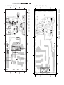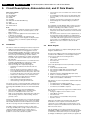
1
Colour Television
Chassis
EM5.3A P/M
AA
CL 36532017_000.eps
240403
Contents
Page
1. Technical Specifications, Connections,
and Chassis Overview
2
2. Safety Instructions, Warnings,
and Notes
4
3. Directions for Use
6
4. Mechanical Instructions
7
5. Service Modes, Error Codes, and Faultfinding 11
6. Block Diagrams, Test Point Overviews,
and Waveforms
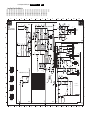
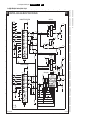
Wiring Diagram
21
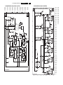
Block Diagram Supply and Deflection
22
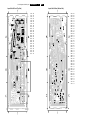
Testpoint Overview LSP and CRT Panel
23
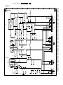
Block Diagram Video
24
Block Diagram Video (DW Sets Only)
25
Testpoint Overview SSB
26
Block Diagram Audio 1 (excl. Wireless Audio
Details)
27
I2C-IC Overview
28
Supply Lines Overview
29
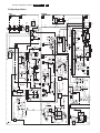
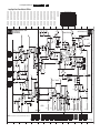
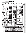
7. Circuit Diagrams and PWB Layouts
Diagram
Main Supply
(Diagram A1) 30
Stand-by Supply
(Diagram A2) 31
Line Deflection
(Diagram A3) 32
Frame Deflection & E/W Drive
(Diagram A4) 33
Rotation Circuitry
(Diagram A5) 34
Audio Amplifier
(Diagram A6) 35
Tuner SIMM connector (Female) (Diagram A8) 36
Receiver
(Diagram A9) 37
Front
(Diagram A10)37
Inputs/Outputs
(Diagram A11)38
SIMM connector (Male)
(Diagram B1) 46
IF, I/O Videoprocessing
(Diagram B2) 47
PICNIC
(Diagram B3A)48
Falconic (FEM)
(Diagram B3B)49
Contents
PWB
39-45
39-45
39-45
39-45
39-45
39-45
39-45
39-45
39-45
39-45
58-63
58-63
58-63
58-63
8.
9.
10
11
Page
Eagle
(Diagram B3C)50
Columbus
(Diagram B3D)51
FBX Supply
(Diagram B3E)52
HOP
(Diagram B4) 53
OTC
(Diagram B5) 54
Audio Demodulator
(Diagram B6) 55
Anti Moiré
(Diagram B9) 56
Headphone Amplifier
(Diagram B10)57
DW Panel
(Diagram C1) 64
DW Panel: Tuner
(Diagram C2) 65
DW Panel: I/O Processing
(Diagram C3) 66
DW Panel: IF Video Sync
(Diagram C41)67
DW Panel: V-Chip Processor
(Diagram C5) 68
DW Panel: NV ROM
(Diagram C6) 68
Mains Switch Panel
(Diagram E) 71
CRT Panel
(Diagram F1) 73
CRT/ Auto SCAVEM Panel
(Diagram F2) 74
DC Shift Panel
(Diagram G) 77
VDAF + 2nd Orders Panel
(Diagram I)
78
Jack-High Defenition:Control
(Diagram N1) 80
Jack-High Defenition:Inputs/Outputs(Diagr. N2) 81
Jack-High Defenition:Sync Slicer (Diagram N3) 82
Jack-High Defenition:Matrix
(Diagram N4) 82
Side I/O Panel
(Diagram O) 84
Top Control Panel
(Diagram P) 86
Auto SCAVEM
(Diagram SC1)87
Auto SCAVEM PCR
(Diagram SC3)88
Alignments
91
Circuit Description
98
Abbreviation List
104
IC Data Sheets
106
Spare Parts List
109
Revision List
123
58-63
58-63
58-63
58-63
58-63
58-63
58-63
58-63
69-70
69-70
69-70
69-70
69-70
69-70
72
75-76
75-76
77
79
83
83
83
83
85
86
89
89
©
Copyright 2004 Philips Consumer Electronics B.V. Eindhoven, The Netherlands.
All rights reserved. No part of this publication may be reproduced, stored in a
retrieval system or transmitted, in any form or by any means, electronic,
mechanical, photocopying, or otherwise without the prior permission of Philips.
Published by WO 0472 Service PaCE
Printed in the Netherlands
Subject to modification
EN 3122 785 14610
EN 2
1.
EM5.3A P/M AA
Technical Specifications, Connections, and Chassis Overview
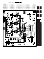
1. Technical Specifications, Connections, and Chassis Overview
1.2
Index of this chapter:
1.1 Technical Specifications
1.2 Connection Overview
1.3 Chassis Overview
Connection Overview
Note: The following connector color abbreviations are used
(acc. to DIN/IEC 757):
Bk= Black, Bu= Blue, Gn= Green, Gy= Grey, Rd= Red, Wh=
White, and Ye= Yellow.
Note: Figures below can deviate slightly from the actual
situation, due to the different set executions.
1.1
Technical Specifications
1.1.1
Vision
Display type
Screen sizes
Tuning system
Colour systems
Video playback
Channel selections
Aerial input
1.1.2
1.2.1
:
:
:
:
:
:
:
:
:
:
:
:
:
:
:
:
:
CRT-DV-RF
29” (74 cm), 4:3
32" (82 cm), 16:9
34" (86 cm), 4:3
PLL
NTSC 3.58, 4.43
PAL B/G, D/K, I, M
NTSC 3.58, 4.43
PAL B/G, D/K, I, M
SECAM B/G, D/K, L/L’
100 presets
UHF
VHF
Hyper-band
S-band
75 ohm, Coax
IEC-type
Maximum power
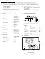
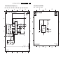
Top Control and Front / Side Connections
- VOLUME +
-
P/CH
+
M
3.5
IR-RECEIVER
SVHS
STANDBY LED
LIGHT SENSOR
SK 1
AUDIO R
VIDEO
AUDIO L
CL 26532058_008.eps
290502
Figure 1-1 Top control and Front / Side connections
Sound
Sound systems
1.1.3
Note: figures below can deviate slightly from the actual
situation, due to the different set executions.
: FM/FM B/G (except
29PT9221),
: NICAM B/G, D/K, I, L
: 2CS D/K (29PT9221)
: 4 x 15 W rms (int.)
: 3 x 15 W (29PT9221)
S-Video: In
1 - Ground
2 - Ground
3 -Y
4 -C
Gnd
Gnd
1 V_pp / 75 ohm
0.3 V_pp / 75 ohm
Cinch: In
Ye - Video-CVBS
Wh - Audio - L
Rd - Audio - R
1 V_pp / 75 ohmfmsymbol
0.5 V_rms / 10 kohm
0.5 V_rms / 10 kohm
Mini Jack: Headphone - Out
- Headphone
32 - 600 ohm / 10 mW
H
H
j
j
jq
jq
jq
ot
Miscellaneous
1.2.2
Mains voltage
Mains frequency
Ambient temperature
Maximum humidity
Power consumption
- Normal operation
- Standby
:
:
:
:
:
:
:
:
:
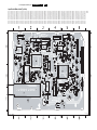
Rear Connections
90 - 276 Vac(/56/69)
220 - 240 Vac(/79/93)
50 / 60 Hz
+5 to +45 °C
90 % R.H.
RGB Y
Y
AUDIO
≈ 109 W
<1W
AUDIO
Pb
L
Pb
L
Pr
R
Pr
R
AV4 IN
AV3 IN
AUDIO MONITOR
OUT
OUT
AV1
IN
AV2
IN
75 Ohm
S
V
Y
Y
Y
L
L
Pb
L
L
S-VIDEO
R
R
Pr
R
R
COMPONENT VIDEO INPUT
SERVICE
CONNECTOR
(COMPAIR)
CL 26532058_009.eps
060601
Figure 1-2 Rear view
Aerial - In
- IEC-type
Coax, 75 ohm
D
Technical Specifications, Connections, and Chassis Overview
1.3
Audio-out (except on 29PT9221)
1 - Audio
S (0.5 Vrms / 10 kohm
2 - Audio
L (0.5 Vrms / 10 kohm)
3 - Audio
R (0.5 Vrms / 10 kohm)
kq
kq
kq
Monitor out
1 - Video
2 - Audio
3 - Audio
kq
kq
kq
1 Vpp / 75 ohm
L (0.5 Vrms / 10 kohm)
R (0.5 Vrms / 10 kohm)
EM5.3A P/M AA
AV2 in (SVHS)
1 2 3 -Y
4 -C
1.
EN 3
H
H
j
j
Gnd
Gnd
1 Vpp / 75 ohm
0.3 Vpp / 75 ohm
AV1 in
1 -Y
2 - Pb
3 - Pr
0.7 Vpp / 75 ohm
0.7 Vpp / 75 ohm
0.7 Vpp / 75 ohm
jq
jq
jq
AV3 in (D-sub connector)
1 - Pr (R)
0.35 Vpp (0.7 Vpp) / 75 ohm
2 - Y (G)
0.7 Vpp (0.7 Vpp) / 75 ohm
3 - Pb (B)
0.35 Vpp (0.7 Vpp) / 75 ohm
4 -H
5 Vpp / 1 kohm
5 -V
5 Vpp / 1 kohm
AV1 in
4 - Video
5 - Audio
6 - Audio
1 Vpp / 75 ohm
L (0.5 Vrms / 10 kohm)
R (0.5 Vrms / 10 kohm)
jq
jq
jq
AV3 and AV4 in (cinch)
1 - Y (G)
0.7 Vpp (0.7 Vpp) / 75 ohm
2 - Pb (B)
0.35 Vpp (0.7 Vpp) / 75 ohm
3 - Pr (R)
0.35 Vpp (0.7 Vpp) / 75 ohm
jq
jq
jq
AV2 in
1 - Video
2 - Audio
3 - Audio
1 Vpp / 75 ohm
L (0.5 Vrms / 10 kohm)
R (0.5 Vrms / 10 kohm)
jq
jq
jq
AV3 and AV4 in (cinch)
1 - Audio
L (0.5 Vrms / 10 kohm)
2 - Audio
R (0.5 Vrms / 10 kohm)
jq
jq
jq
jq
jq
jq
jq
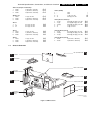
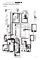
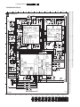
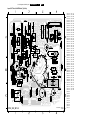
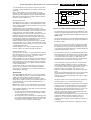
Chassis Overview
F
CRT PANEL
O
SIDE I/O PANEL
N
SC
TOP CONTROL PANEL
P
P
SMALL SIGNAL BOARD
B
MAINS SWITCH PANEL
E
LARGE SIGNAL PANEL
A
DC-SHIFT (optional)
G
JACK HIGH
DEFINITION INTERFACE
AUTO-SCAVEM
DAF PANEL
C
I
PIP/DOUBLE
WINDOW PANEL
(optional)
CL 26532079_001.eps
171204
Figure 1-3 PWB locations
EN 4
2.
EM5.3A P/M AA
Safety Instructions, Warnings, and Notes
2. Safety Instructions, Warnings, and Notes
•
Index of this chapter:
2.1 Safety Instructions
2.2 Maintenance Instructions
2.3 Warnings
2.4 Notes
•
Note: Figures below can deviate slightly from the actual
situation, due to the different set executions.
2.1
Safety Instructions
2.3
Safety regulations require that during a repair:
• Due to the chassis concept, a very large part of the circuitry
(incl. deflection) is “hot”. Therefore, connect the set to the
mains via an isolation transformer (> 800 VA).
• Replace safety components, indicated by the symbol h,
only by components identical to the original ones. Any
other component substitution (other than original type) may
increase risk of fire or electrical shock hazard.
• Wear safety goggles when you replace the CRT.
Safety regulations require that after a repair, you must return
the set in its original condition. Pay, in particular, attention to
the following points:
• General repair instruction: as a strict precaution, we advise
you to re-solder the solder connections through which the
horizontal deflection current is flowing. In particular this is
valid for the:
1. Pins of the line output transformer (LOT).
2. Fly-back capacitor(s).
3. S-correction capacitor(s).
4. Line output transistor.
5. Pins of the connector with wires to the deflection coil.
6. Other components through which the deflection current
flows.
Note: This re-soldering is advised to prevent bad connections
due to metal fatigue in solder connections, and is therefore only
necessary for television sets more than two years old.
• Route the wire trees and EHT cable correctly and secure
them with the mounted cable clamps.
• Check the insulation of the mains cord for external
damage.
• Check the strain relief of the mains cord for proper function,
to prevent the cord from touching the CRT, hot
components, or heat sinks.
• Check the electrical DC resistance between the mains plug
and the secondary side (only for sets that have an isolated
power supply). Do this as follows:
1. Unplug the mains cord and connect a wire between the
two pins of the mains plug.
2. Turn on the main power switch (keep the mains cord
unplugged!).
3. Measure the resistance value between the pins of the
mains plug and the metal shielding of the tuner or the
aerial connection of the set. The reading should be
between 4.5 Mohm and 12 Mohm.
4. Switch the TV “off” and remove the wire between the
two pins of the mains plug.
• Check the cabinet for defects, to prevent the possibility of
the customer touching any internal parts.
2.2
When a customer uses the set in an environment with
higher dust, grease, or moisture levels, for example in a
kitchen, the recommended interval is one year.
The maintenance inspection includes the following actions:
1. Perform the “general repair instruction” noted above.
2. Clean the power supply and deflection circuitry on the
chassis.
3. Clean the picture tube panel and the neck of the picture
tube.
Maintenance Instructions
We recommend a maintenance inspection carried out by
qualified service personnel. The interval depends on the usage
conditions:
• When a customer uses the set under normal
circumstances, for example in a living room, the
recommended interval is three to five years.
Warnings
•
In order to prevent damage to ICs and transistors, avoid all
high voltage flashovers. In order to prevent damage to the
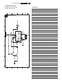
picture tube, use the method shown in Fig. 2-1, to
discharge the picture tube. Use a high voltage probe and a
multi-meter (position V_dc). Discharge until the meter
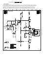
reading is 0 V (after approx. 30 s).
V
E_06532_007.eps
250304
Figure 2-1 Discharge picture tube
•
•
•
•
•
All ICs and many other semiconductors are susceptible to
electrostatic discharges (ESD, w). Careless handling
during repair can reduce life drastically. Make sure that,
during repair, you are connected with the same potential as
the mass of the set by a wristband with resistance. Keep
components and tools also at this potential. Available ESD
protection equipment:
– Complete kit ESD3 (small tablemat, wristband,
connection box, extension cable and earth cable) 4822
310 10671.
– Wristband tester 4822 344 13999.
Together with the deflection unit and any multi-pole unit,
flat square picture tubes form an integrated unit. The
deflection and the multi-pole units are set optimally at the
factory. We do not recommend adjusting this unit during
repair.
Be careful during measurements in the high voltage
section and on the picture tube.
Never replace modules or other components while the unit
is “on”.
When you align the set, use plastic rather than metal tools.
This will prevent any short circuits and the danger of a
circuit becoming unstable.
Safety Instructions, Warnings, and Notes
2.4
Notes
2.4.1
General
•
•
•
•
•
•
2.4.2
•
•
•
•
•
•
2.4.3
All resistor values are in ohms and the value multiplier is
often used to indicate the decimal point location (e.g. 2K2
indicates 2.2 kohm).
Resistor values with no multiplier may be indicated with
either an "E" or an "R" (e.g. 220E or 220R indicates 220
ohm).
All capacitor values are expressed in micro-farads (µ= x
10^-6), nano-farads (n= x 10^-9), or pico-farads (p= x 10^12).
Capacitor values may also use the value multiplier as the
decimal point indication (e.g. 2p2 indicates 2.2 pF).
An "asterisk" (*) indicates component usage varies. Refer
to the diversity tables for the correct values.
The correct component values are listed in the Electrical
Replacement Parts List. Therefore, always check this list
when there is any doubt.
Rework on BGA (Ball Grid Array) ICs
General
Although (LF)BGA assembly yields are very high, there may
still be a requirement for component rework. By rework, we
mean the process of removing the component from the PWB
and replacing it with a new component. If an (LF)BGA is
removed from a PWB, the solder balls of the component are
deformed drastically so the removed (LF)BGA has to be
discarded.
Device Removal
As is the case with any component that, it is essential when
removing an (LF)BGA, the board, tracks, solder lands, or
surrounding components are not damaged. To remove an
(LF)BGA, the board must be uniformly heated to a temperature
close to the reflow soldering temperature. A uniform
temperature reduces the chance of warping the PWB.
To do this, we recommend that the board is heated until it is
certain that all the joints are molten. Then carefully pull the
component off the board with a vacuum nozzle. For the
appropriate temperature profiles, see the IC data sheet.
2.
EN 5
Area Preparation
When the component has been removed, the vacant IC area
must be cleaned before replacing the (LF)BGA.
Removing an IC often leaves varying amounts of solder on the
mounting lands. This excessive solder can be removed with
either a solder sucker or solder wick. The remaining flux can be
removed with a brush and cleaning agent.
After the board is properly cleaned and inspected, apply flux on
the solder lands and on the connection balls of the (LF)BGA.
Note: Do not apply solder paste, as this has shown to result in
problems during re-soldering.
Measure the voltages and waveforms with regard to the
chassis (= tuner) ground (H), or hot ground (I), depending
on the tested area of circuitry.
The voltages and waveforms shown in the diagrams are
indicative. Measure them in the Service Default Mode (see
chapter 5 “Service Modes, ....”) with a colour bar signal and
stereo sound (L: 3 kHz, R: 1 kHz unless stated otherwise)
and picture carrier at 475.25 MHz for PAL, or 61.25 MHz
for NTSC (channel 3).
Where necessary, measure the waveforms and voltages
with (D) and without (E) aerial signal. Measure the
voltages in the power supply section both in normal
operation (G) and in standby (F). These values are
indicated by means of the appropriate symbols.
The picture tube panel has printed spark gaps. Each spark
gap is connected between an electrode of the picture tube
and the Aquadag coating.
The semiconductors indicated in the circuit diagram and in
the parts lists, are interchangeable per position with the
semiconductors in the unit, irrespective of the type
indication on these semiconductors.
Manufactured under license from Dolby Laboratories.
“Dolby”, “Pro Logic” and the “double-D symbol”, are
trademarks of Dolby Laboratories.
Schematic Notes
EM5.3A P/M AA
Device Replacement
The last step in the repair process is to solder the new
component on the board. Ideally, the (LF)BGA should be
aligned under a microscope or magnifying glass. If this is not
possible, try to align the (LF)BGA with any board markers.
To reflow the solder, apply a temperature profile according to
the IC data sheet. So as not to damage neighbouring
components, it may be necessary to reduce some
temperatures and times.
More Information
For more information on how to handle BGA devices, visit this
URL: www.atyourservice.ce.philips.com (needs subscription,
not available for all regions). After login, select “Magazine”,
then go to “Workshop Information”. Here you will find
Information on how to deal with BGA-ICs.
2.4.4
Lead Free Solder
Philips CE is going to produce lead-free sets (PBF) from
1.1.2005 onwards.
P
b
Figure 2-2 Lead-free logo
This sign normally has a diameter of 6 mm, but if there is less
space on a board also 3 mm is possible.
Regardless of this logo (is not always present), one must treat
all sets from this date onwards according to the next rules.
Due to lead-free technology some rules have to be respected
by the workshop during a repair:
• Use only lead-free soldering tin Philips SAC305 with order
code 0622 149 00106. If lead-free solder paste is required,
please contact the manufacturer of your soldering
equipment. In general, use of solder paste within
workshops should be avoided because paste is not easy to
store and to handle.
• Use only adequate solder tools applicable for lead-free
soldering tin. The solder tool must be able
– To reach at least a solder-tip temperature of 400°C.
– To stabilise the adjusted temperature at the solder-tip.
– To exchange solder-tips for different applications.
• Adjust your solder tool so that a temperature around 360°C
- 380°C is reached and stabilised at the solder joint.
Heating time of the solder-joint should not exceed ~ 4 sec.
Avoid temperatures above 400°C, otherwise wear-out of
tips will rise drastically and flux-fluid will be destroyed. To
avoid wear-out of tips, switch “off” unused equipment or
reduce heat.
• Mix of lead-free soldering tin/parts with leaded soldering
tin/parts is possible but PHILIPS recommends strongly to
avoid mixed regimes. If not to avoid, clean carefully the
solder-joint from old tin and re-solder with new tin.
EN 6
•
•
•
3.
EM5.3A P/M AA
Directions for Use
Use only original spare-parts listed in the Service-Manuals.
Not listed standard material (commodities) has to be
purchased at external companies.
Special information for lead-free BGA ICs: these ICs will be
delivered in so-called "dry-packaging" to protect the IC
against moisture. This packaging may only be opened
short before it is used (soldered). Otherwise the body of the
IC gets "wet" inside and during the heating time the
structure of the IC will be destroyed due to high (steam)pressure inside the body. If the packaging was opened
before usage, the IC has to be heated up for some hours
(around 90°C) for drying (think of ESD-protection !).
Do not re-use BGAs at all!
For sets produced before 1.1.2005, containing leaded
soldering tin and components, all needed spare parts will
be available till the end of the service period. For the repair
of such sets nothing changes.
•
De-solder thoroughly (clean solder joints to avoid mix of
two alloys).
Caution: For BGA-ICs, you must use the correct temperatureprofile, which is coupled to the 12NC. For an overview of these
profiles, visit the website www.atyourservice.ce.philips.com
(needs subscription, but is not available for all regions)
You will find this and more technical information within the
"Magazine", chapter "Workshop information".
For additional questions please contact your local repairhelpdesk.
2.4.5
Practical Service Precautions
•
•
In case of doubt wether the board is lead-free or not (or with
mixed technologies), you can use the following method:
• Always use the highest temperature to solder, when using
SAC305 (see also instructions below).
3. Directions for Use
You can download this information from the following website:
http://www.philips.com/support
It makes sense to avoid exposure to electrical shock.
While some sources are expected to have a possible
dangerous impact, others of quite high potential are of
limited current and are sometimes held in less regard.
Always respect voltages. While some may not be
dangerous in themselves, they can cause unexpected
reactions that are best avoided. Before reaching into a
powered TV set, it is best to test the high voltage insulation.
It is easy to do, and is a good service precaution.
Mechanical Instructions
EM5.3A P/M AA
4.
EN 7
4. Mechanical Instructions
1. Disconnect the loudspeaker cable at the top of the
subwoofer box.
2. The subwoofer is fixed in the bottom plate with two “rubber
feet”.
3. Pull the subwoofer box upwards, and remove it.
Index of this chapter:
4.1 Service Connector (for ComPair)
4.2 Set Disassembly
4.3 Service Positions
4.4 Assembly / Board Removal
4.5 Set Reassembly
4.3
Note: Figures below can deviate slightly from the actual
product, due to different set designs.
4.1
Service Positions
This chassis has several predefined service positions, for
better accessibility. They are explained below in more detail.
Service Connector (for ComPair)
4.3.1
Control-Jack-High-Definition-Interface Panel Solder Side
To perform service diagnostics with ComPair, it is not
necessary to disassemble the set. You simply have to connect
the ComPair interface box, with the appropriate cable, to the
service connector (on the rear of the set, see figure below), and
start the ComPair program (see chapter 5).
4.2
2
Set Disassembly
1
4
Follow the disassembly instructions below.
4
3
4.2.1
Back Cover Removal
3
1
CL 26532058_012.eps
290502
1
1
Figure 4-2 Service position 1
To remove or access the “Control-Jack-High-DefinitionInterface” panel, do the following:
1. Remove the screw [1].
2. To release the peg, push it toward the CRT [2].
3. At the same time, pull the complete module away from the
LSP [3]. It hinges in the LSP bracket.
4. To remove the panel, remove the four panel screws [4].
2
3
3
Service connector
CL 26532058_011.eps
040602
Figure 4-1 Rear Cover Removal
4.3.2
LSP Component Side
SSB top-bracket
Warning: Disconnect the AC power cord before you remove
the back cover.
SSB
AUTO-SCAVEM
bracket
LOT - bracket
First, remove the top cover (plate with “saucer”):
1. Remove the three screws [1] that hold the cover plate.
2. Pull the cover (horizontally) backward.
To access the electronics of the set, you must remove the back
cover:
1. Remove the screws [2] of the rear jack panel cover plate.
2. Remove the remaining screws [3] at the two sides, and the
top of the back cover.
3. Remove the back cover. Make sure that wires and cables
are not damaged while removing the cover.
4.2.2
LSP
CONNECTOR SUPPORT
bracket
1
Bottom tray
2
1
2
Subwoofer Removal
Caution: Do not disconnect the loudspeaker cable from the
subwoofer box while the set is operating, because the class-D
amplifier cannot handle a change in load during operation.
There is no problem when the subwoofer is disconnected
before operation, but a change from connected to
disconnected during operation can damage the amplifier.
CL 26532058_013.eps
290502
Figure 4-3 Service position 2
To better access the component side of the LSP, do the
following (see figure above):
1. Remove the LSP bracket from the bottom tray by pulling it
backwards.
EN 8
4.
EM5.3A P/M AA
Mechanical Instructions
2. Hook the bracket in the first row of holes of the bottom tray.
In other words, reposition the bracket from [1] to [2].
4.3.3
LSP Solder Side
1
2
2
1
1502
CL 26532058_015.eps
290502
Figure 4-5 SSB removal (part 1)
1. Put the LSP in service position 2 (as described above).
2. Release the two clamps at the top of the SSB bracket [2]
and pull the bracket upward (it hinges in the bracket on the
LOT side).
3. You can now remove the complete SSB bracket.
1
3
SSB
3
CL 26532058_014.eps
290502
Figure 4-4 Service position 3
To access the bottom side (solder side) of the LSP, do the
following (see figure above):
1. Remove the DAF module (see paragraph “DAF Assembly/
Panel” below).
2. To disconnect the degaussing coil from the LSP, remove
the cable from connector 1502 [1].
3. Release the wires from their clamps to make room to
reposition the LSP.
4. Turn the LSP 90 degrees clockwise [2], and place it in the
hole at the left side of the bottom tray [3].
4.3.4
Small Signal Board (SSB)
There is no predefined service position for the SSB. Most test
points are located on the A-side (the side that faces the tuner).
If you have to replace ICs, you must take the complete SSB
module out of the SIMM-connector.
Note: For access to the A-side, it is necessary to remove the
Auto-Scavem assembly (at the left side of the SSB). See the
description in the “Auto-Scavem Assembly/Panel” section
below.
To access the SSB test points, do the following:
2
2
CL 26532041_068.eps
110402
Figure 4-6 SSB removal (part 2)
1. Push the top of the SSB toward the LOT [1].
2. Due to the pressure, the two metal clamps at both sides of
the SIMM-connector will release [2].
3. Take the complete SSB out [3].
Mechanical Instructions
4.4.2
EM5.3A P/M AA
4.
EN 9
Side-I/O Assembly and Panel
SAM
SDM
3
2
2
2
1
SSB
1
CL 16532149_069.eps
061201
1
Figure 4-9 Side I/O assembly
CL 26532041_069.eps
110402
Figure 4-7 SSB removal (part 3)
1. Once you have taken out the SSB, remove the shieldings
[2]. Sometimes it is necessary to unsolder some solder
tags before doing this [1].
2. Replace the SSB module in the SIMM-connector in reverse
order.
Notes:
• For better access to the SSB, it is possible to order an
“extension board,” which is part number 9965 000 05769.
• If it is necessary for measurements, you can put the LSP in
“service position 2” (as described above).
4.4
1. Release the snap hook [1] with your finger.
2. At the same time, pull the assembly backward [2].
3. Release the two clamps on the right side of the bracket (the
board hinges at the left side).
4. Remove the board from the bracket.
4.4.3
AC Power Switch Assembly/Panel
1
1
2
Assembly / Board Removal
Sometimes, it may be necessary to swap a complete assembly
or Circuit Board Assembly (CBA). This procedure is explained
below.
CL 16532149_070.eps
061201
Figure 4-10 AC Power Switch Assembly
4.4.1
Top Control Assembly/Panel
Top control board
CL 16532149_068.eps
051201
Figure 4-8 Top control assembly
1. Release both screws (about 5 full turns).
2. Pull the complete assembly back and upwards (the
assembly hinges in the cabinet front).
3. Flip the assembly, and you can access the board by
(carefully) releasing the four clamps.
1. Release the two clamps by pushing them upward [1]. At the
same time, pull the complete assembly backward [2].
Note: Be aware that the degaussing coil may hamper this.
2. Release the two clamps on the two sides of the bracket (the
board hinges at the connector side).
3. Remove the board from the bracket.
4. If the light guide (located in the cabinet, in front of the
LEDs) is defective, you can replace it by pushing it forward
at the left side (it hinges at the right side, seen from the
rear).
EN 10
4.4.4
4.
EM5.3A P/M AA
Mechanical Instructions
This panel is placed in a bracket that is located on the left side
of the tuner.
To remove the bracket:
1. Pull the release handle [1] backwards. This will lift the
release catch, and the bracket can be pulled out
backwards.
2. Release the two securing clamps [2] and lift the board out
of the bracket.
3. Both sides of the panel are now easy accessible.
DAF Assembly/Panel
1
4
4
2
4.4.7
3
Small Signal Board (SSB)
See section 4.3.4 “Small Signal Board (SSB)” above.
3
4.4.8
Large Signal Panel (LSP)
CL 16532044_011.eps
150501
1. Remove the SSB (see paragraph “Small Signal Board
(SSB)” above).
2. Remove the Auto-Scavem assembly (see paragraph “Auto
Scavem Assembly/Panel” above).
3. Disconnect the necessary cables.
4. Release the clamps on the left of the LSP-bracket (the
board hinges at the right side).
5. Remove the board from the bracket.
Figure 4-11 DAF module
1. Remove the screw [1] (if present).
2. Push the clamp [2] down, and, at the same time, pull the
complete bracket away from the CRT [3]. The module is
now free from the LSP bracket.
3. Release the clamps [4], in order to remove the board from
its bracket.
4.4.5
Auto-SCAVEM Assembly/Panel
Set Reassembly
To reassemble the set, perform all disassembly processes in
reverse order.
This panel is placed on the left side of the SSB (See figure
“Service Position 2”). Because most of its components are
located on the bottom side, you must lift the panel from its
bracket before you can perform measurements.
1. Release the two clamps at the top.
2. Lift the panel from the bracket (it hinges at the bottom).
To remove the bracket:
1. First, remove the panel from the bracket, as described
above.
2. Remove the two screws at the bottom.
3. Lift the Auto-Scavem bracket slightly up, and at the same
time bend the top slightly away from the tuner.
4. Push the bracket in the direction of the CRT, and lift it out
of the LSP-bracket.
4.4.6
4.5
Double Window Assembly/Panel
2
2
DW - MODULE
1
CL 26532079_002.eps
210602
Figure 4-12 Double Window module
Before replacing the back cover:
• Be sure the AC power cord is mounted correctly in its
guiding brackets.
• Be sure all wires/cables are returned to their original
positions. This is very important due to the large “hot” area
of the set
Service Modes, Error Codes, and Fault Finding
EM5.3A P/M AA
5.
EN 11
5. Service Modes, Error Codes, and Fault Finding
–
–
Index of this chapter:
5.1 Test Points
5.2 Service Modes
5.3 Problems and Solving Tips (related to CSM)
5.4 ComPair
5.5 Error Codes
5.6 The Blinking LED Procedure
5.7 Protections
5.8 Repair tips
5.1
–
–
–
–
How to enter SDM
• Use one of the following methods:
• Use the standard RC-transmitter and key in the code
"062596", directly followed by the "MENU" button.
Note: It is possible that, together with the SDM, the main
menu will appear. To switch it off, push the "MENU" button
again.
• When you shorten for a moment the two solder pads on the
'external part' of the SSB print, with the indication "SDM".
Activation can be performed in all modes, except when the
set has a problem with the main-processor.
Caution: If the SDM is entered via the pins, all the
software-controlled protections are de-activated.
• Use the "DEFAULT" button in the DST-emulation feature of
ComPair.
• Use the "DEFAULT" button on the Dealer Service Tool
(RC7150).
Test Points
The EM5 chassis is equipped with test points printed on the
circuit board assemblies. They refer to the schematic diagram
letters. The numbering is in a logical sequence for diagnostics.
Always start diagnosing (within a functional block), in the
sequence of the relevant test points for that block.
Perform measurements under the following conditions:
• Set in Service Default Mode.
• Video: color bar signal.
• Audio: 3 kHz left, 1 kHz right.
5.2
Service Modes
After entering this mode, "SDM" will appear in the upper right
corner of the screen.
Service Default Mode (SDM) and Service Alignment Mode
(SAM) offer several features for the service technician, while
the Customer Service Mode (CSM) is used for communication
between a Philips Customer Care Centre (P3C) and a
customer.
How to navigate
When you press the "MENU" button on the RC transmitter, the
set will toggle between the SDM and the normal user menu
(with the SDM mode still active in the background).
There is also the option of using ComPair, a hardware interface
between a computer (see requirements below) and the TV
chassis. It offers the ability of structured troubleshooting, test
pattern generation, error code reading, software version
readout, and software upgrading.
Minimum requirements: a Pentium processor, Windows 95/
98, and a CD-ROM drive (see also paragraph "ComPair").
Note: This chassis is equipped with a LED configuration with
separate blue and red LEDs. This is different from the
bicoloured version we know from EM5E. The blue LED is
controlled by software (via ON_OFF_LED). The red LED will
light in anti-phase to the blue one, but with a time delay. This
means that if the blue LED is blinking fast, the red LED will stay
off. But after the blue LED is "OFF" long enough, the red LED
will go "ON".
So take care: In certain service modes (e.g. blinking LED,
stepwise start-up, etc.) you must observe the blue LED and
ignore the red LED.
5.2.1
Service Default Mode (SDM)
Purpose
• To create a pre-defined setting, to get the same
measurement results as given in this manual.
• To override SW protections.
• To start the blinking LED procedure.
Specifications
• Tuning frequency: 475.25 MHz for PAL/SECAM.
Tuning frequency: 61.25 MHz for NTSC.
• Colour system: PAL B/G or NTSC.
• All picture settings at 50 % (brightness, colour, contrast).
• All sound settings at 50 %, except volume at 25 %.
• All service-unfriendly modes (if present) are disabled, like:
– (Sleep) timer.
– Child/parental lock.
– Blue mute.
Automatic volume limiter (AVL).
Auto switch-off (when no video signal was received for
10 minutes).
Skip/blank of non-favourite pre-sets.
Smart modes.
Auto store of personal presets.
Auto user menu time-out.
How to exit SDM
Use one of the following methods:
• Switch the set to STANDBY via the RC-transmitter.
• Press the "EXIT" button in the DST-emulation feature of
ComPair.
• Via a standard customer RC-transmitter: key in "00"sequence.
5.2.2
Service Alignment Mode (SAM)
Purpose
• To perform (software) alignments.
• To change option settings.
• To easily identify the used software version.
• To view operation hours.
• To display (or clear) the error code buffer.
Specifications
• Operation hours counter.
• Software version.
• Option settings.
• Error buffer reading and erasing.
• Software alignments.
How to enter SAM
Use one of the following methods:
• Via a standard RC transmitter: key in the code "062596"
directly followed by the "OSD [i+]" button. After activating
SAM with this method a service warning will appear on the
screen, you can continue by pressing any digit key on the
RC.
• Short for a moment the two solder pads on the 'external
part' of the SSB print, with the indication SAM. Depending
on the software version it is possible that the service
warning will appear, you can continue by pressing any digit
key on the RC.
EN 12
•
•
5.
EM5.3A P/M AA
Service Modes, Error Codes, and Fault Finding
The menu gives an overview of what is received on the
current preset. Following items are displayed:
Use the DST-emulation feature of ComPair.
Press the ALIGN button on the DST while the set is in the
normal operation
After entering this mode, "SAM" will appear in the upper right
corner of the screen.
Contents of SAM:
• OPERATION HOURS. Displays the accumulated total of
operation hours (not the standby hours).
• HARDWARE INFO
– ROM VERSION. Displays the date of the software and
the software version of the ROM (example: EM53AP_
1.0_01234 = AAAABB-X.Y_NNNNN).
• AAAA= the chassis name.
• BB= the region: EU= Europe, AP= Asia Pacific
PAL/Multi, AN= Asia Pacific NTSC, US= USA, LT=
LATAM.
• X.Y= the software version, where X is the main
version number (different numbers are not
compatible with one another) and Y is the sub
version number (a higher number is always
compatible with a lower number).
• NNNNN= last five digits of 12nc code software.
– FBX VERSION. The 12NC-number of the build in
Feature Box software.
• ERRORS (followed by maximal 10 errors). The most
recent error is displayed at the upper left (for an error
explanation see paragraph "Error Codes").
• DEFECTIVE MODULE. Here the module that generates
the error is displayed. If there are multiple errors in the
buffer, which are not all generated by a single module,
there is probably another defect. It will then display the
message "UNKNOWN" here.
• RESET ERROR BUFFER. When you press the "OK"
button, the error buffer is reset.
• ALIGNMENTS. This will activate the "ALIGNMENTS" submenu.
• DEALER OPTIONS. Extra features for the dealers.
• SERVICE OPTIONS. Extra features for Service.
• INITIALISE NVM. When an NVM was corrupted (or
replaced) in the former EM3 chassis, the microprocessor
replaces the content with default data (to assure that the
set can operate). However, all pre-sets and alignment
values are gone now, and option numbers are not correct.
Therefore, this was a very drastic way. In this chassis, the
procedure is implemented in another way: The moment the
processor recognises a corrupted NVM, the "INITIALISE
NVM" line will be highlighted. Now, you can do two things
(dependent of the service instructions at that moment):
– Save the content of the NVM via ComPair for
development analysis, before initialising. This will give
the Philips Service department an extra possibility for
diagnosis (e.g. when Development asks for this).
– Initialise the NVM (same as in the past, however now it
happens conscious).
• STORE. All options and alignments are stored when
pressing the "OK"-button
• FUNCTIONAL TEST. All devices are tested via the "OK"
button. Eventual errors are displayed in the error buffer.
The error buffer is not erased, the content returns when this
test is terminated.
• DAILY MENUS. With the "OK" button, you can go to the
normal user menu. SAM is still active in the background.
With the "MENU" button, you return from the user menu to
SAM menu. This feature can be helpful to quickly change
some settings in the user menu.
• SW MAINTENANCE
– UPGRADE. Not applicable for this chassis
– EVENTS. Not useful for service purposes. In case of
specific software problems, the development
department can ask for this info.
– BDM INFO. Broadcast Debug Menu info. The purpose
of this menu is to debug the broadcast, NOT the TV.
Presetnr:
Presetname:
------
CNI NVM:
---CNI F1:
---CNI F2:
---CNI VPS:
---Morning Prog:
--Name 8/30 F1:
----Name 8/30 F2:
----Name TXT:
----Signal Strength:--EPG Service:
---
UTC:
LTO:
Time:
Date:
--:--:---:--:---:--:---/--/----
Time TXT:
Time 8/30 F1:
Date 8/30 F1:
LTO 8/30 F1:
--:--:---:--:---/--/-----:--:--
WSS
WSS
WSS
WSS
-----------
G1:
G2:
G3:
G4:
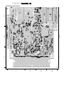
CL 36532017_055.eps
240403
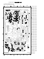
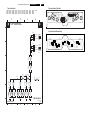
Figure 5-1 Broadcast debug menu overview.
Table 5-1 Broadcast debug menu explanation
Item
Source
Description
Presetnr
Set
Presetnumber of the current selected
preset.
Presetname
Set
Presetname of the current selected
preset.
CNI NVM
Broadcaster
CNI number stored in NVM for the
current preset.
CNI F1
Broadcaster
CNI number from transmitted Packet 8/
30 Format 1.
CNI F2
Broadcaster
CNI number from transmitted Packet 8/
30 Format 2.
CNI VPS
Broadcaster
CNI number from transmitted VPS line.
Morning Prog
Broadcaster
"ARD" or "ZDF" according to dedicated
bit in 8/30 Format 1.
Name 8/30 F1
Broadcaster
Name extracted from status message of
8/30 Format 1.
Name 8/30 F2
Broadcaster
Name extracted from status message of
8/30 Format 2.
Name TXT
Broadcaster
Name extracted from TXT header.
Signal Strength
FBX
Noise figure measured for selected
preset.
EPG Service
Set
EPG Service stored in NVM for current
preset displayed as "TXT", "MCP",
"SCP", "OCP".
UTC
Set
UTC (Universal Time Code formerly
known as Greenwich Mean Time) used in
the set.
LTO
Set
LTO (Local Time Offset) used in the set.
Used by EPG for all Nextview displays. (=
Time TXT header - Time 8/30 F1 )
Time
Set
Current time running in the set. Was
extracted at startup, then maintained by
software.
Date
Set
Current date running in the set. Was
extracted at startup, then maintained by
software.
Time TXT
Broadcaster
TXT header time from the selected
preset.
Time 8/30 F1
Broadcaster
UTC time from 8/30 Format 1.
Date 8/30 F1
Broadcaster
Date from 8/30 Format 1.
LTO 8/30 F1
Broadcaster
LTO from 8/30 Format 1.
WSS G1
Broadcaster
WSS Group 1 (Aspect Ratio) bits 0 1 2 3
WSS G2
Broadcaster
WSS Group 2 (Enhanced Services) bits 4
567
WSS G3
Broadcaster
WSS Group 3 (Subtitles) bits 8 9 10
WSS G4
Broadcaster
WSS Group 4 (Reserved) bits 11 12 13
How to navigate
• In SAM, you can select the menu items with the "CURSOR
UP/DOWN" key on the RC-transmitter. The selected item
will be highlighted. When not all menu items fit on the
screen, move the "CURSOR UP/DOWN" key to display the
next/previous menu items.
• With the "CURSOR LEFT/RIGHT" keys, it is possible to:
– (De) activate the selected menu item.
– Change the value of the selected menu item.
– Activate the selected submenu.
Service Modes, Error Codes, and Fault Finding
How to exit SAM
Use one of the following methods:
• Press the "MENU" button on the RC-transmitter, or
• Switch the set to STANDBY via the RC-transmitter, or
• Press the "EXIT" button on the DST.
5.2.3
•
Customer Service Mode (CSM)
Purpose
When a customer is having problems with his TV-set, he can
call his dealer. The service technician can than ask the
customer to activate the CSM, in order to identify the status of
the set. Now, the service technician can judge the severity of
the complaint. In many cases, he can advise the customer how
to solve the problem, or he can decide if it is necessary to visit
the customer.
The CSM is a read only mode; therefore, modifications in this
mode are not possible.
How to enter CSM
Use one of the following methods:
• Press the "MUTE" button on the RC-transmitter
simultaneously with the "MENU" button on the TV (top
control) for at least 4 seconds.
• Key in the code "123654" via the standard RC transmitter.
Note: Activation of the CSM is only possible if there is no (user)
menu on the screen!
How to navigate
By means of the "CURSOR-DOWN/UP" knob on the RCtransmitter, you can navigate through the five menus.
Contents of CSM
Customer Service Menu 1
• SOFTWARE VERSION (example: EM53AP_1.0_01234).
Displays the build in software version. In case of field
problems related to software, software flash-RAM
pos.7006 must be changed by a new one. Do this via
soldering. You will find details of the software versions in
the chapter "Software Survey" of the "Product Survey Colour Television" publication. This publication is
generated four times a year.
• FEATURE BOX. The 12NC-number of the build in Feature
Box software
• SET TYPE. This information is very helpful for a helpdesk/
workshop as reference for further diagnosis. In this way, it
is not necessary for the customer to look at the rear of the
TV-set.
• CODE 1. Gives the latest 5 errors of the error buffer. As
soon as the built-in diagnose software has detected an
error the buffer is adapted. The last occurred error is
displayed on the leftmost position. Each error code is
displayed as a 3-digit number. When less than 10 errors
occur, the rest of the buffer is empty (000). See also
paragraph "Error Codes" for a description.
• CODE 2. Gives the first 5 errors of the error buffer. See
also paragraph Error Codes for a description.
• VOLUME. Gives the last status of the volume as set by the
customer. The value can vary from 0 (volume is minimum)
to 100 (volume is maximum). Volume values can be
changed via the volume key on the RC-transmitter.
• BRIGHTNESS. Gives the last status of the brightness as
set by the customer. The value can vary from 0 (brightness
is minimum) to 100 (brightness is maximum). Brightness
values can be changed via the "CURSOR LEFT" and
"CURSOR RIGHT" keys on the RC-transmitter after
pressing the "MENU" button and selecting "PICTURE" and
"BRIGHTNESS".
• CONTRAST. Gives the last status of the contrast as set by
the customer. The value can vary from 0 (contrast is
minimum) to 100 (contrast is maximum). Contrast values
can be changed via "CURSOR LEFT" and "CURSOR
•
EM5.3A P/M AA
5.
EN 13
RIGHT" keys on the RC-transmitter after pressing the
"MENU" button and selecting "PICTURE" and
"CONTRAST".
COLOUR. Gives the last status of the colour saturation, as
set by the customer. The value can vary from 0 (colour is
minimum) to 100 (colour is maximum). Colour values can
be changed via "CURSOR LEFT" and "CURSOR RIGHT"
keys on the RC-transmitter after pressing the "MENU"
button and selecting "PICTURE" and "COLOUR".
HUE. Only relevant for NTSC-signals (e.g. some NTSCDVD-discs).
Customer Service Menu 2
• SHARPNESS. Gives the sharpness value. The value can
vary from 0 (sharpness is minimum) to 7 (sharpness is
maximum). In case of bad antenna signals, a too high
value of the sharpness can result in a noisy picture.
Sharpness values can be changed via the "CURSOR
LEFT" and "CURSOR RIGHT" keys on the RC-transmitter
after pressing the "MENU" button and selecting
"PICTURE" and "SHARPNESS".
• HEADPHONE VOLUME. Gives the last status of the
headphone volume, as set by the customer. The value can
vary from 0 (volume is minimum) to 100 (volume is
maximum). Headphone volume values can be changed via
the "CURSOR LEFT" and "CURSOR RIGHT" keys on the
RC-transmitter after pressing the "MENU" button and
selecting "SOUND" and "HEADPHONE VOLUME".
• SURROUND MODE. Indicates the by the customer
selected surround mode (or automatically chosen mode).
In case the set is a Non-Dolby set, there will be displayed
"0". If it is a Dolby-set then is displayed: "STEREO", "3
STEREO", "HALL", "3DSURROUND", "DOLBY PRO
LOGIC" or "DOLBY DIGITAL". These settings can be
influenced after pressing the "MENU" button and selecting
"SOUND" and SURROUND MODE". It can also have been
selected automatically by signalling bits (internal software).
• TUNER FREQUENCY. Indicates the frequency the
selected transmitter is tuned to. The tuner frequency can
be changed via the "CURSOR LEFT" and "CURSOR
RIGHT" keys for fine tune after opening the installation
menu and selecting "INSTALL" and "MANUAL INSTALL".
• DIGITAL OPTION. Gives the selected digital mode, "100
HZ", "DIGITAL SCAN", "NATURAL MOTION", "DOUBLE
LINES", or "PIXEL PLUS". Change via "MENU",
"PICTURE", "DIGITAL OPTIONS".
• CENTRE TRIM. Indicates the difference between main
volume and volume of centre speaker. Change via:
"MENU", "SETUP", "SPEAKERS", and "CENTRE
VOLUME" (not available when "Surround Mode" is set to
"STEREO" or "HALL"). The value can vary from "-10" to
"+10"
• TV SYSTEM. Gives information about the video system of
the selected transmitter.
– BG: PAL BG signal received.
– DK: PAL DK signal received.
– I: PAL I signal received.
– L/La: SECAM L/La signals received.
– M: NTSC M signal received with video carrier on 38.9
MHz.
Customer Service Menu 3
• BALANCE. Indicates the balance settings, between "-50"
and "+50". Change via "MENU", "SOUND", and
"BALANCE". Not applicable for Dolby Pro Logic sets.
• CENTRE MODE. Indicates if centre mode is set "ON" or
"OFF". When centre mode is on, all TV speakers are used
as one centre speaker. Change Centre mode via "MENU",
"SETUP", "SPEAKERS", and "CENTRE MODE".
• DNR. Gives the selected DNR setting (Dynamic Noise
Reduction), "OFF", "MINIMUM", "MEDIUM", or
"MAXIMUM". Change via "MENU", "PICTURE", "DNR"
• NOISE FIGURE. Gives the noise ratio for the selected
transmitter. This value can vary from 0 (good signal) to 127
EN 14
•
•
•
•
•
•
5.
EM5.3A P/M AA
Service Modes, Error Codes, and Fault Finding
(average signal) and to 255 (bad signal). For some
software versions, the noise figure will only be valid when
"Active Control" is set to "medium" or "maximum".
SOURCE. Indicates which source is used and the video/
audio signal quality of the selected source. (Example:
Tuner, Video/NICAM) Source: "TUNER", "EXT1", "EXT2",
"EXT3", "EXT4", "SIDE", "AV1", "AV2", "AV3" or "AV4".
Video signal quality: "VIDEO", "S-VIDEO", "RGB 1FH",
"YPBPR 1FH 480P", "YPBPR 1FH 576P", "YPBPR 1FH
1080I", "YPBPR 2FH 480P", "YPBPR 2FH 576P", "YPBPR
2FH 1080I", "RGB 2FH 480P", "RGB 2FH 576P" or "RGB
2FH 1080I". Audio signal quality: "STEREO", "SPDIF 1",
"SPDIF 2" or "SPDIF".
AUDIO SYSTEM. Gives information about the audio
system of the selected transmitter: "ANALOGUE MONO",
"ANALOGUE STEREO", "PCM 2/0", "DD 1/0", "DD 2/0
LtRt", "DD 2/0 L0R0", "DD 2/1", "DD 2/2", "DD 3/0", "DD 3/
1", "DD 3/2", "DD 1+1", "MPEG 1/0", "MPEG 2/0", "MPEG
2/0 LtRt", "MPEG 2/1", "MPEG 2/2", "MPEG 3/0", "MPEG
3/1", "MPEG 3/2", "MPEG 1+1" or "MPEG 2+2".
TUNED BIT. Gives information about the tuning method of
the stored pre-set. If a channel is found via "automatic
installation", you will see the value "NO". When you change
this (automatically found) frequency via "fine tune"
adjustment (installation menu - manual installation), the
displayed value will change to "YES". Therefore, when you
see the value "YES" in this line, it is an indication that the
received channel is a non-standard signal (e.g. of a VCR).
SURROUND SPEAKERS. Indicates if the surround
speakers are present, "OFF" or "ON". Change via "MENU",
"SETUP", "SPEAKERS", and "SURROUND SPEAKERS".
ON TIMER. Indicates if the "On Timer" is set "ON" or "OFF"
and if the timer is "ON" also displays start time, start day
and program number. Change via "MENU", "TV",
"FEATURES", and "ON TIMER".
PRESET LOCK. Indicates if the selected preset has a child
lock: "LOCKED" or "UNLOCKED". Change via "MENU",
"TV", "FEATURES", "CHILD LOCK", and "CUSTOM
LOCK".
Customer Service Menu 4
• CHILD LOCK. Indicates the last status of the general child
lock: "UNLOCK", "LOCK", or "CUSTOM LOCK". Change
via "MENU", "TV", "FEATURES", "CHILD LOCK", and
"LOCK".
• AGE LOCK. Indicates the last status of the EPG rating for
child lock: "OFF", "4 YEARS", "6 YEARS", "8 YEARS", "10
YEARS", "12 YEARS", "14 YEARS" or "16 YEARS". This
is only displayed if child lock is set to "CUSTOM LOCK"
• LOCK AFTER. Indicates at what time the child lock is set:
"OFF" or e.g. "18:45" (lock time). This is only displayed if
child lock is set to "CUSTOM LOCK"
• CATEGORY LOCK. Indicates the last status of the EPG
theme childlock: "MOVIES", "NEWS", "SHOWS",
"SPORTS", "CHILDREN", "MUSIC", "CULTURE", or
"SERIES". This is only displayed if child lock is set to
"CUSTOM LOCK". It is possible that more than one value
is shown.
• PROGRAM CATEGORY. Indicates the theme of the
selected transmitter: "MOVIES", "NEWS", "SHOWS",
"SPORTS", "CHILDREN", "MUSIC", "CULTURE", or
"SERIES".
• TV RATINGS LOCK. Only applicable for US.
• MOVIE RATINGS LOCK. Only applicable for US.
• V-CHIP TV STATUS. Only applicable for US.
Customer Service Menu 5
• V-CHIP MOVIE STATUS. Only applicable for US.
• OPTIONS 1. Gives the option codes of option group 1 as
set in SAM (Service Alignment Mode).
• OPTIONS 2. Gives the option codes of option group 2 as
set in SAM (Service Alignment Mode).
•
•
•
•
AVL. Indicates the last status of AVL (Automatic Volume
Level): "ON" or "OFF". Change via "MENU", "TV",
"SOUND", "AVL"
DELTA VOLUME. Indicates the last status of the delta
volume for the selected preset as set by the customer: from
"-12" to "+12". Change via "MENU", "TV", "SOUND",
"DELTA VOLUME".
FRONT SPKR DIST. Indicates the last status of the
distance to the front speakers as set by the customer: "1m",
"2m", or "3m",.... Change via "MENU", "SETUP",
"SPEAKERS", "TO FRONT".
SURR. SPKR DIST. Indicates the last status of the
distance to the surround speakers as set by the customer:
"1m", "2m", or "3m",. Change via "MENU", "SETUP",
"SPEAKERS", "TO SURROUND".
How to exit CSM
Use one of the following methods:
• After you press a key on the RC-transmitter (with exception
of the "CHANNEL", "VOLUME" and digit (0-9) keys), or
• After you switch the TV-set "OFF" with the mains switch.
5.3
Problems and Solving Tips (related to CSM)
Note: Below described problems are all related to the TV
settings. The procedures to change the value (or status) of the
different settings are described above. New value(s) are
automatically stored.
5.3.1
Picture Problems
Snowy/noisy picture
1. Check line 24 "Noise Figure". In case the value is 127 or
higher, and the value is also high on other programs, check
the aerial cable/aerial system. For some software
versions, the noise figure will only be valid when "Active
Control" is set to "medium" or "maximum".
2. Check lines 11 "Sharpness" and 24 "Noise Figure". In case
the value of line 11 is 3 or 4 and the value of line 24 is high
(127 or higher), decrease the "Sharpness" value.
Picture too dark
1. Press "MENU", "TV", "PICTURE", "SMART PICTURE". In
case the picture improves, increase the "Brightness" or the
"Contrast" value. The new value(s) are automatically
stored (in "personal" pre-set) for all TV channels.
2. Check line 7 "Brightness" and 8 "Contrast". If the value of
line 7 is low (< 10) or the value of line 8 is low (< 10),
increase the "Brightness" or the "Contrast" value.
Picture too bright
1. Press "MENU", "TV", "PICTURE", "SMART PICTURE". In
case the picture improves, decrease the "Brightness" or
the "Contrast" value. The new value(s) are automatically
stored (in "personal" pre-set) for all TV channels.
2. Check lines 7 "Brightness" and 8 "Contrast". If the value of
line 7 is high (> 40) or the value of line 8 is high (> 50).
Decrease the "Brightness" value or increase the "Contrast"
value.
Service Modes, Error Codes, and Fault Finding
White line around picture elements and text
1. Press "MENU", "TV", "PICTURE", "SMART PICTURE". In
case the picture improves, decrease the "Sharpness"
value. The new value is automatically stored (in "personal"
pre-set) for all TV channels.
2. Check line 11 "Sharpness". Decrease the "Sharpness"
value. The new value is automatically stored for all TV
channels.
5.4.2
Blue picture and/or unstable picture
A scrambled or decoded signal is received.
Black and white picture
Check line 9 "Colour". In case the value is low (< 10), increase
the "Colour" value. The new value is automatically stored for all
TV channels.
Menu text not sharp enough
1. Press "MENU", "TV", "PICTURE", "SMART PICTURE". In
case picture improves, decrease the contrast value. The
new value(s) are automatically stored for all TV channels.
2. Check line 8 "Contrast". The value of line 8 is high (> 50).
Decrease the contrast value.
Sound Problems
Sound too loud for left and right speaker
Check line 6 "Volume". The value is high. Decrease the value
of " Volume". The new value(s) are automatically stored (in
"personal" pre-set) for all TV channels.
5.4.1
Introduction
ComPair (Computer Aided Repair) is a service tool for Philips
Consumer Electronics products. ComPair is a further
development on the European DST (service remote control),
which allows faster and more accurate diagnostics. ComPair
has three big advantages:
• ComPair helps you to quickly get an understanding on how
to repair the chassis in a short time by guiding you
systematically through the repair procedures.
• ComPair allows very detailed diagnostics (on I2C level) and
is therefore capable of accurately indicating problem areas.
You do not have to know anything about I2C commands
yourself because ComPair takes care of this.
• ComPair speeds up the repair time since it can
automatically communicate with the chassis (when the
microprocessor is working) and all repair information is
directly available. When ComPair is installed together with
the SearchMan electronic manual of the defective chassis,
schematics and PWBs are only a mouse click away.
Specifications
Beside fault finding, ComPair provides some additional
features like:
• Up- or downloading of pre-sets.
• Managing of pre-set lists.
• Emulation of the Dealer Service Tool (DST).
• If both ComPair and SearchMan (Electronic Service
Manual) are installed, all the schematics and the PWBs of
the set are available by clicking on the appropriate
hyperlink. Example: Measure the DC-voltage on capacitor
C2568 (Schematic/Panel) at the Mono-carrier.
– Click on the "Panel" hyperlink to automatically show
the PWB with a highlighted capacitor C2568.
– Click on the "Schematic" hyperlink to automatically
show the position of the highlighted capacitor.
No sound from left and right speaker
Check line 6 "Volume". The value is low. Increase the value of
"Volume". The new value(s) are automatically stored (in
"personal" pre-set) for all TV channels.
ComPair
EN 15
The ComPair faultfinding program is able to determine the
problem of the defective television. ComPair can gather
diagnostic information in two ways:
• Automatic (by communication with the television):
ComPair can automatically read out the contents of the
entire error buffer. Diagnosis is done on I2C level. ComPair
can access the I2C bus of the television. ComPair can send
and receive I2C commands to the micro controller of the
television. In this way, it is possible for ComPair to
communicate (read and write) to devices on the I2C busses
of the TV-set.
• Manually (by asking questions to you): Automatic
diagnosis is only possible if the micro controller of the
television is working correctly and only to a certain extends.
When this is not the case, ComPair will guide you through
the faultfinding tree by asking you questions (e.g. Does the
screen give a picture? Click on the correct answer: YES /
NO) and showing you examples (e.g. Measure test-point I7
and click on the correct oscillogram you see on the
oscilloscope). You can answer by clicking on a link (e.g.
text or a waveform picture) that will bring you to the next
step in the faultfinding process.
By a combination of automatic diagnostics and an interactive
question / answer procedure, ComPair will enable you to find
most problems in a fast and effective way.
Blue picture
No proper signal is received. Check the aerial cable/aerial
system.
5.4
5.
ComPair consists of a Windows based faultfinding program
and an interface box between PC and the (defective) product.
The ComPair interface box is connected to the PC via a serial
or RS232 cable.
For this chassis, the ComPair interface box and the TV
communicate via a bi-directional service cable via the service
connector.
No picture
Check line 27 "Tuned bit". In case the value is "No", install the
required program again. Open the installation menu and
perform manual installation.
5.3.2
EM5.3A P/M AA
5.4.3
Stepwise Start-up
Under normal circumstances, a fault in the power supply, or an
error during start-up, will switch the television to protection
mode. ComPair can take over the initialisation of the television.
In this way, it is possible to distinguish which part of the startup routine (hence which circuitry) is causing the problem.
Take notice that the transition between two steps can take
some time, so give the set some time to reach a stable state.
During the transition time the LED can blink strangely.
Stepwise start- up explanation
This is realised via ComPair and is very helpful when a
protection is activated (see also chapter "Protections").
EN 16
5.
Service Modes, Error Codes, and Fault Finding
EM5.3A P/M AA
Table 5-2 Stepwise start-up table
Display
LED
Enabled
protection
On
None
State
Description mode
0
Low power standby: 5V2/3V3 present,
uP in standby-mode
1
High power Standby: TV-set in standby- Wait 1s,
mode
flash 1 x
None
2
Main Power On: HOP in standby, 5V/8V Wait 1s,
present, I2C protections on, SSB is
flash 2 x
powered by standby-supply (5V/8V).
Degaussing (12 s) has been activated,
MSP is reset.
4&5
3
Initialized (Semi standby): most IC's are Wait 1s,
initialized, HOP still in standby
flash 3 x
Plus 1, 6 & 18
4
HOP: HOP fully powered and working, Wait 1s,
EHT is present, rest of IC's initialized, flash 4 x
black current stabilisation is off, picture
is still blanked
Plus 2 & 16
5
On: TV-set operates, black current
Wait 1s,
stabilisation is on, picture is unblanked. flash 5 x
Note (*):
•
When the set is in stepwise mode and, due to stepping-up,
a protection is activated, the set will really go into protection
(blinking LED). The set will not leave the stepwise-mode
however. If state X is the state where the set went to
protection, stepwise start-up will return to state X-1. At
state (X-1) diagnostic measurements can be performed.
Also, in the short time the set is in state X but not yet in
protection, you can also do some measurements.
5.4.4
5.5
Error Codes
5.5.1
Introduction
The error code buffer contains all detected errors since the last
time the buffer was erased. The buffer is written from left to
right, new errors are logged at the left side, and all other errors
shift one position to the right.
When an error has occurred, the error is added to the list of
errors, provided the list is not full or the error is a protection
error.
When an error occurs and the error buffer is full, then the new
error is not added, and the error buffer stays intact (history is
maintained), except when the error is a protection error.
To prevent that an occasional error stays in the list forever, the
error is removed from the list after 50+ operation hours.
When multiple errors occur (errors occurred within a short time
span), there is a high probability that there is some relation
between them.
5.5.2
Use one of the following methods:
• On screen via the SAM (only if you have a picture).
Examples:
– 0 0 0 0 0: No errors detected
– 6 0 0 0 0: Error code 6 is the last and only detected
error
– 9 6 0 0 0: Error code 6 was first detected and error
code 9 is the last detected error
• Via the blinking LED procedure (when you have no
picture). See next paragraph.
• Via ComPair.
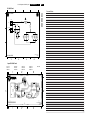
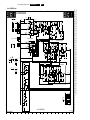
How To Connect
This is described in the chassis fault finding database in
ComPair .
TO
UART SERVICE
CONNECTOR
PC
TO
I2C SERVICE
CONNECTOR
VCR
Power
9V DC
5.5.3
I2C
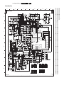
Figure 5-2 ComPair interface connection
How To Order
ComPair order codes (EU/AP/LATAM):
• Starter kit ComPair32/SearchMan32 software and
ComPair interface (excl. transformer): 3122 785 90450.
• ComPair interface (excluding transformer): 4822 727
21631.
• Starter kit ComPair32 software (registration version): 3122
785 60040.
• Starter kit SearchMan32 software: 3122 785 60050.
• ComPair32 CD (update): 3122 785 60070 (year 2002,
3122 785 60110 (year 2003).
• SearchMan32 CD (update): 3122 785 60080 (year 2002),
3122 785 60120 (year 2003), 3122 785 60130 (year 2004).
• ComPair interface cable: 3122 785 90004.
• ComPair firmware upgrade IC: 3122 785 90510.
• Transformer (non-UK): 4822 727 21632.
• Transformer UK: 4822 727 21633.
• Additional ComPair interface cable: 3139 131 03791.
Note: If you encounter any problems, contact your local
support desk.
How to clear the Error Buffer
Use one of the following methods:
• By activation of the "RESET ERROR BUFFER" command
in the SAM menu.
• With a normal RC, key in sequence "MUTE" followed by
"062599" and "OK".
• When you transmit the commands "DIAGNOSE" - "99" "OK" with ComPair (or with a DST).
• If the content of the error buffer has not changed for 50+
hours, it resets automatically.
E_06532_021.eps
180804
5.4.5
How to read the Error Buffer
5.5.4
Error Codes
In case of non-intermittent faults, clear the error buffer before
you begin the repair. This to ensure that old error codes are no
longer present. Before clearing the buffer, write down the
content, as this history can give you significant information.
If possible, check the entire contents of the error buffer. In
some situations, an error code is only the result of another error
code and not the actual cause (e.g., a fault in the protection
detection circuitry can also lead to a protection).
There are various errors:
• I2C device errors.
• I2C bus errors.
• Protection errors.
• Errors not related to an I2C device, but of importance:
– BLACK CURRENT LOOP (ERROR 28): detection of a
continuous fail of the black current stabilisation loop of
the HOP.
– FEM (ERROR 26): at start-up, after initialisation of the
PICNIC, the presence of the FALCONIC can be
checked.
– EAGLE (ERROR 27): at start-up, after initialisation of
the PICNIC, the presence of the Eagle can be
checked.
Service Modes, Error Codes, and Fault Finding
EM5.3A P/M AA
5.
EN 17
Table 5-3 Error table.
Error Device
Description
Def. item Defect. module indication
Diagram
1
M24C32
NVM, spontaneous blinking error 1
7011
Control
B5a
2
Hfail Protection
Horizontal Flyback protection
/
Horizontal Flyback
/
3
SAA4978
PICNIC
7713
Feature Box
B3a
4
Supply 5V
5V protection
/
+5V Supply
B5a
5
Supply 8V
8V protection
/
+8V Supply
B5a
6
Slow I2C bus blocked
Spontaneous blinking error 6
/
Slow I2C Blocked
/
7
TDA9330
HOP High-end Output Processor
7301
Video Controller
B4
8
TDA932x
HIP High-end Input Processor
7323
Chroma IF IO
B2
12
TDA9178
Topic
7302
Video Controller
B4
13
UV1318/...
Tuner protection
1T01
Tuner
A8
14
MSPxxxx
ITT sound processor
7651
Audio module
B6a
16
FBX
Feature Box Protection
/
+3V (Fbx) Supply
B3
18
Fast I2C bus blocked
Spontaneous blinking error 18
/
Fast I2C Blocked
/
19
TDA8444
Auto Scavem DAC
7500
Auto Scavem
SC1
26
SAA4998
FEM
7760
+3V (Fbx) Supply
B3b
27
T6TX5EF
Eagle
7720
+3V (Fbx) Supply
B3c
28
Black current loop
Black current loop
/
Video Controller
/
32
M29W400BT
Flash Ram (EPG)
7012
EPG Memory
B5a
35
T6TU5XB
Columbus
7752
Video Controller
B3d
•
Note:
Error codes 1, 6, or 18 are protection codes and in this case,
supplies of some circuits will be switched "OFF". Also, in
protection, the LED will blink the number of times equivalent to
the most recent error code.
•
5.6
The Blinking LED Procedure
5.6.1
Introduction
Via this procedure, you can make the contents of the error
buffer visible via the front LED. This is especially useful for fault
finding, when there is no picture.
When the SDM is entered, the front LED will show (blink) the
contents of the error-buffer. Error-codes = 10 are shown as
follows:
• A long blink of 750 ms (which is an indication of the decimal
digit),
• A pause of 1.5 s,
• "n" short blinks (where "n" = 1 - 9),
• When all the error-codes are displayed, the sequence
finishes with a LED blink of 3 s,
• The sequence starts again.
Example: Error 12 9 6 0 0.
After activation of the SDM, the red front LED will show:
• 1 long blink of 750 ms (which is an indication of the decimal
digit) followed by a pause of 1.5 s,
• 2 short blinks followed by a pause of 3 s,
• 9 short blinks followed by a pause of 3 s,
• 6 short blinks followed by a pause of 3 s,
• 1 long blink of 3 s to finish the sequence,
• The sequence starts again.
Note: If errors 1, 6 or 18 occur, the LED always gives the last
occurred error even if the set is NOT in service mode.
5.6.2
How to Enter
Use one of the following methods:
• Enter the SDM (only via soldering pads marked "SDM" on
SSB). The blinking red front LED will show the entire
contents of the error buffer (this works in "normal
operation" mode and in "protection" mode).
• Transmit the commands "MUTE" - "062500" - "OK" with a
normal RC. The complete error buffer is shown. Take
notice that it takes some seconds before the blinking led
LED starts.
Transmit the commands "MUTE" - "06250x" - "OK" with a
normal RC (where "x" is a number between 1 and 5). When
x= 1 the last detected error is shown, x= 2 the second last
error, etc.... Take notice that it takes some seconds before
the blinking led LED starts.
"DIAGNOSE X" with the DST (where "x" is a number
between 1 and 5). When x= 1 the last detected error is
shown, x= 2 the second last error, etc.... When x = 0 all
errors are shown.
5.7
Protections
5.7.1
Introduction
This chassis has only one microprocessor (OTC), which
remains active during Standby. This because power of the
microprocessor and the attached memory chip set is coming
from the 3V3 supply, which is derived from the 5V Standbycircuitry. Therefore, in both Power-on as in Standby mode, the
microprocessor is connected to this power supply.
If a fault situation is detected, an error code will be generated
and if necessary, the set is put in protection mode. The
protection mode is indicated by the blinking of the front LED at
a frequency of 3 Hz (or by a coded blinking in special cases).
In some error cases however, the microprocessor does not put
the set in the protection mode (this is the case with the hardware - loudspeaker protection of the audio amplifier).
The content of the error buffer can be read via the service menu
(SAM), the blinking LED procedure or via DST/ComPair.
To get a quick diagnosis, this chassis has three service-modes
implemented:
• The Customer Service Mode (CSM).
• The Service Default Mode (SDM). Start-up of the set in a
predefined way.
• The Service Alignment Mode (SAM). In this mode, items
of the set can be adjusted via a menu.
You can enter both SDM and SAM modes via the 'service pads'
on the SSB, via an RC-transmitter (DST or standard RC), or via
ComPair. It is not possible to enter the SAM in "standby"; the
TV has to be in "normal operation" mode.
The "Protection Diagram" shows the structure of the protection
system. See diagram below.
EN 18
5.
Service Modes, Error Codes, and Fault Finding
EM5.3A P/M AA
of the inputs of the HOP, the relevant error bit in the HOP
register is set to "high". If this error bit is still "high" after 1 s, the
OTC will store the error code in the error buffer of the NVM and,
depending on the relevancy of the error bit, the set will either
go into the protection mode or not.
7301
EHT-info
XPR (43)
HOP
The following protections are implemented:
• HFB (Horizontal Flyback): If the horizontal flyback is not
present, this is detected via the HOP (HFB_XRAY_PROT). One status bit is set to "high". The error code
is stored in the error buffer and the set will go into the
protection mode.
• XPR (X-ray protection): If the HFB pulses are too low
(level detection), the HOP will detect this via the XPR-bit.
The error will be logged in the error buffer and the set will
go into protection mode.
FLS (5)
Flash detect
HFB
HFB-XRAY-PROT
I2C
7001
I2C PROTECTIONS
HIP
+8V_CON
+8V SENSE (105)
HOP
PICNIC
+5V_CON
Note: Both errors will be logged as HFB-failure.
+5V SENSE (106)
TUNER
NVM
DNR
OTC
MSP
5.7.5
Hardware Related Protections
TOPIC
FBX
PROTECTION
PICNIC 3V3
I2C
I2C
CL 16532044_024.eps
090501
Figure 5-3 Protection diagram
There are several types of protections:
• I2C related protections.
• OTC related protections (via polling on I/O pins or via
algorithms).
• HOP related protections (mainly for deflection items).
• Hardware errors that are not sensed by the OTC (e.g.
vertical flyback protection, bridge coil protection, E/W
protection, arcing protection).
All protections are explained below.
5.7.2
I2C Related Protections
In normal operation, some registers of the I2C controlled ICs are
refreshed every 200 ms. During this sequence, the I2C busses
and the I2C ICs are checked.
An I2C protection will take place if the SDA and SCL lines are
short-circuited to ground, or to each other. An I2C error will also
occur, if the power supply of the IC is missing (e.g. FBX_PROT
(error 16)).
5.7.3
OTC Related Protections
If a protection is detected at an OTC input, the OTC will start to
scan all protection inputs every 200 ms for 5 times. If the
protection on one of the inputs is still active after 1 s, the
microprocessor will put the set in the protection mode.
Before the scanning is started, a so-called "ESD refresh" is
carried out. This is done, because the interrupt on one of the
inputs is possibly caused either by a flash or by ESD. As a flash
or ESD can influence IC settings, the HIP, MSP, 3D Comb (US
only) and wireless module are initialised again, to ensure the
normal picture and sound conditions of the set.
8 V and 5 V protection: The microprocessor senses the
presence of the 8 V and 5 V (via the "+5V_CON" and
"+8V_CON" lines). If one (or both) of these voltages is (are) not
present, an error code is stored in the error buffer of the NVM,
and the set is put in the protection mode.
5.7.4
HOP Related Protections
Every 200 ms, the status register of the HOP is read by the
OTC (via the I2C bus). If a protection signal is detected on one
Due to the architecture ("hot" deflection), some protections
cannot be sensed by the microprocessor. Three of these
protections will lead to a protection on set level (Standby mode
and blinking LED), while another will only lead to a circuit
protection.
TV-set Protection
The following fault conditions will lead to a "complete" set
protection:
• BRIDGECOIL protection: This is sensed via the "EW"
signal going to the base of TS7652 (via R3495 and D6499).
In a normal situation, the voltage on C2498 (diagram A4) is
high and TS7652 is conducting. When bridge coil 5422
(diagram A3) is short circuited, the voltage on C2498
changes to low, which will block TS7652. In this case, also
TS7641 will block and the voltage on 2642 will rise until
TS7443 is forced in conduction. The "SUP-ENABLE"
signal (in normal operating condition -20 V) is shorted now
to ground level, which will force the Main Power Supply to
Standby mode.
• ARC protection: If there are "open" connections (e.g. bad
solder joints) in the high-energy deflection circuitry, this can
lead to damaging effects (read: fire). For that reason, the E/
W current is sensed (via 3479//3480). If this current
becomes too high, the "thyristor" circuit (TS7653 and
TS7654) is triggered. TS7442 is switched "on" and TS7443
is forced into conduction. . The "SUP-ENABLE" signal is
shorted now to ground level, which will force the Main
Power Supply to Standby mode.
• NON_VFB (No vertical Flyback) protection: If the frame
stage generates no pulses, TS7641 will block. TS7443 is
now switched "on", which will lead to Standby mode.
Therefore, in normal operation condition, TS7641 and
TS7652 are conducting, while TS7443 is blocked.
Circuit Protection
The following fault condition will lead to a "partly" set protection:
• PROT1 (DC) protection: When a DC-voltage (positive or
negative) is sensed on one of the loudspeaker outputs, the
protection circuit (TS7704, 7705, 7706 and 7707 in
diagram A6) will put the IC7700 in Standby mode (via tristate input pin 6). For more details, see chapter "Circuit
Descriptions".
Service Modes, Error Codes, and Fault Finding
5.8
Repair tips
5.8.1
Miscellaneous
5.
EN 19
5. The OTC will un-blank the picture.
6. When you switch "off" the set, this is done in a controlled
way via the POR signal [3].
The relay you hear when you switch the set "on" (from Standby
or via the mains switch), is from the degaussing circuitry. It is
not used for switching the Power Supply (as done in the MGchassis).
Note: Standby is not directly achieved via the Standby line of
the microprocessor, but indirectly via the HOP circuitry.
5.8.3
Do not try to measure on the SSB side, which is facing the 'hot'
heatsink. This is dangerous. Most service test points are
guided to the 'tuner' side and are indicated by the 'service'
printing.
Where the circuitry was too "crowded" for service printing, you
can find the correct location on the "test point overviews" in this
manual.
A very large part of the LSP is "hot", such as:
• The primary part of the Standby Supply.
• The whole Main supply (except for the secondary Audio
supply).
• And the complete deflection circuitry (so notice that the
deflection coil is hot!).
When you use ComPair, you have the possibility to activate a
"stepwise start-up" mode. With this mode, you can initiate the
start-up sequence step by step. This also means that in certain
steps, some protections are not activated. This is sometimes
very convenient during repair.
5.8.4
The "ARC"- and/or "BRIDGECOIL" protection are hardly ever
triggered, however:
• When you suspect the "ARC" protection, look for bad
solder joints and smell. By interrupting resistor 3497, this
protection is disabled (special attention needed!).
• When you suspect the "BRIDGECOIL" protection, which
can also be due to a too wide picture amplitude, shorten G
and S of the E/W MOSFET 7480. This will disable the
protection. You will now have minimal horizontal amplitude.
Re-align the horizontal amplitude in the SAM menu and
remove the G/S short of TS7480.
HOT
EHT-INFO
8V
5 START/STOP
17/39
I2C BUS
Protections
Activating SDM via the "service pads" will overrule the
processor-controlled protections, but not the hardware
protections. This means, that the A/D-input protections (5 and
8 V) and the I2C "not-acknowledging" info of the feature box
(FBX) and of the Tuner are overruled.
Caution: When doing this, the service technician must know
what he is doing, as it could lead to damaging the set.
Start-up Sequence
COLD
ComPair
This chassis does not have an IR transmitting LED (as in MGsets). Therefore, a "Service" (ComPair) connector is
implemented at the rear side of the set, which is directly
accessible (as in A10-, EM2E-, EM3E and EM5E-sets). In
addition to this, there is also a blinking LED procedure to show
the contents of the error buffer.
Take care not to touch the "hot" heatsink while disconnecting
the SSB, despite the fact that the mains cord is out of the mains
socket. There can still be an annoying rest-voltage on the
heatsink for a short while. This, because the discharge
resistors 3502 and 3503 (on the LSP between hot and cold
part) are not stuffed for Europe. Instead, discharge resistors
3066 and 3057 on the Mains Switch panel are used, but
because they are located before the Mains switch, they only
discharge when this switch is "on".
Advice: when you remove the SSB, disconnect the Mains
cord, but keep the Mains Switch "on".
5.8.2
EM5.3A P/M AA
OUT
HOP
1
29 START/STOP
RESET
5.8.5
CUTOFF
(from
CRT panel)
5VCON
8VCON
106
The simplest way is, to replace the components of the Main
Supply with repair kit 3122 785 90310.
105
OTC
7141
5V
99
POR
Main Supply
2
220 VAC
104
8V
STANDBY
low 7131/41 closed
high 7131/41 open
7131
STBY
SUPPLY
3
MAIN
SUPPLY
SUP-ENABLE
Vbat
+11D
POR
7445
LINE DEFL.
(BRIDGECOIL
-PROT)
(ARC-PROT)
PROTSENSING
FRAME
DEFL
(NON-VFB)
CL16532044_023.eps
140501
Figure 5-4 Start-up circuitry
The start up sequence differs from other sets (e.g. MG-sets or
EM2E-sets, but is same as in EM3E-set):
1. When the set is switched "on", the 5 and 8 V lines
("+5V_CON" and "+8V_CON") of the standby power
supply are activated.
2. After the OTC senses them, the P will address the HOP via
the I2C-bus, to start the drive [1].
3. Via the "SUP-ENABLE" signal, the Main Supply is switched
"on" and will deliver the V_BAT to the Line deflection stage
[2].
4. EHT generation is now started.
More detailed way:
1. Replace FET 7504 and zener 6505.
2. Remove the SSB panel.
3. Short B and E of TS7529, in order to put the Main Supply
in "on"-mode (TS7529 is blocking then).
Caution: To prevent that R3403 and TS7443 will be
damaged, first disable the HW-protection of the
deflection circuit. Therefore short circuit C2642 on the
LSP (diagram A4).
4. Attach a load of 500 O to V_BAT capacitor C2515 (the
supply can not work without a minimum load).
5. Use a variac, and slowly increase the V_MAINS. Measure
over sensing resistors R3514//15, if a nice sawtooth
voltage becomes available.
6. Also measure the V_BAT. This may never exceed +141 V.
If it does, there is something wrong in the feedback circuitry
(e.g. regulator 7506).
Note: Be careful when measuring on the gate of FET TS7504.
This circuitry is very high ohmic and can easily be damaged
(first connect ground to measuring equipment, than measure
the gate).
EN 20
5.8.6
5.
EM5.3A P/M AA
Service Modes, Error Codes, and Fault Finding
Standby Supply
The simplest way is to replace the components of the Standby
Supply with repair kit 3122 785 90460.
5.8.7
Line Deflection
The simplest way is to replace the components of the Line
Deflection circuitry with repair kit 3122 785 90330.
5.8.8
Frame Deflection
To prevent this from happening, you must:
1. Interrupt the resistors 3403 and 3404 on the CRT panel
(diagram F1), in order to remove the "filament" voltage
from the tube (no beam current, so no chance of destroying
the CRT).
2. Interrupt resistor 3403 on the LSP (diagram A4) to disable
the "SUP-ENABLE" line.
3. Measure with a multi-meter, or better with a oscilloscope,
the functionality of the Frame stage.
4. After you have found the cause, exchange the defective
component (e.g. TDA8177), and re-solder the interrupted
resistors.
Caution: When the Frame Deflection circuitry is suspected,
one must be careful. Because there is a DC-voltage on the
frame deflection, the beam current could damage the CRT
neck, leading to a defective CRT.
Table 5-4 Repair Tips
Phenomenon
Possible Cause
Repair tip
No picture, no LED.
Standby Supply defective.
Measure circuitry (see diagram A2). Start at test-point A19.
When the Mains switch is 'on', this voltage must always be available
No picture, no LED.
Bad connection of SSB in SIMMconnector.
In case of a bad connection, it can happen that there is no picture, and that the Standby LED is not
controllable. Re-place the SSB.
No picture, LED blinking at 3 Hz. Set is in protection due to various
causes. For error codes see errorcode list.
You have no picture, so:
- Read the error buffer via ComPair (error buffer is accessible when set is in protection, comparefile will guide you to this)
- Read the blinking LED information via standard remote command <mute>06250X<ok>
- Or you read the error code sequence via standard remote command <mute>062500<ok>.
When you have found the error, check the circuitry related to the supply voltage and I2Ccommunication or the circuitry that triggers the protection.
No picture, LED blinking with
code 6-6-6 or 18-18-18.
No communication on slow I2C- or
fast I2C-bus.
As processor cannot communicate with one of the 2 busses it the standby-led spontaneously starts
blinking 6-6-6... or 18-18-18... If in the error buffer somewhere is an error 6 or 18, these will have
the highest priority starting the mentioned blinking. Measure dependent of the error on the I2C-bus
which device is loading the bus. (Use I2C -overview)
No picture, LED blinking with
code 1-1-1.
No communication on NVM- I2C bus As the uP cannot communicate with the NVM I2C bus, it spontaneously starts blinking 1-1-1. Note:
to the uP.
when there is no access to the NVM, a lot of picture setting can go wrong.
No picture, no sound. Set is
Supply is possibly in hiccup-mode,
making audible squeaking sound which is audible via a squeaking
supply transformer.
Possible causes:
- VBAT is shorted (caused by short circuited line transistor 7421), or
- Sound winding is shorted (amplifier is shortening the power supply lines), or
- D6514 is shorted (due to a too high VBAT).
Remove excessive load, to see what causes the failure, or check feedback circuit. See repair tip
'Main Power Supply' (supply needs a minimal load).
No picture, no sound. Power LED Supply does not work correctly.
works fine
If e.g. VBAT is only about 90 V, it is possible that the regulator IC (7506) is defective.
No RC-reception. LED does not
echo RC-commands.
uP circuitry or RC-receiver is
defective.
In case the set does react on a local keyboard operation, you must check the RC-receiver circuitry.
Relay (degaussing) is not
audible, when set is switched
from 'off' or 'standby' to 'on'.
uP is not working correctly.When pin Check RESET-circuitry on diagram B5. Check the level on pin 115 when you switch the set 'on'.
115 is low, the degaussing must be Signal must be low initially and go to high after approx. 12 s.
activated.
Picture is rotated.
Rotation circuitry on diagram A5, or Measure test points on diagram A5.
related supply to it, malfunctions.
Picture is continuously switching
'off' and 'on', showing heavy
'switch' spots (set does not go
into protection).
200 V is missing on CRT panel.
Probably a bad connection from LSP connector 1424 to CRT connector 1424 (diagram F), or an
interruption of the 200 V supply line (e.g. R3341 on circuit F is interrupted).
Picture is not sharp.
Focus is possibly mis-aligned or
SCAVEM-circuitry does not work
correctly.
Re-align the 'focus' potmeter on the Line Output Transformer, or check the SCAVEM circuitry on
the CRT-panel (diagram F). It is also possible that the DAF circuitry is defective (see diagram I).
Check the Vdc values.
Picture is not synchronised.
The sync is derived in the HIP from Maybe the crystals 1305 and/or 1308 are making a bad contact.
x-tal 1305 and/or 1308.
Picture is distorted.
Check video-path in Service Default Investigate whether there is an error code present in the error buffer. In case there is one, check
Mode.
the I2C -bus and/or supply lines (see overview supply lines).
Measure and check signal path Tuner-HIP-PICNIC-HOP-RGB amplifier.In case it is a geometry
issue, check on diagram A4 opto-coupler 7482, Opamps 7440/7450 and the Frame circuitry
alignments or a possible corrupted NVM (7011) on diagram B5.
No menu, no OSD.
Probably a defective uP.
Measure test points B61to B64 on diagram B5.
How to measure if soldering
connections of a BGA are OK
For most BGA's the pins/balls are ESD protected via diodes to ground, it is possible to measure
these diodes with a multi-meter. Overload means no or bad connection.
How to measure on other IC's
It is advisable to measure both on the pins itself and the solder pads on the PWB. This to find
possible solder faults.
Block Diagrams, Testpoint Overviews, and Waveforms
EM5.3A P/M AA
6.
EN 21
6. Block Diagrams, Testpoint Overviews, and Waveforms
Wiring Diagram
CENTRE
SPEAKER
TOP CONTROL PANEL
3P
DEGAUSSING COIL
BLACK/
WHITE
BLACK
0346
TWEETER
CRT
AQUADAG
(COMPONENT VIEW)
EHT
CRT
CRT PANEL
1424
FRAME
ROTATION
COIL
8483
2P
1483
3P
A (LOT)
TWEETER
7P
F
RED
BLACK
3P
SCAVEM
COIL
1435
CRT
SOCKET
1434
1P
BROWN
BROWN
8000
P
LEFT
SPEAKER
CRT PANEL
BLUE
BLUE
1940
11P
RIGHT
SPEAKER
O
1620
3P
SIDE
I/O PANEL
1146
5P
MAINS SWITCH PANEL
5205
MAINS
SWITCH
8946
1328
SVHS
E
LSP(LARGE SIGNAL PANEL)
A
N.C.
5203
CVBS (YELLOW)
5P
1326
RIGHT (RED)
1502
8202
0202
2P
0241
0201
2P
9P
3P
8190
6
1946
9P
HEADPHONE
N.C.
193
11P
1327
2P
1505
1947
2P
LEFT (WHITE)
MAINS
CORD
1945
(optional)
3P
1440
8346
8440
11P
G
1735
PANEL
1940
80P
1953
2P
1417
1491
8417
LOT
1693
1935
1499
2P
I
11P
(SMALL SIGNAL BOARD)
1738
5P
SSB
1737
8418
3P
SSB
8937
B
8940
HORIZONTAL
DAF PANEL
1417
2P
1424
7P
8424
1418
2P
4P
2P
1933
1104
5P
1304
7P
8304
1304
7P
1497
1P
1491
2P
1498
1625
1492
3P
3P
1943
3P
compair
interface
1492
3P
8492
8625
8680
4P
0207
F
3P
0236
DW PANEL
(OPTIONAL)
TUNER
5P
0200
0201
10P
1680
6P
1419
8498
TUNER
N
80P
1955
1000
3P
3P
1948
HD-JACK PANEL
1936
1937
11P
6P
1680
10P
3P
1681
1940
11P
0317
1205
3P
1951
8951
3P
8955
SUB
WOOFER
2P
8936
8338
1955
3P
8737
2P
5P
SC
4P
2P
AUTO
SCAVEM
DC SHIFT
(OPTIONAL)
E_14600_061.eps
161204
Block Diagrams, Testpoint Overviews, and Waveforms
EM5.3A P/M AA
6.
EN 22
Block Diagram Supply and Deflection
E
DEFLECTION
MAINS SWITCH
PANEL
A1
MAIN SUPPLY
A3
LINE DEFLECTION
DCSHIFT
CIRCUIT
3550
8+ 1
2
0201
2
3
1
1
4
220V
0202
2
0202
2
T5A
1
1
2
1501
V
RS
3
3
2
1502
2
5515
MAINS
FILTER
1
1550
4
6408
+5.2V
3416
A24
7409
4-
+
3
1
A17
2.5A
+
2516
5100
5101
+375V
5109
5
6
3
7
7102
STP3NB60
A11
G
D
A8
8
1
10
CONTROL
CIRCUIT
A12
5113
+8V6-SWITCH
7131
S A20
D
FRAME DEFLECTION
E/W DRIVE
1693
B4
5103
7133
7130
7103 OR 1
7104
-20V
-20V
4
+5V-SWITCH
7141
D
6122
3124
2
7450-B
7
+8V-S
+5V
S A21
7482
CONTROL
MAIN SUPPLY
5
CONTROL
CIRCUIT
A3
3514
3
4
6
4
7
3
8
9
10 6536
1
A4
7507
TCET1103
5507
HOT
COLD
6535
A7
5514
STANDBY
B4
OTC
HOP
HOP
+
2511
GND-AUD
+
2543
-16V-19V
B4
A8
2
3506
1
3
7506
TL431CZP 2
7440-A
1
3
A33
2
POR
3
2
7450-A
1
HOT COLD
COLD
HOT
6499
B4
HOP
7445
A6
AUDIO
EW
3463
B5
OTC
COLD
HOT
6463
A31
+13V - LOT
5463
+8Vb
6462
3462
2462
5621
1
6
5
10
7614
6465
3465
A32
-15V - LOT
+13V-LOT
5465
7641
7443
7652
6464
3464
2464
3635
A50
A36
A35
+8V-S
PROTECTION
CIRCUIT
HOP
FRAMEDRIVE -
SUP-ENABLE
1
3636
7613
TL431
3657
3449
3627
1495
1
2
3637
COLD
HOT
+13V LOT
3
2
-15V_LOT
6627 6626 6625
VBATT
ADJUSTMENT
3530
3498
3499
3
A49
+11D
6620
-12V8
4
+8Vb
TV
3640
3631
3642
3643
3527
GND-STB
SUP-ENABLE
3638 7620
TDA8177
3630
3632
7612
3634
2
6
HOT
A42
6619
+11V_ROT
125mA
FLYBACK
GENERATOR
THERMAL
PROTECTION
A40
4
A39
-15V-LOT
3623
A43 3647
5
OP. AMP
COLD
1601
3
7
1
GND-STB
ROTATING CIRCUITRY
6622
3660
2515
3526
GND-SUP
2622
+
A6
+VBATT
3510
A5
+13V-LOT
+8V6
3507
3531
HOT GROUND
3461
POR
6491
EW
PROTECTION
CIRCUIT
3641
A34
3658
7611
7529
A29
1
A5
ACTIVATING
CIRCUIT
6460
+11D
4
3480
A30
5461
3460
12
POR
FLASH
AUDIO SUPPLY
3520
A8
6
FRAME DEFLECTION
3459
CRT
FILAMENT
3
7442, 7654
7653
B4
+16V+19V
+ AUDIO SUPPLY
2542
5513
3479
2457
HFB_X-RAY-PROT
B5
F
5
EHT-INFO
3483
7455
4
7
11V
2443
9
7487
3404
+8V6
TO
1224
TUNER, SIM
A45 7486
2
3419 7441
+
2512
5509
5
4
FRAMEDRIVE +
5506
3484
7440-B
7
6
3456
7132
7504
7502
STP5NB60FP
7530
D
G
S
A2
3
A28
6400
6480
5467
7480
3488
STP3NB60 A47
D
A46
G
S
A48
3481
3493
1
A38
3400
11
CURRENT
SOURCE
3457
2403
7140
-20V
2
EHT-INFO
3455
G
A16
1424
1
HFB_X-RAY-PROT.
3451
3454
+141V
3492
6615
+8Vb
5
3114
1
6
8
I
A37
+8V6
6103
2102
-20V
5
6
+5.2V_MP
3113
3
FILAMENT
+11D
3450
E/W - DRIVE
+5.2V
A13
5102
3431
10
A19
CONTROL
6111
1491
2
+11D
2431
DAF
6456
EW-DRIVE 1
HOP
5517
5
2430
5421
TO 1693
3654
+8V6
2126
G
3118
A15
1
EW
CORR.
VER. DAF
CIRCUIT
1492
CRT
COLD HOT
A4
5107
3108
+11D
EW
+11V
5111 6130 5130
S
GND-STB
7408
1
VG2
+
3116
3161
2
A23
3404
+11V_STBY
2118 A18
5104
6
6113
5112
A10
7100
7101
7105
7120
1
FOCUS B
HOR. DAF
CIRCUIT
E/W
DRIVE
TO
F1
LINE
OUTPUT
CIRCUIT
HOP
VTUN
STARTUP
A1
1503
9
ARC-PROT
6109
6525
GBU4K 2
A22
LINEDRIVE 1 2492 3406 3414
+
4
TO
FOCUS A
5410
6407
B4
A25
HOT
1693
A4
1
SUP-ENABLE
OTC
3415
7421 A26
BU2520DX
EHT
LINE
DEFLECTION
COIL
COLD
1497
5
+11D
3115
2
1
DYNAMIC FOCUS
LOT
5426
+5.2V_MP
DEGAUSSING B5
6110
2
5800
COLD
STAND-BY SUPPLY
1
5430
HOT
COLD
1418
1
5401
DEG.
COIL
HOT
ACTIVATING
CIRCUIT
V-START
2
3537
1
DAF
I
1417
5400
+VBATT
7501
7528
A2
2
+141V
3509
MAINS
SWITCH
400 mA
1419
1
RP
0+
1031
or
1051
5502 5511
5503 5516
5504
1430
317
or
318
1
DC-SHIFT (OPTIONAL)
G
FILAMENT
PULSES
SUPPLY
5620
A44
3620
7680
TDA7052
1625
1
2
TILT
B5
3
VERT.
DEFL.
COIL
OTC
3686
1
+Vp
5
1620
1
8
3
2
3
7681
7682
SWITCH OFF
CIRCUIT
IN STAND-BY
2
3684
3685
ROTATION
DEFLECTION
COIL
6
6080
E_14600_062.eps
161204
TO
PANEL
ON
CRT
NECK
Block Diagrams, Testpoint Overviews, and Waveforms
EM5.3A P/M AA
6.
EN 23
Testpoint Overview LSP and CRT Panel
LSP COPPER TRACK SIDE
1
2
3
4
5
6
7
8
9
10
S
A20
A
1
4
5
S
A19
G
A68
A21
A70
D 7141
+5V
A7
A57
8
5
7680
ROTATION
B
A
TUNER
D 7131
+8V6
A18
A69
G
A8
A59
6 MAINS 10
TRAFO
A17
6
A15
A16
C
10
5
STANDBY
5 TRAFO 1
7700
AUDIO
L+R
1
1
A56
A58
A64
A33
A4
A5
7702
AUDIO
C+SUB
A11
D
D
A13
A66
A6
A10
1
S
A14
25
A63
A2
A35
A38
A37
A34
A36
A60
A22
D
A24
A3
G 7504
MAIN
SUPPLY
G 7102
STANDBY
SUPPLY
C
A49
A23
A68
S
A61
A62
A12
D
B
A67
5506
5100
1
SIM CON.
80
25
A26
A45
D
A25
B
C
A50
A39
E
A31
E
A46
A1
G
S
7480
E/W
A42
A41
7421
LINE
A48
A47
A32
E
A40
1
A44
56
4
3
2
1
LOT
A71
F
7620
FRAME
8
9
10
11
12
A43
F
A29
A30
MAIN
SWITCH
G
G
A28
COLD HOT
HOT
1
A1
PM3394B
2
A2
PM3394B
3
A3
PM3394B
4
A4
PM3394B
5
A5
PM3394B
6
A6
PM3394B
COLD
7
A10
PM3394B
8
A11
PM3394B
9
A12
PM3394B
A1
A3
A4
A5
A6
A7
A8
A10
A11
A12
A13
A14
A15
A16
A17
A18
A19
A20
A21
A22
A23
A24
A25
A26
A28
A29
A30
A31
A32
A33
A34
A35
A36
A37
A38
A39
A40
A41
A42
A43
A44
A45
A46
A47
A48
A49
A50
A56
A57
E4
D4
C4
C4
C5
A4
B4
C2
C2
D3
D1
D1
C1
C1
B1
A1
A3
A2
A3
D8
D8
D8
D8
D7
G9
G10
G10
E9
E9
C8
D9
C9
D10
D9
C9
D10
E10
E10
E10
F10
E10
D7
E6
E7
E7
C9
D9
C6
B6
A58
A59
A60
A61
A62
A63
A64
A66
A67
A70
A71
A88
PM3394B
1940
1
11
7340
8
9
8
F4
11
6
12
F8
PM3394B
8
F6
1424
1
F7
T
CR ET
CK
SO
7
F15
AUTO SCAVEM PANEL
(COPPER TRACK SIDE)
SC10
7042
B
C
E
SC10
1 V / div DC
10µs / div
SC23
SC24
2 V / div DC
100µs / div
2 V / div DC
100µs / div
16
A14
7330
10
7
5
7350
8
F5
F9
10
A13
CRT PANEL (COPPER TRACK SIDE)
C6
B5
D7
C8
D7
D7
C7
C7
C7
A10
F1
A9
A15
A17
A16
9
PM3394B
7500
50V / div DC
2us / div
A18
PM3394B
50V / div DC
5us / div
A19
PM3394B
50V / div DC
5us / div
A22
PM3394B
50V / div DC
5us / div
A23
PM3394B
5V / div DC
10us / div
A24
PM3394B
1 3 4
20V / div DC
10us / div
A25
PM3394B
50V / div DC
5us / div
A33
PM3394B
5V / div DC
5us / div
A34
PM3394B
2V / div DC
5us / div
A35
PM3394B
5V / div DC
10us / div
A36
PM3394B
200mV / div DC
10us / div
A37
PM3394B
500mV / div DC
5ms / div
A38
PM3394B
5V / div DC
5ms / div
20V / div DC
5us / div
A39
A40
PM3394B
SC23
8
SC24
PM3394B
7026
B
C
E
SC8
5V / div DC
5us / div
A41
PM3394B
1V / div DC
5us / div
A42
PM3394B
1V / div DC
10us / div
A43
PM3394B
200mV / div DC
10us / div
A44
PM3394B
5V / div DC
10us / div
A45
PM3394B
2V / div DC
10us / div
A46
PM3394B
500mV / div DC
2ms / div
500mV / div DC
2ms / div
500mV / div DC
2ms / div
A47
A48
A56
PM3394B
PM3394B
200mV / div DC
10us / div
A57
PM3394B
500mV / div DC
2ms / div
A58
200mV / div DC
10us / div
A59
PM3394B
2V / div DC
10us / div
A68
PM3394B
200mV / div DC
2ms / div
A69
E
B
SC7
7022
PM3394B
C
C
7012
7006
B
200mV / div DC
2ms / div
20V / div DC
2ms / div
10V / div DC
2ms / div
200mV / div DC
2ms / div
1V / div DC
10µs / div
500mV / div DC
10µs / div
50V / div DC
10µs / div
500mV / div DC
10µs / div
200mV / div DC
2ms / div
20V / div AC
2us / div
200mV / div DC
2ms / div
10V / div DC
2us / div
200mV / div DC
5us / div
C
2V / div DC
50us / div
SC6
B
E
SC4
E
7008
A70
PM3394B
F4
F5
F6
F7
F8
F9
F15
SC3
SC4
SC5
SC6
SC7
SC8
B
1940
11 9
1
C
SC5
E
SC3
2V / div DC
50us / div
50V / div DC
10µs / div
50V / div DC
10µs / div
50V / div DC
10µs / div
50V / div DC
10µs / div
50V / div DC
10µs / div
50V / div DC
10µs / div
10 V / div DC
10µs / div
1 V / div DC
10µs / div
2 V / div DC
10µs / div
2 V / div DC
10µs / div
2 V / div DC
10µs / div
2 V / div DC
10µs / div
2 V / div DC
10µs / div
E_14600_052.eps
131204
Block Diagrams, Testpoint Overviews, and Waveforms
EM5.3A P/M AA
6.
EN 24
Block Diagram Video
VIDEO
AUDIO
DEMODULATOR
B6
IF,IO
VIDEOPOCESSING
7402
AUDIO
DEMODULATOR
B3A
B4
HOP
OTC
CVBS-TER-OUT
7736
1411
SEE
BLOCK DIAGRAM
AUDIO
SYNC
SEPAR.
7410
10
CVBS-SC1-AV1-IN
16
Y_CVBS-SC2_AV2-IN
6
7
Y-CVBS-SC2-AV2-IN
C-SC2-SVHS-IN
20
21
63
64
Y-CVBS-FRONT-IN
C-FRONT-IN
23
24
H-SYNC
PROC.
60
3730
VA50
CVBS-SC2-MON-OUT
1305
SDRAM
54
Y
U
57
RGB
MATRIX
47
46
SCL-F
R G B
SCART1
3376
36 37 38 39
SC1-R-IN_V-IN
3
2
R-SC1-IN_V-IN
SC1-B-IN_U-IN
FBL-SC1-IN
1
4
B-SC1-IN_U-IN
FBL-SC1-IN
3.57MHz
R G B
N.C.
UVB
1900
L
SC2-CVBS_MON-OUT
A8
AV2
VIDEO
OUT
C-SC2_SVHS-IN
1994
A
A8
C
AV4
VIDEO
IN
B
UVA
1
Y_CVBS-SC2_AV2-IN
7
4
3
SVHS
1 1901
2
EF
PR
21
3
YA-UVA
BUS C
9
Y
19
B
7714
MS81V04160
A8
SC1-B-IN_U-IN
A8
SC1-R_V-IN
A8
7991,7990
1990
1
R-IN
2
B-IN
3
G-IN
13
11
1
G
14
I
CVBS-SC1_AV1-IN
Pb1-in
11
EF
PB
15
7
BA
3
BN
9
GA
5
GN
11
21
R-MATRIX
R
BA
1
7
19
G-MATRIX
G
15
B-MATRIX
B
FBL_RGB
SIDE I/O
A8
FALCONIC
R-TXT
YF - UVF
4
SVHS
1328 2
3
1
5
CVBS
1326
Y
1936
2
C
4
4
7
7
1936
Y-CVBS-FRONT-IN
2
3
9
5
11
19 G-OUT
2
15 B-OUT
3
14 FBL
5
V-OUT
C-FRONT-IN
4
11
26
TO
BLOCK DIAGRAM
DEFLECTION
29
22
5
ANTI-MOIRE
ANTI-MOIRE
7310
7311
PULSE VSYNC
FORMER
530us
HFB-X-RAY-PROT
B5A
B1
DYN-FASE-COR.
7017
7018
2064
ONE
SHOT
1ms
7303
HFB
7019
7020
FLIP
FLOP
EHT-INFO
3367
B5
PWM-ANTIMOIRE
POR
7729
OUTPUT
FILTER
U_EAGLE_E
7730
YG - UVG
V_EAGLE_E
EAGLE
1C
1424
1
2
3
4
6
5
+3V3EA
27
VD_E
EAG_SD
7717
26
HD_E
+2V5ED
SC1
F2
AUTOSCAVEM
CRT AUTOSCAVEM
7500
TDA8444T
5
6
A8
1955
1
2
4
SCL-S
I/O
EXP.
5300
6x
6
H/V
SEPARATOR
5
H-770-2
EF
2
H
V-770
5
V
2
4
7108
EF
HOT
COLD
SCAVEM
PROC.
F1
1440
1
+11V
HFB_X_RAY_PROT
HFB_X_RAY_PROT
EHT-INFO
CRT PANEL
1940
1
N.C.
HFB_X-RAY_PROT
2
2
3
3
4
4
EHT-INFO
SVM
5
5
Y-SCAVEM
3
4
H-770-3
SCAVEM
COIL
SC10
B
1940
1
7105
1483
1
2
3
SC3
SCAVEM
PROC.
7500
7000-7042
G
7102
74HC4052D
+200V
+8V
3
SDA-S
LSP
7750
74HCT4538D
3
LINEDRIVE1
A4
POR_FLASH
71
SYNC SLICER
JACK-HIGH DEFINITION INTERFACE
1
28
3300
GN
H/V
SEPARATOR
9
11
Y_EAGLE_E
3x
DAC 64
A8
2
13 14
7728
1
7450-C
7700
LM1881M
29
B5B
9
21
55
7760
SAA4998H/V1
BUS A
TO 1955
TUNER
SIMCONNECTOR
31
FRAMEDRIVE-
+8V_CON
7720
T6TX5EF
R
O
EW-DRIVE
TILT
DRAM
H-OUT
GA
N3
B-CRT
CUTOFF
FBLYPbPr
BN
V-IN
21
L13
B5
7400-C
H-IN
23
FRAMEDRIVE+
EAGLE
1304
21 R-OUT
B-CRT
CUTOFF
3782
7400-B
7450-B
10
SC1-G-IN_Y-IN
7995,7994
AV3
VIDEO
IN
15
7993,7992
F
H
AV1
VIDEO
IN
A8
1
RN
8
7361
7362
B3C
BUS F
5
Y_CVBS-SC2_AV2-IN
RN
7453
5
RA
8
3320 10
BUS D
FIELD
MEMORY
1
7101
BA7657F
F18
3367
1
1301
7719
MSN56V16160F-6TS
7450-A
EF
Y1-in
1900
C
RA
STARISTOP
H-DRIVE
PH1-2
PH1-1
20
N2
7107
BA7657F
7400-A
7453
Pr1-in
C
6
AV2
VIDEO
IN
1993
A
3331 24
FRONT
END
Y2-in
7451
FRAME
12MHz
Pr2-in
7901
BA7657F
RAMP
GEN
3321 11
FALCONIC
EMBEDDED
MEMORY BUS G
Pb2-in
3
SDA-F
BUS A
B3B
CONTROL
JACK-HIGH DEFINITION INTERFACE
G-CRT
6401
6402
2
3363 23
MUX
N1
MATRIX
JACK-HIGH DEFINITION INTERFACE
F359
SCL-F
YA
TUNER
SIMM-CONNECTOR
N4
24
PROTECTION
CIRCUIT
VD
YB-UVB
656
DECOD
INPUTS/OUTPUTS
JACK-HIGH DEFINITION INTERFACE
G-CRT
4
BUS B
MUX
N2
7
F19
MUX
A11
R-CRT
V30
44
E/W
DRIVE
L12
656
ENCOD
G-SC1-IN_Y-IN
42
V29
3342
7319
B
F104
B1
41 42 43 40
25
F20
HD100
YB
1308
V
R-CRT
FBL_2FH 33
HD100
COLUMBUS
COL_SD
7309
HOP
RGB
YUV
MATRIX
NOICE
REDUCTION
28
4
7308
V28
41 3341
CATHODE
CALIBR.
30
31
32
3340
G
HD_E
MUX
MEMORY
INTERFACE
SCART2
3377
SDA-F
SC1-G-IN_Y-IN
MID END
7752
T6TU5XB
4.43MHz
32
VD100
40
Y U V
R-2FH
G-2FH
B-2FH
7304
TBC/SRC
COLUMBUS
7753
MSN56V16160F-7TS
32 (N.C.)
CVBS PIP
34
3721
7703
29
HISTOGRAM
3727
HA50
3D COMB
N.C.
A11
A11
3726
F105
OUTPUT
AMPL.
26
F332
F102
VD_E
61
2321
V100
BACK END
Y/U/V
RGB
MATRIX
27
F331
F101
26
MUX
V-SYNC
PROC.
RGB
R
INSERTION
2431
U100
OUTPUT
FILTER
PEAKING
A11
A11
2742
DECODER
PAL
NTSC
SECAM
A11
9
EF
F408
A11
CVBS-SC2-MON-OUT
3715
V-PIP+MAIN-IN
F164
B3D
C-FRONT-IN
9607
F407
CVBS-SC1-AV1-IN
U_EAGLE_E
28
F330
F100
3x
DAC
V_EAGLE_E
A11
Y-CVBS-FRONT-IN
PICNIC
3x
ADC
7734
F406
C
C PROC.
B5
25
F163
V50
V Y U V
2741
EHT-INFO
EHT_INFO
6
7
+8V6
R-CRT
9004
+8V+12V
R-DL
6
7
6
7
+8V
R-CRT
8
G-CRT
9005
G-DL
8
8
G-CRT
9
B-CRT
9006
B-DL
9
9
B-CRT
10
10
11
11
10
11
CUT_OFF
CUT-OFF
7500
7501
EF
3510
7330
TDA6118JF
7503
7504
7340
EF
3520
7506
7507
A3
2
Filament pulses
3
HFB_X-RAY_PROT
4
EHT-INFO
5
(LINE
DEFL.)
6
7
F5
8
G 3351 3339
F8
3510 3510
F7
6
11
7350
3530
VIDEO
OUTPUT
AMPLIFIER
SEE
BLOCK DIAGRAM
DEFLECTION
CRT
VIDEO
OUTPUT
AMPLIFIER
CUTOFF
1424
1
R
3350 3340
EF
FROM
1424
OF
F6
VIDEO
OUTPUT
AMPLIFIER
B
F4
N.C.
200V
F15
FG-A
U
5
QSS-AM
EF
33
3368
B5
3714
U-PIP+MAIN-IN
2
EHT-INFO
VD
SCL-S
VIDEO
SWITCH
+
CONTROL
PSS-AM
SOUND-OUTPUT
9608
U50
2323
Y100
Y_EAGLE_E
F162
7735
F405
1409
AGC
MONITOR
49
50
51
43
23
HD100
QSS
MIXER
AM
DEMO
F404
2740
HFB-X-RAY-PROT
3417
HIP
Y/U/V
SWITCH
EF
G-2FH
TUNER AGC
Y
U
V
3713
Y-PIP+MAIN-IN
R-2FH
Y
Y PROC.
62
SIF2 64
SIF1 63
9609
Y50
32
35 36 37 38
FBL_2FH
GROUP
DELAY
COR.
PLL
DEM
15
C-SC2-SVHS-IN
1940
7713
SAA4978H
3782
1410
1408
40,4
1000 1205
7301
TDA9330H
3782
VIF2
B4 B4
+8VP
29 28
B-2FH
26
7404
2
3
SAW FILTER
AUDIO
SDA-S
14
CONTROL
DA
13
AGC
3250
13
AD
VIF1
1
3200
3201
4
12
MF
11
LATCH
V1
SAW FILTER
VIDEO
5403
IF-TER
V1
SWAN
NOICE REDUCT
9
A68
A11
B5
7712
74HC573D
I6
7323
TDA9321H 10
TUNER
A11
64K
PROM
7711
M27C512
EF
VTUN
6200
7 3
5
EF
SOUND
FILTER
A2
+5VT
1200
UV1318S
7320
3032
EF
7322
2063
1406
1407
7411
FG-B
11
VG1
VG2
CVBS-TER-OUT
N.C.
TUNER
SIMM CONNECTOR
A8
B1
FROM
BLOCK
DIAGRAM
'CONROL'
B5 CVBS-TXT
FBL-TXT
B2
B1
1205 1000
B-TXT
TUNER
SIMCONNECTOR
G-TXT
A8
1434
5309
3341
5310
3301
+200A
VSVM
+8V
SIN
EHT
FROM A3
LOT
LINE
DEFL.
E_14600_063.eps
161204
Block Diagrams, Testpoint Overviews, and Waveforms
EM5.3A P/M AA
6.
EN 25
Block Diagram Video (For Dual Window Versions)
VIDEO
IF,IO
VIDEOPOCESSING
7402
B6
AUDIO
DEMODULATOR
AUDIO
DEMODULATOR
B3A
B4
HOP
B1
OTC
CVBS-TER-OUT
1406
1407
7411
EF
TUNER AGC
AGC
15
HIP
QSS
MIXER
AM
DEMO
SCL-S
SIF2 64
SIF1 63
VIDEO
SWITCH
+
CONTROL
U
SEE
BLOCK DIAGRAM
AUDIO
B5
10
4
C-FRONT-IN
CVBS-SC1-AV1-IN
EF
5
8
V
Y-CVBS-SC2-AV2-IN
C-SC2-SVHS-IN
20
21
63
64
Y-CVBS-FRONT-IN
C-FRONT-IN
23
24
N.C.
CVBS-SC2-MON-OUT
7734
8
6
9
9
3715
9
25
2742
EF
3730
VA50
61
3726
26
3727
32
TUNER
SIM CONN.
1681
1
1948
1
1937
6
3
3
5
C3
A11
A11
R-SC1-IN_V-IN
MUX
VFB
SC1-G-IN_Y-IN
SC1-B-IN_U-IN
FBL-SC1-IN
1
4
B-SC1-IN_U-IN
FBL-SC1-IN
BUS A
YA-UVA
YCVI
7807
2
2
G
3
3
R
10
7895
7824
TUNER
PANEL
+5VS
5262
7201
UV1316/A
+33V
2269
C4 IF VIDEO SYNC
1352
7 6
9
IF-TER 2351
11
F2
TUNER
+8VS
7301-A
TDA8889H
F5
1
4
2
1
F3
PLL
VIDEO
DEM
3268
3267
3
3372
7331
8
2335
B6
PAL/NTSC/SECAM
DEMODULATOT
29
7401
HEF4053BT
C-FRONT-IN
12
C-SC2-SVHS-IN
13
1935
1
3
3
Y-CVBS-SC2-AV2-IN
5
5
F10
U 45
+8VS
Y-CVBS-FRONT-IN
0200
1
7412
1
5
3
21
B-CRT
9
CUTOFF
11
EW-DRIVE
31
FRAMEDRIVE-
29
FRAMEDRIVE+
28
LINEDRIVE1
26
A4
TO
BLOCK DIAGRAM
DEFLECTION
B5B
9
21
13 14
29
22
5
12MHz
PULSE VSYNC
FORMER
530us
HFB-X-RAY-PROT
B1
ANTI-MOIRE
ANTI-MOIRE
7310
7311
7019
7020
B5A
ONE
SHOT
1ms
7303
B5
HFB
B1
DYN-FASE-COR.
7017
7018
2064
FLIP
FLOP
EHT-INFO
3367
B5
PWM-ANTIMOIRE
+8V_CON
POR
POR_FLASH
3x
DAC 64
YF - UVF
7729
OUTPUT
FILTER
U_EAGLE_E
7730
71
YG - UVG
SCL
V_EAGLE_E
EAGLE
1C
7719
MSN56V16160F-6TS
+3V3EA
27
DRAM
7805
VD_E
EAG_SD
26
SV
7717
HD_E
3829 2829 81
1424
3782
+2V5ED
1
2
3
4
5
6
72
7892-7894
SANDCASTLE
56
HORIZONTAL
OUTPUT
PULS
FORMER
3834
87
15
10
CVBS-SC1-AV1-IN
Y-CVBS-SC2-AV2-IN
23
Y_EAGLE_E
7760
SAA4998H/V1
3828 2828 79
3827
8
7728
SU
7385
7386
VCO
+
CONTROL
SYNC
SEPERATOR
C-PIP-IN
73
B-CRT
CUTOFF
TILT
HA
3854
STARISTOP
H-DRIVE
PH1-2
55
+5VS
7806
8
L13
7753
MSN56V16160F
7720
T6TX5EF
FALCONIC
EMBEDDED
MEMORY BUS G
SDA
G-CRT
7361
7362
B3C
BUS F
7832
24
7319
EAGLE
BUS A
3831 2831 83
SY
U
BASE
RGB2
F11
BAND
V INPUT V 46
DELAY
BOCMA
14
2
C-SC2-SVHS-IN
RGB
Y/U/V
MATRIX
FALCONIC
7
G-CRT
12MHz
7301-C
TDA8889H
+8VS
7411
COLUMBUS
52 49
51
1327
I/O PROCESSING
3
CVBS-SC1-AV1-IN
PULS
FORMER
SV-SYNC
0236
1
A11
F13
Y 40
Y
LUM
DELAY
2306 20
PIP-AUDIO
PLL
AUDIO
DEM
3316
2301 24
1
3
BOCMA
11
Y-CVBS-FRONT-IN
1333
16
VIDEO
AMPL.
SCL
SDA
C-FRONT-IN
AGC
3264
SOUND
TRAPS
B3B
F23
74
AGC
1
MUPPET
41 42 43
F1
C3
1953
1
4
7301-B
TDA8889H
7305
PH1-1
3320 10
BUS D
FIELD
MEMORY
1
F24
DU 3818 2866
7871
7874
7876 HA 94
BOCMA
5
7
5
70
HFBSANDCASTLE
7714
MS81V04160
F22
DV 3816 2864
12
VFB
A11
DY 3812 2867
3846 2846 100
0207
1
B
C2
SCL-F
COL_SD
2
F18
3367
1
3321 11
SDRAM
8
3811 2814
V
SC1-R_V-IN
3331 24
98
7810
FRAME
SDA-F
7801
SAB9083H
U
1933
1
SC1-G-IN_Y-IN
L12
HD100
+5VS
C3
SC1-B-IN_Y-IN
RAMP
GEN
1301
57
G-SC1-IN_Y-IN
N.C.
COLUMBUS
YB-UVB
BUS C
V29
3342
3
2
3363 23
BUS B
3839 2832
R-CRT
F19
7752
T6TU5XB
7828
25
PROTECTION
CIRCUIT
VD
B3D
Y
R-CRT
7309
4
FRONT
END
41 42 43 40
4
6401
6402
DA
36 37 38 39
3
2
EHT-INFO
F20
TBC/SRC
HFB0201
SANDCASTLE
6
3.57MHz
33
7308
44
E/W
DRIVE
1308
R G B
2
EHT-INFO
FBL_2FH 33
F359
MF
SCART1
R G B
HFB-X-RAY-PROT
V30
HOP
RGB
YUV
MATRIX
20
RGB
MATRIX
46
30
31
32
NOICE
REDUCTION
28
42
F104
1305
47
3376
B
3340
V28
41 3341
Y U V
R-2FH
G-2FH
B-2FH
HD100
7703
26
F332
7304
VD100
G
CATHODE
CALIBR.
2321
F105
OUTPUT
AMPL.
40
HD_E
54
U V
SCART2
3377
SCL-F
3721
Y/U/V
RGB
MATRIX
27
F331
F102
MID END
F408
I/O
PROCESS.
5
2431
V100
V_EAGLE_E
BACK END
29
RGB
R
INSERTION
U100
OUTPUT
FILTER
HISTOGRAM
HA50
60
32 (N.C.)
Y
U_EAGLE_E
28
F330
F100
3x
DAC
F101
4.43MHz
SC1-R-IN_V-IN
R-TXT
PICNIC
3x
ADC
F163
VD_E
CVBS PIP
34
SDA-F
A11
2741
EF
MUX
A11
A11
3714
8
2323
Y100
Y_EAGLE_E
F164
16
6
7
9
14
DV
A11
CVBS-SC2-MON-OUT
U
23
F162
F407
A11
Y-CVBS-FRONT-IN
EF
3809
4
A8
C-SC2-SVHS-IN
EF
7735
DU 11
A11
Y_CVBS-SC2_AV2-IN
3807
3
43
2740
PEAKING
H-SYNC
PROC.
CVBS-SC1-AV1-IN
3713
7809
V50
V-SYNC
PROC.
SYNC
SEPAR.
7410
7736
1682
6
DECODER
PAL
NTSC
SECAM
C
C PROC.
5
QSS-AM
1411
3
U50
V Y U V
0205
6
7808
F406
1409
B5
F404
49
50
51
F405
PSS-AM
SOUND-OUTPUT
Y/U/V
SWITCH
Y
U
V
Y
32
35 36 37 38
3368
Y
Y PROC.
62
0205
1
1940
7301
TDA9330H
7713
SAA4978H
VD
1410
1408
1682
1
Y50
7803
MM1389XFBE
1
3
DY 16
HD100
40,4
V-PIP+MAIN-IN
GROUP
DELAY
COR.
PLL
DEM
1000 1205
AD
FBL_2FH
VIF2
B4 B4
U-PIP+MAIN-IN
G-2FH
2
3
CONTROL
Y-PIP+MAIN-IN
+8VP
29 28
R-2FH
3200
3201
SDA-S
26
14
B-2FH
13
1
3250
13
3782
11
LATCH
7404
VIF1
AGC
MONITOR
A11
B5
3782
IF-TER
12
SAW FILTER
AUDIO
A11
64K
PROM
V1
SAW FILTER
VIDEO
5403
4
V1
7323
TDA9321H 10
9
A68
A11
7711
M27C512
DW PANEL
7712
74HC573D
I6
TUNER
C2
C1
VTUN
6200
7 3
5
EF
EF
SOUND
FILTER
A2
+5VT
1200
TEDH9
7320
7322
3032
11
2063
CVBS-TER-OUT
N.C.
TUNER
SIMM CONNECTOR
A8
FROM
BLOCK
DIAGRAM
'CONROL'
B5 CVBS-TXT
FBL-TXT
1205 1000
B-TXT
B2
B1
TUNER
SIMCONNECTOR
G-TXT
A8
MAIN-CVBS-EXT-IN
SEL-MAIN-FRNT-RR
57
SANDCASTLE
4
SEL-MAIN-RIR2
9
A11
A11
TUNER
SIMM-CONNECTOR
B
1993
A
SVHS
1 1901
2
7901
BA7657F
Pb2-in
7451
PR
21
Pr1-in
3
9
1900
C
B
7993,7992
SC1-B-IN_U-IN
7991,7990
A8
A8
1990
1
R-IN
2
B-IN
3
G-IN
13
H-IN
11
1
SC1-R_V-IN
A8
10
7995,7994
H
G
14
I
CVBS-SC1_AV1-IN
11
SIDE I/O
A8
BA
4
SVHS
1328 2
3
1
5
CVBS
1326
Y
4
4
C-FRONT-IN
19
G-MATRIX
G
GA
5
GN
11
15
B-MATRIX
B
1
7
21 R-OUT
1
19 G-OUT
2
3
9
SDA-S
3
A8
2
SCL-S
4
I/O
EXP.
5
11
5300
6x
3
14 FBL
5
H-OUT
5
G
1940
1
HOT
COLD
SC10
R
4
SCAVEM
PROC.
F1
1440
1
+11V
HFB_X_RAY_PROT
HFB_X_RAY_PROT
EHT-INFO
1940
1
N.C.
HFB_X-RAY_PROT
2
3
3
4
4
EHT-INFO
SVM
5
5
Y-SCAVEM
+8V+12V
R-DL
6
7
6
7
+8V
R-CRT
EHT_INFO
+8V6
R-CRT
9004
8
G-CRT
9005
G-DL
9
B-CRT
9006
B-DL
CUT_OFF
CRT PANEL
2
6
7
11
V-OUT
CUT-OFF
8
G-CRT
9
9
B-CRT
10
10
11
11
8
7500
7501
EF
3510
7330
TDA6118JF
7503
7504
3520
7506
7507
CUTOFF
EF
H/V
SEPARATOR
3
11
6
H/V
SEPARATOR
1424
1
7102
74HC4052D
7750
74HCT4538D
5
7105
H-770-2
EF
SEE
BLOCK DIAGRAM
DEFLECTION
H-770-3
H
V-770
5
V
2
4
7108
EF
FROM
1424
OF
A3
2
Filament pulses
3
HFB_X-RAY_PROT
4
EHT-INFO
6
7
8
G 3351 3339
F8
3510 3510
F7
6
11
7350
3530
B
F4
1434
5309
5
(LINE
DEFL.)
CRT
F5
VIDEO
OUTPUT
AMPLIFIER
VIDEO
OUTPUT
AMPLIFIER
4
R
3350 3340
7340
EF
6
SYNC SLICER
JACK-HIGH DEFINITION INTERFACE
F6
VIDEO
OUTPUT
AMPLIFIER
A8
7700
LM1881M
SCAVEM
COIL
7500
7000-7042
10
GN
1483
1
2
3
SC3
SCAVEM
PROC.
3
15 B-OUT
+200V
+8V
LSP
2
7450-C
V-IN
1955
1
FBLYPbPr
GA
2
C
9
R
7400-C
TUNER
SIMCONNECTOR
1936
Y-CVBS-FRONT-IN
2
3
BN
R-MATRIX
FBL_RGB
1
1936
2
BA
21
BN
N3
O
EF
PB
15
7
7400-B
7450-B
15
SC1-G-IN_Y-IN
AV3
VIDEO
IN
Pb1-in
1
RN
1304
7500
TDA8444T
TO 1955
B
RN
7453
5
RA
5
F
AV1
VIDEO
IN
A8
6
Y_CVBS-SC2_AV2-IN
RA
7101
BA7657F
7450-A
EF
Y
19
Y1-in
7107
BA7657F
7400-A
EF
7453
C
CRT AUTOSCAVEM
3300
Y2-in
1
3
F2
AUTOSCAVEM
N.C.
200V
F15
FG-B
A8
C
AV4
VIDEO
IN
7
AV2
VIDEO
IN
N2
CONTROL
JACK-HIGH DEFINITION INTERFACE
Pr2-in
Y_CVBS-SC2_AV2-IN
4
N1
MATRIX
JACK-HIGH DEFINITION INTERFACE
SC1
1994
A
FG-A
C-SC2_SVHS-IN
N4
INPUTS/OUTPUTS
JACK-HIGH DEFINITION INTERFACE
AV2
VIDEO
OUT
VG1
VG2
N2
1900
L
SC2-CVBS_MON-OUT
A8
3417
A11
5310
3341
+200A
3301
VSVM
+8V
SIN
EHT
FROM A3
LOT
LINE
DEFL.
E_14600_080.eps
131204
Block Diagrams, Testpoint Overviews, and Waveforms
EM5.3A P/M AA
6.
EN 26
Testpoint Overview Small Signal Board
SSB SIDE Z
SSB SIDE A
7730
E
F764
26
25
C
30
1
100
31
156
DRAM
7719
157
104
FEM
7760
1
100
76
50
75 51
81
50
1
80
F763
F762
208
25
5
1
30
48
EPG
FLASH
RAM
7012
5
1
1
20
OTC
7001
61
1303
18
1408
1
V26
51
V10
40
B62
L7
L6
B64
F104
L5
B65
B75
B74
1
64
49
1
L3
L2
L1
48
V21
V20
16
6
3064
21
B56
B57 F14
B58
L8
B61 F17
V19
22 1
32
B68
24
V7
V6
V8
33 24
10
18
L12
1409
22
HOP
7301
44
12
2 11
F18
33
17
6
B67
25
7006
34
7651
V22
19
B54
L9
B63
B66
V9
HIP
7323
V2
14
V1
52
1
9
I6
4 3
1651
1 2
V24
10
64
1
3
B76
48
DRAM
7007
B52
41
1
V25
7752
160
1681
42
1
COLUMBUS
B53
5
30 1 4
90
25
B51
29
91
60
B60
1
PICNIC
7713
PROM
7711
24
80
13
21
7728
SDRAM
7753
81
14
E
B
C
121
120
52
26
50
120
1
B55
31
25
53
1
50
51
26
4
3
1001
1
2
7729
B
C
E
EAGLE
7720
FM1
7714
1402
B
105
1
9
F20
1680
F19
33
20 26 32
B72
B70
B71
V30
B77
L13
B73
V30
V29
V28
1
B51
PM3394B
2V / div DC
100us / div
I6
PM3394B
V7(F405) PM3394B
500mV / div DC
20us / div
B52
PM3394B
B53
80
80
PM3394B
B54
PM3394B
B55
PM3394B
B57
PM3394B
B58
PM3394B
B60
PM3394B
B65
PM3394B
B66
PM3394B
B67
PM3394B
2V / div DC
100us / div
L1(F100)
2V / div DC
5ms / div
L2(F101)
2V / div DC
5ms / div
L3(F102)
2V / div DC
250ns / div
l4(F104)
500mV / div AC
10us / div
L5(F105)
1V / div DC
5ms / div
L6(F162) PM3394B
500mV / div DC
10us / div
L7(F163) PM3394B
500mV / div DC
2us / div
L9(F710) PM3394B
50mV / div DC
50us / div
L12
50mV / div DC
50us / div
L8
1 V / div DC
10µs / div
V8(F407) PM3394B
1 V / div DC
10µs / div
V19(F330)
1 V / div DC
10µs / div
V20(F331)
1 V / div DC
10ms / div
V21(F332)
1 V / div DC
20µs / div
V28
PM3394B
500mV / div DC
10us / div
V29
PM3394B
500mV / div DC
10us / div
V30
PM3394B
1V / div DC
250ns / div
1V / div DC
10us / div
1 V / div DC
20µs / div
1V / div DC
20us / div
1V / div DC
10us / div
1V / div DC
10us / div
1V / div DC
10us / div
1V / div DC
10us / div
1V / div DC
10us / div
1V / div DC
10us / div
1
B76
PM3394B
1V / div DC
250ns / div
L24(F762)
1 V / div DC
10µs / div
F14(F407)
1V / div DC
5ms / div
L25(F763)
1 V / div DC
10µs / div
F17(F359)
1V / div DC
5ms / div
L26(F764)
1 V / div DC
10µs / div
F18
PM3394B
500mV / div DC
5ms / div
V1
PM3394B
1V / div DC
10us / div
INDICATED ON
SERVICE PRINTING
NOT INDICATED ON
SERVICE PRINTING
F19
PM3394B
500mV / div DC
5ms / div
V2
PM3394B
1V / div DC
10us / div
F357
PM3394B
500mV / div DC
5ms / div
V6(F404) PM3394B
500mV / div DC
20us / div
E_14600_054.eps
131204
Block Diagrams, Testpoint Overviews, and Waveforms
EM5.3A P/M AA
6.
EN 27
Block Diagram Audio 1 (Exclusive Wireless Audio Details)
AUDIO
B2 IF
B6
AUDIO DEMODULATOR
+5V2
54
-16V-19V
7410
7674
SOUND-OUTPUT
B5 RESET AUDIO
16
RESET
AUDIO
HIP
2651
QSS_AM
F1
PIP-AUD
60
NICAMDECODER
1000 1205
2
0205
1682
10
10
DACM-C 22
2653
PIP_AUD_IN
2
DAC
47
Only for Dual Window
INPUTS/OUTPUTS
7656
EF
3
7663
EF
2
DSP
1205 1000
B
AV2
AUDIO
L/R IN
A
ADC
52
L-SC1-AV1-IN
D
AUDIO-SL
72
AUDIO-C
73
L-SC1-AV1-IN
R-SC1-AV1-IN
60
R-SC1-AV1-IN
45
L-SC2-AV2-IN
53
L-SC2-AV2-IN
41
DAC
DIGITAL
SOUND
PROC.
44
LOUDSPEAKER
R
20
L
21
6
AUDIO-SL
7664
EF
3
7652
74HC4053PW
12
14
13
3
11
7653
74HC4053PW
12
14
13
R
58
R-SC2-AV2-IN
R-SC2-AV2-IN
2
7665
EF
25
2
1
26
5
3
ADC
DAC
SC2 OUT
L
76
AUDIO-R
1936
6
8
R
65
L-FRONT-IN
66
8
75
AUDIO-L
AUDIO-L
B5
R-CL_VL-OUT
3655
DAC
3656
B5 SCL-F
SND1_L_IN
7902
HEF4053BT
SND1_R_IN
3
5
1680
3
SND_L_OUT
4
1680
3
SNDL-SC3-IN
SC1 OUT
6
L-CL_VL-OUT
SND2_L_IN
AV4
AUDIO
L/R
2
SNDR-SC3-IN
1
1
2
A59
3718
7652
2
59
R-SC2-OUT
15
-16V-19V
R-SC2-OUT
AV2
AUDIO
L/R OUT
L-SC2-OUT
55
L-SC2-OUT
4
1
2
1900
R-SC2-OUT
7679-A
4
5701
3
PMW
A56
L-SC2-OUT
1902
9676
AUDIO-SL
L
29
9677
R-CL_VL-OUT
AUDIO
L/R/S OUT
L-CL_VL-OUT
DAC
HEADPHONE
R
17
L
18
INPUTS/OUTPUTS
O
36
7681
MC33178D
SCART SWITCHING FACILITIES
SND2_R_IN
R-HEADPHONE
HEADPHONE-R
67
HEADPHONE-L
7
3
68
HEADPHONE-R
1
5
L-HEADPHONE
+16V+19V
7701 : 7707
B5
SOUND-ENABLE
A3
POR
+16V+19V
SOUND
ENABLE
PROT1
HFB-X-RAY-PROT AUDIO
SUPPLY
PROT, CIRCUIT
PROT-AUDIO-SUPPLY
SIDE I/O
1936
11
1936
11
R
10
10
L
HEADPHONE-L
A3
HEADPHONE
3.5 mm SOCKET
CONTROL
P TOP CONTROL
E
O
MAINS SWITCH PANEL
SIDE I/O
A8
SIM
CONN.
B1
SIM
CONN.
B5
OTC
7001
SAA5801H
B60
B2
CVBS-TXT
5
B61
77
R-TXT
B62
7015
SEE ALSO
BLOCK DIAGRAM
VIDEO
78
B57
B4
HFB
VSYNC
84
1936
1936
7016
B54
3017
STANDBY
A2
74
95
SOUND-ENABLE
A6
RESET
94
RESET AUDIO
B6
115
DEGAUSSING
A1
117
SEL_IN_2
B6
116
SEL_IN_1
B6
103
PWW_ANTIMOIRÉ
B9
3082
7013, 7014
RP
3084
3
FORNT-DETECT
0241
COLD
1
1946
1
SCL-S
104
B56
RESET
FLASH
RAM
B52
85
RESET
5V_STANDBY
SEE ALSO
IIC DIAGRAM
SDA-S
+3V3
INTOTO
FRONT
3655
SCL-F
B51
86
7
1
7002 :
7004
GREEN
FBL-TXT
SDA-F
87
4
RED
80
62
7005
LD1117
6051
TLUV5300 1
SEE ALSO
BLOCK DIAGRAM
VIDEO
B4
B-TXT
88
+5V2_CON
A10
79
B53
1205 1000
DETECT
B63
B64
B58
B4
G-TXT
83
OTC
114
7009
N.C.
ON/OFF LED
2
2
ON-OFF LED
RC5
3
3
RC
A11
P50
97
1040
E1
IRRECEIVER
1
4
+5V STANDBY
77
7011
91 SDA 5 MC24C32
ON-OFF-LED
7010
113
4
+5V2
92
5
5
6
6
N.C.
6
EEPROM
NVM.
SCL
+3V3
N.C.
78
RC
100
79
KEYBOARD
107
37
LIGHT_SENSOR
110
7007
MSM51V18165F
DRAM
(TXT)
7006
LH28F320BJE
PROGRAM
FLASH-RAM
SET SW
7012
M29W400BT
EPGFLASH-RAM
RP
ADDRESS
DATA
5x
6070
2
CHANNEL+
CHANNEL-
7
LIGHT SENDER
LIGHT
SENSOR
+8V6
VOLUME+
VOLUMEMENU
7
7
8
8
9
9
7070
KEYBOARD
0345
2
1945
2
LIGHT-SENDER
CONTROL
16
17
B55
1001
+8V
KEYBOARD
R-Speaker
15W/8ohm
OSC
INPUTS/OUTPUTS
A11
28
B10
1
15 SND_R_OUT
STBY-MUTE
L-CL_VL-OUT
69
7678-B
1
35
CENTRE
15W/8ohm
R-CL_VL-OUT
70
R
1992
1
5702
2
1991
AV3
AUDIO
L/R
2
7678-A
4
9.10
7680
1
1735
A57
23
PMW
3717
15
5
3
39
SDA-F
22
7653
7679-B
INPUTS/OUTPUTS
JACK-HIGH DEFINITION INTERFACE
24
18
SELECT
N2
SUBWOOFER
15W/8ohm
+16V+19V
-16V-19V
7700
TDA7490
10
38
R-FRONT-IN
22
AUDIO-R
A58
SELECT_AUDIO_LR
SELECT
AUDIO LR
2
1
1936
6
3729
24
42
SIDE I/O
AUDIO
L/R
2
1738
5720
23
PWM
A60
9.10
L
1
OSC
18
AUDIO-C
7667
1326
STBY-MUTE
11
61
O
5721
A61
3
B1
A8
1900
E
AV1
AUDIO
L/R IN
1737
A63
3
7677
PIP-AUD
Only for Dual Window
4
PWM
3728
BOCMA
A11
2
10
74
AUDIO-SW
3
MUTE
SW
MUTE
SW
DACM-S 24
DAC
7666
EF
DW PANEL
7301
TDA8889H
SIF1 8
7654
SOUND
DEMODULATOR
50
2
+16V+19V
3745
IF VIDEO SYNC
F4
DACM-SUB 23
DAC
7702
TDA7490L
A62
6745
3380
AUDIO AMPLIFIER
55
7323
TDA9321H/N2
5
A6
TUNER SIMM CONECTOR
ANTI-PLOP
CIRCUIT
+5V_AUD
7651
MSP3412G
B1 A8
7675,7668
B76
1651
18M432
SEE ALSO
BLOCK DIAGRAM
VIDEO
E_14600_064.eps
171204
L-Speaker
15W/8ohm
Block Diagrams, Testpoint Overviews, and Waveforms
EM5.3A P/M AA
6.
EN 28
I2C IC’s overview
IIC
PICNIC
B3D
3710
SDA-D
SCL-F
SCL-F
3709
SCL-D
4
7323
TDA9320H
7301
TDA9330
7651
MSP3452G
7713
SAA4978H
HIP
HOP
AUDIO
DECODER
PICNIC
ERR
7
SN-DA
SN-CL
SN-CL
A15
ERR
3
SDA
92
SCL
7011
M24C32
(NVM)
EEPROM
7711
M27C512
PROM
5912
49
SCL-S
2
5
2
SCL
3262
1943
4
7832
HA
74
2
3
1 COMPAIR
CONNECTOR
2 FOR SERVICE
(REACHABLE VIA
3 HOLE IN REAR
COVER)
TUNER
6
SDA
5
F4
4
18
FALCONIC
EMBEDDED
MEMORY
7719
MSM56V1616
DRAM
ERR
26
17
7301
TDA8889H
I/O
EXPANDER
PIP
CONTROLLER
TUNER
BOCMA
ERR
21
ERR
24
ERR
23
ERR
22
ERR
13
41
7760
SAA4998H/V1
IF-VIDEO-SYNC
7201
UV1316/A
ERR
1
Only for Dual Window
Only for Dual Window
SDA-S
1955
1
SCL-S
2
7007
MSM51V18165F
DRAM
(TXT)
2
4
SDA-S
SCL-S
7012
M29W400BT
ERR
32
Only for Dual Window
1955
1
N2
1951
Only for Dual Window
AUTOSCAVEM
3502
7006
LH28F320BJE
PROGRAM
FLASH-RAM
1
1104
1
2
2
I/O JACK
N1
3
CONTROL JACK
7500
TDA8444T
DAC
ERR
19
3130
CONTROL
TUNER PANEL
7801
SAB9081H
3132
DATA
73
ERR
27
7403
M6232OP
SC1
ADDRESS
F2
34
EAGLE
7753
MSM56V16160
SDRAM
3267
SCL-S
0201
1
DW_PANEL
24
7720
EAGLE1C
ERR
35
3854
1937
1
33
COLUMBUS
CTRL
F1
3432
SDA-S
I/O PROCESSING
3431
1000 1205
48
1200
UV1318
3002
5
5918
D14
3500
91
SDA-S
ERR
6
+3V3-INTOTC
F3
TUNER,
SIM. CONN.
3261
3064-A8
A8
3200
3088
3064-B7
SIMM
CONN.
3201
85
3079
86
B1
C14
B15
7752-2
T6TU5XB
7714
MS81V04160A
FM1
+5V2_CON
FALCONIC
SN-DA
2
ERR
14
B3B
+5V
1
ERR
8
EAGLE
9755
5
1
B3C
9757
2
10
9817
SET
PROCESSOR
11
46
3758
47
3655
3321
ERR
18
7001
SAA5801H
3656
SDA-F
3320
SDA-F
COLUMBUS
3329
B3A
3330
AUDIO
DEMODULATOR
9816
B6
3268
HOP
9815
B4
3376
87 3064-C6
I/O, VIDEO PROCESSING
3377
3069
3044
88 3064-D5
B2
9818
+5V2_CON
OTC
3001
B5
3
2
7106
M62320
I/0
EXPANDER
ERR
XX
E_14600_065.eps
131204
Block Diagrams, Testpoint Overviews, and Waveforms
EM5.3A P/M AA
6.
EN 29
Supply Lines Overview
SUPPLYLINE OVERVIEW
A1
0201
1
1051
0202
1
MAIN SUPPLY
0202
1
1501
3509
2
A8
-20V
B1
TUNER SIMM CONNECTOR
COLD
+5.2V
HOT
2
6525
+5.2V
2
B2
B3E
IF/IO
1403
+5V2
+5V2
40
A2
1
SIMM CONNECTOR
1000
1205
B1
B2,B6
5415
+5V
A2
+3V3
3
+3V3_FBX
+3V3_FBX
5416
5651
5652
B3c,e
B6
+5V_VDP
3402
+375V
+5V
45
B3a
5506
3514
6 5507
3
HOT
COLD
6535 5514
5900
+5V_CON
+11V
59001
+5V_VDP
+11V5
5902
+5V-AUD
+11V
A2
+16V+19V
5903
A6
A1
10
1
6535
5509
5513
B1
+8V6
3400
5902
+8V
+8VP
5769
5770
+5VS
+5VT
5901
STAND-BY SUPPLY
-20V
5102
B3A
7911
A3
6103
3941
+8VS
3904
+8VS2
+8V_AUD
5903
+8V_VDP
59004
+8V
B3e
B6
B3e
N2
B3e
6110 3115
VTUN
1937
A8
+5VA
B3e
7
+8V
5401
7
5112
6113
VTUN
A2
5111
8
F3
+11V_STBY
+11V
6113
A8
VTUN
Only for
Dual Window
B3e
B3e
9
B3e
+8V
A8
B3e
1940
+11V5
1
B3e
Control
5103
6111
+5.2V
5772
1
3
5763
A1
A9
7141 +5V
A8
Control
B3b
+5V2
B3a
+3V3_SIM
PCR
+1V8FA
+1V8FA
+2V5_FBXA
+2V5_FBXA
+8V_+12V
+8V_+12V
1940
1
+11V
+11V
6
+8V6
+8V6
B3e
B3e
CRT PANEL
B3e
+8V_+12V
5600
5601 +8V
1440
6
B3a
5752
+3V3_FBX
+3V3_FBX
+3V3_FBXA
+3V3_FBXA
+3V3_FBXB
+3V3_FBXB
+2V5ED
+3V3PA
5764
+2V5EC
5308
+8V
5713
+2V5EA
5762
+2V5EB
B3c
+3V3PB
+3V3PC
+3V3Pr
+3V3Pr
+5V2Pr
+5V2Pr
+5VF
5721
B6
N2
N2
5722
+5V_FBXA
LINE DEFLECTION
N2
1
5400
VBATT
A1
1424
3400 6400
7
5303
+8V-SVM
8
1424
200V
7
200V
B3c
5750
+3V3EA
+8VPA
5751
+3V3EB
5765
+3V3EC
5724
+3V3ED
FALCONIC
+1V8FA
5756
+1V8FA
+141V
6462 3462
+3V3FA
+3V3FA
+3V3FB
+3V3FB
5465 3
I
5463 6
1492
1
12
3460
5309
3341
+200A
5310
3301
VSM
B3e
B3e
B3e
B3e
DAF
5753
5760
1495
-15-LOT 1
+11V_ROT
+13V-LOT
1
B3e
-16V-19V
+1V5EA
B3c
5
TO
2 CRT PANEL
-15-LOT
+5.2V
A2
A2
A10
A2
A8
+8V
+5.2V
+5.2V_MP
+8Vb
COLD
HOT
+141V
B3e
B3e
B3e
FRONT
1946
+5V2
+8V
7
7
5903
5Vs
3941
5904
8Vs
+1V5EB
+2V5EA
+2V5EA
+2V5EB
+2V5EC
+2V5EC
+2V5ED
+2V5ED
+3V3EA
+3V3EA
+3V3EB
+3V3EC
5757
+5V2Pr
+8V_CON
-15-LOT
+13V-LOT
+13V-LOT
3635
+8V-S
B3D
MAIN SWITCH
0241
+5V2
7
B3e
7
+8V
B3e
+5V2
+8V_CON
B3e
+3V3CA
+3V3CB
+3V3CB
+2V5EB
+2V5EB
+1V5_FBXB
B3e
SYNC SLICER JACK HIGH DEFINITION INTERFACE
5Vs
N2
N4
5Vs
MATRIX JACK-HIGH FEFINATION INTERFACE
8Vvideo
N2
8Vvideo
3424
+5V2Pr
HOP
F1
6703
Vref
DW_PANEL
+5VS
F3
+5V_VDP
+5VS
+5V_VDP
3304
1
+3.3V
3
+5VS
3862
+3VD
3863
+3V
F4
B2
+8V_VDP
+8V_VDP
Only for Dual Window
3329
+8VS
F2
B5A
B1
OTC
+5V2_CON
+5V2_CON
TUNER PANEL
+5VS
F3
+5V_CON
7
+33V
F3
+33V
Only for Dual Window
+3V3_INTOTC
+5V_CON
+5VS
F3
+5VD
I/O PROCESSING
0201
+5V
7
5401
3941
+5VS
3941
+8VS
A8
8
+8V
9
+33V
A8
+5V2Pr
N1
+8VPA
5723
4
+3V3CA
8Vaudio
7802
B5B
B1
+8V
3942
7005
+1V5CA
5902
N1,N4
B3a,c,d
B2
COLUMBUS
+1V5CA
8Vd
B3d
+3V3EC
+8V_CON
8Vvideo
5901
+1V5EA
+3V3EB
+5V2Pr
5900
+3V3CB
+1V5EB
+2V5EB
N1,N3
B3c
+141V
-15-LOT
B3e
J
+5V2
+8V
+3V3CA
5759 +1V5CA
B2
+11D
3449
+141V
B3e
FRAME DEFLECTION E/W DRIVE
RECEIVER
+5.2V_MP
3940
A8
+1V5EA
B1
+11D
+11D
+13V-LOT
A9
INPUTS/OUTPUTS JACK-HIGH DEFINITION INTERFACE
B3d
5761
11V DC
AUDIO AMPLIFIER
-16V-19V
N2
1104
+5VA
4
+1V5_FBXA
3
EAGLE
B2
A1
8Vd
N3
B4
1492
11V DC
1
A4
ROTATING SECURITY
+16V+19V
8Vd
A8
7772
B3C
B3e
+16V+19V
8Vvideo
B3c
B3a
6464 3464
A1
5Vs
8Vvideo
B3d
5755
5401 5
+141V
A6
CONTROL JACK-HIGH DEFINITION INTERFACE
5Vs
+3V3_FBXB
3
B3c
B3e
LOT
A2
+8V_AUD
7770
5754
+8VPA
N1
B3c,d
+5VF
+3V3PC
HEADPHONE-AMPLIFIER
B1
5758 +1V5EB
A3
B3a,e
B3c
+3V3PA
+3V3PB
B10
+8V_AUD
+8V_+12V
3305
+3V3_FBX
+2V5_FBXA
3
5784
1940
+8V_+12V
6
5671
5672
7774
1
B3B
AUTOSCAVEM
3600
+11V_ROT
+3V3_SIM
B1
B3c
SC3
SC1
F1
A5
+5V2
B3a,b
B3a
A8
A3
+5.2V_MP
+1V8FA
B3e
+5VF
5654
B1
+8V
6
8
+3V3Pr
F3
A10
7131 +8V6
PICNIC
F3
3116
5400
+3V3FB
5773
7773
B2
5100
6
5771
N2
5
+5V
B1
B6,B10
B3e
1951
+5VA
4
A1
HOT
COLD
2
+3V3FA
+5V
B3b
B2,B6,
B10
+8VA
+3V3PC
B6
+8V
43
+8VC
1
5656
B3a
+5VS
A6
7669
8
B3a
B2,B4
B4
+5DB
+8V_AUD
B1
+8V6
VBATT
A2
+3V3PB
B4
B5,B5a
A2
-16V-19V
+3V3PA
5768
+8V_AUD
B3a
+8V_VDP
+5.2V_MP
Control
5767
B6
+8V_VDP
2.5A
7504
+5VA
1503
+5DA
+3V3_FBXA
+5VCOM
B1
5904
+5V_AUD
B1
5719
+8V_CON
5720
+3V3_SIM
AUDIO DEMODULATOR
B6
B1
47
B6
+5V_AUD
B5
F500mA
+8V
46
7910
FBX SUPPLY
+5V2_CON
44
+5V
T5A
2
5502
5503
5504
5511
5516
V
MAIN SWITCH PANEL
5517
E
ANTI-MOIRE
+5V_CON
+33V
A8
F1,F2
F4
F2
Only for Dual Window
+5V_CON
+5V2Pr
F4
F3
F3
IF VIDEO SYNC
+8VS
+8VS
+3.3V
+3.3V
Only for Dual Window
E_1460_066.eps
131204
Circuit Diagrams and PWB Layouts
EM5.3A P/M AA
7.
EN 30
7. Circuit Diagrams and PWB Layouts
Large Signal Panel: Main Supply
5
6535
18V
20V / div DC
10us / div
STPS8H100
A7
5
10
4
11
83R
2n2
33u
+16V+19V
470u
9
5514
2542
6
2519
2m2
*
*
5507
2512
BC547B
5512
S419C4-01
3512
BAT254
2525
1n5
3505
6506
A
PM3394B
*
5V / div DC
10us / div
B
220p
6534
2510
6
4
7
3
8
1
10
A6
2515 47u
9511
5
GND-AUD
2522
5509
5513
2n2
6536
83R
33u
470u
13
2543
470p
2527
83R
2
83R
5505
-16V-19V
A8
C
STPS8H100 -18V
9
GND-AUD
3540
TO
FOR LATAM - AP SETS
COLD HOT
VBATT
6507
GND-SSP
0301 OF
A2-43
1u
9505
6523
6511
4
BAS216
3
2531
160K
1
7501
3532
1u
2532
3533
1u
15R
2540
2526
6533 *
2n2
BAS216
3534
A3-A4-23
47K
F
GND-SSP
A2-44
BAS216
HOT
COLD
GND-SUP
3541
2533
22R
4n7
GND-SUP
CL 26532067_001.eps
190602
1
2
3
4
5
E
2528
10K
3528
GND-SUP
33K
3524
220K
2K
3549
10n
3527
7528
BC337-25
A8-30
4K7
BAS216
3529
2
820R
3510
6512
3507
1M
2524
*
D
BC847B
BAS216
BAT254
2506
0R15
1K5
6517
2530
BAS316
6537
Vbe= 0V7
(Vbe= 0V)
1550
1K
0R1
3542
3536
*
2n2
3523
2514
3526
0V
3519
10n
2502
6K8
47K
2
*
3530
2V5
3
7506
TL431
7529
BC546B
*
6
1
5K6
3517
BAS216
10n
2538
3531
470p
A5
3522
+t
47R
3506
1 3516 2
330R
BZX384-C47 BZX384-C56 BZX384-C56
6513
6508
1510
*
3525
33K
2513
47K
1n
2 2501 3
2503
6510
3518
BYV95C
6530 30R
TCET1103(G)
1 7507 4
10n
50V / div DC
5us / div
A6
6519
3520
+t
9518
1K
BT151
3548
3551
100n
2529
2521
4M7
COLD
50V / div DC
5us / div
VBATT
GND-STB
10K
3559
47K
3558
1M
10u
2539
3561
220K
3557
2505
*
470p
VBATT
47K
3556
BF423
7508
TUNERGND
HOT
50V / div DC
5us / div
9510
1
3502
4M7
50V / div DC
10µs / div
A5
PM3394B
5506
6509
Rp
MCL4148
6522 BC857B
7505
2545
1n
GND-SUP
PM3394B
Rs
1K
9519
6M8
680K
3554
3555
3550 *
2 232266296
3
GND-STB
1M2
F
6538
6516
D
100n
2520
HEATSINK
3503
5518
BZV85-C6V8
3535
2535
47R
4n7
BAS316
33u
3537
2
0043
3
2
1
*
6515
A4
PM3394B
12
5515
1
DEGAUSSING
COIL
*
15R
2K2
*
3514 3515
9516
1502
TO
*
2517
9513
1R
3500
2516
1
MAINS SWITCH
PANEL
3560
3504
*
BC847B
3553
*
2544
2
E
*
7503
C
100R
3501
1
2
1505
FROM
0202 OF
3508
A3
PM3394B
HOT COLD
BZX284-C27 BYD33D
7502
A4
RES
39K
6518
15K
7530
9504
2K2
3511
2523 47u
3552
1590
DSP
9501
3
4
1
5
9502
4
1
6
1500
SDDF
4
4M7
3544
BY359X-1500 5520
B
*
A2
9
3539
39K
3547 220R
22n
330p
330K
1N4148
5502 3
*
8
A1
3543
3538 33K
3545
A3
2504
2508
6505
9503
144V
2518
143V
0V
22n
2
7504
22n
2537
3
1
4
2 5504 3
3521
100R
9507
2 5503
3562
470n
V
*
2507
3509
2509
*
83R
6525
5519
3
5517
4
2
A2
BZX79-C15
3
F4AH-250V for
US AP NTSC
DSP
4
GBU4J
1591
5516
A
1 5511 2
54A-0018
T6,3AH-250V
for US
1503
3546
1501
BZX79-C33
F2,5AH-250V
for AP-PAL
2541
7
2m2
3513
A1
T5AH- 250V FOR AP
1
143V FOR 120V SETS
277V FOR 230V SETS
A2-8
A2-42
MAIN SUPPLY
6
2511
4
A2-12
3
6520
2
22n
1
6
7
8
9
0043 D1
1500 B1
1501 A1
1502 C1
1503 A4
1505 C1
1510 F2
1550 D8
1590 B2
1591 A3
2501 C5
2502 E6
2503 A6
3511 A6
3512 B6
3513 A5
3514 B5
3515 B5
3516 E4
3517 E4
3518 A4
3519 F5
3520 D6
3521 B1
3522 E5
3523 D6
5516 A2
5517 A4
5518 C5
5519 A4
5520 B6
6505 B4
6506 B5
6507 F3
6508 F3
6509 D6
6510 A5
6511 D8
6512 E8
2504 B4
2505 F1
2506 E6
2507 B2
2508 B3
2509 A3
2510 C6
2511 B8
2512 B8
2513 D6
2514 D6
2515 C6
2516 C3
2517 C4
2518 A6
2519 B8
2520 D2
2521 F2
2522 C8
2523 C6
2524 E7
2525 B6
2526 F6
2527 B6
3524 E9
3525 D5
3526 E6
3527 E7
3528 E8
3529 E8
3530 E7
3531 D4
3532 E9
3533 F6
3534 F9
3535 C5
3536 E5
3537 D2
3538 A5
3539 A6
3540 D7
3541 F8
3542 E6
3543 A6
3544 A5
3545 A5
3546 A5
3547 B5
6513 F3
6515 C5
6516 F5
6517 F5
6518 A5
6519 A6
6520 B5
6522 E1
6523 F5
6525 A3
6530 A4
6533 F6
6534 C6
6535 A8
6536 C8
6537 F4
6538 C4
7501 E8
7502 A6
7503 E3
7504 A4
7505 E2
7506 E5
7507 C4
2528 E9
2529 E2
2530 F5
2531 D7
2532 F6
2533 F9
2535 C5
2537 B3
2538 D4
2539 E1
2540 F6
2541 A5
2542 B9
2543 B9
2544 C4
2545 E1
3500 C2
3501 C2
3502 F1
3503 F1
3504 A5
3505 B6
3506 D5
3548 E3
3549 E7
3550 D3
3551 E3
3552 B4
3553 C4
3554 E1
3555 E1
3556 E1
3557 E1
3558 E2
3559 E2
3560 E1
3561 E1
3562 B3
5502 B3
5503 B2
5504 B2
5505 C5
5506 C6
5507 B7
5509 C8
5511 A2
7508 E2
7528 E8
7529 F4
7530 B4
9501 B1
9502 B1
9503 B3
9504 B3
9505 F5
9507 B3
9510 D5
9511 C5
9513 C3
9516 C2
9518 D4
9519 D3
3507 D7
3508 A6
3509 B1
3510 D7
5512 B7
5513 C9
5514 B8
5515 C2
Circuit Diagrams and PWB Layouts
EM5.3A P/M AA
7.
EN 31
Large Signal Panel: Stand-by Supply
1146 E10
1147 C10
1148 B7
2100 C5
2101 C1
2102 B1
2103 C1
2104 C6
2105 C1
2109 E7
2110 D2
2111 D1
2112 D3
2114 B2
2115 C7
2116 A5
2118 C6
2119 C7
2123 D4
2124 E3
2126 A10
2130 C9
2131 A8
2132 A9
2140 E8
2141 B8
2143 B6
2148 A7
2149 E7
2150 B9
2151 A1
2152 B4
2153 E4
2154 A8
2155 A2
2156 A2
2161 B2
2162 B10
3101 B2
3102 D1
3103 C1
3104 C2
3105 C1
3106 B1
3107 B1
3113 D7
3114 E6
3115 A6
3116 A6
3117 C3
3118 C4
3120 A1
3121 A3
3123 D6
3127 E2
3130 A8
3131 B7
3132 B8
3133 C10
3134 C10
3135 B9
3136 B8
3137 C7
3142 E8
3143 E8
3144 A7
3145 E3
3146 E4
3147 E3
3148 D3
3149 D4
3150 C3
3155 D9
3156 A10
3157 C9
3158 B10
3159 C8
3160 D3
3161 B6
3162 A7
3164 A8
3168 A9
3169 A2
3170 B2
3171 C7
3172 C8
5100 B5
5101 A4
5102 C1
5103 C6
5107 C4
5108 D4
5109 A4
5110 B5
5111 A6
5112 B6
5113 C4
5130 A8
5131 B1
6106 E2
6107 C6
6108 D2
6109 B2
6110 A5
6111 C6
6112 A9
6113 B6
6114 E2
6121 E6
6122 E7
6130 A7
6132 B10
6133 A7
6134 A8
6141 D9
6142 D3
6144 D2
7100 E1
7101 C3
7102 B3
7103 E6
7104 E5
7105 D3
7120 A3
7130 B9
7131 A8
7141 D10
9101 A4
9102 C8
9103 E5
9106 E5
9112 B6
9122 B7
9123 A1
9126 C10
2106 A10
2107 C6
2108 B4
2120 A7
2121 A2
2122 A2
2144 D3
2145 C2
2147 D9
2157 A3
2159 C2
2160 C2
3108 C4
3109 C8
3111 C1
3124 E6
3125 D1
3126 E2
3138 B3
3140 A9
3141 E8
3151 B9
3152 D2
3153 B9
3165 B10
3166 D8
3167 C8
5104 B4
5105 B6
5106 A1
6103 B1
6104 B3
6105 C3
6115 C3
6116 D4
6120 D6
6147 C4
6148 B6
6149 B10
7132 C9
7133 A8
7140 D9
9128 A1
9129 B1
5
2132
2n2
10R 18V(0V)
3124
4V6
(0V)
100R
3155
3141 2K7
(0V)
3K3
VTUN
+11V
2
3
4
5
2m2
2126
2n2
2106
1u
MCL4148
100R
6149
100R
3165
47K
2
N.C.
3
4
5
GND-SSP
CL 26532067_002.eps
171204
GND-SSP
1
6
7
8
D
1146
+5.2V_MP
8204 000 8222.4
+5V
1
GND-SSP
2140
5V1 (0V)
5V(0V)
3143 100R
2
BZM55-C15
A21
(0V3)
7140
BC847B
15n
2147
+8V6
1u
2109
68R
1A6
MP160
9126
19v(0V)
GND-SSP
1N4148
1
A1-43
7141
STP16NE06 5V2 (5V3)
BZX79-B3V9
6122
1N4148
10R
6120
3123
7103
2
1147
+11V_STBY
+5V -switch
+5.2V_MP
22R
3113
4
-14V
(-10V)
BZX384-C6V8
2162
6132
3133
GND-SSP
C
+5.2V
GND-SSP
3109
TCET1102
5
10n
3158
2150
100R
10n
2130
10K
3159
BC847B
GND-SSP
A15
1
A8-9
STANDBY
3134
0V(0V7)
+5.2V_MP
GND-STB
9106
7104
TCDT1102G
100R
4K7
4K7
3156
3168
3151
GND-SSP
7132
680R
3146
3140
100K
100R
3135
10u
3136
*
9102
2m2
2m2
2119
2104
3172
2115
4K7
3137
1m
2118
0V
*
680R
3166
3
B
1K
*
A16
3153
47R
3130
MCL4148
6134
MCL4148
6133
GND-SSP BC847B
6141
6147
BZX79-C6V8
A3-48
2100
9103
GND-SSP
7130
680R
3167
4
GND-SSP
BYV27-200
3n3
GND-STB
47R
1A25
MP125
9122
A19
STPS8H100
6111 SB360 GND-SSP
5103
1n
7133
BC857B
GND-SSP
+11V
6148
A
2131
1u
BYD33D
220R
1148
2n2
6112
BZX384-C10
3164 100K
3132
2143
2149
3145
A18
2141
10
2u2
3161
8V5(0V)
33n 10V5
GND-SSP
+11V_STBY
6113
1 6107 2
2153
6114
1n5
3131
8
GND-STB
5K6
83R
5108
BZM55-C5V6
6116
RES
2120
470R
5110
220n
2
5112
83R
5105
100R
5107
5113
3118
3108
3148 22R
BC557B
7105
2124 10u
BAT254
*
GND-STB
100n
3147 2K2
BAT254
BZX79-B22
6142
*
5111
2107
3149
10K
2123
2144 1u
1u
6108
6106
10K
3126
15R
3125
E
7
30R
47R
1K
2112 10n
3160
3152 1K
6144 MCL4148
1K
470p
2159
1K
3105
100p
2105
3111
1K5
3102
A14
GND-STB
3127
3
A10
3150 100R
12V
STPS8H100
(0V)
A12
7101
BC337-25
1 6130 2
BYW29EX 13V1
9112
5104
BZX79-C15
A8-47
*
83R
2160
BC557B
7100
2152
7102 STP3NB60
150V
6115 BAT254 6105
470p
2110
GND-STB
83R
3104 47R
GND-STB
10n
2108
6104
PDZ-27B
3117
6109
1K
3103
166V
2111 47n
3115
6
1
A11
GND-STB
*
2116
GND-STB
3138 1M
2145
6110
5
A20
2154
3n3
35v(0V0
VTUN
6121
3n3
2157
47K
100u
680p
2161
4M7
5100
S22992-02
15n
10n
2156
9128
1K
5131
2n2
3101
GND-STB
3116
100p
5109
83R
2114 100n
100p
2101
2103
10u
5102
9101
138V
A13
BYV27-200
STP16NE06
7131
470R
3144 220R
+8V6
A17
470p
D
2148
10R
1K
100n
-14V 6103
C
A1-8
7120
BC847B
10
5130 83R
3162
+375V
3169
3107 1K
A1-12
STARTUP GND-STB
V-START
A1-42
BYD33D
COLD
5101
10R
9129
3106
2155
1N5062 (COL)
B
3121
220n
220n
9123
-14V
2102 100u 2151 100u
A
TO
30R
3120
-20V
2122
2121
9
13V
220R
5106
3170
A1-44
8
10K
HOT
FROM
7
3157
STAND-BY SUPPLY
6
47R
4
10u
3142
3
22u
3171
2
3114
1
9
10
E
Circuit Diagrams and PWB Layouts
EM5.3A P/M AA
7.
EN 32
5466 E10
5469 D10
6400 D11
6406 C3
6407 A4
6408 A4
6409 F10
6410 F11
6411 F10
6412 F10
6413 G10
6414 G10
6415 H10
6421 A7
6422 C7
6423 B8
Large Signal Panel: Line Deflection
220n
BY359X-1500
6421
9423
470p
6464
5430
OV2076
RES
12
9410
GND-SUP
4
3689
6
1K
2469
100n
3400
BYV95C
2468
2401
3401
1R
3461
6n8
27R
3402
1R
1
2
2
2461
5461
6460
BYV95C
+11D
2
LINCOR COIL 32"
LINCOR COIL 36"
BRIDGE COIL 32"/36" BRIDGE COIL 32"/36"
LOT 32"
LOT 36"
Wire
#
6415
H
HOT
EW
A4-46
HOT
x
x
= DC FILAMENT
#
= USA XRAY PROT
G
2K2
#
3453
#
7407 100R
BC817-25
#
3448
H
470R
#
3452
1u
2444
x
x
2K7
#
x
BAS316
x
560p
GND-SUP
x
100R
2443
1n5
6411
3447
1u
GND-SUP
100n
DAF
F
1u
2405
GND-SUP
#
TO
1492
3454 *
3446
6
1
3
2441
5
1492
EH-B
1K8
x
2442
2K2
4
E
+11D
FILAMENT PULSES
3444
3
6410
6412
2
6409
BAS316
1
BAS316
x
BZM55-C27
2K2
HEATSINK
+11D
470p
3445
0042
#
A6-A8-45
1498 1499
1
A30
x
PM3394B
COLD
+11D
A29
3460
22u
5401
A28
470p
3n3
5466
#
2V / div DC
10us / div
VDAF
6400
6R8
D
1491
1m
RES
3
5V / div DC
10us / div
A25
TO
1424
2460
6435
BYD33J
6434
A8-20
2445
G
7
100R
Diversity table Line deflection [A3]
32"
36"
3P
1nF
1nF
9.1nF
9.1nF
27nF
27nF
390nF
360nF
22nF
6.8nF
22nF
1Ω
1Ω
4.7Ω
1Ω
5.6Ω
5.6Ω
LINCOR COIL 28"
BRIDGE COIL 28"
LOT 28"
6
EHT-INFO
33u
2402
RES
5469
6413
PM3394B
470K
PANEL
0V 2
9
BYD33J
211V
C
CRT
4
0V 1
5
COLD
TO
1424
0V 5
11
33K
RES 3436
1 SIN
2450
RES
2u2
1493
8
BAS316
BC847B
7445
2
0V
6414
3442
28"
4P
1.5nF
10nF
22nF
430nF
0V
5V8
10K
10K
3451
G2
9401
GND-SUP
GND-SUP
1
-1V4 3
EHT-INFO
RES
0V
1K
3431
FILAMENT
PDZ-8.2B
A24
1u
1K
200mV / div DC
10us / div
HOT
EHT
PDZ-15B
3440
680K
2440
3443
3441
F
22K
PM3394B
GND-SUP
-15V2
TO
1
POR-CIRCUIT = f(V + 11D)
Item
1492
2420
2425
2426
2433
2441
2442
2445
3444
3454
3498
3499
5421
5422
5430
9411
4
B
6465
18u
GND-SUP
3
BYW76
3469
*
33K
*
470n
*
680n
2434
2424
1 CU20 2
*
680n
4 5422 3
1u2
2421
470n
2422
2423
*
*
680n
2433
47u
*
*
A
TO PCB ON
CRT-ASSY
WH4D-1
2431
+141V
A23
6R8
FOCUS
2432
33u
PM3394B
1V / div DC
10us / div
3499
6R8
-15V-LOT
EH-B 1424
5421
6422
RES 10R
BY229X-600
10R
3426
2420
2418
1n2
220n
9417
27n
2426
3425
3417
1R
3465
2
-12V8
A32
0V4
3n3
+141V
5400
VBATT
2400
E
2465
1R
CRT PANEL
D
A22
3498
13V7
3464
0V
GND-SUP
10
3 5424 4
3404
470R
A8-3
5465
DAF
LINE
DEFLECTION
COIL
BC368
GND-LINEDRIVE
TO
1417
VA
2
GND-SUP
7408
A23
1
3n3
6V6
BYW76
1
BYV29X-500
RES
10K
3407
220p
47p
2415
6406
C
MCL4148
2409
9425
330R
A24
7409
BC847B
83R
100R
6V6
RES 470p
3414
1R
1495
13V7
+13V-LOT
2430
5425
2492
3406
6462
6463
RES3423
0V
560n
5463
+13V-LOT
BYV29X-500
1417
14
470p
1R
3463
0V
5411
10R
100u
560n
1K
9623
2417
A22
A8-3
RES
3409
47n
LINEDRIVE1
430n
*
9n1
2488
11n
2435
*
5423
9 CE165T 6
1 5410 4
2412
2414
*
2425
39R
3411
47n
10u
2413
B
A26
7421
BU2520DX
A25
GND-SUP
90R
MCL4148
5V2
2463
RES
LINE DEFLECTION
6407
+5.2V
3462
1m
150u
13
A31
TO
2462
220n
12
1m
47R
SIN
11
2464
2495
10
1
5402
1430
2494
9426
LINE
DEFLECTION
3410
9
3450
BYD33D
8
220R
HOT
7
470p
3u6
COLD
10V4
6
9425 C7
9426 A6
9623 B5
7408 C5
7409 C4
7421 A6
7445 F3
9401 E9
9410 D10
9417 B6
9423 B8
BY228/20
5
6434 D8
6435 D8
6460 E12
6462 A11
6463 A11
6464 B11
6465 B11
7407 H11
RES 3435
6408
11V2
5423 B7
5424 E7
5425 C7
5426 A6
5430 C10
5461 E12
5463 A10
5465 B10
A1-A4-23
4
3689 E10
5400 D6
5401 E9
5402 A7
5410 B5
5411 B5
5421 C8
5422 E7
6R8
6423
3461 E11
3462 A10
3463 A10
3464 B10
3465 B10
3469 E12
3498 A12
3499 A12
2419
3
3447 F11
3448 H10
3450 C10
3451 C11
3452 H11
3453 H11
3454 F11
3460 E11
3436 D8
3440 F3
3441 F3
3442 F4
3443 F4
3444 F12
3445 F13
3446 F13
SUP-ENABLE
3415 A4
3416 A4
3417 C6
3423 B8
3425 C7
3426 C7
3431 C9
3435 D8
1 CU15 2
2
+11D
A
3402 F9
3404 D4
3406 C3
3407 C4
3409 B5
3410 A6
3411 B4
3414 C4
2468 D11
2469 E10
2488 B7
2492 C3
2494 A6
2495 A7
3400 D11
3401 E9
2445 G12
2450 D10
2460 E13
2461 E12
2462 A11
2463 A11
2464 B11
2465 B11
5426
1
2433 D8
2434 D8
2435 B7
2440 F4
2441 G12
2442 F10
2443 G11
2444 H10
100R
2422 E7
2423 E6
2424 D8
2425 B7
2426 B7
2430 C8
2431 C8
2432 D7
15R
2413 B4
2414 B4
2415 C3
2417 B6
2418 B6
2419 C8
2420 B6
2421 E7
3416
1498 D13
1499 D13
2400 D6
2401 E8
2402 D12
2405 G9
2409 C4
2412 B4
3415
0042 F8
1417 B8
1424 C13
1430 A10
1491 D13
1492 E14
1493 D10
1495 A13
COLD
CL 26532067_034.eps
171204
1
2
3
4
5
6
7
8
9
10
11
12
13
14
Circuit Diagrams and PWB Layouts
EM5.3A P/M AA
7.
EN 33
Large Signal Panel: Frame Deflection E/W Drive
2481 F9
2482 G10
2620 C9
2621 D10
2635 A8
2642 B11
3421 D2
3422 D3
3475 F11
3476 E12
3488 E9
3489 F9
3621 D11
3622 D11
3633 B7
3634 C9
3645 A11
3646 C12
3661 C12
3662 B6
6458 G2
6480 E10
6617 B6
6618 A6
7440-A B3
7440-B D3
7487 F8
7611 A7
9482 F7
9483 E7
1693 F4
2403 D3
2404 D2
2487 A12
2490 E8
2491 F12
2622 A10
2623 C3
2624 C11
2653 D10
2656 B2
2657 B3
3449 F2
3455 D2
3456 D2
3478 F11
3479 F10
3480 F10
3490 E5
3491 F12
3492 E8
3623 D10
3624 C11
3625 C12
3635 A9
3636 A9
3637 A9
3647 C11
3652 B12
3653 C11
3663 C12
3688 G10
5467 F10
6481 F9
6482 F8
6483 F10
6619 C11
6620 A10
6621 A10
7441 D3
7442 D13
7443 A12
7612 D6
7613 A8
7614 C5
9499 F12
9620 B10
9622 B11
2448 B12
2451 G2
2454 F3
2493 G4
2497 E12
2498 F13
2625 C10
2627 C11
2628 A8
2659 C2
2660 F11
3403 A13
3457 C4
3458 E3
3459 E2
3481 F10
3482 F9
3483 F9
3493 E8
3495 F13
3496 G8
3626 C12
3627 C12
3628 A7
3638 B8
3639 C6
3640 A7
3654 F4
3655 B2
3656 B2
5620 B11
5621 A5
6405 A12
6491 E13
6493 F12
6494 F12
6622 B10
6623 B11
6624 C12
7450-A B4
7450-B F5
7455 D3
7620 B9
7641 A12
7652 B12
2457 E4
2458 E2
2466 D12
2480 F9
2499 E13
2603 C6
2604 C9
2605 C5
2629 C12
2630 C9
2631 B9
2633 D7
3412 D5
3418 F9
3419 D3
3420 C3
3466 E12
3467 A12
3472 E12
3474 E12
3484 F8
3485 F7
3486 E3
3487 F3
3497 D13
3610 B5
3611 C3
3620 D10
3629 C12
3630 C8
3631 B7
3632 C6
3641 C5
3642 B7
3643 B8
3644 B12
3657 C3
3658 C2
3659 C2
3660 B6
6442 B12
6455 E3
6456 F3
6457 G2
6499 F13
6614 C5
6615 E5
6616 C5
6625 A7
6626 A7
6627 A6
6628 C12
7480 F10
7482 F6
7483 E6
7486 F8
7653 F12
7654 E12
9405 F3
9481 F5
3
4
5
6
7
8
MCL4148
MCL4148
6627
6626
6625
8Vb
3628
A50
100R
BZX384-C10
BAS316
11
13
12
PROTECTION CIRCUIT
FRAME DEFLECTION
+8V-S
BC847B
7443
6405
2487
3467
3644
220R
BZX284-C15
6442
470p
2448
RES
MCL4148
6624
6628
MCL4148
RES100R
120R
3629
47K
3625
3646
150R
150R
3663
3661
100n
1627
1
C
EH-B
2
22K
3627
RES
3626
100R
2629
2R2
3647
3624
1R5
BYD33D
6619
22K
220n
2620
MCL4148
100u
6623
2642
6622
BZV85-C
9622
3637
2u2
2631
2630
2u2
220n
3
100n
2466
A34
500mV / div AC
5ms / div
500mV / div AC
5ms / div
A36
A37
A38
500mV / div DC
20 s / div
500mV / div DC
5ms / div
500mV / div DC
5ms / div
A39
PM3394B
A48
3495
7653
BC847B
A4-46
A4-46
10u
2498
BAT254
F
33K
470n
6493
47K
2491
4K7
3491
3475
MCL4148
RES 6494
3478
100R
6499
9499
RES
BZX384-C10
1PS76SB10
GND-SUP
GND-SUP
G
GND-SUP
GND-SUP
EW
EW
A35
E
3n3
7654
BC857B
2499
3474
4K7
33n
220K
39K
2497
21V7
100n
3466
6491
1n
2660
3479
4R7
3480
6483
BAT254
3688
A46
D
GND-SUP
100K
47n
2482
3489 15K
3476
6480
BYD33D
5467
56K
3418
BZX284-C15
D
GND-SUP
COLD HOT
A33
G
100R
GND-SUP
GND-SUP
GND-SUP
33K
A47
S
HOT GROUND
GND-SUP
3472
680K
3488
3482
100R
2n2
4n7
6481
4K7
3484
VDAF
3497
7442
BC857B
GND-SUP
7480
STP3NB60
0V
-14V2
56K
3R3
1R
3622
+141V
22V5
3481
2480
1V
2481 RES
7487
3n3
2493
1693
4K7
BC847B
3496
TO
3654
5V7
1K8
4
7486
BC847B
3483
2
150K
3493
7482
TCDT1102G
A45
470R
A38
GND-SUP
BAS216
5
3485
4
21V7
3n3
+141V
2K7
3
1
9481
1V2
*
22V7
6482
2
RES
7450-B
LM393D
7
2490
9483
4
6
9405
6456
BAV99
0V7
1R
3621
3620
2653
*
3492
100R
3K3
3490
RES
7483
TCET1102
9482
3
1
8
1V6
8K2
15n
3487
2454
8Vb
100K
10u
22K
3636
100n
1 2635 2
3638
470K
EW - FRAME
*
GND-SUP
7V9
5
2
G
33K
2627
1K8
3412
+8V-S
6458
BZX384-C5V6
1m
6457
2451
100R
BZX384-C2V7
3449
+11D
2K2
3642
47K
18K
3623
6K8
3486
A37
A49
1
MCL4148
6615
15n
2457
3458
MCL4148
6455
0V
A8-6
EW-DRIVE
NOTE
2621
1K5
3457
0V
1
F
DEFLECTION
3
GND-SUP
GND-SUP
8Vb
0V5
500mV / div DC
10 s / div
EH-B
FRAME
2
COIL
470n
4R7
3459
470R
560p
HFB_X-RAY-PROT
1625
1
-15V-LOT
7441
BC857B
470R
2458
2624
470n
B
GND-SUP
0V1
7455
PMBT2369
470K
0V9
2625
7652
BC847B
A44
3419
1n
GND
-15V2
3422
4
A48
7612
BC847B
1n
3K3
2404
90R
THERMAL
PROTECTION
100R
3652
5620
4V1
-0V9
0V
GND-SUP
GND-SUP
A43
4
A39
A1-A3-23
SUP-ENABLE
100R
0V2
OUT 5
POWER
AMPLIFIER
A41
39K
100u
6K8
3456
7440-B
LM358N
7
8
6
50V / div DC
20 s / div
A8-41
3K3
3420
3K3
3455
470K
D
0V4
3
FLYB
10u
3653
3V5
7 IN+
3634
39K
7614
BC847B
A42
FLYBACK
GENERATOR
1 IN-
2604 RES
8Vb
2403
3421
5
3631
3630
6614
BAT254
A47
3633
56K
2n2
8Vb
13V7
6
VSUPO
A40
GND-SUP
3632
8Vb
1V / div DC
20 s / div
220p
2V6
56K
22K
2623
100u
9620
7620
TDA8177 2
VSUP
3643
GND-SUP
GND-SUP
2603
22K
GND-SUP
7V9
13V7
3n3
8Vb
3657
0V
2633
C
3659
22n
A46
3658
2K2
A8-11
FRAMEDRIVE-
4
1V3
330K
1n
A34
2659
2V / div DC
10 s / div
3611
0V
470R
3641
7440-A
LM358N
4
MCL4148
2
7450-A
LM393D
2K2
1V1
10
1
0V4
2
1
1K2
3656
22n
2656
1V3
0V
6617
MCL4148
(SEE NOTE)
3403
BYV27-200
GND-SUP
1K5
3662
1
2
BC847B
7641
-3V6
BYD33D
2622
6620
MCL4148
5K6
3639
A35
8
3660
6
3
6616
2605
3
A36
8 7V9
6K8
3
1V2
3610
10n
2657
12K
3655
A45
A33
1V1
A8-10
FRAMEDRIVE+
5
0V4
6621
3 1V9
7613
TL431CZ
7611
BC847B
BZX79-C47
13V7
10K
100u
2628
2K2
3640
1
GND-SUP
6618
A
GND-SUP
8V2
5621
S13974
14
+141V
RES
A
E
PDZ9.1B
BAS316
3645
+8V-S
+13V-LOT
8Vb
B
+13V-LOT
MCL4148
BZX384-C10
10
COLD HOT
FRAME DEFLECTION
E/W DRIVE
Diversity table Frame deflection [A4]
32"
36"
1P
3.3nF
28"
9
3635
2
330R
1
Item
1693
2493
3480
3488
3621
3622
3625
3626
3654
3661
6499
6624
150K
1625 C13
1627 C13
A40
PM3394B
A41
PM3394B
A42
A43
A44
BRIDGECOIL PROTECTION (5422) IS TRIGGERED VIA EW (SEE DIAGRAM A3 ALSO)
2
3
4
5
2V / div DC
20 s / div
6
7
8
2V / div DC
10us / div
9
200mV / div DC
2ms / div
10
200mV / div DC
2ms / div
11
5V / div DC
2ms / div
5V / div DC
2ms / div
12
500mV / div DC CL 26532067_035.eps
171204
10ms / div
13
14
Circuit Diagrams and PWB Layouts
EM5.3A P/M AA
7.
EN 34
Large Signal Panel: Rotation Circuitry
1601 A2
1620 C4
2601 C2
3681 D2
3682 E2
3683 D1
3684 C2
3685 C1
3686 B1
3687 C3
6080 C2
6081 B3
1
Personal Notes:
7681 D2
7682 D2
6082 B2
6083 C4
7680 B2
2
3
4
ROTATION CIRCUITRY
A
A
125mA
MP13
1
+Vp
13V1
B
A53
A52
5
RES
OV
2
MCL4148
+11V
RES
3687
OV6 820R
1620
EH-B
C
3681
470R
6080
+11V
6
1
6083
C
7
ROTATION
DEFLECTION
COIL
3
8
4
D
6081
3
TO
RES
100n
2601
6K8
3684
2
3685
56K
BZM55-C15
3686
27K
TILT
7680
TDA7052
BZM55-C15
A8-49
6082
B
RES
BAT254
1601
+11V
D
1V2
3683
10K
1V3
7681
BC847B
OV6
0V1
7682
BC368
100K
3682
0V1
E
E
CL 26532067_036.eps
171204
1
2
3
4
Circuit Diagrams and PWB Layouts
EM5.3A P/M AA
7.
EN 35
Large Signal Panel: Audio Amplifier
1
2
3
4
5
6
7
A57
A56
AUDIO AMPLIFIER
A8-19
AUDIO-SW
A8-18
-Vf2
2u2
2749
100n
2763
2762
220n
1K
3795
2753
220n
1K
3794
100p
2761
2747
3736
56K
2783
220n
2797
-Vs
5715
220n
4
-Vf2
83R
83R+16V+19V
2746
2725
3731
1n
1n
220R
3719
-Vf2
68u
5721
100K
22p
3744
2741
10K
3741
1n
CENTRE
5716
E
68u
1n
5720
2759
220n
2791
2745
330p
22K
3732
33n
330p
22K
2742
3733
100p
2743
2723
2785 2748 100n
5 BOOT1
3 OUT1
11 T1
8 OSC
15 T2
23 OUT2
21 BOOT2
+VCC1
D
220n
14
120K
2798
100p 2792
3734
CURREF
33n
A63
3730
3737
4K7
7
9
PWM
STAGE2
OSC
PWM
STAGE2
17
20
100p
22 24
100n
6
G=2.5
68K
-VCC2
220R
220R
C
3735
FEED2
-VCC3
+VCC2
470p
IN1 10
+5V 12
GND 13
-5V 16
-VCC1 1
VREG 25
PRE-AMP1
INTERGR 1
FEED1
470p
3738
8R2
G=2.5
INTERGR 2
PRE-AMP2
IN2 18
19
2756
STBY-MUTE
2744
2796
2784 220n
2795
2757
5722
TDA7490
7702
2
3740
68K
470p
10K
220R
0044
SUBWOOFER
3
3
2
2K2
1737
3752
100K
PROT1 3728
680n
2740
+16V+19V
-Vf2
2K2
680n
100K
2758
2K2
15W/8Ω
PROT1 3729
1738
1
3755
1
3751
A3-A8-45
POR
EH-B
A8-6
SOUND-ENABLE
2
100K
PROT1 3718
680n
2717
PROT1
2K2
2760
470p
-Vf21
-Vf1
3717
1
3750
100p
2782
2794
3709
220R
220R
3720
2
EH-B
3739
56K
83R
-16V-19V
2729
680n
1n
5701
2K2
100K
68u
3743
-Vf11
A62
2719
1n
3
4K7
BAS216
10K
3701
4K7
56K
3706
3708
+16V+19V
A61
3727
5702
68u
15K
3798
220n
2781
83R
0045
BC847B
1n
3797
A60
NC
5723
B
3747
2750
FEED3
-Vf21
-Vs
220n
2780
-Vf1
2715
10K
7708
47K
2755
FEED4
22p
2718
10K
3712
1n
220R
1n
4
3742
100n
2712
4
83R
33n
A59
1735
1K2
-16V-19V
3713
83R
5711
68K
120K
470p
3707
+16V+19V
2714
2716
330p
22K
3710
2728
6701
9706
14
5712
2751
100n
1n
3796
7
2709
2710
3711
9V6
2727
15W/8Ω L
BC847B
22K
470p
2
5 BOOT1
3 OUT1
11 T1
8 OSC
15 T2
23 OUT2
3725
330p
+VCC1
2711
15W/8Ω R
7703
220n
2778
6
G=2.5
PWM
OSC
STAGE2
9
OV
CURREF
OV
22K
220n
100p
2779
33n
4u7
3793
1K
IN1 10
+5V 12
GND 13
PRE-AMP1
INTERGR 1
-5V 16
-VCC1 1
PWM
STAGE2
21 BOOT2
22 24
100n
2724
100p
220n
2789
2790
OV
A57
E
220R
3724
OV
OV
47K
3746
+16V+19V
-VCC2
2726
83R
BZX384-C10
1K
3745
5708
BC857B
7706
A
22n
47K
3714
83R
2787
10K
BC847B
3716
BC847B
FEED2
-VCC3
+VCC2
1K
7701 470n
3715
7707
STBY-MUTE
FEED1
3702
47K
10K
TDA7490
7700
17
20
NC
PROT_AUDIOSUPPLY
3726
VREG 25
INTERGR 2
PRE-AMP2
19
FEED3
OV
83R
+16V+19V
6745
FEED4
5707
2777
100p
-Vf11
-16V-19V
2788
2722
470p
OV
G=2.5
68K
-19V
470n
2713
BC847B
BC847B
1n
3790
A58
2705
33K
7705
7704
OV
IN2 18
2721
470p
3723
56K
10K
3722
C
100n
2706
3705
8R2
1n
3791
3703
10K
2702
2707
2704
100n
3721
4K7
B
2720
220n
3792
1K
A56
1K
3704
-Vs
-16V-19V
2u2
9717
3749
2754
5703
30R
F
PM3394B
10V / div DC
2us / div
200mV / div DC
2ms / div
-Vf21
3748
22n
2786
AUDIO-C
PROT1
-Vf1
-Vf11
220n
AUDIO-R
2708
A8-14
D
9
5725
A8-13
AUDIO-L
A
A59
A58
PM3394B
20V / div AC
2us / div
200mV / div DC
2ms / div
8
EH-B
15W/8 Ω
CL 26532041_015.eps
090402
1
2
3
4
5
6
7
8
9
F
0044 F7
0045 E5
1735 F2
1737 F9
1738 F6
2702 B3
2704 B2
2705 A5
2706 B3
2707 B2
2708 A2
2709 C5
2710 C4
2711 E1
2785 E9
2786 A2
2787 A7
2788 D1
2789 D1
2790 D1
2791 E9
2792 D9
2794 D6
2795 D6
2796 E6
2797 D9
2798 D9
3701 E5
3751 F6
3752 F9
3755 F7
3790 B3
3791 B2
3792 B2
3793 B3
3794 B7
3795 B8
3796 C7
3797 C8
3798 C5
5701 E3
5702 E2
2712 D4
2713 A5
2714 D3
2715 E3
2716 D3
3702 A5
3703 A5
3704 A5
3705 B2
3706 E5
3707 C5
3708 E5
3709 E4
3710 D3
3711 C4
3712 E2
3713 C5
3714 B4
3715 B5
3716 B5
3717 F3
3718 F3
3719 E9
3720 E6
3721 B1
3722 C1
3723 B1
3724 E1
5703 A3
5707 C1
5708 D1
5711 D4
5712 C4
5715 E9
5716 D9
5720 F7
5721 E8
5722 E6
5723 D6
5725 A9
6701 C5
6745 E1
7700 C3
7701 B5
7702 C8
7703 B5
7704 B4
7705 B5
7706 B5
7707 C4
7708 B9
3725 D2
9706 C4
9717 A4
2717 F3
2718 E2
2719 E4
2720 B2
2721 B1
2722 C1
2723 E6
2724 D1
2725 E8
2726 D2
2727 E2
2728 D2
2729 F2
2740 F8
2741 E7
2742 E7
2743 E7
2744 E8
2745 E8
2746 E8
2747 D9
2748 E9
2749 B8
2750 C8
2751 A8
2753 B7
2754 B7
2755 C7
2756 D6
2757 D6
2758 F7
2759 E7
2760 C6
2761 C9
2762 B7
2763 B7
2777 D1
2778 B4
3726 E1
3727 E4
3728 F8
3729 F7
3730 E6
3731 E9
3732 E7
3733 E7
2779 D1
2780 D4
2781 D4
3734 D9
3735 C9
3736 D9
3737 C9
3738 C7
3739 C6
3740 B6
3741 E7
3742 D6
3743 E3
3744 E8
3745 D1
3746 C5
3747 B9
2782 D6
2783 D9
2784 E6
3748 A5
3749 A6
3750 F2
Circuit Diagrams and PWB Layouts
EM5.3A P/M AA
7.
EN 36
Large Signal Panel: Tuner SIM Connector (Female)
1
2
3
4
5
6
7
8
9
10
11
12
13
14
TUNER SIM CONNECTOR (FEMALE)
3432
100K
FBL-SC1-IN
5
+3V3
NC
GND
9987
1961
A11-51
CVBS-TER-OUT
SC1-B-IN_U-IN
2
+8V
3210
5
1932
9905
1
PH-B
1966
PH-B
10
2917
3903
ANTI MOIRE
2
DEGAUSSING
-..-
H
A11
3V
I
80
A9-24
A10-25
KEYBOARD
9998
0V
4V3
73
71
72
GND-AUD
0V
0V
70
69
0V
100u
68
A9-27
A6-18
AUDIO-C
AUDIO-SL
A11-73
A11-72
R-CL_VL-OUT
L-CL_VL-OUT
A11-74
HEADPH-R
HEADPH-L
2948
2949 100u
4V5 HEADPHONE-R
4V5 HEADPHONE-L
0V
66
65
0V
0V
64
67
R-FRONT-IN
L-FRONT-IN
C-FRONT-IN
A9-50
Y_CVBS-FRONT-IN
FRONT-DETECT
0V8
0V
63
61
60
59
58
57
56
55
54
53
52
51
50
49
48
47
46
45
44
43
42
41
40
39
37
36
35
34
33
32
30
31
29
28
27
26
25
24
23
22
21
20
19
18
17
16
15
14
13
12
11
9
10
8
7
6
5
4
3
2
1
SIM CONN MALE
62
R-SC1_AV1-IN
R-SC1_AV-OUT
0V
0V
A11-56
R-SC2-OUT
0V
A8-58
A11-64
A11-62
GND-SCART-AV
R-SC2_AV2-IN
0V
0V
A11-61
0V
0V
0V
0V
5V
5V
3V5
3V5
5V1
3V5
0V
5V2
2V8
+3V3
L-SC1_AV-OUT
A11-57
A11-65
L-SC2_AV2-IN
A6-2
A11-55
GND-SCART-AV
L-SC2-OUT
0V
100n
2943
100n
2942
+3V3
8V1
100n
Y-SCAVEM
2941
L-SC1_AV1-IN
POR
SCL-S
83R
5904
SDA-S
A3-45
3V2
+8V
+5.2V
PIP-MONO
+5VA
0V
A10-31 LIGHT-SENSOR
0V
TILT
2V3
1n
STANDBY
2947
4u7
0V
EHT-INFO
2455
6V
4V
DYN-FASE-COR
HFB_X-RAY-PROT
1V4
EW-DRIVE
GND
0V
1V6
FRAMEDRIVE-
FRAMEDRIVE+
0V9
0V
1V1
GND-LINEDRIVE
R-CRT
B-CRT
LINEDRIVE1
2V5
3V
3V
3V
0V
5V7
3V2
GND-RGB-CRT
G-CRT
CUTOFF
P50
A8-61SC1-STATUS
SEL-SVHS-RR_STATUS2
0V
GND-PIP
PIP-CVBS
0V
AGC
4V1
0V
CVBS-PIP_TUN1-2-CVBS-IN
IF-TER
GND-CVBS-OUT
0V
GND-CVBS-OUT
0V
A11-59 CVBS-SC1_AV1-IN
CVBS-TER-OUT
0V
2V7
CVBS-SC2_MON-OUT
GND-CVBS-IN
0V
2V7
C-SC2_SVHS-IN
Y_CVBS-SC2_AV2-IN
0V
0V
GND-RGB-SC1_YUV
FBL-SC1-IN
0V
+5V
1205
0V
0V
TO
1000
0V
0V
R-SC1_V-IN
B-SC1-IN_U-IN
c002
* components with diversity
G-SC1-IN_Y-IN
c001
IRQ-DIGITAL
A2-9
A5-49
A3-20
A11-67
2V6
A11-69
22K
A4-6
A3-3
3250
A4-41
A2-47
VTUN
6202
RC
G
77
5V7 11
A6-14
CUTOFF
AUDIO-R
9
2u2
8
3V
CRT
2946
3V
GND-RGB-CRT 0V
9215
560R
7
B-CRT
2950
*
*
A11-68
SC2-CVBS_MON-OUT
2
3V
G-CRT
1
6201
F
2V7
RESERVED
3V5
PANORAMA
+8VS
75
TO
1940
7902
BC847B
2V7
100R
76
2203
AUTO SCAVEM
8V1
CVBS-SC2_MON-OUT
3938
A6-19
6
2K7
4
Y_CVBS-SC2_AV2-IN
A11-71
A6-13
8V4
220n
2945 AUDIO-L
5
SC2-C-OUT
3V6
2V8
R-CRT
EH-B
3943
PIP
E
9984
1V1
3945
3
7908
BC847B
1V7
74
4
1n
100R
AUDIO-SW
6V
2
3942
220n
3V5
+8V
3
100u
BZM55-C33
6200
220n
4V9
1V7
2202
10n
220n
2951
2201
GND-LINEDRIVE
EHT-INFO
1955
10n
GND
3
SCL-S 2
TO
1510
SUPPLY
0V
2930
C-SC2_SVHS-IN
A11-70
SDA-S 1
33V
1201 1
2
1
2929
100n
3
9
HFB_X-RAY-PROT
A70
AS
1AGC
TU2
5V
1
0V
100R
MB1
6
9982
+11V5
EH-B
EH-B
2918
*
1940
0V
F
7
EH-S
SCL-S
A68
SCL
C-FRONT-IN
1935
CVBS-SC1_AV1-IN
5V
A11-66
8V1
11
A4-11
MB2
+5VT
100R
3200
3
SCL-S
TEDE9
1200
4
D
SDA-S
IF1
5
3201
SDA
TUNER
4V9
A69
SDA-S
11
15 14 13 12
2
GND
3
PH-B
A3-4
NC
PIP
2
EH-B
10
A4-10
8
10
9205
1
+8VS2
PIP US
2
TER-CVBS-OUT
1948
HA
NOT EUR
9
HEADPH-R A7-30
3
1952
1
SIDE IO
8
9250
9251
HEADPH-L A7-37
SCL-S 2
9206
PIP-CVBS
EH-B
VA
3940
2V2
7
PIP-MONO
9902
9903
560R
FROM
EXTERNAL
FM
2
0V
6
GND-AUD
SDA-S 1
100R
1
3261
9906
L-FRONT-IN
R-FRONT-IN
1943
EH-S
100R
3262
10u
2914
10u
1997
FM
0V
TO
10
7210
BC847B
3
4
FRONT-DETECT
9901
7211
BC847B
10K
TO
COMPAIR
CONNECTOR
+8VS
E
Y_CVBS-FRONT-IN
3212
100R
C
9
VTUN
PROT_AUDIOSUPPLY
PIP
2
C
2437
9201
+8V
AUDIO-SL
EH-B
1
TO
7
8
15R
2K2
3930
C-FRONT-IN
2
3
6R8
3941
6R8
3904
1953
1936
1
+8V
+8VS2
2915
2931
1n
5
6
9203
+11V5
1965
C-FRONT-IN
9904
+5.2V
NOT EUR
3213
5
PIP
EH-B
1
A11-60
4
+5VA
3939
2200
2
9908
D
I
4
3211
A11-54
TER-CVBS-OUT
H
MULTI
MEDIA
3
R-CL_VL-OUT
L-CL_VL-OUT
Y_CVBS-FRONT-IN
G
PIP
9983
HFB_X-RAY-PROT
1
SC1-FBL-IN
NOT EUR
100n
SC1-G-IN_Y-IN
3
OUT
+8V
9213
PIP
5
A11-52
100R
3
2
SOUND-ENABLE
GND
3V
B
2
9907
SC1-STATUS
PH-B
1
AUDIO-SL
0V
IN
1
10K
9988
1933
4
2V4
7911
L78L05
5
EH-B
1K
10u
0V
4n7
0V
GND
100K
VTUN
10K
+8V
7901
BC847B
+5VT
OUT
3929
IN
3928
5901
4V9
7V5
2483
1937
SC1-R_V-IN
A11-53
330p
8V1
560R
C
+8VS
68R
7912
MC78M05
3429
4
+8V
EW-DRIVE
SCL-S
2916
3910
10u
47R
6402
SDA-S
EH-B
3907
330K
6
200mV / div DC
20 s / div
A
3D COMB
2u2ON-OFF-LED
OUT
9909
+5.2V
4
9990
GND
2940
B
IN
100u
+5V
B-SC1-IN_U-IN
RESERVED
+5V
0V
9980
3
BAS316
3V3
A68
7910
LD1086
R-SC1_V-IN
G-SC1-IN_Y-IN
3428
79
1K
2
3
3V1
+11V5
33u
2
SCL-S
100K
6401
EH-B
1
3430
78
3999
9989
5903
+11V
56K
1934
1
10n
+8V
33u
2496
+8V6
38
A
1951
SDA-S
BZX384-C5V6
3427
EHT-INFO
5902
CL 26532067_003.eps
190602
1
2
3
4
5
6
7
8
9
10
11
12
13
14
1200 F2
1201 G1
1205 I2
1932 F9
1933 B6
1934 A6
1935 E9
1936 D6
1937 B13
1940 E6
1943 E4
1948 D13
1951 A13
1952 D9
1953 D9
1955 F4
1961 B9
1965 C6
1966 G9
1997 E3
2200 C2
2201 F1
2202 G2
2203 G2
2455 H7
2483 B9
2496 A7
2914 E2
2915 E1
2916 C4
2917 E12
2918 F11
2929 E10
2930 E8
2931 C8
2940 B3
2941 I8
2942 I8
2943 I8
2945 H13
2946 H13
2947 I7
2948 H12
2949 H12
2950 G3
2951 G2
3200 F3
3201 E3
3210 D10
3211 C10
3212 D11
3213 C11
3250 H3
3261 E4
3262 E4
3427 A7
3428 A8
3429 B8
3430 A8
3432 A8
3903 E11
3904 D1
3907 C1
3910 C1
3928 C4
3929 D3
3930 D3
3938 F10
3939 G10
3940 G11
3941 D2
3942 E11
3943 E11
3945 E11
3999 A3
5901 C2
5902 A1
5903 A1
5904 H8
6200 G2
6201 G3
6202 G3
6401 A8
6402 A9
7210 D10
7211 D11
7901 C3
7902 F11
7908 E11
7910 B2
7911 C1
7912 C1
9201 C12
9203 C12
9205 E8
9206 D8
9213 B11
9215 G2
9250 E6
9251 E6
9901 C12
9902 C12
9903 C12
9904 C12
9905 F8
9906 E3
9907 B11
9908 C3
9909 B1
9980 B1
9982 E6
9983 C11
9984 E12
9987 B6
9988 B6
9989 B6
9990 B5
9998 I13
c001 H1
c002 H1
Circuit Diagrams and PWB Layouts
EM5.3A P/M AA
7.
EN 37
Large Signal Panel: Receiver
1950 A1
2900 B2
3900 A3
3901 B3
1
Large Signal Panel: Front
3902 C3
6900 B3
1
2
3
2
4
3
FRONT
RECEIVER
1947
9978
RES
VS 2
CTRL
CIRCUIT
OUT 1
3900
DEM
220R
3
+5.2V
9973
+8V
3902
6900
B
1949
470R
GND
RC RECEIVER
B
A8-24
NC
B
RC
1
B
EH-B
A8-27
1946
1
TO
0241
C
C
CL 26532067_004.eps
120602
2
2
PH-B
C
1
9970
+5.2V_MP
TLDR5400
M2
5
3
2
1K8
M1
4
NC
A
A8-24
RC
1
3901
BAND
PASS
PIN AGC
4
A8-24
100u
INP
ON-OFF-LED
A
A71
2900
A
A
1950
A8-27
5
3
TACT SWITCH
PANEL
A8-27
2
2V
3
3V1
4
5V2
5
0V
6
0V
7
3V3
8
0V
9
8V2
ON-OFF-LED
A8-24
RC
+5.2V
C
KEYBOARD
A8-25
A8-31
LIGHT-SENSOR
+8V
D
D
4
A8-25
KEYBOARD
E
TO
0345
1945
0V1
3V3 2
0V 3
TOP CONTROL
PANEL
CL 26532067_005.eps
050602
1
2
3
E
1945 E3
1946 B2
1947 A2
1949 B2
3999 E1
9970 A3
9973 B3
Circuit Diagrams and PWB Layouts
EM5.3A P/M AA
7.
EN 38
Large Signal Panel: Inputs/Outputs
1
2
3
4
5
6
7
8
9
INPUTS/OUTPUTS
75R
100u
2989
2988
1K
1K
SC2-CVBS_MON-OUT
10R
3985
A8-71
SC1-G-IN_Y-IN
3986
150R
3984
3983
A8-68
75R
A8-52
180R
1900-K
R-SC2_AV2-IN
3954
3953
A8-61
150R
150R
SC1-B-IN_U-IN
75R
3958
18
15
1900-F
1983
AV1:
3957
3974
100R
10R
R-SC2-OUT
3955
A8-62
150R
150R
BC857B
7994
22
19
C
1998
7995
BC847B
1900-J
3956
2992
A8-51
C
20
1K
3973
1K
3972
A8-65
100p
1K
100K
L-SC2_AV2-IN
2999
1989
3971
3970
5
23
B
1999
L-SC2-OUT
330p
A8-64
330p
1K
100p
1990
3969
2991
4
1900-B
2
1900-L
24
21
3952
1984
2u2
AV2 OUT:
BC857B
7992
3982
Y_CVBS-SC2_AV2-IN
100R
75R
3968
1991
1900-A
1
2998
B
2996
3967
1900-C
A8-70
7993
BC847B
6
3
AV2:
3995
1988
1
1987
100R
3
1K
4
5
+8VS
5u6
A8
A
27K
6
C-SC2_SVHS-IN
3981
3996
3980
2
A
100K
1901
:
100n
SEL-SVHS-RR_STATUS2
A8-69
3979
10K
3950
SVHS-IN:
5900
3977
1K
3978
270R
AUDIO-OUT
AUDIO-SL
1900-G
13
16
150R
150R
2987
3951
1K
3989
1K
3988
100R
100K
A8-73
3987
75R
3962
1995
3961
3997
1982
2u2
3976
100R
39K
2995
330p
75R
3960
1996
D
3959
3975
470R
1900-H
14
17
D
3
6
YKC21-2675
1902-C
SC1-R_V-IN
A8-53
CVBS-SC1_AV1-IN
100R
A8-59
2997
3990
2u2
10R
A8-74
3947
150R
150R
3993
1981
75R
3964
1994
1900-I
3963
12
3946
2986
25
9
E
L-CL_VL-OUT
BC857B
7990
330p
7991
BC847B
2
5
YKC21-2675
1902-B
E
150R
150R
1980
2985
3949
1
4
YKC21-2675
1902-A
F
F
1900-D
3966
A8-56
CL 26532067_006.eps
290502
1
1
2
3
1900-D F1
1900-E F1
1900-F C1
1900-G D1
3964 E2
3965 F2
3966 F2
3967 B3
1900-H D1
1900-I E1
1900-J C9
1900-K B9
3968 B2
3969 B2
3970 C2
3971 C5
1900-L A9
1901 A1
1902-A F9
1902-B E9
3972 C5
3973 C6
3974 C4
3975 D5
1902-C D9
1980 F9
1981 E9
1982 D9
3976 D5
3977 C5
3978 D6
3979 A5
1983 C1
1984 B9
1987 A2
1988 A2
3980 A5
3981 A6
3982 A4
3983 B5
1989 C2
1990 B2
1991 B2
3984 B5
3985 B5
3986 B6
1992 F1
1993 F1
1994 E1
1995 D1
3987 D5
3988 D5
3989 D6
3990 E4
1996 D1
1998 C9
1999 B9
2985 F8
3991 E5
3992 E5
3993 E5
3994 E6
2986 E8
2987 D8
2988 A7
2989 A7
3995 A2
3996 A3
3997 D7
5900 A7
2991 B8
2992 C8
2993 F2
2994 F2
7990 E6
7991 E5
7992 A6
7993 A5
2995 D4
2996 A4
2997 E4
2998 B2
7994 C6
7995 C5
2999 C2
3946 E7
3947 E8
3952 A8
3953 B8
3954 B7
3955 C8
3956 C7
3957 C3
3958 C2
3959 D3
R-SC1_AV1-IN
100p
1K
2994
10
1992
7
3961 D3
3962 D2
3963 E3
3948 F7
3949 F8
3950 A1
3951 D8
1K
3994
330R
A8-72
A8-55
100p
2993
1K
R-CL_VL-OUT
L-SC1_AV1-IN
3948
330p
3965
11
1993
8
3992
1900-E
39K
3991
100R
1900-A B1
1900-B B1
1900-C B1
4
5
6
7
8
9
3960 D2
Circuit Diagrams and PWB Layouts
EM5.3A P/M AA
7.
EN 39
Layout Large Signal Panel (Top Side)
CL 26532067_007.eps
050602
Circuit Diagrams and PWB Layouts
EM5.3A P/M AA
7.
EN 40
Large Signal Panel: Mapping Top Side
0042
0043
0044
0045
1146
1147
1148
1200
1201
1205
1417
1424
1430
1491
1492
1493
1495
1498
1499
1500
1501
1502
1503
1505
1510
1550
1590
1591
1601
1620
1625
1627
1693
1735
1737
1738
1900
1902
1932
1933
1934
1935
1936
1937
1940
1943
1945
1946
1947
1948
1949
1950
1951
1952
1953
1955
1961
1965
1966
1997
2100
2101
2102
2104
2107
2108
2111
2114
2115
2116
2118
2119
2120
2121
2122
2124
2126
2132
2140
2141
2143
2148
2151
2152
2157
2161
2200
2203
2400
2401
2402
2405
2413
2418
2419
2420
2421
2422
2423
2424
2425
2426
2430
2431
2432
2433
2434
2435
2450
2451
C8
C5
E7
F5
G2
G3
F2
G10
G6
F8
B8
A10
C9
A7
A10
A8
C10
A10
D9
A2
B2
A3
C3
A3
D5
B3
A3
B4
G1
F1
B10
B10
D9
G5
F7
F7
E10
F10
E8
E10
F10
F9
F7
G7
F9
G10
G5
G5
G4
G8
G2
B1
G7
G9
E7
G8
G7
E9
F8
G10
E3
D2
E2
F3
F3
C2
D1
C1
E2
E1
F2
F3
G2
E2
E2
C1
G2
F2
G4
G2
F2
F1
E1
E3
E2
C2
G9
G9
B6
A7
A10
A7
D8
C8
C7
C8
B6
A5
A6
C5
C7
C6
B7
B7
B6
B6
B6
C8
A10
D10
2460
2461
2462
2463
2464
2465
2468
2469
2487
2488
2490
2491
2492
2501
2503
2505
2506
2507
2508
2509
2510
2511
2512
2515
2516
2517
2518
2519
2520
2521
2522
2523
2526
2527
2529
2531
2537
2539
2540
2541
2542
2543
2622
2624
2625
2627
2628
2642
2717
2729
2740
2758
2778
2900
2914
2915
2940
2947
2948
2949
2989
3101
3102
3103
3104
3105
3106
3107
3108
3111
3113
3114
3115
3116
3117
3118
3123
3124
3125
3126
3127
3137
3141
3144
3161
3162
3171
3172
3213
3400
3401
3402
3403
3409
3411
3415
3416
3417
3418
3423
3425
3426
3431
3435
3436
3449
3450
3451
3460
3461
A10
A10
C10
C9
C10
C9
A9
A8
A7
C8
D6
A6
E8
D4
D3
D5
E5
A2
B5
B4
D3
G5
G4
D5
B4
C4
D3
F4
A3
B2
F4
D4
D4
C3
C5
E4
B4
C5
F4
C3
G4
G5
C10
B10
B10
B10
D10
A6
G5
G6
E7
E7
D6
B1
F10
E9
F7
G2
F7
F7
F10
C2
D2
D2
D2
D2
D1
D1
C2
D2
E2
E1
G2
G2
D2
C2
F1
E1
D1
E1
E1
G1
G3
F2
F2
F2
F2
F1
F7
A9
A7
A7
A7
C9
D8
D8
E8
C8
C6
C7
C6
C6
B7
B6
B5
E9
A10
B10
A10
A10
3462
3463
3464
3465
3469
3476
3478
3479
3480
3488
3492
3493
3495
3498
3499
3500
3501
3502
3503
3505
3507
3508
3509
3511
3513
3514
3515
3516
3518
3520
3521
3526
3533
3537
3540
3541
3542
3543
3545
3546
3548
3550
3551
3554
3555
3559
3562
3620
3621
3622
3623
3624
3625
3626
3628
3634
3635
3641
3642
3645
3661
3663
3681
3687
3689
3711
3713
3728
3747
3749
3755
3904
3941
3952
3958
3960
3962
3963
3964
3968
3992
3994
3995
5100
5101
5102
5103
5104
5105
5108
5109
5110
5111
5112
5113
5130
5131
5400
5401
5402
5410
5411
5421
5422
5423
5424
5425
5426
5430
5461
C9
C9
C9
C9
A10
A7
C6
C6
C6
C5
D7
C6
A6
C10
C10
A4
A3
D6
D5
E3
E5
E4
B2
D3
C3
E4
D5
B4
C3
E4
A2
E5
F4
A3
E4
D5
E5
D3
D3
D3
C5
B4
C5
C5
C5
C5
B4
C10
C10
C10
C10
B10
C10
C10
D9
C10
C9
D10
B10
A7
C10
C10
G1
G1
A8
F6
E6
F6
E6
D7
E6
E9
F10
F10
E10
E10
F10
E10
E10
D10
F10
F10
D10
E3
C2
D1
F3
E2
F2
C2
D2
E1
E2
E2
D2
F2
E2
C5
A7
B8
D9
C8
B7
A6
C7
A6
C7
C8
B10
A10
5463
5465
5466
5467
5469
5502
5503
5504
5505
5506
5507
5509
5511
5512
5513
5514
5515
5516
5517
5518
5520
5620
5621
5701
5702
5707
5708
5711
5712
5715
5716
5720
5721
5722
5723
5725
5900
5901
5902
5903
5904
6103
6105
6106
6107
6109
6110
6111
6113
6114
6120
6121
6122
6130
6147
6148
6400
6405
6408
6421
6422
6423
6434
6435
6460
6462
6463
6464
6465
6480
6505
6510
6515
6519
6520
6525
6530
6534
6535
6536
6619
6620
6621
6622
6900
7100
7101
7102
7103
7104
7105
7131
7141
7408
7421
7440
7480
7482
7483
7502
7503
7504
7506
7507
7508
7528
7529
7613
7620
7680
C9
C8
A8
C6
A8
A5
A3
A3
D4
E5
F4
F4
A4
E5
F5
F4
A3
A5
D4
D5
E3
B10
D10
F6
F6
G6
F6
G5
F6
E7
E6
E7
E6
D7
D7
E5
F10
G9
G3
G1
G8
D2
D2
D1
F3
C2
E1
F3
F2
D2
F1
F1
E1
F3
C2
F2
A9
A7
E8
D8
D7
C7
B6
C6
A10
C9
C9
C9
C9
C7
D4
C3
D5
E3
E3
B5
D3
D3
F4
G5
B10
C10
C10
C10
B1
D1
C2
D3
E1
E1
C1
F3
G4
D8
D8
D9
D6
D8
D8
E3
D5
D4
E4
E4
C5
B2
F4
D9
C10
F1
7682
7700
7702
7910
7911
7912
9101
9102
9112
9114
9117
9118
9119
9120
9121
9122
9123
9124
9125
9126
9127
9223
9224
9260
9261
9262
9263
9264
9266
9267
9268
9269
9270
9401
9402
9403
9404
9405
9406
9408
9409
9410
9411
9412
9413
9414
9415
9423
9425
9426
9501
9502
9503
9504
9507
9508
9509
9510
9511
9513
9516
9517
9518
9519
9551
9552
9554
9556
9557
9558
9563
9564
9565
9566
9570
9571
9620
9622
9623
9650
9651
9652
9655
9656
9658
9659
9660
9661
9663
9664
9665
9666
9667
9669
9670
9671
9674
9675
9701
9703
9708
9712
9715
9718
9719
9720
9721
9901
9902
9903
G1
9906 G10
F6
9907 G7
E6
9909 G6
G7
9910 E8
G9
9911 E8
G9
9912 E8
C2
9913 E8
G3
9914 E8
F2
9915 E9
D2
9916 E8
E2
9917 E8
G2
9918 E10
G2
9919 E9
G2
9920 E9
G3
9921 E9
F2
9922 E10
E1
9923 E10
F2
9924 E10
G1
9925 F10
G3
9926 F10
E2
9929 G9
G7
9930 G8
G7
9931 F9
E10
9932 G9
E10
9933 F10
D10
9934 F9
E10
9935 G9
D10
9936 G9
F10
9937 G8
E10
9938 G9
E10
9939 F8
E10
9940 G9
F10
9942 F7
B7
9943 G8
B5
9944 G8
C5
9945 G8
C5
9946 G9
E9
9947 G8
B7
9948 F8
C10
9949 F7
A10
9950 F7
A8
9951 G1
A10
9952 G6
E8
9953 G6
E9
9954 F8
E9
9955 G6
E9
9956 G6
C7
9957 B1
C6
9958 B1
C8
9959 F9
A2
9961 F8
A2
9963 G10
B4
9964 G4
B5
9965 G4
B4
9967 G6
D4
9968 F8
C4
9969 F9
D4
9971 G10
C4
9972 G10
B5
9974 G6
A4
9975 G4
E4
9976 B1
C3
9977 E9
B4
9980 G6
B4
9982 F8
F4
9996 F7
C4
E5
E4
E3
E5
C3
B3
E4
F5
F5
C10
C10
C9
C10
C10
A10
A10
A10
C8
B6
B6
B5
B5
C10
C8
C8
C7
D7
C7
B6
A8
A10
E6
E6
D7
E6
D6
E6
E6
E6
D6
G7
G8 CL 26532067_08m.eps
G8
300502
Large Signal Panel: Mapping Bottom Side
2103
2105
2106
2109
2110
2112
2123
2130
2131
2144
2145
2147
2149
2150
2153
2154
2155
2156
2159
2160
2162
2201
2202
2403
2404
2409
2412
2414
2415
2417
2440
2441
2442
2443
2444
2445
2448
2454
2455
2457
2458
2466
2480
2481
2482
2483
2493
2494
2495
2496
2497
2498
2499
2502
2504
2513
2514
2524
2525
2528
2530
2532
2533
2535
2538
2544
2545
2601
2603
2604
2605
2620
2621
2623
2629
2630
2631
2633
2635
2653
2656
2657
2659
2660
2661
2662
2702
2704
2705
2706
2707
2708
2709
2710
2711
2712
2713
2714
2715
2716
2718
2719
2720
2721
2722
2723
2724
2725
2726
2727
2728
2741
D9
D9
G9
F10
C10
C9
C10
G8
G9
C10
C9
G8
F10
G9
E10
F9
E9
E9
D9
D9
G9
G1
G1
D2
D2
D3
D3
D3
D3
C3
D2
B2
B2
B2
B1
B1
A5
E2
F3
D1
E3
A5
C5
C5
D5
F2
E2
B3
B4
F2
A5
A5
A5
E7
D8
E7
E7
E7
E8
B9
E8
F7
D6
D6
E7
D7
C6
F10
D1
C1
D1
C1
C1
D2
B1
D1
D1
C1
D2
C1
D2
D2
D2
A5
C1
E2
E5
E5
D5
F5
F5
F5
F6
F6
F5
F6
D5
F6
F6
F5
F5
G6
F5
F5
F5
E4
F5
E5
F5
F5
F5
E4
2742
2743
2744
2745
2746
2747
2748
2749
2750
2751
2753
2754
2755
2756
2757
2759
2760
2761
2762
2763
2777
2779
2780
2781
2782
2783
2784
2785
2786
2787
2788
2789
2790
2791
2792
2794
2795
2796
2797
2798
2916
2917
2918
2929
2930
2931
2941
2942
2943
2945
2946
2950
2951
2985
2986
2987
2988
2991
2992
2993
2994
2995
2996
2997
2998
2999
3109
3120
3121
3130
3131
3132
3133
3134
3135
3136
3138
3140
3142
3143
3145
3146
3147
3148
3149
3150
3151
3152
3153
3155
3156
3157
3158
3159
3160
3164
3165
3166
3167
3168
3169
3170
3200
3201
3210
3211
3212
3250
3261
3262
3404
3406
E4
E4
E5
E4
E5
E4
D5
D5
E4
E4
E4
D4
D4
E4
D4
E4
E4
E5
E4
E4
F5
F5
F6
F6
E4
E5
E4
E5
F6
E5
F5
F5
F5
E5
E5
E4
D4
E4
E4
E5
F1
E2
F1
E4
F2
F4
F3
G3
G3
F4
F4
G1
G2
F1
F1
F1
F1
F1
F1
E1
E1
E1
E1
F1
E1
E1
G10
E9
E9
F9
G9
G9
F8
G8
G9
G8
D9
F10
G8
G8
D9
C10
D10
C10
C10
C9
G9
C10
F9
G8
G9
G8
G9
G8
C9
F9
G9
G10
G10
F10
E9
E9
G1
G1
F5
G5
F5
G2
G1
G1
D3
D3
3407
3410
3412
3414
3419
3420
3421
3422
3427
3428
3429
3430
3432
3437
3440
3441
3442
3443
3444
3445
3446
3447
3448
3452
3453
3454
3455
3456
3457
3458
3459
3466
3467
3472
3474
3475
3481
3482
3483
3484
3485
3486
3487
3489
3490
3491
3496
3497
3504
3506
3510
3512
3517
3519
3522
3523
3524
3525
3527
3528
3529
3530
3531
3532
3534
3535
3536
3538
3539
3544
3547
3549
3552
3553
3556
3557
3558
3560
3561
3610
3611
3627
3629
3630
3631
3632
3633
3636
3637
3638
3639
3640
3643
3644
3646
3647
3652
3653
3654
3655
3656
3657
3658
3659
3660
3662
3664
3665
3682
3683
3684
3685
D3
C3
D2
D3
D2
D2
D2
D2
F2
F3
F2
F3
F2
B2
E2
D2
D2
D2
B2
B2
B2
B2
B1
B1
B1
B2
D2
D2
D2
E3
E3
A5
A4
A5
A5
A6
D5
D5
D5
D4
D3
D2
E2
D5
D4
A5
D4
A4
E7
E7
E7
D7
E7
E7
E7
E7
B9
E7
E6
B9
B9
E7
E7
B9
B9
D6
E7
D8
D8
D8
D7
E6
D7
D7
C6
C6
C6
C6
C7
D2
E2
B1
B1
C1
D1
D1
D1
D2
D1
C1
D1
D1
C1
A4
B1
B1
A5
B1
E2
D2
E2
D2
E2
D2
D1
D1
D2
A5
G10
G10
F10
G10
3686
3688
3690
3701
3702
3703
3704
3705
3706
3707
3708
3709
3710
3712
3714
3715
3716
3717
3718
3719
3720
3721
3722
3723
3724
3725
3726
3727
3729
3730
3731
3732
3733
3734
3735
3736
3737
3738
3739
3740
3741
3742
3743
3744
3745
3746
3748
3750
3751
3752
3760
3790
3791
3792
3793
3794
3795
3796
3797
3798
3900
3901
3902
3903
3907
3910
3928
3929
3930
3938
3939
3940
3942
3943
3945
3946
3947
3948
3949
3950
3951
3953
3954
3955
3956
3957
3959
3961
3965
3966
3967
3969
3970
3971
3972
3973
3974
3975
3976
3977
3978
3979
3980
3981
3982
3983
3984
3985
3986
3987
3988
3989
G10
C5
C1
E5
E5
D5
E5
F5
F5
F5
F6
G6
F5
F5
E5
D5
D5
G5
G5
E5
D4
F5
F5
F5
F5
F5
F5
G6
E3
D4
E5
E4
E4
E4
E4
E5
E4
E4
E4
E4
E4
E4
G5
E4
G5
E6
D5
G6
E4
E4
F5
E5
F5
E5
F5
D4
D4
D4
E4
E6
B10
B10
B10
F2
G2
G2
F1
F1
G1
F1
F1
F1
E3
F2
F2
F1
F1
F1
F1
F1
F1
F1
F1
F1
F1
E1
E1
F1
E1
E1
D1
E1
E1
E1
E1
E1
E1
E1
E1
E1
E1
E1
E1
E1
E1
E1
E1
E1
E1
F1
F1
F1
3990
3991
3993
3996
3997
3999
5106
5107
5519
5703
6080
6081
6082
6083
6104
6108
6112
6115
6116
6132
6133
6134
6141
6142
6144
6149
6200
6201
6202
6401
6402
6406
6407
6409
6410
6411
6412
6413
6414
6415
6442
6455
6456
6457
6458
6481
6482
6483
6491
6493
6494
6499
6506
6507
6508
6509
6511
6512
6513
6516
6517
6518
6522
6523
6533
6537
6538
6614
6615
6616
6617
6618
6624
6625
6626
6627
6628
6701
6745
6901
7120
7130
7132
7133
7140
7210
7211
7407
7409
7441
7442
7443
7445
7450
7455
7486
7487
7501
7505
7530
7611
7612
7614
7641
7652
7653
7654
7681
7701
7703
7704
7705
F1
F1
F1
D1
F1
B10
E8
E8
D7
F5
G10
F10
F10
F10
D9
D10
G9
C9
C10
G9
F9
F9
G7
C10
C9
G9
G1
G2
G2
B1
F2
D3
E3
B2
B2
B2
B2
B2
B2
B1
B1
D3
E1
E2
E2
C5
D5
C5
A5
A5
A5
A5
E8
D6
D6
E7
C9
C9
D6
E7
E7
D8
C6
F7
F7
E7
E8
D2
D3
D2
D1
D1
B1
D2
D2
D2
B1
E5
G5
F3
E9
G9
G8
G9
G7
G4
F5
B1
D3
D2
A5
A4
D2
D1
E3
D5
D4
B9
C6
E7
D1
C1
D1
A4
B5
A5
A5
G10
E5
E5
E5
D5
7706
7707
7708
7901
7902
7908
7990
7991
7992
7993
7994
7995
9103
9106
9111
9128
9129
9130
9200
9201
9202
9203
9204
9205
9206
9207
9208
9209
9210
9211
9212
9213
9214
9215
9216
9217
9218
9219
9221
9222
9250
9251
9271
9272
9273
9274
9275
9276
9277
9278
9279
9280
9281
9282
9283
9284
9285
9288
9289
9291
9293
9294
9295
9296
9297
9298
9417
9418
9421
9422
9424
9427
9428
9429
9430
9431
9432
9433
9434
9435
9436
9437
9438
9440
9441
9443
9481
9482
9483
9499
9505
9560
9561
9567
9621
9624
9676
9677
9702
9705
9706
9707
9709
9711
9713
9714
9716
9717
9904
9905
9908
9927
E5
9928 F4
E5
9960 G6
D4
9962 G6
G1
9966 G7
G1
9970 G7
F2
9973 G7
F1
9978 G7
F1
9979 G7
E1
9981 G2
E1
9984 E1
E1
9985 E1
E1
9986 E1
E10
9987 F2
E10
9988 F1
E10
9989 F1
D10
9990 F1
D10
9991 F1
G8
9992 F1
F3
9993 F1
G4
9994 F1
F2
9995 F2
G3
9997 F3
F3
9998 F4
G2
G2
G3
G3
B10
F4
F4
G2
G4
G2
G2
G1
G1
G1
F1
G9
G9
F4
F4
F1
F1
F1
E1
F1
F1
D1
D1
D1
E1
E1
E1
E1
E1
E1
F1
F1
F1
D1
D1
D1
E1
E1
F1
C3
A5
E2
E3
D4
E2
D2
E2
E2
D2
E2
D3
D2
D1
D2
E3
C1
G10
D1
D3
E2
D4
D4
A5
F8
D7
E7
E7
G10
D5
E2
D1
E5
F5
E6
E5
F5
D5
D5
F6
F6
F5
G3
E3
G1 CL 26532067_07m.eps
E3
300502
Circuit Diagrams and PWB Layouts
EM5.3A P/M AA
7.
EN 41
Layout Large Signal Panel (Overview Bottom Side)
Part 2
CL 26532067_08b.eps
Part 1
CL 26532067_08a.eps
Part 4
CL 26532067_08d.eps
Part 3
CL 26532067_08c.eps
CL 26532067_008.eps
300502
Circuit Diagrams and PWB Layouts
EM5.3A P/M AA
7.
EN 42
Layout Large Signal Panel (Part 1 Bottom Side)
CL 26532067_08a.eps
300502
Circuit Diagrams and PWB Layouts
EM5.3A P/M AA
7.
EN 43
Layout Large Signal Panel (Part 2 Bottom Side)
CL 26532067_08b.eps
300502
Circuit Diagrams and PWB Layouts
EM5.3A P/M AA
7.
EN 44
Layout Large Signal Panel (Part 3 Bottom Side)
CL 26532067_08c.eps
300502
Circuit Diagrams and PWB Layouts
EM5.3A P/M AA
7.
EN 45
Layout Large Signal Panel (Part 4 Bottom Side)
CL 26532067_08d.eps
300502
1
( SIM CON. FEMALE )
2
3
4
5
6
7
8
F240
9
10
F254
11
12
13
F280
F279
F278
F277
F276
F275
80
79
78
77 3V3
76
75
74 0V
73
72
71
70
v53
v64
v63
v62
v61
v60
v59
v58
v57
v56
v71
v55
v54
2903
2902
2900
2901
600R
5910
5914
600R
5911
600R
600R
5913
9938
Y-CVBS-FRONT-IN
9939
C-FRONT-IN
9937
B2-
B2-
POR
B4
B5-
B5a
B5a
B5a
ON-OFF-LED
RC
KEYBOARD
B5a
B5a
FRONT-DETECT
DEGAUSSING
B5a
B6-
B6-
R-SC2_AV2-IN
B6-
B6AUDIO-R
B6AUDIO-L
B6(3x)
NC
B6-
B6-
AUDIO-SW
AUDIO-C
AUDIO-SL
GND-AUD
R-CL_VL-OUT
B6-
B6B6-
L-FRONT-IN
R-FRONT-IN
L-CL_VL-OUT
B6B6-
R-SC1_AV1-IN
R-SC1_AV-OUT
B6-
B6-
L-SC2-OUT
L-SC1_AV-OUT
R-SC2-OUT
B6B6-
L-SC2_AV2-IN
SCL-F
SDA-F
L-SC1_AV1-IN
B5a(2x)
SCL-S
SOUND-ENABLE
B5a
NC
SDA-S
SCL-F
SDA-F
PIP-MONO
IRQ-DIGITAL
B5a
STANDBY
HEADPHONE-L
HEADPHONE-R
B10
B10
13
8204 000 8261.4
14
100p
100p
100p
100p
9942
9941
9940
600R
5917
B4
B4- B5a
12
F274
F273
F272
F271
F270
F269
68
69
v52
v51
v50
v49
v48
v47
v46
v45
v44
v43
2904
600R
5919
600R
SCL-F
B4B4(2x)
A
F268
67
66
65
64
63
62
61
60
59
58
57
v42
v41
100p
2906
5912
SDA-F
SCL-F
B3
SDA-F
Y-SCAVEM
IRQ-DIGITAL
LIGHT-SENSOR
TILT
11
F267
F266
F265
F264
F263
F262
F261
55
56
v40
v39
100p
600R
5918
9935
600R
5915
B4 (3X)
10
F260
F259
F258
F257
F256
F255
54
53
52
v37
v38
9936
9954
9953
9952
EHT-INFO
DYN-FASE-COR
9
F253
F252
F251
51 0V
50 0V2
49
v36
v35
+5V2
+3V3_SIM
F250
F249
F248
47
48
+5V
+8V
v65
9966
9965
100p
9955
2905
9929
9951
B4B4(2x)
EW-DRIVE
HFB_X-RAY-PROT
B
F247
46
45
44
43
42
41
v32
v31
v30
9964
9950
8
F246
F245
F244
F243
F242
F241
40
39
38
37
36
v29
v28
v27
9963
9962
B4-
B4
B4-
B4-
FRAMEDRIVE-
FRAMEDRIVE+
GND-LINEDRIVE
B4-
B4-
7
F239
F238
F237
F236
F235
35
34
33
v26
v25
9949
9948
9947
9928
LINEDRIVE1
B4B4-
B5a
7.
F234
F233
32
v24
v23
v22
v21
9946
GND-RGB-CRT
9925
B-CRT
9944
G-CRT
9945
R-CRT
B4-
6
F232
31
30
29
28
27
v20
v19
v18
v17
CUTOFF
B1,B2
P50
SC1-STATUS
EM5.3A P/M AA
F231
F230
F229
F228
F227
F226
26
25
24
23
6957
BAS316
1 SOLDERLAND
5
F225
F224
F223
v16
600R 5920
SC1-STATUS
9920
B1,B2
9921
SEL-SVHS-RR_STATUS2 B2-
B2-
+8V
22
21
2907
100p
9934
9923
9924
6929
BAS316
B2-
AGC
9919
CVBS-PIP_TUN1-2-CVBS-IN
6956
BAS316
D
F222
F221
v15
G
20
v13
v14
9922
6928
BAS316
B2-
9927
IF-TER
6926
BAS316
C
F220
F219
19
18
17
v12
9930
6927
BAS316
B2-
B2-
9906
CVBS-SC2_MON-OUT
9907
CVBS-SC1_AV1-IN
9908
CVBS-TER-OUT
B2-
B2-
B2-
B2-
FBL-SC1-IN
9904
Y-CVBS-SC2_AV2-IN
9905
C-SC2_SVHS-IN
B2B2-
R-SC1_V-IN
B2-
B-SC1-IN_U-IN
G-SC1-IN_Y-IN
1 SOLDERLAND
1 SOLDERLAND
0004
1 SOLDERLAND
0003
1 SOLDERLAND
0002
0001
4
F218
16
v11
v10
9917
9916
9915
9914
9913
9903
9902
9901
9909
+8V
F217
F216
15
14
13
12
v9
v8
v7
v6
v5
9912
9911
9910
1 SLOT 1.2x3.2
1 SLOT 1.2x3.2
0013
1 SOLDERLAND
0008
1 SOLDERLAND
0007
1 SOLDERLAND
0006
0005
+8V
F215
F214
F213
F212
11
10
9
8
7
6
5
v4
v3
v2
9918
+8V_VDP
+8V_AUD
1 SLOT 1.2x3.2
0012
1 SLOT 1.2x3.2
0011
1 SLOT 1.2x3.2
0010
0009
3
F211
F210
F209
F208
F207
F206
F205
4
3
2
v1
5904
5903
+5V_AUD
+5V_VDP
+5V_CON
2
F204
F203
TO 1205
1
100n
2912
100n
5902
5901
F
F202
1000
+8V
+8V
2911
100n
2910
100n
5900
1
F201
H
+5V
100n
2909
E
+5V
+5V
2908
Circuit Diagrams and PWB Layouts
EN 46
v1 G3
v2 G3
Small Signal Board: SIM Connector (Male)
v6 G3
v7 G4
v11 G5
v12 G5
v16 G5
v17 G6
v21 G6
v22 G6
v26 G7
v27 G7
v31 G8
v32 G8
v38 G10
v39 G10
v43 G11
v44 G11
v48 G11
v49 G12
v53 G12
v54 G12
v58 G13
v59 G13
v63 G14
v64 G14
0002 C1
0003 C1
0007 D1
0008 D2
0012 E2
0013 E2
2902 G14
2903 G14
2907 G5
2908 G1
2912 G2
5900 F1
5904 F2
5910 F14
5914 F14
5915 F8
5920 F5
6926 D4
6956 D4
6957 D5
9904 F3
9905 F3
9909 F3
9910 G3
9914 G3
9915 G4
9919 F5
9920 F5
9924 G5
9925 D6
9930 G5
9934 G5
9938 F11
9939 F12
9944 D6
9945 D6
9949 F7
9950 F7
9954 F8
9955 G8
v3 G3
v4 G3
v5 G3
v8 G4
v9 G4
v10 G4
v13 G5
v14 G5
v15 G5
v18 G6
v19 G6
v20 G6
v23 G7
v24 G7
v25 G7
v28 G7
v29 G8
v30 G8
v35 G9
v36 G9
v37 G10
v40 G10
v41 G10
v42 G10
v45 G11
v46 G11
v47 G11
v50 G12
v51 G12
v52 G12
v55 G12
v56 G13
v57 G13
v60 G13
v61 G13
v62 G14
v65 G8
v71 G12
0001 C1
0004 C2
0005 D1
0006 D1
0009 E1
0010 E1
0011 E1
1000 H2
2900 G14
2901 G13
2904 G10
2905 G8
2906 G9
2909 G1
2910 G1
2911 G2
5901 F1
5902 F2
5903 F2
5911 F14
5912 F9
5913 F13
5917 F10
5918 F9
5919 F10
6927 E4
6928 E4
6929 E5
9901 F3
9902 F3
9903 F3
9906 F4
9907 F4
9908 F4
9911 G3
9912 G3
9913 G3
9916 G4
9917 G4
9918 G2
9921 F5
9922 G5
9923 G5
9927 F5
9928 F6
9929 F7
9935 F8
9936 G8
9937 F11
9940 G11
9941 G11
9942 G12
9946 F6
9947 F6
9948 F7
9951 F7
9952 F7
9953 F8
9962 G7
9963 G7
9964 G7
14
9965 G8
9966 G8
15
SIM CONNECTOR ( MALE )
B10
B6
OTC
E_14600_001.eps
220304
15
A
HEADPHONE AMPLIFIER
AUDIO DEMODULATOR
B
B5
C
B4
VDP-HOP
D
FEATURE-BOX
E
B2
VDP-HIP
F
G
H
Circuit Diagrams and PWB Layouts
EM5.3A P/M AA
7.
EN 47
Small Signal Board: IF. I/O Video Processing
3437
3V5
B3a-B6
B3a-B6
F408
6K8
3448
2K2
2u2
3449
39K
2389
3447
3444
100n
100R
2364
2322
3375
43
100n
100R
40
3379
49
100R
10p
2426
R-SC3-IN
C
B5a
G-SC3-IN
10p
B5a
2383
B-SC3-IN
10p
B5a
50
2327
FBL-SC3-IN
10p
B2
7413
U50
F405
51
10p
41
42
2428
10p
10p
3374
YOUT-3D
1K8
2316
B5a
2427
39
FBL-SC1-IN
D
BFS20
B2,B6
Y50
F406
V50
B2
COMB-Y_CVBS-OUT
1K
3412
B2
F424
100n
2422
+5VS
E
F426
150R
3451
270R
3452
1p2
12p
2361
2362
1p5
2382
15p
2381
1p5
15p
2380
1p2
2379
F428
9406
7412
BC857BW
F
F427
6p8
2423
9319
100n
10p
2421
33u
+5VCOM
2385
2354
7307-p4
100n
9318
100n
7307
TDA9181
6
5
2 INPSEL
VCC
VDD
B2
F434
47R
CLAMP
ADAPTIVE
COMB FILTER
SANDCASTLE
FILTER
TUNING
B2
COUT 16
F430
2302
COMB-C-OUT
F431
CLOCK
GEN
B2
COUT-3D
OUTSEL
SYS2
11
10
3
4
5
6
7
8
9
10
11
12
H
15
SYS2
100K
8
I
B2
SYS1
100n
3301
9
B2
B2
FSC
7307-p4
2353
F432
SYS1
FSC
4
B2
SC
B2
FSCSEL
B2
DGND
3303
B2(2x),B5a
CVBS-TXT
FSC
SC
B2
B2
SYS2
B2
B2
SYS1
COMB-Y_CVBS-OUT
COMB-C-OUT
B2
B2
CVBS-TXT
B2(2x),B5a
PIP-OUT
CVBS-SC2_MON-OUT
B1
NC
C-FRONT-IN
YOUT-3D
100n
7 SC
AGND
3371
470R
2H/4H DELAY
1 CIN
F423
3372
10p
3 Y|CVBS2
CLAMP
E_14600_002.eps
300304
2
G
Y|CVBSO
14
12 Y|CVBS1
100n
2387
6u8
1K
3450
NTSC M
1308
HC-49/U
3M579545
HC-49/U
3M575611
PAL M
1307
HC-49/U
3M582056
PAL N
1306
HC-49/U
4M433619
15p
2360
2357
F425
3n3
100K
3393
2356
5V1
1305
SCOUT
59
2424
B1-
Y-CVBS-FRONT-IN
B1-
C-SC2_SVHS-IN
B1-
B2,B6
Y50
52
F433
Y-CVBS-SC2_AV2-IN
B3a-
53
F435
B1-
B6-
CVBS-AV3-IN
AV3-CVBS-IN
B1-
CVBS-SC1_AV1-IN
NC
F404
54
2359
SVBCOUT
SYS2
SYS1
0V
2430
30
F418
100R
55
5312
10p
2339
BC847BW
56
100n
100R
3370
3389
CCOMBIN
YCOMBIN
COMBOUT
CVBSOUT
PIPOUT
C4
100n
100n
27
100R
3446
25
+8VP
7404
2337
9322
29
SEC_DEC
3V4
57
8204 000 8260.5
1
5311
+8VP
2355
B
B2
100MHZ
+8VP
100R
9408
CVBS-TER-OUT
B1-
3404
560R
CVBS-PIP_TUN1-2-CVBS-IN
820K
1K
VA
HA
3373
100n
13
B2
SOUND-OUTPUT
B6-
BG
B2
B2(3x)
LMN
I
QSS_AM
COIL 40.4 SUPPRESSION
33n
2388
15K
2371
4n7 F407
1u
2372
3378
HPLL
SDA
5V1
HA50
VA50
3377
100R
B1-
B1-
SCL-F
SDA-F
B2
3376
100R
SCL
AV1
ADSEL
SW01
0V
0V
100n
2373 2u2
5V1 F422
DIGDEC
22n
4V2
+8_1
0V5
2305
38
COUT-3D
9324
3V2
2p7
2408
3
2
1
7
5CCE
5403
F356
B1-
37
B2
5310
+5VCOM
F415
4K7
3457
1K
3405
4
470R
7402
BC847BW
8
5
6
220R
3385
2
5K6
3403
+8VP
3423
H
68p
1
5409
3
3381
7405
2402
3V4
BC847BW
LMN
1K
3420
17
4K7
3456
4K7
16
12
1411
SFSCC
7410
NC
BC847BW
1408-B
OFWK3953LMT
3435
3K9
68p
2407
8
2
YOUT-3D-COMB
36
CVBS-TXT
100MHZ
3413
+8VP
3
F355
BC847BW
2335
+8VP
4
NC
B2(2x),B5a
5309
100MHZ
3V7
100n
7
28
+8VP
680R
68u
2
5417
220p
330p
47R
6404
F400
26
7320
5K6
2406
1 4 5 6 9 10 13 14 15 1811
B2(3x)
2399
5V1
1K
3474
3417
34
SAW-FILTER VIDEO
3406
1SS356
3433
BC857B
32
3422
2K7
3409
7407
24
23
2420
150p
+8VP
BC847BW
1408-A
OFWK3953L
21
100R
1K
3473
20
2370
470R
3445
5K6
18
3382
390R
9420
3421
16
2367
17
2365
2
16
12
V2
2
1 4 5 6 9 10 13 14 15 1811
COL_PLL
Y_CVBS4
CVBSINT
F417 100n
14
BC847BW
4V
NC
7406
G
GND_1
+8_2
GND_2
7322
2369
3
+8VP
X4.43
I/O SWITCH
C3
1
LUMA & CHROMA PROC.
9414
Y_CVBS3
3
X3.582
2384
9401
X3.575
100n
1410-B
OFWK9656LMT
5K6
3407
OUT
2368
1407
TPW
470n
9413
F
X3.579
CVBS2
1406
TPW
1
9402
7401
BC847BW
GROUP
DELAY COR.
100n
8
2K7
IN
CVBS1
3
2417
F439
9412
1SS356
9405
6405
3434
VOUT
9419
2u2
3439
5406
3u9
7
+8VP
YOUT
UOUT
13
470R
5402
2
1SS356
B2IN
FBL2IN
IF DEM
9418
SAW-FILTER-VIDEO
6402
E
3436
82R
R2IN
G2IN
VIFOUT
12
3419
1410-A
OFWK9656L
NC
N.C.
TUNERAGC
10
220R
+8VP
9403
VCO2
F354
I6
F436
2K7
3410
LMN
7323
TDA9320H
VCO1
1303
1
FBL1IN
1K
V1
B2(3x)
60
SYNC
CTRL
PLLRILT
8
7409
1K5
F401
BC847B
9417
6
62
7411
MODULATOR COIL
61
2358
4K7
58
HIP
VIF2
7
3414
47
100n
4
46
100n
5
3
2418
6R8
3416
6u8
2
F414
2V8
22
VIF1
AGCDEC
7408
BC857B
3461
390R
19
A
B1
+8VP
NC
100K
6
4p7
0p47
1
17
9416
16
47u
0V5
7403
BC847B
12
2413
D
5401
4n7
2405
1 4 5 6 9 10 13 14 15 1811
17
B1IN
4
B1
B-SC1-IN_U-IN
+8VP
3462
100n
6403
4V5
G-SC1-IN_Y-IN
3K3
1u 3418
2352
3460
2411
100n
100n
B1
BC857B
100K
3468
8
15
R1IN
100n
9415
7
NC
SUPPLY
48
2351
R-SC1_V-IN
3
G1IN
3
2404 F403
5CCE
5408
+8V_VDP
1409-B
OFWK3953LMT
31
B
2350
5
AGCSIF
2
2403
470n
2419
+8VP
2u2
F409
8
F410
2K7
3411
0u33
F437
5411
3
F402
33
14
CVBS-3D-COMB
SIF1
1
4n7
C
35
44
13
COUT-3D-COMB
OUTP SWITCH
2409
11
12
100n
SIF2
63
22n
45
11
3475
64
2401
F412
9
QSS_AM
3V3
100n
2376
F411
7
5
2366
2
100K
100n
2412
F416
39K
3441
100u
2425
1409-A
OFWK3953L
3401
F420
DIGGND
2378
5405
6u8
SAW-FILTER AUDIO
IF-TER
F421
+5VCOM
3402
B1-
F440
DEC
2u2
100u
+8VP
3408
F438
+5V_VDP
2377
3R9
2394
B
4K7
100R
3463
6u8
4R7
2374
F419
5404
2375
F413
3380
3400
100R
+8V_VDP
100n
100n
2391
2390
441
100n
F 500mA
10K
+8V_CON
3415
+8V
+5V2_CON
9407
5416
5415
9410
1403
c002
+5VS
+5V2
BG
SC1-STATUS
SOUND-OUTPUT
AGC
B1-
B5a
A
AGC-MONITOR
B2
B1(2x)
IF,I/O VIDEOPROCESSING
10
B2(3x)
9
8
LMN
7
AV2
6
SW0
5
B1-
4
SEL-SVHS-RR_STATUS2
3
2K2
2
1
13
14
1303 B13
1305 E11
1306 E12
1307 E12
1308 E13
1403 A1
1406 E5
1407 E5
1408-A F4
1408-B G3
1409-A B4
1409-B C3
1410-A E4
1410-B E3
1411 G6
2302 H14
2305 C11
2316 C11
2322 C11
2327 D12
2335 G9
2337 G9
2339 H8
2350 A11
2351 A11
2352 A11
2353 I12
2354 G12
2355 C12
2356 F11
2357 F11
2358 F11
2359 F11
2360 F12
2361 F13
2362 F13
2364 C12
2365 F7
2366 F8
2367 F8
2368 F8
2369 F8
2370 F8
2371 B10
2372 A10
2373 B8
2374 B8
2375 B8
2376 B7
2377 B6
2378 B7
2379 F12
2380 F12
2381 F12
2382 F12
2383 D12
2384 F7
2385 G13
2387 H8
2388 A11
2389 B12
2390 B1
2391 B3
2394 B6
2399 F7
2401 C6
2402 G7
2403 C7
2404 C7
2405 D1
2406 G2
2407 G3
2408 H3
2409 C7
2411 C6
2412 C1
2413 D5
2417 E7
2418 D7
2419 D7
2420 F8
2421 F14
2422 E13
2423 F14
2424 G11
2425 B1
2426 C13
2427 C14
2428 C14
2430 F9
3301 I12
3303 H10
3370 F9
3371 H9
3372 H9
3373 C12
3374 C12
3375 C12
3376 A10
3377 A10
3378 B10
3379 D11
3380 B7
3381 H8
3382 F7
3385 G7
3389 F9
3393 F11
3400 B6
3401 B7
3402 B1
3403 G7
3404 I6
3405 H5
3406 G2
3407 F2
3408 B5
3409 G2
3410 E3
3411 C2
3412 E12
3413 F9
3414 D2
3415 A5
3416 D5
3417 G5
3418 C7
3419 D5
3420 G6
3421 F5
3422 G9
3423 H1
3433 G1
3434 E2
3435 G5
3436 E6
3437 D7
3439 E6
3441 B5
3444 B11
3445 F6
3446 G8
3447 B11
3448 B12
3449 B12
3450 E14
3451 F14
3452 F14
3456 G5
3457 H5
3460 D13
3461 D14
3462 D14
3463 B5
3468 H11
3473 F7
3474 F6
3475 C11
5309 B14
5310 B14
5311 B14
5312 F14
5401 D3
5402 E5
5403 H2
5404 B7
5405 B7
5406 E6
5408 C6
5409 H8
5411 C1
5415 A2
5416 A3
5417 G7
6402 E2
6403 D2
6404 G2
6405 E2
7307 G11
7320 F9
7322 E7
7323 D9
7401 E2
7402 H7
7403 D2
7404 D12
7405 H1
7406 F5
7407 F5
7408 A12
7409 A12
7410 G5
7411 D6
7412 F14
7413 D13
9318 G11
9319 G11
9322 F8
9324 G11
9401 F3
9402 E3
9403 E2
9405 E2
9406 F13
9407 A4
9408 H7
9410 A4
9412 F6
9413 F6
9414 E7
9415 C3
9416 D5
9417 D6
9418 E5
9419 E7
9420 F6
F354 B14
F355 B14
F356 B14
F400 G3
F401 D7
F402 C7
F403 C7
F404 E12
F405 D11
F406 D12
F407 B10
F408 B11
F409 C5
F410 C5
F411 C4
F412 C4
F413 B6
F414 D5
F415 H8
F416 C1
F417 F8
F418 G8
F419 B7
F420 B7
F421 B8
F422 B8
F423 H9
F424 E14
F425 F14
F426 F14
F427 F14
F428 F13
F430 H14
F431 H14
F432 H12
F433 H11
F434 G11
F435 H11
F436 D6
F437 C1
F438 B2
F439 E6
F440 B8
c002 A8
Circuit Diagrams and PWB Layouts
EM5.3A P/M AA
7.
EN 48
Small Signal Board: PICNIC
4
3
5
6
7
8
PICNIC
9
F107
14
GND
3
B3a,c
CLK32P
RES
9700
7715
PMBT2369
12
13
2727
100n
intern
3711 1K
F151
2731
AD(07)
100n
AD(06)
RES
3702 10R
AD(06) 8
AD(07) 9
YC1
YC0
UVC8
UVC7
VDDO2
UVC6
UVC5
UVC4
UVC3
UVC2
UVC1
UVC0
VSSD3
VSSO5
VDDD4
EAN
ALE
P2-7
P2-5
P2-4
P2-3
P2-2
P2-1
P2-0
P0-7
P0-6
P0-5
P0-4
P0-3
P2-6
CLK
TIMING
68p
2747
0V8
100n
21 DIFFIN
F118 22 VDDA2
5705
150p
2931
18p
2804
100n
F165
F166
2807
1M RES
1703
3727
2
TBC/SRC
2
9706
18p
100n
2738
2710
100n
100n
2711
100n
2725
2716
11
12
14
15
34
37
43
51
62
64
75
83
89
92
CLK32FM1
B3a
100R
CLK32
3760
RES
YF(4)
H
B3b,c
4
5
6
I724 C3
2711 C17
2712 C15
5700 B3
5701 C3
I725 C4
I726 D3
2713 G2
5702 D3
I727 G6
2714 G3
5703 A8
2716 C16
2717 C15
5705 I6
5706 H4
5708 I4
5710 C8
2721 K3
2722 L3
5711 D7
5712 E6
2723 E3
5714 G6
2724 E3
7703 D3
2725 C16
7705 A6
2726 F13
2727 E11
7706 A7
7707 D5
2731 E9
7708 B6
2732 C7
7709 C5
2733 I14
7710 D6
2734 K14
2735 L9
7711 C8
7712 E7
2736 L10
7713 I9
2737 J6
7714 C16
2738 C18
7715 G5
2740 H5
2741 I5
7734 J4
7735 I4
9700 B7
2744 C6
2745 C8
9701 F6
9702 E6
2746 D8
9703 G7
2747 G5
9706 K6
2748 E6
9707-A J14
2749 H6
2754 D8
9707-B J14
9707-C J14
2757 I7
9707-D J14
2800 I6
9708-A I14
2804 J6
9708-B I14
2806 G6
2807 K7
9708-C I14
9708-D J14
2915 I5
9709-A H14
2916 I5
9709-B H14
2917 A7
9709-C I14
2918 A7
2920 J7
9709-D I14
9710-A H14
3700 K14
9727 D18
3701 L6
9728 D15
3702 E11
9729 A4
3703 B3
3704 C4
9730 C8
9731 C7
3710 F3
9737 C3
3711 E11
9738 D3
3712 L7
9739 E3
3713 G2
3714 I3
9809 B5
F100 B2
3715 J3
F101 C2
UVF(5)
10R 4 9708-D5
UVF(4)
10R
UVF(3)
3716 H3
F102 D2
3717 J3
F103 B3
3718 J3
3719 G5
F104 D3
F105 E3
UVF(2)
3720 H5
F107 A8
3721 H3
F108 G2
3722 E3
3723 K6
F109 I2
F110 J2
3724 H18
F112 K3
3725 K4
F114 F3
3726 L3
F115 F3
3727 K4
3728 K3
F118 I7
F119 K3
3729 D3
F120 D3
3730 K3
F122 L6
3731 E3
F123 L6
F124 L6
F125 L6
F126 L6
YF(0)
B3
TO B3c
I
TO B3c
UVF(7)
UVF(6)
10R 3 9708-C6
10R 2 9707-B7
10R 3 9707-C6
UVF(1)
10R 4 9707-D5
UVF(0)
10R
J
0018
F139
B3a,c
1 SLOT 1.2x3.2
CLK32P
F140
CL16
B3a,d
0019
+3V3PB
100n
1 SLOT 1.2x3.2
K
2734
37 TRST
UVB0 84
38 TMS
UVB1 83
3734 E4
UVB4
UVB5
UVB6
UVB7
UVB8
YB0
YB1
YB2
YB3
YB4
YB5
YB6
YB7
YB8
WE-B
VSSD1
VDDD1
VSSO2
WE-A
YA8
YA7
YA6
YA5
YA4
YA3
YA2
YA1
YA0
VDDO1
UVA8
UVA7
UVA6
UVA5
UVA4
UVA3
UVA2
UVA1
3712
UVA0
UVB3 81
TCK
1K0
3735 E4
UVB2 82
BUS B
L
41 42 43 44 45 46 47 48 49 50 51 52 53 54 55 56 57 58 59 60 61 62 63 64 65 66 67 68 69 70 71 72 73 74 75 76 77 78 79 80
UVB(4)
UVB(5)
UVB(6)
UVB(7)
UVB(8)
YB(0)
YB(1)
YB(2)
YB(3)
YB(4)
YB(5)
YB(6)
YB(7)
YB(8)
100n
+3V3PB
WE-B
WE-A
YA(8)
YA(7)
YA(6)
YA(5)
YA(4)
YA(3)
YA(2)
YA(1)
2736
100n
YA(0)
2735
UVA(8)
UVA(7)
UVA(6)
UVA(5)
+3V3PB
7
B3D
M
8
9
10
11
12
13
14
9732 C7
9733 C7
10R 2 9708-B7
CLK
9725 D4
9726 F4
9735 E5
9736 B3
1 9708-A8
CLK32 89
9715 J4
2933 I4
2935 K5
3708 D4
3709 F3
YF(1)
+3V3PB
1 9707-A8
2932 I5
9734 E5
10R
UVD0 91
BUS A
7736 H3
2743 C6
3732 A6
3733 D4
BST
5707 I5
2719 J3
2720 J3
3707 C4
E_14600_003.eps
300304
3
I723 C4
3905 E6
3705 C4
8204 000 8308.6
1
3904 E5
2710 C17
CLK-AS 85
TDO
+3V3PB
B3c
M
3724
F152
FMN
I722 C3
2709 A8
36 TEST
UVA(4)
F127
100n
VSSO3 86
UVA(3)
7
VDDD3 100
UVD1 92
OSC
3903 C5
3706 B4
10R 4 9709-D5
2733
22R
UVA(2)
F126
F
YF(2)
10R 3 9709-C6
VDDD2 87
UVA(1)
6
47K
F125
B3b
MF(1)
MF(2)
MF(3)
MF(4)
MF(5)
MF(6)
MF(7)
MF(8)
74
73
71
70
69
68
66
65
YF(3)
10R 2 9709-B7
34 OSC-I
TMS
5
MF(16)
MF(15)
MF(14)
MF(13)
MF(12)
MF(11)
MF(10)
MF(9)
52
53
55
56
57
58
60
61
YF(5)
10R
3700
B3b,c,d
F124
3701
F123
4
TRST
3
TDOC
2
20
21
22
23
24
25
26
27
E
YF(6)
10R 4 9710-D5
UVD2 93
TIMING
40 TDO
B3b,c,d
HREF_EXT
B3b,c,d
TIMING
I720 A4
I721 B4
2708 D4
2742 I5
YF(7)
CLK16 88
1
F122
20
21
22
23
24
25
26
27
+3V3PC
RE_F
10R 3 9710-C6
33 VSSX
39 TDI
1710
N.C.
VAP
B
RES
3725
3K3
2935
150R
1
RES 18p
560R
100p
2721
3728
F710
1702 CSTCV
3
12M
OUT
VSSD2 90
35 OSC-O
150R
1K2
3730
3726
100p
F112
12MHz
RES 2929
F119
FM1
9727
B3b,c
9711
10R 2 9710-B7
YD0 101
UVD4 95
MUX
VSSO1
B3c,d
K
PLL
32 VSSA4
100n
3879
680R
3723
F150
UVD5 96
31 VDDA4
47p
3718
100K
15p
2720
220R
2926
220R
BC857BW
7734
3892
FRONT
END
CLK
29 V-A
0V1 30 HREF-EXT
3892 J3
3893 J4
9714 I4
UVD3 94
28 H-A
680R
3878
V-PIP+MAIN-IN
F110 3715
B6
F788 G7
2706 D3
2707 D3
9711 H14
9713 H3
UVD6 97
27 VSSA3
+8VPA
TCK
9715
26 VIN
F787 E8
3879 J4
2931 H5
UVD8 99
NOISE
REDUCTION
3 X ADC
3878 J4
2705 C4
9710-D H14
B3b,c,d
J
ANALOG
PROCESSING
25 U-IN
2920
100n
27p
3893
HISTOGRAM
F786 E8
2704 C3
9710-C H14
UVD7 98
24 VDDA3
6u8
2737
F164
100K
3717
15p
220R
6u8
2933
10
11
12
13
14
15
16
17
RES
G
YD1 102
BUS D
F784 E7
F785 F7
3877 H3
2929 K6
2930 H4
YD2 103
END
3829 I4
3852 H4
2703 C3
9710-B H14
YD3 104
MID
2701 B3
2702 B4
2926 J4
YD4 105 1 9709-A8
23 Y-IN
22n
UVA(0)
BC857BW
7735
150p
3826
2916
5708
U-PIP+MAIN-IN
F109 3714
2719
20 AGND
2757
22n 1V5
220R
2742
2722
19 V-D
F161
3759
F710 K6
2923 H4
YD6 107
7713
PICNIC
SAA4978H
F709 D5
3828 I4
DA(00)
YD5 106
17 BGEXT
3827 I4
2700 B3
YC8 114
YD7 108
MUX
F708 C6
1710 L5
2922 I4
YD8 109 1 9710-A8
PEAKING
3826 I3
DA(01)
RE-D 110
3 X DAC
F160 18 H-D
22n
WE2
RE2
IE2
OE2
RSTW2
RSTR2
IN
F706 B6
F707 C6
1703 K6
DA(02)
UVB(3)
18p
F162
22n
2741 F163
6u8
2932
150p
680R
2922
9714
3828 47p
3827
220R
3829
I
5707
18p
2915
680R
3821 47p
2923
2740
NC
D
VSSO4 111
BACK END
12 Y-OUT
100n
6u8
2930
+8VPA
180R
9703 F788 10 FBL
RES
11 VDDA1
16 VSSA2
2800
220R
BC857BW
7736
680R
180R
N.C.
I727
WE1
RE1
IE1
OE1
RSTW1
RSTR1
10
11
12
13
14
15
16
17
F166 J5
3761 A14
3821 I4
YC7 115
F149
2806
(262,214 x 8) x 2
1
8
18
25
26
36
38
40
42
47
50
76
79
84
86
88
90
100
VSS
IE-C 112
5714
DUAL FIFO
MODE1
MODE2
3760 D15
0019 K18
1702 K6
YC6 116
9 RSTR
15 V-OUT
5706
B3a
F156
14 U-OUT
3721
DA(03)
97
98
99
2
4
5
6
7
F148
680R
3852
9713
DA(04)
YC5 117
DA(15)
DA(14)
DA(13)
DA(12)
DA(11)
DA(10)
DA(09)
DA(08)
WE-C 113
13 VSSA1
3877
YC4 118
94
81
95
80
96
82
29
28
27
24
22
21
20
19
8 RSTW
100n
10K
220R
H
3720
+8VPA
100K
3716
15p
2718
+5V2Pr
DA(05)
RSTW
32
45
31
46
30
44
DA(00)
DA(01)
DA(02)
DA(03)
DA(04)
DA(05)
DA(06)
DA(07)
F155
2749
2717
100n
A15
G_
2
E_
25
23
100n
VSS
NC
A14
31
A12
A11
A10
A9
A8
A13
30
3
27
24
28
29
A7
4
A5
A6
5
A4
A3
8
7
6
14
16
15
AD(04) 6
AD(03) 5
AD(05) 7
AD(05)
AD(04)
AD(03)
AD(02)
P0-2
MICRO-PROCESSOR
PSP
DA(06)
YC3 119
B3a(2X)
85
41
Φ
SWCK
SRCK
CLK-AS
+3V3PA
2712
100n
16
26
12
1
17
+3V3PC
AD(07)
AD(05)
AD(06)
22
Q7
Q6
21
AD(03)
AD(04)
Q5
20
18
19
Q4
Q3
AD(02)
15
Q2
7711
AD(02) 4
AD(01) 3
AD(01)
P0-1
P0-0
INT0
INT1
3 VSSO6
YC2 120
RSTW
13
63
3
9
10
16
17
23
33
35
39
48
49
54
59
67
72
77
78
87
91
93
F129
P2
UVB(1)
3719
3K3
180R
L
2726100n
0V1 7 WD-RST
Y-PIP+MAIN-IN
F108 3713
VA50
DA(08)
BUS C
5 SDA
RSTR_I
B2,B6
A2
1D
AD(00) 2
AD(00)
INT1
P0
4 SCL
+3V3PA
HA50
17
18
19
10
GND
11
C1
EN
1
T0
T1
1 SN-DA
2 SN-CL
SN-CL
B3b,c,d
G
B2,B6
9
AD(00)
AD(01)
14
Q1
A1
10
RES
32
VCC Q0 13
100n
M27C512
11
A0
+3V3Pr
9731 +5V2Pr
2732
1n
2745
9733
20
Vcc
7712
74HC573
3758
F128
SN-DA
22p
2714
22p
2713
+5V2Pr
+3V3Pr
9732
RES
3746
3K9
4K7
3905
B3b,c,d
9701
RES
RSTW
B6
DA(09)
+3V3PB
PSEN
100R
3710
VSSD4
3709
F114
0V2 6 UP-RST
B3c,d
DA(10)
160 159 158 157 156 155 154 153 152 151 150 149 148 147 146 145 144 143 142 141 140 139 138 137 136 135 134 133 132 131 130 129 128 127 126 125 124 123 122 121
VDDO3
F115
100R
B6
ALE
B3b,B3c
RSTR_O
DA(11)
UVB(2)
SDA-F
B3a(2x)
B3a
B3a(2X)
B3a,B3b
MF(17)
DA(07)
9726
SCL-F
CL16
B3b,B3c
RSTR_O
DA(12)
1R
SDA-D
F
5710 9730
100n
3754
100n
100R
3K9
10K
3750
22K
3743
RES
3742
F785
SCL-D
B3a,d
B3a,B3b
MF(17)
+3V3PB
ALE
B3d
3734
B3a
DA(15)
DA(14)
F787
F786
4K7
3722
100p
2724
B3D
F784
C
VCC
9728
B3a
9734
RES
+3V3Pr
3K3
B3D
2744
1K
3738
3735
9739
B3a
CLK32FM1
DA(13)
5712
9735
+5V2Pr
F105
B3a,B3b
9702
+2V5_FBXA MF(17)
4K7
VD100
2754
5711
0018 J18
2718 H3
CLK32NE
100n
100n
B4-
B3a,b
1n
2746
2748
VD_E
3K3
3751
3748
2743
3736
100R
24K
3904
+1V5_FBXA
+3V3_FBXB
+3V3_FBXA
+1V8FA
B3c
FBX
SOFTWARE
PROM
7714
MS81V04160A
0V7
3741
3755
8K2
3731
0V7
10K
12p
9725
10K
56p
2723
E
3733
I726
68R
F104
1K
7710
BC847BW
3756
7707
BC847BW
F159
7703
PMBT2369
3729
HD100
F708
F709
HD_E
B4(4x),B5a
0V2 3737
7709
BC847BW
24K
390R
F120
B3c
47K
3747
3903
3p9
5702
2708
3708
2707
2706
3K9
270R
I725
I724
12p
V100 F102 9738
3749
3705
V_EAGLE_E
1u
D
+3V3_FBXA
+3V3_FBXA
100K
1u5
1R
1R
390R
3739 4K7
3p9
5701
3707 F158
2705
15p
2704
270R
2703 I723
3752
F707 3753
0V8
RES 12p
I722
C
B4(2x)
120K
3704
U100 F101 9737
B3c-
7708
BC847BW
F145
F706
RES
F103
U_EAGLE_E
B4-
B
390R
2702
3p9
5700
3706 F157
2u2
B3c-
3761
+1V8FA
RES 12p
2701
B4(2x)
B3a,b
CLK32NE
+3V3_FBXA
390R
2700 I721
F100 9736
Y100
19
100R
3703
6p8
B
RES
9809
Y_EAGLE_E
18
4
I720
B3c-
17
A
Y
A
RST_COL
RST_PIC_EAG
16
15
100n
2917
13
VCC
NC
220n
100n
7705
BC847BW
0V2
47K
RES
2918
3732
9729
RST-FEM
2
12
+3V3_FBXA
2709
4K7
11
5703
5
7706
74LVC1G14GW
1
3740
+3V3_FBXA
A
10
100R
2
UVB(0)
1
15
16
17
18
19
F127 M6
3736 C5
F128 F6
3737 C6
3738 C5
F129 F6
F139 K14
3739 D5
F140 K14
3740 A6
F145 B6
3741 D5
F148 G14
3742 D6
3743 D6
F149 G14
F150 H14
3746 C6
F151 F10
3747 C5
F152 L7
3748 B5
3749 C4
F155 G6
F156 G6
3750 D6
F157 B4
3751 B6
F158 C4
3752 B7
F159 D4
3753 C6
3754 C6
F160 I7
F161 I7
3755 D5
F162 H5
3756 D5
F163 I5
3758 F7
F164 J5
3759 I6
F165 J5
Circuit Diagrams and PWB Layouts
EM5.3A P/M AA
7.
EN 49
Small Signal Board: FEM Falconic Embedded Memory
1
2
3
5
4
6
7
8
9
10
2875 B1
2876 B1
2877 B2
2878 D9
FEM
FALCONIC EMBEDDED MEMORY
A
A
2879 E9
2880 G7
2881 G6
2882 H6
2883 H5
2884 H5
2885 E2
2886 D2
2887 B2
2888 B2
+1V8FA
B
B
3876
B3a(2x)
CLK32NE
3884 G5
3885 E4
3886 E4
3887 E4
100R
RES
+1V8FA
+1V8FA
B3a,c
CLK32
9808
UVF(4)
UVF(2)
UVF(3)
YG(7)
+1V8FA
UVF(0)
UVF(1)
YG(6)
100n
100n
2888
2887
100n
2877
100n
100n
2876
2875
B3a,c
C
100n
2885
+3V3FB
3887
1K0
3889
1K0
3888
1K0
3890
TO B3a
B3a,c,d
B3a,c,d
B3d
B3c
1K0
3891
TRST
TMS
TDOA
TDOB
1K0
9810
+3V3FA
+3V3FA +3V3FA
+3V3FA
YF(6)
YF(7)
RE_F
B3a,c
B3a,c
100n
YF(0)
YF(1)
YF(2)
YF(3)
YF(4)
YF(5)
2878
+3V3FA
D
TO B3a,c
100n
TO B3a
2879
+1V8FA
MF(17)
MF(16)
MF(15)
MF(14)
MF(13)
MF(12)
MF(11)
MF(10)
MF(9)
MF(8)
MF(7)
E
F
31
32
33
34
35
36
37
38
39
40
41
42
43
44
45
46
47
48
49
50
47K
47K
3883
3882
47K
47K
3881
3880
F
+3V3FA
IN
80
79
78
77
76
75
74
73
72
71
70
69
68
67
66
65
64
63
62
61
60
59
58
57
56
55
54
53
52
51
3884
47K
+1V8FA
G
B3a,c,d
B3a,c,d
B3a
B3a,b
B3a,c,d
G
B3a
+3V3FA
100n
100n
2882
100n
2883
2884
+1V8FA
H
H
E_14600_004.eps
300304
8204 000 8308.6
1
2
3
4
5
6
7
8
3888 E4
3889 E4
3890 E4
3891 E4
7760 E6
9808 C6
9810 F4
9811 G5
UVF(5)
UVF(6)
UVF(7)
100n
1K0
7760
SAA4998H/V1
100n
2880
UVG(2)
UVG(1)
UVG(0)
TO B3c
E
3886
UVF5
UVF6
UVF7
VDDE3
YF0
YF1
YF2
YF3
YF4
YF5
VSSE3
YF6
YF7
REF
VSSD2
VDDD2
IE
REA
YA7
YA6
YA5
YA4
YA3
YA2
YA1
YA0
UVA7
UVA6
VSSS1
VDDS1
2881
1K0
FEM
SN-CL
MF(1)
MF(2)
MF(3)
MF(4)
MF(5)
MF(6)
3885
OUT
OUT
TCK
RST
SNRST
SNDA
VDDE2
PIPON
VSSM1
VDDM1
VSSM2
VDDM2
SNCL
UVA0
UVA1
UVA2
UVA3
UVA4
UVA5
VDDD1
VSSD1
TWOFMON
YG(3)
YG(2)
YG(1)
YG(0)
UVG(7)
UVG(6)
UVG(5)
UVG(4)
UVG(3)
TO B3c
YG5|DPIP5
YG4|DPIP4
VDDE1
VSSE1
YG3|DPIP3
YG2|DPIP2
YG1|DPIP1
YG0|DPIP0
UVG7|QPIP7
UVG6|QPIP6
UVG5|QPIP5
UVG4|QPIP4
UVG3|QPIP3
NC|LLC
VSSE2
NC|SWCK2
UVG2|QPIP2
UVG1|QPIP1
UVG0|QPIP0
NC|RSTW2
NC|OIE2
NC|IE2
VDDP
NC|WE2
ACV|RE2
NC|RSTR2
TRSTN
TMS
TDI
TDO
TCK
RST-FEM 9811
RSTR_O
SN-DA
D
100n
2886
+3V3FA
1
2
3
4
5
6
7
8
9
10
11
12
13
14
15
16
17
18
19
20
21
22
23
24
25
26
27
28
29
30
YG6|DPIP6
VSSM4
VDDM4
VSSM3
VDDM3
YG7|DPIP7
VD
UVF0
UVF1
VDDA
VSSA
UVF2
UVF3
VSSD3
VDDD3
VSSS2
VDDS2
CLK32
VSSE4
UVF4
100
99
98
97
96
95
94
93
92
91
90
89
88
87
86
85
84
83
82
81
C
YG(5)
YG(4)
3876 C7
3880 F3
3881 F4
3882 F4
3883 F4
9
10
Circuit Diagrams and PWB Layouts
EM5.3A P/M AA
7.
EN 50
Small Signal Board: Eagle
1
3
2
4
5
6
7
8
9
10
11
12
13
2835
2834
2833
B3c
CLK32IN
2832
3822
CLK32P
2831
B3a(2x)
2830
EAGLE
I734
B3a,c,d
3825
HREF_EXT
+2V5EA
+1V5EA
B3c
HREF_EXT_E
10R
+2V5EB
+3V3EA
B
G
+3V3EA
RES
9705
3820
4K7
VSS2
VSS
9704
4K7
+3V3EA
100n
100n
100n
100n
100n
44
38
3779
68R
3774
68R
3777
3780
68R
3781
68R
3804
68R
68R
3784
68R
3803
B
C
68R
36
14
U
DQM
L
EAG_DQM
B3c
47
41
4
10
82R
2936
50
RES
3906
RES
1n0
RES
1K0
3765
68p
RES 2787
68p
RES 2786
3800
26
+3V3EA
1K0
3766
75R
75R 3773
75R
75R
75R 3772
75R 3771
3794
68R
+2V5ED
1K0
D
1K0
VAP_E
HREF_EXT_E
9753
B3c
B3c
9754
100n
3795
CLK32IN
CLK32O
CLK64
TRST
TMS
TDOB
TDOC
F718
I719
RES
+3V3EA
RES
3797
9764
4K7
9773
9774
9775
136
134
133
132
119
120
121
122
126
127
137
138
140
141
142
128
129
+3V3EA
TCK
B3c
9762
2840
3857
1n0
82R
B3a,b,d
3912-3
EAG_SD_A(0)
EAG_SD_A(1)
3918
EAG_SD_A(2)
EAG_SD_A(3)
3911-4 EAG_SD_A(4)
EAG_SD_A(5)
3911-2 EAG_SD_A(6)
EAG_SD_A(7)
3920
EAG_SD_A(8)
EAG_SD_A(9)
3912-2
7
EAG_SD_A(10)
EAG_SD_A(11)
3900 EAG_SD_RASN
EAG_SD_CASN
3902 EAG_SD_WEN
EAG_SD_CLKIN
EAG_SD_CLKOUT
3912-4 68R
68R
68R
3919
68R
3911-3 68R
68R
3911-1 68R
68R
3921
68R
68R
3912-1 68R
68R
3901 68R
68R
68R
E
7725
PMBT2369 B3a
F720
EAG_SD_A(0:11)
2839
1n0
7702
CY2305SC-1
6
VDD 8
CLKOUT
3
CLK1
1
REF
2
CLK2
5
CLK3
7
CLK4
GND
4
2937
RES
10p
3859
2938 RES
100R
10p
3860
INT1
1V1
15p
9761
3796
2928
B3c
B3c
NC
B3a,b,d
B3a,b,d
B3b
B3a
2940
I717
2K2
I719
4K7
B3a,b
1n0
F718
9721
RE_F
I717
9759
9760
3856
163
147
118
157
36
37
38
39
40
41
42
45
150R
100n
I715
I716
RES
150R 2823
9718
3894
150R
150R
RES
150R 2827
3802
100n
3757
+3V3ED
150R 2825
3792
+3V3ED
3801
9717
0
1
2
3
4
5
ADDR
6
7
8
9
10
11
RASN
CASN
WEN
SDCLKIN
SDCLKOUT
ADDRESS SDRAM
1
28
52
85
98
107
117
124
135
145
148
160
173
184
11
20
34
43
77
86
97
108
114
123
130
144
150
156
161
168
178
183
200
63
70
54
155
62
3819
DATA SDRAM
53
153
154
164
B3c
+3V3EA
0
1
2
3
4
5
6
7
DQ
8
9
10
11
12
13
14
15
3769
68R
3775
RES
EAG_SD_DQ(0)
EAG_SD_DQ(1)
EAG_SD_DQ(2)
EAG_SD_DQ(3)
EAG_SD_DQ(4)
EAG_SD_DQ(5)
EAG_SD_DQ(6)
EAG_SD_DQ(7)
EAG_SD_DQ(8)
EAG_SD_DQ(9)
EAG_SD_DQ(10)
EAG_SD_DQ(11)
EAG_SD_DQ(12)
EAG_SD_DQ(13)
EAG_SD_DQ(14)
EAG_SD_DQ(15)
68R
3770
68R
EAG_SD_DQ(0)
EAG_SD_DQ(1)
EAG_SD_DQ(2)
EAG_SD_DQ(3)
EAG_SD_DQ(4)
EAG_SD_DQ(5)
EAG_SD_DQ(6)
EAG_SD_DQ(7)
EAG_SD_DQ(8)
EAG_SD_DQ(9)
EAG_SD_DQ(10)
EAG_SD_DQ(11)
EAG_SD_DQ(12)
EAG_SD_DQ(13)
EAG_SD_DQ(14)
EAG_SD_DQ(15)
F
100R
9716
RES
EAG_SD_CLKIN
176
175
174
171
170
169
166
165
177
179
180
181
186
187
188
189
3768
68R
EAG_SD_CLK
9766
RES
3783
3767
G
B3c
RES
RES
2925
1n0
5718
F761
+8V_CON
2758
100n
2814
100n
2783
V_EAGLE_E
F764
I738
B3a-
3790
H
F764
7730
BFS20
560R
3787
B3a-
U_EAGLE_E
I737
330R
100n
2812
2813
100n
I736
F763
120R
3789
Y_EAGLE_E
F763
7729
BFS20
F762
B3a-
3788
330R
3786
100n
2803
F762
7728
BFS20
1K5
3785
I735
330R
H
10u 16V
4K7I733
4K7
+2V5ED
VSSQ
2K2
9765
BOUNDARY SCAN
CLKI
CLK32O
CLK64O
CLKSEL
TRST
TMS
TDI
TDO
TCK
0
TESTSEL 1
2
3782
I730
VSS
B3a
3858
RES
CLOCK
B3c
VD_E
RES
EAG_SD_CLKOUT
0V2
EAG_SD_DQ(0:15)
F
2790
2824
9740
3799
RES
100n
F715
HD_E
B3a
3763
68R
3764
68R
3744
3798
2791
2788
2793
9723
EAG_DQM
RST_PIC_EAG
9763
+3V3EA
+3V3EA
2789
100n
9757
F714
7718
PMBT2369
+5V2Pr
B3c
B3a,b
100n
7717
PMBT2369
EAG_SD_RASN
EAG_SD_CASN
EAG_SD_WEN
2K2
100n
100n
9758
SNERT
NC
9751
CLK
CKE
CS
RAS
CAS
WE
3762
68R
3745
100n
+2V5EA
9755
9756
EAGLE - IC
0V1
A11
35
34
18
17
16
15
EAG_SD_CLK
2
3
5
6
8
9
11
12
39
40
42
43
45
46
48
49
1
2
3
4
5
6
7
8
9
10
11
12
13
14
15
16
3778
9752
RES
9750
33
37
NC
4K7
+3V3EA
I713
I714
INPUT BUS G
19
+3V3EB
3793
I732
VIDEO ENHANCEMENT
PROCESSOR
EAG_SD_A(11)
Φ
VDD
VDDQ
0
DRAM
1
512K X 16 X 2
2
3
4
0
5 A 512K-1
6
7
8
9
10
D
YOUT(0)
YOUT(1)
YOUT(2)
YOUT(3)
YOUT(4)
YOUT(5)
YOUT(6)
YOUT(7)
YOUT(8)
YOUT(9)
U_VOUT(0)
U_VOUT(1)
U_VOUT(2)
U_VOUT(3)
U_VOUT(4)
U_VOUT(5)
U_VOUT(6)
U_VOUT(7)
U_VOUT(8)
U_VOUT(9)
O_VAL
1K
E
9712
SN-CL
RSTR_I
SN-DA
RSTR_O
0
1
2
3
4
Y
5
6
7
8
9
COLOUR DIFFERENCE 0
1
2
3
4
UV 5
6
7
8
9
OUTP_VAL
HD
VD
VA
HREF
AOUTNY
AOUTPY
FSADJY
AOUTNU
AOUTPU
FSADJU
AOUTNV
AOUTPV
FSADJV
INTR
FALREF
REFIN
LUMINANCE
Φ
21
22
23
24
27
28
29
30
31
32
20
+3V3EA
I731
B3a,b,d
B3a,d
B3a,b,d
B3a,b
RES
INPUT BUS F
116
115
110
109
106
105
103
102
100
99
94
93
92
91
89
88
84
82
81
80
79
26
27
32
35
55
56
59
64
65
68
71
72
75
31
46
47
2K2
YG(0:7)
D
0
1
2
3
UVF
4
5
6
7
0
1
2
3
YF
4
5
6
7
0
1
2
3
UVG
4
5
6
7
0
1
2
3
YG
4
5
6
7
SNCL
SNRST
SNDA
SNRSTO
VREFY
VBSY
VREFU
VBSU
VREFV
VBSV
DQM
RESET
IS0
IS1
BISTEN
PLLND2
VDDS
3776
UVG(0:7)
B3b,c
2
3
4
5
6
7
8
9
12
13
14
15
16
17
18
19
190
191
192
193
194
195
196
197
201
202
203
204
205
206
207
208
24
25
33
23
57
58
66
67
73
74
146
48
159
158
49
50
VDDC
82R
YF(0:7)
C
UVF(0)
UVF(1)
UVF(2)
UVF(3)
UVF(4)
UVF(5)
UVF(6)
UVF(7)
YF(0)
YF(1)
YF(2)
YF(3)
YF(4)
YF(5)
YF(6)
YF(7)
UVG(0)
UVG(1)
UVG(2)
UVG(3)
UVG(4)
UVG(5)
UVG(6)
UVG(7)
YG(0)
YG(1)
YG(2)
YG(3)
YG(4)
YG(5)
YG(6)
YG(7)
VDD2
RES
3850
UVF(0:7)
VDD
AVSSU
AVSSV
AVSSY
AVSPLL
DVSS
7720
EAGLE1C
AVDDU
AVDDV
AVDDY
AVDPLL
B3a,b,c
29
83
90
95
104
111
30
87
101
112
10
21
44
78
96
113
131
143
151
167
182
199
69
76
60
152
61
22
51
125
139
149
162
172
185
198
EAG_SD_A(0:11)
EAG_SD_A(0)
EAG_SD_A(1)
EAG_SD_A(2)
EAG_SD_A(3)
EAG_SD_A(4)
EAG_SD_A(5)
EAG_SD_A(6)
EAG_SD_A(7)
EAG_SD_A(8)
EAG_SD_A(9)
EAG_SD_A(10)
EAG_SD_DQ(0:15)
+1V5EB
13
7719
MSM56V16160F-6TS
10R
+2V5EC
+2V5ED
A
+3V3EC
+3V3EB
B3c
VAP_E
7
1n0
1n0
1n0
1n0
1n0
1n0
1n0
1n0
1n0
1n0
1n0
1n0
1n0
1n0
1n0
1n0
1n0
1n0
1n0
1n0
1n0
1n0
1n0
1n0
1n0
1n0
1n0
1n0
1n0
1n0
1n0
1n0
1n0
1n0
1n0
1n0
CLK32
68R
3824
VAP
25
CLK32O
B3a,d
B3a,b
1
2750
2751
2752
2753
2805
2755
2756
2808
2809
2759
2794
2768
2769
2770
2771
2772
2773
2795
2796
2797
2777
2778
2798
2780
2781
2782
2799
2784
2785
2760
2761
2762
2763
2764
2821
2822
A
3823
100n
27R
B3c
8204 000 8308.6
1
I
75R
75R
3818
12p
27p
12p
2774
2775
F767
3817
390R
2p2
3806
2u2
2818
5717
2776
220p
RES
3816
75R
75R
3815
3814
12p
2p2
12p
F731
7733
BFS20
2816
2801
27p
2779
82R
390R
9767
2u2
F766
390R
3805
3809
5716
2842
9768
3813
390R
75R
75R
3812
3811
2p2
15p
7732
BFS20
2815
15p
27p
2766
I740
220p
RES
470R
3808
2u2
F765
680R
3791
2838
2765
3810
5715
2767
220p
RES
3807
F729
7731
BFS20
390R
I
120R
I739
B E_14600_005.eps
171204
2
3
4
5
6
7
8
9
10
11
12
13
2750 A2
2751 A3
2752 A3
2753 A3
2755 A3
2756 A3
2758 H12
2759 A3
2760 A5
2761 A5
2762 A5
2763 A5
2764 A5
2765 I6
2766 I7
2767 I6
2768 A3
2769 A3
2770 A3
2771 A4
2772 A4
2773 A4
2774 I12
2775 I12
2776 I11
2777 A4
2778 A4
2779 I9
2780 A4
2781 A4
2782 A4
2783 H11
2784 A4
2785 A4
2786 D7
2787 D8
2788 E2
2789 E1
2790 E2
2791 E1
2793 E1
2794 A3
2795 A4
2796 A4
2797 A4
2798 A4
2799 A4
2801 I9
2803 H6
2805 A3
2808 A3
2809 A3
2812 H10
2813 H9
2814 H12
2815 I7
2816 I9
2818 I12
2821 A5
2822 A5
2823 E8
2824 E2
2825 D8
2827 E8
2830 A11
2831 A11
2832 A11
2833 A12
2834 A12
2835 A12
2838 I7
2839 E12
2840 F10
2842 I9
2925 H6
2928 E10
2936 D11
2937 F12
2938 F12
2940 F13
3744 F9
3745 G9
3757 E8
3762 B13
3763 B13
3764 B13
3765 C9
3766 C8
3767 B13
3768 B13
3769 B13
3770 B13
3771 C6
3772 C7
3773 C7
3774 B13
3775 C13
3776 D6
3777 C13
3778 C10
3779 C13
3780 C13
3781 C13
3782 D8
3783 D9
3784 C13
3785 H5
3786 H8
3787 H10
3788 I6
3789 I8
3790 I11
3791 I7
3792 E7
3793 F9
3794 D7
3795 E8
3796 E7
3797 F8
3798 F1
3799 F1
3800 D7
3801 D7
3802 D8
3803 C13
3804 C13
3805 I10
3806 I12
3807 I6
3808 I8
3809 I11
3810 I6
3811 I7
3812 I8
3813 I8
3814 I10
3815 I10
3816 I11
3817 I12
3818 I13
3819 H1
3820 H1
3822 A8
3823 A8
3824 A8
3825 B8
3850 H5
3856 E11
3857 F10
3858 F11
3859 F12
3860 F12
3894 E7
3900 G6
3901 G6
3902 G7
3906 C11
3911-1 G6
3911-2 G7
3911-3 G6
3911-4 F7
3912-1 G6
3912-2 G7
3912-3 F7
3912-4 F6
3918 F7
3919 F6
3920 G7
3921 G6
5715 I7
5716 I9
5717 I12
5718 H12
7702 E11
7717 C8
7718 C9
7719 A11
7720 B2
7725 G9
7728 H6
7729 H8
7730 H11
7731 I5
7732 I8
7733 I10
9704 H1
9705 H1
9712 E1
9716 G12
9717 F13
9718 F13
9721 F13
9723 F1
9740 F1
9750 C7
9751 C9
9752 C10
9753 D6
9754 D6
9755 E2
9756 E1
9757 E2
9758 E1
9759 E6
9760 E6
9761 E6
9762 F6
9763 F1
9764 F7
9765 F1
9766 F1
9767 I11
9768 I9
9773 F6
9774 F6
9775 F6
F714 C7
F715 C8
F718 E8
F720 G9
F729 I6
F731 I11
F761 H11
F762 H6
F763 H9
F764 H11
F765 I7
F766 I10
F767 I12
I713 E2
I714 E1
I715 E6
I716 E6
I717 E8
I719 E8
I730 D8
I731 E1
I732 E1
I733 F1
I734 B7
I735 H5
I736 H10
I737 I9
I738 I11
I739 I6
I740 I9
Circuit Diagrams and PWB Layouts
EM5.3A P/M AA
7.
EN 51
Small Signal Board: Columbus
1
2
3
4
5
6
7
8
9
10
11
12
COLUMBUS
A
A
+3V3CB
COL_DQM
COLUMBUS_IO
COL_SD_A0
COL_SD_A1
COL_SD_A2
COL_SD_A3
COL_SD_A4
COL_SD_A5
COL_SD_A6
COL_SD_A7
COL_SD_A8
COL_SD_A9
COL_SD_A10
21
22
23
24
27
28
29
30
31
32
20
COL_SD_A11
19
33
SDRAM
A11
D
9802
9801
9800
18
17
16
15
26
4
9803
D
VSSQ
50
10
VSS
DQM
U
L
COL_SD_DQ1
COL_SD_DQ2
COL_SD_DQ3
COL_SD_DQ4
COL_SD_DQ5
COL_SD_DQ6
COL_SD_DQ7
COL_SD_DQ8
COL_SD_DQ9
COL_SD_DQ10
COL_SD_DQ11
COL_SD_DQ12
COL_SD_DQ13
COL_SD_DQ14
COL_SD_DQ15
COL_SD_DQ16
36
14
B3a(2x)
B3a
B7
B9
A9
B10
A10
B11
A11
B12
A12
YA(0)
YA(1)
YA(2)
YA(3)
YA(4)
YA(5)
YA(6)
YA(7)
YA(8)
B3a
B3a,c
B3a,c,d
COL_DQM
H1
B13
CL16
WE-A
47
3846
COL_SD_RASN
COL_SD_CASN
COL_SD_WEN
CLK
CKE
CS
RAS
CAS
WE
41
35
34
4K7
2
3
5
6
8
9
11
12
39
40
42
43
45
46
48
49
1
2
3
4
5
6
7
8
9
10
11
12
13
14
15
16
7753
MSM56V16160F-7TS
COL_SD_CLK
+3V3CB
37
NC
P6
R6
P5
R5
R1
R2
R3
P3
R4
P4
R7
P7
COL_SD_A0
COL_SD_A1
COL_SD_A2
COL_SD_A3
COL_SD_A4
COL_SD_A5
COL_SD_A6
COL_SD_A7
COL_SD_A8
COL_SD_A9
COL_SD_A10
COL_SD_A11
44
38
13
7
Φ
VDD
VDDQ
0
DRAM
1
512K X 16 X 2
2
3
4
0
5 A 512K-1
6
7
8
9
10
9812
B3a
VAP
HREF_EXT
A13
A14
UVA(0)
UVA(1)
UVA(2)
UVA(3)
UVA(4)
UVA(5)
UVA(6)
UVA(7)
UVA(8)
A2
B3
A3
B4
A4
B5
A5
B6
A6
DQM
RAS_
CAS_
CLK
WE_
A0
A1
A2
A3
A4
A5
A6
A7
A8
A9
A10
A11
DQ1
DQ2
DQ3
DQ4
DQ5
DQ6
DQ7
DQ8
DQ9
DQ10
DQ11
DQ12
DQ13
DQ14
DQ15
DQ16
Memory
Interface
CLKASA
WEA / DAVA
YA0 / Di9
YA1
YA2
YA3
YA4
YA5
YA6
YA7
YA8
SWAN 3D
C
1
B
25
COL_SD_RASN
COL_SD_CASN
COL_SD_CLK
COL_SD_WEN
L14
K15
K14
J14
J15
3D Comb
+3V3CB
Noise Reduct
100n
100n
2855
100n
2854
100n
2853
100n
2852
100n
2851
2850
7752-1
COLUMBUS
CLKASB
WEB / DAVB
MUX
YB0 / Do9
YB1
YB2
YB3
YB4
YB5
YB6
YB7
YB8
MUX
656
Decod
656
Encod
P12
R12
P11
P10
R10
P9
P8
R8
R13
R14
R15
P15
N15
M14
M15
L15
3830
3831
68R
COL_SD_DQ1
COL_SD_DQ2
COL_SD_DQ3
COL_SD_DQ4
COL_SD_DQ5
COL_SD_DQ6
COL_SD_DQ7
COL_SD_DQ8
COL_SD_DQ9
COL_SD_DQ10
COL_SD_DQ11
COL_SD_DQ12
COL_SD_DQ13
COL_SD_DQ14
COL_SD_DQ15
COL_SD_DQ16
22R
CLK-AS
WE-B
68R
3832
68R
68R
3833
3834
68R
3835
68R
3836
68R
3837
68R
68R
3838
68R
3840
68R
3842
68R
3839
3841
68R
68R
3844
68R
3843
3845
B
68R
3916-4
G1
A1
3914-1
C
22R
G2
F2
E2
E1
D2
D1
C2
C1
B1
3915-2
3915-1
YB(0)
YB(1)
YB(2)
YB(3)
YB(4)
YB(5)
YB(6)
YB(7)
YB(8)
22R
22R
3913-4
22R
3913-2
3913-3
22R
3913-1
22R
22R
3914-4
22R
3914-2
22R
3914-3
B3a
22R
VA
HREF
UVA0 / Di0
UVA1 / Di1
UVA2 / Di2
UVA3 / Di3
UVA4 / Di4
UVA5 / Di5
UVA6 / Di6
UVA7 / Di7
UVA8 / Di8
UVB0 / Do0
UVB1 / Do1
UVB2 / Do2
UVB3 / Do3
UVB4 / Do4
UVB5 / Do5
UVB6 / Do6
UVB7 / Do7
UVB8 / Do8
MUX
M2
M1
L2
L1
K2
K1
J2
J1
H2
3917-1
3917-2
UVB(0)
UVB(1)
UVB(2)
UVB(3)
UVB(4)
UVB(5)
UVB(6)
UVB(7)
UVB(8)
22R
22R
3917-3
22R
3917-4
22R
3916-3
22R
3916-1
22R
3915-3
3916-2
22R
3915-4
22R
D
B3a
22R
(ONLY FOR 3D COMB)
E
E
+1V5CA
F
+3V3CA
F
5800
+1V5CA
VDDS
+3V3CA
I801
4K7
100n
9805
G14
+3V3CA
3847
B3b
B3a,b,c
+1V5CA
A7
9806
D15
F15
E15
E14
F14
TCK
TDO
TDOA
TMS
TRST
H
+3V3CA
A8
F1
H3
3854
47K
3853
100n
100n
2836
100n
2819
100n
2870
100n
2869
100n
2868
100n
2867
100n
2866
9807
2865
H14
B8
4K7
100n
2864
100n
2863
2862
100n
2861
100n
2860
100n
2859
100n
100n
2858
100n
2857
2856
3848
N1
AVD
CLKSEL
AVS
CLKEXT
SNDA
COLUMBUS_CTRL
A0IIC
TCK
TDI
TDO
TMS
TRST
SN-DA
9815
9816
D14
SNCL
SN-CL
9722
C15
SNRST
656SEL
G
P1
C14
A15
SDA
F735
9817
SDA-D
9818
B15
SCL
RSTR_I
B3a,b,c
B3a,b,c
B3a,c
B3a
SCL-D
F736
TST1
TST2
TST3
D4
N2
NC_2
NC_3
BISTEN
+5V2Pr
VSS
H
4K7
G
H15
3849
4K7
VDDC
RESET
4K7
G15
3851
9804
RST_COL
100n
7752-2
COLUMBUS
B3a
B3a,b,c
2792
C4
C12
G3
G13
L13
M3
N3
N8
N11
N14
P13
TO B3
+3V3CA
C8
C7
D3
C11
H13
E13
N6
N9
K3
I718
+5V2Pr
B2
C3
C5
C6
C13
D13
C9
M13
C10
N4
N12
N13
P2
P14
B14
E3
F3
F13
J3
J13
K13
L3
N5
N7
N10
R9
R11
4K7
3855
+3V3CA
I
I
E_14600_006.eps
220304
8204 000 8308.6
1
2
3
4
5
6
7
8
9
10
11
12
2792 G10
2819 H3
2836 H3
2850 A1
2851 A1
2852 A1
2853 A2
2854 A2
2855 A2
2856 G2
2857 G2
2858 G2
2859 G2
2860 G3
2861 G3
2862 G3
2863 G3
2864 G4
2865 H2
2866 H2
2867 H2
2868 H2
2869 H3
2870 H3
3830 B11
3831 B10
3832 B11
3833 B11
3834 B10
3835 B11
3836 B11
3837 B10
3838 B11
3839 B10
3840 B11
3841 B11
3842 C10
3843 C11
3844 C11
3845 C10
3846 D1
3847 G5
3848 G6
3849 H10
3851 H10
3853 H5
3854 H6
3855 I6
3913-1 C10
3913-2 C10
3913-3 C10
3913-4 C10
3914-1 C10
3914-2 D10
3914-3 D10
3914-4 D10
3915-1 C10
3915-2 C10
3915-3 E10
3915-4 E10
3916-1 D10
3916-2 D10
3916-3 D10
3916-4 C10
3917-1 D10
3917-2 D10
3917-3 D10
3917-4 D10
5800 F10
7752-1 A7
7752-2 G6
7753 C3
9722 G11
9800 D2
9801 D2
9802 D2
9803 D2
9804 G6
9805 G6
9806 H5
9807 H5
9812 B6
9815 G10
9816 G10
9817 H10
9818 H11
F735 H10
F736 H10
I718 F10
I801 G6
Circuit Diagrams and PWB Layouts
EM5.3A P/M AA
7.
EN 52
Small Signal Board: FBX Supply
1
2
3
FBX SUPPLY
4
5
6
7
8
9
+3V3_FBXA
+3V3_FBXB
+3V3_FBXA
F740
5750
+3V3EA
7770
LD1117 RES
100n
2810
100u 16V
100u
2837
2829
+3V3EB
B
+3V3_FBXB
+3V3_FBXA
5765
F742
+3V3EC
+5V2Pr
+5V_FBXA
5722
100n
+5VF
100n
F750
2841
5761
5721
5755
+5V_FBXA
7772
LF15AB F713
1
3
+1V5_FBXA
5724
+3V3ED
+3V3_FBXB
F793
+3V3FA
2893
F745
5757
100n
F712
5764
+8V_CON
+8VPA
5723
2844
100n
F794
2921
+2V5EC
5771
+1V5EA
+1V5_FBXA
100n
+2V5_FBXA
100n
OUT
2939
2
+2V5ED
100n
100n
10u
2899
2898
GND
C
F798
5752
2849
IN
+2V5_FBXA
100u
I748
2871
5760
6719
S1D
D
F741
5751
5784
100n
5770
+3V3_FBXB
5720
2847
S1D
6731
RES
+3V3PC
2892
1
+3V3_FBXB
I745
5719
F749
F792
C
2
+1V5_FBXB
100n
5769
+3V3_FBX
OUT
100u
GND
2
100n
2897
RES
10u
S1D
2891
RES
+3V3PB
2715
F791
6730
5768
IN
2896
5709
+5V_FBXA
100n
RES
B
OUT
GND
7701
LF15AB F799
1
3
RES
IN
GND
GND
10u
2820
GND
2828
100n
2890
100u
2739
GND
A
5777
5754
100n
2924
2889
2
3
GND
100n
+2V5_FBXA
10u
2848
+3V3PA
I743
OUT
GND
100n
F790
5767
10u
I744
2802
IN
2895
A
+3V3_FBXA
100u
5775
7774
KF25BDT
1
3
2811
+5V_FBXA
+3V3_FBXB
D
F744
5756
+3V3CA
F711
+3V3Pr
2826
100n
2872
F748
100n
+1V5EB
+1V5_FBXB
100n
5713
+2V5EA
5773
F746
5758
+2V5_FBXA
2845
100n
2934
2927
100n
100n
+3V3FB
2894
2843
7773
+3V3_FBXB
+3V3CB
100n
2846
E_14600_007.eps
220304
8204 000 8308.6
1
E
F743
5753
100n
2873
+2V5EB
+1V5CA
+1V5_FBXB
2874
F797
5762
OUT
100n
+2V5_FBXA
100n
2
+1V8FA
2817
GND
F796
5763
100u
100n
2729
10u
2728
IN
F747
5759
F795
100u
2730
5772
2919
E
LF18ABT
3
1
100n
I752
2
3
4
5
6
7
8
9
2715 B3
2728 E2
2729 E2
2730 E3
2739 B1
2802 A3
2810 B9
2811 A9
2817 E3
2820 B7
2826 E7
2828 B6
2829 B7
2837 B8
2841 B9
2843 E2
2844 D7
2845 D9
2846 E9
2847 C7
2848 C7
2849 C6
2871 C4
2872 E6
2873 E6
2874 E7
2889 A4
2890 B2
2891 B2
2892 C2
2893 D2
2894 D2
2895 A3
2896 B4
2897 B4
2898 C3
2899 C4
2919 E3
2921 D6
2924 A4
2927 D3
2934 D4
2939 D9
5709 B3
5713 E5
5719 B5
5720 B5
5721 B5
5722 C5
5723 D3
5724 C9
5750 A9
5751 A9
5752 C5
5753 E9
5754 A6
5755 B7
5756 D9
5757 D7
5758 D7
5759 E7
5760 C3
5761 B4
5762 E5
5763 E3
5764 D5
5765 B9
5767 A2
5768 B1
5769 C1
5770 D1
5771 D1
5772 E1
5773 E1
5775 A3
5777 A7
5784 C3
6719 C3
6730 B3
6731 C3
7701 B4
7770 A7
7772 C4
7773 E2
7774 A4
F711 E6
F712 D6
F713 C4
F740 A9
F741 A9
F742 B9
F743 E9
F744 D9
F745 D7
F746 D7
F747 E7
F748 E2
F749 B6
F750 B7
F790 A2
F791 B1
F792 C2
F793 D2
F794 D2
F795 E3
F796 E3
F797 E6
F798 C6
F799 B4
I743 A4
I744 A1
I745 A7
I748 C3
I752 E2
Circuit Diagrams and PWB Layouts
EM5.3A P/M AA
7.
EN 53
Small Signal Board: HOP
3
4
5
6
7
8
G
B
G
B
F315
1
2
4
FBL-TXT
F319
1K8
3337
680R
2K2
F320
3358
1K
3354
Y-SCAVEM
3353
1K
3350
F340 F13
F347 D13
F348 G4
F349 H4
F350 H4
2429 B5
2431 B4
3302 C4
3304 I12
5303 G2
5304 H2
5305 H2
5306 H2
F351 H4
F352 H4
F353 H4
F357 E9
3305 C3
3306 E9
3307 E10
3308 E10
3310 E10
5307 H2
5308 H2
6301 E13
6302 I4
6303 H9
F358 E4
F359 F4
F360 F11
F361 F12
F362 H4
3311 G8
3312 E11
3313 E12
3314 G8
3315 G9
6304 H10
6306 I6
6307 I6
6308 C3
6309 D12
F363 H5
F364 F4
F365 E11
F366 A9
F367 B8
3316 H10
3317 G10
3318 G9
3319 E13
3320 D4
6310 D10
6311 D12
6312 H8
6313 H9
6314 H10
F368 B11
c200 F4
3321 E4
3322 D13
3323 H6
3324 I6
6316 C9
6317 E13
6319 D9
6320 I3
3325 A10
3326 H6
3327 G6
3328 F10
3329 E2
6321 I4
6322 I3
6334 H5
7301 B5
7302 A2
3330 A8
3331 G4
3332 A8
3333 G4
3334 I5
7303 G9
7304 F3
7305 B10
7306 A11
7308 B13
3335 A8
3336 H7
3337 A13
3338 B14
7309 B14
7310 G13
7311 F12
7312 F11
3339 C4
3340 C11
3341 C11
3342 C11
3343 D13
7313 A13
7314 B11
7315 B12
7318 E11
7319 C13
47K
2K2
3459
3399
10n
3312
100K
3310
2326
ANTI-MOIRE
3364
3365
BC857BW
3386
1n5
0V7
F340
F
VSYNC
B5a,B5b
4K7
2392
BC847BW
3391
220p
3362
B1-
+5VS
4V5
680K
3318
1K
10p
2308
B1-B4
B5b
7310
220R
B4
NOHOP1B
FRAMEDRIVE+
B1
6303
6304
BZX384-C47
BAS316
LINEDRIVE1
F329
C001
GND-LINEDRIVE
NOHOP2B
3316
BAS316
47K
EHT-INFO
B1-
+5V_VDP
3304
3R9
+5VS
100u
0014
F304
I
TILT
2340
7361
1 SLOT 1.2x3.2
2306
6314
PDTC144EU
DYN-FASE-COR
B1-
B1B4
H
6313
7
B1,B4
BZX384-C5V6
4K7
6306
HFB_X-RAY-PROT
B1,B4
6
B1-
470p
100K
3323
6334
5
B5a
1K
3315
6312
1K
BAS316
47K
3361
*
3336
7303
F363
3324
3
HFB
SANDCASTLE
8204 000 8260.5
B5a
B4
6321
BAV99
NC
6320
BAV99
3470 B9
3471 A9
3472 I7
5301 E3
5302 E3
1M
3366
BZX384-C22
1K
3334
10p
2344
10p
2345
10p
10p
2347
10p
2346
6322
BAV99
2FH-VD100
2FH-HD100
2FH-FBL
2FH-B
2FH-G
2FH-R
NOHOP2B
6302
9312
PDZ-6.8B
9311
10p
2348
ONLY FOR NO HOP
2349
B4
NOHOP1A
HD100
BAS316
6
F362 7
B4
2393 E14
2395 D4
2396 D4
2397 D4
2398 A3
E
HFB_X-RAY-PROT
3368
22K
2V3
33n
10n
F353
F333 C3
F334 C2
F335 B3
F338 E4
F339 E4
BC857BW
5
POR_FLASH
100MHZ
7362
B5a
5308
3454 B2
3455 C2
3459 B13
3465 B10
3467 A10
HD@HOME
4
3472
F351
F352
3443
220K
3308
1u
3307
18K
10K
F360
+8VS
BC847BW
22K
2324
100MHZ
100MHZ
3
*
5306
5307
3327
F350
100K
100MHZ
POR
5305
2348 H2
2349 H2
2363 F4
2386 G12
2392 G13
B1-B4
B1B1-
G
+8VS
68p
B_2FH
BAT54 COL
B4(2x)
2
B1-
F349
100K
100MHZ
3326
5304
3319
100R
*
G_2FH
F329 H10
F330 B4
F331 B4
F332 B4
220R
N.C.
2311
B4(2x)
1304
1
6307
F348
100n
100MHZ
F361
3317
+8VS
2325
5303
6317
BAS316
+5VS
PDTC144EU
2312
5F307
+8VS
3399 C14
3442 E13
3443 E13
3453 C3
FRAMEDRIVE-
100n
+8VS
10K
22
10p
3314
29
22K
7311
2319
FLASH
LPSU
FBCSO
14
3311
13
100K
2304
9
F305
21
DPC
SCO
XTALO
1
220R
F19
3
R_2FH
3313
BC857BW
39K
2313
VSC 15
L13
12M
2
10p
F365
7312
1301
1K
CSTCV
3331
100R
2320
3387
20
3442
UL ONLY
HOUT 8
PHI- 1
Hsel
XTALI
F364
3333
L12
GENERATOR
6301
BAS316
3367
RAMP
START/STOP
H-DRIVE
2344 H3
2345 H3
2346 H3
2347 H2
100K
3328
PHI-2
12 HSEL
1K
+5VS
470p
2363
7304
12V
F18
SC
F317 E9
F319 B13
F320 A12
F321 F3
F326 B8
1K
F347
7318
VDOA 1
IREF 16
24 HD
B1-
3394 E9
3395 C4
3396 D3
3397 D3
3398 D3
D
4K7
2u2
3394
2u2
2336
F317
DIGGND
F306
1K
EHT-INFO
2336 E9
2338 C13
2340 I12
2342 A9
2343 A11
EHT-INFO
VDOB 2
FRAME
HFB
3363
VD
6 GND1
B1-
TILT
220R
F357
7 DECVD
F359 23 VD
CUTOFF
EW-DRIVE
2386
ANAGND
6311
3390
3306
EWO 3
EW
SUPPLY
1u
2318
F303
NC
F311 D9
F312 E4
F314 D10
F315 D9
F316 D10
3322
2K2
220R
EHTIN 4
19 GND2
2307
100n
NOHOP1A
BAS316
F310
E_14600_008.eps
171204
8
9
10
11
12
13
9313 F14
9314 B13
9315 B13
9316 C13
9421 B11
3386 F12
3387 G3
3388 C12
3390 D10
3391 G13
68K
BZX384-C22
6309
BAS316
F316
c200
3349
F321
3343
3344
2u2
2303
RGB
18 DECBG
GND-RGB-CRT
HD100
F309
2333
6319
DACOUT 25
DIGSUP
0V8
10K
3357 B14
3358 A13
3359 B11
3360 A9
3361 G7
2330 A7
2331 B7
2332 E3
2333 D11
2334 E9
C
BCL
+8VS
HOP
SYNC+GEO
BANDGAP
2317
F311
2313 F10
2314 E2
2315 E3
2317 F3
2318 F4
F306 G6
F307 G7
F309 D12
F310 D11
2K2
3345
BLKIN 44
9309 B5
9310 B5
9311 I2
9312 I2
3367 F12
3368 E13
3383 B13
3384 C13
33K
3348
6310
6-BITS
DAC
39 VP2
F312
100n
CALIBR’N
CATHODE
2334
17 VP1
F339
2315
100n
2332
100u
6u8
CONTIN’S
LIMITER
11 SDA
F338
6u8
5302
PWL +
BEAM CURR
BCL 43
10p
2309
2310
5301
F301
BLACK
STRETCH
2
I C
F358
100R
*
BAS316
3353 A12
3354 A12
3355 B9
3356 B14
2325 G6
2326 E12
2328 B8
2329 B7
3388
10R
2309 D4
2310 E4
2311 H6
2312 F10
B1-
BC847BW
+8VS
9302 A4
9303 A4
9304 A4
9305 A5
9308 B5
B-CRT
7340
3346
3348 D10
3349 F3
3350 B12
3351 B11
3352 A11
C001 H13
F301 E2
F303 F4
F304 I13
F305 G6
V30
F314
2303 E10
2304 G8
2306 H10
2307 F4
2308 G9
3362 G12
3363 F4
3364 F11
3365 F13
3366 G12
+8VS
100R
BO 42
BZM55-C6V8
B4(2x)
B3a,B4(3x),B5a
3352
GO 41
6316
10 SCL
G
I
3V0
3342
100R
WHITE P.
SAT
100n
3321
NOHOP1B
B4,B5a
B1-
RO 40
BRIGHT
3320
PDTC144EU
B4
47R
BC857BW
7319
3341
OUTPUT
AMPL
+ BUFFER
+ BLUE
STRETCH
220K
MATRIX
VD
2338
10K
RGB-YUV
32 BI1
HD100
F368
3359
10K
33K
3465
3351
100R
4n7
31 GI1
2397
4K7
B4
100n
3384
7340 C14
7361 I7
7362 H7
7375 B10
2319 F11
2320 G4
2321 B4
2323 B4
2324 I7
B
10K
RGB-INSERTION
B
680R
1u
G
9316
3344 D11
3345 D9
3346 C10
3347 D10
B1-
47R
BC857BW
7309
+8VS
0014 I10
1301 G5
1304 G4
2301 C3
G-CRT
3357
3340
V29
R
WHITE
POINT
CONTROL
+8VS
3356
PMBT2369
3V1
PWL
R
R
B1-
680R
22K
100n
100n
F
H
7308
BC857BW
9315
34
38
A
47R
3V2
7315
R-CRT
2393
CONTROL
37
3347
2396
3398
FBL_2FH
3338
9314
9313
BRIGHTNESS
36
CONTR
100R
+5VS
B4(2x)
7314
BC847BW
100K
33K
3470
33K
100n
3355
B
30 RI1
3397
+8V_VDP
B3a,B4(3x),B5a
100K
3325
100K
Yltp
10K
FBL_2FH
3467
3471
100K
3360
100K
1K
1K
3335
3332
100n
100n
2330
B4
B4(2x)
B4(2x)
R_2FH
B_2FH
G_2FH
B4(2x)
B4(2x)
B4,B5a
FBL-TXT
B4,B5a
B4,B5a
B-TXT
G-TXT
B4,B5a
Yltp
2329
100n
7305
BC847BW
V
100R
3329
R-TXT
B4
B3a,B4
Y100
100n
U
B_2FH
2314
CONTRAST
AND
Y
Y
G_2FH
VD100
7375
BC847BW
RES ONLY PTV
3305
R_2FH
SDA-F
B3a,B4(3x),B5a
V
G
33 BL1
2395
100R
B4
F330
F331
100n
2323
2431
3302
1K0
SCL-F
B4
U
SWITCH
R
SATUR’N
CONTROL
COLOUR
DIFF
MATRIX
3395
3396
+8VS
PMBT2369
7313
33K
100R
B3a-
35
26 VIN
FBL_2FH
E
100n
B
+8VS
V28
Y
27 UIN
F333
D
B1
14
9421
10p
B4(2x)
+8VS
2343
F326
7301
TDA9330
22n
B4(2x)
13
3383
100R
B4(2x)
+8VS
+8VS
BC847BW
9310
28 YIN
3453
F334
+8VS
9309
1
6308
MCL4148
B4(2x)
12
7306
22p
9308
HD100
SANDCASTLE
ONLY FOR NO HOP
SC
5
100R
LIGHT-SENSOR
C
B4
4
+8VS
F366
F367
BL2
3455
3
+8VS
2328
GI2
15
WINDOW
68K
B3a-
7
2301
100R
SCL-F
B1-B5a
11
2342
100n
RI2
11
VOUT 16
AD3
SCL
14
UOUT 17
3339
3454
SDA-F
YOUT 19
F332
ADC
9305
2429
100n
CONTROL
SDA
SPECTRAL
PROC
AD2
22 CF
B
CHROMA
PROCESSING
AD1
9 VIN
DEC
8 UIN
V100
SOUT 21
100n
U100
B3a-B4
LUMA
PROCESSING
ADR
B3a-B4
20
GND VCC
NC
6 YIN
Y100
18
2331
24
BI2
23
+8VS
+8VS
9304
10
9302
2
2321
12
6K8
13
9303
100n
F335
7302
TDA9178
U100
+8VS
V100
2398
TOPIC
A
B3a,B4
B3a,B4
HOP
B3a-B4
10
9
B4(2x)
2
1K
3330
1
14
Circuit Diagrams and PWB Layouts
EM5.3A P/M AA
7.
EN 54
Small Signal Board: OTC Flash
AA(10)
4 3051-D 5 A(10)
A(13)
3
100R
A(14)
100R
A(15)
2 3074-B7
94 P1-1|T1
0V
470R
3001
2V3
+3V3_INTOTC
9003 RES
93 P1-0|T0
OTC
F045
2001
5
0015
SDA
WC_
7
M24C32 SCL
6
7011
NVM
SLOT 1.2x3.2
VCC
E2
E1
E0
33p
F046
2002
27p
3
100R
100n
D3 24
DD(3)
DD(3)
2 3057-B 7 D(3)
100R
2038
DD(4)
DD(4)
3 3057-C 6 D(4)
100R
D5 27
DD(5)
DD(5)
3 3056-C 6 D(5)
100R
100R
D6 31
DD(6)
DD(6)
3 3055-C 6 D(6)
D7 35
DD(7)
DD(7)
3 3054-C 6 D(7)
100R
D8 34
DD(8)
DD(8)
4 3054-D 5 D(8)
100R
100R
100R
D9 30
DD(9)
DD(9)
4 3055-D 5 D(9)
D10 26
DD(10)
DD(10)
4 3056-D 5 D(10)
D11 22
DD(11)
DD(11)
4 3057-D 5 D(11)
100R
D12 25
DD(12)
DD(12)
1 3057-A 8 D(12)
100R
100R
100R
D13 29
DD(13)
DD(13)
1 3056-A 8 D(13)
D14 33
DD(14)
DD(14)
1 3055-A 8 D(14)
DD(15)
1 3054-A 8 D(15)
RAM_OEn 41
100R
3 3034-C 6
RAM_OE
100R
ROM_CS
2 3034-B 7
100R
CASLn 72
F065
100n
7015
PMBT2369
WEn 70
4 CVBS0_R
EAn 73
7 CVBS1
6 CVBS1_R
1 IREF_DEC
F083
I
+3V3_INTOTC 3095
2 IREF
3 REF+
47K
9002
TEST3
TEST2
TEST1
TEST0
VSSP3
VSSD3
VSSD2
VSSP2
220n
220n
2003
24K
2004
100n
3003
RES
2005
3011
RES
470R
100R
2
3
4
5
6
C
2019
21
DQ1
DQ2
DQ3
DQ4
DQ5
DQ6
DQ7
DQ8
DQ9
DQ10
DQ11
DQ12
DQ13
DQ14
DQ15
DQ16
2
F036
3
F035
4
F039
5
F040
7
F032
8
F031
9
F028
10
F027
33
F041
34
F038
35
F037
36
DD(5)
B
16
13
14
9
10
F029
39
F030
40
F034
41
GND
O1
O2
O3
O4
2
3
6
7
2014 I2
2016 F14
2017 G13
2019 F11
2020 D2
3049-D C8
3050-A B8
3050-B C8
3050-C B8
3050-D C8
7012 A13
7013 H13
7014 G14
7015 I3
7016 J2
3051-A B8
3051-B C8
3051-C B8
3051-D C8
3052-A D8
9001 H2
9002 I2
9003 F2
9004 G2
9005 A4
3052-B D8
3052-C D8
3052-D C8
3053 D8
9006 A3
9007 F13
9008 J11
9009 J12
3054-A G8
3054-B E8
3054-C F8
3054-D F8
3055-A G8
9010 I13
9011 I13
9012 I12
9013 J12
9014 C2
2038 E10
2039 H13
2040 A13
2052 J13
2053 J12
3055-B E8
3055-C F8
3055-D F8
3056-A G8
3056-B E8
9015 D2
9016 C3
F001 D10
F002 H3
F003 D10
2054 J13
2055 J14
E 2056 I14
2057 I14
3056-C F8
3056-D F8
3057-A G8
3057-B E8
F004 D8
F005 C10
F006 F10
F007 G10
2058 C2
2059 C3
2060 A4
2061 A3
3001 F4
3057-C E8
3057-D F8
3058 C2
3059 C2
3061 E9
F008 G10
F009 F10
F010 B10
F011 G10
F012 C10
3002 F4
3003 J4
3004 F13
3005 H2
3006 J6
3062 A11
3064-A F4
3064-B E4
3064-C E4
3064-D E4
F013 F10
F014 C8
F015 G10
F016 C8
F017 F10
3007-A J6
3007-B J6
3007-C J6
3007-D J6
3008-A I7
3065 G13
3066 G13
3067 H13
3068 A2
3069 E3
F018 C8
F019 G10
F020 C10
F021 A10
F022 C10
3008-B I7
3008-C I7
3008-D I8
3009 J8
3073-A C4
3073-B C4
3073-C B4
3073-D B4
F023 D10
F024 D10
F025 D10
F026 D11
3010 I7
3011 I8
3012-A I8
3012-B I8
3012-C I8
3074-A F3
3074-B F4
3074-C F4
3074-D A4
3075 C2
F027 G11
F028 G11
F029 H11
F030 H11
F031 G11
3012-D I8
3013 F13
H 3014 F13
3015 G13
3016 G13
3076-A D4
3076-B D3
3076-C D4
3076-D D4
3077 D3
F032 F11
F033 C11
F034 H11
F035 F11
F036 F11
3017 F14
3018 A3
3019 A3
3020 A3
3078-B C4
3078-C A3
3078-D B3
3079 E3
F037 G11
F038 G11
F039 F11
F040 F11
3021 B3
3024 D3
3025 E1
3026 E4
3027 E2
3080 A2
3081 A5
3088 E4
3090-A C4
3090-B C4
F041 G11
F042 A4
F043 A4
F044 F2
F045 F4
3029 D9
3031 D9
3033 C4
3034-A H7
3034-B H8
3090-C C4
3090-D C4
3091 C3
3093 E12
3094 H2
F046 G3
F047 H5
F048 I9
F049 G13
F050 G14
3034-C G8
3034-D G7
3035-A H8
3035-B H7
3095 I2
3096 J2
3097 A4
3098 J11
F051 F14
F052 J7
F053 J2
F054 I10
3035-C H8
3035-D H7
3039 B3
3099-A B4
3099-B B4
3099-C A5
F055 I9
F056 I9
F057 D8
2027 A6
2028 A6
2029 A7
2031 A10
2033 H8
2034 H9
2035 H9
D
2036 H9
2037 H9
+3V3_INTOTC
F051
1
3014
DD(6)
6K8
3015 F049
DD(1)
470K
DD(7)
DD(0)
DD(11)
3013
0V8
+3V3_INTOTC
B5a
RESET
7004
BC847BW
+3V3_INTOTC
G
F089
DD(12)
DD(10)
3066 2V9
0V7
3067 F076
DD(8)
DD(13)
7014
BC857BW
47K
7013
BC847BW
470K
DD(14)
DD(9)
NC 32
B62
37 42
B4-
R-TXT
B4-
G-TXT
B-TXT
B4B4(2x)
B63
100R
9010
F087
1401 RES
10
3046-D
100R
9011
1402
1
F059
2
B64
PH
TO 1402 OF
3th SCASRT
3
3098
4
10
F063
5
100R
100R
8
9013
3046-B
100R
F085
3046-A 10p
2054
F079
9009
10p
11
12
3045
10p
F078
N.C.
F080
J
3
2
100R
10p
F084 2056
5
4
2052
2053
7
6
IRQ-FTV
B5a
F082
1
13
I
2057
F086
3046-C
9012
FBL-TXT
10p
9
F058
F
0VF050
7003
BC847BW
1V5
5 3012-D4 F048
9
7008 E2
7009 D4
7010 C4
7011 G3
10K
DD(4)
DD(15)
38
5
8
4V0
BC857BW
7002
DD(3)
F056
100R
3048-D D8
3049-A B8
3049-B C8
3049-C B8
A(0)
DD(2)
100R
8
45
16
F062
7
43
IN
F055
8204 000 8259.5
1
41
F054
73012-B 2
2010 I9
2011 I9
B 2012 I10
2013 F12
2022 E3
2023 A5
C 2024 A5
2025 A6
2026 A6
39
B61
+3V3_INTOTC
8 3012-A 1
B2R-SC3-IN
B2G-SC3-IN
B2B-SC3-IN
CVBS-TXT
3010
6 3012-C 3
470R3007-A
1
8
470R3007-B
2
7
470R3007-C
3
6
470R3007-D
4
5
470R 3006
J
15
NC
22
B 79
DATA 81
F074
36
7005
LD1117
4
100n
+3V3_INTOTC
12
WE
7003 G13
7004 G14
7005 E14
7006 A10
7007 F10
27 46
+3V3_INTOTC
+3V3_INTOTC
100R
100R
10 21 39 50 76 102 112 11 12 13 14 15 F052
47K
3096
4K7
100n
2006
2007
7016
PMBT2369
3 3035-C 6
3V5
G 78
VIDEOn
F053 3042
CASH
FADING 80
8 STN|BLACK
CASL
100R
100R
R 77
RAS
F070 1 3035-A 8
100R
3009
3040
5 CVBS0
DISPLAY
INTERFACE
2008
100R
3046-D I13
3047 C3
3048-A B8
3048-B D8
3048-C A8
D
34
+5V2_CON
MSM51V18165F 1 6
17
AA(0)
A0
F017 18
AA(2)
A1
F013 19
7007
AA(4)
A2
F009 20
DRAM
AA(6)
A3
F006 23
(TXT)
AA(7)
A4
F007 24
AA(8)
A5
F008 25
AA(9)
A6
F011 26
AA(5)
A7
F015 27
AA(3)
A8
F019 28
AA(1)
A9
E
14
RAS
RAS
RAS_
F069
31
CASL
CASL
LCAS_
F071
30
CASH
CASH
UCAS_
F072
13
WE
WE
WE_
RAM_OE
RAM_OE 29
OE_
F073
11
RAM_CS
100R
GND
27 46
A
ROM_OE
CASHn 71 2 3035-B 7
VSSP1
HFB
VSYNC
DD(15)
ROM_CSn 43 1 3034-A 8
TXT
EPG
CLOSE CAPTION
USA
TXT
10K
3041
150p
B2(2x)
100R
2 3056-B 7 D(2)
ROM_OEn 40 4 3034-D 5
B60
4K7
2014
B5B, B4-
2 3055-B 7 D(1)
DD(2)
RAM_CSn 42
VSSD1
B4-
DD(1)
DD(2)
D4 23
32
WP_
10K
100R
E
F064
47K
3005
+3V3_INTOTC
DD(1)
RASn 69 4 3035-D 5
HD100
2 3054-B 7 D(0)
2005 J4
2006 J4
2007 J3
2008 H4
2009 I9
RP_
D2 28
RESET
+3V3_INTOTC 3094
OE_
14
D1 32
D15 37
F047
RxD
28
DD(0)
82 FRAME
VSSA
A3a,B4(4x)
84 VSYNC
B58
F002
4K7
B5a
74 RESET
B56
9001
H
B5a
3V4
83 HSYNC
1
8
B5a
18 OSCGND
B57
2
+3V3_INTOTC
TxD
17 OSCIN
D
F061
15
WE_
DD(0)
16 OSCOUT
CLOCK GENERATOR
AND
DISPLAY TIMING
VSS
SCL-F
G
RY|BY_
11
D0 36
B55
1001
4
CX-5F
6M
B1-
9004 RES
F060
CE_
12
C
E
D(0)
6003 E3
6004 D3
6005 A4
7001 A7
7002 F12
10p
F088
3061
A23 68
D(15)
44
2055
85 P0-0|SCL0
86 P0-1|SDA0
F025
F026
45
F075 RAM_CS
VCC1
1 3064-A 8100R
10K
82p
87 P0-2|SCL1
ROM_OE
F001
D(14)
BYTE_
26
47p
3064-C 6100R
3
100R 2 3064-B7
+3V3_INTOTC 3029
2012
88 P0-3|SDA1
A22 67
F023
43
A20
F02447
10K
82p
2037
4K7
89 P0-4|RxDo
AA(20)
DQ15|A_1
D(13)
A19
10
A(20)
+3V3_INTOTC 3031
ROM_CS
100R
A18
9
47p
1 3074-A8
HD@HOME
90 P0-5|TxDo
4 3064-D5
470R
A21 66
E
DQ14
16
41
3065
AA(19)
100R
100R
A17
D(12)
2017
A20 64
A(19)
DQ13
D(11)
39
2039
97 P1-4|INT1
A(18)
100R
A16
36
6002
3076-A
100R
F003
DQ12
2013
AA(18)
17
DQ11
A15
D(10)
B5a
TxD
A19 65
A(17)
F005
A(16)
A14
D(9)
34
9008
98 P1-5|INT2
DQ10
D(8)
F033
32
B5a
RxD
AA(17)
3V4
48
100R
A13
VCC3
A18 63
F022
82p
2036
F044
AA(16)
91 P0-6|CORN
3 3074-C6 100R
SOUND-ENABLE
AA(15)
A17 44
92 P0-7
3026
B52
SCL-S
A16 46
100 P1-7|RC
99 P1-6|INT3
1PS76SB10
+5V2_CON
SDA-S
AA(14)
1
100R
DQ9
2
F020
47p
6003
27K
AA(13)
103 P2-0|PWM0
470R
96 P1-3|INT0
3V4
95 P1-2|T2
0V
F016 2 3049-B 7 A(13)
AA(13)
F018 4 3049-D 5 A(14)
AA(14)
2 3048-B 7 A(15)
AA(15)
4 3048-D 5 A(16)
AA(16)
3 3052-C 6 A(17)
AA(17)
1 3052-A 8 A(18)
AA(18)
F004 2 3052-B 7 A(19)
AA(19)
F057
3053 A(20)
AA(20)
100R
100R
2011
470R
B51
SCL-S
AA(10)
A12
D(7)
30
D(1)
100u
A11 58
DQ8
D(2)
42
2016
110 P2-7|ADC5
DQ7
A11
D(3)
40
3044 E3
3045 J13
3046-A J13
3046-B J13
3046-C I13
4K7
4
5
D(4)
38
3017
A(12)
35
F077
A(11)
100R
D(5)
1402 I11
2001 G4
2002 G4
A
2003 J4
2004 J4
30
NC
100R
2 3051-B 7 A(9)
D(6)
33
3099-D B4
6001 E3
6002 F12
VSS2
4 3052-D 5 A(8)
AA(9)
D(6)
44
VSS1
AA(8)
AA(9)
42
D(7)
31
3040 I2
3041 I2
3042 J2
4K7
AA(8)
A10 60
A10
D(5)
RES 15K
A9 62
113 P3-0|LED0
82p
2035
470R
+3V3_INTOTC
7009
BC847BW
F012
DQ6
6
114 P3-1|LED1
470R
0V2
F010
D(4)
40
1K5
A(10)
38
100n
100R
D(3)
3016
1 3051-A 8 A(7)
A9
35
29
100n
AA(7)
DQ5
D(2)
10K
AA(7)
DQ4
A8
33
9007
RES
3004
7
DQ3
A7
D(1)
3093
8
A(9)
A6
D(0)
31
100u
A(8)
100R
DQ2
29
0015 G2
1001 G4
1401 I14
+3V3_INTOTC
2040
MCL4148
100R
3 3051-C 6 A(6)
A5
VCC2
100n 2029
1 3050-A 8 A(5)
AA(6)
DQ1
VSS3
100n 2028
AA(5)
AA(6)
SDA-F
B5a,B1-
VDDP3
AA(5)
A7 59
D
PROGRAM
A3 FLASH-RAM
DQ0
A4 (Set SW)
14
100n
7012
M29W400BT
37
25
A(1)
VCC
A0
DQ0
24
A(2)
A1
DQ1
23
A(3)
A2
DQ2
EPG22
A(4)
A3
DQ3
FLASH-RAM
21
A(5)
A4
DQ4
20
A(6)
A5
DQ5
19
A(7)
A6
DQ6
18
A(8)
A7
DQ7
8
A(9)
A8
DQ8
7
A(10)
A9
DQ9
6
A(11)
A10
DQ10
5
A(12)
A11
DQ11
4
A(13)
A12
DQ12
3
A(14)
A13
DQ13
2
A(15)
A14
DQ14
1
A(16)
A15
DQ15|A-1
48
A(17)
A16
17
A(18)
A17
15
RB_
RAM_CS 26
E_
RAM_OE 28
G_
11
WE
W_
12
RP_
47
BYTE_
A2
VSS2
100n 2027
VDDD3
A6 57
13
B
7006
A1 LH28F320BJE
VSS1
100n 2026
VDDD2
VDDP2
VDD1
VDDP1
18
A8 61
12
A0
B2FBL-SC3-IN
100n 2025
100n 2024
VDDN1
VDDA
A(7)
2010
3059
100n 2023
100p
3081
470R
470R
3099-C
3076-D
B54
SDA-S
100R
82p
2034
+3V3_INTOTC
3024
470R
B5a,B1-
3 3050-C 6 A(4)
150R
3 3008-C 6
B4-
AA(4)
A15 48
B53
RESET-AUDIO
AA(4)
A5 55
150R
2 3008-B 7
B6-
19
1 3008-A 8
B1-
A(6)
TEST4
B5a,B1B5a,B1-
100R
104 P2-1|PWM1
6001
SCL-F
1 3049-A 8 A(3)
3078-B
4K7
3002
B1-
AA(3)
470R
1PS76SB10
SDA-F
AA(3)
A14 52
2020
220R
B1-
A4 53
107 P2-4|ADC2
10K
F068
119 P3-6|TTC
470R
+5V2_CON
3025
E
20
3090-A
3076-B
220p
21
A(5)
470R
3076-C
7008
BC847BW
A(4)
100R
F014 4 3050-D 5 A(12)
POR_FLASH
P50
100R
3 3049-C 6 A(2)
AA(12)
4K7
B1-
1 3048-A 8 A(1)
AA(2)
AA(11)
RC
IRQ-DIGITAL
F081
AA(1)
AA(2)
AA(12)
4K7
3088
B1(2x)
AA(1)
A3 51
AA(11)
BAT54WS
23
A2 47
A13 54
2K2
3079
B4-
9015
A(2)
120 P3-7|CBB
A12 56
2K2
3069
B1-
STATUS_SC3
PWM_ANTIMOIRE
24
22
108 P2-5|ADC3
470R
A(1)
A(3)
0V3 109 P2-6|ADC4
RES
25
100R
3090-B
3077
10K
3048-C 6 A(0)
470R
6004
+3V3_INTOTC
37
13
VCC VCCW
3
3047
STANDBY
100n
AA(0)
2 3050-B 7 A(11)
2V9
3062
AA(0)
470R
100n
3044
B6B5b-
KEYBOARD
3090-D 470R
10K
B
3090-C
2022
B1,B5a
100p
47K
B1-
10K
SC4_STATUS
9016
3073-A
470R
A
F066
106 P2-3|ADC1
118 P3-5|TTD
3073-B 470R
3033
7010
BC857BW
2058 470R
3027
NC
A1 45
470R 3073-C 3V2 115 P3-2
2059
100p
3091
SAA5801H
OTC
2031
F021
A(0)
2009
9014
SC3_STATUS
3058 RES+3V3_INTOTC
111
11
+3V3_INTOTC
7001
2033
F067
+5V2_CON 6K8
RES 3075
C
2060
RES SAM
9005
3097
100p
3074-D
2061
10K
RES SDM
9006
3018
10K
3019
LIGHT-SENSOR
AGC-MONITOR
101
470R 3099-A
0V 117 P3-4
3073-D 470R 3V4 116 P3-3
120R
+3V3_INTOTC
NC
F
3V4
75
B
150R
SEL_IN_1
49
10
68R
ON-OFF-LED
470R
3099-B
3039
9
+3V3_INTOTC
150R
4 3008-D 5
B1NC
B1-B4B2-
D
3099-D 0V
FRONT-DETECT
38
20
105 P2-2|ADC0
2V8
NC.
19
4K7
B1-
9
6005
PLVA2650A
2V9
470R
8
7
F042
470R
620R
B
3078-D
(DEGAUSS-INPUT)
DEGAUSSING
B1-
IRQ-FTV
B5a
3078-C
6
EXTERNAL CODE AND DATA INTERFACE
SEL_IN_2
2K7
3021
B6-
4K7
3080
3020
B
10K
+3V3_INTOTC
+3V3_INTOTC
3068
A
F043
+8V_CON
+5V_CON
5
470R
OTC
4
RES
3
470R
2
4K7
1
14
E_14600_009.eps
171204
F058 I10
F059 J10
F060 E10
F061 D11
F062 J10
F063 J10
F064 H3
F065 H4
F066 A11
F067 B3
F068 E2
F069 G9
F070 H7
F071 H9
F072 H9
F073 H9
F074 H10
F075 D12
F076 H13
F077 H14
F078 J13
F079 J12
F080 J14
F081 D2
F082 J14
F083 I3
F084 I14
F085 J13
F086 I13
F087 I13
F088 F4
F089 G12
Circuit Diagrams and PWB Layouts
EM5.3A P/M AA
7.
EN 55
Small Signal Board: Anti Moiré
2062 B3
2065 D2
3022 A2
3030 B4
3037 C2
3060 D1
3071 D2
6007 C2
7019 D2
F091 A2
F094 C2
2063 C4
2066 A3
3023 A3
3032 B3
3038 C2
3063 D2
3072 C4
7017 A2
7020 E1
F092 B3
F095 C2
2064 C2
2067 E2
3028 B3
3036 B4
3043 D2
3070 E1
6006 C2
7018 C3
F090 A3
F093 B2
F096 D1
1
2
3
ANTI-MOIRE
F097 D2
l Notes:
4
39K
3022
+5V_CON
A
A
F091
2066 F090
47n
3023
B4-
F092
10K
ANTI-MOIRE
BC847BW
470R
2K7
F094
BAS316
7018
1K2
3030
22n
47n
3036
2063
3032
6007
BAS316
4K7
2062
B
PWM_ANTIMOIRE
B5a-
3K3
3028
F093
6006
B
+5V_CON
3072
7017
B
F090
BC847BW
C
2K2
3037
22n
F095
3038
2064
C
10K
+5V_CON
1K5
3063
2K7
3060
D
10K
D
150K
3071
3043
2065
7019
BC847BW
F096
100n
F097
2067
B4,B5a
VSYNC
100n RES
7020
BC847BW
3070
10K
E
E
E_14600_010.eps
260304
8204 000 8259.5
1
2
3
4
Circuit Diagrams and PWB Layouts
EM5.3A P/M AA
7.
EN 56
Small Signal Board: Audio Demodulator
F688 A9
2504 G2
2505 H2
3546 D10
3547 B13
7652 H12
7653 D13
F689 A9
F690 A10
2506 E2
3550 E3
7654-A H4
F691 A8
2507 E2
3551 D2
7654-B I4
F692 C14
2508 C7
3552 I4
7656-A B12
F693 E14
2509 B12
3553 I5
7656-B B12
F694 E14
2510 D13
3554 I5
7663-A B14
F695 A7
2511 E13
3555 J5
7663-B B14
F696 A8
2512 B9
3556 B14
7664-A C10
F697 A8
2513 B10
3557 C13
7664-B C11
F698 C9
2514 B8
3558 D14
7665-A E10
F699 I14
2515 J9
3559 E13
7665-B E11
2516 C5
2546 G13
3560 E1
3561 E13
7666-A C4
7666-B B4
2547 G13
3562 E1
7667 I5
2548 H13
3563 F13
7668 A6
2549 I13
3564 F1
7669 H9
2550 E3
3567 G1
7670 I9
2551 D2
3568 G14
7674 B6
2552 G2
3569 G14
7675-A A7
2553 H2
3570 G1
7675-B A9
2554 H2
3571 H1
7677 C14
2555 I2
3572 H1
7678-A E14
2556 I7
3573 H13
7678-B E14
2557 I7
2558 I8
3574 I1
3575 I13
7679-A H14
7679-B I14
2559 J7
3576 C1
7680 G13
2560 J7
3577 B2
9520 A8
2561 J8
3578 I14
9521 A8
2562 E1
3579 I14
9522 B8
2563 F1
3601 D12
9523 A7
2564 F1
3602 D12
9603 A3
2565 G1
3603 E12
9604 A2
2566 G1
3604 E12
9606 A1
2567 H1
3605 E12
9607 I6
2568 H1
2569 I1
3606 E12
3607 F12
9608 I6
9609 I6
2570 C1
3608 F12
9610 D13
2571 C2
3609 F12
9611 G11
2572 C14
3612 G13
9632 H13
2573 C13
3613 G13
9642 D13
2574 D14
3614 I14
9645 E13
2575 E13
3615 I14
9652 E1
2576 E13
3616 G14
9676 J12
2577 F13
3617 I9
9677 J12
2580 G14
3618 H9
9682 H7
2581 G14
2582 I13
3619 I9
3624 B4
9683 H7
9684 I7
2583 I13
3626 I4
9685 I7
2584 C5
3627 H4
9686 I7
2585 C5
3628 I5
9687 I7
2586 C6
3630 C4
9688 C8
2587 J8
3634 C4
9689 A6
2588 D1
3636 D10
9691 C9
2589 D1
3637 C10
9692 A9
2590 C6
3639 C4
9693 A9
2591 B6
3640 A10
9694 C2
2592 B1
3641 B11
C100 J3
2593 I3
2594 I3
3642 E9
3643 E9
F601 A4
F602 A4
2595 J3
3644 B8
F603 B11
2600 D11
3650 A2
F604 A13
2601 D11
3651 F2
F605 C7
2602 E11
3652 G2
F606 B7
2603 E11
3653 G1
F607 B5
2604 F11
3654 F1
F608 D11
2609 C8
3655 B3
F609 E11
2610 A4
3656 B3
F610 D3
2611 A4
3657 D10
F611 D3
2612 H9
3658 C10
F617 I8
2629 B11
2630 A13
3659 A13
3663 B13
F618 I8
F619 I8
2632 C5
3664 B14
F620 B2
2634 C5
3666 E10
F622 B2
2637 A11
3667 E10
F623 E1
2640 B6
3668 F10
F624 D2
2643 C9
3669 F10
F625 H2
2644 D9
3670 E10
F626 G2
2645 E9
3671 E10
F627 G2
2646 C10
3673 G12
F628 F2
2649 E9
3675 B12
F629 E2
2651 E4
2652 E4
3676 B11
3677 B13
F630 E2
F631 H8
2653 D2
3680 A13
F632 H8
2654 D3
3681 A11
F633 I8
2659 E2
3682 B12
F634 I8
2660 F2
3683 H13
F637 C8
2661 F2
3684 H1
F638 C8
2662 G2
3685 I1
F639 C5
2663 F2
3686 H2
F641 H12
2664 G2
3687 I2
2665 A3
3688 G1
F643 C5
2666 A4
3689 H1
F644 E3
2667 H7
2668 H8
3690 G2
3691 H2
F645 D2
F646 D2
2670 A2
3692 E1
F647 E2
2673 B11
3693 E2
F648 B12
2674 A11
3694 E2
F649 C5
2677 C8
3695 F2
F650 C6
2678 C8
3698 C10
F651 C7
2679 G9
3699 B4
F652 C2
2680 G9
5651 A3
F653 B13
2681 D4
5652 A3
F654 B11
2682 D3
5653 C8
F655 D10
2686 F9
2687 G10
5654 A5
5655 E4
F656 E9
F657 E10
2690 B5
5656 A1
F658 F9
2691 B5
5657 H7
F659 C10
2693 A5
5658 H7
F660 H3
2694 F9
5659 I7
F661 H3
2695 A1
5660 I7
F662 I14
9676 *
2697 I3
5661 I7
F663 F10
2698 I3
5662 I7
F664 C9
9677 *
2699 A11
5663 C1
F665 E10
3519 A7
5664 C6
F666 D2
3520 C12
5665 C6
F667 A11
3521 E13
3522 E13
5666 J7
5667 D1
F668 E9
F669 B2
3523 A7
5668 D1
F670 B11
3524 A9
5669 C7
F671 A1
3525 A9
5670 C7
F673 A3
3526 A10
5671 J10
F674 A2
3677
*
A
120K
3
4
F663
120K
A
A
2546
5
6
7
3612
*
3613
8
+8V_AUD
11
10K
2y0
F641
2548
10u
10
5
2549
10K
VEE GND
30R
30R
10
10u
F642
8
A
11
100R
1n
7679-A F699
0V 3578 1K
B1B6(5x)
MUTE_SSB
BC847BS
1n
3683
I
L-SC2-OUT
3575
7679-B
100R
F662
0V 3579 1K
B1B6(5x)
MUTE_SSB
BC847BS
A
J
B1-B6(2x)
AUDIO-C
5671 +3V3_FBX
R-HEADPHONE
B6-
5672
100p
2515
R-SC2-OUT
B78
9
3y0
7
SEL_IN_2
B5a
2K7
GND
6 7
*
3616
3573
2y1
3y1
9
0V
4
2 3
G
1n
100R
1
4
B1-
*2581
100R
*
2582
NC
10n L-SC1_AV-OUT
B77
2
+8VC
2580
H
15
1
*
B1-
*
2583
+8V_AUD
2612 +8V_AUD
MUXDX
*3569
R-SC1_AV-OUT
A
3
10
N.C.
6
14
100R
*
47K
* 9632
1u
3618
1K
*
7670
BC847BW
+3V3_SIM
100p
* 7669
LE80AB
B6L-HEADPHONE
F686
G3
1y0
*
F619 9
B70
*
13
INH
F
3568
BC847BW
7652
74HC4053
16
12
5
100K
*
*7680
1y1
*
B6(5x)
MUTE_SSB
47K
10K
OUT
B6
2577 1n
*
* 3673
+8VA
A
IN
E
B1AUDIO-R
100R
A
*
8
7678-B F694
0V 3530 1K
3563
*
1n
2687
2679
100n
10u
2680
3619
100p
RES
2558
*
3617
100p
RES
2557
*
100p
RES
2556
9609
9608
5
F618 8
100p
PIP_AUD_IN
F634 4
7
RES 2587
B6
*
B6(5x)
BC847BS
10u
2547
F617 6
* 9685 *
* 9686 * 5661
* 9687 * 5662
* 5666
RES 2561
U-PIP+MAIN-IN
2
SELECT_AUDIO_LR
2576
8
3522
9645
*
F693
0V 3529 1K
B1-
1u
*
F633 3
5660
100p
Y-PIP+MAIN-IN
V-PIP+MAIN-IN
22K
*
RES 2560
B3a
*
RES 2559
SELECT_AUDIO_LR
B6-
MUTE_SW
8204 000 8258.4
* 3553
* 7667
BC847BW
F682
F632
*
* * *
B3a
B3a
10K
V50
100p
*
3552
F681
A
22K
F685
22K
A
U50
22K
3555
A
*
*9682 * 5658
*9683 * 5659
*9684 *
Y50
3628
*
+8VA
B2
F631 1*
1n
100R
1u
3y1
7
VCC
5657
2574
2510
3521
9
B1-
MUTE_SSB
BC847BS
B1L-CL_VL-OUT
2511 3561
VEE GND
B76
1682
7678-A
100R
3
*
A
100K
2y1
3y0
R-CL_VL-OUT
2575
120K
1
5
AUDIO-L
3559
2
*
A
2604
1n
3558
100R
10
B1-B6
D
11
2y0
B6
B71
15
220K
3606
3605
B69
1n
2573
14
MUXDX
*
4
2603
BC847BW
C
1K
MUTE_SSB
*
9642
G3
6
1y1
A
3528
B1-
9610
*
1y0
2602
F692
*
1u
12
1u
A
3p3
2668
CX-5F
18M432
3p3
+5DA
3556
47K
3520
22K
3601
*
*
*
7677
*
AUDIO-C
7653
74HC4053
VCC
A
A
2572
A
+8VA
1u
A
AUDIO-C
AUDIO-SL
16
3603
*
1K
55 13 14 15
3663
3557
B1-B6(2x)
*
*
*
B
1K
180R
47K
3547
*
9611
54
NC5
NC4
AUDIO PLL
*
100R
220K
3604
8V6
F609
1K2
*
47K
29
*
2
22K
SC1_OUT_L
5
6
7663-A
BC847BPN
1 3664
*
13
26
28
100K
*
4
BC847BPN
7663-B
3
B73
*
*
3602
2601
25
SC1_OUT_R
2u2
*
1u
F668
F658
F604
F653
120K
270R
2600
A
3670
2630
10u F648
2509
3675
180R
47K
3544
330n 1V7 F657
3680
3659
1K2
3545
150K
3681
3676
100K
1n
2673
1K2
3698
3636
B68
1K2
3671
150K
2
150K
1n
2674
3527
10u
3658
150K
82K
3637
1n
56K
*
7665-B
5
6
3
7665-A
BC847BPN
1
B6-
*
B2
B2
*
2u2
100n
2698
470p
2555
*
F684
7654-B
BC847BS
150K
1n
2595
2
F687 A6
7651 D4
A
*
F608
1651
F675
3554
470p
*
COMPONENTS WITH DIVERSITY
1
6658 A10
3545 A12
B72
1K
3608
18
XTAL_OUT
XTAL_IN
AVSUP
61 64 49
2667
4V9
NC3
D-CTR-IO0
D-CTR-IO1
NC2
57 58 59 60
53
9607
*
1n
C100
*
3627
7654-A
BC847BS
F683
1n
2594
1
1
*
3607
DACA-L
SC2-OUT-L
0V
11
NC1
AUD-CL-OUT
TESTEN
DVSS
TP1
ASG0
ASG1
ASG2
AHVSS
VREF1
VREF2
AVSS
56
A
10K
*
330n
0017
3544 B11
2503 I2
SC1_IN_L
F660
2593
0016
*
*
220K
17
SC1_IN_R
+8VA
2697
6K8
3666
21
DACA-R
SC2-OUT-R
D/A
F686 J8
2502 H2
*
47K
44
2503
22K
2569
I
1n
100R
RES
3687
3574
100R
3643
82K
20
A
2u2
2645
100R
SCART-L
6657 A10
1n
3614
45
330n
*
3685
220n
RES 2513
2512
DACM_R
3642
DACM_L
D/A
SCART 1
3626
B1L-SC1_AV1-IN
2644
34 F656 3V9
A
SC2_IN_L
2502
6K8
F698 9691
AGNDC
D/A
SCART-R
3540 A6
+8VA
BC847BPN
4
8V
F665
for MSP3410D only
SC2_IN_R
F685 I5
2501 E4
1n
3615
SCART 2
42
6
7656-A
BC847BPN
1 3682
3609
SC3-IN-L
F626
2554
1n
2568
100R
2649
2694
SCART-R
A/D
A
22K
R-SC1_AV1-IN
*
3684
RES
3686
3572
100R
+5V2
3524
100K
BAT54 COL
9688
23
HEADPHONE
F625
22K
DACM-SUB
F661
B1-
J
24
D/A
HEADPHONE L
6656 A7
220K
470p
2663
330n
DACM-S
D/A
HEADPHONE R
3533 B5
1u
1n
SC3-IN-R
SCART-L
F684 H5
1683 C7
4
BC847BPN
7656-B
3
5
F654
*
2686
39
A/D
F683 I4
6654 B6
10u
470p
6K8
DACM-C
22
LOUDSPEAKER
LOUDSPEAKER L
6653 C8
3532 B6
*
8V6
BC847BPN
4 7664-B
1K
3669
IDENT
3531 C1
1682 H8
*
2
A
SC4-IN-R
SC4-IN-L
*
*
10
16 4V9
D/A
LOUDSPEAKER R
MONO_IN
35
38
F627
2553
100R
RES
3691
2505
1n
2567
H
*
330n 1V7 F655
270R
22u
1K
5655
RES
3550
470p
36
41
330n
3689
F664
63
RESETQ
NICAM A
NICAM B
DSP
F682 J4
1681 C2
F603
5
6
3
7664-A
BC847BPN
1 3546
2
3657
CAPL-M
STANDBYQ
I2SL/R
2504
3571
2643
3667
NICAM
DECODER
19 27 33 37 40 43 48
B1L-SC2_AV2-IN
B66
+5DB
FM2
F681 J3
6652 C8
A
330n
*
7V6
32
FM1
DEMODULATOR
ANA_IN1+
*
A
8V
2u2
A
56K
I2SL/R
ANA-IN2+
470p
6K8
4R7
3644
ANA_IN-
F680 C2
6651 D3
3530 E14
*
2u2
*
A
SCART 3
2552
100R
*
22K
3688
A
3641 F670 2629
3668
51
47
F628
330n
RES
3690
3570
1n
2566
B1R-SC2_AV2-IN
RES
6653
10u
10u
2677
2678
30
CAPL-A
I2S-DA-IN2
7V6
8V6
100MHZ
100MHZ
RES 5670
31
+8VC
SCART Switching Facilities
G
9522
15n
RES
BZX384-C10
1n
6652
100u
2609
2508
1
2
3
I2S-DA-IN1
12
F638
I2S INTERFACE
VREFTOP
IDENT
2662
6K8
2514
220n
6
*
NC6
*
3523
1K
3532
MCL4148
10u
2640
4
5
100MHZ
RES 5669
100MHZ
RES 5665
5
for MSP3415D only
3653
100K
B6(5x)
MUTE_SSB
RES
2591
100p
100p
RES5664
3
*
DVSUP
B65
330n
22K
4
6650 A3
3529 E14
1680 B2
+8VA
* 2699
F659
B67
46
A
2646
SCART 4
2660
22K
RES
3695
62
9
F637
3528 C14
1651 H8
A
1n
100n
10u
2681
2682
RES 6651
470p
3n3
470p
2659
22K
I2C_DA
F690
1M5
+8VA
100n
F630
2661
6K8
1n
2565
100R
2652
470p
3567
330p
2664
B1L-FRONT-IN
*
3654
1n
2564
100R
2
330n
22K
3564
I2C_CL
47p
2501 52
2651 47p
50
2550 F644
F629
2507
6K8
RES
3651
B1R-FRONT-IN
*
3693
2V8
330n
2506
7
*
0017 I1
*
5653
14
+8VA
*
3526
+8VA
330n
RES
3652
*
100R
*
RES
3694
1n
2562
6K8
3562
2563
SNDL-SC3-IN
B6-
100R
1n
*
3692
1
F689
F610
F611
*
3560
8
F651
I2S-DA-OUT1
100p
F666 2653
2551
9652
*
7651
MSP3452G
F605
F650
I2S-CL
PIP Only
F647
F623
SNDR-SC3-IN
B6-
*
TUNER SIM/CONNECTOR
B6
F
2
1K
PIP_AUD_IN
E
TO 1948
3
* 3551
*
PIP_AUDIO
NC
A
*
2654
B2QSS_AM
RES 2589
D
100p
RES 2588
F646
1n
F649
I2S-WS
F624
1
N.C.
FMN
F639
ADR-WS
*
*
1681
1683
13
*
1u
RES
A
MCL4148
RES
12
330n
+8V_AUD
330n
A
F645
RES
6654
180K
3699
*
*
ADR-CL
*
*
F643
RES 2586
100p
2571
1n
*
2632
2
100R
6658
F688 680K
9521
0V
2u2
2516
ADR_SEL
1K
2691
RES 2584
I/O 3d SCART
F680
2570
2K7
3576
5
6
8K2
*
*7666-A6
BC847BPN
3639 * 1
4
F652
*
2634
3531
*
TO 1680
5
ADR-DA
STATUS_SC3
B5a
B2,B3a 5667
HA50
5668
VA50
B2,B3a
MCL4148 7675-A
BC847BS
PDZ-2.7B
100R
7674
BC847BW
*
3
9694
100n
7675-B
BC847BS
0V5 3525
F697
3640 F667 2637
9693
RES
+8V_AUD
11
6657
9692
+5V_AUD
F696 9520
F691
10
F606
F607
56K
2
F622
5663
4
7666-B
BC847BPN
3
1
F669
B2CVBS-AV3-IN
100R
1680
F620
3624
B1SDA-F
2690
100p
RES 2590
*
100R
3655
B6SNDL-SC3-IN
3533
3656
100p
RES 2585
1n 100R
10K
+8VA
ANTI-PLOP
CIRCUIT
RES 6656
5V1
3540
10K
+8VA
3630
2592
B1-
B6SNDR-SC3-IN
C
F695 3519
+5DB
3634
B
7668
BC857BW
9689
9
+5V2
10K
RES 9523
0V
3577
8
+5V2
F687
1K2
SCL-F
RES
F674
BAT54WS
A
B5RESET-AUDIO
B1AUDIO-SW
+5VF
+5DB
RES
2R2
A
F602
5652
5654
+5V
7
AHVSUP
RES
6650
120R
B
+5DA
2665
9606
3650
100n
2695
A
100u
6u8
2670
+8VC
F601
6
1n
+8VA
F673 5651
9603
2n2
2611
F671
9604
100u
2610
5656
+5V_AUD
5
220p
AUDIO DEMODULATOR
4
2693
3
MUTE_SW
B6
2
100u
2666
1
E_14600_011.eps
220304
12
13
14
F642 I13
Circuit Diagrams and PWB Layouts
EM5.3A P/M AA
7.
EN 57
Small Signal Board: Headphone Amplifier
1
2
3
4
6
5
7
8
9
2520 A6
2521 A4
HEADPHONE-AMPLIFIER
2522 C5
2523 C5
2524 C4
2525 E5
2526 E5
+8V_AUD
2520
100n
A
2521
F500
5
100n
+8V_AUD
47K
3511
100K
1u
15K
100K
12K
3536
100p
3504
B1-
3509 E5
3510 A4
3511 B5
3512 B4
3513 B4
3514 C4
3515 D5
A
PDZ-2.4B
+5V_AUD
A
6660
C
6661
A
100K
470K
7685-A
BC847BPN
3538 C8
3539 C8
3541 D6
3543 E7
F505 2
4
D
3541
1u
2530
100K
220R
D
3515
7684-B
BC847BPN
7685-A C7
7685-B C6
F500 A5
F501 A6
15K
A
A
E
A
F506 B4
F507 B4
E_14600_012.eps
220304
2
3
4
5
6
7
8
F502 A5
F503 C5
F504 D6
F505 D5
A
8204 000 8258.4
1
B1-
1n
100K
2578
470p
HEADPHONE-R
47K
3506
3543
2525
12K
100p
3509
1n
2532
2526
A
6660 C8
6661 C8
7681-A C6
7681-B A6
7682 B4
7684-A C6
7684-B E6
3505
E
3516 B4
3535 C7
3536 C6
3537 C7
1 F504
100n
3538
220R
8
3537
3539
3
7684-A
BC847BPN
10u
F503
7681-A
MC33178D
2596
1n
2531
2523
2524
47K
3514
+8V_AUD
R-HEADPHONE
47K
7685-B
BC847BPN
BAS316
C
B6-
HEADPHONE-L
1n
3K9
270K
3516
100n
3513
3501
470p
A
3501 B6
3504 C5
3505 E5
3506 E6
3500
2522
A
B
B
2579
7682
BC847B
F506
2528
2579 B9
2596 C7
3500 B5
4
2529
B
2532 E5
2578 E9
F502 6
150K
F507 3512
3510
+8V_AUD
3535
L-HEADPHONE
220R
B6-
A
7681-B
8 MC33178D
7 F501
2528 B4
2529 B5
2530 D5
2531 C5
9
Circuit Diagrams and PWB Layouts
EM5.3A P/M AA
7.
EN 58
Layout Small Signal Board (Overview Top Side)
PART 1
E_14600_013a.eps
3104 313 6005.4
PART 2
E_14600_013b.eps
E_14600_013.eps
011204
0009
0010
0011
0012
0013
0014
0015
0016
0017
0018
0019
1000
1001
1303
1305
1306
1307
1308
1402
1403
1408
1651
1680
1681
1702
1703
1710
2001
2002
2004
2005
2006
2007
2008
2009
2010
2011
2012
2016
2020
2023
2025
2027
2028
2029
2034
2035
2037
2039
2040
2058
2059
2301
2305
2314
2315
2316
2317
2318
2322
2324
2327
2329
2330
2331
2332
2333
2334
2335
2336
2337
2338
2339
2340
2344
2345
2346
2347
2348
2349
2350
2351
2352
2353
2355
2356
2357
2358
2359
2360
E1
E2
E3
E4
E4
D1
B1
D4
C4
A1
A2
E3
B2
C1
D2
D2
D1
D2
B1
E1
D1
D4
D4
D4
C3
C4
B4
B2
B2
B2
B2
B2
B2
B2
C3
C3
C3
C2
B1
B3
B2
C2
C3
C2
C3
C1
C1
C1
C1
C1
B1
B1
D3
D2
D2
D2
D2
D2
D2
D2
E3
D1
D3
D3
D3
D2
E3
D3
E2
D3
E2
E2
D1
D3
C1
C1
C1
C1
C1
D1
E2
E2
E2
E2
D1
D2
D2
D2
D2
D2
2361
2362
2363
2364
2365
2367
2368
2373
2376
2377
2379
2380
2381
2382
2383
2387
2388
2389
2391
2393
2394
2395
2396
2397
2398
2401
2403
2404
2405
2406
2407
2408
2409
2411
2412
2413
2417
2425
2427
2428
2429
2430
2508
2514
2515
2528
2546
2547
2548
2549
2562
2563
2564
2565
2566
2567
2568
2569
2570
2571
2572
2573
2574
2575
2576
2577
2578
2579
2580
2581
2582
2583
2588
2589
2591
2592
2593
2594
2600
2601
2602
2603
2604
2609
2665
2666
2667
2668
2670
2677
D2
D2
D2
D1
E1
E2
E2
E2
D2
D2
D1
D1
D1
D1
D1
D1
E2
E2
E1
E2
D2
D2
D2
D2
D3
D2
D1
D1
D1
D1
D1
D1
D1
D1
D1
E1
D1
E3
C1
D1
D3
E2
E3
E4
E4
D3
E4
E4
E4
E3
D4
D4
E4
E4
E4
E4
E4
E3
D4
D4
E4
E4
E4
E4
E4
E4
E4
E4
E4
E4
E4
E4
D4
D4
D4
E4
D4
E3
D4
E4
E4
E4
D4
E3
D4
D3
D4
D4
D4
D4
2678
2680
2682
2687
2693
2695
2709
2710
2711
2712
2715
2716
2717
2718
2719
2720
2721
2722
2725
2726
2728
2729
2730
2732
2733
2735
2736
2737
2738
2739
2740
2741
2742
2743
2744
2745
2747
2749
2750
2751
2752
2753
2755
2756
2758
2759
2760
2761
2762
2763
2764
2768
2770
2771
2772
2773
2777
2778
2780
2781
2782
2783
2784
2785
2787
2788
2790
2792
2794
2795
2796
2797
2798
2799
2800
2802
2805
2809
2810
2811
2814
2819
2820
2821
2822
2824
2826
2828
2829
2830
E4
D4
D4
D4
E4
D4
C4
B4
B4
B4
B3
B4
B4
C3
C3
D3
C4
D4
B4
B4
B4
B4
A4
C4
B4
C4
C4
C4
B4
B4
C4
C4
C4
C4
C4
C4
C4
C4
A1
A1
A1
A1
A1
A1
B1
B2
A2
A2
A2
A2
B2
A1
B1
A2
A2
B2
A2
A1
A1
B1
A2
B1
B1
B2
B2
B1
B1
C3
A2
A2
B2
B2
B1
B1
C4
B1
B2
A1
A3
A3
B1
C3
B2
A2
B2
B1
A2
B2
B2
B2
2831
2832
2833
2834
2835
2836
2837
2839
2841
2843
2844
2845
2846
2847
2848
2849
2850
2851
2852
2853
2854
2855
2856
2857
2858
2859
2860
2861
2862
2863
2864
2865
2866
2867
2868
2869
2870
2871
2872
2873
2874
2875
2876
2877
2878
2879
2880
2881
2886
2887
2888
2889
2890
2891
2895
2896
2897
2898
2899
2912
2915
2916
2917
2918
2919
2921
2922
2923
2924
2925
2926
2928
2929
2930
2931
2932
2933
2935
2936
2937
2938
2939
2940
3003
3004
3010
3011
3012
3018
3019
A2
A3
A2
A2
A3
C3
A3
A2
A3
C4
A2
C4
C4
C4
C4
A1
B3
B3
B3
B3
B3
B3
C3
C3
C3
C3
C3
C3
C3
C3
C3
C3
C3
C3
C3
C3
C3
A1
B2
B2
C4
A3
A3
A3
B3
B4
B4
A4
A3
A3
A3
B1
C4
C4
B1
B3
B3
A1
A1
E3
C3
C3
C4
C4
B4
A1
C3
C4
B1
A2
C3
A2
C3
C4
C4
C3
C3
C3
A3
A2
A2
A2
A2
B2
D1
C2
C2
C2
C3
C3
3020
3021
3024
3025
3026
3027
3029
3031
3033
3034
3035
3039
3047
3048
3049
3050
3051
3052
3053
3054
3055
3056
3057
3058
3059
3062
3065
3066
3067
3068
3073
3074
3075
3076
3077
3078
3080
3090
3091
3093
3099
3302
3304
3306
3317
3318
3320
3321
3322
3329
3330
3332
3335
3336
3337
3338
3340
3341
3342
3343
3344
3345
3346
3347
3348
3349
3353
3356
3357
3361
3363
3370
3371
3372
3373
3374
3375
3376
3377
3379
3381
3383
3384
3387
3388
3389
3390
3393
3394
3395
C3
C3
B3
B3
B3
B3
C1
C1
B3
C2
C2
B3
B1
C1
C2
C2
C2
C1
C1
C1
C1
B2
B2
B3
C3
C1
C1
D1
D1
C3
C3
C3
C3
C3
C3
C2
C3
C3
B1
C1
C3
D3
E3
E2
E2
D2
D2
D2
E3
E3
D2
D2
D2
E3
D2
E2
D3
D3
E2
E3
D3
E3
E3
E3
E3
D2
E3
D2
E2
D3
D2
E2
E2
E2
D1
D1
D1
D2
D2
D1
D1
E2
E2
D2
E3
D1
E3
D2
D2
D3
3396
3397
3398
3399
3400
3402
3404
3406
3409
3411
3412
3413
3416
3418
3422
3423
3433
3436
3437
3439
3442
3443
3444
3447
3448
3449
3460
3461
3462
3472
3510
3512
3513
3514
3516
3519
3520
3523
3524
3525
3526
3527
3528
3529
3530
3531
3552
3553
3554
3555
3560
3562
3576
3578
3579
3601
3602
3603
3604
3605
3606
3607
3608
3609
3612
3613
3614
3615
3616
3626
3627
3628
3640
3641
3642
3643
3650
3655
3656
3673
3683
3701
3712
3713
3714
3715
3716
3717
3718
3719
D2
D2
D2
E3
D2
D2
E1
D1
D1
D1
D2
E2
E1
D1
E2
E1
D1
E1
D1
E1
E2
E2
E2
E2
E2
E2
D2
D2
D2
E3
D4
D3
D3
D4
D3
E4
E4
E4
E4
E4
D4
D4
E4
E4
E4
D4
E4
D4
D4
E4
D4
D4
D4
D3
D3
E4
E4
E4
E4
E4
D4
D4
D4
D4
E4
E4
E4
E3
E4
D4
D4
D4
D4
D4
D4
D4
D4
D4
D4
E4
E4
C4
C4
C3
D3
D3
C3
C3
C3
C4
3720
3721
3723
3724
3725
3726
3727
3728
3730
3732
3736
3737
3738
3739
3740
3741
3742
3743
3744
3745
3746
3747
3748
3749
3750
3751
3752
3753
3754
3755
3756
3760
3765
3766
3778
3782
3783
3796
3798
3819
3820
3821
3823
3824
3827
3828
3830
3831
3832
3833
3834
3835
3836
3837
3838
3839
3840
3841
3842
3843
3844
3845
3846
3847
3848
3849
3850
3851
3852
3853
3854
3855
3856
3858
3859
3860
3876
3877
3878
3879
3885
3886
3887
3888
3889
3890
3891
3892
3893
3903
C4
C4
C4
B4
C4
D4
C4
D4
D4
C4
C4
C4
C4
C4
C4
B4
B4
B4
C4
B2
B4
C4
C4
B4
B4
C4
C4
C4
C4
B4
C4
B4
B2
B2
A3
B2
B2
A2
B2
A2
A2
C4
A2
B2
C3
D3
C3
C3
C3
C3
C3
B3
C3
C3
B3
B3
B3
B3
B3
B3
B3
B3
B3
C3
C3
C4
A2
C4
C4
C3
C3
C3
A2
A2
A2
A2
B3
C3
C3
C3
A3
A4
A4
A4
A4
A4
A4
D3
C3
C4
3904
3905
3906
3913
3914
3915
3916
3917
5301
5302
5303
5304
5305
5306
5309
5310
5311
5403
5405
5406
5411
5416
5651
5652
5653
5656
5663
5667
5668
5703
5705
5706
5707
5708
5709
5710
5713
5714
5718
5721
5722
5724
5750
5751
5752
5753
5754
5755
5756
5757
5758
5759
5760
5761
5762
5764
5765
5767
5768
5772
5773
5775
5777
5784
5800
5902
5903
5904
5910
5911
5912
5913
5914
5915
5917
5918
5919
5920
6001
6003
6301
6302
6309
6310
6311
6316
6319
6320
6321
6322
C4
B4
A3
C3
C3
C3
C3
C3
D2
D2
C1
C1
C1
C1
C1
C1
D1
D1
D2
E1
D1
E1
D3
D3
E3
D3
D4
D4
D4
C4
C4
C4
C3
C3
B3
C4
B2
C4
B1
C4
C4
A2
A3
A3
A1
C4
B2
C4
C4
A2
A2
B3
A1
B3
B2
A1
A3
C4
C4
B4
C4
B1
B2
A1
C3
E3
E3
E3
E3
E3
E3
E3
E3
E3
E3
E3
E3
E3
B3
B3
E3
C1
D3
E3
E3
E3
D3
C1
C1
C1
6404
6650
6652
6653
6656
6657
6658
6719
6730
6731
7001
7005
7008
7009
7010
7012
7013
7014
7304
7308
7309
7319
7320
7323
7340
7361
7362
7402
7404
7405
7408
7409
7411
7413
7652
7653
7654
7667
7668
7675
7677
7678
7679
7680
7682
7701
7702
7705
7706
7707
7708
7709
7710
7711
7715
7717
7718
7725
7734
7736
7770
7772
7773
7774
9014
9016
9302
9303
9304
9305
9314
9315
9316
9322
9408
9412
9414
9416
9417
9419
9520
9521
9522
9523
9603
9604
9606
9607
9608
9609
D1
D4
D3
E3
E4
E4
E4
A2
A2
A2
B2
B1
B3
B3
B3
C1
C1
D1
D2
D3
D2
E2
E2
D2
E3
D3
D3
E1
D2
D1
E2
E2
E1
D2
D4
D4
D4
D4
E4
E4
E4
E4
D3
E4
D4
A3
A2
C4
C4
C4
C4
C4
B4
C4
C4
B2
B1
B2
C3
C4
B2
A1
B4
B2
C3
C3
D3
D3
D3
D3
D3
D2
E2
E2
E1
E1
E1
D1
E1
E1
E4
E4
E4
E4
D4
D4
E3
D3
D3
D3
9611
9632
9642
9645
9677
9682
9683
9684
9685
9686
9687
9688
9689
9692
9693
9694
9700
9703
9704
9705
9713
9715
9716
9717
9718
9721
9722
9727
9728
9729
9730
9731
9750
9751
9752
9761
9762
9800
9801
9802
9803
9804
9805
9806
9807
9808
9809
9810
9812
9815
9816
9817
9818
9901
9902
9903
9904
9905
9906
9907
9908
9909
9919
9920
9921
9925
9927
9928
9929
9935
9937
9938
9939
9944
9945
9946
9947
9948
9949
9950
9951
9952
9953
9954
E4
E4
E4
D4
D4
D3
D3
D3
D3
D3
D3
E3
E4
D3
D3
D4
C4
C4
A2
A2
C4
C3
A2
A2
A2
A2
C4
B4
B4
C4
D4
D4
B2
B2
A2
A2
A2
C3
B3
C3
B3
C3
C3
C3
C3
B3
C4
A4
C3
B4
B4
C4
C4
E2
E2
E2
E2
E2
E2
E1
E1
E2
E2
E1
E1
E2
E2
E2
E2
E3
E3
E3
E3
E2
E2
E2
E2
E2
E2
E2
E2
E3
E1
E3
Circuit Diagrams and PWB Layouts
EM5.3A P/M AA
7.
EN 59
Layout Small Signal Board (Part 1 Top Side)
PART 1
E_14600_013b.eps
240304
Circuit Diagrams and PWB Layouts
EM5.3A P/M AA
7.
EN 60
Layout Small Signal Board (Part 2 Top Side)
PART 2
E_14600_013b.eps
240304
Circuit Diagrams and PWB Layouts
EM5.3A P/M AA
7.
EN 61
Layout Small Signal Board (Overview Bottom Side)
PART 1
E_14600_014a.eps
PART 2
E_14600_014b.eps
3104 313 6005.4
E_14600_014.eps
011204
0009
0010
0011
0012
0013
0014
0015
0016
0017
0018
0019
1000
1301
1304
1305
1306
1307
1308
1401
1406
1407
1409
1410
1411
1682
1683
2003
2013
2014
2017
2019
2022
2024
2026
2031
2033
2036
2038
2052
2053
2054
2055
2056
2057
2060
2061
2062
2063
2064
2065
2066
2067
2302
2303
2304
2306
2307
2308
2309
2310
2311
2312
2313
2319
2320
2321
2323
2325
2326
2328
2342
2343
2354
2366
2369
2370
2371
2372
2374
2375
2378
2384
2385
2386
2390
2392
2399
2402
E4
E3
E2
E1
E1
C4
B4
D1
C1
A4
A3
E2
D3
C4
D3
D4
D4
D3
C4
E4
E4
D4
D4
D3
D1
D1
C3
B4
D3
D3
C3
C2
C3
C3
C4
C3
C3
C3
C4
B4
B4
B4
B4
B4
B4
B4
C3
C3
C3
C3
C3
B2
E3
D3
D3
E3
D3
D3
D3
D3
D3
D3
D3
D3
D3
D3
D3
D3
E3
D2
E2
E2
E3
E4
E3
E2
D3
D3
E3
E3
D4
E4
E3
E2
E4
E3
E4
E4
2418
2419
2420
2421
2422
2423
2424
2426
2431
2501
2502
2503
2504
2505
2506
2507
2509
2510
2511
2512
2513
2516
2520
2521
2522
2523
2524
2525
2526
2529
2530
2531
2532
2550
2551
2552
2553
2554
2555
2556
2557
2558
2559
2560
2561
2584
2585
2586
2587
2590
2595
2596
2610
2611
2612
2629
2630
2632
2634
2637
2640
2643
2644
2645
2646
2649
2651
2652
2653
2654
2659
2660
2661
2662
2663
2664
2673
2674
2679
2681
2686
2690
2691
2694
2697
2698
2699
2700
D3
D3
E3
E3
E4
E3
E3
C4
D3
D1
D1
D1
D1
D1
D1
D1
E1
E1
E1
E1
E1
D1
D2
E2
D2
E2
E1
D1
E2
D2
D1
D2
D2
D1
D2
D1
D1
D1
D1
D1
D1
D1
D1
D1
D1
D1
D1
D1
E1
D1
E1
E1
D1
D1
E2
D1
E1
E1
D1
D1
D1
D1
D1
D1
E1
E1
D1
D1
D2
D1
D1
D1
D1
D1
D1
D1
D1
D1
D1
D1
D1
D1
D1
D1
E1
E1
D1
C2
2701
2702
2703
2704
2705
2706
2707
2708
2713
2714
2723
2724
2727
2731
2734
2746
2748
2754
2757
2765
2766
2767
2769
2774
2775
2776
2779
2786
2789
2791
2793
2801
2803
2804
2806
2807
2808
2812
2813
2815
2816
2817
2818
2823
2825
2827
2838
2840
2842
2882
2883
2884
2885
2892
2893
2894
2900
2901
2902
2903
2904
2905
2906
2907
2908
2909
2910
2911
2920
2927
2934
3001
3002
3005
3006
3007
3008
3009
3013
3014
3015
3016
3017
3022
3023
3028
3030
3032
C2
C2
C2
C2
C2
D1
C2
D1
C1
C1
C1
D1
C1
C1
B1
C1
D1
C1
C1
B4
B4
B4
A3
A4
A4
A4
B4
B3
B4
B4
A4
B4
A4
C1
C1
C1
B3
A4
B4
B4
B4
A1
A4
A4
B4
A4
B4
A3
A4
A1
A1
A1
A1
A1
A1
A1
E2
E2
E2
E2
E2
E2
E2
E2
E3
E2
E2
E2
C1
C2
C2
C3
C3
D3
C3
C3
C3
C3
C4
D4
C4
D3
C3
C3
C3
C3
C3
C3
3036
3037
3038
3040
3041
3042
3043
3044
3045
3046
3060
3061
3063
3064
3069
3070
3071
3072
3079
3081
3088
3094
3095
3096
3097
3098
3301
3303
3305
3307
3308
3310
3311
3312
3313
3314
3315
3316
3319
3323
3324
3325
3326
3327
3328
3331
3333
3334
3339
3350
3351
3352
3354
3355
3358
3359
3360
3362
3364
3365
3366
3367
3368
3378
3380
3382
3385
3386
3391
3401
3403
3405
3407
3408
3410
3414
3415
3417
3419
3420
3421
3434
3435
3441
3445
3446
3450
3451
C3
C3
C2
C3
C3
C2
C3
C3
C4
B4
C3
C4
C3
C3
C3
C2
C3
C3
C3
B4
C3
C3
C3
C2
B4
C4
E3
E3
D2
D3
E3
D3
D3
E3
E3
D3
E3
E3
E3
D3
D3
E2
D3
D3
D3
D3
D3
D3
E2
E2
E2
E2
E2
E2
D2
E2
E2
D3
D3
E2
D3
D3
D2
D3
D3
E4
E4
E2
E3
D4
E4
E3
D4
D3
D4
D3
D3
D4
E4
D3
D4
D4
E4
D3
D4
E3
D3
E4
3452
3453
3454
3455
3456
3457
3459
3463
3465
3467
3468
3470
3471
3473
3474
3475
3500
3501
3504
3505
3506
3509
3511
3515
3521
3522
3532
3533
3535
3536
3537
3538
3539
3540
3541
3543
3544
3545
3546
3547
3550
3551
3556
3557
3558
3559
3561
3563
3564
3567
3568
3569
3570
3571
3572
3573
3574
3575
3577
3617
3618
3619
3624
3630
3634
3636
3637
3639
3644
3651
3652
3653
3654
3657
3658
3659
3663
3664
3666
3667
3668
3669
3670
3671
3675
3676
3677
3680
E3
D2
D2
D2
D3
D3
D2
D3
E2
E2
E3
E2
E2
E4
E4
D3
D2
E2
D2
D1
E1
D2
D2
D2
E1
E1
D1
D1
E2
E2
E2
E2
E1
D1
E2
E1
D1
D1
D1
D1
D1
D2
E1
E1
E1
E1
E1
E1
E1
E1
E1
E1
E1
E1
E1
E1
E2
E1
E1
E2
D2
E2
E1
E1
E1
D1
D1
E1
E2
D1
D1
D1
D1
D1
E1
D1
D1
D1
E1
E1
E1
D1
E1
E1
D1
D1
D1
D1
3681
3682
3684
3685
3686
3687
3688
3689
3690
3691
3692
3693
3694
3695
3698
3699
3700
3702
3703
3704
3705
3706
3707
3708
3709
3710
3711
3722
3729
3731
3733
3734
3735
3757
3758
3759
3761
3762
3763
3764
3767
3768
3769
3770
3771
3772
3773
3774
3775
3776
3777
3779
3780
3781
3784
3785
3786
3787
3788
3789
3790
3791
3792
3793
3794
3795
3797
3799
3800
3801
3802
3803
3804
3805
3806
3807
3808
3809
3810
3811
3812
3813
3814
3815
3816
3817
3818
3822
E1
D1
D1
D1
D1
D1
D1
D1
D1
D1
D1
D1
D1
D1
E1
E1
B1
C1
C2
C2
D1
C2
C2
D1
C1
C1
C1
D1
C1
C1
C1
C1
C1
A4
C1
C1
B1
A3
A3
A3
A3
A3
A3
A3
B4
B4
A4
A3
B2
B4
B2
B2
B2
B2
B2
B4
A4
A4
B4
A4
A4
B4
A4
B3
B4
A4
B3
B4
A4
B4
B4
B2
B2
B4
A4
B4
A4
A4
B4
B4
B4
A4
B4
B4
A4
A4
A4
B1
3825
3826
3829
3857
3880
3881
3882
3883
3884
3894
3900
3901
3902
3911
3912
3918
3919
3920
3921
5307
5308
5312
5401
5402
5404
5408
5409
5415
5417
5654
5655
5657
5658
5659
5660
5661
5662
5664
5665
5666
5669
5670
5671
5672
5700
5701
5702
5711
5712
5715
5716
5717
5719
5720
5723
5763
5769
5770
5771
5900
5901
6002
6004
6005
6006
6007
6303
6304
6306
6307
6308
6312
6313
6314
6317
6334
6402
6403
6405
6651
6654
6660
6661
6926
6927
6928
6929
6956
B3
C2
C2
A3
A1
A1
A1
A1
A1
A4
A3
A3
A3
A3
A3
A3
A3
A3
A3
C4
D4
E3
D3
E4
D4
D4
E3
E4
E4
E1
D1
D1
D1
D1
D1
D1
D1
D1
D1
E1
D1
D1
D1
E1
C2
C2
D2
C1
C1
B4
B4
A4
C1
C1
C2
A1
A1
A1
A1
E3
E2
B4
C2
B4
C3
C3
E3
E3
D3
D3
E2
D3
D3
E3
E3
D3
D4
D3
D4
D1
D1
E2
E2
E3
E3
E3
E3
E3
6957
7002
7003
7004
7006
7007
7011
7015
7016
7017
7018
7019
7020
7301
7302
7303
7305
7306
7307
7310
7311
7312
7313
7314
7315
7318
7322
7375
7401
7403
7406
7407
7410
7412
7651
7656
7663
7664
7665
7666
7669
7670
7674
7681
7684
7685
7703
7712
7713
7714
7719
7720
7728
7729
7730
7731
7732
7733
7735
7752
7753
7760
9001
9002
9003
9004
9005
9006
9007
9008
9009
9010
9011
9012
9013
9015
9308
9309
9310
9311
9312
9313
9318
9319
9324
9401
9402
9403
E3
D4
D4
D3
C4
C4
C3
D3
C2
B3
C3
B2
C2
D2
D2
E3
E2
E2
E3
E3
D2
D3
E2
E2
E2
D3
E4
E2
D4
D4
D4
D4
D3
E3
D1
D1
D1
E1
E1
E1
D2
E2
D1
D1
E2
E2
C1
C1
C1
B1
A2
A3
B4
A4
A4
B4
A4
A4
C2
C2
B2
B1
D3
C2
C2
C3
B4
B4
B4
C3
C3
C3
C3
C3
C3
C2
D3
D3
D3
D3
D3
E2
E3
E3
E3
D4
D4
D4
9405
9406
9407
9410
9413
9415
9418
9420
9421
9610
9652
9676
9691
9701
9702
9706
9707
9708
9709
9710
9711
9712
9714
9723
9725
9726
9732
9733
9734
9735
9736
9737
9738
9739
9740
9753
9754
9755
9756
9757
9758
9759
9760
9763
9764
9765
9766
9767
9768
9773
9774
9775
9811
9910
9911
9912
9913
9914
9915
9916
9917
9918
9922
9923
9924
9930
9934
9936
9940
9941
9942
9955
9962
9963
9964
9965
9966
D4
E4
D3
D3
E4
D4
D4
E4
E2
E1
D2
D1
E2
C1
C1
C1
B1
B1
B1
B1
B1
B3
D2
A3
C1
C1
C1
C1
C1
C1
C2
C2
D2
D1
B4
B3
B3
B3
B3
B3
B3
B4
B4
B4
B3
B4
B4
A4
A4
B3
B3
B4
A1
E3
E3
E3
E3
E3
E3
E4
E4
E3
E3
E4
E4
E3
E2
E2
E2
E2
E2
E2
E3
E2
E2
E4
E2
Circuit Diagrams and PWB Layouts
EM5.3A P/M AA
7.
EN 62
Layout Small Signal Board (Part 1 Bottom Side)
PART 1
E_14600_014a.eps
230304
Circuit Diagrams and PWB Layouts
EM5.3A P/M AA
7.
EN 63
Layout Small Signal Board (Part 2 Bottom Side)
PART 2
E_14600_014b.eps
230304
Circuit Diagrams and PWB Layouts
EM5.3A P/M AA
7.
EN 64
Double Window Panel
1
3
4
5
6
7
8
9
10
11
12
DW_PANEL
C1
220R
2831
3870
2848
100n
2847
560p
+3VD 1K8
2899
10u
3832
39K
2V7 92
4828
39K
3851
RES
8K2
RES
8K2 3847
RES
8K2
RES
8K2
2819
100n
100R
2V2
1V9
4825
7V5
MM1389XFBE
D?
Φ VCC
VIDEO SWITCH
IN1A
IN2A
OUTA
CTLA
IN1B
IN2B
OUTB
CTLB
IN1C
IN2C
OUTC
CTLC
2V2
2V
680R
2V
4K7
7891
BC847BW
47p
DY
DU
DV
47p
F25
0V9
+5VS
3825
47p
47p
47p
F26
3890
100R
3891
100R
2V8
N.C
N.C
VSSD(RP)
VSSD(T8)
VSSD(T9)
VSSD(P2)
VDDD(P2)
VSSD(D)
FBL
VDDD(D)
0V1
0V
47uF
12u
12u
2867
F812
2866
100n
F813
2864
100n
15
17
18
19
20
21
22
23
24
25
26
27
28
29
2
3
4
5
6
7
VSSD(T3)
N.C
VDDD(RP)
VSSD(T2)
VSSD(T1)
VDDD(P1)
VSSD(P1)
16
2836
100n
5834
12u
2834
10u
2833
100n
N.C
30
2827
10u
2826
100n
5827
12u
F
+3VD
F22
F23
F24
F23
200mV / div DC
20µs / div
F22
F24
200mV / div DC
20µs / div
200mV / div DC
20µs / div
G
F25
F27
500mV / div DC
20µs / div
F26
500mV / div DC
20µs / div
V17
500mV / div DC
20µs / div
0,5V / div DC
10µs / div
V18
0,5V / div DC
10µs / div
8
H
E_14600_073.eps
171204
3139 123 5952.1
1
E
31
2V8
14
1u0
2V / div DC
20µs / div
F27
13
VSSD(DA)
12
VDDD(DA)
11
2V8
10
2V8 Vref(B)(DA)
9
100n
8
2816
10u
F21
1V9
2888 RES
2889 RES
2890 RES
7
F811
0V
1V9
0V
GND
VDDA(SA)
6
5818
4826
7810
BC847BW
220R
CLAMP
2887 RES
1n0
2885 RES
F3-6 FB_OUT
2886 RES 47p
2V2
5
100n
10u
150p
4
2817
150p
2821
3
5816
3888
3886
3887
220R
2841
10u
100n
2813
2818
100n
T5 32
N.C
RES
100n
2
1V4
D
T3 34
47p
2814
1
RES
3809
2V7
Vref(B)(MA)
DU
560p
2822
100n
T4 33
Vref(T)(MA)
1V1 100 MV
Vref(T)(DA)
99
8K2
47R 0V
2V3
98 MY
100n 1V
RES
1V
C
T2 35
150R
3848
VSSD(RL) 40
INTERNAL
DRAM
3821
100u
VSSD(T5) 49
2860
100n
51
VSSD(T7)
50
VSSD(T6)
N.C
2824
2868
2869
52
T0 37
DAC
&
BUFFER
CLAMP &
ADC
150R
1K0
53
T1 36
3817
##
RES
54
TC 38
2859 RES47p
2877
2876
2874
100R 2873
3866
3849
55
7801
SAB9081H
PLL & CLOCK
GENERATOR
2823
100n
+3V
47p
56
VDDD(RL) 39
3818
47n
47n
1u0
100n
100n
1u0
+8VS
57
VDDD(MA)
Vbias(DA)
2832
100n
8K2
58
96 VSSD(MA)
2812
100n
3811
V18
59
93 T7
2858 RES 47p
2846
60
VSSD(RM) 41
DV
8K2
61
TEST
CONTROL
1V6 97 Vbias(MA)
2856
8K2
62
VSSD(T4) 48
VSSA(DP)
0V9
RES
3843
63
VDDD(RM) 42
22K
3846
680R
64
TM 44
47R 1V
RES
3822
4830
3806
67
2V8 95 VDDD(MA)
3838
3885
8K2
68
VSSA(SP)
4832
+5VS
7809
BC847BW
V17
65
B
TCLK 43
0V2 94 DHSYNC
2857
680R
HFB-SANDCASTLE
3892
680R
RES
3844
4823
2892
100R 2872
+5VS
4824
H
3K3
91
2811
7808
BC847BW
3807 220R
3810
3884
+3V
+5VS
7807
BC847BW
3805 220R
66
4820
PLL & CLOCK
GENERATOR
3816
F809
Y
TO 0205 OF
VIDEO FEATURES
C2
3808
3839
220R
0V
F808
100R 2871
1
Y-MAIN-OUT
10u
2837
100n
2V7 89 VDDA(SP)
0V
47p
4831
2
GND
100n
2853
2V8
TCBD 45
3814
U
2854
3836
3878
1K0
TCBC 46
150R
3
U-MAIN-OUT
V
12u
7874
3873 BC847BW
1K5
TCBR 47
3813
4
V-MAIN-OUT
5853
F814
6801
UDZ-3.9B
2V8 86 VDDD(SA)
90
A
HA F1-11
LINE MEMORY
DY
F810
1K5
3V3
CLAMP &
ADC
0V3
5
2895
100uF
12u
3837
I2-BUS CONTROL
47R
F807
4V6
3823
GND
6
7828
BC847BW
680R
Y-PIP+MAIN-IN
47p
F806
47p
3889
GND
2896
+5VS
69
3812
7
10K
7824
BC847BW
3869 RES 3K3
2898
0V6
85 VSSD(SA)
100n
2849
0V3
0V 88 T6
4827
56R
5851
70
VSSA(DA)
2897
8
U-PIP+MAIN-IN
RES
3824
F805
9
V-PIP+MAIN-IN
2894 47p
PIP-AUDIO
4829
1K8
3841
RES
3868
10
3K3
12u
10R
3840
71
VDDA(MA)
5849
72
0V2 87 SHSYNC
3833
+3V
4K7
22u
1K8
3834
77
7876
BC857BW
220R
4V6
DISPLAY
CONTROL
1V6 84 Vbias(SA)
+3V
+3V
78
1V1 83 SY
1u0
5848
+3VD
79
VDDA(DA)
F21
3831
73
PKOFF
2V3 82 Vref(T)
74
DVSYNC
560p
0V
2825
0V
8K2
75
DCLK
3883
1u0
76
SVSYNC
Vref(B)
1V6 81 SV
100n
3V6
100n
2844
SCL
2829
12u
PIP-AUDIO
3871
4V6
4V6
2K2
3V5
2K2
1V6
0V9
80
2V6
1R
HFB-SANDCASTLE
F3-12
SDA
100n
3829
100n
3862
2839 100n
2843
100n
3874
1K5
3879
4V6
RES
##
2V8 2838
2828
10u
1R
3854
100R
2V7
2K2
5839 12u
2V7
+3.3V
3863
3853
3K3
POR
3828
150p
2852
3858 4K7
4834
0205
2891
3875
2842
2851
7895
BC847BW
F3-4
G
3K3
8K2
2883
6804
100n
F804
VFB
F3-5
3826
VSSA(SA)
4K7
2878
3872
470R
7871
BC847BW
MU
DFB
74HC1G32GW
2863
F
1K8
1u0 3882
0V
4
1
3876
+5VS
E
3827
0V9
3898
5
3
240R
3856
10K
2882
BAT760
0V
##
3880
10K
C
D
3852 100R
1K0
1
3881
390R
2862
2
A
1V8
7804
2V8
220R
O
7802
LM317T
2V8
RES
I
2
3877
100n
10u
2861
3
3857
F3-3
SDA
680R
33K
+3.3V
4V4
2879
100n
RES
3804
BC847BW
7829
0273
6802
1K5
7832
BC847BW
4822
7893
BC847BW UDZ-3.9B
4833
FBLK
+5VS
680R
FBlk(not connected)
6
3894
SANDCASTLE 2K2
3893
B
3802
5
F1-11 HA
220R
3897
3803
4
3865 3K3
VDDA(SF)
F815
F801
RES
VSSA(MA)
470R
7892
BC847BW
4821
BC847BW
220R
RES
MCL4148
SU
3895
7894
BC857BW
3
6803
3864
VDDA(MF)
1K5
+5VS
2V7
3896
SU
F803
7805
BC847BW
220R
3801
N.C
F4-8
+5VS
2
47p
A
SY
F802
RES
F4-10
SV
+5VS
3K3
F4-7 SV-SYNC
F4-9
+3VD
HA
+3V
+5VS
7806
SCL
3855
1
2893
C1
2
9
10
11
12
0205 D2
0273 B5
2811 F7
2812 E7
2813 F7
2814 F6
2816 F8
2817 F8
2818 D12
2819 F7
2821 F7
2822 D12
2823 F8
2824 F9
2825 C6
2826 G10
2827 F10
2828 B6
2829 C6
2831 C6
2832 E6
2833 F10
2834 F10
2836 F10
2837 B9
2838 B8
2839 B8
2841 B7
2842 B6
2843 B5
2844 B6
2846 F5
2847 C6
2848 C5
2849 D6
2851 D6
2852 D7
2853 E5
2854 D5
2856 E6
2857 F6
2858 G8
2859 G9
2860 G9
2861 C1
2862 C2
2863 D3
2864 G7
2866 G7
2867 G7
2868 F4
2869 F4
2871 F2
2872 F2
2873 F3
2874 F3
2876 F3
2877 F3
2878 C3
2879 A8
2882 B5
2883 C5
2885 H2
2886 H2
2887 H2
2888 H4
2889 H4
2890 H4
2891 H2
2892 F3
2893 G6
2894 E3
2895 E3
2896 E2
2897 D3
2898 D6
2899 C5
3801 A5
3802 A5
3803 A6
3804 A6
3805 E4
3806 E4
3807 F1
3808 F1
3809 G2
3810 H2
3811 F5
3812 F8
3813 G8
3814 F8
3816 F8
3817 G9
3818 F9
3821 G9
3822 D4
3823 G5
3824 D3
3825 G6
3826 B6
3827 B6
3828 B5
3829 C5
3831 C5
3832 C6
3833 C6
3834 C5
3836 D6
3837 D5
3838 E6
3839 E6
3840 D5
3841 D5
3843 E5
3844 E5
3846 E4
3847 F6
3848 F5
3849 F5
3851 F6
3852 A7
3853 A9
3854 A8
3855 A8
3856 D2
3857 C2
3858 D2
3862 D3
3863 C3
3864 A7
3865 A7
3866 F3
3868 D3
3869 E3
3871 A10
3872 A10
3873 B10
3874 A11
3876 C3
3877 C4
3878 B12
3879 A11
3880 C2
3881 C2
3882 B5
3883 C5
3884 E5
3885 E6
3886 G2
3887 G2
3888 G3
3889 G4
3890 H5
3891 H5
3892 H1
3893 B2
3894 B2
3895 A2
3896 A3
3897 B3
3898 B4
4820 B11
4821 A5
4822 A6
4823 E4
4824 F2
4825 G2
4826 G6
4827 D6
4828 D7
4829 D3
4830 D4
4831 E3
4832 G4
4833 B3
4834 D2
5816 G7
5818 G7
5827 G10
5834 F10
5839 B7
5848 C5
5849 D5
5851 D5
5853 D5
6801 A11
6802 B3
6803 A7
6804 C4
7801 D9
7802 C2
7803 G3
7804 B3
7805 A5
7806 A6
7807 E4
7808 F2
7809 G1
7810 G5
7824 D3
7828 D5
7829 A9
7832 A7
7871 B10
7874 B11
7876 A12
7891 H2
7892 B2
7893 B3
7894 A3
7895 D2
F801 A4
F802 A4
F803 A4
F804 C3
F805 D2
F806 D2
F807 E2
F808 E2
F809 E2
F810 E2
F811 G7
F812 G7
F813 G7
F814 A12
F815 B2
Circuit Diagrams and PWB Layouts
EM5.3A P/M AA
7.
EN 65
Double Window Panel: Tuner
Personal Notes:
0255 C4
2261 C1
2262 C2
2265 A3
2269 D5
3263 A2
3264 A2
3265 B2
1
C2
3267 D3
3268 D3
3270 C2
5261 B1
F201 A2
5262 B1
7201 B3
2
3
4
TUNER PANEL
5
C2
F1
F1
F4-13
AGC
3264
10K
1V / div DC
20µs / div
F201
F2
A
A
2265
100u
3263
3K9
200mV / div DC
20µs / div
RES
3265
4K7
2
RES
5262
IF1
IF2|GND
5
AGC VST
1
C
0255
33V
3267
+33V
2269
47n
D
E_14600_074.eps
171204
3139 123 5952.1
1
B
10
GND
12 13 14 15
9
100R
1
11 0V
IF-TER F4-15
SDA
3268
SCL
D
2V3
SDA
4
2V4
SCL
100R
C
F2
7201
UV1316/A I-2
0R
2262
1n0
3270
2261
100u
5u6
7
VSPLL
RES
+5VS
6 8
NC
3
VT AS
4V5
B
0V
4V5
2
3
4
5
E_06532_012.eps
131004
Circuit Diagrams and PWB Layouts
EM5.3A P/M AA
7.
EN 66
Double Window Panel: I/O Processing
1
C3
2
3
4
5
6
7
8
9
10
11
12
I/O PROCESSING
C3
PIP-CVBS-MON
F4-16
F4-24
F1-16
F2-14,F4-25
5 RESET
4
3
F426
SEL_YUV_RGB
2
3411
2441
470p
3404
100R
2404
1u0
3405
100R
2405
1u0
F402
F403
1
13 Y1
Z 14
8
3412
47K
4440
2412
220n
Vss Vee E
8
7
F408
3
7412
BC847BW
6
3401
Y-CVBS-FRONT-IN
2 F407
2402
100R 1u0
3402
F409
3 Y1
C-FRONT-IN
4402
TO 0200 OF
SSP-CINCH A5
1 Y1
2V7
3414
47K
7
8
3415
47K
7401-B 16
F405
2415
220n
F406
CVBS-SC1_AV1-IN
2403
1u0
+5VS
Vss Vee E
HFB-SANDCASTLE
6
SEL_PIP_CVBS
PIP_CVBS_OUT
Z 4
4K7
SEL-MAIN-FRNT-RR
3457
4K7
SEL-MAIN-R1R2
D
F5-22
Vss Vee E
8
7
6
F18
3460
4K7
YCVI
2V9
V19
3416
2431
100n
0V
SDA
1K0
F423
MAIN-CVBS-EXT-IN
F424
C-PIP-IN
F4-23
F4-20
F4-21
3V4
+5VD
0201
12
1 SDA
F410
3431
100R
2 SCL
F411
3432
100R 3V6 2
3 F417
HFB-SANDCASTLE
F414 5402
8 +8V
F415
M6232OP
SEL-TUNER1
SEL-TUNER2
7
0V
11
0V
9
0V
15
16
6u8
3453
4K7
7434
BC636
1SS355
4437
4434
2R2
3434
4K7
H
FBLK
F1-2
F
3437
F17
2V/div DC
10ms/div
F15
1V/div DC
5ms/div
F18
V20
1V/divDC
10us/div
G
1
7435
BC636
F14
2436
100u
1V / div DC
20µs / div
F16
1V/div DC
10ms/div
F19
1V / div DC
5µs / div
1V/div DC
10ms/div
3438
3439
0237
F425
TP1
3461 3451
4K7 4K7
SEMI-STD-BY
2434
100n
+8VS
390R
3452
4K7
5401
4u7
9000
3462
3436
390R
4438
470R
47p
14
+33V
6436
0V
2440 47p
2438 47p
F416
2439
F421
7403
6
10 0V
F413
7 +5V
9 +33V
8
E
V20
5
F412
5 VFB
6
4
3V6 3
0V 13
2437
3n3
F14
4
10
4K7
H
F16
0V
7438
BC847BW
0V8
E_14600_075.eps
171204
3139 123 5952.1
1
F4-18
3V3
3456
0V
SCL
TO 0201 OF SSP - TUNER A4
7
3 Y1
7411
BC847BW
100n
F15
VFB
8
BC857BW
7421
Vdd
Z 15
1 Y1
2432
3423
F4-19
CVBS-PIP-INT-IN
5 Y0 HEF4053BT S 9
7V8
3403
100R
560R
F422
7402-C 16
Vdd
2 Y0 HEF4053BT S 10
1
4424
3463
4K7
6415
1SS355
C
F17
4423
3
F1-3
6
6
4 GND
C-SC2_SVHS-IN
F1-5,12
7
3424
560R
560R
3413
1K0
F404
2
7422
BC857BW
3419
Z 15
Vss Vee E
Z 4
8
B
+5VS
3422
560R
Vdd
2 Y0 HEF4053BT S 10
Vss Vee E
Y-CVBS-SC2_AV2-IN
5
+5VS
6
7402-B 16
Vdd
5 Y0 HEF4053BT S 9
7
4419
7V8
7401-C 16
2401
100R 1u0
Z 14
6412
1SS355
3V3
0272
0200
G
13 Y1
Vss Vee E
CVBS-PIP_TUN1-2-CVBS-IN
1
F
2411
10u
7401-A 16
4401
TO 0236 OF
SSP-CINCH A5
CVBS_TER_OUT
2
0236
E
12 Y0 HEF4053BT S 11
47K
Vdd
4439 12 Y0 HEF4053BT S 11
3
D
Vdd
3458
100R
F401
0209
C
+5VD
7402-A 16
4403
CVBS_TER_PIP
F419
CVBS-PIP-OUT F4-17
3417
100R
+8VS
F418
1
B
A
3418
100R
6 FB_OUT
TO 0209 OF
GUIDE + PNL K1
A
RESET
2
3
4
5
6
7
8
9
10
11
12
TP1 F9
0200 D2
0201 E2
0209 B2
0236 C2
0237 H2
0272 C1
2401 C3
2402 C3
2403 D3
2404 B3
2405 B3
2411 B6
2412 B6
2415 C6
2431 E5
2432 D3
2434 F4
2436 F5
2437 E2
2438 G2
2439 G2
2440 G2
2441 B3
3401 C2
3402 C3
3403 D3
3404 B2
3405 B2
3411 B5
3412 B6
3413 C6
3414 C5
3415 C5
3416 E6
3417 A7
3418 A8
3419 C10
3422 B10
3423 C10
3424 C11
3431 E3
3432 E3
3434 G2
3436 G2
3437 H3
3438 H4
3439 H2
3451 F6
3452 F5
3453 F4
3456 D3
3457 E3
3458 B3
3460 E3
3461 F5
3462 G3
3463 C10
4401 C3
4402 C4
4403 B4
4419 B8
4423 C8
4424 C11
4434 G3
4437 G3
4438 F10
4439 B4
4440 B5
5401 F2
5402 F2
6412 B6
6415 C6
6436 G2
7401-A B4
7401-B D4
7401-C C4
7402-A A8
7402-B B8
7402-C D8
7403 E4
7411 D6
7412 B6
7421 C11
7422 C10
7434 G2
7435 H3
7438 H3
9401 F2
F401 B2
F402 B2
F403 B2
F404 C2
F405 D2
F406 D2
F407 C2
F408 C2
F409 C2
F410 E2
F411 E2
F412 F2
F413 F2
F414 F2
F415 F2
F416 F2
F417 E2
F418 A2
F419 B2
F421 F2
F422 C11
F423 E11
F424 E11
F425 F11
F426 A2
Circuit Diagrams and PWB Layouts
EM5.3A P/M AA
7.
EN 67
Double Window Panel: IF Video Sync
4
5
3306
2V3
54 CVBS1OUT
3V6
24 CVBSINT
3V4
29 CVBS|Y2
3V4
21 CVBS|Y3
TO 0207 OF
SSP-CINCH A5
2
3
2V9
4V9
BL|1
BLKIN
30
R|1
19 35 36 37 38
3V3
2V6
2V5
B 31 2V5
RES
3339
3389
BCLIN 34
560R
3329
3330
100R
RES 0R
3344 RES 47R
RES 47R
3341
3350 RES 180K
2386
10K
4K7
4K7
470p
0V7
0V2
7386
BC847BW
E
SCL
SDA
2348 RES 47p
2345 RES 47p
2342 RES 47p
##
3V3
3385
560R
3346
100R
3348
0V4
2385 470p
SCL
SDA
G 32
RGB
OUTPUT
B
7385
BC847BW
2V3
2V5
4V9
WHSTR
39K
39K
3388
100n
3315
10K
22n
4M7
2314
2374
3314
7307
BC847BW
3338
R 33
G
7V5
UI|BI
VO|YI|GI
VI|RI
4310 2V3
2V3
2V3
2V3
1V3
2V6
45 46 47 48
4311
F13
UO|BL3
BL|2
B|2
G|2
R|2
YOUT
YIN
12MHZ
F307
2V6
33p
39 40 41 42 43 44
C
3374
VCS
4
2V9
CATHODE
CALIBRATION
2V6
2328
51 52 49
1327
1V6
1n0
7V6
VP2
3370 100R
DR- 64
EW-DRIVE 62 5V7
E/W
OUTPUT
7V8
R
V
2V9
33p
2375
0V7
LPST-UP
4V7
D
HALFT
SWO2
V
2377
1n0
DR+ 63
3V9
3371
2373
5
3V9
I301
0V
2V2
WHITE /
BLACK
STRETCH
+
RGB1
INPUT
+
TINT
SATURATION
CONTROL
U
4312 2V9
F8
F12
1
2327
FSCOUT
VIDEO
IDENT
F305
0207
U
BASE
PAL / NTSC /
BAND
SECAM
V
DELAY
DEMODULATOR
LINE
OSCOUT
CHROMA
BANDPASS
+TRAP
F7
G
10K
GND2
61
RGB
MATRIX
CVBS
SWITCH
C3
0V
SY
3312
25
IIC BUS
CONTROL
CD
MATRIX
U
RGB / YUV
MATRIX
OSCIN
SV-SYNC
1V4 20
RGB-2
INPUT
Y
1V6
C-PIP-IN
F1-7
2335
F3-20
F3-21
7368
BC847BW
2311
3391
560R
MAIN-CVBS-EXT-IN
YCVI
1u0
3364
1u0
TPWCC16B-TC10
3365 560R
F1-10
1K0
1333
LUMDELAY
PEAKING
CORING
10n
1
3
2
F3-23
10n
SW OUT
2306
3
B
2376
1n0
17 18
B|1
26 CVBS2OUT
1V2
EHTO
2312
13
G|1
2V3
2301
F6
2333
F
100n
3351 RES 150K
10K
2336 RES 820p
4K7
100n
2313
F11
F10
F306
F308
4
+3.3V
RES
3383
100R
2354
3382
100R
2355
3381
100R
2356 RES 470n
3321
10K
3318
H
SV
F1-9
SU
F1-8
I
470n
100R
3322
8K2
2357
10p
H
E_14600_076.eps
171204
2
3
4
G
RES 1u0
3139 123 5952.1
1
A
F1-1
+3.3V
H-DRIVE 56
VERTICAL
OUTPUT
1K0
22 60
SWO1
3334
470R
1u0
7301-B TDA8885
Y
3366 100R
2V1 3
3326
4303
HORIZONTAL
OUTPUT
VERTICAL
SYNC
SEPARATOR
GND1
220n
3372
6u8
120R
+8VS
PIP-CVBS-MON
VCO
+
CONTROL
SYNC
SEPARATOR
100n
10K
2331
2u2
0V
4309
4308
3335
5334
1334 2
TPSCC
14
27K
22n
1K0
53
2309
3V6
4305
4306
1
1u
1K0 3V2
GND
DECBG
2332
F4
IFVO|AUDOUT 27
2334
59 PH1LF
3V9
F3-24
3387
3394
470R
6
50 55
57
IREF
RES
11
4V
SECPLL
28
58
6u8 +8VS
6u8
3384
100R
9
2n2 2V2
5333
5309
3386
7387
BC847BW
8
47p
3311
3395
10
3V7
2V4
2V5
3V1
2V3
3392
SIF2
4u7
4301
100R
OUTPUT
+
VOLUME
CONTROL
2317
220n
7V6
CVBS-PIP-OUT
4307
4304
7331
BC857BW
3340 2K2
7V6
AGC + NARROW
BAND AUDIO FM
PLL DEMODULATOR
DE-EMPHASIS
820p
2304
+8VS
560R
CVBS-PIP-INT-IN
MUTE
SANDCASTLE
15u
2392
2338
F304
4313
IFVO 16
AGC
2K7
1K0
15K
AGCOUT
10u
3V1
F3-19
F3-16
4V6 7
100R
3393
470R
3327
VIDEO
AMPLIFIER
DECDIG
4n7
2302
PIP-AUDIO
7305
BC847BW
SWITCHABLE
SOUND TRAPS
4.5 / 5.5 / 6 / 6.5
MHZ
IF AMPLIFIER
PLL VIDEO DEMOD
AFC
CALIBRATION
3323
100p 5351
2391
1n0
470R
3390
7301-C
TDA8885
5V
15K
2321
3V9
E
IFIN2
QSSO|AMOUT
3317
SEL_PIP_CVBS
F3-17
IFIN1
4337
VP1
SIF1
F303
D
1V9 1
1V9 2
1K0
7337
BC847BW
23
TDA8885
22n
680R
7332
18K BC847BW
F3-18
2V7
5
3316
2303 4n7 3305
F1-4
7301-A
2393
VIDEO|SIF 12
3355 27K
3356
3328 4M7
F5
2322
C
4M7
SIFAGC
RESET
3325
1V3
15 PLLIF
8
IF-TER F301
F3-25
2324 100n
3336
15u
5350
3313
ING GND O2
3
F2-13 AGC
F
4
390R
560R
FBISO
560R 3302
4n7
IN
2
5349
820n
O1
680R
+8VS
2390
SWI
5348
1u0
4314
10
3333
3324
2316
F2-15
3354
F302
GND-IF
1352
OFWK6272K
1
2351 10n
2K2
F3
6301 1SS355
10n
3353
10u
2349
2350
B
F9
2K2
6K8
3352
6u8
4315
5352
+8VS
11
PIP-CVBS-MON
3347
1V9
10
6u8
5332
2372
A
9
4M7
10u
100n
8
PH2LF
2380
2319
7
4V
IF-VIDEO-SYNC
C4
6
47p
3
3V9
2
3301
1
5
6
7
F3
F4
F5
200mV / div AC
100ns / div
50mV / div AC
200ns / div
50mV / div AC
200ns / div
F6
1V / div DC
20µs / div
8
F7
500mV / div DC
2ms / div
9
F8
1V / div DC
20µs / div
F9
1V / div DC
20µs / div
10
F10
1V / div DC
20µs / div
11
F11
1V / div DC
20µs / div
F12
2V / div DC
5ms / div
F13
1V / div DC
20µs / div
0207 G1
1327 G4
1333 F1
1334 F1
1352 B2
2301 E2
2302 C2
2303 C2
2304 C2
2306 F3
2309 B10
2311 F2
2312 C8
2313 G9
2314 D10
2316 C3
2317 D5
2319 A4
2321 C2
2322 C2
2324 A4
2327 G4
2328 G4
2331 D6
2332 D5
2333 F10
2334 D6
2335 F2
2336 G9
2338 A8
2342 F10
2345 F10
2348 E10
2349 B1
2350 B1
2351 B2
2354 G4
2355 H4
2356 H4
2357 H4
2372 C8
2373 C8
2374 D11
2375 B11
2376 C11
2377 B11
2380 A4
2385 E10
2386 E10
2390 B7
2391 A8
2392 A9
2393 A7
3301 C7
3302 A6
3305 C3
3306 D5
3311 D8
3312 D8
3313 D9
3314 D10
3315 D10
3316 B2
3317 C2
3318 H4
3321 H4
3322 H4
3323 A7
3324 A3
3325 A3
3326 C7
3327 D1
3328 A4
3329 E9
3330 E9
3333 A3
3334 E2
3335 E1
3336 A6
3338 E9
3339 G8
3340 A5
3341 F9
3344 F9
3346 E10
3347 A5
3348 E9
3350 F9
3351 F9
3352 A1
3353 B1
3354 B1
3355 C1
3356 C1
3364 F2
3365 F1
3366 F1
3370 B11
3371 C7
3372 D2
3374 D11
3381 H4
3382 H4
3383 G4
3384 D11
3385 D10
3386 D11
3387 D11
3388 D11
3389 G8
3390 A9
3391 F1
3392 D2
3393 D2
3394 D3
3395 D2
4301 D3
4303 D6
4304 D1
4305 D1
4306 E1
4307 D1
4308 E1
4309 E1
4310 G7
4311 G7
4312 G5
4313 A10
4314 B2
4315 B2
4337 A6
5309 A10
5332 A5
5333 A10
5334 E2
5348 B3
5349 B1
5350 A7
5351 A9
5352 A1
6301 B2
7301-A B3
7301-B E3
7301-C B8
7305 D1
7307 E10
7331 A4
7332 C1
7337 A5
7368 F2
7385 D10
7386 E11
7387 D3
F301 B1
F302 B1
F303 C1
F304 A11
F305 G2
F306 G2
F307 G2
F308 G2
I301 C9
Circuit Diagrams and PWB Layouts
EM5.3A P/M AA
7.
EN 68
Double Window Panel V-Chip Processor
1501 B1
2501 A1
2502 B1
2503 B1
2504 C1
2505 C1
2506 B3
2507 A4
2508 C1
2509 C1
1
C5
2511 B4
3501 A2
Double Window Panel NV ROM
3502 A1
3503 B1
2
3504 C1
3506 B3
3507 A4
3508 B1
3509 A3
3510 A3
3
5501 B3
7501 A2
2512 A2
3512 B2
2507
1u
C5
C6
3507
6K8
+5VD
A
7502 A1
1
4
V CHIP PROCESSOR
3513 B2
2
3
NV ROM
C6
A
+5VS
7501
Z86130
##
2
2501
22p
3501
3
470K
4
5
DT-38
32K768
1501
3502
10M
6
7
3508
10M
B
2502
2503
8
9
8p2
100n 3503
SEL
NC
H SEL
NC
XOUT
SDO
SEN
SCK
HIN/XIN
SMS
SDA
VIN
VIDEO
VDD
CSYNC
VSS
LPF
RREF
18
A
17
16
3509
100R
15
3510
100R
14
5501
6u8
7502
M24C32-WMN6T
SCL
Φ
SDA
13
2506
100n
12
1
2
3
2511
100n
B
11
10 3506
A
2512
100n
(4Kx8)
EEPROM
0
1
2
WC
SCL
ADR
7
6
5
SDA
3512
SCL
100R
SDA
3513
100R
4
1
10K
B
B
470R
2505
56p
2509 100n
C
2504
68n 3504
6K8
2508
6n8
C
PIP_CVBS_OUT
F3-22
E_14600_077.eps
171204
3139 123 5952.1
1
E_14600_081.eps
171204
3139 123 5952.1
2
3
4
1
2
3
Circuit Diagrams and PWB Layouts
EM5.3A P/M AA
7.
EN 69
Layout Double Window Panel (Top Side)
0200
0201
0205
0207
0209
0236
0237
0255
0272
0273
1327
A4
A6
A5
A1
A3
A2
C5
C2
A3
A6
A2
1333
1334
1352
1501
2261
2265
2301
2304
2306
2311
2316
B3
B3
B2
A1
C3
B1
A3
B3
B3
B3
B2
2317
2319
2322
2327
2328
2331
2333
2348
2349
2350
2351
8204 000 5952.1
A3
A3
C3
A2
A2
A2
A2
A2
B1
A1
B2
2355
2373
2380
2385
2386
2390
2391
2392
2393
2401
2402
A2
A1
B2
A1
A2
B2
B2
B2
B3
A3
A3
2403
2404
2405
2411
2412
2415
2431
2432
2434
2436
2437
A3
A4
A3
A2
A3
A2
A3
A3
B3
B3
A6
2438
2439
2440
2441
2502
2503
2504
2505
2506
2507
2508
A6
A6
A6
A3
A1
A1
A1
A1
A1
A1
A1
2509
2811
2812
2813
2816
2821
2823
2824
2827
2828
2833
A1
A5
A5
A5
A5
A5
A5
A5
A5
B5
A5
2834
2836
2838
2841
2842
2843
2844
2851
2853
2857
2858
A5
A5
B6
B6
B5
B5
B5
B6
A6
A5
A5
2859
2860
2861
2862
2863
2864
2866
2867
2868
2869
2871
A5
A4
B4
C4
B5
A5
A5
A5
A4
A4
A4
2872
2873
2874
2876
2877
2879
2885
2886
2887
2888
2889
A5
A5
A5
A5
B4
C6
A4
A4
A4
A5
A5
2890
2892
2893
2894
2897
2898
2899
3301
3306
3316
3317
B4
A5
A5
A5
A5
A5
A5
A3
B2
B2
B2
3318
3321
3322
3327
3333
3334
3336
3340
3346
3347
3348
A2
A2
A2
B2
A3
A3
A3
B3
A3
B3
A3
3352
3353
3354
3355
3356
3364
3366
3372
3374
3384
3385
B1
B2
B2
B1
B1
A2
A2
B3
A2
A2
A2
3386
3387
3388
3389
3390
3391
3401
3402
3404
3411
3412
A2
A1
A1
B3
B2
A2
A4
A3
A4
A3
A3
3413
3414
3415
3416
3431
3432
3438
3451
3452
3453
3456
A2
A3
A3
A3
C3
C3
C3
C3
B3
B3
C3
3457
3458
3460
3461
3462
3463
3502
3503
3504
3506
3508
C3
A3
B3
B3
C4
A2
A1
A1
A1
A1
A1
3804
3805
3806
3807
3809
3810
3812
3813
3814
3816
3817
B5
A6
A6
A5
A5
A5
A5
A5
A5
A5
A5
3818
3821
3822
3824
3825
3826
3827
3828
3829
3831
3832
A5
A4
B4
B4
A5
B4
B4
B5
A4
A4
B5
3833
3834
3836
3837
3838
3852
3853
3854
3855
3862
3863
B5
B5
B5
B5
B5
B5
B5
B5
B5
C5
B5
3864
3865
3866
3868
3869
3871
3872
3873
3874
3877
3878
C5
B5
A4
B4
B4
C6
C6
C6
C6
B4
C6
3879
3880
3881
3882
3883
3886
3887
3888
3889
3890
3891
C6
C4
B4
B5
A4
A4
A4
A4
A5
A5
B4
3893
3894
3895
3896
3897
3898
4301
4303
4304
4306
4307
B5
B6
B5
B6
B5
B5
B2
B3
B3
B3
B3
4308
4309
4310
4311
4312
4337
4403
4438
4439
4440
4820
B3
B3
A2
A2
A3
B3
A3
B3
A3
A3
C6
4823
4825
4827
4828
4829
4830
4831
4832
4833
5309
5332
A6
A5
B5
B5
B4
B4
A5
A4
B5
B3
A3
5333
5334
5350
5351
5352
5401
5402
5501
6801
6802
6803
A2
A3
B2
B2
B1
B6
B6
A1
C6
B6
C6
7201
7301
7307
7331
7332
7337
7368
7385
7386
7401
7403
C1
A2
A3
A3
B1
B3
A2
A2
A2
A3
B3
7434
7435
7501
7801
7802
7803
7804
7805
7806
7807
7808
C5
C5
A1
B5
C4
A4
B4
A4
B6
A6
A5
7809
7810
7824
7829
7832
7871
7874
7876
7891
7892
7893
A5
A5
B4
C4
B5
C6
C6
C6
A4
B6
B6
7894 B5
9401 B6
E_14600_078.eps
091204
Circuit Diagrams and PWB Layouts
EM5.3A P/M AA
7.
EN 70
Layout Double Window Panel (Bottom Side)
2262
2269
2302
2303
2309
2312
2313
C5
C5
B4
B4
B4
B5
B4
2314
2321
2324
2332
2334
2335
2336
B5
A4
A4
A5
A5
A4
A4
2338
2342
2345
2354
2356
2357
2372
8204 000 5952.1
A5
A4
A4
A5
A5
A5
A5
2374
2375
2376
2377
2501
2511
2512
A5
A5
A5
A5
A6
A6
A6
2814
2817
2818
2819
2822
2825
2826
A2
A2
B3
A2
B3
B2
B3
2829
2831
2832
2837
2839
2846
2847
B2
B2
A1
B2
B2
A2
B2
2848
2849
2852
2854
2856
2878
2882
B2
B2
B2
B2
A1
B3
B2
2883
2891
2895
2896
3263
3264
3265
B3
A3
A2
A2
B6
B6
B6
3267
3268
3270
3302
3305
3311
3312
B6
B6
C6
A4
B4
B5
B5
3313
3314
3315
3323
3324
3325
3326
A5
A5
A5
A4
A4
A4
B5
3328
3329
3330
3335
3338
3339
3341
A4
B4
B4
B4
A4
A4
A4
3344
3350
3351
3365
3370
3371
3381
A4
A5
A5
A5
A5
A5
A5
3382
3383
3392
3393
3394
3395
3403
A5
A5
B5
B5
B5
B5
A5
3405
3417
3418
3419
3422
3423
3424
A4
B3
B4
C4
C3
C3
C4
3434
3436
3437
3439
3501
3507
3509
C2
C3
C2
C3
A6
A6
A6
3510
3512
3513
3801
3802
3803
3808
A6
A6
A6
A3
B3
B1
A2
3811
3823
3839
3840
3841
3843
3844
A2
A2
A1
B2
B2
A1
A2
3846
3847
3848
3849
3851
3856
3857
A1
A2
A2
A2
A2
C3
C3
3858
3870
3875
3876
3884
3885
3892
C3
B2
B2
B3
A1
A2
A3
4305
4313
4314
4315
4401
4402
4419
B4
A5
B5
B5
A4
A4
C4
4423
4424
4434
4437
4821
4822
4824
B4
C4
C2
C2
B3
B1
A2
4826
4834
5262
5348
5349
5816
5818
A2
C3
B5
B5
B5
A2
A2
5827
5834
5839
5848
5849
5851
5853
B2
A2
B2
B2
B2
B2
B1
6301
6412
6415
6436
6804
7305
7387
B5
A4
A4
C3
B2
B5
B5
7402
7411
7412
7421
7422
7438
7502
B4
A4
A4
C4
C3
C3
A6
7828 A1
7895 C3
E_14600_079.eps
091204
Circuit Diagrams and PWB Layouts
EM5.3A P/M AA
7.
EN 71
Main Switch Panel
1
2
3
Personal Notes:
4
0201 A1
0202 A4
0240 B4
MAIN SWITCH PANEL
SDDF
1051
2
1
4
107V
FROM/TO
1505 OF
107V
2
2
2051 C1
2070 E1
2071 F1
107V
1
1
6
0201
5
TO LSP Line deflection
3M3
3066
A
0202
3
107V
MAINS
AC
IN
0241 C4
0245 E4
1050 C1
1051 A2
A
OR
COLD
3057
HOT MAINS SWITCH
3057 A2
3061 D1
3063 E2
Top supply
3064 E2
3066 A2
3070 F1
3M3
9010
3071 E1
3072 F2
3073 F2
9011
3054
1
1K5
1K5
3084
2V
1K5
3083
560R
TLDR5400
B
3 6051
TLUV5300
0V
4004
9012
8V6
3082
330R
B
3050
6055
RES
0240
FROM/TO
1946 OF
0V
6K8
3076
GND 3 0V
M2
5
0V
470R
3V
5V3 4
3061
3K3
5V3
D
0V
6
RC5
5V2
SEND LED
6052
1
3
0V
TSIP5201
0V5
BZX284-C3V3
GND KEYBOARD
0V
3063
3064
4R7
4R7
8
D
9012 B4
LIGHT SENSOR
9
8V6
7070-B F2
9010 B4
9011 B4
IR-LED
KEYBOARD
4010 C2
6051 B1
6052 E1
6071 C1
7050 D1
7070-A E1
+5V STANDBY
3V3 7
6053
BC327-25
7050
5
4002 C2
4003 C3
4004 B1
6053 D2
6055 B1
6070 F1
ON/OFF LED
3
3V5
C
50Hz/60Hz
2
3051
10K
M1
4
DEM
0V
A10
0241
1
3077
PIN AGC
OUT 1
4001
BAND
PASS
3V
4000
3081 2K2
2051 100u
BZX79-C3V3 6071
VS 2
CTRL
CIRCUIT
INP
3077 D3
3078 F3
3079 F2
3081 D1
3998 F4
4000 D2
4001 D3
4V8
C
3074 E3
3075 F3
3076 C3
3082 B3
3083 B3
3084 B3
N.C.
4003
4002
1
RC5-RECEIVER
1050
4V8
EH-B
2
2 GREEN
RED
4010
0V
3050 B1
3051 C3
3054 B2
+8V6
2070
220n
0245
3071
3074
330K
7070-A
LM358N
2
4
4K7
8V6
1
5
8
3
8
0V2
GND KEYBOARD
7070-B
LM358N
7 1V9
FROM/TO
0345 OF
3075
TOP CONTROL
4K7
F
4
3073
10K
3072
LIGHT
0V SENSOR
KEYBOARD
0V
6
3K3
10u
2071
330K
3070
BPW46
6070
3079
8V6
F
E
3998
1K
1K
0V
2
3V3
3
0V2
EH-S
GND KEYBOARD
0V
1K
0V
1
3078
E
CL 26532079_016.eps
090702
1
2
3
4
E_06532_012.eps
131004
EM5.3A P/M AA
7.
EN 72
4001
3050
4007
4002
4003
3081
3061
4000
6053
3077
2070
3071
3072
3078
3083
3054
3070
3073
B2
C2
A2
A2
A2
A1
C2
A1
A1
B2
A1
A2
B2
A1
A1
A1
B1
A1
A2
A2
B2
A2
B1
B1
C1
4011
0201
0202
0240
0241
0245
1050
1051
2051
2071
3057
3063
3064
3066
3998
6051
6052
6070
6071
7050
7070
9001
9002
9010
9011
9012
3076
Layout Main Switch Panel (Bottom Side)
3051
Layout Main Switch Panel (Top Side)
4009
3084
3075
3074
3079
3082
Circuit Diagrams and PWB Layouts
4010
4008
4004
CL 26532041_045.eps
180402
CL 26532041_046.eps
180402
2070
3050
3051
3054
3061
3070
3071
3072
3073
3074
3075
3076
3077
3078
3079
3081
3082
3083
3084
4000
4001
4002
4003
4004
4007
4008
4009
4010
4011
6053
A1
A2
A1
A2
A1
A2
A1
A1
A1
A1
A1
A2
A1
A1
A1
A2
A2
A2
A2
A2
A2
A2
A2
A2
A2
B2
A1
A2
A1
A1
Circuit Diagrams and PWB Layouts
EM5.3A P/M AA
7.
EN 73
CRT Panel
0031 B7
1237-I D11
1298-K F14
2318 G12
2357 H10
2503 C3
3305 A12
3350 D9
3505 A3
3516 B8
3527 E4
3538 A2
5303 B12
6302 D10
6422 E8
7350 E6
9301 F10
9315 A12
9501 A4
F021 H14
F114 F10
F126 D1
I208 D3
I225 G5
I238 E9
I253 G2
I270 A2
I281 C5
I292 D10
0033 D7
1298-A F14
1424 H2
2319 G9
2358 B13
2504 D4
3334 G12
3351 E9
3506 B4
3517 B9
3528 F4
3539 B3
5304 F9
6303 D9
6426 F9
7500 A2
9302 G11
9320 H5
9502 C4
F101 B2
F115 H14
F127 D1
I209 D3
I226 G5
I239 B9
I254 G9
I271 B2
I282 E2
I293 F11
0035 A7
1237-A F14
1298-B F13
1298-C D11
1434 H15
1435 C11
2320 G9
2324 H14
2359 B13
2403 H8
2505 E3
2506 F4
3338 E10
3339 E10
3352 E9
3401 G5
3507 A4
3508 B4
3518 C10
3519 C5
3529 E5
3530 E5
3540 C2
3541 D2
5305 C2
5308 A12
6305 C9
6306 D9
6427 F9
6428 E9
7501 A4
7502 A4
9303 A5
9304 A6
9321 H5
9322 B2
9503 E4
9504 B14
F102 B2
F103 C1
F116 A13
F117 D1
F128 E1
F129 E1
I210 C4
I211 E9
I227 H5
I229 G6
I240 B9
I241 B9
I258 B1
I260 A6
I272 B4
I273 B5
I283 F2
I284 F4
I294 F8
I295 G11
1237-B G11
1237-C F13
1298-D F13
1298-E E11
1940 A1
2301 A4
2338 A7
2339 B7
2404 H8
2405 G7
2510 E8
2511 F8
3340 D10
3341 H4
3402 G3
3403 G4
3509 A5
3510 A5
3520 C5
3521 F2
3531 C3
3532 D4
3542 E2
3543 F2
5309 H4
5310 H4
6307 D9
6400 H7
6430 F8
6500 B2
7503 D2
7504 D4
9305 A7
9306 C6
9323 B4
9324 D4
9505 B15
9506 G10
F104 B1
F105 B1
F118 D1
F119 B1
I201 B3
I202 B3
I212 F9
I213 F9
I231 G3
I232 H5
I244 A12
I245 A12
I261 A6
I263 C6
I274 A5
I275 A5
I285 E4
I286 F5
1237-D E11
1298-F F11
2302 C4
2340 D7
2407 A15
2512 H2
3345 G8
3404 G4
3511 D2
3522 F2
3533 C4
3544 F7
5400 G5
6405 G7
6501 D2
7505 C4
9307 C6
9325 F4
9507 H8
F109 D5
F120 C2
I203 A4
I214 G13
I233 D10
I246 A12
I264 C6
I276 C2
I287 E5
1237-E F14
1237-F E11
1298-G F11
1298-H D11
2303 E4
2312 F8
2341 F5
2342 B9
2408 G1
2409 H3
2514 C1
3301 H5
3346 G11
3347 H14
3501 B2
3502 B2
3512 D3
3513 D3
3523 F3
3524 F3
3534 D4
3535 A2
3545 B2
3546 C2
5500 A3
5501 D3
6406 B9
6407 B9
6502 F2
6503 H13
7506 E2
7507 E4
9308 E6
9309 E6
9401 G7
9402 A14
F017 E10
F018 E10
F110 H3
F111 H3
F121 B2
F123 C1
I204 C7
I205 A2
I215 F3
I216 F3
I234 E10
I235 E10
I248 G12
I249 G13
I266 E6
I267 E6
I277 D2
I278 D4
I288 E5
I289 H4
1237-G F11
1237-H H11
1298-I F11
1298-J G11
2313 H5
2317 H14
2347 A13
2348 A13
2501 A3
2502 B4
3303 D1
3304 E1
3348 G13
3349 G12
3503 B3
3504 B3
3514 D3
3515 B8
3525 E3
3526 F4
3536 C2
3537 E2
3547 E2
3999 D1
5502 F3
6301 E9
6420 F8
6421 F8
7330 A6
7340 C6
7508 E4
9300 A14
9310 D1
9314 C7
9403 B14
9404 H13
F019 D10
F020 F10
F112 H4
F113 G1
F124 C11
F125 H3
I206 C2
I207 E2
I222 G3
I223 G4
I236 D9
I237 E9
I250 G13
I251 H14
I268 E7
I269 A7
I279 D5
I280 C5
I290 D9
I291 D9
2
3
4
5
6
8
7
10
9
CRT PANEL
11
12
13
14
3401
I226
100R
3403
6400
1 GND LS2
6
3341
F111
5310
100u
2
3
4
I289
5k6
GND_RGB
GND_LS1
5
10n
SG1
SG2
1237-A
1
SG1
FOCUSA
FOCUSB
1298-A
1
G2
* DEPENDANT ON PICTURE TUBE FORMAT
7
8
9
10
*
F021
11
12
13
1
*
LINE DEFLECTION
PCB-TAB4.8x0.5
GND_LS1
CL 36532017_030.eps
140403
VSVM
6
470p
9402
2407
10n
470u
GND_RGB
I227
150V
F115
2
2324
2357
9507
TO
1434
I251
1K5
GND_RGB
CRT THOMSOM
10n
3n3
2319
100u
100u
G
H2
+200A
I232
9320
RES
9321
RES 3301
TO
LOT
I214
GND_RGB
1237-H
11
RES
I250
216V*
47R
F15
GND_LS1
8204_000_6570.3
1K
1K
10n
F112
5u6
F125
7 200V
1298-J
13
I249
3349
10n
5309
6V3
NC
GND
*
I248
3334
3347
F110
47u
10n
2313
2512
LINE DEFLECTION
5
RES
CRT THOMSON
+8V
I295 1237-B
5
GND-BL
BYW76
3 HFB_X-RAY-PROT
218V*
BYV29X-500
2 Filament Pulses
4 EHT-INFO
2320
GND_LS1
*
2409
1424
*
6405 RES
39u
1424
GND_RGB
GND_RGB
9401
5400
GND_LS1
FROM
470p
I229
9506
GND
*
F
EHT
2317
I225
2403
I222
I231
*
2404
I223
GND_LS1
3346
10R
3402
2405 RES
3404
-1V4
2359
36" WSRF
34" RF
32" WSRF
29" RF
180R
RES
*
50R
100 MHZ
G2
I254
9301
33R
RES
2358
470u
RES
6407
BZM55-C5V6
330p
2342
F020
1237-E
8
GND_RGBGND_RGB
3345
3n3
2408
1298-F
9
H1
1298-G
10
H2
1298-I
I293
12
1N4148
6420
BAV99
5304
GND_RGB
1
6426
VG2
6430
GND_RGB
GND_RGB
I253
H
H1
I213
+200A
220K
9325
1N4148
6421
BAV99
I294
1237-G
10
F114
G1
100n
3544
6427
1298-D
7
GND_RGB
F113
G
6307
I212
2511
CR
VG1
4
E
CR
G1
GND
9
Red
1237-C
6
GND_RGB
NC
1237-F
9
6428
1N4148
6422
BAV99
1298-E
8
V
100n
2312
100n
2341
3528
820R
2348
2347
2510
220R
I268
GND_RGB
I286
RES
3526
470R
1K5
RES
3523
GND_RGB
GND_RGB
5
I235
CG
F017
CRT
Green
CG
2322593
GND_RGB
8
IOM
F9
1298-C
6
BYD33D
7 BLS
VOC
1237-D
7
3338
3352
100R
I211
CB
F018
220R
1298-B
5
+
+
-
I234
3348
2 GS
3 VIN
F8
3339
Blue
CB
6503
I267
1237-I
12
9404
*
I238
F019
22n
9309
2506
1p
RES
BAS321
2340
BC847B
I284
470R
3521
470R
9308
GND_RGB
I287
I216
330R
GND_RGB
1 VIP
I266
F6
3340
D
1298-H
11
220R
3351
100R
GND_RGB
VDD
BIAS CIRC.
& THERMAL
PROT.
7507
5502
SDL
I215
I237
GND_RGB
216V*
7350
6
TDA61118JF
3530
*
GND_RGB
1K5
RES
3524
6502
BAS316
3529
3527
470R
1K2
RES
3525
220R
3537
3542
220R
7506
3522
3543
7508
BC857B
I285
9503
BC847B
GND_RGB
I288
1p RES
I233
F5
0033
1099
F7
3350
100R
2303
2505
BAS321
3532
I236
+8V
I282
F
6306
+200A
B
1237
X
1298 X
I292
BAS321
+8V
100n
I283
4
F4
F129
100R
GND
9
9324
+8V
3547
NC
GND_RGB
+8V
I207
1
6305
3534
F109
C
BAS321
GND_RGB
GND_RGB
AQUADAG
1435
+200A
9314
820R
470R
1K5
RES
1K5
RES
3514
3513
GND_RGB
GND_RGB
X
X
5V4
6301
I278
GND_RGB
E
150V
I204
GND_RGB
Item
F124
2318
GND_RGB
I279
9505
GND_RGB
9302
2504
F118
1K
5
+
-
7 BLS
1p
RES
GND_RGB
8
IOM
GND_X
28" WSRF
100n
2339
3518
9307
VOC
B
GND_Y
GND_LS1
[F1] CRT panel
GND_RGB
+
50 V / div DC
5µs / div
9403
BAS321
6302
2 GS
+8V-SVM
GND_X
GND_RGB
BAS321
BC847B
I209
470R
3541
470R
3511
I264
50 V / div DC
5µs / div
47K
3509
I281
330R
1K2
*
GND_RGB
GND_RGB
GND_RGB
100n
9310
6501
BAS316
I277
9306
GND_RGB 2V8 3 VIN
*
F9
GND_RGB
9504
7504
5501
SDL
I208
3512
I239
0031
BZX384-C12
7503
BC847B
F127
3520
GND_RGB
100R
GND_RGB
F128
470R
I280
7505
BC857B
I210
9502
I206
1K
6406
BZX79-C3V3
RES
VDD
BIAS CIRC.
& THERMAL
PROT.
1 VIP
4V7
50 V / div DC
5µs / div
1 V / div DC
5µs / div
F8
9300
5u6
CUT_OFF
GND_RGB
216V*
7340
6
TDA61118JF
I263
A
5u6
I241
3517
6303
1p RES
3519
2503
470R
2302
F116
+8V
I244
1R
GND_RGB
3516
3506
100n
5308
+8V_+12V
5303
+8V
GND_SSB
1K
3304
4
100n
5305
100n
2514
I276
3546
3303
9
+200A
G
I246
9305
GND_RGB
+8V
3305
+8V
GND
GND_RGB GND_RGB
+8V
CUT_OFF
D
I269
9323
GND_RGB
GND_RGB
F126
5
NC
820R
470R
1K5
RES
1K5
RES
3504
3503
3539
470R
3501
470R
3545
100R
GND_RGB
11 CUT OFF
3999
GND_RGB
IOM
I245
GND_LS1
GND_RGB
C
F117
+
-
+8V
GND_RGB
F123
+
7 BLS
8
3508
470R
F103
3 VIN
10 V / div DC
10µs / div
GND_RGB
VOC
GND_RGB
3533
5V3
9 B-CRT
10
I261
I273
470R
0V
F102
F120
2 GS
I240
F101
8 G-CRT
*
9304
1p
RES
I272
1K2
RES
3V7
+8V_+12V
F105
7 R-CRT
2502
I202
3531
3V7
F104
6 +8V_+12V I258
I275
BC847B
330R
3536
3V7
F121 GND_X
Y-SCAVEM_In
I260
GND_RGB
7501
220R
8V1
5
I271
220R
3V8
9322
F119
4 EHT-INFO
6500
B
GND_SSB
3
I201
3502
BAS316
6V3
2 HFB_X-RAY-PROT
9303
GND_RGB
VDD
BIAS CIRC.
& THERMAL
PROT.
1 VIP
*
I203
9501
5500
SDL
BC847B
3540
0V
7500
R
3510
9315
6
3515
GND_RGB
I205
I274
7502
BC857B
7330
TDA61118JF
RES 82K
I270
1940
3507
2301
1p RES
2501
GND_RGB
216V*
470R
1K2
RES
3505
3535
220R
3538
220R
+8V
1
F7
F6
0035
+8V
+8V
100n
2V9
100n
2338
GND_SSB
+8V
A
1 V / div DC
5µs / div
F15
+200A
TO/FROM
1940
OF
F5
1 V / div DC
5µs / div
15
1298-K
2
1
F4
14
15
H
1298
2324
2324
2324
2403
2404
2405
3303
3304
3402
3402
3403
3403
3403
3404
3404
3510
3510
3510
3510
3520
3520
3520
3520
3530
3530
3530
3530
3530
3999
3999
3999
3999
3999
5400
5400
5400
5400
6405
9301
9302
9303
9306
9308
9401
X
X
X
X
X
X
X
X
X
X
X
X
X
X
X
X
X
X
X
X
X
X
X
X
X
X
X
X
X
X
X
X
X
X
X
X
X
X
X
X
X
X
X
X
X
X
X
X
X
X
X
X
X
X
X
X
X
X
X
X
X
X
X
X
X
X
X
X
X
X
X
X
X
X
X
X
X
X
X
X
DESCRIPTION
CRT socket
9p female
CRT socket
10p female
CRT socket
11p female
1N
1N5
4N7
100U
100U
470P
FUSE 1K
FUSE 1K
10R
150R
FUSE 1R
FUSE 1R5
FUSE 1R
FUSE 1R
FUSE 1R5
100R
150R
220R
560R
150R
220R
390R
560R
150R
220R
270R
390R
560R
1K5
1K8
2K2
2K7
3K9
33U
18U
27U
39U
BYV29X-500
Jumper
Jumper
Jumper
Jumper
Jumper
Jumper
Circuit Diagrams and PWB Layouts
EM5.3A P/M AA
7.
EN 74
CRT/ Auto SCAVEM Panel
1483 C9
2430 C1
2438 B4
3410 A5
3417 C6
3448 B6
3456 B3
3471 C6
3489 C3
6402 E7
7414 A7
7429 C7
9407 E1
I128 C8
I133 B2
I138 C6
I143 D7
I149 B3
I155 E1
I163 E7
I179 A5
I184 B4
I189 E1
2410 C2
2411 B2
2431 C2
2435 D7
2439 B6
2445 C8
3411 B5
3412 D5
3422 D4
3423 B4
3449 C6
3451 C2
3458 B5
3459 B2
3473 A7
3474 D3
3492 B4
5300 D8
6403 C7
6404 C7
7415 D7
7422 B2
7430 C7
9311 D8
9408 E1
9409 C3
I129 D8
I130 A7
I134 C6
I135 C3
I139 B5
I140 D3
I144 C6
I145 D6
I150 A7
I151 A7
I157 E4
I158 B4
I167 D7
I175 C7
I180 B3
I181 B3
I185 C3
I186 C3
I190 D8
2420 B4
2428 D6
2436 A5
2437 D4
3310 C9
3356 C8
3413 E5
3416 C6
3424 B4
3425 B4
3453 B3
3454 D6
3460 D5
3465 C7
3478 E7
3488 C3
5301 C8
6401 B7
6431 C1
6432 B1
7427 B3
7428 C3
9312 C8
9406 C8
9410 E1
I127 E1
I131 B7
I132 B6
I136 A5
I137 B1
I141 D5
I142 C5
I147 E5
I148 C8
I152 E7
I153 E7
I161 A7
I162 E7
I177 B3
I178 C3
I182 B3
I183 B4
I187 C3
I188 D1
2
3
4
5
6
7
VSVM
CRT AUTOSCAVEM
150V
3473
470R
3410
I151
I150
22u
2436
I179
A
I130
GND_Y
I136
9
VSVM
150V
A
8
1R
1
BCP53
+8V-SVM
I161
2n2
22R
3424
3425
2M2
I183
2M2
I139
VSVM
BAS316
7430
5
I167
2
1
RES
5300
S13974
10
9311
RES
I190
1K0
5301
1K0
3310
BAS316
6403
I145
22n
3454
22K
2428
22n
56K
10K
RES
3412
1K2
C
1
9406
2435
I140
TO
SCAVEM
3
I175
BCP56
3471
1483
I128
3356
7429
SC3
6
10p
2445
3417
I187
I186
9312
RES
100R
I138
I144
3474
I148
3465
BCP53
3416
18K
I142
18K
7428
BC857B
4R7
3488
22n
9409
GND_X
I134
1K2
22n
2410
GND_X
I132
3449
2439
I185
I131
6404
22K
B
I184
10R
RES
6401
2n2
56K
3489
I178
3458
3411
I182
3492
2420
3448
4R7
I158
1K
3451
10p
2431
3p3
2438
GND_Y
GND_X GND_X
C
RES
6431
2430
BAS316
FROM F1
1940
3423
10K
7427
BC847B
I181
100R
I135
I180
10R
Y-SCAVEM_In
I133
22n
3459
2411
BFS20
I137
I149
3K3
3453
RES
7422
3456
B
6432
BAS316
I177
BAS316
7414
3
I129
I143
GND_X
D
GND_X
GND_Y
GND_Y
D
GND_Y
7415
I127
GND_RGB
GND_X
Item
5300 X
9310
9311
X
X
X
36" WSRF
I189
34" RF
9407
32" WSRF
I155
29" RF
28" WSRF
[F2] CRT autoscavem
E
X
X
X
I162
I163
E
I152
GND_Y
DESCRIPTION
Transformer
Wire
Wire
I153
CL 36532017_031.eps
140403
GND_Y
8204_000_6570.3
1
6402
I147
1R
GND_Y
22R
2n2
3478
GND_X
I157
4R7
3413
GND_X
I188
3460
470R
9408
9410
I141
BAS316
BCP56
2437
3422
2
3
4
5
6
7
8
9
Circuit Diagrams and PWB Layouts
EM5.3A P/M AA
7.
EN 75
Layout CRT / Auto SCAVEM Panel (Top Side)
3104_303_3819.3
CL 36532017_043.eps
230403
0031
0033
0035
1237
1298
1424
1434
1435
1483
1940
2313
2317
2319
2320
2324
2338
2339
2340
2347
2357
2358
2403
2404
2405
2436
2512
3301
3303
3304
3305
3334
3338
3339
3340
3341
3345
3346
3347
3348
3349
3350
3351
3352
3401
3402
3403
3404
3473
3478
3510
3520
3530
3544
5300
A1
A1
A2
A3
C3
B1
B4
B2
C1
A4
B1
A4
B2
A2
A4
A1
A2
A2
A3
A1
C4
B1
B2
B2
C3
B1
C4
C3
B2
A4
A4
A3
B2
B2
B1
B1
B4
B4
B4
B4
A2
A1
A2
B2
B1
B2
B1
C3
C2
A2
A1
A2
A1
C1
5301
5303
5304
5308
5309
5310
5400
5500
5501
5502
6400
6405
6406
6426
6427
6428
6503
7330
7340
7350
9304
9309
9311
9312
9320
9321
9407
9416
9417
9418
9423
9424
9430
9431
9435
9436
9451
9460
9461
9462
9463
9464
9506
9507
C2
B4
B2
A4
C1
C1
B1
A4
A3
A3
B2
B2
A2
A2
A1
A2
B4
A2
A1
A2
A2
A1
C1
C1
C4
B4
A4
B1
C3
C3
A4
A3
A3
A1
A2
A4
B2
C2
C4
C3
C4
C2
B3
B1
Circuit Diagrams and PWB Layouts
EM5.3A P/M AA
7.
EN 76
Layout CRT / Auto SCAVEM Panel (Bottom Side)
3104_303_3819.3
CL 36532017_044.eps
230403
2301
2302
2303
2312
2318
2341
2342
2348
2359
2407
2408
2409
2410
2411
2420
2428
2430
2431
2435
2437
2438
2439
2445
2501
2502
2503
2504
2505
2506
2510
2511
2514
3310
3356
3410
3411
3412
3413
3416
3417
3422
3423
3424
3425
3448
3449
3451
3453
3454
3456
3458
3459
3460
3465
3471
3474
3488
3489
3492
A1
A2
A2
A3
B1
A4
A2
A2
C1
A1
B4
B4
C1
C1
C2
C2
C1
C1
C3
C2
C2
C2
C4
A1
A1
A1
A2
A2
A3
A3
A4
A1
C4
C4
C2
C2
C2
C2
C2
C2
C2
C2
C2
C2
C2
C2
C1
C1
C2
C1
C2
C1
C2
C4
C2
C1
C1
C1
C1
3501
3502
3503
3504
3505
3506
3507
3508
3509
3511
3512
3513
3514
3515
3516
3517
3518
3519
3521
3522
3523
3524
3525
3526
3527
3528
3529
3531
3532
3533
3534
3535
3536
3537
3538
3539
3540
3541
3542
3543
3545
3546
3547
3999
5305
6301
6302
6303
6305
6306
6307
6401
6402
6403
6404
6407
6420
6421
6422
A1
A1
A1
A1
A1
A2
A2
A2
A2
A1
A2
A2
A2
A3
A3
A3
A2
A2
A2
A2
A2
A2
A2
A2
A2
A2
A3
A2
A2
A2
A2
A2
A1
A2
A1
A1
A1
A1
A2
A2
A1
A2
A2
A4
A1
A3
A3
A4
A3
A4
A3
C2
C3
C4
C2
A3
A3
A4
A2
6430
6431
6432
6500
6501
6502
7414
7415
7422
7427
7428
7429
7430
7500
7501
7502
7503
7504
7505
7506
7507
7508
9300
9301
9302
9303
9305
9306
9307
9308
9310
9314
9315
9322
9323
9324
9325
9401
9402
9403
9404
9406
9408
9409
9410
9428
9432
9437
9450
9452
9453
9501
9502
9503
9504
9505
A4
C1
C1
A1
A1
A1
C3
C3
C1
C1
C1
C3
C2
A1
A2
A1
A1
A2
A2
A2
A3
A3
B4
B2
B3
A3
A3
A4
A4
A4
A1
A4
A1
A1
A2
A2
A3
B3
A1
C4
B1
C4
C2
C1
C1
A1
A3
A3
A2
B3
B3
A1
A2
A2
B3
A2
Circuit Diagrams and PWB Layouts
EM5.3A P/M AA
7.
EN 77
DC Shift Panel
Personal Notes:
DC-SHIFT
318
N.C.
A
1430
1
400mA
MP 40
2
5430
9493
1
TO 1419
I
2
DAF
4
5493
317 B1
318 A1
1430 A3
2430 B3
2431 B4
2493 B2
5430 A3
5493 B2
6430 B3
6431 B4
6432 B3
6433 B4
3
317
BYD33V
6433
470p
6431
2431
470p
2430
BY228/20
68n
BY228/20
2493
6430
2
BYD33V
CU15
6432
1
B
C
E_14600_047.eps
250304
3104 303 3654.5
1
2
3
4
Layout DC Shift Panel
317 A3
318 A2
1430 A2
2430 A2
2431 A1
2493 A3
3104 303 3654.5
5430 A1
5493 A3
6430 A2
6431 A2
6432 A2
6433 A2
9493 A3
E_14600_048.eps
250304
E_06532_012.eps
131004
Circuit Diagrams and PWB Layouts
EM5.3A P/M AA
7.
EN 78
VDAF Panel + 2nd Orders
3
VDAF + 2ND ORDERS
4
5
6
-VERTICAL DAFI405
I406
7
8
3809
I407
2816
100u
2809
1K8
2820
2822
4K7
3830 I412
3831
47K
4K7
2812
470K
3810
3822
47K
I410
BYD33V
100n
3821 I413
F408
6810 I409
3808
I428 3807
15R
15R
A
1492
I411
100n
RES
220p
I408
10n
3832
1K8
3823
10R
A
9
11V DC
2 CU15 1
2
3 5810 4
1
1
FROM :
EMG
0392
2
EMG STAR
1492
F409 3
4M7
I426
2824
7822
BC847B
I423
4K7
3816
C
I421
I422
F406
10u
3827
BC857B
7823
I419
3812
BC857B
7821
100K
10n
3828
2818
1
10u
7818
BC847B
4K7
1490
3
470K
1
1K
1u
4K7
3813
3818 I420
F411
1693
I418
I417
BZX79-C22
3K3
I424
C
7820
BC847B
6812
3820
3815
3833
4K7
EMG STAR
1693
3826
EMG
0393
2825 I415
I1
5K6
FROM :
27K
2813
4K7
3819
I2
I3
7810
STP3NB80
2
I416
1
B
V_Parabool
100K
3824
4K7
I427
3814
1n
I414
2814
3811
9806
B
4u7
2823
I425
4u7
2892
F410
F407
3998
100R
9800
9805
1418
TO
DEFLECTION
COIL
-HORIZONTAL DAF-
F401
I429
TO dynamic
focus input
of LOT
2
2322592
V
3898
330p
2891 RES
270p
2890
330p
2803 RES
330p
2
2800
1R
3897
9804
5
D
I401
I402
3
3899
4
2
S21975
5800
2322592
E
1
1417
1
6
FROM :
1417
EMG EMG STAR
DAF GND
F405
TO
0318
1497
1
1
F402
0317
F400
DAF OUTPUT
4M7
I400
E
3805
2
V
D
1491
F404
1419
1
F403
9803
1
TO
1491
V_Parabool
VDAF SIGNAL
2
4 5801 3
F
F
-2ND ORDER S-
DC-SHIFT
I404
2821
1419 F1
1490 C8
7821 C3
7822 C5
1491 E9
1492 A9
7823 C5
9800 D2
1497 D9
1693 C1
9803 F2
9804 E2
2800 E4
2803 E4
9805 D6
9806 B7
2809 A5
2812 A7
F400 D9
F401 D2
2813 C7
2814 B8
F402 E1
F403 F6
2816 A7
2818 C1
F404 F2
F405 F1
2820 A3
2821 F2
F406 C8
F407 C9
2822 A5
2823 B4
F408 A9
F409 A9
2824 C4
2825 B5
F410 B8
F411 C1
2890 E5
2891 E5
I400 D2
I401 E6
2892 B3
3805 D6
I402 E2
I403 F1
3807 A8
3808 A8
I404 F2
I405 A5
3809 A6
3810 A7
I406 A6
I407 A7
3811 B6
3812 C7
I408 A7
I409 A7
3813 C6
3814 B7
I410 A8
I411 A5
3815 B6
3816 C7
I412 B5
I413 A3
3818 C1
3819 B2
I414 B7
I415 B6
3820 C2
3821 A3
3822 A3
I416 B6
I417 C3
I418 C4
3823 A3
3824 B3
I419 C4
I420 C1
3826 C4
3827 C4
I421 C7
I422 C6
3828 C1
3830 B4
I423 C4
I424 C2
3831 B5
3832 A5
I425 B2
I426 B3
3833 C5
3897 E2
I427 B8
I428 A8
3898 D5
3899 E5
I429 D6
3998 C9
5800 E3
6810 A7
6812 C6
68n
E_14600_030.eps
220304
8204 000 6492.4
1
7818 C2
7820 C3
5801 F2
5810 A8
1 CU15 2
I403
1417 E1
1418 D1
2
3
4
5
6
7
8
9
7810 B7
Circuit Diagrams and PWB Layouts
EM5.3A P/M AA
7.
EN 79
Layout VDAF Panel (Top Side)
3104 303 3748.4
Layout VDAF Panel (Bottom Side)
E_14600_031.eps
230304
1417
1418
1419
1490
1491
1492
1497
1693
2800
2803
2809
2812
2813
2814
2816
2820
2821
2822
2823
2824
2825
2890
2891
2892
3805
3807
3808
3809
3810
3811
3812
3813
3814
3815
3816
3897
3898
3899
3998
5800
5801
5810
6810
6812
7810
9800
9803
9804
9805
9806
A1
A1
A1
C2
A3
C3
A3
B3
A3
A3
B3
C2
C3
B3
C3
B3
B1
B3
B3
B3
B3
A3
A3
A3
A3
C3
C3
B3
B3
B3
C3
C3
B3
B3
C3
A2
A3
A3
B1
A2
A1
B2
C2
B3
B3
B3
A2
A2
A3
B2
2818
3818
3819
3820
3821
3822
3823
3824
3826
3827
3828
3830
3831
3832
3833
7818
7820
7821
7822
7823
3104 303 3748.4
E_14600_032.eps
230304
B1
B1
A1
A1
A1
A1
B1
B1
B1
B1
B1
B1
B1
B1
B1
B1
A1
B1
C1
C1
Circuit Diagrams and PWB Layouts
EM5.3A P/M AA
7.
EN 80
Jack-High Defenition Interface Panel: Control
1
2
3
4
5
6
7
8
9
10
11
CONTROL JACK-HIGH DEFINITION INTERFACE
SWITCH-IC
RGB-OUTPUT SELECTION
9100
7102-A
74HC4052D
8
9102
20
11
B2-IN
19
10R
2
22u 6.3V
12
VD1-IN
13
VD2-IN
24
HD1-IN
1
VD-OUT
5Vs
14
I123
2102
N2- B-OUT
2
HD2-IN
2
HD-S-SIG-DET
18
C-V-IN
16
CTL
100K I124
I122
2104
3112
D
DET
7102-B
74HC4052D
2147
HD2-IN
2
HD-S-SIG-DET
18
C-V-IN
16
CTL
22
C-S-OUT
17
LOGIC
I
8Vvideo
3151
CS0
CS2
4K7
4K7
D0
4K7
4
5
6
7
3132
5Vs
9 10 11 12
9106
G
IO-3
9111
I102
IO-4
I103
IO-5
I104
N2-
IO-7
N2-
IO-8
H
3
4
5
6
I106
I
7
2125 G2
2127 G2
2130 F4
2131 E9
2132 G10
I128 E3
2142 C5
2143 D5
2144 G5
2145 G5
3102 H2
3103 C5
3104 D5
3105 D5
3106 D2
3111 C9
3112 D9
3113 B5
3114 B5
3115 C5
3125 F10
3126 B9
3127 C10
3129 G5
3141 G7
3142 G7
3143 G7
3144 G8
3150 B10
7105 E10
7106 F9
7107 F3
7108 B10
7109 C9
7110 D10
9100 A2
9101 B2
9102 B2
E_14600_067.eps
091204
2
I123 C8
I124 C8
I125 C9
I127 D9
3151 E10
3152 I5
7101 B3
7102-A A9
7102-B E9
I101
8204 000 6039.7
1
N2- SDA
100R
N2- IO-6
10
8
6
4
GROUND
2K2
SYNC
SEPA
SCL 2
C BUS 2 I
SHIFT
SDA 3
TRANSCEIVER
REG
8
8
8
VDD 13
IN
I/O OUT PWR
RES GND 8
DATA LATCHES
8
8
8
I/O PORT
2119 G2
2121 G2
2122 D3
2123 D3
3130 F10
3131 G5
3132 G10
3133 H5
3139 G7
N2- SCL
100R
I100
IO-21
2
DET
IO-1
N2-N4
3133
HD-OUT
23
10n
5Vs
B-Matrix
RES
14
F102
1
10n
2148
N2-N3
IO-22
3152
4K7
3102
N3- NO-FBL YPbPr
H
VD-OUT
2
SO
RES
HD1-IN
1
1
3119
24
10R
IO-1
10K
3100
8Vvideo
3118
RES
VD2-IN
15
4K7
VD1-IN
13
B-OUT
2
3143
12
1
G-Matrix
1K
B2-IN
3131
11
10p
22u 6.3V
22u 6.3V
10p
2125
B1-IN
2146
N4- BA
5
2145
2127
N4-BN
G
F101
RES
22u 6.3V
3144
10R
2
4K7
3117
3142
19
4K7
G-OUT
RES
1
F
3130
CHIP SELECT
1K
N4- GA
22u 6.3V
7106
M62320
14 15 16
I111 E9
I112 E10
I119 B10
I120 E11
I122 D8
3116 F5
3117 G5
3118 G5
3119 G8
3124 F9
7105
PMBT2369
3124
1K
E
I120
I112
100p
3
R-Matrix
3139
2121
2119
I111
2
10R
22u 6.3V
N4- GN
F100
3116
RES
9
G2-IN
21
3141
G1-IN
R-OUT
2
9110
3
1
9108
R2-IN
9109
7
9107
1
2131
13
5Vs
1K
22u 6.3V
11
6
0 MDX
1
I/O-expander
3129
2115
15
VCC
10p
N4- RA
N2-H
N3-H-770_2
G4
5Vs
2144
N4- RN
R1-IN
220n
2130
7107
BA7657F
2117
14
20
F
N3-H-770_3
GND
2132
12
5Vs
1
9
100p
MATRIX-SELECTION
VEE
N2- H-OUT
10
2134
8
0
2135
2133
I128
E
VCC
7
2140
16
10K
5Vs
10
8
6
4
GROUND
2109 C2
2111 C2
2113 A4
2115 F2
2117 F2
3107 D2
3108 C8
3109 D8
3110 C8
SWITCH-IC
3125
LOGIC
D7
IO-21
17
100n
SYNC
SEPA
10n
IO-3
IO-5
IO-4
N2- FBL
C-S-OUT
9103
2123
100K
100K
2K2
10n
3104
4K7
3107
D
7110
BC847B
2
470n
2122
I127
3109
I101 H8
I102 H8
I103 H8
I104 H8
I106 I8
2146 H5
2147 H3
2148 H3
3100 H2
3101 B5
NO-FBL-RGB
1K
10p
22
3105
23
2143
10K
3106
HD-OUT
C
I125
3108
470n
1
BC857B
7109
D6
8Vvideo
I100 H8
2102 C7
2103 B2
2104 D7
2105 C2
2107 B2
2133 E8
2134 F10
2135 G10
2140 F10
2141 B5
3115
3110
15
1K
C
B-OUT
10p
N2- B
N2- G-OUT
1
3103
2109 22u 6.3V
2142
2111
3
10R
2
22u 6.3V
B-Matrix
7108
PMBT2369
10K
2
4
100R
B1-IN
G-OUT
3114
2
3126
3
CS1
2105 22u 6.3V
N2- G
1
N2-V
B
I119
1
D5
G-Matrix
2141
2107
5
100n
5
10R
2
22u 6.3V
0 MDX
N3-V-770
(Res)
G2-IN
N2- R-OUT
47p
9
3113
10K
3
G1-IN
21
9
6
3111
7
R-OUT
D4
N2-R
R2-IN
1
VCC
1
G4
D3
2101 22u 6.3V
R1-IN
1
GND
100K
1
1K
2103
R-Matrix
10p
B-OUT
B
0
VEE
47p
7101
BA7657F
3101
B-Matrix
VCC
7
22R
5Vs
G-OUT
N2- V-OUT
10
3150
16
22K
G-Matrix 9101
3127
2113
R-OUT
220n
R-Matrix
A
IO-3
IO-5
IO-4
5Vs
D2
A
N1
D1
N1
2101 B2
8
9
10
11
9103 E6
9106 H7
9107 G6
9108 G7
9109 G6
9110 G7
9111 H7
F100 F5
F101 G5
F102 G5
Circuit Diagrams and PWB Layouts
EM5.3A P/M AA
7.
EN 81
Jack-High Defenition Interface Panel: Inputs / Outputs
1
2
3
4
5
6
7
8
9
1993-A
G1-IN
G2-IN
F913
24
HD1-IN
23
HD2-IN
1
1
HD-OUT
22
2
9901
9902
1K
8Vvideo
5900
N1-N4
5u6
22u
2939
22u
2928
5u6
3
OR
TO CON 1104
3D-COMB MODULE
+5V2 4
I938
C
F942
5902 F917 3942
8Vaudio
5u6
5901
10
3R3
D
8Vaudio
I949
5u6
GND-A
AUDIO-SELECTION
I913
N1-
E
GND-A
8Vaudio
100n
1913
GND-A
3K9
3958
3956
GND-A GND-A
2
2u2
2917
1 Y1
2u2
22K
RES
3928
100p
2920
6924
6915
F918
I914
2916
I908
9910
I944
AV3
SND1_L_IN
1912
3K9
N1- IO-8
GND-A
2u2
2933
6K8
39K
3952
820K
3951
F919
I920
6917
75R
3954
33n
GND-A GND-A
7902-A 16
HEF4053BT VddS
Y0
13 Y1
GND-A
GND 4
TO CON 1680
(AUDIO)
5
N.C.
N.C.
11
Z 14 GND-A
Vss Vee E
8
7
6
GND-A
GND-A
GND-A 8Vaudio
GND-A
GND-A
I932
9930
I945
2918
2u2
2919
1K
22K
RES
3931
100p
2921
2u2
I946
5
7902-C 16
HEF4053BT VddS
Y0
3 Y1
F908
3999
9
H
Z 4
Vss Vee E
8
7
6
GND-A
GND-A
I918
9913
GND-A
I948
I
9904
1K
GND-A
GND-A
J
E_14600_068.eps
091204
8204 000 6039.7
1
F909
68K
GND-A
GND-A
3912
F924
SND_L_OUT 3
F936
22K
RES
7906
BC857B
2932
4
F935
G
3914
1991-B
3
7907
BC857B
F
2
GND-A
8Vaudio
12
2905
8Vd
GND-A GND-A
6916
GND-A
1680
SND_R_OUT 1
GND
GND-A
GND-A
GND-A
1K
100p
I933
6927
75R
6926
SND2_L_IN
AV4
F937
6
3929
F950
BZX384-C6V8
BZX384-C6V8
4
BZX384-C6V8
BZX384-C6V8
1992-B
3
1924
6K8
3959
100n
2937
22K
2u2
7908
BC847B
2936
1K
6930
3955
33n
BAS316
2935
F911
10
Z 15
GND-A
6929
1PS76SB10
7909
BC847B
GND-A
Vss Vee E
8 7 6
9903
GND-A
3911
SND1_R_IN
I941
7902-B 16
HEF4053BT VddS
Y0
GND-A
3909
F921
9927
100p
6
I930
1K
2904
5
AV3
2u2
2931
F910
6914
3949
2K2
N1- IO-6
1PS76SB10
6K8
GND-A GND-A
1991-C
6928
3948
3946
GND-A
BZX384-C6V8
BZX384-C6V8
33n
47p
I931
6925
7904
BC857B
2930
2901
1923
AV4
3926
F949
SND2_R_IN
7905
BC857B
100R
1K
6
BZX384-C6V8
BZX384-C6V8
5
8Vd
22K
RES
47p
1K
2900
SIGNAL-DETECTION
8Vd
3906
6908
7903
BC847B
82K
N1-
3904
BZX384-C6V8
BZX384-C6V8
I912
I940
3932
IO-7
I910
3953
J
3921
6920
6923
1922
I923
SCL 2
2R2
1992-C
F948
6922
Y2-in
TO CON 1951
+8V6 5
3941
F906
8Vd
8Vd
3922
6
BZX384-C6V8 BZX384-C6V8
6921
1994-C
5
BZX384-C6V8 BZX384-C6V8
1921
I
F945
1R5
LOGIC
8Vd
F947
I922
F941
1104
2915
75R
6918
6919
BZX384-C6V8
BZX384-C6V8
3920
F946
I921
I937
5904
17
3957
Pb2-in
5u6
3940
2929
CTL
C-S-OUT
1994-B
4
N1-N3
N3
SYNC
SEPA
100R
3905
6906
6907
I911
6909
1994-A
3
5903 F905
8Vs
3903
BZX384-C6V8
BZX384-C6V8
1907
1908
V-in
1918
16
F944
5Vs
I903
F914
H-in
H
N1-N4- PB
DET
C-V-IN
B
I939
1906
1905
1904
F953
N1-
1917
1920
9900
2
N1-IO-7
F916
Pr2-in
14
GROUND
11
( YPbPr )
VD-OUT
HD-S-SIG-DET
18
(VIDEO CONTROL, HOP)
SDA 1
22u
VD2-IN
16
1916
AV4
7
F939
22u
VD1-IN
13
10n
9
2
6
0V
F940
2914
12
2
2153
8
1
V-OUT
F938
N1-
N1-N3-N4- Y
N1-
10R
2
3935
B2-IN
10n
7
F943
TO CON 1304
I904
2152
6
G
5
9905
3122
15
22u 6.3V
F915
15
4
H-OUT
1K
11
B-OUT
10p
2911
1
39K
B-in
3
FBL
F929
N1-
F952
B1-IN
5
3947
3
B-OUT
3933
G-in
F932
10R
2
2150
22u 6.3V
9916
2
GND-A
2912
9925
G-OUT
22u
2
14
3121
19
F933
2938
F912
13
G-OUT
1
F930
N1-
22u 6.3V
4
17
1
4
1
R-in
12
PR
1K
3
9
R-OUT
4K7
2908
N1-N4-
10R
2
8
6903
I901
DB15
10
F951
3120
21
3934
22u 6.3V
1990
5
R-OUT
820K
1902
6902
Y1-in
D
1
10p
2910
9917
75R
6
R2-IN
1304
F934
F931
N1-
F904
BZX384-C6V8
BZX384-C6V8
3901
5
7
N1N1-
2149
9924
1993-C
F901
A
VCC
3936
C
2906
R1-IN
10p
6905
I902
22u 6.3V
75R
1903
6904
Pb1-in
9915
1
22u 6.3V
F907
BZX384-C6V8
BZX384-C6V8
3902
4
9923
220n
BA7657F
1993-B
3
2913
7901
2907
2151
6901
I900
B
F902
N2
N1-
YPbPr-SELECTION
20
6900
1901
( YPbPr )
F
13
5Vs
6
AV3
F903
10K
2
Pr1-in
75R
1
BZX384-C6V8
BZX384-C6V8
3900
F900
E
12
N1-R
N1-G
N1- B
A
( RGB )
11
INPUTS/OUTPUTS JACK-HIGH DEFINITION INTERFACE
N2
AV3
10
2
3
4
5
6
7
8
9
10
11
12
13
1104 B13
1304 A13
1680 F13
1901 B1
3941 C12
3942 D12
3946 G5
3947 G6
F919 J7
F921 G8
F924 I8
F929 B10
1902 D1
1903 C1
1904 E1
1905 E1
3948 G6
3949 G6
3951 J5
3952 J6
F930 B10
F931 B10
F932 B10
F933 A10
1906 E1
1907 E3
1908 G3
1912 I8
1913 G8
3953 J6
3954 J6
3955 H4
3956 H5
3957 H6
F934 A10
F935 F13
F936 F13
F937 F13
F938 B12
1916 F1
1917 F1
1918 G1
1920 G1
1921 I1
3958 H6
3959 H7
3999 H13
5900 C11
5901 D11
F939 C12
F940 C12
F941 C12
F942 C12
F943 G1
1922 J1
1923 F8
1924 H8
1990 D1
5902 D12
5903 C9
5904 D10
6900 A2
F944 H1
F945 I1
F946 G1
F947 H1
1991-B I8
1991-C G8
1992-B H8
1992-C F8
1993-A A1
6901 B2
6902 D2
6903 D2
6904 C2
6905 C2
F948 I1
F949 F8
F950 H8
F951 B7
F952 B7
1993-B B1
1993-C C1
1994-A G1
1994-B H1
1994-C I1
6906 E3
6907 F3
6908 F3
6909 G3
6914 G9
F953 C7
I900 B2
I901 D2
I902 C2
I903 C9
2149 B7
2150 C7
2151 C6
2152 D4
6915 G9
6916 I9
6917 J9
6918 G2
I904 D10
I908 G9
I910 E8
I911 E3
2153 D4
2900 E4
2901 G4
2904 G9
2905 J9
6919 H2
6920 H2
6921 I2
6922 J2
6923 J2
I912 F3
I913 E8
I914 G9
I918 I9
I920 I9
2906 B4
2907 B4
2908 B4
2910 B4
2911 C4
6924 F9
6925 F9
6926 H9
6927 I9
6928 G7
I921 G2
I922 I2
I923 J2
I930 F9
I931 F9
2912 B4
2913 B6
2914 C9
2915 E12
2916 F10
6929 H7
6930 H5
7901 B5
7902-A G11
7902-B F11
I932 H9
I933 H9
I937 C11
I938 C12
I939 E13
2917 F10
2918 H10
2919 H10
2920 F9
7902-C H11
7903 E13
7904 F6
7905 F6
I940 E11
I941 F10
I944 G10
I945 H10
2921 H9
2928 D10
2929 D12
2930 F5
2931 G7
7906 I6
7907 I6
7908 H5
7909 H6
9900 B7
I946 H11
I948 I10
I949 D12
2932 I5
2933 J7
2935 H4
2936 H5
2937 H7
9901 B7
9902 B7
9903 F10
9904 I10
9905 B11
2938 D10
2939 D9
3120 B6
3121 B6
9910 G10
9913 I10
9915 B3
9916 C3
3122 C6
3900 B2
3901 D2
3902 C2
3903 E4
9917 B3
9923 B3
9924 B3
9925 B3
9927 F10
3904 F4
3905 E4
3906 G4
3909 G9
3911 G10
9930 H10
F900 A1
F901 C1
F902 B1
F903 A1
3912 I9
3914 J10
3920 G2
3921 I2
F904 C1
F905 C10
F906 C11
F907 B1
3922 J2
3926 F9
3928 F10
3929 H9
3931 H10
F908 H13
F909 H13
F910 G8
F911 H8
F912 E2
3932 E10
3933 D13
3934 B7
3935 C7
3936 C7
F913 E2
F914 E2
F915 E3
F916 F3
F917 D12
3940 C10
F918 G7
Circuit Diagrams and PWB Layouts
EM5.3A P/M AA
7.
EN 82
1
N3
Jack-High Defenition Interface Panel: Matrix
7750-B D2
7751-A C4
7751-B D4
7752 A1
9701 E3
2
9702 E3
F700 B1
F701 C1
F702 C3
F703 E3
F704 B2
F705 D4
F706 C4
I701 B1
I702 A2
3
I702
BC857B
7752
I703
1
I703 A1
I704 C1
I715 E3
I719 E4
N4
4
2405
3440
2400 A3
I402 A3
2403 F1
I403 A2
2404 B3
I404 A3
2405 A1
I405 B2
2406 B1
I407 B3
2407 C1
I408 C3
2408 F1
3401 A2
I409 C3
I411 D3
3402 A3
I412 D3
3403 A3
I413 D1
3404 A3
I414 D3
3404
3405 B2
I415 E2
1K5
3406 B3
I416 E3
3407 C3
3408 C3
I417 E3
I418 F3
3409 C2
I419 F3
N4
8Vvideo
7451
BC847B
180R
22K
A
I402
3401
3433
5
7400-A
4
TSH93
820R
1K3
A
Vref
3403
N1- RA
7
3402
100K
IO-22
3
8Vvideo
22u 6.3V
N3
3719
2
MATRIX JACK-HIGH DEFINITION INTERFACE
N1-N2-PR
SYNC SLICER JACK- HIGH DEFINITION INTERFACE
5Vs
A
6700 B2
6701 C1
7700 B2
7713 C4
7750-A C2
2400
3716 C4
3717 D4
3718 D3
3719 A2
3720 A1
1K
3703 D1
3704 C1
3705 C1
3707 B1
3715 C3
2715 D3
2716 A1
2717 A2
3701 B4
3702 B2
3430
2705 C2
2706 D1
2707 C1
2713 C4
2714 C3
100n
Jack-High Defenition Interface Panel: Sync Slicer
2700 A3
2701 B1
2702 B4
2703 C3
2704 D2
A
6
11
I404
F401
680R
1n
2700
7700
LM1881M
100n
4
O|E-FI
VSYNC
RSET
GND
BG|BP
6
100n
5
3701
1n
2
4
>1
7
3
F702
3
C
6 F706
RCX
>1
7
I409
3409
C
2407
3442
7453
22u 6.3V
180R
BC847B
N1-N2-PB
BC847B
7713
3435
D
820R
3411
I415
10
3
1K8
1K1
I414
3436 B2
100n
F404
3440 A1
3416
3441 B1
3442 C1
1K2
12
6400 F1
7400-C
4
6703 E1
TSH93
E
7400-C E3
F405
3421
7450-A B3
7450-B D3
620R
7450-C F3
I417
7451 A2
7452 B2
7453 C2
8Vvideo
12
4
TSH93
14
1K3
8Vvideo
N1-GN
11
3427
Vref
2K7
1K3
3429
F401 A3
F402 B3
F406
F404 D3
F405 E3
I419
3428
1K2
8204 000 6039.7
2
F
F403 C3
13
4
1
F400 E1
7450-C
1K1
N1-N2
7400-A A3
7400-B C3
11
2K7
I418
3433 A1
3434 B1
13
100u
6400
100n
D
8Vvideo
I416
Vref
3426
E_14600_069.eps
091204
N1- BN
3435 C1
3422
F
8204 000 6039.7
3430 A2
3431 C2
TSH93
Vref
BZX384-C3V9
2403
N1- NO-FBL YPbPr
N1- H-770_3
N1- H-770_2
F400
I400
F
3429 F3
7450-B
4
3420
2408
8
I715
3428 F3
1K2
14 N1- GA
3423
2
3412
820R
3419
E
3417
470R
E
R
3426 F2
F403
3427 F3
I411
470R
9
8Vs
1
11
>1
5Vs
(Res)
F
3424 E1
9
Vref
8Vvideo
3421 E3
3422 F3
3423 F2
N1- BA
8
9
3415
10
11
9702
5Vs
CX
RCX
C
TSH93
11
I719
N2
3420 E3
7400-B
4
I413
3424
1n
27K
2715
12
13
R
8
3419 E2
8
560R
BAS316
N1-N2
I412
6703
9
13
E
3718
F703
>1
15
14
9701
220p
2704
15K
3703
10
11
3417 E2
3K0
8Vvideo
D
7751-B
74HCT4538 16
CX
12
3408
5Vs
7750-B
74HCT4538 16
3414 D2
3415 E3
F402
3414
5Vs
RCX
10
3413
F705
14
I408
470R
5Vs
15
11
3410
22K
1K0
5Vs
3413 D2
6
1K5
Vref
8
D
3411 D3
3412 D3
N1- RN
7
8Vvideo
R
8
470p
B
TSH93
1K5
CX
5
R
2706
3407
1K
6
RCX
3410 C3
3416 E3
Vref
8Vvideo
1
7450-A
4
3406
7751-A
100n
74HCT4538 16
33K
2714
2
5
1K8
2713
100n
2703
CX
5
1PS76SB10
I407
3405
5Vs
3715
220p
2705
1
4
I704
BC847B
22K
3431
1K
3705
8K2
180R
3434
5Vs
22n
2707
6701
3704
7452
22u 6.3V
B
5Vs
5Vs
7750-A
74HCT4538 16
F701
5Vs
B
1K3
10K
C
3441
330K
1PS76SB10
3702
2406
N1-N2-N3- Y
2702
7
2404
8Vs
22K
680R
6700
VIN
8
3716
I701
3707
F700
3
VS
22K
B
N1-V-770
2
F704
8Vvideo
CSYNC
1K
2701
N1-N2-N4-Y
8Vvideo
I405
3436
1
100n
3717
2717
100n
2716
2M2
3720
I403
3
F406 F3
E_14600_070.eps
091204
I400 E1
Circuit Diagrams and PWB Layouts
EM5.3A P/M AA
7.
Layout Jack-High Defenition Interface Panel (Top Side)
3104 303 3769.7
E_14600_069.eps
091204
EN 83
Layout Jack-High Defenition Interface Panel (Bottom Side)
1104
1304
1680
1990
1991
1992
1993
1994
2101
2102
2103
2104
2105
2107
2109
2111
2113
2115
2117
2119
2121
2122
2123
2125
2127
2130
2131
2132
2133
2134
2135
2140
2141
2142
2143
2144
2145
2146
2147
2148
2405
2406
2407
2408
2700
2701
2702
2707
2716
2717
2906
2907
2908
2910
2911
2912
2913
2914
2915
2917
2919
2928
2929
2930
2931
2932
2933
2935
2936
2937
2938
2939
3100
3101
3102
3103
3104
3105
3106
3107
3108
3109
3110
3111
3112
3113
3114
3115
3116
3117
3118
3119
3124
3125
3126
3127
3129
3130
3131
3132
3133
3139
3141
3142
3143
3144
3150
D1
B1
D1
C2
B2
C2
B2
D2
A1
A2
A1
A2
A1
A1
A1
A1
A1
A1
A2
A1
A1
A1
A1
A1
A1
A1
A1
A2
A2
A2
A2
A1
A1
A1
A1
A1
A1
A1
A1
A1
A2
A2
A2
A2
A2
A2
A2
A2
A2
A2
C1
C1
C1
C1
C1
C1
C1
A2
D2
D2
D1
A1
D1
C1
C1
D1
C1
C1
B1
B1
A1
A2
A1
A1
A1
A1
B1
A1
A1
A1
A2
A2
A2
A2
A2
A1
A1
A1
A1
A1
A1
A2
A1
A1
B1
B1
A1
D1
A1
D1
A1
A2
A2
A2
A2
A2
B1
3151
3152
3433
3434
3435
3440
3441
3442
3701
3702
3707
3719
3720
3911
3914
3932
3933
3941
3946
3947
3948
3949
3951
3952
3953
3954
3955
3956
3957
3958
3959
5900
5901
5904
6700
6928
6929
6930
7101
7102
7105
7106
7107
7108
7109
7110
7700
7752
7902
7903
7904
7905
7906
7907
7908
7909
9100
9101
9102
9103
9106
9107
9108
9109
9110
9903
9904
9910
9913
B1
A1
A1
A1
A1
A2
A1
A1
A2
A2
A2
A2
A2
D1
D1
D2
D2
A1
C1
C1
C1
C1
D1
D1
C1
C1
C1
B1
B1
B1
B1
A1
C1
A2
A2
C1
B1
B1
A1
A2
B1
A2
A1
B1
A2
A2
A2
A2
D2
D2
C1
C1
D1
C1
B1
B1
A1
A1
A1
A1
A2
A2
A2
A1
A2
D2
D1
D1
D1
3104 303 3769.7
E_14600_072.eps
091204
2149
2150
2151
2152
2153
2400
2403
2404
2703
2704
2705
2706
2713
2714
2715
2900
2901
2904
2905
2916
2918
2920
2921
3120
3121
3122
3401
3402
3403
3404
3405
3406
3407
3408
3409
3410
3411
3412
3413
3414
3415
3416
3417
3419
3420
3421
3422
3423
3424
3426
3427
3428
3429
3430
3431
3436
3703
3704
3705
3715
3716
3717
3718
3900
3901
3902
3903
3904
3905
3906
3909
3912
3920
3921
3922
3926
3928
3929
3931
3934
3935
3936
3940
3942
3999
5902
5903
6400
6701
6703
6900
6901
6902
6903
6904
6905
6906
6907
6908
6909
6914
6915
6916
6917
6918
6919
C2
B2
B2
C2
B2
A2
A1
A2
A1
A1
A1
A1
A1
A1
A1
C1
C1
B1
B1
D1
D1
C1
C1
C2
B2
B2
A2
A2
A2
A2
A2
A2
A2
A2
A2
A2
A2
A2
A2
A2
A2
A2
A2
A2
A2
A2
A2
A2
A2
A2
A2
A2
A2
A2
A2
A2
A1
A1
A1
A1
A1
A1
A1
B1
B2
B1
B1
B1
C1
C1
B1
B1
D1
D1
D2
C1
D1
C1
D1
C2
B2
B2
A1
D2
D2
D2
A1
A2
A1
A2
B1
B1
B2
B2
B1
B1
C1
C1
C1
C1
B1
B1
B1
B1
C1
D1
6920
6921
6922
6923
6924
6925
6926
6927
7400
7450
7451
7452
7453
7713
7750
7751
7901
9111
9701
9702
9900
9901
9902
9905
9915
9916
9917
9923
9924
9925
9927
9930
C1
D1
C1
D2
C1
C1
C1
C1
A2
A2
A1
A1
A1
A1
A1
A1
C2
A1
A1
A1
B1
B2
B1
D2
C2
C2
C2
C1
C2
C1
D1
D1
Circuit Diagrams and PWB Layouts
EM5.3A P/M AA
7.
EN 84
Side I/O Panel
9
SIDE I/O
3847
4K7
10K
75R
3K3
3801
100u
3
GND
4804
2813
3K9
2K2
2u2
3813
39K
7811
BC857B
3811
3812
150K
3810
39R
39R
680K
3816
3815
8
9810
33n
2810
2811
100u
9
DETECT
10
R
11
1
C
2
Y
3828 120R
GNDB
3829 120R
GNDB
3K9
2804
33K
3805
100p
8
A8
(LSP SSP)
D
GNDB
2805
33K
10
11
E
10n
1346
EH-B
L
GND_AUD
GNDB
1
FROM/TO
0346
OF
2
3
( DOUBLE WINDOW )
GNDB
10n
2834
10K
F
3830
1803
GNDB
680p
GNDB
2841
YKB21-5101A
R
R
1
F
680p
1802
8
7
3827 120R
GNDB
680p
2840
7
DETECT
3826 120R
2832
GNDB
3
GND_AUD
3842
2
6
SOUND R-HEADPHONE-OUT
10K
1327
L
SOUND L-HEADPHONE-OUT
1K
3806
6805
GND_AUD
5
4
3804
1804
HEADPHONE-OUT
FROM/TO
1936
OF
9
BZX284-C10
GND_AUD
E
4
5
GND_AUD
GND_AUD
6806 BZX284-C10
9
1800
8
4801
R
2803
6803
1326-C
680p
D
3
C
3835
GND_AUD
7
1936
EH-B
100p
4800
2806
6
5
B
L
1K
BZX284-C10
GND_AUD
6804 BZX284-C10
L
1801
1326-B
GND
7
C
7812
BC857B
FROM/TO
0333
OF
GND
+8V6
3803
4
GND
5
RES (SDM-EMG_S)
CVBS
2
6
6801
2
A
5800
Y
3814
C
1333
EH-B
4
+8V6
75R
1
1326-A
BZX284-C6V8
1805
6802 BZX284-C6V8
1328
5
YKF51-5564
CVBS
+8V6
3808
3802
SVHS
B
6807
1
6808
2
3
BZX284-C6V8
4
7813
BC847B
3849
BZX284-C6V8
Y
3809
220n
1
16/9
10K
2807
A
5K6
3845
3846
1806
c/ 16/9
3848
+8V6
4803
3999
9800
150R
1344
EH-B
SOUND R-HEADPHONE-OUT
GNDB
SOUND L-HEADPHONE-OUT
GNDB
GNDB
GNDB
GND_AUD
1
FROM/TO
0344
OF
2
3
GNDB
CL 36532017_050.eps
240403
9
1326-A C1
1326-B C1
1326-C D1
1327 E2
1328 B1
1333 A9
1344 F9
1346 E9
1800 E2
1801 C2
1802 F2
1803 F2
1804 E3
1805 B2
1806 A2
1936 C9
2803 C3
2804 C4
2805 D4
2806 D3
2807 A3
2810 B4
2811 B5
2813 C6
2832 E6
2834 F4
2840 F2
2841 F2
3801 A3
3802 C3
3803 C4
3804 D4
3805 C3
3806 D3
3808 B4
3809 A3
3810 C4
3811 C4
3812 B4
3813 B5
3814 C5
3815 C3
3816 B3
3826 E5
3827 E5
3828 F3
3829 F3
3830 F4
3835 D5
3842 E5
3845 A3
3846 A4
3847 A4
3848 A5
3849 A5
3999 F7
4800 D2
4801 D2
4803 F5
4804 C6
5800 A8
6801 B3
6802 C2
6803 C3
6804 D2
6805 D3
6806 E2
6807 A3
6808 B2
7811 B4
7812 B5
7813 A5
9800 F6
9810 B6
Circuit Diagrams and PWB Layouts
EM5.3A P/M AA
Layout Side I/O Panel (Top Side)
7.
EN 85
Layout Side I/O Panel (Bottom Side)
1326
1327
1328
1333
1344
1346
1936
2811
2813
3802
3803
3804
3826
3827
3828
3829
3830
3835
3842
3999
5800
9800
9802
9803
9810
CL 26532041_054.eps
180402
B1
A1
C1
A1
A1
A1
A1
B1
A1
C1
B1
B1
A1
A1
A1
A1
A1
A1
A1
A1
A1
B1
A1
A1
A1
2803
2804
2805
2806
2807
2810
2832
2834
2840
2841
3801
3805
3806
3808
3809
3810
3811
3812
3813
3814
3815
3816
3845
3846
3847
3848
3849
4800
4801
4802
4803
4804
6801
6802
6803
6804
6805
6806
6807
6808
7811
7812
7813
CL 26532041_055.eps
180402
B1
B1
B1
B1
C1
C1
A1
A1
A1
A1
C1
B1
B1
C1
C1
C1
B1
C1
B1
B1
C1
C1
C1
C1
C1
C1
C1
B1
B1
A1
A1
B1
C1
C1
B1
C1
B1
B1
C1
C1
C1
B1
C1
Circuit Diagrams and PWB Layouts
EM5.3A P/M AA
7.
EN 86
Top Control Panel
0345 A4
0346 B4
1701 D1
1702 D1
1703 D3
1704 D3
1705 D2
3001 E1
3002 E1
3003 E1
3004 E1
3005 E2
Top Control Panel (Top Side)
3010 D3
3011 E3
3012 C3
3013 C3
3006 E2
3007 E2
3008 D2
3009 E3
P
2
I709 E1
I710 A3
I711 B3
I712 D4
I705 E3
I706 E3
I707 E2
I708 E1
I701 C3
I702 D3
I703 D3
I704 D2
I713 D4
3
CL 26532041_056.eps
180402
1
4004 E3
4005 C3
4006 C3
6005 E2
3999 D4
4001 D2
4002 E3
4003 D3
4
TOP CONTROL
P
0345
1
GND_KEYBOARD
I710
2
KEYBOARD
3
GND_KEYBOARD
MG
MAINS SWTCH
PANEL
GND_KEYBOARD
FROM/TO
0945 of
0346
1
2
B
KEYBOARD
GND_KEYBOARD
EMG
LARGE SIGNAL
PANEL
560R
3013
4006
*
3
C
I701
390R
3012
4005
*
I702
I703
4001
I704
3008
4003
*
3010
270R
D
*
I712
3999
I713
560R
E
*
4004
620R
*
3011
I705
4002
1K1
3009
*
3K3
6005
3007
*
1PS76SB10
I706
1703
CHANNEL +
1704
CHANNEL -
1705
MENU
1K5
*
2K
3006
3005
*
1K5
I707
3004
200R
*
3K3
3003
I708
3002
3001
390R
I709
1702
VOLUME +
1701
VOLUME -
1K
* FOR SAA56XX
E_14600_082.eps
171204
3104 303 3691.2
1
2
3
4
CL 26532041_057.eps
180402
I711
FROM/TO
0245 of
Top Control Panel Bottom Side)
A
Circuit Diagrams and PWB Layouts
EM5.3A P/M AA
7.
EN 87
Auto SCAVEM Panel
1
2
3
4
5
6
7
8
9
10
11
12
13
14
15
16
17
18
AUTOSCAVEM
A
A
2212 RES
5p6
I119
3254 RES
+8V_+12V
SCAVEM CONTROL
SC3
3088
1K
3084
8K2
3066
10p
3058
470R
2016
1K
1K
680R
15R
3068
3064
3060
470R
1K
3116
2K2
3112
27K
3108
56p
5p6
2041
RES
2040
3114
3K9
3110
100R
6K8
3082
1K2
3076
RES
1K
3078
1u
F
I166
*
G
9000
Y-DIFF
I614
*
22n
1R5
9009
7042
BF824
I190
I154
5u6
2600
+11V
8V2
I228
5600
+8V_+12V
I602
2605
100R
3074
3600 I608
I600
2607
9002
470u
+8V6
RES
+8V
8V4
G
I613
DAC2
SVM
7040
BFS20
22n
4K7
DAC7
DAC6
DAC5
I160
7030
BFS20
22n
SC3
3093 I178 2038 I186
I123
1K5
2024
I152
10 11 12 13 14 15 16
I168
I158
I156
I122
1K
9
3054
SC8
7024
BFS20
I218
I188
3091
8
SC10
SC9
3106
I150
7038
BFS20
7028
7032
BFS20 BFS20
RES
+8V
DAC2
F
3050
I162
7026
BFS20
DAC0-7
GND
DAC0
RES
10p
2502
100R
REFERENCE
VOLTAGE
GENERATOR
2K2
2 Vmax
DAC3
3502 I502
E
3096
A1
39K
A0
2
I C BUS
SLAVE RECEIVER
DAC1
I227
SCL-S
560R
RES
+8V
SC24
GND
GND_RGB
SCAVEM PROCESSING
3120
22K
NC
4 SCL
10p
+8V_+12V
7
2K2
Vp
3 SDA
3
GND
10K
10K
6
3092
5
BF824
7020
3094
SC23
1
3090
RES
100R I500
3118
I609
7500
TDA8444T
2018
D
2K2
SCL-S
8K2
I610
3086
SDA-S
2
3500
+8V
DAC4
9001
E
I225
SDA-S
1
10p
1955
2500
+8V
22n
I146
3070
I611
GND
2K2
I130
I612
47K
SCL-S
3
3080
2
2020
RES
I134
3052
1p
1K5
SDA-S
3072
RESERVED FOR FUTURE
1
560R
3056
6K8
2004
RES
N.C.
1K
3046
47K
1K
7016
BFS20
22n
1956
D
C
3062
I220
I140
2014
8K2
1K
100R
3040
3K3
2K2
3036
1K8
3032
3034
RES
47K
3026
39K
3016
BC857B
7004
3048
3004 I104
BBY40
1K
I110
1K
SC3
B-CRT
I148
SC7
1u
CUTOFF
I213
7022
BFS20
I142
2026
11
3010
+8V_+12V
I136
SC6
3044
GND_RGB
B
I132
I120
100n
10
3 6000 1
4p7
2010
RES
I219
3042
2002
BF824
7014
22n
I124
7010
BFS20
560R
B-CRT
22n
3038
G-CRT
9
1K8
BC857B
7002
100R
7006
BFS20
I112
7018
BFS20
I138
BC847B 2012
I690
BC857B
7008
68K
8
9006
3002 I102
3014
22K
9005
B-DL
I108
1K
G-CRT
2008 I118
I126
7012
I215
I114
3030
R-CRT
SC5
SC4
3028
7
2p2
3008
+8V_+12V
4p7
Y-SCAVEM
+8V6
2003
EHT_INFO
5
2000
RES
27K
4
3K3
BC857B
7000
680R
3000 I100
9010
100R
G-DL
C
R-CRT
I116
GND_SSB
100n
3024
3
3012
3018
HFB_X-RAY-PROT
6
8V4
9004
2
I106
1K
2006
9007
GND
R-DL
+11V
1
B
3006
+8V_+12V
9011
EH-B
9003
PCR
1940
8V2
680R
470n
Y-SCAVEM
3022
2210 RES
F902
1K
3020
3999
470R
F900
RES
2028
I217
12K
3212
1K8
3208
1K2
3242
100K
1n
2202
4n7
2200
3238
680R
3234
100R
100u
3228
18K
2608
3224
I212
I204
68R
47K
3216
HFB_X-RAY-PROT
6K8
I226
I210
I206
1u
I209
3218
3210
680R
1K5
3200
3202
+8V
3222
7208
BC847B
J
1K
270R
+8V
BC857B
7202
2606
15K
I203
I200
7204
BC857B
I
2K2
7402
BFS20
3220
1u
I201
3236
I207
2022
22R
I202
7505
BFS20
4K7
3240
12K
3232
3226
470K
1K5
10K
I216
I214
I211
I224
1K
3126
1K
3127
6K8
3230
7501
BC847B
3125
J
I208
22K
I205
1K
R-CRT
3214
3206
100n
3124
2503
PCR
H
3204
7200
BC847B
3244
+8V
1K
7003
BC847B
2208
2602 22n
I
+8V
100u
5u6
LINE PARABOLA
+8V
1K
8V1
5601
3122
8V2
3123
+8V_+12V
1K
3121
1u
H
3128
1K
3129
1K
PARAB
SC3
*
PCR
K
1K
R-DL
3131
G-DL
1K
B-DL
1K
3132
G-CRT
3130
100n
K
2504
7005
BC847B
EH-B
+8V
L
1440
1
PCR
2
HFB_X-RAY-PROT
1K
3134
OF
PCR
3136
1K
3135
7007
BC847B
M
6
SVM
8V1
+8V
7
R-DL
8
G-DL
9
B-DL
10
CUTOFF
3137
SC1:SC3
N
1K
3138
1K
N
* SC3 IS OPTIONAL
E_14600_039.eps
220304
8204 000 6494.7
1
2
3
4
M
GND_RGB
11
1K
B-CRT
EHT_INFO
5
TO / FROM
1940
L
GND_SSB
4
1K
3133
+8V
3
5
6
7
8
9
10
11
12
13
14
15
16
17
18
1440 L16
1940 B3
1955 E4
1956 D4
2000 B8
2002 C8
2003 C9
2004 D8
2006 C8
2008 C9
2010 C11
2012 B12
2014 C12
2016 B14
2018 C15
2020 C15
2022 I12
2024 F12
2026 E12
2028 H11
2038 F15
2040 F16
2041 F16
2200 J14
2202 J14
2208 I3
2210 A6
2212 A7
2500 E7
2502 F7
2503 I6
2504 K6
2600 H3
2602 I3
2605 G11
2606 I13
2607 H3
2608 J12
3000 B6
3002 C6
3004 D6
3006 B7
3008 B7
3010 C7
3012 B8
3014 C8
3016 C8
3018 B8
3020 C8
3022 B9
3024 C9
3026 B9
3028 C9
3030 C9
3032 B10
3034 B10
3036 B10
3038 C10
3040 B11
3042 C11
3044 C11
3046 B12
3048 D12
3050 B13
3052 D13
3054 C14
3056 C14
3058 B14
3060 D14
3062 C15
3064 D15
3066 B15
3068 D15
3070 D9
3072 E11
3074 G11
3076 F11
3078 G11
3080 F12
3082 G12
3084 G12
3086 E13
3088 G13
3090 E13
3091 G15
3092 E14
3093 F14
3094 F14
3096 F14
3106 G15
3108 E15
3110 F15
3112 E16
3114 F15
3116 E16
3118 D10
3120 E10
3121 H5
3122 H6
3123 I6
3124 I5
3125 I5
3126 I5
3127 J5
3128 K6
3129 K6
3130 K5
3131 K5
3132 L5
3133 M5
3134 M6
3135 M6
3136 M5
3137 N5
3138 N5
3200 J10
3202 J10
3204 I14
3206 H11
3208 H14
3210 J11
3212 H15
3214 H11
3216 J11
3218 J12
3220 I12
3222 I16
3224 J16
3226 I12
3228 J12
3230 I12
3232 I13
3234 J13
3236 I13
3238 J13
3240 H14
3242 J15
3244 J15
3254 A7
3500 E6
3502 E6
3600 G2
3999 A3
5600 G3
5601 H3
6000 C10
7000 B7
7002 C7
7003 I5
7004 D7
7005 K5
7006 C8
7007 M5
7008 C10
7010 C10
7012 B11
7014 B13
7016 D13
7018 B14
7020 D14
7022 C15
7024 F11
7026 F11
7028 F13
7030 F13
7032 F13
7038 E14
7040 F16
7042 F17
7200 I13
7202 I14
7204 I14
7208 I15
7402 I12
7500 E7
7501 I10
7505 I11
9000 G13
9001 E2
9002 G2
9003 B3
9004 C3
9005 C3
9006 C3
9007 B2
9009 H2
9010 B5
9011 B5
F900 A2
F902 A3
I100 B7
I102 C7
I104 D7
I106 B7
I108 C7
I110 C7
I112 C8
I114 B8
I116 C9
I118 C9
I119 A6
I120 C11
I122 F12
I123 F14
I124 C11
I126 B12
I130 D12
I132 C12
I134 D13
I136 B13
I138 B14
I140 C14
I142 C14
I146 C15
I148 C15
I150 F11
I152 F11
I154 F13
I156 F12
I158 F12
I160 F13
I162 E14
I166 G13
I168 F14
I178 F15
I186 F15
I188 F16
I190 F16
I200 J10
I201 J11
I202 I11
I203 I12
I204 J12
I205 I12
I206 I14
I207 I13
I208 I15
I209 J13
I210 I15
I211 I11
I212 J16
I213 C9
I214 I14
I215 B10
I216 I15
I217 I13
I218 F16
I219 C11
I220 C14
I224 I10
I225 E6
I226 I16
I227 E6
I228 G3
I500 E6
I502 E6
I600 G2
I602 G2
I608 G2
I609 E8
I610 E9
I611 D9
I612 D9
I613 G7
I614 G9
I690 B11
Circuit Diagrams and PWB Layouts
EM5.3A P/M AA
7.
EN 88
Auto SCAVEM Panel Peak Contrast Reduction
1
2
3
4
5
6
7
8
9
10
11
PCR (PEAK CONTRAST REDUCTION) (NOT USED)
A
A
SC1:SC3
SC1
+8V_+12V
12K
3324
10K
3322
I306
C
3328
3326
22R
I308
680R
2304
18K
3312
47K
3310
3306
680R
3302
270R
SC1
2K2
1K
3428
3330
I302
I316
I300
I310
1u
15K
1u
2300
1u
2604
7502
BFS20
3318
100R
C
I426
1K5
3316
6K8
470K
I304
2603
7503
BFS20
1K5
3300
I312
I314
3320
7300
BC847B
100u
SC16
I454
B
3308
3304
B
D
D
3430
7410
BFS20
7412
BFS20
I436
2412
22n
47K
3458
3K3
3452
47K
3448
47K
22n
SC14
7422
BFS20
I450
I442
2424
I456
I457
SC1
22n
2422
I444
I448
47K
3460
1K
3456
3454
560R
6K8
3450
100n
15p
2420
47K
2416
3446
1K
10K
2K2
3434
6K8
3432
1u
3442
47p
2410
1K
3426
2K2
3408
I446
7420
BFS20
BF824
7416
I455
E
2418
3440
100R
I434
I432
F
3444
I438
SC17
I453
I440
7418
BFS20
7414
BFS20
3438
22K
3420
I430
I412
1K5
3410
SC20
4K7
3404
1K
7408
BFS20
100n
22n
I402
3400
3406
2400
7400
BFS20
SC21
SC19
I414
2414
7504
BFS20
1K
I400
47K
I428 SC18
E
22K
3436
2K2
2K2
3424
3422
39K
3418
47K
3402
+8V_+12V
F
E_14600_040.eps
020404
8204 000 6494.7
1
2
3
4
5
6
7
8
9
10
11
2300 C5
2304 C7
2400 E3
2410 F5
2412 F6
2414 F6
2416 F8
2418 E8
2420 F8
2422 F9
2424 F10
2603 C7
2604 C9
3300 C5
3302 C5
3304 B6
3306 C6
3308 B6
3310 C6
3312 C7
3316 B7
3318 C7
3320 C8
3322 B8
3324 B8
3326 C8
3328 C9
3330 C9
3400 F2
3402 E2
3404 F2
3406 E4
3408 F3
3410 F3
3418 E4
3420 F4
3422 E4
3424 E5
3426 F5
3428 D5
3430 E5
3432 F5
3434 F6
3436 E6
3438 F6
3440 E7
3442 F7
3444 E8
3446 F8
3448 E8
3450 F8
3452 E9
3454 F9
3456 F9
3458 E10
3460 F10
7300 B6
7400 E2
7408 E4
7410 E5
7412 F5
7414 E6
7416 F7
7418 E7
7420 E9
7422 E10
7502 C8
7503 C6
7504 E3
I300 C6
I302 C7
I304 C8
I306 C7
I308 C9
I310 C9
I312 B6
I314 B6
I316 C6
I400 E2
I402 F3
I412 F3
I414 E3
I426 C4
I428 E5
I430 E4
I432 F5
I434 F5
I436 F6
I438 E7
I440 E8
I442 E8
I444 F9
I446 E9
I448 F9
I450 E10
I453 E5
I454 C5
I455 F6
I456 F7
I457 E10
Circuit Diagrams and PWB Layouts
EM5.3A P/M AA
7.
EN 89
Layout Auto SCAVEM Panel (Top Side)
1440
1940
1955
1956
A2
C2
B1
B2
2208
2304
2600
2608
B1
B2
C1
A2
5600
5601
9001
9004
3104 303 3750.7
C1
B1
C2
A2
9005
9006
9021
9022
A2
A2
A2
A1
9023
9024
9025
9026
A1
B1
A1
B2
9027
9028
9029
9030
Layout Auto SCAVEM Panel (Bottom Side)
A2
A2
B2
B2
9031
9032
9033
9034
B1
B1
A1
A1
9035
9036
9037
9038
A2
C1
C1
A2
9039
9040
9041
9042
A2
A1
A1
C1
9043 B1
9044 C2
E_14600_041.eps
260304
2000
2002
2003
2004
2006
2008
2010
2012
C1
C1
C2
C1
C1
C2
C2
C2
2014
2016
2018
2020
2022
2024
2026
2028
B2
B2
B2
B1
A1
B2
A2
A1
2038
2040
2041
2200
2202
2210
2212
2300
A2
A2
A2
A1
A1
C1
C1
B1
3104 303 3750.7
2400
2410
2412
2414
2416
2418
2420
2422
A1
B1
B1
B1
B1
C1
B1
C1
2424
2500
2502
2503
2504
2602
2603
2604
B1
B1
B2
A1
A1
B2
B1
A1
2605
2606
2607
3000
3002
3004
3006
3008
B1
A2
C2
C1
C1
C1
C1
C1
3010
3012
3014
3016
3018
3020
3022
3024
C1
C1
C1
C1
C2
C1
C1
C1
3026
3028
3030
3032
3034
3036
3038
3040
C2
C2
C2
C2
C2
C2
C2
C2
3042
3044
3046
3048
3050
3052
3054
3056
C2
C2
C2
B2
C2
B2
B2
B2
3058
3060
3062
3064
3066
3068
3070
3072
C2
B2
B2
B1
B2
B1
B1
B2
3074
3076
3078
3080
3082
3084
3086
3088
B1
B2
B1
B2
B2
A2
A2
B2
3090
3091
3092
3093
3094
3096
3106
3108
A2
A1
A2
A2
A2
A2
A2
A2
3110
3112
3114
3116
3118
3120
3121
3122
A2
A2
A2
A2
A2
A2
A1
A1
3123
3124
3125
3126
3127
3128
3129
3130
E_14600_042.eps
260304
A1
A1
A1
A1
A1
A1
A1
A1
3131
3132
3133
3134
3135
3136
3137
3138
3200
3202
3204
3206
3208
3210
3212
3214
3216
3218
3220
3222
3224
3226
3228
3230
3232
3234
3236
3238
3240
3242
3244
3254
3300
3302
3304
3306
3308
3310
3312
3316
3318
3320
3322
3324
3326
3328
3330
3400
3402
3404
3406
3408
3410
3418
3420
3422
3424
3426
3428
3430
3432
3434
3436
3438
3440
3442
3444
3446
3448
3450
3452
3454
3456
3458
3460
3500
3502
3600
3999
6000
7000
7002
7003
7004
7005
7006
7007
7008
7010
7012
7014
7016
7018
7020
7022
7024
7026
7028
7030
7032
7038
7040
7042
7200
7202
7204
7208
7300
7400
7402
7408
A1
A1
A1
A1
A1
A1
A1
A1
A1
A1
A2
A2
A2
A1
A2
A2
A1
A1
A2
A2
A2
A2
A1
A2
A2
A2
A2
A2
A2
A1
A1
C1
B1
B1
B1
B1
B1
B1
A1
A1
A1
A1
A1
A1
A1
A1
A1
A1
A1
A1
B1
A1
A1
B1
B1
B1
B1
B1
B1
B1
B1
B1
B1
B1
B1
B1
C1
B1
C1
B1
C1
C1
C1
B1
C1
B2
B2
C2
B2
C2
C1
C1
A1
C1
A1
C2
A1
C2
C2
C2
B2
C2
B2
B2
C2
B1
B2
A2
B2
A2
A2
A2
A2
A2
A2
A2
A2
B1
A1
A2
B1
7410
7412
7414
7416
7418
7420
7422
7500
7501
7502
7503
7504
7505
9000
9002
9003
9007
9009
9010
9011
9020
9045
9046
9047
B1
B1
B1
B1
B1
C1
B1
A2
A1
A1
B1
A1
A1
B2
C2
C2
C2
C2
C1
C1
A2
A2
C1
C2
Circuit Diagrams and PWB Layouts
EM5.3A P/M AA
7.
EN 90
Personal Notes:
E_06532_013.eps
131004
Alignments
EM5.3A P/M AA
8.
EN 91
8. Alignments
Index of this chapter:
8.1 General Alignment Conditions
8.2 Hardware Alignments
8.3 Software Alignments
8.4 Option Settings
8.1
General Alignment Conditions
8.1.1
Start Conditions
8.2
Hardware Alignments
Note: The Service Alignment Mode (SAM) is described in
chapter 5 of the Service Manual. Menu navigation is done with
the "CURSOR UP, DOWN, LEFT or RIGHT" keys of the remote
control (RC) transmitter.
1502
Perform all electrical adjustments under the following
conditions:
• Power supply voltage: 230 VAC (± 10 %), 50/60 Hz.
• Connect the set to the mains via an isolation transformer
with low internal resistance.
• Allow the set to warm up for approximately 20 to 30
minutes.
• Measure the voltages and waveforms in relation to chassis
ground (with the exception of the voltages on the primary
side of the power supply).
Caution: never use the cooling fins/plates as ground.
• Test probe: Ri > 10 Mohm, Ci < 20 pF.
• Use an isolated trimmer/screwdriver to perform the
alignments.
Perform all electrical adjustments with the following start
settings (for all CRTs):
• Set LIGHT SENSOR "off", by setting ACTIVE CONTROL
to "off" with the remote control.
• Set CONTRAST to "75", BRIGHTNESS to "42" and
COLOUR to "54" (via PICTURE menu).
• Set COLOUR ENHANCEMENT to "off" (via PICTURE
menu).
• Set DIGITAL OPTIONS to "Pixel Plus" (via PICTURE
menu), unless otherwise stated (for sets without "Pixel
Plus" (= Eagle), set to "Natural Motion").
• Set DYNAMIC CONTRAST to "off" (via PICTURE menu).
• Set CATHODE DRIVE at "15" (via SAM - Alignments General - Drive - Cathode).
8.1.2
Adjustment Sequence
Use the following adjustment sequence:
1. Set the correct TV-set "options" (after storing, restart the
set!).
2. Rough adjustment of "Vg2".
3. Rough adjustment of "Focus".
4. Rough adjustment of "Geometry".
5. Allow the set to warm up.
6. Accurate adjustment of "Vg2" and "Focus".
7. Accurate adjustment of "Geometry".
8. Software alignments (cut-off, cathode drive, peak white,
white drive, etc).
B
Warning
All alignments
are on hot-part !
5430
SSB
C
LOT
Focus 1
Focus 2
Screen
VG2
3642
TUNER
A
CINCH CINCH
V.SHIFT
CL 26532058_021.eps
0706402
Figure 8-1 Top-view LSP
8.2.1
Vg2 Adjustment
In the frame-blanking period of the R, G, and B signals applied
to the CRT, the "HOP" video processor inserts a measuring
pulse with different DC levels. Measure the black level pulse
during the vertical flyback at the RGB cathodes of the CRT.
1. Go, via the MENU key, to the normal user menu, select
"PICTURE", and set "CONTRAST" and "BRIGHTNESS" to
"0".
2. Activate the SAM.
3. Connect the RF output of a pattern generator to the
antenna input. Test pattern is a "black" picture (blank
screen on CRT without any OSD info).
4. Set the channel of the oscilloscope to 20 V/div and the time
base to 20 us/div. Use external triggering on the vertical
pulse
Caution: use a trigger point at the "cold" side!.
5. Ground the scope at the CRT panel ("cold" side) and
connect a 10:1 probe to one of the cathodes of the picture
tube socket (see diagram F).
6. Measure the cut-off pulse during first full line after the
frame blanking. You will see two pulses, one being the cutoff pulse and the other being the white drive pulse. Choose
the one with the lowest value; this is the cut-off pulse.
7. Select the cathode with the highest VDC value for the
alignment. Adjust the VCUTOFF of this gun with the SCREEN
(lower) potentiometer on the LOT to the correct DC-value,
tolerance is +/- 3 VDC (align the Vg2 potmeter first till the
flyback lines are just visible and then slowly turn back until
they are gone).
• 29 inch (4:3): 160 V for LGPD and Samsung.
• 32 inch (16:9): 160 V for LGPD or 170 V for MEC.
• 34 inch (4:3): 160 V for LGPD/Toshiba or 165 V for
Thomson.
8. Restore "CONTRAST" to "75" and "BRIGHTNESS" to "42".
EN 92
8.
EM5.3A P/M AA
Alignments
2. Adjust the STATIC focus until the vertical lines at the sides
of the screen have minimum width, without introducing a
visible haze.
3. Adjust the DYNAMIC focus until the horizontal lines at the
centre of the screen have minimum width, without
introducing a visible haze.
4. Check overall spot performance and repeat steps 2 and 3
to achieve the best result: a compromise between minimal
visible haze at the middle of the screen and sharp lines at
the edges of the screen.
max.
VCUTOFF [VDC]
0V Ref.
E_06532_011.eps
110204
Figure 8-2 Waveform Vg2 alignment
Method 2 (without oscilloscope)
Note: Use this software driven alignment only in cases when
there is no oscilloscope available, because of the high spread
and tolerances.
1. Enter SAM. To enter SAM, press the following key
sequence on the remote control transmitter: 062596
directly followed by 'STATUS/EXIT' (do not allow the
display to time out between entries while keying the
sequence.)
2. Select 'Alignments.'
3. Select the 'General' sub menu.
4. Set 'Vg2 Test Pattern' to 'On'
5. You will now receive OSD feedback during Vg2 alignment.
6. First, turn the Vg2 potmeter on the LOT to the left. OSD will
read 'Out/High.'
7. Turn the Vg2 potmeter slowly clockwise until the OSD
toggles between 'In/High and In/ Low.' This is the correct
value.
8.2.2
8.3
Software Alignments
8.3.1
Introduction
With the software alignments, it is possible to align the
Geometry, White Tone, and Tuner IF settings.
Put the set in the SAM (see chapter 5). The SAM menu will now
appear on the screen. Select, via ALIGNMENTS, one of the
sub-menus. They are explained below in the sequence of the
sub-menus.
Notes:
• All changes to menu items and alignments must be stored
manually.
• If the OPTION CODES have been changed and stored,
the set has to be switched "OFF" and "ON" using the mains
switch to activate the new settings (when switching via
Standby, the option code settings are NOT read by the
microprocessor).
• If an empty EAROM (permanent memory) is detected, all
settings are set to pre-programmed default values.
Focus alignment
Notes:
• Tune the set to a "circle with crosshatch" test pattern (use
an external video pattern generator).
• Choose picture mode "NATURAL" with the "SMART
PICTURE" button on the remote control transmitter.
• ELDOR LOT outline:
– Focus 1 (F1) = Static alignment (black wire).
– Focus 2 (F2) = Dynamic alignment (red wire).
8.3.2
GENERAL
VG2 TEST PATTERN
In this sub-menu, you can turn "On" the OSD feedback for the
Vg2 alignment (see chapter 8.2.1).
ADJUST PEAK WHITE LIMITER
Fixed setting: "9".
Focus method for Philips 32 inch tube with bleeder gun
You can recognize a CRT with bleeder gun by its type number.
Example:
• W76ERF042X044= with standard gun.
• W76ERF052X044= with bleeder gun.
• W76ERF062X044= with bleeder gun.
You can also recognize a bleeder gun by the ceramic
rectangular plate (this is the bleeder resistance) you will see
inside the gun (viewed from above).
EHT COMPENSATION
Enter value "0" for the all picture tubes.
1. Start the alignment with the STATIC focus (upper
potmeter) turned to the left and the DYNAMIC focus
(middle potmeter) to the right.
2. Adjust the DYNAMIC focus until the horizontal lines at the
centre of the screen have minimum width, without
introducing a visible haze.
3. Adjust the STATIC focus until the vertical lines at the sides
of the screen have minimum width, without introducing a
visible haze.
4. Adjust the DYNAMIC focus until the horizontal lines at the
centre of the screen have minimum width, without
introducing a visible haze.
5. Check overall spot performance and repeat steps 3 and 4
to achieve the best result.
IF AFC
Supply, via an external video generator (e.g. PM5518), a TV
signal with strength of at least 1 mV and a frequency of 475.25
MHz. Use system BG if possible, otherwise match the system
of your generator with the received signal in the set.
Focus method for all other tubes
1. Start with the STATIC and DYNAMIC focus potentiometers
on the LOT at midway.
SOFT CLIPPER
Fixed setting: “Pwl + 0%”
LUMA GAIN
• For sets without Columbus Comb Filter: “2”.
• For sets with Columbus Comb Filter: “1”.
Alignment procedure:
1. Go to the user "Installation" menu.
2. Select "Manual Installation".
3. Tune the TV-set to the system and frequency described
above via "Search" - "475" - "OK".
4. If the frequency, showed in the line "Fine tune", is between
475.18 MHz and 475.31 MHz, you do not need to re-adjust
the "IF AFC".
5. If not, adjust the frequency in the "Fine tune" line to 475.25
MHz and "Store" the program (this is very important
because this will disable the AFC algorithm).
6. Now go to the SAM and select ALIGNMENTS - GENERAL
- IF AFC.
Alignments
Table 8-1 OSD feedback of AFC alignment
Out
AFC-frequency
High
In
High
[In]
[Low]
Out
Low
1. The first item (IN or OUT) informs you whether you are in
or out the AFC-window.
2. The second item (HIGH or LOW) informs you about
whether the AFC-frequency is too high or too low.
3. First, you must align the IF AFC parameter such that you
come into the AFC-window (= IN).
4. Then you must look for the point where the IF AFC
parameter changes from HIGH to LOW. This level is the
value you are looking for.
5. After adjustment, STORE the value.
6. Now return to the user "Installation" menu.
7. Select "Manual Installation" - "Search" - "475" - "OK" and
"Store". This will set the AFC "ON" again.
TUNER AGC
1. Set the external pattern generator to a colour bar video
signal and connect the RF output to the aerial input. Set the
amplitude to 10 mV and set the frequency to 475.25 MHz.
2. Connect a DC multimeter between pin 1 and the shielding
of the Tuner (item 1200 on the LSP).
3. Adjust the TUNER AGC value (default value is 25) with the
LEFT/RIGHT cursor keys until the voltage at pin 1 of the
tuner lies between 3.8 and 2.3 V.
4. STORE the alignment.
8.3.3
DRIVE (Colour Alignments)
Note: Switch off all (available) colour-influencing features (e.g.
set the TV in ECO-mode).
Colour Temp.
Cool
Normal
Warm
X
256
266
289
Y
264
274
299
Method 2 (without colour analyser):
If you do not have a colour analyser, you can use the default
values. This is the next best solution. The default values are
average values coming from production (statistics).
1. Set, via the user menu, the "Contrast" to "100".
2. Select CATHODE and enter the value "15" (for all picture
tubes).
3. RED BL OFFSET: the Black Level can be aligned very
precisely here. The default value is "7".
4. GREEN BL OFFSET: the Black Level can be aligned very
precisely here. The default value is "7".
5. Select a COLOUR TEMPERATURE (e.g. COOL,
NORMAL, or WARM).
6. Set the RED, GREEN and BLUE default values according
to the values in the "Tint settings" table.
IF LPRIME AFC
Use the same procedure as for the IF AFC alignment, but set
the video generator to SECAM L/L' (only necessary for
countries that have or can receive this system).
BLEND INTENSITY
Use this alignment when you replace the microcontroller or the
HOP. It aligns the level of transparency of the menu-picture
blended into the main-picture.
Position the "BRIGHTNESS", "CONTRAST", and "COLOUR"
setting in the middle position (via the user PICTURE menu).
1. Apply a signal with a 100 % white video-pattern.
2. Connect an oscilloscope to pin 8 of connector 1298 of the
CRT panel and measure the Red output level.
3. Align the BLEND INTENSITY parameter such, that the
blended signal is 65 % of the black-white amplitude. In
practice, this is about 1.3 V (blended signal) versus 2 V (full
white signal).
4. The parameter can be adjusted in between "0" and "31".
EN 93
Table 8-2 White levels
Service tip: If you do not trust the frequency accuracy of your
service generator, connect it to a "good" TV set and check it
with the "Fine tune"-line.
TUNER AGC TUNER 2 (only for sets with DW/PIP)
Use the same procedure as described above (under TUNER
AGC) with the set switched to the DW source. Measure on pin
1 of the DW Tuner (this is only applicable for sets with 2-tuner
DW execution).
8.
Method 1 (with colour analyser):
1. Set, via the user menu, the "Contrast" to "100".
2. In SAM, select TEST PATTERN and turn it ON. During the
following alignments, you will see a white block in the
middle of the screen. Measure with the colour analyser on
this area.
3. Set, via the user menu, the "Brightness" to a value between
350 and 400 Nit (rough setting, do not store!).
4. Select CATHODE and enter the value "15" (for all picture
tubes).
5. Set the RED, GREEN and BLUE default values to "32".
6. RED BL OFFSET: the Black Level can be aligned very
precisely here. The default value is "7".
7. GREEN BL OFFSET: the Black Level can be aligned very
precisely here. The default value is "7".
8. Select a COLOR TEMPERATURE (e.g. COOL, NORMAL,
or WARM).
9. Adjust the white level via RED, GREEN, and BLUE,
according to the values in table "White levels".
7. During the IF AFC parameter adjustment, one can see
OSD feedback in the top of the screen.
8. This OSD feedback can give 4 kind of messages:
AFC-window
EM5.3A P/M AA
Table 8-3 Tint settings
8.3.4
∆ Cool
Normal
∆ Warm
R
-4
39
+6
G
0
33
0
B
+3
49
-8
LUM. DEL. (Luminance Delay)
With this alignment, you place the luminance information
exactly on the chrominance information (brightness is pushed
onto the colour). Use a colour bar/grey scale pattern as test
signal.
• LUM. DELAY PAL BG: Apply a PAL BG colour bar/grey
scale pattern as a test signal. Adjust this parameter until
the transients of the colour part and black and white part of
the test pattern are at the same position.
Default value = ”8” for PixelPlus2 sets or “9” for nonPixelPlus2 sets.
• LUM. DELAY PAL I: Apply a PAL I colour bar/grey scale
pattern as a test signal. Adjust this parameter until the
transients of the colour part and black and white part of the
test pattern are at the same position.
Default value = “10” for PixelPlus2 sets or “9” for nonPixelPlus2 sets..
• LUM. DELAY SECAM: Apply a SECAM colour bar/grey
scale pattern as a test signal. Adjust this parameter until
the transients of the colour part and black and white part of
the test pattern are at the same position.
EN 94
•
8.3.5
8.
EM5.3A P/M AA
Alignments
Table 8-4 Vertical S-Correction default value
Default value = “9” for PixelPlus2 sets or “11” for nonPixelPlus2 sets..
LUM. DELAY BYPASS: apply a NTSC colour bar/
greyscale pattern as a test signal. Adjust this value until the
transients of the colour and black & white part of the test
area are at the same position.
Default value = “7” for PixelPlus2 sets or “10” for nonPixelPlus2 sets..
Picture Tube
GEO-NOR (Normal Geometry)
16
29" RF 4:3
32
32" RF 16:9
16
32" RF 16:9 Bleeder
16
32" RF 16:9 EMEC
27
32" RF 16:9 DOD-2
34" RF 4:3 Toshiba / LG.Philips
Note: Use for all geometry alignments an external pattern
generator with a geometry pattern (e.g. crosshatch).
1
VERT. SLOPE
2
VERT. SHIFT
3
VERT. AMPLITUDE
4
V.S-CORRECTION
5
HOR. SHIFT
6
HOR. AMPLITUDE
7
E/W PARABOLE
8
UPPER E/W CORNER
9
LOWER E/W CORNER
10
E/W TRAPEZIUM
11
HOR. PARALLELOGRAM
12
36" RF 16:9
20
31 / 28
20
V. SHIFT AND V. AMPLITUDE (vertical alignment)
Align the vertical centre and height of the picture.
1. Use V. AMPLITUDE to align the vertical amplitude so that
the entire test pattern is visible.
2. Set V. SHIFT to value "32".
3. Connect a voltmeter (VDC) between R3624 and "hot"
ground.
4. Adjust the DC voltage to "0" with potmeter R3642 (see
figure 8-1).
5. Use V. SHIFT again to align the test pattern roughly
vertically in the middle.
6. Repeat the alignment if necessary.
V. S-CORRECTION
Align for equal blocks on top, middle, and bottom of the picture
tube.
Align V. S-CORRECTION such that a block at the top (or
bottom) of the picture has the same height as a block in the
middle of the picture.
H. SHIFT AND H. AMPLITUDE (horizontal alignment)
1. Use H. AMPLITUDE to align the horizontal amplitude so
that the entire test pattern is visible.
2. Use H. SHIFT to align the picture horizontally in the middle.
3. Repeat the H. AMPLITUDE alignment if necessary.
Note: In case the horizontal linearity in wide-screen mode is
out of tolerance, add a "DC-shift correction" panel (3104 328
06230) to connector 1419 of the DAF-panel [diagram I]. On the
DC-shift panel, cut diode 6433 for correction to the right or
diode 6432 for correction to the left.
Caution: Be sure to switch "OFF" the set first. Never plug
in a not pre-aligned module in a playing set!
EAST/WEST ALIGNMENT
1. Use EAST/WEST PARABOLA to align the vertical lines
until straight.
2. Use UPPER EAST/WEST CORNER to align the vertical
lines in the upper corners until straight.
3. Use LOWER EAST/WEST CORNER to align the vertical
lines in the lower corners until straight.
4. Use EAST/WEST TRAPEZIUM to align for a rectangular.
5. Use HORIZONTAL BOW to correct the E/W parabola
such, that it becomes symmetrical.
6. Use HORIZONTAL PARALLELOGRAM to align for straight
vertical lines if necessary.
Repeat steps 1 to 6 if necessary.
HOR. BOW
E_06532_010.eps
110204
Figure 8-3 Geometry Alignments
Service tip: When the set is equipped with a rotation coil, use
this menu item to check its correct alignment. If alignment is not
correct, go to the INSTALLATION menu, choose SETUP,
press OK, and choose PICTURE TILT. With the use of a
crosshatch test pattern, align it to a correct horizontal picture.
V. SLOPE
Align the zero crossing of the frame deflection to the
mechanical middle of the picture tube.
1. First, set the start conditions for the sets according to the
table “Vertical S-Correction default value”. Position the
boundary-stripes of the test pattern on the edges of the
picture tube.
2. Align V. SLOPE (during alignment, the lower half of the
picture is blanked) such, that the middle line of the test
pattern is matched with the edge of the pattern transient in
the middle of the picture.
3. Repeat the alignment if necessary.
V. S-Correction default
28" RF 16:9 Mk2
8.3.6
GEO-4:3 (4:3 geometry alignment in 16:9 sets)
1. Use EAST/WEST PARABOLA to align the vertical lines
until straight.
2. Use UPPER EAST/WEST CORNER to align the vertical
lines in the upper corners until straight.
3. Use LOWER EAST/WEST CORNER to align the vertical
lines in the lower corners until straight.
Alignments
8.3.7
GEO-SW (Super Wide geometry alignment in 16:9 sets)
You only need to set the following values (if the normal
geometry alignment has been performed correctly):
1. V. S-CORRECTION: enter value of the NORMAL
GEOMETRY alignment.
2. H. AMPLITUDE: enter value of the NORMAL GEOMETRY
alignment subtracted by "1".
3. EAST/WEST PARABOLA: enter value of the NORMAL
GEOMETRY alignment.
8.3.8
GEO-100HZ (Digital Scan geometry alignment)
As all alignments are done in Pixel Plus mode (at 75 Hz), the
100 Hz mode needs an extra alignment:
• Select GEO-100HZ. The set automatically switches to 100
Hz mode.
• V. SLOPE: match the middle line of the test pattern with the
upper edge of this blanking picture.
• After the alignment, return to the previous menu. The set
automatically returns to "Pixel Plus" mode.
8.4
Option Settings
8.4.1
Introduction
The microprocessor communicates with a large number of I2C
ICs in the set. To ensure good communication and to make
digital diagnosis possible, the microprocessor has to know
which ICs to address. The presence / absence of these specific
ICs (or functions) is made known by the option codes.
• You can set the "hardware related" options via the SAM ALIGNMENTS - OPTIONS or OPTION NUMBERS menu.
• You can set the "software related" options via the SAM DEALER OPTIONS menu.
Notes:
• After changing the option(s), save them with the STORE
command.
• The new option setting is only active after the TV is
switched "off" and "on" again with the AC power switch (the
EAROM is then read again).
8.4.2
DEALER OPTIONS
Select this sub-menu to set the initialisation codes (= options)
of the set via text menu's.
Table 8-5 Dealer options overview
Menu name Subjects
Options
Physically in set
Personal
Options
Yes
Picture (blue) mute active in
case no picture detected
No
Noise in case of no picture
detected
Yes
TV starts up (once) with
language selection menu after
mains switch on for the first
time (virgin mode)
No
TV does not start up (once) with
language selection menu after
mains switch on for the first
time (virgin mode)
None
Autostore mode disabled (not
in installation menu)
PDC-VPS
Autostore mode via ATS (PDC/
VPS) enabled
TXT page
Autostore mode via ACI
enabled
Picture Mute
Virgin Mode
Auto Store Mode
(only for EU and
AP-PAL sets)
PDC-VPS-TXT Autostore mode via ACI or ATS
enabled
TXT Preference
(only for EU and
AP-PAL sets)
TOP
Preference to TOP Teletext
FLOF
Preference to FLOF Teletext
EM5.3A P/M AA
8.
EN 95
EN 96
8.4.3
8.
EM5.3A P/M AA
Alignments
SERVICE OPTIONS
Select this sub-menu to set the initialisation codes (= options)
of the set via text menu's.
Table 8-6 Option overview
Menu-item
Dual screen
Subjects
PIP/Dual Screen
Text/EPG Dualscreen
DS/PIP Tuner
Teletext
Flash RAM
NexTView
Display
CRT Type
CRT size
Picture Rotation
Video repro
Featurebox type
Lightsensor
3D Combfilter
Auto Scavem
Improv. Noise Reduction
Pixel Plus version
Source Selection
AV3 2fH
AV4 2fH
1152i
Audio Repro
Dolby
Rear speakers
Subwoofer present
Acoustic system
AVL
Miscellaneous
Home Cinema
Integrated RC
Tuner type
38.0 IF
Integrated DVD
Integrated HDD
Integrated Radio
P50 DVD menu line
Option no.
Options
Yes
No
Yes
No
Yes
No
Yes
No
None
Textguide only
Nextview 2c3
4:3
16 : 9
28 / 32 / 36
29 / 34 / 38
30 / 37 / 42
Yes
No
1050i/1250i
Eagle 1B
Eagle 1C
Yes
No
Yes
No
Yes
No
Yes
No
1
2
Yes
No
Yes
No
Yes
No
None
Pro Logic
Virtual
Speakerless
Cordless
Yes
No
None, FL9-DAS,
FL11,
FL12,
PV02,
FL13,
Soft Designline,
Tech Designline.
On
Off
Yes
No
Yes
No
UV1316
TEDE9
Yes
No
Yes
No
Yes
No
Yes
No
Yes
No
Group 1
Group 2
Note: Items in Italic are either fixed or not present.
Description
Feature present.
Feature not present.
Feature present.
Feature not present.
Only selectable if Dual Screen option is set to "Yes"
Feature not present.
Feature present.
Feature not present.
Feature not present.
Feature present, but only as text guide.
Feature present, for countries that support this.
4:3 picture tube.
16:9 picture tube.
CRT size (in inches). MEC= Panasonic, II= Mark 2
Frame rotation circuitry present.
Frame rotation circuitry not present .
HD input
Eagle present (Pixel Plus).
Eagle present (Pixel Plus 2).
Feature present.
Feature not present.
Feature present.
Feature not present.
Feature present.
Feature not present.
Columbus present
Columbus not present
Sets without Columbus but with Eagle (1B)
Sets with Columbus and Eagle (1C)
Not selectable yet
Not selectable yet
Feature present
Feature not present.
Set without Dolby
Set with Dolby ProLogic
Sets with Virtual Dolby
Virtual Dolby (without rear speakers)
Wireless active surroundbox present
Feature present
Feature not present
Indicates the cabinet styling
Automatic Volume Limiter 'on'
Automatic Volume Limiter 'off'
Set with Home Cinema Link (EU only)
Set without Home Cinema Link
Control pheripheral equipment via TV IR receiver (EU only).
Feature not present.
Set with Philips tuner.
Set with Alps tuner.
Feature present.
Feature not present.
Feature present.
Feature not present.
Feature present.
Feature not present.
Feature present.
Feature not present.
DVD control via user menu with TV IR receiver (only in sets with Home Cinema).
Feature not present.
Group 1 option code overview (see CRT sticker).
Group 2 option code overview (see CRT sticker).
Alignments
8.4.4
OPT. NO. (Option numbers)
Select this sub menu to set all options at once (expressed in
two long strings of numbers).
An option number (or option byte) represents a number of
different options. When you change these numbers directly,
you can set all options very fast. All options are controlled via
eight option numbers.
When the EAROM is replaced, all options will require a resetting. To be certain that the factory settings are reproduced
exactly, you must set both option number lines. You can find
the correct option numbers on a CRT sticker inside the TV set.
Example: The CRT sticker in the 28PW9502/12 gives the
following option numbers (Note: this is just an example):
12660 16672 49984 00000
04118 00001 00032 18250
The first line (group 1) indicates options 1 to 4, the second line
(group 2) options 5 to 8 (see tables below).
Every 5-digit number represents 16 bits (so maximum number
can be 65536 if all options are set).
When all the correct options are set, the sum of the decimal
values of each Option Byte (OB) will give the option number.
EM5.3A P/M AA
8.
EN 97
EN 98
9.
EM5.3A P/M AA
Circuit Descriptions, Abbreviation List, and IC Data Sheets
9. Circuit Descriptions, Abbreviation List, and IC Data Sheets
•
Index of this chapter:
9.1 Introduction
9.2 Block Diagram
9.3 Feature Box
9.4 PICNIC
9.5 Columbus
9.6 FEM (Falconic Embedded Memory)
9.7 Eagle
9.8 Abbreviation list
9.9 IC Data Sheets
•
•
•
The availability of Double Window (DW) or Picture In Picture
(PIP) depends on the model range. There are two different
executions, depending on the number of tuners:
• One Tuner: The TV has only one tuner (on the LSP), so the
PIP-picture can be either from this tuner or from an external
AV-source.
• Two Tuners: In this case there are two separate tuners, so
the main picture and the DW picture are independently
selectable. The IF signal from the main tuner is processed
on the SSB, while the IF signal from the second tuner is
processed by a second BOCMA video processor on the
DW-panel. The source selection is done via an I/O
expander.
Note:
• Only new circuits, compared to its predecessor the EM5.1,
are described. For the other circuit descriptions, see the
EM5.1 manual.
• Figures can deviate slightly from the actual situation, due
to different set executions.
• For a good understanding of the following circuit
descriptions, please use the diagrams in chapter 6 and 7.
Where necessary, you will find a separate drawing for
clarification.
9.1
The position of service test lands: most of them are at the
Tuner side.
Accessibility (Tuner side). If there are still problems with
the accessibility, one can order an extension board (see
parts list).
Clearance around surface mounted ICs (for replacing).
Detailed diagnostics and fault finding is possible via
ComPair.
Introduction
9.2
This chassis contains the following new features/components:
• FEM (Falconic Embedded Memories): is a new Falconic
with internal Field memories and jagged line removal.
• Improved 2D/3D Comb filter: The new key components are
Columbus and SDRAM. When SDRAM is used, a 3D comb
filter (or temporal comb filtering) is possible. Without
SDRAM, only 2D comb filtering, (or spatial comb filtering)
is possible. This is improved with respect to the previous
2D comb filter.
• Improved noise reduction: This is a second function of the
Columbus and SDRAM. Noise reduction is possible
without SDRAM (2D) and with SDRAM (3D).
• Pixel Plus 2: Eagle 1B is replaced by Eagle 1C.
– Algorithms for Horizontal LTI and Vertical LTI are
improved.
– Thin Line Control as part of the sharpness control.
– Face Depending Peaking should allow less sharpness
in faces different from the rest of the picture. This could
be used to anti age faces versus the rest of the picture.
– Vivid Colours 1 will result in more saturated colours.
– The range/amount of Blue Stretch is extended.
– More steps of Green Enhancement.
– Improved Colour Dependent Sharpness.
– Increased range of skin gain and skin tone.
The chassis consists of a full sized LSP/SSP combination and
a smaller double sided four layer SSB, which is mounted on the
SSP using a 80-fold SIMM connector. The main functionalities
are:
• LSP: supply, deflection, and sound amplification.
• SSP: tuner input, SIMM interface, I/O, and interface
provisions for extended functions such as PIP.
• SSB: core TV functionalities, being TXT/control, video and
audio decoding, feature box, video featuring, and sync/
geometry control.
The LSP (single sided) is built up very conventional, with hardly
any surface mounted components on the copper side. Similar
with the EM3 (but different as with the MG-chassis), the EM5
LSP has a very large “hot” part, including both deflection coils.
The SSB is a high tech module (four layer, 2 sides reflow
technology, full SMC) with very high component density and
complete shielding for EMC-reasons. Despite this, it is
designed in such a way, that repair on component level is
possible. To achieve this, attention was paid to:
Block Diagram
For the block diagram see chapter 6 “Wiring Diagram, Block
Diagrams, and Overviews”.
The Tuner (item 1200) is a PLL tuner and delivers the IF-signal,
via audio & video SAW-filters, to the HIP (High-end Input
Processor). The HIP has the following functions:
• IF modulation.
• Video source- and record select.
• Colour decoder.
• Synchronisation.
Seven video input/output connections (with audio connections)
are available:
1. Front: interfaces CVBS, SVSH.
2. AV1: interfaces CVBS, RGB- and YUV-input (1fH)
3. AV2: interfaces CVBS and Y/C (meant for VCRconnection.)
4. AV3+AV4: interfaces YPbPr/RGB (HD) inputs (2fH.)
5. Monitor out: interfaces CVBS out.
6. Audio out: interfaces external front and surround speakers.
(Audio out not available on 29PT9221)
After the HIP, we come to the part that is called the Feature box
(diagram B3x):
• For Digital Scan, the PICNIC is required.
• For Natural Motion, the FALCONIC (or FEM) is required.
• For Pixel Plus, the EAGLE is required.
The HIP delivers YUV and sync signals to the PICNIC. This IC
takes care of:
• Analogue to Digital conversion and vice versa.
• 50 to 100 Hz conversion.
• Panorama mode.
• Noise reduction (or via Columbus when present).
• Dynamic contrast.
Attached to the PICNIC is the Columbus chip. This 2D/3D
Comb filter is used to separate chroma and luminance
components out of a CVBS signal. Second function is noise
reduction. It replaces the Comb filter that was attached to the
HIP in the former chassis.
After the PICNIC, the (now 2fH) YUV-signals are fed to the
FALCONIC (or FEM) for “Natural Motion” followed by the Eagle
for “Pixel Plus” enhancement. The processed YUV signals
(from Eagle or PICNIC) are, together with the sync-signals from
Circuit Descriptions, Abbreviation List, and IC Data Sheets
the PICNIC, then fed to the HOP (High-end Output Processor).
This IC handles the video control and geometry part. The RGBsignals for TXT/OSD (from the microprocessor) are also
inserted via the HOP. The video part delivers the RGB signals
to the CRT-panel and the geometry part delivers the H-drive, Vdrive, and a drive-signal for rotation.
Both deflection circuits are “hot” and located on the LSP. They
are driven by the HOP. To make a galvanic separation, the Line
Drive is driven via transformer 5410 and the Frame Drive via
transformer 5621.The horizontal output stage generates some
supply voltages and the EHT-, focus- and Vg2-voltages.
•
•
The RGB amplifiers on the CRT-panel are supplied with 200 V
from the LOT.
The Scavem circuit modulates transitions of the Luminance (Y)
signal on the horizontal deflection current, giving a sharper
picture.
•
The sound part is built around the MSP34xx (Multi-channel
Sound Processor) for IF sound detection, sound control and
source selection. Dolby decoding is also done by the MSP.
Amplification is done via a “class D” integrated power amplifier
IC, the TDA7490.
•
The microprocessor, called OTC (OSD, Teletext and Control)
takes care of the analogue TXT input- and output processing.
The OTC, ROM, and RAM are supplied with 3.3 V, which is
derived from the +5V2.
The NVM (Non Volatile Memory) is used to store the settings,
one Flash-RAM contains the set software, the other FlashRAM (7012) is for EPG, and the DRAM is used for storing the
Teletext pages.
•
There is a separate Standby Supply, in order to reduce the
Standby power consumption. During Standby, the Main Supply
is switched “off” (via TS7529).
A relay (1550) is used to switch the degaussing circuit. It is
switched “on” after set start-up and switched “off” by the uP
after 12 s.
The Main Supply, an SMPS based on the “down-converter”
principle, generates the 141 V (V_BAT) and the +/- 16 V for the
audio part.
Note: Voltage V_BAT is not mains isolated (“hot”), but is
alignment free.
9.3
Feature Box
The key components of the FBX are the following ICs:
9.4 PICNIC
9.5 Columbus
9.6 FEM (Falconic Embedded Memory)
9.7 Eagle
9.4
•
PICNIC
All FBX versions have the PICNIC as basic IC. All functions
located in the PICNIC are therefore basic functions, and will be
described briefly. These functions are completely controlled by
the built-in microprocessor.
• Clamp. In the PICNIC, three analogue clamp circuits are
integrated that assure a well defined DC level for the
luminance (Y) and colour-difference (U, V) input signals.
• AGC. The AGC in the PICNIC consists of a digital
controlled analogue variable gain amplifier with a gain
range of 9.3 dB, and an algorithm that uses input derived
from histogram data and the overflow detection. It is
designed to assure an optimal ADC input range, for all
input signals, and so having minimal quantisation noise.
• Analogue pre and post filters. The pre filters of the
Feature Box are always the integrated filters of the PICNIC.
The internal post filters of the PICNIC are never used.
•
EM5.3A P/M AA
9.
EN 99
ADC/DAC. Analogue to Digital conversion is done with
three identical 9-bit ADCs, and the Digital to Analogue
conversion uses three identical 10-bit DACs. The Y signal
is mapped on 9 bits for black-to-white range and has room
for over- and undershoots by means of the 10th bit at the
output DACs. The U and V channels are processed in 9-bit
accuracy up to the CTI circuit that has a gain of 2, resulting
in a 10-bit output that suits the 10 bit DACs.
Time Base Correction. The Time Base Correction circuit
simulates a fast acquisition line locked clock, while the
actual system clock is locked to the input line frequency
with a very large time constant. In this way the typical VCR
problems linked to a one clock Feature Box can be solved,
particularly the deflection circuit (in case of CRT) driven by
the Feature Box can profit from this feature.
VCR detection. The VCR detection of the PICNIC is an
algorithm that detects the phase jumps (which occurs for
instance with VCRs) to be able to correct the picture
deviations. This detection is done by monitoring the PLL
circuit in the PICNIC by the on-board microprocessor on
several parameters.
Peaking. The two dimensional peaking can boost or
attenuate higher frequencies in both vertical and horizontal
direction. The lowest setting is a 2D low pass. The higher
settings make sharpening, but the resulting overshoots can
clip relatively fast compared to the dynamic peaking,
because there is no room for overshoot above white and
under black. This peaking is done on field base.
Digital Noise Reduction (DNR). The PICNIC
accommodates three noise reduction circuits:
– Clinic. This "clamp noise reduction" circuit consists of
an adaptive temporal field recursive filter. It corrects
the DC level of each line, when it is varying from field
to field in the line segments with likely the least
movement. It can be used to correct clamp errors that
cannot be restored by conventional clamp circuits. The
filter is completely autonomous for the user, who can
only switch it “on” or “off”.
– Limeric (this part is not used in case of Columbus).
This spatial noise reduction circuit is targeted for
reduction of the mid frequency noise spectrum, where
adaptive filtering combines pixels around the centre
pixel and pixels from the lines above in a recursive
way. The quantity of noise reduction is user defined.
– 2D Coring. This circuit attacks spatial noise in a very
drastic way without distinguishing noise from wanted
resolution. It shaves away small details of any kind,
depending on the amplitude of the detail and the user
setting. So, it is advised to use this feature only at the
lowest settings.
Histogram Modification. Using histogram modification
techniques in PICNIC, the contrast of the overall picture
may be improved. From a TV scene, the distribution of all
luminance values is taken (histogram). This histogram is
used to calculate an optimal transfer curve for the particular
scene, which is used to process the video digitally resulting
in a picture with improved contrast (called “Dynamic
Contrast”).
Auto Picture Control. The PICNIC is prepared to make
several APC functions in co-operation with the main
software. This is made by giving relevant video quality data
to main, and by giving several control ‘handles’ to main
microprocessor. In this way, automatic picture quality
settings depending on customer settings and video data
can be made. The following items are prepared in the
AutoTV:
– Automatic Picture Control. This feature controls the
settings for DNR, Limeric, coring, sharpness and
histogram modification as a function of the noise figure
and signal steepness information extracted from the
PICNIC and from external information such as ambient
light.
– Automatic Aspect Ratio Adaptation. This AARA
feature uses data from the black bar detection circuit to
adapt vertical and horizontal amplitude to an aspect
EN 100
•
•
•
9.
EM5.3A P/M AA
Circuit Descriptions, Abbreviation List, and IC Data Sheets
ratio belonging to the display and does not show black
bars. This is done by the control software. Auto Format
is controlled via main software by reading out the black
bar information from the FBX.
Field Rate Upconversion. In order to remove large area
flicker from the TV screen, the field-rate of the video is
doubled by the Feature Box. A 50/60 Hz video input is
converted to 100/120 Hz. The line frequency (16 kHz) is
also doubled (32 kHz). When the video input contains fields
A, B etc..., the conversion provides an AABB sequence
scanning on the display. The actual up-conversion is done
in the first Field Memory (FM1) by reading it twice at double
speed, while writing once.
Input Phase. The horizontal phase of the input video
acquisition can be shifted to allow compensation for
processing delay of other components in front of the
Feature Box.
Miscellaneous Features. To be sure that On Screen
Display (OSD) is always readable, even when no video
signal is received, the feature box can be switched to
stable OSD mode. Free running but stable horizontal and
vertical deflection drive signals will be generated, so that
OSD information and PIP can be displayed jitter free, and
thus clearly readable on the screen. Specially for tuning
purposes and smooth channel switching a stable OSD
mode is implemented that uses the horizontal time base
correction combined with a slow PLL, and a small vertical
catch window. This mode enables undisturbed reading of
OSD while the set is tuning.
9.5
Columbus
9.5.1
Introduction
The Columbus is a combination of:
• A 2D/3D Comb filter for both PAL and NTSC, and
• A spatial/temporal noise reduction system for both
colour and luminance signals.
The Columbus 3D Comb filter uses digitalized CVBS, U, and V
(or C) signals and can be used with or without an external 16
Mbit SDRAM. Without external 16Mbit SDRAM, 3D comb
filtering and temporal noise reduction are not possible.
The noise reduction part of the Columbus is controlled by the
FBX software using the SNERT interface (the “Limeric” noise
reduction in the PICNIC is “off” in case of a Columbus
application). The 2D/3D Comb filter part is controlled by the
Main software using the I2C bus.
9.5.2
•
PAL N: Colour standard PAL, Colour carrier at 3.58 MHz,
field frequency: 50 Hz
• NTSC M: Colour standard NTSC, Colour carrier at 3.58
MHz, field frequency: 60 Hz
For NTSC signals, the PAL delay line must always be
bypassed.
The following signals CANNOT be combed:
• Double Window signals or Multi PIP. For these signals,
only one part or even no part of the signal is in relation with
the burst. The part that is not in relation with the burst can
become very blurred when combed by the Columbus
Comb filter. Such a signal must be bypassed. Notch mode
is not even an option since e.g. in double window, one part
can be a PAL signal while the other part is NTSC or
SECAM.
• In cases where a SECAM signal is presented to the
Columbus Comb filter; both the luminance and UV path
must be bypassed. The PAL delay line inside the
Columbus cannot be used for SECAM signals so it must
also be bypassed. The luminance path must have
luminance at its input instead of CVBS. A chroma delay line
outside Columbus must be used for SECAM signals.
Reason for this: the Columbus PAL delay line halves the
output of the chroma signals in case of SECAM.
• Y/C, YPbPr, and RGB signals do not have to be combed.
So both the luminance and UV path must be bypassed.
The PAL delay line will also be bypassed.
• In cases where the Columbus Comb filter does not receive
a CVBS signal with burst at the right place according to the
standard (this includes black and white signals without
burst), phase correction results become unpredictable and
the Comb filter must be set in bypass (= luminance path
bypassed, UV path bypassed, PAL delay line bypassed)
• VCR signals cannot be combed and must be processed in
notch mode, or bypassed.
Columbus Modes
The several modes of the Columbus 3D Comb filter are:
• Bypass mode.
• Band-Pass-Notch mode.
• 2D Comb filter modes.
– Simple median.
– Median.
• Field Comb filter mode.
• Frame Comb filter mode.
Bypass Mode
The 3D Comb filter can be set in bypass mode. In this mode,
the CVBS, U and V signals are just bypassed to the output.
2D/3D Comb Filter
Introduction
The “3D Comb filter Columbus” is a combined 2D/3D Comb
filter function that is part of the Columbus chip (item 7752). It is
a comb filter for both PAL and NTSC.
The 3D Comb filter is used to separate chroma and luminance
components out of a CVBS signal. It is of no use when the
CVBS signal is a SECAM signal (SECAM signals cannot be
combed) The Columbus chip can be used with or without 16
Mbit external SDRAM (item 7753). When an external SDRAM
is connected to the IC, the Comb filter function can work in
combined 2D/3D processing (depending on the detected pixel
based motion). When no external SDRAM is connected, only
2D Comb filtering is possible.
The Columbus can comb the following standard signals:
• PAL B, PAL G, PAL H, PAL I, PAL D, PAL K: Colour
standard PAL, Colour carrier at 4.43 MHz, field frequency:
50 Hz
• PAL M: Colour standard PAL, Colour carrier at 3.58 MHz,
field frequency: 60 Hz
Band-Pass-Notch Mode
This is a mode where no Comb filtering is applied. A “Band
Pass Filter” is used to filter the chroma information out of the
CVBS signal. A “Notch Filter” is used to subtract the sub carrier
out of the CVBS in order to make a luminance signal without
chroma sub carrier.
In terms of cross colour and cross luminance, this mode has
the worst performance of all. It is only used on these signals
where no comb filtering can be applied (non-standard signals
and most VCR signals for example).
2D Comb filter modes
A Comb filter does an action on a current pixel and a delayed
pixel. When the delayed pixel is a line-delayed pixel, we talk
about a “Spatial or 2D Comb Filter” (for NTSC the delay must
be 1 line, for PAL it must be 2 lines).
Spatial or 2D Comb filters show problems on vertical colour
transients and on single coloured lines. For these situations,
extra hardware is added in the Columbus chip to avoid these
kinds of problems. However even with these extra measures,
there are still situations where the 2D Comb filter does not
perform optimally (diagonal resolution and single lines with
equal luminance content). In order to restrict the working area
Circuit Descriptions, Abbreviation List, and IC Data Sheets
of the 2D Comb filter to the frequencies where the sub carrier
is present, a horizontal band pass filter always precedes a 2D
Comb filter.
When a 2D Comb filter has no extra hardware to avoid
problems at vertical colour transients (or this extra hardware is
switched “off”), the Comb filter is called a “simple median filter”.
When there is extra hardware to avoid these kinds of problems,
the filter is called a “median filter”.
Field Comb filter mode
A Comb filter does an action on a current pixel and a delayed
pixel. When the delayed pixel is a field-delayed pixel, we talk
about a “Field Comb Filter”. Field Comb filters are only for PAL
of commercial interest.
Field Comb filters show also problems on vertical colour
transients and on motion. For the vertical transients, a hanging
dots detector has been added, however the performance on
vertical transients of the field Comb filter, even with this
hanging dots detector, is worse than the performance of the 2D
Comb filter. On motion, the field Comb filter performs very
badly. A motion detector must detect the pixels where there is
motion and on these pixels, the Comb filter must be forced back
to 2D Comb filter mode. This switching back is not
implemented with a hard switch, but with a motion controlled
fader. When there is a lot of motion, the fader will take a lot of
the 2D Comb filter output, when there is less motion, more fieldcombed signal will be taken.
A field Comb filter is also called a “vertical-temporal filter”
because it filters in the vertical and temporal direction.
Frame Comb filter mode
A Comb filter does an action on a current pixel and a delayed
pixel. When the delay is a frame, we talk about a “Frame Comb
Filter”. For NTSC we need a delay of one frame, for PAL
however the delay must be two frames.
Frame Comb filters have the best performance, but just like the
Field Comb filter, they perform very badly on motion. A motion
detector will have to detect motion and on these motion pixels,
2D Comb filtering will have to be applied. A frame Comb filter
is a pure “temporal filter”.
The Columbus needs an external memory connected to it,
before it can do a temporal or vertical-temporal Comb filter
action. When no external memory is connected, field or frame
Comb filtering is impossible.
Block Diagram
The signal CVBS-TXT that used to go to the “old” Comb filter
(item 7307 in EM5.1E) is here re-routed via an emitter follower
(7320) to the Y and C input of the HIP. The chroma
demodulator in the HIP demodulates the CVBS to U and V
signals. These signals are sent to the HIP output together with
the CVBS signal. So, the HIP delivers CVBS (and not Y), U,
and V to the PICNIC.
Note: All these signals are not combed and have no notch filter
either, so there is a lot of cross color and cross luma present.
In the next block diagram, two main parts of the Columbus 2D/
3D Comb filter can be seen:
• The upper part is what is called the luminance Comb filter.
It tries to make an as clean as possible luminance signal
out of the CVBS signal at the input.
• The lower part receives U and V signals (sequentially) that
are normally only band pass filtered in front of the 3D Comb
filter. It filters all left over luminance signals out of it, in order
to make an as clean as possible U and V signal.
CVBS-IN
EM5.3A P/M AA
LUMINANCE
COMB FILTER
FIELD/FRAME
DELAY
UV-IN
UV
COMB FILTER
OFFSET
9.
EN 101
Y-OUT
HORIZONTAL
DYN
PEAKING
(EXTERNAL SDRAM)
UV-OUT
PAL
DELAY
LINE
E_14600_043.eps
230304
Figure 9-1 Columbus 2D/3D Comb filter block diagram
The Comb filter has two inputs. One is the CVBS where clean
luminance (Y) will be extracted from; the other one is UV where
a clean U and V signal will be extracted. Both input signals are
digital signals.
The field or frame delay is used for the Field and Frame Comb
filter mode. An external memory connected to the Columbus IC
provides this delay.
Phase correction is done at the inputs of both the Comb filter
blocks. There is a phase correction for spatial filtering (called
the spatial phase corrector) and a separate phase correction
on the signals used for temporal (Frame or Field) Comb filtering
(called the temporal phase corrector).
The offset block receives the motion dependant 2D/3D Comb
filtered signal as input. The black level of the luminance signal
is restored and the result is output. The black level restoration
is corrected continuously. However, on VCR signals, this
restoration can become unstable. Therefore, on VCR signals,
a fixed black level restoration value must be forced.
A horizontal dynamic peaking can be done on the luminance
signal. This peaking is adaptive in order not to amplify any
cross luminance distortion. It detects where there could be left
over sub carrier in the luminance signal and reduces the
peaking over there. The detection of the left over cross
luminance is different depending on the pre-filter or post-filter
mode.
The amount of peaking and coring can be chosen. The peaking
algorithm behind it is a simplified copy of the luminance
peaking of picnic. After the peaking block, the signal is output
as clean luminance.
The bypass switches have the obvious purpose of bypassing
the input signal, in case no Comb filtering is wanted.
A PAL delay line is added in the UV path. This is done because
a delay line in front of the 3D Comb filter does need an extra
vertical filter action on the UV signals. This vertical filtering
deteriorates the vertical transient performance for colours. The
Columbus Comb filter cannot undo this. However, this
reduction in performance can be omitted by putting the PAL
delay line after the 3D Comb filter block.
For PAL signals, the PAL delay line in front of the Columbus 3D
Comb filter is bypassed and the Columbus delay line is
switched “on”. In cases where the delay line in front of
Columbus cannot be bypassed, the Columbus PAL delay line
is bypassed.
For NTSC signals, the PAL delay line is bypassed as usual.
EN 102
9.5.3
9.
EM5.3A P/M AA
Circuit Descriptions, Abbreviation List, and IC Data Sheets
Noise Reduction and Noise Estimator
9.6.6
EDDI is an Edge Dependent De-Interlacer. This improved deinterlacer, results in smaller jagged lines for video input
sources (not for film sources!).
The noise reduction function is a sophisticated successor of the
noise reduction module from the PICNIC-chip, also known as
“LIMERIC”.
Besides the noise reduction part, the Columbus noise
reduction module also comprises a noise estimator. This noise
estimator (the LORE-noise estimator) is a new design with the
ambition of more accuracy and with less control complexity
than the existing noise estimators.
9.6
9.6.7
Having a FEM in the data path, it is easy to create a still picture
or freeze feature. A frame can be frozen once, or, using the
strobe feature, repetitively after a certain programmable
interval of time. The Eagle is used to make “still pictures”.
9.7
Motion Estimation/Compensation
The FEM utilizes a high quality motion estimator. The motion
estimation is applied to eliminate the motion blur of current 100
Hz TV sets and to eliminate the motion judder of movies. This
judder is visible on all television sets and even in a cinema.
Particularly for movies (with only 25 pictures/second), the
increased number of pictures helps to smoothen the motion.
These improvements a.o. lead to a picture performance
improvement on a global scale, with an optimal quality
independent from the received standard (50/60 Hz and/or
video/film) or display mode (field doubling/de-interlaced 1fV).
Especially film judder removal from a 60 Hz input source, the
so-called 3-2 pull down film mode, makes the FEM globally
applicable.
9.6.2
4:2:2 processing
The colour data path in the FEM is implemented in 4:2:2
bandwidth (as in PICNIC). The 4:2:2 mode requires an Field
Memory (FM1) of 16 bits wide.
9.6.3
Upconversion
The FEM is always used in combination with the Eagle.
Therefore, the output is always adapted to the input of the
Eagle. This 2fV/4fH signal is motion compensated. Only 3 out
of 4 fields are correct motion compensated. The Eagle will only
use these three correct motion compensated fields.
9.6.4
Dynamic Noise Reduction
For signals that have been affected by noise, improvement can
be achieved by combining of the pixel values of the current and
past fields of video. This is however only possible for those
picture areas in which no movement occurs. If movement
occurs in some area, only the information from the current field
of video may be displayed for that area to prevent smearing, so
noise reduction is not effective there.
To reduce loss of detail, the high frequencies can be bypassed.
This can be done because the human eye is more sensitive to
noise with low frequencies. The movement detection is
implemented in the luminance channel and in the colour
channel to reduce artefacts such as smearing.
9.6.5
Strobe
FEM (Falconic Embedded Memory)
The FEM IC (SAA4998) is the successor of the SAA4993H,
and adds ”jagged line removal” and “embedded field
memories” as new/improved features.
9.6.1
EDDI
Vertical Peaking
The vertical peaking circuit in FEM works on de-interlaced
data, resulting in a double resolution (compared to PICNIC)
high vertical frequency enhancement.
Eagle
The Eagle has the following features:
• Vertical upscaler. Two fully programmable vertical
upscalers are implemented in the Eagle chip, one for the
luminance signal, and one for the colour difference signals.
However, the number of output lines is never allowed to
exceed 1024 lines per field including blanking. This means
that 1050i/1250i is still possible.
• Vertical Zoom. The vertical zooming is done with the
vertical upscaler of the Eagle instead of using the FEM
upscaling. Zoom factors varying from 1 to 8 can be
selected. Vertical compression is possible in 1fV up to a
factor of 2.
• Interlacer and horizontal upscaler. Two fully
programmable horizontal upscalers are implemented in the
Eagle chip, one for the luminance signal, and one for the
colour difference signals.
• Continuous horizontal zoom/compression. The
horizontal zooming is done with the interlacer and
horizontal upscaler of the Eagle instead of the PICNIC
upscaling. In the Eagle, a digital sample rate converter can
provide horizontal video compression up to 50 %, and up
to 8 times zoom. In compress mode, a part of the screen
remains unused. In this case, parts of the display can be
filled in with a grey value, a colour, or other signal source
that bypasses the Feature Box (TXT or another
compressed picture).
• Panorama. A panoramic horizontal distortion on the
picture can be applied to make a screen-fitting picture,
without having black side panels, or lost video. This is
mainly used to fit 4:3 pictures in a 16:9 display with a
resulting correct aspect ratio in the middle of the screen
and stretched video at the left and right sides. The inverse
feature is called “amaronap” and can also be applied.
• Sub pixel Luminance Transient Improvement (LTI): The
Eagle contains a horizontal and a vertical sub pixel LTI.
• Peaking: In the Eagle both horizontal and vertical
luminance peaking is implemented. The horizontal peaking
equals the peaking of the PICNIC. The vertical peaking is
an addition of two fixed and one 9-taps fully programmable
peaking filters.
– Horizontal luminance peaking: Peaking in Eagle can
be used in two ways:
a. The first way is to give the luminance a linear boost
of the higher frequency ranges, which makes no
distinction between small and large details or
edges.
b. The other way is to use the peaking dynamically, in
order to boost smaller details and provide less gain
on large details and edges. The effect is detail
enhancement without creation of unnatural large
over- and undershoots on large details and edges.
– Vertical luminance peaking: There are three vertical
peaking filters. Two fixed vertical peaking filter and one
fully programmable vertical peaking filter. The three
filters all have their separate gain setting before the
results are added. To avoid excessive gain settings a
high peak suppression can be set to avoid excessive
output results.
Circuit Descriptions, Abbreviation List, and IC Data Sheets
•
Colour Dependent Sharpness (CDS): The colour
dependent sharpness circuit increases the luminance
sharpness in saturated red and magenta parts. The
reduction of the normal peaking can be switched “on/off”.
The below given colour features are implemented in the Eagle:
• Digital Colour Transient Improvement (DCTI): DCTI
equals the PICNIC DCTI implementation with improved
control range. The DCTI is done with Eagle i.s.o. PICNIC.
• Skin tone correction: The idea of Skin tone correction is
to correct UV components corresponding to skin towards
an “ideal” skin tone axis.
• Blue Stretch: This feature makes it possible to shift
colours near white towards more bluish coloured white.
• Green Enhancement: This feature makes it possible to
shift low saturated green colours towards more saturated
green colours.
• Colour Dependent Peaking (CDP): When using
luminance peaking, the viewer has the impression that the
colour performance is somewhat lower then in the picture
generated without the luminance peaking circuit. This
impression is normal because no action was done in the
colour channel to compensate for the change in the
luminance channel. Locally, at the edge position the
contrast has been increased without increase of the
saturation at this point. That is why the viewer perceives
less colour. To give the viewer the same colour impression
as on the original picture, a correction to the colour has to
be done at the same place where a change was made in
the luminance. This is CDP.
• Skin Tone Dependent Peaking (STDP): The horizontal
and vertical peaking can be reduced in skin tone areas to
avoid that people become too old. Attenuation can be
applied to both horizontal and vertical peaking.
EM5.3A P/M AA
9.
EN 103
EN 104
9.8
9.
EM5.3A P/M AA
Circuit Descriptions, Abbreviation List, and IC Data Sheets
Abbreviation list
2DNR
3DNR
AARA
ACI
ADC
AFC
AGC
AM
ANR
AR
Artistic
ASF
ATV
AUDIO_C
AUDIO_L
AUDIO_R
AUDIO_SL
AUDIO-SR
AUDIO_SW
Auto TV
BC-PROT
BG
BLC-INFO
B-SC1-IN
B-SC2-IN
B-TXT
BOCMA
CL
ComPair
CRT
CSM
CTI
CVBS
CVBS-TER
DAC
DBE
DC-filament
DFU
DNR
DPL
DSP
DST
DVD
DYN-FASE-COR
Spatial (2D) Noise Reduction
Temporal (3D) Noise Reduction
Automatic Aspect Ratio Adaptation:
algorithm that adapts aspect ratio to
remove horizontal black bars; keeping
up the original aspect ratio
Automatic Channel Installation:
algorithm that installs TV sets directly
from cable network by means of a
predefined TXT page
Analogue to Digital Converter
Automatic Frequency Control: control
signal used to tune to the correct
frequency
Automatic Gain Control: algorithm that
controls the video input of the featurebox
Amplitude Modulation
Automatic Noise Reduction: one of the
algorithms of Auto TV
Aspect Ratio: 4 by 3 or 16 by 9
See OTC 2.5: main processor
Auto Screen Fit: algorithm that adapts
aspect ratio to remove horizontal black
bars but without throwing away video
information
See Auto TV
Audio Centre
Audio Left
Audio Right
Audio Surround Left
Audio surround right
Audio Subwoofer
A hardware and software control
system that measures picture content,
and adapts image parameters in a
dynamic way
Protection signal to the uP for a too
high Beam Current.
System B and G
Black Current Info
Blue SCART1 in
Blue SCART2 in
Blue teletext
BiMOS One Chip Mid-end
Architecture: integrated video and
chroma decoder
Constant Level: audio output to
connect with an external amplifier
Computer aided rePair
Cathode Ray Tube or picture tube
Customer Service Mode
Colour Transient Improvement:
manipulates steepness of chroma
transients
Composite Video Blanking and
Synchronisation
CVBS terrestrial
Digital to Analogue Converter
Dynamic Bass Enhancement: extra
low frequency amplification
Filament supply voltage
Direction For Use: description for the
end user
Digital Noise Reduction: noise
reduction feature of the box
Dolby ProLogic
Digital Signal Processing
Dealer Service Tool: special remote
control designed for dealers to enter
e.g. service mode
Digital Versatile Disc
Eagle
EHT
EHT-INFO
EPG
EW
EW-DRIVE
EXT
FALCONIC
FBL
FBL-PIP
FBL-TXT
FBSCO
FBX
FDS
FILAMENT
FLASH
FM
G-TXT
GND-DRIVE
HA50
HD100
HD at HOME
HFB
HIP
HOP
HP
Interlaced
Last Status
LDP
LED
Dynamic phase correction, to correct
the phase of the H-drive
Feature box IC performing peaking,
zooming and sub pixel LTI in both
horizontal and vertical direction, CTI
and other colour features
Extra High Tension
Extra High Tension information, used
for contrast reduction, vertical and
horizontal amplitude correction, beam
current protection, and flash detection.
Electronic Program Guide: system
used by broadcasters to transmit TV
guide information (= NexTView)
East West, related to horizontal
deflection of the set
The drive signal for the EW-transistor
External (source), entering the set via
SCART or via cinches
SAA4992H, Feature Box IC
performing Digital Natural Motion,
3DNR, and vertical zoom and vertical
peaking
Fast Blanking: DC signal
accompanying RGB signals
The fast blanking signal for PIP
The fast blanking signal for TXT. It has
a higher priority than FBL-PIP
Fixed Beam Current Switch Off, a 140
V dip detection to activate the black
switch off circuit
Feature Box: part of small signal /
separate module which contains 100
Hz processing, extra featuring and
AutoTV algorithms (FBX6= based on
PICNIC, FBX7= based on PICNIC and
Eagle)
Full Dual Screen
Filament of CRT
Flash memory
Field Memory or Frequency
Modulation
Green teletext
A separate ground for the line drive
towards the line driver
Horizontal Acquisition 1fh: horizontal
sync pulse coming out of the HIP
Horizontal Drive 2fh: horizontal sync
pulse coming out of the feature-box
A signal from the OTC, to switch the
HOP to the Pixel Plus standard (75 Hz
frame)
Horizontal Flyback Pulse: horizontal
sync pulse from large signal deflection
High-end video Input Processor
(TDA9320): video and chroma
decoder of EM5E
High-end video Output Processor
(TDA9330): video, sync, and
geometry controller of EM5E
Headphone
Scan mode where two fields are used
to form one frame. Each field contains
half the number of the total amount of
lines. The fields are written in 'pairs',
causing line flicker
The settings last chosen by the
customer, read, and stored in RAM or
in the NVM. They are called at start-up
of the set to configure it according the
customers wishes
Line Deflection Protection signal,
derived from the EW-current and
voltage
Light Emitting Diode
Circuit Descriptions, Abbreviation List, and IC Data Sheets
LINE DRIVE
LNA
LORE
LSP
MSP
MUTE
NC
NVM
O/C
ON/OFF LED
OSD
OTC
P50
PCB
PICNIC
PIP
Progressive Scan
PTP
RAM
R-TXT
RC
RC5 / RC6
RESET
RGB-PIP
RGB-TXT
RGB-VC
ROM
SAM
SC
S/C
SCAVEM
SCL-F
SD
SDA-F
SIF
SIMM
SNERT
SSB
STBY
SW
SWAN
TXT
TXT-DS
TXT-KILL
uP
U100
V100
VA50
VBAT
VD100
VDPOS
VDNEG
Line drive signal (for the Line
transistor)
Low Noise Adapter
LOcal REgression based noise
reduction
Large signal panel
Multi-standard Sound Processor: ITT
sound decoder of EM5E
Mute-Line
Not Connected
Non Volatile Memory: IC containing
TV related data e.g. alignments
Open Circuit
On/Off control signal for the LED
On Screen Display
On screen display Teletext and
Control; also named Artistic
(SAA5800)
Project 50 communication: protocol
between TV and peripherals
Printed Circuit Board
Peripheral Integrated Combined
Network IC (SAA4978): main IC for
100 Hz featuring and feature
processing
Picture In Picture
Scan mode where all scan lines are
displayed in one frame at the same
time, creating a double vertical
resolution.
Picture Tube Panel
Random Access Memory
Red teletext
Remote Control
Signal protocol from the remote
control receiver
Reset signal
RGB-input for PIP
RGB-input for Teletext and OSD
RGB-input to the Picture Tube Panel
Read Only Memory
Service Alignment Mode
Sandcastle: two-level pulse derived
from sync signals
Short Circuit
Scan Velocity Modulation
Clock signal on fast I2C bus
Standard Definition
Data signal on fast I2C bus
Sound Intermediate Frequency
80-fold connector between LSP and
SSB
Synchronous No parity Eight bit
Reception and Transmit
Small Signal Board
Standby
Subwoofer
Spatial Weighted Averaging Noise
reduction
Teletext
Teletext Dual Screen
To kill the TXT picture to insert a PIP.
It has a higher priority than FBL-TXT.
Microprocessor
U from Feature Box
V from Feature Box
Vertical Acquisition 1Fh
Main supply for deflection (mostly 141
V)
Vertical Drive 2fh: vertical sync pulse
from deflection
One of the symmetrical drive signals
for the DC frame output stage.
One of the symmetrical drive signals
for the DC frame output stage.
EM5.3A P/M AA
VDS
VFB
VL
WYSIWYR
X-RAY-PROT
XTAL
Y100
Y-OUT
YUV-Feat
9.
EN 105
Virtual Dolby Surround
Vertical Flyback Pulse: vertical sync
pulse coming from the Feature Box
Variable Level out: processed audio
output towards external amplifier
What You See Is What You Record:
record selection that follows main
picture and sound
A protection signal for too high X-ray
radiation
Quartz crystal
Y from Feature Box
Luminance-signal to HOP IC
The YUV input for the main picture,
coming from the Feature box or the
HIP
EN 106
9.9
9.
Circuit Descriptions, Abbreviation List, and IC Data Sheets
EM5.3A P/M AA
IC Data Sheets
In this paragraph, the internal block diagrams and pinning are
given of ICs that are drawn as a 'black box' in the electrical
diagrams (with the exception of 'memory' and 'logic' ICs).
9.9.1
Diagram B3B, SAA4998 (IC7760)
Block diagram of the luminance part in full FALCONIC mode.
FIELD MEMORY 2
DYNAMIC
NOISE
REDUCTION
55 to 62
YA0 to YA7
MEMORY CONTROL
FIELD MEMORY 3
94
VD
41
SNCL
34
SNDA
33
SNRST
SNERT
INTERFACE
COMPRESS
DECOMPRESS
25
ACV
32
RST
MUX
MUX
36
PIPON
50
TWOFMON
CONTROL
SAA4998H
DE-INTERLACER
WITH EDDI
63
REA
68, 69,
71 to 76
64
IE
vectors
67
REF
MPR
LEFT
SPM
31
TCK
29
TDI
ESM
YF7 to YF0
YG7 to YG0
MOTION ESTIMATOR
30
TDO
TPM
1, 2,
5 to 8,
95, 100
VERTICAL
ZOOM
VERTICAL
PEAKING
MPR
RIGHT
vectors
BST/ TEST
28
TMS
UPCONVERSION
27
TRSTN
83
CLK32
Block diagram of the chrominance part in full FALCONIC mode.
FIELD MEMORY 2
COMPRESS/
FORMAT
42 to 47,
53, 54
DECOMPRESS/
REFORMAT
UVA0 to UVA7
FIELD MEMORY 3
DECOMPRESS/
REFORMAT
DNR
SAA4998H
vectors
MPR
LEFT
MPR
RIGHT
UPCONVERSION
FORMAT
VERTICAL
ZOOM
9 to 13,
17 to 19
1
5
YG5/DPIP5
6
2
VSSE
YG3/DPIP3
7
3
YG2/DPIP2
8
VDDE
YG1/DPIP1
YG4/DPIP4
YG0/DPIP0
9
4
UVG7/QPIP7
UVG6/QPIP6 10
UVG5/QPIP5 11
UVG4/QPIP4 12
UVG3/QPIP3 13
n.c./LLC 14
VSSE 15
n.c./SWCK2 16
UVG2/QPIP2 17
UVG1/QPIP1 18
n.c./RSTW2 20
n.c./OIE2 21
n.c./IE2 22
VDDP 23
n.c./WE2 24
ACV/RE2 25
n.c./RSTR2 26
TMS 28
TRSTN 27
TDI 29
TDO 30
UVG0/QPIP0 19
Pin configuration
78 to 81,
88, 89,
92, 93
UVF7 to UVF0
UVG7 to UVG0
TCK 31
100 YG6/DPIP6
RST 32
SNRST 33
99 VSSM
98 VDDM
SNDA 34
97 VSSM
VDDE 35
96 VDDM
PIPON 36
95 YG7/DPIP7
VSSM 37
94 VD
SAA4998H
VDDM 38
VSSM 39
93 UVF0
92 UVF1
91 VDDA
VDDM 40
SNCL 41
UVA0 42
90 VSSA
89 UVF2
UVA1 43
88 UVF3
UVA2 44
87 VSSD
86 VDDD
UVA3 45
UVA5 47
85 VSSS
84 VDDS
VDDD 48
83 CLK32
VSSD 49
82 VSSE
TWOFMON 50
81 UVF4
UVA4 46
80 UVF5
79 UVF6
78 UVF7
77 VDDE
76 YF0
75 YF1
74 YF2
73 YF3
72 YF4
71 YF5
70 VSSE
69 YF6
68 YF7
67 REF
66 VSSD
65 VDDD
64 IE
63 REA
62 YA7
61 YA6
60 YA5
59 YA4
58 YA3
57 YA2
56 YA1
55 YA0
54 UVA7
53 UVA6
52 VSSS
51 VDDS
MXXxxx
Figure 9-2 Internal Block Diagram and Pin Configuration.
E_14600_057.eps
300304
Circuit Descriptions, Abbreviation List, and IC Data Sheets
9.
Diagram B3C, T6TU5EF (IC7720)
RASN
RAS
RAS
CASN
CAS
CAS
SDCLKOUT
CLK
CLK
EAGLE IC digital output
interface to LVDS device
Y0
Eagle 1c
Y2
Y3
CLK
SDCLKIN
Y1
WEN
WE
DQM
DQM
WE
UDQM
Vss
Vdd
TXN4
TXN5
Y7
CS
Y8
CKE
Y9
MSM56V16160F-6
DQ(15:0)
A(11:0)
TXN11
UV4
UV6
A(11:0)
UV7
Internal Clock generation
CLKSEL
IS1
IS0
TXN12
TXN13
TXN14
TXN15
TXN16
TXN17
UV8
TXN18
UV9
TXN19
VDE
TXN20
HDE
TXN21
OUTP_VAL
TXN22
TXN23
TXN24
PLL
power down
TXN8
TXN9
TXN10
UV5
A(11:0)
TXN7
UV1
UV3
DQ(15:0)
TXN6
UV0
UV2
DQ(15:0)
TXN3
Y5
Y6
LVDS Int erface IC
TXN2
Y4
LDQM
Eagle-1c
TXN0
TXN1
TTL to LV DS
Interface between Eagle and External SDRAM
TXN25
0
MUX
VCO
@256MHZ
η
TXN26
1
TXN27
sel
÷2
÷2
1
MUX
÷2
0
CLK32O
CLK64O
SDCLKOUT
PLL
208
207
206
205
204
203
202
201
200
199
198
197
196
195
194
193
192
191
190
189
188
187
186
185
184
183
182
181
180
179
178
177
176
175
174
173
172
171
170
169
168
167
166
165
164
163
162
161
160
159
158
157
YG7
YG6
YG5
YG4
YG3
YG2
YG1
YG0
VSS2
VDDC
VDDS
UVG7
UVG6
UVG5
UVG4
UVG3
UVG2
UVG1
UVG0
DQ15
DQ14
DQ13
DQ12
VDDS
VSS
VSS2
VDDC
DQ11
DQ10
DQ9
VSS2
DQ8
DQ0
DQ1
DQ2
VSS
VDDS
DQ3
DQ4
DQ5
VSS2
VDDC
DQ6
DQ7
NC
CLKI
VDDS
VSS2
VSS
IS0
IS1
CLKSEL
CLK64O
VSS
UVF0
UVF1
UVF2
UVF3
UVF4
UVF5
UVF6
UVF7
VDDC
VSS2
YF0
YF1
YF2
YF3
YF4
YF5
YF6
YF7
VSS2
VDDC
VDDS
SNRSTO
SNCL
SNRST
HD
VD
VSS
1
2
3
4
5
6
7
8
9
10
11
12
13
14
15
16
17
18
19
20
21
22
23
24
25
26
27
28
VDD
VDD2
INTR
VA
SNDA
VSS2
HREF
TRST
TMS
TDI
TDO
TCK
TESTSEL0
TESTSEL1
VSS2
VDDC
TESTSEL2
FALREF
REFIN
RESET
BISTEN
PLLND2
VDDS
VSS
29
30
31
32
33
34
35
36
37
38
39
40
41
42
43
44
45
46
47
48
49
50
51
52
Eagle 1C
156
155
154
153
152
151
150
149
148
147
146
145
144
143
142
141
140
139
138
137
136
135
134
133
132
131
130
129
VSS2
AVSPLL
NC
NC
AVDPLL
VDDC
VSS2
VDDS
VSS
CLK32O
DQM
VSS
VSS2
VDDC
WEN
CASN
RASN
VDDS
ADDR11
ADDR10
ADDR0
VSS
ADDR1
ADDR2
ADDR3
VDDC
VSS2
SDCLKOUT
128
127
126
125
124
123
122
121
120
119
118
117
116
115
114
113
112
111
110
109
108
107
106
105
SDCLKIN
ADDR9
ADDR8
VDDS
VSS
VSS2
ADDR7
ADDR6
ADDR5
ADDR4
CLK64O
VSS
Y0
Y1
VSS2
VDDC
VDD2
VDD
Y2
Y3
VSS2
VSS
Y4
Y5
53
54
55
56
57
58
59
60
61
62
63
64
65
66
67
68
69
70
71
72
73
74
75
76
77
78
79
80
81
82
83
84
85
86
87
88
89
90
91
92
93
94
95
96
97
98
99
100
101
102
103
104
sel
CLKI
NC
AVSSY
AOUTNY
AOUTPY
VREFY
VBSY
FSADJY
AVDDY
DVDD
DVSS
AVSSU
AOUTNU
AOUTPU
VREFU
VBSU
FSADJU
AVDDU
AVSSV
AOUTNV
AOUTPV
VREFV
VBSV
FSADJV
AVDDV
VSS2
VDDC
OUTP_VAL
UV9
UV8
UV7
VDD
UV6
VSS
VSS2
VDD2
UV5
UV4
VDD
UV3
UV2
UV1
UV0
VDD
VDDC
VSS2
VSS
Y9
Y8
VDD2
Y7
Y6
VDD
9.9.2
EM5.3A P/M AA
Figure 9-3 Internal Block Diagrams
E_14600_058.eps
131004
EN 107
EN 108
9.9.3
9.
Circuit Descriptions, Abbreviation List, and IC Data Sheets
EM5.3A P/M AA
Diagram B3D, T6TU5XB (IC7752)
Figure 1 Package outline (top view)
A
1
2
3
4
5
6
7
8
9
10
11
12
WEB/
DAVB
UVA0
/Di0
UVA2
/Di2
UVA4
/Di4
UVA6
/Di6
UVA8
/Di8
13
14
15
SEL656
TST1
YA2
YA4
YA6
UVA1
/Di1
UVA3
/Di3
UVA5
/Di5
UVA7
/Di7
YA 0
/Di9
YA8
VA
HREF
SDA
A
YA5
YA7
WEA/
DAVA
BISTEN
YA1
YA3
VSS
SCL
B
VSS
VSS
VDDC
VDDC
VSS
VSS
VDDC
VDDS
VSS
SNDA
SNRST
C
VSS
SNCL
TCK
D
B
YB8
VSS
C
YB7
YB6
VSS
VDDS
D
YB5
YB4
VDDC
N.C.
E
YB3
YB2
VSS
VDDC
TMS
TDO
E
F
TST2
YB1
VSS
VSS
TRST
TDI
F
CLKASB
YB0
/Do9
VDDS
VDDS
A0ICC
RESET
G
H
CLKASA
UVB8/
Do8
TST3
VDDC
CLK
EXT
CLKSEL
H
J
UVB7
/Do7
UVB6/
Do6
VSS
VSS
CLK
WEN
J
K
UVB5
/Do5
UVB4/
Do4
VDDC
VSS
CASN
RASN
K
L
UVB3
/Do3
UVB2
/Do2
VSS
VDDS
DQM
DQ16
L
M
UVB1
/Do1
UVB0
/Do0
VDDS
VSS
DQ14
DQ15
M
N
AVD
N.C.
VDDS
VSS
VSS
VDDS
DQ13
N
P
AVS
VSS
A7
A9
A2
A0
R
A4
A5
A6
A8
A3
A1
1
2
3
4
5
6
7
G
COLUMBUS
TOP-VIEW
PPA Version 2.7
VSS
VSS
VDDC
VSS
VDDS
VDDC
VSS
VDDS
A11
DQ7
A10
DQ8
DQ6
DQ4
DQ3
DQ1
VDDS
VSS
DQ12
P
VSS
DQ5
VSS
DQ2
DQ9
DQ10
DQ11
R
8
9
10
11
12
13
14
15
E_14600_059.eps
200804
Figure 9-4 Pin Configuration
Spare Parts List
EM5.3A P/M AA
10.
EN 109
10. Spare Parts List
Set Level
(1) =
(2) =
(3) =
(4) =
(5) =
(6) =
(7) =
29PT9221/93R
29PT9421/56R
29PT9421/69R
32PW9529/79R
34PT9421/56R
34PT9421/69R
34PT9421/93R
Various
0111
0290
1014
1022
1099h
1099h
1099h
1099h
1099h
1099h
1114
1114
1114
1116
1126
1154
1154
1154
1160
1180
8190h
8190h
8190h
8190h
3104 304 24851
3111 254 23481
3104 328 19771
3139 188 82091
9301 924 90314
9301 978 20542
9301 978 30542
9322 160 14682
9322 160 15682
9322 213 83682
3104 328 17301
3104 328 35551
3104 328 35561
3104 328 26751
3104 328 30063
3104 328 29291
3104 328 30921
3104 328 36241
3104 328 35571
3104 328 12141
2422 070 98132
4622 006 06061
4822 321 11493
4822 321 11499
b
5203
5203
5203
5203
5205
5210
2422 549 44579
3104 308 20361
3104 308 20401
3139 128 23781
3104 308 20961
3104 130 01981
Large Signal Panel
Various
0320
1146
1200
1200
1200
1205
1417
1424
1491
1492
1498
1499
1501h
1502
1503h
1503h
1505
1511
1512
1520
1521
1522
1550h
1590
1591
1601h
1620
1625
1693
1735
1737
1738
1900
1901
1902
1933
4822 255 41371
4822 267 10734
2422 542 00013
2422 542 90075
2422 542 90106
2422 025 17242
4822 265 20723
2422 025 11244
4822 267 10973
4822 267 10735
2422 025 04849
2422 025 04849
4822 070 35002
4822 267 10774
4822 070 12502
4822 070 14002
2422 025 16374
4822 265 11253
4822 265 11253
3104 301 24181
3104 301 24181
4822 492 70789
2422 132 07411
4822 252 60151
4822 252 60151
2422 086 10919
4822 267 10735
2422 025 16382
4822 267 10676
4822 267 10565
2422 025 16382
2422 025 16383
2422 026 05272
2422 026 04741
4822 267 11033
4822 267 10565
1935
1936
1937
1940
1943
1945
1946
1948
1951
1953
1955
8000h
8000h
Top control ESD foil
8192
Coil & clamp
8193h
Top Control assy US
8194h
DW-Panel AP
8417h
W76ERF062X044 (4)
8424h
A80ERF042X45H (5, 7)
8492h
A80ERF042X46H (6)
8498
A68QCP891X500 (2)
8625h
A68QCP891X501 (3)
8693h
A68QCP691X500 (1)
8737h
Top Control assy (4)
8933
Top Control assy (5, 6, 7) 8937
Top Control assy (1, 2, 3) 8940
Side I/O assy
8948h
Jack Panel
8951
CRT panel 32" LGPD
8951
CRT panel 34" LGPD
8955
CRT panel 29" SAMS
Mains assy
g
DC-shift assy
Mains cord (4)
2100
Mains cord (1, 7)
2100
Mains cord (2, 5)
2101
Mains cord (3, 6)
2102
2102
2103
2104
Degaus. coil 29" (1, 2)
2105
Degaus. coil 34" (5, 6, 7) 2107
Degaus. coil 32" (4)
2108
Degaus. coil 29" (3)
2109
Canceller coil
2110
Subwoofer FL11
2111
2112
2114
[A]
2114
2115
2116
2118
2119
Transistor clamp
2120
Connector 5p
2121
TEDE9-201B
2122
TEDE9X700A
2126
TEDE9-200A
2130
Connector 80p f SIMM
2131
Connector 2p
2140
Connector 7p m
2141
Connector 1p
2144
Connector 3p
2145
Connector 2p m
2147
Connector 2p m
2148
Fuse 5A
2149
Connector 2p male Rd
2150
Fuse 2.5A
2151
Fuse 4A
2152
Connector 2p m
2153
Fuse holder
2154
Fuse holder
2154
Spring for Bracket
2155
Spring for Bracket
2156
Fix transistor
2157
Relay 1p 5V 5A
2161
Surge protect
2161
Surge protect
2162
Fuse 65V 125mA
2164
Connector 3p
2200
Connector 3p m
2201
RT-01T-1.0B (1P)
2202
Connector 4p
2203
Connector 3p m
2400
Connector 3p m
2400
Socket CINCH 12p f
2401
Socket SVHS 4p f
2402
Socket CINCH 3p f
2402
Connector 4p
2403
4822 267 10734
2422 025 12485
4822 267 10557
2422 025 12485
4822 267 10748
4822 267 10735
4822 265 41391
2422 025 10768
2422 025 15848
4822 267 10735
4822 267 10735
3104 311 03272
3104 311 03721
3104 301 08351
4822 320 20216
4822 320 20189
3104 311 04561
3104 311 02991
3104 311 05291
3104 311 04531
3104 311 03101
3104 311 03791
3104 311 04682
3104 311 05091
3104 311 04631
3104 311 04651
3104 311 05021
3104 311 00771
3104 311 01241
3104 311 01211
Connector 5p
Connector 11p m
Connector 10p
Connector 11p m
Connector 3p
Connector 3p
Connector 9p
Connector 3p m
Connector 5p m
Connector 3p
Connector 3p
Cable 640mm EHT
Cable 820 mm EHT
Cable phono/140/phono
Cable focus 364 mm
Cable 440mm HT-focus
Cable 2P3/400/2P3
Cable 7p/560/7p Wh
Cable 3p/400/3p
Cable 2P/400/2P
Cable 3p/560/3p Bk
Wire 1p/480/4p
Cable 2p3/680/2xPosi
Cable tree 09572 ferrite
Cable 10p/400/10p
Cable 11p/140/11p
Cable 3p/220/3p
Cable 5p/400/5p Bk
Cable 5P 400mm
Cable 3p/140/3p Wh
2020 554 90148
2252 811 95021
5322 122 32818
4822 124 40207
4822 124 40248
2020 552 94427
4822 123 14025
2020 552 94427
4822 121 43855
4822 121 70162
4822 126 14472
4822 126 14472
4822 121 43526
5322 126 11583
2222 338 22104
4822 121 10711
4822 124 40764
4822 126 13682
4822 124 80061
4822 123 14025
4822 126 11524
4822 121 41856
4822 121 41856
4822 123 14025
5322 126 11583
4822 126 13881
4822 124 40248
4822 124 40248
4822 126 14472
4822 126 13881
3198 017 31530
4822 126 13599
4822 126 14472
5322 126 11583
4822 124 40207
4822 121 70162
5322 126 11582
3198 017 33330
4822 126 14549
4822 126 14585
5322 126 11583
4822 121 42687
2020 558 90556
4822 126 14152
2238 586 59812
2238 586 59812
4822 124 40248
4822 126 13879
4822 126 13473
4822 124 40433
2020 021 91445
4822 124 11575
4822 121 42077
2020 012 93771
4822 124 12373
2238 916 15641
470pF 20% 250V
1nF 10% 250V
2.2nF 10% 100V
100µF 20% 25V
10µF 20% 63V
100pF 5% 50V
2200µF 20% 16V
100pF 5% 50V
3.3nF 5% 400V
10nF 5% 400V
1µF 10% 10V 0805
1µF 10% 10V 0805
47nF 5% 250V
10nF 10% 50V 0603
100nF 20% 275V
100nF 20% 275V
22µF 100V
100pF 5% 1kV
1000µF 20% 25V
2200µF 20% 16V
1.5nF 10% 1kV
22nF 5% 250V
22nF 5% 250V
2200µF 20% 16V
10nF 10% 50V 0603
470pF 5% 50V
10µF 20% 63V
10µF 20% 63V
1µF 10% 10V 0805
470pF 5% 50V
15nF 20% 50V 0603
3.3nF 10% 500V
1µF 10% 10V 0805
10nF 10% 50V 0603
100µF 20% 25V
10nF 5% 400V
6.8nF 10% 63V
33nF 20% 16V 0603
33nF 16V 0603
100nF 10% 0805 50V
10nF 10% 50V 0603
3.3nF 10% 63V
680pF 10% 1kV
680pF 10% 1kV
100nF 20% 50V 0603
100nF 20% 50V 0603
10µF 20% 63V
220nF +80-20% 16V
220nF +80%/-20% 50V
47µF 20% 25V
47µF 20% 200V
47µF 20% 160V
6.8nF 10% 400V
33µF 20% 250V
47µF 20% 250V
22nF 10% 25V 0603
2404
2412
2413
2414
2415
2417
2419
2420
2420
2421
2421
2425
2426
2430
2431
2433
2433
2440
2441
2442
2443
2445
2448
2450
2451
2454
2455
2457
2457
2458
2460
2461
2462
2463
2464
2465
2466
2468
2469
2480
2482
2490
2490
2491
2492
2493
2494
2494
2495
2496
2496
2497
2498
2499
2501h
2501
2503
2503
2504
2505
2505
2506
2507h
2507
2508
2508
2509
2509
2510
2511
2512
2513
2514
2515
2516
2516
2516
2517
2518h
2518
2519
2520
2520
2522
2524
2525
2526
2527
2528
2238 916 15641
3198 024 44730
4822 124 12255
3198 024 44730
4822 126 13883
4822 126 14076
4822 126 14237
4822 121 70581
4822 121 70594
2038 301 00312
4822 121 42634
4822 121 10526
4822 121 10653
4822 126 10206
4822 126 10206
2022 333 00087
2022 333 00163
2022 552 05679
5322 122 32654
5322 122 31866
9965 000 09661
5322 122 32654
5322 122 32268
4822 121 40434
2020 012 93757
3198 017 31530
5322 126 11578
2020 552 96699
2020 552 96804
4822 126 14241
4822 124 81144
4822 122 31169
4822 124 80061
4822 122 31177
4822 124 80061
4822 122 31177
2238 586 59812
4822 122 31177
4822 126 13599
5322 126 11582
3198 017 34730
2020 021 91773
9965 000 14169
4822 124 81151
9965 000 14169
5322 126 11579
2020 552 96326
2238 780 15654
2238 780 15654
5322 126 11582
5322 126 11583
4822 126 12105
2022 552 05679
5322 126 11579
4822 126 13449
4822 126 14053
4822 121 51472
5322 121 42489
2238 916 15641
2252 811 95018
4822 126 13841
4822 121 43526
2222 338 22474
4822 126 13589
2222 338 23223
4822 124 11913
2222 338 23223
4822 124 11913
4822 126 12263
4822 124 12417
4822 124 12417
4822 126 13881
4822 126 14238
4822 124 80096
2020 024 90727
4822 124 12415
4822 124 12443
4822 121 70162
4822 122 31211
4822 126 13597
4822 126 10206
2222 338 22104
4822 121 10711
4822 126 10206
5322 126 11583
4822 126 14247
2020 558 90571
4822 126 14237
4822 126 14472
22nF 10% 25V 0603
47nF 50V 0603
10µF 20% 50V
47nF 50V 0603
220pF 5% 50V
220nF +80/-20% 25V
470pF 10% 2kV
1.5nF 5% 2kV
1nF 5% 2kV
1.2µF 5% 250V
560nF 5% 250V
9.1nF 5% 2kV
22nF 5% 630V
2.2nF 10% 500V
2.2nF 10% 500V
510nF 5% 250V
360nF 5% 250V
1µF 10% 16V 0805
22nF 10% 63V 0805
6.8nF 10% 63V
470pF 50V 10%
22nF 10% 63V 0805
470pF 5% 50V 0805 NP0
330nF 10% 100V
1000µF 20% 10V
15nF 20% 50V 0603
1nF 10% 50V 0603
15nF 5% 25V
15nF 10% 50V 0805
330pF 0603 50V
1000µF 16V
1.5nF 10% 500V
1000µF 20% 25V
470pF 10% 500V
1000µF 20% 25V
470pF 10% 500V
100nF 20% 50V 0603
470pF 10% 500V
3.3nF 10% 500V
6.8nF 10% 63V
47nF 16V 0603
100µF 20% 10V
100µF 10V 20%
22µF 50V
100µF 10V 20%
3.3nF 10% 63V
220nF 10% 16V
220nF 10% 16V 0805
220nF 10% 16V 0805
6.8nF 10% 63V
10nF 10% 50V 0603
33nF 5% 50V 0805
1µF 10% 16V 0805
3.3nF 10% 63V
1nF 10% 2kV
1nF 10% 2kV
39nF 5% 250V
33nF 5% 250V
22nF 10% 25V 0603
2.2nF 20% 250V
1nF 20% 250V
47nF 5% 250V
470nF 20% 275V
470nF 275V
22nF 20% 275V
22nF 20% 275V
22nF 20% 275V
22nF 20% 275V
220pF 10% 2kV
2200µF 20% 25V
2200µF 20% 25V
470pF 5% 50V
2.2nF 50V 0603
47µF 200V
470?F 20% 450V
220µF 20% 400V
220UF 20% 450V
10nF 5% 400V
100pF 10% 500V
330pF 10% 500V
2.2nF 10% 500V
100nF 20% 275V
100nF 20% 275V
2.2nF 10% 500V
10nF 10% 50V 0603
1.5nF 50V 0603
2.2nF 10% 1kV
470pF 10% 2kV
1µF 10% 10V 0805
EN 110
2530
2531
2531
2532
2533
2534
2535
2537
2537
2538
2539
2540
2540
2541
2541
2542
2543
2544
2544
2601
2603
2604
2605
2620
2621
2622
2623
2624
2624
2625
2625
2627
2628
2630
2631
2633
2633
2635
2642
2653
2653
2656
2657
2659
2660
2661
2662
2702
2704
2705
2706
2707
2708
2709
2710
2711
2712
2713
2714
2714
2715
2716
2717
2718
2719
2720
2721
2722
2723
2724
2725
2726
2726
2727
2728
2729
2730
2740
2741
2742
2743
2744
2745
2746
2747
2748
2749
2750
2751
2753
2754
2755
2756
2757
10.
EM5.3A P/M AA
4822 126 14472
4822 122 31169
4822 122 31175
4822 126 14472
2020 557 90732
2222 580 15649
4822 126 13193
2222 338 23223
4822 124 11913
4822 122 33177
3198 028 41090
4822 124 12255
4822 124 22651
4822 122 31211
4822 126 13597
4822 124 12284
4822 124 12284
4822 126 14238
5322 126 11578
2238 586 59812
4822 126 13883
4822 126 13473
4822 126 13883
4822 126 13473
2238 586 59812
4822 124 40255
4822 126 14238
4822 121 51252
4822 121 51319
4822 121 51252
4822 121 51319
5322 124 40641
4822 124 40255
4822 126 14491
4822 126 14491
5322 126 11579
5322 126 11582
2238 586 59812
4822 124 40255
2238 586 15628
4822 126 13881
2238 916 15641
2238 916 15641
2238 916 15641
5322 126 11578
5322 126 11582
2238 586 15628
3198 016 31020
3198 016 31020
4822 126 13482
4822 126 14585
4822 126 14076
4822 126 14076
4822 126 13881
4822 126 13881
3198 016 31020
2020 552 96683
4822 126 14076
3198 017 33330
4822 126 14549
3198 016 31020
4822 126 14241
5322 121 42498
2222 867 15339
3198 016 31020
4822 126 14076
4822 126 13881
4822 126 13881
3198 016 31020
2020 552 96683
3198 016 31020
3198 017 33330
4822 126 14549
3198 016 31020
4822 126 14241
5322 121 42498
4822 126 14505
4822 121 51252
2222 867 15339
4822 126 14241
4822 126 12105
4822 126 12105
4822 126 14241
3198 016 31020
4822 126 13881
2020 552 96683
2020 552 95447
2238 586 59812
4822 126 14585
4822 126 14076
2020 552 95447
3198 016 31020
4822 126 13881
2020 552 96683
1µF 10% 10V 0805
1.5nF 10% 500V
1nF 10% 500V
1µF 10% 10V 0805
4.7nF 10% 250V
100nF 10% 50V 0805
4.7nF 10% 63V
22nF 20% 275V
22nF 20% 275V
10nF 20% 50V
10µF 20% 35V
10µF 20% 50V
1µF 20% 50V
100pF 10% 500V
330pF 10% 500V
470µF 20% 25V
470µF 20% 25V
2.2nF 50V 0603
1nF 10% 50V 0603
100nF 20% 50V 0603
220pF 5% 50V
220nF +80%/-20% 50V
220pF 5% 50V
220nF +80%/-20% 50V
100nF 20% 50V 0603
100µF 20% 63V
2.2nF 50V 0603
470nF 5% 63V
1µF 10% 63V
470nF 5% 63V
1µF 10% 63V
10µF 20% 100V
100µF 20% 63V
2.2µF 10V 0805
2.2µF 10V 0805
3.3nF 10% 63V
6.8nF 10% 63V
100nF 20% 50V 0603
100µF 20% 63V
2.7nF 10% 50V 0603
470pF 5% 50V
22nF 10% 25V 0603
22nF 10% 25V 0603
22nF 10% 25V 0603
1nF 10% 50V 0603
6.8nF 10% 63V
2.7nF 10% 50V 0603
1nF 25V 0603
1nF 25V 0603
470nF +80%/-20% 16V
100nF 10% 0805 50V
220nF +80/-20% 25V
220nF +80/-20% 25V
470pF 5% 50V
470pF 5% 50V
1nF 25V 0603
220nF 10% 50V
220nF +80/-20% 25V
33nF 20% 16V 0603
33nF 16V 0603
1nF 25V 0603
330pF 0603 50V
680nF 5% 63V
33pF 5% 50V 0603
1nF 25V 0603
220nF +80/-20% 25V
470pF 5% 50V
470pF 5% 50V
1nF 25V 0603
220nF 10% 50V
1nF 25V 0603
33nF 20% 16V 0603
33nF 16V 0603
1nF 25V 0603
330pF 0603 50V
680nF 5% 63V
4.7nF 10% 2KV
470nF 5% 63V
33pF 5% 50V 0603
330pF 0603 50V
33nF 5% 50V 0805
33nF 5% 50V 0805
330pF 0603 50V
1nF 25V 0603
470pF 5% 50V
220nF 10% 50V
2.2µF 20% 16V
100nF 20% 50V 0603
100nF 10% 0805 50V
220nF +80/-20% 25V
2.2µF 20% 16V
1nF 25V 0603
470pF 5% 50V
220nF 10% 50V
Spare Parts List
2758
2759
2760
2761
2762
2763
2777
2778
2779
2780
2781
2782
2783
2784
2785
2786
2787
2791
2792
2914
2915
2930
2931
2940
2941
2942
2943
2945
2946
2947
2947
2948
2949
2950
2951
2985
2986
2987
2988
2989
2991
2992
2993
2994
2995
2996
2997
2998
2999
5322 121 42498
5322 126 10511
5322 122 32268
4822 126 13881
4822 126 14076
4822 126 14076
2020 552 96684
4822 124 41751
2020 552 96684
2020 552 96684
2020 552 96684
2020 552 96684
2020 552 96684
2020 552 96684
2020 552 96684
2238 916 15641
2238 916 15641
2020 552 96684
2020 552 96684
4822 124 40248
4822 124 12255
2020 552 93683
2020 552 93683
9965 000 14169
4822 126 14585
4822 126 14585
4822 126 14585
4822 126 14491
4822 126 14491
2020 012 93843
2020 021 90141
9965 000 14169
9965 000 14169
5322 126 11583
5322 126 11583
4822 126 14241
4822 126 14241
5322 126 11579
4822 126 14585
2020 012 93757
4822 126 14241
4822 126 14241
5322 122 32531
5322 122 32531
4822 126 14491
4822 126 14491
4822 126 14491
5322 122 32531
5322 122 32531
680nF 5% 63V
1nF 5% 50V
470pF 5% 50V 0805 NP0
470pF 5% 50V
220nF +80/-20% 25V
220nF +80/-20% 25V
470nF 10% 25V 0805
47µF 20% 50V
470nF 10% 25V 0805
470nF 10% 25V 0805
470nF 10% 25V 0805
470nF 10% 25V 0805
470nF 10% 25V 0805
470nF 10% 25V 0805
470nF 10% 25V 0805
22nF 10% 25V 0603
22nF 10% 25V 0603
470nF 10% 25V 0805
470nF 10% 25V 0805
10µF 20% 63V
10µF 20% 50V
1.2nF 10% 50V 0603
1.2nF 10% 50V 0603
100µF 10V 20%
100nF 10% 0805 50V
100nF 10% 0805 50V
100nF 10% 0805 50V
2.2µF 10V 0805
2.2µF 10V 0805
4.7µF 20% 50V
4.7µF 20% 50V
100µF 10V 20%
100µF 10V 20%
10nF 10% 50V 0603
10nF 10% 50V 0603
330pF 0603 50V
330pF 0603 50V
3.3nF 10% 63V
100nF 10% 0805 50V
1000µF 20% 10V
330pF 0603 50V
330pF 0603 50V
100pF 5% 50V
100pF 5% 50V
2.2µF 10V 0805
2.2µF 10V 0805
2.2µF 10V 0805
100pF 5% 50V
100pF 5% 50V
4822 053 20225
4822 053 20475
2312 915 11002
3198 039 10020
4822 050 21002
2312 915 11002
3198 039 10020
4822 050 21002
4822 116 52195
4822 050 11002
4822 050 11002
4822 050 11002
2122 101 02083
4822 116 80176
4822 053 10152
4822 116 52186
4822 116 83872
4822 116 52257
4822 116 52264
4822 116 52257
4822 116 52264
4822 116 52195
2122 101 02083
4822 116 80676
4822 051 20109
4822 051 30109
4822 116 52176
4822 116 52199
4822 116 52182
4822 050 21003
4822 116 52289
4822 051 30479
4822 051 20471
4822 051 20479
4822 117 12925
4822 051 30102
4822 051 30101
4822 051 30109
4822 050 24702
4822 051 20105
4822 051 20824
2.2MΩ 5% 0.25W
4.7MΩ 5% 0.25W
1kΩ 1% 0.5W
1kΩ 1% 0.5W
1kΩ 1% 0.6W
1kΩ 1% 0.5W
1kΩ 1% 0.5W
1kΩ 1% 0.6W
47Ω 5% 0.5W
1kΩ 1% 0.4W
1kΩ 1% 0.4W
1kΩ 1% 0.4W
1.5Ω 5% 0.5W
1Ω 5% 0.5W
1.5kΩ 5% 1W
22Ω 5% 0.5W
220Ω 5% 0.5W
22kΩ 5% 0.5W
27kΩ 5% 0.5W
22kΩ 5% 0.5W
27kΩ 5% 0.5W
47Ω 5% 0.5W
1.5Ω 5% 0.5W
1.5Ω 5% 0.5W
10Ω 5% 0.1W
10Ω 5% 0.062W
10Ω 5% 0.5W
68Ω 5% 0.5W
15Ω 5% 0.5W
10kΩ 1% 0.6W
5.6kΩ 5% 0.5W
47Ω 5% 0.062W
470Ω 5% 0.1W
47kΩ 5% 0.1W
47kΩ 1% 0.063W 0603
1kΩ 5% 0.062W
100Ω 5% 0.062W
10Ω 5% 0.062W
4.7kΩ 1% 0.6W
1MΩ 5% 0.1W
820kΩ 5% 0,1W
f
3101
3101
3102
3102
3102
3103
3103
3103
3104
3105
3106
3107
3108
3108
3111
3113
3114
3115
3115
3116
3116
3117
3118
3118
3120
3121
3123
3124
3125
3126
3127
3130
3131
3132
3133
3134
3135
3136
3137
3138
3138
3140
3141
3142
3143
3144
3150
3151
3152
3153
3155
3156
3157
3158
3158
3159
3160
3161
3163
3164
3165
3168
3169
3170
3171
3171
3172
3172
3180
3180
3181
3181
3200
3201
3210
3211
3212
3213
3250
3261
3262
3400
3401
3402
3403
3404
3406
3407
3409
3410
3411
3411
3412
3414
3415
3417
3418
3419
3420
3421
3422
3423
3425
3426
3427
3428
3430
3431
3432
3432
3437
3440
3441
3442
3443
3444
3447
3449
3450
3451
3454
3454
3455
3455
3456
3456
3457
3458
3459
3460
3461
3462
3463
3464
3465
4822 117 10833
4822 116 52263
4822 051 30332
4822 051 30101
4822 053 10221
4822 117 11373
4822 051 30109
4822 051 30102
4822 051 20472
4822 051 30101
5322 117 13017
4822 051 30103
2322 704 64709
5322 117 13021
4822 051 30103
4822 051 30102
4822 052 10101
4822 053 20106
4822 117 13632
4822 051 30331
4822 051 20472
4822 051 30102
4822 117 12925
4822 116 52291
4822 116 52297
4822 116 52291
4822 116 52297
3198 021 31080
4822 117 12917
3198 021 31080
4822 117 12917
4822 117 11373
4822 117 11373
4822 051 30102
4822 051 30222
4822 051 30101
4822 116 52175
4822 051 20008
4822 117 11373
4822 117 11373
4822 052 11108
2120 105 93473
4822 053 10121
4822 116 52175
4822 051 30471
4822 117 11373
4822 051 30103
4822 050 11002
4822 051 20479
2122 101 02111
4822 116 52193
4822 117 11817
4822 051 30331
3198 012 31590
4822 116 52176
4822 050 25603
4822 051 30474
4822 051 30332
4822 051 30474
4822 051 30332
4822 053 10688
4822 116 52176
4822 116 52176
4822 051 30563
4822 051 30684
4822 051 30334
2306 207 03151
2322 702 60564
4822 051 30474
4822 051 20109
4822 051 30102
4822 051 30223
4822 051 30474
4822 051 30684
4822 051 20108
4822 117 11373
4822 052 10101
4822 050 21003
4822 050 21003
4822 051 20108
4822 051 20223
4822 117 12902
5322 117 13056
3198 021 31820
4822 117 12903
4822 051 30152
4822 051 30471
4822 051 30272
4822 052 10108
4822 052 10108
4822 052 11108
4822 052 11108
4822 052 11108
4822 052 11108
10kΩ 1% 0.1W
2.7kΩ 5% 0.5W
3.3Ω 5% 0.062W
100Ω 5% 0.062W
220Ω 5% 1W
100Ω 1% 0805
10Ω 5% 0.062W
1kΩ 5% 0.062W
4.7kΩ 5% 0.1W
100Ω 5% 0.062W
100Ω 1% 0.063W 0603
10kΩ 5% 0.062W
47Ω 1% 0.063W 0603
47Ω 1% 0.063W 0603
10kΩ 5% 0.062W
1kΩ 5% 0.062W
100Ω 5% 0.33W
10MΩ 5% 0.25W
100kΩ 1% 0603 0.62W
330Ω 5% 0.062W
4.7kΩ 5% 0.1W
1kΩ 5% 0.062W
47kΩ 1% 0.063W 0603
56kΩ 5% 0.5W
68kΩ 5% 0.5W
56kΩ 5% 0.5W
68kΩ 5% 0.5W
1Ω 5% 0603
1Ω 5% 0.062W
1Ω 5% 0603
1Ω 5% 0.062W
100Ω 1% 0805
100Ω 1% 0805
1kΩ 5% 0.062W
2.2kΩ 5% 0.062W
100Ω 5% 0.062W
100Ω 5% 0.5W
Jumper 0805
100Ω 1% 0805
100Ω 1% 0805
1Ω 5% 0.5W
27Ω 5% 3W
120Ω 5% 1W
100Ω 5% 0.5W
47Ω 5% 0.062W
100Ω 1% 0805
10kΩ 5% 0.062W
1kΩ 1% 0.4W
47kΩ 5% 0.1W
39Ω 5% 0.5W
39Ω 5% 0.5W
1.2kΩ 1% 0.0625W
330Ω 5% 0.062W
15Ω 5% 3W
10Ω 5% 0.5W
56kΩ 1% 0.6W
470kΩ 5% 0.062W
3.3Ω 5% 0.062W
470kΩ 5% 0.062W
3.3Ω 5% 0.062W
6.8Ω 5% 1W
10Ω 5% 0.5W
10Ω 5% 0.5W
56kΩ 5% 0.062W
680kΩ 5% 0.062W
330kΩ 5% 0.062W
150Ω 5% 0.5W
560kΩ 5% 0603
470kΩ 5% 0.062W
10Ω 5% 0.1W
1kΩ 5% 0.062W
22kΩ 5% 0.062W
470kΩ 5% 0.062W
680kΩ 5% 0.062W
1Ω 5% 0.1W
100Ω 1% 0805
100Ω 5% 0.33W
10kΩ 1% 0.6W
10kΩ 1% 0.6W
1Ω 5% 0.1W
22kΩ 5% 0.1W
8.2kΩ 1% 0.063W 0603
8.2kΩ 1% 0.063W 0603
1.8kΩ 5% 0.062W 0603
1.8kΩ 1% 0.063W 0603
1.5Ω 5% 0.062W
47Ω 5% 0.062W
2.7kΩ 5% 0.062W
1Ω 5% 0.33W
1Ω 5% 0.33W
1Ω 5% 0.5W
1Ω 5% 0.5W
1Ω 5% 0.5W
1Ω 5% 0.5W
EN 111
3466
3467
3472
3474
3475
3476
3478
3479
3480
3481
3482
3483
3483
3485
3486
3486
3487
3487
3488
3489
3490
3491
3492
3493
3495
3496
3497
3500
3501
3501
3504
3505
3505
3506
3507
3508
3509h
3510
3511
3512
3512
3513
3513
3514
3514
3515
3515
3517
3518
3518
3519
3519
3520
3520
3520
3521
3522
3523
3524
3525
3527
3528
3529
3530
3531
3531
3532
3533
3534
3535
3536
3537
3538
3539
3540
3540
3541
3543
3543
3544
3545
3546
3547
3547
3548
3549
3550h
3551
3552
3552
3553
3553
3554
3555
10.
EM5.3A P/M AA
4822 051 30472
4822 117 13632
4822 051 30393
4822 051 30563
4822 051 30472
4822 116 83874
4822 116 52175
4822 052 10478
4822 052 10688
2322 750 61001
4822 051 30221
3198 021 31820
4822 117 12903
4822 051 30471
2120 108 94004
2322 704 67502
4822 117 12902
5322 117 13056
4822 050 26804
4822 051 30103
4822 051 30332
4822 117 12925
4822 116 52175
4822 050 21504
4822 050 21503
4822 051 30272
4822 051 30333
2322 253 41567
2120 103 90057
2120 103 90073
4822 051 30222
4822 116 52245
4822 116 52257
4822 051 30562
4822 050 21604
4822 116 52182
2122 550 00158
5322 117 12487
4822 053 11222
4822 051 30334
4822 117 12891
2322 193 53474
4822 116 52272
2322 193 53397
4822 117 11744
2322 193 53397
4822 117 11744
4822 117 10834
4822 053 20334
4822 116 52234
4822 051 30102
4822 117 11817
3104 307 09971
4822 053 11223
4822 053 11333
4822 053 21475
4822 117 11507
4822 051 20105
4822 051 30333
4822 051 30479
4822 117 11951
4822 051 30103
4822 051 30472
4822 051 30102
4822 051 20472
4822 117 11507
4822 117 12925
4822 116 52182
4822 117 12925
4822 051 30479
4822 051 30152
4822 052 10102
4822 051 20333
4822 051 20393
4822 050 21003
4822 050 23303
4822 116 52186
4822 050 11002
4822 050 24708
4822 051 20393
4822 116 52244
4822 050 21003
4822 051 30008
4822 051 30221
4822 050 11002
4822 051 30393
2122 663 00018
4822 116 52219
4822 051 30222
4822 117 12903
4822 051 30103
4822 051 30153
4822 053 20685
4822 116 52298
4.7Ω 5% 0.062W
100kΩ 1% 0603 0.62W
39kΩ 5% 0.062W
56kΩ 5% 0.062W
4.7Ω 5% 0.062W
220kΩ 5% 0.5W
100Ω 5% 0.5W
4.7Ω 5% 0.33W
6.8Ω 5% 0.33W
100Ω 5% 1206
220Ω 5% 0.062W
1.8kΩ 5% 0.062W 0603
1.8kΩ 1% 0.063W 0603
47Ω 5% 0.062W
7.5kΩ 1% 0603
7.5kΩ 1% 0.5W
8.2kΩ 1% 0.063W 0603
8.2kΩ 1% 0.063W 0603
680kΩ 1% 0.6W
10kΩ 5% 0.062W
3.3Ω 5% 0.062W
47kΩ 1% 0.063W 0603
100Ω 5% 0.5W
150kΩ 1% 0.6W
15kΩ 1% 0.6W
2.7kΩ 5% 0.062W
33kΩ 5% 0.062W
0.56Ω 5% 10W
100Ω 20% 0.5W
100Ω 20% RC1/2
2.2kΩ 5% 0.062W
150kΩ 5% 0.5W
22kΩ 5% 0.5W
5.6kΩ 5% 0.063W 0603
160kΩ 1% 0.6W
15Ω 5% 0.5W
VDR 1mA 612V
1kΩ 1% 0.125W
2.2kΩ 5% 2W
330kΩ 5% 0.062W
220kΩ 1%
470kΩ 5% 0,5W
330k 5% 0.5W
0.39Ω 5% 0.6W
0.22Ω 5% 1W
0.39Ω 5% 0.6W
0.22Ω 5% 1W
47kΩ 1% 0.1W
330kΩ 5% 0.25W
100kΩ 5% 0.5W
1kΩ 5% 0.062W
1.2kΩ 1% 0.0625W
2x 15kΩ assy PR02
22kΩ 5% 2W
33kΩ 5% 2W
4.7MΩ 5% 0.5W
6.8kΩ 1% 0.1W
1MΩ 5% 0.1W
33kΩ 5% 0.062W
47Ω 5% 0.062W
2kΩ 1% 0.1W
10kΩ 5% 0.062W
4.7Ω 5% 0.062W
1kΩ 5% 0.062W
4.7kΩ 5% 0.1W
6.8kΩ 1% 0.1W
47kΩ 1% 0.063W 0603
15Ω 5% 0.5W
47kΩ 1% 0.063W 0603
47Ω 5% 0.062W
1.5Ω 5% 0.062W
1kΩ 5% 0.33W
33kΩ 5% 0.1W
39kΩ 5% 0.1W
10kΩ 1% 0.6W
33kΩ 1% 0.6W
22Ω 5% 0.5W
1kΩ 1% 0.4W
4.7Ω 1% 0.6W
39kΩ 5% 0.1W
15kΩ 5% 0.5W
10kΩ 1% 0.6W
Jumper 0603
220Ω 5% 0.062W
1kΩ 1% 0.4W
39kΩ 5% 0.062W
4.7Ω 20%
330Ω 5% 0.5W
2.2kΩ 5% 0.062W
1.8kΩ 1% 0.063W 0603
10kΩ 5% 0.062W
15kΩ 5% 0.062W
6.8MΩ 5% 0.25W
680k 5% 0.5W
Spare Parts List
3556
3557
3558
3559
3560
3563
3610
3611
3620
3620
3621
3621
3622
3622
3622
3623
3623
3624
3625
3625
3626
3626
3627
3630
3630
3631
3632
3632
3633
3634
3634
3635
3636
3637
3638
3639
3640
3641
3642
3643
3644
3645
3646
3647
3649
3652
3653
3654
3655
3655
3656
3657
3658
3659
3660
3661
3661
3662
3664
3665
3681
3682
3683
3684
3685
3686
3687
3688
3689
3690
3690
3701
3702
3703
3703
3704
3705
3706
3707
3708
3709
3710
3711
3711
3712
3713
3714
3715
3716
3717
3718
3719
3720
3721
4822 117 10834
4822 117 13579
4822 117 10834
4822 050 21003
2322 734 61205
4822 050 21003
4822 051 30223
4822 051 30222
4822 116 80176
4822 116 81154
4822 116 80176
4822 116 81154
2122 101 02108
4822 050 21208
4822 050 21808
4822 116 52251
4822 116 52257
4822 052 10158
4822 116 52206
4822 116 83872
4822 116 52175
4822 116 83872
4822 051 20223
4822 051 30333
4822 051 30393
4822 051 30222
4822 051 30183
4822 051 30393
4822 051 30563
4822 116 52251
4822 116 83882
4822 116 52219
4822 051 30223
4822 051 30103
4822 051 30474
4822 051 30563
4822 051 30222
4822 116 83883
4822 101 11193
4822 051 30334
4822 051 30221
4822 116 52245
4822 117 12925
4822 051 20228
4822 051 30103
4822 051 20479
4822 051 20223
4822 051 30472
4822 051 30103
4822 051 30123
4822 117 11817
4822 051 30223
4822 051 30223
4822 051 30222
4822 051 30562
4822 116 52226
4822 116 83883
4822 051 30152
4822 117 12925
4822 051 30479
4822 116 52207
4822 117 13632
4822 051 30103
4822 051 30682
4822 051 30273
4822 051 30563
4822 116 52207
4822 051 20684
4822 050 11002
4822 051 30109
4822 051 30183
4822 051 30103
4822 051 30682
4822 051 30333
4822 051 30472
4822 117 10833
4822 051 20828
2322 704 65102
4822 051 30683
4822 051 30563
4822 117 11503
4822 051 30223
4822 050 11204
4822 050 21204
4822 117 12706
4822 116 83884
4822 117 12925
4822 117 12925
4822 117 12925
4822 117 13632
4822 117 13632
4822 117 11503
4822 117 11503
2322 704 65102
47kΩ 1% 0.1W
220kΩ 1% 0.1W 0805
47kΩ 1% 0.1W
10kΩ 1% 0.6W
1.2MΩ 1% 0805
10kΩ 1% 0.6W
22kΩ 5% 0.062W
2.2kΩ 5% 0.062W
1Ω 5% 0.5W
2.2Ω 5% 0.5W
1Ω 5% 0.5W
2.2Ω 5% 0.5W
1.2Ω 5%
1.2Ω 1% 0.6W
1.8Ω 1% 0,6W
18kΩ 5% 0.5W
22kΩ 5% 0.5W
1.5Ω 5% 0.33W
120Ω 5% 0.5W
220Ω 5% 0.5W
100Ω 5% 0.5W
220Ω 5% 0.5W
22kΩ 5% 0.1W
33kΩ 5% 0.062W
39kΩ 5% 0.062W
2.2kΩ 5% 0.062W
18kΩ 5% 0.062W
39kΩ 5% 0.062W
56kΩ 5% 0.062W
18kΩ 5% 0.5W
39kΩ 5% 0.5W
330Ω 5% 0.5W
22kΩ 5% 0.062W
10kΩ 5% 0.062W
470kΩ 5% 0.062W
56kΩ 5% 0.062W
2.2kΩ 5% 0.062W
470Ω 5% 0.5W
47kΩ 30% 0.1W
330kΩ 5% 0.062W
220Ω 5% 0.062W
150kΩ 5% 0.5W
47kΩ 1% 0.063W 0603
2.2Ω 5% 0.1W
10kΩ 5% 0.062W
47kΩ 5% 0.1W
22kΩ 5% 0.1W
4.7Ω 5% 0.062W
10kΩ 5% 0.062W
12kΩ 5% 0.1W
1.2kΩ 1% 0.0625W
22kΩ 5% 0.062W
22kΩ 5% 0.062W
2.2kΩ 5% 0.062W
5.6kΩ 5% 0.063W 0603
560Ω 5% 0.5W
470Ω 5% 0.5W
1.5Ω 5% 0.062W
47kΩ 1% 0.063W 0603
47Ω 5% 0.062W
1.2kΩ 5% 0.5W
100kΩ 1% 0603 0.62W
10kΩ 5% 0.062W
6.8Ω 5% 0.062W
27kΩ 5% 0.062W
56kΩ 5% 0.062W
1.2kΩ 5% 0.5W
680kΩ 5% 0.1W
1kΩ 1% 0.4W
10Ω 5% 0.062W
18kΩ 5% 0.062W
10kΩ 5% 0.062W
6.8Ω 5% 0.062W
33kΩ 5% 0.062W
4.7Ω 5% 0.062W
10kΩ 1% 0.1W
8.2Ω 5% 0.1W
5.1kΩ 1% 0603
68kΩ 5% 0.062W
56kΩ 5% 0.062W
220Ω 1% 0.1W
22kΩ 5% 0.062W
120kΩ 1% 0.4W
120kΩ 1% 0.6W
10kΩ 1% 0.063W 0603
47kΩ 5% 0.5W
47kΩ 1% 0.063W 0603
47kΩ 1% 0.063W 0603
47kΩ 1% 0.063W 0603
100kΩ 1% 0603 0.62W
100kΩ 1% 0603 0.62W
220Ω 1% 0.1W
220Ω 1% 0.1W
5.1kΩ 1% 0603
3722
3723
3724
3725
3726
3727
3728
3729
3730
3731
3732
3733
3734
3735
3736
3737
3738
3739
3740
3741
3742
3743
3744
3745
3746
3748
3749
3750
3751
3752
3760
3790
3791
3792
3793
3794
3795
3796
3797
3798
3904
3907
3910
3928
3938
3939
3940
3941
3946
3947
3948
3949
3951
3952
3953
3954
3955
3956
3957
3959
3960
3961
3962
3963
3964
3965
3966
3967
3968
3969
3970
3971
3972
3973
3974
3975
3976
3977
3978
3979
3980
3981
3982
3983
3984
3985
3986
3987
3988
3989
3990
3991
3992
3993
4822 051 30683
4822 051 30563
4822 117 11503
4822 051 30223
4822 117 11503
4822 117 11503
4822 116 52234
4822 117 10837
4822 117 11503
4822 117 11503
4822 051 30223
4822 051 30223
4822 051 20124
4822 051 30683
4822 051 30563
2322 704 65102
4822 051 20828
4822 051 30683
2322 704 65102
2322 704 61243
4822 051 30563
4822 117 11449
4822 117 12891
4822 051 30102
4822 051 30223
4822 051 30008
4822 116 83883
4822 117 11449
4822 117 11449
4822 117 11449
4822 117 12891
4822 051 30272
4822 051 30272
4822 051 30103
4822 051 30103
4822 051 30103
4822 051 30103
4822 051 30272
4822 051 30272
4822 051 30153
4822 052 10688
4822 051 20479
4822 117 12521
4822 051 30008
4822 117 11373
4822 051 30103
4822 051 20561
4822 052 10688
4822 051 30151
4822 117 10353
4822 051 30151
4822 117 10353
4822 117 10353
4822 116 52201
4822 117 10353
4822 051 30151
4822 117 10353
4822 051 30151
4822 117 11373
4822 117 11373
4822 116 52201
4822 117 11373
4822 116 52201
4822 116 52175
4822 116 52201
4822 051 10102
4822 051 10102
4822 117 11373
4822 116 52201
4822 051 10102
4822 051 10102
4822 117 13632
4822 051 30102
4822 051 30102
4822 051 20109
4822 051 30393
4822 051 30271
4822 051 30471
4822 051 30102
4822 117 13632
4822 051 30102
4822 051 30102
4822 051 20109
4822 051 30273
4822 051 30151
4822 051 30181
4822 051 30102
4822 117 13632
4822 051 30102
4822 051 30102
4822 051 20109
4822 051 30393
4822 116 52219
4822 051 30101
68kΩ 5% 0.062W
56kΩ 5% 0.062W
220Ω 1% 0.1W
22kΩ 5% 0.062W
220Ω 1% 0.1W
220Ω 1% 0.1W
100kΩ 5% 0.5W
100kΩ 1% 0.1W
220Ω 1% 0.1W
220Ω 1% 0.1W
22kΩ 5% 0.062W
22kΩ 5% 0.062W
120kΩ 5% 0.1W
68kΩ 5% 0.062W
56kΩ 5% 0.062W
5.1kΩ 1% 0603
8.2Ω 5% 0.1W
68kΩ 5% 0.062W
5.1kΩ 1% 0603
12.4kΩ 1% 0603
56kΩ 5% 0.062W
2.2kΩ 5% 0.1W 0805
220kΩ 1%
1kΩ 5% 0.062W
22kΩ 5% 0.062W
Jumper 0603
470Ω 5% 0.5W
2.2kΩ 5% 0.1W 0805
2.2kΩ 5% 0.1W 0805
2.2kΩ 5% 0.1W 0805
220kΩ 1%
2.7kΩ 5% 0.062W
2.7kΩ 5% 0.062W
10kΩ 5% 0.062W
10kΩ 5% 0.062W
10kΩ 5% 0.062W
10kΩ 5% 0.062W
2.7kΩ 5% 0.062W
2.7kΩ 5% 0.062W
15kΩ 5% 0.062W
6.8Ω 5% 0.33W
47kΩ 5% 0.1W
68Ω 1% 0.1W
Jumper 0603
100Ω 1% 0805
10kΩ 5% 0.062W
560Ω 5% 0.1W
6.8Ω 5% 0.33W
150Ω 5% 0.062W
150Ω 1% 0.1W
150Ω 5% 0.062W
150Ω 1% 0.1W
150Ω 1% 0.1W
75Ω 5% 0.5W
150Ω 1% 0.1W
150Ω 5% 0.062W
150Ω 1% 0.1W
150Ω 5% 0.062W
100Ω 1% 0805
100Ω 1% 0805
75Ω 5% 0.5W
100Ω 1% 0805
75Ω 5% 0.5W
100Ω 5% 0.5W
75Ω 5% 0.5W
1kΩ 2% 0.25W
1kΩ 2% 0.25W
100Ω 1% 0805
75Ω 5% 0.5W
1kΩ 2% 0.25W
1kΩ 2% 0.25W
100kΩ 1% 0603 0.62W
1kΩ 5% 0.062W
1kΩ 5% 0.062W
10Ω 5% 0.1W
39kΩ 5% 0.062W
270Ω 5% 0.062W
47Ω 5% 0.062W
1kΩ 5% 0.062W
100kΩ 1% 0603 0.62W
1kΩ 5% 0.062W
1kΩ 5% 0.062W
10Ω 5% 0.1W
27kΩ 5% 0.062W
150Ω 5% 0.062W
180Ω 5% 0.062W
1kΩ 5% 0.062W
100kΩ 1% 0603 0.62W
1kΩ 5% 0.062W
1kΩ 5% 0.062W
10Ω 5% 0.1W
39kΩ 5% 0.062W
330Ω 5% 0.5W
100Ω 5% 0.062W
EN 112
3994
3995
3996
3997
9103
9111
9128
9129
9130
9131
9200
9201
9202
9203
9204
9207
9208
9209
9210
9211
9212
9214
9215
9216
9217
9218
9219
9221
9222
9251
9265
9271
9272
9273
9274
9275
9276
9277
9278
9279
9280
9281
9282
9283
9284
9285
9288
9289
9291
9293
9294
9295
9296
9297
9298
9418
9421
9422
9424
9427
9428
9429
9430
9431
9432
9433
9434
9435
9436
9437
9438
9440
9441
9443
9481
9483
9499
9505
9560
9561
9567
9621
9624
9676
9677
9702
9704
9705
9706
9707
9711
9713
9714
9716
10.
4822 050 11002
4822 116 52201
4822 117 11373
4822 051 30151
4822 051 20008
4822 051 20008
4822 051 20008
4822 051 20008
4822 051 30008
4822 051 30008
4822 051 20008
4822 051 30008
4822 051 30008
4822 051 30008
4822 051 30008
4822 051 30008
4822 051 20008
4822 051 20008
4822 051 30008
4822 051 30008
4822 051 20008
4822 051 20008
4822 051 20008
4822 051 20008
4822 051 20008
4822 051 20008
4822 051 20008
4822 051 20008
4822 051 20008
4822 051 30008
4822 051 30008
4822 051 30008
4822 051 30008
4822 051 30008
4822 051 30008
4822 051 30008
4822 051 30008
4822 051 30008
4822 051 30008
4822 051 30008
4822 051 30008
4822 051 30008
4822 051 30008
4822 051 30008
4822 051 30008
4822 051 30008
4822 051 30008
4822 051 30008
4822 051 30008
4822 051 30008
4822 051 30008
4822 051 30008
4822 051 30008
4822 051 30008
4822 051 30008
4822 051 20008
4822 051 20008
4822 051 30008
4822 051 30008
4822 051 30008
4822 051 30008
4822 051 30008
4822 051 30008
4822 051 30008
4822 051 30008
4822 051 30008
4822 051 30008
4822 051 30008
4822 051 30008
4822 051 30008
4822 051 30008
4822 051 30008
4822 051 30008
4822 051 30008
4822 051 30008
4822 051 30008
4822 051 30008
4822 051 30008
4822 051 30008
4822 051 20008
4822 051 20008
4822 051 30008
4822 051 30008
4822 051 30008
4822 051 20008
4822 051 30008
4822 051 20008
4822 051 20008
4822 051 30471
4822 051 30008
4822 051 30008
4822 051 30008
4822 051 20008
4822 051 20008
EM5.3A P/M AA
1kΩ 1% 0.4W
75Ω 5% 0.5W
100Ω 1% 0805
150Ω 5% 0.062W
Jumper 0805
Jumper 0805
Jumper 0805
Jumper 0805
Jumper 0603
Jumper 0603
Jumper 0805
Jumper 0603
Jumper 0603
Jumper 0603
Jumper 0603
Jumper 0603
Jumper 0805
Jumper 0805
Jumper 0603
Jumper 0603
Jumper 0805
Jumper 0805
Jumper 0805
Jumper 0805
Jumper 0805
Jumper 0805
Jumper 0805
Jumper 0805
Jumper 0805
Jumper 0603
Jumper 0603
Jumper 0603
Jumper 0603
Jumper 0603
Jumper 0603
Jumper 0603
Jumper 0603
Jumper 0603
Jumper 0603
Jumper 0603
Jumper 0603
Jumper 0603
Jumper 0603
Jumper 0603
Jumper 0603
Jumper 0603
Jumper 0603
Jumper 0603
Jumper 0603
Jumper 0603
Jumper 0603
Jumper 0603
Jumper 0603
Jumper 0603
Jumper 0603
Jumper 0805
Jumper 0805
Jumper 0603
Jumper 0603
Jumper 0603
Jumper 0603
Jumper 0603
Jumper 0603
Jumper 0603
Jumper 0603
Jumper 0603
Jumper 0603
Jumper 0603
Jumper 0603
Jumper 0603
Jumper 0603
Jumper 0603
Jumper 0603
Jumper 0603
Jumper 0603
Jumper 0603
Jumper 0603
Jumper 0603
Jumper 0603
Jumper 0805
Jumper 0805
Jumper 0603
Jumper 0603
Jumper 0603
Jumper 0805
Jumper 0603
Jumper 0805
Jumper 0805
47Ω 5% 0.062W
Jumper 0603
Jumper 0603
Jumper 0603
Jumper 0805
Jumper 0805
Spare Parts List
9717
9908
9927
9960
9962
9966
9979
9981
9985
9986
9987
9988
9989
9990
9991
9992
9993
9994
9997
4822 051 30008
4822 051 30008
4822 051 20008
4822 051 30008
4822 051 30008
4822 051 30008
4822 051 20008
4822 051 20008
4822 051 30008
4822 051 20008
4822 051 20008
4822 051 20008
4822 051 20008
4822 051 20008
4822 051 20008
4822 051 20008
4822 051 20008
4822 051 20008
4822 051 20008
Jumper 0603
Jumper 0603
Jumper 0805
Jumper 0603
Jumper 0603
Jumper 0603
Jumper 0805
Jumper 0805
Jumper 0603
Jumper 0805
Jumper 0805
Jumper 0805
Jumper 0805
Jumper 0805
Jumper 0805
Jumper 0805
Jumper 0805
Jumper 0805
Jumper 0805
3104 308 20431
4822 526 10704
2422 535 94639
4822 526 10704
4822 157 11411
2422 535 94632
4822 157 11716
4822 157 11716
4822 526 10704
4822 157 11411
4822 526 10704
4822 157 11411
4822 157 11411
4822 526 10704
4822 157 11411
4822 157 50964
4822 157 11869
2422 536 00059
3198 018 21510
3128 138 39091
4822 157 71097
3104 308 20471
3104 308 20611
2422 531 02357
3104 308 20671
4822 157 71097
4822 157 11411
4822 157 70826
3104 308 20491
3104 308 20551
4822 157 11411
4822 157 11411
4822 157 11411
2422 535 94996
4822 157 11411
4822 157 11411
2422 549 44877
2422 549 44362
4822 157 11411
2422 531 02501
4822 157 11411
4822 157 11411
3104 308 20511
3104 308 20441
4822 157 11869
4822 157 11869
4822 157 11869
4822 157 11411
4822 526 10704
4822 157 11716
4822 157 11411
4822 157 11771
3104 308 20571
2422 536 00385
2422 536 00951
2422 536 00385
2422 536 00951
4822 157 11716
4822 157 11411
4822 157 11411
4822 157 11411
4822 157 11411
4822 157 11411
4822 157 11411
2422 536 00385
2422 536 00951
2422 536 00385
2422 536 00951
4822 157 11411
4822 157 11411
4822 157 11411
Transf. BS25126-03
Bead 50 Ω at 100MHz
10µH 20%
Bead 50 Ω at 100MHz
Bead 80Ω at 100MHz
1µH 30%
Bead 30Ω at 100MHz
Bead 30Ω at 100MHz
Bead 50 Ω at 100MHz
Bead 80Ω at 100MHz
Bead 50 Ω at 100MHz
Bead 80Ω at 100MHz
Bead 80Ω at 100MHz
Bead 50 Ω at 100MHz
Bead 80Ω at 100MHz
100µH
33µH 10%
12µH 10%
150µH 10%
Transformer CE165T
0.56µH 10%
Linearity coil 28"
Linearity coil 5µH 30"
Bridge coil W7132-004Y
Bridge coil BC21215-01
0.56µH 10%
Bead 80Ω at 100MHz
2.4µH
LOT 1392.9014A
1392.9012B Y
Bead 80Ω at 100MHz
Bead 80Ω at 100MHz
Bead 80Ω at 100MHz
18µH 10%
Bead 80Ω at 100MHz
Bead 80Ω at 100MHz
Filter 45mH DMF2845H
Mains filter DMF3512H
Bead 80Ω at 100MHz
Transf. S30940-04
Bead 80Ω at 100MHz
Bead 80Ω at 100MHz
Filter mains 40mH
Transf. EE41X33
33µH 10%
33µH 10%
33µH 10%
Bead 80Ω at 100MHz
Bead 50 Ω at 100MHz
Bead 30Ω at 100MHz
Bead 80Ω at 100MHz
0.09µH 10%
Transf. S13974-03
68µH 10%
68µH 20% LHL10
68µH 10%
68µH 20% LHL10
Bead 30Ω at 100MHz
Bead 80Ω at 100MHz
Bead 80Ω at 100MHz
Bead 80Ω at 100MHz
Bead 80Ω at 100MHz
Bead 80Ω at 100MHz
Bead 80Ω at 100MHz
68µH 10%
68µH 20% LHL10
68µH 10%
68µH 20% LHL10
Bead 80Ω at 100MHz
Bead 80Ω at 100MHz
Bead 80Ω at 100MHz
b
5100h
5101
5102
5103
5104
5105
5106
5107
5108
5109
5110
5111
5113
5113
5130
5131
5400
5401
5402
5410h
5411
5421
5421
5422
5422
5423
5425
5426
5430h
5430h
5461
5463
5465
5466
5467
5469
5503
5504h
5505
5506h
5507
5509
5511
5512h
5513
5514
5515
5517
5518
5519
5520
5620
5621
5701
5701
5702
5702
5703
5707
5708
5711
5712
5715
5716
5720
5720
5721
5721
5722
5723
5725
5900
5901
5902
5903
5904
4822 157 11867
4822 157 11299
4822 157 11869
4822 157 10359
4822 157 11411
5.6µH 5%
10µH 5%
33µH 10%
33µH
Bead 80Ω at 100MHz
4822 130 11397
4822 130 11528
4822 130 80622
4822 130 11522
4822 130 41601
9340 548 69115
4822 130 34281
3198 010 52290
4822 130 11572
4822 130 11528
4822 130 31083
9340 418 70133
9322 161 78682
4822 130 11551
4822 130 11596
4822 130 11397
4822 130 11528
4822 130 30621
4822 130 30621
3198 010 53980
9340 548 71115
9340 548 71115
9340 548 71115
4822 130 11572
9322 171 80685
4822 130 11397
4822 130 11397
4822 130 11522
9322 129 42685
4822 130 11528
4822 130 11397
4822 130 34278
4822 130 11397
9340 548 71115
4822 130 11397
4822 130 70055
4822 130 11397
4822 130 34383
4822 130 11397
4822 130 11397
4822 130 41601
4822 130 10753
4822 130 10218
4822 130 11522
4822 130 11397
5322 130 34337
9322 102 64685
3198 020 55680
4822 130 41487
9322 127 32682
9322 192 67682
9322 192 67682
3139 120 52021
4822 130 41601
4822 130 11522
4822 130 11397
4822 130 11528
4822 130 80622
4822 130 11528
4822 130 80622
4822 130 11551
4822 130 34281
4822 130 10654
4822 130 80622
9322 150 19685
9322 150 19685
4822 130 11397
4822 130 34142
4822 130 61219
4822 130 11397
4822 130 11397
9322 150 19685
4822 130 33657
4822 130 11397
4822 130 11528
4822 130 80622
9340 548 69115
4822 130 41601
4822 130 30621
4822 130 11397
4822 130 10654
4822 130 80622
3198 010 10640
4822 130 10741
4822 130 41487
BAS316
1PS76SB10
BAT54
UDZ15B
BYV95A
PDZ27B
BZX79-B15
BZX79-B22
STPS8H100F
1PS76SB10
BYW55
BYV27-600
SB360L-7024
UDZS10B
BYW29EX-200
BAS316
1PS76SB10
1N4148
1N4148
BZX79-B3V9
PDZ33B
PDZ33B
PDZ33B
STPS8H100F
BZX384-B6V8
BAS316
BAS316
UDZ15B
BZM55-C15
1PS76SB10
BAS316
BZX79-B6V8
BAS316
PDZ33B
BAS316
BYV27-400
BAS316
BZX79-B47
BAS316
BAS316
BYV95A
BY359X-1500
BY229X-800
UDZ15B
BAS316
BAV99
UDZ2.7B
BZX384-C5V6
BYV95C
BYW76-RAS15/10
BYW76-PK1
BYW76-PK1
BYV29X-500
BYV95A
UDZ15B
BAS316
1PS76SB10
BAT54
1PS76SB10
BAT54
UDZS10B
BZX79-B15
BAT254
BAT54
BZX384-C56
BZX384-C56
BAS316
BZX79-B33
BZX79-B10
BAS316
BAS316
BZX384-C56
BZV85-C6V8
BAS316
1PS76SB10
BAT54
PDZ27B
BYV95A
1N4148
BAS316
BAT254
BAT54
Bridge cell GBU4K
GBU6J
BYV95C
d
6080
6082
6082
6084
6103
6104
6105
6106
6107
6108
6109
6110
6111
6112
6113
6115
6115
6120
6121
6122
6123
6124
6125
6130
6132
6133
6134
6141
6141
6142
6144
6147
6149
6200
6203
6400
6402
6405
6406
6407
6408
6421
6422
6442
6455
6456
6457
6458
6460
6462
6462
6464
6465
6480
6481
6482
6483
6483
6493
6493
6499
6505
6506
6506
6507
6508
6509
6510
6510
6511
6512
6513
6515
6516
6517
6517
6518
6519
6520
6522
6523
6523
6525
6525
6530
EN 113
6533
6533
6534
6535
6536
6537
6538
6614
6615
6616
6617
6618
6619
6620
6621
6622
6623
6624
6625
6626
6627
6701
6745
6901
10.
EM5.3A P/M AA
4822 130 10654
4822 130 80622
9322 165 72687
4822 130 11572
4822 130 11572
4822 130 11397
4822 130 11397
4822 130 11528
4822 130 11397
4822 130 11397
4822 130 11397
4822 130 11397
4822 130 41601
5322 130 31938
4822 130 41601
5322 130 32296
4822 130 11397
4822 130 11397
4822 130 11397
4822 130 11397
4822 130 11397
4822 130 11397
4822 130 11551
9340 548 52115
BAT254
BAT54
DTV1500MFP
STPS8H100F
STPS8H100F
BAS316
BAS316
1PS76SB10
BAS316
BAS316
BAS316
BAS316
BYV95A
BYV27-200
BYV95A
BZV85-C10
BAS316
BAS316
BAS316
BAS316
BAS316
BAS316
UDZS10B
PDZ5.1B
4822 130 44568
4822 130 40981
4822 130 11417
9322 126 65687
9322 149 04682
5322 130 60159
5322 130 60159
4822 130 11336
5322 130 60159
4822 130 60373
5322 130 60159
4822 130 11336
5322 130 60159
4822 130 42804
5322 130 44647
5322 130 60159
9340 210 30127
4822 209 70672
4822 130 60373
4822 130 60373
5322 130 60159
5322 130 60159
5322 209 61472
4822 209 73852
4822 130 11417
4822 130 11418
5322 130 60159
5322 130 60159
5322 130 60159
4822 130 40959
4822 130 40981
9340 380 60127
9322 179 23687
9322 194 28687
4822 130 60373
4822 209 14933
9322 149 04682
4822 130 41646
4822 130 40981
4822 130 44461
5322 130 60159
5322 130 60159
5322 130 60159
4822 209 14933
4822 209 81397
5322 130 60159
4822 209 90009
5322 130 60159
5322 130 60159
5322 130 60159
4822 130 60373
4822 209 60956
5322 130 60159
5322 130 44647
9322 163 86682
5322 130 60159
9322 163 86682
5322 130 60159
5322 130 60159
5322 130 60159
4822 130 60373
5322 130 60159
5322 130 60159
9322 166 03682
4822 209 72042
5322 209 86445
BC557B
BC337-25
STP3NB60FP
STP5NB60FP
TCET1102
BC846B
BC846B
STP16NE06FP
BC846B
BC856B
BC846B
STP16NE06FP
BC846B
BC817-25
BC368
BC846B
BU2520DX
LM358N Selection
BC856B
BC856B
BC846B
BC846B
LM393M
PMBT2369
STP3NB60FP
TCDT1102G
BC846B
BC846B
BC846B
BC547B
BC337-25
BT151X-650R
STP20NM60
STP5NK40ZFP
BC856B
TL431IZ
TCET1102
BF423
BC337-25
BC546B
BC846B
BC846B
BC846B
TL431IZ
TL431CLPST
BC846B
TDA8177
BC846B
BC846B
BC846B
BC856B
TDA7052/N2
BC846B
BC368
TDA7490L
BC846B
TDA7490L
BC846B
BC846B
BC846B
BC856B
BC846B
BC846B
LD1085V36
L78L05ACZ
LM7805CT
ce
7100
7101
7102
7102
7103
7120
7130
7131
7132
7133
7140
7141
7210
7211
7408
7409
7421
7440
7441
7442
7443
7445
7450
7455
7480
7482
7486
7487
7501
7502
7502
7503
7504
7504
7505
7506
7507
7508
7528
7529
7530
7611
7612
7613
7613
7614
7620
7641
7652
7653
7654
7680
7681
7682
7700
7701
7702
7703
7704
7705
7706
7707
7902
7910
7911
7912
Spare Parts List
2332
2333
2334
2335
2336
2337
2338
2340
2342
Small Signal Board [B]
2350
2351
Various
2352
2356
1001
2422 543 89022 Xtal 6MHz 20p
2357
1301
2422 540 98456 Resonator 12MHz
2358
1304
2422 025 17104 Connector 7p m SMD
2359
1305
2422 543 01184 Xtal 4.433619MHz 20p
2360
1308
2422 543 01183 Xtal 3.579545MHz 16p
2361
1402
2422 025 16966 Connector 5p m SMD
2362
2422 086 11092 Fuse 500mA 50V F SMD
1403h
2363
1406
2422 549 44324 Filt. 5.5/5.74MHz
2365
1407
2422 549 44043 Filt. 4.5MHz TPSCC*MB
2366
1408
2422 549 44373 SAW 38MHz K3955L
2367
1409
2422 549 44374 SAW 38MHz K9352L
2368
1409
2422 549 44389 SAW 38.9MHz K9361L
2369
1410
2422 549 44376 SAW 38MHz M3956L
2370
1410
2422 549 44388 SAW 38.9MHz K7265L
2371
1651
2422 543 89019 Xtal 18.432MHz 12p
2372
1680
2422 025 16961 Connector 6p m SMD
2373
1681
2422 025 17103 Connector 3p m SMD
2374
1682
2422 025 16729 Connector 10p f foil
2375
1702
2422 540 98456 Resonator 12MHz
2376
8304
3104 311 04661 Cable 7p/220/7p
2377
8680
3104 311 03231 Cable 6p/340/6p
2378
8682
3104 311 02951 Flex foil 10p/280/10p
2384
2386
2388
g
2389
2390
2001
2222 867 15339 33pF 5% 50V 0603
2391
2002
4822 126 11669 27pF 5% 50V 0603
2392
2003
4822 126 13879 220nF +80-20% 16V
2394
2004
4822 126 13879 220nF +80-20% 16V
2395
2005
2238 586 59812 100nF 20% 50V 0603
2396
2006
2238 586 59812 100nF 20% 50V 0603
2397
2007
2238 586 59812 100nF 20% 50V 0603
2399
2008
2238 586 59812 100nF 20% 50V 0603
2404
2010
4822 126 11785 47pF 5% 50V 0603
2405
2011
4822 126 11785 47pF 5% 50V 0603
2406
2012
4822 126 11785 47pF 5% 50V 0603
2409
2013
4822 124 12095 100µF 20% 16V
2411
2016
4822 124 12095 100µF 20% 16V
2412
2017
2238 586 59812 100nF 20% 50V 0603
2417
2019
2238 586 59812 100nF 20% 50V 0603
2418
2020
4822 126 13883 220pF 5% 50V
2418
2022
2238 586 59812 100nF 20% 50V 0603
2420
2023
2238 586 59812 100nF 20% 50V 0603
2425
2024
2238 586 59812 100nF 20% 50V 0603
2431
2025
2238 586 59812 100nF 20% 50V 0603
2501
2026
2238 586 59812 100nF 20% 50V 0603
2502
2027
2238 586 59812 100nF 20% 50V 0603
2503
2028
2238 586 59812 100nF 20% 50V 0603
2504
2029
2238 586 59812 100nF 20% 50V 0603
2505
2031
2238 586 59812 100nF 20% 50V 0603
2506
2033
4822 126 14226 82pF 5% 50V 0603
2507
2034
4822 126 14226 82pF 5% 50V 0603
2508
2035
4822 126 14226 82pF 5% 50V 0603
2509
2036
4822 126 14226 82pF 5% 50V 0603
2510
2037
4822 126 14226 82pF 5% 50V 0603
2511
2038
2238 586 59812 100nF 20% 50V 0603
2512
2039
2238 586 59812 100nF 20% 50V 0603
2513
2040
2238 586 59812 100nF 20% 50V 0603
2515
2303
4822 122 33177 10nF 20% 50V
2516
2304
4822 122 33741 10pF 10% 50V
2516
2306
4822 126 13881 470pF 5% 50V
2520
2307
2238 586 59812 100nF 20% 50V 0603
2521
2308
4822 122 33741 10pF 10% 50V
2522
2312
2020 552 96659 33µF 5% 50V 1206
2523
2313
2020 552 96685 100nF 5% 25V 1206
2524
2314
4822 124 12095 100µF 20% 16V
2525
2315
2238 586 59812 100nF 20% 50V 0603
2526
2317
2022 552 05679 1µF 10% 16V 0805
2528
2318
2238 916 15641 22nF 10% 25V 0603
2529
2319
4822 126 14247 1.5nF 50V 0603
2530
2320
4822 122 33741 10pF 10% 50V
2548
2321
2238 586 59812 100nF 20% 50V 0603
2549
2323
2238 586 59812 100nF 20% 50V 0603
2550
2324
5322 126 11583 10nF 10% 50V 0603
2552
2325
2238 586 59812 100nF 20% 50V 0603
2553
2326
5322 126 11583 10nF 10% 50V 0603
2554
2328
4822 122 33761 22pF 5% 50V
2555
2329
2238 586 59812 100nF 20% 50V 0603
2562
2330
2238 586 59812 100nF 20% 50V 0603
2563
2331
2238 586 59812 100nF 20% 50V 0603
2564
7990
7991
7992
7993
7994
7995
4822 130 60373
5322 130 60159
4822 130 60373
5322 130 60159
4822 130 60373
5322 130 60159
BC856B
BC846B
BC856B
BC846B
BC856B
BC846B
2238 586 59812
4822 126 14491
4822 126 14491
2238 586 59812
4822 126 14491
2238 586 59812
2238 586 59812
4822 124 12095
2238 586 59812
2238 586 59812
2238 586 59812
2238 586 59812
2238 586 59812
2238 586 59812
5322 126 11579
4822 122 33752
3198 016 31280
3198 016 31280
4822 126 11663
4822 126 13881
2238 586 59812
2238 586 59812
2238 586 59812
2238 586 59812
2238 586 59812
2238 586 59812
4822 126 13193
4822 126 14043
2238 586 59812
4822 126 14491
2238 916 15641
2238 586 59812
4822 124 12095
2238 586 59812
2238 586 59812
4822 126 13883
3198 017 33330
4822 126 14491
2238 586 59812
2238 586 59812
4822 126 13193
4822 126 14491
5322 126 11583
5322 126 11583
5322 126 11583
4822 126 14221
2022 552 05679
4822 126 13193
4822 126 13193
4822 126 14491
2238 586 59812
4822 126 13193
3198 017 44740
4822 126 13956
4822 126 14487
3198 016 31510
4822 124 12095
2238 586 59812
4822 126 11785
4822 126 14107
4822 126 14107
4822 126 14107
4822 126 14107
4822 126 14107
4822 126 14107
4822 124 12095
4822 124 23002
2022 552 05679
2022 552 05679
4822 126 13879
4822 124 12084
2020 552 94427
2020 552 96221
2020 552 96637
2238 586 59812
2238 586 59812
4822 126 13881
3198 016 31020
2238 586 59812
4822 126 13881
3198 016 31020
4822 126 14585
4822 126 14472
4822 126 14472
4822 124 23002
4822 124 23002
2020 552 94427
4822 126 13881
4822 126 13881
4822 126 13881
4822 126 13881
3198 016 31020
3198 016 31020
3198 016 31020
100nF 20% 50V 0603
2.2µF 10V 0805
2.2µF 10V 0805
100nF 20% 50V 0603
2.2µF 10V 0805
100nF 20% 50V 0603
100nF 20% 50V 0603
100µF 20% 16V
100nF 20% 50V 0603
100nF 20% 50V 0603
100nF 20% 50V 0603
100nF 20% 50V 0603
100nF 20% 50V 0603
100nF 20% 50V 0603
3.3nF 10% 63V
15pF 5% 50V
1.2pF 0.25pF 50V 0603
1.2pF 0.25pF 50V 0603
12pF 5% 50V 0603
470pF 5% 50V
100nF 20% 50V 0603
100nF 20% 50V 0603
100nF 20% 50V 0603
100nF 20% 50V 0603
100nF 20% 50V 0603
100nF 20% 50V 0603
4.7nF 10% 63V
1µF +80-20% 16V 0805
100nF 20% 50V 0603
2.2µF 10V 0805
22nF 10% 25V 0603
100nF 20% 50V 0603
100µF 20% 16V
100nF 20% 50V 0603
100nF 20% 50V 0603
220pF 5% 50V
33nF 20% 16V 0603
2.2µF 10V 0805
100nF 20% 50V 0603
100nF 20% 50V 0603
4.7nF 10% 63V
2.2µF 10V 0805
10nF 10% 50V 0603
10nF 10% 50V 0603
10nF 10% 50V 0603
68pF 5% 50V NP0 0603
1µF 10% 16V 0805
4.7nF 10% 63V
4.7nF 10% 63V
2.2µF 10V 0805
100nF 20% 50V 0603
4.7nF 10% 63V
470nF 10V 0603
6.8pF 5% 63V 0603
8.2pF 0.5% 50V 0603
150pF 10% 50V 0603
100µF 20% 16V
100nF 20% 50V 0603
47pF 5% 50V 0603
330nF +-80/-20% 25V
330nF +-80/-20% 25V
330nF +-80/-20% 25V
330nF +-80/-20% 25V
330nF +-80/-20% 25V
330nF +-80/-20% 25V
100µF 20% 16V
10µF 16V
1µF 10% 16V 0805
1µF 10% 16V 0805
220nF +80-20% 16V
1µF 20% 50V
100pF 5% 50V
10µF 20% 6.3V 0805
10µF 10% 6.3V 0805
100nF 20% 50V 0603
100nF 20% 50V 0603
470pF 5% 50V
1nF 25V 0603
100nF 20% 50V 0603
470pF 5% 50V
1nF 25V 0603
100nF 10% 0805 50V
1µF 10% 10V 0805
1µF 10% 10V 0805
10µF 16V
10µF 16V
100pF 5% 50V
470pF 5% 50V
470pF 5% 50V
470pF 5% 50V
470pF 5% 50V
1nF 25V 0603
1nF 25V 0603
1nF 25V 0603
EN 114
2565
2566
2567
2568
2569
2570
2571
2572
2573
2574
2575
2576
2577
2578
2579
2582
2583
2592
2593
2594
2595
2600
2601
2602
2603
2604
2609
2610
2611
2612
2629
2630
2632
2634
2637
2640
2643
2643
2644
2645
2645
2646
2649
2651
2652
2653
2654
2659
2660
2661
2662
2663
2664
2665
2666
2667
2668
2670
2673
2674
2677
2678
2679
2680
2681
2682
2686
2687
2690
2693
2694
2695
2697
2698
2699
2701
2704
2707
2709
2710
2711
2712
2713
2714
2716
2717
2718
2719
2720
2721
2722
2723
2724
2725
10.
3198 016 31020
3198 016 31020
3198 016 31020
3198 016 31020
3198 016 31020
3198 016 31020
2020 552 94427
3198 016 31020
3198 016 31020
3198 016 31020
3198 016 31020
3198 016 31020
3198 016 31020
2020 552 94427
2020 552 94427
3198 016 31020
3198 016 31020
5322 126 11578
3198 016 31020
3198 016 31020
3198 016 31020
2022 552 05679
2022 552 05679
2022 552 05679
2022 552 05679
2022 552 05679
3198 016 31020
4822 126 14238
3198 016 31020
3198 017 41050
4822 126 14107
4822 126 14491
4822 126 14107
3198 016 31020
4822 126 14107
4822 126 13879
2022 552 05679
4822 126 14107
3198 016 31020
2022 552 05679
4822 126 14107
4822 126 14491
4822 126 14491
2238 586 59812
4822 126 11785
4822 126 14107
4822 126 13881
4822 126 13881
4822 126 13881
4822 126 14107
4822 126 14107
4822 126 13881
4822 126 13881
4822 124 12095
4822 124 12095
3198 016 33380
3198 016 33380
2238 586 59812
3198 016 31020
3198 016 31020
4822 124 23002
4822 124 23002
2238 586 59812
4822 124 23002
2238 586 59812
4822 124 23002
3198 016 31020
3198 016 31020
2238 586 59812
4822 126 13883
3198 016 31020
4822 124 12095
2238 586 59812
4822 126 14491
4822 126 14491
4822 126 13956
4822 122 33752
4822 126 11663
2238 586 59812
2238 586 59812
2238 586 59812
2238 586 59812
4822 122 33761
4822 122 33761
2238 586 59812
2238 586 59812
4822 122 33752
4822 122 33752
4822 122 33752
2020 552 94427
2020 552 94427
4822 126 14225
2020 552 94427
2238 586 59812
EM5.3A P/M AA
1nF 25V 0603
1nF 25V 0603
1nF 25V 0603
1nF 25V 0603
1nF 25V 0603
1nF 25V 0603
100pF 5% 50V
1nF 25V 0603
1nF 25V 0603
1nF 25V 0603
1nF 25V 0603
1nF 25V 0603
1nF 25V 0603
100pF 5% 50V
100pF 5% 50V
1nF 25V 0603
1nF 25V 0603
1nF 10% 50V 0603
1nF 25V 0603
1nF 25V 0603
1nF 25V 0603
1µF 10% 16V 0805
1µF 10% 16V 0805
1µF 10% 16V 0805
1µF 10% 16V 0805
1µF 10% 16V 0805
1nF 25V 0603
2.2nF 50V 0603
1nF 25V 0603
1µF 10V 0603
330nF +-80/-20% 25V
2.2µF 10V 0805
330nF +-80/-20% 25V
1nF 25V 0603
330nF +-80/-20% 25V
220nF +80-20% 16V
1µF 10% 16V 0805
330nF +-80/-20% 25V
1nF 25V 0603
1µF 10% 16V 0805
330nF +-80/-20% 25V
2.2µF 10V 0805
2.2µF 10V 0805
100nF 20% 50V 0603
47pF 5% 50V 0603
330nF +-80/-20% 25V
470pF 5% 50V
470pF 5% 50V
470pF 5% 50V
330nF +-80/-20% 25V
330nF +-80/-20% 25V
470pF 5% 50V
470pF 5% 50V
100µF 20% 16V
100µF 20% 16V
3.3pF 50V 0603
3.3pF 50V 0603
100nF 20% 50V 0603
1nF 25V 0603
1nF 25V 0603
10µF 16V
10µF 16V
100nF 20% 50V 0603
10µF 16V
100nF 20% 50V 0603
10µF 16V
1nF 25V 0603
1nF 25V 0603
100nF 20% 50V 0603
220pF 5% 50V
1nF 25V 0603
100µF 20% 16V
100nF 20% 50V 0603
2.2µF 10V 0805
2.2µF 10V 0805
6.8pF 5% 63V 0603
15pF 5% 50V
12pF 5% 50V 0603
100nF 20% 50V 0603
100nF 20% 50V 0603
100nF 20% 50V 0603
100nF 20% 50V 0603
22pF 5% 50V
22pF 5% 50V
100nF 20% 50V 0603
100nF 20% 50V 0603
15pF 5% 50V
15pF 5% 50V
15pF 5% 50V
100pF 5% 50V
100pF 5% 50V
56pF 5% 50V 0603
100pF 5% 50V
100nF 20% 50V 0603
Spare Parts List
2726
2727
2728
2729
2730
2731
2732
2733
2734
2735
2736
2737
2738
2739
2740
2741
2742
2743
2744
2745
2746
2747
2748
2749
2750
2751
2752
2753
2754
2755
2756
2757
2758
2759
2760
2761
2762
2763
2764
2766
2767
2768
2769
2770
2771
2772
2773
2774
2775
2776
2777
2778
2779
2780
2781
2782
2783
2784
2785
2788
2789
2790
2791
2792
2793
2794
2795
2796
2797
2798
2799
2800
2801
2802
2803
2804
2805
2806
2807
2808
2809
2810
2811
2812
2813
2814
2815
2816
2817
2818
2819
2820
2821
2822
2238 586 59812
2238 586 59812
2020 021 91854
2238 586 59812
2020 021 91557
2238 586 59812
5322 126 11578
2238 586 59812
2238 586 59812
2238 586 59812
2238 586 59812
4822 126 11669
2238 586 59812
2020 021 91557
2238 916 15641
2238 916 15641
2238 916 15641
2238 586 59812
2238 586 59812
2238 586 59812
2238 586 59812
4822 126 14221
2238 586 59812
2238 586 59812
2020 552 96618
2020 552 96618
2020 552 96618
2020 552 96618
5322 126 11578
2020 552 96618
2020 552 96618
2238 916 15641
2020 021 91854
2020 552 96618
2238 787 15641
2238 787 15641
2238 787 15641
2238 787 15641
2238 787 15641
4822 122 33752
4822 122 33752
2020 552 96618
2020 552 96618
2020 552 96618
2020 552 96618
2020 552 96618
2020 552 96618
4822 126 11669
4822 126 11663
4822 126 11663
2020 552 96618
2020 552 96618
4822 126 11663
2020 552 96618
2020 552 96618
2020 552 96618
2238 586 59812
2238 787 15641
2238 787 15641
2238 586 59812
2238 586 59812
2238 586 59812
2238 586 59812
2238 586 59812
2238 586 59812
2020 552 96618
2020 552 96618
2020 552 96618
2020 552 96618
2020 552 96618
2020 552 96618
2238 586 59812
4822 126 11663
2238 586 59812
2238 586 59812
2238 586 59812
2020 552 96618
2238 586 59812
2238 586 59812
2020 552 96618
2020 552 96618
2238 586 59812
2238 586 59812
2238 586 59812
2238 586 59812
2238 586 59812
4822 126 14223
4822 126 14223
2238 586 59812
4822 126 14223
2238 586 59812
2238 586 59812
2238 787 15641
2238 787 15641
100nF 20% 50V 0603
100nF 20% 50V 0603
10µF 20% 16V
100nF 20% 50V 0603
100µF 20% 16V
100nF 20% 50V 0603
1nF 10% 50V 0603
100nF 20% 50V 0603
100nF 20% 50V 0603
100nF 20% 50V 0603
100nF 20% 50V 0603
27pF 5% 50V 0603
100nF 20% 50V 0603
100µF 20% 16V
22nF 10% 25V 0603
22nF 10% 25V 0603
22nF 10% 25V 0603
100nF 20% 50V 0603
100nF 20% 50V 0603
100nF 20% 50V 0603
100nF 20% 50V 0603
68pF 5% 50V NP0 0603
100nF 20% 50V 0603
100nF 20% 50V 0603
1nF 10% 50V 0402
1nF 10% 50V 0402
1nF 10% 50V 0402
1nF 10% 50V 0402
1nF 10% 50V 0603
1nF 10% 50V 0402
1nF 10% 50V 0402
22nF 10% 25V 0603
10µF 20% 16V
1nF 10% 50V 0402
22nF 5% 16V 0402
22nF 5% 16V 0402
22nF 5% 16V 0402
22nF 5% 16V 0402
22nF 5% 16V 0402
15pF 5% 50V
15pF 5% 50V
1nF 10% 50V 0402
1nF 10% 50V 0402
1nF 10% 50V 0402
1nF 10% 50V 0402
1nF 10% 50V 0402
1nF 10% 50V 0402
27pF 5% 50V 0603
12pF 5% 50V 0603
12pF 5% 50V 0603
1nF 10% 50V 0402
1nF 10% 50V 0402
12pF 5% 50V 0603
1nF 10% 50V 0402
1nF 10% 50V 0402
1nF 10% 50V 0402
100nF 20% 50V 0603
22nF 5% 16V 0402
22nF 5% 16V 0402
100nF 20% 50V 0603
100nF 20% 50V 0603
100nF 20% 50V 0603
100nF 20% 50V 0603
100nF 20% 50V 0603
100nF 20% 50V 0603
1nF 10% 50V 0402
1nF 10% 50V 0402
1nF 10% 50V 0402
1nF 10% 50V 0402
1nF 10% 50V 0402
1nF 10% 50V 0402
100nF 20% 50V 0603
12pF 5% 50V 0603
100nF 20% 50V 0603
100nF 20% 50V 0603
100nF 20% 50V 0603
1nF 10% 50V 0402
100nF 20% 50V 0603
100nF 20% 50V 0603
1nF 10% 50V 0402
1nF 10% 50V 0402
100nF 20% 50V 0603
100nF 20% 50V 0603
100nF 20% 50V 0603
100nF 20% 50V 0603
100nF 20% 50V 0603
2.2pF 10% 50V 0603
2.2pF 10% 50V 0603
100nF 20% 50V 0603
2.2pF 10% 50V 0603
100nF 20% 50V 0603
100nF 20% 50V 0603
22nF 5% 16V 0402
22nF 5% 16V 0402
2823
2824
2825
2826
2827
2828
2829
2830
2831
2832
2833
2834
2835
2836
2837
2838
2840
2841
2842
2844
2845
2846
2847
2848
2849
2850
2851
2852
2853
2854
2855
2856
2857
2858
2859
2860
2861
2862
2863
2864
2865
2866
2867
2868
2869
2870
2871
2872
2873
2874
2875
2876
2877
2878
2879
2880
2881
2882
2883
2884
2885
2886
2887
2888
2889
2890
2891
2892
2893
2894
2895
2896
2898
2899
2908
2909
2910
2911
2912
2917
2918
2919
2920
2921
2924
2930
2932
2933
2238 586 59812
2238 586 59812
2238 586 59812
2238 586 59812
2238 586 59812
2020 021 91854
2020 021 91557
2238 586 59812
2238 586 59812
2238 586 59812
2238 586 59812
2238 586 59812
2238 586 59812
2238 586 59812
2020 021 91557
4822 126 11669
4822 117 13605
2238 586 59812
4822 126 11669
2238 586 59812
2238 586 59812
2238 586 59812
2020 021 91854
2238 586 59812
2238 586 59812
2238 586 59812
2238 586 59812
2238 586 59812
2238 586 59812
2238 586 59812
2238 586 59812
2238 586 59812
2238 586 59812
2238 586 59812
2238 586 59812
2238 586 59812
2238 586 59812
2238 586 59812
2238 586 59812
2238 586 59812
2238 586 59812
2238 586 59812
2238 586 59812
2238 586 59812
2238 586 59812
2238 586 59812
2020 021 91557
2238 586 59812
2238 586 59812
2238 586 59812
2238 586 59812
2238 586 59812
2238 586 59812
2238 586 59812
2238 586 59812
2238 586 59812
2238 586 59812
2238 586 59812
2238 586 59812
2238 586 59812
2238 586 59812
2238 586 59812
2238 586 59812
2238 586 59812
2020 021 91557
2238 586 59812
2238 586 59812
2238 586 59812
2238 586 59812
2238 586 59812
2020 021 91854
2020 021 91557
2020 021 91854
2238 586 59812
2238 586 59812
2238 586 59812
2238 586 59812
2238 586 59812
3198 017 44740
2238 586 59812
4822 126 13879
2020 021 91557
2238 586 59812
2238 586 59812
2238 586 59812
4822 117 13605
4822 117 13605
4822 117 13605
100nF 20% 50V 0603
100nF 20% 50V 0603
100nF 20% 50V 0603
100nF 20% 50V 0603
100nF 20% 50V 0603
10µF 20% 16V
100µF 20% 16V
100nF 20% 50V 0603
100nF 20% 50V 0603
100nF 20% 50V 0603
100nF 20% 50V 0603
100nF 20% 50V 0603
100nF 20% 50V 0603
100nF 20% 50V 0603
100µF 20% 16V
27pF 5% 50V 0603
Jumper 0402
100nF 20% 50V 0603
27pF 5% 50V 0603
100nF 20% 50V 0603
100nF 20% 50V 0603
100nF 20% 50V 0603
10µF 20% 16V
100nF 20% 50V 0603
100nF 20% 50V 0603
100nF 20% 50V 0603
100nF 20% 50V 0603
100nF 20% 50V 0603
100nF 20% 50V 0603
100nF 20% 50V 0603
100nF 20% 50V 0603
100nF 20% 50V 0603
100nF 20% 50V 0603
100nF 20% 50V 0603
100nF 20% 50V 0603
100nF 20% 50V 0603
100nF 20% 50V 0603
100nF 20% 50V 0603
100nF 20% 50V 0603
100nF 20% 50V 0603
100nF 20% 50V 0603
100nF 20% 50V 0603
100nF 20% 50V 0603
100nF 20% 50V 0603
100nF 20% 50V 0603
100nF 20% 50V 0603
100µF 20% 16V
100nF 20% 50V 0603
100nF 20% 50V 0603
100nF 20% 50V 0603
100nF 20% 50V 0603
100nF 20% 50V 0603
100nF 20% 50V 0603
100nF 20% 50V 0603
100nF 20% 50V 0603
100nF 20% 50V 0603
100nF 20% 50V 0603
100nF 20% 50V 0603
100nF 20% 50V 0603
100nF 20% 50V 0603
100nF 20% 50V 0603
100nF 20% 50V 0603
100nF 20% 50V 0603
100nF 20% 50V 0603
100µF 20% 16V
100nF 20% 50V 0603
100nF 20% 50V 0603
100nF 20% 50V 0603
100nF 20% 50V 0603
100nF 20% 50V 0603
10µF 20% 16V
100µF 20% 16V
10µF 20% 16V
100nF 20% 50V 0603
100nF 20% 50V 0603
100nF 20% 50V 0603
100nF 20% 50V 0603
100nF 20% 50V 0603
470nF 10V 0603
100nF 20% 50V 0603
220nF +80-20% 16V
100µF 20% 16V
100nF 20% 50V 0603
100nF 20% 50V 0603
100nF 20% 50V 0603
Jumper 0402
Jumper 0402
Jumper 0402
f
3001
3002
4822 051 30472 4.7Ω 5% 0.062W
4822 051 30472 4.7Ω 5% 0.062W
EN 115
3003
3006
3007
3008
3009
3011
3012
3013
3014
3015
3016
3017
3018
3019
3020
3021
3024
3025
3026
3027
3029
3031
3033
3034
3035
3039
3040
3041
3042
3044
3048
3049
3050
3051
3052
3053
3054
3055
3056
3057
3059
3061
3062
3064
3065
3066
3067
3068
3069
3073
3074
3076
3078
3079
3080
3081
3088
3090
3093
3094
3095
3096
3097
3099
3302
3304h
3306
3307
3308
3308
3310
3311
3312
3313
3314
3315
3316
3317
3318
3319
3320
3321
3322
3324
3327
3328
3329h
3330
3331
3332
3333
3334
3335
3336
10.
EM5.3A P/M AA
4822 117 13525
4822 051 30471
3198 031 14710
4822 117 13526
2322 702 60829
4822 051 30471
3198 031 11010
4822 051 30103
4822 051 30682
4822 051 30474
4822 051 30152
4822 051 30472
4822 051 30103
4822 051 30472
4822 051 30103
4822 051 30103
4822 051 30273
4822 051 30221
4822 051 30472
4822 117 12925
4822 051 30103
4822 051 30103
4822 051 30103
3198 031 11010
3198 031 11010
4822 051 30181
4822 051 30472
4822 051 30472
4822 051 30472
4822 051 30272
3198 031 11010
3198 031 11010
3198 031 11010
3198 031 11010
3198 031 11010
4822 051 30101
3198 031 11010
3198 031 11010
3198 031 11010
3198 031 11010
2322 704 66201
4822 051 30103
4822 051 30103
3198 031 11010
4822 051 30472
4822 117 12925
4822 051 30474
4822 051 30272
4822 051 30272
3198 031 14710
3198 031 14710
3198 031 14710
3198 031 14710
4822 051 30472
4822 051 30472
4822 051 30008
4822 051 30472
3198 031 14710
4822 051 30103
4822 117 12925
4822 117 12925
4822 117 12925
4822 051 30008
3198 031 14710
4822 051 30102
2322 750 63908
4822 051 30221
4822 051 30183
3198 021 52240
4822 051 20474
4822 051 30563
4822 117 13632
4822 117 13632
4822 117 13632
4822 051 30103
4822 051 30102
4822 117 10834
4822 051 30221
4822 051 30102
4822 051 30221
4822 051 30101
4822 051 30101
4822 051 10102
4822 051 30472
4822 117 13632
4822 051 30393
4822 117 13568
4822 051 30102
4822 051 30102
4822 051 30102
4822 051 30102
4822 051 30102
4822 051 30102
4822 051 30102
24kΩ 1% 0.62W 0603
47Ω 5% 0.062W
4 x 470Ω 5% 1206
150Ω 5% 0.63W
82Ω 5% 0603
47Ω 5% 0.062W
4 x 100Ω 5% 1206
10kΩ 5% 0.062W
6.8Ω 5% 0.062W
470kΩ 5% 0.062W
1.5Ω 5% 0.062W
4.7Ω 5% 0.062W
10kΩ 5% 0.062W
4.7Ω 5% 0.062W
10kΩ 5% 0.062W
10kΩ 5% 0.062W
27kΩ 5% 0.062W
220Ω 5% 0.062W
4.7Ω 5% 0.062W
47kΩ 1% 0.063W 0603
10kΩ 5% 0.062W
10kΩ 5% 0.062W
10kΩ 5% 0.062W
4 x 100Ω 5% 1206
4 x 100Ω 5% 1206
180Ω 5% 0.062W
4.7Ω 5% 0.062W
4.7Ω 5% 0.062W
4.7Ω 5% 0.062W
2.7kΩ 5% 0.062W
4 x 100Ω 5% 1206
4 x 100Ω 5% 1206
4 x 100Ω 5% 1206
4 x 100Ω 5% 1206
4 x 100Ω 5% 1206
100Ω 5% 0.062W
4 x 100Ω 5% 1206
4 x 100Ω 5% 1206
4 x 100Ω 5% 1206
4 x 100Ω 5% 1206
620Ω 1% 0603
10kΩ 5% 0.062W
10kΩ 5% 0.062W
4 x 100Ω 5% 1206
4.7Ω 5% 0.062W
47kΩ 1% 0.063W 0603
470kΩ 5% 0.062W
2.7kΩ 5% 0.062W
2.7kΩ 5% 0.062W
4 x 470Ω 5% 1206
4 x 470Ω 5% 1206
4 x 470Ω 5% 1206
4 x 470Ω 5% 1206
4.7Ω 5% 0.062W
4.7Ω 5% 0.062W
Jumper 0603
4.7Ω 5% 0.062W
4 x 470Ω 5% 1206
10kΩ 5% 0.062W
47kΩ 1% 0.063W 0603
47kΩ 1% 0.063W 0603
47kΩ 1% 0.063W 0603
Jumper 0603
4 x 470Ω 5% 1206
1kΩ 5% 0.062W
3.9Ω 5% Fuse 1206
220Ω 5% 0.062W
18kΩ 5% 0.062W
220kΩ 5% 0805
470kΩ 5% 0.1W
56kΩ 5% 0.062W
100kΩ 1% 0603 0.62W
100kΩ 1% 0603 0.62W
100kΩ 1% 0603 0.62W
10kΩ 5% 0.062W
1kΩ 5% 0.062W
47kΩ 1% 0.1W
220Ω 5% 0.062W
1kΩ 5% 0.062W
220Ω 5% 0.062W
100Ω 5% 0.062W
100Ω 5% 0.062W
1kΩ 2% 0.25W
4.7Ω 5% 0.062W
100kΩ 1% 0603 0.62W
39kΩ 5% 0.062W
6.8Ω 5% 1206
1kΩ 5% 0.062W
1kΩ 5% 0.062W
1kΩ 5% 0.062W
1kΩ 5% 0.062W
1kΩ 5% 0.062W
1kΩ 5% 0.062W
1kΩ 5% 0.062W
Spare Parts List
3337
3338
3340
3341
3342
3343
3344
3345
3346
3347
3348
3349
3355
3356
3357
3360
3362
3363
3364
3365
3366
3367
3368
3370
3371
3372
3376
3377
3378
3380
3382
3382
3383
3384
3385
3386
3387
3390
3391
3393
3394
3395
3396
3397
3398
3400h
3402h
3403
3404
3405
3407
3408
3409
3410
3412
3413
3415
3417
3418
3419
3419
3421
3422
3423
3433
3434
3436
3437
3437
3439
3439
3441
3444
3445
3446
3447
3448
3449
3463
3467
3470
3471
3472
3473
3500
3501
3504
3505
3506
3509
3510
3511
3512
3513
4822 051 30681
4822 051 30479
4822 051 30101
4822 051 30101
4822 051 30101
4822 051 20683
4822 051 30222
4822 051 30103
4822 051 30333
4822 051 30223
4822 051 30222
4822 051 30472
4822 051 30333
4822 051 30681
4822 051 30479
4822 117 13632
4822 051 30684
4822 051 30102
4822 051 30103
4822 051 30103
4822 051 30221
4822 051 30221
3198 021 32250
4822 051 30101
4822 051 30479
4822 051 30471
4822 051 30101
4822 051 30101
4822 051 30153
4822 051 30101
4822 051 30391
4822 051 30471
4822 051 30681
4822 051 30479
4822 051 30471
4822 051 30223
4822 051 30101
4822 051 30221
4822 051 30472
4822 117 13632
4822 051 30472
4822 051 30101
4822 051 30221
4822 051 30221
4822 051 30221
4822 117 11152
2322 750 63908
4822 051 30101
4822 051 30561
4822 051 30102
4822 051 30562
4822 051 30101
4822 051 30472
4822 051 30472
4822 051 30102
4822 051 30271
4822 051 30103
4822 051 30562
4822 051 30391
2322 702 60829
4822 051 30479
4822 051 30562
4822 051 30102
4822 051 30562
4822 051 30392
4822 051 30472
4822 051 30271
4822 051 30102
4822 051 30471
4822 051 30471
4822 051 30561
4822 051 30223
4822 051 30684
4822 051 30008
4822 051 30101
4822 051 30393
4822 051 30103
4822 051 30222
4822 051 30183
4822 051 30103
4822 051 30333
4822 117 13632
4822 051 30223
4822 051 30008
4822 051 30153
2422 549 43769
4822 051 30123
4822 051 30153
2422 549 43769
4822 051 30123
4822 117 12925
4822 117 13632
4822 051 30154
4822 117 12889
680Ω 5% 0.062W
47Ω 5% 0.062W
100Ω 5% 0.062W
100Ω 5% 0.062W
100Ω 5% 0.062W
68kΩ 5% 0.1W
2.2kΩ 5% 0.062W
10kΩ 5% 0.062W
33kΩ 5% 0.062W
22kΩ 5% 0.062W
2.2kΩ 5% 0.062W
4.7Ω 5% 0.062W
33kΩ 5% 0.062W
680Ω 5% 0.062W
47Ω 5% 0.062W
100kΩ 1% 0603 0.62W
680kΩ 5% 0.062W
1kΩ 5% 0.062W
10kΩ 5% 0.062W
10kΩ 5% 0.062W
220Ω 5% 0.062W
220Ω 5% 0.062W
2.2MΩ 5% 0603
100Ω 5% 0.062W
47Ω 5% 0.062W
47Ω 5% 0.062W
100Ω 5% 0.062W
100Ω 5% 0.062W
15kΩ 5% 0.062W
100Ω 5% 0.062W
390Ω 5% 0.062W
47Ω 5% 0.062W
680Ω 5% 0.062W
47Ω 5% 0.062W
47Ω 5% 0.062W
22kΩ 5% 0.062W
100Ω 5% 0.062W
220Ω 5% 0.062W
4.7Ω 5% 0.062W
100kΩ 1% 0603 0.62W
4.7Ω 5% 0.062W
100Ω 5% 0.062W
220Ω 5% 0.062W
220Ω 5% 0.062W
220Ω 5% 0.062W
4.7Ω 5%
3.9Ω 5% Fuse 1206
100Ω 5% 0.062W
560Ω 5% 0.062W
1kΩ 5% 0.062W
5.6kΩ 5% 0.063W 0603
100Ω 5% 0.062W
4.7Ω 5% 0.062W
4.7Ω 5% 0.062W
1kΩ 5% 0.062W
270Ω 5% 0.062W
10kΩ 5% 0.062W
5.6kΩ 5% 0.063W 0603
390Ω 5% 0.062W
82Ω 5% 0603
47Ω 5% 0.062W
5.6kΩ 5% 0.063W 0603
1kΩ 5% 0.062W
5.6kΩ 5% 0.063W 0603
3.9Ω 5% 0.063W 0603
4.7Ω 5% 0.062W
270Ω 5% 0.062W
1kΩ 5% 0.062W
47Ω 5% 0.062W
47Ω 5% 0.062W
560Ω 5% 0.062W
22kΩ 5% 0.062W
680kΩ 5% 0.062W
Jumper 0603
100Ω 5% 0.062W
39kΩ 5% 0.062W
10kΩ 5% 0.062W
2.2kΩ 5% 0.062W
18kΩ 5% 0.062W
10kΩ 5% 0.062W
33kΩ 5% 0.062W
100kΩ 1% 0603 0.62W
22kΩ 5% 0.062W
Jumper 0603
15kΩ 5% 0.062W
Bead 30Ω at 100MHz
12kΩ 5% 0.1W
15kΩ 5% 0.062W
Bead 30Ω at 100MHz
12kΩ 5% 0.1W
47kΩ 1% 0.063W 0603
100kΩ 1% 0603 0.62W
150kΩ 5% 0.062W
270kΩ 1% 0.063W 0603
3514
3515
3516
3519
3520
3521
3522
3523
3524
3525
3526
3527
3528
3529
3530
3531
3532
3533
3540
3544
3545
3546
3547
3552
3553
3554
3555
3556
3557
3558
3559
3560
3561
3562
3563
3564
3567
3570
3571
3572
3573
3574
3575
3576
3577
3578
3579
3601
3602
3603
3604
3605
3606
3607
3608
3609
3614
3615
3617
3618h
3619
3624
3626
3627
3628
3630
3634
3636
3637
3639
3640
3641
3642
3643
3644h
3653
3654
3655
3656
3657
3658
3659
3663
3664
3666
3667
3668
3669
3670
3671
3675
3676
3677
3680
4822 117 12925
4822 117 13632
4822 051 30392
4822 051 30103
4822 117 12925
4822 117 13632
4822 117 13632
4822 117 13632
4822 117 13632
4822 051 30684
4822 051 30105
4822 051 30101
4822 051 30103
4822 051 30103
4822 051 30103
5322 117 13056
4822 051 30102
4822 051 30103
4822 051 30103
4822 117 12925
4822 117 11817
4822 051 30102
4822 117 12925
4822 051 30103
4822 051 30223
4822 051 30223
4822 051 30223
4822 051 30101
4822 051 30101
4822 051 30101
4822 051 30101
4822 051 30101
4822 051 30101
4822 051 30101
4822 051 30101
4822 051 30101
4822 051 30101
4822 051 30101
4822 051 30101
4822 051 30101
4822 051 30101
4822 051 30101
4822 051 30101
4822 051 30272
4822 051 30101
4822 051 30103
4822 051 30103
4822 051 30223
4822 051 30124
4822 117 12891
4822 051 30124
4822 117 12891
4822 051 30124
4822 117 12891
4822 051 30124
4822 117 12891
4822 117 12925
4822 117 12925
4822 051 30103
4822 051 30103
4822 051 30102
4822 117 11817
4822 051 30154
4822 051 30103
4822 051 30223
4822 051 30563
4822 051 30121
4822 051 30271
4822 117 12864
4822 051 30102
4822 051 30101
4822 051 30101
4822 051 30101
4822 051 30101
4822 117 11152
4822 051 30008
4822 051 30008
4822 051 30101
4822 051 30101
4822 051 30563
4822 051 30154
4822 051 30154
4822 051 30181
4822 051 30102
4822 051 30154
4822 117 12864
4822 051 30563
4822 051 30271
4822 051 30102
4822 117 11817
4822 051 30181
4822 117 13632
4822 117 13632
4822 117 11817
47kΩ 1% 0.063W 0603
100kΩ 1% 0603 0.62W
3.9Ω 5% 0.063W 0603
10kΩ 5% 0.062W
47kΩ 1% 0.063W 0603
100kΩ 1% 0603 0.62W
100kΩ 1% 0603 0.62W
100kΩ 1% 0603 0.62W
100kΩ 1% 0603 0.62W
680kΩ 5% 0.062W
1MΩ 5% 0.062W
100Ω 5% 0.062W
10kΩ 5% 0.062W
10kΩ 5% 0.062W
10kΩ 5% 0.062W
8.2kΩ 1% 0.063W 0603
1kΩ 5% 0.062W
10kΩ 5% 0.062W
10kΩ 5% 0.062W
47kΩ 1% 0.063W 0603
1.2kΩ 1% 0.0625W
1kΩ 5% 0.062W
47kΩ 1% 0.063W 0603
10kΩ 5% 0.062W
22kΩ 5% 0.062W
22kΩ 5% 0.062W
22kΩ 5% 0.062W
100Ω 5% 0.062W
100Ω 5% 0.062W
100Ω 5% 0.062W
100Ω 5% 0.062W
100Ω 5% 0.062W
100Ω 5% 0.062W
100Ω 5% 0.062W
100Ω 5% 0.062W
100Ω 5% 0.062W
100Ω 5% 0.062W
100Ω 5% 0.062W
100Ω 5% 0.062W
100Ω 5% 0.062W
100Ω 5% 0.062W
100Ω 5% 0.062W
100Ω 5% 0.062W
2.7kΩ 5% 0.062W
100Ω 5% 0.062W
10kΩ 5% 0.062W
10kΩ 5% 0.062W
22kΩ 5% 0.062W
120kΩ 5% 0.062W
220kΩ 1%
120kΩ 5% 0.062W
220kΩ 1%
120kΩ 5% 0.062W
220kΩ 1%
120kΩ 5% 0.062W
220kΩ 1%
47kΩ 1% 0.063W 0603
47kΩ 1% 0.063W 0603
10kΩ 5% 0.062W
10kΩ 5% 0.062W
1kΩ 5% 0.062W
1.2kΩ 1% 0.0625W
150kΩ 5% 0.062W
10kΩ 5% 0.062W
22kΩ 5% 0.062W
56kΩ 5% 0.062W
120Ω 5% 0.062W
270Ω 5% 0.062W
82kΩ 5% 0.6W
1kΩ 5% 0.062W
100Ω 5% 0.062W
100Ω 5% 0.062W
100Ω 5% 0.062W
100Ω 5% 0.062W
4.7Ω 5%
Jumper 0603
Jumper 0603
100Ω 5% 0.062W
100Ω 5% 0.062W
56kΩ 5% 0.062W
150kΩ 5% 0.062W
150kΩ 5% 0.062W
180Ω 5% 0.062W
1kΩ 5% 0.062W
150kΩ 5% 0.062W
82kΩ 5% 0.6W
56kΩ 5% 0.062W
270Ω 5% 0.062W
1kΩ 5% 0.062W
1.2kΩ 1% 0.0625W
180Ω 5% 0.062W
100kΩ 1% 0603 0.62W
100kΩ 1% 0603 0.62W
1.2kΩ 1% 0.0625W
EN 116
3681
3682
3684
3685
3688
3689
3692
3693
3698
3699
3700
3701
3702
3703
3704
3705
3709
3710
3712
3713
3714
3715
3716
3717
3718
3719
3720
3721
3722
3724
3725
3726
3727
3728
3729
3730
3731
3732
3733
3735
3736
3737
3738
3739
3740
3742
3743
3744
3745
3746
3747
3748
3749
3750
3751
3752
3752
3753
3753
3754
3755
3756
3757
3758
3759
3762
3763
3764
3766
3767
3768
3769
3770
3771
3772
3773
3774
3775
3776
3777
3778
3779
3780
3781
3782
3784
3785
3786
3787
3788
3789
3790
3791
3792
10.
EM5.3A P/M AA
4822 051 30154
4822 051 30102
4822 051 30008
4822 051 30008
4822 051 30008
4822 051 30008
4822 051 30008
4822 051 30008
4822 117 11817
2322 702 60184
9965 000 23109
4822 051 30102
4822 051 30109
5322 117 13062
2322 704 62701
2322 704 62701
4822 051 30101
4822 051 30101
4822 117 12925
4822 051 30181
4822 051 30181
4822 051 30181
4822 117 13632
4822 117 13632
4822 117 13632
4822 051 30332
4822 051 30103
4822 117 13605
3198 031 04720
4822 051 30101
4822 051 30332
4822 117 11817
2322 704 61501
2322 704 61501
4822 051 30689
4822 051 30561
5322 117 13056
3198 031 04730
4822 051 30103
4822 051 30332
4822 051 30101
4822 051 30102
4822 051 30102
4822 117 13525
3198 031 04720
4822 117 13601
4822 051 30103
4822 051 30222
4822 051 30102
5322 117 13042
4822 117 12925
4822 051 30124
5322 117 13042
3198 031 03920
3198 031 03320
3198 021 31080
4822 117 12917
3198 021 31080
4822 117 12917
4822 051 30101
3198 031 04720
4822 051 30103
2322 704 61501
3198 031 04720
4822 051 30221
3198 031 06890
3198 031 06890
3198 031 06890
4822 051 30102
3198 031 06890
3198 031 06890
3198 031 06890
3198 031 06890
4822 051 30759
4822 051 30759
4822 051 30759
3198 031 06890
3198 031 06890
4822 051 30759
3198 031 06890
3198 031 04720
3198 031 06890
3198 031 06890
3198 031 06890
4822 051 30102
3198 031 06890
4822 051 30331
4822 051 30331
4822 051 30331
5322 117 13034
2322 704 61201
2322 704 65601
5322 117 13049
2322 704 61501
150kΩ 5% 0.062W
1kΩ 5% 0.062W
Jumper 0603
Jumper 0603
Jumper 0603
Jumper 0603
Jumper 0603
Jumper 0603
1.2kΩ 1% 0.0625W
180kΩ 5% 0603
22Ω 5% 0603
1kΩ 5% 0.062W
10Ω 5% 0.062W
390Ω 1% 0.063W 0603
270Ω 1% 0603
270Ω 1% 0603
100Ω 5% 0.062W
100Ω 5% 0.062W
47kΩ 1% 0.063W 0603
180Ω 5% 0.062W
180Ω 5% 0.062W
180Ω 5% 0.062W
100kΩ 1% 0603 0.62W
100kΩ 1% 0603 0.62W
100kΩ 1% 0603 0.62W
3.3Ω 5% 0.062W
10kΩ 5% 0.062W
Jumper 0402
4.7kΩ 5% 0402
100Ω 5% 0.062W
3.3Ω 5% 0.062W
1.2kΩ 1% 0.0625W
150Ω 1% 0603
150Ω 1% 0603
68Ω 5% 0.063W 0603
560Ω 5% 0.062W
8.2kΩ 1% 0.063W 0603
47Ω 5% 0402
10kΩ 5% 0.062W
3.3Ω 5% 0.062W
100Ω 5% 0.062W
1kΩ 5% 0.062W
1kΩ 5% 0.062W
24kΩ 1% 0.62W 0603
4.7kΩ 5% 0402
22kΩ 5% 0402
10kΩ 5% 0.062W
2.2kΩ 5% 0.062W
1kΩ 5% 0.062W
3.9kΩ 1% 0.063W 0603
47kΩ 1% 0.063W 0603
120kΩ 5% 0.062W
3.9kΩ 1% 0.063W 0603
3.9kΩ 5% 0402
3.3kΩ 5% 0402
1Ω 5% 0603
1Ω 5% 0.062W
1Ω 5% 0603
1Ω 5% 0.062W
100Ω 5% 0.062W
4.7kΩ 5% 0402
10kΩ 5% 0.062W
150Ω 1% 0603
4.7kΩ 5% 0402
220Ω 5% 0.062W
68Ω 5% 0402
68Ω 5% 0402
68Ω 5% 0402
1kΩ 5% 0.062W
68Ω 5% 0402
68Ω 5% 0402
68Ω 5% 0402
68Ω 5% 0402
75Ω 5% 0.062W
75Ω 5% 0.062W
75Ω 5% 0.062W
68Ω 5% 0402
68Ω 5% 0402
75Ω 5% 0.062W
68Ω 5% 0402
4.7kΩ 5% 0402
68Ω 5% 0402
68Ω 5% 0402
68Ω 5% 0402
1kΩ 5% 0.062W
68Ω 5% 0402
330Ω 5% 0.062W
330Ω 5% 0.062W
330Ω 5% 0.062W
1.5kΩ 1% 0.063W 0603
120Ω 1% 0.063W 0603
560Ω 1% 0.063W 0603
470Ω 1% 0.063W 0603
150Ω 1% 0603
Spare Parts List
3793
3794
3795
3797
3800
3801
3802
3803
3804
3805
3806
3807
3808
3809
3810
3811
3812
3813
3814
3815
3816
3817
3818
3820
3822
3823
3824
3825
3826
3827
3830
3831
3832
3833
3834
3835
3836
3837
3838
3839
3840
3841
3842
3843
3844
3845
3846
3853
3855
3857
3860
3877
3878
3880
3881
3882
3883
3884
3885
3886
3887
3888
3889
3890
3891
3892
3894
3900
3901
3902
3903
3904
3905
3911
3912
3913
3914
3915
3916
3917
3918
3919
3920
3921
9014
9302
9303
9304
9322
9402
9403
9407
9410
9413
4822 051 30222
4822 051 30759
2322 704 61501
3198 031 04720
4822 051 30759
2322 704 61501
2322 704 61501
3198 031 06890
3198 031 06890
5322 117 13062
5322 117 13062
2322 704 61201
5322 117 13051
2322 704 68209
5322 117 13062
4822 051 30759
4822 051 30759
5322 117 13062
4822 051 30759
4822 051 30759
5322 117 13062
4822 051 30759
4822 051 30759
3198 031 04720
2322 705 70279
3198 031 06890
3198 031 01090
3198 031 01090
4822 117 13605
4822 117 13605
3198 031 06890
3198 031 06890
3198 031 06890
3198 031 06890
3198 031 06890
3198 031 06890
3198 031 06890
3198 031 06890
3198 031 06890
3198 031 06890
3198 031 06890
3198 031 06890
3198 031 06890
3198 031 06890
3198 031 06890
3198 031 06890
4822 051 30472
4822 117 12925
3198 031 04720
4822 117 13605
4822 117 13605
4822 117 13605
4822 117 13605
4822 117 12925
4822 117 12925
4822 117 12925
4822 117 12925
4822 117 12925
4822 051 30102
4822 051 30102
4822 051 30102
4822 051 30102
4822 051 30102
4822 051 30102
4822 051 30102
4822 117 13605
2322 704 61501
3198 031 06890
3198 031 06890
3198 031 06890
4822 117 13632
4822 117 13525
3198 031 04720
2350 033 11689
2350 033 11689
2350 033 11229
2350 033 11229
2350 033 11229
2350 033 11229
2350 033 11229
3198 031 06890
3198 031 06890
3198 031 06890
3198 031 06890
4822 051 30008
4822 051 30008
4822 051 30008
4822 051 30008
4822 051 30008
4822 051 30008
4822 051 30008
4822 051 30008
4822 051 30008
4822 051 30008
2.2kΩ 5% 0.062W
75Ω 5% 0.062W
150Ω 1% 0603
4.7kΩ 5% 0402
75Ω 5% 0.062W
150Ω 1% 0603
150Ω 1% 0603
68Ω 5% 0402
68Ω 5% 0402
390Ω 1% 0.063W 0603
390Ω 1% 0.063W 0603
120Ω 1% 0.063W 0603
680Ω 1% 0.063W 0603
82Ω 1% 0603
390Ω 1% 0.063W 0603
75Ω 5% 0.062W
75Ω 5% 0.062W
390Ω 1% 0.063W 0603
75Ω 5% 0.062W
75Ω 5% 0.062W
390Ω 1% 0.063W 0603
75Ω 5% 0.062W
75Ω 5% 0.062W
4.7kΩ 5% 0402
27Ω 5% 0402
68Ω 5% 0402
10Ω 5% 0.01W 0402
10Ω 5% 0.01W 0402
Jumper 0402
Jumper 0402
68Ω 5% 0402
68Ω 5% 0402
68Ω 5% 0402
68Ω 5% 0402
68Ω 5% 0402
68Ω 5% 0402
68Ω 5% 0402
68Ω 5% 0402
68Ω 5% 0402
68Ω 5% 0402
68Ω 5% 0402
68Ω 5% 0402
68Ω 5% 0402
68Ω 5% 0402
68Ω 5% 0402
68Ω 5% 0402
4.7Ω 5% 0.062W
47kΩ 1% 0.063W 0603
4.7kΩ 5% 0402
Jumper 0402
Jumper 0402
Jumper 0402
Jumper 0402
47kΩ 1% 0.063W 0603
47kΩ 1% 0.063W 0603
47kΩ 1% 0.063W 0603
47kΩ 1% 0.063W 0603
47kΩ 1% 0.063W 0603
1kΩ 5% 0.062W
1kΩ 5% 0.062W
1kΩ 5% 0.062W
1kΩ 5% 0.062W
1kΩ 5% 0.062W
1kΩ 5% 0.062W
1kΩ 5% 0.062W
Jumper 0402
150Ω 1% 0603
68Ω 5% 0402
68Ω 5% 0402
68Ω 5% 0402
100kΩ 1% 0603 0.62W
24kΩ 1% 0.62W 0603
4.7kΩ 5% 0402
4x 68Ω 5% Netw.
4x 68Ω 5% Netw.
4x 22Ω 5% Netw.
4x 22Ω 5% Netw.
4x 22Ω 5% Netw.
4x 22Ω 5% Netw.
4x 22Ω 5% Netw.
68Ω 5% 0402
68Ω 5% 0402
68Ω 5% 0402
68Ω 5% 0402
Jumper 0603
Jumper 0603
Jumper 0603
Jumper 0603
Jumper 0603
Jumper 0603
Jumper 0603
Jumper 0603
Jumper 0603
Jumper 0603
9415
9416
9417
9419
9520
9522
9603
9604
9607
9608
9609
9632
9652
9676
9677
9682
9683
9684
9685
9686
9687
9688
9689
9691
9692
9694
9702
9704
9706
9713
9714
9715
9716
9717
9718
9722
9723
9725
9727
9728
9731
9733
9735
9736
9737
9738
9739
9751
9752
9753
9754
9755
9756
9757
9758
9759
9760
9761
9762
9763
9765
9766
9773
9774
9775
9800
9801
9802
9803
9804
9805
9806
9808
9809
9811
9812
9815
9816
9817
9818
9901
9902
9903
9904
9905
9906
9907
9908
9909
9919
9920
9921
9925
9927
4822 051 30008
4822 051 30008
4822 051 30008
4822 051 30008
4822 051 30008
4822 051 30008
4822 051 30008
4822 051 30008
4822 051 30008
4822 051 30008
4822 051 30008
4822 051 30008
4822 051 30008
4822 051 30008
4822 051 30008
4822 051 30008
4822 051 30008
4822 051 30008
4822 051 30008
4822 051 30008
4822 051 30008
4822 051 30008
4822 051 30008
4822 051 30008
4822 051 30008
4822 051 30008
4822 051 30008
4822 117 13605
4822 051 30008
4822 117 13605
4822 117 13605
4822 117 13605
4822 117 13605
4822 117 13605
4822 117 13605
4822 117 13605
4822 117 13605
4822 051 30008
4822 051 30008
4822 051 30008
4822 051 30008
4822 051 30008
4822 051 30008
4822 051 30008
4822 051 30008
4822 051 30008
4822 051 30008
4822 117 13605
4822 117 13605
4822 117 13605
4822 117 13605
4822 117 13605
4822 117 13605
4822 117 13605
4822 117 13605
4822 117 13605
4822 117 13605
4822 117 13605
4822 117 13605
4822 117 13605
4822 117 13605
4822 117 13605
4822 117 13605
4822 117 13605
4822 117 13605
4822 117 13605
4822 117 13605
4822 117 13605
4822 117 13605
4822 117 13605
4822 117 13605
4822 117 13605
4822 051 30008
4822 051 30008
4822 117 13605
4822 117 13605
4822 051 30008
4822 051 30008
4822 051 30008
4822 051 30008
4822 051 30101
4822 051 30101
4822 051 30008
4822 051 30008
4822 051 30008
4822 051 30008
4822 051 30008
4822 051 30008
4822 051 30101
4822 051 30008
4822 051 30008
4822 051 30008
4822 051 30008
4822 051 30008
Jumper 0603
Jumper 0603
Jumper 0603
Jumper 0603
Jumper 0603
Jumper 0603
Jumper 0603
Jumper 0603
Jumper 0603
Jumper 0603
Jumper 0603
Jumper 0603
Jumper 0603
Jumper 0603
Jumper 0603
Jumper 0603
Jumper 0603
Jumper 0603
Jumper 0603
Jumper 0603
Jumper 0603
Jumper 0603
Jumper 0603
Jumper 0603
Jumper 0603
Jumper 0603
Jumper 0603
Jumper 0402
Jumper 0603
Jumper 0402
Jumper 0402
Jumper 0402
Jumper 0402
Jumper 0402
Jumper 0402
Jumper 0402
Jumper 0402
Jumper 0603
Jumper 0603
Jumper 0603
Jumper 0603
Jumper 0603
Jumper 0603
Jumper 0603
Jumper 0603
Jumper 0603
Jumper 0603
Jumper 0402
Jumper 0402
Jumper 0402
Jumper 0402
Jumper 0402
Jumper 0402
Jumper 0402
Jumper 0402
Jumper 0402
Jumper 0402
Jumper 0402
Jumper 0402
Jumper 0402
Jumper 0402
Jumper 0402
Jumper 0402
Jumper 0402
Jumper 0402
Jumper 0402
Jumper 0402
Jumper 0402
Jumper 0402
Jumper 0402
Jumper 0402
Jumper 0402
Jumper 0603
Jumper 0603
Jumper 0402
Jumper 0402
Jumper 0603
Jumper 0603
Jumper 0603
Jumper 0603
100Ω 5% 0.062W
100Ω 5% 0.062W
Jumper 0603
Jumper 0603
Jumper 0603
Jumper 0603
Jumper 0603
Jumper 0603
100Ω 5% 0.062W
Jumper 0603
Jumper 0603
Jumper 0603
Jumper 0603
Jumper 0603
EN 117
9928
9929
9935
9937
9938
9939
9941
9942
9944
9945
9946
9947
9948
9949
9950
9951
9952
9953
9954
10.
EM5.3A P/M AA
4822 051 30008
4822 051 30008
4822 051 30008
4822 051 30008
4822 051 30008
4822 051 30008
4822 051 30759
4822 051 30759
4822 051 30008
4822 051 30008
4822 051 30008
4822 051 30008
4822 051 30008
4822 051 30008
4822 051 30008
4822 051 30008
4822 051 30008
4822 051 30008
4822 051 30008
Jumper 0603
Jumper 0603
Jumper 0603
Jumper 0603
Jumper 0603
Jumper 0603
75Ω 5% 0.062W
75Ω 5% 0.062W
Jumper 0603
Jumper 0603
Jumper 0603
Jumper 0603
Jumper 0603
Jumper 0603
Jumper 0603
Jumper 0603
Jumper 0603
Jumper 0603
Jumper 0603
4822 157 11876
4822 157 11876
4822 051 30008
4822 051 30008
4822 051 30008
4822 051 30008
4822 051 30008
4822 051 30008
3198 018 33980
2422 535 95427
2422 535 95427
3198 018 33380
4822 157 11876
2422 549 00232
2422 549 44983
2422 549 42896
3198 018 32770
3198 018 33370
4822 157 11716
4822 157 11716
4822 051 20008
2422 549 43769
2422 549 43769
2422 549 43769
4822 157 11716
4822 157 11828
4822 157 11876
4822 051 30008
4822 051 30008
4822 051 30008
4822 051 30008
4822 051 30008
4822 051 30008
4822 051 30008
4822 051 30008
4822 051 30008
4822 051 30008
4822 157 11716
4822 157 11716
4822 157 10586
3198 018 31580
3198 018 31080
4822 157 11506
4822 157 11876
4822 157 11716
4822 157 11716
4822 157 11716
4822 157 11716
4822 157 11716
4822 157 10586
4822 157 10586
4822 157 10586
4822 157 11716
4822 157 11716
4822 157 11716
4822 157 11716
4822 157 11716
4822 157 11716
4822 157 11716
4822 157 11716
4822 157 11716
4822 157 11716
4822 157 11716
4822 157 11716
4822 157 11716
4822 157 11716
4822 157 11716
4822 157 11716
4822 157 11716
4822 157 11716
4822 157 11716
6.8µH 10% 0805
6.8µH 10% 0805
Jumper 0603
Jumper 0603
Jumper 0603
Jumper 0603
Jumper 0603
Jumper 0603
3.9µH 10% 0805
Bead 120Ω at 100MHz
Bead 120Ω at 100MHz
3.3µH 10% 0805
6.8µH 10% 0805
Trimmer 78MHz 5JKH
Trimmer 78MHz 5CCB
Bead 120Ω 100MHz
0.27µH 10% 0805
0.33µH 10% 0805
Bead 30Ω at 100MHz
Bead 30Ω at 100MHz
Jumper 0805
Bead 30Ω at 100MHz
Bead 30Ω at 100MHz
Bead 30Ω at 100MHz
Bead 30Ω at 100MHz
22µH 20% 0805
6.8µH 10% 0805
Jumper 0603
Jumper 0603
Jumper 0603
Jumper 0603
Jumper 0603
Jumper 0603
Jumper 0603
Jumper 0603
Jumper 0603
Jumper 0603
Bead 30Ω at 100MHz
Bead 30Ω at 100MHz
2.2µH 10% 0805
1.5µH 10% 0805
1µF 10% 0805
Bead 120Ω at 100MHz
6.8µH 10% 0805
Bead 30Ω at 100MHz
Bead 30Ω at 100MHz
Bead 30Ω at 100MHz
Bead 30Ω at 100MHz
Bead 30Ω at 100MHz
2.2µH 10% 0805
2.2µH 10% 0805
2.2µH 10% 0805
Bead 30Ω at 100MHz
Bead 30Ω at 100MHz
Bead 30Ω at 100MHz
Bead 30Ω at 100MHz
Bead 30Ω at 100MHz
Bead 30Ω at 100MHz
Bead 30Ω at 100MHz
Bead 30Ω at 100MHz
Bead 30Ω at 100MHz
Bead 30Ω at 100MHz
Bead 30Ω at 100MHz
Bead 30Ω at 100MHz
Bead 30Ω at 100MHz
Bead 30Ω at 100MHz
Bead 30Ω at 100MHz
Bead 30Ω at 100MHz
Bead 30Ω at 100MHz
Bead 30Ω at 100MHz
Bead 30Ω at 100MHz
b
5301
5302
5303
5304
5305
5306
5307
5308
5402
5404
5405
5406
5406
5408
5408
5409
5411
5411
5415
5416
5417
5651
5652
5653
5654
5655
5656
5657
5658
5659
5660
5661
5662
5663
5666
5667
5668
5671
5672
5700
5701
5702
5703
5705
5710
5711
5712
5713
5714
5715
5716
5717
5718
5720
5722
5750
5751
5752
5753
5754
5755
5756
5757
5758
5759
5760
5761
5762
5763
5764
5765
Spare Parts List
5767
5768
5769
5770
5771
5772
5775
5800
5900
5901
5902
5903
5904
5910
5911
5912
5913
5914
5915
5917
5918
5919
5920
4822 157 11716
4822 157 11716
4822 157 11716
4822 157 11716
4822 157 11716
4822 157 11716
4822 157 11716
4822 157 11506
4822 157 11716
4822 157 11716
4822 157 11716
4822 157 11716
4822 157 11716
2422 549 43062
2422 549 43062
2422 549 43062
2422 549 43062
2422 549 43062
2422 549 43062
2422 549 43062
2422 549 43062
2422 549 43062
2422 549 43062
Bead 30Ω at 100MHz
Bead 30Ω at 100MHz
Bead 30Ω at 100MHz
Bead 30Ω at 100MHz
Bead 30Ω at 100MHz
Bead 30Ω at 100MHz
Bead 30Ω at 100MHz
Bead 120Ω at 100MHz
Bead 30Ω at 100MHz
Bead 30Ω at 100MHz
Bead 30Ω at 100MHz
Bead 30Ω at 100MHz
Bead 30Ω at 100MHz
Bead 600Ω at 100MHz
Bead 600Ω at 100MHz
Bead 600Ω at 100MHz
Bead 600Ω at 100MHz
Bead 600Ω at 100MHz
Bead 600Ω at 100MHz
Bead 600Ω at 100MHz
Bead 600Ω at 100MHz
Bead 600Ω at 100MHz
Bead 600Ω at 100MHz
4822 130 80622
4822 130 11397
4822 130 80622
4822 130 80622
4822 130 11422
4822 130 11416
9322 150 18685
4822 130 11397
3198 020 55680
4822 130 80622
4822 130 11397
4822 130 11416
9340 548 67115
4822 130 11397
9340 548 67115
4822 130 11397
4822 130 11397
4822 130 11397
5322 130 34337
5322 130 34337
5322 130 34337
4822 130 11397
9340 552 30115
9340 552 30115
9340 552 30115
4822 130 11551
4822 130 10838
4822 130 11397
9322 128 69685
9322 128 69685
9322 128 69685
4822 130 11397
4822 130 11397
4822 130 11397
4822 130 11397
4822 130 11397
4822 130 11397
BAT54
BAS316
BAT54
BAT54
PLVA2650A
PDZ6.8B
BZX384-C47
BAS316
BZX384-C5V6
BAT54
BAS316
PDZ6.8B
PDZ22B
BAS316
PDZ22B
BAS316
BAS316
BAS316
BAV99
BAV99
BAV99
BAS316
BA591
BA591
BA591
UDZS10B
UDZ3.3B
BAS316
S1D
S1D
S1D
BAS316
BAS316
BAS316
BAS316
BAS316
BAS316
9352 684 81557
3198 010 42320
3198 010 42310
3198 010 42310
9322 116 74668
SAA5801H/015
BC857BW
BC847BW
BC847BW
LD1117D33
For SW see item 7098
IS41LV16100-50K
BC847BW
BC847BW
BC857BW
M24C32-WMN6TNKSA
BC847BW
BC857BW
PMBT2369
PMBT2369
SW (check Prod. Survey)
TDA9330N3
BC857BW
BC847BW
BC847BW
BC857BW
BC857BW
BC847BW
BC857BW
PDTC144ET
BC857BW
d
6001
6002
6003
6004
6005
6302
6303
6304
6306
6307
6309
6310
6311
6312
6313
6314
6317
6319
6320
6321
6322
6334
6402
6404
6405
6652
6657
6658
6719
6730
6731
6926
6927
6928
6929
6956
6957
ce
7001
7002
7003
7004
7005
7006
7007
7008
7009
7010
7011
7013
7014
7015
7016
7098
7301
7303
7304
7305
7308
7309
7310
7311
7312
7318
9322 200 55668
3198 010 42310
3198 010 42310
3198 010 42320
9322 156 81668
3198 010 42310
3198 010 42320
4822 209 73852
4822 209 73852
3104 317 47901
9352 681 65518
3198 010 42320
3198 010 42310
3198 010 42310
3198 010 42320
3198 010 42320
3198 010 42310
3198 010 42320
9340 310 30215
3198 010 42320
7319
7320
7322
7323
7375
7401
7402
7404
7405
7406
7407
7408
7409
7410
7411
7651
7651
7652
7653
7654
7656
7663
7664
7665
7666
7667
7668
7669
7670
7674
7675
7677
7678
7679
7681
7682
7703
7705
7706
7707
7708
7709
7710
7711
7711
7712
7713
7714
7715
7717
7719
7720
7725
7728
7729
7730
7731
7732
7733
7752
7753
7760
7770
7772
7773
7774
7999
3198 010 42320
3198 010 42310
3198 010 42310
9352 625 24518
3198 010 42310
3198 010 42310
3198 010 42310
3198 010 42310
3198 010 42310
3198 010 42310
4822 130 60373
4822 130 60373
4822 130 60373
3198 010 42310
5322 130 60159
9322 180 61702
9322 183 28702
9351 869 40118
9351 869 40118
9340 425 20115
9340 425 30115
9340 425 30115
9340 425 30115
9340 425 30115
9340 425 30115
3198 010 42310
3198 010 42320
9322 182 42668
3198 010 42310
3198 010 42310
9340 425 20115
3198 010 42310
9340 425 20115
9340 425 20115
9322 060 73668
5322 130 60159
4822 209 73852
3198 010 42310
3198 010 70400
3198 010 42310
3198 010 42310
3198 010 42310
3198 010 42310
2422 486 80938
9351 870 00118
9352 688 09557
9965 000 02179
4822 209 73852
4822 209 73852
9322 206 19672
9322 207 36702
4822 209 73852
5322 130 42718
5322 130 42718
5322 130 42718
5322 130 42718
5322 130 42718
5322 130 42718
9322 202 21671
9322 206 19672
9352 730 86557
4822 209 17398
9322 170 14668
9322 179 78668
9322 142 88668
3104 317 47001
BC857BW
BC847BW
BC847BW
TDA9321H/N2
BC847BW
BC847BW
BC847BW
BC847BW
BC847BW
BC847BW
BC856B
BC856B
BC856B
BC847BW
BC846B
MSP3411G-FH-B8-V3
MSP3412G-FH-B3
74HC4053PW
74HC4053PW
BC847BS
BC847BPN
BC847BPN
BC847BPN
BC847BPN
BC847BPN
BC847BW
BC857BW
LE80ABD
BC847BW
BC847BW
BC847BS
BC847BW
BC847BS
BC847BS
MC33178DR2
BC846B
PMBT2369
BC847BW
74LVC1G14GW
BC847BW
BC847BW
BC847BW
BC847BW
Socket 32p f PLCC
For SW see item 7999
74HC573PW
SAA4978H/V204
MS81V04160-25TB
PMBT2369
PMBT2369
MSM56V16160F-7T3-FG
T6TX5EF-0001
PMBT2369
BFS20
BFS20
BFS20
BFS20
BFS20
BFS20
T6TU5XB-0001
MSM56V16160F-7T3-FG
SAA4998H/V1
LD1117DT33
LF15ABDT
LF18ABDT
LF25CDT
SW (check Prod. Survey)
DW Panel [C]
Various
0200
0201
0205
0207
0236
0237
1327
1333
1352
1352
4822 267 10734
4822 267 10557
2422 025 16587
4822 267 10565
4822 267 10735
4822 267 10676
4822 242 10694
2422 549 44311
2422 549 44202
2422 549 44223
Connector 5p
Connector 10p
Connector 10p f foil
Connector 4p
Connector 3p
RT-01T-1.0B (1P)
Resonator 12MHz
Filter TPWCC16B
SAW 38MHz K6287K
SAW 38MHz K7260M
4822 124 40207
5322 126 10511
4822 124 40207
4822 126 13751
3198 017 41050
5322 126 10184
100µF 20% 25V
1nF 5% 50V
100µF 20% 25V
47nF 10% 63V
1µF 10V 0603
820pF 5% 50V 3
g
2261
2262
2265
2269
2301
2302
EN 118
2303
2306
2309
2312
2313
2314
2316
2317
2319
2321
2322
2324
2327
2328
2331
2332
2333
2334
2335
2336
2338
2342
2345
2348
2349
2350
2351
2354
2355
2356
2357
2372
2373
2374
2375
2376
2377
2380
2385
2386
2390
2391
2392
2393
2401
2402
2403
2404
2405
2411
2412
2415
2431
2432
2434
2436
2438
2439
2440
2811
2812
2813
2814
2816
2817
2818
2819
2821
2822
2823
2824
2825
2826
2827
2828
2829
2831
2832
2833
2834
2836
2837
2838
2839
2841
2842
2843
2844
2846
2847
2848
2849
2851
2852
10.
EM5.3A P/M AA
5322 126 10223
5322 126 11583
4822 126 14585
4822 122 33177
4822 126 14585
4822 126 14585
2238 916 15641
4822 126 13879
2238 586 59812
5322 126 10465
4822 124 40248
4822 126 14585
2222 867 15339
2222 867 15339
4822 124 22652
4822 126 14076
2238 586 59812
5322 122 32654
4822 126 14043
5322 126 10184
4822 122 33127
4822 126 13692
4822 126 13692
4822 126 11785
4822 122 33177
4822 124 40248
4822 122 33177
4822 126 13482
3198 017 41050
4822 126 13482
2238 861 18109
5322 126 10223
4822 124 21913
5322 122 32654
5322 126 10511
5322 126 10511
5322 126 10511
4822 124 40248
4822 126 13881
4822 126 13881
4822 126 11785
2020 552 94427
4822 126 14225
2020 552 94427
3198 017 41050
3198 017 41050
3198 017 41050
3198 017 41050
3198 017 41050
4822 124 40248
4822 126 13879
4822 126 13879
2238 586 59812
2238 586 59812
2238 586 59812
4822 124 40207
3198 017 34730
3198 017 34730
3198 017 34730
2238 586 59812
2238 586 59812
3198 016 31510
4822 126 14585
4822 124 40248
4822 126 14585
4822 126 14585
4822 126 14585
4822 124 40248
4822 126 14585
2238 586 59812
2238 586 59812
5322 122 33538
4822 126 14585
4822 124 40207
2238 586 59812
4822 126 14585
4822 126 14043
4822 126 14043
2238 586 59812
4822 124 40248
2238 586 59812
4822 126 14585
4822 124 11912
4822 126 14585
4822 124 40248
3198 016 31510
2238 586 59812
2238 586 59812
4822 126 14585
5322 122 33538
4822 126 14585
4822 126 14585
4822 124 40248
4822 126 14585
4.7nF 10% 63V
10nF 10% 50V 0603
100nF 10% 0805 50V
10nF 20% 50V
100nF 10% 0805 50V
100nF 10% 0805 50V
22nF 10% 25V 0603
220nF +80-20% 16V
100nF 20% 50V 0603
3.9nF 10% 50V
10µF 20% 63V
100nF 10% 0805 50V
33pF 5% 50V 0603
33pF 5% 50V 0603
2.2µF 20% 50V
220nF +80/-20% 25V
100nF 20% 50V 0603
22nF 10% 63V 0805
1µF +80-20% 16V 0805
820pF 5% 50V 3
2.2nF 10% 63V
47pF 1% 63V
47pF 1% 63V
47pF 5% 50V 0603
10nF 20% 50V
10µF 20% 63V
10nF 20% 50V
470nF +80%/-20% 16V
1µF 10V 0603
470nF +80%/-20% 16V
10pF 1% 50V 0805 NP0
4.7nF 10% 63V
1µF 20% 63V
22nF 10% 63V 0805
1nF 5% 50V
1nF 5% 50V
1nF 5% 50V
10µF 20% 63V
470pF 5% 50V
470pF 5% 50V
47pF 5% 50V 0603
100pF 5% 50V
56pF 5% 50V 0603
100pF 5% 50V
1µF 10V 0603
1µF 10V 0603
1µF 10V 0603
1µF 10V 0603
1µF 10V 0603
10µF 20% 63V
220nF +80-20% 16V
220nF +80-20% 16V
100nF 20% 50V 0603
100nF 20% 50V 0603
100nF 20% 50V 0603
100µF 20% 25V
47nF 16V 0603
47nF 16V 0603
47nF 16V 0603
100nF 20% 50V 0603
100nF 20% 50V 0603
150pF 10% 50V 0603
100nF 10% 0805 50V
10µF 20% 63V
100nF 10% 0805 50V
100nF 10% 0805 50V
100nF 10% 0805 50V
10µF 20% 63V
100nF 10% 0805 50V
100nF 20% 50V 0603
100nF 20% 50V 0603
150pF 2% 63V NP0
100nF 10% 0805 50V
100µF 20% 25V
100nF 20% 50V 0603
100nF 10% 0805 50V
1µF +80-20% 16V 0805
1µF +80-20% 16V 0805
100nF 20% 50V 0603
10µF 20% 63V
100nF 20% 50V 0603
100nF 10% 0805 50V
220µF 20% 6.3V
100nF 10% 0805 50V
10µF 20% 63V
150pF 10% 50V 0603
100nF 20% 50V 0603
100nF 20% 50V 0603
100nF 10% 0805 50V
150pF 2% 63V NP0
100nF 10% 0805 50V
100nF 10% 0805 50V
10µF 20% 63V
100nF 10% 0805 50V
Spare Parts List
2853
2854
2856
2857
2861
2862
2863
2864
2866
2867
2868
2869
2871
2872
2873
2874
2876
2877
2878
2879
2891
2892
2893
2894
2895
2896
2897
2898
2899
4822 124 40248
4822 126 14585
5322 122 33538
3198 016 31510
4822 124 40248
2238 586 59812
4822 124 81151
2238 586 59812
2238 586 59812
3198 017 41050
2238 586 59812
4822 124 40207
3198 017 41050
2238 586 59812
2238 586 59812
4822 051 30008
4822 051 30008
4822 051 30008
4822 126 14585
2238 586 59812
5322 122 31647
4822 126 11785
4822 126 11785
4822 126 11785
4822 126 13692
4822 126 13692
4822 126 11785
4822 124 40207
4822 124 40207
10µF 20% 63V
100nF 10% 0805 50V
150pF 2% 63V NP0
150pF 10% 50V 0603
10µF 20% 63V
100nF 20% 50V 0603
22µF 50V
100nF 20% 50V 0603
100nF 20% 50V 0603
1µF 10V 0603
100nF 20% 50V 0603
100µF 20% 25V
1µF 10V 0603
100nF 20% 50V 0603
100nF 20% 50V 0603
Jumper 0603
Jumper 0603
Jumper 0603
100nF 10% 0805 50V
100nF 20% 50V 0603
1nF 10% 63V
47pF 5% 50V 0603
47pF 5% 50V 0603
47pF 5% 50V 0603
47pF 1% 63V
47pF 1% 63V
47pF 5% 50V 0603
100µF 20% 25V
100µF 20% 25V
4822 117 11449
4822 117 10833
4822 051 20109
4822 051 20109
4822 051 20008
4822 051 30102
4822 117 12955
4822 051 20273
4822 117 10833
4822 117 12708
4822 051 30681
4822 051 30101
4822 051 30103
5322 117 13056
4822 051 20391
5322 117 12487
4822 051 30561
4822 117 11373
4822 117 11373
4822 051 30681
4822 051 30471
4822 051 20121
4822 051 20008
4822 117 10833
4822 051 30222
4822 051 20479
4822 051 20479
4822 051 30561
4822 051 30008
4822 051 30222
4822 051 30682
4822 051 30222
4822 051 30273
4822 051 30183
4822 117 11373
4822 116 83933
4822 051 30008
4822 051 30472
4822 117 11373
4822 117 11373
4822 117 11373
4822 051 30103
4822 051 30472
4822 051 30103
4822 051 30393
4822 051 30103
4822 051 30472
4822 051 30471
4822 051 30101
4822 051 30101
4822 117 11373
4822 051 30101
4822 117 11373
4822 117 12925
4822 117 12925
4822 051 30102
4822 117 12925
4822 117 12925
4822 051 30102
4822 051 30101
4822 051 30101
2.2kΩ 5% 0.1W 0805
10kΩ 1% 0.1W
10Ω 5% 0.1W
10Ω 5% 0.1W
Jumper 0805
1kΩ 5% 0.062W
2.7kΩ 1% 0.1W 0805
27kΩ 5% 0.1W
10kΩ 1% 0.1W
39kΩ 1% 0.1W 0805
680Ω 5% 0.062W
100Ω 5% 0.062W
10kΩ 5% 0.062W
8.2kΩ 1% 0.063W 0603
390Ω 5% 0.1W
1kΩ 1% 0.125W
560Ω 5% 0.062W
100Ω 1% 0805
100Ω 1% 0805
680Ω 5% 0.062W
47Ω 5% 0.062W
120Ω 5% 0.1W
Jumper 0805
10kΩ 1% 0.1W
2.2kΩ 5% 0.062W
47kΩ 5% 0.1W
47kΩ 5% 0.1W
560Ω 5% 0.062W
Jumper 0603
2.2kΩ 5% 0.062W
6.8Ω 5% 0.062W
2.2kΩ 5% 0.062W
27kΩ 5% 0.062W
18kΩ 5% 0.062W
100Ω 1% 0805
15kΩ 1% 0.1W
Jumper 0603
4.7Ω 5% 0.062W
100Ω 1% 0805
100Ω 1% 0805
100Ω 1% 0805
10kΩ 5% 0.062W
4.7Ω 5% 0.062W
10kΩ 5% 0.062W
39kΩ 5% 0.062W
10kΩ 5% 0.062W
4.7Ω 5% 0.062W
47Ω 5% 0.062W
100Ω 5% 0.062W
100Ω 5% 0.062W
100Ω 1% 0805
100Ω 5% 0.062W
100Ω 1% 0805
47kΩ 1% 0.063W 0603
47kΩ 1% 0.063W 0603
1kΩ 5% 0.062W
47kΩ 1% 0.063W 0603
47kΩ 1% 0.063W 0603
1kΩ 5% 0.062W
100Ω 5% 0.062W
100Ω 5% 0.062W
f
3263
3264
3267
3268
3270
3301
3305
3311
3312
3315
3316
3318
3321
3322
3324
3326
3327
3329
3330
3333
3334
3335
3338
3339
3340
3341
3344
3346
3348
3352
3353
3354
3355
3356
3370
3371
3372
3374
3381
3382
3383
3384
3385
3386
3387
3388
3389
3390
3401
3402
3403
3404
3405
3411
3412
3413
3414
3415
3416
3431
3432
3437
3438
3439
3453
3456
3457
3460
3462
3801
3802
3803
3804
3805
3806
3807
3808
3809
3810
3811
3812
3813
3814
3816
3817
3818
3821
3822
3823
3824
3825
3826
3827
3828
3829
3831
3832
3833
3834
3836
3837
3838
3839
3846
3854
3856
3857
3858
3862
3863
3865
3866
3868
3869
3871
3872
3873
3874
3876
3878
3879
3881
3884
3886
3887
3888
3889
3890
3891
3892
3893
3894
3895
3896
3897
3898
4304
4305
4310
4311
4312
4313
4314
4315
4434
4437
4438
4439
4440
4827
4828
4831
4822 051 20472
4822 051 30471
4822 051 20008
4822 051 30472
4822 051 30472
4822 051 30472
4822 051 30472
4822 052 10228
4822 117 11503
4822 117 10361
4822 117 11503
4822 051 30681
4822 051 30221
4822 051 30681
4822 051 30221
4822 117 10361
4822 051 30221
4822 051 30681
4822 117 11503
4822 051 30479
4822 051 30151
4822 051 30223
4822 051 30479
4822 051 30151
4822 051 30479
4822 051 30151
4822 051 30472
4822 117 10361
4822 051 30008
4822 051 30221
4822 051 30332
4822 117 12903
4822 051 30221
4822 051 30221
4822 051 30221
4822 051 30393
4822 051 30332
4822 117 12903
4822 051 30332
4822 117 12903
4822 051 30393
4822 117 11503
4822 117 11503
4822 051 30101
4822 051 20562
4822 117 10833
4822 051 20562
4822 052 10108
4822 052 10108
4822 051 30332
4822 051 30102
4822 117 12903
4822 051 30332
4822 051 30222
4822 051 30471
4822 051 30152
4822 051 30152
4822 051 20472
4822 051 30102
4822 051 30221
4822 051 30008
4822 117 10361
4822 051 30008
4822 051 30008
4822 051 30008
4822 051 30339
4822 051 30339
4822 051 30339
4822 051 20472
4822 051 30152
4822 051 30222
4822 051 30471
4822 051 30152
4822 051 30221
4822 051 30102
4822 051 30008
4822 051 20008
4822 051 30008
4822 051 30008
4822 051 30008
4822 051 20008
4822 051 20008
4822 051 20008
4822 051 20008
4822 051 20008
4822 051 20008
4822 051 30008
4822 051 30008
4822 051 30008
4822 051 30008
4822 051 30221
4.7kΩ 5% 0.1W
47Ω 5% 0.062W
Jumper 0805
4.7Ω 5% 0.062W
4.7Ω 5% 0.062W
4.7Ω 5% 0.062W
4.7Ω 5% 0.062W
2.2Ω 5% 0.33W
220Ω 1% 0.1W
680Ω 1% 0.1W
220Ω 1% 0.1W
680Ω 5% 0.062W
220Ω 5% 0.062W
680Ω 5% 0.062W
220Ω 5% 0.062W
680Ω 1% 0.1W
220Ω 5% 0.062W
680Ω 5% 0.062W
220Ω 1% 0.1W
47Ω 5% 0.062W
150Ω 5% 0.062W
22kΩ 5% 0.062W
47Ω 5% 0.062W
150Ω 5% 0.062W
47Ω 5% 0.062W
150Ω 5% 0.062W
4.7Ω 5% 0.062W
680Ω 1% 0.1W
Jumper 0603
220Ω 5% 0.062W
3.3Ω 5% 0.062W
1.8kΩ 1% 0.063W 0603
220Ω 5% 0.062W
220Ω 5% 0.062W
220Ω 5% 0.062W
39kΩ 5% 0.062W
3.3Ω 5% 0.062W
1.8kΩ 1% 0.063W 0603
3.3Ω 5% 0.062W
1.8kΩ 1% 0.063W 0603
39kΩ 5% 0.062W
220Ω 1% 0.1W
220Ω 1% 0.1W
100Ω 5% 0.062W
5.6kΩ 5% 0.1W 0805
10kΩ 1% 0.1W
5.6kΩ 5% 0.1W 0805
1Ω 5% 0.33W
1Ω 5% 0.33W
3.3Ω 5% 0.062W
1kΩ 5% 0.062W
1.8kΩ 1% 0.063W 0603
3.3Ω 5% 0.062W
2.2kΩ 5% 0.062W
47Ω 5% 0.062W
1.5Ω 5% 0.062W
1.5Ω 5% 0.062W
4.7kΩ 5% 0.1W
1kΩ 5% 0.062W
220Ω 5% 0.062W
Jumper 0603
680Ω 1% 0.1W
Jumper 0603
Jumper 0603
Jumper 0603
33Ω 5% 0.062W
33Ω 5% 0.062W
33Ω 5% 0.062W
4.7kΩ 5% 0.1W
1.5Ω 5% 0.062W
2.2kΩ 5% 0.062W
47Ω 5% 0.062W
1.5Ω 5% 0.062W
220Ω 5% 0.062W
1kΩ 5% 0.062W
Jumper 0603
Jumper 0805
Jumper 0603
Jumper 0603
Jumper 0603
Jumper 0805
Jumper 0805
Jumper 0805
Jumper 0805
Jumper 0805
Jumper 0805
Jumper 0603
Jumper 0603
Jumper 0603
Jumper 0603
220Ω 5% 0.062W
EN 119
10.
EM5.3A P/M AA
b
5262
5309
5332
5333
5334
5349
5350
5351
5352
5401
5816
5818
5827
5834
5839
5848
5849
5851
5853
f
4822 157 11778
4822 157 71334
4822 157 71334
4822 157 71334
4822 157 71334
4822 157 71694
3198 018 61590
3198 018 61590
4822 157 71334
2422 535 94637
4822 157 11506
4822 157 11506
4822 157 11506
4822 157 11506
4822 157 11506
4822 157 11506
4822 157 11506
4822 157 11506
4822 157 11506
5.6µH 0805 10%
0.68µH 5% 1008
0.68µH 5% 1008
0.68µH 5% 1008
0.68µH 5% 1008
0.82µH 10%
15µF 5% 1008
15µF 5% 1008
0.68µH 5% 1008
4.7µH 20% LHL08
Bead 120Ω at 100MHz
Bead 120Ω at 100MHz
Bead 120Ω at 100MHz
Bead 120Ω at 100MHz
Bead 120Ω at 100MHz
Bead 120Ω at 100MHz
Bead 120Ω at 100MHz
Bead 120Ω at 100MHz
Bead 120Ω at 100MHz
4822 130 11525
4822 130 11397
4822 130 11397
4822 130 11564
4822 130 11564
4822 130 11397
1SS356
BAS316
BAS316
UDZ3.9B
UDZ3.9B
BAS316
2422 542 90103
2422 542 90104
9352 638 73557
3198 010 42310
3198 010 42310
3198 010 42320
3198 010 42310
3198 010 42310
3198 010 42310
5322 209 14481
4822 209 17345
3198 010 42310
3198 010 42310
3198 010 42310
9352 639 83557
9322 123 54687
9322 208 24668
9352 457 50115
3198 010 42310
3198 010 42310
3198 010 42310
3198 010 42310
3198 010 42310
3198 010 42310
3198 010 42310
3198 010 42310
3198 010 42310
3198 010 42310
3198 010 42310
3198 010 42320
3198 010 42310
3198 010 42310
3198 010 42310
3198 010 42320
3198 010 42310
TEDE9X216A
TEDE9X217A
TDA8889H/N1
BC847BW
BC847BW
BC857BW
BC847BW
BC847BW
BC847BW
HEF4053BT
M62320FP
BC847BW
BC847BW
BC847BW
SAB9083H/N4
LD1117V33
SM MM1389XFBE
74HC1G32GW
BC847BW
BC847BW
BC847BW
BC847BW
BC847BW
BC847BW
BC847BW
BC847BW
BC847BW
BC847BW
BC847BW
BC857BW
BC847BW
BC847BW
BC847BW
BC857BW
BC847BW
d
6301
6412
6415
6801
6802
6803
ce
7201
7201
7301
7305
7307
7331
7332
7385
7386
7401
7403
7411
7412
7438
7801
7802
7803
7804
7805
7806
7807
7808
7809
7810
7824
7828
7832
7871
7874
7876
7891
7892
7893
7894
7895
Mains Switch Panel [E]
Various
0201
0202
0241
1050
1051
8202
8946h
2422 025 16268
2422 025 16268
2422 025 06354
9322 155 82667
2422 128 02972
3104 311 02571
3104 311 04981
Connector 2p m
Connector 2p m
Connector 9p m
TSOP2236
Switch power 2p 8/128A
Cable 2p3/680/2p3 Bk
Cable 9p/820/9p
g
2051
2070
2071
Spare Parts List
4822 124 41584 100µF 20% 10V
4822 126 13879 220nF +80-20% 16V
4822 124 40248 10µF 20% 63V
3050
3051
3054
3057
3066
3070
3071
3072
3073
3074
3075
3076
3077
3078
3079
3082
3998
4000
4002
4007
4008
4009
4010
4011
4822 117 13577
4822 051 30471
4822 051 20471
4822 053 21335
4822 053 21335
4822 051 30334
4822 051 30334
4822 051 30102
4822 051 30103
4822 051 30472
4822 051 30472
4822 051 30682
4822 051 30103
4822 051 30102
4822 051 30332
4822 051 30008
4822 116 52213
4822 051 30008
4822 051 30008
4822 051 30008
4822 051 30008
4822 051 30008
4822 051 30008
4822 051 30008
330Ω 1% 1.25W 0805
47Ω 5% 0.062W
470Ω 5% 0.1W
3.3MΩ 5% 0.5W
3.3MΩ 5% 0.5W
330kΩ 5% 0.062W
330kΩ 5% 0.062W
1kΩ 5% 0.062W
10kΩ 5% 0.062W
4.7Ω 5% 0.062W
4.7Ω 5% 0.062W
6.8Ω 5% 0.062W
10kΩ 5% 0.062W
1kΩ 5% 0.062W
3.3Ω 5% 0.062W
Jumper 0603
180Ω 5% 0.5W
Jumper 0603
Jumper 0603
Jumper 0603
Jumper 0603
Jumper 0603
Jumper 0603
Jumper 0603
d
6051
6070
4822 209 72895 TLUV5320
4822 130 11595 BPW46
ce
7070
4822 209 70672 LM358N Selection
CRT Panel [F]
Various
1298h
1298h
1424
1434
1483
1940h
8483h
2422 500 80063
2422 500 80078
2422 025 11244
4822 267 10973
2422 025 16382
2422 025 12485
3104 311 03111
Socket CRT 10p f v
Socket CRT 11p f v
Connector 7p m
Connector 1p
Connector 3p m
Connector 11p m
Cable 3p/340/3p ferrite
4822 126 14585
4822 124 12373
2238 916 15641
2252 648 08032
4822 121 70581
4822 121 70594
2222 365 45104
2222 365 45104
2222 365 45104
2238 586 59812
4822 126 14241
4822 124 80791
5322 126 11583
4822 124 80791
5322 126 11583
4822 124 41584
4822 124 41584
4822 122 31177
2238 916 15641
2238 916 15641
2222 930 56627
3198 017 42230
2020 557 90734
2020 012 93596
5322 126 11578
2222 930 56627
2020 557 90734
2238 586 59812
2238 586 59812
2238 586 59812
4822 126 14585
4822 126 14585
100nF 10% 0805 50V
47µF 20% 250V
22nF 10% 25V 0603
10nF 20% 500V
1.5nF 5% 2kV
1nF 5% 2kV
100nF 10% 250V
100nF 10% 250V
100nF 10% 250V
100nF 20% 50V 0603
330pF 0603 50V
470µF 20% 16V
10nF 10% 50V 0603
470µF 20% 16V
10nF 10% 50V 0603
100µF 20% 10V
100µF 20% 10V
470pF 10% 500V
22nF 10% 25V 0603
22nF 10% 25V 0603
2.2nF 10% 200V 0805
22nF 50V 0603
22nF 10% 250V
22µF 20% 250V
1nF 10% 50V 0603
2.2nF 10% 200V 0805
22nF 10% 250V
100nF 20% 50V 0603
100nF 20% 50V 0603
100nF 20% 50V 0603
100nF 10% 0805 50V
100nF 10% 0805 50V
4822 117 12517
4822 052 10102
4822 052 10108
4822 051 10102
5.6kΩ 5% 5W
1kΩ 5% 0.33W
1Ω 5% 0.33W
1kΩ 2% 0.25W
g
2312
2313
2318
2320
2324
2324
2338
2339
2340
2341
2342
2347
2348
2358
2359
2403
2404
2405
2410
2411
2420
2428
2435
2436
2437
2438
2439
2501
2503
2505
2510
2511
f
3301
3304h
3305h
3310
3334
3338
3339
3340
3341h
3345
3347
3348h
3349
3350
3351
3352
3356
3401
3402
3402
3403h
3403h
3404h
3410
3411
3412
3413
3416
3417
3422
3448
3449
3451
3453
3454
3456
3458
3459
3460
3465
3471
3473
3474
3478
3488
3489
3492
3501
3502
3506
3507
3510
3510
3510
3511
3512
3516
3517
3518
3520
3520
3520
3521
3522
3526
3527
3530
3530
3530
3532
3533
3535
3536
3537
3539
3541
3543
3544
3545
3546
3547
3999
3999
3999
9301
9302
9303
9305
9306
9307
9308
9314
9323
9324
9325
9401
9402
9403
4822 050 11002
3198 013 04710
3198 013 04710
3198 013 04710
4822 052 11479
4822 116 52191
3198 013 01520
4822 117 13016
3198 013 01020
4822 116 52175
4822 116 52175
4822 116 52175
4822 051 10102
4822 053 11101
4822 116 52176
4822 116 83868
4822 052 10108
4822 052 11108
4822 052 10108
4822 051 30471
4822 117 11148
4822 117 11148
4822 051 30471
4822 051 20333
4822 051 20333
4822 051 30008
4822 051 20333
4822 117 11817
4822 051 30102
4822 051 30103
4822 051 20333
4822 051 30332
9965 000 23109
4822 051 30101
9965 000 23109
4822 051 30008
4822 117 11817
4822 116 80176
4822 051 30103
4822 116 80176
4822 051 30008
4822 051 30109
4822 051 30008
4822 117 10361
4822 051 30331
4822 051 30471
4822 051 30008
4822 116 52219
4822 116 52226
4822 116 52228
4822 117 10361
4822 051 30331
4822 117 13632
4822 051 30102
4822 051 30008
4822 116 52219
4822 116 52226
4822 116 52228
4822 117 10361
4822 051 30331
4822 051 30471
4822 051 30008
4822 116 52219
4822 116 52226
4822 116 83881
4822 051 30471
4822 051 30008
4822 051 20008
4822 051 20008
4822 051 20008
4822 051 20561
4822 051 20561
4822 051 20561
4822 116 52285
4822 051 30109
4822 051 30109
4822 051 30109
4822 051 30183
4822 051 30222
4822 051 30562
4822 051 30008
4822 051 30008
4822 051 30008
4822 051 30008
4822 051 30008
4822 051 30008
4822 051 30008
4822 051 30008
4822 051 30008
4822 051 30008
4822 051 30008
4822 051 20008
4822 051 30008
4822 051 30008
1kΩ 1% 0.4W
470Ω 20% 0.5W
470Ω 20% 0.5W
470Ω 20% 0.5W
47Ω 5% 0.5W
33Ω 5% 0.5W
1.5kΩ 20% 0.5W
VDR 1mA/50V
1kΩ 20% 0.5W
100Ω 5% 0.5W
100Ω 5% 0.5W
100Ω 5% 0.5W
1kΩ 2% 0.25W
100Ω 5% 2W
10Ω 5% 0.5W
150Ω 5% 0.5W
1Ω 5% 0.33W
1Ω 5% 0.5W
1Ω 5% 0.33W
47Ω 5% 0.062W
56kΩ 1% 0.1W
56kΩ 1% 0.1W
47Ω 5% 0.062W
33kΩ 5% 0.1W
33kΩ 5% 0.1W
Jumper 0603
33kΩ 5% 0.1W
1.2kΩ 1% 0.0625W
1kΩ 5% 0.062W
10kΩ 5% 0.062W
33kΩ 5% 0.1W
3.3Ω 5% 0.062W
22Ω 5% 0603
100Ω 5% 0.062W
22Ω 5% 0603
Jumper 0603
1.2kΩ 1% 0.0625W
1Ω 5% 0.5W
10kΩ 5% 0.062W
1Ω 5% 0.5W
Jumper 0603
10Ω 5% 0.062W
Jumper 0603
680Ω 1% 0.1W
330Ω 5% 0.062W
47Ω 5% 0.062W
Jumper 0603
330Ω 5% 0.5W
560Ω 5% 0.5W
680Ω 5% 0.5W
680Ω 1% 0.1W
330Ω 5% 0.062W
100kΩ 1% 0603 0.62W
1kΩ 5% 0.062W
Jumper 0603
330Ω 5% 0.5W
560Ω 5% 0.5W
680Ω 5% 0.5W
680Ω 1% 0.1W
330Ω 5% 0.062W
47Ω 5% 0.062W
Jumper 0603
330Ω 5% 0.5W
560Ω 5% 0.5W
390Ω 5% 0.5W
47Ω 5% 0.062W
Jumper 0603
Jumper 0805
Jumper 0805
Jumper 0805
560Ω 5% 0.1W
560Ω 5% 0.1W
560Ω 5% 0.1W
470kΩ 5% 0.5W
10Ω 5% 0.062W
10Ω 5% 0.062W
10Ω 5% 0.062W
18kΩ 5% 0.062W
2.2kΩ 5% 0.062W
5.6kΩ 5% 0.063W 0603
Jumper 0603
Jumper 0603
Jumper 0603
Jumper 0603
Jumper 0603
Jumper 0603
Jumper 0603
Jumper 0603
Jumper 0603
Jumper 0603
Jumper 0603
Jumper 0805
Jumper 0603
Jumper 0603
EN 120
9406
9408
9409
9428
9432
9437
9450
9452
9453
10.
4822 051 20008
4822 051 30008
4822 051 30008
4822 051 30008
4822 051 30008
4822 051 30008
4822 051 20008
4822 051 20008
4822 051 20008
EM5.3A P/M AA
Jumper 0805
Jumper 0603
Jumper 0603
Jumper 0603
Jumper 0603
Jumper 0603
Jumper 0805
Jumper 0805
Jumper 0805
3104 308 20571
3198 036 90010
4822 526 10704
2422 549 42896
4822 157 11867
4822 157 11867
4822 157 50964
4822 157 11869
4822 157 11891
2722 122 00337
2722 122 00337
2722 122 00337
Transf. S13974-03
Wire 0.58mm
Bead 50 Ω at 100MHz
Bead 120Ω 100MHz
5.6µH 5%
5.6µH 5%
100µH
33µH 10%
27UH 10% 9X9,5
Del line 70ns SDL-5135
Del line 70ns SDL-5135
Del line 70ns SDL-5135
9340 553 52115
9340 553 52115
9340 553 52115
9340 553 52115
9340 553 52115
9340 553 52115
4822 130 11397
4822 130 11397
4822 130 11397
4822 130 11397
3139 120 52021
4822 130 11397
5322 130 34337
5322 130 34337
5322 130 34337
4822 130 30613
4822 130 30613
4822 130 30613
9340 548 61115
4822 130 11397
9340 553 52115
4822 130 11397
4822 130 11397
4822 130 11397
4822 130 41601
BAS321
BAS321
BAS321
BAS321
BAS321
BAS321
BAS316
BAS316
BAS316
BAS316
BYV29X-500
BAS316
BAV99
BAV99
BAV99
BAW62
BAW62
BAW62
PDZ12B
BAS316
BAS321
BAS316
BAS316
BAS316
BYV95A
9352 694 46112
9352 694 46112
9352 694 46112
5322 130 62804
5322 130 63033
5322 130 42718
5322 130 60159
4822 130 60373
5322 130 63033
5322 130 62804
5322 130 42718
5322 130 60159
5322 130 42718
5322 130 60159
5322 130 42718
5322 130 60159
TDA6118JF/N1
TDA6118JF/N1
TDA6118JF/N1
BCP53
BCP56
BFS20
BC846B
BC856B
BCP56
BCP53
BFS20
BC846B
BFS20
BC846B
BFS20
BC846B
d
6301
6302
6303
6305
6306
6307
6401
6402
6403
6404
6405
6407
6420
6421
6422
6426
6427
6428
6430
6431
6432
6500
6501
6502
6503
ce
7330
7340
7350
7414
7415
7422
7427
7428
7429
7430
7500
7501
7503
7504
7506
7507
DC-shift Panel [G]
Various
1430
8317
2422 086 10581 Fuse 400mA 65V
3104 311 01421 Cable 2P3/220/2P3 Wh
4822 122 31177 470pF 10% 500V
4822 122 31177 470pF 10% 500V
b
5430
6432
6433
9340 317 00133 BYD33V
9340 317 00133 BYD33V
DAF Panel/DAF + 2nd order S [I]
1417
1418
1419
1491h
1492
1497
1693
8418
4822 265 20723
2422 025 16374
4822 265 20723
3104 311 02452
4822 267 10735
4822 267 10973
4822 267 10676
3104 311 01951
Connector 2p
Connector 2p m
Connector 2p
Cable f-hook/340/1p
Connector 3p
Connector 1p
RT-01T-1.0B (1P)
Cable 2p3/560/2p4 Bk
g
2800
2800
2809
2812
2813
2814
2821
2822
2824
2825
2890
2890
2890
2222 375 90276
2222 375 90495
4822 124 40207
4822 121 70435
4822 124 40248
4822 121 70594
2222 479 90166
4822 121 43856
4822 124 40248
4822 121 51319
2222 375 90276
2222 375 90493
2222 375 90501
220pF 5% 2kV
330pF 5% 2kV
100µF 20% 25V
10nF 5% 2kV
10µF 20% 63V
1nF 5% 2kV
68pF 5% 400V
4.7nF 5% 250V
10µF 20% 63V
1µF 10% 63V
220pF 5% 2kV
270pF 5% 2kV
560pF 5% 2kV
4822 052 10159
4822 052 10159
4822 052 10109
4822 053 21474
4822 053 20475
4822 116 52264
4822 116 52285
4822 050 21004
4822 050 11002
4822 116 52269
4822 116 83961
4822 051 20333
4822 051 20008
4822 051 20008
4822 051 20008
4822 117 11139
4822 051 20333
4822 117 11449
4822 051 20562
4822 117 10837
4822 117 10834
4822 051 20472
4822 051 20182
4822 051 20472
4822 116 21239
4822 116 21239
4822 116 52213
4822 116 52243
4822 116 52249
3198 036 90010
3198 036 90010
15Ω 5% 0.33W
15Ω 5% 0.33W
10Ω 5% 0.33W
470k 5% 0.5W
4.7MΩ 5% 0.25W
27kΩ 5% 0.5W
470kΩ 5% 0.5W
100kΩ 1% 0.6W
1kΩ 1% 0.4W
3.3kΩ 5% 0.5W
6.8kΩ 5%
33kΩ 5% 0.1W
Jumper 0805
Jumper 0805
Jumper 0805
1.5kΩ 1% 0.1W
33kΩ 5% 0.1W
2.2kΩ 5% 0.1W 0805
5.6kΩ 5% 0.1W 0805
100kΩ 1% 0.1W
47kΩ 1% 0.1W
4.7kΩ 5% 0.1W
1.8kΩ 5% 0.1W
4.7kΩ 5% 0.1W
VDR 1mA/612V
VDR 1mA/612V
180Ω 5% 0.5W
1.5kΩ 5% 0.5W
1.8Ω 5% 0.5W
Wire 0.58mm
Wire 0.58mm
2422 531 02437
4822 148 81242
2422 531 02435
3128 138 38881
8228 001 34391
3128 138 40041
Transf. S21975-03
Transf. CU20C2
Transf. C948-02
Transf. CU15 B
Transf. CU15
Transf. CU15B
f
3807h
3808h
3809h
3810h
3811
3812
3813
3814
3815
3816
3816
3818
3820
3821
3822
3823
3824
3826
3827
3828
3830
3831
3832
3833
3898
3899
3998
3998
3998
9800
9805
b
5800
5800h
5801
5801
5801
5810
d
g
2430
2431
7822
7823
d
Various
b
5300h
5303
5304
5305
5308
5309
5310
5400
5400
5500
5501
5502
Spare Parts List
6810
6810
6812
9335 214 80133 BYV97G
9340 317 00133 BYD33V
4822 130 34441 BZX79-B22
ce
3128 138 38911 DC-shift coil CU15
7810
7810
7818
9322 136 03687 STP3NB80FP
9322 198 75687 STP3NK90ZFP
5322 130 60159 BC846B
5322 130 60159 BC846B
4822 130 60373 BC856B
HD-Jack Panel [N]
Various
1104
1304
1680
1990
1991
1992
1993
1994
2422 025 16759
4822 265 41343
4822 265 31067
2422 025 16257
2422 026 04758
2422 026 04758
2422 026 05079
2422 026 05079
Connector 5p m
Connector 7p m
Connector 7p m
Connector Sub-D 15p m
Socket CINCH 2p f
Socket CINCH 2p f
Socket CINCH 3p f
Socket CINCH 3p f
4822 124 23237
3198 017 44740
4822 124 23237
3198 017 44740
4822 124 23237
4822 124 23237
4822 124 23237
4822 124 23237
4822 126 13879
4822 124 23237
4822 124 23237
4822 124 23237
4822 124 23237
5322 126 11583
5322 126 11583
4822 124 23237
4822 124 23237
4822 126 13879
2020 552 94427
2238 586 59812
2238 586 59812
4822 126 11785
4822 126 11785
5322 126 11583
5322 126 11583
5322 126 11583
5322 126 11583
2238 586 59812
2238 586 59812
2238 586 59812
4822 124 23237
4822 124 23237
4822 124 23237
4822 124 12095
2238 586 59812
2238 586 59812
2238 586 59812
2238 586 59812
4822 126 13883
4822 126 13883
4822 126 13881
2238 916 15641
2238 586 59812
5322 126 10511
5322 126 10511
2238 586 59812
5322 126 11578
4822 126 11785
4822 126 11785
2020 552 94427
2020 552 94427
4822 124 23237
4822 124 23237
4822 124 23237
4822 124 23237
4822 124 23237
4822 124 23237
4822 126 13879
4822 124 23237
4822 126 14585
4822 126 14491
4822 126 14491
4822 126 14491
4822 126 14491
2020 552 94427
2020 552 94427
4822 124 23237
4822 124 23237
3198 017 33330
4822 126 14491
3198 017 33330
4822 126 14491
3198 017 33330
22µF 6.3V
470nF 10V 0603
22µF 6.3V
470nF 10V 0603
22µF 6.3V
22µF 6.3V
22µF 6.3V
22µF 6.3V
220nF +80-20% 16V
22µF 6.3V
22µF 6.3V
22µF 6.3V
22µF 6.3V
10nF 10% 50V 0603
10nF 10% 50V 0603
22µF 6.3V
22µF 6.3V
220nF +80-20% 16V
100pF 5% 50V
100nF 20% 50V 0603
100nF 20% 50V 0603
47pF 5% 50V 0603
47pF 5% 50V 0603
10nF 10% 50V 0603
10nF 10% 50V 0603
10nF 10% 50V 0603
10nF 10% 50V 0603
100nF 20% 50V 0603
100nF 20% 50V 0603
100nF 20% 50V 0603
22µF 6.3V
22µF 6.3V
22µF 6.3V
100µF 20% 16V
100nF 20% 50V 0603
100nF 20% 50V 0603
100nF 20% 50V 0603
100nF 20% 50V 0603
220pF 5% 50V
220pF 5% 50V
470pF 5% 50V
22nF 10% 25V 0603
100nF 20% 50V 0603
1nF 5% 50V
1nF 5% 50V
100nF 20% 50V 0603
1nF 10% 50V 0603
47pF 5% 50V 0603
47pF 5% 50V 0603
100pF 5% 50V
100pF 5% 50V
22µF 6.3V
22µF 6.3V
22µF 6.3V
22µF 6.3V
22µF 6.3V
22µF 6.3V
220nF +80-20% 16V
22µF 6.3V
100nF 10% 0805 50V
2.2µF 10V 0805
2.2µF 10V 0805
2.2µF 10V 0805
2.2µF 10V 0805
100pF 5% 50V
100pF 5% 50V
22µF 6.3V
22µF 6.3V
33nF 20% 16V 0603
2.2µF 10V 0805
33nF 20% 16V 0603
2.2µF 10V 0805
33nF 20% 16V 0603
g
2101
2102
2103
2104
2105
2107
2109
2111
2113
2115
2117
2119
2121
2122
2123
2125
2127
2130
2131
2132
2133
2134
2135
2147
2148
2152
2153
2400
2403
2404
2405
2406
2407
2408
2700
2701
2702
2703
2704
2705
2706
2707
2713
2714
2715
2716
2717
2900
2901
2904
2905
2906
2907
2908
2910
2911
2912
2913
2914
2915
2916
2917
2918
2919
2920
2921
2928
2929
2930
2931
2932
2933
2935
EN 121
2936
2937
2938
2939
10.
EM5.3A P/M AA
4822 126 14491
2238 586 59812
4822 124 23237
4822 124 23237
2.2µF 10V 0805
100nF 20% 50V 0603
22µF 6.3V
22µF 6.3V
4822 051 30103
4822 051 30102
4822 051 30472
4822 051 30102
4822 051 30222
4822 051 30102
4822 051 30103
4822 051 30472
4822 117 13632
4822 117 13632
4822 117 13632
4822 051 30103
4822 117 13632
4822 051 30109
4822 051 30109
4822 051 30109
4822 051 30109
4822 051 30109
4822 051 30109
4822 051 30109
4822 051 30109
4822 051 30109
4822 051 30102
4822 051 30103
4822 051 30103
4822 051 30223
4822 051 30102
4822 051 30101
4822 051 30102
4822 051 30101
4822 051 30102
9965 000 23109
4822 051 30101
4822 051 30222
5322 117 13057
2322 704 61302
5322 117 13051
5322 117 13034
5322 117 13046
2322 704 61302
5322 117 13034
2322 704 63002
5322 117 13034
5322 117 13057
5322 117 13049
5322 117 13036
2322 704 61002
2322 704 65601
5322 117 13049
5322 117 13036
5322 117 13057
5322 117 13046
5322 117 13018
2322 704 62702
5322 117 13018
4822 051 30471
2322 704 61302
2322 704 61302
5322 117 13036
2322 704 62702
4822 051 30102
4822 051 30102
4822 051 30223
4822 051 30223
4822 051 30223
4822 051 30102
4822 051 30181
4822 051 30181
4822 051 30181
4822 051 30334
4822 051 30103
4822 051 30153
5322 117 13056
4822 051 30102
4822 051 30681
4822 051 30333
4822 051 30223
4822 051 30223
4822 051 30273
4822 117 13632
3198 021 32250
4822 051 30759
4822 051 30759
4822 051 30759
4822 051 30101
4822 051 30101
10kΩ 5% 0.062W
1kΩ 5% 0.062W
4.7Ω 5% 0.062W
1kΩ 5% 0.062W
2.2kΩ 5% 0.062W
1kΩ 5% 0.062W
10kΩ 5% 0.062W
4.7Ω 5% 0.062W
100kΩ 1% 0603 0.62W
100kΩ 1% 0603 0.62W
100kΩ 1% 0603 0.62W
10kΩ 5% 0.062W
100kΩ 1% 0603 0.62W
10Ω 5% 0.062W
10Ω 5% 0.062W
10Ω 5% 0.062W
10Ω 5% 0.062W
10Ω 5% 0.062W
10Ω 5% 0.062W
10Ω 5% 0.062W
10Ω 5% 0.062W
10Ω 5% 0.062W
1kΩ 5% 0.062W
10kΩ 5% 0.062W
10kΩ 5% 0.062W
22kΩ 5% 0.062W
1kΩ 5% 0.062W
100Ω 5% 0.062W
1kΩ 5% 0.062W
100Ω 5% 0.062W
1kΩ 5% 0.062W
22Ω 5% 0603
100Ω 5% 0.062W
2.2kΩ 5% 0.062W
820Ω 1% 0.063W 0603
1.3kΩ 1% 0.063W 0603
680Ω 1% 0.063W 0603
1.5kΩ 1% 0.063W 0603
1.8kΩ 1% 0.063W 0603
1.3kΩ 1% 0.063W 0603
1.5kΩ 1% 0.063W 0603
3kΩ 1%
1.5kΩ 1% 0.063W 0603
820Ω 1% 0.063W 0603
470Ω 1% 0.063W 0603
1.2kΩ 1% 0.063W 0603
1kΩ 1%
560Ω 1% 0.063W 0603
470Ω 1% 0.063W 0603
1.2kΩ 1% 0.063W 0603
820Ω 1% 0.063W 0603
1.8kΩ 1% 0.063W 0603
1kΩ 1% 0.063W 0603
2.7kΩ 1%
1kΩ 1% 0.063W 0603
47Ω 5% 0.062W
1.3kΩ 1% 0.063W 0603
1.3kΩ 1% 0.063W 0603
1.2kΩ 1% 0.063W 0603
2.7kΩ 1%
1kΩ 5% 0.062W
1kΩ 5% 0.062W
22kΩ 5% 0.062W
22kΩ 5% 0.062W
22kΩ 5% 0.062W
1kΩ 5% 0.062W
180Ω 5% 0.062W
180Ω 5% 0.062W
180Ω 5% 0.062W
330kΩ 5% 0.062W
10kΩ 5% 0.062W
15kΩ 5% 0.062W
8.2kΩ 1% 0.063W 0603
1kΩ 5% 0.062W
680Ω 5% 0.062W
33kΩ 5% 0.062W
22kΩ 5% 0.062W
22kΩ 5% 0.062W
27kΩ 5% 0.062W
100kΩ 1% 0603 0.62W
2.2MΩ 5% 0603
75Ω 5% 0.062W
75Ω 5% 0.062W
75Ω 5% 0.062W
100Ω 5% 0.062W
100Ω 5% 0.062W
f
3100
3101
3102
3103
3104
3105
3106
3107
3108
3109
3110
3111
3112
3113
3114
3115
3116
3117
3118
3120
3121
3122
3124
3125
3126
3127
3129
3130
3131
3132
3133
3150
3151
3152
3401
3402
3403
3404
3405
3406
3407
3408
3409
3410
3411
3412
3413
3414
3415
3416
3417
3419
3420
3422
3423
3424
3426
3427
3428
3429
3430
3431
3433
3434
3435
3436
3440
3441
3442
3701
3702
3703
3704
3705
3707
3715
3716
3717
3718
3719
3720
3900
3901
3902
3903
3904
Spare Parts List
3905
3906
3909
3912
3920
3921
3922
3926
3929
3932
3933
3934
3935
3936
3940
3941
3942
3946
3947
3948
3949
3951
3952
3953
3954
3955
3956
3957
3958
3959
3999
4822 051 30102
4822 051 30102
4822 051 30102
4822 051 30102
4822 051 30759
4822 051 30759
4822 051 30759
4822 051 30102
4822 051 30102
4822 117 12864
4822 051 30472
4822 051 30102
4822 051 30102
4822 051 30102
4822 117 13574
4822 117 11748
4822 117 12984
2322 702 60824
4822 051 30393
4822 051 30682
4822 051 30222
2322 702 60824
4822 051 30393
4822 051 30682
4822 051 30392
4822 051 30102
4822 051 30103
4822 051 30223
4822 051 30392
4822 051 30682
4822 051 30683
1kΩ 5% 0.062W
1kΩ 5% 0.062W
1kΩ 5% 0.062W
1kΩ 5% 0.062W
75Ω 5% 0.062W
75Ω 5% 0.062W
75Ω 5% 0.062W
1kΩ 5% 0.062W
1kΩ 5% 0.062W
82kΩ 5% 0.6W
4.7Ω 5% 0.062W
1kΩ 5% 0.062W
1kΩ 5% 0.062W
1kΩ 5% 0.062W
1.5Ω 5% 1206
Fuse 2.2Ω 5% 1206
3.3Ω 5% 0.125W 1206
820kΩ 5% 0603
39kΩ 5% 0.062W
6.8Ω 5% 0.062W
2.2kΩ 5% 0.062W
820kΩ 5% 0603
39kΩ 5% 0.062W
6.8Ω 5% 0.062W
3.9Ω 5% 0.063W 0603
1kΩ 5% 0.062W
10kΩ 5% 0.062W
22kΩ 5% 0.062W
3.9Ω 5% 0.063W 0603
6.8Ω 5% 0.062W
68kΩ 5% 0.062W
4822 157 11778
4822 157 11778
4822 157 11778
4822 157 11778
4822 157 11778
5.6µH 0805 10%
5.6µH 0805 10%
5.6µH 0805 10%
5.6µH 0805 10%
5.6µH 0805 10%
b
5900
5901
5902
5903
5904
d
6400
6700
6701
6703
6900
6901
6902
6903
6904
6905
6906
6907
6908
6909
6914
6915
6916
6917
6918
6919
6920
6921
6922
6923
6924
6925
6926
6927
6928
6929
6930
4822 130 11564
4822 130 11528
4822 130 11528
4822 130 11397
4822 130 11416
4822 130 11416
4822 130 11416
4822 130 11416
4822 130 11416
4822 130 11416
4822 130 11416
4822 130 11416
4822 130 11416
4822 130 11416
4822 130 11416
4822 130 11416
4822 130 11416
4822 130 11416
4822 130 11416
4822 130 11416
4822 130 11416
4822 130 11416
4822 130 11416
4822 130 11416
4822 130 11416
4822 130 11416
4822 130 11416
4822 130 11416
4822 130 11528
4822 130 11528
4822 130 11397
UDZ3.9B
1PS76SB10
1PS76SB10
BAS316
PDZ6.8B
PDZ6.8B
PDZ6.8B
PDZ6.8B
PDZ6.8B
PDZ6.8B
PDZ6.8B
PDZ6.8B
PDZ6.8B
PDZ6.8B
PDZ6.8B
PDZ6.8B
PDZ6.8B
PDZ6.8B
PDZ6.8B
PDZ6.8B
PDZ6.8B
PDZ6.8B
PDZ6.8B
PDZ6.8B
PDZ6.8B
PDZ6.8B
PDZ6.8B
PDZ6.8B
1PS76SB10
1PS76SB10
BAS316
ce
7101
7102
7105
7106
7107
7108
7109
7110
7400
7450
7451
7452
7453
7700
7713
7750
4822 209 16095
4822 209 15765
4822 209 73852
4822 209 17345
4822 209 16095
4822 209 73852
4822 130 60373
5322 130 60159
9322 145 66668
9322 145 66668
5322 130 60159
5322 130 60159
5322 130 60159
4822 209 60767
5322 130 60159
4822 209 71585
BA7657F
74HC4052D
PMBT2369
M62320FP
BA7657F
PMBT2369
BC856B
BC846B
TSH93ID
TSH93ID
BC846B
BC846B
BC846B
LM1881M
BC846B
74HCT4538N
7751
7752
7901
7902
7903
7904
7905
7906
7907
7908
7909
4822 209 71585
4822 130 60373
4822 209 16095
5322 209 14481
5322 130 60159
4822 130 60373
4822 130 60373
4822 130 60373
4822 130 60373
5322 130 60159
5322 130 60159
74HCT4538N
BC856B
BA7657F
HEF4053BT
BC846B
BC856B
BC856B
BC856B
BC856B
BC846B
BC846B
Side I/O Panel [O]
Various
1016
1326
1327
1328
1936
8936
3104 328 26481
4822 267 10975
4822 267 31014
2422 026 05133
2422 025 12485
3104 311 05271
Side I/O assy
Soc. CINCH f YeWhRd
Soc. headphone
Connector SVHS 4p f
Connector 11p m
Cable 11p/820/11p
5322 126 10733
5322 122 32531
5322 122 32531
5322 126 10733
4822 126 14076
4822 124 22652
5322 122 31863
5322 122 31863
4822 122 33177
4822 122 33177
680pF 5% 50V
100pF 5% 50V
100pF 5% 50V
680pF 5% 50V
220nF +80/-20% 25V
2.2µF 20% 50V
330pF 5% 63V 0805
330pF 5% 63V 0805
10nF 20% 50V
10nF 20% 50V
4822 050 11002
4822 050 11002
4822 051 20008
4822 051 20008
4822 117 10833
4822 051 20008
4822 116 52199
4822 116 52199
4822 116 52199
4822 116 52199
4822 050 21003
4822 116 52175
4822 050 21003
4822 051 20008
4822 051 20008
4822 051 20008
4822 051 20008
1kΩ 1% 0.4W
1kΩ 1% 0.4W
Jumper 0805
Jumper 0805
10kΩ 1% 0.1W
Jumper 0805
68Ω 5% 0.5W
68Ω 5% 0.5W
68Ω 5% 0.5W
68Ω 5% 0.5W
10kΩ 1% 0.6W
100Ω 5% 0.5W
10kΩ 1% 0.6W
Jumper 0805
Jumper 0805
Jumper 0805
Jumper 0805
9322 129 38685
9322 129 38685
9322 129 40685
9322 129 40685
9322 129 40685
9322 129 40685
9322 129 38685
9322 129 38685
BZM55-C6V8
BZM55-C6V8
BZM55-C10
BZM55-C10
BZM55-C10
BZM55-C10
BZM55-C6V8
BZM55-C6V8
g
2803
2804
2805
2806
2807
2813
2832
2834
2840
2841
f
3803
3804
3808
3809
3814
3816
3826
3827
3828
3829
3830
3835
3842
4800
4801
4802
4803
d
6801
6802
6803
6804
6805
6806
6807
6808
Top Control Panel [P]
Various
0346
1701
1702
1703
1704
1705
8346
8346
4822 267 10748
2422 128 02778
2422 128 02778
2422 128 02778
2422 128 02778
2422 128 02778
3104 311 01401
3104 311 04671
Connector 3p
Tact switch
Tact switch
Tact switch
Tact switch
Tact switch
Cable 3P/1500/3P Wh
Cable 3p/1200/3p
4822 051 20391
4822 117 13528
4822 117 11951
4822 117 11534
4822 117 10845
4822 051 20471
390Ω 5% 0.1W
200Ω 1% 0.125W 0805
2kΩ 1% 0.1W
1.1kΩ 1% 0.1W
620Ω 1% 0.1W
470Ω 5% 0.1W
f
3001
3003
3005
3009
3011
3999
EN 122
10.
EM5.3A P/M AA
Spare Parts List
Auto Scavem Panel [SC]
9002
9010
9020
9033
9045
9046
9047
Various
b
4001
4003
4005
4006
1440
1940
1955
8440
4822 051 20008
4822 051 20008
4822 051 20008
4822 051 20008
2422 025 12485
2422 025 12485
4822 267 10735
3104 311 05882
Jumper 0805
Jumper 0805
Jumper 0805
Jumper 0805
Connector 11p m
Connector 11p m
Connector 3p
Cable 11p/400/11p
g
2000
2002
2003
2004
2006
2008
2010
2012
2014
2016
2020
2038
2040
2041
2208
2600
2602
2605
2607
4822 126 14223
4822 126 13887
4822 126 13887
3198 016 31080
2238 586 59812
2238 916 15641
2238 586 59812
2238 916 15641
2238 916 15641
4822 122 33741
2238 916 15641
2238 916 15641
4822 126 14225
3198 016 35680
4822 124 41584
4822 124 80791
5322 122 32654
3198 017 41050
5322 122 32654
2.2pF 10% 50V 0603
4.7pF 50V
4.7pF 50V
1pF 25% 50V 0603
100nF 20% 50V 0603
22nF 10% 25V 0603
100nF 20% 50V 0603
22nF 10% 25V 0603
22nF 10% 25V 0603
10pF 10% 50V
22nF 10% 25V 0603
22nF 10% 25V 0603
56pF 5% 50V 0603
5.6pF 0.5pF 50V 0603
100µF 20% 10V
470µF 20% 16V
22nF 10% 63V 0805
1µF 10V 0603
22nF 10% 63V 0805
4822 051 30101
4822 051 30101
4822 051 30101
4822 051 30102
4822 051 30102
4822 051 30102
4822 051 30332
4822 117 12903
4822 117 12902
4822 051 30681
4822 051 30471
4822 051 30393
4822 051 30273
4822 051 30223
4822 051 30683
4822 117 12903
4822 051 30222
4822 051 30332
4822 051 30561
4822 117 12925
4822 051 30682
4822 051 30102
4822 051 30102
4822 051 30102
4822 051 30561
4822 051 30561
4822 051 30102
4822 051 30102
4822 051 30471
4822 051 30471
4822 051 30222
4822 117 12971
4822 117 12902
4822 051 30681
4822 117 12902
4822 051 30152
4822 051 30101
4822 117 11817
4822 051 30102
4822 051 30152
4822 051 30472
4822 051 30273
4822 051 30392
4822 051 30222
4822 051 30101
4822 051 30102
4822 051 30103
4822 051 30103
4822 051 30101
4822 051 30101
4822 117 13574
4822 117 12903
4822 051 30008
100Ω 5% 0.062W
100Ω 5% 0.062W
100Ω 5% 0.062W
1kΩ 5% 0.062W
1kΩ 5% 0.062W
1kΩ 5% 0.062W
3.3Ω 5% 0.062W
1.8kΩ 1% 0.063W 0603
8.2kΩ 1% 0.063W 0603
680Ω 5% 0.062W
47Ω 5% 0.062W
39kΩ 5% 0.062W
27kΩ 5% 0.062W
22kΩ 5% 0.062W
68kΩ 5% 0.062W
1.8kΩ 1% 0.063W 0603
2.2kΩ 5% 0.062W
3.3Ω 5% 0.062W
560Ω 5% 0.062W
47kΩ 1% 0.063W 0603
6.8Ω 5% 0.062W
1kΩ 5% 0.062W
1kΩ 5% 0.062W
1kΩ 5% 0.062W
560Ω 5% 0.062W
560Ω 5% 0.062W
1kΩ 5% 0.062W
1kΩ 5% 0.062W
47Ω 5% 0.062W
47Ω 5% 0.062W
2.2kΩ 5% 0.062W
15Ω 5% 0603 0.62W
8.2kΩ 1% 0.063W 0603
680Ω 5% 0.062W
8.2kΩ 1% 0.063W 0603
1.5Ω 5% 0.062W
100Ω 5% 0.062W
1.2kΩ 1% 0.0625W
1kΩ 5% 0.062W
1.5Ω 5% 0.062W
4.7Ω 5% 0.062W
27kΩ 5% 0.062W
3.9Ω 5% 0.063W 0603
2.2kΩ 5% 0.062W
100Ω 5% 0.062W
1kΩ 5% 0.062W
10kΩ 5% 0.062W
10kΩ 5% 0.062W
100Ω 5% 0.062W
100Ω 5% 0.062W
1.5Ω 5% 1206
1.8kΩ 1% 0.063W 0603
Jumper 0603
Jumper 0603
Jumper 0603
Jumper 0603
100Ω 5% 0.5W
Jumper 0603
Jumper 0603
Jumper 0603
4822 157 11867 5.6µH 5%
4822 157 11867 5.6µH 5%
d
6000
f
3000
3002
3004
3006
3008
3010
3012
3014
3016
3018
3020
3022
3024
3028
3030
3032
3034
3036
3038
3040
3042
3044
3046
3048
3050
3052
3054
3056
3058
3060
3062
3064
3066
3068
3070
3072
3074
3076
3078
3093
3106
3108
3110
3112
3114
3116
3118
3120
3500
3502
3600h
3999
9000
5600
5601
4822 051 30008
4822 051 30008
4822 051 30008
4822 116 52175
4822 051 30008
4822 051 30008
4822 051 30008
5322 130 80119 BBY40
ce
7000
7002
7004
7006
7008
7010
7012
7014
7016
7018
7020
7022
7024
7026
7040
7042
7500
4822 130 60373
4822 130 60373
4822 130 60373
5322 130 42718
4822 130 60373
5322 130 42718
5322 130 42718
4822 130 60383
5322 130 42718
5322 130 42718
4822 130 60383
5322 130 42718
5322 130 42718
5322 130 42718
5322 130 42718
4822 130 60383
5322 209 90559
BC856B
BC856B
BC856B
BFS20
BC856B
BFS20
BFS20
BF824
BFS20
BFS20
BF824
BFS20
BFS20
BFS20
BFS20
BF824
TDA8444T/N4
Revision List
11. Revision List
First release
EM5.3A P/M AA
11.
EN 123