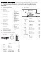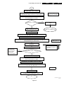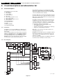
1
Colour Television
Chassis
EM1A
AA
CL 06532111_000.eps
171000
Contents
Page
1. Technical specifications, connection facilities &
chassis overview
2. Safety- and maintenance instructions,
warnings and notes.
3. Directions for use
4. Mechanical instructions
5. Faultfinding and repair tips
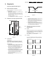
6. Block-, wiring diagrams and testpoint overviews
Blockdiagram video processing
Blockdiagram audio & control
Blockdiagram Large Signal Panel: supply
Powerlines overview
Wiring diagram
I2C overview
Testpoint overview LSP
Testpoint overview SSB / DW / CRT panel
7. Electrical diagram’s en PWB’s
Main supply
(Diagram A1)
Standby supply
(Diagram A2)
Line deflection
(Diagram A3)
Frame deflection
(Diagram A4)
Audio amplifier
(Diagram A5)
Headphone amplifier
(Diagram A6)
Tuner, I/O, SIMM-connector
(Diagram A7)
Front control
(Diagram A8)
SSB: SIMM-connector
(Diagram B1)
IF, I/O, videoprocessing
(Diagram B2)
Feature box
(Diagram B3)
HOP
(Diagram B4)
Audio demodulator
(Diagram B6)
Painter
(Diagram B7)
Multi PIP controller
(Diagram C1)
Tuner
(Diagram C2)
I/O processing
(Diagram C3)
Contents
IF video sync
Side I/O panel
Top control panel
CRT panel
DC-shift panel
Horizontal DAF panel
Vertical DAF panel
Mains switch panel
Mains harmonic panel
8. Alignments
9. Circuit description and
list of abbreviations
10. Spareparts list
2
4
6
11
15
27
28
29
30
31
32
33
34
Diagram
35
36
37
38
39
40
41
42
49
50
51
52
53
54
61
62
63
Page
(Diagram C4)
(Diagram D)
(Diagram E)
(Diagram F)
(Diagram G)
(Diagram I1)
(Diagram I2)
(Diagram J)
(Diagram Y)
64
67
69
70
71
72
73
75
76
77
82
96
98
65/66
67
69
71
71
74
74
75
76
PWB
43-48
43-48
43-48
43-48
43-48
43-48
43-48
43-48
55-60
55-60
55-60
55-60
55-60
55-60
65/66
65/66
65/66
©
Copyright 2000 Philips Consumer Electronics B.V. Eindhoven, The Netherlands.
All rights reserved. No part of this publication may be reproduced, stored in a
retrieval system or transmitted, in any form or by any means, electronic, mechanical,
photocopying, or otherwise without the prior permission of Philips.
Published by CO 0070 Service PaCE
Printed in the Netherlands
Subject to modification
5 3122 785 10850
GB 2
1.
Technical specifications, connection facilities & chassis overview
EM1A
1. Technical specifications, connection facilities & chassis
overview
1.1
Technical specifications
1.1.1
Reception
Tuning system
Colour systems (off-air)
: PLL
: NTSC M (3.58 &
4.43 MHz),
: PAL B/G/D/K/I/M/N,
: SECAM B/G/D/K/L
: FM/FM,
: 2SC B/G,
: NICAM B/G/D/K/I/L
: PAL B/G,
: SECAM,
: NTSC M (3.58 &
4.43 MHz).
: 100 channels,
: UVSH-channels
: 44.25 - 855.25 MHz
: 75 Ω, Coax
Sound systems
A/V connections
Channel selections
Frequency range
Aerial input
1.1.2
1.2.2
Miscellaneous
Set stroke numbers
: /56, /57, /69, /79,
/93
: 160 - 276 V
(± 10 %),
: 50 / 60 Hz (± 5 %)
: + 5 to + 45 deg. C.
: < 1 W.
Mains voltage
Ambient temperature
Standby Power consumption
1.2
Connection facilities
1.2.1
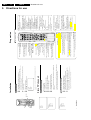
Control buttons & Side I/O connections
FRONT CONTROL
TOP CONTROL
SIDE I/O
P+
S-Video
Video
V-
IR
V+
P-
RED
L
Audio
R
CL 06532130_002.eps
031000
Figure 1-1
SVHS
1 2 3 -Y
4 -C
gnd
gnd
1 Vpp / 75 Ω
0.3 Vpp / 75 Ω
Audio / video
1 - Video
2 - Audio
3 - Audio
4 - Headphone
1 Vpp / 75 Ω
L (0.2 Vrms / 10 kΩ)
R (0.2 Vrms / 10 kΩ)
32 - 2000 Ω / 10 mW
v
v
j
j
jq
jq
jq
rt
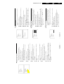
Rear connections
75Ω
MONITOR
OUT
AV1
IN
AV2
IN
VIDEO
Y
L/MONO
AUDIO
Pb
S-VIDEO
R
Pc
COMPONENT VIDEO INPUT
CL 06532130_001.eps
021000
SERVICE
CONNECTOR
Figure 1-2
Monitor out
1 - Video
2 - Audio
3 - Audio
1 Vpp / 75 Ω
L (0.5 Vrms / 10 kΩ)
R (0.5 Vrms / 10 kΩ)
kq
kq
q
AV1 in
1 -Y
2 - Pb
3 - Pr
0.7 Vpp / 75 Ω
0.7 Vpp / 75 Ω
0.7 Vpp / 75 Ω
jq
jq
jq
AV1 in
4 - Video
5 - Audio
6 - Audio
1 Vpp / 75 Ω
L (0.5 Vrms / 10 kΩ)
R (0.5 Vrms / 10 kΩ)
jq
jq
jq
AV2 in
1 - Video
2 - Audio
3 - Audio
1 Vpp / 75 Ω
L (0.5 Vrms / 10 kΩ)
R (0.5 Vrms / 10 kΩ)
jq
jq
jq
AV2 in (SVHS)
1 2 3 -Y
4 -C
gnd
gnd
1 Vpp / 75 Ω
0.3 Vpp / 75 Ω
v
v
j
j
Technical specifications, connection facilities & chassis overview
1.3
EM1A
1.
GB 3
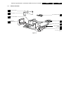
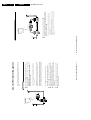
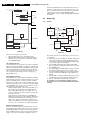
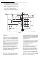
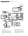
Chassis overview
F
CRT/SCAVEM PANEL
D
SIDE I/O PANEL
B
SMALL SIGNAL BOARD
C
PIP/DOUBLE
WINDOW PANEL
TOP CONTROL PANEL
E
MAINS SWITCH PANEL
J
LARGE SIGNAL PANEL
A
MAINS HARMONIC
PANEL
Y
DAF PANEL
I
CL 06532130_003.eps
181000
Figure 1-3
GB 4
2.
EM1A
Safety & maintenance instructions, warnings and notes
2. Safety & maintenance instructions, warnings and notes
2.1
Safety instructions for repairs
Safety regulations require that during a repair:
• Safety components, indicated by the symbol ∆, should be
replaced by components identical to the original ones;
• When replacing the CRT, safety goggles must be worn.
Safety regulations require that after a repair, the set must be
returned in its original condition. In particular attention should
be paid to the following points:
• General repair instruction: as a strict precaution, we
advise you to resolder the solder joints, through which
the horizontal deflection current is flowing, in particular:
– All pins of the line output transformer (LOT);
– Fly-back capacitor(s);
– S-correction capacitor(s);
– Line output transistor;
– Pins of the connector with wires to the deflection coil;
– Other components through which the deflection
current flows.
Note: This resoldering is advised to prevent bad connections
due to metal fatigue in solder joints and is therefore only
necessary for television sets older than 2 years.
• The wire trees and EHT cable should be routed correctly
and fixed with the mounted cable clamps.
• The insulation of the mains lead should be checked for
external damage.
• The mains lead strain relief should be checked for its
function in order to avoid touching the CRT, hot
components or heat sinks.
• The electrical DC resistance between the mains plug and
the secondary side should be checked (only for sets
which have a mains isolated power supply). This check
can be done as follows:
– Unplug the mains cord and connect a wire between
the two pins of the mains plug;
– Set the mains switch to the 'ON' position (keep the
mains cord unplugged!);
– Measure the resistance value between the pins of
the mains plug and the metal shielding of the tuner or
the aerial connection on the set. The reading should
be between 4.5 MΩ and 12 MΩ.
– Switch off the TV and remove the wire between the
two pins of the mains plug.
• The cabinet should be checked for defects to avoid
touching of any inner parts by the customer.
2.3
Warnings
•
V
CL 26532098/042
140792
Figure 2-1
•
•
•
•
•
2.2
Maintenance instructions
It is recommended to have a maintenance inspection carried
out by a qualified service employee. The interval depends on
the usage conditions:
• When the set is used under normal circumstances, for
example in a living room, the recommended interval is 3
to 5 years.
• When the set is used in circumstances with higher dust,
grease or moisture levels, for example in a kitchen, the
recommended interval is 1 year.
• The maintenance inspection contains the following
actions:
– Execute the above-mentioned 'general repair
instruction'.
– Clean the power supply and deflection circuitry on
the chassis.
– Clean the picture tube panel and the neck of the
picture tube.
In order to prevent damage to IC's and transistors, all
high-voltage flashovers must be avoided. In order to
prevent damage to the picture tube, the method shown in
Fig. 2-1 should be used to discharge the picture tube.
Use a high-voltage probe and a multimeter (position
VDC). Discharge until the meter reading is 0 V (after
approx. 30 s).
All IC's and many other semiconductors are susceptible
to electrostatic discharges (ESD). Careless handling
during repair can reduce life drastically. When repairing,
make sure that you are connected with the same
potential as the mass of the set by a wristband with
resistance. Keep components and tools also at this same
potential. Available ESD protection equipment:
– Complete kit ESD3 (small table mat, wristband,
connection box, extension cable and earth cable)
4822 310 10671.
– Wristband tester 4822 344 13999.
Together with the deflection unit and any multipole unit,
the used flat square picture tubes form an integrated unit.
The deflection and the multipole units are set optimally at
the factory. Adjustment of this unit during repair is
therefore not recommended.
Be careful during measurements in the high-voltage
section and on the picture tube.
Never replace modules or other components while the
unit is switched ON.
When making settings, use plastic rather than metal
tools. This will prevent any short circuits and the danger
of a circuit becoming unstable.
Safety & maintenance instructions, warnings and notes
2.4
Notes
•
•
•
•
•
•
The direct voltages and oscillograms should be
measured with regard to the tuner earth (H), or hot earth
(I) as this is called.
The direct voltages and oscillograms shown in the
diagrams are indicative and should be measured in the
Service Default Mode (see chapter 5) with a colour bar
signal and stereo sound (L: 3 kHz, R: 1 kHz unless stated
otherwise) and picture carrier at 475.25 MHz.
Where necessary, the oscillograms and direct voltages
are measured with (D) and without ( E) aerial signal.
Voltages in the power supply section are measured both
for normal operation (G) and in Standby (F). These
values are indicated by means of the appropriate
symbols.
The picture tube PWB has printed spark gaps. Each
spark gap is connected between an electrode of the
picture tube and the Aquadag coating.
The semiconductors indicated in the circuit diagram and
in the parts lists are completely interchangeable per
position with the semiconductors in the unit, irrespective
of the type indication on these semiconductors.
DOLBY, the double D symbol and PRO LOGIC are
trademarks of Dolby Laboratories Licensing Corporation.
Manufactured under license from Dolby Laboratories
Licensing Corporation.
EM1A
2.
GB 5
4
M
SMART
AV
g
MOVIES
VIDEO
h
X
i
¬
0
U
C
CH
SURF
a
SMART
Installation
INSTALL
LANGUAGE
AUTO STORE
MANUAL STORE
SORT
CHANNEL EDIT
NAME
INSTALL
LANGUAGE
AUTO STORE
MANUAL STORE
SORT
CHANNEL EDIT
NAME
b
V
MENU
select menu
item
Note: If no action is executed, the menu automatically disappears after about 12
seconds.
PICTURE
SOUND
FEATURES
INSTALL
Press the i key to switch the menu off.
Press the menu key to return.
Use the cursor in the left/right directions to access the sub-menu and to
adjust the settings.
Use the cursor in the up/down directions to select a menu item.
Note: Sometimes not all the menu items are visible on the screen; press the cursor
down until all the items are displayed.
Press the MENU key to display/cancel the main menu.
You can now search for and store the TV channels in two different ways: using
Auto store or Manual store (tuning in channel by channel).
From now onwards, all on-screen displays will appear in the language that you
have chosen.
Press the MENU key to return to the main menu.
Select your language with the cursor up/down.
Press the cursor right again.
Press the cursor right to select LANGUAGE.
Select INSTALL with the cursor down.
Press the MENU key.
“
&
é
Note: Channel numbers will always be written in Latin characters, even when a
language has been selected which uses other characters.
When the tuning is completed, press the MENU key to return to the
INSTALL menu or press the i key to switch the menu off.
Press the cursor right to start the searching.
All TV channels are searched for and stored automatically.
Select AUTO STORE in the INSTALL menu.
Automatic tuning of channels
&
é
“
‘
(
§
First, select your language.
Select the menu language
Store TV channels
‘
(
“
&
é
2
Sleep D
AV
◊
DOLBY V.
b
V
MENU
M
SMART
7
4
1
q
A/CH
D
f
¬
0
8
5
2
PI P
g
X
UP
ß
DN
S
ê
î
PROGRAM LIST
U
C
CH
SURF
a
SMART
9
6
3
PIP CH
DOLBY V ◊
h
ACTIVE CONTROL
h
i
©
æ
B
Allows you to navigate through a list of installed programmes for a quick overview
of the channels and activate the channel you have selected.
PROGRAM LIST î
ON: Sharpness and Noise Reduction are controlled automatically.The Picture
settings are being adapted continuously and automatically. The menu items cannot
be selected.
Measures and corrects all incoming signals in order to provide the best picture
quality settings. Press to select the Active Control values On or Off.
Active Control On/Off h
In Mono sound mode, this feature, when switched on, enables you to hear
a spatial effect of sound.
Incredible Surround
In Stereo sound mode, when Incredible Surround is selected, it seems as
though the loudspeakers are spread further apart from one another.
Dolby Virtual (Virtual Dolby Surround) enables you to experience the effect
of Dolby Pro Logic Surround, reproducing a rear sound effect.
Dolby Virtual (with Dolby Surround signals)
Allows you to select 5 types of picture settings.
Press the key repeatedly to select the different
settings.
Smart Picture a
Allows you to select your desired sound setting
from 4 types of sound settings.
Press the key repeatedly to select the different
settings.
Smart Sound M
Allows you to select a channel.
Note: For a 2-digit number, the second digit
must be entered before the “-” sign disappears.
Digit (0-9)
Press this key repeatedly to select another
screen format: Auto, 4:3, Expand 4:3 and
Compress 16:9. See also p. 11.
Screen format q
Allows you to freeze the main picture.
Freeze S
(if provided) See p. 12
ßê© PIP CH UP/DOWN
PIP (Picture in Picture)/Dual Window On/Off æ
Allows you to alternate between the last
viewed channel and the present channel.
(Alternate Channel) A/CH
• Switch set off temporarily to standby mode.
(The red light indicator lights up when set is
on standby mode).
• To switch on set from standby mode, press
button again.
Standby B
Allows you to select a time period after which
the set will switch to standby mode
automatically.
Allows you to select the AV channels.
g for future use
(if provided) See p. 13
Allows you to access teletext information.
Colour keys,bhUf Teletext
Allows you to set the clock to switch to
another channel at a specified time while you
are watching another channel or when the
set is on standby mode.
C Timer
Allows you to switch from Stereo to Mono
sound during stereo transmission or to choose
between Language Y or Language Z during
dual sound transmission.
X
• Displays the channel number, sound
transmission mode, the clock and the status
of the sleeptimer.
• Also allows you to exit menu from screen.
i On Screen Display
AV
descending order.
CH +/- Selects channels in ascending or
Mutes the sound.To restore the sound, press
the button again.
¬ Mute
Increases or decreases volume.
V Volume +/-
Up/Down: allows you to select the next or
previous item on the menu and to
select another picture format
Left/Right: allows you to access the sub-menus
and adjust the settings.
Cursor
Allows you to select up to a maximum of 10
favourite channels or sources and view quickly
the selected channels or sources.
To add a new channel or source:
• Select the channel number or source you
want to add to the surf list.
• Press the SURF key.
The request ADD? appears next to the
selected channel number or source.
• Press the cursor right to add.
To delete a channel or source:
• Select the channel number or source you
want to remove from the surf list.
• Press the SURF key.
The request DELETE? appears next to the
selected channel number or source.
• Press the cursor right to delete.
Press the SURF key repeatedly to scroll
through the selected channels or sources.
SURF
Also exits the menu from the screen or returns
to a higher menu level.
MENU Displays main menu.
EM1A
PICTURE
SOUND
FEATURES
INSTALL
i
switch
menu off
return
9
8
7
3
6
2
DN
S
ê
B
PIP CH
5
UP
ß
4
©
q
PI P
1
æ
D
Your remote control
Preparation
3.
A/CH
To use the menus
Installation
GB 6
Directions for use
3. Directions for use
MANUAL STORE
COLOUR SYSTEM
SOUND SYSTEM
SEARCH
CHANNEL
STORE/STORED
FINE TUNE
PLL
INSTALL
LANGUAGE
AUTO STORE
MANUAL STORE
SORT
CHANNEL EDIT
NAME
è to 4 to continue searching for another transmitting
Now repeat steps
channel.
Press the MENU key to return to the INSTALL menu or press the i key to
switch menu off.
5
6
6
Installation
INSTALL
LANGUAGE
AUTO STORE
MANUAL STORE
SORT
CHANNEL EDIT
NAME
CNN
3
4
5
6
7 SKIPPED
“ to è until all TV channel are allocated as you like.
Press the MENU key to return to the INSTALL menu or press the i key to
switch menu off.
Repeat steps
Press the cursor right.
The message EXCHANGED appears and the selected channels are exchanged.
Press the cursor down and select EXCHANGE.
Key in the channel number in the TO column you want to swap to.
Press the cursor down and select TO.
Key in the channel number in the FROM column you want to swap from. Use
the digit keys or the cursor left/right.
Press the cursor right to enter the menu.
Select SORT in the INSTALL menu.
§
é
“
‘
(
&
‘.
Press the cursor left or the MENU key to return to the install menu or the
i key to switch menu off.
Note: to add back channels to the list, repeat steps & to ‘ and press the
i key to switch menu off.
Press the cursor up/down to select another channel and repeat step
Press the cursor right to skip the selected channel.
The message SKIPPED is displayed.
Select the channel you want to skip with the cursor up/down.
Press the cursor right to enter the channel list.
Select CHANNEL EDIT in the INSTALL menu.
Press the MENU key to store the named channel.
Move to the next character with the cursor right and key in the next
character.You can key up to a maximum of 5 characters.
Key in the selected character with the cursor up/down.
Press the cursor right to enter the menu.
Select NAME in the INSTALL menu.
Select a TV channel or peripheral you want to assign a name or modify the
existing name.
It is possible to assign a name to a TV channel.This feature allows you to
enter a new name or modify an existing name of a channel, including
peripherals.
Note: Even when you have selected another language in the language menu, only
the English language character set is offered to enter names to the TV channels
stored.
Naming of channels
(
§
&
é
“
‘
This feature allows you to edit or skip channels from the channel list which
have bad or weak signals or channels which you do not watch often.
Note: Once a channel is skipped, you cannot select it with the CH - or + key.
You can only access the channel with the digit keys.
Editing of channels
!
ç
‘
(
§
è
&
é
“
According to your preference you can change the order of the stored TV
channels.
3.
5
Press the cursor right.
The message STORED appears and the search menu item is highlighted again.
INSTALL
LANGUAGE
AUTO STORE
MANUAL STORE
SORT
CHANNEL EDIT ƒ
NAME
SORT
FROM
TO
EXCHANGE/EXCHANGED
INSTALL
LANGUAGE
AUTO STORE
MANUAL STORE
SORT
CHANNEL EDIT
NAME
Sorting of channels
EM1A
Installation
Press the cursor down to select STORE.
4
1
3
In case of poor reception, you can improve the reception by adjusting the
frequency.
Select FINE TUNE and press the cursor left/right to adjust.
In rare cases certain TV channels may reproduce distorted or unstable
pictures.
Select PLL (Phase Locked Loop) to switch to the setting 2 with the cursor
left/right to restore the picture for the respective transmission.
Press the cursor down.
0
2
Key in the desired channel number with the digit keys or with the cursor
left/right.
Select CHANNEL.
Select SEARCH and press the cursor left or right to start the searching.
Searching stops once a transmitting channel is found.
Note: If the reception is poor, select another colour and/or sound system.
Press the MENU key or the cursor left.
Select SOUND SYSTEM and press the cursor right.
If AUTO is selected, the respective sound system will be automatically
selected according to the transmission system.
Note: If the reception is poor, select another sound system with the cursor up/down.
Press the MENU key or the cursor left.
ç
!
è
§
(
‘
Select COLOUR SYSTEM and press the cursor right.
If AUTO is selected, the respective colour system will be automatically
selected according to the transmission system.
If the reception is poor, select another colour system with the cursor up/down.
Press the cursor right to enter the menu.
é
“
Select MANUAL STORE in the INSTALL menu.
&
Manual tuning allows you to store channel by channel.
You must go through every step of the manual store menu.
Manual tuning of channels
Directions for use
GB 7
j
VCR
3
VIDEO
OUT
x
R
AUDIO
L/Mono
AV 1
in
out
in
AV 2
COMPONENT VIDEO INPUT
Pr
Pb
Y
Monitor
S-VIDEO
‘
(
“
&
é
VIDEO
input. (See the instructions of your video recorder.)
Connect Peripheral Equipment
Replace the RF cable in the RF socket x of your video recorder after
you have stored the test signal.
Store the test signal under programme number 0 or between 90 and 99.
Search for the test signal of your video recorder in the same way as you
searched for and stored the TV signals. See Installation, Store TV Channels,
Manual Tuning, p. 5.
Switch on your TV and put the video recorder on the test signal or play a
prerecorded tape (See the handbook for your video recorder.).
Unplug the RF cable 1 from the RF socket x of your video recorder.
Search for and store the test signal of the video recorder
If the cables 3 are not used the following steps are required:
recorder to the
15
S-VHS-Video quality with a S-VHS video recorder is obtained by connecting
the S-VHS-Video cable with the S-VIDEO input instead of connecting the video
The MONITOR OUT connectors can be used for daisy chaining or to record
programmes from your TV. See Record with your video recorder, p. 18.
Note: in case of mono equipment, only the left loudspeaker reproduces sound.
Use a mono to stereo adaptor (not supplied) for sound reproduction via all
internal loudspeakers.
Connect another RF cable 2 from the output j of your video recorder to
the input x of your TV.
Better playback quality can be obtained if you also connect the Video, Audio
Left and Right (only for stereo equipment) cables 3 to the VIDEO,
AUDIO L/Mono and R input AV2 IN.
Connect the RF cable 1 to the RF socket x of your video recorder.
16
j
VCR
x
OUT
R
AUDIO
Pr
Pb
3
in
AV 2
COMPONENT VIDEO INPUT
in
AV 1
Y
S-VIDEO
OUT
4
IN
OUT
CABLE
1
Note: in case of mono equipment, only the left loudspeaker reproduces sound.
Use a mono to stereo adaptor (not supplied) for sound reproduction via all
internal loudspeakers.
When a video recorder is not connected to MONITOR OUT you can only record a
programme from the aerial or from the cable system.
Only when a video recorder is connected to MONITOR OUT it is possible to record a
programme from other equipment connected to the TV. See Record with your video
recorder, p. 18.
To obtain better picture quality, also connect the Video, Audio left and Audio
right (only for stereo equipment) cables to the VIDEO, AUDIO L/Mono and
AUDIO R input of AV2 IN sockets 4.
Interconnect your video recorder with extra RF cables 3.
Connect Peripheral Equipment
&
é
75
out
Monitor
VIDEO
L/Mono
EM1A
75
CABLE
&
é
Video recorder
Video recorder and other A/V peripherals
3.
There is a wide range of audio and video equipment that can be connected
to your TV.The following connection diagrams show you how to connect
them.
Connect Peripheral Equipment
GB 8
Directions for use
1
VIDEO
R
AUDIO
L/Mono
in
in
out
L
DVD
COMPONENT VIDEO INPUT
Pr
Pb
Y
AV 2
AV 1
Monitor
AUDIO
VIDEO
S•VIDEO
2
2
S-VIDEO
1
3
S-VHS quality with an S-VHS camcorder is obtained by connecting the S-VHS
cables with the S-VIDEO input 3 (instead of VIDEO 2) and AUDIO
inputs 1.
For stereo equipment also connect AUDIO R 1.
Connect the equipment to VIDEO 2 and AUDIO L 1 for mono
equipment.
Connect your camera or camcorder to sockets at the right side of your TV.
Connect the Audio left and right (only for stereo equipment) cables to the
AUDIO L/Mono and R input.
Connect the cables of your Y-Pb-Pr DVD player 1 to the Y-Pb-Pr input
AV1 in sockets on the TV.
For correct picture reproduction also connect to VIDEO.
(See the handbook of your DVD player.)
&
é
18
AV
g
h
ACTIVE CONTROL
h
UP
ß
X
f
¬
0
8
5
2
PI P
i
©
Record
◊
DOLBY V.
b
V
MENU
M
SMART
7
4
1
q
æ
PROGRAM LIST
U
C
CH
SURF
a
SMART
9
6
3
DN
S
ê
B
PIP CH
&
é
“
&
é
Do not switch channel numbers or do not switch off your TV when you are recording !
Set your video recorder to record.
You record what you are watching on the screen.
Select the correct external on your TV and on your video recorder.
Record a programme on your video recorder connected to
MONITOR OUT from Audio/Video equipment connected to
AV1, AV2 or to sockets on the right side of the TV
Switch on the equipment.
Switching channel numbers on your TV does not disturb recording !
Set your video recorder to record.
See the handbook for your video recorder.
Record a TV programme
Select the channel number on your video recorder.
To record S-VHS quality, connect an S-VHS peripheral directly to the video
recorder.
Record with your video recorder
If you want to change to TV channels?
Enter the channel number of the TV channel which you want to watch with
the digit keys.
Equipment connected to the back or to the right side of the TV
Press the AV key repeatedly to select AV1, CVI, AV2 or FRONT, according to
where you connected your equipment at the back or the right side of your
TV.
Select CVI to view the playback of DVD discs if you used the Component
Video Input sockets (Y-Pb-Pr and AUDIO L/Mono and R inputs).
Equipment connected with an aerial cable only :
Select the channel number under which you have stored the test signal with
the digit keys.
To select connected equipment
3.
17
AV
D
A/CH
EM1A
Connect Peripheral Equipment
In the SOUND menu select Headphone to adjust the headphone volume and
balance.
Press ¬ on the remote control to switch off the internal loudspeakers
of the TV.
The headphone impedance must be between 8 and 4000 Ohm.
The headphone socket has a 3.5 mm jack.
Insert the plug into the headphone socket L at the right side of the TV.
Headphone
é
&
DVD-player
“
&
é
Camera & camcorder
Directions for use
GB 9
Before Calling Service
•
No picture
Turn off the television immediately and consult a qualified service personnel.
Check whether the batteries are working. Replace if necessary.
Clean the remote control sensor lens on the television.
Operating range between television and the remote control should not be more than 6 meters.
You can still use the keys at the top of your TV.
This could be due to antenna siting or reflected signal.
Switch over to “MONO” mode by pressing the X key.
Press the i key again to exit from the menu.
•
•
•
•
•
•
•
•
•
•
•
Snowish picture and noise
Horizontal dotted line
One white line across the
screen
NICAM sound distortion
(crackling noise)
Wrong menu
Before Calling Service
This may be caused by electrical interference (e.g. hairdryer, nearby neon lights, etc.)
Turn off the equipment.
If your problem is not solved
Turn your TV off and then on again once.
Never attempt to repair a defective TV yourself.
Check with your dealer or call a TV technician.
Television not responding to
remote control
Sometimes, poor picture quality occurs when having activated an S-VHS camera or camcorder
connected to the right side of of your TV and another peripheral is connected to AV1 or AV2 at the
same time. In this case, switch off one of the other peripherals.
•
Poor picture
Check the antenna connection.
Adjust the contrast and brightness setting or select another picture setting with the smart picture key.
Check the transmission system’s colour settings of this set.
Increase the VOLUME.
Check that the television is not muted, press the ¬ button on the remote control.
When no signal is detected, the television automatically switches off the sound.
This is proper operation and does not indicate a malfunction.
Check the transmission system’s sound settings of this set.
•
•
•
•
•
•
Check the antenna connection at the rear of the television to see if it is properly connected to the
television input terminal.
Possible broadcast station trouble. Try another channel.
Adjust the contrast and brightness settings or select another picture setting with the smart picture key.
Check that the television's AC power cord is plugged into the mains socket.
Unplug the television, wait for 60 seconds.
Then re-insert the plug into the mains socket and turn on the television again.
Good sound but poor
colour or no picture
Good picture but no sound
•
•
No power
19
EM1A
•
•
•
This may be caused by obstruction to the antenna due to high rise buildings or hills.
Using a highly directional antenna may improve the picture.
Items to Check and Actions to follow
“Ghost” or double images
3.
Symptoms
Please make these simple checks before calling service.These tips may save you time and money since charges for television installation and
adjustments of customer controls are not covered under your warranty.
Personal notes:
GB 10
Directions for use
Mechanical instructions
EM1A
4.
GB 11
4. Mechanical instructions
4.1
Removing the Rear Cover
1. Remove all the fixation screws of the rear cover.
2. Now the rear cover can be removed by pulling it
backward.
4.2
Service positions
4.2.1
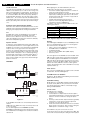
Service position LSP
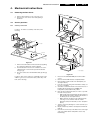
Position 1: For better accessibility of the LSP, do the
following:
1
2
SSB
LSP
A
LSP - bracket
3
1
4
Bottom tray
2
1
2
CL 06532130_004.eps
031000
Figure 4-1
1. Remove the LSP-module from the bottom tray by pulling
the complete module back- and then upward.
2. Hook the bracket in the first row of fixation holes of the
cabinet bottom. In other words reposition the bracket
from [1] to [2].
3. The same can be done with the DW-module (position [3]
to [4]).
Position 2: This service position is comparable to that of the
A10A. To get access to the bottom side (solder side) of the
LSP, do the following:
3
4
B
CL 06532130_006.eps
121000
Figure 4-2
1. Disconnect the CRT/SCAVEM panel from the CRTsocket.
2. Release LSP and DW-module, and pull backward.
3. Remove Mains switch module from bottomplate (see
description below).
4. Free the necessary wiring from their fixation clamps, for
the ease of handling.
5. Sometimes a cable must be disconnected for the ease of
handling, like the degaussing coil (0020) and
loudspeaker (1735, 1736 & 1737) cables.
6. Now reposition following modules, in order to cope with
the LSP service position:
– DAF-module from the LSP-bracket by pressing lever
while pushing the module forward in the direction of
the CRT (see also description below).
– Mains Harmonic module from the LSP-bracket by
removing 1 screw and then slide the module
backward, away from the CRT (see also description
below).
7. Turn the chassis tray 90 degrees counter clockwise (see
figure 4.2 - [2]).
8. Flip the chassis tray with the rear I/O panel towards the
CRT [3].
9. Place the hook of the tray in the fixation hole at the right
side of the cabinet bottom and pull the chassis tray
backward [4].
GB 12
4.
Mechanical instructions
EM1A
10. Reconnect cables (except degaussing cable 0020),
panels and modules.
To get access to the test points of the SSB, the shielding has
to be removed:
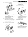
Alternative position 2: A somewhat easier way to access the
bottom side (solder side) of the LSP is the following (only
possible when the high tension cable is long enough):
2
3
2
5
1
1
1
FR
PIP/D
W M OM
ODU
LE (0
0948
205)
0946
1
4
4
CL 06532130_008.eps
131000
Figure 4-4
3
A
CL 06532130_007.eps
131000
Figure 4-3
1. Disconnect the CRT/SCAVEM panel from the CRTsocket.
2. Release LSP and DW-module, and pull backward.
3. Remove Mains switch module from bottomplate (see
description below).
4. Free the necessary wiring from their fixation clamps, for
the ease of handling.
5. Sometimes a cable must be disconnected for the ease of
handling, like the degaussing coil (0020), loudspeaker
(1735, 1736 & 1737) cables and 0325 (frame deflection).
6. Now reposition following modules, in order to cope with
the LSP service position:
– DAF-module from the LSP-bracket by pressing lever
while pushing the module forward in the direction of
the CRT (see also description below).
– Mains Harmonic module from the LSP-bracket by
removing 1 screw and then slide the module
backward, away from the CRT (see also description
below).
7. Flip the chassis tray 90 degrees clockwise [2].
8. Place the hook of the tray in fixation hole [A] of the
cabinet bottom and pull the chassis tray backward [3].
9. Reconnect the cables (except degaussing cable 0020),
panels and modules.
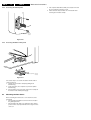
4.2.2
Service position SSB
All relevant test points can be accessed with the SSB in
original position, but for ease of use a 'SSB extension board'
is available under number 9965 000 05769.
Before usage of this board, the 'LSP top-bracket' has to be
taken out. This can be done by:
1. Remove the DAF panel (see 4.2.5).
2. Remove the 2 screws which hold the bracket at the right
side.
3. Lift the bracket at the same side. It hinges at the cooling
plate.
Note: For some type numbers, the LSP has to be moved
slightly to the right side in order to create enough space for
the SSB extension board.
1. Put the LSP in service position 1 (as described above).
2. If a PIP/DW module is present, then disconnect the IFcable from connector 1946, flatcable from connector
1948 and flatfoil on DW-module connector 0205 [1].
3. Release the 'top fixation clamp' which holds the SSB [2]
and pull the SSB slightly towards the Tuner [3]. At the
same time, the 2 metal clamps at both sides of the SIMMconnector must be released [4] . The complete SSB can
be taken out now by pulling the topside of the SSB
towards the Tuner [5]. It 'hinges' in the SIM-connector.
2
1
1
CL 06532130_009.eps
031000
Figure 4-5
1. Once the SSB has been taken out of the connector, the
shielding can be removed.
2. After removal of the shielding, the panel can be replaced
in its connector in reverse order. Don't forget to
reconnect the cables.
3. If necessary for the measurement, the LSP can be put in
'service position 2' (as described above).
Mechanical instructions
4.2.3
4.
GB 13
1. The complete module can be removed from the LSPbracket by pressing its fixation clamp [1] (located behind
the PWB), while sliding the module in the direction of the
CRT [2].
2. The board can easily be lifted from its bracket after
releasing the 2 fixation clamps [3].
Accessing the Double Window (DW) panel
PIP/Double Window
EM1A
1
Multi Voltage
1
4.2.6
Accessing the Mains Harmonic panel
4
2
1
3
2
3
3
3
4
CL 06532130_015.eps
031000
CL 06532130_017.eps
131000
Figure 4-6
Figure 4-8
1. Remove the DW bracket from the bottom tray by pulling
it backward (after pressing the fixation clamp).
2. The board can easily be lifted out of the bracket [2] after
releasing the 2 fixation clamps [1].
4.2.4
1. The complete module can be removed from the LSPbracket (after removal of the DAF-panel) by removing
screw [1] and then slide the module in the opposite
direction of the CRT [2].
2. The board can easily be lifted from its bracket after
releasing the 2 fixation clamps [3].
Accessing the Multi Voltage panel (if present)
1. Remove the DW bracket from the bottom tray by pulling
it backward.
2. Press the 2 fixation clamps downward [3] (see figure 47).
3. The board can easily be lifted out of the bracket after
releasing the 2 fixation clamps [4].
4.2.7
Accessing the Top Control panel
M
Top control board
4.2.5
Accessing the Double Astigmatic Focus (DAF) panel
CL 06532012_003.eps
030200
Figure 4-9
3
3
3
2
1
CL 06532130_016.eps
031000
Figure 4-7
1. Remove the two fixation screws, which hold the panel.
2. Pull the board backward (w.o.w. release it from its front
hinge [M]).
3. The board can easily be lifted from its bracket after
releasing the 2 fixation clamps at the connector side.
GB 14
4.2.8
4.
Mechanical instructions
EM1A
1. The complete Side I/O-assembly can easily be removed
by unscrewing the 2 fixation screws.
2. The board can easily be lifted out of the bracket after
releasing the 2 fixation clamps.
Accessing the Side I/O panel
CL 06532012_004.eps
030200
Figure 4-10
4.2.9
Accessing the Mains Switch panel
1
1
2
3
3
CL 06532130_018.eps
021000
Figure 4-11
The easiest way to access this module is with the LSP in
service position 2.
1. Release the two fixation clamps by pulling them
backward [1].
2. At the same time, the complete assy must be pulled
backward [2].
3. If the board has to be removed, release the 2 clamps at
the bracket sides and lift panel up [3].
4.3
Mounting the Rear Cover
Before mounting the Rear Cover, some checks has to be
performed:
• Check whether the Mains Cord is mounted correctly in
the guiding brackets.
• Check whether all cables are replaced in their original
position. This is very important due to the large 'hot' area
of the set.
Fault finding and repair tips
EM1A
5.
GB 15
5. Fault finding and repair tips
•
In this chapter the following paragraphs are included:
1. Test points.
2. Service Modes.
3. Problems and solving tips (related to CSM).
4. ComPair.
5. Error codes.
6. The 'blinking LED' procedure.
7. Protections.
8. Repair tips.
5.1
•
Via grounding the 'Front Detect'-line on the Side I/O
panel during switch ON (pins 1 and 7 of connector
0936).
By the 'DEFAULT' button on the DST while the set is in
the normal operation mode.
CAUTION: Entering SDM by grounding the 'Front Detect'line will override the 5V-protection. This should only be
done for a short period of time. In case of SW-protections
(errors 1 - 4), the set will shutdown in 15 s.
When doing this, the service-engineer must know what
he is doing as it could lead to damaging the set.
Test points
The EM1A chassis is equipped with test points in the service
printing. These test points are referring to the functional
blocks:
• A1-A2-A3, etc.: Test points for the audio processing
circuitry [A5, A6, and B6].
• C1-C2-C3, etc.: Test points for the control circuitry [B7].
• F1-F2-F3, etc.: Test points for the frame drive and frame
output circuitry [A4, B4] and Double Window [C].
• F1F-F2F, etc.: Test points for the RGB-signals on the
CRT panel [F].
• I1-I2-I3, etc.: Test points for the intermediate frequency
circuitry [A7, B2].
• L1-L2-L3, etc.: Test points for the line drive and line
output circuitry [A3, B4].
• P1-P2-P3, etc.: Test points for the power supply [A1, A2].
• SC1-SC2, etc.: Test points for the synchronisation
circuitry on the CRT panel [F].
• V1-V2-V3, etc.: Test points for the video processing
circuitry [B].
After entering SDM, the following screen will be shown with
'SDM' at the upper right side for recognition.
The numbering is done, in a for diagnostics logical sequence;
always start diagnosing within a functional block in the
sequence of the relevant test points for that functional block.
Access to normal user menu
Pressing the 'MENU' button on the remote control, switches
between the SDM and the normal user menus (with the SDM
mode still active in the background).
SDM Menu
SDM
HRS: 0001 SWID: EM11A1-1.0
ERR: 0 0 0 0 0 0 0
i +
Service modes
5.2.1
Service Default Mode (SDM)
Entering
• Via a standard RC-handset by entering the code
'062596' followed by the 'MENU' button.
• Via ComPair.
C
U
A
S
T
N
T
T
URE
D
URES
ALL
B
C
C
S
C
R
O
O
H
O
I
L
N
A
L
G
O
T
R
O
H
U
R
P
U
SDM
TNESS
R
AST
NESS
R TEMP
CL 06532130_010.eps
031000
Figure 5-1
Explanation
Error buffer
Pressing the 'OSD' button [i+] of the remote control, shows /
hides the error buffer. OSD can be hidden to prevent
interference with oscillogram measurements.
Access to SAM
By pressing the 'VOLUME +' and 'VOLUME -' buttons on the
local keyboard simultaneously for a few seconds, the set
toggles from SDM to SAM.
Purpose
• To provide a situation with predefined settings to get the
same measurement results as given in this manual.
• Start the 'Blinking LED' procedure.
• Have the possibility to override the 5V-protection.
Specification
• Tuning frequency 475.25 MHz for PAL/SECAM sets and
at channel 3 (61.25 MHz) for NTSC-sets.
• All picture settings at 50 % (brightness, colour, contrast,
hue).
• All sound settings at 50 % except volume at 25 % (so
bass, treble, balance at 50 %, volume at 25 %).
• All service-unfriendly modes are disabled, like timer,
sleep timer, parental lock, blue mute, hospitality mode
and no-ident timer (normally the set is automatically
switched off when no video signal - IDENT - was received
for 15 minutes).
I
O
E
N
SDM
Measurements are performed under the following conditions:
• Service mode: SDM.
• Video: colour bar signal.
• Audio: 3 kHz left, 1 kHz right.
5.2
MENU
P
S
F
I
Exiting
There are 2 ways to exit this mode:
• Switch the set to 'STANDBY', the error buffer will also be
cleared (by switching the set OFF-ON with the mains
switch, the set will come up again in the SDM).
• By pressing the 'EXIT' button on the DST.
5.2.2
Service Alignment Mode (SAM)
Purpose
• To perform alignments.
• To change option settings.
• To display / clear the error code buffer.
Specification
• Software alignments (see chapter 8).
• Option settings (see chapter 8).
• Error buffer reading and erasing. The most recent error
code is displayed on the left side.
• Operation counter.
• Software version.
GB 16
5.
Fault finding and repair tips
EM1A
Entering
• Via a standard RC-handset by entering the code
'062596' followed by the 'OSD' button [i+].
• Via ComPair.
•
By the 'ALIGN' button on the DST while the set is in the
normal operation mode.
The following screen will be shown, with 'SAM' at the upper
right side for recognition.
SAM Menu
P
S
F
I
I
O
E
N
C
U
A
S
T
N
T
T
1
URE
D
URES
ALL
B
C
C
S
C
R
O
O
H
O
0003
G
O
T
R
O
H
U
R
P
U
SAM
SAM
TNESS
R
AST
NESS
R TEMP
2
MENU
HRS:
I
L
N
A
L
MENU
3
SWID:
N
W
S
O
O
P
S
Y
B
B
RG
SB
STEM
1
2
4
EM11A1-1.0
SAM
SAM
TUNER
ERR:
OPT:
C
O
A
O
V
T
W
G
S
L
P
K
P
S
U
H
E
O
E
T
B
C
D
N
I
O
U
0 0
254
AR
ION
ON
ON
ON
ER
TE
MET
ND
E
S
/
/
/
0 0
100
0 0
128
0
0
MENU
0
0
0
0
IF-PLL OFFSET
AGC
2ND
RRORS
OFF
OFF
OFF
AFA
AFB
TONE
RY
MENU
SAM
NORMAL
RED
5
SAM
VER-SLOPE
MENU
SAM
MENU
SOUND
N
2
P
P
P
I
C
S
S
S
C
S
-
F
N
N
F
F
M
I
I
MAM
M
C-BGDK
C-I
CL 06532130_011.eps
021000
Figure 5-2
Explanation
The Service Alignment Mode menu will now appear on the
screen. The following information is displayed:
1. Operation hours timer (hexadecimal).
2. Software identification of the main micro controller
(AAABBB-X.Y).
• AAA is the chassis name (EM1= Painter processor,
EM2= OTC processor).
• B = Software code belonging to a certain stroke
number (see table below).
• X = (main version number).
• Y = (subversion number).
3. Error buffer (7 errors possible).
4. Option bytes (8 codes possible), summary of options are
explained below.
5. Sub menus are listed in a scroll-menu.
Country
Strokenumber
Software
/69
2A1
Middle East
/56
2A2
China
/93
1A1
Hong Kong
/57
2A1
Australia
/79
Singapore
Thailand
Malaysia
Indonesia
New Zealand
Fault finding and repair tips
Line 3:
Software and hardware functionality of the EM1A is
controlled by option bits. An option byte or option number
represents 8 of those bits. Each option number is displayed
as a decimal number between 0 and 255. The set may not
work correctly when an incorrect option code is set. See
chapter 8 for more information on correct option settings
The menus and submenus
• CLEAR ERRORS. Erasing the contents of the error
buffer. Select the CLEAR ERRORS menu item and press
the 'CURSOR RIGHT' key. The content of the error
buffer is cleared.
• The functionality of the OPTIONS and ALIGNMENTS
(TUNER, WHITE TONE, SOUND, GEOMETRY and
SMART SETTING) sub menus is described in chapter 8.
Line 4:
Indicates which colour and sound system is installed for the
selected pre-set:
Line 5:
Indicates that the set is not receiving an 'ident' signal on the
selected source.
Note: On some models, BLUE MUTE is displayed (if the BM
option is ON) when no signal is received.
Exiting
There are 2 ways to exit this mode:
• Switch the set to 'STANDBY', the error buffer will also be
cleared (by switching the set OFF-ON with the mains
switch, the set will come up again in the SAM).
• By pressing the 'EXIT' button on the DST.
Line 6:
Indicates whether the SLEEPTIMER function is ON/OFF.
Line 7:
Indicates whether the CHILD LOCK function is ON/OFF.
Line 8:
Indicates whether the current pre-set is defined as SKIPPED
or NON-PREFERRED.
Customer Service Mode (CSM)
Purpose
The 'Customer Service Mode' is a special service mode,
which can be activated and deactivated by the customer
upon request of the service technician/dealer during a
telephone conversation, in order to identify the status of the
set. This CSM is a 'read only' mode, therefore modifications
in this mode are not possible.
Line 9:
Indicates whether the HOTEL MODE is activated.
Line 10:
Indicates which SOURCE is installed for this pre-set: EXT1,
SVHS2, EXT2, and Tuner.
Line 11:
Indicates which sound mode is installed for this pre-set:
Mono, NICAM, Stereo, L1, L2, SAP or Virtual
Entering
The Customer Service Mode will switch ON after pressing
the 'MUTE' key on the remote control handset and any of the
top control buttons on the TV for at least 4 seconds
simultaneously. This activation only works if there is no menu
on the screen.
Line 12 to 17:
Value indicates parameter levels at CSM entry.
Exiting
The Customer Service Mode will switch OFF after pressing
any key of the remote control handset (with exception of the
'P+' and 'P-' keys) and switching OFF the TV set with the
mains switch.
Explanation
After switching on the Customer Service Menu the following
screen will appear:
CSM Menu
HRS: 0005 SWID: EM1
CODES: 0 0 0 0 0 0
OPT: 254 100 128 0
SYSTEM: AUTO
11
NO SIGNAL
12
TIMER ON
13
CHANNEL BLOCKED
14
NOT PREFERRED
15
HOTELMODE ON
16
SOURCE: 1
17
C S M
1A1-1.0
0
0 0 0 0
SOUND: MONO
VOLUME:
BALANCE: +/HUE:
+/COLOUR:
BRIGHTNESS:
CONTRAST:
CL 06532130_012.eps
131000
Figure 5-3
Line 1:
GB 17
Line 2:
Error code buffer (for more details see paragraph 5.3).
Displays the last 7 errors of the error code buffer.
Access to normal user menu
Pressing the 'MENU' button on the remote control switches
between the SDM and the normal user menus (with the SAM
mode still active in the background). Pressing the 'MENU'
key in a submenu will go to the previous menu.
1
2
3
4
5
6
7
8
9
10
5.
HRS: Hexadecimal counter of operating hours (example: 1B
(hex) = 0001 1011 (bin) = 27 (dec)). Standby hours are not
counted as operating hours.
SWID: Software identification of the main micro controller
(see paragraph 5.2.2). Details on available software versions
can be found in the chapter 'Software Survey' of the
publication 'Product Survey - Colour Television'.
Menu control
Menu items can be selected with the 'CURSOR UP/DOWN'
key. The selected item will be highlighted. When not all menu
items fit on the screen, moving the 'CURSOR UP/DOWN' will
display the next/previous menu items.
With the 'CURSOR LEFT/RIGHT' keys, it is possible to:
• (De)activate the selected menu item (e.g. GEOMETRY).
• Change the value of the selected menu item (e.g. VERSLOPE).
• Activate the selected submenu (e.g. SERV-BLK).
5.2.3
EM1A
5.3
Problems and solving tips (related to CSM)
5.3.1
Picture problems
No colours / noise in picture
Check CSM line 4. Wrong colour system installed. To change
the setting:
1. Press the 'MENU' button on the remote control.
2. Select the INSTALL sub menu.
3. Select the MANUAL STORE sub menu.
4. Select and change the COLOUR SYSTEM setting until
picture and sound are correct.
5. Select the STORE menu item.
GB 18
5.
EM1A
Fault finding and repair tips
Colours not correct / unstable picture
Check CSM line 4. Wrong colour system installed. To change
the setting:
1. Press the 'MENU' button on the remote control.
2. Select the INSTALL sub menu.
3. Select the MANUAL STORE sub menu.
4. Select and change the COLOUR SYSTEM setting until
picture and sound are correct.
5. Select the STORE menu item.
TV switches off or changes channel without any user
action
The TV-set switches off after 'TV SWITCHING OFF' was
displayed.
Auto standby switched the set off because:
• There was no ident signal for more than 15 minutes.
• There was no remote control signal received or local key
pressed for > 2 hours.
See chapter 8 for a description on the options to enable/
disable auto standby
Picture too dark or too bright
• Press 'Smart Picture' button on the remote control. In
case the picture improves, increase / decrease the
brightness value or increase / decrease the contrast
value. The new 'Personal Preference' value is
automatically stored after 3 minutes.
• After switching on the Customer Service Mode the
picture is OK. Increase / decrease the brightness value
or increase / decrease the contrast value. The new
'Personal Preference' value is automatically stored after
3 minutes.
White line around picture elements and text
• Press 'Smart Picture' button on the remote control. In
case the picture improves, decrease the sharpness
value. The new 'Personal Preference' value is
automatically stored after 3 minutes.
• After switching on the Customer Service Mode the
picture is OK. Decrease the sharpness value. The new
'Personal Preference' value is automatically stored after
3 minutes.
Snowy picture
Check CSM line 5. If this line indicates NO SIGNAL, check
following:
• no or bad antenna signal; connect a proper antenna
signal
• antenna not connected; connect the antenna
• no channel / pre-set is stored at this program number; go
to the INSTALL menu and store a proper channel at this
program number
• the tuner is faulty (in this case the CODES line will
contain number 13 or 16); check the tuner and replace/
repair if necessary
Snowy picture and/or unstable picture
• A scrambled or decoded signal is received.
Black and white picture
• Press 'Smart Picture' button on the remote control. In
case picture improves, increase the COLOUR value. The
new 'Personal Preference' value is automatically stored
after 3 minutes.
• After switching on the Customer Service Mode the
picture is OK. Increase the COLOUR value. The new
'Personal Preference' value is automatically stored after
3 minutes.
Menu text not sharp enough
• Press 'Smart Picture' button on the remote control. In
case the picture improves, decrease the CONTRAST
•
5.3.2
value. The new 'Personal Preference' value is
automatically stored after 3 minutes.
After switching on the Customer Service Mode the
picture is OK. Decrease the CONTRAST value. The new
'Personal Preference' value is automatically stored after
3 minutes.
Sound problems
No sound or sound too loud (after channel change /
switching on)
• After switching on the Customer Service Mode the
volume is OK. Increase / decrease the volume level. The
new 'Personal Preference' value is automatically stored
after 3 minutes.
5.4
ComPair
5.4.1
Introduction
ComPair (Computer Aided Repair) is a service tool for Philips
Consumer Electronics products. ComPair is a further
development on the DST service remote control allowing
faster and more accurate diagnostics. ComPair has three big
advantages:
1. ComPair helps you to quickly get an understanding how
to repair the EM1A in short time by guiding you step by
step through the repair procedures.
2. ComPair allows very detailed diagnostics (on I2C level)
and is therefore capable of accurately indicating problem
areas. You do not have to know anything about I2C
commands yourself; ComPair takes care of this.
3. ComPair speeds up the repair time since it can
automatically communicate with the EM1A (when the
microprocessor is working) and all repair information is
directly available. When ComPair is installed together
with the SearchMan EM1A electronic manual,
schematics and PWBs are only a mouse-click away.
ComPair consists of a Windows based faultfinding program
and an interface box between PC and the (defective)
product. The ComPair interface box is connected to the PC
via a serial or RS232 cable. In case of the EM1A chassis, the
ComPair interface box and the TV communicate via a bidirectional service cable via the service connector at the rear
side of the set (located at the left side of the rear cinch
connectors, see also figure 1-2).
The ComPair faultfinding program is able to determine the
problem of the defective television. ComPair can gather
diagnostic information in 2 ways:
1. Communication to the television (automatic)
2. Asking questions to you (manually)
ComPair combines this information with the repair
information in its database to find out how to repair the TVset.
Automatic information gathering
Reading out the error buffer, ComPair can automatically read
out the contents of the entire error buffer.
Diagnosis is done on I2C level. ComPair can access the I2C
bus of the television. ComPair can send and receive I2C
commands to the micro controller of the television. In this
way it is possible for ComPair to communicate (read and
write) to devices on the I2C busses of the TV-set.
Manual information gathering
Automatic diagnosis is only possible if the micro controller of
the television is working correctly and only to a certain
extend. When this is not the case, ComPair will guide you
through the faultfinding tree by asking you questions and
showing you examples. You can answer by clicking on a link
(e.g. text or a waveform picture) that will bring you to the next
step in the faultfinding process.
Fault finding and repair tips
EM1A
5.
GB 19
A question could be: Does the screen give a picture? (Click
on the correct answer)
YES / NO
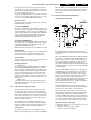
An example can be: Measure test-point I7 and click on the
correct oscillogram you see on the oscilloscope
I7 B7502
L
EXTERNAL 2
R
AUDIO
EXTERNAL 1
SERVICE
CONNECTOR
1V / div DC
10µs / div
PC
VCR
Power
9V DC
I2C
CL96532160_029.eps
110100
Figure 5-4
Figure 5-5
By a combination of automatic diagnostics and an interactive
question/answer procedure, ComPair will enable you to find
most problems in a fast and effective way.
Additional features
Beside fault finding, ComPair provides some additional
features like:
• Uploading/downloading of pre-sets.
• Managing of pre-set lists.
• Emulation of the Dealer Service Tool.
5.4.2
5.4.4
5.4.5
Ordering ComPair
ComPair order codes:
• Starter kit ComPair + SearchMan software + ComPair
interface (excluding transformer): 4822 727 21629
• ComPair interface (excluding transformer): 4822 727
21631
• Starter kit ComPair software: 4822 727 21634
• Starter kit SearchMan software: 4822 727 21635
• Starter kit ComPair + SearchMan software: 4822 727
21636
• ComPair CD (update): 4822 727 21637
• SearchMan CD (update): 4822 727 21638
• ComPair interface cable (for EM1A): 4822 727 21641
Connecting the ComPair interface
The ComPair Browser software should be installed and setup before connecting the ComPair interface to the TV-set
(see the ComPair Browser Quick Reference Card for
installation instructions).
1. Connect the RS232 interface cable to a free serial (COM)
port on the PC and the ComPair interface PC connector
(connector marked with 'PC').
2. Connect the mains adapter to the connector marked
'POWER 9V DC' on the ComPair interface.
3. Switch the ComPair interface 'OFF'.
4. Switch the television set 'OFF' with the mains switch.
5. Connect the interface cable to the connector on the rear
side of the ComPair interface that is marked 'I2C' (see
figure 5-6).
6. Connect the other end of the interface cable to the
ComPair connector on the monocarrier (left to the rear
cinch connectors).
7. Plug the mains adapter in the mains outlet and switch
'ON' the interface. The green and red LEDs light up
together. The red LED extinguishes after approx. 1
second (the green LED remains lit).
8. Start-up ComPair and select 'File' menu, 'Open...:; select
'EM1A Fault finding' and click 'OK'.
9. Click on the icon to switch 'ON' the communication mode
(the red LED on the ComPair interface will light up).
10. Switch 'ON' the TV-set with the mains switch.
11. When the set is in standby, click on 'Start-up in ComPair
mode from standby' in the ComPair EM1A faultfinding
tree, otherwise continue.
Pre-set installation
Pre-sets can be installed via the service cable:
• sending TO the television and reading FROM the
television
• the rear cover does NOT have to be removed
Click on 'File', 'Open' and select 'EM1A fault finding' to use
the cable.
Pre-sets can be installed via menu 'Tools', 'Installation' and
'Pre-sets'.
SearchMan (Electronic Service Manual)
If both ComPair and SearchMan are installed, all the
schematics and the PWBs of the faulty set are available
when clicking on the hyper-link of a schematic or a PWB in
ComPair. Example: Measure the DC-voltage on capacitor
C2568 (Schematic/Panel) at the Monocarrier.
Clicking on the PWB hyper-link automatically shows the
PWB with a highlighted capacitor C2568. Clicking on the
schematic hyper-link automatically shows the position of a
highlighted capacitor at the schematic.
5.4.3
The set has now started up in ComPair mode. Follow the
instruction in the EM1A faultfinding tree to diagnose the set.
Note that the OSD works but that the actual user control is
disabled
5.5
Error codes
5.5.1
Error buffer
The error code buffer contains all errors detected since the
last time the buffer was erased. The buffer is written from left
to right. When an error occurs that is not yet in the error code
buffer, the error is written at the left side and all other errors
shift one position to the right.
The error code buffer will be cleared in the following cases:
• By activating 'CLEAR ERRORS' in the SAM menu:
– Exiting SDM or SAM with the 'Standby' command on
the remote control (by leaving SDM or SAM with the
mains switch, the error buffer is not reset).
– Transmitting the commands 'DIAGNOSE 99 OK' with
the DST (RC7150) or with ComPair
• Automatically reset if the content of the error buffer has
not changed for 50 hours
Examples:
ERROR: 0 0 0 0 0 0 0 : No errors detected
ERROR: 6 0 0 0 0 0 0 : Error code 6 is the last and only
detected error
GB 20
5.
EM1A
Fault finding and repair tips
ERROR: 9 6 0 0 0 0 0 : Error code 6 was first detected and
error code 9 is the last detected (newest) error
error code (and not the actual cause). E.g. a fault in the
protection detection circuitry can also lead to a protection.
The contents of the error buffer can also be made visible
through the 'blinking LED' procedure. This is especially
useful when there is no picture. See paragraph 5.6 'The
blinking LED procedure '.
5.5.2
Error codes
In case of non-intermittent faults, clear the error buffer before
starting the repair. This is to prevent that 'old' error codes are
still present.
If possible, check the entire content of the error buffer. In
some situations an error code is only the result of another
Error Device
Description
Def. item
Diagram
0
1
FBX 3V3 prot
FBX 3V3 protection
5703
B3
2
No HFB
No Horizontal Flyback
0325
A4
3
X-Ray protection
X-Ray protection
4
5 V protection
5 V protection
5
No HOP POR
Startup failure
6
General I2C bus error
General I2C bus error
1200/7651 A7/B6
B4
7
Mains Dip error
HW-error
10
MC24C32
NVM communication error
7012
11
MC24C32
NVM identification error
7012
12
SAA5667
Main µP, int. RAM test failure
7001
B7
13
TEDE9
Main Tuner
1200
A7
14
MSP3415D
MSP34xx
7651
B6
15
CY7C1019
SRAM test failure
7011
B7
C2
B7
16
TELE9
PIP/DW Tuner
7201
17
SAB9081H
Multi PIP-IC
7801
C1
18
M62320P
PIP/DW IO-expander
7403
C3
23
TDA888xx
PIP/DW BOCMA-IC
7301
C4
27
Virtual Dolby
Virtual Dolby error
30
TDA9320
HIP I/O-video processing
7323
B2
31
SAA4978
PICNIC
7709
B3
32
TDA9330
HOP video control/geometry
7301
B4
Explanation of error codes:
Error 0
No errors.
Error 1
This protection is activated, when the PICNIC (pos. 7709 on
diagram B3) can not communicate via I2C for a certain time.
This could mean that stabiliser 7713 is defective. When e.g.
2704 makes a short circuit to ground, 7713 will become very
hot. For safety reasons the set will be switched to protection
mode.
Error 2
The absence of an HFB-pulse (pin 4 of connector 0324 on
LSP, diagram A3) is detected by the HOP (pos. 7301 on
diagram B4). A bit will be set in the HOP. After filtering by the
software, the set will switch to protection mode.
Error 3
Reserved.
Error 4
When the +5 V protection is active, the set is switched to
protection and error code 4 is placed in the error buffer. The
LED will blink 4 times (repeatedly). A 5 V failure can cause
a drop in the 5 V supply output, resulting in an undefined
behaviour of the set. Therefore, some I2C devices (Tuner
and MSP) connected to the 5 V supply are constantly
monitored. When none of these devices responds to the
micro controller for a prolonged time, the micro controller
assumes that there is a failure in the 5 V supply. By starting
up the set via grounding of the FRONT_DETECT-line (on the
side I/O), the +5 V protection will be overruled and it will be
easier to determine the cause. The +5V protection will be
activated when these I2C devices fail (no I2C
communication):
– Main Tuner (pos. 1200 on the LSP),
– MSP34xx sound processor (pos. 7651 on the SSB).
The following tips are useful to isolate the problem area, after
overriding the +5 V protection. Determine whether:
– The MSP sound processor is loading the +5 V; isolate
3650 and/or 4604 (see diagram B6).
– The main Tuner is loading the +5 V source; isolate coil
5200.
Caution! Overriding the +5 V protection when there is a 5 V
failure can increase the temperature in the set and may
cause permanent damage to components. Do not override
the +5V-protection for a prolonged time.
Error 5
Fault finding and repair tips
5.6
Example:
Error code position 1 2 3 4 5
Error buffer:
12 9 6 0 0
After entering SDM: 1 long blink (750 ms.) - pause (1500 ms.)
- 2 short blinks - pause (3 s.) - 9 short blinks - pause (3 s.) 6 short blinks - pause (3 s.) - long blink (3 s.) - etc.
Error 11
During the last start-up, the NVM and the micro controller did
not recognise each other (e.g. one of them was replaced or
the NVM memory has been changed/adapted or lost),
therefore the NVM was loaded with default values.
Error 14
Sound controller MSP34xx (pos. 7651) does not respond to
the micro controller.
Error 15
SRAM test failure (pos. 7011).
Error 16
The Tuner (pos. 7201) on the PIP/DW-panel does not
respond to the micro controller.
Error 17
Multi PIP IC SAB9081 I2C communication failure (pos. 7801
on the PIP/DW-panel).
Error 18
I/O expander IC M62320P I2C communication failure (pos.
7403 on the PIP/DW-panel).
Error 23
BOCMA IC TDA888xx I2C communication failure (pos. 7301
on the PIP/DW-panel).
Error 27
Virtual Dolby IC error.
Error 30
TDA 9320 HIP I/O-video processing (pos. 7323 on the SSB).
Error 31
SAA4978 PICNIC error (pos. 7709 on the SSB).
Error 32
TDA 9330 HOP video control/geometry error (pos. 7301 on
the SSB).
The 'blinking LED' procedure
When the SDM is entered, the LED will blink the contents of
the error-buffer. Error-codes ≥ 10 are shown as follows. A
long blink of 750 msec. which is an indication of the decimal
digit, followed by a pause of 1500 msec, followed by n short
blinks. When all the error-codes are displayed, the sequence
is finished with a LED display of 3 seconds. Then the
sequence starts again.
Error 10
Non Volatile Memory (EEPROM - pos. 7012) does not
respond to the micro controller.
Error 13
Tuner (pos. 1200) is corrupted, the I2C line to the tuner is low,
or there is no supply voltage at pins 7, 4 and 5 of the tuner.
GB 21
The contents of the error buffer can also be made visible
through the 'blinking LED' procedure. This is especially
useful when there is no picture.
Error 7
Flash detection: From the EHT-info, via D6303 and T7303 a
flash will stop the H-drive and line output stage immediately.
The FLS-bit in the status register of the HOP is set to ‘high’.
As the duration of a flash is very short the FLS-bit will be reset
to ‘low’ again after the flash refresh, so via a slow start the set
will be started again. If this interrupt occurs 5 times within an
interval of 10 seconds (indicating a mains interruption), the
set will go into protection and will generate error 7.
Error 12
Microprocessor (Painter - pos. 7001) internal RAM test
failure.
5.
Note:
Error codes 1, 2 and 4 are protection codes and in this case
supplies of some circuits will be switched off. Also in
protection, the LED will blink the number of times equivalent
to the most recent error code.
This error is covered by the Flash/Main routine described at
error 7. When during restart the 8 V remains absent, error 5
will be generated.
Error 6
This will occur in the following cases:
– SCL or SDA is shorted to ground.
– SCL is shorted to SDA.
– SDA or SCL connection at the micro controller is open
circuit.
EM1A
Note: If errors 1, 2 or 4 occur, the LED always gives the last
occurred error, even if the set is NOT in service mode.
5.7
Protections
5.7.1
General
The EM1A has only one microprocessor (Painter) which
remains active during Standby. This because power of the
microprocessor and the memories is coming from the 3V3
supply, which is derived from the 5V Standby-circuitry. So in
both Power-on as in Standby-mode the microprocessor is
connected to this power supply.
If a fault situation is detected an error code will be generated
and if necessary the set will be put in the protection-mode.
The protection-mode is indicated by blinking of the red LED
at a frequency of 3 Hz. In some error cases the
microprocessor does not put the set in the protection-mode.
The error codes of the error buffer can be read via the
service-menu (SAM), the blinking LED procedure or via DST/
ComPair. The DST diagnose functionality will force the set
into the Service-standby, which is alike the usual Standby,
however the microprocessor has to remain in normal
operation completely.
To get a quick diagnosis the EM1A has 3 service-modes
implemented:
• The Customer Service Mode (CSM).
• The Service Default Mode (SDM). Start-up of the set in a
predefined way.
• The Service Alignment Mode (SAM). In this mode items
of the set can be adjusted via a menu and with the help
of test patterns.
The 'Protection Diagram' shows the structure of the
protection system. See diagram below.
GB 22
5.
HFB X-RAY PROTECT
Fault finding and repair tips
EM1A
positioned in ‘Standby’-mode. The Painter will now try to restart the set. If this will not succeed after 5 times (after ≈ 30 60 s.), the Painter will generate error 7 (this error can have
several causes, such as a Flash, BRIDGE_PROT,
DEFL_PROT or a serious mains dip). A blinking red LED will
be started.
X-RAY PROTECT
EHT-INFO
BCL
XPR (43)
HOP
FLS (5)
FLASH DETECT
HFB
NHF (13)
5.8
Repair tips
5.8.1
General
I2C
RESET
COLD
POR-bit
IF NOT POR: ERROR 5 IS
GENERATED
73
I2C-bus
OUT
START/
STOP
PAINTER
7308
I2C SLOW BUS
79
+5V2
HOP
7324
START/
STOP
29
STANDBY INFO
STANDBY-POR
7013
5V STANDBY
PAINTER
NVM
CUT OFF
7306
MSP
FBX
PROTECTION
44
(TEMPORARELY LOW THEN HIGH
LIKE STARTING A CAR)
PICNIC
TUNER
HOP
22
13
(OUT)
HIP
HOT
PICNIC 3V3
I2C
STANDBY-POR
I2 C
MAIN SUPPLY
STANDBY
TUNER
PROTECTION
TUNER 8V
CL 06532111_055.eps
121000
NON-VFB
DEFL.
BRIDGE-PROT
CL 06532111_056.eps
121000
Figure 5-6
Figure 5-7
There are several types of protections:
• I2C related protections (e.g. +5V supply check).
• HOP related protections (mainly for deflection items).
• Hardware errors which are not sensed by the Painter
(e.g. BRIDGE_PROT)
I2C related protections
In normal operation some registers of the I2C controlled IC's
will be refreshed every 200 msec. During this sequence the
I2C-busses and the I2C -IC's as well will be checked. The I2C
protection will take place if the SDA and SCL are whether
short-circuited to ground or to each other. An I2C error can
also occur, if the power supply of the IC is missing (e.g.
FBX_PROT; error 1).
HOP related protections
Every 200 msec. the status register of the HOP is read by the
Painter via I2C. If a protection signal is detected on one of the
inputs of the HOP, then the relevant error bit in the HOP
register is set to ‘high’. If the error bit is still ‘high’ after 1 sec.,
the Painter will store the error code in the error buffer (NVM)
and depending on the relevancy of the error bit the set will
either go into the protection-mode or not.
• HFB: Horizontal Flyback. If the horizontal flyback is not
present, then this is detected via the HOP (HFB_XRAY_PROT). One status bit is set to ‘high’. The error
code is stored in the error buffer and the set will go into
the protection mode
• Flash detection. From the EHT-info, via D6303 and
T7303 a flash will stop the H-drive and line output stage
immediately. The FLS-bit in the status register of the
HOP is set to ‘high’. As the duration of a flash is very
short the FLS-bit will be reset to ‘low’ again after the flash
refresh, so via a slow start the set will be started again.
Hardware related protections
Due to the architecture (with 'hot' deflection) there are two
protections that are 'unknown' to the microprocessor, namely
the 'BRIDGE_PROT' (coming from the line stage) and the
'DEFL_PROT' protection (coming from the frame deflection
stage). If one of these protections is triggered, the set is
The start-up of the set is very different as of other sets (see
fig. 5-7 & 5-8):
1. When the set is switched ‘ON’, first the HOP is placed in
'low power start-up' mode (HOP-standby-mode). This
means that 5 V (derived from available Standby-supply)
is connected to pin 22 of the HOP-IC.
2. Now the HOP is driving the line-circuitry with 50 kHz
pulses. At the base of the line-transistor this is sensed via
the 'STANDBY’-line.
3. This signal triggers the Main supply to operate. Now the
line-stage has 'BAT'-voltage (141 V), it will also start.
4. After the 5 and 8 V-supply lines are sensed by the Painter
(via I2C), it will read the POR-bit from the HOP via the
I2C-bus.
5. Now the HOP is switched in ‘ON’-mode and the set will
start-up further with normal drive (31.25 kHz for PAL).
6. The last step will be the unblanking of the picture.
So standby is not controlled via a standby-line from
microprocessor, but is achieved indirectly via the HOPcircuitry.
Fault finding and repair tips
EM1A
5.
GB 23
off
Standby supply starts oscillating
Standby-supply is running; +3.3V, +5V2 ready
'Standby-info' = high; µP has been reset by POR
Low_power_standby
High_power_standby
Degaussing is activated automatically and should
be acivated after 12 seconds
Standby bit set in NVM?
yes
no
Initialize I/O pins of the OTC
Make 'Standby-info' low
'Standby-info' remains
high
Supply is in standby-mode
Mute
5V2 present on the HOP. HOP starts in low power start up mode
Deflection starts on 50kHz; +5V and +8V become present
+5V and +8V levels can be detected by the Painter. Vcc of the HOP is present.
Activate protection for +8V and +5V
Main_power_on
Wait 1500ms and reset MSP
(Sound-IC)
read POR bit from the HOP
Standby high
Go to protection
Error code 05
'HOP POR
not successfull'
no
From here onwards,
I2C communication is
possible
POR available within 1 second ?
yes
Put 'Standby-INFO' high again
Give HOP_start_commando within 23.5 ms after a
POR is obtained from the HOP
DISABLE I2C while EHT is starting up: 250ms
Activate I2C protection. Set protection algorithms active for
I2C, +5V, +8V, HFB, FBX
HOP_on
Initialize I2C IC's
Set Black Current Stabilisation = Active
on
CL 06532130_021.eps
171000
Figure 5-8
GB 24
•
•
•
•
5.8.2
5.
EM1A
Fault finding and repair tips
Notice that a very big part of the set (Large Signal Panel)
is 'hot', meaning the primary part of the Standby supply,
the whole Main supply (except for the secondary Audio
supply) and the complete deflection circuit. So notice
that the deflection-coil is hot!
This set does not have an IR transmitting-LED. In its
place, a Service (ComPair) connector is implemented at
the rear of the set, which is directly accessible. In addition
to this, there is a blinking LED procedure to show the
contents of the error buffer.
The relay you hear during switching 'ON' (via the main
switch) is from the degaussing-circuitry. So it is not used
for switching the supply as in the MG-chassis.
When there is a menu in the picture, entry of servicemodes cannot be performed. So see to it that there is no
menu on the picture.
Repair tips
'Repair-tips how to repair the Main power supply:
• Simplest way is to replace components of the Main
supply with repair kit (3122 785 90260)
• More detailed way:
– Replace FET 7504 and zener 6505
– Remove SSB-panel
– Short-circuit BE of TS7529 in order to put supply in
‘on’-mode (TS7529 is blocking then)
– Load capacitor C2515 (VBAT) with a load of 500
ohm. Supply can not work without a minimum load.
– Use a variac to slowly increase the VMAINS.
Measure over sensing-resistors R3514/15 whether a
nice sawtooth-voltage becomes available. Also
measure the VBAT-output
– VBAT may never exceed 141 V. If so there is
something wrong in the feedback-circuitry (e.g.
regulator 7506)
Repair-tips how to repair the Standby power supply:
• Simplest way is to replace components of the Standby
supply with repair kit (3122 785 90270)
Repair-tips how to repair the Deflection-circuitry:
• Simplest way is to replace components of the Deflectioncircuitry with repair kit (3122 785 90120)
Service-tips:
• Be careful measuring on gate of FET 7504. Circuitry is
very high ohmic and can easily be damaged.
• Take care not to touch ‘hot’ heatsink while disconnecting
SSB, despite the fact that mains cord is out of mains
socket. There still is an annoying rest-voltage for a short
while.
• Do not try to measure on side of SSB directed to the hot
heatsink. This is dangerous. All service test points are
guided to the Tuner side and are pointed out by service
printing. Where the circuitry was too crowded to place
this service-printing it has been explained on the Test
point overviews in this manual
Fault finding and repair tips
EM1A
5.
GB 25
Phenomenon
Possible Cause
Repair tip
No picture, no LED.
Standby Supply defective.
No picture, red LED
(high intensity).
Despite expectation,
the set should be ON
(this looks like
Standby). After some
time LED will start
blinking.
Set going into
protection after 5
restarts (error 7),
taking about 30 - 60 s.
No picture, red LED
blinking (3 Hz)
There are 2 protections (which
are not ’seen’ by the processor)
that force the set in protection
(after 5 restart attempts):
BRIDGE_PROT or MAINS DIP
error.
Measure circuitry (see diagram A2). Start at test-point P16.
Regardless the mode of the set, this voltage should always be available.
If protection is activated due to an absence of the Frame deflection, this
can be measured on test-point F10 (diagr. A4). Error 33 will be generated.
The BRIDGE_PROT could be triggered by an E/W failure.
An MAINS_DIP error (error 7) will be generated in both cases after 5
restart attempts, and will be visible via the blinking LED procedure.
No picture, red LED
blinking (code 6, 6, 6)
No communication on I2 C1-bus
(’devices’ bus) to processor. Set
is in protection-mode
No communication on I2 C3-bus
(’NVM’ bus) to processor. Set is
in protection-mode
Supply could be in hiccup-mode
which can be heard via supplytransformer squeaking
No picture, red LED
blinking (code 10, 10,
10)
No picture, no sound,
set is making audible
squeaking sound
No picture, no sound,
LED works fine
No RC5-reception.
Red LED does not
echo RC-commands.
Relay-activation
(degaussing) not
audible when switch
set on from off .
No sound, but picture.
No sound at
headphone output.
Picture is rotated.
No picture.
Picture looks like
cushion, further OK
Very white picture,
with flyback lines
visible
Un-sharp picture
Un-synced picture
Picture distorted.
No menu, OSD.
180 V missing on CRT-panel
(diagr. F). Most probably R3341
is interrupted, or RGB-amplifier
IC7307 is defective.
Set is in protection due to
various causes. For error codes
see error code list.
ComPair is very useful here.
Measure 180 V behind R3341 (diagr. F) while operating, or measure
resistance of R3341 while set is of.
You have no picture, so:
Read out the error buffer via ComPair.
Read out blinking LED information via ’DIAGNOSE X’ with DST.
When error is known, check circuitry related to supply voltage and I2C communication.
Measure, dependent of the error, on the I2C-bus which device is loading
the bus. This protection can be overruled via SDM-entry (via shortcircuiting FRONT_DETECT to GND on Side I/O).
No contact of processor with the NVM. A lot of settings will therefore be
wrong.
Supply does not work correctly
This could be caused by:
Short-circuited V BAT (caused by short circuited line transistor 7421) or
Short-circuited sound-winding (amplifier is short-circuiting 28 V) or
Short-circuited D6514 (due to a too high V BAT ).
Delete excessive load to see where failure is caused by or check feed
back circuit. See repair-tip main power supply (supply needs a minimal
load).
If e.g. VBAT is only about 90 V, regulator-IC 7506 could be damaged.
Processor-circuitry or RCreceiver is wrong.
In case set reacts on local keyboard operation, error must be found in the
IR-receiver circuitry (diagram J).
Processor not working correctly.
Check RESET-circuitry on diagram B5. When switching on the set all I/opins of processor should become high for a moment, so also the degaussinput signal.
Measure P7 on diagram A1.
Possible sound-amplifier is
defect (but not short-circuited),
or sound-enable line is high
(see diagram A5).
Further the audio-signal path
must be measured (HIP, MSP,
switch-IC s, amplifier).
Discrete amplifiers or supply to
it could be damaged.
Rotation-circuitry or supply to it
could be damaged (if present).
Check functionality and cabling
Tuner to SSB.
Or NVM-content is overwritten
or E/W-MOSFET is shortcircuited
180 V is missing on CRT-panel
Measure and repair. With ComPair there is a beep-test that can determine
where the signal stops (use loudspeakers, headphone).
Focus could be misaligned or
SCAVEM-circuitry does not
work correctly
Sync is derived in HIP-IC from
X-tals 1309 and/or 1310
Check video-path, service
default mode.
Align focus-potmeter of Line Transformer; check SCAVEM-circuitry on
CRT-panel [F].
Probably processor is defective.
Measure A12, A13, A14, A15 and supply-line on diagram A6.
Measure test-points F3, R1, R2 on diagram A4.
Notice cable 1946.
First check in Service Alignment Mode, whether geometry can be
restored. If not check test point L4 and diagram A3, or measure with an
ohmmeter whether TS7480 is defective.
Probably R3468 on LSP (diagram A3) is interrupted, or bad connection
plug 0324 to 0224 (CRT-panel).
Maybe an X-tal is making bad contact.
Investigate whether there exists an error code in the error buffer.
In case there is an error code, check I2C-bus and/or supply-lines (see
overview supply-lines).
Measure and check signal path Tuner, HIP, PICNIC, HOP, RGB-amplifier.
In case it is a geometry-issue, check Frame-circuitry, alignments or
possible corrupted NVM (7012)
Measure test points C7, C8, C9, C10 on diagram B7.
CL 06532111_057.EPS
121000
GB 26
5.
Personal notes:
EM1A
Fault finding and repair tips
Alignments
EM1A
8.
GB 77
8. Alignments
Note: The Service Default Mode (SDM) and Service
Alignment Mode (SAM) are described in chapter 5.
8.1
General alignment conditions
max.
All electrical adjustments should be performed under the
following conditions:
• Supply voltage: 110 / 220 V (± 10 %); 50 / 60 Hz (± 5 %)
• Warm-up time: ≈ 20 minutes
• The voltages and oscillograms are measured in relation
to the tuner earth (with exception to the voltages on the
primary side of the power supply). Never use the cooling
fins / plates as ground.
• Test probe: Ri > 10 MΩ; Ci < 2.5 pF.
• Use an isolated trimmer / screwdriver for the alignments.
8.2
VCUTOFF [VDC]
0V Ref.
CL 06532130_014.eps
131000
Figure 8-2
8.2.2
1. Tune the set to a circle or crosshatch test pattern (use an
external video pattern generator).
2. Adjust the 1st Focus potmeter (upper LOT potmeter, see
figure 8-1) until the horizontal and vertical lines at 1/4
from east and west, at the height of the centre line, are of
minimum width without visible haze.
3. Adjust the 2nd Focus potmeter (middle LOT potmeter,
see figure 8-1) until the horizontal and vertical lines at 1/
4 from north and south, at the height of the centre line,
are of minimum width without visible haze.
Alignments on the large signal panel (LSP)
Large Signal panel (LSP)
Warning
8.3
Alignments and settings in the Service
Alignment Menu
8.3.1
General
SSB
All alignments
are on hot-part !
With the software alignments of the Service Alignment Mode
the Geometry, White tone and Tuner (IF)can be aligned. Put
the set in the SAM mode (see chapter 5). The SAM menu will
now appear on the screen.
Menu navigation is done with the 'CURSOR UP, DOWN,
LEFT or RIGHT' keys of the RC-handset.
LOT
Focus 1
Focus 1
Screen
3480
TUNER
CINCH
3603
3609
V.AMPL
H.AMPL
V.SHIFT
CL 06532130_013.eps
031000
Figure 8-1
8.2.1
Focusing
Vg2 adjustment
8.3.2
Geometry
The geometry alignments menu contains several items to
align the set, in order to obtain a correct picture geometry.
East/West Trapezium
Rough method
Using a pattern generator displaying a black pattern (PAL
BG, 475.25 MHz), adjust the Vg2 potmeter of LOT (item
5430) to obtain normal picture (without visible fly-back lines).
Accurate method
1. Connect the RF output of the pattern generator to the
antenna-input of the TV. Test pattern is a 'black' pattern
(blank screen on CRT without any OSD info).
2. Set the channel of the oscilloscope to 50 V/div and the
time base to 5 ms. Select 'external triggering' on the
vertical pulse (anode of diode 6619, located near
connector 0325 to frame deflection coil).
3. Measure the black level pulse during the vertical flyback
(1st full line after the frame blanking) at the R, G and B
cathodes of the CRT (pin 8, 6 and 11 of the CRT
connector). Select the cathode with the highest VDC
value for the measurement.
4. Adjust Vcutoff with the Vg2 (SCREEN) potmeter of the
LOT to 170 ± 2 VDC.
East/West Parabola
Horizontal Bow
CL 96532156_012.eps
250100
Figure 8-3
GB 78
8.
EM1A
Alignments
Initial set-up
1. Connect an external video pattern generator (PAL BG,
475.25 MHz) to the aerial input of the TV-set with a
crosshatch test pattern.
2. Set 'Smart Picture' to NATURAL.
3. Activate the SAM-menu (see chapter 5).
4. Go to sub-menu GEOMETRY. Now the following
alignments can be performed:
4. If the frequency showed in the line 'Fine tune' is between
471.18 MHz and 471.31 MHz, you don't need to re-adjust
the IF-AFC.
5. If not, adjust the frequency in the 'Fine tune' line to
471.25 MHz and store the program by leaving the menu
(this is very important because this will disable the AFC
algorythm).
6. Now go to the SAM and select 'Alignments' - 'General' 'IF AFC'.
7. First you must align the 'IF AFC'-parameter such that you
come into the AFC-window (AFA = 1)
8. Then you must look for the point where the AFBparameter changes from 1 to 0. This level is the value
you are looking for.
9. After adjustment store the value by returning to the
former menu.
10. Now return to the 'Installation' menu.
11. Select 'Manual Installation' - 'Search' - '47' - 'OK' and
store it. This will set the AFC 'on' again.
12. During the 'IF PLL'-parameter adjustment, one can see
feedback at the screen, by means of the 'AFA' and 'AFB'
indication (see table).
Vertical slope (VER. SLOPE)
Align the vertical centre of the picture to the vertical centre of
the CRT.This is the first alignment to be performed of the
vertical alignments. For an easy alignment set SERV.BLK to
ON.
Service blanking (SERV. BLK)
Switch the blanking of the lower half of the screen ON/OFF
(to be used in combination with the vertical slope alignment).
Vertical amplitude alignment
Align the vertical amplitude with potentiometer R3603 on the
LSP (see Fig. 8-1) so that the complete test pattern is visible.
Vertical shift alignment
Align the vertical centering with potentiometer R3609 on the
LSP (see Fig. 8-1) so that the test pattern is located vertically
in the middle. Repeat the 'vertical amplitude' alignment if
necessary.
Horizontal shift (HOR. SHIFT)
Align the horizontal centre of the picture to the horizontal
centre of the CRT.
Horizontal parallelogram (HOR. PARALLEL)
Align straight vertical lines in the top and the bottom; vertical
rotation around the centre.
East West width (EW. WIDTH)
Align the picture width until the complete test pattern is
visible.
East West Trapezium (EW. TRAP)
Align straight vertical lines in the middle of the screen.
East West Upper Corner (EW. UCORN)
Align straight vertical lines in the upper corners of the screen.
East West Lower Corner (EW. LCORN)
Align straight vertical lines in the lower corners of the screen.
Tuner (Large Signal Panel and Double Window)
IF PLL OFFSET
Supply, via a video generator (e.g. PM5518), a TV-signal
(e.g. colour bar) with a signal-strength of at least 1 mV and a
frequency of 471.25 MHz (use BG if possible, otherwise
match the system of your generator with the received signal
in the set).
Alignment procedure:
1. Go to the 'Installation' menu.
2. Select 'Manual installation'.
3. Tune the TV-set to the system and frequency described
above via 'Search' - '471' - 'OK'.
IF-PLL offset
0
Decrease offset value
0
1
Increase off-set value
1
0
Correct
1
1
Correct
2ND AGC
Set pattern generator (e.g. PM5418) to a colour bar video
signal and connect the RF output to aerial input. Set
amplitude to at least 1 mV and set frequency for PAL-BG to
471.25 MHz.
1. Activate the SAM-menu. Go to the sub-menu TUNER,
and select the '2nd AGC' sub-menu.
2. Connect a DC multi-meter to pin 1 of the tuner (7201 on
DW panel).
3. Adjust the 2nd AGC until the voltage at pin 1 of the Tuner
is just below 3.8 V.
4. The value can be incremented or decremented by
pressing the MENU LEFT/RIGHT button on the RC.
5. Switch the set to STANDBY.
East West parabola (EW. PARA)
Align straight vertical lines at the sides of the screen.
Note: Described alignments are only necessary when HIP or
NVM is changed.
AFB
0
AGC
Set pattern generator (e.g. PM5418) to a colour bar video
signal and connect the RF output to aerial input. Set
amplitude to at least 1 mV and set frequency for PAL-BG to
471.25 MHz.
1. Activate the SAM-menu. Go to the sub-menu TUNER,
and select the 'AGC' sub-menu.
2. Connect a DC multi-meter to pin 1 of the tuner (item
1200 on LSP).
3. Adjust the AGC until the voltage at pin 1 of the Tuner is
just below 3.8 V.
4. The value can be incremented or decremented by
pressing the MENU LEFT/RIGHT button on the RC.
5. Switch the set to STANDBY.
Horizontal bow (HOR. BOW)
Align straight horizontal lines in the top and the bottom;
horizontal rotation around the centre.
8.3.3
AFA
8.3.4
Black cut off
In the WHITE TONE sub menu, the values of the black cut off
level can be adjusted. The colour temperature mode
(NORMAL, DELTA COOL, DELTA WARM) or the colour (R,
G, B) can be selected with the UP/DOWN RIGHT/LEFT
cursor keys. The value can be changed with the RIGHT/
LEFT cursor keys.
First the values for the NORMAL colour temperature should
be selected. Then the offset values for the DELTA COOL and
DELTA WARM mode can be selected (note that the
alignment values are non-linear).
• +1 to +63 represent a positive offset (63 is the maximum
positive offset).
Alignments
•
-63 to -1 represent a negative offset (-63 is the minimum
negative offset).
1. Set pattern generator (e.g. PM5418) to a white spot
(chess board) pattern and connect RF output with aerial
input. Set amplitude to 1 mV and set frequency for PALBG to 475.25 MHz.
2. Set CONTRAST to the maximum value (99).
3. NORMAL settings
– NORMAL RED = 32
– NORMAL GREEN = 32
– NORMAL BLUE =32
4. COOL settings
– DELTA COOL RED = -3
– DELTA COOL GREEN = 0
– DELTA COOL BLUE = 3
5. WARM settings
– DELTA WARM RED = 4
– DELTA WARM GREEN = 0
– DELTA WARM BLUE = -8
6. CUT OFF (default) settings
– BLACK LEVEL R = 7
– BLACK LEVEL G = 7
7. Measure with a colour analyser (calibrated with the
spectra) on the centre of a white square on the screen.
Adjust the values of BLACK LEVEL R and BLACK
LEVEL G to get the right XY-coordinates for Tint =
Normal (see table 8-1).
Note: When there is no colour analyser available, use the
default settings mentioned above.
8.3.5
Light output
In the WHITE TONE sub menu, also the light output of the
CRT can be adjusted. In this case a colour analyser is
necessary.
1. Set pattern generator (e.g. PM5418) to a white spot
pattern and connect RF output to aerial input. Set
amplitude to 1 mV and set frequency for PAL-BG to
475.25 MHz.
2. Set CONTRAST to the maximum value (99).
3. Measure with a colour analyser (calibrated with the
spectra) on the centre of the white square on the screen.
Adjust the level of NORMAL RED, NORMAL GREEN
and NORMAL BLUE in a simultaneous way to get the
360 cd light output.
8.3.6
White drive
In the WHITE TONE sub menu, the values of the WHITE
DRIVE level can be adjusted. The colour temperature mode
(NORMAL, DELTA COOL, DELTA WARM) or the colour (R,
G, B) can be selected with the UP/DOWN RIGHT/LEFT
cursor keys. The value can be changed with the RIGHT/
LEFT cursor keys.
1. Set pattern generator (e.g. PM5418) to a white spot
pattern and connect RF output to aerial input. Set
amplitude to 1 mVRMS and set frequency for PAL-BG to
475.25 MHz.
2. Set CONTRAST to the maximum value (99).
3. Measure with a colour analyser (calibrated with the
spectra) on the centre of the white square on the screen.
Adjust the level of NORMAL BLUE and NORMAL RED to
get the right XY-coordinates. See table 8-1.
Table 8-1
Tint
Temperature (K) X
Y
Warm
8700
299
289
Normal 13500
266
274
Cool
256
264
18300
8.4
Options
8.4.1
Options
EM1A
8.
GB 79
Options are used to control the presence / absence of certain
features and hardware. There are two ways to change the
option settings (see also fig. 8-3):
Changing a single option
An option can be selected with the MENU UP/DOWN keys
and its setting can be changed with the MENU LEFT/RIGHT
keys.
Changes in the option settings are saved by leaving the
OPTION submenu. Some changes will only take affect after
the set has been switched OFF and ON with the mains switch
(cold start).
Changing multiple options by changing option byte
values
Changing the option bytes directly, makes it possible to set
all options very fast. An option byte (OB1..8) can be selected
with the MENU UP/DOWN keys and its setting can be
changed with the MENU LEFT/RIGHT keys. An option byte
represents a number of different options. All options of the
EM1A are controlled via 8 option bytes. Select the option
byte (OB1..OB8) and key in the new value.
Changes in the option byte settings are saved by leaving the
OPTION submenu. Some changes will only take affect after
the set has been switched OFF and ON with the mains switch
(cold start).
Option bits/bytes
An option byte value is calculated in the following way:
Value 'option bit 1' x 1 =
Value 'option bit 2' x 2 =
Value 'option bit 3' x 4 =
Value 'option bit 4' x 8 =
Value 'option bit 5' x 16 =
Value 'option bit 6' x 32 =
Value 'option bit 7' x 64 =
Value 'option bit 8' x 128 =
========================
Total: value 'option byte' =
2 Software versions are used: 1A1 and 2A1/2A2. Below find,
in table 8-2 and 8-3, the option definition for both versions (for
an explanation of the SW-version versus country code see
table in chapter 5.2.2, page 16).
GB 80
8.
EM1A
Alignments
Option table (version 1A1):
Table 8-2
Byte
Bit
Abbr.
Feature
Description (OFF = 0, ON = 1)
OB1
1
AUSB
Auto Standby After 2hrs
OFF = function disabled / ON= function enabled
OB1
2
AV3
Side AV source
OFF = side AV source not available / ON = available
OB1
3
HOSP
Hospitality mode
OFF = hospital mode disabled / ON = enabled
OB1
4
E149
Picture setting for expand 14:9
OFF = not available in FORMAT menu / ON = available
OB1
5
C169
Pict. setting for compress 16:9
OFF = not available in FORMAT menu / ON = available
OB1
6
CVI
External source selection for PIP OFF = disabled / ON = enabled
OB1
7
SBNP
Auto Standby with no picture
OB1
8
ASBY
Auto Standby After 2 hours
OFF = no switch to stdby / ON= switch to stdby after 10m. when no ident
OFF = disabled / ON = active after 2 hrs of no RC or keyboard response
OB2
1
PIPC
PIP Control
OFF = disabled / ON = enabled
OB2
2
BLMU
Blue Mute
OFF = disabled / ON = enabled
OB2
3
SOSD
Smart OSD
OFF = full display of OSD not available / ON = available
OB2
4
PLST
Program List
OFF = access to Command is ignored / ON = access is processed
OB2
5
PITN
Philips tuner
OFF = ALPS compatible tuner used / ON= Philips compatible tuner used
OB2
6
VDBY
Virtual Dolby
OFF = Virtual Dolby not available / ON = Virtual Dolby is available
OB2
7
IPMU
Incredible picture via menu
OFF = menu item 'INCR. PICT' not available / ON = available
OB2
8
CBFL
Comb filter
OFF = no comb filter on the SSB / ON = comb filter present on the SSB
OB3
1
SURF
Surf
OFF = disabled / ON = enabled
OB3
2
CHNA
China set
OFF = disabled / ON = enabled
OB3
3
VSLC
Vertical slicing
OFF = disabled / ON = enabled
OB3
4
W169
Double Window 16:9
OFF = disabled / ON = enabled
OB3
5
W4X3
Double Window 4:3
OFF = disabled / ON = enabled
OB3
6
PIPF
PIP Functionality
OFF = disabled / ON = enabled
OB3
7
PIPT
PIP Tuner
OFF = disabled / ON = enabled
OB3
8
PIPS
PIP Surf
OFF = disabled / ON = enabled
OB4
1
APC
Auto Picture Control
OFF = Time Window is set to 2 s. / ON = Time window is set to 5 s.
OB4
2
INCF
Internal Combfilter
OB4
3
TMWIN Time Window
OFF = disabled / ON = enabled
OFF = Time Window is set to 2 s. / ON = Time window is set to 5 s.
OB4
4
SNIC
Sound IC MSP3451
OFF = sound IC MSP3451 not present / ON = present
OB4
5
ROTI
Rotation tilt
OFF = menu item 'ROTATION' not available / ON = available
OFF = function disabled / ON = enabled
OB4
6
CHLK
Child Lock
OB4
7
AAVL
Automatic Volume Leveller
OFF = menu item 'AVL' not available / ON = menu item available
OB4
8
TIME
Timer
OFF = disabled / ON = enabled
OB5
1
N/A
(RESERVED)
N/A
OB5
2
N/A
(RESERVED)
N/A
OB5
3
N/A
(RESERVED)
N/A
OB5
4
N/A
(RESERVED)
N/A
OB5
5
N/A
(RESERVED)
N/A
OB5
6
N/A
(RESERVED)
N/A
OB5
7
N/A
(RESERVED)
N/A
OB5
8
PAGC
PICNIC AGC
OFF = disabled / ON = enabled
OB6
1..8
N/A
(RESERVED)
N/A
OB7
1..8
N/A
(RESERVED)
N/A
OB8
1..8
N/A
(RESERVED)
N/A
Alignments
EM1A
8.
GB 81
Option table (version 2A1 / 2A2):
Table 8-3
Byte
Bit
Abbr.
Feature
OB1
1
AV3
Side AV source
Description (OFF = 0, ON = 1)
OFF = side AV source not available / ON = available
OB1
2
SMCK
Smart clock
OFF = function disabled / ON= function enabled
OB1
3
HOSP
Hospitality mode
OFF = hospital mode disabled / ON = enabled
OB1
4
E149
Picture setting for expand 14:9
OFF = not available in FORMAT menu / ON = available
OB1
5
C169
Pict. setting for compress 16:9
OFF = not available in FORMAT menu / ON = available
OB1
6
CVI
External source selection for PIP
OFF = function disabled / ON= function enabled
OB1
7
SBNP
Auto Standby with no picture
OFF = no switch to stdby / ON= switch to stdby after 10m. when no ident
OB1
8
ASBY
Auto Standby After 2 hours
OFF = disabled / ON = active after 2 hrs of no RC or keyboard response
OB2
1
SOSD
Smart OSD
OFF = full display of OSD not available / ON = available
OB2
2
PLST
Program List
OFF = access to Command is ignored / ON = access is processed
OB2
3
PITN
Philips tuner
OFF = ALPS compatible tuner used / ON= Philips compatible tuner used
OB2
4
VDBY
Virtual Dolby
OFF = Virtual Dolby not available / ON = Virtual Dolby is available
OB2
5
NTSC
NTSC playback
OFF = not possible via EXT-in / ON= function enabled
OB2
6
IPMU
Incredible picture via menu
OFF = menu item 'INCR. PICT' not available / ON = available
OB2
7
CBFL
Comb filter
OFF = no comb filter on the SSB / ON = comb filter present on the SSB
OB2
8
AUSB
Auto Standby auto on
OFF = function disabled / ON= function enabled
OB3
1
W4X3
Double Window 4:3
OFF = function disabled / ON= function enabled
OB3
2
ISUR
Incredible Surround
OFF = function disabled / ON= function enabled
OB3
3
PIPF
PIP Functionality
OFF = function disabled / ON= function enabled
OB3
4
PIPT
PIP Tuner
OFF = function disabled / ON= function enabled
OB3
5
PIPS
PIP Surf
OFF = function disabled / ON= function enabled
OB2
6
PIPC
PIP Control
OFF = function disabled / ON= function enabled
OB3
7
BLMU
Blue Mute
OFF = function disabled / ON= function enabled
OB3
8
FAPG
Favorite page
OFF = function disabled / ON= function enabled
OB4
1
CHLK
Child Lock
OFF = function disabled / ON= function enabled
OB4
2
AAVL
Automatic Volume Leveller
OFF = menu item 'AVL' not available / ON = menu item available
OB4
3
TIME
Timer
OFF = function disabled / ON= function enabled
OB4
4
DTXT
Double window TXT
OFF = function disabled / ON= function enabled
OB4
5
TXT
Teletext available
OFF = function disabled / ON= function enabled
OB4
6
SURF
Surf
OFF = function disabled / ON= function enabled
OB4
7
VSLC
Vertical slicing
OFF = function disabled / ON= function enabled
OB4
8
W169
Double Window 16:9
OFF = function disabled / ON= function enabled
OB5
1
N/A
(RESERVED)
N/A
OB5
2
N/A
(RESERVED)
N/A
OB5
3
APC
Auto Picture Control
OFF = disabled / ON = enabled
OB5
4
PAGC
PICNIC AGC
OFF = disabled / ON = enabled
OB5
5
INCF
Selection colour delay line
OB5
6
TMWIN Time Window
OFF = disabled / ON = enabled
OFF = Time Window is set to 2 s. / ON = Time window is set to 5 s.
OB5
7
SNIC
Sound IC MSP3451
OFF = sound IC MSP3451 not present / ON = present
OB5
8
ROTI
Rotation tilt
OFF = menu item 'ROTATION' not available / ON = available
OB6
1..8 N/A
(RESERVED)
N/A
OB7
1..8 N/A
(RESERVED)
N/A
OB8
1..8 N/A
(RESERVED)
N/A
GB 82
9.
Circuit descriptions and abbreviation list
EM1A
9. Circuit descriptions and abbreviation list
9.1
Circuit descriptions
The architecture consists of a conventional Large Signal
Panel (LSP) a Double Window panel (DW) and a Small
Signal Board (SSB) module, placed into a so-called SIMMconnector (Standard Interface, 80 pins).
The following circuits are described:
1. Introduction
2. Block diagrams
3. Power supply
4. Control & Teletext
5. Tuner & IF
6. Video: High-end Input Processor
7. Video: Feature box
8. Video: High-end Output Processor
9. Synchronisation
10. Horizontal deflection
11. Vertical deflection
12. Audio
13. CRT & SCAVEM
14. Double Window (DW)
9.1.1
The LSP is built up very conventional, with hardly any surface
mounted components on the copper side. Difference with the
MG-chassis is that the EM1A LSP has a very large 'hot' part,
including the deflection coil.
The SSB is a high tech module (2 sides reflow technology,
full SMC) with very high component density and complete
shielding for EMC-reasons. Despite this, it is designed in
such a way, that repair on component level will be possible.
To achieve this, attention has been paid to:
• The position of service test lands (Tuner side).
• Accessibility (Tuner side).
• Clearance around surface mounted IC's (for replacing).
• Diagnostics & Fault Finding via ComPair.
Introduction
The EM1A is a lower specified MG-chassis. EM stands for
Eco-MG, 1 for the used processor (Painter) and A stands for
Asian Pacific.
The user interface and processor are the same as used in the
A10A set. In the EM1A however, a HIP, PICNIC and HOP are
used for the 100 Hz function i.s.o. the BOCMA in the A10A.
So the HIP and HOP have the same functionality as the
BOCMA (to let the set work in 2fH-mode), while the PICNIC
is used for video features like AutoTV and Freeze.
Protection: The start-up behaviour of the EM1A is different
then that of the MG-chassis, meaning that there does not
exist a situation as in the MG where we have 'supply ON/
deflection circuit OFF'.
This means that isolating failures in the EM1A must be done
in a different way. See Chapter 5 of this manual.
Block diagrams
PIP/DW MODULE
TUNER
PIP/DW
IF
FILTER
VIF
SIF
YUV
DW
PROC.
BOCMA
AUDIO-PIP
TUNER
IF
FILTER
YUV50
VIF
HA
SIF
VA
PROZONIC
FBL
PICNIC (FBX)
SPLITTER
YUV
VD
HD100
HIP
HOP
HD
VIDEO-EXT
MONITOR-OUT (A+V)
CVBS-TEXT
RGB-TEXT
(V)
E/W
TOP
CONTROL
NVM
IR
REC.
TXT
RAM
EHT
180V
141V
28V
SIF
AUDIO-PIP
AUDIO-EXT
L
MSP
R
AMPL
E/W
R
CRT
G
+
B
SCAVEM
CRT
SCAVEM
L
S/W
(A) MONITOR-OUT
R
ETC.
LOW
POWER
STBY
HOR
FBL-TEXT
AUDIO-EXT
PAINTER
EXT
I/O
VERT
VDHOP
VD100
COMB
FILTER
POWER
SUPPLY
9.1.2
Warning: Be aware that half of the LSP-circuitry is 'hot',
including the deflection coil.
5V2
HP
HP
MULTI
VOLTAGE
POWER
ON/OFF
MAINS
CL 06532130_019.eps
131000
Figure 9-1
Circuit descriptions and abbreviation list
The tuner type is a PLL tuner and delivers the IF-signal, via
audio & video SAW-filters, to the HIP (High-end Input
Processor). The HIP has the following functions:
• IF modulation.
• Video source- and record select.
• Colour decoder.
• Synchronisation.
•
•
•
•
EM1A
9.
Mains filter
Degaussing picture tube
Standby power supply
Main supply
Mains filter (diagram A1)
0001 3501
3500
1501
Two EXT-connectors can be used: AV1 is fully equipped and
AV2 is meant for VCR. There is also a possibility for Y/C in.
The MON-out can be used for WYSIWYR (What You See Is
What You Record).
The HIP delivers the signal to the PICNIC. This IC takes care
of:
• Analogue to Digital conversion and vice versa.
• 50 to 100 Hz conversion.
• Panorama mode.
• Noise reduction.
• Dynamic contrast.
For Digital Scan the PROZONIC is required, which can be
connected to the PICNIC.
After the PICNIC the, now doubled, YUV- and H/V-signals
are fed to the HOP (High-end Output Processor). This IC
handles the video control and geometry part. The RGBsignals from TXT/OSD are also inserted via the HOP. The
video part delivers the RGB signals to the CRT-panel and the
geometry part delivers the H-drive, V-drive and also a drivesignal for rotation (as a variable DC-level on the V-drive
signal).
Both deflection circuits are 'hot' and located on the LSP and
are driven by the HOP. To make the galvanic separation, the
line drive is driven via transformer 5410 and the framedrive
via optocoupler 7610.The horizontal output stage generates
some supply voltages, the EHT-, focus- and Vg2-voltages.
The RGB amplifiers on the CRT-panel are integrated in one
IC and are supplied with 180 V from the LOT.
The SCAVEM circuit modulates transitions of the Luminance
(Y) signal on the horizontal deflection current, giving a
sharper picture.
The sound part is built around the MSP34xx (Multichannel
Sound Processor) for IF sound detection, sound control and
source selection. Amplification is done via an integrated
power amplifier IC, the TDA2616.
The microprocessor, called Painter (OSD, Teletext and
Control) takes care of the analogue TXT input- and output
processing. The Painter processor and RAM (if present) are
supplied with 3.3 V, which is derived from the +5VSTANDBY.
The NVM (Non Volatile Memory) is used to store the settings,
the Painter is an OTP (One Time Programmable) chip with
programmed ROM-code and the (optional) DRAM is used for
storing the Teletext pages.
GB 83
3521
4M7
3509
2507 1
4
6501
1R5
+375V
6502
2
3
5503
6504
+ 2510
220µ
6503
GND
CL 96532156_019.eps
180100
Figure 9-2
The mains filter has 2 functions: it prevents high-frequency
signals to be transferred into the mains and it protects the set
from lightning damage.
C2507 prevents the high-frequency signals, generated by the
set, to be conveyed into the mains by short-circuiting them.
In case of a lightning surge between the 2 phases (differential
mode) the energy is immediately bled away through the VDR
(R3509) to the other phase.
In case of a lightning surge on both phases of the mains in
relation to the aerial earth, the mains filter acts as a high
resistance (UEMK=L * dI/dt) as a result of which the voltage
across coil L5503/04 increases. A spark gap (0001) prevents
that the voltage increases too much, which would lead to a
damaged coil. When ignited, the current will be discharged
via this spark gap.
The two networks using R3503//0002 and R3502//0003 are
also used for lightning protection. They lead the energy of a
common-mode lightning surge from the 'cold' to the 'hot' side
in case of insertion on the aerial or from the 'hot' to the 'cold'
side in case of insertion via the mains-input.
Resistor R3500 is used for limiting the inrush-current.
Degaussing picture tube (diagram A1)
After switching 'ON' the set via the mains switch, the
DEGAUSS_INPUT signal from the processor (Painter) will
be made high, transistor 7528 will conduct and relay 1002 will
be activated. Initially a considerable current will flow, via PTC
3516, through the degaussing coil. The PTC will heat up,
resistance will rise and the current will decay rapidly. The
Painter will switch off the relay after 12 seconds.
Standby power supply (diagram A2)
This power supply is of a SOPS type (Self-Oscillating Power
Supply) and is regulated by the controlled switching of an
oscillator. It uses the so-called 'Flyback' principle:
S
Id
+
D
Uout
+
375V
C
RL
+
In the EM1A there is a separate Standby Supply in order to
reduce the Standby power consumption. During Standby, the
Main Supply is switched off (via TS7529). A relay is used to
switch the Degaussing circuit.
The Main Supply, a SOPS supply based on the 'downconverter' principle, generates the 141 V (VBAT) and the 28
V for the audio part.
Difference with former MG-sets is that VBAT is not mains
isolated ('hot') and is alignment free.
9.1.3
S
Uout
+
Isec
375V
+
C
RL
+
96532156_020.eps
210100
Figure 9-3
Power supply (diagram A1 & A2)
General
The power supply has a number of main functions. These
functions are dealt with in succession:
D
-
•
After closing switch 'S', the current ID will increase linear
in time. The magnetic energy in the primary coil is directly
proportional with the self-inductance of the coil and
current ID (thus with the time the switch is closed). The
GB 84
•
9.
Circuit descriptions and abbreviation list
EM1A
voltage polarity at the secondary winding is negative
(due to different winding direction), meaning that diode D
will block. Capacitor C will discharge via RL, UOUT will
decrease.
Opening switch 'S' will generate a counter-e.m.f. in the
primary winding, trying to maintain current ID. Through
this the polarity of the secondary voltage will inverse. The
magnetic energy, stored in the coil, will now be
transformed to the secondary side. Diode D will now
conduct, capacitor C will be charged and UOUT will
increase.
HOT
3120
COLD
6111
6103
5102
UA
-20V
5101
2
10R
2101
2n2
3103
1K
+375V
GND-STB
UMAINS
2K2
3117
47R
2K2
5
ON
UA
UOUT
RL
OFF
IPRIM
t
UD
6M8
7102
D
G
6105
15V
2102
2104
2µ2
9
3
3101
3106
+5V2
ISEC
8
2114
10n
3110
10R
3102
1K
3107
6107
1
S
3104
47R
UD
N.Usec
UMAIN
t
3113
15R
IPRIM
+
10µ
7101
t
6108
3125
15R
3126
10K
6106
20V
3108
//3118
ISEC
2109
t0
t1
t2
t
330N
GND-STB
3127
5K6
7100
3124
6122
68R
3V9
3114
220R
7103/04
CL 96532156_021.eps
250100
Figure 9-4
To apply this on the EM1A (diagram A2): replace Switch 'S'
by FET TS7102, coil L by L5101, diode D by D6107//D6111
and C by C2104.
Time interval t0 - t1:
After switching on the set, the gate of MOSFET TS7102 will
be high (max. 15 V due to zenerdiode D6105). This will drive
the FET into saturation (UDS = 0 V). The DC-voltage
UMAINS will be transposed across the primary winding of
L5101 (3, 5) resulting in a linear increasing current through
this coil.
The voltage across the co-coupled coil (1, 2) is also positive
and will keep the FET into conductivity via C2101, R3103,
R3105, R3102 and R3117 for some time. The slope of the
primary current is determined by the self-induction of the coil
and on the magnitude of the supply voltage (+375 V).
The maximum current is determined by the time the FET
stays into conductance (t0 - t1). This time is directly
determined by the voltage across R3108//R3118. This
voltage is a measure of the current and if it exceeds 1.4 V,
TS7101 will be driven into conductivity and consequently
connect the gate of TS7102 to earth; the FET will block. The
current will be: 1.4 V/(10//4.7 ohm) = 0.43 A.
The voltage across the secondary winding (8, 9) will be
negative, diodes D6111 and D6107 will block.
Time interval t1 - t2:
The sudden current interruption in the primary coil, will
induce a counter-e.m.f. that wants to maintain the current.
The voltage on the drain of the FET will increase. The
secondary voltage (8, 9) will become positive and will charge
C2104 via D6107 and D6111. All energy that was stored in
L5101 during t0 - t1 will be transferred into the load. Due to
the transformer principle, a voltage will now be induced in the
primary winding (3, 5) and the co-coupled winding (1, 2). This
voltage will be: N * USEC (N = winding ratio).
The voltage across the co-coupled coil will be negative,
keeping the FET blocked.
Time t2:
At t2, the current through the secondary coil will be reduced
to zero, as C2104 is no longer charged. As a consequence,
the voltages will decay and will change polarity. The gate of
the FET will be again made positive, is driven into
conductivity and the cycle starts again.
Feedback, stabilisation:
The Standby Power Supply always oscillates at maximum
power; the only limiting factor is the maximum primary
current that has been pre-set with R3108//3118.
UOUT is determined by R3114, R3124 and zenerdiode
D6122. If the voltage across R3114 exceeds the threshold
voltage of the diode of the optocoupler 7104 (±1 V) or, in
other words, UOUT exceeds 5.2 V the transistor of the
optocoupler will conduct.
Transistor TS7100 will be driven and a negative voltage will
be transposed to the emitter of TS7101. When TS7101
conducts, the gate of the FET is at earth potential forcing the
oscillator stop. Due to the load, the secondary voltage UOUT
will decrease. At a certain voltage, optocoupler TS7103/04
will block and the oscillator will start again.
Circuit descriptions and abbreviation list
Since there are no capacitors and there is a high
amplification-factor in the feedback circuit, the feedback is
ultra-fast. This is why the ripple on UOUT is minimal. The
negative supply voltage (-20 V) used in the feedback circuit
originates from the co-coupling coil and is rectified through
D6103.
Stabilisation is not effected through duty-cycle control but
through burst-mode of TS7100.
Burst-mode is load dependent. If the power supply is less
loaded, the secondary voltage will have the tendency to
increase more rapidly. If the load on the power supply
increases, then the oscillator stops less often, right up to the
moment that the oscillator is operating continuously:
maximum load. If the power supply is now loaded even more,
the output voltage will decay. The maximum load is
determined by the maximum primary current set by R3108//
3118.
Protection:
If the optocoupler would fail, the secondary voltage will
increase. This would have disastrous consequences since
many IC's (e.g. Painter, flash-RAM, DRAM) are fed with this
5.2 V. In other words, very expensive repairs would be
required.
We already know that the negative supply is directly
dependent upon the secondary 5.2 V, as a consequence of
which the negative supply will increase proportionally as the
secondary voltage increases.
If the negative supply in the mean time reaches -30 V, D6106
will start to zener and as a consequence TS7101 will start
conducting. Basically, D6106 will take over the stabilisation
task of the optocoupler, however, with a considerable
spread: from -20 V to -30 V is a 50 % increase, thus UOUT
will increase from 5.2 V to max. 7.5 V.
•
•
•
The Main Power Supply generates the 141 V (VBAT) and the
28 V for the audio part, and is based on the so-called 'down
converter' principle.
S
L
VBAT
D
IT
+
C
RL
S
ID
L
Vin
VBAT
D
+
C
Sclosed
Sopen
IT
ID
GB 85
After closing switch 'S', the linear in time increasing
current IT, , will charge capacitor C.
Opening switch 'S' will generate a counter-e.m.f. in coil L,
trying to maintain current IT. This is possible via diode D
(this diode is also called 'freewheel diode'). So after
opening 'S', the magnetic energy stored in coil L will be
transferred to electrostatic energy in capacitor C. The
VIN will only supply current during the time that 'S' is
closed while a constant current is flowing through RL.
VBAT is directly proportional with VIN and the time that
'S' is closed and reverse proportional with period time 'T'.
So by changing the duty cycle, it will be possible to
control VBAT.
3513
1503
HOT
A
ID
COLD
3514
D
3515
S
6506
3518
120K
6510
15V
7504
3511
G
VGS
3508
2503
5
6505
15V
7502
1502
3512
68K
6507
VS
4
3504
B
7
2512
5506
(28V)
8
5506
3
6508
1
VBAT
5505
RLOAD
2515
UR3514
TOFF
TOFF
0
UMAINS
180V
i.s.o. 240V
-1.4V
t
ca 10 µs
VGS
+12V
t
CL 96532156_014.eps
210100
Figure 9-6
Some important notes on beforehand:
VBAT is not isolated from the mains supply ('hot').
VBAT is alignment free.
Vin
9.
Uin
-0.7V
Main supply (diagram A1)
EM1A
RL
.
VBAT = VIN δT
T
δT
T
96532156_022.eps
060100
Figure 9-5
At start-up of the main supply, C2515 can be assumed as
being a shortcircuit. UAB will be 15 V (R3513, D6510) and
UGS of the FET will be +5.4 V (voltage division over R3512
and R3518). The FET will be driven into saturation (same as
closing switch 'S' ). The drain-current will increase linear in
time. With other words: resistors R3513 and R3518 will start
the oscillator.
The voltage across the co-coupled coil (4, 5) is also positive
and will keep the FET into conductivity.
The drain-current will also flow through R3514//R3515. The
voltage on the base of TS7502 will be +0.8 V due to the
stabilisation circuit (which is explained further). At increasing
current, the emitter-voltage of TS7502 will get more negative.
When this voltage reaches -0.7 V, TS7502 will be driven into
conductivity and consequently connect the gate of TS7504 to
earth; the FET will block (same as opening switch 'S'). The
maximum drain-current is: 0.7 V/(R3514//R3515) = 1.4 A.
The voltage polarities on L5506 will invert, keeping the gate
of TS7504 negative via the co-coupled coil (4, 5). The voltage
on the secondary winding of L5506 (7, 8) will be positive,
generating the +28 V audio supply voltage via D6507 and
C2512.
The sudden current interruption in the primary coil, will
induce a counter-e.m.f. that wants to maintain the current via
the 'freewheel' diode D6508. This current is linear decreasing
in time and as it is also flowing through R3414//R3415,
TS7502 will be blocked after a certain time period. The gate
of the FET will be again made positive, is driven into
conductivity and the cycle starts again.
Stabilisation of VBAT:
The output voltage VBAT will be determined by: VBAT = VIN
* TON/(TON + TOFF) = VIN * duty-cycle.
GB 86
9.
EM1A
Circuit descriptions and abbreviation list
To stabilise the output voltage, a feedback loop is
implemented, which will reduce TON when VBAT increases
and vice versa.
Guarding circuit:
The negative pulses on the secondary winding of L5506 are
rectified by D6520 and smoothed by C2535. The resulting
negative DC-voltage will keep TS7510 blocked, even as
TS7511.
Via a voltage divider, excisting of (1 %) resistors R3507,
R3510 and R3527, a voltage of 2.5 V (when VBAT = 141 V)
is fed to the input of precision shunt regulator 7506. This
regulator will conduct, a current will flow through R3524 and
TS7505 will be driven into conductivity. The base of TS7502
will now be set at a certain positive voltage. As this transistor
switches the FET TS7504 on and off, this circuit can
determine the dutycycle.
E.g. when the load increases, VBAT will decrease. As a
consequence, the input-voltage of regulator 7506 will
decrease, resulting in a lower current. Through that, the
emitter-base voltage of TS7505 will diminish.
The current through R3504 will decline, changing the basevoltage of TS7502 and through that the TON (will increase)
of the FET. The output voltage VBAT will rise.
If the load continues to increase, the regulator will block at a
certain moment, the collector-current of TS7505 will now be
zero. If there flows no current through R3504, TON will now
be maximum (IMAX = 1.4 A). This is the point where VBAT
will be below 141 V, and at further increasing load will be
switched off (The voltage across the co-coupled coil (4, 5) will
decrease due to the increasing load. Therefore the voltage
on the gate of TS7504 comes below the threshold voltage.
The supply switches off and an audible hiccuping can be
heard).
On the other hand when the load decreases, VBAT will rise.
As a consequence, the input-voltage of 7506 will also rise
resulting in a higher current. The current through R3504 will
rise, changing the base-voltage of TS7502 and through that
the TON (will decrease) of the FET. The output voltage VBAT
will be reduced.
If, for instance, VIN will decrease (e.g. UMAINS is 180 V i.s.o.
240 V), the slope of the drain-current will be flattened,
through which the FET will be longer into conductance,
keeping VOUT constant.
If, for any reason, the stabilisation circuit might fail, the output
voltage VBAT can never exceed 200 V (via D6514). D6514
will form a shortcircuit, VBAT will drop and the set will switch
off (this will result in an audible hick-uping of the supply).
Set to 'STANDBY" (via RC):
When the set is switched to 'STANDBY' via the Remote
Control, the Main supply will be switched off.
This is done by the circuit around TS7529 (see diagram A1):
During 'ON'-state the Main supply is fed with line pulses via
the STANDBY line. They are rectified and smoothed via
D6517, D6516 and C2530 and fed to TS7529. Because they
are less than -20 V, this transistor will be blocked.
When these pulses are stopped (STANDBY), TS7529 will be
saturated and TS7502 will be switched off. This will switch off
the Main supply.
Set to 'ON' (via 'STANDBY'):
At the moment the set is switched 'ON', the HOP is not
working (as much as possible IC's are made voltageless
during 'STANDBY'). Therefore it is impossible that the
STANDBY line carries line-pulses, so the main supply cannot
start up. This problem is solved via the 'low power start-up'
possibility of the HOP.
Via pin 22, the HOP receives, via the STANDBY_INFO line
from the Painter, a voltage of 5.2 V coming from the Standby
supply. The result will be that the HOP will generate pulses
with a nominal TOFF and TON growing from 0 to 30 % of the
nominal value.
This signal is unchanged until the Main supply is switched
'ON' and the HOP the correct I2C-command POR-bit) has
received.
When something happens in the Main supply through which
these pulses will decrease, the DC-voltage will increase.
TS7510 starts to conduct, even as TS7511. Via R3541 and
D6522 this situation will be maintained (thyristor principle).
The collector of TS7511 drives via R3538 a positive pulse
back to the Painter (named STANDBY(POR)). The Painter
will now switch off the Main supply via the STANDBY_INFO
signal.
SSB
There are 3 voltages used for the SSB: +8 V, +5.2 V and +5
V.
+5.2 V is the Standby voltage; it should always be present.
The 8 V is derived from the 11D V with stabiliser 7906 (on
LSP). This 11D voltage is only present when the line-drive
pulses start the deflection.
The 8 V is used to switch the +5.2 V with transistor 7905 to
supply the +5 V.
9.1.4
Control & Teletext (diagram B7)
Painter
The SAA5667 (IC7001) is called the Painter (OSD, TXT and
Control). In this IC, the microprocessor and the TXT-decoder
(level 2.5) are integrated.
Some of its functions are:
• Set control.
• TXT/OSD acquisition.
• RGB-outputs to the HOP
• Menu blending; for blending the contrast is software
controlled.
• I/O-ports for I2C, RC5, LED, and service modes.
• Error code generation.
The software for EM1A can be 192 kB.
For TXT-data 100 pages can be stored in IC7011.
The Non Volatile Memory IC7011 is a 4-kb version M24C32.
All ICs in this part are supplied with 3V3. For this voltage a
3V3 stabiliser is used (IC7005).
When the 3.3 V is available, a POR is generated with
TS7003/7004 to wake up the Painter. During the reset all I/O
pins are high. When a POR is generated the TV-set is in
Standby mode.
The horizontal (HD100) and vertical (VSYNC) sync pulses
are also fed to the Painter for stable OSD and TXT.
Teletext
The TXT-decoder in the Painter gets its video signal directly
on pin 31 (from the HIP).
The RGB-outputs are available on pins 46/47/48. Fast
blanking is realised via pen 52.
A separate memory is used to store the TXT information
(IC7011).
I2C
In the EM1A-chassis with Painter-processor there are two
I2C-busses used:
• Slow (max. 100 kHz) hardware I2C-bus (called I2C1),
used for all IC communication.
• Separate short bus (called I2C3) for the Non Volatile
Memory (NVM) to avoid data corruption.
Circuit descriptions and abbreviation list
NVM
The Non Volatile Memory contains all set related data that
must be kept permanently, such as:
• Software identification.
• Operational hours.
• Error-codes.
• Option codes.
• All factory alignments.
• Last Status items for the customer + a complete factory
recall.
• TXT featuring (keeping habit watch data).
9.1.5
•
The output of the tuner is controlled via an IF-amplifier with
AGC-control. This is a voltage feedback from pin 62 of the
HIP to pin 1 of the tuner. AGC take-over point is adjusted via
the service alignment mode ’Tuner AGC’. If there is too much
noise in the picture, then it could be that the AGC setting is
wrong. The AGC-setting could also be mis-aligned if the
picture deforms with perfect signal. The IF-amplifier amplifies
too much.
Video: High-end Input Processor (HIP, diagram B2)
In the EM1A the TDA932xH input processor is used, which
contains the following functions:
• IF demodulation.
• Group delay correction.
• AFC signal generation, used to track drifting transmitters.
• Sound carrier re-generation (SIF).
• AM demodulation.
• Sync acquisition, delivering HA and VA.
• Switching off IF-filtering.
The HIP has various inputs.
• Full matrix switch with:
– 2 CVBS inputs
– 2 Y/C (or additional CVBS) inputs
– 1 CVBS front end input
Two RGB and 1 YUV-input
Video processing
The sandcastle-pulse of the HIP will not be used for
synchronisation. The HOP will generate synchronisation
signal derived from the feature box (PICNIC) signals. The
HIP itself (no external voltage) controls the Y/C switch in the
HIP.
The chrominance decoder in the HIP is full multistandard:
PAL/SECAM/NTSC.
Two different crystals can be connected to the pins 54 & 57
without any alignment. The crystals are also used as a
reference for the synchronisation. A digital control circuit that
is locked to the reference signal of the colour decoder
determines the start-up of the sync. This crystal may only be
replaced by the original one. If just a crystal is taken, the
internal capacitance will be different and the effect will be that
there is no colour.
In the HIP, a sync separation circuit has been integrated; the
HIP delivers the HA and VA (50/60 Hz) to the PICNIC and
PIP/DW module. On pin 59 there is the 1fH sandcastle but
this is not connected to any circuit and only used internally for
the colour demodulator. The 2fH-sandcastle signal is
generated by the HOP.
The IF-filter is integrated in a SAW (Surface Acoustic Wave)
filter. The type of this filter is depending of the standard(s)
that has to be received. Two SAW filters are used: One for
filtering picture-IF and one for filtering sound-IF.
9.1.6
GB 87
The input signals from the Front I/O are fed to the HIP and
front detection is fed to the Painter.
AV1 is a CVBS- and a YUV input (e.g. for DVD), while AV2 is
meant for CVBS and Y/C (SVHS). The 3rd option is a
MONITOR OUT-output.
The tuner is I2C-controlled and is capable of receiving off-air,
S- (cable) and Hyperband channels:
The tuning is done via I2C. The reference voltage on pin 9 is
33 V. This voltage is derived from the 180 V (from the LOT)
via 2 resistors of 120 kΩ (diagram F) and a zenerdiode. The
Painter together with the HIP controls the tuning procedure.
There is also automatic switching for the different video
systems.
To realise quasi split sound, the IF-signal is fed to the HIP on
pin 63 & 64 via SAW-filter 1405. The FM (or AM for L-norm)
-modulated signal is available on pin 5 and is fed to the audio
demodulator MSP34xx.
9.
Outputs: Three separate switchable outputs can be used:
• 1 YUV-output is fed to the PICNIC
• 2 CVBS outputs: One for Teletext Dual Screen and the
other for output to MONITOR OUT to have WYSIWYR
(What you see is what you record)
Tuner & IF (diagram A7 & B2)
The video IF-signal is fed to pins 2 & 3 of the PLL-controlled
IF-demodulator. The voltage controlled oscillator of the PLL
is adjusted via the service menu ‘IF AFC’. If the alignment is
correct then the displayed frequency in the installation menu
is the same as the applied frequency from a generator. The
external coil L5408 connected between pins 7 & 8 is used as
reference. The demodulated IF-video signal is available at
pin 10 of the HIP. In this video signal there is a rest of sound
carrier, which is filtered by the sound trap 1406 or 1407
(depends on the received standard).
Then the signal is fed to the HIP again (pin 12) where the
group delay can be corrected, dependent on the standard
that is received. On pin 13 the CVBS-signal becomes
available which is used for further processing in the TV. Via
TS7322 the signal is supplied to AV1 (PIP/DW) and back into
the HIP (pin 14) to the I/O selection.
EM1A
9.1.7
Video: Feature box (PICNIC, diagram B3)
Introduction
The basic function of the Feature box (FBX6) is picture
improvement, and depending on the version several scan
conversion methods can be applied. The PICNIC is the
central key component.
In the EM1A-chassis the featurebox is integrated on the SSB.
The PICNIC is used for the 100 Hz conversion. In the PICNIC
the following functions are present:
• The ADC.
• The DAC.
• The 100 Hz conversion.
• The noise limiter (DNR).
• The contrast improvement.
All these functions are integrated in one IC: SAA4978H, a
160 pins QFP
ADC/DAC
Analogue to Digital conversion is done with three identical 9bit ADC's.
Digital to Analogue conversion uses three identical 10-bit
DAC's.
In the PICNIC there are three 9 bits ADCs present for Y, U &
V. For digitising the Y (luminance) 9 bits are used, to realise
a more detailed picture. The 9 bits are only internally used.
Via dithering the 9 bits are reduced to 8 bits and that data is
stored into the memory. The data in the memory is fed back
to the PICNIC and via undithering the data is again
reproduced 9 bits for processing.
U/V (colour difference signals) is also sampled with 9 bits.
These two 9 bit data streams are multiplexed to 4 bits data
streams. This reduction can be allowed, as the perception for
colours by the human eye is less sensitive as for luminance.
GB 88
9.
Circuit descriptions and abbreviation list
EM1A
100 Hz conversion
The main task of the PICNIC is the conversion from 50 Hz to
100 Hz for YUV and HV-sync. In order to remove 'large area
flicker' (especially visible in a white picture), the field-rate of
the video is doubled by the FBX6. A 50 Hz frame frequency
is converted to 100 Hz. Also the line frequency (16 kHz) is
doubled (32 kHz). Basically, when the video input contains
fields A, B etc..., the conversion provides an AABB sequence
on the display. The actual conversion is done in the first Field
Memory by reading it twice at double speed, while writing it
once.
When applying this, the 2nd Field Memory has to be
installed. The following functions are available:
• Line flicker reduction (Digital Scan): this is a feature to
reduce the 25 Hz interlace line flicker.
• Dynamic Noise Reduction: noise affected signals can be
improved by combining the pixel values of the current
and past video fields. This is however only possible in
areas without movement.
• Variable Vertical Sample Rate Conversion
• Synchronous No Parity Eight bit Reception an
Transmission interface (SNERT-bus)
Depending on the chassis model, the FBX6 can have the
following specification:
Automatic Aspect Ratio Adaptation (AARA)
This feature uses data from the 'black bar detection circuit' to
adapt the vertical and horizontal amplitude to an aspect ratio
belonging to the display without showing the black bars.
CTI
At CVBS video signals, the bandwidth of colour signals is
limited to 1/4 of the luminance bandwidth. Transients
between areas of different colours are therefore not very
sharp. The PICNIC can steepen these transients artificially
with a time manipulation algorithm.
Dynamic Contrast
To make the contrast (black/white) range wider, Philips has
invented Dynamic Contrast. It uses the digital memory used
in 100 Hz sets. It measures every A-field (25 x/s) and digitally
analyses where on the greyscale most of the image is
located. If it's a relatively dark image, the lighter part of that
image is stretched towards white, so that more contrast will
become visible in that picture. If it's a relatively light image,
the darker part of that image is stretched towards black, so
that these darker parts will have more contrast. When the
image is in the middle of the greyscale, both dark and light
parts are stretched.
PROZONIC
M
E
M
1
BUS A
BUS B
BUS C
BUS D
Y DEC
U DEC
V DEC
HA
VA
Y FEAT
U FEAT
V FEAT
HD100
VD100
PICNIC/SAA4978H
I2C
Featurebox 6 diversity
Set
Chipset
EM1A 1fH
N.A.
EM1A 2fH
1 Memory
EM1A 2fH DNR
1 Memory incl. DNR
EM1A 2fH Dig. Scan PROZONIC + 2 Memories
9.1.8
Video: High-end Output Processor (HOP, diagram B4)
General
In the HOP (High-end Output Processor, TDA9330) the video
processor and digital deflection processor are integrated.
The main functions of the HOP are:
• Video control (contrast, brightness, saturation, etc.).
• 2nd RGB interface for OSD/TXT.
• Peak White Limiting.
• Cut-off control and White Drive (RGB outputs).
• Geometry control.
The YUV-signals from the PICNIC are fed to the HOP. In the
HOP, the video and geometry control parts are integrated.
Also the RGB-signals from TXT/OSD are inserted via the
HOP. This IC has all functions from a video processor and
geometry control (like the DDP in MD2). The geometry part
delivers the H-drive, EW-drive and also a drive signal for
rotation. The internal V-drive circuit of the HOP is not used (is
explained further on).
Video Control
After conversion to RGB again, the signals can be controlled
for Saturation, Contrast and Brightness.
2nd RGB interface for OSD/TXT
On pins 35 - 38 the RGB and fast blanking from the Painter
(OSD and TXT) are inserted.
100Hz CONFIGURATION
M
E
M
1
BUS A
BUS B
BUS C
P
R
O
Z
N
I
C
Peak White Limiting
On pin 43 there is a Peak White Limiting signal line (PWL). If
the beam current (EHT-info line) increases, then the EHTinfo voltage will decrease. PWL is controlled by average
limiting via R3343/C2333.
M
E
M
2
BUS D
Y DEC
U DEC
V DEC
HA
VA
Y FEAT
U FEAT
V FEAT
HD100
VD100
PICNIC/SAA4978H
I2C
DIGITAL SCAN
CL 96532156_017.eps
110100
Figure 9-7
To the PICNIC external IC's are connected dependent of the
features.
If EM1A has only 100 Hz, then only one memory-IC is used
to store one frame.
For sets with Digital Scan the PROZONIC (IC7708,
SAA4990H) is added with two memory-ICs (IC7714 & 7715).
It is an abbreviation for PROgressive scan Zoom and Noise
reduction IC.
Cut-off control
Switching the TV to Standby:
1. Vertical scan is completed.
2. Vertical flyback is completed (the horizontal output is
gated with the flyback pulse, so that the horizontal output
transistor cannot be switched on during the flyback
pulse).
3. Slow stop of the horizontal output is started, by gradually
reducing the 'on' time at the horizontal output from
nominal to zero (this will take 50 ms).
4. At the same time the fixed beam current is forced via the
black current loop for 25 ms. This is done by setting the
RGB outputs to a maximum voltage of 5.6 V.
In the EM1A a 'one-point' cut-off control is used:
A current of 8 µA (for cut-off) is fed to pin 44 of the HOP. This
is done with a measurement pulse during the frame flyback.
Circuit descriptions and abbreviation list
During the 1st frame, 3 pulses are generated to adjust the
cut-off voltage at a current of 8 µA. With this measurement
the black level at the RGB-outputs is adjusted. So at start-up
there is no monitor pulse anymore.
At start-up, the HOP measures the pulses, which come back
via pin 44. The RGB-outputs have to be between 1.5 V and
3.5 V. If one of the outputs is higher than 3.5 V or one of them
lower then 1.5 V, the RGB-outputs will be blanked.
EM1A
9.
GB 89
When no CVBS is offered to the video processor, the VA and
HA pulses are switched off by the HIP, and the VD and HD
pulses are then generated by the PICNIC. This to assure a
stable OSD.
9.1.10 Horizontal (line) deflection (diagram A3)
Driving the line output stage
*1
Geometry control
All geometry control is done via I2C and the data is stored in
the NVM (IC7012) of the SSB.
COLD
Linearity Correction
Caused by
serial losses in
the line output stage
HOT
141V
6408
5
MAIN SUPPLY +11D
*2
S-correction
X
Y
X
5430
3409
STANDBY SUPPLY +5V2
X>Y
5410
TOFF
5411
East/West drive.
At pin 3 the E/W-drive is available. Pin 4 is a feedback input
for the EHT-info and is used to prevent pumping of the
picture. EHT varies also dependent of the beam current.
Frame rotation.
For frame rotation a control voltage is used from pin 25 of the
HOP. This voltage can vary from 0.4 till 4 V.
Guarding protections:
• Flash detection:
When a flash occurs, the EHT-info will become negative very
fast. Via D6303/D6304/R3316, TS7303 starts to conduct.
This makes pin 5 of HOP high. When pin 5 of HOP is high,
then the output (pin 8) is immediately stopped. If the H-drive
stops, then also pin 5 will be low again, which will reset the
flash detection. A bit (FLS) will be set in an output status
register, so via the Painter it can be seen when there was a
flash. This FLS-bit will be reset when the Painter has read
that register.
• HFB protection:
If the HFB is not present then this will be detected via the
HOP. The Painter puts the TV into protection and an error
code will be generated.
9.1.9
Synchronisation (diagram B3 & B4)
The HIP video processor provides vertical and horizontal
sync pulses VA and HA, which are synchronised with the
incoming CVBS signal. These pulses are fed to the PICNIC
where they are doubled to be synchronous with the 100 Hz
picture. The outgoing pulses, V D100 and HD100 are fed to the
HOP that supplies the vertical and horizontal drive pulses
and the 2fH sandcastle pulse.
The VD100 pulse from the PICNIC is only one line long.
Therefore this pulse is converted into a VDHOP signal by a
530 µs monostable oscillator (extended by 16.5 lines). This
signal is on block function level equal to VSYNC and
FRAMEDRIVE+.
The Painter is synchronised on the HD100 pulse from the
FBX and on the VSYNC for the synchronisation of TXT/OSD.
3411
2417
2412
2414
3417
1
7421
LINE DEFL. COIL.
2420
2
2425
6423
T7421 conducting
LINEDRIVE 1
(HOP)
2402
3406
3414
LINEARITY
COIL. (*1)
5421
7409
141V
2415
3407
3431
2431
7408
2432//33//34
( 2)
2421
3404
4
*
2
5422
3418
3
1
+8V
3486
Frame drive (FRAMEDRIVE+).
The VD100 signal from the PICNIC will be extended for 16.5
lines by the circuit around TS7309 and 7311. The resulting
signal (VDHOP) will drive TS7310. This will result in the
(asymmetric) FRAMEDRIVE+ signal.
Note: The Frame outputs (pins 1/2) of the HOP are not used!
Deflection centre
1
NORMAL
Line drive (LINEDRIVE1).
Line drive is derived from an internal VCO. As a reference an
external resonator is used (1301). The internal VCO is locked
with the HD100-pulse, which comes from the PICNIC. The
'PHI-2' part in the HOP receives the HFB_X-RAY_PROT (pin
13) to correct the phase of the line drive. The EHT-info is
supplied to pin 14 (DYN-PHASE-CORR) to compensate
picture breathing depending on the beam current.
START
6407
TON
6480
6422
3484
3481
EW_DRIVE
(HOP)
2426
7480
7481
3483
3487
3485
7482
6481
2480
CL 96532156_013.eps
260100
Figure 9-8
The HOP (located on the SSB) generates the line-drive
pulses (LINEDRIVE1), which have a frequency of 31250 Hz
(T = 32 µs).
When the LINEDRIVE1 signal is high, TS7409 and TS7408
will conduct. A constant DC voltage will be applied across
L5410, causing a linear increasing current through this coil.
The secondary voltage of L5410 has a negative polarity so
that TS7421 will block. When switching on the set, the
current through L5410 is supplied by the 5V2 Standby supply
(via D6407), and taken over by the +11D voltage (via D6408)
of the main supply.
When the LINEDRIVE1 signal becomes low, TS7409 and
TS7408 will block. The voltage polarity across the primary
winding of L5410 will invert. The positive voltage on the
secondary winding will now drive TS7421 into conductivity.
Because of the storage time of the line transistor (TS7421),
L5410 cannot transfer its energy immediately to the
secondary side. This may result in high voltage peaks on the
collector of TS7409 and TS7408. To prevent that these
peaks will damage the transistors, a 'snubber' circuit (C2414,
C2412 and R3411) will suppress them.
When the LINEDRIVE1 signal is high again, the abovedescribed sequence starts again. Circuit L5411 and R3409
will increase the switch-off time of the line transistor.
The line stage will be started via the 'slow start' principle.
During start-up, the HOP generates line drive pulses with a
small TON and a high frequency (50 kHz); TOFF will be
constant and TON will be gradually increased until the dutycycle is 50 % (normal condition). The time interval from start
to normal condition takes about 150 ms. When switching off,
the same procedure is followed, but now in reverse order.
Operation of the line output stage
To explain the operation of the line output stage, we use the
following start conditions:
• C2433 is charged to max. 141 V (VBAT)
• TS7421 is driven into conductivity.
GB 90
9.
Circuit descriptions and abbreviation list
EM1A
5430
5430
I Defl
I Defl
141V
141V
t1
t2
t2
6423
2425
7421
2421
Line defl.
+
2433
-
100V
6423
t3
Line defl.
2425
7421
141V
2433
2421
2420
2420
41V
6422
2426
5422
6422
41V
2426
5422
CL 96532156_024.eps
060199
Figure 9-9
Period t1 - t2:
When TS7421 is driven into conductivity, the capacitor
voltage of 141 V, will be divided across bridgecoil L5422 and
the deflection coil (conn. 0317). Due to the chosen
inductance values, there will be 100 V across the deflection
coil and 41 V across L5422. The linear increasing current in
the deflection coil will result in a spot moving from the centre
of the picture tube to the right.
The voltage across L5422 will also charge C2421 (41 V - 0.7
V).
Period t2 - t3:
At the moment the LINEDRIVE signal becomes high,
TS7421 will stop conducting. In the coils a voltage will be
induced, trying to maintain the current. The current through
the line deflection coils continues to flow through C2425 and
C2421 and the current through L5422 continues to flow
through C2426 and C2421. The energy stored in the line
deflection coil is passed to C2425, and the energy of L5422
to C2426.
The resonance-frequencies of these 2 LC-circuits define the
flyback time of the spot from the right side of the picture tube
to the left.
On average no current flows through C2421 and thus the
voltage across this capacitor remains constant.
5430
5430
I Defl
I Defl
141V
141V
t3 t4
6423
7421
2425
2421
2420
t4
Line defl.
2433
6423
7421
2426
2421
2420
41V
6422
5422
2425
2426
The S-correction
Since the sides of the picture are further away from the point
of deflection than the centre, a linear saw-tooth current would
result in a non-linear image (the centre would be scanned
slower than the sides). To solve this, the deflection current for
the right- and left side will be reduced.
C2433 is charged quadratic during time interval t1 - t2. Left
and right the voltage across the deflection coil decreases,
causing the deflection to slow down. In the centre, the
voltage increases and the deflection will be faster. An Sshaped current will have to be superimposed onto the sawtooth current. This correction is called finger-length
correction or S-correction. C2433 is relatively small, as a
result of which the saw-tooth current will generate a parabolic
voltage with negative voltage peaks. The current also results
in a parabolic voltage across C2421, resulting in the fingerlength correction, proportionally increasing with the picture
width. The EW-DRIVE signal will ensure the largest picture
width in the centre of the frame. Here the largest correction is
applied. The larger the picture width, the higher the deflection
current through C2433.
The E/W-correction
A line, written at the upper- or lower side of the screen, will
be larger at the screen centre when a fixed deflection current
is used. Therefore the amplitude of the deflection current
must be increased when the spot approaches the screen
centre. This is called East/West correction.
The EW-DRIVE signal is generated in the HOP and will drive
FET TS7480 via TS7481 and optocoupler TS7482. TS7480
will charge capacitor C2423 more or less, increasing the
deflection current when reaching the centre of the screen.
t5
Line defl.
+
- 2433
100V
141V
41V
6422
The linearity correction
A constant voltage across the horizontal deflection coil
should result in a linear increasing saw-tooth current. This
however is not the case as the resistance of the coil is not
negligible. In order to compensate for this, a pre-magnetised
coil L5421 in series with the deflection coil is used. This coil
ensures that during time interval t1 - t3 the circuit-resistance
will be higher than during t4 - t5. L5421 is called the linearity
coil.
To avoid self-oscillation, R3431 and C2431 are placed
parallel to L5421.
5422
41V
CL 96532156_025.eps
231299
Figure 9-10
Period t3 - t4:
As for the period t2 - t3; but now the current flows in the
opposite direction, since the voltage across C2425 and
C2426 is higher than the voltage across C2433 and C2421.
Period t4 - t5:
The coils want to maintain the negative current and will
charge the capacitors negative. Because of this, D6422 and
D6423 will conduct. The voltage is 100 V across the
deflection coil and 41 V across L5422. As both diodes
conduct, we may consider the voltage to be constant. A linear
current flows with the same changing characteristics as in
period t1 - t2. The spot now moves from the extreme left of
the picture tube to the centre. Before the current becomes
zero, and the spot is located in the centre of the frame,
TS7421 reverts back into conductivity. First a short negative
current will flow. The cycle starts again.
Secondary line-voltages
During the blocking time of TS7421, the magnetic energy of
coil 1 - 5 of the LOT will be transferred to electrical energy in
the secondary winding. Via rectifying and smoothing, the
several secondary supply voltages will be generated:
• EHT, Focus and Vg2-voltage
• +180V for the CRT panel (pin 8 LOT)
• +11D for the line deflection (pin 12 LOT)
• +13VLOT for the frame deflection (pin 6 LOT)
• -15VLOT for the frame deflection (pin 3 LOT)
• Filament voltage (pin 9 LOT)
•
The EHT-INFO signal is derived via R3450//R3451. This
signal decreases while the beam current increases. It is fed
to the HOP to compensate for loss of picture width and
picture height.
The DYN-FASE-CORR signal is fed to the HOP via C2455
and drives a dynamic phase correction necessary because of
beam current variations. This is done by regulating TON of
the line transistor TS7421.
East-West circuit
The moment TS7480 is driven into saturation, C2421 will
discharge during the flyback. As a consequence of which
C2421 must be charged again during the scan via the
conduction diode D6422 (as long as C2421 is not charged to
the voltage across L5422, D6422 will conduct). The current
in the deflection coil is therefore larger than the current
Circuit descriptions and abbreviation list
flowing in L5422 (1-2). The voltage across the deflection coil
increases, so the picture width increases. When TS7480
blocks, C2421 will not discharge anymore and the voltage
across C2421 will remain constant. The result is that the
voltage across the deflection coil is minimal. The voltage
across coil L5422, however, is maximal. This coil (L5422)
consists of a transformer:
• As the current through the coil 1-2 increases (smaller
picture width), the current through coil 3-4 decreases.
Because of the transformer characteristic a higher
voltage will be subjected to coil 3-4, which will counteract
the current. The current will diminish even further.
• When the current through coil 1-2 diminishes (larger
picture width), the current through coil 3-4 increases.
EM1A
9.
The output voltage of the rotation circuit is between -8 and +8
V.
141V
+13V
+12V
3614
3600
3612
2600
3615
E/W
7603
3601
3633
+13V
7600
V. AMPL.
3602
3603
3618
3606
3607
A
7602
1
2601
Beam current correction
The EHT-info at point 10 of the LOT is dependent on the
value of the beam current and the voltage divider R3450,
R3451 and C2450. The EHT-info is fed to the HOP to trim the
contrast and to compensate for the changes in picture-width
as a function of the EHT-info, when the high-voltage is
decreased. The EHT-info is integrated via C2450 and sent
to the gate of the E/W FET (TS7480) as a DC-voltage to
correct the EW-current.
9.1.11 Vertical (frame) deflection (diagram A4)
COLD
HOP
HOT
+13V_LOT
+13V_LOT
141V
3389
(6-BITS DAC) 25
3600
2M2
7312
3390
3394
3388
3601
2M2
FRAMEDRIVE+
3632
3619
A
7610
6600
-15V
2602
V. SHIFT
3610
5
FRAME
DEFL.
COIL
VOUT
ICOIL
3623
3620//21//22
CL 96532156_027.eps
070100
Figure 9-12
The sawtooth voltage for the frame output stage is not
generated by the HOP but by a discrete circuit after the
optocoupler 7610: via R3600 and R3601 a linear increasing
voltage over C2601 is built up with a large time constant.
The circuit around TS7603 is a current source, driving C2601
with a current value derived from the E/W modulator. This will
result in an S-shaped voltage on C2601 (also known as EWcorrection).
Flyback generator
The frame output stage is supplied via the +13 V and -15 V
coming from the LOT. The output of the amplifier is 0 VDC,
so a coupling capacitor is not required.
During the (forward) scan, a supply of +13 and -15 V is
sufficient to respond to the slow changing current. The
flyback generator puts a voltage of -15 V on pin 3. Because
of the voltage drop over zenerdiode D6622 (8.2 V), C2622
will be charged to 19 V: being 13 + (15 - 8.2 - 0.7) V.
During the flyback scan, the change in current per time is
much larger, so a higher voltage is required. The flyback
generator will now generate a voltage of +13 V on pin 3.
Added to the charge on C2622 this will give a flyback voltage
of 32 V (depending on the CRT size, this value can differ).
Driving the frame output stage
+8V
3605
-
7 + 7620
3608
3609
The EW Drive
The EW drive signal originates in the HOP and is supplied to
TS7480. The shape of this signal determines the various
geometric correction parameters:
• H amplitude
• EW-parabola
• EW-corner
• EW-trapezium
• Horizontal parallelogram
• Horizontal bow
GB 91
2601
470n
7606
VDHOP
3440
3630
7310
7605
3631
3386
VSYNC
3391
ROTATION
CIRCUIT
CL 96532156_026.eps
210100
Figure 9-11
The HOP drives the frame output stage. As the HOP is 'cold'
and the frame output stage is 'hot', they must be galvanic
isolated. This is done by means of an optocoupler. In the MGchassis the HOP generates 3 signals needed for the frame
output stage: VDPOS, VDNEG and FRAME ROTATION. To
avoid the costs of 3 optocouplers, the frame drive pulse and
rotation DC-voltage are added together and then fed to
optocoupler TS7610.This is done as follows:
The VD100 signal from the PICNIC (diagram B3 pin 19) is
extended for 16.5 lines and inverted via a monostable
multivibrator (TS7311 & TS7309, diagram B4). The output
signal VDHOP is then superimposed on a DC-voltage from
pin 25 of the HOP. The resulting signal is called
FRAMEDRIVE+ and is fed to optocoupler 7610 (diagram
A4). So this signal contains info for both the frame deflection
and the frame rotation (if present).
The circuit around IC7440 will amplify this signal and the
output current will flow through the rotation coil. The vertical
pulses on this signal are filtered by C2445 to ensure that only
a DC-voltage will be supplied to the rotation coil.
The IC amplifier (IC7620, pin 5) supplies the sawtooth
current to the frame deflection coil. The current through this
coil is measured via R3620//R3621//R3622 and fed back to
the inverting input of the amplifier.
R3624 and C2624 on the output of the amplifier, form a filter
for high frequencies and in that way also prevents
oscillations.
Peak voltages on the output, e.g. as a result of a possible
flash, are damped by the clamp circuit consisting of D6619,
C2627 and R3627. The network consisting of R3625, R3629
and C2629 form an extra damping circuit.
Protection circuit for bridge-coil and frame output stage
The secondary voltage of bridge coil L5422 is guarded at the
diode modulator (D6421/22) via a detection circuit consisting
of an 8.2 V zenerdiode (diagram A3). When the bridge-coil is
working properly, the average voltage on D6422 is such that
this zenerdiode will conduct and will drive TS7652 into
saturation via the BRIDGE_PROT signal (see diagram A4).
When, for any reason, the secondary side of the bridge-coil
is shorted, the average voltage on D6422 will drop below the
zener-voltage and TS7652 will block. Now capacitor C2642
will be charged. Transistor TS7407 will start conducting and
the STANDBY signal will be grounded via R3403. This will
switch off the main supply (see diagram A1).
GB 92
9.
EM1A
Circuit descriptions and abbreviation list
Via the circuit built around TS7641 the frame output stage is
guarded. If the frame output stage is working properly,
TS7641 and TS7652 will both conduct and thereby
discharging C2642. TS7407 is blocked now, causing the
STANDBY signal to be high ohmic.
If there are frame pulses missing, TS7641 will block and
capacitor C2642 can be charged. Transistor TS7407 will now
start conducting and the STANDBY signal will be grounded
via R3403. This will switch off the main supply (see diagram
A1).
9.1.12 Audio (diagram B6, A5 & A6)
Introduction
All EM1A sets contain one of ITT's Multistandard Sound
Processing IC's for sound decoding. The diversity arises
because each member of the MSP-family handles its own set
of sound standards:
• MSP3415D:
Europe & AP decoding, Stereo incl.
NICAM.
• MSP3451G:
Global decoding, Virtual Dolby.
This IC takes care of the main FM sound decoding. AM
decoding for the L system is done by the HIP. The
demodulated L sound is then again source selected and
processed in the MSP. The reason for this is the bad AM
detection performance of the MSP. In case of NICAM L
however, this is handled by the MSP.
All MSP versions contain digital audio processing, used for
the basic left/right stereo sound, such as bass, treble,
balance, incredible sound and spatial. In addition to that, the
MSP3451 is also able to perform Virtual Dolby, a Dolby
approved sound mode for surround sound reproduction with
left/right speakers only.
Audio source selection
MSP3515D (stereo)
This IC is an economised version of the MSP3410 that is
used in the MG-chassis. It can cover 2 stereo and 1 mono
(AM) input. Since more inputs are required, a separate
source selector is used (HEF4052, IC7675). This selector
has AV1, AV2, FRONT and MON-OUT (Tuner) as input and
is connected to the EXT1 input of the MSP3415. The EXT2
input is not used.
Since the MSP3415 has only one EXT output, which is
connected to the EXT1, a constant level output and
connection to EXT2 is not available. This is fixed by
connecting the HEF4052 input selector to the constant level
output and to EXT2 via a so-called 'Régimbeau' switch
(IC7652).
This switch is needed to prevent feedback (Larsen effect).
When EXT2 is chosen as input signal, and the output of
EXT2 is selected, this means that the main picture is also
EXT2 and will cause the Larsen effect. To prevent this, the
record select must be switched to Tuner. This is especially
important when decoders are used, behind a 'transparent'
VCR connected to EXT2.
To get a constant level output if the Tuner is selected, the
EXT1 output (Tuner at any time), has to be fed back to the
input selector and selected as input for the MSP (EXT1
input).
The MSP3415 has no separate output to drive a headphone.
The headphone is therefore hardwired (on the LSP) to the
main sound output.
MSP3451G (Virtual Dolby)
The MSP3451, which is used in all versions supporting
Virtual Dolby, is capable of supporting 4 stereo inputs and 1
mono (AM) INPUT. Therefore the extra input selector
(HEF4052) is not needed.
The MSP3451 is also capable of supporting 2 EXT outputs,
so the trick used in the MSP3415 set-up to get a constant
level output is not needed.
The MSP3451 has a separate headphone output, so sound
control be done separate from the speakers.
Audio decoding
At the input a choice can be made between two IF-signals;
SIF and SIFM.
The selected signal is fed to the AGC. After this, an ADC
converts the IF-signal to digital.
This digital signal can be processed by 2 demodulation
channels. The first one is able to handle FM and NICAM
signals. The second one can handle FM and AM signals.
Each channel contains a mixer to shift the incoming signal in
the frequency domain. This shift is determined by the value
of a DCO (Digital Controlled Oscillator)..
After the down-mix, the signal is fed, via a filter, to a
discriminator. From here the AM, FM or NICAM
demodulation can be performed.
Both channels contain an 'automatic carrier mute' function,
which automatically mutes the output of the analogue section
when no carrier is detected.
After demodulation, the FM-signals are subjected to a deemphasis operation. After that the matrix of the stereo
system is applied.
Audio processing
The sound processing in EM1A is completely done by the
MSP3415D for 'Stereo' sets and the MSP3451G for 'Virtual
Dolby' sets:
• Volume control is done by the user via the SOUND
menu.
• Tone control is done via the BASS/TREBLE control.
• Headphone control in 'Stereo'-sets is done via the
loudspeaker output of the MSP, no sound control
possible. In 'Virtual Dolby'-sets, the MSP has a separate
Headphone output so separate sound control is possible.
• Mute control can be done in different ways:
– Via the SOUND_ENABLE line of the Painter. Used
during start-up/switch-off conditions, in order to avoid
audible plops. This line is active low (high = mute).
– Via the decoding part of the MSP.
– Via the processing part of the MSP.
The mute on the RC or in the UI is per today a combination
of processing mute and SOUND_ENABLE line. When a user
mute is done, the processing mute will turn down the volume,
after which the SOUND_ENABLE line is switched. De-muting
is the other way around. The reason for this is a technical
problem with crosstalk of the headphone into the
loudspeakers.
Automatic Volume Levelling (AVL)
One of the features of the MSP-family is AVL. If used, it limits
the big volume differences in the broadcast between e.g.
news transmissions and commercials or within a movie.
To be able to get a Dolby approval (for the Virtual Dolby sets),
the AVL feature must be switchable. Therefore, the AVL
feature is customer switchable via the menu.
Audio amplification
The audio amplifier part is very straightforward. It uses 2
integrated power amplifier ICs (TDA2616). It delivers an
output of 2 x 10 WRMS to 2 full range speakers and/or
subwoofer.
Circuit descriptions and abbreviation list
The supply voltage is +28 V, generated by the main supply
via L5506.
Muting is done via the SOUND-ENABLE line connected to
pin 2 of the amplifier-IC and coming from the Painter. This
signal is inverted by TS7730, as a result of which at a high
level of the SOUND-ENABLE signal, current is sinked from
pin 2 and the IC mutes.
9.1.13 CRT & SCAVEM (diagram F)
RGB amplifiers
On the CRT panel, the RGB amplifier (TDA6108, IC7307) is
located. Via the outputs 9, 8 and 7 the cathodes of the picture
tube are driven.
The supply voltage for the amplifier is 180 V and is derived
from the LOT.
SCAVEM
The SCAVEM-circuitry is implemented in the layout of the
picture tube panel. It is thus not an extra module. SCAVEM
means SCAn VElocity Modulation. This means that the
picture content influences the horizontal deflection. In an
ideal square wave, the sides are limited in slope by a limited
bandwidth (5 MHz).
SCAVEM will improve the slope as follows: At a positive
slope, an SCAVEM-current is generated which supports the
deflection current. The first half of the slope the spot is
accelerated and the picture is darker, while at the second half
of the slope, the spot is delayed and the slope becomes
steeper.
At the end of the slope, the SCAVEM-current decays to zero
and the spot is at the original position. An overshoot occurs
which improves the impression of sharpness. At the negative
slope, the SCAVEM-current counteracts the deflection.
During the first half of the slope, the spot is delayed and the
slope becomes steeper.
During the second half the spot accelerates, the SCAVEMcurrent is zero at the end of the slope.
Via the three resistors R33315, R33317 and R3320, Red,
Green and Blue are added together and offered to the emitter
TS7300. On the collector of this transistor, configured in a
common base, the sum of these 3 signals is obtained. Via the
emitter follower formed with TS7301, this signal is conveyed
to the differentiator C2303, R3309 and R3318. Only the high
frequencies are differentiated (small RC-time).
The positive and negative pulses of this signal drive
respectively TS7303 and TS7302 into conductivity. The DC
setting of the output stage is set by R3304, R3308, R3316
and R3319. The working voltage of the transistors is settled
at half the supply voltage.
At the positive section of the pulse, the current flows through
R3318, C2307, the SCAVEM-coil and TS7303. At the
negative section of the pulse, the current flows through
R3318, C2409, the SCAVEM-coil and TS7302.
9.1.14 Double Window (DW)
Introduction
The Double Window (DW) panel provides the option for
viewer to see two pictures or programs on the displayed area
of a TV screen. The displayed pictures can be in PIP mode
or DW mode. The viewer can also select the size and position
of the 'second' picture.
The DW-models always have 2 tuners. In the AP execution,
the TV uses one RF signal, which is connected, to the tuner
with splitter located on the DW panel. The 2nd tuner on the
main panel is fed with the signal from this splitter. Due to this
connection, the Main PCB tuner (Tuner 1) always processes
the Main Picture, and the tuner located on the DW panel
(Tuner 2) always process the DW picture. If the picture
EM1A
9.
GB 93
between the two tuners need to be swapped, then the tuner
RF frequency is swapped.
The AV-switching is the same for all regions.
Key components
• Tuner (7201):
– AP Non-China TEDE9X700A
– China TEDE9X701A
• SAW Filter (1352):
– AP Non-China OFWK7260M (39.8MHz)
– China OFWK6287K (38.0 MHz)
• IF + Video processor (7301):
– AP/China & LATAM TDA8889H
• PIP processor (7801) SAB9081H
• Switching IC's TDA8601 (7803), HEF4053 (7401 &
7402)
• IO expander (7403) M62320P
GB 94
9.
Circuit descriptions and abbreviation list
EM1A
2 100
98
IC7801
DU
SAB9081H
1
5
2
1
PIP-AUDIO
87
49
56
81
8
7402-B
SEL_TUNER1
10
7402-A
12
4305
15
10
8
12
11
10
7803
TDA8601
83
RGB
OUTPUT
RGB/YUV
MATRIX
AP & LATAM
1
12
7
SYNC
IF
16
2
79
6
TDA888X
IC7301
CVBS-PIP_TUN1-2-CVBS-IN
CVBS_TER_OUT
72
8
68
SY
SU
DV
SV
11
4
SHSYNC
SPLITTER
LATAM & AP
1352
SVSYNC
TUNER - 7201
4 3 2
DY
DOUBLE WINDOW PROCESSOR
RF to Main Tuner
6 8 9 10
MV
94
MY
70
0205
4 3 1
MU
DVSYNC
DHSYNC
V-MAIN-OUT
U-MAIN-OUT
Y-MAIN-OUT
Y-PIP+MAIN-IN
U-PIP+MAIN-IN
V-PIP+MAIN-IN
PIP-AUDIO
Block Diagram
There is one configuration as shown below.
+
+
RGB
INPUT1
COLOUR
DECODING
1333
14
13
11
NAFTA & AP-NTSC
7401-B
CVBS-SC1_AV1-IN
CVBS-SC2_AV2-IN
SEL_TUNER2
2
5
15
3
YUV INTERFACE
29
7401-C
1
RBG/YUV
MATRIX
RGB/
YUV
INPUT2
24
4
26
20
41
60
54
42
43
40 45 46
7401-A
14
13
C-FRONT-IN
B-SC1-IN_U-IN
12
C-SC2_SVHS-IN
G-SC1-IN_Y-IN
Y-CVBS-FRONT-IN
R-SC1-IN_V-IN
SEL-MAIN-R1R2
11
SEL-FRNT-RR
4
5
SDA
SCL
3
2
6
7403
IO
7
EXPANDER
9
10
11
12
7402-C
SEL-MAIN-R1R2
14
5
4
SEL-FRNT-RR
3
SEL_TUNER1
7
7501
V-CHIP
15
SDA
SCL
SEL_TUNER2
SEL_PIP_CVBS
FBLK
RESET
NAFTA ONLY
GUIDE+
SEL-YUV_RGB
SEMI-STD-BY
CL 06532045_070.eps
010800
Figure 9-13
Circuit Description
IF & Video section
The TV uses one RF input to the DW’s tuner with a splitter.
The tuner on the main board receives RF from the splitter.
Due to this configuration, the main board tuner always
processes the Main picture while the DW tuner always
processes the Sub picture. If the picture between the two
tuners needs to be swapped, then the tuners’ RF frequencies
are swapped.
IF-TER from the tuner is fed to pin-1 & 2, IF circuits of
TDA888x IC7301 via a SAW filter. The AGC voltage for the
tuner can be adjusted in the SAM’s tuner menu.
Dependant of the region execution, different SAW-filters are
applied.Therefore circuit diversity is unavoidable as shown in
figure below. The RESET-signal is used to set the SAW-filter
to different IF frequency modes. Table below shows IF
frequency settings by the RESET signal.
Circuit descriptions and abbreviation list
EM1A
9.
GB 95
Power supplies
The power supplies used by DW panel are from the main
board 5V, 8V and 33V (for tuner only). The 5V is regulated to
+3.3V, +3V & +3VD by IC7802 LM317T. These voltages are
mainly used by DW processor circuitry. The 8V is mainly
supplied to IC7301 TDA888x IF + video processing circuitry
and also to fast switching IC7803.
CL06532045_072.eps
100500
Figure 9-14
SAW-filter (pos. 1352) RESET = Low RESET = High
AP P/M (38.9MHz)
NTSC-M/N
PAL BG/DK/I
China (38.0MHz)
NTSC-M/N
PAL BG/DK/I
In order to display the external AV sources by the DW panel,
source selection circuit is incorporated on the panel. In
EM1A, 4 external AV sources are possible (AV1, AV2/SVHS1, AV3/S-VHS2 & YUV). The selection between these
sources is done by IC7401 HEF4053.
Note: When S-VHS is inserted from the rear, AV2 source will
be disabled. Likewise when S-VHS is inserted from the sideAV. The YUV is fed directly to video processor IC7301. This
source selection is done internally by the IC.
The video processor IC7301 will decode the CVBS at pin-24
or pin-29 into YC signal and further process it into YUV signal
and output at pin-40, 45 & 46. The IC7301 internal FM
demodulator is used to produce mono audio and is available
at the pin-8 of IC7301. This audio signal PIP-AUDIO is fed to
the SSB sound processor as such that DW sound appeared
at the headphone
DW/PIP processing
IC7801 SAB9081 is a multi-standard PIP controller, which
can be used in double window or PIP applications. The YUV
from the video processor IC7301 is fed to pin-79, 81 & 83.
IC7801 will inserts YUV from the IC7301 with reduced size
into the main picture YUV source in PIP environment. The
main picture YUV is fed to pin-100, 2 & 98 respectively.
These signals are mainly used during the DW mode.
Inside IC7801, the conversion to the digital environment is
done on chip with ADCs. Processing and storage (1 MB
DRAM) of the video data is done entirely in the digital
domain. The conversion back to the analogue domain is
done by DACs. Internal clocks are generated by PLLs, which
lock on to the applied horizontal and vertical syncs from the
main & sub pictures. The main picture syncs are applied to
pin-70 (vert.) & pin-94 (hor.) and the sub picture syncs are
applied to pin-72 (vert.) and pin-87 (hor.).
For DW mode, the main picture is compressed horizontally
by a factor of two and directly fed to the output. After
compression, a horizontal expansion of two is possible for
the main picture. The sub picture is also compressed
horizontally by a factor of two but stored in memory before it
is fed to the outputs.
Post-processed YUV signals are fed to fast switching IC7803
TDA8601 pin-6, 7 & 8. In normal operation (w/o DW), the
main picture YUV signals (at pin-2, 3 & 4) are bypassed by
IC7803, and returned back to the main video processor.
When DW mode is active, the compressed YUV signals
(main & sub pictures) are used and fed to main video
processor. During the PIP mode, only sub-picture YUV
signals are used. The insertion control is made possible by
fast blanking signal from IC7801 pin-68.
GB 96
9.2
9.
EM1A
Circuit descriptions and abbreviation list
Abbreviation list
AARA
ACI
ADC
AFC
AGC
AI
AM
ANR
AR
ASF
ATV
AUDIO_C
AUDIO_L
AUDIO_R
AUDIO_SL
AUDIO_SW
AUDIO-L-PROC
AUDIO-R-PROC
AUDIO-SR
Auto TV
BC-PROT
BG
BLC-INFO
B-SC1-IN
B-SC2-IN
B-TXT
CENTER
C-FRONT
CL
ComPair
CRT
CSM
CTI
CVBS
CVBS-SC1-IN
CVBS-SC2 OUT
CVBS-SC2-IN
CVBS-SC3-IN
CVBS-SC4-IN
CVBS-TER
CVBS-TXT-DSOUT
CVBS-TXT-OUT
CVBS-Y-FRONT
DAC-HOP
DBE
DC-filament
DC-PROT
DFU
DNR
Automatic Aspect Ratio Adaptation:
algorithm that adapts aspect ratio to
remove horizontal black bars;
keeping up the original aspect ratio
Automatic Channel Installation:
algorithm that installs TV sets
directly from cable network by
means of a predefined TXT page
Analogue Digital Converter
Automatic Frequency Control:
control signal used to tune to the
correct frequency
Automatic Gain Control: algorithm
that controls the video input of the
featurebox
Artificial Intelligence
Amplitude Modulation
Automatic Noise Reduction: one of
the algorithms of Auto TV
Aspect Ratio: 4 by 3 or 16 by 9
Auto Screen Fit: algorithm that
adapts aspect ratio to remove
horizontal black bars but without
throwing away video information
See Auto TV
Audio Centre
Audio Left
Audio Right
Audio Surround Left
Audio Subwoofer
Audio left processed
Audio right processed
Audio surround right
Name for the combination of picture
features/improvements, which work
automatically (ANR/Auto sharpness/
Auto Histo/ambient light).
Beam current protection
System B and G
Black current information
Blue EXT1 in
Blue EXT2 in
Blue teletext
Centre speaker
Chrominance front input
Constant Level: audio output to
connect with an external amplifier
Computer aided rePair
Cathode Ray Tube or picture tube
Customer Service Mode
Colour Transient Improvement:
manipulates steepness of chroma
transients
Composite Video Blanking and
Synchronisation
CVBS EXT1 in
CVBS EXT2 out
CVBS EXT2 in
CVBS EXT3 in
CVBS EXT4 IN
CVBS terrestrial
CBVBS teletext Dual Screen out
CVBS teletext out
CVBS luminance front input
Digital analogue converter HOP IC
Dynamic Bass Enhancement: extra
low frequency amplification
Filament supply voltage
DC protection
Direction For Use: description for the
end user
DSP
DST
DVD
DYN-FASE-COR
EHT
EHT-INFO
EPG
EW
EXT
FBL
FBL-SC1-IN
FBL-SC2-IN
FBL-TXT
FBX
FEAT-U
FEAT-V
FEAT-Y
FILAMENT
FLASH
FM
FMS
FRONT-C
FRONT-DETECT
FRONT-Y_CVBS
FRS
G-SC1-IN
G-SC2-IN
G-TXT
HA
HD100
HDTV
Headroom
HEATER
HFB
HFB+13V
HIP
HOP
HP
HSI
IN-FRONT-SNDL
IN-FRONT-SNDR
IN-SC1-B
Digital Noise Reduction: noise
reduction feature of the box
Digital Signal Processing
Dealer Service Tool: special remote
control designed for dealers to enter
e.g. service mode
Digital Versatile Disc
Dynamic phase correction
Extra High Tension
Extra High Tension information
Electronic Program Guide: system
used by broadcasters to transmit TV
guide information (= NexTView)
East West, related to horizontal
deflection of the set
External (source), entering the set
via EXT or via cinches
Fast Blanking: DC signal
accompanying RGB signals
Fast blanking signal for EXT1 in
Fast blanking signal for EXT2 in
Fast Blanking Teletext
Feature Box: part of small signal /
separate module which contains 100
Hz processing, extra featuring and
AutoTV algorithms
U from Feature Box
V from Feature Box
Y from Feature Box
Filament of CRT
Flash memory
Field Memory or Frequency
Modulation
Functional Module Specification:
document that describes an isolated
hardware function
Front input chrominance (SVHS)
Front input detection
Front input luminance or CVBS
(SVHS)
Functional Requirement
Specification: software specification
document
Green EXT1 in
Green EXT2 in
Green teletext
Horizontal Acquisition: horizontal
sync pulse coming out of the HIP
Horizontal Drive: horizontal sync
pulse coming out of the featurebox
High Definition TV: highest
resolution defined by the ATSC
standard (1080 lines and 1920
horizontal pixels, referred to as
1080i) The second HDTV standard,
720p x 1280 is not used in EM1A
chassis (3fH standard not feasible)
Extra margin provision to avoid
clipping of signals
Heater (Filament)
Horizontal Flyback Pulse: horizontal
sync pulse from large signal
deflection
Non rectified output 13V-winding
LOT
High-end video Input Processor:
video and chroma decoder of EM1A
High-end video Output Processor:
video, sync and geometry controller
of EM1A
Headphone
Hardware Software Interface
Sound left front in
Sound right front in
In EXT1 Blue
Circuit descriptions and abbreviation list
IN-SC1-G
IN-SC1-R
IN-SC1-SNDL
IN-SC1-SNDR
IN-SC2-B
IN-SC2-CVBS_Y
IN-SC2-FBL
IN-SC2-G
Interlaced
IO-BUS
Last Status
LDP
LED
LINE-DRIVE
LNA
LSP
MSP
MUTE
NC
NDF
NHF
NVM
O/C
ON/OFF LED
OSD
Painter
P50
PCB
PICNIC
PILOT
PILOTMUTE
Progressive Scan
PTP
RAM
RC
RC5
RESET
ROM
SAM
SC
SCAVEM
S/C
SC1-OUT
SC2-B-IN
SC2-C-IN
SC2-OUT
SIF
SIMM
SLDP
SNDL-SC1-IN
In EXT1 Green
In EXT1 Red
In EXT1 sound left
In EXT1 sound right
In EXT2 Blue
In EXT2 CVBS or luminance (SVHS)
In EXT2 fast blanking
In EXT2 Green
Scan mode where two fields are
used to form one frame. Each field
contains half the number of the total
amount of lines. The fields are
written in “pairs”, causing line flicker.
In/Out - Bus
The settings last chosen by the
customer and read and stored in
RAM or in the NVM. They are called
at start-up of the set to configure it
according the customers wishes
Line Deflection Protection
Light Emitting Diode
Line drive signal
Low Noise Adapter
Large signal panel
Multistandard Sound Processor: ITT
sound decoder of EM1A
Mute-Line
Not Connected
No vertical DeFlection: vertical
flyback protection
No Horizontal deflection: horizontal
flyback protection
Non Volatile Memory: IC containing
TV related data e.g. alignments
Open Circuit
On/Off control signal for the LED
On Screen Display
On screen display Teletext and
Control; also named Artistic
(SAA5800)
Project 50 communication: protocol
between TV and peripherals
Printed Circuit board
Peripheral Integrated Combined
Network IC: main IC for 100 Hz
featuring and feature processing
Pilot Signal
Pilot Mute signal
Scan mode where all scan lines are
displayed in one frame at the same
time, creating a double vertical
resolution.
Picture Tube Panel
Random Access Memory
Remote Control
RC5 signal from the remote control
receiver
Reset signal
Read Only Memory
Service Alignment Mode
Sandcastle: pulse derived from sync
signals
Scan Velocity Modulation
Short Circuit
EXT output of the MSP audio IC
Scart2 Blue in
Scart2 chrominance in
EXT output of the MSP audio IC
Sound Intermediate Frequency
80-fold connector between LSP and
SSB
Smart Local Dooming Prevention
(HW and SW)
Sound left EXT1 in
SNDL-SC1-OUT
SNDL-SC2-IN
SNDL-SC2-OUT
SNDR-SC1-IN
SNDR-SC1-OUT
SNDR-SC2-IN
SNDR-SC2-OUT
SNDS-VL-OUT
SNDS-VR-OUT
SNERT
SSB
STBY
SW
TXT
TXT DS
µP
VA
VBAT
VD100
VFB
VL
WYSIWYR
XTAL
Y-OUT
EM1A
9.
GB 97
Sound left EXT1 out
Sound left EXT2 in
Sound left EXT2 out
Sound right EXT1 in
Sound right EXT1 out
Sound right EXT2 out
Sound right EXT2 out
Surround sound left variable level
out
Surround sound right variable level
out
Synchronous No parity Eight bit
Reception and Transmit
Small Signal Board
Standby
Subwoofer
Teletext
Teletext Dual Screen
microprocessor
Vertical Acquisition
main supply for deflection (mostly
141 V)
Vertical Drive: vertical sync pulse
from deflection
Vertical Flyback Pulse: vertical sync
pulse coming from the feature box
Variable Level out: processed audio
output towards external amplifier
What You See Is What You Record:
record selection that follows main
picture and sound
Quartz crystal
Luminance-signal to HOP IC
GB 98
10.
Spare parts list
EM1A
10. Spare parts list
[A] Large Signal Panel + [F] CRT
Panel
Various
0010
0020
0029
0032
0036
0037
0045
0050
0065
0102
0125
0150
0153
0203
0204
0224
0298
0317
0324
0325
0340
0383
0391
0395
0396
0480
0504
0505
0620
0750
0760
1001
1002
1200
1200
1401
1501
1503
1735
1736
1737
1900
1901
1920
1921
1922
1923
1936
1937
1940
1943
1945
1946
1947
1948
3122 785 90260
3122 785 90270
3122 785 90120
2422 025 16374
4822 267 10774
3104 304 22832
4822 492 70788
4822 265 20723
3104 304 21114
4822 267 10734
4822 466 93461
3104 304 22031
3104 304 21601
3104 304 90361
4822 265 11253
4822 265 11253
4822 265 30734
2422 025 04854
4822 265 41113
2422 500 80036
4822 265 20723
4822 265 41113
2422 025 16382
4822 267 10968
4822 267 10735
4822 267 10973
4822 492 70789
4822 492 70789
4822 492 70789
4822 492 63524
3122 121 24785
4822 492 70789
3122 121 24785
3122 121 24785
4822 252 60151
2422 132 07411
2422 542 90067
2422 542 90072
4822 071 51601
4822 070 34002
4822 070 12502
2422 025 16407
2422 025 16382
4822 267 10735
2422 026 05064
2422 026 04926
4822 265 30735
2422 025 04851
2422 025 04851
2422 025 16599
2422 025 12485
4822 267 10557
4822 267 10968
4822 267 10748
4822 267 10735
5322 268 90415
4822 267 10734
4822 265 31215
Main Supply Repair Kit
Standby Supply Repair Kit
Line Supply Repair Kit
2P male V
2P male red
Chassis frame
Fix IC
2P
LOT SSB support
5P
20 X 25
LOT Spacer EMG
Support bracket AP
Insulation plate EMG
Fuse holder
Fuse holder
4P
6P female V
7P
CRT V 9P female
2P
7P
3P male V
11P
3P
1P
Fix transistor
Fix transistor
Fix transistor
Fix transistor
Spring for bracket
Fix transistor
Spring for bracket
Spring for bracket
Spark gap
Relay 1P 5V 5A
TUN V+U PLL PH Dk
TUN TV V+U
Fuse 160mA
Fuse 4A
Fuse 2.5A
3P male V
3P male V
3P
Cinch 12P female H
4P female H
5P
3P
3P
80P female V
11P male V
10P
11P
3P
3P
2P
5P
3P
5322 122 32818
4822 124 81151
4822 123 14025
5322 126 10223
4822 121 70162
4822 126 13482
5322 121 42498
4822 121 43526
4822 124 11913
4822 122 33127
4822 121 10711
5322 121 42386
4822 124 80195
4822 126 14076
4822 126 13473
4822 124 40433
4822 124 40764
4822 124 40196
5322 122 31863
4822 121 41856
3198 017 44740
4822 126 14585
2n2F 10% 100V
22µF 50V
2200µF 20% 16V
4n7F 10% 63V
10nF 5% 400V
470nF 20-80% 16V
680nF 5% 63V
47nF 5% 250V
22nF 20% 275V
2n2F 10% 63V
100nF 20% 275V
100nF 5% 63V
470µF 20% 10V
220nF 25V
220nF 80-20% 50V
47µF 20% 25V
22µF 100 V
220µF 20% 16V
330pF 5% 63V
22nF 5% 250V
470nF 10V
100nF 10% 50V
g
2101
2102
2104
2106
2108
2109
2110
2111
2112
2113
2114
2120
2200
2201
2202
2203
2300
2301
2303
2304
2305
2306
2307
2309
2313
2315
2316
2317
2318
2319
2320
2325
2400
2402
2411
2412
2413
2414
2415
2416
2417
2419
2420
2421
2424
2425
2426
2429
2430
2431
2433
2446
2447
2448
2450
2455
2459
2460
2461
2462
2463
2464
2465
2466
2467
2468
2469
2471
2480
2485
2489
2492
2493
2494
2495
2496
2497
2498
2499
2501
2502
2503
2505
2506
2507
2508
2509
2510
2512
2513
2514
2515
2518
2519
2520
2521
2528
2530
2531
2536
2538
2601
2602
2603
2604
2607
2609
2610
2620
2621
2622
5322 122 32654
5322 122 32654
4822 124 11565
4822 122 33216
4822 121 40518
5322 121 44356
5322 122 32654
4822 122 30043
4822 126 13838
4822 126 14585
4822 124 11575
4822 126 13599
4822 126 14585
4822 126 13751
4822 124 12255
4822 126 13751
4822 122 33575
4822 126 14133
4822 126 14076
4822 126 14237
4822 121 70595
4822 121 42634
4822 126 10206
4822 121 10526
2222 375 90218
4822 121 43343
4822 121 41857
4822 126 10206
2222 479 90022
5322 122 32268
5322 122 32268
5322 122 32268
5322 121 42578
5322 122 34099
4822 122 31177
4822 124 40784
4822 122 31177
4822 124 80061
4822 122 31177
4822 124 80061
4822 122 31177
4822 124 41584
4822 124 41584
4822 124 12297
4822 122 31169
2222 460 90025
4822 121 43856
2222 460 90022
4822 124 40433
4822 126 14076
5322 122 32654
4822 126 14076
4822 126 14076
4822 126 13838
4822 126 14076
4822 126 14585
4822 122 33891
4822 126 14588
5322 122 32818
5322 121 42489
2020 554 90148
4822 121 43913
4822 126 13589
4822 124 11913
4822 124 11913
4822 124 12415
4822 124 12056
5322 122 34099
5322 122 31863
2020 021 91543
4822 126 13249
5322 122 32818
4822 126 14585
4822 122 33216
4822 126 14585
4822 126 14585
4822 122 31169
4822 124 21913
5322 126 10223
4822 121 51319
4822 124 81151
2020 552 95447
4822 124 40248
4822 124 40769
4822 124 40196
4822 122 33127
4822 126 14076
4822 126 13838
4822 124 40255
22nF 10% 63V
22nF 10% 63V
10µF 20% 250V
270pF 5% 50V
100nF 10% 250V
4n7F 5% 2kV
22nF 10% 63V
10nF 80% 63V
100nF 20-80% 50V
100nF 10% 50V
7µF 20% 160V
3n3F 10% 500V
100nF 10% 50V
47nF 10% 63V
10µF 20% 50V
47nF 10% 63V
220pF 5% 63V
1nF 20% 250V
220nF 25V
470pF 10% 2kV
1n2F 5% 2kV
560nF 5% 250V
2n2F 10% 500V
9n1F 5% 2kV
18nF 5% 630V
4n7F 10% 400V
10nF 5% 250V
2n2F 10% 500V
0.43µF 250V
470pF 10% 50V
470pF 10% 50V
470pF 10% 50V
100nF 5% 250V
470pF 10% 63V
470pF 10% 500V
3300µF 20% 16V
470pF 10% 500V
1000µF 20% 25V
470pF 10% 500V
1000µF 20% 25V
470pF 10% 500V
100µF 20% 10V
100µF 20% 10V
4.7µF 20% 350V
1n5F 10% 500V
18nF 2% 63V
4n7F 5% 250V
10nF 2% 63V
47µF 20% 25V
220nF 25V
22nF 10% 63V
220nF 25V
220nF 25V
100nF 20-80% 50V
220nF 25V
100nF 10% 50V
3.3nF10% 63V
2n2F 10% 1kV
2n2F 10% 100V
33nF 5% 250V
470pF 20% 250V
470nF 10% 100V
470nF 275V
22nF 20% 275V
22nF 20% 275V
20µF 20% 400V
1000µF 20% 35V
470pF 10% 63V
330pF 5% 63V
47µF 20% 160V
150pF 10% 500V
2n2F 10% 100V
100nF 10% 50V
270pF 5% 50V
100nF 10% 50V
100nF 10% 50V
1n5F 10% 500V
1µF 20% 63V
4n7F 10% 63V
1µF 10% 63V
22µF 50V
16V 2U2
10µF 20% 63V
4.7µF 20% 100V
220µF 20% 16V
2n2F 10% 63V
220nF 25V
100nF 20-80% 50V
100µF 20% 63V
2624
2625
2627
2639
2640
2642
2653
2704
2730
2731
2732
2733
2734
2735
2738
2739
2756
2758
2759
2760
2761
2762
2765
2766
2767
2768
2775
2776
2782
2784
2785
2786
2906
2910
2912
2913
2917
2920
2923
2925
2926
2927
2928
2941
2942
2944
2946
2951
2952
2953
4822 121 51252
4822 121 51252
5322 124 40641
2238 780 15654
4822 124 21913
4822 124 40255
5322 126 10511
4822 124 41751
4822 124 81151
4822 124 81151
4822 124 40255
4822 124 40255
4822 124 81151
4822 124 81151
4822 124 80791
4822 124 80791
4822 126 13751
4822 124 40769
4822 124 40769
4822 124 80061
4822 124 80061
4822 124 80061
4822 124 40255
4822 124 40255
4822 124 80144
4822 124 80144
4822 126 13751
4822 126 13751
4822 126 13751
4822 121 43526
4822 121 43526
5322 121 42498
5322 122 32531
5322 122 32531
4822 124 40248
4822 126 14585
5322 122 32531
5322 122 32531
5322 122 31863
5322 122 31863
4822 124 11767
4822 124 41751
4822 126 13482
5322 122 31865
5322 122 31865
4822 121 10779
5322 122 31865
4822 124 21913
4822 126 13751
4822 126 13751
470nF 5% 63V
470nF 5% 63V
10µF 20% 100V
220n 10% 16V
1µF 20% 63V
100µF 20% 63V
1nF 5% 50V
47µF 20% 50V
22µF 50V
22µF 50V
100µF 20% 63V
100µF 20% 63V
22µF 50V
22µF 50V
470µF 16V 20%
470µF 16V 20%
47nF 10% 63V
4.7µF 20% 100V
4.7µF 20% 100V
1000µF 20% 25V
1000µF 20% 25V
1000µF 20% 25V
100µF 20% 63V
100µF 20% 63V
220µF 20% 25V
220µF 20% 25V
47nF 10% 63V
47nF 10% 63V
47nF 10% 63V
47nF 5% 250V
47nF 5% 250V
680nF 5% 63V
100pF 5% 50V
100pF 5% 50V
10µF 20% 63V
100nF 10% 50V
100pF 5% 50V
100pF 5% 50V
330pF 5% 63V
330pF 5% 63V
470µF 20% 25V
47µF 20% 50V
470nF 20-80% 16V
1n5F 10% 63V
1n5F 10% 63V
1n5F 10% 50V
1n5F 10% 63V
1µF 20% 63V
47nF 10% 63V
47nF 10% 63V
4822 053 20106
4822 050 26801
4822 050 26801
4822 116 52195
4822 050 26801
4822 050 11002
4822 050 11002
4822 116 52176
4822 051 20109
4822 052 10109
4822 116 52186
4822 116 83872
4822 116 52195
4822 050 24708
4822 051 20109
4822 116 52176
4822 116 52199
4822 116 52182
4822 050 21003
4822 116 52289
4822 116 52195
4822 051 20101
4822 051 20101
4822 050 11002
4822 051 10102
4822 053 11223
4822 052 10109
4822 053 12472
4822 117 10965
4822 051 10102
4822 051 20109
4822 117 11148
4822 117 10353
4822 051 10102
4822 051 20479
4822 117 11449
10M 5% 0.25W
680Ω 1% 0.6W
680Ω 1% 0.6W
47Ω 5% 0.5W
680Ω 1% 0.6W
1k 1% 0.4W
1k 1% 0.4W
10Ω 5% 0.5W
10Ω 5% 0.1W
10Ω 5% 0.33W
22Ω 5% 0.5W
220Ω 5% 0.5W
47Ω 5% 0.5W
4Ω7 1% 0.6W
10Ω 5% 0.1W
10Ω 5% 0.5W
68Ω 5% 0.5W
15Ω 5% 0.5W
10k 1% 0.6W
5k6 5% 0.5W
47Ω 5% 0.5W
100Ω 5% 0.1W
100Ω 5% 0.1W
1k 1% 0.4W
1k 2% 0.25W
22k 5% 2W
10Ω 5% 0.33W
4k7 5% 3W
18k 1% 0.1W
1k 2% 0.25W
10Ω 5% 0.1W
56k 1% 0.1W
150Ω 1% 0.1W
1k 2% 0.25W
47Ω 5% 0.1W
2k2 5% 0.1W
f
3101
3102
3103
3104
3105
3106
3107
3108
3109
3110
3113
3114
3117
3118
3120
3123
3124
3125
3126
3127
3130
3200
3201
3202
3203
3230
3300
3301
3303
3304
3307
3308
3309
3310
3311
3312
Spare parts list
3316
3318
3319
3321
3322
3334
3335
3336
3337
3338
3339
3340
3341
3342
3343
3345
3347
3348
3349
3350
3351
3352
3354
3355
3356
3357
3358
3365
3402
3403
3404
3406
3407
3408
3409
3410
3411
3414
3415
3417
3418
3431
3450
3451
3460
3461
3462
3463
3464
3465
3466
3467
3468
3469
3470
3471
3472
3473
3474
3476
3477
3478
3481
3484
3485
3486
3487
3489
3490
3495
3496
3497
3498
3499
3500
3501
3504
3505
3506
3507
3508
3509
3510
3511
3512
3513
3514
3515
3516
3517
3518
3519
3520
3521
4822 117 11148
4822 051 20478
4822 051 10102
4822 053 12472
4822 051 20101
4822 050 11002
4822 051 10102
4822 051 10102
4822 051 10102
3198 013 01020
3198 013 01020
3198 013 01020
4822 052 10151
4822 051 20471
4822 050 22202
4822 116 52191
3198 013 01520
4822 050 22202
3198 013 01020
4822 116 83883
4822 116 83883
4822 116 83883
4822 117 11449
4822 051 20478
4822 051 10102
4822 051 20478
4822 117 11139
4822 051 20478
4822 117 10837
4822 051 20101
4822 051 20471
4822 051 20101
4822 117 10833
4822 117 11504
4822 050 11002
4822 051 20479
4822 116 52193
4822 117 13577
3198 012 31590
4822 116 52176
4822 050 23303
4822 052 10331
4822 116 52238
4822 116 52303
4822 052 10108
4822 052 10108
4822 052 10108
4822 052 10108
4822 052 11108
4822 052 11108
4822 052 10228
4822 052 10228
4822 052 11688
4822 116 52175
4822 051 20472
4822 117 11507
4822 051 20393
4822 117 10834
4822 117 10833
4822 116 83874
4822 117 10833
4822 117 11503
4822 116 52175
4822 051 10102
4822 051 10102
4822 051 20472
4822 051 20223
4822 117 11449
4822 051 20223
4822 050 23303
4822 050 11002
4822 051 20101
4822 051 10102
4822 051 20101
4822 117 12074
3198 013 04710
4822 116 83883
4822 051 20683
4822 117 10834
4822 050 21604
3198 012 16820
2322 595 90022
4822 117 11951
4822 116 52276
4822 116 52297
4822 116 52272
3198 012 16870
2322 193 53128
4822 116 10075
4822 051 20472
4822 116 52234
4822 051 20223
4822 053 11333
4822 117 10118
56k 1% 0.1W
4Ω7 5% 0.1W
1k 2% 0.25W
4k7 5% 3W
100Ω 5% 0.1W
1k 1% 0.4W
1k 2% 0.25W
1k 2% 0.25W
1k 2% 0.25W
1k 20% 0.5W
1k 20% 0.5W
1k 20% 0.5W
150Ω 5% 0.33W
470Ω 5% 0.1W
2k2 1% 0.6W
33Ω 5% 0.5W
1k5 20% 0.5W
2k2 1% 0.6W
1k 20% 0.5W
470Ω 5% 0.5W
470Ω 5% 0.5W
470Ω 5% 0.5W
2k2 5% 0.1W
4Ω7 5% 0.1W
1k 2% 0.25W
4Ω7 5% 0.1W
1k5 1% 0.1W
4Ω7 5% 0.1W
100k 1% 0.1W
100Ω 5% 0.1W
470Ω 5% 0.1W
100Ω 5% 0.1W
10k 1% 0.1W
270Ω 1% 0.1W
1k 1% 0.4W
47Ω 5% 0.1W
39Ω 5% 0.5W
330Ω 1% 1.25W
15Ω 5% 3W
10Ω 5% 0.5W
33k 1% 0.6W
330Ω 5% 0.33W
12k 5% 0.5W
8k2 5% 0.5W
1Ω 5% 0.33W
1Ω 5% 0.33W
1Ω 5% 0.33W
1Ω 5% 0.33W
1Ω 5% 0.5W
1Ω 5% 0.5W
2Ω2 5% 0.33W
2Ω2 5% 0.33W
6Ω8 5% 0.5W
100Ω 5% 0.5W
4k7 5% 0.1W
6k8 1% 0.1W
39k 5% 0.1W
47k 1% 0.1W
10k 1% 0.1W
220k 5% 0.5W
10k 1% 0.1W
220Ω 1% 0.1W
100Ω 5% 0.5W
1k 2% 0.25W
1k 2% 0.25W
4k7 5% 0.1W
22k 5% 0.1W
2k2 5% 0.1W
22k 5% 0.1W
33k 1% 0.6W
1k 1% 0.4W
100Ω 5% 0.1W
1k 2% 0.25W
100Ω 5% 0.1W
1Ω5 10% 7W
470Ω 20% 0.5W
470Ω 5% 0.5W
68k 5% 0.1W
47k 1% 0.1W
160k 1% 0.6W
6.8k.1W
VDR DC 1mA/612V
2k 1% 0.1W
3k9 5% 0.5W
68k 5% 0.5W
330k 5% 0.5W
0Ω68 5% 1W
1Ω2 5%
9Ω 220V
4k7 5% 0.1W
100k 5% 0.5W
22k 5% 0.1W
33k 5% 2W
1M 5% 0.5W
3522
3523
3524
3525
3526
3527
3528
3529
3530
3531
3533
3535
3536
3537
3540
3542
3543
3544
3545
3600
3601
3602
3603
3604
3605
3606
3607
3608
3609
3610
3612
3613
3614
3615
3616
3617
3618
3619
3620
3621
3622
3623
3624
3625
3626
3627
3628
3630
3631
3632
3633
3639
3640
3641
3642
3643
3644
3645
3652
3653
3661
3662
3663
3665
3701
3702
3703
3705
3706
3707
3708
3710
3711
3714
3715
3716
3717
3718
3719
3730
3731
3732
3733
3734
3735
3736
3737
3738
3739
3740
3741
3742
3743
3744
4822 116 83961
4822 051 20105
4822 051 10102
4822 051 20479
4822 116 83303
4822 117 11454
4822 117 10833
4822 051 20472
4822 116 52297
4822 117 10833
4822 051 20159
4822 051 20184
4822 051 20684
4822 051 20223
4822 117 10834
3198 012 11570
4822 117 11504
4822 051 20479
4822 051 20471
4822 050 24704
4822 050 24704
4822 051 20822
4822 101 11186
4822 051 20471
4822 051 20273
4822 051 10102
4822 051 20223
4822 051 20223
4822 101 11192
4822 051 20333
4822 051 20274
4822 051 20274
4822 050 21504
4822 116 52292
4822 116 52285
4822 050 11002
4822 051 10102
4822 051 20562
4822 116 80176
4822 116 80176
4822 116 80176
4822 051 20223
4822 052 10158
4822 116 83872
4822 116 83872
4822 116 52238
5322 116 53564
4822 051 10102
4822 051 20472
4822 117 10833
4822 117 11449
4822 051 20105
4822 116 52257
4822 117 10833
4822 117 10833
4822 051 20223
4822 117 10833
4822 116 52272
4822 051 20101
4822 051 20472
4822 051 10102
4822 051 20225
4822 051 20332
4822 051 20684
4822 117 10833
4822 117 10833
4822 117 10833
4822 051 20122
4822 051 20122
4822 051 20122
4822 116 83961
4822 051 10102
4822 117 10833
4822 051 20472
4822 051 10102
4822 117 11139
4822 051 20472
4822 116 52243
4822 051 10102
4822 117 10833
4822 117 10833
4822 051 20822
4822 051 20822
4822 117 10834
4822 117 10834
4822 051 10102
4822 051 10102
4822 117 11148
4822 117 11148
4822 051 20683
4822 051 20683
4822 116 52199
4822 116 52199
4822 117 11503
6k8 5%
1M 5% 0.1W
1k 2% 0.25W
47Ω 5% 0.1W
10Ω 2W
820Ω 1% 0.1W
10k 1% 0.1W
4k7 5% 0.1W
68k 5% 0.5W
10k 1% 0.1W
15Ω 5% 0.1W
180k 5% 0.1W
680k 5% 0.1W
22k 5% 0.1W
47k 1% 0.1W
0Ω15 5% 1W
270Ω 1% 0.1W
47Ω 5% 0.1W
470Ω 5% 0.1W
470k 1% 0.6W
470k 1% 0.6W
8k2 5% 0.1W
470Ω 30% lin 0.1W
470Ω 5% 0.1W
27k 5% 0.1W
1k 2% 0.25W
22k 5% 0.1W
22k 5% 0.1W
22k 30% lin 0.1W
33k 5% 0.1W
270k 5% 0.1W
270k 5% 0.1W
150k 1% 0.6W
560k 5% 0.5W
470k 5% 0.5W
1k 1% 0.4W
1k 2% 0.25W
5k6 5% 0.1W
1Ω 5% 0.5W
1Ω 5% 0.5W
1Ω 5% 0.5W
22k 5% 0.1W
1Ω5 5% 0.33W
220Ω 5% 0.5W
220Ω 5% 0.5W
12k 5% 0.5W
3Ω3 5% 0.5W
1k 2% 0.25W
4k7 5% 0.1W
10k 1% 0.1W
2k2 5% 0.1W
1M 5% 0.1W
22k 5% 0.5W
10k 1% 0.1W
10k 1% 0.1W
22k 5% 0.1W
10k 1% 0.1W
330k 5% 0.5W
100Ω 5% 0.1W
4k7 5% 0.1W
1k 2% 0.25W
2M2 5% 0.1W
3k3 5% 0.1W
680k 5% 0.1W
10k 1% 0.1W
10k 1% 0.1W
10k 1% 0.1W
1k2 5% 0.1W
1k2 5% 0.1W
1k2 5% 0.1W
6k8 5%
1k 2% 0.25W
10k 1% 0.1W
4k7 5% 0.1W
1k 2% 0.25W
1k5 1% 0.1W
4k7 5% 0.1W
1k5 5% 0.5W
1k 2% 0.25W
10k 1% 0.1W
10k 1% 0.1W
8k2 5% 0.1W
8k2 5% 0.1W
47k 1% 0.1W
47k 1% 0.1W
1k 2% 0.25W
1k 2% 0.25W
56k 1% 0.1W
56k 1% 0.1W
68k 5% 0.1W
68k 5% 0.1W
68Ω 5% 0.5W
68Ω 5% 0.5W
220Ω 1% 0.1W
EM1A
3745
3750
3756
3757
3758
3762
3763
3765
3770
3773
3784
3789
3790
3792
3794
3798
3908
3909
3910
3911
3913
3915
3919
3920
3925
3928
3929
3930
3932
3935
3936
3937
3940
3941
3944
3946
3950
3970
3971
3972
3991
3992
3993
3995
3996
3997
4xxx
4xxx
10.
4822 117 11503
4822 117 10834
4822 117 10833
4822 117 10837
4822 117 10837
4822 051 20828
4822 117 10837
4822 117 11507
4822 117 10834
4822 051 20154
4822 051 20828
4822 051 20828
4822 051 20822
4822 051 20822
4822 116 52195
4822 116 52249
4822 116 52201
4822 116 52201
4822 051 20101
4822 116 52201
4822 116 52201
4822 116 52201
4822 051 10102
4822 051 10102
4822 052 10688
4822 051 20101
4822 117 10833
4822 051 20561
4822 116 52201
4822 116 52201
4822 117 10353
4822 117 10353
4822 117 10353
4822 117 10353
4822 051 10102
4822 051 10102
4822 116 52249
4822 051 20121
4822 117 10833
4822 117 10833
4822 116 52175
4822 116 52175
4822 051 20101
4822 116 52175
4822 116 52175
4822 116 52175
4822 051 10008
4822 051 20008
220Ω 1% 0.1W
47k 1% 0.1W
10k 1% 0.1W
100k 1% 0.1W
100k 1% 0.1W
8Ω2 5% 0.1W
100k 1% 0.1W
6k8 1% 0.1W
47k 1% 0.1W
150k 5% 0.1W
8Ω2 5% 0.1W
8Ω2 5% 0.1W
8k2 5% 0.1W
8k2 5% 0.1W
47Ω 5% 0.5W
1k8 5% 0.5W
75Ω 5% 0.5W
75Ω 5% 0.5W
100Ω 5% 0.1W
75Ω 5% 0.5W
75Ω 5% 0.5W
75Ω 5% 0.5W
1k 2% 0.25W
1k 2% 0.25W
6Ω8 5% 0.33W
100Ω 5% 0.1W
10k 1% 0.1W
560Ω 5% 0.1W
75Ω 5% 0.5W
75Ω 5% 0.5W
150Ω 1% 0.1W
150Ω 1% 0.1W
150Ω 1% 0.1W
150Ω 1% 0.1W
1k 2% 0.25W
1k 2% 0.25W
1k8 5% 0.5W
120Ω 5% 0.1W
10k 1% 0.1W
10k 1% 0.1W
100Ω 5% 0.5W
100Ω 5% 0.5W
100Ω 5% 0.1W
100Ω 5% 0.5W
100Ω 5% 0.5W
100Ω 5% 0.5W
0Ω 5% 0.25W
0Ω 5% 0.25W
8204 000 73591
4822 157 70436
4822 526 10704
4822 157 11411
4822 157 11411
4822 157 11411
4822 157 11411
3198 018 16870
4822 157 11775
4822 157 71206
4822 157 71206
4822 157 71206
4822 157 11869
2422 531 02447
4822 157 71097
2422 536 00102
2422 531 02357
4822 157 70826
3128 138 21091
4822 157 11411
4822 157 11411
4822 157 11411
4822 157 11869
4822 157 11411
4822 157 11737
3198 018 11890
4822 157 11855
4822 157 11411
2422 549 43286
4822 157 11411
2422 531 98042
4822 157 11411
4822 157 11771
TFM standby
8.2µH
Bead 100mHz
Bead 100mHz
Bead 100mHz
Bead 100mHz
Bead 100mHz
680nF 10%
6.8µH 5%
Coil
Coil
Coil
33µH 10%
TFM sig driver
0.56µH
Coil lincor 6µH
Bridge coil
2.4µH
TFM LOT slot
Bead 100mHz
Bead 100mHz
Bead 100mHz
33µH 10%
Bead 100mHz
22µH 10%
18U 5%
68µH 10%
Bead 100mHz
Bridge coil
Bead 100mHz
TFM SMT
Bead 100mHz
0.09µH 10%
4822 130 42488
4822 130 34281
4822 130 34398
4822 130 30621
4822 130 31083
BYD33D
BZX79-B15
BZX79-B24
1N4148
BYW55
b
5101
5102
5103
5104
5105
5110
5115
5120
5200
5203
5204
5205
5400
5410
5411
5421
5422
5426
5430
5461
5463
5465
5466
5467
5468
5469
5494
5502
5504
5505
5506
5510
5620
d
6103
6105
6106
6108
6109
GB 99
GB 100
6111
6120
6121
6122
6200
6204
6205
6206
6207
6305
6306
6307
6308
6309
6310
6405
6406
6407
6408
6421
6422
6442
6461
6463
6465
6466
6468
6480
6481
6482
6492
6493
6499
6504
6505
6506
6507
6508
6510
6511
6512
6514
6515
6516
6517
6518
6519
6600
6616
6619
6620
6623
6660
6665
6731
6732
10.
4822 130 83865
4822 130 30621
4822 130 30621
3198 010 53980
9322 149 10685
9322 129 38685
9322 129 38685
9322 129 38685
9322 129 38685
4822 130 30842
4822 130 30842
4822 130 30842
4822 130 83757
4822 130 83757
4822 130 83757
9322 149 10685
4822 130 83757
4822 130 83757
4822 130 42488
4822 130 10753
4822 130 10218
9322 129 42685
4822 130 83796
4822 130 83796
4822 130 83796
4822 130 83796
4822 130 42488
4822 130 42488
4822 130 31024
4822 130 83757
4822 130 83757
4822 130 11594
9322 129 39685
4822 130 10741
4822 130 34281
4822 130 30621
9340 550 66112
4822 130 11415
4822 130 34281
4822 130 83757
4822 130 83757
5322 130 31932
4822 130 32904
4822 130 83757
4822 130 31983
4822 130 83757
4822 130 42488
4822 130 30621
4822 130 83757
4822 130 42488
5322 130 31938
4822 130 83757
4822 130 31983
4822 130 83757
4822 130 83757
4822 130 83757
SB360
1N4148
1N4148
BZX79-B3V9
BZM55-C33
BZM55-C6V8
BZM55-C6V8
BZM55-C6V8
BZM55-C6V8
BAV21
BAV21
BAV21
BAS216
BAS216
BAS216
BZM55-C33
BAS216
BAS216
BYD33D
BY359X-1500
BY229X-800
BZM55-C15
BYV29F-500
BYV29F-500
BYV29F-500
BYV29F-500
BYD33D
BYD33D
BZX79-B18
BAS216
BAS216
BZX284-C47
BZM55-C8V2
GBU6J
BZX79-B15
1N4148
BYV28-200/24
BYV28-400/20
BZX79-B15
BAS216
BAS216
BZT03-C200
BZV85-C5V6
BAS216
BAT85
BAS216
BYD33D
1N4148
BAS216
BYD33D
BYV27-200
BAS216
BAT85
BAS216
BAS216
BAS216
ce
7100
7101
7102
7104
7228
7300
7301
7302
7303
7304
7307
7407
7408
7409
7421
7440
7480
7481
7482
7501
7502
7504
7505
7506
7510
7528
7529
7600
7602
7603
7605
7606
7610
7620
4822 130 44568
4822 130 40959
4822 130 11417
4822 130 11418
4822 209 73852
4822 130 44154
5322 130 60159
5322 130 41888
5322 130 41886
4822 130 60373
9352 561 40112
5322 130 60159
5322 130 44647
5322 130 60159
9340 210 30127
4822 209 70672
4822 130 11417
4822 130 44568
4822 130 11418
4822 130 60373
4822 130 61675
9322 126 65687
4822 130 60373
4822 209 14933
5322 130 60159
4822 130 40981
5322 130 60159
4822 130 44461
5322 130 60159
4822 130 60373
5322 130 60159
5322 130 60159
4822 130 11418
4822 209 90009
Spare parts list
EM1A
BC557B
BC547B
STP3NB60FP
TCDT1102G
PMBT2369
BF199
BC846B
BD140-16
BD139-16
BC856B
TDA6108
BC846B
BC368
BC846B
BU2520DX
LM358N
STP3NB60FP
BC557B
TCDT1102G
BC856B
BF487
STP5NB60FP
BC856B
TL431IZ
BC846B
BC337-25
BC846B
BC546B
BC846B
BC856B
BC846B
BC846B
TCDT1102G
TDA8177
2302
2303
2304
2306
2307
2308
2313
2314
2315
2317
2318
2319
2320
2321
2322
2323
2324
2325
2328
2329
2330
2331
2332
2333
2334
2335
2336
2338
2340
2341
2342
2343
2350
2351
2352
2353
2354
2356
2357
2358
2359
2360
2361
2362
[B] Small Signal Board
2365
2366
Various
2367
2368
0002 3104 301 23991 Shielding frame
2369
0003 3104 301 24001 Shielding top cover
2370
0026 3104 301 24011 Shielding bottom cover
2371
0302 2422 025 16542 2P male V
2372
1001 2422 543 89018 Crystal 12MHz
2373
1020 3104 328 06281 SSB multi AP virtual DS
2374
1020 3104 328 06291 SSB China virtual DS
2375
1020 3104 328 10991 SSB Middle East virtual DS
2376
1301 2422 540 98456 Crystal 12MHz
2377
1309 2422 543 01184 Crystal 4.433619MHz
2378
1310 2422 543 01183 Crystal 3.579545MHz
2384
1405 2422 549 44374 Saw Filter OFWK9352L
2385
1405 2422 549 44389 Saw Filter OFWK9361L
2409
1406 2422 549 44324 Crystal 5.5-5.74MHz
2410
1407 2422 549 44043 Crystal 4MHz
2411
1408 2422 549 44376 Saw Filter
2412
1408 2422 549 44388 Saw Filter
2413
1409 2422 549 44373 Saw Filter OFWK3955L
2417
1651 2422 543 89019 Crystal 18.432MHz
2418
1681 2422 025 16835 3P male H
2418
1682 2422 025 16729 10P female V
2420
1701 2422 543 89018 Crystal 12MHz
2422
2424
2425
g
2426
2501
2001 4822 126 11671 33pF
2502
2002 4822 126 11671 33pF
2503
2004 4822 126 14305 100nF 10% 16V
2504
2005 4822 126 14305 100nF 10% 16V
2505
2006 4822 126 14305 100nF 10% 16V
2508
2007 4822 126 14305 100nF 10% 16V
2509
2008 4822 126 14305 100nF 10% 16V
2510
2010 4822 122 33777 47pF 5% 63V
2550
2011 4822 122 33777 47pF 5% 63V
2602
2012 4822 122 33777 47pF 5% 63V
2603
2013 4822 124 12095 100µF 20% 16V
2604
2014 4822 126 14305 100nF 10% 16V
2605
2015 4822 126 14305 100nF 10% 16V
2609
2016 4822 124 12095 100µF 20% 16V
2610
2017 4822 126 14305 100nF 10% 16V
2611
2020 5322 126 11583 10nF 10% 50V
2629
2030 4822 126 14305 100nF 10% 16V
2632
2031 4822 126 14305 100nF 10% 16V
2634
2300 4822 124 12095 100µF 20% 16V
2637
2301 3198 017 41050 1µF 10V
2639
7640
7641
7652
7653
7654
7655
7701
7702
7720
7721
7722
7723
7724
7725
7730
7731
7732
7733
7740
7750
7901
7905
7906
7907
8001
8036
8203
8204
8317
8324
8325
8326
8340
8400
8501
8737
8920
8921
8922
8937
9312
5322 130 60159
5322 130 60159
5322 130 60159
5322 130 60159
4822 130 60373
5322 130 60159
5322 130 60159
5322 130 60159
5322 130 60159
5322 130 60159
4822 130 60373
4822 130 60373
5322 130 60159
5322 130 60159
5322 130 60159
4822 130 60373
5322 130 60159
5322 130 60159
4822 209 32269
4822 209 32269
4822 130 40959
5322 130 44647
4822 209 12334
5322 130 60159
4822 320 20233
3104 311 01421
3104 311 02441
3104 311 02521
3104 311 01421
3104 311 01881
4822 320 20189
4822 320 20216
3104 311 02321
2422 025 16691
3104 311 01892
3104 311 01101
3104 311 02511
3104 311 01831
3104 311 01831
3104 311 02071
4822 051 20008
BC846B
BC846B
BC846B
BC846B
BC856B
BC846B
BC846B
BC846B
BC846B
BC846B
BC856B
BC856B
BC846B
BC846B
BC846B
BC856B
BC846B
BC846B
TDA2616/N1
TDA2616/N1
BC547B
BC368
L4940V85
BC846B
cable
2P3 220mm
4P 400mm
6P 280mm
2P3 220mm
7P 480mm
EHT cable
EHT cable
11P 400mm
3P 2.5mm H
JST 560mm
3P 1m
5P 280mm
3P 280mm
3P 280mm
10P 280mm
Jumper
4822 126 14305
5322 126 11583
4822 122 33741
4822 126 13881
4822 126 14305
4822 122 33741
4822 121 70159
4822 124 12095
4822 126 14305
4822 126 14491
4822 126 14494
5322 126 11583
4822 122 33741
4822 126 14305
4822 126 14305
4822 126 14305
5322 126 11583
4822 126 14305
4822 122 33761
4822 126 14305
4822 126 14305
4822 126 14305
4822 126 14305
4822 126 14491
4822 126 14491
4822 124 80349
4822 126 14491
5322 126 11583
4822 124 23002
4822 124 12095
4822 126 14305
4822 126 14305
4822 126 14305
4822 126 14305
4822 126 14305
4822 126 14305
4822 126 14305
4822 126 14305
4822 126 14305
5322 126 11579
4822 122 33752
3198 016 31280
3198 016 31280
4822 126 11663
4822 126 14305
4822 126 14305
4822 126 14305
4822 126 14305
4822 126 14305
4822 126 14305
4822 126 13193
4822 126 14043
4822 126 14305
4822 126 14491
4822 126 14494
4822 126 14305
4822 124 12095
4822 126 14305
4822 126 14305
4822 126 14305
4822 126 14491
4822 126 14472
4822 126 14305
4822 126 13193
4822 124 80151
3198 017 44740
3198 016 38280
4822 122 33741
4822 122 33753
4822 126 14305
4822 126 14305
4822 124 12095
4822 126 14305
4822 122 33777
4822 122 32927
4822 122 32927
4822 122 32927
4822 122 32927
2020 021 91557
4822 122 33752
4822 122 33752
4822 126 14241
4822 126 14107
4822 126 14107
4822 126 14107
4822 126 14305
3198 016 31020
4822 126 14238
5322 126 11578
4822 126 14107
4822 126 14107
3198 016 31020
4822 126 14107
4822 124 23002
100nF 10% 16V
10nF 10% 50V
10pF 10% 50V
470pF 5% 50V
100nF 10% 16V
10pF 10% 50V
0.1µF 16V
100µF 20% 16V
100nF 10% 16V
2.2µF 10V
22nF 10% 25V
10nF 10% 50V
10pF 10% 50V
100nF 10% 16V
100nF 10% 16V
100nF 10% 16V
10nF 10% 50V
100nF 10% 16V
22pF 5% 50V
100nF 10% 16V
100nF 10% 16V
100nF 10% 16V
100nF 10% 16V
2.2µF 10V
2.2µF 10V
47µF 20% 6.3V
2.2µF 10V
10nF 10% 50V
10µF 16V
100µF 20% 16V
100nF 10% 16V
100nF 10% 16V
100nF 10% 16V
100nF 10% 16V
100nF 10% 16V
100nF 10% 16V
100nF 10% 16V
100nF 10% 16V
100nF 10% 16V
3n3F 10% 63V
15pF 5% 50V
1p5F 50V
1p5F 50V
12pF
100nF 10% 16V
100nF 10% 16V
100nF 10% 16V
100nF 10% 16V
100nF 10% 16V
100nF 10% 16V
4n7F 10% 63V
1µF 20-80% 16V
100nF 10% 16V
2.2µF 10V
22nF 10% 25V
100nF 10% 16V
100µF 20% 16V
100nF 10% 16V
100nF 10% 16V
100nF 10% 16V
2.2µF 10V
1µF 10% 10V
100nF 10% 16V
4n7F 10% 63V
47µF 16V
470nF 10V
8p2F 50V
10pF 10% 50V
150pF 5% 50V
100nF 10% 16V
100nF 10% 16V
100µF 20% 16V
100nF 10% 16V
47pF 5% 63V
20nF 20-80% 50V
20nF 20-80% 50V
20nF 20-80% 50V
20nF 20-80% 50V
100µF 20% 16V
15pF 5% 50V
15pF 5% 50V
50V 330P
330nF 20-80% 25V
330nF 20-80% 25V
330nF 20-80% 25V
100nF 10% 16V
1nF 25V
50V 2N2
1nF 10% 50V
330nF 20-80% 25V
330nF 20-80% 25V
1nF 25V
330nF 20-80% 25V
10µF 16V
Spare parts list
2640
2651
2652
2653
2654
2655
2656
2657
2658
2661
2662
2663
2664
2665
2666
2667
2668
2669
2670
2673
2674
2675
2677
2678
2679
2680
2681
2682
2685
2686
2693
2694
2702
2703
2704
2706
2707
2708
2709
2710
2712
2713
2728
2729
2730
2731
2733
2738
2743
2747
2748
2755
2756
2757
2758
2759
2760
2761
2762
2763
2764
2765
2766
2767
2770
2771
2772
2773
2774
2776
2785
2786
2788
2790
2792
2795
2796
2798
2900
2901
2902
2903
2904
2906
2908
2909
2910
2911
2912
2913
2914
2915
2916
2917
4822 126 13879
4822 126 14305
4822 122 33777
4822 122 32927
4822 126 13881
4822 126 13881
4822 126 13881
4822 126 13881
4822 126 13881
4822 122 32927
4822 122 32927
4822 126 13881
4822 126 13881
4822 124 12095
4822 124 12095
3198 016 33380
3198 016 33380
4822 124 23002
4822 126 14305
3198 016 31020
3198 016 31020
4822 124 23002
2020 021 91554
2020 021 91554
4822 126 14305
2020 021 91554
4822 126 14305
2020 021 91554
3198 016 31020
3198 016 31020
4822 126 13883
4822 126 14305
2020 021 91554
4822 126 14305
2020 021 91554
2020 021 91557
4822 126 14305
2020 021 91554
4822 126 14305
2020 021 91554
2020 021 91554
4822 126 14305
4822 126 14305
4822 126 14225
4822 126 14494
4822 122 31765
4822 126 14494
4822 126 14494
4822 126 14494
4822 126 14507
4822 126 14507
4822 126 14305
4822 126 14305
2020 021 91554
4822 126 14305
4822 126 14305
4822 126 14305
4822 126 14305
4822 126 14305
4822 126 14305
4822 126 14305
4822 126 14305
4822 126 14305
4822 126 14305
4822 126 14305
4822 126 14305
4822 126 14305
3198 016 31020
4822 126 14305
4822 126 14305
4822 126 14305
4822 126 14305
4822 126 14305
4822 126 14305
4822 126 14305
4822 126 14305
4822 126 14305
3198 016 36810
5322 126 11582
5322 126 11582
5322 126 11583
5322 126 11582
5322 126 11582
5322 126 11582
4822 126 13883
4822 126 13883
4822 126 13883
4822 126 13883
4822 126 13883
4822 126 13883
4822 126 13883
4822 126 13883
4822 126 13883
5322 126 11582
20nF 20-80% 16V
100nF 10% 16V
47pF 5% 63V
20nF 20-80% 50V
470pF 5% 50V
470pF 5% 50V
470pF 5% 50V
470pF 5% 50V
470pF 5% 50V
20nF 20-80% 50V
20nF 20-80% 50V
470pF 5% 50V
470pF 5% 50V
100µF 20% 16V
100µF 20% 16V
3p3F 50V
3p3F 50V
10µF 16V
100nF 10% 16V
1nF 25V
1nF 25V
10µF 16V
10µF 20% 16V
10µF 20% 16V
100nF 10% 16V
10µF 20% 16V
100nF 10% 16V
10µF 20% 16V
1nF 25V
1nF 25V
220pF 5% 50V
100nF 10% 16V
10µF 20% 16V
100nF 10% 16V
10µF 20% 16V
100µF 20% 16V
100nF 10% 16V
10µF 20% 16V
100nF 10% 16V
10µF 20% 16V
10µF 20% 16V
100nF 10% 16V
100nF 10% 16V
56pF 5% 50V
22nF 10% 25V
100pF 2% 63V
22nF 10% 25V
22nF 10% 25V
22nF 10% 25V
18pF 5% 50V
18pF 5% 50V
100nF 10% 16V
100nF 10% 16V
10µF 20% 16V
100nF 10% 16V
100nF 10% 16V
100nF 10% 16V
100nF 10% 16V
100nF 10% 16V
100nF 10% 16V
100nF 10% 16V
100nF 10% 16V
100nF 10% 16V
100nF 10% 16V
100nF 10% 16V
100nF 10% 16V
100nF 10% 16V
1nF 25V
100nF 10% 16V
100nF 10% 16V
100nF 10% 16V
100nF 10% 16V
100nF 10% 16V
100nF 10% 16V
100nF 10% 16V
100nF 10% 16V
100nF 10% 16V
680pF 25V
6n8F 10% 63V
6n8F 10% 63V
10nF 10% 50V
6n8F 10% 63V
6n8F 10% 63V
6n8F 10% 63V
220pF 5% 50V
220pF 5% 50V
220pF 5% 50V
220pF 5% 50V
220pF 5% 50V
220pF 5% 50V
220pF 5% 50V
220pF 5% 50V
220pF 5% 50V
6n8F 10% 63V
f
3001
3002
3003
3004
3005
3006
3007
3008
3009
3010
3011
3012
3013
3014
3015
3016
3017
3018
3019
3026
3027
3028
3029
3030
3031
3032
3033
3034
3035
3036
3037
3038
3039
3040
3041
3042
3043
3044
3045
3049
3050
3051
3052
3053
3055
3056
3057
3059
3060
3061
3062
3063
3064
3300
3301
3302
3304
3306
3307
3308
3310
3311
3314
3315
3316
3317
3318
3320
3321
3322
3324
3327
3328
3329
3330
3331
3333
3335
3336
3337
3338
3340
3341
3342
3343
3344
3345
3346
3347
3348
4822 051 30472
4822 051 30472
4822 051 30151
4822 051 30151
4822 051 30151
4822 051 30102
4822 051 30102
4822 051 30103
4822 117 12925
4822 117 12925
4822 051 30103
4822 051 30222
4822 051 30103
4822 051 30472
4822 051 30474
4822 051 30102
4822 051 30472
4822 117 13525
4822 051 30471
4822 051 30221
4822 051 30221
4822 051 30221
4822 051 30221
4822 051 30472
4822 051 30472
4822 051 30472
4822 051 30472
4822 051 30471
4822 051 30471
4822 051 30471
4822 051 30103
4822 051 30472
4822 051 30471
4822 051 30471
4822 051 30471
4822 051 30103
4822 051 30471
4822 051 30471
4822 051 30471
4822 051 30471
4822 051 30471
4822 051 30471
4822 051 30682
4822 051 30103
2422 086 11013
4822 117 12925
4822 117 12925
4822 051 30472
4822 051 30272
4822 051 30103
4822 051 30101
4822 051 30101
4822 051 30101
2322 750 63908
4822 117 13632
2322 750 63908
2322 750 63908
4822 051 30221
4822 051 30183
4822 051 30684
4822 117 12925
4822 117 13632
4822 051 30103
4822 051 30102
4822 051 30123
4822 051 30221
4822 051 30102
4822 051 30101
4822 051 30101
4822 051 10102
4822 051 30472
4822 117 13632
4822 051 30393
4822 117 13568
4822 051 30332
4822 051 30102
4822 051 30102
4822 051 30332
4822 051 30102
4822 051 30153
4822 051 30682
4822 051 30101
4822 051 30101
4822 051 30101
4822 051 30683
4822 051 30222
4822 051 30103
4822 051 30333
4822 051 30223
4822 051 30222
4k7 5% 0.062W
4k7 5% 0.062W
150Ω 5% 0.062W
150Ω 5% 0.062W
150Ω 5% 0.062W
1k 5% 0.062W
1k 5% 0.062W
10k 5% 0.062W
47k 1% 0.063W
47k 1% 0.063W
10k 5% 0.062W
2k2 5% 0.062W
10k 5% 0.062W
4k7 5% 0.062W
470k 5% 0.062W
1k 5% 0.062W
4k7 5% 0.062W
24k 1% 0.62W
470Ω 5% 0.062W
220Ω 5% 0.062W
220Ω 5% 0.062W
220Ω 5% 0.062W
220Ω 5% 0.062W
4k7 5% 0.062W
4k7 5% 0.062W
4k7 5% 0.062W
4k7 5% 0.062W
470Ω 5% 0.062W
470Ω 5% 0.062W
470Ω 5% 0.062W
10k 5% 0.062W
4k7 5% 0.062W
470Ω 5% 0.062W
470Ω 5% 0.062W
470Ω 5% 0.062W
10k 5% 0.062W
470Ω 5% 0.062W
470Ω 5% 0.062W
470Ω 5% 0.062W
470Ω 5% 0.062W
470Ω 5% 0.062W
470Ω 5% 0.062W
6k8 5% 0.062W
10k 5% 0.062W
Fuse 1Ω5
47k 1% 0.063W
47k 1% 0.063W
4k7 5% 0.062W
2k7 5% 0.062W
10k 5% 0.062W
100Ω 5% 0.062W
100Ω 5% 0.062W
100Ω 5% 0.062W
Fuse 3Ω9 5%
100k 1% 0.62W
Fuse 3Ω9 5%
Fuse 3Ω9 5%
220Ω 5% 0.062W
18k 5% 0.062W
680k 5% 0.062W
47k 1% 0.063W
100k 1% 0.62W
10k 5% 0.062W
1k 5% 0.062W
12k 5% 0.062W
220Ω 5% 0.062W
1k 5% 0.062W
100Ω 5% 0.062W
100Ω 5% 0.062W
1k 2% 0.25W
4k7 5% 0.062W
100k 1% 0.62W
39k 5% 0.062W
6Ω8 5% 1206
3k3 5% 0.062W
1k 5% 0.062W
1k 5% 0.062W
3k3 5% 0.062W
1k 5% 0.062W
15k 5% 0.062W
6k8 5% 0.062W
100Ω 5% 0.062W
100Ω 5% 0.062W
100Ω 5% 0.062W
68k 5% 0.062W
2k2 5% 0.062W
10k 5% 0.062W
33k 5% 0.062W
22k 5% 0.062W
2k2 5% 0.062W
EM1A
3351
3352
3353
3354
3355
3356
3358
3359
3360
3361
3362
3363
3364
3365
3366
3367
3370
3371
3372
3376
3377
3378
3382
3384
3385
3386
3388
3389
3390
3391
3393
3394
3395
3400
3407
3410
3411
3415
3416
3418
3419
3419
3421
3423
3433
3434
3435
3436
3437
3439
3439
3441
3446
3453
3530
3532
3544
3545
3550
3601
3602
3603
3604
3605
3606
3610
3611
3621
3624
3625
3630
3634
3637
3651
3652
3653
3654
3655
3656
3658
3660
3662
3680
3684
3685
3686
3687
3688
3689
3690
3691
3702
3703
3705
4822 051 30109
4822 117 13632
4822 051 30102
4822 051 30103
4822 051 30109
4822 051 30101
4822 051 30222
4822 117 13632
4822 051 30102
4822 051 30151
4822 051 30103
4822 051 30102
4822 051 30683
4822 051 30472
4822 051 30102
4822 051 30102
4822 051 30101
4822 051 30479
4822 051 30471
4822 051 30101
4822 051 30101
4822 051 30153
4822 051 30471
4822 051 30101
4822 051 30471
4822 051 30223
4822 051 30681
4822 117 12925
4822 051 30183
4822 051 30683
4822 117 13632
4822 051 30472
4822 051 30222
4822 117 11152
4822 051 30562
4822 051 30472
4822 051 30472
4822 051 30103
4822 117 13568
4822 051 30391
4822 051 30101
4822 051 30479
4822 051 30562
4822 051 30562
4822 051 30392
4822 051 30472
4822 051 30562
4822 051 30271
4822 051 30102
4822 051 30471
4822 051 30561
4822 051 30393
4822 051 30101
4822 051 30223
4822 157 71593
4822 051 30273
4822 117 12864
4822 117 12864
4822 051 30102
4822 117 12864
4822 051 30681
4822 051 30681
4822 051 30471
4822 051 30471
4822 051 30154
4822 117 12925
4822 117 12925
4822 051 30273
4822 051 30681
4822 051 30333
4822 051 30273
4822 051 30121
4822 051 30681
4822 051 30223
4822 051 30223
4822 051 30682
4822 051 30682
4822 051 30101
4822 051 30101
4822 051 30273
4822 051 30154
4822 051 30271
4822 051 30271
4822 051 30682
4822 051 30682
4822 051 30223
4822 051 30223
4822 051 30682
4822 051 30682
4822 051 30223
4822 051 30223
4822 117 12139
4822 051 30101
4822 051 30101
10.
GB 101
10Ω 5% 0.062W
100k 1% 0.62W
1k 5% 0.062W
10k 5% 0.062W
10Ω 5% 0.062W
100Ω 5% 0.062W
2k2 5% 0.062W
100k 1% 0.62W
1k 5% 0.062W
150Ω 5% 0.062W
10k 5% 0.062W
1k 5% 0.062W
68k 5% 0.062W
4k7 5% 0.062W
1k 5% 0.062W
1k 5% 0.062W
100Ω 5% 0.062W
47Ω 5% 0.062W
470Ω 5% 0.062W
100Ω 5% 0.062W
100Ω 5% 0.062W
15k 5% 0.062W
470Ω 5% 0.062W
100Ω 5% 0.062W
470Ω 5% 0.062W
22k 5% 0.062W
680Ω 5% 0.062W
47k 1% 0.063W
18k 5% 0.062W
68k 5% 0.062W
100k 1% 0.62W
4k7 5% 0.062W
2k2 5% 0.062W
4Ω7 5%
5k6 5% 0.063W
4k7 5% 0.062W
4k7 5% 0.062W
10k 5% 0.062W
6Ω8 5% 1206
390Ω 5% 0.062W
100Ω 5% 0.062W
47Ω 5% 0.062W
5k6 5% 0.063W
5k6 5% 0.063W
3k9 5% 0.063W
4k7 5% 0.062W
5k6 5% 0.063W
270Ω 5% 0.062W
1k 5% 0.062W
470Ω 5% 0.062W
560Ω 5% 0.062W
39k 5% 0.062W
100Ω 5% 0.062W
22k 5% 0.062W
10µH 10%
27k 5% 0.062W
82k 5% 0.6W
82k 5% 0.6W
1k 5% 0.062W
82k 5% 0.6W
680Ω 5% 0.062W
680Ω 5% 0.062W
470Ω 5% 0.062W
470Ω 5% 0.062W
150k 5% 0.062W
47k 1% 0.063W
47k 1% 0.063W
27k 5% 0.062W
680Ω 5% 0.062W
33k 5% 0.062W
27k 5% 0.062W
120Ω 5% 0.062W
680Ω 5% 0.062W
22k 5% 0.062W
22k 5% 0.062W
6k8 5% 0.062W
6k8 5% 0.062W
100Ω 5% 0.062W
100Ω 5% 0.062W
27k 5% 0.062W
150k 5% 0.062W
270Ω 5% 0.062W
270Ω 5% 0.062W
6k8 5% 0.062W
6k8 5% 0.062W
22k 5% 0.062W
22k 5% 0.062W
6k8 5% 0.062W
6k8 5% 0.062W
22k 5% 0.062W
22k 5% 0.062W
22Ω 5% 0.062W
100Ω 5% 0.062W
100Ω 5% 0.062W
GB 102
3706
3707
3708
3709
3711
3714
3716
3717
3718
3719
3720
3725
3728
3731
3732
3733
3739
3740
3741
3744
3745
3746
3747
3748
3749
3754
3755
3757
3759
3790
3791
3792
3793
3794
3795
3796
3797
10.
4822 051 30109
4822 051 30392
4822 051 30272
4822 051 30008
4822 051 30102
4822 117 12139
4822 051 30472
4822 051 30472
4822 051 30221
4822 117 13574
4822 117 13574
4822 051 30105
4822 051 30101
4822 051 30101
4822 051 10102
4822 051 30101
4822 051 30101
4822 051 30008
4822 051 30102
4822 051 30102
4822 051 30102
4822 051 30472
4822 051 30689
4822 051 30689
4822 051 30689
4822 051 30109
4822 051 30008
4822 051 30008
4822 051 30008
3198 031 11010
3198 031 11010
3198 031 11010
3198 031 11010
3198 031 11010
3198 031 11010
4822 051 30101
4822 051 30101
Spare parts list
EM1A
10Ω 5% 0.062W
3k9 5% 0.063W
2k7 5% 0.062W
Jumper
1k 5% 0.062W
22Ω 5% 0.062W
4k7 5% 0.062W
4k7 5% 0.062W
220Ω 5% 0.062W
1Ω5 5% 1206
1Ω5 5% 1206
1M 5% 0.062W
100Ω 5% 0.062W
100Ω 5% 0.062W
1k 2% 0.25W
100Ω 5% 0.062W
100Ω 5% 0.062W
Jumper
1k 5% 0.062W
1k 5% 0.062W
1k 5% 0.062W
4k7 5% 0.062W
68Ω 5% 0.063W
68Ω 5% 0.063W
68Ω 5% 0.063W
10Ω 5% 0.062W
Jumper
Jumper
Jumper
4X100Ω 5%
4X100Ω 5%
4X100Ω 5%
4X100Ω 5%
4X100Ω 5%
4X100Ω 5%
100Ω 5% 0.062W
100Ω 5% 0.062W
5930
5931
5932
5933
5935
5940
5943
5944
5945
5946
5947
5948
5949
5950
5951
4822 157 11781
4822 157 11781
4822 157 11781
4822 157 11781
4822 157 11781
4822 157 11781
4822 157 11781
4822 157 11781
4822 157 11781
4822 157 11781
4822 157 11781
4822 157 11781
4822 157 11781
4822 157 11781
4822 157 11781
Coil BLM11A601SPT1
Coil BLM11A601SPT1
Coil BLM11A601SPT1
Coil BLM11A601SPT1
Coil BLM11A601SPT1
Coil BLM11A601SPT1
Coil BLM11A601SPT1
Coil BLM11A601SPT1
Coil BLM11A601SPT1
Coil BLM11A601SPT1
Coil BLM11A601SPT1
Coil BLM11A601SPT1
Coil BLM11A601SPT1
Coil BLM11A601SPT1
Coil BLM11A601SPT1
4822 130 11594
4822 130 83757
9322 129 37685
4822 130 11528
4822 130 83757
9322 129 38685
9322 149 08685
4822 130 83757
4822 130 83757
4822 130 83757
4822 130 83757
4822 130 11525
4822 130 11525
4822 130 11525
9322 149 08685
9322 129 40685
4822 130 83757
BZX284-C47
BAS216
BZM55-C5V6
1PS76SB10
BAS216
BZM55-C6V8
BZM55-C22
BAS216
BAS216
BAS216
BAS216
1SS356
1SS356
1SS356
BZM55-C22
BZM55-C10
BAS216
d
6303
6304
6306
6307
6309
6310
6311
6319
6320
6321
6322
6403
6404
6405
6406
6652
6654
ce
b
5301
5302
5401
5401
5405
5406
5407
5408
5409
5410
5639
5640
5641
5642
5643
5644
5645
5651
5652
5653
5654
5655
5656
5701
5702
5703
5704
5705
5706
5707
5711
5713
5718
5720
5911
5912
5913
5914
5915
5916
5917
5918
5919
5920
5921
5922
5923
5924
5925
5926
5927
5928
5929
4822 157 11876
4822 157 11876
3198 018 33370
4822 157 71303
3198 018 33980
4822 157 11876
2422 535 95427
2422 549 44459
2422 535 95427
3198 018 51080
4822 157 11781
4822 157 11781
4822 157 11781
4822 157 11781
4822 157 11781
4822 157 11781
4822 157 11781
2422 549 43769
2422 549 43769
2422 549 43769
4822 157 11716
3198 018 56880
4822 157 71593
4822 157 71206
2422 535 95427
4822 157 11716
4822 157 11716
2422 535 95427
4822 157 11778
4822 157 11781
4822 157 11781
4822 157 11781
3198 018 33370
4822 157 11781
4822 157 11781
4822 157 11781
4822 157 11781
4822 157 11781
4822 157 11781
4822 157 11781
4822 157 11781
4822 157 11781
4822 157 11781
4822 157 11781
4822 157 11781
4822 157 11781
4822 157 11781
4822 157 11781
4822 157 11781
4822 157 11781
4822 157 11781
4822 157 11781
4822 157 11781
6.8µH 10%
6.8µH 10%
0U33 10%
Coil MLF2012DR39KT
3U9 10%
6.8µH 10%
Bead 100mHz
IND VAR 78mHz
Bead 100mHz
1U 10%
Coil BLM11A601SPT1
Coil BLM11A601SPT1
Coil BLM11A601SPT1
Coil BLM11A601SPT1
Coil BLM11A601SPT1
Coil BLM11A601SPT1
Coil BLM11A601SPT1
100mHz 30R
100mHz 30R
100mHz 30R
Coil BLM21P300SPT
6U8 10%
10µH 10%
Coil
Bead 100mHz
Coil BLM21P300SPT
Coil BLM21P300SPT
Bead 100mHz
5U6 10%
Coil BLM11A601SPT1
Coil BLM11A601SPT1
Coil BLM11A601SPT1
0U33 10%
Coil BLM11A601SPT1
Coil BLM11A601SPT1
Coil BLM11A601SPT1
Coil BLM11A601SPT1
Coil BLM11A601SPT1
Coil BLM11A601SPT1
Coil BLM11A601SPT1
Coil BLM11A601SPT1
Coil BLM11A601SPT1
Coil BLM11A601SPT1
Coil BLM11A601SPT1
Coil BLM11A601SPT1
Coil BLM11A601SPT1
Coil BLM11A601SPT1
Coil BLM11A601SPT1
Coil BLM11A601SPT1
Coil BLM11A601SPT1
Coil BLM11A601SPT1
Coil BLM11A601SPT1
Coil BLM11A601SPT1
7001
7001
7002
7003
7004
7005
7006
7007
7011
7012
7301
7303
7307
7308
7309
7310
7311
7312
7313
7314
7315
7320
7322
7323
7324
7401
7405
7406
7407
7411
7651
7656
7661
7682
7701
7702
7704
7708
7709
7713
7714
7715
7716
8681
8682
9352 641 92557
9352 659 94557
4822 130 60373
3198 010 42310
3198 010 42310
9322 116 74668
4822 209 73852
4822 209 73852
9322 156 63668
4822 209 17377
9352 625 23518
5322 130 42756
9352 630 99118
9340 310 30215
9340 310 30215
9340 310 30215
3198 010 42310
3198 010 42310
4822 209 73852
3198 010 42310
4822 209 73852
3198 010 42310
3198 010 42310
9352 625 24518
5322 130 63679
3198 010 42310
3198 010 42310
3198 010 42310
5322 130 42756
5322 130 60159
9322 151 17671
9340 425 30115
9340 425 30115
9340 425 30115
5322 130 42756
3198 010 42310
4822 209 73852
4822 209 90034
9352 640 20557
9322 116 74668
4822 209 17307
4822 209 17307
2422 486 80737
3104 311 00121
3104 311 02951
SAA5667
SAA5647HL/M1
BC856B
BC847BW
BC847BW
LD1117D33
PMBT2369
PMBT2369
CY7C1019V33-15VC
M24C32-WMN6
TDA9330H/N2
BC857C
Comb filter multi TDA9181
PDTC144ET
PDTC144ET
PDTC144ET
BC847BW
BC847BW
PMBT2369
BC847BW
PMBT2369
BC847BW
BC847BW
TDA9321H/N2
BC847CW
BC847BW
BC847BW
BC847BW
BC857C
BC846B
MSP3411G-FH-A2
BC847BPN
BC847BPN
BC847BPN
BC857C
BC847BW
PMBT2369
SAA4990H/V0
SAA4978H/V203
LD1117D33
MSM54V12222A-30JS
MSM54V12222A-30JS
32P female V
3P 280mm
10P 280mm
[C] PIP DW Panel
Various
0172
0175
0200
3104 301 08351 Phone 120 phone
3104 304 22073 multi voltage bracket
4822 267 10734 5P
0201
0205
0207
0236
0272
0273
1327
1333
1352
1352
4822 267 10557
2422 025 16587
4822 267 10565
4822 267 10735
2422 025 16382
2422 025 12482
4822 242 10694
2422 549 44311
2422 549 44202
2422 549 44223
10P
10P female V
4P
3P
3P male V
6P male V
Crystal 12MHz
Filter 5.8-6.5MHz
Saw Filter OFWK6287K
Saw Filter OFWK7260M
4822 124 40207
5322 126 10511
4822 124 40207
4822 126 13751
3198 017 41050
5322 126 10184
5322 126 10223
5322 126 11583
4822 126 14585
4822 122 33177
4822 126 14585
4822 126 14585
4822 126 14494
4822 126 13879
4822 126 14305
5322 126 10465
4822 124 40248
4822 126 14585
4822 126 11671
4822 126 11671
4822 124 22652
4822 126 14076
4822 126 14305
5322 122 32654
4822 126 14043
5322 126 10184
4822 122 33127
4822 126 13692
4822 126 13692
4822 122 33777
4822 122 33177
4822 124 40248
4822 122 33177
4822 126 13482
3198 017 41050
4822 126 13482
5322 122 32448
5322 126 10223
4822 124 21913
5322 122 32654
5322 126 10511
5322 126 10511
5322 126 10511
4822 124 40248
4822 126 13881
4822 126 13881
4822 122 33777
4822 122 31765
4822 126 14507
4822 122 31765
3198 017 41050
3198 017 41050
3198 017 41050
3198 017 41050
3198 017 41050
4822 124 40248
4822 126 13879
4822 126 13879
4822 126 14305
4822 126 14305
4822 126 14305
4822 124 40207
4822 126 14305
4822 126 14305
4822 122 33753
4822 126 13838
4822 124 40248
4822 126 13838
4822 126 13838
4822 126 13838
4822 124 40248
4822 126 13838
4822 126 14305
4822 126 14305
5322 122 33538
4822 126 13838
4822 124 40207
4822 126 14305
4822 126 13838
4822 126 14043
100µF 20% 25V
1nF 5% 50V
100µF 20% 25V
47nF 10% 63V
1µF 10V
820P 5% 50V 3
4n7F 10% 63V
10nF 10% 50V
100nF 10% 50V
10nF 20% 50V
100nF 10% 50V
100nF 10% 50V
22nF 10% 25V
20nF 20-80% 16V
100nF 10% 16V
3.9nF 10% 50V
10µF 20% 63V
100nF 10% 50V
33pF
33pF
2.2µF 20% 50V
220nF 25V
100nF 10% 16V
22nF 10% 63V
1µF 20-80% 16V
820P 5% 50V 3
2n2F 10% 63V
47pF 1% 63V
47pF 1% 63V
47pF 5% 63V
10nF 20% 50V
10µF 20% 63V
10nF 20% 50V
470nF 20-80% 16V
1µF 10V
470nF 20-80% 16V
10pF 5% 63V
4n7F 10% 63V
1µF 20% 63V
22nF 10% 63V
1nF 5% 50V
1nF 5% 50V
1nF 5% 50V
10µF 20% 63V
470pF 5% 50V
470pF 5% 50V
47pF 5% 63V
100pF 2% 63V
18pF 5% 50V
100pF 2% 63V
1µF 10V
1µF 10V
1µF 10V
1µF 10V
1µF 10V
10µF 20% 63V
20nF 20-80% 16V
20nF 20-80% 16V
100nF 10% 16V
100nF 10% 16V
100nF 10% 16V
100µF 20% 25V
100nF 10% 16V
100nF 10% 16V
150pF 5% 50V
100nF 20-80% 50V
10µF 20% 63V
100nF 20-80% 50V
100nF 20-80% 50V
100nF 20-80% 50V
10µF 20% 63V
100nF 20-80% 50V
100nF 10% 16V
100nF 10% 16V
150pF 2% 63V
100nF 20-80% 50V
100µF 20% 25V
100nF 10% 16V
100nF 20-80% 50V
1µF 20-80% 16V
g
2261
2262
2265
2269
2301
2302
2303
2306
2309
2312
2313
2314
2316
2317
2319
2321
2322
2324
2327
2328
2331
2332
2333
2334
2335
2336
2338
2342
2345
2348
2349
2350
2351
2354
2355
2356
2357
2372
2373
2374
2375
2376
2377
2380
2385
2386
2390
2391
2392
2393
2401
2402
2403
2404
2405
2411
2412
2415
2431
2432
2434
2436
2811
2812
2813
2814
2816
2817
2818
2819
2821
2822
2823
2824
2825
2826
2827
2828
2829
2831
Spare parts list
2832
2833
2834
2836
2837
2838
2839
2841
2842
2843
2844
2846
2847
2848
2849
2851
2852
2853
2854
2856
2857
2861
2862
2863
2864
2866
2867
2868
2869
2871
2872
2873
2874
2876
2877
2878
2882
2883
2891
2892
2893
2894
2895
2896
2897
2898
2899
4822 126 14043
4822 126 14305
4822 124 40248
4822 126 14305
4822 126 13838
4822 124 40248
4822 126 13838
4822 124 40248
4822 122 33753
4822 126 14305
4822 126 14305
4822 126 13838
5322 122 33538
4822 126 13838
4822 126 13838
4822 124 40248
4822 126 14585
4822 124 40248
4822 126 13838
5322 122 33538
4822 122 33753
4822 124 40248
4822 126 14305
4822 124 81151
3198 017 34730
3198 017 34730
3198 017 41050
4822 126 14305
4822 124 40207
3198 017 41050
3198 017 34730
3198 017 34730
4822 051 30008
4822 051 30008
4822 051 30008
4822 126 13838
4822 051 20008
4822 051 20008
5322 122 31647
4822 122 33777
4822 122 33777
4822 122 33777
4822 126 13692
4822 126 13692
4822 122 33777
4822 124 40207
4822 124 40207
1µF 20-80% 16V
100nF 10% 16V
10µF 20% 63V
100nF 10% 16V
100nF 20-80% 50V
10µF 20% 63V
100nF 20-80% 50V
10µF 20% 63V
150pF 5% 50V
100nF 10% 16V
100nF 10% 16V
100nF 20-80% 50V
150pF 2% 63V
100nF 20-80% 50V
100nF 20-80% 50V
10µF 20% 63V
100nF 10% 50V
10µF 20% 63V
100nF 20-80% 50V
150pF 2% 63V
150pF 5% 50V
10µF 20% 63V
100nF 10% 16V
22µF 50V
47nF 16V
47nF 16V
1µF 10V
100nF 10% 16V
100µF 20% 25V
1µF 10V
47nF 16V
47nF 16V
Jumper
Jumper
Jumper
100nF 20-80% 50V
Jumper
Jumper
1nF10% 63V
47pF 5% 63V
47pF 5% 63V
47pF 5% 63V
47pF 1% 63V
47pF 1% 63V
47pF 5% 63V
100µF 20% 25V
100µF 20% 25V
4822 117 11449
4822 117 10833
4822 051 20479
4822 051 20479
4822 051 20008
4822 051 30102
4822 117 12955
4822 051 20273
4822 117 10833
4822 117 12708
4822 051 30681
4822 051 30101
4822 051 30103
4822 117 12902
4822 051 20391
5322 117 12487
4822 051 30561
4822 051 20101
4822 051 20101
4822 051 30681
4822 051 30471
4822 051 20121
4822 051 20008
4822 117 10833
4822 051 30222
4822 051 20479
4822 051 20479
4822 051 30479
4822 051 30561
4822 051 30008
4822 051 30479
4822 051 30222
4822 051 30682
4822 051 30222
4822 051 30273
4822 051 30183
4822 051 20101
4822 116 83933
4822 051 30008
4822 051 30472
4822 051 20101
4822 051 20101
4822 051 20101
2k2 5% 0.1W
10k 1% 0.1W
47Ω 5% 0.1W
47Ω 5% 0.1W
Jumper
1k 5% 0.062W
2k7 1% 0.1W
27k 5% 0.1W
10k 1% 0.1W
39k 1% 0.1W
680Ω 5% 0.062W
100Ω 5% 0.062W
10k 5% 0.062W
8k2 1% 0.063W
390Ω 5% 0.1W
1k 1% 0.125W
560Ω 5% 0.062W
100Ω 5% 0.1W
100Ω 5% 0.1W
680Ω 5% 0.062W
470Ω 5% 0.062W
120Ω 5% 0.1W
Jumper
10k 1% 0.1W
2k2 5% 0.062W
47Ω 5% 0.1W
47Ω 5% 0.1W
47Ω 5% 0.062W
560Ω 5% 0.062W
Jumper
47Ω 5% 0.062W
2k2 5% 0.062W
6k8 5% 0.062W
2k2 5% 0.062W
27k 5% 0.062W
18k 5% 0.062W
100Ω 5% 0.1W
15k 1% 0.1W
Jumper
4k7 5% 0.062W
100Ω 5% 0.1W
100Ω 5% 0.1W
100Ω 5% 0.1W
f
3263
3264
3267
3268
3270
3301
3305
3311
3312
3315
3316
3318
3321
3322
3324
3326
3327
3329
3330
3333
3334
3335
3338
3339
3340
3341
3344
3345
3346
3348
3349
3352
3353
3354
3355
3356
3370
3371
3372
3374
3381
3382
3383
3384
3385
3386
3387
3388
3389
3390
3401
3402
3403
3404
3405
3411
3412
3413
3414
3415
3416
3431
3432
3437
3438
3439
3440
3441
3444
3453
3456
3457
3460
3462
3465
3801
3802
3803
3804
3805
3806
3807
3808
3809
3810
3811
3812
3813
3814
3816
3817
3818
3821
3823
3825
3826
3827
3828
3829
3831
3832
3833
3834
3836
3837
3838
3839
3846
3852
3854
3860
3862
3863
3866
3868
3869
3871
3872
3873
3874
3876
3878
3879
3880
3881
3882
3883
3884
3886
3887
3888
3889
3890
3891
3892
3893
3894
4822 051 30103
4822 051 30472
4822 051 30103
4822 051 30393
4822 051 30103
4822 051 30472
4822 051 30471
4822 051 30101
4822 051 30101
4822 051 20101
4822 051 30101
4822 051 20101
4822 117 12925
4822 117 12925
4822 051 30102
4822 117 12925
4822 117 12925
4822 051 30102
4822 051 30101
4822 051 30101
4822 051 20472
4822 051 30471
4822 051 20008
4822 051 20471
4822 051 30152
4822 051 20471
4822 051 30472
4822 051 30472
4822 051 30472
4822 051 30472
4822 052 10228
4822 051 20471
4822 117 11503
4822 117 10361
4822 117 11503
4822 051 30681
4822 051 30221
4822 051 30681
4822 051 30221
4822 117 10361
4822 051 30221
4822 051 30681
4822 117 11503
4822 051 30479
4822 051 30151
4822 051 30223
4822 051 30479
4822 051 30151
4822 051 30479
4822 051 30151
4822 117 10361
4822 051 30221
4822 051 30332
4822 117 12903
4822 051 30221
4822 051 30221
4822 051 30221
4822 051 30393
4822 051 30332
4822 117 12903
4822 051 30332
4822 117 12903
4822 051 30393
4822 117 11503
4822 117 11503
4822 051 30101
4822 051 30101
4822 051 30008
4822 052 10108
4822 052 10108
4822 051 30102
4822 117 12903
4822 051 30332
4822 051 30222
4822 051 30471
4822 051 30152
4822 051 30152
4822 051 20472
4822 051 30102
4822 051 30221
4822 051 30221
4822 051 30391
4822 051 30472
4822 051 30332
4822 117 10361
4822 051 30008
4822 051 30008
4822 051 30008
4822 051 30339
4822 051 30339
4822 051 30339
4822 051 20472
4822 051 30152
4822 051 30222
10k 5% 0.062W
4k7 5% 0.062W
10k 5% 0.062W
39k 5% 0.062W
10k 5% 0.062W
4k7 5% 0.062W
470Ω 5% 0.062W
100Ω 5% 0.062W
100Ω 5% 0.062W
100Ω 5% 0.1W
100Ω 5% 0.062W
100Ω 5% 0.1W
47k 1% 0.063W
47k 1% 0.063W
1k 5% 0.062W
47k 1% 0.063W
47k 1% 0.063W
1k 5% 0.062W
100Ω 5% 0.062W
100Ω 5% 0.062W
4k7 5% 0.1W
470Ω 5% 0.062W
Jumper
470Ω 5% 0.1W
1k5 5% 0.062W
470Ω 5% 0.1W
4k7 5% 0.062W
4k7 5% 0.062W
4k7 5% 0.062W
4k7 5% 0.062W
2Ω2 5% 0.33W
470Ω 5% 0.1W
220Ω 1% 0.1W
680Ω 1% 0.1W
220Ω 1% 0.1W
680Ω 5% 0.062W
220Ω 5% 0.062W
680Ω 5% 0.062W
220Ω 5% 0.062W
680Ω 1% 0.1W
220Ω 5% 0.062W
680Ω 5% 0.062W
220Ω 1% 0.1W
47Ω 5% 0.062W
150Ω 5% 0.062W
22k 5% 0.062W
47Ω 5% 0.062W
150Ω 5% 0.062W
47Ω 5% 0.062W
150Ω 5% 0.062W
680Ω 1% 0.1W
220Ω 5% 0.062W
3k3 5% 0.062W
1k8 1% 0.063W
220Ω 5% 0.062W
220Ω 5% 0.062W
220Ω 5% 0.062W
39k 5% 0.062W
3k3 5% 0.062W
1k8 1% 0.063W
3k3 5% 0.062W
1k8 1% 0.063W
39k 5% 0.062W
220Ω 1% 0.1W
220Ω 1% 0.1W
100Ω 5% 0.062W
100Ω 5% 0.062W
Jumper
1Ω 5% 0.33W
1Ω 5% 0.33W
1k 5% 0.062W
1k8 1% 0.063W
3k3 5% 0.062W
2k2 5% 0.062W
470Ω 5% 0.062W
1k5 5% 0.062W
1k5 5% 0.062W
4k7 5% 0.1W
1k 5% 0.062W
220Ω 5% 0.062W
220Ω 5% 0.062W
390Ω 5% 0.062W
4k7 5% 0.062W
3k3 5% 0.062W
680Ω 1% 0.1W
Jumper
Jumper
Jumper
33Ω 5% 0.062W
33Ω 5% 0.062W
33Ω 5% 0.062W
4k7 5% 0.1W
1k5 5% 0.062W
2k2 5% 0.062W
EM1A
3895
3896
3897
3898
4xxx
4xxx
10.
GB 103
4822 051 30471
4822 051 30152
4822 051 30221
4822 051 30102
4822 051 10008
4822 051 20008
470Ω 5% 0.062W
1k5 5% 0.062W
220Ω 5% 0.062W
1k 5% 0.062W
0Ω 5% 0.25W
0Ω 5% 0.25W
4822 157 11778
4822 157 71334
4822 157 71334
4822 157 71334
4822 157 71334
4822 157 71694
3198 018 61590
3198 018 61590
4822 157 71334
4822 157 11506
4822 157 11506
4822 157 11506
4822 157 11506
4822 157 11506
4822 157 11506
4822 157 11506
4822 157 11506
4822 157 11506
5U6 10%
0.68µH
0.68µH
0.68µH
0.68µH
0U82 10%
15U 5%
15U 5%
0.68µH
12uF
12uF
12uF
12uF
12uF
12uF
12uF
12uF
12uF
4822 130 11525
4822 130 11397
4822 130 11397
4822 130 11564
4822 130 11564
1SS356
BAS316
BAS316
UDZ3.9B
UDZ3.9B
b
5261
5309
5332
5333
5334
5349
5350
5351
5352
5816
5818
5827
5834
5839
5848
5849
5851
5853
d
6301
6412
6415
6801
6802
ce
7201
7201
7301
7305
7307
7331
7332
7385
7386
7401
7403
7411
7412
7438
7801
7802
7803
7804
7805
7806
7807
7808
7809
7810
7828
7871
7874
7876
7891
7892
7893
7894
2422 542 90075
2422 542 90076
9352 638 73557
3198 010 42310
3198 010 42310
5322 130 42756
3198 010 42310
3198 010 42310
3198 010 42310
5322 209 14481
4822 209 17345
3198 010 42310
3198 010 42310
3198 010 42310
9352 639 81557
4822 209 80591
4822 209 12776
9352 457 50115
3198 010 42310
3198 010 42310
3198 010 42310
3198 010 42310
3198 010 42310
3198 010 42310
3198 010 42310
3198 010 42310
3198 010 42310
5322 130 42756
3198 010 42310
3198 010 42310
3198 010 42310
5322 130 42756
Tuner TEDE9X700A ALPS
TUN SPL V+U PLL IEC Dk
TDA8889H/N1
BC847BW
BC847BW
BC857C
BC847BW
BC847BW
BC847BW
HEF4053BT
M62320FP
BC847BW
BC847BW
BC847BW
SAB9081H/N4
LM317T
TDA8601T/C1
74HC1G32GW
BC847BW
BC847BW
BC847BW
BC847BW
BC847BW
BC847BW
BC847BW
BC847BW
BC847BW
BC857C
BC847BW
BC847BW
BC847BW
BC857C
[D] Side I/O Panel
Various
0044
1901
1902
1903
1936
3139 124 30421
2422 026 04926
4822 267 10975
4822 267 31014
2422 025 12485
Side I/O bracket
4P female H
3P
Headphone socket
11P male V
5322 122 32531
5322 122 32531
4822 122 33177
4822 122 33177
100pF 5% 50V
100pF 5% 50V
10nF 20% 50V
10nF 20% 50V
g
2903
2904
2905
2906
GB 104
10.
f
3901
3902
3903
3904
3905
3906
3908
3910
3911
3912
8936
[J] Mains Switch Panel
4822 051 20101
4822 116 52201
4822 051 20101
4822 116 52201
4822 116 52249
4822 050 11002
4822 050 11002
4822 116 52276
4822 050 21003
4822 050 21003
3104 301 07753
100Ω 5% 0.1W
75Ω 5% 0.5W
100Ω 5% 0.1W
75Ω 5% 0.5W
1k8 5% 0.5W
1k 1% 0.4W
1k 1% 0.4W
3k9 5% 0.5W
10k 1% 0.6W
10k 1% 0.6W
11P 560mm
[E] Top Control Panel
4822 267 10748
4822 276 13775
4822 276 13775
4822 276 13775
4822 276 13775
Various
0132h
0187h
0214
1002
1008h
4822 276 14024
3139 124 30431
2422 025 06353
9322 127 54667
9322 050 99682
Power switch
Front interface bracket
5P male H
IR receiver TSOP1836UH1
LED
g
2001
2002
4822 124 40207 100uF 20% 25V
4822 122 30043 10nF 80% 63V
f
Various
0215
1091
1092
1093
1094
Spare parts list
EM1A
3P
Switch
Switch
Switch
Switch
3003
3004
3008
3009
4822 116 52228
4822 116 80176
4822 053 21475
4822 053 21225
680Ω 5% 0.5W
1Ω 5% 0.5W
4M7 5% 0.5W
2M2 5% 0.5W
[Y] Mains Harmonic Panel
f
3091
3092
3093
3094
3095
3096
4822 051 20561
4822 051 20391
4822 051 20561
4822 117 11504
4822 051 20332
4822 117 11139
560Ω 5% 0.1W
390Ω 5% 0.1W
560Ω 5% 0.1W
270Ω 1% 0.1W
3k3 5% 0.1W
1k5 1% 0.1W
0030
0061
4822 130 31983 BAT85
4822 320 12511 3P 1500mm
Various
0317
0318
1001
1430
4822 265 20723
4822 265 20723
3104 328 06231
2422 086 10581
2P
2P
DC shift assy EMG
Fuse 400mA 65V
b
5430
3128 138 38911 DC shift coil
d
6432
6433
8318
9340 317 00133 BYD33V
9340 317 00133 BYD33V
3104 301 08731 2P3 220mm
[I] DAF Panel
Various
0030
0317
0318
0391
0397
3104 304 21651
4822 265 20723
2422 025 16374
3104 311 02452
4822 267 10973
DAF DC-SHIFT BRACKET
2P
2P male V
JST 340mm
1P
g
2800
2890
2222 375 90504 820pF 5% 2kV
2222 375 90504 820pF 5% 2kV
f
3898
3899
4822 116 21211 VDR 420V
4822 116 21211 VDR 420V
b
5800
2422 531 02437 TFM SIG DAF S21975-03
4822 122 33799 1nF 10% 1kV
b
5066
[G] DC Shift Panel
3139 124 33211 Mains harmonic bracket
4822 265 20723 2P
g
2061
d
6091
8345
Various
8204 000 74291 Coil Mains harmonic