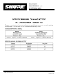
1
Shure Incorporated 222 Hartrey Avenue Evanston IL 60202-3696 U.S.A. UC UHF Wireless System SERVICE MANUAL CHANGE NOTICE UC2 UHF HAND-HELD TRANSMITTER Changes or corrections have been made to this service manual. Update your service manual by replacing the pages listed in the table below with the ones attached to this change notice. CHANGES EFFECTIVE [DATE] REMOVE these pages from your current manual Revision 1 Revision 2 INSERT the following revised pages attached to this notice ALL Revision 2 pages:14,15,17,20,22,27,29 and 30 Revision3 ALL pages:14,15,17,20,22,27,29 and 30 SERVICE MANUAL REVISION HISTORY Release Part Number Date Code Original 25A1044 RI Revision 1 25B1044 SB Revision 2 25C1044 TB Revision 3 25C1044 TK E1999, Shure Incorporated Printed in U.S.A. Service Manual UC2 Hand-Held UHF Transmitter 25C1044 (TK) Characteristics General The Shure UC2 Hand-Held UHF Transmitter is a microprocessorcontrolled microphone transmitter, operating in the 692 to 716 MHz and 774 to 862 MHz frequency range. The UC2 hand-held transmitter is used in mid-level installed sound, rental, and concert sound applications. Six frequency range variations are available. Controls and Connectors 1 2 3 8 4 5 7 6 1. Mic Cartridge Grille (87 shown) 5. 9 V Battery 2. Battery Fuel Gauge LEDs 6. Battery Cup 3. Power ON/OFF Switch 7. Group Selection Rotary Switch 4. Audio Gain Control 8. Channel Selection Rotary Switch Figure 1. UC2 Controls and Connectors Service Note: Shure recommends that all service procedures be performed by a FactoryAuthorized Service Center or that the product be returned directly to Shure Brothers Inc. Licensing: Operation may require a user license. Frequency or power-output modifications may violate this product’s approvals. Contact your country’s communications authorities. 1999, Shure Incorporated 25C1044 (TK) Printed in U.S.A. Shure UC2 Hand-Held UHF Transmitter Circuit Description LIMITER CONTROL INPUT Σ MIC REG. +5v BATTERY MGMT. & FUEL GAUGE TONE KEY 32.768 kHz FROM ON / OFF BATT. SWITCH TONE KEY LIMITER CONTROL OUTPUT +5V CIRCUIT AUDIO OUT CALL ID UNREG. PWR. TONE CONTROL 4 MHz PWR. OFF DETECT MCU PLL CONTROL FET BYPASS EEPROM (MEM) MC68HC705 PWR. CONTROL HOLD 4 MHz CIRCUIT SYNTH. MB15A02 GROUP RF POWER RF MUTE CHANNEL RF MUTE AUDIO IN VCO Figure 2. UC2 Hand-Held Transmitter Circuit Block Diagram Audio Section FCC-Approved Audio enters L200, an inductor used as an rf choke. The signal is ac coupled through capacitor C200 into a user adjustable gain stage. Resistors R202 and R203 set up a half-supply bias, and R204 sets the input impedance for the stage. The back-to-back diodes, D201, are used to keep the op-amp from snapping to the rail and reverse phasing when the maximum input voltage range is exceeded. The 30 dB adjustable gain stage is built around U200A. The user externally controls the gain of this stage. C206, C207, and C208 protect Characteristics 2 25C1044 (TK) Shure UC2 Hand-Held UHF Transmitter the amplifier and bias circuits from rf interference. Due to its topology, this stage is unique because it is non-inverting and allows for a gain less than unity. Audio then enters a buffer to the pre-emphasis network and the compression stage. R213, R214, and C211 set up two corners for the pre-emphasis network. The pre-emphasis boosts the high frequencies before transmission. This network feeds an NE575 compander, U202, that utilizes an external amplifier, U201B. The compander performs a 2:1 logarithmic compression of the audio signal. The pre-emphasis network also plays a role in setting the hinge point (0 dB gain) of the compander. From the compressor, the processed audio enters a low-pass filter, U201D, and then a summing amplifier, U201C. The tone key (and for J frequencies, the call ID signal) is added here to the processed audio signal. Transistors Q208 and Q209, with crystal Y200, form the tone key oscillator circuit to provide a stable, continuous 32.768 kHz sine wave. Transistor Q210 buffers the tone key signal before it is added to the audio signal. The tone key signal is used in the receiver to provide audio output only when the tone key signal is present with the transmitted signal. If the tone key or the transmitter is turned off, the receiver will be muted. The tone key squelch eliminates receiver noise associated with loss of a carrier. Q211 acts as a switch for toggling the tone key MUTE/ UNMUTE; it is controlled via the microprocessor. The tone key signal, along with the processed audio signal, is then fed to a summing amplifier, U201C. R244, at the output of the summing amplifier, helps prevent spurious oscillations from the op-amp. After passing the ac coupling capacitor, C243, the signal is fed to the rf module via the rf choke, L207. The battery meter circuit is comprised of U205; LEDs D203, D204, D205; and various resistors. The meter works by comparing a divided down version of the battery voltage (R250, R251) to two thresholds (set by R252, R253, and R254), and lighting the appropriate LED. A 9 Vdc battery provides power to the audio printed circuit board (pcb), via switch S200. FET Q203 provides electrical reverse battery protection by connecting the negative battery terminal to the pcb ground only when the battery is connected with the correct polarity. The 9 Vdc then enters U203, a low dropout 5 V regulator, which gives a clean, regulated 5 V supply to run the audio circuitry. The regulator has appropriate bypass capacitors on its input and output. Q201, Q202, Q212, Q213, and their respective resistors, provide power management and timing. 25C1044 (TK) 3 Circuit Description Shure UC2 Hand-Held UHF Transmitter ETSI-Approved This transmitter uses the same pcb as the domestic system, but it requires a different topology and different parts. A limiter is inserted between the pre-emphasis and the compressor to limit the occupied bandwidth. The buffer after the gain stage, U201A, is now an inverter with pre-emphasis and 20 dB of attenuation. Previously bypassed, the expander side of the NE575 (U202) is now activated and used as a limiter. A sample of the audio is taken from the limiter output, U202, pin 6, and sent to a control circuit that detects signals above a limiting threshold. The comparator then sends a control signal to U202, pin 5, which clamps the signal. Rf Section Processed audio enters R320, an internal potentiometer that is adjusted for 45 kHz deviation (40 kHz for England), 100% modulation, with a 6.8 dBu 1 kHz tone at the output of the compressor. For J frequencies, R320 is adjusted for 5 kHz deviation with 1 kHz tone injected into the mic input, to give –23.47 dBu at U201, pin 7 (TPA4). The audio is then fed to the tuning voltage pin of the voltage controlled oscillator (VCO), which modulates the carrier directly. A phase locked-loop (PLL) frequency-synthesized system eliminates the need for multiplier stages and results in a much higher degree of spectral purity. The VCO is shielded to prevent external rf fields from affecting its operation. Regulated 5 Vdc power from the low drop-out regulator, U311, is provided to ensure frequency stability with changes in battery voltage. The VCO is capable of tuning from 782 to 806 MHz (FCC-approved), with a 1 to 4 V tuning voltage range. At the output of the VCO, the rf signal splits into two paths. Frequency variations by country are given in a table in the Service Procedures section. The output of the VCO is coupled by C323 to the frequency control pin of the synthesizer, U304. The synthesizer’s internal circuitry divides the rf signal down, as necessary. The synthesizer contains a quartz-controlled reference oscillator circuit operating from a 4.0 MHz crystal, Y302, that is adjusted by trimmer C314. The transmitter output frequency is user-selectable in groups of compatible channels from 782 to 806 MHz for domestic groups. Frequency selection is made via microprocessor U303, which interfaces with the user by means of the Group/Channel switches, S301 and S302. The output of the synthesizer is a series of pulses integrated by a passive loop filter (R316, C319, R317, C353, R318, C320) to produce a control voltage signal. The control voltage signal is then connected to the VCO through buffer amplifier U306B, which is used to isolate the PLL filter from the audio modulation signals. The VCO output is also coupled to the pre-driver and rf power amplifier through a resistive network (R322, R324, R325) and a coupling capacitor, C329. Characteristics 4 25C1044 (TK) Shure UC2 Hand-Held UHF Transmitter The pre-driver stage, Q302, provides approximately 6 to 8 dB of gain, which makes up for the pad. R326 and R327 provide base bias for the transistor, while R328 sets its operating current. L303 is an rf choke used to provide power to the stage, while L304, C332, C333, C357, and C2 provide filtering/matching for the stage. The collector of Q302 feeds into the power amplifier stage via coupling capacitor C338 and a pi-matching network made up of C339, L305, and C340. The rf power amplifier, Q304, is a dual emitter BJT. This high-gain, high-frequency low-noise device can provide +18 dBm out at its 1 dB compression point. It is biased via base resistors R331 and R332. Its operating current is controlled via emitter resistor R333. L306 acts as a choke, and C349, C350, C355, and C356 provide a good emitter bypass to ground. The amplifier output is matched to lowpass filter U1, via L307. The low-pass filter output couples to the printed circuit board (pcb) via C347 and L308. The transmitter can deliver +17 dBm (50 mW) maximum to the antenna for domestic frequencies; JA and JB frequency transmitters can deliver +10 dBm maximum to the antenna. During transmitter power-up and frequency selection, the rf power is muted by bringing the gates of Q303/Q305 low. This provides approximately 45 dB rf attenuation until the PLL has locked. The transmitter rf is then unmuted by bringing the gates Q303/Q305 high. During transmitter power off conditions, voltage is first removed from the VCO by bringing the base of Q301 high. Thus, the carrier signal of the transmitter is not allowed to drift off frequency during power on/off conditions. Digital Section The digital section contains several circuitry blocks. Microcontroller Section The microcontroller section consists of the U303 microcontroller. The rotary switches indicate the UHF frequency group and channel. A 4.000 MHz oscillator provides the operating frequency to the microcontroller. The oscillator circuit includes C300, C301, and Y301. U5, R306, and C305 form the reset circuit. U5 is the reset IC that resets the U303 microcontroller if the 5 Vdc normal operating voltage falls below 4.3 Vdc. C302 and C303 form the power supply bypass filter circuit. Memory Section The memory section consists of U302, a non-volatile, Electrically Erasable/Programmable Read Only Memory (EEPROM) that stores the 25C1044 (TK) 5 Circuit Description Shure UC2 Hand-Held UHF Transmitter mapping of the compatible groups and channels. The microcontroller serially communicates with this part via data and clock lines to read the frequency corresponding to the Group and Channel position. The ability to write to the memory occurs during factory programming only. During normal usage, this memory is used as a look-up table only. R335 and R305 resistors allow the clock and data lines to be driven independently of the microcontroller port pin states during in-circuit programming of the EEPROM. Battery Management Section The U303 microcontroller provides low battery shutdown. The shutdown threshold is 1.88 Vdc ± 10%. A voltage lower than the shutdown threshold on U303, pin 17, shuts down the transmitter. Resistors R308 and R309 divide down the battery voltage for U303; a battery voltage less than 5.65 Vdc must shut down the transmitter. This auto shutdown disables the audio tone key mix, mutes the rf output, and powers down the rf output amplifier section. The current draw from a 9 Vdc battery in this state is 14 ± 2.0 mA, and the battery fuel gauge is not functional. Turning off the power switch completely shuts off the transmitter. The audio circuit description section provides information for the battery fuel gauge circuit description. Rotary Switches for Frequency Selection A 10-position Group switch (S302) and a 16-position Channel switch (S301) select the transmitter frequency. Both rotary switches share the same U303 microcontroller port pins (3 through 6) for a multiplexed switch read operation. The individual switches are selected by U303, pins 7 and 8. Resistors R4, R300, R302, and R303 are the pull-ups for the switch position read. Diode packs D301 through D304 isolate the switches during the multiplexed read operation. The multiplexed scheme to read switches does not allow incorporating switch change detection based on interrupts. Also, the switches cannot be constantly scanned to determine changes because the scanning frequency being in audio range is difficult to filter out. In a steady state, the switch selector common pins are inputs to the U303, pins 7 and 8, while U303, pins 3 through 6, are outputs. In this state, pins 4, 5, and 6 are held low while pin 3 is held high. This forces logic high level on switch selector pins if the switches are set on odd positions. For even position settings, the contact on pin 1 is open from the switch common pin and the internal pull-down resistors force logic low to U303, pins 7 and 8. Any switch change is comprised of state toggle from odd to even, and vice versa. Only this change is detected, and it is followed by a multiplexed switch read, in which U303, pins 7 and 8, become selectively grounded outputs to read the selected switch’s state on pins 3 through 6. A multiplexed switch read is preceded by tone key and rf mutes. This mutes the audio in the receiver to allow a quiet change to another frequency. Characteristics 6 25C1044 (TK) Shure UC2 Hand-Held UHF Transmitter For JA frequencies, the Group switch has 16 positions, and the Channel switch has 10 positions. Power Switch and Mute Interface When a transmitter is turned off, the PWRDN signal goes to logic low on U303, pin 19. This immediately disables the tone key, and the power hold circuit automatically kicks in to bypass the power switch. This is followed by 500 mS of delay, and then the rf is muted and turned off. The power hold circuit is also disabled at this point, and the transmitter shuts off. 25C1044 (TK) 7 Circuit Description Shure UC2 Hand-Held UHF Transmitter Notes This page intentionally left blank. Notes 8 25C1044 (TK) Shure UC2 Hand-Held UHF Transmitter Functional Test Verify operation and reported malfunction, referring to the product User’s Guide for a description of the unit as well as information on its operation, troubleshooting, and technical data. Disassembly and Assembly ! CAUTION ! Observe precautions when handling this static-sensitive device. Disassembly 1. Remove the microphone cartridge from the UC2. 2. Use a pair of needlenosed pliers to remove the circuit board retaining ring from inside the handle. 3. Push the bezel tab-snap in the handle behind the contact pcb to remove the bezel and switch actuator. 4. Slide the circuit board out by pushing on the battery connectors. Bezel Switch actuator Right side view of microphone Handle Tab Contact pcb Circuit board subassembly Tab Figure 3. Bezel Removal 25C1044 (TK) 9 Disassembly Shure UC2 Hand-Held UHF Transmitter Á Ball screen Retaining ring Contact board Á ÁÁÁ ÁÁÁ ÁÁÁ ÁÁÁ Microphone cartridge (SM58 shown) Bezel Audio circuit board Gain control Rf circuit board ÁÁÁ ÁÁÁ Handle Gain control access Switch actuator 9 Vdc alkaline battery ÁÁÁÁ ÁÁÁÁ ÁÁÁÁ ÁÁÁ ÁÁÁÁ ÁÁÁÁ ÁÁÁ Á Á ÁÁÁÁ Battery cup Figure 4. UC2 Hand-Held Transmitter, exploded view. Reassembly To reassemble the unit, reverse the disassembly steps given above: 1. Slide the circuit board back into the handle. 2. Reinstall the retaining ring, switch actuator, bezel, and the microphone cartridge. Disassembly and Assembly 10 25C1044 (TK) Shure UC2 Hand-Held UHF Transmitter Service Procedures Measurement Reference dBu is a measure of voltage, and dBm is a measure of power. For example, the HP8903 should be labeled dBu instead of dBm because it is a voltage measurement. These two terms are often used interchangeably even though they have different meanings. Audio levels in dBu are marked as dBm on the HP8903. dB Conversion Chart 0 dBV = 2.2 dBu 0 dBu = 0 dBm, assuming the load = 600 Ω Test Equipment Most test equipment needed is described in the Shure Wireless Service Equipment Manual. The following test equipment (or approved equivalent) is also needed. Table 1 Test Equipment Equipment Type Audio analyzer Digital multimeter Rf signal generator Frequency counter Spectrum analyzer (domestic) Spectrum analyzer (JA, JB) Shure UC4 receiver Test head Brass ring for use with test head BNC to “rocket launch” cable. For use on Japan PCB versions “N” and earlier BNC(male) to unterminated 50W test cable Model *Hewlett-Packard 8903B Fluke 87 Hewlett-Packard 8656B Hewlett-Packard 53181A Hewlett-Packard 8590L Hewlett-Packard 8591E Shure UC4 PT1840 PT1838–Y 95C8418 PT–1824 *Audio levels in dBu are marked as dBm on the HP8903B. Test Equipment Set-Up The alignment procedure is sequential and does not change, unless specified. 1. Use the following test cables for all RF test points: Use PT1824 cable for European and USA models. For the Japan models use the 95C8418 test cable for PCB versions “N” and earlier. 2. Keep the test cables as short as possible (less than 12 inches). 3. Include the insertion loss of the cables and connectors for all rf measurements. 4. Dc voltages may be present at rf test points. As a precaution, use dc blocks to protect the test equipment. 25C1044 (TK) 11 Test Equipment Set-Up Shure UC2 Hand-Held UHF Transmitter Test Set-Up 1. Desolder the printed circuit boards (pcbs) and pull them apart. When the pcbs are desoldered, leave the battery contacts soldered to the audio board for powering up the unit. 2. Remove C347 and connect the respective RF test cable between TPRF1 / RF GND and a frequency counter.For Japan models with PCB version “N” and earlier, do not remove C347. Connect a 95C8418 cable between J2 and the frequency counter. 3. Use the PT1843 cable to connect the audio board to the rf board through the 11-pin board interconnects (J200, J300, side 2). 4. Set the audio GAIN potentiometer (R207, side 1) to minimum, full counter-clockwise (CCW). 5. Apply + 9 Vdc across the battery terminals (J201, J202, side 2). 6. Toggle the power switch, S200, to turn on the UC2 transmitter. 7. Set the UC2 Group and Channel switches, S301 and S302, according to the group designators on the board and the settings given in Table 2. Table 2 Group Carrier Frequencies and Tuning Voltages (in order by carrier frequency) Group Group Code Group Switch (S101) Channel Switch (S102) Carrier Frequency (MHz) VCO Tuning Voltage (TP30) Deviation (kHz) UA A 4 0 805.500 3.7 45 UB F 1 A 703.750 2.6 45 MB B 1 3 805.500 2.2 15 JA C 0 2 805.500 3.7 5 JB D 4 2 807.500 3.8 5 KK E 5 5 851.125 2.9 15 MC B 1 1 774.125 1.3 ±0.25 15 MD B 3 7 805.500 2.2 15 Table 2 lists the group carrier frequencies, switch settings, and tuning voltages for all the alignment tests that follow. Service Procedures 12 25C1044 (TK) Shure UC2 Hand-Held UHF Transmitter AUDIO SIDE 1 TP18 U200 Q203 +9V C214 C222 +5V Q213 C216 Q212 Q202 U202 S200 R7 U201 Q201 Q204 U205 Q220 Q209 TP4 C291 J205 C27 P200 R39 PAD TP6 Y200 TP10 L2 C200 R25 D201 1 P201 U203 GND 1 RED RF SIDE 1 RF GND* S302 U302 R40* P204 VCO R320 Adj Q304 GREEN TP30 C308 U501 C314 Y302 L302 S301 C309 C510 U311 J2* TPRF1 U303 P203 Y301 Q301 TP+9 *J2 and R40 are placed for JA, JB frequencies only. RF GND is accessed thru a hole in the pcb. AUDIO SIDE 2 C251 +5V C227 C223 J202 TP18 Q3 Q2 C221 Q1 +9V TP16 C213 C210 J201 TP4 L207 Q210 U2 J200 TP10 Q211 L1 C243 Q208 TP2 1 TP6 RF SIDE 2 D304 J301 TPRF1 D302 C324 C336 L308 D301 U5 Q305 Q303 C303 D303 TP30 TP+9 U1 U306 U304 J300 C353 C347 C315 J302 L300 Figure 5. UC2 Major Test Component Locations 25C1044 (TK) 13 Test Set-Up Shure UC2 Hand-Held UHF Transmitter Alignment Frequency Use this service procedure to correctly align the transmitter’s operating (output) frequency. C510 tunes the voltage-controlled oscillator (VCO) to the operating frequency selected, with a 1 – 4 Vdc tuning range. C314 adjusts the reference oscillator on the synthesizer, U304. AUDIO ANALYZER RF GND: FEED THRU HOLE ON PCB FREQUENCY COUNTER S302 RED RF GND J2* CH 2 S301 GREEN R40* C510 TP30 U501 TPRF1 C314 CH 1 *R40 and J2 are placed for JA, JB frequencies only. UC2 Transmitter Frequency Counter Power: ON (+9 Vdc) Operating freq: See Table 2 Operating freq: See Table 2 Connect CH 2: TPRF1 and GND Channel switch: See Table 2 Group switch: See Table 2 Audio Analyzer Connect + : TP30 Connect – : RF GND Measurement: DC level For Japan models with PCB versions: “N” and earlier connect to J2 (pcb rf side 1) Figure 6. UC2 Frequency Test Set-Up 1. Put a dc voltmeter across TP30 (tuning voltage line) and RF GND. 2. Adjust the VCO trimmer, C510, until the voltmeter reading matches the appropriate entry in Table 2, ± 0.125 Vdc. 3. Adjust the variable capacitor, C314, until the frequency counter measurement matches the appropriate frequency in Table 2, ± 1 kHz. 4. Leave the test cable connected to the rf output. 5. The dc voltmeter can be removed from TP30. Service Procedures 14 25C1044 (TK) Shure UC2 Hand-Held UHF Transmitter Power Output Measurement The output power measurement ensures that the output signal is strong enough for sufficient range when the system is in use. The output power measurement also verifies that the output power is not above the specified maximum level, to ensure compliance with regulatory agencies standards. SPECTRUM ANALYZER RF GND: FEED THRU HOLE IN PCB S302 RED RF GND J2* S301 GREEN R40* C510 TP30 TPRF1 U501 C314 *R40 and J2 are placed for JA, JB frequencies only. UC2 Transmitter Power: ON Spectrum Analyzer Frequency: See Table 2 Operating freq: See Table 2 Group switch: See Table 2 Channel switch: See Table 2 Span: 200 MHz Reference voltage: 20 dBm Peak search: ON Signal track: ON Marker: ON Figure 7. UC2 Power Output Measurement Test Set-Up 1. Remove the BNC cable end from the frequency counter and connect it to the 50 Ω input of the spectrum analyzer.. Use the equipment settings shown in Figure 8. 2. Measure the output power. The output power should be: UA, UB, MB, MC, MD frequencies: 16 + 1 / – 2 dBm KK frequencies: 14 + 1 / – 2 dBm For J frequencies, with C347 in place, adjust R40 to obtain 8.8 ± 0.5 dBm. 3. Turn the UC2 power OFF. 4. Disconnect only the BNC end of the RF test cable from the spectrum analyzer. 25C1044 (TK) 15 Alignment Shure UC2 Hand-Held UHF Transmitter Deviation Deviation must be set to make sure the companding systems between the transmitter and receiver correctly track each other. The level coming out of the transmitter’s audio compressor must match the level going into the receiver’s audio expander. A fixed gain structure does not ensure an exact match, primarily because of variations in voltagecontrolled oscillators (VCOs). Option 1 – Using a UC4 or U4S Receiver This test requires a UC4 or a U4S receiver and is designed to tune the transmitter regardless of the accuracy of the receiver’s tuning. It is, however, recommended that a properly-tuned receiver be used to perform the transmitter deviation adjustment. Reference Voltage 1. Connect the rf signal generator to one of the receiver’s antenna ports. 2. Turn the UC4 or U4S receiver ON. 3. Set the receiver frequency to match the transmitter frequency. 4. Set the rf signal generator frequency to match the transmitter frequency. 5. Modulate the generator frequency with 1 kHz audio at a –60 dBm output level. See Table 2 for deviation. 6. Set the tone key switch (S501 for the UC4, S201 for the U4S) to the OFF position. 7. Connect the ac voltmeter to the unbalanced output of the receiver. 8. Read the ac voltage. Record this voltage. This is the deviation reference voltage. 9. Turn off RF output. UC4 RECEIVER (BACK) UC4 RECEIVER (FRONT) A B SQUELCH S501 (TONE KEY SWITCH) AUDIO ANALYZER TK ON DC BLOCK TK OFF RF SIGNAL GENERATOR NOTE: DC VOLTAGES ARE PRESENT AT MOST RF TEST POINTS. USE A DC BLOCK ON THE RF SIGNAL GENERATOR TO PROTECT TEST EQUIPMENT. UC4 Receiver Audio Analyzer Output: Unbalanced Gain: Maximum Squelch: Mid INT: FM Filters: Low-Pass (30 kHz): ON Tone Key (S501): OFF Rf Signal Generator Measurement: AC level High-Pass (400 Hz): ON Group switch: See Table 2 INT: 1 kHz Output amplitude: –60 dBm Frequency: See Table 2 Deviation: See Table 2 Channel switch: See Table 2 Figure 8. Deviation Reference Voltage Test Set-Up, Using a UC4 or U4S Receiver Service Procedures 16 25C1044 (TK) Shure UC2 Hand-Held UHF Transmitter Adjustment Voltage 1. Remove the RF test cable from TPRF1 and GND, and replace C347. For Japan models PCB version “N” and earlier remove cable from J2. 2. Reassemble the printed circuit boards. Use a PT1840 test head and brass ring (PT1838-Y) to connect the audio analyzer to the UC2 audio input (J205). Turn ON the Low-Pass (30 kHz) and High-Pass (400 Hz) filters on the audio analyzer. For bench testing, the audio analyzer can be directly connected to the contact board gold contacts with clip leads. 3. Disconnect the rf signal generator from the UC4 receiver and return the UC4 tone key switch to the ON position. 4. Adjust the audio analyzer output level (typically = –2.2 dBu) to measure the following at TPA4 (U201, pin 7) : UA, UB –6.8 dBu ± 0.2 dB (354 mV ± 1 mV) MB, MC, MD – 16.3 dBu (118 mV ± 1 mV) JA JB KK –26.5dBu (36.7mV± – 23.47 dBu (133 mV ± 1 mV) 1 mV) – 15.3 dBu (52 mV ± 1 mV) See Figure 10 for equipment set-up and equipment settings for the rest of this test. AUDIO ANALYZER S501 (TONE KEY SWITCH) AUDIO SIDE 1 TPA4 – U201, pin 7 UC4 Receiver Output: Unbalanced Gain: Maximum Squelch: Mid 25C1044 (TK) UC2 Transmitter Power: + 9 Vdc Gain: Minimum Group switch: See Table 2 17 Audio Analyzer Measurement: AC level Frequency Output: 1 kHz Filters: Alignment Shure UC2 Hand-Held UHF Transmitter Tone Key (S501): ON Channel switch: See Table 2 Low-Pass (30 kHz): ON High-Pass (400 Hz): ON Figure 9. Deviation Adjustment Voltage Test Set-Up, Using a UC4 or U4S Receiver 5. Connect the unbalanced output of the UC4 to the input of the audio analyzer (ac voltmeter). 6. Take a radiative measurement by holding the battery of the UC2 next to the receiver’s antenna. 7. Turn the transmitter ON and adjust R320 until the ac voltmeter on the receiver reads the same as the deviation reference voltage, measured above, ± 0.1 dB; or ± 0.2 dB for JA, JB frequencies. AUDIO ANALYZER S501 (TONE KEY SWITCH) R320 VCO RF SIDE 1 UC4 Receiver UC2 Transmitter Output: Unbalanced Gain: Maximum Power: + 9 Vdc Gain: Minimum Squelch: Mid Group switch: See Table 2 Tone key (S501): ON Channel switch: See Table 2 Audio Analyzer Measurement: AC level Frequency Output: 1 kHz Filters: Low-Pass (30 kHz): ON High-Pass (400 Hz): ON Figure 10. Deviation Reference Voltage Test Set-Up, Using a UC4 or U4S Receiver Service Procedures 18 25C1044 (TK) Shure UC2 Hand-Held UHF Transmitter Option 2 – Using a Modified SC4 IF Receiver Deviation tests can also be performed using a modified SC4 IF receiver. For instructions on modifying an SC4 receiver, consult the Shure Service Equipment manual. Reference Voltage 1. See Figure 12 for equipment test set-up and equipment settings. 2. Connect the rf signal generator output to the input port (L) of a Zad-1 mixer 3. Connect the output port I (intermediate frequency) of the Zad–1 mixer to antenna input B of the SC4 IF receiver. 4. Turn the SC4 IF receiver ON and set the tone key switch on the front panel of the SC4 IF receiver to OFF. 5. Connect the audio voltmeter to the receiver’s unbalanced output. 6. Measure the output voltage. Record this voltage. This is the deviation reference voltage. Use the same Zad-1 mixer connections for the next adjustment test. ZAD–1 MIXER R MODIFIED SC4 IF RECEIVER I ANTENNA INPUT B AUDIO OUT L TONE KEY SWITCH: OFF DC BLOCK AUDIO ANALYZER RF SIGNAL GENERATOR NOTE: DC VOLTAGES ARE PRESENT AT MOST RF TEST POINTS. USE A DC BLOCK ON THE RF SIGNAL GENERATOR TO PROTECT TEST EQUIPMENT. SC4 IF Receiver Output: Unbalanced Gain: Maximum Squelch: Mid Tone Key switch: OFF Audio Analyzer Rf Signal Generator Measurement: AC level INT: FM Filters: Low-Pass (30 kHz): ON INT: 1 kHz Output amplitude: + 7 dBm High-Pass (400 Hz): ON Operating freq: See Table 2 Frequency: 10.7 MHz Deviation: See Table 2 Figure 11. Deviation Reference Voltage Test Set-Up, Using a Modified SC4 IF Receiver 25C1044 (TK) 19 Alignment Shure UC2 Hand-Held UHF Transmitter Adjustment Voltage 1. Disconnect the rf signal generator from the SC4 IF receiver. 2. Set the SC4 tone key switch on the SC4 front panel to ON. 3. Connect the audio analyzer output to the MIC input of the transmitter, using the test head or clip leads to the gold spring contacts. 4. Turn the UC2 power back ON. 5. Adjust the audio analyzer output level (typically = –2.2 dBu) to measure the following at TPA4 (U201, pin 7) : UA, UB –6.8 dBu ± 0.2 dB (354 mV ± 1 mV) MB, MC, MD – 16.3 dBu JA, JB – 23.47 dBu KK – 15.3 dBu (118 mV ± 1 mV) (52 mV ± 1 mV) (133 mV ± 1 mV) See Figure 14 for equipment set-up and equipment settings for the rest of this test. AUDIO ANALYZER TEST HEAD AUDIO SIDE 1 TPA4 (U201, PIN 7) UC2 Transmitter Power: +9 Vdc Gain: Minimum Group switch: See Table 2 Channel switch: See Table 2 Audio Analyzer Measurement: AC level Frequency Output: 1 kHz Filters: Low-Pass (30 kHz): ON High-Pass (400 Hz): ON Figure 12. Deviation Adjustment Voltage Test Set-Up, Using a Modified SC4 IF Receiver Service Procedures 20 25C1044 (TK) Shure UC2 Hand-Held UHF Transmitter 6. Connect the UC2 rf output test cable BNC end to the input port (R) of the Zad-1 mixer. 7. Connect the rf signal generator, and set the frequency to the operating frequency (from Table 2) minus 10.7 MHz. 8. Turn ON the UC2 and adjust R320 until the audio voltmeter connected to the unbalanced output of the UC4 reads the same as the deviation reference voltage, measured above, ± 0.1 dB, or ± 0.2 dB for JA, JB frequencies.. ZAD–1 MIXER TRANSMITTER AUDIO IN ANTENNA OUTPUT R MODIFIED SC4 IF RECEIVER I ANTENNA INPUT B AUDIO OUT L TONE KEY SWITCH: ON DC BLOCK RF SIGNAL GENERATOR AUDIO ANALYZER NOTE: DC VOLTAGES ARE PRESENT AT MOST RF TEST POINTS. USE A DC BLOCK ON THE RF SIGNAL GENERATOR TO PROTECT TEST EQUIPMENT. SC4 IF Receiver UC2 Transmitter Output: Unbalanced Gain: Maximum Power: Gain: Audio Analyzer + 9 Vdc Measurement: Minimum Output: Rf Signal Generator AC level INT: FM 1 kHz INT: 1 kHz Squelch: Mid Filters: Tone Key switch: ON Low-Pass (30 kHz): ON Output amplitude: + 7 dBm Deviation: See Table 2 High-Pass (400 Hz): ON Frequency: Oper. Freq. minus 10.7 MHz Figure 13. Deviation Adjustment Voltage Test Set-Up, Using a Modified SC4 IF Receiver 25C1044 (TK) 21 Alignment Shure UC2 Hand-Held UHF Transmitter Product Specifications After tuning, the unit should meet the following specifications. Specification Minimum Typical Maximum Current drain 50 mA 60 mA 70 mA Frequency –1.0 kHz See Table 2 +1.0 kHz Audio freq response @ 100 Hz wrt 1 k –5.0 dB –4.0 dB –3.0 dB Audio freq response @ 10 KHz wrt 1 k +8.0 dB +9.0 dB +10.0 dB 95.0 dB 100.0 dB – 14.0 dBm 16.0 dBm 17.0 dBm 80.0 dB 85.0 dB – 14.0 dBm 16.0 dBm 17.0 dBm 80.0 dB 85.0 dB – 12.0 dBm 14.0 dBm 15.0 dBm System S/N @ 1% THD, A weighted 85.0 dB 90.0 dB – Output power, at J2, with C347 in place 8.3 dBm 8.8 dBm 9.3 dBm UA, UB: System S/N @ 45 kHz, A weighted Output power, UA, without C347 MB, MC,MD System S/N @ 1% THD, A weighted Output power, without C347 KK: System S/N @ 1% THD, A weighted Output power, without C347 JA, JB: Service Procedures 22 25C1044 (TK) Shure UC2 Hand-Held UHF Transmitter Bench Checks Dc Problems Make all dc measurements with respect to the rf ground unless otherwise specified. Connect the rf and audio printed circuit boards together via the 11 pin connector, the battery contacts, and the “D” board. n Make sure the battery voltage is between 6 and 9 Vdc. Make sure TP+9 has this voltage. Check for the correct Vcc and +5 V rf at Q301. If incorrect voltage is present: n Trace the dc back to the voltage regulator. n Check the biasing resistor values around Q301. n Check the power switch. n Look for open coils, cracked parts, reversed polarity capacitors, or solder shorts. If there is a short to ground from 5 V, try to isolate different parts of the circuit. Make sure that: n The rf OFF signal changes from +5 Vdc at power up and power down to 0 Vdc during normal operation. Trace the signal to the microprocessor. Q301 should be saturated during normal operation. n Battery voltage appears at TP+9, U311, pin 6. Check for reversed polarity capacitors, C308 and C309. Check for open coil, L300. Rf Problems n If the carrier is out of specification by less than 40 kHz and cannot be corrected by adjusting C314, put the transmitter on the operating frequency (see Table 2). Measure and adjust the dc voltage at TP30. (See Table 2 for frequency variations.) If the carrier still cannot be trimmed properly, then check C314, C313, and Y302. If they are correct, replace the synthesizer. If the carrier frequency is not in the correct frequency range shown in Table 2, or is unstable, the loop is unlocked. n Check dc voltage at TP30. If it is 0 V or +5 V, look for a short. n Check the solder connections at the contact board, VCO, micro processor (traces LE, D, and CK), and synthesizer U304. If the connections are good and there is no 4.0 MHz oscillation at U304, pins 1 and 2, replace the crystal, Y302. n Check the values and polarity of the loop filter: R316, C319, R317, C353, R318, C320, C354, U306B, R319, R320, and R321. Check the bias voltage of U304, pins 3 and 4, and U306B, pin 8. As a last resort, replace the synthesizer, U304. 25C1044 (TK) 23 Product Specifications Shure UC2 Hand-Held UHF Transmitter Low Rf Output Power n Check the polarity/soldering of the output low-pass filter, U1. (Rf IN is marked with a dot.) n Check for opens or shorts on output coil L308. n Check the polarity of Q304. n Verify the dc bias of Q302 and Q304. Check L303, L304, and L306, if no bias. Verify that the rf MUTE signal changes from 0 Vdc at power up and power down to +5 Vdc during normal operation. If Q303 and Q305 are not in a low impedance state during normal operation, the rf power at the antenna port will be attenuated by about 45 dB. n Check for missing ground connections. n Check the dc level at the VCO Vcc pin. If no dc power, check L302. n Verify the VCO output power. n Partially isolate the VCO from the rest of the circuit by removing C323. The carrier frequency will no longer be locked, but the output power from the VCO should be around –1 ± 2 dBm into a 50 Ω load. n If the power out of the VCO is still low, the problem is in the VCO. n Check the values of R322, R323, R324, R325, and C329. n Isolate components starting from the antenna and working back to the rf power amp. n Check the values/continuity of the input and output matching networks for Q302, Q304 (C329, C338, L305, C339, C340, L307). n Check the values of the bypass capacitors C357, C2, C332, C333, C334, C335, C360, C341, C342, C349, C350, C355, C356. n As a last resort, replace Q302 or Q304. Excessive Current Drain n Try isolating different sections of the circuit: rf, audio, digital. Look for reversed polarity capacitors or wrong resistor values. Check the voltage regulators. Deviation Problems n If R320 cannot be adjusted to obtain the deviation reference voltage (see the Service Procedures section), try to isolate the problem to the audio or rf section. Check the value of R320. To check the rf section, set the transmitter frequency (see Table 2), and verify the tuning voltage of the VCO. n Check the audio section by applying audio to the mic input. With an oscilloscope, make sure audio is present at TPA7. If not, work backwards towards the input. Bench Checks 24 25C1044 (TK) Shure UC2 Hand-Held UHF Transmitter Audio Problems No Tone Key No tone key means that the 32.768 kHz tone key sidebands are not visible when the carrier is viewed on a spectrum analyzer. If tone key levels are there but are too low, the deviation is off and needs to be recalibrated. They should be, roughly, –23 dBc ± 3 dB. n Apply a 1 kHz tone at a level of 0 dBu to the audio input with the audio gain pot at minimum. n If the carrier on the spectrum analyzer does not show any deviation, check part integrity and audio path continuity between U201, pin 14, and the VCO. n If the spectrum analyzer shows a deviated carrier, probe for a 32 kHz signal at TPA6 and I209 and continue to the next step. n If there is a signal at I209 but not at TPA6, then the mute circuit through Q211 is being activated. Verify that the logic signal at Q211, pin 1, is logic low. If it is low, replace Q211. If it is not low, check the line for a short to +5 V. If there is no short, the microprocessor is defective and must be replaced. n If there is a 32 kHz signal at both I209 and TPA6, replace R236. n If there is not a 32 kHz signal at either I209 or TPA6, there is something wrong with the tone key circuit or the tone key supply voltage. If the tone key supply voltage (U200, pin 8) is less than 2 V, there is a problem with one or more of the following components: R261, R264, R265, R266, C238, Q220, C237, R232, or R260. n If the voltage at U200, pin 8, is greater than 2 V, the problem is in the tone key circuit itself. Check for shorts and opens. Replace parts in this circuit beginning with the crystal until the 32 kHz oscillation returns. No Audio n View the carrier on the spectrum analyzer. If there are not 32 kHz tone key sidebands around the carrier, follow the steps above for “No Tone Key.” n Verify +9 V, half-supply bias, and ground connections to U200. n Verify +9 V, half-supply bias, and ground connections to U201. n Follow the audio path from where audio is applied until the point of discontinuity is reached and replace the appropriate part. 25C1044 (TK) 25 Product Specifications Shure UC2 Hand-Held UHF Transmitter Notes This page intentionally left blank. Notes 26 25C1044 (TK) Shure UC2 Hand-Held UHF Transmitter Replacement Parts and Drawings Parts Designations The following comments apply to the parts list and the schematic: Resistors: Unless otherwise noted, all resistors are surface-mount 0603 size, with 1/10 W rating and 1% tolerance. Capacitors: Unless otherwise noted, non-polarized capacitors are surface-mount NPO dielectric types with a 100 V capacity and a 5% tolerance, and polarized capacitors are tantalum types. Table 3 UC2 Model Frequency Variations Printed Circuit Boards (in order by frequency) Country Code Country Designation Frequency Range UC2 Printed Circuit Board # UA U.S.A. and Canada 782 – 806 MHz 90UA8792 UB U.S.A. 692 – 716 MHz 90UB8792 MB Europe 800 – 830 MHz 90MB8792 MC Netherlands 774 – 782 MHz 90MC8792 MD Scandanavia 800 –820 MHz 90MD8792 JA Japan 797 – 806 MHz 90JA8792 JB Japan 806 – 810 MHz 90JB8792 KK United Kingdom 838 – 862 MHz 90KK8792 Table 4 Replacement Parts 25C1044 (TK) Reference Designation Description Shure Part Number MP1 (1)Actuator/(3)Gold mic contact/(1)Retaining ring RPW624 MP2 Battery snap (positive) 56A317 MP3 Battery snap (negative) 56A318 MP4 Bezel 65A8299 MP5 Compression disc (in battery cup) 38A180 MP7 Battery Cup 65A8300A MP8 Handle 65A8301A MP9 3–pin gold interconnect header for headboard MP9 Nameplate, bottom MP10 Headboard PCB 27 56D8074 39B8302 34A8597D Parts Designations Shure UC2 Hand-Held UHF Transmitter Table 5 Printed Circuit Board Replacement Parts Reference Designation C314 Description Capacitor, trim, 5 – 40 pF Shure Part Number 152F03 C510 Capacitor, trim, 1 – 3 pF 152A04 D201 Diode, signal / switching, SMD, SOT-23, 1.1 V 184A08 D203 LED, red 184A18 D204 LED, yellow 184B18 D205 LED, green 184C18 D301–304 Diode, dual switching, SOT-23, 1 V 184A07 D501 Diode, rf tuning 184A36 J200 Connector, receptacle, 11-pin header, female 170A08 J205 Socket, strip 170C15 J300 Connector, 11-pin header, male 170A07 L1 Bead, ferrite 162A12 L200,203,207, 300,32,303,306 L304 Inductor, 180 nH 162R10 Inductor, 8.2 nH 162W10 L305 Inductor, 3.3 nH 162T10 L307 Inductor, 22 nH 162D10 L308 Inductor, 6.8 nH 162V10 L501,503 Inductor, 100 nH 162A25 L502 Inductor, 10 nH 162N25 Transistor, SMD, SOT–23, FET, TMOS 183A30 Transistor, chopper, PNP, SOT-23 183A07 Q3,201,211,212, 213 Q202 Q203,303,305 Transistor, SMD, power MOSFET 183A46 Q204,208,209, 210,220 Q301 Transistor, SOT-23, NPN 183A02 Transistor 183A01 Q302,501,502 Transistor 183A48 R207 Potentiometer, Gain R320 Potentiometer, Trim, 1 k S200 Switch, slide, DPDT U5 U107,108, 109 U311 U200,201 U202 U203,311 Detector, SMD voltage 46H8014 146B02 55A178 188C210 Filter, low-pass 162A28 IC voltage regulator, 5V 188A115 IC, quad op amp 188A49 IC, compandor, low voltage 188A126 IC voltage regulator, 5 V 188A115 U205 IC, comparator, quad, ultra-low power 188A123 U303 Microprocessor, programmed U304 PLL frequency synthesizer 188A265 U306 Amplifier, operational, dual, SMD 188A118 U501 Dielectric resonator 140A14 Y200 Tonekey Crystal, 32.768 kHz 40A8010 Crystal, 4.0 MHz 40A8012 Y301,302 Replacement Parts and Drawings 28 188D238G 25C1044 (TK) Shure UC2 Hand-Held UHF Transmitter Table 6 Group Designators (in order by frequency) Frequency Range (MHz) Country Designation Country Code R19 kΩ R20 kΩ R21 kΩ R22 kΩ R26 kΩ R27 kΩ 774–782 Netherlands MC – 1.0 – – – – 782–806 U. S. & Canada UA 1.0 – – – – – 692–716 U.S. UB – – – – – 1.0 797–806 Japan JA – – 1.0 – – – 800–830 Europe MB/MD – 1.0 – – – – 806–810 Japan JB – – – 1.0 – – 838–862 England KK – – – – 1.0 – Country Code R28 Ω R29 Ω R30 kΩ R31 kΩ R32 kΩ R33 kΩ R34 kΩ R35 kΩ R36 Ω R37 Ω MC – – – 1.0 – – – – – – UA – – 1.0 – – – – – – – UB – – – – – – – 1.0 – – JA – – – – 1.0 – – – – – MB/MD – – – 1.0 – – – – – – JB – – – – – 1.0 – – – – KK – – – – – – 1.0 – – – Table 7 U302 EEPROM Programed Part Numbers 25C1044 (TK) Country Code U102 Part Number UA 188UCT131UA UB 188UCT131UB MB 188UCT131MB MC 188UCT131MC MD 188UCT131MD JA 188UCT131JA JB 188UCT131JB KK 188UCT131KK 29 Parts Designations Shure UC2 Hand-Held UHF Transmitter Table 7 Frequency Dependent Parts (in order by frequency) Frequency Range (MHz) Country Designation Country Code C4 uF C24 uF C35 pF C210 uF C211 uF C254 uF C330 pF C345 pF 774–782 Netherlands MC .047 0.1 220 2.2 – – – 27 782–806 U. S. & Canada UA – – – – .047 – – 27 692–716 U. S. UB – – – – .047 – n/a n/a 797–806 Japan JA .047 0.1 220 2.2 – – 10 4.7 800–830 Europe MB/MD .047 0.1 220 2.2 – – – 27 806–810 Japan JB – – – – .047 – 10 4.7 838–862 England KK .047 0.1 220 2.2 – – – 27 Country Code C505 pF C506 pF C507 pF C509 pF J2 L2 Q1 Q2 R1 kΩ R2 kΩ MC 4.7 4.7 4.7 1.0 – – 183A01 183A02 249 10.0 UA 4.7 4.7 4.7 1.0 – 162A12 – – – – UB 4.7 6.8 6.8 2.2 – 162A12 – – – – JA 4.7 4.7 4.7 1.0 95A8278 – 183A01 183A02 249 10.0 MB/MD 4.7 4.7 4.7 1.0 – – 183A01 183A02 249 10.0 JB 4.7 4.7 4.7 1.0 95A8278 162A12 – – – – KK 3.9 2.2 3.9 – – – 183A01 183A02 249 10.0 Country Code R3 kΩ R6 kΩ R7 kΩ R8 kΩ R9 kΩ R10 MΩ R11 kΩ R12 kΩ R13 MΩ R16 kΩ R40 kΩ MC 1.5 10.0 4.02 10.0 100 1.0 10.0 22.1 1.0 – – UA 0 – – – – – – – – 0 – UB 0 – – – – – – – – 0 – JA 1.5 4.02 4.02 4.02 100 1.0 10.0 22.1 1.0 – 146B02 MB/MD 1.5 10.0 4.02 10.0 100 1.0 10.0 22.1 1.0 – – JB 0 10.0 – – – – – – – 0 146B02 KK 1.5 10.0 4.02 10.0 100 1.0 10.0 22.1 1.0 – – Country Code R42 kΩ R233 kΩ R264 kΩ R265 kΩ MC – 15 24.9 200 UA – 15 24.9 200 UB – 1.5 24.9 200 10.0 JA 100 20 – 24.9 0 MB/MD – 15 24.9 200 JB 100 20 – KK – 15 24.9 Replacement Parts and Drawings 30 R287 kΩ R289 kΩ R333 kΩ S301 CH S302 GRP U2 0 – 1.0 155A11 155B11 188A136 10.0 4.02 1.0 155A11 155B11 – 4.02 1.0 155A11 155B11 – – 2.49 155B11 155A11 188A136 0 – 1.0 155A11 155B11 188A136 24.9 10.0 4.02 2.49 155A11 155B11 – 200 0 – 1.0 155A11 155B11 188A136 25C1044 (TK) UC2 Hand-Held UHF Transmitter Printed Circuit Board, Side 1 Shure UC2 Hand-Held UHF Transmitter 25C1044 (TK) 31 Parts Designations UC2 Hand-Held UHF Transmitter Printed Circuit Board, Side 2 Shure UC2 Hand-Held UHF Transmitter Replacement Parts and Drawings 32 25C1044 (TK) 25C1044 (TK) 33 Version K UC2 Hand-Held UHF Transmitter Printed Circuit Board, Side 1 Shure UC2 Hand-Held UHF Transmitter Parts Designations Replacement Parts and Drawings 34 Version K UC2 Hand-Held UHF Transmitter Printed Circuit Board, Side 1 Shure UC2 Hand-Held UHF Transmitter 25C1044 (TK)