1
Previous
Products
Service Manual
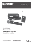
EC1 Body-Pack Transmitter
Characteristics
General
This transmitter is a single-channel unit that operates in the VHF
band between 169.445 and 230.000 MHz. Its phase-locked loop (pll)
circuit is programmable, enabling a factory-authorized technician to
change the transmitter’s carrier frequency. The unit is approved by the
European Telecommunications Standards Institute (ETSI) and other
authorities, and is sold in Europe and many other parts of the world.
The EC1 is typically used with the Shure EC4 diversity receiver and a
lavalier (WL93, WL183, WL184, WL185), headset (WH10, WCM16), or instrument (WM98) microphone.
1
3
ÁÁÁ
Á
ÁÁÁ
Á
ÁÁÁ
ÁÁ
ÁÁÁ
ÁÁÁ
Á
ÁÁ
2
4
9
8
6
7
5
Figure 1.
1.
2.
3.
4.
5.
Input jack
”Power” LED
Microphone on/off switch
Power on/off switch
Antenna
6. Audio level control
7. Frequency label
8. Belt clip
9. Battery compartment
Service Note: Shure recommends that all service procedures be
performed by a factory-authorized service center or that the product
be returned directly to Shure Brothers Inc.
E1998,
Shure Brothers Inc.
25A1002 (RA)
Printed in U.S.A.
Previous
Products
EC1 Body-Pack Transmitter
Circuit Description
The Shure EC1 transmitter has two interconnected circuit boards,
which comprise the audio and rf sections, respectively, plus a small audio
filter board mounted directly to the input connector.
Audio Section
Input: Audio signals enter the EC1 by way of a four-pin miniature Tini
Q-G (quick-ground) audio connector:
S
Pin 1: Ground
S
Pin 2: Regulated 5 Vdc bias for electret condenser microphones
S
Pin 3: Audio input
S
Pin 4: 20 kΩ load resistor connected to pin 3 for Shure electret
microphones
The rf filtering networks on pins 2 and 3 prevent the radiation of spurious signals via the audio input cable and prevent strong rf fields from
disrupting the preamplification and bias-voltage circuits.
Preamp: The audio signal next enters a preamplifier (transistors
Q101 and Q102). An externally-accessible variable gain control (R115)
provides up to 40 dB of gain, enabling the user to compensate for level
differences at the source. Low-pass filtering restricts the bandwidth of the
system to audio frequencies.
Pre-emphasis Network and Compander: The amplified audio signal then passes through a 62-microsecond pre-emphasis network (C105,
C106, R105, and R107). The output is fed to an NE571D compander
(U101A), which uses an external buffer transistor (Q103) to improve the
signal-to-noise ratio. The compander performs 2:1 logarithmic compression of the audio signal to effectively limit the peak deviation and spectral
bandwidth of the transmitted signal. An internal potentiometer (R131)
nulls the system audio distortion.
5 Vdc Bias and “Power” LED: The NE571D’s identical second channel (U101B) supplies regulated, low-noise 5 Vdc bias to various audio
and rf circuit points. Transistor Q104 provides input bias for the compander section (U101A), and transistor Q105 drives LED D101, which
serves as a “Power On” and low-battery indicator. Transistor Q106 provides electronic reverse-polarity protection.
Output and Mute: The processed audio signal enters unity-gain inverting amplifier U106A, whose output feeds the rf printed circuit board
through connector J101. The Mute switch (S102) controls the audio signal for standby operation without shutting off the carrier.
RF Section
Audio Input: Processed audio enters R204, an internal potentiometer that is factory-adjusted for 15 kHz deviation (100% modulation) when
the audio section provides a 0 dBu (0.775 V), 1 kHz tone.
Voltage-Controlled Oscillator (VCO) Assembly
This assembly is represented as “A201” on the rf schematic; its circuitry is detailed in the separate vco schematic.
Replacement Parts and Drawings
2
25A1002 (RA)
Previous
Products
EC1 Body-Pack Transmitter
Oscillation: The signal from R204 enters the audio input of voltagecontrolled oscillator (vco) assembly A201. This feeds the signal to varactor diode D401, which is part of a common-gate Colpitts oscillator
(Q401). This vco stage operates directly at the carrier frequency.
Filtering and Frequency Stability: The oscillator output is coupled
by C410 to Q402, a GaAs MESFET (gallium-arsenide metal-oxide semiconductor field-effect transistor) buffer stage, which isolates the vco from
subsequent circuits. A seven-pole, low-pass filter is added to the output
of the buffer. These two stages are shielded to prevent external rf fields
from affecting their operation and to reduce harmonic radiation from the
oscillator. Regulated 5 Vdc power ensures frequency stability despite
changes in battery voltage. The use of a phase-locked loop (pll), frequency-synthesized system eliminates the need for multiplier stages, resulting
in a much higher degree of spectral purity.
At this point the rf signal splits into two paths. The output of the vco
assembly described above is coupled by C208 to the frequency-control
section, and by C213 to the rf output section.
Frequency Control
Frequency Control: An MB504L prescaler (U202) is programmed by
an MC145152 synthesizer (U201) to divide the signal by 32 or 33 to derive the comparison frequency. The synthesizer contains a quartz-controlled reference oscillator circuit operating at 6.4 MHz (Y201), which is
factory-calibrated by trimmer C243. Internal circuitry divides this signal by
a factor of 128 to produce a 50 kHz reference frequency. The factory programs the operating frequency of each unit by 13 solder jumpers on the
rf printed circuit board, which control the internal synthesizer divider circuitry.
DC Control Voltage: The synthesizer output, a series of pulses, is
integrated by loop filter U203 to provide a dc control voltage for the vco.
This voltage is fed back to varactor diode D402 in the vco assembly. The
factory adjusts trimmer capacitor C409 to center the vco frequency within
the lock range.
RF Output
Power Amplifier: In the signal path, transistor Q201 operates as an
emitter follower to provide impedance-matching. The output of this stage
is coupled via C221 to the final output stage Q204, which operates as a
tuned amplifier. The output of Q204 contains a four-pole tuned circuit
(L205, C228, C226, L208, and C227).
Output Filter and Antenna: A dual-pi-section low-pass filter (C229,
L206, C230, L207, C246, C247, and L209) further reduces any harmonic
energy that remains. The 50 Ω filter output is connected to the antenna,
a quarter-wavelength, permanently attached, flexible wire. The pcb
ground serves as a counterpoise.
Transmitter Output: The transmitter can deliver up to +17 dBm
(50 mW) to the antenna. No user adjustments permit this value to be ex-
25A1002 (RA)
3
Replacement Parts and Drawings
Previous
Products
EC1 Body-Pack Transmitter
ceeded. The unit is intended to be powered exclusively by a 9 Vdc battery (an alkaline type, such as a Duracell MN1604, is recommended).
Spurious Emissions: To minimize the production and radiation of
spurious emissions and harmonic energy, and to promote stable operation, the collector circuit of each rf stage is separately decoupled from the
nine-volt supply by ferrite chokes and bypass capacitors. The base circuits, which are all operated from the regulated five-volt supply, are similarly decoupled except that they use resistor-capacitor (RC) networks,
which are more appropriate for the higher impedance level.
Replacement Parts and Drawings
4
25A1002 (RA)
Previous
Products
EC1 Body-Pack Transmitter
Functional Test
Before disassembling the unit, operate it to determine whether it is
functioning normally. Review the customer’s complaint and focus your
tests on it. See the product User’s Guide for a description of the unit as
well as information on its operation, troubleshooting, and technical data.
Disassembly and Assembly
To access the pc boards, disassemble the unit.
CAUTION
Observe precautions when handling this static-sensitive device.
Disassembly
1. Slide open the battery-compartment cover and remove the battery and, if necessary, the serial-number and date-code labels.
2. Remove the two smaller-head Phillips screws from the back of
the case (it is not necessary to remove the belt clip).
3. Carefully separate the top and bottom halves of the case to expose the pc boards.
4. Grasp the edges of the pc boards, as well as the front control
panel, and remove them as a unit by gently lifting them up and
out of the case.
5. Remove the rubber grommets from between the pc boards.
Figure 2.
25A1002 (RA)
5
Replacement Parts and Drawings
Previous
Products
EC1 Body-Pack Transmitter
Reassembly
1. Place the top half of the case upside down, then orient the rf board
so its gold pins point up. Fit the board inside the case and over the
plastic bosses (studs).
2. Slide the rubber grommets over the plastic bosses protruding
through the rf board.
3. Fit the audio board over the rf board so that the sockets on the
audio board line up with the pins on the rf board. Make sure the
front panel is seated properly in the slot at the front of the case,
that the battery terminals are inside the battery compartment,
and that the bosses are just below the surface of the audio
board.
4. Orient the the battery cover so its “Open” arrow points toward the
antenna and will be on the outside. Fit the cover into the slots at
the edge of the battery-compartment opening on the top case
half (closed position).
5. Place the bottom half of the case over the audio board and align
the edges of the case sections.
Note: Make sure the front panel, battery clips, antenna, and connector pins are properly aligned and seated before joining the
two case sections.
6. Align the two case sections and make sure they are properly
seated before securing them with the two Phillips screws.
Replacing the Belt Clip
The belt clip is secured with a single Phillips screw. When replacing
the clip, be sure to fit the section with the screw hole inside the square
indentation in the rear case.
Replacement Parts and Drawings
6
25A1002 (RA)
Previous
Products
EC1 Body-Pack Transmitter
Service Procedures
Reference Material
Refer to the Service Equipment Manual for Shure standard test
equipment.
Special Equipment
The Service Equipment Manual covers the standard items needed
for servicing the transmitters. It also explains how to modify and use an
SC4 receiver for testing any vhf microphone transmitter at the standard if
frequency. If you do not have this receiver, you will need an appropriate
receiver (usually an EC4) set to the same frequency as the transmitter.
System Operating Frequencies
Each rf board is marked with a group letter (A, B, or C) that identifies
the range of frequencies on which the transmitter can operate. The letter
is scratched into the underside of the rf board, near the part number for
the bare (unpopulated) board.
Table 1
Rf Board Groups
Group
Frequency Range
A 169.000–190.000 MHz
B 190.050–210.000 MHz
C 210.050–230.000 MHz
Used with pcb assembly 90_8596A
(pcb marking 34A8476C)
Table 2 (page 8) lists the frequencies and frequency codes available on the EC1 plus the rf board group number needed to provide each
frequency.
Changing the Frequency
The transmitter operating frequency is set by soldering jumpers
across the appropriate solder pads on the back of the EC1 rf board, as
shown in Figure 6 (page 19). Table 2 identifies the solder pads used for
each frequency. Each location that requires a solder jumper is indicated
by a “0” and shading; a “1,” unshaded, indicates a location that should
not be jumpered. Complete these connections before tuning the transmitter.
You will also need to change the frequency of the matching EC4 receiver to match the new transmitter frequency (see the EC4 service
manual).
Important: Remove any unwanted solder-bridging between jumpers.
25A1002 (RA)
7
Replacement Parts and Drawings
Previous
Products
EC1 Body-Pack Transmitter
Pc Board Groups
Table 2
Group
Freq.
(MHz)
Model
A
A
A
A
A
A
A
A
A
A
A
A
A
A
A
A
A
A
A
A
A
A
A
A
A
A
A
A
A
A
A
A
A
A
A
A
A
A
A
A
169.445
169.505
170.245
170.305
171.045
171.105
171.845
171.905
173.800
173.800
174.100
174.100
174.400
174.500
174.500
174.500
174.800
174.800
175.000
175.000
175.600
176.000
176.200
176.400
177.000
177.250
177.600
177.800
178.350
180.400
181.500
182.200
183.250
183.600
184.050
184.800
186.100
186.200
186.600
189.000
V
AD
AC
AH
AB
AG
W
AA
AQ *
EA
AY *
EB
CB
AZ *
DA
EC
BA *
ED
EE
BB *
FA *
FB *
CA
EF
K
DB
CC
FC *
FD *
CD
DC
CE
DD
CF
FE *
FF *
FG *
CG
CH
CJ
I208 I207 I206 I205 I204 I203 I202 I201 I213 I212
N0
N7
N6
N5
N4
N3
N2
N1
A4
A3
0
0
0
0
0
0
0
0
0
0
0
0
0
0
0
0
0
0
0
0
0
0
0
0
0
0
0
0
0
0
0
0
0
0
0
0
0
0
0
0
1
1
1
1
1
1
1
1
1
1
1
1
1
1
1
1
1
1
1
1
1
1
1
1
1
1
1
1
1
1
1
1
1
1
1
1
1
1
1
1
Replacement Parts and Drawings
1
1
1
1
1
1
1
1
1
1
1
1
1
1
1
1
1
1
1
1
1
1
1
1
1
1
1
1
1
1
1
1
1
1
1
1
1
1
1
1
0
0
0
0
0
0
0
0
0
0
0
0
0
0
0
0
0
0
0
0
0
0
0
0
0
0
0
0
0
1
1
1
1
1
1
1
1
1
1
1
8
1
1
1
1
1
1
1
1
1
1
1
1
1
1
1
1
1
1
1
1
1
1
1
1
1
1
1
1
1
0
0
0
0
0
0
0
0
0
0
0
0
0
0
0
0
0
0
0
1
1
1
1
1
1
1
1
1
1
1
1
1
1
1
1
1
1
1
1
1
0
0
0
0
0
0
0
1
1
1
1
0
0
1
1
1
1
1
1
0
0
0
0
0
0
0
0
0
0
0
0
0
1
1
1
1
1
1
1
1
0
0
0
1
1
1
1
0
0
0
1
1
1
0
0
0
0
1
1
0
0
0
0
1
1
1
1
1
1
1
1
1
0
0
0
0
0
1
1
1
0
1
1
0
0
1
1
0
0
0
0
1
1
0
0
1
1
0
0
1
1
1
1
0
0
0
0
0
0
0
0
1
0
0
0
1
1
0
0
0
1
0
1
1
1
0
1
0
0
1
0
1
1
1
1
1
1
1
1
0
0
1
1
0
0
0
0
1
1
1
1
1
0
0
1
0
1
0
0
1
1
1
1
0
1
0
0
1
1
0
0
I211
I210
I209
A2
A1
A0
1
1
1
1
1
1
1
1
1
1
0
0
0
0
0
0
0
0
1
1
0
0
1
0
1
0
0
1
1
0
1
1
0
0
0
0
0
1
1
1
0
1
0
1
0
1
0
1
0
0
1
1
0
1
1
1
0
0
0
0
0
0
0
0
0
0
0
0
1
0
1
0
0
0
0
0
1
0
0
0
1
0
1
0
1
0
1
0
0
0
0
0
0
0
0
0
0
0
0
0
0
0
0
0
0
1
0
0
1
0
0
0
1
0
1
0
0
0
0
0
25A1002 (RA)
Previous
Products
EC1 Body-Pack Transmitter
Group
Freq.
(MHz)
B
B
B
B
B
B
B
B
B
B
B
B
B
B
B
B
B
C
C
C
C
C
C
C
C
190.600
191.900
192.200
192.600
195.000
196.600
198.250
199.500
200.300
200.900
202.200
203.000
203.500
206.000
208.200
208.300
209.000
210.750
213.000
216.100
216.750
221.250
222.250
227.000
229.000
25A1002 (RA)
I208 I207 I206 I205 I204 I203 I202 I201 I213 I212
Model
N7
N6
N5
N4
N3
N2
N1
N0
A4
A3
I211
I210
I209
A2
A1
A0
CK
0
1
1
1
0
1
1
1
0
0
1
0
0
EG
0
1
1
1
0
1
1
1
1
1
1
1
0
CL
0
1
1
1
1
0
0
0
0
0
1
0
0
CM
0
1
1
1
1
0
0
0
0
1
1
0
0
CN
0
1
1
1
1
0
0
1
1
1
1
0
0
CP
0
1
1
1
1
0
1
0
1
1
1
0
0
DE
0
1
1
1
1
0
1
1
1
1
1
0
1
DF
0
1
1
1
1
1
0
0
1
0
1
1
0
CS
0
1
1
1
1
1
0
1
0
0
1
1
0
CZ
0
1
1
1
1
1
0
1
1
0
0
1
0
CQ
0
1
1
1
1
1
1
0
0
1
1
0
0
CR
0
1
1
1
1
1
1
0
1
1
1
0
0
DG
0
1
1
1
1
1
1
1
0
0
1
1
0
CT
1
0
0
0
0
0
0
0
1
0
0
0
0
CV
1
0
0
0
0
0
1
0
0
0
1
0
0
EH
1
0
0
0
0
0
1
0
0
0
1
1
0
CU
1
0
0
0
0
0
1
0
1
0
1
0
0
DJ
1
0
0
0
0
0
1
1
1
0
1
1
1
DK
1
0
0
0
0
1
0
1
0
0
1
0
0
EJ
1
0
0
0
0
1
1
1
0
0
0
1
0
DL
1
0
0
0
0
1
1
1
0
1
1
1
1
DM
1
0
0
0
1
0
1
0
0
1
0
0
1
DN
1
0
0
0
1
0
1
0
1
1
1
0
1
DP
1
0
0
0
1
1
0
1
1
1
1
0
0
DR
1
0
0
0
1
1
1
1
0
0
1
0
0
* These models have jumper X201 (see Figure 6, page 19) connected to lower the
power output, which is part of the special requirements for these MPT1345 frequencies.
9
Replacement Parts and Drawings
Previous
Products
EC1 Body-Pack Transmitter
Alignment
The rf and audio alignments are generally done together, as a single,
continuous procedure. Before beginning, be sure to do the setup described in the following subsection, “Test Conditions.”
Test Conditions
Initial Setup
1. Separate the rf board from the audio board.
2. Prepare the rf board as follows:
S
Solder a short, insulated wire to TP7 (figure 6, page 19). This
wire must extend enough beyond the board to be accessed
by a probe when the two pc boards are plugged together.
S
Obtain an RG174 (50 Ω coaxial) cable with a ferrite choke, a
BNC connector at one end, and stripped leads at the other
(see the service-equipment manual).
S
Unsolder and remove the antenna. Attach the 50 Ω coaxial
cable’s center conductor to the antenna solder pad, and the
shield to ground (see figure 5, page 19).
3. Plug the rf and audio boards back together.
4. Connect a 9 Vdc power supply to the battery terminals on the
audio board: the green LED should glow.
5. On the audio analyzer, activate the 400 Hz high-pass and the
30 kHz low-pass filters.
RF Alignment
A: VCO Alignment
This small pc board is enclosed in a metal shield on top of the
rf board. To access C409, remove the date-code label from the top of the
shield.
1. Connect the dc-voltage probe to the wire you attached to TP7.
2. Adjust C409 for 4 Vdc (± 0.5 Vdc) at TP7.
3. Remove the wire from TP7.
B: RF Power Alignment
1. Plug the coaxial cable on the antenna output into the spectrum
analyzer.
2. Set the spectrum analyzer as follows:
S
Center Frequency: Carrier
S
Span: 30 MHz
S
Reference Level: +20 dBm
S
Scale: 10 dB/div
Replacement Parts and Drawings
10
25A1002 (RA)
Previous
Products
EC1 Body-Pack Transmitter
3. Adjust C228 and C227 (rf board) for maximum power output.
Note: To obtain the maximum output, set the spectrum analyzer
to indicate 10 dB per division while you make the initial adjustments of C228 and C227. For their final adjustments, set the
spectrum analyzer to 2 dB per division.
4. Check the carrier output power indicated on the spectrum analyzer The maximum conducted power measurement varies according to the applicable standard:
S
MPT1345 (X201 jumpered): 5 dBm to 10 dBm
S
MPT1350 (X201 open): 8 dBm to 17 dBm
Note: After measuring the output power, add to it the calculated
power (insertion) losses from the cables and connectors.
In table 2 (page 8), frequencies marked with an asterisk are
subject to standard MPT1345. They require a jumper at X201 to
reduce the transmitter’s output power.
C: Frequency Alignment
1. Remove the cable from the spectrum analyzer and connect it to
the frequency counter through a 20 dB attenuator.
2. Adjust C243 to set the carrier frequency to FC "1 kHz.
Note: If you measure 4 V at TP7 but cannot adjust the carrier
frequency to FC "1 kHz, check the programming jumpers.
Audio Alignment
Make sure the microphone is turned on.
D: Gain
1. Unsolder and remove the 50 Ω coaxial cable, then resolder the antenna to the rf board.
2. Connect the audio analyzer’s output to pins 3 and 1 of the unit’s
microphone input connector. If necessary, use an appropriate
adapter cable.
3. Set the audio analyzer as follows:
S
Frequency: 1 kHz
S
Amplitude: 32 mV
4. Adjust the audio gain control (R115) for 0 dBu (0.775 Vrms),
" 0.5 dB, at TP4 on the rf board.
E: Deviation Reference Voltage
1. Turn off the EC1.
2. Connect the output of the audio generator to the modulation input of the rf signal generator.
25A1002 (RA)
11
Replacement Parts and Drawings
Previous
Products
EC1 Body-Pack Transmitter
3. Set the rf signal generator as follows:
S
Frequency: Carrier
S
Modulation: FM
S
Modulation Source: Ext 1 kHz
S
FM Deviation: $15 kHz
S
Amplitude: –38 dBm
4. Set the frequency on the audio generator to 1 kHz and adjust the
level until the “Hi Ext” and “Lo Ext” lights on the signal generator
turn off.
5. To modify and use an SC4 receiver for testing at the if frequency,
see the Service Equipment manual. Otherwise, obtain a receiver
set to the same frequency as the transmitter (usually the EC4
that came with the unit) and prepare it as follows:
S
Disconnect the antenna(s) from the receiver input and connect the output of the rf signal generator to either antenna
input of the receiver.
S
Set the Volume control on the front panel of the receiver to
its maximum (fully clockwise) position and apply power to the
receiver.
S
Set the receiver’s Squelch control to its midway position.
S
Terminate the receiver’s unbalanced output (1/4I jack) with a
1 kΩ resistor.
6. The measured rms voltage at the unbalanced output should be
382 mV, "66 mV (between –4.8 and –7.8 dBu), which corresponds to a deviation level of 15 kHz. If it is not, the receiver
needs tuning.
Record this voltage as the Deviation Reference Voltage.
Note: At this point you may want to press the audio analyzer’s Ratio
button (to perform the relative measurement in the next section) and
its Log-Lin button (to display the measurements in dB).
F: Frequency Modulation Alignment
1. Turn off the rf output of the rf signal generator. Disconnect the
output of the signal generator from the receiver. Connect an antenna to either antenna input of the receiver.
2. Verify that the audio analyzer’s output is connected to the microphone jack. Turn on the transmitter’s Power and Mute switches.
3. Set the audio analyzer as follows:
S
Frequency: 1 kHz
S
Amplitude: 32 mV
4. Measure the voltage at the high Z output (1/4I jack) of the receiver. Adjust R204 so this voltage is within 1 dB of the deviation reference voltage measured in step 6 of the preceding subsection.
Replacement Parts and Drawings
12
25A1002 (RA)
Previous
Products
EC1 Body-Pack Transmitter
G: Frequency Response Test
1. Change the setup as follows:
S
Press the Log/Lin button on the audio analyzer (to measure
in dBu).
S
Press the Ratio button twice to perform the next relative
measurement.
S
Deactivate the 400 Hz high-pass filter on the audio analyzer.
S
Change the frequency of the audio generator to 100 Hz.
2. Verify that the audio level is +0 dB, –3 dB of your measurement
in step 4, subsection F.
3. Activate the 400 Hz high-pass filter on the audio analyzer, and
change the frequency of the audio generator to 10 kHz.
4. Verify that the audio level is "1 dB relative to the 1 kHz voltage
recorded in step 4 of subsection F.
5. Return the frequency of the audio generator to 1 kHz.
H: Audio Distortion Alignment
1. Set the audio analyzer to measure distortion (Distn). Verify that
audio distortion is less than 0.5%. If distortion is greater, adjust
R131 on the audio board for a minimum reading.
DC Current Test
1. Verify the transmitter current in the 9 V supply line is as follows:
25A1002 (RA)
S
MPT1345 (X201 jumpered): 60 mA ("6 mA)
S
MPT1350 (X201 open): 53 mA ("6 mA)
13
Replacement Parts and Drawings
Previous
Products
EC1 Body-Pack Transmitter
Notes
Replacement Parts and Drawings
14
25A1002 (RA)
Previous
Products
EC1 Body-Pack Transmitter
Replacement Parts and Drawings
On the next page, the parts are listed according to the designations
from the pc board (see figures 3 through 8, on pages 18 through 20) and
the schematics at the end of this manual. Parts shown on the circuit diagram and not listed below are available at electronic-parts distributors.
On the pages following the parts list are the drawings of the printed
circuit boards and the schematics.
Product Changes
This section briefly describes significant changes to the EC1.
Microphone Jack: In 1994, the microphone-jack board was
changed to the “B” version, which accepts a WA302 guitar cable. The
change included new values for C301 and C302 on the jack board, and
to C104 and R119 on the audio board. It also changed the input impedance from 100 Ω to 1 MΩ.
Battery Terminals: In 1995, the battery clips were changed to stainless steel. The present version may be used as a direct substitution on
earlier models.
Dual Operational Amplifier (U106): Temporary shortages of the
Shure part number 183A02 necessitated various substitutions. The present part number may be used to replace any of those earlier substitutes
at U106 on the audio board.
“J” Frequency Code: Starting in the summer of 1997, EC Series
transmitters and receivers tuned to 175.000 MHz have been labeled as
“BB” rather than “J.” The change was made to avoid confusion with the
different meaning of the “J” designation in the LX88 and ELX88 units. It is
only a labeling change; the units are physically the same. The relabeling
does not apply to other 175 MHz units (e.g., EE).
Parts Designations
The following comments apply to the parts list and the schematic:
Resistors: All resistors are surface-mount with 1/10 W rating and 1%
tolerance.
Capacitors: Unless otherwise noted, non-polarized capacitors are
surface-mount NPO dielectric types with a w50 V capacity.
25A1002 (RA)
15
Replacement Parts and Drawings
Previous
Products
EC1 Body-Pack Transmitter
Table 3
Replacement Parts
Reference
Designation Description
Shure Part No. (commercial alternative)
A1 Audio pcb assembly
90B8449J
A2 Rf pcb assembly
90_8596A [in the underlined space, insert the
proper letter code from the “Group” column in
table 2 (page 8)—e.g., 90B8596A].
A3 Microphone-jack pcb assembly
90B8420B
E201 Antenna
70B8007
MP1 Case front
65A8173
MP2 Case back
65A8139
MP3 Belt clip
53A8247B
MP4 Battery door
65A8226
Audio Circuit Board
D101 Light-emitting diode (green)
86C8422
J101, J102 Socket strip
56A8041
MP3 Battery clip
56A8066
Q101, Q104, Transistor, NPN
Q105
183A38 (MMBT5089LT1)
Q102, Q103 Transistor, PNP
183A01 (MMBT5087T)
Q106 Transistor, PNP
183A07 (MMBT404AL)
R115 Trim pot, 5 k, log
46D8008
R131 Potentiometer
146F02
S101 Slide switch, spdt
55B8048
S102 Slide switch, spdt
55C8048
U101 Integrated circuit
188A01 (NE571D)
U106 Dual operational amplifier
188A02 (TL062ACDR)
Mic-Jack Board
J1 Four-pin receptacle
95A8188
RF Circuit Board
A201 Voltage-controlled oscillator assembly
90_8597A [in the underlined space, insert the
proper letter code from the “Group” column in
table 1 (page 7)—e.g., 90C8597A].
C227, C228 Trim capacitor (3–10 pF)
152C02
C243 Trim capacitor (7–50 pF)
152H02
P201, P202 Interconnect strip
56A8042
Q201 Transistor, NPN
183A03 (MMBTH10L)
Q204 Transistor, NPN
183A17 (NE73433)
R204 Potentiometer, 5 k, 25%
146D02
U201 Integrated circuit-synthesizer
188A16 (MC145152FN2)
U202 Integrated circuit-prescaler
188A15 (MB504L)
U203 Single operational amplifier
188A14 (MC33171D)
Y201 Crystal (6.4 MHz)
140A002
Replacement Parts and Drawings
16
25A1002 (RA)
Previous
Products
EC1 Body-Pack Transmitter
Reference
Designation Description
Shure Part No. (commercial alternative)
Voltage-Controlled Oscillator Board (mounted inside the shield on the rf board)
Q401 Transistor, vhf/uhf (N channel)
183A18 (MMBFJ310L)
Q402 Transistor, dual-gate agc amp,
GaAs MESFET (gallium-arsenide
metal-oxide semiconductor field-effect transistor)
183B12 (NE25139/U72)
25A1002 (RA)
17
Replacement Parts and Drawings
Previous
Products
EC1 Body-Pack Transmitter
Figure 3. EC1 Audio Board, Top
Figure 4. EC1 Audio Board, Bottom
Replacement Parts and Drawings
18
25A1002 (RA)
Previous
Products
EC1 Body-Pack Transmitter
Spectrum Analyzer
or
Frequency Counter
ÌÌ
Shield
Conductor
Figure 5. EC1 RF Board, Top
TP4
TP2
Wire for DC
voltmeter
TP3
TP7
TP8
TP5
“A” freq.
jumpers
TP6
TP1
“N” freq.
jumpers
X201
jumper
Figure 6. EC1 RF Board, Bottom
25A1002 (RA)
19
Replacement Parts and Drawings
Previous
Products
EC1 Body-Pack Transmitter
Figure 7. EC1 VCO Board, Top
Figure 8. EC1 Microphone-jack Board, Bottom
Replacement Parts and Drawings
20
25A1002 (RA)
Previous
Products
EC1 Body-Pack Transmitter
Schematics
(Note to Printer: do not print this page)
Please print the attached schematics in the order they are listed:
25A1002 (RA)
S
EC1 Audio Board (letter size)
S
EC1 Rf Board (ledger size)
S
EC1 VCO Board (ledger size)
21
Replacement Parts and Drawings