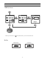
1
Service Manual
XGA COLOR MONITOR
Model : 719B
719BF
DAEWOO ELECTRONICS CO., LTD.
http : //svc.dwe.co.kr
February, 2001
CONTENTS
SAFETY PRECAUTIONS
1
GENERAL SAFETY INFORMATION
2
SERVICING PRECAUTIONS
3
TECHNICAL INFORMATION
6
GENERAL INFORMATION
7
PIN CONNECTOR
8
CAUTIONS FOR ADJUSTMENT AND REPAIR
8
OPERATION AND ADJUSTMENT
9
ALIGNMENT PROCEDURE
15
TROUBLESHOOTING HINTS
17
BLOCK DIAGRAM
33
PCB LAYOUT
34
SCHEMATIC DIAGRAM
38
EXPLODED VIEW & MECHANICAL PARTS LIST
42
INFORMATION OF PART DESCRIPTION
44
ELECTRICAL PARTS LIST
45
SAFETY PRECAUTIONS
CAUTION: No modifications of any circuits should be attempted. Service work should be performed
only after you are thoroughly familiar with all of the following safety checks and servicing
guidelines.
◆ Safety Check
Care should be taken while servicing this analog color display because of the high voltages used in the
deflection circuits. These voltages are exposed in such areas as the associated flyback and yoke circuits.
◆ Fire & Shock Hazard
• Insert an isolation transformer between the analog color display and AC power line before servicing the
chassis.
• When servicing, pay close attention to the original lead dress especially in the high voltage circuit area;
if a short circuit is found, replace all parts which have been overheated as a result of the short circuit.
• All the protective devices must be reinstalled per original design.
• Soldering must be inspected for possible cold solder points, frayed leads, damaged insulation, solder
splashes or sharp solder points. Be certain to remove all foreign materials.
◆ Implosion Protection
Picture tube in this monitor employs intergral implosion protection system, but care should be taken to
avoid damage and scratching during installation.
Only use same type replacement picture tubes.
IMPORTANT SAFETY NOTICE: There are special components used in this analog color display,
which are important for safety. These parts are shaded on the
schematic diagram and on the replacement parts list. It is essential
that these critical parts should be replaced with manufacturer’s
specified parts to prevent X-Ray, shock, fire or other hazards. Do
not modify the original design without getting written permission
from DAEWOO ELECTRONICS CO. or this will void the original
parts and labor warranty.
◆ X-Ray
WARNING: The only potential source of X-Ray is the picture tube. However when the high voltage
circuitry is operating properly, there is no possibility of an X-Ray problem. The basic
precaution which must be exercised is to keep the high voltage at the following factory
recommended level.
NOTE: It is important to use an accurate, periodically, calibrated high voltage meter.
• To measure the high voltage, use a high-impedance high-voltage meter.
Connect(-) to chassis and (+) to the CRT anode button.
• Set the Contrast & Brightness Control to the minimum on OSD Menu.
• Measure the high voltage. The high voltage meter should indicate the following factory
recommended levels.
• If the upper meter indication exceeds the maximum level, immediate service is required to
prevent the possibility of premature component failure.
• To prevent X-Ray possibility, it is essential to use the specified picture tube.
• The normal high voltage is 25.5KV or below and must not exceed 29KV at zero beam current
at rated voltage.
1
GENERAL SAFETY INFORMATION
◆ Terms in the manual
CAUTION
Statements identify conditions or practices that could result in damage to the equipment or
other property.
WARNING Statements identify conditions or practices that could result in personal injury or loss of
life.
◆ Terms as marked on equipment
CAUTION
Statements indicate a personal injury hazard not immediately accessible as one reads the
marking or a hazard which is properly included on the equipment itself.
WARNING Statements are clearly concerning indicated personal injury hazards.
◆ Symbols in the manual
The symbols indicate where applicable cautionary or other information is to be found.
◆ Symbols as marked on equipment
Protective GROUND terminal
◆ High Voltage Warning
And Critical Component Warning Label
The following warning label is on the CRT PWB shield case inside the unit.
Warning: This product includes critical mechanical and electrical parts which are essential for x ray
protection. For continued safety, replace critical components that are indicated in the service
manual with exact replacement parts given in the parts list.
Operating high voltage with this product is 29Kv at minimum brightness. Refer to service
manual for measurement procedures and proper service adjustments.
2
SERVICING PRECAUTIONS
CAUTION: Before servicing instruments covered by this service manual, its supplements, and
addendum, please read and follow the SAFETY PRECAUTIONS of this manual.
NOTE: If unforeseen circumstances create conflict between the following servicing precautions and any
of the safety precautions on page 1 of this manual, always follow the safety precautions.
Remember: Safety First.
◆ General Servicing Precautions
1. Always unplug the AC power cord from the AC power source before:
a. Removing or reinstalling any component, circuit board, module, or any other instrument assembly.
b. Disconnecting or reconnecting any electrical plug or other electrical connection.
c. Connecting a test substitute in parallel with an electrolytic capacitor in the instrument.
CAUTION: A wrong part substitution or incorrect polarity installation of electrolytic capacitors
may result in a explosion.
d. Discharging the picture tube anode.
2. Test high voltage only by measuring it with an appropriate high voltage meter or other voltage
measuring device (DVM, FETVOM. etc.) equipped with a suitable high voltage probe. Do not test high
voltage by “drawing an arc”.
3. Discharge the picture tube anode only by: (a) first connecting one end of an insulated clip lead to the
degaussing or line grounding system shield at the point where the picture tube socket ground lead is
connected, and then (b) touching the other end of the insulated clip lead to the picture tube anode
button, using an insulating handle to avoid personal contact with high voltage.
4. Do not any spray chemicals on or near this instrument, or any of its assemblies.
5. Unless otherwise specified in this service manual, only clean electrical contacts by applying the
following mixture to the contacts with a pipe cleaner, cotton-tipped stick, or comparable nonabrasive
applicator: 10% (by volume) Aceton and 90% (by volume) isopropyl alchohol (90%-99% strength).
CAUTION: This is a flammable mixture. Unless specified in this service manual, lubrication of
contacts is not required.
6. Do not damage any plug/socket B+ voltage interlocks with which instruments covered by this service
manual might be equipped.
7. Do not apply AC power to this instrument and/or any other of its electrical assemblies unless all the
solid-state device heat sinks are correctly installed.
8. Always connect the test instrument ground lead to the appropriate instrument chassis ground before
connecting the test instrument positive lead. Always remove the test instrument ground lead last.
9. Only use the test fixtures specified in this service manual with this instrument.
CAUTION: Do not connect the test fixture ground strap to any heatsink in this instrument.
3
◆ Electrostatically Sensitive (ES) Devices
Some semiconductor (solid state) devices can be damaged easily by static electricity.
Such components are commonly called Electrostatically Sensitive (ES) Devices.
The typical examples of ES devices are integrated circuits, some field-effect transistors, and
semiconductor “chip” components. The following techniques should be used to help reduce the incidence
of component damage caused by static electricity.
1. Immediately before handling any semiconductor component or semiconductor-equipped assembly,
wipe off any electrostatic charge on your body by touching any known earth ground. Alternatively,
obtain and wear a commercially available discharging wrist strap device which should be removed for
potential shock reasons prior to applying power to the unit under testing conditions.
2. After removing the electrical assembly equipped with ES devices, place the assembly on a conductive
surface such as aluminum foil to prevent electrostatic charge buildup or exposure to the assembly.
3. Only use a grounded-tip soldering iron to solder or unsolder ES devices.
4. Only use an anti-static type solder removal device. Some solder removal devices not classified as “antistatic” can generate enough electrical charges to damage ES devices.
5. Do not use freon-propelled chemicals. These can generate enough electrical charges to damage ES devices.
6. Do not remove a replacement ES device from its protective package until immediately before you are
ready to install it. (Most replacement ES devices are packaged with leads electrically shorted together
by conductive foam, aluminum foil, or comparable conductive material).
7. Immediately before removing the protective material from the leads of replacement ES devices, touch
the protective material to the chassis or circuit assembly into which the device will be installed.
CAUTION: Be sure that no power is applied to the chassis or circuit, and observe all other safety
precautions.
8. Minimize bodily movements when handling unpackaged replacement ES devices. (Otherwise harmful
motion such as the brushing together clothes fabric or the lifting your foot from a carpeted floor can
generate enough static electricity to damage ES devices).
◆ General Soldering Guidelines
1. Use a grounded-tip, low-wattage soldering iron with appropriate tip size and shape that will maintain
tip temperature between a 550°F-660°F (288°C-316°C) range.
2. Use an appropriate gauge of RMA resin-core solder composed of 60 parts tin/40 parts lead.
3. Keep the soldering iron tip clean.
4. Throughly clean the surface to be soldered. Use a small wire-bristle (0.5 inch or 1.25cm) brush with a
metal handle. Do not use freon-propelled spray-on cleaners.
5. Use the following soldering technique:
a. Allow the soldering iron tip to reach normal temperature (550°F to 660°F or 288°C to 316°C)
b. Hold the soldering iron tip and solder strand against the component lead until the solder melts.
c. Quickly move the soldering iron tip to the junction of the component lead and the printed circuit foil,
and hold it there until the solder flows onto and around both the component lead and the foil.
d. Closely inspect the solder area and remove any excess or splashed solder with a small wire-bristle brush.
CAUTION: Work quickly to avoid overheating the circuit board printed foil.
4
FIGURE 1. USE SOLDERING IRON TO PRY LEADS
◆ IC Removal/Replacement
Some utilized chassis circuit boards have slotted (oblong) holes through which the IC leads are inserted
and then bent flat against the circuit foil. When holes are slotted, the following technique should be used
to remove and replace the IC. When working with boards using the familiar round hole, use the standard
technique as outlined in paragraphs 5 on the page under the title of general soldering guidelines.
◆ Removal
1. Desolder and straighten each IC lead in one operation by gently prying up on the lead with the
soldering iron tip as the solder melts.
2. Draw away the melted solder with an anti-static suction-type solder removal device (or with
desoldering braid before removing the IC.
◆ Replacement
1. Carefully insert the replacement IC in the circuit board.
2. Carefully bend each IC lead against the circuit foil pad and solder it.
3. Clean the soldered areas with a small wire-bristle brush. (lt is not necessary to reapply acrylic coating
to the area).
◆ “Small-Signal” Discrete Transistor Removal/Replacement
1. Remove the defective transistor by clipping its leads as close as possible to the component body.
2. Bend the ends of each of three leads remaining on the circuit board into a “U” shape.
3. Bend the replacement transistor leads into a “U” shape.
4. Connect the replacement transistor leads to the corresponding leads extending from the circuit board
and crimp the “U” with long nose pliers to ensure metal-to-metal contact, then solder each connection.
5
◆ Power IC, Transistor or Devices Removal/Replacement
1. Heat and remove all solders from the device leads.
2. Remove the heatsink mounting screw (if applicable).
3. Carefully remove the device from the circuit board.
4. Insert new device in circuit board.
5. Solder each device lead and then clip off excess lead.
6. Replace heatsink.
◆ Diode Removal/Replacement
1. Remove defective diode by clipping its leads as close as possible to diode body.
2. Bend the two remaining leads perpendicularly to the circuit board.
3. Observing diode polarity, wrap each lead out of the new diode around the corresponding lead on the
circuit board.
4. Securely crimp each connection and solder it.
5. Inspect the solder joints of the two “original” leads on the circuit board copper side. If they are not
shiny, reheat them and apply additional solder if necessary.
TECHNICAL INFORMATION
Model
719B
719BF
CDT Size
17-inch
17-inch DynaFlat
Diagonal visible image area
16.2-inch
16.01-inch
Dot Pitch
0.28 mm
0.25 mm
Synchronization
Horizontal
30 - 70 KHz
Vertical
50 - 160 Hz
Plug and Play
DDC1/2B/CI
Power Saving
EPA, VESA DPMS, Nutek Compliant
Power Source
100-240 Vac, 50/60Hz (Free Voltage)
Power Consumption
85W
Dimension-W x H x D
410 x 402 x 425mm
410 x 407 x 419mm
Weight-unpacked(lbs/Kg)
32.0/14.5
35.2/16
Operating Temperature
10 ~ 40°C /50 ~ 104°F
(set with stand)
6
GENERAL INFORMATION
This color monitor automatically scans all horizontal frequencies from 30KHz to 70KHz, and all vertical
frequencies from 50Hz to 160Hz. This color monitor supports IBM PC, PC/XT, PC/AT, personal
System/2 (PS/2), Apple Macintosh, and compatible users crisp text and vivid color graphics display when
using the following graphics adapters : (VGA, 8514/A, Super VGA, VESA and XGA and Apple
Macintosh Video Card). And so, this color monitor has a maximum horizontal resolution of 1280 dots and
a maximum vertical resolution of 1024 lines for superior clarity of display.
By accepting analog signal inputs which level is zero to 0.7 Volts. This color monitor can display and
unlimited palette of colors depending on the graphics adapter and software being used.
◆ Abbreviations
ADJ
AFC
CRT
Def
D.Y
FBT
H.SYNC
OSC
P.S.U
PWA
R.G.B
V.Sync
Adjustment
Automatic Frequency Control
Cathode Ray Tube
Deflection
Deflection Yoke
Flyback Transformer
Horizontal Synchronization
Oscillator
Power Supply Unit
Printed Circuit Board Wiring Assembly
Red, Green, Blue
Vertical Synchronization
7
PIN CONNECTOR
Pin
1
2
3
4
5
6
7
8
9
10
11
12
13
14
15
Signal
1
Red
Green
Blue
GND
GND
GND - Red
GND - Green
GND - Blue
+5Vdc
GND - H.Sync
GND - V.Sync
Bi-directional Data (SDA)
Horizontal Sync
Vertical Sync (VCLK)
Data Clock (SCL)
6
10
15
Arrangement of 15-pin D-sub connector
CAUTIONS FOR ADJUSTMENT AND REPAIR
• Degaussing is always required when adjusting purity or convergence.
• The white balance adjustment has been done by a color analyzer in factroy. The adjustment procedure,
described in the service manual is made by a visual check.
• Allow 20 minutes warm-up time for the display before checking or adjusting only electrical
specification or function.
• Reform the leadwire after any repair work.
◆ Caution For Servicing
• In case of servicing or replacing CRT, high voltage sometimes remains in the anode of the CRT.
Completely discharge high voltage before servicing or replacing CRT to prevent a shock to the
serviceman.
8
OPERATION AND ADJUSTMENT
719B Control Panel
•
•
Move cursor to the right window on the OSD window.
Increase the value of any selected function.
•
•
Move cursor to the left window on the OSD window.
Decrease the value of any selected function.
•
Launch OSD(On-Screen Display) MENU window.
•
•
Move cursor to the high window on the OSD window.
Increase the value of V.size or V.center.
•
•
Move cursor to the low window on the OSD window.
Decrease the value of V.size or V.center.
9
719BF Control Panel
•
•
Move cursor to the right window on the OSD window.
Increase the value of any selected function.
•
•
Move cursor to the left window on the OSD window.
Decrease the value of any selected function.
•
Launch OSD(On-Screen Display) MENU window.
•
•
Move cursor to the high window on the OSD window.
Increase the value of V.size or V.center.
•
•
Move cursor to the low window on the OSD window.
Decrease the value of V.size or V.center.
10
719B Key Process
MENU
MENU
MENU
MENU
OSD OFF
•
When you choose the icon
on the OSD window, you can exit the OSD screen.
Hot Key
BRIGHTNESS
CONTRAST
11
719BF Key Process
OSD OFF
•
When you choose the icon
on the OSD window, you can exit the OSD screen.
Hot Key
BRIGHTNESS
CONTRAST
12
OSD Functions
ICON
CONTROL
FUNCTIONS
PINCUSHION
Adjust the left and right margins for more convex or more concave margins.
TRAPEZOID
Adjust the trapezoid of the screen by moving the lines inward or outward.
PARALLELOGRAM Adjust the parallelogram when the screen is leaning left or right.
PIN BALANCE
Adjust the side balance when the sides of the screen are bowed towards left or right.
ROTATION
Adjust the rotation when the screen is tilted left or right. (719BF only)
T. PIN CORNER Adjust the pin corner top when the top sides of the screen are bowed.
B. PIN CORNER Adjust the pin corner bottom when the bottom sides of the screen are bowed.
H. CENTER &
V. CENTER
Adjust the position of the display horizontally(left or right) and vertically (up or down).
COLOR TEMP
Choose different preset color temperatures or set your own customized color parameters.
RED GAIN
Adjust the red gain.
GREEN GAIN
Adjust the green gain.
BLUE GAIN
Adjust the blue gain.
H. SIZE &
V. SIZE
DEGAUSS
Adjust the width (horizontal size) and the height (vertical size) of the display.
Degauss the display and restore image quality.
13
ICON
CONTROL
FUNCTIONS
STATUS
Display horizontal & vertical frequency and polarity.
H. MOIRE
Adjust the horizontal picture moire cancellation.
V. MOIRE
Adjust the vertical picture moire cancellation.
LANGUAGE
Select language for OSD (5 languages).
RECALL
Reset the screen to the Factory Preset Display Settings.
14
ALIGNMENT PROCEDURE
◆ Standard Adjustment Conditions
1. Power source voltage : AC 120V, 60Hz/AC 220V, 50Hz.
2. Aging : Take at least 20 minutes warm-up time.
3. Signals.
Video : Analog 0.7Vpp 75Ω terminal positive polarity
Synchronizing : TTL Level Negative/Positive Separate/Composite
Deflection frequency
Horizontal Frequency : 30KHz - 70KHz
Vertical Frequency : 50Hz - 160Hz
◆ Pre-Adjustment
1. High Voltage Adjustment
Adjust 26K Vdc between Anode cap and ground at a cross hatch pattern of 60KHz by using VR 502.
◆ Method to launch the factory mode
Step 1. Push the menu button.
Step 2. Push the menu button and Brightness minus control button (
) for 5 times in same time.
◆ Main Adjustment
1. Setting the Controls
Set the value of items as following.
Contrast : Max. (OSD value up to 100)
Brightness : Center (Set the OSD value to 50)
2. H.size, V.size, H.phase, V.position, Pincushion, Trapezoid
Receive the cross hatch pattern of Factory preset mode.
H.size, V.size, H.phase, V.position, Pincushion, Trapezoid are adjusted at each mode.
In Factory, Auto Alignment was done at each mode. Therefore, Factory preset mode has it’s own value
according to each control.
3. Focus
(a) Set brightness control to center and contrast control to MAX.
(b) Receive all “H” character pattern of 60KHz mode signal.
(c) Adjust the Focus control of FBT to obtain best Focus (static focus and Dynamic focus).
4. Geometric Distortion Adjustment
(a) Receive the cross hatch pattern of VGA mode signal by using the signal generator.
(b) Pin balance, Parallelogram are adjusted the best geometric status.
(c) Repeat the adjustment at each mode.
5. White Balance Adjustment
(a) Receive a full white pattern of 60KHz mode.
(b) Set the bright control and contrast control to the maximum and receive the all black pattern.
(c) Select a Temperature function on the R, G, B item of the OSD menu and select 9300.
(d) If the screen luminosity is changed, adjust the sub brightness control to get the 0.6 ~ 0.8 Ft/L screen
luminosity.
(e) Select the R, G, B Bias on the OSD menu and adjust the
/
key to get the color coordinates in
X=0.281, Y=0.311.
(f) Set the brightness control to the center and contrast control to the maximum.
(g) Receive a full white pattern.
15
(h) Select the R, G, B gain on the OSD menu and adjust the
/
key to get the color coordinates in
X=0.281±0.02, Y=0.311±0.02.
(i) Adjust the sub contrast control to get the screen luminosity to 32Ft/L.
6. Static Convergence Adjustment
(a) Apply a magenta cross hatch pattern on display.
(b) Adjust the focus from the best over all focus on the display.
Also adjust the brightness to the desired condition.
(c) Vertical red and blue lines are converged by varying the angles between the two tabs of the 4-pole
magnets.
(d) Horizontal red and blue lines are converged by varying the tabs together keeping the angle between
them constant.
(e) Apply a yellow cross hatch pattern on the display.
(f) Vertical green and red lines are converged by varying the angle between the two tabs of the 6-pole
magnets.
(g) Horizontal green and red lines are converged by varying the tabs together and keeping the angle
between them constant.
16
TROUBLESHOOTING HINTS
1. No Character
No Character
Are the
Contrast &
Brightness Controls
maximum
No
Change the Contrast &
Brightness control to
maximum
Yes
Is whole
screen bright?
No
No Raster
Refer to
No Raster
Yes
Is CRT
Cathode (Rk, Gk, Bk)
signal level
normal?
No
Is the
output signal of the
(pin 16,18,20) pre-amp
(IC801, TDA9210)
normal?
Yes
Check the peripheral circuit
of CRT Board
Rk, Gk, Bk
About 40Vpp
Yes
Check the video output
(IC802, TDA9536) and
their ambient circuit
No
Trouble in 6.3Vdc line
of the Main PWB
No
Check the blanking pulse
circuit
No
Is 6.3Vdc line
normal?
Yes
Is blanking
pulse (pin 20 of IC801)
normal?
Yes
Is input signal
normal?
No
Yes
Trouble in IC801 and
its ambient circuit
17
Check the signal cable
2. No Raster
No Raster
Is CRT
heater red-hot?
Is Heater
Voltage (CRT PWB)
about 6V?
No
Yes
Yes
Trouble in
CRT
No
Trouble in
power supply
circuit
Turn the Brightness
& Contrast control
to set Maximum
Refer to trouble in
power supply unit.
Yes
Is whole
screen bright?
No
Trouble in power
supply circuit
No
Trouble in G1
line of Main PWB
No
Trouble in FBT or
peripheral circuit
No
Trouble in 100Vdc
line of power
supply unit
No
High Voltage
trouble in FBT
Yes
Check
G1 voltage about
-30V?
Yes
Is CRT
G2 (screen) voltage
about 450~
550V?
Yes
Is 100Vdc
line normal?
Yes
Does
turning the SubBrightness control to the
maximun on OSD menu
make screen
bright?
Yes
Trouble in FBT
18
Refer to trouble
in P.S.U
3. A Missing Color
One color is
missing
Is input signal
normal?
No
Check video signal
cable or video card.
No
Trouble in IC801 or its
ambient circuit
0.7Vpp
Yes
Is the
output of pre-amp
(IC801, TDA9210)
pin 16,18, 20 all
normal?
Yes
CRT
No
Cathode (Rk, Gk, Bk)
is normal?
RK, GK, BK
About 40V p-p
Yes
Each grid (G1, G2)
voltage normal?
Is video
output IC(IC802,
TDA9536)
normal?
No
Replace Video output IC
Yes
No
Trouble in 100Vdc line
Replace CRT
19
Yes
Trouble in
video output
circuit or
ambient
4. Abnormal OSD Font
Abnormal OSD Font
Is menu
key selected?
Is OSD Font
exist?
* If menu key selected.
Is +5V
Voltage about 5V?
No
Yes
Yes
One color is
missing
Troubie in
IC803 or its
ambient circuit
Yes
Is the
output of IC803
(pin 13, 14, 15)
normal?
No
Trouble in IC803
and its ambient
circuit
Yes
Refer to Missing Color
20
No
Trouble in
+5V voltage
line.
Refer to trouble in P.S.U
5. Horizontal Output Circuit
Trouble in Horizontal
output circuit
(No Raster
Is the
B+line voltage
over 45V?
No
Trouble in B+ Booster Circuit
(Check the B+section of IC501)
Yes
Is the H-out
waveform of IC501
normal?
11V
0V
No
Trouble in IC501
Yes
Is the Collector
wave form of
Q504 normal?
10V
0V
No
Trouble in Q504
Yes
Is the Collector
waveform of
Q505 normal?
66V
Yes
Trouble in Q505 and
its ambient circuit.
21
No
Trouble in Q505 and its
ambient circuit.
6. Unstable Picture
6-1. Horizontal
Unstable
picture
Is H.Sync
input pin of IC501
correct?
No
Check H.Sync Out of
Micom or its ambient
circuits.
No
Check the value of
C513, R522
Yes
Is the
pin 10 of IC501
12V?
Yes
Trouble in IC501
22
6-2. Vertical
Unstable or
Abnormal picture
Is
13V DC line
correct?
No
Check PWR 13V
ambient circuit.
Yes
Check V.DY
and ambient circuit.
Yes
Check the IC401
or ambient circuit.
Yes
45Vp-p
Is
the output
waveform of IC401
(pin 6) normal?
No
Is the
output pulse
of IC501 (pin 23)
normal?
No
Trouble in V.Sync line
or IC501 failure.
23
7. Focus
Monitor remains
unfocused
Check
Focus VR in
FBT
Is
focus
acceptable?
Yes
No
Trouble in Focus
circuit (FBT)
24
OK
7-1. Dynamic Focus
FVH FVV
* Check after adjusting the static focus
finely by VR in FBT
Focus is poor
ORION
: 300V 120V
SAMSUNG : 300V 120V
DF
waveform
FVH
FVV
Is the
waveform of the
DF pin in FBT
correct?
Yes
1. Check the CRT socket
or connector wire
2. Trouble in FBT or CRT
No
Is the
waveform of
the pin 32 in IC501
correct?
Yes
Trouble in Q602, R611,T601
25
No
Trouble in IC501 or C503
8. Convergence
Poor convergence
Is
convergence
on the center area
bad?
Yes
Adjust static
convergence
Refer to
Adjustment
procedure of
convergence
No
Is
convergence on the
fringe area bad?
Yes
Adjust D.Y
Location
26
9. Abnormal Picture
9-1. Horizontal Size
Abnormal
H.Size
When
the H.Size on the
OSD is changed, is the
H.size changed?
No
Yes
It isn’t out of order.
27
Check pin 11 of IC501
and its ambient circuit
9-2. Vertical Size
Abnormal
V.Size
Is
changeable the
DC voltage of
IC401 pin 6?
No
Is
the 3.5Vdc of pin
23 of the IC501?
No
Yes
Trouble V.OSC/
Deflection Circuit
Check the pin 23 of IC501
and its ambient circuit
Refer to V.OSC/Deflection circuit
28
Yes
Check the IC401
and its
ambient circuit
10. High Voltage Output Circuit
Trouble in H.V circuit
(No Raster)
Is
B+(45V) line
voltage normal?
No
Trouble in power
supply circuit
Yes
Trouble in FBT
Yes
Trouble in IC501
ambient circuit
Yes
Trouble in IC501
ambient circuit
Yes
Is Q505
collector waveform
normal?
No
Is IC501
pin 8
normal?
No
Is the
IC501 pin15 H.trigger
correct?
No
Trouble in H.trigger
29
11. Side-Pincushion Circuit
Side-Pincusion distortion
is excessive or barrel
Select the
side-pincushion
icon on OSD menu,
and adjust acceptable
position.
Yes
O.K
No
Is the pin 5,10
waveform of IC803
correct?
Yes
Check IC803 or
their ambient circuit
Yes
Check IC803or
it’s ambient circuit.
No
Is the
waveform of IC803
pin 7,8?
No
Trouble in H.Size
30
12. Power Supply Unit (P.S.U)
Trouble in P.S.U
Is
power switch
on?
No
Switch on
Yes
Is
fuse F001
O.K?
No
Check the power cord outlet
and diode D001, D002,
D003, D004, Q001
No
Trouble in D001, D002,
D003, D004, C004 and
TH001.
Yes
Is
voltage of T001
pin 7 130V
(370V)?
Yes
Is the
waveform of Q001
Drain pin
correct?
400Vpp (620Vpp)
No
Trouble in T001, IC001, Q001
and D009 etc.
Yes
Is
voltage of C104
45Vdc?
No
Trouble in D102 or
its ambient circuit
Yes
Is
voltage of C102
100Vdc?
No
Trouble in D101 or
Video Part
Yes
Is
voltage of C105
8Vdc?
No
A
31
Trouble in D103
A
Is voltage
of C109 13Vdc?
No
Trouble in D106 or
horizontal part
No
Trouble in D104 or
vertical part
Yes
Is
voltage of C108
-13Vdc?
Yes
Is voltage
of C106
27Vdc?
No
Trouble in D108
Yes
P.S.U O.K
32
33
SMPS
Transformer
AC INPUT
D -SUB
RGB H/V
IIC
Control
CRT
Driver
TDA9536
(SGS
Thompson)
H/V Moire
Cancellation
H/V OSC Processor
TDA4856 (Philips)
MCU
NT68P62
(Novatek)
Geometrical
Compensation
IIC
Control
PWM
D/A
OSD
NT6828
(Novatek)
TDA9210 (SGS Thompson)
Video Pre- amp (65M
Hz)
(85MHz)
Dynamic
Focus H/V
B+ PWM
EUT
V - Driver
KA2142B
(Samsung)
H/Linearity
Coil
TRL-531 X
TRL-719B
B+
Booster
H-Driver
Drive
Transformer
FBT
H/V Converter
(Lienchang)
H- Size
D1273TR : BD677A
(Fairchild)
CRT:: ORION
Orion Mini
CRT
17" -Neck
15"
H/Def Output
TR/Damper
C/S S witching
2SC5681(SANYO)
DTV-1500MFP(SGS)
IRF630A
CRT
SOCKET
BLOCK DIAGRAM
PCB LAYOUT
719B/719BF Main PCB Component Side
34
719B/719BF Main PCB Solder Side
35
719B/719BF CRT PCB Component Side
719B/719BF CRT PCB Solder Side
36
719BF Control PCB Component Side
719BF Control PCB Solder Side
37
SCHEMATIC DIAGRAM
Power & Connection Section
38
Control & Vert. out Section
39
Horizontal Section
40
Video Section
41
EXPLODED VIEW & MECHANICAL PARTS LIST
719B
42
719BF
719B
43
ELECTRICAL PARTS LIST
The components identified by mark ! have special characteristics important for safety and x-ray radiation.
These should be replaced only with the types specified in the parts list.
◆ Parts List for 719B & 719BF
LOC
PART-CODE
PART-NAME
PART-DESC
LOC
PART-CODE
PART-NAME
PART-DESC
00020 W3475N731- CORD POWER
3 H05VV-F 3X0.75 1.8 IV
C210 CCXB1H181K C CERA
50V B 180PF K (TAPPING)
B001 5PB13857--
COIL BEAD
BI3857(AXIAL)
C211 CCXB1H181K C CERA
50V B 180PF K (TAPPING)
! B003 5PB13890--
COIL BEAD
BI3890
C212 CCXF1H104Z C CERA
50V F 0.1MF Z
! B004 5PB13890--
COIL BEAD
BI3890
C213 CCXF1H104Z C CERA
50V F 0.1MF Z
! B005 5PB13890--
COIL BEAD
BI3890
C221 CCXF1H104Z C CERA
50V F 0.1MF Z
B102 5PB13857--
COIL BEAD
BI3857(AXIAL)
C223 CCXF1H104Z C CERA
50V F 0.1MF Z
B104 5PB13857--
COIL BEAD
BI3857(AXIAL)
B501 5PB13857--
COIL BEAD
BI3857(AXIAL)
! C406 CMXL1J105J C MYLAR
B801 5PB13857--
COIL BEAD
BI3857(AXIAL)
C408 CMXM2A562J C MYLAR
100V 5600PF J (TP)
B802 5PB13857--
COIL BEAD
BI3857(AXIAL)
C409 CMXM2A103J C MYLAR
100V 0.01MF J (TP)
B803 5PB13857--
COIL BEAD
BI3857(AXIAL)
C411 CEXF1V221V C ELECTRO
35V RSS 220MF (10X12.5)TP
B804 5PB13857--
COIL BEAD
16V RSS 1000MF (10X20) TP
C405 CEXF1C102V C ELECTRO
16V RSS 1000MF (10X20) TP
MEU 63V 1MF J
BI3857(AXIAL)
C412 CEXF1C102V C ELECTRO
WORLD AC250V 0.1UF M R.47
C501 CEXF1H478V C ELECTRO
50V RSS 0.47MF (5X11) TP
C002 CEYP2G151Z C ELECTRO
400V SMH 150MF (25.4*40)
C502 CMXM2A562J C MYLAR
100V 5600PF J (TP)
C003 CEXF1C101V C ELECTRO
16V RSS 100MF (6.3X11) TP
C503 CMXM2A103J C MYLAR
100V 0.01MF J (TP)
C005 CEXF1H330V C ELECTRO
50V RSS 33MF (6.3X11) TP ! C504 CMXL2A104J C MYLAR
MEU 100V 0.1MF J
HIKB 500V 0.01MF K
! C001 CL1UC3104M C LINE ACROSS
! C007 CCXB2H103K C CERA
C505 CMXM2A822J C MYLAR
100V 8200PF J (TP)
C008 CCXF1H104Z C CERA
50V F 0.1MF Z
! C506 CMXL2A154J C MYLAR
MEU 100V 0.15MF J
C009 CEXF1H109V C ELECTRO
50V RSS 1MF (5X11) TP
! C507 CMXL2A154J C MYLAR
MEU 100V 0.15MF J
C010 CCXB1H221K C CERA
50V B 220PF K (TAPPING)
C508 CEXF1H220V C ELECTRO
50V RSS 22MF (5X11) TP
C011 CMXM2A222J C MYLAR
100V 2200PF J (TP)
C509 CMXM2A562J C MYLAR
100V 5600PF J (TP)
C012 CMXM2A152J C MYLAR
100V 1500PF J (TP)
C510 CMXM2A222J C MYLAR
100V 2200PF J (TP)
C013 CCXB1H681K C CERA
50V B 680PF K (TAPPING)
C511 CMXM2A102J C MYLAR
100V 1000PF J (TP)
! C014 CCXB3A271K C CERA
1KV B 270PF K (TAPPING)
C512 CMXM2A472J C MYLAR
100V 4700PF J (TP)
! C018 CMXL2A334J C MYLAR
MEU 100V 0.33MF J
C513 CEXF1C331V C ELECTRO
16V RSS 330MF (8X11.5) TP
C019 CEXF1H100V C ELECTRO
50V RSS 10MF (5X11) TP
C516 CCXB2H331K C CERA
500V B 330PF K (TAPPING)
C020 CMXM2A332J C MYLAR
100V 3300PF J (TP)
! C024 CH1FDF472M C CERA AC
C102 CEXF2C470V C ELECTRO
! C517 CMXL2A104J C MYLAR
! C518 CMXL2A224J C MYLAR
2.5KV 4700PF M AC250V
MEU 100V 0.1MF J
100V MEU 0.22MF J
160V RSS 47MF (13X25) TP
C519 CMYH3C222J C MYLAR
1.6KV BUP 2200PF J
! C104 CEXF1J471C C ELECTRO
RUS 63V 470MF (13*25)
C520 CMXE2J103J C MYLAR
630V PL 0.01MF J
! C105 CEXF1C102C C ELECTRO
16V RUS 1000MF (10X20) TP
C521 CMYH3C222J C MYLAR
1.6KV BUP 2200PF J
50V RSS 33MF (6.3X11) TP
C522 CCXB1H271K C CERA
50V B 270PF K (TAPPING)
! C108 CEXF1V102C C ELECTRO
35V RUS 1000MF (13X25) TP
C523 CMXM2A103J C MYLAR
100V 0.01MF J (TP)
! C109 CEXF1C102C C ELECTRO
16V RUS 1000MF (10X20) TP
C526 CMXE2J103J C MYLAR
630V PL 0.01MF J
50V F 0.1MF Z
C528 CMXF2D184J C MYLAR
MPP 200V 0.18MF J (TP)
C106 CEXF1H330V C ELECTRO
C110 CCXF1H104Z C CERA
! C111 CEXF1C471C C ELECTRO
16V RUS 470MF (10X12.5)TP
C529 CMXF2D154J C MYLAR
200V MPP 0.15MF J
C113 CEXF1E471V C ELECTRO
25V RSS 470MF (10X16) TP
C530 CMYF2D684J C MYLAR
200V MPP 0.68MF J
C201 CCXB1H181K C CERA
50V B 180PF K (TAPPING)
C531 CMXF2D474J C MYLAR
MPP 200V 0.47MF J
C202 CCXB1H221K C CERA
50V B 220PF K (TAPPING)
C532 CMXF2D184J C MYLAR
MPP 200V 0.18MF J (TP)
C203 CEXF1H100V C ELECTRO
50V RSS 10MF (5X11) TP
C535 CEXF1H109V C ELECTRO
50V RSS 1MF (5X11) TP
C205 CCXF1H104Z C CERA
50V F 0.1MF Z
C539 CCXF1H104Z C CERA
50V F 0.1MF Z
C206 CCXB1H221K C CERA
50V B 220PF K (TAPPING)
C541 CEXF1C470V C ELECTRO
16V RSS 47MF (5X11) TP
C207 CCXB1H221K C CERA
50V B 220PF K (TAPPING)
! C543 CEXD1H339W C ELECTRO
C208 CCXB1H102K C CERA
50V B 1000PF K (TAPPING)
C544 CEXF2E479V C ELECTRO
250V RSS 4.7MF (10X16)TP
C209 CCXB1H102K C CERA
50V B 1000PF K (TAPPING)
C545 CCXB2H181K C CERA
500V B 180PF K (TAPPING)
45
50V RHD 3.3MF(16*25)
LOC
PART-CODE
PART-NAME
PART-DESC
LOC
PART-CODE
PART-NAME
PART-DESC
C546 CMXM2A682J C MYLAR
100V 6800PF J (TP)
C891 CCZB1H221K C CERA
50V B 220PF K
C548 CCXF1H104Z C CERA
50V F 0.1MF Z
C892 CCZB1H221K C CERA
50V B 220PF K
C549 CMXM2A152J C MYLAR
100V 1500PF J (TP)
C550 CCXF1H104Z C CERA
50V F 0.1MF Z
! C932 CMXL2E104J C MYLAR
CA202 9970770028
CONN AS
SMH200-07+YBNH200-07=270
MEU 250V 0.1MF J
C551 CCXF1H104Z C CERA
50V F 0.1MF Z
CA203 99707C0012
CONN AS
SMH200-11+YBNH200-12=300
C552 CMYF2D125J C MYLAR
MPP 200V 1.2MF J BULK
CA601 9970710232
CONN AS
1032#22+35404-9002=320
! C553 CMXL2E104J C MYLAR
MEU 250V 0.1MF J
CDT
CDT
M41KXU100XX021 (5X10(5))
C596 CMXM2A103J C MYLAR
100V 0.01MF J (TP)
CGND 9970710248
CRT GND AS
0.16X3X16+BL101NG=660
C597 CEXF1H100V C ELECTRO
50V RSS 10MF (5X11) TP
CT801 9979300008
SOCKET CRT
033 0 7700 44(ISDW-16S)
C598 CEXF1H229V C ELECTRO
50V RSS 2.2MF (5X11) TP
CW203 9979220102
CONN WAFER
SMW200-07 (ST)
C599 CMYH3C222J C MYLAR
1.6KV BUP 2200PF J
CW801 9979220087
CONN WAFER
SMAW200-06 (ANGLE)
C601 CCXE3D103P C CERA
HIKE 2KV 0.01MF P
CW802 9979220088
CONN WAFER
SMAW200-07 (ANGLE)
C602 CCXB3A102K C CERA
1KV B 1000PF K (TAPPING)
CW803 9979220092
CONN WAFER
SMAW200-11 (ANGLE)
C603 CCXB2H101K C CERA
500V B 100PF K (TAPPING)
D001 DRL205----
DIODE
RL205
16V RND 10MF(5X11)
D002 DRL205----
DIODE
RL205
! C604 CEXD1C100F C ELECTRO
! C605 CMXL2E823J C MYLAR
9979617037
MEU 250V 0.082MF J(TP)
D003 DRL205----
DIODE
RL205
C606 CCXB2H102K C CERA
500V B 1000PF K (TAPPING)
D004 DRL205----
DIODE
RL205
C801 CCXF1H104Z C CERA
50V F 0.1MF Z
D005 DZN4148---
DIODE
1N4148 AUTO 52MM
! C802 CMXL2E104J C MYLAR
MEU 250V 0.1MF J
D007 DSUF4007SP DIODE
C804 CEXF1H229V C ELECTRO
50V RSS 2.2MF (5X11) TP
D008 DZN4148---
C811 CEXF1E101V C ELECTRO
25V RSS 100MF (6.3X11) TP
D009 DRGP10G--- DIODE
RGP10G
C812 CEXF1E470V C ELECTRO
25V RSS 47MF (5X11) TP
D101 DSUF4007SP DIODE
SUF4007SP
C813 CEXF1E101V C ELECTRO
25V RSS 100MF (6.3X11) TP
D102 DRL2AV1---
DIODE
RL2AV1
UG2D 200V 2A
! C814 CMXL2E104J C MYLAR
DIODE
SUF4007SP
1N4148 AUTO 52MM
MEU 250V 0.1MF J
D103 DUG2D-----
DIODE
C815 CCXF1H104Z C CERA
50V F 0.1MF Z
D104 DUG2D-----
DIODE
C816 CCXF1H104Z C CERA
50V F 0.1MF Z
D106 DSUF2004SP DIODE
C818 CCXF1H104Z C CERA
50V F 0.1MF Z
D107 DZN4148---
C820 CCXE3D103P C CERA
HIKE 2KV 0.01MF P
D108 DSUF2004SP DIODE
SUF2004SP
C821 CCXB1H101K C CERA
50V B 100PF K (TAPPING)
D109 DZN4148---
DIODE
1N4148 AUTO 52MM
C822 CCXB1H101K C CERA
50V B 100PF K (TAPPING)
D110 DRL2AV1---
DIODE
RL2AV1
C823 CCXB1H101K C CERA
50V B 100PF K (TAPPING)
D112 DSUF2004SP DIODE
SUF2004SP
C824 CCXB1H101K C CERA
50V B 100PF K (TAPPING)
D207 DZN4148---
DIODE
1N4148 AUTO 52MM
C825 CCXB2H471K C CERA
500V B 470PF K (TAPPING)
D208 DZN4148---
DIODE
1N4148 AUTO 52MM
C826 CCXF1H104Z C CERA
50V F 0.1MF Z
D209 DZN4148---
DIODE
1N4148 AUTO 52MM
C827 CCXF1H104Z C CERA
50V F 0.1MF Z
D210 DZN4148---
DIODE
1N4148 AUTO 52MM
C831 CCXF1H104Z C CERA
50V F 0.1MF Z
D213 DZN4148---
DIODE
1N4148 AUTO 52MM
C861 CCXF1H104Z C CERA
50V F 0.1MF Z
D401 D1N4002A--
DIODE
1N4002
C862 CCXF1H104Z C CERA
50V F 0.1MF Z
D501 DERD07-15-
DIODE
ERD07-15
C864 CCXF1H104Z C CERA
50V F 0.1MF Z
D502 DUG2D-----
DIODE
UG2D 200V 2A
C866 CCXB1H103K C CERA
50V B 0.01MF K
D503 DZN4148---
DIODE
1N4148 AUTO 52MM
C880 CEXF1C101V C ELECTRO
16V RSS 100MF (6.3X11) TP
D504 DZN4148---
DIODE
1N4148 AUTO 52MM
C881 CCXF1H104Z C CERA
50V F 0.1MF Z
D505 DZN4148---
DIODE
1N4148 AUTO 52MM
C883 CMXM2A103J C MYLAR
100V 0.01MF J (TP)
D506 DRK36-----
DIODE
RK36
C884 CMXM2A103J C MYLAR
100V 0.01MF J (TP)
D507 DS2L60---R
DIODE
S2L60
C885 CCZB1H102K C CERA
50V B 1000PF K
D508 D1N4937GP- DIODE
1N4937GP (TAPPING)
C886 CCXB1H152K C CERA
50V B 1500PF K (TAPPING)
D509 DDTV1500MF DIODE
DTV-1500MFP
C887 CCXB1H101K C CERA
50V B 100PF K (TAPPING)
D510 DZN4148---
1N4148 AUTO 52MM
C889 CEXF1H100V C ELECTRO
50V RSS 10MF (5X11) TP
D512 DZN4148---
DIODE
1N4148 AUTO 52MM
C890 CCXF1H104Z C CERA
50V F 0.1MF Z
D513 DRGP10D---
DIODE
RGP 10-D (TAPPING)
46
DIODE
DIODE
UG2D 200V 2A
SUF2004SP
1N4148 AUTO 52MM
LOC
PART-CODE
PART-NAME
PART-DESC
LOC
PART-CODE
PART-NAME
PART-DESC
D514 DRGP10D---
DIODE
RGP 10-D (TAPPING)
IC401 1KA2142---
IC V-OUT
KA2142
D515 DZN4148---
DIODE
1N4148 AUTO 52MM
IC501 1TDA4856--
IC H.OSC
TDA4856
D517 DZN4148---
DIODE
1N4148 AUTO 52MM
IC801 1TDA9210--
IC VIDEO PREAMP TDA9210
D518 RD-AZ331J-
R CARBON FILM
1/6 330 OHM J
IC802 1TDA9536--
IC VIDEO OUTPUT TDA9536
D519 DZN4148---
DIODE
1N4148 AUTO 52MM
IC803 1DW0SD11-- IC OSD
NT6828-00005
D521 D1N4007---
DIODE
IN4007
L503
5MC0000081 COIL CHOKE
CH-85D
D522 D1N4007---
DIODE
IN4007
L504
5MC0000082 COIL CHOKE
CH-272K
D523 D1N4007---
DIODE
IN4007
L505
5MC0000085 COIL CHOKE
CH-100A
D560 DRGP10D---
DIODE
RGP 10-D (TAPPING)
L801
5CPZ568K02 COIL PEAKING
0.56UH K (AXIAL 3.5MM)
D570 DZN4148---
DIODE
1N4148 AUTO 52MM
L831
5CPZ568K02 COIL PEAKING
0.56UH K (AXIAL 3.5MM)
D601 DSUF4007SP DIODE
SUF4007SP
L861
5CPZ338K02 COIL PEAKING
D610 DZN4148---
DIODE
1N4148 AUTO 52MM
P001 9979500022
RECEPTACLE
BNS-02AB2L-1
D801 DZN4148---
DIODE
1N4148 AUTO 52MM
PCB1 9979800541
PCB MAIN
T=1.6*246*247 (719B)
D802 DZN4148---
DIODE
1N4148 AUTO 52MM
PCB2 9979800543
PCB VIDEO
T=1.6*123*95(719B)
D803 DZN4148---
DIODE
1N4148 AUTO 52MM
PR001 DECPAC140M POSISTOR
D804 DZN4148---
DIODE
1N4148 AUTO 52MM
D831 DZN4148---
DIODE
1N4148 AUTO 52MM
Q002 TZTC3198Y- TR
KTC3198Y-(1815Y) (AUTO)
D832 DZN4148---
DIODE
1N4148 AUTO 52MM
Q101 TZTC3202Y- TR
KTC3202Y (AUTO)(1959Y)
D833 DZN4148---
DIODE
1N4148 AUTO 52MM
Q103 TKTA1273Y- TR
KTA1273-Y
D834 DZN4148---
DIODE
1N4148 AUTO 52MM
Q104 TZTC3202Y- TR
KTC3202Y (AUTO)(1959Y)
D861 DZN4148---
DIODE
1N4148 AUTO 52MM
Q105 TZTC3198Y- TR
KTC3198Y-(1815Y) (AUTO)
D862 DZN4148---
DIODE
1N4148 AUTO 52MM
Q201 TZTC3198Y- TR
KTC3198Y-(1815Y) (AUTO)
D863 DZN4148---
DIODE
1N4148 AUTO 52MM
Q202 TZTC3198Y- TR
KTC3198Y-(1815Y) (AUTO)
! Q001 TSPP04N60S FET
0.33UH K (AXIAL 3.5MM)
ECPAC140M290
SPP04N60S5
D864 DZN4148---
DIODE
1N4148 AUTO 52MM
Q203 TZTC3198Y- TR
KTC3198Y-(1815Y) (AUTO)
D872 DS2L60---R
DIODE
S2L60
Q501 TZTA1266Y-
TR
KTA1266Y- (AUTO)(1015Y)
Q502 TZTA1266Y-
TR
KTA1266Y- (AUTO)(1015Y)
FET
! DG001 5MG0000062 COIL DEGAUSSING DG-710B
DL211 DSD50GYW-- LED
SD50GYW(GREEN/AMBER)
Q503 T2N7000---
DZ003 DDZ22BM---
DIODE ZENER
DZ22BM
Q504 TKSC2383Y- TR
KSC 2383-Y
DZ004 DDZ7R5BM-- DIODE ZENER
DZ7.5BM
Q505 T2SC5681--
2SC5681
DZ006 DGDZJ18C-- DIODE ZENER
GDZJ 18C
Q506 TZTC3198Y- TR
KTC3198Y-(1815Y) (AUTO)
DZ200 DDZ5R1B---
DIODE ZENER
DZ-5.1B
Q508 TZTC3197--
KTC3197 (AUTO)(388A)
DZ201 DDZ5R1B---
DIODE ZENER
DZ-5.1B
Q509 TZTC3198Y- TR
DZ202 DDZ5R1B---
DIODE ZENER
DZ-5.1B
Q510 TZTC3198Y- TR
KTC3198Y-(1815Y) (AUTO)
DZ205 DDZ5R1B---
DIODE ZENER
DZ-5.1B
Q511 T2SK2522--
2SK2522-01MR
TR H.OUT
TR
FET
2N7000
KTC3198Y-(1815Y) (AUTO)
DZ206 DDZ5R1B---
DIODE ZENER
DZ-5.1B
Q512 TZTC3198Y- TR
KTC3198Y-(1815Y) (AUTO)
DZ501 DDZ12BM---
DIODE ZENER
DZ12BM
Q513 T1RF630A--
IRF630A
DZ560 DDZ5R1B---
DIODE ZENER
DZ-5.1B
Q514 TZTC3202Y- TR
KTC3202Y (AUTO)(1959Y)
DZ801 DDZ5R1B---
DIODE ZENER
DZ-5.1B
Q515 TZTA1266Y-
TR
KTA1266Y- (AUTO)(1015Y)
EMI
9970K00012
CORE FERRITE
RING-23
Q516 TZTA1266Y-
TR
KTA1266Y- (AUTO)(1015Y)
EMI1 9970K00010
CORE FERRITE
F001
5F3CB3122L FUSE CERA
FET
RING-18
Q517 TKSD1273P- TR
SEMKO TL 3.15AH 250V MF51
Q518 TZTC3198Y- TR
KSD1273-P
KTC3198Y-(1815Y) (AUTO)
GND1 9970710249
CONN AS
35750+1015#22+SOLDER=260
Q519 T2SK2522--
FET
2SK2522-01MR
GND2 9970710250
CONN AS
35072+1015#22+SOLDER=180
Q523 T1RF630A--
FET
IRF630A
GND3 9970710233
CONN AS
HOLDER+1015#18+SOLDER=100
Q555 TZTC3198Y- TR
KTC3198Y-(1815Y) (AUTO)
IC001 1H3842P---
IC POWER
H3842P
Q560 TKSP92----
TR
KSP92
IC101 1K1A7805P1 IC REGULATOR
KIA7805API
Q601 TKSP44----
TR
KSP44
IC102 1KA78R12--
KA78R12
Q602 TKSP44----
TR
KSP44
IC201 1DWM240T-- IC MICOM
NT68P62
Q705 TZTC3198Y- TR
KTC3198Y-(1815Y) (AUTO)
IC202 124LC08B--
24LC08B
Q801 TZSR1009--
KSR1009
IC REGULATOR
IC MEMORY
47
TR
LOC
PART-CODE
R001 RC-2Z684J-
PART-NAME
PART-DESC
LOC
R CARBON COMP 1/2 680K OHM J
PART-CODE
PART-NAME
PART-DESC
R223 RD-AZ101J-
R CARBON FILM
1/6 100 OHM J
R003 RS01Z513JS R M-OXIDE FILM
1W 51K OHM J SMALL
R224 RD-AZ202J-
R CARBON FILM
1/6 2K OHM J
R004 RS01Z513JS R M-OXIDE FILM
1W 51K OHM J SMALL
R225 RD-AZ101J-
R CARBON FILM
1/6 100 OHM J
R005 RD-AZ102J-
R CARBON FILM
1/6 1K OHM J
R226 RD-AZ202J-
R CARBON FILM
1/6 2K OHM J
R007 RD-AZ333J-
R CARBON FILM
1/6 33K OHM J
R227 RD-AZ202J-
R CARBON FILM
1/6 2K OHM J
R008 RD-AZ472J-
R CARBON FILM
1/6 4.7K OHM J
R228 RD-AZ183J-
R CARBON FILM
1/6 18K OHM J
R009 RS02Z683JS R M-OXIDE FILM
2W 68K OHM J SMALL
R229 RD-AZ562J-
R CARBON FILM
1/6 5.6K OHM J
R010 RS02Z683JS R M-OXIDE FILM
2W 68K OHM J SMALL
R230 RD-AZ562J-
R CARBON FILM
1/6 5.6K OHM J
R011 RD-AZ304J-
R CARBON FILM
1/6 300K OHM J
R232 RD-AZ472J-
R CARBON FILM
1/6 4.7K OHM J
R012 RD-AZ301J-
R CARBON FILM
1/6 300 OHM J
R233 RD-AZ472J-
R CARBON FILM
1/6 4.7K OHM J
R013 RD-AZ223J-
R CARBON FILM
1/6 22K OHM J
R234 RD-AZ562J-
R CARBON FILM
1/6 5.6K OHM J
R014 RD-AZ102J-
R CARBON FILM
1/6 1K OHM J
R246 RD-AZ202J-
R CARBON FILM
1/6 2K OHM J
R015 RW01Z278JN R WIRE WOUND
1W 0.27 OHM J NON-INDUCT
R248 RD-AZ152J-
R CARBON FILM
1/6 1.5K OHM J
R016 RD-AZ472J-
1/6 4.7K OHM J
R249 RD-AZ102J-
R CARBON FILM
1/6 1K OHM J
R017 RN-AZ1503F R METAL FILM
1/6 150K OHM F
R250 RD-AZ101J-
R CARBON FILM
1/6 100 OHM J
R018 RD-AZ563J-
R CARBON FILM
1/6 56K OHM J
R251 RD-AZ101J-
R CARBON FILM
1/6 100 OHM J
R019 RD-AZ823J-
R CARBON FILM
1/6 82K OHM J
R405 RD-2Z189J-
R CARBON FILM
1/2 1.8 OHM J
R026 RN-AZ2322F R METAL FILM
1/6 23.2K OHM F
R408 RD-AZ682J-
R CARBON FILM
1/6 6.8K OHM J
R027 RD-AZ101J-
1/6 100 OHM J
R409 RD-AZ682J-
R CARBON FILM
1/6 6.8K OHM J
R102 RD-2Z689JS R CARBON FILM
1/2W 6.8 OHM J SMALL
R410 RD-4Z189J-
R CARBON FILM
1/4 1.8 OHM J
R106 RD-AZ622J-
R CARBON FILM
1/6 6.2K OHM J
R411 85801052GY WIRE COPPER
1/0.52 TIN COATING
R107 RD-AZ472J-
R CARBON FILM
1/6 4.7K OHM J
R412 RD-4Z189J-
R CARBON FILM
1/4 1.8 OHM J
R109 RD-AZ202J-
R CARBON FILM
1/6 2K OHM J
R413 RD-2Z229J-
R CARBON FILM
1/2 2.2 OHM J
R110 RD-AZ471J-
R CARBON FILM
1/6 470 OHM J
R414 RD-2Z229J-
R CARBON FILM
1/2 2.2 OHM J
R111 RS02Z159JS R M-OXIDE FILM
2W 1.5 OHM J SMALL
R416 RD-AZ682J-
R CARBON FILM
1/6 6.8K OHM J
R112 RD-AZ102J-
R CARBON FILM
1/6 1K OHM J
R417 RD-AZ562J-
R CARBON FILM
R114 RD-AZ103J-
R CARBON FILM
1/6 10K OHM J
R418 RN-AZ6491F R METAL FILM
1/6W 6.49K OHM F (TP)
R115 RD-AZ472J-
R CARBON FILM
1/6 4.7K OHM J
R420 RS01Z331JS R M-OXIDE FILM
1W 330 OHM J SMALL(TP)
R199 RD-AZ101J-
R CARBON FILM
1/6 100 OHM J
R423 RD-AZ562J-
R CARBON FILM
1/6 5.6K OHM J
R200 RD-AZ101J-
R CARBON FILM
1/6 100 OHM J
R501 RD-AZ154J-
R CARBON FILM
1/6 150K OHM J
R201 RD-AZ122J-
R CARBON FILM
1/6 1.2K OHM J
R502 RN-AZ2741F R METAL FILM
1/6 2.74K OHM F
R202 RD-AZ101J-
R CARBON FILM
1/6 100 OHM J
R503 RN-AZ1211F R METAL FILM
1/6 1.21K OHM F
R203 RD-AZ101J-
R CARBON FILM
1/6 100 OHM J
R504 RD-AZ332J-
R CARBON FILM
1/6 3.3K OHM J
R206 RD-AZ202J-
R CARBON FILM
1/6 2K OHM J
R505 RD-AZ223J-
R CARBON FILM
R207 RD-AZ103J-
R CARBON FILM
1/6 10K OHM J
R506 RN-AZ8201F R METAL FILM
1/6 8.2K OHM F
R208 RD-AZ105J-
R CARBON FILM
1/6 1M OHM J
R507 RN-AZ4301F R METAL FILM
1/6 4.30K OHM F
R209 RD-AZ562J-
R CARBON FILM
1/6 5.6K OHM J
R508 RD-AZ101J-
R CARBON FILM
1/6 100 OHM J
R210 RD-AZ562J-
R CARBON FILM
1/6 5.6K OHM J
R509 RD-AZ101J-
R CARBON FILM
1/6 100 OHM J
R211 RD-AZ153J-
R CARBON FILM
1/6 15K OHM J
R510 RD-AZ302J-
R CARBON FILM
1/6 3K OHM J
R212 RD-AZ433J-
R CARBON FILM
1/6 43K OHM J
R511 RD-AZ302J-
R CARBON FILM
1/6 3K OHM J
R213 RD-AZ203J-
R CARBON FILM
1/6 20K OHM J
R512 RD-AZ623J-
R CARBON FILM
1/6 62K OHM J
R214 RD-AZ103J-
R CARBON FILM
1/6 10K OHM J
R513 RD-AZ242J-
R CARBON FILM
1/6 2.4K OHM J
R215 RD-AZ153J-
R CARBON FILM
1/6 15K OHM J
R514 RD-AZ153J-
R CARBON FILM
1/6 15K OHM J
R216 RD-AZ433J-
R CARBON FILM
1/6 43K OHM J
R515 RD-AZ513J-
R CARBON FILM
1/6 51K OHM J
R217 RD-AZ203J-
R CARBON FILM
1/6 20K OHM J
R516 RD-AZ105J-
R CARBON FILM
R218 RD-AZ202J-
R CARBON FILM
1/6 2K OHM J
R517 RN-AZ7501F R METAL FILM
1/6 7.50K OHM F
R220 RD-AZ101J-
R CARBON FILM
1/6 100 OHM J
R518 RD-AZ103J-
R CARBON FILM
1/6 10K OHM J
R221 RD-AZ472J-
R CARBON FILM
1/6 4.7K OHM J
R519 RD-AZ562J-
R CARBON FILM
1/6 5.6K OHM J
R222 RD-AZ472J-
R CARBON FILM
1/6 4.7K OHM J
R520 RD-AZ104J-
R CARBON FILM
1/6 100K OHM J
R CARBON FILM
R CARBON FILM
48
1/6 5.6K OHM J
1/6 22K OHM J
1/6 1M OHM J
LOC
PART-CODE
PART-NAME
PART-DESC
LOC
PART-CODE
PART-NAME
PART-DESC
R521 RD-AZ471J-
R CARBON FILM
1/6 470 OHM J
R576 RD-AZ223J-
R CARBON FILM
1/6 22K OHM J
R522 RD-AZ122J-
R CARBON FILM
1/6 1.2K OHM J
R579 RD-4Z220J-
R CARBON FILM
1/4 22 OHM J
R523 RD-2Z221J-
R CARBON FILM
1/2 220 OHM J
R580 RD-AZ824J-
R CARBON FILM
1/6 820K OHM J
R524 RS02Z680JS R M-OXIDE FILM
2W 68 OHM J SMALL
R581 RD-4Z100J-
R CARBON FILM
1/4 10 OHM J
R525 RS02Z240JS R M-OXIDE FILM
2W 24 0HM J SMALL
R584 RD-4Z473J-
R CARBON FILM
1/4 47K OHM J
R526 RD-2Z229J-
R CARBON FILM
1/2 2.2 OHM J
R585 RD-4Z473J-
R CARBON FILM
1/4 47K OHM J
R527 RD-AZ222J-
R CARBON FILM
1/6 2.2K OHM J
R586 RD-4Z473J-
R CARBON FILM
1/4 47K OHM J
R528 RD-AZ392J-
R CARBON FILM
1/6 3.9K OHM J
R587 RS02Z209JS R M-OXIDE FILM
2W 2 OHM J SMALL
R530 RS01Z330JS R M-OXIDE FILM
1W 33 OHM J SMALL(TP)
R588 RS02Z209JS R M-OXIDE FILM
2W 2 OHM J SMALL
R531 RD-2Z100J-
R CARBON FILM
1/2 10 OHM J
R589 RD-AZ103J-
R CARBON FILM
1/6 10K OHM J
R532 RD-AZ102J-
R CARBON FILM
1/6 1K OHM J
R592 RD-AZ472J-
R CARBON FILM
1/6 4.7K OHM J
R534 RD-2Z681J-
R CARBON FILM
1/2 680 OHM J
R593 RD-AZ472J-
R CARBON FILM
1/6 4.7K OHM J
R535 RD-4Z472J-
R CARBON FILM
1/4 4.7K OHM J
R594 RS02Z470J-
R M-OXIDE FILM
2W 47 OHM J (TAPPING)
R536 RD-AZ472J-
R CARBON FILM
1/6 4.7K OHM J
R595 RN-AZ5111F R METAL FILM
1/6 5.11K OHM F
R537 RD-AZ683J-
R CARBON FILM
1/6 68K OHM J
R596 RN-AZ1502F R METAL FILM
1/6 15K OHM F
R538 RD-4Z472J-
R CARBON FILM
1/4 4.7K OHM J
R597 RD-AZ104J-
R CARBON FILM
1/6 100K OHM J
R539 RD-AZ472J-
R CARBON FILM
1/6 4.7K OHM J
R598 RD-AZ243J-
R CARBON FILM
R540 RS02Z560JS R M-OXIDE FILM
2W 56 OHM J SMALL
R599 85801052GY WIRE COPPER
1/0.52 TIN COATING
R541 RD-AZ102J-
R CARBON FILM
1/6 1K OHM J
R601 RD-2Z184J-
R CARBON FILM
1/2 180K OHM J
R542 RD-AZ153J-
R CARBON FILM
1/6 15K OHM J
R602 RD-2Z334J-
R CARBON FILM
1/2 330K OHM J
R543 RD-AZ123J-
R CARBON FILM
1/6 12K OHM J
R603 RD-2Z105J-
R CARBON FILM
1/2 1M OHM J
R544 RD-AZ391J-
R CARBON FILM
1/6 390 OHM J
R604 RD-4Z122J-
R CARBON FILM
1/4 1.2K OHM J
R545 RD-AZ471J-
R CARBON FILM
1/6 470 OHM J
R607 RD-AZ244J-
R CARBON FILM
1/6 240K OHM J
R546 RD-AZ154J-
R CARBON FILM
1/2 330 OHM J
1/6 24K OHM J
1/6 150K OHM J
R608 RD-2Z331J-
R CARBON FILM
R547 RS02Z560JS R M-OXIDE FILM
2W 56 OHM J SMALL
R609 RD-4Z244J-
R CARBON FILM
R548 RS02Z122JS R M-OXIDE FILM
2W 1.2K OHM J SMALL
R611 RD-2Z680JS R CARBON FILM
1/2 68 OHM J SMALL
R549 RD-AZ822J-
R CARBON FILM
1/4 240K OHM J
1/6 8.2K OHM J
R612 RD-4Z102J-
R CARBON FILM
1/4 1K OHM J
R550 RN-AZ1803F R METAL FILM
1/6 180K OHM F
R613 RD-4Z244J-
R CARBON FILM
1/4 240K OHM J
R551 RD-AZ913J-
R CARBON FILM
1/6 91K OHM J
R614 RD-4Z243J-
R CARBON FILM
1/4 24K OHM J
R552 RD-AZ123J-
R CARBON FILM
1/6 12K OHM J
R615 RD-AZ682J-
R CARBON FILM
1/6 6.8K OHM J
R553 RS02Z122JS R M-OXIDE FILM
2W 1.2K OHM J SMALL
R616 RD-2Z334J-
R CARBON FILM
1/2 330K OHM J
R554 RS02Z122JS R M-OXIDE FILM
2W 1.2K OHM J SMALL
R801 RD-AZ750J-
R CARBON FILM
1/6 75 OHM J
R555 RS02Z680JS R M-OXIDE FILM
2W 68 OHM J SMALL
R802 RD-AZ330J-
R CARBON FILM
1/6 33 OHM J
R556 RD-AZ223J-
R CARBON FILM
1/6 22K OHM J
R803 RD-AZ360J-
R CARBON FILM
1/6 36 OHM J
R557 RD-4Z472J-
R CARBON FILM
1/4 4.7K OHM J
R804 RD-4Z181J-
R CARBON FILM
1/4 180 OHM J
R558 RD-AZ472J-
R CARBON FILM
1/6 4.7K OHM J
R805 RD-4Z121J-
R CARBON FILM
1/4 120 OHM J
R559 RD-AZ152J-
R CARBON FILM
1/6 1.5K OHM J
R811 RD-AZ101J-
R CARBON FILM
1/6 100 OHM J
R560 RW01Z568JN R WIRE WOUND
1W 0.56 OHM J NON-INDUCT
R812 RD-AZ279J-
R CARBON FILM
1/6 2.7 OHM J
R561 RD-AZ823J-
R CARBON FILM
1/6 82K OHM J
R813 RD-AZ279J-
R CARBON FILM
1/6 2.7 OHM J
R562 RD-AZ823J-
R CARBON FILM
1/6 82K OHM J
R815 RD-AZ562J-
R CARBON FILM
1/6 5.6K OHM J
R563 RD-AZ101J-
R CARBON FILM
1/6 100 OHM J
R816 RD-4Z564J-
R CARBON FILM
1/4 560K OHM J
R564 RD-AZ102J-
R CARBON FILM
1/6 1K OHM J
R831 RD-AZ750J-
R CARBON FILM
1/6 75 OHM J
R565 RD-AZ474J-
R CARBON FILM
1/6 470K OHM J
R832 RD-AZ330J-
R CARBON FILM
1/6 33 OHM J
R566 RD-AZ104J-
R CARBON FILM
1/6 100K OHM J
R833 RD-AZ360J-
R CARBON FILM
1/6 36 OHM J
R568 RW01Z568JN R WIRE WOUND
1W 0.56 OHM J NON-INDUCT
R834 RD-4Z181J-
R CARBON FILM
1/4 180 OHM J
R570 RD-AZ103J-
R CARBON FILM
1/6 10K OHM J
R835 RD-4Z121J-
R CARBON FILM
1/4 120 OHM J
R571 RD-AZ103J-
R CARBON FILM
1/6 10K OHM J
R841 RD-AZ101J-
R CARBON FILM
1/6 100 OHM J
R572 RD-AZ103J-
R CARBON FILM
1/6 10K OHM J
R842 RD-AZ101J-
R CARBON FILM
1/6 100 OHM J
R575 RD-AZ472J-
R CARBON FILM
1/6 4.7K OHM J
R861 RD-AZ750J-
R CARBON FILM
1/6 75 OHM J
49
LOC
PART-CODE
PART-NAME
PART-DESC
LOC
PART-CODE
PART-NAME
PART-DESC
R862 RD-AZ330J-
R CARBON FILM
1/6 33 OHM J
R972 RD-AZ433J-
R CARBON FILM
1/6 43K OHM J
R863 RD-AZ360J-
R CARBON FILM
1/6 36 OHM J
R973 RD-AZ752J-
R CARBON FILM
R864 RD-4Z201J-
R CARBON FILM
1/4 200 OHM J
RL001 5SC0101325 SW RELAY
R865 RD-4Z121J-
R CARBON FILM
1/4 120 OHM J
SC001 9970800045
R866 RS01Z519JS R M-OXIDE FILM
1W 5.1 OHM J SMALL
SG801 DWSP201M-- SURGE ABSORBER WSP-201M
R871 RD-AZ101J-
R CARBON FILM
1/6 100 OHM J
SG831 DWSP201M-- SURGE ABSORBER WSP-201M
R880 RD-AZ123J-
R CARBON FILM
1/6 12K OHM J
SG861 DWSP201M-- SURGE ABSORBER WSP-201M
R881 RD-AZ562J-
R CARBON FILM
1/6 5.6K OHM J
SW201 5S50101Z01
SW TACT
KPT-1115VM 1C-1P
R883 RD-AZ562J-
R CARBON FILM
1/6 5.6K OHM J
SW202 5S50101Z01
SW TACT
KPT-1115VM 1C-1P
R884 RD-AZ105J-
R CARBON FILM
1/6 1M OHM J
SW203 5S50101Z01
SW TACT
KPT-1115VM 1C-1P
R885 RD-AZ511J-
R CARBON FILM
1/6 510 OHM J
SW204 5S50101Z01
SW TACT
KPT-1115VM 1C-1P
R886 RD-AZ511J-
R CARBON FILM
1/6 510 OHM J
SW205 5S50101Z01
SW TACT
KPT-1115VM 1C-1P
R887 RD-AZ563J-
R CARBON FILM
1/6 56K OHM J
SW206 5S50101Z01
SW TACT
KPT-1115VM 1C-1P
R888 RD-AZ362J-
R CARBON FILM
1/6 3.6K OHM J
SW501 5S80303001
SW LEVER
P12T21
R890 RD-AZ101J-
R CARBON FILM
1/6 100 OHM J
T001
5RM0000106 TRANS SMPS
DMT-719B
R891 RD-AZ101J-
R CARBON FILM
1/6 100 OHM J
T500
5RH0000120 FBT
FFA79014U
R892 RD-AZ101J-
R CARBON FILM
1/6 100 OHM J
T501
5RD0000055 TRANS DRIVE
DDT-719B
R893 RD-AZ101J-
R CARBON FILM
1/6 100 OHM J
T601
5R50000039
DYT-719B
R916 RD-AZ202J-
R CARBON FILM
1/6 2K OHM J
TH001 DTP8D13---
R922 DZN4148---
DIODE
1N4148 AUTO 52MM
VR502 RV6421502P R SEMI FIXED
R934 RD-2Z100J-
R CARBON FILM
1/2 10 OHM J
VR601 RV6421503P R SEMI FIXED
CCT 065AT 50K OHM B TAP
R970 RD-AZ101J-
R CARBON FILM
1/6 100 OHM J
X202 5PEF0EC8T4 RESONATOR
EFOEC8004T4
R971 RD-4Z103J-
R CARBON FILM
1/4 10K OHM J
1/6 7.5K OHM J
HR-CR7 DC12V
CABLE SIGNAL AS 15P+3C/DDC=1.5M(GY275A)
TRANS DYNAMIC
THERMISTOR
TP8D13
CCT 065AT 5K OHM B TAP
◆ Parts List for only 719BF
LOC
PART-CODE
PART-NAME
PART-DESC
LOC
PART-CODE
PART-NAME
R CARBON FILM
PART-DESC
C519 CMXH3C222J C MYLAR
1.6KV BUP 2200PF J (TP)
R409 RD-AZ682J-
C521 CMXH3C222J C MYLAR
1.6KV BUP 2200PF J (TP)
R418 RN-AZ6491F R METAL FILM
1/6W 6.49K OHM F (TP)
1/6 6.8K OHM J
C528 CMXF2D184J C MYLAR
MPP 200V 0.18MF J (TP)
R420 RD-2Z811J-
R CARBON FILM
1/2 810 OHM J
C530 CMYF2D684J C MYLAR
200V MPP 0.68MF J
R545 RD-AZ471J-
R CARBON FILM
1/6 470 OHM J
C531 CMXF2D474J C MYLAR
MPP 200V 0.47MF J
R551 RD-AZ124J-
R CARBON FILM
1/6 120K OHM J
C532 CMXF2D184J C MYLAR
MPP 200V 0.18MF J (TP)
R701 RD-AZ472J-
R CARBON FILM
1/6 4.7K OHM J
C701 CEXF1H479V C ELECTRO
50V RSS 4.7MF (5X11) TP
R702 RD-AZ103J-
R CARBON FILM
1/6 10K OHM J
C702 CCXF1H104Z C CERA
50V F 0.1MF Z
R703 RD-AZ511J-
R CARBON FILM
1/6 510 OHM J
CA201 9970750036
CONN AS
SMH250-05+1007#24=150
R704 RD-2Z152J-
R CARBON FILM
1/2 1.5K OHM J
CGND 9970710248
CRT GND AS
0.16X3X16+BL101NG=660
R705 RD-2Z100J-
R CARBON FILM
1/2 10 OHM J
CRT
CDT
M41QCJ761X172(FLAT)
R706 RD-2Z229J-
R CARBON FILM
1/2 2.2 OHM J
CW202 9979220082
CONN WAFER
5045-03A
R804 RD-4Z121J-
R CARBON FILM
1/4 120 OHM J
CW204 9979220020
CONN WAFER
SMAW250-05 (ANGLE)
R864 RD-4Z151J-
R CARBON FILM
1/4 150 OHM J
D701 DZN4148---
DIODE
1N4148 AUTO 52MM
SW201 5S50101Z10
SW TACT
KPT-1115AM
EMI1
9979617051
9970K00010
CORE FERRITE
RING-18
SW202 5S50101Z10
SW TACT
KPT-1115AM
PCB1 9979800558
PCB CONTROL
T=1.6*209*31 MONITOR)
SW203 5S50101Z10
SW TACT
KPT-1115AM
Q701 TZTC3198Y-
TR
KTC3198Y-(1815Y) (AUTO)
SW204 5S50101Z10
SW TACT
KPT-1115AM
Q702 TZTC3202Y-
TR
KTC3202Y (AUTO)(1959Y)
SW205 5S50101Z10
SW TACT
KPT-1115AM
Q703 TZTA1270Y-
TR
KTA1270Y(AUTO)(562Y)
SW206 5S50101Z10
SW TACT
KPT-1115AM
50
DAEWOO ELECTRONICS CO., LTD
686, AHYEON-DONG MAPO-GU
SEOUL, KOREA
C.P.O. BOX 8003 SEOUL, KOREA
TELEX : DWELEC K28177-8
CABLE : "DAEWOOELEC"
E-mail : [email protected]