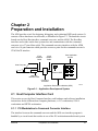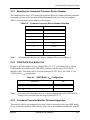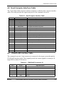
1
Order this document by Order Number
DSPCOMMANDUM/AD
Rev. 2,0, 2/99
Universal Command Converter
User’s Manual
Motorola, Incorporated
Semiconductor Products Sector
6501 William Cannon Drive West
Austin TX 78735-8598
©MOTOROLA INC., 1998-1999. All rights reserved.
OnCE and Mfax are registered trademarks and/or trademarks of Motorola, Inc. in the United States and other
countries. Windows and Windows NT 4.0 are registered trademarks and/or trademarks of Microsoft in United States
and/or other countries. Pentium is a registered trademark and/or trademark of Intel Corporation in the United States
and/or other countries. Sun and Solaris are registered trademarks and/ or trademarks of Sun Microsystems, Inc. in
the United States and/or other countries.
MOTOROLA reserves the right to make changes without further notice to any products included and covered
hereby. MOTOROLA makes no warranty, representation or guarantee regarding the suitability of its products for
any particular purpose, nor does MOTOROLA assume any liability arising out of the application or use of any
product or circuit, and specifically disclaims any and all liability, including without limitation incidental,
consequential, reliance, exemplary, or any other similar such damages, by way of illustration but not limitation, such
as, loss of profits and loss of business opportunity. "Typical" parameters which may be provided in MOTOROLA
data sheets and/or specifications can and do vary in different applications and actual performance may vary over
time. All operating parameters, including "Typicals" must be validated for each customer application by customer's
technical experts. MOTOROLA does not convey any license under its patent rights nor the rights of others.
MOTOROLA products are not designed, intended, or authorized for use as components in systems intended for
surgical implant into the body, or other applications intended to support life, or for any other application in which the
failure of the MOTOROLA product could create a situation where personal injury or death may occur. Should Buyer
purchase or use MOTOROLA products for any such unintended or unauthorized application, buyer shall indemnify
and hold MOTOROLA and its officers, employees, subsidiaries, affiliates, and distributors harmless against all
claims, costs, damages, and expenses, and reasonable attorney fees arising out of, directly or indirectly, any claim
of personal injury or death associated with such unintended or unauthorized use, even if such claim alleges that
MOTOROLA was negligent regarding the design or manufacture of the part.
Motorola and
are registered trademarks of Motorola, Inc. Motorola, Inc. is an Equal Opportunity/Affirmative
Action Employer. All other tradenames, trademarks, and registered trademarks are the property of their respective
owners.
Application Development System
1
Preparation and Installation
2
Functional Description
3
Host Computer Card and Command Converter Support Information
4
Index
I
1
Application Development System
2
Preparation and Installation
3
Functional Description
4
Host Computer Card and Command Converter Support Information
I
Index
Table of Contents
Chapter 1
Application Development System
1.1
General Description . . . . . . . . . . . . . . . . . . . . . . . . . . . . . . . . . . . . . . . . . . . . . . .
1.2
Operating Environment . . . . . . . . . . . . . . . . . . . . . . . . . . . . . . . . . . . . . . . . . . . .
1.2.1
PC-Workstation Requirements . . . . . . . . . . . . . . . . . . . . . . . . . . . . . . . . . . . .
1.2.2
Hewlett Packard HP700 Workstation Requirements . . . . . . . . . . . . . . . . . . .
1.2.3
Sun-4 or Compatible Workstation Requirements. . . . . . . . . . . . . . . . . . . . . .
1.3
ADS Software Features . . . . . . . . . . . . . . . . . . . . . . . . . . . . . . . . . . . . . . . . . . . .
1-2
1-3
1-4
1-4
1-4
1-5
Chapter 2
Preparation and Installation
2.1
Host Computer Interface Card . . . . . . . . . . . . . . . . . . . . . . . . . . . . . . . . . . . . . . . 2-1
2.1.1
PC-Workstation to Command Converter Interface . . . . . . . . . . . . . . . . . . . . 2-1
2.1.2
Installing the PC-Workstation Software. . . . . . . . . . . . . . . . . . . . . . . . . . . . . 2-4
2.1.3
SUN 4 to Command Converter Interface . . . . . . . . . . . . . . . . . . . . . . . . . . . . 2-5
2.1.4
HP7xx to Command Converter Interface . . . . . . . . . . . . . . . . . . . . . . . . . . . . 2-6
2.2
Configuring the Command Converter . . . . . . . . . . . . . . . . . . . . . . . . . . . . . . . . 2-12
2.2.1
Selecting the Command Converter Device Number . . . . . . . . . . . . . . . . . . 2-13
2.2.2
JTAG/OnCE Port Buffer VDD . . . . . . . . . . . . . . . . . . . . . . . . . . . . . . . . . . . 2-13
2.2.3
Command Converter Monitor Firmware Upgrades . . . . . . . . . . . . . . . . . . . 2-13
2.3
Trouble Shooting the Command Converter . . . . . . . . . . . . . . . . . . . . . . . . . . . . 2-14
Chapter 3
Functional Description
3.1
Host Computer Hardware . . . . . . . . . . . . . . . . . . . . . . . . . . . . . . . . . . . . . . . . . .
3.1.1
Host Computer Bus Interface Card . . . . . . . . . . . . . . . . . . . . . . . . . . . . . . . .
3.1.2
Host Computer Interface Cable . . . . . . . . . . . . . . . . . . . . . . . . . . . . . . . . . . .
3.1.3
Command Converter Card . . . . . . . . . . . . . . . . . . . . . . . . . . . . . . . . . . . . . . .
3.1.4
Command Converter Handshake Signals . . . . . . . . . . . . . . . . . . . . . . . . . . . .
3.1.5
Command Converter Interface Connector . . . . . . . . . . . . . . . . . . . . . . . . . . .
3.1.6
Multiple Target Connections . . . . . . . . . . . . . . . . . . . . . . . . . . . . . . . . . . . . .
3.1.7
TCK Drive and Timing Considerations . . . . . . . . . . . . . . . . . . . . . . . . . . . . .
3.1.8
Resetting Target DSP Devices. . . . . . . . . . . . . . . . . . . . . . . . . . . . . . . . . . . .
Motorola
Table of Contents
3-1
3-2
3-3
3-4
3-5
3-6
3-7
3-8
3-9
v
Chapter 4
Host Computer Card and Command Converter Support Information
4.1
4.2
4.3
4.4
4.5
4.6
4.7
4.8
vi
Host Interface Card Bus Signal Description . . . . . . . . . . . . . . . . . . . . . . . . . . . . 4-1
Host Computer Interface Cable . . . . . . . . . . . . . . . . . . . . . . . . . . . . . . . . . . . . . . 4-3
JTAG/ONCE Interface Cable . . . . . . . . . . . . . . . . . . . . . . . . . . . . . . . . . . . . . . . 4-3
Host Computer Card Bills of Materials . . . . . . . . . . . . . . . . . . . . . . . . . . . . . . . . 4-4
Command Converter Bill of Materials . . . . . . . . . . . . . . . . . . . . . . . . . . . . . . . . 4-6
ISA-16 Bus Host Interface Card Schematics. . . . . . . . . . . . . . . . . . . . . . . . . . . . 4-8
SBus Host Interface Card Schematics . . . . . . . . . . . . . . . . . . . . . . . . . . . . . . . . 4-13
Command Converter Card Schematics . . . . . . . . . . . . . . . . . . . . . . . . . . . . . . . 4-18
Universal Command Converter
Motorola
List of Figures
1-1
Application Development System or Target Platform Emulation . . . . . . . . . . . . 1-2
2-1
Application Development System . . . . . . . . . . . . . . . . . . . . . . . . . . . . . . . . . . . . 2-1
2-2
PC-Workstation Interface Card Jumper Group Locations . . . . . . . . . . . . . . . . . . 2-3
2-3
HP-7xx Chassis Rear View . . . . . . . . . . . . . . . . . . . . . . . . . . . . . . . . . . . . . . . . . 2-8
3-1
Host Computer Bus Interface Card . . . . . . . . . . . . . . . . . . . . . . . . . . . . . . . . . . . 3-2
3-2
37-Pin Host Computer Interface Cable . . . . . . . . . . . . . . . . . . . . . . . . . . . . . . . . 3-4
3-3
Command Converter Block Diagram . . . . . . . . . . . . . . . . . . . . . . . . . . . . . . . . . 3-5
3-4
Target VDD System JTAG/OnCE Interface Connector . . . . . . . . . . . . . . . . . . . . 3-7
3-5
JTAG Connections . . . . . . . . . . . . . . . . . . . . . . . . . . . . . . . . . . . . . . . . . . . . . . . . 3-7
3-6
Multiple JTAG Target Connections. . . . . . . . . . . . . . . . . . . . . . . . . . . . . . . . . . . 3-8
3-7
Fan Out of TCK at Source . . . . . . . . . . . . . . . . . . . . . . . . . . . . . . . . . . . . . . . . . . 3-9
3-8
Reset JTAG Device with RESET Signal . . . . . . . . . . . . . . . . . . . . . . . . . . . . . . . 3-9
4-1
Command Converter Interface. . . . . . . . . . . . . . . . . . . . . . . . . . . . . . . . . . . . . . . 4-4
4-2
ISA-16 Host Interface Card Address Decoder (1 of 4) . . . . . . . . . . . . . . . . . . . . 4-9
4-3
ISA-16 Host Interface Card Registers (2 of 4) . . . . . . . . . . . . . . . . . . . . . . . . . 4-10
4-4
ISA-16 Host Interface Card Connectors (3 of 4) . . . . . . . . . . . . . . . . . . . . . . . . 4-11
4-5
ISA-16 Host Interface Card Resistors and Capacitors (4 of 4) . . . . . . . . . . . . . 4-12
4-6
SBUS Address Decoders (1 of 4) . . . . . . . . . . . . . . . . . . . . . . . . . . . . . . . . . . . 4-14
Motorola
List of Figures
vii
4-7
SBUS ADS Interface (2 of 4) . . . . . . . . . . . . . . . . . . . . . . . . . . . . . . . . . . . . . . 4-15
4-8
SBUS ADS Interface (3 of 4) . . . . . . . . . . . . . . . . . . . . . . . . . . . . . . . . . . . . . . 4-16
4-9
SBUS ADS Interface (4 of 4) . . . . . . . . . . . . . . . . . . . . . . . . . . . . . . . . . . . . . . 4-17
4-10 Command Converter Controller, RESET and CLOCK (1 of 5) . . . . . . . . . . . . 4-19
4-11 Command Converter JTAG/OnCE Interface (2 of 5) . . . . . . . . . . . . . . . . . . . . 4-20
4-12 Command Converter Host Interface (3 of 5) . . . . . . . . . . . . . . . . . . . . . . . . . . . 4-21
4-13 Command Converter SRAM and Select Logic (4 of 5) . . . . . . . . . . . . . . . . . . 4-22
4-14 Command Converter Decoupling (5 of 5) . . . . . . . . . . . . . . . . . . . . . . . . . . . . . 4-23
viii
Universal Command Converter
Motorola
List of Tables
2-1
PC-Workstation I/O Addresses . . . . . . . . . . . . . . . . . . . . . . . . . . . . . . . . . . . . . . 2-3
2-2
Command Converter Device Number Selection . . . . . . . . . . . . . . . . . . . . . . . . 2-13
2-3
CMOS Buffer VDD Configuration . . . . . . . . . . . . . . . . . . . . . . . . . . . . . . . . . . 2-13
4-1
PC Interface Card J2 (ISA-16 Bus) Connector . . . . . . . . . . . . . . . . . . . . . . . . . . 4-1
4-2
Sun 4 SPARC (SBus) Connector . . . . . . . . . . . . . . . . . . . . . . . . . . . . . . . . . . . . 4-2
4-3
Host Computer Interface Cable . . . . . . . . . . . . . . . . . . . . . . . . . . . . . . . . . . . . . . 4-3
4-4
JTAG/OnCE Connector J2 . . . . . . . . . . . . . . . . . . . . . . . . . . . . . . . . . . . . . . . . . 4-3
4-5
ADS PC-Workstation Interface Electrical Parts List Rev 2.01 . . . . . . . . . . . . . 4-4
4-6
ADS PC-Workstation Interface Hardware Parts List Rev 2.01 . . . . . . . . . . . . . . 4-5
4-7
37-Conductor Cable Assembly List Rev 2.0 . . . . . . . . . . . . . . . . . . . . . . . . . . . . 4-6
4-8
Sun-4 SBus Parts List Rev 01 . . . . . . . . . . . . . . . . . . . . . . . . . . . . . . . . . . . . . . . 4-6
4-9
ADS Command Converter Electrical Parts List Rev 7.0 . . . . . . . . . . . . . . . . . . 4-6
4-10 ADS Command Converter Hardware Parts List Rev 7.0 . . . . . . . . . . . . . . . . . . 4-7
4-11 JTAG/OnCE 14-Pin Cable Assembly . . . . . . . . . . . . . . . . . . . . . . . . . . . . . . . . . 4-8
Motorola
List of Tables
ix
x
Universal Command Converter
Motorola
Chapter 1
Application Development System
The Motorola Universal Command Converter is one component of a four-component
development tool for designing real-time signal processing systems. When combined with
a host card, a target board, and Motorola software and documentation, the universal
command converter becomes part of an advanced development tool called an application
development system (ADS). The ADS consolidates complex hardware and software
development tools within a low-cost workstation environment using a well-supported
operating system. By providing a solid foundation for application development and
testing, the ADS significantly reduces development costs and time to market. The versatile
ADS allows rapid initial development and supports comprehensive testing of prototype
designs. The ADS consists of the following four components:
•
Host-Bus Interface Board—a 16-bit ISA bus (for PC-workstations and HP700
workstations) and SBus (for Sun and SPARC workstations).
•
Command Converter (CC)— a universal design that supports all Motorola DSPs.
•
Control, Development, and Debugging Software—available in Windows®
compatible (Windows 95/NT 4.0), Sun OS compatible (Rel. 4.1.1 or later), Solaris
compatible (Rel. 2.5 or later), and HPUX compatible (Ver. 9.0 or 10.20).
•
Application Development Module (ADM)— supports development and testing
using a specific digital signal processor (DSP) chip. To identify currently available
ADMs, consult your local Motorola distributor, a Motorola semiconductor sales
office, or, for the latest information, Motorola’s DSP tools home page on the
Internet (http://www.mot.com/SPS/WIRELESS/dsptools).
For more information about ADS software, you can obtain a copy of the ADS User’s
Manual from the Development Tools CD included with the kit or from the following web
address:
http//:www.mot.com/SPS/DSP/documentation/tools.html
Motorola DSPs have a common On-Chip Emulation (OnCE™) module that gives
different development tools identical features. Using the concept of a common serial
debug port, one set of tools has been designed to allow a user to communicate with any of
the architectures using a single command converter. In some Motorola DSPs, this module
Motorola
Application Development System
1-1
General Description
uses a dedicated OnCE serial port to access the internal module. In other Motorola DSPs,
the internal OnCE module is addressed using the IEEE Joint Test Action Group (JTAG)
four-wire test access port (TAP) boundary scan architecture protocol. The tools software
can use either the direct OnCE serial port or the JTAG serial port.
This manual describes the installation, use, and functional description of the control
system that interacts with the target DSP.
1.1 General Description
The ADS is a tool for designing, debugging, and evaluating DSP-based systems. It
consists of three hardware circuit boards, as illustrated in Figure 1-1, and two software
programs. The hardware circuit boards are the host-bus interface, the command converter,
and the ADM. The two software programs are the ADS user interface program, which is
executed on the host computer, and the command converter monitor program which is
expected on the command converter. Figure 1-1 illustrates the ADS being used as a
hardware evaluation tool or host software accelerator. The ADM card has a 14-pin
connector, which provides an access point for the command converter JTAG/OnCE
interface.
37-pin
Interface
Cable
14-pin
Ribbon
Cable
User Application
Circuits
Host Computer
Motorola DSP
Host-Bus
Interface Card
Command
Converter
Application Development Module (ADM)
Target Platform
AA1972
Up to 24
Target
Devices
Figure 1-1. Application Development System or Target Platform Emulation
1-2
Universal Command Converter
Motorola
Operating Environment
Figure 1-1 also illustrates how the ADS can be used as an emulator for a defined target
system whose hardware or software the user needs to debug. Here the user must provide
an access point on the target hardware for a 14-pin JTAG/OnCE interface cable, which
may be as simple as a 2-row × 7-set of test points. Chapter 3, "Functional Description,"
provides complete details of the pinout on the JTAG/OnCE interface cable.
The ADS software program provides routines the user needs to communicate with the
target DSP on the ADM or the target application. This program has a group of powerful
commands that enable the user to perform a variety of tasks. Operating system command
calls may be made from within the program, or temporary exits to the operating system
may be made without disturbing current set-ups with the target DSP.
For more information about the above paragraph, refer to the ADS User’s Manual which
can be found on the Development Tools CD included with the kit or at the following web
address:
http//:www.mot.com/SPS/DSP/documentation/tools.html
The Host interface board provides a physical link between the HOST computer and the
Command Converter via a parallel data and control bus cable. The parallel data path is
used for high-speed data transfers. The control bus signals enable the HOST computer to
reset, interrupt, and send commands to Command Converter simultaneously or
sequentially. The command converter then sends the reset, intercept, and various
commands to the ADM via the JTAG/OnCE cable.
The ADM is the basic platform for evaluating the DSP. It contains a DSP chip with a
JTAG/OnCE interface connector to configure it as a slave to the HOST computer or as a
stand-alone unit. In the slave configuration, the user controls the DSP processor and is
able to interrogate its status. This enables the user to debug hardware and software easily.
In the stand-alone configuration, a user program resident in ROM controls the ADM and
may be used as a prototype system for an end product.
1.2 Operating Environment
The ADS hardware and software is currently supported on the following three host
computers:
•
PC-workstations
•
Hewlett Packard HP700 workstations
•
Sun-4 and compatible workstations
Motorola
Application Development System
1-3
Operating Environment
1.2.1 PC-Workstation Requirements
The minimum hardware requirements for the PC-workstation ADS user interface program
include the following:
•
PC-compatible (Pentium® class) with
•
Windows 95 with 16MB of RAM/NT 4.0 with 32MB of RAM
•
CD-ROM drive
•
Hard drive with 15MB of free space
•
Mouse and keyboard
•
One 16-bit I/O ISA expansion slot
•
Free I/O addresses 100-102 hex, or 200-202 hex, or 300-302 hex.
1.2.2 Hewlett Packard HP700 Workstation Requirements
The minimum hardware requirements for the HP-workstation ADS user interface program
include the following:
•
HP700 Workstation running HPUX Version 9.0 or 10.20
•
32MB of RAM
•
CD-ROM drive
•
Hard drive with 20MB of free space
•
Mouse and keyboard
•
One EISA expansion slot
1.2.3 Sun-4 or Compatible Workstation Requirements
The minimum hardware requirements for the Sun-workstation ADS user interface
program include the following:
1-4
•
SUN Operating System Release 4.1.1 or later or SOLARIS Release 2.5 or later
•
32MB of RAM
•
CD-ROM drive
•
Hard drive with 20MB of free space
•
Mouse and keyboard
•
One SBus expansion slot
Universal Command Converter
Motorola
ADS Software Features
1.3 ADS Software Features
Please refer to the ADS User’s Manual for detailed information on the software features.
The ADS User’s Manual can be found on the Development Tools CD included with the kit
or at the following web address:
http//:www.mot.com/SPS/DSP/documentation/tools.html
Motorola
Application Development System
1-5
ADS Software Features
1-6
Universal Command Converter
Motorola
Chapter 2
Preparation and Installation
The ADS provides a tool for designing, debugging, and evaluating DSP based systems. It
consists of three hardware circuit boards, as illustrated in Figure 2-1. The hardware circuit
boards are the Host-Bus interface, command converter, and the ADM. The Host-Bus
interface card resides on the host systems bus and communicates with the command
converter via a 37-pin ribbon cable. The command converter interfaces with the ADM
card via a 14-pin connector which provides an access point for the command converter’s
JTAG/OnCE interface.
37-pin
Interface
Cable
User Application
Circuits
14-pin
Ribbon
Cable
Host Computer
Motorola DSP
Host-Bus
Interface Card
Command
Converter
Application Development Module (ADM)
AA1941
Figure 2-1. Application Development System
2.1 Host Computer Interface Card
This section covers the Host Computer Interface card hardware and software installation
instructions for the different host computer platforms, i.e. PC-workstation, SUN 4
workstation and HP700 workstation.
2.1.1 PC-Workstation to Command Converter Interface
The interface between the command converter and the ADS user interface program is
handled by a circuit board that resides in one of the PC-workstation motherboard system
Motorola
Preparation and Installation
2-1
Host Computer Interface Card
ISA expansion slots. A single PC-workstation interface card can control up to eight
command converters.
2.1.1.1 Installing the PC-Workstation’s Interface
Warning
Before removing or
installing any equipment
in the PC-workstation
computer, turn off the
power and disconnect the
power cord.
Refer to the appropriate installation and set-up manual for your PC-workstation for
instructions on removing the system cover.
Jumper group JG1 selects the interrupt asserted on the host processor by the host interface
card when the target DSP device makes a service request (for example, by reaching a
breakpoint).
Note:
The ADS software does not support interrupts. No jumper should be placed on
JG1 when used with the ADS software.
Jumper group JG2 specifies the host interface card I/O address. The host interface card
supports 16-bit I/O addresses and uses three consecutive addresses from the specified
address. The starting address may be configured, with jumper pairs A8–A15 in JG2, to
any multiple of $100, up to $FF00. Place a jumper over a pair of pins to set that address bit
to 0; remove the jumper to set the address bit to 1. Address bits A0–A7 are not decoded. In
Figure 2-2, the selected address range is $100–$102.
Note:
Although the host interface card supports 16-bit addressing, the ADS software
only supports addresses $100, $200, and $300.
Once you have ensured that the selected address does not conflict with another expansion
card installed in the motherboard, you may install the host interface card. Figure 2-2
illustrates the physical locations of JG1 and JG2.
2-2
Universal Command Converter
Motorola
Host Computer Interface Card
37-PIN
COMMAND CONVERTER
INTERFACE
J1
IRQ
SELECT
3
5
10
11
15
JG1
ADDRESS
SELECT
A8
A9
A10
A11
A12
A13
A14
A15
JG2
1
ISA INTERFACE
AA1943
(not to scale)
Figure 2-2. PC-Workstation Interface Card Jumper Group Locations
The host interface card resides in the PC-workstations I/O bus; the ADS user interface
software communicates with the card through this I/O address block. The host interface
card address block may be changed to start at one of three addresses as described in
Table 2-1.
Table 2-1. PC-Workstation I/O Addresses
PC-Workstation I/O
Address
PC-Workstation Peripheral
100–102 (default)
Undefined
A8 open, all other pairs linked
200–202
Game Port
A9 open, all other pairs linked
300–302
Prototype Port
JG1
A8, A9 open, all other pairs linked
If the host interface card address block is changed from the default $100, the selected
address must be specified to the ADS. This may be done in one of the following three
ways:
•
Set the environment variable ADMADDR:
>SET ADMADDR=200
•
Issue the ADS command HOST:
> host io 200
•
Use the -d option on the ADS command line:
>ADS56300 -d 200
To install the host interface card properly, position its front bottom corner in the plastic
card guide channel at the front of the PC-workstation chassis. Keeping the top of the host
interface card level and any ribbon cables out of the way, lower the card until the card
connectors are aligned with the PC-workstation system board expansion slot connectors.
Using an evenly distributed pressure, press the host interface card straight down until it
seats in the expansion slot.
Motorola
Preparation and Installation
2-3
Host Computer Interface Card
Secure the host interface card to the PC-workstation chassis using the bracket retaining
screw. Refer to the PC-workstation installation and set-up manual for instructions on
reinstalling the cover.
The host interface card is factory-configured for no interrupts and address decoding at
$100–$102 of the PC-workstation I/O address map, which are undefined peripheral
addresses.
Note:
Jumper JG2 should be left disconnected.
2.1.2 Installing the PC-Workstation Software
A GUI debugger program that supports multiple windows, menus, and dialog boxes is
available for use in the Microsoft Windows environment.
2.1.2.1 Defining Environment Variables
The following sections specify environment variables which may need to be defined to
establish the correct operating environment for the ADS user interface software. These
environment variables may be defined during system start-up by adding lines to the file
c:\autoexec.bat, which applies to all versions of DOS and WINDOWS operating systems.
Some Windows 95 installations may not use the autoexec.bat file. If it does not exist, it
may be created and the SET commands inserted.
The general form of the SET command is as follows:
SET
symbolname=value
Use the names and values from the sections below, and do not use spaces around the “=”
sign.
If the I/O address of the host interface card is changed from the default setting of $100, the
ADS user interface program must be informed of the address to access the card. This may
be done with the environment variable ADMADDR:
set admaddr=200
2.1.2.2 GUI Program Installation
To install the development software, place the Motorola DSP Software Development
Tools CD in the CD drive. If the Motorola DSP Software Development Tools Setup does
not appear within fifteen (15) seconds of activating the CD drive, you will have to
manually install the software. To do so, position the mouse pointer over the Start icon on
the Windows 95/NT toolbar and click once to bring up the selections. Move the mouse
pointer to Run and click once. Move the mouse pointer to Browse and click once. In the
dialog window that appears, select the CD drive on the computer. The file SETUP.EXE
2-4
Universal Command Converter
Motorola
Host Computer Interface Card
should appear in the dialog window. If it does not, in the lower portion of the dialog
window, select “All Files (*.*)” under “Files of type”. Move the mouse pointer over
SETUP.EXE and double click. When the Motorola DSP Software Development Tools
Setup appears, follow the instructions.
2.1.3 SUN 4 to Command Converter Interface
The Motorola SBus/ADS Interface board is designed to be installed in an SBus slot on a
Sun SPARC station or compatible workstation. The board provides a parallel
communication path between the workstation and a Motorola DSP development system.
2.1.3.1 Installing the Sun-4 Interface
The Motorola SBus/ADS Interface is delivered ready to install in your SBus system.
There are no user-configurable jumpers or hardware configurable options. Please consult
the “SPARC station xxx Installation Guide” or the board installation instructions supplied
with your SBus system for installation details. Following is a summary of the instructions
in the Sun manual:
1. Save all open files, then shut down your system with the following series of
commands:
hostname% /bin/su
Password: mypasswd
hostname# /usr/etc/halt
Wait for the following messages:
Syncing file systems... done
Halted
Program Terminated
Type b(boot), c(continue), n(new command mode)
2. When these messages appear, you can safely turn off the power to the system unit.
Turn off power to the system, but keep the power cord plugged in. Open the system
unit. Be sure to attach a grounding strap to your wrist and to the metal casing of the
power supply. Follow the instructions supplied with your system to gain access to
the SBus slots.
3. Remove the SBus slot filler panel for the desired slot from the inner surface of the
back panel of the system unit. Note that the Motorola SBus/ADS Interface board is
a slave-only board and thus will function in any available SBus slot.
4. Slide the SBus board at an angle into the back panel of the system unit. Make sure
that the mounting plate on the SBus board hooks into the holes on the back panel of
the system unit.
Motorola
Preparation and Installation
2-5
Host Computer Interface Card
5. Push the SBus board against the back panel, align the connector with its mate, and
gently press the corners of the board to seat the connector firmly.
6. Close the system unit.
7. Connect the 37-pin ADM interface cable to the SBus/ADS Interface board and
secure.
8. Turn power on to the system unit and check for proper operation.
2.1.3.2 Software Installation
The distribution CD included with the ADS package contains the “mdsp” SBus device
driver for the ADS as well as the ADSxxx user interface program for the ADS. The
following steps will allow you to install the device driver and run the user interface.
Note:
In the instructions that follow, ADSxxx represents the name of your particular
system, such as ADS56000, etc.
1. Copy all of the software from the distribution CD onto your system using
uncompress and tar. See the “readme” file for details
2. Install the driver with the following commands:
hostname# cd adsxxx/driver
hostname# make install
3. After a successful installation, you should see a module status message indicating
that your module was successfully loaded and giving its ID. To see this status at
any time, issue the “modinfo” command on SOLARIS, “modstat” for SunOS.
4. If the ADSxxx driver module was loaded properly, you should be ready to run the
ADSxxx user interface:
hostname# cd ../bin
hostname# adsxxx
If for any reason you wish to uninstall the driver, use the following commands:
hostname# cd adsxxx/driver
hostname# make unload (SunOS 4.x)
hostname# make uninstall
(SOLARIS 2.x)
2.1.4 HP7xx to Command Converter Interface
The Motorola HP7xx Interface uses the same ISA card installed in the PC-workstation. It
is controlled by an HPUX device driver. The HP7xx computer must have an ISA slot
available for plugging in this card. Older versions of the HP700 series computer did not
have ISA expansion slots. The ISA board provides a parallel communication path between
the HP workstation and a Motorola DSP development system. For details on jumper
2-6
Universal Command Converter
Motorola
Host Computer Interface Card
configurations of the ISA card, refer to Section 2.1.1, "PC-Workstation to Command
Converter Interface."
The HP7xx device driver and user interface program support multiple host interface cards
in a system. Therefore, when reading the software installation instructions keep in mind
that the device driver name(s) must be different for each card installed in a system.
2.1.4.1 Installing the HP-7xx Interface
Before installing one or more ISA cards, a sequence of steps must be followed to shut
down your system. If you are using HP VUE, carry out the first four steps of
Section 2.1.4.1.1, "HP VUE Shut-Down." If you are using the HP-UX command line
shell, carry out the first four steps of Section 2.1.4.1.2, "HP-UX Command Line Shell
Shut-Down."
To shut down your computer you must first be logged in as “root”. Save all open files
before shutting down, and always follow the proper shutdown procedure before turning
off the power to your workstation. Failure to do so could cause damage to files.
Note:
“hostname#” represents the system prompt; that is, it is not to be entered as part
of the command.
2.1.4.1.1 HP VUE Shut-Down
1. Use the HaltSystem application, located in the System_Admin file of the General
toolbox, by double-clicking on its icon.
2. Click on the “OK, Halt System” button to initiate shut-down.
3. When the message “Halted, you may now cycle power” appears, you may safely
turn off the power to your workstation.
4. Go to step 1 of Section 2.1.4.1.3, "ISA Card Installation."
2.1.4.1.2 HP-UX Command Line Shell Shut-Down
1. Change to the root directory with the following command:
hostname# cd /
2. Enter this command to initiate shut-down:
hostname# /etc/shutdown -h 0
3. When the message “Halted, you may now cycle power” appears, you may safely
turn off the power to your workstation.
4. Go to step 1 of Section 2.1.4.1.3.
2.1.4.1.3 ISA Card Installation
The following steps should be used to install the ISA card:
Motorola
Preparation and Installation
2-7
Host Computer Interface Card
1. Remove the power cord from both the wall socket and the unit.
2. Remove the power supply cover plate located on the rear of the unit and marked
“TO ACCESS EISA PULL THIS HANDLE”, and gently slide the EISA Adapter
Card Assembly (hereafter called “assembly”) out of the unit. See Figure 2-3.
3. Remove the blank EISA slot cover from the assembly. The cover is simply a piece
of metal that covers the hole when there is no card installed and is held in place by
a single screw. Be sure to save this screw as it will be used to secure the card.
4. Carefully slide the ISA card into the assembly, making sure that the connector pins
on the assembly meet up properly with those on the card, and that the cable socket
is positioned fully within the hole. Use the screw saved from the previous step to
securely attach the card to the assembly.
5. Carefully slide the assembly back into the unit. Press firmly on all four corners to
ensure that the connectors on the front of the assembly fully engage with those
inside the unit.
6. Reinstall the power supply cover plate, and then reconnect the power cord to both
the unit and the wall socket. Also connect the 37-pin ribbon cable from the ISA
card to the ADM board.
7. The system may now be restarted.
POWER SUPPLY COVER PLATE
AC POWER CONNECTION
EISA CONNECTOR HOLE
AA1944
Figure 2-3. HP-7xx Chassis Rear View
2.1.4.2 Installing the HP-7xx Device Driver
An HP-700 formatted CD-ROM contains the necessary files for the installation of the
device driver. The device driver supports multiple cards so only one device driver needs to
be installed regardless of the number of cards being used. This CD is UNIX tar formatted
and should be read in with the following command:
tar xvf /dev/rmt/0mn
An alternate command would be
2-8
Universal Command Converter
Motorola
Host Computer Interface Card
tar xvf /dev/rmt/0m
The number at the end of the command is the device number and should be changed if the
CD drive number is different on the machine being used. After the files are extracted from
the CD-ROM, a directory named “driver” is created.
The user must be logged in as “root” or superuser to proceed from this point. The
following steps should be followed for proper installation of the driver program:
Note:
“hostname#” represents the system prompt; that is, it is not to be entered as part
of the command.
The HP device driver for the ADS supports multiple host interface cards (up to three,
limited by the addresses that can be selected on the host interface card) installed into a
single HP-700 workstation.
1. When the files were installed, a directory called driver was created in the hierarchy.
Make this the current directory now by executing the following command, where
ADS-PATH is the path to where the ADS files were installed:
hostname# cd
/ADS-PATH/driver
2. Copy and change the ownership, group and mode of the device driver library file,
libmdsp.a, using the following commands:
hostname#
hostname#
hostname#
hostname#
cp libmdsp.a /etc/conf
chown bin /etc/conf/libmdsp.a
chgrp bin /etc/conf/libmdsp.a
chmod 444 /etc/conf/libmdsp.a
3. To install the device configuration file, type the following command. (Note that it
may be necessary to escape the ! by using a backslash \, depending on the shell you
are using.)
hostname# cp
!MOT0010.CFG
/etc/eisa
This copies the configuration file into the system EISA configuration directory.
Modify the copy of the file in /etc/eisa to reflect the I/O port that the card is
configured for (change the PORT entry).
If you are using multiple host interface cards in your HP, make multiple copies of
this file in /etc/eisa, changing the last digit of the file name on each copy. Modify
each copy to have the correct ID and PORT entries (the ID entry should be the
name of the file without the .CFG extension). Each PORT entry should be modified
to contain the proper addresses for the additional cards that are supported.
4. Run the EISA configuration program by typing this command:
hostname# /etc/eisa_config
Motorola
Preparation and Installation
2-9
Host Computer Interface Card
At the EISA prompt, type “add !MOT0010.CFG <slot num>”, where <slot num> is
the slot number in which the card is installed.
If you have installed multiple host interface cards, repeat the “add” command once
for each configuration file and slot. For example, if you created a file
MOT0011.CFG for a card in slot 2, and modified the PORT and ID entries in
MOT0011.CFG to reflect the I/O address of the card in slot 2, you would type add
!MOT0011.CFG 2" to add that card to the EISA configuration information.
On machines with one EISA expansion slot, the slot number is 1.
Press “q” to quit the EISA configuration program, and “s” to save.
5. You must now edit the /etc/master file to include the ADS device driver. Make a
backup copy of “/etc/master”. You will need to change one line and add three new
lines in this file. The entries will be in the “Third Party and User Drivers,” the alias
table, the driver/library table, and the library table.
Change the first available line of the “Third Party and User Drivers” section to look
like the following line. An available line is one which has dashes in the first four
entries. Note that the last two entries are already set and are not to be changed. The
last entry is the major number for the device. You may use a line with 38, 39, 40,
42, or 43 for the major number. Make note of the number you choose, as it is used
in the next step.
Name Handle Type Mask Block Char (Do not add this line.)
mdsp mdsp 1
1FA
-1 <major>
Find the alias table and add the following line:
mdsp mdsp
Find the driver/library table and add the following line:
mdsp libmdsp.a
Find the library table and add the following line:
libmdsp.a0
6. Make a device file for the driver by executing the following command:
hostname# mknod
/dev/mdsp0 c
<major> <minor>
The major and minor numbers of the device are given by <major> and <minor>,
respectively. N is a user chosen device group number. The ADS user interface
software always defaults to device group 0 or mdsp0.
Note:
2-10
The <major> must be the same major number you used in the previous step.
The minor number is 0x4S0000, where ‘S’ should be replaced by the card slot
number in which the card was placed (1 – n). For machines with a single slot,
Universal Command Converter
Motorola
Host Computer Interface Card
the slot number is 1. For example, slot 4 of a multi-slot machine would be
0x440000
Be sure to change the permissions for this file(s) by typing this command:
hostname# chmod
666
/dev/mdsp0
If you have installed multiple host interface cards, repeat the “mknod” and
“chmod”steps for each new card. The <major> number for each will be the same,
but the <minor> number will reflect the slot in which the card was installed. The
device file names are arbitrary, but you should make note of which card
corresponds to each device file name. We suggest using a final digit of “N– 1”for
slot “N”.
7. Edit the file /usr/sam/lib/kc/drivers.tx and add an entry for the ADS device driver.
You may wish to make a backup of the file before editing it. Add the following
line:
mdsp:::Out:Motorola ADS Host Interface Card
8. Select and edit a dfile (configuration description file). First, change directories by
executing the following command:
hostname# cd
/etc/conf
A dfile must now be selected. Your current system dfile should be called either
dfile, dfile.SAM (for a kernel that has been configured with the HP System
Administration Manager), or a unique name given by you if you have altered your
kernel configuration by hand. Use the dfile appropriate for your system. If you
aren’t sure which version to use, or if your choice doesn’t work, then you can use
the file created by the command
hostname# /system/TOOL/get_kdfile
/hp-ux > dfile.current
to get your current system dfile.
Make a back-up copy of the selected dfile and edit the selected dfile by adding the
following lines to the top of it:
* Motorola DSP ADS Device Driver
mdsp
9. Generate the files needed to rebuild the kernel with your new device driver.
Execute this command, replacing dfile-name with the dfile you selected in the
previous step:
hostname# /etc/config dfile-name
10. Generate a new kernel object file in the current directory using the following
command:
hostname# make
Motorola
-f
config.mk
XOBJS=libmdsp.a
Preparation and Installation
2-11
Configuring the Command Converter
11. If the build finished successfully, your new kernel may now be installed. Make a
backup of the current kernel by executing the following copy command:
hostname# cp
/hp-ux
/hp-ux.pre-ads
12. The final step is to install the new kernel in the root path and reboot the system.
Note the period before the first slash in the first argument of the cp command:
hostname# cp
./hp-ux
/hp-ux
To reboot the system using the new kernel, type the following command:
hostname# exec
reboot
During boot-up, you should see the following message displayed on the screen if
the installation was successful:
“Slot <slot-num>: Motorola DSP ADS Host Interface Card Initialized”
where <slot-num> is the previously selected slot number in which the card is
installed.
The ADS Device Driver is now installed and ready for use. By default, the ADS
program attempts to open the device file dev/mdsp0. If you want to use a different
device (i.e., different host interface card), you can specify the device file name in
an environment variable, or on the command line. The environment variable is
ADMADDR. The command line option is `-d', followed by the name of the device
file. The `-d' option must come before a command file name.
For example, to use /dev/mdsp2, you could set an environment variable before
invoking the ADS software using the following statements:
# setenv ADMADDR /dev/mdsp2
# adsXXXXX [command-file] (where XXXXX is the device)
or you can invoke the ADS software with a command line argument such as the
following:
# adsXXXXX -d /dev/mdsp2 [command-file]
2.2 Configuring the Command Converter
The universal command converter supports both the JTAG and OnCE serial protocols.
The universal command converter may be identified by the surface-mount DSP56002
which controls its operation. The monitor program resides in SRAM, and is downloaded
by the ADS software during command converter initialization and reset operations.
The universal command converter has two user-configurable jumper groups: JG2, which
selects the device number, and JG1, which selects the power source for the JTAG/OnCE
buffers.
2-12
Universal Command Converter
Motorola
Configuring the Command Converter
2.2.1 Selecting the Command Converter Device Number
The command converter’s JG2 jumper group selects the device number that this particular
command converter will respond to when commanded by the user interface program.
Table 2-2 describes the device address select option:
Table 2-2. Command Converter Device Number Selection
Note:
Device Address
JG2
0 (default)
no jumpers
1
5–6
2
3–4
3
3–4, 5–6
4
1–2
5
1–2, 5–6
6
1–2, 3–4
7
1–2, 3–4, 5–6
All command converters are factory configured for device address 0.
2.2.2 JTAG/OnCE Port Buffer VDD
In order to provide support for low voltage DSPs (5V-2.7V), an advanced low voltage
CMOS buffer exists between the DSP56002 controller and the target JTAG/OnCE
interface cable. This buffer has its VDD pin connected to JG1, Pin 2. See Table 2-3 for
CMOS buffer VDD configuration.
Table 2-3. CMOS Buffer VDD Configuration
VDD Source
Note:
JG1
Supply VDD from Host System (+5 V)
1–2
Supply VDD from Target System (default)
2–3
The universal command converter is factory-configured for the JTAG/OnCE
buffers to be powered from the target system (JG1 2–3).
2.2.3 Command Converter Monitor Firmware Upgrades
The monitor code for the command converter, which is tailored for the target DSP family
in use, is provided with the ADS software. The code is downloaded automatically into the
Motorola
Preparation and Installation
2-13
Trouble Shooting the Command Converter
command converter during ADS system initialization and universal command converter
reset. If a revision is issued for the monitor firmware, an environment variable must be
defined to specify the filename of the revised monitor. The specified file will be loaded
into the command converter instead of the standard monitor program. The variable which
must be defined is CC56000, where “56000” is replaced with name of the DSP family in
use, and the defined value is the fully-specified filename of the revised monitor software.
For example,
•
DOS, in AUTOEXEC.BAT:
SET CC56300=C:\ADS\REVISIONS\MONITOR.LOD
•
UNIX, with C shell, in .login or .cshrc:
setenv cc56300 /ads/revisions/monitor.lod
•
UNIX, with Bourne shell, in .profile:
cc56300=/ads/revisions/monitor.lod
export cc56300
specifies that, for the GUI56300, the standard DSP56300 family universal command
converter monitor code is to be replaced by the code in the file
ADS\REVISIONS\MONITOR.LOD.
To verify that the monitor file is loading correctly, start the ADS program and enter the
following commands:
force s
display v
The monitor revision will be displayed. If the error ‘Unable to reset Command Converter’
is issued, make sure the correct path is specified in the definition of CC56x00.
2.3 Trouble Shooting the Command Converter
To ensure the command converter is connected correctly to the host card, there are several
commands that are directed specifically to the command converter. The first is:
cforce r
This command will reset the ADS chain throughout the host card, up to the command
converter. Another helpful command is:
cdisplay x:0#10
This command displays x memory locations 0 through 10 of the command converter. The
values in memory are irrelevant, the fact that memory from the command converter can be
read indicates that you are communicating correctly with the command converter. If these
2-14
Universal Command Converter
Motorola
Trouble Shooting the Command Converter
two commands execute correctly, your ADS is working properly up through the JTAG
port on the command converter. If you are still having problems, there may be something
wrong with your 14-pin JTAG cable or target board.
Motorola
Preparation and Installation
2-15
Trouble Shooting the Command Converter
2-16
Universal Command Converter
Motorola
Chapter 3
Functional Description
The application development system (ADS) user interacts with the target DSP through
two subsystem components, the host computer interface and the command converter
controller. The host computer interface consists of a program written in the C language
that interacts with a host computer bus interface card. The command converter consists of
a program written in DSP56002 assembly language which interacts with the host
computer bus interface card and the target JTAG/OnCE port.
It should be noted that older versions of Motorola DSP products use the OnCE port
protocol, while newer versions of Motorola DSP products use the IEEE JTAG 4-wire
protocol to interact with their OnCE port. New versions of the command converter support
both JTAG and OnCE protocols.
Commands entered from the host computer’s keyboard are parsed and a series of low level
command packets are sent to the command converter. The command converter translates
these low level command packets into serial sequences that are transferred to the target
DSP via its JTAG/OnCE port. The JTAG/OnCE port provides the necessary control to the
target so programs may be loaded or saved, registers read or modified, and hardware
breakpoints set or cleared.
The host computer interface is designed to communicate with as many as eight command
converter cards. This requires a special software protocol to avoid data collisions between
one target and another. The purpose of this section is to describe the subsystem
components of the ADS to give a better understanding of the communication link between
the user and the target DSP.
3.1 Host Computer Hardware
The host computer’s hardware interface provides the communications link between the
user and the command converter. The ADS user interface program uses a software
handshake when communicating with the command converter. There are signals defined
on the host computer bus interface card which are used for requesting and acknowledging
information transfer. Since the handshake is software driven the transfer rate will be
Motorola
Functional Description
3-1
Host Computer Hardware
dependent upon the host computer bus speed and its operating system. This section
describes the host computer interface hardware and software components.
3.1.1 Host Computer Bus Interface Card
Figure 3-1 shows a block diagram of the host computer interface card for all computer
platforms. The interface consists of three fixed addresses in the host computer I/O
memory map. The host computer’s interface card address zero is used as a control port for
selecting, resetting, or interrupting one or more command converters. Address one reads
and writes eight bit data bytes to one or more command converters. Address two
acknowledges command converter service requests and selects group members for
multiple command converter commands. All data is passed high-order byte first. For
example, in a 32-bit transfer, bits 31–24 are transferred first, followed by bits 23–16, bits
15–8, and then bits 7–0.
ADDR
BUS ADDRESS
R/W
DECODER
CTRL1
BUS
DATA
DATA
LOCAL DATA
AD1
OE
CTRL2
AD2
37-PIN CONNECTOR
CTRL
CTRL
BUS INTERFACE
HOST COMPUTER BUS
BUS
TO COMMAND CONVERTER(S)
AD0
+5V AND GND
AA1973
Figure 3-1. Host Computer Bus Interface Card
The ADS user interface program allows as many as eight command converters to be
addressed using one host computer interface card. Command converters may be addressed
in groups or individually depending upon the command and command arguments entered
by the user.
Host computer interface card address zero has eight output control lines. These output
control lines are asserted using positive logic (VOH = TRUE). Three address zero signals
3-2
Universal Command Converter
Motorola
Host Computer Hardware
(ADM_SEL0, ADM_SEL1, ADM_SEL2) select a command converter before sending a
command. Further information on the method of command converter selection is
discussed in subsequent sections.
Two handshake signals originate at the host computer and are used to pass data to and
from a command converter. HOST_REQ initiates a data byte transfer to a command
converter, while HOST_ACK acknowledges receipt of a data byte from a command
converter.
Two control signals (ADM_BRK,ADM_RESET) allow the user to assert an interrupt or a
reset exception on a single command converter or a group of command converters. The
ADM_BRK signal is used to put the command converter back into Command Entry mode;
the ADM_RESET signal is used to reset the command converter.
The command converter informs the host computer of target DSP entries to the Debug
mode of operation by asserting the HOST_BRK signal. The ADS user interface program
on the host computer periodically polls the HOST_BRK signal from the keyboard polling
routine. If the HOST_BRK signal is asserted, the host computer will determine which
command converter is requesting service by reading the ADM_INT signal. The
INT_ACK signal is asserted by the host computer when a service request has been
recognized. Further details on the functions of each signal will be given in a subsequent
section. Figure 3-2 illustrates the 37-pin cable and the direction of the signal groups.
3.1.2 Host Computer Interface Cable
The host computer interface card interacts with the command converters via a 37-pin
ribbon cable assembly. Each end of the ribbon cable has a 37-pin subminiature-D
Insertion Displacement receptacle connector. The cable assembly is approximately 4 feet
in length and is designed so that additional command converters may be easily attached to
the existing cable by crimping on new connectors.
Normally the ADS is shipped with an application development module (ADM), and
power for the command converter is supplied by the host computer interface card via the
37-pin cable. Power for the ADM card is provided by a wall power transformer. The
ribbon cable is not designed to draw more than 2 amps current at 5 volts. Since each
command converter draws approximately 250 milliamperes, it is safe to power all eight
units via the cable, but the target systems must be powered by a different source to ensure
correct operation.
Motorola
Functional Description
3-3
Host Computer Hardware
8-BIT DATA BUS (HOST COMPUTER AND COMMAND CONVERTER)
HOST_REQ, HOST_ACK, INT_ACK (HOST COMPUTER HANDSHAKE)
ADM_REQ, ADM_ACK (COMMAND CONVERTER HANDSHAKE)
ADM_BRK, ADM_RESET (HOST COMPUTER CONTROL)
ADM_INT, HOST_BRK (COMMAND CONVERTER SERVICE REQUEST)
COMMAND CONVERTER CARD
TO COMMAND CONVERTER(S)
37-PIN CONNECTOR FROM HOST CARD
ADM_SEL0,ADM_SEL1,ADM_SEL2 (ADDRESS SELECT)
+5 V, GROUND (COMMAND CONVERTER POWER)
AA1946
Figure 3-2. 37-Pin Host Computer Interface Cable
3.1.3 Command Converter Card
The command converter is based on a DSP56002, which uses its on-chip resources to
minimize and simplify the interface to the target JTAG/OnCE debug port. Communication
with the host computer is via the DSP56002 Port B, while the serial interface to the target
DSP is via the DSP56002’s SSI port.
Each command converter has a unique address, ranging from 0 to 7. This allows the user
to debug multiprocessor systems where as many as eight command converters are
physically in the target system. JG2 of the command converter card defines the address
selected for that card.
3-4
Universal Command Converter
Motorola
Host Computer Hardware
37-PIN HOST COMPUTER INTERFACE CONNECTOR
SRAM
WORDS
GAL
DECODER
BUFFER
32K
PORT A
NMI
IRQ A
PORT B
DSP56002
SSI
SCI
PLL
BUFFER &
I/P SELECT
+5V
VOLTAGE
TRANSLATOR
14--PIN TARGET JTAG/ONCE CONNECTOR
20MHZ
CLOCK
AA1947
Figure 3-3. Command Converter Block Diagram
3.1.4 Command Converter Handshake Signals
The DSP56002 on the command converter card is configured in such a way that bits 0–7
of its Port B are used for 8-bit data transfers, and bits 8–14 are used for data transfer
control.
There are three output control bits in the middle order byte of the DSP56002 Port B data
word. These bits are the ADM_INT, ADM_REQ, and ADM_ACK signals. ADM_REQ
and ADM_ACK, act as handshake lines for reading and writing data. ADM_INT acts as a
flag to indicate whether the ADM is requesting host computer service. These three control
bits are part of the host parallel control bus. They are enabled when the host computer
selects the ADM.
Motorola
Functional Description
3-5
Host Computer Hardware
There are three input control bits in the middle-order byte of Port B data word that
represent the HOST_ACK, HOST_REQ, and INT_ACK. These signals are sent from the
host computer for reading and writing data. INT_ACK informs the monitor program that
the host computer has received its service request and is ready to communicate.
HOST_BRK is a wired-OR control line. HOST_BRK is used by the command converter
to inform the host computer whenever the target DSP has entered the Debug mode of
operation for non-JTAG devices only. Since more than one command converter may be
started for a user debug session, more than one may hold HOST_BRK active low at one
time. Once this signal is asserted it may only be deasserted by the host computer or by a
command converter reset.
3.1.5 Command Converter Interface Connector
The target application board must have a 14-pin connector to interface to the command
converter controller. This interface comprises nine signals and three ground connections
on a 7-row × 2-column male pin header, which are spaced on 1/10 inch centers as
illustrated in Figure 3-4 on page 3-7.
Since the target system will have a resident reset circuit, it is recommended to have an
AND gate in series with the CC_RESET signal. This will insure that the target DSP will
be reset with a valid VOL level from either the target reset circuit or from the command
converter. The pull-down resistors are to insure that no false signals are propagated to the
JTAG/OnCE circuit when the test data input/debug serial input (TDI/DSI) and test data
clock/debug serial clock (TCK/DSCK) lines are active. The test data out/debug serial
output (TDO/DSO) pullup is to insure that the Debug Acknowledge signal from the OnCE
circuit is deasserted. The debug request (DR) pullup is to insure that the command
converter controls when the target DSP is placed into its Debug mode.
3-6
Universal Command Converter
Motorola
Host Computer Hardware
10K
GND
10K
VCC
GND
vcc
VCC
10K
TDI/DSI
1
2
3
4
5
6
GND
7
8
KEY (No Connect)
9
10
TARGET VDD
11
12
DEZ
13
14
TDO/DSO
10K
TCK/DSCK
10K
DR
DSP
RESET
PIN
(Not used w/ JTAG)
CC_RESET
TARGET
RESET
CIRCUIT
VCC
10K
TMS0 (for JTAG devices)
TMS1 (for JTAG devices)
TRST (for JTAG devices)
(for JTAG devices)
vcc
10K
DSP
TRST
PIN
Figure 3-4. Target VDD
TOP VIEW
System JTAG/OnCE Interface Connector
AA1976
3.1.6 Multiple Target Connections
The basic JTAG connection comprises 5 pins, as illustrated in Figure 3-5.
TDI
TDO
TCK
TARGET
TMS
PROCESSOR
TRST1
1
IF PINNED OUT, REQUIRED ON DEVICE
AA1975
Figure 3-5. JTAG Connections
Multiple target devices may be connected in series, allowing a single command converter
JTAG/OnCE connector to control multiple devices, as in Figure 3-6. Data flows from the
JTAG host, into each JTAG implementation through TDI, out through TDO and into TDI
in the next chip, eventually returning to the JTAG host.
Motorola
Functional Description
3-7
Host Computer Hardware
RESET
TRST
TDO
TRST RESET
TDI TDO
TCK TMS
TRST RESET
TDI TDO
TCK TMS
TRST RESET
TDI TDO
TCK TMS
TRST RESET
TDI TDO
TCK TMS
TRST RESET
TDI
TDO
TCK TMS
TRST RESET
TDI TDO
TCK TMS
TDI
TCK
TMS
MAXIMUM OF 4 LOADS ON
TCK CIRCUITS
BUFFER—74HCT244
OR SIMILAR
AA1950
Figure 3-6. Multiple JTAG Target Connections
3.1.7 TCK Drive and Timing Considerations
The signals from the command converter are TDO, TCK and TMS, and TRST. Signal
TCK requires fast rise and fall times dictated by the TCK pin timing specification, and
consequently attention must be given to the drive capabilities of the circuits driving this
signals. There is no problem with TDO, as each TDO output is connected to only one TDI
input. TMS need only be valid at the rising edge of TCK, similarly there is no problem
with TRST as the reset signal is not subject to the timing constraints of TCK.
There is a potential problem with driving the TCK circuit with a large number of target
devices. The problem is related to the rise and fall times of TCK, caused by excessive
capacitance, which can cause communication problems with a single circuit connecting
multiple TCK input pins.
Acceptable transition times may be achieved for TCK by driving no more than four JTAG
inputs from each buffered output. This may be achieved with two configurations.
Figure 3-6 shows one method. Here (in effect) one signalling connects each of the TCK
inputs. A buffer is placed in the circuit after each fourth input, at most, to restore the signal
quality for subsequent inputs. The propagation delay of the buffer is not significant.
Figure 3-7 shows another possible configuration which also enables signal quality to meet
the requirements. In this configuration the signal is split and buffered into a number of
parallel TCKn signals. Each of these signals may drive up to 4 TCK inputs.
3-8
Universal Command Converter
Motorola
Host Computer Hardware
TCK
TCK1
TCK2
TCKn
TCK
TCK
TCK
TCK
TCK
TCK
TCK
TCK
TCK
TCK
TCK
AA1951
Figure 3-7. Fan Out of TCK at Source
Either configuration above is equally valid. The choice will depend on practical
considerations related to each project, or a combination could be used.
JTAG signal TMS may also need some consideration. Although TMS is not subject to the
strict requirements as TCK, it is still important that TMS has settled to a valid level at the
rising edge of TCK.
3.1.8 Resetting Target DSP Devices.
The RESET signal and TRST signals from the command converter are typically connected
to all target devices on a JTAG chain. RESET and TRST are asserted by the ADS
command FORCE R. All devices on the JTAG chain handling the specified command
converter device are reset. Execution control is established immediately after deassertion
of TRST before any instructions are executed. The sequence of events is illustrated in
Figure 3-8. Because all targets on the JTAG chain are connected to the same RESET
signal, all devices enter reset. The JTAG controller is still active after deassertion of TRST
during reset, and while RESET is held low, the JTAG instruction DEBUG_REQ is
clocked in. When RESET is deasserted, the device is immediately in Debug mode, with no
instructions executed since releasing RESET.
1
RESET
1
COMMAND CONVERTER
ASSERTS RESET. ALL
TARGETS ENTER RESET.
JTAG RESET
TRST
INSTRUCTION
2
JTAG INSTRUCTION
DEBUG_REQUEST IS
LOADED.
3
COMMAND CONVERTER
RELEASES RESET. TARGETS
EXIT RESET IN DEBUG MODE.
DEBUG_REQ
REGISTER
1
2
3
AA1969
Figure 3-8. Reset JTAG Device with RESET Signal
Motorola
Functional Description
3-9
Host Computer Hardware
3-10
Universal Command Converter
Motorola
Chapter 4
Host Computer Card and Command
Converter Support Information
This chapter provides the host computer connector signal descriptions, part lists and
schematics for hardware that is required to run with the ADS software. This list includes
the host interface cards, host interface cable, and the command converter card.
4.1 Host Interface Card Bus Signal Description
Each host interface card is designed for a unique host computer bus architecture. This
section describes the card edge connector signals used by each host computer’s expansion
bus. This information is for reference only.
Table 4-1. PC Interface Card J2 (ISA-16 Bus) Connector
Pin #
Mnemonic
A1
I/O CH CK
A2–A9
D7–D0
A10
I/O CH RDY
A11
AEN
A12–A21
A19–A10
A22–A31
A9–A0
B1
GND
B2
RESET
B3
+5v
B4-B8
Signal Name and Description
No Connect
PC Bus data bits 7 to 0.
No Connect
PC BUS Address Enable output
No Connect
PC Bus address bits 9 to 0.
PC ground
PC reset signal,(positive true).
PC +5 V
No Connect
B9
PC +12 V
B10
GND
B11–B12
MEMW/MEMR
B13
IOW
I/O write command,(negative true).
B14
IOR
I/O read command,(negative true).
B15–B20
B21
Motorola
No Connect
No Connect
IRQ7
B22–B23
B24
PC ground
PC Interrupt request 7,(Printer), NOT USED.
No Connect
IRQ4
PC Interrupt request 4,(COM1), NOT USED
Host Computer Card and Command Converter Support Information
4-1
Host Interface Card Bus Signal Description
Table 4-1. PC Interface Card J2 (ISA-16 Bus) Connector (Continued)
Pin #
Mnemonic
B25
IRQ3
Signal Name and Description
PC Interrupt request 3,(COM2),
B26–B31
No Connect
Table 4-2. Sun 4 SPARC (SBus) Connector
4-2
Pin #
Description
1
GND
2
BR
3
SEL
4
Pin #
Description
Pin #
Description
33
PA(06)
65
D(18)
34
PA(08)
66
D(20)
35
PA(10)
67
D(22)
INTREQ1
36
ACK0
68
GND
5
D(00)
37
PA(12)
69
D(24)
6
D(02)
38
PA(14)
70
D(26)
7
D(04)
39
PA(16)
71
D(28)
8
INTREQ2
40
ACK1
72
+5V
9
D(06)
41
PA(18)
73
D(30)
10
D(08)
42
PA(20)
74
SIZ(1)
11
D(10)
43
PA(22)
75
RD
12
INTREQ(3)
44
ACK2
76
GND
13
D(12)
45
PA(24)
77
PA(01
14
D(14)
46
PA(26)
78
PA(03)
15
D(16)
47
DTAPAR
79
PA(05)
16
INTREQ4
48
-12V
80
+5V
17
D(19)
49
CLK
81
PA(07)
18
D(21)
50
BG
82
PA(09)
19
D(23)
51
AS
83
PA(11)
20
INTREQ5
52
GND
84
GND
21
D(25)
53
D(01)
85
PA(13)
22
D(27)
54
D(03)
86
PA(15)
23
D(29)
55
D(05)
87
PA(17)
24
INTREQ6
56
+5V
88
+5V
25
D(31)
57
D(07)
89
PA(19)
26
SIZ(0)
58
D(09)
90
PA(21)
27
SIZ(2)
59
D(11)
91
PA(23)
28
INTREQ7
60
GND
92
GND
29
PA(00)
61
D(13)
93
PA(25)
30
PA(02)
62
D(15)
94
PA(27)
31
PA(04)
63
D(17)
95
RESET
32
LERR
64
+5V
96
+12V
Universal Command Converter
Motorola
JTAG/ONCE Interface Cable
4.2 Host Computer Interface Cable
The 37-pin cable which connects to the host computer is called the host computer interface
cable. This cable provides the signals and power to the command converters.
Table 4-3. Host Computer Interface Cable
Pin #
Mnemonic
Signal Name and Description
1
INT_ACK
Host ack of ADM service request
2
ADM_GROUP
CC group control flag from Host
3
HOST_ACK
Host ack of ADM data transfer request
4
ADM_ALL
5
ADM_RESET
Host signal which selects all ADMs
6-8
ADM_SEL2,1,0
9
HOST_REQ
Host signal which requests CC data
10
ADM_REQ
CC signal which requests Host data transfer
11
ADM_ACK
CC ack of Host data transfer request
12
ADM_INT
CC service request status signal to Host
13
HOST_BRK
Host signal which asserts CC(s) reset
CC address select signals 2-0 for one of 8 CCs
CC service request signal to Host, (low true)
14
ADM_BRK
15
BRACE_SEL
Brace56 Emulator select signal
Host signal to interrupt CC(s)
16-19
PD1,3,5,7
HOST/CC data bus bits1, 3, 5, 7
20-25
GND
HOST/CC ground lines
26
NC
No Connect
27-29
+5v
+5 volts from the HOST
30
HOST_ENABLE
31-33
GND
34-37
PD0,2,4,6
HOST signal which enables CC address logic
HOST/CC ground lines
HOST/CC data bus bits 0, 2, 4, 6
4.3 JTAG/OnCE Interface Cable
The command converter 14-pin connector is connected to the target system through the
JTAG/OnCE interface cable. These signals provide the control signals to as many as 24
target DSPs or other JTAG devices.
Table 4-4. JTAG/OnCE Connector J2
Motorola
Pin #
Signal
1
TDI/DSI
2
GND
3
TDO/DSO
4
GND
5
TCK/DSCK
6
GND
Signal Description
Target JTAG/OnCE Serial Input
Ground
Target JTAG/OnCE Serial Output
Ground
Target JTAG/OnCE Serial Clock
Ground
Host Computer Card and Command Converter Support Information
4-3
Host Computer Card Bills of Materials
Table 4-4. JTAG/OnCE Connector J2 (Continued)
Pin #
Signal
Signal Description
7
DR
8
No Connect
Used as Key
9
CC_RESET
Target DSP Reset Input
10
TMS0
11
Vdd
12
TMS1
13
DEZ
Target JTAG/OnCE Debug Event (input/output)
14
TRST
Target JTAG Reset Input
Target OnCE Debug Request Input
Target JTAG Test Mode Select 0 input
Target Vdd—Supplies OnCE Buffer (HC367)
Optional Target Test Mode Select 1 (not required)
TDI/DSI
TDO/DSO
TCK/DSCK
DR
1
2
3
4
5
6
7
8
9
10
11
12
13
14
GND
KEY (No Connect)
CC_RESET
TARGET VDD
DEZ
TMS0 (for jtag devices)
TMS1 (for jtag devices)
TRST (for jtag devices)
(for jtag devices)
TOP VIEW
AA1971
Figure 4-1. Command Converter Interface
Note:
This is a plug connector that has all odd numbers on the left side and all even
numbers on the right side when viewing from top. Pin 1 is on upper left side.
Spacing between pins is 1/10th of an inch. Refer to command converter J2
connector as an example.
4.4 Host Computer Card Bills of Materials
This section contains the bill of materials for each of the host computer interface printed
circuit board assemblies in the ADS.
Table 4-5. ADS PC-Workstation Interface Electrical Parts List Rev 2.01
Qty
Description
Ref. Designator
Vendor Part #
Integrated Circuits
4-4
1
MC74LS04D
2
MC74F521DW
U1
Motorola
U2,U3
Motorola
Universal Command Converter
Motorola
Host Computer Card Bills of Materials
Table 4-5. ADS PC-Workstation Interface Electrical Parts List Rev 2.01 (Continued)
Qty
Description
Ref. Designator
Vendor Part #
1
MC74F138D
U4
Motorola
2
MC74F32D
U5,U6
Motorola
1
MC74LS00D
U7
Motorola
1
MC74F245DW
U8
Motorola
2
SN74ALS373DW
U9,U11
Texas Instrument
2
SN74ALS575DW
U10,U13
Texas Instrument
1
SN74ALS374DW
U12
Texas Instrument
1
MC74F125D
U14
Motorola
Resistors
1
100 KΩ
R1
Bourns CR1206-1003-FVCA
1
10 KΩ
R2
Bourns CR1206-1002-FVCA
Resistor Networks
1
10 KΩ—8 resistor pack-common
pullup
RN1
Bourns 4610X-101-103
1
22 Ω—8 series resistors
RN2
Brady 4816-P-001-220
1
22 Ω—10 series resistors
RN3
Brady 4820-P-001-220
Capacitors
15
2
Note:
0.1 µF
C1–C15
Murata
GRM42-6COG104K050BL
100 µF
C16,17
Sprague 501D107M6R3LL
Resistors are 5% 1/4 w carbon (unless otherwise specified).
Table 4-6. ADS PC-Workstation Interface Hardware Parts List Rev 2.01
Qty
Location
Description
Vendor Part #
Jumpers
1
JG1
5 row × 2 berg stick
R.N. NSH-10DB-S2-TG30
1
JG2
8 row × 2 berg stick
R.N. NSH-16DB-S2-TG30
Connectors
1
J2
AMP 37-pin SUB-D Connector
AMP 745097-1
Miscellaneous
1
PC Bracket
2
4-40 3/8 Screws
2
4-40 3/8 Nuts
Olsen 9007001
1
AMP Female Screwlocks
AMP 205817-3
2
Molex jumpers
Molex 15-29-1024
Motorola
Host Computer Card and Command Converter Support Information
4-5
Command Converter Bill of Materials
Table 4-7. 37-Conductor Cable Assembly List Rev 2.0
Qty
Description
2
Vendor Part #
AMP Mating Connector
1
AMP# 747319-1
37-Conductor Ribbon Cable 4 ft.
T&B/Ansley
28AWG,stranded, .050 inch pitch
#171-37
Table 4-8. Sun-4 SBus Parts List Rev 01
Qty
Description
Ref. Designator
Vendor
2
74ACT138
U10,12
Motorola
4
74ACT244
U4,7,8,9
Motorola
1
74ACT245
U11
Motorola
1
74ACT02
U6
Motorola
1
74ACT08
U5
Motorola
1
74ACT32
U2
Motorola
1
74ACT04
U1
Motorola
1
74F374
U17
Motorola
1
74F273
U18
Motorola
2
74ACT273
1
74F373
U13,16
Motorola
U19
Motorola
2
74ACT373
1
PALCE22V10H-15PC/4
U14,20
1
WS57C291B-35T
U15
2
R pack 8 × 2 22 Ω
RN1,2
Motorola
U3
AMD
WSI
Bourns 4116R-001-RC
1
100 k Ω
R1
Newark 10F305
20
0.01 µf Ceramic
C22
Kemet C322C104M5R5CA
1
10 µf Electrolythic Axial
C22
Sprague 501D106M063LL
1
100 µf Electrolythic Axial
C21
Sprague 501D107M010LM
2
24 Pin IC socket
1
SBUS Male connector
J1
Fujitsu FCN-234P096-GO
1
37-pin D connector
J2
Amphenol 617-C037P-AJ221
U3,15
R.N. ICE-243-S-TG30
4.5 Command Converter Bill of Materials
Table 4-9. ADS Command Converter Electrical Parts List Rev 7.0
Qty
Description
Ref. Designator
Vendor Part #
Integrated Circuits
4-6
1
DSP56002PV66
U1
Motorola
1
DS1233-5
U2
Dallas Semiconductor
1
SG-531P-20.000MC
U3
Epson
1
MC74F245DW
U4
Motorola
2
MC74HC244ADW
U5, 8
Motorola
1
MC74F373DW
U6
Motorola
1
CD74AC244M
U7
Harris
Universal Command Converter
Motorola
Command Converter Bill of Materials
Table 4-9. ADS Command Converter Electrical Parts List Rev 7.0 (Continued)
Qty
Description
3
CY7C199-15VC
1
PALCE20V8Q15PC
Ref. Designator
Vendor Part #
U9,10,11
Cypress
U12
AMD
Resistors
1
3 KΩ
R9
Bourns CR12060302JVCA
24
10 KΩ
R13,17,21,23-30,38-41,44,45,
47-50, 54-56
Bourns CR12061002JVCA
2
1.8 KΩ
R16,37
Bourns CR12060182JVCA
2
1 KΩ
R43,46
Bourns CR12060102JVCA
15
220 Ω
R1-8,10-12,14,15,18-20
Bourns CR12060220JVCA
4
330 Ω
R6,33,51,52
Bourns CR12060330JVCA
2
100 Ω
R42,53
Bourns CR12060100JVCA
1
510 Ω
R22
Bourns CR12060510JVCA
5
51 Ω
R31,32,34-36
Bourns CR12060051JVCA
Capacitors
12
0.01 µF
16
1
C1,11-17,20,23,27,29
Kemet C1206C103K5RAC
0.1 µF
C3-10,18,19,21,22,24,26,28, 30
Kemet C1206C104K5RAC
390 pF
C2
Kemet C1206C391J5GAC
Transistors
2
2N3904
Q1, 2
Motorola MMBT3904LT1
Light Emitting Diode
1
Green SMT
LED1
Hewlett Packard HSMG-C650
Table 4-10. ADS Command Converter Hardware Parts List Rev 7.0
Qty
Description
Ref. Designator
Vendor Part #
Jumpers
1
1 × 3 Bergstik
JG1
SAMTEC TSW-103-07-S-S
1
2 × 3 Bergstik
JG2
SAMTEC TSW-103-07-S-D
Connectors
1
37-Pin Connector
P1
Amphenol 617C037PAJ221
1
2 × 5 Bergstik
J1
SAMTEC TSW-105-07-S-D
1
2 × 7 Bergstik
J2
SAMTEC TSW-107-07-S-D
Sockets
1
8-PIN DIP Socket
U3
Mill-Max 110-93-308-41-001
1
24-PIN/300 DIP Socket
U12
Mill-Max 110-93-324-41-001
Switches
1
Motorola
SPST Mom PushButton
SW 1
Panasonic EVQ-QS205K
Host Computer Card and Command Converter Support Information
4-7
ISA-16 Bus Host Interface Card Schematics
Table 4-10. ADS Command Converter Hardware Parts List Rev 7.0 (Continued)
Qty
Description
Ref. Designator
Vendor Part #
Miscellaneous
4
Rubber Feet
N/A
Amatom #5186
4
3/ 4” Nylon Standoffs
N/A
HH Smith
4
4-40 x 1/4” Nylon Screws
N/A
Waldon
Table 4-11. JTAG/OnCE 14-Pin Cable Assembly
Qty
Description
Vendor Part #
2
IDC Receptacle Connector
Dupont #66432-014
1
12” Flat Ribbon 14-Pin Cable
Dupont #76825-014
2
Polarization Plug
Dupont #65762-001
4.6 ISA-16 Bus Host Interface Card Schematics
4-8
Universal Command Converter
Motorola
8
7
2
4
6
8
10
12
14
16
RN1
10K
VCC
1
3
5
7
9
JG1
2
4
6
8
10
6
A7
A6
A5
A4
A3
AEN
A15
A14
A13
A12
A11
A10
A9
A8
GND
Host Computer Card and Command Converter Support Information
5
GND
RN1P10NC
5
1
18
16
14
12
9
7
5
3
17
15
13
11
8
6
4
2
1
18
16
14
12
9
7
5
3
17
15
13
11
8
6
4
2
6
A=B
B7
B6
B5
B4
B3
B2
B1
B0
A7
A6
A5
A4
A3
A2
A1
A0
U3
A=B
B7
B6
B5
B4
B3
B2
B1
B0
A7
A6
A5
A4
A3
A2
A1
A0
U2
5
LS04
U1
A=B
A=B
F521
A
GND
1
3
5
7
9
11
13
15
JG2
IRQ3
IRQ5
IRQ10
IRQ11
IRQ15
6
10
9
8
7
6
5
4
3
2
B
C
D
7
F521
19
19
4
HOST_BRK*
4
GND
5
2
F125
4
U14
1
U14
F125
6
3
3
3
TITLE:
DRAWING
INOWS*
NC_U14_PIN6
VCC
2
2
ADDRESS DECODER
ISA 16 HOST INTERFACE CARD
PAGE:
DATE:
LAST_MODIFIED=Fri Jan 17 13:39:09 1997
10K
R4
1
2
Motorola
RES10COM
8
1
1 OF 4
REV 2.0
1
A
B
C
D
ISA-16 Bus Host Interface Card Schematics
1
Figure 4-2. ISA-16 Host Interface Card Address Decoder (1 of 4)
4-9
4-10
Universal Command Converter
A
8
RESET
D0
D1
D2
D3
D4
D5
D6
D7
IOW*
IOR*
INOWS*
GND
2
1
5
4
U1
F32
U6
F32
U6
LS04
3
GND
VCC
4
3
6
6
4
5
1
2
3
7
A
B
C
E
RESET*
2
1
Y0
Y1
Y2
Y3
Y4
Y5
Y6
Y7
2
3
4
5
6
7
8
9
LS00
U7
7
9
15
14
13
12
11
10
9
1
DIR
E
6
19
F245
A7 TS B7
B6
A6
B5
A5
B4
A4
A3
B3
B2
A2
A1
B1
A0
B0
U8
3
8
18
17
16
15
14
13
12
11
LS04
U1
IOD0
IOD1
IOD2
IOD3
IOD4
IOD5
IOD6
IOD7
13
12
U6
F32
11
10
9
13
12
10
9
5
4
2
1
5
F32
U6
F32
U5
F32
U5
F32
U5
F32
U5
5
8
11
8
6
3
IOWA0
B
C
A0
A1
A2
F138
U4
6
4
4
TITLE:
VCC
U1
LS04
2
REGISTERS
2
RADM_GROUP
RINT_ACK
ADM_SEL3
ADM_SEL4
RPD7
RPD6
RPD5
RPD4
RPD3
RPD2
RPD1
RPD0
RADM_RESET
RADM_SEL2
RADM_SEL1
RADM_SEL0
RADM_ALL
RHOST_ACK
RHOST_REQ
RADM_BRK
HOST_BRK*
ADM_ACK
ADM_REQ
ADM_INT
VCC
1
2 OF 4
REV 2.0
DATE:
PAGE:
1
LAST_MODIFIED=Mon Jun 10 11:41:10 1996
R1
100K
ISA 16 HOST INTERFACE CARD
DRAWING
GND
15
16
17
18
19
20
21
22
19
16
15
12
9
6
5
2
11
18
17
14
13
8
7
4
3
GND
2
15
16
17
18
19
20
21
22
11
18
17
14
13
8
7
4
3
CLR OE
1
2
U13
ALS575
D7 Q7
D6 Q6
D5 Q5
D4 Q4
D3 Q3
D2 Q2
D1 Q1
D0 Q0
1
OE
U12
ALS374
D7 Q7
D 6 Q6
D5 Q5
D 4 Q4
D3 Q3
D 2 Q2
D 1 Q1
D 0 Q0
1
OE E
U11
ALS373
Q7 D7
Q6 D6
Q5 D5
Q4 D4
Q3 D3
Q2 D2
Q1 D1
Q0 D0
1
CLR OE
U10
ALS575
D7 Q7
D6 Q6
D5 Q5
D4 Q4
D3 Q3
D2 Q2
D1 Q1
D0 Q0
1
OE E
U9
ALS373
Q7 D7
Q6 D 6
Q5 D5
Q4 D 4
Q3 D3
Q2 D 2
Q1 D1
Q0 D 0
3
14
10
9
8
7
6
5
4
3
11
18
17
14
13
8
7
4
3
19
16
15
12
9
6
5
2
14
10
9
8
7
6
5
4
3
19
16
15
12
9
6
5
2
3
1
D
7
IORA0
2
8
A
B
C
D
ISA-16 Bus Host Interface Card Schematics
IORA1
IOWA2
IOWA1
Figure 4-3. ISA-16 Host Interface Card Registers (2 of 4)
Motorola
Motorola
A
B
C
D
8
8
C01
C02
C03
C04
C05
C06
C07
C08
C09
C10
C11
C12
C13
C14
C15
C16
C17
C18
SBHE*
LA23
LA22
LA21
LA20
LA19
LA18
LA17
MRDC*
MWDC*
D8
D9
D10
D11
D12
D13
D14
D15
7
A01
A02
A03
A04
A05
A06
A07
A08
A09
A10
A11
A12
A13
A14
A15
A16
A17
A18
A19
A20
A21
A22
A23
A24
A25
A26
A27
A28
A29
A30
A31
D7
D6
D5
D4
D3
D2
D1
D0
IO_CH_RDY*
AEN
A19
A18
A17
A16
A15
A14
A13
A12
A11
A10
A9
A8
A7
A6
A5
A4
A3
A2
A1
A0
IO_CH_CK*
7
6
Host Computer Card and Command Converter Support Information
6
SBHE*
LA23
LA22
LA21
LA20
LA19
LA18
LA17
MEMRD*
MEMWR*
D<8>
D<9>
D<10>
D<11>
D<12>
D<13>
D<14>
D<15>
IOCHK*
SD7
SD6
SD5
SD4
SD3
SD2
SD1
SD0
IOREADY
AEN
SA19
SA18
SA17
SA16
SA15
SA14
SA13
SA12
SA11
SA10
SA9
SA8
SA7
SA6
SA5
SA4
SA3
SA2
SA1
SA0
ISA-CON2
J1-2
ISA-CON1
J1-1
DRQ0
DACK5*
DRQ5
DACK6*
DRQ6
DACK7*
DRQ7
+5V
MASTER*
ISAGND
M16*
IO16*
IRQ10
IRQ11
IRQ12
IRQ15
IRQ14
DACK0*
IRQ5
IRQ4
IRQ3
DACK*
T/C
BALE
+5VB
OSC
ISAGND3
+12V
ISAGND2
MEMER*
MEMRD*
IOWR*
IORD*
DACK3*
DRQ3
DACK1*
DRQ1
REFRESH*
SYSCLK
IRQ7
IRQ6
ISAGND1
ISARESET
+5VA
IRQ9
-5V
DRQ2
-12V
NOW*
ISA8 CONNECTOR
5
D10
D11
D12
D13
D14
D15
D16
D17
D18
D09
D01
D02
D03
D04
D05
D06
D07
D08
B24
B25
B26
B27
B28
B29
B30
B31
B23
B10
B11
B12
B13
B14
B15
B16
B17
B18
B19
B20
B21
B22
B09
B01
B02
B03
B04
B05
B06
B07
B08
5
GND
DRQ0
DACK5*
DRQ5
DACK6*
DRQ6
DACK7*
DRQ7
VCC
MASTER16*
GND
M16*
IO16*
IRQ10
IRQ11
IRQ12
IRQ15
IRQ14
DACK0*
IRQ5
IRQ4
IRQ3
DACK2*
TC
BALE
VCC
OSC
GND
+12V
GND
MEMW*
MEMR*
IOW*
IOR*
DACK3*
DRQ3
DACK1*
DRQ1
REFRESH*
BCLK
IRQ7
IRQ6
NOWS*
RESET
VCC
IRQ2_IRQ9
-5V
DRQ2
-12V
4
4
3
3
J2
DRAWING
TITLE:
ADM_SEL4
VCC
VCC
26
27
28
GND
PD0
PD2
PD4
33
34
35
36
CONNECTORS
2
ISA 16 HOST INTERFACE CARD
PAGE:
DATE:
LAST_MODIFIED=Mon Jun 17 17:13:49 1996
PD6
GND
32
37
GND
31
GND (HOST_ENABLE*)
GND
VCC
GND
25
30
GND
24
29
GND
PD5
18
GND
PD3
17
23
PD1
16
GND
ADM_SEL3
15
22
ADM_BRK
14
PD7
HOST_BRK
21
ADM_INT
13
20
ADM_ACK
12
19
ADM_REQ
ADM_SEL1
7
11
ADM_SEL2
6
HOST_REQ
ADM_RESET
5
10
ADM_ALL
4
ADM_SEL0
HOST_ACK
3
9
ADM_GROUP
2
8
INT_ACK
1
37 PIN CONNECTOR
2
1
1
3 OF 4
REV 2.0
A
B
C
D
ISA-16 Bus Host Interface Card Schematics
Figure 4-4. ISA-16 Host Interface Card Connectors (3 of 4)
4-11
4-12
Universal Command Converter
A
B
C
D
8
8
4
5
RADM_ALL
RADM_SEL0
RADM_SEL2
5
RPD4
RADM_GROUP
RINT_ACK
RPD7
7
8
4
RPD3
RPD6
3
RPD2
6
2
RPD1
RPD5
1
7
8
RPD0
RADM_RESET
6
3
RHOST_ACK
RADM_SEL1
2
1
RHOST_REQ
RADM_BRK
7
7
R2
22
R3
22
22
RN3
22
RN2
PD6
6
ADM_GROUP
INT_ACK
PD7
PD5
10
9
PD4
PD3
PD2
PD1
PD0
ADM_RESET
ADM_SEL2
ADM_SEL1
ADM_SEL0
ADM_ALL
HOST_ACK
HOST_REQ
ADM_BRK
11
12
13
14
15
16
10
9
11
12
13
14
15
16
6
5
5
0.1 µF
100 µF
C15
VCC
2
4
GND
2
1
VCC
GND
0.1 µF
GND
2
C8 1
VCC
2
1
VCC
GND
0.1 µF
C2
GND
2
1
VCC
C7 1
0.1 µF
C1
4
VCC
GND
2
1
VCC
3
0.1 µF
C10
0.1 µF
C4
TITLE:
DRAWING
GND
2
C9 1
0.1 µF
0.1 µF
C3
3
2
GND
0.1 µF
C12
0.1 µF
C6
GND
2
0.1 µF
2
RESISTORS/CAPS.
PAGE:
DATE:
1
4 OF 4
REV 2.0
GND
2
1
VCC
1
VCC
2
1
VCC
GND
C14
0.1 µF
C13
1
GND
2
1
VCC
LAST_MODIFIED=Mon Jun 10 11:43:25 1996
GND
2
1
1
0.1 µF
VCC
VCC
2
1
VCC
GND
C11
0.1 µF
C5
GND
2
1
VCC
2
A
B
C
D
ISA-16 Bus Host Interface Card Schematics
Figure 4-5. ISA-16 Host Interface Card Resistors and Capacitors (4 of 4)
Motorola
SBus Host Interface Card Schematics
4.7 SBus Host Interface Card Schematics
Motorola
Host Computer Card and Command Converter Support Information
4-13
Universal Command Converter
A
B
C
8
S_Rd 11
1
2
7
10
U1
ALS04
S_D<31>
S_D<30>
S_D<29>
S_D<28>
S_D<27>
S_D<26>
S_D<25>
S_D<24>
S_PA<02>
S_PA<01>
S_PA<00>
S_RESET
13 I
11 I
10
9 II
S_PA<11> 8
S_Rd
7 II
S_SEL
6 I
S_AS
5
S_siz(0) 4 I
S_siz(1) 3 I
S_siz(2) 2 I
S_Clk
1 I
S_Ack(0)
S_Ack(1)
S_Ack(2)
7
9
8
7
6
5
4
3
2
3
14
15
16
17
18
19
20
21
22
23
TS
B7
B6
B5
B4
B3
B2
B1
B0
1
19
DIRE
A7
A6
A5
A4
A3
A2
A1
A0
11
12
13
14
15
16
17
18
U11
ALS245
U5
ALS08
CLK/I
I/O
I/O
I/O
I/O
I/O
I/O
I/O
I/O
I/O
I/O
U3
22V10
6
D<31>
D<30>
D<29>
D<28>
D<27>
D<26>
D<25>
D<24>
read_ack*
write_ack*
reg_sel*
rom_sel*
q1
q0
6
5
12
13
U5
ALS08
vcc
S_PA<00>
S_PA<01>
S_PA<02>
S_PA<03>
S_PA<04>
S_PA<05>
S_PA<06>
S_PA<07>
S_PA<08>
S_PA<09>
S_PA<10>
4
5
4
3
2
1
S2
S1
S0
6
9
3
TITLE:
U1
ALS04
8
4
5
Y7
Y6
Y5
Y4
Y3
Y2
Y1
Y0
9
10
11
13
14
15
16
17
3
4
U1
ALS04
d<24>
d<25>
d<26>
d<27>
d<28>
d<29>
d<30>
d<31>
2
2
SBUS ADDRESS DECODERS
U5
ALS08
4
6
5
7
9
10
11
12
13
14
15
U12
ALS138
DEMUX
CS1
CS2
CS3
O0
O1
O2
O3
O4
O5
O6
O7
U15
CY7C291
A0
A1
A2
A3
A4
A5
A6
A7
A8
A9
A10
vcc
3
U1
ALS04
5
6
8
7
6
5
4
3
2
1
23
22
21
20
19
18
LAST_MODIFIED=Wed Jul 14 13:08:27 1993
11
4-14
EN 1
EN 2A
EN2B
D
8
1
PAGE:
1 of 4
DATE:
12/25/90
DB_EN*
Add<3>
Add<2>
Add<1>
Add<0>
RESET
1
A
B
C
D
SBus Host Interface Card Schematics
Figure 4-6. SBUS Address Decoders (1 of 4)
Motorola
Motorola
A
B
C
D
Host Computer Card and Command Converter Support Information
8
int2
int1
int0
int_en
Add<3>
Add<0>
WRITE_ACK
RESET
READ_ACK
8
D<31>
D<30>
D<29>
D<28>
D<27>
D<26>
D<25>
D<24>
7
4 U2
6
5 ALS32
D<31>
D<30>
D<29>
D<28>
D<27>
D<26>
D<25>
D<24>
D<31>
D<30>
D<29>
D<28>
D<27>
D<26>
D<25>
D<24>
U6
8
10
9 ALS02
9 U2
8
10 ALS32
D<31>
D<30>
D<29>
D<28>
D<27>
D<26>
D<25>
D<24>
11 U6
13
12 ALS02
7
Q7
Q6
Q5
Q4
Q3
Q2
Q1
Q0
19
16
15
12
9
6
5
2
19
16
15
12
9
6
5
2
7Q
6Q
5Q
4Q
3Q
2Q
1Q
0Q
1
OE E
7D
6D
5D
4D
3D
2D
1D
0D
6
U20
ALS373
18
7Q 7D 17
6Q 6D 14
5Q 5D 13
4Q 4D 8
3Q 3D 7
2Q 2D 4
1Q 1D 3
0Q 0D
11
E
vcc
1OE
19
16
15
12
9
6
5
2
1
2
3
4
5
6
7
8
RN2
/HOST_BRK
ADM_ACK
ADM_REQ
ADM_INT
gnd
vcc
11
18
17
14
13
8
7
4
3
U14
ALS373
CL
1
D7
D6
D5
D4
D3
D2
D1
D0
U16
ALS273
18 D7 Q7
17 D6 Q6
14 D5 Q5
13 D4 Q4
8 D3 Q3
7 D2 Q2
4 D1 Q1
3 D0 Q0
11
CL
1
19
16
15
12
9
6
5
2
11
18
17
14
13
8
7
4
3
U13
ALS273
6
16
15
14
13
12
11
10
9
Add<2>
Add<1>
ADM_RESET
ADM_SEL2
ADM_SEL1
ADM_SEL0
ADM_ALL
HOST_ACK
HOST_REQ
ADM_BRK
4
U6
ALS02
5
4
4
RESET
WRITE_ACK
U1
3
19
16
15
12
9
6
5
2
Q7
Q6
Q5
Q4
Q3
Q2
Q1
Q0
7Q
6Q
5Q
4Q
3Q
2Q
1Q
0Q
11
18
17
14
13
8
7
4
3
1
CL
D7
D6
D5
D4
D3
D2
D1
D0
Q3
Q2
Q1
Q0
Q7
Q6
Q5
Q4
U18
ALS273
11
18
17
14
13
8
7
4
3
19
16
15
12
9
6
5
2
1
2
3
4
5
6
7
8
2
SBUS ADS Interface
1
OE E
7D
6D
5D
4D
3D
2D
1D
0D
2
19 IO7
16 IO6
15 IO5
12 IO4
9
IO3
IO2
6
5 IO1
2 IO0
U19
ALS373
1
OE
D7
D6
D5
D4
D3
D2
D1
D0
U17
ALS374
D<31>
D<30>
D<29>
D<28>
D<27>
D<26>
D<25>
D<24>
U6
ALS02
2
1
3
TITLE:
11
18
17
14
13
8
7
4
3
2
ALS04
D<31>
D<30>
D<29>
D<28>
D<27>
D<26>
D<25>
D<24>
1
D<31>
D<30>
D<29>
D<28>
D<27>
D<26>
D<25>
D<24>
3
U2
ALS32
1
3
READ_ACK 2
6
WRITE_ACK 5
LAST_MODIFIED=Wed Jul 21 14:34:04 1993
5
16 pd<7>
15 pd<6>
14 pd<5>
13 pd<4>
12 pd<3>
11 pd<2>
10 pd<1>
9 pd<0>
1
PAGE:
DATE:
2 of 3
12/25/90
ADM_GROUP
INT_ACK
BRACE_SEL
RN1
1
A
B
C
D
SBus Host Interface Card Schematics
Figure 4-7. SBUS ADS Interface (2 of 4)
4-15
Universal Command Converter
A
B
C
8
7
7
DB_EN
1
OE
6
5
8
6
4
2
17
15
13
11
U2
S_D<03>
S_D<02>
S_D<01>
S_D<00>
S_D<07>
S_D<06>
S_D<05>
S_D<04>
7
9
10
11
12
13
14
15
5
4 6
7Y
6Y
5Y 2 S
4Y 1 S
3Y 0 S
2Y
1Y
0Y
3
2
1
U10
DEMUX
vcc
U1
ALS04
12
13
11
12
13
9 U5
8
10
vcc
IntReq<7>
IntReq<6>
IntReq<5>
IntReq<4>
IntReq<3>
IntReq<2>
IntReq<1>
U7
ALS244
3
5
7
9
OE
19
U7
ALS244
12
14
16
18
OE
1
4
int2
int1
int0
8
6
4
2
17
15
13
11
TITLE:
vcc
2
2
SBUS ADS Interface
int_en
U4
ALS244
3
5
7
9
OE
19
U4
ALS244
12
14
16
18
OE
1
3
LAST_MODIFIED=Wed Jul 21 17:02:48 1993
5
4
3
8
6
4
2
17
15
13
11
S_D<11>
S_D<10>
S_D<09>
S_D<08>
S_D<15>
S_D<14>
S_D<13>
S_D<12>
U8
ALS244
3
5
7
9
OE
19 U8
Vcc
ALS244
12
14
16
18
OE
1
8
6
4
2
17
15
13
11
/HOST_BRK
S_IntReq<3>
S_IntReq<2>
S_IntReq<1>
S_IntReq<7>
S_IntReq<6>
S_IntReq<5>
S_IntReq<4>
S_D<19>
S_D<18>
S_D<17>
S_D<16>
S_D<23>
S_D<22>
S_D<21>
S_D<20>
U9
ALS244
3
5
7
9
OE
19
U9
ALS244
12
14
16
18
6
R1 2
100K
1
4-16
EN 2B
EN 2A
EN1
D
8
12/25/90
PAGE: 3 OF 4
1
DATE:
1
A
B
C
D
SBus Host Interface Card Schematics
Figure 4-8. SBUS ADS Interface (3 of 4)
Motorola
A
B
C
8
J1
1
2
3
4
5
6
7
8
9
10
11
12
13
14
15
16
17
18
19
20
21
22
23
24
25
26
27
28
29
30
31
32
33
34
35
36
37
38
39
40
41
42
43
44
45
46
47
48
Host Computer Card and Command Converter Support Information
7
gnd
S_BR
S_SEL
S_IntReq<1>
S_D<00>
S_D<02>
S_D<04>
S_IntReq<2>
S_D<06>
S_D<08>
S_D<10>
S_IntReq<3>
S_D<12>
S_D<14>
S_D<16>
S_IntReq<4>
S_D<19>
S_D<21>
S_D<23>
S_IntReq<5>
S_D<25>
S_D<27>
S_D<29>
S_IntReq<6>
S_D<31>
S_Siz(0)
S_Siz(2)
S_IntReq<7>
S_PA<00>
S_PA<02>
S_PA<04>
S_LERR
S_PA<06>
S_PA<08>
S_PA<10>
S_Ack(0)
S_PA<12>
S_PA<14>
S_PA<16>
S_Ack(1)
S_PA<18>
S_PA<20>
S_PA<22>
S_Ack(2)
S_PA<24>
S_PA<26>
S_DtaPar
-12V
7
6
S_Clk
S_BG
S_AS
gnd
S_D<01>
S_D<03>
S_D<05>
vcc
S_D<07>
S_D<09>
S_D<11>
gnd
S_D<13>
S_D<15>
S_D<17>
vcc
S_D<18>
S_D<20>
S_D<22>
gnd
S_D<24>
S_D<26>
S_D<28>
vcc
S_D<30>
S_Siz(1)
S_Rd
gnd
S_PA<01>
S_PA<03>
S_PA<05>
vcc
S_PA<07>
S_PA<09>
S_PA<11>
gnd
S_PA<13>
S_PA<15>
S_PA<17>
vcc
S_PA<19>
S_PA<21>
S_PA<23>
gnd
S_PA<25>
S_PA<27>
S_RESET
+12 V
6
49
50
51
52
53
54
55
56
57
58
59
60
61
62
63
64
65
66
67
68
69
70
71
72
73
74
75
76
77
78
79
80
81
82
83
84
85
86
87
88
89
90
91
92
93
94
95
96
5
gnd
gnd
gnd
PD<0>
PD<2>
PD<4>
PD<6>
HOST_ENABLE
J2
INT_ACK
ADM_GROUP
HOST_ACK
ADM_ALL
ADM_RESET
ADM_SEL2
ADM_SEL1
ADM_SEL0
HOST_REQ
ADM_REQ
ADM_ACK
ADM_INT
/HOST_BRK
ADM_BRK
BRACE_SEL
PD<1>
PD<3>
PD<5>
PD<7>
gnd
gnd
gnd
gnd
gnd
gnd
+12V
vcc
vcc
vcc
5
4
1
2
3
4
5
6
7
8
9
10
11
12
13
14
15
16
17
18
19
20
21
22
23
24
25
26
27
28
29
30
31
32
33
34
35
36
37
4
C11
gnd
vcc
C16
gnd
vcc
gnd
gnd
C5
gnd
gnd
gnd
+12v
C22
C20
vcc
C19
gnd
gnd
vcc
C15
vcc
C14
gnd
gnd
vcc
C10
vcc
C9
gnd
vcc
vcc
gnd
vcc
C4
2
3
Title:
2
SBUS ADS Interface
LAST_MODIFIED=Wed Jul 21 16:52:55 1993
Decoupling Capacitors
gnd
vcc
C21
C18
vcc
C17
gnd
gnd
vcc
C13
vcc
C12
gnd
gnd
gnd
vcc
vcc
vcc
vcc
C8
C7
C6
gnd
vcc
gnd
vcc
vcc
C3
gnd
C2
C1
3
2P
Motorola
3P
D
8
Page: 4 of 4
1
Date:
12/25/90
are 100uf
C21-C22
are 0.1uf
C1-C20
1
A
B
C
D
SBus Host Interface Card Schematics
Figure 4-9. SBUS ADS Interface (4 of 4)
4-17
Command Converter Card Schematics
4.8 Command Converter Card Schematics
4-18
Universal Command Converter
Motorola
Motorola
1
2
3
4
+5V
10K
R30
10K
R29
10K
R28
10K
R27
10K
R26
10K
R25
ODR\
PINIT
A
BR\
WT\
MODC/NMI\
MODB/IRQB\
A
+5V
3
1
1 2 3
DS1233
1 2 3
DS1233
GND
RESET
Vcc
U2
SIDE
TOP
2
B
B
+5V
4
8
U3
OUT
C1
0.01uF
S1
RESET
20.00MHZ
GND
Vcc
5
D[0..23]
PC0
PC1
PC2
PC3
PC4
PC5
PC6
PC7
PC8
+5V
C
C
PINIT
C3
0.1UF
C2
390PF
MODB/IRQB\
MODC/NMI\
RESETCC\
14
12
13
6
5
4
10
19
17
8
11
15
16
45
46
48
49
56
52
51
59
53
PC0
PC1
PC2
PC3
PC4
PC5
PC6
PC7
PC8
CLKIN
110
111
113
114
116
117
119
120
121
122
126
128
130
131
133
134
135
136
138
139
141
142
2
3
D0
D1
D2
D3
D4
D5
D6
D7
D8
D9
D10
D11
D12
D13
D14
D15
D16
D17
D18
D19
D20
D21
D22
D23
U1A
B
DR
DSCK
DSO
DSI
TIO
74
71
75
76
60
44
43
41
39
38
35
33
32
25
24
22
30
28
31
26
82
80
68
67
78
63
65
64
62
77
83
84
86
87
88
92
95
96
97
98
100
101
102
104
106
107
ODR\
DSCK
DSO
DSI
PB0
PB1
PB2
PB3
PB4
PB5
PB6
PB7
PB8
PB9
PB10
PB11
PB12
PB13
PB14
WT\
BR\
A0
A1
A2
A3
A4
A5
A6
A7
A8
A9
A10
A11
A12
A13
A14
A15
DS\
RD\
WR\
2
4
6
8
10
OnCE Interface
1
3
5
7
9
J1
(512)891-6513
FAX: (512)891-7260
Austin, TX, 78735-8598
6 5 0 1 W i l l i a m C a n non Drive West
UCC7.DSN
D
D a te: Thursday, November 19, 1998
Document
Number
Designer:
E
Sheet
1
of
MD:OE314
Wireless Subscriber Division
RESETCC\
PB[0..14]
A[0..15]
E
COMMAND CONVERTER CONTROLLER, RESET and CLOCK
Size
Title
PS
DS
RD
WR
X/Y
WT
BR
BG
BN
BS
A0
A1
A2
A3
A4
A5
A6
A7
A8
A9
A10
A11
A12
A13
A14
A15
H0/PB0
H1/PB1
H2/PB2
H3/PB3
H4/PB4
H5/PB5
H6/PB6
H7/PB7
HA0/PB8
HA1/PB9
HA2/PB10
HR/W/PB11
HEN/PB12
HREQ/PB13
HACK/PB14
DSP56002PV66
GndP
VccP
PCAP
MODA/IRQA
MODB/IRQB
MODC/IRQC
RESET
EXTAL
XTAL
CKOUT
CKP
PLOCK
PINIT
RXD/PC0
TXD/PC1
SCLK/PC2
SC0/PC3
SC1/PC4
SC2/PC5
SCK/PC6
SRD/PC7
STD/PC8
D0
D1
D2
D3
D4
D5
D6
D7
D8
D9
D10
D11
D12
D13
D14
D15
D16
D17
D18
D19
D20
D21
D22
D23
D
5
1.3
Rev.
1
2
3
4
Command Converter Card Schematics
Figure 4-10. Command Converter Controller, RESET and CLOCK (1 of 5)
Host Computer Card and Command Converter Support Information
4-19
4-20
Universal Command Converter
1
2
3
VCC_TBUF
TRST1\
14
12
10
8
6
4
2
1K
A
10K
R47
R46
ORESET\
10K
1K
R44
DE\
R41
R43
+5V
R38
10K
1.8K
10K
TRST1\
TDO/DSO
TVCC
ORESET\
DR\
TCK/DSCK
TDO/DSO
TDI/DSI
R37
10K
R40
10K
R39
Q2
2N3904
ORESET\
13
11
9
7
5
3
1
JTAG/OnCE Interface
KEY
TRST\
TMS1
TMS0
J2
Note: J2 pin 8 pad (KEY Pin)
is not present on board.
330
R33
B
PB14
PB13
PC5
DE\
B
VCC_TBUF
+5v
PC4
B
C
51
51
51
51
51
Title
PC6
RADMGROUP
RBRACESEL
PC7
PC6_BUFF8
PC6_BUFF7
PC6_BUFF5
PC6_BUFF4
PC6_BUFF3
PC6_BUFF2
PC6_BUFF1
VCC_TBUF
1
19
2
4
6
8
11
13
15
17
20
10
18
16
14
12
9
7
5
3
74HC244
1G
2G
1A1
1A2
1A3
1A4
2A1
2A2
2A3
2A4
U8
74AC244
VCC
GND
1Y1
1Y2
1Y3
1Y4
2Y1
2Y2
2Y3
2Y4
U7
1Y1
1Y2
1Y3
1Y4
2Y1
2Y2
2Y3
2Y4
1G
2G
1A1
1A2
1A3
1A4
2A1
2A2
2A3
2A4
18
16
14
12
9
7
5
3
1
19
2
4
6
8
11
13
15
17
PC0
PC2
PC5
PB13
PB14
PC8
10K
6 5 0 1 W i l l i a m C a n non Drive West
B
UCC7.DSN
D
D a te: Thursday, November 19, 1998
Document
Number
Designer: DSP TOOLS
E
2
of
MD:OE314
Sheet
FAX: (512)891-7260
COMMAND CONVERTER JTAG/OnCE INTERFACE
Size
E
Wireless Subscriber Division
PC6_BUFF6
PC6_BUFF5
PC6_BUFF4
PC6_BUFF3
PC6_BUFF2
PC6_BUFF1
TDO/DSO
PC6_BUFF7
PC6_BUFF6
PC6_BUFF8
(512)891-6513
VCC
R36
R35
R34
R32
R31
Austin, TX, 78735-8598
+5V
T M S1
T M S0
DR\
TCK/DSCK
TDI/DSI
D
R45
PC6
PC8
C
100
R42
E
2N3904
C
VOLTAGE SELECT
1-2 +5V
2-3 TARGET VOLTAGE
JG1
3
2
1
4
A
5
1.3
Rev.
1
2
3
4
Command Converter Card Schematics
Figure 4-11. Command Converter JTAG/OnCE Interface (2 of 5)
Motorola
Motorola
1
2
3
4
A
D18/SELECT1\
PB[0..14]
D[0..23]
PB[0..14]
A
10K
R24
10K
R23
10K
R21
+5V
PB10
PB9
PB8
D22
D21
D20
D19
D18
D17
D16
D15
PB11
1
11
3
4
7
8
13
14
17
18
74F373
OC
G
D0
D1
D2
D3
D4
D5
D6
D7
U6
D20/INTACK
D21/HSTACK
2G
1G
Q0
Q1
Q2
Q3
Q4
Q5
Q6
Q7
2A4
2A3
2A2
2A1
1A4
1A3
1A2
1A1
74F245
G
DIR
A1
A2
A3
A4
A5
A6
A7
A8
74HC244
2Y4
2Y3
2Y2
2Y1
1Y4
1Y3
1Y2
1Y1
19
1
2
3
4
5
6
7
8
9
D22/HSTREQ
3
5
7
9
12
14
16
18
U5
R9
3K
D18/SELECT1\
PB0
PB1
PB2
PB3
PB4
PB5
PB6
PB7
U4
2
5
6
9
12
15
16
19
B1
B2
B3
B4
B5
B6
B7
B8
17
15
13
11
8
6
4
2
19
1
18
17
16
15
14
13
12
11
+5V
+5V
B
VCC
RADMREQ
RADMINT
RADMACQ
220
220
220
220
R19
R20
220
R18
RBRACESEL
R15
D18/SELECT1\
R56
10K
R14
220
220
R11
R12
220
R10
220
220
R7
R8
220
220
R5
R4
220
220
R2
R3
220
R1
D22/HSTREQ
D21/HSTACK
D20/INTACK
DS\
B
Power ON
LED
ADMACK
ADMINT
ADMREQ
BRACESEL
INTACK
HOSTACK
HOSTREQ
PBD7
PBD6
PBD5
PBD4
PBD3
PBD2
PBD1
PBD0
+5V
LED1
R22
510
C
C
B
R16
1.8K
R13
10K
R6
330
B
R17
10K
Q1
2N3904
ADMBRK
HOSTENABLE
ADMSEL0
ADMSEL1
ADMSEL2
UCC7.DSN
D
D a te: Thursday, November 19, 1998
Document
Number
GND
BRACESEL
PBD0
PBD1
PBD2
PBD3
PBD4
PBD5
PBD6
PBD7
1
20
2
21
3
22
4
23
5
24
6
25
7
26
8
27
9
28
10
29
11
30
12
31
13
32
14
33
15
34
16
35
17
36
18
37
19
(512)891-6513
Designer: DSP TOOLS
E
3
of
MD:OE314
Sheet
FAX: (512)891-7260
Austin, TX, 78735-8598
6 5 0 1 W i l l i a m C a n non Drive West
P1
5
HOST Interface
Connector
ADMINT
GND
HOSTBREAK
GND
+5V
HOSTREQ
+5V
ADMREQ
+5V
ADMACK
GND
GND
GND
GND
INTACK
GND
ADMGROUP
GND
E
Wireless Subscriber Division
E
2N3904
C
ADMALL
HOSTACK
A D M R E S ET
COMMAND CONVERTER HOST INTERFACE
Size
Title
PC3
PC1
RADMGROUP
D
1.3
Rev.
1
2
3
4
Command Converter Card Schematics
Figure 4-12. Command Converter Host Interface (3 of 5)
Host Computer Card and Command Converter Support Information
4-21
4-22
Universal Command Converter
1
2
3
4
A[0..15]
A
A
20
A15
U9
GND
Vcc
OE
WE
I/O0
I/O1
I/O2
I/O3
I/O4
I/O5
I/O6
I/O7
2
4
6
14
28
22
27
11
12
13
15
16
17
18
19
+5V
RD\
WR\
D0
D1
D2
D3
D4
D5
D6
D7
Command Conveter
Selector
1
3
5
JG2
CY7C199-15VC
CE
A0
A1
A2
A3
A4
A5
A6
A7
A8
A9
A10
A11
A12
A13
A14
+5V
21
23
24
25
26
1
2
3
4
5
6
7
8
9
10
A0
A1
A2
A3
A4
A5
A6
A7
A8
A9
A10
A11
A12
A13
A14
R48
10K
B
R49
10K
B
R50
10K
D[0..23]
A[0..15]
PC5
HOSTACK
A D M R E S ET
HOSTENABLE
PC7
ADMALL
ADMSEL2
ADMSEL1
ADMSEL0
PB12
ADMBRK
PB12
PB9
+5V
P0
P1
P2
A15
A0
A1
A2
A3
A4
A5
A6
A7
A8
A9
A10
A11
A12
A13
A14
12
23
14
13
11
10
9
8
7
6
5
4
3
2
1
10K
R55
10K
U10
CE
A0
A1
A2
A3
A4
A5
A6
A7
A8
A9
A10
A11
A12
A13
A14
GND
Vcc
OE
WE
I/O0
I/O1
I/O2
I/O3
I/O4
I/O5
I/O6
I/O7
+5V
20V8-15
GND
I13
I12
I11
I10
I9
I8
I7
I6
I5
I4
I3
I2
I1
I0
VCC
U12
C
B5
B4
B3
B2
B1
B0
Y1
Y0
CY7C199-15VC
24
R54
20
21
23
24
25
26
1
2
3
4
5
6
7
8
9
10
C
21
20
19
18
17
16
22
15
14
28
22
27
11
12
13
15
16
17
18
19
+5V
RD\
WR\
D8
D9
D10
D11
D12
D13
D14
D15
PB9
DE\
B
A[0..15]
100
R53
330
R52
330
R51
A15
A0
A1
A2
A3
A4
A5
A6
A7
A8
A9
A10
A11
A12
A13
A14
U11
GND
Vcc
OE
WE
I/O0
I/O1
I/O2
I/O3
I/O4
I/O5
I/O6
I/O7
CY7C199-15VC
CE
A0
A1
A2
A3
A4
A5
A6
A7
A8
A9
A10
A11
A12
A13
A14
14
28
22
27
11
12
13
15
16
17
18
19
+5V
RD\
WR\
D16
D17
D18
D19
D20
D21
D22
D23
UCC7.DSN
D
D a te: Thursday, November 19, 1998
Document
Number
D[0..23]
E
(512)891-6513
Designer: DSP TOOLS
E
4
of
MD:OE314
Sheet
FAX: (512)891-7260
Austin, TX, 78735-8598
6 5 0 1 W i l l i a m C a n non Drive West
Wireless Subscriber Division
RESETCC\
D18/SELECT1\
MODB/IRQB\
20
21
23
24
25
26
1
2
3
4
5
6
7
8
9
10
COMMAND CONVERTER SRAM and SELECT LOGIC
Size
Title
TRST1\
MODC/NMI\
D[0..23]
D
5
1.3
Rev.
1
2
3
4
Command Converter Card Schematics
Figure 4-13. Command Converter SRAM and Select Logic (4 of 5)
Motorola
Motorola
1
2
3
4
A
A
+5V
+5V
+5V
+5V
C28
0.1UF
DB37
C18
0.1UF
DS1233
C11
0.01UF
C4
0.1UF
OSC
C29
0.01UF
DB37
C19
0.1UF
C12
0.01UF
C5
0.1UF
C20
0.01UF
74HC244
C13
0.01UF
C6
0.1UF
B
C15
0.01UF
C8
0.1UF
C21
0.1UF
20V8
C14
0.01UF
C7
0.1UF
DSP56002
B
74AC244
C23
0.01UF
74HC244
C17
0.01UF
C10
0.1UF
C30
0.1UF
VCC_TBUF
C22
0.1UF
74F245
C16
0.01UF
C9
0.1UF
C24
0.1UF
74F373
C
C
C25
0.01UF
CY7C199
B
C27
0.01UF
CY7C199
1
18
36
37
55
61
70
72
115
129
140
9
66
81
93
103
27
40
89
123
20
58
50
U1B
NC
NC
NC
NC
NC
NC
GND
GND
GND
GND
GND
GND
GND
GND
GND
GND
GND
GND
GND
GND
GND
GND
GND
GND
GND
GND
GND
GND
GND
144
127
109
108
91
73
79
85
94
99
105
69
7
112
118
125
132
137
143
23
29
34
42
90
124
21
57
47
54
UCC7.DSN
Host Computer Card and Command Converter Support Information
D
D a te: Thursday, November 19, 1998
Document
Number
E
(512)891-6513
Designer: DSP TOOLS
E
5
of
MD:OE314
Sheet
FAX: (512)891-7260
Austin, TX, 78735-8598
6 5 0 1 W i l l i a m C a n non Drive West
Wireless Subscriber Division
DSP56002PV66
NC
NC
NC
NC
NC
NC
NC
NC
VccD
VccD
VccD
VccCK
VccC
VccN
VccN
VccN
VccH
VccH
VccQ
VccQ
VccQ
VccQ
VccS
COMMAND CONVERTER DECOUPLING
Size
Title
C26
0.1UF
CY7C199
+5V
D
5
1.3
Rev.
1
2
3
4
Command Converter Card Schematics
Figure 4-14. Command Converter Decoupling (5 of 5)
4-23
Command Converter Card Schematics
4-24
Universal Command Converter
Motorola
Index
A
M
ADS Software Features 1-5
Application development
multiple targets 1-3
single target 1-3
Application Development Module 1-1
Multiple Target Connections 3-7
C
command converter
addressing 3-4
block diagram 3-4
handshake 3-5
O
OnCE
concept 1-1
OnCE port
connector pinout 4-3
recommended target interface 4-4
S
D
Sun 4 Card
installation 2-5
Device Number 2-13
T
H
Target DSP Device 3-9
Handshake Signals 3-5
hardware requirements
Hewlett Packard HP7xx 1-4
IBM-PC 1-4
Sun-4 1-4
host computer interface
37 pin cable pinout 4-3
cable 3-3
PC BUS connector 4-1
SBUS connector 4-2
Host-Bus Interface Board 1-1
HP7xx Card
installation 2-7
I
IBM PC Card
jumper group locations 2-3
IBM PC software
DOS4GVM default settings 2-4
installation 2-4
IBM-PC Card
installation 2-2
Interface Connector 3-6
J
JTAG/OnCE Port Buffer VDD 2-13
Motorola
Index
I-i
I-ii
Universal Command Converter
Motorola
1
Application Development System
2
Preparation and Installation
3
Functional Description
4
Host Computer Card and Command Converter Support Information
I
Index
Application Development System
1
Preparation and Installation
2
Functional Description
3
Host Computer Card and Command Converter Support Information
4
Index
I