1
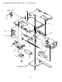
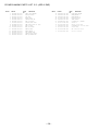
ADC-EX108 ADC-M105 YJ YJ SERVICE MANUAL STEREO CAR CD CHANGER SYSTEM BASIC CD MECHANISM : 8ZG-4 RNF This Service Manual is the "Revision Publishing" and replaces "Simple Manual" ADC-EX108(YJ2)/ADC-M105(YJ), (S/M Code No. 09-008-404-5T9). S/M Code No. 09-009-404-5R9 N O SI I V TA E R A D SPECIFICATIONS <Compact disc changer> System Frequency response Wow and flutter Signal to noise ratio Outputs Operating temperature Dimensions Weight Power requirement D/A converter Sampling rate Disc size Compact disc digital audio system 5 Hz - 20 kHz Below measurable limit 91 dB or more Line output (for changer connector only) -10 oC to 55 oC 254 x 83 x 173mm (w/h/d) (10 x 3 3/8 x 6 7/8 in.) 2.1 kg (4.62 lbs.) 12 V DC car battery (negative ground) 1 bit DAC, 8 times over sampling 44.1 kHz 120 mm Design and specifications are subject to change without notice. ACCESSORIES / PACKAGE LIST REF. NO. 1 1 2 3 4 PART NO. KANRI DESCRIPTION NO. 8Z-KM3-919-010 IB,Y M105-B<M105> 8Z-KM3-918-010 IB,Y 108-B<EX108> 87-B10-208-010 VWWS+4-12 BLK 8Z-KM1-222-110 PLATE,UNIT ASSY 8Z-KM1-218-010 NUT,5 HEX-FLANGE 5 8Z-KM1-209-010 6 8Z-KM1-216-010 7 8Z-KM4-651-010 HLDR,UNIT 10A HLDR,UNIT 10B CABLE ASSY,13PIN-DIN 2 PROTECTION OF EYES FROM LASER BEAM DURING SERVICING CAUTION This set employs laser. Therefore, be sure to follow carefully the instructions below when servicing. Use of controls or adjustments or performance of procedures other than those specified herin may result in hazardous radiation exposure. WARNING!! WHEN SERVICING, DO NOT APPROACH THE LASER EXIT WITH THE EYE TOO CLOSELY. IN CASE IT IS NECESSARY TO CONFIRM LASER BEAM EMISSION. BE SURE TO OBSERVE FROM A DISTANCE OF MORE THAN 30cm FROM THE SURFACE OF THE OBJECTIVE LENS ON THE OPTICAL PICK-UP BLOCK. s s ATTENTION Lutillisation de commandes, réglages ou procédures autres que ceux spécifiés peut entraîner une dangereuse exposition aux radiations. ADVARSEL Usynlig laserståling ved åbning, når sikkerhedsafbrydereer ude af funktion. Undgå udsættelse for stråling. Caution: Invisible laser radiation when open and interlocks defeated avoid exposure to beam. Advarsel: Usynlig laserståling ved åbning, når sikkerhedsafbrydere er ude af funktion. Undgå udsættelse for stråling. This Compact Disc player is classified as a CLASS 1 LASER product. The CLASS 1 LASER PRODUCT label is located on the rear exterior. VAROITUS! Laiteen Käyttäminen muulla kuin tässä käyttöohjeessa mainitulla tavalla saataa altistaa käyt-täjän turvallisuusluokan 1 ylittävälle näkymättömälle lasersäteilylle. CLASS 1 KLASSE 1 LUOKAN 1 KLASS 1 VARNING! Om apparaten används på annat sätt än vad som specificeras i denna bruksanvising, kan användaren utsättas för osynling laserstrålning, som överskrider gränsen för laserklass 1. LASER PRODUCT LASER PRODUKT LASER LAITE LASER APPARAT Precaution to replace Optical block PICK-UP ASSY P.C.B (KSS-710A) Body or clothes electrostatic potential could ruin laser diode in the optical block. Be sure ground body and workbench, and use care the clothes do not touch the diode. 1) After the connection, remove solder shown in right figure. SOLDER 3 SERVICE JIG AND TOOLS 1. How to Use the Repair Jig FFC Use the following repair jig kit for servicing. FFC For 10 CD changer Part name Part code JIG-ADC-EX106 SV-J00-090-010 PWB JIG TRANSISTOR The kit contains the following parts (Refer to Fig-1) ; 1. FFC (26P/25 cm) 1 pcs 2. P.W.B. FLEX 1 pcs 3. P.W.B. JIG 1 pcs 4. TRANSISTOR (2SD-2395) 1 pcs 5. P.W.B. KEY 1 pcs (1) (2) (3) PWB KEY Fig-1 REMOVE SCREW Remove the cabinet as follows; 1) Remove the CABI BOTTOM by removing the four screws VTT+2.6-6B (Refer to Fig-2). LED(LED201) Remove the P.W.B. MAIN as follows; 1) Remove all terminals of the transistor Q623 (2SD2395) by unsoldering them. 2) Remove the two motor wires (BLU/WHT). 3) Remove the two wires (BLK/BRN) of the sensor (PD201). 4) Remove the P.W.B. MAIN from the unit by removing the four screws V+2-3. 5) Disconnect the FFC of pickup from CN101. 6) Disconnect the PWB FLEX from CON1. 7) Remove the LED (LED201,GL380) from the P.W.B. MAIN. 8) Remove the sensor (PS201,SENR GP1S94) from P.W.B. MAIN. REMOVE MOTOR WIRE PWB FLEX REMOVE SENSOR WIRE Q623 PICKUP FCC SENSOR (PS201) Fig-2 Install the repair jig as follows; 1) Install the P.W.B. JIG into the unit and fix it with screws. (Refer to Fig-3). PWB JIG Fig-3 (4) Attach the parts as follows, (Refer to Fig-4); 1) Attach the supplied transistor to the location of the P.W.B. MAIN from which Q623 is removed in step (2). 2) Connect the supplied PWB FLEX to CON1. When the CONTROL UNIT is not used, use the P.W.B. KEY instead. (Refer to step (6), How to use the repair jig.) 3) Connect the FFC cable to CON101 and pickup. (The supplied FFC cannot be used because pitches and number of pins are different.) Q623 PWB FLEX FFC CABLE Fig-4 4 (5) (6) Perform wirings to the C.Bs. Refer to Fig-5/-6; Be sure to connect the wires coming from the P.W.B. JIG to the same connecting points on the MAIN C.B as follows. 1) Connect the motor wires and sensor (PD201) wires that are removed in step (2) to the P.W.B. JIG. 2) Connect all wires coming from the P.W.B. JIG to the respective lands of the MAIN C.B by soldering. Connect the motor wires (BLU/WHT) of the P.W.B. JIG to the motor wire connecting lands on the MAIN C.B by soldering. Connect the LED (LED201) wires (RED/GRY) of the P.W.B. JIG to the LED wire connecting lands on the MAIN C.B by soldering. Connect the sensor wires (BRN/BLK) of the P.W.B. JIG to the sensor wire connecting lands on the MAIN C.B by soldering. Connect the sensor (PS201) wires (YEL/ORG/ RED/BRN) of the P.W.B. JIG to the sensor wire connecting lands on the MAIN C.B by soldering. Connect the SW202 wire (WHT) of the P.W.B. JIG to the SW202 wire connecting lands on the MAIN C.B by soldering. Connect the SW203 wire (BLK) of the P.W.B. JIG to the SW203 wire connecting lands on the MAIN C.B by soldering. Connect the SW204 wires (BLU/WHT) of the P.W.B. JIG to the leads of SW204 on the MAIN C.B by soldering. Refer to Fig-6. Fig-5 Fig-6 How to use the repair jig; When the Control Unit (CDC/CT) is going to be used. 1) After all wires and connections are complete, connect the Control Unit (CDC/CT) with the DIN jack of the P.W.B. FLEX. 2) Connect external power +12 V to ACC/BACKUP wire and ground (-) to the GROUND wire. 3) Perform the operation check. When the Control Unit (CDC/CT) is not used. 1) Connect the supplied P.W.B KEY to the MAIN C.B by performing all connections between them. Refer to Fig-7/-8. (Wires to be used for connecting the MAIN C.B are not supplied.) 2) Connect the wires as follows. Refer to Fig-9. P.W.B KEY MAIN C.B HOT TO GND GND 5 Fig-8 GND TO PWB KEY GND +12V Fig-8 Fig-9 Fig-7 ACC 3) Connect the wires as follows (Refer to Fig-9); Connect wire for +12 V power to BACK UP of ICP601 by soldering. Connect ICP601 and ACC pattern land by soldering a wire. Connect GND by soldering a wire. Connect the +12 V power to the ACC/BACK UP wire and connect ground (-) to the GROUND wire of the connector (Wires to be used for connection are not supplied.) Add wire GND ICP601 +12V Fig-9 4) Perform the operation check (Refer to Fig-10). STOP PLAY BSKIP Fig-10 6 FSKIP DOWN UP ELECTRICAL MAIN PARTS LIST REF. NO. PART NO. IC KANRI NO. DESCRIPTION 87-A20-892-010 87-A21-467-010 8Z-KM3-692-010 87-A21-158-040 87-017-888-080 C-IC,CXD2588R C-IC,CXA2581N C-IC,CXP84632-160Q C-IC,TC74HC365AF IC,NJM4558MD 87-A20-574-010 87-A21-160-040 87-A21-161-040 87-A21-162-040 87-A21-102-040 C-IC,SM5902AF<EX108> C-IC,MSM5117400C-60SJ<EX108> C-IC,BA6392FP C-IC,BA6247FP C-IC,S-80828ANNP-EDR-T2 87-A21-190-040 C-IC,PQ20WZ1U REF. NO. TRANSISTOR PART NO. C202 C251 C252 C301 C302 KANRI DESCRIPTION NO. 87-016-669-080 C-CAP,S 0.1-25 K B 87-010-197-080 C-CAP,S 0.01-25 KB 87-012-140-080 C-CAP,S 470P-50 J CH 87-010-552-040 CAP,E 22-16 GAS 87-010-552-040 CAP,E 22-16 GAS C303 C304 C305 C306 C307 87-010-318-080 87-010-318-080 87-015-696-040 87-015-696-040 87-010-178-080 C-CAP,S 47P-50 CH C-CAP,S 47P-50 CH CAP,E 2.2-50 SRA CAP,E 2.2-50 SRA CHIP CAP 1000P C308 C321 C322 C323 C324 87-010-178-080 87-010-555-040 87-016-669-080 87-010-550-040 87-016-669-080 CHIP CAP 1000P CAP,E 100-10 C-CAP,S 0.1-25 K B CAP,E 100-6.3 GAS C-CAP,S 0.1-25 K B C325 C401 C402 C403 C404 87-010-550-040 87-A10-711-080 87-016-669-080 87-016-669-080 87-010-178-080 CAP,E 100-6.3 GAS C-CAP,E 100-6.3 M MF<EX108> C-CAP,S 0.1-25 KB<EX108> C-CAP,S 0.1-25 KB<EX108> CHIP CAP 1000P<EX108> C452 C501 C503 C505 C506 87-016-669-080 87-010-555-040 87-016-669-080 87-010-178-080 87-A11-257-010 C-CAP,S 0.1-25 KB<EX108> CAP,E 100-10 GAS C-CAP,S 0.1-25 K B CHIP CAP 1000P CAP,E 470U-10M C551 C552 C553 C554 C555 87-010-555-040 87-A11-257-010 87-016-669-080 87-016-669-080 87-016-669-080 CAP,E 100-10 M CAP,E 470U-10M C-CAP,S 0.1-25 C-CAP,S 0.1-25 C-CAP,S 0.1-25 C556 C601 C602 C603 C604 87-016-669-080 87-010-552-040 87-A10-368-080 87-010-552-040 87-010-782-010 C-CAP,S 0.1-25 K B CAP,E 22-16 GAS C-CAP,S 2.2-10 Z F CAP,E 22-16 GAS CAP,DL 0.047F-5.5 Z 70 C605 C606 C621 C622 C623 87-016-669-080 87-A10-368-080 87-010-552-040 87-010-555-040 87-010-555-040 C-CAP,S 0.1-25 K B C-CAP,S 2.2-10 Z F CAP,E 22-16 GAS CAP,E 100-10 M 5L CAP,E 100-10 M 5L 87-A30-248-040 89-110-372-080 87-026-648-080 89-327-125-080 87-A30-272-040 C-TR,2SB1197KQ TR,2SA1037KR C-TR,UPA608T CHIP TR,2SC2712GR C-TR,DTA124EKA 87-A30-273-040 87-A30-274-040 87-A30-317-080 89-423-952-010 87-A30-371-040 C-TR,DTC124EKA C-TR,2SD1622S-TD TR,2SA1702 TR,2SD2395E C-TR,2SD1623 87-A30-448-040 C-TR,DTA123JK<EX108> 87-A40-250-040 87-A40-196-080 87-020-331-080 87-A40-524-040 87-070-136-080 CHIP-DIODE,DAN217 C-ZENER,UDZ6.2B CHIP-DIODE,DAN202K C-DIODE,1SR154-400 ZENER,MTZJ5.1B 87-A40-437-080 ZENER,MTZJ4.3B C102 C103 C104 C105 C106 87-010-499-040 87-A12-154-010 87-016-669-080 87-016-669-080 87-016-669-080 CAP,E 22-6.3 GAS CAP,E 470-4 MA GAS C-CAP,S 0.1-25 K B C-CAP,S 0.1-25 K B C-CAP,S 0.1-25 K B C624 C625 C626 C631 C632 87-010-260-080 87-016-669-080 87-016-044-040 87-010-555-040 87-010-552-040 CAP,E 47-25 M 11L SME C-CAP,S 0.1-25 K B CAP,E 100-16 GAS CAP,E 100-10 M 5L CAP,E 22-16 M 5L C107 C108 C109 C110 C111 87-010-184-080 87-016-526-080 87-012-156-080 87-010-184-080 87-010-992-080 C-CAP,S 3300P-50 KB C-CAP,S 0.47-16 BK C-CAP,S 220P-50 CH CHIP CAPACITOR 3300P(K) C-CAP,S 0.047-25 B C901 C902 CN101 FC101 FC102 87-010-197-080 87-016-669-080 87-A61-155-080 8Z-KM3-674-010 8Z-KM3-608-010 C-CAP,S 0.01-25 K B C2012 C-CAP,S 0.1-25 K B C-CONN,30P H XF2H-3015-1 FF-CABLE, 30P 0.5 145MM-C F-CABLE,2P (SENS KM3) C112 C115 C116 C117 C118 87-016-669-080 87-012-154-080 87-012-154-080 87-010-176-080 87-010-176-080 C-CAP,S C-CAP,S C-CAP,S C-CAP,S C-CAP,S 0.1-25 K B 150P-50 CH 150P-50 CH 680P-50 SL 680P-50 SL HL201 ICP601 L101 L151 L152 8Z-KM1-232-010 87-A91-337-080 87-A50-536-080 87-A50-536-080 87-A50-536-080 HLDR,LED PROTECTOR,IC ICP-N75 C-COIL, 10UH K LQH3C24 C-COIL,10UH K LQH3C24 C-COIL,10UH K LQH3C24 C151 C152 C153 C155 C156 87-A10-711-080 87-016-669-080 87-A10-711-080 87-016-669-080 87-016-669-080 C-CAP,E C-CAP,S C-CAP,E C-CAP,S C-CAP,S 100-6.3 M MF 0.1-25 K B 100-6.3 M MF 0.1-25 K B 0.1-25 K B L201 L301 L401 L501 L551 87-A50-536-080 87-A50-536-080 87-A50-536-080 87-A50-536-080 87-A50-536-080 C-COIL,10UH C-COIL,10UH C-COIL,10UH C-COIL,10UH C-COIL,10UH C157 C158 C159 C161 C162 87-012-156-080 87-010-992-080 87-012-156-080 87-016-669-080 87-A12-031-080 C-CAP,S C-CAP,S C-CAP,S C-CAP,S C-CAP,E 220P-50 CH 0.047-25 B 220P-50 CH 0.1-25 K B 33-10 M MF LED201 M8 01 PS201 SW201 SW202 87-070-288-010 87-A91-054-010 87-A90-244-010 87-A91-155-010 87-036-110-010 LED,GL380 MOT,FF-050SK SNSR,GP1S94 SW,TACT SKHHLQ SW,MICRO SPPB62 C165 C166 C17 0 C171 C201 87-016-669-080 87-016-669-080 87-016-669-080 87-010-500-040 87-016-669-080 C-CAP,S 0.1-25 KB C-CAP,S 0.1-25 KB C-CAP,S 0.1-25 KB<EX108> CAP-E,33-4 M 5L SRE<EX108> C-CAP,S 0.1-25 K B SW203 SW204 X101 X200 87-036-110-010 87-036-312-080 87-A70-163-080 87-A70-200-080 SW,MICRO SPPB62 SW PUSH ESE102MH4-Q C-VIB,CER 16.93MHZ CSTCVMXJ0C4 C-VIB,CER 12MHZ CSTCV12MTJ0C4 DIODE MAIN C.B ! 7 K K K K K 5L K B K B K B LQH3C24 LQH3C24 LQH3C24<EX108> LQH3C24 LQH3C24 REF. NO. PART NO. KANRI NO. SENS C.B PD201 DESCRIPTION REF. NO. KANRI NO. CONNECT C.B 87-026-674-010 P-TR,PT4850F 8Z-KM3-638-010 JACK,DIN 13 P TCS5125-014151 CON801 CON802 M802 M803 M804 DIN C.B J901 PART NO. DESCRIPTION 87-A61-155-080 87-A61-240-080 87-A91-054-010 87-A91-054-010 87-A90-926-010 C-CONN,30P H XF2H-3015-1 C-CONN,16P H FLZ-RSM1-TB MOT,FF-050SK MOT,FF-050SK MOT,RF-3L0PA 87-036-312-080 8Z-KM3-624-010 C-SW,PUSH ESE102MH4-Q F-CABLE,2P (LIMIT) LIMIT C.B FLEX DIN C.B 8Z-KM3-617-010 SW803 W804 PWB,FLEX DIN (ZKM3)-C SW C.B FLEX PICK UP C.B SW801 SW802 W803 87-036-269-080 87-036-312-080 8Z-KM3-625-010 C-SW,PUSH 1-1-1 ESE102MH2 C-SW,PUSH ESE102MH4-Q F-CABLE,4P (SWITCH) 8Z-KM3-623-210 87-009-863-010 87-A40-319-080 87-A40-320-080 87-A40-319-080 CONN ASSY,2P (LED) CONN,2P WHT ZH C-LED,LT1E40A GRN C-LED,LT1H40A Y C-LED,LT1E40A GRN 8Z-KM4-631-010 PWB,FLEX PICK UP (AK) LED C.B CNA800 CON803 LED801 LED802 LED803 CHIP RESISTOR PART CODE Chip Resistor Part Coding 8 8 A Figure Resistor Code Value of resistor Chip resistor L W t :A Resistor Code : A 1.0 0.5 0.35 104 1.6 0.8 0.45 108 2 1.25 0.45 118 3.2 1.6 0.55 128 Dimensions (mm) Wattage 1/16W Type 1005 Symbol CJ Tolerance 5% 1/16W 1/10W 1608 2125 5% 5% CJ CJ 1/8W 3216 5% CJ Form L t W TRANSISTOR ILLUSTRATION C C B E 2SA1037KR 2SB1197KQ 2SC2712GR 2SD1623 DTA124EKA DTA123JKA DTC124EKA C1 E1 B1 B2 C2 UPA608T E2 B C E 2SD1622S 8 BC E 2SD2395E E C B 2SA1702 WIRING - 1 (MAIN / SENS) <1/2> 32 31 30 29 28 27 26 25 24 23 22 21 20 19 18 17 16 15 14 13 12 11 10 9 8 7 6 5 4 3 2 1 A B C D E F G H I J K L M N O P Q R S T U –9– WIRING - 1 (MAIN / DIN / FLEX DIN) <2/2> 1 2 3 4 5 6 7 8 9 10 11 12 13 14 15 16 17 A B C D E F G H I J K L M N O P Q R S T U – 10 – 18 19 20 21 22 23 24 25 26 27 28 29 30 31 32 WIRING - 2 (SW / LED / CONNECT / LIMIT / FLEX PICK UP) 32 31 30 29 28 27 26 25 24 23 22 21 20 19 18 17 16 15 14 13 12 11 10 9 8 7 6 5 4 3 2 1 A B C D E F G H I J K L M N O P Q R S T U – 11 – SCHEMATIC DIAGRAM 12 IC BLOCK DIAGRAM 13 14 IC DESCRIPTION IC, CXP84632-160Q Pin No. Pin Name I/O Description 1~4 NC Not connected. 5 EEPDI Connected to GND. 6 SCLK O SENS read clock out. 7 SENS I SENS in. 8 XLAT O DSP data latch out. 9 SYSM O DSP(DAC) system mute control. (H : MUTE). 10 DRST O DSP IC reset. (L : RESET). 11 EMPHA O DSP(DAC) DE EMPHASYS control. (H : ON). 12, 13 PWRCNT1, 2 O POWER control out 1, 2. 14 SENS I DISC IN detect sensor in. 15 RFSW O RFAMP GAIN select out. (H : CD - RW). 16 (EASSON) RFSEL O RFAMP Fs select out. (x2 speed : L). (Not used). 17 LEDCONT O LED on / off out. (H : ON). 18 ELCONT O MOTOR DRIVER control out 1. 19 LDCONT O MOTOR DRIVER control out 2. 20 MCONT O MOTOR DRIVER control out 3. 21 PHPWR O PHOTO SENSOR ON / OFF out. (H : ON). 22 EJECT I EJECT SW in. (Pull 22 ~ 28 SW L : ON). 23 INIT I INITIAL POSITION SW in. 24 MZIN I DISC MAGAZINE IN SW in. 25 MZLOCK I DISC MAGAZINE LOCK SW in. 26 UNLOAD I UNLOAD POSITION SW in. 27 LS I PU INNER POSITION SW in. 28 CHUCK I CHUCKING POSITION SW in. 29 CD6/10 I 6 / 10 DISC selector. (OPEN : 6 disc). (Connected to GND). 30 RESET IC RESET. (L : RESET). 31 EXTAL 12 MHz CLOCK. 32 XTAL 12 MHz CLOCK. 33 VSS IC GND. 34 TX Not used. 35 TEX Not used. 36 AVSS GND. (A/D in GND). 37 AVREF VDD. (A/D in Vref). 38 TEST0 I/O 39 ~ 42 TEST1 ~ 4 Not used. 43 TEST5 I CD TEXT FUNTION select. (L : NO TEXT). (M105 only) 44 TEST6 Not used. 45 TEST7 I EASS FUNCTION select. (L : NO EASS). (M105 only). 46 NC Not connected. 47 SQSI I SUBCODE CRC flag check. 48 SQCLK O SUBCODE READ CLOCK out. TEST MODE select (L) / TEST KEY connect. 15 Pin No. Pin Name I/O Description 49 SQSI I SUBCODE DATA in. 50 NC Not connected. 51 DCLK O DSP / DRAM controller DATA CLOCK out. 52 ZSENS I DRAM controller DATA in. (EX108 only). 53 DATAO O DSP / DRAM controller DATA out. 54 PHSENS I PHOTO SENSOR in. 55 C2PO I C2 error flag in. (H : C2 error). 56 LOCK I LOCK in. (H : SPINDLE SERVO LOCK). 57 FOK I FOK in (H : FOCUS OK). 58, 59 NC Not connected. 60 ACCCNT I ACC CONT in. (H : ON). 61 CLKO O Adjust SERIAL CLOCK out. 62 CLKI I SERIAL CLOCK in. 63 SCOR I SUBCODE SYNC in. 64 DSPSEL I SERIAL BUS enable in. 65 SBCLKI I Adjust SERIAL CLOCK in. 66 SBDTI I SERIAL DATA in. 67 NC Not connected. 68 SBCLKO O SERIAL CLOCK out. 69 SBDTO O SERIAL DATA out. 70 NC Not connected. 71 BUCHK I Connected to VDD. 72 VDD IC VDD. 73 NC Connected to VDD. 74 AMUTE Not used. 75 SPCON O MOTOR DRIVER STANDBY control. (L : MUTE). 76 NRST O DRAM controller IC RESET. (L : RESET). (EX108 only). 77 YMLD O DRAM controller DATA LATCH out. (EX108 only). 78 LED1 O DISC detect sensor LED on / off. (L : ON). 79, 80 LED2, 3 Not used. 16 VOLTAGE CHART IC101, CXD2588R PIN NO. CD x 1 CD x 2 RW x 1 1 DATA LINE DATA LINE DATA LINE 2 4.56 4.56 3 0.11 4 PIN NO. CD x 1 CD x 2 RW x 1 61 1.96 1.96 1.96 4.56 62 0 0 0 0.11 0.11 63~64 2.04 2.04 2.04 0 0 0 65~66 1.96 1.96 1.96 5 4.60 4.60 4.60 67 3.92 3.92 3.92 6 0 0 0 68 0 0 0 7 DATA LINE DATA LINE DATA LINE 69~70 1.63 1.63 1.63 8 4.59 4.59 4.59 71 0.01 0.01 0.01 9 4.57 4.57 4.57 72~73 0 0 0 10 0.03 0.03 0.03 74 4.06 4.06 4.06 11 4.61 4.61 4.61 75 0.01 0.01 0.01 12~14 4.06 4.06 4.06 76 2.02 2.02 2.02 15~18 0 0 0 77~78 2.03 2.03 2.03 19~20 2.03 2.03 2.03 79 1.35 1.35 1.35 21 1.92 1.92 1.92 80 1.96 1.96 1.96 22 4.06 4.06 4.06 81 2.00 2.00 2.00 23 0 0 0 82 4.06 4.06 4.06 24 0.05 0.05 0.05 83 4.60 4.60 4.60 25 1.92 1.92 1.92 84 4.06 4.06 4.06 26 2.00 2.00 2.00 85 0 0 0 27~28 0.01 0.01 0.01 86 1.98 1.98 1.98 29 0.04 0.04 0.04 87 0 0 0 30~31 4.06 4.06 4.06 88 3.91 3.91 3.91 32 2.25 2.25 2.25 89 0 0 0 33 0 0 0 90~91 1.62 1.62 1.62 34~35 2.25 2.25 2.25 92~93 0 0 0 36~41 DATA LINE DATA LINE DATA LINE 94 1.61 1.61 1.61 42~46 0 0 0 95 1.62 1.62 1.62 47 2.02 2.02 2.02 96 1.63 1.63 1.63 48 1.98 1.98 1.98 97 3.93 3.93 3.93 49~50 0 0 0 98~99 4.06 4.06 4.06 51 DATA LINE DATA LINE DATALINE 100 0 0 0 52 2.02 2.02 2.02 53 2.79 2.79 2.79 54 1.95 1.95 1.95 55 0 0 0 56 1.73 1.73 1.73 57 3.92 3.92 3.92 58 1.95 1.95 1.95 59 1.96 1.96 1.96 60 0.80 0.80 0.80 17 IC151, CXA2581N PIN NO. CD x 1 CD x 2 RW x 1 1 2.57 2.57 2.57 14 4.59 4.59 4.59 2 0.158 0.158 0.158 15 0 0 4.6 3 2.03 2.03 2.03 16 4.63 0.09 4.63x1 / 0.09x2 4 2.10 2.10 2.10 17 4.62 4.62 4.62 5 0 0 0 18~21 0 0 0 6 2.15 2.15 2.15 22~23 4.59 4.59 4.59 7 2.14 2.14 2.14 24~25 0 0 0 8~9 2.13 2.13 2.13 26~27 4.59 4.59 4.59 10~11 2.04 2.04 2.04 28~29 0 0 0 12 0 0 4.61 30 4.16 4.16 4.16 13 4.06 4.06 4.06 31 2.27 2.27 2.27 14 2.04 2.04 2.04 32 2.43 2.43 2.43 15 2.19 2.19 2.19 33 0 0 0 16 2.00 2.00 2.00 34 4.64 4.64 4.64 17 2.04 2.04 2.04 35~36 0 0 0 18 1.95 1.95 1.95 37 4.65 4.65 4.65 19 2.04 2.04 2.04 38 4.62 4.62 4.62 20 2.02 2.02 2.02 39~41 0 0 0 21 2.04 2.04 2.04 42 4.60 0 0 22 4.06 4.06 4.06 43 4.60 4.60 4.60 23 2.97 2.97 2.97 44 4.60 0 0 24 2.43 2.43 2.43 45~46 4.60 4.60 4.60 25 1.57 1.57 1.57 47 DATA LINE DATA LINE DATA LINE 26 2.80 2.77 2.77 48 4.56 4.56 4.56 27 2.04 2.04 2.04 49 DATA LINE DATA LINE DATA LINE 28 2.19 2.19 2.19 50 0 0 0 29 2.04 2.04 2.04 51 4.57 4.57 4.57 30 1.54 1.54 1.54 52~53 DATA LINE DATA LINE DATA LINE 54 4.64 4.64 4.64 55 0 0 0 IC201, CXP84632160Q PIN NO. CD x 1 CD x 2 RW x 1 PIN NO. CD x 1 CD x 2 RW x 1 56~57 4.06 4.06 4.06 1 0 0 0 58~59 0 0 0 2~3 4.64 4.64 4.64 60 4.65 4.65 4.65 4~5 0 0 0 61 4.64 4.64 4.64 6 4.61 4.61 4.61 62 0 0 0 7 0.03 0.03 0.03 63 0.05 0.05 0.05 8 4.59 4.59 4.59 64 DATA LINE DATA LINE DATA LINE 9 0 0 0 65 4.64 4.64 4.64 10~11 4.59 4.59 4.59 66~67 0 0 0 12~13 4.57 4.57 4.57 68 4.64 4.64 4.64 18 PIN NO. CD x 1 CD x 2 RW x 1 PIN NO. CD x 1 CD x 2 RW x 1 69 DATA LINE DATA LINE DATA LINE 24 4.62 4.62 4.62 70 0 0 0 25 DATA LINE DATA LINE DATA LINE 71~73 4.65 4.65 4.65 26 4.56 4.56 4.56 74 0 0 0 27~28 DATA LINE DATA LINE DATA LINE 75 4.59 4.59 4.59 29 2.03 2.03 2.03 76~77 4.63 4.63 4.63 30 2.02 2.02 2.02 78 4.00 4.00 4.00 31~32 2.05 2.05 2.05 79~80 0 0 0 33 3.51 3.51 3.51 34 3.17 3.17 3.17 35~38 DATA LINE DATA LINE DATA LINE 39~40 2.40 2.40 2.40 41 2.01 2.01 2.01 42 1.94 1.94 1.94 43 2.04 2.04 2.04 44 2.08 2.08 2.08 IC251, TC74HC365AF PIN NO. CD x 1 CD x 2 RW x 1 1~8 0 0 0 9~10 4.64 4.64 4.64 11~14 DATA LINE DATA LINE DATALINE 15 0 0 0 16 4.65 4.65 4.65 IC451, MSM5117400C-60SJ <EX108 ONLY> IC301, NJM4558MD PIN NO. CD x 1 CD x 2 RW x 1 PIN NO. CD x 1 CD x 2 RW x1 1~3 6.30 6.30 6.30 1 4.06 4.06 4.06 4 0 0 0 2~3 2.02 2.02 2.02 5~7 6.30 6.30 6.30 4 3.50 3.50 3.50 8 10.65 10.65 10.65 5 3.17 3.17 3.17 6 0 0 0 7 - - - 8 DATA LINE DATA LINE DATA LINE 9 2.0 2.0 2.0 10 1.94 1.94 1.94 11 2.04 2.04 2.04 12 2.07 2.07 2.07 13 4.05 4.05 4.05 14 0 0 0 15~16 2.40 2.40 2.40 17~19 DATA LINE DATA LINE DATA LINE 20 - - - 21 DATA LINE DATA LINE DATA LINE 22 0 0 0 23 DATA LINE DATA LINE DATA LINE 24 2.03 2.03 2.03 25 2.00 2.00 2.00 26 0 0 0 IC401, SM5902AF <EX108 ONLY> PIN NO. CD x 1 CD x 2 RW x 1 1 4.06 4.06 4.06 2~6 4.00 4.00 4.00 7 0 0 0 8 4.00 4.00 4.00 9 1.68 1.68 1.68 10 0 0 0 11 2.03 2.03 2.03 12 2.02 2.02 2.02 13 1.95 1.95 1.95 14 2.00 2.00 2.00 15 2.02 2.02 2.02 16 1.34 1.34 1.34 17 4.05 4.05 4.05 18 0 0 0 19 0.05 0.05 0.05 20 4.62 4.62 4.62 21 DATA LINE DATA LINE DATA LINE 22 4.05 4.05 4.05 23 0 0 0 19 IC501, BA6392FP IC622, PQ20WZ1U PIN NO. CD x 1 CD x 2 RW x 1 PIN NO. CD x 1 CD x 2 RW x 1 1 4.45 4.45 4.45 1 13.10 13.10 13.10 2 5.03 5.03 5.03 2 4.57 4.57 4.57 3 4.48 4.48 4.48 3 11.11 11.11 11.11 4~5 DATA LINE DATA LINE DATA LINE 4 2.67 2.67 2.67 6 4.75 4.75 4.75 5 0 0 0 7 4.77 4.77 4.77 8 0 0 0 9~10 DATA LINE DATA LINE DATALINE 11 4.73 4.73 4.73 12 4.71 4.71 4.71 13 4.76 4.76 4.76 14 0 0 0 15 4.59 4.59 4.59 16 4.78 4.78 4.78 17 4.69 4.69 4.69 18 4.76 4.76 4.76 19~20 DATA LINE DATA LINE DATA LINE 21~22 9.90 9.90 9.90 23 2.03 2.03 2.03 24 2.22 2.03 2.03 25 2.03 2.03 2.03 26 5.02 5.02 5.02 27 4.36 4.36 4.36 28 0 0 0 PIN NO. CD x 1 CD x 2 RW x 1 1 0.55 0.55 0.55 2~4 0 0 0 5~6 DATA LINE DATA LINE DATA LINE 7 0 0 0 8 DATA LINE DATA LINE DATA LINE 9 10.33 10.33 10.33 10~15 0 0 0 16 10.33 10.33 10.33 17 0 0 0 18 0.55 0.55 0.55 19~21 0 0 0 22 0.55 0.55 0.55 23~25 0 0 0 IC551, BA6247FP 20 Q253, 2SC2712GR Q151, 2SB1197KQ PIN CD x 1 CD x 2 RW x 1 PIN CD x 1 CD x 2 RW x 1 E 3.18 3.18 3.18 E 0 0 0 C 2.18 2.18 2.18 C 0 0 0 B 2.54 2.54 2.54 B 0.68 0.68 0.68 Q601, 2SD1622S-TD Q152, DTA123JK <EX108 ONLY> PIN CD x 1 CD x 2 RW x 1 PIN CD x 1 CD x 2 RW x 1 E 4.05 4.00 4.05x1/4.00x2 E 4.65 4.65 4.65 C 2.77 3.96 2.77x1/3.96x2 C 13.10 13.10 13.10 B 4.60 0.09 4.60x1/0.09x2 B 5.23 5.23 5.23 Q621, 2SA1702 Q153, 2SA1037K(R) PIN CD x 1 CD x 2 RW x 1 PIN CD x 1 CD x 2 RW x 1 E 2.80 2.80 2.80 E 13.10 13.10 13.10 C 0 0 0 C 13.05 13.05 13.05 B 2.19 2.19 2.19 B 0 0 0 Q201, UPA608T Q622, DTC124EKA PIN CD x 1 CD x 2 RW x 1 PIN CD x 1 CD x 2 RW x 1 E1 4.65 0 4.65 E 0 0 0 E2 0 4.64 0 C 0.13 0.13 0.13 C1 0 4.65 0 B 4.57 4.57 4.57 C2 4.64 0 4.64 B1 4.65 4.65 4.65 B2 0 0 0 PIN CD x 1 CD x 2 RW x 1 E 4.62 4.62 4.62 C 13.03 13.03 13.03 B 4.07 4.07 4.07 PIN CD x 1 CD x 2 RW x 1 E 11.06 11.06 11.06 C 11.10 11.10 11.10 B 11.65 11.65 11.65 Q202,2SC2712GR PIN CD x 1 CD x 2 RW x 1 E 2.15 2.15 2.15 C 4.63 4.63 4.63 B 2.83 2.83 2.83 Q251,2SC2712GR PIN CD x 1 CD x 2 RW x 1 E 0 0 0 C 0 0 0 B 0.64 0.64 0.64 Q252, DTA124EKA PIN CD x 1 CD x 2 RW x 1 E 4.65 4.65 4.65 C 4.65 4.65 4.65 B 0 0 0 Q623, 2SD2395E Q631, 2SD1623 PD201, PT4850F PIN CD x 1 CD x 2 RW x 1 E 0 0 0 C 4.58 4.58 4.58 21 TEST MODE There are two methods to perform operation check using test mode. One method uses the head unit. The other method uses the repair jig. Because different operation buttons must be used for entering the operation modes and there are cases that unit does not run at all, in the method that uses the head unit, the method using the repair jig is described as follows; 1. How to start up the CD test mode Connect the P.W.B Key in accordance SERVICE JIG AND TOOLS step (6). How to use the repair jig - When the Control Unit (CDC/CT) is not used . 1) While pressing the STOP button of the P.W.B Key, turn on the +12 V power of ACC/BACK UP. 2. How exit the CD test mode 1) 3. Turn off the +12 V power of ACC/BACK UP. Function description of CD test mode Uses of the respective buttons of the P.W.B Key are described in Fig-11. Fig-11 Mode Operation key Servo OFF STOP Search mode FOCUS Operation Contents All servo off Continuous focus search APC circuit check Pickup lens repeats full swing (Note 1) Laser current measurement Focus error waveform check Play mode FOCUS Normal playback Focus servo Tracking servo V SV ON CLV servo Sled servo Sled mode CD change FWD Pickup moves to outer circumference Sled servo RVS Pickup moves to inner circumference Mechanism operation check Disc unload Mechanism operation check (cyclic) DISC UP V Magazine change V Disc load During the PLAY mode, the REV, FWD and DISC UP keys are invalid. Press the STOP key once. When a Head Unit is connected, the Disc No. and the Track No. are shown on display in the same way as in the normal operation. Note 1: If the focus search operation is continued for 10 minutes or longer, the driver IC heats up sufficiently to trigger the protection circuit, which stops the CD system. Turn off the main power and re-start operation about 10 minutes later. 22 MECHANICAL EXPLODED VIEW 1 / 1 A 16 15 14 17 19 13 H A F P.C.B 14 20 13 18 15 P.C.B 21 8ZG-4 RNF PWB,FLEX DIN (ZKM3) 12 A 9 H 23 7 I 8 A 6 G 4 10 B G 11 C 22 F 5 A A WIRE ASSY 40 LUG A 25 E 4 B 6 D MAIN C.B 24 F F 2 1 3 F 23 SH,BOTTOM 10 D MECHANICAL PARTS LIST 1 / 1 REF. NO. PART NO. KANRI DESCRIPTION NO. PANEL,FRONT 10 WINDOW,FRONT 10 CABI,FRONT EX108<EX108 YJ2SF> CABI,FRONT M105<M105 YJSF> PLATE,MAG REF. NO. 19 20 21 22 23 8Z-KM1-204-010 8Z-KM1-201-010 8Z-KM3-638-010 8Z-KM1-225-010 8Z-KM3-036-110 KANRI DESCRIPTION NO. HLDR,DECK R10 HLDR,CD JACK,DIN 13 P TCS5125-014151 HLDR,REG CABI,BOTTOM 10S 24 25 A B C 8Z-KM3-674-010 8Z-KM1-232-010 87-B10-260-010 8Z-KM1-223-010 87-B10-255-010 FF-CABLE,30P 0.5 145MM -C HLDR,LED VTT+2.6-6 W/O SLOT BLK S-SCREW,2-5 (BLK) U+2-3 W/O CR KEY,EJECT PLATE,DECK COVER, PLATE 10 HLDR,DECK L10 DMPR, D E F G H 8Z-KM1-215-010 8Z-KM1-224-010 87-571-032-410 87-B10-244-010 87-B10-245-010 S-SCREW,M3-5-12 S-SCREW,M3-7-11 VIT+2-3 V+2-5 W/O BLK U+2.6-4 W/O CR SHAFT,FRAME SPR-E,DMPR 10 WINDOW,CD S CABI,TOP 10S F-CABLE,2P (SENS KM3) I 87-B10-097-010 W-M,3.2-8-0.188 W/ADH 1 2 3 3 4 8Z-KM1-003-010 8Z-KM1-004-010 8Z-KM3-031-010 8Z-KM3-039-010 8Z-KM1-207-010 5 5 6 7 8 8Z-KM3-034-010 8Z-KM3-038-010 8Z-KM1-220-010 8Z-KM3-032-010 8Z-KM1-208-010 WINDOW,DECK EX108<EX108 YJ2SF> WINDOW,DECK M105<M105 YJSF> MAGNET,HLDR ASSY CABI,FRAME 10S COVER, DECK 10 9 10 11 12 13 8Z-KM1-006-110 8Z-KM1-230-010 8Z-KM1-217-010 8Z-KM1-203-010 88-ZG3-371-010 14 15 16 17 18 8Z-KM1-202-010 88-ZG4-542-010 8Z-KM3-033-010 8Z-KM3-035-110 8Z-KM3-608-010 COLOR NAME TABLE PART NO. Basic color symbol Color Basic color symbol Color Basic color symbol Color B Black C Cream D Orange G Green H Gray L Blue LT Transparent Blue N Gold P Pink R Red S Silver ST Titan Silver T Brown V Violet W White WT Transparent White Y Yellow YT Transparent Yellow LM Metallic Blue LL Light Blue GT Transparent Green LD Dark Blue DT Transparent Orange GM Metallic Green YM Metallic Yellow DM Metallic Orange PT Transparent Pink 24 CD MECHANISM EXPLODED VIEW 1 / 2 (8ZG-4 RNF) A 31 F A A 32 A A 1 F F A CHAS,REAR 2 28 33 27 29 34 3 F A 33 4 H 30 5 17 26 H E 35 36 5 A E E 6 25 24 D D 37 C 8 22 10 SW C.B A 12 20 A G I 7 A B 23 21 9 D D 19 G 13 11 38 18 LED C.B B 14 PLATE ASSY CKG-R 15 17 16 A A 8ZG-8 RNF 25 A CD MECHANISM PARTS LIST 1 / 2 (8ZG-4 RNF) REF. NO. PART NO. DESCRIPTION KANRI NO. PLATE,SLIT 10 PLATE,ELV-R 10 CHAS ASSY,MAIN 10 GEAR,ELV-R GEAR,ELV 26 27 28 29 30 88-ZG3-304-010 88-ZG3-351-110 88-ZG3-274-010 88-ZG3-352-010 88-ZG3-301-010 KANRI DESCRIPTION NO. GEAR,ELV-F SPR-T,LEVER LOCK PLATE,LOCK SW SPR-E,LOCK SW GEAR,WORM ELV SHAFT,GATA 10 PLATE,ELV-F 10 F-CABLE,4P (SWITCH) LEVER ASSY,SLD-1 CAM,SLD 31 32 33 34 35 88-ZG3-277-010 88-ZG4-506-110 88-ZG4-541-010 88-ZG3-278-010 88-ZG4-001-110 SPR-P,MAGAZINE CHAS ASSY,TOP 10 SPR-E,EJECT 10 PLATE,EJECT MAGAZINE,T 10 88-ZG3-002-210 88-ZG3-246-010 88-ZG3-231-010 88-ZG3-312-110 88-ZG3-221-010 MAGAZINE,B PLATE ASSY,CKG-R LEVER ASSY,CKG WORM-WHL,SLD HLDR ASSY,MOT ELV 36 37 38 A B 88-ZG4-514-110 88-ZG3-003-210 8Z-KM1-214-010 87-262-545-310 87-261-031-410 SPR-P,TRAY 10 TRAY, HLDR,LED V+2-2.5 V+2-2 16 17 18 19 20 88-ZG3-311-010 87-A91-054-010 88-ZG3-211-110 88-ZG3-314-010 88-ZG3-315-210 GEAR,WORM SLD MOT,FF-050SK CHAS ASSY,ELV GUIDE,F GUIDE,R C D E F G 87-B10-258-010 86-544-437-010 87-B10-272-010 87-571-032-410 87-067-869-010 W-P,2.15-3.5-0.5 PW,1.5-3.5-0.5 W-P,2.15-3.5-0.5 SLIT VIT+2-3 V+1.7-8 HL BLK 21 22 23 24 25 88-ZG3-236-010 88-ZG3-266-110 88-ZG3-276-310 88-ZG3-275-010 88-ZG3-302-010 ARM ASSY, CLAMP ASSY, SPR-P,CLAMP LEVER,SLD-2 WORM-WHL,ELV H I 87-067-310-010 87-262-545-310 PW,2.1-4-0.15 C V+2-2.5 1 2 3 4 5 88-ZG4-521-210 88-ZG4-513-110 88-ZG4-501-110 88-ZG3-305-010 88-ZG3-303-010 6 7 8 9 10 88-ZG4-531-010 88-ZG4-512-110 8Z-KM3-625-010 88-ZG3-226-010 88-ZG3-313-010 11 12 13 14 15 REF. NO. 26 PART NO. CD MECHANISM EXPLODED VIEW 2 / 2 (8ZG-8 RNF) LIMIT C.B F A 21 1 20 15 14 2 12 19 3 18 E E D 17 A 4 13 A C 5 6 11 16 8 A 7 9 10 B CONNECT C.B A 27 CD MECHANISM PARTS LIST 2 / 2 (8ZG-8 RNF) REF. NO. PART NO. KANRI DESCRIPTION NO. CHAS ASSY,MECHA GUIDE,PICKUP CLR,ELV HLDR,LEAD LEVER,PUSH SW 1 2 3 4 5 88-ZG8-401-210 88-ZG8-425-010 88-ZG3-317-010 88-ZG8-426-010 88-ZG8-428-110 6 7 8 9 10 88-ZG8-412-010 87-A91-630-010 8Z-KM4-631-010 88-ZG8-411-110 87-A91-054-010 SPR-P,PICKUP PICKUP,KSS-710A PWB,FLEX PICK UP (AK) SPR-P,LEAD MOT,FF-050SK 11 12 13 14 15 88-ZG8-431-010 88-ZG8-424-010 88-ZG3-332-010 88-ZG3-256-110 88-ZG3-354-010 SHAFT,LEAD GEAR,MECHA 3 CLR,LEVER ATK LEVER ASSY,ATK-F SPR-E,LEVER ATK REF. NO. 28 PART NO. KANRI DESCRIPTION NO. HLDR,MOT MECHA GEAR,MECHA 1 GEAR,MECHA 2 MOT,RF-3L0PA TURN TABLE 16 17 18 19 20 88-ZG8-427-010 88-ZG8-422-010 88-ZG8-423-010 87-A90-926-010 88-ZG8-421-010 21 A B C D 8Z-KM3-624-010 87-571-032-410 87-352-529-310 88-ZG8-432-010 87-262-547-310 F-CABLE,2P (LIMIT) VIT+2-3 VT2+1.7-4.0 BLK S-SCREW,V+1.7-5 IB LOCK V+2-3 BLK E F 87-078-018-010 87-262-523-310 PW 1.55-3.6-0.25 V+1.7-2 3 BLK 211, IKENOHATA 1CHOME, TAITO-KU, TOKYO 110, JAPAN TEL:03 (3827) 3111 2000058 0251431 Printed in Singapore