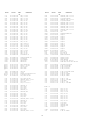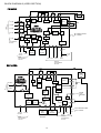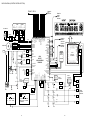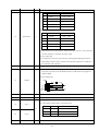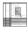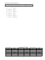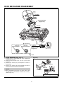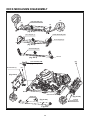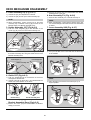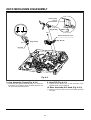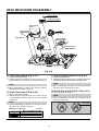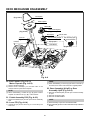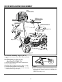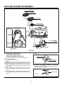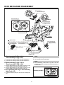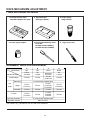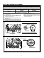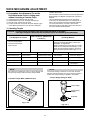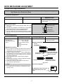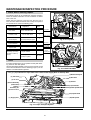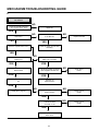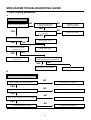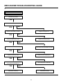
1
HV-FX5200 LE
SERVICE MANUAL
STEREO VIDEO CASSETTE RECORDER
BASIC TAPE MECHANISM : D-33
S/M Code No. 09-996-332-8R1
DA
TA
RE
VI
SIO
N
This Service Manual is the "Revision Publishing" and replaces "Simple Manual"
(S/M Code No. 09-996-332-8T1).
TABLE OF CONTENTS
SPECIFICATIONS ............................................................ 3
15. Support CST ............................................................. 62
ACCESSORIES LIST ....................................................... 3
16. Base Assembly P4 .................................................... 62
DISASSEMBLY INSTRUCTIONS ..................................... 4
17. Opener Lid ................................................................ 62
SERVICE POSITION ........................................................ 5
18. Arm Assembly T/up ................................................... 62
VCR TEST TAPE INTERCHANGEABILITY TABLE ........ 6
19. Arm Assembly Pinch ................................................. 62
ELECTRICAL MAIN PARTS LIST .............................. 7 ~ 9
20. Belt Capstan/Motor Capstan ..................................... 63
TRANSISTOR ILLUSTRATION ........................................ 9
21.Clutch Assembly D33 ................................................. 63
WIRE HARNESS DIAGRAM .......................................... 10
22. Lever F/R .................................................................. 63
BLOCK DIAGRAM ................................................. 11 ~ 20
23. Gear Assembly H-Up/D or Gear Assembly Up/D ...... 63
SCHEMATIC DIAGRAM
24. Bracket Assembly Jog ............................................... 64
1. POWER SECTION .............................................. 21 ~ 22
25. Guide Rack F/L, Gear Rack F/L ................................ 64
2. AUDIO/VIDEO SECTION .................................... 23 ~ 24
26. Brake Assembly Capstan .......................................... 64
3. SYSTEM CONTROL/SERVO/OSD SECTION) .. 27 ~ 28
27. Gear Drive/Gear Cam/Gear Connector .................... 65
4. Hi-Fi/SCART SECTION ...................................... 29 ~ 30
28. Bracket Assembly L/D motor ..................................... 65
5. TUNER/IF SECTION ........................................... 31 ~ 32
29. Gear Sector ............................................................... 66
6. NICAM SECTION ................................................ 33 ~ 34
30. Base Tension/Plate Slider/Lever Tension .................. 66
7. FRONT-1 C.B .............................................................. 37
31. Gear Assembly P3/Gear Assembly P2 ..................... 67
8. FRONT-2 C.B .............................................................. 37
32. Base Assembly P3/Base Assembly P2 ..................... 67
WAVEFORM
33. Arm Assembly Idler Jog or Arm assembly Idler ......... 67
1. VIDEO SECTION ........................................................ 25
DECK MECHANISM ADJUSTMENT
2. SERVO/OSD SECTION .............................................. 26
Tools and Fixtures for service ......................................... 68
3. TUNER/IF SECTION ................................................... 32
1. Mechanism Alignment Position Check ........................ 69
4. NICAM SECTION ........................................................ 34
2. Preparation for Adjustment ......................................... 70
WIRING
3. Checking Torque ......................................................... 70
1. MAIN C.B SECTION ........................................... 35 ~ 36
4. Guide Roller Height Adjustment .................................. 71
2. FRONT 1 C.B SECTION ............................................. 38
4-1. Preliminary Adjustment .......................................... 71
3. FRONT 2 C.B SECTION ............................................. 38
4-2. Precise Adjustment ................................................ 71
IC DESCRIPTION ................................................... 40 ~ 45
5. Audio/Control (A/C) Head Adjustment ......................... 72
ADJUSTMENT ........................................................ 46 ~ 47
5-1. Preliminary Adjustment .......................................... 72
MECHANICAL EXPLODED VIEW 1/1 ........................... 48
5-2. Confirm that the Tape Path smoothly between
MECHANICAL PARTS LIST 1/1 ................................... 49
the Take-up Guide and Pinch Roller ..................... 73
MECHANISM EXPLODED VIEW 1/3, 2/3, 3/3 ..... 50,52,54
5-3. Precise Adjustment (Azimuth Adjustment) ............. 73
MECHANISM PARTS LIST 1/3, 2/3, 3/3 .............. 51,53,55
6. X-Value Adjustment ..................................................... 73
DECK MECHANISM PARTS LOCATIONS
7. Adjustment after Replacing Drum Assembly
(Video Heads) ............................................................. 74
Top View .......................................................................... 56
8. Check the Tape Travel after Reassembling
Bottom View .................................................................... 56
Deck Mechanism ......................................................... 74
DECK MECHANISM DISASSEMBLY
8-1. Checking Audio and RF Locking Time
1. Drum Assembly ......................................................... 57
2. Plate Assembly Top ................................................... 59
during Playback and after CUE or REV ................ 74
3. Holder Assembly CST ............................................... 59
8-2. Check for Tape Curling or Jamming ....................... 74
4. Guide CST ................................................................ 59
MAINTENANCE/INSPECTION PROCEDURE
5. Bracket Side (L)/Bracket Assembly Door .................. 59
1. Check before starting Repairs .................................... 75
6. Arm Assembly F/L ..................................................... 59
2. Required Maintenance ................................................ 76
7. Lever Assembly S/W ................................................. 59
3. Scheduled Maintenance ............................................. 76
8. Arm Assembly Cleaner .............................................. 60
4. Supplies Required for Inspection and Maintenance ... 76
9. Head F/E ................................................................... 60
5. Maintenance Procedure .............................................. 76
10. Base Assembly A/C Head ......................................... 60
5-1. Cleaning ................................................................. 76
5-2. Greasing ................................................................ 77
11. Brake Assembly S ..................................................... 61
12. Brake Assembly T ..................................................... 61
MECHANISM TROUBLESHOOTING GUIDE
13. Arm Assembly Tension .............................................. 61
1. Deck Mechanism ........................................................ 78
14. Reel S & Reel T ........................................................ 61
2. Front Loading Mechanism .......................................... 81
2
SPECIFICATIONS
Video recording system
Video head
Tuner system
TV system
Video signal system
Usable cssettes
Recording/playback time
Tape speed
Rewind time:
Channel coverage
Approx. 3 min. with E-180 tspe
VHF-low: C02 to C04, C13 to C20
(SECAM), S01 to S07
VHF-high: C05 to C12, S08 to S41
UHF: C21 to C71
Video input
0.5 - 2.0 Vp-p, 75 ohm, unbalanced
Video output
1.0 Vp-p, 75 ohm, unbalanced
Horizontal resolution
240 lines
Video S/N
43 dB (SP)
Audio track
3 tracks (Hi-Fi sound 2 tracks,
Normal sound 1 track)
Audio input
SCART: -8 dBs, 22 k ohm
Audio output
SCART: -8 dBs, less than 2.2 k ohm
Hi-Fi frequency response 20 Hz - 20 kHz
Hi-Fi dynamic range
More than 80 dB
Hi-Fi wow & flutter
Less than 0.01%(nominal)
Operating temperature:
5 °C to 40 °C
Power requirements
200 - 240 V AC, 50 Hz
Power consumption
20 watts
TYPE 3.5 watts (power save mode.)
Dimensions
360 (W) x 278 (D) x 95 (H) mm
(141/4 x 11 x 33/4 in.)
Weight
Approx. 3.3 kg (7.26 lbs.)
Rotary 2 head helical scanning system
Double azimuth 4 heads
Frequency synthesized tuner
B/G, L/L’ SECAM, B/G PAL
SECAM/MESECAM/PAL color signal,
625 lines, 50 fields
VHS video cassettes
PAL/SECAM/MESECAM
SP: 4 hours 20 minutes max. with
E-260 tape.
LP: 8 hours 40 minutes max. with
E-260 tape
NTSC (Playback only)
SP: 3 hours max. with T-180 tape
LP: 6 hours max. with T-180 tape
EP: 9 hours max. with T-180 tape
PAL/SECAM/MESECAM
SP: 23.39 mm/sec.
LP: 11.69 mm/sec.]
NTSC (Playback only)
SP: 33.35 mm/sec.
LP: 16.67 mm/sec.
EP: 11.12 mm/sec.
• Design and specifications are subject to change without notice.
ACCESSORIES LIST
REF. NO
1
2
3
4
5
PART NO.
KANRI
DESCRIPTION
NO.
S8-35R-P00-36B
INSTRUCTION ASSY(FX52OOLE)
S7-11R-1P0-16A
REMOTE CONTROLLER ASSY
S5-640-18B-000
PLUG ASSY PHONO CORD
S8-610-33B-000
CABLE SET ASSY
S8-610-45F-000
CABLE,COAXIAL 1.2M/M
6 S8-615-05R-000
CABLE ASSY
3
DISASSEMBLY INSTRUCTIONS
1. Top Case Removal
1) Remove 4 screws holding the top case.
4. Mechanism Removal (see Fig. 3)
1) Disconnect the drum FF cable from the connector
(PMD01) on the Main C.B.
2) Disconnect the ACE head FF cable from the connector
(P3D02) on the Main C.B.
3) Remove 6 screws (A).
2. Panel Front Removal (see Fig. 1)
1) Release 7 tabs, and then remove the panel front.
PMD01
P3D02
A
FF CABLE
PANEL
FRONT
FF CABLE
A
A
TAB
Fig. 1
Fig. 3
3. Front-1 C.B. and Front-2 C.B. Removal (see Fig. 2)
1) Release 2 tabs, and then remove front-1 C.B. from the
connector (PKM02) in the direction of arrow (1).
2) Release the tab, and then remove front-2 C.B. from the
connector (PKM01) in the direction of arrow (2).
5. Main C.B. Removal (see Fig. 4)
1) Remove 2 screws (B) holding the panel assy, distri-butor.
2) Release 5 tabs, and then simultaneously lift the panel assembly, distributor and Main C.B. to remove them.
B
PANEL ASSY,
DISTRIBUTOR
TAB
(1)
PKM01
TAB
TAB
TAB
TAB
TAB
(2)
TAB
Front-2 C,B
MAIN C,B
Front-1 C,B
TAB
PKM02
MAIN C,B
Fig. 2
Fig. 4
4
SERVICE POSITION
To set the mechanism to the service position in active status:
Insert a spacer as shown below: The service position can be set in the stable status without any defective contact.
MAIN C.B
D33
MECHA
SPACER
60mm
MAIN C.B
Use a spacer with a diameter of 10-15 mm,
and of any shape (round, square, etc.).
Caution: The spacer must be of insulated
material, of a size that does not hinder
the mechanism loading.
D33 MECHANISM
REAR PANEL
Side view
SPACER
Location
Install spacers at locations (A) and (B).
CYLINDER
B
A
HEAD CLEANER
D33 Mechanism Top View
5
VCR TEST TAPE INTERCHANGEABILITY TABLE
There are two types of the new allgnment tape CH-1B (for NTSC) and CH-2 (for PAL). On each tape four signals (1)-(4)
are recorded for the times and in the order shown below.
(1) : 8min. → (2) : 2min. → (3) : 5min. → (4) : 5min.
The TTV-MP1 (for M-PAL), TTV-MS1 (for MESECAM) and TTV-S1 (for SECAM) allgnment tapes have the same
contents as the previous tapes.
Now in use TYPE
New TYPE
Application
Method
Model
Contents *1
Model
Contents *1
TTV-N1
NTSC, Color bar,
1 kHz, SP
TTV-NS1
NTSC, Color bar,
1 kHz, SP
TTV-N1E
NTSC, Color bar,
1 kHz, EP
TTV-NS6E
NTSC, Color bar,
No sound, EP
TTV-N2
NTSC, Stairsteps,
7 kHz, SP
CH-1B(1)
NTSC, Stairsteps,
7 kHz, SP
Head ACE Azimuth ADJ.
TTV-N12 NTSC, Color bar,
(SCV-1998) 1 kHz, SP
CH-1B(4)
NTSC, Color bar,
1 kHz, EP
FM Envelope ADJ.
X-Value ADJ.
NTSC
CH-1B(2)
NTSC, Stairsteps,
1 kHz, SP
No Changed.
CH-1B(4)
*2
PB-Y Level/General electrical ADJ.
Head ACE Height/Tilt ADJ.
For S-VHS (SQPB) check
NTSC, Color bar,
1 kHz, EP
No Changed.
Switching position ADJ.
For S-VHS (SQPB) check
TTV-N6
(TTV-N06T)
NTSC, Mono scope,
7 kHz, SP
TTV-N7A
NTSC, Stairsteps,
CH-1B(3)
1 kHz, SP, HiFi 400 Hz
NTSC, Color bar,
No sound SP,
HiFi 400 Hz
HiFi Audio PB Level ADJ.
TTV-P1
PAL, Color bar,
1 kHz, SP
CH-2 (2)
*3
PAL, Stairsteps,
1 kHz, SP
Switching position ADJ.
PB-Y Level/General electrical ADJ.
Head ACE Height/Tilt ADJ.
TTV-P1L
PAL, Color bar,
1 kHz, LP
CH-2 (4)
PAL, Color bar,
1 kHz, LP
Switching position. (LP Model)
FM Envelope ADJ. (LP Model)
X-Value ADJ. (LP Model)
TTV-P2
PAL, Stairsteps,
6 kHz, SP
CH-2 (1)
PAL, Stairsteps,
6 kHz, SP
HEAD ACE Azimuth ADJ.
FM Envelope ADJ. (SP Model)
X-Value ADJ. (SP Model)
TTV-P6
(TTV-N06T)
PAL, Monoscope,
6 kHz, SP
No Changed.
For total picture quality check (resolution, etc)
PAL
TTV-P7
TTV-P16
PAL, Stairsteps,
1 kHz, SP,
HiFi 1 kHz
PAL, Color bar,
400 Hz,
SP, HiFi 1 kHz
No Changed.
CH-2 (3)
For total picture quality check (resolution, etc)
PAL, Color bar,
No sound
SP, HiFi400 Hz
No Changed.
HiFi Audio PB Level ADJ.
FM Filter ADJ.
* 1. Described in the order of color format. video signal. linear audio. tape speed and Hi-Fi audio.
* 2. Use CH-1B (1)-(3) with models used exclusively in the SP mode.
* 3. Use CH-2 (3) and (4) when it is necessary to observe the chroma signal.
6
ELECTRICAL MAIN PARTS LIST
REF. NO
PART NO.
KANRI
NO.
DESCRIPTION
REF. NO
IC
!
!
SI-SS4-310-00A
SI-SK6-153-00A
S2-309-024-040
S6-570-62B-000
SI-KE4-310-00A
IC,KA431AZ
IC,STR-G6153T 5P
SENSOR LTV-817B PHOTO COU
SENSOR PC123Y
IC,KIA431 3P
SI-TO1-238-00A
SI-SA7-159-10A
SI-GS3-977-57B
SI-HI3-977-17A
SI-SS3-082-00A
IC,TA1238N
IC,LA71591M
IC,GMS3977RAA57F
IC,HD3977RC17F
IC,KA3082
SI-AL2-416-00B
SI-SS7-531-00A
SI-KE7-031-00A
SI-SS7-542-00A
87-001-196-010
IC,AT24C16-10PC
IC,KA7531Z
IC,KIA7031P
IC,KA7542Z
IC,KIA7042P
87-A20-281-010
87-A21-261-010
SI-SA7-479-30A
SI-PH9-605-00A
SI-RH7-635-00A
IC,MN12510
IC,MSP3417D
IC,LC74793
IC,TDA9605H
IC,BH7635S
ST-R31-990-9AF
ST-R10-300-9AE
ST-R32-030-9AA
S7-A30-293-010
ST-R31-980-9AC
TR,KTC3199-BL
TR,KRC103M
TR,KTC3203-Y
TR,KTC2804-Y
TR,KTC3198-TP-BL
S3-1KR-A10-3M0
ST-R70-900-9AE
ST-R12-680-9BA
ST-R12-730-9AA
SK-RC1-01M-000
TR,KRA103M-TP
TR,KSA709C-Y
TR,KTA1268-BL
TR,KTA1273-TP-Y
TR,KRC101M
ST-R12-670-9AC
TR,KTA1267-GR
TRANSISTOR
DIODE
SD-D01-000-9AC
87-020-465-080
87-017-011-080
83-NEG-677-080
87-070-173-010
DIODE,EU01W
DIODE,1SS133
DIODE,IN4003A
DIODE,MTZ5.6B
DIODE,S1WBA60
SD-D01-000-9CA
87-A40-284-080
87-020-215-010
SD-R18-020-9AA
87-070-112-060
DIODE,EG01CW
DIODE,ERA22-10
DIODE,ERC81-004L22
DIODE,ERA18-02KFRB
DIODE,RU4YX-LF
87-A40-345-080
SM-TZ6-8CT-000
83-NEG-678-080
87-002-743-080
SD-Z51-000-9HA
ZENER,MTZ10-C
ZENER,MTZ6.8C
ZENER,MTZ6.2B
ZENER,MTZ33B
ZENER,MTZ5.1B 0.5W
SD-Z13-000-9AA
ZENER,MTZ13A
MAIN C.B
!C101
!C102
C103
!C105
!C106
S6-240-88F-000
S6-240-88F-000
S0-2TF-H68-0M0
87-016-375-010
S6-240-87B-000
CAP,0.1UF-275V
CAP,0.1UF-275V
CAP,E 68U-400V
CAP,0.01UF-630V
CAP,100P-1KV
C109
!C112
!C113
C115
C116
87-010-982-040
87-012-379-010
SA-1B3-0KH-2M0
87-010-408-040
87-010-237-910
CAP,E 33UF-25V
CAP,3300PF-400V
CAP,220PF-400V
CAP,E 47UF-50V
CAP,E 1000UF-16V
C117
C118
87-016-577-080
87-010-248-080
CAP,E 470UF-16V
CAP,E 220-10V
7
PART NO.
KANRI
NO.
DESCRIPTION
C119
C120
C121
C123
C124
87-010-408-040
87-010-387-010
87-010-387-080
87-010-078-080
87-010-552-040
CAP,E
CAP,E
CAP,E
CAP,E
CAP,E
47UF-50V
470UF-25V KME
470UF-25V
47M-6.3V
22-16V
C151
C152
C153
C156
C157
87-015-698-080
87-015-698-080
87-015-698-080
87-015-681-080
87-015-681-080
CAP,E
CAP,E
CAP,E
CAP,E
CAP,E
4.7-50V
4.7-50V
4.7-50V
10-16V
10-16V
C159
C201
C203
C206
C208
87-015-681-080
87-010-402-040
87-010-400-080
87-010-400-080
87-015-681-080
CAP,E
CAP,E
CAP,E
CAP,E
CAP,E
10-16V
2.2-50V
0.47-50V
0.47-50V
10-16V
C210
C213
C303
C304
C310
87-010-078-080
87-010-402-040
87-015-695-080
87-016-088-040
87-015-698-080
CAP,E
CAP,E
CAP,E
CAP,E
CAP,E
47M-6.3V
2.2-50V
1.0-50V
220-6.3V
4.7-50V
C315
C316
C318
C320
C322
87-015-681-080
87-015-681-080
87-010-402-040
SC-N10-50K-948
87-010-078-080
CAP,E 10-16V
CAP,E 10-16V
CAP,E 2.2-50V
CAP,1UF-50V
CAP,E 47M-6.3V
C323
C325
C326
C327
C331
87-010-078-080
SC-N10-50K-948
87-015-681-080
SC-N10-50K-948
87-016-088-040
CAP,E 47M-6.3V
CAP,1UF-50V
CAP,E 10-16V
CAP,1UF-50V
CAP,E 220-6.3V
C334
C337
C339
C346
C348
87-016-088-040
87-015-698-080
87-015-698-080
87-016-088-040
87-015-695-080
CAP,E
CAP,E
CAP,E
CAP,E
CAP,E
220-6.3V
4.7-50V
4.7-50V
220-6.3V
1.0-50V
C354
C358
C401
C405
C406
87-016-088-040
87-015-695-080
87-010-078-080
87-015-681-080
87-015-681-080
CAP,E
CAP,E
CAP,E
CAP,E
CAP,E
220-6.3V
1.0-50V
47M-6.3V
10-16V
10-16V
C415
C420
C423
C466
C4A1
87-010-552-040
87-010-408-040
87-015-698-080
87-010-403-040
87-010-552-040
CAP,E
CAP,E
CAP,E
CAP,E
CAP,E
22-16V
47UF-50V
4.7-50V
3.3-50V
22-16V
C500
C502
C504
C505
C524
87-016-455-080
87-010-078-080
87-016-088-040
87-010-078-080
87-010-265-080
CAP,E
CAP,E
CAP,E
CAP,E
CAP,E
470UF-6.3V
47M-6.3V
220-6.3V
47M-6.3V
33-16V
C525
C526
C530
C534
C535
87-015-684-080
87-016-130-080
87-015-681-080
87-015-698-080
87-015-698-080
CAP,E 47-16V
CAP,47-25V
CAP,E 10-16V
CAP,E 4.7-50V
CAP,E 4.7-50V
C541
C546
C561
C588
C5F7
87-015-698-080
87-015-684-080
87-010-078-080
87-015-698-080
87-010-078-080
CAP,E
CAP,E
CAP,E
CAP,E
CAP,E
4.7-50V
47-16V
47M-6.3V
4.7-50V
47M-6.3V
C5F8
C701
C702
C703
C704
87-010-078-080
87-015-698-080
87-015-681-080
87-015-681-080
87-010-078-080
CAP,E
CAP,E
CAP,E
CAP,E
CAP,E
47M-6.3V
4.7-50V
10-16V
10-16V
47M-6.3V
C706
C7S1
C7V1
C7V2
C7V6
87-016-577-080
87-010-265-080
87-015-684-080
SC-N10-50K-948
87-015-698-080
CAP,E 470UF-16V
CAP,E 33-16V
CAP,E 47-16V
CAP,1UF-50V
CAP,E 4.7-50V
REF. NO
PART NO.
C7V7
C7V8
C806
C807
C810
KANRI
NO.
87-015-695-080
CAP,E
87-015-695-080
CAP,E
87-015-698-080
CAP,E
87-015-698-080
CAP,E
87-015-681-080
CAP,E
DESCRIPTION
REF. NO
PART NO.
1.0-50V
1.0-50V
4.7-50V
4.7-50V
10-16V
L902
L904
L905
L906
L907
KANRI
DESCRIPTION
NO.
87-003-152-080
INDUCTOR,100M 2.3-3.4-5
87-003-152-080
INDUCTOR,100M 2.3-3.4-5
S6-360-04C-000
COIL,BFS3550R2FD8
87-003-152-080
INDUCTOR,100M 2.3-3.4-5
S6-360-04C-000
COIL,BFS3550R2FD8
C811
C813
C814
C815
C816
87-015-681-080
87-015-681-080
87-015-681-080
87-015-681-080
87-015-681-080
CAP,E
CAP,E
CAP,E
CAP,E
CAP,E
10-16V
10-16V
10-16V
10-16V
10-16V
L911
L912
L914
L916
L924
87-003-152-080
87-003-152-080
87-003-152-080
87-003-152-080
87-003-152-080
INDUCTOR,100M
INDUCTOR,100M
INDUCTOR,100M
INDUCTOR,100M
INDUCTOR,100M
C817
C818
C819
C821
C822
87-015-681-080
87-015-698-080
87-015-681-080
87-015-684-080
87-015-681-080
CAP,E
CAP,E
CAP,E
CAP,E
CAP,E
10-16V
4.7-50V
10-16V
47-16V
10-16V
L926
L941
LD501
MS501
P3D01
87-003-152-080
87-005-696-080
S9-31R-001-7A0
S6-00R-PY0-01B
S5-612-34Y-000
INDUCTOR,100M 2.3-3.4-5
COIL,100UH
LED
SW,MMS00420ZMBO MIC
CONN,6P
C823
C824
C825
C827
C828
87-015-681-080
87-015-681-080
87-015-684-080
87-015-681-080
87-015-684-080
CAP,E
CAP,E
CAP,E
CAP,E
CAP,E
10-16V
10-16V
47-16V
10-16V
47-16V
P3D02
P3D03
PM701
PM702
PMC01
S6-30R-5S0-08E
S5-612-51B-000
S6-724-43B-000
S5-618-43J-000
S6-30R-2P0-05C
CONN,6P
CONN,2P
CONN,6P
CONN,9P
CONN,8P
C832
C835
C902
C912
C941
87-010-078-080
87-010-400-080
87-016-577-080
87-016-577-080
87-015-681-080
CAP,E
CAP,E
CAP,E
CAP,E
CAP,E
47M-6.3V
0.47-50V
470UF-16V
470UF-16V
10-16V
PMD01
PMK01
PMK02
PML01
PML01
S5-612-34V-000
S6-724-34B-000
S5-618-43J-000
S6-30R-2S0-11A
S6-30R-2S0-11A
CONN,7P
CONN,5P
CONN,10P
CONN,2P
CONN,2P
C942
C948
C950
C951
CS501
87-010-132-080
87-015-681-080
87-015-681-080
87-015-684-080
S6-00R-DB0-04B
CAP,E 1.0-50V
CAP,E 10-16V
CAP,E 10-16V
CAP,E 47-16V
SW SPPB62042 5V
!PW101
R101
R102
R109
R/C5F1
S5-612-92B-000
S6-140-07R-000
SR-S10-03K-619
SR-S03-50K-619
S7-12R-293-8GA
CONN,2P
RES,2.7-2W
RES,100K-2W
RES,0.35-2W
REMOCON RECEIVER
CS501
DIG5F1
DIG5F1
ES501
ES502
S6-00R-DB0-04C
S3-02R-1N0-03A
S3-02R-2N0-03A
S9-31R-001-6A0
S9-31R-001-6A0
SW,MPU10252MLB4 MIC
DH 9MT168GK
DH SVV09MM14
SENSOR END
SENSOR END
RS501
RS502
!T101
TL401
TU701
S5-00R-AB0-02A
S5-00R-AB0-02A
S6-420-23M-000
S6-330-32K-000
S7-00R-P3L-02A
SENSOR GP1S566
SENSOR GP1S566
TRANS EER2828
COIL,OSC BIAS 1CHIP 5V
TUNER TADC-S003D LGC&N BG SECA
!F101
!F101
!F103
!FH01
!FH02
S5-850-11T-000
S5-850-11C-000
87-001-196-010
S5-860-08B-000
S5-860-08B-000
FUSE,1600MA 250V
FUSE,T 1.6A 250V
ICP-N10 T104
FUSE CLUMP
FUSE CLUMP
VR501
X201
X201
X301
X301
S6-130-32W-000
S2-02R-142-8BE
S2-02R-142-8AC
S2-02R-144-3AD
S2-02R-144-3AC
SFR,RH0638CJ5R(220K)
X’TAL,4.286230MHZ
X’TAL,4.286M 16PF
X’TAL,4.433709M
X’TAL,4.433709M
JK901
JK902
!L102
!L102
L103
S6-20R-M00-02A
S5-720-36H-000
S6-161-45H-000
S6-161-45J-000
S6-330-88G-000
JACK 42P
JK BJP
FILTER SHT LFS2020V4-04350
FL BUJEON V-04350
COIL,CHOCK TP 5MM
X301
X501
X501
X502
X502
S2-02R-144-3AE
S2-02R-310-01F
S2-02R-310-01E
S5-290-01B-000
S5-290-01K-000
X’TAL,4.433709MHZ 15PPM
X’TAL,10.0000
X’TAL,10.0000MHZ
X’TAL,32.768KHZ
X’TAL,32.768KHZ
L104
L105
L201
L301
L302
S6-330-88G-000
87-003-152-080
87-003-282-080
87-005-196-080
87-003-286-080
COIL,CHOCK TP 5MM
INDUCTOR,100M 2.3-3.4-5
COIL,12 2.3-3.4-5
COIL,10UH
COIL,56 2.3-3.4-5
X503
X503
X5F1
X7V1
X7V1
S2-02R-317-71F
S2-02R-317-71E
S6-180-10B-000
S2-02R-317-71F
S2-02R-317-71E
X’TAL,17.7344
X’TAL,17.734476MHZ
X’TAL,4MHZ
X’TAL,17.7344
X’TAL,17.734476MHZ
L303
L304
L307
L309
L401
87-003-148-080
87-005-696-080
87-005-696-080
87-005-696-080
87-003-145-080
INDUCTOR,33
COIL,100UH
COIL,100UH
COIL,100UH
INDUCTOR,8.2
L402
L405
L502
L505
L506
87-003-129-080
87-005-196-080
87-005-696-080
87-005-696-080
87-005-686-080
INDUCTOR,6800
COIL,10UH
COIL,100UH
COIL,100UH
COIL,15UH
C752
C753
C760
C761
C763
87-015-684-080
87-015-684-080
87-015-684-080
87-010-403-040
87-015-681-080
CAP,E
CAP,E
CAP,E
CAP,E
CAP,E
47-16V
47-16V
47-16V
3.3-50V
10-16V
L507
L5S1
L701
L702
L703
87-003-152-080
87-003-148-080
87-005-696-080
87-005-196-080
87-005-196-080
INDUCTOR,100M 2.3-3.4-5
INDUCTOR,33
COIL,100UH
COIL,10UH
COIL,10UH
C765
C773
C774
C775
C776
87-015-684-080
87-015-681-080
87-015-681-080
87-015-681-080
87-015-681-080
CAP,E
CAP,E
CAP,E
CAP,E
CAP,E
47-16V
10-16V
10-16V
10-16V
10-16V
L704
L7V1
L801
L802
L901
87-003-145-080
87-005-696-080
87-005-696-080
87-005-696-080
87-003-152-080
INDUCTOR,8.2
COIL,100UH
COIL,100UH
COIL,100UH
INDUCTOR,100M 2.3-3.4-5
L752
L753
L754
L755
P7M51
87-005-696-080
87-005-696-080
87-003-129-080
87-003-129-080
S5-618-48D-000
COIL,100UH
COIL,100UH
INDUCTOR,6800
INDUCTOR,6800
CONN,6P
P7M52
X751
S5-618-48F-000
S5-290-219-000
CONN,9P
X’TAL 18.432MHZ
2.3-3.4-5
2.3-3.4-5
2.3-3.4-5
2.3-3.4-5
2.3-3.4-5
NICAM C.B
8
REF. NO
PART NO.
KANRI
NO.
DESCRIPTION
FRONT-1 C.B
PMK02
SW5A1
SW5A2
SW5A3
SW5A4
S5-618-44J-000
S5-562-82C-000
S5-562-82C-000
S5-562-82C-000
S5-562-82C-000
CONN,10P
SW,SKQNQED
SW,SKQNQED
SW,SKQNQED
SW,SKQNQED
SW5A5
SW5A6
S5-562-82C-000
S5-562-82C-000
SW,SKQNQED ALPS 5MM
SW,SKQNQED ALPS 5MM
ALPS
ALPS
ALPS
ALPS
5MM
5MM
5MM
5MM
FRONT-2 C.B
LD5A1
PMK01
SW5A0
SW5A7
SW5A8
SD-L53-110-0AA
S5-610-36D-000
S5-562-82C-000
S5-562-82C-000
S5-562-82C-000
LED,SG5311(GRN)
CONN,5P
SW,SKQNQED ALPS 5MM
SW,SKQNQED ALPS 5MM
SW,SKQNQED ALPS 5MM
SW5A9
S5-562-82C-000
SW,SKQNQED ALPS 5MM
TRANSISTOR ILLUSTRATION
ECB
KRA103M
KRC101M
KRC103M
KTA1267
KTC3198
KTC3199
ECB
KSA709
KTA1268
KTC3203
9
ECB
ECB
KTA1273
KTC2804
WIRE HARNESS DIAGRAM
PMD01
PMD01
1
D.CTL
1
2
M.GND
2
3
DFG
3
4
12V
4
5
PG
5
6
GND
6
7
5.3V
7
P7M51
1
MONO AUDIO
2
GND
3
SIF
4
GND
5
GND
6
P7M52
1
GND
PM702
1
2
GND
2
3
GND
3
4
TU AUDIO (R)
4
5
GND
5
6
TU AUDIO (L)
6
7
9V
7
8
IIC CLOCK
8
9
IIC DATA
9
B NICAM C.B
PMC01
PM701
5V
PCM01
GND
1
2 MOTOR GND
I-LIMIT
3
CAP CTL
4
12V
5
CFG
6
7 CAP REV "L"
5.3V
8
A MAIN C.B
1
2
3
4
5
6
7
8
P3D02
P3D02
1
CTL(+)
1
2
CTL(-)
2
3
A/E(-)
3
4
A/E(+)
4
5
A.REC
5
6
A.PB
6
MS501
GND
1
MODE S1
2
MODE S2
3
MODE S3
4
MODE S4
5
1
2
3
4
5
CAPSTAN
MOTOR
ACE
HEAD
MS501
MODE SW
PKM02
C FRONT1 C.B
D FRONT2 C.B
1
2
3
4
5
6
7
8
9
10
PMK02
1
2
3
4
5
6
7
8
GND
9
KEY RTN0
10
LOWER
DRUM
P3D03
PD303
1
GND
2 FULLERASE
P3D01
1
2
3
4
5
6
7
8
9
10
PKM01
PMK01
1
GND
1
2
OTB "H"
2
3
5.3VA
3
4
GND
4
5
5 KEY RTN1
10
FULL ERASE
HEAD
P3D01
Hi-Fi A PB
Hi-Fi REC
Hi-Fi B PB
SP A PB
SP REC
SP B PB
LP A PB
LP REC
LP B PB
PML01
1
2
1
2
1
2
3
4
5
6
7
8
9
10
CYL.
HEADS
PML01
LD(+)
LD(-)
1
2
LOADING
MOTOR
R102
3
4
1
11
NOTES:
BK
WH
(BR)
(BL)
PW101
F101
R101
+
C112
HOT GND
D104,R103,C109)
(IC101,R109,C111,
Symbol denotes DC chassis ground.
Hot Circuit
(D102,R104,
C105,C106)
SNUBBER
BLOCK
DRIVE & S/W BLOCK
OVER CURRENT LIMIT
BLOCK
C103
Symbol denotes AC ground.
C113
(C101,L102,
C102)
LINE FILTER
BLOCK
2
BD101
3
4
1
2
IC102
4
6
13
13
12
7
8
11
10
9
T101
TRANSFORMER
2
1
(D105, C115)
RECTIFIER
& SMOOTHING
(D108, C119)
RECTIFIER
& SMOOTHING
IC103
(R116,R117,R118
R119,R120,R121
C114)
FEED-BACK
BLOCK
(D106, C116,
L103,C117)
RECTIFIER
& SMOOTHING
(D107, F103,
C118)
RECTIFIER
& SMOOTHING
(D109, C120,
L104,C121)
RECTIFIER
& SMOOTHING
(Q158,R154,
R155)
36V S/W
BLOCK
(Q153,C152
R171, ZD153)
12VT REG.
BLOCK
D154 D155
(Q162, R161,
R162)
5VT SW
BLOCK
Q160
(Q161)
PWR CTL
BLOCK
(Q159, R158,
R159)
5V S/W
BLOCK
(Q164,R169,R170)
5VG SW BLK
(Q152,R152,
Q165,C153,
ZD152)
9V REG.
BLOCK
(Q151,R151, ZD151, C151)
12VA REG.
BLOCK
(Q156,Q157,R166,R167)
FD(+) REG BLK
(Q154,R164,R165,Q155)
-27VG S/W BLK
D152
FROM µ-COM
P.CTL"H"
5V
5VT
5.3VA
5VG
12V(DRUM)
9V
33V
12VA
FD(+)
FD(-)
STAND-BY "H"
-27VA
12.5VA
FROM
SYSCON/SERVO
SECTION
TO
SYSCON/SERVO,
TUNER/IF,AUDIO/VIDEO,
Hi-Fi SECTION
TO
SYSCON/SERVO,
TUNER/IF SECTION
TO
SYSCON/SERVO,
TUNER/IF,AUDIO/VIDEO
SECTION
TO
SYSCON/SERVO
SECTION
TO
TUNER/IF
SECTION
TO
Hi-Fi SECTION
FROM/TO
SYSCON/SERVO
SECTION
BLOCK DIAGRAM-1 (POWER SECTION)
BLOCK DIAGRAM-2 (VIDEO SECTION)
PB MODE
Q304
15
74
59
57
54
52
51
61
72
21
71
IC201 TA1238N
MAIN
CONV
FROM
CYL.HEADS
ACC
LP 'A' PB
82
LP 'B' PB
85
SP 'B' PB
88
SP 'A' PB
91
C LPF
93
DOUBLE
LIMIT
PB EQ
10
18
11
46
Y
DELAY
45
Q303
41
NL
DE EMP
YNR
Y/C
MIX
:PB CHROMA SIGNAL
:PB Y SIGNAL
FM
DEM
ENV.
DET
TO
SYSCON/SERVO
SECTION
LPF
43
IC301
LA71591M
VIDEO/AUDIO
PROCESSOR
PB FM
AGC
V. ENV
C. COMB
17
LPF
SUB
LPF
CLAMP
21
60dB AMP
20
23
24
28
29
Q305
PB
PEAKING
MAIN
DE-EMPH
Q301
Q302
COLOR V.H S/W
ROTARY
V. OUT
VPS
FROM
SYSCON/SERVO
SECTION
Y/C
VIDEO
CLOCK DATA C SYNC
FROM/TO
SYSCON/SERVO
SECTION
REC MODE
Q304
71
TO
CYL.HEADS
LP REC
IC 301
LA71591M
VIDEO/AODIO
PROCESSOR
72
61
BPF
COMB
AMP
Q201
51
52
54
57
12
IC201
TA1238N
24
59
C. COMB
46
Y
DELAY
BPF1
45
Q303
CCD
LPF
84
43
YNR
41
SP REC
90
+
DETAIL
ENH
Y-LPF
NL EMPH
FBC
38
REC FM
EQ
FM
MOD
10
11
COLOR V. H S/W
ROTARY
FROM
SYSCON/SERVO
SECTION
32
AGC
19
MAIN
EMPH
20
21
MAIN
DE-EMPH
Q302
R308,R309,
C309,C363
23
24
28
31
30
:REC CHROMA SIGNAL
:REC Y SIGNAL
CLOCK
C. SYNC
REC 'H'
DATA
FROM/TO
SYSCON/SERVO
SECTION
12
FROM
Hi-Fi
SECTION
S/W
W/D
CLIP
18
V. IN 1
BLOCK DIAGRAM-3 (TUNER/IF, NICAM, A2 SECTION)
A MAIN(TUNER/IF SECTION)C.B
To
POWER
SECTION
5.3VA
1B
9V
2B
5VT
3B
33VT
4B
5V
5B
TU701
ANTENA IN
ANTENA OUT
TU AUDIO(L) 1E
To
Hi_Fi
SECTION
TU AUDIO(R) 2E
VIDEO
4E
TU VIDEO
5E
SECAM AGC
CONTROL
Q701
OSD VIDEO 1H
To
SYSCON/
SERVO
SECTION
IIC CLOCK
2H
IIC DATA
3H
VIDEO(VPS) 4H
5H
TU SEC "H"
1
BB
2
AUDIO
3
SDA
4
4MB
5
SCL
6
VIDEO
7
MD TU
8
RF AGC
9
NC
TU SECVL "H" 6H
IIC CLOCK
7H
AFT
8H
24
23
22
21
20
19
18
17
16
15
14
13
10 AS
VDD2
VDD1 RST
B NAICAM C.B
Data
Latch
V.Sync
Sep.
Timing
Generator
Sync Sep/
Data
Sucer
Sync
Detect
11 SCL
AFC
(VCO)
IIC BUS
Interface
12 SDA
Data
Acousition
13 B+
D751
14 B+
FILTER
VSS1
1
P7M52
30
29
28
27
SC2 OUT R
31
VREF1
32
SC1 OUT R
33
SC1 OUT L
34
CAPL A
35
A8VSUP
36
CAPL M
37
AGND
38
AGNDC
39
SC3 IN L
40
SC3 IN R
41
SC2 IN L
42
SC2 IN R
43
SC1 IN L
44
SC1 IN R
45
VREF TOP
46
MONO IN
ANA IN-
TESTEN
AUDIO
PLL
47
AGND
48
AVSUP
49
ANA IN1
50
ANA IN2
51
IN
OUT
52
FILTER
IC751
MSP3415D
NICAM,A2
SC2 OUT L
X751
18.432MHz
GEN1
PM702
4
TU AUDIO(R)
4
6
7
8
9
TU AUDIO(L)
9V
IIC CLOCK
IIC DATA
6
7
8
9
P7M51
NC
2
3
4
5
VSS2
6
X7V1
17.734476MHz
7
8
9
10
5V
MONO AUDIO
1
2
C7V3 C7V4
OUTPUT SELECT
MIXER
4
SIF
4
DECIMATION
16 TU
17 TP
SECAM AGC
CONTROL
18 IF
19 SW 1
20 SW 2
A/D
21 AUDIO
INPUT
SELECT
LEVEL
CTL
GEN2
SHAPING
FILTER
15 NC
Q7S1
7-LINE
TIMING
RECOVERY
12
IC7V1
LC74793
VPS
PM701
1
2
11
I/P
SELECT
A/D
DAC
DAC
DEEMPHASIS
22 SIF
23 AFT
12
14
ADR CLK
ADR WS
ADR DA
13
15
RESETQ
11
NC
10
IIS DA IN2
9
DGND
8
DVSSUP
7
IIS DA IN
6
IIS DA OUT
STANDBYQ
5
IIS WS
ADR SEL
4
IIS CL
C CTL 0
3
IIC DATA
C CTL 1
2
IIC CLK
AUD CLK
1
OVERSAM
FILTER
DAC
VOL
16
17
18
19
20
21
22
23
24
:PB AUDIO SIGNAL
:REC AUDIO SIGNAL
:PB VIDEO SIGNAL
:REC VIDEO SIGNAL
DAC
VOL
25
DACM SUB
DAC
VOL
24 VIDEO
DACM L
IIS2 BUS
INTERFACE
FM
BLOCK
NC
PILOT
DET
IIS1 BUS
INTERFACE
MATRIX
DAC
VOL
DACM R
IIC BUS
INTERFACE
OVERSAM
FILTER
VREF2
S-BUS
INTERFACE
DEINTERLEAVING
NICAM DECODING
DACA L
FRAME
SYNC
DACA R
DQPSK
DECODER
PD
26
:REC AUDIO SIGNAL
13
14
25 NC
BLOCK DIAGRAM-4 (Hi-Fi/SCART SECTION)
A MAIN(Hi-Fi SECTION)C.B
To
POWER
SECTION
12VA
1A
5V
2A
ZD802
ZD801
To
SYSCON/
SERVO
SECTION
HF A PB
HF REC
HF B PB
1G
2G
3G
A.H/SW
IIC DATA
IIC CLOCK
A.ENV.
1J
2J
3J
4J
JK902
AUDIO
OUT(R)
44
43
42
41
A.H/SW
40
VCCH
39
GNDH
38
37
36
35
IC801
TDA9605H
VHS Hi-Fi AUDIO
PROCESSOR
34
AUDIO
OUT(L)
VCC
C827
10/16
I 2C
C801
1
DCL
DOC
R822
33K C826
6800P
DCR
TU AUDIO(L)
To
TUNER/IF
SECTION
TU AUDIO(R)
1E
2E
L905
BEAD
JK901
SCART1
33
2
HF
LPF
LEVEL DET.
HF LIMITER
PLL 1.3M
CCO
32
1.3M
BPF
HF
LPF
LEVEL DET.
HF LIMITER
PLL 1.7M
CCO
20
19
R821
2.7K
18
17
HF
AGC
3
21
16
31
1.7M
BPF
15
C825
47/16
14
13
12
VIDEO
4E
TU VIDEO
5E
4
NOISE
AUDIO
SUPPR. CLIPPER
30
NOISE
AUDIO
SUPPR. CLIPPER
INPUT
SELECT
10
9
8
NOISE
REDUCTION
5
11
C824
10/16
Vref 29
7
C823
10/16
6
AV1 IN/OUT (TV)
To
A/V
SECTION
5
4
6
Lref 28
3
R820
39K
NOISE
REDUCTION
7
GND 27
8
26
2
1
C822
10/16
PEAK
HOLD
OUTPUT
SELECT
C821
47/16
25
R819 C820
2.7K 6800P
10
24
LINE
SELECT
DEC.
SELECT
NORMAL
SELECT
42
41
R818
33K
11
JK901
SCART2
L907
BEAD
9
40
39
23
38
37
C819
10/16
36
35
12
13
14
15
16
17
18
19
20
21
22
34
33
32
31
30
29
28
27
AUDIO IN 1 5G
MONO AUDIO 4G
AV2 IN (DECODER)
DCL
DCR
26
25
To
A/V
SECTION
24
23
22
VIDEO IN 1
6G
13
14
15
16
17
18
19
20
21
22
23
VCC
:PB VIDEO SIGNAL
:REC VIDEO SIGNAL
: VIDEO SIGNAL
IC901
BH7635S
24
IC-BUS
CONT.
C+ DET "H"
8J
LV MT "L"
ZD805
:PB AUDIO SIGNAL
:REC AUDIO SIGNAL
9J
CLAMP
5V
REG
12
15
7J
CLAMP
11
10
9
8
7
GND
6
5
CLAMP
VCC
4
3
ZD806
CLAMP
GND
2
1
16
LV MT "R"
To
SYSCON/
SERVO
SECTION
BLOCK DIAGRAM-5 (Hi-Fi PB SECTION)
FROM/TO
SYSCON/SERVO
SECTION
FROM
POWER
SECTION
A.ENV
5V
12VA
A.OUT L
41
44
40
34
A.OUT R
LEVEL
DET
AMP
HI-FI A
JK902
HI-FI S/W 25
35
AMP
BPF
(L,R)
HP
LIMITER
SWITCH
NOISE
PLL
NOISE
REDUCTION
AUDIO
LPF
OUT SELECT
HF
AGC
FROM
CYL.HEADS
37
HI-FI B
AMP
EU1 A.OUT L
17
EU1 A.OUT R
19
EU2 A.OUT L
20
EU2 A.OUT R
TO
SCART 1,
SCART 2
I 2C
22
IC801
TDA9605H
VHS Hi-Fi AUDIO
PROCESSOR
AUDIO
REC/PB
HEAD
16
43
DATA CLOCK
1
100
4
Q402
Q403
Q404
42
96
LINE
AMP
5
MUTE
IC301
LA71591M
VIDEO/AUDIO
PROCESSOR
SERIAL
DECODER
DECOEDR
LP/EP
23
REC"H"
FROM
SYSCON/SERVO
SECTION
:PB AUDIO SIGNAL
24
CLK DATA
FROM
SYSCON/SERVO
SECTION
BLOCK DIAGRAM-6 (Hi-Fi REC SECTION)
FROM
POWER
SECTION
IC801
TDA9605H
VHS Hi-Fi AUDIO
PROCESSOR
1
FROM
TUNER/IF
SECTION
2
3
6
7
EU2A.IN L
8
EU2A.IN R
9
AUIDO
LPF
NOISE
REDUCTION
AUIDO
CLIPPER
12VA
40
34
CCO
HF
LPF
CURRENT
AMP
MIX
HF REC
TO
CYL.HEAD
I2 C
21
76
36
NOMAL
SELECT
EU1A.IN L
EU1A.IN R
INPUT SELECT
FROM
SCART 1,
SCART 2
TU A.IN L
TU A.IN R
EE
VOLUME
5V
LINE
AMP
ALC
IC301
LA71591M
VIDEO/AUDIO
PROCESSOR
AUTO
BIAS
REC
AMP
MUTE
99
6
96
98
CONTROL
Q401
BIAS
OSC
TL401
Q405
42
43
DATA
CLOCK
FROM
SYSCON/SERVO
SECTION
:PB AUDIO SIGNAL
7
AUDIO
REC,PB
HEAD
17
18
BLOCK DIAGRAM-6 (SYSTEM CONTROL SECTION)
FROM/TO
Hi-Fi
SECTION
FROM/TO DECK
KA3082
OUT 1
P1
V ret
IN 1
IN 2
VCC 1
VCC 2
P2
OUT 2
1
2
3
4
5
6
7
8
9
10
ZD501
GND
IC502
L/D MOTOR
FROM/TO
AUDIO/
VIDEO
SECTION
C528
12V
(DRUM)
ES501
T-UP END
1 T-UP SENSOR
5 SUPPLY REEL
4 T-UP REEL
L506
R518
C518
C519
OSC
51 DOSC OUT
50 DOSC IN
RC5F1
REMOCON
SENSOR
Q514
Vcc(A/D)
Vcc(OSD)
Vcc(SERVO)
Vcc(SYS)
52 4fsc out
53 4fsc in
CTL1
CTL2
CTL3
CTL CONT.
OSC
CTL.GAIN ADJ
X503
17.734MHz
KEY RTN 0
R
R560
RS502
SUP.REEL
R558
Q515
82
57
14
13
55
34 35 36 37
15 42 41 22
1
2
R556
5.3VA
CLK
DATA IN
DATA OUT
SHUTTLE1
SHUTTLE2
SHUTTLE3
SHUTTLE4
P1
POWER LED
P2
P3
G5
G7 13
G6 12
G4
43 P13
44 P14
G3
G9 15
G8 14
1 2 3 4 5 6 7 8 9 10 11
RESE 16
3
2
1
3
CTL.
GAIN
ADJ
OSC
VPP 16
42 P12
5 6 7 8
X5F1 4MHz
IC505
KIA7042P
IC504
KIA703P
Q503
3
2
1
5VG
-27VG
Q501
Q5A1
19
C561
5V
R503
5VT
C554
C503
L502
5.3VA
C505
CH-UP
CH DOWN
ONE-TOUCH POWER
PLAYBACK
CS501
CST&REC SW
C506
P/STILL REW
PLAY STOP
C FRONT 1 C.B
C521
L505
D FRONT 2 C.B
REC
FF
EEPROM
VSS 21
VDD 18
17
IC5F1
MN12510
LED DRIVE
40 P10
41 P11
GND VCC V OUT
R
RS501
T-UP REEL
39 P9
G2
10 PG ADJ
IC503
AT24C16
G1
R559
VR501
PG ADJ
IC501
HD3977
SYSCON/SERVO
PROCESS
37 P7
38 P8
ENA 22
OSC2 20
OSC1 19
NC
R550
R555
R553
LD501
DECK IR LED
3 END SENSOR
1 2 3 4
NC
70 X-TAL1
69 X-TAL2
35 P5
36 P6
VCC
OSC
34 P4
P16
X502
32.768KHZ
33 32 31 30 29 28 27 26 25 24 23
FROM/TO
TUNER/IF
SECTION
62
54
60
79
27
6
66
28
29
30
43
45
88
9
87
81
90
63
18
91
90
94
97
96
95
89
P15
OSC
A.MUTE "H"
C.SYNC(NOR)
PWR CTL 'H'
REC 'H'
DV.SYNC
SECAM DET "H"
TIMER "H"
C.ROTARY
H AMP SW
COMP. IN
CVin
CVout
STAND-BY 'H'
AFT
C.SYNC(INV)
IIC DATA
IIC CLK
TU SEC "H"
TU SEC VL "H"
IIC DATA
IIC CLK
S7/ FLD ENV
S4/ FLD DATA OUT
S5/ FLD DATA IN
S6/ FLD CLK
PWR FA
GND
X501
10MHZ
72 OSC1
73 OSC2
5V
ES502
END
MODE SW1
MODE SW2
MODE SW3
MODE SW4
OUT
RESET
77
76
75
74
KEY RTN 1
MODE SW
R525
1
2
3
4
5
GND
MODE S1
MODE S2
MODE S3
MODE S4
19 LD(-)
20 LD(+)
VCC
MS501
FROM/TO
POWER
SECTION
IIC DATA 91
V.ENV 12
V. H/SW 24
GND
R526
OUT
RESET
2
CST SW 'H'
LD -
31 32 61 78 26 25 38 39 40 80 81 7 8 11 23 21 90 91 90
C500
C529
C501
1
R/C
LD +
CTL+
CTLCAP REV "H"
I - LIMIT
DRUM PWM
CAP PWM
DFG
DPG
CFG
CAP ADJ
DRUM ADJ
LEVEL METER 'L'
LEVEL METER 'R'
A.ENV
A. H/SW
C+ DET 'H'
IIC CLK
IIC DATA
IIC CLK
PML01
20
FROM
POWER
SECTION
SCHEMATIC DIAGRAM-1(POWER SECTION)
A MAIN(POWER SECTION)C.B
D152
1N4003A
Q153
KTC2804Y
D154
1N4003A
D155
1N4003A
1B
C159
10/16
Q151
KTC3203Y
BD101
S1WBA60
T101
EER2828
6
9
R101
2.7 2W
R104
56K
2W
C105
0.01/630
C120
470/25
C106
100P/1K
4
11
BC102
BEAD
BC101
BEAD CORE
C102
R102
0.1
100K 2W
D108
EU01W
FR02
4.7 1/4W
D107
F103
ICP-N10 ERA18
5
VCC
L102
33m
Latch
D104
EU01W
R103
8.2
DROIN
1
C101
0.1
S
TSD
R Q
FB
IC101
G-6153T
1
2
Mirror
FB Curent
Detector
F101
T1.6A/250V
4
R109
GND 0.35 2W
FB
3
C111
0.022
4
IC103
KA431AZ
or
C112 KIA431
3300P
PW101
HOT CIRCUIT
R166
2.2K
1
R117
2.2K
4B
33VT
5B
5V
6B
GND
1A
12VA
2A
5V
3A
GND
C155
0.1
To
Hi-Fi
SECTION
1A
3A
2C 12V(DRUM)
3C
-27VG
4C
-21VG(F-)
5C
-15VG(F+)
R
D153
T/W
6C STAND-BY "H"
R118
1K
R169
1K
Q158
KTA1268BL or KSA709CY
C114
0.047
R170
1K
7C
R119
3.3K
1%
5VG
Q164
KTA1273Y
R154
1K
R155
27K
R161
270
R162
330
R156
10K
To
SYSCON/
SERVO
SECTION
1C
13C
R157
1K
2
R120
2.7K
1%
R
D151
1SS133
R121
180
Q162
KTA1273Y
Q159
KTA1273Y
C113
220P
R158
270
R159
330
8C
TIMER "H"
9C
5VT
10C
5V
Q160
KRC101M
C123
47/6.3
R172
12K
POWER CORD
11C PWR CTL "H"
C124
22/16
Q161
KTC3199BL
12C
13C
1D
2D
3D
21
To
TUNER/IF
SECTION
1B
6B
Q157
KRA103M
R167
2.2K
3
Counter
FH01
IC102
PC123Y
or
LTB-8178
5VT
1C 12.3V(CAP)
ZD104
MTZ5.6B
Q156
KTC3203Y
C115
47/50
9V
3B
Q165
KRC101M
Q155
KRA103M
R
C117
470/16
R116
330
OCP
FH02
15
D105
EU01W
OCP
Buffer
Amp.
R114
100K
2B
L105
100M
R165
12K
L103
22MH
C109
33/25
Drive
OSC
13
C118
220/10
C116
1000/16
D106
ERC81-004L
2
Reg1(9.4V)
Reg2(7.2V)
Reg3(7.2V)
ZD152
MTZ10C
Q154
KTC3198BL
R164
12K
7
12
OVP
R
R171
3.9K
C151
4.7/50
C119
47/50
8
C122
0.022
Slort
ZD151
MTZ13A
C121
470/25
C153
4.7/50
ZD153
MTZ13A
L104
22MH
C156
10/16
10
D102
ERA22-10
EG01CW
C103
68/400
D109
RU4YXLF
C152
4.7/50
C157
10/16
R151
1.2K
R152
1.2K
Q152
KTC3203Y
5.3VA
22
5.3VA
GND
5VT
5V
GND
To
A/V
SECTION
1D
3D
SCHEMATIC DIAGRAM-2 (AUDIO/VIDEO SECTION)
A MAIN(AUDIO/VIDEO SECTION)C.B
1D
2D
3D
5VT
5V
To
POWER
SECTION
1D
3D
REC "H" 79
L401
8.2M
R222
1K
5.0
75
74
3.4
73
3.2
72
2.5
71
70
Vref
2.3V
H.A
GND
3.8
68
67
C-GND
64
REC
APC
DET
VXO2
PILOT
BG
KIL
DET
83
R
0.7
P
84
BPF
85
NAP
87
H.A
GND
HEAD AMP
RF
PROCESSING
86
H.A
GND
1.9(4.8)
KIL
C337
4.7/50
R326
2.7K
R321
1.5K
5.0
3.5
63
3.4
62
3.4
61
60
320FH
VXO
P
R
CCD
LPF
BPF1
R409
4.7K
C4A1
22/16
C414
0.01
C423
4.7/50
R421
2.2
C419
0.01
C418
0.015
1
6
2
5
3
4
R419
47
C420
47/50
15
C421
0.022
Y-VCC
11
12
13
14
15
16
1.0
1.7
5.1 1.5
(2.7)
1.9
(1.5)
14
C3B1
0.033
R417
1K
R422
560
R491
12K
R490
47K
2.3
(2.5)
17
5.1
18
19
R341 1.2
2.7K (1.7)
20
3.0 1.9 1.1
3.0
(0.2) (2.5)
R308 1
2.7K
22
34
4.9
26
0
0.1
10
60dB
AMP
27
28
PB
CTL
0.3
0.3
3
6
C369
0.022
C304
220/6.3
5.1
2.2
(2.5)
L304
100UH
(3.4)
C318
2.2/50
1.8
(3.3)
C317
0.01
1.9(1.3)
LP
2
AFC
TRICK
ID-DET
PHASE
ADJ
MAIN
ID-DET
1
2
R318
4.7K
29
EE
AGC
EQ
TC1
30
2
1.1
(4.4)
1.7
(2)
2
2.9
PB
ATT
SYNC
GATE
PB
1.1/4.3
Anti Ball
ACC2
EP
SYSTEM
SW
IDENT
1/4
C/D
REC
SW5
V C/D
V C/D
V SEP
VCO
SLICER
AFC
IIC BUS
XVCO
4
C215
0.1
5
6
C314
0.1
8
9
10
R325
1K
C214
15P
C370
180P
D301
1SS131
R209
100
R206
100
R210
1K
C323
47/6.3
:PB Y SIGNAL
:PB CHROMA SIGNAL
:PB VIDEO SIGNAL
:REC VIDEO SIGNAL
:PB AUDIO SIGNAL
:REC AUDIO SIGNAL
5V
5VT
R312 C311
1.8K 180P
C312
22P
R313
470
*
ONE VOLTAGE:PB OR REC MODE
TWO VOLTAGES:PB AND (REC) MODE
: WAVEFORMS No.
L303
33M
R311
4.7K
24
12
R205
1K
C213
2.2/50
:REC Y SIGNAL
:REC CHROMA SIGNAL
L301
10uH
11
R204
1K
Q305
KTA1267
GR
0
SW8
X201
4.286MHz
27 DV.SYNC
R317
82K
REC
TRICK
7
90 IIC CLOCK
54 C.SYNC
C315
10/16
13
SECAM
1/4
91 IIC DATA
31
14
SYSTEM
SW
DAC
2.4
1.3
(1.9)
15
SW7
SW6
PB
QUAD DET
3
C216
0.1
16
PAL/NTSC
SYNC
COMORESS
SW4
ADJ
1.8
(3.3)
1.7(0.6)
R307
330
C305
0.1
25
R335
18K
Q302
KTC3199BL
35
17
32
Chara
INS
24
4.9
9
C324
0.1
33
23
2.2 0
(2.5)
37
L/M
18
Anti Bell
ADJ
X2
REC
LIMITER
(2.3) 1.5 C316
10/16
SERIAL
DECODER
C363
39P
1.8(2.3)
Q301
KTC3199
BL
R310
1K
23
21
C325
0.1
39
AGC
TC2
C309
330P
R306
330
4.3(3.8)
C371
0.022
Y-GND
BAL/TCI
10
C310
4.7/50
4
0
V.H/SW TP
L405
10uH
C424
0.1
0
C368
1000P
TL401
BIAS COIL
R420
1K
2.4
9
C417
1200P
R418
27K
Q405
KTC3203Y
2.4
8
CLAMP
R309
820
5
7
R
90 IIC CLOCK
79
REC "H"
0.1
(2.4)
R415
330K
Q404
KTC3199BL
R411
22K
2.4
6
H-PLL
SYNC
SEP
R
P
C353
22P
R413
8.2K
2.5
5
P
R349
5.6K
2.4
4
P
NL
EMPHA
1.2K
56M
C307
27P
2.4
3
AFC
DET
R
R
R319
1K
4.1
36 1.3
R
CLAMP
ACC DET
2
SP
DET
B.B
C303
1/50
C306
0.01
C413
0.01
1
EQ
AMP
DOUBLE
LIM
W/D
CLIP
FM AGC
DET
R412
1.8K
R
R P
PB EQ
THROUGH
PB/EE
REC:EP/LP
PB:EP
SYNC
DET
P
DETAIL
ENH
R305
L302
R410
10K
2
1
PB/EE
EQ
AMP
Y/C
MIX
4.3/1.1
BELL
19
ACC
DET
REC
PB
2.2 C322
47/6.3
38
1.6
C319
(4.7)
SYNC
0.1
PB-Y
P
1/2
R
P
V/I
CON
FM
DEM
REC
S-FM IN
Vref
2.3V
99
FM
MOD
FM
PROCESSING
Vref
REG
PIC-CTL
ANR
FBC
P
PB FM
EQ
98
C412
0.1
Q403
KTC3199BL
Y.LPF
PB
2.2M BPF
SW2
20
IC201
TA1238N
L-SECAM
CHRONA
PROCESSOR
C211
0.022
C203
0.47/50
1.1M BPF
40
ALWAYS
5V
21
REC
X2
C204
0.047
C205
0.01
1.1M
PRE-BPF
ACC1
7
5.1
N.C1
N.C2
22
BELL
ADJ
SW3
C326
2.8 10/16
41
P
R
C301
0.1
4.9
(4.1)
R406 C410
2.7K 0.1
S-VHS:OPEN
RFSW/
HASW IN
2.4(1.6)
P
PB FM
AGC
REC
FM EQ
18K
ALC
DET
R408
2.2K
P3D03
To
FULL
ERASE
HEAD
97
AUDIO
SIGNAL
PROCESSING
REC FM
AGC1
R340
Q402
KTA1267GR
1F
2F
To
CTL/AUDIO
HEADS
F/E
GND
LINE
AMP
2.4(3.3)
100
Q401
KTA1267GR
6
5
4
3
2
1
C466 0
3.3/50
96 MUTE
NL
DEEMP
Y.N.R
P
23
42
3.0
DELAYED
SIGNAL
CLAMP
R
A-MUTE/
C+ROT
4G
5G
6G
R
2.3
P
PB-C
29 H.AMP SW
P3D02
AUDIO PB
AUDIO REC
A/E (+)
A/E (-)
CTL (-)
CTL (+)
R407
22K
95 A.GND
R403
6.8K
R404
270
Y/C SEP
IN
C206
0.47
ACC
BPF
4.3M
BPF
C327
1
2.1
VCA
DET
ACC
SUB
LPF
24
0
43
COMP
OUT
94
C207
0.047
C208
10/16
1.6
1.5 C313
(2.3) 100P
44
R
R
AGC
DET
0
2.6
(2.2)
R211
1.5K
0
R
10K
18K
10K
R431 C431
4.7K 0.01
To
Hi-Fi
SECTION
1G
6G
CTL(-)
CTL(+)
To
SYSCON/
SERVO
SECTION
1F , 2F
L402
6800u
45
Y DELAY
16
BPF2
R302
R303
R304
REC "H"
0(0.3)
Q303
KTA1267GR
C328
0.047
9.5
47
P
R
B-UP
AMP
C329
0.01
48
CCD
LC89981/82
DELAY
PROCESSING
R213
100
1.6
PB BGA
AFTER
R
C201
22/50
C330
0.01
0.9
49
Cn-CTL
D.E.
COMP
IN
P
62 A.MUTE
28 C.ROTARY
24 V.H/SW
C375
0.1
93
270
0
50
2.2
R
ENV
DET
C415
22/16
MONO A.OUT
AUDIO IN1
VIDEO IN1
3G
2G
1G
4.2(0)
REC
FM AGC2
DET
LP/EP
79
HF B PB
HF REC
HF A PB
92
6 SECAM DET "H"
(3.1)
MAIN
BALANCE CONV
REC
FM
AGC2
C416
2200P
R3B1
30
4.7K
COMP.OUT
C408
Q3A1
0.015
R424
KTC3199BL
R3A3
1K
91
0.2
R416
150
Q3A2
KTC3199BL
To
CYL.HEADS
CCD
GND
C-DELAY
C-LPF
SUB
CONV
VXO
XO
R212
100
1.9
51
P
1.9(4.8)
12 V.ENV
2.6
52
46
P
REC
BGA
320/321FH
VCO
90
C350
0.1
R333
560
R3A2
C302
47K
0.1
0
53
C COMB
P
1.9(0)
R350
470
2.6
54
CCD
VCC
NTSC:H
PB BGA
BEFORE
AFTER
89
C348
1/50
55
D.E.
NON CORR
MES
REC REC REC
APC APC AFC
BEFORE
ID DET
KIL
B.D.
R414
12K
Hi-Fi A PB
Hi-Fi REC
Hi-Fi B PB
SP A PB
SP REC
SP B PB
LP A PB
LP REC
LP B PB
56
12
R
0
1
2
3
4
5
6
7
8
9
10
57
C-MAIN
Cn-CTL
88
P3D01
3.4
5.0
58
To
SEC
DET
COMB
AMP
12
12
0.2
(0.5) 5.1
SLD
CORRE
D.E.
3.3
59
C-VCC
VXO1
PHASE
ALT
0.7
5.0
65
NTSC-M
0
0
2.7
66
SECAM DET
PAL M DET
ALC
82
C367
0.022
C341
0.022
R322
8.2K
0
69
2.1
(1.4) 5.0
R316
150
R337
18K
To
SYSCON/
SERVO
SECTION
3F
16F
2.4
76
A-VCC
81
12
16F
0
77
0
0
V.ENV
78
13
8
2.0
(2.9) 0.6
79 REC "H"
C3A1
0.022
2.4
79
1.8
(0)
C336 0.01
C332 0.01
54 C.SYNC
R3A1
2.2K
80
11
1.9
C217 0.1
(1.9) 2.5
30
X301
4.43MHz
27 DV.SYNC
C320
1
C209
0.022
1.3
91 IIC DATA
54
C405
10/16
IC301 10/16
LA71591M
VIDEO/AUDIO
PROCESSOR 2.4
C210
47/6.3
5.0
Q304
KTC3199BL
C335
0.1
C338
0.022
6
C406
C346
220/6.3
C340
0.033
C339
4.7/50
C373
0.1
C342
0.01
L307
100uH
L201
12M
C331
220/6.3
C354
220/6.3
C343
0.047
90
C403
0.1
C355
0.01
91
27
C218
0.1
Q202
KTC3199BL
R323
5.6K
RF TP
24
C344
0.022
11F
12F
13F
14F
15F
62
C334
220/6.3
10K
VIDEO(VPS)
VIDEO(Y/C)
SEC DET "H"
C.SYNC
COMP OUT
C220
0.022
R324
6F
7F
8F
9F
10F
28
R301
A.MUTE "H"
V.H/SW
IIC DATA
IIC CLOCK
DV.SYNC
C402
0.022
R430
3.9K
C401
47/6.3
29
R402 2.2M
3F
4F
5F
R425
47K
79
REC "H"
H.AMP SW
C.ROTARY
L309
100uH
R201
470
C358
1/50
5VT
5V
GND
C212
0.033
Q201
KTA1267GR
WAVEFORM-1 (VIDEO SECTION)
3
2
1
IC301 Pin
Video in
1Vp-p
IC301 Pin 20
PBmode
500mvp-p
5
38 , 32 , 31
6
9
IC301 Pin 23
PB/REC mode
5Vp-p
IC301 Pin 63
PB mode
600mVp-p
IC301 Pin 64
PB mode
600mVp-p
IC301 Pin 41
PB mode
400mVp-p
11
12
IC301 Pin 71,
REC mode
340mVp-p
IC301 Pin 24
PB/REC mode
5Vp-p
14
IC301 Pin 7
REC mode
1.4Vp-p
8
7
10
13
IC301 Pin 28
PB/REC mode
4.2Vp-p
IC301 Pin 29
PB mode
2.1 Vp-p
IC301 Pin 6
REC mode
2.2Vp-p
4
16
15
IC301 Pin 10
PB mode
1.8Vp-p
IC301 Pin 71
PB mode
3.2Vp-p
25
IC301 Pin 51 , 52 , 54
PB mode
300mVp-p
72
IC301 Pin 43
PB mode
400mVp-p
WAVEFORM-2 (SERVO/OSD SECTION)
1
3
2
5
IC501 Pin 31
1V/10mS
REC mode
(CTL+)
IC501 Pin 27
1V/2mS
QUE/REV modes
(D.V-SYNC)
IC501 Pin 24
1V/5mS
REC/PB mdes
(V.H/SW)
7
6
IC501 Pin 39
1V/10µS
REC/PB modes
(DPG)
IC501 Pin 38
1V/1mS
REC/PB mode
(DFG)
IC501 Pin 45
500mV/10µS
EE/PB modes
(V-OUT)
IC501Pin 54
1V/20µS
EE/PB modes
(C-SYNC)
26
IC501Pin 32
1V/10mS
REC mode
(CTL–)
8
IC501 Pin 40
1V/1mS
REC/PB modes
(CFG)
10
9
4
IC501 Pin 43
100mV/10µS
EE/PB modes
(V-IN)
SCHEMATIC DIAGRAM-3 (SYSCON/SERVO SECTION)
A MAIN(SYSCON/SERVO SECTION)C.B
12V(DRUM)
GND
1 2
3
2
1
4.7K
4.7K
4.7K
4.7K
1
2
3
4
5
R575
R576
R577
R578
R547
12K
MS501
R5C1
R5C2
R5C3
R5C4
1K
1K
1K
1K
C502
47/6.3
77
76
75
74
23
24
25
26
27
28
29
30
R531
10K
12V(CAP)
25
3
26
5V
1
C533
32 1000P
R5C5
1K
3 RS501 4
GP1S566
R557
27K
LD501
DECK IR LED
C536
0.01
R560
4.7K
2
3 RS502 4
GP1S566
R562
560
4
38 39 40
5.1
ES502
ST5811-A,B
SUP END
R564
27K
R
Q514
KRC103M
R5C7
1K
4
R
R5A1
55 68K
R5A2
120K
2.2
R5A3
56K
Q5A1
KTC3199BL
C582
0.01
C588
4.7/50
R568 R527
680K 560
C527
180P
5
Q515
KRC103M
R513
100K
C564
330P
C581
0.01
R5B4
1K
5.3
F+
F+
NP
NP
NC
NC
NC
NC
P1
P2
P3
P4
P5
P6
P7
P8
P9
P10
P11
P12
P13
P14
P15
P16
NX
NX
NX
NX
NX
1G
2G
3G
4G
5G
6G
7G
8G
9G
NC
NC
40 P10
41 P11
6H TU SECVL "H"
7H IIC CLOCKAFT
8H
C552
0.01
R548
100K
44
R544
4.7K
CLK
DATA IN
DATA OUT
SHUTTLE1
SHUTTLE2
SHUTTLE3
SHUTTLE4
X5F1
4.0MHz
62
91
11
58
64
21
7
8
VPP 16
42 P12
43 P13
44 P14
G7 13
G6 12
15
14
13
C576
14P
32
31
79
29
28
R5H0
27K
R5G7 27K
X503
17.734MHz
R518
560
1
C577
14P
C519
39P
L506
15uH
2
6
C532
0.022
ZD503
MTZ6.2B
C506
0.022
8
62
24
91
9 10
R590
1K
L502
100uH
R517
1M
7
C5F4
0.1
C505
47/6.3
C5F8
47/6.3
ZD5F1
MTZ5.1B
87
6J
7J
8J
9J
16:9 "H"
C+ DET "H"
LEV MET "L"
LEV MET "R"
To
Hi-Fi
SECTION
1J
8J
1 2 3 4 5 6 7 8 9 10 11
R589
1M
A.H/SW
IIC DATA
IIC CLK
A.ENV
SCART "H"
12
R5G6 27K
56
55
54
1J
2J
3J
4J
5J
G5
43
G4
42
CS501
CST/REC.SW
VSS 21
G9 15
G8 14
G3
41
ENA 22
VDD 18
17
IC5F1
MN12510
DISPLAY DRIVE
39 P9
40
G1
X502
32.768KHz
P1
POWER LED
37 P7
38 P8
38
C514
18P
P2
P3
37
C518
33P
C512
180P
18
90
9
C524
33/16
C521
0.022
R567
820
C513
0.1
27
1F
2F
3F
4F
5F
CTL(-)
CTL(+)
REC "H"
H.AMP SW
C.ROTARY
6F
7F
8F
9F
10F
A.MUTE "H"
V.H/SW
IIC DATA
IIC CLK
DV.SYNC
90
43
6
54
30
12
11F VIDEO(VPS)
12F VIDEO(Y/C)
13F SEC DET "H"
C.SYNC
14F
COMP IN
15F
16F
V.ENV
To
A/V
SECTION
1F
16F
1C
2C
3C
4C
5C
12.3V(CAP)
12V(DRUM)
-27VG
-21VG(F-)
-15VG(F+)
45
* OT WN EO VVOOLLTTAAGGEE:SP:BP BO RA NRDE C( RMEOC )DME O D E
56
: WAVEFORMS No.
27
R5S2
6.8K
Q503
KTA1267
5.3
C596
0.022
D502
1SS133
R519
27K
C501
0.1
C500
470/6.3
R583
10K
R529
10K
C5S2
0.022
R5S3
330
L505
100uH
C541
4.7/50
0
Q5S2
C5S1 L5S1 KTC3199BL
43P 33M
C561
47/6.3
C503
0.1
C504
220/6.3
5.4
3.6
88
R542
2.2K
66
Q501
KTC3199BL
60
L507
100M
28
OSD VIDEO
IIC CLK
IIC DATA
VIDEO(VPS)
TU SEC "H"
To
TUNER/IF
SECTION
1H
8H
OSC2 20
OSC1 19
12V(DRUM)
C535
4.7/50
R559
4.7K
36
5V
3
C537
0.01
5.1
45
58
63
12V(CAP)
5.3VA
0
R558
22K
43
35 P5
36 P6
39
R509
10K
C589
150P
34 P4
35
C534
4.7/50
R5B3
1K
22K
R555
220
1
6
5.3
5.3 R556
8
1
2
ES501
ST5811-A,B
T-UP END
5
31 32 33 34 35 36 37 38 39 40 41 42 43 44 45 46 47 48 49 50
R561
560 2.9(2.3)
31
5.3
R550
220
R553
220
S1
S2
S3
S4/FLD DATA OUT
S5/FLD DATA IN
S6/FLD CLK
S7/FLD ENA
S8
S9
IIC DATA
IIC CLK
PWR FAIL
STAND BY "H"(3W LED)
C.SYNC(INV)
G1
G2
G3
G4
R/C
DRUM
ADJ
5.1V
To
MODE SW
7
34
C571
18P
C515
15P
NC
1
C570
18P
R534
1M
R5C6
1K
5.3VA
GND
KEY RTN 0
1H
2H
3H
4H
5H
90
33 32 31 30 29 28 27 26 25 24 23
R515
270
NC
2
R5F9
1K
R5F8
27K
X501
10MHz
67
66
65
64
63
62
61
60
45
91
R5F7
1K
33 32 31 30 29 28 27 26
P16
3
80
79
78
77
76
75
74
73
72
P15
C551
0.033
2.7
0
3.1
5.0
5.4
0
5.4
2.5
2.5
0
0.8
1.5
0
0
0.1(0.2)
5.1
0
0
0
5.0(0)
4.9(4.5)
0
0
5.1
0
5.1
0(0.4)
2.3
2.4
1.2(0)
R591
470
94
R5H1 56
C543
2200P
5.3VA
IC501
HD3977RC17F or
GMS3977RAA57F
SYSCON/SERVO
PROCESS
CAP ACCEL "H" 80
REC "H" 79
I-LIMIT 78
MODE SW1 77
MODE SW2 76
MODE SW3 75
MODE SW4 74
OSC2 73
OSC1 72
VSS(SYS) 71
X-TAL1 70
X-TAL2 69
TEST "H" 68
OPT RTN(CTL MON) 67
TIMER "H" 66
TSS "L" 65
16:9 "H" 64
TU SEC "H" 63
A.MUTE "H" 62
CAP.REV "H" 61
PWR CTL "H" 60
OSD"H" 59
C-SYNC "H" 58
SCART "H" 57
SEC/MEC "H" 56
CTL GAIN ADJ 55
C.SYNC 54
10
4fsc in/2fsc in 53
9
4fsc out/2fsc out 52
D OSC 51
OUT
96 97 95
R5F5
1K
C5F7
47/6.3
R5G5 27K
80
C508
0.1
18
19
20
21
T-UP SENSOR
VSS(A/D)
END SENSOR
T-UP REEL
SUPPLY REEL
SEC DET "H"
LEVEL METER "L"
LEVEL METER "R"
AFT
PG ADJ
A.ENV
V.ENV
KEY RTM 0
KEY RTM 1
VCC(A/D)
RESET
NC
TU SECAM VL "H"
LD (-)
LD (+)
C+ DET "H"
VCC(SYS)
A.H/SW 1
V.H/SW
CAP.PWM
DRUM PWM
2
D.V-SYNC
C.ROTARY
H.AMP SW
COMP.IN
1
2
3
4
5
6
7
8
9
10
To C
FRONT 1 C.B
PKM02
R5H2
330
C542
680P
13
R5F3
10
2 1 44 43 42 41 40 39 38 37 36 35 34 33 32 31
R5F6
1K
R5G4 27K
R546
5.6K
C507
0.1
1
2
3
4
5
6
7
8
9
10
11
12
13
14
15
16
17
18
19
20
21
22
23
24
25
26
27
28
29
30
0
0.1
2.2
2.2
2.2
2.2
4.4
2.5
5.2
0
2.6
1.3
2.6
0
2.0
0
0
1.2
C526
47/25
C556 R5C9
10K
0.01
IC504
KIA7031P or
KA75312
RESET
0.4
0
0.1(0)
0
0
5.1
4.5
4.5
1.6
R507 1K 3.5
0.2(2.3)
2.3(4.2)
R543 100 5.1
0
5.3
R5B5 100 5.0
0
5.2
0
5.0(0)
0
5.3
2.5
2.5
2.7
2.4
0
2.5
0
0
2.3
C525
47/16
R5F2
10
R5G3 27K
0
0
0
4.8(0)
4.9
0(4.9)
4.9
0
0
4.8
4.8
4.3
0
4.6
0
0
0
0
5.1
1.2
1K
11
12
13
14
15
C509
0.022
VCC
61
R505
R5F1
10
15 14 13 12 10 9 8 7 6
R511
1K
CTL+
CTLVSS(SERVO)
CTL1
CTL2
CTL3
CTL OUT
DFG
DPG
CFG
VCC(SERVO)
VCC(OSD)
CV IN
VREF(OSD)
CV OUT
CHAR BIAS
AFC LPF
AFC OSC
VSS(OSD)
D OSC
IN
C557 0.01
R523
15K
VR501
220KB
GND
R579
56K
R528
10K
0
C522
0.01
PG ADJ
5.3
C544
0.047
C567
3900P
R5E7 10K
C545
0.1
1
3
4
5
6
7
8
9
C575
1000P
RESET
R563
10K
R521
3.3K
78
38
40
39
C574
1000P
R535
470K
R5E8 10K
R569
1M
81
PMC01
To
CAPSTAN
MOTOR C.B
PCM01
1K
1K
1K
D509
1SS133
7 8 9 10 11 12 13 14 15 16 17 18 19 20 21 22 23 24 25 26 27 28 29 30 31 32 33 34 35 36 37 38 39 40 41 42 43 44 45
R5G2 27K
2.2K
3.3K
100 99 98 97 96 95 94 93 92 91 90 89 88 87 86 85 84 83 82 81
C546
47/16
3 4 5 6
0
PMD01
R506
R522
R512
R5F0
10
R
G2
2.2K
GND
2.2K
R586
81
V OUT
(REMOCON SENSOR)
88 87 86 85 84 83
VCC
R545
R510
R508
1
2
3
4
5
6
7
PMK02
C520
1000P
5.3VA
1
2
3
4
5
6
7
8
R570
4.7K
RC5F1
GND
OTPB "H"
5VA
K.RTN 1
GND
To D
FRONT 2 C.B
PKM01
L
100 99 98 97 96 95 94 93 92 91 90
R525
5.6K
1
2
To
LOWER
DRUM C.B
PDM01
RESET
VCC
1SS133
1SS133
1SS133
1SS133
DJ011
DJ010
DJ09
1SS133
1SS133
DJ07
1SS133
1SS133
DJ04
DJ014
R504
1K
R581
68K
0
0
0
0
19
20
To
LOADING
MOTOR
GND
MODE S1
MODE S2
MODE S3
MODE S4
R5B1
1K
IC503
AT24C16
EEPROM
5.3VA
C529
0.1 R526
5.6K
BIL SAP Hi-Fi ST
1
2
3
4
5
SP LP EP
1 2 3 4
ZD501
MTZ6.8C
REC TIMER VCR M REM
NC
0.5
14
3
0
NP
10
2
5.3
R5G1 27K
9
1
PMK01
DIG5F1
9MT168GK or SVV09MM14 (DISPLAY)
NP
8
12.2 12.2 0.9
5.3VA
IC505
KIA7042P or KA7542Z
F-
7
1.8
PML01
GND
MOTOR GND
I.LIMIT
CAP.CONTROL
12V
CFG
CAP.REV "L"
5.1V
67
65
R5G0 27K
6
1.8
C528
0.01
C530
10/16
D.CTL
M.GND
DFG
12V
PG
GND
5.1V
86 85 84
F-
5
3
GND VCC
GND GND
GND CLK
GND DATA
4
0.8
5.3VA
3
0.5
R524
6.8 1W
LD+
LD-
94 93
8 7 6 5
GND
1
2
0
97
DJ02
MOTOR DET
R501
100
C516
0.022
MOTOR DRIVE
99
DJ06
90 91
5.3
R502
0
4.6(5.2) 100
4.6(5.2)
12V(DRUM)
IC502
KA3082
MOTOR DRIVE
6C STAND-BY "H"
7C
5VG
TIMER "H"
8C
5VT
9C
5V
10C
11C
12C
13C
PWR CTL "H"
5.3VA
GND
To
POWER
SECTION
1C
13C
SCHEMATIC DIAGRAM-4 (Hi-Fi/SCART SECTION)
A MAIN(Hi-Fi SECTION)C.B
2A
3A
HF A PB
HF REC
HF B PB
1G
2G
3G
A.H/SW
IIC DATA
IIC CLOCK
A.ENV.
ZD801
MTZ5.6B
L802
100uH
C832
47/6.3
L801
100uH
C833
0.01
ZD802
MTZ13A
R826
R824
R825
1J
2J
3J
4J
5J
6J
C835
0.47/50
R828
1K
3.6
(1.9)
TP801
HiFi RF
C801
0.1
44
3.8
C828
47/16
18K
100
560
C831
0.01
R827
10K
4.4
43
4.2
42
0.9
41
A.H/SW
5.1
40
VCCH
0
39
GNDH
R823
470
C830
0.1
0
(4.2)
0.7
(4.3)
38
0.6
(4.2)
37
0.7(4.3)
35
34
36
IC801
TDA9605H
VHS Hi-Fi AUDIO
12.0
PROCESSOR
2
HF
LPF
LEVEL DET.
HF LIMITER
PLL 1.3M
CCO
3.9
32
1.3M
BPF
HF
AGC
3.9
TU AUDIO(R)
3
2E
HF
LPF
LEVEL DET.
HF LIMITER
PLL 1.7M
CCO
VIDEO
4E
TU VIDEO
5E
3.8
C806
4.7/50
3.8
4
NOISE
AUDIO
SUPPR. CLIPPER
1.7M
BPF
NOISE
AUDIO
SUPPR. CLIPPER
14
13
12
11
C901
1000P
0.8
26
DCL
PEAK
HOLD
OUTPUT
SELECT
3.9
25
3.8
9
3.9
24
10
LINE
SELECT
DEC.
SELECT
NORMAL
SELECT
3.9
23
3.8
11
8
7
6
C903
L904 100M
R905
560
1000P
5
4
3
2
L902
100M
0
GND 27
8
10
9
L901
100M
R820
39K
3.8
3.8
16
3.9
Lref 28
DCR
18
17
15
C823
10/16
7
C809
0.1
ZD902
39P
3.9
Vref 29
3.8
C808
0.1
20
19
R902
75
C824
10/16
6
JK901
SCART1
21
R821
2.7K
0.8
30
NOISE
REDUCTION
C807
4.7/50
R822
33K C826
6800P
C825
47/16
NOISE
REDUCTION
5
L905
BEAD
3.9
31
3E
3.9
C827
10/16
3.9
33
DCL
INPUT
SELECT
To
TUNER/IF
SECTION
1E
5E
1E
AUDIO
OUT(L)
C923
1000P
DOC
TU AUDIO(L)
L924
100M
R925
560
VCC
DCR
3.9
AUDIO
OUT(R)
C924
1000P
I 2C
1
JK902
L926
100M
R926
560
C829
0.01
1
C908
1000P
L906
100M
R906
560
C822
10/16
C904
1000P
C821
47/16
C906
10P
C905
10P
R819 C820
2.7K 6800P
JK901
SCART2
42
41
R818
33K
C953
82P
40
R911
75
R912
75
39
38
37
C819
10/16
36
35
12
0
R817
3.3M
C810
10/16
13
14
3.8
0
C811
10/16
15
0
16
6.0
17
6.0
C813
10/16
18
0
19
20
6.0
6.0
C816
C815
10/16
10/16
C814
10/16
21
22
4.5
C817
10/16
34
3.8
C818
4.7/50
33
C911
1000P
32
31
30
29
L911
100M
To
A/V
SECTION
4G
6G
AV1 IN/OUT (TV)
To
SYSCON/
SERVO
SECTION
1J
6J
1A
5V
GND
28
27
AUDIO IN 1 5G
MONO AUDIO 4G
L941
100µH
R915
560
AV2 IN (DECODER)
To
A/V
SECTION
1A
3A
12VA
L907
BEAD
To
POWER
SECTION
1A
3A
26
L914
100M
25
24
23
C942
1/50
VIDEO IN 1
L912
100M
C902
470/16
6G
C959
43P
R950
R949
: VIDEO SIGNAL
14
15
16
17
18
12.0
19
20
21
22
23
VCC
IC901
BH7635S
C941
10/16
24
CLAMP
R948
330
C957
0.047
C952
0.01
IC-BUS
CONT.
R933
12K
C912
470/16
R947
330
C951
47/16
C958
0.047
:PB AUDIO SIGNAL
:REC AUDIO SIGNAL
CLAMP
5V
REG
12
11
10
9
8
7
GND
6
0
C948
10/16
29
C918
1000P
R916
560
13
VOLTAGE:PB OR REC MODE
*ONE
TWO VOLTAGES:PB AND (REC) MODE
:PB VIDEO SIGNAL
:REC VIDEO SIGNAL
100
100
22
L916
100M
5
CLAMP
VCC
4
3
12.0
CLAMP
GND
2
0
C949
0.1
1
C950
10/16
30
7J
C+ DET "H"
8J
LV MT "L"
R934
10K
R982
2.2K
R829
47K
ZD805
MTZ5.1B
R830
47K
ZD806
MTZ5.1B
R981
2.2K
9J
LV MT "R"
To
SYSCON/
SERVO
SECTION
7J
9J
WAVEFORM-3
SCHEMATIC DIAGRAM-5 (TUNER/IF SECTION)
1
A MAIN(TUNER/IF SECTION)C.B
TU701 Pin 1
(IF Signal)
L702
10µH
To
POWER
SECTION
1B
6B
5.3VA
1B
9V
2B
C705
0.01
C704
47/6.3
5VT
3B
33VT
4B
5V
5B
TU701
GND
6B
ANTENNA IN
2
ANTENNA OUT
TU AUDIO(L) 1E
To
Hi_Fi
SECTION
1E
5E
TU AUDIO(R) 2E
MOD.AUDIO 3E
VIDEO
4E
TU VIDEO
5E
OSD VIDEO 1H
To
SYSCON/
SERVO
SECTION
1H
IIC CLOCK
2H
IIC DATA
3H
L701
100uH
VIDEO(VPS) 4H
TU SEC "H"
5H
C702
10/16
L7V1
100uH
8H
C7V1
47/16
C7V7
1/50
C7V2
1
IIC CLOCK
7H
AFT
8H
24
23
22
R7V6
5.6K
C7V8
1/50
TU SECVL "H" 6H
21
20
19
18
17
16
To B
NICAM C.B
P7M52
14
13
Sync Sep/
Data
Sucer
Sync
Detect
Data
Acousition
VSS1
1
NC
2
3
4
5
R707
220
C707
0.01
To B
NICAM C.B
P7M51
3
SDA
4
4MB
5
SCL
6
VIDEO
7
MD TU
8
RF AGC
9
NC
6
7
8
9
10
11
15 NC
16 TU
C701
4.7/50
ZD701
MTZ33B
17 TP
C7V5
0.056
C7S1
33/16
C703
10/16
1
18 IF
19 SW 1
Q7S1
KTC3199BL
1
2
3
4
5
6
20 SW 2
4
R7S1
22K
21 AUDIO
3
22 SIF
23 AFT
2
24 VIDEO
25 NC
31
4
14 B+
12
R7V5
10K
R7V4
2.2K
C7V6
4.7/50
C7V3 C7V4
12P 12P
:PB AUDIO SIGNAL
:REC AUDIO SIGNAL
TU701 Pin 22
(SIF Signal)
VSS2
X7V1
17.734476MHz
:PB VIDEO SIGNAL
:REC VIDEO SIGNAL
3
13 B+
C710
43P
PM701
5V
MONO AUDIO
GND
SIF
GND
GND
AUDIO
12 SDA
L703
10uH
C706
470/16
1
2
3
4
5
6
7
8
9
2
TU701 Pin 24
(Video Signal)
11 SCL
AFC
(VCO)
IIC BUS
Interface
BB
10 AS
R706
220
Data
Latch
V.Sync
Sep.
Timing
Generator
PM702
GND
GND
GND
TU AUDIO(R)
GND
TU AUDIO(L)
9V
IIC CLOCK
IIC DATA
15
Q701
KTA1267GR
VDD2
VDD1 RST
IC7V1
LC74793
VPS
R704
470
1
: WAVEFORMS No.
C712
5.6P
L704
8.2M
32
TU701 Pin 21
(Audio Signal)
WAVEFORM-4
SCHEMATIC DIAGRAM-6 (NICAM SECTION)
1
IC751 Pin 1
(IF Signal)
B NICAM C.B
D751
1N4003A
C760
47/16
C765
47/16
L753
100u
P7M51
C770
3P
C769
3P
C763
10/16
C764
0.1
C768
56P
X751
18.432MHz
C762
0.1
C775
10/16
C761
3.3/50
C767
56P
2
IC751Pin 2
L754
6800uH
C757
0.01
C755
0.01
0
37
3.7
36
0
35
7.6
34
8.6
0
33
32
3.7
31
3.7
30
0
29
0
28
0
27
C773
10/16
SC2 OUT R
0
38
SC2 OUT L
3.7
39
VREF1
3.7
40
SC1 OUT R
3.7
41
SC1 OUT L
3.7
42
CAPL A
2.6
43
A8VSUP
2.4
44
CAPL M
0
45
AGND
5.1
46
AGNDC
1.6
47
SC3 IN L
1.6
48
SC3 IN R
0
49
ANA IN2
0
50
TESTEN
IN
OUT
2.3
51
AUDIO
PLL
GEN1
7-LINE
OUTPUT SELECT
MIXER
GND
3
TU AUDIO (R)
4
GND
5
TU AUDIO (L)
6
9V
7
IIC CLOCK
8
IIC DATA
9
2.3
7
5.1
R752
100
8
5.2
5.2
9
0.2
10
0.2
11
0.2
12
0
14
0.2
15
0.2
16
17
5.1
0
18
0
19
0
20
21
5.1
0
DAC
VOL
22
0
23
0
24
0.1
25
0.1
26
0
R753
100
C753
47/16
C754
0.01
R758
39K
To A MAIN C.B
(TUNER SECTION)
PM702
OVERSAM
FILTER
IC751
MSP3417D
NAICAM,A2
DACM SUB
DGND
DVSSUP
ADR CLK
ADR WS
ADR DA
13
0.2
DAC
VOL
DACM L
DAC
VOL
DAC
VOL
DACM R
IIS2 BUS
INTERFACE
IIS DA IN
IIS DA OUT
IIS WS
IIS CL
6
0
IIC DATA
5
IIC CLK
4
0
STANDBYQ
3
0
ADR SEL
2
0.2
C CTL 0
1
C CTL 1
2
AUD CLK
1
GND
IIS1 BUS
INTERFACE
FM
BLOCK
NC
PILOT
DET
OVERSAM
FILTER
VREF2
IIC BUS
INTERFACE
MATRIX
DACA L
S-BUS
INTERFACE
DEINTERLEAVING
NICAM DECODING
DAC
DAC
DEEMPHASIS
DACA R
FRAME
SYNC
I/P
SELECT
A/D
RESETQ
DQPSK
DECODER
PD
INPUT
SELECT
LEVEL
CTL
GEN2
SHAPING
FILTER
NC
DECIMATION
A/D
IIS DA IN2
TIMING
RECOVERY
P7M52
R756
2.2K
2
1
2.2
52
SC2 IN L
To A MAIN C.B
(TUNER SECTION)
PM701
GND
R757
2.2K
R754
680
SC2 IN R
6
SC1 IN L
5
GND
SC1 IN R
GND
C756
0.01
C771
0.0039
VREF TOP
4
MONO IN
3
SIF
AGND
2
GND
AVSUP
MONO AUDIO
L755
6800uH
C758
0.01
C776
10/16
ANA IN1
1
R755
680
C759
0.01
C766
0.01
ANA IN-
5V
2
C772
0.0039
L752
100uH
C752
47/16
R751
1K
OR REC MODE
* VOLTAGE:PB
: WAVEFORMS No.
:AUDIO REC SIGNAL
33
34
C774
10/16
WIRING-1 (MAIN C.B SECTION)
1
2
3
4
5
6
7
9
8
11
10
AC200 ~ 240V
50Hz
A MAIN C.B
A
AUDIO OUT
(SORTIE)
ENTREE
ANTENNE
JK901-1
AV1 ENTREE/SORTIE (TV)
R(D)
C906
R902
3
C924
5
L926
ZD902
C902
C912
R911
R926
7
1
C954
14
16
18
5
2 P3D03
C942
1
R934
C805
C831
19
R947
R948
21
R933
C712
1
R827
C949
C808
C804
23
24
C832
C334
L701
B
C
E
C706
C701
R505
5
3
C5F7
R5H2
To D
KEY2 C.B
PKM02
3
1
R/C5F1
R/C5F1
35
(REMOTE
SENSOR )
45 44
42
40
36
R590
34
32
30
28
26 24
22
PM701
3
16 15
13
11
9
7
5
3
PM702
3
1
11 12
5
3
1
To C
KEY1 C.B
PKM01
R7V6
C7V8
C7V1
L7V1
R529
17 15 13
C7V7
24 23 21 19
VR501
ORG
GRN
PMK01
1
CS501
(CST/REC.SW)
36
ZD9F3
ZD9F1
ZD9F4
ZD9F2
ZD9F5
ZD9F6
C9F2
L9F4
R5F0
1
5
3
1
C9F1
C5F8
R5F1
R5G7
R5H0
R5G5
R5G6
R5G4
R5G3
R5G1
R5G2
2
CS501
To B
NICAM C.B
P7M52
5 6
9
R544
DIG5F1
DIG5F1
(DISPLAY)
1
R591
L702
R7V4
C7V2
C7V5
5
7
R7V5
R829
R830
C509
3
IC7V1
C505
3
2
1
IC505
C506
L502
C502
R531
R5C9
R5C6
5
1
C7V6
L9F5
R5G0
38
To B
NICAM C.B
P7M51
5 6
1
L5S1
C5S2
R5S3
R510
R545
R586
R548
C552
R570
C520
R504
R5F8
C5F4
C507
DJ04
X5F1
C571
C570
DJ07
1
2
3
IC504
PMK02
7
1
R542
E C B Q501
C500
DJ02
DJ06
R5F5
X501
C515
C514
DJ09
C542
10 9
C7V3
1
R583
4 3
DJ11
DJ10
R511
44
J
IC5F1
11
R518
R517
L506
X502
L703
C5S1
1
X7V1
Q503
R5F9
30
R515
R828
C7V4
C516
R555
23
C576
R5C7
C835
B C E
R5F6
33
R5B1
X503
R564
C535
R508
C589
R501
ZD806
R502
1
C556
R5E7
C582
10
5
R558
15
R5B4
R559
R5E8
R5B5
R507
C501
D502
25
20
R5S2
R550
R543
ZD503
C532
C557
R561
C533
75
80
IC503
4
C537
9
R5F7
R581
DJ14
C518
7
B
C
E
Q5S2
PG.ADJ
3
40
C519
R553
2
C577
R534
C521
C123
30
65
70
3
1
RS501
1
MS501
R5C1
R5C2
R5C3
R5B3
L507
R521
3
12
C561
R562
51
55
60
5
R5C4
Q160
C541
C522
R523
4
34
L505
C508
C575
C567
C574
C596
C320
R528
R5C5
R151
D151
R155
R172
R162
R165
R161
2
R589
ZD5F1
5
15
R556
R577
R576
R575
C504
C581
C151
R159
C536
D109
R171
ZD151
C157
ZD153
R158
Q159
R154
R557
Q158
C120
R156
L104
C121
L103
R114
C152
Q154
R164
B C E
R578
Q515
B
C
E
RS502
22
R560
Q162
B
C
E
Q514
B
C
E
C124
95
R166
C153
IC501
0
R169
R5H1
R170
R5F2
R5F3
R152
B C E
Q152
81
R167 Q157
B
C
E
C588
E C B Q5A1
R5A2
R567
C524
C513
R5A1
C512
C156
85
Q155
E E
C C
B B
C503
10
L105
E
C
B
Q165
C159
R509
R547
R513
D152
90
D107
Q151
B
C
E
ZD152
R519
35
C118
R512
R579
31
Q156
B
C
E
F103
E
C
B
R527
C564
50
C155
R568
C527
D154
E
C
B
R982
LD501
45
H
C957
R5A3
Q153
E
C
B
Q161
B
C
E
R157
C534
C958
R981
ES501
40
C117
ZD104
R751
R322
R704
E
C
B
C751
ZD802
Q751
C828
L802
C703
C833
Q701
X301
C801
R823
C373
C807
C810
11
C830
R323
C941
C809
R817
IC801
L704
30
33
C829
R425
ES502
E
C
B
R707
12
C950
C817
C814
3
C948
5
C953
C952
C951
7
C707
R950
R949
9
10
C813
C815
C816
C818
23
R706
R546
C543
C710
8
C806
R818
C402
R820
19 21 23 24
IC901
12 11
C822
L307
C406
R925
39 41
C705
1
L401
C343
C339
42
L911
L901
C901
L912
C918
37
R901
L914
35
38 40
R912
L902 C905
L906
L916
R915
L904
C903
Q3A2
36
ZD801
R321
L924
C704
18 20
13 15 17
R350
R430
C403 C346
R324
C340
C335
R326
C338
C336
C904
R905
C824
R822
C821
C827
C826
C348
R333
Q404
R3A2
R402
80
75
70
65
60
55
C331
L309
C329
10
C341
C358
15
20
25
C328
R821
C825
C431
R431
R408
R409
R413
R412
R3B1
R417
1
5
10
C369
30
C314
R317
C322
C319
C820 R906
R916
C408
R341
R306
R349
R310
R312
C311
Q403
C3A1
L402
C466
R403
R307
R305
C307
L302
Q301
C423
R325 C315
C324
16
C819
9
6
L905
21
D108
FR02
D106
C115
C119
C116
G
Q164
34
29 31 33
R119
I
17 19
C911
C342
C337
Q401
R422
C421
C318
C316
R318
C326
28 30 32
14
ZD701
R120
R121
2
1
15
C702
R118
1 2 3
3
C923
13
10 12
8
R825
8 7
5
Q304
E
C
B
6
23 25 27
R824
9
4
C354
C332
4
22 24 26
R826
10
IC103
R116
12 11
R117
13
D105
15
6
R522
C330
8
C114
C327
R302
PMC01
7
R303
D155
C368
R319
R304
R340
T101
C317
C551
C112
C526
2
44
6
50
4
45
2
C325
R563
C544
C419
E C B
C313
1
E C B
11
C823
5
C405
C344
9
7
TU701
C908
C401
IC301
51
C214
C215
C216
C323
BC102
Q303
Q305
5
40
D102
R525
R526
9
10
R524
D301
P3D01
2
3
34
C106
5
3
1
P3D02
40
2
C312
35
3
7
C528
2
C529 1
2
31
C105
1
4
1
R819
C350
1
JK902
JK901
12
C530
4
6
B
C
E
C417
C412
C310
L303
R313
PML01
IC502
F
SORTIE
ANTENNE
L(G)
15
IC102
C111
6
TL401
L304
R103
5
R104
E
JK901-2
AV2 ENTREE(DECODEUR)
22
5
1
Q405
C305
C415
R418
C303
R3A3
81
3
C122
4
C416
B
C
E
85
1
3
Q302
E
C
R311
B
7
90
C525
ZD501
4
3
R416
C3B1
L301
B
C
E
C353 R415
C306 C301
B
C
E
95
IC101
D104
C367
R337
1
2
C414
0
10
R109
C375
C413
R414
C304
R420
C370
R335
C545
R506
BC101
R102
C109
D509
C103
C309
C418
R569
1
R308
C424
R535
D
14
TU701
L907
C355
E
C
B
C363
C420
R421
C
X201
R209
C113
L405
C217
R205
R210
R206
C201
R101
R407
1
R309
3
R204
C212
FH02
5
C4A1
7
R316
C102
9
PMD01
2
6
Q3A1
C410
E
C
B
C546
B C E
R404
R406
C213
F101
R411
12 11
BD101
C218
C220
Q201
IC201
E
C
B
R410
19 21 23 24
Q402
13 15 17
R491
Q202
E
R201 C
R222 B
C208
B C E
R419
FH01
L201
R490
R424
R3A1
C207
C206
C204
C205
C203
R211
C211
C209
C210
PW101
L102
C101
R212
B
13
JK902
BL
BLU
BRN
BR
12
R9F3
WIRING-2 (FRONT-1 C.B)
SCHEMATIC DIAGRAM-7 (FRONT-1 C.B SECTION)
1
2
3
4
5
6
C FRONT-1 C.B
A
C FRONT-1 C.B
PKM02
1
2
3
4
5
6
7
8
9
10
SW5A6
PAUSE/STILL
/
SW5A6
SW5A2
REC/ITR
REW/
SW5A3
PLAY
R5A5
3.9K
SW5A4
/F FWD
SW5A5
STOP
SW5A2
SW5A4
SW5A6
PAUSE/
STILL
C
SW5A4
/F FWD
SW5A3
)
SW5A2
/REW
R5A1
SW5A1
R5A4
2.7K
R5A5
R5A3
2.2K
R5A2
1.5K
R5A4
R5A1
1.8K
R5A2
(
To A
MAIN C.B
SYSCON/SERVO
SECTION
PMK02
SW5A1
SW5A1
REC/OTR
R5A3
GND
K.RTN 0
B
SW5A3
PLAY
SW5A5
STOP/EJECT
/
SW5A5
D
10 9
E
7
5
3
1 PKM02
To A
MAIN C.B
PMK02
WIRING-3 (FRONT-2 C.B)
SCHEMATIC DIAGRAM-8 (FRONT-2 C.B SECTION)
F
D FRONT-2 C.B
To A
MAIN C.B
PMK01
PKM01
5
3
1
G
D FRONT-2 C.B
Q5A1
E C B
PMK01
C5A1
R5A9
1
2
3
4
5
GND
OTPB "H"
5.3VA
GND
KEY RTN 1
H
R5A6
1.8K
R5A7
1.5K
LD5A1
R5A8
2.2K
R5A8
SW5A0
(
To A
MAIN C.B
SYSCON/SERVO
SECTION
PMK01
R5A9
120
)
SW5A7
CH UP
SW5A9
ONE-TOUCH
PLAYBACK
SW5A0
OPTB
R5A6
SW5A0
ONE-TOUCH
PLAYBACK
R
J
SW5A7
SW5A8
SW5A7
SW5A8
CHANNEL
37
38
SW5A9
SW5A9
POWER
STANDBY/ON
R5A7
I
LD5A1
SG5311
Q5A1
KRC103M
SW5A8
CH DOWN
WIRING-4 (NICAM C.B)
1
2
3
4
5
6
7
A
B
B NICAM C.B
X751
P7M51
6 5
3
C772
R755
C771
L755
P7M52
1
9
7
5
3
To A MAIN C.B
PM702
To A MAIN C.B
PM701
F
G
H
I
J
39
1
C773
R756
1
C755
3
C756
5
R757
7
C774
9
R753
R752
R751
C754
C753
R758
C752
26 25 23 21 19 17 15 13 11
C757
D
R754
C775
C758
C770
IC751
E
D751
47 49 51 52
L754
C765
C767
C766
C764
C763
C762
C761
29 31 33 35 37 39 41 43 45
C769
C768
C776
27
L752
C
C759
C760
L753
IC DESCRIPTION
IC, HD3977RC17F
Pin No.
Pin Name
I/O
End sensor to detect the tape’s terminal (Lead taps section).
TAKE UP
1
SENSOR
Description
I
If “H” is detected signal in the REW, REV modes, the mechanism stops and ejects the
cassette automatically.
2
3
VSS (A/D)
END
–
I
SENSOR
GND
End sensor to detect tape’s terminal (Lead tape section).
If “H” signal is detected in the FF mode, then REW mode will occur automatically.
1. When the tape is transporting. Reel pulses are input.
2. If the tape is transporting and take-up reel pulses are not input during regular time,
the unit stops at STOP point automatically.
4
TAKE UP REEL
Each operating mode
Sec
PLAY, REC
SP=3 EP/LP=6
FF, (REW)
2
CUE, (REV)
1
I
3. Distinguishes the tape type, counts the tape remaining and reduces the tape speed at
the end of FF/REW modes.
1. When the tape is transporting, Reel pulses are input.
2. Distinguishes the tape type, counts the tape remaining and reduces the tape speed at
5
SUPPLY REEL
I
the end of FF/REW modes.
3. If supply reel pulses are not detected, FF/REW mode is not operating normally.
And the unit stops at stop point automatically. (Refer to table of pin 17.)
6
SED DET “H”
I
System detect for B/G or SECAM in VV/EE mode. (from SECAM I.C)
7
NC “L”
–
Not connect
8
NC “R”
–
Not connect
Port to detect AFT (+)’s state during tuning. When more than 4V, is detected by AFT
9
AFT
I
(+) detector.
Detects AFT (–)’s state during tuning. When less than 0.96V, is detected by AFT (–)
detector.
10
PG ADJ
I
A DC bias level set by VR501 determines the pulse width of PG M.M for H. S/W 30
switching interval.
11
NC
–
Not connect.
1. Reference input signal to perform auto tracking mode.
Video envelope (F/F) signal is input through LPF.
2. Perform auto tracking mode by sampling video envelope signal which is input
12
V.ENV
I
during a period of head switching and changing servo tracking data to obtain
maximum value.
Note : When the DC level of the envelope is at its maximum, it is considered tracking
properly.
13
KEY RTN 0
I
KEY RTN 0
40
Pin No.
Pin Name
I/O
Description
No.
KEY NAME
A/D RANGE
1
SP/EP
0.0V ~ 0.45V
2
CH UP
0.46V ~ 0.96V
3
CH DOWN
0.97V ~ 1.47V
4
STOP/EJECT
1.48V ~ 1.97V
5
REC/ITR
1.99V ~ 2.48V
KEY RTN1
No.
14
KEY RTN 1
I
KEY NAME
A/D RANGE
1
PAUSE
0.0V ~ 0.45V
2
FF
0.46V ~ 0.96V
3
REW
0.97V ~ 1.47V
4
PLAY
1.48V ~ 1.97V
5
POWER
1.99V ~ 2.48V
1. Input detector port of A/D input key. Samples 256 steps with AVcc in the center and
confirms which key is pressed by the input voltage.
2. Key voltage table.
3. Excluding above item’s key sfter receiving, detecting and amplifying the remocon
Data from the remocon receiver (RCSF1), decodes input signals from µ-COM (pin
82), performs its key operation.
15
VCC(A/D)
–
A/D Vcc.
1. Initially 5.3 VA is applied to Vcc pin 22 of µ-COM.
This pulses is applied to clear the RAM inside the µ-COM and to reset programs to
0000H in ROM.
2. Reset timing pulse.
16
RESET
I
Vcc
t
5.3VA
3.1V
1.5V
RESET
PULSE
t
RESET Period
17
NC
–
Not connect
18
TUNER SECAM VL“H”
O
Now TUNING BAND is SECAM VHF-L. (to TUNER)
1. Output signal to IC502 for control of the loading motor’s direction of rotation.
19
2. Control table of loading motor’s driving direction.
LD (–)
O
20
LD (+)
21
C+DET “H”
I
Pin 19
Pin 20
Rotation of Loading Motor
H
H
Brake Mode.
H
L
Reverse Direction.
L
H
Forward Direction.
Now input signal is CANAL/PREMIER. (from SCART 2)
41
Pin No.
Pin Name
I/O
Description
22
Vcc (SYS)
–
SYSCON Vcc.
23
A.H.S/W 30
O
Not connect
Pulses output for switching video head A and B.
- Produces PG M.M pulses internally by using inputted DPG, DFG pulses to pin 38,
39.
24
V.H.S/W
O
- Produces video head switching 30 Hz pulses by sychronizing at edge point of first
PG. M.M.(PG monostable multivibratior)
- Produces audio head switching 30 Hz pulses by synchronizing at edge point of
second PG.M.M.
- Output pulses (PWM waveform) for controlling capstan motor speed and phase;
25
CAPSTAN PWM
O
control feedback voltage which is inputted to the capstan motor driver IC.
- Output pulses (PWM waveform) for controlling capstan motor stop and drive during
slow mode.
26
DRUM PWM
O
Output pulses (PWM waveform) for controlling drum motor speed and phase; control
feedback voltage which is inputted to the drum motor driver IC.
27
D.V. SYNC.
O
Provides an output sync signal to prevent the picture from rolling upward or
downward, when the video track is not being scanned in the search mode.
28
COLOR ROTARY
O
A pulse to control phase of color at Y/C circuit.
29
HEAD AMP S/W
O
Apulse for switching the HEAD SP and EP on the DRUM.
30
COMP IN
I
A reference signal for switching video head (SPA, SPB, EPA, EPB) on the drum in
search the mode.
31
CTL (+)
CTL pulse is outputted at recording, CTL pulse is inputted at playback. Functions
I/O
32
CTL (–)
33
Vss (SERVO)
34
CTL 1
35
CTL 2
36
CTL 3
37
CTL OUT
which control Capstan motor phase at playback, check tape speed, Viss and Real time
counter are performed by using CTL pulse (input/output).
–
I/O
Servo circuit GND in the µ-COM.
Port for gain (Amp) control of CTL pulse during recording and playback.
D.FG pulse input according to rotation of drum motor.
38
D.FG
I
Produces Audio/Video Head S/W 30Hz by using these pulses. And it is used as a
comparison signal for speed control of the drum motor.
One D.PG pulse is generated for each rotation the drum motor and inputted to µ-COM.
39
D.PG
I
When producing Head S/W pulses, D.PG pulse is used as reference point, and it is
used as comparision signal when controlling drum motor phase.
C.FG pulses are generated by the rotating capstan motor and are inputted to µ-COM.
40
C.FG
I
When checking tape speed and controlling. The capstan motor phase, These CFG
pulses are used as comparison signal.
41
Vcc (SERVO)
I
Vcc for servo circuit in the µ-COM.
42
Vcc (OSD)
I
Vcc for OSD circuit in the µ-COM.
43
CV IN
I
When the OSD display function is activated both video and text are present, when in
the EE or PB modes.
42
Pin No.
Pin Name
I/O
44
Vref (OSD)
–
GND.
45
CV OUT
O
The video signal is output to the RF modulator and line output jack.
46
CHAR BIAS
–
GND.
47
AFC LPF
48
AFC OSC
49
Vss (OSD)
–
GND.
50
DOSC IN
I
OSD DOT CLOCK oscillator. (OSD charactor oscillator)
51
DOSC OUT
O
Determining the horizontal position (left or right) of OSD.
52
4fsc OUT
O
Oscillator for OSD Sync. signal.
53
4fsc IN
I
Generating a blue background.
I
Description
Horizontal sync is used to lock the OSD.
(Reduce Jitter)
- Receives composite signal from Y/C circuit.
54
COMPOSITE SYNC.
I
- Separates V-sync and H-sync in the OSD internal block.
- The sync signal determines the character position of OSD.
55
CTL GAIN ADJ
O
Level control for PB CTL. (to CTL control circuit)
56
SHC/MEC “H”
O
Y/C processing of Video signal at SCAM/MESECAM. (to Y/C)
57
CST IN
I
1. Port to detect CST(cassette tape) switch input state.
2. With CST S/W input state, determaines whether CST tape is inserted or not.
58
SCART “H”
O
SCART 8 pin level control to GND or 12V. (to SCART 1)
59
VIDEO Mute “H”
O
High “H” applied, turns on the OSD or POWER.
1. A signal to switch voltages (5.3V, 12V)on/off whitch is controlled by the power
POWER
60
CONTROL “H”
O
key.
2. Outputs “H” in power On mode. Outputs “L” in power Off mode.
61
CAPSTAN
O
REVERSE
A signal to control capstan motor’s direction of rotation.
“L” output = reverse direction. “H” output = forward direction.
1. Outputs “H” to mute audio signal in search mode and without sync signal.
62
AUDIO MUTE “H”
O
2. Outputs “H” to eliminate pop noise generated in each mode during early switching
point (Approx. 500ms)
(EE/VV, TUNER/LINE, POWER ON/OFF, CH. UP/DOWN etc.)
63
TU SEC “H”
O
Now TUNER system is SECAM-L. (to TUNER)
64
16:9 “H”
O
SCART 8 pin level control to GND or 7V. (to SCART 1)
65
TSS “L”
O
Output chip enable signal for ACSS IC (IC5A1)
66
THER “H”
O
POWER switching of VPS I.C Vdd in POWER off state.
67
OPT RITC
I
(CTL MON)
1. Outputs “H” to mute speakez.
2. Outputs “H” to eliminate pop noise generated in speakez.
68
TEST (GND)
–
GND.
69
X-TAL 2
O
1. 32.768 kHz oscillator is used as standard clock for clock display.
70
X-TAL 1
I
2. When Vcc supplied, oscillation occurs.
71
Vss
–
µ-COM main ground.
72
OSC 1
I
1. 10MHz oscillator is used to generate the standard clock used to operate the u-COM.
2. When Vcc is applied, Oscillation occurs. (But, when “L” is applied to pin 89 in
73
OSC 2
O
power failure, Oscillation stops.)
43
Pin No.
Pin Name
I/O
Description
1. Port to ditect the mechanism’s position.
MODE SW3
I
76
77
78
MODE SW2
MODE SW1
I-LIMIT
I
No.
MODE
SW4
MODE
SW3
MODE MODE
SW2
SW1
DECK POSITION
NAME
1
L
H
L
H
RETURN
2
L
L
L
H
EJECT
3
L
L
H
L
ULC
4
L
H
H
L
LOADING START
5
H
H
L
L
LOADING END
6
H
L
L
L
TUNE
7
H
L
H
H
REV
8
H
L
H
H
PLAY
9
H
L
L
H
STOP
10
H
H
L
H
FF, REW
11
H
H
H
H
PASS
LOADING
75
2. Deck and Mode SW Positions.
MODE SW4
UNLOADING
74
1. Input signal for stopping capstan motor.
2. When this port inputs “L”, the capstan motor stops.
1. When REC mode is operaing normally, outputs “H”.
79
REC “H”
O
2. Switched to REC mode by operating audio, Y/C pre-amp.
3. Outputs “H” and record audio, video signals on the tape.
80
CAP ACCEL “H”
O
Pulse output to control capstan motor in slow mode.
81
DRUM ADJ
O
Pulse output to control drum motor in slow mode.
1. This pin receives remocon data through RC901, which amplifies and detects the
82
R/C
I
R/C signal.
2. After input signal is decoded in u-COM (IC501), and performs related key
operation.
83
G4
O
84
G3
O
85
G2
O
86
G1
O
87
COMPOSITE
I
SYNC. (INV)
88
STAND BY “H”
The signal for each segment and grid driving in the LED Clock.
1. Input C-Sync (composite sync) to confirm whether video signal is present or not.
2. Confirms by counting 1H (63.5µsec) horizontal sync for a fixed time period.
O
Power switching of DIGITRON in 3W mode.
44
Pin No.
Pin Name
I/O
Description
1. When a power failure is detected, this pin goes “L” and the following sequence of
events occurs.
2. Power failure detector timing sequence.
AC POWER ON
AC POWER OFF
Vcc for (Back-up)
t
AVcc No (Back-up)
t
5.3VA
89
POWER FAIL
I
Power failure signal
t
10MHz OSC
t
36.768kHz OSC
t
Reset pulse
t
Power failure
compensation relation
Normal
operation
state
Power failure Power failure
compensation compensation cancel state
state
(µ-COM memory loss state)
90
IIC
O
A reference CLOCK for Hi-Fi, TU/IF, MTS, SPEAKER
91
IIC
O
A reference DATA for Hi-Fi, TU/IF, MTS, SPEAKER
92
S9
O
93
S8
O
94
FLD ENABLE
O
Outputs chip enable signal for FLD Drive IC (IC5F1).
95
FLD CLOCK
O
Outputs clock signal to operate FLD Drive IC (IC5F1).
96
FLD DATA IN
I
97
FLD DATA OUT
O
98
S3
O
99
S2
O
100
S1
O
The signal for each segment and grid driving in the LED Clock.
Serial interface signals for FLD Drive IC control.
The signal for each segment and grid driving in the LED Clock.
45
ADJUSTMENT
Test Equipment
• Oscilloscope
• AC Millivolt Meter
• Test Tape
TTV-P1
Adjustment Location
A MAIN C.B (TOP VIEW)
W317
W318
H/SW
TU701
P3D01
P3D02
IC502
T101
IC301
PMC01
IC501
VR501
PG ADJ.
IC503
IC7VI
IC5F1
PMK02
46
1. Servo Adjustment
1) PG Adjustment
MODE
MEASUREMENT POINT
ADJUSTMENT POINT
SPECIFICATION
PLAY
(TTV-P1)
VIDEO OUT
H/SW (W317, W318)
VR501
6.5 ± 0.5H
• Adjustment Procedure
1. Insert the PAL SP Test Tape (TTV-P1) and play.
Note - Adjust the distance of X, pressing the Tracking(+) or Tracking(-) when the “ATR” is blink after the
PAL SP Test Tape is inserted.
2. Connect the CH1 of the oscilloscope to the H/SW (W317, 318) and CH2 to the Video Out for the VCR.
3. Trigger the mixed Video Signal of CH2 to the CH1 H.SW (W317, W318), and then check the distance (time
difference), which is from the selected A(B) Head point of the H.SW(W317, W318) signal to the starting
point of the vertical synchronized signal, to 6.5H ± 0.5H (412µs, 1H=63.5µs).
• WAVEFORM
H/SW
6.5H(412µs)
Composite
VIDEO
47
4
7
48
3
FRONT-2 C.B
A
2
A
1
FRONT-1 C.B
A
B
6
DIG5F1
5
8
NICAM C.B
12
TU701
C
11
B
MAIN C.B
B
C
10
9
B
MECHANICAL EXPLODED VIEW 1/1
MECHANICAL MAIN PARTS LIST
REF. NO
!
PART NO.
001
002
003
004
005
KANRI
DESCRIPTION
NO.
S7-21R-F09-4D0
PANEL ASSY,FRONT
———
PANEL FRONT
S4-426-81A-000
SPR,DOOR
S5-80R-003-3D0
DOOR CST
S5-50R-021-0A0
COVER BOTTOM
006
007
008
009
010
S2-10R-002-3D0
———
S1-10R-012-8K0
S4-10R-CHD-01A
S7-21R-D02-3J0
FRAME MAIN
DECK ASSY D33 4HF
CASE TOP
POWER CORD
PANEL ASSY L
011
012
A
B
C
S1-11R-008-9B0
S9-30R-013-3B0
87-741-097-410
S3-530-51A-000
S3-531-36A-000
CASE ASSY
HOLDER DIGITRON
SCREW,3-12
SCREW,SPECIAL
SCREW,SPECIAL(FBK)
COLOR NAME TABLE
Basic color symbol
Color
Basic color symbol
Color
Basic color symbol
Color
B
Black
C
Cream
D
Orange
G
Green
H
Gray
L
Blue
LT
Transparent Blue
N
Gold
P
Pink
R
Red
S
Silver
ST
Titan Silver
T
Brown
V
Violet
W
White
WT
Transparent White
Y
Yellow
YT
Transparent Yellow
LM
Metallic Blue
LL
Light Blue
GT
Transparent Green
LD
Dark Blue
DT
Transparent Orange
49
031
024
010
011
50
017
012
504
022
401
401
019
003
002
018
001
401
023
A01
014
004
016
A03
406
409
406
007
406
013
006
005
032
028
015
504
029
025
020
A04
027
026
021
008
009
A02
MECHANISM EXPLODED VIEW 1/3
MECHANISM MAIN PARTS LIST 1/3
REF. NO
DRUM ASSY SUB D33-6CH
MOTOR(MECH)
HOLDER FPC(6CH)
CAP,FPC
CAP,A CLEANER
026
027
028
029
031
KANRI
DESCRIPTION
NO.
S6-81R-000-7A0
MOTOR ASSY L/D
S4-70R-002-5A0
GEAR WHEEL
S4-08R-000-2A0
REEL T
S2-61R-001-1A0
ARM ASSY PINCH
S9-70R-005-2A0
SPRING TENSION
006
———
007
———
008 S9-70R-004-3A0
009 S2-60R-001-1A0
010 S7-70R-000-4A0
ROLLER CLEANER
ARM CLEANER
SPRING T/UP
ARM T/UP
BAND ASSY TENSION(MECH)
032
401
406
409
504
S1-41R-000-2A0
87-261-071-410
87-261-094-410
87-741-095-410
S3-540-01B-000
011
012
013
014
015
S2-61R-000-4A0
———
S0-41R-000-4A0
S0-41R-000-7A0
S8-70R-000-1A0
ARM ASSY TENSION
BASE ASSY P2
BASE ASSY P3
BASE ASSY P4
OPENER LID
A01
———
A02
———
A03 S2-61R-000-3A0
A04
———
016
017
018
019
020
S0-41R-000-5A0
S4-08R-000-1A0
S9-70R-005-4A0
S4-21R-000-3A0
S9-70R-005-3A0
BASE ASSY A/C HEAD
REEL S
SPRING SB
BRAKE ASSY S
SPRING TB
021
022
023
024
025
S4-21R-000-4A0
S5-238-33B-000
S9-80R-001-0A0
S2-61R-000-9A0
S8-10R-005-3A0
BRAKE ASSY T
HEAD FE D33
SUPPORTER CST
ARM ASSY IDLER-J
BRACKET L/D MOTOR
001
002
003
004
005
PART NO.
KANRI
NO.
S7-23R-010-6D0
S6-80R-B00-04A
S9-30R-010-8A0
S0-06R-001-4A0
———
DESCRIPTION
REF. NO
51
PART NO.
CHASSIS ASSY
PAN HEAD SCREW 2.6-4
PAN HEAD SCREW 3-6
SCREW,PAN HEAD 3.0-8.0
WASHER,P.S 3.1-6-0.5
DRUM(CIRC) ASSY D33-6CH
ARM ASSY
ARM ASSY CLEANER
BRACKET ASSY L/D MOTOR
053
054
426
060
517
52
062
517
061
032
063
055
518
051
056
052
057
058
059
A14
410
518
064
077
066
067
065
070
A11
078
426
069
068
A12
079
073
426
074
075
076
072
071
A13
MECHANISM EXPLODED VIEW 2/3
MECHANISM MAIN PARTS LIST 2/3
REF. NO
PART NO.
KANRI
NO.
DESCRIPTION
REF. NO
PART NO.
032
051
052
052
S1-41R-000-2A0
S4-00R-000-5A0
S6-80R-000-2A0
S6-80R-A00-03A
S9-74R-001-8A0
CHASSIS ASSY
BELT CAPSTAN
MOTOR(MECH)
MOTOR(MECH)
GUIDE RACK F/L
069
070
071
072
073
054
055
056
057
058
S4-70R-003-7A0
S4-70R-003-3A0
S4-70R-003-2A0
S4-70R-003-6B0
———
GEAR RACK F/L
GEAR DRIVE
GEAR CAM
GEAR CONNECT
BRAKE CAPSTAN
074 S9-70R-004-9A0
075
———
076
———
077 S3-00R-015-7A0
078 S5-10R-002-2A0
SPRING JOG
GEAR JOG
ARM JOG
PLATE SLIDER
LEVER TENSION
059
060
061
062
063
S9-70R-005-9A0
S5-10R-002-5A0
S2-65R-000-2A0
S4-70R-004-4A0
S9-70R-005-1A0
SPRING CAPSTAN
LEVER F/R
CLUTCH ASSY
GEAR ASSY UP/D
SPRING UP/D
079
410
426
517
518
BASE TENSION
SCREW,PAN HEAD 2.6-6.8
PAN HEAD SCREW 3-6
WASHER STOPPER
WASHER STOPPER
GEAR SECTOR
LEVER P3
SPRING L/D
GEAR P3
GEAR P2
A11 S4-70R-002-8A0
A12 S4-70R-002-6A0
A13 S8-11R-001-2A0
A14
———
064 S4-70R-003-4A0
065
———
066
———
067
———
068
———
53
———
———
———
———
———
KANRI
DESCRIPTION
NO.
SPRING L/D
LEVER P2
BRACKET JOG
LEVER JOG
LEVER SLOW
S0-40R-001-8A0
SA-PF0-262-218
87-261-094-410
SW-ZZR-000-4B0
SW-ZZR-000-4A0
GEAR ASSY P3
GEAR ASSY P2
BRACKET ASSY JOG
BRAKET ASSY CAPSTAN
101
426
102
A24
110
103
54
116
115
111
407
104
105
A21
100
112
407
113
106
114
107
A23
108
032
109
426
A22
MECHANISM EXPLODED VIEW 3/3
MECHANISM MAIN PARTS LIST 3/3
REF. NO
032
100
101
102
103
PART NO.
KANRI
DESCRIPTION
NO.
S1-41R-000-2A0
CHASSIS ASSY
S3-01R-002-9A0
PLATE ASSY TOP
S8-10R-005-6A0
BRACKET SIDE(L)
———
LEVER STOPPER(L)
———
HOLDER SIDE(L)
104 S9-74R-001-9A0
105
———
106
———
107
———
108
———
GUIDE CST
HOLDER CST
HOLDER SIDEE(R)
LEVER STOPPER(R)
BRAKET SIDE(R)
109
110
111
112
113
OPENER DOOR
ARM F/L(L)
SPRING F/L(L)
BODY F/L
SPRING F/L(R)
———
———
———
———
———
REF. NO
114
115
116
407
426
PART NO.
KANRI
DESCRIPTION
NO.
———
ARM F/L(R)
S9-70R-005-0A0
SPRING SWITCH
S5-10R-002-0A0
LEVER SWITCH
87-841-034-210
SCREW PAN HEAD 2.0-5.0
87-261-094-410
PAN HEAD SCREW 3-6
A21 S9-31R-001-5A0
A22 S8-11R-001-4A0
A23 S2-61R-001-0A0
A24
———
55
HOLDER ASSY CST
BRACKET ASSY
ARM ASSY F/L
LEVER ASSY SWITCH
DECK MECHANISM PARTS LOCATIONS
• Top View
Pracedure
Starting
No.
Bracket Side 'L' 5
6 Bracket
Assembly Door
Plate Assembly 2
Top
7 Arm Assembly F/L
Opener Door
Lever Assembly 8
S/W
Drum Assembly 1
19 Opener Lid
Support CST 17
18 Base Assembly P4
41 Base Assembly P3
Base Assembly P2 42
Brake Spring S
Two Hooks
A-2
Chassis Hole
A-2
4
Guide CST
2 Hooks
A-2
2,3,4
5
Bracket Side (L)
1 Screw
A-2
2,3,4
6
Bracket Assembly Door
1 Screw
A-2
2,3,4,5,6
7
Arm Assembly F/L
Chassis Hole
A-2
2,3,4,5
8
Lever Assembly S/W
Chassis Hole
A-2
9
Arm Assembly Cleaner
Chassis Embossing A-3
Lever
Assembly S/W 8
2 Hooks
A-3
11 Base Assembly A/C Head
1 Screw
A-3
12 Brake Assembly S
Chassis Hole
A-4
13 Brake Assembly T
Chassis Hole
A-4
2,3,12,
14 Arm Assembly Tension
Chassis Hole
A-4
2,3,12,14 15 Reel S
Chassis Shaft
A-4
2,3,13
16 Reel T
Chassis Shaft
A-4
17 Support CST
Chassis Embossing A-5
18 Base Assembly P4
Chassis Embossing A-5
19 Opener Lid
Chassis Embossing A-5
19
20 Arm Assembly T/Up
Chassis Embossing A-5
19
21 Arm Assembly Pinch
Chassis Shaft
Pracedure
Starting
No.
• Bottom View
22
23
24
22,24
25
22,24
26
27
28
28
29
28, 29
30
28, 29
31
28, 29, 30 32
28, 29, 30, 31 33
34
35
36
22, 24, 25, 27 37
28, 29, 31, 35
36
22, 24, 25, 27
28, 29, 31, 35 38
36
35
39
35, 39
40
35, 39, 40 41
35, 39, 40, 41 42
1, 2
43
22
39 Gear Assembly P3
Motor Capstan 23
Gear Connector 33
40 Gear Assembly P2
Gear Cam 32
Brake Assembly 30
Capstan
Belt Capstan 22
Gear Drive 31
36 Base Tension
35 Gear Sector
38 Lever Tension
37 Plate Slider
Guide Rack F/L 28
27 Bracket Assembly
Jog
Gear Rack F/L 29
Clutch Assembly D33 24
Lever F/R 25
10 Head F/E
2,3
16 Reel T
Brake Spring T
3 Screws , Cap FPC A-1
Holder Assembly CST
13 Brake Assembly T
Reel S 15
Drum Assembly
Plate Assembly Top
43 Arm Assembly
ldler Jog
Arm Assembly 14
Tension
Band Assembly
Tension
1
3
20 Arm Assembly T/Up
Brake Assembly S 12
26 Gear Assembly H-Up/D
NOTE : When reassembly perform the
procedure in the reverse order.
1) When reassembling, confirm Mechanism and Mode
Switch Alignment Position (Pefer to Page 69)
2) When disassembling, the Parts for Starting No. Should
be removed first.
56
Figure
2
9 Arm Assembly Cleaner
34 Bracket Assembly
L/D Motor
11 Base Assembly
A/C Head
21 Arm Assembly Pinch
Fixing Type
2
4 Guide CST
3 Holder Assembly CST
Head F/E 10
Part
Part
Belt Capstan
Motor Capstan
Clutch Assembly D33
Lever F/R
Gear Assembly H-Up/D
Bracket Assembly Jog
Guide Rack F/L
Gear Rack F/L
Brake Assembly Capstan
Gear Drive
Gear Cam
Gear Connector
Bracket Assembly L/D Motor
Gear Sector
BaseTension
Plate Slider
Fixing Type
A-5
Figure
Chassis Shaft
1 Washer
Chassis Shaft
Chassis Shaft
3 Hooks
3 Washers
1 Screw
Chassis Shaft
A-6
A-6
A-6
A-6
A-6
A-7
A-7
A-7
A-7
A-8
A-8
A-8
A-8
A-9
A-9
A-9
Lever Tension
Chassis Hole
A-9
Gear Assembly P3
Gear Assembly P2
Base Assembly P3
Base Assembly P2
Arm Assembly Idler Jog
2 Hooks
2 Hooks
Chassis Hole
Chassis Hole
1 Hook
A-10
A-10
A-10
A-10
A-10
3 Screws
1 Washer
1 Hook
2 Washers
1 Screw
1Screw
DECK MECHANISM DISASSEMBLY
(S2)
Stator
(S2)
(S3)
Drum Motor
(S3)
Rotor
Drum Sub Assembly
(Fig. A-1-1)
Drum FPC
(S1)
(S1)
Optional Parts
Holder FPC or
(only for 2HD Models)
or Holder FPC
Holder FPC
(only for 4HD-Mono Models)
H1
(only for 4HD-Hi-Fi Models)
Cap FPC
(Fig. A-1-1)
Fig. A-1
1. Drum Assembly (Fig. A-1-1)
(Fig. B-1)
1) Unhook the (H1) on the back side of the Chassis and
separate the Cap FPC.
2) Remove three Screws (S1) and lift up the Drum
Assembly.
3) Remove two Screws (S2) and Separate the Stator of
Drum Motor.
4) Remove two Screws (S3) and Separate the Rotor of
Drum Motor from the Drum Sub Assembly.
Cap FPC
Drum FPC
NOTE
Holder FPC
(1) When reassembling Cap FPC, two Holes of Drum FPC
are inserted to the two Bosses of Holder FPC correctly.
(Refer to Fig. B-1)
Figure in the opposite direction
57
DECK MECHANISM DISASSEMBLY
H1
H2
Plate Assembly Top
(A)
(B)
(Fig. A-2-1)
Holder Assembly CST
Lever Stopper (L)
Lever Stopper (R)
(Fig. A-2-2)
Arm Assembly F/L
Arm F/L
(Fig. A-2-6)
(S2)
Lever Assembly S/W
(Fig. A-2-7)
(H5)
Bracket Side (L)
(S1)
(Fig. A-2-4)
Groove
Gear Rack F/L Groove
(Fig. A-2-5)
Guide CST
Bracket
Assembly Door
(Fig. A-2-3)
H3
H4
Fig. A-2
58
DECK MECHANISM DISASSEMBLY
2) Remove the Screw (S2) and disassemble the Bracket
Assembly Door in the front.
2. Plate Assembly Top (Fig. A-2-1)
1) Unhook the (H1) and separate the Left Side.
2) Unhook the (H2) and lift up the Plate Assembly Top.
6. Arm Assembly F/L (Fig. A-2-6)
1) Push the Arm Assembly F/L to the left and lift up it.
NOTE
NOTE
(1) When reassembling, confirm (A),(B) Part of the Plate
Assembly Top is inserted to the (L),(R) Grooves of the
Bracket Side(L) and Bracket Assembly Door.
(1) When reassembling, confirm that the Gear(A) of the Arm
F/L and the Gear(B) of the Gear Rack F/L are assembled
as below.
3. Holder Assembly CST (Fig.A-2-2)
7. Lever Assembly S/W (Fig. A-2-7)
1) Push the Lever Stopper(L),(R) in the direction of the
arrows (A), (B), and move the Holder Assembly CST.
Gear (A)
Plate Assembly Top
Bracket Side (L)
Gear (B)
Bracket Assembly Door
1) Hook the Spring Lever S/W on (H5).
2) Lift up the left side of the Lever S/W from the Groove(A)
of the Chassis.
2) Push the Bracket Assembly Door to the right and lift up
the Holder Assembly CST along the Guide Groove of the
Bracket Assembly Door.
Lever Stopper (R)
Lever Stopper (L)
Holder Assembly CST
Spring
Lever S/W
(B)
(A)
(H5)
(H5)
4. Guide CST (Fig.A-2-3)
1) Push two Hooks(H3),(H4) in the direction of the arrow
and separate the left side.
2) Unhook (H5),(H6) as above No.1) and disassemble the
Guide CST in the direction of the arrow.
NOTE
(1) Place the Spring Lever S/W of the above (No.1) as
original position.
(H4)
Spring
Lever S/W
(H3)
Bracket Side (L)
Bracket Assembly Door
(H5)
5. Bracket Side(L) (Fig. A-2-4)/
Bracket Assembly Door (Fig.A-2-5)
(H5)
1) Remove the Screw (S1) and disassemble the Bracket
Side(L) in the front.
59
DECK MECHANISM DISASSEMBLY
Arm Assembly
Cleaner
(A)
(Fig. A-3-1)
(S1)
Base Assembly A/C Head
(H1)
(Fig. A-3-3)
(Fig. A-3-2)
Head F/E
Fig. A-3
8. Arm Assembly Cleaner(Fig. A-3-1)
9. Head F/E (Fig. A-3-2)
1) Break away the (A) part shown above Fig. A-3-1 from the
Embossing of the Chassis in the clockwise direction and
lift up the Arm Assembly Cleaner.
1) Unhook the two Hooks (H1) on the back side of the
Chassis and lift up the Head F/E.
10. Base Assembly A/C Head (Fig. A-3-3)
1) Remove the Screw (S1) and lift up the Base Assembly
A/C Head.
60
DECK MECHANISM DISASSEMBLY
Spring S Brake
Brake Assembly S
(A)
(Fig. A-4-1)
Arm Assembly
Tension
Spring Tension
Reel T
(C)
(Fig. A-4-5)
Band
Assembly
Tension
Reel S
(Fig. A-4-3)
Spring T Brake
B
Brake Assembly T
(Fig. A-4-2)
(Fig. A-4-4)
Fig. A-4
11. Brake Assembly S (Fig. A-4-1)
13. Arm Assembly Tension (Fig. A-4-3)
1) Remove the Spring S Brake.
2) Hold the (A) part shown above Fig. A-4-1 and turn to the
clockwise direction, and then lift up the Brake Assembly S.
1) Remove the Spring Tension.
2) Hold the (C) part shown above Fig. A-4-3 and turn to the clockwise direction, and then lift up the Arm Assembly Tension.
NOTE
NOTE
(1) When reassembling, be careful not to change the Spring
with above No.11,12.(Refer to Fig. B-2).
(1) When reassembling, be careful not to change the Spring
with below No.12.(Refer to Fig. B-2).
14. Reel S (Fig. A-4-4) & Reel T (Fig. A-4-5)
12. Brake Assembly T (Fig. A-4-2)
1) Lift up the Reel S and Reel T.
1) Remove the Spring T Brake.
2) Hold the (B) part shown above Fig. A-4-2 and turn to the
counterclockwise direction, and then lift up the Brake
Assembly T.
NOTE
(1) When reassembling, be careful not to change the Reel S
and Reel T each other.
NOTE
Three Holes
(1) When reassembling, be careful not to change the Spring
with above No.11.(Refer to Fig. B-2).
(Difference for Springs)
Spring T Brake
Spring S Brake
Spring Tension
(Fig. B-2)
Color (Black)
Reel S
Reel T
(2) Confirm two Slide Washers under the Reel S and Reel T.
61
DECK MECHANISM DISASSEMBLY
(D)
Opener Lid
(Fig. A-5-3)
(C)
Spring
Arm T/Up
Arm Assembly T/up
(Fig. A-5-4)
Arm
Assembly
Pinch
Base Assembly P4
(Fig. A-5-5)
Support CST
(B)
(Fig. A-5-1)
(A)
(Fig. A-5-2)
Fig. A-5
2) Lift up the Arm Assembly T/up.
15. Support CST (Fig. A-5-1)
1) Break away the (A) part shown above Fig. A-5-1 from the
Embossing of the Chassis in the clockwise direction, and
lift up the Support CST.
NOTE
(1) When reassembling, unhook the Spring Arm T/up Shown
above (No.17.1) to the original position.
16. Base Assembly P4 (Fig. A-5-2)
1) Break away the (B) part shown above Fig. A-5-2 from the
Embossing of the Chassis in the counterclockwise direction and lift up the Base Assembly P4.
Opener Lid
17. Opener Lid (Fig. A-5-3)
1) Hook the Spring Arm T/up on the Split digged under the
Arm Assembly T/up.(Refer to Fig.A-5-4(D)).
2) Break away the (C) Part of the Opener Lid from the
Embossing of the Chassis in the Clockwise direction and
lift up the Opener Lid.
Spring Arm T/up
Arm Assembly T/up
18. Arm Assembly T/up (Fig. A-5-4)
19. Arm Assembly Pinch (Fig. A-5-5)
1) Confirm that the Spring Arm T/up is placed as above
(No.17.1).
1) Lift up the Arm Assembly Pinch.
62
DECK MECHANISM DISASSEMBLY
Belt Capstan
(Fig. A-6-1)
(B)
Motor Capstan
(A)
Washer(W1)
Clutch Assembly D33
(Fig. A-6-3)
(Fig. A-6-2)
Washer(W2)
Optional Parts
Gear Assembly H-Up/D or Gear Assembly Up/D
Lever F/R
(For Hi-Rewind Models)
(Fig. A-6-4)
Hook(H1)
(For Normal Models)
Spring Up/D
(C)
Slide Washer
(Fig. A-6-5)
(B')
(A')
(S1)
Fig. A-6
20. Belt Capstan (Fig. A-6-1)/
Motor Capstan (Fig. A-6-2)
NOTE
(1) When reassembling, move the (C) part of the Lever F/R up
and down, then confirm if it is returned to original position.
1) Remove the Belt Capstan.
2) Remove three Screws(S1) on the back side of the
Chassis and lift up the Motor Capstan.
23. Gear Assembly H-Up/D or Gear
Assembly Up/D (Fig. A-6-5)
NOTE
1) Remove the Washer(W2) and lift up the Gear Assembly
H-up/D.
2) Remove the Spring Up/D.
3) Remove the Slide Washer.
(1) When reassembling, Confirm the (A), (B) parts of Motor
Capstan is located to the (A'), (B') of the Chassis.
21. Clutch Assembly D33 (Fig. A-6-3)
1) Remove the Washer(W1) and lift up the Clutch Assembly
D33.
NOTE
22. Lever F/R (Fig. A-6-4)
(1) Gear Assembly H-Up/D is for Hi-Rewind Models.
(2) Gear Assembly Up/D is for Normal Models except Hi-Rewind
Models.
1) Unhook the (H1) shown above Fig. A-6-4 and lift up the
Lever F/R.
63
DECK MECHANISM DISASSEMBLY
Brake
Assembly Capstan
Hole (A)+(B)
Brake
Assembly Capstan
(H2)
Gear Cam
Spring Capstan
(Fig. A-7-4)
Hole (A)
Guide Rack F/L
(H1)
(S2)
(S1)
(Fig. A-7-2)
Bracket Assembly Jog
(Fig. A-7-1)
Gear Rack F/L
Gear Cam
Hole (B)
(Fig. A-7-3)
Fig. A-7
24. Bracket Assembly Jog (Fig. A-7-1)
1) Remove the Screw(S1) and lift up the Bracket Assembly
Jog.
Hook(H2)
25. Guide Rack F/L (Fig. A-7-2)/
Gear Rack F/L (Fig. A-7-3)
Hook(H2)
1) Remove the Screw(S2) and lift up the Guide Rack F/L.
2) Lift up the Gear Rack F/L.
26. Brake Assembly Capstan (Fig. A-7-4)
NOTE
1) Hook the Spring Capstan on the Hook(H1).
2) Unhook the Hook(H2) and lift up the Brake Assembly
Capstan.(Refer to Fig. to the right)
(1) When reassembling, confirm that the Hole(A) of the
Brake Assembly Capstan is aligned to the Hole(B) of the
Gear Cam.
(Refer to above Fig. A-7-4).
64
DECK MECHANISM DISASSEMBLY
Washer (W1)
Gear Drive
(Fig. A-8-1)
Gear Cam
Hole(B)
(Fig. A-8-2)
Gear Connector
Hole(A)
Hole(A')+(A)
(Fig. A-8-3)
Gear Connector
Hole(B')
Hole(A')
Chassis
H1
Bracket Assembly
L/D Motor
Hole(B')+(B)
H2
(Fig. A-8-4)
Gear Cam
Fig. A-8
(Fig. B-3)
27. Gear Drive (Fig. A-8-1)/
Gear Cam (Fig. A-8-2)/
Gear Connector (Fig. A-8-3)
Gear Cam (C)
1) Remove the Washer(W1) and lift up the Gear Drive.
2) Lift up the Gear Cam.
3) Lift up the Gear Connector.
Gear Drive (D)
NOTE
(1) When reassembling, confirm that the Hole (A) of the
Gear Connector is aligned to the Hole (A') of the Chassis
(Fig. A-8-3).
(2) When reassembling, confirm that the Hole (B) of the
Gear Cam is aligned to the Hole (B') of the Chassis (Fig.
A-8-2).
(3) When reassembling, confirm that the (C) part of the Gear
Cam is aligned to the (D) part of the Gear Drive as shown
Fig. B-3
28. Bracket Assembly L/D Motor (Fig. A-8-4)
1) Unhook the three Hooks(H1),(H2) and push down the
Bracket Assembly L/D Motor.
Hook (H1), (H2)
Chassis
65
DECK MECHANISM DISASSEMBLY
(W1)
Washer
Gear Sector
( S1)
(Fig. A-9-1)
Base Tension
Plate Slider
(Fig. A-9-2)
(Fig. A-9-3)
Lever Tension
(Fig. A-9-4)
(A)
Fig. A-9
29. Gear Sector (Fig. A-9-1)
NOTE
1) Remove the Washer(W1) and lift up the Gear Sector.
30. Base Tension (Fig. A-9-2)/
Plate Slider (Fig. A-9-3)/
Lever Tension (Fig. A-9-4)
(1) When reassembling, turn the Lever Tension to the clockwise direction in maximum.
1) Remove the Screw(S1) and lift up the Base Tension.
2) Lift up the Plate Slider.
3) Hold the (A) Part of the Lever Tension and turn to the
counterclockwise direction, and then lift up the Lever
Tension.
66
DECK MECHANISM DISASSEMBLY
(Fig. A-10-1)
Gear Assembly P3
H1
Gear Assembly P3
H2
Gear Assembly P2
(Fig. A-10-2)
(A)
(B)
(A)
Gear Assembly P2
(B)
Chassis
Optional Parts
Base Assembly P2
Arm Assembly Idler or Arm Assembly Idler Jog
(For 2HD Models)
(For 4HD Models)
(Fig. A-10-4)
(Fig. A-10-5)
(H3)
(Fig. A-10-3)
Base Assembly P3
Fig. A-10
31. Gear Assembly P3 (Fig. A-10-1)/
Gear Assembly P2 (Fig. A-10-2)
NOTE
1) Arm Assembly Idler Jog is for 4HD Models.
2) Arm Assembly Idler is for 2HD Models.
1) Unhook the two Hooks(H1) and lift up the Gear Assembly P3.
2) Unhook the two Hooks(H2) and lift up the Gear Assembly P2.
NOTE
32. Base Assembly P3 (Fig. A-10-3)/
Base Assembly P2 (Fig. A-10-4)
1) When reassembling, confirm that the (A) Part of the Gear
Assembly P3 is aligned to the (B) Part of the Gear Assembly P2
as shown below.
1) Move the Base Assembly P3 in the direction of the arrow of the
Chassis Hole(A) and push down the Base Assembly P3.
2) Move the Base Assembly P2 in the direction of the arrow of the
Chassis Hole(B) and push down the Base Assembly P2.
Gear Assembly P3
33. Arm Assembly Idler Jog or Arm Assembly
Idler (Fig. A-10-5)
(Unloading Condition)
(A)
(B)
1) Unhook the Hook(H3) and push down the Arm Assembly Idler
Jog.
Gear Assembly P2
67
DECK MECHANISM ADJUSTMENT
• Tools and Fixtures for Service
SR K
1. Cassette Torque meter
1. SRK-VHT-303(Not SVC part)
-V
HT
-S
2. Alignment tape
(See figure below)
3. Torque gauge
3. 600g.Cm ATG
5. Post height adjusting driver
Parts No:
SV-TGO-030-000 (SMALL)
SV-TGO-020-000 (LARGE)
6. + Type driver (ø 5)
300
250
200
150
SR
K
0 50
VID
CAS EO
S
TOR ETTE
Q
MET UE
VHT ER
-303
-T
K- V HT0
SR
50
100
150
200
300
250
4. Torque gauge adaptor
ALIGNMENT TAPES FOR ADJUSTMENT
A
B
PAL
PAL
Adjustment ltems
SP/LP
2/4 Head
SP
2 Head
FM Envelope
TTV-P2L
TTV-P2
Derivation No.
Mechanism
Head
Azimuth
X-value
NTSE
SP
2 Head
TTV-N2
TTV-P1
TTV-N1
(TTV-N12)
(TTV-N1E)
(TTV-N12)
TTV-P2
TTV-N2
TTV-N2
TTV-P2
TTV-N2
TTV-N2E
TTV-N12
TTV-N2
TTV-P1
Height
SP/LP/EP
2/4 Head
TTV-N1
(TTN-N12)
D
A commercially available tape
Slantness
A/C
C
NTSC
(TTV-P1L)
TTV-P2
TTV-P2
(TTV-P2L)
RG Post lnclination
A commercially available tape
Tape Back Tension
SRK-VHT-303
The numbers in ( ) parenthesis can be used as the substiture.
68
TTV-N1
DECK MECHANISM ADJUSTMENT
1.Mechanism Alignment Position Check
Purpose:To determine if the Mechanism is in the correct position, when a Tape is ejected.
Test Equipment/ Fixture
Test Conditions (Mechanism
Condition)
• Blank tape
• Eject Mode (with Cassette ejected)
1) Turn the Power S/W on and eject the Cassette by pressing the Eject Button.
2) Remove the Top Cover and Plate Assembly Top, visually check if the Gear Cam Hole is aligned with the
Chassis Hole as below Fig. C-2.
3) IF not, rotate the Shaft of the Loading Motor to either
Clockwise or Counterclockwise until the Alignment is
as below Fig. C-2.
4) Remove the Screw which fixes the Deck Mechanism and
Main Frame and confirm if the Gear Cam is aligned with
Check Point
• Mechanism and Mode Switch Position
the Gear Drive as below Fig. C-1(A).
5) Confirm if the Mode S/W on the Main P.C.Board is
aligned as below Fig. C-1(B).
6) Remount the Deck Mechanism on the Main P.C.Board
and check each operation.
CHECK DIAGRAM
Mode S/W
Gear Cam
(B)
(A)
Gear Drive
Gear Cam (o) and Gear Drive (o) groove alignment
BOTTOM VIEW
Fig. C-1
L/D Motor Assembly
Gear Cam
Chassis Hole
Gear Cam Hole
TOP VIEW
Fig. C-2
69
DECK MECHANISM ADJUSTMENT
2. Preparation for Adjustment (To set the
Deck Mechanism to the Loading state
without inserting a Cassette Tape).
1)
2)
3)
4)
Cassette without Tape.
Cover the Holes of the End Sensors at the both sides of the
Bracket Side(L) and Bracket Assembly Door to prevent a
light leak.
Then The Deck Mechanism drives to the Stop Mode.
In this case, The Deck Mechanism can accept inputs of
each mode, however the Rewind and Review Operation
can not be performed for more than a few seconds
because the Take-up Reel Table is in the Stop State and
can not be detected the Reel Pulses.
Unplug the Power Cord from the AC Outlet.
Disassemble the Top Cover and Plate Assembly Top.
Plug the Power Cord into the AC Outlet.
Turn the Power S/W on and push the Lever Stopper (L),(R)
of the Holder Assembly CST to the back for Loading the
3. Checking Torque
Purpose: To insure smooth Transport of the Tape during each Mode of Operation.
If the Tape Transport is abnormal, then check the Torque as indicated by the chart below.
Test Conditions (Mechanism
Condition)
Test Equipment/ Fixture
• Torque Gauge(600g/cm ATG)
• Torque Gauge Adaptor
• Cassette Torque Meter
SRK-VHT-303
Checking Method
• Play (FF) or Review (REW) Mode • Perform each Deck Mechanism Mode without
inserting a Cassette Tape(Refer to above No.2
Preparation for Adjustment).
• Read the Measurement of the Take-up or Supply
Reels on the Cassette Torque Meter(Fig. C-3-2).
• Attach the Torque Gauge Adaptor to the Torque
Gauge and then read the Value of it(Fig. C-3-1).
Mode
Item
Test Equipment
Measurement Reel
Measurement Values
Fast Forward Torque
Fast Forward
Cassette Torque Gauge
Take-Up Reel
More than 400g/cm
Rewind Torque
Rewind
Cassette Torque Gauge
Supply Reel
More than 400g/cm
Play Take-Up Torque
Play
Cassette Torque Meter
Take-Up Reel
75~115g/cm
Review Torque
Review
Cassette Torque Meter
Supply Reel
130~200g/m
NOTE:
NOTE:
The Values are measured by using a Torque Gauge and
Torque Gauge Adaptor with the Torque Gauge affixed.
The Torque reading to measure occurs when the Tape
abruptly changes direction from Fast Forward of Rewind
Mode, when quick bracking is applied to both Reels.
• Torque Gauge (600g.cm ATG)
• Cassette Torque Meter (SRK-VHT-303)
SR K
Torque Gauge
-V
H
S
T-
300
250
200
150
0 50
SR
K
VID
CAS EO
S
TOR ETTE
Q
MET UE
VHT ER
-303
Torque Gauge
Adaptor
-T
K- V HT0
SR
50
100
150
200
300
250
Reel Table
Fig. C-3-2
Fig. C-3-1
70
DECK MECHANISM ADJUSTMENT
4.Guide Roller Height Adjustment
Purpose: To regulate the Height of the Tape so that the Bottom of the Tape runs along the
Tape Guide Line on the Lower Drum.
4-1. Preliminary Adjustment
Test Equipment/ Fixture
• Post Height Adjusting Driver
Test Conditions (Mechanism Condition)
• Play or Review Mode
Adjustment Procedure
Adjustment Point
• Guide Roller Height Adjustment
screws on the Supply and Take-Up
Guide Rollers.
ADJUSTMENT DIAGRAM
1) Confirm if the Tape runs along the Tape Guide Line of the
Lower Drum.
2) If the Tape runs the Bottom of the Guide Line, turn the Guide
Roller Height Adjustment Screw to Clockwise direction.
3) If it runs the Top, turn to Counterclockwise direction.
4) Adjust the Height of the Guide Roller to be guided to the Guide
Line of the Lower Drum from the Starting and Ending Point of
the Drum.
Guide Roller Height
Adjustment screw
Upper Flange
Guide Roller
Retaining Screw
Fig. C-4-1
4-2. Precise Adjustment
Test Equipment/Fixture
• Oscilloscope
• Alignment Tape
• Post Height Adjusting
Driver
• CH-1:PB RF Envelope
• CH-2:NTSC: SW 30Hz
PAL: SW 25Hz
• Head Switching Output
Point
• RF Envelope Output
Point
Adjustment Point
Test Conditions VCR(VCP) State
Test Equipment Connection Points
• Guide Roller Height
Adjustment Screws
• Play an Alignment Tape
Waveform Diagrams
P2 POST
ADJUSTMENT
Adjustment Procedure
1) Play an Alignment Tape after connecting the Probe of the
Oscilloscope to the RF Envelope Output Test Point and
Head Switching Output Test Point.
2) Tracking Control(in PB Mode) : Center Position(When
this Adjustment is performed after the Drum Assembly
has been replaced, set the Tracking Control so that the
RF Output is Maximum).
3) Height Adjustment Screw : Flatten the RF Waveform.
(Fig. C-4-2)
4) Turn(Move) the Tracking Control(in PB Mode) Clockwise
and Counterclockwise.(Fig. C-4-3)
5) Check that any Drop of RF Output is uniform at the
Start and End of the Waveform.
Turn the Roller Guide Height
Adjustment Screw slightly
to flatten the waveform.
P3 POST
ADJUSTMENT
Fig. C-4-2
Tracking control at center
Turn(Move) the tracking
control to both directions
Fig. C-4-3
NOTE
Connection Diagram
OSCILLOSCOPE
If the adjustment is excessive or insufficient the tape
will jam or fold.
RF ENVELOPE OUTPUT TEST POINT
HEAD SWITCHING OUTPUT TEST
POINT
71
DECK MECHANISM ADJUSTMENT
5. Audio/Control (A/C) Head Adjustment
Purpose: To insure that the Tape passes accurately over the Audio and Control Tracks in exact
Alignment in both the Record and Playback Modes.
5-1. Preliminary Adjustment (Height and Tilt Adjustment)
Perform the Preliminary Adjustment, when there is no Audio Output Signal with the Alignment Tape.
Test Equipment/ Fixture
Test Conditions (Mechanism Condition)
• Blank Tape
• Screw Driver(+) Type 5mm
Adjustment Point
• Tilt Adjustment Screw(C)
• Height Adjustment Screw(B)
• Azimuth Adjustment Screw(A)
• Play the blank tape
Adjustment Procedure/Diagrams
1) Initially adjust the Base Assembly A/C Head as shown
Fig. C-5-1 by using the Height Adjustment Screw(B).
2) Play a Blank Tape and observe if the Tape passes accurately over the A/C Head without Tape Curling or
Folding.
3) If Folding or Curling is occured then adjust the Tilt
Adjustment Screw(C) while the Tape is running to
resemble Fig. C-5-3.
4) Reconfirm the Tape Path after Playback about 4~5 seconds.
NOTE
Ideal A/C head height occurs, when the tape runs
between 0.2~0.25mm above the bottom edge of the A/C
head core.
Tape
A/C Head
-0.05
P4
10.9
Tape
0.2~0.25mm
A/C Head Base
Fig. C-5-3
Fig. C-5-1
X-Value Adjustment
Hole
Fixed Screw
Azimuth Adjustment
Screw(A)
Tilt Adjustment
Screw(C)
Height Adjustment
Screw(B)
A/C Head Assembly
Fig. C-5-2
72
DECK MECHANISM ADJUSTMENT
slowly turn the Tilt Adjustment Screw(C) in the
Counterclockwise direction.
5-2. Confirm that the Tape passes smoothly
between the Take-up Guide and Pinch
Roller(using a Mirror or the naked eye).
1)
Afetr completing Step 5-1.(Preliminary Adjustment),
check that the Tape passes around the Take-up Guide
and Pinch Roller without Folding or Curling at the Top or
Bottom.
(1) If Folding or Curling is observed at the Bottom of
the Take-up Guide then slowly turn the Tilt
Adjustment Screw(C) in the Clockwise directioin.
(2) If Folding or Curling is observed at the Top of it then
NOTE:
Check the RF Envelope after adjusting the A/C Head, if
the RF Waveform differs from Fig. C-5-4, performs
Precise Adjustment to flat the RF Waveform.
5-3. Precise Adjustment (Azimuth adjustment)
• Oscilloscope
• Alignment Tape(SP)
• Screw Driver(+) Type 5mm
Test Conditions
(Mechanism Condition)
Connection Point
Test Equipment/ Fixture
• Play an Alignment Tape
1KHz, 7KHz Sections
• Audio output jack
Adjustment Procedure
Adjustment Point
• Azimuth Adjustment Screw(A)
• Height Adjustment Screw(B)
1KHZ
1) Connect the Probe of the Oscilloscope to Audio Output
Jack.
2) Alternately adjust the Azimuth Adjustment Screw(A) and
the Tilt Adjustment Screw(C) for Maximum Output of the
1Khz and 7Khz segments, while maintaining the flattest
Envelope differential between the two Frequencies.
7KHZ
A:Maximum
B:Maximum
Fig. C-5-4
6. X-Value Adjustment
Purpose: To obtain compatibility with other VCR(VCP) Models.
Test Equipment/ Fixture
• Oscilloscope
• Alignment tape(SP only)
• Screw Driver(+) Type 5mm
Test Conditions
(Mechanism Condition)
Connection Point
Adjustment Point
• Play an Alignment Tape
• CH-1: PB RF Envelope
• CH-2: NTSC: SW 30Hz
PAL: SW 25Hz
• Head Swithching Output
Test Point
• RF Envelope Output Test
Point
Left
Groove at the
Base A/C
Right
Adjustment Procedure
Adjustment Diagram
1) Release the Automatic Tracking to run long enough for
Tracking to complete it’s Cycle.
Tracking center position.
2) Loosen the Fixed Mounting Screw and move the Base
Assembly A/C Head in the direction as shown in the
Diagram to find the center of the peak that allows for the
maximum Waveform Envelope.
This method should allow the 31um Head to be centrally
located over the 58um Tape Track.
3) Tighten the Base Assembly A/C Head mounting Screw.
X-Value Adjustment Hole
Fixed Screw
Azimuth Adjustment
Screw(A)
Tilt Adjustment Screw(C)
Height Adjustment Screw(B)
OSCILLOSCOPE
Connection Diagram
RF ENVELOPE OUTPUT TEST POINT
CH-1 CH-2
HEAD SWITCHING OUTPUT TEST POINT
73
DECK MECHANISM ADJUSTMENT
7. Adjustment after Replacing Drum Assembly (Video Heads)
Purpose: To correct for shift in the Roller Guide and X value after replacing the Drum.
• Oscilloscope
• Alignment tapes
• Blank Tape
• Post Height Adjusting Driver
• Screw Driver(+) Type 5mm
Test Conditions
(Mechanism Condition)
Connection Point
Test Equipment/ Fixture
• CH-1: PB RF Envelope
• CH-2: NTSC: SW 30Hz
PAL: SW 25Hz
• Head Swithching Output
Test Point
• RF Envelope Output Test Point
• Guide Roller Precise
Adjustment
• Switching Point
• Tracking Preset
• X-Value
• Play the blank tape
• Play an alignment tape
Checking/Adjustment Procedure
Adjustment Points
Connection Diagram
Play a blank tape and check for tape curling or creasing around
the roller guide. If there is a problem then follow the procedure 4.
"Guide Roller Height" and 5. "Audio Control(A/C) Head
Adjustment".
OSCILLOSCOPE
RF ENVELOPE OUTPUT TEST POINT
CH1 CH2
HEAD SWITCHING OUTPUT TEST
POINT
Waveform
V1/V MAX ≤ 0.7
V2/V MAX ≤ 0.8
RF ENVELOPE OUTPUT
V1
V
V2
Fig. C-7
8. Check the Tape Travel after Reassembling Deck Assembly.
8-1.Check Audio and RF Locking Time during playback and after CUE or REV (FF/REW)
Test Equipment
Connection
Connection Points
Points
Test Equipment/ Fixture
Specification
• Oscilloscope
• Alignment tapes(with 6H
3kHz Color Bar Signal)
• Stop Watch
• RF Locking Time: Less than 5 sec.
• Audio Locking Time:Less than
10sec
• CH-1: PB RF Envelope
• CH-2: Audio Output
• RF Envelope Output Point
• Audio Ouptut Jack
Checking Procedure
Test Conditions
(Mecanism Condition)
• Play an alignment tape
(with 6H 3kHz Color Bar
Signal)
NOTES:
Play an alignment tape then change the operating mode to
CUE or REV and confirm if the unit meets the above listed
specifications.
1) CUE is fast forward mode (FF)
2) REV is the rewind mode (REW)
3) Referenced to the Play mode
8-2.Check for tape curling or jamming
Test Equipment/ Fixture
• T-160 Tape
• T-120 Tape
Specification
Test Conditions
VCR(VCP)
(Mecanism
StateCondition)
• Be sure there is no tape jamming or curling
at the begining, middle or end of the tape.
• Run the CUE, REV play mode at the
beginning and the end of the tape.
Checking Procedure
1) Confirm that the tape runs smoothly around the roller
guides, drum and A/C head assemblies while abruptly
changing operating modes from Play to CUE or REV.
This is to be checked at the begining, middle and end
sections of the cassette.
2) Confirm that the tape passes over the A/C head assembly as indicated by proper audio reproduction and proper tape counter performance.
74
MAINTENANCE/INSPECTION PROCEDURE
1 Check before starting repairs
The following faults can be remedied by cleaning and oiling.
Check the needed lubrication and the conditions of cleanliness in the unit.
Check with the customer to find out how often the unit is
used, and then determine that the unit is ready for inspection
and maintenance. Check the following parts.
Phenomenon
Color beats
Replacement
Inspection
Dirt on full-erase head
o
Poor S/N, no color
Dirt on video head
o
Vertical or
Horizontal jitter
Dirt on video head
Dirt on tape transport system
o
Low volume,
Sound distorted
Dirt on Audio/control head
o
Tape does not run.
Tape is slack
In Review and
Unloading (off mode),
the Tape is rolled up
loosely.
F/E Head
Video Head
Fig. C-9-1 Top VIEW
A/C Head
Pinch Roller
Dirt on pinch roller
Clutch Ass’y S27
Torque reduced
Cleaning Drum and
transport system
o
Belt Capston
o
Clutch
Assembly D33
Fig. C-9-3
NOTE
If locations marked with o do not operate normally after cleaning, check for wear and replace.
See the EXPLODED VIEWS at the end of this manual as well
as the above illustrations See the Greasing (Page 77) for the
sections to be lubricated and greased.
Fig. C-9-2 BOTTOM VIEW
* No. (1)~(13) Indicates the Tape Path to be traveled from Supply Reel to Take-up Reel.
(7) Base Assembly P3
(4) F/E Head
(8) A/C Head
(3) P1 Post
(9) P4 Post
(6) Drum Assembly
(Video Head)
(5) Base
Assembly P2
(11) Pinch Roller
(12) Take-up Guide Post
(2) Tension Post
(10) Capstan Shaft
(13) Take-up Reel
(1) Supply Reel
Fig. C-9-3 Tape Transport System
75
MAINTENANCE/INSPECTION PROCEDURE
4. Supplies Required for Inspection and
Maintence
2. Required Maintenance
The recording density of a VCR(VCP) is much higher than
that of an audio tape recorder. VCR(VCP) components must
be very precise, at tolerances of 1/1000mm, to ensure compatiblity with other VCRs. If any of these components are
worn or dirty, the symptoms will be the same as if the part is
defective. To ensure a good picture, periodic inspection and
maintenance, including replacement of worn out parts and
lubrication, is necessary.
(1) Grease : Kanto G-311G (Blue) or equivalent
(2) Isopropyl Alcohol or equivalent
(3) Cleaning Patches
(4) Grease : Kanto G-381(Yellow) : Used only for Reel S and
Reel T
5) Maintenance Procedure
5-1) Cleaning
3. Scheduled Maintenance
(1) Cleaning video head
First use a cleaning tape. If the dirt on the head is too
stubborn to remove by tape, use the cleaning patch.
Coat the cleaning patch with Isopropyl Alcohol. Touch
the cleaning patch to the head tip and gently turn the
head(rotating cylinder) right and left.
(Do not move the cleaning patch vertically. Make sure
that only the buckskin on the cleaning patch comes into
contact with the head. Otherwise, the head may be
damaged.)
Thoroughly dry the head. Then run the test tape. If
lsopropyl Alcohol remains on the video head, the
tape may be damaged when it comes into contact
with the head surface.
(2) Clean the tape transport system and drive system, etc,
by wiping with a cleaning patch wetted with Isporopyl
Alcohol.
Schedules for maintenance and inspection are not fixed
because they vary greatly according to the way in which the
customer uses the VCR(VCP), and the environment in which
the VCR(VCP) is used.
But, in general home use, a good picture will be maintained
if inspection and maintenance is made every 1,000 hours.
The table below shows the relation between time used and
inspection period.
Table 1
When
inspection is
necessary
About 1
year
About 18
months
About 3
years
Average
hours used
per day
NOTES:
One hour
1
Two hours
2
Three hours
It is the tape transport system which comes into contact
with the running tape. The drive system consists of those
parts which moves the tape.
Make sure that during cleaning you do not touch the tape
transport system with the tip of a screw driver and no that
force is that would cause deforming or damage applied to
the system.
Drum
(Rotating Cylinder)
Cleaning Patch
Head Tip
Coat With Isopropyl Alcohol
Touch this section of cleaning
patch to the head tip and gently
turn the Drum (Rotating Cylinder)
Fig. C-9-4
76
MAINTENANCE/INSPECTION PROCEDURE
(2) Periodic greasing
Grease specified locations every 5,000 hours.
5-2) Greasing
(1) Greasing guidelines
Apply grease, with a cleaning patch. Do not use excess
grease. It may come into contact with the tape transport
or drive system. Wipe any excess and clean with clean
ing patch wetted in Isopropyl Alcohol.
1) Loading Path Inside & Top side
2) Shaft
3) Gear Rack F/L Moving Section
4) Shaft
5) Lever Tension Groove
6) Clutch Assembly D33 Shaft
7) Brake "S" Rubbing Section
NOTE:Greasing Points
1) Loading Path Inside & Top side
2) Base Tension Boss inside Hole
3) Arm Assembly F/L "U" Groove
4) Arm Take-up Rubbing Section
5) L/D Motor Worm Wheel Part
1
6) Shaft
7) Arm Assembly F/L of Buming
Inside Hole
8) Reel S, T Shaft (G381:Yellow)
9) Brake T Groove
1
4
2
4
3
5
5
6
2
6
9
3
7
Chassis (Bottom)
7
8
Chassis (Top)
Side
Gear Part
Bottom
inside
Cam Part
Gear Sector
Cam &
Gear Part
Bottom
Gear Cam
Cam Part
Guide Rack F/L
Gear Rack F/L
Press
Cam Part
Gear Assembly Up/D Gear Drive
Stopper Part
Plate Slider (Top)
Gear Part
Cam Part
Guide Rail
Bracket Side (L)
Plate Slider (Bottom)
Bracket Assembly Door
77
MECHANISM TROUBLESHOOTING GUIDE
1.Deck Mechanism
A.
Auto REW doesn't work.
YES
Is the output of END sensor
of supply side "H"?
“H”: more than 3.5V
“L”: less than 0.7V~1V
YES
NO
Is the Vcc. voltage of End
sensor 5V?
NO
Check the syscon power.
YES
Replace End sensor.
Is the voltage across IR LED
between 0.8~1.5V?
NO
Replace LED.
NO
Check syscon circuit.
B.
No F/R modes.
YES
Is the present mode,
F/R Mode?
NO
Is the mode SW assembled
correctly (refer to Page 69.)
YES
NO
Does the Capstan Motor rotate?
YES
Do the T/Up, Supply Reel rotate?
YES
Check syscon circuit.
Is the normal voltage supplied to
the Capstan Motor Vcc1, Vcc2.?
YES
Does terminal voltage(Vctl) of
Capstan Motor supply side
more than 4V?
YES
Replace the Capstan Motor.
78
NO
Check Servo, Power Circuits.
MECHANISM TROUBLESHOOTING GUIDE
C.
AUTO STOP.
(PLAY/CUE/REV)
Check aligment positions (page 69)
Check spring Pinch.
In Play/Cue/Rev is the pinch
roller in contact with the capstan
shaft.
NO
Is the output of DFG, DPG OK?
YES
Are there T/up and supply reel
pulses.
Replace Drum Motor.
NO
YES
NO
Check Servo, Syscon.
YES
Check the Syscon, µ-COM.
Replace Reel Sensor.
D.
No cassette loading.
Insert the cassette.
YES
Does the lever S/W work
normally.
NO
Check Cassette Carry Assembly.
YES
Is there variation for F/L S/W
Output?
(In Tape with REC Tab
“L”→“H”→“L”)
(In Tape without REC Tab
“L”→“H”→“L”→“H”)
NO
NO
Does the F/L S/W work normally?
YES
YES
NO
Check Syscon Circuit.
Check Syscon Circuit.
79
Replace F/L S/W.
MECHANISM TROUBLESHOOTING GUIDE
E.
In PB mode Tape Presence
not sensed.
Is the Pinch Roller attached
to the Capstan Motor Shaft?
NO
Check Alignment positions
(page 69)
YES
Does the T/Up
Reel turn?
NO
NO
Is the Belt ok?
YES
Replace the Belt.
YES
Check the clutch and the Idler
Assembly.
Does the Capstan Motor turn?
YES
Does the Drum
Motor turn?
NO
YES
Is the Voltage supplied to the Capstan
Motor Vcc1,Vcc2 each?
YES
Are there DPG,
DFG Pulses?
Is the terminal voltage of Capstan
Motor supplied more than 4V?
YES
NO
Check Servo,
Power.
YES
Are the T/Up Supply Reel Sensors
ok?
Replace the
Capstan Motor.
YES
NO
Check Servo, Syscon.
Is the Vcc voltage of the Drum
Motor normal?
NO
Check Syscon,
Circuit.
YES
Is the terminal voltage
of the Drum Motor
more than 2.3V?
YES
Replace the
Drum Motor.
80
NO
Check Syscon,
Circuit.
MECHANISM TROUBLESHOOTING GUIDE
2. Front Loading Mechanism
A.
Cassette cannot be inserted.
Does the Lever Switch work?
NO
Is the Lever Switch Spring
damaged or omitted?
NO
Replace or add the
Lever Switch Spring.
YES
YES
Does the F/L switch work
normally?
NO
Replace F/L Switch.
YES
Is the Vcc of Main P.C.Board 5V?
Check syscon circuit.
YES
NO
Is the voltage between cassette
switch and GND on Main
P.C.Board 5V??
YES
Check power circuit.
NO
Check Mode switch location and
syscon circuit.
Is there a short circuit between cassette
switch and GND on main P.C.Board?
NO
YES
Remove the short circuit part or
Replace the main P.C.Board.
Replace F/L Switch.
B.
Cassette will not eject.
Does the L/D motor rotate in reverse?
NO
Check L/D Motor or Drive IC.
YES
NO
Does the Lever Switch work?
Replace lever Switch.
YES
NO
Does the Arm Assembly F/L work normally?
Replace Arm Assembly F/L.
YES
NO
Replace the Opener Door.
Does the Opener Door work?
81
MECHANISM TROUBLESHOOTING GUIDE
C.
Cassette will not load.
Does the CST insert?
YES
Does the opener Lid work?
YES
NO
Replace the Opener Lid.
Does the Gear Rack F/L work?
YES
NO
Replace the Rear Rack F/L.
Does the Opener Door work?
YES
NO
Does the Arm Assembly F/L work?
YES
Is the opener Door assembled correctly?
NO
Does the L/D Motor work?
YES
Replace the Arm Assembly F/L.
NO
Does the Holder Assembly Cassette
move the Arm Assembly F/L?
YES
Check the power of L/D Motor.
NO
Replace the Front Loading
Mechanism Assembly.
Is the Holder Assembly Cassette
assembled correctly?
82
2–11, IKENOHATA 1–CHOME, TAITO-KU, TOKYO 110-8710, JAPAN TEL:03 (3827) 3111
920074
Printed in Singapore