1
MAX5865 Evaluation Kit
Recommended Equipment
•
•
•
•
•
•
•
•
•
•
•
•
•
•
Two +3.0VDC power supplies
Two +2.0VDC power supplies
One ±5.0V bipolar DC power supply
One function generator with low phase noise and
low jitter for clock input (e.g., HP 8662A)
Two function generators for single-ended analog
inputs (e.g., HP 8662A)
One 10-bit digital pattern generator for data inputs
(e.g., Tektronix DG2020A)
Two spectrum analyzers (e.g., HP 8560E)
One logic analyzer or data-acquisition system
(e.g., HP 1663EP, HP 16500C)
Voltmeter
Oscilloscope
MAX5865 evaluation software
Windows 98/2000/XP computer with a spare
printer port
25-pin female-to-male I/O extension cable
Analog input filters (select appropriate ADC input
filters per application specific)
Procedure
The MAX5865 EV kit is a fully assembled and tested
surface-mount board. Follow the steps below for proper
board operation. Do not turn on power supplies or
enable signal generators until all connections are
completed:
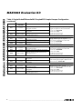
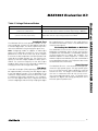
1) Verify that shunts are installed across pins 1 and 2
of jumpers JU1, JU2, JU3, and JU4 (single-ended
analog signals IA and QA converted to differential
input signals with transformers T1 and T2).
2) Verify that shunts are installed across pins 2 and 3
of jumpers JU5, JU6, JU7, and JU8 (differential
analog output signals converted to single-ended
signals ID and QD with operational-amplifier circuits
U3 and U4).
3) Verify that no shunts are installed across jumpers
JU9 and JU10.
4) Verify that a shunt is installed across jumper JU11
(internal reference).
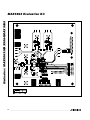
5) Connect the 25-pin I/O extension cable from the
computer’s parallel port to the MAX5865 EV kit
board DB25 right-angle male plug J4. The EV kit
software uses a loopback connection to confirm
that the correct port has been selected.
6) Install the evaluation software on your computer by
running the INSTALL.EXE program on the CD-ROM.
The program files are copied and icons are created
for them in the Start menu.
7) Connect the clock-function signal generator (HP
8662A) to the CLOCK SMA connectors on the
EV kit.
8) Connect the two function generators to SMA connectors IA and QA.
9) Synchronize the two function generators to the
clock function generator.
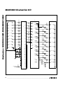
10) Connect the logic analyzer to the 2 x 10 square pin
header J1. The CLOCK signal is available on pin
J1-2 and bits DA0–DA7 are available on the even
pins J1-4 to J1-18. All other header J1 pins are connected to ground. The clock pin and data pins are
labeled CLK and DA0–DA7 on the EV board.
11) Verify that the logic analyzer is programmed for an
8-bit input at CMOS voltage levels.
12) Verify that the 10-bit digital pattern generator is programmed for valid CMOS output voltage levels.
13) Connect the digital pattern generator DG2020A output to the J3 input header connector on the EV kit
board. The input header pins are labeled for proper
connection with the digital pattern generator (i.e.,
connect bit 0 to the J3-19 header pin labeled DD0,
connect bit 1 to the J3-17 header pin labeled DD1,
etc. Input data pins are the odd pins of header J3.
All other pins are connected to ground).
14) Synchronize the digital pattern generator with the
clock function generator.
15) Connect a +3.0V power supply to the VDD pad.
Connect the ground terminal of this supply to the
GND pad.
16) Connect a +3.0V power supply to the VCLK pad.
Connect the ground terminal of this supply to the
GND pad.
17) Connect a +2.0V power supply to the OVDD pad.
Connect the ground terminal of this supply to the
OGND pad.
18) Connect a +2.0V power supply to the VDDRV pad.
Connect the ground terminal of this supply to the
OGND pad.
19) Connect the +5.0V terminal of the bipolar power
supply to the VCC pad. Connect the ground terminal of this supply to the GND pad.
_______________________________________________________________________________________
3
Evaluates: MAX5863/MAX5864/MAX5865
Quick Start