1
MAX5865 Evaluation Kit
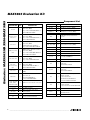
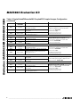
MODE
EV KIT
FUNCTION
COMMAND BYTE SENT TO
MAX5865
Shutdown
Device shutdown. REF is off, ADCs are off, the ADC bus is tri-stated,
and DACs are off. The DAC input bus must be set to zero or OVDD to
achieve the lowest shutdown-mode power consumption.
xxxx x000
Idle
REF is on, ADCs are off, the ADC bus is tri-stated, and DACs are off.
The DAC input bus must be set to zero or OVDD to achieve the
lowest Idle Mode™ power consumption.
xxxx x001
Receive (Rx)
REF is on, ADCs are on, and DACs are off. The DAC input bus must
be set to zero or OVDD to achieve the lowest Rx-mode power
consumption.
xxxx x010
Transmit (Tx)
Transceive (Xcvr)
Standby
REF is on, ADCs are off, the ADC bus is tri-stated, and DACs are on.
xxxx x011
REF is on, ADCs and DACs are on.
xxxx x100
REF is on, ADCs are off, the ADC bus is tri-stated, and DACs are off.
The DAC input bus must be set to zero or OVDD to achieve the
lowest standby-mode power consumption.
xxxx x101
x = Don’t care
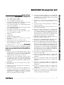
MAX5863 analog front end. The MAX5863/MAX5864/
MAX5865 integrate a 1.024V temperature-stable voltage
reference, a dual-input 8-bit parallel-output receive
ADC, and a 10-bit parallel-input dual-output transmit
DAC. The MAX5863/MAX5864/MAX5865 accept ACcoupled or DC-coupled, differential, or single-ended
analog inputs at the receive ADC. The digital output
produced by the ADC can be easily captured with a
high-speed logic analyzer or data-acquisition system.
The MAX5863/MAX5864/MAX5865 digital inputs at the
transmit DAC are designed for CMOS-compatible voltage levels. The DAC produces differential analog outputs with 1.4VDC common mode.
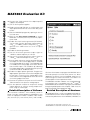
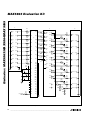
The EV kit comes with the MAX5865 installed, which
operates at speeds of up to 40Msps. The EV kit operates from a +3.0V analog power supply, +3.0V digital
power supply, and ±5V bipolar operational amplifier
power supply. For best dynamic performance, set the
digital power supply to +2V. The EV kit includes circuitry that generates a clock signal from an AC sine wave
provided by the user. Other features include: circuitry
to convert single-ended inputs to differential input analog signals and circuitry to convert the differential outputs of the DAC to single-ended analog signals. The
MAX5865 EV kit can be used to evaluate the 22Msps
MAX5864 or the 7.5Msps MAX5863 after replacing the
MAX5865.
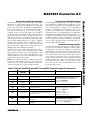
Power Supplies
The MAX5865 EV kit can operate from a single +3.0V
power supply connected to the VDD, OVDD, VCLK,
and VDDRV input power pads and their respective
ground pads for simple board operation. An additional
±5V bipolar power supply is needed at VCC and VEE
when the operational-amplifier differential to singleended output circuitry (U3 and U4) is used. See the
Transmit Dual DAC Outputs section for further details.
However, two +3.0V (VDD and VCLK) and two +2V
(OVDD and VDDRV) power supplies are recommended
for best dynamic performance. The EV kit PC board
ground layer is divided into two sections: digital
(OGND) and analog (GND). The EV kit PC board power
plane is divided into four sections: VDD (MAX5865 analog circuit), OVDD (MAX5865 output driver circuit),
VCLK (clock-shaping circuit U2), and VDDRV (digital
components U5 and U6). VDD, VCLK, VCC, and VEE
inputs are referenced to analog ground GND. OVDD
and VDDRV inputs are referenced to the OGND
ground. Using separate power supplies for each input
section reduces crosstalk noise and improves the integrity of the output signals. Another advantage of using separate power supplies is that the input power sources do
not have to be at the same voltage level for the EV kit circuit to operate normally. VDD has a +2.7V to +3.3V input
range, OVDD has a +1.8V to VDD input range, VCLK has
a +2.7V to +3.3V input range , and VDDRV has a +2.0V
to +3.3V input range.
Idle Mode is a trademark of Maxim Integrated Products, Inc.
_______________________________________________________________________________________
5
Evaluates: MAX5863/MAX5864/MAX5865
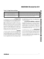
Table 1. Operational Modes