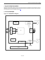
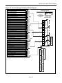
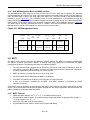
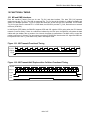
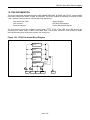
1
DS33Z41
Quad IMUX Ethernet Mapper
www.maxim-ic.com
GENERAL DESCRIPTION
FEATURES
The DS33Z41 extends a 10/100 Ethernet LAN
segment by encapsulating MAC frames in HDLC or
X.86 (LAPS) for transmission over up to four
interleaved PDH/TDM data streams using robust,
balanced, and programmable inverse multiplexing.
The Interleave Bus (IBO) serial link supports
seamless bidirectional interconnection with Dallas
Semiconductor’s T1/E1 framers and transceivers.
10/100 IEEE 802.3 Ethernet MAC (MII and
RMII) Half/Full Duplex with Automatic Flow
Control
Layer 1 Inverse Multiplexing Allows Bonding of
Up to 4 T1/E1/J1 or DSL Links
Supports Up to 7.75ms Differential Delay
Channel (Byte) Interleaved Bus Operation
The device performs store-and-forward of packets
with full wire-speed transport capability. The built-in
Committed Information Rate (CIR) Controller
provides fractional bandwidth allocation up to the
line rate in increments of 512kbps.
In-Band OAM and Signaling Capability
HDLC/LAPS Encapsulation with Programmable
FCS, Interframe Fill
Committed Information Rate Controller Provides
Fractional Allocation in 512kbps Increments
Programmable BERT for the Serial Interface
FUNCTIONAL DIAGRAM
External 16MB, 100MHz SDRAM Buffering
Parallel Microprocessor Interface
DS33Z41
Serial
Port
IBO
1.8V Operation with 3.3V Tolerant I/O
Up to 4
Transceivers
IEEE 1149.1 JTAG Support
or Framers
Features continued on page 8.
Config.
Loader
BERT
µC
HDLC/X.86
Mapper
SDRAM
10/100
MAC
MII/RMII
10/100
Ethernet
PHY
APPLICATIONS
Bonded Transparent LAN Service
LAN Extension
Ethernet Delivery Over T1/E1/J1, T3/E3, OC-1/EC-1,
G.SHDSL, or HDSL2/4
ORDERING INFORMATION
PART
TEMP RANGE
PIN-PACKAGE
DS33Z41
-40°C to +85°C
169 CSBGA
Note: Some revisions of this device may incorporate deviations from published specifications known as errata. Multiple revisions of any device
may be simultaneously available through various sales channels. For information about device errata, click here: www.maxim-ic.com/errata.
1 of 167
REV: 122006
DS33Z41 Quad IMUX Ethernet Mapper
TABLE OF CONTENTS
1
DESCRIPTION ....................................................................................................................7
2
FEATURE HIGHLIGHTS ....................................................................................................8
2.1
2.2
2.3
2.4
2.5
2.6
2.7
2.8
2.9
2.10
GENERAL ......................................................................................................................................8
LINK AGGREGATION (INVERSE MULTIPLEXING) ...............................................................................8
HDLC ...........................................................................................................................................8
COMMITTED INFORMATION RATE (CIR) CONTROLLER .....................................................................8
X.86 SUPPORT ..............................................................................................................................8
SDRAM INTERFACE ......................................................................................................................9
MAC INTERFACE ...........................................................................................................................9
MICROPROCESSOR INTERFACE ......................................................................................................9
TEST AND DIAGNOSTICS ................................................................................................................9
SPECIFICATIONS COMPLIANCE .....................................................................................................10
3
APPLICATIONS................................................................................................................11
4
ACRONYMS AND GLOSSARY........................................................................................12
5
MAJOR OPERATING MODES .........................................................................................13
6
BLOCK DIAGRAMS .........................................................................................................13
7
PIN DESCRIPTIONS.........................................................................................................14
7.1
8
PIN FUNCTIONAL DESCRIPTION ....................................................................................................14
FUNCTIONAL DESCRIPTION..........................................................................................22
8.1
PROCESSOR INTERFACE ..............................................................................................................23
8.1.1
8.1.2
8.1.3
8.2
CLOCK STRUCTURE .....................................................................................................................24
8.2.1
8.2.2
8.3
8.4
8.5
8.6
8.7
8.8
8.9
Read-Write/Data Strobe Modes..........................................................................................................23
Clear on Read.....................................................................................................................................23
Interrupt and Pin Modes......................................................................................................................23
Serial Interface Clock Modes..............................................................................................................26
Ethernet Interface Clock Modes .........................................................................................................26
RESETS AND LOW-POWER MODES ...............................................................................................27
INITIALIZATION AND CONFIGURATION ............................................................................................28
GLOBAL RESOURCES...................................................................................................................28
PER-PORT RESOURCES...............................................................................................................28
DEVICE INTERRUPTS....................................................................................................................29
SERIAL INTERFACE ......................................................................................................................31
LINK AGGREGATION (IMUX).........................................................................................................31
8.9.1
8.9.2
8.9.3
8.9.4
Microprocessor Requirements............................................................................................................33
IMUX Command Protocol ...................................................................................................................34
Out of Frame (OOF) Monitoring..........................................................................................................36
Data Transfer ......................................................................................................................................36
8.10 CONNECTIONS AND QUEUES ........................................................................................................37
8.11 ARBITER .....................................................................................................................................38
8.12 FLOW CONTROL ..........................................................................................................................39
8.12.1 Full-Duplex Flow Control.....................................................................................................................40
8.12.2 Half-Duplex Flow control.....................................................................................................................41
8.12.3 Host-Managed Flow control ................................................................................................................41
8.13 ETHERNET INTERFACE PORT .......................................................................................................42
8.13.1 DTE and DCE Mode ...........................................................................................................................43
2 of 167
DS33Z41 Quad IMUX Ethernet Mapper
8.14 ETHERNET MAC..........................................................................................................................46
8.14.1 MII Mode .............................................................................................................................................47
8.14.2 RMII Mode ..........................................................................................................................................47
8.14.3 PHY MII Management Block and MDIO Interface ..............................................................................48
8.15 BERT .........................................................................................................................................48
8.15.1
8.15.2
8.15.3
8.15.4
8.15.5
8.16
8.17
8.18
8.19
9
BERT Features ...................................................................................................................................48
Receive Data Interface .......................................................................................................................49
Repetitive Pattern Synchronization.....................................................................................................49
Pattern Monitoring...............................................................................................................................50
Pattern Generation..............................................................................................................................50
TRANSMIT PACKET PROCESSOR ..................................................................................................52
RECEIVE PACKET PROCESSOR ....................................................................................................53
X.86 ENCODING AND DECODING ..................................................................................................55
COMMITTED INFORMATION RATE CONTROLLER ............................................................................58
DEVICE REGISTERS .......................................................................................................60
9.1
REGISTER BIT MAPS ....................................................................................................................61
9.1.1
9.1.2
9.1.3
9.1.4
9.1.5
9.1.6
9.2
9.3
GLOBAL REGISTER DEFINITIONS ..................................................................................................68
ARBITER REGISTERS ...................................................................................................................81
9.3.1
9.4
9.5
Arbiter Register Bit Descriptions.........................................................................................................81
BERT REGISTERS .......................................................................................................................82
SERIAL INTERFACE REGISTERS ....................................................................................................89
9.5.1
9.5.2
9.5.3
9.5.4
9.5.5
9.6
Global Register Bit Map ......................................................................................................................61
Arbiter Register Bit Map......................................................................................................................62
BERT Register Bit Map.......................................................................................................................62
Serial Interface Register Bit Map ........................................................................................................63
Ethernet Interface Register Bit Map....................................................................................................65
MAC Register Bit Map ........................................................................................................................66
Serial Interface Transmit and Common Registers..............................................................................89
Serial Interface Transmit Register Bit Descriptions ............................................................................89
Transmit HDLC Processor Registers..................................................................................................90
X.86 Registers ....................................................................................................................................97
Receive Serial Interface......................................................................................................................99
ETHERNET INTERFACE REGISTERS.............................................................................................112
9.6.1
9.6.2
Ethernet Interface Register Bit Descriptions.....................................................................................112
MAC Registers..................................................................................................................................124
10 FUNCTIONAL TIMING....................................................................................................140
10.1 MII AND RMII INTERFACES ........................................................................................................140
11 OPERATING PARAMETERS .........................................................................................142
11.1
11.2
11.3
11.4
11.5
11.6
11.7
11.8
11.9
THERMAL CHARACTERISTICS .....................................................................................................143
MII INTERFACE ..........................................................................................................................144
RMII INTERFACE .......................................................................................................................146
MDIO INTERFACE .....................................................................................................................148
TRANSMIT WAN INTERFACE ......................................................................................................149
RECEIVE WAN INTERFACE ........................................................................................................150
SDRAM TIMING ........................................................................................................................151
MICROPROCESSOR BUS AC CHARACTERISTICS .........................................................................155
JTAG INTERFACE TIMING ..........................................................................................................158
12 JTAG INFORMATION.....................................................................................................159
12.1 JTAG TAP CONTROLLER STATE MACHINE DESCRIPTION ...........................................................160
12.2 INSTRUCTION REGISTER ............................................................................................................162
12.2.1 SAMPLE:PRELOAD .........................................................................................................................163
3 of 167
DS33Z41 Quad IMUX Ethernet Mapper
12.2.2
12.2.3
12.2.4
12.2.5
12.2.6
BYPASS............................................................................................................................................163
EXTEST ............................................................................................................................................163
CLAMP..............................................................................................................................................163
HIGHZ ...............................................................................................................................................163
IDCODE ............................................................................................................................................163
12.3 JTAG ID CODES .......................................................................................................................164
12.4 TEST REGISTERS ......................................................................................................................164
12.4.1 Boundary Scan Register ...................................................................................................................164
12.4.2 Bypass Register................................................................................................................................164
12.4.3 Identification Register .......................................................................................................................164
12.5 JTAG FUNCTIONAL TIMING ........................................................................................................165
13 PACKAGE INFORMATION ............................................................................................166
13.1 169-BALL CSBGA, 14MM X 14MM (56-G6035-001)...................................................................166
14 DOCUMENT REVISION HISTORY.................................................................................167
4 of 167
DS33Z41 Quad IMUX Ethernet Mapper
LIST OF FIGURES
Figure 3-1. Quad T1/E1 SCT to DS33Z41 .............................................................................................................. 11
Figure 6-1. Detailed Block Diagram......................................................................................................................... 13
Figure 7-1. DS33Z41 256-Ball CSBGA Pinout........................................................................................................ 21
Figure 8-1. Clocking for the DS33Z41 ..................................................................................................................... 25
Figure 8-2. Device Interrupt Information Flow Diagram .......................................................................................... 30
Figure 8-3. IMUX Interface to T1/E1 Transceivers.................................................................................................. 32
Figure 8-4. Diagram of Data Transmission with IMUX Operation ........................................................................... 32
Figure 8-5. Command Structure for IMUX Function................................................................................................ 34
Figure 8-6. Flow Control Using Pause Control Frame ............................................................................................ 41
Figure 8-7. IEEE 802.3 Ethernet Frame .................................................................................................................. 42
Figure 8-8. Configured as DTE Connected to an Ethernet PHY in MII Mode ......................................................... 44
Figure 8-9. DS33Z41 Configured as a DCE in MII Mode ........................................................................................ 45
Figure 8-10. RMII Interface...................................................................................................................................... 47
Figure 8-11. MII Management Frame...................................................................................................................... 48
Figure 8-12. PRBS Synchronization State Diagram................................................................................................ 49
Figure 8-13. Repetitive Pattern Synchronization State Diagram............................................................................. 50
Figure 8-14. LAPS Encoding of MAC Frames Concept .......................................................................................... 55
Figure 8-15. X.86 Encapsulation of the MAC field .................................................................................................. 56
Figure 8-16. CIR in the WAN Transmit Path ........................................................................................................... 59
Figure 10-1. MII Transmit Functional Timing......................................................................................................... 140
Figure 10-2. MII Transmit Half Duplex with a Collision Functional Timing............................................................ 140
Figure 10-3. MII Receive Functional Timing.......................................................................................................... 141
Figure 10-4. RMII Transmit Interface Functional Timing ....................................................................................... 141
Figure 10-5 RMII Receive Interface Functional Timing ......................................................................................... 141
Figure 11-1. Transmit MII Interface ....................................................................................................................... 144
Figure 11-2. Receive MII Interface Timing ............................................................................................................ 145
Figure 11-3. Transmit RMII Interface..................................................................................................................... 146
Figure 11-4. Receive RMII Interface Timing.......................................................................................................... 147
Figure 11-5. MDIO Timing ..................................................................................................................................... 148
Figure 11-6. Transmit WAN Timing ....................................................................................................................... 149
Figure 11-7. Receive WAN Timing ........................................................................................................................ 150
Figure 11-8. SDRAM Interface Timing .................................................................................................................. 152
Figure 11-9. Receive IBO Channel Interleave Mode Timing................................................................................. 153
Figure 11-10. Transmit IBO Channel Interleave Mode Timing.............................................................................. 154
Figure 11-11. Intel Bus Read Timing (MODEC = 00)............................................................................................ 156
Figure 11-12. Intel Bus Write Timing (MODEC = 00) ............................................................................................ 156
Figure 11-13. Motorola Bus Read Timing (MODEC = 01) .................................................................................... 157
Figure 11-14. Motorola Bus Write Timing (MODEC = 01)..................................................................................... 157
Figure 11-15. JTAG Interface Timing Diagram ..................................................................................................... 158
Figure 12-1. JTAG Functional Block Diagram....................................................................................................... 159
Figure 12-2. TAP Controller State Diagram .......................................................................................................... 162
Figure 12-3. JTAG Functional Timing.................................................................................................................... 165
5 of 167
DS33Z41 Quad IMUX Ethernet Mapper
LIST OF TABLES
Table 2-1. T1 Related Telecommunications Specifications .................................................................................... 10
Table 7-1. Detailed Pin Descriptions ....................................................................................................................... 14
Table 8-1. Clock Selection for the Ethernet (LAN) Interface ................................................................................... 24
Table 8-2. Reset Functions ..................................................................................................................................... 27
Table 8-3. Commands Sent and Received on the IMUX Links............................................................................... 34
Table 8-4. Command and Status for the IMUX for Processor Communication....................................................... 35
Table 8-5. Registers Related to Connections and Queues ..................................................................................... 38
Table 8-6. Options for Flow Control......................................................................................................................... 39
Table 8-7. Registers Related to the Ethernet Port .................................................................................................. 43
Table 8-8. MAC Control Registers........................................................................................................................... 46
Table 8-9. MAC Status Registers ............................................................................................................................ 46
Table 9-1. Register Address Map............................................................................................................................ 60
Table 9-2. Global Register Bit Map ......................................................................................................................... 61
Table 9-3. Arbiter Register Bit Map ......................................................................................................................... 62
Table 9-4. BERT Register Bit Map .......................................................................................................................... 62
Table 9-5. Serial Interface Register Bit Map ........................................................................................................... 63
Table 9-6. Ethernet Interface Register Bit Map ....................................................................................................... 65
Table 9-7. MAC Indirect Register Bit Map ............................................................................................................... 66
Table 11-1. Recommended DC Operating Conditions.......................................................................................... 142
Table 11-2. DC Electrical Characteristics.............................................................................................................. 142
Table 11-3. Thermal Characteristics ..................................................................................................................... 143
Table 11-4. Theta-JA vs. Airflow ........................................................................................................................... 143
Table 11-5. Transmit MII Interface ........................................................................................................................ 144
Table 11-6. Receive MII Interface ......................................................................................................................... 145
Table 11-7. Transmit RMII Interface...................................................................................................................... 146
Table 11-8. Receive RMII Interface....................................................................................................................... 147
Table 11-9. MDIO Interface ................................................................................................................................... 148
Table 11-10. Transmit WAN Interface ................................................................................................................... 149
Table 11-11. Receive WAN Interface .................................................................................................................... 150
Table 11-12. SDRAM Interface Timing.................................................................................................................. 151
Table 11-13. AC Characteristics—Microprocessor Bus Timing ............................................................................ 155
Table 11-14. JTAG Interface Timing ..................................................................................................................... 158
Table 12-1. Instruction Codes for IEEE 1149.1 Architecture ................................................................................ 163
Table 12-2. ID Code Structure............................................................................................................................... 164
6 of 167
DS33Z41 Quad IMUX Ethernet Mapper
1 DESCRIPTION
The DS33Z41 provides interconnection and mapping functionality between Ethernet Packet Systems and WAN
Time-Division Multiplexed (TDM) systems such as T1/E1/J1, HDSL, and T3/E3. The device is composed of a
10/100 Ethernet MAC, Packet Arbiter, Committed Information Rate controller (CIR), HDLC/X.86 (LAPS) Mapper,
SDRAM interface, control ports, and Bit Error Rate Tester (BERT). The packet interface consists of an Ethernet
interface using several physical layer protocols. The Ethernet interface can be configured for 10Mbps or 100Mbps
service. The DS33Z41 encapsulates Ethernet traffic with HDLC or X.86 (LAPS) to be transmitted over the WAN
interface. The WAN interface also receives encapsulated Ethernet packets and transmits the extracted packets
over the Ethernet port. The WAN physical interface is based on the Dallas Semiconductor Interleaved Bus
Operation (IBO), running at 8.192Mbps. The IBO interface can be configured to allow up to four bonded T1 or E1
data streams. The IBO interface provides for seamless connection to the Dallas Semiconductor/Maxim multi-port
T1/E1/J1 Framers and Single-Chip Transceivers (SCTs). See Application Note 3411: DS33Z11—Ethernet LAN to
Unframed T1/E1 WAN Bridge for an example of a complete LAN to WAN solution.
The DS33Z41 is controlled through an 8-bit microcontroller port. The DS33Z41 has a 100MHz SDRAM controller
and interfaces to a 32-bit wide 128Mb SDRAM. The SDRAM is used to buffer the data from the Ethernet and
WAN ports for transport. The external SDRAM can accommodate up to 8192 frames with a maximum frame size
of 2016 bytes. The DS33Z41 operates with a 1.8V core supply and 3.3V I/O supply.
7 of 167
DS33Z41 Quad IMUX Ethernet Mapper
2
2.1
FEATURE HIGHLIGHTS
General
•
•
•
•
•
2.2
Link Aggregation (Inverse Multiplexing)
•
•
•
•
2.3
HDLC controller engine
Compatible with polled or interrupt driven environments
Programmable FCS insertion and extraction
Programmable FCS type
Supports FCS error insertion
Programmable packet size limits (Minimum 64 bytes and maximum 2016 bytes)
Supports bit stuffing/destuffing
Selectable packet scrambling/descrambling (X43+1)
Separate FCS errored packet and aborted packet counts
Programmable inter-frame fill for transmit HDLC
Committed Information Rate (CIR) Controller
•
•
•
2.5
Link aggregation for up to 4 T1/E1 Links
8.192Mbps IBO interface to Dallas Semiconductor Framers/Transceivers
Differential delay compensation up to 7.75ms for the 4 T1/E1 links
Handshaking protocol between local and distant end for establishment of aggregation
HDLC
•
•
•
•
•
•
•
•
•
•
2.4
169-pin, 14mm x 14mm CSBGA package
1.8V supply with 3.3V tolerant inputs and outputs
IEEE 1149.1 JTAG boundary scan
Software access to device ID and silicon revision
Development support includes evaluation kit, driver source code, and reference designs
CIR controller limits transmission of data from the Ethernet Interface to the Serial Interface.
CIR granularity at 512kbps
CIR Averaging for smoothing traffic peaks
X.86 Support
•
•
•
•
•
•
•
•
•
•
•
Programmable X.86 address/control fields for transmit and receive
Programmable 2-byte protocol (SAPI) field for transmit and receive
32 bit FCS
Transmit Transparency processing - 7E is replaced by 7D, 5E
Transmit Transparency processing – 7D replaced by 7D, 5D
Receive rate adaptation (7D, DD) is deleted.
Receive Transparency processing - 7D, 5E is replaced by 7E
Receive Transparency processing – 7D, 5D is replaced by 7D
Receive Abort Sequence the LAPS packet is dropped if 7D7E is detect
Self-synchronizing X43+1 payload scrambling.
Frame indication due to bad Address/Control/SAPI, FCS error, abort sequence or frame size longer
than preset max.
8 of 167
DS33Z41 Quad IMUX Ethernet Mapper
2.6
SDRAM Interface
•
•
•
•
•
•
2.7
MAC Interface
•
•
•
•
•
•
•
•
•
•
•
2.8
MAC port with standard MII (less TX_ER) or RMII
10Mbps and 100Mbps Data rates
Configurable DTE or DCE modes
Facilitates auto-negotiation by host microprocessor
Programmable half and full-duplex modes
Flow control for both half-duplex (back-pressure) and full-duplex (PAUSE) modes
Programmable Maximum MAC frame size up to 2016 bytes
Minimum MAC frame size: 64 bytes
Discards frames greater than Programmed Maximum MAC frame size and Runt, non-octet bounded,
or bad-FCS frames upon reception
Programmable threshold for SDRAM queues to initiate flow control and status indication
MAC Loopback support for Transmit data looped to Receive Data at the MII/RMII interface
Microprocessor Interface
•
•
•
•
2.9
Interface for 128Mb, 32-bit-wide SDRAM
SDRAM Interface speed up to 100MHz
Auto Refresh Timing
Automatic Precharge
Master clock provided to the SDRAM
No external components required for SDRAM connectivity
8 bit data bus
Non-multiplexed Intel and Motorola Timing Modes
Internal software reset and External Hardware reset input pin
Global interrupt output pin
Test and Diagnostics
•
•
•
•
IEEE 1149.1 Support
Programmable on-chip Bit Error Rate Tester (BERT)
Patterns include Pseudorandom QRSS, Daly, and user-defined repetitive patterns
Loopbacks (remote, local, analog, and per-channel loopback)
9 of 167
DS33Z41 Quad IMUX Ethernet Mapper
2.10 Specifications compliance
The DS33Z41 meets relevant telecommunications specifications. The following table provides the specifications
and relevant sections that are applicable to the DS33Z41.
Table 2-1. T1 Related Telecommunications Specifications
IEEE 802.3-2002—CSMA/CD access method and physical layer specifications
RFC1662—PPP in HDLC-like Framing
RFC2615—PPP over SONET/SDH
X.86—Ethernet over LAPS
RMII—Industry Implementation Agreement for “Reduced MII Interface” (Sept. 1997)
10 of 167
DS33Z41 Quad IMUX Ethernet Mapper
3 APPLICATIONS
•
•
•
Bonded Transparent LAN Service
LAN Extension
Ethernet Delivery Over T1/E1/J1, T3/E3, OC-1/EC-1, G.SHDSL, or HDSL2/4
Refer also to Application Note 3411: DS33Z11—Ethernet LAN to Unframed T1/E1 WAN Bridge for an example of
a complete LAN to WAN design.
Figure 3-1. Quad T1/E1 SCT to DS33Z41
T1/E1
Framer/LIU
DS21455
DS21458
DS26528
HDLC/X.86
Serial
Stream
(IBO)
RMII, MII
10 Base T
100 Base T
DS33Z41
Ethernet
Clock
Sources
SDRAM
11 of 167
DS33Z41 Quad IMUX Ethernet Mapper
4 ACRONYMS AND GLOSSARY
•
•
•
•
•
•
•
•
•
BERT—Bit Error Rate Tester
DCE—Data Communication Interface
DTE—Data Terminating Interface
FCS—Frame Check Sequence
HDLC—High Level Data Link Control
MAC—Media Access Control
MII—Media Independent Interface
RMII—Reduced Media Independent Interface
WAN—Wide Area Network
Note 1: Previous versions of this document used the term “Subscriber” to refer to the Ethernet Interface function.
The register names have been allowed to remain with a “SU.” prefix to avoid register renaming.
Note 2: Previous versions of this document used the term “Line” to refer to the Serial Interface. The register
names have been allowed to remain with a “LI.” prefix to avoid register renaming.
Note 3: The terms “Transmit Queue” and “Receive Queue” are with respect to the Ethernet Interface. The
Receive Queue is the queue for the data that arrives on the MII/RMII interface, is processed by the MAC and
stored in the SDRAM. Transmit queue is for data that arrives from the Serial port, is processed by the HDLC and
stored in the SDRAM to be sent to the MAC transmitter.
Note 4: This data sheet assumes a particular nomenclature of the T1 and E1 operating environment. In each
125µs T1 frame, there are 24 8-bit channels plus a framing bit. It is assumed that the framing bit is sent first
followed by channel 1.
TIME SLOT NUMBERING SCHEMES
Time Slot 0 1 2 3 4 5 6 7 8 9 10 11 12 13 14 15 16 17 18 19 20 21 22 23 24 25 26 27 28 29 30 31
Channel 1 2 3 4 5 6 7 8 9 10 11 12 13 14 15 16 17 18 19 20 21 22 23 24 25 26 27 28 29 30 31 32
Phone
1 2 3 4 5 6 7 8 9 10 11 12 13 14 15
16 17 18 19 20 21 22 23 24 25 26 27 28 29 30
Channel
12 of 167
DS33Z41 Quad IMUX Ethernet Mapper
5 MAJOR OPERATING MODES
Operation of the DS33Z41 operation requires a host microprocessor for initialization and maintenance of the link
aggregation functions. Microprocessor control is possible through the 8-bit parallel control port. More information
on microprocessor control is available in Section 8.1.
6 BLOCK DIAGRAMS
Figure 6-1. Detailed Block Diagram
50 or 25 Mhz Oscillator
Buffer
Div by 1,2,4,8,10
Output clocks:
50,25 Mhz,2.5 Mhz
Microport
REF_CLK
TSER
TCLKI1
Line 1
RCLKI1
RSER
IMUX
HDLC
+
Serial
Interface
TX_CLK1
MAC
RMII
MII
CIR
Arbiter
RXD
RX_CLK1
TXD
X.86
MDC
100 Mhz Oscillator
JTAG
Buffer Dev
Div by 2,4,12
Output Clocks
25,50
Mhz
SDRAM
Interface
SDCLKO
REF_CLKO
50 or 25 Mhz
SDRAM
13 of 167
SYSCLKI
DS33Z41 Quad IMUX Ethernet Mapper
7 PIN DESCRIPTIONS
7.1
Pin Functional Description
Note that all digital pins are inout pins in JTAG mode. This feature increases the effectiveness of board level
ATPG patterns.
Table 7-1. Detailed Pin Descriptions
Note: I = Input; O = Output; Ipu = Input with pullup; Oz = Output with tri-state; IO = Bidirectional pin; IOz = Bidirectional pin with tri-state.
NAME
PIN
TYPE
TCLKI
F1
I
TSER
F2
O
TSYNC
G3
I
RCLKI
G2
I
RSER
H1
I
RSYNC
G1
I
REF_CLK
D13
I
REF_CLKO
E13
O
FUNCTION
SERIAL INTERFACE IO PINS
Serial Interface Transmit Clock Input. The clock reference for TSER,
which is output on the rising edge of the clock. TCLKI supports gapped
clocking, up to a maximum frequency of 52MHz.
Transmit Serial Data Output. Output on the rising edge of TCLKI.
Selective clock periods can be skipped for output of TSER with a
gapped clock input on TCLKI. The maximum data rate is 52Mbps.
Transmit Synchronization Input. An 8lHz synchronization pulse, used
to denote the first Channel 1 of the 8.192Mbps byte-interleaved IBO
data stream. Note that this input is also used to generate the transmit
byte synchronization if X.86 mode is enabled.
Serial Interface Receive Clock Input. Reference clock for receive
serial data on RSER. Gapped clocking is supported, up to the
maximum RCLKI frequency of 52MHz.
Receive Serial Data Input. Receive Serial data arrives on the rising
edge of the clock.
Receive Synchronization Input. An 8kHz synchronization pulse, used
to denote the first Channel 1 of the 8.192Mbps byte-interleaved IBO
data stream. Note that this input is also used to generate the receive
byte synchronization if X.86 mode is enabled.
MII/RMII PORT
Reference Clock (RMII and MII). When in RMII mode, all signals from
the PHY are synchronous to this clock input for both transmit and
receive. This required clock can be up to 50MHz and should have
±100ppm accuracy.
When in MII mode in DCE operation, the DS33Z41 uses this input to
generate the RX_CLK and TX_CLK outputs as required for the
Ethernet PHY interface. When the MII interface is used with DTE
operation, this clock is not required and should be tied low.
In DCE and RMII modes, this input must have a stable clock input
before setting the RST pin high for normal operation.
Reference Clock Output (RMII and MII). A derived clock output up to
50MHz, generated by internal division of the SYSCLKI signal.
Frequency accuracy of the REF_CLKO signal will be proportional to the
accuracy of the user-supplied SYSCLKI signal. See Section 8.2.2 for
more information.
14 of 167
DS33Z41 Quad IMUX Ethernet Mapper
NAME
PIN
TYPE
FUNCTION
Transmit Clock (MII). Timing reference for TX_EN and TXD[3:0]. The
TX_CLK frequency is 25MHz for 100Mbps operation and 2.5MHz for
10Mbps operation.
TX_CLK
TX_EN
A8
E10
IO
O
TXD[0]
TXD[1]
TXD[2]
TXD[3]
B9
C9
D9
E9
O
RX_CLK
A10
IO
RXD[0]
RXD[1]
RXD[2]
RXD[3]
B11
C11
D11
A11
I
RX_DV
D10
I
RX_CRS/
CRS_DV
C8
I
RX_ERR
B12
In DTE mode, this is a clock input provided by the PHY. In DCE mode,
this is an output derived from REF_CLK providing 2.5MHz (10Mbps
operation) or 25MHz (100Mbps operation).
Transmit Enable (MII):
This pin is asserted high when data TXD [3:0] is being provided by the
DS33Z41. The signal is deasserted prior to the first nibble of the next
frame. This signal is synchronous with the rising edge TX_CLK. It is
asserted with the first bit of the preamble.
Transmit Enable (RMII):
When this signal is asserted, the data on TXD [1:0] is valid. This signal
is synchronous to the REF_CLK.
Transmit Data 0 through 3(MII). TXD [3:0] is presented synchronously
with the rising edge of TX_CLK. TXD [0] is the least significant bit of the
data. When TX_EN is low the data on TXD should be ignored.
Transmit Data 0 through 1(RMII). Two bits of data TXD [1:0]
presented synchronously with the rising edge of REF_CLK.
Receive Clock (MII). Timing reference for RX_DV, RX_ERR and
RXD[3:0], which are clocked on the rising edge. RX_CLK frequency is
25MHz for 100Mbps operation and 2.5MHz for 10Mbps operation. In
DTE mode, this is a clock input provided by the PHY. In DCE mode,
this is an output derived from REF_CLK providing 2.5MHz (10Mbps
operation) or 25MHz (100Mbps operation).
Receive Data 0 through 3(MII). Four bits of received data, sampled
synchronously with the rising edge of RX_CLK. For every clock cycle,
the PHY transfers 4 bits to the DS33Z41. RXD[0] is the least significant
bit of the data. Data is not considered valid when RX_DV is low.
Receive Data 0 through 1(RMII). Two bits of received data, sampled
synchronously with REF_CLK with 100Mbps mode. Accepted when
CRS_DV is asserted. When configured for 10Mbps mode, the data is
sampled once every 10 clock periods.
I
Receive Data Valid (MII). This active high signal indicates valid data
from the PHY. The data RXD is ignored if RX_DV is not asserted high.
Receive Carrier Sense (MII). Should be asserted (high) when data
from the PHY (RXD[3:0) is valid. For each clock pulse 4 bits arrive from
the PHY. Bit 0 is the least significant bit. In DCE mode, connect to VDD.
Carrier Sense/Receive Data Valid (RMII). This signal is asserted
(high) when data is valid from the PHY. For each clock pulse 2 bits
arrive from the PHY. In DCE mode, this signal must be grounded.
Receive Error (MII). Asserted by the MAC PHY for one or more
RX_CLK periods indicating that an error has occurred. Active High
indicates Receive code group is invalid. If CRS_DV is low, RX_ERR
has no effect. This is synchronous with RX_CLK. In DCE mode, this
signal must be grounded.
Receive Error (RMII). Signal is synchronous to REF_CLK.
15 of 167
DS33Z41 Quad IMUX Ethernet Mapper
NAME
PIN
TYPE
FUNCTION
Collision Detect (MII). Asserted by the MAC PHY to indicate that a
collision is occurring. In DCE Mode this signal should be connected to
ground. This signal is only valid in half duplex mode, and is ignored in
full duplex mode
Management Data Clock (MII). Clocks management data between the
PHY and DS33Z41. The clock is derived from SYSCLKI, with a
maximum frequency is 1.67MHz. The user must leave this pin
unconnected in the DCE Mode.
MII Management data IO (MII). Data path for control information
between the PHY and DS33Z41. When not used, pull to logic high
externally through a 10kΩ resistor. The MDC and MDIO pins are used
to write or read up to 32 Control and Status Registers in 32 PHY
Controllers. This port can also be used to initiate Auto-Negotiation for
the PHY. The user must leave this pin unconnected in the DCE Mode.
MICROPROCESSOR PORT
COL_DET
B13
I
MDC
C12
O
MDIO
C13
IO
A0
A1
I
Address Bit 0. Address bit 0 of the microprocessor interface. Least
Significant Bit.
A1
B1
I
Address Bit 1. Address bit 1 of the microprocessor interface.
A2
A2
I
Address Bit 2. Address bit 2 of the microprocessor interface.
A3
B2
I
Address Bit 3. Address bit 3 of the microprocessor interface.
A4
C2
I
Address Bit 4. Address bit 4 of the microprocessor interface.
A5
A3
I
Address Bit 5. Address bit 5 of the microprocessor interface.
A6
B3
I
Address Bit 6. Address bit 6 of the microprocessor interface.
A7
C3
I
Address Bit 7. Address bit 7 of the microprocessor interface.
A8
A4
I
Address Bit 8. Address bit 8 of the microprocessor interface.
A9
B4
I
D0
A5
IOZ
D1
A6
IOZ
D2
A7
IOZ
D3
B5
IOZ
D4
B6
IOZ
D5
B7
IOZ
D6
C5
IOZ
D7
C6
IOZ
CS
C1
I
Address Bit 9. Address bit 9 of the microprocessor interface. Most
Significant Bit.
Data Bit 0. Bidirectional data bit 0 of the microprocessor interface.
Least Significant Bit. Not driven when CS = 1 or RST = 0.
Data Bit 1. Bidirectional data bit 1 of the microprocessor interface. Not
driven when CS = 1 or RST = 0.
Data Bit 2. Bidirectional data bit 2 of the microprocessor interface. Not
driven when CS = 1 or RST = 0.
Data Bit 3. Bidirectional data bit 3 of the microprocessor interface. Not
driven when CS = 1 or RST = 0.
Data Bit 4. Bidirectional data bit 4 of the microprocessor interface. Not
driven when CS = 1 or RST = 0.
Data Bit 5. Bidirectional data bit 5 of the microprocessor interface. Not
driven when CS = 1 or RST = 0.
Data Bit 6. Bidirectional data bit 6 of the microprocessor interface. Not
driven when CS = 1 or RST = 0.
Data Bit 7. Bidirectional data bit 7 of the microprocessor interface. Most
Significant Bit. Not driven when CS = 1 or RST = 0.
Chip Select. This pin must be taken low for read/write operations.
When CS is high, the RD/DS and WR signals are ignored.
16 of 167
DS33Z41 Quad IMUX Ethernet Mapper
NAME
RD/DS
WR/RW
PIN
TYPE
FUNCTION
Read Data Strobe (Intel Mode). The DS33Z41 drives the data bus
(D0-D7) with the contents of the addressed register while RD and CS
are both low.
E1
I
Data Strobe (Motorola Mode). Used to latch data through the
microprocessor interface. DS must be low during read and write
operations.
Write (Intel Mode). The DS33Z41 captures the contents of the data
bus (D0:D7) on the rising edge of WR and writes them to the addressed
register location. CS must be held low during write operations.
E2
I
INT
F3
OZ
RST
D8
I
MODEC[0]
MODEC[1]
D6
D7
I
DCEDTES
A13
I
RMIIMIIS
C4
I
Read Write (Motorola Mode). Used to indicate read or write
operation. RW must be set high for a register read cycle and low for a
register write cycle.
Interrupt Output. Outputs a logic zero when an unmasked interrupt
event is detected. Outputs a logic zero when an unmasked interrupt
event is detected. INT is deasserted when all interrupts have been
acknowledged and serviced. Active low. Inactive state is programmable
in register GL.CR1. is deasserted when all interrupts have been
acknowledged and serviced. Active low. Inactive state is programmable
in register GL.CR1.
Reset. An active-low signal on this pin resets the internal registers and
logic. This pin should remain low until power, SYSCLKI, RX_CLK, and
TX_CLK are stable, then set high for normal operation. This input
requires a clean edge with a rise time of 25ns or less to properly reset
the device.
Mode Control
00 = Read/Write Strobe Used (Intel Mode)
01 = Data Strobe Used (Motorola Mode)
10 = Reserved. Do not use.
11 = Reserved. Do not use.
DCE or DTE Selection. The user must set this pin high for DCE Mode
selection or low for DTE Mode. In DCE Mode, the DS33Z41 MAC port
can be directly connected to another MAC. In DCE Mode, the Transmit
clock (TX_CLK) and Receive clock (RX_CLK) are output by the
DS33Z41. Note that there is no software bit selection of DCEDTES.
Note that DCE Mode is only relevant when the MAC interface is in MII
mode.
RMII or MII Selection. Set high to configure the MAC for RMII
interfacing. Set low for MII interfacing.
17 of 167
DS33Z41 Quad IMUX Ethernet Mapper
NAME
PIN
TYPE
FUNCTION
SDRAM CONTROLLER
SDATA[0]
SDATA[1]
SDATA[2]
SDATA[3]
SDATA[4]
SDATA[5]
SDATA[6]
SDATA[7]
SDATA[8]
SDATA[9]
SDATA[10]
SDATA[11]
SDATA[12]
SDATA[13]
SDATA[14]
SDATA[15]
SDATA[16]
SDATA[17]
SDATA[18]
SDATA[19]
SDATA[20]
SDATA[21]
SDATA[22]
SDATA[23]
SDATA[24]
SDATA[25]
SDATA[26]
SDATA[27]
SDATA[28]
SDATA[29]
SDATA[30]
SDATA[31]
SDA[0]
SDA[1]
SDA[2]
SDA[3]
SDA[4]
SDA[5]
SDA[6]
SDA[7]
SDA[8]
SDA[9]
SDA[10]
SDA[11]
M1
L2
N1
M2
N2
N4
N3
L4
J3
M3
H3
J1
J2
K1
K2
L1
M12
H11
M11
N13
N11
L13
N12
K13
J13
J12
H13
H12
G12
F11
G11
L10
N9
N10
L11
K11
L7
L8
L9
L5
M5
M7
M8
N8
IOZ
SDRAM Data Bus Bits 0 to 31: The 32 pins of the SDRAM data bus
are inputs for read operations and outputs for write operations. At all
other times, these pins are high impedance.
Note: All SDRAM operations are controlled entirely by the DS33Z41.
No user programming for SDRAM buffering is required.
O
SDRAM Address Bus 0 to 11. The 12 pins of the SDRAM address bus
output the row address first, followed by the column address. The row
address is determined by SDA0 to SDA11 at the rising edge of clock.
Column address is determined by SDA0-SDA9 and SDA11 at the rising
edge of the clock. SDA10 is used as an auto-precharge signal.
Note: All SDRAM operations are controlled entirely by the DS33Z41.
No user programming for SDRAM buffering is required.
SDRAM Bank Select. These 2 bits select 1 of 4 banks for the
read/write/precharge operations.
SBA[0]
SBA[1]
M6
N7
I
SRAS
K6
O
Note: All SDRAM operations are controlled entirely by the DS33Z41.
No user programming for SDRAM buffering is required.
SDRAM Row Address Strobe. Active-low output, used to latch the row
address on rising edge of SDCLKO. It is used with commands for Bank
Activate, Precharge, and Mode Register Write.
18 of 167
DS33Z41 Quad IMUX Ethernet Mapper
NAME
PIN
TYPE
SCAS
H4
O
SWE
M4
O
SDMASK[0]
SDMASK[1]
SDMASK[2]
SDMASK[3]
N6
G4
M10
M9
O
SDCLKO
N5
O
(4mA)
SYSCLKI
G13
I
SDCS
L6
O
QOVF
C7
O
FUNCTION
SDRAM Column Address Strobe. Active-low output, used to latch the
column address on the rising edge of SDCLKO. It is used with
commands for Bank Activate, Precharge, and Mode Register Write.
SDRAM Write Enable. This active-low output enables write operation
and auto precharge.
SDRAM Mask 0 to 3. When high, a write is done for that byte. The
least significant byte is SDATA7 to SDATA0. The most significant byte
is SDATA31 to SDATA24.
SDRAM CLK Out. System clock output to the SDRAM. This clock is a
buffered version of SYSCLKI.
System Clock In. 100MHz System Clock input to the DS33Z41, used
for internal operation. This clock is buffered and provided at SDCLKO
for the SDRAM interface. The DS33Z41 also provides a divided version
output at the REF_CLKO pin. A clock supply with ±100ppm frequency
accuracy is suggested.
SDRAM Chip Select. Active-low output enables SDRAM access.
QUEUE STATUS
Queue Overflow. This pin goes high when the transmit or receive
queue has overflowed. This pin will go low when the high watermark is
reached again.
JTAG INTERFACE
JTRST
E6
Ipu
JTCLK
D4
Ipu
JTDO
E5
Oz
JTDI
E4
Ipu
JTMS
F7
Ipu
JTAG Reset. JTRST is used to asynchronously reset the test access
port controller. After power-up, a rising edge on JTRST will reset the
test port and cause the device I/O to enter the JTAG DEVICE ID mode.
Pulling JTRST low restores normal device operation. JTRST is pulled
HIGH internally via a 10kΩ resistor operation. If boundary scan is not
used, this pin should be held low.
JTAG Clock. This signal is used to shift data into JTDI on the rising
edge and out of JTDO on the falling edge.
JTAG Data Out. Test instructions and data are clocked out of this pin
on the falling edge of JTCLK. If not used, this pin should be left
unconnected.
JTAG Data In. Test instructions and data are clocked into this pin on
the rising edge of JTCLK. This pin has a 10kΩ pullup resistor.
JTAG Mode Select. This pin is sampled on the rising edge of JTCLK
and is used to place the test access port into the various defined IEEE
1149.1 states. This pin has a 10kΩ pullup resistor.
19 of 167
DS33Z41 Quad IMUX Ethernet Mapper
NAME
PIN
TYPE
FUNCTION
POWER SUPPLIES
VDD3.3
VDD1.8
VSS
N.C.
G5–G10,
H2, H5,
H6,
H7–H10
D3, D2,
E3, F4,
J4, K4,
L3, F10,
E11, E12,
D12, M13,
L12
A9, A12,
B10, C10,
D1, D5,
E7, E8,
F6, F8,
F12, F13,
J5, J6,
J11, J7,
J8, J9,
J10, K3,
K5, K7,
K8, K9,
K10, K12
F5, F9, B8
I
VDD3.3: Connect to 3.3V Power Supply
I
VDD1.8: Connect to 1.8V Power Supply
I
VSS: Connect to the Common Supply Ground
—
No Connection. Do not connect these pins.
20 of 167
DS33Z41 Quad IMUX Ethernet Mapper
Figure 7-1. DS33Z41 256-Ball CSBGA Pinout
1
2
3
4
5
6
7
8
9
10
11
12
13
A
A0
A2
A5
A8
D0
D1
D2
TX_CLK
VSS
RX_CLK
RXD[3]
VSS
DCEDTES
B
A1
A3
A6
A9
D3
D4
D5
NC
TXD[0]
VSS
RXD[0]
RX_ERR
COL_DET
C
CS
A4
A7
RMIIMIIS
D6
D7
QOVF
RX_CRS
TXD[1]
VSS
RXD[1]
MDC
MDIO
D
VSS
VDD1.8
VDD1.8
JTCLK
VSS
MODEC[0]
MODEC[1]
RST
TXD[2]
RX_DV
RXD[2]
VDD1.8
REF_CLK
E
RD /
DS
WR /
RW
VDD1.8
JTDI
JTDO
JTRST
VSS
VSS
TXD[3]
TX_EN
VDD1.8
VDD1.8
REF_CLKO
F
TCLKI
TSER
INT
VDD1.8
NC
VSS
JTMS
VSS
NC
VDD1.8
SDATA[29]
VSS
VSS
G
RSYNC
RCLKI
TSYNC
SDMASK[1]
VDD3
VDD3
VDD3
VDD3
VDD3
VDD3
SDATA[30]
SDATA[28]
SDCLKI
H
RSER
VDD3
SDATA[10]
SCAS
VDD3
VDD3
VDD3
VDD3
VDD3
VDD3
SDATA[17]
SDATA[27]
SDATA[26]
J
SDATA[11]
SDATA[12]
SDATA[8]
VDD1.8
VSS
VSS
VSS
VSS
VSS
VSS
VSS
SDATA[25]
SDATA[24]
K
SDATA[13]
SDATA[14]
VSS
VDD1.8
VSS
SRAS
VSS
VSS
VSS
VSS
SDA[3]
VSS
SDATA[23]
L
SDATA[15]
SDATA[1]
VDD1.8
SDATA[7]
SDA[7]
SDCS
SDA[4]
SDA[5]
SDA[6]
SDATA[31]
SDA[2]
VDD1.8
SDATA[21]
M
SDATA[0]
SDATA[3]
SDATA[9]
SWE
SDA[8]
SBA[0]
SDA[9]
SDA[10]
SDATA[18]
SDATA[16]
VDD1.8
N
SDATA[2]
SDATA[4]
SDATA[6]
SDATA[5]
SDCLKO
SDMASK[0]
SBA[1]
SDA[11]
SDATA[20]
SDATA[22]
SDATA[19]
21 of 167
SDMASK[3] SDMASK[2]
SDA[0]
SDA[1]
DS33Z41 Quad IMUX Ethernet Mapper
8
FUNCTIONAL DESCRIPTION
The DS33Z41 provides interconnection and mapping functionality between Ethernet Packet Systems and WAN
Time-Division Multiplexed (TDM) systems such as T1/E1/J1, HDSL, and T3/E3. The device is composed of a
10/100 Ethernet MAC, Packet Arbiter, Committed Information Rate controller (CIR), HDLC/X.86(LAPS) Mapper,
SDRAM interface, Serial IBO interface, control ports, and Bit Error Rate Tester (BERT).
The Ethernet Packet interfaces support MII and RMII interfaces allowing DSZ33Z41 to connect to commercially
available Ethernet PHY and MAC devices. The Ethernet interfaces can be individually configured for 10Mbps or
100Mbps service, in DTE and DCE configurations. The DS33Z41 MAC interface can be configured to reject
frames with bad FCS and short frames (less than 64 bytes).
Ethernet frames are queued and stored in external 32-bit SDRAM. The DS33Z41 SDRAM controller enables
connection to a 128Mbit SDRAM without external glue logic, at clock frequencies up to 100MHz. The SDRAM is
used for both the Transmit and Receive Data Queues. The Receive Queue stores data to be sent from the Packet
interface to the WAN interface. The Transmit Queue stores data to be sent from the WAN interface to the Packet
interface. The external SDRAM can accommodate up to 8192 frames with a maximum frame size of 2016 bytes.
The sizing of the queues can be adjusted by software. The user can also program high and low watermarks for
each queue that can be used for automatic or manual flow control. The packet data stored in the SDRAM is
encapsulated in HDLC or X.86 (LAPS) to be transmitted over the WAN interfaces. The device also provides the
capability for bit and packet scrambling.
The WAN interface also receives encapsulated Ethernet packets and transmits the extracted packets over the
Ethernet port. The WAN physical interface supports up to four serial data streams on a 8.192Mbps IBO bus. The
WAN serial port can operate with a gapped clock, and can be connected to a framer or T/E-Carrier transceiver for
transmission to the WAN. The WAN interface can be seamlessly connected to the Dallas Semiconductor/Maxim
T1/E1/J1 Framers and Single-Chip Transceivers (SCTs).
The DS33Z41 can be configured through an 8-bit Microprocessor interface port. The DS33Z41 also provides two
on-board clock dividers for the System Clock input and Reference Clock Input for the 802.3 interfaces, further
reducing the need for ancillary devices.
22 of 167
DS33Z41 Quad IMUX Ethernet Mapper
8.1
Processor Interface
Microprocessor control of the DS33Z41 is accomplished through the 20 interface pins of the microprocessor port.
The 8-bit parallel data bus can be configured for Intel or Motorola modes of operation with the two MODEC[1:0]
pins. When MODEC[1:0] = 00, bus timing is in Intel mode, as shown in Figure 11-11 and Figure 11-12. When
MODEC[1:0] = 01, bus timing is in Motorola mode, as shown in Figure 11-13 and Figure 11-14. The address
space is mapped through the use of 8 address lines, A0 - A7. Multiplexed Mode is not supported on the processor
interface.
The Chip Select (CS) pin must be brought to a logic low level to gain read and write access to the microprocessor
port. With Intel timing selected, the Read (RD) and Write (WR) pins are used to indicate read and write operations
and latch data through the interface. With Motorola timing selected, the Read-Write (RW) pin is used to indicate
read and write operations while the Data Strobe (DS) pin is used to latch data through the interface.
The interrupt output pin (INT) is an open-drain output that will assert a logic-low level upon a number of software
maskable interrupt conditions. This pin is normally connected to the microprocessor interrupt input. The register
map is shown in Table 9-1.
8.1.1
Read-Write/Data Strobe Modes
The processor interface can operate in either read-write strobe mode or data strobe mode. When MODEC[1:0] =
00 the read-write strobe mode is enabled and a negative pulse on RD performs a read cycle, and a negative
pulse on WR performs a write cycle. When MODEC[1:0] pins = 01 the data strobe mode is enabled and a
negative pulse on DS when RW is high performs a read cycle, and a negative pulse on DS when RW is low
performs a write cycle. The read-write strobe mode is commonly called the “Intel” mode, and the data strobe
mode is commonly called the “Motorola” mode.
8.1.2
Clear on Read
The latched status registers will clear on a read access. It is important to note that in a multi-task software
environment, the user should handle all status conditions of each register at the same time to avoid inadvertently
clearing status conditions. The latched status register bits are carefully designed so that an event occurrence
cannot collide with a user read access.
8.1.3
Interrupt and Pin Modes
The interrupt (INT) pin is configurable to drive high or float when not active. The INTM bit controls the pin
configuration, when it is set the INT pin will drive high when not active. After reset, the INT pin is in high
impedance mode until an interrupt source is active and enabled to drive the interrupt pin.
23 of 167
DS33Z41 Quad IMUX Ethernet Mapper
8.2
Clock Structure
The DS33Z41 clocks sources and functions are as follows:
•
Serial Transmit Data (TCLKI) and Serial Receive Data (RCLKI) clock inputs are used to transfer data from
the serial interface. These clocks can be gapped.
•
System Clock (SYSCLKI) input. Used for internal operation. This clock input cannot be a gapped clock. A
clock supply with ±100ppm frequency accuracy is suggested. A buffered version of this clock is provided
on the SDCLKO pin for the operation of the SDRAM. A divided and buffered version of this clock is
provided on REF_CLKO for the RMII/MII interface.
•
Packet Interface Reference clock (REF_CLK) input that can be 25MHz or 50MHz. This clock is used as
the timing reference for the RMII/MII interface.
•
The Transmit and Receive clocks for the MII Interface (TX_CLK and RX_CLK). In DTE mode, these are
input pins and accept clocks provided by an Ethernet PHY. In the DCE mode, these are output pins and
will output an internally generated clock to the Ethernet PHY. The output clocks are generated by internal
division of REF_CLK. In RMII mode, only the REF_CLK input is used.
•
REF_CLKO is an output clock that is generated by dividing the 100MHz System clock (SYSCLKI) by 2 or
4.
•
A Management Data Clock (MDC) output is derived from SYSCLKI and is used for information transfer
between the internal Ethernet MAC and external PHY. The MDC clock frequency is 1.67MHz.
The following table provides the different clocking options for the Ethernet interface.
Table 8-1. Clock Selection for the Ethernet (LAN) Interface
RMIIMIIS
PIN
SPEED
(Mbps)
DCE/
DTE
REF_CLKO
OUTPUT
(MHz)
0 (MII)
10
DTE
25
0 (MII)
10
DCE
25
0 (MII)
10
DCE
25
1 (RMII)
10
—
50
1 (RMII)
10
—
50
REF_CLK
INPUT
25MHz
±100ppm
25MHz
±100ppm
25MHz
±100ppm
50MHz
±100ppm
50MHz
±100ppm
24 of 167
MDC
OUTPUT
(MHz)
RX_CLK
TX_CLK
Input from
PHY
2.5MHz
(Output)
25MHz
(Output)
Input from
PHY
2.5MHz
(Output)
25MHz
(Output)
1.67
Not Applicable
Not Applicable
1.67
Not Applicable
Not Applicable
1.67
1.67
1.67
DS33Z41 Quad IMUX Ethernet Mapper
Figure 8-1. Clocking for the DS33Z41
50 or 25 Mhz Oscillator
Buffer
Div by 1,2,4,8,10
Output clocks:
50,25 Mhz,2.5 Mhz
Microport
REF_CLK
TSER
TCLKI1
Line 1
RCLKI1
RSER
IMUX
HDLC
+
Serial
Interface
TX_CLK1
MAC
RMII
MII
CIR
Arbiter
RXD
RX_CLK1
TXD
X.86
MDC
100 Mhz Oscillator
JTAG
Buffer Dev
Div by 2,4,12
Output Clocks
25,50
Mhz
SDRAM
Interface
SDCLKO
REF_CLKO
50 or 25 Mhz
SDRAM
25 of 167
SYSCLKI
DS33Z41 Quad IMUX Ethernet Mapper
8.2.1
Serial Interface Clock Modes
The Serial Interface timing is determined by the line clocks. 8.192MHz is the required clock rate for interfacing the
IBO bus to Dallas Semiconductor Framers and Single-Chip Transceivers. Both the transmit and receive clocks
(TCLKI and RCLKI) are inputs.
8.2.2
Ethernet Interface Clock Modes
The Ethernet PHY interface has several different clocking requirements, depending on the mode of operation.
Table 8-1 outlines the possible clocking modes for the Ethernet Interface. The buffered REF_CLKO output is
generated by division of the 100MHz system clock input by the user on SYSCLKI. The frequency of the
REF_CLKO pin is automatically determined by the DS33Z41 based on the state of the RMIIMIIS pin. The
REF_CLKO function can be turned off with the GL.CR1.RFOO bit. Note that in DCE and RMII operating modes,
the REF_CLKO signal should not be used to provide an input to REF_CLK, due to the reset requirements in these
operating modes.
In RMII mode, receive and transmit timing is always synchronous to a 50MHz clock input on the REF_CLK pin.
The source of REF_CLK is expected to be the external PHY. More information on RMII mode can be found in
Section 8.14.2.
While using MII mode with DTE operation, the MII clocks (RX_CLK and TX_CLK) are inputs that are expected to
be provided by the external PHY. While using MII mode with DCE operation, the MII clocks (TX_CLK and
RX_CLK) are output by the DS33Z41, and are derived from the 25MHz REF_CLK input. More information on MII
mode can be found in Section 8.14.1.
26 of 167
DS33Z41 Quad IMUX Ethernet Mapper
8.3
Resets and Low-Power Modes
The external RST pin and the global reset bit in GL.CR1 create an internal global reset signal. The global reset
signal resets the status and control registers on the chip (except the GL.CR1. RST bit) to their default values and
resets all the other flops to their reset values. The device should be reset after all power supplies, SYSCLKI,
RX_CLK, and TX_CLK are stable. The processor bus output signals are also placed in high-impedance mode
when the RST pin is active (low). The global reset bit (GL.CR1. RST) stays set after a one is written to it, but is
reset to zero when the external RST pin is active or when a zero is written to it. Allow 5ms after initiating a reset
condition for the reset operation to complete.
The Serial Interface reset bit in LI.RSTPD resets all the status and control registers on the Serial Interface to their
default values, except for the LI.RSTPD.RST bit. The Serial Interface includes the HDLC encoder/decoder, X86
encoder and decoder and the corresponding serial port. The Serial Interface reset bit (LI.RSTPD.RST) stays set
after a one is written to it, but is reset to zero when the global reset signal is active or when a zero is written to it.
Table 8-2. Reset Functions
RESET FUNCTION
LOCATION
COMMENTS
Transition to a logic 0 level resets the
device.
Hardware Device Reset
RST Pin
Hardware JTAG Reset
JTRST Pin
Global Software Reset
GL.CR1
Serial interface Reset
LI.RSTPD
Writing to this bit resets a Serial
Interface.
Queue Pointer Reset
GL.C1QPR
Writing to this bit resets the Queue
Pointers.
Resets the JTAG test port.
Writing to this bit resets the device.
There are several features in the DS33Z41 to reduce power consumption. The reset bit in the LI.RSTPD register
minimizes power usage in the Serial Interface. Additionally, the RST pin or GL.CR1.RST bit may be held in reset
indefinitely to keep the device in a low-power mode. Note that exiting a reset condition requires re-initialization
and configuration. For the lowest possible standby current, clocks may be externally gated.
27 of 167
DS33Z41 Quad IMUX Ethernet Mapper
8.4
Initialization and Configuration
EXAMPLE DEVICE INITIALIZATION SEQUENCE:
STEP 1: Reset the device by pulling the RST pin low or by using the software reset bits outlined in Section 8.3.
Clear all reset bits. Allow 5 milliseconds for the reset recovery.
STEP 2: Check the Device ID in the GL.IDRL and GL.IDRH registers.
STEP 3: Configure the system clocks. Allow the clock system to properly adjust.
STEP 4: Initialize the entire remainder of the register space with 00h (or otherwise if specifically noted in the
register’s definition), including the reserved bits and reserved register locations.
STEP 5: Write FFFFFFFFh to the MAC indirect addresses 010Ch through 010Fh.
STEP 6: Setup connection in the GL.CON1 register.
STEP 7: Configure the Serial Port register space as needed.
STEP 8: Configure the Ethernet Port register space as needed.
STEP 9: Configure the Ethernet MAC indirect registers as needed.
STEP 10: Configure the external Ethernet PHYs through the MDIO interface.
STEP 11: Clear all counters and latched status bits.
STEP 12: Set Queue sizes in the Arbiter and reset the queue pointers for the Ethernet and Serial interfaces.
STEP 13: Enable Interrupts as needed.
STEP 14: Initiate link aggregation as discussed in Section 8.9.
STEP 15: Begin handling interrupts and latched status events.
8.5
Global Resources
In order to maintain software compatibility with the multiport devices in the product family, a set of Global registers
are located at 0F0h-0FFh. The global registers include Global resets, global interrupt status, interrupt masking,
clock configuration, and the Device ID registers. See the Global Register Definitions in Table 9-2.
8.6
Per-Port Resources
Multi-port devices in this product family share a common set of global registers, BERT, and Arbiter. All other
resources are per-port.
28 of 167
DS33Z41 Quad IMUX Ethernet Mapper
8.7
Device Interrupts
Figure 8-2 diagrams the flow of interrupt conditions from their source status bits through the multiple levels of
information registers and mask bits to the interrupt pin. When an interrupt occurs, the host can read the Global
Latched Status registers GL.LIS, GL.SIS, GL.IBIS, GL.TRQIS, GL.IMXSLS, GL.IMXDFDELS, and GL.IMXOOFLS
to initially determine the source of the interrupt. The host can then read the LI.TQCTLS, LI.TPPSRL, LI.RPPSRL,
LI.RX86S, SU.QCRLS, and BSRL registers to further identify the source of the interrupt(s). In order to maintain
software compatibility with the multiport devices in the product family, the global interrupt status and interrupt
enable registers have been preserved, but do not need to be used. If GL.TRQIS is determined to be the interrupt
source, the host will then read the LI.TPPSRL and LI.RPPSRL registers for the cause of the interrupt. If GL.LIS is
determined to be the interrupt source, the host will then read the LI.TQCTLS, LI.TPPSRL, LI.RPPSRL, and
LI.RX86S registers for the source of the interrupt. If GL.SIS is the source, the host will then read the SU.QCRLS
register for the source of the interrupt. If GL.IBIS is the source, the host will then read the BSRL register for the
source of the interrupt. All Global Interrupt Status Register bits are real-time bits that will clear once the
appropriate interrupt has been serviced and cleared, as long as no additional, enabled interrupt conditions are
present in the associated status register. All Latched Status bits must be cleared by the host writing a “1” to the bit
location of the interrupt condition that has been serviced. In order for individual status conditions to transmit their
status to the next level of interrupt logic, they must be enabled by placing a “1” in the associated bit location of the
correct Interrupt Enable Register. The Interrupt enable registers are LI.TPPSRIE, LI.RPPSRIE, LI.RX86LSIE,
BSRIE, SU.QRIE, GL.LIE, GL.SIE, GL.IBIE, GL.TRQIE, GL.IMXSIE, GL.IMXDFEIE, and GL.IMXOOFIE. Latched
Status bits that have been enabled via Interrupt Enable registers are allowed to pass their interrupt conditions to
the Global Interrupt Status Registers. The Interrupt enable registers allow individual Latched Status conditions to
generate an interrupt, but when set to zero, they do not prevent the Latched Status bits from being set. Therefore,
when servicing interrupts, the user should AND the Latched Status with the associated Interrupt Enable Register
in order to exclude bits for which the user wished to prevent interrupt service. This architecture allows the
application host to periodically poll the latched status bits for non-interrupt conditions, while using only one set of
registers. Note the bit-orders of SU.QRIE and SU.QCRLS are different.
Note that the inactive state of the interrupt output pin is configurable. The INTM bit in GL.CR1 controls the inactive
state of the interrupt pin, allowing selection of a pull-up resistor or active driver.
The interrupt structure is designed to efficiently guide the user to the source of an enabled interrupt source. The
latched status bits for the interrupting entity must be read to clear the interrupt. Also reading the latched status bit
will reset all bits in that register. During a reset condition, interrupts cannot be generated. The interrupts from any
source can be blocked at a global level by the placing a zero in the global interrupt enable registers (GL.LIE,
GL.SIE, GL.IBIE, GL.TRQIE, GL.IMXSIE, GL.IMXDFEIE, and GL.IMXOOFIE). Reading the Latched Status bit for
all interrupt generating events will clear the interrupt status bit and Interrupt signal will be deasserted.
29 of 167
DS33Z41 Quad IMUX Ethernet Mapper
<Reserved>
<Reserved>
<Reserved>
Transmit Queue FIFO Overflowed
Transmit Queue Overflow
Transmit Queue for Connection Exceeded Low Threshold
Transmit Queue for Connection Exceeded High
Threshold
<Reserved>
<Reserved>
<Reserved>
<Reserved>
Receive Queue FIFO Overflowed
Receive Queue Overflow
Receive Queue for Connection Exceeded Low Threshold
Receive Queue for Connection Exceeded High Threshold
<Reserved>
<Reserved>
<Reserved>
<Reserved>
Performance Monitor Update
Bit Error Detected
Bit Error Count
Out Of Synchronization
3
2
1
0
7
6
5
4
3
2
1
0
7
6
5
4
3
2
1
0
30 of 167
GL.TRQIE
GL.TRQIS
LI.RPPSRIE
0
3
2
1
0
Interrupt Pin
<Reserved>
GL.LIE
Address is not equal to LI.TRX86A
GL.SIE
Control is not equal to LI.TRX8C
GL.IBIE
SAPI Low is not equal to LI.TRX86SAPIL
GL.LIS
SAPI High is not equal to LI.TRX86SAPIH
GL.SIS
<Reserved>
GL.IBIS
<Reserved>
...
<Reserved>
...
<Reserved>
GL.IMXSIE
Transmit Errored Packet Insertion Finished
7
6
5
4
3
2
1
0
7
6
5
4
3
2
1
0
GL.IMXDFEIE
<Reserved>
Register Name
GL.IMXOOFIE
<Reserved>
Interrupt Enable
Registers
GL.IMXSLS
<Reserved>
Register Name
GL.IMXDFDELS
<Reserved>
Interrupt Status
Registers
GL.IMXOOFLS
<Reserved>
Drawing Legend:
LI.TPPSRIE
<Reserved>
LI.RX86LSIE
<Reserved>
LI.TQTIE
Receive Size Violation Packet Count
SU.QRIE
Receive Aborted Packet Count
BSRIE
Receive FCS Errored Packet Count
LI.TPPSRL
Receive Large Packet Detected
LI.RX86S
Receive Small Packet Detected
LI.TQCTLS
Receive Invalid Packet Detected
7
6
5
4
3
2
1
0
7
6
5
4
3
2
1
0
7
6
5
4
3
2
1
0
7
6
5
4
3
2
1
SU.QCRLS
Receive Aborted Packet
BSRL
Receive FCS Errored Packet
LI.RPPSL
Figure 8-2. Device Interrupt Information Flow Diagram
DS33Z41 Quad IMUX Ethernet Mapper
8.8
Serial Interface
The Serial Interface consists of physical serial port, IMUX/IBO Formatter, and HDLC/X.86 engine. The Serial
Interface supports time-division multiplexed serial data, in a format compatible with Dallas Semiconductor’s
8.192Mbps Channel Interleaved Bus Operation (IBO). The Serial Interface receives and transmits the
encapsulated Ethernet packets. The physical interface consists of Transmit Data, Transmit Clock, Transmit
Synchronization, Receive Data, Receive Clock, and Receive Synchronization. The Serial Interface can be
seamlessly connected to the IBO bus of the Dallas Semiconductor/Maxim T1/E1/J1 Framers and Single-Chip
Transceivers (SCT’s) such as the DS21Q42, DS21Q44, DS2155, and DS21458. Functional timing is shown in
Figure 11-9.
8.9
•
Byte-aligned data is always input through the RSER pin at a rate of 8.192Mbps. RSYNC is an 8kHz
reference input used to determine the position of channel 1 for the first T1/E1 link. If the device is
configured to use less than 4 T1/E1 links, the data on RSER associated with the unused links must
be filled with “all ones”.
•
Data on the IBO bus is byte-interleaved (by channel) for up to 4 T1/E1 interfaces, and is “byte-striped”
across the available links. The Channel 1 byte arrives (MSB first) for all four T1/E1 links, followed by
the Channel 2 byte for all four T1/E1 links, etc.
•
Channel 1 is never used for data. In T1 mode, channels 5, 9, 13, 17, 21, 25, 29 are also not used for
data. Bytes for all unused timeslots will be replaced with FFh. All 4 TDM links must be configured for
T1 operation, or all 4 links must be configured for E1 operation.
•
Channel 2 is a reserved for link management and coordination. This timeslot is used for inter-node
communication to initiate, control, and monitor the IMUX function. The IMUX operation is initiated with
a handshaking procedure and if successful, followed by a data phase. There is no data transfer
during the handshaking phase. During data transfer, channel 2 is used to provide frame sequence
numbers. The receiver uses the sequence numbers (0-63) to reassemble the frames to compensate
for a differential delay of up to 7.75ms. If the differential delay exceeds 7.75ms, packet errors will
occur.
•
Byte-aligned data is output on the TSER pin at a rate of 8.192Mbps. TSYNC is used as an 8kHz
synchronization for the TSER data and is used to determine the position of channel 1 for the first
T1/E1 link. If the device is configured to use less than 4 T1/E1 links, data bytes on TSER associated
with the unused links are set to FFh.
Link Aggregation (IMUX)
The DS33Z41 has a link aggregation feature that allows data from the Ethernet interface to be inverse multiplexed
over up to 4 bonded T1/E1 links. The T1/E1 data streams are input and output from the DS33Z41 on an
8.192Mbps Interleaved Bus (IBO). The IMUX function is shown graphically in Figure 8-3 and Figure 8-4.
31 of 167
DS33Z41 Quad IMUX Ethernet Mapper
Figure 8-3. IMUX Interface to T1/E1 Transceivers
T1E1
T1E1
TSER
LIU
Framer
TSYNC
T1E1
T1E1
T1E1
LIU
LIU
TCLKI
Framer
I
B
O
Framer
H
D
L
C
Line 1
IMUX
RSER
Arbiter
Ethernet Port
RSYNC
RCLKI
T1E1
LIU
Framer
SDRAM
Interface
Figure 8-4. Diagram of Data Transmission with IMUX Operation
Sequence 02
. . . 128 Byte Sequence 02 128 Byte Sequence 01
Sequence 01
L1 32 L1 31 . . . L1 04 L1 03 s02 xxxx L1 32 L1 31 . . . L1 04 L1 03 s01 xxxx LINK 1
FRAMER IBO
From TSER
Data on IBO Bus
L2 32 L2 31 . . . L2 04 L2 03 s02 xxxx L2 32 L2 31 . . . L2 04 L2 03 s01 xxxx LINK 2
L3 32 L3 31 . . . L3 04 L3 03 s02 xxxx L3 32 L3 31 . . . L3 04 L3 03 s01 xxxx LINK 3
L4 32 L4 31 . . . L4 04 L4 03 s02 xxxx L4 32 L4 31 . . . L4 04 L4 03 s01 xxxx LINK 4
Sequence
Numbers
Signaling
Channel
Byte Sequence Detail
. . . L4 04 L3 04 L2 04 L1 04 L4 03 L3 03 L2 03 L1 03 s01
Encapsulated L4 32 L3 32 L2 32 L1 32 L4 31 L3 31 L2 31 L1 31
. . . N+7 N+6 N+5 N+4 N+3 N+2 N+1
N
Packet Byte: N+120 N+119 . . .
s01
s01
s01 xxxx xxxx xxxx xxxx
TSYNC:
Time
32 of 167
DS33Z41 Quad IMUX Ethernet Mapper
8.9.1
Microprocessor Requirements
Link aggregation requires an external host microprocessor to issue instructions and to monitor the IMUX function
of the DS33Z41. The host microprocessor is responsible for the following tasks to open a transmit channel:
•
Configuring GL.IMXCN to control the links participating in the aggregation.
•
Issuing a link start command through GL.IMXC.
•
Monitoring the ITSYNC1-4 status from GL.IMXSS or GL.IMXSLS.
•
Monitoring GL.IMXDFDELS.IDDELS0 to ensure that differential delay is not larger than 7.75ms.
•
Setting GL.IMXCN.SENDE to begin transmitting data after all links are synchronized.
•
Resetting the queue pointers in GL.C1QPR.
•
Monitoring the TOOFLS1-4 status from GL.IMXOOFLS to restart handshaking procedure if needed.
The host microprocessor is also responsible for the following tasks to open a receive channel:
•
Monitoring the status of IRSYNC1-4 and setting GL.IMXCN.RXE to receive data.
When in the data phase, if any of the links are detected to be out of frame (OOF), data will be corrupted. The link
initialization procedure must be initiated again. Note that the serial HDLC or X.86 encoded data is sent on 4 T1/E1
links, each link will not have separate HDLC/X.86 encoded data. The HDLC/X.86 encoding and decoding is data
is only available when the DS33Z41 has performed an IMUX function. Hence on the line the FCS for a given
HDLC packet could transport on a separate link than the HDLC data.
33 of 167
DS33Z41 Quad IMUX Ethernet Mapper
8.9.2
IMUX Command Protocol
The format for all commands sent and received in Channel 2 of the IBO Serial Interface is shown in Figure 8-5.
The MSB for all commands is a “1”. The next 6 bits contain the actual opcode for the command. The LSB is the
even parity calculation for the byte. These commands will be sent and received on Channel 2 of each of the
T1/E1 interleaved IBO data. The commands that are possible are outlined in Table 8-3. Note that the 4 portions of
the IMUX link are separate and the Channel 2 for each link will send and receive commands specific to that link.
The microprocessor can disable links that are not to be aggregated.
Figure 8-5. Command Structure for IMUX Function
M
S
B
L
S
B
Command
Even
Parity
"1"
Table 8-3. Commands Sent and Received on the IMUX Links
COMMAND
NAME
COMMAND BYTE
(P IS EVEN
PARITY)
TRANSMIT/
RECEIVE
Link Start
1000 001P
Tx or Rx
Initiate the link. The receiver will then search for 3
consecutive sequence numbers.
Sequence
1sss 010P
Tx or Rx
“sss” contains the frame sequence number for
packet segmentation and reassembly.
Rsync
1000 011P
Tx or Rx
This command is sent to indicate to the distant
node that link synchronization has been achieved.
OOF
1000 100P
Tx or Rx
The transmitting device has detected an out of
frame condition.
Nop
1111 111P
Tx or Rx
No operation.
COMMENTS
34 of 167
DS33Z41 Quad IMUX Ethernet Mapper
The command and status registers for the IMUX function are detailed below:
Table 8-4. Command and Status for the IMUX for Processor Communication
REGISTER
IMUX Configuration Register
IMUX Command Register
NAME
COMMENTS
GL.IMXCN
Used to configure the number of links
participating and select T1 or E1.
GL.IMXC
Used to issue commands for link
management
IMUX Sync Status Register
GL.IMXSS
Provides the real time sync status of
the 4 transmit and receive links
IMUX Sync Latched Status Register
GL.IMXSLS
Latched status register for the IMXSS
register.
IMUX Interrupt Mask Register
GL.IMXSIE
Interrupt enable bits for Sync Latched
Status bits
Differential Delay Register
GL.IMXDFD
Provides the largest differential delay
value for the receive path. Measured
only at link initialization.
Differential Delay Error Interrupt
Enable Register
GL.IMXDFEIE
Differential Delay Latched Status
Register
GL.IMXDFDELS
OOF Interrupt Enable
OOF Latched Status Register
Interrupt enable for the differential
delay register.
Latched Status for GL.IMXDFD. Note
that differential delay is measured
only at link initiation.
GL.IMXOOFIE
Interrupt enable for the IMXOOFLS
register.
GL.IMXOOFLS
Indicates out of frame conditions for
both ends of the communication. If
detected, the user must re-initiate all
links.
35 of 167
DS33Z41 Quad IMUX Ethernet Mapper
8.9.3
Out of Frame (OOF) Monitoring
Once the links are in synchronization, frame synchronization monitoring is started. The device will declare an out
of frame (OOF) if 2 consecutive sequence errors are received. The device automatically adjusts for single-frame
slips by increasing or decreasing the expected frame sequence number. If a frame sequence number is neither
repeated nor skipped by one (indicating a single-frame slip), it is considered a sequence error. Two consecutive
frames with sequence errors result in an OOF state being declared. The OOF state is used to set OOF Latched
bits in GL.IMXOOFLS and an OOF command is sent to the distant end. If an OOF command is received from the
distant end, the latched status register will be updated.
8.9.4
Data Transfer
Once synchronization is established, data transfer is enabled by the microprocessor setting the GL.IMXCN.RXE
and GL.IMXCN.SENDE bits. The user must then reset the queue pointers (GL.C1QPR) for proper data transfer.
Data is byte-striped across the available links.
36 of 167
DS33Z41 Quad IMUX Ethernet Mapper
8.10 Connections and Queues
The multi-port devices in this product family provide bidirectional cross-connections between the multiple Ethernet
ports and Serial ports when operating in software mode. A single connection is preserved in this single-port
device to provide software compatibility with multi-port devices. The connection will have an associated transmit
and receive queue. Note that the terms “Transmit Queue” and “Receive Queue” are with respect to the Ethernet
Interface. The Receive queue is for data arriving from Ethernet interface to be transmitted to the WAN interface.
The Transmit queue is for data arriving from the WAN to be transmitted to the Ethernet interface. Hence the
transmit and receive direction terminology is the same as is used for the Ethernet MAC port.
The user can define the connection and the size of the transmit and receive queues. The size is adjustable in
units of 32(by 2048 byte) packets. The external SDRAM can hold up to 8192 packets of data. The user must
ensure that all the connection queues do no exceed this limit. The user also must ensure that the transmit and
receive queues do not overlap each other. Unidirectional connections are not supported.
When the user changes the queue sizes, the connection must be torn down and re-established. When a
connection is disconnected all transmit and receive queues associated with the connection are flushed and a one
is sourced towards the Serial transmit and the HDLC receiver. The clocks to the HDLC are sourced a zero.
The user can also program High and Low watermarks. If the queue size grows past the High watermark, an
interrupt is generated if enabled. The registers of relevance are described in Table 8-5. The AR.TQSC1 size
provides the size of the transmit queue for the connection. The High Watermark will set a latched status bit. The
latched status bit will clear when the register is read. The status bit is indicated by LI.TQCTLS.TQHTS. Interrupts
can be enabled on the latched bit events by LI.TQTIE. A latched status bit (LI.TQCTLS.TQLTS) is also set when
the queue crosses a low watermark.
The Receive Queue functions in a similar manner. Note that the user must ensure that sizes and watermarks are
set in accordance with the configuration speed of the Ethernet and Serial interfaces. The DS33Z41 does not
provide error indication if the user creates a connection and queue that overwrites data for another connection
queue. The user must take care in setting the queue sizes and watermarks. The registers of relevance are
AR.RQSC1and SU.QCRLS. Queue size should never be set to 0.
37 of 167
DS33Z41 Quad IMUX Ethernet Mapper
It is recommended that the user reset the queue pointers for the connection after disconnection. The pointers
must be reset before a connection is made. If this disconnect/connect procedure is not followed, incorrect data
may be transmitted. The proper procedure for setting up a connection follows:
•
Set up the queue sizes for both transmit and receive queue (AR.TQSC1 and AR.RQSC1).
•
Set up the high/low thresholds and interrupt enables if desired (GL.TRQIE, LI.TQTIE, SU.QRIE)
•
Reset all the pointers for the connection desired (GL.C1QPR)
•
Set up the connections (GL.CON1)
•
If a connection is disconnected, reset the queue pointers after the disconnection.
Table 8-5. Registers Related to Connections and Queues
REGISTER
FUNCTION
GL.CON1
Enables connection between the Ethernet Interface and the Serial Interface. Note that
once connection is set up, then the queues and thresholds can be setup for that
connection.
AR.TQSC1
Size for the Transmit Queue in Number of 32—2K packets.
AR.RQSC1
Size for the Receive Queue in Number of 32—2K packets.
GL.TRQIE
Interrupt enable for items related to the connections at the global level.
GL.TRQIS
Interrupt enable status for items related to the connections at the global level.
LI.TQTIE
LI.TQCTLS
SU.QRIE
Enables for the Transmit queue crossing high and low thresholds.
Latched status bits for connection high and low thresholds for the transmit queue.
Enables for the receive queue crossing high and low thresholds.
SU.QCRLS
Latched status bits for receive queue high and low thresholds.
GL.C1QPR
Resets the connection pointer.
8.11 Arbiter
The Arbiter manages the transport between the Ethernet port and the Serial port. It is responsible for queuing and
dequeuing packets to a single external SDRAM. The arbiter handles requests from the HDLC and MAC to
transfer data to and from the SDRAM.
38 of 167
DS33Z41 Quad IMUX Ethernet Mapper
8.12 Flow Control
Flow control may be required to ensure that data queues do not overflow and packets are not lost. The DS33Z41
allows for optional flow control based on the queue high watermark or through host processor intervention. There
are 2 basic mechanisms that are used for flow control:
•
In half duplex mode, a jam sequence is sent that causes collisions at the far end. The collisions cause the
transmitting node to reduce the rate of transmission.
•
In full duplex mode, flow control is initiated by the receiving node sending a pause frame. The pause
frame has a timer parameter that determines the pause timeout to be used by the transmitting node.
Note that the terms “transmit queue” and “receive queue” are with respect to the Ethernet Interface. The Receive
Queue is the queue for the data that arrives on the MII/RMII interface, is processed by the MAC and stored in the
SDRAM. Transmit queue is for data that arrives from the Serial port, is processed by the HDLC and stored in the
SDRAM to be sent to the MAC transmitter.
The following flow control options are possible:
•
Automatic flow control can be enabled in software mode with the SU.GCR.ATFLOW bit. Note that the
user does not have control over SU.MACFCR.FCE and FCB bits if ATFLOW is set. The mechanism of
sending pause or jam is dependent only on the receive queue high threshold.
•
Manual flow control can be performed through software when SU.GCR.ATFLOW=0. The host processor
must monitor the receive queues and generate pause frames (full duplex) and/or jam bytes through the
SU.MACFCR.FCB, SU.GCR.JAME, and SU.MACFCR FCE bits.
Note that in order to use flow control, the receive queue size (in AR.RQSC1) must be 02h or greater. The receive
queue high threshold (in SU.RQHT) must be set to 01h or greater, but must be less than the queue size. If the
high threshold is set to the same value as the queue size, automatic flow control will not be effective. The high
threshold must always be set to less than the corresponding queue size.
The following table provides all the options on flow control mechanism for DS33Z41.
Table 8-6. Options for Flow Control
OPTION
MODE
0
N/A
N/A
ATFLOW Bit
JAME Bit
Controlled By User
FCB Bit
(Pause)
NA
NA
Controlled by User
FCE Bit
Controlled by User
Controlled
Automatically
Controlled by User
Pause Timer
N/A
N/A
Programmed by User
Configuration
Half Duplex;
Automatic Flow
Control
1
Controlled
Automatically
Full Duplex;
Automatic Flow
Control
1
Half Duplex;
Manual Flow
Control
0
39 of 167
Full Duplex; Manual
Flow Control
Controlled
Automatically
Controlled
Automatically
Programmed by User
DS33Z41 Quad IMUX Ethernet Mapper
8.12.1 Full-Duplex Flow Control
Automatic flow control is enabled by default. The host processor can disable this functionality with
SU.GCR.ATFLOW. The flow control mechanism is governed by the high watermarks (SU.RQHT). The SU.RQLT
low threshold can be used as indication that the network congestion is clearing up. The value of SU.RQLT does
not affect the flow control. When the connection queue high threshold is exceeded the DS33Z41 will send a
pause frame with the timer value programmed by the user. See Table 8-8 for more information. It is
recommended that 80 slots (80 by 64 bytes or 5120 bytes) be used as the standard timer value.
The pause frame causes the distant transmitter to “pause for a time” before starting transmission again. The
pause command has a multicast address 01-80-62-00-00-01. The high and low thresholds for the receive queue
are configurable by the user but it is recommended that the high threshold be set approximately 96 packets from
the maximum size of the queue and the low threshold 96 packets lower than the high threshold. The DS33Z41 will
send a pause frame as the queue has crossed the high threshold and a frame is received. Pause is sent every
time a frame is received in the “high threshold state.” Pause control will only take care of temporary congestion.
Pause control does not take care of systems where the traffic throughput is too high for the queue sizes selected.
If the flow control is not effective the receive queue will eventually overflow. This is indicated by
SU.QCRLS.RQOVFL latched bit. If the receive queue is overflowed any new frames will not be received.
The user has the option of not enabling automatic flow control. In this case the thresholds and corresponding
interrupt mechanism to send pause frame by writing to flow control busy bit in the MAC flow control registers
SU.MACFCR.FCB, SU.GCR.JAME, and SU.MACFCR. This allows the user to set not only the watermarks but
also to decide when to send a pause frame or not based on watermark crossings.
On the receive side the user has control over whether to respond to the pause frame sent by the distant end (PCF
bit). Note that if automatic flow control is enabled the user cannot modify the FCE bit in the MAC flow control
register. On the Transmit queue the user has the option of setting high and low thresholds and corresponding
interrupts. There is no automatic flow control mechanism for data received from the Serial side waiting for
transmission over the Ethernet interface during times of heavy Ethernet congestion.
40 of 167
DS33Z41 Quad IMUX Ethernet Mapper
Figure 8-6. Flow Control Using Pause Control Frame
8
Receive Queue Low
Water
Rx
Data
Receive Queue
Growth
Receive Queue High
Water Mark
Initiate Flow control
8.12.2 Half-Duplex Flow control
Half duplex flow control uses a jamming sequence to exert backpressure on the transmitting node. The receiving
node jams the first 4 bytes of a packet that are received from the MAC in order to cause collisions at the distant
end. In both 100Mbps and 10Mbps MII/RMII modes, 4 bytes are jammed upon reception of a new frame. Note
that the jamming mechanism does not jam the current frame that is being received during the watermark crossing,
but will wait to jam the next frame after the SU.RQHT bit is set. If the queue remains above the high threshold,
received frames will continue to be jammed. This jam sequence is stopped when the queue falls below the high
threshold.
8.12.3 Host-Managed Flow control
Although automatic flow control is recommended, flow control by the host processor is also possible. By utilizing
the high watermark interrupts, the host processor can manually issue pause frames or jam incoming packets to
exert backpressure on the transmitting node. Pause frames can be initiated with SU.MACFCR.FCB bit. Jam
sequences can be initiated be setting SU.GCR.JAME. The host can detect pause frames by monitoring
SU.RFSB3.UF and SU.RFSB3.CF. Jammed frames will be indistinguishable from packet collisions.
41 of 167
DS33Z41 Quad IMUX Ethernet Mapper
8.13 Ethernet Interface Port
The Ethernet port interface allows for direct connection to an Ethernet PHY. The interface consists of a
10/100Mbps MII/RMII interface and an Ethernet MAC. In RMII operation, the interface contains 7 signals with a
reference clock of 50MHz. In MII operation, the interface contains 17 signals and a clock reference of 25MHz. The
DS33Z41 can be configured to RMII or MII interface by the Hardware pin RMIIMIIS. If the port is configured for
MII in DCE mode, REF_CLK must be 25MHz. The DS33Z41 will internally generate the TX_CLK and RX_CLK
outputs (at 25MHz for 100Mbps, 2.5MHz for 10Mbps) required for DCE mode from the REF_CLK input. In MII
mode with DTE operation, the TX_CLK and RX_CLK signals are generated by the PHY and are inputs to the
DS33Z41. For more information on clocking the Ethernet Interface, see Section 8.2.2.
The data received from the MII or RMII interface is processed by the internal IEEE 802.3 compliant Ethernet
MAC. The user can select the maximum frame size (up to 2016 bytes) that is received with the SU.RMFSRH and
SU.RMFSRL registers. The maximum frame length (in bits) is the number specified in SU.RMFSRH and
SU.RMFSRL multiplied by 8. Any programmed value greater than 2016 bytes will result in unpredictable
behavior and should be avoided. The maximum frame size is shown in Figure 8-7. The length includes only
destination address, source address, VLAN tag (2 bytes), type length field, data and CRC32. The frame size is
different than the 802.3 “type length field.”
Frames coming from the Ethernet PHY or received from the packet processor are rejected if greater than the
maximum frame size specified. Each Ethernet frame sent or received generates status bits (SU.TFSH and
SU.TFSL and SU.RFSB0 to SU.RFSB3). These are real time status registers and will change as each frame is
sent or received. Hence they are useful to the user only when one frame is sent or received and the status is
associated with the frame sent or received.
Figure 8-7. IEEE 802.3 Ethernet Frame
Preamble
SFD
Destination Adrs
Source Address
Type
Length
Data
CRC32
7
1
6
6
2
46-1500
4
Max Frame Length
The distant end will normally reject the sent frames if jabber timeout, loss of carrier, excessive deferral, late
collisions, excessive collisions, under run, deferred or collision errors occur. Transmission of a frame under any of
theses errors will generate a status bit in SU.TFSL, SU.TFSH. The DS33Z41 provides user the option to
automatically retransmit the frame if any of the errors have occurred through the bit settings in SU.TFRC.
Deferred frames and heartbeat fail have separate resend control bits (SU.TFRC.TFBFCB and
SU.TFRC.TPRHBC). If there is no carrier (indicated by the MAC Transmit Packet Status), the transmit queue
(data from the Serial Interface to the SDRAM to Ethernet Interface) can be selectively flushed. This is controlled
by SU.TFRC.NCFQ.
The MAC circuitry generates a frame status for every frame that is received. This real time status can be read by
SU.RFSB0 to SU.RFSB3. Note the frame status is the “real time” status and hence the value will change as new
frames are received. Hence the real time status reflects the status in time and may not correspond to the current
received frame being processed. This is also true for the transmitted frames.
Frames with errors are usually rejected by the DS33Z41. The user has the option of accepting frames by settings
in Receive Frame Rejection Control register (SU.RFRC). The user can program whether to reject or accept
frames with the following errors:
42 of 167
DS33Z41 Quad IMUX Ethernet Mapper
•
MII error asserted during the reception of the frame.
•
Dribbling bits occurred in the frame.
•
CRC error occurred.
•
Length error occurred—the length indicated by the frame length is inconsistent with the number of bytes
received.
•
Control frame was received. The mode must be full duplex.
•
Unsupported control frame was received.
Note that frames received that are runt frames or frames with collision will automatically be rejected.
Table 8-7. Registers Related to the Ethernet Port
REGISTER
FUNCTION
SU.TFRC
This register determines if the current frame is retransmitted due to various
transmit errors
SU.TFSL and SU.TFSH
These 2 registers provide the real time status of the transmit frame. Only apply
to the last frame transmitted.
SU.RFSB0 to 3
These registers provide the real time status for the received frame. Only apply
to the last frame received.
SU.RFRC
This register provides settings for reception or rejection of frame based on
errors detected by the MAC.
SU.RMFSRH and SU.RMFSRL
The settings for this register provide the maximum size of frames to be
accepted from the MII/RMII receive interface.
SU.MACCR
This register provides configuration control for the MAC
8.13.1 DTE and DCE Mode
The Ethernet MII/RMII port can be configured for DCE or DTE Mode. When the port is configured for the DTE
Mode it can be connected to an Ethernet PHY. In DCE mode, the port can be connected to MII/RMII MAC devices
other than an Ethernet PHY. The DTE/DCE connections for the DS33Z41 in MII mode are shown in the following
two figures.
In DCE Mode, the DS33Z41 transmitter is connected to an external receiver and DS33Z41 receiver is connected
to an external MAC transmitter. The selection of DTE or DCE mode is done by the hardware pin DCEDTES.
43 of 167
DS33Z41 Quad IMUX Ethernet Mapper
Figure 8-8. Configured as DTE Connected to an Ethernet PHY in MII Mode
DS33Z41
Rx
Ethernet Phy
RXD[3:0]
DTE
Arbiter
WAN
MAC
RXD[3:0]
RXDV
RX_CLK
RXDV
RX_CLK
RX_ERR
RX_ERR
RX_CRS
RX_CRS
COL_DET
COL_DET
TXD[3:0]
TXD[3:0]
TX_CLK
TX_CLK
TX_EN
Rx
DCE
Tx
Tx
TX_EN
MDIO
MDC
44 of 167
MDIO
MDC
DS33Z41 Quad IMUX Ethernet Mapper
Figure 8-9. DS33Z41 Configured as a DCE in MII Mode
DS33Z41
DTE
DCE
Rx
Tx
RXD[3:0]
WAN
Arbiter
MAC
Tx
TXD[3:0]
RXDV
RX_CLK
TX_EN
TX_CLK
RX_ERR
TX_ERR
RX_CRS
RX_CRS
COL_DET
COL_DET
TXD[3:0]
RXD[3:0]
TX_CLK
RX_CLK
MAC
Rx
TX_EN
MDIO
MDC
45 of 167
RXDV
MDIO
MDC
DS33Z41 Quad IMUX Ethernet Mapper
8.14 Ethernet MAC
Indirect addressing is required to access the MAC register settings. Writing to the MAC registers requires the
SU.MACWD0-3 registers to be written with 4 bytes of data. The address must be written to SU.MACAWL and
SU.MACAWH. A write command is issued by writing a zero to SU.MACRWC.MCRW and a one to
SU.MACRWC.MCS (MAC command status). MCS is cleared by the DS33Z41 when the operation is complete.
Reading from the MAC registers requires the SU.MACRADH and SU.MACRADL registers to be written with the
address for the read operation. A read command is issued by writing a one to SU.MACRWC.MCRW and a zero to
SU.MACRWC.MCS. SU.MACRWC.MCS is cleared by the DS33Z41 when the operation is complete. After MCS
is clear, valid data is available in SU.MACRD0-SU.MACRD3. Note that only one operation can be initiated (read
or write) at one time. Data cannot be written or read from the MAC registers until the MCS bit has been cleared by
the device. The MAC Registers are detailed in the following table.
Table 8-8. MAC Control Registers
ADDRESS
REGISTER
0000h-0003h
SU.MACCR
0004h-0007h
SU.MACAH
0008h-000Bh
SU.MACAL
0014h-0017h
SU.MACMIIA
0018h-001Bh
SU.MACMIID
001Ch-001Fh
0100h-0103h
SU.MACFCR
SU.MMCCTRL
DESCRIPTION
MAC Control Register. This register is used for programming full
duplex, half duplex, promiscuous mode, and back-off limit for half
duplex. The transmit and receive enable bits must be set for the
MAC to operate.
MAC Address High Register. This provides the physical address for
this MAC.
MAC Address Low Register. This provides the physical address for
this MAC.
MII Address Register. The address for PHY access through the
MDIO interface.
MII Data Register. Data to be written to (or read from) the PHY
through MDIO interface.
Flow Control Register
MMC Control Register bit 0 for resetting the status counters
Table 8-9. MAC Status Registers
ADDRESS
0200h-0203h
0204h-0207h
0300h-0303h
0308h-030Bh
030Ch-030Fh
0334h-0337h
0338h-033Bh
REGISTER
SU.RxFrmCntr
SU.RxFrmOKCtr
SU.TxFrmCtr
SU.TxBytesCtr
SU.TxBytesOkCtr
SU.TxFrmUndr
SU.TxBdFrmsCtr
DESCRIPTION
All Frames Received counter
Number of Received Frames that are Good
Number of Frames Transmitted
Number of Bytes Transmitted
Number of Bytes Transmitted with good frames
Transmit FIFO underflow counter
Transmit Number of Frames Aborted
46 of 167
DS33Z41 Quad IMUX Ethernet Mapper
8.14.1 MII Mode
The Ethernet interface can be configured for MII operation by setting the hardware pin RMIIMIIS low. The MII
interface consists of 17 pins. For instructions on clocking the Ethernet Interface while in MII mode, see Section
8.2.2. Diagrams of system connections for MII operation are shown in Figure 8-8 and Figure 8-9.
8.14.2 RMII Mode
The Ethernet interface can be configured for RMII operation by setting the hardware pin RMIIMIIS high. RMII
interface operates synchronously from the external 50MHz reference (REF_CLK). Only 7 signals are required.
The following figure shows the RMII architecture. Note that DCE mode is not supported for RMII mode and RMII
is valid only for full duplex operation.
Figure 8-10. RMII Interface
MAC MII to RMII
PHY RMII to MII
TX_EN
TX_EN
TXD[1:0]
TXD[3:0]
TX_EN
TX_ERR
TXD[3:0]
TX_ERR
TX_CLK
TX_CLK
CRS
RX_CRS
CRS_DV
RX_DV
RX_DV
RXD[1:0]
RXD[3:0]
RX_CRS
REF_CLK
RX_ER
RX_CLK
RX_CLK
47 of 167
DS33Z41 Quad IMUX Ethernet Mapper
8.14.3 PHY MII Management Block and MDIO Interface
The MII Management Block allows for the host to control up to 32 PHYs, each with 32 registers. The MII block
communicates with the external PHY using 2-wire serial interface composed of MDC (serial clock) and MDIO for
data. The MDIO data is valid on the rising edge of the MDC clock. The Frame format for the MII Management
Interface is shown Figure 8-11. The read/write control of the MII Management is accomplished through the
indirect SU.MACMIIA MII Management Address Register and data is passed through the indirect SU.MACMIID
Data Register. These indirect registers are accessed through the MAC Control Registers defined in Table 8-8.
The MDC clock is internally generated and runs at 1.67MHz. Note that the DS33Z41 provides a single MII
Management port, and all control registers for this function are located in MAC 1.
Figure 8-11. MII Management Frame
Preamble
Start
Opco
de
Phy Adrs
Phy Reg
32 bits
2 bits
2 bits
5 bits
5 bits
Turn
Aroun
d
2 bits
READ
111...111
01
10
PHYA[4:0]
PHYR[4:0]
ZZ
ZZZZZZZZZ
Z
WRITE
111...111
01
01
PHYA[4:0]
PHYR[4:0]
10
PHYD[15:0]
Z
Data
Idle
16
bits
1
Bit
8.15 BERT
The BERT can be used for generation and detection of BERT patterns. The BERT is a software programmable
test pattern generator and monitor capable of meeting most error performance requirements for digital
transmission equipment. The following restrictions are related to the BERT:
•
The user should provide a gapped clock on RCLKI and TCLKI that is active during channels in which the
user wishes to insert the BERT pattern. Several of the Dallas Semiconductor Framers and Transceivers
provide programmable channel blocking pins for this purpose.
•
BERT will transmit even when the device is set for X.86 mode.
•
The normal traffic flow is halted while the BERT is in operation.
•
If the BERT is enabled for a Serial port, it will override the normal connection.
•
If there is a connection overridden by the BERT, when BERT operation is terminated the normal
operation is restored.
The transmit direction generates the programmable test pattern, and inserts the test pattern payload into the data
stream. The receive direction extracts the test pattern payload from the receive data stream, and monitors the test
pattern payload for the programmable test pattern.
8.15.1 BERT Features
•
•
•
•
PRBS and QRSS patterns of 29-1, 215-1, 223-1, and QRSS pattern support.
Programmable repetitive pattern. The repetitive pattern length and pattern are programmable (length n =
1 to 32 and pattern = 0 to (2n – 1).
24-bit error count and 32-bit bit count registers.
Programmable bit error insertion. Errors can be inserted individually.
48 of 167
DS33Z41 Quad IMUX Ethernet Mapper
8.15.2 Receive Data Interface
8.15.2.1 Receive Pattern Detection
The Receive BERT receives only the payload data and synchronizes the receive pattern generator to the
incoming pattern. The receive pattern generator is a 32-bit shift register that shifts data from the least significant
bit (LSB) or bit 1 to the most significant bit (MSB) or bit 32. The input to bit 1 is the feedback. For a PRBS pattern
(generating polynomial xn + xy + 1), the feedback is an XOR of bit n and bit y. For a repetitive pattern (length n),
the feedback is bit n. The values for n and y are individually programmable (1 to 32). The output of the receive
pattern generator is the feedback. If QRSS is enabled, the feedback is an XOR of bits 17 and 20, and the output
is forced to one if the next 14 bits are all zeros. QRSS is programmable (on or off). For PRBS and QRSS
patterns, the feedback is forced to one if bits 1 through 31 are all zeros. Depending on the type of pattern
programmed, pattern detection performs either PRBS synchronization or repetitive pattern synchronization.
8.15.2.2 PRBS Synchronization
PRBS synchronization synchronizes the receive pattern generator to the incoming PRBS or QRSS pattern. The
receive pattern generator is synchronized by loading 32 data stream bits into the receive pattern generator, and
then checking the next 32 data stream bits. Synchronization is achieved if all 32 bits match the incoming pattern.
If at least is incoming bits in the current 64-bit window do not match the receive pattern generator, automatic
pattern resynchronization is initiated. Automatic pattern resynchronization can be disabled.
Figure 8-12. PRBS Synchronization State Diagram
Sync
f6
err
ors
6o
32
ors
err
bi t
sw
ith
th
wi
its
out
4b
1 bit error
Verify
Load
32 bits loaded
8.15.3 Repetitive Pattern Synchronization
Repetitive pattern synchronization synchronizes the receive pattern generator to the incoming repetitive pattern.
The receive pattern generator is synchronized by searching each incoming data stream bit position for the
repetitive pattern, and then checking the next 32 data stream bits. Synchronization is achieved if all 32 bits match
the incoming pattern. If at least sis incoming bits in the current 64-bit window do not match the receive PRBS
pattern generator, automatic pattern resynchronization is initiated. Automatic pattern resynchronization can be
disabled.
49 of 167
DS33Z41 Quad IMUX Ethernet Mapper
Figure 8-13. Repetitive Pattern Synchronization State Diagram
Sync
f6
err
ors
6o
32
ors
err
bi t
sw
ith
th
wi
its
out
4b
1 bit error
Verify
Match
Pattern Matches
8.15.4 Pattern Monitoring
Pattern monitoring monitors the incoming data stream for Out Of Synchronization (OOS) condition, bit errors, and
counts the incoming bits. An OOS condition is declared when the synchronization state machine is not in the
“Sync” state. An OOS condition is terminated when the synchronization state machine is in the “Sync” state.
Bit errors are determined by comparing the incoming data stream bit to the receive pattern generator output. If
they do not match, a bit error is declared, and the bit error and bit counts are incremented. If they match, only the
bit count is incremented. The bit count and bit error count are not incremented when an OOS condition exists.
8.15.5 Pattern Generation
Pattern Generation generates the outgoing test pattern, and passes it onto Error Insertion. The transmit pattern
generator is a 32-bit shift register that shifts data from the least significant bit (LSB) or bit 1 to the most significant
bit (MSB) or bit 32. The input to bit 1 is the feedback. For a PRBS pattern (generating polynomial xn + xy + 1), the
feedback is an XOR of bit n and bit y. For a repetitive pattern (length n), the feedback is bit n. The values for n
and y are individually programmable. The output of the receive pattern generator is the feedback. If QRSS is
enabled, the feedback is an XOR of bits 17 and 20, and the output is forced to one if the next 14 bits are all zeros.
QRSS is programmable (on or off). For PRBS and QRSS patterns, the feedback is forced to one if bits 1 through
31 are all zeros. When a new pattern is loaded, the pattern generator is loaded with a pattern value before pattern
generation starts. The pattern value is programmable (0 – 2n - 1). When PRBS and QRSS patterns are generated
the seed value is all ones.
8.15.5.1 Error Insertion
Error insertion inserts errors into the outgoing pattern data stream. Errors are inserted one at a time Single bit
error insertion can be initiated from the microprocessor interface. If pattern inversion is enabled, the data stream
is inverted before the overhead/stuff bits are inserted. Pattern inversion is programmable (on or off).
50 of 167
DS33Z41 Quad IMUX Ethernet Mapper
8.15.5.2 Performance Monitoring Update
All counters stop counting at their maximum count. A counter register is updated by asserting (low to high
transition) the performance monitoring update signal (PMU). During the counter register update process, the
performance monitoring status signal (PMS) is deasserted. The counter register update process consists of
loading the counter register with the current count, resetting the counter, forcing the zero count status indication
low for one clock cycle, and then asserting PMS. No events shall be missed during an update procedure.
51 of 167
DS33Z41 Quad IMUX Ethernet Mapper
8.16 Transmit Packet Processor
The Transmit Packet Processor accepts data from the Transmit FIFO performs bit reordering, FCS processing,
packet error insertion, stuffing, packet abort sequence insertion, inter-frame padding, and packet scrambling. The
data output from the Transmit Packet Processor to the Transmit Serial Interface is a serial data stream (bit
synchronous mode). HDLC processing can be disabled (clear channel enable). Disabling HDLC processing
disables FCS processing, packet error insertion, stuffing, packet abort sequence insertion, and inter-frame
padding. Only bit reordering and packet scrambling are not disabled.
Bit reordering changes the bit order of each byte. If bit reordering is disabled, the outgoing 8-bit data stream
DT[1:8] with DT[1] being the MSB and DT[8] being the LSB is output from the Transmit FIFO with the MSB in
TFD[7] (or 15, 23, or 31) and the LSB in TFD[0] (or 8, 16, or 24) of the transmit FIFO data TFD[7:0] 15:8, 23:16,
or 31:24). If bit reordering is enabled, the outgoing 8-bit data stream DT[1:8] is output from the Transmit FIFO with
the MSB in TFD[0] and the LSB in TFD[7] of the transmit FIFO data TFD[7:0]. In bit synchronous mode, DT [1] is
the first bit transmitted.
FCS processing calculates an FCS and appends it to the packet. FCS calculation is a CRC-16 or CRC-32
calculation over the entire packet. The polynomial used for FCS-16 is x16 + x12 + x5 + 1. The polynomial used for
FCS-32 is x32 + x26 + x23 + x22 + x16 + x12 + x11 + x10 + x8 + x7 + x5 + x4 + x2 + x + 1. The FCS is inverted after
calculation. The FCS type is programmable. If FCS append is enabled, the calculated FCS is appended to the
packet. If FCS append is disabled, the packet is transmitted without an FCS. The FCS append mode is
programmable. If packet processing is disabled, FCS processing is not performed.
Packet error insertion inserts errors into the FCS bytes. A single FCS bit is corrupted in each errored packet. The
FCS bit corrupted is changed from errored packet to errored packet. Error insertion can be controlled by a register
or by the manual error insertion input (LI.TMEI.TMEI). The error insertion initiation type (register or input) is
programmable. If a register controls error insertion, the number and frequency of the errors are programmable. If
FCS append is disabled, packet error insertion will not be performed. If packet processing is disabled, packet
error insertion is not performed.
Stuffing inserts control data into the packet to prevent packet data from mimicking flags. A packet start indication
is received, and stuffing is performed until, a packet end indication is received. Bit stuffing consists of inserting a
zero directly following any five contiguous ones. If packet processing is disabled, stuffing is not performed.
There is at least one flag plus a programmable number of additional flags between packets. The inter-frame fill
can be flags or all ones followed by a start flag. If the inter-frame fill is all ones, the number of ones between the
end and start flags does not need to be an integer number of bytes, however, there must be at least 15
consecutive ones between the end and start flags. The inter-frame padding type is programmable. If packet
processing is disabled, inter-frame padding is not performed.
Packet abort insertion inserts a packet abort sequences as necessary. If a packet abort indication is detected, a
packet abort sequence is inserted and inter-frame padding is done until a packet start flag is detected. The abort
sequence is FFh. If packet processing is disabled, packet abort insertion is not performed.
The packet scrambler is a x43 + 1 scrambler that scrambles the entire packet data stream. The packet scrambler
runs continuously, and is never reset. In bit synchronous mode, scrambling is performed one bit at a time. In byte
synchronous mode, scrambling is performed 8 bits at a time. Packet scrambling is programmable.
Once all packet processing has been completed serial data stream is passed on to the Transmit Serial Interface.
52 of 167
DS33Z41 Quad IMUX Ethernet Mapper
8.17 Receive Packet Processor
The Receive Packet Processor accepts data from the Receive Serial Interface performs packet descrambling,
packet delineation, inter-frame fill filtering, packet abort detection, destuffing, packet size checking, FCS error
monitoring, FCS byte extraction, and bit reordering. The data coming from the Receive Serial Interface is a serial
data stream. Packet processing can be disabled (clear channel enable). Disabling packet processing disables
packet delineation, inter-frame fill filtering, packet abort detection, destuffing, packet size checking, FCS error
monitoring, and FCS byte extraction. Only packet descrambling and bit reordering are not disabled.
The packet descrambler is a self-synchronous x43 + 1 descrambler that descrambles the entire packet data
stream. Packet descrambling is programmable. The descrambler runs continuously, and is never reset. The
descrambling is performed one bit at a time. Packet descrambling is programmable. If packet processing is
disabled, the serial data stream is demultiplexed in to an 8-bit data stream before being passed on.
If packet processing is disabled, a packet boundary is arbitrarily chosen and the data is divided into "packets" of
programmable size (dependent on maximum packet size setting). These packets are then passed on to bit
reordering with packet start and packet end indications. Data then bypasses packet delineation, inter-frame fill
filtering, packet abort detection, destuffing, packet size checking, FCS error monitoring, and FCS byte extraction.
Packet delineation determines the packet boundary by identifying a packet start or end flag. Each time slot is
checked for a flag sequence (7Eh). Once a flag is found, it is identified as a start/end flag and the packet
boundary is set. The flag check is performed one bit at a time. If packet processing is disabled, packet delineation
is not performed.
Inter-frame fill filtering removes the inter-frame fill between packets. When a packet end flag is detected, all data
is discarded until a packet start flag is detected. The inter-frame fill can be flags or all ones. The number of ones
between flags does not need to be an integer number of bytes, and if at least seven ones are detected in the first
16 bits after a flag, all data after the flag is discarded until a start flag is detected. There may be only one flag
between packets. When the inter-frame fill is flags, the flags may have a shared zero (011111101111110). If there
is less than 16 bits between two flags, the data is discarded. If packet processing is disabled, inter-frame fill
filtering is not performed.
Packet abort detection searches for a packet abort sequence. Between a packet start flag and a packet end flag,
if an abort sequence is detected, the packet is marked with an abort indication, the aborted packet count is
incremented, and all subsequent data is discarded until a packet start flag is detected. The abort sequence is
seven consecutive ones. If packet processing is disabled, packet abort detection is not performed.
Destuffing removes the extra data inserted to prevent data from mimicking a flag or an abort sequence. A start
flag is detected, a packet start is set, the flag is discarded, destuffing is performed until an end flag is detected, a
packet end is set, and the flag is discarded. In bit synchronous mode, bit destuffing is performed. Bit destuffing
consists of discarding any zero that directly follows five contiguous ones. After destuffing is completed, the serial
bit stream is demultiplexed into an 8-bit parallel data stream and passed on with packet start, packet end, and
packet abort indications. If there is less than eight bits in the last byte, an invalid packet flag is raised, the packet
is tagged with an abort indication, and the packet size violation count is incremented. If packet processing is
disabled, destuffing is not performed.
Packet size checking checks each packet for a programmable maximum and programmable minimum size. As
the packet data comes in, the total number of bytes is counted. If the packet length is below the minimum size
limit, the packet is marked with an aborted indication, and the packet size violation count is incremented. If the
packet length is above the maximum size limit, the packet is marked with an aborted indication, the packet size
violation count is incremented, and all packet data is discarded until a packet start is received. The minimum and
maximum lengths include the FCS bytes, and are determined after destuffing has occurred. If packet processing
is disabled, packet size checking is not performed.
FCS error monitoring checks the FCS and aborts errored packets. If an FCS error is detected, the FCS errored
packet count is incremented and the packet is marked with an aborted indication. If an FCS error is not detected,
the receive packet count is incremented. The FCS type (16-bit or 32-bit) is programmable. If FCS processing or
packet processing is disabled, FCS error monitoring is not performed.
53 of 167
DS33Z41 Quad IMUX Ethernet Mapper
FCS byte extraction discards the FCS bytes. If FCS extraction is enabled, the FCS bytes are extracted from the
packet and discarded. If FCS extraction is disabled, the FCS bytes are stored in the receive FIFO with the packet.
If FCS processing or packet processing is disabled, FCS byte extraction is not performed.
Bit reordering changes the bit order of each byte. If bit reordering is disabled, the incoming 8-bit data stream
DT[1:8] with DT[1] being the MSB and DT[8] being the LSB is output to the Receive FIFO with the MSB in RFD[7]
(or 15, 23, or 31) and the LSB in RFD[0] (or 8, 16, or 24) of the receive FIFO data RFD[7:0] (or 15:8, 23:16, or
31:24). If bit reordering is enabled, the incoming 8-bit data stream DT[1:8] is output to the Receive FIFO with the
MSB in RFD[0] and the LSB in RFD[7] of the receive FIFO data RFD[7:0]. DT[1] is the first bit received from the
incoming data stream.
Once all of the packet processing has been completed, The 8-bit parallel data stream is demultiplexed into a 32bit parallel data stream. The Receive FIFO data is passed on to the Receive FIFO with packet start, packet end,
packet abort, and modulus indications. At a packet end, the 32-bit word may contain 1, 2, 3, or 4 bytes of data
depending on the number of bytes in the packet. The modulus indications indicate the number of bytes in the last
data word of the packet.
54 of 167
DS33Z41 Quad IMUX Ethernet Mapper
8.18 X.86 Encoding and Decoding
X.86 protocol provides a method for encapsulating Ethernet Frame onto LAPS. LAPS provides a HDLC-type
framing structure for encapsulation of Ethernet frames, but does not inflict dynamic bandwidth expansion as
HDLC does. LAPS encapsulated frames can be used to send data onto a SONET/SDH network. The DS33Z41
expects a byte synchronization signal to provide the byte boundary for the X.86 receiver. This is provided by the
RSYNC pin. The functional timing is shown in Figure 11-7. The X.86 transmitter provides a byte boundary
indicator with the signal TSYNC. The functional timing is shown in Figure 11-6. Note that in some cases,
additional logic may be required to meet RSYNC/TSYNC sychronization timing requirements when operating in
X.86 mode.
Figure 8-14. LAPS Encoding of MAC Frames Concept
IEEE
802.3 MAC Frame
LAPS
Rate Adaption
SDH
55 of 167
DS33Z41 Quad IMUX Ethernet Mapper
Figure 8-15. X.86 Encapsulation of the MAC field
Number of Bytes
Flag(0x7E)
1
Address(0x04)
1
Control(0x03)
1
1st Octect of SAPI(0xfe)
1
2nd Octect of SAPI(0x01)
1
Destination Adrs(DA)
6
Source Adrs(SA)
6
Length/Type
2
MAC Client Data
46-1500
PAD
FCS for MAC
4
FCS for LAPS
4
Flag(0x7E)
MSB
LSB
The DS33Z41 will encode the MAC Frame with the LAPS encapsulation on a complete serial stream if configured
for X.86 mode in the register LI.TX86E. The DS33Z41 provides the following functions:
•
•
•
Control Registers for Address, SAPI, Destination Address, Source Address.
32 bit FCS enabled.
Programmable X43+1 scrambling.
The sequence of processing performed by the receiver is as follows:
•
•
•
•
•
•
•
Programmable octets X43+1 descrambling.
Detect the Start Flag (7E).
Remove Rate adaptation octets 7d, dd.
Perform transparency-processing 7d, 5e is converted to 7e and 7d, 5d is converted to 7d.
Check for a valid Address, Control and SAPI fields (LI.TRX86A to LI.TRX86SAPIL).
Perform FCS checking.
Detect the closing flag.
56 of 167
DS33Z41 Quad IMUX Ethernet Mapper
The X86 received frame is aborted if:
•
•
•
•
•
If 7d, 7E is detected. This is an abort packet sequence in X.86.
Invalid FCS is detected.
The received frame has less than 6 octets.
Control, SAPI and address field are mismatched to the programmed value.
Octet 7d and octet other than 5d, 5e, 7e, or dd is detected.
For the transmitter if X.86 is enabled the sequence of processing is as follows:
•
•
•
•
•
Construct frame including start flag SAPI, Control and MAC frame
Calculate FCS
Perform transparency processing - 7E is translated to 7D5E, 7D is translated to 7D5D
Append the end flag(7E)
Scramble the sequence X43+1
Note that the Serial transmit and receive registers apply to the X.86 implementations with specific exceptions. The
exceptions are outlined in the Serial Interface transmit and receive register sections.
57 of 167
DS33Z41 Quad IMUX Ethernet Mapper
8.19 Committed Information Rate Controller
The DS33Z41 provides a CIR provisioning facility. The CIR can be used to restrict the transport of received MAC
data to the serial port at a programmable rate. This is shown in Figure 8-16. The CIR will restrict the data flow
from the Receive MAC to Transmit HDLC. This can be used for provisioning and billing functions towards the
WAN. The user must set the CIR register to control the amount of data throughput from the MAC to the
HDLC/X.86 transmitter. The CIR register is in granularity of 500kbps with a range of 0 to 52Mbps. The operation
of the CIR is as follows:
•
The CIR block counts the credits that are accumulated at the end of every 125ms.
•
If data is received and stored in the SDRAM to be sent to the Serial Interface, the interface will request
the data if there is a positive credit balance. If the credit balance is negative, transmit interface does not
request data.
•
New credit balance is calculated: credit balance = old credit balance – frame size in bytes after the frame
is sent.
•
The credit balance is incremented every 125ms by CIR/8.
•
Credit balances not used in 250ms are reset to 0.
•
The maximum value of CIR can not exceed the transmit line rate.
•
If the data rate received from the Ethernet interface is higher than the CIR, the receive queue buffers will
fill and the high threshold water mark will invoke flow control to reduce the incoming traffic rate.
•
CIR function is only available in data received at the Ethernet Interface to be sent to WAN. There is not
CIR functionality for data arriving from the WAN to be sent to the Ethernet Interface.
•
Negative credits are not allowed, if there is not a credit balance, no frames are sent until there is a credit
balance again.
58 of 167
DS33Z41 Quad IMUX Ethernet Mapper
Figure 8-16. CIR in the WAN Transmit Path
50 or 25 Mhz Oscillator
Buffer
Dev
Div by 1,2,4,8,10
Output clocks:
50,25 Mhz,2.5 Mhz
Microport
REF_CLKI
TSER
TCLKI1
Line 1
RCLKI1
RSER
IMUX
HDLC
+
Serial
Interface
TX_CLK1
MAC
RMII
MII
CIR
Arbiter
RXD
RX_CLK1
TXD
X.86
MDC
100 Mhz Oscillator
JTAG
Buffer Dev
Div by 2,4,12
Output Clocks
25,50
Mhz
SDRAM
Interface
SDCLKO
REF_CLKO
50 or 25 Mhz
SDRAM
59 of 167
SYSCLKI
DS33Z41 Quad IMUX Ethernet Mapper
9 DEVICE REGISTERS
Ten address lines are used to address the register space. Table 9-1 shows the register map for the DS33Z41.
The addressable range for the device is 0000h to 08FFh. Each Register Section is 64 bytes deep. Global
Registers are preserved for software compatibility with multiport devices. The Serial Interface (Line) Registers are
used to configure the serial port and the associated transport protocol. The Ethernet Interface (Subscriber)
registers are used to control and observe the Ethernet port. The registers associated with the MAC must be
configured through indirect register write /read access due to the architecture of the device.
When writing to a register input values for unused bits and registers (those designated with “–“) should be zero
unless specifically noted otherwise, as these bits and registers are reserved. When a register is read from, the
values of the unused bits and registers should be ignored. A latched status bit is set when an event happens and
is cleared when read.
The register details are provided in the following tables.
Table 9-1. Register Address Map
Global Registers
0000h – 003Fh
Port 1
Arbiter
0040h – 007Fh
-
-
BERT
0080h – 00BFh
-
Reserved address space: 0180h - 07FFh.
60 of 167
Serial Interface
Ethernet
Interface
-
-
00C0h – 013Fh
0140h – 017Fh
DS33Z41 Quad IMUX Ethernet Mapper
9.1
Register Bit Maps
Table 9-2, Table 9-3, Table 9-4, Table 9-5, Table 9-6, and Table 9-7 contain the registers of the DS33Z41. Bits
that are reserved are noted with a single dash “-“. All registers not listed are reserved and should be initialized
with a value of 00h for proper operation, unless otherwise noted.
9.1.1
Global Register Bit Map
Table 9-2. Global Register Bit Map
ADDR
000h
BIT 7
BIT 6
BIT 5
BIT 4
BIT 3
BIT 2
BIT 1
BIT 0
GL.IDRL
Name
ID07
ID06
ID05
ID04
ID03
ID02
ID01
ID00
001h
GL.IDRH
ID15
ID14
ID13
ID12
ID11
ID10
ID09
ID08
002h
GL.CR1
-
-
-
-
-
REF_CLKO
INTM
RST
003h
GL.BLR
-
-
-
-
-
-
-
GL.BLC1
004h
GL.RTCAL
-
-
-
RLCALS1
-
-
-
TLCALS1
005h
GL.SRCALS
-
-
-
-
-
-
REFCLKS
SYSCLS
006h
GL.LIE
-
-
-
LIN1TIE
-
-
-
LIN1RIE
007h
GL.LIS
-
-
-
LIN1TIS
-
-
-
LIN1RIS
008h
GL.SIE
-
-
-
-
-
-
-
SUB1IE
009h
GL.SIS
-
-
-
-
-
-
-
SUB1IS
00Ah
GL.TRQIE
-
-
-
TQ1IE
-
-
-
RQ1IE
00Bh
GL.TRQIS
-
-
-
TQ1IS
-
-
-
RQ1IS
00Ch
GL.IBIE
-
-
-
-
-
-
IMUXIE
BIE
00Dh
GL.IBIS
-
-
-
-
-
-
IIS
BIS
00Eh
GL.CON1
-
-
-
-
-
-
-
LINE1[0]
012h
GL.C1QPR
-
-
-
-
C1MRPRR
C1HWPRR
C1MHPR
C1HRPR
016h
GL.IMXCN
-
T1E1
RXE
SENDE
L4
L3
L2
L1
017h
GL.IMXC
IMUXC7
IMUXC6
IMUXC5
IMUXC4
IMUXC3
IMUXC2
IMUXC1
IMUXC0
018h
GL.IMXSS
ITSYNC4
ITSYNC3
ITSYNC2
ITSYNC1
IRSYNC4
IRSYNC3
IRSYNC2
IRSYNC1
019h
GL.IMXSIE
ITSYNCIE4
ITSYNCIE3
ITSYNCIE2
01Ah
GL.IMXSLS
ITSYNCLS4 ITSYNCLS3 ITSYNCLS2 ITSYNCLS1 IRSYNCLS4 IRSYNCLS3 IRSYNCLS2 IRSYNCLS1
01Bh
GL.IMXDFD
IMUXDFD7
IMUXDFD6
IMUXDFD5
IMUXDFD4
IMUXDFD3
IMUXDFD2
IMUXDFD1
IMUXDFD0
01Ch
GL.IMXDFEIE
-
-
-
-
-
-
-
IDDEIE0
01Dh
GL.IMXDFDELS
-
-
-
-
-
-
-
IDDELS0
01Eh
GL.IMXOOFIE
TOOFIE4
TOOFIE3
TOOFIE2
TOOFIE1
ROOFIE4
ROOFIE3
ROOFIE2
ROOFIE1
01Fh
GL.IMXOOFLS
TOOFLS4
TOOFLS3
TOOFLS2
TOOFLS1
ROOFL4
ROOFL3
ROOFLS2
ROOFLS1
020h
GL.BISTEN
-
-
-
-
-
-
-
BISTE
021h
GL.BISTPF
-
-
-
-
-
-
BISTDN
BISTPF
03Ah
GL.SDMODE1
-
-
-
-
WT
BL2
BL1
BL0
03Bh
GL.SDMODE2
-
-
-
-
-
LTMOD2
LTMOD1
LTMOD0
03Ch
GL.SDMODEWS
-
-
-
-
-
-
-
SDMW
03Dh
GL.SDRFTC
SREFT7
SREFT6
SREFT5
SREFT4
SREFT3
SREFT2
SREFT1
SREFT0
ITSYNCIE1 IRSYNCIE4 IRSYNCIE3 IRSYNCIE2 IRSYNCIE1
Note: All address locations not listed are reserved.
61 of 167
DS33Z41 Quad IMUX Ethernet Mapper
9.1.2
Arbiter Register Bit Map
Table 9-3. Arbiter Register Bit Map
ADDR
040h
041h
9.1.3
NAME
BIT 7
BIT 6
BIT 5
BIT 4
BIT 3
BIT 2
BIT 1
BIT 0
AR.RQSC1
RQSC1[7]
RQSC1[6]
RQSC1[5]
RQSC1[4]
RQSC1[3]
RQSC1[2]
RQSC1[1]
RQSC1[0]
AR.TQSC1
TQSC1[7]
TQSC1[6]
TQSC1[5]
TQSC1[4]
TQSC1[3]
TQSC1[2]
TQSC1[1]
TQSC1[0]
BIT 5
RNPL
PTS
BSP5
BSP13
BSP21
BSP29
TIER2
BEC5
BEC13
BEC21
BC5
BC13
BC21
BC29
-
BIT 4
RPIC
PLF4
PTF4
BSP4
BSP12
BSP20
BSP28
TIER1
BEC4
BEC12
BEC20
BC4
BC12
BC20
BC28
-
BIT 3
MPR
PLF3
PTF3
BSP3
BSP11
BSP19
BSP27
TIER0
PMS
PMSL
PMSIE
BEC3
BEC11
BEC19
BC3
BC11
BC19
BC27
-
BIT 2
APRD
PLF2
PTF2
BSP2
BSP10
BSP18
BSP26
BEI
BEL
BEIE
BEC2
BEC10
BEC18
BC2
BC10
BC18
BC26
-
BIT 1
TNPL
PLF1
PTF1
BSP1
BSP9
BSP17
BSP25
TSEI
BEC
BECL
BECIE
BEC1
BEC9
BEC17
BC1
BC9
BC17
BC25
-
BIT 0
TPIC
PLF0
PTF0
BSP0
BSP8
BSP16
BSP24
OOS
OOSL
OOSIE
BEC0
BEC8
BEC16
BC0
BC8
BC16
BC24
-
BERT Register Bit Map
Table 9-4. BERT Register Bit Map
ADDR
080h
081h
082h
083h
084h
085h
086h
087h
088h
08Ah
08Bh
08Ch
08Dh
08Eh
08Fh
090h
091h
092h
093h
094h
095h
096h
097h
098h
099h
09Ah
09Bh
09Ch
09Dh
09Eh
09Fh
NAME
BCR
Reserved
BPCLR
BPCHR
BSPB0R
BSPB1R
BSPB2R
BSPB3R
TEICR
Reserved
Reserved
BSR
Reserved
BSRL
Reserved
BSRIE
Reserved
Reserved
Reserved
RBECB0R
RBECB1R
RBECB2R
Reserved
RBCB0
RBCB1
RBCB2
RBCB3
Reserved
Reserved
Reserved
Reserved
BIT 7
BSP7
BSP15
BSP23
BSP31
BEC7
BEC15
BEC23
BC7
BC15
BC23
BC31
-
BIT 6
PMU
QRSS
BSP6
BSP14
BSP22
BSP30
BEC6
BEC14
BEC22
BC6
BC14
BC22
BC30
-
62 of 167
DS33Z41 Quad IMUX Ethernet Mapper
9.1.4
Serial Interface Register Bit Map
Table 9-5. Serial Interface Register Bit Map
ADDR
NAME
0C0h Reserved
BIT 7
-
BIT 6
-
BIT 5
-
BIT 4
-
BIT 3
-
BIT 2
-
BIT 1
-
BIT 0
-
0C1h LI.RSTPD
0C2h LI.LPBK
-
-
-
-
-
-
RESET
-
-
-
-
-
-
-
-
QLP
0C3h Reserved
0C4h LI.TPPCL
-
-
-
-
-
-
-
-
-
-
TFAD
TF16
TIFV
TSD
TBRE
-
TIFG7
TIFG6
TIFG5
TIFG4
TIFG3
TIFG2
TIFG1
TIFG0
TPEN7
TPEN6
TPEN5
TPEN4
TPEN3
TPEN2
TPEN1
TPEN0
MEIMS
TPER6
TPER5
TPER4
TPER3
TPER2
TPER1
TPER0
-
-
-
-
-
-
-
TEPF
0C9h LI.TPPSRL
0CAh LI.TPPSRIE
-
-
-
-
-
-
-
TEPFL
-
-
-
-
-
-
-
TEPFIE
0CBh Reserved
0CCh LI.TPCR0
-
-
-
-
-
-
-
-
TPC7
TPC6
TPC5
TPC4
TPC3
TPC2
TPC1
TPC0
0CDh LI.TPCR1
0CEh LI.TPCR2
TPC15
TPC14
TPC13
TPC12
TPC11
TPC10
TPC9
TPC8
TPC23
TPC22
TPC21
TPC20
TPC19
TPC18
TPC17
TPC16
0CFh Reserved
0D0h LI.TBCR0
-
-
-
-
-
-
-
-
TBC7
TBC6
TBC5
TBC4
TBC3
TBC2
TBC1
TBC0
0D1h LI.TBCR1
0D2h LI.TBCR2
TBC15
TBC14
TBC13
TBC12
TBC11
TBC10
TBC9
TBC8
TBC23
TBC22
TBC21
TBC20
TBC19
TBC18
TBC17
TBC16
0D3h LI.TBCR3
0D4h LI.TMEI
TBC31
TBC30
TBC29
TBC28
TBC27
TBC26
TBC25
TBC24
-
-
-
-
-
-
-
TMEI
-
-
-
-
-
-
-
-
-
-
-
-
-
-
-
TPMUU
-
-
-
-
-
-
-
TPMUS
-
-
-
-
-
-
-
X86ED
0C5h LI.TIFGC
0C6h LI.TEPLC
0C7h LI.TEPHC
0C8h LI.TPPSR
0D5h Reserved
0D6h LI.THPMUU
0D7h LI.THPMUS
0D8h LI.TX86EDE
0D9h LI.TRX86A
0DAh LI.TRX8C
X86TRA7 X86TRA6 X86TRA5 X86TRA4 X86TRA3 X86TRA2 X86TRA1 X86TRA0
X86TRC7 X86TRC6 X86TRC5 X86TRC4 X86TRC3 X86TRC2 X86TRC1 X86TRC0
0DBh
LI.TRX86SAPI
H
0DCh
LI.TRX86SAPIL TRSAPIL7 TRSAPIL6 TRSAPIL5 TRSAPIL4 TRSAPIL3 TRSAPIL2 TRSAPIL1 TRSAPIL0
0DDh LI.CIR
100h Reserved
101h LI.RPPCL
102h LI.RMPSCL
TRSAPIH7 TRSAPIH6 TRSAPIH5 TRSAPIH4 TRSAPIH3 TRSAPIH2 TRSAPIH1 TRSAPIH0
CIRE
CIR6
CIR5
CIR4
CIR3
CIR2
CIR1
CIR0
-
-
-
-
-
-
-
-
-
-
RFPD
RF16
RFED
RDD
RBRE
RCCE
RMX7
RMX6
RMX5
RMX4
RMX3
RMX2
RMX1
RMX0
63 of 167
DS33Z41 Quad IMUX Ethernet Mapper
ADDR
NAME
103h LI.RMPSCH
104h LI.RPPSR
BIT 7
RMX15
BIT 6
RMX14
BIT 5
RMX13
BIT 4
RMX12
BIT 3
RMX11
BIT 2
RMX10
BIT 1
RMX9
BIT 0
RMX8
-
-
-
-
-
REPC
RAPC
RSPC
105h LI.RPPSRL
106h LI.RPPSRIE
REPL
RAPL
RIPDL
RSPDL
RLPDL
REPCL
RAPCL
RSPCL
REPIE
RAPIE
RIPDIE
RSPDIE
RLPDIE
REPCIE
RAPCIE
RSPCIE
107h Reserved
108h LI.RPCB0
RPC7
RPC6
RPC5
RPC4
RPC3
RPC2
RPC1
RPC0
109h LI.RPCB1
10Ah LI.RPCB2
RPC15
RPC14
RPC13
RPC12
RPC11
RPC10
RPC09
RPC08
RPC23
RPC22
RPC21
RPC20
RPC19
RPC18
RPC17
RPC16
10Ch LI.RFPCB0
10Dh LI.RFPCB1
RFPC7
RFPC6
RFPC5
RFPC4
RFPC3
RFPC2
RFPC1
RFPC0
RFPC15
RFPC14
RFPC13
RFPC12
RFPC11
RFPC10
RFPC9
RFPC8
10Eh LI.RFPCB2
10Fh Reserved
RFPC23
RFPC22
RFPC21
RFPC20
RFPC19
RFPC18
RFPC17
RFPC16
110h LI.RAPCB0
111h LI.RAPCB1
RAPC7
RAPC6
RAPC5
RAPC4
RAPC3
RAPC2
RAPC1
RAPC0
RAPC15
RAPC14
RAPC13
RAPC12
RAPC11
RAPC10
RAPC9
RAPC8
112h LI.RAPCB2
113h Reserved
RAPC23
RAPC22
RAPC21
RAPC20
RAPC19
RAPC18
RAPC17
RAPC16
-
-
-
-
-
-
-
-
114h LI.RSPCB0
115h LI.RSPCB1
RSPC7
RSPC6
RSPC5
RSPC4
RSPC3
RSPC2
RSPC1
RSPC0
RSPC15
RSPC14
RSPC13
RSPC12
RSPC11
RSPC10
RSPC9
RSPC8
RSPC23
RSPC22
RSPC21
RSPC20
RSPC19
RSPC18
RSPC17
RSPC16
RBC7
RBC6
RBC5
RBC4
RBC3
RBC2
RBC1
RBC0
119h LI.RBC1
11Ah LI.RBC2
RBC15
RBC14
RBC13
RBC12
RBC11
RBC10
RBC9
RBC8
RBC23
RBC22
RBC21
RBC20
RBC19
RBC18
RBC17
RBC16
11Bh LI.RBC3
11Ch LI.RAC0
RBC31
RBC30
RBC29
RBC28
RBC27
RBC26
RBC25
RBC24
REBC7
REBC6
REBC5
REBC4
REBC3
REBC2
REBC1
REBC0
11Dh LI.RAC1
11Eh LI.RAC2
REBC15
REBC14
REBC13
REBC12
REBC11
REBC10
REBC9
REBC8
REBC23
REBC22
REBC21
REBC20
REBC19
REBC18
REBC17
REBC16
11Fh LI.RAC3
120h LI.RHPMUU
REBC31
REBC30
REBC29
REBC28
REBC27
REBC26
REBC25
REBC24
-
-
-
-
-
-
-
RPMUU
121h LI.RHPMUS
122h LI.RX86S
-
-
-
-
-
-
-
RPMUUS
-
-
-
-
SAPIHNE SAPILNE
CNE
ANE
123h LI.RX86LSIE
124h LI.TQLT
-
-
-
-
SAPINE01IM
SAPINEFEIM
TQLT7
TQLT6
TQLT5
TQLT4
TQLT3
TQLT2
TQLT1
TQLT0
TQHT7
TQHT6
TQHT5
TQHT4
TQHT3
TQHT2
TQHT1
TQHT0
-
-
-
-
TFOVFIE TQOVFIE TQHTIE
TQLTIE
-
-
-
-
TFOVFLS TQOVFLS TQHTLS
TQLTLS
116h LI.RSPCB2
118h LI.RBC0
125h LI.TQHT
126h LI.TQTIE
127h LI.TQCTLS
Note: 0DEh–0FFh, 128h–13Fh are reserved.
64 of 167
CNE3LIM ANE4IM
DS33Z41 Quad IMUX Ethernet Mapper
9.1.5
Ethernet Interface Register Bit Map
Table 9-6. Ethernet Interface Register Bit Map
ADDR
140h
141h
142h
143h
144h
145h
146h
147h
148h
149h
14Ah
14Bh
14Ch
14Dh
14Eh
14Fh
150h
151h
152h
153h
154h
155h
156h
157h
158h
159h
15Ah
15Bh
15Ch
15Dh
15Eh
NAME
SU.MACRADL
BIT 7
MACRA7
BIT 6
MACRA6
BIT 5
MACRA5
BIT 4
MACRA4
BIT 3
MACRA3
BIT 2
MACRA2
BIT 1
MACRA1
BIT 0
MACRA0
SU.MACRADH
MACRA15
MACRA14
MACRA13
MACRA12
MACRA11
MACRA10
MACRA09
MACRA08
SU.MACRD0
MACRD7
MACRD6
MACRD5
MACRD4
MACRD3
MACRD2
MACRD1
MACRD0
SU.MACRD1
MACRD15
MACRD14
MACRD13
MACRD12
MACRD11
MACRD10
MACRD9
MACRD8
MACRD23
MACRD22
MACRD21
MACRD20
MACRD19
MACRD18
MACRD17
MACRD16
SU.MACRD3
MACRD31
MACRD30
MACRD29
MACRD28
MACRD27
MACRD26
MACRD25
MACRD24
SU.MACWD0
MACWD7
MACWD6
MACWD5
MACWD4
MACWD3
MACWD2
MACWD1
MACWD0
SU.MACWD1
MACWD15
MACWD14
MACWD13
MACWD12
MACWD11
MACWD10
MACWD09
MACWD08
SU.MACWD2
MACWD23
MACWD22
MACWD21
MACWD20
MACWD19
MACWD18
MACWD17
MACWD16
SU.MACWD3
MACD31
MACD30
MACD29
MACD28
MACD27
MACD26
MACD25
MACD24
SU.MACAWL
MACAW 7
MACAW 6
MACAW 5
MACAW4
MACAW3
MACAW2
MACAW1
MACAW0
SU.MACAWH
MACAW 15
MACAW 14
MACAW 13
MACAW12
MACAW11
MACAW10
MACAW9
MACAW8
SU.MACRWC
-
-
-
-
-
-
MCRW
MCS
RESERVED
-
-
-
-
-
-
-
-
RESERVED
-
-
-
-
-
-
-
-
SU.LPBK
-
-
-
-
-
-
-
QLP
SU.GCR
-
-
-
-
CRCS
H10S
ATFLOW
JAME
SU.TFRC
-
-
-
-
NCFQ
TPDFCB
TPRHBC
TPRCB
SU.TFSL
UR
EC
LC
ED
LOC
NOC
-
FABORT
SU.TFSH
PR
HBF
CC3
CC2
CC1
CC0
LCO
DEF
SU.RFSB0
FL7
FL6
FL5
FL4
FL3
FL2
FL1
Fl0
SU.RFSB1
RF
WT
FL13
FL12
FL11
FL10
FL9
Fl8
SU.RFSB2
-
-
CRCE
DB
MIIE
FT
CS
FTL
SU.RFSB3
MF
-
-
BF
MCF
UF
CF
LE
SU.RMFSRL
RMPS7
RMPS6
RMPS5
RMPS4
RMPS3
RMPS2
RMPS1
RMPS0
SU.RMFSRH
RMPS15
RMPS14
RMPS13
RMPS12
RMPS11
RMPS10
RMPS09
RMPS08
SU.RQLT
RQLT7
RQLT6
RQLT5
RQLT4
RQLT3
RQLT2
RQLT1
RQLT0
SU.RQHT
RQHT7
RQHT6
RQHT5
RQHT4
RQHT3
RQHT2
RQHT1
RQHT0
SU.QRIE
-
-
-
-
RFOVFIE
RQVFIE
RQLTIE
RQHTIE
SU.QCRLS
-
-
-
-
RFOVFLS
RQOVFLS
RQHTLS
RQLTLS
SU.RFRC
-
UCFR
CFRR
LERR
CRCERR
DBR
MIIER
BFR
Note: The address locations in this table are for Ethernet Interface 1. 15Fh–17Fh are reserved.
65 of 167
DS33Z41 Quad IMUX Ethernet Mapper
9.1.6
MAC Register Bit Map
Table 9-7. MAC Indirect Register Bit Map
ADDR
0000h
0001h
0002h
0003h
0004h
0005h
0006h
0007h
0008h
0009h
000Ah
000Bh
000Ch
000Dh
000Eh
000Fh
0010h
0011h
0012h
0013h
0014h
0015h
0016h
0017h
0018h
0019h
001Ah
001Bh
001Ch
001Dh
001Eh
001Fh
100h
101h
102h
103h
10Ch
10Dh
10Eh
10Fh
NAME
BIT 7
SU.MACCR
31:24
23:16
DRO
15:8
7:0
BOLMT1
SU.MACAH
31:24
23:16
15:8
PADR47
7:0
PADR39
SU.MACAL PADR31
31:24
23:16
PADR23
15:8
PADR15
7:0
PADR07
Reserved
Reserved
Reserved
Reserved
Reserved
Reserved
Reserved
Reserved
SU.MACMIIA
31:24
23:16
15:8
PHYA4
7:0
MIIA1
SU.MACMIID
31:24
23:16
15:8
MIID15
7:0
MIID07
SU.MACFCR
PT15
31:24
23:16
PT07
15:8
7:0
SU.MMCCTRL
31:24
23:16
15:8
7:0
RESERVED –
initialize to FF
RESERVED –
initialize to FF
RESERVED –
initialize to FF
RESERVED –
initialize to FF
BIT 6
-
BIT 5
-
BIT 4
HDB
BIT 3
PS
BIT 2
-
BIT 1
-
BIT 0
-
OML1
BOLMT0
-
OML0
DC
-
F
LCC
-
PM
TE
-
PAM
DRTY
RE
-
-
ASTP
-
PADR46
PADR38
PADR30
PADR45
PADR37
PADR29
PADR44
PADR36
PADR28
PADR43
PADR35
PADR27
PADR42
PADR34
PADR26
PADR41
PADR33
PADR25
PADR40
PADR32
PADR24
PADR22
PADR14
PADR06
-
PADR21
PADR13
PADR05
-
PADR20
PADR12
PADR04
-
PADR19
PADR11
PADR03
-
PADR18
PADR10
PADR02
-
PADR17
PADR09
PADR01
-
PADR16
PADR08
PADR00
-
PHYA3
MIIA0
-
PHYA2
-
PHYA1
-
PHYA0
-
MIIA4
-
MIIA3
MIIW
-
MIIA2
MIIB
-
MIID14
MIID06
PT14
MIID13
MIID05
PT13
MIID12
MIID04
PT12
MIID11
MIID03
PT11
MIID10
MIID02
PT10
MIID09
MIID01
PT09
MIID08
MIID00
PT08
-
PT06
-
PT05
-
PT04
-
PT03
-
PT02
PCF
-
PT01
FCE
-
PT00
FCB
-
-
-
MXFRM4
-
-
-
-
-
-
-
MXFRM9
MXFRM1
MXFRM8
MXFRM0
MXFRM7
MXFRM6
MXFRM5
MXFRM3
MXFRM10
MXFRM2
-
-
-
-
-
-
-
-
-
-
-
-
-
-
-
-
-
-
-
-
-
-
-
-
-
-
-
-
-
-
-
66 of 167
DS33Z41 Quad IMUX Ethernet Mapper
ADDR
110h
111h
112h
113h
200h
201h
202h
203h
204h
205h
206h
207h
300h
301h
302h
303h
308h
309h
30Ah
30Bh
30Ch
30Dh
30Eh
30Fh
334h
335h
336h
337h
338h
339h
33Ah
33Bh
NAME
BIT 7
BIT 6
BIT 5
BIT 4
BIT 3
BIT 2
BIT 1
BIT 0
RESERVED –
initialize to FF
RESERVED –
initialize to FF
RESERVED –
initialize to FF
RESERVED –
initialize to FF
SU.RxFrmCtr
RXFRMC31 RXFRMC30 RXFRMC29 RXFRMC28 RXFRMC27 RXFRMC26 RXFRMC25 RXFRMC24
31:24
23:16
RXFRMC23 RXFRMC22 RXFRMC21 RXFRMC20 RXFRMC19 RXFRMC18 RXFRMC17 RXFRMC16
15:8
RXFRMC15 RXFRMC14 RXFRMC13 RXFRMC12 RXFRMC11 RXFRMC10 RXFRMC9 RXFRMC8
7:0
RXFRMC7 RXFRMC6 RXFRMC5 RXFRMC4 RXFRMC3 RXFRMC2 RXFRMC1 RXFRMC0
SU.RxFrmOKCtr
31:24
23:16
RXFRMOK31
RXFRMOK30
RXFRMOK29
RXFRMOK28
RXFRMOK27
RXFRMOK23
RXFRMOK22
RXFRMOK21
RXFRMOK20
15:8
RXFRMOK15
RXFRMOK14
RXFRMOK13
RXFRMOK12
RXFRMOK7
RXFRMOK6
RXFRMOK5
7:0
SU.TxFrmCtr
RXFRMOK26
RXFRMOK25
RXFRMOK24
RXFRMOK19
RXFRMOK18
RXFRMOK17
RXFRMOK16
RXFRMOK11
RXFRMOK10
RXFRMOK9
RXFRMOK8
RXFRMOK4
RXFRMOK3
RXFRMOK2
RXFRMOK1
RXFRMOK0
TXFRMC31
TXFRMC30
TXFRMC29
TXFRMC28
TXFRMC27
TXFRMC26
TXFRMC25
TXFRMC24
23:16
TXFRMC23
TXFRMC22
TXFRMC21
TXFRMC20
TXFRMC19
TXFRMC18
TXFRMC17
TXFRMC16
15:8
TXFRMC15
TXFRMC14
TXFRMC13
TXFRMC12
TXFRMC11
TXFRMC10
TXFRMC9
TXFRMC8
7:0
TXFRMC7
TXFRMC6
TXFRMC5
TXFRMC4
TXFRMC3
TXFRMC2
TXFRMC1
TXFRMC0
SU.TxBytesCtr
TXBYTEC31
TXBYTEC30
TXBYTEC29
TXBYTEC28
TXBYTEC27
TXBYTEC26
TXBYTEC25
TXBYTEC24
23:16
TXBYTEC23
TXBYTEC22
TXBYTEC21
TXBYTEC20
TXBYTEC19
TXBYTEC18
TXBYTEC17
TXBYTEC16
15:8
TXBYTEC15
TXBYTEC14
TXBYTEC13
TXBYTEC12
TXBYTEC11
TXBYTEC10
TXBYTEC9
TXBYTEC8
7:0
TXBYTEC7
TXBYTEC6
TXBYTEC5
TXBYTEC4
TXBYTEC3
TXBYTEC2
TXBYTEC1
TXBYTEC0
SU.TxBytesOkCtr TXBYTEOK31 TXBYTEOK30 TXBYTEOK29 TXBYTEOK28 TXBYTEOK27 TXBYTEOK26 TXBYTEOK25 TXBYTEOK24
23:16
15:8
TXBYTEOK23 TXBYTEOK22 TXBYTEOK21 TXBYTEOK20 TXBYTEOK19 TXBYTEOK18 TXBYTEOK17 TXBYTEOK16
TXBYTEOK15 TXBYTEOK14 TXBYTEOK13 TXBYTEOK12 TXBYTEOK11 TXBYTEOK10 TXBYTEOK9
TXBYTEOK8
7:0
TXBYTEOK7
TXBYTEOK6
TXBYTEOK5
TXBYTEOK4
TXBYTEOK3
TXBYTEOK2
TXBYTEOK1
TXBYTEOK0
SU.TxFrmUndr
TXFRMU31
TXFRMU30
TXFRMU29
TXFRMU28
TXFRMU27
TXFRMU26
TXFRMU25
TXFRMU24
23:16
TXFRMU23
TXFRMU22
TXFRMU21
TXFRMU20
TXFRMU19
TXFRMU18
TXFRMU17
TXFRMU16
15:8
TXFRMU15
TXFRMU14
TXFRMU13
TXFRMU12
TXFRMU11
TXFRMU10
TXFRMU9
TXFRMU8
7:0
TXFRMU7
TXFRMU6
TXFRMU5
TXFRMU4
TXFRMU3
TXFRMU2
TXFRMU1
TXFRMU0
TXFRMBD31
TXFRMBD30
TXFRMBD29
TXFRMBD28
TXFRMBD27
TXFRMBD26
TXFRMBD25
TXFRMBD24
23:16
TXFRMBD23
TXFRMBD22
TXFRMBD21
TXFRMBD20
TXFRMBD19
TXFRMBD18
TXFRMBD17
TXFRMBD16
15:8
TXFRMBD15
TXFRMBD14
TXFRMBD13
TXFRMBD12
TXFRMBD11
TXFRMBD10
TXFRMBD9
TXFRMBD8
7:0
TXFRMBD7
TXFRMBD6
TXFRMBD5
TXFRMBD4
TXFRMBD3
TXFRMBD2
TXFRMBD1
TXFRMBD0
SU.TxBdFrmCtr
Note that the addresses in the table above are the indirect addresses that must be provided to the SU.MACAWH and SU.MACAWL.
All unused and reserved locations must be initialized to zero for proper operation unless specifically noted otherwise.
67 of 167
DS33Z41 Quad IMUX Ethernet Mapper
9.2
Global Register Definitions
Functions contained in the global registers include: framer reset, LIU reset, device ID, BERT interrupt status,
framer interrupt status, IBO configuration, MCLK configuration, and BPCLK configuration. These registers are
preserved to provide code compatibility with the multiport devices in this product family. The global registers bit
descriptions are presented below.
Register Name:
Register Description:
Register Address:
Bit #
Name
Default
7
ID07
0
GL.IDRL
Global ID Low Register
00h
6
ID06
0
5
ID05
1
4
ID04
1
3
ID03
0
2
ID02
0
1
ID01
0
0
ID00
0
Bit 7: ID07. Reserved for future use.
Bit 6: ID06. Reserved for future use.
Bit 5: ID05. If this bit is set the device contains a RMII interface.
Bit 4: ID04. If this bit is set the device contains a MII interface.
Bit 3: ID03. If this bit is set the device contains an Ethernet PHY.
Bits 2 to 0: ID03 to ID00. A three-bit count that is equal to 000b for the first die revision, and is incremented with
each successive die revision. May not match the two-letter die revision code on the top brand of the device.
Register Name:
Register Description:
Register Address:
Bit #
Name
Default
7
ID15
0
GL.IDRH
Global ID High Register
01h
6
ID14
0
5
ID13
0
4
ID12
0
3
ID11
0
Bits 7 to 5: ID15 to ID13. Number of ports in the device – 1.
Bit 4: ID12. If this bit is set the device has LIU functionality.
Bit 3: ID11. If this bit is set the device has a framer.
Bit 2: ID10. Reserved for future use.
Bit 1: ID09. If this bit is set the device has HDLC or X.86 encapsulation.
Bit 0: ID08. If this bit is set the device has inverse multiplexing functionality.
68 of 167
2
ID10
0
1
ID09
1
0
ID08
1
DS33Z41 Quad IMUX Ethernet Mapper
Register Name:
Register Description:
Register Address:
Bit #
Name
Default
7
—
GL.CR1
Global Control Register 1
02h
6
—
5
—
4
—
3
—
2
REF_CLKO
0
1
INTM
0
0
RST
0
Bit 2: REF_CLKO OFF (REF_CLKO). This bit determines the REF_CLKO output mode.
1 = REF_CLKO is disabled and outputs an active-low signal.
0 = REF_CLKO is active and in accordance with RMII/MII Selection
Bit 1: INT Pin Mode (INTM). This bit determines the inactive mode of the INT pin. The INT pin always drives low
when active.
1 = Pin is high impedance when not active
0 = Pin drives high when not active
Bit 0: Reset (RST). When this bit is set to 1, all of the internal data path and status and control registers (except
this RST bit), on all ports, are reset to their default state. This bit must be set high for a minimum of 100ns.
0 = Normal operation
1 = Reset and force all internal registers to their default values
Register Name:
Register Description:
Register Address:
Bit #
Name
Default
7
—
0
GL.BLR
Global BERT Connect Register
03h
6
—
0
5
—
0
4
—
0
3
—
0
2
—
0
1
—0
0
BLC1
0
Bit 0: BERT Connect 1 (BLC1). If this bit is set to 1, the BERT is connected to Serial Interface 1.
The BERT transmitter is connected to the transmit serial port and the BERT receive to the receive serial port.
When the BERT is connected, normal data transfer is interrupted. Note that connecting the BERT overrides a
connection to the Serial Interface, if a connection exists. When the BERT is disconnected, the connection is
restored.
69 of 167
DS33Z41 Quad IMUX Ethernet Mapper
Register Name:
Register Description:
Register Address:
Bit #
Name
Default
7
—
0
GL.RTCAL
Global Receive and Transmit Serial Port Clock Activity Latched Status
04h
6
—
0
5
—
0
4
RLCALS1
0
3
—
0
2
—
0
1
—
0
0
TLCALS1
0
Bit 4: Receive Serial Interface Clock Activity Latched Status 1 (RLCALS1). This bit is set to 1 if the receive
clock for Serial Interface 1 has activity. This bit is cleared upon read.
Bit 0: Transmit Serial Interface Clock Activity Latched Status 1 (TLCALS1). This bit is set to 1 if the transmit
clock for Serial Interface 1 has activity. This bit is cleared upon read.
Register Name:
Register Description:
Register Address:
Bit #
Name
Default
7
—
0
GL.SRCALS
Global SDRAM Reference Clock Activity Latched Status
05h
6
—
0
5
—
0
4
—
0
3
—
0
2
—
0
1
REFCLKS
0
0
SYSCLS
0
Bit 1: Reference Clock Activity Latched Status (REFCLKS). This bit is set to 1 if REF_CLK has activity. This
bit is cleared upon read.
Bit 0: System Clock Input Latched Status (SYSCLS). This bit is set to 1 if SYSCLKI has activity. This bit is
cleared upon read.
70 of 167
DS33Z41 Quad IMUX Ethernet Mapper
Register Name:
Register Description:
Register Address:
Bit #
Name
Default
7
—
0
GL.LIE
Global Serial Interface Interrupt Enable
06h
6
—
0
5
—
0
4
LIN1TIE
0
3
—
0
2
—
0
1
—
0
0
LIN1RIE
0
Bit 4: Serial Interface 1 Tx Interrupt Enable (LINE1TIE). Setting this bit to 1 enables an interrupt on LIN1TIS.
Bit 0: Serial Interface 1 Rx Interrupt Enable (LINE1RIE). Setting this bit to 1 enables an interrupt on LIN1RIS.
Register Name:
Register Description:
Register Address:
Bit #
Name
Default
7
0
GL.LIS
Global Serial Interface Interrupt Status
07h
6
0
5
0
4
LIN1TIS
0
3
0
2
0
1
0
0
LIN1RIS
0
Bit 4: Serial Interface 1 Tx Interrupt Status (LIN1TIS). This bit is set if Serial Interface 1 Transmit has an
enabled interrupt generating event. Serial Interface interrupts consist of HDLC interrupts and X.86 interrupts.
Bit 0: Serial Interface 1 Rx Interrupt Status (LIN1RIS). This bit is set if Serial Interface 1 Receive has an
enabled interrupt generating event. Serial Interface interrupts consist of HDLC interrupts and X.86 interrupts.
Register Name:
Register Description:
Register Address:
Bit #
Name
Default
7
—
0
GL.SIE
Global Ethernet Interface Interrupt Enable
08h
6
—
0
5
—
0
4
—
0
3
—
0
2
—
0
1
—
0
0
SUB1IE
0
Bit 0: Ethernet Interface 1 Interrupt Enable (SUB1IE). Setting this bit to 1 enables an interrupt on SUB1S.
Register Name:
Register Description:
Register Address:
Bit #
Name
Default
7
—
0
GL.SIS
Global Ethernet Interface Interrupt Status
09h
6
—
0
5
—
0
4
—
0
3
—
0
2
—
0
1
—
0
0
SUB1IS
0
Bit 0: Ethernet Interface 1 Interrupt Status (SUB1IS). This bit is set to 1 if Ethernet Interface 1 has an enabled
interrupt generating event. The Ethernet Interface consists of the MAC and The RMII/MII port.
71 of 167
DS33Z41 Quad IMUX Ethernet Mapper
Register Name:
Register Description:
Register Address:
Bit #
Name
Default
7
—
0
GL.TRQIE
Global Transmit Receive Queue Interrupt Enable
0Ah
6
—
0
5
—
0
4
TQ1IE
0
3
—
0
2
—
0
1
—
0
0
RQ1IE
0
Bit 4: Transmit Queue 1 Interrupt Enable (TQ1IE). Setting this bit to 1 enables an interrupt on TQ1IS.
Bit 0: Receive Queue 1 Interrupt Enable (RQ1IE). Setting this bit to 1 enables an interrupt on RQ1IS.
Register Name:
Register Description:
Register Address:
Bit #
Name
Default
7
—
0
GL.TRQIS
Global Transmit Receive Queue Interrupt Status
0Bh
6
—
0
5
—
0
4
TQ1IS
0
3
—
0
2
—
0
1
—
0
0
RQ1IS
0
Bit 4: Transmit Queue 1 Interrupt Enable (TQ1IS). If this bit is set to 1, the Transmit Queue 1 has interrupt
status event. Transmit queue events are transmit queue crossing thresholds and queue overflows.
Bit 0: Receive Queue 1 Interrupt Status (RQ1IS). If this bit is set to 1, the Receive Queue 1 has interrupt status
event. Receive queue events are transmit queue crossing thresholds and queue overflows.
Register Name:
Register Description:
Register Address:
Bit #
Name
Default
7
—
0
GL.IBIE
Global IMUX and BERT Interrupt Enable
0Ch
6
—
0
5
—
0
4
—
0
3
—
0
2
—
0
1
IMUXIE
0
0
BIE
0
1
IIS
0
0
BIS
0
Bit 1: IMUX Interrupt Enable (IMUXIE). Setting this bit to 1 enables an interrupt on IIS.
Bit 0: BERT Interrupt Enable (BIE). Setting this bit to 1 enables an interrupt on BIS.
Register Name:
Register Description:
Register Address:
Bit #
Name
Default
7
—
0
GL.IBIS
Global IMUX and BERT Interrupt Status
0Dh
6
—
0
5
—
0
4
—
0
3
—
0
2
—
0
Bit 1: IMUX Interrupt Status (IIS). This bit is set to 1 if the IMUX has an enabled interrupt generating event.
Bit 0: BERT Interrupt Status (BIS). This bit is set to 1 if the BERT has an enabled interrupt generating event.
72 of 167
DS33Z41 Quad IMUX Ethernet Mapper
Register Name:
Register Description:
Register Address:
Bit #
Name
Default
GL.CON1
Connection Register for Ethernet Interface 1
0Eh
7
—
0
6
—
0
5
—
0
4
—
0
3
—
0
2
—
0
1
—
0
0
LINE1[0]
1
Bit 0: LINE1[0]. This bit is preserved to provide software compatibility with multiport devices. The LINE1[0] bit
selects the Ethernet port that is to be connected to the Serial Interface. Note that bidirectional connection is
assumed between the Serial and Ethernet Interfaces. The connection register and corresponding queue size
must be defined for proper operation. Writing a 0 to this register will disconnect the connection. When a
connection is disconnected, “1”s are sourced to the Serial Interface transmit and to the HDLC receiver and the
clocks to the HDLC transmitter/receiver are disabled.
Register Name:
Register Description:
Register Address:
Bit #
Name
Default
7
—
0
GL.C1QPR
Connection 1 Queue Pointer Reset
12h
6
—
0
5
—
0
4
—
0
3
C1MRPRR
0
2
C1HWPRR
0
1
C1MHPR
0
0
C1HRPR
0
Bit 3: MAC Read Pointer Reset (C1MRPR). Setting this bit to 1 resets the receive queue read pointer for
connection 1. This queue pointer must be reset after a disconnect and before a connection. The user must clear
the bit before subsequent reset operations.
Bit 2: HDLC Write Pointer Reset (C1HWPR). Setting this bit to 1 resets the receive queue write pointer for
connection 1. This queue pointer must be reset after a disconnect and before a connection. The user must clear
the bit before subsequent reset operations.
Bit 1: HDLC Read Pointer Reset (C1MHPR). Setting this bit to 1 resets the transmit queue read pointer for
connection 1. This queue pointer must be reset after a disconnect and before a connection. The user must clear
the bit before subsequent reset operations.
Bit 0: MAC Transmit Write Pointer Reset (C1HRPR). Setting this bit to 1 resets the transmit queue write pointer
for connection 1. This queue pointer must be reset after a disconnect and before a connection. The user must
clear the bit before subsequent reset operations.
73 of 167
DS33Z41 Quad IMUX Ethernet Mapper
Register Name:
Register Description:
Register Address:
Bit #
Name
Default
7
—
0
GL.IMXCN
Inverse MUX Configuration Register
16h
6
T1E1
0
5
RXE
0
4
SENDE
0
3
L4
0
2
L3
0
1
L2
0
0
L1
0
Bit 6: T1E1 Mode (T1E1). This bit determines if IMUX if for T1 or E1 Mode.
0 = T1 Mode
1 = E1 Mode
Bit 5: Receive Enable (RXE). If this bit is set to 1, data will be received from the Serial Interface and passed to
the packet processor. If equal to 0, no data will be sent to the packet processor.
Bit 4: SEND Enable (SENDE). If this bit is set to 1, the data will be transmitted on the Serial Interface. If equal to
0, data is blocked.
Bit 3: Link 4 (L4). If this bit is set to 1, link number four is participating in the communication. If this bit is equal to
0, the link does not participate.
Bit 2: Link 3 (L3). If this bit is set to 1, link number three is participating in the communication. If this bit is equal
to 0, the link does not participate.
Bit 1: Link 2 (L2). If this bit is set to 1, link number two is participating in the communication. If this bit is equal to
0, the link does not participate.
Bit 0: Link 1 (L1). If this bit is set to 1, link number one is participating in the communication. If this bit is equal to
0, the link does not participate.
Register Name:
Register Description:
Register Address:
Bit #
Name
Default
7
IMUXC7
1
GL.IMXC
Inverse MUX Command Register
17h
6
IMUXC6
1
5
IMUXC5
1
4
IMUXC4
1
3
IMUXC3
1
2
IMUXC2
1
1
IMUXC1
1
0
IMUXC0
1
Bits 0 to 7: Inverse Multiplexing Command (IMUXC[0:7]). This byte is used to issue IMUX commands.
AVAILABLE USER COMMANDS
VALUE
COMMAND
1111 1111b
NOP
1000 0010b
Link Start
COMMENT
No operation to perform.
Establish Link with the distant end. Upon reception of this message,
this distant end begins searching for 3 consecutive sequence
numbers.
The user must send a link start command. The NOP command may be written to this register after the link start
command is written. All values other than those listed above will be ignored.
74 of 167
DS33Z41 Quad IMUX Ethernet Mapper
Register Name:
Register Description:
Register Address:
Bit #
Name
Default
7
ITSYNC4
0
GL.IMXSS
Inverse MUX Sync Status
18h
6
ITSYNC3
0
5
ITSYNC2
0
4
ITSYNC1
0
3
IRSYNC4
0
2
IRSYNC3
0
1
IRSYNC2
0
0
IRSYNC1
0
Bit 7: IMUX Transmit Sync 4 (ITSYNC4). If this bit is set to 1, the device has received a rsync command for the
4th portion of the 8.192Mbps link from the distant node. This status bit indicates that the distant end is in sync.
Bit 6: IMUX Transmit Sync 3 (ITSYNC3). If this bit is set to 1, the device has received a rsync command for the
3rd portion of the 8.192Mbps link from the distant node. This status bit indicates that the distant end is in sync.
Bit 5: IMUX Transmit Sync 2 (ITSYNC2). If this bit is set to 1, the device has received a rsync command for the
2nd portion of the 8.192Mbps link from the distant node. This status bit indicates that the distant end is in sync.
Bit 4: IMUX Transmit Sync 1 (ITSYNC1). If this bit is set to 1, the device has received a rsync command for the
1st portion of the 8.192Mbps link from the distant node. This status bit indicates that the distant end is in sync.
Bit 3: IMUX Receive Sync 4 (IRSYNC4). If this bit is set to 1, the local end is in sync for the 4th portion of the
8.192Mbps link. The command states that the local end is in sync.
Bit 2: IMUX Receive Sync 3 (IRSYNC3). If this bit is set to 1, the local end is in sync for the 3rd portion of the
8.192Mbps link. The command states that the local end is in sync.
Bit 1: IMUX Receive Sync 2 (IRSYNC2). If this bit is set to 1, the local end is in sync for the 2nd portion of the
8.192Mbps link. The command states that the local end is in sync.
Bit 0: IMUX Receive Sync 1 (IRSYNC1). If this bit is set to 1, the local end is in sync for the 1st portion of the
8.192Mbps link. The command states that the local end is in sync.
Register Name:
Register Description:
Register Address:
Bit #
Name
Default
7
ITSYNCIE4
0
GL.IMXSIE
Inverse Mux Sync Interrupt Enable
19h
6
ITSYNCIE3
0
5
ITSYNCIE2
0
4
ITSYNCIE1
0
3
IRSYNCIE4
0
2
IRSYNCIE3
0
1
IRSYNCIE2
0
0
IRSYNCIE1
0
Bit 7: IMUX Transmit Sync Interrupt Enable 4 (ITSYNCIE4). Setting this bit to 1 enables an interrupt on
ITSYNCLS4.
Bit 6: IMUX Transmit Sync Interrupt Enable 3 (ITSYNCIE3). Setting this bit to 1 enables an interrupt on
ITSYNCLS3.
Bit 5: IMUX Transmit Sync Interrupt Enable 2 (ITSYNCIE2). Setting this bit to 1 enables an interrupt on
ITSYNCLS2.
Bit 4: IMUX Transmit Sync Interrupt Enable 1 (ITSYNCIE1). Setting this bit to 1 enables an interrupt on
ITSYNCLS1.
Bit 3: IMUX Receive Sync Interrupt Enable 4 (IRSYNCIE4). Setting this bit to 1 enables an interrupt on
IRSYNCLS4.
Bit 2: IMUX Receive Sync Interrupt Enable 3 (IRSYNCIE3). Setting this bit to 1 enables an interrupt on
IRSYNCLS3.
Bit 1: IMUX Receive Sync Interrupt Enable 2 (IRSYNCIE2). Setting this bit to 1 enables an interrupt on
IRSYNCLS2.
Bit 0: IMUX Receive Sync Interrupt Enable 1 (IRSYNCIE1). Setting this bit to 1 enables an interrupt on
IRSYNCLS1.
75 of 167
DS33Z41 Quad IMUX Ethernet Mapper
Register Name:
Register Description:
Register Address:
Bit #
Name
Default
7
ITSYNCLS4
0
GL.IMXSLS
Inverse MUX Sync Latched Status
1Ah
6
ITSYNCLS3
0
5
ITSYNCLS2
0
4
ITSYNCLS1
0
3
IRSYNCLS4
0
2
IRSYNCLS3
0
1
IRSYNCLS2
0
0
IRSYNCLS1
0
Bit 7: IMUX Transmit Sync Latched Status 4 (ITSYNCLS4). This is a latched status bit for ITSYNC4.
Bit 6: IMUX Transmit Sync Latched Status 3 (ITSYNCLS3). This is a latched status bit for ITSYNC3.
Bit 5: IMUX Transmit Sync Latched Status 2 (ITSYNCLS2). This is a latched status bit for ITSYNC2.
Bit 4: IMUX Transmit Sync Latched Status 1 (ITSYNCLS1). This is a latched status bit for ITSYNC1.
Bit 3: IMUX Receive Sync Latched Status 4 (IRSYNCLS4). This is a latched status bit for IRSYNC4.
Bit 2: IMUX Receive Sync Latched Status 3 (IRSYNCLS3). This is a latched status bit for IRSYNC3.
Bit 1: IMUX Receive Sync Latched Status 2 (IRSYNCLS2). This is a latched status bit for IRSYNC2.
Bit 0: IMUX Receive Sync Latched Status 1 (IRSYNCLS1). This is a latched status bit for IRSYNC1.
Register Name:
Register Description:
Register Address:
Bit #
Name
Default
7
IMUXDFD7
0
GL.IMXDFD
Inverse MUX Diff Delay
1Bh
6
IMUXDFD6
0
5
IMUXDFD5
0
4
IMUXDFD4
0
3
IMUXDFD3
0
2
IMUXDFD2
0
1
IMUXDFD1
0
0
IMUXDFD0
0
Bits 7 to 0 IMUX Differential Delay. These 8 bits provide the IMUX differential delay. The maximum differential
delay that can be measured is 64ms.
Register Name:
Register Description:
Register Address:
Bit #
Name
Default
7
—
0
GL.IMXDFEIE
Inverse MUX Diff Delay Error Interrupt Enable
1Ch
6
—
0
5
—
0
4
—
0
3
—
0
2
—
0
1
—
0
0
IDDEIE
0
Bit 0: IMUX Differential Delay Error Interrupt Enable (IDDEIE). Setting this bit to 1 enables an interrupt on
IDDELS0.
Register Name:
Register Description:
Register Address:
Bit #
Name
Default
7
—
0
GL.IMXDFDELS
Inverse MUX Diff Delay Error Latched Status
1Dh
6
—
0
5
—
0
4
—
0
3
—
0
2
—
0
1
—
0
0
IDDELS0
0
Bit 0: IMUX Differential Delay Error latched Status (IDDELS0). This bit provides the differential delay error
latched status. It is set to 1 when the differential delay has exceeded 7.75ms.
76 of 167
DS33Z41 Quad IMUX Ethernet Mapper
Register Name:
Register Description:
Register Address:
Bit #
Name
Default
7
TOOFIE4
0
GL.IMXOOFIE
Inverse MUX OOF Interrupt Enable
1Eh
6
TOOFIE3
0
5
TOOFIE2
0
4
TOOFIE1
0
3
ROOFIE4
0
2
ROOFIE3
0
1
ROOFIE2
0
0
ROOFIE1
0
Bit 7: IMUX Transmit OOF Interrupt Enable 4 (TOOFIE4). Setting this bit to 1 enables an interrupt on
TOOFLS4.
Bit 6: IMUX Transmit OOF Interrupt Enable 3 (TOOFIE3). Setting this bit to 1 enables an interrupt on
TOOFLS3.
Bit 5: IMUX Transmit OOF Interrupt Enable 2 (TOOFIE2). Setting this bit to 1 enables an interrupt on
TOOFLS2.
Bit 4: IMUX Transmit OOF Interrupt Enable 1 (TOOFIE1). Setting this bit to 1 enables an interrupt on
TOOFLS1.
Bit 3: IMUX Receive OOF Interrupt Enable 4 (ROOFIE4). Setting this bit to 1 enables an interrupt on
ROOFLS4.
Bit 2: IMUX Receive OOF Interrupt Enable 3 (ROOFIE3). Setting this bit to 1 enables an interrupt on
ROOFLS3.
Bit 1: IMUX Receive OOF Interrupt Enable 2 (ROOFIE2). Setting this bit to 1 enables an interrupt on
ROOFLS2.
Bit 0: IMUX Receive OOF Interrupt Enable 1 (ROOFIE1). Setting this bit to 1 enables an interrupt on
ROOFLS1.
77 of 167
DS33Z41 Quad IMUX Ethernet Mapper
Register Name:
Register Description:
Register Address:
Bit #
Name
Default
7
TOOFLS4
0
GL.IMXOOFLS
Inverse MUX Out Of Frame Latched Status
1Fh
6
OOFLS3
0
5
TOOFLS2
0
4
TOOFLS1
0
3
ROOFL4
0
2
ROOFL3
0
1
ROOFLS2
0
0
ROOFLS1
0
Bit 7: IMUX Transmit OOF Latched Status 4 (TOOFLS4). This is a latched bit for Transmit OOF, this bit is set if
the distant end is out of frame.
Bit 6: IMUX Transmit OOF Latched Status 3 (TOOFLS3). This is a latched bit for Transmit OOF, this bit is set if
the distant end is out of frame.
Bit 5: IMUX Transmit Sync Latched Status 2 (TOOFLS2). This is a latched bit for Transmit OOF, this bit is set if
the distant end is out of frame.
Bit 4: IMUX Transmit Sync Latched Status 1 (TOOFLS1). This is a latched bit for Transmit OOF , this bit is set
if the distant end is out of frame.
Bit 3: IMUX Receive Sync Latched Status 4 (ROOFLS4). This is a latched bit for Receiver OOF, this bit is set if
the receiver end is out of frame.
Bit 2: IMUX Receive Sync Latched Status 3 (ROOFLS3). This is a latched bit for Receiver OOF, this bit is set if
the receiver end is out of frame.
Bit 1: IMUX Receive Sync Latched Status 2 (ROOFLS2). This is a latched bit for Receiver OOF, this bit is set if
the receiver end is out of frame.
Bit 0: IMUX Receive Sync Latched Status 1 (ROOFLS1). This is a latched bit for Receiver OOF, this bit is set if
the receiver end is out of frame.
Note that the user must clear the GL.IMXCN.SENDE bit to stop data transmission when an OOF condition is
detected. The user must re-initiate the handshaking procedure for re-establishment of communication.
Register Name:
Register Description:
Register Address:
Bit #
Name
Default
7
—
0
GL.BISTEN
BIST Enable
20h
6
—
0
5
—
0
4
—
0
3
—
0
2
—
0
1
—
0
0
BISTE
0
Bit 0: BIST Enable (BISTE). If this bit is set the DS33Z41 performs BIST test on the SDRAM. Normal data
communication is halted while BIST enable is high. The user must reset the DS33Z41 after completion of BIST
test before normal dataflow can begin.
Register Name:
Register Description:
Register Address:
Bit #
Name
Default
7
—
0
GL.BISTPF
BIST PassFail
21h
6
—
0
5
—
0
4
—
0
3
—
0
2
—
0
1
BISTDN
0
0
BISTPF
0
Bit 1: BIST DONE (BISTDN). If this bit is set to 1, the DS33Z41 has completed the BIST Test initiated by BISTE.
The pass fail result is available in BISTPF.
78 of 167
DS33Z41 Quad IMUX Ethernet Mapper
Bit 0: BIST Pass-Fail (BISTPF). This bit is equal to 0 after the DS33Z41 performs BIST testing on the SDRAM
and the test passes. This bit is set to 1 if the test failed. This bit is valid only after the BIST test is complete and
the BIST DN bit is set. If set this bit can only be cleared by resetting the DS33Z41.
Register Name:
Register Description:
Register Address:
Bit #
Name
Default
7
—
0
GL.SDMODE1
Global SDRAM Mode Register 1
3Ah
6
—
0
5
—
0
4
—
0
3
WT
0
2
BL2
0
1
BL1
1
0
BL0
1
Bit 3: Wrap Type (WT). This bit is used to configure the wrap mode.
0 = Sequential
1 = Interleave
Bits 2 to 0: Burst Length 2 to 0 (BL2 to BL0). These bits are used to determine the burst length.
Note: This register has a non-zero default value. This should be taken into consideration when initializing
the device.
Note: After changing the value of this register, the user must toggle the GL.SDMODEWS.SDMW bit to
write the new values to the SDRAM.
Register Name:
Register Description:
Register Address:
Bit #
Name
Default
7
—
0
GL.SDMODE2
Global SDRAM Mode Register 2
3Bh
6
—
0
5
—
0
4
—
0
3
—
0
2
LTMOD2
0
1
LTMOD1
1
0
LTMOD0
0
Bits 2 to 0: CAS Latency Mode (LTMOD2 to LTMOD0). These bits are used to set up CAS latency. Note: Only
CAS latency of 2 or 3 is allowed.
Note: This register has a non-zero default value. This should be taken into consideration when initializing
the device.
Note: After changing the value of this register, the user must toggle the GL.SDMODEWS.SDMW bit to
write the new values to the SDRAM.
Register Name:
Register Description:
Register Address:
Bit #
Name
Default
7
—
0
GL.SDMODEWS
Global SDRAM Mode Register Write Status
3Ch
6
—
0
5
—
0
4
—
0
3
—
0
2
—
0
1
—
0
0
SDMW
0
Bit 0: SDRAM Mode Write (SDMW). Setting this bit to 1 will write the current values of the mode control and
refresh time control registers to the SDRAM. The user must clear this bit and set it again for subsequent write
operations.
79 of 167
DS33Z41 Quad IMUX Ethernet Mapper
Register Name:
Register Description
Register Address:
Bit #
Name
Default
7
SREFT7
0
GL.SDRFTC
Global SDRAM Refresh Time Control
3Dh
6
SREFT6
1
5
SREFT5
0
4
SREFT4
0
3
SREFT3
0
2
SREFT2
1
1
SREFT1
1
0
SREFT0
0
Bits 7 to 0: SDRAM Refresh Time Control (SREFT7 to SREFT0). These 8 bits are used to control the SDRAM
refresh frequency. The refresh rate will be equal to this register value x 8 x 100MHz.
Note: This register has a non-zero default value. This should be taken into consideration when initializing
the device.
Note: After changing the value of this register, the user must toggle the GL.SDMODEWS.SDMW bit to
write the new values to the SDRAM.
80 of 167
DS33Z41 Quad IMUX Ethernet Mapper
9.3
Arbiter Registers
The Arbiter manages the transport between the Ethernet port and the Serial Interface. It is responsible for
queuing and dequeuing data to an external SDRAM. The arbiter handles requests from the HDLC and MAC to
transfer data to/from the SDRAM. The base address of the Arbiter register space is 0040h.
9.3.1
Arbiter Register Bit Descriptions
Register Name:
Register Description:
Register Address:
Bit #
Name
Default
7
RQSC7
0
AR.RQSC1
Arbiter Receive Queue Size Connection
40h
6
RQSC6
0
5
RQSC5
1
4
RQSC4
1
3
RQSC3
1
2
RQSC2
1
1
RQSC1
0
0
RQSC0
1
Bits 7 to 0: Receive Queue Size (RQSC7 to RQSC0). These 7 bits of the size of receive queue associated with
the connection. Receive queue is for data arriving from the MAC to be sent to the WAN. The Queue address size
is defined in increments of 32 x 2048 bytes. The queue size is AR.RQSC1 multiplied by 32 to determine the
number of 2048 byte packets that can be stored in the queue. This queue is constructed in the external SDRAM.
Note: Queue size of 0 is not allowed and should never be set.
Register Name:
Register Description:
Register Address:
Bit #
Name
Default
7
TQSC7
0
AR.TQSC1
Arbiter Transmit Queue Size Connection 1
41h
6
TQSC6
0
5
TQSC5
0
4
TQSC4
0
3
TQSC3
0
2
TQSC2
0
1
TQSC1
1
0
TQSC0
1
Bits 7 to 0: Transmit Queue Size (TQSC7 to TQSC0). This is size of transmit queue associated with the
connection. The queue address size is defined in increments of 32 packets. The range of bytes will depend on the
external SDRAM connected to the DS33Z41. Transmit queue is the data queue for data arriving on the WAN that
is sent to the MAC. Note that queue size of 0 is not allowed and should never be set.
81 of 167
DS33Z41 Quad IMUX Ethernet Mapper
9.4
BERT Registers
Register Name:
Register Description:
Register Address:
Bit #
Name
Default
7
—
0
BCR
BERT Control Register
80h
6
PMU
0
5
RNPL
0
4
RPIC
0
3
MPR
0
2
APRD
0
1
TNPL
0
0
TPIC
0
Bit 7: This bit must be kept low for proper operation.
Bit 6: Performance Monitoring Update (PMU). This bit causes a performance monitoring update to be initiated.
A 0 to 1 transition causes the performance monitoring registers to be updated with the latest data, and the
counters reset (0 or 1). For a second performance monitoring update to be initiated, this bit must be set to 0, and
back to 1. If PMU goes low before the PMS bit goes high, an update might not be performed.
Bit 5: Receive New Pattern Load (RNPL). A zero to one transition of this bit will cause the programmed test
pattern (QRSS, PTS, PLF [4:0], PTF [4:0], and BSP [31:0]) to be loaded in to the receive pattern generator. This
bit must be changed to zero and back to one for another pattern to be loaded. Loading a new pattern will forces
the receive pattern generator out of the “Sync” state which causes a resynchronization to be initiated. Note:
QRSS, PTS, PLF [4:0], PTF [4:0], and BSP [31:0] must not change from the time this bit transitions from 0 to 1
until four RCLKI clock cycles after this bit transitions from 0 to 1.
Bit 4: Receive Pattern Inversion Control (RPIC). When 0, the receive incoming data stream is not altered.
When 1, the receive incoming data stream is inverted.
Bit 3: Manual Pattern Resynchronization (MPR). A zero to one transition of this bit will cause the receive
pattern generator to resynchronize to the incoming pattern. This bit must be changed to zero and back to one for
another resynchronization to be initiated. Note: A manual resynchronization forces the receive pattern generator
out of the “Sync” state.
Bit 2: Automatic Pattern Resynchronization Disable (APRD). When 0, the receive pattern generator will
automatically resynchronize to the incoming pattern if six or more times during the current 64-bit window the
incoming data stream bit and the receive pattern generator output bit did not match. When 1, the receive pattern
generator will not automatically resynchronize to the incoming pattern. Note: Automatic synchronization is
prevented by not allowing the receive pattern generator to automatically exit the “Sync” state.
Bit 1: Transmit New Pattern Load (TNPL). A 0-to-1 transition of this bit will cause the programmed test pattern
(QRSS, PTS, PLF[4:0], PTF[4:0], and BSP[31:0]) to be loaded in to the transmit pattern generator. This bit must
be changed to zero and back to one for another pattern to be loaded. Note: QRSS, PTS, PLF[4:0], PTF[4:0], and
BSP[31:0] must not change from the time this bit transitions from 0 to 1 until four TCLKI clock cycles after this bit
transitions from 0 to 1.
Bit 0: Transmit Pattern Inversion Control (TPIC). When 0, the transmit outgoing data stream is not altered.
When 1, the transmit outgoing data stream is inverted.
82 of 167
DS33Z41 Quad IMUX Ethernet Mapper
Register Name:
Register Description:
Register Address:
BPCLR
BERT Pattern Configuration Low Register
82h
Bit #
7
6
5
4
3
2
1
0
Name
—
QRSS
PTS
PLF4
PLF3
PLF2
PLF1
PLF0
Default
0
0
0
0
0
0
0
0
The BERT’s BPCLR, BPCHR, and BSPB registers are used for polynomial-based pattern generation, with a
formula of xn + xy + 1. The initial value for x (the seed) is placed in the BSPB (bert seed/pattern) register. The
BERT generates a series of bits by iteration of the formula.
Bit 6: QRSS Enable (QRSS). When 0, the pattern generator configuration is controlled by PTS, PLF[0:4], and
PTF[0:4], and BSP[0:31]. When 1, the pattern generator configuration is forced to a QRSS pattern with a
generating polynomial of x20 + x17 + 1. The output of the pattern generator is forced to one if the next 14 output
bits are all zero.
Bit 5: Pattern Type Select (PTS). When 0, the pattern is a PRBS pattern. When 1, the pattern is a repetitive
pattern.
Bits 4 to 0: Pattern Length Feedback (PLF4 to PLF0). These five bits control the “length” feedback of the
pattern generator. The “length” feedback will be from bit n of the pattern generator (n = PLF[4:0] +1). For a PRBS
signal, the feedback is an XOR of bit n and bit y. For a repetitive pattern the feedback is bit n. The values possible
are outlined in Section 8.15.
Register Name:
Register Description:
Register Address:
Bit #
Name
Default
7
—
0
BPCHR
BERT Pattern Configuration High Register
83h
6
—
0
5
—
0
4
PTF4
0
3
PTF3
0
2
PTF2
0
1
PTF1
0
0
PTF0
0
Bits 4 to 0: Pattern Tap Feedback (PTF4 to PRF0). These five bits control the PRBS “tap” feedback of the
pattern generator. The “tap” feedback will be from bit y of the pattern generator (y = PTF[4:0] +1). These bits are
ignored when programmed for a repetitive pattern. For a PRBS signal, the feedback is an XOR of bit n and bit y.
The values possible are outlined in Section 8.15.
83 of 167
DS33Z41 Quad IMUX Ethernet Mapper
Register Name:
Register Description:
Register Address:
Bit #
Name
Default
7
BSP7
0
BSPB0R
BERT Pattern Byte 0 Register
84h
6
BSP6
0
5
BSP5
0
4
BSP4
0
3
BSP3
0
2
BSP2
0
1
BSP1
0
0
BSP0
0
Bits 7 to 0: BERT Pattern (BSP7 to BPS0). Lower eight bits of 32 bits. Register description follows next register.
Register Name:
Register Description:
Register Address:
BSPB1R
BERT Pattern Byte 1 Register
85h
Bit #
7
6
5
4
3
2
1
Name
BSP15
BSP14
BSP13
BSP12
BSP11
BSP10
BSP9
Default
0
0
0
0
0
0
0
Bits 7 to 0: BERT Pattern (BSP15 to BSP8). 8 bits of 32 bits. Register description below.
Register Name:
Register Description:
Register Address:
Bit #
Name
Default
7
BSP23
0
0
BSP8
0
BSPB2R
BERT Pattern Byte 2 Register
86h
6
BSP22
0
5
BSP21
0
4
BSP20
0
3
BSP19
0
2
BSP18
0
1
BSP17
0
0
BSP16
0
Bits 7 to 0: BERT Pattern (BSP23 to BSP16). 8 bits of 32 bits. Register description below.
Register Name:
Register Description:
Register Address:
Bit #
Name
Default
7
BSP31
0
BSPB3R
BERT Seed/Pattern Byte 3 Register
87h
6
BSP30
0
5
BSP29
0
4
BSP28
0
3
BSP27
0
2
BSP26
0
1
BSP25
0
0
BSP24
0
Bits 7 to 0: BERT Pattern (BSP31 to BSP24). Upper 8 bits of 32 bits. Register description below.
BERT Pattern (BSP31 to BSP0). These 32 bits are the programmable seed for a transmit PRBS pattern, or the
programmable pattern for a transmit or receive repetitive pattern. BSP(31) is the first bit output on the transmit
side for a 32-bit repetitive pattern or 32-bit length PRBS. BSP(31) is the first bit input on the receive side for a 32bit repetitive pattern.
84 of 167
DS33Z41 Quad IMUX Ethernet Mapper
Register Name:
Register Description:
Register Address:
Bit #
Name
Default
7
—
0
TEICR
Transmit Error Insertion Control Register
88h
6
—
0
5
TIER2
0
4
TIER1
0
3
TIER0
0
2
BEI
0
1
TSEI
0
0
—
0
Bits 5 to 3: Transmit Error Insertion Rate (TEIR2 to TEIR0). These three bits indicate the rate at which errors
are inserted in the output data stream. One out of every 10n bits is inverted. TEIR[2:0] is the value n. A TEIR[2:0]
value of 0 disables error insertion at a specific rate. A TEIR[2:0] value of 1 result in every 10th bit being inverted. A
TEIR[2:0] value of 2 results in every 100th bit being inverted. Error insertion starts when this register is written to
with a TEIR[2:0] value that is non-zero. If this register is written to during the middle of an error insertion process,
the new error rate is started after the next error is inserted.
Bit 2: Bit Error Insertion Enable (BEI). When 0, single bit error insertion is disabled. When 1, single bit error
insertion is enabled.
Bit 1: Transmit Single Error Insert (TSEI). This bit causes a bit error to be inserted in the transmit data stream if
and single bit error insertion is enabled. A 0 to 1 transition causes a single bit error to be inserted. For a second
bit error to be inserted, this bit must be set to 0, and back to 1. Note: If this bit transitions more than once between
error insertion opportunities, only one error is inserted.
All other bits in this register besides BEI and TSEI and TIER must be reset to 0 for proper operation.
Register Name:
Register Description:
Register Address:
Bit #
Name
Default
7
—
0
BSR
BERT Status Register
8Ch
6
—
0
5
—
0
4
—
0
3
PMS
0
2
—
0
1
BEC
0
0
OOS
0
Bit 3: Performance Monitoring Update Status (PMS). This bit indicates the status of the receive performance
monitoring register (counters) update. This bit will transition from low to high when the update is completed. PMS
is asynchronously forced low when the PMU bit goes low. TCLKI and RCLKI must be present.
Bit 1: Bit Error Count (BEC). When 0, the bit error count is zero. When 1, the bit error count is one or more.
Bit 0: Out Of Synchronization (OOS). When 0, the receive pattern generator is synchronized to the incoming
pattern. When 1, the receive pattern generator is not synchronized to the incoming pattern.
85 of 167
DS33Z41 Quad IMUX Ethernet Mapper
Register Name:
Register Description:
Register Address:
Bit #
Name
Default
7
—
—
BSRL
BERT Status Register Latched
8Eh
6
—
—
5
—
—
4
—
—
3
PMSL
—
2
BEL
—
1
BECL
—
0
OOSL
—
Bit 3: Performance Monitor Update Status Latched (PMSL). This bit is set when the PMS bit transitions from 0
to 1.
Bit 2: Bit Error Detected Latched (BEL). This bit is set when a bit error is detected.
Bit 1: Bit Error Count Latched (BECL). This bit is set when the BEC bit transitions from 0 to 1.
Bit 0: Out Of Synchronization Latched (OOSL). This bit is set when the OOS bit changes state.
Register Name:
Register Description:
Register Address:
Bit #
Name
Default
7
—
0
BSRIE
BERT Status Register Interrupt Enable
90h
6
—
0
5
—
0
4
—
0
3
PMSIE
0
2
BEIE
0
1
BECIE
0
0
OOSIE
0
Bit 3: Performance Monitoring Update Status Interrupt Enable (PMSIE). This bit enables an interrupt if the
PMSL bit is set.
0 = interrupt disabled
1 = interrupt enabled
Bit 2: Bit Error Interrupt Enable (BEIE). This bit enables an interrupt if the BEL bit is set.
0 = interrupt disabled
1 = interrupt enabled
Bit 1: Bit Error Count Interrupt Enable (BECIE). This bit enables an interrupt if the BECL bit is set.
0 = interrupt disabled
1 = interrupt enabled
Bit 0: Out Of Synchronization Interrupt Enable (OOSIE). This bit enables an interrupt if the OOSL bit is set.
0 = interrupt disabled
1 = interrupt enabled
86 of 167
DS33Z41 Quad IMUX Ethernet Mapper
Register Name:
Register Description:
Register Address:
Bit #
Name
Default
7
BEC7
0
RBECB0R
Receive Bit Error Count Byte 0 Register
94h
6
BEC6
0
5
BEC5
0
4
BEC4
0
3
BEC3
0
2
BEC2
0
1
BEC1
0
0
BEC0
0
Bits 7 to 0: Bit Error Count (BEC7 to BEC0). Lower eight bits of 24 bits. Register description below.
Register Name:
Register Description:
Register Address:
Bit #
Name
Default
7
BEC15
0
RBECB1R
Receive Bit Error Count Byte 1 Register
95h
6
BEC14
0
5
BEC13
0
4
BEC12
0
3
BEC11
0
2
BEC10
0
1
BEC9
0
0
BEC8
0
Bits 7 to 0: Bit Error Count (BEC15 to BEC8). Eight bits of a 24 bit value. Register description below.
Register Name:
Register Description:
Register Address:
Bit #
Name
Default
7
BEC23
0
RBECR2
Receive Bit Error Count Byte 2 Register
96h
6
BEC22
0
5
BEC21
0
4
BEC20
0
3
BEC19
0
2
BEC18
0
1
BEC17
0
0
BEC16
0
Bits 7 to 0: Bit Error Count (BEC23 to BEC16). Upper 8-bits of the register.
Bit Error Count (BEC23 to BEC0). These 24 bits indicate the number of bit errors detected in the incoming data
stream. This count stops incrementing when it reaches a count of FF FFFFh. The associated bit error counter will
not incremented when an OOS condition exists.
Register Name:
Register Description:
Register Address:
Bit #
Name
Default
7
BC7
0
RBCB0
Receive Bit Count Byte 0 Register
98h
6
BC6
0
5
BC5
0
4
BC4
0
3
BC3
0
2
BC2
0
Bits 7 to 0: Bit Count (BC7 to BC0). Eight bits of a 32-bit value. Register description below.
87 of 167
1
BC1
0
0
BC0
0
DS33Z41 Quad IMUX Ethernet Mapper
Register Name:
Register Description:
Register Address:
Bit #
Name
Default
7
BC15
0
RBCB1
Receive Bit Count Byte 1 Register #1
99h
6
BC14
0
5
BC13
0
4
BC12
0
3
BC11
0
2
BC10
0
1
BC9
0
0
BC8
0
Bits 7 to 0: Bit Count (BC15 to BC8). Eight bits of a 32-bit value. Register description below.
Register Name:
Register Description:
Register Address:
Bit #
Name
Default
7
BC23
0
RBCB2
Receive Bit Count Byte 2 Register
9Ah
6
BC22
0
5
BC21
0
4
BC20
0
3
BC19
0
2
BC18
0
1
BC17
0
0
BC16
0
Bits 7 to 0: Bit Count (BC23 to BC16). Eight bits of a 32-bit value. Register description below.
Register Name:
Register Description:
Register Address:
Bit #
Name
Default
7
BC31
0
RBCB3
Receive Bit Count Byte 3 Register
9Bh
6
BC30
0
5
BC29
0
4
BC28
0
3
BC27
0
2
BC26
0
1
BC25
0
0
BC24
0
Bits 7 to 0: Bit Count (BC31 to BC24). Upper 8-bits of the register.
Bit Count (BC31 to BC0). These 32 bits indicate the number of bits in the incoming data stream. This count
stops incrementing when it reaches a count of FFFF FFFFh. The associated bit counter will not incremented
when an OOS condition exists.
88 of 167
DS33Z41 Quad IMUX Ethernet Mapper
9.5
Serial Interface Registers
The Serial Interface contains the Serial HDLC transport circuitry and the associated serial port. The Serial
Interface register map consists of registers that are common functions, transmit functions, and receive functions.
Bits that are underlined are read-only; all other bits can be written. All reserved registers and bits with “-“
designation should be written to zero, unless specifically noted in the register definition. When read, the
information from reserved registers and bits designated with “-“ should be discarded.
Counter registers are updated by asserting (low to high transition) the associated performance monitoring update
signal (xxPMU). During the counter register update process, the associated performance monitoring status signal
(xxPMS) is deasserted. The counter register update process consists of loading the counter register with the
current count, resetting the counter, forcing the zero count status indication low for one clock cycle, and then
asserting xxPMS. No events are missed during this update procedure.
A latched bit is set when the associated event occurs, and remains set until it is cleared by reading. Once cleared,
a latched bit will not be set again until the associated event occurs again. Reserved configuration bits and
registers should be written to zero.
9.5.1
Serial Interface Transmit and Common Registers
Serial Interface Transmit Registers are used to control the HDLC transmitter associated with each Serial
Interface. The register map is shown in the following Table. Note that throughout this document the HDLC
Processor is also referred to as a “packet processor”.
9.5.2
Serial Interface Transmit Register Bit Descriptions
Register Name:
Register Description:
Register Address:
Bit #
Name
Default
7
—
0
LI.RSTPD
Serial Interface Reset Register
0C1h
6
—
0
5
—
0
4
—
0
3
—
0
2
—
0
1
RESET
0
0
—
0
Bit 1: Reset (RESET). If this bit set to 1, the Data Path and Control and Status for this interface are reset. The
Serial Interface is held in Reset as long as this bit is high. This bit must be high for a minimum of 200ns for a valid
reset to occur.
Register Name:
Register Description:
Register Address:
Bit #
Name
Default
7
—
0
LI.LPBK
Serial Interface Loopback Control Register
0C2h
6
—
0
5
—
0
4
—
0
3
—
0
2
—
0
1
—
0
0
QLP
0
Bit 0: Queue Loopback Enable (QLP). If this bit set to 1, data received on the Serial Interface is looped back to
the Serial Interface transmitter. Received data will not be sent from the Serial Interface to the Ethernet Interface.
Buffered packet data will remain in queue until the loopback is removed.
89 of 167
DS33Z41 Quad IMUX Ethernet Mapper
9.5.3
Transmit HDLC Processor Registers
Register Name:
Register Description:
Register Address:
Bit #
Name
Default
7
—
0
LI.TPPCL
Transmit Packet Processor Control Low Register
0C4h
6
—
0
5
TFAD
0
4
TF16
0
3
TIFV
0
2
TSD
0
1
TBRE
0
0
TIAEI
0
Note: The user should take care not to modify this register value during packet error insertion.
Bit 5: Transmit FCS Append Disable (TFAD). This bit controls whether or not an FCS is appended to the end of
each packet. When equal to 0, the calculated FCS bytes are appended to packets. When set to 1, packets are
transmitted without FCS. In X.86 Mode, FCS is always 32 bits and is always appended to the packet.
Bit 4: Transmit FCS-16 Enable (TF16). When 0, the FCS processing uses a 32-bit FCS. When 1, the FCS
processing uses a 16-bit FCS. In X.86 Mode, 32-bit FCS processing is enabled.
Bit 3: Transmit Bit Synchronous Inter-Frame Fill Value (TIFV). When 0, inter-frame fill is done with the flag
sequence (7Eh). When 1, inter-frame fill is done with all ones. This bit is ignored in byte synchronous mode. In
X.86 mode the interframe flag is always 7E.
Bit 2: Transmit Scrambling Disable (TSD). When equal to 0, X43+1 scrambling is performed. When set to 1,
scrambling is disabled. Note that in hardware mode, transmit scrambling is controlled by the SCD hardware pin.
Bit 1: Transmit Bit Reordering Enable (TBRE). When equal to 0, bit reordering is disabled (The first bit
transmitted is from the MSB of the transmit FIFO byte TFD [7]). When set to 1, bit reordering is enabled (The first
bit transmitted is from the LSB of the transmit FIFO byte TFD [0]). Note that this function can be controlled in
Hardware mode with the BREO hardware pin.
Bit 0: Transmit Initiate Automatic Error Insertion (TIAEI). This write-only bit initiates error insertion. See the
LI.TEPHC register definition for details of usage.
90 of 167
DS33Z41 Quad IMUX Ethernet Mapper
Register Name:
Register Description:
Register Address:
Bit #
Name
Default
7
TIFG7
0
LI.TIFGC
Transmit Inter-Frame Gapping Control Register
0C5h
6
TIFG6
0
5
TIFG5
0
4
TIFG4
0
3
TIFG3
0
2
TIFG2
0
1
TIFG1
0
0
TIFG0
1
Bits 7 to 0: Transmit Inter-Frame Gapping (TIFG7 to TIFG0). These eight bits indicate the number of additional
flags and bytes of inter-frame fill to be inserted between packets. The number of flags and bytes of inter-frame fill
between packets is at least the value of TIFG[7:0] plus 1. Note: If inter-frame fill is set to all ones, a TFIG value of
2 or 3 will result in a flag, two bytes of ones, and an additional flag between packets.
Register Name:
Register Description:
Register Address:
Bit #
Name
Default
7
TPEN7
0
LI.TEPLC
Transmit Errored Packet Low Control Register
0C6h
6
TPEN6
0
5
TPEN5
0
4
TPEN4
0
3
TPEN3
0
2
TPEN2
0
1
TPEN1
0
0
TPEN0
0
Bits 7 to 0: Transmit Errored Packet Insertion Number (TPEN7 to TPEN0). These eight bits indicate the total
number of errored packets to be transmitted when triggered by TIAEI. Error insertion will end after this number of
errored packets have been transmitted. A value of FFh results in continuous errored packet insertion at the
specified rate.
91 of 167
DS33Z41 Quad IMUX Ethernet Mapper
Register Name:
Register Description:
Register Address:
Bit #
Name
Default
7
MEIMS
0
LI.TEPHC
Transmit Errored Packet High Control Register
0C7h
6
TPER6
0
5
TPER5
0
4
TPER4
0
3
TPER3
0
2
TPER2
0
1
TPER1
0
0
TPER0
0
Bit 7: Manual Error Insert Mode Select (MEIMS). When 0, the transmit manual error insertion signal (TMEI) will
not cause errors to be inserted. When 1, TMEI will cause an error to be inserted when it transitions from a 0 to a
1. Note: Enabling TMEI does not disable error insertion using TCER[6:0] and TCEN[7:0].
Bits 6 to 0: Transmit Errored Packet Insertion Rate (TPER6 to TPER0). These seven bits indicate the rate at
which errored packets are to be output. One out of every x * 10y packets is to be an errored packet. TPER[3:0] is
the value x, and TPER[6:4] is the value y which has a maximum value of 6. If TPER[3:0] has a value of 0h errored
packet insertion is disabled. If TPER[6:4] has a value of 6xh or 7xh the errored packet rate is x * 106. A TPER[6:0]
value of 01h results in every packet being errored. A TPER[6:0] value of 0Fh results in every 15th packet being
errored. A TPER[6:0] value of 11h results in every 10th packet being errored.
To initiate automatic error insertion, use the following routine:
1) Configure LI.TEPLC and LI.TEPHC for the desired error insertion mode.
2) Write the LI.TPPCL.TIAEI bit to 1. Note that this bit is write-only.
3) If not using continuous error insertion (LI.TPELC is not equal to FFh), the user should monitor the
LI.TPPSR.TEPF bit for completion of the error insertion. If interrupt on completion of error insertion is enabled
(LI.TPPSRIE.TEPFIE = 1), the user only needs to wait for the interrupt condition.
4) Proceed with the cleanup routine listed below.
Cleanup routine:
1) Write LI.TEPLC and LI.TEPHC each to 00h.
2) Write the LI.TPPCL.TIAEI bit to 0.
92 of 167
DS33Z41 Quad IMUX Ethernet Mapper
Register Name:
Register Description:
Register Address:
Bit #
Name
Default
7
—
0
LI.TPPSR
Transmit Packet Processor Status Register
0C8h
6
—
0
5
—
0
4
—
0
3
—
0
2
—
0
1
—
0
0
TEPF
0
Bit 0: Transmit Errored Packet Insertion Finished (TEPF). This bit is set when the number of errored packets
indicated by the TPEN[7:0] bits in the TEPC register have been transmitted. This bit is cleared when errored
packet insertion is disabled, or a new errored packet insertion process is initiated.
Register Name:
Register Description:
Register Address:
Bit #
Name
Default
7
—
—
LI.TPPSRL
Transmit Packet Processor Status Register Latched
0C9h
6
—
—
5
—
—
4
—
—
3
—
—
2
—
—
1
—
—
0
TEPFL
—
Bit 0: Transmit Errored Packet Insertion Finished Latched (TEPFL). This bit is set when the TEPF bit in the
TPPSR register transitions from zero to one.
Register Name:
Register Description:
Register Address:
Bit #
Name
Default
7
—
0
LI.TPPSRIE
Transmit Packet Processor Status Register Interrupt Enable
0CAh
6
—
0
5
—
0
4
—
0
3
—
0
2
—
0
1
—
0
0
TEPFIE
0
Bit 0: Transmit Errored Packet Insertion Finished Interrupt Enable (TEPFIE). This bit enables an interrupt if
the TEPFL bit in the LI.TPPSRL register is set.
0 = interrupt disabled
1 = interrupt enabled
93 of 167
DS33Z41 Quad IMUX Ethernet Mapper
Register Name:
Register Description:
Register Address:
Bit #
Name
Default
7
TPC7
0
LI.TPCR0
Transmit Packet Count Byte 0
0CCh
6
TPC6
0
5
TPC5
0
4
TPC4
0
3
TPC3
0
2
TPC2
0
1
TPC1
0
0
TPC0
0
Bits 7 to 0: Transmit Packet Count (TPC7 to TPC0). Eight bits of 24-bit value. Register description below.
Register Name:
Register Description:
Register Address:
Bit #
Name
Default
7
TPC15
0
LI.TPCR1
Transmit Packet Count Byte 1
0CDh
6
TPC14
0
5
TPC13
0
4
TPC12
0
3
TPC11
0
2
TPC10
0
1
TPC9
0
0
TPC8
0
Bits 7 to 0: Transmit Packet Count (TPC15 to TPC8). Eight bits of 24-bit value. Register description below.
Register Name:
Register Description:
Register Address:
Bit #
Name
Default
7
TPC23
0
LI.TPCR2
Transmit Packet Count Byte 2
0CEh
6
TPC22
0
5
TPC21
0
4
TPC20
0
3
TPC19
0
2
TPC18
0
1
TPC17
0
0
TPC16
0
Bits 7 to 0: Transmit Packet Count (TPC23 to TPC16). These 24 bits indicate the number of packets extracted
from the Transmit FIFO and output in the outgoing data stream.
94 of 167
DS33Z41 Quad IMUX Ethernet Mapper
Register Name:
Register Description:
Register Address:
Bit #
Name
Default
7
TBC7
0
LI.TBCR0
Transmit Byte Count Byte 0
0D0h
6
TBC6
0
5
TBC5
0
4
TBC4
0
3
TBC3
0
2
TBC2
0
1
TBC1
0
0
TBC0
0
Bits 7 to 0: Transmit Byte Count (TBC7 to TBC0). Eight bits of 32-bit value. Register description below.
Register Name:
Register Description:
Register Address:
Bit #
Name
Default
7
TBC15
0
LI.TBCR1
Transmit Byte Count Byte 1
0D1h
6
TBC14
0
5
TBC13
0
4
TBC12
0
3
TBC11
0
2
TBC10
0
1
TBC9
0
0
TBC8
0
Bits 7 to 0: Transmit Byte Count (TBC15 to TBC8). Eight bits of 32-bit value. Register description below.
Register Name:
Register Description:
Register Address:
Bit #
Name
Default
7
TBC23
0
LI.TBCR2
Transmit Byte Count Byte 2
0D2h
6
TBC22
0
5
TBC21
0
4
TBC20
0
3
TBC19
0
2
TBC18
0
1
TBC17
0
0
TBC16
0
Bits 7 to 0: Transmit Byte Count (TBC23:TBC16). Eight bits of 32-bit value. Register description below.
Register Name:
Register Description:
Register Address:
Bit #
Name
Default
7
TBC31
0
LI.TBCR3
Transmit Byte Count Byte 3
0D3h
6
TBC30
0
5
TBC29
0
4
TBC28
0
3
TBC27
0
2
TBC26
0
1
TBC25
0
0
TBC24
0
Bits 7 to 0: Transmit Byte Count (TBC31 to TBC24). These 32 bits indicate the number of packet bytes
inserted in the outgoing data stream.
Register Name:
Register Description:
Register Address:
Bit #
Name
Default
7
—
0
LI.TMEI
Transmit Manual Error Insertion
0D4h
6
—
0
5
—
0
4
—
0
3
—
0
2
—
0
1
—
0
0
TMEI
0
Bit 0: Transmit Manual Error Insertion (TMEI). A zero to one transition will insert a single error in the transmit
direction.
95 of 167
DS33Z41 Quad IMUX Ethernet Mapper
Register Name:
Register Description:
Register Address:
Bit #
Name
Default
7
—
0
LI.THPMUU
Serial Interface Transmit HDLC PMU Update Register
0D6h
6
—
0
5
—
0
4
—
0
3
—
0
2
—
0
1
—
0
0
TPMUU
0
Bit 0: Transmit PMU Update (TPMUU). This signal causes the transmit cell/packet processor block performance
monitoring registers (counters) to be updated. A 0 to 1 transition causes the performance monitoring registers to
be updated with the latest data, and the counters reset (0 or 1). This update updates performance monitoring
counters for the Serial Interface.
Register Name:
Register Description:
Register Address:
Bit #
Name
Default
7
—
0
LI.THPMUS
Serial Interface Transmit HDLC PMU Update Status Register
0D7h
6
—
0
5
—
0
4
—
0
3
—
0
2
—
0
1
—
0
0
TPMUS
0
Bit 0: Transmit PMU Update Status (TPMUS). This bit is set when the Transmit PMU Update is completed. This
bit is cleared when TPMUU is reset.
96 of 167
DS33Z41 Quad IMUX Ethernet Mapper
9.5.4
X.86 Registers
X.86 Transmit and common Registers are used to control the operation of the X.86 encoder and decoder.
Register Name:
Register Description:
Register Address:
Bit #
Name
Default
7
—
0
LI.TX86EDE
X.86 Encoding Decoding Enable
0D8h
6
—
0
5
—
0
4
—
0
3
—
0
2
—
0
1
—
0
0
X86ED
0
Bit 0: X.86 Encoding Decoding (X86ED). If this bit is set to 1, X.86 encoding and decoding is enabled for the
Transmit and Receive paths. The MAC Frame is encapsulated in the X.86 Frame for Transmit and the X.86
headers are checked for in the received data. If X.86 functionality is selected, the X.86 receiver byte boundary is
provided by the RSYNC signal and the DS33Z41 provides the transmit byte synchronization TSYNC. No HDLC
encapsulation is performed.
Register Name:
Register Description:
Register Address:
LI.TRX86A
Transmit Receive X.86 Address
0D9h
Bit #
7
6
5
4
3
2
1
0
Name
X86TRA7 X86TRA6 X86TRA5 X86TRA4 X86TRA3 X86TRA2 X86TRA1 X86TRA0
Default
0
0
0
0
0
1
0
0
Bits 7 to 0: X86 Transmit Receive Address (X86TRA7 to X86TRA0). This is the address field for the X.86
transmitter and for the receiver. The register default value is 0x04.
Register Name:
Register Description:
Register Address:
Bit #
Name
Default
7
X86TRC7
0
LI.TRX8C
Transmit Receive X.86 Control
0DAh
6
X86TRC6
0
5
X86TRC5
0
4
X86TRC4
0
3
X86TRC3
0
2
X86TRC2
0
1
X86TRC1
1
0
X86TRC0
1
Bits 7 to 0: X86 Transmit Receive Control (X86TRC7 to X86TRC0). This is the control field for the X.86
transmitter and expected value for the receiver. The register is reset to 0x03
Register Name:
Register Description:
Register Address:
Bit #
Name
Default
LI.TRX86SAPIH
Transmit Receive X.86 SAPIH
0DBh
7
6
5
4
3
2
1
0
TRSAPIH7
TRSAPIH6
TRSAPIH5
TRSAPIH4
TRSAPIH3
TRSAPIH2
TRSAPIH1
TRSAPIH0
1
1
1
1
1
1
1
0
Bits 7 to 0: X86 Transmit Receive Address (TRSAPIH7 to TRSAPIH0). This is the address field for the X.86
transmitter and expected for the receiver. The register is reset to 0xfe.
97 of 167
DS33Z41 Quad IMUX Ethernet Mapper
Register Name:
Register Description:
Register Address:
Bit #
Name
Default
LI.TRX86SAPIL
Transmit Receive X.86 SAPIL
0DCh
7
6
5
4
3
2
1
0
TRSAPIL7
TRSAPIL6
TRSAPIL5
TRSAPIL4
TRSAPIL3
TRSAPIL2
TRSAPIL1
TRSAPIL0
0
0
0
0
0
0
0
1
Bits 7 to 0: X86 Transmit Receive Control (TRSAPIL7 to TRSAPIL0). This is the address field for the X.86
transmitter and expected value for the receiver. The register is reset to 0x01.
Register Name:
Register Description:
Register Address:
Bit #
Name
Default
7
CIRE
0
LI.CIR
Committed Information Rate
0DDh
6
CIR6
0
5
CIR5
0
4
CIR4
0
3
CIR3
0
2
CIR2
0
1
CIR1
0
0
CIR0
1
Bit 7: Committed Information Rate Enable (CIRE). Set this bit to 1 to enable the Committed Information Rate
Controller feature.
Bits 6 to 0: Committed Information Rate (CIR6 to CIR0). These bits provide the value for the committed
information rate. The value is multiplied by 500kbps to get the CIR value. The user must ensure that the CIR
value is less than or equal to the maximum Serial Interface transmit rate. The valid range is from 1 to 104. Any
values outside this range will result in unpredictable behavior. Note that a value of 104 translates to a 52Mbps line
rate. Hence if the CIR is above the line rate, the rate is not restricted by the CIR. For instance, if using a T1 line
and the CIR is programmed with a value of 104, it has no effect in restricting the rate.
98 of 167
DS33Z41 Quad IMUX Ethernet Mapper
9.5.5
Receive Serial Interface
Serial Receive Registers are used to control the HDLC Receiver associated with each Serial Interface. Note that
throughout this document HDLC Processor is also referred to as “Packet Processor”. The receive packet
processor block has seventeen registers.
Register Name:
Register Description:
Register Address:
Bit #
Name
Default
7
—
0
LI.RPPCL
Receive Packet Processor Control Low Register
101h
6
—
0
5
RFPD
0
4
RF16
0
3
RFED
0
2
RDD
0
1
RBRE
0
0
RCCE
0
Bit 5: Receive FCS Processing Disable (RFPD). When equal to 0, FCS processing is performed and FCS is
appended to packets. When set to 1, FCS processing is disabled (the packets do not have an FCS appended). In
X.86 mode, FCS processing is always enabled.
Bit 4: Receive FCS-16 Enable (RF16). When 0, the error checking circuit uses a 32-bit FCS. When 1, the error
checking circuit uses a 16-bit FCS. This bit is ignored when FCS processing is disabled. In X.86 mode, the FCS is
always 32 bits.
Bit 3: Receive FCS Extraction Disable (RFED). When 0, the FCS bytes are discarded. When 1, the FCS bytes
are passed on. This bit is ignored when FCS processing is disabled. In X.86 mode, FCS bytes are discarded.
Bit 2: Receive Descrambling Disable (RDD). When equal to 0, X43+1 descrambling is performed. When set to 1,
descrambling is disabled.
Bit 1: Receive Bit Reordering Enable (RBRE). When equal to 0, reordering is disabled and the first bit received
is expected to be the MSB DT [7] of the byte. When set to 1, bit reordering is enabled and the first bit received is
expected to be the LSB DT [0] of the byte. Note that function is controlled by the BREO in Hardware Mode.
Bit 0: Receive Clear Channel Enable (RCCE). When equal to 0, packet processing is enabled. When set to 1,
the device is in clear channel mode and all packet-processing functions except descrambling and bit reordering
are disabled.
Register Name:
Register Description:
Register Address:
Bit #
Name
Default
7
RMX7
1
LI.RMPSCL
Receive Maximum Packet Size Control Low Register
102h
6
RMX6
1
5
RMX5
1
4
RMX4
0
3
RMX3
0
2
RMX2
0
1
RMX1
0
0
RMX0
0
Bits 7 to 0: Receive Maximum Packet Size (RMX7 to RMX0). Eight bits of a 16-bit value. Register description
below.
99 of 167
DS33Z41 Quad IMUX Ethernet Mapper
Register Name:
Register Description:
Register Address:
Bit #
Name
Default
7
RMX15
0
LI.RMPSCH
Receive Maximum Packet Size Control High Register
103h
6
RMX14
0
5
RMX13
0
4
RMX12
0
3
RMX11
0
2
RMX10
1
1
RMX9
1
0
RMX8
1
Bits 7 to 0: Receive Maximum Packet Size (RMX15 to RMX8). These 16 bits indicate the maximum allowable
packet size in bytes. The size includes the FCS bytes, but excludes bit/byte stuffing. Note: If the maximum packet
size is less than the minimum packet size, all packets are discarded. When packet processing is disabled, these
16 bits indicate the "packet" size the incoming data is to be broken into.
The maximum packet size allowable is 2016 bytes plus the FCS bytes. Any values programmed that are greater
than 2016 + FCS will have the same effect as 2016+ FCS value.
In X.86 mode, the X.86 encapsulation bytes are included in maximum size control.
Register Name:
Register Description:
Register Address:
LI.RPPSR
Receive Packet Processor Status Register
104h
Bit #
7
6
5
4
3
2
1
0
Name
—
—
—
—
—
REPC
RAPC
RSPC
Default
0
0
0
0
0
0
0
0
Bit 2: Receive FCS Errored Packet Count (REPC). This read-only bit indicates that the receive FCS errored
packet count is non-zero.
Bit 1: Receive Aborted Packet Count (RAPC). This read-only bit indicates that the receive aborted packet count
is non-zero.
Bit 0: Receive Size Violation Packet Count (RSPC). This read-only bit indicates that the receive size violation
packet count is non-zero.
100 of 167
DS33Z41 Quad IMUX Ethernet Mapper
Register Name:
Register Description:
Register Address:
Bit #
Name
Default
7
REPL
—
LI.RPPSRL
Receive Packet Processor Status Register Latched
105h
6
RAPL
—
5
RIPDL
—
4
RSPDL
—
3
RLPDL
—
2
REPCL
—
1
RAPCL
—
0
RSPCL
—
Bit 7: Receive FCS Errored Packet Latched (REPL). This bit is set when a packet with an errored FCS is
detected.
Bit 6: Receive Aborted Packet Latched (RAPL). This bit is set when a packet with an abort indication is
detected.
Bit 5: Receive Invalid Packet Detected Latched (RIPDL). This bit is set when a packet with a non-integer
number of bytes is detected.
Bit 4: Receive Small Packet Detected Latched (RSPDL). This bit is set when a packet smaller than the
minimum packet size is detected.
Bit 3: Receive Large Packet Detected Latched (RLPDL). This bit is set when a packet larger than the
maximum packet size is detected.
Bit 2: Receive FCS Errored Packet Count Latched (REPCL). This bit is set when the REPC bit in the RPPSR
register transitions from zero to one.
Bit 1: Receive Aborted Packet Count Latched (RAPCL). This bit is set when the RAPC bit in the RPPSR
register transitions from zero to one.
Bit 0: Receive Size Violation Packet Count Latched (RSPCL). This bit is set when the RSPC bit in the RPPSR
register transitions from zero to one.
101 of 167
DS33Z41 Quad IMUX Ethernet Mapper
Register Name:
Register Description:
Register Address:
Bit #
Name
Default
7
REPIE
0
LI.RPPSRIE
Receive Packet Processor Status Register Interrupt Enable
106h
6
RAPIE
0
5
RIPDIE
0
4
RSPDIE
0
3
RLPDIE
0
2
REPCIE
0
1
RAPCIE
0
0
RSPCIE
0
Bit 7: Receive FCS Errored Packet Interrupt Enable (REPIE). This bit enables an interrupt if the REPL bit in
the LI.RPPSRL register is set.
0 = interrupt disabled
1 = interrupt enabled
Bit 6: Receive Aborted Packet Interrupt Enable (RAPIE). This bit enables an interrupt if the RAPL bit in the
LI.RPPSRL register is set.
0 = interrupt disabled
1 = interrupt enabled
Bit 5: Receive Invalid Packet Detected Interrupt Enable (RIPDIE). This bit enables an interrupt if the RIPDL bit
in the LI.RPPSRL register is set.
0 = interrupt disabled
1 = interrupt enabled
Bit 4: Receive Small Packet Detected Interrupt Enable (RSPDIE). This bit enables an interrupt if the RSPDL
bit in the LI.RPPSRL register is set.
0 = interrupt disabled
1 = interrupt enabled
Bit 3: Receive Large Packet Detected Interrupt Enable (RLPDIE). This bit enables an interrupt if the RLPDL bit
in the LI.RPPSRL register is set.
0 = interrupt disabled
1 = interrupt enabled
Bit 2: Receive FCS Errored Packet Count Interrupt Enable (REPCIE). This bit enables an interrupt if the
REPCL bit in the LI.RPPSRL register is set. Must be set low when the packets do not have an FCS appended.
0 = interrupt disabled
1 = interrupt enabled
Bit 1: Receive Aborted Packet Count Interrupt Enable (RAPCIE). This bit enables an interrupt if the RAPCL bit
in the LI.RPPSRL register is set.
0 = interrupt disabled
1 = interrupt enabled
Bit 0: Receive Size Violation Packet Count Interrupt Enable (RSPCIE). This bit enables an interrupt if the
RSPCL bit in the LI.RPPSRL register is set.
0 = interrupt disabled
1 = interrupt enabled
102 of 167
DS33Z41 Quad IMUX Ethernet Mapper
Register Name:
Register Description:
Register Address:
Bit #
Name
Default
7
RPC7
0
LI.RPCB0
Receive Packet Count Byte 0 Register
108h
6
RPC6
0
5
RPC5
0
4
RPC4
0
3
RPC3
0
2
RPC2
0
1
RPC1
0
0
RPC0
0
Bits 7 to 0: Receive Packet Count (RPC7 to RPC0). Eight bits of a 24-bit value. Register description below.
Register Name:
Register Description:
Register Address:
Bit #
Name
Default
7
RPC15
0
LI.RPCB1
Receive Packet Count Byte 1 Register
109h
6
RPC14
0
5
RPC13
0
4
RPC12
0
3
RPC11
0
2
RPC10
0
1
RPC09
0
0
RPC08
0
Bits 7 to 0: Receive Packet Count (RPC15 to RPC8). Eight bits of a 24-bit value. Register description below.
Register Name:
Register Description:
Register Address:
LI.RPCB2
Receive Packet Count Byte 2 Register
10Ah
Bit #
7
6
5
4
3
2
1
0
Name
RPC23
RPC22
RPC21
RPC20
RPC19
RPC18
RPC17
RPC16
Default
0
0
0
0
0
0
0
0
Bits 7 to 0: Receive Packet Count (RPC23 to RPC16). These 24 bits indicate the number of packets stored in
the receive FIFO without an abort indication. Note: Packets discarded due to system loopback or an overflow
condition are included in this count. This register is valid when clear channel is enabled.
103 of 167
DS33Z41 Quad IMUX Ethernet Mapper
Register Name:
Register Description:
Register Address:
Bit #
Name
Default
7
RFPC7
0
LI.RFPCB0
Receive FCS Errored Packet Count Byte 0 Register
10Ch
6
RFPC6
0
5
RFPC5
0
4
RFPC4
0
3
RFPC3
0
2
RFPC2
0
1
RFPC1
0
0
RFPC0
0
Bits 7 to 0: Receive FCS Errored Packet Count (RFPC7 to RFPC0). Eight bits of a 24-bit value. Register
description below.
Register Name:
Register Description:
Register Address:
Bit #
Name
Default
7
RFPC15
0
LI.RFPCB1
Receive FCS Errored Packet Count Byte 1 Register
10Dh
6
RFPC14
0
5
RFPC13
0
4
RFPC12
0
3
RFPC11
0
2
RFPC10
0
1
RFPC9
0
0
RFPC8
0
Bits 7 to 0: Receive FCS Errored Packet Count (RFPC15 to RFPC8). Eight bits of a 24-bit value. Register
description below.
Register Name:
Register Description:
Register Address:
LI.RFPCB2
Receive FCS Errored Packet Count Byte 2 Register
10Eh
Bit #
7
6
5
4
3
2
1
0
Name
RFPC23
RFPC22
RFPC21
RFPC20
RFPC19
RFPC18
RFPC17
RFPC16
Default
0
0
0
0
0
0
0
0
Bits 7 to 0: Receive FCS Errored Packet Count (RFPC23 to RFPC16). These 24 bits indicate the number of
packets received with an FCS error. The byte count for these packets is included in the receive aborted byte
count register REBCR.
104 of 167
DS33Z41 Quad IMUX Ethernet Mapper
Register Name:
Register Description:
Register Address:
Bit #
Name
Default
7
RAPC7
0
LI.RAPCB0
Receive Aborted Packet Count Byte 0 Register
110h
6
RAPC6
0
5
RAPC5
0
4
RAPC4
0
3
RAPC3
0
2
RAPC2
0
1
RAPC1
0
0
RAPC0
0
Bits 7 to 0: Receive Aborted Packet Count (RAPC7 to RAPC0). Eight bits of a 24-bit value. Register
description below.
Register Name:
Register Description:
Register Address:
Bit #
Name
Default
7
RAPC15
0
LI.RAPCB1
Receive Aborted Packet Count Byte 1 Register
111h
6
RAPC14
0
5
RAPC13
0
4
RAPC12
0
3
RAPC11
0
2
RAPC10
0
1
RAPC9
0
0
RAPC8
0
Bits 7 to 0: Receive Aborted Packet Count (RAPC15 to RAPC8). Eight bits of a 24-bit value. Register
description below.
Register Name:
Register Description:
Register Address:
Bit #
Name
Default
7
RAPC23
0
LI.RAPCB2
Receive Aborted Packet Count Byte 2 Register
112h
6
RAPC22
0
5
RAPC21
0
4
RAPC20
0
3
RAPC19
0
2
RAPC18
0
1
RAPC17
0
0
RAPC16
0
Bits 7 to 0: Receive Aborted Packet Count (RAPC23 to RAPC16). The 24-bit value from these three registers
indicates the number of packets received with a packet abort indication. The byte count for these packets is
included in the receive aborted byte count register REBCR.
105 of 167
DS33Z41 Quad IMUX Ethernet Mapper
Register Name:
Register Description:
Register Address:
Bit #
Name
Default
7
RSPC7
0
LI.RSPCB0
Receive Size Violation Packet Count Byte 0 Register
114h
6
RSPC6
0
5
RSPC5
0
4
RSPC4
0
3
RSPC3
0
2
RSPC2
0
1
RSPC1
0
0
RSPC0
0
Bits 7 to 0: Receive Size Violation Packet Count (RSPC7 to RSPC0). Eight bits of a 24-bit value. Register
description below.
Register Name:
Register Description:
Register Address:
Bit #
Name
Default
7
RSPC15
0
LI.RSPCB1
Receive Size Violation Packet Count Byte 1 Register
115h
6
RSPC14
0
5
RSPC13
0
4
RSPC12
0
3
RSPC11
0
2
RSPC10
0
1
RSPC9
0
0
RSPC8
0
Bits 7 to 0: Receive Size Violation Packet Count (RSPC15 to RSPC8). Eight bits of a 24-bit value. Register
description below.
Register Name:
Register Description:
Register Address:
Bit #
Name
Default
7
RSPC23
0
LI.RSPCB2
Receive Size Violation Packet Count Byte 2 Registers
116h
6
RSPC22
0
5
RSPC21
0
4
RSPC20
0
3
RSPC19
0
2
RSPC18
0
1
RSPC17
0
0
RSPC16
0
Bits 7 to 0: Receive Size Violation Packet Count (RSPC23 to RSPC16). These 24 bits indicate the number of
packets received with a packet size violation (below minimum, above maximum, or non-integer number of bytes).
The byte count for these packets is included in the receive aborted byte count register REBCR.
106 of 167
DS33Z41 Quad IMUX Ethernet Mapper
Register Name:
Register Description:
Register Address:
Bit #
Name
Default
7
RBC7
0
LI.RBC0
Receive Byte Count 0 Register
118h
6
RBC6
0
5
RBC5
0
4
RBC4
0
3
RBC3
0
2
RBC2
0
1
RBC1
0
0
RBC0
0
Bits 7 to 0: Receive Byte Count (RBC7 to RBC0). Eight bits of a 32-bit value. Register description below.
Register Name:
Register Description:
Register Address:
Bit #
Name
Default
7
RBC15
0
LI.RBC1
Receive Byte Count 1 Register
119h
6
RBC14
0
5
RBC13
0
4
RBC12
0
3
RBC11
0
2
RBC10
0
1
RBC9
0
0
RBC8
0
Bits 7 to 0: Receive Byte Count (RBC15 to RBC8). Eight bits of a 32-bit value. Register description below.
Register Name:
Register Description:
Register Address:
Bit #
Name
Default
7
RBC23
0
LI.RBC2
Receive Byte Count 2 Register
11Ah
6
RBC22
0
5
RBC21
0
4
RBC20
0
3
RBC19
0
2
RBC18
0
1
RBC17
0
0
RBC16
0
Bits 7 to 0: Receive Byte Count (RBC23 to RBC16). Eight bits of a 32-bit value. Register description below.
Register Name:
Register Description:
Register Address:
Bit #
Name
Default
7
RBC31
0
LI.RBC3
Receive Byte Count 3 Register
11Bh
6
RBC30
0
5
RBC29
0
4
RBC28
0
3
RBC27
0
2
RBC26
0
1
RBC25
0
0
RBC24
0
Bits 7 to 0: Receive Byte Count (RBC31 to RBC24). These 32 bits indicate the number of bytes contained in
packets stored in the receive FIFO without an abort indication. Note: Bytes discarded due to FCS extraction,
system loopback, FIFO reset, or an overflow condition may be included in this count.
107 of 167
DS33Z41 Quad IMUX Ethernet Mapper
Register Name:
Register Description:
Register Address:
Bit #
Name
Default
7
REBC7
0
LI.RAC0
Receive Aborted Byte Count 0 Register
11Ch
6
REBC6
0
5
REBC5
0
4
REBC4
0
3
REBC3
0
2
REBC2
0
1
REBC1
0
0
REBC0
0
Bits 7 to 0: Receive Aborted Byte Count (RBC7 to RBC0). Eight bits of a 32-bit value. Register description
below.
Register Name:
Register Description:
Register Address:
Bit #
Name
Default
7
REBC15
0
LI.RAC1
Receive Aborted Byte Count 1 Register
11Dh
6
REBC14
0
5
REBC13
0
4
REBC12
0
3
REBC11
0
2
REBC10
0
1
REBC9
0
0
REBC8
0
Bits 7 to 0: Receive Aborted Byte Count (RBC15 to RBC8). Eight bits of a 32-bit value. Register description
below.
Register Name:
Register Description:
Register Address:
Bit #
Name
Default
7
REBC23
0
LI.RAC2
Receive Aborted Byte Count 2 Register
11Eh
6
REBC22
0
5
REBC21
0
4
REBC20
0
3
REBC19
0
2
REBC18
0
1
REBC17
0
0
REBC16
0
Bits 7 to 0: Receive Aborted Byte Count (RBC16 to RBC23). Eight bits of a 32-bit value. Register description
below.
Register Name:
Register Description:
Register Address:
Bit #
Name
Default
7
REBC31
0
LI.RAC3
Receive Aborted Byte Count 3 Register
11Fh
6
REBC30
0
5
REBC29
0
4
REBC28
0
3
REBC27
0
2
REBC26
0
1
REBC25
0
0
REBC24
0
Bits 7 to 0: Receive Aborted Byte Count (REBC31 to REBC24). These 32 bits indicate the number of bytes
contained in packets stored in the receive FIFO with an abort indication. Note: Bytes discarded due to FCS
extraction, system loopback, FIFO reset, or an overflow condition may be included in this count.
108 of 167
DS33Z41 Quad IMUX Ethernet Mapper
Register Name:
Register Description:
Register Address:
Bit #
Name
Default
7
—
0
LI.RHPMUU
Serial Interface Receive HDLC PMU Update Register
120h
6
—
0
5
—
0
4
—
0
3
—
0
2
—
0
1
—
0
0
RPMUU
0
Bit 0: Receive PMU Update (RPMUU). This signal causes the receive cell/packet processor block performance
monitoring registers to be updated. A 0 to 1 transition causes the performance monitoring registers to be updated
with the latest data, and resets the associated counters. This bit updates performance monitoring counters for the
Serial Interface.
Register Name:
Register Description:
Register Address:
Bit #
Name
Default
7
—
0
LI.RHPMUS
Serial Interface Receive HDLC PMU Update Status Register
121h
6
—
0
5
—
0
4
—
0
3
—
0
2
—
0
1
—
0
0
RPMUUS
0
Bit 0: Receive PMU Update Status (RPMUUS). This bit is set when the Transmit PMU Update is completed.
This bit is cleared when RPMUU is set to 0.
Register Name:
Register Description:
Register Address:
Bit #
Name
Default
7
—
—
LI.RX86S
Receive X.86 Latched Status Register
122h
6
—
—
5
—
—
4
—
—
3
SAPIHNE
—
2
SAPILNE
—
1
CNE
—
0
ANE
—
Bit 3: SAPI High is Not Equal to LI.TRX86SAPIH Latched Status (SAPIHNE). This latched status bit is set if
SAPIH is not equal to LI.TRX86SAPIH. This latched status bit is cleared upon read.
Bit 2: SAPI Low is Not Equal to LI.TRX86SAPIL Latched Status (SAPILNE). This latched status bit is set if
SAPIL is not equal to LI.TRX86SAPIL. This latched status bit is cleared upon read.
Bit 1: Control is Not Equal to LI.TRX8C (CNE). This latched status bit is set if the control field is not equal to
LI.TRX8C. This latched status bit is cleared upon read.
Bit 0: Address is Not Equal to LI.TRX86A (ANE). This latched status bit is set if the X.86 Address field is not
equal to LI.TRX86A. This latched status bit is cleared upon read.
109 of 167
DS33Z41 Quad IMUX Ethernet Mapper
Register Name:
Register Description:
Register Address:
Bit #
Name
Default
7
—
0
LI.RX86LSIE
Receive X.86 Interrupt Enable
123h
6
—
0
5
—
0
4
—
0
3
SAPINE01IM
0
2
SAPINEFEIM
0
1
CNE3LIM
0
0
ANE4IM
0
Bit 3: SAPI Octet Not Equal to LI.TRX86SAPIH Interrupt Enable (SAPINE01IM). If this bit is set to 1,
LI.RX86S.SAPIHNE will generate an interrupt.
Bit 2: SAPI Octet Not Equal to LI.TRX86SAPIL Interrupt Enable (SAPINEFEIM). If this bit is set to 1,
LI.RX86S.SAPILNE will generate an interrupt.
Bit 1: Control Not Equal to LI.TRX8C Interrupt Enable (CNE3LIM). If this bit is set to 1, LI.RX86S.CNE will
generate an interrupt.
Bit 0: Address Not Equal to LI.TRX86A Interrupt Enable (ANE4IM). If this bit is set to 1, LI.RX86S.ANE will
generate an interrupt.
Register Name:
Register Description:
Register Address:
Bit #
Name
Default
7
TQLT7
0
LI.TQLT
Serial Interface Transmit Queue Low Threshold (Watermark)
124h
6
TQLT6
0
5
TQLT5
0
4
TQLT4
0
3
TQLT3
0
2
TQLT2
0
1
TQLT1
0
0
TQLT0
0
Bits 7 to 0: Transmit Queue Low Threshold (TQLT7 to TQLT0). The transmit queue low threshold for the
connection, in increments of 32 packets of 2048 bytes each. The value of this register is multiplied by 32 * 2048
bytes to determine the byte location of the threshold. Note that the transmit queue is for data that was received
from the Serial Interface to be sent to the Ethernet Interface.
110 of 167
DS33Z41 Quad IMUX Ethernet Mapper
Register Name:
Register Description:
Register Address:
Bit #
Name
Default
7
TQHT7
0
LI.TQHT
Serial Interface Transmit Queue High Threshold (Watermark)
125h
6
TQHT6
0
5
TQHT5
0
4
TQHT4
0
3
TQHT3
0
2
TQHT2
0
1
TQHT1
0
0
TQHT0
0
Bits 7 to 0: Transmit Queue High Threshold (TQHT7 to TQTH0). The transmit queue high threshold for the
connection, in increments of 32 packets of 2048 bytes each. The value of this register is multiplied by 32 * 2048
bytes to determine the byte location of the threshold. Note that the transmit queue is for data that was received
from the Serial Interface to be sent to the Ethernet Interface.
Register Name:
Register Description:
Register Address:
Bit #
Name
Default
7
—
0
LI.TQTIE
Serial Interface Transmit Queue Cross Threshold Interrupt Enable
126h
6
—
0
5
—
0
4
—
0
3
TFOVFIE
0
2
TQOVFIE
0
1
TQHTIE
0
0
TQLTIE
0
Bit 3: Transmit FIFO Overflow for Connection Interrupt Enable (TFOVFIE). If this bit is set, the watermark
interrupt is enabled for TFOVFLS.
Bit 2: Transmit Queue Overflow for Connection Interrupt Enable (TQOVFIE). If this bit is set, the watermark
interrupt is enabled for TQOVFLS.
Bit 1: Transmit Queue for Connection High Threshold Interrupt Enable (TQHTIE). If this bit is set, the
watermark interrupt is enabled for TQHTS.
Bit 0: Transmit Queue for Connection Low Threshold Interrupt Enable (TQLTIE). If this bit is set, the
watermark interrupt is enabled for TQLTS.
Register Name:
Register Description:
Register Address:
Bit #
Name
Default
7
—
—
LI.TQCTLS
Serial Interface Transmit Queue Cross Threshold Latched Status
127h
6
—
—
5
—
—
4
—
—
3
TFOVFLS
—
2
TQOVFLS
—
1
TQHTLS
—
0
TQLTLS
—
Bit 3: Transmit Queue FIFO Overflowed Latched Status (TFOVFLS). This bit is set if the transmit queue FIFO
has overflowed. This register is cleared after a read. This FIFO is for data to be transmitted from the HDLC to be
sent to the SDRAM.
Bit 2: Transmit Queue Overflow Latched Status (TQOVFLS). This bit is set if the transmit queue has
overflowed. This register is cleared after a read.
Bit 1: Transmit Queue for Connection Exceeded High Threshold Latched Status (TQHTLS). This bit is set if
the transmit queue crosses the High Watermark. This register is cleared after a read.
Bit 0: Transmit Queue for Connection Exceeded Low Threshold Latched Status (TQLTLS). This bit is set if
the transmit queue crosses the Low Watermark. This register is cleared after a read.
111 of 167
DS33Z41 Quad IMUX Ethernet Mapper
9.6
Ethernet Interface Registers
The Ethernet Interface registers are used to configure RMII/MII bus operation and establish the MAC parameters
as required by the user. The MAC Registers cannot be addressed directly from the Processor port. The registers
below are used to perform indirect read or write operations to the MAC registers. The MAC Status Registers are
shown in Table 9-7. Accessing the MAC Registers is described in the Section 8.14.
9.6.1
Ethernet Interface Register Bit Descriptions
Register Name:
Register Description:
Register Address:
Bit #
Name
Default
7
MACRA7
0
SU.MACRADL
MAC Read Address Low Register
140h
6
MACRA6
0
5
MACRA5
0
4
MACRA4
0
3
MACRA3
0
2
MACRA2
0
1
MACRA1
0
0
MACRA0
0
Bits 7 to 0: MAC Read Address (MACRA7 to MACRA0). Low byte of the MAC address. Used only for read
operations.
Register Name:
Register Description:
Register Address:
Bit #
Name
Default
7
MACRA15
0
SU.MACRADH
MAC Read Address High Register
141h
6
MACRA14
0
5
MACRA13
0
4
MACRA12
0
3
MACRA11
0
2
MACRA10
0
1
MACRA9
0
0
MACRA8
0
Bits 7 to 0: MAC Read Address (MACRA15 to MACRA8). High byte of the MAC address. Used only for read
operations.
Register Name:
Register Description:
Register Address:
Bit #
Name
Default
7
MACRD7
0
SU.MACRD0
MAC Read Data Byte 0
142h
6
MACRD6
0
5
MACRD5
0
4
MACRD4
0
3
MACRD3
0
2
MACRD2
0
1
MACRD1
0
0
MACRD0
0
Bits 7 to 0: MAC Read Data Byte 0 (MACRD7 to MACRD0). One of four bytes of data read from the MAC. Valid
after a read command has been issued and the SU.MACRWC.MCS bit is zero.
112 of 167
DS33Z41 Quad IMUX Ethernet Mapper
Register Name:
Register Description:
Register Address:
Bit #
Name
Default
7
MACRD15
0
SU.MACRD1
MAC Read Data Byte 1
143h
6
MACRD14
0
5
MACRD13
0
4
MACRD12
0
3
MACRD11
0
2
MACRD10
0
1
MACRD9
0
0
MACRD8
0
Bits 7 to 0: MAC Read Data Byte 1 (MACRD15 to MACRD8). One of four bytes of data read from the MAC.
Valid after a read command has been issued and the SU.MACRWC.MCS bit is zero.
Register Name:
Register Description:
Register Address:
Bit #
Name
Default
7
MACRD23
0
SU.MACRD2
MAC Read Data Byte 2
144h
6
MACRD22
0
5
MACRD21
0
4
MACRD20
0
3
MACRD19
0
2
MACRD18
0
1
MACRD17
0
0
MACRD16
0
Bits 7 to 0: MAC Read Data Byte 2 (MACRD23 to MACRD16). One of four bytes of data read from the MAC.
Valid after a read command has been issued and the SU.MACRWC.MCS bit is zero.
Register Name:
Register Description:
Register Address:
SU.MACRD3
MAC Read Data Byte 3
145h
Bit #
7
6
5
4
3
2
1
0
Name
MACRD31
MACRD30
MACRD29
MACRD28
MACRD27
MACRD26
MACRD25
MACRD24
Default
0
0
0
0
0
0
0
0
Bits 7 to 0: MAC Read Data Byte 3 (MACRD31 to MACRD24). One of four bytes of data read from the MAC.
Valid after a read command has been issued and the SU.MACRWC.MCS bit is zero.
Register Name:
Register Description:
Register Address:
SU.MACWD0
MAC Write Data Byte 0
146h
Bit #
7
6
5
4
3
2
1
0
Name
MACWD7 MACWD6 MACWD5 MACWD4 MACWD3 MACWD2 MACWD1 MACWD0
Default
0
0
0
0
0
0
0
0
Bits 7 to 0: MAC Write Data Byte 0 (MACWD7 to MACWD0). One of four bytes of data to be written to the
MAC. Data has been written after a write command has been issued and the SU.MACRWC.MCS bit is zero.
113 of 167
DS33Z41 Quad IMUX Ethernet Mapper
Register Name:
Register Description:
Register Address:
Bit #
Name
Default
7
MACWD15
0
SU.MACWD1
MAC Write Data Byte 1
147h
6
MACWD14
0
5
MACWD13
0
4
MACWD12
0
3
MACWD11
0
2
MACWD10
0
1
MACWD09
0
0
MACWD08
0
Bits 7 to 0: MAC Write Data Byte 1 (MACWD15 to MACWD08). One of four bytes of data to be written to the
MAC. Data has been written after a write command has been issued and the SU.MACRWC.MCS bit is zero.
Register Name:
Register Description:
Register Address:
Bit #
Name
Default
7
MACWD23
0
SU.MACWD2
MAC Write Data Register 2
148h
6
MACWD22
0
5
MACWD21
0
4
MACWD20
0
3
MACWD19
0
2
MACWD18
0
1
MACWD17
0
0
MACWD16
0
Bits 7 to 0: MAC Write Data 2 (MACWD23 to MACWD16). One of four bytes of data to be written to the MAC.
Data has been written after a write command has been issued and the SU.MACRWC.MCS bit is zero.
Register Name:
Register Description:
Register Address:
Bit #
Name
Default
7
MACD31
0
SU.MACWD3
MAC Write Data 3
149h
6
MACD30
0
5
MACD29
0
4
MACD28
0
3
MACD27
0
2
MACD26
0
1
MACD25
0
0
MACD24
0
Bits 7 to 0: MAC Write Data 3 (MACD31 to MACD24). One of four bytes of data to be written to the MAC. Data
has been written after a write command has been issued and the SU.MACRWC.MCS bit is zero.
Register Name:
Register Description:
Register Address:
SU.MACAWL
MAC Address Write Low
14Ah
Bit #
7
6
5
4
3
2
1
0
Name
MACAW 7 MACAW 6 MACAW 5 MACAW4 MACAW3 MACAW2 MACAW1 MACAW0
Default
0
0
0
0
0
0
0
0
Bits 7 to 0: MAC Write Address (MACAW7 to MACAW0). Low byte of the MAC address. Used only for write
operations.
114 of 167
DS33Z41 Quad IMUX Ethernet Mapper
Register Name:
Register Description:
Register Address:
Bit #
Name
Default
7
MACAW 15
0
SU.MACAWH
MAC Address Write High
14Bh
6
MACAW 14
0
5
MACAW 13
0
4
MACAW12
0
3
MACAW11
0
2
MACAW10
0
1
MACAW9
0
0
MACAW8
0
Bits 7 to 0: MAC Write Address (MACAW15 to MACAW8). High byte of the MAC address. Used only for write
operations.
Register Name:
Register Description:
Register Address:
Bit #
Name
Default
7
—
0
SU.MACRWC
MAC Read Write Command Status
14Ch
6
—
0
5
—
0
4
—
0
3
—
0
2
—
0
1
MCRW
0
0
MCS
0
Bit 1: MAC Command RW (MCRW). If this bit is written to 1, a read is performed from the MAC. If this bit is
written to 0, a write operation is performed. Address information for write operations must be located in
SU.MACAWH and SU.MACAWL. Address information for read operations must be located in SU.MACRADH and
SU.MACRADL. The user must also write a 1 to the MCS bit, and the DS33Z41 will clear MCS when the operation
is complete.
Bit 0: MAC Command Status (MCS). Setting MCS in conjunction with MCRW will initiate a read or write to the
MAC registers. Upon completion of the read or write this bit is cleared. Once a read or write command has been
initiated the host must poll this bit to see when the operation is complete.
115 of 167
DS33Z41 Quad IMUX Ethernet Mapper
Register Name:
Register Description:
Register Address:
Bit #
Name
Default
7
—
0
SU.LPBK
Ethernet Interface Loopback Control Register
14Fh
6
—
0
5
—
0
4
—
0
3
—
0
2
—
0
1
—
0
0
QLP
0
Bit 0: Queue Loopback Enable (QLP). If this bit is set to 1, data from the Ethernet Interface receive queue is
looped back to the transmit queue. Buffered data from the serial interface will remain until the loopback is
removed.
Register Name:
Register Description:
Register Address:
Bit #
Name
Default
7
—
0
SU.GCR
Ethernet Interface General Control Register
150h
6
—
0
5
—
0
4
—
0
3
CRCS
0
2
H10S
0
1
ATFLOW
1
0
JAME
0
Bit 3: CRCS. If this bit is zero (default), the received MAC or Ethernet Frame CRC is stripped before the data is
encapsulated and transmitted on the serial interface. Data received from the serial interface is decapsulated, a
CRC is recalculated and appended to the packet for transmission to the Ethernet interface. If this bit is set to 1,
the CRC is not stripped from received packets prior to encapsulation and transmission to the serial interface, and
data received from the serial interface is decapsulated directly. No CRC recalculation is performed on data
received from the serial interface. Note that the maximum packet size supported by the Ethernet interface is still
2016 (this includes the 4 bytes of CRC).
Bit 2: H10S. This bit controls the 10/100 selection for RMII and DCE Mode. When in RMII mode, setting this bit
to 1 will cause the MAC will operate at 100Mbps and setting this bit to zero will cause the MAC to operate at
10Mbps. When in DCE mode, the bit function is inverted; setting this bit to 1 will cause the MAC to operate at
10Mbps. In DTE and MII mode, the MAC determines the data rate from the incoming TX_CLK and RX_CLK.
Bit 1: Automatic Flow Control Enable (ATFLOW). If this bit is set to 1, automatic flow control is enabled based
on the connection receive queue size and high watermarks. Pause frames are sent automatically in full duplex
mode. The pause time must be programmed through SU.MACFCR. The jam sequence will not be sent
automatically in half duplex mode unless the JAME bit is set. This bit is applicable only in software mode.
Bit 0: Jam Enable (JAME). If this bit is set to 1, a Jam sequence is sent for a duration of 4 bytes. This function is
only valid in half duplex mode, and will only function if Automatic Flow Control is disabled. Note that if the receive
queue size is less than receive high threshold, setting a JAME will JAM one received frame. If JAME is set and
the receiver queue size is higher than the high threshold, all received frames are jammed until the queue empties
below the threshold.
Note that SU.GCR is only valid in the software mode. In hardware mode, pins are used to control Automatic flow
control and 100/10-speed selection.
116 of 167
DS33Z41 Quad IMUX Ethernet Mapper
Register Name:
Register Description:
Register Address:
Bit #
Name
Default
7
—
0
SU.TFRC
Transmit Frame Resend Control
151h
6
—
0
5
—
0
4
—
0
3
NCFQ
0
2
TPDFCB
0
1
TPRHBC
0
0
TPRCB
0
Bit 3: No Carrier Queue Flush Bar (NCFQ). If this bit is set to 1, the queue for data passing from Serial Interface
to Ethernet Interface will not be flushed when loss of carrier is detected.
Bit 2: Transmit Packet Deferred Fail Control Enable (TPDFCB). If this bit if set to 1, the current frame is
transmitted immediately instead of being deferred. If this bit is set to 0, the frame is deferred if CRS is asserted
and sent when the CRS is unasserted indicating the media is idle.
Bit 1: Transmit Packet HB Fail Control Bar (TPRHBC). If this bit is set to 1, the current frame will not be
retransmitted if a heartbeat failure is detected.
Bit 0: Transmit Packet Resend Control Bar (TPRCB). If this bit is set to 1, the current frame will not be
retransmitted if any of the following errors have occurred:
• Jabber time out
• Loss of carrier
• Excessive deferral
• Late collision
• Excessive collisions
• Under run
• Collision
Note that blocking retransmission due to collision (applicable in MIII/Half Duplex Mode) can result in unpredictable
system level behavior.
117 of 167
DS33Z41 Quad IMUX Ethernet Mapper
Register Name:
Register Description:
Register Address:
Bit #
Name
Default
7
UR
0
SU.TFSL
Transmit Frame Status Low
152h
6
EC
0
5
LC
0
4
ED
0
3
LOC
0
2
NOC
0
1
—
0
0
FABORT
0
Bit 7: Under Run (UR). When this bit is set to 1, the frame was aborted due to a data under run condition of the
transmit buffer.
Bit 6: Excessive Collisions (EC). When this bit is set to 1, a frame has been aborted after 16 successive
collisions while attempting to transmit the current frame. If the Disable Retry bit is set to 1, then Excessive
Collisions will be set to 1 after the first collision.
Bit 5: Late Collision (LC). When this bit is set to 1, a frame was aborted by collision after the 64 bit collision
window. Not valid if an under run has occurred.
Bit 4: Excessive Deferral (ED). When this bit is set to 1, a frame was aborted due to excessive deferral.
Bit 3: Loss Of Carrier (LOC). When this bit is set to 1, a frame was aborted due to loss of carrier for one or more
bit times. Valid only for non-collided frames. Valid only in half-duplex operation.
Bit 2: No Carrier (NOC). When this bit is set to 1, a frame was aborted because no carrier was found for
transmission.
Bit 0: Frame Abort (FABORT). When this bit is set to 1, the MAC has aborted a frame for one of the above
reasons. When this bit is clear, the previous frame has been transmitted successfully.
Register Name:
Register Description:
Register Address:
Bit #
Name
Default
7
PR
0
SU.TFSH
Transmit Frame Status High
153h
6
HBF
0
5
CC3
0
4
CC2
0
3
CC1
0
2
CC0
0
1
LCO
0
0
DEF
0
Bit 7: Packet Resend (PR). When this bit is set, the current packet must be retransmitted due to a collision.
Bit 6: Heartbeat Failure (HBF). When this bit is set, the device failed to detect a heart beat after transmission.
This bit is not valid if an under run has occurred.
Bits 5 to 2: Collision Count (CC3 to CC0). These 4 bits indicate the number of collisions that occurred prior to
successful transmission of the previous frame. Not valid if Excessive Collisions is set to 1.
Bit 1: Late Collision (LCO). When set to 1, the MAC observed a collision after the 64-byte collision window.
Bit 0: Deferred Frame (DEF). When set to 1, the current frame was deferred due to carrier assertion by another
node after being ready to transmit.
118 of 167
DS33Z41 Quad IMUX Ethernet Mapper
Register Name:
Register Description:
Register Address:
Bit #
Name
Default
7
FL7
0
SU.RFSB0
Receive Frame Status Byte 0
154h
6
FL6
0
5
FL5
0
4
FL4
0
3
FL3
0
2
FL2
0
1
FL1
0
0
FL0
0
Bits 7 to 0: Frame Length (FL7 to FL0). These 8 bits are the low byte of the length (in bytes) of the received
frame, with FCS and Padding. If Automatic Pad Stripping is enabled, this value is the length of the received
packet without PCS or Pad bytes. The upper 6 bits are contained in SU.RFSB1.
Register Name:
Register Description:
Register Address:
Bit #
Name
Default
7
RF
0
SU.RFSB1
Receive Frame Status Byte 1
155h
6
WT
0
5
FL13
0
4
FL12
0
3
FL11
0
2
FL10
0
1
FL9
0
0
FL8
0
Bit 7: Runt Frame (RF). This bit is set to 1 if the received frame was altered by a collision or terminated within the
collision window.
Bit 6: Watchdog Timeout (WT). This bit is set to 1 if a packet receive time exceeds 2048 byte times. After 2048
byte times the receiver is disabled and the received frame will fail CRC check.
Bits 5 to 0: Frame Length (FL13 to FL8). These 6 bits are the upper bits of the length (in bytes) of the received
frame, with FCS and Padding. If Automatic Pad Stripping is enabled, this value is the length of the received
packet without PCS or Pad bytes.
Register Name:
Register Description:
Register Address:
Bit #
Name
Default
7
—
0
SU.RFSB2
Receive Frame Status Byte 2
156h
6
—
0
5
CRCE
0
4
DB
0
3
MIIE
0
2
FT
0
1
CS
0
0
FTL
0
Bit 5: CRC Error (CRCE). This bit is set to 1 if the received frame does not contain a valid CRC value.
Bit 4: Dribbling Bit (DB). This bit is set to 1 if the received frame contains a non-integer multiple of 8 bits. It does
not indicate that the frame is invalid. This bit is not valid for runt or collided frames.
Bit 3: MII Error (MIIE). This bit is set to 1 if an error was found on the MII bus.
Bit 2: Frame Type (FT). This bit is set to 1 if the received frame exceeds 1536 bytes. It is equal to zero if the
received frame is an 802.3 frame. This bit is not valid for runt frames.
Bit 1: Collision Seen (CS). This bit is set to 1 if a late collision occurred on the received packet. A late collision is
one that occurs after the 64-byte collision window.
Bit 0: Frame Too Long (FTL). This bit is set to 1 if a frame exceeds the 1518 byte maximum standard Ethernet
frame. This bit is only an indication, and causes no frame truncation.
119 of 167
DS33Z41 Quad IMUX Ethernet Mapper
Register Name:
Register Description:
Register Address:
Bit #
Name
Default
7
MF
0
SU.RFSB3
Receive Frame Status Byte 3
157h
6
—
0
5
—
0
4
BF
0
3
MCF
0
2
UF
0
1
CF
0
0
LE
0
Bit 7: Missed Frame (MF). This bit is set to 1 if the packet is not successfully received from the MAC by the
packet Arbiter.
Bit 4: Broadcast Frame (BF). This bit is set to 1 if the current frame is a broadcast frame.
Bit 3: Multicast Frame (MCF). This bit is set to 1 if the current frame is a multicast frame.
Bit 2: Unsupported Control Frame (UF). This bit is set to 1 if the frame received is a control frame with an
opcode that is not supported. If the Control Frame bit is set, and the Unsupported Control Frame bit is clear, then
a pause frame has been received and the transmitter is paused.
Bit 1: Control Frame (CF). This bit is set to 1 when the current frame is a control frame. This bit is only valid in
full-duplex mode.
Bit 0: Length Error (LE). This bit is set to 1 when the frames length field and the actual byte count are unequal.
This bit is only valid for 802.3 frames.
120 of 167
DS33Z41 Quad IMUX Ethernet Mapper
Register Name:
Register Description:
Register Address:
Bit #
Name
Default
7
RMPS7
1
SU.RMFSRL
Receiver Maximum Frame Low Register
158h
6
RMPS6
1
5
RMPS5
1
4
RMPS4
0
3
RMPS3
0
2
RMPS2
0
1
RMPS1
0
0
RMPS0
0
Bits 7 to 0: Receiver Maximum Frame (RMPS7 to RMPS0). Eight bits of 16-bit value. Register description
below.
Register Name:
Register Description:
Register Address:
Bit #
Name
Default
7
RMPS15
0
SU.RMFSRH
Receiver Maximum Frame High Register
159h
6
RMPS14
0
5
RMPS13
0
4
RMPS12
0
3
RMPS11
0
2
RMPS10
1
1
RMPS9
1
0
RMPS8
1
Bits 7 to 0: Receiver Maximum Frame (RMPS15 to RMPS8). This value is the receiver’s maximum frame size
(in bytes), up to a maximum of 2016 bytes. Any frame received greater than this value is rejected. The frame size
includes destination address, source address, type/length, data and CRC-32. The frame size is not the same as
the frame length encoded within the IEEE 802.3 frame. Any values programmed that are greater than 2016
will have unpredictable behavior and should be avoided.
Register Name:
Register Description:
Register Address:
SU.RQLT
Receive Queue Low Threshold (Watermark)
15Ah
Bit #
7
6
5
4
3
2
1
0
Name
RQLT7
RQLT6
RQLT5
RQLT4
RQLT3
RQLT2
RQLT1
RQLT0
Default
0
0
0
0
0
0
0
0
Bits 7 to 0: Receive Queue Low Threshold (RQLT7 to RQLT0). The receive queue low threshold for the
connection, in increments of 32 packets of 2048 bytes each. The value of this register is multiplied by 32 * 2048
bytes to determine the byte location of the threshold. Note that the receive queue is for data that was received
from the Ethernet Interface to be sent to the Serial Interface.
Register Name:
Register Description:
Register Address:
SU.RQHT
Receive Queue High Threshold (Watermark)
15Bh
Bit #
7
6
5
4
3
2
1
0
Name
RQHT7
RQHT6
RQHT5
RQHT4
RQHT3
RQHT2
RQHT1
RQHT0
Default
0
0
0
0
0
0
0
0
Bits 7 to 0: Receive Queue High Threshold (RQHT7 to RQHT0). The receive queue high threshold for the
connection, in increments of 32 packets of 2048 bytes each. The value of this register is multiplied by 32 * 2048
bytes to determine the byte location of the threshold. Note that the receive queue is for data that was received
from the Ethernet Interface to be sent to the Serial Interface.
121 of 167
DS33Z41 Quad IMUX Ethernet Mapper
Register Name:
Register Description:
Register Address:
Bit #
Name
Default
7
—
0
SU.QRIE
Receive Queue Cross Threshold Enable
15Ch
6
—
0
5
—
0
4
—
0
3
RFOVFIE
0
2
RQVFIE
0
1
RQLTIE
0
0
RQHTIE
0
Bit 3: Receive FIFO Overflow Interrupt Enable (RFOVFIE). If this bit is set, the interrupt is enabled for
RFOVFLS.
Bit 2: Receive Queue Overflow Interrupt Enable (RQVFIE). If this bit is set, the interrupt is enabled for
RQOVFLS.
Bit 1: Receive Queue Crosses Low Threshold Interrupt Enable (RQLTIE). If this bit is set, the watermark
interrupt is enabled for RQLTS.
Bit 0: Receive Queue Crosses High Threshold Interrupt Enable (RQHTIE). If this bit is set, the watermark
interrupt is enabled for RQHTS.
Register Name:
Register Description:
Register Address:
Bit #
Name
Default
7
—
—
SU.QCRLS
Queue Cross Threshold Latched Status
15Dh
6
—
—
5
—
—
4
—
—
3
RFOVFLS
—
2
RQOVFLS
—
1
RQHTLS
—
0
RQLTLS
—
Bit 3: Receive FIFO Overflow latched Status (RFOVFLS). This bit is set if the receive FIFO overflows for the
data to be transmitted from the MAC to the SDRAM.
Bit 2: Receive Queue Overflow Latched Status (RQOVFLS). This bit is set if the receive queue has
overflowed. This register is cleared after a read.
Bit 1: Receive Queue for Connection Crossed High Threshold Latched Status (RQHTLS). This bit is set if
the receive queue crosses the high watermark. This register is cleared after a read.
Bit 0: Receive Queue for Connection Crossed Low Threshold Latched Status (RQLTLS). This bit is set if the
receive queue crosses the low watermark. This register is cleared after a read.
Note the bit order differences in the high/low threshold indications in SU.QCRLS and the interrupt enables in
SU.QRIE.
122 of 167
DS33Z41 Quad IMUX Ethernet Mapper
Register Name:
Register Description:
Register Address:
Bit #
Name
Default
7
—
0
SU.RFRC
Receive Frame Rejection Control
15Eh
6
UCFR
0
5
CFRR
0
4
LERR
0
3
CRCERR
0
2
DBR
0
1
MIIER
0
0
BFR
0
Bit 6: Uncontrolled Control Frame Reject (UCFR). When set to 1, Control Frames other than Pause Frames
are allowed. When this bit is equal to zero, non-pause control frames are rejected.
Bit 5: Control Frame Reject (CFRR). When set to 1, control frames are allowed. When this bit is equal to zero,
all control frames are rejected.
Bit 4: Length Error Reject (LERR). When set to 1, frames with an unmatched frame length field and actual
number of bytes received are allowed. When equal to zero, only frames with matching length fields and actual
bytes received will be allowed.
Bit 3: CRC Error Reject (CRCERR). When set to 1, frames received with a CRC error or MII error are allowed.
When equal to zero, frames with CRC or MII errors are rejected.
Bit 2: Dribbling Bit Reject (DBR). When set to 1, frames with lengths of non-integer multiples of 8 bits are
allowed. When equal to zero, frames with dribbling bits are rejected. The dribbling bit setting is only valid only if
there is not a collision or runt frame.
Bit 1: MII Error Reject (MIIER). When set to 1, frames are allowed with MII Receive Errors. When equal to zero,
frames with MII errors are rejected.
Bit 0: Broadcast Frame Reject (BFR). When set to 1, broadcast frames are allowed. When equal to zero,
broadcast frames are rejected.
123 of 167
DS33Z41 Quad IMUX Ethernet Mapper
9.6.2
MAC Registers
The control registers related to the control of the individual MACs are shown in the following tables. The DS33Z41
keeps statistics for the packet traffic sent and received. The register address map is shown in the following Table.
Note that the addresses listed are the indirect addresses that must be provided to SU.MACRADH/SU.MACRADL
or SU.MACAWH/SU.MACAWL.
Register Name:
Register Description:
Register Address:
SU.MACCR
MAC Control Register
0000h (indirect)
0000h:
Bit #
Name
Default
31
Reserved
0
30
Reserved
0
29
Reserved
0
28
HDB
0
27
PS
0
26
Reserved
0
25
Reserved
0
24
Reserved
0
0001h:
Bit #
Name
Default
23
DRO
0
22
Reserved
0
21
OML0
0
20
F
0
19
PM
0
18
PAM
0
17
Reserved
0
16
Reserved
0
0002h:
Bit #
Name
Default
15
Reserved
0
14
Reserved
0
13
Reserved
0
12
LCC
0
11
Reserved
0
10
DRTY
0
09
Reserved
0
08
ASTP
0
0003h:
Bit #
Name
Default
07
BOLMT1
0
06
BOLMT0
0
05
DC
0
04
Reserved
0
03
TE
0
02
RE
0
01
Reserved
0
00
Reserved
0
Bit 28: Heartbeat Disable (HDB). When set to 1, the heartbeat (SQE) function is disabled. This bit should be set
to 1 when operating in MII mode.
Bit 27: Port Select (PS). This bit should be equal to 0 for proper operation.
Bit 23: Disable Receive Own (DRO). When set to 1, the MAC disables the reception of frames while TX_EN is
asserted. When this bit equals zero, transmitted frames are also received by the MAC. This bit should be cleared
when operating in full-duplex mode. This bit must be set to 1 for half-duplex operation.
Bit 21: Loopback Operating Mode (OMLO). When set to 1, data is looped from the transmit side, back to the
receive side, without being transmitted to the PHY.
Bit 20: Full-Duplex Mode Select (F). When set to 1, the MAC transmits and receives data simultaneously. When
in full-duplex mode, the heartbeat check is disabled and the heartbeat fail status should be ignored.
Bit 19: Promiscuous Mode (PM). When set to 1, the MAC is in Promiscuous Mode and forwards all frames.
Note that the default value is 1.
Bit 18: Pass All Multicast (PAM). When set to 1, the MAC forwards Multicast Frames.
124 of 167
DS33Z41 Quad IMUX Ethernet Mapper
Bit 12: Late Collision Control (LCC). When set to 1, enables retransmission of a collided packet even after the
collision period. When this bit is clear, retransmission of late collisions is disabled.
Bit 10: Disable Retry (DRTY). When set to 1, the MAC makes only a single attempt to transmit each frame. If a
collision occurs, the MAC ignores the current frame and proceeds to the next frame. When this bit equals 0, the
MAC will retry collided packets 16 times before signaling a retry error.
Bit 8: Automatic Pad Stripping (ASTP). When set to 1, all incoming frames with less than 46 byte length are
automatically stripped of the pad characters and FCS.
Bits 7 and 6: Back-Off Limit (BOLMT1 and BOLMT0). These two bits allow the user to set the back-off limit
used for the maximum retransmission delay for collided packets. Default operation limits the maximum delay for
retransmission to a countdown of 10 bits from a random number generator. The user can reduce the maximum
number of counter bits as described in the table below. See IEEE 802.3 for details of the back-off algorithm.
Bit 7
Bit 6
0
0
1
1
0
1
0
1
Random Number Generator
Bits Used
10
8
4
1
Bit 5: Deferral Check (DC). When set to 1, the MAC will abort packet transmission if it has deferred for more
than 24,288 bit times. The deferral counter starts when the transmitter is ready to transmit a packet, but is
prevented from transmission because CRS is active. If the MAC begins transmission but a collision occurs after
the beginning of transmission, the deferral counter is reset again. If this bit is equal to zero, then the MAC will
defer indefinitely.
Bit 3: Transmitter Enable (TE). When set to 1, packet transmission is enabled. When equal to zero,
transmission is disabled.
Bit 2: Receiver Enable (RE). When set to 1, packet reception is enabled. When equal to zero, packets are not
received.
125 of 167
DS33Z41 Quad IMUX Ethernet Mapper
Register Name:
Register Description:
Register Address:
SU.MACAH
MAC Address High Register
0004h (indirect)
0004h:
Bit #
Name
Default
31
Reserved
1
30
Reserved
1
29
Reserved
1
28
Reserved
1
27
Reserved
1
0005h:
Bit #
Name
Default
23
Reserved
1
22
Reserved
1
21
Reserved
1
20
Reserved
1
19
Reserved
1
0006h:
Bit #
Name
Default
15
PADR47
1
14
PADR46
1
13
PADR45
1
12
PADR44
1
11
PADR43
1
26
Reserved
1
25
Reserved
1
24
Reserved
1
18
Reserved
1
17
Reserved
1
16
Reserved
1
10
PADR42
1
09
PADR41
1
08
PADR40
1
0007h:
Bit #
07
06
05
04
03
02
01
00
Name
PADR39
PADR38
PADR37
PADR36
PADR35
PADR34
PADR33
PADR32
Default
1
1
1
1
1
1
1
1
Bits 31 to 00: PADR47 to PADR32. These 32 bits should be initialized with the upper 4 bytes of the Physical
Address for this MAC device.
Register Name:
Register Description:
Register Address:
SU.MACAL
MAC Address Low Register
0008h (indirect)
0008h:
Bit #
Name
Default
31
PADR31
1
30
PADR30
1
29
PADR29
1
28
PADR28
1
27
PADR27
1
26
PADR26
1
25
PADR25
1
24
PADR24
1
0009h:
Bit #
Name
Default
23
PADR23
1
22
PADR22
1
21
PADR21
1
20
PADR20
1
19
PADR19
1
18
PADR18
1
17
PADR17
1
16
PADR16
1
000Ah:
Bit #
Name
Default
15
PADR15
1
14
PADR14
1
13
PADR13
1
12
PADR12
1
11
PADR11
1
10
PADR10
1
09
PADR09
1
08
PADR08
1
000Bh:
Bit #
Name
Default
07
PADR07
1
06
PADR06
1
05
PADR05
1
04
PADR04
1
03
PADR03
1
02
PADR02
1
01
PADR01
1
00
PADR00
1
Bits 31 to 00: PADR31 to PADR00. These 32 bits should be initialized with the lower 4 bytes of the Physical
Address for this MAC device.
126 of 167
DS33Z41 Quad IMUX Ethernet Mapper
Register Name:
Register Description:
Register Address:
SU.MACMIIA
MAC MII Management (MDIO) Address Register
0014h (indirect)
0014h:
Bit #
Name
Default
31
Reserved
0
30
Reserved
0
29
Reserved
0
28
Reserved
0
27
Reserved
0
26
Reserved
0
25
Reserved
0
24
Reserved
0
0015h:
Bit #
Name
Default
23
Reserved
0
22
Reserved
0
21
Reserved
0
20
Reserved
0
19
Reserved
0
18
Reserved
0
17
Reserved
0
16
Reserved
0
0016h:
Bit #
Name
Default
15
PHYA4
0
14
PHYA3
1
13
PHYA2
0
12
PHYA1
1
11
PHYA0
1
10
MIIA4
0
09
MIIA3
1
08
MIIA2
0
0017h:
Bit #
Name
Default
07
MIIA1
1
06
MIIA0
1
05
Reserved
0
04
Reserved
0
03
Reserved
0
02
Reserved
0
01
MIIW
0
00
MIIB
0
Bits 15 to 11: PHY Address (PHYA4 to PHYA0). These 5 bits select one of the 32 available PHY address
locations to access through the PHY management (MDIO) bus.
Bits 10 to 6: MII Address (MIIA4 to MIIA0). These 5 bits are the address location within the PHY that is being
accessed.
Bit 1: MII Write (MIIW). Write this bit to 1 in order to execute a write instruction over the MDIO interface. Write the
bit to zero to execute a read instruction.
Bit 0: MII Busy (MIIB). This bit is set to 1 by the DS33Z41 during execution of a MII management instruction
through the MDIO interface, and is set to zero when the DS33Z41 has completed the instruction. The user should
read this bit and ensure that it is equal to zero prior to beginning a MDIO instruction.
127 of 167
DS33Z41 Quad IMUX Ethernet Mapper
Register Name:
Register Description:
Register Address:
SU.MACMIID
MAC MII (MDIO) Data Register
0018h (indirect)
0018h:
Bit #
Name
Default
31
Reserved
0
30
Reserved
0
29
Reserved
0
28
Reserved
0
27
Reserved
0
26
Reserved
0
25
Reserved
0
24
Reserved
0
0019h:
Bit #
Name
Default
23
Reserved
0
22
Reserved
0
21
Reserved
0
20
Reserved
0
19
Reserved
0
18
Reserved
0
17
Reserved
0
16
Reserved
0
001Ah:
Bit #
Name
Default
15
MIID15
0
14
MIID14
0
13
MIID13
0
12
MIID12
0
11
MIID11
0
10
MIID10
0
09
MIID09
0
08
MIID08
0
001Bh:
Bit #
Name
Default
07
MIID07
0
06
MIID06
0
05
MIID05
0
04
MIID04
0
03
MIID03
0
02
MIID02
0
01
MIID01
0
00
MIID00
0
Bits 15 to 0: MII (MDIO) Data (MIID15 to MIID00). These two bytes contain the data to be written to or the data
read from the MII management interface (MDIO).
128 of 167
DS33Z41 Quad IMUX Ethernet Mapper
Register Name:
Register Description:
Register Address:
SU.MACFCR
MAC Flow Control Register
001Ch (indirect)
001Ch:
Bit #
Name
Default
31
PT15
0
30
PT14
0
29
PT13
0
28
PT12
0
27
PT11
0
26
PT10
0
25
PT09
0
24
PT08
0
001Dh:
Bit #
Name
Default
23
PT07
0
22
PT06
1
21
PT05
0
20
PT04
1
19
PT03
0
18
PT02
0
17
PT01
0
16
PT00
0
001Eh:
Bit #
Name
Default
15
Reserved
0
14
Reserved
0
13
Reserved
0
12
Reserved
0
11
Reserved
0
10
Reserved
0
09
Reserved
0
08
Reserved
0
001Fh:
Bit #
Name
Default
07
Reserved
0
06
Reserved
0
05
Reserved
0
04
Reserved
0
03
Reserved
0
02
Reserved
0
01
FCE
1
00
FCB
0
Bits 31 to 16: Pause Time (PT15 to PT00). These bits are used for the Pause Time Field in transmitted Pause
Frames. This value is the number of time slots the remote node should wait prior to transmission.
Bit 1: Flow Control Enable (FCE) When set to 1, the MAC automatically detects pause frames and will disable
the transmitter for the requested pause time.
Bit 0: Flow Control Busy (FCB) The host can set this bit to 1 in order to initiate transmission of a pause frame.
During transmission of a pause frame, this bit remains set. The DS33Z41 will clear this bit when transmission of
the pause frame has been completed. The user should read this bit and ensure that this bit is equal to zero prior
to initiating a pause frame.
129 of 167
DS33Z41 Quad IMUX Ethernet Mapper
Register Name:
Register Description:
Register Address:
SU.MMCCTRL
MAC MMC Control Register
0100h (indirect)
0100h:
Bit #
Name
Default
31
Reserved
0
30
Reserved
0
29
Reserved
0
28
Reserved
0
27
Reserved
0
26
Reserved
0
25
Reserved
0
24
Reserved
0
0101h:
Bit #
Name
Default
23
Reserved
0
22
Reserved
0
21
Reserved
0
20
Reserved
0
19
Reserved
0
18
Reserved
0
17
Reserved
0
16
Reserved
0
0102h:
Bit #
Name
Default
15
Reserved
0
14
Reserved
0
13
MXFRM10
1
12
MXFRM9
0
11
MXFRM8
1
10
MXFRM7
1
09
MXFRM6
1
08
MXFRM5
1
0103h:
Bit #
Name
Default
07
MXFRM4
0
06
MXFRM3
1
04
MXFRM1
1
03
MXFRM0
0
02
Reserved
0
01
Reserved
1
00
Reserved
0
05
MXFRM2
1
Bits 13 to 3: Maximum Frame Size (MXFRM10 to MXFRM0). These bits indicate the maximum packet size
value. All transmitted frames larger than this value are counted as long frames.
Bit 1: Reserved. Note that this bit must be written to a “1” for proper operation.
130 of 167
DS33Z41 Quad IMUX Ethernet Mapper
Register Name:
Register Description:
Register Address:
Reserved
MAC Reserved Control Register
010Ch (indirect)
010Ch:
Bit #
Name
Default
31
Reserved
0
30
Reserved
0
29
Reserved
0
28
Reserved
0
27
Reserved
0
26
Reserved
0
25
Reserved
0
24
Reserved
0
010Dh:
Bit #
Name
Default
23
Reserved
0
22
Reserved
0
21
Reserved
0
20
Reserved
0
19
Reserved
0
18
Reserved
0
17
Reserved
0
16
Reserved
0
010Eh:
Bit #
Name
Default
15
Reserved
0
14
Reserved
0
13
Reserved
0
12
Reserved
0
11
Reserved
0
10
Reserved
0
09
Reserved
0
08
Reserved
0
010Fh:
Bit #
Name
Default
07
Reserved
0
06
Reserved
0
05
Reserved
0
04
Reserved
0
03
Reserved
0
02
Reserved
0
01
Reserved
0
00
Reserved
0
Note: Addresses 10Ch through 10Fh must each be initialized with all ones (FFh) for proper software-mode
operation.
131 of 167
DS33Z41 Quad IMUX Ethernet Mapper
Register Name:
Register Description:
Register Address:
Reserved
MAC Reserved Control Register
0110h (indirect)
0110h:
Bit #
Name
Default
31
Reserved
0
30
Reserved
0
29
Reserved
0
28
Reserved
0
27
Reserved
0
26
Reserved
0
25
Reserved
0
24
Reserved
0
0111h:
Bit #
Name
Default
23
Reserved
0
22
Reserved
0
21
Reserved
0
20
Reserved
0
19
Reserved
0
18
Reserved
0
17
Reserved
0
16
Reserved
0
0112h:
Bit #
Name
Default
15
Reserved
0
14
Reserved
0
13
Reserved
0
12
Reserved
0
11
Reserved
0
10
Reserved
0
09
Reserved
0
08
Reserved
0
0113h:
Bit #
Name
Default
07
Reserved
0
06
Reserved
0
05
Reserved
0
04
Reserved
0
03
Reserved
0
02
Reserved
0
01
Reserved
0
00
Reserved
0
Note: Addresses 110h through 113h must each be initialized with all ones (FFh) for proper software-mode
operation.
132 of 167
DS33Z41 Quad IMUX Ethernet Mapper
Register Name:
Register Description:
Register Address:
0200h:
Bit #
Name
Default
0201h:
Bit #
Name
Default
0202h:
Bit #
Name
Default
0203h:
Bit #
Name
Default
SU.RxFrmCtr
MAC All Frames Received Counter
0200h (indirect)
31
30
29
28
27
26
25
24
RXFRMC31
RXFRMC30
RXFRMC29
RXFRMC28
RXFRMC27
RXFRMC26
RXFRMC25
RXFRMC24
0
0
0
0
0
0
0
0
23
22
21
20
19
18
17
16
RXFRMC23
RXFRMC22
RXFRMC21
RXFRMC20
RXFRMC19
RXFRMC18
RXFRMC17
RXFRMC16
0
0
0
0
0
0
0
0
15
14
13
12
11
10
09
08
RXFRMC15
RXFRMC14
RXFRMC13
RXFRMC12
RXFRMC11
RXFRMC10
RXFRMC9
RXFRMC8
0
0
0
0
0
0
0
0
07
06
05
04
03
02
01
00
RXFRMC7
RXFRMC6
RXFRMC5
RXFRMC4
RXFRMC3
RXFRMC2
RXFRMC1
RXFRMC0
0
0
0
0
0
0
0
0
Bits 31 to 0: All Frames Received Counter (RXFRMC31 to RXFRMC0). 32-bit value indicating the number of
frames received. Each time a frame is received, this counter is incremented by 1. This counter resets only upon
device reset, does not saturate, and rolls over to zero upon reaching the maximum value. The user should ensure
that the measurement period is less than the minimum length of time required for the counter to increment 2^32-1
times at the maximum frame rate. The user should store the value from the beginning of the measurement period
for later calculations, and take into account the possibility of a rollover occurring.
133 of 167
DS33Z41 Quad IMUX Ethernet Mapper
Register Name:
Register Description:
Register Address:
0204h:
Bit #
Name
Default
0205h:
Bit #
Name
Default
0206h:
Bit #
Name
Default
0207h:
Bit #
Name
Default
SU.RxFrmOkCtr
MAC Frames Received OK Counter
0204h (indirect)
31
30
29
28
27
26
25
24
RXFRMOK31
RXFRMOK30
RXFRMOK29
RXFRMOK28
RXFRMOK27
RXFRMOK26
RXFRMOK25
RXFRMOK24
0
0
0
0
0
0
0
0
23
22
21
20
19
18
17
16
RXFRMOK23
RXFRMOK22
RXFRMOK21
RXFRMOK20
RXFRMOK19
RXFRMOK18
RXFRMOK17
RXFRMOK16
0
0
0
0
0
0
0
0
15
14
13
12
11
10
09
08
RXFRMOK15
RXFRMOK14
RXFRMOK13
RXFRMOK12
RXFRMOK11
RXFRMOK10
RXFRMOK9
RXFRMOK8
0
0
0
0
0
0
0
0
07
06
05
04
03
02
01
00
RXFRMOK7
RXFRMOK6
RXFRMOK5
RXFRMOK4
RXFRMOK3
RXFRMOK2
RXFRMOK1
RXFRMOK0
0
0
0
0
0
0
0
0
Bits 31 to 0: Frames Received OK Counter (RXFRMOK31 to RXFRMOK0). 32-bit value indicating the number
of frames received and determined to be valid. Each time a valid frame is received, this counter is incremented by
1. This counter resets only upon device reset, does not saturate, and rolls over to zero upon reaching the
maximum value. The user should ensure that the measurement period is less than the minimum length of time
required for the counter to increment 2^32-1 times at the maximum frame rate. The user should store the value
from the beginning of the measurement period for later calculations, and take into account the possibility of a
rollover occurring.
134 of 167
DS33Z41 Quad IMUX Ethernet Mapper
Register Name:
Register Description:
Register Address:
0300h:
Bit #
Name
Default
0301h:
Bit #
Name
Default
0302h:
Bit #
Name
Default
0303h:
Bit #
Name
Default
SU.TxFrmCtr
MAC All Frames Transmitted Counter
0300h (indirect)
31
30
29
28
27
26
25
24
TXFRMC31
TXFRMC30
TXFRMC29
TXFRMC28
TXFRMC27
TXFRMC26
TXFRMC25
TXFRMC24
0
0
0
0
0
0
0
0
23
22
21
20
19
18
17
16
TXFRMC23
TXFRMC22
TXFRMC21
TXFRMC20
TXFRMC19
TXFRMC18
TXFRMC17
TXFRMC16
0
0
0
0
0
0
0
0
15
14
13
12
11
10
09
08
TXFRMC15
TXFRMC14
TXFRMC13
TXFRMC12
TXFRMC11
TXFRMC10
TXFRMC9
TXFRMC8
0
0
0
0
0
0
0
0
07
06
05
04
03
02
01
00
TXFRMC7
TXFRMC6
TXFRMC5
TXFRMC4
TXFRMC3
TXFRMC2
TXFRMC1
TXFRMC0
0
0
0
0
0
0
0
0
Bits 31 to 0: All Frames Transmitted Counter (TXFRMC31 to TXFRMC0). 32-bit value indicating the number of
frames transmitted. Each time a frame is transmitted, this counter is incremented by 1. This counter resets only
upon device reset, does not saturate, and rolls over to zero upon reaching the maximum value. The user should
ensure that the measurement period is less than the minimum length of time required for the counter to increment
2^32-1 times at the maximum frame rate. The user should store the value from the beginning of the measurement
period for later calculations, and take into account the possibility of a rollover occurring.
135 of 167
DS33Z41 Quad IMUX Ethernet Mapper
Register Name:
Register Description:
Register Address:
0308h:
Bit #
Name
Default
0309h:
Bit #
Name
Default
030Ah:
Bit #
Name
Default
SU.TxBytesCtr
MAC All Bytes Transmitted Counter
0308h (indirect)
31
30
29
28
27
26
25
24
TXBYTEC31
TXBYTEC30
TXBYTEC29
TXBYTEC28
TXBYTEC27
TXBYTEC26
TXBYTEC25
TXBYTEC24
0
0
0
0
0
0
0
0
23
22
21
20
19
18
17
16
TXBYTEC23
TXBYTEC22
TXBYTEC21
TXBYTEC20
TXBYTEC19
TXBYTEC18
TXBYTEC17
TXBYTEC16
0
0
0
0
0
0
0
0
15
14
13
12
11
10
09
08
TXBYTEC15
TXBYTEC14
TXBYTEC13
TXBYTEC12
TXBYTEC11
TXBYTEC10
TXBYTEC9
TXBYTEC8
0
0
0
0
0
0
0
0
030Bh:
Bit #
07
06
05
04
03
02
01
00
TXBYTEC7 TXBYTEC6 TXBYTEC5 TXBYTEC4 TXBYTEC3 TXBYTEC2 TXBYTEC1 TXBYTEC0
Name
Default
0
0
0
0
0
0
0
0
Bits 31 to 0: All Bytes Transmitted Counter (TXBYTEC31 to TXBYTEC0). 32-bit value indicating the number
of bytes transmitted. Each time a byte is transmitted, this counter is incremented by 1. This counter resets only
upon device reset, does not saturate, and rolls over to zero upon reaching the maximum value. The user should
ensure that the measurement period is less than the minimum length of time required for the counter to increment
2^32-1 times at the maximum data rate. The user should store the value from the beginning of the measurement
period for later calculations, and take into account the possibility of a rollover occurring.
136 of 167
DS33Z41 Quad IMUX Ethernet Mapper
Register Name:
Register Description:
Register Address:
030Ch:
Bit #
Name
Default
030Dh:
Bit #
Name
Default
030Eh:
Bit #
Name
Default
030Fh:
Bit #
Name
Default
SU.TxBytesOkCtr
MAC Bytes Transmitted OK Counter
030Ch (indirect)
31
30
29
28
27
26
25
24
TXBYTEOK31
TXBYTEOK30
TXBYTEOK29
TXBYTEOK28
TXBYTEOK27
TXBYTEOK26
TXBYTEOK25
TXBYTEOK24
0
0
0
0
0
0
0
0
23
22
21
20
19
18
17
16
TXBYTEOK23
TXBYTEOK22
TXBYTEOK21
TXBYTEOK20
TXBYTEOK19
TXBYTEOK18
TXBYTEOK17
TXBYTEOK16
0
0
0
0
0
0
0
0
15
14
13
12
11
10
09
08
TXBYTEOK15
TXBYTEOK14
TXBYTEOK13
TXBYTEOK12
TXBYTEOK11
TXBYTEOK10
TXBYTEOK9
TXBYTEOK8
0
0
0
0
0
0
0
0
07
06
05
04
03
02
01
00
TXBYTEOK7
TXBYTEOK6
TXBYTEOK5
TXBYTEOK4
TXBYTEOK3
TXBYTEOK2
TXBYTEOK1
TXBYTEOK0
0
0
0
0
0
0
0
0
Bits 31 to 0: Bytes Transmitted OK Counter (TXBYTEOK31 to TXBYTEOK0). 32-bit value indicating the
number of bytes transmitted and determined to be valid. Each time a valid byte is transmitted, this counter is
incremented by 1. This counter resets only upon device reset, does not saturate, and rolls over to zero upon
reaching the maximum value. The user should ensure that the measurement period is less than the minimum
length of time required for the counter to increment 2^32-1 times at the maximum frame rate. The user should
store the value from the beginning of the measurement period for later calculations, and take into account the
possibility of a rollover occurring.
137 of 167
DS33Z41 Quad IMUX Ethernet Mapper
Register Name:
Register Description:
Register Address:
0334h:
Bit #
Name
Default
0335h:
Bit #
Name
Default
0336h:
Bit #
Name
Default
0337h:
Bit #
Name
Default
SU.TXFRMUNDR
MAC Transmit Frame Under Run Counter
0334h (indirect)
31
30
29
28
27
26
25
24
TXFRMU31
TXFRMU30
TXFRMU29
TXFRMU28
TXFRMU27
TXFRMU26
TXFRMU25
TXFRMU24
0
0
0
0
0
0
0
0
23
22
21
20
19
18
17
16
TXFRMU23
TXFRMU22
TXFRMU21
TXFRMU20
TXFRMU19
TXFRMU18
TXFRMU17
TXFRMU16
0
0
0
0
0
0
0
0
15
14
13
12
11
10
09
08
TXFRMU15
TXFRMU14
TXFRMU13
TXFRMU12
TXFRMU11
TXFRMU10
TXFRMU9
TXFRMU8
0
0
0
0
0
0
0
0
07
06
05
04
03
02
01
00
TXFRMU7
TXFRMU6
TXFRMU5
TXFRMU4
TXFRMU3
TXFRMU2
TXFRMU1
TXFRMU0
0
0
0
0
0
0
0
0
Bits 31 to 0: Frames Aborted Due to FIFO Under Run Counter (TXFRMU31 to TXFRMU0). 32-bit value
indicating the number of frames aborted due to FIFO under run. Each time a frame is aborted due to FIFO under
run, this counter is incremented by 1. This counter resets only upon device reset, does not saturate, and rolls over
to zero upon reaching the maximum value. The user should ensure that the measurement period is less than the
minimum length of time required for the counter to increment 2^32-1 times at the maximum frame rate. The user
should store the value from the beginning of the measurement period for later calculations, and take into account
the possibility of a rollover occurring.
138 of 167
DS33Z41 Quad IMUX Ethernet Mapper
Register Name:
Register Description:
Register Address:
0338h:
Bit #
Name
Default
0339h:
Bit #
Name
Default
033Ah:
Bit #
Name
Default
033Bh:
Bit #
Name
Default
SU.TxBdFrmCtr
MAC All Frames Aborted Counter
0338h (indirect)
31
30
29
28
27
26
25
24
TXFRMBD31
TXFRMBD30
TXFRMBD29
TXFRMBD28
TXFRMBD27
TXFRMBD26
TXFRMBD25
TXFRMBD24
0
0
0
0
0
0
0
0
23
22
21
20
19
18
17
16
TXFRMBD23
TXFRMBD22
TXFRMBD21
TXFRMBD20
TXFRMBD19
TXFRMBD18
TXFRMBD17
TXFRMBD16
0
0
0
0
0
0
0
0
15
14
13
12
11
10
09
08
TXFRMBD15
TXFRMBD14
TXFRMBD13
TXFRMBD12
TXFRMBD11
TXFRMBD10
TXFRMBD9
TXFRMBD8
0
0
0
0
0
0
0
0
07
06
05
04
03
02
01
00
TXFRMBD7
TXFRMBD6
TXFRMBD5
TXFRMBD4
TXFRMBD3
TXFRMBD2
TXFRMBD1
TXFRMBD0
0
0
0
0
0
0
0
0
Bits 31 to 0: All Frames Aborted Counter (TXFRMBD31 to TXFRMBD0). 32-bit value indicating the number of
frames aborted due to any reason. Each time a frame is aborted, this counter is incremented by 1. This counter
resets only upon device reset, does not saturate, and rolls over to zero upon reaching the maximum value. The
user should ensure that the measurement period is less than the minimum length of time required for the counter
to increment 2^32-1 times at the maximum frame rate. The user should store the value from the beginning of the
measurement period for later calculations, and take into account the possibility of a rollover occurring.
139 of 167
DS33Z41 Quad IMUX Ethernet Mapper
10 FUNCTIONAL TIMING
10.1 MII and RMII Interfaces
Each MII Interface Transmit Port has its own TX_CLK and data interface. The data TXD [3:0] operates
synchronously with TX_CLK. The LSB is presented first. TX_CLK should be 2.5MHz for 10Mbps operation and
25MHz for 100Mbps operation. TX_EN is valid at the same time as the first byte of the preamble. In DTE Mode
TX_CLK is input from the external PHY. In DCE Mode, the DS33Z41 provides TX_CLK, derived from an external
reference (SYSCLKI).
In Half-Duplex (DTE) Mode, the DS33Z41 supports CRS and COL signals. CRS is active when the PHY detects
transmit or receive activity. If there is a collision as indicated by the COL input, the DS33Z41 will replace the data
nibbles with jam nibbles. After a “random“ time interval, the packet is retransmitted. The MAC will try to send the
packet a maximum of 16 times. The jam sequence consists of 55555555h. Note that the COL signal and CRS can
be asynchronous to the TX_CLK and are only valid in half duplex mode.
Figure 10-1. MII Transmit Functional Timing
TX_CLK
P
TXD[3:0]
R
E
A
E
M
B
L
E
F
TX_EN
Figure 10-2. MII Transmit Half Duplex with a Collision Functional Timing
TX_CLK
TXD[3:0]
P
R
E
A
M
B
L
E
J
J
J
J
J
TX_EN
CRS
COL
140 of 167
J
J
J
C
S
DS33Z41 Quad IMUX Ethernet Mapper
Receive Data (RXD[3:0]) is clocked from the external PHY synchronously with RX_CLK. The RX_CLK signal is
2.5MHz for 10Mbps operation and 25MHz for 100Mbps operation. RX_DV is asserted by the PHY from the first
Nibble of the preamble in 100Mbps operation or first nibble of SFD for 10Mbps operation. The data on RXD[3:0] is
not accepted by the MAC if RX_DV is low or RX_ERR is high (in DTE mode). RX_ERR should be tied low when
in DCE Mode.
Figure 10-3. MII Receive Functional Timing
RX_CLK
P
RXD[3:0]
R
E
A
E
M
B
L
E
F
C
S
In RMII Mode, TX_EN is high with the first bit of the preamble. The TXD[1:0] is synchronous with the 50MHz
REF_CLK. For 10Mbps operation, the data bit outputs are updated every 10 clocks.
Figure 10-4. RMII Transmit Interface Functional Timing
REFCLK
TXD[1:0]
P
R
E
A
M
B
L
E
F
C
S
TX_EN
RMII Receive data on RXD[1:0] is expected to be synchronous with the rising edge of the 50MHz REF_CLK. The
data is only valid if CRS_DV is high. The external PHY asynchronously drives CRS_DV low during carrier loss.
Figure 10-5 RMII Receive Interface Functional Timing
REFCLK
RXD[1:0]
P
R
E
A
M
B
L
E
F
CRS_DV
141 of 167
C
S
DS33Z41 Quad IMUX Ethernet Mapper
11 OPERATING PARAMETERS
ABSOLUTE MAXIMUM RATINGS
Voltage Range on Any Lead with Respect to VSS (except VDD)………………………………………….–0.5V to +5.5V
Supply Voltage (VDD3.3) Range with Respect to VSS.……………………………………………………–0.3V to +3.6V
Supply Voltage (VDD1.8) Range with Respect to VSS….…………………………………………………–0.3V to +2.0V
Ambient Operating Temperature Range………………………………………………...…………………–40ºC to +85ºC
Junction Operating Temperature Range…………………………………………………..……………..–40ºC to +125ºC
Storage Temperature………………………………………………………………………….……………–55ºC to +125ºC
Soldering Temperature………………………………………………………..See IPC/JEDEC J-STD-020 specification
These are stress ratings only and functional operation of the device at these or any other conditions beyond those indicated in the operation
sections of this specification is not implied. Exposure to absolute maximum rating conditions for extended periods of time can affect reliability.
Ambient Operating Temperature Range is assuming the device is mounted on a JEDEC standard test board in a convection cooled JEDEC
test enclosure.
Note: The “typ” values listed below are not production tested.
Table 11-1. Recommended DC Operating Conditions
(VDD3.3 = 3.3V ±5%, VDD1.8 = 1.8 ±5% Tj = -40°C to +85°C.)
PARAMETER
SYMBOL
CONDITIONS
Logic 1
VIH
Logic 0
VIL
VDD3.3
Supply (VDD3.3) ±5%
VDD1.8
Supply(VDD1.8) ±5%
MIN
2.0
-0.3
3.135
1.71
MIN
TYP
3.300
1.8
MAX
3.465
+0.8
3.465
1.89
UNITS
V
V
V
V
TYP
MAX
UNITS
35
125
mA
35
125
mA
Table 11-2. DC Electrical Characteristics
(VDD3.3 = 3.3V ±5%, VDD1.8 = 1.8 ±5% Tj = -40°C to +85°C.)
PARAMETER
SYMBOL
CONDITIONS
I/O Supply Current
Iddio
(Notes 1, 2)
(VDD3.3 = 3.465V)
Core Supply Current
Iddcore
(Notes 1, 2)
(VDD1.8 = 1.89)
I/O Standby Current in Reset
IDDD
(Notes 2, 3)
(VDD3.3 = 3.465V)
Core Standby Current in Reset
(Notes 2, 3)
IDDDCORE
(VDD1.8 = 1.89)
I/O Static Current
IDDD
(Notes 2, 4)
(VDD3.3 = 3.465V)
Core Static Current
IDDDCORE
(Notes 2, 4)
(VDD1.8 = 1.89)
Lead Capacitance
CIO
Input Leakage
IIL
Input Leakage
IILP
Output Leakage (when Hi-Z)
ILO
Output Voltage (IOH = -4.0mA)
VOH
All Outputs
Output Voltage (IOL = +4.0mA)
VOL
All Outputs
Output Voltage (IOH = -8.0mA)
VOH
REF_CLKO
Output Voltage (IOL = +12.0mA)
VOL
TSER
Input Voltage
VIL
Input Voltage
VIH
142 of 167
15
mA
35
mA
15
30
mA
0.2
2
mA
7
-10
-50
-10
2.4
+10
-10
+10
0.4
2.4
0.4
0.8
2.0
pF
µA
µA
µA
V
V
V
V
V
V
DS33Z41 Quad IMUX Ethernet Mapper
Note 1:
Typical power is 145mW.
Note 2:
All outputs loaded with rated capacitance; all inputs between VDD and VSS; inputs with pullups connected to VDD.
Note 3:
RST pin held low, or RST bit set.
Note 4:
RST pin held low, or RST bit set. All clocks stopped.
11.1 Thermal Characteristics
Table 11-3. Thermal Characteristics
PARAMETER
Ambient Temperature
Junction Temperature
Theta-JA (θJA) in Still Air for 169-Pin
14mm CSBGA
MIN
-40°C
TYP
+52.7°C/W
MAX
+85°C
+125°C
NOTES
1
2
Note 1:
The package is mounted on a four-layer JEDEC standard test board.
Note 2:
Theta-JA (θJA) is the junction to ambient thermal resistance, when the package is mounted on a four-layer JEDEC standard
test board.
Table 11-4. Theta-JA vs. Airflow
AIR FLOW
0m/s
1m/s
2.5m/s
THETA-JA
52.7°C/W
45.8°C/W
43.8°C/W
143 of 167
DS33Z41 Quad IMUX Ethernet Mapper
11.2 MII Interface
Table 11-5. Transmit MII Interface
PARAMETER
TX_CLK Period
TX_CLK Low Time
TX_CLK High Time
TX_CLK to TXD, TX_EN
Delay
SYMBOL
MIN
10Mbps
TYP
400
MAX
MIN
100Mbps
TYP
40
UNITS
t1
t2
t3
140
140
260
260
14
14
26
26
ns
ns
ns
t4
0
20
0
20
ns
Figure 11-1. Transmit MII Interface
t1
TX_CLK
MAX
t2
t3
t4
TXD[3:0]
t4
TX_EN
144 of 167
DS33Z41 Quad IMUX Ethernet Mapper
Table 11-6. Receive MII Interface
10Mbps
TYP
400
100Mbps
TYP
40
PARAMETER
SYMBOL
RX_CLK Period
RX_CLK Low Time
RX_CLK High Time
RXD, RX_DV to RX_CLK
Setup Time
RX_CLK to RXD, RX_DV
Hold Time
t5
t6
t7
140
140
t8
5
5
ns
t9
5
5
ns
MIN
MAX
MIN
260
260
14
14
MAX
26
26
Figure 11-2. Receive MII Interface Timing
t5
t7
RX_CLK
t6
t8
t9
RXD[3:0]
t9
t8
RX_DV
145 of 167
UNITS
ns
ns
ns
DS33Z41 Quad IMUX Ethernet Mapper
11.3 RMII Interface
Table 11-7. Transmit RMII Interface
PARAMETER
SYMBOL
MIN
REF_CLK Frequency
REF_CLK Period
REF_CLK Low Time
REF_CLK High Time
REF_CLK to TXD,
TX_EN Delay
10Mbps
TYP
50MHz
±50ppm
20
MAX
MIN
100Mbps
TYP
50MHz
±50ppm
20
UNITS
t1
t2
t3
7
7
13
13
7
7
13
13
ns
ns
ns
t4
5
10
5
10
ns
Figure 11-3. Transmit RMII Interface
t1
REF_CLK
MAX
t2
t3
t4
TXD[1:0]
t4
TX_EN
146 of 167
DS33Z41 Quad IMUX Ethernet Mapper
Table 11-8. Receive RMII Interface
PARAMETER
SYMBOL
MIN
REF_CLK Frequence
REF_CLK Period
REF_CLK Low Time
REF_CLK High Time
RXD, CRS_DV to
REF_CLK Setup Time
REF_CLK to RXD,
CRS_DV Hold Time
10Mbps
TYP
50MHz
±50ppm
20
MAX
100Mbps
TYP
50MHz
±50ppm
20
MIN
MAX
UNITS
MHz
t1
t2
t3
7
7
t8
5
5
ns
t9
5
5
ns
13
13
7
7
13
13
Figure 11-4. Receive RMII Interface Timing
t5
t7
REF_CLK
t6
t8
t9
RXD[1:0]
t9
t8
CRS_DV
147 of 167
ns
ns
ns
DS33Z41 Quad IMUX Ethernet Mapper
11.4 MDIO Interface
Table 11-9. MDIO Interface
PARAMETER
SYMBOL
MIN
t1
t2
t3
t4
t5
t6
540
270
270
20
10
20
MDC Frequency
MDC Period
MDC Low Time
MDC High Time
MDC to MDIO Output Delay
MDIO Setup Time
MDIO Hold Time
TYP
1.67
600
300
300
Figure 11-5. MDIO Timing
t1
MDC
t2
t3
t4
MDIO
MDC
t5
t6
MDIO
148 of 167
MAX
660
330
330
10
UNITS
MHz
ns
ns
ns
ns
ns
ns
DS33Z41 Quad IMUX Ethernet Mapper
11.5 Transmit WAN Interface
Table 11-10. Transmit WAN Interface
PARAMETER
TCLKI Frequency
TCLKI Period
TCLKI Low Time
TCLKI High Time
TCLKI to TSER Output Delay
TSYNC Setup Time
TSYNC Hold Time
SYMBOL
MIN
t1
t2
t3
t4
t5
t6
19.2
8
8
3
3.5
7
TYP
10
Figure 11-6. Transmit WAN Timing
t1
TCLKI
t2
t3
t4
TSER
t5
TSYNC
t6
149 of 167
MAX
52
UNITS
MHz
ns
ns
ns
ns
ns
ns
DS33Z41 Quad IMUX Ethernet Mapper
11.6 Receive WAN Interface
Table 11-11. Receive WAN Interface
PARAMETER
SYMBOL
MIN
t1
t2
t3
t4
t4
t5
t5
19.2
8
8
7
7
2
2
RCLKI Frequency
RCLKI Period
RCLKI Low Time
RCLKI High Time
RSER Setup Time
RSYNC Setup Time
RSER Hold Time
RSYNC Hold Time
TYP
Figure 11-7. Receive WAN Timing
t1
RCLKI
t2
t3
t4
t5
RSER
t4
t5
RSYNC
t4
t5
150 of 167
MAX
52
UNITS
MHz
ns
ns
ns
ns
ns
ns
ns
DS33Z41 Quad IMUX Ethernet Mapper
11.7 SDRAM Timing
Table 11-12. SDRAM Interface Timing
PARAMETER
SYMBOL
SDCLKO Period
SDCLKO Duty Cycle
SDCLKO to SDATA Valid
Write to SDRAM
SDCLKO to SDATA Drive On
Write to SDRAM
SDCLKO to SDATA Invalid
Write to SDRAM
SDCLKO to SDATA Drive Off
Write to SDRAM
SDATA to SDCLKO Setup Time
Read from SDRAM
SDCLKO to SDATA Hold Time
Read from SDRAM
SDCLKO to SRAS, SCAS, SWE, SDCS Active
Read or Write to SDRAM
SDCLKO TO SRAS, SCAS, SWE, SDCS
Inactive Read or Write to SDRAM
SDCLKO to SDA, SBA Valid
Read or Write to SDRAM
SDCLKO TO SDA, SBA Invalid
Read or Write to SDRAM
SDCLKO to SDMASK Valid
Read or Write to SDRAM
SDCLKO TO SDMASK Invalid
Read or Write to SDRAM
t1
t2
MIN
9.7
4
t3
100MHz
TYP
10
MAX
10.3
6
7
UNITS
ns
ns
ns
t4
4
ns
t5
3
ns
t6
t7
4
2
ns
ns
t8
2
ns
t9
5
ns
t10
2
t11
t12
7
2
t13
t14
151 of 167
ns
ns
5
2
ns
ns
ns
DS33Z41 Quad IMUX Ethernet Mapper
Figure 11-8. SDRAM Interface Timing
t1
SDCLKO
(output)
t2
t5
t3
SDATA
(output)
t6
t4
t7
t8
SDATA
(input)
SRAS, SCAS,
SWE, SDCS
(output)
t9
t10
t11
t12
t13
t14
SDA, SBA
(output)
SDMASK
(output)
152 of 167
DS33Z41 Quad IMUX Ethernet Mapper
Figure 11-9. Receive IBO Channel Interleave Mode Timing
LINK #1, CHANNEL #1
RSYNC
RSER
L3 C32
L4 C32
L1 C1
L2 C1
L3 C1
L4 C1
L1 C2
L2 C2
L3 C2
L4 C2
BIT LEVEL DETAIL
RCLKI
RSYNC
LINK 4, CHANNEL 32
RSER
LINK 2, CHANNEL 1
LINK 1, CHANNEL 1
LSB MSB
LSB MSB
Note 1: 8.192MHz bus configuration.
Note 2: Data on unused channels must be filled with all ones.
153 of 167
LSB
DS33Z41 Quad IMUX Ethernet Mapper
Figure 11-10. Transmit IBO Channel Interleave Mode Timing
Note 1: 8.192MHz bus configuration.
Note 2: Unused channels filled with FFh.
154 of 167
DS33Z41 Quad IMUX Ethernet Mapper
11.8 Microprocessor Bus AC Characteristics
Table 11-13. AC Characteristics—Microprocessor Bus Timing
(VDD3.3 = 3.3V ±5%,VDD1.8 = 1.8 ± 5% Tj = -40°C to +85°C.)
PARAMETER
SYMBOL
MIN
Setup Time for A[12:0] Valid to CS Active
t1
0
ns
Setup Time for CS Active to either RD, or WR
Active
t2
0
ns
Delay Time from Either RD or DS Active to
DATA[7:0] Valid
t3
Hold Time from Either RD or WR Inactive to
CS Inactive
t4
0
Hold Time from CS or RD or DS Inactive to
DATA[7:0] Tri-State
t5
5
Wait Time from RW Active to Latch Data
t6
80
ns
Data Setup Time to DS Inactive
t7
10
ns
Data Hold Time from RW Inactive
t8
2
ns
Address Hold from RW inactive
t9
0
ns
Write Access to Subsequent Write/Read
Access Delay Time
t10
80
ns
155 of 167
TYP
MAX
75
UNITS
ns
ns
20
ns
DS33Z41 Quad IMUX Ethernet Mapper
Figure 11-11. Intel Bus Read Timing (MODEC = 00)
t9
ADDR[12:0]
Address Valid
Data Valid
DATA[7:0]
t5
WR
t1
CS
t2
t3
t4
RD
t10
Figure 11-12. Intel Bus Write Timing (MODEC = 00)
t9
ADDR[12:0]
Address Valid
DATA[7:0]
t7
t8
RD
t1
CS
t2
t6
t4
WR
t10
156 of 167
DS33Z41 Quad IMUX Ethernet Mapper
Figure 11-13. Motorola Bus Read Timing (MODEC = 01)
t9
ADDR[12:0]
Address Valid
Data Valid
DATA[7:0]
t5
RW
t1
CS
t2
t3
t4
DS
t10
Figure 11-14. Motorola Bus Write Timing (MODEC = 01)
t9
ADDR[12:0]
Address Valid
DATA[7:0]
t7
t8
RW
t1
CS
t2
t6
t4
DS
t10
157 of 167
DS33Z41 Quad IMUX Ethernet Mapper
11.9 JTAG Interface Timing
Table 11-14. JTAG Interface Timing
(VDD3.3 = 3.3V ±5%, VDD1.8 = 1.8V ±5%, Tj = -40°C to +85°C.)
PARAMETER
SYMBOL
JTCLK Clock Period
CONDITIONS
MIN
t1
JTCLK Clock High:Low Time
t2:t3
(Note 1)
50
TYP
MAX
UNITS
1000
ns
500
ns
JTCLK to JTDI, JTMS Setup Time
t4
2
ns
JTCLK to JTDI, JTMS Hold Time
t5
2
ns
JTCLK to JTDO Delay
t6
2
50
ns
JTCLK to JTDO HIZ Delay
t7
2
50
ns
JTRST Width Low Time
t8
100
Note 1: Clock can be stopped high or low.
Figure 11-15. JTAG Interface Timing Diagram
t1
t2
t3
JTCLK
t4
t5
JTDI, JTMS,
JTRST
t6
t7
JTD0
t8
JTRST
158 of 167
ns
DS33Z41 Quad IMUX Ethernet Mapper
12 JTAG INFORMATION
The device supports the standard instruction codes SAMPLE:PRELOAD, BYPASS, and EXTEST. Optional public
instructions included are HIGHZ, CLAMP, and IDCODE. The device contains the following as required by IEEE
1149.1 Standard Test Access Port and Boundary Scan Architecture.
Test Access Port (TAP)
TAP Controller
Instruction Register
Bypass Register
Boundary Scan Register
Device Identification Register
The Test Access Port has the necessary interface pinsL: JTRST, JTCLK, JTMS, JTDI, and JTDO. See the pin
descriptions for details. Refer to IEEE 1149.1-1990, IEEE 1149.1a-1993, and IEEE 1149.1b-1994 for details
about the Boundary Scan Architecture and the Test Access Port.
Figure 12-1. JTAG Functional Block Diagram
Boundary Scan
Register
Identification
Register
Mux
Bypass
Register
Instruction
Register
Select
Test Access Port
Controller
10K
10K
JTDI
JTMS
Tri-State
10K
JTCLK
JTRST
159 of 167
JTDO
DS33Z41 Quad IMUX Ethernet Mapper
12.1 JTAG TAP Controller State Machine Description
This section covers the details on the operation of the Test Access Port (TAP) Controller State Machine. The TAP
controller is a finite state machine that responds to the logic level at JTMS on the rising edge of JTCLK.
TAP Controller State Machine
The TAP controller is a finite state machine that responds to the logic level at JTMS on the rising edge of JTCLK.
See Figure 12-2 for a diagram of the state machine operation.
Test-Logic-Reset
Upon power up, the TAP Controller is in the Test-Logic-Reset state. The Instruction register will contain the
IDCODE instruction. All system logic of the device will operate normally.
Run-Test-Idle
The Run-Test-Idle is used between scan operations or during specific tests. The Instruction register and test
registers will remain idle.
Select-DR-Scan
All test registers retain their previous state. With JTMS LOW, a rising edge of JTCLK moves the controller into the
Capture-DR state and will initiate a scan sequence. JTMS HIGH during a rising edge on JTCLK moves the
controller to the Select-IR-Scan state.
Capture-DR
Data may be parallel-loaded into the test data registers selected by the current instruction. If the instruction does
not call for a parallel load or the selected register does not allow parallel loads, the test register will remain at its
current value. On the rising edge of JTCLK, the controller will go to the Shift-DR state if JTMS is LOW or it will go
to the Exit1-DR state if JTMS is HIGH.
Shift-DR
The test data register selected by the current instruction is connected between JTDI and JTDO and will shift data
one stage towards its serial output on each rising edge of JTCLK. If a test register selected by the current
instruction is not placed in the serial path, it will maintain its previous state.
Exit1-DR
While in this state, a rising edge on JTCLK will put the controller in the Update-DR state, which terminates the
scanning process, if JTMS is HIGH. A rising edge on JTCLK with JTMS LOW will put the controller in the PauseDR state.
Pause-DR
Shifting of the test registers is halted while in this state. All test registers selected by the current instruction will
retain their previous state. The controller will remain in this state while JTMS is LOW. A rising edge on JTCLK
with JTMS HIGH will put the controller in the Exit2-DR state.
Exit2-DR
A rising edge on JTCLK with JTMS HIGH while in this state will put the controller in the Update-DR state and
terminate the scanning process. A rising edge on JTCLK with JTMS LOW will enter the Shift-DR state.
160 of 167
DS33Z41 Quad IMUX Ethernet Mapper
Update-DR
A falling edge on JTCLK while in the Update-DR state will latch the data from the shift register path of the test
registers into the data output latches. This prevents changes at the parallel output due to changes in the shift
register.
Select-IR-Scan
All test registers retain their previous state. The instruction register will remain unchanged during this state. With
JTMS LOW, a rising edge on JTCLK moves the controller into the Capture-IR state and will initiate a scan
sequence for the instruction register. JTMS HIGH during a rising edge on JTCLK puts the controller back into the
Test-Logic-Reset state.
Capture-IR
The Capture-IR state is used to load the shift register in the instruction register with a fixed value. This value is
loaded on the rising edge of JTCLK. If JTMS is HIGH on the rising edge of JTCLK, the controller will enter the
Exit1-IR state. If JTMS is LOW on the rising edge of JTCLK, the controller will enter the Shift-IR state.
Shift-IR
In this state, the shift register in the instruction register is connected between JTDI and JTDO and shifts data one
stage for every rising edge of JTCLK towards the serial output. The parallel register, as well as all test registers,
remains at their previous states. A rising edge on JTCLK with JTMS HIGH will move the controller to the Exit1-IR
state. A rising edge on JTCLK with JTMS LOW will keep the controller in the Shift-IR state while moving data one
stage thorough the instruction shift register.
Exit1-IR
A rising edge on JTCLK with JTMS LOW will put the controller in the Pause-IR state. If JTMS is HIGH on the
rising edge of JTCLK, the controller will enter the Update-IR state and terminate the scanning process.
Pause-IR
Shifting of the instruction shift register is halted temporarily. With JTMS HIGH, a rising edge on JTCLK will put the
controller in the Exit2-IR state. The controller will remain in the Pause-IR state if JTMS is LOW during a rising
edge on JTCLK.
Exit2-IR
A rising edge on JTCLK with JTMS LOW will put the controller in the Update-IR state. The controller will loop back
to Shift-IR if JTMS is HIGH during a rising edge of JTCLK in this state.
Update-IR
The instruction code shifted into the instruction shift register is latched into the parallel output on the falling edge
of JTCLK as the controller enters this state. Once latched, this instruction becomes the current instruction. A
rising edge on JTCLK with JTMS held low will put the controller in the Run-Test-Idle state. With JTMS HIGH, the
controller will enter the Select-DR-Scan state.
161 of 167
DS33Z41 Quad IMUX Ethernet Mapper
Figure 12-2. TAP Controller State Diagram
1
Test Logic
Reset
0
0
Run Test/
Idle
1
Select
DR-Scan
1
Select
IR-Scan
0
1
0
1
Capture DR
Capture IR
0
Shift DR
0
Shift IR
0
1
Exit IR
Pause IR
0
1
0
Exit2 DR
1
0
0
Pause DR
0
1
1
Exit DR
1
0
1
0
Exit2 IR
1
1
Update DR
Update IR
1
1
0
0
12.2 Instruction Register
The instruction register contains a shift register as well as a latched parallel output and is 3 bits in length. When
the TAP controller enters the Shift-IR state, the instruction shift register is connected between JTDI and JTDO.
While in the Shift-IR state, a rising edge on JTCLK with JTMS LOW will shift the data one stage towards the serial
output at JTDO. A rising edge on JTCLK in the Exit1-IR state or the Exit2-IR state with JTMS HIGH will move the
controller to the Update-IR state. The falling edge of that same JTCLK will latch the data in the instruction shift
register to the instruction parallel output. Instructions supported by the device and its respective operational binary
codes are shown in Table 12-1.
162 of 167
DS33Z41 Quad IMUX Ethernet Mapper
Table 12-1. Instruction Codes for IEEE 1149.1 Architecture
INSTRUCTION
SAMPLE:PRELOAD
BYPASS
EXTEST
CLAMP
HIGHZ
IDCODE
SELECTED REGISTER
Boundary Scan
Bypass
Boundary Scan
Bypass
Bypass
Device Identification
INSTRUCTION CODES
010
111
000
011
100
001
12.2.1 SAMPLE:PRELOAD
This is a mandatory instruction for the IEEE 1149.1 specification. This instruction supports two functions. The
digital I/Os of the device can be sampled at the boundary scan register without interfering with the normal
operation of the device by using the Capture-DR state. SAMPLE:PRELOAD also allows the device to shift data
into the boundary scan register via JTDI using the Shift-DR state.
12.2.2 BYPASS
When the BYPASS instruction is latched into the parallel instruction register, JTDI connects to JTDO through the
one-bit bypass test register. This allows data to pass from JTDI to JTDO not affecting the device’s normal
operation.
12.2.3 EXTEST
This allows testing of all interconnections to the device. When the EXTEST instruction is latched in the instruction
register, the following actions occur. Once enabled via the Update-IR state, the parallel outputs of all digital output
pins are driven. The boundary scan register is connected between JTDI and JTDO. The Capture-DR will sample
all digital inputs into the boundary scan register.
12.2.4 CLAMP
All digital outputs of the device will output data from the boundary scan parallel output while connecting the
bypass register between JTDI and JTDO. The outputs will not change during the CLAMP instruction.
12.2.5 HIGHZ
All digital outputs of the device are placed in a high-impedance state. The BYPASS register is connected between
JTDI and JTDO.
12.2.6 IDCODE
When the IDCODE instruction is latched into the parallel instruction register, the identification test register is
selected. The device identification code is loaded into the identification register on the rising edge of JTCLK
following entry into the Capture-DR state. Shift-DR can be used to shift the identification code out serially via
JTDO. During Test-Logic-Reset, the identification code is forced into the instruction register’s parallel output. The
ID code will always have a one in the LSB position. The next 11 bits identify the manufacturer’s JEDEC number
and number of continuation bytes followed by 16 bits for the device and 4 bits for the version.
163 of 167
DS33Z41 Quad IMUX Ethernet Mapper
12.3 JTAG ID Codes
Table 12-2. ID Code Structure
DEVICE
DS33Z41
REVISION
ID[31:28]
0000
DEVICE CODE
ID[27:12]
0000 0000 0110 0010
MANUFACTURER’S CODE
ID[11:1]
000 1010 0001
REQUIRED
ID[0]
1
12.4 Test Registers
IEEE 1149.1 requires a minimum of two test registers; the bypass register and the boundary scan register. An
optional test register has been included with the device design. This test register is the identification register and
is used in conjunction with the IDCODE instruction and the Test-Logic-Reset state of the TAP controller.
12.4.1 Boundary Scan Register
This register contains both a shift register path and a latched parallel output for all control cells and digital I/O cells
and is n bits in length.
12.4.2 Bypass Register
This is a single one-bit shift register used in conjunction with the BYPASS, CLAMP, and HIGHZ instructions,
which provides a short path between JTDI and JTDO.
12.4.3 Identification Register
The identification register contains a 32-bit shift register and a 32-bit latched parallel output. This register is
selected during the IDCODE instruction and when the TAP controller is in the Test-Logic-Reset state.
164 of 167
DS33Z41 Quad IMUX Ethernet Mapper
12.5 JTAG Functional Timing
This functional timing for the JTAG circuits shows:
•
The JTAG controller starting from reset state.
•
Shifting out the first 4 LSB bits of the IDCODE.
•
Shifting in the BYPASS instruction (111) while shifting out the mandatory X01 pattern.
•
Shifting the TDI pin to the TDO pin through the bypass shift register.
•
An asynchronous reset occurs while shifting.
Figure 12-3. JTAG Functional Timing
(INST)
(STATE)
IDCODE
Run Test
Idle
Reset
Select DR
Scan
Capture
DR
Exit1
DR
Shift
DR
IDCODE
BYPASS
Update
DR
Select DR
Scan
Select IR
Scan
Capture
IR
Shift IR
Exit1
IR
Update
IR
Select DR
Scan
Capture
DR
Shift
DR
Test
Logic Idle
JTCLK
JTRST
JTMS
JTDI
X
X
X
X
JTDO
Output
Pin
X
Output pin level change if in "EXTEST" instruction mode
165 of 167
X
DS33Z41 Quad IMUX Ethernet Mapper
13 PACKAGE INFORMATION
(The package drawing(s) in this data sheet may not reflect the most current specifications. The package number provided for
each package is a link to the latest package outline information.)
13.1 169-Ball CSBGA, 14mm x 14mm (56-G6035-001)
166 of 167
DS33Z41 Quad IMUX Ethernet Mapper
14 DOCUMENT REVISION HISTORY
REVISION
DESCRIPTION
021405
New Product Release
122006
Added TCLKI to TSER Output Delay Minimum of 3ns.
Added TCLKI to TSYNC Setup Time Minimum of 3.5ns.
Added definition for BPCLR.PLF[4:0].
Corrected pin description of MDC.
Corrected default value listed in the SU.RMFSRL register definition.
Added GL.SDMODE1, GL.SDMODE2, GL.SDMODEWS, and GL.SDRFTC register
definitions.
Added GL.SDMODE1, GL.SDMODE2, GL.SDMODEWS, and GL.SDRFTC registers to the
register bit map.
Clarified the GL.C1QPR register definition.
Corrected SU.MACCR.PM and SU.MACCR.PAM bit definitions.
Corrected pin description of RST.
Corrected pin description of REF_CLK.
Clarified text regarding use of REF_CLKO in DCE and RMII modes.
Corrected SU.GCR.H10S bit definition.
Corrected the SU.RQLT and SU.RQHT default values to zero.
Corrected SU.MACCR register definition.
Removed a reference to SPI and EEPROM mode.
Clarified section 8.19 on X.86 mode synchronization.
Corrected low-power mode information in section 8.4.
Added D/C operating current maximum values.
Updated D/C operating current typical values.
Added D/C Characteristic entries for Supply currents in “standby” conditions.
Corrected the link start command value in the GL.IMXC register definition.
Clarified RSER conditions for unused input time slots.
Updated package drawing.
167 of 167
Maxim/Dallas Semiconductor cannot assume responsibility for use of any circuitry other than circuitry entirely embodied in a Maxim/Dallas Semiconductor product.
No circuit patent licenses are implied. Maxim/Dallas Semiconductor reserves the right to change the circuitry and specifications without notice at any time.
Maxim Integrated Products, 120 San Gabriel Drive, Sunnyvale, CA 94086 408-737-7600
© 2006 Maxim Integrated Products
The Maxim logo is a registered trademark of Maxim Integrated Products, Inc. The Dallas logo is a registered trademark of Dallas Semiconductor.