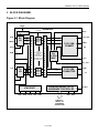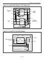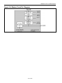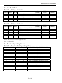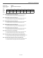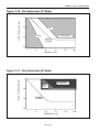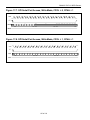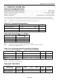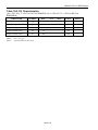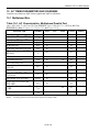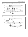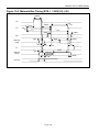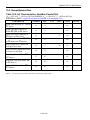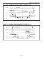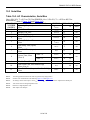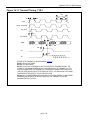
1
DESIGN KIT AVAILABLE
DS26503
T1/E1/J1 BITS Element
www.maxim-ic.com
GENERAL DESCRIPTION
FEATURES
The DS26503 is a building-integrated timingsupply (BITS) clock-recovery element. It also
functions as a basic T1/E1 transceiver. The
receiver portion can recover a clock from T1,
E1, and 6312kHz synchronization timing
interfaces. In T1 and E1 modes, the
Synchronization Status Message (SSM) can also
be recovered. The transmit portion can directly
interface to T1 or E1 interfaces as well as source
the SSM in T1 and E1 modes. The DS26503 can
translate between any of the supported inbound
synchronization clock rates to any supported
outbound rate. A separate output is provided to
source a 6312kHz clock. The device is
controlled through a parallel, serial, or hardware
controller port.
APPLICATIONS
BITS Timing
Rate Conversion
Basic Transceiver
ORDERING INFORMATION
PART
DS26503L
DS26503LN
TEMP RANGE
PIN-PACKAGE
0°C to +70°C
64 LQFP
-40°C to +85°C
64 LQFP
G.703 2048kHz Synchronization Interface
Compliant
G.703 6312kHz Japanese Synchronization
Interface Compliant
Interfaces to Standard T1/J1 (1.544MHz) and
E1 (2.048MHz)
Interface to CMI-Coded T1/J1 and E1
Short- and Long-Haul Line Interface
Transmit and Receive T1 and E1 SSM
Messages with Message Validation
T1/E1 Jitter Attenuator with Bypass Mode
Fully Independent Transmit and Receive
Functionality
Internal Software-Selectable Receive- and
Transmit-Side Termination for
75Ω/100Ω/110Ω/120Ω
Monitor Mode for Bridging Applications
Accepts 16.384MHz, 12.8MHz, 8.192MHz,
4.096MHz, 2.048MHz, or 1.544MHz Master
Clock
8-Bit Parallel Control Port, Multiplexed or
Nonmultiplexed, Intel or Motorola
Serial (SPI) Control Port
Hardware Control Mode
Provides LOS, AIS, and LOF Indications
Through Hardware Output Pins
Fast Transmitter-Output Disable Through
Device Pin for Protection Switching
IEEE 1149.1 JTAG Boundary Scan
3.3V Supply with 5V-Tolerant Inputs and
Outputs
Note: Some revisions of this device may incorporate deviations from published specifications known as errata. Multiple revisions of any device
may be simultaneously available through various sales channels. For information about device errata, click here: www.maxim-ic.com/errata.
1 of 122
REV: 121707
DS26503 T1/E1/J1 BITS Element
TABLE OF CONTENTS
1.
FEATURES ....................................................................................................................................7
1.1
1.2
1.3
1.4
1.5
1.6
GENERAL .....................................................................................................................................7
LINE INTERFACE ...........................................................................................................................7
JITTER ATTENUATOR (T1/E1 MODES ONLY) ..................................................................................7
FRAMER/FORMATTER ...................................................................................................................8
TEST AND DIAGNOSTICS ...............................................................................................................8
CONTROL PORT ............................................................................................................................8
2.
SPECIFICATIONS COMPLIANCE.................................................................................................9
3.
BLOCK DIAGRAMS.....................................................................................................................11
4.
PIN FUNCTION DESCRIPTION...................................................................................................14
TRANSMIT PLL ...........................................................................................................................14
TRANSMIT SIDE ..........................................................................................................................14
RECEIVE SIDE ............................................................................................................................15
CONTROLLER INTERFACE ............................................................................................................16
JTAG.........................................................................................................................................21
LINE INTERFACE .........................................................................................................................21
POWER ......................................................................................................................................22
4.1
4.2
4.3
4.4
4.5
4.6
4.7
5.
PINOUT ........................................................................................................................................23
6.
HARDWARE CONTROLLER INTERFACE .................................................................................26
TRANSMIT CLOCK SOURCE .........................................................................................................26
INTERNAL TERMINATION ..............................................................................................................26
LINE BUILD-OUT .........................................................................................................................27
RECEIVER OPERATING MODES ....................................................................................................27
TRANSMITTER OPERATING MODES ..............................................................................................28
MCLK PRE-SCALER ...................................................................................................................28
OTHER HARDWARE CONTROLLER MODE FEATURES ....................................................................29
6.1
6.2
6.3
6.4
6.5
6.6
6.7
7.
PROCESSOR INTERFACE .........................................................................................................30
7.1
7.2
7.2.1
7.2.2
7.2.3
7.2.4
7.2.5
7.2.6
7.3
7.3.1
7.3.2
7.3.3
7.4
7.5
7.6
7.7
8.
PARALLEL PORT FUNCTIONAL DESCRIPTION ................................................................................30
SPI SERIAL PORT INTERFACE FUNCTIONAL DESCRIPTION ............................................................30
Clock Phase and Polarity ......................................................................................................30
Bit Order................................................................................................................................30
Control Byte ..........................................................................................................................30
Burst Mode............................................................................................................................30
Register Writes .....................................................................................................................31
Register Reads .....................................................................................................................31
REGISTER MAP ...........................................................................................................................32
Power-Up Sequence.............................................................................................................34
Test Reset Register ..............................................................................................................34
Mode Configuration Register ................................................................................................35
INTERRUPT HANDLING ................................................................................................................38
STATUS REGISTERS....................................................................................................................38
INFORMATION REGISTERS ...........................................................................................................39
INTERRUPT INFORMATION REGISTERS .........................................................................................39
T1 FRAMER/FORMATTER CONTROL REGISTERS .................................................................40
8.1
T1 CONTROL REGISTERS............................................................................................................40
2 of 122
DS26503 T1/E1/J1 BITS Element
9.
E1 FRAMER/FORMATTER CONTROL REGISTERS .................................................................46
9.1
9.2
E1 CONTROL REGISTERS ...........................................................................................................46
E1 INFORMATION REGISTERS......................................................................................................48
10.
I/O PIN CONFIGURATION OPTIONS..........................................................................................52
11.
T1 SYNCHRONIZATION STATUS MESSAGE ...........................................................................55
11.1
11.2
11.3
12.
12.1
12.2
13.
T1 BIT-ORIENTED CODE (BOC) CONTROLLER ............................................................................55
TRANSMIT BOC .........................................................................................................................55
RECEIVE BOC ...........................................................................................................................56
E1 SYNCHRONIZATION STATUS MESSAGE ...........................................................................64
SA/SI BIT ACCESS BASED ON CRC4 MULTIFRAME ......................................................................64
ALTERNATE SA/SI BIT ACCESS BASED ON DOUBLE-FRAME .........................................................74
LINE INTERFACE UNIT (LIU)......................................................................................................77
13.1
LIU OPERATION .........................................................................................................................78
13.2
LIU RECEIVER ...........................................................................................................................78
13.2.1 Receive Level Indicator.........................................................................................................78
13.2.2 Receive G.703 Section 10 Synchronization Signal...............................................................79
13.2.3 Monitor Mode ........................................................................................................................79
13.3
LIU TRANSMITTER .....................................................................................................................79
13.3.1 Transmit Short-Circuit Detector/Limiter.................................................................................80
13.3.2 Transmit Open-Circuit Detector ............................................................................................80
13.3.3 Transmit BPV Error Insertion ................................................................................................80
13.3.4 Transmit G.703 Section 10 Synchronization Signal (E1 Mode) ............................................80
13.4
MCLK PRE-SCALER ..................................................................................................................80
13.5
JITTER ATTENUATOR ..................................................................................................................80
13.6
CMI (CODE MARK INVERSION) OPTION.......................................................................................81
13.7
LIU CONTROL REGISTERS..........................................................................................................82
13.8
RECOMMENDED CIRCUITS ..........................................................................................................90
14.
LOOPBACK CONFIGURATION ..................................................................................................95
15.
6312KHZ SYNCHRONIZATION INTERFACE .............................................................................96
15.1
15.2
16.
16.1
16.2
16.3
16.4
16.5
17.
RECEIVE 6312KHZ SYNCHRONIZATION INTERFACE OPERATION ...................................................96
TRANSMIT 6312KHZ SYNCHRONIZATION INTERFACE OPERATION .................................................96
JTAG BOUNDARY SCAN ARCHITECTURE AND TEST ACCESS PORT ................................97
INSTRUCTION REGISTER ...........................................................................................................101
TEST REGISTERS .....................................................................................................................102
BOUNDARY SCAN REGISTER ....................................................................................................102
BYPASS REGISTER ...................................................................................................................102
IDENTIFICATION REGISTER .......................................................................................................102
FUNCTIONAL TIMING DIAGRAMS ..........................................................................................105
17.1
PROCESSOR INTERFACE ...........................................................................................................105
17.1.1 Parallel Port Mode ..............................................................................................................105
17.1.2 SPI Serial Port Mode ..........................................................................................................105
18.
OPERATING PARAMETERS ....................................................................................................108
19.
AC TIMING PARAMETERS AND DIAGRAMS..........................................................................110
19.1
MULTIPLEXED BUS ...................................................................................................................110
3 of 122
DS26503 T1/E1/J1 BITS Element
19.2
19.3
19.4
19.5
NONMULTIPLEXED BUS.............................................................................................................113
SERIAL BUS .............................................................................................................................116
RECEIVE SIDE AC CHARACTERISTICS .......................................................................................118
TRANSMIT SIDE AC CHARACTERISTICS .....................................................................................119
20.
REVISION HISTORY..................................................................................................................121
21.
PACKAGE INFORMATION........................................................................................................122
4 of 122
DS26503 T1/E1/J1 BITS Element
LIST OF FIGURES
Figure 3-1. Block Diagram ........................................................................................................................11
Figure 3-2. Loopback Mux Diagram (T1/E1 Modes Only) ........................................................................12
Figure 3-3. Transmit PLL Clock Mux Diagram..........................................................................................12
Figure 3-4. Master Clock PLL Diagram ....................................................................................................13
Figure 13-1. Basic Network Connection ...................................................................................................77
Figure 13-2. Typical Monitor Application ..................................................................................................79
Figure 13-3. CMI Coding ..........................................................................................................................81
Figure 13-4. Software-Selected Termination, Metallic Protection.............................................................90
Figure 13-5. Software-Selected Termination, Longitudinal Protection .....................................................91
Figure 13-6. E1 Transmit Pulse Template ................................................................................................92
Figure 13-7. T1 Transmit Pulse Template ................................................................................................92
Figure 13-8. Jitter Tolerance (T1 Mode) ...................................................................................................93
Figure 13-9. Jitter Tolerance (E1 Mode)...................................................................................................93
Figure 13-10. Jitter Attenuation (T1 Mode)...............................................................................................94
Figure 13-11. Jitter Attenuation (E1 Mode) ..............................................................................................94
Figure 16-1. JTAG Functional Block Diagram ..........................................................................................97
Figure 16-2. TAP Controller State Diagram............................................................................................100
Figure 17-1. SPI Serial Port Access, Read Mode, CPOL = 0, CPHA = 0...............................................105
Figure 17-2. SPI Serial Port Access, Read Mode, CPOL = 1, CPHA = 0...............................................105
Figure 17-3. SPI Serial Port Access, Read Mode, CPOL = 0, CPHA = 1...............................................105
Figure 17-4. SPI Serial Port Access, Read Mode, CPOL = 1, CPHA = 1...............................................106
Figure 17-5. SPI Serial Port Access, Write Mode, CPOL = 0, CPHA = 0...............................................106
Figure 17-6. SPI Serial Port Access, Write Mode, CPOL = 1, CPHA = 0...............................................106
Figure 17-7. SPI Serial Port Access, Write Mode, CPOL = 0, CPHA = 1...............................................107
Figure 17-8. SPI Serial Port Access, Write Mode, CPOL = 1, CPHA = 1...............................................107
Figure 19-1. Intel Bus Read Timing (BTS = 0 / BIS[1:0] = 00)...............................................................111
Figure 19-2. Intel Bus Write Timing (BTS = 0 / BIS[1:0] = 00)................................................................111
Figure 19-3. Motorola Bus Timing (BTS = 1 / BIS[1:0] = 00) ..................................................................112
Figure 19-4. Intel Bus Read Timing (BTS = 0 / BIS[1:0] = 01)................................................................114
Figure 19-5. Intel Bus Write Timing (BTS = 0 / BIS[1:0] = 01)................................................................114
Figure 19-6. Motorola Bus Read Timing (BTS = 1 / BIS[1:0] = 01) ........................................................115
Figure 19-7. Motorola Bus Write Timing (BTS = 1 / BIS[1:0] = 01).........................................................115
Figure 19-8. SPI Interface Timing Diagram, CPHA = 0, BIS[1:0] = 10 ...................................................117
Figure 19-9. SPI Interface Timing Diagram, CPHA = 1, BIS[1:0] = 10 ...................................................117
Figure 19-10. Receive Timing, T1/E1 .....................................................................................................118
Figure 19-11. Transmit Timing, T1/E1 ....................................................................................................120
5 of 122
DS26503 T1/E1/J1 BITS Element
LIST OF TABLES
Table 2-1. T1-Related Telecommunications Specifications........................................................................9
Table 2-2. E1-Related Telecommunications Specifications .....................................................................10
Table 5-1. LQFP Pinout ............................................................................................................................23
Table 6-1. Transmit Clock Source ............................................................................................................26
Table 6-2. Internal Termination ................................................................................................................26
Table 6-3. E1 Line Build-Out ....................................................................................................................27
Table 6-4. T1 Line Build-Out ....................................................................................................................27
Table 6-5. Receive Path Operating Mode ................................................................................................27
Table 6-6.Transmit Path Operating Mode ................................................................................................28
Table 6-7. MCLK Pre-Scaler for T1 Mode ................................................................................................28
Table 6-8. MCLK Pre-Scaler for E1 Mode ................................................................................................29
Table 6-9. Other Operational Modes ........................................................................................................29
Table 7-1. Port Mode Select.....................................................................................................................30
Table 7-2. Register Map Sorted By Address ............................................................................................32
Table 8-1. T1 Alarm Criteria .....................................................................................................................45
Table 9-1. E1 Sync/Resync Criteria .........................................................................................................47
Table 9-2. E1 Alarm Criteria .....................................................................................................................49
Table 10-1. TS Pin Functions ...................................................................................................................53
Table 10-2. RLOF Pin Functions ..............................................................................................................53
Table 11-1. T1 SSM Messages ................................................................................................................55
Table 12-1. E1 SSM Messages ................................................................................................................64
Table 13-1. Component List (Software-Selected Termination, Metallic Protection) .................................90
Table 13-2. Component List (Software-Selected Termination, Longitudinal Protection) ..........................91
Table 15-1. Specification of 6312kHz Clock Signal at Input Port ............................................................96
Table 15-2. Specification of 6312kHz Clock Signal at Output Port...........................................................96
Table 16-1. Instruction Codes for IEEE 1149.1 Architecture ..................................................................101
Table 16-2. ID Code Structure................................................................................................................102
Table 16-3. Device ID Codes .................................................................................................................102
Table 16-4. Boundary Scan Control Bits ................................................................................................103
Table 18-1. Thermal Characteristics ......................................................................................................108
Table 18-2. Theta-JA (θJA) vs. Airflow.....................................................................................................108
Table 18-3. Recommended DC Operating Conditions ...........................................................................108
Table 18-4. Capacitance ........................................................................................................................108
Table 18-5. DC Characteristics ..............................................................................................................109
Table 19-1. AC Characteristics, Multiplexed Parallel Port ......................................................................110
Table 19-2. AC Characteristics, Non-Mux Parallel Port..........................................................................113
Table 19-3. AC Characteristics, Serial Bus ............................................................................................116
Table 19-4. Receive Side AC Characteristics.........................................................................................118
Table 19-5. Transmit Side AC Characteristics........................................................................................119
6 of 122
DS26503 T1/E1/J1 BITS Element
1. FEATURES
1.1 General
64-pin, 10mm x 10mm LQFP package
3.3V supply with 5V-tolerant inputs and outputs
Evaluation kits
IEEE 1149.1 JTAG Boundary Scan
Driver source code available from the factory
1.2 Line Interface
Requires a single master clock (MCLK) for E1, T1, or J1 operation. Master clock can be
2.048MHz, 4.096MHz, 8.192MHz, 12.8MHz (available in CPU interface mode only), or
16.384MHz. Option to use 1.544MHz, 3.088MHz, 6.176MHz, or 12.5552MHz for T1-only
operation.
Fully software configurable
Short- and long-haul applications
Automatic receive sensitivity adjustments
Ranges include 0dB to -43dB or 0dB to -12dB for E1 applications; 0dB to -36dB or 0dB to -15dB
for T1 applications
Receive level indication in 2.5dB steps from -42.5dB to -2.5dB
Internal receive termination option for 75Ω, 100Ω, 110Ω, and 120Ω lines
Monitor application gain settings of 20dB, 26dB, and 32dB
G.703 receive-synchronization signal mode
Flexible transmit-waveform generation
T1 DSX-1 line build-outs
E1 waveforms include G.703 waveshapes for both 75Ω coax and 120Ω twisted cables
AIS generation independent of loopbacks
Alternating ones and zeros generation
Square-wave output
Open-drain output option
Transmitter power-down
Transmitter 50mA short-circuit limiter with exceeded indication of current limit
Transmit open-circuit-detected indication
1.3 Jitter Attenuator (T1/E1 Modes Only)
32-bit or 128-bit crystal-less jitter attenuator
Requires only a 2.048MHz master clock for both E1 and T1 operation with the option to use
1.544MHz for T1 operation
Can be placed in either the receive or transmit path or disabled
Limit trip indication
7 of 122
DS26503 T1/E1/J1 BITS Element
1.4 Framer/Formatter
Full receive and transmit path transparency
T1 framing formats include D4 and ESF
E1 framing formats include FAS and CRC4
Detailed alarm and status reporting with optional interrupt support
RLOF, RLOS, and RAIS alarms interrupt on change of state
Japanese J1 support includes:
− Ability to calculate and check CRC6 according to the Japanese standard
− Ability to generate yellow alarm according to the Japanese standard
1.5 Test and Diagnostics
Remote and Local Loopback
1.6 Control Port
8-bit parallel or serial control port
Multiplexed or nonmultiplexed buses
Intel or Motorola formats
Supports polled or interrupt-driven environments
Software access to device ID and silicon revision
Software-reset supported with automatic clear on power-up
Hardware controller port
Hardware reset pin
8 of 122
DS26503 T1/E1/J1 BITS Element
2. SPECIFICATIONS COMPLIANCE
The DS26503 meets all applicable sections of the latest telecommunications specifications including
those in the following tables.
Table 2-1. T1-Related Telecommunications Specifications
ANSI T1.102 - Digital Hierarchy Electrical Interface
ANSI T1.231 - Digital Hierarchy–Layer 1 in Service Performance Monitoring
ANSI T1.403 - Network and Customer Installation Interface–DS1 Electrical Interface
TR62411
(ANSI) “Digital Hierarchy – Electrical Interfaces”
(ANSI) “Digital Hierarchy – Formats Specification”
(ANSI) “Digital Hierarchy – Layer 1 In-Service Digital Transmission Performance Monitoring”
(ANSI) “Network and Customer Installation Interfaces–DS1 Electrical Interface”
(AT&T) “Requirements for Interfacing Digital Terminal Equipment to Services Employing the Extended
Super frame Format”
(AT&T) “High Capacity Digital Service Channel Interface Specification”
(TTC) “Frame Structures on Primary and Secondary Hierarchical Digital Interfaces”
(TTC) “ISDN Primary Rate User-Network Interface Layer 1 Specification”
9 of 122
DS26503 T1/E1/J1 BITS Element
Table 2-2. E1-Related Telecommunications Specifications
ITUT G.703 Physical/Electrical Characteristics of G.703 Hierarchical Digital Interfaces
ITUT G.736 Characteristics of Synchronous Digital Multiplex Equipment operating at 2048kbps
ITUT G.742 Second-Order Digital Multiplex Equipment Operating at 8448kbps
ITUT G.772
ITUT G.775
ITUT G.823 The control of jitter and wander within digital networks, which are based on 2.048kbps
hierarchy
ETSI 300 233
(ITU) “Synchronous Frame Structures used at 1544, 6312k, 2048, 8488, and 44,736kbps Hierarchical
Levels”
(ITU) “Frame Alignment and Cyclic Redundancy Check (CRC) Procedures Relating to Basic Frame
Structures Defined in Recommendation G.704”
(ITU) “Characteristics of primary PCM Multiplex Equipment Operating at 2048kbps”
(ITU) Characteristics of a synchronous digital multiplex equipment operating at 2048kbps”
(ITU) “Loss Of Signal (LOS) and Alarm Indication Signal (AIS) Defect Detection and Clearance
Criteria”
(ITU) “The Control of Jitter and Wander Within Digital Networks Which are Based on the 2048kbps
Hierarchy”
(ITU) “Primary Rate User-Network Interface – Layer 1 Specification”
(ITU) “Error Performance Measuring Equipment Operating at the Primary Rate and Above”
(ITU) “In-service code violation monitors for digital systems”
(ETSI) “Integrated Services Digital Network (ISDN); Primary rate User-Network Interface (UNI); Part
1/ Layer 1 specification”
(ETSI) “Transmission and multiplexing; Physical/electrical characteristics of hierarchical digital
interfaces for equipment using the 2048kbps-based plesiochronous or synchronous digital hierarchies”
(ETSI) “Integrated Services Digital Network (ISDN); Access digital section for ISDN primary rate”
(ETSI) “Integrated Services Digital Network (ISDN); Attachment requirements for terminal equipment
to connect to an ISDN using ISDN primary rate access”
(ETSI) “Business Telecommunications (BT); Open Network Provision (ONP) technical requirements;
2048lkbps digital unstructured leased lines (D2048U) attachment requirements for terminal equipment
interface”
(ETSI) “Business Telecommunications (BTC); 2048kbps digital structured leased lines (D2048S);
Attachment requirements for terminal equipment interface”
(ITU) “Synchronous Frame Structures used at 1544, 6312, 2048, 8488, and 44,736kbps Hierarchical
Levels”
(ITU) “Frame Alignment and Cyclic Redundancy Check (CRC) Procedures Relating to Basic Frame
Structures Defined in Recommendation G.704”
10 of 122
DS26503 T1/E1/J1 BITS Element
3. BLOCK DIAGRAMS
Figure 3-1. Block Diagram
MCLK
DS26503
JA CLOCK
MASTER CLOCK
RTIP
RRING
RX
RX
LIU
LIU
RLOS
- DATA
L
O
C
A
L
L
O
O
P
B
A
C
K
RAIS
TTIP
CLOCK
+ DATA
TX
LIU
M
U
X
JA
ENABLED
AND IN RX
PATH
JITTER
ATTENUATOR
CAN BE
ASSIGNED TO
RECEIVE OR
TRANSMIT PATH
OR DISABLED
JA
ENABLED
AND IN TX
PATH
LOF_CCE
R
E
M
O
T
E
L
O
O
P
B
A
C
K
T1/E1 SSM
FRAMER
PLL
CLOCK
MUX
RSER
RS
TCLK
PLL_OUT
TX CLOCK
M
U
X
+ DATA
- DATA
T1/E1 SSM
FORMATTER
PARALLEL/SERIAL CPU I/F
HARDWARE CONTROLLER
JTAG
JTAG
PORT
PORT
JTMS JTRST JTCLK JTDI
RCLK
JTDO
BIS1
PARALLEL,
SERIAL, OR
HARDWARE
CONTROLLER
11 of 122
BIS0
TSER
TS
TSTRST
DS26503 T1/E1/J1 BITS Element
Figure 3-2. Loopback Mux Diagram (T1/E1 Modes Only)
CLOCK
FROM RX
LIU
RCLK
JITTER
ATTENUATOR
ENABLED AND
IN RX PATH
+ DATA
TO RX
FRAMER
+ DATA
- DATA
- DATA
LOCAL
LOOPBACK
(LBCR.3)
TX CLOCK
CLOCK
TO TX
LIU
JITTER
ATTENUATOR
ENABLED AND
IN TX PATH
+ DATA
+ DATA
FROM TX
FORMATTER
- DATA
- DATA
REMOTE
LOOPBACK
(LBCR.4)
Figure 3-3. Transmit PLL Clock Mux Diagram
TPCR.3
TPCR.4
TPCR.6
TPCR.7
IN
SEL
OUT
SEL
TPCR.5
TPCR.2
RECOVERED CLOCK
TCLK PIN
PLL_OUT PIN
TX PLL
OUTPUT = 1.544MHz,
2.048MHz, 6.312MHz
TX CLOCK
JA CLOCK
TPCR.0
(TCSS0)
(HARDWARE MODE PIN NAME)
12 of 122
TPCR.1
(TCSS1)
DS26503 T1/E1/J1 BITS Element
Figure 3-4. Master Clock PLL Diagram
13 of 122
DS26503 T1/E1/J1 BITS Element
4. PIN FUNCTION DESCRIPTION
4.1 Transmit PLL
NAME
TYPE
PLL_OUT
O
TCLK
I
FUNCTION
Transmit PLL Output. This pin can be selected to output the 1544kHz,
2048kHz, 64kHz, or 6312kHz output from the internal TX PLL or the internal
signal, TX CLOCK. See Figure 3-3 and Figure 3-4.
Transmit Clock Input. A 64kHz, 1.544MHz, 2.048MHz, or 6312kHz primary
clock. May be selected by the TX PLL mux to either directly drive the transmit
section or be converted to one of the other rates prior to driving the transmit
section. See Figure 3-3 and Figure 3-4.
4.2 Transmit Side
NAME
TYPE
TSER
I
TS
I/O
TCLKO
O
TPOSO
O
TNEGO
O
FUNCTION
Transmit Serial Data. Source of transmit data sampled on the falling edge of
TX CLOCK (an internal signal). See Figure 3-3, Figure 3-4, and Figure 19-11
(transmit timing diagram).
TSYNC. When in input mode, this pin is sampled on the falling edge of TX
CLOCK (an internal signal) and a pulse at this pin will establish either frame or
multiframe boundaries for the transmit side. See Figure 3-1 and Figure 19-11.
In output mode, the pin is updated on the rising edge of TX CLOCK (an
internal signal) and can be programmed to output a frame or multiframe sync
pulse useful for aligning data. See Figure 3-1 and Figure 19-11.
Transmit Clock Output. Buffered clock that is used to clock data through the
transmit-side formatter (i.e., either TCLK or RCLK).
Transmit Positive-Data Output. In T1 or E1 mode, updated on the rising edge
of TCLKO with the bipolar data out of the transmit-side formatter. Can be
programmed to source NRZ data via the output-data format (IOCR1.0) control
bit. In 6312kHz mode, this pin is low.
Transmit Negative-Data Output. In T1 or E1 mode, updated on the rising
edge of TCLKO with the bipolar data out of the transmit-side formatter. In
6312kHz mode, this pin is low.
14 of 122
DS26503 T1/E1/J1 BITS Element
4.3 Receive Side
NAME
TYPE
RCLK
O
RS
O
FUNCTION
Receive Clock. Recovered 1.544MHz (T1), 2.048MHz (E1), or 6312kHz
(G.703 Synchronization Interface).
Receive Sync
T1/E1 Mode: An extracted pulse, one RCLK wide, is output at this pin that
identifies either frame (IOCR1.5 = 0) or multiframe (IOCR1.5 = 1)
boundaries. If set to output frame boundaries, then through IOCR1.6, RS can
also be set to output double-wide pulses on signaling frames in T1 mode.
6312kHz Mode: This pin will be in a high-impedance state.
Receive Serial Data
RSER
O
T1/E1 Mode: This is the received NRZ serial data updated on rising edges of
RCLK.
6312kHz Mode: This pin will be in a high-impedance state.
Receive Loss Of Frame. This output can be configured to be a Loss Of
Transmit Clock indicator via IOCR.4 when operating in T1 or E1 mode.
RLOF
O
T1/E1 Mode: Set when the receive synchronizer is searching for frame
alignment (RLOF mode), or set when the signal at the TCLK pin has not
transitioned for approximately 15 periods of the scaled MCLK (LOTC mode).
6312kHz Mode: This pin will be in a high-impedance state.
Receive Loss Of Signal
RLOS
O
T1 Mode: High when 192 consecutive zeros detected.
E1 Mode: High when 255 consecutive zeros detected.
6312kHz Mode: High when consecutive zeros detected for 65µs typically.
Receive Alarm Indication Signal
RAIS
O
T1 Mode: Will toggle high when receive Blue Alarm is detected.
E1 Mode: Will toggle high when receive AIS is detected.
6312kHz Mode: This pin will be in a high-impedance state.
15 of 122
DS26503 T1/E1/J1 BITS Element
4.4 Controller Interface
NAME
TYPE
INT/
JACKS0
I/O
TMODE1
I
TMODE2
I
TSTRST
I
BIS[1:0]
I
FUNCTION
Active-Low Interrupt/Jitter Attenuator Clock Select 0
INT: Flags host controller during events, alarms, and conditions defined in the
AD[7]/
RITD
status registers. Active-low open-drain output.
JACKS0: Hardware Mode: Jitter Attenuator Clock Select 0. Set this pin high
for T1 mode operation when either a 2.048MHz, 4.096MHz, 8.192MHz or
16.382MHz signal is applied at MCLK.
Transmit Mode Select 1. In Hardware Mode (BIS[1:0] = 11), this bit is used
to configure the transmit operating mode.
Transmit Mode Select 2. In Hardware Mode (BIS[1:0] = 11), this bit is used
to configure the transmit operating mode.
Three-State Control and Device Reset. A dual-function pin. A zero-to-one
transition issues a hardware reset to the DS26503 register set. Configuration
register contents are set to the default state. Leaving TSTRST high three-states
all output and I/O pins (including the parallel control port). Set low for normal
operation. Useful for in-board level testing.
Processor Interface Mode Select 1, 0. These bits select the processor
interface mode of operation.
BIS[1:0] : 00 = Parallel Port Mode (Multiplexed)
01 = Parallel Port Mode (Nonmultiplexed)
10 = Serial Port Mode
11 = Hardware Mode
Data Bus D[7] or Address/Data Bus AD[7]/Receive Internal Termination
Disable
A[7]: In nonmultiplexed bus operation (BIS[1:0] = 01), it serves as the data
bus D[7].
I/O
AD[7]: In multiplexed bus operation (BIS[1:0] = 00), it serves as the
multiplexed address/data bus AD[7].
RITD: In Hardware Mode (BIS[1:0] = 11), internal receive termination is
disabled when RITD = 1.
Data Bus D[6] or Address/Data Bus AD[6]/Transmit Internal Termination
Disable
AD[6]/
TITD
A[6]: In nonmultiplexed bus operation (BIS[1:0] = 01), it serves as the data
bus D[6].
I/O
AD[6]: In multiplexed bus operation (BIS[1:0] = 00), it serves as the
multiplexed address/data bus AD[6].
TITD: In Hardware Mode (BIS[1:0] = 11), internal transmit termination is
disabled when TITD = 1.
16 of 122
DS26503 T1/E1/J1 BITS Element
NAME
AD[5]/
RMODE1
TYPE
I/O
FUNCTION
Data Bus D[5] or Address/Data Bus AD[5]/Receive Framing Mode Select
Bit 1
A[5]: In nonmultiplexed bus operation (BIS[1:0] = 01), it serves as the data
bus D[5].
AD[5]: In multiplexed bus operation (BIS[1:0] = 00), it serves as the
multiplexed address/data bus AD[5].
RMODE1: In Hardware Mode (BIS[1:0] = 11), it selects the receive side
operating mode.
Data Bus D[4] or Address/Data Bus AD[4]/Receive Framing Mode Select
Bit 0
AD[4]/
RMODE0
I/O
A[4]: In nonmultiplexed bus operation (BIS[1:0] = 01), it serves as the data
bus D[4].
AD[4]: In multiplexed bus operation (BIS[1:0] = 00), it serves as the
multiplexed address/data bus AD[4].
RMODE0: In Hardware Mode (BIS[1:0] = 11), it selects the receive side
operating mode.
Data Bus D[3] or Address/Data Bus AD[3]/TS Mode Select
A[3]: In nonmultiplexed bus operation (BIS[1:0] = 01), it serves as the data
bus D[3].
AD[3]/TSM
I/O
AD[3]: In multiplexed bus operation (BIS[1:0] = 00), it serves as the
multiplexed address/data bus AD[3].
TSM: In Hardware Mode (BIS[1:0] = 11), this pin selects the function of TS.
Please see the register descriptions for more detailed information.
Data Bus D[2] or Address/Data Bus AD[2]/RS Mode Select/Serial Port
Clock
A[2]: In nonmultiplexed bus operation (BIS[1:0] = 01), it serves as the data
bus D[2].
AD[2]/RSM/
SCLK
I/O
AD[2]: In multiplexed bus operation (BIS[1:0] = 00), it serves as the
multiplexed address/data bus AD[2].
RSM: In Hardware Mode (BIS[1:0] = 11), this pin selects the function of RS.
Please see the register descriptions for more detailed information.
SCLK: In Serial Port mode this is the serial clock input.
17 of 122
DS26503 T1/E1/J1 BITS Element
NAME
TYPE
FUNCTION
Data Bus D[1] or Address/Data Bus AD[1]/Receive Mode Select 3/Master
Out-Slave In
A[1]: In nonmultiplexed bus operation (BIS[1:0] = 01), it serves as the data
bus D[1].
AD[1]/
RMODE3/
MOSI
I/O
AD[1]: In multiplexed bus operation (BIS[1:0] = 00), it serves as the
multiplexed address/data bus AD[1].
RMODE3: In Hardware Mode (BIS[1:0] = 11), this pin selects the receive side
operating mode.
MOSI: Serial data input called Master Out-Slave In for clarity of data transfer
direction.
Data Bus D[0] or Address/Data Bus AD[0]/Transmit Clock Source Select
0/Master In-Slave Out
AD[0]/
TCSS0/
MISO
A[0]: In nonmultiplexed bus operation (BIS[1:0] = 01), it serves as the data
bus D[0].
I/O
AD[0]: In multiplexed bus operation (BIS[1:0] = 00), it serves as the
multiplexed address/data bus AD[0].
TCSS0: Transmit Clock Source Select 0.
MISO: In serial bus mode (BIS[1:0] = 10), this pin serves as the serial data
output Master In-Slave Out.
TCSS1
I
Transmit Clock Source Select 1
Address Bus Bit A[6]/MCLK Prescale Select 0
A6/MPS0
I
A6: In nonmultiplexed bus operation (BIS[1:0] = 01), this pin serves as A[6].
In multiplexed bus operation (BIS[1:0] = 00), these pins are not used and
should be tied low.
MPS0: In Hardware Mode (BIS[1:0] = 11), MCLK prescale select is used to
set the prescale value for the PLL.
Address Bus Bit A[5]/Serial Port Clock Polarity Select/Transmit Mode
Select 0
A5/CPOL/
TMODE0
I
A5: In nonmultiplexed bus operation (BIS[1:0] = 01), this pin serves as A[5].
In multiplexed bus operation (BIS[1:0] = 00), these pins are not used and
should be tied low.
CPOL: In Serial Port Mode (BIS[1:0] = 10), this pin selects the serial port
clock polarity. Please see the functional timing diagrams for the Serial Port
Interface for more information.
TMODE0: In Hardware Mode (BIS[1:0] = 11), this pin is used to configure the
transmit operating mode.
18 of 122
DS26503 T1/E1/J1 BITS Element
NAME
A4/CPHA/
L2
TYPE
FUNCTION
Address Bus Bit A[4]/Serial Port Clock Phase Select/Line Build-Out
Select 2
A4: In nonmultiplexed bus operation (BIS[1:0] = 01), this pin serves as A[4].
In multiplexed bus operation (BIS[1:0] = 00), these pins are not used and
should be tied low.
I
CPHA: In Serial Port Mode (BIS[1:0] = 10), this pin selects the serial port
clock phase. See the functional timing diagrams for the Serial Port Interface
for more information.
L2: In Hardware Mode (BIS[1:0] = 11), this pin selects the line build-out
value.
Address Bus Bit A[3]/Line Build-Out Select 1
A3/L1
I
A3: In nonmultiplexed bus operation (BIS[1:0] = 01), this pin serves as A[3].
In multiplexed bus operation (BIS[1:0] = 00), these pins are not used and
should be tied low.
L1: In Hardware Mode (BIS[1:0] = 11), this pin selects the line build-out
value.
Address Bus Bit A[2]/Line Build-Out Select 0
A2/L0
I
A2: In nonmultiplexed bus operation (BIS[1:0] = 01), this pin serves as A[2].
In multiplexed bus operation (BIS[1:0] = 00), these pins are not used and
should be tied low.
L0: In Hardware Mode (BIS[1:0] = 11), this pin selects the line build-out
value.
Address Bus Bit A[1]/Transmit AIS
A1/TAIS
I
A1: In nonmultiplexed bus operation (BIS[1:0] = 01), this pin serves as A[1].
In multiplexed bus operation (BIS[1:0] = 00), these pins are not used and
should be tied low.
TAIS: When set to a 0 and in T1/E1 operating modes, the transmitter will
transmit an AIS pattern. Set to 1 for normal operation. This pin is ignored in
all other operating modes.
Address Bus Bit A[0]/E1 Termination Select
A0/E1TS
I
A0: In nonmultiplexed bus operation (BIS[1:0] = 01), this pin serves as A[0].
In multiplexed bus operation (BIS[1:0] = 00), these pins are not used and
should be tied low.
E1TS: In Hardware Mode (BIS[1:0] = 11), selects the E1 internal termination
value (0 = 75Ω, 1 = 120Ω).
19 of 122
DS26503 T1/E1/J1 BITS Element
NAME
BTS/HBE
TYPE
I
FUNCTION
Bus Type Select/Transmit and Receive B8ZS/HDB3 Enable
BTS: Strap high to select Motorola bus timing; strap low to select Intel bus
timing. This pin controls the function of the RD (DS), ALE (AS), and WR
(R/W) pins. If BTS = 1, then these pins assume the function listed in
parentheses ().
HBE: In Hardware Mode (BIS[1:0] = 11), this pin enables transmit and receive
B8ZS/HDB3 when in T1/E1 operating modes.
Read Input-Data Strobe/Receive Mode Select Bit 2
RD(DS)/
RMODE2
RD (DS): These pins are active-low signals. DS is active high when BIS[1:0]
I
= 01. See the bus timing diagrams.
RMODE2: In Hardware Mode (BIS[1:0] = 11), this pin selects the receive side
operating mode.
Chip Select/Remote Loopback Enable
CS: This active-low signal must be low to read or write to the device. This
CS/RLB
I
signal is used for both the parallel port and the serial port modes.
RLB: In Hardware Mode (BIS[1:0] = 11), when high, remote loopback is
enabled. This function is only valid when the transmit side and receive side are
in the same operating mode.
Address Latch Enable (Address Strobe)/Address Bus Bit 7/MCLK
Prescale Select 1
ALE (AS)/
A7/MPS1
I
ALE (AS): In multiplexed bus operation (BIS[1:0] = 00), it serves to
demultiplex the bus on a positive-going edge.
A7: In nonmultiplexed bus operation (BIS[1:0] = 01), this pin serves as A[7].
MPS1: In Hardware Mode (BIS[1:0] = 11), MCLK prescale select, used to set
the prescale value for the PLL.
Write Input (Read/Write)/Transmit Mode Select 3
WR (R/W)/
TMODE3
I
WR: In Processor Mode, this pin is the active-low write signal.
TMODE3: In Hardware Mode, this pin selects the transmit-side operating
mode.
20 of 122
DS26503 T1/E1/J1 BITS Element
4.5 JTAG
NAME
TYPE
JTCLK
I
JTMS
I
JTDI
I
JTDO
O
JTRST
I
FUNCTION
JTAG Clock. This clock input is typically a low frequency (less than 10MHz)
50% duty cycle clock signal.
JTAG Mode Select (with Pullup). This input signal is used to control the
JTAG controller state machine and is sampled on the rising edge of JTCLK.
JTAG Data Input (with Pullup). This input signal is used to input data into
the register that is enabled by the JTAG controller state machine and is sampled
on the rising edge of JTCLK.
JTAG Data Output. This output signal is the output of an internal scan shift
register enabled by the JTAG controller state machine and is updated on the
falling edge of JTCLK. The pin is in the high-impedance mode when a register
is not selected or when the JTRST signal is high. The pin goes into and exits the
high impedance mode after the falling edge of JTCLK
JTAG Reset (Active Low). This input forces the JTAG controller logic into
the reset state and forces the JTDO pin into high impedance when low. This pin
should be low while power is applied and set high after the power is stable.
The pin can be driven high or low for normal operation, but must be high for
JTAG operation.
4.6 Line Interface
NAME
TYPE
MCLK
I
RTIP
I
RRING
I
TTIP
O
TRING
O
THZE
I
FUNCTION
Master Clock Input. A (50ppm) clock source. This clock is used internally for
both clock/data recovery and for the jitter attenuator for both T1 and E1 modes.
The clock rate can be 16.384MHz, 8.192MHz, 4.096MHz, or 2.048MHz. When
using the DS26503 in T1-only operation, a 1.544MHz (50ppm) clock source
can be used.
Receive Tip. Analog input for clock recovery circuitry. This pin connects via a
1:1 transformer to the network. See the Line Interface Unit section for details.
Receive Ring. Analog input for clock recovery circuitry. This pin connects via
a 1:1 transformer to the network. See the Line Interface Unit section for details.
Transmit Tip. Analog line-driver output. This pin connects via a 1:2 step-up
transformer to the network. See the Line Interface Unit section for details.
Transmit Ring. Analog line-driver output. This pin connects via a 1:2 step-up
transformer to the network. See the Line Interface Unit section for details.
Transmit High-Impedance Enable. When high, TTIP and TRING will be
placed into a high-impedance state.
21 of 122
DS26503 T1/E1/J1 BITS Element
4.7 Power
NAME
TYPE
DVDD
—
RVDD
—
TVDD
—
DVSS
—
RVSS
—
TVSS
—
FUNCTION
Digital Positive Supply. 3.3V ±5%. Should be tied to the RVDD and TVDD
pins.
Receive Analog Positive Supply. 3.3V ±5%. Should be tied to the DVDD and
TVDD pins.
Transmit Analog Positive Supply. 3.3V ±5%. Should be tied to the DVDD
and RVDD pins.
Digital Signal Ground. 0.0V. Should be tied to the RVSS and TVSS pins.
Receive Analog Signal Ground. 0.0V. Should be tied to the DVSS and TVSS
pins.
Transmit Analog Signal Ground. 0.0V. Should be tied to the DVSS and
RVSS pins.
22 of 122
DS26503 T1/E1/J1 BITS Element
5. PINOUT
Table 5-1. LQFP Pinout
PIN
TYPE
PARALLEL
PORT
MODE
SERIAL
PORT
1
I/O
AD2
SCLK
RSM
2
I/O
AD3
—
TSM
3
I/O
AD4
—
RMODE0
4
I/O
AD5
—
RMODE1
5
I/O
AD6
—
TITD
6
I/O
AD7
—
RITD
I
DVDD
DVDD
DVDD
Digital Positive Supply
I
DVSS
DVSS
DVSS
Digital Signal Ground
9
I
A0
—
E1TS
10
I
A1
—
TAIS
11
I
A2
—
L0
12
I
A3
—
L1
13
I
A4
CPHA
L2
14
I
A5
CPOL
TMODE0
15
I
A6
—
MPS0
16
I
ALE (AS)/A7
—
MPS1
17
I
TCLK
TCLK
TCLK
7, 24,
58
8, 22,
56
HARDWARE
23 of 122
FUNCTION
Parallel Port Mode: Address/Data Bus Bit 2
Serial Port Mode: Serial Clock
Hardware Mode: RS Mode Select
Parallel Port Mode: Address/Data Bus Bit 3
Serial Port Mode: Unused, should be connected to VSS.
Hardware Mode: TS Mode Select
Parallel Port Mode: Address/Data Bus Bit 4
Serial Port Mode: Unused, should be connected to VSS.
Hardware Mode: Receive Mode Select 0
Parallel Port Mode: Address/Data Bus Bit 5
Serial Port Mode: Unused, should be connected to VSS.
Hardware Mode: Receive Mode Select 1
Parallel Port Mode: Address/Data Bus Bit 6
Serial Port Mode: Unused, should be connected to VSS.
Hardware Mode: Transmit Internal Termination Disable
Parallel Port Mode: Address/Data Bus Bit 7
Serial Port Mode: Unused, should be connected to VSS.
Hardware Mode: Receive Internal Termination Disable
Parallel Port Mode: Address Bus Bit 0
Serial Port Mode: Unused, should be connected to VSS.
Hardware Mode: E1 Internal Termination Select
Parallel Port Mode: Address Bus Bit 1
Serial Port Mode: Unused, should be connected to VSS.
Hardware Mode: Transmit AIS
Parallel Port Mode: Address Bus Bit 2
Serial Port Mode: Unused, should be connected to VSS.
Hardware Mode: Line Build-Out Select 0
Parallel Port Mode: Address Bus Bit 3
Serial Port Mode: Unused, should be connected to VSS.
Hardware Mode: Line Build-Out Select 1
Parallel Port Mode: Address Bus Bit 4
Serial Port Mode: Serial Port Clock Phase Select
Hardware Mode: Line Build-Out Select 2
Parallel Port Mode: Address Bus Bit 5
Serial Port Mode: Serial Port Clock Polarity Select
Hardware Mode: Transmit Mode Select 0
Parallel Port Mode: Address Bus Bit 6
Serial Port Mode: Unused, should be connected to VSS.
Hardware Mode: MCLK Pre-Scaler Select 0
Parallel Port Mode: Address Latch Enable/Address Bus
Bit 7
Serial Port Mode: Unused, should be connected to VSS.
Hardware Mode: MCLK Pre-Scaler Select 1
Transmit Clock Input
DS26503 T1/E1/J1 BITS Element
O
O
O
I
I/O
O
O
—
O
O
O
PARALLEL
PORT
TCLKO
TNEGO
TPOSO
TSER
TS
RCLK
RS
N.C.
RSER
RAIS
RLOF
MODE
SERIAL
PORT
TCLKO
TNEGO
TPOSO
TSER
TS
RCLK
RS
N.C.
RSER
RAIS
RLOF
31
I
—
—
TCSS1
32
33
34
35
36
37
38
39
40,
43, 45
41
42
44
O
I
I
I
I
O
I
I
RLOS
JTMS
JTCLK
JTRST
JTDI
JTDO
RVDD
TSTRST
RLOS
JTMS
JTCLK
JTRST
JTDI
JTDO
RVDD
TSTRST
RLOS
JTMS
JTCLK
JTRST
JTDI
JTDO
RVDD
TSTRST
I
RVSS
RVSS
RVSS
I
I
I
RTIP
RRING
MCLK
RTIP
RRING
MCLK
RTIP
RRING
MCLK
46
I/O
INT
INT
JACKS0
47
O
PLL_OUT
PLL_OUT
PLL_OUT
48
I
—
—
TMODE2
49
I
—
—
TMODE1
50
51
52
53
54
I
O
I
I
O
THZE
TTIP
TVSS
TVDD
TRING
THZE
TTIP
TVSS
TVDD
TRING
THZE
TTIP
TVSS
TVDD
TRING
55
I
BTS
—
HBE
57
59
I
I
BIS0
BIS1
BIS0
BIS1
BIS0
BIS1
PIN
TYPE
18
19
20
21
23
25
26
27
28
29
30
HARDWARE
TCLKO
TNEGO
TPOSO
TSER
TS
RCLK
RS
N.C.
RSER
RAIS
RLOF
24 of 122
FUNCTION
Transmit Clock Output
Transmit Negative-Data Output
Transmit Positive-Data Output
Transmit Serial Data
T1/E1 Mode: Transmit Frame/Multiframe Sync
Receive Clock
T1/E1 Mode: Receive Frame/Multiframe Boundary
No Connect. This pin must be left open.
Receive Serial Data
Receive Alarm Indication Signal
Receive Loss of Frame
Parallel Port Mode: Unused, should be connected to
VSS.
Serial Port Mode: Unused, should be connected to VSS.
Hardware Mode: Transmit Clock Source Select 1
Receive Loss Of Signal
IEEE 1149.1 Test Mode Select
IEEE 1149.1 Test Clock Signal
IEEE 1149.1 Test Reset
IEEE 1149.1 Test Data Input
IEEE 1149.1 Test Data Output
Receive Analog Positive Supply
Test/Reset
Receive Analog Signal Ground
Receive Analog Tip Input
Receive Analog Ring Input
Master Clock Input
Parallel Port Mode: Active-Low Interrupt
Serial Port Mode: Active-Low Interrupt
Hardware Mode: Jitter Attenuator Clock Select 0
Transmit PLL (TX PLL) Clock Output
Parallel Port Mode: Unused, should be connected to
VSS.
Serial Port Mode: Unused, should be connected to VSS.
Hardware Mode: Transmit Mode Select 2
Parallel Port Mode: Unused, should be connected to
VSS.
Serial Port Mode: Unused, should be connected to VSS.
Hardware Mode: Transmit Mode Select 1
Transmit High-Impedance Enable
Transmit Analog Tip Output
Transmit Analog Signal Ground
Transmit Analog Positive Supply
Transmit Analog Ring Output
Parallel Port Mode: Bus Type Select (Motorola/Intel)
Serial Port Mode: Unused, should be connected to VSS.
Hardware Mode: Receive and Transmit DB3/B8ZS
Enable
Bus Interface Select Mode 0
Bus Interface Select Mode 1
DS26503 T1/E1/J1 BITS Element
PIN
TYPE
PARALLEL
PORT
MODE
SERIAL
PORT
60
I
CS
CS
RLB
61
I
RD (DS)
—
RMODE2
62
I
WR (R/W)
—
TMODE3
63
I/O
AD0
MIS0
TCSS0
64
I/O
AD1
MOSI
RMODE3
HARDWARE
25 of 122
FUNCTION
Parallel Port Mode: Active-Low Chip Select
Serial Port Mode: Active-Low Chip Select
Hardware Mode: Remote Loopback Enable
Parallel Port Mode: Active-Low Read Input (Data
Strobe)
Serial Port Mode: Unused, should be connected to VSS.
Hardware Mode: Receive Mode Select 2
Parallel Port Mode: Active-Low Write Input
(Read/Write)
Serial Port Mode: Unused, should be connected to VSS.
Hardware Mode: Transmit Mode Select 3
Parallel Port Mode: Address/Data Bus Bit 0
Serial Port Mode: Serial Data Out (Master In-Slave
Out)
Hardware Mode: Transmit Clock Source Select 0
Parallel Port Mode: Address/Data Bus Bit 1
Serial Port Mode: Serial Data In (Master Out-Slave In)
Hardware Mode: Receive Mode Select 3
DS26503 T1/E1/J1 BITS Element
6. HARDWARE CONTROLLER INTERFACE
In Hardware Controller mode, the parallel and serial port pins are reconfigured to provide direct access to
certain functions in the port. Only a subset of the device’s functionality is available in hardware mode.
Each register description throughout the data sheet indicates the functions that may be controlled in
hardware mode and several alarm indicators that are available in both hardware and processor mode.
Also indicated are the fixed states of the functions not controllable in hardware mode.
6.1 Transmit Clock Source
Refer to Figure 3-3. In Hardware Controller mode, the input to the TX PLL is always TCLK PIN. TX
CLOCK is selected by the TCSS0 and TCSS1 pins, as shown in Table 6-1. The PLL_OUT pin is always
the same signal as select for TX CLOCK. If the user wants to slave the transmitter to the recovered
clock, then the RCLK pin must be tied to the TCLK pin externally.
Table 6-1. Transmit Clock Source
TCSS1
PIN 31
TCSS0
PIN 63
0
0
The TCLK pin is the source of transmit clock.
0
1
The PLL_CLK is the source of transmit clock.
1
0
The scaled signal present at MCLK as the transmit
clock.
1
1
The signal present at RCLK is the transmit clock.
TRANSMIT CLOCK SOURCE
6.2 Internal Termination
In Hardware Controller mode, the internal termination is automatically set according to the receive or
transmit mode selected. It can be disabled via the TITD and RITD pins. If internal termination is enabled
in E1 mode, the E1TS pin is use to select 75Ω or 120Ω termination. The E1TS pin applies to both
transmit and receive.
Table 6-2. Internal Termination
PIN NAME
TITD
PIN 5
RITD
PIN 6
E1TS
PIN 9
FUNCTION
Transmit Internal Termination Disable. Disables the internal transmit
termination. The internal transmit termination value is dependent on the state of
the TMODEx pins.
Receive Internal Termination Disable. Disables the internal receive
termination. The internal receive termination value is dependent on the state of
the RMODEx pins.
E1 Termination Select. Selects 120Ω or 75Ω internal termination when one of
the E1 modes is selected and internal termination is enabled. IF E1 is selected for
both transmit and receive, then both terminations will be the same.
0 = 75Ω
1 = 120Ω
26 of 122
DS26503 T1/E1/J1 BITS Element
6.3 Line Build-Out
Table 6-3. E1 Line Build-Out
L2
PIN 13
0
0
1
1
1
1
L1
PIN 12
0
0
0
0
1
1
L0
PIN 11
0
1
0
1
0
1
APPLICATION
75Ω normal
120Ω normal
75Ω with high return loss (Note 2)
120Ω with high return loss (Note 2)
Reserved
Reserved
N
(NOTE 1)
1:2
1:2
1:2
1:2
—
—
RETURN
LOSS
N.M.
N.M.
21dB
21dB
—
—
Rt
(NOTE 1)
0
0
6.2Ω
11.6Ω
—
—
N
(NOTE 1)
1:2
1:2
1:2
1:2
1:2
—
—
—
RETURN
LOSS
N.M.
N.M.
N.M.
N.M.
N.M.
—
—
—
Rt
(NOTE 1)
0
0
0
0
0
—
—
—
Table 6-4. T1 Line Build-Out
L2
L1
L0
APPLICATION
PIN 13 PIN 12
PIN 11
0
0
0
DSX-1 (0 to 133 feet)/0dB CSU
0
0
1
DSX-1 (133 to 266 feet)
0
1
0
DSX-1 (266 to 399 feet)
0
1
1
DSX-1 (399 to 533 feet)
1
0
0
DSX-1 (533 to 655 feet)
1
0
1
Reserved
1
1
0
Reserved
1
1
1
Reserved
Note 1: Transformer turns ratio.
Note 2: TTD pin must be connected high in this mode.
N.M. = not meaningful
6.4 Receiver Operating Modes
Table 6-5. Receive Path Operating Mode
RMODE3
PIN 64
0
0
0
0
0
0
0
0
1
1
1
1
1
1
1
1
RMODE2
PIN 61
0
0
0
0
1
1
1
1
0
0
0
0
1
1
1
1
RMODE1
PIN 4
0
0
1
1
0
0
1
1
0
0
1
1
0
0
1
1
RMODE0
PIN 3
0
1
0
1
0
1
0
1
0
1
0
1
0
1
0
1
RECEIVE PATH OPERATING MODE
T1 D4
T1 ESF
J1 D4
J1 ESF
E1 FAS
E1 CAS
E1 CRC4
E1 CAS and CRC4
E1 G.703 2048kHz Synchronization Interface
Reserved
Reserved
6312kHz Synchronization Interface
Reserved
Reserved
Reserved
Reserved
27 of 122
DS26503 T1/E1/J1 BITS Element
6.5 Transmitter Operating Modes
Table 6-6.Transmit Path Operating Mode
TMODE3
PIN 62
0
0
0
0
0
0
0
0
0
0
1
1
1
1
1
1
1
1
Note 1:
Note 2:
TMODE2
PIN 48
0
0
0
0
1
1
1
1
1
1
0
0
0
0
1
1
1
1
TMODE1
PIN 49
0
0
1
1
0
0
0
1
1
1
0
0
1
1
0
0
1
1
TMODE0
PIN 14
0
1
0
1
0
0
1
0
0
1
0
1
0
1
0
1
0
1
TRANSMIT PATH OPERATING MODE
T1 D4
T1 ESF
J1 D4
J1 ESF
E1 FAS
E1 FAS + CAS (Note 1)
Reserved
E1 CRC4
E1 CRC4 + CAS (Note 1)
Reserved
E1 G.703 2048kHz Synchronization Interface
Reserved
Reserved
6312kHz Synchronization Interface (Note 2)
Reserved
Reserved
Reserved
Reserved
The DS26503 does not have an internal source for CAS signaling and multiframe alignment generation. CAS
signaling, and the multiframe alignment word, must be embedded in the transmit data (in the TS16 position) present
on the TSER pin and frame aligned to sync signal on the TS pin.
In addition to setting the TMODE bits to 6312kHz Synchronization Interface mode, the Transmit PLL must also be
configured to transmit a 6312kHz signal through the Transmit PLL Control Register (TPCR.6 and TPCR.7).
6.6 MCLK Pre-Scaler
Table 6-7. MCLK Pre-Scaler for T1 Mode
MPS1
PIN 16
0
0
1
1
0
0
1
1
MPS0
PIN 15
0
1
0
1
0
1
0
1
JACKS0
PIN 46
0
0
0
0
1
1
1
1
MCLK
(MHz)
1.544
3.088
6.176
12.352
2.048
4.096
8.192
16.384
28 of 122
DS26503 T1/E1/J1 BITS Element
Table 6-8. MCLK Pre-Scaler for E1 Mode
MPS1
PIN 16
0
0
0
0
1
1
1
1
MPS0
PIN 15
0
0
1
1
0
0
1
1
JACKS0
PIN 46
0
1
0
1
0
1
0
1
MCLK
(MHz)
2.048
Reserved
4.096
Reserved
8.192
Reserved
16.384
Reserved
6.7 Other Hardware Controller Mode Features
Table 6-9. Other Operational Modes
PIN
NAME
RSM
PIN 1
TSM
PIN2
RLB
PIN 60
TAIS
PIN 10
HBE
PIN 55
DESCRIPTION
RS Mode Select: Selects frame or multiframe pulse at RS pin.
0 = frame mode
1 = multiframe mode
TS Mode Select: In T1 or E1 operation, selects frame or multiframe mode for the TS pin.
0 = frame mode
1 = multiframe mode
Remote Loopback Enable: In this loopback, data input to the framer portion of the
DS26503 will be transmitted back to the transmit portion of the LIU. Data will continue to
pass through the receive side framer of the DS26503 as it would normally and the data
from the transmit side formatter will be ignored.
0 = loopback disabled
1 = loopback enabled
Transmit AIS
0 = transmit AIS alarm
1 = normal transmission
Receive and Transmit HDB3/B8ZS Enable
0 = HDB3/B8ZS disabled
1 = HDB3/B8ZS enabled
29 of 122
DS26503 T1/E1/J1 BITS Element
7. PROCESSOR INTERFACE
The DS26503 is controlled via a nonmultiplexed (BIS[1:0] = 01) or a multiplexed (BIS[1:0] = 00)
parallel bus. There is also a serial bus mode option, as well as a hardware mode of operation. The bus
interface type is selected by BIS1 and BIS0 as shown in Table 7-1.
Table 7-1. Port Mode Select
BIS1
0
0
1
1
BIS0
0
1
0
1
PORT MODE
Parallel Port Mode (Multiplexed)
Parallel Port Mode (Nonmultiplexed)
Serial Port Mode (SPI)
Hardware Mode
7.1 Parallel Port Functional Description
In parallel mode, the DS26503 can operate with either Intel or Motorola bus timing configurations. If the
BTS pin is tied low, Intel timing will be selected; if tied high, Motorola timing will be selected. All
Motorola bus signals are listed in parentheses (). See the timing diagrams in the AC Electrical
Characteristics section for more details.
7.2 SPI Serial Port Interface Functional Description
A serial SPI bus interface is selected when bus select is 10 (BIS[1:0] = 10). In this mode, a master/slave
relationship is enabled on the serial port with three signal lines (SCK, MOSI, and MISO) and a chip
select (CS), with the DS26503 acting as the slave. Port read/write timing is not related to the system
read/write timing, thus allowing asynchronous, half-duplex operation. See the AC Electrical
Characteristics section for the AC timing characteristics of the serial port.
7.2.1 Clock Phase and Polarity
Clock Phase and Polarity are selected by the CPHA and CPOL pins. The slave device should always be
configured to match the bus master. See the SPI Serial Port Mode section for detailed functional timing
diagrams.
7.2.2 Bit Order
The most significant bit (MSB) of each byte is transmitted first.
7.2.3 Control Byte
The bus master will transmit two control bytes following a chip select to a slave device. The MSB will be
a R/W bit (1=read, 0=write). The next 6 bits will be padded with 0s. The LSB of the first byte will be
A[7]. The second control byte will be the address bits (A[6:0]) of the target register, followed by a Burst
bit in the LSB position (1=Burst, 0=Non-burst).
7.2.4 Burst Mode
The last bit of the second control byte (LSB) is the Burst mode bit. When the Burst bit is enabled (set to
1) and a read operation is performed, the register address is automatically incremented after the LSB of
the previous byte read to the next register address. Data will be available on the next clock edge following
the LSB of the previous byte read. When the Burst bit is enabled (set to 1) and a write operation is
performed, the register address will be automatically incremented to the next byte boundary following the
LSB of the previous register write, and 8 more data bits will be expected on the serial bus. Burst accesses
30 of 122
DS26503 T1/E1/J1 BITS Element
are terminated when CS is removed. If CS is removed before all 8 bits of the data are read, the remaining
data will be lost. If CS is removed before all 8 bits of data are written to the part, no write access will
occur and the target register will not be updated.
Note: During a Burst read access, data must be fetched internally to the part as the LSB of the previous
byte is transmitted out. If this pre-fetch read access occurs to a Clear-On-Read register or a FIFO register
address, and the Burst access is terminated without reading this byte out of the port, the data will be lost
and/or the register cleared. Users should not terminate their Burst Read accesses at the address byte
proceeding a Clear-On-Read register or a FIFO register. Data loss could occur due to the internal prefetch operation performed by the interface.
7.2.5 Register Writes
The register write sequence is shown in the functional timing diagrams in Section 17. After a CS, the bus
master transmits a write control byte containing the R/W bit, the target register address, and the Burst bit.
These two control bytes will be followed by the data byte to be written. After the first data byte, if the
Burst bit is set, the DS26503 auto-increments its address counter and writes each byte received to the next
higher address location. After writing address FFh, the address counter rolls over to 00h and continues to
auto-increment.
7.2.6 Register Reads
The register read sequence is shown in Section 17. After a CS, the bus master transmits a read control
byte containing the R/W bit, the target register address, and the Burst bit. After these two control bytes,
the DS26503 responds with the requested data byte. After the first data byte, if the Burst bit is set, the
DS26503 auto-increments its address counter and transmits the byte stored in the next higher address
location. Note the warning mentioned above as data loss could potentially occur due to the data pre-fetch
that is required to support this mode. After reading address FFh, the address counter rolls over to 00h and
continues to auto-increment.
31 of 122
DS26503 T1/E1/J1 BITS Element
7.3 Register Map
Table 7-2. Register Map Sorted By Address
ADDRESS
TYPE
00
01
02
03
04
05
06
07
08
09
0A
0B
0C
0D
0E
0F
10
11
12
13
14
15
16
17
18
19
1A
1B
1C
1D
1E
1F
20
21-2F
30
31
32
33
34
35-3F
40
41
42
43
R/W
R/W
R/W
R/W
R/W
R/W
R/W
R/W
R/W
R/W
—
—
—
—
—
—
R
R
R
R
R
R/W
R
R/W
R
R/W
R
R/W
R
R/W
R/W
R/W
R/W
—
R/W
R/W
R/W
R/W
R/W
—
R/W
R/W
R/W
R/W
REGISTER NAME
Test Reset Register
I/O Configuration Register 1
I/O Configuration Register 2
T1 Receive Control Register 1
T1 Receive Control Register 2
T1 Transmit Control Register 1
T1 Transmit Control Register 2
T1 Common Control Register
Mode Configuration Register
Transmit PLL Control Register
Reserved
Reserved
Reserved
Reserved
Reserved
Reserved
Device Identification Register
Information Register 1
Information Register 2
Interrupt Information Register
Status Register 1
Interrupt Mask Register 1
Status Register 2
Interrupt Mask Register 2
Status Register 3
Interrupt Mask Register 3
Status Register 4
Interrupt Mask Register 4
Information Register 3
E1 Receive Control Register
E1 Transmit Control Register
BOC Control Register
Loopback Control Register
Reserved
Line Interface Control 1
Line Interface Control 2
Line Interface Control 3
Line Interface Control 4
Transmit Line Build-Out Control
Reserved
Transmit Align Frame Register
Transmit Non-Align Frame Register
Transmit Si Align Frame
Transmit Si Non-Align Frame
32 of 122
REGISTER
ABBREVIATION
TSTRREG
IOCR1
IOCR2
T1RCR1
T1RCR2
T1TCR1
T1TCR2
T1CCR
MCREG
TPCR
—
—
—
—
—
—
IDR
INFO1
INFO2
IIR
SR1
IMR1
SR2
IMR2
SR3
IMR3
SR4
IMR4
INFO3
E1RCR
E1TCR
BOCC
LBCR
—
LIC1
LIC2
LIC3
LIC4
TLBC
—
TAF
TNAF
TSiAF
TSiNAF
DS26503 T1/E1/J1 BITS Element
ADDRESS
TYPE
44
45
46
47
48
49
4A
4B-4F
50
51
52
53
54-55
56
57
58
59
5A
5B
5C
5D
5E
5F
60-EF
F0
F1
F2
F3
F4
F5
F6
F7
F8
F9
FA
FB
FC
FD
FE
FF
R/W
R/W
R/W
R/W
R/W
R/W
R/W
—
R
R/W
R/W
R/W
—
R
R
R
R
R
R
R
R
R
R
—
R/W
R/W
R/W
R/W
R/W
R/W
R/W
R/W
R/W
R/W
R/W
R/W
R/W
R/W
R/W
R/W
REGISTER NAME
Transmit Remote Alarm Bits
Transmit Sa4 Bits
Transmit Sa5 Bits
Transmit Sa6 Bits
Transmit Sa7 Bits
Transmit Sa8 Bits
Transmit Sa Bit Control Register
Reserved
Receive FDL Register
Transmit FDL Register
Receive Facility Data Link Match Register 1
Receive Facility Data Link Match Register 2
Reserved
Receive Align Frame Register
Receive Non-Align Frame Register
Receive Si Align Frame
Receive Si Non-Align Frame
Receive Remote Alarm Bits
Receive Sa4 Bits
Receive Sa5 Bits
Receive Sa6 Bits
Receive Sa7 Bits
Receive Sa8 Bits
Reserved
Test Register 1
Test Register 2
Test Register 3
Test Register 4
Test Register 5
Test Register 6
Test Register 7
Test Register 8
Test Register 9
Test Register 10
Test Register 11
Test Register 12
Test Register 13
Test Register 14
Test Register 15
Test Register 16
*TEST1 to TEST16 registers are used only by the factory.
33 of 122
REGISTER
ABBREVIATION
TRA
TSa4
TSa5
TSa6
TSa7
TSa8
TSACR
—
RFDL
TFDL
RFDLM1
RFDLM2
—
RAF
RNAF
RSiAF
RSiNAF
RRA
RSa4
RSa5
RSa6
RSa7
RSa8
—
TEST1*
TEST2*
TEST3*
TEST4*
TEST5*
TEST6*
TEST7*
TEST8*
TEST9*
TEST10*
TEST11*
TEST12*
TEST13*
TEST14*
TEST15*
TEST16*
DS26503 T1/E1/J1 BITS Element
7.3.1 Power-Up Sequence
The DS26503 contains an on-chip power-up reset function, which automatically clears the writeable
register space immediately after power is supplied to the device. The user can issue a chip reset at any
time. Issuing a reset will disrupt signals flowing through the DS26503 until the device is reprogrammed.
The reset can be issued through hardware using the TSTRST pin or through software using the SFTRST
function in the master mode register. The LIRST (LIC2.6) should be toggled from zero to one to reset the
line interface circuitry. (It will take the DS26503 about 40ms to recover from the LIRST bit being
toggled.)
7.3.2 Test Reset Register
Register Name:
Register Description:
Register Address:
TSTRREG
Test Reset Register
00h
Bit #
Name
Default
HW
Mode
7
—
0
6
—
0
5
TEST1
0
4
TEST0
0
3
—
0
2
—
0
1
—
0
0
SFTRST
0
X
X
X
X
X
X
X
X
Bit 0: Software-Issued Reset (SFTRST). A zero-to-one transition causes the register space in the DS26503 to be cleared. A
reset clears all configuration and status registers. The bit automatically clears itself when the reset has completed.
Bits 1, 2, 3, 6, 7: Unused, must be set = 0 for proper operation.
Bits 4 and 5: Test Mode Bits (TEST0, TEST1). Test modes are used to force the output pins of the DS26503 into known
states. This can facilitate the checkout of assemblies during the manufacturing process and also be used to isolate devices from
shared buses.
TEST1
0
0
1
1
TEST0
0
1
0
1
Effect On Output Pins
Operate normally
Force all output pins into three-state (including all I/O pins and parallel port pins)
Force all output pins low (including all I/O pins except parallel port pins)
Force all output pins high (including all I/O pins except parallel port pins)
34 of 122
DS26503 T1/E1/J1 BITS Element
7.3.3 Mode Configuration Register
Register Name:
Register Description:
Register Address:
Bit #
Name
Default
HW
Mode
7
TMODE3
0
TMODE3
PIN 62
MCREG
Mode Configuration Register
08h
6
TMODE2
0
TMODE2
PIN 48
5
TMODE1
0
TMODE1
PIN 49
4
TMODE0
0
TMODE0
PIN 14
3
RMODE3
0
RMODE3
PIN 64
2
RMODE2
0
RMODE2
PIN 61
1
RMODE1
0
RMODE1
PIN 4
0
RMODE0
0
RMODE0
PIN 3
Bit 0 to 3: Receive Mode Configuration (RMODE[3:0]). Used to select the operating mode of the receive path for the
DS26503.
RMODE3
0
0
0
0
0
0
0
0
1
1
1
1
1
1
1
1
RMODE2
0
0
0
0
1
1
1
1
0
0
0
0
1
1
1
1
RMODE1
0
0
1
1
0
0
1
1
0
0
1
1
0
0
1
1
RMODE0
0
1
0
1
0
1
0
1
0
1
0
1
0
1
0
1
35 of 122
Receive Path Operating Mode
T1 D4
T1 ESF
J1 D4
J1 ESF
E1 FAS
E1 CAS
E1 CRC4
E1 CAS and CRC4
E1 G.703 2048kHz Synchronization Interface
Reserved
Reserved
6312kHz Synchronization Interface
Reserved
Reserved
Reserved
Reserved
DS26503 T1/E1/J1 BITS Element
Bits 4 to 7: Transmit Mode Configuration (TMODE[3:0]). Used to select the operating mode of the transmit path for the
DS26503.
TMODE3
0
0
TMODE2
0
0
TMODE1
0
0
TMODE0
0
1
0
0
0
0
0
0
0
0
1
1
1
1
1
1
0
0
1
1
1
1
1
1
0
0
0
0
1
1
1
1
0
0
0
1
1
1
0
0
1
1
0
0
0
1
0
0
1
0
0
1
0
1
0
1
0
1
Note 1:
Note 2:
Transmit Path Operating Mode
T1 D4
T1 ESF (Note: In this mode the TFSE (T1TCR2.6) bit should be
set = 0.)
J1 D4
J1 ESF
E1 FAS
E1 FAS + CAS (Note 1)
Reserved
E1 CRC4
E1 CRC4 + CAS (Note 1)
Reserved
E1 G.703 2048 kHz Synchronization Interface
Reserved
Reserved
6312kHz Synchronization Interface (Note 2)
Reserved
Reserved
The DS26503 does not have an internal source for CAS signaling and multiframe alignment generation. CAS signaling, and the
multiframe alignment word, must be embedded in the transmit data (in the TS16 position) present on the TSER pin and frame
aligned to sync signal on the TS pin.
In addition to setting the TMODE bits to 6312kHz Synchronization Interface mode, the Transmit PLL must also be configured to
transmit a 6312kHz signal through the Transmit PLL Control Register (TPCR.6 and TPCR.7)
36 of 122
DS26503 T1/E1/J1 BITS Element
Register Name:
Register Description:
Register Address:
Bit #
Name
Default
HW
Mode
TPCR
Transmit PLL Control Register
09h
7
TPLLOFS1
0
6
TPLLOFS0
0
5
PLLOS
0
4
TPLLIFS1
0
3
TPLLIFS0
0
2
TPLLSS
0
0
0
0
0
0
0
1
TCSS1
0
TCSS1
PIN 31
0
TCSS0
0
TCSS0
PIN 63
For more information on all the bits in the Transmit PLL control register, refer to Figure 3-3.
Bits 0 and 1: Transmit Clock (TX CLOCK) Source Select (TCSS[1:0]). These bits control the output of the TX PLL
Clock Mux function. See Figure 3-3.
TCSS1
TCSS0
0
0
1
1
0
1
0
1
Transmit Clock (TX CLOCK) Source
(See Figure 3-3)
The TCLK pin is the source of transmit clock.
The PLL_CLK is the source of transmit clock.
The scaled signal present at MCLK as the transmit clock.
The signal present at RCLK is the transmit clock.
Bit 2: Transmit PLL_CLK Source Select (TPLLSS). Selects the reference signal for the TX PLL.
0 = Use the recovered network clock. This is the same clock available at the RCLK pin (output).
1 = Use the externally provided clock present at the TCLK pin.
Bit 3 and 4: Transmit PLL Input Frequency Select (TPLLIFS[0:1]). These bits are used to indicate the reference
frequency being input to the TX PLL.
TPLLIFS1
TPLLIFS0
Input Frequency
0
0
1
1
0
1
0
1
1.544MHz
2.048MHz
—
6312kHz
Bit 5: PLL_OUT Select (PLLOS). This bit selects the source for the PLL_OUT pin. See Figure 3-3.
0 = PLL_OUT is sourced directly from the TX PLL.
1 = PLL_OUT is the output of the TX PLL mux.
Bits 6 and 7: Transmit PLL Output Frequency Select (TPLLOFS[0:1]). These bits are used to select the TX PLL output
frequency.
TPLLOFS1
TPLLOFS0
Output Frequency
0
0
1
1
0
1
0
1
1.544MHz
2.048MHz
—
6312kHz
37 of 122
DS26503 T1/E1/J1 BITS Element
7.4 Interrupt Handling
Various alarms, conditions, and events in the DS26503 can cause interrupts. For simplicity, these are all
referred to as events in this explanation. All STATUS registers can be programmed to produce interrupts.
Each status register has an associated interrupt mask register. For example, SR1 (Status Register 1) has an
interrupt control register called IMR1 (Interrupt Mask Register 1). Status registers are the only sources of
interrupts in the DS26503. On power-up, all writeable registers are automatically cleared. Since bits in
the IMRx registers have to be set = 1 to allow a particular event to cause an interrupt, no interrupts can
occur until the host selects which events are to product interrupts. Since there are potentially many
sources of interrupts on the DS26503, several features are available to help sort out and identify which
event is causing an interrupt. When an interrupt occurs, the host should first read the IIR register
(interrupt information register) to identify which status register(s) is producing the interrupt. Once that is
determined, the individual status register or registers can be examined to determine the exact source.
Once an interrupt has occurred, the interrupt handler routine should clear the IMRx registers to stop
further activity on the interrupt pin. After all interrupts have been determined and processed, the interrupt
hander routine should restore the state of the IMRx registers.
7.5 Status Registers
When a particular event or condition has occurred (or is still occurring in the case of conditions), the
appropriate bit in a status register will be set to a one. All the status registers operate in a latched fashion,
which means that if an event or condition occurs a bit is set to a one. It will remain set until the user reads
that bit. An event bit will be cleared when it is read and it will not be set again until the event has
occurred again. Condition bits such as RLOS, etc., will remain set if the alarm is still present.
The user will always precede a read of any of the status registers with a write. The byte written to the
register will inform the DS26503 which bits the user wishes to read and have cleared. The user will write
a byte to one of these registers, with a one in the bit positions he or she wishes to read and a zero in the
bit positions he or she does not wish to obtain the latest information on. When a one is written to a bit
location, the read register will be updated with the latest information. When a zero is written to a bit
position, the read register will not be updated and the previous value will be held. A write to the status
registers will be immediately followed by a read of the same register. This write-read scheme allows an
external microcontroller or microprocessor to individually poll certain bits without disturbing the other
bits in the register. This operation is key in controlling the DS26503 with higher-order languages.
Status register bits are divided into two groups: condition bits and event bits. Condition bits are typically
network conditions such as loss of frame, or all-ones detect. Event bits are typically markers such as the
one-second timer. Each status register bit is labeled as a condition or event bit. Some of the status
registers have bits for both the detection of a condition and the clearance of the condition. For example,
SR2 has a bit that is set when the device goes into a loss of frame state (SR2.0, a condition bit) and a bit
that is set (SR2.4, an event bit) when the loss of frame condition clears (goes in sync). Some of the status
register bits (condition bits) do not have a separate bit for the “condition clear” event but rather the status
bit can produce interrupts on both edges, setting, and clearing. These bits are marked as “double interrupt
bits.” An interrupt will be produced when the condition occurs and when it clears.
38 of 122
DS26503 T1/E1/J1 BITS Element
7.6 Information Registers
Information registers operate the same as status registers except they cannot cause interrupts. INFO3
register is a read-only register and it reports the status of the E1 synchronizer in real time. INFO3
information bits are not latched, and it is not necessary to precede a read of these bits with a write.
7.7 Interrupt Information Registers
The Interrupt Information Registers provide an indication of which Status Registers (SR1 through SR4)
are generating an interrupt. When an interrupt occurs, the host can read IIR to quickly identify which of
the three status registers are causing the interrupt.
Register Name:
Register Description:
Register Address:
IIR
Interrupt Information Register
13h
Bit #
Name
Default
HW
Mode
7
—
0
6
—
0
5
—
0
4
—
0
3
SR4
0
2
SR3
0
1
SR2
0
0
SR1
0
X
X
X
X
X
X
X
X
Bit 0: Status Register 1 (SR1)
0 = Status Register 1 interrupt not active.
1 = Status Register 1 interrupt active.
Bit 1: Status Register 2 (SR2)
0 = Status Register 1 interrupt not active.
1 = Status Register 1 interrupt active.
Bit 2: Status Register 3 (SR3)
0 = Status Register 1 interrupt not active.
1 = Status Register 1 interrupt active.
Bit 3: Status Register 4 (SR4)
0 = Status Register 1 interrupt not active.
1 = Status Register 1 interrupt active.
Bits 4 to 7: Unused
39 of 122
DS26503 T1/E1/J1 BITS Element
8. T1 FRAMER/FORMATTER CONTROL REGISTERS
The T1 framer portion of the DS26503 is configured via a set of five control registers. Typically, the
control registers are only accessed when the system is first powered up. Once the DS26503 has been
initialized, the control registers will only need to be accessed when there is a change in the system
configuration. There are two receive control registers (T1RCR1 and T1RCR2), two transmit control
registers (T1TCR1 and T1TCR2), and a common control register (T1CCR). Each of these registers is
described in this section.
8.1 T1 Control Registers
Register Name:
Register Description:
Register Address:
Bit #
Name
Default
HW
Mode
T1RCR1
T1 Receive Control Register 1
03h
7
—
0
6
ARC
0
5
OOF1
0
4
OOF2
0
3
SYNCC
0
2
SYNCT
0
1
SYNCE
0
0
RESYNC
0
0
0
0
0
0
0
0
0
Bit 0: Resynchronize (RESYNC). When toggled from low to high, a resynchronization of the receive side framer is initiated.
Must be cleared and set again for a subsequent resync.
Bit 1: Sync Enable (SYNCE)
0 = auto resync enabled
1 = auto resync disabled
Bit 2: Sync Time (SYNCT)
0 = qualify 10 bits
1 = qualify 24 bits
Bit 3: Sync Criteria (SYNCC)
In D4 Framing Mode:
0 = search for Ft pattern, then search for Fs pattern
1 = cross couple Ft and Fs pattern
In ESF Framing Mode:
0 = search for FPS pattern only
1 = search for FPS and verify with CRC6
Bits 4 and 5: Out Of Frame Select Bits (OOF2, OOF1)
OOF2
0
0
1
1
OOF1
0
1
0
1
Out Of Frame Criteria
2/4 frame bits in error
2/5 frame bits in error
2/6 frame bits in error
2/6 frame bits in error
Bit 6: Auto Resync Criteria (ARC)
0 = resync on OOF or RLOS event
1 = resync on OOF only
Bit 7: Unused, must be set = 0 for proper operation.
40 of 122
DS26503 T1/E1/J1 BITS Element
Register Name:
Register Description:
Register Address:
T1RCR2
T1 Receive Control Register 2
04h
Bit #
Name
Default
HW
Mode
7
—
0
6
—
0
0
0
5
RB8ZS
0
HBE
PIN55
4
—
0
3
—
0
2
—
0
1
RJC
0
0
RD4YM
0
0
0
0
0
0
Bit 0: Receive Side D4 Yellow Alarm Select (RD4YM)
0 = zeros in bit 2 of all channels
1 = a one in the S-bit position of frame 12 (J1 Yellow Alarm Mode)
Bit 1: Receive Japanese CRC6 Enable (RJC)
0 = use ANSI/AT&T/ITU CRC6 calculation (normal operation)
1 = use Japanese standard JT–G704 CRC6 calculation
Bits 2, 3, 4, 6, 7: Unused, must be set = 0 for proper operation.
Bit 5: Receive B8ZS Enable (RB8ZS)
0 = B8ZS disabled
1 = B8ZS enabled
41 of 122
DS26503 T1/E1/J1 BITS Element
Register Name:
Register Description:
Register Address:
Bit #
Name
Default
HW
Mode
7
TJC
0
RMODEx
PINS
T1TCR1
T1 Transmit Control Register 1
05h
6
TFPT
0
5
TCPT
0
4
—
0
3
—
0
2
—
0
1
—
0
0
TYEL
0
0
0
0
0
0
0
0
Bit 0: Transmit Yellow Alarm (TYEL)
0 = do not transmit yellow alarm
1 = transmit yellow alarm
Bits 1 to 4: Unused, must be set = 0 for proper operation.
Bit 5: Transmit CRC Pass-Through (TCPT)
0 = source CRC6 bits internally
1 = CRC6 bits sampled at TSER during F-bit time
Bit 6: Transmit F-Bit Pass-Through (TFPT)
0 = F bits sourced internally
1 = F bits sampled at TSER
Bit 7: Transmit Japanese CRC6 Enable (TJC)
0 = use ANSI/AT&T/ITU CRC6 calculation (normal operation)
1 = use Japanese standard JT–G704 CRC6 calculation
42 of 122
DS26503 T1/E1/J1 BITS Element
Register Name:
Register Description:
Register Address:
Bit #
Name
Default
HW
Mode
7
TB8ZS
0
HBE
PIN 55
T1TCR2
T1 Transmit Control Register 2
06h
6
TFSE
1
5
—
0
4
FBCT2
0
3
FBCT1
0
2
TD4YM
0
1
—
0
0
TB7ZS
0
1
0
0
0
0
0
0
Bit 0: Transmit-Side Bit 7 Zero-Suppression Enable (TB7ZS)
0 = no stuffing occurs
1 = bit 7 forced to a 1 in channels with all 0s
Bits 1 and 5: Unused, must be set = 0 for proper operation.
Bit 2: Transmit-Side D4 Yellow Alarm Select (TD4YM)
0 = 0s in bit 2 of all channels
1 = a 1 in the S-bit position of frame 12
Bit 3: F-Bit Corruption Type 1 (FBCT1). A low-to-high transition of this bit causes the next three consecutive Ft (D4
framing mode) or FPS (ESF framing mode) bits to be corrupted causing the remote end to experience a loss of frame (loss of
synchronization).
Bit 4: F-Bit Corruption Type 2 (FBCT2). Setting this bit high enables the corruption of one Ft (D4 framing mode) or FPS
(ESF framing mode) bit in every 128 Ft or FPS bits as long as the bit remains set.
Bit 6: Transmit Fs-Bit Insertion Enable (TFSE). Only set this bit to a 1 in D4 framing applications. Must be set to 1 to
source the Fs pattern from the TFDL register. In all other modes this bit must be set = 0.
0 = Fs-bit insertion disabled
1 = Fs-bit insertion enabled
Bit 7: Transmit B8ZS Enable (TB8ZS)
0 = B8ZS disabled
1 = B8ZS enabled
43 of 122
DS26503 T1/E1/J1 BITS Element
Register Name:
Register Description:
Register Address:
Bit #
Name
Default
HW
Mode
T1CCR
T1 Common Control Register
07h
7
—
0
6
—
0
5
—
0
4
TRAI-CI
0
3
TAIS-CI
0
2
—
0
1
PDE
0
0
—
0
0
0
0
0
0
0
0
0
Bits 0, 2, 5, 6, 7: Unused, must be set = 0 for proper operation.
Bit 1: Pulse-Density Enforcer Enable (PDE). The framer always examines the transmit and receive data streams for
violations of these, which are required by ANSI T1.403: No more than 15 consecutive zeros and at least N ones in each and
every time window of 8 x (N + 1) bits, where N = 1 through 23. When this bit is set to one, the DS26503 forces the transmitted
stream to meet this requirement no matter the content of the transmitted stream. When running B8ZS, this bit should be set to
zero, as B8ZS encoded data streams cannot violate the pulse-density requirements.
0 = disable transmit pulse-density enforcer
1 = enable transmit pulse-density enforcer
Bit 3: Transmit AIS-CI Enable (TAIS-CI). Setting this bit causes the AIS-CI code to be transmitted from the framer to the
LIU, as defined in ANSI T1.403.
0 = do not transmit the AIS-CI code
1 = transmit the AIS-CI code
Bit 4: Transmit RAI-CI Enable (TRAI-CI). Setting this bit causes the ESF RAI-CI code to be transmitted in the FDL bit
position.
0 = do not transmit the ESF RAI-CI code
1 = transmit the ESF RAI-CI code
44 of 122
DS26503 T1/E1/J1 BITS Element
Table 8-1. T1 Alarm Criteria
ALARM
Blue Alarm (AIS) (Note 1)
SET CRITERIA
CLEAR CRITERIA
Over a 3ms window, five or
fewer zeros are received
Over a 3ms window, six or more zeros
are received
D4 Bit-2 Mode (T1RCR2.0 = 0)
Bit 2 of 256 consecutive
channels is set to zero for at
least 254 occurrences
Bit 2 of 256 consecutive channels is
set to zero for less than 254
occurrences
D4 12th F-bit Mode (T1RCR2.0
= 1; this mode is also referred to
as the “Japanese Yellow Alarm”)
12th framing bit is set to one
for two consecutive
occurrences
12th framing bit is set to zero for two
consecutive occurrences
Yellow Alarm (RAI)
ESF Mode
Red Alarm (RLOS) (Also
referred to as Loss Of Signal)
16 consecutive patterns of
00FF appear in the FDL
192 consecutive zeros are
received
14 or fewer patterns of 00FF hex out of
16 possible appear in the FDL
14 or more ones out of 112 possible bit
positions are received, starting with the
first one received
Note: The definition of Blue Alarm (or Alarm Indication Signal) is an unframed, all-ones signal. Blue Alarm detectors should be able to
operate properly in the presence of a 10E-3 error rate, and they should not falsely trigger on a framed, all-ones signal. The Blue Alarm
criteria in the DS26503 has been set to achieve this performance.
45 of 122
DS26503 T1/E1/J1 BITS Element
9. E1 FRAMER/FORMATTER CONTROL REGISTERS
The E1 framer portion of the DS26503 is configured via a set of two control registers. Typically, the
control registers are only accessed when the system is first powered up. Once the DS26503 has been
initialized, the control registers will only need to be accessed when there is a change in the system
configuration. There is one receive control register (E1RCR) and one transmit control register (E1TCR).
There are also two information registers and a status register, as well as an interrupt mask register. Each
of these registers is described in this section.
9.1 E1 Control Registers
Register Name:
Register Description:
Register Address:
Bit #
Name
Default
HW
Mode
E1RCR
E1 Receive Control Register
1Dh
7
—
0
6
RLOSA
0
0
0
5
RHDB3
0
HBE
PIN 55
4
—
0
3
—
0
2
FRC
0
1
SYNCE
0
0
RESYNC
0
0
0
0
0
0
Bit 0: Resync (RESYNC). When toggled from low to high, a resync is initiated. Must be cleared and set again for a
subsequent resync.
Bit 1: Sync Enable (SYNCE)
0 = auto resync enabled
1 = auto resync disabled
Bit 2: Frame Resync Criteria (FRC)
0 = resync if FAS received in error three consecutive times
1 = resync if FAS or bit 2 of non-FAS is received in error three consecutive times
Bits 3, 4, 7: Unused, must be set = 0 for proper operation.
Bit 5: Receive HDB3 Enable (RHDB3)
0 = HDB3 disabled
1 = HDB3 enabled
Bit 6: Receive Loss Of Signal (RLOS) Alternate Criteria (RLOSA). Defines the criteria for a Receive Loss Of Signal
condition.
0 = RLOS declared upon 255 consecutive zeros (125µs)
1 = RLOS declared upon 2048 consecutive zeros (1ms)
46 of 122
DS26503 T1/E1/J1 BITS Element
Table 9-1. E1 Sync/Resync Criteria
FRAME OR
MULTIFRAME
LEVEL
FAS
CRC4
SYNC CRITERIA
RESYNC CRITERIA
FAS present in frame N and
N + 2, and FAS not present in
frame N + 1
G.706
4.1.1
4.1.2
Three consecutive incorrect FAS
received
Alternate: (E1RCR.2 = 1) The above
criteria is met or three consecutive
incorrect bit 2 of non-FAS received
915 or more CRC4 code words out of
1000 received in error
Two consecutive MF alignment
words received in error
Two valid MF alignment
words found within 8ms
Valid MF alignment word
found and previous time slot
16 contains code other than
all zeros
CAS
ITU SPEC.
Register Name:
Register Description:
Register Address:
E1TCR
E1 Transmit Control Register
1Eh
Bit #
Name
Default
HW
Mode
7
TFPT
0
6
—
0
5
—
0
4
TSiS
0
3
—
0
2
—
0
0
0
0
0
0
0
1
THDB3
0
HBE
PIN 55
Bits 0, 2, 3, 5, 6: Unused, must be set = 0 for proper operation.
Bit 1: Transmit HDB3 Enable (THDB3)
0 = HDB3 disabled
1 = HDB3 enabled
Bit 4: Transmit International Bit Select (TSiS)
0 = sample Si bits at TSER pin
1 = source Si bits from TAF and TNAF registers (in this mode, E1TCR1.7 must be set to 0)
Bit 7: Transmit Time Slot 0 Pass-Through (TFPT)
0 = FAS bits/Sa bits/remote alarm sourced internally from the TAF and TNAF registers
1 = FAS bits/Sa bits/remote alarm sourced from TSER
47 of 122
0
—
0
0
G.706
4.2 and 4.3.2
G.732 5.2
DS26503 T1/E1/J1 BITS Element
9.2 E1 Information Registers
Register Name:
Register Description:
Register Address:
INFO2
Information Register 2
12h
Bit #
Name
Default
HW
Mode
7
—
0
6
—
0
5
—
0
4
—
0
3
—
0
2
CRCRC
0
1
FASRC
0
0
CASRC
0
X
X
X
X
X
X
X
X
Bit 0: CAS Resync Criteria Met Event (CASRC). Set when two consecutive CAS MF alignment words are received in
error.
Bit 1: FAS Resync Criteria Met Event (FASRC. Set when three consecutive FAS words are received in error.
Bit 2: CRC Resync Criteria Met Event (CRCRC). Set when 915/1000 codewords are received in error.
Bits 3 to 7: Unused
Register Name:
Register Description:
Register Address:
Bit #
Name
Default
HW
Mode
INFO3
Information Register 3 (Real Time)
1Ch
7
CSC5
0
6
CSC4
0
5
CSC3
0
4
CSC2
0
3
CSC0
0
2
FASSA
0
1
CASSA
0
0
CRC4SA
0
X
X
X
X
X
X
X
X
Bit 0: CRC4 MF Sync Active (CRC4SA). Set while the synchronizer is searching for the CRC4 MF alignment word.
Bit 1: CAS MF Sync Active (CASSA). Set while the synchronizer is searching for the CAS MF alignment word.
Bit 2: FAS Sync Active (FASSA). Set while the synchronizer is searching for alignment at the FAS level.
Bits 3 to 7: CRC4 Sync Counter Bits (CSC0 and CSC2 to CSC5). The CRC4 sync counter increments each time the 8msCRC4 multiframe search times out. The counter is cleared when the framer has successfully obtained synchronization at the
CRC4 level. The counter can also be cleared by disabling CRC4 mode. This counter is useful for determining the amount of
time the framer has been searching for synchronization at the CRC4 level. ITU G.706 suggests that if synchronization at the
CRC4 level cannot be obtained within 400ms, then the search should be abandoned and proper action taken. The CRC4 sync
counter will rollover. CSC0 is the LSB of the 6-bit counter. (Note: The second LSB, CSC1, is not accessible. CSC1 is omitted
to allow resolution to >400ms using 5 bits.)
48 of 122
DS26503 T1/E1/J1 BITS Element
Table 9-2. E1 Alarm Criteria
ALARM
SET CRITERIA
RLOF
An RLOF condition exists on power-up
prior to initial synchronization, when a
resync criteria has been met, or when a
manual resync has been initiated via
E1RCR.0
255 or 2048 consecutive zeros received as
determined by E1RCR.0
Bit 3 of non-align frame set to one for
three consecutive occasions
RLOS
RRA
RUA1
RDMA
V52LNK
Fewer than three zeros in two frames (512
bits)
Bit 6 of time slot 16 in frame 0 has been
set for two consecutive multiframes
Two out of three Sa7 bits are zero
Register Name:
Register Description:
Register Address:
Bit #
Name
Default
HW
Mode
ITU
SPEC.
CLEAR CRITERIA
In 255-bit times, at least 32
ones are received
Bit 3 of non-align frame set to
zero for three consecutive
occasions
More than two zeros in two
frames (512 bits)
G.775/G.962
O.162
2.1.4
O.162
1.6.1.2
G.965
IDR
Device Identification Register
10h
7
ID7
0
6
ID6
0
5
ID5
0
4
ID4
1
3
ID3
N
2
ID2
N
1
ID1
N
0
ID0
N
X
X
X
X
X
X
X
X
Bits 0 to 3:Chip Revision Bits (ID0 to ID3). The lower four bits of the IDR are used to display the die revision of the chip.
ID0 is the LSB of a decimal code that represents the chip revision.
Bits 4 to 7: Device ID (ID4 to ID7). The upper four bits of the IDR are used to display the DS26503 ID. The DS26503 ID is
0001.
49 of 122
DS26503 T1/E1/J1 BITS Element
Register Name:
Register Description:
Register Address:
Bit #
Name
Default
HW
Mode
SR2
Status Register 2
16h
7
RYELC
0
6
RAISC
0
5
RLOSC
0
4
RLOFC
0
3
RYEL
0
X
X
X
X
X
2
RAIS
0
RAIS
PIN 29
1
RLOS
0
RLOS
PIN 32
0
RLOF
0
LOF
PIN 30
Bit 0: Receive Loss of Frame Condition (RLOF). Set when the DS26503 is not synchronized to the received data stream.
Bit 1: Receive Loss Of Signal Condition (RLOS). Set when 255 (or 2048 if E1RCR.6 = 1) E1 mode or 192 T1 mode
consecutive zeros have been detected. In 6312kHz Synchronization Interface Mode, this bit will be set when the signal
received is out of range as defined by the G.703 Appendix II specification.
Bit 2: Receive Alarm Indication Signal (T1= Blue Alarm, E1= AIS) Condition (RAIS). Set when an unframed all-ones
code is received.
Bit 3: Receive Yellow Alarm Condition (RYEL). (T1 only) Set when a yellow alarm is received.
Bit 4: Receive Loss of Frame Clear Event (RLOFC). Set when the framer achieves synchronization; will remain set until
read.
Bit 5: Receive Loss Of Signal Clear Event (RLOSC). Set when loss of signal condition is no longer detected.
Bit 6: Receive Alarm Indication Signal Clear Event (RAISC). Set when the unframed all-ones condition is no longer
detected.
Bit 7: Receive Yellow Alarm Clear Event (RYELC). (T1 only) Set when the yellow alarm condition is no longer detected.
50 of 122
DS26503 T1/E1/J1 BITS Element
Register Name:
Register Description:
Register Address:
Bit #
Name
Default
HW
Mode
IMR2
Interrupt Mask Register 2
17h
7
RYELC
0
6
RAISC
0
5
RLOSC
0
4
RLOFC
0
3
RYEL
0
2
RAIS
0
1
RLOS
0
0
RLOF
0
X
X
X
X
X
X
X
X
Bit 0: Receive Loss of Frame Condition (RLOF)
0 = interrupt masked
1 = interrupt enabled–interrupts on rising edge only
Bit 1: Receive Loss Of Signal Condition (RLOS)
0 = interrupt masked
1 = interrupt enabled–interrupts on rising edge only
Bit 2: Receive Alarm Indication Signal Condition (RAIS)
0 = interrupt masked
1 = interrupt enabled–interrupts on rising edge only
Bit 3: Receive Yellow Alarm Condition (RYEL)
0 = interrupt masked
1 = interrupt enabled–interrupts on rising edge only
Bit 4: Receive Loss of Frame Clear Event (RLOFC)
0 = interrupt masked
1 = interrupt enabled
Bit 5: Receive Loss Of Signal Condition Clear (RLOSC)
0 = interrupt masked
1 = interrupt enabled
Bit 6: Receive Alarm Indication Signal Clear Event (RAISC)
0 = interrupt masked
1 = interrupt enabled
Bit 7: Receive Yellow Alarm Clear Event (RYELC)
0 = interrupt masked
1 = interrupt enabled
51 of 122
DS26503 T1/E1/J1 BITS Element
10. I/O PIN CONFIGURATION OPTIONS
Register Name:
Register Description:
Register Address:
Bit #
Name
Default
HW
Mode
IOCR1
I/O Configuration Register 1
01h
7
—
0
6
RSMS2
0
0
0
5
RSMS1
0
RSM
PIN 1
4
RLOFF
0
3
TSDW
0
0
0
2
TSM
0
TSM
PIN 2
1
TSIO
0
0
ODF
0
0
0
Bit 0: Output Data Format (ODF)
0 = bipolar data at TPOS and TNEG
1 = NRZ data at TPOS; TNEG = 0
Bit 1: TS I/O Select (TSIO). This bit determines whether the TS pin is an input or and output. See Table 10-1.
0 = TS is an input
1 = TS is an output
Bit 2: TS Mode Select (TSM). In T1 or E1 operation, selects frame or multiframe mode for the TS pin. In 6312kHz mode,
this bit should be set = 0. See Table 10-1.
0 = frame mode
1 = multiframe mode
Bit 3: Transmit Signaling Double-Wide Sync (TSDW). In T1 mode, setting this bit = 1 and setting TSIO = 1 will cause the
sync-pulse output on TS to be two clocks wide during signaling frames. In E1 or 6312kHz mode, this bit should be set = 0. See
Table 10-1.
0 = (T1) normal sync pulses
1 = (T1) double-wide sync pulses during signaling frames
Bit 4: RLOF Output Function (RLOFF). In T1 or E1 receive mode this bit determines the function of the RLOF pin. In
6312kHz receive mode, this bit should be set = 0.
0 = receive loss of frame (RLOF)
1 = loss-of-transmit clock (LOTC)
Bit 5: RS Mode Select 1(RSMS1). In T1 or E1 receive mode, this bit selects a frame or multiframe output pulse at RS pin.
IOCR.6 may be used to select other function for the RS pin.
0 = frame mode
1 = multiframe mode
Bit 6: RS Mode Select 2 (RSMS2). In T1 and E1 receive mode, this bit along with IOCR.5 selects the function of the RS pin.
T1 Mode: (when IOCR.5 set = 0)
0 = do not pulse double-wide in signaling frames
1 = do pulse double-wide in signaling frames
E1 Mode: (when IOCR.5 set = 1)
0 = RS outputs CAS multiframe boundaries
1 = RS outputs CRC4 multiframe boundaries
Bit 7: Unused, must be set = 0 for proper operation.
52 of 122
DS26503 T1/E1/J1 BITS Element
Table 10-1. TS Pin Functions
TRANSMIT
MODE
T1/E1
T1/E1
T1/E1
T1/E1
IOCR.3
IOCR.2
IOCR.1
0
0
0
0
0
0
1
1
0
1
0
1
TS
FUNCTION
Frame sync input
Frame sync output
Multiframe sync input
Multiframe sync output
Table 10-2. RLOF Pin Functions
RECEIVE
MODE
T1/E1
T1/E1
IOCR.4
RLOF PIN FUNCTION
0
1
Indicate loss of frame
Indicates loss of transmit clock
53 of 122
DS26503 T1/E1/J1 BITS Element
Register Name:
Register Description:
Register Address:
Bit #
Name
Default
HW
Mode
IOCR2
I/O Configuration Register 2
02h
7
RCLKINV
6
TCLKINV
5
RSINV
0
0
0
0
4
TSINV
3
—
2
—
1
—
0
—
0
0
0
0
0
0
0
0
0
0
0
0
Bits 0 to 3: Unused, must be set = 0 for proper operation.
Bit 4: TS Invert (TSINV)
0 = no inversion
1 = invert
Bit 5: RS Invert (RSINV)
0 = no inversion
1 = invert
Bit 6: TCLK Invert (TCLKINV)
0 = no inversion
1 = invert
Bit 7: RCLK Invert (RCLKINV)
0 = no inversion
1 = invert
54 of 122
DS26503 T1/E1/J1 BITS Element
11. T1 SYNCHRONIZATION STATUS MESSAGE
The DS26503 has a BOC controller to handle SSM services in T1 mode.
Table 11-1. T1 SSM Messages
QUALITY
LEVEL
1
2
3
4
5
6
7
User Assignable
DESCRIPTION
BOC CODE
Stratum 1 Traceable
Synchronized Traceablity Unknown
Stratum 2 Traceable
Stratum 3 Traceable
SONET Minimum Clock Traceable
Stratum 4 Traceable
Do Not Use For Synchronization
Reserved For Network Synchronization Use
0000010011111111
0000100011111111
0000110011111111
0001000011111111
0010001011111111
0010100011111111
0011000011111111
0100000011111111
11.1 T1 Bit-Oriented Code (BOC) Controller
The DS26503 contains a BOC generator on the transmit side and a BOC detector on the receive side. The
BOC function is available only in T1 mode. In typical BITS applications, the BOC controller would be
used to transmit and receive Synchronization Status Messages in T1 mode over the data link.
11.2 Transmit BOC
Bits 0 through 5 in the TFDL register contain the BOC or synchronization status message to be
transmitted. Setting BOCC.0 = 1 causes the transmit BOC controller to immediately begin inserting the
BOC sequence into the FDL bit position. The transmit BOC controller automatically provides the abort
sequence. BOC messages will be transmitted as long as BOCC.0 is set. TFSE (T1TCR2.6) must be set =
0 when using the transmit BOC function.
To transmit a BOC, use the following:
1) Write 6-bit code into the TFDL register.
2) Set SBOC bit in BOCC register = 1.
55 of 122
DS26503 T1/E1/J1 BITS Element
11.3 Receive BOC
The receive BOC function is enabled by setting BOCC.4 = 1. The RFDL register will now operate as the
receive BOC message and information register. The lower six bits of the RFDL register (BOC message
bits) are preset to all ones. When the BOC bits change state, the BOC change of state indicator, SR3.0
will alert the host. The host will then read the RFDL register to get the BOC message. A change of state
will occur when either a new BOC code has been present for time determined by the receive BOC filter
bits, RBF0 and RBF1, in the BOCC register.
To receive a BOC, use the following:
1)
2)
3)
4)
5)
6)
Set integration time via BOCC.1 and BOCC.2.
Enable the receive BOC function (BOCC.4 = 1).
Enable interrupt (IMR3.0 = 1).
Wait for interrupt to occur.
Read the RFDL register.
The lower six bits of the RFDL register is the message.
56 of 122
DS26503 T1/E1/J1 BITS Element
Register Name:
Register Description:
Register Address:
BOCC
BOC Control Register
1Fh
Bit #
Name
Default
HW
Mode
7
—
0
6
—
0
5
—
0
4
RBOCE
0
3
RBR
0
2
RBF1
0
1
RBF0
0
0
SBOC
0
0
0
0
0
0
0
0
0
Bit 0: Send BOC (SBOC). Set = 1 to transmit the BOC code placed in bits 0 to 5 of the TFDL register.
Bits 1 and 2: Receive BOC Filter Bits (RBF0, RBF1). The BOC filter sets the number of consecutive patterns that must be
received without error prior to an indication of a valid message.
RBF1
RBF0
0
0
1
1
0
1
0
1
CONSECUTIVE BOC CODES FOR VALID
SEQUENCE IDENTIFICATION
None
3
5
7
Bit 3: Receive BOC Reset (RBR). A 0-to-1 transition will reset the BOC circuitry. Must be cleared and set again for a
subsequent reset.
Bit 4: Receive BOC Enable (RBOCE). Enables the receive BOC function. The RFDL register will report the received BOC
code.
0 = receive BOC function disabled
1 = receive BOC function enabled. The RFDL register will report BOC messages
Bits 5, 6, 7: Unused, must be set = 0 for proper operation.
57 of 122
DS26503 T1/E1/J1 BITS Element
Register Name:
Register Description:
Register Address:
RFDL (RFDL register bit usage when BOCC.4 = 1)
Receive FDL Register
50h
Bit #
Name
Default
HW
Mode
7
—
0
6
—
0
5
RBOC5
0
4
RBOC4
0
3
RBOC3
0
2
RBOC2
0
1
RBOC1
0
0
RBOC0
0
0
0
0
0
0
0
0
0
Bit 0: BOC Bit 0 (RBOC0)
Bit 1: BOC Bit 1 (RBOC1)
Bit 2: BOC Bit 2 (RBOC2)
Bit 3: BOC Bit 3 (RBOC3)
Bit 4: BOC Bit 4 (RBOC4)
Bit 5: BOC Bit 5 (RBOC5)
Bits 6 and 7: This bit position is unused when BOCC.4 = 1.
Register Name:
Register Description:
Register Address:
Bit #
Name
Default
HW
Mode
RFDLM1, RFDLM2
Receive FDL Match Register 1
Receive FDL Match Register 2
52h, 53h
7
RFDLM7
0
6
RFDLM6
0
5
RFDLM5
0
4
RFDLM4
0
3
RFDLM3
0
2
RFDLM2
0
1
RFDLM1
0
0
RFDLM0
0
0
0
0
0
0
0
0
0
Bit 0: Receive FDL Match Bit 0 (RFDLM0). LSB of the FDL Match Code.
Bit 1: Receive FDL Match Bit 1 (RFDLM1)
Bit 2: Receive FDL Match Bit 2 (RFDLM2)
Bit 3: Receive FDL Match Bit 3 (RFDLM3)
Bit 4: Receive FDL Match Bit 4 (RFDLM4)
Bit 5: Receive FDL Match Bit 5 (RFDLM5)
Bit 6: Receive FDL Match Bit 6 (RFDLM6)
Bit 7: Receive FDL Match Bit 7 (RFDLM7). MSB of the FDL Match Code.
58 of 122
DS26503 T1/E1/J1 BITS Element
Register Name:
Register Description:
Register Address:
Bit #
Name
Default
HW
Mode
SR3
Status Register 3
18h
7
RAIS-CI
0
6
LOTC
0
5
BOCC
0
4
RFDLAD
0
3
RFDLF
0
2
TFDLE
0
1
RMTCH
0
0
RBOC
0
X
X
X
X
X
X
X
X
Bit 0: Receive BOC Detector Change-of-State Event (RBOC). Set whenever the BOC detector sees a change of state to a
valid BOC. The setting of this bit prompts the user to read the RFDL register.
Bit 1: Receive FDL Match Event (RMTCH). Set whenever the contents of the RFDL register matches RFDLM1 or
RFDLM2.
Bit 2: TFDL Register Empty Event (TFDLE). Set when the transmit FDL buffer (TFDL) empties.
Bit 3: RFDL Register Full Event (RFDLF). Set when the receive FDL buffer (RFDL) fills to capacity.
Bit 4: RFDL Abort Detect Event (RFDLAD). Set when eight consecutive ones are received on the FDL.
Bit 5: BOC Clear Event (BOCC). Set when 30 FDL bits occur without an abort sequence.
Bit 6: Loss Of Transmit Clock Event (LOTC). Set when the signal at the TCLK pin has not transitioned for approximately
15 periods of the scaled MCLK.
Bit 7: Receive AIS-CI Event (RAIS-CI) (T1 Only). Set when the receiver detects the AIS-CI pattern as defined in ANSI
T1.403.
59 of 122
DS26503 T1/E1/J1 BITS Element
Register Name:
Register Description:
Register Address:
Bit #
Name
Default
HW
Mode
IMR3
Interrupt Mask Register 3
19h
7
RAIS-CI
0
6
LOTC
0
5
BOCC
0
4
RFDLAD
0
3
RFDLF
0
2
TFDLE
0
1
RMTCH
0
0
RBOC
0
X
X
X
X
X
X
X
X
Bit 0: Receive BOC Detector Change-of-State Event (RBOC)
0 = interrupt masked
1 = interrupt enabled
Bit 1: Receive FDL Match Event (RMTCH)
0 = interrupt masked
1 = interrupt enabled
Bit 2: TFDL Register Empty Event (TFDLE)
0 = interrupt masked
1 = interrupt enabled
Bit 3: RFDL Register Full Event (RFDLF)
0 = interrupt masked
1 = interrupt enabled
Bit 4: RFDL Abort Detect Event (RFDLAD)
0 = interrupt masked
1 = interrupt enabled
Bit 5: BOC Clear Event (BOCC)
0 = interrupt masked
1 = interrupt enabled
Bit 6: Loss Of Transmit Clock Event (LOTC)
0 = interrupt masked
1 = interrupt enabled
Bit 7: Receive AIS-CI Event (RAIS-CI)
0 = interrupt masked
1 = interrupt enabled
60 of 122
DS26503 T1/E1/J1 BITS Element
Register Name:
Register Description:
Register Address:
Bit #
Name
Default
HW
Mode
SR4
Status Register 4
1Ah
7
—
0
6
RSA1
0
5
RSA0
0
4
TMF
0
3
TAF
0
2
RMF
0
1
RCMF
0
0
RAF
0
X
X
X
X
X
X
X
X
Bit 0: Receive Align Frame Event (RAF). (E1 only) Set every 250µs at the beginning of align frames. Used to alert the host
that Si and Sa bits are available in the RAF and RNAF registers.
Bit 1: Receive CRC4 Multiframe Event (RCMF). (E1 only) Set on CRC4 multiframe boundaries; will continue to be set
every 2ms on an arbitrary boundary if CRC4 is disabled.
Bit 2: Receive Multiframe Event (RMF)
E1 Mode: Set every 2ms (regardless if CAS signaling is enabled or not) on receive multiframe boundaries. Used to
alert the host that signaling data is available.
T1 Mode: Set every 1.5ms on D4 MF boundaries or every 3ms on ESF MF boundaries.
Bit 3: Transmit Align Frame Event (TAF). (E1 only) Set every 250µs at the beginning of align frames. Used to alert the host
that the TAF and TNAF registers need to be updated.
Bit 4: Transmit Multiframe Event (TMF)
E1 Mode: Set every 2ms (regardless if CRC4 is enabled) on transmit multiframe boundaries. Used to alert the host
that signaling data needs to be updated.
T1 Mode: Set every 1.5ms on D4 MF boundaries or every 3ms on ESF MF boundaries.
Bit 5: Receive Signaling All Zeros Event (RSA0). (E1 only) Set when over a full MF, time slot 16 contains all zeros.
Bit 6: Receive Signaling All Ones Event (RSA1). (E1 only) Set when the contents of time slot 16 contains fewer than three
zeros over 16 consecutive frames. This alarm is not disabled in the CCS signaling mode.
Bit 7: Unused
61 of 122
DS26503 T1/E1/J1 BITS Element
Register Name:
Register Description:
Register Address:
Bit #
Name
Default
HW
Mode
IMR4
Interrupt Mask Register 4
1Bh
7
—
0
6
RSA1
0
5
RSA0
0
4
TMF
0
3
TAF
0
2
RMF
0
1
RCMF
0
0
RAF
0
X
X
X
X
X
X
X
X
Bit 0: Receive Align Frame Event (RAF)
0 = interrupt masked
1 = interrupt enabled
Bit 1: Receive CRC4 Multiframe Event (RCMF)
0 = interrupt masked
1 = interrupt enabled
Bit 2: Receive Multiframe Event (RMF)
0 = interrupt masked
1 = interrupt enabled
Bit 3: Transmit Align Frame Event (TAF)
0 = interrupt masked
1 = interrupt enabled
Bit 4: Transmit Multiframe Event (TMF)
0 = interrupt masked
1 = interrupt enabled
Bit 5: Receive Signaling All Zeros Event (RSA0)
0 = interrupt masked
1 = interrupt enabled
Bit 6: Receive Signaling All Ones Event (RSA1)
0 = interrupt masked
1 = interrupt enabled
Bit 7: Unused, must be set = 0 for proper operation.
62 of 122
DS26503 T1/E1/J1 BITS Element
Register Name:
Register Description:
Register Address:
Bit #
Name
Default
HW
Mode
TFDL
Transmit FDL Register
51h
7
TFDL7
0
6
TFDL6
0
5
TFDL5
0
4
TFDL4
0
3
TFDL3
0
2
TFDL2
0
1
TFDL1
0
0
TFDL0
0
0
0
0
1
1
1
0
0
Note: Also used to insert Fs framing pattern in D4 framing mode.
The transmit FDL register (TFDL) contains the FDL information that is to be inserted on a byte-basis into the outgoing T1 data
stream. The LSB is transmitted first.
Bit 0: Transmit FDL Bit 0 (TFDL0). LSB of the transmit FDL code.
Bit 1: Transmit FDL Bit 1 (TFDL1)
Bit 2: Transmit FDL Bit 2 (TFDL2)
Bit 3: Transmit FDL Bit 3 (TFDL3)
Bit 4: Transmit FDL Bit 4 (TFDL4)
Bit 5: Transmit FDL Bit 5 (TFDL5)
Bit 6: Transmit FDL Bit 6 (TFDL6)
Bit 7: Transmit FDL Bit 7 (TFDL7). MSB of the transmit FDL code.
63 of 122
DS26503 T1/E1/J1 BITS Element
12. E1 SYNCHRONIZATION STATUS MESSAGE
The DS26503 provides access to both the transmit and receive Sa/Si bits. In E1, the Sa bits are used to
transmit and receive the SSM. The primary method to access the Sa (and Si) bits is based on CRC4
multiframe access. An alternate method is based on double-frame access.
Table 12-1. E1 SSM Messages
QUALITY
LEVEL
0
1
2
3
4
5
6
7
8
9
10
11
12
13
14
15
DESCRIPTION
Quality unknown (existing sync network)
Reserved
Rec. G.811 (Traceable to PRS)
Reserved
SSU-A (Traceable to SSU type A, see G.812)
Reserved
Reserved
Reserved
SSU-B (Traceable to SSU type B, see G.812)
Reserved
Reserved
Synchronous Equipment Timing Source
Reserved
Reserved
Reserved
Do not use for synchronization
Sa BIT
MESSAGE
0000
0001
0010
0011
0100
0101
0110
0111
1000
1001
1010
1011
1100
1101
1110
01111
In E1 operation, SSMs are transmitted using one of the Sa bits—Sa4, Sa5, Sa6, Sa7, or Sa8. The SSM is
transmitted MSB first in the first frame of the multiframe. Each multiframe will contain two SSMs, one in
each sub-multiframe. An SSM is declared valid when the message in three sub-multiframes are alike.
12.1 Sa/Si Bit Access Based on CRC4 Multiframe
On the receive side, there is a set of eight registers (RSiAF, RSiNAF, RRA, RSa4 to RSa8) that report the
Si and Sa bits as they are received. These registers are updated on CRC4 multiframes. A bit in status
register 4 (SR4.1) indicates the multiframe boundary. The host can use the SR4.1 bit to know when to
read these registers. The user has 2ms to retrieve the data before it is lost. The MSB of each register is the
first received. See the following register descriptions for more details.
On the transmit side, there is also a set of eight registers (TSiAF, TSiNAF, TRA, TSa4 to TSa8) that, via
the transmit Sa bit control register (TSaCR), can be programmed to insert both Si and Sa data. Data is
sampled from these registers with the setting of the transmit multiframe bit in status register 2 (SR4.4).
The host can use the SR4.4 bit to know when to update these registers. It has 2ms to update the data or
else the old data will be retransmitted. The MSB of each register is the first bit transmitted. See the
following register descriptions for details.
64 of 122
DS26503 T1/E1/J1 BITS Element
Register Name:
Register Description:
Register Address:
Bit #
Name
Default
HW
Mode
RSiAF
Receive Si Bits of the Align Frame
58h
7
SiF0
0
6
SiF2
0
5
SiF4
0
4
SiF6
0
3
SiF8
0
2
SiF10
0
1
SiF12
0
0
SiF14
0
X
X
X
X
X
X
X
X
Bit 0: Si Bit of Frame 14(SiF14)
Bit 1: Si Bit of Frame 12(SiF12)
Bit 2: Si Bit of Frame 10(SiF10)
Bit 3: Si Bit of Frame 8(SiF8)
Bit 4: Si Bit of Frame 6(SiF6)
Bit 5: Si Bit of Frame 4(SiF4)
Bit 6: Si Bit of Frame 2(SiF2)
Bit 7: Si Bit of Frame 0(SiF0)
Register Name:
Register Description:
Register Address:
Bit #
Name
Default
HW
Mode
RSiNAF
Receive Si Bits of the Non-Align Frame
59h
7
SiF1
0
6
SiF3
0
5
SiF5
0
4
SiF7
0
3
SiF9
0
2
SiF11
0
1
SiF13
0
0
SiF15
0
X
X
X
X
X
X
X
X
Bit 0: Si Bit of Frame 15(SiF15)
Bit 1: Si Bit of Frame 13(SiF13)
Bit 2: Si Bit of Frame 11(SiF11)
Bit 3: Si Bit of Frame 9(SiF9)
Bit 4: Si Bit of Frame 7(SiF7)
Bit 5: Si Bit of Frame 5(SiF5)
Bit 6: Si Bit of Frame 3(SiF3)
Bit 7: Si Bit of Frame 1(SiF1)
65 of 122
DS26503 T1/E1/J1 BITS Element
Register Name:
Register Description:
Register Address:
Bit #
Name
Default
HW
Mode
RRA
Receive Remote Alarm
5Ah
7
RRAF1
0
6
RRAF3
0
5
RRAF5
0
4
RRAF7
0
3
RRAF9
0
2
RRAF11
0
1
RRAF13
0
0
RRAF15
0
X
X
X
X
X
X
X
X
Bit 0: Remote Alarm Bit of Frame 15(RRAF15)
Bit 1: Remote Alarm Bit of Frame 13(RRAF13)
Bit 2: Remote Alarm Bit of Frame 11(RRAF11)
Bit 3: Remote Alarm Bit of Frame 9(RRAF9)
Bit 4: Remote Alarm Bit of Frame 7(RRAF7)
Bit 5: Remote Alarm Bit of Frame 5(RRAF5)
Bit 6: Remote Alarm Bit of Frame 3(RRAF3)
Bit 7: Remote Alarm Bit of Frame 1(RRAF1)
Register Name:
Register Description:
Register Address:
Bit #
Name
Default
HW
Mode
RSa4
Receive Sa4 Bits
5Bh
7
RSa4F1
0
6
RSa4F3
0
5
RSa4F5
0
4
RSa4F7
0
3
RSa4F9
0
2
RSa4F11
0
1
RSa4F13
0
0
RSa4F15
0
X
X
X
X
X
X
X
X
Bit 0: Sa4 Bit of Frame 15(RSa4F15)
Bit 1: Sa4 Bit of Frame 13(RSa4F13)
Bit 2: Sa4 Bit of Frame 11(RSa4F11)
Bit 3: Sa4 Bit of Frame 9(RSa4F9)
Bit 4: Sa4 Bit of Frame 7(RSa4F7)
Bit 5: Sa4 Bit of Frame 5(RSa4F5)
Bit 6: Sa4 Bit of Frame 3(RSa4F3)
Bit 7: Sa4 Bit of Frame 1(RSa4F1)
66 of 122
DS26503 T1/E1/J1 BITS Element
Register Name:
Register Description:
Register Address:
Bit #
Name
Default
HW
Mode
RSa5
Receive Sa5 Bits
5Ch
7
RSa5F1
0
6
RSa5F3
0
5
RSa5F5
0
4
RSa5F7
0
3
RSa5F9
0
2
RSa5F11
0
1
RSa5F13
0
0
RSa5F15
0
X
X
X
X
X
X
X
X
Bit 0: Sa5 Bit of Frame 15(RSa5F15)
Bit 1: Sa5 Bit of Frame 13(RSa5F13)
Bit 2: Sa5 Bit of Frame 11(RSa5F11)
Bit 3: Sa5 Bit of Frame 9(RSa5F9)
Bit 4: Sa5 Bit of Frame 7(RSa5F7)
Bit 5: Sa5 Bit of Frame 5(RSa5F5)
Bit 6: Sa5 Bit of Frame 3(RSa5F3)
Bit 7: Sa5 Bit of Frame 1(RSa5F1)
Register Name:
Register Description:
Register Address:
Bit #
Name
Default
HW
Mode
RSa6
Receive Sa6 Bits
5Dh
7
RSa6F1
0
6
RSa6F3
0
5
RSa6F5
0
4
RSa6F7
0
3
RSa6F9
0
2
RSa6F11
0
1
RSa6F13
0
0
RSa6F15
0
X
X
X
X
X
X
X
X
Bit 0: Sa6 Bit of Frame 15(RSa6F15)
Bit 1: Sa6 Bit of Frame 13(RSa6F13)
Bit 2: Sa6 Bit of Frame 11(RSa6F11)
Bit 3: Sa6 Bit of Frame 9(RSa6F9)
Bit 4: Sa6 Bit of Frame 7(RSa6F7)
Bit 5: Sa6 Bit of Frame 5(RSa6F5)
Bit 6: Sa6 Bit of Frame 3(RSa6F3)
Bit 7: Sa6 Bit of Frame 1(RSa6F1)
67 of 122
DS26503 T1/E1/J1 BITS Element
Register Name:
Register Description:
Register Address:
Bit #
Name
Default
HW
Mode
RSa7
Receive Sa7 Bits
5Eh
7
RSa7F1
0
6
RSa7F3
0
5
RSa7F5
0
4
RSa7F7
0
3
RSa7F9
0
2
RSa7F11
0
1
RSa7F13
0
0
RSa7F15
0
X
X
X
X
X
X
X
X
Bit 0: Sa7 Bit of Frame 15(RSa7F15)
Bit 1: Sa7 Bit of Frame 13(RSa7F13)
Bit 2: Sa7 Bit of Frame 11(RSa7F11)
Bit 3: Sa7 Bit of Frame 9(RSa7F9)
Bit 4: Sa7 Bit of Frame 7(RSa7F7)
Bit 5: Sa7 Bit of Frame 5(RSa7F5)
Bit 6: Sa7 Bit of Frame 3(RSa7F3)
Bit 7: Sa7 Bit of Frame 1(RSa4F1)
Register Name:
Register Description:
Register Address:
Bit #
Name
Default
HW
Mode
RSa8
Receive Sa8 Bits
5Fh
7
RSa8F1
0
6
RSa8F3
0
5
RSa8F5
0
4
RSa8F7
0
3
RSa8F9
0
2
RSa8F11
0
1
RSa8F13
0
0
RSa8F15
0
X
X
X
X
X
X
X
X
Bit 0/Sa8 Bit of Frame 15(RSa8F15)
Bit 1: Sa8 Bit of Frame 13(RSa8F13)
Bit 2: Sa8 Bit of Frame 11(RSa8F11)
Bit 3: Sa8 Bit of Frame 9(RSa8F9)
Bit 4: Sa8 Bit of Frame 7(RSa8F7)
Bit 5: Sa8 Bit of Frame 5(RSa8F5)
Bit 6: Sa8 Bit of Frame 3(RSa8F3)
Bit 7: Sa8 Bit of Frame 1(RSa8F1)
68 of 122
DS26503 T1/E1/J1 BITS Element
Register Name:
Register Description:
Register Address:
Bit #
Name
Default
HW
Mode
TSiAF
Transmit Si Bits of the Align Frame
42h
7
TsiF0
0
6
TsiF2
0
5
TsiF4
0
4
TsiF6
0
3
TsiF8
0
2
TsiF10
0
1
TsiF12
0
0
TsiF14
0
0
0
0
0
0
0
0
0
Bit 0: Si Bit of Frame 14(TsiF14)
Bit 1: Si Bit of Frame 12(TsiF12)
Bit 2: Si Bit of Frame 10(TsiF10)
Bit 3: Si Bit of Frame 8(TsiF8)
Bit 4: Si Bit of Frame 6(TsiF6)
Bit 5: Si Bit of Frame 4(TsiF4)
Bit 6: Si Bit of Frame 2(TsiF2)
Bit 7: Si Bit of Frame 0(TsiF0)
Register Name:
Register Description:
Register Address:
Bit #
Name
Default
HW
Mode
TSiNAF
Transmit Si Bits of the Non-Align Frame
43h
7
TsiF1
0
6
TsiF3
0
5
TsiF5
0
4
TsiF7
0
3
TsiF9
0
2
TsiF11
0
1
TsiF13
0
0
TSiF15
0
0
0
0
0
0
0
0
0
Bit 0: Si Bit of Frame 15(TSiF15)
Bit 1: Si Bit of Frame 13(TsiF13)
Bit 2: Si Bit of Frame 11(TsiF11)
Bit 3: Si Bit of Frame 9(TsiF9)
Bit 4: Si Bit of Frame 7(TsiF7)
Bit 5: Si Bit of Frame 5(TsiF5)
Bit 6: Si Bit of Frame 3(TsiF3)
Bit 7: Si Bit of Frame 1(TsiF1)
69 of 122
DS26503 T1/E1/J1 BITS Element
Register Name:
Register Description:
Register Address:
Bit #
Name
Default
HW
Mode
TRA
Transmit Remote Alarm
44h
7
TRAF1
0
6
TRAF3
0
5
TRAF5
0
4
TRAF7
0
3
TRAF9
0
2
TRAF11
0
1
TRAF13
0
0
TRAF15
0
0
0
0
0
0
0
0
0
Bit 0: Remote Alarm Bit of Frame 15(TRAF15)
Bit 1: Remote Alarm Bit of Frame 13(TRAF13)
Bit 2: Remote Alarm Bit of Frame 11(TRAF11)
Bit 3: Remote Alarm Bit of Frame 9(TRAF9)
Bit 4: Remote Alarm Bit of Frame 7(TRAF7)
Bit 5: Remote Alarm Bit of Frame 5(TRAF5)
Bit 6: Remote Alarm Bit of Frame 3(TRAF3)
Bit 7: Remote Alarm Bit of Frame 1(TRAF1)
Register Name:
Register Description:
Register Address:
Bit #
Name
Default
HW
Mode
TSa4
Transmit Sa4 Bits
45h
7
TSa4F1
0
6
TSa4F3
0
5
TSa4F5
0
4
TSa4F7
0
3
TSa4F9
0
2
TSa4F11
0
1
TSa4F13
0
0
TSa4F15
0
0
0
0
0
0
0
0
0
Bit 0: Sa4 Bit of Frame 15(TSa4F15)
Bit 1: Sa4 Bit of Frame 13(TSa4F13)
Bit 2: Sa4 Bit of Frame 11(TSa4F11)
Bit 3: Sa4 Bit of Frame 9(TSa4F9)
Bit 4: Sa4 Bit of Frame 7(TSa4F7)
Bit 5: Sa4 Bit of Frame 5(TSa4F5)
Bit 6: Sa4 Bit of Frame 3(TSa4F3)
Bit 7: Sa4 Bit of Frame 1(TSa4F1)
70 of 122
DS26503 T1/E1/J1 BITS Element
Register Name:
Register Description:
Register Address:
Bit #
Name
Default
HW
Mode
TSa5
Transmit Sa5 Bits
46h
7
TSa5F1
0
6
TSa5F3
0
5
TSa5F5
0
4
TSa5F7
0
3
TSa5F9
0
2
TSa5F11
0
1
TSa5F13
0
0
TSa5F15
0
0
0
0
0
0
0
0
0
Bit 0: Sa5 Bit of Frame 15(TSa5F15)
Bit 1: Sa5 Bit of Frame 13(TSa5F13)
Bit 2: Sa5 Bit of Frame 11(TSa5F11)
Bit 3: Sa5 Bit of Frame 9(TSa5F9)
Bit 4: Sa5 Bit of Frame 7(TSa5F7)
Bit 5: Sa5 Bit of Frame 5(TSa5F5)
Bit 6: Sa5 Bit of Frame 3(TSa5F3)
Bit 7: Sa5 Bit of Frame 1(TSa5F1)
Register Name:
Register Description:
Register Address:
Bit #
Name
Default
HW
Mode
TSa6
Transmit Sa6 Bits
47h
7
TSa6F1
0
6
TSa6F3
0
5
TSa6F5
0
4
TSa6F7
0
3
TSa6F9
0
2
TSa6F11
0
1
TSa6F13
0
0
TSa6F15
0
0
0
0
0
0
0
0
0
Bit 0: Sa6 Bit of Frame 15(TSa6F15)
Bit 1: Sa6 Bit of Frame 13(TSa6F13)
Bit 2: Sa6 Bit of Frame 11(TSa6F11)
Bit 3: Sa6 Bit of Frame 9(TSa6F9)
Bit 4: Sa6 Bit of Frame 7(TSa6F7)
Bit 5: Sa6 Bit of Frame 5(TSa6F5)
Bit 6: Sa6 Bit of Frame 3(TSa6F3)
Bit 7: Sa6 Bit of Frame 1(TSa6F1)
71 of 122
DS26503 T1/E1/J1 BITS Element
Register Name:
Register Description:
Register Address:
Bit #
Name
Default
HW
Mode
TSa7
Transmit Sa7 Bits
48h
7
TSa7F1
0
6
TSa7F3
0
5
TSa7F5
0
4
TSa7F7
0
3
TSa7F9
0
2
TSa7F11
0
1
TSa7F13
0
0
TSa7F15
0
0
0
0
0
0
0
0
0
Bit 0: Sa7 Bit of Frame 15(TSa7F15)
Bit 1: Sa7 Bit of Frame 13(TSa7F13)
Bit 2: Sa7 Bit of Frame 11(TSa7F11)
Bit 3: Sa7 Bit of Frame 9(TSa7F9)
Bit 4: Sa7 Bit of Frame 7(TSa7F7)
Bit 5: Sa7 Bit of Frame 5(TSa7F5)
Bit 6: Sa7 Bit of Frame 3(TSa7F3)
Bit 7: Sa7 Bit of Frame 1(TSa4F1)
Register Name:
Register Description:
Register Address:
Bit #
Name
Default
HW
Mode
TSa8
Transmit Sa8 Bits
49h
7
TSa8F1
0
6
TSa8F3
0
5
TSa8F5
0
4
TSa8F7
0
3
TSa8F9
0
2
TSa8F11
0
1
TSa8F13
0
0
TSa8F15
0
0
0
0
0
0
0
0
0
Bit 0: Sa8 Bit of Frame 15(TSa8F15)
Bit 1: Sa8 Bit of Frame 13(TSa8F13)
Bit 2: Sa8 Bit of Frame 11(TSa8F11)
Bit 3: Sa8 Bit of Frame 9(TSa8F9)
Bit 4: Sa8 Bit of Frame 7(TSa8F7)
Bit 5: Sa8 Bit of Frame 5(TSa8F5)
Bit 6: Sa8 Bit of Frame 3(TSa8F3)
Bit 7: Sa8 Bit of Frame 1(TSa8F1)
72 of 122
DS26503 T1/E1/J1 BITS Element
Register Name:
Register Description:
Register Address:
Bit #
Name
Default
HW
Mode
TSACR
Transmit Sa Bit Control Register
4Ah
7
SiAF
0
6
SiNAF
0
5
RA
0
4
Sa4
0
3
Sa5
0
2
Sa6
0
1
Sa7
0
0
Sa8
0
0
0
0
0
0
0
0
0
Bit 0: Additional Bit 8 Insertion Control Bit (Sa8)
0 = do not insert data from the TSa8 register into the transmit data stream
1 = insert data from the TSa8 register into the transmit data stream
Bit 1: Additional Bit 7 Insertion Control Bit (Sa7)
0 = do not insert data from the TSa7 register into the transmit data stream
1 = insert data from the TSa7 register into the transmit data stream
Bit 2: Additional Bit 6 Insertion Control Bit (Sa6)
0 = do not insert data from the TSa6 register into the transmit data stream
1 = insert data from the TSa6 register into the transmit data stream
Bit 3: Additional Bit 5 Insertion Control Bit (Sa5)
0 = do not insert data from the TSa5 register into the transmit data stream
1 = insert data from the TSa5 register into the transmit data stream
Bit 4: Additional Bit 4 Insertion Control Bit (Sa4)
0 = do not insert data from the TSa4 register into the transmit data stream
1 = insert data from the TSa4 register into the transmit data stream
Bit 5: Remote Alarm Insertion Control Bit (RA)
0 = do not insert data from the TRA register into the transmit data stream
1 = insert data from the TRA register into the transmit data stream
Bit 6: International Bit in Non-Align Frame Insertion Control Bit (SiNAF)
0 = do not insert data from the TSiNAF register into the transmit data stream
1 = insert data from the TSiNAF register into the transmit data stream
Bit 7: International Bit in Align Frame Insertion Control Bit (SiAF)
0 = do not insert data from the TSiAF register into the transmit data stream
1 = insert data from the TSiAF register into the transmit data stream
73 of 122
DS26503 T1/E1/J1 BITS Element
12.2 Alternate Sa/Si Bit Access Based on Double-Frame
On the receive side, the RAF and RNAF registers will always report the data as it received in the Sa and
Si bit locations. The RAF and RNAF registers are updated on align frame boundaries. The setting of the
receive align frame bit in status register 4 (SR4.0) will indicate that the contents of the RAF and RNAF
have been updated. The host can use the SR4.0 bit to know when to read the RAF and RNAF registers.
The host has 250µs to retrieve the data before it is lost.
On the transmit side, data is sampled from the TAF and TNAF registers with the setting of the transmit
align frame bit in status register 4 (SR4.3). The host can use the SR4.3 bit to know when to update the
TAF and TNAF registers. It has 250µs to update the data or else the old data will be retransmitted. If the
TAF an TNAF registers are only being used to source the align frame and non-align frame-sync
patterns, then the host need only write once to these registers. Data for the Si bit can come from the Si
bits of the RAF and TNAF registers, the TSiAF and TSiNAF registers, or passed through from the TSER
pin.
Register Name:
Register Description:
Register Address:
Bit #
Name
Default
HW
Mode
RAF
Receive Align Frame Register
56h
7
Si
0
6
FAS6
0
5
FAS5
0
4
FAS4
0
3
FAS3
0
2
FAS2
0
1
FAS1
0
0
FAS0
0
X
X
X
X
X
X
X
X
Bit 0: Frame Alignment Signal Bit 0 (FAS0). In normal operation this bit will be = 1.
Bit 1: Frame Alignment Signal Bit 1 (FAS1). In normal operation this bit will be = 1.
Bit 2: Frame Alignment Signal Bit 2 (FAS2). In normal operation this bit will be = 0.
Bit 3: Frame Alignment Signal Bit 3 (FAS3). In normal operation this bit will be = 1.
Bit 4: Frame Alignment Signal Bit 4 (FAS4). In normal operation this bit will be = 1.
Bit 5: Frame Alignment Signal Bit 5 (FAS5). In normal operation this bit will be = 0.
Bit 6: Frame Alignment Signal Bit 6 (FAS6). In normal operation this bit will be = 0.
Bit 7: International Bit (Si)
74 of 122
DS26503 T1/E1/J1 BITS Element
Register Name:
Register Description:
Register Address:
RNAF
Receive Non-Align Frame Register
57h
Bit #
Name
Default
HW
Mode
7
Si
0
6
1
0
5
A
0
4
Sa4
0
3
Sa5
0
2
Sa6
0
1
Sa7
0
0
Sa8
0
X
X
X
X
X
X
X
X
Bit 0: Additional Bit 8 (Sa8)
Bit 1: Additional Bit 7 (Sa7)
Bit 2: Additional Bit 6 (Sa6)
Bit 3: Additional Bit 5 (Sa5)
Bit 4: Additional Bit 4 (Sa4)
Bit 5: Remote Alarm (A)
Bit 6: Frame Nonalignment Signal Bit (1). In normal operation this bit will be = 1.
Bit 7: International Bit (Si)
Register Name:
Register Description:
Register Address:
TAF
Transmit Align Frame Register
40h
Bit #
Name
Default
HW
Mode
7
Si
0
6
0
0
5
0
0
4
1
1
3
1
1
2
0
0
1
1
1
0
1
1
0
0
0
1
1
0
1
1
Bit 0: Frame Alignment Signal Bit (1)
Bit 1: Frame Alignment Signal Bit (1)
Bit 2: Frame Alignment Signal Bit (0)
Bit 3: Frame Alignment Signal Bit (1)
Bit 4: Frame Alignment Signal Bit (1)
Bit 5: Frame Alignment Signal Bit (0)
Bit 6: Frame Alignment Signal Bit (0)
Bit 7: International Bit (Si)
75 of 122
DS26503 T1/E1/J1 BITS Element
Register Name:
Register Description:
Register Address:
TNAF
Transmit Non-Align Frame Register
41h
Bit #
Name
Default
6
1
1
7
Si
0
5
A
0
4
Sa4
0
3
Sa5
0
Bit 0: Additional Bit 8 (Sa8)
Bit 1: Additional Bit 7 (Sa7)
Bit 2: Additional Bit 6 (Sa6)
Bit 3: Additional Bit 5 (Sa5)
Bit 4: Additional Bit 4 (Sa4)
Bit 5: Remote Alarm (used to transmit the alarm A)
Bit 6: Frame Nonalignment Signal Bit (1)
Bit 7: International Bit (Si)
76 of 122
2
Sa6
0
1
Sa7
0
0
Sa8
0
DS26503 T1/E1/J1 BITS Element
13. LINE INTERFACE UNIT (LIU)
The LIU in the DS26503 contains three sections: the receiver, which handles clock and data recovery; the
transmitter, which waveshapes and drives the network line; and the jitter attenuator. These three sections
are controlled by the line interface control registers (LIC1–LIC4), which are described below.
The DS26503 can switch between T1 or E1 networks without changing any external components on
either the transmit or receive side. Figure 13-1 shows a network connection using minimal components.
In this configuration the DS26503, using a fixed 120Ω external termination, can connect to T1, J1, E1, or
6312kHz without any component change. The receiver can adjust the 120Ω termination to 100Ω, 110Ω or
75Ω. The transmitter can adjust its output impedance to provide high return loss characteristics for 75Ω,
100Ω, 110Ω, and 120Ω lines. Other components may be added to this configuration to meet safety and
network protection requirements. This is covered in the Recommended Circuits section.
Figure 13-1. Basic Network Connection
TTIP
10µF
TRANSMIT
LINE
BACKPLANE
CONNECTIONS
TRING
2:1
DS26503
RTIP
RECEIVE
LINE
RRING
1:1
60
60
0.01µF
77 of 122
DS26503 T1/E1/J1 BITS Element
13.1 LIU Operation
The LIU interfaces the T1, E1, and 6312kHz signals to the various types of network media through
coupling transformers. The LIU transmit and receive functions are independent. For example, the receiver
can be in T1 mode while the transmitter is in E1 mode. The 6312kHz transmission is an exception to the
other modes. For transmission, 6312kHz is only available as a 0 to 3.3V signal on the TCLKO pin. It is
not output to the TTIP and TRING pins for coupling to twisted pair. Because the G.703 specifications of
the transmit pulse shape for Japanese 6312kHz are unclear, the user can externally filter this signal to
generate a sine wave type of signal. However, on the receive side, 6312kHz can be input through the
receive transformer to the RTIP and RRING pins.
13.2 LIU Receiver
The analog AMI/HDB3 E1 waveform or AMI/B8ZS T1 waveform is transformer-coupled into the RTIP
and RRING pins of the DS26503. The user has the option to use internal termination, software selectable
for 75/100/110/120Ω application, or external termination. The LIU recovers clock and data from the
analog signal and passes it through the jitter attenuation mux. (Note: The jitter attenuator is only available
in T1 or E1 mode.) The DS26503 contains an active filter that reconstructs the analog-received signal for
the nonlinear losses that occur in long-haul T1 and E1 transmission. The receiver is configurable for
various T1 and E1 monitor applications. The device has a usable receive sensitivity of 0dB to –43dB for
E1 and 0dB to –36dB for T1, which allows the device to operate on 0.63mm (22AWG) cables up to
2.5km (E1) and 6000ft (T1) in length.
The DS26503’s LIU is designed to be fully software selectable for E1 and T1 without the need to change
any external resistors for the receive-side. The receiver will allow the user to configure the DS26503 for
75Ω, 100Ω, 110Ω, or 120Ω receive termination by setting the RT0(LIC4.0), RT1(LIC4.1), and
RT2(LIC4.2). When using the internal termination feature, the resistors labeled R in Figure 13-4 should
be 60Ω each. If external termination is used, RT0, RT1, and RT2 should be set to zero and the resistors
labeled R in Figure 13-4 will need to be 37.5Ω, 50Ω, 55Ω, or 60Ω each, depending on the required
termination.
There are two ranges of receive sensitivity for T1 and E1, which is selectable by the user. The EGL bit of
LIC1 (LIC1.4) selects the full or limited sensitivity.
Normally, the clock that is output at the RCLK pin is the recovered clock from the waveform presented at
the RTIP and RRING inputs. If the jitter attenuator is placed in the receive path (as is the case in most
applications), the jitter attenuator restores the RCLK to an approximate 50% duty cycle. If the jitter
attenuator is either placed in the transmit path or is disabled, the RCLK output can exhibit slightly shorter
high cycles of the clock. This is due to the highly over-sampled digital clock recovery circuitry. See the
Receive AC Timing Characteristics section for more details. When no signal is present at RTIP and
RRING, a receive loss of signal (RLOS) condition will occur and the signal at RCLK will be derived
from the scaled signal present on the MCLK pin.
13.2.1 Receive Level Indicator
The DS26503 will report the signal strength at RTIP and RRING in 2.5dB increments via RL3-RL0
located in the Information Register 1 (INFO1). This feature is helpful when trouble shooting line
performance problems.
78 of 122
DS26503 T1/E1/J1 BITS Element
13.2.2 Receive G.703 Section 10 Synchronization Signal
The DS26503 can receive a 2.048MHz square-wave synchronization clock as specified in Section 10 of
ITU G.703. To use the DS26503 in this mode, set the mode configuration bits in the Mode Configuration
Register (MCREG).
13.2.3 Monitor Mode
Monitor applications in both E1 and T1 require various flat gain settings for the receive-side circuitry.
The DS26503 can be programmed to support these applications via the monitor mode control bits MM1
and MM0 in the LIC3 register.
Figure 13-2. Typical Monitor Application
PRIMARY
T1/E1 TERMINATING
DEVICE
T1/E1 LINE
Rm
Rm
MONITOR
PORT JACK
X
F
M
R
Rt
DS26503
SECONDARY T1/E1
TERMINATING
DEVICE
13.3 LIU Transmitter
The DS26503 uses a phase-lock loop along with a precision digital-to-analog converter (DAC) to create
the waveforms that are transmitted onto the E1 or T1 line. The waveforms created by the DS26503 meet
the latest ETSI, ITU, ANSI, and AT&T specifications. The waveform that is to be generated is set by the
transmit mode bits (TMODE[3:0]) in the MCREG register, as well as the L2/L1/L0 bits in register LIC1
if applicable.
ITU specification G.703 requires an accuracy of ±50ppm for both T1 and E1. TR62411 and ANSI specs
require an accuracy of ±32ppm for T1 interfaces. The transmit clock can be sourced from the recovered
clock (RCLK), the pre-scaled MCLK, the TCLK pin or the TX PLL. See the TX PLL clock mux diagram
in Figure 3-3. Due to the nature of the design of the transmitter in the DS26503, very little jitter (less than
0.005 UIP-P broadband from 10Hz to 100kHz) is added to the jitter present on the selected transmit clock
source. Also, the waveforms created are independent of the duty cycle of TCLK. The transmitter in the
DS26503 couples to the transmit twisted pair (or coaxial cable in some applications) via a 1:2 step-up
transformer. For the device to create the proper waveforms, the transformer used must meet the
specifications listed in Table 13-1. The DS26503 has the option of using software-selectable transmit
termination.
79 of 122
DS26503 T1/E1/J1 BITS Element
The transmit line drive has two modes of operation: fixed gain or automatic gain. In the fixed gain mode,
the transmitter outputs a fixed current into the network load to achieve a nominal pulse amplitude. In the
automatic gain mode, the transmitter adjusts its output level to compensate for slight variances in the
network load. See the Transmit Line Build-Out Control (TLBC) register for details.
13.3.1 Transmit Short-Circuit Detector/Limiter
The DS26503 has an automatic short-circuit limiter that limits the source current to approximately 50mA
(rms) on the network side of the transformer in E1 modes of operations and 70mA (rms) on the network
side of the transformer in T1 modes of operation. These values are approximate and are not guaranteed by
production testing. This feature can be disabled by setting the SCLD bit (LIC2.1) = 1. TCLE (SR1.2)
provides a real-time indication of when the current limiter is activated. If the current limiter is disabled,
TCLE will indicate that a short-circuit condition exist. Status Register SR1.2 provides a latched version
of the information, which can be used to activate an interrupt when enable via the IMR1 register. When
set low, the TPD bit (LIC1.0) will power-down the transmit line driver and tri-state the TTIP and TRING
pins.
13.3.2 Transmit Open-Circuit Detector
The DS26503 can also detect when the TTIP or TRING outputs are open circuited. TOCD (SR1.1) will
provide a real-time indication of when an open circuit is detected. SR1 provides a latched version of the
information (SR1.1), which can be used to activate an interrupt when enable via the IMR1 register. The
functionality of these bits is not guaranteed by production testing.
13.3.3 Transmit BPV Error Insertion
When IBPV (LIC2.5) is transitioned from a zero to a one, the device waits for the next occurrence of
three consecutive ones to insert a BPV. IBPV must be cleared and set again for another BPV error
insertion.
13.3.4 Transmit G.703 Section 10 Synchronization Signal (E1 Mode)
The DS26503 can transmit the 2.048MHz square-wave synchronization clock. To transmit the 2.048MHz
clock, when in E1 mode, set the mode configuration bits in the Mode Configuration Register (MCREG).
13.4 MCLK Pre-Scaler
A 2.048MHz x 2N (where N = 0 to 3), 1.544MHz x 2N (where N = 0 to 3), or 12.8MHz (available in CPU
interface mode only) clock must be applied to MCLK. A pre-scaler (divide by 2, 4, or 8) and PLLs are
selected to product an internal 2.048MHz or 1.544MHz clock. ITU specification G.703 requires an accuracy
of ±50ppm for both T1 and E1. TR62411 and ANSI specs require an accuracy of ±32ppm for T1 interfaces.
A pre-scaler divides the 16.384MHz, 12.8MHz, 8.192MHz, or 4.096MHz clock down to 2.048MHz. An onboard PLL for the jitter attenuator converts the 2.048MHz clock to a 1.544MHz rate for T1 applications.
Setting JACKS0 (LIC2.3) to logic 0 bypasses this PLL.
13.5 Jitter Attenuator
The DS26503’s jitter attenuator can be set to a depth of either 32 bits or 128 bits via the JABDS bit
(LIC1.2). The 128-bit mode is used in applications where large excursions of wander are expected. The
32-bit mode is used in delay-sensitive applications. The characteristics of the attenuation are shown in
Figure 13-10 and Figure 13-11. The jitter attenuator can be placed in either the receive path or the
transmit path by appropriately setting or clearing the JAS bit (LIC1.3). If the part is configured for
hardware mode and the jitter attenuator is enabled, it will automatically be placed in the receive path. The
80 of 122
DS26503 T1/E1/J1 BITS Element
the incoming jitter exceeds either 120 UIP-P (buffer depth is 128 bits) or 28 UIP-P (buffer depth is 32 bits),
then the DS26503 will divide the internal nominal 32.768MHz (E1) or 24.704MHz (T1) clock by either
15 or 17 instead of the normal 16 to keep the buffer from overflowing. When the device divides by either
15 or 17, it also sets the Jitter Attenuator Limit Trip (JALT) bit in Status Register 1 (SR1.4).
13.6 CMI (Code Mark Inversion) Option
The DS26503 provides a CMI interface for connection to optical transports. This interface is a unipolar
1T2B type of signal. Ones are encoded as either a logical one or zero level for the full duration of the
clock period. Zeros are encoded as a zero-to-one transition at the middle of the clock period.
Figure 13-3. CMI Coding
CLOCK
DATA
1
1
0
1
0
0
1
CMI
Transmit and receive CMI is enabled via LIC4.7. When this register bit is set, the TTIP pin will output
CMI-coded data at normal levels. This signal can be used to directly drive an optical interface. When
CMI is enabled, the user can also use HDB3/B8ZS coding. When this register bit is set, the RTIP pin will
become a unipolar CMI input. The CMI signal will be processed to extract and align the clock with data.
81 of 122
DS26503 T1/E1/J1 BITS Element
13.7 LIU Control Registers
Register Name:
Register Description:
Register Address:
Bit #
Name
Default
HW
Mode
7
L2
0
L2
PIN 13
LIC1
Line Interface Control 1
30h
6
L1
0
L1
PIN 12
5
L0
0
L0
PIN 11
4
EGL
0
3
JAS
0
2
JABDS
0
1
DJA
0
0
TPD
0
0
0
0
0
1
Bit 0: Transmit Power-Down (TPD)
0 = powers down the transmitter and three-states the TTIP and TRING pins
1 = normal transmitter operation
Bit 1: Disable Jitter Attenuator (DJA)
0 = jitter attenuator enabled
1 = jitter attenuator disabled
Bit 2: Jitter Attenuator Buffer Depth Select (JABDS)
0 = 128 bits
1 = 32 bits (use for delay-sensitive applications)
Bit 3: Jitter Attenuator Select (JAS)
0 = place the jitter attenuator on the receive side
1 = place the jitter attenuator on the transmit side
Bit 4: Receive Equalizer Gain Limit (EGL). This bit controls the sensitivity of the receive equalizer.
T1 Mode: 0 = -36dB (long haul)
1 = -15dB (limited long haul)
E1 Mode: 0 = -43dB (long haul)
1 = -12dB (short haul)
Bits 5 to 7: Line Build-Out Select (L0 to L2). When using the internal termination, the user needs only to select 000 for 75Ω
operation or 001 for 120Ω operation. This selects the proper voltage levels for 75Ω or 120Ω operation. Using TT0, TT1, and
TT2 of the LICR4 register, users can then select the proper internal source termination. Line build-outs 100 and 101 are for
backwards compatibility with older products only.
E1 Mode
L2
L1
L0
APPLICATION
0
0
1
1
0
0
0
0
0
1
0
1
75Ω normal
120Ω normal
75Ω with high return loss (Note 2)
120Ω with high return loss (Note 2)
N
(NOTE 1)
1:2
1:2
1:2
1:2
Note 1: Transformer turns ratio.
Note 2: TT0, TT1, and TT2 of LIC4 register must be set to zero in this configuration.
N.M. = not meaningful
82 of 122
RETURN LOSS
N.M.
N.M.
21dB
21dB
Rt
(NOTE 1)
0
0
6.2Ω
11.6Ω
DS26503 T1/E1/J1 BITS Element
T1 Mode
L2
L1
0
0
0
0
0
1
0
1
1
0
1
0
1
1
1
1
L0
0
1
0
1
0
1
0
1
APPLICATION
DSX-1 (0 to 133 feet)/0dB CSU
DSX-1 (133 to 266 feet)
DSX-1 (266 to 399 feet)
DSX-1 (399 to 533 feet)
DSX-1 (533 to 655 feet)
Reserved
Reserved
Reserved
N (NOTE 1)
1:2
1:2
1:2
1:2
1:2
—
—
—
RETURN LOSS
N.M.
N.M.
N.M.
N.M.
N.M.
—
—
—
Rt (NOTE 1)
0
0
0
0
0
—
—
—
Note 1: Transformer turns ratio.
N.M. = not meaningful
Register Name:
Register Description:
Register Address:
Bit #
Name
Default
HW
Mode
TLBC
Transmit Line Build-Out Control
34h
7
—
0
6
AGCE
0
5
GC5
0
4
GC4
0
3
GC3
0
2
GC2
0
1
GC1
0
0
GC0
0
0
0
0
0
0
0
0
0
Bit 0 to 5: Gain Control Bits 0–5 (GC0–GC5). The GC0 through GC5 bits control the gain setting for the non-automatic gain
mode. Use the tables below for setting the recommended values. The LBO (line build-out) column refers to the value in the
L0–L2 bits in LIC1 (Line Interface Control 1) register.
NETWORK MODE
T1, Impedance Match Off
T1, Impedance Match On
E1, Impedance Match Off
E1, Impedance Match On
LB
0
1
2
3
4
5
6
7
0
1
2
3
4
5
6
7
0
1
4
5
0
1
GC5
1
0
0
1
1
1
0
1
0
0
0
0
1
1
0
1
1
1
1
1
0
0
GC4
0
1
1
0
0
0
1
1
1
1
1
1
0
0
0
1
0
0
0
0
1
1
GC3
0
1
1
0
0
0
0
1
1
0
0
1
0
0
1
1
0
0
1
1
1
1
GC2
1
0
0
0
1
1
0
1
1
1
1
0
0
0
1
1
0
0
0
0
0
0
Bit 6: Automatic Gain Control Enable (AGCE)
0 = use Transmit AGC, TLBC bits 0–5 are “don’t care”
1 = do not use Transmit AGC, TLBC bits 0–5 set nominal level
Bit 7: Unused, must be set = 0 for proper operation.
83 of 122
GC1
1
1
1
0
1
1
1
1
1
0
0
1
1
0
0
1
0
0
1
0
1
1
GC0
0
1
0
0
1
1
1
1
0
1
1
0
0
0
0
1
1
1
0
0
0
0
DS26503 T1/E1/J1 BITS Element
Register Name:
Register Description:
Register Address:
Bit #
Name
Default
HW
Mode
LIC2
Line Interface Control 2
31h
7
JACKS1
0
6
LIRST
0
5
IBPV
0
0
0
0
4
TAIS
0
TAIS
PIN 10
3
JACKS0
0
JACKS0
PIN 46
2
—
0
1
SCLD
0
0
CLDS
0
0
0
0
Bit 0: Custom Line Driver Select (CLDS). Setting this bit to a one will redefine the operation of the transmit line driver.
When this bit is set to a one and LIC1.5 = LIC1.6 = LIC1.7 = 0, then the device will generate a square wave at the TTIP and
TRING outputs instead of a normal waveform. When this bit is set to a one and LIC1.5 = LIC1.6 = LIC1.7 ≠ 0, then the device
will force TTIP and TRING outputs to become open-drain drivers instead of their normal push-pull operation. This bit should
be set to zero for normal operation of the device.
Bit 1: Short Circuit Limit Disable (in E1 mode) (SCLD). Controls the 50mA (RMS) current limiter.
0 = enable 50mA current limiter
1 = disable 50mA current limiter
Bits 2 and 7: Unused, must be set = 0 for proper operation.
Bit 3: Jitter Attenuator Clock Select 0 (JACKS0). This bit, along with JACKS1 (LIC2.7), MPS0 (LIC4.6), and MPS1
(LIC4.7), controls the source for JA CLOCK from the MCLK pin. Note: This bit must be configured even if the jitter
attenuator is disabled. The clock and data recovery engine also uses the JA CLOCK. Setting this bit enables the 2.048MHz to
1.544MHz conversion PLL for T1 applications. See the table in the LIC4 register description for more details on setting up the
JA CLOCK source.
0 = 2.048MHz to 1.544MHz PLL bypassed
1 = 2.048MHz to 1.544MHz PLL enabled
Bit 4: Transmit Alarm Indication Signal (TAIS)
0 = transmit an unframed all-ones code
1 = transmit data normally
Bit 5: Insert BPV (IBPV). A zero-to-one transition on this bit will cause a single BPV to be inserted into the transmit data
stream. Once this bit has been toggled from a zero to a one, the device waits for the next occurrence of three consecutive ones
to insert the BPV. This bit must be cleared and set again for a subsequent error to be inserted.
Bit 6: Line Interface Reset (LIRST). Setting this bit from a zero to a one will initiate an internal reset that resets the clock
recovery state machine and recenters the jitter attenuator. Normally this bit is only toggled on power-up. Must be cleared and
set again for a subsequent reset.
Bit 7: Jitter Attenuator Clock Select 1 (JACKS1). This bit, along with JACKS0 (LIC2.3), MPS0 (LIC4.6), and MPS1
(LIC4.7), controls the source for JA CLOCK from the MCLK pin. Note: This bit must be configured even if the jitter
attenuator is disabled. The clock and data recovery engine also uses the JA CLOCK. Setting this bit enables the 12.8MHz to
2.048MHz conversion PLL. See the table in the LIC4 register description for more details on setting up the JA CLOCK source.
0 = 12.8MHz to 2.048MHz PLL bypassed
1 = 12.8MHz to 2.048MHz PLL enabled
84 of 122
DS26503 T1/E1/J1 BITS Element
Register Name:
Register Description:
Register Address:
Bit #
Name
Default
HW
Mode
LIC3
Line Interface Control 3
32h
7
CMIE
0
6
CMII
0
5
—
0
4
MM1
0
3
MM0
0
2
—
0
1
—
0
0
TAOZ
0
0
0
0
0
0
0
0
0
Bit 0: Transmit Alternate Ones and Zeros (TAOZ). Transmit a …101010… pattern at TTIP and TRING.
0 = disabled
1 = enabled
Bits 1, 2, 5: Unused, must be set = 0 for proper operation.
Bits 3 and 4: Monitor Mode (MM0 to MM1)
MM1
0
0
1
1
MM0
0
1
0
1
INTERNAL LINEAR GAIN BOOST (dB)
Normal operation (no boost)
20
26
32
Bit 6: CMI Invert (CMII)
0 = CMI normal at TTIP and RTIP
1 = invert CMI signal at TTIP and RTIP
Bit 7: CMI Enable (CMIE)
0 = disable CMI mode
1 = enable CMI mode
85 of 122
DS26503 T1/E1/J1 BITS Element
Register Name:
Register Description:
Register Address:
Bit #
Name
Default
HW
Mode
7
MPS1
0
MPS1
PIN 16
LIC4
Line Interface Control 4
33h
6
MPS0
0
MPS0
PIN 15
5
TT2
0
4
TT1
0
3
TT0
0
2
RT2
0
1
RT1
0
0
RT0
0
—
—
—
—
—
—
Bits 0 to 2: Receive Termination Select (RT0 to RT2)
INTERNAL RECEIVE
RT2
RT1
RT0
TERMINATION CONFIGURATION
0
0
0
Internal Receive-Side Termination Disabled
0
0
1
Internal Receive-Side 75Ω Enabled
0
1
0
Internal Receive-Side 100Ω Enabled
0
1
1
Internal Receive-Side 120Ω Enabled
1
0
0
Internal Receive-Side 110Ω Enabled
Internal Receive-Side Termination Disabled
1
0
1
1
1
0
Internal Receive-Side Termination Disabled
1
1
1
Internal Receive-Side Termination Disabled
Bits 3 to 5: Transmit Termination Select (TT0 to TT2)
INTERNAL TRANSMIT
TT2
TT1
TT0
TERMINATION CONFIGURATION
0
0
0
Internal Transmit-Side Termination Disabled
0
0
1
Internal Transmit-Side 75Ω Enabled
0
1
0
Internal Transmit-Side 100Ω Enabled
0
1
1
Internal Transmit-Side 120Ω Enabled
1
0
0
Internal Transmit-Side 110Ω Enabled
1
0
1
Internal Transmit-Side Termination Disabled
1
1
0
Internal Transmit-Side Termination Disabled
1
1
1
Internal Transmit-Side Termination Disabled
Bits 6 and 7: MCLK Pre-Scaler (MPS0 to MPS1) (T1 Mode)
MCLK (MHz)
MPS1
MPS0
JACKS1 (LIC2.3)
1.544
0
0
0
3.088
0
1
0
6.176
1
0
0
12.352
1
1
0
12.80
0
0
1
2.048
0
0
1
4.096
0
1
1
8.192
1
0
1
16.384
1
1
1
JACKS0 (LIC2.7)
0
0
0
0
1
0
0
0
0
Bits 6 and 7: MCLK Pre-Scaler (MPS0 to MPS1) (E1 Mode)
MCLK (MHz)
MPS1
MPS0
JACKS (LIC2.3)
2.048
0
0
0
4.096
0
1
0
8.192
1
0
0
12.80
0
0
0
16.384
1
1
0
JACKS0 (LIC2.7)
0
0
0
1
0
86 of 122
DS26503 T1/E1/J1 BITS Element
Register Name:
Register Description:
Register Address:
INFO1
Information Register 1
11h
Bit #
Name
Default
HW
Mode
7
—
0
6
—
0
5
—
0
4
—
0
3
RL3
0
2
RL2
0
1
RL1
0
0
RL0
0
X
X
X
X
X
X
X
X
Bits 0 to 3: Receive Level Bits (RL0 to RL3). Real-time bits.
RL3
0
0
0
0
0
0
0
0
1
1
1
1
1
1
1
1
RL2
0
0
0
0
1
1
1
1
0
0
0
0
1
1
1
1
RL1
0
0
1
1
0
0
1
1
0
0
1
1
0
0
1
1
RL0
0
1
0
1
0
1
0
1
0
1
0
1
0
1
0
1
RECEIVE LEVEL (dB)
Greater than -2.5
-2.5 to -5.0
-5.0 to -7.5
-7.5 to -10.0
-10.0 to -12.5
-12.5 to -15.0
-15.0 to -17.5
-17.5 to -20.0
-20.0 to -22.5
-22.5 to -25.0
-25.0 to -27.5
-27.5 to -30.0
-30.0 to –32.5
-32.5 to -35.0
-35.0 to -37.5
Less than -37.5
Bits 4 to 7: Unused
87 of 122
DS26503 T1/E1/J1 BITS Element
Register Name:
Register Description:
Register Address:
SR1
Status Register 1
14h
Bit #
Name
Default
HW
Mode
7
—
0
6
—
0
5
—
0
4
JALT
0
3
—
0
2
TCLE
0
1
TOCD
0
0
—
0
X
X
X
X
X
X
X
X
Bits 0, 3, 5, 6, 7: Unused, must be set = 0 for proper operation.
Bit 1: Transmit Open Circuit Detect Condition (TOCD). Set when the device detects that the TTIP and TRING outputs are
open-circuited. Note: This function not supported in transmit 6312kHz mode and is not guaranteed by production testing.
Bit 2: Transmit Current Limit Exceeded Condition (TCLE). Set when the current limiter is activated whether the current
limiter is enabled or not. This is set at approximately 50mA (RMS) on the network side of the transformer in E1 operating
modes and 70mA (RMS) on the network side of the transformer in T1 operating modes. These values are approximate and are
not guaranteed by production testing. Note: This function not supported in transmit CMI, 64kHz or 6312kHz mode.
Bit 4: Jitter Attenuator Limit Trip Event (JALT). Set when the jitter attenuator FIFO reaches to within 4 bits of its useful
limit. Will be cleared when read. Useful for debugging jitter-attenuation operation.
88 of 122
DS26503 T1/E1/J1 BITS Element
Register Name:
Register Description:
Register Address:
IMR1
Interrupt Mask Register 1
15h
Bit #
Name
Default
HW
Mode
7
—
0
6
—
0
5
—
0
4
JALT
0
3
—
0
2
TCLE
0
1
TOCD
0
0
—
0
X
X
X
X
X
X
X
X
Bits 0, 3, 5, 6, 7: Unused, must be set = 0 for proper operation.
Bit 1: Transmit Open-Circuit Detect Condition (TOCD)
0 = interrupt masked
1 = interrupt enabled–generates interrupts on rising and falling edges
Bit 2: Transmit Current Limit Exceeded Condition (TCLE)
0 = interrupt masked
1 = interrupt enabled–generates interrupts on rising and falling edges
Bit 4: Jitter Attenuator Limit Trip Event (JALT)
0 = interrupt masked
1 = interrupt enabled
89 of 122
DS26503 T1/E1/J1 BITS Element
13.8 Recommended Circuits
Figure 13-4. Software-Selected Termination, Metallic Protection
Table 13-1. Component List (Software-Selected Termination, Metallic
Protection)
NAME
F1 and F2
S1 and S2
S3 andS4
T1 and T2
T3 and T4
Note 1:
Note 2:
Note 3:
Note 4:
DESCRIPTION
1.25A slow blow fuse
25V (max) transient suppressor
77V (max) transient suppressor
Transformer 1:1CT and 1:136CT (5.0V, SMT) (Note 1)
Transformer 1:1CT and 1:2CT (3.3V, SMT) (Note 1)
Dual common-mode choke (SMT)
T3 and T4 are optional. For more information, contact the Telecom Support Group at
www.maxim-ic.com/support.
The layout from the transformers to the network interface is critical. Traces should be at least 25
mils wide and separated from other circuit lines by at least 150 mils. The area under this portion
of the circuit should not contain power planes.
Some T1 (never in E1) applications source or sink power from the network-side center taps of
the Rx/Tx transformers.
A list of transformer part numbers and manufacturers is available by contacting
www.maxim-ic.com/support.
90 of 122
DS26503 T1/E1/J1 BITS Element
Figure 13-5. Software-Selected Termination, Longitudinal Protection
Table 13-2. Component List (Software-Selected Termination, Longitudinal
Protection)
NAME
F1 to F4
S1 and S2
S3, S4, S5, S6
S7 and S8
T1 and T2
T3 and T4
Note 1:
Note 2:
Note 3:
Note 4:
Note 5:
DESCRIPTION
1.25A slow blow fuse
25V (max) transient suppressor (Note 1)
180V (max) transient suppressor (Note 1)
40V (max) transient suppressor
Transformer 1:1CT and 1:136CT (5.0V, SMT) (Note 2)
Transformer 1:1CT and 1:2CT (3.3V, SMT) (Note 2)
Dual common-mode choke (SMT)
T3 and T4 are optional. For more information, contact the Telecom Support Group at
www.maxim-ic.com/support.
A list of alternate transformer part numbers and manufacturers is available at
www.maxim-ic.com/support.
The layout from the transformers to the network interface is critical. Traces should be at least 25
mils wide and separated from other circuit lines by at least 150 mils. The area under this portion
of the circuit should not contain power planes.
Some T1 (never in E1) applications source or sink power from the network-side center taps of
the Rx/Tx transformers.
The ground trace connected to the S2/S3 pair and the S4/S5 pair should be at least 50 mils wide
to conduct the extra current from a longitudinal power-cross event.
91 of 122
DS26503 T1/E1/J1 BITS Element
Figure 13-6. E1 Transmit Pulse Template
1.2
1.1
269ns
SCALED AMPLITUDE
(in 75 ohm systems, 1.0 on the scale = 2.37Vpeak
in 120 ohm systems, 1.0 on the scale = 3.00Vpeak)
1.0
0.9
0.8
0.7
G.703
Template
194ns
0.6
0.5
219ns
0.4
0.3
0.2
0.1
0
-0.1
-0.2
-250
-200
-150
-100
-50
0
50
100
150
200
250
TIME (ns)
Figure 13-7. T1 Transmit Pulse Template
1.2
MAXIMUM CURVE
UI
Time Amp.
1.1
1.0
-0.77
-0.39
-0.27
-0.27
-0.12
0.00
0.27
0.35
0.93
1.16
0.9
0.8
NORMALIZED AMPLITUDE
0.7
0.6
-500
-255
-175
-175
-75
0
175
225
600
750
0.05
0.05
0.80
1.15
1.15
1.05
1.05
-0.07
0.05
0.05
0.5
MINIMUM CURVE
UI
Time Amp.
-0.77
-0.23
-0.23
-0.15
0.00
0.15
0.23
0.23
0.46
0.66
0.93
1.16
-500
-150
-150
-100
0
100
150
150
300
430
600
750
-0.05
-0.05
0.50
0.95
0.95
0.90
0.50
-0.45
-0.45
-0.20
-0.05
-0.05
0.4
0.3
0.2
0.1
0
-0.1
-0.2
-0.3
T1.102/87, T1.403,
CB 119 (Oct. 79), &
I.431 Template
-0.4
-0.5
-500 -400 -300
-200 -100
0
100
200
TIME (ns)
92 of 122
300
400
500
600
700
DS26503 T1/E1/J1 BITS Element
Figure 13-8. Jitter Tolerance (T1 Mode)
UNIT INTERVALS (UIpp)
1K
DS26503
Tolerance
100
TR 62411 (Dec. 90)
10
ITU-T G.823
1
0.1
10
1
100
1K
10K
100K
FREQUENCY (Hz)
Figure 13-9. Jitter Tolerance (E1 Mode)
UNIT INTERVALS (UIpp)
1k
DS26503
Tolerance
100
40
10
1.5
1
0.1
Minimum Tolerance
Level as per
ITU G.823
1
10
20
100
1k
FREQUENCY (Hz)
93 of 122
0.2
2.4k
10k
18k
100k
DS26503 T1/E1/J1 BITS Element
Figure 13-10. Jitter Attenuation (T1 Mode)
JITTER ATTENUATION (dB)
0
-20
Curve A
TR 62411 (Dec. 90)
Prohibited Area
Curve B
-40
DS26503
T1 MODE
-60
1
10
100
1K
FREQUENCY (Hz)
10K
100K
JITTER ATTENUATION (dB)
Figure 13-11. Jitter Attenuation (E1 Mode)
0
ITU G.7XX
Prohibited Area
TBR12
Prohibited
Area
-20
DS26503
E1 MODE
-40
-60
1
10
100
1K
FREQUENCY (Hz)
94 of 122
10K
100K
DS26503 T1/E1/J1 BITS Element
14. LOOPBACK CONFIGURATION
Register Name:
Register Description:
Register Address:
LBCR
Loopback Control Register
20h
Bit #
Name
Default
HW
Mode
7
—
0
6
—
0
5
—
0
4
—
0
3
LLB
0
0
0
0
0
0
2
RLB
0
RLB
PIN 60
1
—
0
0
—
0
0
0
Bits 0, 1, 4 to 7: Unused, must be set = 0 for proper operation.
Bit 2: Remote Loopback (RLB). In this loopback, data received at RTIP and RRING will be looped back to the transmit LIU.
Received data will continue to pass through the receive side framer of the DS26503 as it would normally and the data from the
transmit side formatter will be ignored.
0 = loopback disabled
1 = loopback enabled
Bit 3: Local Loopback (LLB). In this loopback, data will continue to be transmitted as normal through the transmit side of the
DS26503. Data being received at RTIP and RRING will be replaced with the data being transmitted. Data in this loopback will
pass through the jitter attenuator if enabled.
0 = loopback disabled
1 = loopback enabled
95 of 122
DS26503 T1/E1/J1 BITS Element
15. 6312kHz SYNCHRONIZATION INTERFACE
The DS26503 has a 6312kHz Synchronization Interface mode of operation that conforms with Appendix
II.2 of G.703, with the exception that the DS26503 transmits a square wave as opposed to the sine wave
that is defined in the G.703 specification.
15.1 Receive 6312kHz Synchronization Interface Operation
On the receive interface, a 6312kHz sine wave is accepted conforming to the input port requirements of
G.703 Appendix II. Alternatively, a 6312kHz square wave will also be accepted. A 6312kHz square wave
is output on RCLK in the receive direction. RS is not driven in this mode and will be three-stated.
Table 15-1. Specification of 6312kHz Clock
Signal at Input Port
Frequency
6312kHz
Signal format
Sinusoidal wave
Alarm condition
Alarm should not be occurred against
the amplitude ranged
-16dBm to +3dBm
15.2 Transmit 6312kHz Synchronization Interface Operation
On the transmit interface, a nominally 50% duty cycle, 6312kHz square wave at standard logic levels is
available from the PLL_OUT pin. In normal operation, the TCLKO pin will output the same signal.
However, if remote loopback is enabled then TCLKO will be replaced with the recovered receive clock.
See Figure 3-1. The G.703 requirements for the 6312kHz transmitted signal are shown in Table 15-2. The
user must provide an external circuit to convert the TCLKO or PLL_OUT signal to the level and
impedance required by G.703. The RSER and TS pins are ignored in this mode. TTIP and TRING will be
three-stated in this mode.
Table 15-2. Specification of 6312kHz Clock
Signal at Output Port
Frequency
6312kHz
Load impedance
75Ω resistive
Transmission media
Coaxial pair cable
Amplitude
0dBm ± 3dBm
96 of 122
DS26503 T1/E1/J1 BITS Element
16. JTAG BOUNDARY SCAN ARCHITECTURE AND TEST ACCESS PORT
The DS26503 supports the standard IEEE 1149.1 instruction codes SAMPLE/PRELOAD, BYPASS, and
EXTEST. Optional public instructions included are HIGHZ, CLAMP, and IDCODE. The DS26503
contains the following as required by IEEE 1149.1 Standard Test Access Port and Boundary Scan
Architecture:
Test Access Port (TAP)
TAP Controller
Instruction Register
Bypass Register
Boundary Scan Register
Device Identification Register
Details on Boundary Scan Architecture and the Test Access Port can be found in IEEE 1149.1-1990,
IEEE 1149.1a-1993, and IEEE 1149.1b-1994.
The Test Access Port has the necessary interface pins: JTRST, JTCLK, JTMS, JTDI, and JTDO. See the
pin descriptions for details.
Figure 16-1. JTAG Functional Block Diagram
BOUNDRY SCAN
REGISTER
IDENTIFICATION
REGISTER
MUX
BYPASS
REGISTER
INSTRUCTION
REGISTER
TEST ACCESS PORT
CONTROLLER
VDD
10kΩ
VDD
OUTPUT ENABLE
VDD
10kΩ
JTDI
SELECT
10kΩ
JTMS
JTCLK
97 of 122
JTRST
JTDO
DS26503 T1/E1/J1 BITS Element
TAP Controller State Machine
The TAP controller is a finite state machine that responds to the logic level at JTMS on the rising edge of
JTCLK. See Figure 16-2.
Test-Logic-Reset
Upon power-up, the TAP controller will be in the test-logic-reset state. The instruction register will
contain the IDCODE instruction. All system logic of the device will operate normally.
Run-Test-Idle
The run-test-idle is used between scan operations or during specific tests. The instruction register and test
registers will remain idle.
Select-DR-Scan
All test registers retain their previous state. With JTMS LOW, a rising edge of JTCLK moves the
controller into the capture-DR state and will initiate a scan sequence. JTMS HIGH during a rising edge
on JTCLK moves the controller to the select-IR-scan state.
Capture-DR
Data can be parallel-loaded into the test-data registers selected by the current instruction. If the
instruction does not call for a parallel load or the selected register does not allow parallel loads, the test
register will remain at its current value. On the rising edge of JTCLK, the controller will go to the shiftDR state if JTMS is LOW or it will go to the exit1-DR state if JTMS is HIGH.
Shift-DR
The test-data register selected by the current instruction will be connected between JTDI and JTDO and
will shift data one stage toward its serial output on each rising edge of JTCLK. If a test register selected
by the current instruction is not placed in the serial path, it will maintain its previous state.
Exit1-DR
While in this state, a rising edge on JTCLK will put the controller in the update-DR state, which
terminates the scanning process, if JTMS is HIGH. A rising edge on JTCLK with JTMS LOW will put
the controller in the pause-DR state.
Pause-DR
Shifting of the test registers is halted while in this state. All test registers selected by the current
instruction will retain their previous state. The controller will remain in this state while JTMS is LOW. A
rising edge on JTCLK with JTMS HIGH will put the controller in the exit2-DR state.
Exit2-DR
A rising edge on JTCLK with JTMS HIGH while in this state will put the controller in the update-DR
state and terminate the scanning process. A rising edge on JTCLK with JTMS LOW will enter the shiftDR state.
Update-DR
A falling edge on JTCLK while in the update-DR state will latch the data from the shift register path of
the test registers into the data output latches. This prevents changes at the parallel output due to changes
in the shift register.
98 of 122
DS26503 T1/E1/J1 BITS Element
Select-IR-Scan
All test registers retain their previous state. The instruction register will remain unchanged during this
state. With JTMS LOW, a rising edge on JTCLK moves the controller into the capture-IR state and will
initiate a scan sequence for the instruction register. JTMS HIGH during a rising edge on JTCLK puts the
controller back into the test-logic-reset state.
Capture-IR
The capture-IR state is used to load the shift register in the instruction register with a fixed value. This
value is loaded on the rising edge of JTCLK. If JTMS is HIGH on the rising edge of JTCLK, the
controller will enter the exit1-IR state. If JTMS is LOW on the rising edge of JTCLK, the controller will
enter the shift-IR state.
Shift-IR
In this state, the shift register in the instruction register is connected between JTDI and JTDO and shifts
data one stage for every rising edge of JTCLK toward the serial output. The parallel register as well as all
test registers remain at their previous states. A rising edge on JTCLK with JTMS HIGH will move the
controller to the exit1-IR state. A rising edge on JTCLK with JTMS LOW will keep the controller in the
shift-IR state while moving data one stage thorough the instruction shift register.
Exit1-IR
A rising edge on JTCLK with JTMS LOW will put the controller in the pause-IR state. If JTMS is HIGH
on the rising edge of JTCLK, the controller will enter the update-IR state and terminate the scanning
process.
Pause-IR
Shifting of the instruction shift register is halted temporarily. With JTMS HIGH, a rising edge on JTCLK
will put the controller in the exit2-IR state. The controller will remain in the pause-IR state if JTMS is
LOW during a rising edge on JTCLK.
Exit2-IR
A rising edge on JTCLK with JTMS LOW will put the controller in the update-IR state. The controller
will loop back to shift-IR if JTMS is HIGH during a rising edge of JTCLK in this state.
Update-IR
The instruction code shifted into the instruction shift register is latched into the parallel output on the
falling edge of JTCLK as the controller enters this state. Once latched, this instruction becomes the
current instruction. A rising edge on JTCLK with JTMS LOW puts the controller in the run-test-idle
state. With JTMS HIGH, the controller will enter the select-DR-scan state.
99 of 122
DS26503 T1/E1/J1 BITS Element
Figure 16-2. TAP Controller State Diagram
1
Test Logic
Reset
0
0
Run Test/
Idle
1
Select
DR-Scan
1
Select
IR-Scan
0
1
0
1
Capture DR
Capture IR
0
Shift DR
0
Shift IR
0
1
Exit IR
Pause IR
0
1
0
1
0
0
Pause DR
0
1
1
Exit DR
1
Exit2 DR
1
0
Exit2 IR
1
1
Update DR
Update IR
1
1
0
100 of 122
0
0
DS26503 T1/E1/J1 BITS Element
16.1 Instruction Register
The instruction register contains a shift register as well as a latched parallel output and is 3 bits in length.
When the TAP controller enters the shift-IR state, the instruction shift register will be connected between
JTDI and JTDO. While in the shift-IR state, a rising edge on JTCLK with JTMS LOW will shift the data
one stage toward the serial output at JTDO. A rising edge on JTCLK in the exit1-IR state or the exit2-IR
state with JTMS HIGH will move the controller to the update-IR state. The falling edge of that same
JTCLK will latch the data in the instruction shift register to the instruction parallel output.
Table 16-1. Instruction Codes for IEEE 1149.1 Architecture
INSTRUCTION
SAMPLE/PRELOAD
BYPASS
EXTEST
CLAMP
HIGHZ
IDCODE
SELECTED REGISTER
Boundary Scan
Bypass
Boundary Scan
Bypass
Bypass
Device Identification
INSTRUCTION CODES
010
111
000
011
100
001
SAMPLE/PRELOAD
This is a mandatory instruction for the IEEE 1149.1 specification that supports two functions. The digital
I/Os of the device can be sampled at the boundary scan register without interfering with the normal
operation of the device by using the capture-DR state. SAMPLE/PRELOAD also allows the device to
shift data into the boundary scan register via JTDI using the shift-DR state.
BYPASS
When the BYPASS instruction is latched into the parallel instruction register, JTDI connects to JTDO
through the one-bit bypass test register. This allows data to pass from JTDI to JTDO not affecting the
device’s normal operation.
EXTEST
This allows testing of all interconnections to the device. When the EXTEST instruction is latched in the
instruction register, the following actions occur. Once enabled via the Update-IR state, the parallel
outputs of all digital output pins will be driven. The boundary scan register will be connected between
JTDI and JTDO. The Capture-DR will sample all digital inputs into the boundary scan register.
CLAMP
All digital outputs of the device will output data from the boundary scan parallel output while connecting
the bypass register between JTDI and JTDO. The outputs will not change during the CLAMP instruction.
HIGHZ
All digital outputs of the device will be placed in a high-impedance state. The BYPASS register will be
connected between JTDI and JTDO.
101 of 122
DS26503 T1/E1/J1 BITS Element
IDCODE
When the IDCODE instruction is latched into the parallel instruction register, the identification test
register is selected. The device identification code will be loaded into the identification register on the
rising edge of JTCLK following entry into the capture-DR state. Shift-DR can be used to shift the
identification code out serially via JTDO. During test-logic-reset, the identification code is forced into the
instruction register’s parallel output. The ID code will always have a 1 in the LSB position. The next 11
bits identify the manufacturer’s JEDEC number and number of continuation bytes followed by 16 bits for
the device and 4 bits for the version Table 16-2. Table 16-3 lists the device ID codes.
Table 16-2. ID Code Structure
MSB
Version
Contact Factory
4 bits
LSB
Device ID
JEDEC
1
16 bits
00010100001
1
Table 16-3. Device ID Codes
DEVICE
DS26503
16-BIT ID
0035h
16.2 Test Registers
IEEE 1149.1 requires a minimum of two test registers: the bypass register and the boundary scan register.
An optional test register has been included with the DS26503 design. This test register is the
identification register and is used with the IDCODE instruction and the test-logic-reset state of the TAP
controller.
16.2.1 Boundary Scan Register
This register contains both a shift register path and a latched parallel output for all control cells and
digital I/O cells and is n bits in length. See for all the cell bit locations and definitions.
16.2.2 Bypass Register
This is a single 1-bit shift register used with the BYPASS, CLAMP, and HIGHZ instructions that
provides a short path between JTDI and JTDO.
16.2.3 Identification Register
The identification register contains a 32-bit shift register and a 32-bit latched parallel output. This register
is selected during the IDCODE instruction and when the TAP controller is in the test-logic-reset state.
102 of 122
DS26503 T1/E1/J1 BITS Element
Table 16-4. Boundary Scan Control Bits
CELL #
NAME
TYPE
CONTROL
CELL
0
AD1
Output3
1
1
AD1_7_CTRL
Controlr
2
AD0
Output3
3
AD0_CTRL
Controlr
4
WR_RW
observe_only
5
RD_DS
observe_only
6
CS
observe_only
7
BIS1
observe_only
8
BIS0
observe_only
9
BTS
observe_only
10
THZE
observe_only
11
TMODE1
observe_only
12
TMODE2
observe_only
13
PLL_CLK
observe_only
14
INT
Output3
15
INT_CTRL
Controlr
16
TSTRST
observe_only
17
RLOS
observe_only
18
TCSS1
observe_only
19
RLOF
observe_only
20
RAIS
observe_only
21
RSER
observe_only
22
OUT_400HZ*
observe_only
23
RS
observe_only
24
RCLK
observe_only
25
TS
Output3
26
TS_CTRL
Controlr
27
TSER
observe_only
28
TPOSO
observe_only
3
15
26
103 of 122
DS26503 T1/E1/J1 BITS Element
CONTROL
CELL
CELL #
NAME
TYPE
29
TNEGO
observe_only
30
TCLKO
observe_only
31
TCLK
observe_only
32
ALE_A7
observe_only
33
A6
observe_only
34
A5
observe_only
35
A4
observe_only
36
A3
observe_only
37
A2
observe_only
38
A1
observe_only
39
A0
observe_only
40
AD7
Output3
1
41
AD6
Output3
1
42
AD5
Output3
1
43
AD4
Output3
1
44
AD3
Output3
1
45
AD2
Output3
1
* This pin is not bonded out on the DS26503 package, however, it must be
accounted for in the chain.
104 of 122
DS26503 T1/E1/J1 BITS Element
17. FUNCTIONAL TIMING DIAGRAMS
17.1 Processor Interface
17.1.1 Parallel Port Mode
See the AC Timing section.
17.1.2 SPI Serial Port Mode
Figure 17-1. SPI Serial Port Access, Read Mode, CPOL = 0, CPHA = 0
SCK
CS
MOSI
1
0
0
0
0
0
0
MSB
A7
A6
LSB
MSB
A5
A4
A3
A2
A1
A0
B
LSB
MISO
D7
D6
D5
D4
D3
D2
D1
MSB
D0
LSB
Figure 17-2. SPI Serial Port Access, Read Mode, CPOL = 1, CPHA = 0
SCK
CS
MOSI
1
0
0
0
0
0
0
MSB
A7
A6
LSB
MSB
A5
A4
A3
A2
A1
A0
B
LSB
MISO
D7
D6
D5
D4
D3
D2
D1
MSB
D0
LSB
Figure 17-3. SPI Serial Port Access, Read Mode, CPOL = 0, CPHA = 1
SCK
CS
MOSI
1
MSB
0
0
0
0
0
0
A7
A6
LSB
MSB
A5
A4
A3
A2
A1
A0
B
LSB
MISO
D7
MSB
105 of 122
D6
D5
D4
D3
D2
D1
D0
LSB
DS26503 T1/E1/J1 BITS Element
Figure 17-4. SPI Serial Port Access, Read Mode, CPOL = 1, CPHA = 1
SCK
CS
MOSI
1
0
0
0
0
0
0
MSB
A7
A6
LSB
MSB
A5
A4
A3
A2
A1
A0
B
LSB
MISO
D7
D6
D5
D4
D3
D2
D1
MSB
D0
LSB
Figure 17-5. SPI Serial Port Access, Write Mode, CPOL = 0, CPHA = 0
SCK
CS
MOSI
0
0
0
0
0
0
0
MSB
A7
A6
LSB
MSB
A5
A4
A3
A2
A1
A0
B
D7
LSB
MSB
D6
D5
D4
D3
D2
D1
MISO
Figure 17-6. SPI Serial Port Access, Write Mode, CPOL = 1, CPHA = 0
SCK
CS
MOSI
0
MSB
0
0
0
0
0
0
A7
A6
LSB
MSB
A5
A4
A3
A2
MISO
106 of 122
A1
A0
B
D7
LSB
MSB
D6
D0
LSB
D5
D4
D3
D2
D1
D0
LSB
DS26503 T1/E1/J1 BITS Element
Figure 17-7. SPI Serial Port Access, Write Mode, CPOL = 0, CPHA = 1
SCK
CS
MOSI
0
0
0
0
0
0
0
A7
MSB
A6
A5
A4
A3
A2
A1
A0
D7
B
D6
D5
D4
D3
D2
D1
LSB MSB
LSB MSB
D0
LSB
MISO
Figure 17-8. SPI Serial Port Access, Write Mode, CPOL = 1, CPHA = 1
SCK
CS
MOSI
0
MSB
0
0
0
0
0
0
A7
A6
A5
A4
A3
A2
A1
A0
B
D7
LSB MSB
LSB MSB
MISO
107 of 122
D6
D5
D4
D3
D2
D1
D0
LSB
DS26503 T1/E1/J1 BITS Element
18. OPERATING PARAMETERS
ABSOLUTE MAXIMUM RATINGS
Voltage Range on Any Pin Relative to Ground………………………………………………………-1.0V to +6.0V
Operating Temperature Range for DS26503L…………………………………………………………0°C to +70°C
Operating Temperature Range for DS26503LN……………………………………………-40°C to +85°C (Note 1)
Storage Temperature Range………………………………………………………………………...-55°C to +125°C
Soldering Temperature………………………………………………….….See IPC/JEDEC J-STD-20 Specification
This is a stress rating only and functional operation of the device at these or any other conditions above those indicated in the operation
sections of this specification is not implied. Exposure to absolute maximum rating conditions for extended periods of time can affect reliability.
Note 1:
Specifications to -40°C are guaranteed by design (GBD) and not production tested.
Table 18-1. Thermal Characteristics
PARAMETER
Ambient Temperature
MIN
-40°C
TYP
MAX
+85°C
Junction Temperature
NOTES
2
+125°C
Theta-JA (θJA) in Still Air
3
+46.3°C/W
Table 18-2. Theta-JA (θJA) vs. Airflow
FORCED AIR
(meters per second)
0
1
2.5
Note 2:
Note 3:
THETA-JA (θJA)
+45.3°C/W
+37.2°C/W
+34.4°C/W
The package is mounted on a four-layer JEDEC standard test board.
Theta-JA (θJA) is the junction-to-ambient thermal resistance, when the package is mounted on a
four-layer JEDEC standard test board.
Table 18-3. Recommended DC Operating Conditions
(TA = 0°C to +70°C for DS26503L; TA = -40°C to +85°C for DS26503LN.)
PARAMETER
SYMBOL
MIN
Logic 1
VIH
Logic 0
Supply
Note 4:
Note 5:
TYP
MAX
UNITS
NOTES
2.0
5.5
V
4
VIL
-0.3
+0.8
V
4
VDD
3.135
3.3
3.465
V
5
MIN
TYP
MAX
UNITS
NOTES
Guaranteed by design (GBD).
Applies to RVDD, TVDD, and DVDD.
Table 18-4. Capacitance
(TA = +25°C)
PARAMETER
Input Capacitance
Output Capacitance
SYMBOL
CIN
5
pF
COUT
7
pF
108 of 122
DS26503 T1/E1/J1 BITS Element
Table 18-5. DC Characteristics
(VDD = 3.3V ±5%, TA = 0°C to +70°C for DS26503L; VDD = 3.3V ±5%, TA = -40°C to +85°C for
DS26503LN.)
PARAMETER
SYMBOL
MIN
TYP
MAX
UNITS
85
150
mA
+1.0
μA
6
1.0
μA
7
Supply Current
IDD
Input Leakage
IIL
Output Leakage
ILO
Output Current (2.4V)
IOH
-1.0
mA
Output Current (0.4V)
IOL
+4.0
mA
Note 6:
Note 7:
-1.0
0.0V < VIN < VDD
Applied to INT when three-stated.
109 of 122
NOTES
DS26503 T1/E1/J1 BITS Element
19. AC TIMING PARAMETERS AND DIAGRAMS
Capacitive test loads are 40pF for bus signals and 20pF for all others.
19.1 Multiplexed Bus
Table 19-1. AC Characteristics, Multiplexed Parallel Port
(VDD = 3.3V ±5%, TA = 0°C to +70°C for DS26503L; VDD = 3.3V ±5%, TA = -40°C to +85°C for
DS26503LN.) (Note 1, Figure 19-1, Figure 19-2, and Figure 19-3)
PARAMETER
SYMBOL
MIN
Cycle Time
Pulse Width, DS Low or RD High
tCYC
PWEL
200
100
Pulse Width, DS High or RD Low
Input Rise/Fall Times
R/W Hold Time
PWEH
tR, tF
tRWH
100
10
ns
ns
ns
R/W Setup Time Before DS High
tRWS
50
ns
CS Setup Time Before DS, WR, or
RD Active
tCS
20
ns
CS Hold Time
tCH
0
ns
Read-Data Hold Time
tDHR
10
Write-Data Hold Time
Muxed Address Valid to AS or
ALE Fall
Muxed Address Hold Time
tDHW
5
ns
tASL
15
ns
tAHL
10
ns
tASD
20
ns
PWASH
30
ns
Delay Time, AS or ALE to DS,
WR, or RD
tASED
10
ns
Output Data Delay Time from DS
or RD
tDDR
Data Setup Time
tDSW
Delay Time DS, WR, or RD to AS
or ALE Rise
Pulse Width AS or ALE High
Note 1:
TYP
MAX
ns
ns
20
50
80
50
The timing parameters listed in this table are guaranteed by design (GBD).
110 of 122
UNITS
ns
ns
ns
NOTES
DS26503 T1/E1/J1 BITS Element
Figure 19-1. Intel Bus Read Timing (BTS = 0 / BIS[1:0] = 00)
t CYC
ALE
WR
PWASH
t ASD
t ASD
t ASED
RD
PWEL
PWEH
t CH
t CS
CS
t ASL
t DHR
t DDR
AD0-AD7
t AHL
Figure 19-2. Intel Bus Write Timing (BTS = 0 / BIS[1:0] = 00)
t CYC
ALE
RD
PWASH
t ASD
t ASED
t ASD
WR
PWEL
PWEH
t CH
t CS
CS
t ASL
t DHW
AD0-AD7
t AHL
111 of 122
t DSW
DS26503 T1/E1/J1 BITS Element
Figure 19-3. Motorola Bus Timing (BTS = 1 / BIS[1:0] = 00)
PWASH
AS
DS
PWEH
t ASED
t ASD
PWEL
t CYC
t RWS
t RWH
R/W
AD0-AD7
(read)
t DDR
t ASL
t AHL
t DHR
t CH
t CS
CS
AD0-AD7
(write)
t DSW
t ASL
t AHL
A8 & A9
112 of 122
t DHW
DS26503 T1/E1/J1 BITS Element
19.2 Nonmultiplexed Bus
Table 19-2. AC Characteristics, Non-Mux Parallel Port
(VDD = 3.3V ±5%, TA = 0°C to +70°C for DS26503L; VDD = 3.3V ±5%, TA = -40°C to +85°C for
DS26503LN.) (Note 1, Figure 19-4, Figure 19-5, Figure 19-6, and Figure 19-7)
PARAMETER
SYMBOL
MIN
Setup Time for A0 to A7, Valid to
CS Active
t1
0
ns
Setup Time for CS Active to
Either RD, WR, or DS Active
t2
0
ns
Delay Time from Either RD or
DS Active to Data Valid
Hold Time from Either RD, WR,
or DS Inactive to CS Inactive
TYP
t3
MAX
75
UNITS
ns
t4
0
Hold Time from CS Inactive to
Data Bus Three-State
t5
5
Wait Time from Either WR or DS
Activate to Latch Data
t6
75
ns
Data Setup Time to Either WR or
DS Inactive
t7
10
ns
Data Hold Time from Either WR
or DS Inactive
t8
10
ns
Address Hold from Either WR or
DS Inactive
t9
10
ns
Note 1:
The timing parameters listed in this table are guaranteed by design (GBD).
113 of 122
ns
20
ns
NOTES
DS26503 T1/E1/J1 BITS Element
Figure 19-4. Intel Bus Read Timing (BTS = 0 / BIS[1:0] = 01)
A0 to A7
Address Valid
D0 to D7
Data Valid
t5
5ns min/20ns max
WR
t1
0ns min
0ns min
t2
CS
t3
t4
75ns max
RD
0ns min
Figure 19-5. Intel Bus Write Timing (BTS = 0 / BIS[1:0] = 01)
A0 to A7
Address Valid
D0 to D7
t7
10ns
min
RD
t1
CS
0ns min
WR
t8
10ns
min
0ns min
t2
t6
75ns min
114 of 122
t4
0ns min
DS26503 T1/E1/J1 BITS Element
Figure 19-6. Motorola Bus Read Timing (BTS = 1 / BIS[1:0] = 01)
A0 to A7
Address Valid
D0 to D7
Data Valid
5ns min. / 20ns max.
t5
R/W
t1
CS
0ns min.
0ns min.
t2
t3
t4
0ns min.
75ns max.
DS
Figure 19-7. Motorola Bus Write Timing (BTS = 1 / BIS[1:0] = 01)
A0 to A7
Address Valid
D0 to D7
10ns
min.
R/W
t1
t7 t8
10ns
min.
0ns min.
CS
0ns min.
DS
t2
t6
75ns min.
115 of 122
t4
0ns min.
DS26503 T1/E1/J1 BITS Element
19.3 Serial Bus
Table 19-3. AC Characteristics, Serial Bus
(VDD = 3.3V ±5%, TA = 0°C to +70°C for DS26503L; VDD = 3.3V ±5%, TA = -40°C to +85°C for
DS26503LN.) (Note 1, Figure 19-8 and Figure 19-9)
DIAGRAM
NUMBER
(NOTE 2)
1
2
3
4
5
6
7
8
9
10
11
CHARACTERISTIC (NOTE 3)
Operating Frequency
Slave
Cycle Time: Slave
Enable Lead Time
Enable Lag Time
Clock (CLK) High Time
Slave
Clock (CLK) Low Time
Slave
Data Setup Time (inputs)
Slave
Data Hold Time (inputs)
Slave
Access Time, Slave
(Note 4)
SYMBOL
MIN MAX
fBUS(S)
10
UNITS
MHz
tCYC(S)
tLEAD(S)
tLAG(S)
100
15
15
ns
ns
ns
tCLKH(S)
50
ns
tCLKL(S)
50
ns
tSU(S)
5
ns
tH(S)
15
ns
CPHA = 0
tA(CP0)
0
40
CPHA = 1
tA(CP1)
0
20
Disable Time, Slave (Note 5)
Data Valid Time, After Enable Edge
Slave (Note 6)
Data Hold Time, Outputs, After Enable Edge
Slave
tDIS(S)
25
ns
tV(S)
40
ns
tHD(S)
5
Note 1:
The timing parameters listed in this table are guaranteed by design (GBD).
Note 2:
Numbers refer to dimensions in the following Figure 19-8 and Figure 19-9.
Note 3:
All timing is shown with respect to 20% VDD and 70% VDD, unless otherwise noted. 100pF load on all SPI pins.
Note 4:
Time to data active from high-impedance state.
Note 5:
Hold time to high-impedance state.
Note 6:
With 100pF on all SPI pins.
116 of 122
ns
ns
DS26503 T1/E1/J1 BITS Element
Figure 19-8. SPI Interface Timing Diagram, CPHA = 0, BIS[1:0] = 10
CS
INPUT
1
3
5
CLK INPUT
CPOL = 0
4
2
CLK INPUT
CPOL = 1
5
4
8
9
MISO
INPUT
SLAVE MSB
6
MOSI
OUTPUT
BITS 6-1
BITS 6-1
MSB
NOTE
11
10
7
SLAVE LSB
11
LSB
NOTE: NOT DEFINED, BUT USUALLY MSB OF CHARACTER JUST RECEIVED.
Figure 19-9. SPI Interface Timing Diagram, CPHA = 1, BIS[1:0] = 10
CS
INPUT
1
5
CLK INPUT
CPOL = 0
4
2
3
CLK INPUT
CPOL = 1
5
4
8
9
10
MISO
OUTPUT
NOTE
6
MOSI
INPUT
BITS 6-1
SLAVE MSB
SLAVE LSB
11
7
10
BITS 6-1
MSB
NOTE: NOT DEFINED, BUT USUALLY LSB OF CHARACTER PREVIOUSLY
TRANSMITTED
117 of 122
LSB
DS26503 T1/E1/J1 BITS Element
19.4 Receive Side AC Characteristics
Table 19-4. Receive Side AC Characteristics
(VDD = 3.3V ±5%, TA = 0°C to +70°C for DS26503L; VDD = 3.3V ±5%, TA = -40°C to +85°C for
DS26503LN.) (Note 1, Figure 19-10)
PARAMETER
SYMBOL
RCLK Period
MIN
RCLK to RSER Delay
tCH
tCL
tCH
tCL
tD1
RCLK to RS Delay
tD2
RCLK Pulse Width
MAX
488
648
158.4
tCP
RCLK Pulse Width
TYP
200
200
150
150
Note 1:
The timing parameters listed in this table are guaranteed by design (GBD).
Note 2:
E1 mode.
Note 3:
T1 or J1 mode.
Note 4:
6312kHz mode.
Note 5:
Jitter attenuator enabled in the receive path.
Note 6:
Jitter attenuator disabled or enabled in the transmit path.
ns
5
ns
6
50
ns
t D1
RSER
E1 = MSB of Channel 1
T1 = F-Bit
118 of 122
ns
2
3
4
ns
RCLK
RS
NOTES
20
Figure 19-10. Receive Timing, T1/E1
t D2
UNITS
DS26503 T1/E1/J1 BITS Element
19.5 Transmit Side AC Characteristics
Table 19-5. Transmit Side AC Characteristics
(VDD = 3.3V ±5%, TA = -40°C to +85°C.) (Note 1 and Figure 19-11)
PARAMETER
TCLK Period
SYMBOL
MIN
TYP
MAX
UNITS
NOTES
2
3
4
25
ns
ns
ns
ns
ns
ns
ns
5, 6
488
648
158.4
tCP
tCH
tCL
tR, tF
75
75
TX CLOCK Setup to TSER, TS
tSU
20
Delay TX CLOCK to TS
tD2
50
ns
6, 7
Delay TCLK to PLL_OUT, TX
CLOCK
tD3
20
ns
6, 8
Delay TCLKO to TPOSO and
TNEGO
tDD
50
ns
TCLK Pulse Width
TCLK Rise and Fall Times
Note 1:
The timing parameters listed in this table are guaranteed by design (GBD).
Note 2:
E1 mode.
Note 3:
T1 or J1 mode.
Note 4:
6312kHz mode.
Note 5:
TS in input mode.
Note 6:
TX CLOCK is an internal signal.
Note 7:
TS in output mode.
Note 8:
TX CLOCK is an internal signal that samples TSER and TS when TS is in input mode.
119 of 122
DS26503 T1/E1/J1 BITS Element
Figure 19-11. Transmit Timing, T1/E1
t CP
t CL
tF
tR
t CH
TCLK
RCLK, JA CLOCK4
PLL_OUT
t D3
TX CLOCK3
t SU
TSER
t HD
t D2
1
TS_8K_4
TS1
t SU
2
TS2
TS_8K_4
(REFER TO THE TRANSMIT PLL BLOCK DIAGRAM, Figure 3-3.)
NOTE 1: TS IN OUTPUT MODE.
NOTE 2: TS IN INPUT MODE.
NOTE 3: TX CLOCK IS THE INTERNAL CLOCK THAT DRIVES THE TRANSMIT SECTION. THE
SOURCE OF THIS SIGNAL DEPENDS ON THE CONFIGURATION OF THE TRANSMIT PLL. IF TX
CLOCK IS GENERATED BY THE TRANSMIT PLL (CONVERSION FROM ANOTHER CLOCK RATE)
THEN THE USER SHOULD OUTPUT THAT SIGNAL ON THE PLL_OUT PIN AND USE THAT SIGNAL
TO REFERENCE TSER AND TS IF TS IS IN THE INPUT MODE.
NOTE 4: RCLK (THE RECOVERED LINE CLOCK) AND JA CLOCK (AN INTERNAL CLOCK DERIVED
FROM MCLK) MAY BE SELECTED AS THE SOURCE FOR THE TRANSMIT PLL OR USED
UNCONVERTED FOR TX CLOCK.
120 of 122
DS26503 T1/E1/J1 BITS Element
20. REVISION HISTORY
REVISION
070904
DESCRIPTION
New product release.
Updated Table 2-1 and Table 2-2.
032405
Replaced the older recommended LIU circuits in Section 13.8 with newer versions (Figure 13-4
and Figure 13-5, Table 13-1 and Table 13-2).
Modified the value of tDD in Table 19-5. Added timing information to Table 19-5 and updated
Figure 19-11.
Corrected the bit order for the TCPR register. Bits 6 and 7 were reversed. Bits 3 and 4 were
reversed.
081105
Corrected the polarity of the TAIS pin description for hardware mode operation (pages 18 and
28). The register control bit description for LIC2.4 is correct.
Added thermal values to Table 18-2.
Changed Section 13.4 to read “2.048 x 2N (where N = 1 to 3)” instead of “2.048 x N (where N
= 1 to 4).”
101805
Edited Figure 3-4 to show 12.8MHz clock option and added references throughout relevant
sections of the document.
Added JACKS1 bit to LIC2.7—This feature is available in Rev B1 and later.
022806
Clarified the open circuit and short circuit wording in Sections 13.3.1 and 13.3.2 and SR1 bits 1
and 2.
053107
(Page 48) Removed reference to E1RCR and E1TCR bit 3 (this bit functionality has been
moved to the MCREG).
100507
121707
(Pages 108–109) In the Absolute Maximum Ratings (Section 18), added Note 1: Specifications
at -40°C are guaranteed by design GBD and not production tested. to Operating Temp Range
for DS26503LN. Renumbered notes for Table 18-1 to Table 18-5.
(Page 16) Clarified RITD and TITD descriptions.
(Page 19) For E1TS description, changed 0 = 120Ω and 1 = 75Ω to 0 = 75Ω and 1 = 120Ω.
(Page 82) Corrected Note 2 in the LIC1[7:5] register description to include TT2 along with TT0
and TT1.
121 of 122
DS26503 T1/E1/J1 BITS Element
21. PACKAGE INFORMATION
(The package drawing(s) in this data sheet may not reflect the most current specifications. The package number provided for
each package is a link to the latest package outline information.)
64-Pin LQFP (56-G4019-001)
122 of 122
Maxim/Dallas Semiconductor cannot assume responsibility for use of any circuitry other than circuitry entirely embodied in a Maxim/Dallas Semiconductor product.
No circuit patent licenses are implied. Maxim/Dallas Semiconductor reserves the right to change the circuitry and specifications without notice at any time.
Maxim Integrated Products, 120 San Gabriel Drive, Sunnyvale, CA 94086 408-737-7600
© 2007 Maxim Integrated Products
The Maxim logo is a registered trademark of Maxim Integrated Products, Inc. The Dallas logo is a registered trademark of Dallas Semiconductor Corporation.