1
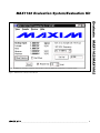
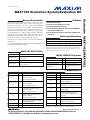
19-2582; Rev 1; 12/06
MAX1162 Evaluation System/Evaluation Kit
The MAX1162 evaluation system (EV system) is a complete 16-bit data-acquisition system consisting of a
MAX1162 evaluation kit (EV kit), Maxim 68HC16MODULE-DIP microcontroller (µC) module, and USBTO232.
Order the complete EV system (MAX1162EVC16) for
comprehensive evaluation of the MAX1162, using a personal computer (PC). Order the EV kit (MAX1162EVKIT)
separately if the 68HC16MODULE-DIP module has
already been purchased with a previous Maxim EV system or for custom use in other µC-based systems.
This EV kit can also be used to evaluate the MAX1062
14-bit ADC.
To evaluate the MAX1062, request a MAX1062AEUB free
sample when ordering this EV kit.
MAX1162 EV Kit Files
PROGRAM
Features
♦ Proven PCB Layout
♦ Convenient On-Board Test Points
♦ Fully Assembled and Tested
♦ EV Kit Software Supports Windows® 98/2000/XP
with RS-232/COM Ports
♦ EV Kit Software Supports Windows 2000/XP with
USB Ports
Ordering Information
PART
TEMP RANGE
INTERFACE
MAX1162EVKIT
0°C to +70°C
User supplied
MAX1162EVC16
0°C to +70°C
Windows software
Note: The MAX1162 software is designed for use with the complete EV system. It includes both a µC module and the EV kit. If
the Windows software will not be used, the EV kit board can be
purchased by itself, without the µC module.
FUNCTIONS
MAX1162EVC16 System
INSTALL.EXE
Installs the EV kit files on your
computer
MAX1162.EXE
Application program
MAX1162EVKIT
1
MAX1162 EV kit
KIT1162.C16
Software loaded into 68HC16
microcontroller
68HC16MODULE-DIP
1
68HC16 µC module
USBTO232+
1
USB-to-COM port adapter
board
PART
QTY
DESCRIPTION
Component List
DESIGNATION
QTY
C1, C4
2
10µF ±20%, 16V X5R ceramic
capacitors (1210)
TDK C3225X5R1C106M
C2, C3, C5, C7,
C8
5
0.1µF ±10%, 16V X7R ceramic
capacitors (0603)
TDK C1608X7R1C104KT
C6
1
C9
1
DESCRIPTION
DESIGNATION
QTY
DESCRIPTION
TB0
1
2-circuit terminal block
TP1
1
5-pin header
U1
1
16-bit ADC (10-pin µMAX)
MAX1162BCUB
U2
1
Logic buffer (5-pin SOT23)
Fairchild Semiconductor NC7SZ125
4.7µF ±20%, 16V X5R ceramic
capacitor (1206)
TDK C3216X5R1C475M
U3
1
Op amp (5-pin SOT23)
MAX4430EUK
4700pF ±10%, 50V X7R ceramic
capacitor (0603)
TDK C1603X7R1H472KT
—
1
MAX1162 EV kit data sheet
(includes 68HC16MODULE-DIP
manual)
—
1
PCB: MAX1162EVKIT
FB1, FB2
2
Surface-mount ferrite beads (0603)
TDK MMZ1608B601C
—
1
3.5in software disk,
MAX1162 evaluation kit
J1
1
2 x 20 right-angle female connector
—
1
MAX1162 data sheet
R1
1
200Ω ±1% resistor (0603)
Windows is a registered trademark of Microsoft Corp.
________________________________________________________________ Maxim Integrated Products
For pricing, delivery, and ordering information, please contact Maxim/Dallas Direct! at
1-888-629-4642, or visit Maxim’s website at www.maxim-ic.com.
1
Evaluate: MAX1162/MAX1062
General Description
Evaluate: MAX1162/MAX1062
MAX1162 Evaluation System/Evaluation Kit
Component Suppliers
SUPPLIER
PHONE
WEBSITE
Fairchild Semiconductor
888-522-5372
www.fairchildsemi.com
TDK Corp.
847-803-6100
www.component.tdk.com
Note: Indicate that you are using the MAX1162 when contacting these component suppliers.
Quick Start
Recommended Equipment—USB Port PC
Connection Option
Before you begin, the following equipment is needed:
•
MAX1162EVC16
(MAX1162EVKIT
68HC16MODULE-DIP, and USBTO232)
board,
•
Three DC power supplies: 8V to 20V, 5V, and -5V
•
External reference: +4.096V
•
Analog signal source: 0 to +4.096V
•
A PC running Windows 2000/XP with an available
standard USB port to connect to the USBTO232
•
USB cable included with the USBTO232
Procedure
Caution: Do not turn on the power until all the connections are completed.
1) Visit the Maxim website (www.maxim-ic.com) to
download the latest version of the USBTO232 User
Guide. Follow the steps in the USBTO232 User
Guide Quick Start section and return to step 2 of
this Quick Start section when finished.
7) Apply a 4.096V reference voltage to the MAX1162
EV kit’s terminal block (TB0) located in the upperleft corner of the MAX1162 EV kit board. Observe
the polarity marked on the board.
8) Connect the USBTO232 board to the 68HC16MODULE-DIP module if you have not done so already.
9) The MAX1162 EV kit software should have already
been downloaded and installed in the USBTO232
Quick Start.
10) Start the MAX1162 program by opening its icon in
the Start | Programs menu.
11) Turn on all power supplies and enable the reference voltage. Slide SW1 to the ON position on the
68HC16MODULE-DIP module. Press the OK button
to automatically connect and download the
KIT1162.C16 file to the module.
12) Apply an input signal (0V to VREF) between AIN
and GND. Observe the readout on the running
Windows program.
Recommended Equipment—RS-232/COM
Port PC Connection Option
Before you begin, the following equipment is needed:
2) Carefully connect the boards by aligning the 40-pin
connector of the MAX1162 EV kit with the 40-pin
header of the 68HC16MODULE-DIP module. Gently
press them together. The two boards should be
flush against one another.
•
MAX1162EVC16 (MAX1162EVKIT board and
68HC16MODULE-DIP)
•
Three DC power supplies: 8V to 20V, 5V, and -5V
•
External reference: +4.096V
3) Ensure that the 68HC16MODULE-DIP module’s
SW1 switch is in the OFF position.
•
Analog signal source: 0 to +4.096V
•
4) Connect the 8V to 20V power supply to the
68HC16MODULE-DIP module’s terminal block (J2)
located next to SW1. Observe the polarity marked
on the board.
A PC running Windows 98/2000/XP with an available standard serial port, preferably a 9-pin plug
•
A standard serial cable to connect the PC’s standard
serial port to the 68HC16MODULE-DIP module
5) Connect the 5V power supply to the VDD pad (with
respect to the GND pad) on the MAX1162 EV kit
board.
Caution: Do not turn on the power until all the connections are completed.
6) Connect the -5V power supply to the VEE pad (with
respect to the GND pad) on the MAX1162 EV kit
board.
1) Visit the Maxim website (www.maxim-ic.com/evkitsoftware) to download the latest version of the EV kit
software. Save the EV kit software to a temporary
folder and uncompress the file (if it is a .zip file).
2
Procedure
_______________________________________________________________________________________
MAX1162 Evaluation System/Evaluation Kit
3) Carefully connect the boards by aligning the 40-pin
connector of the MAX1162 EV kit with the 40-pin
header of the 68HC16MODULE-DIP module. Gently
press them together. The two boards should be
flush against one another.
4) Ensure that the 68HC16MODULE-DIP module’s
SW1 switch is in the OFF position.
5) Connect the 8V to 20V power supply to the
68HC16MODULE-DIP module’s terminal block (J2)
located next to SW1. Observe the polarity marked
on the board.
6) Connect the 5V power supply to the VDD pad (with
respect to the GND pad) on the MAX1162 EV kit
board.
7) Connect the -5V power supply to the VEE pad (with
respect to the GND pad) on the MAX1162 EV kit
board.
8) Apply a 4.096V reference voltage to the MAX1162
EV kit’s terminal block (TB0) located in the upperleft corner of the MAX1162 EV kit board. Observe
the polarity marked on the board.
9) Connect a standard serial cable from the computer’s serial port to the 68HC16MODULE-DIP module.
If the PC’s standard serial port has a 9-pin connector, use a straight-through, 9-pin female-to-male
cable. If the PC’s only available standard serial port
has a 25-pin connector, a standard 25-pin to 9-pin
adapter is required. The EV kit software checks the
modem status lines (CTS, DSR, DCD) to confirm
that the correct port has been selected.
10) Start the MAX1162 program by opening its icon in
the Start | Programs menu.
11) Turn on all power supplies and enable the reference voltage. Slide SW1 to the ON position on the
68HC16MODULE-DIP module. Press the OK button
to automatically connect and download the
KIT1162.C16 file to the module.
12) Apply an input signal (0V to VREF) between AIN
and GND. Observe the readout on the running
Windows program.
Detailed Description
MAX1162 Stand-Alone EV Kit
The MAX1162 EV kit provides a proven PCB layout to
evaluate the MAX1162. It must be interfaced to appropriate timing signals for proper operation. Connect 5V
to VDD and -5V to VEE with respect to GND. Apply a
4.096V reference voltage to the MAX1162 EV kit’s terminal block (TB0) located in the upper-left corner of the
MAX1162 EV kit board. See the MAX1162 EV Kit
Schematic (Figure 2) and refer to the MAX1162 data
sheet for timing requirements.
MAX1162 EV System
The MAX1162EVC16 EV system operates from three
user-supplied power supplies: 8V to 20V, 5V, and -5V.
Connect the 8V to 20V power supply to the µC module’s terminal block (J2) located next to SW1. Observe
the polarity marked on the board. Connect 5V to VDD
and -5V to VEE with respect to GND on the MAX1162
EV kit board. Apply a 4.096V reference voltage to the
MAX1162 EV kit’s terminal block (TB0) located in the
upper left corner of the MAX1162 EV kit board. See the
MAX1162 EV Kit Schematic (Figure 2).
Windows 98/2000/XP-compatible software interfaces to
the EV system board through the PC’s standard serial
port (virtual COM port). See the Quick Start section for
complete setup and operating instructions.
Detailed Description of
Software
The EV software’s main window is shown in Figure 1. It
controls the serial clock speed and sample rate. It also
displays the voltage and output code as well as some
statistics of the input signal. A separate graph shows
the data changing in real time. The update rate is limited to about 10 samples per second, due to COM port
bandwidth limitations.
Sample Rate
The SPI SCLK Frequency area allows the user to vary
the ADC to µC sample rate. The PC is not capable of
retrieving the data that was stored in the memory of the
µC as fast as the µC can obtain the data from the ADC.
This is because the µC’s SPI interface is much faster
than the PC’s standard serial port (virtual COM port).
Hence, the ADC to µC sample rate refers to the sample
_______________________________________________________________________________________
3
Evaluate: MAX1162/MAX1062
2) Install the MAX1162 EV kit software on your computer by running the INSTALL.EXE program. The
program files are copied and icons are created for
them in the Windows Start | Programs menu.
Evaluate: MAX1162/MAX1062
MAX1162 Evaluation System/Evaluation Kit
rate at which data is being sampled by the ADC and
stored in the µC’s memory. Use the pulldown menu to
select the desired SCLK frequency. The first two digits
are the divisor for the µC’s internal clock. The next floating point number is the corresponding SCLK frequency. The ADC to µC sample rate is displayed in the ADC
to µC sample rate field located on the right side of the
main window.
The µC to PC transfer rate is controlled using the field
at the bottom of the main window and can be controlled
in two different ways. Pressing the Read button allows
the user to manually grab a sample from the µC’s memory. Clicking the Read Every checkbox allows the user
to automatically read samples from the µC’s memory at
a rate selectable in milliseconds.
To retrieve a block of consecutively sampled data to
the PC, click on the Sample menu located at the top
left-hand corner of the main window. The data-block
length is selectable and the data can be saved to a file.
Statistics
The Minimum and Maximum fields in the statistics area
show the highest and lowest readings acquired. The
Average field displays a running mean. When reading
data manually by pressing the Read button, the Average
and RMS fields require approximately five samples until
they are accurately represented. The Clear Statistics
button resets the statistics. To remove offset errors, first
apply zero volts to the active input channel, press the
Clear Statistics button, acquire some samples, and then
check the Null Offset checkbox. Once checked, the
label next to the Null Offset checkbox shows the sampled offset error. This value is subtracted from all subsequent measurements until the checkbox is unchecked.
4
Reference Voltage
The EV software assumes a 4.096V reference voltage,
unless otherwise specified. To override the 4.096V reference value, apply the new reference voltage at the
terminal block (TB0) on the MAX1162 EV kit board, type
in the new reference voltage, without the volt unit, and
press the Set Vref button. The EV kit software uses the
value typed in the VREF field to translate the digital
code to a voltage.
Detailed Description of
Hardware
The MAX1162 is a 16-bit serial ADC. When the
MAX1162 EV kit board is connected to the
68HC16MODULE-DIP module, power is provided to U2
by the module. The user must also provide 5V to VDD
and -5V to VEE (with respect to the GND pads) on the
MAX1162 EV kit board. The MAX1162 EV kit contains
two different types of buffers. U2 is a logic buffer to limit
the load capacitance that is seen by the DOUT line of
the MAX1162. U1 is powered from VDD. U3 is powered
from VDD and VEE. A terminal block (TB0) has also
been provided on the MAX1162 EV kit board for the
external reference. See the Reference Voltage section
and the MAX1162 EV Kit Schematic (Figure 2).
_______________________________________________________________________________________
MAX1162 Evaluation System/Evaluation Kit
Evaluate: MAX1162/MAX1062
Note: The MAX1162 evaluation software’s main window controls the MAX1162 and displays conversion results.
Figure 1. MAX1162 EV Software’s Main Window
_______________________________________________________________________________________
5
Evaluate: MAX1162/MAX1062
MAX1162 Evaluation System/Evaluation Kit
AVDD
DVDD
FB1
VDD
C1
10µF
GND
C2
0.1µF
C3
0.1µF
FERRITE
C4
10µF
TP1
TP1-1
TP1-2
AIN
3
IN+
OUT
IN-
1
4
R1
200Ω
1%
TBO
U3
GND
VEE
GND
8
AVDD
DVDD
UCVDD
AIN
C9
4700pF
TERMINAL
BLOCK
1
J1-38
10
CS
U1
REF
VCC
DOUT
TP1-5
5
C5
0.1µF
TP1-4
TEST POINT
U2
NC7SZ125
5
6
TP1-3
DVDD
J1-37
SCLK
C6
4.7µF
OE
4
MAX1162
1
TBO-1
MAX4430
2
J1
J1-1
2
A
J1-2
2
VEE
VCC
5
C7
0.1µF
TBO-2
AGND AGND DGND
C8
0.1µF
3
9
7
FB2
J1-35
3
GND
Y
J1-3
4
FERRITE
J1-4
UCVDD
J1-7
J1-8
Figure 2. MAX1162 EV Kit Schematic
6
_______________________________________________________________________________________
MAX1162 Evaluation System/Evaluation Kit
Figure 4. MAX1162 EV Kit PCB Layout—Component Side
Figure 5. MAX1162 EV Kit PCB Layout—Inner Layer 2 (GND)
Figure 6. MAX1162 EV Kit PCB Layout—Inner Layer 3 (VDD)
_______________________________________________________________________________________
Evaluate: MAX1162/MAX1062
Figure 3. MAX1162 EV Kit Component Placement Guide—
Component Side
7
Evaluate: MAX1162/MAX1062
MAX1162 Evaluation System/Evaluation Kit
Figure 7. MAX1162 EV Kit PCB Layout—Solder Side
Figure 8. MAX1162 EV Kit Component Placement Guide—
Solder Side
Revision History
Pages changed at Rev 1: 1–8
Maxim cannot assume responsibility for use of any circuitry other than circuitry entirely embodied in a Maxim product. No circuit patent licenses are
implied. Maxim reserves the right to change the circuitry and specifications without notice at any time.
8 _____________________Maxim Integrated Products, 120 San Gabriel Drive, Sunnyvale, CA 94086 408-737-7600
© 2006 Maxim Integrated Products
is a registered trademark of Maxim Integrated Products, Inc.