1
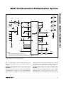
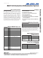
19-2161; Rev 1; 12/06
MAX1132 Evaluation Kit/Evaluation System
The MAX1132 evaluation system (EV system) is a complete, single-channel data-acquisition system, consisting
of the MAX1132 evaluation kit (EV kit), Maxim
68HC16MODULE-DIP microcontroller (µC) module, and
USBTO232. The MAX1132 is a high-speed, single-channel, 16-bit data acquisition system. Windows ®
98/2000/XP-compatible software provides a handy user
interface to exercise the MAX1132’s features. Order the
complete EV System (MAX1132EVC16) for comprehensive evaluation of the MAX1132 using a PC. Order the EV
kit (MAX1132EVKIT) if the 68HC16MODULE-DIP module
has already been purchased with a previous Maxim EV
system, or for custom use in other µC-based systems.
Features
♦ Proven PCB Layout
♦ Complete Evaluation System
♦ Convenient Test Points Provided On-Board
♦ Data-Logging Software
♦ Fully Assembled and Tested
♦ EV Kit Software Supports Windows® 98/2000/XP
with RS-232/COM Port
♦ EV Kit Software Supports Windows 2000/XP with
USB Port
Ordering Information
MAX1132EVKIT Parts List
REFERENCE QTY
DESCRIPTION
C1, C2
2
10µF 10V B-size tantalum capacitors
C3
1
2.2µF 10V X7R ceramic capacitor
0.22µF X7R ceramic capacitor (1206)
C4
1
C5, C6, C8
3
0.1µF X7R ceramic capacitors (1206)
C7
1
1µF X7R ceramic capacitor (1206)
FB1, FB2
2
Ferrite beads
J1
1
2 x 20 right-angle socket
SamTec SSW-120-02-S-D-RA
JU1, JU5
2
3-pin headers
JU2, JU3, JU4
2
2-pin headers
R1
1
100kΩ ±1% 1206 resistor
TB1, TB2
2
0.200in screw terminal blocks
TP1
1
9-pin header
U1
1
MAX1132BCAP
U2
1
74HC04 (14-pin SO) hex inverter
—
1
PCB: MAX1132EVKIT
—
1
3.5in software disk, MAX1132 EV kit
—
1
MAX1132 EV kit data sheet
(includes 68HC16MODULE-DIP
manual)
—
1
MAX1132 data sheet
PART
TEMP RANGE
INTERFACE
MAX1132EVKIT
0°C to +70°C
User supplied
MAX1132EVC16
0°C to +70°C
Windows software
Note: The MAX1132 EV kit software is included with the
MAX1132 EV kit, but is designed for use with the complete EV
system. The EV system includes the Maxim 68HC16MODULEDIP µC module, a USBTO232+ USB-to-COM port adapter
board, and the EV kit. If the Windows software will not be used,
the MAX1132 EV kit board can be purchased by itself, without
the µC and adapter board.
MAX1132EVC16 System
Component List
PART
MAX1132EVKIT
QTY
1
DESCRIPTION
MAX1132 EV kit
68HC16MODULE-DIP
1
68HC16 µC module
USBTO232+
1
USB-to-COM port adapter
board
List of Files in MAX1132
EV Kit
FILE
INSTALL.EXE
MAX1132.EXE
KIT1132.C16
DESCRIPTION
Installs the EV kit files on computer
Application program
Software loaded into 68HC16 µC
Windows is a registered trademark of Microsoft Corp.
________________________________________________________________ Maxim Integrated Products
For pricing, delivery, and ordering information, please contact Maxim/Dallas Direct! at
1-888-629-4642, or visit Maxim’s website at www.maxim-ic.com.
1
Evaluate: MAX1132/MAX1133
General Description
Evaluate: MAX1132/MAX1133
MAX1132 Evaluation Kit/Evaluation System
MAX1132 Stand-Alone EV Kit
The MAX1132EVKIT provides a proven PCB layout to
facilitate evaluation of the MAX1132. It must be interfaced to appropriate timing signals for proper operation. Connect +5V to AVDD and connect ground return
to AGND (Figure 1). Refer to the MAX1132 data sheet
for timing requirements.
MAX1132 EV System
The MAX1132EVC16 EV system operates from a usersupplied +7VDC to +20VDC power supply. Windows
98/2000/XP-compatible software running PC interfaces
to the EV system board through the computer’s serial
communications port (virtual COM port). See the Quick
Start section for setup and operating instructions.
Quick Start
Recommended Equipment—USB Port PC
Connection Option
6) The MAX1132 EV kit software should have already
been downloaded and installed in the USBTO232
Quick Start.
7) Start the MAX1132 program by opening its icon in
the Start | Programs menu.
8) Turn on the power supply and slide SW1 to the ON
position on the 68HC16MODULE-DIP module.
Press the OK button to automatically connect and
download the KIT1132.C16 file to the module.
9) Apply the input signal across the pins of JU2.
Observe the readout on the screen.
Recommended Equipment—RS-232/COM
Port PC Connection Option
Before you begin, the following equipment is needed:
• MAX1132EVC16 (contains MAX1132EVKIT board
and 68HC16MODULE-DIP)
•
Before you begin, the following equipment is needed:
• MAX1132EVC16 (contains MAX1132 EV kit board,
68HC16MODULE-DIP, and USBTO232)
Small DC power supply, such as a 12VDC, 0.25A
plug-in transformer, or a +9V battery
•
PC-compatible computer running Windows
98/2000/XP with an available serial communications
port, preferably a 9-pin plug
•
Small DC power supply, such as a 12VDC, 0.25A
plug-in transformer, or a +9V battery
•
Serial cable to connect the computer’s serial port to
the 68HC16MODULE-DIP
•
PC-compatible computer running Windows 2000/XP
with an available USB port to connect to the
USBTO232 board
•
USB cable included with the USBTO232
Procedure
Caution: Do not turn on the power until all the connections are completed.
1) Visit the Maxim website (www.maxim-ic.com) to
download the latest version of the USBTO232 User
Guide. Follow the steps in the USBTO232 User
Guide Quick Start section and return to step 2 of
this Quick Start section when finished.
2) Carefully connect the boards by aligning the 40-pin
connector of the MAX1132 EV kit with the 40-pin
connector of the 68HC16MODULE-DIP module.
Gently press them together. The two boards should
be flush against one another.
3) Check the jumper settings (Table 1).
4) Connect a +7VDC to +20VDC power source to the
µC module at the terminal block located next to the
ON/OFF switch, along the top edge of the µC module. Observe the polarity marked on the board.
5) Connect the USBTO232 board to the 68HC16MODULE-DIP module if you have not done so already.
2
Procedure
Caution: Do not turn on the power until all the connections are completed.
1) Visit the Maxim website (www.maxim-ic.com/evkitsoftware) to download the latest version of the EV kit
software. Save the EV kit software to a temporary
folder and uncompress the file (if it is a .zip file).
2) Install the MAX1132 EV kit software on your computer by running the INSTALL.EXE program. The
program files are copied and icons are created for
them in the Windows Start | Programs menu.
3) Carefully connect the boards by aligning the 40-pin
connector of the MAX1132 EV kit with the 40-pin
connector of the 68HC16MODULE-DIP module.
Gently press them together. The two boards should
be flush against one another.
4) Check the jumper settings (Table 1).
5) Connect a +7VDC to +20VDC power source to the
68HC16MODULE-DIP module at the terminal block
J2 located next to the ON/OFF switch. Observe the
polarity marked on the board.
6) Connect a cable from the computer’s serial port to
the 68HC16MODULE-DIP module. If using a 9-pin
serial port, use a straight-through, 9-pin female-to-
_______________________________________________________________________________________
MAX1132 Evaluation Kit/Evaluation System
7) Start the MAX1132 program by opening its icon in
the Start | Programs menu.
8) Turn on the power supply and slide SW1 to the ON
position on the 68HC16MODULE-DIP module.
Press the OK button to automatically connect and
download the KIT1132.C16 file to the module.
9) Apply the input signal across the pins of JU2.
Observe the readout on the screen.
Detailed Description
of Software
The evaluation software main window controls the
active control word bits, serial clock speed, and sample rate. It displays the voltage and output code, as
well as some statistics of the input signal. A separate
graph window shows the data changing in real time.
The update rate is limited to about 10 samples per second, due to COM port bandwidth limitations.
Controls
The control word is divided into several fields. To
change the active control word, drop down the appropriate field’s combo box and select the desired option.
If the QSPI clock is set to STOP, the configuration data
is not sent until the READ button is clicked.
Statistics
The minimum and maximum fields show the lowest and
highest readings acquired. The average and RMS
fields show the running mean and root-mean-square of
the input signal. The Clear button resets the statistics.
To remove offset errors, first apply zero volts to the
active input channel, clear statistics, acquire some
samples, and then check Tare. This offset is now subtracted from all subsequent voltage measurements.
Sampling
To sample data at rates up to 125ksps, select the
Sample menu item, make your selections, and click the
Begin Sampling button. Sample size is restricted to a
power of two to permit FFT processing once the data is
saved to a file. After the samples have been collected,
the data is automatically uploaded to the host and is
Table 1. Jumper Functions
JUMPER
POSITION
—
1-2
FUNCTION
JU1
Open
—
2-3
JU2
Closed
—
Open
JU3
Closed
Illegal
Enable internal reference, or apply an external reference
Operate
SHDN is controlled by 68HC16 module
Shutdown
Measure short circuit (zero volts)
Apply input signal at JU2
—
Open*
JU4
Closed
Disable internal reference
—
Open*
Enable internal reference
—
1
JU5
2
User-programmable output pin P2
User-programmable output pin P1
—
3
User-programmable output pin P0
*Default configuration.
_______________________________________________________________________________________
3
Evaluate: MAX1132/MAX1133
male cable. If the only available serial port uses a
25-pin connector, a standard 25-pin to 9-pin
adapter is required. The EV kit software checks the
modem status lines (CTS, DSR, DCD) to confirm
that the correct port has been selected.
Evaluate: MAX1132/MAX1133
MAX1132 Evaluation Kit/Evaluation System
graphed. Once displayed, the data can optionally be
saved to a file.
ues into the appropriate edit box and click the Set VREF
button.
Saving Graphs to Disk
Data in the real-time graph and in sampled data graphs
may be saved to a file. Only the raw output codes are
saved, but voltages may be inferred based on the reference voltage and the maximum code value.
Evaluating Shutdown
The evaluation software configures the 68HC16’s QSPI
submodule to continuously read data from the MAX1132
into the 68HC16. The sample rate is controlled by the
QSPI clock. To evaluate power-saving modes, these
automatic updates must be stopped. First, set the QSPI
clock control to STOP. This reconfigures the 68HC16’s
QSPI submodule to stop driving the serial clock. Second,
in the evaluation software’s main window, uncheck the
Read Every checkbox. Next, choose the desired software
power-down control word, and click the Read button to
send the new configuration to the MAX1132. If evaluating
the hardware shutdown, move JU2 to the 2-3 position.
Detailed Description
of Hardware
The MAX1132 (U1) is a high-speed, single-channel, 16bit data-acquisition system. There is no antialiasing filter
provided. The input signal may be applied directly to
JU2. High-impedance signal sources may require an
input buffer, which may be installed in the prototype
area. C4 bypasses the bandgap reference, and C3
bypasses the A/D converter‘s voltage reference. When
plugged into the 68HC16MODULE, the AVDD and DVDD
circuits are both powered by +5V. (Figure 1). Refer to the
MAX1132 data sheet.
Evaluating the MAX1133
To change the evaluation software's full-scale voltage
for use with the MAX1133, type 4.096 into the full-scale
edit box and click the Set VREF button.
Reference Voltage
Troubleshooting
The evaluation software assumes a +4.096V reference
voltage and a +12V full-scale voltage, unless otherwise
specified. Refer to the MAX1132 data sheet for more
information. To override these values, type the new val-
Problem: No output measurement. System seems to
report zero voltage, or fails to make a measurement.
Check VDD and VLOGIC supply voltages. Check the
+4.096V reference voltage using a digital voltmeter.
4
_______________________________________________________________________________________
MAX1132 Evaluation Kit/Evaluation System
Evaluate: MAX1132/MAX1133
U2-C
5
DVDD
74HC04
U2-D
AVDD
FB2
JU3
1
J1-7
C2
10µF
10V
J1-8
JU4
AGND
REFADJ
C4
0.22µF
TB1
FB1
CREF
AGND
CS
TP1-2
J1-4
1
2
J1-29
TP1-2
DVDD
JU1
11
74HC04
U2-F
10
13
74HC04
U2-G
12
74HC04
17
J1-38
DVDD
TP1-5
MAX1132
4
J1-3
8
18
TP1-4
C5
0.1µF
J1-2
19
C7
1.0µF
3
J1-1
9
20
JU2
2
AVDD
C1
10µF
10V
AIN
REF
C3
2.2µF
10V
AVDD
TP1-1
6
AVDD
5
DGND
DIN
DVDD
6
3
DGND
SHDN
16
C8
0.1µF
J1-36
DVDD
15
C6
0.1µF
14
TP1-6
DVDD
JU5
1
2
3
TB2
7
8
9
TP1-3
J1-27
10
SCLK
P2
13
J1-37
DVDD
P1
R1 TP1-7
100kΩ
P0
RST
12
J1-31
SSTRB
U2-A
NOTES:
1. MINIMIZE PARASITIC CAPACITANCE OF U1 PIN 11–U2 PIN 1.
KEEP THE TRACE SHORT AND KEEP GROUND PLANE 0.025in AWAY.
2. U2 SUPPLY AND GROUND RETURN SHOULD BE ROUTED TO CONNECTOR J1, NOT FLOODED.
DOUT
11
1
U2-B
2
74HC04
3
TP1-8
4
J1-35
74HC04
Figure 1. MAX1132 EV Kit Schematic Diagram
Use an oscilloscope to verify that the conversion-start
signal is being strobed. Verify that SHDN is being driven high.
Problem: Unacceptable errors when measuring a
transducer.
Although most signal sources can be connected directly
to the MAX1132’s analog input, some high-impedance
signal sources may require an input buffer. Check for
settling errors by increasing the acquisition time: operate
the evaluation kit in external clock mode, 32 clocks per
conversion, with the QSPI clock at its slowest setting.
Problem: Measurements are erratic, unstable; poor
accuracy.
Check the reference voltage and input using a digital
voltmeter. Use an oscilloscope to check for noise.
When probing for noise, keep the oscilloscope ground
_______________________________________________________________________________________
5
Evaluate: MAX1132/MAX1133
MAX1132 Evaluation Kit/Evaluation System
,QLW /'$$
&6KLJKFORFNORZE\GHIDXOW
67$$43'5
/'$$)
67$$43$5
SLQVWKDWDUHDVVLJQHGWRWKH463,
/'$$(
67$$4''5
460SLQVWKDWDUHRXWSXWV
/'$$
&5&217
67$$&5
VHQGHLJKWELWFRQWUROZRUGDQGFRQWLQXH
67$$&5
67$$&5
67$$&5(
/'$$
&5%,76(
67$$&5
UHFHLYHVL[WHHQELWGDWDILHOG
67$$&5
67$$&5
67$$&5)
&/5'
VHQG]HURZKHQUHFHLYLQJGDWD
67'75
67'75
67'75
67'75)
/'$%
FKDQQHOXQLSRODUVLQJOHHQGHGSG VWG75
FKDQQHOFRPPDQG
OGDE
FKDQQHOELWPDVN
RUG75
VWG75
FKDQQHOFRPPDQG
OGDE
FKDQQHOELWPDVN
RUG75
VWG75
FKDQQHOFRPPDQG
OGDE
FKDQQHOELWPDVN
RUG75
VWG75(
FKDQQHOFRPPDQG
&/563&5
GLVDEOH463,KDOWPRGHLQWHUUXSW
/''
%,76 63%5 0+]&32/ &3+$ 67'63&5
/''
'6&.'7/QRWXVHG
67'63&5
/'')
QHZTS HQGTS ZUDSWR]HUR
67'63&5
UXQ463,FRQWLQXRXVO\RQDOOFKDQQHOV
%6(7:63&5
VWDUWWKH463,
%&/56365
FOHDU63,)ELW
5HDG/RRS
/''55
MVU3URFHVVB&KDQQHOB
/''55
MVU3URFHVVB&KDQQHOB
/''55
MVU3URFHVVB&KDQQHOB
/''55)
MVU3URFHVVB&KDQQHOB
MPS5HDG/RRS
Listing 1. Reading All Channels with QSPI
6
_______________________________________________________________________________________
MAX1132 Evaluation Kit/Evaluation System
Evaluate: MAX1132/MAX1133
,QLW /'$$
&6KLJKFORFNORZE\GHIDXOW
67$$43'5
/'$$)
67$$43$5
SLQVWKDWDUHDVVLJQHGWRWKH463,
/'$$(
67$$4''5
460SLQVWKDWDUHRXWSXWV
/'$$
&5&217
67$$&5
VHQGHLJKWELWFRQWUROZRUGDQGFRQWLQXH
/'$$
&5%,76(
67$$&5
UHFHLYHVL[WHHQELWGDWDILHOG
&/5'
VHQG]HURZKHQUHFHLYLQJGDWD
67'75
/'$%
FKDQQHOXQLSRODUVLQJOHHQGHGSG VWG75
FKDQQHOFRPPDQG
&/563&5
GLVDEOH463,KDOWPRGHLQWHUUXSW
/''
%,76 63%5 0+]&32/ &3+$ 67'63&5
/''
'6&.'7/QRWXVHG
67'63&5
/''
QHZTS HQGTS QRZUDS
67'63&5
5HDG/RRS
%6(7:63&5
VWDUWWKH463,
%&/56365
FOHDU63,)ELW
,GOH %5&/56365,GOH
ZDLWXWLO63,)ELWLVVHW
/''55
52/'
52/'
52/'
MVU3URFHVVB&KDQQHOB
MPS5HDG/RRS
Listing 2. Reading a Single Channel with QSPI
_______________________________________________________________________________________
7
Evaluate: MAX1132/MAX1133
MAX1132 Evaluation Kit/Evaluation System
1.0"
1.0"
Figure 2. MAX1132 EV Kit Component Placement Guide —
Component Side
Figure 3. MAX1132 EV Kit PCB Layout—Component Side
1.0"
Figure 4. MAX1132 EV Kit PCB Layout—Solder Side
Revision History
Pages changed at Rev 1: 1, 2, 3, 7, 8
Maxim cannot assume responsibility for use of any circuitry other than circuitry entirely embodied in a Maxim product. No circuit patent licenses are
implied. Maxim reserves the right to change the circuitry and specifications without notice at any time.
8 _____________________Maxim Integrated Products, 120 San Gabriel Drive, Sunnyvale, CA 94086 408-737-7600
© 2006 Maxim Integrated Products
is a registered trademark of Maxim Integrated Products, Inc.