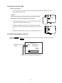
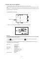
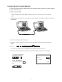
1
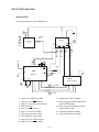
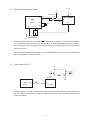
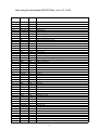
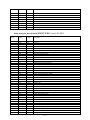
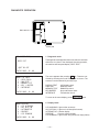
(without
price)
(with price)
SF-7900E(LX-552A)
SF-8900(LX-552I/J)
JAN. 1995
SF-7900E
R
CONTENTS
SPECIFICATIONS ................................................................................................................ 1
TO REPLACE THE BATTERY ............................................................................................. 2
TO CHECK THE MEMORY CAPACITY ............................................................................... 2
ERROR MESSAGE ............................................................................................................... 3
TO RESET THE SF UNIT'S MEMORY ................................................................................. 4
TO SAVE THE DATA TO ANOTHER UNIT ......................................................................... 5
BLOCK DIAGRAM ................................................................................................................ 8
CIRCUIT EXPLANATIONS
System chart ................................................................................................................. 9
Power supply circuit .................................................................................................. 10
CPU pin description (HD62076C03) .......................................................................... 12
Gate array pin descriptions (SSC2571F0A) ............................................................. 13
Gate array pin descriptions (SSC2571F0B) ............................................................. 14
Operation program ROM pin descriptions .............................................................. 15
RAM pin descriptions ................................................................................................ 15
DIAGNOSTIC OPERATION................................................................................................ 16
TROUBLESHOOTING ........................................................................................................ 21
SCHEMATIC DIAGRAM
Main PCB .................................................................................................................... 23
Display PCB ................................................................................................................ 25
Key Matrix ................................................................................................................... 26
Key Matrix (Display side) ........................................................................................... 27
PARTS LIST ........................................................................................................................ 29
ASSEMBLY VIEW .............................................................................................................. 31
SPECIFICATIONS
Main modes:
Telephone Directory, Business Card Library, Memo, Schedule Keeper,
Expense, Reminder, Calendar, Home Time, World Time and Calculator
Data storage:
Storage and recall of telephone, business card, memo, schedule, expense,
reminder data, calendar display, secret area; editing; memory status display
Clock:
World Time; reminder alarm; schedule alarm; daily alarm; accuracy under
normal temperatures: ±3 seconds average
Calculation:
12-digit arithmetic calculations; arithemetic constants (+, –, ×, ÷); independent memory; percentages; square roots; 24-digit approximations; date calculations; other mixed calculations
General:
Display element:
Memory capacity:
16-column × 8-line LCD
SF-7900E: 128KB (103436 bytes)
SF-8900: 256KB (234508 bytes)
Main component:
LSI
Power supply:
3 lithium batteries (CR2032)
Power consumption:
0.07 W
Battery life*:
Approximately 170 hours continuous operation in Telephone Directory;
approximately 130 hours repeating one minute of input and 10 minutes of
display in Telephone Directory; approximately 12 months for memory back
up
* The batteries that come installed in this unit when you purchase it are for
factory test purposes, so they will probably not provide normal service life.
Auto power off:
Approximately 6 minutes after last key operation
Operating temperature: 0°C ~ 40°C (32°F ~ 104°F)
Dimensions:
Unfolded: 9.55H × 144W × 155D mm (3/8"H × 5 11/16"W × 6 1/8"D)
Folded:
15.95H × 144W × 77.5D mm (5/8"H × 5 11/16"W × 3 1/16"D)
Weight:
123g (4.3 oz.)
• Design and specifications are subject to change without notice.
Current consumption:
Power switch
OFF
TYP. [µA]
MAX [µA]
11.7
37.1
ON
1,670.0
13,711.0
ON (Operating)
4,520.0
16,645.0
—1—
TO REPLACE THE BATTERY
To replace the batteries
1.
Loosen the screw on the back of the SF unit that holds the battery compartment cover in
place, and remove the cover.
Caution
In the next step, be sure to remove only one battery at a time.
Otherwise, you will lose all data stored in memory.
2.
Loosen the screw that secures one of the three battery holders
in place and remove the battery holder.
3.
Replace the old battery with a new one, making sure that the
positive (+) side of the new battery is facing up (so you can see
it).
4.
Screw
RESET
+
Replace the battery holder and secure it by tightening its screw.
TO CHECK THE MEMORY CAPACITY
Hold down CAPA to display a screen that shows the current memory status. To clear the memory
status display, release CAPA .
C A PA C IT Y
Remaining memory
capacity
FREE
USED
76420Bytes
27016Bytes
26 %
50
0
100
Total number of characters stored in memory
—2—
ERROR MESSAGE
Message
Meaning
Action
DATA ITEM
NOT FOUND!
NO DATA
IN MEMORY!
Search operation
attempted when no data
is stored in memory.
Current search operation
cannot be performed.
DATA ITEM
NOT FOUND!
Data specified in search
operation does not exist
in memory.
Change specification or
cancel search.
MEMORY FULL!
No more room in memory Delete unnecessary data
for storage of data.
items from memory.
ALARM TIME
ALREADY USED!
Attempt to set a Schedule Set a different alarm time
Keeper alarm time that
or change the existing alarm
is already used for
time to another one.
another entry.
ALARM TIME
ALREADY PASSED!
Attempt to set a Schedule Set a different alarm time
Keeper alarm time for a
(for a future time/date.)
time/date that is already
passed.
SECRET DATA!
Alarm for a secret
Enter the secret memory
memory area data item is area to view details of the
sounding.
alarm.
PASSWORD
MISMATCH!
Attempt to enter the
Use the correct password.
secret memory area
using a password that
does not match the one
preset for the secret area.
TRANSMIT ERROR!
Error during data
communications.
Cancel the data
communications
operation and try again.
DATA ERROR!
CONSULT THE
OWNER'S MANUAL!
Data corrupted by strong
impact, electrostatic
charge, etc.
See page 11 of the
owner's manual.
SAME TYPE
ALREADY USED!
Attempt to store a label
that is identical to one
already stored.
Use a different label.
STOPPED!
—3—
TO RESET THE SF UNIT'S MEMORY
The following procedure erases all data stored in the memory of the SF unit.
Perform the following operation only when you want to delete all data and initialize the settings of the SF
unit.
Remember – you should always keep copies of important data by writing it down, by transferring it to a
personal computer or other SF unit.
To reset the SF Unit's memory
RESET button
RESET
1. Switch on power and press the RESET button with a thin, pointed object.
Warning!
The next step deletes all data stored in the SF unit's memory. Make sure that you really want
to delete the data before you continue!
2. Press Y to reset the memory and delete all data or N to abort the reset operation without
deleting anything.
Following the reset operation described above, the Home Time display appears and the SF unit
settings are initialized as noted below.
Home Time:
World Time:
Daily Alarm:
Sound:
Character input:
12-hour format
JAN/1/1995
AM/12:00 00
Washington D.C.
12:00 PM
Schedule alarm → ON
Reminder alarm → ON
Daily alarm → OFF
Key → ON
CAPS
—4—
TO SAVE THE DATA TO ANOTHER UNIT
SF-7900 can transfer customers data to another SF-7900 with memory protection only when replacing
the LCD or the outer case.
How to transfer the data
* Before connecting the cable (SB-60 or SB-62), be sure to reset the slave unit to clear all
data.
1) Turn off the power switch and connect the two units using the cable (SB-60 or SB-62) as shown in
the drawing.
2) Turn on the power switch of both units.
3) The slave unit must be set the date of Feb. 3rd, 1901 into the memory under the calculator
mode.
CAL
Operation:
ON
1
DATE 2
DATE 3 DATE M+
CLEAR
If you don't set the date, the "PASSWORD" isn't transferred to the slave unit.
4) Check the hardware parameters, and if the units have another condition, reset as follows.
To change the hardware
parameters, press the
,
,
and
cursol keys.
SET UP
PARITY
BIT LENGTH
To set the hardware
parameters, press the SET
key.
BPS
TEL
FUNC 4 4
—5—
NONE
7
9600
5) Set up the slave unit.
1
While in the Calendar Display, Telephone Directory, Business Card Library, Memo Mode, or
Schedule Keeper, press the FUNCTION key followed by 4 to select " DATA COMM", and
the following menu appears.
TEL
FUNCTION
1 SEND
4
2 RECEIVE
3 PRINT
4 SET UP
2
Press 2 to select "RECEIVE" and the following display appears to indicate that the slave unit
is ready to receive data.
2
DATA
RECEIVE OK
TO STOP
PRESS [ESC]
6) Set up the customer's unit.
1
While the transmitting unit is in the Calendar Display, Telephone Directory, Business Card
Library, Memo Mode, or Schedule Keeper, press the FUNCTION key followed by 4 to
select "DATA COMM", and the following menu appears.
TEL
FUNCTION
4
1 SEND
2 RECEIVE
3 PRINT
4 SET UP
2
Press 1 to select "SEND" and the following menu appears.
SEND
1 ONE ITEM
1
2 MODE DATA
3 ALL DATA
—6—
3
Press 3 to select "ALL DATA". The following display appears to confirm if you wish to
proceed.
SEND ALL
3
DATA ITEM ?
SET / ESC
4
Press the SET key to proceed with the data transmission, or press ESC if you wish to
cancel.
NOW SENDING !
SET
TO STOP, PRESS
ESC
Data are transmitted in the sequence of Telephone Directory data, Memo data, Reminder data,
Schedule Keeper data and Calendar data.
* The following messages appear on the display of the receiving unit when a problem occurs during
data communications. All data transferred up to display of the message is retained in memory, but
data communication is terminated.
TEL
MEMO
SCHEDULE
HOME/WORLD
REMINDER
If one of the following error messages appear, press the
,
,
,
,
CAL
CALENDAR
,
keys, to clear the error message. Then, take corrective action and try data
communication again.
Message
Meaning
Action
TRANSMIT ERROR!
STOPPED!
Error during data
communications.
Cancel the data
communications operation
and try again.
DATA ERROR!
CONSULT THE
OWNER'S MANUAL!
Data corrupted by strong
impact, electrostatic
charge, etc.
See page 9 of the owner's
manual.
—7—
,
BLOCK DIAGRAM
LCD
96 × 64 dots
CD760-TS
S0~S15
C0~C63
S16~S95
KEYBOARD
PCB-L589-E4
LCD DRIVER
LCD DRIVER
MSM6585AV
-Z-358B
MSM6585AV
-Z-358B
PCB-L589-E2
DATA BUS
TO KEYBOARD
LCD DRIVE
VOLTAGES
V1 ~ V5
CPU
HD62076C03
LSI1
PCB-L522-1(SF-7900E)
or
PCB-L552-1(SF-8900)
VDD
OPEN (OFF)
LOCK (ON)
ROM
MAIN SWITCH
(Operation Program)
GND
LSI5
Power supply circuit
RAM
MSM51008AFP-10LL
LSI3, LSI4
SF-7900E: RAM × 1
SF-8900: RAM × 2
GATE ARRAY
SSC2571
LSI2
INTERFACE FOR
DATA TRANSMISSION
& DATA RECEPTION
—8—
CIRCUIT EXPLANATIONS
System chart
The circuitry operates in the following order:
VDD
1
VDD
11
Low battery
detector
VSS
10
Gate array
Power supply
circuit
IC4
(Pin24)
V1~V5
for LCD
VOB
VIN
PDN
SWO
OEO
(Pin35) (Pin62)
MSO
(Pin28)
(Pin49)
(Pin58)
3
2
12
13
"L"
"L"
"L"
"L"
"H"
VDD
2 MHz
9
(Pin45)
8
(Pin41)
V2ON
VDD1
OSCI
(Pin40)
OSCO
VDD
(Pin70)
INT0
OFF
CPU
GND
MAIN SWITCH
SW (Pin36)
HD62076C03
5
"L"
4
ON
(Pin24)
OE
(Pin22)
CE
GND
ROM
KIO
KAC
(Pin54)
(Pin53)
(Operation program)
"H"
"L"
6
14
7
ADDRESS
ADDRESS BUS
DATA BUS
15
1. Supply 5V to VDD1 and VDD2.
2.
3.
4.
5.
6.
7.
8.
9.
10.
Output "L" from SWO terminal.
Output "L" from IC4 and Q5 terminal.
Main switch ON.
Input "L" to SW terminal.
Input "L" from KAC terminal.
Push power on button switch.
CPU oscillation is generated.
Output "H" from V2ON terminal.
Output "L" from VOB terminal.
—9—
DATA
11. Output all LCD drive voltages.
12. Gate array sends ROM output enable
signal to OE terminal.
13. Gate array sends ROM Chip enable
signal to CE terminal.
14. CPU sends address to ROM.
15. CPU receives data from ROM.
Power supply circuit
1)
Power supply circuit for CPU, GATE ARRAY and RAMs.
When the main batteries are set, the voltage (9V) is applied to the terminal VDD1 of CPU (LSI1), GATE
ARRAY (LSI2) and RAM (LSI4).
When IC2 receives the voltage, it provides 4V to the GND lines from the terminal OUT (Pin No.1).
2)
Main switch
The CPU (LSI1) detects the informations of the Main switch by the terminal SW (Pin No.36) from the
SWO signal of the GATE ARRAY (LSI2).
3)
How to turn the display ON.
When pressing "ON" key under the ON side of the Main switch , the CPU (LSI1) generates the signal
to turn the display ON on the terminal V2ON (Pin No.45).
This signal goes to the terminal VIN (Pin No.24) of the GATE ARRAY (LSI2), then the GATE ARRAY
(LSI2) generates "L" level on the terminal VOB (Pin No.28). When the transistor 2SA1179 (Q2) receives "L" level, the transistor 2SC2812 (Q1) will be also turned ON. Then LCD drive voltage V1~V4
will be applied.
4)
How to detect the voltage for the main batteries.
When the voltage of the VDD lines becomes +6.6V±0.18V, the terminal OUT (Pin No.1) of the detector
RH5V60BA (IC4) becomes "L" level, then this signal goes to the terminal INTO (Pin No.70) of the CPU
(LSI1) and the terminal PDN (Pin No.35) of the GATE ARRAY (LSI2).
The CPU detects the low battery condition, then the display turns OFF.
— 10 —
5)
Main switch and power on switch
from IC4
VDD
(Pin35)
MAIN SWITCH
OFF
(Pin36)
SW
PDN
"L"
ON
(Pin62)
CPU
"L"
GATE ARRAY
SWO
OSCI
HD62076C03
KON
2 MHz
(Pin26)
OSCO
KAC
(Pin54)
KIO
(Pin53)
4S66F
"H"
"L"
POWER ON SWITCH
When the main switch is set to on position, SW terminal of CPU receives "L", then KAC terminal will be
"L" to enable the system power on. The KI0 terminal is "H" when VDD is applied to CPU. Therefore,
when pressing the power on switch, CPU will generate a clock pulse (2 MHz) at OSCO terminal for
start up the system.
When the PDN terminal will be receiving "L" level, GATE ARRAY will send "L" signal from KON terminal for cutting the line of power on switch.
6)
Power supply for LCD
VDD
(Pin1)
(Pin2)
V1~V4
C20
R3
(Pin3)
(Pin3)
VR1
R2
(Pin28) "L"
VOB
CPU
HD62076C03
V2ON
"H"
(Pin45)
(Pin24)
(Pin31)
GND
VIN
GATE ARRAY
When the system is start up, CPU will send "H" signal to VIN terminal of gate array from V2ON terminal. Then, gate array will send "L" signal from VOB terminal to turn ON the transistors Q2 and Q1 for
LCD drive voltages.
— 11 —
CPU pin description (HD62076C03)
Pin No.
Name
In/Out
Status
of OFF
Status
of ON
Description
1~14,16,17
15,39, 100
24
25
26
27
28
29
30
31
32
33
34
35
36
37
38
40,41
42
43, 91
44
45
46~53
54
55~65,67
66
68
69
70
71
72
73
74
75
76
77
78
79
80
81
82
83
84
85
86
87
88
89
90
92~99
18~23
A0~A15
VSS
WE
OE
FE
CS1
CS2
CS3
E0
E1
E2
E3
BCON
MDP2
SW
ONMK
TEST
OSC O/I
VDSC
VDD1
VDD2
V2ON
KI7~KI0
KAC
KC0~KC11
GND
INT2
INT1
INT0
BRK
P0
P1
P2
P3
P4
P5
P6
P7
H1
WENL
H2
L1
L2
DT
PRO
FR
LP
GC
DE
IO7~IO0
RA14~19
Out
In
Out
Out
Out
Out
Out
Out
Out
Out
Out
Out
Out
Out
In
In
In
In
In
In
In
Out
In
Out
Out
In
In
In
In
In
Out
In
In
In
Out
Out
In
In
Out
In
Out
Out
Out
Out
Out
Out
Out
Out
Out
In/Out
Out
L
GND
H
H
H
H
H
H
L
L
L
L
H
H
L
H
L
L
L
H
H
L
H
L
H
L
H
L
H
H
H
L
H
L
H
H
H
H
H
L
H
L
L
H
L
L
H
H
H
L
L
Pulse
GND
Pulse
Pulse
Pulse
H
H
Pulse
Pulse
H
H
H
H
L
L
H
L
Pulse
H
H
H
H
H
Pulse
Pulse
L
H
H
H
H
H
H
H
H
Pulse
Pulse
H
H
H
L
H
H
L
Pulse
H
Pulse
Pulse
Pulse
Pulse
Pulse
Pulse
Address Bus line
GND terminal
Write signal
Read signal
Chip select signal for Gate array
Chip select signal
Chip select signal
Chip select signal
Chip enable signal (Not used)
Chip enable signal (Not used)
Chip enable signal (Not used)
Chip enable signal (Not used)
BCN signal (Not used)
MDP signal (Not used)
Switch signal (When switches are at ON position)
Battery detection
TEST terminal (connect to GND)
Clock input
Power input for Clock
VDD input terminal
VDD input terminal
Power on output signal
Key input signal
Power on switch signal output
Key common signal output
GND terminal
Interrupt signal from Gate array
Interrupt signal for transmission
Interrupt signal for Power down
VDD input terminal
Transmission data output
Reception data input
Card lock switch input (Not used)
IC card detection signal input (Not used)
Not used
Not used
Memory back-up battery detection input (Not used)
Battery detection input (Not used)
Not used
GND terminal
Not used
Not used
Not used
DT signal output
LCD driver mode selection signal
LCD driver synchronous signal
LCD driver latch pulse signal
GC signal output
LCD driver data latch clock signal
Data bus line
Address line (Not used)
— 12 —
Gate array pin descriptions (SSC2571F0A): Used in SF-7900E
Pin No.
Name
In/Out
Description
1
2
3
4
5~10
11
12
13
14
15
16
17
18
19
20
21
22
23
24
25
26
27
28
29
30
31
32
33
34
35
36
37
38
39
40
41
42
43
44
45
46
47
48
49
50
51
52
53
54
55
56
VSS1
OSO
OSI
VL1
A0~3,A14,15
FE
CS1
CS2
CS3
OEI
VSS(GND)
VH1(VCC)
TXI
WEI
GC
IO0
DT
IO1
VIN
IO2
KON
IO3
VOB
IO4
INT
VH2(VCC)
VL2(VLL)
VSS(GND)
BBC
PDN
IO5
RLD
RA15
IO6
RA16
IO7
RA17
RA18
MS3
RA19
RA20
R15
VSS(GND)
VH3(VCC)
VDD1(VLL)
R16
R17
MSO
MS4
MS1
MS5
In
Out
In
In
In
In
In
In
In
In
In
In
In
In
In
In/Out
In
In/Out
In
In/Out
Out
In/Out
Out
In/Out
Out
In
In
In
Out
In
In/Out
Out
Out
In/Out
Out
In/Out
Out
Out
Out
Out
Out
Out
In
In
In
Out
Out
Out
Out
Out
Out
GND terminal
Clock out
Clock in
6V input
Address input
Chip select signal from CPU
Chip select signal from CPU
Chip select signal from CPU
Chip select signal from CPU
Output enable signal from CPU
GND terminal
9V input
Transmission data input from CPU
Write enable signal from CPU
GC signal from CPU
Data bus line
DT signal input
Data bus line
Power ON signal from CPU (V2ON)
Data bus line
Switch control signal
Data bus line
Inverted signal for VIN
Data bus line
Interrupt signal
9V input
6V input
GND terminal
Not used
Power down detection input
Data bus line
Not used
Address bus output
Data bus line
Inverted signal for VIN
Data bus line
Address bus output
Address bus output
Not used
Not used
Not used
Address bus
GND terminal
9V input
6V input
Address bus
Address bus
Chip enable signal for ROM
Chip select signal for RAM (Not used)
Not used
Not used
— 13 —
Pin No.
Name
In/Out
Description
57
MS2
Out
Not used
58
OEO
Out
Output enable for ROM
59
BZ1
Out
Buzzer signal
60
OTP
In
Connected to GND
61
BZ2
Out
Buzzer signal
62
SWO
Out
Main switch control signal
63
VH4(VCC)
In
9V input
64
TXO
Out
Transmission data output terminal
Gate array pin descriptions (SSC2571F0B): Used in SF-8900
Pin No.
Name
In/Out
Description
1
2
3
4
5~10
11
12
13
14
15
16
17
18
19
20
VSS1
OSO
OSI
VL1
A0~3,A14,15
FE
CS1
CS2
CS3
OEI
VSS(GND)
VH1(VCC)
TXI
WEI
GC
In
Out
In
In
In
In
In
In
In
In
In
In
In
In
In
GND terminal
Clock out
Clock in
6V input
Address input
Chip select signal from CPU
Chip select signal from CPU
Chip select signal from CPU
Chip select signal from CPU
Output enable signal from CPU
GND terminal
9V input
Transmission data input from CPU
Write enable signal from CPU
GC signal from CPU
21
22
23
24
25
26
IO0
DT
IO1
VIN
IO2
KON
In/Out
In
In/Out
In
In/Out
Out
Data bus line
DT signal input
Data bus line
Power ON signal from CPU (V2ON)
Data bus line
Switch control signal
27
28
29
30
IO3
VOB
IO4
INT
In/Out
Out
In/Out
Out
Data bus line
Inverted signal for VIN
Data bus line
Interrupt signal
31
VH2(VCC)
In
9V input
32
33
34
VL2(VLL)
VSS(GND)
BBC
In
In
Out
6V input
GND terminal
Not used
35
PDN
In
Power down detection input
36
37
38
39
40
41
IO5
LRAM
CM32
IO6
RA16
IO7
In/Out
Out
Out
In/Out
Out
In/Out
Data bus line
Connected to 9V
Connected to GND
Data bus line
Inverted signal for VIN
Data bus line
42
43
RA17
RA18
Out
Out
Address bus output
Address bus output
44
45
MS3
RA19
Out
Out
Not used
Not used
— 14 —
Pin No.
Name
In/Out
Description
46
47
48
49
50
51
52
53
54
55
56
RA20
R15
VSS(GND)
VH3(VCC)
VL3
CAC
MS7
MSO
MS4
MS1
MS5
Out
Out
In
In
In
Out
Out
Out
Out
Out
Out
Not used
Address bus
GND terminal
9V input
6V input
Address bus
Address bus
Chip enable signal for ROM (Not used)
Chip select signal for RAM (Not used)
Chip select signal
Not used
57
MS2
Out
Not used
58
MS6
Out
Chip select signal
59
BZ1
Out
Buzzer signal
60
OTP
In
Connected to GND
61
BZ2
Out
Buzzer signal
62
SWO
Out
Main switch control signal
63
VH4(VCC)
In
9V input
64
TXO
Out
Transmission data output terminal
Operation program ROM pin descriptions
Pin No.
Name
In/Out
Status
of OFF
Status
of ON
Description
2~12,23,
25~30
13~15, 17~21
16
22
24
31
1, 32
A0~A17
In
L
Pulse
Address bus line (A0~A14, RA15~RA17)
O0~O7
GND
CE
OE
A18
VPP, VCC
Out
In
In
In
In
In
L
L
H
L
L
L
Pulse
L
Pulse
Pulse
Pulse
H
Data bus line (IO0~IO7)
GND terminal
Chip enable signal from Gate array
Output enable signal from Gate array
Address line (RA18)
VDD terminal
RAM pin descriptions
Pin No.
Name
In/Out
Status
of OFF
Status
of ON
Description
3~12, 23
25~28, 31
13~15, 17~21
16
22
24
29
32
A0~A15
In
L
Pulse
Address bus line (A0~A15)
IO0~IO7
GND
S1
OE
W
VCC
Out
In
In
In
In
In
L
L
H
L
H
L
Pulse
L
Pulse
Pulse
Pulse
H
Data bus line (IO0~IO7)
GND terminal
Chip enable signal from Gate array
Output enable signal from Gate array
Write enable signal from CPU
VDD terminal
— 15 —
DIAGNOSTIC OPERATION
Main switch
Check pad
SELF TEST PROG.
PRESS SET
1. Diagnostic mode
The diagnostic mode appears when main switch is turned on
while there is a short in the checkpad. After this operation,
the machine will beep and display "SELF-TEST".
QUIT BY OFF
CASIO 1993. 11. 09
MENU
1 :
2 :
3 :
4 :
5 :
TOP SHEET
DISP CHECK
RAM TEST
MEMORY TEST
KEY / BUZZER
INTERFACE
CASIO 1993. 11. 09
The menu appears after pressing SET key. Tests are conducted by selecting the mode from the list on screen. The
each test can be selected by numeral keys.
DISPLAY TEST
RAM TEST
MEMORY TEST
KEY/BUZZER
INTERFACE
: LCD display check
: RAM chip check
: ROM/Clock check
: Keys and Buzzer check
: Transmission check
To return to the menu display, press DISP CHNG button .
MENU
1 :
2 :
3 :
4 :
5 :
DISPLAY
LCD ALIGNING
ALL DOTS ON
ALTERNATIVE
REVERSE
LCD FRAMING
2. Display check
LCD ALIGNING: Lights on dot at corners
ALL DOTS ON : Lights on in all dots (black screen)
ALTERNATIVE : Checker display
REVERSE
: Reverse checker display
LCD FRAMING : Lights on dot along the screen edge (frame)
CASIO 1993. 11. 09
— 16 —
3. RAM check
DISP CHNG key
MENU
1 :
2 :
3 :
4 :
5 :
RAM
DATE WRITE
DATA READ
PAT. CHANGE
#1
DATA WRITE
DATA READ
PAT. CHANGE
:Return to menu
: Write the set pattern to the RAM area
: Compare the pattern displayed after # with
the write data of RAM and displays the
results.
: Change the test data pattern.
CASIO 1993. 11. 09
#1---Test data pattern(00,01,02...)
#2---Test data pattern(FF,FE,FD....)
1) RAM write
The unit will beep after a second.
The menu will be appeared.
RAM WRITING
#1
NOW EXECUTING!
CASIO 1993. 11. 09
It means RAM write is succeeded.
2) RAM read
Normal end display is;
RAM COMPARE
COMPLETE!
CASIO 1993. 11. 09
Error end display is;
#1
RAM COMPARE
DATA ERROR!
ADDRESS
CORR
XXXX
XX
#1
RAM
XX
CASIO 1993. 11. 09
To escape from this message, press DISP CHNG
key.
— 17 —
4. ROM/Clock check
MENU
1 :
2 :
3 :
4 :
5 :
CHECK-SUM
: Call up check sum and XOR
values for connected ROM.
SPECIFIC ADDR : Call up check sum for certain
address.
TIME DISPLAY : Bring up clock display. The
present time, date and daily
alarm can be set.
MEMORY
CHECK–SUM
SPECIFIC ADDR
TIME DISPLAY
CASIO 1993. 11. 09
1) Check sum
3)
Time display
CHECKSUM CALC
TP
C0 O
SZ
256
TIME DISPLAY
SUM
XXXX
XOR
XX
1990-03-00
10:10 00
XXXXXXXXXXXXXXX
CASIO 1993. 11. 09
CASIO 1993. 11. 09
2) Specific address
SPECIFIC ADDR
TP
D0 O
SZ
256
SUM
XXXX
XOR
XX
Input can be made in the line which
shows "x" using the numeric keys.
Entry of 12 or more digits sets the time
and date. Entry of 4 or 6 digits sets the
daily alarm. The ON key clears current entries.
CASIO 1993. 11. 09
5. Key/Buzzer check
MENU
1 :
2 :
3 :
4 :
5 :
KEY / BZR
RANDOM
COMPULSORY
BEEP
ALARM NOTE 1
ALARM NOTE 2
CASIO 1993. 11. 09
RANDOM :
The 'key code' will be displayed.
The 'key code' is numbered incrementally from
left to right with the DATE key as "00", and
HOME/WORLD key as "34" etc. Accordingly,
the left cursor key is "40". To release this test, press
SEARCH key.
COMPULSORY :
Limits the mode mentioned above so that the
keys must be pressed according to the key code.
If an error is made, a buzzer sounds for about 1
second. (A correct entry results in a beep tone.)
BEEP
ALARM NOTE 1
ALARM NOTE 2
— 18 —
: Key input sound every 1 second
: Sound alarm 1
: Sound alarm 2
Pressing of the SEARCH key in either mode will return to the screen of the menu mode.
Sound can be stopped by pressing any key.
While an alarm is sounding the screen display is as shown left. If an irregularity is found in voltage
of battery while the alarm is sounding, the alarm will stop. After 256 seconds, the alarm will stop
automatically.
6. Interface check
The three charactors that appear on the right side at display
represent the parameter. In the case of the example display,
it indicates 7 BIT, NON PARITY, 9600 BPS. The operation
continues until stopped by pressing the ESC key and then
pressing the ON key for all modes.
MENU
INTERFACE
1: DATA RECEIVE
2: DATA TRANSMIT
3: ASCII CODE
4: LOOP BACK
5:
7N9
CASIO 1993.11.09
Parameter
EXECUTING !
6 key
7 key
8 key
DISP CHNG key : Return to menu mode
1 key
: Transmission mode. The data of transmission is "H" and it is sent out by the data
of H34 and H38 by the Xon/Xoff control.
2 key
: Reception mode. Make sure to set the
parameter to match that of the transitting
side. The data received appears on the
display.
3 key
: Output the following ASCII code by Xon/
Xoff control.
!"#*+,-/0123456789:
ABCDEFGHIJKLMNOPQRSTUVWXYZ
abcdefghijklmnopqrstuvwxyz
A line end code is added with each line.
4 key
: Loop back test. Short the Tx and Rx
terminals for this test. Transmit and check
from H20 to H7E. When complete, the
message 'CHECK COMPLETE' is displayed.
: Switch the data length 7 bit(7) or 8 bit(8)
: Switch the parity bit : NON(N)—EVEN(E) —NON(N) —ODD(O)
: Switch the transmission speed : 9600(9)—4800(4)—2400(2)—1200(1)
NOTE : As diagnostic program area does not have all ASCII code, to display a reception data, some
charactor will be changed to other charactor. For example, a capital letter will be changed
to small letter.
— 19 —
LOOP BACK
LOOP BACK
NOW EXECUTING!
COMPLETE!
CASIO 1993. 11. 09
CASIO 1993. 11. 09
Break display (Broken transmission)
Error display
TRANS BREAK!
TRANS ERROR!
CASIO 1993. 11. 09
CASIO 1993. 11. 09
7. Others
1) When power is off after presetting an alarm time, the unit automatically powered on at the alarm
time. However, the display is not reserved in this case.
2) When executing memory sum check, execute the RAM write check before.
3) To release diagnostic mode, press RESET button.
4) The display contrast can be changed by the contrast dial.
— 20 —
TROUBLESHOOTING
Before the following solutions will be done, save data if possible.
SYMPTOM
No power
No display at all or wrong
display
No key input at all
CAUSE
SOLUTION
Battery shortage
Replace batteries
Poor soldering of the power supply
circuit
Resolder
Defective LSI-1 or LSI-2
Replace it
Defective TAB LSI
Replace it
Defective heat seal
Replace it
Defective LCD
Replace it
Poor soldering LSI-1 or LSI-2
Resolder
Defective LSI-1 or LSI-2
Replace it
— 21 —
SCHEMATIC DIAGRAM
Main PCB: SF-7900E
IC4
D2
Q5
R22 R27
S-80766AH
—
O
O
RH5VA60BA
O
—
O
R28
R29
O
—
O
—
O
—
Note: The following parts are not mounted.
C16, R24
— 23 —
Main PCB: SF8900
— 24 —
Display PCB
— 25 —
Key Matrix
— 26 —
Key Matrix (Display side)
— 27 —
PARTS LIST
N
Item
N
N
C1
C4
C5
C6,C7
C8,C9
C10,11,16
C81~87
C20
D1
D2
D2
D3
IC2
IC3
IC4
IC4
IC6
IC7
IC8
J1
LSI1
LSI2
LSI2
LSI3, 4
LSI5
Q1
Q2
Q4
R1,R2
R3,R22
R6,R7
R10
R12
R13,R31
R14~R18
R19
R23
R24
R25,R28
VR1
X1
X2
1
2
3
3
N
LSI6,7
4
N
N
N
N
N
N
N
N
N
Code No.
Parts Name
CPU BOARD ASS'Y
2803 6813 Capapcitor
2845 2289 Chip capacitor
2845 1673 Chip capacitor
2845 2499 Chip capacitor
6411 8550 Chip capacitor
2845 1540 Chip capacitor
Specification
CB0011341R3
MCH215C471KK
MCH215A221JK
MCH215A300JK
CP016F602T3
MCH212F104ZK
2845 3486 Chip capacitor
MCH312F474ZP
2390 0847 Chip diode
MA718-(TX)
2305 1028 Chip diode
MA157-(TX)
2390 2338 Diode
BC10SB007T4
2390 0364 Shottky diode
MA713-(TX)
2105 2982 IC
S-80250AG-GB-T1
2105 2989 IC
S-81220PG-PS-T1
2105 3794 IC, CMOS
S-80766AL-EX-T1
2105 2247 CMOS-IC
RH5VA60BA-T1
2105 1141 L-MOS IC
TC4S66F-TE85R
2114 3759 IC
ABT7S080007
2114 3752 IC
ABT7S320008
3501 6538 Jack
HSJ1169-012010
2011 3843 LSI
HD62076C03
2011 7350 LSI
SSC2571FOA
2011 8393 LSI
SSC2571FOB
2011 6300 LSI
M5M51008AFP-10LL
2011 9478 LSI
UPD23C4001EBGW-J14
2221 0378 Chip transistor
2SC2812-L5, L6-TB
2200 4417 Transistor
2SA1179M5, M6-TB
2259 0959 Chip digital transistor
DTC114YKT-146
2795 1309 Chip resistor
MCR10EZHJ684
2795 0532 Chip resistor
MCR10EZHJ105
2792 0217 Chip resistor
MCR10EZHJ101
2792 0462 Chip resistor
MCR10EZHJ473
2792 1191 Chip resistor
MCR10EZHJ182
2792 0470 Chip resistor
MCR10EZHJ102
2775 1939 Chip resistor
CC0512D10E8
2792 0209 Chip resistor
MCR10EZHJ104
2775 1946 Chip resistor
CC2201D11C3
2775 1953 Chip resistor
CC3902D15E7
2795 0056 Chip resistor
MCR10EZHJ000
6414 1300 Volume
CF100230002
2590 0777 Ceramic oscillator
CSAC2.01MGCM001-TC
6510 4550 Crystal
BD0063P2509
6411 8490 Battery spring (+)
EF01DB21109
6409 6310 Battery contact plate (-)
EF02DB10100
6414 1280 CPU board ass'y
DB21BX3100N*1
6414 1420 CPU board ass'y
DB21CX3100V*1
DISPLAY PCB ASS'Y
2011 1974 LSI
MSM6385AV-Z-358B
6414 1270 Display PCB ass'y
DB21BX3F00U
Notes: N – New parts
M – Minimum order/supply quantity
R – Rank
Q – Quantity used per unit
— 29 —
AT : SF-7900E
IT : SF-8900
JT : SF-8900 (B.O.S.S.)
FOB Japan
Quantity M N.R.Yen
R
AT IT JT
Unit Price
1
1
1
2
2
9
1
1
1
2
2
10
1
1
1
2
2
10
20
20
20
20
20
20
22
3
4
3
13
4
C
C
C
C
C
C
1
1
1
0
1
1
1
0
1
1
0
0
1
1
1
0
1
1
1
1
1
2
2
2
1
1
2
5
1
1
1
2
1
1
1
3
3
1
0
1
1
0
1
1
1
1
1
0
1
1
1
1
1
0
1
2
1
1
1
1
2
2
2
1
1
2
5
1
1
1
0
1
1
1
3
3
0
1
1
1
0
1
1
1
1
1
0
1
1
1
1
1
0
1
2
1
1
1
1
2
2
2
1
1
2
5
1
1
1
0
1
1
1
3
3
0
1
20
5
10
5
10
1
10
5
5
5
1
1
5
1
1
1
1
1
20
20
20
10
20
20
20
10
20
20
20
20
20
20
1
1
5
20
20
1
1
21
47
34
64
33
100
45
70
65
39
130
130
56
720
460
460
1270
630
12
15
12
9
3
3
3
9
3
13
3
13
13
3
720
98
55
12
16
4,750
6,000
C
B
B
B
B
B
B
B
B
B
A
A
X
A
A
A
A
A
B
B
B
C
C
C
C
C
C
C
C
C
C
C
C
B
C
X
X
B
AA
2
1
R–A:
B:
C:
X:
2 2
1
370
1 1
1
940
Essential
Stock recommended
Others
No stock recommended
A
J
N
N
N
N
N
N
N
N
N
N
N
N
N
N
Item
5
6
7
8
9
10
11
12
12
13
14
14
15
16
16
16
17
18
19
20
21
22
22
23
24
25
26
26
26
27
28
29
30
31
32
33
34
35
36
37
38
39
40
40
40
41
42
43
44
45
45
46
Code No.
Parts Name
Specification
COMPONENT
3335 5257 LCD
CD791-TS
6411 6340 Heat seal
FX20P320003
6512 1280 Haet seal
FX200P80074
6512 1230 Heat seal
FX200P60014
6512 1240 Protection tape
HGFC0007409
6411 8470 Protection tape
HGJ00003706
6414 0980 Sponge cushion
FH100030702
6411 8450 Keyboard PCB
DADB21XX304
4311 9690 Keyboard PCB
DADB21CX105
6408 5920 Switch knob ass'y
DB2AXX4A00M
6412 8240 Battery cover
FADDB211014
6414 1410 Battery cover
FADDB211022
6412 8250 Battery cover label
HGFC0010507
6412 8230 Lower case (KB)
FABDB211018
6414 3850 Lower case (KB)
FABDB211034
6414 1400 Lower case (KB)
FABDB211042
6510 4440 Insulation seal
HGFC0001206
6512 1080 Nut
MD100000602
3122 2380 Buzzer
EFB-S55C41A8
6510 4500 Buzzer tape
HGFC0000501
6412 8200 Upper case (DIS)
FAADB212018
6412 8210 Upper case (KB)
FAADB211020
6414 1390 Upper case (KB)
FAADB211046
6412 8220 Hinge A
FC0DB061017
6512 1210 Pin
FC002870000
6512 1220 Pin (L)
FC002870018
6414 1250 Lower case(DIS)
FABDB212031
6414 3860 Lower case(DIS)
FABDB212049
6414 1350 Lower case(DIS)
FABDB212057
6409 6120 Battery holder
ECDB1011108
6511 8400 Key contact rubber C
LADB0220105
6411 8250 Knob
FB3DB211007
6411 8260 Key contact rubber (61)
LADB2110005
6411 8270 Key contact rubber (25)
LADB2120001
6511 7160 RB insert
LC120000102
6510 4310 Decoration screw
MAA80006311
6510 4350 Decoration screw
MAA80006302
6512 1000 Screw
MABA0004207
6510 5260 Screw
MAB10032301
6406 8750 Screw
MAB20070302
6412 8130 Hinge B
FC0DB062013
6412 8140 Battery insulation
EL4F0002111
6414 1260 Display plate
EL5F0008405
6414 3870 Display plate
EL5F0008707
6414 1370 Display plate
EL5F0008600
6410 9680 Mask tape
HGC00001609
6412 8170 Hinge tape
HGFC0010604
6512 0730 Hinge stopper
EF15DB06102
6411 8370 Screw
MABA0006307
6412 8180 Alphabet key set
KGDB2110106
6414 1380 Alphabet key set
KGDB2110203*1
6412 8190 Numeric key set
KCDB2120105
Notes: N – New parts
M – Minimum order/supply quantity
R – Rank
Q – Quantity used per unit
— 30 —
Quantity M
AT IT JT
1
1
1
1
1
1
2
1
0
1
1
0
1
1
0
0
4
4
1
1
1
1
0
1
2
2
1
0
0
3
1
1
1
1
1
3
1
5
3
10
1
1
1
0
0
1
1
2
5
1
0
1
R–A:
B:
C:
X:
FOB Japan
N.R.Yen
R
Unit Price
1 1
1
760
1 1
1
200
1 1 10
49
1 1
1
120
1 1 20
22
1 1 20
22
2 2 20
19
0 0
5
65
1 1
1
650
1 1 10
30
0 0 20
27
1 1 20
28
1 1 20
15
0 0
5
95
0 1
1
110
1 0
1
110
4 4 20
6
4 4 20
13
1 1 10
36
1 1 20
17
1 1
1
68
0 0
1
250
1 1
1
150
1 1 20
21
2 2 20
9
2 2 20
16
0 0
1
110
0 1
1
110
1 0
1
110
3 3 20
26
1 1 20
10
1 1 20
9
1 1
1
200
1 1
5
83
1 1 20
17
3 3 20
3
1 1 20
2
5 5 20
3
3 3 20
3
10 10 20
10
1 1 20
18
1 1 20
24
0 0
1
110
0 1
1
110
1 0
1
110
1 1 20
7
1 1 20
22
2 2 20
27
5 5 20
3
0 0
1
120
1 1
1
180
1 1
1
120
Essential
Stock recommended
Others
No stock recommended
A
A
B
A
B
B
C
C
C
C
X
X
X
X
X
X
X
X
X
X
X
X
X
X
X
X
X
X
X
X
C
X
C
C
C
B
B
C
C
C
X
X
C
C
C
X
C
X
X
X
X
X
ASSEMBLY VIEW
37
41
37
26
16
33
20
34
35
19
37
28
27
4
13
6
14
17
18
10
44
44
8
39
15
J1
32
9
12
VR1
7
3
2
42
11
31
35
30
5
1
23
38
46
45
25
37
24
21
43
37
36
43
22
40
29
— 31 —
MA0400751A