1
(without price)
SF-8500(LX-575)
AUG. 1993
INDEX
R
CONTENTS
1.
SCHEMATIC DIAGRAM................................................................................................ 1
2.
SPECIFICATIONS ......................................................................................................... 5
3.
TO REPLACE THE BATTERY ...................................................................................... 6
4.
ERROR MESSAGE ....................................................................................................... 7
5.
TO RESET THE DIGITAL DIARY ................................................................................. 7
6.
TO SAVE THE DATA TO OTHER MACHINE ............................................................... 8
7.
TO CHECK THE MEMORY CAPACITY ...................................................................... 11
8.
DISASSEMBLY ........................................................................................................... 12
9.
BLOCK DIAGRAM ...................................................................................................... 14
10.
CIRCUIT EXPLANATIONS
10-1.
System chart ................................................................................................. 15
10-2.
Power supply circuit .................................................................................... 16
10-3.
CPU pin description (HD62076C02) ............................................................ 21
10-4.
Gate array pin descriptions (µPD65005GC-566-3B6) ................................ 22
10-5.
Power supply chip IC pin descriptions (SC371015FU) ............................. 22
10-6.
Character generator ROM pin descriptions (HD62063B01) ..................... 23
10-7.
Operation program ROM pin descriptions (µPD23C4001EBGW-304) ..... 24
10-8.
RAM pin descriptions (M5M51008AFP-10LL) ............................................ 24
11.
DIAGNOSTIC OPERATION ........................................................................................ 25
12.
TROUBLESHOOTING ................................................................................................. 30
13.
PARTS LIST ................................................................................................................ 33
14.
PCB VIEW ................................................................................................................... 35
15.
ASSEMBLY VIEW ....................................................................................................... 37
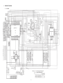
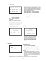
1.
SCHEMATIC DIAGRAM
1-1.
Main PCB
—1—
1-2.
Display PCB
—2—
1-3.
Key Matrix
—3—
2.
SPECIFICATIONS
Data storage:
Telephone/business card/memo/schedule data storage/recall, calendar display, marker, phrase memory,
secret area, editing, capacity display, auto display
Clock:
Average of accuracy ±3 seconds per day under normal temperatures; worldtime, schedule alarm, daily
alarm
Calculation:
12-digit arithmetic calculations, constants for + / – / × / ÷, independent memory, percentages, square roots,
24-digit approximations, date calculations, other mixed calculations
General:
Display element:
Memory capacity:
32-column × 6-line LCD
64 KB (65,499 bytes) for the Spreadsheet Mode data plus
64 KB (51,910 bytes) for other mode's data
Main component:
LSI
Power supply:
Main Power Supply — Two CR2032 lithium batteries
Backup Power Supply — One CR2032 lithium battery
Power consumption:
0.05W
Battery life:
Main:
Approximately 120 hours (Repeated cycle of 1-minute data input
into Telephone Directory followed by 10-minute display. Operation
temperature of 20°C)
Approximately 150 hours (Continuous display in Telephone Directory. Operation temperature of 20°C)
Backup: 5 years if main batteries are replaced as soon as they become weak.
1 year if dead main batteries are left in the unit.
• Note That the life of the battery that comes with the unit starts when the
battery is loaded in the unit at the factory. The life you get from the battery may
be shorter than normal because of the time the unit spends in transport, on
the shelf, etc.
Auto power off:
Approximately 6 minutes after last key operation
Operating temperature: 0°C ~ 40°C (32°F ~ 104°F)
Dimensions:
Unfolded: 10.5H × 154W × 155.2mmD (3/8"H × 6"W × 61/8"D)
Folded: 17.9H × 154W × 78mmD (3/4"H × 6"W × 31/16 "D)
Weight:
152.5g (5.4 oz) including batteries
Current consumption:
Power switch
TYP. [µA]
MAX [µA]
8
29
ON
1,447
13,258
ON (Operating)
6,707
19,958
OFF
—5—
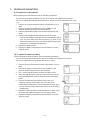
3.
TO REPLACE THE BATTERY
A) To replace the main batteries
Before replacing the main batteries, note the following precautions.
• Do not remove the back-up battery from the SF Unit while main batteries are removed.
• Be sure to replace both batteries at the same time, and do not use an old battery with a new
one.
1. Remove the screw that hold the battery compartment cover in
place.
2. Remove the battery compartment cover by sliding it in the
direction indicated by the arrow in the illustration.
3. Slide the main battery holder in the direction indicated by the
arrow.
4. Remove both old batteries and replace with two new ones.
• Use two new batteries. Wipe the surfaces of the batteries with a
soft, dry cloth. Make sure that the positive (+) sides of the
batteries are facing up (so you can view the positive sides as the
batteries lie in the battery compartment).
5. Replace the battery holder.
6. Replace the battery compartment cover and fasten it in place
using the screw.
B) To replace the back-up battery
Before replacing the back-up battery, note the following precautions:
• Do not remove the main batteries from the SF Unit while back-up battery is removed.
• Be sure to replace the back-up battery at least once a year.
1.
2.
3.
4.
5.
6.
7.
Remove the screw that hold the battery compartment cover in
place.
Remove the battery compartment cover by sliding it in the
direction indicated by the arrow in the illustration.
First , remove this sticker from the back-up battery holder.
After removing this sticker, take the screw off that secures the
back-up battery holder in place, and then remove the battery
holder.
Remove the old battery and replace it with a new one.
• Wipe the surfaces of the battery with a soft, dry cloth.
Make sure that the positive (+) side of the battery is facing up (so
you can view the positive side as the battery lies in the battery
compartment.)
Replace the back-up battery holder and fasten it in place using
the screw, and replace the sticker over the battery holder.
Replace the battery compartment cover and fasten it in place
using the screw.
—6—
4.
ERROR MESSAGE
Message
Meaning
Action
Text specified for
search does not exist.
Correct or change
specified text.
Wrong password
entered.
Enter correct
password.
MEMORY FULL!
No more room in
memory for storage of
data.
Delete unnecessary
data items from
memory.
DATA ERROR!
CONSULT YOUR
OWNER'S MANUAL
UNDER "DATA
ERROR"
Abnormal data caused
by strong impact, static
electricity, etc.
Consult the "DATA
ERROR" section on
page 2 of owner's
manual.
DATA ITEM NOT
FOUND!
PASSWORD
MISMATCH!
5.
TO RESET THE DIGITAL DIARY
Before describing the RESET operation, a note of WARNING — The following procedure will erase
all data stored in memory, including marked data items. Be sure to perform the RESET operation
only if you wish to clear all data.
To reset the SF Unit's memory
1. Switch on power and press the RESET button with a thin, pointed object.
The following message appears on the display.
DELETE ALL DATA ITEMS
STORED IN MEMORY ?
YES Y / NO N
2. Press Y to reset the SF Unit and clear everything from its memory. To abort the procedure
without clearing anything, press N .
—7—
Following the RESET operation, the Home Time Display appears. The initial settings of the SF Unit after
reset are shown below.
HOME TIME:
Washington D.C.
JAN/1/1994 (SAT)
12:00 AM
12-hour format
WORLD TIME: New York
Daily Alarm:
12:00 PM
Sound:
Schedule alarm
Daily alarm
Key
Character input: CAPS
6.
ON
OFF
ON
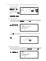
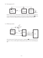
TO SAVE THE DATA TO OTHER MACHINE
SF-8500 can transfer customers data to other SF-8500 with memory protection only when replacing the
LCD or the outer case. How to transfer the data.
* Before connecting the cable (SB-60 or SB-62), be sure to reset the slave machine to clear all
data.
1) Turn off the power switch and connect the two units using the cable (SB-60 or SB-62) as shown in
the drawing.
2) Turn on the power switch of each machine.
3) The slave machine must be set the date of Feb. 3rd, 1901 into the memory under the calculator
mode.
Operation:
ON
CLEAR/AC
CAL
1
9
0
1
TIME
DATE
2
TIME
DATE
3
TIME
M+
DATE
R
If you don't set the date, the "PASSWORD" isn't transferred to the slave machine.
—8—
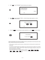
4) Check the hardware parameters, and if the units have another condition, reset as follows.
To change the hardware
parameters, press the
,
,
and
cursol keys.
To set the hardware
parameters, press the set
key.
***
HARDWARE PARAMETERS
PARITY
BIT LENGTH7 bits
BPS
1200
EVEN
2400
***
ODD
7 bits
4800
NONE
8 bits
9600
TEL
TEL
FUNCTION
4
4
5) Set up the slave machine.
1
While in the Calendar Display, Telephone Directory, Business Card Library, Memo Mode, or
Schedule Keeper, press the FUNCTION key followed by 4 to select " DATA COMMUNICATION", and the following menu appears.
TEL
FUNCTION
4
1
2
3
4
5
6
SEND
RECEIVE
PRINT
HARDWARE PARAMETERS
DATA TO RAM CARD
PEN PRINTING
TEL
2
Press 2 to select "RECEIVE" and the following display appears to indicate that the slave
machine is ready to receive data.
2
RECEIVE OK !
TO STOP, PRESS ESC
TEL
6) Set up the customer's machine.
1
While the transmitting unit is in the Calendar Display, Telephone Directory, Business Card
Library, Memo Mode, or Schedule Keeper, press the FUNCTION key followed by 4 to select
"DATA COMMUNICATION", and the following menu appears.
TEL
FUNCTION
4
1
2
3
4
5
6
SEND
RECEIVE
PRINT
HARDWARE PARAMETERS
DATA TO RAM CARD
PEN PRINTING
TEL
—9—
2
Press 1 to select "TRANSMIT" and the following menu appears.
1 ONE DATA ITEM
2 MODE DATA ITEMS
3 ALL DATA ITEMS
1
— SEND —
TEL
3
Press 3 to select "ALL DATA ITEMS", and the following display appears to confirm
whether you wish to proceed.
SEND ALL DATA ITEMS ?
3
YES SET / NO ESC
TEL
4
Press the SET key to proceed with the data transmission, or press ESC if you wish to cancel.
SET
NOW SENDING !
TO STOP, PRESS ESC
Data are transmitted in the sequence of Telephone Directory data, Business Card Library data, Memo
data, Schedule Keeper data and Calendar data.
* If the customer's machine uses full memory, it takes about one minute and ten seconds for this
transferring.
* The following messages appear on the display of the receiving unit when a problem occurs during
data communications. All data transferred up to display of the message is retained in memory, but
data communication is terminated.
TEL
BUSINESS CARD
MEMO
SCHEDULE
If one of the following error messages appear, press the
,
,
,
,
HOME TIME
, WORLD TIME , CAL , CALENDAR key, to clear the error message. Then, take corrective
action and try data communication again.
— 10 —
Message
Cause
STOPPED !
7.
• ESC key pressed on transmitting or receiving unit.
• Memory area of receiving unit full.
• Battery power drops below a certain level.
TRANSMIT ERROR !
Cable connection broken or abnormal noise in cable.
MEMORY FULL !
Memory area of receiving unit full.
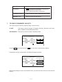
TO CHECK THE MEMORY CAPACITY
There are two types of Memory Capacity Display, as shown below:
SF UNIT:
Total memory used for storage of Telephone Directory, Business Card Library,
Memo, Calendar, and Schedule Keeper data.
SPREADSHEET: Total memory used for storage of Spreadseet data.
CAPACITY
SF UNIT
60%
FREE
20565 Bytes
SPREADSHEET 16%
FREE
54520 Bytes
Press the
SHIFT
key and then press the
CAPA
0
50
100
0
50
100
key to check the current memory capacity.
Following the memory reset operation, the display will appear as follows.
CAPACITY
SF UNIT
0%
FREE
51910 Bytes
SPREADSHEET 0%
FREE
64848 Bytes
0
50
100
0
50
100
When the percentage of memory used reaches 100%, you will not be able to enter any more data into
memory.
— 11 —
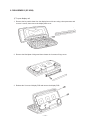
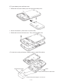
8. DISASSEMBLY (SF-8500)
1) To open display unit
1. Remove the key switch sheet from the display frame with care using a sharp tweezers and
remove 2 screws, then remove the display back cover.
2. Remove the blind plate of hinge and then release the 2 screws of hinge cover.
3. Release the 5 screws of display PCB and remove the display PCB.
— 12 —
2) To open battery cover and back cover
1. Release the one screw of battery cover and remove the battery cover.
2. Remove the batteries. (Refer section 3 in this manual.)
3. Release the 8 screws of the back cover. Then, remove the back cover.
4. To check the circuit by oscilloscope, apply the power to main PCB as follow:
External Power supply
Switch
GND
Prepare some 2P switch for Main switch.
+6V
+3V
Prepare some power supply for + 6V and +3V.
— 13 —
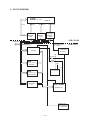
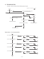
9. BLOCK DIAGRAM
LCD
192 × 48 dots
CD760-TS
S0~S31
C0~C47
S32~S111
S112~S191
LCD DRIVER
LCD DRIVER
LCD DRIVER
MSM6585AV
-Z-358B
MSM6585AV
-Z-358B
MSM6585AV
-Z-358B
PCB-L574-E2
DATA BUS
TO KEYBOARD
LCD DRIVE VOLTAGES
V1 ~ V4, VREG
CPU
POWER SUPPLY
CHIP FOR LCD
HD62076C02
SC371015FU
VDD
OPEN (OFF)
LOCK (ON)
ROM
MAIN SWITCH
(Character Generator)
GND
HD62063B01
Power supply circuit
ROM
(Operation Program)
µPD23C4001EBGW-304
RAM
M5M51008AFP10LL
GATE ARRAY
µPD65005G-566-22
INTERFACE FOR
DATA TRANSMISSION
& DATA RECEPTION
— 14 —
PCB-L575-1
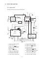
10. CIRCUIT EXPLANATIONS
10-1. System chart
Generally, SF-8500 is working with the following steps.
VDD
11
"H"
(Pin32)
(Pin31)
12
2
PDB
(Pin2)
VO1
VREG,V1~V4
Output
for LCD
driver
VOT
VDD
Power supply chip
SC371015FU
(Pin1)
VDD1
GND
VDD2
(Pin32)
(Pin19)
(Pin22)
1
(Pin7)
(Pin33)
(Pin34)
VDD
GND
Power supply
Circuit
3
15
16
13
"H"
"L"
"L"
"L"
"L"
(Pin2)
VDD
2 MHz
10
(Pin69)
(Pin45)
(Pin41)
V2ON
INIT1
ON
4
"H"
VDD
VDD
(Pin26)
LSI
Gate array
µPD65005GC-566-3B6 MON (Pin25)
VOB
(Pin31)
(Pin39)
VIN
RSO
LSO SWO
OEO
(Pin49)
(Pin27) (Pin40) (Pin43)
OSCI
(Pin1)
9
Transistor Q1
(Pin3)
(Pin40)
OSCO
VDD1
VDD
(Pin70)
14
INT0
OFF
CPU
GND
HD62076C02
MAIN SWITCH
SW (Pin36)
ON
6
"L"
"H"
5
(Pin24)
OE
8
VCC
GND
(Operation program)
"H"
"L"
CE
ROM
KIO
KAC
(Pin54)
(Pin53)
7
(Pin22)
µPD23C4001EBGW-304
17
ADDRESS
ADDRESS BUS
DATA BUS
18
11.
12.
13.
14.
1. Supply 5V to VDD1 and VDD2.
2. Output VDD (4.5V).
3.
4.
5.
6.
7.
8.
DATA
Output "L" from SWO terminal.
Output "H" from LSO terminal.
Main switch ON.
Input "L" to SW terminal.
Output "L" from KAC terminal.
Push power on button switch.
Output "H" from VOT terminal.
Output all LCD drive voltages.
Output "L" from VOB terminal.
Apply VDD to ROM.
15. Gate array sends ROM output
enable signal from OE terminal.
16. Gate array sends ROM Chip enable
enable signal from CE terminal.
17. CPU sends address to ROM.
9. CPU oscillation is generated.
10. Output "H" from V2ON terminal.
18. CPU receives data from ROM.
— 15 —
10-2. Power supply circuit
1)
Power supply circuit for CPU, GATE ARRAY, CG ROM and RAMs.
When the memory back-up battery or main batteries are set, the voltage supplies at the terminal VDD1
(Pin No.1) of SC371015FU (LSI2) through the diode MA743 (D1).
When LSI2 receives a voltage, the regulated voltage VDD (4.3V~4.7V) will be applied to the VDD lines
from the terminal VO1 (Pin No.2).
HD62076C02 (LSI1), µPD65005GC-566 (LSI3), HD62063B01 (LSI4), and M5M51008AFP-10LL
(LSI5) are connected the VDD lines.
2)
Power supply circuit for ROMs
When the GATE ARRAY (LSI3) controls the terminal VOB (Pin No.39) with "L" level, the transistor
2SA1411 (Q1) will be turned ON, then the voltage of the VDD lines will be applied the VCC lines.
The voltage of the ROM (LSI6) is supplied from the VCC lines.
3)
Main switch
The CPU (LSI1) detects the informations of the Main switch by the terminal SW (Pin No.36) from the
SWO signal of the GATE ARRAY (LSI3).
4)
How to turn the display ON.
When pressing "ON" key under the ON side of the Main switch , the CPU (LSI1) generates the signal
to turn the display ON at the terminal V2ON (Pin No.45).
This signal goes to the terminal VIN (Pin No.31) of the GATE ARRAY (LSI3), then the GATE ARRAY
(LSI3) generates "H" level at the terminal VOT (Pin No.32). When the power supply chip (LSI2) receives "H" level at the terminal PDB (Pin No.31) from VOT, the LSI2 generates the outputs VSS (Pin
No.8) and V1~V4 (Pin No.9~12) for LCD drivers.
5)
How to detect the voltage for the main batteries.
There are three detectors of the main batteries in the circuits.
When the voltage of the VDD lines becomes +4.58V±0.155V, the terminal VCOMP2 (Pin No.7) of the
power supply chip (LSI2) becomes "L" level, then this signal goes t the terminal P7 (Pin No.79) of the
CPU (LSI1) and the terminal BLI (Pin No.29) of the GATE ARRAY (LSI3).
The CPU detects the low battery condition, and the display shows "MAIN POWER SUPPLY GETTING
WEAK".
When the voltage of the VDD lines becomes +4.38V ±0.155V, the terminal VCOMP1 (Pin No.6) of the
power supply chip (LSI2) bocomes "L" level, and the terminal BLI (Pin No.29) of the GATE ARRAY
(LSI3) receives this shignal, then the display turns OFF.
— 16 —
When the voltage from the main batteries becomes +3.7V ±0.1V, the terminal VCOMP0 (Pin No.5) of
the power supply chip (LSI2) becomes "L" level, then this signal goes to the terminal PDN (Pin No.28)
of the GATE ARRAY (LSI3). After this, the terminal VOT (Pin No.32) of GATE ARRAY (LSI3) become
"L" level, and the terminal PDB (Pin No. 31) of the power supply chip (LSI2) receives this signal.
In this condition, the voltages for LCD will be cut off compulsorily.
When the voltage from the memory back-up battery becomes +2.5V±0.065V, the terminal SUBOUT
(Pin No.4) of the power supply chip (LCI2) becomes "L" level, and the terminal P6 (Pin No.78) of the
CPU (LSI1) detects the low battery condition. The display shows "MEMORY BACKUP BATTERY
GETTING WEAK".
6)
Others
The voltages of the circuit are applied from the main batteries or the memory back-up battery by the
diode MA743 (D3). The voltage of memory back-up is also provided with the main batteries.
— 17 —
7)
Power supply chip SC371015FU
+
The IC SC371015FU is power supply chip for
SF-8500. When IC SC371015FU receives a Voltage 5V from main power supply circuit at the terminal VDD1(Pin No.2), the regulated voltage
VDD (4.3~4.7V) will be applied to the VDD lines.
The outputs VSS (VREG) and V1~V4 are the
LCD drive voltages. When the terminal PDB becomes "H", those voltages are generated by IC
SC371015FU and capacitors C3 and applied to
LCD driver IC MSM6385AV-Z-358B.
The voltages for LCD driving are shown below:
C3
20
17
POWER SUPPLY CHIP
SC371015FU
VSS 8
9
V1
10
V2
11
V3
V4 12
V COMP2
V COMP1
7
6
V COMP0 5
4
SUB OUT
VO1
2
VDD1 1
PDB
31
VDD
(4.3 V ~ 4.7 V)
VDD2 19
3
SUB IN
GND1 GND2
32
LCD DRIVE VOLTAGE
22
FROM
GATE ARRAY
VOT terminal
CR2032
Back-up battery
MAIN POWER
SUPPLY CIRCUIT
Value (Approx.)
[V]
Contrust : Min.
Contrust : Max.
VSS(VREG)
-3.07
-5.27
V1
+3.50
+3.23
V2
+2.57
+2.02
V3
-1.16
-2.80
V4
-2.11
-4.04
The V comp0 ~ V comp2 and Sub out outputs are the battery voltage detection outputs. According to
VDD1 and VDD2 voltages, those outputs will change the status as follows:
OUTPUTS
STATUS "H"
STATUS "L"
V COMP 0
When the VDD1,2 voltages When the VDD1,2 voltages Switch off the LCD
are more than 3.7±0.1V.
V COMP 1
are less than 3.7±0.1V.
NOTE
driving voltages
When the VDD1,2 voltages When the VDD1,2 voltages Main battery check
are more than 4.38±0.155V. are less than 4.38±0.155V.
V COMP 2
When the VDD1,2 voltages When the VDD1,2 voltages Main battery check
are more than 4.58±0.165V. are less than 4.58±0.165V.
SUB OUT
When the SUB IN voltage
When the SUB IN voltage
is more than 2.5±0.065V.
is less than 2.5±0.065V.
— 18 —
Back-up battery check
8)
Gate array
GND
Open
(Pin 26)
TO MAIN SWITCH
"L"
(Pin 40)
(Pin 25)
LSI
SWO
MON
GATE ARRAY
µPD65005GC-566-3B6
"H"
TO CPU
INT0 terminal
(Pin 70)
9)
(Pin 27)
LSO
(Pin 34)
(Pin 7)
(Pin 33)
VDD
GND
CSB
(Pin 24)
"H"
FROM CPU
CS2 terminal (Pin 28)
When VDD is applied from power supply IC
SC371015FU to gate array µPD65005GC-5563B6, gate array will send "L" signal to active the
main switch signal from terminal SWO.
Also, gate array will send "H" signal to release
the INT0 terminal of CPU from LSO terminal.
The terminal CSB is for the chip select of gate
array. This signal is sent from CPU terminal
CS2. And when the VDD is applied to CPU, CPU
will send "H" signal to CSB terminal.
Main switch and power on switch
VDD
MAIN SWITCH
(Pin36)
SW
"L"
CPU
OFF
ON
GATE ARRAY
(Pin40)
"L"
SWO
µPD65005GC-566-3B6
HD62076C02
KAC
(Pin54)
"L"
KIO
(Pin53)
"H"
POWER ON SWITCH
When the main switch is set to on position, SW terminal of CPU becomes "L", then CPU will send "L"
signal to KAC terminal to enable the system power on. The KI0 terminal is "H" when VDD is applied to
CPU. Therefore, when pressing the power on switch, CPU will generate a clock pulse (2 MHz) for start
up the system.
— 19 —
10) Power supply for LCD
(Pin69)
(Pin32) "H"
(Pin31)
PDB
VOT
INT1
CPU
V2ON
"H"
(Pin45)
(Pin31)
HD62076C02
VIN
GATE ARRAY
µPD65005GC-566-3B6
POWER SUPPLY CHIP
SC371015FU
LCD drive voltages
VREG,V1~V4
When the system is start up, CPU will send "H" signal to VIN terminal of gate array from V2ON terminal. Then, gate array will send "H" signal from VOT terminal to release interruption signal INT1 of CPU
and also, it will be sent to PDB terminal of power supply chip to generate LCD drive voltages.
11) ROM driving transistor
VDD
(Pin3)
R10
Transistor Q1
2SA1411
(Pin1)
" L " (Pin39)
VOB
(Pin32)
GATE ARRAY
OEO
VCC
VDD
µPD65005GC-566-3B6
RSO
(Pin2)
ROM
µPD23C4001
"Pulse"
(Pin43)
(Pin24)
OEB
(Pin49)
EBGW-304
DATA
CPU
ADDRESS
"Pulse"
HD62076C02
CEB
(Pin22)
After gate array send VOT signal, gate array send "L" signal from VOB terminal to base terminal of
transistor Q1. Then, the VDD is applied to ROM (operation program), CPU can read a ROM program
data.
— 20 —
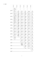
10-3. CPU pin description (HD62076C02)
Pin No.
Name
In/Out
Status
of OFF
Status
of ON
Description
1~14,16,17
15,39, 100
24
25
26
27
28
29
30
31
32
33
34
35
36
37
38
40,41
42
43, 91
44
45
46~53
54
55~65,67
66
68
69
70
71
72
73
74
75
76
77
78
79
80
81
82
83
84
85
86
87
88
89
90
92~99
18~23
A0~A15
VSS
WE
OE
FE
CS1
CS2
CS3
E0
E1
E2
E3
BCON
MDP2
SW
ONMK
TEST
OSC O/I
VOSC
VDD1
VDD2
V2ON
KI7~KI0
KAC
KC0~KC11
GND
INT2
INT1
INT0
BRK
P0
P1
P2
P3
P4
P5
P6
P7
H1
WENL
H2
L1
L2
DT
PRO
FR
LP
GC
DE
IO7~IO0
RA14~19
Out
In
Out
Out
Out
Out
Out
Out
Out
Out
Out
Out
Out
Out
In
In
In
In
In
In
In
Out
In
Out
Out
In
In
In
In
In
Out
In
In
In
Out
Out
In
In
Out
In
Out
Out
Out
Out
Out
Out
Out
Out
Out
In/Out
Out
L
GND
H
H
H
H
H
H
L
L
L
L
H
H
L
H
L
L
L
H
H
L
H
L
H
L
H
L
H
H
H
L
H
L
H
H
H
H
H
L
H
L
L
H
L
L
H
H
H
L
L
Pulse
GND
Pulse
Pulse
Pulse
H
H
Pulse
Pulse
H
H
H
H
L
L
H
L
Pulse
H
H
H
H
H
Pulse
Pulse
L
H
H
H
H
H
H
H
H
Pulse
Pulse
H
H
H
L
H
H
L
Pulse
H
Pulse
Pulse
Pulse
Pulse
Pulse
Pulse
Address Bus line
GND terminal
Write signal
Read signal
Not used
Not used
Chip select signal for gate array
Chip select signal for ROM (Charactor generator)
Chip enable signal for ROM (Operation program)
Chip enable signal (Not used)
Chip enable signal (Not used)
Chip enable signal (Not used)
BCN signal to gate array
MDP signal to gate array
Switch signal (When switches are at ON position)
Battery detection V comp1 input
TEST terminal (connect to GND)
Clock input
Power input for Clock
VDD input terminal
VDD input terminal
Power on output signal
Key input signal (K17…Not used)
Power on switch signal output
Key common signal output
GND terminal
Interrupt signal from ROM (Charactor generator)
Interrupt signal for transmission
Interrupt signal for transmission
VDD input terminal
Transmission data output
Reception data input
Card lock switch input
IC card detection signal input
KC 12 key common signal output
KC 13 key common signal output
Memory back-up battery detection input
Battery detection V comp2 input
Display contrast control signal output (Up/Down)
GND terminal
Not used
Chip enable signal for gate array
Dispray contrast control clock signal
Not used
LCD driver mode selection signal
LCD driver synchronous signal
LCD driver latch pulse signal
GC signal output
LCD driver data latch clock signal
Data bus line
Address line (Used exept RA 14)
— 21 —
10-4. Gate array pin descriptions (µPD65005GC-566-3B6)
Pin No.
Name
In/Out
Status
of OFF
Status
of ON
Description
1~6, 8, 9
7, 33
10
11~13
14
15
16~23
24
25
26
27
28
29
30
31
32
34
35
36
37
38
39
40
41
42
43
44
45, 51
46, 47
48
49
50
52
OI7~OI0
GND
B15
A15,A01,A00
N.C.
DT
IO0~IO7
CSB
MON
LSI
LSO
PDN
BLI
DEB
VIN
VOT
VDD
OEI
WEI
BBC
CDE
VOB
SWO
BCN
MDP
OEO
WEO
A19, A16
R15, R16
EOB
RS0
CS3
RS3
In/Out
In
In
In
In
In/Out
In
Out
In
Out
In
In
Out
In
Out
In
In
In
Out
In
Out
Out
In
In
Out
Out
In
Out
In
Out
In
Out
L
L
L
L
H
L
H
L
L
H
H
H
H
L
L
H
H
H
L
L
H
L
H
H
L
L
L
L
H
H
H
H
L
L
Pulse
Pulse
Pulse
Pulse
Pulse
L
L
H
H
H
Pulse
H
H
H
Pulse
Pulse
Pulse
H
L
L
H
L
Pulse
Pulse
Pulse
Pulse
Pulse
Pulse
Pulse
Pulse
Not used
GND terminal
Address input
Address input
Not used
GC signal input
Data bus line
Chip select signal from CPU
Not used
Connected to GND
Always "H"
Power down detection input
Battery detection V comp1 input
Chip selection signal for ROM (Charactor generator)
Power on signal input
Power on signal output
VDD terminal
Read signal input
Write signal input
Memory back-up battery scanning signal
IC card detection signal input
ROM power switching signal (Operation program)
Main switch control signal
BCON signal from CPU
MDP2 signal from CPU
Read signal for ROM
Not used
Address input
Address output
Chip enable signal from CPU
Chip enable signal for ROM (µPD27C4001EBGW-304)
Chip select signal from CPU
Chip enable signal for ROM (Character generator)
10-5. Power supply chip IC pin descriptions (SC371015FU)
Pin No.
Name
In/Out
Status
of OFF
Status
of ON
Description
32, 22
1, 19
2
31
GND1, 2
VDD1, 2
Vo1
PDB
In
In
Out
In
L
H
H
L
L
H
H
H
GND terminal
Main battery positive terminal (+5V)
VDD output terminal (4.5V)
Power on switch signal from gate array
— 22 —
Pin No.
Name
In/Out
Status
of OFF
Status
of ON
Description
3
4
5
6
7
8
9
10
11
12
13~16
17
18
20
21
23
24
25
26
27
28
29
30
SUB IN
SUB OUT
V COMP0
V COMP1
V COMP2
VSS
V1
V2
V3
V4
VDIV1~4
C1N
C2P
C1P
C2N
SUB CONT
EROUT
VFB
MIN
MAX
UPDOWN
CLOCK
SET
In
Out
Out
Out
Out
Out
Out
Out
Out
Out
**
**
**
**
**
In
Out
**
In
In
In
In
In
+3V
H
H
H
H
H
L
L
H
H
H
GND
3V
3V
GND
L
H
H
5V
%v
H
L
H
+3V
H
H
H
H
-7V
3V
2V
-5V
-6V
Wave
Wave
Wave
Wave
Wave
L
Wave
Wave
5V
5V
H
L
H
Back-up battery detection input
Back-up battery detection output (less than 2.5V…"L")
Battery detection signal (less than 3.7V…"L")
Battery detection signal (less than 4.4V…"L")
Battery detection signal (less than 4.7V…"L")
LCD drive power VREG
LCD drive power V1
LCD drive power V2
LCD drive power V3
LCD drive power V4
Voltage drividing terminal for LCD drive power
Negative terminal for doubler capacitor C3
Not used
Positive terminal for doubler capacitor C3
GND
Back-up battery detection clock input
LCD drive basic voltage output
LCD drive basic voltage input
LCD drive MIN voltage setting terminal
LCD drive MAX voltage setting terminal
LCD contrast control signal input (Up/Down)
LCD contrast clock signal input
Switch signal for contrast ("L"…software, "H"…hardware)
10-6. Character generator ROM pin descriptions (HD62063B01)
Pin No.
Name
In/Out
Status
of OFF
Status
of ON
Description
1, 7~12, 23
2
3
4, 20
5, 6
13
14, 19
15, 32
16, 21
17, 22
18
24
25
26` 27
28
29, 30
31
33
34~37
38~42
43
44
NC
BLD
VOSC
GND
OSI/OSO
TNL
IN1+, IN2+
VSS1, VSS2
IN1-, IN2OUT1, OUT2
TNH
IN
OUT
BZ1, 2
INT
CEH, CEL
CED
EN
IO3~IO0
A0~A3, A15
WEB
CSB
**
In
In
In
In
Out
In
In
In
Out
Out
In
Out
Out
Out
Out
In
In
In/Out
In
In
In
**
L
3V
L
Pulse
**
H
L
H
**
**
L
H
L
H
H
H
L
L
L
H
H
**
L
3V
L
Pulse
**
H
L
H
**
**
Pulse
Pulse
L
H
Pulse
Pulse
H
Pulse
Pulse
Pulse
Pulse
Not used
Not used (Battery voltage detection terminal)
Connected capacitor
GND terminal
Exterminal clock terminal (32.768 KHz)
Not used
Connected to VDD
GND terminal
Connected to VDD
Not used
Not used
Power on key input terminal
K10 terminal for power on
Buzzer signal
Interrupt signal for alarm clock (alarm time…"L")
RAM chip select signal
Chip enable signal from CPU
Enable signal (Buzzer off…"L")
Data bus line (IO0~IO3)
Address bus line (A0~A3, A15)
Write signal
Chip select signal
— 23 —
10-7. Operation program ROM pin discriptions (µPD23C4001EBGW-304)
Pin No.
Name
In/Out
Status
of OFF
Status
of ON
Description
2~12,23,
25~31
13~15, 17~21
16
22
24
1, 32
A0~A18
In
L
Pulse
Address bus line (A0~A14, RA15~RA18)
O0~O7
GND
CEB
OEB
N.C., VCC
Out
In
In
In
In
L
L
H
L
L
Pulse
L
Pulse
Pulse
H
Data bus line (IO0~IO7)
GND terminal
Chip enable signal from Gate array
Output enable signal from Gate array
VDD terminal
10-8. RAM pin discriptions (M5M51008AFP-10LL)
Pin No.
Name
In/Out
Status
of OFF
Status
of ON
Description
2~12,23,
25~28, 31
13~15, 17~21
16
22
24
1, 32
29
A0~A16
In
L
Pulse
Address bus line (A0~A14, RA15, RA16)
O0~O7
GND
CS1
OEB
N.C., VCC
WEB
Out
In
In
In
In
In
L
L
H
L
L
H
Pulse
L
Pulse
Pulse
H
Pulse
Data bus line (IO0~IO7)
GND terminal
Chip enable signal from Gate array
Output enable signal from Gate array
VDD terminal
Write enable signal from CPU
— 24 —
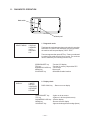
11. DIAGNOSTIC OPERATION
Main switch
Check pad
1. Diagnostic mode
SELECT MENU
1 DISPLAY
2 MEMORY
3 KEY
4 BUZZER
5 I/F
The diagnostic mode appears when main switch is turned on
while there is a short in the checkpad. After this operation,
the machine will beep and display "SELF-TEST".
The menu appears after press SET key. Tests are conducted
by selecting the mode from the list on screen. The each test
can be selected by the following function keys.
SPREADSHEET key
TEL key
BUSINEESS CARD key
MEMO key
SCHEDULE key
: Test the LCD display
: Test the IC memory chip and the RTC
: Test all keys
: Buzzer test
: SB-60/SB-62cable interface
2. Display check
DISPLAY
1 WHITE
2 BLACK
3 CHECKER
4 REVERSE
5 FRAME
DISP CHNG key
SPREADSHEET key
TEL key
BUSINEESS CARD key
MEMO key
SCHEDULE key
— 25 —
: Return to menu display
: Lights on dot at corners
: Lights on in all dots (black screen)
: Checker display
: Reverse checker display
: Lights on dot along the screen edge (frame)
3. ROM/RAM check
DISP CHNG key
MEMORY
INT #1
1 WRITE
2 READ
3 CHKSUM
4 SPECIFIC
5 RTC
SPREADSHEET key
TEL key
BUSINESS CARD key
INT---Internal RAM
EXT--External RAM(RAM card)
#1---Test data pattern(00,01,02...)
#2---Test data pattern(FF,FE,FD....)
MEMO key
SCHEDULE key
:Return to menu
: Write the set pattern to the selected
RAM area
: Compare the pattern displayed after
# with the write data of RAM and
displays the results.
: Dump contents of memory. (direction depens on setting of internal/
extarnal switch)
: Call up checksum and XOR values
for connected ROM/RAM data.
: Bring up clock display. The present
time, data and daily alarm can be set.
NOTE 1. To change the RAM internal or extenal, press HOME/WORLD key. As SF-8500 has no RAM card
interface, Test only Internal RAM area.
NOTE 2. To change the test data pattern,
press CALENDAR key for data pattern 1 (00,01,02,03,......FF,00,01,02,03,......).
press HOME/WORLD key for data pattern 2 (FF,FE,FD,......00,FF,FE,FD,...........).
1) RAM write
The machine will beep after 3 seconds.
The menu is unchanged.
When there is no RAM to write a data,
the following message will be displayed.
EXECUTING !
NO RAM
It means RAM write is succeeded.
To release this message, press DISP CHNG key.
2) RAM read
Normal end display is;
Error end display is;
DATA ERROR !
COMPLETE !
ADDRESS
XXXX
CORR
XX
RAM
XX
To release this message, press DISP CHNG key.
— 26 —
3) CHECK SUM
When memory dump is operated by pressing BUSINESS CARD button, a display will appear as shown
at left. The first two lines, begining from the top left,
signify the following address values in reference to
the one megabyte "E0" area:
00001,00002,00004,....,00080,00100,00200
00400,00800,01000,....,20000,40000,80000
The lower two lines refer to the data in the "E1" area.
TYPE SIZE CHECK-SUM XOR
E0 ROM 512KB
342B
6D
CE RAM 128KB
8300
00
Type : ROM and RAM are shown.
However, if the ROM is not in
standard Casio format, a format
error will be displayed.
Size : Memory capacity (total)
Checksum:
XOR : Logic operation for all data.
Note: The Internal/External switch is activated
pressing CAL button. SF8500 has no external RAM area.
The ON key is the only key that remains
functional when an error has occurred
or check-sum is being displayed.
4) SPECIFIC (ROM check)
5)
RTC
TM DISP
yyyymmddhhmmss........
..............
SPECIFIC SUM
E0
1CE2
C6
1990 04 04 12 34 56
Input can be made in the second and
third lines using the numeric keys.
Entry of 12 or more digits sets the time
and date. Entry of 4 or 6 digits sets the
daily alarm. The ON key clears current
entries.
4. Key check
KEY
1 RANDOM
2 AUTO
SPREADSHEET Key :
The 'key code' will be displayed.
The 'key code' is numbered incrementally from
left to right with the DISPLAY CHANGE key as
"00", and TEL key as "02" etc. Accordingly,
the SET keys is "81". To release this test, press
SEARCH key.
TEL key :
Limits the mode mentioned above so that the
keys must be pressed in order according to the
key code. If an error is made a buzzer sounds
for about 1 second. (A correct entry results in a
beep tone)
In either mode a press of the SEARCH key will return the screen to the menu mode.
— 27 —
5. Buzzer check
BUZZER
1 BEEP
2 ALARM 1
3 ALARM 2
EXECUTING !
SPREADSHEET key : Key input sound every 1 second
TEL key
: Sound alarm 1
BUSINESS CARD key : Sound alarm 2
Sound can be stopped by pressing the any key.
While an alarm is sounding the screen display is as shown at
left. If an irregularity is found in voltage of battery while the
alarm is sounding, the alarm will stop. After 256 seconds, the
alarm will stop automatically.
6. SB-60/SB-62 cable interface check
I/F
1 TRANSMIT
2 RECEIVE
3 LOOP
4 ASCII
7N9
The SPREADSHEET to MEMO keys are used to select mode;
the CALENDAR, SCHEDULE and HOME/WORLD key are
used to set the transmission paraments. The three charactors
that appear on the right side at display represent the parameter. In the case of the exampledisplay, it indicates 7 BIT,
NON PARITY, 9600 BPS. The operation continues until
stopped by pressing the ESC key and then pressing the ON
key for all modes.
DISP CHNG key : Return to menu mode
SPREADSHEET key : Transmission mode. The data of transmission is "H" and it is sent out by the data of &
Parameter
H34 and & H38 by the Xon/Xoff control.
TEL key
: Reception mode. Make sure to set the
parameter to match that of the transitting
side. The data received appears on the
display.
EXECUTING !
BUSINESS CARD key : Loop back test. Short the Tx and Rx
terminals for this test. Transmit and check
from &H20 to &H7E. When complete, the
message 'CHECK COMPLETE' is displayed.
MEMO key
: Output the following ASCII code by Xon/
Xoff control.
!"#*+,-/0123456789:
ABCDEFGHIJKLMNOPQRSTUVWXYZ
abcdefghijklmnopqrstuvwxyz
A line end code is added with each line.
SCHEDULE key : Switch the data length 7 bit(7) or 8 bit(8)
CALENDAR key : Switch the parity bit : NON(N)—EVEN(E) —NON(N) —ODD(O)
HOME/WORLD key : Switch the transmission speed : 9600(9)—4800(4)—2400(2)—1200(1)
To communicate two machines, please set the transmission machine before setting the receiving unit.
To release communication, press ESC button. In this case, the break code is sent to receive units.
Therefore, both machines display "TRNS BREAK !" and communication will be stopped. Also, if the error
is occurred, both machines display "TRNS ERROR !" and communication will be sttoped.
— 28 —
NOTE : As diagnostic program area does not have all ASCII code, to display a reception data, some
charactor will be changed to other charactor. For example, a chapital letter will be changed
to small letter.
Break display (Broken transmission)
Error display
TRNS ERROR !
TRNS BREAK !
7. Battery level check
Memory back up battery
The memory back up voltage detector detects any
irregularity in voltage, the machine goes into an
error state and the display is as shown at left figure.
To release this display, press any key.
LOW BATTERY!
BACK UP
Main battery
When the main battery voltage detector detects
low battery condition while display is on, the machine shows the message as shown at left figure.
When this message is displayed, only ON/OFF
key are possible to operate. And if the voltage
becomes lower than 4.4V, the display will be off
mode (auto power off mode).
LOW BATTERY!
8. Others
1) When power is off after presetting a alarm time, automatically power is on at a alarm time.
However, the display is not reserved in this case.
2) When executing memory sum check, before execute the RAM write check (with SPREADSHEET
button).
3) To release diagnostic mode, press reset button.
4) The display contrast can be changed by the contrast volume.
— 29 —
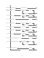
12. TROUBLESHOOTING
Generally, check the machine with the followning steps for repair.
CONDITION : Main battery switch
ON
START
No
Main battries 6V?
Yes
Replace main battries (CR2032 2pcs.)
(Clean and adjust battery contact.)
1
Key input OK?
Yes
No
Reset operation
No
Display OK?
Yes
Yes
Save data to P/C if necessary.
Key input OK?
No
Current consumption OK?
No
Yes
Follow repair section 2.
Load data from P/C if necessary.
Follow repair section 1.
No
Data OK?
Yes
Follow repair section 3.
END
Repair section 1 : For no key input problem
START
Pin 2 of SC371015FU Approx. 4.5 V ?
No
Yes
Poor connection?
No
Yes
Solder line
1
Replace parts.
Pin 26 of µPD65005G-566-3B6 "L"?
Yes
No
Poor connection?
Yes
Solder line
No
1
Replace parts.
Pin 40 of µPD65005G-566-3B6 "L" ?
No
Poor connection?
Yes
Solder line
No
Yes
1
Replace parts.
Pin 36 of HD62076C02 "L" ?
Yes
No
Poor connection?
No
Yes
Solder line
1
Replace parts.
Pin 54 of HD62076C02 "L" ?
No
Poor connection?
Yes
Yes
Solder line
No
Replace parts.
2
— 30 —
1
2
Connection of keyboard cable OK?
Yes
No
No
When press power on Key, any
oscillation at oscillator?
1
Adjust keyboard cable.
Poor connection Yes
on oscillator?
Yes
Solder line
No
1
Replace parts.
No
Pin 45 of HD62076C02 "H" ?
Poor connection?
No
Yes
Yes
Solder line
1
Replace parts.
Pin 31 of µPD65005G-566-3B6 "H" ?
Yes
Pin 32 of µPD65005G-566-3B6 "H"
?
Yes
No
Solder line
No
Poor connection?
Yes
Solder line
No
1
Replace parts.
Pin 31 of SC371015FU "H" ?
No
Poor connection?
Solder line
Yes
Pin 39 of µPD65005G-566-3B6 "L" ?
1
No
Poor connection? Yes
1
Solder line
No
Yes
1
Replace parts.
No
Poor connection?
No
Pin 3 of transistor Q1 "H" ?
Yes
Yes
Solder line
1
Replace parts.
Pin 1 and 32 of ROM µPD23C4001EBGW-304 "+4.5V" ?
No
Solder line
1
Yes
Pin 32 of ROM µPD23C4001EBGW-304 "Pulse" ?
Yes
No
Yes
Poor connection
on ROM or CPU?
Solder line
No
1
Replace CPU.
Poor connection on ROM, RAM or CPU ?
Yes
Solder line
No
Replace ROM, RAM or CPU.
— 31 —
1
Repair section 2 : For no display or wrong display problem
START
Pin 32 of µPD65005G-566-3B6 "H" ?
No
Poor connection?
No
Yes
Yes
Solder line
1
Replace parts.
No
Solder line
Pin 31 of SC371015FU "H"?
Yes
LCD drive voltages OK?
(Pin8~12) of
Yes
SC371015FU
No
Poor connection?
No
1
Yes
Poor connection on chip Yes
resistors R8~R10 ?
No
Yes
Poor connection on
capacitor C7~C8 ?
No
Chip capacitor OK ?
Yes
Chip resistor OK?
Yes
Solder line
No
No
Replace parts.
Replace SC371015FU.
1
Yes
Replace heat seal.
Poor connection or cut of heat seal cable ?
No
Poor connection on LCD driver ?
No
Yes
Poor connection or cut of heat seal cable for LCD ?
Solder line
Yes
1
1
Replace heat seal.
1
Replace LCD.
1
No
LCD cracked ?
No
Yes
Repleace Display PCB ass'y.
1
Repair section 3 : For memory problem
START
Poor connection on RAM chips ?
No
Poor connection on CPU ?
No
Yes
Yes
Solder line
1
Replace RAM chips or CPU.
— 32 —
13. PARTS LIST (SF-8500)
— 33 —
— 34 —
14. PCB VIEW
— 35 —
15. ASSEMBLY VIEW
— 37 —
8-11-10, Nishi-Shinjuku
Shinjuku-ku, Tokyo 160, Japan
Telephone: 03-3347-4926