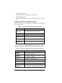
1
BL1600 C-Programmable Controller Users Manual 001115 - G BL1600 Users Manual Part Number 019-0016 001115 - G Printed in U.S.A. Copyright © 1999 Z-World, Inc. All rights reserved. Z-World reserves the right to make changes and improvements to its products without providing notice. Trademarks ® Dynamic C is a registered trademark of Z-World, Inc. ® Windows is a registered trademark of Microsoft Corporation PLCBus is a trademark of Z-World, Inc. ® Hayes Smart Modem is a registered trademark of Hayes Microcomputer Products, Inc. Notice to Users When a system failure may cause serious consequences, protecting life and property against such consequences with a backup system or safety device is essential. The buyer agrees that protection against consequences resulting from system failure is the buyers responsibility. This device is not approved for life-support or medical systems. All Z-World products are 100 percent functionally tested. Additional testing may include visual quality control inspections or mechanical defects analyzer inspections. Specifications are based on characterization of tested sample units rather than testing over temperature and voltage of each unit. Z-World may qualify components to operate within a range of parameters that is different from the manufacturers recommended range. This strategy is believed to be more economical and effective. Additional testing or burn-in of an individual unit is available by special arrangement. Company Address Z-World, Inc. 2900 Spafford Street Davis, California 95616-6800 USA Telephone: Facsimile: Web Site: E-Mail: (530) 757-3737 (530) 753-5141 http://www. z w orld.c om [email protected] TABLE OF CONTENTS About This Manual vii Chapter 1: Overview 11 Chapter 2: Getting Started 17 Chapter 3: BL1600 Operation 23 Chapter 4: System Development 29 Introduction .......................................................................................... 12 Features ................................................................................................ 13 Options and Upgrades ..................................................................... 14 Development and Evaluation Tools ..................................................... 15 Software .......................................................................................... 15 CE Compliance .................................................................................... 16 Initial BL1600 Setup ............................................................................ 18 Parts Required ................................................................................. 18 Connecting the BL1600 to a Host PC .................................................. 18 Running Dynamic C ............................................................................. 21 Operating Modes.................................................................................. 24 Run Mode ........................................................................................ 25 EPROM ................................................................................................ 25 Programming EPROMs .................................................................. 25 Memory Size ................................................................................... 25 Copyrights ....................................................................................... 27 BL1600 Interfaces ............................................................................... 30 Digital Inputs ................................................................................... 30 Digital Outputs ................................................................................ 30 Serial Ports ...................................................................................... 32 Miscellaneous Signals ..................................................................... 33 PLCBus Port ................................................................................... 34 Dynamic C Libraries ............................................................................ 35 BL1600 Table of Contents s iii Driver Software .................................................................................... 36 Digital Inputs ................................................................................... 36 Digital Outputs ................................................................................ 36 High-Speed DMA Counter .............................................................. 37 Battery-Backed Clock ..................................................................... 38 Writing to Flash EPROM ................................................................ 38 Virtual Drivers ................................................................................. 39 Invoking the Virtual Driver ........................................................... 41 Virtual Driver Variables ................................................................ 41 Digital Inputs .............................................................................. 41 Digital Outputs ........................................................................... 41 Timers ......................................................................................... 42 Serial Communication .......................................................................... 43 RS-232 Communication .................................................................. 43 Receive and Transmit Buffers ....................................................... 43 Echo Option .................................................................................. 43 CTS/RTS Control ......................................................................... 43 XMODEM File Transfer .............................................................. 44 Modem Communication ............................................................... 44 Software Support ............................................................................. 45 Interrupt Handling for Z180 Port 0 ............................................... 45 RS-232 Software Support ............................................................. 46 XMODEM Commands ................................................................. 48 Miscellaneous Functions .............................................................. 49 Master-Slave Networking ............................................................... 51 RS-485 Network Hardware Connections ..................................... 52 RS-485 Network Software Support .............................................. 54 Miscellaneous RS-485 Network Functions .................................. 55 Support Libraries and Sample Programs......................................... 56 Direct Programming of the Serial Ports ............................................... 57 Attainable Baud Rates ..................................................................... 57 Z180 Serial Ports ............................................................................ 58 Asynchronous Serial Communication Interface (ASCI) ...................... 60 ASCI Status Registers ..................................................................... 60 CTS1E (CTS Enable, Channel 1) ................................................. 61 RDRF (Receiver Data Register Full) ............................................ 61 ASCI Control Register A ................................................................ 62 ASCI Control Register B ................................................................ 63 iv s Table of Contents BL1600 Appendix A: Troubleshooting 67 Appendix B: Specifications 71 Appendix C: Prototyping Board 81 Appendix D: Sinking and Sourcing Drivers 89 Appendix E: PLCBus 95 Out of the Box ...................................................................................... 68 Dynamic C Will Not Start .................................................................... 69 BL1600 Resets Repeatedly .................................................................. 69 Dynamic C Loses Serial Link .............................................................. 69 Common Programming Errors ............................................................. 70 Electrical and Mechanical Specifications ............................................ 72 BL1600 Mechanical Dimensions .................................................... 73 Factory Default Jumper Positions ........................................................ 74 Installation Concepts ............................................................................ 77 Connectors ...................................................................................... 77 Power Consumption and Heat Dissipation ...................................... 77 High-Voltage Drivers ........................................................................... 78 Sinking Driver ................................................................................. 78 Sourcing Driver ............................................................................... 79 Introduction .......................................................................................... 82 Features ................................................................................................ 82 System Description .............................................................................. 83 Connecting the Prototyping Board to the BL1600 .............................. 84 Power Supply .................................................................................. 84 Power Rails ..................................................................................... 85 Interface with BL1600 ......................................................................... 87 Prototyping Board Pinouts .............................................................. 88 BL1600 Series Sinking and Sourcing Outputs ..................................... 90 Installing Sourcing Driver ............................................................... 92 Using Output Drivers ........................................................................... 93 PLCBus Overview ............................................................................... 96 Allocation of Devices on the Bus ...................................................... 100 Bit Devices .................................................................................... 100 8-Bit Devices ................................................................................ 101 Expansion Bus Software .................................................................... 101 BL1600 Table of Contents s v Appendix F: EEPROM 107 EEPROM Parameters ........................................................................ 108 Baud Rate ...................................................................................... 108 Startup Mode ................................................................................. 108 Clock Speed .................................................................................. 109 Changing Parameters Stored in EEPROM ......................................... 109 Library Routines ................................................................................ 109 Appendix G: Memory, I/O Map, and Interrupt Vectors 111 BL1600 Memory ................................................................................ 112 Memory and Input/Output Cycle Timing ...................................... 113 Input/Output Cycle Timing ......................................................... 114 Execution Timing .......................................................................... 115 Memory Map ..................................................................................... 116 Input/Output Select Map ............................................................... 116 Z180 Internal Input/Output Registers Addresses 0x000x3F ....... 116 Epson 72421 Timer Registers 0x40000x400F ............................ 118 Other Addresses ............................................................................ 119 Interrupt Vectors ................................................................................ 121 Nonmaskable Interrupts ................................................................ 122 Power Failure Interrupts ............................................................. 122 Jump Vectors ................................................................................. 123 Interrupt Priorities ......................................................................... 124 Appendix H: Power Management 125 Appendix I: Battery 131 Index 135 ADM691 Power Supervisor ............................................................... 126 Power Failure Management ............................................................... 127 Power Failure Sequence ................................................................ 127 Holdup Time ................................................................................. 129 Multiple Power-Line Insults .......................................................... 129 Sample Program to Handle Power Failure .................................... 130 Battery Life and Storage Conditions .................................................. 132 Replacing Soldered Lithium Battery .................................................. 132 Battery Cautions ................................................................................ 133 Schematics vi s Table of Contents BL1600 ABOUT THIS MANUAL This manual provides instructions for installing, testing, configuring, and interconnecting the Z-World BL1600 controller. Instructions are also provided for using Dynamic C® functions. Assumptions Assumptions are made regarding the user's knowledge and experience in the following areas. Ability to design and engineer the target system that the BL1600 will control. Understanding of the basics of operating a software program and editing files under Windows on a PC. Knowledge of the basics of C programming. $ For a full treatment of C, refer to the following texts. The C Programming Language by Kernighan and Ritchie and/or C: A Reference Manual by Harbison and Steel Knowledge of basic assembly language and architecture for the Z180 microprocessor. $ BL1600 For documentation from Zilog, refer to the following texts. Z180 MPU User's Manual Z180 Serial Communication Controllers Z80 Microprocessor Family User's Manual About This Manual s vii Terms and Abbreviations Table 1 lists and defines the acronyms that may be used in this manual. Table 1. Acronyms Acronym Meaning EPROM Erasable Programmable Read-Only Memory EEPROM Electronically Erasable Programmable Read-Only Memory NMI Nonmaskable Interrupt PIO Parallel Input/Output Circuit (Individually Programmable Input/Output) PRT Programmable Reload Timer RAM Random Access Memory RTC Real-Time Clock SIB Serial Interface Board SRAM Static Random Access Memory UART Universal Asynchronous Receiver Transmitter Conventions Table 2 lists and defines the typographical conventions that may be used in this manual. Table 2. Typographical Conventions Example Description while Courier font (bold) indicates a program, a fragment of a program, or a Dynamic C keyword or phrase. // IN-01… Program comments are written in Courier font, plain face. Italics Indicates that something should be typed instead of the italicized words (e.g., in place of filename, type a file’s name). Edit Sans serif font (bold) signifies a menu or menu selection. ... An ellipsis indicates that (1) irrelevant program text is omitted for brevity or that (2) preceding program text may be repeated indefinitely. [ ] Brackets in a C function’s definition or program segment indicate that the enclosed directive is optional. < > Angle brackets occasionally enclose classes of terms. a | b | c A vertical bar indicates that a choice should be made from among the items listed. viii s About This Manual BL1600 Pin Number 1 A black square indicates pin 1 of all headers. Pin 1 J1 Measurements All diagram and graphic measurements are in inches followed by millimeters enclosed in parenthesis. Icons Table 3 displays and defines icons that may be used in this manual. Table 3. Icons Icon $ ( Meaning Refer to or see Please contact Caution ! Note High Voltage 7,3 FD BL1600 Tip Factory Default About This Manual s ix Blank x s About This Manual BL1600 CHAPTER 1: OVERVIEW Chapter 1 provides an overview and a brief description of the BL1600 features. BL1600 Overview s 1-11 Introduction The BL1600s combination of logic-level inputs/outputs and high-current drivers makes it a versatile controller in a compact form factor. The BL1600 is ideal for OEM applications such as industrial control and data acquisition. The BL1600s battery-backed RAM, real-time clock, and EEPROM provide data integrity in the event of power fluctuations or power failure. The BL1600 is readily connected to peripheral devices through standard headers or screw terminals. An optional Prototyping Board facilitates the development of custom circuits and operator interfaces. Figure 1-1 illustrates the BL1600 board layout. Inputs 011 Misc. Outputs RS-232 H1 H2 H3 U5 Misc. U3 U4 U1 Reg. Z1 RS-232 U2 D1 J1 H4 RS-485 U6 MV1 DCIN C8 K MV2 U7 U8 U11 U13 RS485 RS485+ HI1 Super. HI2 Y1 U12 H5 GND U10 H.V. Driver PLCBus Port U9 U14 HI3 C16 HI4 EPROM Battery U16 J3 U17 U18 RAM PAL HI5 U15 HI6 Z180 HI7 J2 RTC EEPROM Figure 1-1. BL1600 Board Layout 12 s Overview BL1600 Features The BL1600 includes the following features. 12 digital inputs. 14 digital outputs. RS-485 and RS-232 serial communication. 9.216 MHz clock. PLCBus port for system expansion. The BL1600 also includes battery-backed RAM (up to 512K) and a battery-backed real-time clock (an Epson 72421 with time and date functions), EPROM (up to 512K) or flash EPROM (to 256K), programmable timers, DMA, EEPROM (512 bytes standard), a watchdog timer, and power-failure interrupt. $ Appendix B provides detailed specifications for the BL1600. The maximum power dissipation is 5 W at 50°C with the standard (large) heat sink, and 3 W with the optional small heat sink supplied with the Experimenters Kit. The maximum operating temperature is 70°C, but the BL1600 may not be able to operate for extended periods at 70°C. $ Chapter 2, Getting Started, provides further information on environmental constraints. The BL1600s RS-485 capability allows you to build a network of controllers with links up to several kilometers. The PLCBus port allows you to expand your system by adding expansion boards, such as Z-Worlds XP8700 or XP8900, or devices of your own design. The BL1600 is designed to allow you to build and add your own expansion boards. Z-World supplies a Prototyping Board for this purpose. $ BL1600 Appendix C, Prototyping Board, provides further information on the Prototyping Board. Overview s 1-13 Options and Upgrades The BL1600 Series of controllers has two versions. Table 1-1 lists their standard features. Table 1-1. BL1600 Series Features Model Features BL1600 9.216 MHz clock, 12 digital inputs, 14 high-current sinking outputs, RS-232/RS-485 serial ports, EEPROM, real-time clock, PLCBus expansion port. BL1610 BL1600 without serial ports, high-current drivers, EEPROM, or real-time clock. The following optional items are available for BL1600 Series controllers. 128K or 256K flash EPROM to replace regular EPROM. 128K or 512K SRAM. Prototyping Board. XP8700 expansion board to program the BL1600 if the BL1600s RS-232 serial port is required by the application. A full line of Z-World expansion boards is available. ( For ordering information, call your Z-World Sales Representative at (530) 757-3737. 14 s Overview BL1600 Development and Evaluation Tools The BL1600 is supported by a Developers Kit that include everything you need to start development with the BLl600. The Developers Kit includes these items. Programming cables and adapter. 24 V DC wall-mount power supply. 128K flash EPROM. Smaller heat sink. Sinking and sourcing high-current driver chips. 14-pin and 20-pin breakout cables. Software The BL1600 is programmed using Z-Worlds Dynamic C, an integrated development environment that includes an editor, a C compiler, and a debugger. Library functions provide an easy and robust interface to the BL1600. $ BL1600 Z-Worlds Dynamic C reference manuals provide complete software descriptions and programming instructions. Overview s 1-15 CE Compliance The BL1600 has been tested by an approved competent body, and was found to be in conformity with applicable EN and equivalent standards. Note the following requirements for incorporating the BL1600 in your application to comply with CE requirements. The power supply provided with the Development Kit if for development purposes only. It is the customers responsibility to provide a clean DC supply to the controller for all applications in end-products. The BL1600 has been tested to Light Industrial Immunity standards. Additional shielding or filtering may be required for an industrial environment. The BL1600 has been tested to EN55022 Class A emission standards. Additional shielding or filtering may be required to meet Class B emission standards. $ Visit the Technical Reference pages of the Z-World Web site at http://www.zworld.com for more information on shielding and filtering. 16 s Overview BL1600 CHAPTER 2: GETTING STARTED Chapter 2 provides instructions for connecting the BL1600 to a host PC and running a sample program. BL1600 Getting Started s 17 Initial BL1600 Setup Parts Required 24 V unregulated DC power supply Programming cable Optional XP8700 expansion board (needed if the RS-232 port on the BL1600 is required by the application). The necessary parts are supplied with the Developers Kit. Connecting the BL1600 to a Host PC 1. Connect the power supply to the BL1600. Connect the two leads from the DC power supply or wall transformer to header J2 as shown in Figure 2-1. Do not power up the power supply until the remaining steps have been completed. DCIN K to wall transformer GND RS485 RS485+ HC1 HC2 HC3 HC4 HC5 HC6 HC7 J2 Figure 2-1. Bl1600 Power Supply Connections at Header J2 Be careful to connect the power supply wires to the correct sockets on header H2. The BL1600 may be destroyed in an instant if the power supply is connected to the wrong socket. A protective diode prevents damage to the BL1600 if the power supply polarity is reversed. 18 s Getting Started BL1600 2. Check jumper settings on header J1. Jumpers on header J1 define the hardware configuration, the mode, and the baud rate. Figure 2-2 shows the jumper settings for the various programming options. 2 4 6 8 2 J1 4 6 8 J1 1 3 5 7 Run program from RAM 2 4 6 1 3 5 7 Program at 9600 bps 8 2 J1 4 6 8 FD J1 1 3 5 7 Program at baud rate stored in EEPROM location 1 1 3 5 7 Program at 19,200 bps Figure 2-2. BL1600 Programming Jumper Settings for Header J1 $ Appendix B, Specifications, lists all the jumper settings. 3. Establish a serial communication link. A PC communicates with the BL1600 via Serial Port 0 on the BL1600s microprocessor using RS-232 protocols. There are two options to install the communication link. Option 1BL1600 serial port (header H3). Use the programming cable to connect the PCs 9-pin or 25-pin RS-232 serial port to header H3 on the BL1600 as shown in Figure 2-3. Either PC serial port (COM1 or COM2) may be used. 9-pin to 25-pin adapter (optional) to PC COM port BL1600 Wall transformer 9-pin serial connector H3 J2 Figure 2-3. Connecting Programming Cable to BL1600 Header H3 BL1600 Getting Started s 19 Option 2XP8700 expansion board. Use the programming cable to connect the PCs 9-pin or 25-pin RS-232 serial port to header H1 on the XP8700. Either PC serial port (COM1 or COM2) may be used. (If you are using a non-Z-World programming cable with an RJ-12 plug instead of a 10-pin connector, connect the RJ-12 plug to the RJ-12 jack on the XP8700.) Connect the XP8700 to the BL1600s PLCBus port as shown in Figure 2-4. BL1600 H1 XP8700 U1 U2 H4 U6 U6 PAL U4 PAL U11 U1 SCC2691 UART 3.686 MHz P1 P2 U5 H5 Latch RN1 U2 RS-232 Driver C1 C3 C4 R1 R2 D1 D2 H1 RS-232 Jack C2 H2 H1 Battery J1 J4 serial cable to PC Figure 2-4. Use of XP8700 to Program BL1600 4. The BL1600 is now ready for programming. The power supply may be plugged in and turned on. 20 s Getting Started BL1600 Running Dynamic C Double-click the Dynamic C icon to start the software. Note that the PC attempts to communicate with the BL1600 each time Dynamic C is started. No error messages are displayed once communication is established. The communication rate, port, and protocol are all selected by choosing Serial Options from Dynamic Cs OPTIONS menu. The BL1600s default communication rate is 19,200 bps. However, the Dynamic C software shipped by Z-World may be initialized for a different rate. To begin, adjust the communications rate to 19,200 bps. Make sure that the PC serial port used to connect the serial cable (COM1 or COM2) is the one selected in the Dynamic C OPTIONS menu. Select the 1-stop-bit protocol. $ See Appendix A, Troubleshooting, if an error message such as Target Not Responding or Communication Error appears. ! Once the necessary changes have been made to establish communication between the host PC and the BL1600, use the Dynamic C shortcut <Ctrl Y> to reset the controller and initiate communication. BL1600 Getting Started s 21 Blank 22 s Getting Started BL1600 CHAPTER 3: BL1600 OPERATION Chapter 3 describes how to use the BL1600, with a focus on how to set the run and programming modes, and how to burn a custom program on EPROM. BL1600 BL1600 Operation s 23 Operating Modes A hardware reset takes place when the BL1600 is powered up, when a reset is done manually by connecting pins 910 on header H4, or when the watchdog timer times out. If a valid program (created with Dynamic C) has been installed in EPROM, the program starts running. A valid program is recognized by a code that Dynamic C places in the file used to burn the EPROM. The flowchart in Figure 3-1 shows the startup sequence of the BL1600 after a hardware reset. Begin from hardware reset Flash YES EPROM installed? Valid program in EPROM? YES J1 pins 12 or 34 connected? Valid program in RAM or in flash EPROM? YES YES Run application. Run Dynamic C at baud rate specified by jumpers on header J1 Run application. Error halt Figure 3-1. BL1600 Activity at Startup 24 s BL1600 Operation BL1600 Run Mode Before running a program from battery-backed RAM or flash EPROM, be sure pins 12 and 34 on header J1 are not connected. If a valid user program is already in EPROM, that program will run immediately after a hardware reset. ! If the Dynamic C EPROM is present on the board, the BL1600 executes the program stored in battery-backed RAMthat is, the program last run under Dynamic C. If the Dynamic C EPROM has been replaced with a custom EPROM, then the BL1600 executes that program. EPROM Programming EPROMs Dynamic C can be used to create a file for programming an EPROM by selecting the Compile to File option in the COMPILE menu. The BL1600 must be connected to the PC running Dynamic C during this step because essential library routines must be uploaded from the Dynamic C EPROM and linked to the resulting file. The output is a binary file (optionally an Intel hex format file) that can be used to build an application EPROM. The application EPROM is then programmed with an EPROM programmer that reads either a binary image or the Intel hex format file. The resulting application EPROM can then replace the EPROM that came with the BL1600. Whenever the Dynamic C EPROM is replaced by a custom EPROM, the BL1600 ignores the program in battery-backed RAM in favor of the program stored in EPROM. Memory Size When doing program development with Dynamic C, it is best to use a 128K SRAM or larger. Dynamic C will work with a 32K SRAM, but the total program space will be limited to 16K of root and 16K of extended memory. This is enough for many programs, but it is inconvenient to run out of memory during development. Once a program is burned into EPROM, there is no reason to use SRAM larger than 32K unless the data space is larger than 32K. BL1600 BL1600 Operation s 25 The BL1600 can accommodate SRAM and EPROM chips from 32K to 512K, and flash EPROM from 64K to 256K. The memory chips may have 28 or 32 pins, and must be seated in the sockets as shown in Figure 3-2. The location of pin 1 relative to the socket varies, depending on the size of the chip. J1 J1 6-8-10 12-14-16 6-8-10 12-14-16 5-7-9 11-13-15 5-7-9 11-13-15 U8 U7 28-pin SRAM EPROM U1 U8 U7 EPROM 32-pin SRAM Figure 3-2. Placement of 28-pin and 32-pin EPROMs on BL1600 The corresponding jumper settings for header J1 are shown in Figure 3-3. 6 8 10 12 14 16 FD J1 non-Flash EPROM 5 7 9 11 13 15 6 8 10 12 14 16 J1 Flash EPROM 5 7 9 11 13 15 6 8 10 12 14 16 FD J1 32K EPROM 5 7 9 11 13 15 6 8 10 12 14 16 J1 64K, 128K EPROM 5 7 9 11 13 15 6 8 10 12 14 16 J1 256K, 512K EPROM 5 7 9 11 13 15 6 8 10 12 14 16 FD J1 32K, 128 K SRAM 5 7 9 11 13 15 6 8 10 12 14 16 J1 512K SRAM 5 7 9 11 13 15 Figure 3-3. BL1600 Jumper Settings for Different-Sized SRAM and EPROM Either 28-pin or 32-pin chips may be used. 26 s BL1600 Operation BL1600 Copyrights The Dynamic C library is copyrighted. Place a label containing the following copyright notice on the EPROM whenever an EPROM that contains portions of the Dynamic C library is created. ©19911995 Z-World. Your own copyright notice may also be included on the label to protect your portion of the code. Z-World grants purchasers of the Dynamic C software and the copyrighted EPROM library permission to copy portions of the EPROM library as described above, provided that the following two conditions are complied with. 1. The resulting EPROM are used only with BL1600 controllers manufactured by Z-World. 2. Z-Worlds copyright notice is placed on all copies of the EPROM. BL1600 BL1600 Operation s 27 Blank 28 s BL1600 Operation BL1600 CHAPTER 4: SYSTEM DEVELOPMENT Chapter 4 provides the following information to develop the BL1600 for specific uses. BL1600 interfaces Dynamic C libraries Driver software Serial communication Direct programming of the serial ports Asynchronous serial communication interface BL1600 System Development s 29 BL1600 Interfaces Figure 4-1 shows a block diagram of the BL1600. + RS-485 Z180 IN 12 RS-232 Digital Input Real-Time Clock Each user line selects a group of 16 registers. 3 Battery User lines DMA request E, Interrupt, Reset 2 Misc. 3 8 RAM Digital Output EPROM OUTB SCL OUT 7 OUT7 is the same as EN485. If you use EN485 to enable RS485 transmission, it is not available as an output. EEPROM PLCBus 7 7 HC High-current output K Figure 4-1. BL1600 Block Diagram Digital Inputs The 12 digital inputs, IN00IN11, accept CMOS levels, which are at a digital threshold of approximately 2.5 V. The digital inputs are arranged in two groups, IN00IN07 and IN08 IN11, on header H1. Each input line has a 4.7 kΩ pull-up resistor. Figure 4-2 shows the pinout for header H1. ! IN00 IN02 IN04 IN06 IN08 IN10 GND 1 2 3 H1 4 5 6 7 8 9 10 11 12 13 14 +5 V IN01 IN03 IN05 IN07 IN09 IN11 Figure 4-2. BL1600 Digital Inputs Header H1 Pinout Although the digital inputs are IN00-IN11, the software function calls refer to the channels as channels 112. Digital Outputs There are 14 digital outputs. The EN485 line can be used as an additional digital output if RS-485 communication is not usedno special jumper settings or software calls have to be made. The SCL line can be used as an additional digital output on the Bl1610, which has no EEPROM. The output lines are arranged into two groups. OUTB1OUTB8 eight 8-bit parallel outputs OUT1OUT6, EN485 and SCL eight individually selectable lines 30 s System Development BL1600 The OUTB1OUTB8 and SCL signals are carried on header H2 as shown in Figure 4-3. Seven of the digital outputs (OUT1OUT6 and EN485) feed the high-current driver, providing seven high-current outputs (HC1 HC7) suitable for driving relays, solenoids, or lamps. The high-current outputs are available on header J2 as shown in Figure 4-4. DCIN K +5 V OUT1 OUT3 OUT5 EN485 +5 V OUTB1 OUTB3 OUTB5 OUTB7 1 2 3 H2 4 5 6 7 8 9 10 11 12 13 14 15 16 17 18 19 20 GND OUT2 OUT4 OUT6 SCL GND OUTB2 OUTB4 OUTB6 OUTB8 Figure 4-3. BL1600 Digital Outputs Header H2 Pinout J2 GND RS485 RS485+ HC1 HC2 HC3 HC4 HC5 High-current outputs HC6 HC7 Figure 4-4. BL1600 Header J2 Pinout Each high-current output includes a protective diode that can return inductive spikes to the power supply. The diodes use a common bus (K). Sinking drivers are the factory default. Sourcing drivers may also be used. Both can be seated in the same 18-pin socket. $ BL1600 See Appendix D, Sinking and Sourcing Drivers, for more information on using or changing between sinking and sourcing driver chips. System Development s 31 Serial Ports Two serial ports support asynchronous communication at baud rates from 300 bps to 57,600 bps. The drivers can be configured either as two 3-wire RS-232 ports or as one 5-wire RS-232 port (with RTS and CTS) and one half-duplex RS-485 port. Header H3 supports full-duplex RS-232 communication with handshake lines. The RS-485 lines (on the screw terminals, header J2) provide halfduplex asynchronous communication over twisted pair wires up to 3 km. Figure 4-5 illustrates the pinout on header H3 for RS-232 communication and provides the appropriate RS-232 and RS-485 jumper settings on header J1. Figure 4-4 shows the location of the RS-485 signals on header J2. 20 22 24 26 28 / TX0 / RX0 1 3 5 7 9 2 4 H3 6 8 10 Two 3-wire RS-232 / RX1 or / CTS0 / TX1 or / RTS0 J1 19 21 23 25 27 18 20 22 24 26 28 One 5-wire RS-232 & 2-wire RS-485 J1 FD 17 19 21 23 25 27 Figure 4-5. BL1600 RS-232 Serial Port Header H3 Pinout and Jumper Settings ! When header H3 is used as the programming port, it cannot be used as a communication port by the application. Refer to Chapter 2, Getting Started, for information on how to program with an XP8700 expansion board if your application will need header H3. Figure 4-6 shows the configuration of two 3-wire RS-232 channels. Z180 TXD0 TXD0 RXD0 RXD0 /RTS0 /CTS0 TXD1 RXD1 J1 20 22 24 23 RS232CH1TX /TX0 U4 (RS-232) RS232CH1RX /RX0 /TX1 to H3 /RX1 J1 RX485 TXD1 U9 (RS-485) 485+ 485 to J2 Figure 4-6. BL1600 Configuration for Two 3-wire RS-232 Channels 32 s System Development BL1600 Figure 4-7 shows the configuration for one 5-wire RS-232 channel and one 2-wire RS-485 channel. TXD0 TXD0 RXD0 RXD0 J1 18 20 /RTS0 Z180 /CTS0 RS232CH1TX /TX0 U4 (RS-232) RS232CH1RX /RX0 /RTS0 to H3 /CTS0 25 23 J1 TXD1 24 26 RXD1 RX485 TXD1 U9 (RS-485) 485+ 485 to J2 Figure 4-7. BL1600 Configuration for One 5-wire RS-232 Channel and One 2-wire RS-485 Channel ! The high-current output chip, U10, and the RS-485 driver, U9, are coupled, so that disabling the RS-485 driver will also disable the high-current output. The EN485 line may be used as high-current output HC7 if RS-485 communication is not needed. Miscellaneous Signals Header H4, shown in Figure 4-8, has three user lines, two DMA request lines, and three miscellaneous signals. These signals are provided to support customer-designed expansion boards for the BL1600. The signals are discussed briefly. / USER1 / USER2 / USER3 E 1 3 5 7 9 2 4 H4 6 8 10 / DREQ0 / DREQ1 / INT2 / RESET Figure 4-8. BL1600 Miscellaneous Signals Header H4 Pinout /USER1/USER3 Coupled with address lines A0A3, /USER1/USER3 allow you to read and write to as many as 48 devices (registers) in your system. Only one line asserts at any one time. Each line identifies a group of registers. The groups have the following base addresses. /USER1 /USER2 /USER3 0x150 0x160 0x170 A registers address is group + register#. For example, to read or write to register 5 of group 2, use address 0x165. BL1600 System Development s 33 /DREQ0, /DREQ1 These are DMA request lines for Z180 DMA Channels 0 and 1. /INT2 This interrupt line is available to the designer. (/INT0 is reserved and /INT1 is the PLCBus interrupt.) /RESET The /RESET signal can be used to manually reset the BL1600. A pushbutton reset switch may be added across pins 9 and 10 of H4. E The E signal is useful for customer-designed expansion boards for the BL1600. $ Refer to page 39 of the Zilog Z180 MPU Users Manual for more information about using E. PLCBus Port Header H5 provides the PLCBus signals. The eight data lines on this header can be used as TTL-level inputs and outputs if the PLCBus is not otherwise used. $ Refer to Appendix E, PLCBus, for more information about the PLCBus. 34 s System Development BL1600 Dynamic C Libraries Functions specific to the BL1600 can be found in the software libraries supplied with Dynamic C. These libraries are maintained in source code so they can be easily modified or augmented by the user. The BL1600 functions are in the BL16XX.LIB, CPLC.LIB, DRIVERS.LIB, AASC.LIB, and SERIAL.LIB libraries. Whenever unresolved calls to functions remain after an application is compiled, Dynamic C scans all the source libraries for functions with that name. When found, the functions are extracted from the library and are compiled with the application. The libraries are scanned until no more unresolved names are found, so library functions can call other library functions and their order of appearance in the library is not important. Dynamic C also accesses a library in the EPROM on the BL1600 board. This library is in machine language and the library functions can be called directly from a program. This library has the advantage that the code does not need to be downloaded, reducing the compile time, particularly for the standard version of Dynamic C with its slower communication rate. The EPROM library version is used if the same function appears in both the EPROM library and the source library. Use the following preprocessor command to replace a function in the EPROM library. #KILL func1, func2, func3 . . . This causes the specified functions in the EPROM library to be ignored. Replaceable functions in the EPROM library have a period (.) in their name. The KILL directive will change the period to an underscore (_), causing a search for a legal C name to occur. Your own version of the function can then be added to the program or taken from one of the libraries. The Dynamic C SAMPLES\BL16XX subdirectory provides sample programs to illustrate the software described in this chapter. BL1600 System Development s 35 Driver Software Z-Worlds drivers make it easy to communicate with the BL1600 inputs and outputs. A direct driver immediately reads or writes to the controlled hardware. An indirect driver uses intermediate variables. Z-Worlds virtual driver (described later in this section under Virtual Drivers) is a periodically called interrupt service routine that connects the hardware with intermediate variables. Low-level drivers return, send, or transmit values as received or as presented by the hardware interface. High-level drivers modify the inputs or outputs in some way, such as by introducing calibration, hysteresis or averaging. Indirect, high-level drivers eliminate concerns about the technical details of the I/O interface, but the price for this convenience is a slight loss of speed and efficiency. Digital Inputs int up_digin( int chan ) Gets the value at the specified digital input channel chan (112). RETURN VALUE: 1 when the input voltage is high (>2.5 V) and 0 when the input voltage is low. Digital Outputs There are 14 digital outputs, plus two additional outputs (EN485 and SCL) that depend on the hardware. Z-Worlds driver software library does not provide drivers for the additional outputs. CPLC.LIB needs to be modified to use EN485 and SCL as digital outputs. Outputs 18 correspond to the signals OUTB1OUTB8. Outputs 914 correspond to OUT1OUT6. Outputs 914 also feed the high-current driver (HC1HC6). Bear in mind that the total number of high-current outputs that can be on at one time is subject to chip power limits and ambient temperature. With the sinking driver (ULN2003), no more than two 500 mA channels per chip should be on continuously. All channels can be on at once as long as they do not consume more than 100 mA per channel. The UDN2985A chips can drive all channels at 30 V and 250 mA per channel at 25°C. All 14 digital outputs appear on H2. A 0 makes the output on H2 low; a 1 makes it high. For outputs 914, a 0 switches the high-current output off and a 1 turns it on. Sinking driver outputs pull low when turned on; sourcing driver outputs pull high. int up_setout( int channel, int value ) Turns on a digital output. Pass channel number (114) and value (0 for OFF, 1 for ON). A 0 turns the output off, 1 turns the output on. Digital outputs 914 support high-current channels 16. 36 s System Development BL1600 High-Speed DMA Counter The two DMA channels of the Z180 are used as high-speed counters (up to 500 kHz). Function calls load the countdown value for the DMA channel and enable the DMA interrupt. Once a counter reaches zero, flags for the DMA channel are set to 1. Your program can monitor these flags. void DMA0Count( unsigned integer count ) Loads DMA Channel 0 with the count value and enables the DMA Channel 0 interrupt. The function sets the flag _DMAFLAG0 to zero. When count negative edges have been detected, the channel will cause an interrupt and the interrupt service routine will set the flag _DMAFLAG0 to 1. A program can monitor _DMAFLAG0 to determine if the number of counts has occurred. void DMA1Count( unsigned integer count ) Loads DMA Channel 1 with the count value and enables the DMA Channel 1 interrupt. The function sets the flag _DMAFLAG1 to zero. When count negative edges have been detected, the channel will cause an interrupt and the interrupt service routine will set the flag _DMAFLAG1 to 1. A program can monitor _DMAFLAG1 to determine if the number of counts has occurred. unsigned integer DMASnapShot( byte channel, unsigned integer *counter ) Reads the number of pulses that a DMA channel (0 or 1) has counted. A DMA counter is initialized with one of the two preceding functions. If a DMA channel is counting too fast to allow for stable reading of the count value, the function returns 0. If the function reads a stable count value, it returns 1 and sets the parameter count. Note that even if you are unable to read the counts, DMA interrupts will still occur when the DMA channel counts down from its loaded value. Sample DMA Counter Program main(){ unsigned integer count, oldcount; oldcount = 0; DMA0Count( 100 ); // count 100 pulses while( !DMA0FLAG ){ // not finished if( DMASnapShot(0,&count) ){ // is it stable? if( oldcount != count ){ oldcount = count; printf( DMA counted %u\n, count ); } } } printf( finished counting\n ); } BL1600 System Development s 37 GENDMA.C in the SAMPLES\BL16XX directory illustrates the use of DMA functions. Battery-Backed Clock The battery-backed clock retains the time and date with a resolution of one second, and an accuracy of about one second per day. It automatically accounts for leap year. The following structure is used to hold the time and date: struct char char char char char char char }; tm { tm_sec; tm_min; tm_hour; tm_mday; tm_mon; tm_year; tm_wday; // // // // // // // 0-59 0-59 0-23 1-31 1-12 0-150 (1900-2050) 0-6 where 0 means Sunday The following routines are used to read and write the clock. int tm_wr( struct tm *x ); // write the clock int tm_rd( struct tm *x ); // read the clock The following routines convert the time to and from a long integer. The long-integer format represents the number of seconds that have passed since January 1, 1980 at midnight (00:00:00). // return long seconds from structure long mktime( struct tm *t ); // return structure from long seconds int mktm( struct tm *t, long time ); The long-integer format is convenient for comparing dates and times. The mktime function correctly handles dates beyond the year 2000. Writing to Flash EPROM int WriteFlash( unsigned long addr, char* buf, int num ) Writes num bytes from buf to flash EPROM, starting at addr. addr is an absolute physical address. To do this, allocate flash data in the Dynamic C program by declaring initialized variables or arrays, or by initialized xdata. For xdata, pass the data name directly to the following function. xdata my_data { 0, 0xFF, 0x08 }; ... WriteFlash( my_data, my_buffer, my_count ); 38 s System Development BL1600 For normal data, pass the physical address of the data to the following function. char xxx[] = { 0, 0xFF, 0x08 }; ... WriteFlash( phy_adr(xxx), my_buffer, my_count ); RETURN VALUE: 0 if the operation was successful. 1 if no flash EPROM is present. 2 if a physical address is within the BIOS area (low 8K). 3 if a physical address is within the symbol table. 4 if the write times out. The data must be initialized when it is declared, otherwise it will be placed in RAM, not ROM, and this function will not work. ! Writing to flash EPROM, in essence, treats the flash memory as a nonvolatile memory. The flash EPROM is rated for 10,000 writes. In tests, the flash EPROM has lasted at least 100,000 writes. Nevertheless, there is a limit, after which the flash EPROM will increasingly fail to accept a write. Virtual Drivers Z-World supports application development for the BL1600 in a variety of ways. Some of this support stems from a virtual driver that monitors the BL1600s ports and provides a set of virtual latches, timers, counters, and function keys. The virtual drivers are a software package that is activated by a periodic interrupt (every 25 ms) and provides certain services to the application programmer. These services include the following. Run real-time second and millisecond clocks Scan the digital inputs and setting digital outputs Provide any number of virtual watchdog timers Provide clock drive for the optional real-time kernel Provide up to 10 software timers Support DelayMs and DelaySec for costatements. BL1600 System Development s 39 The following function call in the BL16XX.LIB library initializes the virtual I/O. void VIOInit(); Initializes virtual I/O. This dummy function is used as a host for the global initialization of the virtual I/O variables. Virtual inputs are read and virtual outputs are written whenever VIODrvr() is called. The inputs are DIGIN1 to DIGIN16, and the outputs are OUT1 to OUT16. Two inputs have to be same for two consecutive reads in order to be valid. void VIODrvr(); This virtual I/O driver updates the virtual inputs DIGIN1 to DIGIN16. The virtual outputs OUT1 to OUT16 are sent to their corresponding output ports. The following switches turn off services of the virtual driver. If used, they must precede driver calls. To avoid disabling the service, leave the switch undefined. #define NOTIMERS Disables the virtual timers. The virtual timers are software timers, useful in ladder logic programming. The following preprocessor variables control features of the virtual driver. #define N_WATCHDOG nn Specifies the number of virtual watchdog timers. Each virtual watchdog has a counter that has to be reloaded. If the counter for any virtual watchdog counts down to zero, a hardware reset is forced. Use up_wdoghit( int watchdog, byte count ) where count is the number of ticks (25 ms) to countdown, to reload a virtual watchdog. You can monitor a virtual watchdog wdog, if necessary, by reading the internal variable lc_wdogarray[wdog-1]. The program VWDOG.C in the SAMPLES\CPLC subdirectory illustrates the use of virtual watchdog timers. #define RUNKERNEL Requests the real-time kernel. It will be initialized. 40 s System Development BL1600 Invoking the Virtual Driver To invoke the virtual driver, call uplc_init from your main function. The uplc_init function will initialize the following items. Variables for the virtual driver Virtual watchdog timers (if requested) The real-time kernel (if requested) The timer that runs the background routine. If you do not use uplc_init, your program must periodically hit the hardware watchdog (if it is enabled by connecting pins 2728 on header J1). Otherwise, the BL1600 will reset approximately once every second. Virtual Driver Variables The variables described in this section are defined in the CPLC.LIB library. The virtual driver updates input variables every 25 ms to reflect the state of the hardware inputs, and also sets hardware outputs based on the state of its output variables. The virtual driver does not change input variables unless the hardware input has the same value for at least 2 consecutive ticks of the virtual driver. Digital Inputs Once uplc_init is called, the virtual driver references the 12 variables DIGIN1, DIGIN2, DIGIN3, DIGIN4, ..., DIGIN10, DIGIN11, DIGIN12 that represent the 12 digital inputs. For example, heater = DIGIN1 || DIGIN12; These variables take the value 1 if the input is high (>2.5 V) and 0 if the input is low. The parameter value is changed only if the new value remains the same for 2 ticks (25 ms to 50 ms) of the virtual driver. Digital Outputs Sets the variables OUTB1, OUTB2, ..., OUTB7, OUTB8 for digital outputs to a value of 0 for a low level, or to a value of 1 for a high level. Sets the variables HC1, HC2, ..., HC5, HC6 for high-current outputs to a value of 0 to turn off the high-current output (on the screw terminals, header J2), or to a value of 1 to turn on the output. Sinking driver outputs pull low when on; sourcing driver outputs pull high. BL1600 System Development s 41 Timers There are 10 virtual timers. Each timer has an input flag, an output flag, and a reload value as follows. T1I, T2I, ..., T10I input flags T1O, T2O, ..., T10O output flags T1RLD, T2RLD, ..., T10RLD reload values When a timer input (e.g., T1I) goes from 0 to 1, the counter starts counting down from the reload value (e.g., T1RLD), one count every virtual driver tick (25 ms). When the count reaches zero, the output flag (T1O) is set to 1. Whenever the input is set to zero, the output flag is forced to zero. If the input goes to zero before the counter expires, nothing happens to the output. It stays at 0. Figure 4-9 shows the behavior of the output flags for both counter scenarios. The virtual timers are implemented in software and do not correspond to any BL1600 hardware. TxI Counter TxO (a) Input Drops to 0 After Counter Reaches 0 TxI Counter TxO (b) Input Drops to 0 Before Counter Reaches 0 Figure 4-9. Output Flag as Timer Counts Down 42 s System Development BL1600 Serial Communication RS-232 Communication Z-World has RS-232 support libraries for the Z180s Ports 0 and 1, and for the XP8700 expansion board. Functional support for serial communication includes the following. Initialization of the serial ports. Monitoring and reading a circular receive buffer. Monitoring and writing to a circular transmit buffer. An echo option. CTS (clear to send) and RTS (request to send) control. XMODEM protocol for downloading and uploading data. A modem option. Receive and Transmit Buffers Serial communication is made easier with a background interrupt routine that updates receive and transmit buffers. Every time a port receives another character, the interrupt routine places it into the receive buffer. Your program can read the data one character at a time or as a stream of characters terminated by a special character. A program sends data by writing characters into the transmit buffer. If the serial port is not already transmitting, the write functions will automatically initiate transmission. Once the last character of the buffer is sent, the transmit interrupt is turned off. Data can be written one character at a time or as a stream of characters. Echo Option If the echo option is turned on during initialization of the serial port (with Dinit_z0, Dinit_z1, or Dinit_uart) any character received is automatically echoed back (transmitted out). This feature is ideal for use with a dumb terminal and also for checking the characters received. CTS/RTS Control Z180 Port 0 is constrained by hardware to have the CTS (clear to send) pulled low by the RS-232 device to which it is talking. An XP8700, however, can enable or disable the effect of the CTS line. Z180 Port 1 does not support the CTS/RTS lines. If you choose the CTS/RTS option, the support software will pull the RTS (request to send) line high when the receive buffer has reached 80% of its capacity. Thus, the transmitting device (if its CTS is enabled) will stop transmitting. The RTS line is pulled low again when the received buffer has gone below 20% of its capacity. BL1600 System Development s 43 If the device with which the BL1600 is communicating does not support CTS and RTS, the CTS and RTS lines on the BL1600 side can be tied together to make communication possible. The CTS line (/CTS0) is grounded when not in use. XMODEM File Transfer The BL1600 supports the XMODEM protocol for downloading and uploading data. Currently, the library supports downloading an array of data whose size is a multiple of 128 bytes. Uploaded data are written to a specified area in RAM. The targeted area for writing should not conflict with the current resident program or data. Character echo is automatically suspended during XMODEM transfer. Modem Communication Using modems and telephone lines allows RS-232 communication across great distances. If you choose the modem option, character streams that are read from the receive buffer are automatically scanned for modem commands. When a modem command is found, the software takes appropriate action. Normally, the communication package would be in COMMAND mode while waiting for valid modem commands or messages. Once a link is established, communication is in DATA mode (regular RS-232). However, the software continues to monitor the modem for a NO_CARRIER message. The software assumes that modem commands are terminated with CR, that is, a carriage return (0x0D). The modem option is easiest to use when the user protocol also has CR as the terminating character. Otherwise, the software has to check for two different terminating characters. The users terminating character cannot be any of the ASCII characters used in modem commands nor can it be a line-feed character. The RS-232 library supports communication with a Hayes Smart Modem or compatible modem. The CTS, RTS and DTR lines of the modem are not used. If the modem used is not truly Hayes Smart Modem compatible, the CTS, RTS and DTR lines on the modem side need to be tied together. The CTS and RTS lines on the BL1600 side also have to be tied together. A NULL connection is also required for the TX and RX lines. A commercial NULL modem would already have its CTS and RTS lines tied together on both sides. 44 s System Development BL1600 Software Support This section describes functions for Port 0 of the Z180. Similar functions are available for the XP8700 expansion card. For the XP8700, substitute uart for z0 in the function name. For Z180 Port 1, substitute z1 for z0 in the function name. For example, the initialization routine for Z180 Port 0 is called Dinit_z0. The equivalent function for the XP8700 would be Dinit_uart and the equivalent function for Z180 Port 1 would be Dinit_z1. $ Refer to the XP8700 and XP8800 Users Manual for more information on the XP8700 expansion board. Interrupt Handling for Z180 Port 0 Normally, a serial interrupt service routine would be declared with the following compiler directive. #INT_VEC SER0_VEC routine However, if you use the same serial port for Dynamic C programming, your program has to be downloaded first with Dynamic C before the address of the serial interrupt service routine is loaded into the interrupt vector table. That is, the service routine must be loaded at run-time. The function reload_vec( int vector, int(*serv_function)() ) will load the address of the service function into the specified location in the interrupt vector table. In this case, do not use the #INT_VEC directive. Once your service routine has taken over, Dynamic C cannot be used to debug your program. When executable programs are generated for EPROM or for download to RAM, there will be no need for communication with Dynamic C. Then, the compile-time directive #INT_VEC can be used freely. BL1600 System Development s 45 RS-232 Software Support int Dinit_z0 ( void *rbuf, int rsize, byte mode, byte modem, void *tbuf, int tsize, byte baud, byte echo ); Initializes Z180 Port 0 for communication. PARAMETERS: rbuf is a pointer to the receive buffer. tbuf is a pointer to the transmit buffer. rsize is the size of the receive buffer. tsize is the size of the transmit buffer. mode selects the operation mode as follows. bit 0 0 1 1 stop bit 2 stop bits bit 1 0 1 no parity with parity bit 2 0 1 7 data bits 8 data bits bit 3 0 1 even parity odd parity bit 4 0 1 CTS, RTS disabled CTS, RTS enabled baud is the baud rate in multiples of 1200 (e.g., specify 8 for 9600 bps). modem 1modem is supported; 0no modem. echo 1every character is echoed; 0no echo. If CTS/RTS handshaking is selected, transmission from the sender is disabled (by raising RTS) when the receive buffer is 80% full. The software lowers RTS (enabling the sender to transmit) when the receive buffer falls below 20% of capacity. In a similar manner, a remote system can prevent transmission of data by Z180 Port 0 by asserting its RTS (connected to the Z180 Port 0 CTS). int Dread_z01ch( char *ch ) Reads a character from the circular receive buffer into character ch. RETURN VALUE: 0buffer empty; 1 byte has been successfully extracted from buffer. 46 s System Development BL1600 int Dwrite_z01ch( char ch ) Places a character in the transmit buffer. If the serial port is not already transmitting, the function initiates transmission. RETURN VALUE: 0transmit buffer did not have space for ch; 1write was successful. int Dread_z0( char *buffer, char terminate ) Checks the receive buffer for a message terminated with the character terminate. The message is copied to the buffer and is terminated with a null character according to the C convention. RETURN VALUE: 0no message found with the specified terminating character; 1message has been successfully extracted from buffer. int Dwrite_z0( char *buffer, int count ) Copies count bytes from buffer to the transmit buffer. If the serial port is not already transmitting, the function initiates transmission. RETURN VALUE: 0transmit buffer did not have space for count bytes; 1write is successful. void Dz0send_prompt() Places CR, LF and > in the transmit buffer. void Dreset_z0rbuf() Resets the receive buffer. void Dreset_z0tbuf() Reset the transmit buffer and stop transmission. void Dkill_z0() Resets Z180 Port 0. void z0binaryreset() Sets the serial communication mode to regular ASCII mode. This means that the backspace character is tracked. void z0binaryset() Sets the serial communication mode to binary. This means that all data received are placed directly to the receive buffer without preprocessing. BL1600 System Development s 47 XMODEM Commands int Dxmodem_z0down( char *buffer, int count ) Sends (downloads) count 128-byte blocks in buffer using XMODEM protocol. RETURN VALUE: 0timed out (no transfer). 1successful transfer. 2canceled transfer (canceled by receiver side). int Dxmodem_z0up ( unsigned long address, int *pages, int dest, int(*parser)() ) Receives (uploads) a file using XMODEM protocol. PARAMETERS: address is the physical address in RAM where the received data are to be stored. If the receive buffer is allocated by xdata (a Dynamic C keyword to allocate extended memory data), then the name of the array may be used for the address argument. If, however, the data area is allocated using normal C, the logical address of the buffer must first be converted to a physical address using the library function phy_adr. pages is the number of 4K blocks of data that have been transferred. dest If an RS-485 master-slave network is set up, specify dest = 0 when the upload is intended for the master. If dest is non-zero, the upload is intended for the designated slave. parser is the function that handles parsing of the uploaded data. RETURN VALUE: 0timed out (no transfer). 1successful transfer. 2canceled transfer (canceled by sender side). int z0modemset() Returns information about modem selection. RETURN VALUE: 1 if the modem option is selected (with Dinit_z0), and 0 if not. int z0modemstat() Returns the status of the modem. RETURN VALUE: 1 if the modem is in command mode, and 0 if it is in data mode. 48 s System Development BL1600 Miscellaneous Functions int Dget_modem_command() Deciphers Hayes-compatible modem command. These are the modem commands. 0 1 2 3 4 5 6 7 8 9 10 "\nOK" "\nCONNECT" "\nRING" "\nNO CARRIER" "\nERROR" "\nCONNECT 1200" "\nNO DIALTONE" "\nBUSY" "\nNO ANSWER" "\nCONNECT 2400" "\n" // // // // // // // // // // // okay respond connect at 300 bps ring detected no carrier command error connect at 1200 bps no dial tone line busy no answer connect at 2400 bps just a line feed A Hayes Smart Modem ( or compatible) is recommended. A NULL modem is needed between the BL1600 and the modem. Some modems may require that the RTS(4), CTS(5) and DTR(20) lines on the modem side be tied together. A NULL modem is not needed between COM1 and COM2 and external modems. RETURN VALUE: 1 if no modem command is matched. void Drestart_z0modem() Restarts the modem (during start of program or abnormal operation). void Dz0modem_chk( char *buffer ) Checks buffer for valid modem commands. The function takes the appropriate response to the modem command if it finds a valid modem command. RETURN VALUE: 0valid modem command; 1invalid modem command. void Dz0_circ_int() Interrupt service routine for Z180 Port 0. void Ddelay_1sec() Creates a 1-second delay (approximately). If RUNKERNEL is defined, suspend(40) is used. void Ddelay_100ms() Creates a 100 ms delay (approximately). BL1600 System Development s 49 void reload_vec( int vector, int (*function)() ) Loads the address of a function into the interrupt vector table. This function is only useful during program development when Z180 Port 0 is used as the Dynamic C programming port. The compile-time interrupt directive loads the serial service functions address in the interrupt vector table to generate the executable code for the EPROM or for download to RAM. PARAMETERS: vector is the offset for the specific interrupt. function is a pointer to the interrupt service function. int getcrc( char *buffer, byte count, int accum ) Computes the CRC (cyclic redundancy check, or check sum) for data in buffer. Calls to getcrc can be concatenated to compute the CRC for a large buffer. PARAMETERS: buffer contains the characters for which to compute the CRC. count is the number of characters in buffer, limited to 255, for this function. accum is the accumulated CRC value from previous computation. RETURN VALUE: the integer CRC value. void resetZ180int() General reset function that resets, or disables, interrupts for DMA channels, Z180 serial channels 0 and 1, PRT timers, CSI/O, INT1 and INT2. 50 s System Development BL1600 Master-Slave Networking Dynamic C contains library functions for master-slave two-wire halfduplex RS-485 9th-bit binary communication. This protocol is supported only on Z180 Port 1, which can be configured for RS-485 communication (see Figure 4-5 on page 4-4). Any Z-World controller with an RS-485 serial port can be the master or the slave. There can only be one master, with a board identification address of 0. Slaves each have their own distinct identification number from 1 to 255. Functional support for master-slave serial communication follows this scheme: Z180 Port 1 is initialized for RS-485 communication. The master sends an inquiry and waits for a response from a slave. Slaves monitor for their address during the 9th-bit transmission. The targeted slave replies to the master. The binary command message protocol adopted is similar to that used for the opto 22 binary protocol. A master message has this form. [slave id] [len] [ ] [ ]...[ ] [CRC hi][CRC lo] The slaves response has this form. [len] [ ] [ ]...[ ] [CRC hi] [CRC lo] The term len is the length of the message that follows. len does not include the slave id byte (if it is part of the message) or the two CRC bytes. The CRC bytes include the slave id byte (if it is part of the message) and the len byte. During a transfer from the master, the address byte is transferred in 9th-bit address mode, and only the slave that matches this address will listen to the rest of the message, which is sent in regular 8-bit data mode. BL1600 System Development s 51 RS-485 Network Hardware Connections Figure 4-10 and Figure 4-11 show the connections for a two-wire RS-485 network. Remove RP2, shown in Figure 4-12, from all BL1600 controllers in the network, except the BL1600 that is the master controller. RP2 contains the bias and termination resistors. Add a 220 Ω termination resistor to the end BL1600 as shown in Figure 4-12. BL1600 Add termination and bias resistors on the master controller only BL1600 No termination or bias resistors on other controllers BL1600 BL1600 Add a termination resistor on the end controller Figure 4-10. RS-485 Multidrop Network 52 s System Development BL1600 485 Rx+ 485 Tx+ 485 Rx 485 Tx BL1000, BL1100, BL1300, PK2100 485+ 485 BL1200, BL1400, BL1500, BL1600, BL1700, PK2200 Figure 4-11. RS-485 Networking Among Z-World Controllers RP2 220 Ω termination resistor Figure 4-12. Installation of Termination and Bias Resistors BL1600 System Development s 53 RS-485 Network Software Support void op_init_z1( char baud, char *rbuf, byte address ) Initializes Z180 Port 1 for RS-485 9th-bit binary communication. The data format defaults to 8 bits, no parity, 1 stop bit. PARAMETERS: baud selects the baud rate in multiples of 1200 bps (specify 16 for 19,200 bps). rbuf is the receive buffer. address is the network address of the board: 0 for the master board. 1255 for slaves. int check_opto_command() Checks for a valid and completed command or reply in the receive buffer. RETURN VALUE: 0 if there is no completed command or message available. 1 if there is a completed command or reply available. 2 if the completed command or reply has a bad CRC check. int sendOp22( byte dest, char *message, byte len, int delays ) Sends a message to the slave and waits for a reply. The function puts the message in the following format. [slave id] [len+2] [ ] [ ]...[ ] [CRC hi][CRC lo] PARAMETERS: dest is the slave destination (1255). message is the message. len is the length of the message not including the two CRC bytes. The maximum message length is 251 bytes. delays is the number of delays to wait for the slave reply. Each delay is ~50 ms if the real-time kernel (RTK) is used. If the RTK is not used, the software-generated delay is approximately 50 ms. RETURN VALUE: 1 if there is no reply from the slave. 2 if a completed reply has a bad CRC. 1 if there is a completed reply with a proper CRC. The slaves reply is stored in the receive buffer initialized with op_init_z1(). 54 s System Development BL1600 void replyOpto22( char *reply, byte count, int delays ) The slave replies to the masters inquiry. The function puts the reply in the following format. [count+2] [ ] [ ]...[ ] [CRC hi] [CRC lo] PARAMETERS: reply is the slaves reply string. count is the length of the reply not including the two CRC bytes. Because two CRC bytes are appended at the end, the longest reply is 252 bytes. delays is the number of delays before the message is transmitted back. Each delay is ~50 ms when the real-time kernel (RTK) is used. If the RTK is not used, the software-generated delay is approximately 50 ms. The delay is implemented with suspend() if the RTK is used. Otherwise, the delay is a software countdown delay. Miscellaneous RS-485 Network Functions void misticware( char *tbuf, char count ) Gateway for RS-485 9th-bit binary communication. The receive buffer and the transmit buffer must be already set up, and interrupt-driven transmission must already be initialized. PARAMETERS: tbuf is the transmit buffer. Data in the buffer should already be in the correct format. count is the number of bytes to be transmitted. void optodelay() Produces a delay of ~50 ms. The delay is implemented with suspend() if the real-time kernel is used. Otherwise, the delay is a software countdown delay. int rbuf_there() Monitors the receive buffer for a completed command or reply. RETURN VALUE: 1 if a completed command or reply is available. 0 if a completed command or reply is not available. void op_send_z1( char *tbuf, byte count ) Is called by misticware() to initiate transmission of data. void op_rec_z1() Is called by misticware() to reset and to ready the receiver for data reception. BL1600 System Development s 55 void op_kill_z1() Turns off Z180 Port 1 and disables the RS-485 driver. void z1_op_int() Interrupt service routine for Z180 Port 1 used in master-slave networking. Support Libraries and Sample Programs Table 4-1 lists the libraries in the Dynamic C LIB subdirectory that support serial communication. Table 4-1. Dynamic C Serial Communication Libraries Library Description AASC.LIB Abstract Application-Level Serial Communication set of libraries for all Z-World controllers. Z0232.LIB RS-232 library for Z180 Port 0. Z1232.LIB RS-232 library for Z180 Port 1. MODEM232.LIB Miscellaneous functions common to other communication libraries. UART232.LIB RS-232 library for the XP8700. NETWORK.LIB RS-485 9-bit binary half-duplex support for Z180 Port 1. Table 4-2 lists Dynamic C SAMPLES\NETWORK subdirectories with sample programs to illustrate the use of the various serial communication functions. Table 4-2. Dynamic C Sample Serial Communication Programs Sample Program Description CZ0REM.C Z0REM.C Sample master program using Z180 Port 0 as the RS-232 communication port. CSREMOTE.C SREMOTE.C Sample slave program, talks with the master running with CZ0REM.C (Z0REM.C). RS232.C Simple RS-232 sample program. Z1232.C Simple RS-232 sample program for Z180 Port 1. RS485.C Simple slave program to talk with a running master. UART232.C Simple RS-232 sample program using the XP8700. CUARTREM.C UARTREM.C Same program as CZ0REM.C or Z0REM.C, but it uses an XP8700 as the RS-232 communication port. 56 s System Development BL1600 Direct Programming of the Serial Ports If you are planning to use the serial ports extensively, or if you intend to use synchronous communication, Z-World recommends that you obtain copies of the Zilog technical manuals, available from Zilog, Inc., in Campbell, California. You will need the Z180 MPU Users Manual and the Z180 SIO Microprocessor Family Users Manual (which describes the CPU and CTC, DMA, PIO and SIO functions). Z-World provides two low-level utility functions to get you started. int sysclock() int z180baud( int clock, int baud ) The sysclock function returns the clock frequency in multiples of 1200 bps as read from the EEPROM. The clock frequency was stored at location 108H at the factory. The z180baud return value is an integer whose least significant byte is stored in CNTLB0 or CNTLB1, considering only the bits needed to set the baud rate. You must supply the clock and baud rate in multiples of 1200 Hz. Thus, a 9.216 MHz clock is expressed by 7680 and 19,200 bps is represented by 16. The return value is 1 if the baud value cannot be derived from the given clock frequency. Each serial port appears to the CPU as a set of registers. You can access each serial port directly with the inport and outport library functions, using the symbolic constants for addresses 0x000x09. $ The symbolic constants for addresses 0x000x09 are listed in Table G-3, Appendix G., Memory, I/O Map, and Interrupt Vectors. The following sample code shows how to read and write from Z180 Port 0. char ch; ch = inport( RDR0 ); outport( TDR0, ch ); Ports may be polled or interrupt-driven. The interrupt vectors are SER0_VEC for Z180 Port 0, and SER1_VEC for Z180 Port 1. $ Appendix G, Memory, I/O Map, and Interrupt Vectors, provides further information about interrupt vectors. Attainable Baud Rates The serial ports built into the Z180 can generate standard baud rates with a 9.216 MHz clock. (The crystal is 18.432 MHz.) BL1600 System Development s 57 Z180 Serial Ports The Z180 has two independent, full-duplex asynchronous serial channels, with a separate baud rate generator for each channel. The baud rate can be divided down from the microprocessor clock or from an external clock for either or both channels. The serial ports have a multiprocessor communication feature that can be enabled. When enabled, an extra bit is included in the transmitted character (where the parity bit would normally go). Receiving Z180s can be programmed to ignore all received characters except those with the extra multiprocessing bits enabled. This provides a 1-byte attention message that can be used to wake up a processor without the processor having to monitor (intelligently) all traffic on a shared communication link. The block diagram in Figure 4-13 shows Serial Channel 0. Serial Channel 1 is similar, but modem control lines /RTS and /DCD do not exist. The five unshaded registers shown in Figure 4-13 are directly accessible as internal registers. Microprocessor Internal Bus RXA0 RDR0 TDR0 RSR0 TSR0 Shift Register In /RTS0 /CTS0 /DCD0 CNTLA0 CNTLB0 Baud-Rate Generator TXA0 Shift Register Out CKA0 STAT0 Figure 4-13. Z180 Serial Channel 0 58 s System Development BL1600 The serial ports can be polled or interrupt-driven. A polling driver tests the ready flags (TDRE and RDRF) until a ready condition appears (transmitter data register empty or receiver data register full). If an error condition occurs on receive, the routine must clear the error flags and take appropriate action, if any. If the /CTS line is used for flow control, transmission of data is automatically stopped when /CTS goes high because the TDRE flag is disabled. This prevents the driver from transmitting more characters because it thinks the transmitter is not ready. The transmitter will still function with /CTS high, but exercise care since TDRE is not available to synchronize loading the data register (TDR) properly. An interrupt-driven driver works as follows. The program enables the receiver interrupt as long as the program wants to receive characters. The transmitter interrupt is enabled only while characters are waiting in the output buffer. When an interrupt occurs, the interrupt routine must determine the cause: receiver data register full, transmitter data register empty, receiver error, or /DCD0 pin high (channel 0 only). None of these interrupts is edge-triggered. Another interrupt will occur immediately if interrupts are re-enabled without disabling the condition causing the interrupt. The signal /DCD0 needs special attention because it cannot be disabled while the receive interrupts are on. The /DCD0 line on the BL1600 is grounded to take it out of the picture. BL1600 System Development s 59 Asynchronous Serial Communication Interface (ASCI) The Z180 incorporates an ASCI interface that supports two independent full-duplex channels. ASCI Status Registers A status register for each channel provides information about the state of each channel and allows interrupts to be enabled and disabled. STAT0 (04H) 7 6 5 4 3 2 1 0 RDRF OVRN PE FE RIE /DCD0 TDRE TIE R R R R R/W R R R/W STAT1 (05H) 7 6 5 4 3 2 1 0 RDRF OVRN PE FE RIE CTS1E TDRE TIE R R R R R/W R R R/W /DCD0 (Data Carrier Detect) This bit echoes the state of the /DCD0 input pin for Channel 0. However, when the input to the pin switches from high to low, the data bit switches low only after STAT0 has been read. The receiver is held reset as long as the input pin is held high. This function is not generally useful because an interrupt is requested as long as /DCD0 is a 1. This forces the programmer to disable the receiver interrupts to avoid endless interrupts. A better design would cause an interrupt only when the state of the pin changes. In the BL1600, this pin is tied to ground. TIE (Transmitter Interrupt Enable) This bit masks the transmitter interrupt. If set to 1, an interrupt is requested whenever TDRE is 1. The interrupt is not edge-triggered. Set this bit to 0 to stop sending. Otherwise, interrupts will be requested continuously as soon as the transmitter data register is empty. TDRE (Transmitter Data Register Empty) A 1 means that the channel is ready to accept another character. A high level on the /CTS pin forces this bit to 0 even though the transmitter is ready. 60 s System Development BL1600 CTS1E (CTS Enable, Channel 1) The signals RXS and CTS1 are multiplexed on the same pin. A 1 stored in this bit makes the pin serve the CTS1 function. A 0 selects the RXS function. (The pin RXS is the CSI/O data receive pin.) When RXS is selected, the CTS line has no effect. It is not advisable to use the CTS1 function on the BL1600 because the RXS line is needed to control several other devices on the board. RIE (Receiver Interrupt Enable) A 1 enables receiver interrupts and 0 disables them. A receiver interrupt is requested under any of the following conditions: /DCD0 (channel 0 only), RDRF (read data register full), OVRN (overrun), PE (parity error), and FE (framing error). The condition causing the interrupt must be removed before the interrupts are re-enabled, or another interrupt will occur. Reading the receiver data register (RDR) clears the RDRF flag. The EFR bit in CNTLA is used to clear the other error flags. FE (Framing Error) A stop bit was missing, indicating scrambled data. This bit is cleared by the EFR bit in CNTLA. PE (Parity Error) Parity is tested only if MOD1 in CNTLA is set. This bit is cleared by the EFR bit in CNTLA. OVRN (Overrun Error) Overrun occurs when bytes arrive faster than they can be read from the receiver data register. The receiver shift register (RSR) and receiver data register (RDR) are both full. RDRF (Receiver Data Register Full) This bit is set when data is transferred from the receiver shift register to the receiver data register. It is set even when one of the error flags is set, in which case defective data are still loaded to RDR. The bit is cleared when the receiver data register is read, when the /DCD0 input pin is high, and by RESET and IOSTOP. BL1600 System Development s 61 ASCI Control Register A Control Register A affects various aspects of the asynchronous channel operation. CNTLA0 (00H) 7 6 5 4 3 2 1 0 MPE RE TE /RTS0 MPBR/ EFR MOD2 MOD1 MOD0 R/W R/W R/W R/W R/W R/W R/W R/W 5 4 3 2 1 0 MOD2 MOD1 MOD0 R/W R/W R/W CNTLA1 (01H) 7 6 MPE RE TE R/W R/W R/W MPBR/ CKA1D EFR R/W R/W MOD0MOD2 (Data Format Mode Bits) MOD0 controls stop bits: 0 ⇒ 1 stop bit, 1 ⇒ 2 stop bits. If 2 stop bits are expected, then 2 stop bits must be supplied. MOD1 controls parity: 0 ⇒ parity disabled, 1 ⇒ parity enabled. (See PEO in the ASCI Control Register B section for even/odd parity control.) MOD2 controls data bits: 0 ⇒ 7 data bits, 1 ⇒ 8 data bits. MPBR/EFR (Multiprocessor Bit Receive/Error Flag Reset) Reads and writes on this bit are unrelated. Storing a byte when this bit is 0 clears all the error flags (OVRN, FE, PE). Reading this bit obtains the value of the MPB bit for the last read operation when the multiprocessor mode is enabled. /RTS0 (Request to Send, Channel 0) Store a 1 in this bit to set the RTS0 line from the Z180 high. This line is further inverted by the output driver. This bit is essentially a 1-bit output port without other side effects. CKA1D (CKA1 Disable) This bit controls the function assigned to the multiplexed pin (CKA1/ TEND0): 1 ⇒ TEND0 (a DMA function) and 0 ⇒ CKA1 (external clock I/O for channel 1 serial port). TE (Transmitter Enable) This bit controls the transmitter: 1 ⇒ transmitter enabled, 0 ⇒ transmitter disabled. When this bit is cleared, the processor aborts the operation in progress, but does not disturb TDR or TDRE. 62 s System Development BL1600 RE (Receiver Enable) This bit controls the receiver: 1 ⇒ enabled, 0 ⇒ disabled. When this bit is cleared, the processor aborts the operation in progress, but does not disturb RDRF or the error flags. MPE (Multiprocessor Enable) This bit (1 ⇒ enabled, 0 ⇒ disabled) controls the multiprocessor communication mode which uses an extra bit for selective communication when a number of processors share a common serial bus. This bit has effect only when MP in ASCI Control Register B is set to 1. When this bit is 1, only bytes with the MP bit on will be detected. Others are ignored. If this bit is 0, all bytes received are processed. Ignored bytes do not affect the error flags or RDRF. ASCI Control Register B Control register B configures the multiprocessor mode, parity and baudrate selection for each channel. CNTLB0 (02H) and CNTLB1 (03H) 7 6 5 4 3 2 1 0 MPBT MP /CTS PS PEO DR SS2 SS1 SS0 R/W R/W R/W R/W R/W R/W R/W R/W SS (Source/Speed Select) Coupled with the prescaler (PS) and the divide ratio (DR), the SS bits select the source (internal or external clock) and the baud-rate divider, as shown in Table 4-3. Table 4-3. Baud Rate Divide Ratios for Source/Speed Select Bits BL1600 SS2 SS1 SS0 Divide Ratio 0 0 0 0 1 1 1 1 0 0 1 1 0 0 1 1 0 1 0 1 0 1 0 1 ÷1 ÷2 ÷4 ÷8 ÷ 16 ÷ 32 ÷ 64 external clock System Development s 63 The prescaler (PS) the divide ratio (DR) and the SS bits form a baud-rate generator, as shown in Figure 4-14. Z180 Clock Prescaler (PS) )10 Baud Rate Divider )1 to )64 or )30 External Clock Divide Ratio (DR) 16 or 64 Figure 4-14. Baud-Rate Generator DR (Divide Ratio) This bit controls one stage of frequency division in the baud-rate generator. If 1, then divide by 64. If 0, then divide by 16. This is the only control bit that affects the external clock frequency. PEO (Parity Even/Odd) This bit affects parity: 0 ⇒ even parity, 1 ⇒ odd parity. It is effective only if MOD1 is set in CNTLA (parity enabled). CTS/PS (Clear to Send/Prescaler) When read, this bit gives the state of external pin /CTS: 0 ⇒ low, 1 ⇒ high. When the /CTS pin is high, RDRF is inhibited so that incoming receive characters are ignored. When written, this bit has an entirely different function. If a 0 is written, the baud rate prescaler is set to divide by 10. If a 1 is written, it is set to divide by 30. MP (Multiprocessor Mode) When this bit is set to 1, the multiprocessor mode is enabled. The multiprocessor bit (MPB) is included in transmitted data: start bit, data bits, MPB, stop bits The MPB is 1 when MPBT is 1 and 0 when MPBT is 0. MPBT (Multiprocessor Bit Transmit) This bit controls the multiprocessor bit (MPB). When the MPB is 1, transmitted bytes will get the attention of other units listening only for bytes with MPB set. 64 s System Development BL1600 Table 4-4 relates ASCI Control Register B to the baud rate. The Z180 in the BL1600 has a 9.216 MHz clock. Table 4-4. Baud Rates for ASCI Control Register B ASCI Control Register B Value Baud Rate at 9.216 MHz (bps) 00 57,600 ASCI Control Register B Value Baud Rate at 9.216 MHz (bps) 20 19,200 01 28,800 21 9600 02 or 08 14,400 22 or 28 4800 03 or 09 7200 23 or 29 2400 04 or 0A 3600 24 or 2A 1200 05 or 0B 1800 25 or 2B 600 06 or 0C 900 26 or 2C 300 0D 450 2D 150 0E 225 2E 75 BL1600 System Development s 65 Blank 66 s System Development BL1600 APPENDIX A: TROUBLESHOOTING Appendix A provides procedures for troubleshooting system hardware and software. The sections include the following topics. Out of the Box Dynamic C Will Not Start BL1600 Repeatedly Resets Dynamic C Loses Serial Link Common Programming Errors BL1600 Troubleshooting s 67 Out of the Box Check the items listed below before starting development. Rechecking may help to solve problems found during development. Do not connect any boards with PLCBus, RS-485 or any other I/O devices until you verify that the BL1600 runs standalone. Verify that the entire system has good, low-impedance, separate grounds for analog and digital signals. The BL1600 is often connected between the host PC and another device. Any differences in ground potential can cause serious problems that are hard to diagnose. Double-check the connecting cables. It is possible to reverse the connections to the BL1600 headers. Do not connect analog ground to digital ground anywhere. Verify that the host PCs COM port works by connecting a known-good serial device to the COM port. Remember that a PCs COM1/COM3 and COM2/COM4 share interrupts. User shells and mouse software, in particular, often interfere with proper COM-port operation. For example, a mouse running on COM1 can preclude running Dynamic C on COM3. Use the Z-World power supply supplied with the Developers Kit. If another power supply must be used, verify that it has enough capacity and filtering to support the BL1600. Use the supplied Z-World cables. The most common fault of homemade cables is their failure to properly assert CTS at the RS-232 port of the BL1600. Without CTS being asserted, the BL1600s RS-232 port will not transmit. You can assert CTS by either connecting the RTS signal of the PCs COM port or looping back the BL1600s RTS. 68 s Troubleshooting BL1600 Dynamic C Will Not Start If Dynamic C will not start, an error message on the Dynamic C screen (for example, Target Not Responding or Communication Error), announces a communication failure: Wrong Baud Rate Either Dynamic Cs baud rate is not set correctly or the BL1600s baud rate is not set correctly. Both baud rates must be identical. The programming baud rate is set on the BL1600 by jumpering pins 12 or 34 on header J1 as described in Chapter 2. Dynamic Cs baud rate is set by the Serial Options command in the OPTIONS menu. Wrong Communication Mode Both the PC and the BL1600 must be using RS-232. Use Dynamic Cs Serial Options command in the OPTIONS menu to check and alter the protocol for the PC. Wrong COM Port A PC generally has two serial ports, COM1 and COM2. Specify the one used in the Dynamic C Serial Options command in the OPTIONS menu. Use trial and error, if necessary. Wrong Operating Mode The jumpers on pins 12 and 34 of header J1 must be configured for a programming option as described in Chapter 2. Communication with Dynamic C is not possible with the BL1600 in run mode. Wrong Memory Size Pins 510 on header J1 are used to specify the memory sizes of the EPROM and SRAM chips. If all else fails, try connecting the serial cable to the BL1600 after power is applied. Some RS-232 converters enter a nondestructive latch-up, and this will overcome that problem. BL1600 Resets Repeatedly With the watchdog timer enabled by connecting pins 2728 on header J1, a system reset will occur every second if the watchdog timer is not hit at least every 1.0 seconds. Dynamic C hits the timer, but a user program must include calls to hitwd within the application to make sure the watchdog timer is hit. Dynamic C Loses Serial Link If the program disables interrupts for a period greater than 50 ms, Dynamic C will lose its serial link with the program. Make sure that interrupts are not disabled for longer than 50 ms. BL1600 Troubleshooting s 69 Common Programming Errors Values for constants or variables out of range. Table A-1 lists acceptable ranges for variables and constants. Table A-1. Ranges of Dynamic C Function Types Type Range int –32,768 (–215) to +32,767 (215 – 1) long int −2,147,483,648 (−231) to +2147483647 (231 – 1) float 1.18 × 10-38 to 3.40 × 1038 char 0 to 255 Mismatched types. For example, the literal constant 3293 is of type int (16-bit integer). However, the literal constant 3293.0 is of type float. Although Dynamic C can handle some type mismatches, avoiding type mismatches is the best practice. Counting up from, or down to, one instead of zero. In software, ordinal series often begin or terminate with zero, not one. Confusing a functions definition with an instance of its use in a listing. Not ending statements with semicolons. Not inserting commas as required in functions parameter lists. Leaving out ASCII space character between characters forming a different legalbut unwantedoperator. Confusing similar-looking operators such as && with &, == with =, and // with /. Inadvertently inserting ASCII nonprinting characters into a source-code file. 70 s Troubleshooting BL1600 APPENDIX B: SPECIFICATIONS Appendix B provides comprehensive BL1600 physical, electronic and environmental specifications. BL1600 Specifications s 71 Electrical and Mechanical Specifications Table B-1 lists electrical, mechanical, and environmental specifications for the BL1600. Table B-1. BL1600 General Specifications Parameter Specification Board Size 4.52" × 4.175" × 1.0" (115 mm × 106 mm × 25 mm) Operating Temperature -40°C to 70°C, may be stored at –55°C to 85°C Humidity 5% to 95%, noncondensing Power 9 V DC to 30 V DC, 150 mA, linear supply Digital Inputs 12, TTL and CMOS compatible, 2.5 V digital threshold (8 additional inputs possible when PLCBus is not used) Digital Outputs 14, TTL and CMOS compatible — 7 of these are high-current outputs and can sink 100 mA each at 50°C and 48 V DC; a single channel can sink up to 500 mA continuously at 25°C Processor Z180 Clock 9.216 MHz SRAM 32K standard, supports up to 512K EPROM 32K standard, may be replaced with 128K or 256K flash EPROM Flash EPROM May replace factory-installed EPROM Counters Software-implementable Serial Ports Two RS-232 OR one RS-232 (with CTS/RTS) and one RS-485 Serial Rate Up to 57,600 bps Watchdog Yes Time/Date Clock Yes Backup Battery Renata CR2325RH 3 V DC lithium ion, rated life 190 mA"h 72 s Specifications BL1600 BL1600 Mechanical Dimensions 3.9 (106) (91) 3.6 (5) (5) 0.2 0.2 typ (99) 4.175 Figure B-1 shows the mechanical dimensions for the BL1600. 0.160 dia, 4x 4.52 (115) (4) ~0.35 (25) ~1.0 (22) ~0.85 (9) Figure B-1. BL1600 Dimensions BL1600 Specifications s 73 Factory Default Jumper Positions Table B-2 lists the jumper configurations for the BL1600 configurable header (J1). The header locations are shown in Figure B-2. H1 H2 H3 J1 H4 DCIN K GND 485– 485+ HC1 HC2 HC3 H5 HC4 HC5 HC6 HC7 J2 J3 (soldered) Figure B-2. BL1600 Headers 74 s Specifications BL1600 Table B-2. Standard BL1600 Jumper Settings on Header J1 Pin Group 1–4 Description Operating mode: n.c. Run the program in RAM. 1-2 Place unit in programming mode at 9600 bps. 3-4 Place unit in programming mode at baud rate specified in EEPROM location 1. 1-2, 3-4 5–10 EPROM sizes: 5-7, 6-8 11, 13, 15 12, 14, 16 17, 19, 21 18, 20, 22, 23–26 27–28 BL1600 Place unit in programming mode at 19,200 bps (default) 32K (default) 6-8, 7-9 64K, 128K 7-9, 8-10 256K, 512K 11-13 Flash EPROM 13-15 non-flash EPROM (default) SRAM sizing: 12-14 32K or 128K SRAM. (default) 14-16 512K SRAM 17-19 Write-protect the upper half of the EEPROM. 19-21 Write-enable the upper half of the EEPROM. Serial communication: 18-20 23-25 24-26 One 5-wire RS-232 channel (Z180 Port 0) with RTS/CTS and one half-duplex RS-485 channel (Z180 Port 1). This is the default. 20-22 23-24 Two 3-wire RS-232 channels. No RS-485. Connect to enable the watchdog timer (default). Specifications s 75 Table B-3 lists the header functions for the input/output and serial communication headers. Table B-3. BL1600 Header Functions Header Function H1 Digital inputs 0–11 (numbered 1–12 in the software). H2 Digital outputs. OUTB1–OUTB8 are 8-bit parallel. OUT1–OUT6, EN485 and SCL are individually selectable. H3 RS-232 and programming port. H4 Miscellaneous lines. /USER1–/USER3, E, /DREQ0, /DREQ1, /INT2, /RESET. H5 PLCBus expansion connector — this connector supports the “LCD bus” as well. Use a 26-pin ribbon cable to attach PLCBus devices to the BL1600. J2 Screw terminal block — power, ground, RS-485, highcurrent outputs (HC1–HC7). Table B-4 provides the relevant pin 1 locations for these headers. Table B-4. BL1600 Pin 1 Locations (in inches from corner with heat sink) Header 76 s Specifications Location H1 0.5, 3.8 H2 1.4, 3.8 H3 2.6, 3.8 H4 0.2, 3.2 H5 0.2, 1.6 BL1600 Installation Concepts Connectors Ideally, you should place a single, solid conductor in a screw clamp terminal. Bare copper, particularly if exposed to the air for a long period before installation, can become oxidized. The oxide can cause a highresistance (~20 Ω) connection, especially if the clamping pressure is not sufficient. To avoid this, use tinned wires, clean, shiny copper wire, or crimp the connector. If you are using multiple conductors or stranded wire, consider soldering the wire bundle or using a crimp connector to avoid a loss of contact pressure to a spontaneous rearrangement of the wire bundle at a later time. Soldering may make the wire subject to fatigue failure at the junction with the solder if there is flexing or vibration. Power Consumption and Heat Dissipation With the standard heat sink, the total thermal resistance at the voltage regulator is about 15.2°C/W. The smaller heat sink has a thermal resistance of about 25.2°C/W. The maximum junction temperature of the regulator is 125°C. If the BL1600 is drawing 3 W, the regulator (with the large heat sink) will operate at TA + 3 × 15.2°C = 95.6°C for an ambient temperature, TA, of 50°C. The maximum power dissipation would be WT = (125°C 50°C)/(15.2°C/W) = 4.93 W for the large heat sink WT = (125°C 50°C) /(25.2°C/W) = 2.98 W for the small heat sink at 50°C. Additional power draw is possible if forced convection cooling is provided. The BL1600 draws about 150 mA from the total current available. Therefore, the current available to external accessories or additional onboard devices is I= P − 150 mA V IN − 5 V . (B-1) If the input voltage is 12 V, the total current available to accessories is 560 mA with the standard heat sink (5 W) and 270 mA with the small heat sink (3 W). For a 24 V input, the total current available is 90 mA with the standard heat sink, and no power is left over with the small heat sink. These values are approximate. BL1600 Specifications s 77 High-Voltage Drivers Table B-5 lists the high-voltage driver characteristics when sinking drivers or sourcing drivers are used. Table B-5. High-Voltage Driver Characteristics Sinking Driver Characteristic Sourcing Driver FD IC ULN2003A UDN2985A Number of Channels 7 8 Max. Current per Channel (all channels ON) 75 mA @ 60°C 75 mA @ 60°C 125 mA @ 50°C 125 mA @ 50°C Voltage Source Range 2 V to 48 V DC 3 V to 30 V DC Package Power Dissipation 2.2 W @ 25°C 2.2 W@ 25°C Max. Current (all channels ON) 1.38 A 1.38 A Max. Collector-Emitter Voltage (VCE) 1.6 V 1.6 V Derating 18 mW/°C (55°C/W) 18 mW/°C (55°C/W) Output Flyback Diode (K) Yes Yes Max. Diode-Drop Voltage (K) 2 V DC 2 V DC ( For additional information on maximum operating conditions for the BL1600 high-voltage drivers, call Z-World Technical Support at (530) 757-3737. Sinking Driver The sinking-driver IC can handle a maximum of 1.38 A (500 mA for any channel), or 75 mA per channel on average if all channels are ON, at 60°C. The absolute maximum power that the driver IC can dissipate depends on several factors. The sinking ICs saturation voltage is 1.6 V DC max per channel. The sinking drivers source voltage must range from 2 V to 48 V DC. 78 s Specifications BL1600 Sourcing Driver The sourcing-driver IC can handle a maximum of 1.38 A (250 mA for any channel), or 75 mA per channel on average if all channels are ON, at 60°C. The sourcing IC can dissipate a maximum of 2.2 W. The saturation voltage is 1.6 V DC max per channel. The sourcing drivers source voltage must range from 3 V to 30 V DC. The minimum output sustaining voltage is 15 V DC. Operating the driver at more than 15 V without providing for energy dissipation may destroy the driver when an inductive load is connected. $ For more information on sinking and sourcing high-voltage drivers, refer to the Motorola (DL128) or Allegro (AMS 502Z) data books. $ See Appendix D, Sinking and Sourcing Drivers, for more information on installing and using sourcing drivers. BL1600 Specifications s 79 80 s Specifications BL1600 APPENDIX C: PROTOTYPING BOARD BL1600 Prototyping Board s 81 Introduction The BL1600 was designed to allow customers to build expansion boards that piggyback on the BL1600. Z-Worlds Prototyping Board lets you develop such circuitry efficiently. The Prototyping Board is an array of uncommitted pads on 0.1" centers. Five power rails bring ±15 V, +5 V, and ground to the pads. The rails are spaced with pads judiciously connected so that you easily place and connect 300-mil and 600-mil DIPs. A large section of the board is available for discrete components. The Prototyping Board has direct connections to the BL1600s input/ output headers: the PLCBus port, expansion header, digital inputs, digital outputs, and serial ports. The BL1600 can access up to 48 addresses on an expansion board. Features Compactness The Prototyping Board fits directly over the BL1600, providing a sound foundation for your design. Power Rails There are five power rails on board allowing ICs and components easy access to various operating voltages. Each power rail supplies +15 V, -15 V, +5 V, and ground. Direct Header Connections All the BL1600 headers connect directly the Prototyping Board. Sea of Pads An array of pads is provided for DIPs and discrete components. Pads and power rails are arranged and interconnected so that it is easy to place and connect 300-mil and 600-mil DIPs. Extra Pads Extra pads bring out signals from the PLCBus and the expansion header for easier soldering. 82 s Prototyping Board BL1600 System Description The Prototyping Board is slightly smaller than the BL1600. It provides a large prototyping area, and permits easy access to the terminal screws on the BL1600 and ample ventilation for the heat sink. Figure C-1 shows the Prototyping Boards dimensions and layout. H1 H2 H3 H101 H102 H103 H107 4.1 (104) H4 H106 H105 U1 J1 U3 0.2 typ 0.160 dia, 3x (5) (4) (5) U2 0.2 typ H5 4.52 (41) (23) (17) ~1.6 ~0.9 ~0.65 (115) Figure C-1. BL1600 Prototyping Board Dimensions and Layout BL1600 Prototyping Board s 83 Connecting the Prototyping Board to the BL1600 Connect the Prototyping Board to the BL1600 by pressing the five header blocks underneath the Prototyping Board onto the corresponding header pins of the BL1600. The headers on the BL1600 and the Prototyping Board have the same names: H1, H2, H3, H4, and H5. Power Supply The power (24 V) for the Prototyping Board is obtained from pin 4 on the PLCBus (header H5). Two LM340 series regulators, shown in Figure C-2, regulate the voltage at +15 V, 15 V, and +5 V: The output tolerance of the regulators is ±2% at 25°C and ±4% over the BL1600s operating temperature range. The complementary 15 V comes from a Harris ICL7662 voltage converter input from +15 V. DCIN 22 µF C1 24 V LM340T15 C5 LM340T5 7662 C4 0.1 µF 10 µF C3 0.1 µF +15 V 15 V +5 V Figure C-2. BL1600 Prototyping Board Voltage Regulators 84 s Prototyping Board BL1600 Power Rails The five power rails on the Prototyping Board each supply +15 V , 15 V, +5 V, and ground. A small section of the Prototyping Board (next to header H106) has labels indicating the repeating sequence of the voltages. Figure C-3 shows the power rails. H106 GND +5 V +15 V 15 V Power Rails 15 V +15 V +5 V J1 Figure C-3. BL1600 Prototyping Board Power Rails The pads on the Prototyping Board have various diameters. All the pads along a power rail have a 60-mil outer diameter and a 37-mil inner diameter. Most other pads are 65/45, except the three columns of pads nearest the ICL7662 converter, which have pads that have an outer diameter of 70 mil and an inner diameter of 50 mil. These larger pads are ideal for components, such as diodes, with thicker legs. Note that all ground pins have square pads on the power rails. BL1600 Prototyping Board s 85 If you look closely at the top side of the board, you will note that some pads are connected to adjacent pads. This pattern is laid out with DIP placement in mind. You can place either 300-mil or 600-mil DIPs in many different positions and still have DIP pins connected to the adjacent pads. This makes it easy to connect them to other components. For a standard 300-mil DIP, a power rail fits in between its two rows of pins; for DIPs 600 mils in width, two power rails fit between its pins. This arrangement gives the DIPs easy access to the different operating voltages. GND +5 V +15 V –15 V GND +5 V +15 V –15 V Figure C-4 illustrates this arrangement. (a) GND and 5 V on Top Side (b) +15 V and 15 V on Bottom Side Figure C-4. BL1600 Prototyping Board Connections Among Adjacent Pads Figure C-5 shows the top left part wired to a ground pad through an adjacent connected pad. The middle part is wired to +5 V. The larger part on the right is wired to +15 V. Figure C-5. DIP Placement Along Power Rails 86 s Prototyping Board BL1600 Interface with BL1600 Headers H1, H2, H3, H4 and H5 connect directly to the BL1600, bringing all relevant signals of the BL1600 to the Prototyping Board. These headers represent the PLCBus, the digital I/O, the serial channels, and the PLCBus expansion bus. H101, H102, H103, and H105 duplicate the digital input, output, serial, and PLCBus headers, respectively, permitting easier soldering. Header H106 duplicates the address and data lines of the PLCBus as well as its read and write signals. Header H107 duplicates the signals of H4. The signals on these headers are listed in Table C-1. Table C-1. BL1600 Prototyping Board Header Signals Headers Signals BL1600 Prototyping Board H1 H101 Digital inputs IN00–IN11 H2 H102 Digital outputs OUT1–OUT6, EN485, SCL, OUTB1–OUTB8 H3 H103 RS-232, /RX0, /TX0, /RX1, /TX1 H5 H105 PLCBus (4 address lines, 8 data lines, read, write, 24 V DC, etc.) — H106 Address and data lines with read and write lines from the PLCBus H4 H107 PLCBus expansion bus (/USER1–/USER3, E, /DREQ0–/DREQ1, /INT2, /RESET) $ $ BL1600 Chapter 4, System Development, discusses these header signals in more detail. Z-Worlds Technical Note 102, BL1600 Prototyping Board, describes the design an A/D converter using the Prototyping Board, and discusses the integration of the software, firmware and hardware. Prototyping Board s 87 Prototyping Board Pinouts Figure C-6 shows the pinouts for the BL1600 Prototyping Board. H102 H101 IN00 IN02 IN04 IN06 IN08 IN10 GND 1 3 5 7 9 11 13 2 4 6 8 10 12 14 +5 V IN01 IN03 IN05 IN07 IN09 IN11 +5 V OUT1 OUT3 OUT5 EN485 +5 V OUTB1 OUTB3 OUTB5 OUTB7 H103 /TX0 /RX0 GND 1 3 5 7 9 2 4 6 8 10 1 3 5 7 9 11 13 15 17 19 21 23 25 2 4 6 8 10 12 14 16 18 20 22 24 26 2 4 6 8 10 12 14 16 18 20 GND OUT2 OUT4 OUT6 SCL GND OUTB2 OUTB4 OUTB6 OUTB8 H107 /RX1 or /CTS0 /TX1 or /RTS0 /USR1 /USR2 /USR3 E 1 3 5 7 2 4 6 8 /RST /INT2 /DR0 /DR1 H106 H105 GND /AT /STBX A3X A2X A1X D6X D4X D2X D0X /WRX /RDX +5 V 1 3 5 7 9 11 13 15 17 19 +5 V +24 V GND GND GND GND D7X D5X D3X D1X LCDX A0X GND A3X A2X A1X A0X D7X D6X D5X D4X D3X D2X D1X D0X /WRX /RDX 1 2 2 4 5 6 7 8 9 10 11 12 13 14 Figure C-6. BL1600 Prototyping Board Signals 88 s Prototyping Board BL1600 APPENDIX D: SINKING AND SOURCING DRIVERS BL1600 Sinking and Sourcing Drivers s 89 BL1600 Series Sinking and Sourcing Outputs The BL1600 Series controllers are normally supplied with ULN2003 sinking drivers. Figure D-1 shows a typical sinking driver output configuration. I # 500 mA/channel K Freewheel Diode VSAT # 1.6 V DC External Load Flyback Current Path +DC ULN2003 Figure D-1. BL1600 Sinking Driver Output Sourcing outputs are possible by replacing the factory-installed sinking driver chips with sourcing output drivers (UDN2985). The UDN2985 sourcing driver chip is capable of sourcing a maximum of 75 mA per output. 90 s Sinking and Sourcing Drivers BL1600 Figure D-2 shows a typical sourcing driver output. K Freewheel Diode VSAT # 1.6 V DC +DC External Load UDN2985 Figure D-2. BL1600 Series Sourcing Driver Output ( BL1600 Z-World also offers all BL1600 Series controllers for quantity orders with factory-installed sourcing drivers. For ordering information, call your Z-World Sales Representative at (530) 757-3737. Sinking and Sourcing Drivers s 91 Installing Sourcing Driver Figure D-3 shows the location of the driver to be changed. H1 H2 H3 J1 H4 DCIN K GND U10 H.V. Driver 485– 485+ HC1 HC2 HC3 H5 HC4 HC5 HC6 HC7 J2 J3 Figure D-3. Location of BL1600 Sinking Driver Pay particular attention to the orientation of the chip when changing the driver. Exercise caution when installing sourcing drivers in the field. 1. Be sure power is removed from the controller. 2. Remove the ULN2003 sinking driver from the IC socket. 3. Install the UDN2985 sourcing driver chip into the IC socket. 92 s Sinking and Sourcing Drivers BL1600 Using Output Drivers The common supply for all seven channels supplied by a driver chip is called K, and is labeled as such on header J2. K must be powered up to allow proper operation. The K connection performs two vital functions to the high-voltage driver circuitry on the BL1600. 1. K supplies power to driver circuitry inside the driver chip. 2. K also allows a diode internal to the driver chip to snub voltage transients produced during the inductive kick associated with switching inductive loads. (Relays, solenoids, and speakers are examples of inductive loads.) Long leads may present enough induction to also produce large potentially damaging voltage transients. The anodes of the protection diodes for each channel are common, and so only one voltage supply can be used for all high-voltage driver loads. The following points summarize the functions of K. K provides power to the driver chip circuitry. K provides clamping for all high-voltage driver loads. It is mandatory to connect K regardless of whether sourcing or sinking. The loads supply must have a common ground with all other supplies in your system. All loads must use same supply voltage. Refer to Figure D-4 and Figure D-5 when connecting K. BL1600 Sinking and Sourcing Drivers s 93 To BL1600 K Connection To Load Power (+DC source) LOAD BL1600 K Connection Sinking Configuration To BL1600 High-Voltage Output Figure D-4. BL1600 K Connections (Sinking Configuration) To BL1600 K Connection To Load Power (+DC source) To BL1600 High-Current Output LOAD BL1600 K Connection Sourcing Configuration Figure D-5. BL1600 K Connections (Sourcing Configuration) K must be connected to the power supply used for the highvoltage load. See Figure D-4 and Figure D-5. 94 s Sinking and Sourcing Drivers BL1600 APPENDIX E: PLCBUS Appendix E provides the pin assignments for the PLCBus, describes the registers, and lists the software drivers. BL1600 PLCBus s 95 PLCBus Overview The PLCBus is a general-purpose expansion bus for Z-World controllers. The PLCBus is available on the BL1200, BL1600, BL1700, PK2100, and PK2200 controllers. The BL1000, BL1100, BL1300, BL1400, and BL1500 controllers support the XP8300, XP8400, XP8600, and XP8900 expansion boards using the controllers parallel input/output port. The BL1400 and BL1500 also support the XP8200 and XP8500 expansion boards. The ZB4100s PLCBus supports most expansion boards, except for the XP8700 and the XP8800. The SE1100 adds expansion capability to boards with or without a PLCBus interface. Table E-1 lists Z-Worlds expansion devices that are supported on the PLCBus. Table E-1. Z-World PLCBus Expansion Devices Device Description EXP-A/D12 Eight channels of 12-bit A/D converters SE1100 Four SPDT relays for use with all Z-World controllers XP8100 Series 32 digital inputs/outputs XP8200 “Universal Input/Output Board” —16 universal inputs, 6 high-current digital outputs XP8300 Two high-power SPDT and four high-power SPST relays XP8400 Eight low-power SPST DIP relays XP8500 11 channels of 12-bit A/D converters XP8600 Two channels of 12-bit D/A converters XP8700 One full-duplex asynchronous RS-232 port XP8800 One-axis stepper motor control XP8900 Eight channels of 12-bit D/A converters Multiple expansion boards may be linked together and connected to a Z-World controller to form an extended system. Figure E-1 shows the pin layout for the PLCBus connector. GND A0X LCDX D1X D3X D5X D7X GND GND GND GND +24 V (+5 V) VCC 26 24 22 20 18 16 14 12 10 8 6 4 2 25 23 21 19 17 15 13 11 9 7 5 3 1 VCC (+5 V) /RDX /WRX D0X D2X D4X D6X A1X A2X A3X strobe /STBX attention /AT GND Figure E-1. PLCBus Pin Diagram 96 s PLCBus BL1600 Two independent buses, the LCD bus and the PLCBus, exist on the single connector. The LCD bus consists of the following lines. LCDXpositive-going strobe. /RDXnegative-going strobe for read. /WRXnegative-going strobe for write. A0Xaddress line for LCD register selection. D0X-D7Xbidirectional data lines (shared with expansion bus). The LCD bus is used to connect Z-Worlds OP6000 series interfaces or to drive certain small liquid crystal displays directly. Figure E-2 illustrates the connection of an OP6000 interface to a controller PLCBus. Yellow wire on top PLCBus Header Note position of connector relative to pin 1. From OP6000 KLB Interface Card Header J2 Pin 1 Figure E-2. OP6000 Connection to PLCBus Port The PLCBus consists of the following lines. /STBXnegative-going strobe. A1XA3Xthree control lines for selecting bus operation. D0XD3Xfour bidirectional data lines used for 4-bit operations. D4XD7Xfour additional data lines for 8-bit operations. /ATattention line (open drain) that may be pulled low by any device, causing an interrupt. The PLCBus may be used as a 4-bit bus (D0XD3X) or as an 8-bit bus (D0XD7X). Whether it is used as a 4-bit bus or an 8-bit bus depends on the encoding of the address placed on the bus. Some PLCBus expansion cards require 4-bit addressing and others (such as the XP8700) require 8-bit addressing. These devices may be mixed on a single bus. BL1600 PLCBus s 97 There are eight registers corresponding to the modes determined by bus lines A1X, A2X, and A3X. The registers are listed in Table E-2. Table E-2. PLCBus Registers Register Address A3 A2 A1 Meaning BUSRD0 C0 0 0 0 Read data, one way BUSRD1 C2 0 0 1 Read data, another way BUSRD2 C4 0 1 0 Spare, or read data BUSRESET C6 0 1 1 Read this register to reset the PLCBus BUSADR0 C8 1 0 0 First address nibble or byte BUSADR1 CA 1 0 1 Second address nibble or byte BUSADR2 CC 1 1 0 Third address nibble or byte BUSWR CE 1 1 1 Write data Writing or reading one of these registers takes care of all the bus details. Functions are available in Z-Worlds software libraries to read from or write to expansion bus devices. To communicate with a device on the expansion bus, first select a register associated with the device. Then read or write from/to the register. The register is selected by placing its address on the bus. Each device recognizes its own address and latches itself internally. A typical device has three internal latches corresponding to the three address bytes. The first is latched when a matching BUSADR0 is detected. The second is latched when the first is latched and a matching BUSADR1 is detected. The third is latched if the first two are latched and a matching BUSADR2 is detected. If 4-bit addressing is used, then there are three 4-bit address nibbles, giving 12-bit addresses. In addition, a special register address is reserved for address expansion. This address, if ever used, would provide an additional four bits of addressing when using the 4-bit convention. If eight data lines are used, then the addressing possibilities of the bus become much greatermore than 256 million addresses according to the conventions established for the bus. 98 s PLCBus BL1600 Place an address on the bus by writing (bytes) to BUSADR0, BUSADR1 and BUSADR2 in succession. Since 4-bit and 8-bit addressing modes must coexist, the lower four bits of the first address byte (written to BUSADR0) identify addressing categories, and distinguish 4-bit and 8-bit modes from each other. There are 16 address categories, as listed in Table E-3. An x indicates that the address bit may be a 1 or a 0. Table E-3. First-Level PLCBus Address Coding First Byte Mode Addresses Full Address Encoding – – – – – – – – – – – – – – – – 0 0 0 0 0 0 0 0 0 0 1 1 0 1 0 1 4 bits × 3 256 256 256 256 – – – – – – – – – – – – x x x x 0 0 0 0 1 1 1 1 0 0 1 1 0 1 0 1 5 bits × 3 2,048 2,048 2,048 2,048 – – x x 1 0 0 0 – – x x 1 0 0 1 6 bits × 3 16,384 16,384 – – x x 1 0 1 0 6 bits × 1 4 xx1010 – – – – 1 0 1 1 4 bits × 1 1 1011 (expansion register) x x x x 1 1 0 0 8 bits × 2 4,096 x x x x 1 1 0 1 8 bits × 3 1M x x x x 1 1 1 0 8 bits × 1 16 xxxx1110 x x x x 1 1 1 1 8 bits × 1 16 xxxx1111 0000 0001 0010 0011 xxxx xxxx xxxx xxxx x0100 x0101 x0110 x0111 xxxx xxxx xxxx xxxx xxxxx xxxxx xxxxx xxxxx xxxxx xxxxx xxxxx xxxxx xx1000 xxxxxx xxxxxx xx1001 xxxxxx xxxxxx xxxx1100 xxxxxxxx xxxx1101 xxxxxxxx xxxxxxxx This scheme uses less than the full addressing space. The mode notation indicates how many bus address cycles must take place and how many bits are placed on the bus during each cycle. For example, the 5 × 3 mode means three bus cycles with five address bits each time to yield 15-bit addresses, not 24-bit addresses, since the bus uses only the lower five bits of the three address bytes. BL1600 PLCBus s 99 Z-World provides software drivers that access the PLCBus. To allow access to bus devices in a multiprocessing environment, the expansion register and the address registers are shadowed with memory locations known as shadow registers. The 4-byte shadow registers, which are saved at predefined memory addresses, are as follows. SHBUS0 Bus expansion SHBUS0+1 BUSADR0 SHBUS1 SHBUS0+2 BUSADR1 SHBUS1+1 SHBUS0+3 BUSADR2 Before the new addresses or expansion register values are output to the bus, their values are stored in the shadow registers. All interrupts that use the bus save the four shadow registers on the stack. Then, when exiting the interrupt routine, they restore the shadow registers and output the three address registers and the expansion registers to the bus. This allows an interrupt routine to access the bus without disturbing the activity of a background routine that also accesses the bus. To work reliably, bus devices must be designed according to the following rules. 1. The device must not rely on critical timing such as a minimum delay between two successive register accesses. 2. The device must be capable of being selected and deselected without adversely affecting the internal operation of the controller. Allocation of Devices on the Bus 4-Bit Devices Table E-4 provides the address allocations for the registers of 4-bit devices. Table E-4. Allocation of Registers A1 A2 A3 000j 000j xxxj digital output registers, 64 registers 64 × 8 = 512 1-bit registers 000j 001j xxxj analog output modules, 64 registers 000j 01xj xxxj digital input registers, 128 registers 128 × 4 = 512 input bits 000j 10xj xxxj analog input modules, 128 registers 000j 11xj xxxj 128 spare registers (customer) 001j xxxj xxxj 512 spare registers (Z-World) j x 100 s PLCBus Meaning controlled by board jumper controlled by PAL BL1600 Digital output devices, such as relay drivers, should be addressed with three 4-bit addresses followed by a 4-bit data write to the control register. The control registers are configured as follows bit 3 A2 bit 2 A1 bit 1 A0 bit 0 D The three address lines determine which output bit is to be written. The output is set as either 1 or 0, according to D. If the device exists on the bus, reading the register drives bit 0 low. Otherwise bit 0 is a 1. For digital input, each register (BUSRD0) returns four bits. The read register, BUSRD1, drives bit 0 low if the device exists on the bus. 8-Bit Devices Z-Worlds XP8700 and XP8800 expansion boards use 8-bit addressing. Refer to the XP8700 and XP8800 manual. Expansion Bus Software The expansion bus provides a convenient way to interface Z-Worlds controllers with expansion boards or other specially designed boards. The expansion bus may be accessed by using input functions. Follow the suggested protocol. The software drivers are easier to use, but are less efficient in some cases. Table E-5 lists the libraries. Table E-5. Dynamic C PLCBus Libraries Library Needed Controller DRIVERS.LIB All controllers EZIOTGPL.LIB BL1000 EZIOLGPL.LIB BL1100 EZIOMGPL.LIB BL1400, BL1500 EZIOPLC.LIB BL1200, BL1600, PK2100, PK2200, ZB4100 EZIOPLC2.LIB BL1700 EZIOBL17.LIB BL1700 PBUS_TG.LIB BL1000 PBUS_LG.LIB BL1100, BL1300 PLC_EXP.LIB BL1200, BL1600, PK2100, PK2200 BL1600 PLCBus s 101 There are 4-bit and 8-bit drivers. The 4-bit drivers employ the following calls. void eioResetPlcBus() Resets all expansion boards on the PLCBus. When using this call, make sure there is sufficient delay between this call and the first access to an expansion board. LIBRARY: EZIOPLC.LIB, EZIOPLC2.LIB, EZIOMGPL.LIB. void eioPlcAdr12( unsigned addr ) Specifies the address to be written to the PLCBus using cycles BUSADR0, BUSADR1, and BUSADR2. PARAMETER: addr is broken into three nibbles, and one nibble is written in each BUSADRx cycle. LIBRARY: EZIOPLC.LIB, EZIOPLC2.LIB, EZIOMGPL.LIB. void set16adr( int adr ) Sets the current address for the PLCBus. All read and write operations access this address until a new address is set. PARAMETER: adr is a 16-bit physical address. The high-order nibble contains the value for the expansion register, and the remaining three 4-bit nibbles form a 12-bit address (the first and last nibbles must be swapped). LIBRARY: DRIVERS.LIB. void set12adr( int adr ) Sets the current address for the PLCBus. All read and write operations access this address until a new address is set. PARAMETER: adr is a 12-bit physical address (three 4-bit nibbles) with the first and third nibbles swapped. LIBRARY: DRIVERS.LIB. void eioPlcAdr4( unsigned addr ) Specifies the address to be written to the PLCBus using only cycle BUSADR2. PARAMETER: addr is the nibble corresponding to BUSADR2. LIBRARY: EZIOPLC.LIB, EZIOPLC2.LIB, EZIOMGPL.LIB. 102 s PLCBus BL1600 void set4adr( int adr ) Sets the current address for the PLCBus. All read and write operations access this address until a new address is set. A 12-bit address may be passed to this function, but only the last four bits will be set. Call this function only if the first eight bits of the address are the same as the address in the previous call to set12adr. PARAMETER: adr contains the last four bits (bits 811) of the physical address. LIBRARY: DRIVERS.LIB. char _eioReadD0( ) Reads the data on the PLCBus in the BUSADR0 cycle. RETURN VALUE: the byte read on the PLCBus in the BUSADR0 cycle. LIBRARY: EZIOPLC.LIB, EZIOPLC2.LIB, EZIOMGPL.LIB. char _eioReadD1( ) Reads the data on the PLCBus in the BUSADR1 cycle. RETURN VALUE: the byte read on the PLCBus in the BUSADR1 cycle. LIBRARY: EZIOPLC.LIB, EZIOPLC2.LIB, EZIOMGPL.LIB. char _eioReadD2( ) Reads the data on the PLCBus in the BUSADR2 cycle. RETURN VALUE: the byte read on the PLCBus in the BUSADR2 cycle. LIBRARY: EZIOPLC.LIB, EZIOPLC2.LIB, EZIOMGPL.LIB. char read12data( int adr ) Sets the current PLCBus address using the 12-bit adr, then reads four bits of data from the PLCBus with BUSADR0 cycle. RETURN VALUE: PLCBus data in the lower four bits; the upper bits are undefined. LIBRARY: DRIVERS.LIB. BL1600 PLCBus s 103 char read4data( int adr ) Sets the last four bits of the current PLCBus address using adr bits 8 11, then reads four bits of data from the bus with BUSADR0 cycle. PARAMETER: adr bits 811 specifies the address to read. RETURN VALUE: PLCBus data in the lower four bits; the upper bits are undefined. LIBRARY: DRIVERS.LIB. void _eioWriteWR( char ch) Writes information to the PLCBus during the BUSWR cycle. PARAMETER: ch is the character to be written to the PLCBus. LIBRARY: EZIOPLC.LIB, EZIOPLC2.LIB, EZIOMGPL.LIB. void write12data( int adr, char dat ) Sets the current PLCBus address, then writes four bits of data to the PLCBus. PARAMETER: adr is the 12-bit address to which the PLCBus is set. dat (bits 03) specifies the data to write to the PLCBus. LIBRARY: DRIVERS.LIB. void write4data( int address, char data ) Sets the last four bits of the current PLCBus address, then writes four bits of data to the PLCBus. PARAMETER: adr contains the last four bits of the physical address (bits 811). dat (bits 03) specifies the data to write to the PLCBus. LIBRARY: DRIVERS.LIB. The 8-bit drivers employ the following calls. void set24adr( long address ) Sets a 24-bit address (three 8-bit nibbles) on the PLCBus. All read and write operations will access this address until a new address is set. PARAMETER: address is a 24-bit physical address (for 8-bit bus) with the first and third bytes swapped (low byte most significant). LIBRARY: DRIVERS.LIB. 104 s PLCBus BL1600 void set8adr( long address ) Sets the current address on the PLCBus. All read and write operations will access this address until a new address is set. PARAMETER: address contains the last eight bits of the physical address in bits 1623. A 24-bit address may be passed to this function, but only the last eight bits will be set. Call this function only if the first 16 bits of the address are the same as the address in the previous call to set24adr. LIBRARY: DRIVERS.LIB. int read24data0( long address ) Sets the current PLCBus address using the 24-bit address, then reads eight bits of data from the PLCBus with a BUSRD0 cycle. RETURN VALUE: PLCBus data in lower eight bits (upper bits 0). LIBRARY: DRIVERS.LIB. int read8data0( long address ) Sets the last eight bits of the current PLCBus address using address bits 1623, then reads eight bits of data from the PLCBus with a BUSRD0 cycle. PARAMETER: address bits 1623 are read. RETURN VALUE: PLCBus data in lower eight bits (upper bits 0). LIBRARY: DRIVERS.LIB. void write24data( long address, char data ) Sets the current PLCBus address using the 24-bit address, then writes eight bits of data to the PLCBus. PARAMETERS: address is 24-bit address to write to. data is data to write to the PLCBus. LIBRARY: DRIVERS.LIB. void write8data( long address, char data ) Sets the last eight bits of the current PLCBus address using address bits 1623, then writes eight bits of data to the PLCBus. PARAMETERS: address bits 1623 are the address of the PLCBus to write. data is data to write to the PLCBus. LIBRARY: DRIVERS.LIB. BL1600 PLCBus s 105 Blank 106 s PLCBus BL1600 APPENDIX F: EEPROM BL1600 EEPROM s 107 EEPROM Parameters The onboard EEPROM (electrically erasable, programmable, read-only memory) is used to store the constants and parameters listed in Table F-1. The five bytes presently in use determine the operation of the BL1600 board when it starts up. Table F-1. BL1600 EEPROM Assignments Address Definition 0 Startup Mode — if 1, enter program mode; if 8, execute loaded program at startup. 1 Programming baud rate in multiples of 1200 bps. The factory default is 48, meaning 57,600 bps. This location applies only if J1 pins 1–2 are not connected and J1 pins 3–4 are connected. 0x100 Unit “serial number” in BCD time and date with the following format: second, minutes, hours, day, month, and year. 0x108 Microprocessor clock speed in multiples of 1200 Hz (16 bits). (This value is 7680 for a 9.216 MHz clock speed.) 0x16C Long coefficient relating speed of microprocessor clock relative to speed of real-time clock. Nominal value is 107,374,182, which is 1/40 of a second microprocessor clock time on the scale where 232 is 1 second. This requires 4 bytes of EEPROM, stored least byte first. The EEPROM has 512 bytes. The upper 256 bytes can be written to only when pins 19 and 21 on header J1 are connected. Connect pins 17 and 19 on header J1 to write-protect the EEPROM. Baud Rate When the EEPROM is first initialized, the baud rate is set to 57,600 bps. The next section outlines the procedure to change these parameters. Startup Mode In programming mode, the board initializes Serial Port 0 for Dynamic C. When set for run mode, the board attempts to execute a user-written program stored in battery-backed RAM or in EPROM. The baud rate code determines the serial communication rate at which the BL1600 attempts to communicate with the PC and Dynamic C. 108 s EEPROM BL1600 Clock Speed The clock speed code is used by the BL1600 to compute parameters necessary to set the serial port. The clock speed is also used by several Dynamic C library functions. Changing Parameters Stored in EEPROM 1 Install jumper across pins 1921 on header J1. 2 Use the ee_wr function to change the parameters. 3 Reset the BL1600 by interrupting power or by momentarily connecting pins 910 on header H4. 4 Reconnect pins 1719 on header J1. The BL1600 will automatically use the new mode or baud rate specified for the next restart. The board will continue to operate with the new setting until the EEPROM is changed. Follow the above procedures to change any of the parameters listed in Table F-1. First, perform the procedure for one of these parameters, then repeat the procedure for the other parameters. Library Routines The following library routines can be used to read and write the EEPROM. int ee_rd( int address ); int ee_wr( int address, char value ); The function ee_rd returns the data value in the lower byte, and the function ee_wr writes the character value at address. The functions return a negative value if there is a hardware problem. If this happens with ee_wr, try writing again after checking pins 1921 on header J1 to make sure the EEPROM is write-enabled. Repeated negative values may be indicative of a worn-out EEPROM. A write-protection violation does not wear out the EEPROM. These routines each require about 2.5 ms to execute. They are not reentrant, that is, only one routine at a time will run. ! BL1600 The EEPROM has a rated lifetime of only 10,000 writes (unlimited reads). Do not write the EEPROM from within a loop. The EEPROM should be written to only in response to a human request for each write. EEPROM s 109 Blank 110 s EEPROM BL1600 MEMORY, I/O MAP, AND INTERRUPT VECTORS APPENDIX G: Appendix G provides detailed information on memory, provides an I/O map, and lists the interrupt vectors. BL1600 Memory, I/O Map, and Interrupt Vectors s 111 BL1600 Memory Figure G-1 shows the memory map of the 1M address space. 1024K Socket U8 RAM 512K 0x80000 Socket U7 EPROM 0x00000 Figure G-1. Memory Map of 1M Address Space Figure G-2 shows the memory map within the 64K virtual space. 64K XMEM XMEM UNITIALIZED DATA UNITIALIZED DATA STACK RAM STACK UNUSED UNUSED USER CODE USER CODE RAM ROM LIBRARY ROM LIBRARY 0 RAM-Based ROM-Based Figure G-2. Memory Map of 64K Virtual Space The various registers in the input/output (I/O) space can be accessed in Dynamic C by the symbolic names listed below. These names are treated as unsigned integer constants. The Dynamic C library functions inport and outport access the I/O registers directly. data_value = inport( CNTLA0 ); outport( CNTLA0, data_value ); 112 s Memory, I/O Map, and Interrupt Vectors BL1600 Memory and Input/Output Cycle Timing There are two types of memory cycles that need to be considered: standard memory cycles and Load Instruction Register (LIR) cycles. LIR cycles, which fetch the op code, have the most critical timing requirement. The memory access time, t, in nanoseconds, can be calculated for these cycles using t = 2T - 95 , (G-1) where T is the period of a clock cycle. Figure G-3 shows these cycles with and without a wait state. 0 wait states T1 T2 1 wait state T3 T1 T2 Tw T3 /ME /RD /WR address address data TAD = 70 ns data TDRS = 25 ns TAD = 70 ns TDRS = 25 ns 0 wait access time = 2T - 95 ns 1 wait access time = 3T - 95 ns = 122 ns for 9.216 MHz clock = 230 ns for 9.216 MHz clock Figure G-3. Memory Cycles for 9.216 MHz Processor With and Without a Wait State The standard version of the PAL generates a wait state only during the LIR cycles. Therefore it is called a ½ wait state PAL. BL1600 Memory, I/O Map, and Interrupt Vectors s 113 The standard memory cycles require an access time of 2.5T - 95 nanoseconds. Table G-1 lists the memory access times required for various clock frequencies and wait states. Table G-1. Memory Access Times (ns) Clock Frequency EPROM SRAM 9.216 MHz, 0 wait states 122 176 9.216 MHz, 1 wait state 230 283 The memory access times in Table G-1 were calculated assuming that LIR cycles only take place in EPROM. These access times are conservative, and no problem should be encountered by using an EPROM with a memory access time that is more than the time listed in Table G-1. Input/Output Cycle Timing Customer peripheral devices are usually interfaced as I/O devices. This is convenient because only eight address lines need to be decoded in most cases. Figure G-4 shows how wait cycles are inserted in I/O cycles. At least one wait cycle (TW) is always inserted. Up to four additional wait states can be inserted, depending on the setup of the wait-state generator. One additional wait state, the default number (TW1), is shown in Figure G-4. T1 T2 Tw Tw1 T3 /IOE /RD /WR A0A15 D0D7 write D0D7 read Figure G-4. Inserting Wait Cycles in I/O Cycles 114 s Memory, I/O Map, and Interrupt Vectors BL1600 Execution Timing The times reported in Table G-2 were measured using Dynamic C and they reflect the use of Dynamic C libraries. The time required to fetch the arguments from memory, but not to store the result, is included in the timings. The times are for a 9.216 MHz clock with 0 wait states. Table G-2. BL1600 Execution Times for Dynamic C Execution Time (µs) Operation DMA copy (per byte) 0.73 Integer assignment (i=j;) 3.4 Integer add (j+k;) 4.4 Integer multiply (j*k;) 18 Integer divide (j/k;) 90 Floating add (p+q;) (typical) 85 Floating multiply (p*q;) 113 Floating divide (p/q;) 320 Long add (l+m;) 28 Long multiply (l*m;) 97 Long divide (l/m;) 415 Floating square root (sqrt(q);) 849 Floating exponent (exp(q);) 2503 Floating cosine (cos(q);) 3049 The execution times can be adjusted proportionally for clock speeds other than 9.216 MHz. Operations involving one wait state will slow the execution speed about 25%. BL1600 Memory, I/O Map, and Interrupt Vectors s 115 Memory Map Input/Output Select Map The Dynamic C library functions IBIT, ISET and IRES in the BIOS.LIB library allow bits in the I/O registers to be tested, set, and cleared. Both 16-bit and 8-bit I/O addresses can be used. Z180 Internal Input/Output Registers Addresses 0x000x3F The internal registers for the I/O devices built into to the Z180 processor occupy the first 40 (hex) addresses of the I/O space. These addresses are listed in Table G-3. Table G-3. Z180 Internal I/O Registers Addresses 0x00–0x3F Address Name Description 0x00 CNTLA0 Serial Channel 0, Control Register A 0x 01 CNTLA1 Serial Channel 1, Control Register A 0x02 CNTLB0 Serial Channel 0, Control Register B 0x03 CNTLB1 Serial Channel 1, Control Register B 0x04 STAT0 Serial Channel 0, Status Register 0x05 STAT1 Serial Channel 1, Status Register 0x06 TDR0 Serial Channel 0, Transmit Data Register 0x07 TDR1 Serial Channel 1, Transmit Data Register 0x08 RDR0 Serial Channel 0, Receive Data Register 0x09 RDR1 Serial Channel 1, Receive Data Register 0x0A CNTR Clocked Serial Control Register 0x0B TRDR Clocked Serial Data Register 0x0C TMDR0L Timer Data Register Channel 0, least 0x0D TMDR0H Timer Data Register Channel 0, most 0x0E RLDR0L Timer Reload Register Channel 0, least 0x0F RLDR0H Timer Reload Register Channel 0, most 0x10 TCR Timer Control Register 0x11–0x13 — Reserved 0x14 TMDR1L Timer Data Register Channel 1, least 0x15 TMDR1H Timer Data Register Channel 1, most 0x16 RLDR1L Timer Reload Register Channel 1, least 0x17 RLDR1H Timer Reload Register Channel 1, most continued… 116 s Memory, I/O Map, and Interrupt Vectors BL1600 Table G-3. Z180 Internal I/O Registers Addresses 0x00–0x3F (concluded) Address Name Description 0x18 FRC Free-running counter 0x19–0x1F — Reserved 0x20 SAR0L DMA source address Channel 0, least 0x21 SAR0H DMA source address Channel 0, most 0x22 SAR0B DMA source address Channel 0, extra bits 0x23 DAR0L DMA destination address Channel 0, least 0x24 DAR0H DMA destination address Channel 0, most 0x25 DAR0B DMA destination address Channel 0, extra bits 0x26 BCR0L DMA Byte Count Register Channel 0, least 0x27 BCR0H DMA Byte Count Register Channel 0, most 0x28 MAR1L DMA Memory Address Register Channel 1, least 0x29 MAR1H DMA Memory Address Register Channel 1, most 0x2A MAR1B DMA Memory Address Register Channel 1, extra bits 0x2B IAR1L DMA I/O Address Register Channel 1, least 0x2C IAR1H DMA I/O Address Register Channel 1, most 0x2D — Reserved 0x2E BCR1L DMA Byte Count Register Channel 1, least 0x2F BCR1H DMA Byte Count Register Channel 1, most 0x30 DSTAT DMA Status Register 0x31 DMODE DMA Mode Register 0x32 DCNTL DMA/WAIT Control Register 0x33 IL Interrupt Vector Low Register 0x34 ITC Interrupt/Trap Control Register 0x35 — Reserved 0x36 RCR Refresh Control Register 0x37 — Reserved 0x38 CBR MMU Common Base Register 0x39 BBR MMU Bank Base Register 0x3A CBAR MMU Common/ Bank Area Register 0x3B–0x3D — Reserved 0x3E OMCR Operation Mode Control Register 0x3F ICR I/O Control Register BL1600 Memory, I/O Map, and Interrupt Vectors s 117 Epson 72421 Timer Registers 0x40000x400F Table G-4 lists the Epson 72421 timer registers. Table G-4. Epson 72421 Timer Registers 0x4000–0x400F Address 0x4000 Name Data Bits Description D7–D0 seconds 0x4001 D7–D0 10 seconds 0x4002 D7–D0 minutes 0x103 D7–D0 10 minutes 0x4004 D7–D0 hours 0x4005 D7–D0 10 hours 0x4006 D7–D0 days 0x4007 D7–D0 10 days 0x4008 D7–D0 months 10 months SEC1 0x4009 D7–D0 0x400A D7–D0 years 0x400B D7–D0 10 years 0x400C D7–D0 day of week D7–D0 Register D 0x400E D7–D0 Register E 0x400F D7–D0 Register F 0x400D TREGD 118 s Memory, I/O Map, and Interrupt Vectors BL1600 Other Addresses Table G-5 lists the other registers. Table G-5. Other I/O Addresses Address Name Data Bits Description 0x040 SDA_W D7 EEPROM serial data, write. Bit 7. 0x080 LCDRD LCDWR D0–D7 LCD read/write register, control. 0x081 LCDRD+1 LCDWR+1 D0–D7 LCD read/write register, data. 0x110 INENLO D0–D7 Bits 0–7 represent digital inputs 0–7. 0x111 INENHI D0–D3 Bits 0–3 represent digital inputs 8–11. 0x111 CONFIG D4 Bit 4 represents pins 1-2 on header J1. 0x111 SDA_R D5 Read bit 5 to get EEPROM SDA line. 0x111 NMI D6 Bit 6 is the power-failure (NMI) state. 0x111 CONFIG D7 Bit 7 represents pins 3-4 on header J1. 0x120 DRV1 D0 High-current output 1 (HC1). Bit 0. This output also appears on H2. 0x121 DRV2 D0 High-current output 2 (HC2). Bit 0. This output also appears on H2. 0x122 DRV3 D0 High-current output 3 (HC3). Bit 0. This output also appears on H2. 0x123 DRV4 D0 High-current output 4 (HC4). Bit 0. This output also appears on H2. 0x124 DRV5 D0 High-current output 5 (HC5). Bit 0. This output also appears on H2. 0x125 DRV6 D0 High-current output 6 (HC6). Bit 0. This output also appears on H2. 0x126 ENB485 D0 Set bit 0 to enable RS-485 transmission. Clear bit 0 to disable. The line controlled by this bit can also be used as a digital output channel and a highcurrent channel (HC7). continued… BL1600 Memory, I/O Map, and Interrupt Vectors s 119 Table G-5. Other I/O Addresses (concluded) Address Name Data Bits Description 0x127 SCL D0 EEPROM clock bit. Set the clock high by setting bit 0 of this address, and low by clearing bit 0. 0x130 OUTBYTE D0–D7 8-bit parallel TTL-level digital output (OUTB1–OUTB8 on the schematic). 0x150 USER1 — Base address of expansion register group 1. These 16 registers have addresses 0x150 to 0x15F. Addressing any of these registers makes /USER1 assert. 0x160 USER2 — Base address of expansion register group 2. These 16 registers have addresses 0x160 to 0x16F. Addressing any of these registers makes /USER2 assert. 0x170 USER3 — Base address of expansion register group 3. These 16 registers have addresses 0x170 to 0x17F. Addressing any of these registers makes /USER3 assert. 0x1C0 WDOG — Watchdog is “hit” (J1:27-28 enables watchdog) by reading or writing this address. 120 s Memory, I/O Map, and Interrupt Vectors BL1600 Interrupt Vectors Table G-6 presents a suggested interrupt vector map. Most of these interrupt vectors can be altered under program control. The addresses are given here in hex, relative to the start of the interrupt vector page, as determined by the contents of the I-register. These are the default interrupt vectors set by the boot code in the Dynamic C EPROM. Table G-6. Interrupt Vectors for Z180 Internal Devices Address Name Description 0x00 INT1_VEC Expansion bus attention INT1 vector. 0x02 INT2_VEC INT2 vector, can be jumpered to the output of the real-time clock for a periodic interrupt 0x04 PRT0_VEC PRT Timer Channel 0 0x06 PRT1_VEC PRT Timer Channel 1 0x08 DMA0_VEC DMA Channel 0 0x0A DMA1_VEC DMA Channel 1 0x0C CSIO_VEC Clocked Serial I/O 0x0E SER0_VEC Asynchronous Serial Port Channel 0 0x10 SER1_VEC Asynchronous Serial Port Channel 1 To vector an interrupt to a user function in Dynamic C, use a directive such as the following. #INT_VEC 0x10 myfunction The above example causes the interrupt at offset 10H (Serial Port 1 of the Z180) to invoke the function myfunction(). The function must be declared with the interrupt keyword, as shown below. interrupt myfunction() { ... } $ BL1600 Refer to the Dynamic C manuals for further details on interrupt functions. Memory, I/O Map, and Interrupt Vectors s 121 Nonmaskable Interrupts Power Failure Interrupts The following sequence of events takes place when power fails. 1. The power-failure nonmaskable interrupt (NMI) is triggered when the unregulated DC input voltage falls below approximately 7.9 V. 2. The system reset is triggered when the regulated +5 V supply falls below 4.65 V. The reset remains enabled as the voltage falls further. At this point, the chip select for the SRAM is forced high (standby mode). 3. The time/date clock and SRAM are switched to the lithium backup battery as the regulated voltage falls below the battery voltage of approximately 3 V. The following function shows how to handle a power-failure interrupt. #JUMP_VEC NMI_VEC myint interrupt retn myint(){ body of interrupt routine while(!IBIT(WDO,0)){} // input voltage is still below the threshold // that triggered the NMI return; // if just a power glitch, return } Normally, a power-failure interrupt routine will not return, but will execute the shutdown code and then enter a loop until the +5 V voltage falls low enough to trigger a reset. However, the voltage might fall low enough in a brownout situation to trigger a power failure interrupt, but not low enough to reset, resulting in an endless hangup. Bit 0 of WDO is 0 when the voltage level is below the NMI threshold, and 1 otherwise. If this bit indicates that the low-voltage condition has reversed itself, then the powerfail routine can restart execution. If a lowbut not fatally lowvoltage persists, then you will have to decide what action to take, if any. A situation similar to a brownout will occur if the power supply is overloaded. For example, when an LED is turned on, the voltage supplied to the Z180 may dip below 7.9 V. The interrupt routine does a shutdown. This turns the LED off, clearing the problem. However, the cause of the overload may persist, and the system will oscillate, alternately experiencing an overload and then resetting. To correct this situation, you need to get a larger power supply. 122 s Memory, I/O Map, and Interrupt Vectors BL1600 Do not forget the interaction between the watchdog timer and the powerfailure interrupt. If a brownout causes an extended stay in the powerfailure interrupt routine, the watchdog can time out and cause a system restart. A few milliseconds of computing time remain when the +5 V supply falls below 4.5 V, even if power is abruptly cut off from the board. The amount of time depends on the size of the capacitors in the power supply. The standard wall transformer provides about 10 ms. If the power cable is abruptly removed from the BL1600 side, only the capacitors on the board are available and the computing time is reduced to a few hundred microseconds. These times can vary considerably depending on the system configuration and loads on the 5 V or 9 V power supplies. The interval between the power-failure detection and entry to the powerfailure interrupt routine is approximately 100 µs, or less if Dynamic C NMI communications is not in use. Testing power-failure interrupt routines presents some problems. Normally, a power-failure interrupt routine disables interrupts. Probably the best test method is to leave messages in battery-backed memory to track the execution of the power-failure routines. Use a variable transformer to simulate brownouts and other types of power-failure conditions. The power-failure interrupt must be disabled if an external +5 V power supply is used. Jump Vectors These special interrupts occur in a different manner. Instead of loading the address of the interrupt routine from the interrupt vector, these interrupts cause a jump directly to the address of the vector, which will contain a jump instruction to the interrupt routine. This example illustrates a jump vector. 0x66 nonmaskable power-failure interrupt Since nonmaskable interrupts (NMI) can be used for Dynamic C communications, an interrupt vector for power failure is normally stored just in front of the Dynamic C program. Use the command #JUMP_VEC NMI_VEC name to store the vector here. The Dynamic C communication routines relay to this vector when the NMI is caused by a power failure rather than by a serial interrupt. BL1600 Memory, I/O Map, and Interrupt Vectors s 123 Interrupt Priorities Table G-7 lists the interrupt priorities. Table G-7. Interrupt Priorities Interrupt Priorities (Highest Priority) Trap (illegal instruction) NMI (nonmaskable interrupt) INT 0 (maskable interrupts, Level 0; three modes) INT 1 (maskable interrupts, Level 1; PLCBus attention line interrupt) INT 2 (maskable interrupts, Level 2) PRT Timer Channel 0 PRT Timer Channel 1 DMA Channel 0 DMA Channel 1 Clocked Serial I/O Z180 Serial Port 0 (Lowest Priority) Z180 Serial Port 1 124 s Memory, I/O Map, and Interrupt Vectors BL1600 APPENDIX H: POWER MANAGEMENT Appendix H provides information about power management and handling power failures. BL1600 Power Management s 125 ADM691 Power Supervisor The ADM691 power-supervisor IC (U13) helps the system survive power fluctuations and outages. It provides these vital services. Power-on reset. The ADM691 generates the power-on reset for the BL1600 by holding /RESET low until the ICs internal comparators sense that VCC has risen above 4.65 V (the ICs preset reset threshold ). RAM protection The ADM691 gates the decoded RAM-select line, /RAMCEIN, to the RAMs chip-enable line, /RAMCE, whenever VCC is above the reset threshold and VBAT. When VCC falls below the threshold, the ADM691 deasserts /RAMCE to prevent spurious writing to the RAM. Watchdog timer The ADM691 provides a watchdog timer that guards against system or software faults by resetting the BL1600 if the software does not hit the watchdog timer input, WDI, at least every 1.0 seconds. Hit the watchdog timer by calling the function hitwd. The supervisors watchdog output, /WDO, connects to the Z180s RXS/ CTSI- interrupt line; /WDO is at a logic zero level after a watchdog reset and a logic 1 after a power-on reset. Nonmaskable interrupt The ADM691 generates a nonmaskable interrupt, /NMI, from its power-fail output, /PFO, if the unregulated DC input, normally 9 V to 12 V DC, falls below 7.9 V, giving the BL1600 advanced warning of an impending power failure so that it can execute shutdown routines. The voltage divider, R1-R2, determines this 7.9 V level. /NMI also connects to the Z180 via multiplexer U2 to allow your software to monitor the /NMI line after the nonmaskable interrupt, and to recover from temporary low-input voltage conditions or brownouts. Backup-battery switchover The ADM691 switches the RAM over to battery power if VCC falls below the batterys voltage 126 s Power Management BL1600 Power Failure Management Figure H-1 shows the power-failure detection circuitry of the BL1600. DCIN U13 U15 R1 IC691 R2 PFI VBAT /PFO /RES Data Bus Z180 /NMI D6 VBAT /RESET Figure H-1. BL1600 Power-Failure Detection Circuit Power Failure Sequence The following events occur as the input power fails. 1. The ADM691 first triggers a power-failure /NMI (nonmaskable interrupt) when the unregulated DC input voltage falls below approximately 7.9 V (as determined by the voltage divider R1R2), allowing the power-failure routine to store important state data during the holdup interval, tH. 2. At some point, the raw input voltage level will drop below the regulated voltage level required by the regulators dropout voltage, whereupon the regulated output will begin to droop. The ADM691 next triggers a system reset, /RESET, when the regulated +5 V supply falls below ≈4.65 V. The ADM691 forces the chip-enable line of the SRAM high (standby mode). Thus your power-failure routine uses the holdup interval (the time between steps 1 and 2), tH, to store important state data. 3. The SRAM switches to the backup battery when the regulated voltage falls below the batterys voltage, preserving the RAMs data. 4. The ADM691 keeps /RESET enabled until the regulated voltage drops below 1 V. At this point the ADM691 ceases operating. By this time, the portion of the circuitry not battery-backed should have long since ceased functioning. BL1600 Power Management s 127 Figure H-2 shows the power-failure sequence. Power Fails 9.0 Unregulated DC 8.0 Regulated +5 V Voltage (V) 7.0 Dropout Voltage 6.0 5.0 4.0 C 3.0 Slope = C/-I 2.0 I 1.0 tH 691 Asserts PFO 691 Asserts RESET Time 691 Ceases Operation Figure H-2. Power-Failure Sequence Of course, if the DC input voltage continues to decrease, then the controller will just power down. The routine calls hitwd to make sure that the watchdog does not time out and thereby reset the processor. The controller can continue to run, after a fashion, at low voltages, and might not be able to detect the low-voltage condition because the Z180s /NMI input needs to see a high-to-low transition edge. A situation similar to a brownout will occur if the power supply is overloaded. In such a case, when a high-current load turns on, the raw voltage supplied to the Z180 may dip below 7.9 V. In response, the interrupt routine does a shutdown. This shutdown turns off the high-current load, clearing the problem. However, if the cause of the overload persists, the system will hunt, alternately experiencing an overload and then resetting. To correct this situation, you must get a larger power supply. 128 s Power Management BL1600 Holdup Time A few milliseconds of computing time remain until the regulated +5 V supply falls below ∼4.65 V, even if the power cuts off abruptly. The amount of time depends on the size of the capacitors in the power supply. The standard power supply included with Z-Worlds Developers Kit provides about 10 ms. If the power cable is removed abruptly from the BL1600 side, then only the capacitors on the board are available, reducing computing time to a few hundred microseconds. These times can vary considerably depending on the systems configuration and loads on the 5 V or 9 V supplies. The interval between detection of the power failure detection and entry to the power-failure interrupt routine is approximately 6 µs or less Z-World cannot predict how much time will actually be available to save important state data. The ratio of the raw DC power supplys output capacitors value to the circuits current draw determines the actual duration of the holdup time, tH. Multiple Power-Line Insults This simple setup can fail when multiple power fluctuations follow each other rapidlya common occurrence. If the BL1600s Z180 microprocessor receives multiple /NMIs, it will overwrite an internal register, making a correct return from the first /NMI impossible. Also, depending on the number of fluctuations of the raw DC input (and hence, the number of stacked /NMIs), the microprocessors stack could possibly overflow, corrupting the programs code or data. When the Z180 senses an /NMI, it saves the program counter (PC) on its processor stack. The Z180 copies the maskable interrupt flag, IEF1, to IEF2 and zeroes IEF1. The Z180 will restore IEF2s saved state information when it executes a RETN (return from nonmaskable interrupt) instruction. BL1600 Power Management s 129 Sample Program to Handle Power Failure Z-World recommends the following routine to handle an /NMI. The routines monitor the state of the /PFO line via U2 and the data bus to determine if the brownout condition is continuing or if the power has returned to normal levels. If you use this routine, you will never have to worry about multiple power-failure /NMIs because this routine simply never returns from the first /NMI unless the power returns. main(){ ... } ... char dummy[24]; ... #define NMI_BIT 6 // reserve dummy stack // for /NMI processing // routine will test data // bit 6 to determine // state of /NMI line #JUMP_VEC NMI_VEC myint #asm myint:: ld sp,dummy+24 ; ; ; ; ; force stack pointer to top of "dummy" array to prevent overwriting of code or data do whatever service, within allowable execution time loop: call hitwd ld bc,NMI in a,(c) bit jr NMI_BIT, a z,loop timeout: jp timeout ; ; ; ; ; ; ; ; ; ; make sure no watchdog reset during brownout load the read-NMI register to bc read the read-NMI register to /PFO check /PFO status wait until brownout condition clears ; ; ; ; ; then... a tight loop to force a watchdog timeout which will reset the Z180 #endasm 130 s Power Management BL1600 APPENDIX I: BATTERY Appendix I provides information about the onboard lithium backup battery. BL1600 Battery s 131 Battery Life and Storage Conditions The battery on the BL1600 controller will provide at least 9,000 hours of backup time for the onboard real-time clock and SRAM. However, backup time longevity is affected by many factors, including the amount of time the controller is unpowered and the SRAM size. Most systems are operated on a continuous basis, with the battery supplying power to the real-time clock and the SRAM during power outages and/or during routine maintenance. The time estimate reflects the shelf life of a lithium ion battery with occasional use rather than the ability of the battery to power the circuitry full time. The battery has a capacity of 190 mA·h. At 25°C, the real-time clock draws 3 µA when idle, and the 32K SRAM draws 2 µA. If the BL1600 were unpowered 100 percent of the time, the battery would last 38,000 hours (4.3 years). To maximize the battery life, the BL1600 should be stored at room temperature in the factory packaging until field installation. Take care that the BL1600 is not exposed to extreme temperature, humidity, and/or contaminants such as dust and chemicals. To ensure maximum battery shelf life, follow proper storage procedures. Replacement batteries should be kept sealed in the factory packaging at room temperature until installation. Protection against environmental extremes will help maximize battery life. Replacing Soldered Lithium Battery Use the following steps to replace the battery. 1. Locate the three pins on the bottom side of the printed circuit board that secure the battery to the board. 2. Carefully de-solder the pins and remove the battery. Use a solder sucker to clean up the holes. 3. Install the new battery and solder it to the board. Use only a Renata CR2325RH or its equivalent. 132 s Battery BL1600 Battery Cautions Caution (English) There is a danger of explosion if the battery is incorrectly replaced. Replace only with the same or equivalent type recommended by the manufacturer. Dispose of used batteries according to the manufacturers instructions. Warnung (German) Explosionsgefahr durch falsches Einsetzen oder Behandein der Batterie. Nur durch gleichen Typ oder vom Hersteller empfohlenen Ersatztyp ersetzen. Entsorgung der gebrauchten Batterien gemäb den Anweisungen des Herstellers. Attention (French) Il y a danger dexplosion si la remplacement de la batterie est incorrect. Remplacez uniquement avec une batterie du même type ou dun type équivalent recommandé par le fabricant. Mettez au rebut les batteries usagées conformément aux instructions du fabricant. Cuidado (Spanish) Peligro de explosión si la pila es instalada incorrectamente. Reemplace solamente con una similar o de tipo equivalente a la que el fabricante recomienda. Deshagase de las pilas usadas de acuerdo con las instrucciones del fabricante. Waarschuwing (Dutch) Explosiegevaar indien de batterij niet goed wordt vervagen. Vervanging alleen door een zelfde of equivalent type als aanbevolen door de fabrikant. Gebruikte batterijen afvoeren als door de fabrikant wordt aangegeven. Varning (Swedish) Explosionsfära vid felaktigt batteribyte. Använd samma batterityp eller en likvärdigt typ som rekommenderas av fabrikanten. Kassera använt batteri enligt fabrikantens instruktion. BL1600 Battery s 133 Blank 134 s Battery BL1600 INDEX Symbols #define .................................... 40 #INT_VEC ......................... 45, 121 #JUMP_VEC ..................... 122, 123 +5 V power supply ................... 127 holdup time .......................... 129 /AT .............................................. 97 /CTS .................................... 60, 64 /CTS0 ......................................... 44 /DCD0 ........................................ 60 /DREQ0 ............................... 33, 34 /DREQ1 ............................... 33, 34 /INT0 .......................................... 34 /INT1 .......................................... 34 /INT2 ................................... 33, 34 /PFO ................................ 126, 130 /RAMCE ................................... 126 /RAMCEIN ............................... 126 /RDX .......................................... 97 /RESET ............. 33, 34, 126, 127 /RTS0 ......................................... 62 /STBX ........................................ 97 /USER1/USER3 ....................... 33 /WDO ....................................... 126 /WRX .......................................... 97 =(assignment) use .......................................... 70 4-bit bus operations ... 97, 98, 100 5 × 3 addressing mode ............... 99 8-bit bus operations ... 97, 99, 101 9th-bit address mode .................. 51 9th-bit binary communication ..54, 55 9th-bit transmission ................... 51 A A0X ............................................ 97 A1X, A2X, A3X ................... 97, 98 BL1600 addresses encoding ................................. 99 modes ..................................... 99 PLCBus .................................. 99 ADM691 (power supervisor IC) 126 applications relays ...................................... 31 solenoids ................................ 31 stepping motors ...................... 31 ASCI ............................ 60, 62, 63 Control Register A ................. 62 Control Register B ................. 63 status registers ........................ 60 ASCII characters and modem commands .......... 44 asynchronous channels ................................. 62 serial ports ............................. 58 asynchronous serial communication interface. See ASCI attention line .............................. 97 B background routine .................. 100 backup battery .......................... 127 battery cautions ................................ 132 replacing .............................. 132 battery-backed clock .................. 38 battery-backed RAM ..................... .................... 13, 26, 44, 123 baud rate ................................... 24, .. 32, 46, 54, 57, 58, 64, 65 serial ports ............................. 57 bidirectional data lines ............... 97 BL1600 ...................................... 12 default communication rate ... 21 features ................................... 13 power supply .......................... 18 setup ....................................... 18 Index s 135 block diagram BL1600 .................................. 30 brownouts ..... 122, 123, 126, 128 buffer receive . 43, 44, 46, 47, 54, 55 initialization ....................... 46 reading ............................... 46 transmit .................... 43, 47, 55 initialization ....................... 46 writing ................................ 47 bus control registers ................... 101 digital inputs ........................ 101 expansion .............................. 96, ........... 97, 98, 99, 100, 101 8-bit drivers ..................... 104 addresses .......................... 100 devices .................... 100, 101 functions 102, 103, 104, 105 rules for devices ............... 100 software drivers ............... 101 LCD ....................................... 97 operations 4-bit .................... 97, 98, 100 8-bit ........................... 97, 101 PLCBus ........................... 43, 45 BUSADR0 ........................... 98, 99 BUSADR1 ........................... 98, 99 BUSADR2 ........................... 98, 99 BUSADR3 ....................... 104, 105 BUSRD0 ....... 101, 102, 103, 105 BUSRD1 ......................... 101, 102 BUSWR ................................... 102 C CARRIAGE RETURN as modem command terminator . 44 CE compliance ........................... 16 check sum .................... 51, 54, 55 computing .............................. 50 check_opto_command ............ 54 checking for modem commands .. 49 CKA1 ......................................... 62 CKA1 disable ............................. 62 136 s Index CKA1/TEND0 ............................. 62 CKA1D ....................................... 62 Clear to Send/Prescaler .............. 64 clock battery-backed ....................... 38 external .................................. 58 frequency system ............................... 13, .......... 32, 57, 58, 63, 64, 65 millisecond ............................. 39 real-time .................... 13, 38, 39 time/date ....... 13, 38, 122, 127 CMOS ........................................ 30 CNTLA ....................................... 61 CNTLB ....................................... 63 CNTLB0 ..................................... 57 CNTLB1 ..................................... 57 COMMAND mode modem communication .......... 44 command protocol master-slave ........................... 51 common problems programming errors ............... 70 wrong COM port ................... 68 communication Dynamic C ........................... 123 function libraries .................... 56 initialization routines ............. 45 RS-232 . 13, 32, 43, 44, 46, 47 RS-485 ............................ 13, 30, ........ 32, 51, 52, 54, 55, 56 serial ................ 13, 30, 32, 43, .. 44, 45, 46, 52, 54, 55, 57, . 58, 59, 60, 62, 63, 65, 116 interrupts ............................ 43 master-slave ......... 51, 54, 55 compile-time interrupt directive .. 50 connections RS-485 two-wire network ...... 52 connectors 26-pin PLCBus pin assignments .................. 96 screw ...................................... 77 costatements ............................... 39 BL1600 counter input .............................. 37 counters virtual timer ........................... 42 CPLC.LIB .................................. 41 CRC ............................. 51, 54, 55 computing .............................. 50 CSI/O .................................. 50, 61 CTS ................ 43, 44, 46, 59, 61 CTS enable ................................ 61 CTS/PS ...................................... 64 CTS1 .......................................... 61 cyclic redundancy check. See CRC D D0XD7X ................................... 97 Data Carrier Detect .................... 60 Data Format Mode Bits ............. 62 DATA mode modem communication .......... 44 date and time .............................. 38 DCD0 ........................... 58, 59, 61 DCD0 line to ground .................. 59 Ddelay_100ms ......................... 49 deciphering modem commands ... 49 default jumper settings ............... 74 delay in slave response .................... 55 modem communication ... 49, 50 delay_1sec ............................. 49 DelayMs .................................... 39 DelaySec .................................. 39 Developer's Kit .......................... 15 development tools ...................... 15 Dget_modem_command ............ 49 DIGIN1...DIGIN12 .................... 41 digital inputs ... 13, 30, 36, 39, 41 pinout ..................................... 31 digital outputs . 13, 30, 36, 39, 41 high-voltage driver specifications 78 pinout ..................................... 31 dimensions BL1600 .................................. 73 Dinit_uart ...................... 43, 45 BL1600 Dinit_z0 .................... 43, 45, 48 Dinit_z1 ........................... 43, 45 diodes protective ............................... 31 DIP relays .................................. 96 direct drivers .............................. 36 disabling interrupts .................... 50 DMA channels ....................... 50 Z180 serial channels 0 and 1 . 50 disabling the RS-485 driver ....... 56 display liquid crystal .......................... 97 divide ratio ................................. 64 Dkill_z0 .................................. 47 DMA channels ................................. 37 disabling interrupts ............ 50 counter ................................... 37 interrupts ................................ 37 request ............................. 33, 34 DMA0Count ................................ 37 DMA1Count ................................ 37 DMAFLAG0 .................................. 37 DMASnapShot ........................... 37 downloading data ......... 43, 44, 48 downloading programs ....... 45, 50 DR .............................................. 64 Dread_z0 .................................. 47 Dread_z01ch ........................... 46 Dreset_z0rbuf ....................... 47 Dreset_z0tbuf ....................... 47 Drestart_z0modem ................. 49 drivers high-current ............................ 31 sinking .................................... 15 software ................................. 36 direct .................................. 36 expansion bus .................. 101 expansion bus 8-bit .......... 104 high-level ........................... 36 indirect ........................ 36, 41 low-level ............................ 36 relay ................................. 101 virtual ..... 36, 39, 40, 41, 42 Index s 137 drivers software virtual function library ....... 40, 41 variables ......................... 40 sourcing ................................. 15 installation ......................... 92 DRIVERS.LIB .................. 35, 101 DTR ............................................ 44 Dwrite_z0 ................................ 47 Dwrite_z01ch ......................... 47 Dxmodem_z0down ..................... 48 Dxmodem_z0up ......................... 48 Dynamic C .......................... 15, 21 communications ................... 123 libraries .................................. 35 programming BL1600 ........... 24 programming port .................. 50 serial options .......................... 21 standard version ..................... 35 will not start ........................... 69 Dz0_circ_int ......................... 49 Dz0modem_chk ......................... 49 Dz0send_prompt ..................... 47 E E .......................................... 33, 34 echo option .................. 43, 44, 46 ee_rd ...................................... 109 ee_wr ...................................... 109 EEPROM .............. 13, 30, 50, 57 baud rate .............................. 108 changing stored parameters ... 109 clock speed .......................... 109 constants .............................. 121 initialization ......................... 108 library routines ..................... 109 operating mode .................... 108 programming .................... 108 run .................................... 108 writes lifetime ............................. 109 EFR ............................................ 61 EFR bit ....................................... 61 138 s Index eioPlcAdr12 ......................... 102 eioReadD0 .............................. 103 eioReadD1 .............................. 103 eioReadD2 .............................. 103 eioResetPlcBus ................... 102 eioWriteWR ........................... 104 electrical specifications .............. 72 EN485 .......................... 30, 31, 36 environmental specifications ..... 72 EPROM ...................................... 13, ........... 24, 25, 26, 38, 39, 45 copyright ................................ 27 flash ................................ 26, 38 how to write data ............... 38 programming .......................... 25 Epson 72421 real-time clock ..... 13 execution times ........................ 115 Exp-A/D12 ................................. 96 expansion boards ....................... 13 reset ...................................... 102 expansion bus ........................... 13, .... 96, 97, 98, 99, 100, 101 8-bit drivers ......................... 104 addresses .............................. 100 devices ........................ 100, 101 digital inputs ........................ 101 functions ... 102, 103, 104, 105 rules for devices ................... 100 software drivers ................... 101 expansion register .................... 100 external clock ............................. 58 EZIOBL17.LIB ....................... 101 EZIOLGPL.LIB ....................... 101 EZIOMGPL.LIB ....................... 101 EZIOPL2.LIB ......................... 101 EZIOPLC.LIB ......................... 101 EZIOTGPL.LIB ....................... 101 F FE ....................................... 61, 62 flash EPROM ...................... 26, 38 how to write data ................... 38 float use .......................................... 70 BL1600 framing error .............................. 61 frequency system clock .......................... 13, ........ 32, 57, 58, 63, 64, 65 function libraries ................. 36, 98 serial communication ............. 56 virtual driver ................... 40, 41 G getcrc ...................................... 50 H H1 digital inputs .......................... 31 H2 digital outputs ................. 31, 36 H3 RS-232 serial port .................. 32 H4 miscellaneous outputs ..... 33, 34 H5 PLCBus .................................. 96 handshaking RS-232 ................................... 43 hardware reset ............................ 40 Hayes Smart Modem .......... 44, 49 HC1 HC6 ......................... 36, 41 HC1 HC7 ................................ 31 headers H1 ................................... 84, 87 H2 ................................... 84, 87 H3 .......................................... 84 H4 ................................... 84, 87 H5 ............................ 84, 87, 96 J2 ........................................... 32 Prototyping Board ... 85, 87, 88 heat dissipation .......................... 77 high-current drivers ................... 31 high-current outputs ....................... ...................... 30, 31, 36, 41 pinout ..................................... 31 high-level software drivers ........ 36 high-speed DMA counter ........... 37 BL1600 high-voltage drivers K ............................................ 93 specifications ......................... 78 hitwd ...................................... 128 holdup time power-failure management ........ ................................ 127, 129 how to write data to flash EPROM ........................................... 38 I I/O interface ............................... 36 ICL7662 ..................................... 85 IEF1 ......................................... 129 IEF2 ......................................... 129 IN00IN11 ................................. 30 indirect drivers .................... 36, 41 inductive spikes ......................... 31 initialization serial communication ............. 45 transmit buffer ........................ 46 Z180 Port 1 ..................... 51, 54 initializiation receive buffer ......................... 46 initiating serial communication ...... 47, 55 inport ............................ 57, 102, ..... 103, 105, 112, 116, 122 input counter ................................... 37 digital .................................... 13, ........ 30, 36, 39, 41, 82, 87 RS-232 ............................ 46, 47 input/output interface ................. 36 inputs/outputs cycle timing ......................... 114 devices ................................. 116 map ...................................... 116 space .................................... 116 int type specifier, use .................. 70 INT1 .......................................... 50 INT2 .......................................... 50 Index s 139 interface I/O .......................................... 36 intermediate variables ................ 36 interrupt handling Z180 Port 0 ............................ 45 interrupt-driven driver ............... 59 interrupt-driven transmission ..... 55 interrupts ............................ 60, 61, ....... 97, 100, 121, 123, 129 disabling ................................. 50 DMA ...................................... 37 interrupt service routines ...... 36, ........... 49, 50, 56, 122, 123 interrupt vectors ... 57, 121, 123 default .............................. 121 vector table ................. 45, 50 nonmaskable .............................. ..... 122, 123, 127, 128, 129 power failure ....................... 122, .............. 123, 127, 128, 129 priorities ............................... 124 routines ................................ 100 serial ............................. 45, 123 and debugging .................... 45 serial communication ............. 43 virtual driver .......................... 39 invoking the virtual driver .. 39, 40 J J1 EEPROM write-protect ......... 75 enable watchdog timer ........... 75 EPROM size ................... 26, 75 flash/non-flash EPROM configuration .................................. 75 program/run mode ................. 25 program/run mode configuration .................................... 19, 75 serial communication ............. 75 serial communication configuration ..................................... 32 SRAM size ............................. 75 140 s Index J2 ............................................... 18 high-current outputs ............... 31 RS-485 ................................... 31 jump vectors ............................ 123 jumper settings default settings ................ 74, 75 EPROM size ................... 26, 75 J1 ............... 19, 25, 26, 32, 75 program/run mode ................. 75 programming mode ................ 19 programming options ............. 19 run mode ......................... 19, 25 serial communication ...... 32, 75 SRAM size ...................... 26, 75 K K ......................................... 31, 93 KILL ........................................... 35 L lc_wdogarray ......................... 40 LCD ........................................... 97 LCD bus ..................................... 97 LCDX ........................................ 97 leap year ..................................... 38 libraries EPROM vs. source ................ 35 function ........................... 36, 98 communication .................. 56 virtual driver ............... 40, 41 replacing EPROM functions .. 35 source ..................................... 35 liquid crystal display .................. 97 literal (C term) use .......................................... 70 lithium backup battery ............. 122 lithium battery .......................... 132 LM340 ....................................... 84 low-level software drivers ......... 36 BL1600 M master message format ........ 51, 54 master-slave command protocol ................. 51 library functions ..................... 51 networking ...................... 51, 56 serial communication 51, 54, 55 software ................................. 54 mechanical dimensions .............. 73 mechanical specifications .......... 72 memory ...................................... 13 access times ......................... 114 battery-backed . 26, 44, 45, 123 extended and uploaded data .............. 48 random access ........................ 39 read-only .................. 13, 38, 39 memory cycles ......................... 113 execution timing .................. 115 inserting wait states .............. 114 LIR cycles ............................ 113 standard ................................ 114 memory map ............................ 112 millisecond clock ....................... 39 miscellaneous outputs pinout ..................................... 33 misticware ............................. 55 mktime ...................................... 38 mktm .......................................... 38 MOD0 ........................................ 62 MOD1 ................................. 61, 62 MOD2 ........................................ 62 mode 691 ....................................... 127 standby ............................. 127 8-bit data ................................ 51 9th-bit address ....................... 51 addressing .............................. 99 communication ASCII ................................. 47 binary ................................. 47 mode parameter ................. 46 data format ............................. 62 BL1600 mode modem command .................... 44, 48 data ............................. 44, 48 mode parameter ................. 46 RS-232 ............................... 44 multiprocessor ......... 62, 63, 64 multiprocessor communication63 operating program .............................. 19 run ............................... 19, 25 RS-232 mode parameter ................. 46 standby ................................. 127 supervisor ............................ 127 modem ....................................... 48 commands ....................... 44, 49 deciphering ........................ 49 termination ......................... 44 communication ...................... 46 checking for commands ..... 49 delay ........................... 49, 50 restarting ............................ 49 control lines ........................... 58 options ............................ 43, 44 MP ....................................... 63, 64 MPBR/EFR ................................ 62 MPBT ......................................... 64 MPE ........................................... 63 Multiprocessor Bit Receive/Error Flag Reset .......................... 62 Multiprocessor Bit Transmit ...... 64 Multiprocessor Enable ............... 63 Multiprocessor Mode .......... 62, 64 N N_WATCHDOG ............................. 40 network connections RS-485 ................................... 52 NMI_VEC ......................... 122, 123 NO_CARRIER message ............... 44 nonmaskable interrupts .................. ..... 122, 123, 127, 128, 129 nonvolatile memory ................... 39 Index s 141 NOTIMERS ............................... 40 NULL modem ..................... 44, 49 number of bits ............................ 46 O op_init_z1 ............................. op_kill_z1 ............................. op_rec_z1 ................................ op_send_z1 ............................. 54 56 55 55 operating modes flowchart ................................ 24 run mode ................................ 25 operating temperature ................ 13 opto 22 binary protocol ................. ...................... 51, 54, 55, 56 optodelay ................................ 55 OUT1 OUT6 ............. 30, 31, 36 OUTB1 OUTB8 ....... 30, 36, 41 outport ................................... 57, ..... 102, 103, 105, 112, 116 outputs digital .................................... 13, ........ 30, 36, 39, 41, 82, 87 high-current ....... 30, 31, 36, 41 RS-232 ............................ 43, 47 sourcing ................................. 90 overload power failure ........................ 128 overloaded power supply ......... 122 overrun ....................................... 61 overrun error .............................. 61 OVRN .................................. 61, 62 P parity ................................... 46, 64 even/odd ................................ 64 parity error ................................. 61 PE ....................................... 61, 62 PEO ............................................ 64 phy_adr .................................... 48 pin 1 locations ............................ 76 pinouts digital inputs .......................... 31 142 s Index pinouts digital outputs ........................ 31 header H1 ............................... 31 header H2 ............................... 31 header H3 ............................... 32 header H4 ............................... 33 header J2 ................................ 31 high-current outputs ............... 31 miscellaneous outputs ............ 33 RS-485 ................................... 31 serial port ............................... 32 PLCBus ........................ 13, 34, 43, ..... 45, 96, 97, 98, 100, 101 26-pin connector pin assignments .................. 96 4-bit operations ............... 97, 99 8-bit operations ............... 97, 99 addresses ................................ 99 memory-mapped I/O register . 98 reading data ........................... 98 relays DIP ..................................... 96 drivers .............................. 101 writing data ............................ 98 ports serial ........................ 43, 57, 59 asynchronous ..................... 58 baud rate ............................ 57 interrupt-driven .................. 57 polling ................................ 57 power dissipation ....................... 13 power failure holdup time .......................... 129 interrupt handler .................. 130 interrupts ............................... 13, ..... 122, 123, 127, 128, 129 sequence of events ............... 127 power for external accessories .... 77 power supply .............................. 18 connection .............................. 18 specification ........................... 18 power-on reset ......................... 126 prescaler ..................................... 64 programmable ROM ..... 13, 38, 39 BL1600 programmable timer ................... 13 programming .............................. 39 protective diodes ........................ 31 protocol command master-slave ....................... 51 Prototyping Board ......................... ............... 13, 14, 82, 83, 84 header signals ................. 87, 88 power rails ...................... 82, 85 voltage converter ................... 84 PRT ............................................ 50 pull-up resistor ........................... 30 R R1 ................................... 126, 127 R2 ................................... 126, 127 RAM .......................................... 45 battery-backed 13, 26, 44, 123 static ................................ 26, 39 rbuf_there ............................. 55 RDR ........................................... 61 RDRF ........................... 59, 61, 63 RE .............................................. 63 read data register full ................. 61 read-only memory .......................... ........ 13, 38, 39, 45, 50, 57 read12data ........................... 103 read24data ........................... 105 read4data .............................. 104 read8data .............................. 105 reading data on the PLCBus .......... .................................. 98, 103 real-time clock ............. 13, 38, 39 real-time kernel ..... 39, 40, 49, 55 receive buffer ................................. ........ 43, 44, 46, 47, 54, 55 initialization ........................... 46 reading ................................... 46 receiver data register .................. 61 Receiver Data Register Full ....... 61 receiver enable ........................... 63 Receiver Interrupt Enable .......... 61 BL1600 receiver interrupts ........ 59, 60, 61 receiver shift register ................. 61 registers other ..................................... 119 Z180 ..................................... 116 regulated input voltage ... 122, 127 reload_vec ...................... 45, 50 replyOpto22 ........................... 55 Request to Send ......................... 62 reset expansion boards ................. 102 hardware ................................ 24 system ................ 122, 123, 127 reset threshold .......................... 126 resetZ180int ......................... 50 restarting modem communication .. ........................................... 49 ROM .......................................... 13 programmable ............................ ........ 13, 38, 39, 45, 50, 57 RS-232 handshaking ........................... 43 programming BL1600 ........... 19 serial communication ............ 13, ........ 19, 32, 43, 44, 46, 47 serial input ...................... 46, 47 serial output .................... 43, 47 software support .................... 46 RS-232 serial port pinout ..................................... 32 RS-485 disabling driver ...................... 56 network connections .............. 52 pinout ..................................... 32 serial communication ..... 13, 19, . 30, 32, 51, 52, 54, 55, 56 RSR ........................................... 61 RTS .............................. 43, 44, 46 RTS0 ......................................... 62 RTS1 .......................................... 58 RUNKERNEL ...................... 40, 49 RX line ....................................... 44 RXS ............................................ 61 Index s 143 S sample programs ................. 36, 56 virtual driver .......................... 40 SCL ..................................... 30, 36 screw connectors ........................ 77 screw terminals ................... 32, 77 SE1100 ....................................... 96 select PLCBus address ............. 102 sendOp22 ................................... 54 SER0_VEC ................................ 45 Serial Channel 0 block diagram ........................ 58 Serial Channel 1 ......................... 58 serial communication ................ 13, . 19, 30, 32, 4346, 52, 54, . 55, 5760, 62, 63, 65, 116 master-slave ............. 51, 54, 55 serial interrupts ................. 45, 123 and debugging ........................ 45 serial ports ................... 43, 57, 59 asynchronous ......................... 58 baud rate ................................ 57 interrupt-driven ...................... 57 low-level utility functions ...... 57 polling .................................... 57 serial transmission initiating ................................. 47 terminating ............................. 47 SERIAL.LIB ............................. 35 set12adr ................................ 102 set16adr ................................ 102 set24adr ................................ 104 set4adr .................................. 103 set8adr .................................. 105 shadow registers....................... 100 shutdown ......................... 122, 128 sinking drivers ........................... 15 specifications ......................... 78 slave identification number ........ 51 slave response delay .................. 55 slave response format ......... 51, 55 Smart Modem Hayes ..................................... 49 144 s Index software ..................................... 15 libraries ........ 36, 40, 41, 56, 98 timers .............................. 40, 42 source (C term) use .......................................... 70 Source/Speed Select .................. 63 sourcing drivers .................. 15, 90 specifications ......................... 78 specifications ............................. 71 electrical ................................ 72 environmental ........................ 72 mechanical ............................. 72 SS0 ............................................ 63 SS1 ............................................ 63 SS2 ............................................ 63 startup sequence ......................... 24 STAT0 ........................................ 60 static RAM .......................... 26, 39 stop bits ...................................... 46 struct tm ................................ 38 support libraries ......................... 56 suspend ............................. 49, 55 sysclock .................................. 57 system clock frequency .............. 13 system ... 32, 57, 58, 63, 64, 65 system reset ............ 122, 123, 127 T T1I ............................................. T1I...T10I ................................. T1O ............................................. T1O...T10O ................................. T1RLD ........................................ T1RLD...T10RLD ........................ TDR ............................................ TDRE ........................... 59, 60, TE .............................................. 42 41 42 41 42 41 62 62 62 temperature operating ................................ 13 TEND0 ....................................... 62 TIE ............................................. 60 time and date ............ 38, 122, 127 time/date clock ... 13, 38, 122, 127 registers ................................ 118 BL1600 V timer ......................................... 116 programmable ........................ 13 watchdog ......... 13, 24, 40, 123 virtual .......................... 39, 40 timers PRT ........................................ 50 virtual ................ 39, 40, 41, 42 tm ............................................... 38 tm_rd ........................................ 38 tm_wr ........................................ 38 transmission initiating .......................... 47, 55 interrupt-driven ...................... 55 transmit buffer .............. 43, 47, 55 initialization ........................... 46 writing .................................... 47 Transmitter Data Register .......... 60 empty ..................................... 60 transmitter enable ....................... 62 transmitter interrupt ................... 59 Transmitter Interrupt Enable ...... 60 troubleshooting baud rate ................................ 69 cables ..................................... 68 com port ................................. 69 communication mode ............. 69 repeated interrupts ................. 69 watchdog timer ...................... 69 TX line ........................................ 44 watchdog timer ......................... 13, ........... 24, 40, 69, 123, 126 virtual .............................. 39, 40 WDI .......................................... 126 write12data ......................... 104 write24data ......................... 105 write4data ........................... 104 write8data ........................... 105 WriteFlash ...................... 38, 39 writing data on the PLCBus ........... .................................. 98, 104 U X U2 ................................... 126, 130 U9 (ADM691) ......................... 126 UDN2895 .................................. 79 UDN2985 .................... 78, 90, 91 ULN2003 ............................ 78, 90 unregulated input voltage .. 122, 127 up_digin .................................. 36 up_setout ................................ 36 uplc_init ................................ 40 uploading data ............. 43, 44, 48 xdata ................................. 38, 48 BL1600 VBAT ....................................... 126 VIODrvr .................................... 40 VIOInit .................................... 40 virtual drivers... 36, 39, 40, 41, 42 function library ............... 40, 41 Invoking .......................... 39, 40 sample programs .................... 40 services .................................. 39 variables ................................. 40 virtual timers ......... 39, 40, 41, 42 virtual watchdog timers ...... 39, 40 voltage divider power failure ............... 126, 127 VWDOG.C .................................... 40 W XMODEM commands .............................. 48 protocol .................... 43, 44, 48 XP8100 ...................................... 96 XP8200 ...................................... 96 XP8300 ...................................... 96 XP8400 ...................................... 96 XP8500 ...................................... 96 XP8600 ...................................... 96 Index s 145 XP8700 ........ 43, 45, 96, 97, 101 connection .............................. 20 programming BL1600 ........... 20 XP8800 ............................. 96, 101 XP8900 ...................................... 96 Z z0binaryreset ....................... z0binaryset ........................... z0modemset ............................. z0modemstat ........................... 146 s Index 47 47 48 48 z1_op_int ................................ 56 Z180 ........................................... 37 internal I/O registers ............ 116 Z180 Port 0 ... 43, 45, 46, 47, 49, 50 interrupt handling ............... 45 Port 1 ....... 43, 51, 52, 56, 121 initialization ................ 51, 54 serial channels 0 and 1 disabling interrupts ............ 50 z180baud .................................. 57 BL1600 SCHEMATICS BL1600 Schematics This page is intentionally blank. Z-World, Inc. 2900 Spafford Street Davis, California 95616-6800 USA Telephone: Facsimile: Web Site: E-Mail: (530) 757-3737 (530) 753-5141 http://www.z w orld.com [email protected] Part No. 019-0016 001115 - G Printed in U.S.A.