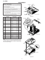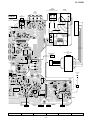
1
XL-1500W
SERVICE MANUAL
No. S6242XL1500W/
COMPACT AUDIO SYSTEM
MODEL
XL-1500W
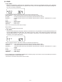
XL-1500W Compact Audio System consisting of XL-1500W
(main unit) and CP-XL1500H (speaker system).
• In the interests of user-safety the set should be restored to its original
condition and only parts identical to those specified should be used.
CONTENTS
Page
SAFETY PRECAUTION FOR SERVICE MANUAL .......................................................................................................... 2
VOLTAGE SELECTION .................................................................................................................................................... 2
AC POWER CORD AND PLUG ADAPTOR ..................................................................................................................... 2
SPECIFICATIONS ............................................................................................................................................................ 3
NAMES OF PARTS .......................................................................................................................................................... 4
OPERATION MANUAL ..................................................................................................................................................... 6
DISASSEMBLY ................................................................................................................................................................. 8
REMOVING AND REINSTALLING THE MAIN PARTS .................................................................................................. 10
ADJUSTMENT ................................................................................................................................................................ 11
TEST MODE ................................................................................................................................................................... 12
NOTES ON SCHEMATIC DIAGRAM ............................................................................................................................. 19
TYPES OF TRANSISTOR AND LED .............................................................................................................................. 19
WAVEFORMS OF CD CIRCUIT ..................................................................................................................................... 20
BLOCK DIAGRAM .......................................................................................................................................................... 21
SCHEMATIC DIAGRAM ................................................................................................................................................. 24
WIRING SIDE OF P.W.BOARD ...................................................................................................................................... 32
TROUBLESHOOTING .................................................................................................................................................... 36
FUNCTION TABLE OF IC .............................................................................................................................................. 42
LCD SEGMENT .............................................................................................................................................................. 44
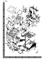
PARTS GUIDE/EXPLODED VIEW
SHARP CORPORATION
–1–
This document has been published to be used
for after sales service only.
The contents are subject to change without notice.
XL-1500W
SAFETY PRECAUTION FOR SERVICE MANUAL
This product is classified as a CLASS 1 LASER PRODUCT.
Precaution to be taken when replacing and servicing the
Laser Pickup.
The AEL (Accessible Emission Level) of Laser Power Output is
less than Class 1 but the laser component is capable of emitting
radiation exceeding the limit for Class1. Therefore it is important
that the following precautions must be observed during servicing
to protect your eyes against exposure to the Laser beam.
(1) When the cabinet has been removed, the power is turned
on without a compact disc, and the Pickup is on a position
outer than the lead-in position, the Laser will light for several
seconds to detect a disc. Do not look into the Pickup Lens.
(2) The Laser Power Output of the Pickup inside the unit and
replacement service parts have already been adjusted prior
to shipping.
(3) No adjustment to the Laser Power should be attempted
when replacing or servicing the Pickup.
(4) Under no circumstances look directly into the Pickup Lens
at any time.
(5) CAUTION - Use of controls or adjustments, or performance
of procedures other than those specified herein may result
in hazardous radiation exposure.
Laser Diode Properties
Material: GaAIAs
Wavelength: 780 nm
Emission Duration: continuous
Laser Output: max. 0.6 mW
VOLTAGE SELECTION
Before operating the unit on mains, check the preset voltage. If the voltage is different from your local voltage, adjust the voltage
as follows, Turn the selector with a screwdriver unit the appropriate voltage number appears in the window (110 V,127 V, 220 V
or 230 V - 240 V AC).
AC POWER CORD AND PLUG ADAPTOR
QACCA0002SJ00
QACCE0002SJZZ
QACCB0003SJ00
QACCL0002SJ00
–2–
XL-1500W
FOR A COMPLETE DESCRIPTION OF THE OPERATION OF THIS UNIT, PLEASE REFER
TO THE OPERATION MANUAL.
SPECIFICATIONS
■ CD player
■ General
Power source
AC 110, 127, 220, 230 - 240 V, 50/60 Hz
Type
Compact disc player
Power consumption
30 W
Signal readout
Non-contact, 3-beam semiconductor laser
pickup
Dimensions
Width: 226 mm (8-15/16")
Height: 145 mm (5-3/4")
Depth: 292 mm (11-1/2")
D/A converter
1-bit D/A converter
Frequency response
20 - 20,000 Hz
Dynamic range
90 dB (1 kHz)
Weight
3.3 kg (7.3 lbs.)
■ Amplifier
Output power
■ Tuner
MPO: 30 W (15 W + 15 W) (10 % T.H.D.)
Frequency range
RMS: 20 W (10 W + 10 W) (10 % T.H.D.)
Output terminals
AM: 531 - 1,602 kHz
Speakers: 8 ohms
Headphones: 16 - 50 ohms (recommended:
32 ohms)
CD digital output (optical)
Input terminals
FM: 88 - 108 MHz
■ Speaker
Type
Video/Auxiliary (audio signal): 500 mV/47
kohms
2-way type speaker system
Tweeter
10 cm (4") Woofer
Maximum input
power
20 W
Rated input power
10 W
Impedance
8 ohms
Dimensions
Width: 146 mm (5-3/4")
Height: 267 mm (10-9/16")
Depth: 186 mm (7-3/8")
Weight
1.5 kg (3.3 lbs.)/each
Specifications for this model are subject to change without
prior notice.
–3–
XL-1500W
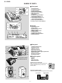
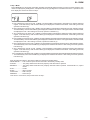
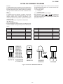
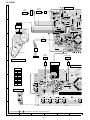
NAMES OF PARTS
■ Front panel
11
8
1
9
1. CD Compartment
2. CD Open/Close Button
3. On/Stand-by Button
4. Function Selector Button
5. Bass/Treble Selector Button
6. Memory/Set Button
7. Clear Button
8. CD Stop, Tuning Down Button
9. CD Track Up or Fast Forward,
Tuner Preset Up Button
10. CD Track Down or Fast Reverse,
Tuner Preset Down Button
11. Volume Up and Down Buttons
12. CD Play or Pause, Tuning Up Button
12
10
2
5
6
3
4
1
■ Display
7
2
4
3
1. Timer Play Indicator
2. Sleep Indicator
3. CD Random Play Indicator
4. Memory Indicator
5. FM Stereo Mode Indicator
6. CD Play Indicator
7. CD Repeat Play Indicator
8. FM Stereo Receiving Indicator
9. Surround Indicator
5
8
6
9
7
■ Rear panel
1
2
3
4
6
7
8
5
9
1. CD Digital Output Socket
2. Headphone Socket
3. AM Aerial Terminal
4. Aerial Earth Terminal
5. FM 75 Ohms Aerial Socket
6. Video/Auxiliary (Audio Signal) Input Sockets
7. Speaker Terminals
8. AC Power Input Socket
9. AC Voltage Selector
■ Speaker system
1. Tweeter
2. Woofer
3. Bass Reflex Duct
4. Speaker Terminals
The rating label is located
on the bottom of the unit.
Speaker grilles are removable:
Make sure nothing comes into contact with the
speaker diaphragms when you remove the
speaker grilles.
1
Placing the speaker system:
There is no distinction between the right and the left speakers.
Left speaker
2
3
4
–4–
Right speaker
XL-1500W
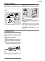
■ Remote control
1
2
3
4
5
6
7
8
11
12
13
14
15
16
17
18
21
19
22
20
23
24 25
9
10
26
27
1. Remote Control Transmitter
2. On/Stand-by Button
3. CD Button
4. Tuner Button
5. Timer Button
6. Clock Button
7. Memory Button
8. Dimmer Button
9. Surround Button
10. Volume Up and Down Buttons
11. Video/Auxiliary Button
12. Band Selector Button
13. Clear Button
14. Sleep Button
15. Random/Repeat Button
16. CD Open/Close Button
17. Tuner Preset Up Button
18. CD Track Down Button
19. CD Fast Reverse, Tuning Down Button
20. CD Play Button
21. CD Track Up Button
22. CD Fast Forward, Tuning Up Button
23. CD Pause Button
24. CD Stop Button
25. Tuner Preset Down Button
26. Bass Up and Down Buttons
27. Treble Up and Down Buttons
Buttons with " " mark in the illustration can be operated on the remote control only.
–5–
XL-1500W
OPERATION MANUAL
Setting the clock
3
Within 1 minute, press the PRESET ( or ) button to
adjust the hour and then press the MEMORY button.
When the 12-hour display is selected, "AM" will change automatically to "PM".
4
This may be operated only with the remote control.
In this example, the clock is set for the 24-hour (0:00) display.
1
Press the CLOCK button and within 3 seconds, press
the MEMORY button.
Within 1 minute, press the PRESET ( or ) button to
adjust the minutes and then press the MEMORY button.
● The hour will not advance even if minutes advance from "59" to
"00".
● The clock starts from "0" second. (Seconds are not displayed.)
2
Within 1 minute, press the PRESET ( or ) button to
select 24-hour or 12-hour display and then press the
MEMORY button.
"0:00"
"AM 12:00"
The 24-hour display will appear.
(0: 00 - 23:59)
The 12-hour display will appear.
(AM 12:00 - PM 11:59)
Note that this can only be set when the unit is first installed or it
has been reset.
To confirm the time display when the power is on:
Press the CLOCK button.
The time display will appear for about 5 seconds.
Note:
The "0:00" or time will flash at the push of the CLOCK button when the
AC power supply is restored after a power failure or unplugging the unit.
Readjust the clock as follows.
To readjust the clock:
Perform "Setting the clock" from the beginning. If the time display is
flashing, step 2 (for selecting the 24-hour or 12-hour display) will be
skipped.
To change the 24-hour or 12-hour display:
1 Clear all the programmed contents.
2 Perform "Setting the clock" from the beginning.
Remote control
■ Battery installation
■ Test of the remote control
1
2
Face the remote control directly to the remote sensor on the unit.
3
Remove the battery cover.
Insert the supplied batteries according to the direction indicated in the battery compartment.
When inserting or removing the batteries, push them towards the
battery terminals.
Replace the cover.
The remote control can be used within the range shown below:
Press the ON/STAND-BY button. Does the power turn on? Now, you
can enjoy the music.
Remote sensor
Precautions for battery use:
● Replace all old batteries with new ones at the same time.
● Do not mix old and new batteries.
● Remove the batteries if the unit is not to be used for long periods
of time. This will prevent potential damage due to battery leakage.
0.2 m - 6 m
(8" - 20')
Caution:
● Do not use rechargeable batteries (nickel-cadmium battery, etc.).
● Installing the batteries incorrectly may cause the unit to malfunc-
tion.
Notes concerning use:
● Replace the batteries if the operating distance is reduced or if the
operation becomes erratic. Purchase 2 "AAA" size batteries (UM4, R03, HP-16 or similar).
● Periodically clean the transmitter on the remote control and the
sensor on the unit with a soft cloth.
● Exposing the sensor on the unit to strong light may interfere with
operation. Change the lighting or the direction of the unit.
● Keep the remote control away from moisture, heat, shock, and
vibrations.
–6–
XL-1500W
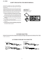
System connections
■ Setting the AC voltage selector
■ Connecting the AC power lead
Check the setting of the AC voltage selector located on the rear
panel before plugging the unit into a wall socket. If necessary, adjust
the selector to correspond to the AC power voltage used in your
area.
After checking all the connections have been made correctly,
connect the AC power lead to the AC power input socket, then
into the wall socket.
Wall socket
Turn the selector with a screwdriver until the appropriate voltage number appears in the window (110 V, 127 V, 220 V or 230 V
- 240 V AC).
1
2
Notes:
● Unplug the AC power lead from the wall socket if the unit will not
be in use for a prolonged period of time.
● Never use a power lead other than the one supplied. Use of a
power lead other than the one supplied may cause an electric shock or fire.
AC Plug Adaptor
In areas (or countries) where a wall socket as shown in illustration
is used, connect the unit using the AC plug adaptor supplied with
the unit, as illustrated. The AC plug adaptor is not included in areas
where the wall socket and AC power plug can be directly connected
(see illustration ).
Note for users in Australia and New Zealand:
An AC plug adaptor is not supplied if the lead has an Australian
Standard plug.
Troubleshooting
■ If trouble occurs
When this product is subjected to strong external interference
(mechanical shock, excessive static electricity, abnormal supply
voltage due to lightning, etc.) or if it is operated incorrectly, it may
malfunction.
If such a problem occurs, do the following:
1 Set the unit to the stand-by mode and turn the power on
again.
2 If the unit is not restored in step 1, unplug and plug in the
unit, and then turn the power on.
3 If neither step 1 nor 2 restores the unit, do the following:
Press the ON/STAND-BY button to enter the power stand-by
mode.
Unplug the AC power lead from the AC INPUT socket on the
unit.
Whilst pressing down the MEMORY/SET button and the
button, plug the AC power lead into the AC INPUT socket on
the unit.
AC INPUT
Caution:
● This operation will erase all data stored in memory including
clock, timer settings, tuner preset, and CD programme.
● After the above operation, interval span setting for AM will be
returned to 9 kHz (50 kHz for FM) automatically.
–7–
XL-1500W
DISASSEMBLY
Caution on Disassembly
Follow the below-mentioned notes when disassembling
the unit and reassembling it, to keep it safe and ensure
excellent performance:
1. Take compact disc out of the unit.
2. Be sure to remove the power supply plug from the wall
outlet before starting to disassemble the unit.
3. Take off nylon bands or wire holders where they need to
be removed when disassembling the unit. After servicing
the unit, be sure to rearrange the leads where they were
before disassembling.
4. Take sufficient care on static electricity of integrated
circuits and other circuits when servicing.
Top Cabinet
(B1) x1
ø3 x10mm
(A1) x2
ø3 x10mm
(B1) x1
ø3 x10mm
(B1) x1
ø3 x6mm
Cover,Rear Panel
(C2) x4
ø3 x10mm
Figure 8-1
STEP
REMOVAL
PROCEDURE
FIGURE
1
Top Cabinet
1. Screw .................. (A1) x4
2. Socket ................. (A2) x9
8-1,2
8-2
2
Cover,Rear panel
1. Screw .................. (B1) x3
8-1
3
Chassis
1. Screw .................. (C1) x5
2. Screw .................. (C2) x4
3. Hook .................... (C3) x4
8-3
8-1
8-3
4
Tuner PWB
1. Screw .................. (D1) x1
2. Socket ................. (D2) x1
9-1
5
Terminal PWB
1. Screw .................. (E1) x2
2. Socket ................. (E2) x1
9-1
6
Rear Panel
1. Screw .................. (F1) x1
9-1
7
Main PWB
1. Screw .................. (G1) x6
2. Screw .................. (G2) x2
3. Socket ................. (G3) x2
9-1
TOP Cabinet
Cover,
Rear Panel
(A2) x8
(A2) x1
8
CD PWB
1. Flat Cable ............ (H1) x1
2. Socket ................. (H2) x2
3. Screw .................. (H3) x4
9-2
9
CD Mechanism
1. Screw .................. (J1) x4
9-2
10
LED PWB
1. Screw .................. (K1) x2
9-2
11
Switch PWB
1. Hook .................... (L1) x2
2. Socket ................. (L2) x1
9-3
12
Display PWB
1. Screw .................. (M1) x6
2. Socket ................. (M2) x1
9-3
13
Gear Box
1. Hook .................... (N1) x3
9-3
(A1) x2
ø3 x10mm
Bottom Cabinet
Figure 8-2
Note:
After removing the connector for the optical pickup from the
connector, wrap the conductive aluminium foil around the
front end of connector remove to protect the optical pickup
from electrostatic damage.
,
Chassis
Hook
(C3) x4
2
Chassis
1
Bottom
Cabinet
Bottom Cabinet
(C1) x5
ø3 x6mm
Figure 8-3
–8–
XL-1500W
(E1) x2
ø3 x10mm
(G2) x2
ø3 x10mm
(G3) x2
Terminal PWB
Rear Panel
(F1) x1
ø3 x6mm
(E2) x1
(G1) x6
ø3 x8mm
(H1) x1
(H2) x1
(H3) x4
ø2.5 x10mm
(K1) x2
ø2.5 x10mm
(D1) x1
ø3 x10mm
CD PWB
Tuner PWB
Main PWB
Holder,
Indicator Panel,CD
(J1) x4
ø2.5 x10mm
(D2) x1
LED PWB
Holder PWB
Chassis
CD
Mechanism
Figure 9-1
,
Display PWB
(H2) x1
Top Cabinet
Gear Box
Gear Box
Switch
PWB
Figure 9-2
Pull
Pull
Hook
(N1) x3
(M1) x6
ø2.5 x10mm
Hook
(N1) x3
(L2) x1
Display PWB
Hook
(L1) x2
(M2) x1
Switch
PWB
Switch
Pull
Pull
Top Cabinet
Tweeter
Hook
(L1) x2
Front Panel
( A2 ) x1
Figure 9-3
( A3 ) x4
ø3.5 x12mm
STEP
1
REMOVAL
Speaker
PROCEDURE
FIGURE
1. Net Frame ........... (A1) x1
2. Front Panel ......... (A2) x1
3. Screw .................. (A3) x4
9-4
Net Frame
( A1 ) x1
Woofer
Screwdriver
Figure 9-4
–9–
XL-1500W
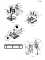
REMOVING AND REINSTALLING THE MAIN PARTS
How to remove the CD lid (See Fig. 10-1.)
Perform steps 1 to 13 of the disassembly method to remove
the gear box. (See page 8,9)
1. Remove the screws (A1) x 2 pcs., to remove the CD lid
motor.
2. Remove the hooks (A2) x 3 pcs., to remove the worm wheel.
Caution:
Be careful so that the gear is not damaged.
(The damage gear emits noise during searching.)
Hook
(A2) x3
Worm Wheel
(A1) x2
ø2 x3mm
CD Lid Motor
Figure 10-1
CD MECHANISM SECTION (See Fig. 10-2.)
Perform steps 1 to 9 of the disassembly method to remove the
CD mechanism. (See page 8,9)
1. Remove the mechanism cover, paying attention to the
pawls (A1)x 4 pcs.
2. Remove the screws (A2) x 2 pcs., to remove the shaft (A3)
x 1 pc.
3. Remove the stop washer (A4) x 1 pc., to remove the gear
(A5) x 1 pc.
4. Remove the pickup unit.
Note:
After removing the connector for the optical pickup from the
connector, wrap the conductive aluminium foil around the
front end of connector remove to protect the optical pickup
from electrostatic damage.
(A1) x4
Mechanism Cover
(A2) x2
ø2.6 x6mm
CD Mechanism
Shaft
(A3) x1
Gear
(A5) x1
Stop Washer
(A4) x1
Pickup unit
Figure 10-2
– 10 –
XL-1500W
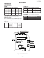
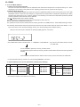
ADJUSTMENT
TUNER SECTION
fL: Low-range frequency
fH: High-range frequency
• AM IF/RF
Signal generator: 400 Hz, 30%, AM modulated
Frequency Frequency
Display
• FM Mute Level
Signal generator: 1 kHz, 40 kHz dev., FM modulated
Setting/ Instrument
Adjusting Connection
Parts
T351
*1
AM IF
450 kHz
1,620 kHz
AM Band
Coverage
—
522 kHz
(fL): T306 *2
1.1 ± 0.1 V
AM
Tracking
990 kHz
990 kHz
(fL): T302
Frequency
98.00 MHz
(30 dBµV)
VR351*1
Instrument
Connection
Input: SO301
Output: Speaker
Terminal
• Check FM VT
Signal generator: 1 kHz, 40 kHz dev., FM modulated
Frequency
• Setting the Test Mode
Keeping the FF/FWD button and MEMORY/SET button
pressed, turn on ON/STAND-BY. Then, the frequency is
initially set in the memory as shown in Table. Call it with the
VOLUME UP/DOWN button to use it for adjustment and check
of tuner circuit.
Preset No.
98.00 MHz
Adjusting
Parts
*1. Adjust so that an output signal appears.
*1
*1. Input: Antenna, Output: Speaker Terminal
*2. Input: Input is not connected, Output: TP301
1
2
3
4
5
Display
FM
87.50 MHz
108.00 MHz
98.00 MHz
90.00 MHz
106.00 MHz
Display
Check Point
87.5 MHz
87.5 MHz
2.2 V ± 0.7 V
TP301
108 MHz
108 MHz
7.3 V ± 1.0 V
TP301
AM
Preset No.
6
7
8
9
10
522 kHz
1,620 kHz
990 kHz
603 kHz
1,404 kHz
FM
75
SO301 OHMS
ANTENNA
TERMINAL
TUNER PWB-B1
GND
AM
FE301
TP301
20
T302
AM
Tracking fL
IC302
VR351
FM Mute
Level
T351
AM IF
T306
AM Band
Coverage fL
IC303
Figure 11 ADJUSTMENT POINTS
– 11 –
Instrument
Connection
XL-1500W
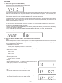
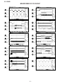
TEST MODE
The test mode applied to this microcomputer has three modes, namely the ordinary test mode for adjustment or measurement,
the aging test mode, and the self-diagnosis test mode for self-judgment in case of final product inspection.
1. Turning on the test mode
For obtaining each test mode, press the ON/STAND-BY button, while keeping pressing the following two buttons in the ordinary
stand-by mode (power off ). In this case, the main unit buttons are valid. When turning the ON/STAND-BY on with remote control
buttons, test modes are not obtained.
[Ordinary test mode]
1. CD Test Mode (TEST 1).....................................BASS/TREBLE + STOP
2. Tuner Test Mode (TEST 2).................................BASS/TREBLE + VOL+
3. Electronic Volume Test Mode (TEST 3)............. BASS/TREBLE + VOL–
4. Timer Test Mode (TEST 4)................................. MEMORY/SET + STOP
5. LCD Test Mode (TEST 5)................................... MEMORY/SET + VOL–
6. Electric CD Lid Aging Test Mode (TEST 8)........ MEMORY/SET + VOL+
[Self-diagnosis Test Mode]
1. Button input diagnosis test mode (TEST6).…....MEMORY/SET + PLAY
Processes are different depending on destinations at initial settings.
2. CD Test Mode (TEST 1)
In the CD test mode the operation of each step is possible even if the LID-SW is off. If focus cannot be taken in step 3 or any error
is processed, it is impossible to proceed to the next step. During error processing, end the test mode by pressing the ON/STANDBY button or return to the step 1 by pressing the CD STOP button. Any other operations are inhibited.
1. Step 1 Mode
When the CD test mode is obtained, the following display lights up. Then CD initialization operation flow proceeds up to CD
STB off to wait for the following buttons to be pressed.
One second after display lights up
Press the following buttons in this state to obtain the operations specified below.
"ON/STAND-BY" ...... Test mode and power turned off to shift to the ordinary standby mode.
"FF/FWD" ................. After the pickup returns to the innermost periphery, it slides toward the outer periphery while this button
is pressed.
"REW/REV" .............. After the pickup returns to the innermost periphery, it slides toward the inner periphery while this button
is pressed. If PICKUP IN is on, input is invalid.
"PLAY" ..................... Shift to step 2
"STOP" ..................... Invalid
"FUNCTION" ............ Shift to step 5
* In case of initialization, the pickup is moved toward the inner periphery. Any buttons other than "ON/STAND-BY" button are
not accepted until the shift of pickup to the inner periphery is completed at this time. If PICKUP IN SW ON cannot be detected
within 10 seconds, the slide motor stops, and the following error display appears. Press the ON/STAND-BY button to end
the test mode, or press the CD STOP button to return to step 1. Any other operations are inhibited.
– 12 –
XL-1500W
2. Step 2 Mode
Press the "CD PLAY" button in this mode to transmit the laser lighting command LDON (8400) and turn on the laser. Any other
operations are not performed in this case.
Press the following buttons in this state to obtain the operations specified below.
"ON/STAND-BY" ..... Test mode and power turned off to shift to the ordinary standby mode.
"FF/FWD" ................ The pickup slides toward the outer periphery while this button is pressed.
"REW/REV" ............. The pickup slides toward the inner periphery while this button is pressed. If PICKUP IN is on, input is
invalid.
"PLAY" ..................... Shift to step 3
"STOP" .................... Return to step 1
"FUNCTION" ........... Shift to step 5
3. Step 3 Mode
While the laser keeps lighting, CD initialization operation flow proceeds up to 'CLV servo ON' to wait for the following buttons
to be pressed. (Focus servo turned on for focus search)
The focus search is repeated to take focus.
Press the following buttons in this state to obtain the operations specified below.
"ON/STAND-BY" ..... Test mode and power turned off to shift to the ordinary standby mode.
"FF/FWD" ................ The pickup slides toward the outer periphery while this button is pressed.
"REW/REV" ............. The pickup slides toward the inner periphery while this button is pressed. If PICKUP IN is on, input is
invalid.
"PLAY" ..................... If focus has been taken, shift to step 4 is executed. If not, acceptance is inhibited.
"STOP" .................... Return to step 1
"FUNCTION" ........... Shift to step 5
*If the focus is not received after it has been taken, the process returns to step 1.
4. Step 4 Mode
The CLV servo ON command (8600) is transmitted to wait for the following buttons to be pressed. (The disc is rotated for CLV
lock.)
The time display always indicates "0:00".
Press the following buttons in this state to obtain the operations specified below.
"ON/STAND-BY" ..... Test mode and power turned off to shift to the ordinary standby mode.
"FF/FWD" ................ The pickup slides toward the outer periphery while this button is pressed.
"REW/REV" ............. The pickup slides toward the inner periphery while this button is pressed. If PICKUP IN is on, input is
invalid.
"PLAY" ..................... Shift to step 5
"STOP" .................... Return to step 1
"FUNCTION" ........... Shift to step 5
*If the focus is not received, the process returns to step 1.
– 13 –
XL-1500W
5. Step 5 Mode
When the CD initialization operation flow is completed, the mute is turned off, and playback is started. Even if playback
reaches the outermost periphery of disc, the operation does not stop. The LCD display indicates the playback passage time
as in case of ordinary CD playback.
Press the following buttons in this state to obtain the operations specified below.
"ON/STAND-BY" ...... Test mode and power turned off to shift to the ordinary standby mode.
"FF/FWD" ................. The pickup slides toward the outer periphery while this button is pressed.
"REW/REV" .............. The pickup slides toward the inner periphery while this button is pressed. If PICKUP IN is on, input is
invalid.
"PLAY" ..................... Invalid
"STOP" ..................... Return to step 1
"FUNCTION" ........... Shift to step 6
"MEMORY" .............. Shift to step 7
*If the is not received, the process returns to step 1.
Other cautions
• TOC IL is not available for this test mode.
6. Step 6 Mode
Press the FUNCTION button during step 5 operation to set EC/FC bit to "H" by PROSET command (9188 transmission) and
to monitor BUS2 (QDRE) during idle mode. The number of errors for 1 frame (1 sub-code block in IC data) is read by read
command SRC6 during "H". The number of errors accumulated in 750 frames for 10 seconds is displayed on LCD. During
the display, music signal is played back.
Press the following buttons in this state to obtain the operations specified below.
"ON/STAND-BY" ...... Test mode and power turned off to shift to the ordinary standby mode.
"FF/FWD" ................. The pickup slides toward the outer periphery while this button is pressed.
"REW/REV" .............. The pickup slides toward the inner periphery while this button is pressed. If PICKUP IN is on, input is
invalid.
"PLAY" ..................... Invalid
"STOP" ..................... Return to step 1
"FUNCTION" ........... Shift to step 5
"MEMORY" .............. Shift to step 7
Press FF/PRESET UP or REW/PRESET DOWN button to slide the pickup. The number of errors accumulated up to that time
is cleared and addition is restarted after shift.
*If the focus is not received, the process returns to step 1.
– 14 –
XL-1500W
7. Step 7 Mode
Press "MEMORY" key during step 6 operation to display automatically adjusted values on LCD in the order as below. Item
names are displayed by left alignment, and adjusted values by right alignment in hexadecimal numbers. Operations other
than display are as same as those for step 5.
a) "Fb" is displayed on the left of LCD. FTBAST command (D480) is transmitted to designate focus balance adjusting
register. Then data read by read command SRC2 (2) are displayed in hexadecimal numbers. After waiting 2 seconds,
operation is shifted to (b).
b) "FG" is displayed on the left of LCD. FTBAST command (D481) is transmitted to designate focus gain adjusting register.
Then data read by read command SRC2 (2) are displayed in hexadecimal numbers. The upper two bits, which are invalid,
are displayed as "00". After waiting two seconds, operation is shifted to (c).
c) "Tb" is displayed on the left of LCD. FTBAST command (D482) is transmitted to designate tracking balance adjusting
register. Then data read by read command SRC2 (2) are displayed in hexadecimal numbers. After waiting 2 seconds,
operation is shifted to (d).
d) "TG" is displayed on the left of LCD. FTBAST command (D483) is transmitted to designate tracking gain adjusting register.
Then data read by read command SRC2 (2) are displayed in hexadecimal numbers. The upper two bits, which are invalid,
are displayed as "00". After waiting 2 seconds, operation is shifted to (e).
e) "FO" is displayed on the left of LCD. FTBAST command (D484) is transmitted to designate focus offset adjusting register.
Then data read by read command SRC2 (2) are displayed in hexadecimal numbers. After waiting 2 seconds, operation
is shifted to (f).
f) "TO" is displayed on the left of LCD. FTBAST command (D485) is transmitted to designate tracking offset adjusting
register. Then data read by read command SRC2 (2) are displayed in hexadecimal numbers. After waiting 2 seconds,
operation is shifted to (g).
g) "FF" is displayed on the left of LCD. FTBAST command (D486) is transmitted to designate RF amplitude adjusting register.
Then data read by read command SRC2 (2) are displayed in hexadecimal numbers. After waiting 2 seconds, operation
is shifted to (a).
Press the following buttons in this state to obtain the operations specified below.
"ON/STAND-BY" ...... Test mode and power turned off to shift to the ordinary standby mode.
"FF/FWD" ................. The pickup slides toward the outer periphery while this button is pressed.
"REW/REV" .............. The pickup slides toward the inner periphery while this button is pressed. If PICKUP IN is on, input is
invalid.
"PLAY" ..................... Invalid
"STOP" ..................... Return to step 1
"FUNCTION" ........... Shift to step 6
"MEMORY" .............. Shift to step 5
*If the focus is not received, the process returns to step 1.
– 15 –
XL-1500W
3. Tuner Test Mode (TEST 2)
1. Outline of tuner (radio) test mode
The tuner test mode is intended to store the adjustment and measurement frequencies in the preset memory CH. When
adjusting the tuner section in the production line, adjusting personnel are not required to set frequency.
2. Details of tuner test mode
Press the "REW/PRESET DOWN" and "CD PLAY" buttons in POWER OFF state and turn on the power by the use of "ON/
STAND-BY" button to preset and store frequency for adjustment and measurement of destination specified by the AREA
terminal in the preset memory CH. However, Ordinary 1 and Ordinary 2 are stored in the destinations (selected by SPAN
switching operation) when the test mode is obtained.
("FF " + "MEMORY/SET" KEY SPAN CHANGE)
(As for frequencies to be preset and stored for each destination, refer to item 3.)
The tuner test mode is started from preset No.1.
The operations of test mode are identical with the ordinary operations of TUNER function. FUNCTION switching is invalid.
It is necessary to discard the content of preset memory when the tuner test mode is ended; be sure to write "0000" or "1111"
bits in the memory to be checked for judging memory error at initial setting and to initialize memory.
When the tuner test mode is obtained, the following display lights for one second.
• The TUNER TEST2 mode is obtained with >> + MEMORY + ON/STAND-BY. ->Turn off AC in the TEST2 mode to restore
the initial state.
Turn off POWER to protect the memory of TEST2 mode.
Turn off POWER again to obtain the ordinary operation while the data is stored in the memory (besides
TUNER).
If AC OFF state is maintained in this state for about 1/2 day, start is executed in the initial state.
• To clear the whole memory, insert the AC cord, pressing MEMORY + CD PLAY.
3. Preset frequencies for various destinations (random preset memory)
CH
1
2
3
4
5
BAND
FM
STEREO
FM
FM 87.50 MHz
FM108.00 MHz
FM 98.00 MHz
FM 90.00 MHz
FM106.00 MHz
CH
6
7
8
9
10
BAND
AM
AM
AM 522 kHz
AM1620 kHz
AM 990 kHz
AM 603 kHz
AM1404 kHz
• The slant line sections of the table store no memory.
– 16 –
CH
16-25
26
27
28
29
30
BAND
FM
MONO
FM
FM106.00 MHz
FM 90.00 MHz
FM 98.00 MHz
FM108.00 MHz
FM 87.50 MHz
XL-1500W
4. Electronic volume Test Mode (TEST 3)
When this test mode is obtained, the following display lights for one second.
In this mode, volume is -14 dB (STEP28), BASS/TREBLE is set to 0 (0 dB) and SURROUND mode to OFF, and start-up function
to CD, respectively. The button operations in the test mode are the same as those of ordinary operation except volume UP/
DOWN.
(1) The display is the same as that of ordinary operation except test mode setting.
(2) Unlike the ordinary state, the volume is controlled with the volume UP/DOWN button in accordance with the following three
steps.
Volume-
∞ (STEP 0) <-> Volume-14 dB (STEP 23) <-> Volume-0 (STEP 30)
(3) BASS/TREBLE and SURROUND are switched when button is pressed..
5. Timer test Mode (TEST 4)
When this test mode is obtained, the following display lights for one second.
Set the current time and timer time according to the following procedure to reproduce the timer.
1.Set the current time to 1:00, the timer to ON time 1:05, the function to CD, and volume to STEP 12, respectively. One minute
is counted as one second, and the timer is reproduced. The fade-in (when playback is started) is executed at a rate of one step
for 1 sec. After completion of fade-in, the fade-out is executed at a rate of one step for 1 sec (WAIT 1 sec inserted).
After completion of fade-out, the power is turned off (after WAIT 1 sec), and the mode is shifted to the standby.
The display during operation is the same as that of ordinary timer operation.
6. LCD Test Mode (TEST 5)
When the LCD test mode is obtained, all the LCD segments are lighted. Then pressing the "PLAY" button switches display as
below.
Lighting of all segments
Lighting of odd segments
– 17 –
Lighting of even segments
XL-1500W
7. Button input diagnosis Test Mode (TEST 6)
When the test mode is obtained, the following is displayed.
This test mode is intended to check whether all the main unit buttons can be detected. Accordingly, in this test mode, it is checked
whether the "ON/STAND-BY" button was pressed after all the buttons shown below were pressed. If the result is OK, OK is
displayed. If any one of keys was not pressed, an error is displayed. In both cases of OK termination or error termination, the
mode is shifted to the standby mode if the "ON/STAND-BY" button is pressed subsequently.
All models using this type of microcomputer are not always provided with the same buttons. Since the buttons used are different
depending on models, types of buttons to be used are determined by whether RDS, SURROUND, and an electric lid are
available at the initial setting by MODEL port.
The order of buttons to be pressed is not determined. Accordingly, it is checked whether all buttons have been pressed.
1. PU-IN buttons: REW/PRESET DOWN + CD STOP
Since this model is provided with SURROUND (HAVE OR NOT), RDS (HAVE OR NOT), and electric CD lid, the following
10 buttons are detected as all buttons.
PLAY, BASS/TREBLE, FUNCTION, VOLUME UP/DOWN, MEMORY/SET, REW, FF, STOP, CD-OPEN/CLOSE
The OK/NG display of test result is as follows.
8. Electric CD lid Aging Test Mode (TEST 8) (Only for model with electric CD lid)
Outline
OPEN/CLOSE operations of electric CD lid are repeated. The number of repeated times and time period are monitored. If the
lid does not move to the regular position after the specified time, operation is stopped. When an error is detected by [CLID_PRO]
during CLOSE, operation is also stopped.
a. POWER ON for function AUX
CD lid position is checked.
CLOSE position: Operation proceeds to the next process.
Position other than CLOSE: After the lid moves to CLOSE, operation proceeds to the next process.
b. CD lid operation started
OPEN operation
WAIT 1 second
CLOSE operation
WAIT 1 second
c. Operations above are repeated.
Specified monitoring time
OPEN operation: 5 seconds
CLOSE operation: 5 seconds
d. Display
OPEN>CLOSE is counted as 1. 1 to 59999 are counted; if the count is over
59999, display is returned to 0 to repeat counting.
Display when the lid does not move to the regular position after the specified
time
(Ex: Defective operation occurring in the middle of 1538.)
Highlight display of stop when an error is detected by [CLID-PRO]
(Ex: Defective operation occurring in the middle of 1538.)
– 18 –
XL-1500W
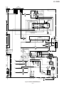
NOTES ON SCHEMATIC DIAGRAM
• Resistor:
To differentiate the units of resistors, such symbol as K and
M are used: the symbol K means 1000 ohm and the symbol
M means 1000 kohm and the resistor without any symbol is
ohm-type resistor. Besides, the one with “Fusible” is a fuse
type.
• Capacitor:
To indicate the unit of capacitor, a symbol P is used: this
symbol P means micro-micro-farad and the unit of the
capacitor without such a symbol is microfarad. As to
electrolytic capacitor, the expression “capacitance/withstand
voltage” is used.
(CH), (TH), (RH), (UJ): Temperature compensation
(ML): Mylar type
(P.P.): Polypropylene type
• Schematic diagram and Wiring Side of P.W.Board for this
model are subject to change for improvement without prior
notice.
REF. NO
DESCRIPTION
• The indicated voltage in each section is the one measured
by Digital Multimeter between such a section and the chassis with no signal given.
1. In the tuner section,
( ) : AM mode
: FM stereo mode
2. In the CD section, the CD is stopped.
• Parts marked with “
”(
) are important for
maintaining the safety of the set. Be sure to replace these
parts with specified ones for maintaining the safety and
performance of the set.
POSITION
REF. NO
ON—OFF
SW719
VOLUME DOWN
ON/STAND-BY
ON—OFF
SW720
VOLUME UP
ON—OFF
CD LID OPEN/CLOSE
ON—OFF
SW725
BASS/TREBLE
ON—OFF
REW/PRESET DOWN
ON—OFF
SW726
MEMORY/SET
ON—OFF
ON—OFF
SW727
CLEAR
ON—OFF
SW702
PICKUP IN
SW709
SW710
SW711
DESCRIPTION
POSITION
ON—OFF
SW712
FF/PRESET UP
SW713
CD STOP/TUNING DOWN
ON—OFF
SW728
FUNCTION
ON—OFF
SW718
CD PLAY/PAUSE/TUNING UP
ON—OFF
SW802
CD LID
ON—OFF
FRONT
VIEW
E C B
(S) (G) (D)
(1) (2) (3)
2SB562 C
2SC380 O
2SK2541
KRA102 M
KRA107 M
KRC102 M
KRC104 M
KRC107 M
KTA1266 GR
KTC3199 GR
KTC3200 GR
FRONT
VIEW
FRONT
VIEW
B C E
2SD2012 Y
SLI343YC
SYD5310
Figure 19 TYPES OF TRANSISTOR AND LED
– 19 –
1
2
3
SVC348S
XL-1500W
WAVEFORMS OF CD CIRCUIT
NO DISC FOCUS SEARCH
1
STOP
12
1
FOO
FO+
13
2
IC803 26pin
3
FO-
14
3
SEL
5
6
1
11
2
TEI
15
3
6
SBAD
11
2
3
TEI
1
TRO
2
IC801 34pin
RFO
15
3
FMO
3
IC801 40pin
IC802 22pin
STOP
PLAY
REVIEW
6
1
FEI
TEI
1
TRO
2
IC801 31pin
IC801 29pin
RFGO
11
2
IC802 19pin
IC801 34pin
RFRP
15
3
IC802 17pin
3
FMO
IC801 40pin
STOP
TEI
PLAY
TCD-782 TNO-02 PLAYBACK
16
1
IC801 31pin
TRO
SBAD
LO
1
RO
2
IC801 53pin
2
IC801 34pin
7
FMO
IC801 31pin
IC801 30pin
11
2
CUE
1
FEI
6
TRO
PLAY
IC801 29pin
10
1
IC801 40pin
STOP
5
TEI
IC801 34pin
IC801 31pin
5
PLAY
IC801 31pin
FEI
6
3
STOP
IC801 29pin
9
2
DMO
TOC IL
IC801 38pin
8
SBOK
IC801 41pin
FOCUS SEARCH
7
1
IC801 8pin
IC803 25pin
4
TMAX
IC801 16pin
IC801 33pin
2
PLAY
17
IC801 50pin
3
IC801 30pin
– 20 –
XL-1500W
TUNER PWB
SWITCHING
AM Band
Tracking fL
Q351
FM MUTE
LEVEL
7
6
5
4
3
2
FM IF
1
CF301
Q301
4
5
6
7
FM IF
AM IF
AM IF
CF302
T351
CF352
8
R-CH
OUT
L-CH
OUT
9
13
MO/ST
15 14
10 11
12
IF OUT
MPX VCO
16
VCC
FM DET
STEREO
SD
VSM
3
17
MPX IN
18
AM LOW
CUT
FM/AM
OUT
AM RF
IN
19
AM IF
IN
GND
FM AFC
20
PHASE
(AM/FM)
2
21
PHASE
1
22
CF351
FE301
FM FRONT END
FM IF AM OSC
OUT
IN
AM MIX
OUT
AM OSC
IN
REG
IC303
LA1832S
FM IF DET./
FM MPX./AM IF
AM Band
Coverage fL
8
24 23
VR351
T306
+5V
X351
456kHz
+5V
VD301
SVC348S
FM IF
T302
+5V
+5V
FM +B
AM
FM ST
ZD351
FM
75ohms
DO
VOLTAGE
REGULATOR
CL
+5V
DI
TP301
CE
VT
SO301
ANTENNA
TERMINAL
+B
Q360
FM +B
A_12V
TUN_L
TUN_R
+5V
11
10
TO
MAIN PWB
SD
GND
9
8
7
6
5
4
3
2
1
6
7
AM IN
8
IF REQ IF IN
5
MO/ST
4
14 13 12
FM
FM
3
1
VDD
MUTE FM IN
DO
PD
17 16 15
CL
AIN
18
DI
AOUT
19
CE
VSS
X IN X OUT
X352
4.5MHz
IC302
LC72131
PLL(TUNER)
CNS301
22 21 20
9
10
11
D_GND A_GND
DISPLAY PWB
CD LID
MOTOR DRIVER
IC804
TA7291S
LCD701
FL DISPLAY
1
1
4
5
2
3
5
6
7
8
M801(246-6)
CD LID
OPEN/CLOSE
9
M
38
SWITCHING
Q806
Q804
LED801
67
Q807
CD-RES 65
8 VDD
CCE 64
9 OSC2
BUCK 63
10 OSC1
11 VSS
8MHz
12 XI
X702
13 XO
32.768kHz
PU-IN 58
CNW701
25 26 27 28
SD
DATA
ST
37 38 39
10
9
9
8
8
7
7
6
6
5
5
4
4
3
3
2
2
1
1
BUCK
BUS3
BUS2
BUS1
BUS0
PU-IN
CD-RW
CNW704
LIGHT 53
CD+B
32
P-MUTE
23
SURR
47 P—CONT
CLE
DIMMER 54
CE
17 KEY1
18 KEY2
D_GND
P_CONT
USWD5.6V
CL
CLID_UP 56
DI
16 CLID_SW
DO
SW710
GVSW 33
REMOCON
SW709
SWITCH PWB
40 43 45 46 48 49 50 51 41 44
SW802
CD LID
P_STB
1
PROTECT
2
CNW703
RESET
Q701
BUS0 59
CLID_DW 57
SYS_STOP
M_GND
M_12V
BUS1 60
24 VREF+
POWER
7
6
5
4
3
2
1
BUS2 61
15 VREF
RESET
7
6
5
4
3
2
1
14 MMOD
VSM
TO
MAIN PWB
SW711~713
SW718~720
SW725~728
BUS3 62
IC701
IX0043SJ
SYSTEM MICROCOMPUTER/
FL DRIVER
10
CCE
B-LIGHT
X701
CD-STB
CD-RES
Q702
Q703
CE
DI
RX701
REMOTE
SENSOR
CL
DO
STEREO
LED701 LED702
Q708
CLE
Q707
SWITCHING
Q709
LED704 LED703
D_GND
P_MUTE
CD+B
SURROUND
GND
SWITCHING
Q706
LED PWB
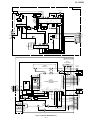
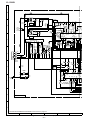
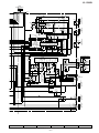
Figure 21 BLOCK DIAGRAM (1/3)
– 21 –
CNW702
1
2
1
1
2
2
3
3
4
4
5
5
6
6
7
7
8
GND
TO
CD PWB
CD-STB 66
7 VLC1
LED PWB
8
9
9
10
10
11
11
12
12
13
13
TO
MAIN PWB
SEG33
SEG0
COM3
COM0
5 VLC3
6 VLC2
100
1
4
XL-1500W
FROM
TUNER PWB
FROM
DISPLAY PWB
CNP704
CNP301
10 9 8 7 6 5 4 3 2 1
11 10 9 8 7 6 5 4 3 2
SD
FM ST
DO
CL
DI
CE
D_GND
A_12V
TUN L
A_GND
TUN R
BUS0
GVSW
BUS1
PU_IN
BUS2
BUS3
CCE
BUCK
CD_STB
CD_RES
CD PWB
+B4
+B2
R-CH
SO401
VIDEO/AUX
INPUT
ZD801
Q808
Q809
Q810
ZD802
+B6
L-CH
+B4
VOLTAGE
REGULATOR
3.3V
+B5
7.3V
Q802
M701
SPINDLE
MOTOR
+B1
+
SP+
SP–
SL+
SL–
PU-IN
GND
MUTE
REG O
TRB
VIN4
VG1
VIN1
VO3+
VO3–
VO1+
GND
VO1–
GND
21 22 23 24 25 17 18 28
+
–
M
M
M702
SLED
MOTOR
J801
DIGITAL
OUT
1
2
3
M_GND
SW702
PICKUP IN
IC803
MM1469PH
FOCUS/
TRACKING/
SPIN/SLED
DRIVER
TERMINAL
PWB
CD MOTOR PWB
FO
+B1
16 26 27 19
BIAS
VG4
VO4–
VIN3
VG3
VCC
VCC
PO1–
PO1+
VO4+
OPO
GND
VO2VO2+
VIN2
VG2
13 12 11 10 9 8 7 6 5 4 3 2 1
–
TR
40
DMO
FMO
+B6
41
DOUT 4
51 DVDD
57
58
59
60
61
62
BUS0
BUS1
BUS2
BUS3
BUCK
CCE
63 RST
X801
16.93MHz
CNW803
CD_L
RO 50
LO 53
CD_R
IC801
SEL
TC94A14F
SERVO/SIGNAL CONTROL
38
1
2
2
3
3
37
36
35
34
FOO 33
TEZI 32
TEI 31
FOCUS COIL
TRACKING COIL
6 DVDD
15 PDO
25 AVDD
13
15
16
14
17
18
19
20
21
22
23
24
RFRP 28
RFCT 26
RFI 24
39 AVDD
43 DVDD
48 XVDD
PVREF 20
LPFO 19
LPFN 18
64 VDD
GVSW
FEO
FEN
VRO
RFRP
RFIS
RFGO
RFGC
AGCI
RFO
RFN
GND
RFDC
TEO
TEN
TEBC
SEL
LDO
MDI
TN1
TPI
FPI
FNI
VCC
12
11
10
9
8
7
6
5
4
3
2
1
+B5
SWITCHING
LD
Q801
E
F
B
A
MON
+B5
TMAX 16
XVSS
DVSL
TESIN
AVSS
DVSS
GND
DVSS
+B6
7 22 42 44 45
54
GND
CD_R
CD PICKUP UN
SBAD 30
FEI 29
+B5
CNP803
CD_L
A
A_GND
TEBC
RFGC
VREF
TRO
46 XI
47 XO
1
IC802
TA2157F
HEAD AMP.
C
1/2V
A_GND
+B6
Figure 22 BLOCK DIAGRAM (2/3)
– 22 –
5V
XL-1500W
FROM
DISPLAY PWB
+B4
CD +B
CNP702
SURROUND
7 8 9 10 11 12 13
D_GND
SD
DO
FM ST
DI
CL
1 2 3 4 5 6
CE
D_GND
A_12V
TUN L
A_GND
TUN R
5 4 3 2 1
P_MUTE
M
PWB
MAIN PWB
R-CH OUT
R-CH IN
+B
+B2
Q203
5
6
7
8
4
3
2
1
Q201
IC201
KIA4558P
SURROUND
CONTROL
L-CH OUT
L-CH IN
R-CH OUT
AUX R
14
13
12
11
10
8
9
6
7
4
5
3
2
1
VSS
15
DI
CE
TUN R
CD R
NC
VDD
LOGIC
16
19
18
20
21
24
23
22
25
26
27
28
29
30
CL
17
CD L
TUN L
IC401
LC75342M
FUNCTION/VOLUME
EQUALISER
SO601
SPEAKER TERMINAL
AUX L
L-CH OUT
+B6 A_12V
10
L-CH
POWER
–GND1,2
4
OUT1
3
+
OUT2
5 L-CH
IC101
LA4282
POWER AMP.
VCC
GND
R-CH 2
FIL
IN1
Q101
Q102
IN2
MUTE
7
11
L-CH R-CH
9
R-CH
12
+
JK101
HEADPHONES
+B
3
2
1
Q103
Q104
+B3
4
5
9
10
Q108
Q105
Q106
F652
1 2
CNP651
CD_R
A_GND
F653
T1.25A L 250V
UP UNIT
4
3
2
1
4
3
2
1
TF
D_GND
+B1
CD_7.2V
Q604
Q605
3
1
SW651
VOLTAGE
SELECTOR
2
+B2
CD +B
1 2 3 4 5 6 7 8 9
110V
D657~D660
1 2 3 4 5 6 7 8 9
CNP681
IC681
KIA7805AP
CONSTANT
VOLTAGE
REGULATOR
L
IL
T651
POWER
TRANSFORMER
(MAIN)
FROM
DISPLAY PWB
CNP703
127V
230~240V
220V
2
3
P_STB
T2.5A L 250V
Q606
Q607
Q681
VOLTAGE
REGURATOR
M_12V
+B3
Q683
Q603
RLY601
D681~D684
A_12V
Q601
Q602
+B3
USWD_5.6V
P_CONT
D_GND
+B4
T681
POWER
TRANSFORMER
(SUB)
M_12V
M_GND
1
D651~D654
CNP803
CD_L
PROTECT
Q109
+B
1 2 3 4 5 6 7
FROM
DISPLAY PWB
SO651
AC POWER
INPUT SOCKET
AC110,127,220,
230~240V, 50/60Hz
CNP701
AC110,127,220,
230~240V, 50/60Hz
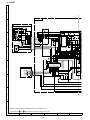
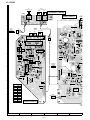
Figure 23 BLOCK DIAGRAM (3/3)
– 23 –
AC POWER SUPPLY CORD
C384
0.001
G
1
CHASSIS
GND
2
3
C349
0.001
C382
F
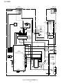
Figure 24 SCHEMATIC DIAGRAM (1/8)
– 24 –
4
2.6V
15P
5
IC302
LC72131
PLL(TUNER)
R380
1.5K
18
3
4
5
6
7
TUNER PWB-B1
H
• NOTES ON SCHEMATIC DIAGRAM can be found on page 19.
6
8
FM DET
MPX VCO
STEREO
8
270 2.9V
R353
5V
5V
CF351
FM IF
1K 0V
C353
0.022
C354
0.022
0.6V
X351
456kHz
2 3V
C332
0.022
C366
0.001
C361
0.022
C363
0.022
C367 R350
1/50
2.7K
C343
R358
8.2K
33P
C362
3.3/50
C364
2.1V (2.7V)
2.1V
(2.7V)
5V
2.5V
C330
8P (CH)
C331
0.047
VD301
SVC348S
AM IF
0V
4.7/25
IN
(0.9V)
AM LOW
C365 0.022
GND CUT
FM/AM
SD
OUT
VSM
AM RF
IN
FM AFC
7
C385
0.022
C387
C380 10/16
R352
3
0V
(2.6V)
2.6V (0V)
5.2V
C393
1/50
R379
2.2K
C350
0.022
FM IF AM OSC
OUT
IN
5V
AM MIX
OUT AM OSC
IN
REG
6
3 5V
FM
19
0.9V
CF352
AM IF
2
PD
22 21 20
0.9V
1
5
VDD
FM IN
MUTE
AM IN
FM
DO
2
AIN
R386
330
C392
0.001
C352
10/16
R351
5.6K
R336
5.6K
IC303
LA1832S
FM IF DET./
FM
MPX./AM IF
2.1V
CFW301
2.1V 4
3.7V
(0V)
3.9V
1
T351
AM IF
1.7V
(11.4V)
C381
12P
(CH)
3 2.1V
20
R371 1K 5.1V
C302
0.001
330
CL
R382
DI
75
4
ohms
SO301
ANTENNA
TERMINAL
21
R372 1K 4.8V
D303
1N4148
2
CE
TP301
FM IF
CF302
2
22
R373 1K 0.1V
C301
0.012
0.022
C341
1 3
C351
1
1
C394
47/16
9.5V
0.022 L342 2.2µH
R346
R347
330
6.8K
FM IF
CF301
1 3
Q301
2SC380 O
FE301
FM FRONT END
R381
10K
2
R349
33
2
0.8V
C334
27P(UJ)
T306
R348
680
3
R344
680
2.5V
4
C347
0.022
C345
0.022
8 7 6 5 9V
R343
180
AM Band
Coverage
24 23
AOUT
FM
C335
560P
C360
0.022
R374 1K 0.1V
D304
1N4148
R323
68K
L353
1mH
0.022
GND
R369B
82
C
R345
4.7K
D301
1N4148
0V
E
AM
AM OSC
VR351
10K
C397
3
C337
0.022
D302
1N4148
C348 100/16
R369A 68
B
2.6V
2
T302
AM
Tracking
X OUT
X IN
VSS
1
0.022
C329
0.022
X352
4.5MHz
D
C346
XL-1500W
A
FM Mute
Level
19 18 2.3V
R
L
10
R
5
17 16 15
9
PD
7
8
7
9 10
14 13 12
C383
0.022
3.8V
(1.2V)
C358 12
1/50
L352
100µH
R377
5.6K
R391
390
L351
100µH
11
R359
1.8K
8
4V
(2.2V)
1/50
1.3V C371
C369
56P
C368 R356
1/50 1K
1.3V
2.1V
X351
456kHz
2.3V
(0V)
R363
3.3K
C373
0.022
R364
3.3K
0.022
470K
C374
R357
C366
0.001
5.6K
3
Q351
KRC104 M
1
C396
100/10
C395
0.022
R383
5.6K
R384
6.8K
SD
FM ST
DO
CL
DI
CE
D_GND
A_12V
TUN_L
A_GND
TUN_R
R392
390
Q360
KTA1266 GR
9
10
Figure 25 SCHEMATIC DIAGRAM (2/8)
– 25 –
11
11
10
9
8
7
6
5
4
3
2
1
TO
CNP301 MAIN PWB-A1
P30 5-A
R355
3.3K
PHASE MO/ST
(AM/FM)
PHASE R-CH
OUT
L-CH
OUT
C365 0.022
C367 R350
1/50
2.7K
C372
1/50
15 14
13
ZD351
DZ5.1BSB
0.001
C357
2.2/50
R376
10K
1/50
C370
3.8V
(1.9V)
10 11
R387
5.6K
47K
C355
220P
MPX IN
IF OUT
16
4.7V
R361 (0V) 2
C391
47/16
330P
R393
1K
0V C386
5V
0V
9
R395
0.047
C398
C356 100/10
17
R365
10K
17 16 15
C399
FM DET
(4.3V)
270 2.9V
R353
MPX VCO
VCC
STEREO
8
5V
5V
SD
CUT
FM/AM
OUT
GND
18 2.3V
IF IN
IF REQ
CF351
FM IF
C353
0.022
C354
0.022
7
C385
0.01
0.022
C387
C380 10/16
6
MO/ST
0V
(2.6V)
2.6V (0V)
5.2V
R379
2.2K
5
3.5V
(0V)
FM
6
VDD
FM IN
MUTE
AM IN
FM
DO
18
3.7V
(0V)
3.9V
1.7V
(11.4V)
XL-1500W
AM SIGNAL
FM SIGNAL
R362
5.6K
R366
2.2K
CNS301
11.7V
10.8V
R385
5.6K
10.9V
R360
4.7K
D308
1N4148
12
XL-1500W
A
CD PWB-A3
CD PICK-UP UNIT (308)
B
HPC-3LX
VCC
C801
0.022
+B
A_3.3V
C823
0.1
A3.3V
1/2V
GH6C605B3A1
C4A
VR1A
TR–
TR+
FO–
ACTUATOR
1
2
3
4
1.6V
5
0V
6
2.6V
7
0V
8
1.6V
1.6V 9
10
1.6V
11
12
1.6V
1.6V
C815
L805
2.2µH
1.6V
0.022
FFC
PO+
VREF
1
+5V
2
E
3
C
4
A
5
B
6
C
7
F
8
GND
9
LD
10
VR
11
PD
12
FO+
13
TR–
14
TR+
15
FO–
16
CNW801 CNP801
R812
47K
1/2VCC
E
C
A
B
C
F
GND
LD
VR
PD
FO+
TR–
TR+
FO–
1
2
3
4
5
6
7
8
9
10
11
12
13
14
15
16
0.6V
F
3.3V
Q801
KTA1266 GR
B
8
C812
100/10
C806
0.022
C805
100/10
+
–
+
–
+
–
+
–
+
–
A
82K
82K
47K
82K
82K
47K
R809
10
R802
R803
R804
R805
R806
R801
E
VCC
FNI
FPI
TPI
TNI
MDI
LDO
SEL
TEBC
TEN
TEO
RFDC
GND
RFN
RFO
AGCI
RFGC
RFGO
RAS
RFRP
FEN
FEO
VRO
GVSW
0V
24
1.6V
R818
23
10K
1.1V
22 2.3V
R816
21
C810
100
20
1.2V 0.1
19 1.6V
RFGO
18
0.7V C811
17
R817
1.6V 0.1
16
47K
1.6V
15
1.6V
14
R856
2.0V
13
1K
C867
0.1
C822
100/10
C807 100/10
C
9
R821
8.2K
C817
22P C818
0.1
C819
100/10
10
VREF
IC802
TA2157F
HEAD AMP.
REDC
FEO
D
R815
820
+B
C814
0.0068
GND
C
C802
47/16
+5V
R819
33K
C3A
R820
10K
+B
C2A
MON
C813
1.5P
LD
IC803
MM1469PH
FOCUS/TRACKING/
SPIN/SLED DRIVER
0.022
C804
R808
CNW802
SP+
SP–
SL+
SL–
PU-IN
GND
C816
0.022
R811
4.7
7.3V
F
+B
C820
100/10
6
5
4
3
2
1
C809
0.022
M
6
5
4
3
2
1
C808
100/10
M702
SLED
MOTOR
SW702
PICKUP IN
–
+
R810
2.2K
CNP703A
SP+
6
SP–
5
SP+
4
SL–
3
PU-IN
–
2
GND
1
+
M
GND
VO1–
VO1+ V04–
V04+
VIN1
VIN4
VG1
VG4
TRB
BIAS
REG
MUTE VCC
VCC
GND
VG3
VG2
VIN3
VIN2
V02+ VO3+
V03–
V02–
PO1+
GND
PO1–
OPO
330/10
1 2 3 4 5 6 7 8 9 10 11 12 13 14
CD MOTOR PWB-C
M701
SPINDLE
MOTOR
+B
28 27 26 25 24 23 22 21 20 19 18 17 16 15
2.2K
E
C803
+B
2.2K
R807
3
2
3.3V
Q802
2SB562 C
+B
C871
0.022
G
H
• NOTES ON SCHEMATIC DIAGRAM can be found on page 19.
• The numbers 1 to 17 are waveform numbers shown in page 20.
1
2
3
4
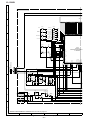
Figure 26 SCHEMATIC DIAGRAM (3/8)
– 26 –
5
6
CD SIGNAL
CD_STB
R848
1K
CD_RES
R849
1K
CCE
R870
10K
BUCK
R841
10K
BUS3
R842
10K
BUS2
R843
10K
BUS1
R844
10K
BUS0
PU_IN
+B
C823
0.1
GVSW
7
6
5
4
3
2
1
C847
10P
(CH)
BCK
10K
A_GND
+B
R862
CD_R
10K
C849
0.022
X801
16.93MHz
L853
CD_GND
100mA
M_GND
1
1
2
2
3
3
4
4
5
5
CNW805
Q808
+B KTC3199 GR
+B
C816
0.022
C870
0.022
C872
0.022
C868
100/10
2
1
Q809 3
KRA102 M
2
1
3
D802
1N4148
C850
47/10
R835
390K
D801
1N4148
D803
1N4148
+B
D804
1N4148
D805
1N4148
D806
1N4148
7
8
9
10
Figure 27 SCHEMATIC DIAGRAM (4/8)
– 27 –
11
1
1
2
2
CNW808
12
TO
CNP808 MAIN PWB-A1
P31 11-B
R837
10K
R864
100
Q810
KRC107 M
+B
ZD801
DZ5.1BSB
R865
820
R863
10
+B
R826
100
CD_7.2V
+B
L802
2.2µH
L801
2.2µH
3
CD+B
100/10
C821
0.022
2
3
CD_12V
C869
+B
1
2
+B
ZD802
DZ3.9BSB
47/10
C838
0.047
C839
C834
0.047
C841
0.1
L808
CORE
1
TO
CNP803 MAIN PWB-A1
P31 11-G
CNW803
CD_L
R861
C857
100/10
C859
0.022
1
CNP804
TO
MAIN PWB-A1 CNP805
P31 11-G
R846
100K
C851
47/10
0V
3.3V
1.2V
XO
XVSS
TESIN
XI
C855
12P(CH)
2
5V
+B
0.047
+B
4
3
+B
3.3V
1.5V
1.5V
0V
DVDD
DMO
DVSS
0V
3.3V
AVDD
SEL
FMO
1.6V
0V
1.6V
3.3V
TEBC
1.0V
C843
DOUT
GND
XVDD
LRCK
AUTO
DOUT
IPF
DVSS
SBOK
DVDD
SFSY
CLCK
DATA
SBSY
HSO
1.6V
0V
R840
1M
11
C846
100/10
C837
0.047
RFGC
PDO
PVDO
VREF
1.6V
1.6V
1
IC801
TC94A14F
SERVO/SIGNAL
CONTROL
7
16
6 4 15 14
17
C844
100P
R839
100
C848
0.022
2.6V
3.3V
0V
5.2V
3.3V
1.6V
47K
15K
R828
C827
5
470P
TEO
C820
100/10
8
R855
1K
5V
R832 TMAX 16 15 14 13 12 11 10 9 8 7 6 5 4 3 2 1
150K 0V
VDD 5.2V
64
17
5V
1.2V
18 LPFN
RST 63
3.2V
4.5V
C860
CCE 62
19 LPFO
R850
1K
5V
0.1
1.6V
20 PVREF
BUCK 61
R851
1K
C832
5V
0V
BUS3 60
21 VCOF
0.01
R852
1K
5V
0V
BUS2 59
22 AVSS
C833
R853
1K
5V
0V
BUS1 58
23 SLCO
R854
1K
5V
1.6V
C828
0.0027
24 RFI
BUS0 57
0.01
0V
3.3V
U-COM 56
25 AVDD
VSS
R827 10K
1.6V
ZDET 55
26 RFCT
C853
C829
1.6V
27 RFZI
0V DVSS 54
0.033
10/16
0.7V
LO 53
28 RFRP
C856
1.6V
1.6V
DVR 52
29 FEI
L852
100/16
0.6V
3.3V
30 SBAD
DVDD 51
C854
1.6V
100mA
RO 50
31 TEI
10/16
1.6V
32 TEZI
49
DVSS 0V
C836
0.033
33 34 35 36 37 38 39 40 41 42 43 44 45 46 47 48
1.6V FOO
L851 100mA
TRO
C852 15P(CH)
C858
R831
4.7K
0.022
C831
VREF
13
R833
5.6K
0.015
C825
47/10
C830
470P
C819
100/10
C814
0.0068
7
K
12
C835
47P (CH)
C824
0.1
R829
RFGO
10
+B
A3.3V
C817
22P C818
R821
0.1
8.2K
C826
0.047
9
9
CNP704
C822
100/10
R819
33K
R820
10K
R818
10K
816
00
10
FROM
FROM
CNW804 TERMINAL PWB-A4 CNW704 DISPLAY PWB-A2
P30 2-B
P29 11-D
XL-1500W
XL-1500W
DISPLAY PWB-A2
A
+B
+B
LCD701
FL DISPLAY
1
2
3
4
5
6
7
8
9
10 11 12 13 14 15 16 17 18 19 20 21
B
SW720
SW727
CLEAR
VOLUME UP
SW719
R716
10K
SW718
R717
5.6K
SW713
R718
3.9K
SW712
R719
4.7K
SW711
R720
3.9K
FUNCTION
C
SEG16
SEG15
SEG14
SEG13
SEG12
SEG11
SEG9
SEG8
SEG10
SEG7
3 COM1
R727
R729
4 COM0
5 VLC3
47K
47K
6 VLC2
R723
R728
1K
8 VDD
C703
0.1
9 OSC2
10 OSC1
X701
8MHz
11 VSS
IC701
IX0043SJ
SYSTEM MICROCOMPUT
FL DRIVER
12 XI
X702
32.768kHz
22P
C702
13 XO
C701
22P
14 MMOD
15 VREF
1K
R732
1K
R733
1K
R734
1K
R735
1K
R736
1K
17 KEY1
18 KEY2
19 MODEL
20 CLID_PRO
21 FAN_DET
AMP_DET
RESET
CE
25 DI
CL
R722
10K
24 VREF+
PROTECT
23 VSM
CLE
22
+B
P30 1-F TO
CNP701 MAIN PWB-A1
16 CLID_SW
REMOCON
R721
10K
R725
10K
CD LID
OPEN/CLOSE
R731
DO
D
R724
8.2K
R703
47K
SW710
SYS_STOP
ON/
STAND-BY
POWER
R702
10K
SW709
7 VLC1
47K
GVSW
L701
10µH
+B
1K
1K
1K
1K
1K
1K
R750
R751
R752
R754
R755
+B
L704
D_GND
P_CONT
USWD-5.6V
P_CONT
+B
R7A5
10K
Q702
KTC3199 GR
3
C710
0.01
1
R7A4
R7A3
100
REMOTE
SENSOR
RX701
120
Q703
KTC3199 GR
1
R7A8
82
2
C715
100/10
2
+B
3
C713
10/16
F
Q701
KRC102 M
+B
R7B0
10K
ZD701
R7A6
1K
0.01
R7A7
1K
+B
R7A0
1K
+B
DZ3.3BSB
1N4148
R7A9
3.3K
C714
560P
1K
1N4148
R7A1
D723
D720
1N4148
+B
D722
C712
CNW701
D721
1N4148
1
LED PWB-A6
2
LED703
LED704
1
Q707
KTA1266 GR
R791
4.7K
R798
2 390
Q708
KTA1266 GR
Q706
KRC102 M
R792
47K
LED702
CFW702
LED701
CFW701
2
CFW702A
G
CFW701A
R796
1K
LED PWB-A7
R787
47K
R778
47K
R779
47K
R780
47K
R781
47K
R783
33K
+B
+B
2
R793
10K
R799
2 390
Q709
KRC102 M
R797
2
+B
3
2.2K
1
3
C704 0.022
1
1
1
H
• NOTES ON SCHEMATIC DIAGRAM can be found on page 19.
1
R748
R749 1K
R744 1K
1K
R740
1K
1K
R739
R741
1K
C705
0.01
+B
C711
3.3/50
7
6
5
4
3
2
1
100K
7
6
5
4
3
2
1
M_GND
M_12V
R738
26 27 28 29 30 31 32 33 34 35 36 37 38 39 40 41 42
R7A2
E
SEG6
2 COM2
R708
1.2K
>>REW
PRESET DOWN
SW728
100 99 98 97 96 95 94 93 92 91 90 89 88 87 86 85 84
1 COM3
SEG5
FF<<
PRESET UP
SEG4
BASS/TREBLE
SEG3
SW725
SEG2
CD PLAY/PAUSE/
TUNING UP
R707
1.2K
CD STOP/
TUNING DOWN
SEG1
SW726
MEMORY/
SET
SEG0
R706
1.5K VOLUME DOWN
2
3
4
Figure 28 SCHEMATIC DIAGRAM (5/8)
– 28 –
5
6
XL-1500W
IC804
TA7291S
CD LID MOTOR DRIVER
9
+B
8
7
6
5
4
3
2
1
+B
R838
3.3K
C845
47/16
+B
C840
0.1
2
Q806
KRC102 M
+B
2
R824
47K
82
R845
1.5K
R825
2.2K
3
R836
1
14 15 16 17 18 19 20 21 22 23 24 25 26 27 28 29 30 31 32 33 34 35 36 37 38
R834
3.3K
LCD701
FL DISPLAY
TO SHIELD
SHEEET
(242)
3
1
Q807
KRC102 M
Q804
KTA1266 GR
1
1
2
2
SEG25 75
SEG26 74
SEG32 68
SEG33 67
CD-STB 66
CCE 64
BUCK 63
BUS3 62
BUS2 61
BUS1 60
BUS0 59
PU-IN 58
CLID_DW 57
R761
1K
CD-STB
R774
1K
CD-RES
R762
1K
CCE
R763
1K
BUCK
R764
1K
BUS3
R765
1K
BUS2
R766
1K
BUS1
R767
1K
BUS0
R768
1K
PU-IN
R769
1K
R775
CLID_UP 56
1K
CLID_DW
R772
R773
10
10
9
9
8
8
7
7
6
6
5
5
4
4
3
3
2
2
1
1
P_STB
1K
PROTECT
1K
1
1
2
2
CNW703
R785
SW802
CD LID
1K
LED801
LED PWB-A8
SD
B-LIGHT 51
ST
2
CFW703A
CLID_UP
SP_RLY 52
DATA
P-CONT
CD+B
P-MUTE
P-STB
1
2
CD-RW
FAN 55
LIGHT 53
SURR
1
CNW704
DIMMER 54
AMP_DET
2
R813
470
CD-RES 65
PROTECT
2
CNP704
TO
CD PWB-A3
P27 12-B
SEG31 69
CLE
2
R866
68K
CNP703
TO
MAIN PWB-A1
P31 11-F
SEG30 70
REMOCON
1
CFW703
SEG29 71
SYS_STOP
1
CNP706
SEG28 72
POWER
150K
R867
1
C899
0.022
SEG27 73
IC701
IX0043SJ
M MICROCOMPUTER/
FL DRIVER
M801(246-6)
CD LID
OPEN/CLOSE
SWITCH PWB-A5
CLID_SW
SEG22
SEG21
SEG20
SEG19
SEG18
SEG17
SEG16
SEG15
SEG14
SEG13
SEG12
SEG11
R784
47K
1K
1K
1K
1K
1K
1K
1K
1K
1K
1K
1K
1K
1K
R748
R750
R751
R752
R754
R755
R757
R756
R758
R759
R760
R777
R776
35 36 37 38 39 40 41 42 43 44 45 46 47 48 49 50
R786
47K
R789
47K
CLE
P_CONT
DATA
1
DI
CL
DO
STEREO
STEREO
SD
SD
P_STB
D_GND
P_MUTE
P_MUTE
CD+B
SURROUND
SURROUND
1
2
2
3
3
4
4
5
5
6
6
7
7
8
8
9
9
10
10
11
11
12
12
13
13
CNP702
TO
MAIN PWB-A1
P31 7,8-A
CE
CNW702
CE
CL
DO
CNW707
DI
CLID_SW
D701
1N4148
1
1
2
2
CNP707
TO
MAIN PWB-A1
P31 11-A
SEG9
91 90 89 88 87 86 85 84 83 82 81 80 79 78 77 76
SEG10
M
CNW705
CNW706
SEG24
SEG23
CNP705
CD+B
B-LIGHT
D702
1N4148
7
8
9
10
Figure 29 SCHEMATIC DIAGRAM (6/8)
– 29 –
11
12
XL-1500W
FROM
TUNER PWB-B1
CNS301
P25 11-D,E
FRO
DISPLAY
CNW7
P29 1
TERMINAL PWB-A4
DOUT
CNW804
3
1
J801
CD DIGITAL OUT 2
+B
C866
0.0047
2
1
CNP301
FM SIGNAL
CD SIGNAL
R408
2.7K
CHASSIS
GND
3
2
1
3
2
1
R401
1K
D651
1N5402M
1
2
3
4
F652
T2.5A L 250V
Q606
KRA102 M
C606
4700/25
+B
RLY601
C607
470/25
Q603
2SD2012 Y
L681 D686
1mH 1N4004
1
11.7V
20V
SW651
VOLTAGE
SELECTOR
C661
0.001
D683
1N4004
R602 13V
100
D684
1N4004
C601
470/25
T681
POWER
TRANSFORMER
(SUB)
R604
47
12.3V
20V
R601
820
D681
1N4004
C681
C684 0.047
0.047
D682
1N4004
C608
100/25
C605
10/16
Q602
2SD2012 Y 11.7V
Q601
KTC3200 GR
R605
22K
+B
R610
33K
ZD602
DZ8.2BSC
C604
0.022
R607
22K
R606
47
20V
CNP701
R611
47
+B
22K
0.022
10/16
R608
820
R612
C609
C610
110V
127V
230~240V
220V
Q681
KTC3199 GR
5
D685
1N4004
R686
47K
R685
10K
R688
1K
Q605
2SD2012 Y
+B
+B
C683
2200/35
FROM
DISPLAY PWB-A2
CNW701
P28 1-E
R687
2.7K
R689
1K
(1/4W)
ZD683
MTZJ160C
CFW682
C689
0.47/50
0.047
CFW682A
C688
D688
1N4004
C665
0.047
2
ZD684
MTZJ160C
Q607
KRC107 M
+B
1
F
CHASSIS
GND
GND
D602
1N4148
IC681
KIA7805AP
CONSTANT VOLTAGE REGULATOR
G
C131
2200/50
R609
100
E
+B
+B
+B2
TF
110V
0V
1
2
3
4
5
6
7
8
9
CNP681
1
2
3
4
5
6
7
8
9
127V
+B
+B
D660 D659
1N4004 1N4004
220V
D689
1N4004
Q683
KTC3199 GR
D657 D658
1N4004 1N4004
C660 C657
0.1
0.1
T651
POWER
TRANSFORMER
(MAIN)
230~240V
+B
C659 C658
0.1
0.1
F653
T1.25A L 250V
3
+B
+B
D
+B
C654
0.1
1
2
3
4
+B
D653
1N5402M
D654
1N5402M
CNP651
USWD_5.6V 1
P_CONT 2
D_GND 3
4
5
M_12V 6
M_GND 7
D652
1N5402M
C651
0.1
CHASSIS
GND
Q604
KTC3200 GR
R405
27K
C413
0.0047
L-CH
3
2
1
CNW401
R407
2.7K
C
R402
1K
CNP401
L401
2.2µH
SO401
VIDEO
AUX INPUT
D601
1N4148
R406
27K
R-CH
+B
C603
0.022
R603
33K
ZD601
DZ130A
C602
100/25
+B
+B
SO651
AC POWER
INPUT SOCKET
AC110,127,220,
230~240V, 50/60Hz
AC POWER SUPPLY CORD
AC110,127,220,
230~240V, 50/60Hz
H
• NOTES ON SCHEMATIC DIAGRAM can be found on page 19.
1
2
3
4
Figure 30 SCHEMATIC DIAGRAM (7/8)
– 30 –
5
6
SD
FM ST
DI
CL
SD
FM ST
DO
CL
DI
CE
D_GND
A_12V
TUN_L
A_GND
TUN_R
DO
1 2 3 4 5 6
C864
100/10
B
5V
1
C865
0.0022
3
3
GND
2
L804
0.82µH
4
TO
CNP804 CD PWB-A3
P27 12-C
MAIN PWB-A1
CE
11 10 9 8 7 6 5 4 3 2 1
A
7
XL-1500W
FROM
DISPLAY PWB-A2
CNW702
P29 11-F
L2
R2
8
10K
10K
R442
R440
3.9K
7
6
5
4
3
2
C433
220P
C431
220P
5V
9.6V
4.8V
4.8V
1K
1K
1K
R423
R424
R425
CNW909
1
1
2
2
+B
CHASSIS
GND
D403
1N4004
D402
1N4004
CL
DI
CE
L
+B
CNP909
C432
220P
1
C430
100/16
C407
10/16
2
C691
0.01
4.8V
4.8V
9
R437
6.8K
AUX L
L3
R3
R421
1K
L4
C415 4.8V R4
4.8V
RSL0
10/16
L1
R1
R417
1K
C403
10/16
1
R201
8.2K
CHASSIS
GND
16 17 18 19 20 21 22 23 24 25 26 27 28 29 30
R415
1K
CNP808
C424
C422 0.1
0.1
15 14 13 12 11 10
4.8V
C401
10/16
CD L
TUN L
CNW808
P27 12-F
FROM
CD PWB-A3
C213
4.7/50
4.8V
IC401
LC75342M
FUNCTION/
VOLUME EQUALISER
AUX L
R418
1K
R416
1K
C402
10/16
CHASSIS
GND
C203
1/50
C404
10/16
AUX R
2
R217
12K
C215
1/50
C209
47/16
C408
10/16
TUN R
CD R
C208
100/16
R210
10K
FROM
SPRING(233)
1
R213
12K
R211
2.7K
C211 R205
0.0033 10K
+B
IC201
KIA4558P
SURROUND
CONTROL
C201
0.0056
2
1
R208
330
R203
100K
3
8
R215
12K
Q203
3 KRC107 M
R209
R212
2.7K
4
7
+B
RBS1
4.8V LBS1
4.8V
RBS2
4.8V LBS2
4.8V
ROUT LOUT
4.8V
0V C426
TEST
0V 1/50
VREF
VSS
0V
VDD CE
0V
CL
DI
S
CNP707
C216
1/50
R422 1K
C416
R438
10/16
LSL0
6.8K
4.8V C418
2.2/50
RIN
4.8V LIN
4.8V
C420
RTRE
4.8V LTRE
0.0027
4.8V
D201
2 1N4148
1
6
C202
0.0056
R218
12K
R216
12K
5
R202
8.2K
CNW707
P29 11-G
FROM
DISPLAY PWB-A2
C214
4.7/50
R214
12K
C417
2.2/50
C419
0.0027 C421
0.1
R439
C423
3.9K
0.1
R441
10K
C425
1/50
C429
4.8V
33/16
Q201
2SK2541
D
G
R207
47K
R204
100K
C204
1/50
C212
0.0033
R206
10K
CD +B
CNP702
SURROUND
D_GND
7 8 9 10 11 12 13
P_MUTE
SD
FM ST
DI
CL
DO
CE
1 2 3 4 5 6
D401
1N4004
+B
OUT2
MUTE
POWER
–GND2
VCC
OUT1
6
7
8
9
10
11
12
R119
0.2
(1W)
C110
470/25
R129
6.8
C117
0.022
Q106
KRC102 M
R108
2
820
R123
10K
Q103
KTC3199 GR
R127
330
4
5
9
10
P_STB
PROTECT
+B
1
2
CNP703
Q108
KRA107 M
+
SP602
6 Ohm
WOOFER
JK101
HEADPHONES
JACK
1
CD_L
A_GND
CD_R
1
2
3
CNP805
C862 C861
470P 470P
+B
–
+
Q109
KRC107 M
3
2
CNP803
2
R858 R857
1.8K 1.8K
1
C128
3.3/16
+B
–
SP601
6 Ohm
WOOFER
3
2
1
R122
1K
3
–
R-CH SPEAKER BOX
R128
330
10µH
R124
10K
Q104
KTC3199 GR
+
–
R130
6.8
0.1
0.1
C112 C114
L102
3µH
L105
R120
R121 0.2
(1W)
1K
C118
0.022
+
SP604
TWEETER
D102
1N4148
Q105
KRC102 M
R115
4.7
D101
1N4148
R107
+B
3
C111
0.1
R116
4.7
Q102
KTC3199 GR
Q101
KTC3199 GR
1
2
22K
1
3
R104
10K
C120
0.022
R114
270
R113
270
C103
470P
R103
10K
R106
6.8K
C101
100/16
+B
C113
0.1
470P
C104
A GND
C122
0.022
C116
0.022
1 2 CNW102
C115
10/50
R111
56K
C109
470/25
C108
100/25
C105 R109
0.082 1K
C106 1K
0.082
C129
0.022
+B
100/25
R110
C130
47/25
C107
+B
CNW703
FROM
DISPLAY PWB-A2
P29 11-D
NF2
5
+B
CD_7.2V
CD–12V
CD+B
CD_GND
M_GND
+B
+B
C127
0.001
1
2
3
4
5
CNW803
FROM
CD PWB-A3
P27 12-D
IN2
4
SP603
TWEETER
SO601
SPEAKER
TERMINAL
CNW805
FROM
CD PWB-A3
P27 12-E
GND
3
C119
0.022
C121
0.022
C123
0.0022
FIL
2
L-CH SPEAKER BOX
C124
0.0022
IN1
1
L101
3µH
POWER
–GND1
NF1
1K
IC101
LA4282
POWER AMP.
1K
R105
10K
R102
R101
R
CHASSIS
GND
7
8
9
10
Figure 31 SCHEMATIC DIAGRAM (8/8)
– 31 –
11
12
XL-1500W
3
D801
ZD801
15
28
R809
5
R808
CNW805
1
C808
B
E
+
WH
BK
E
SW702
PICKUP IN
R864
RD
ZD802
+
RD
BK
WH
C868
B
Q808
R863
C
R862
C869
1 R861
49
C827
C837
C843
45
50
55
P35 8-G
CNP703
CNP707
P35 8-D
P34 5-G
CD MOTOR PWB-C
5
64
1
C860 R83
R846
R870
C851
15 14 17
16 13
TO MAIN PWB-A1
2 1
2 1
1 2 3 4 5 6 7 8 9 10
DISPLAY PWB-A
BK
GY
GY
GY
GY
GY
GY
GY
GY
GY
GY
BR
E
R841
R842
R843
R844
TO MAIN
PWB-A1
20
1
10
60
C853
CNP803
25
IC801
1 2 3 4 5 6 7 8 9 10
TO MAIN
PWB-A1
-
48
L852
4
M701
SPINDLE MOTOR
35 30
R852
R851
R853
CNP704
32
40
C856
1 2 3
R831
C838
C855
C854
3
33
C848
R865
BR
C857
C858
C859
L851
C830
R848
1
C852 X801
C870
2
C846
R850
R849
1
CNW803
3
Q809
L808
CORE
2
C872
3
C826
C849
1
11
-
L802
CNW802
C871
Q810
D
C
C834
6
R855
CNP703A
C
Q802
1
R854
M702
SLED MOTOR
6 5 4 3 2 1
C805
14
6 5 4 3 2 1
GY
GY
GY
GY
GY
WH
C816
R840
L853
IC80310
C809
GY
GY
GY
GY
GY
WH
B
5
20
R812
25
R811
C803
D804
R835
R810
C821
R807
C804
D803
GY
GY
GY
GY
BK
CD PWB-A3
C820
1
P35 10-G
D806
P34 6-F
2
2
1
CNP808
D805
CNP805
GY
GY
GY
GY
BK
CNW808
A
5
4
3
2
1
TO MAIN
PWB-A1
R826
2
TO MAIN
PWB-A1
COLOR TABLE
B C E
1
2
3
Q701
R717
VOLUME
Q702
R7A4 Q703
R7A1
R7A6
LED701
CFW701
C
E
B
2
3
80
76
85
90
1
R792
2
3
1
95
Q706
100
5
1
38 37 36 35 34 33 32 31 30 29 28 27 26 25 24 23 22 21 20 19 18 17 16 15 14 13 12 11 10 9 8 7 6
SW713
R719
SW712
R720
SW711
SW727
C715
R718
TUNINNG
2
CLEAR
PRESET
H
• The numbers 1 to 17 are waveform numbers shown in page 20.
1
IC701
70
R785
R750
4
65
75
LCD701
SW718
CFW701A
1
C
45
60
1
2
LED702
E
R796
1
R798
SW719
G
B
R793
R7A9
LED PWB-A7
R7A5
B C E
1
D701 CNW707
R791
R797
PINK
SW720
55
2
D702
Q709
PK
C711
Q708
BLACK
R787
50
R761
C712
BK
D721
51
10
CNW704
Q707
GRAY
WHITE
1
R784
GY
WH(W)
1
2
R7A0
VIOLET
R7A8
BLUE
VL
R754
R774
CNW703
R799
BL
R768
R767
R766
R765
R764
R763
R762
GREEN
C710
GR
R757
R7B0
YELLOW
R7A7
YL
ZD701
ORANGE
R7A2
RED
OR
D720
F
BROWN
R716
BR
RD(R)
2
3
4
Figure 32 WIRING SIDE OF P.W.BOARD (1/4)
– 32 –
5
6
XL-1500W
D PWB-A3
D801
C802
C801
CNP801
1
16
CD PICKUP UNIT (308)
16 14 12 10 8 6 4 2
15 13 11 9 7 5 3 1
L805
R804
L801
C815
60
R820
C811
C822
C835
R832
R833
C819
R867
2
1
C850
16 13
CNP706
R866
5
CNP804
SWITCH PWB-A5
12
R848
15 14 17
1 3 5 7 9 11 13 15
2 4 6 8 10 12 14 16
1
6
7
R829
4 3 2 1
64
1
C860 R839
C847
R846
C851
16
9
D802
C814
C829
R827
C832
C833
C831
16
C848
R850
R849
1
C818
R818
R856
R821
R828
17
5
R870
R841
20
15
10
24
R816 C810
R815
IC801
20
C823
C825
25
55
1 2 3 4 5 6 7 8 9 10
M801(246-6)
CD LID OPEN/CLOSE
C844
FROM TERMINAL
PWB-A4
CNW804
P34 2-B
AIN PWB-A1
RED
LED PWB-A8
TO MAIN
PWB-A1
CNP707
CNP702
P34 5-G
P35 10-F,G
LED801
R844
C827
C836
C837
45
50
R852
R851
R842
13 15
R817
SW802
CD LID
48
49
L852
R843
IC802
35 30
C853
R853
32
40
C856
R854
33
5
8
BK
RD
C870
C855
C854
R862
C869
R861
C830
R831
C846
R840
C852 X801
C843
C834
C838
C826
1
C813
C839
R812
Q802
E
C849
L802
CNW802
C
CNW801
R802
12 10
B
10
R803
R806
C807
C805
C806
Q801
14
6
R801
B
R805
C
C824
R810
0310
E
C816
C867
C828
20
C841
R811
R809
C817
15
R819
R835
R837
R807
C812
1 2
CFW703A
2
CNW705
1
SW726
R706
SW728
BASS/
TREBLE
FUNCTION
9
D723
8
9
R838
R834
R735
3
2
1
L704
2
CNP701
P35 11-G
TO SHIELD
SHEET(242)
1
R836
2
1
CFW703
Q806
R773
C714
3 2 1
RX701
C713
CFW702
MEMORY/
SET
8
CNW701
R778
R780
R725
D722
Q804
3
7
R825
R824
R708
CLEAR
7
E C B
C704
R707
SW725
C715
SW727
L701
R729
R727
SW709
ON/
STAND-BY
BK
Q807
5
TO MAIN
PWB-A1
LED703
C703
LCD701
R731
C845
4
1
2
3
4
5
6
7
2
CFW702A
R728
27 26 25 24 23 22 21 20 19 18 17 16 15 14 13 12 11 10 9 8 7 6 5 4 3 2 1
R732
7
3
6
BK
GY
GY
GY
GY
GY
GY
1
2
SW710
OPEN/CLOSE
1
R7A3
X701
1
R738
R736
R702
C702
R723
R722
R733
X702
100
R734
5
R721
10
95
2
1
R845
R781
25
15
90
C840
R751
R748
R724
85
2
R813
20
R789
80
76
26 R740
30
C899
R741
R739
35
IC701
70
R785
750
40
65
75
C701
CNW707
60
CNP705
CNW706
1
1
CNW702
C705
45
R752
1
R769
R759
R779
R777
R775
R703
R755
55
2
R760
13
50
R772
R786
51
R758
R756
R776
R744
R749
R754
R783
GY
GY
GY
GY
GY
GY
GY
GY
GY
GY
GY
GY
BK
BR
13 12 11 10 9 8 7 6 5 4 3 2 1
DISPLAY PWB-A2
IC804
2 1
GY
2 1
LED704
1
1
2
LED PWB-A6
10
Figure 33 WIRING SIDE OF P.W.BOARD (2/4)
– 33 –
11
12
XL-1500W
J801
CD DIGITAL OUTPUT
SO401
VIDEO/AUX INPUT
RIGHT
LEFT
TERMINAL PWB-A4
A
CHASSIS
GND
R406
R408
2 3 1
C866
C865
RD
BK
WH
3 C864
RD
BK
CHASSIS
GND
L401
CNW401
1
3
WH
R405
R407
CNW804
1
C413
L804
JK101
HEADPH
JACK
MAIN PWB-A1
G
VL
VIOLET
GY
GRAY
WH (W)
WHITE
BK
BLACK
PK
PINK
R127
R102
R438
R44
C430
C429
C431
10
11
C425
CNW707
P32 5-F
C420
2 1
20
16
C424
C42
R421
R415
R416
R440
FROM
DISPLAY PWB-A2
C423
IC401
15
CHASSIS
GND
25
BLUE
C416
C426
R425
10
GREEN
BL
C418
R423
R424
1
2
3
4
5
6
7
8
9
C106
D402
R442
D401
D403
10
11
5
GR
C657
CNP805
54 3 2 1
30
YELLOW
C660
C404
ZD351
C396
R366
C395
C403
C391
R377
C127
CNP301
R395
R391
L352
1
2
3
4
5
6
7
8
9
1
ORANGE
YL
C605
D660
C433 C432
OR
D658
C658
D657
R418
RED
C606
D659
CHASSIS
GND
FROM CD
PWB-A3
CNW805
P32 4-B
R417
R D (R )
C118
C603
R605
3 2 1 Q105
R383
CNS301
BROWN
Q104
C609
Q605
Q602
Q603
R612
R611
R606
D308
C384
R373
R360
R386
E
C
B
C10
C116
3 2 1 Q106
COLOR TABLE
BR
C115
R107
R607
C604
X352
R372
R374
R604
ZD601
R365
R371
R603
3
Q351 2
1
F
C601
C380
Q607
C394
R380
R387
Q601
E
C
B
B C E
B C E Q360
R384
R385
R392
CF351
R602
R601
D601
R345
R343
IC302
R382
R352
C399
C360
R351
IC303
C392 C381
C382
B
C
E
C608
R608
C352
C358
R355
C357
C371
R363
C386
3 2 1 CF352
C351
C356
C354 R376
C353
R393
C373
10
11
12
R359
R610
3 2 1
R1
C610
E
C
B
C602
T351
AM IF
R353
CF302
1
2
3
4
5
6
C363 7
8
9
C350
R356
C374
C372 X351
R362
R361
R364 R357
C369
E
24
23
22
C365 21
C366 20
C367 19
18
17
16
15
C368 14
13
C361
C364
R350
1
2
3
1 2 3
C397
R381
R379
9 8 7 6 5 4 3 2 1
C385
L353
R347
11 10
D602
ZD602
Q606
C387
C383
L351
FM Mute
Level
VR351
E C B
C607
12 13 14 15 16 17 18 19 20 21 22
C398
C370
R349
C341
R348
C337
C343
R358
4 3 2 1
C345
C393
L342
CF301
1
2
3
Q301
C332
T306
R336
C347
R344
R346
VD301
C330
C331
R323
C334
AM Band
Coverage C335
R111
R369A
C348
C355
D302
R369B
T302
AM
Tracking
C362
R114
12 11 10 9 8 7 6 5
C346
D
B
C
E
R609
FE301
8 7 6 5
C329
WH
BK
RD
1 2 3
CFW301
D301
C
R122
C112
R124
R120
D303
D304
C349
C302
C301
CHASSIS
GND
1
2
3
D101
D102
C110
Q108
1 2 3
Q109
GND
C128
AM
C114
FM 75 OHMS
WH
Q604
CNP804
P33 8-C
BR
R116
RD
BK
1
2
3
4
SO301
ANTENNA
TERMINAL
GY
TO CD
PWB-A3
R128
B
R422
C422
CNP707
TUNER PWB-B1
FROM
PWB-
H
1
2
3
4
Figure 34 WIRING SIDE OF P.W.BOARD (3/4)
– 34 –
5
6
XL-1500W
SO651
AC POWER
INPUT SOCKET
AC 110,127,220,230~240V,50/60Hz
SW651
VOLTAGE
SELECTOR
SO601
SPEAKER
TERMINAL
RIGHT
LEFT
110V
JK101
HEADPHONES
JACK
PWB-A1
220V
230~240V
C124
C119
127V
D101
D102
C113
C107
7
8
8
9
9
Q101
CNP703
2 1
R104
R106
R103
E C B
C605
C606
B
C
E
C101
1
C131
CNW102
2
D659
D657
C657
C651
7
8
C665
Q203
BK
CNW909
C684
D683
D689
CNP701
5 CFW682
7 6 5 4 3 2 1
R686
R688
ZD683
2 1
Q683 B C E
B
C
E
CNP909
Q681
FROM DISPLAY CNW702 GND
PWB-A2
P33 8,9-F
9
FROM
CNW808 CD PWB-A3
P32 4-A
2 1
1
C691
ZD684
C689
C203
D684
D682
D688
2 1
CHASSIS
FROM CD CNW803
PWB-A3
P32 5-C
D681
1 2 3
CNP702
R217
C209
R210
R203
C201
CNP651
4 3 2 1
R215
C213
R213
R211
C211
C215
IC201
3 2 1
C681
IC681
10
11
12
13
CNP808
C683
R685
D201
1
2
3
4
5
6
7
8
9
R201
R205
C661
L681
D686
C688
R687
R689
R206
Q201
G D S
CHASSIS
GND
4
3
2
1
R207
C204
R212
C212 R216
5 6 7 8
CNP803
C402
1
2
3
R858
C862
C861
R422
R857
R416
R402
R401
C407
R437
C401
10
15
R415
C202
C408
20
25
16
30
5
R421
R218
1 2 3
C421 C419
IC401
1
R439
R214
CNP401 R204
C425
C423
C216
R208
C208 C214
R209
C417
C415
R202
D403
R438
C416
C418
R441
C430
C429
C431
R105
R101
R102
C404
D402
R442
C422
TO SPRING
(233)
F652
T2.5A L 250V
54 3 2 1
C424
BR
BR
D652
F653
T1.25A L 250V
CNP805
D401
YL
3
2
1
D653
D660
C660
YL
4
D654
D651
C659
D658
C658
T651
POWER TRANSFORMER
(MAIN)
FROM DISPLAY
PWB-A2
CNW703
P32 4-F
C654
C603
R605
C106
C104
Q102
C127
WH
RD
RD
BR
BL
POWER TRANSFORMER
(SUB)
C105
C103
C609
Q605
R612
Q602
C116
R607
C604
Q603
6
7
T681
3 2 1 Q105
C426
5
6
1
R109
R110
C108
3 2 1 Q106
C433 C432
4
5
D685
IC101
C129
C130
R108
C115
R107
CHASSIS
GND
R418
3
4
5
R115
C610
C420
2
3
C111
CFW682A
R113
12 11 10 9 8 7 6 5 4 3 2 1
E
C
B
1
2
CNP681
C109
R119
C117
R123
C118
Q104
R116
B C E Q103
R111
E
C
B
R129
R121
B
C
E
R114
E
C
B
R130
L105
R127
RLY601
R122
C112
C110
L102
1
L101
R124
R120
C114
R128
C120
C121
C122
C123
CHASSIS
GND
CNW701 FROM DISPLAY
PWB-A2
P33 11-F
10
Figure 35 WIRING SIDE OF P.W.BOARD (4/4)
– 35 –
11
12
XL-1500W
TROUBLESHOOTING
When the CD does not function
When the CD section does not operate when the objective lens of the optical pickup is dirty, this section may not operate. Clean
the objective lens, and check the playback operation. When this section does not operate even after the above step is taken,check
the following items.
Remove the cabinet and follow the troubleshooting instructions.
"Track skipping and/or no TOC (Table Of Contents) may be caused by build up of dust other foreign matter on the laser pickup
lens. Before attempting any adjustment make certain that the lens is clean. If not, clean it as mentioned below."
Turn off the power, and wipe the lens softly using a cleaning paper moistened with commercially available cleaning solution so
as not to damage it.
Be careful not to touch the lens with bare hands.
Dust gradually accumulates on the objective lens during use, and it may degrade performance.
To avoid this problem, use a cleaning disc designed for CD optical pickup lenses.
HOW TO USE
1. Using the brush in the cleaner cap, apply 1 or 2 drops of the cleaning fluid to the brush on the CD cleaner disc which has
the mark next to it.
2. Place the CD cleaner disc onto the CD disc tray with the brush side down, then press the play button.
3. You will hear music for about 20 seconds and the CD player will automatically stop. If it continues to turn, press the stop button.
CAUTION
The CD lens cleaner should be effective for 30 - 50 operations, however if the brushes become worn out earlier then please
replace the cleaner disc.
If the CD cleaner brushes become very wet then wipe off any excess fluid with a soft cloth.
Do not drink the cleaner fluid or allow it to come in contact with the eyes. In the event of this happening then drink and / or
rinse with clean water and seek medical advice.
The CD cleaner disc must not be used on car CD player or on computer CD ROM drives.
All rights reserved. Unauthorized duplicating, broadcasting and renting product is prohibited by law.
Cleaner Liquid
Cleaning Disc
PARTS CODE: UDSKA0004AFZZ
– 36 –
XL-1500W
Make sure that the disc is normal, and set the CD TEST MODE (STEP 1).
Is the measured voltage as specified in circuit diagram?
Check the main unit power supply circuit.
No
Yes
Is "Er-CD01" displayed"?
No
Yes
Move the pickup to most internal circumference side of disc.
Turn the power off and reset the CD TEST MODE (STEP 1).
Is "PU ERROR " not displayed?
No
Check the pattern between pin 58 (PU_IN) of IC701 and
CNW704/CNP704.
Check the between CNW704/CNP704 and PU-IN switch.
Yes
Is +5V applied to pin 63 (RST) of IC801?
No
Check the PWB pattern between pin 65 (CD_RES) of IC701 and
pin 63 (RST) of IC801.
No
Is CD Lid switch SW802
ON condition ?
Yes
Does the CD TEST MODE advance from "STEP 2"?
Yes
No
Set ON condition the CD
Lid switch.
Yes
Check the between pattern IC701 and SW802 If OK.
Check the main unit power supply circuit.
Does the laser come on in CD TEST MODE "STEP 2"?
No
Check the procedure in "LASER FAILURE".
Yes
Does the CD TEST MODE advance from "STEP 3" to "STEP
4"?
Yes
No
Does the spindle motor rotate normally when the CD TEST
MODE changes from "STEP 4" to "STEP 3"?
No
Check the procedure in "FOCUS FAILURE".
Check the procedure in "SPINDLE MOTOR CLV SERVO
FAILURE".
Yes
Is the HF output on pin 24 of IC801 in CD TEST MODE "STEP 5"?
No
Check the procedure "HF ERROR".
Yes
Does the sound heard when the optical pickup move to the
selected play by the FF
/REW
key.
No
Does the sled motor
move ?
No
Yes
Check the procedure in
"SLED MOTOR
OPERATING FAILURE ".
Yes
Check the procedure "NO SOUND"
Does the LCD track number and time indicator work properly ?
No
Check the pattern between IC701 and LCD701.
Yes
Turn the power off and then back on.
Does the unit initialize properly and start playback when PLAY
key is pressed?
No
Is "Er-CD01 "
displayed ?
No
Check the procedure in
"HF ERROR".
Yes
Yes
Check the pattern between pin 58 (PU_IN) of IC701
and CNW704/CNP704. Check the between CNW704/
CNP704 and PU-IN switch.
Does the unit play in order in the FF mode?
No
Check the procedure in "TRACK SEARCH FAILURE".
Yes
Does playback continue for 30 seconds after the start of
playback ?
No
Yes
Normal
– 37 –
Check the procedure in "SLED SERVO FAILURE".
XL-1500W
• Laser failure.
Is +7.2V applied to the pin 1 of CNW805 ?
No
Check the PWB pattern between emitter of Q605 and CNP805/
CNW805.
Yes
Check the peripheral parts of ZD801,C820 and C821.
Is +5V applied to the cathode side of ZD801 ?
No
Yes
No
Check the PWB pattern between cathode side of ZD801 and pin
64 of IC801.
No
Check the PWB pattern between collector of Q802 and pin 1 of
IC802.
No
Does the laser come on when pattern cut between pin 8 (SEL) of
IC802 and pin 38 (SEL) of IC801 ?
Is +5V applied to the pin 64 (VDD) of IC801 ?
Yes
Is +3.3V applied to the pin 1 (VCC) of IC802 ?
Yes
Is 0V applied to the pin 38 (SEL) of IC801 ?
Yes
Yes
No
Check the PWB pattern between IC701 and IC801 (BUCK/CCE/
BUS0~3)
Is approx. 2V applied to the collector of Q801.
No
Check the peripheral parts of IC802 and Q801. If it is normal, the
optical pickup is faulty.
No
Check as stated in item "FOCUS SERVO SAWTOOTH WAVE
FAILURE".
Yes
Check CNP801/CNW801. If it is normal, the optical pickup is
faulty.
• Focus failure.
Does the optical pickup move up and down when the disc is
removed?
Yes
Is the following waveform output at the pin 29 (FEI) of IC801
when the disc is set?
Check the periphery of IC802 and CNP801/CNW801. Is it normal?
No
Yes
Yes
pin 29
The optical pickup is faulty.
(FEI)
pin 33
(FOO)
pin 30
(SBAD)
Is the waveform shown above input at the pin 30 (SBAD) of
IC801?
No
Yes
IC802 is faulty.
– 38 –
Check the pattern between pin 12 of IC802 and pin 30 of IC801.
Check the periphery of IC802 and CNP801/CNW801.
XL-1500W
• Focus servo sawtooth wave failure.
Is sawtooh wave output to the pin 33 (FOO) of IC801 ?
No
IC801 is faulty.
Yes
1.5~2.5sec
Check the PWB pattern between pin emitter of Q605 and IC803.
Is +7.0V applied to the pins 21 and 22 (VCC) of IC803 ?
No
Yes
Is sawtooth wave obtained between pins 17 and 18 of IC803 ?
No
Yes
Is +5V applied to the pin 7
(MUTE) of IC803 ?
No
Yes
1.5~2.5sec
Check the PWB pattern
between pin 7 of IC803
and pin 66 (CD STB) of
IC701.
Check the PWB pattern between pin 33 (FOO) of IC801 and pins
19 and 20 of IC803. If OK. IC803 is faulty.
Is sawtooth wave obtained between pins 13 and 16 of
CNP801/CNW801 ? (as shown above)
Check the PWB pattern between CNP801/CNW801 and IC803.
No
Yes
CNP801/CNW801 connection failure or optical pickup failure.
• Spindle motor clv servo failure.
Is following wave output to the pin 41 (DMO) of IC801 when
the CD TEST MODE "STEP 3" is changed to " STEP 4" ?
No
Check the procedure in "HF ERROR".
If OK. IC801 is faulty.
No
Check the PWB pattern between pin 41 (DMO) of IC801 and pins
9 and 10 of IC803. If OK. IC803 is faulty.
Yes
DMO
Is above wave obtained between pins 1 and 2 of IC803 ?
Yes
Is above wave obtained between pins 9 and 12 of CNP801/
CNW801 ?
Check the PWB pattern between CNP801/CNW801 and IC803.
No
Yes
CNP801/CNW801 connection failure or optical pickup failure.
– 39 –
XL-1500W
• HF error.
Is output (tracking error signal) obtained at the pins 31 (TEI)
and 32 (TEZI) of IC801 the CD TEST MODE "STEP 4" is
changed to "STEP 5"?
No
Is output obtained at the pins 3 and
No
8 of CNP801/CNW801.
Optical pickup failure.
Yes
Yes
test mode "step 4"
Check the periphery of IC802.
Check the PWB pattern between
pin 11 (TEO) of IC802 and pins 31
and 32 of IC801.
Is it normal ?
test mode "step 5"
TEI
TEZI
IC802 is faulty.
No
Yes
Check the PWB pattern between pin 34 (TRO) of IC801 and pin 25
of IC803.
Check the periphery of IC803 and CNP801/CNW801.
If OK. Optical pickup failure.
Is output (HF signal) obtained at the pin 24 (RFI) of IC801
when the CD TEST MODE "STEP 4" is changed to "STEP 5"?
No
Optical pickup failure.
Yes
Yes
test mode "step 4"
test mode "step 5"
Check the periphery of IC802.
Check the PWB pattern between pin 19 (RFGO) of IC802 and pins
24 (RFI) of IC801.
If OK. IC802 is faulty
RFI
Is output (HF signal) obtained at the pins 27 (RFZI) and 28
(RFRP) of IC801 when the CD TEST MODE "STEP 4" is
changed to "STEP 5"?
Yes
Is output obtained at the pins 4 and
5,6 of CNP801/CNW801.
No
test mode "step 4"
No
Check the periphery of IC802.
Check the PWB pattern between pin17 (RFRP) of IC802 and pins
27 (RFZI) and 28 (RFRP) of IC801.
If OK. IC802 is faulty.
test mode "step 5"
RFZI
RFRP
Is the following wave output to the pin 41 (DMO) of IC801
when the CD TEST MODE "STEP 4" or "STEP 5"?
Yes
test mode "step 4"
No
Check the periphery pins 15~19 of IC801.
If OK. IC801 failure.
No
Check the interval between the pins 50 or 53 of IC801 and the pins
2 or 5 of IC101.
test mode "step 5"
DMO
Normal.
• No sound.
No sound from both L and R-ch?
Yes
Check the PWB pattern between pin 51 of IC801 and Q808.
Is +3.3V applied to pin 51 (DVDD) of IC801?
Yes
No
Is signal of pins 50 and 53 of IC801 output?
Yes
Check the peripheral parts of IC801. If OK, IC801 is faulty.
No
The main PWB is faulty.
– 40 –
XL-1500W
• Track search failure
Does the sled motor run in FF/REW state when the SERVO
TEST MODE "STEP1" is set?
No
Check as stated in item "SLED MOTOR OPERATION FAILURE".
Yes
Is the following wave output to the pin 34 (TRO) of IC801
during track search in normal playback?
No
IC801 failure.
Yes
TRO
Is the following wave output to the pins 11 (TEO) of IC802
during track search in normal playback?
No
Yes
TEO
TEI
Check the PWB pattern between pin 34 (TRO) of IC801 and pin
25 of IC803.
Check the PWB pattern between pins 26 and 27 of IC803 and
Optical pickup.
If OK. Optical pickup failure.
TEZI
Is the above wave output to the pins 31 (TEI) and 32 (TEZI) of
IC801 during track search in normal playback?
No
Check the PWB pattern between pin 11 (TEO) of IC802 and pins 31
and 32 of IC801. If OK. IC802 failure.
No
Check the PWB pattern between pins 22 (RFO),17 (RFRP), 19
(RFGO) and 20 (RFGC) of IC802 and pins 24,27,28 and 36 of IC801.
If OK. IC802 failure.
Yes
Is the following wave output to the pin 27 (RFZI) and 28
(RFRP) of IC801 during track search in normal playback?
Yes
RFRP
RFZI
Normal.
• Sled motor operation failure.
Is following sled feed signal output the pin 40 (FMO) of IC801
when FF
/REW
key is pressed after the CD TEST
MODE "STEP 1" is set?
FF
REW
Yes
C801 is faulty.
No
FMO
Is following sled feed signal output the pins 3 and 4 of IC803
when FF
/REW
key is pressed after the CD TEST
MODE "STEP 1" is set?
FF
Yes
No
Check the PWB pattern between pin 40 of IC801 and pins 3 and 4
of IC803.
REW
SL ±
Is sled feed signal output the pins 1 and 2 of IC803?
No
Check the peripheral parts of IC803. If OK, IC803 is faulty.
Yes
Is sled feed voltage applied between both terminals of sled
motor?
Yes
No
Check the CNW802.
Check the CD mechanism (periphery of sled motor).
If the sled motor does not run when DC2.0V is applied to
both terminals of sled motor, the sled motor is faulty.
• Sled servo failure.
Is following sled signal output the pin 40 (FMO) of IC801
during playback?
IC801 is faulty.
No
Yes
FMO
Normal.
– 41 –
XL-1500W
FUNCTION TABLE OF IC
IC401 VHiLC75342M-1: Function/Volume Equaliser (LC75342M)
Pin No.
Port Name
Function
1
DI
Serial data and clock input pin for control.
2
CE
Chip enable pin. Data written into an internal latch in a timing of [H] -> [L]. Each analog switch is activated.
Data transfer enabled at [H] level.
3
VSS
Ground pin.
4
TEST
Electronic volume control pin. To be set to the VSS potential.
5
LOUT
Volume + equalizer output pin.
6
LBASS2
Bass-band filter comprising capacitor and resistor connection pin.
7
LBASS1
Bass-band filter comprising capacitor and resistor connection pin.
8
LTRE
Capacitor connection pin comprising treble band filter.
9
LIN
Volume + equalizer input pin.
10
LSEL0
Input selector output pin.
11
L4
Input signal pin.
12*
L3
Input signal pin.
13
L2
Input signal pin.
14
L1
Input signal pin.
15*
NC
No CONNECT pin. To be open or connected to VSS.
16*
NC
No CONNECT pin. To be open or connected to VSS.
17
R1
Input signal pin.
18
R2
Input signal pin.
19*
R3
Input signal pin.
20
R4
Input signal pin.
21
RSEL0
Input selector output pin.
22
RIN
Volume + equalizer input pin.
23
RTRE
Capacitor connection pin comprising treble band filter.
24
RBASS1
Bass-band filter comprising capacitor and resistor connection pin.
25
RBASS2
Bass-band filter comprising capacitor and resistor connection pin.
26
ROUT
Volume + equalizer output pin.
27*
NC
No CONNECT pin. To be open or connected to VSS.
28
Vref
0.5 x VDD voltage generation block for analog ground. Capacitor of several 10µF to be connected between
Vref and AWSS (VSS) as a counter measure against power ripple.
29
VDD
Supply pin.
30
CL
Serial data and clock input pin for control.
In this unit, the terminal with asterisk mark (*) is (open) terminal which is not connected to the outside.
– 42 –
XL-1500W
IC401 VHiLC75342M-1: Function/Volume Equaliser (LC75342M)
TEST VSS CE
4
3
2
DI
CL VDD Vref
NC
1
30
29
27
28
LOUT 5
CONTROL
CIRCUIT
LBASS1 7
LTRE 8
RVref
25 RBASS2
24 RBASS1
CONTROL
CIRCUIT
LBASS2 6
LOGIC
CIRCUIT
CCB
INTERFACE
LVref
26 ROUT
23 RTRE
22 RIN
LIN 9
21 RSEL0
LSEL0 10
11
12
13
14 15 16 17
18
19
20
L4
L3
L2
L1 NC NC R1
R2
R3
R4
Figure 43 BLOCK DIAGRAM OF IC
– 43 –
XL-1500W
LCD701: RV-LX0015SJZZ LCD Display
z1
z4
z2
r
z3
q
1 2 3 4 5 6 7 8 9 10 11 12 13 14 15 16 17 18 19 20 21 22 23 24 25 26 27 28 29 30 31 32 33 34 35 36 37 38 39 40 41 42
PinNo
com1
1
com1
2
com2
com3
PinNo
com1
com2
com3
com4
22
h5
j5
l5
k5
23
g5
n5
m5
d5
24
a5
p5
f5
e5
com4
25
RDS
b6
c6
ST
com4
com2
3
com3
4
5
z1
b1
c1
z2
26
h6
j6
l6
k6
6
h1
j1
l1
k1
27
g6
n6
m6
d6
7
g1
n1
m1
d1
28
a6
p6
f6
e6
8
a1
p1
f1
e1
29
r
b7
c7
q
9
REC
b2
c2
z3
30
h7
j7
l7
k7
10
h2
j2
l2
k2
31
g7
n7
m7
d7
11
g2
n2
m2
d2
32
a7
p7
f7
e7
12
a2
p2
f2
e2
33
TP
b8
c8
13
SLEEP
b3
c3
MHz
34
h8
j8
l8
k8
14
h3
j3
l3
k3
35
g8
n8
m8
d8
15
g3
n3
m3
d3
36
a8
p8
f8
e8
16
a3
p3
f3
e3
37
EON
PTY
TI
TA
17
RANDOM
b4
c4
kHz
38
SRS(0)
18
h4
j4
l4
k4
39
com4
19
g4
n4
m4
d4
40
20
a4
p4
f4
e4
41
21
MEMORY
b5
c5
z4
42
Figure 44 LCD SEGMENT
– 44 –
com3
com2
com1
XL-1500W
PARTS GUIDE
COMPACT AUDIO SYSTEM
MODEL
XL-1500W
XL-1500W Compact Audio System consisting of XL-1500W
(main unit) and CP-XL1500H (speaker system).
“HOW TO ORDER REPLACEMENT PARTS”
To have your order filled promptly and correctly, please furnish the
following information.
1. MODEL NUMBER
2. REF. No.
3. PART NO.
4. DESCRIPTION
For U.S.A. only
Contact your nearest SHARP Parts Distributor to order.
For location of SHARP Parts Distributor,
Please call Toll-Free;
1-800-BE-SHARP
MARK: SPARE PARTS-DELIVERY SECTION
Explanation of capacitors/resistors parts codes
Capacitors
Resistors
VCC ....................... Ceramic type
VCK ........................ Ceramic type
VCT ........................ Semiconductor type
VC • • MF ............... Cylindrical type (without lead wire)
VC • • MN ............... Cylindrical type (without lead wire)
VC • • TV ................ Square type (without lead wire)
VC • • TQ ............... Square type (without lead wire)
VC • • CY ............... Square type (without lead wire)
VC • • CZ ............... Square type (without lead wire)
VC • • • • • • • • • J .. The 13th character represents capacity difference.
("J" ±5%, "K" ±10%, "M" ±20%, "N" ±30%,
"C" ±0.25 pF, "D" ±0.5 pF, "Z" +80-20%.)
VRD ....................... Carbon-film type
VRS ........................ Carbon-film type
VRN ....................... Metal-film type
VR • • MF ............... Cylindrical type (without lead wire)
VR • • MN ............... Cylindrical type (without lead wire)
VR • • TV ................ Square type (without lead wire)
VR • • TQ ............... Square type (without lead wire)
VR • • CY ............... Square type (without lead wire)
VR • • CZ ............... Square type (without lead wire)
VR • • • • • • • • • J .. The 13th character represents error.
("J" ±5%, "F" ±1%, "D" ±0.5%.)
If there are no indications for the electrolytic capacitors, error is ±20%.
If there are no indications for other parts, the resistors are ±5%
carbon-film type.
NOTE:
Parts marked with “
” are important for maintaining the safety of the set.
Be sure to replace parts with specified ones for maintaining the safety and performance of the set.
XL-1500W
NO.
PRICE
RANK
PART CODE
DESCRIPTION
INTEGRATED CIRCUITS
VHILA4282//-1
VHIKIA4558P-1
VHILC72131/-1
VHILA1832S/-1
J
J
J
J
AM
AC
AP
AN
IC401
VHILC75342M-1
J
AN
IC681
VHIKIA7805API
J
AF
IC701
RH-IX0043SJZZ
J
AX
IC801
IC802
IC803
VHITC94A14F-1
VHITA2157F/-1
VHIMM1469PH-1
J
J
J
AY
AN
AN
IC804
VHITA7291S/-1
J
AH
Power Amp.,LA4282
Surround Control ,KIA4558P
PLL (Tuner),LC72131
FM IF Det./FM Mpx./AM IF,
LA1832S
Function/Volume Equaliser,
LC75342M
Constant Voltage Regulator,
KIA7805AP
System Microcomputer/FL
Driver,IX0043SJ
Servo/Signal Control,TC94A14F
Head Amp.,TA2157F
Focus/Tracking/Spin/Sled Driver,
MM1469PH
CD LID Motor Driver,TA7291S
VSKTC3199GR-1
VSKRC102M//-1
VSKRA107M//-1
VSKRC107M//-1
VS2SK2541//-1
VSKRC107M//-1
VS2SC380-O/-1
VSKRC104M//-1
VSKTA1266GR-1
VSKTC3200GR-1
VS2SD2012Y/-1
VSKTC3200GR-1
VS2SD2012Y/-1
VSKRA102M//-1
VSKRC107M//-1
VSKTC3199GR-1
VSKTC3199GR-1
VSKRC102M//-1
VSKTC3199GR-1
VSKRC102M//-1
VSKTA1266GR-1
VSKRC102M//-1
VSKTA1266GR-1
VS2SB562-C/-1
VSKTA1266GR-1
VSKRC102M//-1
VSKTC3199GR-1
VSKRA102M//-1
VSKRC107M//-1
J
J
J
J
J
J
J
J
J
J
J
J
J
J
J
J
J
J
J
J
J
J
J
J
J
J
J
J
J
AB
AC
AE
AC
AC
AC
AC
AC
AB
AC
AF
AC
AF
AC
AC
AB
AB
AC
AB
AC
AB
AC
AB
AD
AB
AC
AB
AC
AC
Silicon,NPN,KTC3199 GR
Digital,NPN,KRC102 M
Digital,PNP,KRA107 M
Digital,NPN,KRC107 M
FET,2SK2541
Digital,NPN,KRC107 M
Silicon,NPN,2SC380 O
Digital,NPN,KRC104 M
Silicon,PNP,KTA1266 GR
Silicon,NPN,KTC3200 GR
Silicon,NPN,2SD2012 Y
Silicon,NPN,KTC3200 GR
Silicon,NPN,2SD2012 Y
Digital,PNP,KRA102 M
Digital,NPN,KRC107 M
Silicon,NPN,KTC3199 GR
Silicon,NPN,KTC3199 GR
Digital,NPN,KRC102 M
Silicon,NPN,KTC3199 GR
Digital,NPN,KRC102 M
Silicon,PNP,KTA1266 GR
Digital,NPN,KRC102 M
Silicon,PNP,KTA1266 GR
Silicon,PNP,2SB562 C
Silicon,PNP,KTA1266 GR
Digital,NPN,KRC102 M
Silicon,NPN,KTC3199 GR
Digital,PNP,KRA102 M
Digital,NPN,KRC107 M
VHD1N4148//-1
VHD1N4148//-1
VHD1N4148//-1
VHD1N4148//-1
VHD1N4004//-1
VHD1N4148//-1
VHD1N5402M/-1
VHD1N4004//-1
VHD1N4004//-1
VHD1N4004//-1
VHD1N4004//-1
VHD1N4004//-1
VHD1N4148//-1
VHD1N4148//-1
VHD1N4148//-1
VHPSLI343YC-1
VHPSYD5310+-1
VHCSVC348S/-1
VHEDZ5R1BSB-1
VHEDZ130BSA-1
VHEDZ8R2BSC-1
VHEMTZH160C-1
VHEDZ3R3BSB-1
VHEDZ5R1BSB-1
VHEDZ3R9BSB-1
J
J
J
J
J
J
J
J
J
J
J
J
J
J
J
J
J
J
J
J
J
J
J
J
J
AA
AA
AA
AA
AB
AA
AE
AB
AB
AB
AB
AB
AA
AA
AA
AF
AF
AK
AC
AC
AB
TRANSISTORS
DIODES
D101,102
D201
D301~304
D308
D401~403
D601,602
1 D651~654
1 D657~660
1 D681~684
D685
D686
D688,689
D701,702
D720~723
D801~806
LED701~704
LED801
VD301
ZD351
ZD601
ZD602
ZD683,684
ZD701
ZD801
ZD802
PRICE
RANK
PARTS CODE
DESCRIPTION
FILTERS
IC101
IC201
IC302
IC303
Q101~104
Q105,106
Q108
Q109
Q201
Q203
Q301
Q351
Q360
Q601
Q602,603
Q604
Q605
Q606
Q607
Q681
Q683
Q701
Q702,703
Q706
Q707,708
Q709
Q801
Q802
Q804
Q806,807
Q808
Q809
Q810
NO.
Silicon,1N4148
Silicon,1N4148
Silicon,1N4148
Silicon,1N4148
Silicon,1N4004
Silicon,1N4148
Silicon,1N5402M
Silicon,1N4004
Silicon,1N4004
Silicon,1N4004
Silicon,1N4004
Silicon,1N4004
Silicon,1N4148
Silicon,1N4148
Silicon,1N4148
LED,SLI343YC
LED,SYD5310
Variable Capacitance,SVC348S
Zener,5.1V,DZ5.1BSB
Zener,13V,DZ130A
Zener,8.2V,DZ8.2BSC
Zener,16V,MTZH160C
AB Zener,3.3V,DZ3.3BSB
AC Zener,5.1V,DZ5.1BSB
AC Zener,3.9V,DZ3.9BSB
CF301,302
CF351
CF352
RFILF0072AFZZ
RFILF0003AWZZ
RFILA0003SJZZ
J
J
J
AG FM IF
AK FM IF
AF AM IF
RCILA0007SJZZ
RCILB0009SJZZ
RCILI0004SJZZ
RTRNP0090SJZZ
RTRNP0093SJZZ
J
J
J
J
J
AG AM Antenna
AG AM OSC.
AF AM IF
Power Transformer (Main)
Power Transformer (Sub)
RCILZ0024AWZZ
VP-DH100K0000
VP-DH2R2K0000
VP-DH101K0000
VP-DH102K0000
VP-DH2R2K0000
VP-DH102K0000
VP-DH100K0000
RCILC0353AFZZ
VP-DH2R2K0000
VP-XHR82K0000
VP-DH2R2K0000
RCILC0353AFZZ
J
J
J
J
J
J
J
J
J
J
J
J
J
AC
AB
AB
AB
AB
AB
AB
AB
AB
AB
AC
AB
AB
J
AC 10 kohm (B),Semi-VR
J
J
J
J
J
AG
AF
AG
AE
AL
VCO,456 kHz
Crystal,4.5 MHz
Ceramic,8 MHz
Crystal,32.768 kHz
Crystal,16.93 MHz
J
J
J
J
J
J
J
J
J
J
J
J
J
J
J
J
J
J
J
J
J
J
J
J
J
J
J
J
J
J
J
J
J
J
J
AB
AA
AC
AB
AC
AC
AB
AB
AA
AA
AB
AB
AB
AH
AA
AB
AB
AB
AA
AB
AB
100 µF,16V,Electrolytic
470 pF,50V
0.082 µF,50V,Mylar
100 µF,25V,Electrolytic
470 µF,25V,Electrolytic
0.1 µF,50V,Thin Film
10 µF,50V,Electrolytic
0.022 µF,50V
0.0022 µF,50V
0.001 µF,50V
3.3 µF,16V,Electrolytic
0.022 µF,50V
47 µF,25V,Electrolytic
2200 µF,50V,Electrolytic
0.0056 µF,50V
1 µF,50V,Electrolytic
100 µF,16V,Electrolytic
47 µF,16V,Electrolytic
0.0033 µF,50V
4.7 µF,50V,Electrolytic
1 µF,50V,Electrolytic
0.012µF,25V
0.001 µF,50V
0.022 µF,25V
8 pF (CH),50V
0.047 µF,25V
0.022 µF,50V
27 pF (UJ),50V
560 pF,50V
0.022 µF,50V
0.022 µF,25V
33 pF,50V
0.022 µF,25V
100 µF,16V,Electrolytic
0.001 µF,50V
TRANSFORMERS
T302
T306
T351
1 T651
1 T681
COILS
L101,102
L105
L342
L351,352
L353
L401
L681
L701
L704
L801,802
L804
L805
L851~853
3 µH,Choke
10 µH,Choke
2.2 µH,Peaking
100 µH,Choke
1 mH,Choke
2.2 µH,Peaking
1 mH,Choke
10 µH,Choke
Tip Solid Induction,100mA
2.2 µH,Peaking
0.82 µH
2.2 µH,Peaking
Tip Solid Induction,100mA
VARIABLE RESISTOR
VR351
RVR-M0026AWZZ
VIBRATORS
X351
X352
X701
X702
X801
RCRM-0007SJZZ
RCRSP0006SJZZ
RCRM-0008SJZZ
RCRSP0007SJZZ
RCRSP0002SJZZ
CAPACITORS
C101
C103,104
C105,106
C107,108
C109,110
C111~114
C115
C116~122
C123,124
C127
C128
C129
C130
C131
C201,202
C203,204
C208
C209
C211,212
C213,214
C215,216
C301
C302
C329
C330
C331
C332
C334
C335
C337
C341
C343
C345~347
C348
C349
–1–
RC-GZA107AF1C
VCKYPA1HB471K
VCQYKA1HM823J
RC-GZA107AF1E
RC-GZV477AF1E
VCFYFA1HA104J
RC-GZA106AF1H
VCKYPA1HF223Z
VCKYPA1HB222K
VCKYPA1HB102K
RC-GZA335AF1C
VCKYPA1HF223Z
RC-GZA476AF1E
RC-GZW228AF1H
VCKYCY1HB562K
RC-GZA105AF1H
RC-GZA107AF1C
RC-GZA476AF1C
VCKYCY1HB332K
RC-GZA475AF1H
RC-GZA105AF1H
VCKYCY1EF123Z
VCKYCY1HB102K
VCKYCY1EF223Z
VCCCPA1HH8R0D
VCKYCY1EF473Z
VCKYPA1HF223Z
VCCUPA1HJ270J
VCKYCY1HB561K
VCKYPA1HF223Z
VCKYCY1EF223Z
VCCSCY1HL330J
VCKYCY1EF223Z
RC-GZA107AF1C
VCKYCY1HB102K
AA
AB
AA
AB
AB
AA
AA
AB
AB
AD
AB
AB
AA
XL-1500W
NO.
C350,351
C352
C353,354
C355
C356
C357
C358
C360,361
C362
C363
C364
C365
C366
C367,368
C369
C370
C371,372
C373,374
C380
C381
C382
C383
C384
C385
C386
C387
C391
C392
C393
C394
C395
C396
C397
C398
C399
C401~404
C407,408
C413
C415,416
C417,418
C419
C420
C421~424
C425,426
C429
C430
C431~433
C601
C602
C603,604
C605
C606
C607
C608
C609
C610
C651
C654
1 C657~660
C661
C665
C681
C683
C684
C688
C689
C691
C701,702
C703
C704
C705
C710
C711
C712
C713
C714
C715
C801
C802
C803
C804
C805
PRICE
RANK
PART CODE
VCKYCY1EF223Z
RC-GZA106AF1C
VCKYCY1EF223Z
VCCSCY1HL220J
VCKYCY1HB102K
RC-GZA225AF1H
RC-GZA105AF1H
VCKYCY1EF223Z
RC-GZA335AF1H
VCKYCY1EF223Z
RC-GZA475AF1E
VCKYCY1EF223Z
VCKYCY1HB102K
RC-GZA105AF1H
VCCSCY1HL560J
RC-GZA105AF1H
RC-EZD105AF1H
VCTYPA1CX223K
RC-GZA106AF1C
VCCCCY1HH120J
VCCCCY1HH150J
VCKYCY1EF223Z
VCKYCY1HB102K
VCKYPA1HF103Z
VCKYPA1HB331K
VCKYCY1EF223Z
RC-GZA476AF1C
VCKYCY1HB102K
RC-GZA105AF1H
RC-GZA476AF1C
VCKYCY1EF223Z
RC-GZA107AF1A
VCKYCY1EF223Z
RC-GZA107AF1A
VCKYPA1HF473Z
RC-GZA106AF1C
RC-GZA106AF1C
VCKYCY1HB472K
RC-GZA106AF1C
RC-GZA225AF1H
VCKYCY1HB272K
VCKYPA1HB272K
RC-QZA104AFYJ
RC-GZA105AF1H
RC-GZA336AF1C
RC-GZA107AF1C
VCKYCY1HB221K
RC-GZV477AF1E
RC-GZA107AF1E
VCKYPA1HF223Z
RC-GZA106AF1C
RC-GZW478AF1E
RC-GZV477AF1E
RC-GZA107AF1E
VCKYPA1HF223Z
RC-GZA106AF1C
VCFYFA1HA104J
VCFYFA1HA104J
VCFYFA1HA104J
VCKYPA1HB102K
VCFYFA1HA473J
VCFYFA1HA473J
RC-GZW228AF1V
VCFYFA1HA473J
VCFYFA1HA473J
RC-GZA474AF1H
VCKYPA1HF103Z
VCCCCY1HH220J
VCKYCY1EF104Z
VCKYCY1EF223Z
VCKYPA1HF103Z
VCKYCY1EB103K
RC-GZA335AF1H
VCKYCY1EB103K
RC-EZD106AF1C
VCKYCY1HB561K
RC-GZA107AF1A
VCKYCY1EF223Z
RC-GZA476AF1C
RC-GZA337AF1A
VCKYCY1EF223Z
RC-GZA107AF1A
J
J
J
J
J
J
J
J
J
J
J
J
J
J
J
J
J
J
J
J
J
J
J
J
J
J
J
J
J
J
J
J
J
J
J
J
J
J
J
J
J
J
J
J
J
J
J
J
J
J
J
J
J
J
J
J
J
J
J
J
J
J
J
J
J
J
J
J
J
J
J
J
J
J
J
J
J
J
J
J
J
J
AB
AB
AB
AD
AA
AB
AB
AB
AB
AB
AB
AB
AA
AB
AD
AB
AB
AA
AB
AA
AA
AB
AA
AB
AA
AB
AB
AA
AB
AB
AB
AB
AB
AB
AB
AB
AB
AA
AB
AB
AA
AA
AC
AB
AB
AB
AA
AC
AB
AB
AB
AG
AC
AB
AB
AB
AC
AC
AC
AA
AB
AB
AF
AB
AB
AA
AB
AA
AA
AB
AB
AA
AB
AA
AB
AA
AB
AB
AB
AB
AB
AB
DESCRIPTION
NO.
0.022 µF,25V
10 µF,16V,Electrolytic
0.022 µF,25V
220 pF,50V
0.001 µF,50V
2.2 µF,50V,Electrolytic
1 µF,50V,Electrolytic
0.022 µF,25V
3.3 µF,50V,Electrolytic
0.022 µF,25V
4.7 µF,25V,Electrolytic
0.022 µF,25V
0.001 µF,50V
1 µF,50V,Electrolytic
56 pF,50V
1 µF,50V,Electrolytic
1 µF,50V,Electrolytic
0.022 µF,16V
10 µF,16V,Electrolytic
12 pF (CH),50V
15 pF (CH),50V
0.022 µF,25V
0.001 µF,50V
0.01 µF,50V
330 pF,50V
0.022 µF,25V
47 µF,16V,Electrolytic
0.001 µF,50V
1 µF,50V,Electrolytic
47 µF,16V,Electrolytic
0.022 µF,25V
100 µF,10V,Electrolytic
0.022 µF,25V
100 µF,10V,Electrolytic
0.047 µF,50V
10 µF,16V,Electrolytic
10 µF,16V,Electrolytic
0.0047 µF,50V
10 µF,16V,Electrolytic
2.2 µF,50V,Electrolytic
0.0027 µF,50V
0.0027 µF,50V
0.1 µF,50V,Mylar
1 µF,50V,Electrolytic
33 µF,16V,Electrolytic
100 µF,16V,Electrolytic
220 pF,50V
470 µF,25V,Electrolytic
100 µF,25V,Electrolytic
0.022 µF,50V
10 µF,16V,Electrolytic
4700 µF,25V,Electrolytic
470 µF,25V,Electrolytic
100 µF,25V,Electrolytic
0.022 µF,50V
10 µF,16V,Electrolytic
0.1 µF,50V,Thin Film
0.1 µF,50V,Thin Film
0.1 µF,50V,Thin Film
0.001 µF,50V
0.047 µF,50V,Thin Film
0.047 µF,50V,Thin Film
2200 µF,35V,Electrolytic
0.047 µF,50V,Thin Film
0.047 µF,50V,Thin Film
0.47 µF,50V,Electrolytic
0.01 µF,50V
22 pF (CH),50V
0.1 µF,25V
0.022 µF,25V
0.01 µF,50V
0.01 µF,25V
3.3 µF,50V,Electrolytic
0.01 µF,25V
10 µF,16V,Electrolytic
560 pF,50V
100 µF,10V,Electrolytic
0.022 µF,25V
47 µF,16V,Electrolytic
330 µF,10V,Electrolytic
0.022 µF,25V
100 µF,10V,Electrolytic
C806
C807,808
C809
C810,811
C812
C813
C814
C815,816
C817
C818
C819,820
C821
C822
C823,824
C825
C826
C827
C828
C829
C830
C831
C832
C833
C834
C835
C836
C837,838
C839
C840
C841
C843
C844
C845
C846
C847
C848,849
C850,851
C852
C853,854
C855
C856
C857
C858,859
C860
C861,862
C864
C865
C866
C867
C868,869
C870,871
C872
C899
PRICE
RANK
PARTS CODE
VCKYCY1EF223Z
RC-GZA107AF1A
VCKYCY1EF223Z
VCKYCY1CB104K
RC-GZA107AF1A
VCCCCY1HH1R5C
VCKYCY1HB682K
VCKYCY1EF223Z
VCCCCY1HH220J
VCKYCY1HF104Z
RC-GZA107AF1A
VCKYCY1EF223Z
RC-GZA107AF1A
VCKYCY1HF104Z
RC-GZA476AF1A
VCKYCY1CB473K
VCCCCY1HH471J
VCKYCY1HB103K
VCKYCY1EB333K
VCCCCY1HH471J
VCKYCY1HB153K
VCKYCY1HB103K
VCKYCY1HB272K
VCKYCY1CB473K
VCCCCY1HH470J
VCKYCY1EB333K
VCKYCY1CB473K
RC-GZA476AF1A
VCKYCY1EB104K
VCKYCY1HF104Z
VCKYCY1CB473K
VCKYPA1HB101K
RC-GZA476AF1C
RC-GZA107AF1A
VCCCCY1HH100J
VCKYCY1EF223Z
RC-GZA476AF1A
VCCCCY1HH150J
RC-GZA106AF1C
VCCCCY1HH120J
RC-GZA107AF1C
RC-GZA107AF1A
VCKYCY1EF223Z
VCKYCY1HF104Z
VCKYCY1HB471K
RC-GZA107AF1A
VCQYKA1HM222J
VCKYPA1HB472K
VCKYCY1CB104K
RC-GZA107AF1A
VCKYCY1EF223Z
VCKYPA1HF223Z
VCKYCY1HF223Z
DESCRIPTION
J
J
J
J
J
J
J
J
J
J
J
J
J
J
J
J
J
J
J
J
J
J
J
J
J
J
J
J
J
J
J
J
J
J
J
J
J
J
J
J
J
J
J
J
J
J
J
J
J
J
J
J
J
AB
AB
AB
AB
AB
AA
AA
AB
AA
AB
AB
AB
AB
AB
AB
AA
AA
AA
AC
AA
AA
AA
AA
AA
AA
AC
AA
AB
AD
AB
AA
AA
AB
AB
AA
AB
AB
AA
AB
AA
AB
AB
AB
AB
AA
AB
AB
AB
AB
AB
AB
AB
0.022 µF,25V
100 µF,10V,Electrolytic
0.022 µF,25V
0.1 µF,16V
100 µF,10V,Electrolytic
1.5 pF (CH),50V
0.0068 µF,50V
0.022 µF,25V
22 pF (CH),50V
0.1 µF,50V
100 µF,10V,Electrolytic
0.022 µF,25V
100 µF,10V,Electrolytic
0.1 µF,50V
47 µF,10V,Electrolytic
0.047 µF,16V
470 pF (CH),50V
0.01 µF,50V
0.033 µF,25V
470 pF (CH),50V
0.015 µF,50V
0.01 µF,50V
0.0027 µF,50V
0.047 µF,16V
47 pF (CH),50V
0.033 µF,25V
0.047 µF,16V
47 µF,10V,Electrolytic
0.1 µF,25V
0.1 µF,50V
0.047 µF,16V
100 pF,50V
47 µF,16V,Electrolytic
100 µF,10V,Electrolytic
10 pF (CH),50V
0.022 µF,25V
47 µF,10V,Electrolytic
15 pF (CH),50V
10 µF,16V,Electrolytic
12 pF (CH),50V
100 µF,16V,Electrolytic
100 µF,10V,Electrolytic
0.022 µF,25V
0.1 µF,50V
470 pF,50V
100 µF,10V,Electrolytic
0.0022 µF,50V,Mylar
0.0047 µF,50V
0.1 µF,16V
100 µF,10V,Electrolytic
0.022 µF,25V
0.022 µF,50V
0.022 µF,50V
J
J
J
J
J
J
J
J
J
J
J
J
J
J
J
J
J
J
J
J
J
J
J
J
J
AA
AA
AA
AA
AA
AA
AA
AA
AA
AA
AA
AA
AA
AA
AA
AA
AA
AA
AA
AA
AA
AA
AB
AA
AA
0 ohm,Jumper,0.8×1.55mm,Green
1 kohm,1/16W
100 kohm,1/16W
100 ohm,1/4W
120 ohms,1/16W
10 kohm,1/16W
1 kohm,1/16W
1 kohm,1/4W
82 ohms,1/16W
3.3 kohms,1/6W
10 kohm,1/16W
1 kohm,1/4W
10 kohm,1/4W
10 kohm,1/16W
10 kohm,1/4W
6.8 kohms,1/4W
22 kohms,1/6W
820 ohms,1/6W
1 kohm,1/4W
56 kohms,1/6W
270 ohms,1/2W
4.7 ohms,1/4W
0.2 ohms,1W
1 kohm,1/4W
10 kohm,1/4W
RESISTORS
R7A0,A1
R7A2
R7A3
R7A4
R7A5
R7A6
R7A7
R7A8
R7A9
R7B0
R101,102
R103
R104
R105
R106
R107
R108
R109,110
R111
R113,114
R115,116
R119,120
R121,122
R123,124
–2–
VRS-CY1JB000J
VRS-CY1JB102J
VRS-CY1JB104J
VRD-ST2EE101J
VRS-CY1JB121J
VRS-CY1JB103J
VRS-CY1JB102J
VRD-ST2EE102J
VRS-CY1JB820J
VRD-ST2CD332J
VRS-CY1JB103J
VRD-ST2EE102J
VRD-ST2EE103J
VRS-CY1JB103J
VRD-ST2EE103J
VRD-ST2EE682J
VRD-ST2CD223J
VRD-ST2CD821J
VRD-ST2EE102J
VRD-ST2CD563J
VRD-RT2HD271J
VRD-ST2EE4R7J
VRS-VV3AAR20J
VRD-ST2EE102J
VRD-ST2EE103J
XL-1500W
NO.
R127,128
R129,130
R201
R202
R203,204
R205,206
R207
R208
R209,210
R211
R212
R213~216
R217
R218
R323
R336
R343
R344
R345
R346
R347
R348
R349
R350
R351
R352
R353
R355
R356
R357
R358
R359
R360
R361,362
R363
R364
R365
R366
R369A
R369B
R371~374
R376
R377
R379
R380
R381
R382
R383
R384
R385
R386
R387
R391,392
R393
R395
R401,402
R405,406
R407,408
R415
R416~418
R421
R422
R423~425
R437,438
R439
R440
R441
R442
R601
R602
R603
R604
R605
R606
R607
R608
R609
R610
R611
R612
R685
R686
PRICE
RANK
PART CODE
VRD-ST2EE331J
VRD-ST2EE6R8J
VRS-CY1JB822J
VRD-ST2EE822J
VRS-CY1JB104J
VRS-CY1JB103J
VRD-ST2CD473J
VRD-ST2EE331J
VRS-CY1JB103J
VRS-CY1JB272J
VRD-ST2CD272J
VRS-CY1JB123J
VRD-ST2CD123J
VRD-ST2EE123J
VRS-CY1JB683J
VRD-ST2CD562J
VRD-ST2CD181J
VRS-CY1JB681J
VRS-CY1JB472J
VRD-ST2CD331J
VRS-CY1JB682J
VRS-CY1JB681J
VRS-CY1JB330J
VRS-CY1JB272J
VRS-CY1JB562J
VRS-CY1JB102J
VRS-CY1JB271J
VRS-CY1JB332J
VRS-CY1JB102J
VRS-CY1JB474J
VRS-CY1JB822J
VRS-CY1JB182J
VRS-CY1JB472J
VRS-CY1JB562J
VRD-ST2CD332J
VRS-CY1JB332J
VRS-CY1JB103J
VRS-CY1JB222J
VRS-CY1JB680J
VRS-CY1JB820J
VRS-CY1JB102J
VRS-CY1JB103J
VRD-ST2CD562J
VRS-CY1JB222J
VRD-ST2CD152J
VRS-CY1JB103J
VRD-ST2EE331J
VRS-CY1JB562J
VRD-ST2CD682J
VRD-ST2CD562J
VRD-ST2EE331J
VRD-ST2CD562J
VRD-ST2EE391J
VRS-CY1JB102J
VRD-ST2CD473J
VRS-CY1JB102J
VRS-CY1JB273J
VRS-CY1JB272J
VRS-CY1JB102J
VRD-ST2EE102J
VRS-CY1JB102J
VRD-ST2EE102J
VRD-ST2CD102J
VRS-CY1JB682J
VRS-CY1JB392J
VRD-ST2EE392J
VRS-CY1JB103J
VRD-ST2EE103J
VRD-ST2EE821J
VRD-ST2EE101J
VRD-ST2EE333J
VRD-ST2EE470J
VRD-ST2CD223J
VRD-ST2EE470J
VRD-ST2CD223J
VRD-ST2EE821J
VRD-ST2EE101J
VRD-ST2EE333J
VRD-ST2EE470J
VRD-ST2CD223J
VRD-ST2CD103J
VRD-ST2CD473J
J
J
J
J
J
J
J
J
J
J
J
J
J
J
J
J
J
J
J
J
J
J
J
J
J
J
J
J
J
J
J
J
J
J
J
J
J
J
J
J
J
J
J
J
J
J
J
J
J
J
J
J
J
J
J
J
J
J
J
J
J
J
J
J
J
J
J
J
J
J
J
J
J
J
J
J
J
J
J
J
J
J
AA
AA
AA
AA
AA
AA
AA
AA
AA
AA
AA
AA
AA
AA
AA
AA
AA
AA
AA
AA
AA
AA
AA
AA
AA
AA
AA
AA
AA
AA
AA
AA
AA
AA
AA
AA
AA
AA
AA
AA
AA
AA
AA
AA
AA
AA
AA
AA
AA
AA
AA
AA
AA
AA
AA
AA
AA
AA
AA
AA
AA
AA
AA
AA
AA
AA
AA
AA
AA
AA
AA
AA
AA
AA
AA
AA
AA
AA
AA
AA
AA
AA
DESCRIPTION
330 ohms,1/4W
6.8 ohms,1/4W
8.2 kohms,1/16W
8.2 kohms,1/4W
100 kohm,1/16W
10 kohm,1/16W
47 kohms,1/6W
330 ohms,1/4W
10 kohm,1/16W
2.7 kohms,1/16W
2.7 kohms,1/6W
12 kohms,1/16W
12 kohms,1/6W
12 kohms,1/4W
68 kohms,1/16W
5.6 kohms,1/6W
180 ohms,1/6W
680 ohms,1/16W
4.7 kohms,1/16W
330 ohms,1/6W
6.8 kohms,1/16W
680 ohms,1/16W
33 ohms,1/16W
2.7 kohms,1/16W
5.6 kohms,1/16W
1 kohm,1/16W
270 ohms,1/16W
3.3 kohms,1/16W
1 kohm,1/16W
470 kohms,1/16W
8.2 kohms,1/16W
1.8 kohms,1/16W
4.7 kohms,1/16W
5.6 kohms,1/16W
3.3 kohms,1/6W
3.3 kohms,1/16W
10 kohm,1/16W
2.2 kohms,1/16W
68 ohms,1/16W
82 ohms,1/16W
1 kohm,1/16W
10 kohm,1/16W
5.6 kohms,1/6W
2.2 kohms,1/16W
1.5 kohms,1/6W
10 kohm,1/16W
330 ohms,1/4W
5.6 kohms,1/16W
6.8 kohms,1/6W
5.6 kohms,1/6W
330 ohms,1/4W
5.6 kohms,1/6W
390 ohms,1/4W
1 kohm,1/16W
47 kohms,1/6W
1 kohm,1/16W
27 kohms,1/16W
2.7 kohms,1/16W
1 kohm,1/16W
1 kohm,1/4W
1 kohm,1/16W
1 kohm,1/4W
1 kohm,1/6W
6.8 kohms,1/16W
3.9 kohms,1/16W
3.9 kohms,1/4W
10 kohm,1/16W
10 kohm,1/4W
820 ohms,1/4W
100 ohm,1/4W
33 kohms,1/4W
47 ohms,1/4W
22 kohms,1/6W
47 ohms,1/4W
22 kohms,1/6W
820 ohms,1/4W
100 ohm,1/4W
33 kohms,1/4W
47 ohms,1/4W
22 kohms,1/6W
10 kohm,1/6W
47 kohms,1/6W
NO.
R687
R688
R689
R702
R703
R706
R707,708
R716
R717
R718
R719
R720
R721,722
R723
R724
R725
R727
R728
R729
R731
R732~736
R738,739
R740,741
R744
R748
R749,750
R751
R752
R754
R755~758
R759
R760~769
R772~777
R778~781
R783
R784
R785
R786
R787
R789
R791
R792
R793
R796
R797
R798,799
R801
R802
R803
R804
R805,806
R807,808
R809
R810
R811
R812
R813
R815
R816
R817
R818
R819
R820
R821
R824
R825
R826
R827
R828
R829
R831
R832
R833
R834
R835
R836
R837
R838
R839
R840
R841~844
R845
–3–
PRICE
RANK
PARTS CODE
VRD-RT2HD272J
VRD-ST2CD102J
VRD-ST2EE102J
VRS-CY1JB103J
VRS-CY1JB473J
VRS-CY1JB152J
VRS-CY1JB122J
VRS-CY1JB103J
VRS-CY1JB562J
VRS-CY1JB392J
VRS-CY1JB472J
VRS-CY1JB392J
VRS-CY1JB103J
VRS-CY1JB473J
VRS-CY1JB822J
VRS-CY1JB103J
VRS-CY1JB473J
VRS-CY1JB102J
VRS-CY1JB473J
VRD-ST2EE102J
VRS-CY1JB102J
VRS-CY1JB102J
VRS-CY1JB102J
VRD-ST2CD102J
VRS-CY1JB102J
VRD-ST2EE102J
VRD-ST2CD102J
VRS-CY1JB102J
VRD-ST2EE102J
VRS-CY1JB102J
VRD-ST2CD102J
VRS-CY1JB102J
VRS-CY1JB102J
VRS-CY1JB473J
VRD-ST2CD333J
VRS-CY1JB473J
VRD-ST2EE102J
VRD-ST2CD473J
VRS-CY1JB473J
VRD-ST2CD473J
VRS-CY1JB472J
VRS-CY1JB473J
VRS-CY1JB103J
VRD-ST2EE102J
VRS-CY1JB222J
VRD-ST2EE391J
VRD-ST2CD473J
VRS-CY1JB823J
VRD-ST2CD823J
VRD-ST2CD473J
VRS-CY1JB823J
VRS-CY1JB222J
VRD-ST2EE100J
VRS-CY1JB222J
VRD-ST2EE4R7J
VRS-CY1JB473J
VRD-ST2CD471J
VRD-ST2CD821J
VRS-CY1JB101J
VRS-CY1JB473J
VRS-CY1JB103J
VRD-ST2CD333J
VRS-CY1JB103J
VRD-ST2CD822J
VRS-CY1JB473J
VRS-CY1JB222J
VRD-ST2EE101J
VRS-CY1JB103J
VRS-CY1JB153J
VRS-CY1JB473J
VRS-CY1JB472J
VRS-CY1JB154J
VRS-CY1JB562J
VRS-CY1JB332J
VRS-CY1JB394J
VRS-CY1JB152J
VRD-ST2CD103J
VRS-CY1JB332J
VRS-CY1JB101J
VRS-CY1JB105J
VRS-CY1JB103J
VRD-ST2EE820J
J
J
J
J
J
J
J
J
J
J
J
J
J
J
J
J
J
J
J
J
J
J
J
J
J
J
J
J
J
J
J
J
J
J
J
J
J
J
J
J
J
J
J
J
J
J
J
J
J
J
J
J
J
J
J
J
J
J
J
J
J
J
J
J
J
J
J
J
J
J
J
J
J
J
J
J
J
J
J
J
J
J
AA
AA
AA
AA
AA
AA
AA
AA
AA
AA
AA
AA
AA
AA
AA
AA
AA
AA
AA
AA
AA
AA
AA
AA
AA
AA
AA
AA
AA
AA
AA
AA
AA
AA
AA
AA
AA
AA
AA
AA
AA
AA
AA
AA
AA
AA
AA
AA
AA
AA
AA
AA
AA
AA
AA
AA
AA
AA
AA
AA
AA
AA
AA
AA
AA
AA
AA
AA
AA
AA
AA
AA
AA
AA
AA
AA
AA
AA
AA
AA
AA
AA
DESCRIPTION
2.7 kohms,1/2W
1 kohm,1/6W
1 kohm,1/4W
10 kohm,1/16W
47 kohms,1/16W
1.5 kohms,1/16W
1.2 kohms,1/16W
10 kohm,1/16W
5.6 kohms,1/16W
3.9 kohms,1/16W
4.7 kohms,1/16W
3.9 kohms,1/16W
10 kohm,1/16W
47 kohms,1/16W
8.2 kohms,1/16W
10 kohm,1/16W
47 kohms,1/16W
1 kohm,1/16W
47 kohms,1/16W
1 kohm,1/4W
1 kohm,1/16W
1 kohm,1/16W
1 kohm,1/16W
1 kohm,1/6W
1 kohm,1/16W
1 kohm,1/4W
1 kohm,1/6W
1 kohm,1/16W
1 kohm,1/4W
1 kohm,1/16W
1 kohm,1/6W
1 kohm,1/16W
1 kohm,1/16W
47 kohms,1/16W
33 kohms,1/6W
47 kohms,1/16W
1 kohm,1/4W
47 kohms,1/6W
47 kohms,1/16W
47 kohms,1/6W
4.7 kohms,1/16W
47 kohms,1/16W
10 kohm,1/16W
1 kohm,1/4W
2.2 kohms,1/16W
390 ohms,1/4W
47 kohms,1/6W
82 kohms,1/16W
82 kohms,1/6W
47 kohms,1/6W
82 kohms,1/16W
2.2 kohms,1/16W
10 ohm,1/4W
2.2 kohms,1/16W
4.7 ohms,1/4W
47 kohms,1/16W
470 ohms,1/6W
820 ohms,1/6W
100 ohm,1/16W
47 kohms,1/16W
10 kohm,1/16W
33 kohms,1/6W
10 kohm,1/16W
8.2 kohms,1/6W
47 kohms,1/16W
2.2 kohms,1/16W
100 ohm,1/4W
10 kohm,1/16W
15 kohms,1/16W
47 kohms,1/16W
4.7 kohms,1/16W
150 kohms,1/16W
5.6 kohms,1/16W
3.3 kohms,1/16W
390 kohms,1/16W
1.5 kohms,1/16W
10 kohm,1/6W
3.3 kohms,1/16W
100 ohm,1/16W
1 Mohm,1/16W
10 kohm,1/16W
82 ohms,1/4W
XL-1500W
NO.
R846
R848~854
R855,856
R857,858
R861,862
1 R863
R864
R865
R866
R867
R870
PRICE
RANK
PART CODE
VRS-CY1JB104J
VRS-CY1JB102J
VRD-ST2CD102J
VRS-CY1JB182J
VRS-CY1JB103J
VRG-ST2EM100J
VRD-ST2EE101J
VRD-ST2CD821J
VRS-CY1JB683J
VRS-CY1JB154J
VRS-CY1JB103J
J
J
J
J
J
J
J
J
J
J
J
AA
AA
AA
AA
AA
AC
AA
AA
AA
AA
AA
DESCRIPTION
NO.
100 kohm,1/16W
1 kohm,1/16W
1 kohm,1/6W
1.8 kohms,1/16W
10 kohm,1/16W
10 ohm,1/4W,Fusible
100 ohm,1/4W
820 ohms,1/6W
68 kohms,1/16W
150 kohms,1/16W
10 kohm,1/16W
OTHER CIRCUITRY PARTS
CFW301
CFW682/A
CFW701/A
CFW702/A
CFW703/A
CNP301
CNP401
CNP651
1 CNP681
CNP701
CNP702
CNP703
CNP703A
CNP704
CNP705
CNP706
CNP707
CNP801
CNP803
CNP804
CNP805
CNP808
CNP909
CNS301
CNW102
CNW401
CNW701
CNW702
CNW703
CNW704
CNW705
CNW706
CNW707
CNW801
CNW802
CNW803
CNW804
CNW805
CNW808
CNW909
1 F652
1 F653
FE301
J801
JK101
L808
LCD701
M701
M702
M801(246-6)
1 RLY601
RX701
SO301
SO401
SO601
1 SO651
SP601,602
SP603,604
1 SW651
SW702
SW709
SW710
PRICE
RANK
PARTS CODE
SW713
QSW-K0004SJZZ
J
SW718
QSW-K0004SJZZ
J
SW719
SW720
SW725
SW726
SW727
SW728
SW802
QSW-K0004SJZZ
QSW-K0004SJZZ
QSW-K0004SJZZ
QSW-K0004SJZZ
QSW-K0004SJZZ
QSW-K0004SJZZ
QSW-B0001SJZZ
J
J
J
J
J
J
J
DESCRIPTION
AD Switch,Key Type
[CD Stop/Tuning Down]
AD Switch,Key Type
[CD Play/Pause/Tuning Up]
AD Switch,Key Type [Volume Down]
AD Switch,Key Type [Volume Up]
AD Switch,Key Type [Bass/Treble]
AD Switch,Key Type [Memory/Set]
AD Switch,Key Type [Clear]
AD Switch,Key Type [Function]
AG Switch,Lever Type [CD Lid]
CD MECHANISM PARTS
QCNWN0450SJZZ
QCNWN0394SJZZ
QCNWN0378SJZZ
QCNWN0378SJZZ
QCNWN0388SJZZ
QCNCM010LAWZZ
QCNCM999CAFZZ
QCNCM039DSJZZ
QCNCM041ESJZZ
QCNCM999GAFZZ
QCNCM999NAFZZ
QCNCM999BAFZZ
QCNCM035FSJZZ
QCNCM999KAFZZ
QCNCM998BAFZZ
QCNCM999BAFZZ
QCNCM998BAFZZ
QCNCW011RSJZZ
QCNCM998CAFZZ
QCNCM999DAFZZ
QCNCM999EAFZZ
QCNCM998BAFZZ
QCNCM998BAFZZ
QCNCW010LAWZZ
QCNWN0451SJZZ
QCNWN0465SJZZ
QCNWN0381SJZZ
QCNWN0448SJZZ
QCNWN0383SJZZ
QCNWN0384SJZZ
QCNWN0387SJZZ
QCNWN0385SJZZ
QCNWN0449SJZZ
QCNWN0390SJZZ
QCNWN0391SJZZ
QCNWN0463SJZZ
QCNWN0396SJZZ
QCNWN0393SJZZ
QCNWN0445SJZZ
QCNWN0458SJZZ
QFS-D252CAWNI
QFS-D132CAWNI
RTUNS0016AWZZ
VHPIF11381+-1
QJAKM0001SJZZ
RCORF0026FCZZ
RV-LX0015SJZZ
RMOTV0408SJM4
RMOTV0409AFM1
RMOTV0010SJZZ
RRLYD0004SJZZ
VHLN61V380A-1
QTANC9003SJZZ
QSOCJ0003SJZZ
QTANA0007SJZZ
QSOCA0212AWZZ
RSPA00020SJ8W
RALMB0001SJZZ
QSOCE0008AWZZ
QSW-F9001AWZZ
QSW-K0004SJZZ
QSW-K0004SJZZ
J
J
J
J
J
J
J
J
J
J
J
J
J
J
J
J
J
J
J
J
J
J
J
J
J
J
J
J
J
J
J
J
J
J
J
J
J
J
J
J
J
J
J
J
J
J
J
J
J
J
J
J
J
J
J
J
J
J
J
J
J
J
SW711
QSW-K0004SJZZ
J
AD
SW712
QSW-K0004SJZZ
J
AD
AC
AG
AD
AE
AC
AD
AD
AC
AD
AC
AE
AG
AG
AC
AC
AD
AD
AF
AD
AC
AX
AM
AG
AF
AS
AQ
AN
AG
AN
AF
AG
AF
AD
AQ
AH
AH
AE
AD
AD
Lead Wire
Flat Wire,5Pin
Flat Wire,2Pin
Flat Wire,2Pin
Flat Wire,2Pin
Plug,11Pin
Plug,3Pin
Plug,4Pin
Plug,9Pin
Plug,7Pin
Plug,13Pin
Plug,2Pin
Plug,6Pin
Plug,10Pin
Plug,2Pin
Plug,2Pin
Plug,2Pin
Plug,16Pin
Plug,3Pin
Plug,4Pin
Plug,5Pin
Plug,2Pin
Plug,2Pin
Socket,11Pin
Connector Ass’y,2/1Pin
Connector Ass’y,3/3Pin
Connector Ass’y,7/7Pin
Connector Ass’y,13/13Pin
Connector Ass’y,2/2Pin
Connector Ass’y,10/10Pin
Connector Ass’y,2Pin
Connector Ass’y,2/2Pin
Connector Ass’y,2/2Pin
Flat Cable,16Pin
Connector Ass’y,6/6Pin
Connector Ass’y,3/3Pin
Connector Ass’y,3/4Pin
Connector Ass’y,5/5Pin
Connector Ass’y,2/2Pin
Connector Ass’y,2Pin
Fuse,T2.5A L 250V
Fuse,T1.25A L 250V
FM Front End
Jack,CD Digital Output
Jack,Headphone
Core
FL Display
Motor with Chassis [Spindle]
Motor with Gear [Sled]
Motor [CD Lid]
Relay
Remote Sensor
Terminal,Antenna
Socket,Video/AUX Input
Terminal,Speaker
Socket AC Input
Woofer
Tweeter
Switch,Slide Type
Switch,Push Type [Pickup In]
Switch,Key Type [On/Stand-By]
Switch,Key Type
[CD Lid Open/Close]
Switch,Key Type
[REW/Preset Down]
Switch,Key Type [FF/Preset Up]
–4–
301
302
303
304
305
306
307
1 308
308- 1
308- 2
308- 3
701
702
703
704
M701
M702
SW702
MLEVP1054AFZZ
NGERH0586AFZZ
NGERH0587AFZZ
NSFTM0291AFFW
PCOVP1333AFSA
PCUSG0001AWSA
PCUSG0004AWSA
DCTRH8005SJ01
————
J
J
J
J
J
J
J
J
AC
AC
AC
AD
AF
AD
AD
BA
—
Rail Guide
Gear,Middle
Gear,Drive
Shaft,Guide
Cover,Mechanism
Cushion (Green)
Cushion (Red-Brown]
Pickup Unit Ass’y
Pickup Unit
(Not Replacement Item)
Spring,Rack
Gear,Rack
Washer,ø1.5×ø3.8×0.25mm
Screw,ø2×3mm
Screw,ø2.6×6mm
Screw,ø2×5mm
Moter with Chassis [Spindle]
Motor with Gear [Sled]
Switch,Push Type [Pickup In]
MSPRC0961AFZZ
NGERR0043AFZZ
LX-WZ1070AFZZ
XBBSD20P03000
XBSSD26P06000
XHBSD20P05000
RMOTV0408SJM4
RMOTV0409AFM1
QSW-F9001AWZZ
J
J
J
J
J
J
J
J
J
AA
AC
AA
AA
AA
AA
AQ
AN
AE
GCABA1077SJSA
GCABB1094SJSA
GCOVA1016SJSA
GCOVA1017SJSA
GFTAT1012SJSA
GFTAT1013SJSA
HBDGA1002SJSB
HDECA0001SJSA
HDECA0002SJSA
HDECB0003SJSA
HDECP0006SJSA
HDECQ0067SJSA
HDECQ0068SJSA
HDECQ0069SJSA
HDECQ0070SJSA
HDECQ0071SJSA
JKNBZ0059SJSA
JKNBZ0060SJSA
JKNBZ0061SJSA
LANGF0054SJFW
LANGK0032SJFW
LANGQ0003SJFW
LCHSM0015SJZZ
LHLDM1005SJSB
LHLDW1001SJZZ
LHLDZ1043SJSA
LHLDZ1044SJSA
LHLDZ1045SJSA
LHLDZ1050SJSA
MSPRD0018SJZZ
MSPRD0022SJFD
NSFTG0001SJZZ
PCUSG0010SJZZ
PGUMS0002SJZZ
PMAGF0002AWZZ
PRDAR0061SJFW
PRDAR0054SJFW
PSHEP0006SJSA
PSHEP0009SJZZ
QFSHD0001AWZZ
TLABS0042SJZZ
TSPC-0324SJZZ
J
J
J
J
J
J
J
J
J
J
J
J
J
J
J
J
J
J
J
J
J
J
J
J
J
J
J
J
J
J
J
J
J
J
J
J
J
J
J
J
J
J
TSPC-0336SJZZ
J
AQ Top Cabinet
Bottom Cabinet
AG Cover,Rear Panel
AD Cover,Remote Sensor
AG CD Lid
AG Slide Door
AD Badge,SHARP
AT Cover Plate,CD Lid
AN Plate,Slide Door
AK Plate,CD Lid
AH Sheet,Operation
AF CD Ring Panel
AK Clear Panel,CD Lid
AH LCD Window
AE Indicator Panel,CD
AG Indicator Panel,LCD
AE Knob,CD Open/Volume
AE Knob,Power/Volume
AF Knob,Operation
Bracket,Display PWB
Bracket
Rear Panel
Chassis
AE Stabilizer
AD Nylon Band
AE Holder,Indicator Panel,CD
AE LCD Holder
AD LED Holder
Holder,Remote Sensor
AD Spring,Slide Door
Spring
Gear Shaft,Door
Cushion,Leg
AA Cushion,CD Lid
AE Magnet
Radiator,Main
Radiator,Transistor
LCD Diffusion Sheet
Sheet,Shield
AB Holder,Fuse
Label,Laser
Label,Specification [Except for
Thailand/Taiwan/Hong Kong]
Label,Specification
[For Taiwan/Hong Kong]
CABINET PARTS
201
202
203
204
205
206
208
209
210
211
212
213
214
215
216
217
218
219
220
221
222
223
224
225
227
228
229
230
231
232
233
234
235
236
237
239
240
241
242
1 243
244
245
245
XL-1500W
NO.
245
246
246- 1
246- 2
246- 3
246- 4
246- 5
246- 6
248
249
601
603
604
606
607
608
610
611
612
613
614
615
616
617
618
PRICE
RANK
PART CODE
TSPC-0341SJZZ
CGERW0008SJ01
LHLDZ1041SJSA
LHLDZ1042SJSA
NGERW0008SJSA
NGERW0009SJSA
NGERW0010SJSA
RMOTV0010SJZZ
LANGK0048SJFW
PSHEP0010SJZZ
LX-HZ0087AFFD
LX-JZ0001SJFD
LX-JZ0010AFFD
XEBSD25P10000
XEBSD25P12000
XEBSF25P08000
XHBSD30P06000
XHBSF30P06000
XJBSD30P06000
XJBSD30P08000
XJBSD30P10000
XJBSF30P10000
XHBSD20P03000
LX-WZ9004SJSA
LX-HZ0240AFFD
J
J
J
J
J
J
J
J
J
J
J
J
J
J
J
J
J
J
J
J
J
J
J
J
J
DESCRIPTION
NO.
Label,Specification [For Thailand]
AP Gear Box Ass’y
Lid,Gear Box
Gear Box
Gear Drive
Worm Wheel
Worm Gear
Motor [CD Lid],M801
Bracket,AC
Sheet,Shield Front End
AA Screw,ø3×8mm
AA Screw,ø3×10mm
AA Screw,ø3×10mm
AA Screw,ø2.5×10mm
AA Screw,ø2.5×12mm
AA Screw,ø2.5×8mm
AA Screw,ø3×6mm
AA Screw,ø3×6mm
AA Screw,ø3×6mm
AA Screw,ø3×8mm
AA Screw,ø3×10mm
AA Screw,ø3×10mm
AA Screw,ø2×3mm
Washer,5×5mm
AB Screw,Special
SPEAKER BOX PARTS
901
902
903
903- 1
GBOXS6003SJSA
GLEGP0003SJSB
GWAKP1020SJ01
————
J
J
J
AS
AD
AL
—
903- 2
903- 3
904
904- 1
PGUMM0003SJSA J
HBDGA1002SJSA J
HPNLS1011SJ01
J
————
AD
AF
AQ
—
904- 2
904- 3
904- 4
905
906
907
908
SP601,602
SP603,604
HDECQ0073SJSA
PCOVZ1003SJSA
PDUC-0005SJZZ
PSPAG0005SJZZ
QTANA9011SJZZ
TSPC-0221SJZZ
XTBSF40P12000
RSPA00020SJ8W
RALMB0001SJZZ
AG
AG
AE
AE
AE
AD
AA
AQ
AH
J
J
J
J
J
J
J
J
J
Box Ass’y
Leg
Net Flame Ass’y
Net Flame
(Not Replacement Item)
Net Catcher
Badge,SHARP
Front Panel Ass’y
Front Panel
(Not Replacement Item)
Panel,Tweeter
Duct Cap
Duct Pipe
Gsket
Terminal
Specification Label
Screw,ø4×12mm
Woofer
Tweeter
—
1
GCABB1064SJSB
QACCA0002SJ00
J
J
1
QACCB0003SJ00
J
1
QACCE0002SJZZ
J
1
QACCL0002SJ00
J
QANTL0001SJZZ
QANTW0002SJZZ
QCNWH0005SJ01
RRMCG0038SJSA
SPAKA0112SJZZ
J
J
J
J
J
SPAKA0116SJZZ
SPAKA0117SJZZ
SPAKC0225SJZZ
SPAKS0007SJZZ
SPAKZ0039SJZZ
SPAKZ0063SJZZ
SPAKZ0064SJZZ
SSAKA0009SJZZ
TGANE0005SJ01
J
J
J
J
J
J
J
J
J
TGANZ0007SJ10
TINSE0092SJZZ
J
J
AK
AH
AF
AH
AC
TINSZ0141SJZZ
J
TINSZ0142SJZZ
TLABE0107SJZZ
TLABG0049SJZZ
TLABG0054SJZZ
TLABG0061SJZZ
TLABZ0088SJZZ
J
J
J
J
J
J
TLABZ0089SJZZ
J
TLABZ0090SJZZ
J
TLABN0190SJZZ
J
TLABN0192SJZZ
TLABN0193SJZZ
J
J
TLABN0194SJZZ
TLABN0210SJZZ
TLABZ0069SJZZ
J
J
J
TLABZ0070SJZZ
J
TLSTS0005SJZZ
Z-SER-NO-LIST
J
J
DESCRIPTION
[For Australia/New Zealand]
Operation Manual
[Except for Australia/New
Zealand/Thailand]
Operation Manual [For Thailand]
Label,Bar Code
Label,Rated Input [For Hong Kong]
Label,Packing Case [For Taiwan]
Label,Safety [For Hong Kong]
Sheet,English/Chinese
Comparison [For Taiwan]
Sheet,English/Chinese
Comparison [For Taiwan]
Sheet,English/Chinese
Comparison [For Taiwan]
Label,SER.No.
[For Australia/New Zealand]
Label,SER.No. [For Hong Kong]
Label,SER.No.
[Except for Australia/New
Zealand/Thailand/Taiw
Label,SER.No. [For Thailand]
Label,SER.No. [For Taiwan]
Label,Made In China,Set
[For Australia/New Zealand]
Label,Made In China,Packing Case
[For Australia/New Zealand]
Service Station List [For Taiwan]
AC List,SER.No. [For Thailand]
P.W.B. ASSEMBLY (Not Replacement Item)
1 PWB-A1~8
PWB-B1,2
PWB-C
DCEKLV199SJ03
J
DCEKJV199SJ03
QPWBF3895AFZZ
J
J
Main/Display/CD/Terminal/
Switch/Led/Led/Led
Tuner/Washer
AC CD Motor (PWB Only)
J
AZ
OTHER SERVICE PART
UDSKA0004AFZZ
ACCESSORIES/PACKING PARTS
————
PRICE
RANK
PARTS CODE
Battery (UM-4)
(Not Replacement Item)
Battery Lid,Remote Control
AC Power Supply Cord
[For Thailand/Taiwan]
AC Power Supply Cord
[For Hong Kong]
AC Power Supply Cord
[Except for Australia/New
Zealand/Thaila
AC Power Supply Cord
[For Australia/New Zealand]
AM Loop Antenna
FM Antenna
Speaker Cord
Remote Control
Packing Add.,Speaker
[Top/Bottom]
Packing Add.,Left
Packing Add.,Right
Packing Case
Sleeve Carton,Speaker
Polyethylene Bag,Speaker
Pad,Accessories
Polyethylene Bag,Unit
Polyethylene Bag,Accessories
Warranty Card
[For Australia/New Zealand]
Warranty Card [For Taiwan]
Operation Manual
–5–
CD Pickup Lens Cleaner Disc
XL-1500W
A
308-3
308
B
308-1
305
703
308-2
304
C
703
701
303
704
D
302
301
E
702x2
M701
F
307x2
M702
G
306x2
SW702
H
PWB-C
1
2
3
4
Figure 6 CD MECHANISM EXPLODED VIEW
–6–
5
6
XL-1500W
611
618x4
203
A
615x4
614x3
209
T651
214
612
239
211
240
604
B
213
Silicon
Grease
205
208
IC101
210
614x2
C
601x6
243x4
237
yz,{|y,,yy,|{y,z|y,|zy,
248
222
601
612
223
601x2
611
Q605
Q603
Q602
613x3
PWB-A4
249
PWB-A1
603
617
206
PWB-A8
230
D
225
215
201
216
228
246-1
246-4 616
246-3
233
232
236
CNW909
606x2
615x2
246-5
606
218
246-2
246-6
(M801)
219
E
204
236
PWB-A5
236
212
224
236
234
F
PWB-B1
246
244
202
CD MECHANISM
221
242
606
220
LCD701
218
615x5
PWB-B2
607x4
PWB-A6
241
219
231
220
PWB-A2
217
230x2
G
235x2
230x2
606x6
229
PWB-A7
615x2
PWB-A3
610x5
227x4
608
245
606x4
H
1
2
3
4
Figure 7 CABINET EXPLODED VIEW
–7–
5
6
XL-1500W
A
Tweeter
SP603 (L-CH)
SP604 (R-CH)
904
Black
904-1
White Line
904-3
Red
B
904-2
903
Black
Woofer
SP601 (L-CH)
SP602 (R-CH)
903-1
904-4
C
901
907
D
903-2
SP603, 604
903-3
E
906
SP601,602
908x4
F
Tweeter
SP603 (L-CH)
SP604 (R-CH)
G
902x2
905
Woofer
SP601 (L-CH)
SP602 (R-CH)
H
1
2
3
4
Figure 8 SPEAKER EXPLODED VIEW
–8–
5
6
XL-1500W
–MEMO–
XL-1500W
–MEMO–
XL-1500W
COPYRIGHT
©
2002 BY SHARP CORPORATION
ALL RIGHTS RESERVED.
No part of this publication may be reproduced,
stored in a retrieval system, or transmitted in
any from or by any means, electronic, mechanical,
photocopying, recording, or otherwise, without
prior written permission of the publisher.
SHARP CORPORATION
AV Systems Group
Audio Systems Division
Higashihiroshima, Hiroshima 739-0192, Japan
Printed in Japan
A0206-363SS•HA•C
EX • SA• SZ