1
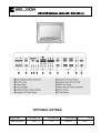
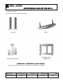
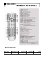
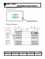
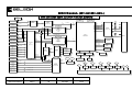
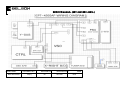
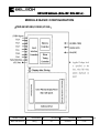
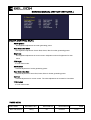
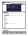
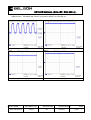
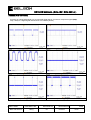
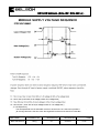
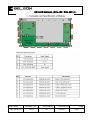
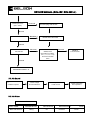
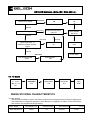
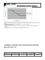
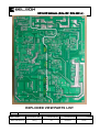
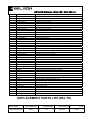
SERVICE MANUAL (BSV-4251 BSV-4251A )
Service Manual
MODEL NAME
BSV-4251/4251A
DOCUMENT NO
RD(1)
REVISION NO REVISION DATE
00
03/10/23
PAGE
1/75
SERVICE MANUAL (BSV-4251 BSV-4251A )
CONTENTS
SPECIFICATION ..………………………………………………. 4
CONTROL DESCRIPTIONS …………………………………... 7
OPTIONS EXTRAS ..……………………..…………………… 9
REMOTE CONTROL BUTTONS ………..……………………. 10
DISPLAY CELL DEFECT SPECIFICATION …………………. 12
BLOCK & WIRING DIAGRAM …………………………………14
MODULE FUNCTION & DEFINITION ……………………….. 16
MODULE BASIC CONFIGURATION …………………….……17
VSC BOARD PIN CONFIGURATION …………….………….. 18
OSD MENU (FACTORY)……………………………………….. 21
DESCRIPTION OF VSC FUNCTIONS ……………………….. 32
CIRCUIT OPERATION & WAVEFORM……………………….. 34
MODULE SUPPLY VOLTAGE SEQUENCE …………………. 41
VSC & PSU POWER SEQUENCE ……………………….….... 42
VOLTAGE & W/B ADJUSTMENT……………………………… 44
SAFETY PRECAUTIONS …………………………………………49
MODEL NAME
BSV-4251/4251A
DOCUMENT NO
RD(1)
REVISION NO
00
REVISION DATE
03/10/23
PAGE
2/75
SERVICE MANUAL (BSV-4251 BSV-4251A )
(MODULE USE AND CONSIDERATIONS IN SERVICING)
TROUBLESHOOTING.…….…………………………..…………. 53
IMAGE STICKING CHARACTERISTICS ……………………… 64
ISM MODE………………………………………………………….. 66
SCHEMATIC &PRINTED CIRCUIT BOARD &EXPLODE VIEW ……… 67
EXPLODED VIEW PARTS LIST ………………………………… 69
REPLACMENT PARTS LIST …………………………………….. 71
EXPLODE VIEW …………………………………………………… 75
MODEL NAME
BSV-4251/4251A
DOCUMENT NO
RD(1)
REVISION NO
00
REVISION DATE
03/10/23
PAGE
3/75
SERVICE MANUAL (BSV-4251 BSV-4251A )
SPECIFICATIONS
Note : Specification and others are subject to change without notice for improvement.
● TV
1.Input Signal :
PAL
SECAM
SD,HD
VGA ~XGA
2. Tuner : PAL
SECAM
2. Input Voltage : AC 100V ~ 240V,@ 50/60Hz, 4A
3. Power Consumption : 320W
Stand-by : 5W
4. PDP Module : PDP42V51000,51300(YBT), 51330(new ASIC) - LGE
5. Speaker Impedance : 8 §Ù
6. Sound Output : 10W + 10W
7. Feature :
-
8. Function :
-
AV Input (Bottom)
Component1 Input (Bottom, DVD)
Component2 Input (Bottom, DTV)
D-SUB (Bottom, RGB 15 pin)
S-Video Input (Bottom,4Pin DIN)
SCART1 Input (Bottom, Full)
SCART2 Input (Bottom, Half)
Tuner (Bottom, PAL,SECAM)
External SPK Out (Bottom, SPK Jack)
Audio Input (Bottom,RCA Jack,AV,Component1/2,S-Video,RGB)
RS-232C (9 pin) , TCP / IP Support (0~255set)
ARC
PIP (PIP Swap,Sound Swap)
PBP (4:3,16:9)
MTS
TTX
9. External Interface
MODEL NAME
BSV-4251/4251A
DOCUMENT NO
RD(1)
REVISION NO
00
REVISION DATE
03/10/23
PAGE
4/75
SERVICE MANUAL (BSV-4251 BSV-4251A )
1) AV / COMPONENT Output
ITEM
AV Video Input Level
AV Sync Input Level
AV Burst Input Level
AV Video Input Level
AV Audio Input L/R
Component Video Input Level
(Y,Cb/Pb,Cr/Pr)
Analog RGB, H/V Input Level
MIN
0.85
0.24
0.14
0.47
0.47
TYP
1.00
0.29
0.28
0.63
0.63
MAX
1.15
0.32
0.35
0.79
0.79
UNIT
Vpp
Vpp
Vpp
V
V
0.6
0.7
0.8
Vpp
0.6
0.7
0.8
Vpp
2) COMPONENT Mode (Y,Cb/Pb,Cr/Pr)
RESOLUTION
H-Freq(KHz)
V-Freq(Hz)
Proposed
720*480
720*576
720*480
1280*720
1280*720
1920*1080
1920*1080
15.73
15.63
31.47
45.00
44.96
33.75
33.72
60.00
50.00
59.94
60.00
59.94
60.00
59.94
SDTV,DVD 480I
SDTV,DVD 576I
SDTV 480P
HDTV 720P
HDTV 720P
HDTV 1080I
HDTV 1080I
3)SUPPORTIING DISPLAY Mode
* It is optimal screen when the resolution is 640 * 480
RESOLUTION
640*480
720*400
800*600
1024*768
H-Freq(KHz)
V-Freq(Hz)
31,47
37.86
37.50
31.47
35.15
37.88
48.88
46.88
48.36
56,48
60.02
60
72
75
70
56
60
72
75
60
70
75
10. RS-232C Signal
MODEL NAME
BSV-4251/4251A
DOCUMENT NO
RD(1)
REVISION NO
00
REVISION DATE
03/10/23
PAGE
5/75
SERVICE MANUAL (BSV-4251 BSV-4251A )
Pin No
Pin Name
Spec
Pin No
Pin Name
Spec
1
2
3
4
5
DCD
RXD
TXD
DTR
GND
NC
12 Vpp
12 Vpp
NC
GND
6
7
8
9
DSR
RTS
CTS
R
NC
NC
NC
NC
CONTROL DESCRIPTIONS
MODEL NAME
BSV-4251/4251A
DOCUMENT NO
RD(1)
REVISION NO
00
REVISION DATE
03/10/23
PAGE
6/75
SERVICE MANUAL (BSV-4251 BSV-4251A )
MODEL NAME
BSV-4251/4251A
DOCUMENT NO
RD(1)
REVISION NO
00
REVISION DATE
03/10/23
PAGE
7/75
SERVICE MANUAL (BSV-4251 BSV-4251A )
OPTIONAL EXTRAS
MODEL NAME
BSV-4251/4251A
DOCUMENT NO
RD(1)
REVISION NO
00
REVISION DATE
03/10/23
PAGE
8/75
SERVICE MANUAL (BSV-4251 BSV-4251A )
◐Optional extras can be changed or modified for quality improvement without notification new optional
extras can be added.
◐Contract your dealer for buying these items.
REMOTE CONTROL BUTTONS
※ When using the remote control aim it at the remote control sensor of the Monitor.
MODEL NAME
BSV-4251/4251A
DOCUMENT NO
RD(1)
REVISION NO
00
REVISION DATE
03/10/23
PAGE
9/75
SERVICE MANUAL (BSV-4251 BSV-4251A )
TELETEXT FUNCTION
MODEL NAME
BSV-4251/4251A
DOCUMENT NO
RD(1)
REVISION NO
00
REVISION DATE
03/10/23
PAGE
10/75
SERVICE MANUAL (BSV-4251 BSV-4251A )
DISPLAY CELL DEFECT SPECIFICATION
MODEL NAME
BSV-4251/4251A
DOCUMENT NO
RD(1)
REVISION NO
00
REVISION DATE
03/10/23
PAGE
11/75
SERVICE MANUAL (BSV-4251 BSV-4251A )
[ PDP42V51000,51300,51330]
DEFINITION OF CELL DEFECT ZONE
MODEL NAME
BSV-4251/4251A
DOCUMENT NO
RD(1)
REVISION NO
00
REVISION DATE
03/10/23
PAGE
12/75
SERVICE MANUAL (BSV-4251 BSV-4251A )
1) Definition of Cell defect Zone
2) Display Dot Diagram
MODEL NAME
BSV-4251/4251A
DOCUMENT NO
RD(1)
REVISION NO
00
REVISION DATE
03/10/23
PAGE
13/75
SERVICE MANUAL (BSV-4251 BSV-4251A )
BSV-4251 &BSV-4251A (42") PDP TV BLOCK DIAGRAM
24LC21
EEPROM
3
Y,Pb,Pr
COMPONENT1
(DTV)
80.000MHz
20.000MHz
5
R,G,B,H,V
ANALOG RGB
(U8)
BA7657
SWITCH
5
TX0 +
(U2)
AD9883
A/D
CONVERTER
24
24
CH1 RGB
DE [23:0]
16
V OUT2
V SYNC
CH1 GB
(U39)
VPC3230D-C5
VIDEO
DECODER
(SUB)
2
TUNER
CVBS
TX1 -
H SYNC
3
Y,Pb,Pr
TX1 +
DO [23:0]
20.25MHz
COMPONENT2
(DVD)
TX0
TX0+
24
SIL164
TMDS
TRANSMITTER
DEN
DCLK
Y,C OUT2
H_SCART_OUT
CVBS,ID
CVBS,ID
FULL SCART
VIDEO IN/OUT
Y,C OUT1
CH,LU
2
SVIDEO_IN R/L
CXA2089Q
A/V
MUX(U3)
PC_IN R/L
2
SCART_FULL
AUDIO IN
2
SCART_HALF
AUDIO IN
H_SC_IN R/L
2
COMPOSITE
AUDIO IN
AV_IN R/L
2
MODULE
42"
ADR[12:0]
FSDQM[7:0]
16
CH2 GB
K4S643232E X 2
SDRAM
FSDATA[63:0]
A[21:0]
4
TM28F800B3
FLASH
MOMORY
D[7:0]
6.000MHz
TTX_CVBS
2
F_SC_IN R/L
PC
AUDIO IN
(U41)
VPC3230D-C5
VIDEO
DECODER
(MAIN)
2
TXC -
(U21)
PW565
20.25MHz
V OUT1
2
S-VIDEO
S-VIDEO
AUDIO IN
4
2
TX2 -
TXC +
COMPOSITE
IN
HALF SCART
VIDEO IN/OUT
TX2 +
BA7657
(U28)
SWITCH
TTX RGB
(R,G,B,FB)
4
SST39VF080AT
FLASH
SDA5550
(U26)
TTX
24LC256
EEPROM
HY62U8200
RAM
DS232AS
RS232
TRANSMITTER
24LC16
EEPROM
I/O EXTENDER
REMOCON
MSP0 L/R
MSP1 L/R
18.432MHz
FULL SCART
RGB
SPK
R
SCART RGB(R,G,B,FB)
4
2
2
DTV
AUDIO IN
DTV_IN R/L
2
DVD
AUDIO IN
DVD_IN R/L
2
SCART_FULL
AUDIO OUT
2
F_CVBS_OUT_R/L
SCART_HALF
AUDIO OUT
2
H_CVBS_OUT_R/L
BSV-4251/4251A
RS232
DSUB-9P
KYE
PAD
TDA7495S
AUDIO AMP
VCC5
(U45)
MSP3453
AUDIO
PROCESSOR
TUNER
SIF
MODEL NAME
MSP_OUT1
L/R
SPK
L
VCC3
VCC5D
VCC5A
VCC12
AP1501-50
12V
12V
RC1117
AP1501-50
12V
RD(1)
REVISION NO
00
REVISION DATE
03/10/23
PAGE
14/75
AP1501-50
12V
POWER
MODULE
DOCUMENT NO
VCC9
5VST
KIA7809
12V
5V
FAN
12V
SERVICE MANUAL (BSV-4251 BSV-4251A )
MODEL NAME
BSV-4251/4251A
DOCUMENT NO
RD(1)
REVISION NO
00
REVISION DATE
03/10/23
PAGE
15/75
SERVICE MANUAL (BSV-4251 BSV-4251A )
MODULE FUNCTION & DEFINITION
1. The function of each part
Part name
Main function
Y-Board (Scan Driver)
Execution of the scan and sustain operation connecting scan electrode (Y-electrode) and FPC of panel
Z-Board (Common Sustain Driver)
Execution of the sustain operation connecting sustain electrode (Z-electrode) and FPC of panel
X-Board (Address Driver)
Execution of the address operation connecting the botton plate address electrode (X-electrode) and FPC of panel
Control Board
DC/DC-2 Board
FPC (Flexible Plate Circuit)
COF (Chip On Film)
Distribution to X, Y, Z board after creation of display data and driver timing for an image and sound signal to be input from outside
Distribution to X, Y, Z board after conversion from input voltage of Vs, Va, Voc to circuit logic voltage (5V)
The pattern connection of PCB and panel
It means to integrate a kind of IC Chip with FPC
2. A term and definition of defect
2.1 CELL DEFECT
Term
The actual state
Non lighting Cell Defect
Flashing Cell Defect
¢º a different thing or structural defect of Cell
¢º a different thing or structural defect of Cell
Non-extinguishing Cell Defect
Cell is always “On”
High Intensity Cell Defect
A cell is the brighter than others on same color
MODEL NAME
BSV-4251/4251A
A cause
Cell is always “Off”
Cell repeat On / Off
DOCUMENT NO
RD(1)
REVISION NO
00
¢º a different thing or structural defect of Cell
¢º a different thing or structural defect of Cell
REVISION DATE
03/10/23
PAGE
16/75
SERVICE MANUAL (BSV-4251 BSV-4251A )
MODULE BASIC CONFIGURATION
[PDP42V51000,51300,51330]
MODEL NAME
BSV-4251/4251A
DOCUMENT NO
RD(1)
REVISION NO
00
REVISION DATE
03/10/23
PAGE
17/75
SERVICE MANUAL (BSV-4251 BSV-4251A )
VSC BOARD PIN CONFIGURATION
J7
Pin No
I/O
Specification
Description
1 ( 5V )
I
5V
VSC 5V Input
2 ( 5V )
I
5V
VSC 5V Input
3 ( 5V )
I
5V
VSC 5V Input
4 ( GND )
GND
5V Ground
5 ( GND )
GND
5V Ground
6 ( GND )
GND
5V Ground
7 ( 12V )
I
12V
VSC 12V Input
8 ( 12V )
I
12V
VSC 12V Input
9 ( GND )
GND
12V Ground
10 ( GND )
GND
12V Ground
12V
FAN 12V
GND
FAN 12V Ground
AC POWER DETECT PORT
11 ( 12V )
I
12 ( GND )
: AC INPUT DETECTING.
: AC POWER ON
1 ( AC-DET )
I
5V / 0V
AC POWER OFF
High ,
LOW
:Turn off the power by power sequence to
stabilize PDP MODULE in case of power
J6
3 ( 5V STBY )
I
5V
2 ( RL-ON )
O
5V / 0V
6 ( 5V-MNT )
I
5V / 0V
breakdown.
5V INPUT PORT FOR VSC STANDBY
RELAY CONTROL PORT FOR POWER ON
: Relay On
High , Relay off
Low
PDP MODULE STABLE CHECK PORT.
: The port to provide control signal to PDP
MODULE after the controller stabilized. At the
moment, MICOM always check this signal and
turn off the power when the signal is low.
4 ( GND )
5 (VAVS-ON )
PORT FOR VA/VS OF PDP MODULE.
: ON
HIGH , OFF LOW
:To protect PDP MODULE, Micom turn on the
Va/Vs 2 seconds after checking 5V-MNT.
No Connection
O
5V / 0V
I
5V
Monitor transmitter signal input port
O
5V
Stand by 5V Output Port
5 (LED-R )
O
5V / 0V
6 (LED-G )
O
5V / 0V
7 ( NC )
P2
1 ( REMOCON )
2 ( GND )
3 ( 5VST )
4 ( GND )
MODEL NAME
BSV-4251/4251A
DOCUMENT NO
RD(1)
RED LED CONTORL OUTPUT PORT
: High : Red LED On
GREEN LED CONTORL OUTPUT PORT
: High : Green LED On
REVISION NO
00
REVISION DATE
03/10/23
PAGE
18/75
SERVICE MANUAL (BSV-4251 BSV-4251A )
J9
7 ( POWER )
I
5V / 0V
LOCAL KEY INPUT PORT FOR POWER
8 ( VOL+ )
I
5V / 0V
LOCAL KEY INPUT PORT FOR VOL +
9 ( VOL- )
I
5V / 0V
LOCAL KEY INPUT PORT FOR VOL -
10 ( SRC/SEL )
I
5V / 0V
LOCAL KEY INPUT PORT FOR SOURCE
11 (MENU)
I
5V / 0V
LOCAL KEY INPUT PORT FOR MENU
12 (CH-)
I
5V / 0V
LOCAL KEY INPUT PORT FOR CH-
13 (CH+)
I
5V / 0V
LOCAL KEY INPUT PORT FOR CH+
1 ( 32V )
I
32V
Audio AMP POWER INPUT PORT
2 ( 32V )
I
32V
Audio AMP POWER INPUT PORT
3 ( GND )
0V
Audio AMP POWER GROUND PORT
4 ( GND )
0V
Audio AMP POWER GROUND PORT
1 ( L OUT )
J10
J11
O
Audio AMP LEFT OUTPUT PORT( 8 §Ù )
2 ( L GND )
Audio AMP LEFT GROUND PORT
3 ( R OUT )
O
Audio AMP RIGHT OUTPUT PORT ( 8 §Ù )
4 ( R GND )
Audio AMP RIGHT GROUND PORT
1 ( S-SCL )
RS-232C CLOCK LINE
2 ( S-SDA )
RS-232C DATA LINE
3 ( FS )
4 ( GND )
J1
0V
1 ( VCC5 )
I
5V
5V Input
2 ( VCC5 )
I
5V
5V Input
3 (SCART_R)
I
0.7Vpp±0.1pp
SCART RED INPUT PORT
4 (SCART_G)
I
0.7Vpp±0.1pp
SCART GREEN INPUT PORT
5 (SCART_B)
I
0.7Vpp±0.1pp
SCART BLUE INPUT PORT
6 (SCART_FB)
I
+1V to +3V / 0V to 0.4V
7 ( GND )
SCART FAST BLANKING
0V
8 (FSCART_CVBS_IN)
I
1.0Vpp±3dB
I
1.0Vpp±3dB
9 ( GND ))
SCART1 CVBS INPUT PORT
0V
10 (HSCART_CVBS_IN)
11 ( GND )
SCART2 CVBS INPUT PORT
0V
12 ( FSCART_ID )
I
4:3 / 16:9
VIDEO STATUS
13 ( HSCART_ID )
I
4:3 / 16:9
VIDEO STATUS
14 ( GND )
0V
15 (F_CVBS_OUT)
O
SCART1 CVBS OUTPUT PORT
1.0Vpp±3dB
16 ( GND )
0V
17 (H_CVBS_OUT)
O
1.0Vpp±3dB
19 (F_CVBS_L_OUT)
O
0.5Vrms±3dB
SCART1 AUDIO LEFT OUTPUT PORT
20 (F_CVBS_R_OUT)
O
0.5Vrms±3dB
SCART1 AUDIO RIGHT OUTPUT PORT
22 (H_CVBS_L_OUT)
O
0.5Vrms±3dB
SCART2 AUDIO LEFT OUTPUT PORT
23 (H_CVBS_R_OUT)
O
0.5Vrms±3dB
SCART2 AUDIO RIGHT OUTPUT PORT
18 ( GND )
0V
21 ( GND )
MODEL NAME
BSV-4251/4251A
SCART2 CVBS OUTPUT PORT
0V
DOCUMENT NO
RD(1)
REVISION NO
00
REVISION DATE
03/10/23
PAGE
19/75
SERVICE MANUAL (BSV-4251 BSV-4251A )
24 ( GND )
0V
1 ( VCC5)
I
5V
2 ( F_SC_L_IN )
I
0.5Vrms±3dB
SCART1 AUDIO LEFT OUTPUT PORT
3 ( F_SC_R_IN )
I
0.5Vrms±3dB
SCART1 AUDIO RIGHT OUTPUT PORT
4 ( GND )
0V
5 ( H_ SC_L_IN )
I
0.5Vrms±3dB
SCART2 AUDIO LEFT OUTPUT PORT
6 ( H_SC_R_IN )
I
0.5Vrms±3dB
SCART2 AUDIO RIGHT OUTPUT PORT
7 ( GND )
8 ( AFT )
0V
I
9 ( GND )
10 ( TUNER_SIF )
0V
I
11 ( GND )
J2
5V INPUT
12 (TUNER_CVBS)
0V
I
TV VIDEO INPUT PORT
1.0Vpp±3dB
13 ( GND )
0V
14 ( SDA3 )
I
5V / 0V
DATA LINE
15 ( SCL3 )
I
5V / 0V
CLOCK LINE
16 ( GND )
0V
17 ( VCC12 )
I
12V
12V INPUT
18 ( VCC12 )
I
12V
12V INPUT
19 ( GND )
0V
20 ( VCC5A )
I
21 (VCC5A )
I
5V
5V INPUT
5V
5V INPUT
22 ( GND )
0V
23 ( GND )
0V
24 ( GND )
0V
OSD MENU(FACTORY)
■ FACTORY MODE
MODEL NAME
BSV-4251/4251A
DOCUMENT NO
RD(1)
REVISION NO
00
REVISION DATE
03/10/23
PAGE
20/75
SERVICE MANUAL (BSV-4251 BSV-4251A )
FACTORY MODE
„ 1. Calibration
: Automatic adjustment of white balance for Analogue input (PC) and Component2 (DTV)
input.
„ 2. Option Table 0002
: Initial installation of OSD.
„ 3. Color control
: Adjustment of contrast and brightness for scaler generating power.
„ 4. PW565
: Adjustment of contrast and brightness for scaler input port (CH1 or CH2).
„ 5. VPC3230-MAIN
: Value adjustment for video decoder¡¯s brightness and contrast, color tickness in
the main window.
„ 6. VPC3230-SUB
: Value adjustment for video decoder¡¯s brightness and contrast, color tickness in
the sub window.
„ 7. ADC
: Value adjustment for brightness and contrat, color thickness of analogue RGB,
Y,Pb,Pr of AD9883 A/D convertor.
„ 8. Heatrun
: The mode when you do aging.
„ 9. Version
: It shows the information of Firmware version and Panel.
„ 10. Setup
: Installation of TTX language and video, protocol, logo.
CALIBRATION MENU
MODEL NAME
BSV-4251/4251A
DOCUMENT NO
RD(1)
REVISION NO
00
REVISION DATE
03/10/23
PAGE
21/75
SERVICE MANUAL (BSV-4251 BSV-4251A )
CALIBRATION MENU
„ 1. PC Calibration
: Automatic adjustment as the fittest status of white balance for analogue input (PC)
„ 2. DTV Calibration
: Automatic adjustment as the fittest status of white balance for component2 (DTV)
input.
OPTION TABLE MENU
MODEL NAME
BSV-4251/4251A
DOCUMENT NO
RD(1)
REVISION NO
00
REVISION DATE
03/10/23
PAGE
22/75
SERVICE MANUAL (BSV-4251 BSV-4251A )
OPTION TABLE MENU
„ Flesh tone
„ LNA(Low Noise Amplifier)
: On/Off Installation of screen quality improv
ement fuc tion, when TV input signal is
weak.
„ Blue Screen
: When there are no input signal of the TV and
external equipment, you can install the
screen color as blue.
„ Melody Volume
: Installation of the melody volume for initial soft power On/Off. The volume is exfactoried as ¡°0 ¡± due to license.
„ Video Mute
„ TTX TOP
„ Auto FM
„ Help
„ Area
„ High Deviation
COLOR CONTROL MENU
MODEL NAME
BSV-4251/4251A
DOCUMENT NO
RD(1)
REVISION NO
00
REVISION DATE
03/10/23
PAGE
23/75
SERVICE MANUAL (BSV-4251 BSV-4251A )
COLOR CONTROL MENU
„ Sub-Brightness
: The brightness adjustment of scaler generating power.
„ Red, Green, Blue Offset
: The brightness adjustment of each Red, Green, Blue for scaler generating power.
„ Brightness
: The brightness adjustment of current screen. Adjustment value of brightness for User
Menu
„ TTX-Bright
: It is not useful mode.
„ Sub Contrast
: Contrast adjustment of scaler generating power.
„ Red, Green, Blue Gain
: Contrast adjustment of each Red, Green, Blue for Scaler generating power.
„ Contrast
: Contrast adjustment for current screen. The value adjustment of contrast for User Menu
„ TTX-Contrast
: It is not useful mode.
PW565 MENU
MODEL NAME
BSV-4251/4251A
DOCUMENT NO
RD(1)
REVISION NO
00
REVISION DATE
03/10/23
PAGE
24/75
SERVICE MANUAL (BSV-4251 BSV-4251A )
PW565 MENU
„ Red,Green,Blue Gain
: The contrast value adjustment of each Red, Green, Blue for scaler input port (CH1 OR
CH2)
„ Red,Green,Blue Offset
: The brightness adjustment of each Red, Green, Blue for scaler input port (CH1 OR CH2)
„ APL
„ Pixel Shift
„ Pixel Number
„ Time
„ Virtual Framelock
: Installation of flame frequency for panel (50Hz, 60Hz).
„ Alpha
„ Beta
„ Degree
VPC3230-MAIN MENU
MODEL NAME
BSV-4251/4251A
DOCUMENT NO
RD(1)
REVISION NO
00
REVISION DATE
03/10/23
PAGE
25/75
SERVICE MANUAL (BSV-4251 BSV-4251A )
VPC3230-MAIN MENU
„ CT
: Contrast adjustment of Composite & S-Video form¡¯s signal.
„ BR
: Brightness adjustment of Composite & S-Video form¡¯s signal.
„ ACC_SAT
„ TINT
: The color sense adjustment of Composite & S-Video form¡¯s signal.
„ SATCb
: The blue color sense adjustment of Component & RGB form¡¯s signal.
„ SATCr
: The red color sense adjustment of Component & RGB form¡¯s signal
„ CIPTNT
: The color sense adjustment of Component & RGB form¡¯s signal.
„ CIPBR
: The brightness adjustment of Component & RGB form¡¯s signal.
„ KILVL
„ LDLY
: The delayed time adjustment of brightness signal.
„ PKCOR
„ FB_GAIN
VPC3230-SUB MENU
MODEL NAME
BSV-4251/4251A
DOCUMENT NO
RD(1)
REVISION NO
00
REVISION DATE
03/10/23
PAGE
26/75
SERVICE MANUAL (BSV-4251 BSV-4251A )
VPC3230-SUB MENU
„ CT
: The contrast adjustment of Composite & S-Video form¡¯s signal.
„ BR
: The brightness adjustment of Composite & S-Video form¡¯s signal.
„ ACC_SAT
„ TINT
: The color sense adjustment of Composite & S-Video form¡¯s signal.
„ SATCb
: The blue color sense adjustment of Component & RGB form¡¯s signal.
„ SATCr
: The red color sense adjustment of Component & RGB form¡¯s signal.
„ CIPTNT
: The color sense adjustment of Component & RGB form¡¯s signal.
„ CIPBR
: The brightness adjustment of Component & RGB form¡¯s signal.
„ KILVL
„ LDLY
: The delayed time installation of brightness signal.
„ PKCOR
„ FB_GAIN
ADC MENU
MODEL NAME
BSV-4251/4251A
DOCUMENT NO
RD(1)
REVISION NO
00
REVISION DATE
03/10/23
PAGE
27/75
SERVICE MANUAL (BSV-4251 BSV-4251A )
ADC MENU
„ Red, Green, Blue Gain
: Control ADC input range (Contrast) of each respective channel.
„ Red, Green, Blue Offset
: Control dc offset (Brightness) of each respective channel.
„ Current
: Installation of PLL Part VCO Current. (For test)
„ VCO
: Installation of PLL Part VCO Range (For test)
„ Pr, Y, Pb Gain
: Contrast adjustment of Component2 Pr, Y, Pb signal.
„ Pr, Y, Pb Offset
: Brightness adjustment of Component2 Pr, Y, Pb signal.
„ TTX Phase
: It is not useful mode.
„ TTX Contrast
: It is not useful mode.
HEATRUN MENU
MODEL NAME
BSV-4251/4251A
DOCUMENT NO
RD(1)
REVISION NO
00
REVISION DATE
03/10/23
PAGE
28/75
SERVICE MANUAL (BSV-4251 BSV-4251A )
HEATRUN MENU
„ 1. Auto Run
: It is the mode to change the heatrun pattern as a certain time interval.
„ 2. Luma Ramp (16 Step)
: It is gray pattern of 16 Step.
„ 3. Luma Ramp (128 Step)
: It is gray pattern of 128 Step.
„ 4. White 16
: It is low Gray pattern.
„ 5. White 240
: It is high gray pattern.
„ 6. Color Bar
: It is color Bar Pattern.
„ 7. RGB Ramp (32 Step)
: It is RGB Ramp pattern of 32 Step.
VERSION MENU
MODEL NAME
BSV-4251/4251A
DOCUMENT NO
RD(1)
REVISION NO
00
REVISION DATE
03/10/23
PAGE
29/75
SERVICE MANUAL (BSV-4251 BSV-4251A )
VERSION MENU
„ Version
: It is to show the Firmware Version.
„ Release
: It is to show the date of Firmware revision.
„ Panel Used Time
: It is to show the used time of Panel.
„ Panel Name
: It is to show the name of the PDP.
SETUP MENU
MODEL NAME
BSV-4251/4251A
DOCUMENT NO
RD(1)
REVISION NO
00
REVISION DATE
03/10/23
PAGE
30/75
SERVICE MANUAL (BSV-4251 BSV-4251A )
SETUP MENU
„ 1. TTX Language
: Installation of initial language of the TTX.
„ 2. Video
: Video format per country and it is composed of Normal, NTSC, PAL N, M
„ 3. Protocol
: Installation of communication protocol for remote control.
„ 4. LOGO
: Installation to show company logo on the screen when power ¡°On¡±(ON/OFF).
DESCRIPTION OF VSC FUNCTIONS
MODEL NAME
BSV-4251/4251A
DOCUMENT NO
RD(1)
REVISION NO
00
REVISION DATE
03/10/23
PAGE
31/75
SERVICE MANUAL (BSV-4251 BSV-4251A )
PSM (Picture Status Memory)
Function to adjust picture status to an optimal condition in accordance with the type of program being
viewed (standard, moving picture, movie, muted, game).
SSM (Sound Status Memory)
Function to adjust sound status to an optimal condition in accordance with the type of program being
viewed (standard, music, movie, news).
ARC (Aspect Ratio Control)
Function to adjust the picture size. (16:9. enlargement 1, enlargement 2, panorama, 4:3)
Panorama
Function to prevent pictures recorded in the 4:3 format from being stretched to the extreme left and right
when played on a 16:9 display. Since the focus of the camera is concentrated on the center, it naturally
enlarges the picture within the outer perimeter of the screen without expanding the central area.
PIP (Picture In Picture )
Function to enable the simultaneous viewing of two pictures by displaying a small sub-frame within the
main picture. The main picture may be viewed with multiple types of input source (Analog/Digital RGB,
composite, S-Video, component), while the sub-frame is only available in composite, S-Video or
component (480i).
PBP (Picture By Picture) ,Twin Picture
Function to assign two separate signals onto a single screen, thereby enabling the viewer to
simultaneously watch different pictures on each half of the display.
PIP Swap Simultaneous Conversion Between Sub and Main Pictures.
Function to convert between the sub-frame and main picture being watched simultaneously.
PIP Sound Swap Simultaneous Conversion Between sub and Main Picture Audio
Function to convert between simultaneous audio streams from the sub-frame and main picture being
viewed.
MODEL NAME
BSV-4251/4251A
DOCUMENT NO
RD(1)
REVISION NO
00
REVISION DATE
03/10/23
PAGE
32/75
SERVICE MANUAL (BSV-4251 BSV-4251A )
EQUALIZER
Function to control sound according to frequency. (100Hz, 300Hz, 1KHz, 3KHz, 10KHz)
AVL (Auto Volume Leveler)
Function to automatically adjust varying sound levels from each individual broadcasting company to an
appropriate volume, in case of watching a television connected to external equipment. This allows to
viewer to enjoy a comfortable and stable sound level even when changing the channel.
CIRCUIT OPERATION & WAVEFORM
VPC3230D (Video Processor)
MODEL NAME
BSV-4251/4251A
DOCUMENT NO
RD(1)
REVISION NO
00
REVISION DATE
03/10/23
PAGE
33/75
SERVICE MANUAL (BSV-4251 BSV-4251A )
Converts analog pictures (including Composite, S-Video, Component (480i) or the like) to Y-UV
digital pictures. Compatible with various TV formats of NTSC, PAL, SECAM, etc.
U41 (VPC323OD)_#28_S-LLC1
U42 (LM2937-3.3V)_#3_V3.3
LC18 (STS104B)_#2_VAA3230
MODEL NAME
BSV-4251/4251A
DOCUMENT NO
RD(1)
U40 (LM2937-3.3V)_#3_V3.3V-1
REVISION NO
00
REVISION DATE
03/10/23
PAGE
34/75
SERVICE MANUAL (BSV-4251 BSV-4251A )
LC16 (STS104B)_#2_VAA3230_1
U41 (VPC3230D)_#28_VID_CLK
U41 (VPC3230D)_#53_INTLC
U41 (VPC3230D)_#57_VID-VS
U41 (VPC3230D)_#56_VID-HS
MODEL NAME
BSV-4251/4251A
DOCUMENT NO
RD(1)
REVISION NO
00
REVISION DATE
03/10/23
PAGE
35/75
SERVICE MANUAL (BSV-4251 BSV-4251A )
AD9883 (A/D Converter)
Converts an analog RGB signal to a process able digital signal. Converts a component signal (480p,
720p, 1080i) to a digital signal and transmits it to PW565 (Scaler).
U2 (AD9883)_#30_ Hsync0
U2 (AD9883)_#31_Vsync0
U2 (AD9883)_#67_DATACK
U2 (AD9883)_#64_VSOUT
U2 (AD9883)_#66_HSOU T
U2 (AD9883)_#65_SOG
MODEL NAME
BSV-4251/4251A
DOCUMENT NO
RD(1)
REVISION NO
00
REVISION DATE
03/10/23
PAGE
36/75
SERVICE MANUAL (BSV-4251 BSV-4251A )
U1 (LM2937)_#3_ VO
PW565 (Scaler)
MODEL NAME
BSV-4251/4251A
DOCUMENT NO
RD(1)
REVISION NO
00
REVISION DATE
03/10/23
PAGE
37/75
SERVICE MANUAL (BSV-4251 BSV-4251A )
Receives, at the same time, a video signal from VPC3230, an Analog/Digital RGB signal and a
Component signal, which are converted at AD9883 and THC63DV151, adjusted to a PDP display,
and transmitted to a PDP module. In particular, it receives any PC signal input at various scanning
rates and performs scaling to adjust to PDP resolution.
RP12 (R-ARRAY)_#1_DEN
RP12 (R-ARRAY)_#4_DCLK
RP12 (R-ARRAY)_#3_DVS
RP12 (R-ARRAY)_#2_DHS
MSP3450 (Sound Processor)
MODEL NAME
BSV-4251/4251A
DOCUMENT NO
RD(1)
REVISION NO
00
REVISION DATE
03/10/23
PAGE
38/75
SERVICE MANUAL (BSV-4251 BSV-4251A )
Receives and converts any Sound IF signal from a TV Tuner to a general audio signal (LCD TV).
Also, outputs the desired input signal out of many audio input signal options, and produces a woofer
signal or Headphone signal as well as a general Speaker signal (LCD TV).
U45 (MSP3450)_#65_AVSUP
U43 (KIA7808AF)_#3_8V-Output
U45(MSP3450)_#36¡±_Audio R-Out
U45(MSP3450)_#36¡±_Audio L-Out
Power & MISC Waveform
MODEL NAME
BSV-4251/4251A
DOCUMENT NO
RD(1)
REVISION NO
00
REVISION DATE
03/10/23
PAGE
39/75
SERVICE MANUAL (BSV-4251 BSV-4251A )
LC20 (STS104B)_#2_C344_5VST
LC21 (STS104B)_#2_C353_5VDD
U15 (RC1117_3.3V)_#2_VCC3
L10 (33uH)_#2_R410_VCC12
Q33 (MMBT3904)_¡±C¡±_RL_ON
Q30 (MMBT3904)_¡±C¡±_VAVS_ON
MODEL NAME
BSV-4251/4251A
DOCUMENT NO
RD(1)
REVISION NO
00
REVISION DATE
03/10/23
PAGE
40/75
SERVICE MANUAL (BSV-4251 BSV-4251A )
MODULE SUPPLY VOLTAGE SEQUENCE
[PDP42V5####]
¡Ü Life Expectancy
The anticipated life-time is estimated more than 25,000 hours of continuous operations
¡Ø Average life time is the time when the brightness level becomes half of its initial value.
MODEL NAME
BSV-4251/4251A
DOCUMENT NO
RD(1)
REVISION NO
00
.
REVISION DATE
03/10/23
PAGE
41/75
SERVICE MANUAL (BSV-4251 BSV-4251A )
VSC POWER SEQUENCE
Display Enable
Relay On
VaVs On
1. After Relay On
•
•
•
•
2. Continue 5Volt Monitoring – If there is no 5Volt more than 10 minutes, then
power “Off”
3. Check if it is OK the 5Volt Mnt first. And then VaVs “On” after 3 seconds
.
4. VaVs “On” --> waiting 3 seconds --> Display Enable “On”.
5. If 5Volt Mnt “Low” or AC-Det “Low”, immediately Display Enable “Off” and
then VaVs “Off”, Relay “Off”.
MODEL NAME
BSV-4251/4251A
DOCUMENT NO
RD(1)
REVISION NO
00
REVISION DATE
03/10/23
PAGE
42/75
SERVICE MANUAL (BSV-4251 BSV-4251A )
PSU POWER SEQUENCE
[POWER DGK-420W]
MODEL NAME
BSV-4251/4251A
DOCUMENT NO
RD(1)
REVISION NO
00
REVISION DATE
03/10/23
PAGE
43/75
SERVICE MANUAL (BSV-4251 BSV-4251A )
VOLTAGE & W/B ADJUSTMENT
Power PCB Assy Voltage Adjustment
1-1-1. Va Adjustment (Address Voltage Adjustment)
(°¡) Connect pin 9,10 of CN806 to(+) jack of D.M.M
(³ª) After turning the VR2 (Va Adj),Voltage of D.M.M adjustment as same as Va voltage which on
Label of panel right/bottom.(Deviation : ± 0.5V)
1-1-2. Vs Adjustment
(°¡) Connect pin 1~3 of CN806 to (+) jack of D.M.M
(³ª) After turning the VR3(Vs Adj),voltage of D.M.M adjustment as same as Vs voltage which
indicated on Label of panel right/bottom.(Deviation : ± 0.5V)
Refer to Typical Voltage
1. Va
2. Vs
: 65V
: 190V
¡Ø Replace PDP Module or Power Board, adjust certainly Power PCB Ass’y Voltage
MODEL NAME
BSV-4251/4251A
DOCUMENT NO
RD(1)
REVISION NO
00
REVISION DATE
03/10/23
PAGE
44/75
SERVICE MANUAL (BSV-4251 BSV-4251A )
MODEL NAME
BSV-4251/4251A
DOCUMENT NO
RD(1)
REVISION NO
00
REVISION DATE
03/10/23
PAGE
45/75
SERVICE MANUAL (BSV-4251 BSV-4251A )
2. W/B adjustment
2-2. Color temperature (White Balance) adjustment
1) How to enter Factory mode for adjustment of White Balance
(1) PDP TV Power ¡°On¡± --> Input select key on Remote control.
(2) Choose composite first and then PDP TV Power ¡°Off¡±.
(3) PDP TV Power ¡°Off¡± and INFO on the R/C ==> ERASE ==> ENTER Key
2) For COMPOSITE adjustment (manual adjustment)
(1) Signal Generator supply the pattern of above picture. (Timing ¢¡ 386, Pattem ¢¡ 10)
(2) After movement to 2.color control on Factory Mode2, move to sub menu as choice of volume
button .
(3) After check the Brightness ¢¡ 50, Contrast ¢¡ 90, choose the Sub-Brightn
ess.
(4) Zero calibration¡¯s execution of CA-100 and the sensor should be closed to surface of PDP
module.
(5) Adjustment as choice of volume button in order that it becomes Y= 6.0 ¡¾0.5 cd/m©÷ on the sub
brightness.
(6) Color coordinates¡¯ adjustment of Red Offset, Green Offset, Blue Offset using this kind of metho
Color coordination ¢¡ x= 0.281 ¡¾0.007, y=0.295 ¡¾0.007, Y= 6.0 ¡¾0.5 cd/m©÷
(Color temperature : 9500° K ¡¾ 500°K)
(7) The Sub-Brightness¡¯ readjustment when it is not satisfied with brightness after adjustment.
3) For DTV adjustment
MODEL NAME
BSV-4251/4251A
DOCUMENT NO
RD(1)
REVISION NO
00
REVISION DATE
03/10/23
PAGE
46/75
d.
SERVICE MANUAL (BSV-4251 BSV-4251A )
(1) Signal Generator supply the pattern of above picture.
Timing ¢¡ 395, Pattem ¢¡ 251, Reverse (720P, 60Hz)
(2) After movement to 1.calibration on Factory Mode, move to sub menu as choice of volume button.
(3) After movement to 2. DTV Calibration, choose it with volume button.
(4) If Enter key, it starts the calibratio
4) For PC adjustment
MODEL NAME
BSV-4251/4251A
DOCUMENT NO
RD(1)
REVISION NO
00
REVISION DATE
03/10/23
PAGE
47/75
SERVICE MANUAL (BSV-4251 BSV-4251A )
(1) Signal Generator supply the pattern of above picture.
Timing ¢¡ 313, Pattem ¢¡ 609 (1024 x 768, 60Hz)
(2) After movement to 1.calibration on Factory Mode, move to sub menu as choice of volume
button .
(3) After movement to 2. PC Calibration, choose it with volume button.
(4) If Enter key, it starts the calibration automatically
How to exit the Factory Mode
INFO ¢¡ LAST ¢¡ ERASE ¢¡ ENTER Key
5) Adjustment verification
Adjustment as volume ¡°0¡± and then 4 times of Enter key
MODEL NAME
BSV-4251/4251A
DOCUMENT NO
RD(1)
REVISION NO
00
REVISION DATE
03/10/23
PAGE
48/75
SERVICE MANUAL (BSV-4251 BSV-4251A )
SAFETY PRECAUTIONS
( MODULE USE AND CONSIDERATIONS IN SERVICING)
PDP Module is a display device to be divided into a Panel part and a Drive part. The Panel part consists of
Electrodes, Phosphor, various dielectrics and gas, and the Drive part includes electronic circuitry and PCB.
When using / handling this PDP Module, pay attention to the below warning and cautions.
Indicates a hazard that may lead to death or injury if the warning is ignored and the product is handled
incorrectly.
Indicates a hazard that can lead to injury or damage to property if the caution is ignored and the product is
handled incorrectly.
■. WARNING
(1) Do not supply a voltage higher than that specified to this product. This may damage the product and may
cause a fire.
(2) Do not use this product in locations where the humidity is extremely high, where it may be splashed with
water, or where flammable materials surround it.
Do not install or use the product in a location that does no satisfy the specified environmental conditions.
This may damage the product and may cause a fire.
(3) If a foreign substance (such as water, metal, or liquid) gets inside the product, immediately turn off the
power.
Continuing to use the product, it is may cause fire or electric shock.
(4) If the product emits smoke, and abnormal smell, or makes an abnormal sound, immediately turn off the
power.
Continuing to use the product, it may cause fire or electric shock.
(5) Do not disconnect or connect the connector while power to the product is on. It takes some time for the
voltage to drop to a sufficiently low level after the power has been turned off.
Confirm that the voltage has dropped to a safe level before disconnecting or connecting the connector.
(6) Do not pull out or insert the power cable from/to an outlet with wet hands. It may cause electric shock.
(7) Do not damage or modify the power cable. It may cause fire or electric shock.
(8) If the power cable is damaged, or if the connector is loose, do not use the product: otherwise, this can
lead to fire or electric shock.
(9) If the power connector or the connector of the power cable becomes dirty or dusty, wipe it with a dry cloth.
Otherwise, this can lead to fire.
(10) PDP Module uses a high voltage (Max.450V dc). Keep the cautions concerning electric shock and do
not touch the Device circuitry when handling the PDP Unit. And because the capacitor of the Device
circuitry may remain charged at the moment of Power OFF, standing by for 1 minute is required in order
to touch the Device circuitry.
MODEL NAME
BSV-4251/4251A
DOCUMENT NO
RD(1)
REVISION NO
00
REVISION DATE
03/10/23
PAGE
49/75
SERVICE MANUAL (BSV-4251 BSV-4251A )
CAUTIONS
(1) Do not place this product in a location that is subject to heavy vibration, or on an unstable surface such as
an inclined surface. The product may fall off or fall over, causing injuries.
(2) Before disconnecting cable from the product, be sure to turn off the power. Be sure to hold the connector
when disconnecting cables. Pulling a cable with excessive force may cause the core of the cable to be
exposed or break the cable, and this can lead to fire or electric shock.
(3) This product should be moved by two or more persons. If one person attempts to carry this product alone,
he/she may be injured.
(4) This product contains glass. The glass may break, causing injuries, if shock, vibration, heat, or distortion
is applied to the product.
(5) The temperature of the glass of the display may rise to 80°C or more depending on the conditions of use.
If you touch the glass inadvertently, you may be burned.
(6) If glass surface of the display breaks or is scratched, do not touch the broken pieces or the scratches with
bare hands. You may be injured.
(7) PDP Module requires to be handled with care not to be touched with metal or hard materials, and must
not be stressed by heat or mechanical impact.
(8) There are some exposed components on the rear panel of this product. Touching these components may
cause an electric shock.
(9) When moving the product, be sure to turn off the power and disconnect all the cables. While moving the
product, watch your step. The product may be dropped or all, leading to injuries of electric shock.
(10) In order to protect static electricity due to C-MOS circuitry of the Drive part, wear a wrist band to protect
static electricity when handling.
(11) If cleaning the Panel, wipe it with a soft cloth moistened with water or a neutral detergent and squeezed,
being careful not to touch the connector part of the Panel. And don’t use chemical materials like thinner
or benzene.
(12) If this product is used as a display board to display a static image, “image sticking” occurs. This means
that the luminance of areas of the display that remain lit for a long time drops compared with luminance
of areas that are lit for a shorter time, causing uneven luminance across the display.
The degree to which this occurs is in proportion to the luminance at which the display is used. To prevent
this phenomenon, therefore, avoid static images as much as possible and design your system so that it
is used at a low luminance, by reducing signal level difference between bright area and less bright area
through signal processing.
(13) Because PDP Module emits heat from the Glass Panel part and the Drive circuitry, the environmental
temperature must not be over 40°C.
The temperature of the Glass Panel part is especially high owing to heat from internal Drive circuitry. And
because the PDP Module is driven by high voltage, it must avoid conductive materials.
(14) If inserting components or circuit board in order to repair, be sure to fix a lead line to the connector
before soldering.
MODEL NAME
BSV-4251/4251A
DOCUMENT NO
RD(1)
REVISION NO
00
REVISION DATE
03/10/23
PAGE
50/75
SERVICE MANUAL (BSV-4251 BSV-4251A )
(15) If inserting high-power resistor(metal-oxide film resistor or metal film resistor) in order to repair, insert it
as 10mm away as from a board.
(16) During repairs, high voltage or high temperature components must be put away from a lead line.
(17) This is a Cold Chassis but you had better use a cold transformer for safety during repairs. If repairing
electricity source part, you must use the cold transformer.
(18) Do not place an object on the glass surface of the display.
The glass may break or be scratched.
(19) This product may be damaged if it is subject to excessive stresses (such as excessive voltage, current,
or temperature).
The absolute maximum ratings specify the limits of these stresses.
(20) The recommended operating conditions are conditions in which the normal operation of this product is
guaranteed. All the rated values of the electrical specifications are guaranteed within these conditions.
Always use the product within the range of the recommended operating conditions. Otherwise, the
reliability of the product may be degraded.
(21) This product has a glass display surface. Design your system so that excessive shock and load are not
applied to the glass. Exercise care that the vent at the corner of the glass panel is not damaged.
If the glass panel or vent is damaged, the product is inoperable.
(22) Do not cover or wrap the product with a cloth or other covering while power is supplied to the product.
(23) Before turning on power to the product, check the wiring of the product and confirm that the supply
voltage is within the rated voltage range. If the wiring is wrong or if a voltage outside the rated range is
applied, the product may malfunction or be damaged.
(24) Do not store this product in a location where temperature and humidity are high. This may cause the
product to malfunction. Because this product uses a discharge phenomenon, it may take time to light
(operation may be delayed) when the product is used after it has been stored for a long time. In this case,
it is recommended to light all cells for about 2 hours (aging).
(25) This product is made from various materials such as glass, metal, and plastic. When discarding it, be
sure to contact a professional waste disposal operator.
(26) If faults occur due to arbitrary modification or disassembly, Erae Electronics is not responsible for
function, quality or other items.
(27) Use of the product with a combination of parameters, conditions, or logic not specified in the
specifications of this product is not guaranteed. If intending to use the product in such a way, be sure to
consult Erae Electronics in advance.
(28) Within the warranty period, general faults that occur due to defects in components such as ICs will be
rectified by Erae Electronics without charge. However, IMAGE STICKING due to misapplying the above
(12) provision is not included in the warranty. Repairs due to the other faults may be charged for
depending on responsibility for the faults.
MODEL NAME
BSV-4251/4251A
DOCUMENT NO
RD(1)
REVISION NO
00
REVISION DATE
03/10/23
PAGE
51/75
SERVICE MANUAL (BSV-4251 BSV-4251A )
MODEL NAME
BSV-4251/4251A
DOCUMENT NO
RD(1)
REVISION NO
00
REVISION DATE
03/10/23
PAGE
52/75
SERVICE MANUAL (BSV-4251 BSV-4251A )
TROUBLE SHOOTING
1. Checking for no Picture
A screen doesn if display at all and condition of black pattern or power off.
(1) Check whether the CTRL B/D LED(D1~D4) is turned on or not.
(2) Check the power and signal cable of CTRL B/D.
(3) X B/D, Y B/D, Z B/D is well plugged in.
(4) Check the connection of X B/D, Y B/D and Z B/D to CTRL B/D.
(5) Measure the output wave of X, Y, Z B/D with oscilloscope(more than 200MHz)
and find the trouble of B/D by comparing the output wave with below figure.
- Measure Point fo Y B/D : TP (Connector P4 80 pin)
- Measure Point fo Z B/D : Connection part of panel (SUS_OUT)
- Measure Point fo X B/D : L1(RIGHT), L2(LEFT BOTTOM)
(6) Check the SCAN(Y side) IC
(7) Check the DATA(X side) COF IC
(8) Replace the CTRL B/D.
2. Hitch Diagnosis Following Display Condition
2-1. 4/7 or 3/7 of the screen doesn’t be shown
(1) Confirm the power connector of X B/D is well plugged in which is correspond to not showing screen.
(2) Confirm the connector that is connected between CTRL B/D and X B/D correspond to not showing
part.
(3) Replace relevant X B/D.
Relationship between screen and X B/D
MODEL NAME
BSV-4251/4251A
Display
X B/D
Left of the Screen 4/7
Right X B/D
Right of the Screen 3/7
Left X B/D
DOCUMENT NO
RD(1)
REVISION NO
00
REVISION DATE
03/10/23
PAGE
53/75
SERVICE MANUAL (BSV-4251 BSV-4251A )
¡Ø Screen Display Form
2-2. The screen doesn’t be shown as Data COF
(Include not be shown part of Data COF quantity or a part)
(1) The problem between Data COF and X B/D is more possible that the screen is not be shown as data
COF.
(2) Confirm the connector of Data COF is well connected to X B/D. Correspond to the part that screen is
not showing
(3) Confirm whether the Data COF is failed and replace X B/D
※ Example of the screen display form
(Anything of the 7 Data COF can be shown beside below pictures)
※ How to examine Data COF IC
MODEL NAME
BSV-4251/4251A
DOCUMENT NO
RD(1)
REVISION NO
00
REVISION DATE
03/10/23
PAGE
54/75
SERVICE MANUAL (BSV-4251 BSV-4251A )
2-3. It Generates Unusual Pattern of Data COF IC unit
(1) In case of generating unusual pattern of Data COF IC unit as below picture, there is problem in the check
that is input into Data COF IC
(2) In case of <case 1, 2, 3>
- confirm the connection of Data COF connector
- replace the relevant X B/D
(3) In case of <case 4, 5>
- confirm the connector that is connected from CTRL to X B/D
- Replace relevant XB/D or CTRL B/D
※ Screen Display Form
MODEL NAME
BSV-4251/4251A
DOCUMENT NO
RD(1)
REVISION NO
00
REVISION DATE
03/10/23
PAGE
55/75
SERVICE MANUAL (BSV-4251 BSV-4251A )
2-4. Regular Stripe is Generated about the Quantity of one Data COF IC or more
(1) In case of generating regular stripe about the quantity of one Data COF IC, there is problem at the
output of outputflatworm of X B/D
In case of generating regular stripe about the quantity of two Data COF IC, that means the data
which is conveyed from CTRL B/D doesn’t conveyed well.
(2) Confirm the XB/D connection connector plugged in well.
Correspond to unusual screen.
(3) Replace relevant XB/D or CTRL B/D.
※ Relationship between screen and X B/D
MODEL NAME
BSV-4251/4251A
DOCUMENT NO
RD(1)
REVISION NO
00
REVISION DATE
03/10/23
PAGE
56/75
SERVICE MANUAL (BSV-4251 BSV-4251A )
Display
X B/D
Left Bottom of the Screen 4/7
Right X B/D
Right Bottom of the Screen 3/7
Left
X B/D
※ Screen Display Form
2-5. The screen display has a problem for Scan FFC.
(1) It’s may be a problem between Scan FFC and Y B/D.
(2) Check the connection of Y B/D and Scan COF.
(3) If the Scan IC is failed, replace the Y DRV B/D.
.
Screen Display Form
※ Check a method of SCAN IC
MODEL NAME
BSV-4251/4251A
DOCUMENT NO
RD(1)
REVISION NO
00
REVISION DATE
03/10/23
PAGE
57/75
SERVICE MANUAL (BSV-4251 BSV-4251A )
2-6. The screen has a vertical line with regular gap.
(A vertical stripe flash at especial color)
(1) This is a problem about control B/D.
(2) Replace Control B/D.
※ Screen Display Form
2-7. A data copy is happened into vertical direction
MODEL NAME
BSV-4251/4251A
DOCUMENT NO
RD(1)
REVISION NO
00
REVISION DATE
03/10/23
PAGE
58/75
SERVICE MANUAL (BSV-4251 BSV-4251A )
(1) In this case, it’s due to incorrect marking of scan wave.
(2) Replace a Y DRV B/D or Y SUS B/D.
※ Screen Display Form
2-8. The screen has one or several vertical line
(1) In this case, It isn’t a problem about controller B/D or X B/D.
(2) It may cause followings.
- It’s out of order a panel
- Open or short of DATA COF FPC attached panel
- It’s out of order a DATA COF attached panel
(3) Replace Module.
2- 9. The screen has one or several horizontal line
(1) In this case, it isn’t a problem about controller B/D or X B/D.
MODEL NAME
BSV-4251/4251A
DOCUMENT NO
RD(1)
REVISION NO
00
REVISION DATE
03/10/23
PAGE
59/75
SERVICE MANUAL (BSV-4251 BSV-4251A )
(2) It may cause followings.
- It’s out of order a panel
- Open or short of SCAN FPC attached panel
- It’s out of order a SCAN IC attached panel
(3) Replace Y DRV B/D
2-10. The screen displays input signal pattern but the brightness is dark
(1) In this case, Z B/D operation isn’t complete.
(2) Check the power cord of Z B/D.
(3) Check the connector of Z B/D and Controller B/D.
(4) Replace the Controller B/D or Z B/D.
2-11. The screen displays other color partially on full white screen or happens
discharge partially on full black screen.
(1) Check the declination of Y B/D set up, set down wave.
(2) Check the declination of Z B/D ¢«ramp wave.
(3) Measure each output wave with oscilloscope(more than 200MHz) and compare the data with below
figure data.
Adjust the Y B/D set up(Test-up:B/C[¥s/¥s])/setdown(Testdown: D[¥s]) and Z B/D
ramp(Tramp:F/G[¥s/¥s]) declination by changing VR1/VR2/VR3.
- Measuring Point of Y B/D : P4 (Connector P4 36 pin)
- Measuring Point of Z B/D : B37 (SUS_OUT)
2-12. A center of screen is darker than a edge of screen at full white pattern.
(1) In this case, it’s a problem about Z B/D ramp wave.
(2) Check the connection cable of Z B/D and CTRL B/D.
MODEL NAME
BSV-4251/4251A
DOCUMENT NO
RD(1)
REVISION NO
00
REVISION DATE
03/10/23
PAGE
60/75
SERVICE MANUAL (BSV-4251 BSV-4251A )
(3) Replace the Z B/D.
2-13. It doesn’t display a specified brightness at specified color
(1) Check the connector of CTRL B/D input signal.
(2) Replace the CTRL B/D.
3-1. No Power
Nothing output
of image.
MODEL NAME
BSV-4251/4251A
DOCUMENT NO
RD(1)
REVISION NO
00
REVISION DATE
03/10/23
PAGE
61/75
SERVICE MANUAL (BSV-4251 BSV-4251A )
Check Input of AC
(90V ~225V)
Abnormal
Connect plug with the set.
Normal
Check ST-BY LED ON
Main S/W ON.
Abnorma l
Check AC Line Fuse
Normal
Abnormal
Check LED YELL OW
Sub S/W ON
Check OPEN With
CN806,CN13
Check the Vs Voltage
IC1 5,IC16(PSU Part)
and VSC Part Q30
Shor t
Abnormal
Replace
IC15,IC16,Q30
Normal
Check a connective condition
and various connect or.
3-2. No Sound
Check a connective
condition of power
cable
Check voltage
of sound terminal .
Check Open with
FuseF1 Fuse
Check connection
line of speake r.
3-3. No Video
Abnormal Picture
MODEL NAME
BSV-4251/4251A
DOCUMENT NO
RD(1)
REVISION NO
00
REVISION DATE
03/10/23
PAGE
62/75
SERVICE MANUAL (BSV-4251 BSV-4251A )
Check AD9883
U2
Check BA7657
U8
Abnormal
Input PC,DTV Signal
Normal
Abnorma l
Check VPC3230 Dual
U39,U41
Input DV D Signal
Check PW565
RP12~18
Normal
Abnormal
Input Tuner-CVB S,
CVBS,F/H SCART,S-Video
Signal
Abnormal
Check CX A2089Q
U3
Check SiI164
U48
Normal
Check Cable
Abnormal
Input F/SCART RGB
Signal
Check BA7657
U28
3-4. No Sound
Check
co nnector
Speaker t o
set.
Check
CXA2089Q
U3
Check
MSP3450G
U45
Check
TDA7495S
U14
Check
Input
Jack.
IMAGE STICKING CHARACTERISTICS
1) Image Sticking
The fluorescent substance used in the plasma module loses its brightness with the lapse of lighting time.
This deterioration in brightness apprears to be a difference in brightness in relation to the surroundings,
and cornes to be recognized as image sticking.
MODEL NAME
BSV-4251/4251A
DOCUMENT NO
RD(1)
REVISION NO
00
REVISION DATE
03/10/23
PAGE
63/75
SERVICE MANUAL (BSV-4251 BSV-4251A )
In other words, the image sticking is defined as follows: when the same pattern(of the fixed display)is
displayed for a long times, a difference in brightness is caused around the lighting area and non-lighting
area due to deterioration in the fluorescent substance.
When the present pattern is changed over to another one, the boundary comes to be seen between the
lighting area and non-lighting area due to difference in brightness in the pattern shown shorty before
changeover. If this conditions is accumulated, the boundary or image sticking comes to be seen with the
naked eyes.
2) Secular change in brightness
The life of brightness, defined as the reduction to half the initial level, is more than 25 thousand hours on
average.
Conditions: All white (100% white) input at an ambient temperature of 25℃.
However, this lifetime is not a guarantee value for life and brightness. It should be recognized simply as
the data for refernce.
3) Warrenty
Image sticking and faults in brightness and picture elements are excluded from the warranty objects.
4) Cause of deterioration in brightness
A major possible cause of deterioration in brightness is damage in the fluorescent substance due to
impact caused by ions generated at the time of plasma discharges.
5) Practical value for Image sticking
The relationship between intergrated lighting time and brightness in this plasma module is described in
the attached material. In particular, the deterioration in brightness tends to be accelerated up to 100
hours in the initial period. In the initial period, the fixed display of patterns particularly tends to cause
image sticking. The practical value for image sticking is difficult in concrete numerals. As described
below, you are advised to take proper measures to make the occurrence of image sticking as slow
possible.
6) Proposed measures taken to relieve image sticking
So long as there is the reduction of brightness in the fluorescent substance, it is impossible to the avoid
the occurrence of image sticking .Therefore, to relieve image sticking ,we offer you a method of entering an
image input that may ensure reluctance to the generation of the difference in brightness reduction among
the displayed dots.
The images from TV broadcasting involve a high rate of motion picture displays. Therefore, there is less
change of being a cause of difference in brightness reduction among the cells. Even when the fixed
patterns are displayed, they generally last for a few minutes. Since the same pattern is less liable to be
displayed, there is almost no influence toward image sticking.
If the fixed patterns tend to be displayed for a long time, however, there occurs a substantial imbalance
between the lighting and non-lighting areas, this causing a difference in brightness as a result. In this
document , we offer you some proposals of installation, paying attentions to the two points: the reduction of
difference of brightness achieved by intergrated lighting time leveling and the method of edge smearing to
make image sticking hard to be discerned.
The result from these proposals can, however, greatly depend on the contents of images and operating
environment.
Therefore, we consider that it is essential to take the suitable measures in consideration of the customer’s
operating environment.
Example of Poposal 1: The display position is moved while the fixed display pattern is changed over, or it is
scrolled during the display.
Example of Proposal 2: If possible, a pattern of complementary color is incorporated (for intergrated time
leveling).
Example of Proposal 3: The fixed pattern and the motion picture display are reciprocally exchanged, in
MODEL NAME
BSV-4251/4251A
DOCUMENT NO
RD(1)
REVISION NO
00
REVISION DATE
03/1
0/23
PAGE
64/75
SERVICE MANUAL (BSV-4251 BSV-4251A )
order to minimize display period of the fixed pattern.
Example of Proposal 4: During operation, the brightness of screen is suppressed as low as possible.
For the display patterns, characters are indicated not on the black ground (non-picture area) but on the
colored ground (mixture of R, G,B recommended).
ISM Mode(Image Sticking Minimization Mode)
Apart from the above proposal, This module has been equipped with a special method that minimizes the
image sticking phenomenon. When in the fixed pattern display mode, the module decreases the brightness
over a period of 10 minutes with small steps. The figure blow shows that the decrease in brightness is so
small the user will not notice.
MODEL NAME
BSV-4251/4251A
DOCUMENT NO
RD(1)
REVISION NO
00
REVISION DATE
03/10/23
PAGE
65/75
SERVICE MANUAL (BSV-4251 BSV-4251A )
The basis of the evaluation was while the ISM Mode in the module was operating, the brightness decrease
about
55 % of its initial value at the white window pattern ( 1/25 of full white pattern )
ISM operational conditions
1. Detective deviation : The change of APL Data is no less than ±4 and it will remain for more than 5
minutes.
2. Regardless of time, it will not operate where the display load is over 50%.
SCHEMATIC & PRINTED CIRCUIT BOARD & EXPLODE VIEW
¡á PSU(DGK-420W) TOP
MODEL NAME
BSV-4251/4251A
DOCUMENT NO
RD(1)
REVISION NO
00
REVISION DATE
03/10/23
PAGE
66/75
SERVICE MANUAL (BSV-4251 BSV-4251A )
■ PSU(DGK-420W) BOTTOM
MODEL NAME
BSV-4251/4251A
DOCUMENT NO
RD(1)
REVISION NO
00
REVISION DATE
03/10/23
PAGE
67/75
SERVICE MANUAL (BSV-4251 BSV-4251A )
EXPLODED VIEW PARTS LIST
No
Part no
MODEL NAME
BSV-4251/4251A
Description
DOCUMENT NO
RD(1)
REVISION NO
00
REVISION DATE
03/10/23
PAGE
68/75
SERVICE MANUAL (BSV-4251 BSV-4251A )
2
S150110021
MAIN ASSY EPT-4200A(PAL)
3
S15012G021
FRONT FRAME ASSY EPT-4200A(PAL-STD)
4
S15013F016
FRAME FILTER ASSY EPM-4200A(MONITOR-STD)
5
S15014B016
FRAME ASSY EPM-4200B(MONITOR-STD)
2
S15012C021
JACK HOUSING ASSY EPT-4200(PAL)
4
S15014A021
FRONT ASSY EPT-4200A(PAL)
3
S15013C016
HEAT SINK ASSY EPM-4200A
3
S15013B016
MODULE ASSY EPM-4200A
2
S15012F016
AC IN-LET ASSY EPM-4200A
3
S150120036
VSC BOARD ASSY(TOP) EPT-4200AP
2
S150113036
VSC BOARD ASSY EPT-4200AP(PW565)
4
S150130036
VSC BOARD ASSY(BOTTOM) EPT-4200AP
6
S15015B021
OSD PCB ASSY EPT-4200A(TV用_7KEY)
2
S150114036
TUNER BOARD ASSY EPT-4200AP(PW565)
3
S150121036
TUNER BOARD ASSY(SMD) EPT-4200AP(PW565)
2
S150134021
AUDIO OUT B/D ASSY EPM4200A
2
S150112021
POWER S/W ASSY EPT-4200A(PAL-STD)
3
S150132009
POWER S/W PCB ASSY EPM-420AN
5
S150141021
OSD ASSY EPT-4200A(TV用_7KEY)
1
S150111021
PACKING ASSY EPT-4200A(PAL)
2
S15012F021
ACCESSORY ASSY EPT-4200A(PAL)
3
S15013C021
REMOCON ASSY EPT-4200A(PAL)
3
71BELP324
JACK HOUSING
3
71BELP315
HEAT SHINK
AL/PAL TV
AL 28X28X13
4
71BELP1801
HEAT SINK ASSY AL+SPTH
3
71FELP314
SHIELD VSC-B
2
71FELP313
SHIELD VSC-T SPTH-C, 0.3T
2
70AELM310
BUTTON POWER
SPTH-C, 0.5T
ABS
2
71AELP126
BRKT SUPP EGI/1T
2
71AELP288
BRKT A EGI/1T
2
71AELP289
BRKT B
2
71AELP310
BRKT IN-LET EGI/1T
EGI/1T
2
71AELP311
BRKT VSCEGI/1T
2
71BELP287
BACK
6
71AELP115
BRKT STAND
6
71AELP118
BRKT C EGI 1T
6
71AELP284
BRKT D EGI/1T/EPM-420KK
5
71AELP117
BRKT FILTER EGI 1T
6
77A1010540
BLACK SH B FELT 1TX10X540
6
77A1010950
BLACK SH A FELT 1TX10X950
6
71BELP285
FRAME X AL
6
71BELP286
FRAME Y AL
5
70EELM311
LENS PMMA
5
70PELM3298
FRONT A PC/ABS/SILVER/DCDI/STAND BY/7KEY/EPM-4200A
5
72BELR111
PROTECTOR SILICON/25X25X45
6
70AELM460
BUTTON CTRL ABS(7KEY)/EPT-4200(TV用)
6
73DELi046
INSULATION-BUTTON PVC(25X15X0.3T)
AL 1.5T PAINT/KK VERSION
EGI 1.5T
7
70AEPM1173
LED GUIDE 4MMX5ΦX3P
4
71HELP246
SUPPORT Y SPC, 1.6t
4
70AELM310
BUTTON POWER ABS
MODEL NAME
BSV-4251/4251A
DOCUMENT NO
RD(1)
REVISION NO
00
REVISION DATE
03/10/23
PAGE
69/75
SERVICE MANUAL (BSV-4251 BSV-4251A )
4
71AELP125
BRKT PW EGI 1T
4
73DELi032
INSULATION SW PC 0.5tX70X53
4
AJ-00003
SNAP RIVET DASR 470
3
74B2BN3008FB
T/SCREW BH T 3X8 2S ZB
2
74B2BN3005FW
T/SCREW BH T 3X5 2S ZW
2
74B2BN3008FB
T/SCREW BH T 3X8 2S ZB
4
74B2PN4010FW
T/SCREW PH T 4X10 2S ZW
5
74B2BN3005FW
T/SCREW BH T 3X5 2S ZW
6
74B2BN3005FW
T/SCREW BH T 3X5 2S ZW
5
74B2BN3010FB
T/SCREW PH T 3X10 2S ZB
4
74B2BN3008FW
T/SCREW BH T3X8 2S ZW
4
74A2BZ3006FY
M/SCREW BH M 3X6 ZN
2
74A2FN3008FB
M/SCREW FH M 3X8 ZB
2
74A9BZ3008FB
M/SCREW BH M 3X8 ZB
4
74A9BZ3008FB
M/SCREW BH M 3X8 ZB
4
74A9BZ5012FB
M/SCREW BH M 5X12 ZB
2
74GELC0015
À°°¢º¼Æ®
2
74GELM006
CHAMFER SCREW
TH M 4X8 ZB
2
74GELM007
CHAMFER SCREW
PH M 3X10 SPRING WASHER(φ8)
4
74GELM006
CHAMFER SCREW
TH M 4X8 ZB
3
74GELM007
CHAMFER SCREW
PH M 3X10 SPRING WASHER(φ8)
2
74GELM008
GRAOUND SCREW PH M 4X10 (SPECIAL)
3
76AZW15D42D15
WASHER SPCC 15X4.2X1.5T ZW
2
50-0007
WIRE ASSY AUDIO OUT 4P EPM-420
2
50-0074
WIRE ASSY AUDIO POWER 4P 250mm
2
50-0075
WIRE ASSY A/D POWER SOURCE 12P 210mm
2
50-0077
WIRE ASSY AC POWER 2P 430mm
2
50-0089
WIRE ASSY OSD 13P 690mm
15"°ø¿ë
2
50-0103
WIRE ASSY A/D CONTROL 7P 220mm
2
50-0104
WIRE ASSY PANEL LINK 21P 270mm
2
50-0108
WIRE ASSY FFC 24P 280mm
4
65-0024
PDP MODULE PDP42V51000(42"PDP MODULE)
5
79FELG0013
FILTER GLASS 1142G03E/45%/972X660X3.8T
3
66-0020
TUNER TCPQ9091PD27D(S)
2
66-0049
FAN H35094-57ERA
7
31-0167
PCB E83-U005-02-PB00 REV.00 OSD 7KEY
3
31-0162
PCB E83-U005-00-PB00 REV.00(PAL_VSC)
4
31-0163
PCB E83-U006-11 PB00 REV.00 (PAL_TUNER)
3
31-0146
PCB E83-U004-07-PB00 REV.00 (Audio Out)
4
31-0036
PCB PB-001E EPM420 AC POWER REV.00
2
72SELM044
ACEET TAPE 10X60
2
73DELi051
INSULATION-PS PC,0.45TX80X125
2
73DELi054
INSULATION TN PVC 0.25TX232X342
2
AL-00001
CABLE TIE DACT-100(140mm)
2
AL-00022
수축튜브
φ13X0.15X14mm/F4(Z)
REPLACEMENT PARTS LIST(PAL TV)
MODEL NAME
BSV-4251/4251A
DOCUMENT NO
RD(1)
REVISION NO
00
REVISION DATE
03/10/23
PAGE
70/75
SERVICE MANUAL (BSV-4251 BSV-4251A )
No
Part no
Description
IC
4
01-0019
4
01-0020
IC REG LM317EMP SOT-223
4
01-0059
IC REG RC1117S33 SOT-223
4
01-0071
IC REG KIA7809AF D-PAK
4
01-0088
IC REG KIA7805AF D-PAK
4
01-0089
IC REG KIA7808AF D-PAK
4
01-0273
IC REG NCP1117ST18T30
4
01-0040
IC EEPROM 24LC16B SOP-08
4
01-0041
IC EEPROM 24LC21A SOP-08
4
01-0053
01-0055
01-0057
01-0225
01-0091
01-0073
01-0108
01-0253
01-0259
01-0260
01-0261
01-0262
01-0263
01-0264
01-0265
01-0266
01-0278
01-0282
01-0283
01-0284
01-0285
01-0286
01-0287
01-0288
01-0092
33-0003
IC TTL 74LCX14M SOP-14
IC TTL SN74LV273A SOP-20
IC TTL SN74LVC541A SOP-20
IC MCU HMS87C1102AD SOP-16
IC TDA7495S MULTI-WATT 15V ST
IC K4S643232E TSSOP(II)
IC DS232AS SO-16
IC VPC3230D-C5 PQFP-80
IC FDC6561AN-Super SOT-6
IC MSP3450G PQFT-80
IC SST39VF080AT-TSOP40
IC SDA5550 M 3901.A14 9RF
IC HY62U8200BLLST-85I sTSOP
IC CXA2089Q
IC SiI164CT64
IC BA7657-SOP24
IC AD9883AKST-140
IC 24LC256-SOIC8
IC AP1084K18-TO263
IC PW565_10Q_BGA
IC MT28F800B3WG-9T
IC SN74LVC139AD-SOIC16
IC SN74LVX74AD-SOIC14
IC TLC7733QD SOIC-08
IC ZJY51R5-4P(EMI)
IR RECEIVER KSM-603LM2(Straight)
4
4
4
4
4
4
4
4
4
4
4
4
4
4
4
4
4
4
4
4
4
4
4
3
7
IC REG LM2937IMP-3.3 SOT-223
TRANSISTOR
4
02-0012
TR MMBT3904 SOT-23
4
02-0025
TR KTC3875Y SOT-23
4
02-0038
TR KSC1623Y
5
02-0012
TR MMBT3904 SOT-23
5
02-0025
TR KTC3875Y SOT-23
04-0005
04-0054
04-0058
04-0030
DIODE BAV99 SOT-23
DIODE KDS184
DIODE ZENER Z02W18V-Y
DIODE ZENER Z02W3.3 SOT-23
DIODE
4
4
4
4
MODEL NAME
BSV-4251/4251A
DOCUMENT NO
RD(1)
REVISION NO
00
REVISION DATE
03/10/23
PAGE
71/75
SERVICE MANUAL (BSV-4251 BSV-4251A )
4
5
4
3
7
4
04-0128
04-0127
04-0128
04-0038
04-0033
04-0053
DIODE KDZ8.2EV-RTK
DIODE 1SR154-400
DIODE KDZ8.2EV-RTK
DIODE 1N4004 TP
LED SAM3270
LED SR2333-H SOT-23
CAPACITOR
4
10-0009
10-0016
10-0017
10-0021
CC CHIP
CC CHIP
CC CHIP
CC CHIP
4
10-0022
CC CHIP 25V 103Z 1608 TP
4
10-0023
CC CHIP 25V 104Z 1608 TP
4
4
10-0024
10-0028
CC CHIP 25V 180J 1608 TP
CC CHIP 25V 393K 1608 TP
4
10-0029
CC CHIP 25V 473K 1608 TP
4
10-0053
CC CHIP 25V 392K 1608 TP
4
10-0054
CC CHIP 25V 331J 1608 TP
4
10-0057
CC CHIP 10V 684Z 1608 TP
4
10-0058
CC CHIP 25V 200J 1608 TP
4
10-0059
CC CHIP 25V 471J 1608 TP
4
10-0060
CC CHIP 25V 334Z 1608 TP
4
10-0063
CC CHIP 25V 221J 1608 TP
4
10-0189
CC CHIP 25V 105Z 1608 TP
4
10-0197
CC CHIP 25V 682J 1608 TP
5
10-0004
CC CHIP 25V 101J 1608 TP
5
10-0016
CC CHIP 16V 224Z 1608 TP
5
10-0021
CC CHIP 25V 102K 1608 TP
10-0022
CC CHIP 25V 103Z 1608 TP
5
10-0023
CC CHIP 25V 104Z 1608 TP
5
10-0024
CC CHIP 25V 180J 1608 TP
5
10-0029
CC CHIP 25V 473K 1608 TP
5
10-0049
CC CHIP 25V 560J 1608 TP
5
10-0050
CC CHIP 25V 391J 1608 TP
5
10-0055
CC CHIP 25V 152K 1608 TP
5
10-0059
CC CHIP 25V 471J 1608 TP
5
10-0063
CC CHIP 25V 221J 1608 TP
5
10-0189
CC CHIP 25V 105Z 1608 TP
4
10-0004
CC CHIP 25V 101J 1608 TP
4
10-0023
CC CHIP 25V 104Z 1608 TP
3
10-0052
CC 400V SD222M
7
10-0051
CC 50V 104Z(AXIAL)
4
4
4
4
4
4
4
4
4
11-0044
11-0045
11-0046
11-0048
11-0049
11-0051
11-0055
11-0123
11-0146
EC SMD
EC SMD
4
4
4
MODEL NAME
BSV-4251/4251A
25V 330J 1608 TP
16V 224Z 1608 TP
16V 474Z 1608 TP
25V 102K 1608 TP
MV 16V 22UF (5X5.3) TP
MV 16V 10UF (4X5.3) TP
EC SMD MV 16V 100UF (6.3X5.3) TP
EC SMD MV 16V 47UF (6.3X5.3) TP
EC SMD MV 50V 3.3UF (4X5.3)TP
EC SMD MV 50V 1UF (4X5.3) TP
EC SMD MV 16V 33UF(6.3X5)TP
EC SMD MV 16V 330UF (8X10)TP
DOCUMENT NO
RD(1)
REVISION NO
00
REVISION DATE
03/10/23
PAGE
72/75
SERVICE MANUAL (BSV-4251 BSV-4251A )
4
4
4
3
7
3
3
3
3
3
4
11-0045
11-0048
11-0049
11-0054
11-0042
11-0010
11-0054
11-0148
12-0003
12-0004
13-0002
EC SMD MV 16V 10UF (4X5.3) TP
EC SMD MV 16V 100UF (6.3X5.3) TP
EC SMD MV 16V 47UF (6.3X5.3) TP
EC SHL 50V 470UF (10X20)
EC SRA 16V 47UF (6.3X7)
EC SHL 16V 470UF (8X11.5)
EC SHL 50V 470UF (10X20)
EC KMG 50V 1000UF (12.5X25)
PC PE 50V 104J RST
PC 10PS 470MJ 12 (10X12.5)
TC TAJB106M016R (16V 10UF)
53-0060
53-0064
53-0068
53-0070
53-0055
52-0002
52-0124
52-0072
JACK PPJ122A-11
JACK PPJ122-17(AUDIO JACK)
JACK S 456S-J(CVBS)
JACK PJ6046B-05
JACK SCART JACK
CONNECTOR DHR20-15K-7100 (15PIN D-SUB R/A)
CONNECTOR MYD-09-2100010(9PIN D-SUB R/A)
TERMINAL SP 026B
JACK
3
3
3
3
3
3
3
3
COIL,CORE,BEAD
4
4
4
7
2
4
4
4
4
4
5
16-0015
16-0016
16-0017
16-0002
17-0011
17-0003
17-0004
17-0016
17-0023
17-0023
17-0023
COIL
COIL
COIL
COIL
CORE
BEAD
BEAD
BEAD
BEAD
BEAD
BEAD
3.3UH (3216) 50MA
10UH (10X10 SMD)1.
33UH (12X12 SMD) 2.8A
10UH (AXIAL)
ZCAT 1518-0730-M-K
HB-1M2012-221JT
HH-1M3216-121JT
HB-1M2012-121JT
HCB 4516K-600T60
HCB 4516K-600T60
HCB 4516K-600T60
R ARRAY
R ARRAY
R CHIP
R CHIP
R CHIP
R CHIP
R CHIP
R CHIP
R CHIP
R CHIP
R CHIP
R CHIP
R CHIP
R CHIP
R CHIP
R CHIP
R CHIP
R CHIP
R CHIP
R CHIP
R CHIP
R CHIP
R CHIP
R CHIP
R CHIP
R CHIP
R CHIP
164P 000J TP
164P 470J TP
1608 000J TP
1608 101F TP
1608 102F TP
1608 103F TP
1608 153F TP
1608 202F TP
1608 332F TP
1608 333J TP
1608 470F TP
1608 472F TP
1608 750F TP
1608 222J TP
1608 820J TP
1608 152F TP
1608 122J TP
1608 241J TP
1608 392J TP
1608 511J TP
1608 000J TP
1608 101F TP
1608 102F TP
1608 103F TP
1608 153F TP
1608 181J TP
1608 201F TP
RESISTOR
4
4
4
4
4
4
4
4
4
4
4
4
4
4
4
4
4
4
4
4
5
5
5
5
5
5
5
14-0001
14-0003
14-0007
14-0008
14-0010
14-0012
14-0022
14-0030
14-0043
14-0045
14-0050
14-0052
14-0069
14-0128
14-0175
14-0179
14-0268
14-0278
14-0289
14-0481
14-0007
14-0008
14-0010
14-0012
14-0022
14-0027
14-0029
MODEL NAME
BSV-4251/4251A
DOCUMENT NO
RD(1)
REVISION NO
00
REVISION DATE
03/10/23
PAGE
73/75
SERVICE MANUAL (BSV-4251 BSV-4251A )
5
5
5
5
5
5
5
5
5
5
5
5
5
5
5
5
5
5
5
5
5
4
4
4
4
4
4
3
14-0030
14-0034
14-0037
14-0043
14-0045
14-0050
14-0052
14-0055
14-0064
14-0066
14-0069
14-0107
14-0128
14-0175
14-0178
14-0179
14-0205
14-0268
14-0270
14-0321
14-0476
14-0008
14-0010
14-0012
14-0052
14-0055
14-0069
14-0181
R CHIP
1608 202F TP
R CHIP
1608 223F TP
R CHIP
1608 271J TP
R CHIP
1608 332F TP
R CHIP
1608 333J TP
R CHIP
1608 470F TP
R CHIP
1608 472F TP
R CHIP
1608 473J TP
R CHIP
1608 562J TP
R CHIP
1608 681J TP
R CHIP
1608 750F TP
R CHIP
1608 471F TP
R CHIP
1608 222J TP
R CHIP
1608 820J TP
R CHIP
1608 220F TP
R CHIP
1608 152F TP
R CHIP
1608 683J TP
R CHIP
1608 122J TP
R CHIP
1608 131J TP
R CHIP
1608 391F TP
R CHIP
1608 474F TP
R CHIP
1608 101F TP
R CHIP
1608 102F TP
R CHIP
1608 103F TP
R CHIP
1608 472F TP
R CHIP
1608 473J TP
R CHIP 1608 750F TP
R MOS 2W 470 J
22-0002
22-0013
S/W TACT KLT-1105(4.3MM)
S/W AC POWER SDDFC30300
SWITCH
7
4
FILTER & CRYSTAL
3
4
5
3
3
3
3
3
3
20-0004
20-0001
20-0001
60-0033
19-0007
19-0009
19-0010
19-0011
30-0001
FILTER LINE 4P(12MH)
FILTER NOISE STS104B 2012.5 TP
FILTER NOISE STS104B 2012.5 TP
AC INLET ID-N10BEH(42")
X-TAL 6.000MHZ
X-TAL 20.000MHZ
X-TAL 20.250MHZ 18PF
X-TAL 18.432MHZ 18PF
OSCILLATOR 80MHz(3.3V)
ACCESSORIES
3
3
3
3
3
4
27-0004
55-0023
55-0024
57-0130
92AELV0012
60-0031
MODEL NAME
BSV-4251/4251A
BATTERY AAA Type(¸Á°£)
CABLE Scart Cable 1.2M
CABLE RF-CABLE(PAL) 1P/2.1M
P-CORD EL SALVADOR 115V/60HZ F ¿µ±¹Çâ G Type(57-0038)
POLY BAG-M LDPE 0.08TX300X320
REMOCON EPT-4200TV (PAL)
DOCUMENT NO
RD(1)
REVISION NO
00
REVISION DATE
03/10/23
PAGE
74/75
SERVICE MANUAL (BSV-4251 BSV-4251A )
EXPLODE VIEW
MODEL NAME
BSV-4251/4251A
DOCUMENT NO
RD(1)
REVISION NO
00
REVISION DATE
03/10/23
PAGE
75/75